Embed Size (px)
Citation preview
Black plate (230,1)
High-performance electronics usingdense, perfectly aligned arrays ofsingle-walled carbon nanotubes
SEONG JUN KANG1*, COSKUN KOCABAS2*, TANER OZEL2, MOONSUB SHIM1,7, NINAD PIMPARKAR8,MUHAMMAD A. ALAM8, SLAVA V. ROTKIN9 AND JOHN A. ROGERS1,3 – 7†
1Department of Materials Science and Engineering, 2Department of Physics, 3Department of Mechanical Science and Engineering, 4Department of Electrical
and Computer Engineering, 5Department of Chemistry, 6Beckman Institute for Advanced Science and Technology, 7Frederick Seitz Materials Research
Laboratory, University of Illinois at Urbana Champaign, Urbana, Illinois 61801, USA8School of Electrical and Computer Engineering, Purdue University, West Lafayette, Indiana 47907-1285, USA9Department of Physics and Center for Advanced Materials and Nanotechnology, Lehigh University, Bethlehem, Pennsylvania 18015, USA
*These authors contributed equally to this work.†e-mail: [email protected]
Published online: 25 March 2007; doi:10.1038/nnano.2007.77
Single-walled carbon nanotubes (SWNTs) have many exceptional electronic properties. Realizing the full potential of SWNTs inrealistic electronic systems requires a scalable approach to device and circuit integration. We report the use of dense, perfectlyaligned arrays of long, perfectly linear SWNTs as an effective thin-film semiconductor suitable for integration into transistorsand other classes of electronic devices. The large number of SWNTs enable excellent device-level performance characteristicsand good device-to-device uniformity, even with SWNTs that are electronically heterogeneous. Measurements on p- andn-channel transistors that involve as many as �2,100 SWNTs reveal device-level mobilities and scaled transconductancesapproaching �1,000 cm2 V21 s21 and � 3,000 S m21, respectively, and with current outputs of up to �1 A in devices that useinterdigitated electrodes. PMOS and CMOS logic gates and mechanically flexible transistors on plastic provide examples ofdevices that can be formed with this approach. Collectively, these results may represent a route to large-scale integratednanotube electronics.
Fundamental studies of charge transport through individualSWNTs reveal remarkable room-temperature properties,including mobilities more than ten times larger than silicon,current-carrying capacities as high as 109 A cm22 and idealsubthreshold characteristics in single-tube transistors1–4. Theimplications of these behaviours could be significant for manyapplications in electronics, optoelectronics, sensing and otherareas5–9. Devices that use single SWNTs as functional elementsmight not, however, form a realistic basis for these technologies,due in part to their low current outputs and small active areas.More importantly, integration of single tube devices intoscalable integrated circuits requires a solution to the verydifficult problem of synthesizing and accurately positioninglarge numbers of individual, electrically homogeneous tubeswith linear geometries. The use of densely packed, perfectlyaligned horizontal arrays of non-overlapping linear SWNTs asan effective thin-film electronic material has the potential toavoid these problems while retaining the attractive properties ofthe individual tubes. The multiple, parallel transport pathwaysin these arrays provide large current outputs and active areas,together with statistical averaging effects that lead to smalldevice-to-device variations in properties, even with tubes thatindividually have widely different transport characteristics.Although theoretical work has examined some of the
anticipated electrical properties of such arrays10,11, experimentalresults are lacking12–14, owing to difficulties associated withgenerating dense, large-scale, aligned SWNTs at the extremelyhigh degrees of alignment and linearity needed to avoidpercolating transport pathways, tube/tube overlap junctions,electrostatic screening effects and non-ideal electricalproperties15–17. This paper presents high-performance p- andn-channel transistors and unipolar and complementary logicgates that use perfectly aligned arrays of long, pristine,individual SWNTs with perfectly linear geometries. Theexcellent properties of the devices derive directly from acomplete absence, to within experimental uncertainties, of anydefects in the arrays, as defined by tubes or segments of tubesthat are misaligned or have nonlinear shapes. This level ofperfection represents several orders of magnitude improvementover previous results12,18–20. Analysis of measurements on thesedevices using rigorous models of the capacitance coupling ofthe arrays to the gate electrodes reveals device-level propertiesthat approach those of pristine individual tubes. These features,together with the ability of these devices to provide both p- andn-type operation and CMOS circuit designs, and theircompatibility with a range of substrates, suggest that theseapproaches have some promise for realistic SWNT-basedelectronic and optoelectronic technologies.
ARTICLES
nature nanotechnology | VOL 2 | APRIL 2007 | www.nature.com/naturenanotechnology230
Black plate (231,1)
FABRICATION OF NANOTUBE ARRAYS AND DEVICES
Figure 1 shows scanning electron microscope (SEM) images ofrepresentative arrays of SWNTs, SEM images and schematics oftheir integration into transistors, and some electrical properties.Chemical vapour deposition (CVD) on ST (stable temperature) cutquartz wafers using patterned stripes of iron catalyst and methanefeed gas forms arrays of individual SWNTs with average diametersof �1 nm, lengths of up to 300 mm, and densities (D) approaching�10 SWNTs mm21. More than 99.9% of the SWNTs lie along the[21̄1̄0] direction of the quartz, to within ,0.018, with perfectlylinear configurations, within the measurement resolution of anatomic force microscope12. (Fig. 1a; see also SupplementaryInformation, Fig. S1). This nearly ideal layout, in particular asobtained at high D, is critically important to the device resultspresented here, and represents a significant improvement overpreviously reported results18–20. The simplest method to integratethese arrays into transistors begins with photolithography todefine source and drain electrodes (Ti, 1 nm/Pd, 20 nm) on theSWNT/quartz substrates in regions between the catalyst stripes.Etching SWNTs outside the channel region, spin casting auniform epoxy gate dielectric (1.5 mm) and photolithographicallydefining top gate electrodes (Ti, 1 nm/Au, 20 nm) aligned to thechannel regions yields arrays of electrically isolated transistors.Figure 1b,c shows a schematic illustration and image. We formeddevices in this manner with channel lengths (L) between 5 and50 mm, all with widths (W) of 200 mm. For these geometries,each device incorporates �1,000 perfectly linear parallel
SWNTs in the channel, most of which (for example, .80%, evenfor L ¼ 50 mm) span the source/drain electrodes. This largenumber of active tubes per device provides high current outputsand good statistics for uniform reproducible properties.Figure 1d presents measurements that show a �10% standarddeviation in source/drain currents, ID, measured in more than100 two-terminal test structures (source/drain voltage, VD ¼ 10V; L ¼ 5 mm; W ¼ 200 mm). We observe high yields both forgrowing the arrays and for building devices that incorporatethem (see Supplementary Information, Figs. S1 and S2).
Figure 1e shows typical transfer characteristics measured froma set of devices. The responses indicate p-channel behaviour,consistent with observations in single-tube devices that usesimilar materials and designs (see Supplementary Information,Fig. S3). The large current outputs are consistent with the highchannel conductance provided by the multiple tubes. Thesecurrents vary approximately linearly with the channel length,indicating diffusive transport, with ratios of the on and offcurrents in a range (between �2.3 and �5) consistent with therelative populations of metallic and semiconducting SWNTs (seeSupplementary Information, Figs. S1 and S4). Resistances of thesemiconducting tubes in their ‘on’ state (that is, biased to gatevoltages, VG, of –50 V), are 36+10 kVmm21 for L ¼ 50mm,where the effects of contacts are least significant. Single-tubedevice results, computed using reported diameter-dependentresistances1 and diameter distributions measured from these arrays(see Supplementary Information, Fig. S1), yield a resistance of�21 kVmm21. Similar calculations for the metallic tubes in these
0 20 40 6010–4
10–3
10–2
L ( m)
400
800
1,200
dev (cm2 V
–1 s –1)I D
/W (m
A
m–1
)
0
20
40
No. o
f dev
ices
ID (mA)
10 m
Source10 m
Drain
L
Quartz
S
G
D
–50–4 –3 –2 –1 –25 0 25 500.0
0.3
0.6
0.9
–ID
(mA)
VG (V)
a d
f
e
b c
100 m
Figure 1 Perfectly aligned arrays of long, linear SWNTs and their implementation in thin-film-type transistors. a, SEM image of a pattern of perfectly aligned,
perfectly linear SWNTs formed by CVD growth on a quartz substrate. The bright horizontal stripes correspond to the regions of iron catalyst. The inset provides a
magnified view. These arrays contain �5 SWNTsmm21. b, Schematic illustration of the layout of a type of transistor that incorporates these aligned SWNTs as the
semiconductor. The device uses source (S), drain (D) and gate (G) electrodes, and a dielectric layer formed sequentially on top of the SWNTs on quartz. c, SEM
image of the channel region of such a device. The distance between the source and drain electrodes defines the channel length (L ). d, Output currents (ID) measured
on more than 100 two-terminal test structures using electrodes with widths, W, of 200mm and separated by distances (that is, channel lengths, L ) of 7mm,
evaluated with an applied potential, VD, of 10 V. e, Transfer curves (ID as a function of gate voltage, VG) measured from transistors with L ¼ 5, 10, 25 and 50mm,
from top to bottom, and W ¼ 200mm at VD ¼ –0.5 V. The blue lines indicate the linear regions of the transfer curves. These devices used polymer gate dielectrics,
with thickness of �1.5mm. f, Width-normalized on and off currents (open circles and squares, respectively, left axis) and linear-regime device mobilities (solid
circles, mdev, right axis) as a function of L.
ARTICLES
nature nanotechnology | VOL 2 | APRIL 2007 | www.nature.com/naturenanotechnology 231
Black plate (232,1)
devices yield higher and lower resistances in the low- and high-biasregimes, respectively, than the best single-tube devicemeasurements14,21–23 (see Supplementary Information, Figs. S4–S6).
CAPACITANCE COUPLING AND MOBILITY CALCULATIONS
The low on-state resistances of the semiconducting tubes yieldexcellent device-level transistor properties. Figure 1f presentslinear-regime device mobilities as a function of channel length,computed from the transfer curves, the physical widths of thesource/drain electrodes (W ¼ 200 mm), and a parallel plate modelfor the capacitance, C, according to mdev ¼ (L/WC)(1/VD)@ID/@VG.These mobilities are as high as �1,100 cm2 V21 s21 for L . 25mm,decreasing with L, likely owing to effects of contacts1,24,25 that arenot considered explicitly in these calculations. The validity of thissimple parallel plate model for the capacitance can be exploredthrough measurements and calculations for devices havingdifferent values of D. Figure 2a,b presents SEM images of SWNTarrays with D between �0.2 SWNTs mm21 and �5 SWNTs mm21,obtained by controlling the growth conditions. The responses ofdevices built with these arrays and with single tubes are similarto those in Fig. 1 (see Supplementary Information, Figs. S3 andS7). The influence of fringing fields and partial electrostaticscreening by the tubes on the capacitance, C, are important inthis range of tube spacing and gate dielectric thickness10,11.Figure 2c,d presents results of calculations that include theseeffects, the quantum nature of the tubes and their intrinsiccapacitance for D ¼ 5 SWNTs mm21, where screening isdominant, and for D ¼ 0.2 SWNTs mm21, where it is small. Inthe former regime, the calculated C differs, only by �10%, fromthat determined by a simple parallel plate model. In the lattercase, the capacitance coupling to each individual tube is nearlythe same as that for isolated tubes (see SupplementaryInformation, Figs. S8 and S9).
Such models enable calculations of the average per tubemobilities, which we denote as kmtl , according to kmtl ¼ (L/WCt
Ds)(1/VD)@ID/@VG where Ct is the capacitance per unit lengthfor a semiconducting tube in the array (computed using D), andDs is the density of semiconducting tubes that span the channel.For L ¼ 50mm and D ¼ 5 SWNTs mm21, kmtl � 2,200 +130cm2 V21 s21, if we assume that approximately two out of threeof the SWNTs in the channel are semiconducting and that �80%of them span the source and drain electrodes. As with the devicemobility, the per tube mobility (as computed in a manner thatdoes not account for the contacts) decreases with channellength (for example, �570 cm2 V21 s21, L ¼ 5 mm), which isqualitatively consistent with expectations based on reports onsingle-tube devices1,24–26. Averaging the diameter-dependentmobilities inferred from single-tube devices1, weighted by themeasured distribution of tube diameters in the arrays (seeSupplementary Information, Fig. S1d), yields �3,000 cm2 V21 s21
if we assume that most of the 3–4 nm tubes are small bundles( �4,300 cm2 V21 s21 without this assumption). This value isonly somewhat higher than the results determined frommeasurements on the array devices. An analysis of per tubemobilities in devices with various tube densities at L ¼ 10 mm,where the effects of contacts are significant, yields kmtl � 800+100cm2 V21 s21, with a negligible systematic dependence on D.Similar mobility values are observed in single-tube devices (seeSupplementary Information, Fig. S3).
HIGH-PERFORMANCE NANOTUBE ARRAY DEVICES
Although the devices of Figs. 1 and 2 have high mobilities, theiron/off ratios are modest, owing to the presence of metallic tubes,
and their transconductances are low, owing to the use of low-capacitance gate dielectrics. The on/off ratios can be improvedby destroying the metallic tubes in a breakdown procedure thatinvolves slowly increasing VD, while holding VG at a largepositive value (Fig. 3a; see also Supplementary Information,Fig. S10) in a manner similar to previous demonstrations onrandom-network and multiwalled nanotube devices15,27. Toimplement this procedure, the SWNT arrays were firsttransferred, with high yields (see Supplementary Information,Figs. S10–S12), onto a substrate of epoxy (150 nm)/SiO2
(100 nm)/Si, using an adaptation of previously reportedtechniques28–30. The epoxy/SiO2 bilayer and Si provided the gatedielectric and gate, respectively, in a back-gate geometry thatleaves the SWNTs exposed to air to facilitate the breakdown
a b
c
e
d
50.510–4
10–3
10–2
I D (m
A
m–1
)
D (SWNTs m–1)
100
101
102
103
t (cm2 V
–1 s –1)
Figure 2 Capacitance effects and density scaling studies of transistors that
use aligned arrays of SWNTs. a,b, SEM images of an array of aligned SWNTs
with �0.2 SWNTsmm21 (a) and �5 SWNTsmm21 (b). c,d, Colour contour
plots and electric field lines for the computed electrostatic coupling of a gate
electrode (top yellow plate) through a dielectric layer to an array of SWNTs with
low density (that is, average spacing between the SWNTs is larger than the gate
dielectric) (c), and with high density (average spacing between the SWNTs is
smaller than the gate dielectric) (d). The results in c and d show field
distributions that are similar to those associated with an isolated tube and a
parallel plate, respectively. e, Width-normalized on and off currents (open circles
and squares, respectively, left axis) measured in transistors built with arrays of
SWNTs with different densities, D. The thickness of the gate dielectric was
�1.5mm. The plot also shows the average per tube mobilities (filled circles,
kmtl , right axis) computed from transfer curves measured from these devices.
ARTICLES
nature nanotechnology | VOL 2 | APRIL 2007 | www.nature.com/naturenanotechnology232
Black plate (233,1)
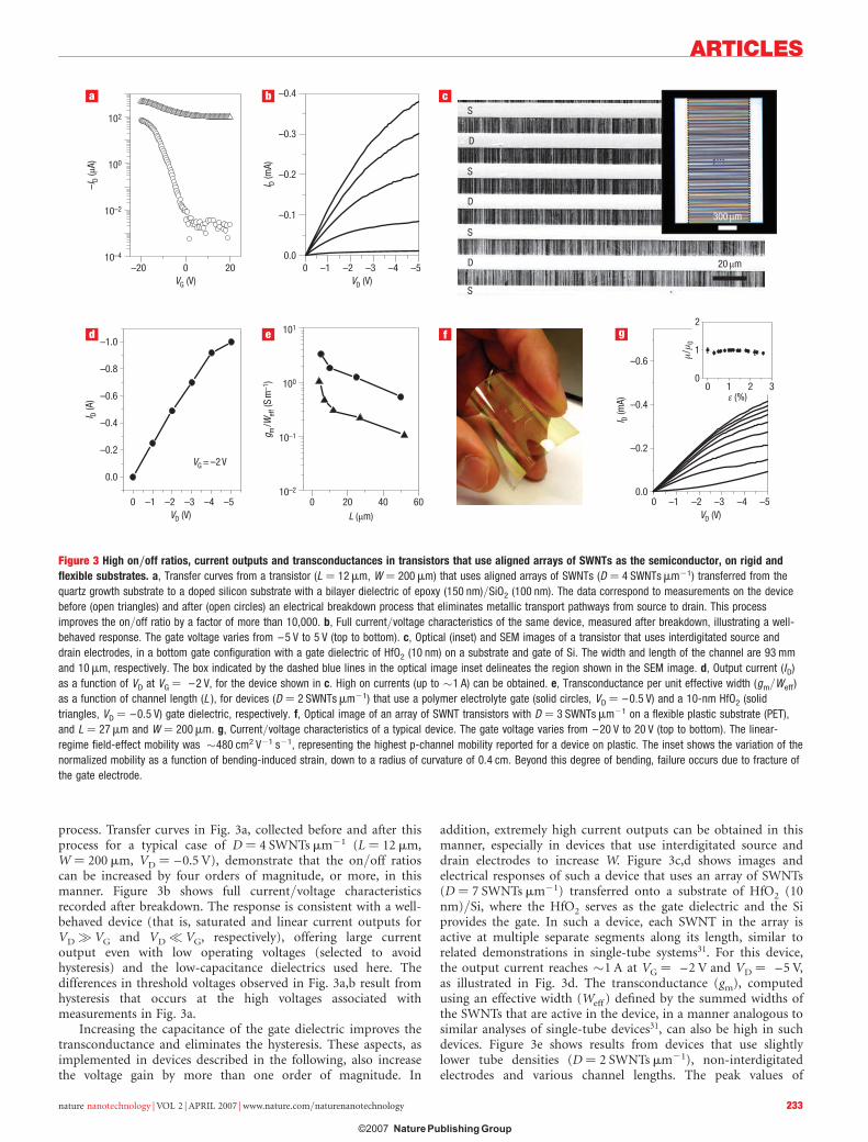
process. Transfer curves in Fig. 3a, collected before and after thisprocess for a typical case of D ¼ 4 SWNTs mm21 (L ¼ 12 mm,W ¼ 200 mm, VD ¼ –0.5 V), demonstrate that the on/off ratioscan be increased by four orders of magnitude, or more, in thismanner. Figure 3b shows full current/voltage characteristicsrecorded after breakdown. The response is consistent with a well-behaved device (that is, saturated and linear current outputs forVD� VG and VD� VG, respectively), offering large currentoutput even with low operating voltages (selected to avoidhysteresis) and the low-capacitance dielectrics used here. Thedifferences in threshold voltages observed in Fig. 3a,b result fromhysteresis that occurs at the high voltages associated withmeasurements in Fig. 3a.
Increasing the capacitance of the gate dielectric improves thetransconductance and eliminates the hysteresis. These aspects, asimplemented in devices described in the following, also increasethe voltage gain by more than one order of magnitude. In
addition, extremely high current outputs can be obtained in thismanner, especially in devices that use interdigitated source anddrain electrodes to increase W. Figure 3c,d shows images andelectrical responses of such a device that uses an array of SWNTs(D ¼ 7 SWNTs mm21) transferred onto a substrate of HfO2 (10nm)/Si, where the HfO2 serves as the gate dielectric and the Siprovides the gate. In such a device, each SWNT in the array isactive at multiple separate segments along its length, similar torelated demonstrations in single-tube systems31. For this device,the output current reaches �1 A at VG ¼ –2 V and VD ¼ –5 V,as illustrated in Fig. 3d. The transconductance (gm), computedusing an effective width (Weff ) defined by the summed widths ofthe SWNTs that are active in the device, in a manner analogous tosimilar analyses of single-tube devices31, can also be high in suchdevices. Figure 3e shows results from devices that use slightlylower tube densities (D ¼ 2 SWNTs mm21), non-interdigitatedelectrodes and various channel lengths. The peak values of
0 –1 –2 –3 –4 –50.0
–0.2
–0.4
–0.6
10–4
10–2
100
102
VG (V)
VG = –2 V
VD (V)
VD (V)VD (V)
0.0
101
100
10–1
10–2
0 –1–20 0 20 –2 –3 –4 –5
–0.1
–0.2
–0.3
–0.4
I D (m
A)
I D (m
A)
–ID
(μA)
0 1 2ε (%)
30
1
2
20 μm
S
D
S
D
S
D
S
0 –1 –2 –3 –4 –5
0.0
–0.2
–0.4
–0.6
–0.8
–1.0
I D (A
)
g m /W
eff (
S m
–1)
0 20 40 60L (μm)
μ / μ 0
300 μm
a b c
d e f g
Figure 3 High on/off ratios, current outputs and transconductances in transistors that use aligned arrays of SWNTs as the semiconductor, on rigid and
flexible substrates. a, Transfer curves from a transistor (L ¼ 12mm, W ¼ 200mm) that uses aligned arrays of SWNTs (D ¼ 4 SWNTsmm21) transferred from the
quartz growth substrate to a doped silicon substrate with a bilayer dielectric of epoxy (150 nm)/SiO2 (100 nm). The data correspond to measurements on the device
before (open triangles) and after (open circles) an electrical breakdown process that eliminates metallic transport pathways from source to drain. This process
improves the on/off ratio by a factor of more than 10,000. b, Full current/voltage characteristics of the same device, measured after breakdown, illustrating a well-
behaved response. The gate voltage varies from –5 V to 5 V (top to bottom). c, Optical (inset) and SEM images of a transistor that uses interdigitated source and
drain electrodes, in a bottom gate configuration with a gate dielectric of HfO2 (10 nm) on a substrate and gate of Si. The width and length of the channel are 93 mm
and 10mm, respectively. The box indicated by the dashed blue lines in the optical image inset delineates the region shown in the SEM image. d, Output current (ID)
as a function of VD at VG ¼ –2 V, for the device shown in c. High on currents (up to �1 A) can be obtained. e, Transconductance per unit effective width (gm/Weff)
as a function of channel length (L ), for devices (D ¼ 2 SWNTsmm21) that use a polymer electrolyte gate (solid circles, VD ¼ –0.5 V) and a 10-nm HfO2 (solid
triangles, VD ¼ –0.5 V) gate dielectric, respectively. f, Optical image of an array of SWNT transistors with D ¼ 3 SWNTsmm21 on a flexible plastic substrate (PET),
and L ¼ 27mm and W ¼ 200mm. g, Current/voltage characteristics of a typical device. The gate voltage varies from –20 V to 20 V (top to bottom). The linear-
regime field-effect mobility was �480 cm2 V21 s21, representing the highest p-channel mobility reported for a device on plastic. The inset shows the variation of the
normalized mobility as a function of bending-induced strain, down to a radius of curvature of 0.4 cm. Beyond this degree of bending, failure occurs due to fracture of
the gate electrode.
ARTICLES
nature nanotechnology | VOL 2 | APRIL 2007 | www.nature.com/naturenanotechnology 233
Black plate (234,1)
transconductances scaled in this manner are �800 S m21 (at VD ¼–0.5 V, L ¼ 7 mm) with HfO2 (10 nm) dielectrics, and up to �3,000 S m21 (at VD ¼ –0.5 V, L ¼ 5 mm) with polymer electrolytegating32.
The transfer process used for these devices also enables integrationonto unusual substrates, including flexible plastics. As an example,Fig. 3f,g shows an image and electrical characteristics of devices(D¼ 3 SWNTs mm21) on a sheet of poly(ethylene terephthalate)(180mm), where polyimide (1.6mm) and indium tin oxide(150 nm) provide the gate dielectric and gate, respectively, withL¼ 27 mm and W¼ 200 mm. The linear-regime mobility,computed using a parallel plate approximation for the capacitance,is � 480 cm2 V21 s21. The inset of Fig. 3g shows the normalizedmobility as a function of bending induced strain (1) for bendingdown to radii of curvature of 0.4 cm. At higher values of strain, thedevices fail owing to fracture of the gate electrode.
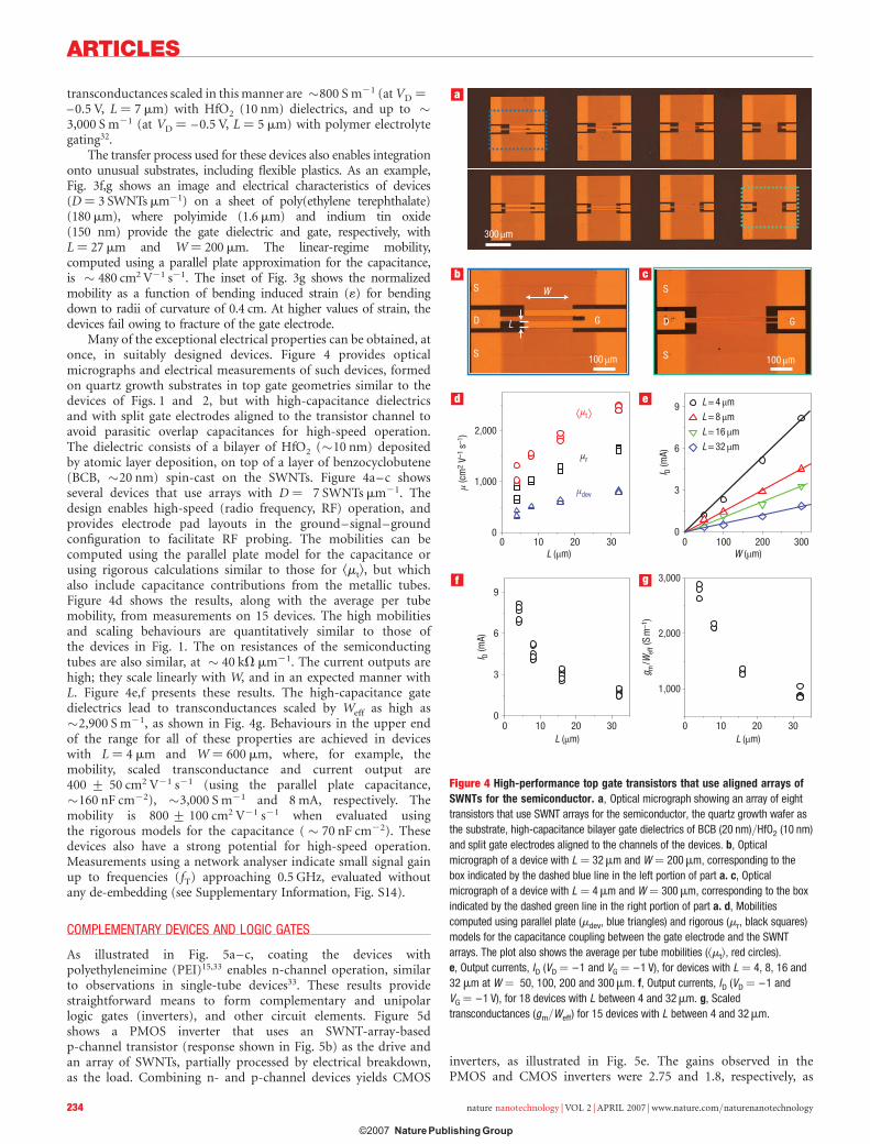
Many of the exceptional electrical properties can be obtained, atonce, in suitably designed devices. Figure 4 provides opticalmicrographs and electrical measurements of such devices, formedon quartz growth substrates in top gate geometries similar to thedevices of Figs. 1 and 2, but with high-capacitance dielectricsand with split gate electrodes aligned to the transistor channel toavoid parasitic overlap capacitances for high-speed operation.The dielectric consists of a bilayer of HfO2 (�10 nm) depositedby atomic layer deposition, on top of a layer of benzocyclobutene(BCB, �20 nm) spin-cast on the SWNTs. Figure 4a–c showsseveral devices that use arrays with D ¼ 7 SWNTs mm21. Thedesign enables high-speed (radio frequency, RF) operation, andprovides electrode pad layouts in the ground–signal–groundconfiguration to facilitate RF probing. The mobilities can becomputed using the parallel plate model for the capacitance orusing rigorous calculations similar to those for kmtl, but whichalso include capacitance contributions from the metallic tubes.Figure 4d shows the results, along with the average per tubemobility, from measurements on 15 devices. The high mobilitiesand scaling behaviours are quantitatively similar to those ofthe devices in Fig. 1. The on resistances of the semiconductingtubes are also similar, at � 40 kVmm21. The current outputs arehigh; they scale linearly with W, and in an expected manner withL. Figure 4e,f presents these results. The high-capacitance gatedielectrics lead to transconductances scaled by Weff as high as�2,900 S m21, as shown in Fig. 4g. Behaviours in the upper endof the range for all of these properties are achieved in deviceswith L ¼ 4 mm and W ¼ 600 mm, where, for example, themobility, scaled transconductance and current output are400 + 50 cm2 V21 s21 (using the parallel plate capacitance,�160 nF cm22), �3,000 S m21 and 8 mA, respectively. Themobility is 800 + 100 cm2 V21 s21 when evaluated usingthe rigorous models for the capacitance ( � 70 nF cm22). Thesedevices also have a strong potential for high-speed operation.Measurements using a network analyser indicate small signal gainup to frequencies (fT) approaching 0.5 GHz, evaluated withoutany de-embedding (see Supplementary Information, Fig. S14).
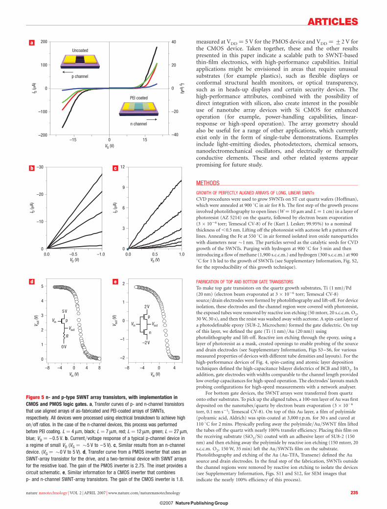
COMPLEMENTARY DEVICES AND LOGIC GATES
As illustrated in Fig. 5a–c, coating the devices withpolyethyleneimine (PEI)15,33 enables n-channel operation, similarto observations in single-tube devices33. These results providestraightforward means to form complementary and unipolarlogic gates (inverters), and other circuit elements. Figure 5dshows a PMOS inverter that uses an SWNT-array-basedp-channel transistor (response shown in Fig. 5b) as the drive andan array of SWNTs, partially processed by electrical breakdown,as the load. Combining n- and p-channel devices yields CMOS
inverters, as illustrated in Fig. 5e. The gains observed in thePMOS and CMOS inverters were 2.75 and 1.8, respectively, as
0
1,000
2,000
0
3
6
9 L = 4 μm
L = 8 μm
μr
μt
μdev
L = 16 μm
L = 32 μm
GD
S
S 100 μm
0
3
6
9
0 10 20 30
0 100 200 300
1,000
2,000
3,000
L (μm)0 10 20 30
L (μm)
0 10 20 30L (μm) W (μm)
g m /W
eff (
S m
–1)
I D (m
A)
I D (m
A)
μ (c
m2
V–1 s
–1)
300 μm
D
S
S
L
W
G
100 μm
a
b
d e
f g
c
Figure 4 High-performance top gate transistors that use aligned arrays of
SWNTs for the semiconductor. a, Optical micrograph showing an array of eight
transistors that use SWNT arrays for the semiconductor, the quartz growth wafer as
the substrate, high-capacitance bilayer gate dielectrics of BCB (20 nm)/HfO2 (10 nm)
and split gate electrodes aligned to the channels of the devices. b, Optical
micrograph of a device with L ¼ 32mm and W ¼ 200mm, corresponding to the
box indicated by the dashed blue line in the left portion of part a. c, Optical
micrograph of a device with L ¼ 4mm and W ¼ 300mm, corresponding to the box
indicated by the dashed green line in the right portion of part a. d, Mobilities
computed using parallel plate (mdev, blue triangles) and rigorous (mr, black squares)
models for the capacitance coupling between the gate electrode and the SWNT
arrays. The plot also shows the average per tube mobilities (kmtl, red circles).
e, Output currents, ID (VD ¼ –1 and VG ¼ –1 V), for devices with L ¼ 4, 8, 16 and
32mm at W ¼ 50, 100, 200 and 300mm. f, Output currents, ID (VD ¼ –1 and
VG ¼ –1 V), for 18 devices with L between 4 and 32mm. g, Scaled
transconductances (gm/Weff) for 15 devices with L between 4 and 32mm.
ARTICLES
nature nanotechnology | VOL 2 | APRIL 2007 | www.nature.com/naturenanotechnology234
Black plate (235,1)
measured at VDD ¼ 5 V for the PMOS device and VDD ¼+2 V forthe CMOS device. Taken together, these and the other resultspresented in this paper indicate a scalable path to SWNT-basedthin-film electronics, with high-performance capabilities. Initialapplications might be envisioned in areas that require unusualsubstrates (for example plastics), such as flexible displays orconformal structural health monitors, or optical transparency,such as in heads-up displays and certain security devices. Thehigh-performance attributes, combined with the possibility ofdirect integration with silicon, also create interest in the possibleuse of nanotube array devices with Si CMOS for enhancedoperation (for example, power-handling capabilities, linear-response or high-speed operation). The array geometry shouldalso be useful for a range of other applications, which currentlyexist only in the form of single-tube demonstrations. Examplesinclude light-emitting diodes, photodetectors, chemical sensors,nanoelectromechanical oscillators, and electrically or thermallyconductive elements. These and other related systems appearpromising for future study.
METHODS
GROWTH OF PERFECTLY ALIGNED ARRAYS OF LONG, LINEAR SWNTs
CVD procedures were used to grow SWNTs on ST cut quartz wafers (Hoffman),which were annealed at 900 8C in air for 8 h. The first step of the growth processinvolved photolithography to open lines (W ¼ 10 mm and L ¼ 1 cm) in a layer ofphotoresist (AZ 5214) on the quartz, followed by electron beam evaporation(3 � 1026 torr; Temescal CV-8) of Fe (Kurt J. Lesker; 99.95%) to a nominalthickness of ,0.5 nm. Lifting off the photoresist with acetone left a pattern of Felines. Annealing the Fe at 550 8C in air formed isolated iron oxide nanoparticleswith diameters near �1 nm. The particles served as the catalytic seeds for CVDgrowth of the SWNTs. Purging with hydrogen at 900 8C for 5 min and thenintroducing a flow of methane (1,900 s.c.c.m.) and hydrogen (300 s.c.c.m.) at 9008C for 1 h led to the growth of SWNTs (see Supplementary Information, Fig. S2,for the reproducibility of this growth technique).
FABRICATION OF TOP AND BOTTOM GATE TRANSISTORS
To make top gate transistors on the quartz growth substrates, Ti (1 nm)/Pd(20 nm) (electron beam evaporated at 3 � 1026 torr; Temescal CV-8)source/drain electrodes were formed by photolithography and lift-off. For deviceisolation, these electrodes and the channel region were covered with photoresist,the exposed tubes were removed by reactive ion etching (50 mtorr, 20 s.c.c.m. O2,30 W, 30 s), and then the resist was washed away with acetone. A spin-cast layer ofa photodefinable epoxy (SU8-2, Microchem) formed the gate dielectric. On topof this layer, we defined the gate (Ti (1 nm)/Au (20 nm)) usingphotolithography and lift-off. Reactive ion etching through the epoxy, using alayer of photoresist as a mask, created openings to enable probing of the sourceand drain electrodes (see Supplementary Information, Figs S3–S6, for variousmeasured properties of devices with different tube densities and layouts). For thehigh-performance devices of Fig. 4, spin-casting and atomic layer depositiontechniques defined the high-capacitance bilayer dielectrics of BCB and HfO2. Inaddition, gate electrodes with widths comparable to the channel length providedlow overlap capacitances for high-speed operation. The electrodes’ layouts matchprobing configurations for high-speed measurements with a network analyser.
For bottom gate devices, the SWNT arrays were transferred from quartzonto other substrates. To pick up the aligned tubes, a 100-nm layer of Au was firstdeposited on the nanotubes/quartz by electron beam evaporation (3 � 1026
torr, 0.1 nm s21; Temescal CV-8). On top of this Au layer, a film of polyimide(polyamic acid, Aldrich) was spin-coated at 3,000 r.p.m. for 30 s and cured at110 8C for 2 mins. Physically peeling away the polyimide/Au/SWNT film liftedthe tubes off the quartz with nearly 100% transfer efficiency. Placing this film onthe receiving substrate (SiO2/Si) coated with an adhesive layer of SU8-2 (150nm) and then etching away the polyimide by reactive ion etching (150 mtorr, 20s.c.c.m. O2, 150 W, 35 min) left the Au/SWNTs film on the substrate.Photolithography and etching of the Au (Au-TFA, Transene) defined the Ausource and drain electrodes. In the final step of the fabrication, SWNTs outsidethe channel regions were removed by reactive ion etching to isolate the devices(see Supplementary Information, Figs. S11 and S12, for SEM images thatindicate the nearly 100% efficiency of this process).
–200
–100
0
100
200
–40
–20
20
0
40
Uncoated
PEI coated
0
–10
–20
–30
0.0 0.5 1.00.0 –0.5 –1.00
3
6
9
12
–8 –4 0 4 8 –8 –4 0 4
0
1
2
3
4
5
5 V2 V
0 V–2 V
Vin Vin VoutVout
R
p
n
p
–2
–1
0
1
2
VD (V) VD (V)
–15 0
p channel
n channel
15VG (V)
Vin (V)
V out (
V)
V out (
V)
Vin (V)
I D (μ
A)
I D (μ
A)I D
(μA)
ID (μA)
a
b
d
c
e
Figure 5 n- and p-type SWNT array transistors, with implementation in
CMOS and PMOS logic gates. a, Transfer curves of p- and n-channel transistors
that use aligned arrays of as-fabricated and PEI-coated arrays of SWNTs,
respectively. All devices were processed using electrical breakdown to achieve high
on/off ratios. In the case of the n-channel devices, this process was performed
before PEI coating. L ¼ 4mm, black; L ¼ 7mm, red; L ¼ 12mm, green; L ¼ 27mm,
blue; VD ¼ –0.5 V. b. Current/voltage response of a typical p-channel device in
a regime of small VD (VG ¼ �5 V to –5 V). c, Similar results from an n-channel
device. (VG ¼ �0 V to 5 V). d, Transfer curve from a PMOS inverter that uses an
SWNT-array transistor for the drive, and a two-terminal device with SWNT arrays
for the resistive load. The gain of the PMOS inverter is 2.75. The inset provides a
circuit schematic. e, Similar information for a CMOS inverter that combines
p- and n-channel SWNT-array transistors. The gain of the CMOS inverter is 1.8.
ARTICLES
nature nanotechnology | VOL 2 | APRIL 2007 | www.nature.com/naturenanotechnology 235

Black plate (236,1)
FABRICATION OF TRANSISTORS WITH POLYMER ELECTROLYTE AND HfO2 GATE DIELECTRICS
To achieve high transconductances, we used high-capacitance gate dielectricsconsisting of either 10-nm HfO2 or a polymer electrolyte. The electrolytes weremade by directly dissolving LiClO4 * 3H2O in poly(ethylene oxide) (PEO, Mn ¼
550) or in polyethylenimine (PEI, Mn ¼ 800) in air at room temperature with2.4:1 and 1:1 polymer to salt weight ratios, respectively. The electrolytes wereinjected into a polydimethylsiloxane (PDMS) fluidic channel laminated overaligned arrays of SWNTs on quartz substrates with source/drain electrodesdefined according to the previously described procedures. In these devices, gatevoltages were applied through a silver wire dipped in the electrolyte. The HfO2
was prepared on a doped silicon substrate by atomic layer deposition (Savannah100, Cambridge NanoTech) using H2O and Hf(NMe2)4 (99.99þ%, Aldrich) anda substrate temperature of 150 8C. SWNT arrays were transferred onto the HfO2
using the procedures described above, but without the adhesive layer.Photolithography and etching defined the Au electrodes for source and drain.
FABRICATION OF n-TYPE TRANSISTORS, CMOS AND PMOS LOGIC GATES
Spin-coating layers of PEI (Mn ¼ 800, Aldrich) on the top of the nanotubesswitches the operation of the transistors from unipolar p-channel to unipolarn-channel. To form these coatings, PEI was first dissolved in methanol with avolume concentration of 1:5. Spin-casting the PEI directly onto the SWNTs at2,000 r.p.m. for 30 s created the coatings. Heating at 50 8C for 10 h gaven-channel transistors. Suitable interconnection of such devices can yield logicgates of various types. For PMOS inverters, one transistor served as a resistorload, and the other served as the drive. CMOS inverters were formed withuncoated p-channel devices and PEI-coated n-channel devices.
Received 3 November 2006; accepted 23 February 2007; published
25 March 2007.
References1. Zhou, X., Park, J.-Y., Huang, S., Liu, J. & Mceuen, P. L. Band structure, phonon scattering and the
performance limit of single-walled carbon nanotube transistors. Phys. Rev. Lett. 95, 146805 (2005).2. Durkop, T., Getty, S. A., Cobas, E. & Fuhrer, M. S. Extraordinary mobility in semiconducting carbon
nanotubes. Nano Lett. 4, 35–39 (2004).3. Yao, Z., Kane, C. L. & Dekker, C. High-field electrical transport in single-wall carbon nanotubes.
Phys. Rev. Lett. 84, 2941–2944 (2000).4. Lin, Y.-M., Appenzeller, J., Knoch, J. & Avouris P. High-performance carbon nanotube field-effect
transistor with tunable polarities. IEEE Trans. Nanotechnol. 4, 481–489 (2005).5. Chen, Z. et al. An integrated logic circuit assembled on a single carbon nanotube. Science 311,
1735 (2006).6. Bachtold, A., Hadley, P., Nakanishi, T. & Dekker, C. Logic circuits with carbon nanotube transistors.
Science 294, 1317–1320 (2001).7. Misewich, J. A. et al. Electrically induced optical emission from a carbon nanotube FET. Science
300, 783–786 (2003).8. Chen, J. et al. Bright infrared emission from electrically induced excitons in carbon nanotubes.
Science 310, 1171–1174 (2005).9. Kong, J. et al. Nanotube molecular wires as chemical sensors. Science 287, 622–625 (2000).10. Guo, J., Hasan, S., Javey, A., Bosman, G. & Lundstrom, M. Assessment of high-frequency
performance potential of carbon nanotube transistors. IEEE Trans. Nanotechnol. 4, 715–721 (2005).11. Guo, J., Goasguen, S., Lundstrom, M. & Datta, S. Metal–insulator–semiconductor electrostatics of
carbon nanotubes. Appl. Phys. Lett. 81, 1486–1488 (2002).12. Kocabas, C. et al. Guided growth of large-scale, horizontally aligned arrays of single-walled carbon
nanotubes and their use in thin-film transistors. Small 1, 1110–1116 (2005).
13. Liu, X., Han, S. & Zhou, C. Novel nanotube-on-insulator (NOI) approach toward single-walledcarbon nanotube devices. Nano Lett. 6, 34–39 (2006).
14. Li, S., Yu, Z., Rutherglen, C. & Burke, P. J. Electrical properties of 0.4 cm long single-walled carbonnanotubes. Nano Lett. 4, 2003–2007 (2004).
15. Zhou, Y. et al. P-channel, n-channel thin film transistors and p-n diodes based on single wall carbonnanotube networks. Nano Lett. 4, 2031–2035 (2004).
16. Hu, L., Hecht, D. S. & Gruner, G. Percolation in transparent and conducting carbon nanotubenetworks. Nano Lett. 4, 2513–2517 (2004).
17. Snow, E. S., Campbell, P. M., Ancona, M. G. & Novak, J. P. High-mobility carbon-nanotube thin-filmtransistors on a polymeric substrate. Appl. Phys. Lett. 86, 033105 (2005).
18. Ismach, A., Segev, L., Wachtel, E. & Joselevich, E. Atomic-step-templated formation of single wallcarbon nanotube patterns. Angew. Chem. Int. Edn 43, 6140–6143 (2004).
19. Han, S., Liu, X. & Zhou, C. Template-free directional growth of single-walled carbon nanotubes on a-and r-plane sapphire. J. Am. Chem. Soc. 127, 5294–5295 (2005).
20. Kocabas, C., Shim, M. & Rogers, J. A. Spatially selective guided growth of high-coverage arrays andrandom networks of single-walled carbon nanotubes and their integration into electronic devices.J. Am. Chem. Soc. 128, 4540–4541 (2006).
21. Park, J.-Y. et al. Electron–phonon scattering in metallic single walled carbon nanotubes. Nano Lett. 4,517–520 (2004).
22. Javey, A. et al. High-field quasiballistic transport in short carbon nanotubes. Phys. Rev. Lett. 92,106804 (2004).
23. McEuen, P. L., Fuhrer, M. & Park, H. Single-walled carbon nanotube electronics. IEEE Trans.Nanotechnol. 1, 78–86 (2002).
24. Chen, Z., Appenzeller, J., Knoch, J., Lin, Y.-M. & Avouris, P. The role of metal–nanotube contact inthe performance of carbon nanotube field-effect transistors. Nano Lett. 5, 1497–1502 (2005).
25. Kim, W. et al. Electrical contacts to carbon nanotubes down to 1 nm in diameter. Appl. Phys. Lett. 87,173101 (2005).
26. Heinze, S. et al. Carbon nanotubes as Schottky barrier transistors. Phys. Rev. Lett. 89, 106801 (2002).27. Collins, P. G., Arnold, M. S. & Avouris, P. Engineering carbon nanotubes and nanotube circuits using
electrical breakdown. Science 292, 706–709 (2001).28. Hur, S.-H., Park, O. O. & Rogers, J. A. Extreme bendability of single-walled carbon nanotube
networks transferred from high-temperature growth substrates to plastic and their use in thin-filmtransistors. Appl. Phys. Lett. 86, 243502 (2005).
29. Huang, X. M. H. et al. Controlled placement of individual carbon nanotubes. Nano Lett. 5,1515–1518 (2005).
30. Bradley, K., Gabriel, J.-C. P. & Gruner G. Flexible nanotube electronics. Nano Lett. 3,1353–1355 (2003).
31. Javey, A. et al. High-k dielectrics for advanced carbon-nanotube transistors and logic gates. NatureMater. 1, 241–246 (2002).
32. Ozel, T., Gaur, A., Rogers, J. A. & Shim, M. Polymer electrolyte gating of carbon nanotube networktransistors. Nano Lett. 5, 905–911 (2005).
33. Shim, M., Javey, A., Kam, N. W. S. & Dai, H. Polymer functionalization for air-stable n-type carbonnanotube field-effect transistors. J. Am. Chem. Soc. 123, 11512–11513 (2001).
AcknowledgementsWe thank T. Banks and K. Colravy for help with processing, using facilities at the Frederick Seitz MaterialsResearch Laboratory. This material is based upon work supported by the National Science Foundationunder grant NIRT-0403489 and the US Department of Energy, Division of Materials Sciences underAward No. DEFG02-91ER45439, through the Frederick Seitz MRL and Center for Microanalysis ofMaterials at the University of Illinois at Urbana-Champaign. S.J.K. acknowledges fellowship support fromthe Institute of Information Technology Assessment of Korea. N.P. and M.A.A. acknowledge the supportfrom the Network for Computational Nanotechnology. Correspondence and requests for materialsshould be addressed to J.A.R.Supplementary information accompanies this paper on www.nature.com/naturenanotechnology.
Author contributionsS.J.K, C.K. and J.A.R. designed the experiments, S.J.K., C.K. and T.O. performed the experiments, S.J.K.,C.K., T.O., M.S., N.P., M.A.A., S.V.R. and J.A.R. analysed the data, S.J.K, C.K. and J.A.R. wrote the paper.
Competing financial interestsThe authors declare that they have no competing financial interests.
Reprints and permission information is available online at http://npg.nature.com/reprintsandpermissions/
ARTICLES
nature nanotechnology | VOL 2 | APRIL 2007 | www.nature.com/naturenanotechnology236


