Embed Size (px)
Citation preview
Purdue UniversityPurdue e-Pubs
Birck and NCN Publications Birck Nanotechnology Center
8-1-2010
III-nitride nanopyramid light emitting diodesgrown by organometallic vapor phase epitaxyIsaac WildesonPurdue Univ, Sch Elect & Comp Engn, [email protected]
Robert ColbyPurdue University - Main Campus, [email protected]
David EwoldtBirck Nanotechnology Center, Purdue University, [email protected]
Zhiwen LiangPurdue University - Main Campus, [email protected]
Dmitri ZakharovBirck Nanotechnology Center, Purdue University, [email protected]
See next page for additional authors
This document has been made available through Purdue e-Pubs, a service of the Purdue University Libraries. Please contact [email protected] foradditional information.
Wildeson, Isaac; Colby, Robert; Ewoldt, David; Liang, Zhiwen; Zakharov, Dmitri; Zaluzec, Nestor J.; García, R. Edwin; Stach, E A.;and Sands, Timothy D., "III-nitride nanopyramid light emitting diodes grown by organometallic vapor phase epitaxy" (2010). Birckand NCN Publications. Paper 640.http://docs.lib.purdue.edu/nanopub/640

AuthorsIsaac Wildeson, Robert Colby, David Ewoldt, Zhiwen Liang, Dmitri Zakharov, Nestor J. Zaluzec, R. EdwinGarcía, E A. Stach, and Timothy D. Sands
This article is available at Purdue e-Pubs: http://docs.lib.purdue.edu/nanopub/640

III-nitride nanopyramid light emitting diodes grown by organometallic vaporphase epitaxy
Isaac H. Wildeson,1,3 Robert Colby,2,3 David A. Ewoldt,2,3 Zhiwen Liang,2,3
Dmitri N. Zakharov,3 Nestor J. Zaluzec,4 R. Edwin García,2,3 Eric A. Stach,2,3 andTimothy D. Sands1,2,3,a�
1School of Electrical and Computer Engineering, Purdue University, West Lafayette, Indiana 47906, USA2School of Materials Engineering, Purdue University, West Lafayette, Indiana 47906, USA3Birck Nanotechnology Center, Purdue University, West Lafayette, Indiana 47906, USA4Electron Microscopy Center, Materials Science Division, Argonne National Laboratory, Argonne, Illinois60439, USA
�Received 1 April 2010; accepted 26 June 2010; published online 18 August 2010;publisher error corrected 23 August 2010�
Nanopyramid light emitting diodes �LEDs� have been synthesized by selective area organometallicvapor phase epitaxy. Self-organized porous anodic alumina is used to pattern the dielectric growthtemplates via reactive ion etching, eliminating the need for lithographic processes. �In,Ga�Nquantum well growth occurs primarily on the six �11̄01� semipolar facets of each of thenanopyramids, while coherent �In,Ga�N quantum dots with heights of up to �20 nm areincorporated at the apex by controlling growth conditions. Transmission electron microscopy �TEM�indicates that the �In,Ga�N active regions of the nanopyramid heterostructures are completelydislocation-free. Temperature-dependent continuous-wave photoluminescence of nanopyramidheterostructures yields a peak emission wavelength of 617 nm and 605 nm at 300 K and 4 K,respectively. The peak emission energy varies with increasing temperature with a double S-shapedprofile, which is attributed to either the presence of two types of InN-rich features within thenanopyramids or a contribution from the commonly observed yellow defect luminescence close to300 K. TEM cross-sections reveal continuous planar defects in the �In,Ga�N quantum wells andGaN cladding layers grown at 650–780 °C, present in 38% of the nanopyramid heterostructures.Plan-view TEM of the planar defects confirms that these defects do not terminate within thenanopyramids. During the growth of p-GaN, the structure of the nanopyramid LEDs changed frompyramidal to a partially coalesced film as the thickness requirements for an undepleted p-GaN layerresult in nanopyramid impingement. Continuous-wave electroluminescence of nanopyramid LEDsreveals a 45 nm redshift in comparison to a thin-film LED, suggesting higher InN incorporation inthe nanopyramid LEDs. These results strongly encourage future investigations of III-nitridenanoheteroepitaxy as an approach for creating efficient long wavelength LEDs. © 2010 AmericanInstitute of Physics. �doi:10.1063/1.3466998�
I. INTRODUCTION
Nanoheteroepitaxy is an attractive approach towardsachieving highly efficient light emitting diodes �LEDs�. Spe-cifically, one-dimensional nanostructures such as nanorodsand nanowires offer the advantages of high light extractionefficiencies and the potential to be grown free of extendeddefects. The rejection of dislocations from nanorod andnanowire LEDs is particularly important for the III-nitridematerials system for which threading dislocation densities of108–1011 cm−2 are typical for thin-film heterostructures, de-pending on the growth conditions.1 Various reports havedemonstrated the growth of dislocation-free, one-dimensional III-nitride nanostructures.2–6 Another inherentadvantage of nanoheteroepitaxy is coherency strain relax-ation. Theoretical investigations have demonstrated that lat-eral strain relaxation along the radial directions of nanorodand nanowire heterostructures allows a greater lattice mis-
match without the introduction of misfit dislocations as com-pared to a thin-film heterostructure.7–9 Experimental observa-tions also indicate that nanorods and nanowires have greatercompliancy as compared to a thin film as the Young’s modu-lus along the length of GaN nanowires was observed to de-crease with diameters below 80 nm.10 Reduced elastic modu-lus should allow greater InN incorporation in �In,Ga�Nnanostructures—and thus a longer wavelength of emission—without the incorporation of misfit dislocations. The elimina-tion of misfit dislocations in quantum wells with high InNcontent is necessary for creating highly efficient LEDswithin the green/yellow portion of the visible spectrumwhere LED efficiencies are currently the lowest.11
Growth of GaN nanorods and nanowires has been real-ized by the use of rf-plasma-assisted molecular beam epitaxy�rf-MBE�,12 hydride vapor phase epitaxy �HVPE�,13 and or-ganometallic vapor phase epitaxy �OMVPE�.3,14 Severalgroups have further processed one-dimensional LED nano-structures. The results have been very promising, leading tohigh internal quantum efficiencies �IQE� of 77% at 487 nma�Electronic mail: [email protected].
JOURNAL OF APPLIED PHYSICS 108, 044303 �2010�
0021-8979/2010/108�4�/044303/8/$30.00 © 2010 American Institute of Physics108, 044303-1
Downloaded 27 Oct 2010 to 128.210.126.199. Redistribution subject to AIP license or copyright; see http://jap.aip.org/about/rights_and_permissions
in rf-MBE grown nanorods,12 and high light extraction with4.3 times the light output in metalorganic-HVPE grown na-norods, as compared to equivalent thin-film samples.2 Whilethese results demonstrate the strong potential of nanohet-eroepitaxy within the III-nitride materials system, there arefew reports of such LED nanostructures grown by OMVPE,the growth technique that is standard in the LED industry.Instead, a substantial portion of the OMVPE research hasprimarily focused on using nanorods and nanowires asgrowth templates for higher quality coalesced thin films.15–17
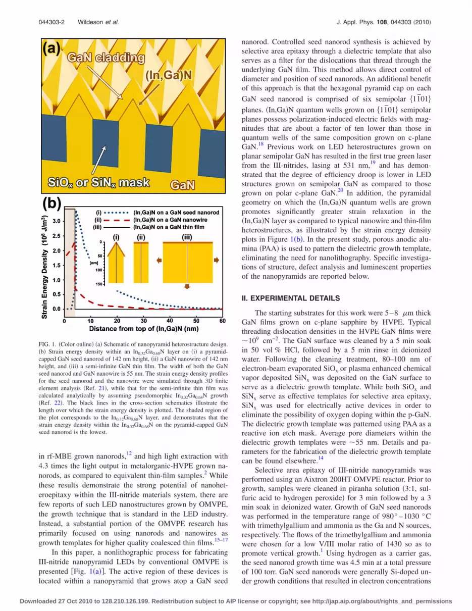
In this paper, a nonlithographic process for fabricatingIII-nitride nanopyramid LEDs by conventional OMVPE ispresented �Fig. 1�a��. The active region of these devices islocated within a nanopyramid that grows atop a GaN seed
nanorod. Controlled seed nanorod synthesis is achieved byselective area epitaxy through a dielectric template that alsoserves as a filter for the dislocations that thread through theunderlying GaN film. This method allows direct control ofdiameter and position of seed nanorods. An additional benefitof this approach is that the hexagonal pyramid cap on each
GaN seed nanorod is comprised of six semipolar �11̄01�planes. �In,Ga�N quantum wells grown on �11̄01� semipolarplanes possess polarization-induced electric fields with mag-nitudes that are about a factor of ten lower than those inquantum wells of the same composition grown on c-planeGaN.18 Previous work on LED heterostructures grown onplanar semipolar GaN has resulted in the first true green laserfrom the III-nitrides, lasing at 531 nm,19 and has demon-strated that the degree of efficiency droop is lower in LEDstructures grown on semipolar GaN as compared to thosegrown on polar c-plane GaN.20 In addition, the pyramidalgeometry on which the �In,Ga�N quantum wells are grownpromotes significantly greater strain relaxation in the�In,Ga�N layer as compared to typical nanowire and thin-filmheterostructures, as illustrated by the strain energy densityplots in Figure 1�b�. In the present study, porous anodic alu-mina �PAA� is used to pattern the dielectric growth template,eliminating the need for nanolithography. Specific investiga-tions of structure, defect analysis and luminescent propertiesof the nanopyramids are reported below.
II. EXPERIMENTAL DETAILS
The starting substrates for this work were 5–8 �m thickGaN films grown on c-plane sapphire by HVPE. Typicalthreading dislocation densities in the HVPE GaN films were�109 cm−2. The GaN surface was cleaned by a 5 min soakin 50 vol % HCl, followed by a 5 min rinse in deionizedwater. Following the cleaning treatment, 80–100 nm ofelectron-beam evaporated SiOx or plasma enhanced chemicalvapor deposited SiNx was deposited on the GaN surface toserve as a dielectric growth template. While both SiOx andSiNx serve as effective templates for selective area epitaxy,SiNx was used for electrically active devices in order toeliminate the possibility of oxygen doping within the p-GaN.The dielectric growth template was patterned using PAA as areactive ion etch mask. Average pore diameters within thedielectric growth templates were �55 nm. Details and pa-rameters for the fabrication of the dielectric growth templatecan be found elsewhere.14
Selective area epitaxy of III-nitride nanopyramids wasperformed using an Aixtron 200HT OMVPE reactor. Prior togrowth, samples were cleaned in piranha solution �3:1, sul-furic acid to hydrogen peroxide� for 3 min followed by a 3min soak in deionized water. Growth of GaN seed nanorodswas performed in the temperature range of 980° –1030 °Cwith trimethylgallium and ammonia as the Ga and N sources,respectively. The flows of the trimethylgallium and ammoniawere chosen for a low V/III molar ratio of 1430 so as topromote vertical growth.1 Using hydrogen as a carrier gas,the seed nanorod growth time was 4.5 min at a total pressureof 100 torr. GaN seed nanorods were generally Si-doped un-der growth conditions that resulted in electron concentrations
FIG. 1. �Color online� �a� Schematic of nanopyramid heterostructure design.�b� Strain energy density within an In0.32Ga0.68N layer on �i� a pyramid-capped GaN seed nanorod of 142 nm height, �ii� a GaN nanowire of 142 nmheight, and �iii� a semi-infinite GaN thin film. The width of both the GaNseed nanorod and GaN nanowire is 55 nm. The strain energy density profilesfor the seed nanorod and the nanowire were simulated through 3D finiteelement analysis �Ref. 21�, while that for the semi-infinite thin film wascalculated analytically by assuming pseudomorphic In0.32Ga0.68N growth�Ref. 22�. The black lines in the cross-section schematics illustrate thelength over which the strain energy density is plotted. The shaded region ofthe plot corresponds to the In0.32Ga0.68N layer, and demonstrates that thestrain energy density within the In0.32Ga0.68N on the pyramid-capped GaNseed nanorod is the lowest.
044303-2 Wildeson et al. J. Appl. Phys. 108, 044303 �2010�
Downloaded 27 Oct 2010 to 128.210.126.199. Redistribution subject to AIP license or copyright; see http://jap.aip.org/about/rights_and_permissions

of 2�1018 cm−3 for equivalent thin-film samples. Followingthe growth of the seed nanorods, the temperature was de-creased to 650–780 °C for growth of an �In,Ga�N quantumwell and a GaN cladding layer on the pyramidal caps of theseed nanorods. Typical parameters for �In,Ga�N quantumwell growth were a V/III ratio of 7700, trimethylindium asthe In source, and a total pressure of 100 torr. Typical param-eters for the GaN cladding layer growth were 0.5 min ofundoped GaN growth followed by 1.5 min of Mg-dopedGaN growth, both performed with a V/III ratio of 1630, agrowth temperature of 715 °C and a total pressure of 100torr. Electrically active devices included additional Mg-doped p-GaN epitaxy at 1030 °C and subsequent magne-sium activation steps that produced hole concentrations of2�1017 cm−3 in thin films. Device isolation was achievedby chlorine-based inductively coupled plasma etching.Ohmic metal contacts were deposited by e-beam evapora-tion, using Ni/Au or Pt for p-GaN, and Ti/Al or In forn-GaN.
Characterization of the nanopyramid morphology wasperformed with a Hitachi S4800 field emission scanningelectron microscope �FESEM�, while analytical electron mi-croscopy, transmission electron microscopy �TEM�, andscanning transmission electron microscopy �STEM� studieswere conducted using an FEI Titan 80-300 and an FEI TecnaiF20 operating at 300 kV and 200 kV, respectively. TEM wasused to investigate the quality of the nanopyramid hetero-structures, the associated lattice defects and local composi-tion variation. Spectral imaging measurements were con-ducted using an ultrathin window EDAX-Sapphire Si�Li�energy dispersive spectrometer interfaced to a 4Pi-Revolution data acquisition system on the Tecnai F20. TEMsamples were prepared by a focused ion beam �FIB� lift-outmethod with an FEI Nova 200 dual beam SEM/FIB equippedwith a Klöcke nanomanipulator. In some instances, sampleswere further thinned using an argon ion mill at �1 kV �Ga-tan precision ion polishing system�.
III. RESULTS AND DISCUSSION
A. GaN seed nanorods
Plan-view FESEM and cross-sectional TEM imagesshow arrays of GaN seed nanorods with hexagonally facetedpyramidal caps selectively grown through dielectric tem-plates �Fig. 2�. The facets on the hexagonal pyramid are the
six semipolar �11̄01� planes. The seed nanorod growth self-terminates with the structure in Fig. 2 at the high growth
temperatures employed here. Epitaxial growth on the GaNseed nanorod structures must be reinitiated at lower growthtemperatures, as will be discussed in detail in Sec. III B.
TEM examination further revealed that the seed nanorodmorphology is dependent on growth temperature. Althoughseed nanorods grown at 1030 °C terminate with a pyramidal
cap primarily comprised of six semipolar �11̄01� facets �a“sharp” nanopyramid�, seed nanorods grown at 980 °C alsopossess a basal facet at the apex of their cap �a “truncated”nanopyramid� �Fig. 3�. As will be discussed in Sec. III B, theability to alter the structure of the seed nanorod cap allowscontrolled variation in the heterostructures that can be grownsubsequently. TEM examination also revealed that all GaNseed nanorods were free of dislocations that thread throughthe underlying HVPE GaN, affirming that the dielectricgrowth template serves as an efficient dislocation filter.6,21
B. Nanopyramid heterostructures
Nanopyramid heterostructure growth was performed onseed nanorods with both truncated and sharp caps. Nanopy-ramid heterostructures are comprised of the initial GaN seednanorods, followed by �In,Ga�N quantum wells and GaNcladding layers. The resulting nanopyramid morphology ishighly dependent on the growth temperature of the GaNcladding layers. Uniform cladding layers are essential forprotecting the �In,Ga�N quantum well during the temperatureramp-up necessary for p-GaN growth and the undoped GaNserves as a diffusion barrier for the p-GaN dopant �magne-sium�, which has been shown to lower the IQE when dif-fused into the quantum well.23 It was found that at low tem-peratures ��650 °C� selective area growth was no longerrealized and polycrystalline GaN deposition was observed onthe dielectric growth template. At higher temperatures of�780 °C, GaN cladding layer growth was nonuniform;many of the seed nanorods remained their initial size, whileovergrowth on a few was substantial. Using the parametersemployed in this work, growth at 715 °C resulted in themost uniform cladding layers.
The �In,Ga�N quantum well growth was initiated by out-lining the profile of the GaN seed nanorods. However, by theend of the quantum well growth, the �In,Ga�N epitaxy re-sulted in a nanopyramid shell with a sharp apex. This wastrue for quantum well growth on seed nanorods with bothsharp and truncated nanopyramid caps. In this fashion, theactive region of the nanopyramid LED is either defined as
quantum wells primarily located on the six semipolar �11̄01�
FIG. 2. �a� Plan-view FESEM of a GaN seed nanorod array selectivelygrown through a dielectric template. �b� Bright-field STEM cross-section oftwo typical GaN seed nanorods �grown at 1030 °C� with faceted pyramidalcaps protruding above the dielectric template.
FIG. 3. Bright-field STEM images of GaN seed nanorods with �a� a trun-cated pyramidal cap grown at 980 °C and �b� a sharp pyramidal cap grownat 1030 °C.
044303-3 Wildeson et al. J. Appl. Phys. 108, 044303 �2010�
Downloaded 27 Oct 2010 to 128.210.126.199. Redistribution subject to AIP license or copyright; see http://jap.aip.org/about/rights_and_permissions

facets by growing on seed nanorods with sharp nanopyramidcaps, or as a quantum dot in addition to semipolar quantumwells by growing on seed nanorods with truncated nanopy-ramid caps �Figs. 4�a� and 4�b��. The distribution of �In,Ga�Nwithin complete nanopyramid heterostructures is shown bythe partial “Z-contrast”24 in the annular dark field �ADF�STEM images in Figs. 4�a� and 4�b�. Here, heterostructuregrowth on seed nanorods with both truncated and sharp nan-opyramid caps was investigated. The nanopyramid hetero-
structures grown on seed nanorods with truncated caps wereadditionally characterized with spectral imaging measure-ments, as shown in Fig. 4�c�. Here, background subtractedintegrated intensities were extracted for the Ga–K, the In–Land the In–K, and the Si–K x-ray emission lines, and thedistribution of these three signals is mapped to red �In�,green �Ga�, and blue �Si� signals, which were overlayed intoa 211�176 pixel elemental map. This overlay results in the�In,Ga�N layer appearing as a yellowish hue �Fig. 4�c��. Thebackground Si signal arises from the amorphous SiOx
present in the growth template and deposited atop the pyra-mids as a protective layer prior to TEM preparation. Thespectral imaging results clearly indicate the outline of thetruncated nanopyramid caps of the seed nanorods and dem-onstrate that the �In,Ga�N continued to grow to yield a sharpapex, in agreement with the ADF-STEM imaging. Also moreevident in the spectral imaging is the presence of the solid,coherent �In,Ga�N hexagonal pyramid with a height of ap-proximately 20 nm that forms a quantum dot within eachnanopyramid grown on a truncated seed nanorod.
Nanopyramid heterostructures were characterized bytemperature-dependent continuous-wave photoluminescence�cw-PL� with the use of a liquid helium cryostat. Prior to thecw-PL measurements, the dielectric growth masks werechemically removed by immersing the sample in bufferedoxide etch. The excitation source was a 325 nm HeCd laseroperating in the weak excitation regime, which has been rec-ommended when using the ratio of integrated cw-PL inten-sity at 300 K to that at 4 K as an estimation of IQE.25 Bothexcitation and collection were performed at approximately45° from the surface normal of the sample. Figure 4�d�shows the cw-PL spectrum of the nanopyramid heterostruc-tures at temperatures ranging from 300 to 4 K. Various os-cillation peaks, spaced 38 meV apart, are observed in thecw-PL spectra due to the presence of a Fabry–Perot effect inthe sapphire/GaN/air cavity, as was confirmed through theuse of the analytical method described in Ref. 26 for a7.2 �m GaN film �thickness confirmed by FESEM cross-section� and the 45° collection of the cw-PL.27,28 Using Voigtprofile fits for the emission spectra,26 the peak wavelength ofemission at each temperature was determined �Fig. 4�d��.The peak wavelength of emission shifted from 617 nm at300 K to 605 nm at 4 K, with full-width-at-half-maxima�FWHM� of 448 meV and 420 meV, respectively. The largeFWHM may have resulted from the variation in size of theGaN seed nanorods on which the �In,Ga�N quantum wellswere grown, as the standard deviation in pore diameterwithin the PAA-templated dielectric masks is about 10–15nm.14 Additionally, a spread in energy of emission is ex-pected as the relaxed apices and faceted edges of the nan-opyramids incorporate higher InN content during growth as
compared to the �11̄01� faces. Such results indicating inho-mogeneity of InN incorporation during �In,Ga�N growth onpyramids have been experimentally reported by others.29,30
Using a Vegard approximation and the Varshni coeffi-cients from Ref. 31, the anticipated redshift in emission from4 to 300 K is 58 meV, which is larger than the 40 meVobserved here.32,33 However, typical temperature-dependentcw-PL of �In,Ga�N thin films and quantum wells demon-
FIG. 4. �Color online� STEM cross-sections of nanopyramid heterostruc-tures indicating the location of �In,Ga�N grown on both sharp �a� and trun-cated �b� seed nanorods. The truncated nanorod �b� was additionally thinnedby Ar-ion milling, resulting in both the improved clarity over �a�, and theresputtered copper particles �the bright dots�. �c� X-ray spectral images offour complete nanopyramid heterostructures grown on truncated seed nano-rods. The Ga–K signal is plotted in green, the In–L,K in red, and Si–K inblue, such that the yellow in the plot represents the combination of the Gaand In signals. �d� Temperature-dependent cw-PL of a heterostructure nan-opyramid array grown on truncated seed nanorods using Voigt profiles �graylines� for finding the peak energy of emission at each temperature. Data isnormalized and shifted for clarity. Oscillations in the cw-PL intensity origi-nate from the presence of a Fabry–Perot effect in the sapphire/GaN/aircavity.
044303-4 Wildeson et al. J. Appl. Phys. 108, 044303 �2010�
Downloaded 27 Oct 2010 to 128.210.126.199. Redistribution subject to AIP license or copyright; see http://jap.aip.org/about/rights_and_permissions

strate peak emission energies that do not follow a Varshniprofile with temperature, but instead an S-shape �redshift,blueshift, redshift� with increasing temperature. The S-shapedependence has been attributed to the involvement of band-tail states associated with composition fluctuations within the�In,Ga�N.34,35 As demonstrated in Fig. 4�d�, the position ofpeak emission energy from nanopyramid heterostructuresfollowed a double S-shape �redshift, blueshift, redshift, blue-shift� with increasing temperature. The peak emission energyinitially redshifted 30 meV from 4 to 50 K, in comparisonwith an anticipated redshift from the Varshni expression forthis change in temperature of only 2 meV. The peak emissionenergy then blueshifted 15 meV from 50 to 60 K. By con-sidering the band-gap shrinkage of 1 meV caused by thetemperature increase in this range, the actual blueshift was16 meV. The turning temperature from redshift to blueshiftobserved here between 50 and 60 K is in close agreementwith that reported in other studies of �In,Ga�N.34,35 When thetemperature was increased from 60 K to 100 K, the peakemission energy redshifted 29 meV, while the anticipatedredshift was only 5 meV. As the temperature was increasedabove 100 K, the peak emission energy blueshifts 4 meV. Byconsidering the band-gap shrinkage of 50 meV from 100 to300 K, the estimated blueshift is 54 meV.
The double S-shape profile of peak emission energy withtemperature has been previously observed in III-nitride filmsand was attributed to the contributions of two differentgroups of InN-rich features with different potentialbarriers.36 Within the nanopyramid heterostructures, the twodifferent groups of InN-rich features may arise from the en-hanced InN incorporation at the relaxed apex of each of thenanopyramids and along the relaxed faceted edges that bor-
der the �11̄01� planes of the nanopyramids, as these areashave demonstrated longer wavelengths of emission in�In,Ga�N grown on pyramids.29,30 An alternative explanationfor the second blueshift with increasing temperature is thatthe contribution from the commonly observed yellow defectluminescence in III-nitrides, typically observed at wave-lengths lower than the �In,Ga�N emission demonstrated here,increases as the temperature approaches 300 K.37,38 The wideFWHM of both the nanopyramid heterostructure emissionand typical yellow defect luminescence prevents conclusiveseparation of the two possibilities from the recorded cw-PLdata.
The integrated cw-PL intensity at 300 K was 10% of theintegrated cw-PL intensity at 4 K. While the PL ratio is mostlikely an overestimate of the IQE—as the assumption thatthe IQE at 4 K is 100% has been shown to be false in somesituations39—10% is among the highest reported PL ratios atwavelengths greater than 600 nm from the III-nitrides. Animportant caveat to these results is that further quantitativestudies of the temperature dependence of the cw-PL signal isrequired in order to separate the contributions that may havearisen from yellow defect luminescence at 300 K, which istypically observed in PL or CL of GaN nanostructures.40–42
In this work, nanopyramids grown without quantum wellsdid yield yellow luminescence with a peak wavelength ofemission and an intensity that was weakly dependent on tem-perature �585 nm at 300 K and 588 nm at 4 K�, as is typical
for yellow defect luminescence in GaN.37,38 Thus, for moreaccurate estimations of IQE by the PL ratio method, specialcare must be given to ensure that the contribution of yellowdefect luminescence is not included in the integrated PL in-tensity at 300 K. Further clarification of IQE results can beachieved through the use of electroluminescent �EL� mea-surement techniques.43,44
C. Planar defects
Cross-sectional TEM investigation of GaN seed nano-rods grown at 980–1030 °C revealed that these structureswere free of dislocations and that the vast majority ��99.9%of the more than 3000 examined� were free of stackingfaults, as in Fig. 2�b�. However, planar defects were observedin some of the nanopyramid heterostructures grown at650–780 °C. While 62% of nanopyramid heterostructuresappeared free of extended defects, 38% contained clear pla-nar faults, and 9% of the total included distinguishablezincblende inclusions in addition to stacking faults, oftengreater than 5 nm in thickness. Figure 5 illustrates one suchnanopyramid heterostructure that includes both stackingfaults and zincblende inclusions. Stacking faults andzincblende inclusions were apparent within the low tempera-ture GaN cladding layer, even for samples that did not con-tain an �In,Ga�N quantum well. TEM cross-sectional imag-ing of the planar defects was performed for nanopyramidheterostructures grown on both sharp and truncated seed na-norods. The initiation point of the planar defects roughlycorresponded to the apex of the underlying seed nanorod,with the average position of the planar defects on truncatedseed nanorods being �4 nm lower than for sharp seed na-norods. The percentages of nanopyramids containing planardefects were similar regardless of the shape of the seed na-norod. In both cases, the stacking faults were observed onlyat positions above the initial, high temperature seed nano-rods. The zincblende inclusions, however, were only ob-served at positions above the apparent �In,Ga�N layer.
The presence of planar defects in GaN grown at lowtemperatures �650–780 °C� suggests that the adatom diffu-sivity in this temperature range is insufficient to guarantee
FIG. 5. Cross-sectional TEM image illustrating planar defects, both stackingfaults and zincblende inclusions of thicknesses greater than 5 nm, within aGaN cladding layer grown at 715 °C from a nanopyramid heterostructure.62% of nanopyramid heterostructures were free of extended defects, 38%contained clear planar faults, and 9% of the total included distinguishablezincblende inclusions.
044303-5 Wildeson et al. J. Appl. Phys. 108, 044303 �2010�
Downloaded 27 Oct 2010 to 128.210.126.199. Redistribution subject to AIP license or copyright; see http://jap.aip.org/about/rights_and_permissions

that adatoms are binding in the most thermodynamicallystable configurations. Planar defects through the �In,Ga�Nquantum well and GaN cladding layer may have no signifi-cant effect on the performance of the nanopyramid LEDs, asthe band offsets between the wurtzite and zincblende phaseof the III-nitrides are modest.45,46 However, the discontinui-ties in polarization arising at the wurtzite/zincblende phaseinterface may introduce electric fields in the cladding layer,as well as alter the magnitude of the electric fields in thequantum well.45
TEM analysis of thin-film samples grown in parallelwith the investigated nanopyramid heterostructures revealedthat these samples were free of planar defects. Thin-filmsamples are most likely resistant to the formation of lowtemperature growth mistakes due to the locally vicinal natureof their growth surface, which contains numerous atomicsteps and ledges.47 The steps and ledges provide favorablelow energy sites for absorbing adatoms, and thus restrict atransition from the wurtzite AaBbAaBbAaBb stacking se-quence to the zincblende AaBbCcAaBbCc stacking se-quence. However, growth at the apex of a nanopyramid oc-curs on a small area that may well be free of steps andledges. The result is a Frank–Van der Merwe, layer-by-layergrowth mode that may increase the chance of incorporating afault in the stacking sequence. In addition, by using selectivearea epitaxy for the synthesis of the nanopyamids, the ma-jority of the surface is covered by a dielectric template onwhich neither Ga nor GaN can nucleate. This results in asignificantly larger effective adatom flux onto the growthsurface of the nanopyramids as compared to a thin-film sur-face, which additionally increases the chances of introducingplanar defects.
All nanopyramid planar defects appeared continuouswhen viewed in cross-section; however, cross-sectionalviews are not well suited for identifying the dislocations thatmight be associated with planar defects in GaN. Plan-viewTEM samples were investigated for nanopyramids with andwithout �In,Ga�N quantum wells, to confirm that the planardefects did not terminate within the nanopyramids and, thus,leave behind bound partial dislocations. The plan-view im-ages revealed dislocation-free nanopyramids, indicating thatthe stacking faults and zincblende inclusions are continuous,sweeping completely through the nanopyramids �Fig. 6�. Thecontinuous nature of the planar defects is advantageous from
an LED device standpoint, as nonradiative defects are notintroduced in close proximity to the quantum well. Ashby–Brown, or “coffee-bean,” contrast was observed in thebright-field TEM and STEM images of nanopyramids con-taining �In,Ga�N quantum wells �Fig. 6�a��. Ashby–Browncontrast indicates strain in a film induced by a lattice-mismatched inclusion.48 In this study, the lattice-mismatchedinclusion is the �In,Ga�N quantum dot near the apex of eachnanopyramid. The Ashby–Brown contrast is not observed innanopyramids that do not contain �In,Ga�N quantum wells.
D. Nanopyramid LEDs
Following the synthesis of nanopyramid heterostruc-tures, p-type GaN growth was required to make complete,electrically active devices. P-type GaN growth was initiatedduring a 3 min temperature ramp-up from 715 to 1030 °C inorder to provide greater uniformity in the coverage of theinitial growth. An additional 27 min of p-type GaN epitaxywas performed at 1030 °C, resulting in a partially coalescedfilm covering the nanopyramid array, as illustrated by theplan-view FESEM in Fig. 7�b�. The transition from pyrami-dal to thin-film geometry results from the relatively close
FIG. 6. �Color online� Plan-view bright-field STEM images of nanopyramidarrays obtained under similar imaging conditions �a� with �In,Ga�N quantumwells and �b� without �In,Ga�N quantum wells, illustrating the “coffee-bean”-like Ashby–Brown contrast arising from strain related to the �In,Ga�Nquantum well. Images were acquired with a slight tilt for g� 112̄0�. Thedashed line in the schematic of �b� illustrates the border between the hightemperature GaN and the low temperature GaN.
FIG. 7. �Color online� �a� Schematic of complete LED heterostructure.Black lines in schematic illustrate threading dislocations. �b� Plan-viewFESEM after p-GaN growth that results in a partially coalesced film. �c�Bright-field TEM image illustrating three threading dislocations arising frommerging nanopyramids. Some of the seed nanorods in this section are almostentirely milled away in the process of making a cross-section thin enoughfor TEM. Fringes in image result from small changes in the sample thick-ness. �d� Room temperature cw-EL spectrum collected from a nanopyramidLED grown on sharp seed nanorods. �e� Bright-field TEM cross-sectionillustrating the termination of three planar defects �termination points indi-cated by arrows� during the merging of nanopyramids. The dashed lines in�c� and �e� indicate the locations of �In,Ga�N active regions.
044303-6 Wildeson et al. J. Appl. Phys. 108, 044303 �2010�
Downloaded 27 Oct 2010 to 128.210.126.199. Redistribution subject to AIP license or copyright; see http://jap.aip.org/about/rights_and_permissions

spacing of the seed nanorods and the thickness required tocreate an undepleted p-GaN layer. Figure 7�a� shows a sche-matic illustrating the resulting LED structure. New disloca-tions are introduced in the p-GaN when the initially pyrami-dal cladding layers coalesce into a film, often clearlyassociated with the termination of planar defects as nanopy-ramids merge �Fig. 7�e��. Other threading dislocations mayresult from the misalignment of atomic planes as the nanopy-ramids relax with respect to the substrate. In the bright-fieldTEM cross-section in Fig. 7�c�, three such threading disloca-tions are discernable. It is important to note that the newlyintroduced dislocations, either partial or threading, do nottraverse the active region of the nanopyramids �Fig. 7�e��.However, the specific role of these dislocations in the perfor-mance of the LED devices is still under investigation. If thespacing of the nanopyramids were increased so that a suffi-cient p-GaN thickness was achieved without nanopyramidimpingement, the formation of new dislocations would beprevented.
Following growth, device structures were isolated viaoptical lithography and chlorine-based inductively coupledplasma etching, and metal contacts were deposited. Figure7�d� shows cw-electroluminescence �cw-EL� results thatwere collected directly normal to a nanopyramid LED devicegrown on sharp seed nanorods. The peak wavelength ofemission was at 606 nm, and similar to the cw-PL measure-ments of nanopyramid heterostructures, the cw-EL spectrumpossesses a wide FWHM of emission �597 meV�. A thin-filmdevice grown in parallel with the nanopyramid LED yieldeda peak wavelength of emission at 561 nm. The 45 nm �160meV� redshift observed between the nanopyramid and thin-film LEDs may have resulted from higher InN incorporationon the relaxed nanopyramids. The degree of the observedredshift between the nanopyramid and thin-film LEDs agreeswell with results reported by Zang et al.49
IV. SUMMARY
Nanopyramid heterostructures were selectively grownby OMVPE through a PAA-derived dielectric template andelectrically active nanopyramid LEDs were fabricated. TEManalysis revealed that GaN seed nanorods were free ofthreading dislocations, while low temperature �In,Ga�Nquantum well and GaN cladding layer growth resulted incontinuous planar defects within some of the nanopyramids.Upon merging of nanopyramids, dislocations were intro-duced within the coalesced p-GaN film. While none of thedislocations intersected the active region of the devices, theirexact role on the performance of the LEDs merits futureinvestigation. Quantum wells were grown on semipolar
�11̄01� planes, and control of the �In,Ga�N quantum dot sizehas been demonstrated by altering the seed nanorod geom-etry. Temperature-dependent cw-PL investigations revealed adouble S-shape dependence of peak emission energy withincreasing temperature, and an integrated cw-PL ratio of10% for 300 K:4 K. A longer peak wavelength of cw-EL isobserved in nanopyramids as compared to thin-film LEDs,which suggests suppressed desorption of InN due to strainrelaxation in nanopyramid heterostructures during quantum
well growth. These results encourage further investigationsof nanoheteroepitaxy as an approach for creating efficientlong wavelength, III-nitride LEDs.
ACKNOWLEDGMENTS
This material is based on work supported by the Depart-ment of Energy under Award No. DE-FC26-06NT42862.Portions of the electron microscopy were accomplished un-der proposal number 081113-02A at the Electron MicroscopyCenter, Argonne National Laboratory, a U.S. Department ofEnergy Office Science Laboratory operated under ContractNo. DE-AC02-06CH11357 by UChicago Argonne, LLC. Wealso thank the U.S. Department of Defense for supportingone of the authors �I.H.W.� with the National Defense Sci-ence and Engineering Graduate �NDSEG� research fellow-ship. R.C. and E.A.S. would like to acknowledge additionalfunding under NSF-DMR Grant No. 0606395.
1P. Gibart, Rep. Prog. Phys. 67, 667 �2004�.2H. M. Kim, Y. H. Cho, H. Lee, S. I. Kim, S. R. Ryu, D. Y. Kim, T. W.Kang, and K. S. Chung, Nano Lett. 4, 1059 �2004�.
3S. D. Hersee, X. Sun, and X. Wang, Nano Lett. 6, 1808 �2006�.4F. Qian, S. Gradecak, Y. Li, C. Y. Wen, and C. M. Lieber, Nano Lett. 5,2287 �2005�.
5M. A. Mastro, J. A. Freitas, Jr., M. Twigg, R. T. Holm, C. R. Eddy, Jr., F.Kub, H. Y. Kim, J. Ahn, and J. Kim, Phys. Status Solidi A 205, 378�2008�.
6R. Colby, Z. Liang, I. H. Wildeson, D. A. Ewoldt, T. D. Sands, E. A.Stach, and R. E. Garcia, Nano Lett. 10, 1568 �2010�.
7S. Luryi and E. Suhir, Appl. Phys. Lett. 49, 140 �1986�.8D. Zubia and S. D. Hersee, J. Appl. Phys. 85, 6492 �1999�.9E. Ertekin, P. A. Greaney, D. C. Chrzan, and T. D. Sands, J. Appl. Phys.97, 114325 �2005�.
10C. Y. Nam, P. Jaroenapibal, D. Tham, D. E. Luzzi, S. Evoy, and J. E.Fischer, Nano Lett. 6, 153 �2006�.
11G. Chen, M. Craven, A. Kim, A. Munkholm, S. Watanabe, M. Camras, W.Götz, and F. Steranka, Phys. Status Solidi A 205, 1086 �2008�.
12H. Sekiguchi, K. Kishino, and A. Kikuchi, Appl. Phys. Express 1, 124002�2008�.
13H. M. Kim, D. S. Kim, D. Y. Kim, T. W. Kang, Y. H. Cho, and K. S.Chung, Appl. Phys. Lett. 81, 2193 �2002�.
14P. Deb, H. Kim, V. Rawat, M. Oliver, S. Kim, M. Marshall, E. Stach, andT. Sands, Nano Lett. 5, 1847 �2005�.
15T. Y. Tang, W. Y. Shiao, C. H. Lin, K. C. Shen, J. J. Huang, S. Y. Ting, T.C. Liu, C. C. Yang, C. L. Yao, J. H. Yeh, T. C. Hsu, W. C. Chen, H. C.Hsu, and L. C. Chen, J. Appl. Phys. 105, 023501 �2009�.
16K. Y. Zang, Y. D. Wang, S. J. Chua, L. S. Wang, S. Tripathy, and C. V.Thompson, Appl. Phys. Lett. 88, 141925 �2006�.
17S. C. Ling, C. L. Chao, J. R. Chen, P. C. Liu, T. S. Ko, T. C. Lu, H. C.Kuo, S. C. Wang, S. J. Cheng, and J. D. Tsay, Appl. Phys. Lett. 94,251912 �2009�.
18S. H. Park and D. Ahn, Appl. Phys. Lett. 90, 013505 �2007�.19Y. Enya, Y. Yoshizumi, T. Kyono, K. Akita, M. Ueno, M. Adachi, T.
Sumitomo, S. Tokuyama, T. Ikegami, K. Katayama, and T. Nakamura,Appl. Phys. Express 2, 082101 �2009�.
20H. Zhong, A. Tyagi, N. N. Fellows, F. Wu, R. B. Chung, M. Saito, K.Fujito, J. S. Speck, S. P. DenBaars, and S. Nakamura, Appl. Phys. Lett. 90,233504 �2007�.
21Z. Liang, R. Colby, I. H. Wildeson, D. A. Ewoldt, T. D. Sands, E. A. Stachand R. E. García, J. Appl. Phys. �to be published�.
22J. F. Nye, Physical Properties of Crystals: Their Representation by Ten-sors and Matrices �Oxford University Press, New York, 1985�.
23K. Köhler, T. Stephan, A. Perona, J. Wiegert, M. Maier, M. Kunzer, and J.Wagner, J. Appl. Phys. 97, 104914 �2005�.
24S. J. Pennycook and D. E. Jesson, Phys. Rev. Lett. 64, 938 �1990�.25S. F. Chichibu, A. Uedono, T. Onuma, B. A. Haskell, A. Chakraborty, T.
Koyama, P. T. Fini, S. Keller, S. P. Denbaars, J. S. Speck, U. K. Mishra, S.Nakamura, S. Yamaguchi, S. Kamiyama, H. Amano, I. Akasaki, J. Han,and T. Sota, Nature Mater. 5, 810 �2006�.
044303-7 Wildeson et al. J. Appl. Phys. 108, 044303 �2010�
Downloaded 27 Oct 2010 to 128.210.126.199. Redistribution subject to AIP license or copyright; see http://jap.aip.org/about/rights_and_permissions

26C. Hums, T. Finger, T. Hempel, J. Christen, A. Dadgar, A. Hoffmann, andA. Krost, J. Appl. Phys. 101, 033113 �2007�.
27A. Billeb, W. Grieshaber, D. Stocker, E. F. Schubert, and R. F. Karlicek,Jr., Appl. Phys. Lett. 70, 2790 �1997�.
28T. Kawashima, H. Yoshikawa, S. Adachi, S. Fuke, and K. Ohtsuka, J.Appl. Phys. 82, 3528 �1997�.
29V. Pérez-Solórzano, A. Gröning, M. Jetter, T. Riemann, and J. Christen,Appl. Phys. Lett. 87, 163121 �2005�.
30P. R. Edwards, R. W. Martin, I. M. Watson, C. Liu, R. A. Taylor, J. H.Rice, J. H. Na, J. W. Robinson, and J. D. Smith, Appl. Phys. Lett. 85, 4281�2004�.
31I. Vurgaftman and J. R. Meyer, J. Appl. Phys. 94, 3675 �2003�.32E. F. Schubert, Light-Emitting Diodes, 2nd ed. �Cambridge University
Press, New York, 2006�.33Y. P. Varshni, Physica 34, 149 �1967�.34Y. H. Cho, G. H. Gainer, A. J. Fischer, J. J. Song, S. Keller, U. K. Mishra,
and S. P. DenBaars, Appl. Phys. Lett. 73, 1370 �1998�.35P. G. Eliseev, P. Perlin, J. Lee, and M. Osinski, Appl. Phys. Lett. 71, 569
�1997�.36S. W. Feng, Y. C. Cheng, Y. Y. Chung, C. C. Yang, K. J. Ma, C. C. Yan,
C. Hsu, J. Y. Lin, and H. X. Jiang, Appl. Phys. Lett. 82, 1377 �2003�.37M. A. Reshchikov and H. Morkoc, J. Appl. Phys. 97, 061301 �2005�.
38M. A. Reshchikov and R. Y. Korotkov, Phys. Rev. B 64, 115205 �2001�.39M. Peter, A. Laubsch, W. Bergbauer, T. Meyer, M. Sabathil, J. Baur and
B. Hahn, Phys. Status Solidi A 206, 1125 �2009�.40M. A. Mastro, S. Maximenko, M. Gowda, B. S. Simpkins, P. E. Pehrsson,
J. P. Long, A. J. Makinen, J. A. Freitas, J. K. Hite, C. R. Eddy, Jr., and J.Kim, J. Cryst. Growth 311, 2982 �2009�.
41Q. Li and G. T. Wang, Nano Lett. 10, 1554 �2010�; G. Wang, Q. Li, A.A.Talin, A. Armstrong, Y. Lin and J. Huang, ECS Trans. 19�8�, 55 �2009�.
42X. Wang, X. Sun, M. Fairchild, and S. D. Hersee, Appl. Phys. Lett. 89,233115 �2006�.
43A. Getty, E. Matioli, M. Iza, C. Weisbuch, and J. S. Speck, Appl. Phys.Lett. 94, 181102 �2009�.
44S. Saito, T. Narita, K. Zaima, K. Tachibana, H. Nago, G. Hatakoshi, and S.Nunoue, Phys. Status Solidi C 5, 2195 �2008�.
45J. A. Majewski and P. Vogl, MRS Internet J. Nitride Semicond. Res. 3, 21�1998�.
46Z. Z. Bandić, T. C. McGill, and Z. Ikonic, Phys. Rev. B 56, 3564 �1997�.47O. Ambacher, J. Phys. D: Appl. Phys. 31, 2653 �1998�.48M. F. Ashby and L. M. Brown, Philos. Mag. 8, 1083 �1963�; 8, 1649
�1963�.49K. Zang, Y. Wang, and S.J. Chua, Phys. Status Solidi C 6, S514 �2009�.
044303-8 Wildeson et al. J. Appl. Phys. 108, 044303 �2010�
Downloaded 27 Oct 2010 to 128.210.126.199. Redistribution subject to AIP license or copyright; see http://jap.aip.org/about/rights_and_permissions