Embed Size (px)
Citation preview
Old Dominion University Old Dominion University
ODU Digital Commons ODU Digital Commons
Electrical & Computer Engineering Theses & Dissertations Electrical & Computer Engineering
Summer 2013
Improving the Stability of High and Low Bandgap Polymers Improving the Stability of High and Low Bandgap Polymers
Organic Photovoltaic Devices Using a Solution Based Titanium Organic Photovoltaic Devices Using a Solution Based Titanium
Sub-Oxide Interfacial Layer Sub-Oxide Interfacial Layer
Kurniawan Foe Old Dominion University
Follow this and additional works at: https://digitalcommons.odu.edu/ece_etds
Part of the Electrical and Computer Engineering Commons, Materials Science and Engineering
Commons, and the Polymer Chemistry Commons
Recommended Citation Recommended Citation Foe, Kurniawan. "Improving the Stability of High and Low Bandgap Polymers Organic Photovoltaic Devices Using a Solution Based Titanium Sub-Oxide Interfacial Layer" (2013). Doctor of Philosophy (PhD), Dissertation, Electrical & Computer Engineering, Old Dominion University, DOI: 10.25777/bgbx-ey61 https://digitalcommons.odu.edu/ece_etds/66
This Dissertation is brought to you for free and open access by the Electrical & Computer Engineering at ODU Digital Commons. It has been accepted for inclusion in Electrical & Computer Engineering Theses & Dissertations by an authorized administrator of ODU Digital Commons. For more information, please contact [email protected].
IMPROVING THE STABILITY OF HIGH AND LOW BANDGAP POLYMERS
ORGANIC PHOTOVOLTAIC DEVICES USING A SOLUTION BASED
TITANIUM SUB-OXIDE INTERFACIAL LAYER
Kumiawan FoeB.Sc. May 1998, Physics, University of Indonesia, Indonesia M.Sc. May 2000, Physics, University of Indonesia, Indonesia
M.S. May 2006, Physics, Old Dominion University
A Dissertation Submitted to the Faculty of Old Dominion University in Partial Fulfillment of the
Requirements for the Degree of
DOCTOR OF PHILOSOPHY
ELECTRICAL AND COMPUTER ENGINEERING
OLD DOMINION UNIVERSITY August 2013
by
GqnNam^oong (Director)
Helmut Baumgart (Member)
Sylvain Marsillac (Member)
Tarek Abdel-Fattah (Member)
ABSTRACT
IMPROVING THE STABILITY OF HIGH AND LOW BANDGAP POLYMERS ORGANIC PHOTOVOLTAIC DEVICES USING A SOLUTION BASED
TITANIUM SUB-OXIDE INTERFACIAL LAYER
Kumiawan Foe Old Dominion University, 2013 Director: Dr. Gon Namkoong
The improvement in device efficiency has brought organic photovoltaic (OPV)
devices closer to commercial viability, highlighting the importance of studying the
lifetime and stability of OPV devices. At present, the lifetime and stability of OPV
devices is much shorter and poor mainly caused by oxygen, moisture, and light resulting
in the oxidation on low work function electrodes and the degradation of the morphology
of the photoactive layer. To improve the lifetime and stability of the OPV devices, we
used newly developed low bandgap polymer, PCDTBT, as the electron acceptor material
and a solution based titanium sub-oxide (TiOx) interfacial layer inserted between the
active layer and the cathode.
In our experiment, we fabricated unencapsulated bulk heterojunctions OPV devices
based on the high and low bandgap polymers of P3HT:PC61BM and PCDTBT:PC71BM,
respectively. We synthesized a solution based TiOx by using a sol-gel chemistry method.
We performed stability tests on the OPV devices: (1) with and without the TiOx layer
(Case (I)) to test the effectiveness of the TiOx layer in protecting the photoactive layer
from degradation, (2) with and without a protection cover (a high research grade opaque
A1 foil) to observe the device performance in a dark/light environment (Case (II)), and (3)
in different storage media conditions: (a) air, (b) glove box, (3) ante-chamber of a glove
box, and (4) (Case (III)). We spent significant time and effort in optimizing the
fabrication processing steps including; the thickness of the active layer, pre-annealing and
post-annealing treatments. We fabricated the OPV devices by using the optimal
fabrication procedure.
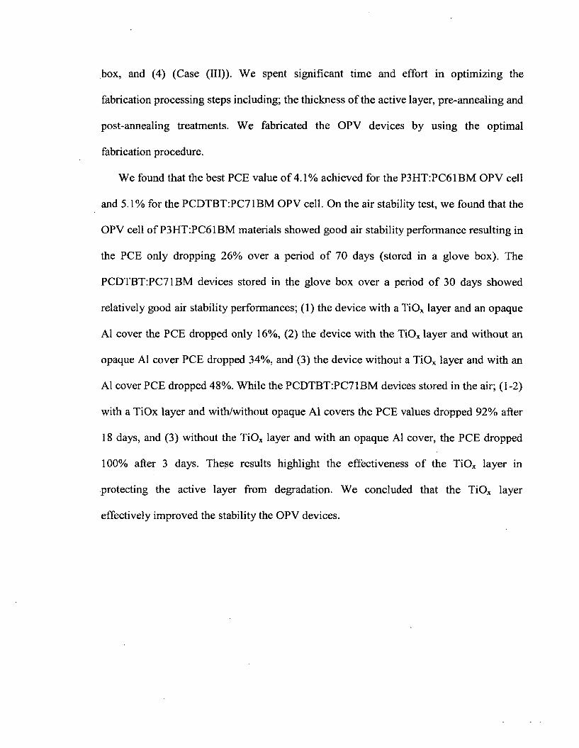
We found that the best PCE value of 4.1% achieved for the P3HT:PC61BM OPV cell
and 5.1% for the PCDTBT:PC71BM OPV cell. On the air stability test, we found that the
OPV cell of P3HT:PC61BM materials showed good air stability performance resulting in
the PCE only dropping 26% over a period of 70 days (stored in a glove box). The
PCDTBT:PC71BM devices stored in the glove box over a period of 30 days showed
relatively good air stability performances; (1) the device with a TiOx layer and an opaque
A1 cover the PCE dropped only 16%, (2) the device with the TiOx layer and without an
opaque A1 cover PCE dropped 34%, and (3) the device without a TiOx layer and with an
A1 cover PCE dropped 48%. While the PCDTBT:PC71BM devices stored in the air; (1-2)
with a TiOx layer and with/without opaque A1 covers the PCE values dropped 92% after
18 days, and (3) without the TiOx layer and with an opaque A1 cover, the PCE dropped
100% after 3 days. These results highlight the effectiveness of the TiOx layer in
protecting the active layer from degradation. We concluded that the TiOx layer
effectively improved the stability the OPV devices.

With love and humble admiration, I dedicate this thesis to my God and Savior, Lord Jesus,
my wife, Lian, and our children, Joshua, Mieah, and Nehemiah, and to my parents, brothers, and sisters.
ACKNOWLEDGMENTS
‘To everything there is a season, and a time to every purpose under the heaven”
(Ecclesiastes 3:1). This academic life has been a long journey. I thank God for all people
whom He has brought to help, to inspire, to teach, and to support me in the journey.
I want to thank my research advisor, Dr. Gon Namkoong, for his guidance, for
inspiring me to work so hard in the research lab, for introducing me so many exciting
nanoscale research projects, in particular, the organic photovoltaic devices that I have
never imagined before, and for the invaluable input to finish this dissertation. I want to
thank my doctoral committee, Dr. Helmut Baumgart, Dr. Tarek Abdel-Fattah, and Dr.
Sylvain Marsillac, for their valuable discussions and guidance in this dissertation.
I want to thank faculties at Department of Physics and Department of Electrical and
Computer Engineering at Old Dominion University for teaching me wonderful lessons in
science and technology during my academic studies there. I want to thank the Chairs and
Graduate Program Directors from both departments, especially Dr. Gail Dodge and Dr.
Oscar Gonzalez, for their support in the transition and the completion of my doctoral
studies, respectively. Also I want to thank to the staff from both departments for their
help.
1 enjoyed my time working in the ODU Applied Research Center Laboratories. I
want to thank Dr. Hani Elsayed-Ali as the Director of ODU ARC, Dr. Wei Cao and Dr.
Diefeng Gu for their help in characterizing my samples and their valuable input, and the
ODU-ARC staff. I also want to thank staff at the Applied Research Center of the William
and Mary College, Dr. Fattah and the staff at Christopher Newport University, Dr. Sham-
Shajing Sun from The Center for Materials Research at Norfolk State University, and Dr.
In-Wook Hwang from Gwangju Institute of Science and Technology for their help in
characterizing my samples and sharing their knowledge in organic photovoltaic devices.
I want to thank my research lab mates, Sri Sabarinadh, Sampath Chennuri, Arda
Akman, Kevin Latimer, Matthew Sampson, and Dr. Patrick Boland Jr. for making the
work around the lab so much fun. I appreciate their friendship, hard work, and support in
maintaining the research equipment and facility in good condition, sharing their brilliant
ideas, and working until late at night sometimes either to fix equipment or to conduct
experiments.
I could not be thankful enough for the late Prof. Darmadi Kusno and Prof. Yohanes
Surya who encouraged me to study in the US. They had encouraged me greatly to pursue
my academic dream. They are more than just mentors who had inspired me immensely;
they have become great models and friends to me.
I appreciate greatly the help from staff at the ODU Writing Center, Mr. Bill
Thompson, and Mrs. Linda Jones in writing this dissertation. I want to thank them for
working with my English and for making time out of their busy schedules to read and edit
my dissertation.
I greatly appreciate the support from the former ODU President, Dr. Roseann Runte,
the current ODU President, President John R. Broderick, Vice President, Dr. Ellen
Neufeldt, and ODU administrations. They have been encouraging me during my studies
and are great supporters and partners in serving the international community at ODU.

viii
There are so many great friends in many different paths of life that really helped me
during my study in the US. I also want to thank my international and American friends in
Hampton Roads area. In particular, I want to thank the individuals who worked and have
been working along with me in Global Student Friendship. I want to thank Pastor Rich
and Kathy Hardison, Sundeep Bodapati, Swetha Gali, Senthilraja Singaravelu, Frency
and Kavitha Varghese, Soyoung and Sanghoon Son, Ron and JoAnn Evers, Charlie and
Gail Woolford, Gordon and Ruth Paulson, Scott and Kathy Strickland, Jimmy and
Barbara King, Martin and Edwina Morgan, Tom and Ellen Biro, Mrs. Helena Garrick,
Dr. Hap Struthers, Dr. Lytton and Mrs. Libby Musselman, Danya Horton, Semuel
Rompis, Diana Thomas, and Nick and Gail Rerras. I want to thank friends from the local
churches especially from Tabernacle Church of Norfolk for their support and prayer.
I am forever grateful for the unconditional love that I am blessed with my parents,
Men Than Foe and Sinjorita Foe, and my siblings; Joesmiati Stevanus, Fadjarawati
Lahey, Sastra August Kumiawan, Setiawan Kumiawan, and their families. I also want to
thank my parent-in-laws, David and Esther Sutanto. I am thankful to God for my
children; Joshua, Micah, and Nehemiah. They are wonderful children and gifts from God.
Most of all, I want to thank God for my wife, Lian, for her love, her sacrifice, endless
support, encouragement, and believing in me. This dissertation is certainly not possible
without God. I thank Lord Jesus Christ for His blessing and provision, for giving me the
opportunity to study in the US, for loving me unconditionally, for allowing me to finish
my work, and for His divine guidance. I pray that my work will bring glory to Him and
His name alone.
NOMENCLATURE
AFM atomic force microscope/microscopy
AMI ,5G air mass 1.5 global
a.u. arbitrary unit
BHJ bulk heterojunction
DI de-ionized water
e electron charge, C
eV electron volt
e-beam electron beam
HOMO the highest occupied molecular orbital
IPCE incident photon-to-current collection efficiency
IQE internal quantum efficiency
J- V current density - voltage
LUMO the lowest unoccupied molecular orbital
NREL National Renewable Energy Laboratory
OPV organic photovoltaic
OLED organic light emitting diode
PTFE polytetrafluoroethylene
PV photovoltaic
TEM transmission electron microscope
UV-Vis ultraviolet visible
Vc Coulombic potential
X
XPS x-ray photoelectron spectroscope/spectroscopy
XRD x-ray diffraction/diffractometer
MATERIALS
CB chlorobenzene
DCB 1,2-di chlorobenzene
ITO indium tin oxide
P3HT poly(3-hexylthiophene)
PC61BM [6,6]-phenyl-C6i-butyric acid methyl ester
PCDTBT poly[N-9"-hepta-decanyl-2,7-carbazole-a/z-5,5-(4',7'-di-2-thienyl-2',l ',3'-
benzo-thiadiazole)]
PC71BM [6,6]-phenyl-C7i-butyric acid methyl ester
PEDOT:PSS poly(3,4-ethylene dioxythiophene) : poly(styrene sulfonate)
TiOx titanium sub-oxide
CONSTANTS and VARIABLES
Eg bandgap energy, eV
FF fill factor, %
Jsc short circuit current density, mA cm'2
PCE power conversion energy, %
Tg the glass-transition temperature, °C
fie the electron mobility, cm2 V '1 s-1
Voc open circuit voltage, V
TABLE OF CONTENTS
PageLIST OF TABLES ........................................................................................................... xiv
LIST OF FIGURES............................................................................................................xvii
Chapter1. ORGANIC PHOTOVOLTAIC DEVICES................................................................. 1
1.1. PHOTOVOLTAIC TECHNOLOGY..................................................................... 11.2. ORGANIC PHOTO VOLT A IC S..............................................................................21.3. STATE OF THE ART OF OPV DEVICES .......................................................... 31.4. MOTIVATION..........................................................................................................41.5. GOAL OF THIS STUDY.........................................................................................41.6. THESIS OUTLINE................................................................................................... 61.7. SUMMARY................................................... 7
2. DEGRADATION ISSUES IN ORGANIC PHOTOVOLTAIC DEVICES................. 82.1. LOSS MECHANISM IN AN OPV CELL........................................................... 82.2. DEGRADATION ISSUES IN OPV DEVICES................................................... 92.3. DEGRADATION AT THE ACTIVE LAYER................................................... 112.4. DEGRADATION AT THE ELECTRODES.........................................................112.5. DEGRADATION AT THE PEDOT.PSS LAYER...............................................122.6. SOLUTIONS TO DEGRADATION ISSUES.......................................................13
2.6.1. INVERTED STRUCTURE OPV DEVICE................................................132.6.2. ENCAPSULATION TECHNIQUE.......................................................... 132.6.3. INTERFACIAL LAYER........................................................................... 14
2.7. SUMMARY.............................................................................................. 14
3. A SOLUTION BASED TITANIUM SUB-OXIDE INTERFACIAL LAYER 163.1. INTRODUCTION ................................................................................................ 163.2. LITERATURE STUDIES OF STATE-OF-THE-ART RESEARCH IN THE USE
OF THE TIOx LAYERS IN OPV DEVICES ...................................................... 173.2.1. TIOx LAYER AS AN INTERFACIAL LAYER.................................... 173.2.2. TiOx LAYER AS AN OPTICAL SPACER............................................. 193.2.3. TIOx LAYER AS AN OXYGEN SCAVENGER AGENT..................... 21
3.3. EX PERIM EN TA L M ETHOD OF THE SO LU TIO N -B A SED T IO x SYNTHESIS ........................................................................................................... 23
3.4. SUMMARY..................................................................... 27
4. RESULTS ON THE FABRICATION OF P3HT:PC61BM BASED OPV DEVICES : 284.1. OPV DEVICE FABRICATION............................................................................ 284.2. STANDARD OF OPV DEVICE CHARACTERIZATIONS ..............................294.3. P3HT:PC61BM OPV DEVICES........................................................................... 32
xii
4.4. ABSORPTION STUDY ON THE P3HT:PC61BM LAYER..............................334.5. ACTIVE LAYER THICKNESS............................................................................ 354.6. PRE-ANNEALING TREATMENT.......................................................................374.7. POST-ANNEALING TREATMENT.......................................... .-...394.8. THE BEST P3H T :PC 61B M OPV D E V IC E A C H IEV ED IN OUR
EXPERIMENT..........................................................'..............................................404.9. SUMMARY.............................................................................................................42
5. RESULTS ON THE FABRICATION OF PCDTBT.PC71BM BASED OPV DEVICES........................................................................................................................435.1. PCDTBT:PC71BM OPV DEVICES..................................................................... 435.2. MORPHOLOGY OF PCDTBT:PC71BM COMPOSITE.................................... 445.3. ABSORPTION STUDY ON THE PCDTBT:PC71BM LAYER ......... 465.4. ACTIVE LAYER THICKNESS............................................................ 485.5. PRE-ANNEALING TREATMENT...................................................................... 515.6. POST-ANNEALING TREATMENT..................................: ................................ 525.7. AGED ACTIVE SOLUTION STUDY.............................................................. ..535.8. THE BEST PCD TBT:PC71BM OPV DEVICE ACHIEVED IN OUR
EXPERIMENT .........................................................................................................575.9. SUMMARY........................................................................................................... 58
6. IMPROVING THE STABILITY OF HIGH BANDGAP OPV DEVICES USING A SOLUTION-BASED TITANIUM SUB-OXIDE INTERFACIAL LAYER 606.1. INTRODUCTION ................................................................................................. 606.2. ABSORPTION STUDY ON P3HT:PC61BM/TIOx LAYERS ........................ 626.3. TiOx SPIN COATING TEST.................................................................................646.4. TIOx SOLUTION DRYING T EST ..................................................................... 656.5. SURFACE TOPOGRAPHY OF P3HT:PC61BM/TIOx LAYERS.................. 676.6. STABILITY STUDY ON THE P3HT:PC61BM OPV DEVICE..................... 676.7. SUMMARY........................................................................................................... 71
7. IMPROVING THE STABILITY OF LOW BANDGAP OPV DEVICES USING A SOLUTION-BASED TITANIUM SUB-OXIDE INTERFACIAL LAYER 727.1. INTRODUCTION ................................................................................................. 727.2. ABSORPTION STUDY ON PCDTBT:PC71BM/TIOx LAYERS .....................737.3. TIOx SPIN COATING TEST.................................................................................757.4. TIOx SOLUTION DRYING T EST .................................................................:....767.5. SURFACE TOPOGRAPHY OF PCDTBT:PC71BM/T10X LAYERS ..............777.6. STABILITY STUDIES ON THE PCDTBT:PC71BM OPV DEVICES............787.7.1-V MEASUREMENTS OF OPV DEVICES..................................................... 807.8. CASE (I) : STABILITY STUDY OF OPV DEVICES WITH AND WITHOUT
TIOx LAYERS ....................................................................................................... 807.9. CASE (II) : STABILITY STUDY OF OPV DEVICES WITH AND WITHOUT
OPAQUE AL COVERS ....................................................................................... 847.10. CASE (III) : STABILITY STUDY OF OPV DEVICES BASED ON
DIFFERENT STORAGE MEDIA ............................................... 86
7.11. SUMMARY ....................................................................................................... 89
8. CONCLUSIONS AND FUTURE WORKS ............................................................. 95
REFERENCES ................................................................................................................. 108
APPENDIXES .................................................................................................................. 118A. MATERIALS PREPARATIONS AND FABRICATION OPV DEVICES ... 118
A.I. PREPARATION OF ITO SUBSTRATES................................................. 118A.2. PREPAPATION OF ACTIVE SOLUTIONS ............................................ 119A.3. FABRICATION DIAGRAMS ................................................................... 120A.4. APPLICATION OF THE PEDOT:PSS SOLUTION.................................. 122A.5. APPLICATION OF THE ACTIVE SOLUTIONS.................................... 123A.6. APPLICATION OF THE AL METAL CATHODE................................... 124A.7. SUMMARY................................................................................................. 125
B. OPTIMIZATION PROCESSES....................................................................... 127B .l. INTRODUCTION..........................................................................................127B.2. OPTIMIZING THE ACTIVE LAYER DEPOSITION............................. 127
B.2.1. OPTIMIZING THE SUBSTRATE STOPPER............................... 128B.2.2. OPTIMIZING THE SUBSTRATE MOUNTING HOLDER 130
B.3. PRE- AND POST-ANNEALING TREATMENTS.................................. 132B.4. INTERFACIAL LAYER THICKNESS .......................................................133B.5. SUMMARY ................................................................................................. 133
C. STATISTICAL METHOD ..................................................................................135
D. STABILITY TESTS.......................................................................................... 141D.l. HIGH BANDGAP OF A P3HT:PC61BM OPV DEVICE..........................141D.2. LOW BANDGAP OF PCDTBT.PC71BM OPV DEVICES...................... 141
E. COPYRIGHTED MATERIALS ......................................................................... 145E. 1. M. Jorgensen, K. Norrman, and F.C. Krebs, “Stability/degradation of
polymer solar cells” ...................................................................................... 145E.2. K. Lee, J.Y. Kim, S.H. Park, S.H. Kim, S. Cho, and A.J. Heeger, “ A i r -
Stable Polymer Electronic Devices” ...................................... 146E.3. J.Y. Kim, S.H. Kim, H.-H. Lee, K. Lee, W. Ma, X. Gong, and A.J. Heeger,
“New Architecture for High-Efficiency Polymer Photovoltaic Cells UsingSolution-Based Titanium Oxide as an Optical Spacer” ............................... 147
APPENDIX REFERENCES ........................................................................................... 148
VITA 151
xiv
LIST OF TABLES
Table Page
4.1. The parameters of P3HT:PC61BM OPV cells fabricated at different active layer thicknesses..................................................................................................................... 37
4.2. The parameters of P3HT:PC61BM OPV cells fabricated at different pre-annealing conditions........................................................................................................................ 38
4.3. The parameters of P3HT:PC61BM OPV cells fabricated at different post-annealing conditions........................................................................................................................40
4.4. The parameters of the best P3HT:PC61BM OPV cell achieved in our experiment ........................................................................................................................................ 41
5.1. The parameters of PCDTBT:PC71BM OPV cells fabricated at different active layer thicknesses .................................................................................................................... 50
5.2. The parameters of PCDTBT:PC71BM OPV cells fabricated at different preannealing conditions ........................................................................................... 52
5.3. The parameters of PCDTBT:PC71BM OPV cells fabricated at different postannealing conditions ..................................................................................................... 53
5.4. The parameters of PCDTBT:PC71BM OPV cells fabricated at different aging times of the active solutions of PCDTBT:PC71BM..............................................................55
5.5. The parameters of the best PCDTBT:PC71BM OPV cell achieved in our experiment ................................................................................................ 58
6.1. The parameters of P3HT:PC61BM OPV cells fabricated at different spin speeds of the TiOx solution............................................................................................................ 65
6.2. The parameters of P3HT:PC61BM OPV cells fabricated at different TiOx solution drying conditions........................................................................................................... 66
7.1. The parameters of PCDTBT:PC71BM OPV cells fabricated at different spin speeds of the TiO* solution....................................................................................................... 76
7.2. The parameters of PCDTBT:PC71BM OPV cells fabricated at different TiO solution drying conditions .................................................................................... 77
X
XV
7.3. Different stability study conditions for PCDTBT:PC71BM based OPV devices................................................................................................................................................ 79
8.1. The best P3HT:PC61BM and PCDTBT:PC71BM OPV parameters achieved in our experiment bench marked with literature studies [85,165]........................................ 96
8.2. The stability study performance of OPV devices fabricated using different photoactive layers, different stability conditions : with and without TiOx layers (Case (I)), with and without opaque A1 protection covers (Case (II)), and different storage media ((1) glove box, (2) air, (3) ante-chamber of the glove box, and refrigerator (Case (III)) ......................................................................................................................................... 97
B.l. The parameters of PCDTBT:PC71BM OPV cells fabricated with different substrate holder designs............................................................................................................ 132
C.l. List of the parameters variability of the best 20 OPV cells out of 200 high bandgap polymer of P3HT:PC61BM OPV devices tested with PCE values equal or larger than 4 % ...................................................................................................................... 136
C.2. List of the parameters variability of the best 10 OPV cells of 100 low bandgap polymer of PCDTBT:PC71BM OPV devices tested with PCE values equal or larger than 5 % .......... 137
C.3. List of experimentally determined PCE values o f all 200 P3HT:PC61BM OPV devices that were fabricated for this thesis work. The overall average of all PCE values for high bandgap polymer is 2.46 ± 0.97 % ........................... 138
C.4. List of experimentally determined PCE values of all 100 PCDTBT:PC71BM OPV devices that were fabricated for this thesis work. The overall average of all PCE values for low bandgap polymer is 3.21 ± 1.20 % ....................................................139
D.l. The parameters of a P3HT:PC61BM OPV cell with a TiOx layer in the glove box and with an opaque A1 cover.................................................................................. 141
D.2. The parameters of a PCDTBT:PC71BM OPV cell with a TiOx layer stored in the air and with an opaque A1 cover.................................................................................. 141
D.3. The parameters of a PCDTBT:PC71BM OPV cell with a TiOx layer stored in the air and without an opaque A1 cover............................................................................. 142
D.4. The parameters of a PCDTBT:PC71BM OPV cell with a TiOx layer stored in the glove box and with an opaque A1 cover................................................................... 142
D.5. The parameters of a PCDTBT:PC71BM OPV cell with a TiOx layer stored in the glove box and without an opaque A1 cover........................................................... 142
xvi
D.6. The parameters of a PCDTBT:PC71BM OPV cell without a TiOx layer stored in the air and with an opaque Al cover............................................................................. 143
D.7. The parameters of a PCDTBT:PC71BM OPV cell without a TiOx layer stored in the glove box and with an opaque Al cover................................................................... 143
D.8. The parameters of a PCDTBT:PC71BM OPV cell with a TiOx layer stored in the ante-chamber and with an opaque Al cover.............................................................. 143
D.9. The parameters of a PCDTBT:PC71BM OPV cell with a TiOx layer stored in the refrigerator and with an opaque Al cover................................................................ 144
XVII
LIST OF FIGURES
Figure Page
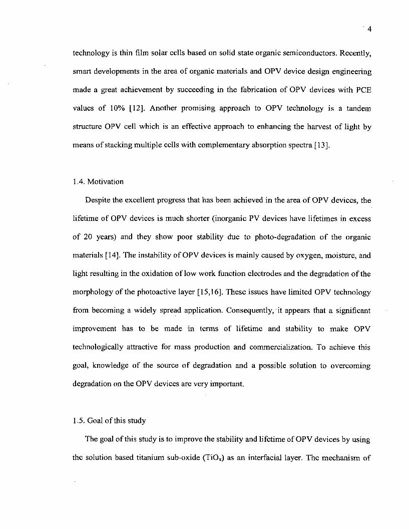
1.1. Laboratory best device efficiencies for various PV technologies including OPV devices. Reprinted with permission [10]. Copyright (2013) National Renewable Energy Laboratory.......................................................................................................... 3
2.1. Possible loss mechanism processes in an OPV device................................................. 9
2.2. Cross-sectional view of a BHJ OPV cell with possible degradation processes. Reprinted with permission [22]. Copyright (2008) Elsevier..................................... 10
3.1. (a) XPS evidence of the oxygen scavenger effect of the TiOx layer. Reprinted with permission [18]. Copyright (2007) John Wiley and Sons, (b) XRD patterns of two different TiOx thin films deposited at room temperature and sintered at 500 °C. Reprinted with permission [77]. Copyright (2006) John Wiley and S ons............... 17
3.2. A schematic illustration of the device structure with a TiOx layer. Reprinted with permission [18]. Copyright (2007) John Wiley and Sons......................................... 18
3.3. Schematic representation of the spatial distribution of the squared optical electric field strength \E\2 inside the devices without optical spacer (left) and with optical spacer (right). Reprinted with permission [77]. Copyright (2006) John Wiley and Sons.................................................................................................................................20
3.4. (a) J-V characteristics of P3HT:PC61BM OPV devices fabricated with and without TiOx layers measured after various storage times in the air. The same devices were characterized periodically with increasing storage times, (b). Comparison of efficiencies of OPV devices fabricated with and without TiOx layers as a function of storage time. Reprinted with permission [18]. Copyright (2007) John Wiley and Sons .......................................................................................................................................... 23
3.5. An IKA rotary evaporator system ..................................... 24
3.6. A schematic diagram of the sol-gel TiOx synthesis............................................. .....25
3.7. (a) A fresh mixture solution of TiOx precursor and solvents. The mixed solution appeared (b) after stirring for 1 h at 80 °C (dark orange color) and (c) after stirring for another 1 h at 120 °C (dark red wine color)..................................................................26
3.8. The final TiOx sol-gel product (right) 26
XV111
4.1. A diagram of typical fabrication processes on a 25.4 x 25.4 mm2 OPV device, (a) Patterning an ITO glass substrate, (b) depositing a PEDOT.PSS layer, (c) depositing an active layer, (d) cleaning ITO anode films, (e) a pre-annealing treatment, and (f) depositing an Al cathode layer and a post-annealing treatment.................................. 28
4.2. An OPV device characterization set u p ....................................................................... 29
4.3. The back side image of an OPV device captured by Hirox KH-3000 VD. The dotted rectangular area is an active area o f the OPV device with a structure of ITO/PEDOT-.PSS/ P3HT:PC61BM/A1......................................................................... 31
4.4. Energy levels of an OPV device of P3HT:PC61BM (with respect to the vacuum level) .............................................................................................................................. 32
4.5. The UV-Vis absorption profile of P3HT:PC61BM active layers: as cast (black) and annealed at 140 °C for 2 min (red).................. 34
4.6. J-V characteristics of P3HT.PC61BM OPV cells fabricated at different thicknesses of the active layer............................................................................................ 36
4.7. J-V characteristics of P3HT:PC61BM OPV cells fabricated at different pre-annealing conditions........................................................................................................................38
4.8. J-V characteristics of P3HT:PC61BM OPV cells fabricated at different postannealing conditions ...................................................................................................... 40
4.9. J-V characteristics of the best P3HT:PC61BM OPV cell achieved in our experiment ........................................................................................................ 41
5.1. Energy levels of OPV device of PCDTBT:PC71BM (with respect to the vacuum level) ...................................................................................................... 44
5.2. TEM images of PCDTBT:PC71BM composite with (a) low and (b) high resolutions .......................................................................................................................................... 45
5.3. The UV-Vis absorption profile of PCDTBT polymer (black) and PC71BM fullerene (red) ............................................................................................................................47
5.4. The UV-Vis absorption profile of PCDTBT:PC71BM active layers: as cast (black) and annealed at 140 °C for 2 min (red)......................................... 48
5.5. The UV-Vis absorption profile of four different thicknesses of PCDTBT:PC71BM active layers; 40 nm (green), 51 nm (blue), 62 nm (red) and 77 nm (black) ............... 49
5.6. J-V characteristics o f PCDTBT:PC71BM OPV cells fabricated at different thicknesses of the active layer........................................................................................50
xix
5.1. J-V characteristics of PCDTBT:PC71BM OPV cells fabricated at different preannealing conditions.......................................................................................................51
5.8. J-V characteristics of PCDTBT:PC71BM OPV cells fabricated at different postannealing conditions.......................................................................................................53
5.9. J-V characteristics of cells fabricated at different aging times of the active solutions of PCDTBT:PC71BM.................................................................................................... 54
5.10. Parameters of PCDTBT :PC71BM OPV cells as a function of the aging time of the active solutions of PCDTBT: PC71BM.........................................................................56
5.11. J-V characteristics of the best PCDTBT:PC71BM OPV cell achieved in our experiment.......................................................................................................................58
6.1. Energy level of an OPV device of P3HT:PC61BM with the TiOx interfacial layer (with respect to the vacuum level).................................................................................61
6.2. The UV-Vis absorption profile of P3HT:PC61BM immediately following fabrication or (TFO, green) and P3HT:PC61BM/TiOx at different spin speeds of the TiO solution: 3000 rpm (TF1, blue), 2000 rpm (TF2, red), and 1000 rpm (TF3, black).. 63
X
6.3. J-V characteristics of P3HT:PC61BM OPV cells fabricated at different spin speeds of the TiOx solution: 3000 rpm (TF1, diamond), 2000 rpm (TF2, square), and 1000 rpm (TF3, circle).............................................................................................................64
6.4. J-V characteristics of P3HT:PC61BM OPV cells fabricated at different TiOx solution drying conditions .......................................................................................................... 66
6.5. (a) 2-D and (b) 3-D AFM images of P3HT:PC61BM/TiOx .......................................67
6.6. J-V characteristics of a P3HT:PC61BM OPV cell with a TiOx layer and stored with a cover up to 70 days of the storage tim es.................................. 69
6.7. The change of the normalized OPV parameters, (a) Jsc, (b) Voc, (c) FF, and (d) PCE, of P3HT:PC61BM OPV device with TiOx layer and stored with an opaque Al cover up to 70 days.................................................................................................................... 70
7.1. Energy level of an OPV device of PCDTBT:PC71BM with the TiOx interfacial layer (with respect to the vacuum level).................................................................................73
7.2. The UV-Vis absorption profile of PCDTBT:PC71BM immediately following fabrication (TFO, green) and PCDTBT:PC71BM/TiOx at different spin speeds of the TiOx solution: 3000 rpm (TF1, black), 2000 rpm (TF2, red), and 1000 rpm (TF3, blue) .............................................................................................................................. 74
XX
13. J-V characteristics o f PCDTBT:PC71BM OPV cells fabricated at different spin speeds of the TiOx solution: 3000 rpm (TF1, diamond), 2000 rpm (TF2, square), and 1000 rpm (TF3, circle)............................................................ 75
7.4. J-V characteristics of PCDTBT:PC71BM cells fabricated at different TiOx solution drying conditions .......................................................................................................... 76
7.5. (a) 2-D and (b) 3-D AFM images of PCDTBT:PC71BM/TiOx .................................78
7.6. PCDTBT:PC71BM OPV devices (a) with and (b) without an opaque Al cover 80
1.1. J-V characteristics of PCDTBT:PC71BM OPV cells fabricated with and without TiOx layers (Case (I) and stored in air and inside the glove box. The devices were protected with an opaque Al cover ...............................................................................82
7.8. J-V characteristics of PCDTBT:PC71BM OPV cells stored with and without opaque Al covers (Case (II)) in the air and glove box. The device were fabricated with a TiO layer................................................................................................................................. 85
X
7.9. J-V characteristics of PCDTBT:PC71BM OPV cells fabricated with a TiOx layer and stored with an opaque Al cover in different storage media: (a) air, (b) glove box, (c) ante-chamber of the glove box, and (d) refrigerator (Case (III)).................................88
7.10. The change of param eters, (a) Jsc, (b) V0c, (c) FF, and (d) PCE, o f PCDTBT:PC71BM OPV cells fabricated with and without TiOx layers (Case (I)). The devices were stored with and without Al opaque covers (Case (II)) in the air and glove box atmospheres for 30 days............................................................................... 90
7.11. The change of param eters, (a) Jsc, (b) V0c, (c) FF, and (d) PCE, of PCDTBT:PC71BM OPV cells fabricated with a TiOx layer and stored with an opaque Al cover in different storage media: glove box (diamond), refrigerator (square), antechamber of a glove box (circle), and air (triangle) (Case (III)) for 30 days............... 93
8.1. The change o f param eters, (a) Jsc, (b) Voc, (c) FF, and (d) PCE, o f PCDTBT:PC71BM OPV cells fabricated with and without TiOx layers (Case (I)). The devices were stored with and without opaque Al covers (Case (II)) in air and glove box atmospheres for 30 days..........................................................................................98
8.2. The stability study based on different stability conditions o f low bandgap PCDTBT:PC71BM OPV cells fabricated with and without TiOx layers (Case (I)). The devices were stored with an opaque Al cover in the air and glove box atmospheres for 30 days............................................................................................................................99
xxi
8.3. The stability study based on different stability conditions of low bandgap PCDTBT: PC71BM OPV cells stored with and without opaque Al covers (Case (II)) in the air and glove box atmospheres for 30 days. The devices were fabricated with a TiO* layer.................. 101
8.4. The change of normalized OPV parameters, (a) Jsc, (b) V0c, (c) FF, and (d) PCE, of PCDTBT:PC71BM OPV cells fabricated with a TiOx layer and stored with an opaque Al cover in different storage media: glove box (diamond), refrigerator (square), antechamber of a glove box (circle), and air (triangle) (Case (III)) for 30 day s 102
8.5. The stability study based on different storage media conditions of low bandgap PCDTBT:PC71BM OPV devices stored in the air, a glove box, an ante-chamber, and a refrigerator (Case (III)). The devices were fabricated with a TiOx layer and stored with an opaque Al cover............................................................................................ 104
A.I. Vials with active solutions of (a) P3HT:PC61BM (yellowish color) and (b) PCDTBT:PC71BM (reddish color)........................................................................ 120
A.2. A schematic diagram of fabricating an OPV device without the TiOx layer 120
A.3. A schematic diagram of fabricating an OPV device with the TiOx layer.............. 121
A.4. Spin coater set ups: (a) Prior to spin coating the PEDOT.PSS and (b) during thespin coating process (Al foils protect the PEDOT:PSS from the light)................ 122
A.5. A SP1N150® mechanical spin coater unit (Al foils protect active solution from the light)......................................................................................................................... 123
A.6. An e-beam unit in our laboratory. The inset picture shows the metal evaporation and transportation processes taking place inside the e-beam deposition chamber (taken from the observation window)..................................................................................124
A.7. OPV devices with active layers of (a) P3HT:PC61BM and (b) PCDTBT:PC71BM fabricated without the TiOx layer............................................................................ 125
B .l. (a) 25.4 mm x 25.4 mm and (b) 50.8 mm * 50.8 mm sample holders o f the SPIN 150® mechanical spin coater. Thin film images (c) with and (d) without edge effects....................................................................................................................... 128
B.2. Different designs of sample mounting holder with (a) a polyimide tape, (b) a foam tape, and (c) a carbon tape ...................................................................................... 130
B.3. J-V characteristics of PCDTBT:PC71BM OPV cells fabricated with different designs of the substrate mounting holder................................................................. 131
1
Chapter 1
Organic Photovoltaic Devices
1.1. Photovoltaic technology
According to the first law of thermodynamics, any human activity requires energy
input. With strong economic growth and continued heavy reliance of the energy demand
on fossil fuels, it is projected that there will be a significant increase in carbon dioxide
(CO2 ) emissions. Today, about 20 x 1012 kg of CO2 are put into the atmosphere every
year, mainly by burning fossil fuel [1], International discourse on climate change has
been emphasizing the need for clean (near zero carbon-emission) and renewable energy
technologies. Photovoltaic (PV) technology is the most attractive solution to modem
energy demands. It has the ability to meet some of these demands by directly converting
sunlight into electricity, while minimizing detrimental effects on the environment. The
first oil crisis in the 1970’s prompted a surge of interest in PV energy and other
alternative energy sources and led to increased funding and research in these areas. In
particular, this led to the development of the first non-single crystal PV devices such as
polycrystalline silicon, amorphous silicon, and thin film and organic semiconductors [2].
This technology produces near-zero carbon emissions and limits the concentration of
greenhouse gases in the atmosphere which is potentially slowing the global climate
change [3]. Moreover, PV technology can potentially generate power anywhere there is
light.
1.2. Organic photovoltaics
Alexandre Becquerel first observed the photovoltaic effect in an electrolyte solution
in 1839 [4]. The basis for organic photovoltaic (OPV) technology was the discovery of
dark conductivity in halogen doped organic compounds at Bell Laboratories in 1954,
although many of them were not stable [5]. The first breakthrough in modem solid state
PV based on organic materials was performed by C.W. Tang during his time at Eastman
Kodak in the 1980s [6]. In 2000, Shirakawa, Heeger, and MacDiarmid were each
awarded the Nobel Prize in Chemistry for “the discovery and development of conductive
polymers" [7].
OP Vs promise potential as a novel type of a renewable, delocalized, and competitive
energy source. All properties of organic semiconductor materials are directly derived
from the chemical properties of a carbon atom. The conductivity in organic
semiconductors is due to conjugation, the alternation of single and double bonds between
the carbon atoms [8], Thin film photovoltaic devices based on organic semiconductors
are interesting for several reasons. First, organic semiconductor materials have relatively
strong absorption coefficients (usually > 10s cm'1), which partly balances low mobility,
giving high absorption in even thin devices (< 100 nm). Second, the electrical and
chemical properties of organic semiconductors can be tailored by modifying the chemical
structure of the compounds in endless combinations. Third, inorganic semiconductors
have a relatively small diffusion length of excitons in these rather amorphous and
disordered organic materials [9]. Fourth, organic semiconductors can be deposited at low
temperatures with high throughput such as evaporation and solution processing that can
lower manufacturing costs. Fifth, the use of very thin organic layers reduces the amount
3
of active material needed and also makes lightweight and flexible devices possible. For
these and other reasons, OP Vs have gained great attention.
1.3. State of the art of OPV devices
Best Research-Cell Efficiencies NRELMuibjunction Cells (2-terminal, monolithic) Thin-FOm Technologies Spectrotab { Fraunhofer JSE
(metarnofpMe. 299*1 fmetamcrffic.454*}Three-junction (concenlrator) v Three-junction (non-concentrator)
Two-junction (concentrator) a Two-junction (non-concentrator)
• Cu(in.Ga)Se? oCdTeoAmorphousSl:H (stabilized) •Nano-, micro-, poly-SI
Sctar
SenBoeing-Spectrolab Boemg-Spectrolab
^ (metarapftit, 240x)□ Four-junction or more (non-concentrator) D Multifunction potycrysfaLnneEmerging PV oDys-sensitized cells
Organic cells (various types) a Organic tandem cells
Inorganic cells O Quantum dot cells
m e nNRELfsrrveneo. (htbee matched.
NREL (imatecl. meiafflc rtr»c.l-w n ) S h a rp (iMM.i-»un)
v Fh&tSE 0-sun)FhG-tSE
RaJ*wl -JToSo” </ 7x|Dmtesa
Singte-Junctlon GaAsASingle crystal ^Concentrator VThin-film crystal
Crystalline Si Cells Single crystal
o Mutlicrystafline♦ Thick Si film• Silicon heterostructures (HIT) VThin-film crystal
(nverted, metamorpnc)NREL
Bodno* Spectrwab
Varan (2t6x) (4.0 cm*, 1-sun)Amonix
(SCbclStanford(1*0x1 A 'Alta
r S » u tRadboud Uftfv.’
japyj, Sanyo
UNSW_laasM X UNSW UNSW> i < : Cu(tn,Ga>Sej UNSWX UNSW/ mo 24 Spfre
UNSW Sa—n Sanyo ------------- EMPA2SW (Flex polymer sub)
IBM A(T.J. Watson
Research Center) Georgia Georgia y,Westing- UNSWNational
UmversiNo. Carts na State Univ. \ y
Kodak Solarex NREL**1* " United Sotar transfed (CdTeOS). x IBM Cr-(CZTSSe)Photon Energy
EPPL Kanaka (2 pm
on glass)
Matsushita
Heteteks ! ^ o Chemicaf
to m o y NTUCLA —— Urav.of
NREL/Konarka
\ KonartaGroningen
" \ Ptextronics'univ A University Siemens Dresden
Linz ,i L_ i
Kodak Boeing
RCA
ARCO United SoarBoeing
University of Maine
Solarex
Unryersdy unz NREL (PbS*»)RCA RCA(ZnOPbS-QD)
1975 1980 1985 1990 1995 2000 2005 2010 2015
Figure 1.1: Laboratory best device efficiencies for various PV technologies including OPV devices. Reprinted with permission (10). Copyright (2013) National Renewable Energy Laboratory.
Figure 1.1 summarizes the highest efficiencies in various solar cell technologies
obtained throughout the years. It is clear that there are many different approaches to reach
the same goal of converting sunlight to electricity, and each approach may be able to fill
an appropriate role based on its individual advantages and tradeoffs. Numerous OPV
technologies exist that are still not widely available commercially. Dye-sensitized solar
cells with efficiencies of 11% have been reported to use an organic dye coated porous
electrode with a high surface area to absorb light [11]. Another organic solar cell
4
technology is thin film solar cells based on solid state organic semiconductors. Recently,
smart developments in the area of organic materials and OPV device design engineering
made a great achievement by succeeding in the fabrication of OPV devices with PCE
values of 10% [12]. Another promising approach to OPV technology is a tandem
structure OPV cell which is an effective approach to enhancing the harvest of light by
means of stacking multiple cells with complementary absorption spectra [13].
1.4. Motivation
Despite the excellent progress that has been achieved in the area of OPV devices, the
lifetime of OPV devices is much shorter (inorganic PV devices have lifetimes in excess
of 20 years) and they show poor stability due to photo-degradation of the organic
materials [14]. The instability of OPV devices is mainly caused by oxygen, moisture, and
light resulting in the oxidation of low work function electrodes and the degradation of the
morphology of the photoactive layer [15,16]. These issues have limited OPV technology
from becoming a widely spread application. Consequently, it appears that a significant
improvement has to be made in terms of lifetime and stability to make OPV
technologically attractive for mass production and commercialization. To achieve this
goal, knowledge of the source of degradation and a possible solution to overcoming
degradation on the OPV devices are very important.
1.5. Goal of this study
The goal of this study is to improve the stability and lifetime of OPV devices by using
the solution based titanium sub-oxide (TiOx) as an interfacial layer. The mechanism of
OPV device instability caused by degradation is not yet fully understood and very
complex. The interfacial layer protects the organic materials from a physical or chemical
interaction with the electrode materials. The diffusion of metal atoms into polymeric
layers during the metallic cathode deposition process causes shunting or electrical
shorting of the organic devices and limits their lifetime [17]. We will use a solution based
titanium sub-oxide (TiOx) as the interfacial layer which has been reported to be an
efficient approach to improve the lifetime of OPV devices [18]. In the stability study of
the OPV devices, we will investigate three different stability conditions. First, we will
fabricate OPV devices with and without TiOx layers by using optimal fabricating
conditions (Case (I)). Second, we will store the fabricated OPV devices with and without
a protection cover (a high research grade opaque A1 foil) to observe the device
performance in a dark environment and in an exposure to light environment (Case (II)).
Third, we will vary the storage media: (1) in the ambient atmosphere, (2) in the N2 -filled
atmosphere, (3) in the ante-chamber of a glove box, and (4) inside a refrigerator. We will
observe the OPV device performance in different storage media conditions (Case (III)).
We will perform a stability study on the OPV device at a prolonged storage time (over 30
days). Both the organic materials and electrodes need to be stable without any
encapsulation.
We also will use the low bandgap polymer, PCDTBT, to improve the stability of the
OPV devices. PCDTBT has large ionization potential energy and the highest occupied
molecular orbital (HOMO) level below the air oxidation threshold of 5.27 eV, ensuring
better air stability [19], The stability of the fully aromatic backbone and the amorphous
structure of PCDTBT are responsible for the remarkable ability of this semiconducting
6
polymer to withstand exposure to high temperatures.
1.6. Thesis outline
Chapter 1 has given a brief background of photovoltaic technology. The improvement
and the trend of PV technologies are likely to face many new opportunities in the years
ahead. The goal of the study is also presented. Chapter 2 discusses the degradation issues
in the OPV cell which cause the instability of the OPV device and some of smart
solutions. Chapter 3 presents literature studies of the state-of-the-art in the use of solution
based titanium sub-oxide (TiOx) materials in OPV devices and explains important
functional features of the TiOx interfacial layer in the OPV research. The experimental
method and sol-gel synthesis of the solution based TiOx material are also discussed.
Chapter 4 and 5 present the results on conventional high and low bandgap OPV
devices without TiOx layer. These two chapters discuss the uniqueness of the organic
materials based on high and low bandgap polymers and the optimization processes in
fabricating OPV devices. The results of the best high and low bandgap OPV devices
achieved in our study by using optimal fabrication conditions are presented as well.
Chapter 6 discusses the application and the optimization process of the TiOx layer in the
high bandgap P3HT:PC61BM OPV devices. A brief stability study o f a high bandgap
P3HT:PC61BM device using a TiOx layer is presented. Chapter 7 discusses the
application and optimization processes of the TiOx layer in the low bandgap PCDTBT:
PC71BM devices. Detailed stability studies based on fabricated OPV devices (1) with
and without TiOx layer (Case (I)), (2) with and without opaque A1 covers (Case (II)), and
(3) different storage media conditions (Case (III)) are discussed. Finally, Chapter 8
concludes and suggests the future work of OPV devices.
1.7. Summary
In this chapter, we described the need of a photovoltaic (PV) technology which is a
near-zero carbon emissions renewable technology. We discussed one of the PV
technologies that we focused in our study which is the organic photovoltaic (OPV)
technology. The progress and state of the art of OPV devices were described. The
motivation and goal of our study, which is to improve the stability and lifetime of OPV
devices, was explained. We described briefly the use of a solution based TiOx material as
the interfacial layer between the active layer and the A1 cathode and the plan to perform a
stability study to utilize and to test the efficacy of the solution based TiOx material.
Finally, the outline of this thesis was presented.
8
Chapter 2
Degradation Issues in Organic Photovoltaic Devices
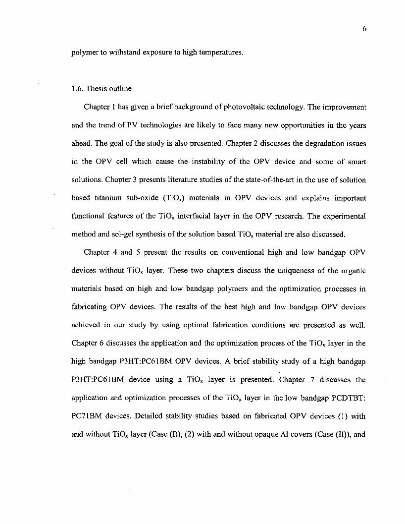
2.1. Loss mechanism in an OPV cell
Photogenerated current in an OPV cell generally occurs in four main steps: (1) light
absorption and exciton creation, (2) exciton diffusion, (3) exciton dissociation and charge
separation, (4) charge transport and charge collection. The multilayered BHJ OPV
structures show a great potential to achieve highly efficient OPV devices. However, the
performance of the OPV devices, in reality, decreases due to loss mechanism processes
as shown in Figure 2.1. Two key loss mechanisms operative in OPVs are geminate pair
and bimolecular recombination losses [20]. Recombination of excess charge through
localized states or trap states occurs radiatively or non-radiatively. In the radiative
recombination mechanism, an electron transitioning into a relaxed state releases
transition energy via a photon. In the non-radiative recombination mechanism, an
electron’s relaxation is mediated via a phonon emission.
The disordered nature of solution processed films of a BHJ OPV cell results in low
charge carrier mobilities. The mobility of the slower charge carriers limits the
photocurrent and efficiency of the OPV cells due to accumulation and concomitant high
carrier concentration. If during charge transport, the charge carrier meets another carrier
with an opposite sign, it recombines and does not contribute to the photocurrent thereby
creating another photocurrent loss mechanism. Recombination of photogenerated charge
carriers in BHJ OPV cells reduces the short circuit current density (Jsc) and the fill factor
(FF) of the OPV devices [21]. Smart electron and hole blocking materials have been used
as an interfacial layer between the active layer and the metal electrode in OPV devices in
order to protect the photoactive area of the device from the metal electrode.
4. Charge transport and charge collection
3. Exciton dissociation and charge separation
2. Exciton diffusion
1. Photon absorption and exciton creation
Incident photons
LOSS MECHANISMS
C harge re co m b in a t io n Limited c h arg e mobili ty
Barriers a t e le c t ro d e s
R e c o m b in a t io n o f excitons
R e co m b in a t io n o f excitons
T
R eflect ion
Figure 2.1: Possible loss mechanism processes in an OPV device.
2.2. Degradation issues in OPV devices
In general, degradation refers to the natural process of the declining qualities or
certain properties of a given material over a period of time. At this time, the mechanism
of OPV device degradation is not yet fully understood. A number of studies on
degradation show that the degradation issue is rather complicated and might occur at
multiple sites inside an OPV cell as shown in Figure 2.2 [14,16,22], The critical problem
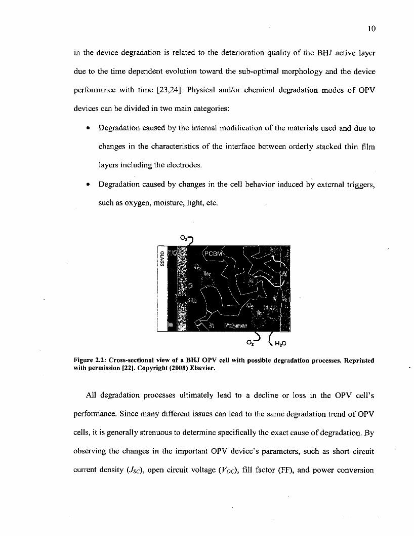
in the device degradation is related to the deterioration quality of the BHJ active layer
due to the time dependent evolution toward the sub-optimal morphology and the device
performance with time [23,24], Physical and/or chemical degradation modes of OPV
devices can be divided in two main categories:
• Degradation caused by the internal modification of the materials used and due to
changes in the characteristics of the interface between orderly stacked thin film
layers including the electrodes.
• Degradation caused by changes in the cell behavior induced by external triggers,
such as oxygen, moisture, light, etc.
Figure 2.2: Cross-sectional view of a BHJ OPV cell with possible degradation processes. Reprinted with permission [22]. Copyright (2008) Elsevier.
All degradation processes ultimately lead to a decline or loss in the OPV cell’s
performance. Since many different issues can lead to the same degradation trend of OPV
cells, it is generally strenuous to determine specifically the exact cause of degradation. By
observing the changes in the important OPV device’s parameters, such as short circuit
current density (Jsc), open circuit voltage (Voc), fill factor (FF), and power conversion
efficiency (PCE) values as a function of time, we can make some intelligent guesses
concerning the type of degradation taking place. For example, a decrease in Jsc values
during the OPV operation corresponds to a decrease in the number of charges collected at
the OPV electrodes. Understanding and combating various loss mechanisms that occur in
processes from optical excitation to charge collection and developing new materials
(particularly donor materials) should lead to OPV’s efficiencies of approximately 10% in
the near future [1 2 ].
2.3. Degradation at the active layer
Organic materials such as P3HT, PC61BM, PCDTBT, and PC71BM are by nature
more susceptible to chemical degradation from, for example, O2 and H2 O, than they are
to inorganic materials [25]. Fullerene materials are air sensitive once they have been in
contact with O2 . The oxidative polymerization on the organic materials would take place
under thermal treatments, even when no additional O2 is present [26]. This
polymerization is greatly accelerated when it occurs in an environment containing
oxygen. Exposure to O2 will also lower the conductivity of fullerene films. Upon O2
uptake, the electron mobility is reduced by several orders of magnitude because the
inserted oxygen acts as an electron trap [27].
2.4. Degradation at the electrodes
A typical metal used for a low work-function electrode (in the case of a conventional
OPV structure, in which the metal electrode is the electron collecting electrode) is
aluminum. At the organic-inorganic interface, metal atoms interact with carbon atoms
12
from the organic materials and create an Al-polymer complex interlayer [28,29]. When
the A1 evaporates onto organic materials, it also preferentially interacts with the carbon
atoms in the conjugated backbone, which leads to a significant charge transfer from the
metal atoms to some carbon and sulfur sites [30]. Thus, the control of the organic-
inorganic interface is becoming an important issue in organic electronics [31].
Degradation of these negative electrodes is mainly caused by metal oxidation. Small
amounts of O2 and H2 O can be introduced unintentionally during the device fabrication
absorbed in the different layers through the microscopic holes in the electrode [32]. As a
result, a chemical reaction with O2 and H2 O takes place. Krebs and his coworkers
reported that radical species formed in the active layer may react with the A1 electrode,
leading to a gradual deterioration of the active layer/electrode interface quality [16].
Furthermore, light appeared to accelerate the degradation of the metal electrode as well
[33].
2.5. Degradation at the PEDOT: PSS layer
Though the poly(3,4-ethylene dioxythiophene):poly(styrene sulfonate) or PEDOT:
PSS has been used extensively in organic semiconductor devices, its acidic nature could
cause interface instability to the active layer [34], corrosion to the ITO film [35],
electrical inhomogeneities [36], and degradation to the interfacial layer of ITO/PEDOT:
PSS [37]. It has also been reported that indium ions migrated into the PEDOT:PSS layer
[38]. PEDOT:PSS also has a relatively low work function of 5.2 eV, showing that the
hole injection could be a limiting factor in the OPV device [39].
13
2.6. Solutions to degradation issues
2.6.1. Inverted structure OPV device
To avoid the aforementioned degradation issues, as especially posted by PEDOT:
PSS, an inverted structure of the OPV device was introduced. In an inverted OPV device
structure, it is important to determine the appropriate energy level of the collecting
electrode to match the active layer [40]. Different metal oxide semiconductor materials
are introduced in device fabrication as a substitution for PEDOTrPSS. CS2 CO3 , ZnO,
Ti0 2 , WO3 , M0 O3 , or V2 O5 has been used to effectively substitute PEDOT:PSS and
inserted between the active layers and top electrode [41,42,43,44]. In an inverted OPV
structure, an air-stable high work function metal such as Au or Ag as the top anode, a
transparent ITO is used as the bottom cathode, and air-stable solution interfacial layer
metal oxides (between the active layer and the electrodes) have been used. Significant
improvement of the lifetime of inverted OPV devices has been reported [45,46,47].
However, the use of expensive metals such as Au and Ag as the anodes would greatly
increase the production cost.
2.6.2. Encapsulation technique
Encapsulation research in OPV devices is more particularly aimed to protecting OPV
devices from degradation triggers such as oxygen and moisture. Thin film encapsulation
layers such as A12 0 3 [48], Si0 x/Al2 0 3 /parylene [49], and Al2 0 3 /Hf2 0 [50] on top of OPV
devices also demonstrated significant improvement in the lifetime of the devices. The
inorganic barrier layer plays a significant role in reducing moisture and oxygen
penetration and in increasing the thermal stability of the OPV cells [51].
14
2.6.3. Interfacial layer
To improve the stability and lifetime of OPV devices, an interfacial layer is inserted
between the active layer and the electrodes. The interfacial layer has proven to slow
down the degradation between the active layer and the electrode [52]. The interfacial
layer is used to extract photogenerated carriers from the active layer to the electrode. One
of the functional features of the interfacial layer is to determine the polarity of the OPV
device. Depending on whether the bottom electrode forms the anode or the cathode, there
are two different geometries of OPV devices; conventional and inverted structures.
Therefore, the order of insertion of an interfacial layer in each case matters. Different
solution based metal oxides (TiOx, M0 O3 , and ZnO) have been used as the interfacial
layers [53,54]. In our study, we focused on the conventional structure. The interfacial
layer was also effective in adjusting the energy level between the active layer and the
electrode, to form a selective contact for charge carriers, and to act as an optical spacer.
More detailed discussion about the TiOx interfacial layer will be presented in the
following chapter.
2.7. Summary
We have learned that oxygen, water, and light are major degradation sources of OPV
devices. They could be introduced into the OPV system during the preparation of active
solutions, fabrication processes, and in the storage environment of the OPV devices.
Several alternative solutions to improve air-stability of OPV devices have been
introduced such as inverted OPV device structures, encapsulation techniques, and metal
oxide interfacial layers. At present, the exact degradation mechanism in OPV devices is
still unclear and an ongoing research topic. We can also study the degradation trend of
OPV cells by observing the changes in the important OPV device’s parameters, such as
the Jsc, Vqc, FF, and PCE values as a function of time.
1 6
Chapter 3
A Solution Based Titanium Sub-oxide Interfacial Layer
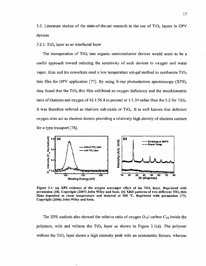
3.1. Introduction
Titanium dioxide (Ti02) belongs to the family of transition metal oxides [55]. T i0 2
has received a great deal of attention due to its chemical stability, non-toxicity, low cost,
and other advantageous properties. Today, the primary use for the annual production of
T i0 2 is as white pigment in paints [56,57,58], while the remaining production is used in
various applications such as textiles, food additives, toothpaste, sunscreen cream,
cosmetic products, medicine, plastic, paper, sensors, and semiconductors [59,60,61,62].
T i0 2 has also become a photocatalyst in the environmental decontamination [63,64] and
semiconductor industry [65], Due to its high refractive index, Ti0 2 is also used as anti
reflection coating in inorganic PV cells and in many thin film optical devices [6 6 ].
In 1972, Fujishima and Honda [67] pioneered and studied the effect of T i0 2 as
oxygen/water protection and as an oxygen scavenging agent originating from a
combination of photocatalysis and inherent oxygen deficiency [68,69,70], T i0 2 has also
been reported as an electron acceptor and transport material and has been used in dye-
sensitized photovoltaic devices [71,72], hybrid polymer/Ti02 devices [73,74], and
multilayer Cu-phthalocyanine/dye/Ti02 devices [75,76]. T i0 2 is also a good hole
blocking and electron selective contact in inverted photovoltaic devices [40].
17
3.2. Literature studies of the state-of-the-art research in the use of TiOx layers in OPV
devices
3.2.1. TiOx layer as an interfacial layer
The incorporation of Ti0 2 into organic semiconductor devices would seem to be a
useful approach toward reducing the sensitivity of such devices to oxygen and water
vapor. Kim and his coworkers used a low temperature sol-gel method to synthesize Ti0 2
thin film for OPV application [77]. By using X-ray photoelectron spectroscopy (XPS),
they found that the Ti0 2 thin film exhibited an oxygen deficiency and the stoichiometric
ratio of titanium and oxygen of 42.1:56.4 in percent or 1:1.34 rather than the 1:2 for Ti0 2 -
It was therefore referred as titanium sub-oxide or TiOx. It is well known that deficient
oxygen sites act as electron donors providing a relatively high density of electron carriers
for n-type transport [78].
o s . (a)
without TiO> layer with TIOi layerO 0.4
0.2
* 0.0
530 520525
Sintering at 500°C Room Temp.
10 20 30 40 SO 60 70 80Binding Energy (eV) 20 (degrees)
Figure 3.1: (a) XPS evidence of the oxygen scavenger effect of the TiOx layer. Reprinted with permission [18]. Copyright (2007) John Wiley and Sons, (b) XRD patterns of two different TiOx thin films deposited at room temperature and sintered at 500 °C. Reprinted with permission 177). Copyright (2006) John Wiley and Sons.
The XPS analysis also showed the relative ratio of oxygen Ois/ carbon Cis inside the
polymers, with and without the TiOx layer as shown in Figure 3.1(a). The polymer
without the TiOx layer shows a high intensity peak with an asymmetric feature, whereas
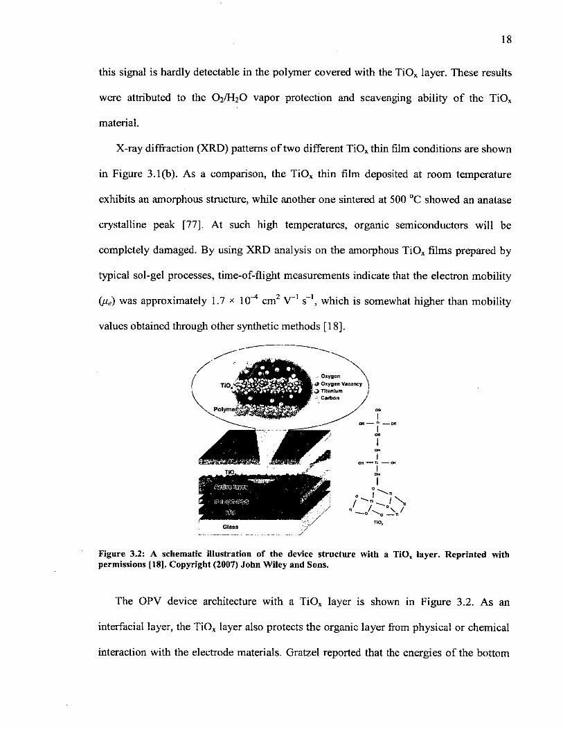
18
this signal is hardly detectable in the polymer covered with the TiOx layer. These results
were attributed to the O2/H2 O vapor protection and scavenging ability of the TiOx
material.
X-ray diffraction (XRD) patterns of two different TiOx thin film conditions are shown
in Figure 3.1(b). As a comparison, the TiOx thin film deposited at room temperature
exhibits an amorphous structure, while another one sintered at 500 °C showed an anatase
crystalline peak [77]. At such high temperatures, organic semiconductors will be
completely damaged. By using XRD analysis on the amorphous TiOx films prepared by
typical sol-gel processes, time-of-flight measurements indicate that the electron mobility
{pie) was approximately 1.7 x 10^ cm2 V- 1 s-1, which is somewhat higher than mobility
values obtained through other synthetic methods [18].
o OxygenOxygen Vacancy Titanium
; Carbon
Polymej
Figure 3.2: A schematic illustration of the device structure with a TiO* layer. Reprinted with permissions [18]. Copyright (2007) John Wiley and Sons.
The OPV device architecture with a TiOx layer is shown in Figure 3.2. As an
interfacial layer, the TiOx layer also protects the organic layer from physical or chemical
interaction with the electrode materials. Gratzel reported that the energies of the bottom
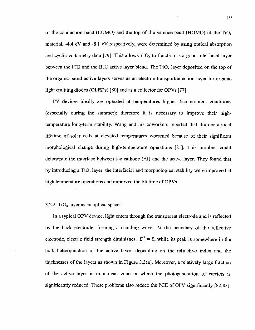
19
of the conduction band (LUMO) and the top of the valence band (HOMO) of the TiOx
material, -4.4 eV and -8 .1 eV respectively, were determined by using optical absorption
and cyclic voltametry data [79]. This allows TiOx to function as a good interfacial layer
between the ITO and the BHJ active layer blend. The TiOx layer deposited on the top of
the organic-based active layers serves as an electron transport/injection layer for organic
light emitting diodes (OLEDs) [80] and as a collector for OPVs [77],
PV devices ideally are operated at temperatures higher than ambient conditions
(especially during the summer); therefore it is necessary to improve their high-
temperature long-term stability. Wang and his coworkers reported that the operational
lifetime of solar cells at elevated temperatures worsened because of their significant
morphological change during high-temperature operations [81]. This problem could
deteriorate the interface between the cathode (Al) and the active layer. They found that
by introducing a TiOx layer, the interfacial and morphological stability were improved at
high temperature operations and improved the lifetime of OPVs.
3.2.2. TiOx layer as an optical spacer
In a typical OPV device, light enters through the transparent electrode and is reflected
by the back electrode, forming a standing wave. At the boundary of the reflective
electrode, electric field strength diminishes, |E|2 = 0, while its peak is somewhere in the
bulk heterojunction of the active layer, depending on the refractive index and the
thicknesses of the layers as shown in Figure 3.3(a). Moreover, a relatively large fraction
of the active layer is in a dead zone in which the photogeneration of carriers is
significantly reduced. These problems also reduce the PCE of OPV significantly [82,83].
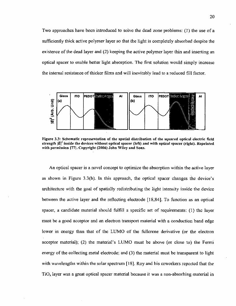
Two approaches have been introduced to solve the dead zone problems: (1) the use of a
sufficiently thick active polymer layer so that the light is completely absorbed despite the
existence of the dead layer and (2 ) keeping the active polymer layer thin and inserting an
optical spacer to enable better light absorption. The first solution would simply increase
the internal resistance of thicker films and will inevitably lead to a reduced fill factor.
rro pedot EH PEDOT
Figure 3.3: Schematic representation of the spatial distribution of the squared optical electric field strength [E|2 inside the devices without optical spacer (left) and with optical spacer (right). Reprinted with permission [77]. Copyright (2006) John Wiley and Sons.
An optical spacer is a novel concept to optimize the absorption within the active layer
as shown in Figure 3.3(b). In this approach, the optical spacer changes the device’s
architecture with the goal of spatially redistributing the light intensity inside the device
between the active layer and the reflecting electrode [18,84]. To function as an optical
spacer, a candidate material should fulfill a specific set of requirements: ( 1 ) the layer
must be a good acceptor and an electron transport material with a conduction band edge
lower in energy than that of the LUMO of the fullerene derivative (or the electron
acceptor material); (2) the material’s LUMO must be above (or close to) the Fermi
energy of the collecting metal electrode; and (3) the material must be transparent to light
with wavelengths within the solar spectrum [18]. Roy and his coworkers reported that the
TiOx layer was a great optical spacer material because it was a non-absorbing material in
the visible and infrared, the interference between the incident and reflected waves was
changed and therefore the position of maximum intensity was shifted [85]. The efficacy
of the TiOx layer depended not only on its optical constants and thickness, but also on the
optical constants and thickness of other layers within the device. Kim and his coworkers
have reported that the OPV device with the TiOx layer demonstrated a substantial
enhancement of about 40% in the incident photon-to-current efficiency (IPCE) over the
entire excitation spectral range [77]. The IPCE is defined as the number of photo
generated charge carriers contributing to the photocurrent per incident photon. This
enhancement was attributed to increased absorption in the BHJ layer as a result of using a
solution based TiOx layer as the optical spacer.
3.2.3. TiOx layer as an oxygen scavenger agent
As previously demonstrated in Chapter 2, the degradation behavior o f OPV cells
includes the direct photo-oxidation of BHJ active layer components. This problem leads
to a loss of conjugation and irreversible deterioration of the light absorbing properties, the
photochemical reduction of the organic constituents by the A1 electrode and a subsequent
chemical reaction between the organo-aluminum species and oxygen atoms [8 6 ]. The
solution based TiOx layer was also found to passivate the OPV device against intrusion of
oxygen and moisture into the electronically active polymers and to improve device
operating lifetimes [80,81,84,87]. The TiOx layer allows the flow of electrons and blocks
transport of holes.
Direct evidence of the oxygen barrier and scavenging effects came from the XPS
measurements as shown in Figure 3.1(a). Heeger’s group proposed two possible
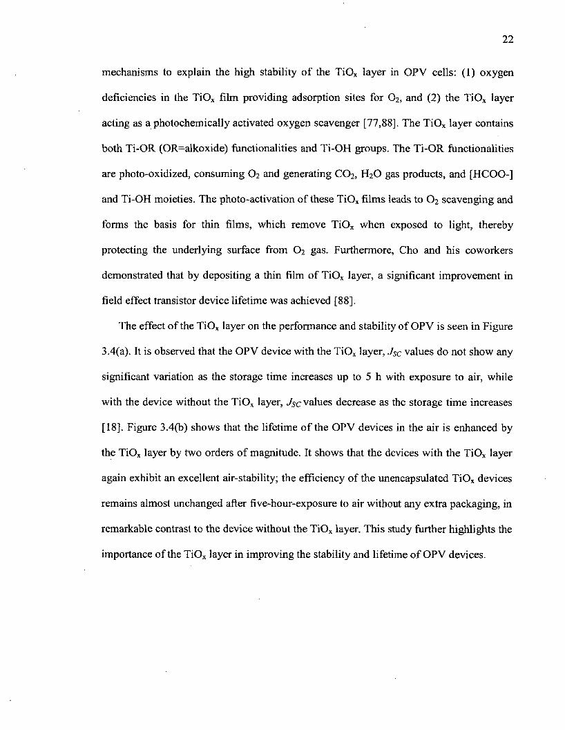
mechanisms to explain the high stability o f the TiOx layer in OPV cells: (1) oxygen
deficiencies in the TiOx film providing adsorption sites for O2 , and (2) the TiOx layer
acting as a photochemically activated oxygen scavenger [77,88]. The TiOx layer contains
both Ti-OR (OR=alkoxide) functionalities and Ti-OH groups. The Ti-OR functionalities
are photo-oxidized, consuming O2 and generating CO2 , H2 O gas products, and [HCOO-]
and Ti-OH moieties. The photo-activation of these TiOx films leads to O2 scavenging and
forms the basis for thin films, which remove TiOx when exposed to light, thereby
protecting the underlying surface from O2 gas. Furthermore, Cho and his coworkers
demonstrated that by depositing a thin film of TiOx layer, a significant improvement in
field effect transistor device lifetime was achieved [8 8 ].
The effect of the TiOx layer on the performance and stability of OPV is seen in Figure
3.4(a). It is observed that the OPV device with the TiOx layer, JSc values do not show any
significant variation as the storage time increases up to 5 h with exposure to air, while
with the device without the TiOx layer, J$c values decrease as the storage time increases
[18]. Figure 3.4(b) shows that the lifetime of the OPV devices in the air is enhanced by
the TiOx layer by two orders o f magnitude. It shows that the devices with the TiOx layer
again exhibit an excellent air-stability; the efficiency of the unencapsulated TiOx devices
remains almost unchanged after five-hour-exposure to air without any extra packaging, in
remarkable contrast to the device without the TiOx layer. This study further highlights the
importance of the TiOx layer in improving the stability and lifetime of OPV devices.
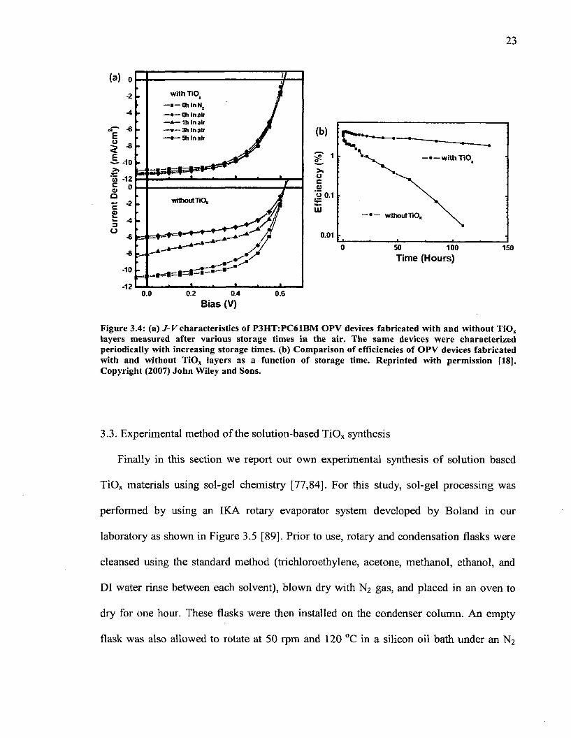
23
with TiO— ■— C h ln N , —• —Oh Inatr —*— 1h In air —*— 3hlnair —•— Sh Inalr
■a »
-10
W -12
without TiO,
-10 -
-120.0 0.2 0.4 0.6
—• —w ith TiO
O 0.1
— *— without TiO.
0.010 50 100 150
Time (Hours)
Bias (V)
Figure 3.4: (a) / - V characteristics of P3HT:PC61BM OPV devices fabricated with and without TiO, layers measured after various storage times in the air. The same devices were characterized periodically with increasing storage times, (b) Comparison of efficiencies of OPV devices fabricated with and without TiO, layers as a function of storage time. Reprinted with permission [18]. Copyright (2007) John Wiley and Sons.
3.3. Experimental method of the solution-based TiOx synthesis
Finally in this section we report our own experimental synthesis of solution based
TiOx materials using sol-gel chemistry [77,84], For this study, sol-gel processing was
performed by using an IKA rotary evaporator system developed by Boland in our
laboratory as shown in Figure 3.5 [89]. Prior to use, rotary and condensation flasks were
cleansed using the standard method (trichloroethylene, acetone, methanol, ethanol, and
DI water rinse between each solvent), blown dry with N2 gas, and placed in an oven to
dry for one hour. These flasks were then installed on the condenser column. An empty
flask was also allowed to rotate at 50 rpm and 120 °C in a silicon oil bath under an N2
environment for one hour to ensure all moisture was removed from the system. The
schematic diagram of the sol-gel TiOx synthesis is shown in Figure 3.6.
C ondense r co lu m n
^ Silicon oil b a th
C ondensa tion flask
Figure 3.5: An IKA rotary evaporator system.
The sol-gel procedure started with an injection of the precursor, in the following
order: (1) titanium (IV) isopropoxide (Ti(OCH(CH3)2)4 , 5 ml), (2) 2-methoxyethanol
(CH3 OCH2 CH2 OH, 20 ml), and (3) ethanolamine (H2NCH2 CH2OH, 2 ml) into the rotary
flask connected with a water condenser and nitrogen gas inlet/outlet at room temperature
[84]. Figure 3.7(a) shows the fresh initial solution. After stirring for one hour at room
temperature, the mixed solution was heated at 80 °C (using a silicon oil bath) for one
hour resulting in a dark orange colored solution as observed in Figure 3.7(b). During this
process, the inside of the flask must be in a dry N2 environment and the mixed solution
must be stirred continuously (600 - 800 rpm). The final step was to stir the mixed
solution at the same speed at an elevated temperature of 120 °C for another hour. At the
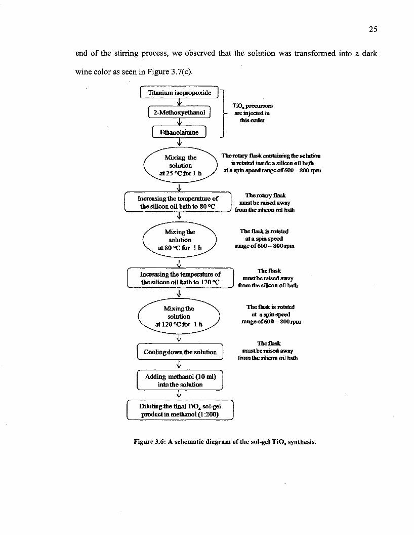
25
end of the stirring process, we observed that the solution was transformed into a dark
wine color as seen in Figure 3.7(c).
Ethano lamine
2-Methoxyethanol
Titanium isopropoxide
/ M3
TiO„ precursors - are injected in
this order
M ixing the The rotary flask containing the solution( solution ) is rotated inside a silicon oil bathV at25°C forlh / 31 a SP™ speed range o f600 — 800 rpm
Increasing the temperature o f the silicon oil bath to 80 °C
The rotary flask must be raised away
from die silicon oil bath
f Mixing thef solution J\ a t 80 °C for l h J
The flask is rotated at a spin speed
range o f600 — 800 ipm
Increasing the temperature of the silicon oil bath to 120 °C
The flask must be raised away
from the silicon oil bath
f Mixingthe( solutionN. at 120 °C for 1 h
Cooling down the solution
Adding methanol (10 ml) into the solution
Diluting the final TiOa sol-gel product in methanol (1:200)
The flask is rotated at a spin speed
range o f600 — 800rpm
The flask must be raised away
from die silicon oil bath
Figure 3.6: A schematic diagram of the sol-gel TiOx synthesis.
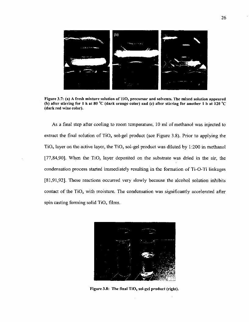
26
Figure 3.7: (a) A fresh mixture solution of TiO, precursor and solvents. The mixed solution appeared (b) after stirring for 1 h at 80 °C (dark orange color) and (c) after stirring for another 1 h at 120 °C (dark red wine color).
As a final step after cooling to room temperature, 10 ml of methanol was injected to
extract the final solution of TiOx sol-gel product (see Figure 3.8). Prior to applying the
TiOx layer on the active layer, the TiOx sol-gel product was diluted by 1: 2 0 0 in methanol
[77,84,90]. When the TiOx layer deposited on the substrate was dried in the air, the
condensation process started immediately resulting in the formation of Ti-O-Ti linkages
[81,91,92], These reactions occurred very slowly because the alcohol solution inhibits
contact of the TiOx with moisture. The condensation was significantly accelerated after
spin casting forming solid TiOx films.
Figure 3.8: The final TiO, sol-gel product (right).
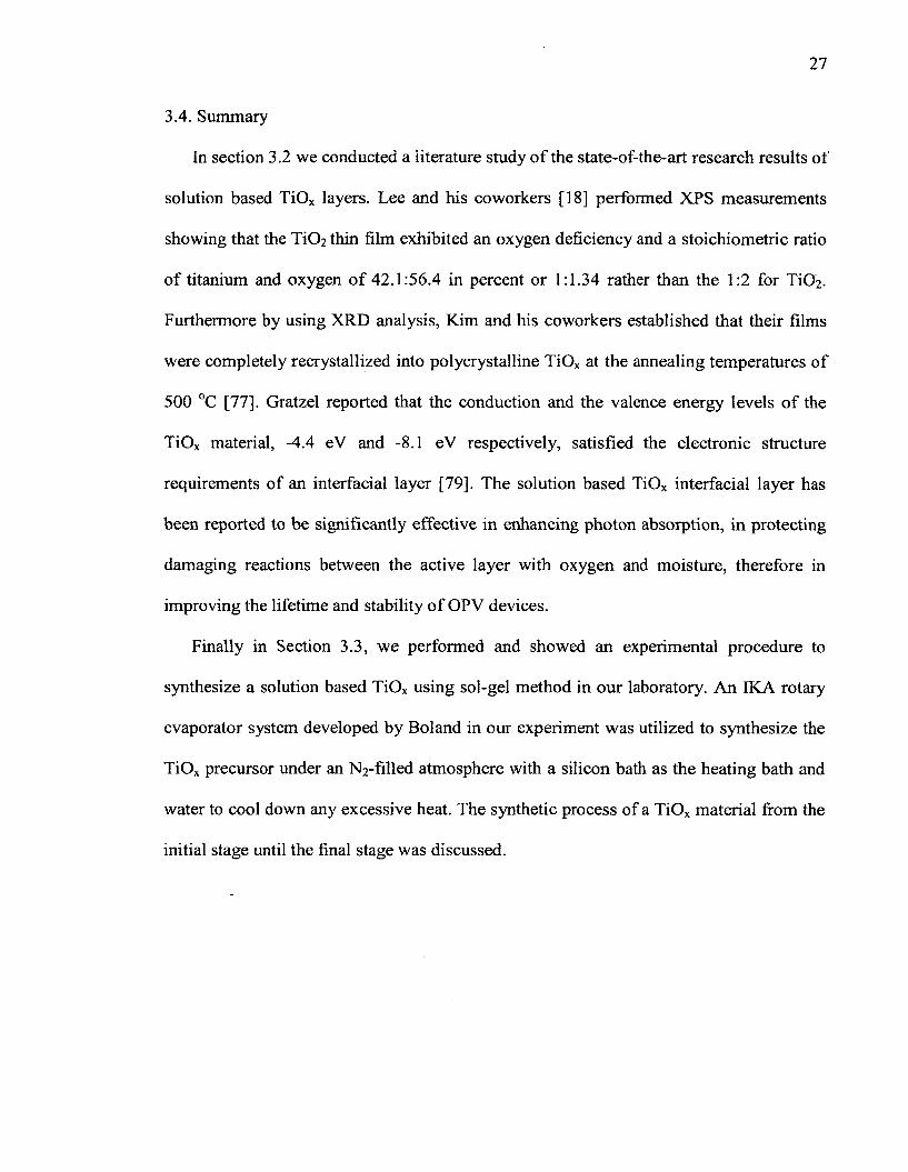
27
3.4. Summary
In section 3.2 we conducted a literature study of the state-of-the-art research results of
solution based TiOx layers. Lee and his coworkers [18] performed XPS measurements
showing that the TiC>2 thin film exhibited an oxygen deficiency and a stoichiometric ratio
of titanium and oxygen o f 42.1:56.4 in percent or 1:1.34 rather than the 1 : 2 for TiC>2 .
Furthermore by using XRD analysis, Kim and his coworkers established that their films
were completely recrystallized into polycrystalline TiOx at the annealing temperatures of
500 °C [77], Gratzel reported that the conduction and the valence energy levels of the
TiOx material, -4.4 eV and -8.1 eV respectively, satisfied the electronic structure
requirements of an interfacial layer [79]. The solution based TiOx interfacial layer has
been reported to be significantly effective in enhancing photon absorption, in protecting
damaging reactions between the active layer with oxygen and moisture, therefore in
improving the lifetime and stability of OPV devices.
Finally in Section 3.3, we performed and showed an experimental procedure to
synthesize a solution based TiOx using sol-gel method in our laboratory. An IKA rotary
evaporator system developed by Boland in our experiment was utilized to synthesize the
TiOx precursor under an N2 -filled atmosphere with a silicon bath as the heating bath and
water to cool down any excessive heat. The synthetic process of a TiOx material from the
initial stage until the final stage was discussed.
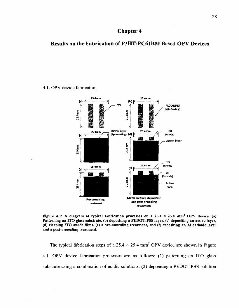
28
Chapter 4
Results on the Fabrication of P3HT:PC61BM Based OPV Devices
4.1. OPV device fabrication
25.4 mm 25.4 mm
PEDOT: PSS (Spin coating)
Active layer >| (Spin coating) (d) j<
25.4 mm25.4 mm
25.4 mm25.4 mm
(Cathode)
no(Anode)
Active layer
Pre-annealingtreatment
Metal contact deposition and post-annealing
treatm ent
Figure 4.1: A diagram of typical fabrication processes on a 25.4 x 25.4 mm2 OPV device, (a) Patterning an 1TO glass substrate, (b) depositing a PEDOT:PSS layer, (c) depositing an active layer, (d) cleaning 1TO anode films, (e) a pre-annealing treatment, and (f) depositing an A1 cathode layer and a post-annealing treatment.
The typical fabrication steps of a 25.4 x 25.4 mm OPV device are shown in Figure
4.1. OPV device fabrication processes are as follows: (1) patterning an ITO glass
substrate using a combination of acidic solutions, (2) depositing a PEDOT:PSS solution
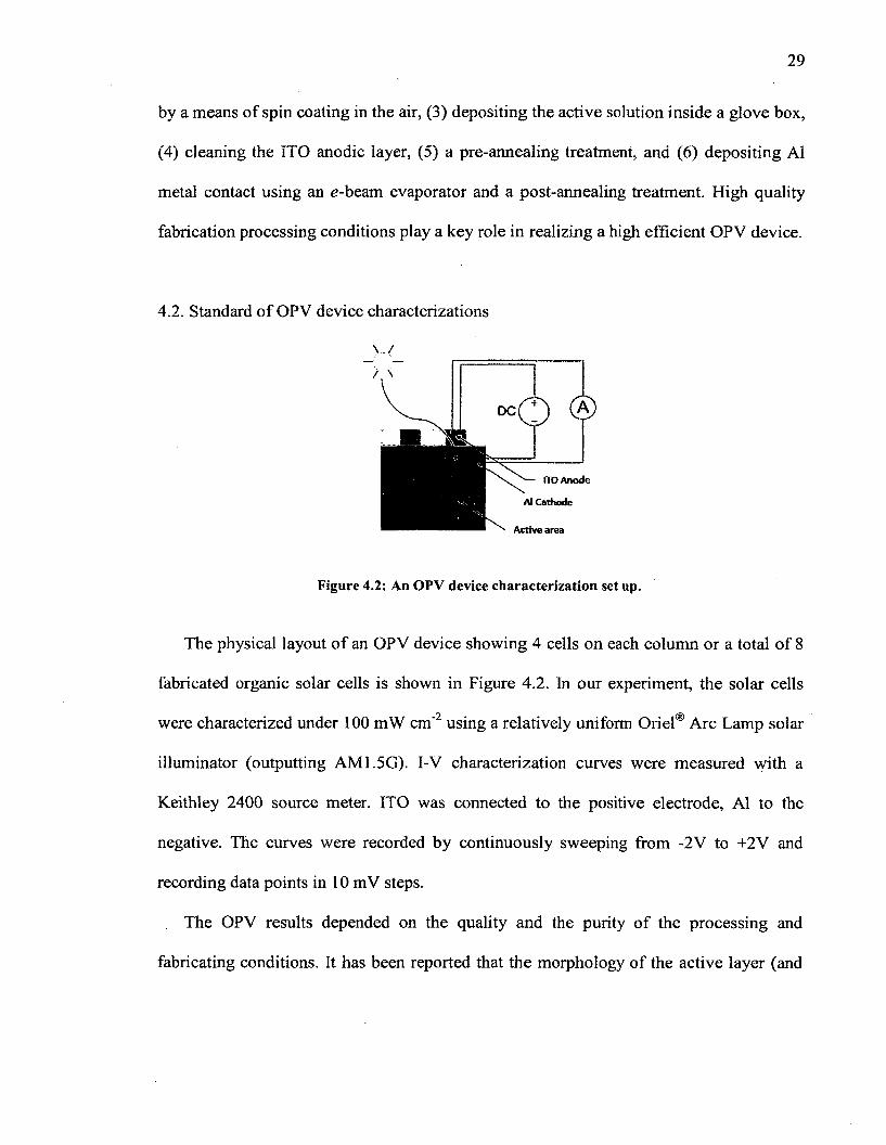
29
by a means of spin coating in the air, (3) depositing the active solution inside a glove box,
(4) cleaning the ITO anodic layer, (5) a pre-annealing treatment, and (6 ) depositing A1
metal contact using an e-beam evaporator and a post-annealing treatment. High quality
fabrication processing conditions play a key role in realizing a high efficient OPV device.
4.2. Standard of OPV device characterizations
\ /
/ \
The physical layout of an OPV device showing 4 cells on each column or a total of 8
fabricated organic solar cells is shown in Figure 4.2. In our experiment, the solar cells
illuminator (outputting AM1.5G). I-V characterization curves were measured with a
Keithley 2400 source meter. ITO was connected to the positive electrode, A1 to the
negative. The curves were recorded by continuously sweeping from -2V to +2V and
recording data points in 10 mV steps.
The OPV results depended on the quality and the purity of the processing and
fabricating conditions. It has been reported that the morphology of the active layer (and
Al Cathode
Active area
Figure 4.2: An OPV device characterization set up.
were characterized under 100 mW cm' 2 using a relatively uniform Oriel® Arc Lamp solar
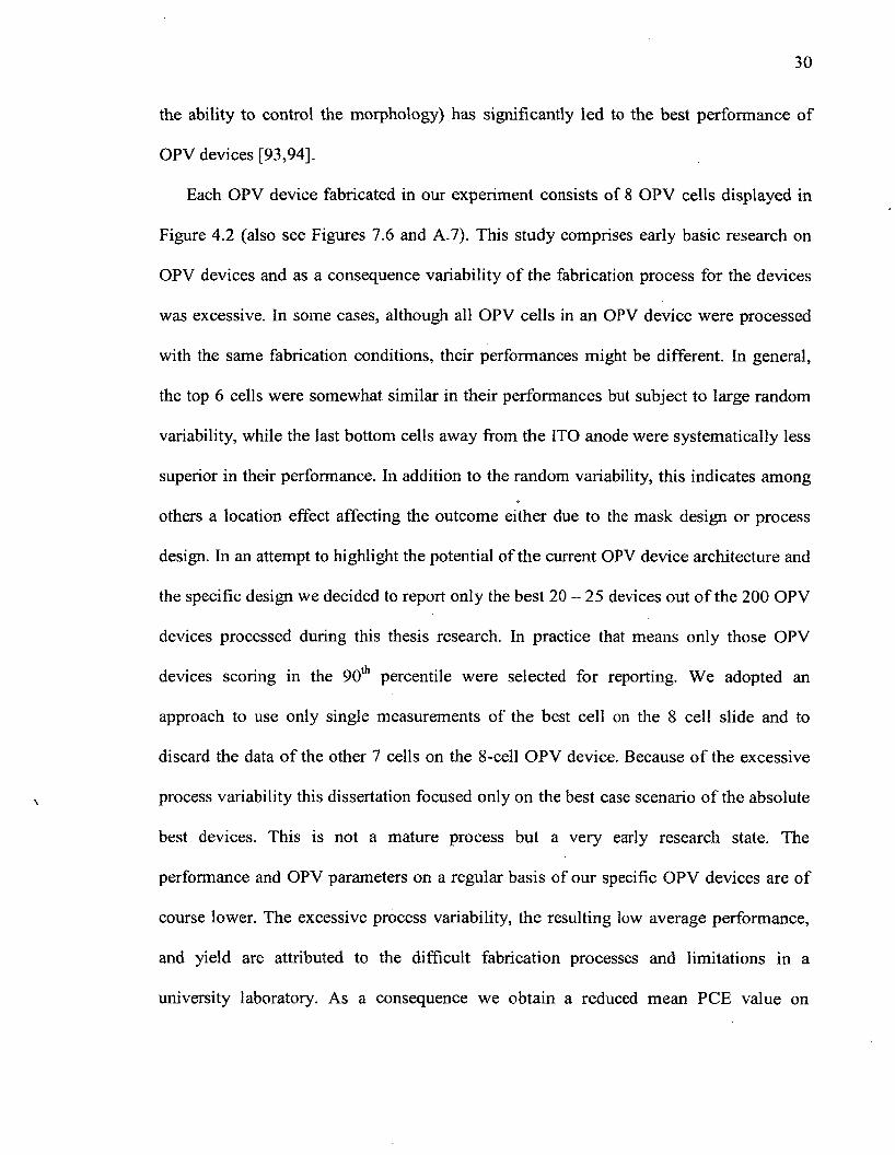
30
the ability to control the morphology) has significantly led to the best performance of
OPV devices [93,94].
Each OPV device fabricated in our experiment consists of 8 OPV cells displayed in
Figure 4.2 (also see Figures 7.6 and A.7). This study comprises early basic research on
OPV devices and as a consequence variability of the fabrication process for the devices
was excessive. In some cases, although all OPV cells in an OPV device were processed
with the same fabrication conditions, their performances might be different. In general,
the top 6 cells were somewhat similar in their performances but subject to large random
variability, while the last bottom cells away from the ITO anode were systematically less
superior in their performance. In addition to the random variability, this indicates among
others a location effect affecting the outcome either due to the mask design or process
design. In an attempt to highlight the potential of the current OPV device architecture and
the specific design we decided to report only the best 20 - 25 devices out of the 200 OPV
devices processed during this thesis research. In practice that means only those OPV
devices scoring in the 90th percentile were selected for reporting. We adopted an
approach to use only single measurements of the best cell on the 8 cell slide and to
discard the data of the other 7 cells on the 8 -cell OPV device. Because of the excessive
process variability this dissertation focused only on the best case scenario of the absolute
best devices. This is not a mature process but a very early research state. The
performance and OPV parameters on a regular basis of our specific OPV devices are of
course lower. The excessive process variability, the resulting low average performance,
and yield are attributed to the difficult fabrication processes and limitations in a
university laboratory. As a consequence we obtain a reduced mean PCE value on
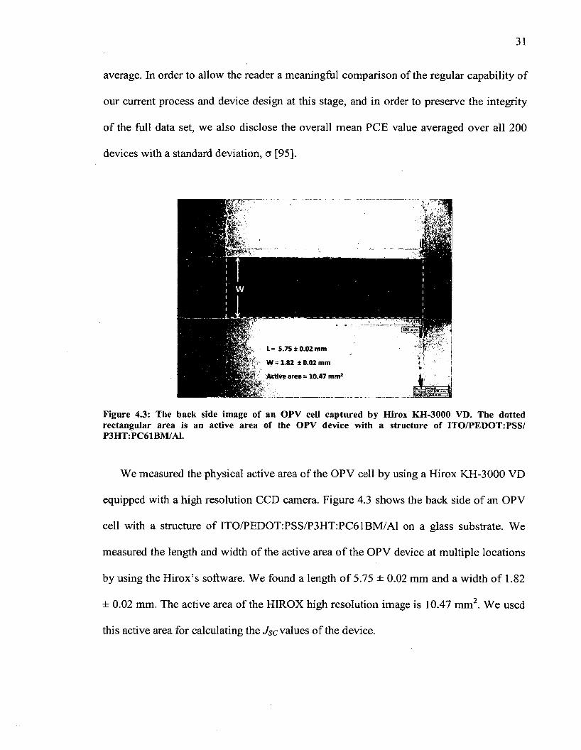
31
average. In order to allow the reader a meaningful comparison of the regular capability of
our current process and device design at this stage, and in order to preserve the integrity
of the full data set, we also disclose the overall mean PCE value averaged over all 200
devices with a standard deviation, a [95].
Active area = 10.47 mm1
Figure 4.3: The back side image of an OPV cell captured by Hirox KH-3000 VD. The dotted rectangular area is an active area of the OPV device with a structure of ITO/PEDOT:PSS/ P3HT :PC61BM/A1.
We measured the physical active area of the OPV cell by using a Hirox KH-3000 VD
equipped with a high resolution CCD camera. Figure 4.3 shows the back side of an OPV
cell with a structure of ITO/PEDOT:PSS/P3HT:PC61BM/Al on a glass substrate. We
measured the length and width of the active area of the OPV device at multiple locations
by using the Hirox’s software. We found a length of 5.75 ± 0.02 mm and a width of 1.82
± 0.02 mm. The active area of the HIROX high resolution image is 10.47 mm2. We used
this active area for calculating the Jsc values of the device.
32
4.3. P3HT.PC61BM OPV devices
PEDOT: S PSS «
-6.5 -
Figure 4.4: Energy levels of an OPV device of P3HT:PC61BM (with respect to the vacuum level).
We fabricated OPV devices using BHJ materials with P3HT as the electron donor and
PC61BM as the acceptor. The composition of the active blend of P3HT:PC61BM was
kept at a ratio of 1:0.8. The device structure for a high bandgap polymer OPV device is
ITO/PEDOT:PSS/P3HT:PC61BM/Al. The energy levels of an OPV device of P3HT:
PC61BM with respect to the vacuum level are shown in Figure 4.4. Aluminum with a
thickness of 80 nm was used as the metal contact. It was deposited by using an e-beam
evaporating system at a pressure of 2.0 x 10' 7 Torr. The influence of selected control
fabrication parameters, including the film thickness of the active layer, the pre- and post
annealing treatments on the structure evolution of polymer based BHJ systems is
important in achieving an optimal morphology of the active layer as discussed in this
chapter. Studies investigating the performance of polymer based BHJ systems based on
fabrication parameters were taken into account.
33
Optimization steps such as the active layer thickness and the annealing treatment are
important in OPV device fabrication. Since P3HT:PC61BM BHJ OPV devices have been
explored extensively in past decades, we focused on the optimization of experimental
conditions to achieve an excellent OPV device performance within the limitations of our
laboratory facility and environment.
4.4. Absorption study on the P3HT:PC61BM layer
We examined the annealing effect on the absorption of the P3HT:PC61BM thin film.
First, we deposited the active layer solution of P3HT:PC61BM onto two separate pre
cleaned glass substrates. Second, one of the coated substrates was annealed at a
temperature of 140 °C for 2 min inside a N2 -filled glove box atmosphere (O2 , H2 O <0.1
ppm), while the other was not. At a temperature slightly higher than the glass-transition
temperature (Tg) of P3HT, the polymer chains become soft and modify their matrix to
make an interpenetrating network of P3HT and PC61BM [96,97], Thermal annealing
increases inter-diffusion and mutual mixing of P3HT and PC61BM. Mixing of acceptor
and donor materials results in improved charge transport and device performance [96].
The PC61BM molecules diffuse out of the polymer matrix to form percolated paths upon
the annealing treatment on the P3HT:PC61BM composite film, resulting in an increase in
the carrier mobility in the active layer. Phase segregation between P3HT and PC61BM
also took place upon thermal treatment [98].
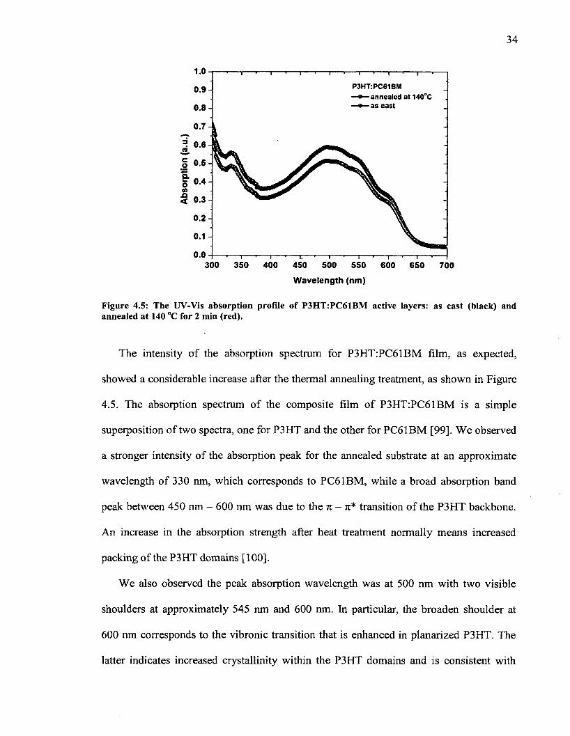
34
i.O
P3HT:PC61BM —• — annealed a t 140°C
• a s cast
0.9-
0 .8 -
0.7
0.5-
* 0.4-
< 0.3-
0 . 2 -
0.1 -
0.0300 350 400 450 500 550 600 650 700
Wavelength (nm)
Figure 4.5: The UV-Vis absorption profile of P3HT:PC61BM active layers: as cast (black) and annealed at 140 °C for 2 min (red).
The intensity of the absorption spectrum for P3HT:PC61BM film, as expected,
showed a considerable increase after the thermal annealing treatment, as shown in Figure
4.5. The absorption spectmm of the composite film of P3HT:PC61BM is a simple
superposition of two spectra, one for P3HT and the other for PC61BM [99]. We observed
a stronger intensity of the absorption peak for the annealed substrate at an approximate
wavelength of 330 nm, which corresponds to PC61BM, while a broad absorption band
peak between 450 nm - 600 nm was due to the 7C - n* transition of the P3HT backbone.
An increase in the absorption strength after heat treatment normally means increased
packing of the P3HT domains [100].
We also observed the peak absorption wavelength was at 500 nm with two visible
shoulders at approximately 545 nm and 600 nm. In particular, the broaden shoulder at
600 nm corresponds to the vibronic transition that is enhanced in planarized P3HT. The
latter indicates increased crystallinity within the P3HT domains and is consistent with
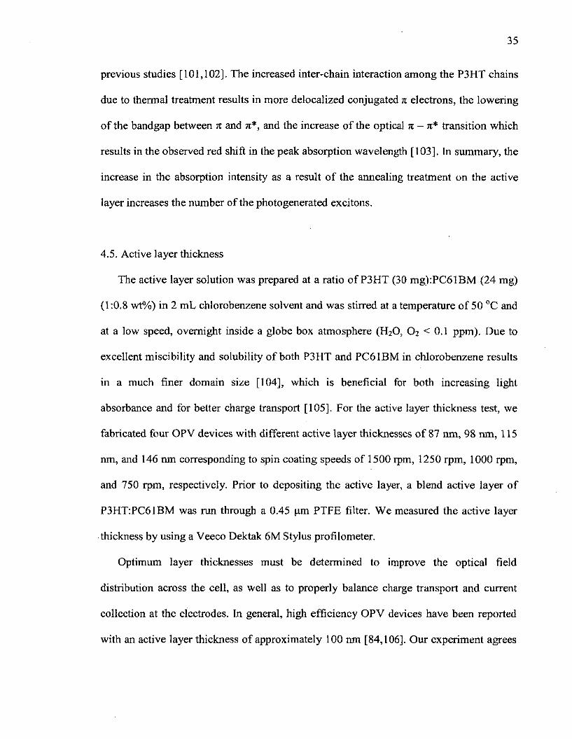
35
previous studies [101,102]. The increased inter-chain interaction among the P3HT chains
due to thermal treatment results in more delocalized conjugated n electrons, the lowering
of the bandgap between n and n*, and the increase of the optical n - n * transition which
results in the observed red shift in the peak absorption wavelength [103]. In summary, the
increase in the absorption intensity as a result of the annealing treatment on the active
layer increases the number of the photogenerated excitons.
4.5. Active layer thickness
The active layer solution was prepared at a ratio of P3HT (30 mg):PC61BM (24 mg)
(1:0.8 wt%) in 2 mL chlorobenzene solvent and was stirred at a temperature of 50 °C and
at a low speed, overnight inside a globe box atmosphere (H2O, O2 < 0.1 ppm). Due to
excellent miscibility and solubility of both P3HT and PC61BM in chlorobenzene results
in a much finer domain size [104], which is beneficial for both increasing light
absorbance and for better charge transport [105]. For the active layer thickness test, we
fabricated four OPV devices with different active layer thicknesses of 87 nm, 98 nm, 115
nm, and 146 nm corresponding to spin coating speeds of 1500 rpm, 1250 rpm, 1000 rpm,
and 750 rpm, respectively. Prior to depositing the active layer, a blend active layer of
P3HT:PC61BM was run through a 0.45 pm PTFE filter. We measured the active layer
thickness by using a Veeco Dektak 6 M Stylus profilometer.
Optimum layer thicknesses must be determined to improve the optical field
distribution across the cell, as well as to properly balance charge transport and current
collection at the electrodes. In general, high efficiency OPV devices have been reported
with an active layer thickness of approximately 100 nm [84,106]. Our experiment agrees
36
with these results. From the current density (JSc) level and high fill factor (FF) values
attained in our experiment we know that the OPV devices we fabricated were near an
optimum condition.
Device structure:ITO/PEDOT;PSS/P3HT:PC61BM/AIDifferent thicknesses of active layer- 0 —148 nm—V —121 nm—0 —87 nm^ > -“99 nm
1---------'---------1---------'---------1-------- *---------1---------'---------1-------- *---------1--------«---------T "0.0 0.1 0.2 0.3 0.4 0.5 0.6
Voltage (V)
Figure 4.6: J- V characteristics of P3HT:PC61BM OPV cells fabricated at different thicknesses of the active layer.
The J- V curves of the OPV cells fabricated at different thicknesses of the active layer
are shown in Figure 4.6. Each data represents the optimal performance of a single OPV
cell in the respected OPV devices. We found that a 98-nm thickness of the active layer
yielded the best results with an FF value of approximately 62% and a PCE value of 3.8%.
The optimal fabrication condition (the active layer thickness) resulted in an increased
photocurrent due to the increase in both charge mobility and absorption (where the space
charge limit was reached). As shown in Table 4.1, as the active layer thickness of OPV/
cells increases, the Jsc, FF, and PCE values decrease, due mainly to the build-up of space
charge, the increase of the series resistance, and recombination issues [107]. When the
active solution was too thin, we observed the PCE value dropping slightly, possibly due
37
to the condition of organic semiconductor materials producing excitons not in the
optimum condition.
Table 4.1: The parameters of P3HT:PC61BM OPV cells fabricated at different active layer thicknesses.
Active layer thickness (nm) Jsc (mA cm ') VOC (V) FF (%) PCE (%)87 8.80 0.61 58.69 3.1398 10.07 0.61 61.69 3.80121 7.43 0.60 56.71 2.52146 6.06 0.60 54.56 1.98
4.6. Pre-annealing treatment
The best annealing temperature achieving the most favorable morphological
development of the OPV cell is normally above the glass-transition temperature, Tg, but
below the melting point of the polymer [108]. The crystallinity of the polymer could also
be improved by using a pre-annealing treatment process. This approach aims at
maintaining the polymer ordering during the film formation stage. Reducing the solvent
removal accelerates results in self-organization in polymer chains by controlling the
active polymer layer growth rate from solution to a solid state. Pre-annealed films consist
of highly ordered polymer chains, which cannot be achieved through thermal annealing.
The extra step of annealing the films provides further enhancement in device
performance [109], In general, a pre-annealing temperature of 140 °C was used. For the
pre-annealing test, we fabricated OPV devices with different pre-annealing times of 2
min, 4 min, and 8 min. We also fabricated a separate OPV device without the pre
annealing treatment as a comparison. In this particular OPV fabrication, other fabrication
conditions (the thickness of the active layer and post-annealing treatment parameters)
were fixed.
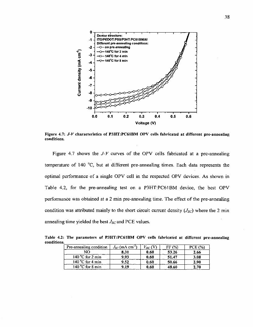
38
. Device structure:■1 - ITO/PEDOT:PSS/P3HT:PC61 BM/AI
- Different pre-annealing conditions: •2 - —O—no pre-annealing
—O — 140°C for 2 min ■3“ —o — 140°C for 4 min - " —v —140°Cfor8 min
0.0 0.1 0.2 0.3 0.4 0.5 0.6Voltage (V)
Figure 4.7: J-V characteristics of P3HT:PC61BM OPV cells fabricated at different pre-annealing conditions.
Figure 4.7 shows the J-V curves of the OPV cells fabricated at a pre-annealing
temperature of 140 °C, but at different pre-annealing times. Each data represents the
optimal performance of a single OPV cell in the respected OPV devices. As shown in
Table 4.2, for the pre-annealing test on a P3HT:PC61BM device, the best OPV
performance was obtained at a 2 min pre-annealing time. The effect o f the pre-annealing
condition was attributed mainly to the short circuit current density (Jsc) where the 2 min
annealing time yielded the best Jsc and PCE values.
Table 4.2: The parameters of P3HT:PC61BM OPV cells fabricated at different pre-annealing conditions.
Pre-annealing condition Jsc (mA cm2) Voc (V) FF (%) PCE (%)NO 8.31 0.60 53.26 2.66
140 °C for 2 min 9.93 0.60 51.47 3.08140 °C for 4 min 9.52 0.60 50.66 2.90140 °C for 8 min 9.19 0.60 48.60 2.70
39
The pre-annealing step has not only improved the blend of active layer by adhering it
more strongly to the substrate, but it also enhanced the photocurrent of the device. This
finding suggests that a pre-annealing time of 2 min is sufficient to allow optimal
reorganization of the morphology, or that thermal annealing provides a more effective
driving force for reorganization of the film. Longer annealing times resulted in a decrease
in the peak efficiency of this device, likely as a result of phase segregation taking place
on a larger than optimal length scale [110]. The OPV device fabricated without pre
annealing treatment did not show good results compared to other OPV devices with pre
annealing treatment.
4.7. Post-annealing treatment
The final optimization step in a P3HT:PC61BM OPV device is the post-production
thermal annealing treatment. This step is also known as the post-annealing treatment. The
effect of the post-annealing treatment on P3HT:PC61BM OPV devices has been studied
and reported elsewhere [34,101,111]. A post-annealing temperature of 150 °C has been
reported to be commonly used in fabricating solar cells [81,112], We fabricated OPV
devices with different post-annealing times of 5 min, 10 min, 20 min, and 30 min. As a
comparison, we also fabricated a separate OPV device without the post-annealing
treatment.
Figure 4.8 shows the J-V curves of the P3HT:PC61BM BHJ OPV cells fabricated at
different post-annealing conditions. Each data represents the optimal performance of a
single OPV cell in the respected OPV devices. The post-annealing treatment on the OPV
device showed an increase of the short current density originating from an increase of the
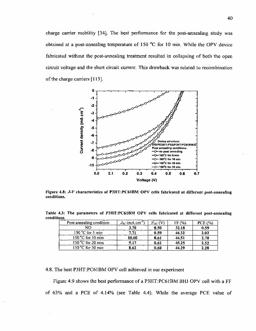
40
charge carrier mobility [34]. The best performance for the post-annealing study was
obtained at a post-annealing temperature of 150 °C for 10 min. While the OPV device
fabricated without the post-annealing treatment resulted in collapsing of both the open
circuit voltage and the short circuit current. This drawback was related to recombination
of the charge carriers [113].
<J Device structure: TTO/PEDOT:PSS/P3HT:PC61 BM/AJ Post annealing conditions:—O - no post annealing - V - 150°C for 6 min —O— 160“C for 10 min -a — 1S0°C for 20 min —O-ISO'CforSOmin
0.0 0.1 0.2 0.3 0.4 0.5 0.6 0.7V oltage (V)
Figure 4.8: J-V characteristics of P3HT:PC61BM OPV cells fabricated at different post-annealing conditions.
Table 4.3: The parameters of P3HT:PC61BM OPV cells fabricated at different post-annealing conditions.
Post annealing condition Jsc (mA cm'2) Voc(V) FF (%) PCE (%)NO 3.70 0.50 32.18 0.59
150 °C for 5 min 7.71 0.59 44.32 2.02150 °C for 10 min 10.00 0.61 44.51 2.70150 °C for 20 min 9.17 0.61 45.25 2.52150 °C for 30 min 8.62 0.60 44.29 2.28
4.8. The best P3HT:PC61BM OPV cell achieved in our experiment
Figure 4.9 shows the best performance of a P3HT:PC61BM BHJ OPV cell with a FF
of 63% and a PCE of 4.14% (see Table 4.4). While the average PCE value of
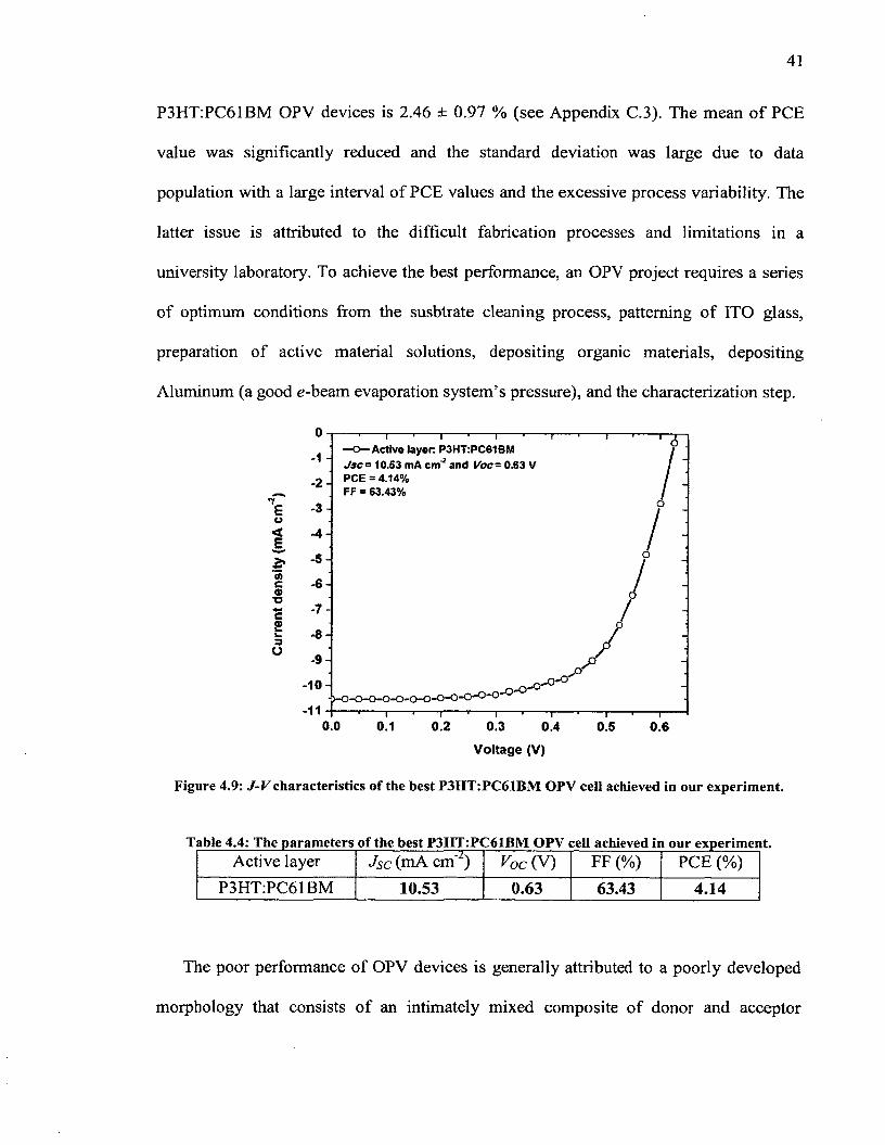
41
P3HT:PC61BM OPV devices is 2.46 ± 0.97 % (see Appendix C.3). The mean of PCE
value was significantly reduced and the standard deviation was large due to data
population with a large interval of PCE values and the excessive process variability. The
latter issue is attributed to the difficult fabrication processes and limitations in a
university laboratory. To achieve the best performance, an OPV project requires a series
of optimum conditions from the susbtrate cleaning process, patterning of ITO glass,
preparation of active material solutions, depositing organic materials, depositing
Aluminum (a good e-beam evaporation system’s pressure), and the characterization step.
0-|-1 -
-2-CME -3-o< -4-E& -5-tf>c -6-
T3>*■* -7-?k. *8 -u -9-
-10-
-11 -
1-------■-------1-------'-------r—o - Active layer; P3HT:PC61BM Jsc= 10.53 mA cm’ and V oc- 0.63 V PCE = 4.14%FF = 63.43%
— ’— T
>-0-0-0-O-O-O-O-O-O-0-0-0,-0- 0'
1-0 ^°
o/o
/
0.0 0.1 0.2 0.3 0.4Voltage (V)
0.5 0.6
Figure 4.9; J-V characteristics of the best P3HT:PC61BM OPV cell achieved in our experiment.
Active layer Jsc (mA cm_/) Voc (V) FF (%) PCE (%)P3HT:PC61BM 10.53 0.63 63.43 4.14
The poor performance of OPV devices is generally attributed to a poorly developed
morphology that consists of an intimately mixed composite of donor and acceptor
42
materials rather than a bi-continuous network of well-developed and ordered pathways
for the charge transport [114]. The intimate and homogenous mixing of components in
spin-coated films confirms that the interaction between P3HT and PC61BM is crucial in
the production of OPV devices with excellent performances.
4.9. Summary
We have demonstrated a fabrication procedure of OPV devices based on
P3HT:P61BM. We tested and optimized the fabrication procedure on a widely used blend
of active solution of P3HT:PC61BM (1:0.8 wt%). The weight concentration used in our
experiment was 30 mg of P3HT and 24 mg of PC61BM in a 2 mL chlorobenzene solvent.
Optimization steps including the thickness of the active layer, pre- and post annealing
treatments were performed in our experiments. The structural order of the organic
materials and the device is improved by using annealing treatment processes. We
investigated different optimization variables by means of fabricating OPV devices
directly. We found that the optimal thickness of the active layer was 100 nm, the optimal
pre-annealing condition was at 140 °C for 2 min, and the optimal post-annealing
condition was 150 °C for 10 min. Over 200 OPV devices of the blend active layer of
P3HT:PC61BM, of less than 10% resulted in PCE values of 4.06 ± 0.04 % (Table C.l).
While the average PCE value of P3HT:PC61BM OPV devices is 2.46 ± 0.97 % (see
Appendix C.3). In our study, the best OPV cell with the blend active solution of
P3HT:PC61BM fabricated using the optimal condition yielded a PCE of 4.14% with a Jsc
value of 10.53 mA cm'2, a Voc of 0.63 V, and a FF of 63%. These results are compatible
with the best OPV in the literature.
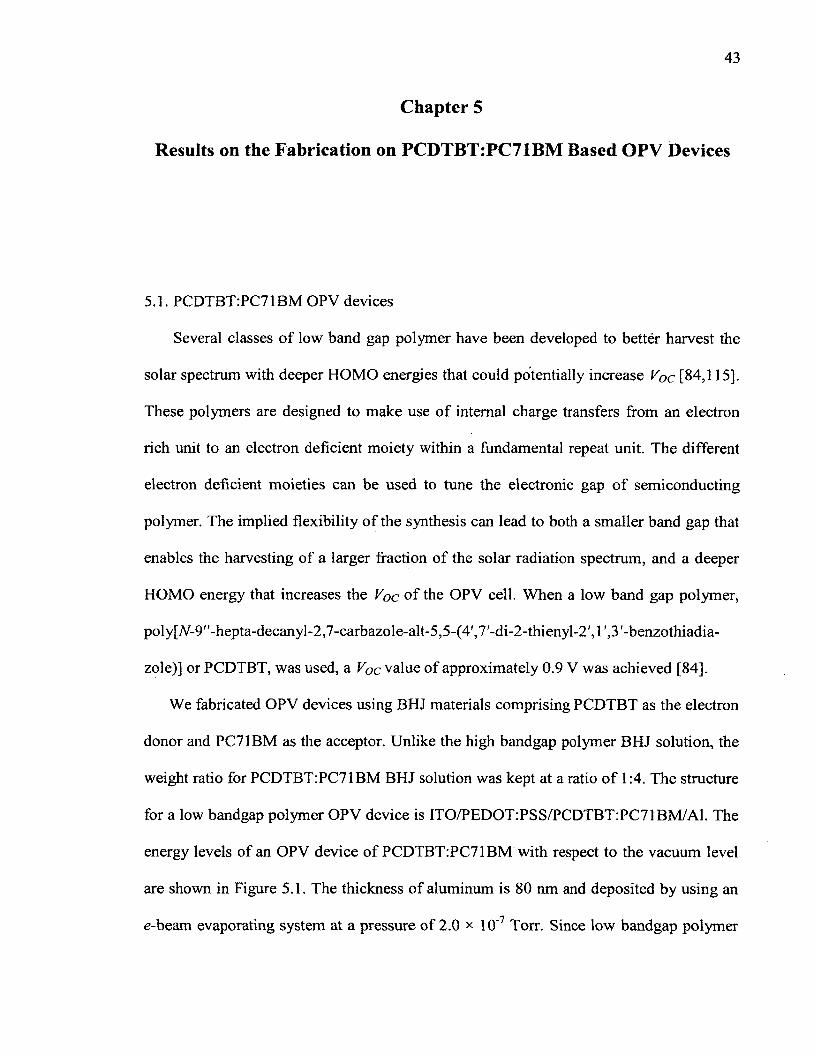
43
Chapter 5
Results on the Fabrication on PCDTBT:PC71BM Based OPV Devices
5.1. PCDTBT:PC71BM OPV devices
Several classes of low band gap polymer have been developed to better harvest the
solar spectrum with deeper HOMO energies that could potentially increase Voc [84,115],
These polymers are designed to make use of internal charge transfers from an electron
rich unit to an electron deficient moiety within a fundamental repeat unit. The different
electron deficient moieties can be used to tune the electronic gap of semiconducting
polymer. The implied flexibility of the synthesis can lead to both a smaller band gap that
enables the harvesting of a larger fraction of the solar radiation spectrum, and a deeper
HOMO energy that increases the Voc of the OPV cell. When a low band gap polymer,
poly[yV-9"-hepta-decanyl-2,7-carbazole-alt-5,5-(4,,7'-di-2-thienyl-2', 1 ',3 '-benzothiadia-
zole)] or PCDTBT, was used, a Voc value of approximately 0.9 V was achieved [84].
We fabricated OPV devices using BHJ materials comprising PCDTBT as the electron
donor and PC71BM as the acceptor. Unlike the high bandgap polymer BHJ solution, the
weight ratio for PCDTBT:PC71BM BHJ solution was kept at a ratio o f 1:4. The structure
for a low bandgap polymer OPV device is lTO/PEDOT:PSS/PCDTBT:PC71BM/Al. The
energy levels of an OPV device of PCDTBT:PC71BM with respect to the vacuum level
are shown in Figure 5.1. The thickness of aluminum is 80 nm and deposited by using an
e-beam evaporating system at a pressure of 2.0 x 10~7 Torr. Since low bandgap polymer
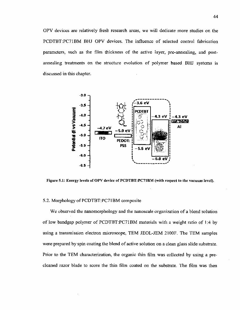
44
OPV devices are relatively fresh research areas, we will dedicate more studies on the
PCDTBT:PC71BM BHJ OPV devices. The influence of selected control fabrication
parameters, such as the film thickness of the active layer, pre-annealing, and post
annealing treatments on the structure evolution of polymer based BHJ systems is
discussed in this chapter.
-3.0
-3.5
| -4.0
£ *W -4.5>uIB - 5 0 -J **gf -5.5 H ol
•6,0
-6,5 H
f-3 .6 eV
—4.7 eV -5 .0 eV
ITO PEDOT:PSS
PCDTBT- 4 .3 eV
-5 .5 eV
6.0 eV
-4 .3 eV□SAl
Figure 5.1: Energy levels of OPV device of PCDTBT:PC71BM (with respect to the vacuum level).
5.2. Morphology of PCDTBT:PC7IBM composite
We observed the nanomorphology and the nanoscale organization of a blend solution
of low bandgap polymer of PCDTBT:PC71BM materials with a weight ratio of 1:4 by
using a transmission electron microscope, TEM JEOL-JEM 21 OOF. The TEM samples
were prepared by spin coating the blend of active solution on a clean glass slide substrate.
Prior to the TEM characterization, the organic thin film was collected by using a pre
cleaned razor blade to score the thin film coated on the substrate. The film was then
45
rinsed with DI water using an ultrasonic bath. The film that was floating on the surface of
the water was deposited onto a TEM copper grid and then dried at room temperature.
rt. ■/ r ■ vnariUQgsfe'tsyj.
Figure 5.2: TEM images of PCDTBT:PC71BM composite with (a) low and (b) high resolutions.
Figure 5.2(a) shows a low resolution of the composite film of PCDTBT:PC71BM on
the TEM copper grid. We observed in Figure 5.2(b) that PC71BM nanoclusters were
formed and the ‘fibrillar’ PCDTBT nanostructures blended smoothly in a composite of
PCDTBT:PC71BM with 1:4 weight ratio solutions. The PC7*1BM molecules can diffuse
in the polymer matrix to form nanocluster domains [116]. In the kinetic theory of
crystallization, the nucleation of crystal begins at a certain temperature and forms small
but unstable clusters [117]. After nucleation of the PC71BM crystals and upon reaching a
46
certain size, it can provide a growth surface for further crystallization. The diffused
PC71BM molecules further growth of the crystal into a nanocluster.
The increasing amount of PC71BM has been reported to cause the PCDTBT network
to form longer and better connected pathways [84]. The PC71BM nanoclusters in the
active layer provide efficient percolation paths for photogenerated charges. With better
electron transportation in the composite film, there is improved photocurrent which
facilitates better device performance. The TEM results show clearly that it is very
important to consider the nanomorphology of PCDTBT:PC71BM interpenetrating
networks resulting in an optimized and stable phase separation for efficient charge
separation and transport. In turn this leads to thermal stability, the optimum PCDTBT:
PC71BM nanomorphology, which will enhance the efficiency of the BHJ OPV devices.
5.3. Absorption study of the PCDTBT:PC71BM layer
In contrast to the traditional first generation conjugated polymers (polyacetylene,
polythiophene, and poly(phenylene-vinylene) [118], the PCDTBT absorption spectrum,
as seen in Figure 5.3, exhibits two distinct absorption bands centered at approximately
400 nm and 580 nm. Similar double peak absorption has been observed in other
alternating acceptor/donor copolymers [119]. Two absorption peaks were previously
attributed to 71 - 7 1 * transitions with a lower energy peak associated with intra-chain charge
transfer [120], The absorption spectrum for the BHJ film shows additional absorption
from the PC71BM in the 2 eV - 3 eV ranges. For PC71BM, the spherical symmetry is
broken and forbidden transitions in the visible part of the spectrum become allowed
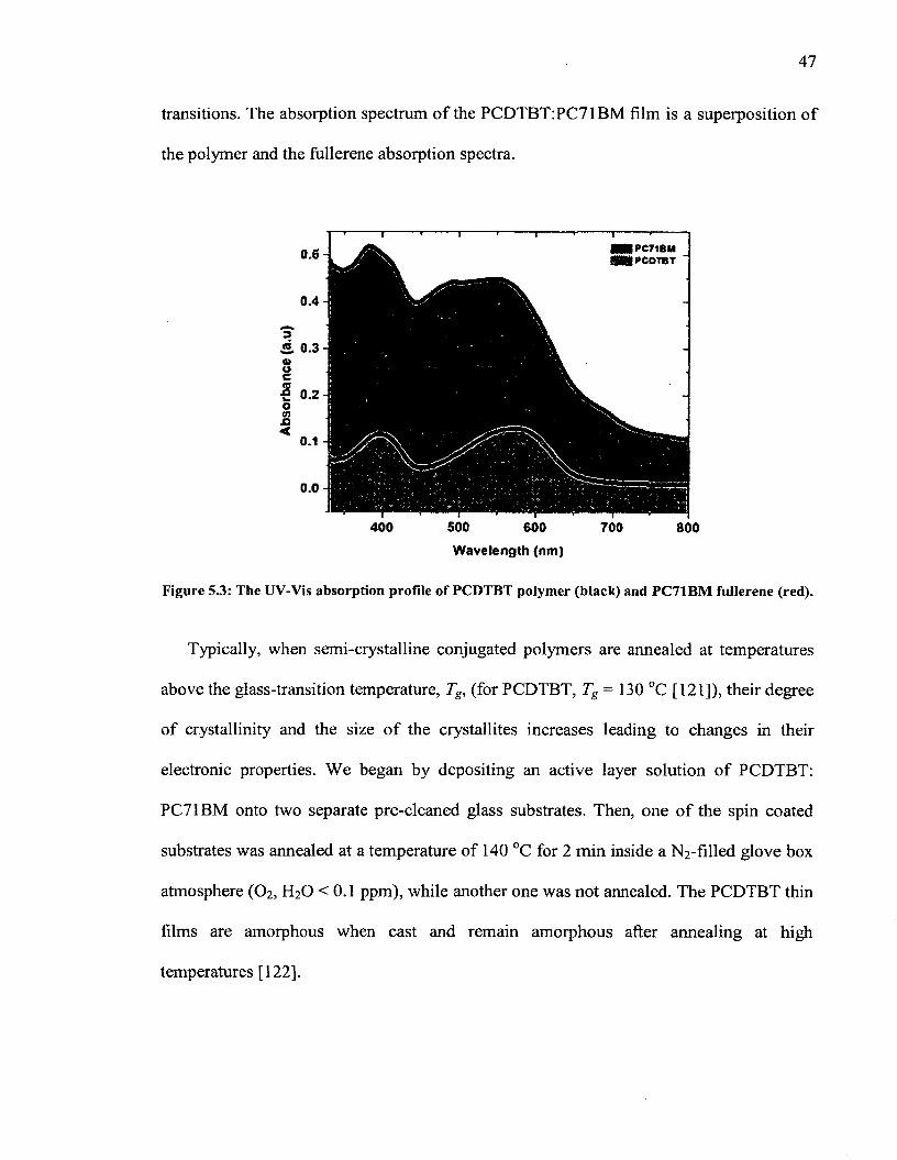
47
transitions. The absorption spectrum of the PCDTBT:PC71BM film is a superposition of
the polymer and the fullerene absorption spectra.
■ R P C 7 1 B M O H PCDTBT
400 500 600 700 800Wavelength (nm)
Figure 5.3: The UV-Vis absorption profile of PCDTBT polymer (black) and PC71BM fullerene (red).
Typically, when semi-crystalline conjugated polymers are annealed at temperatures
above the glass-transition temperature, Tg, (for PCDTBT, Tg = 130 °C [121]), their degree
of crystallinity and the size of the crystallites increases leading to changes in their
electronic properties. We began by depositing an active layer solution of PCDTBT:
PC71BM onto two separate pre-cleaned glass substrates. Then, one of the spin coated
substrates was annealed at a temperature of 140 °C for 2 min inside a N2 -filled glove box
atmosphere (O2 , H2 O <0.1 ppm), while another one was not annealed. The PCDTBT thin
films are amorphous when cast and remain amorphous after annealing at high
temperatures [1 2 2 ].
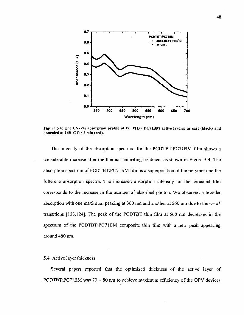
48
0.7PCDTBT:PC71BM ■ • annealed at 140°C
- • - as east0 .6 -
0.5-3
I® 0.4-
«0.3-
oto£»< 0 .2 -
0.1 -
0.0350 400 450 500 550 600 650 700
Wavelength (nm)
Figure 5.4: The UV-Vis absorption profile of PCDTBT:PC71BM active layers: as cast (black) and annealed at 140 °C for 2 min (red).
The intensity of the absorption spectrum for the PCDTBT:PC71BM film shows a
considerable increase after the thermal annealing treatment as shown in Figure 5.4. The
absorption spectrum of PCDTBT:PC71BM film is a superposition of the polymer and the
fullerene absorption spectra. The increased absorption intensity for the annealed film
corresponds to the increase in the number of absorbed photon. We observed a broader
absorption with one maximum peaking at 360 nm and another at 560 nm due to the n - n*
transitions [123,124], The peak of the PCDTBT thin film at 560 nm decreases in the
spectrum of the PCDTBT:PC71BM composite thin film with a new peak appearing
around 480 nm.
5.4. Active layer thickness
Several papers reported that the optimized thickness of the active layer of
PCDTBT:PC71BM was 70 - 80 nm to achieve maximum efficiency of the OPV devices
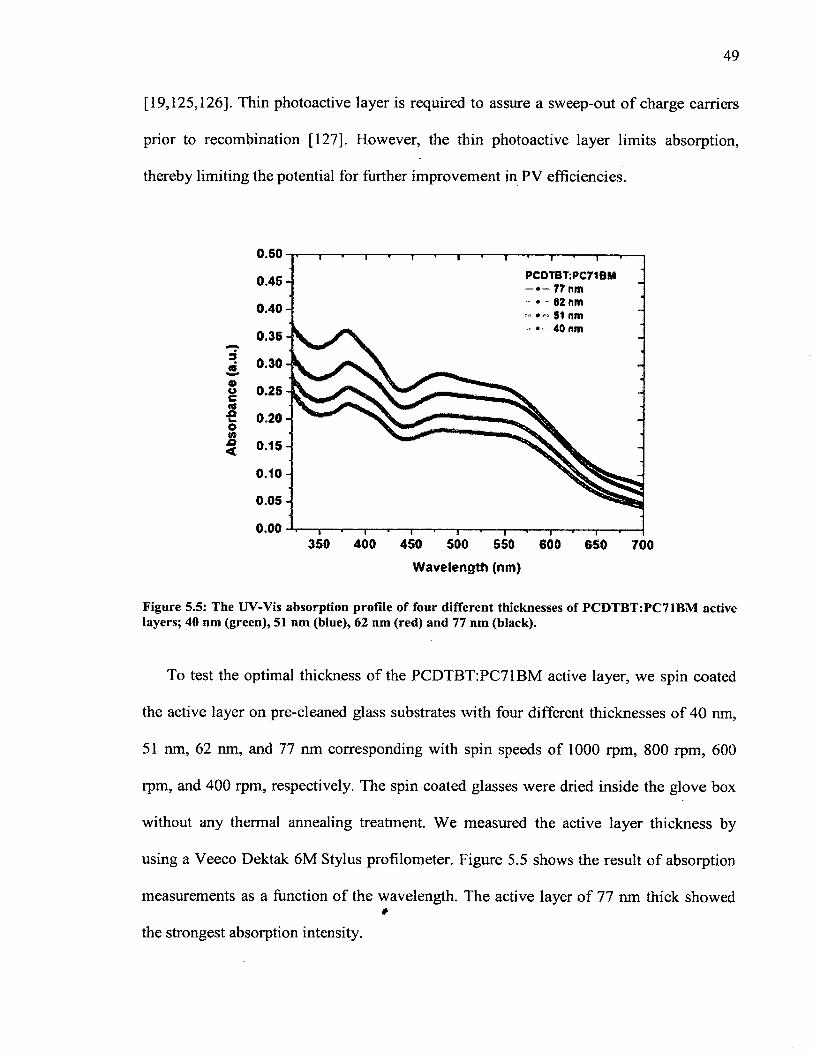
49
[19,125,126]. Thin photoactive layer is required to assure a sweep-out of charge carriers
prior to recombination [127]. However, the thin photoactive layer limits absorption,
thereby limiting the potential for further improvement in PV efficiencies.
0.50
0.45
0.40
0.35
i 0.30
| 0.25
-2 0.20 0W< 0 1 5
0.10
0.05
0.00
Wavelength (nm)
Figure 5.5: The UV-Vis absorption profile of four different thicknesses of PCDTBT:PC71BM active layers; 40 nm (green), 51 nm (blue), 62 nm (red) and 77 nm (black).
To test the optimal thickness of the PCDTBT:PC71BM active layer, we spin coated
the active layer on pre-cleaned glass substrates with four different thicknesses of 40 nm,
51 nm, 62 nm, and 77 nm corresponding with spin speeds of 1000 rpm, 800 rpm, 600
rpm, and 400 rpm, respectively. The spin coated glasses were dried inside the glove box
without any thermal annealing treatment. We measured the active layer thickness by
using a Veeco Dektak 6 M Stylus profilometer. Figure 5.5 shows the result of absorption
measurements as a function of the wavelength. The active layer of 77 nm thick showed*
the strongest absorption intensity.
PCOtBT: PC71BM —*—77 nm
62 nm SI nm 40 nm
700
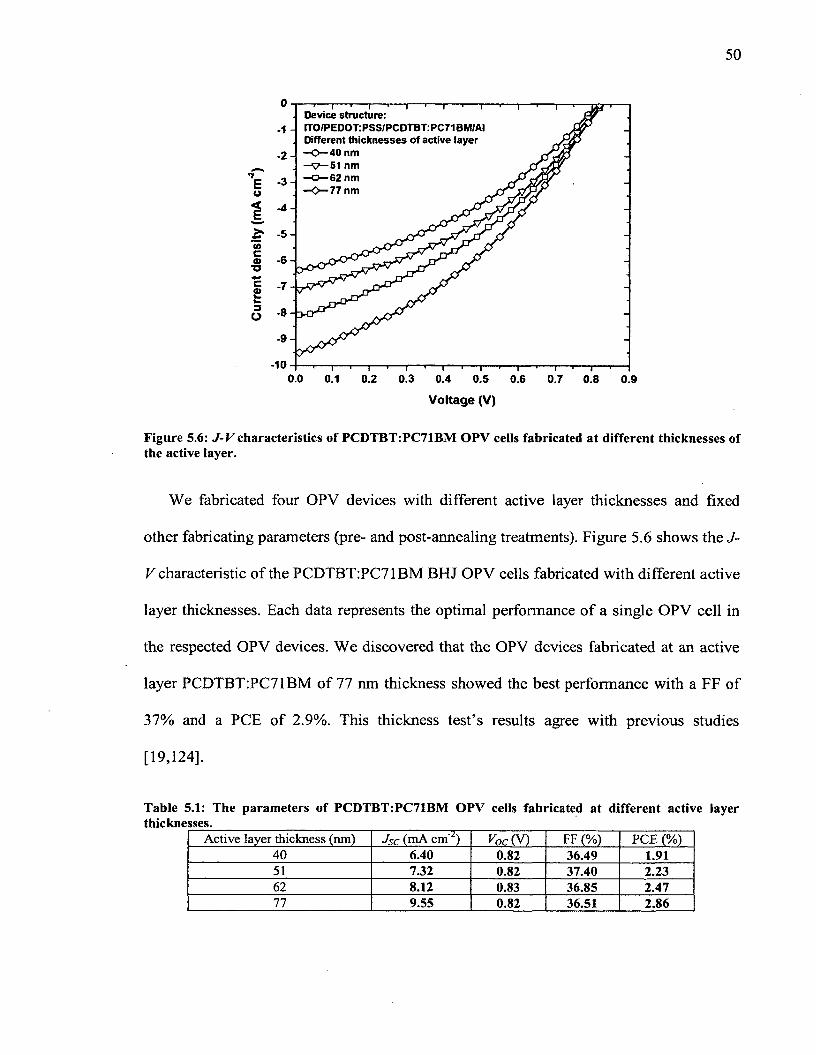
50
o -1
-2
\ *0
1 ^£ ' 5 w ca> -6 TJ
I 7o ■*
-9
-100.0 0.1 0.2 0.3 0.4 0.5 0.6 0.7 0.8 0.9
Voltage (V)
Figure 5.6: J-V characteristics of PCDTBT:PC71BM OPV cells fabricated at different thicknesses of the active layer.
We fabricated four OPV devices with different active layer thicknesses and fixed
other fabricating parameters (pre- and post-annealing treatments). Figure 5.6 shows the J-
V characteristic of the PCDTBT:PC71BM BHJ OPV cells fabricated with different active
layer thicknesses. Each data represents the optimal performance of a single OPV cell in
the respected OPV devices. We discovered that the OPV devices fabricated at an active
layer PCDTBT:PC71BM of 77 nm thickness showed the best performance with a FF of
37% and a PCE of 2.9%. This thickness test’s results agree with previous studies
[19,124],
Table 5.1: The parameters of PCDTBT:PC71BM OPV cells fabricated at different active layer thicknesses.
Active layer thickness (nm) Jsc (mA cm 2) VDC (V) FF (%) PCE (%)40 6.40 0.82 36.49 1.9151 7.32 0.82 37.40 2.2362 8.12 0.83 36.85 2.4777 9.55 0.82 36.51 2.86
Device structure:ITO/PEDOT:PSS/PCDTBT: PC71BM/AI Different thicknesses of active layer —0 —40 nm —ST—51 nm —0 —62 nm —C>—77 nm
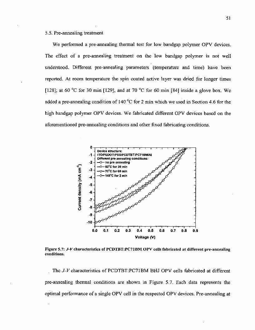
51
5.5. Pre-annealing treatment
We performed a pre-annealing thermal test for low bandgap polymer OPV devices.
The effect of a pre-annealing treatment on the low bandgap polymer is not well
understood. Different pre-annealing parameters (temperature and time) have been
reported. At room temperature the spin coated active layer was dried for longer times
[128]; at 60 °C for 30 min [129], and at 70 °C for 60 min [84] inside a glove box. We
added a pre-annealing condition of 140 °C for 2 min which we used in Section 4.6 for the
high bandgap polymer OPV devices. We fabricated different OPV devices based on the
aforementioned pre-annealing conditions and other fixed fabricating conditions.
Device structure:ITO/PEDOT:PSS/PCDTBT:PC71BM/AI Different pre-annealing conditions:—O— no pre-annealing —a — 60°C for 30 min —ST— 70°C for 60 min j- 0 - 140°C for 2 min r T
0.0 0.1 0.2 0.3 0.4 0.5 0.6 0.7 0.8 0.9Voltage (V)
Figure 5.7: J-V characteristics of PCDTBT:PC71BM OPV cells fabricated at different pre-annealing conditions.
The J-V characteristics of PCDTBT:PC71BM BHJ OPV cells fabricated at different
pre-annealing thermal conditions are shown in Figure 5.7. Each data represents the
optimal performance of a single OPV cell in the respected OPV devices. Pre-annealing at
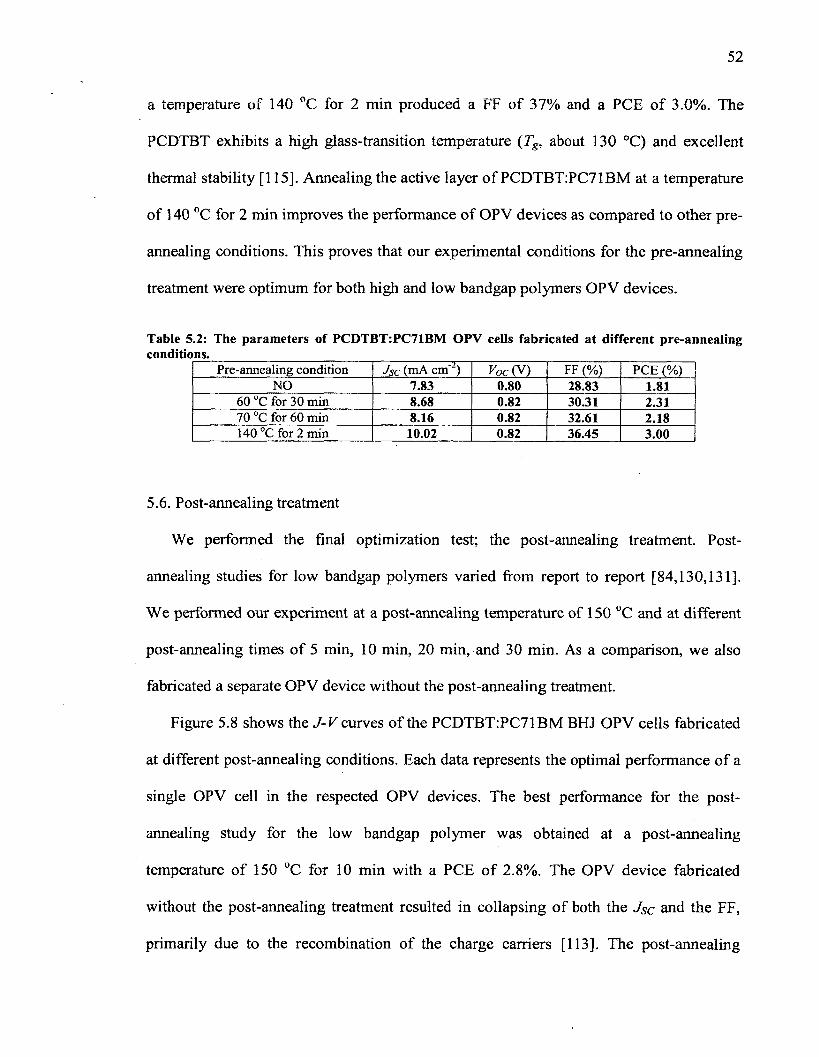
52
a temperature of 140 °C for 2 min produced a FF of 37% and a PCE of 3.0%. The
PCDTBT exhibits a high glass-transition temperature (Tg, about 130 °C) and excellent
thermal stability [115]. Annealing the active layer of PCDTBT:PC71BM at a temperature
of 140 °C for 2 min improves the performance of OPV devices as compared to other pre
annealing conditions. This proves that our experimental conditions for the pre-annealing
treatment were optimum for both high and low bandgap polymers OPV devices.
Table 5.2: The parameters of PCDTBT:PC71BM OPV cells fabricated at different pre-annealing conditions.
Pre-annealing condition Jsc (mA cm'2) Voc Of) FF (%) PCE (%)NO 7.83 0.80 28.83 1.81
60 °C for 30 min 8.68 0.82 30.31 2.3170 °C for 60 min 8.16 0.82 32.61 2.18140 °C for 2 min 10.02 0.82 36.45 3.00
5.6. Post-annealing treatment
We performed the final optimization test; the post-annealing treatment. Post
annealing studies for low bandgap polymers varied from report to report [84,130,131].
We performed our experiment at a post-annealing temperature of 150 °C and at different
post-annealing times of 5 min, 10 min, 20 min, and 30 min. As a comparison, we also
fabricated a separate OPV device without the post-annealing treatment.
Figure 5.8 shows the J-V curves of the PCDTBT:PC71BM BHJ OPV cells fabricated
at different post-annealing conditions. Each data represents the optimal performance of a
single OPV cell in the respected OPV devices. The best performance for the post
annealing study for the low bandgap polymer was obtained at a post-annealing
temperature of 150 °C for 10 min with a PCE of 2.8%. The OPV device fabricated
without the post-annealing treatment resulted in collapsing of both the Jsc and the FF,
primarily due to the recombination of the charge carriers [113]. The post-annealing
53
results for the low bandgap polymer show the same optimum condition as its high
bandgap counterpart. Due to the amorphous nature of PCDTBT and the complex
solubility and miscibility properties between PCDTBT and PC71BM, the effect of either
pre- or post-annealing treatments on the low bandgap is not well understood [132].
Device structure:ITO/PDEOT:PSS/PCDTBT:PC71 BM/AI. Different post-annealing conditions —O — no post-annealing —Q—150°C for 5 min -O — 150°C for 10 min -0-150°Cfor20m in
150°C for 30 min
Voltage (V)
Figure 5.8: J-V characteristics of PCDTBT:PC71BM OPV cells fabricated at different postannealing conditions.
Table 5.3: The parameters of PCDTBT:PC71BM OPV cells fabricated at different post-annealing conditions.
Post-annealing condition Jsc (mA cm"2) Voc (V) FF (%) PCE (%)NO 5.19 0.81 30.42 1.28
150 °C for 5 min 9.17 0.83 33.76 2.58150 °C for 10 min 9.75 0.84 33.47 2.75150 °C for 20 min 8.70 0.82 32.79 2.34150 °C for 30 min 8.29 0.81 32.64 2.20
5.7. Aged active solution study
The effect of an aged active solution on the performance of low bandgap polymers is
rarely reported. The aged active solution reportedly formed organic material aggregates
[133]. For a prolonged blend polymer operation, phase separation leads to spatial donor
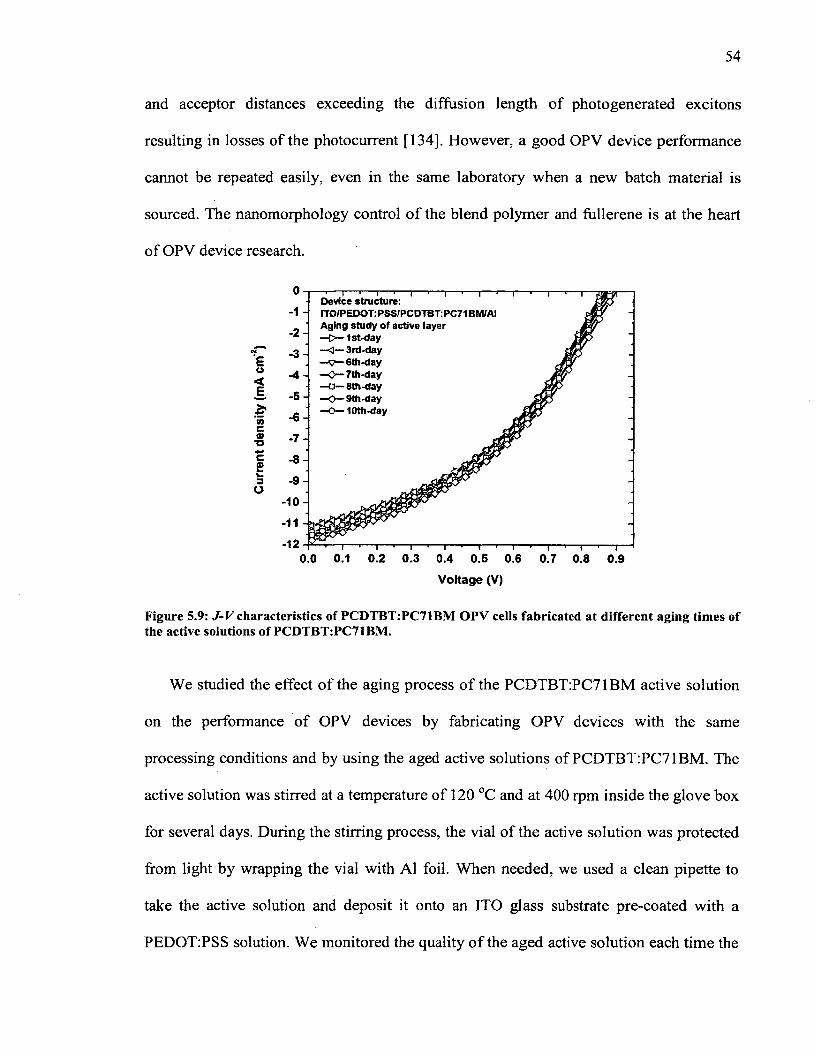
54
and acceptor distances exceeding the diffusion length of photogenerated excitons
resulting in losses of the photocurrent [134], However, a good OPV device performance
cannot be repeated easily, even in the same laboratory when a new batch material is
sourced. The nanomorphology control of the blend polymer and fullerene is at the heart
of OPV device research.
Device structure:ITCWPEDOT:PSS/PCDTBT:PC71BIWAI Aging study of active layer —1>—1st-day —<— 3rd-day —v — 6th -day —O— 7th -day —o —8 th -day —O—9th-day —O— 10th -day
0.0 0.1 0.2 0.3 0.4 0.5 0.6 0.7 0.8 0.9V oltage (V)
Figure 5.9: J -V characteristics of PCDTBT:PC71BM OPV cells fabricated at different aging times of the active solutions of PCDTBT:PC71BM.
We studied the effect of the aging process of the PCDTBT:PC71BM active solution
on the performance of OPV devices by fabricating OPV devices with the same
processing conditions and by using the aged active solutions of PCDTBT:PC71BM. The
active solution was stirred at a temperature of 120 °C and at 400 rpm inside the glove box
for several days. During the stirring process, the vial of the active solution was protected
from light by wrapping the vial with A1 foil. When needed, we used a clean pipette to
take the active solution and deposit it onto an ITO glass substrate pre-coated with a
PEDOT:PSS solution. We monitored the quality of the aged active solution each time the
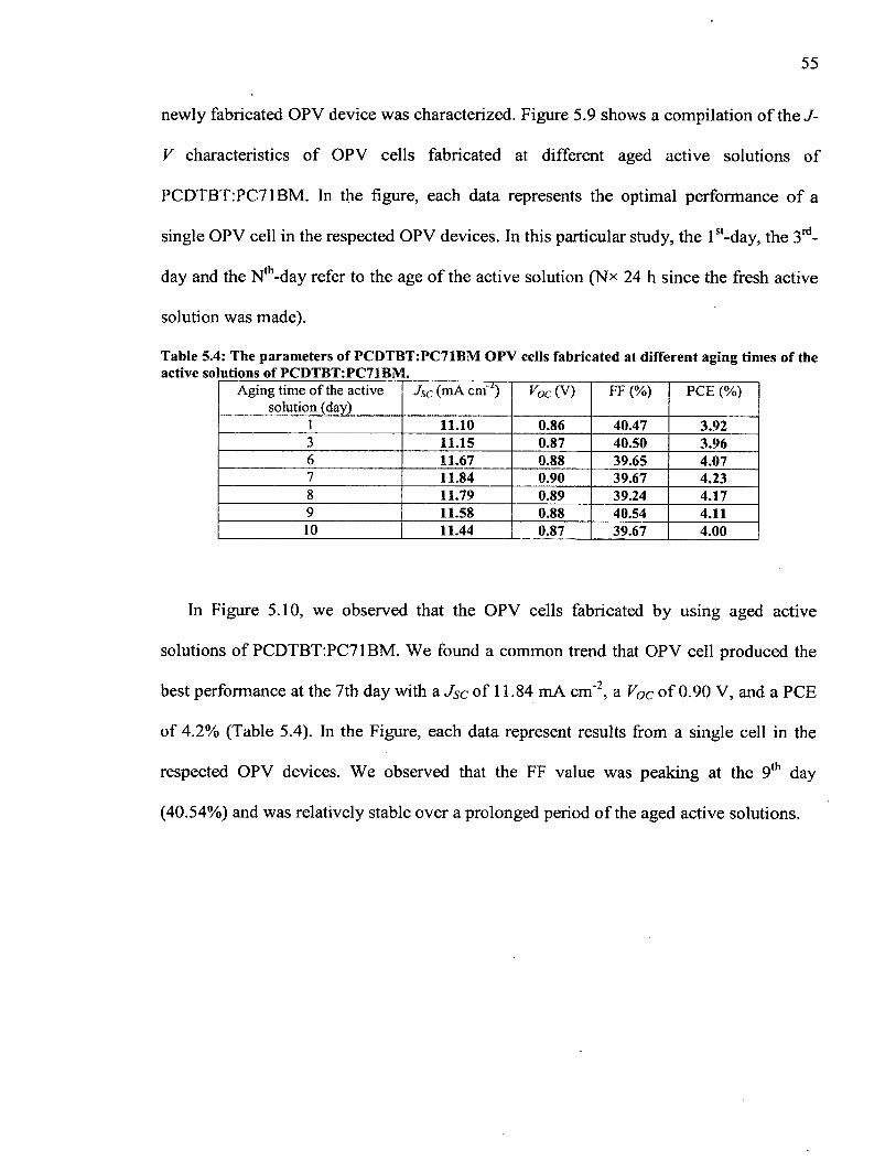
newly fabricated OPV device was characterized. Figure 5.9 shows a compilation of th e /-
V characteristics of OPV cells fabricated at different aged active solutions of
PCDTBT:PC71BM. In the figure, each data represents the optimal performance of a
single OPV cell in the respected OPV devices. In this particular study, the l st-day, the 3rd-
day and the Ntb-day refer to the age of the active solution (Nx 24 h since the fresh active
solution was made).
Table 5.4: The parameters of PCDTBT:PC71BM OPV cells fabricated at different aging times of the active solutions of PCDTBT:PC71BM.
Aging time of the active solution (day)
Jsc (mA cm'2) VOC (V) FF (%) PCE (%)
1 11.10 0.86 40.47 3.923 11.15 0.87 40.50 3.966 11.67 0.88 39.65 4.077 11.84 0.90 39.67 4.238 11.79 0.89 39.24 4.179 11.58 0.88 40.54 4.1110 11.44 0.87 39.67 4.00
In Figure 5.10, we observed that the OPV cells fabricated by using aged active
solutions of PCDTBT:PC71BM. We found a common trend that OPV cell produced the
best performance at the 7th day with a Jsc of 11.84 mA cm'2, a V0c of 0.90 V, and a PCE
of 4.2% (Table 5.4). In the Figure, each data represent results from a single cell in the
respected OPV devices. We observed that the FF value was peaking at the 9th day
(40.54%) and was relatively stable over a prolonged period of the aged active solutions.
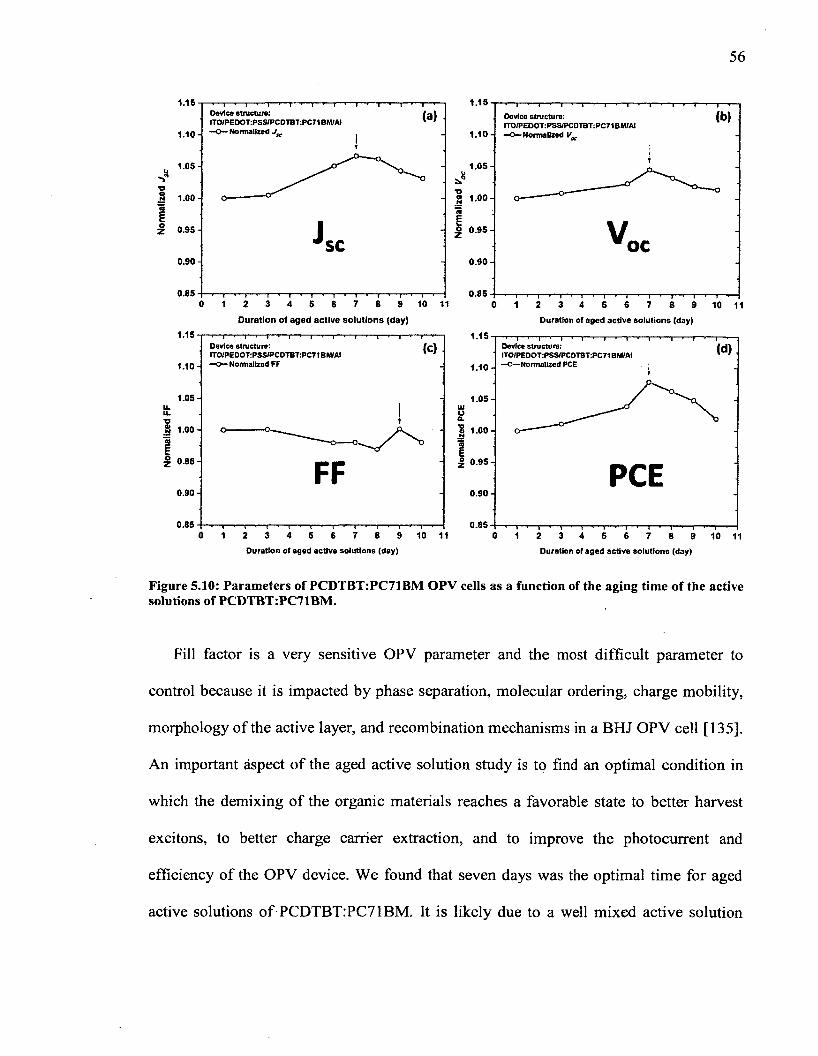
56
1.151.15
1. 10 -1.1 0 -
1.05- 1.05-
1.0 0 -
0.95-Z 0.95 -
SC o c0.90- 0.90-
0.85 0.85
Duration of aged active solutions (day) Duration of aged active solutions (day)1.15 1.15
Device structure:ITO/PEDOT:PSS/PCDTBT:PC71 BM/AI —o —Normalized PCE1 .1 0 - 1 .1 0 -
1.05- 1.05-
S 1.00- 1.0 0 -
S 0.95-0.95-
0.90- 0.90-
0.8S 0.850 1 2 3 4 5 6 7 8 9 10 11 0 1 2 3 4 6 6 7 8 9 10 11
Ouratlon of aged active solutions (day) Duration of aged active solutions (day)
Figure 5.10: Parameters of PCDTBT:PC71BM OPV cells as a function of the aging time of the active solutions of PCDTBT :PC71BM.
Fill factor is a very sensitive OPV parameter and the most difficult parameter to
control because it is impacted by phase separation, molecular ordering, charge mobility,
morphology of the active layer, and recombination mechanisms in a BHJ OPV cell [135].
An important aspect of the aged active solution study is to find an optimal condition in
which the demixing of the organic materials reaches a favorable state to better harvest
excitons, to better charge carrier extraction, and to improve the photocurrent and
efficiency of the OPV device. We found that seven days was the optimal time for aged
active solutions of PCDTBT:PC71BM. It is likely due to a well mixed active solution
that improves the nanomorphology, the percolation path, and the interconnected transport
network in the bulk heterojunction OPV cell. We observed, however, after 7 days using
the aged active solution, the device performance decreased. The declining quality in the
OPV devices after 7 days might be due to several factors. First, the active solution
evaporates during the aging process resulting in a decrease in the concentration of donor
and acceptor materials in the solution. Second, excessive stirring of the active solution
might have causes the decrease in the quality o f the nanomorphology of the active
solution. Third, degradation of the active solution due to its exposure to light worsened
each time the solution was exposed. However, we observed the declining qualities of the
aged active solution after 7 days was not catastrophic; since the devices still functioned
properly without disastrous failure.
5.8. The best PCDTBT:PC71BM OPV cell achieved in our experiment
From different optimization tests and adjusting several fabricating procedures, the
best performance of the PCDTBT:PC71BM BHJ OPV device in our experiment was
achieved with a JSc of 12.73 mA cm'2, a Vqc of 0.89 V, a FF of 45%, and a PCE of
5.13% as seen in Figure 5.11 (Table 5.5). While the average PCE value of all
PCDTBT:PC71BM OPV devices is 3.21 ± 1.20 % (Table C.4). The performances of
OPV devices on a regular basis are of course lower. The mean of the PCE value was
reduced and the standard deviation was large due to data population with a large interval
of PCE values. This study comprises early basic research on OPV devices and as a
consequence variability of the fabrication process for the devices was excessive. The
excessive process variability is attributed to the difficult fabrication processes and
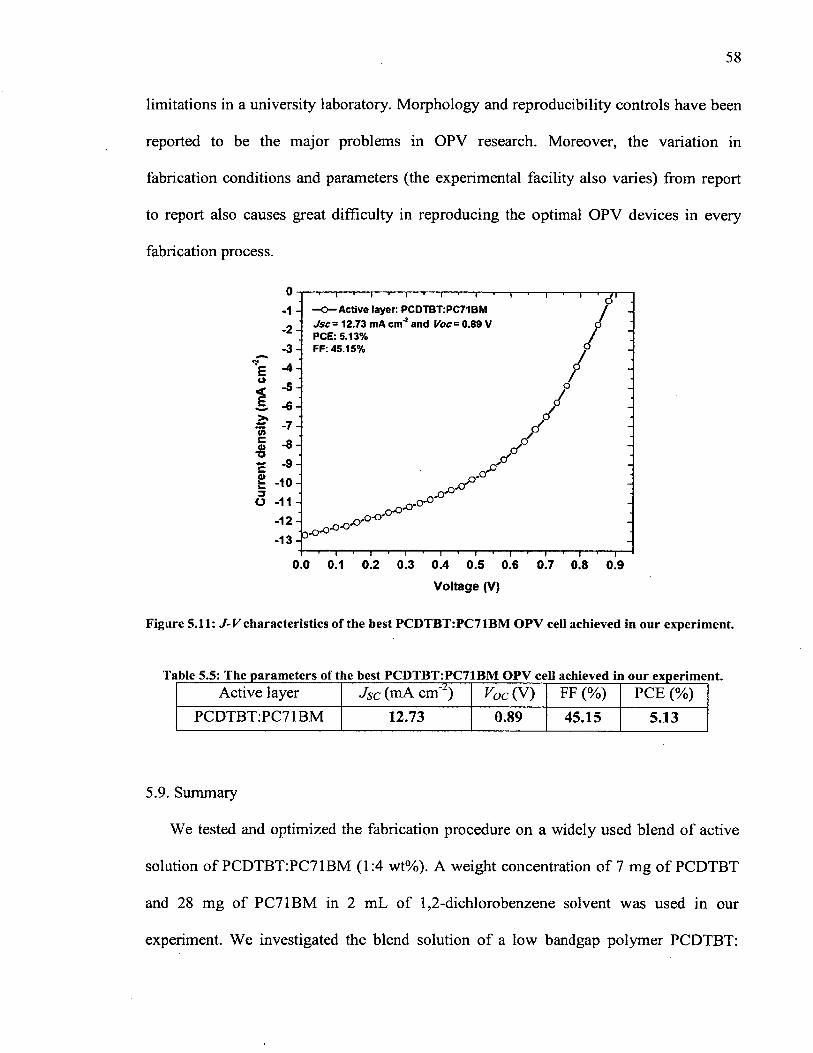
58
limitations in a university laboratory. Morphology and reproducibility controls have been
reported to be the major problems in OPV research. Moreover, the variation in
fabrication conditions and parameters (the experimental facility also varies) from report
to report also causes great difficulty in reproducing the optimal OPV devices in every
fabrication process.
° 1-1 --2--3 -
E -4-4>l
-5 - -6 -
£■ -7 -(0co -8 -"Oc -9-s>k- -10-3 -
o -11 --12--13-
1------1------ 1------ 1------ >------ 1------ ■------ 1------ ■------ 1 r
—O - Active layer PCDTBT:PC71BM Jsc= 12.73 mA cm'2 and V o c - 0.89 V PCE: 5.13%FF: 45.15%
' ■' ' d'
//
J
' 3-0' ° 'i-O-O'
,-0 - 0O'O't-C r°
-O ' 0
.O'0'
-I— I— I— I— I— I— .— I— I— I— I— I— I— I— I— I— I— I—
i.O 0.1 0.2 0.3 0.4 0.5 0.6 0.7 0.8 0.9Voltage (V)
Figure 5.11: J -V characteristics of the best PCDTBT:PC71BM OPV cell achieved in our experiment.
Table 5.5: The parameters of the best PCDTBT:PC71BM OPV cell achieved in our experimentActive layer Jsc (mA cm*2) Voc(V) FF (%) PCE (%)
PCDTBT :PC71BM 12.73 0.89 45.15 5.13
5.9. Summary
We tested and optimized the fabrication procedure on a widely used blend of active
solution of PCDTBT:PC7IBM (1:4 wt%). A weight concentration of 7 mg of PCDTBT
and 28 mg of PC71BM in 2 mL of 1,2-dichlorobenzene solvent was used in our
experiment. We investigated the blend solution of a low bandgap polymer PCDTBT:
PC71BM by fabricating OPV devices and monitoring their performances. We performed
the optimization steps similar to the steps used in the high bandgap polymer. We found
that the optimal thickness of the active layer was 80 nm. the optimal pre-annealing
condition was at 140 °C for 2 min, and the optimal post-annealing condition was at 150
°C for 10 min. From the TEM measurement as seen in Figure 5.2, we found that in the
PC7IBM-rich environment, the nanocomposite of PCDTBT:PC71BM was dominated by
the formation of PC71BM nanoclusters.
We studied the effect of the aging process of PCDTBT:PC71BM active solutions on
the performance of OPV devices. We found that 7 days stirring was optimal for the aged
active solution of PCDTBT:PC71BM and yielded a FF of 40% and a PCE of 4.3%. Over
100 OPV devices of PCDTBT:PC71BM were fabricated, with less than 10% of them
resulting in PCE values of 5.04 ± 0.05 % (Table C.2). The average PCE value of
PCDTBT:PC71BM OPV devices is 3.12 ± 1.20 % (Table C.4). By using optimum
fabrication conditions, we found that the best performance of the PCDTBT:PC71BM
BHJ OPV device in our experiment was achieved with a Jsc of 12.73 mA cm'2, a Voc of
0.89 V, a FF of 45%, and a PCE of 5.1%. This result is still slightly lower than the best
performance of PCDTBT:PC71BM based OPV device with a PCE of 7% reported in the
literature [84]. We concluded that our fabrication procedure for low bandgap polymer
OPV devices is not optimal yet.
60
Chapter 6
Improving the Stability of the High Bandgap OPV Devices using a Solution Based Titanium Sub-oxide Interfacial Layer
6 .1. Introduction
The degradation of the active layer was accelerated due to exposure to three primary
factors; oxygen, air, and light [25,136], To achieve OPV device stability, either the
development of improved barrier materials for packing or the development of devices
with less air sensitivity (or both) is required. Air stable OPV devices have reportedly
been achieved by inserting a solution based metal oxide as a buffer layer between the
active layer and the metal cathode [137,138], For example, a solution based titanium sub
oxide (TiOx) with a thickness less than 20 nm has been reported to effectively minimize
physical and chemical damages [18], The TiOx layer serves as an effective barrier for
oxygen permeation to improve device stability in an ambient atmosphere.
The improvement in device efficiency has brought OPV cells closer to commercial
viability, highlighting the importance of studying the lifetime and reliability of OPV
devices. The lifetime and degradation mechanisms of BHJ solar cells that employ the
high bandgap polymer (P3HT) have been well studied [51,137,138,140]. We synthesized
the solution based TiOx material by using the sol-gel chemistry method as previously
discussed in Section 3.5 [18,77]. We performed optimization tests on the TiOx layer
including a TiOx layer thickness test and a TiOx solution drying test. We used the
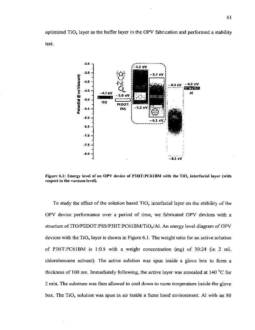
61
optimized TiOx layer as the buffer layer in the OPV fabrication and performed a stability
test.
-3.0 -
-3.5 -?i *0 -£W -4.5 ->mTB -50-If - 5 . 5 -CL.
- 6.0 -
-6.5 -
-7.0 -
-7.5 -
- 8.0 -
Figure 6.1: Energy level of an OPV device of P3HT:PC61BM with the TiO* interfacial layer (with respect to the vacuum level).
To study the effect of the solution based TiOx interfacial layer on the stability o f the
OPV device performance over a period of time, we fabricated OPV devices with a
structure of ITO/PEDOT:PSS/P3HT:PC61BM/TiOx/Al. An energy level diagram of OPV
devices with the TiOx layer is shown in Figure 6.1. The weight ratio for an active solution
of P3HT:PC61BM is 1:0.8 with a weight concentration (mg) of 30:24 (in 2 mL
chlorobenzene solvent). The active solution was spun inside a glove box to form a
thickness of 100 nm. Immediately following, the active layer was annealed at 140 °C for
2 min. The substrate was then allowed to cool down to room temperature inside the glove
box. The TiOx solution was spun in air inside a fame hood environment. A1 with an 80
/ - 3 . 3 eV
PEDOT:PSS
-8.1 eV
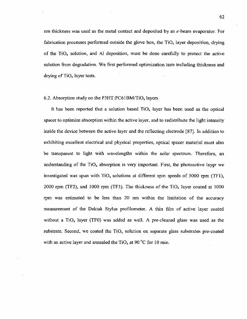
62
nm thickness was used as the metal contact and deposited by an e-beam evaporator. For
fabrication processes performed outside the glove box, the TiOx layer deposition, drying
of the TiOx solution, and A1 deposition, must be done carefully to protect the active
solution from degradation. We first performed optimization tests including thickness and
drying of TiOx layer tests.
6.2. Absorption study on the P3HT:PC61BM/TiOx layers
It has been reported that a solution based TiOx layer has been used as the optical
spacer to optimize absorption within the active layer, and to redistribute the light intensity
inside the device between the active layer and the reflecting electrode [87]. In addition to
exhibiting excellent electrical and physical properties, optical spacer material must also
be transparent to light with wavelengths within the solar spectrum. Therefore, an
understanding of the TiOx absorption is very important. First, the photoactive laygr we
investigated was spun with TiOx solutions at different spin speeds of 3000 rpm (TF1),
2000 rpm (TF2), and 1000 rpm (TF3). The thickness of the TiOx layer coated at 1000
rpm was estimated to be less than 2 0 nm within the limitation of the accuracy
measurement of the Dektak Stylus profilometer. A thin film of active layer coated
without a TiOx layer (TF0) was added as well. A pre-cleaned glass was used as the
substrate. Second, we coated the TiOx solution on separate glass substrates pre-coated
with an active layer and annealed the TiOx at 90 °C for 10 min.
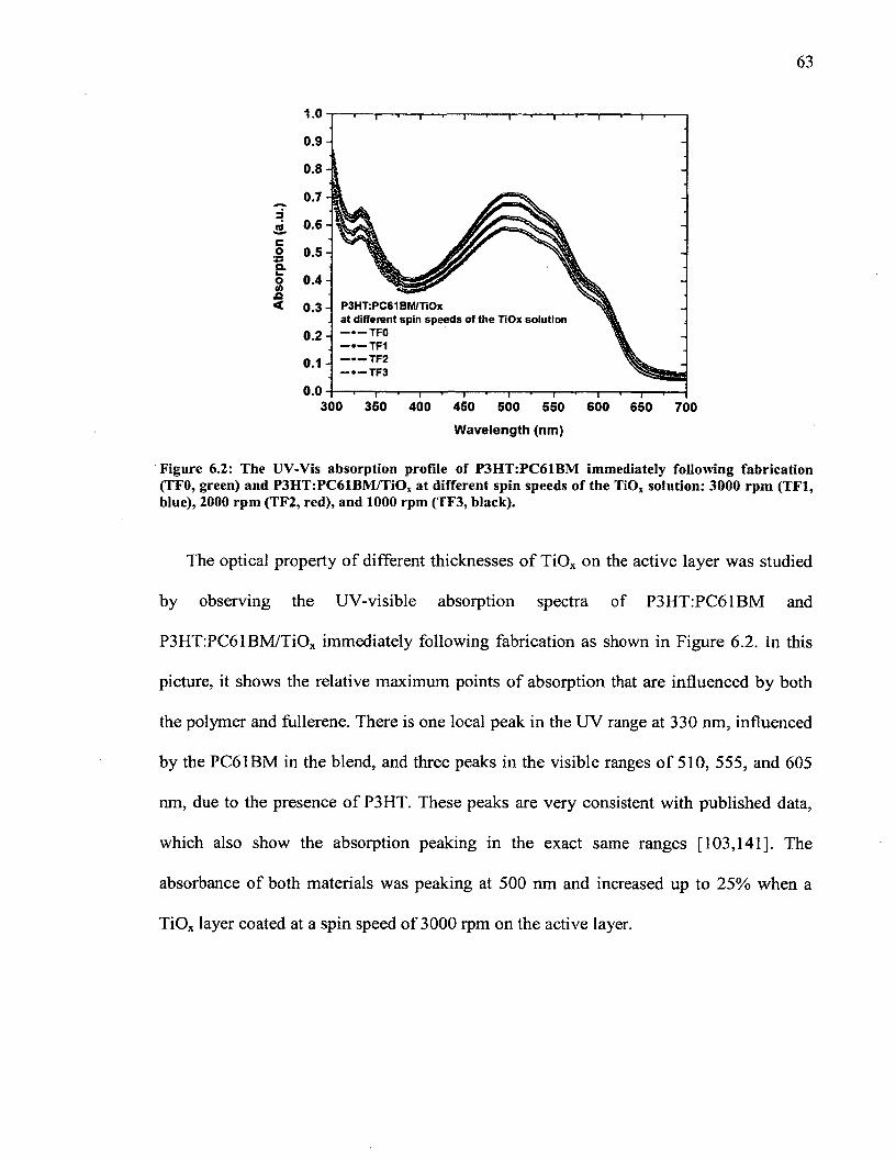
63
1.0
0.9
0.8
_ 071 0.6
.1 0.5
I<0
< 0.3
0.2
0.1
0.0300 350 400 450 500 550 600 650 700
Wavelength (nm)
Figure 6.2: The UV-Vis absorption profile of P3HT:PC61BM immediately following fabrication (TF0, green) and P3HT:PC61BM/TiO* at different spin speeds of the TiO* solution: 3000 rpm (TF1, blue), 2000 rpm (TF2, red), and 1000 rpm (TF3, black).
The optical property of different thicknesses of TiOx on the active layer was studied
by observing the UV-visible absorption spectra of P3HT:PC61BM and
P3HT:PC61BM/TiOx immediately following fabrication as shown in Figure 6.2. In this
picture, it shows the relative maximum points of absorption that are influenced by both
the polymer and fullerene. There is one local peak in the UV range at 330 nm, influenced
by the PC61BM in the blend, and three peaks in the visible ranges of 510, 555, and 605
nm, due to the presence of P3HT. These peaks are very consistent with published data,
which also show the absorption peaking in the exact same ranges [103,141], The
absorbance of both materials was peaking at 500 nm and increased up to 25% when a
TiOx layer coated at a spin speed of 3000 rpm on the active layer.
P3HT:PC61BM/TiOxat different spin speeds of the TiOx solution— TF0— TF1 — TF2 —*—TF3
64
6.3. TiOx spin coating test
We used the absorption study as previously discussed and fabricated three OPV
devices with a structure of ITO/PEDOT:PSS/P3HT:PC61BM/TiOx/Al at different spin
speeds of the TiOx solution. By varying the spin speed, we indirectly varied the thickness
of the TiOx layer. However, our TiOx layer was too thin and difficult to be measured
precisely with the Dektak profilometer at the facility. Thicknesses of each layer in the
OPV device were optimized to maximize light absorption by the active layer [142]. In the
BHJ OPV cell, the light entering into the device from the glass side travels through the
nearly transparent ITO and PEDOT:PSS layers, is partly absorbed in the photoactive BHJ
layer, passes through the nearly transparent TiOx layer, and is then reflected onto the A1
surface for a second pass through the BHJ, PEDOT:PSS, and ITO layers. Another
excellent property of the TiOx layer is that it is non-absorbing in visible and infrared light
and improves optical absorption of the light [85],
ITO/PEDOT:PSS/P3HT:PC61BMniOx/AI Different spin speeds of the TiOx solution —O—TF1 —D-TF2 —0-TF3
E -3-01i -5-<A C 01 T3
-6 -
-7-c£V.3 - 8 -
O -9-
- 1 0 -
- 1 1
0.0 0.30.1 0.2 0.4 0.5 0.6Voltage (V)
Figure 6.3: J -V characteristics of P3HT:PC61BM OPV cells fabricated at different spin speeds of the TiOx solution: 3000 rpm (TF1, diamond), 2000 rpm (TF2, square), and 1000 rpm (TF3, circle).
Figure 6.3 shows the J-V characteristics o f the OPV cells fabricated at different spin
speeds of the TiOx solution (the spin coating time was kept the same at 3 min). Each data
represents the optimal performance of a single OPV cell in the respected OPV devices. In
this Figure, the device fabricated a TiOx layer (TF1) with the spin speed of 3000 rpm
produced the best performance with an FF of 50% and PCE of 3.0% (see Table 6.1). The
thickness of TF3 was measured to be less than 20 nm within the limitation of the Dektak
Stylus profilometer. Other studies have reported that optimal thicknesses of the TiOx
layer for OPV devices are in the 5 nm - 20 nm ranges [82,143]. The OPV performance
with the TiOx layer thickness we tested agreed with those reports.
Table 6.1: The parameters of P3HT:PC61BM OPV cells fabricated at different spin speeds of the TiOj solution.____________________________________________________________________
Spin speed of the TiOx solution
y5C(mA cm'2) V0c (V) FF (%) PCE (%)
3000 rpm (TF1) 9.88 0.61 50.28 3.002000 rpm (TF2) 9.21 0.60 52.37 2.891000 rpm (TF3) 8.78 0.59 52.34 2.72
6.4. TiOx solution drying test
The next optimization step is the TiOx solution drying by means of thermal annealing.
Hal and his coworkers reported that the conversion of Ti(OC3 H7 ) 4 to Ti0 2 was estimated
to be 77% - 91% (the result is called a partial conversion process) [74]. In the drying test
of the TiOx layer, we compared four different drying conditions (1) at a room temperature
(25 °C) for 60 min [77], (2) at 80 °C for 10 min [84], (3) at 90 °C for 10 min [144], and
(4) at 100 °C for 10 min in the air. During the drying process, the substrate pre-coated
with multi-layered films of ITO/PEDOT:PSS/P3HT:PC61BM/TiOx was protected by a
Petri dish covered with A1 foil to shield the active layer from the light.
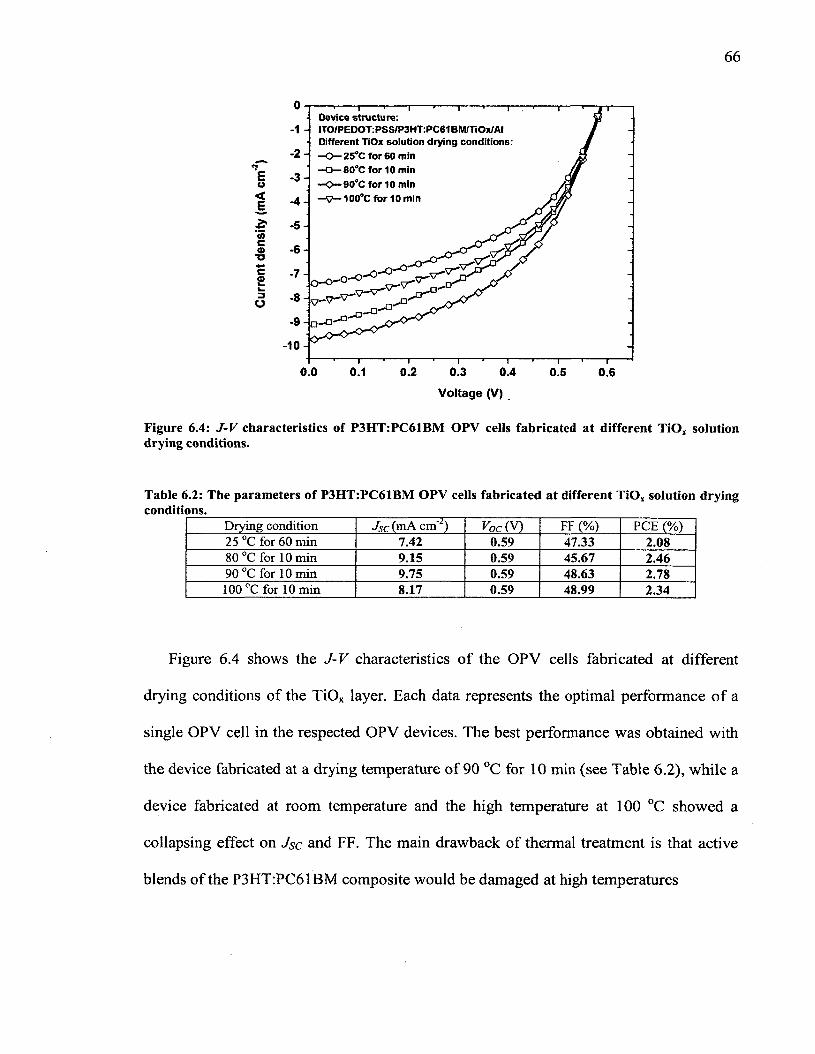
66
Eo<E
<oc<u■a
3o
0
-1 A -2
-3
-44 -5
-6
-7
-8
-9-
- 1 0 -
—>---- 1---->—Device structure:ITO/PEDOT: PSS/P3HT:PC61 BM/TiOx/AI Different TiOx solution drying conditions: - O — 25°C for 60 min —a —80*C for 10 min —O—90°C for 10 min —V—100°C for 10 min
—- v - v " n-
0.0— I—
0.1— I—
0.2— i—
0.3 0.4 0.5— i—
0.6
V oltage (V)
Figure 6.4: J-V characteristics of P3HT:PC61BM OPV cells fabricated at different TiO, solution drying conditions.
Table 6.2: The parameters of P3HT:PC61BM OPV cells fabricated at different TiO, solution drying conditions.
Drying condition Jsc (mA cm'2) VOC (V) FF (%) PCE (%)25 °C for 60 min 7.42 0.59 47.33 2.0880 °C for 10 min 9.15 0.59 45.67 2.4690 °C for 10 min 9.75 0.59 48.63 2.78100 °C for 10 min 8.17 0.59 48.99 2.34
Figure 6.4 shows the J-V characteristics of the OPV cells fabricated at different
drying conditions of the TiOx layer. Each data represents the optimal performance of a
single OPV cell in the respected OPV devices. The best performance was obtained with
the device fabricated at a drying temperature of 90 °C for 10 min (see Table 6.2), while a
device fabricated at room temperature and the high temperature at 100 °C showed a
collapsing effect on Jsc and FF. The main drawback of thermal treatment is that active
blends of the P3HT:PC61BM composite would be damaged at high temperatures
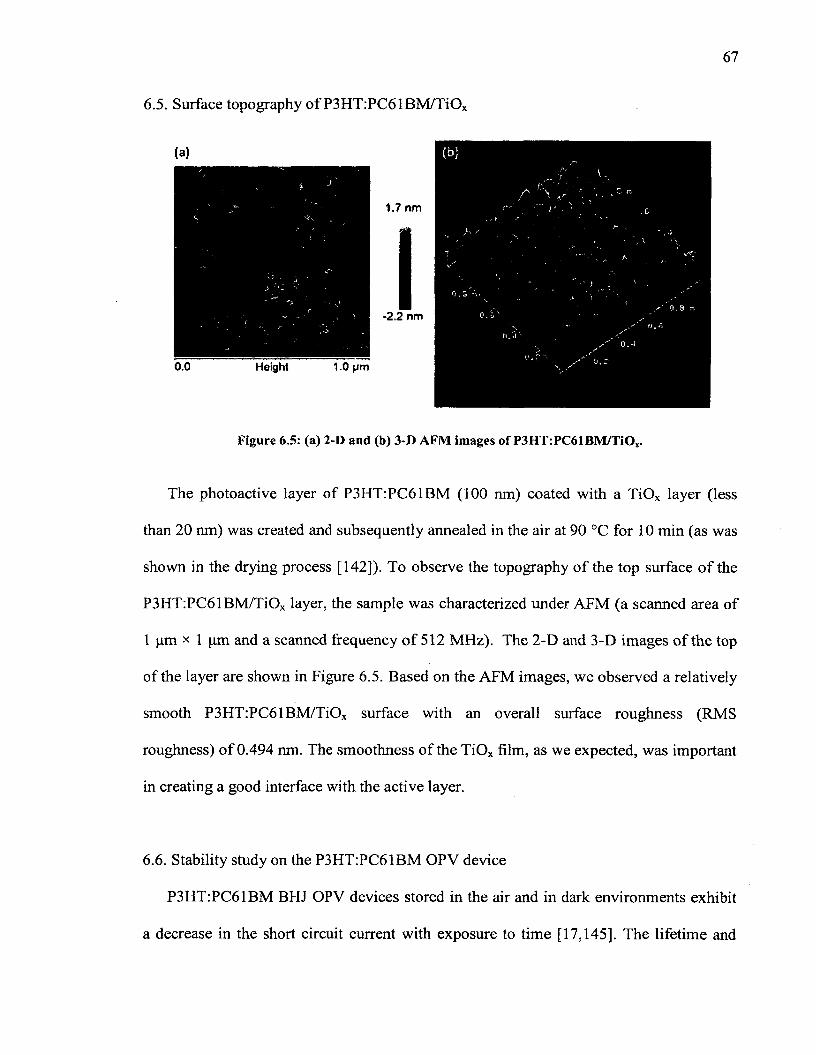
67
6.5. Surface topography of P3HT:PC61BM/TiOx
o.o
(a)
Height 1.0 pm
*2 .;
1.7
Figure 6.5: (a) 2-D and (b) 3-D AFM images of P3HT:PC61BM/TiOx.
The photoactive layer of P3HT:PC61BM (100 nm) coated with a TiOx layer (less
than 20 nm) was created and subsequently annealed in the air at 90 °C for 10 min (as was
shown in the drying process [142]). To observe the topography of the top surface of the
P3HT:PC61BM/TiOx layer, the sample was characterized under AFM (a scanned area of
1 pm x 1 pm and a scanned frequency of 512 MHz). The 2-D and 3-D images of the top
of the layer are shown in Figure 6.5. Based on the AFM images, we observed a relatively
smooth P3HT:PC61BM/TiOx surface with an overall surface roughness (RMS
roughness) of 0.494 nm. The smoothness of the TiOx film, as we expected, was important
in creating a good interface with the active layer.
6 .6 . Stability study on the P3HT:PC61BM OPV device
P3HT:PC61BM BHJ OPV devices stored in the air and in dark environments exhibit
a decrease in the short circuit current with exposure to time [17,145]. The lifetime and
68
stability of OPV devices is a very important aspect in the commercialization of
photovoltaic devices. The aim of this study is to produce an OPV device with air stability
under a prolonged storage time by using a solution-based TiOx material as the interfacial
layer. We fabricated an OPV device with a structure of ITO/PEDOT:PSS/P3HT:
PC61BM/TiOx/Al by using optimal fabrication procedures as previously discussed. We
investigated the lifetime and stability of the OPV device with the TiOx layer.
The change of J-V characteristics of the P3HT:PC61BM OPV device fabricated with
a TiOx layer was monitored with a 70 day storage time. We compared the degradation
trend of the device by evaluating their Jsc, Toe, FF, and PCE values as a function of the
storage time. To maintain the consistency of our results, for a total of 8 cells in the OPV
device, we characterized the same cell showing the best performance over a period of
time. The rest of the OPV cells were operating well with less than 10% lower in their
performances comparing to the best cell.
In our experiment, we stored the OPV device fabricated with a TiOx layer inside the
glove box and characterized it periodically in the air for 70 days. We performed both a
stability study using a solution based TiOx layer to protect the active layer from moisture
and oxygen and a stability study using an opaque A1 cover to protect the device from
light (Case (II)). Figure 6 . 6 shows the J-V characteristic of an OPV device with a TiOx
layer as a function of storage time. We found that semi-crystalline P3HT materials prove
to be an excellent air stability material and are slow to degrade as reported elsewhere
[146]. The degradation of OPV devices consisting of at least two active organic materials
is a complex problem. Reactions of the organic materials with oxygen [12], water [147],
and light [145] have been reported to accelerate degradation of the organic materials. For
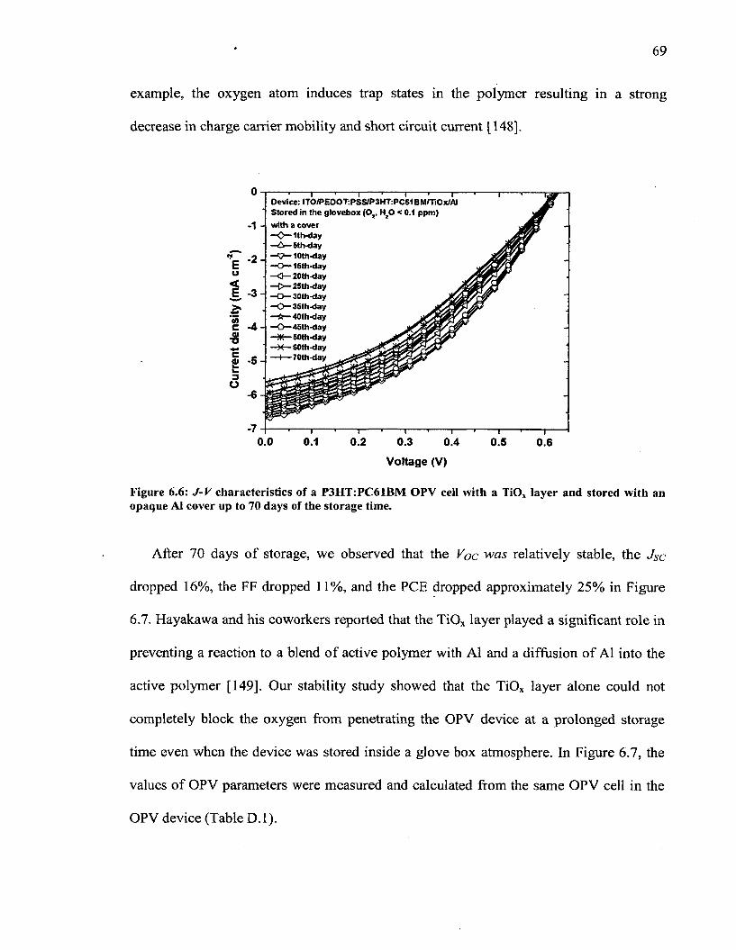
69
example, the oxygen atom induces trap states in the polymer resulting in a strong
decrease in charge carrier mobility and short circuit current [148].
Device: ITO/PEDOT:PSS/P3HT:PC618M/TlOx/AI Stored in the glovebox (02, H30 < 0.1 ppm) with a cover —O— 1th-day —A —Sth-day —t?—10th-day —O— 15th-day —0—20th-day—C~25th-day ,—□— 30th-day —O— 35th-day —tr— 40th-day —O—45th-day
50th-day 601h-day
—I— 70th-day
0.0 0.1 0.2 0.3 0.4 0.5 0.6Voltage (V)
Figure 6.6: J-V characteristics of a P3HT:PC61BM OPV cell with a TiOx layer and stored with an opaque A1 cover up to 70 days of the storage time.
After 70 days of storage, we observed that the Voc was relatively stable, the JSc
dropped 16%, the FF dropped 11%, and the PCE dropped approximately 25% in Figure
6.7. Hayakawa and his coworkers reported that the TiOx layer played a significant role in
preventing a reaction to a blend of active polymer with A1 and a diffusion of A1 into the
active polymer [149]. Our stability study showed that the TiOx layer alone could not
completely block the oxygen from penetrating the OPV device at a prolonged storage
time even when the device was stored inside a glove box atmosphere. In Figure 6.7, the
values of OPV parameters were measured and calculated from the same OPV cell in the
OPV device (Table D.l).
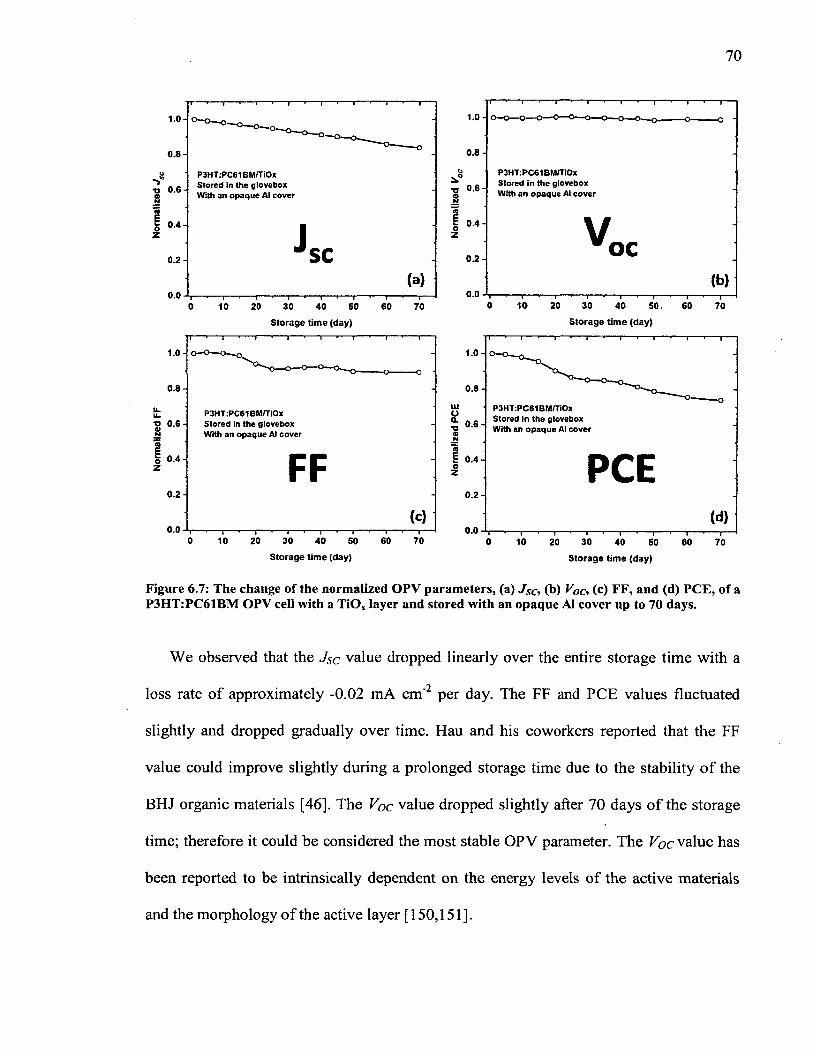
70
1 .0 -
0 .8 -
P3HT:PC61BM/TiOx Stored in the glovebox With an opaque AI cover•o 0 . 6 -
0.4-
sc0.0
60 700 10 20 30 40 50
1.0-
0 .8-
T3 0.6-aA§ 0.4-z
0.2-
0 .0-
P3HT:PC61BMHiOx Stored in the glovebox With an opaque AI cover
V oc(b)
Storage time (day)0 10 20 30 40 50. 60 70
Storage time (day)
1.0 - 1 .0 -
-o0 .8 -
P3HT:PC61BM/TiOx Stored in the glovebox With an opaque AI cover
u- P3HT :PC61BM/TIOx Stored In the glovebox With an opaque AI cover
•o 0.6 - 0 .6 -
0.4-
0 .2 - 0 .2 -
(C)0.0 0.0
0 20 60 7010 30 40 50 0 10 20 30 40 50 60 70Storage time (day) Storage time (day)
Figure 6.7: The change of the normalized OPV parameters, (a) JSc, (b) Voc, (c) FF, and (d) PCE, of a P3HT:PC61BM OPV cell with a TiOx layer and stored with an opaque AI cover up to 70 days.
We observed that the Jsc value dropped linearly over the entire storage time with a
loss rate of approximately -0.02 mA cm' 2 per day. The FF and PCE values fluctuated
slightly and dropped gradually over time. Hau and his coworkers reported that the FF
value could improve slightly during a prolonged storage time due to the stability of the
BHJ organic materials [46]. The Voc value dropped slightly after 70 days of the storage
time; therefore it could be considered the most stable OPV parameter. The Voc value has
been reported to be intrinsically dependent on the energy levels of the active materials
and the morphology of the active layer [150,151].
71
6.7. Summary
We used a sol-gel TiOx material as the interfacial layer between the active layer of
P3HT:PC61BM and the AI cathode. We performed optimization tests on the TiOx layer
including a TiOx spin coating test and a TiOx solution drying test. We found that a
solution based TiOx layer coated at a spin speed of 3000 rpm (TF1) improved the photon
absorption of the active layer. For the drying TiOx solution test, we found that 90 °C for
10 min was the optimal drying condition for the TiOx solution. A relatively smooth
P3HT:PC61BM/TiOx surface with an overall surface roughness (RMS roughness) of
0.494 nm was observed with an AFM measurement. An optimized TiOx layer was used
as the buffer layer in the OPV fabrication. We also performed a stability study using a
solution based TiOx layer to protect the active layer from moisture and oxygen and a
stability study using an opaque AI cover to protect the device from the light (Case (II)).
After 70 days of storage, we observed that the Jsc dropped 16%, FF dropped 11%, and
PCE dropped approximately 25%, while the Voc remained relatively stable. We
concluded that a solution based TiOx layer synthesized using a sol-gel chemistry method
is effective in protecting the active layer from degradation.
72
Chapter 7
Improving the Stability of the Low Bandgap OPV Devices using a Solution Based Titanium Sub-oxide Interfacial Layer
7.1. Introduction
Stability and lifetime studies on recently developed low bandgap polymers
(PCDTBT) are limited. Because of their inherent chemical and physical properties, low
bandgap polymers generally exhibit different lifetimes and degradation pathways than do
high bandgap polymers [152,153]. The PCDTBT is different from its high bandgap
counterpart, P3HT. We assumed that the stability and the acceleration of physical and
chemical degradation of the semi-crystalline polymer-based (P3HT) BHJ cell and an
amorphous polymer-based (PCDTBT) BHJ cell might be different. In general,
degradation can occur at the electrodes or within the photoactive layer of OPV devices.
For example, a photochemical reaction in the photoactive layer of PCDTBT based OPV
devices was reported to reduce the FF, Voc, and Jsc [154],
We fabricated OPV devices with a structure of ITOPEDOT:PSS/PCDTBT:
PC71BM/TiOx/Al. The energy level diagram of OPV devices with a TiOx layer is shown
in Figure 7.1. The weight ratio for an active solution of PCDTBT:PC71BM is 1:4 with a
weight concentration (mg) of 7:28 (in 2 mL 1,2-dichlorobenzene solvent). The active
solution was spun inside the glove box to form an 80 ran thickness. Immediately
following, the active layer was annealed at 140 °C for 2 min. The substrate was then
allowed to cool down to room temperature inside the glove box. The TiOx solution was
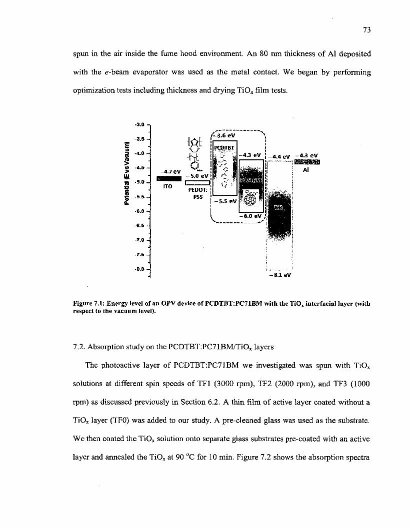
73
spun in the air inside the fume hood environment. An 80 nm thickness of AI deposited
with the e-beam evaporator was used as the metal contact. We began by performing
optimization tests including thickness and drying TiOx film tests.
PCQTBT
PEDOT:PSS
Figure 7.1: Energy level of an OPV device of PCDTBT:PC71BM with the TiOx interfacial layer (with respect to the vacuum level).
7.2. Absorption study on the PCDTBT:PC71BM/TiOx layers
The photoactive layer of PCDTBT:PC71BM we investigated was spun with TiOx
solutions at different spin speeds of TF1 (3000 rpm), TF2 (2000 rpm), and TF3 (1000
rpm) as discussed previously in Section 6.2. A thin film of active layer coated without a
TiOx layer (TF0) was added to our study. A pre-cleaned glass was used as the substrate.
We then coated the TiOx solution onto separate glass substrates pre-coated with an active
layer and annealed the TiOx at 90 °C for 10 min. Figure 7.2 shows the absorption spectra
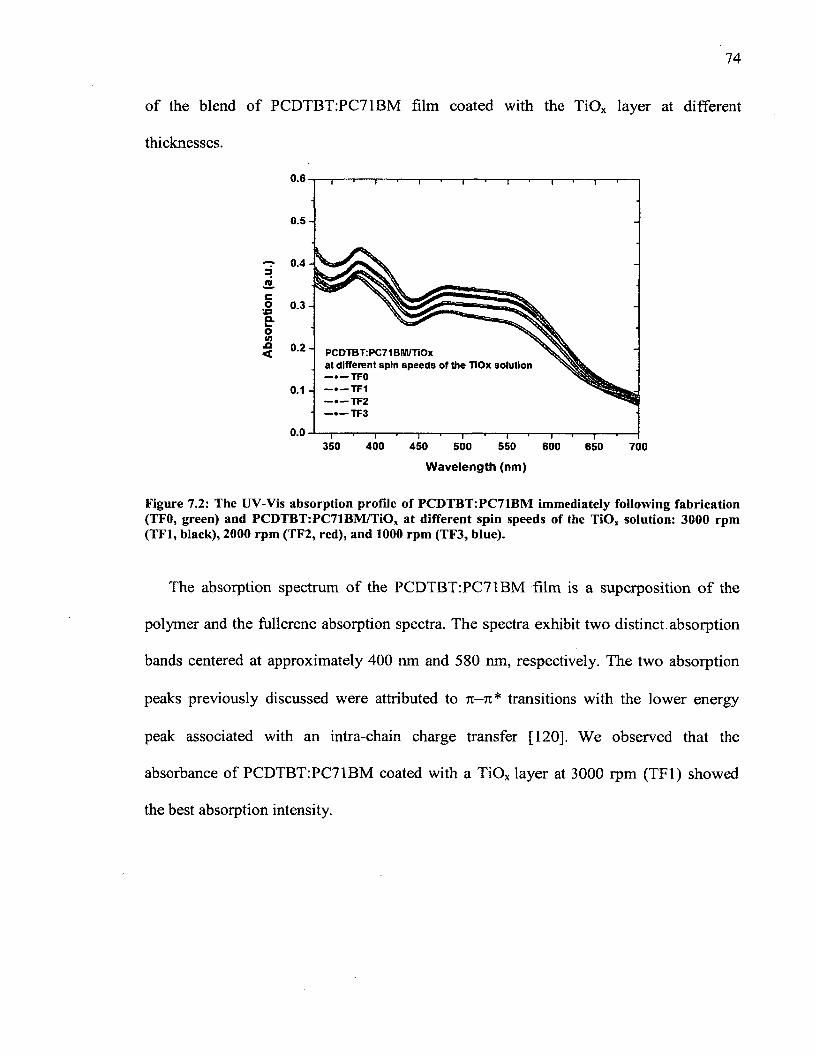
74
of the blend of PCDTBT:PC71BM film coated with the TiOx layer at different
thicknesses.
0.6
0.5
-r 0.4 3<gco 0.3
<£3
e-o105 0.2
0.1
0.0350 400 450 500 550 600 650 700
Wavelength (nm)
Figure 7.2: The UV-Vis absorption profile of PCDTBT:PC71BM immediately following fabrication (TFO, green) and PCDTBT:PC71BM/TiOx at different spin speeds of the TiOx solution: 3000 rpm (TF1, black), 2000 rpm (TF2, red), and 1000 rpm (TF3, blue).
The absorption spectrum of the PCDTBT:PC71BM film is a superposition of the
polymer and the fullerene absorption spectra. The spectra exhibit two distinct, absorption
bands centered at approximately 400 nm and 580 nm, respectively. The two absorption
peaks previously discussed were attributed to n-n* transitions with the lower energy
peak associated with an intra-chain charge transfer [120], We observed that the
absorbance of PCDTBT:PC71BM coated with a TiOx layer at 3000 rpm (TF1) showed
the best absorption intensity.
PCDTBT:PC71BM/TiOxat different spin speeds of the TiOx solution—• —TFO— — TF1— — TF2 — —TF3
1---- 1---- 1---- 1---- r T m— '---- r
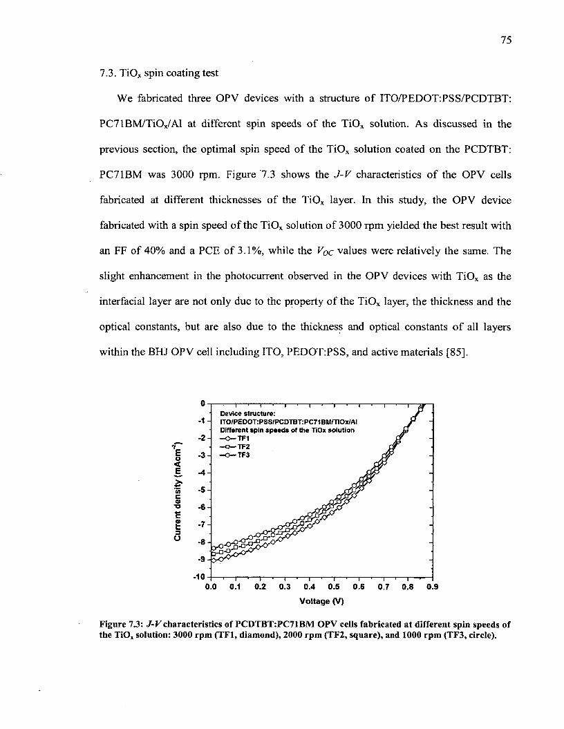
75
7.3. TiOx spin coating test
We fabricated three OPV devices with a structure o f ITO/PEDOT:PSS/PCDTBT:
PC71BM/TiOx/Al at different spin speeds of the TiOx solution. As discussed in the
previous section, the optimal spin speed of the TiOx solution coated on the PCDTBT:
PC71BM was 3000 rpm. Figure ‘7.3 shows the J-V characteristics of the OPV cells
fabricated at different thicknesses of the TiOx layer. In this study, the OPV device
fabricated with a spin speed of the TiOx solution of 3000 rpm yielded the best result with
an FF of 40% and a PCE of 3.1%, while the Voc values were relatively the same. The
slight enhancement in the photocurrent observed in the OPV devices with TiOx as the
interfacial layer are not only due to the property of the TiOx layer, the thickness and the
optical constants, but are also due to the thickness and optical constants of all layers
within the BHJ OPV cell including ITO, PEDOT:PSS, and active materials [85].
Device structure:ITO/PEDOT.PSS/PCDTBT: PC71 BM/TIOx/AI Different spin speeds of the TiOx solution —0 —TF1 — TF2 —o — TF3
0.0 0.1 0.2 0.3 0.4 0.5 0.6 0.7 0.8 0.9Voltage (V)
Figure 7.3: J -V characteristics of PCDTBT:PC71BM OPV ceils fabricated at different spin speeds of the TiO, solution: 3000 rpm (TF1, diamond), 2000 rpm (TF2, square), and 1000 rpm (TF3, circle).
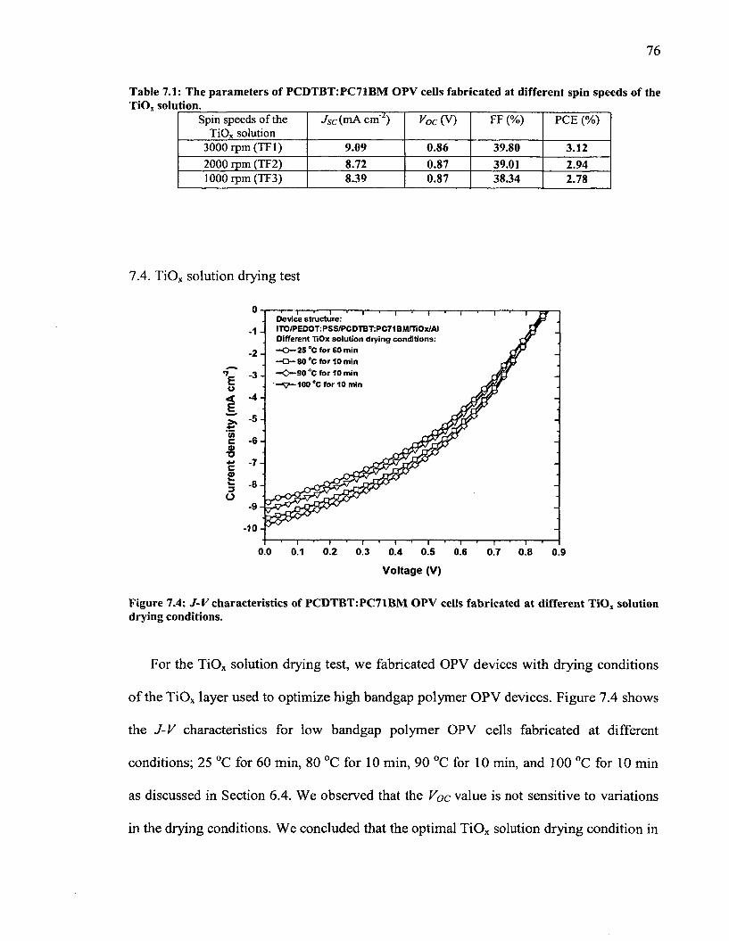
76
Table 7.1: The parameters of PCDTBT:PC71BM OPV cells fabricated at different spin speeds of the TiO, solution._____________________________________________________________________
Spin speeds of the TiOx solution
Jsc (mA cm'2) Voc o n FF (%) PCE (%)
3000 rpm (TF1) 9.09 0.86 39.80 3.122000 rpm (TF2) 8.72 0.87 39.01 2.941000 rpm (TF3) 8.39 0.87 38.34 2.78
7.4. TiOx solution drying test
i— 1 iDevice structure:ITO/PEDOT: PSS/PCDTBT:PC71 BM/TiOx/AI Different TiOx solution drying conditions: —0 —25 °C for £0 min - 0 - 8 0 °C for 10 min —0 —90 °C for 10 min —V —100 °C for 10 min
0.0 0.1 0.2 0.3 0.4 0.5 0.6 0.7 0.8 0.9
Voltage (V)
Figure 7.4: J-V characteristics of PCDTBT:PC71BM OPV cells fabricated at different TiOx solution drying conditions.
For the TiOx solution drying test, we fabricated OPV devices with drying conditions
of the TiOx layer used to optimize high bandgap polymer OPV devices. Figure 7.4 shows
the J-V characteristics for low bandgap polymer OPV cells fabricated at different
conditions; 25 °C for 60 min, 80 °C for 10 min, 90 °C for 10 min, and 100 °C for 10 min
as discussed in Section 6.4. We observed that the V0c value is not sensitive to variations
in the drying conditions. We concluded that the optimal TiOx solution drying condition in
77
a device structure of ITO/PEDOT:PSS/PCDTBT:PC71BM/TiOx/Al was at 90 °C for 10
min which yielded a FF of 40% and a PCE of 3.4%.
Table 7.2: The parameters of PCDTBT:PC71BM OPV cells fabricated at different TiO, solution drying conditions.____________________________ __________________________________ __
Drying condition /sc (mA cm'2) Voc (V) FF (%) PCE (%)25 °C for 60 min 8.82 0.86 38.16 2.9180 °C for 10 min 9.55 0.87 39.06 3.2390 °C for 10 min 9.81 0.86 39.91 3.37100 °C for 10 min 9.15 0.86 38.57 3.02
7.5. Surface topography of the PCDTBT:PC71BM/TiOx layers
The photoactive layer of PCDTBT:PC71BM (80 nm) coated with a TiOx film (less
than 20 nm) was created and subsequently annealed in the air at 90° C for 10 min (as
used in the drying process). To observe the topography of the top surface of the
PCDTBT: PC71BM/TiOx layer, the sample was characterized under AEM (a scanned
area of 2 pm x 2 pm and a scanned frequency of 512 MHz). The 2-D and 3-D images of
the top of the layer are shown in Figure 7.5. Based on the AFM images, we observed a
few random bumps and spikes with approximately 6 nm in height of a freshly deposited a
solution TiOx material on a PCDTBT:PC71BM layer. Figure 7.5 clearly indicates the
presence of large TiOx grains at 90 °C annealing temperature. From this AFM surface
morphology revealed in Figure 7.5 one can conclude that a 90 °C annealing temperature
results already in a mixture of large grains embedded in a polycrystalline structure of the
TiOx film. The surface of the PCDTBT: PC71BM/TiOx was a little bit rougher that of the
P3HT:PC61BM/TiOx as discussed in Section 6.5. However, the overall RMS roughness
of the PCDTBT:PC71BM/TiOx surface of 0.989 nm was observed.
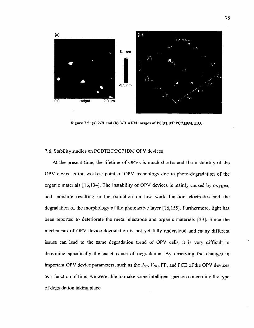
78
(b)
.n
n
i .
(a)
6.1 nm
-3.3 nm
0.0 Height 2.0 pm
Figure 7.5: (a) 2-D and (b) 3-D AFM images of PCDTBT:PC71BM/TiO*
7.6. Stability studies on PCDTBT:PC71BM OPV devices
At the present time, the lifetime of OP Vs is much shorter and the instability of the
OPV device is the weakest point of OPV technology due to photo-degradation of the
organic materials [16,134]. The instability of OPV devices is mainly caused by oxygen,
and moisture resulting in the oxidation on low work function electrodes and the
degradation of the morphology of the photoactive layer [16,155], Furthermore, light has
been reported to deteriorate the metal electrode and organic materials [33]. Since the
mechanism of OPV device degradation is not yet fully understood and many different
issues can lead to the same degradation trend of OPV cells, it is very difficult to
determine specifically the exact cause of degradation. By observing the changes in
important OPV device parameters, such as the Jsc, Voc, FF, and PCE of the OPV devices
as a function of time, we were able to make some intelligent guesses concerning the type
of degradation taking place.
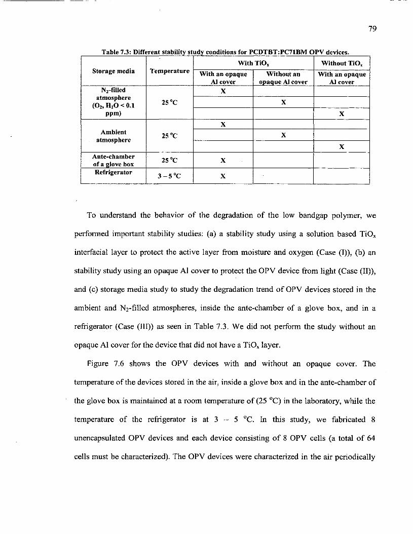
79
Table 7.3: Different stability study conditions for PCDTBT:PC71BM OPV devices.
Storage media TemperatureWith TiO„ Without TiOj
With an opaque A1 cover
Without an opaque Al cover
With an opaque Alcover
N2-filledatmosphere
(0 2, h 2o < 0.1ppm)
25 °C
XX
X
Ambientatmosphere 25 °C
XX
XAnte-chamber of a glove box 25 °C X
Refrigerator 3 - 5 °C X
To understand the behavior of the degradation of the low bandgap polymer, we
performed important stability studies: (a) a stability study using a solution based TiOx
interfacial layer to protect the active layer from moisture and oxygen (Case (I)), (b) an
stability study using an opaque A1 cover to protect the OPV device from light (Case (II)),
and (c) storage media study to study the degradation trend of OPV devices stored in the
ambient and N2 -filled atmospheres, inside the ante-chamber of a glove box, and in a
refrigerator (Case (III)) as seen in Table 7.3. We did not perform the study without an
opaque A1 cover for the device that did not have a TiOx layer.
Figure 7.6 shows the OPV devices with and without an opaque cover. The
temperature of the devices stored in the air, inside a glove box and in the ante-chamber of
the glove box is maintained at a room temperature of (25 °C) in the laboratory, while the
temperature of the refrigerator is at 3 - 5 °C. In this study, we fabricated 8
unencapsulated OPV devices and each device consisting of 8 OPV cells (a total of 64
cells must be characterized). The OPV devices were characterized in the air periodically
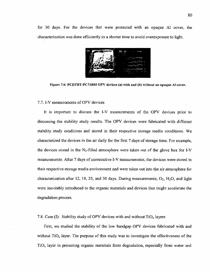
80
for 30 days. For the devices that were protected with an opaque Al cover, the
characterization was done efficiently in a shorter time to avoid overexposure to light.
Figure 7.6: PCDTBT:PC71BM OPV devices (a) with and (b) without an opaque Al cover.
7.7 .1-V measurements of OPV devices
It is important to discuss the I-V measurements of the OPV devices prior to
discussing the stability study results. The OPV devices were fabricated with different
stability study conditions and stored in their respective storage media conditions. We
characterized the devices in the air daily for the first 7 days of storage time. For example,
the devices stored in the N2 -filled atmosphere were taken out of the glove box for I-V
measurements. After 7 days of consecutive I-V measurements, the devices were stored in
their respective storage media environment and were taken out into the air atmosphere for
characterization after 12, 18, 25, and 30 days. During measurements, O2 , H2 0 , and light
were inevitably introduced to the organic materials and devices that might accelerate the
degradation process.
7.8. Case (I): Stability study of OPV devices with and without TiOx layers
First, we studied the stability of the low bandgap OPV devices fabricated with and
without TiOx layer. The purpose of this study was to investigate the effectiveness of the
TiOx layer in protecting organic materials from degradation, especially from water and
81
oxygen. For an ideal intrinsically stable OPV device, both the organic materials and
electrodes must be stable without using any encapsulation. We also performed a storage
media study at the same time. We prepared four low bandgap OPV devices fabricated
with and without a TiOx protection layer (less than 20 nm) and stored them in the air and
inside a glove box. We stored the fabricated OPV devices with and without opaque Al
covers (with a high research grade quality).
We were interested in monitoring the change in the J-V characteristics of OPV cells
with and without a TiOx layer. We compared the relative degradation trend from device
to device by evaluating their Jsc, Voc, FF, and PCE values as a function of the storage
time. Figure 7.7 shows the change in the J-V characteristics of four OPV cells fabricated
without the TiOx layer stored in the air and inside the glove box up to 7 days of storage
time. The devices were protected with an opaque Al foil cover. To maintain the
consistency of our results, Figure 7.7 shows the J-V characteristics of the same OPV cell
(from the total of 8 cells in each OPV device) with the best performance on a periodic
basis. The devices were characterized at a period of 30 days, but the J-V characteristics
were only shown up to 7 days since the J-V curves were too crowded. We observed that
the device with a TiOx layer and stored inside the glove box is the most stable with both
Jsc and FF values dropping only approximately 5% and 2% over 7 days of storage time,
as seen in Figure 7.7(b). While for the device fabricated without the TiOx layer and stored
in the glove box, the Jsc and FF values dropped 20% and 23%, respectively, over 7 days
of storage time as seen in Figure 7.7(d).
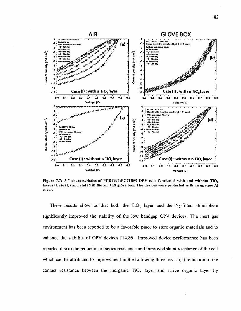
82
AIR GLOVE BOXPCPTB¥:PC7TBBff iP iTStored in airWith an opaque Al cover-O —1st-day- O —2nd-day•H>~3rd«dsy—0 -4 th -d ay—«£r-6tf>-day—O - 6 th-day-< p" 7th-day
PCOTBT: PC71 BUTTtOtStored inside the glove box (0a>|}0 < 0.1 ppm)With an opaque At cover-O - la t -d a y- O —2nd-day- 0 —3rd-day-0 -4 tfv d a y-9-5th<day—0 -6 th -d a y—<*■—7th-day
Case ( I ) : w ith a TiOx layer <---- 1-----■-----1----->-----1---- '-----1-----'-----P---- ■-----1-----■---- 1-----•-----1-----'----- 1-----1-----1-----1-----■---- 1---- 1-----1-----1-----1-----.-----1-----r-----1-----.-----1-----.----
0.0 0.1 0.2 0.3 0.4 0.5 0.6 0.7 0.8 0.9 0.0 0.1 0.2 0.3 0.4 0.5 0.6 0.7 0.8 0.9Voltage (V) Voltage (V)
PCDTBT:PC71BMStored inside the glove box (0 ,tHtO < 0.1 ppm) With an opaque At cover —O —1st-day- O - 2nd-day- O — 3rd-day w»-—O —dth-day J * r f—7— 5th-day —0 - 6th-day—ft— 7th-day .
PCDTBT:PC71BM Stored in airWith an opaque A) cover ^ “Istday ^ 0 —2nd*day —CJ—3rd-day - 0 -4 th -d a y
Case (I) : w ithout a TiO, layer Case (I) : w ithou t a TiOx layer
Voltage (V) Voltage (V)
Figure 7.7: J-V characteristics of PCDTBT:PC71BM OPV cells fabricated with and without TiOx layers (Case (I)) and stored in the air and glove box. The devices were protected with an opaque Al cover.
These results show us that both the TiOx layer and the N2 -filled atmosphere
significantly improved the stability of the low bandgap OPV devices. The inert gas
environment has been reported to be a favorable place to store organic materials and to
enhance the stability of OPV devices [14,86]. Improved device performance has been
reported due to the reduction of series resistance and improved shunt resistance of the cell
which can be attributed to improvement in the following three areas: ( 1 ) reduction of the
contact resistance between the inorganic TiOx layer and active organic layer by
83
passivation of surface trap states; (2 ) enhancement o f the electronic coupling between the
inorganic TiOx and active organic layer to mediate better forward charge transfer and
reduce back charge recombination at the interface, and (3) in affecting the upper organic
layer growth mode and morphology [156].
We monitored the OPV device performances in the air as well. For the device with a
TiOx layer and stored in the air, the Jsc and FF values dropped 32% and 44%,
respectively, over 7 days of storage time as seen in Figure 7.7(a). We observed that the
degradation of the low bandgap OPV device fabricated without the TiOx layer was the
fastest when it was stored in the air, as seen in Figure 7.7(c), where the Jsc and FF values
dropped 98% and 81%, respectively, after 3 days of storage time. The reactions between
O2 and H2 O and the Al cathode lead to metal oxidation and active layer damage [157].
An opaque Al foil cover was not enough to slow down the degradation. The degradation
of the performance of the OPV device has been reported to be related to recombination of
the charge carriers [113] and oxygen induced trap states in the polymer resulting in a
strong decrease in charge carrier mobility [158].
We found that the TiOx layer effectively improved the lifetime and stability of the
OPV device. The polymers with low ionization potential and amorphous structure
materials such as PCDTBT are the most susceptible to oxygen diffusion into the blend of
the active solution [159]. The effect of the TiOx material as the oxygen/water protection
and as the oxygen scavenging agent for the OPV device application is reportedly due to
the combination of photo-catalysis and inherent oxygen deficiency [160]. This study
further highlights the importance of the TiOx layer in the lifetime and stability of OPV
devices.
84
7.9. Case (II): Stability study of OPV devices with and without opaque Al covers
We then performed a stability study of low bandgap OPV devices stored with and
without opaque Al protection covers. The purpose of this study was to investigate the
effects of the Al cover in protecting OPV device from degradation, especially from
exposure to light. We prepared four low bandgap OPV devices with and without an Al
cover (with a high research grade quality) stored in the air and inside the glove box. We
fabricated OPV devices with a TiOx layer (less than 20 nm) as the protection layer.
Similar to what we did in Case (I) stability study, we monitored the change in J-V
characteristics of OPV devices with and without an opaque Al cover. In this study, all
devices were fabricated with a TiOx layer and we compared the relative degradation trend
from device to device by evaluating their OPV parameter values. To maintain the
consistency of our results, in a total of 8 cells in each OPV device, we characterized and
monitored the same cell showing the best performance periodically.
Figure 7.8 shows the change in the J-V characteristics of four OPV cells fabricated
with and without an opaque Al cover stored in the air and inside the glove box up to 7
days of storage time. The devices were fabricated with a TiOx layer. Over 7 days of
storage time, we observed that the device stored with an opaque Al cover inside the glove
box was the most stable with both Jsc and FF values dropping only approximately 5%
and 2% as seen in Figure 7.8(d). While the device stored without an opaque Al cover
inside the glove box is relatively stable and gradually dropped its performance over time
showing the Jsc and FF values dropping only 14% and 1%, respectively as seen in Figure
7.8(b).
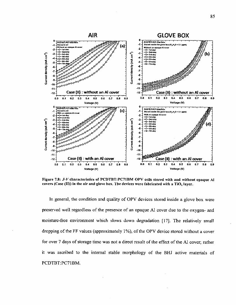
85
AIR GLOVE BOX
« -4<£
PCOTBT:PC718U/TiOx
without an opaque Al
Case (II): w ithout an Al coverr— j------ .--- 1— .-----1----- ----- 1------- 1--------1------- 1------«-1-----
0.0 0.1 0.2 0.3 0.4 0.5 0.6 0.7 0.8 0.9
Voltage (V)
<E
c0■O
o
PCbTBt:PC71BWTi'Ox Stored In air With an opaque Al cover - O —lBt-cUy -<>“ 2nd-d3y —O —3rd-day -0 -4 th -d a y -V -G th-day - O —6 th-day
7th*d«!
(c)
Case (II): w ith an Al cover0.0 0.1 0.2 0.3 0.4 0.5 0.6 0.7 0.8 0.9
Voltage (V)
PCOTBT:PC71BM/TtOxStored inside the glove box (0^14,0 < 0.1 ppm) Without an opaque Al cover - O —lat-ctoy-0 -2 n d -d a y—0 -3 rd -d a y -0 -4 th -d a y— Sth-day
6th*day7th-day
Case (II): w ithou t an Al coverl.o 0.1 0.2 0.3 0.4 0.5 0.6 0.7 0.8 0.!
Voltage (V)
PCDTBT:PC71BM/TiOxStored inside the glove box (OjrH}0 < 0.1 ppm) With an opaque A! cover - -Ist-day -KD—2nd-day —O —3rd-day —O — 4th-day - Jv'“ tth d a y
6th-day --0~-7th-day
A
Case (II): w ith an Al cover1.0 0.1 0.2 0.3 0.4 0.5 0.6 0.7 0.8 0.9
Voltage (V)
Figure 7.8: J-V characteristics of PCDTBT:PC71BM OPV cells stored with and without opaque Al covers (Case (II)) in the air and glove box. The devices were fabricated with a TiOx layer.
In general, the condition and quality of OPV devices stored inside a glove box were
preserved well regardless of the presence of an opaque Al cover due to the oxygen- and
moisture-free environment which slows down degradation [17]. The relatively small
dropping of the FF values (approximately 1%), of the OPV device stored without a cover
for over 7 days of storage time was not a direct result of the effect of the Al cover; rather
it was ascribed to the internal stable morphology of the BHJ active materials of
PCDTBT:PC71BM.
We observed degradation of OPV devices stored with and without an opaque Al
cover in an ambient atmosphere. We found that the device with an opaque Al cover
showed that Jsc and FF values dropped 32% and 44%, respectively as seen in Figure
7.8(c). While the devices stored without an opaque Al cover, Jsc and FF values dropped
29% and 46%, respectively as seen in Figure 7.8(a). In general, we observed that the
OPV devices stored in the air with and without Al covers degraded significantly faster
under exposure to air and moisture compared to the ones stored inside the N2 -filled
atmosphere. It seems that the Al cover was not as effective in protecting the OPV devices
from photodegradation because the Jsc and FF values are relatively similar We believe
the reason that the Al cover was ineffective in protecting the OPV devices were (1) the
reaction between the organic materials or metal electrodes and O2 and H2 O was stronger
compared to the reaction between the organic materials/electrodes with the light and (2 )
the devices were not completely protected from the light because they were characterized
in the air and under an intense solar illuminator on a periodic basis. In the latter case, the
photodegradation inevitably deteriorated the performance and the quality of OPV
devices.
7.10. Case (III): Stability study of OPV devices based on different storage media
We also investigated the degradation trend of the PCDTBT:PC71BM based OPV
devices influenced by the storage media environment. Krebs and his coworkers had
investigated different degradation variables affecting the lifetime and stability of OPV
devices [22]. They studied the effects of different storage media on the lifetime of OPV
device stored in extreme conditions such as outdoor and cool environments. In addition to
87
(1) the ambient and (2) N2 -filled atmosphere environments (as previously mentioned in
Section 7.6 and 7.7), two separate storage media, (3) the ante-chamber and (4)
refrigerator, were used. The refrigerator provided a controlled environment with
temperatures of a 3 - 5 °C range.
The device stored inside the refrigerator also had limited exposure to light. The ante
chamber of the glove box was utilized when access was needed in and out of the glove
box and also had a limited exposure to light. The ante-chamber of the glove box is not a
moisture free or oxygen free environment; rather it is a partial environment which is
sometimes an inert gas or ambient atmosphere. The ante-chamber environment might be
useful if we do not have enough space to keep the OPV devices inside a glove box but we
want to study them at a later time. It would be beneficial to manufacture an affordable
partial glove box that does not require a completely O2 - and H2 0 -free environment.
Similar to previous studies, we were interested in monitoring the change of J-V
characteristics of OPV devices stored in different storage media environments. We
compared the relative degradation trend from device to device by evaluating their Jsc,
V0c, FF, and PCE values as a function of storage time. To maintain the consistency of
our results, for the total of 8 cells in each OPV device, we characterized and monitored
the same cell showing the best performance over a period of time.
We fabricated four PCDTBT.PC71BM OPV devices with a TiOx layers. Following
fabrication, we protected the devices with Al foil and stored them in different storage
environments; the ambient and N2 -filled atmosphere environment, a refrigerator and an in
ante-chamber of the glove box as shown in Figure 7.9. We characterized the devices
periodically in the air. As previously discussed, we found that the Jsc and FF values
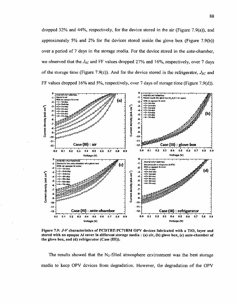
8 8
dropped 32% and 44%, respectively, for the device stored in the air (Figure 7.9(a)), and
approximately 5% and 2% for the devices stored inside the glove box (Figure 7.9(b))
over a period of 7 days in the storage media. For the device stored in the ante-chamber,
we observed that the Jsc and FF values dropped 27% and 16%, respectively, over 7 days
of the storage time (Figure 7.9(c)). And for the device stored in the refrigerator, JSc and
FF values dropped 16% and 5%, respectively, over 7 days of storage time (Figure 7.9(d)).
PCi>TBY:PC7tBfc!/Tibx ' Stored in air With an opaque Al cover —O— 1st <day —0~ 2nd-day —O—3rd-day " O " 4 th-day
5th-day —O — 6th-day - 6 -* 7 t h - d a .
PCDTBT:RC71BM/T!OxStored inside the Steve box < 0.1 ppm)With an opaque Al cover—O— lat-day-O - ln d -d a y—O —3rd-day—O -dlh-day—<0—5lh*day—O—6th-day—ft*— 7th-day
Voltage (V) Voltage (V)
PCDTflT: PC7tBM/TiOV ' ' ' ' ^Stored in the ante-chamber of a g love box With an opaque Al cover —O— 1st-day —O— 2nd*day—o — 3rd-day jjt& f—O —4th-day- V — 5 th-day—O— 6th-day—it— T i n ^ l a y ^ * ^
PCDTB T:PC71 BM/TiOxStored inside a refrigerator (3*5*0With an opaque A! cover- O — fstd ayMC2nd-day- o — Srd-day- O —4tb-day-f?-5 th -day-O -e th -d ay—<J— 7th-day ^
Case (HI): refrigerator0.0 0.1 0.2 0.3 0.4 0.5 0.6 0.7 0.8 0.9 0.0 0.1 0.2 0.3 0.4 0.S 0.6 0.7 0.8 0.9
Voltage (V) Voltage (V)
Figure 7.9: J-V characteristics of PCDTBT:PC71BM OPV devices fabricated with a TiOx layer and stored with an opaque Al cover in different storage media : (a) air, (b) glove box, (c) ante-chamber of the glove box, and (d) refrigerator (Case (III)).
The results showed that the N2 -filled atmosphere environment was the best storage
media to keep OPV devices from degradation. However, the degradation of the OPV
89
device was slowed down in the refrigerator. It has been reported that a low temperature
storage environment has helped tremendously in keeping organic materials from
degrading over long periods of time [161,162]. Moreover, the dark environment inside
the refrigerator and the cool temperatures improved the stability and lifetime of the OPV
device. While the ambient and ante-chamber environments deteriorated the quality o f the
OPV devices approximately 30% compared to their initial performances. The degradation
of the OPV device performance stored in any place where O2 and H20 are available has
been reported to be related to recombination of the charge carriers [113] and oxygen
induced trap states in the polymer resulting in a strong decrease in charge carrier mobility
[156],
7.11. Summary
We used the sol-gel TiOx material as an interfacial layer between the active layer of
PCDTBT:PC71BM and the Al cathode. We performed optimization tests on the TiOx
layer including the TiOx solution spin coating test and the TiOx solution drying test. We
found that the TiOx solution deposited at a spin speed of 3000 rpm (TF1) improved the
photon absorption of the active layer. For the drying test, we found that 90 °C for 10 min
was the optimal drying condition for the TiOx solution. The surface roughness of
PCDTBT:PC71BM/TiOx of a 0.989 nm was observed with an AFM measurement.
We performed stability studies on the low bandgap OPV devices based on (1) with
and without TiOx layers (Case (I)), (2) with and without opaque Al protection covers
(Case (II)), and (3) different storage media (Case (III)). We investigated the degradation
of the OPV devices by observing the changes in the Jsc, VQc, FF, and PCE values of the
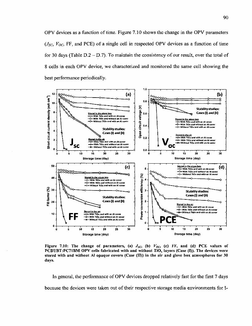
90
OPV devices as a function of time. Figure 7.10 shows the change in the OPV parameters
(JSc, Voc, FF, and PCE) o f a single cell in respected OPV devices as a function of time
for 30 days (Table D.2 - D.7). To maintain the consistency o f our result, over the total of
8 cells in each OPV device, we characterized and monitored the same cell showing the
best performance periodically.
1 2 -
E.*<0c01*o§
to
Stability studies; Cases (I) and (II)Stored in the d o v e box
—O—With TiOx and with an Al cover —O—With TiOx and without an Al cover
Without TiOx and with an Al coverStored m the ortove box -O -W ith TiOx and with an Al cover -O — With TiOx and without an Al cover —O—Without TiOx and with an Al coverP 0.4
Stability studies; Cases (I) and (III
Stored In the air-Jvw With TiOx and with an Al cover
With TiOx and vrithout an Al cover " BO1 Without TiOx and with an Al cover
Stored in the air— Wi t h TiOx and with an Al cover
w ith TiOx and without an Al cover 3 l \ v )K Without TiOx and with an Al cover
50-
40-
£ 30-2O £— 2 0 -
\Z
1 0 -
Storage time (day) Storage time (day)
(C)
Stored in the glove boxWith TiOx and with an AJ cover
—O—With TiOx and without an Al cover - O — Without TiOx and with an Al cover
Stability studies: Cases (I) and (II)
Stored in the a irWith TiOx and vnth an Al cover
—O—With TiOx and without an Al cover '""HC"" Without TiOx and with an Al cover
—,— 10
T—15
— *1—
20— i—
25■ i30
5-
coo? 3 c o Ȥ 2co
1 -
oQ.
0 -
I I------- r 1.......... 1 ' IStored in the olove box / J—O — With TiOx and with an Al cover *— Wi t h TiOx and without an Al cover - O —W ithout TiOx and with an Al cover
Stability studies: Cases (I) and (II)
Stored in the air— Wi t h TiOx and with an Al cover ■■O1 With TiOx and without an Al cover
M Without TiOx and with an Al cover
V.PCE—I—
10
Storage time (day)
15 20Storage time (day)
25— i—
30
Figure 7.10: The change of parameters, (a) Jsc, (b) Voc, (c) FF, and (d) PCE values of PCDTBT:PC71BM OPV cells fabricated with and without TiO, layers (Case (I)). The devices were stored with and without Al opaque covers (Case (II)) in the air and glove box atmospheres for 30 days.
In general, the performance of OPV devices dropped relatively fast for the first 7 days
because the devices were taken out of their respective storage media environments for 1-
91
V measurements in the air. While measuring, OPV devices were exposed to O2 , H2 O, and
light. After 7 consecutive days of I-V measurements, the devices were only taken out and
characterized in the air periodically (every other 5 days) which significantly improved the
stability of the devices. The decrease in the OPV device parameters {Jsc, FF, and PCE)
correlates to the loss of the physical or chemical qualities of the device due to
recombination, loss mechanism, or degradation. However, the V0c value was relatively
stable and was reported to be internally dependent on the energy levels of the active
materials and the morphology of the active layer [12,148].
From the stability study of the low bandgap OPV devices with and without TiOx
layers (Case (I)), we found that the TiOx layer was significantly effective in protecting
the active solution and the OPV device from degradation especially from exposure to O2
and H2 O. After 30 days of storage time, the PCE values dropped 16% for the device with
a TiOx layer and 48% for the device without the TiOx layer stored in a N2 -filled
atmosphere. While for the device stored in the air, the PCE values dropped 92% after 18
days of the storage time for the device with a TiOx layer and 100% after 3 days for the
device without the TiOx layer. We concluded that the solution based TiOx layer was
effective in slowing down degradation by 300% for the device stored in the N2 -filled and
ambient atmospheres. This study highlighted the effectiveness of the TiOx layer as an
oxygen/water protection and as an oxygen scavenging agent in improving the lifetime
and stability of OPV devices.
From the stability study of the low bandgap OPV devices stored with and without
opaque Al protection covers (Case (II)), we found that the Al cover was not effective in
protecting the organic materials and OPV devices from degradation especially from the
light. After 30 days of storage, the PCE values dropped 16% in the device with an opaque
Al cover and 34% in the device without a cover stored in the N2 -filled atmosphere. For
the device stored in the air, the PCE values of both devices with and without an Al cover
dropped approximately 92% after 18 days of storage time. We suggest the reasons for the
ineffectiveness of the Al cover are (1) the reaction between the organic materials or metal
electrodes and O2 and H2 O was stronger comparing the reaction between the organic
materials/electrodes with light and (2 ) the devices were not completely protected from
light.
From the stability study of the low bandgap OPV devices with different storage
media (Case (III)), we found that the N2 -filled atmosphere environment was the most
optimum environment to store OPV devices and to keep them from degradation as seen
in Figure 7.11. As observed in stability studies for Cases (I) and (II), the performance of
OPV devices stored in different storage media environments also dropped relatively
faster in the first 7 days compared to the later storage times because the devices were
exposed to O2 , H2 O, and light more often during the I-V measurements. Figure 7.11
shows the change in the OPV parameters (Jsc, Voc, FF, and PCE) o f a single cell in
respected OPV devices as a function of time for 30 days (Appendix D.2, D.4, D.8 , and
D.9). We characterized and monitored the same cell showing the best performance
periodically.
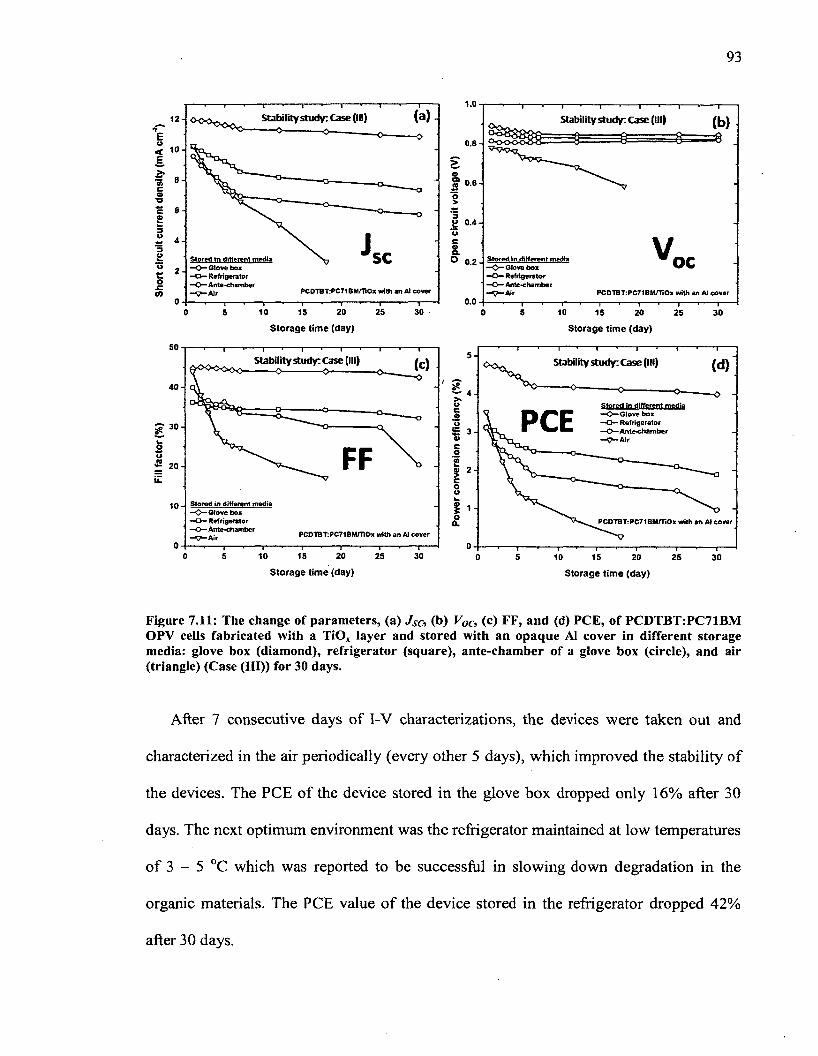
93
1.0
(a) -o - o o ^ ^ Stability study: Case (in)1 2 - Stability study: Case (III)
1 0 -
0 .6 -
s c ° 0 . 2 -Stored in d iffered media Glove box Refrigerator
—O —Ante-chamber — —Air
OC
0.0300 10 15 20 25 105 0 5 15 20 25 30
Storage time (day) Storage time (day)
50Stability study: Case (III) Stability study: Case (III)
40- 4-S tored tn different media —0 -< 3 lo v e box —O — Refrigerator —O —Ante-cham ber ~<7~Air
• O
PCE
Ik.
Stored in different media —O - Glove box —O - Refrigerate r — Ante-chamber -* ?—Air
1 0 -
ID 15 20Storage time (day)
25 30 2515Storage time (day)
20
Figure 7.11: The change of parameters, (a) Jsa (b) Voc, (c) FF, and (d) PCE, of PCDTBT:PC71BM OPV cells fabricated with a TiO, layer and stored with an opaque Al cover in different storage media: glove box (diamond), refrigerator (square), ante-chamber of a glove box (circle), and air (triangle) (Case (III)) for 30 days.
After 7 consecutive days of I-V characterizations, the devices were taken out and
characterized in the air periodically (every other 5 days), which improved the stability of
the devices. The PCE of the device stored in the glove box dropped only 16% after 30
days. The next optimum environment was the refrigerator maintained at low temperatures
of 3 - 5 °C which was reported to be successful in slowing down degradation in the
organic materials. The PCE value of the device stored in the refrigerator dropped 42%
after 30 days.
We found that the condition in a partial inert environment of the antechamber would
be a comprising optimum condition where the OPV device would be operational without
causing any catastrophic failures (The PCE value dropped 75% after 30 days). After 25
days of storage time in the ante-chamber, the OPV device quality dropped significantly
which might be caused by activity in the glove box during that period of storage time.
The activity of the ante-chamber that introduced 0 2, H20 , and light to an OPV device
certainly accelerates the degradation processes. Finally, the PCE of the device stored in
the air dropped 100% after 18 days because the 0 2 and H20 aggressively reacted with the
organic materials/electrodes. Similar to our previous findings, the Voc was stable as
expected since the Voc values depended intrinsically on the energy level of the active
materials.
95
Chapter 8
Conclusions and Future Work
In this thesis, we fabricated unencapsulated bulk heterojunction (BHJ) organic
photovoltaic (OPV) devices based on the high and low bandgap polymers with structures
of ITO/PEDOT:PSS/P3HT:PC-61BM/A1 and ITO/PEDOT:PSS/PCDTBT:PC71BM/Al,
respectively. There are two major parts to this study. First, we fabricated conventional
OPV devices without a TiOx layer. Prior to fabrication, we spent significant time and
effort in optimizing the fabrication processing steps including; the thickness of the active
layer (using spin coating deposition), and the pre-annealing and post-annealing
treatments. The majority of BHJ films were formed by spin coating where the initial
phase morphology was determined by a complex combination of solvent removal and
solidification of acceptor and donor materials. We found that although the principle of
spin coating might sound simple, it can limit morphological controllability.
We fabricated the OPV devices by using the optimal fabrication procedure. In our
experiment, we achieved that the best PCE value of 4.1% for the P3HT:PC61BM based
OPV device and 5.1% for the PCDTBT:PC71BM OPV device as seen in Table 8.1.
However, the fill factor for our low bandgap polymer based OPV devices was below 50%
which means the control morphology for the PCDTBT:PC71BM layer was not fully
optimized. Reproducibility of the OPV devices is another major issue in OPV research.
The main reason for a reproducibility issue is the instability of the morphological donor
and acceptor phase separation. The reproducibility issue could be improved with an
optimum fabricating and processing environment. Moreover, reproducing good results
for BHJ OPV devices in a non dust free laboratory environment is even harder.
Table 8.1: The best P3HT:PC61BM and PCDTBT:PC71BM OPV parameters achieved in our experiment bench marked with literature values ]85,163|.
Active layer Reference Eg (eV) Jsc (mA/cm'2) v o c (y) FF (%) PCE (%)
P3HT :PC61BM[163]
1.811.3 0.64 69 5.2
This work 10.5 0.63 63 4.1
PCDTBT:PC71BM185]
1.910.6 0.86 64 6.0
This work 12.7 0.90 45 5.1
We then studied the long term stability trends of two different BHJ systems: semi
crystalline and amorphous polymer based BHJ cells. Since both the P3HT and the
PCDTBT displayed distinctive morphological characteristics in BHJ OPV cells, we
believe that the acceleration of physical and chemical degradation may occur at different
speeds for the P3HT:PC61BM and the PCDTBT:PC71BM active layers. There are rarely
any reports about the stability study on a low bandgap polymer, PCDTBT based OPV
devices. Therefore we focused the stability study on the blend of PCDTBT:PC71BM
based OPV devices in this study. We synthesized a solution based titanium sub-oxide
(TiOx) by using a sol-gel chemistry method. We inserted a solution based TiOx layer
coated at a spin speed of 3000 rpm (less than 20 nm) between the photoactive layer and
the Al cathode in OPV devices. We studied the effectiveness of the TiOx layer in
protecting the photoactive layer from degradation and performed a stability study on the
OPV devices by using the TiOx solution.
97
Table 8.2: The stability study performance of OPV devices fabricated using different photoactive layers, different stability conditions: with and without TiO, layers (Case (I)), with and without opaque Al protection covers (Case (II)), and different storage media ((1) glove box, (2) air, (3) ante-
No Active layer of BHJ OPV device
TiOxlayer
9— ---\ --- vStorage condition of
OPV deviceInitialPCE(%)
Storagetime(day)
Percentage of PCE
reduction] P3HT:PC61BM YES Glove box
with an Al cover1.7 70 26.02
2 PCDTBT.PC71BM YES Glove box with an Al cover
4.8 30 16.16
3 PCDTBT:PC71BM YES Glove box without an Al cover
4.6 30 33.80
4 PCDTBT: PC7 IBM NO Glove box with an Al cover
3.7 30 48.04
5 PCDTBT :PC71BM YES Airwith an Al cover
3.5 18 92.35
6 PCDTBT :PC71BM YES Airwithout an Al cover
3.6 18 92.48
7 PCDTBT:PC71BM NO Airwith an Al cover
3.7 3 100.00
8 PCDTBT:PC71BM YES Ante-chamber with an Al cover
3.1 30 75.21
9 PCDTBT:PC71BM YES Stored in a refrigerator
3.1 30 42.93
We performed stability studies on PCDTBT:PC71BM OPV devices based on
different stability conditions : (1) with and without TiOx layers (Case (I)), (2) with and
without opaque Al covers (Case (II)), and (3) different storage media conditions (Case
(III)) as seen in Table 8.2. To determine the trend of the performance of OPV devices as
a function of the storage time, we used normalized OPV parameters, Jsc, Voc, FF, and
PCE values. Normalized parameters of OPV devices would be useful in comparing the
relative degradation effect from one device to another. Figure 8.1 shows the change in the
normalized OPV parameters (Jsc, Voc , FF, and PCE) as a function of time for 30 days.
Each normalized data represents results of a single cell o f OPV parameters reported in
Figure 7.10 (Table D.2 - D.7). To maintain the consistency of our result, over the total of
8 cells in each OPV device, we characterized and monitored the same cell showing the
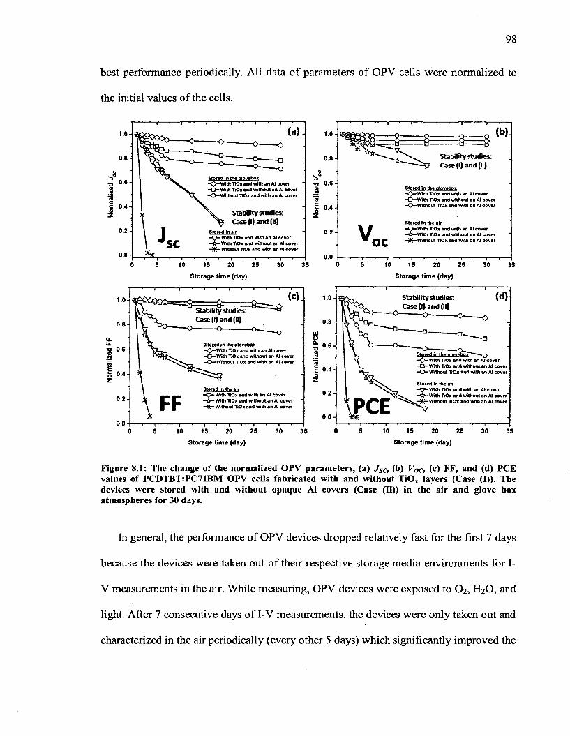
98
best performance periodically. All data of parameters of OPV cells were normalized to
the initial values of the cells.
Stability studies: Case (I) and (II)
Stored m the otovcpoaWith TiOx and with an Al cover
- O —With TiOx and without an At cover Without TiOx and with an Al cover
Stored m the olovebox ~ 0 “ With TiOx and with an AJ cover
With TiOx and without an Al cover - 0 “ Without TiOx and with an Al cover
Stability studies: Case (I) and (II) Stored in the air
- ^ ^ W lth TiOx and with an Al coverStored In air - V W i t h TiOx and with an Al cover - f r -W ith TiOx and without an Al cover ■■■'W' Without TiOx and with an A! cover
—W—With TiOx and without an Al cover Q £ —X-- Without TiOx and with an Al cover
Storage time (day) Storage time (day)
1 .0 -
0 .8 -
u.■o 0 .6 -I
I 0.4 H
0 .2 -
Stabilfty Judies: Case (I) and (II)
0 .0 *
(c)
—1-----------■------- 1—S 10
Stored in the alovebox ^^■ W ilh TiOx and with an Al cover
With TiOx and without an Al cover - O —Without TiOx and with an Al cover
s .lo f rd . j n ) h » a i r-v -w ith TiOx and with an Al cover
With TiOx and without, an Al cover Without TiOx and with an Al cover
—I—15 20 25
— I—
30Storage time (day)
1.0
0. 8 -
0 . 6 -
a| 0.4oz
0 .2-
0 . 0 -
35
Stability studies: Case (I) and (II)
(d)
Stored in the qlove^ST*-——-O -W ith TiOx and with an Al cover —O — With TtOx and without an Al cover - O — Without TiOx and with an Al cover
Stored in the air— With TiOx and with an Al cover
With TiOx and without an Al cover* —X*" Without TiOx and with an AJ cover
10 15 20—t— 25 30 35
Storage time (day)
Figure 8.1: The change of the normalized OPV parameters, (a) Jsc, (b) Voc, (c) FF, and (d) PCE values of PCDTBT:PC71BM OPV cells fabricated with and without TiOx layers (Case (I)). The devices were stored with and without opaque Al covers (Case (II)) in the air and glove box atmospheres for 30 days.
In general, the performance of OPV devices dropped relatively fast for the first 7 days
because the devices were taken out of their respective storage media environments for I-
V measurements in the air. While measuring, OPV devices were exposed to O2 , H2 O, and
light. After 7 consecutive days of I-V measurements, the devices were only taken out and
characterized in the air periodically (every other 5 days) which significantly improved the
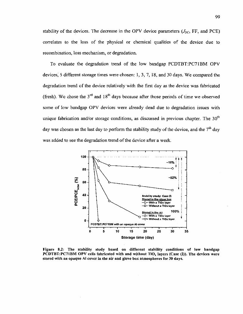
99
stability of the devices. The decrease in the OPV device parameters (JSc, FF, and PCE)
correlates to the loss of the physical or chemical qualities of the device due to
recombination, loss mechanism, or degradation.
To evaluate the degradation trend of the low bandgap PCDTBT:PC71BM OPV
devices' 5 different storage times were chosen: 1, 3, 7, 18, and 30 days. We compared the
degradation trend of the device relatively with the first day as the device was fabricated
(fresh). We chose the 3rd and 18th days because after those periods of time we observed
some of low bandgap OPV devices were already dead due to degradation issues with
unique fabrication and/or storage conditions, as discussed in previous chapter. The 30th
day was chosen as the last day to perform the stability study of the device, and the 7th day
was added to see the degradation trend of the device after a week.
1 0 0 -
8 0 -
6 0 -1c
u fOCL 4 0 -u3oO.
2 0 -
0 -
-18%
Stability study: Case (I) Stored in the dove box —O-W ith a TiOx layer —O —Without a TiOx layer
Stored in the air 100% —O—With a TiOx layer —V ~ Without a TiOx layer
PCDTBT:PC71BM with an opaque Al cover ' 1 '----1—I 5 10 15
T -2 0
~T-25 30 3 5
Storage time (day)
Figure 8.2: The stability study based on different stability conditions of low bandgap PCDTBT:PC71BM OPV cells fabricated with and without TiOi layers (Case (I)). The devices were stored with an opaque Al cover in the air and glove box atmospheres for 30 days.
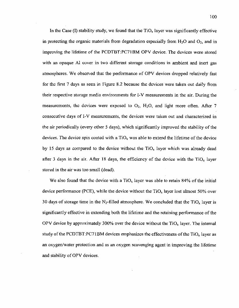
In the Case (I) stability study, we found that the TiOx layer was significantly effective
in protecting the organic materials from degradation especially from H2 O and O2 , and in
improving the lifetime of the PCDTBT:PC71BM OPV device. The devices were stored
with an opaque Al cover in two different storage conditions in ambient and inert gas
atmospheres. We observed that the performance of OPV devices dropped relatively fast
for the first 7 days as seen in Figure 8.2 because the devices were taken out daily from
their respective storage media environments for I-V measurements in the air. During the
measurements, the devices were exposed to O2 , H2 O, and light more often. After 7
consecutive days of I-V measurements, the devices were taken out and characterized in
the air periodically (every other 5 days), which significantly improved the stability o f the
devices. The device spin coated with a TiOx was able to extend the lifetime of the device
by 15 days as compared to the device without the TiOx layer which was already dead
after 3 days in the air. After 18 days, the efficiency of the device with the TiOx layer
stored in the air was too small (dead).
We also found that the device with a TiOx layer was able to retain 84% of the initial
device performance (PCE), while the device without the TiOx layer lost almost 50% over
30 days of storage time in the N2 -filled atmosphere. We concluded that the TiOx layer is
significantly effective in extending both the lifetime and the retaining performance of the
OPV device by approximately 300% over the device without the TiOx layer. The internal
study of the PCDTBT:PC71BM devices emphasizes the effectiveness of the TiOx layer as
an oxygen/water protection and as an oxygen scavenging agent in improving the lifetime
and stability of OPV devices.
101
In the Case (II) stability study, we found that the Al cover was relatively effective in
protecting the organic materials from degradation especially from light. The devices were
fabricated with a TiOx layer and stored with an opaque Al cover in two different storage
conditions: in ambient and inert gas atmospheres. Figure 8.3 shows the percentage ratio
of PCE of devices stored with and without an Al cover, and measured at different storage
times. For the devices stored in the glove box, we observed that the performance of the
device with an opaque Al cover was improved by 50% compared to the device without
the Al cover.
1 0 0 -
-1 8 % ;
8 0 --3 6 %
6 0 -sc Stability study: Case (II)
Stored in the alove box —O— With an Al cover —O— Without an Al cover
Ul2 4 0 - UJo£L
2 0 -
100%Stored in the air —O— With an Al cover — Without an Al cover
PCDTBT:PC71BM with UOx
5 200 10 15 25 30 35
S to ra g e tim e (day)
Figure 8.3: The stability study based on different stability conditions of low bandgap PCDTBT:PC71BM OPV cells stored with and without opaque Al covers (Case (II)) in the air and glove box atmospheres for 30 days. The devices were fabricated with a TiOx layer.
The improvement in the lifetime is also attributed to the effectiveness of the TiOx
layer and the inert gas atmosphere in slowing down degradation. The OPV devices stored
in the air, with and without an opaque Al cover, degraded at a relatively same
degradation rate up to 18 days, but degraded faster than their counterparts stored in an
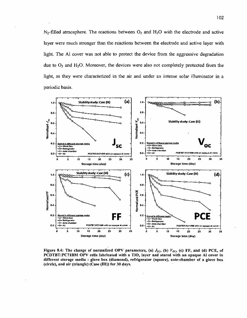
102
N2 -filled atmosphere. The reactions between O2 and H2 O with the electrode and active
layer were much stronger than the reactions between the electrode and active layer with
light. The Al cover was not able to protect the device from the aggressive degradation
due to O2 and H2 O. Moreover, the devices were also not completely protected from the
light, as they were characterized in the air and under an intense solar illuminator in a
periodic basis.
(a). (b)-Stability study: Case (III) 1.0 -1 .0 -
0.8 -0.8 -
Stability study: Case (III)0 .6 - T3©N
<0
E 0.4- 0.4-oZ
0 .2 - Stored In different storage media Glove box
—O — Refrigerator —O — Antecham ber —< 7 - A J r
Stored in different«to rage media —C>—Otove box —O — Refrigerator - O ” Ante-chamber —S?—Air
OCSCPC0TBT:PC71BM with an opaque Ai cover _0 .0 -0.0 - PCOTBT:PC71 BM with AJ cover -
0 5 10 15 20 25 35300 5 10 15 25 3520 30Storage time (day) Storage time (day)
Stability study; Case (ill) Stability study; Case (III)(c) (d)1.0 -1.0 -
0 .8 - 0 .8 -
u.0 .6 -TJ0.4-
0.2 - 0 .2 -Stored In different storage media — Glove box —O— Refrigerator —O — Ante-chamber
Stored in different media —O— Glove box —O — Refrigerator
Ante-chamber — AirPCDTBT:PC718M with an opaque AJ 0.0 - PCOTBT:PC71BM with an opaque Al cover -
15 20 25 350 5 10 30 0 105 15 20 25 30 35Storage time (day) Storage time (day)
Figure 8.4: The change of normalized OPV parameters, (a) Jsc, (b) V0c, (c) FF, and (d) PCE, of PCDTBT:PC71BM OPV cells fabricated with a TiO, layer and stored with an opaque Al cover in different storage media : glove box (diamond), refrigerator (square), ante-chamber of a glove box (circle), and air (triangle) (Case (III)) for 30 days.
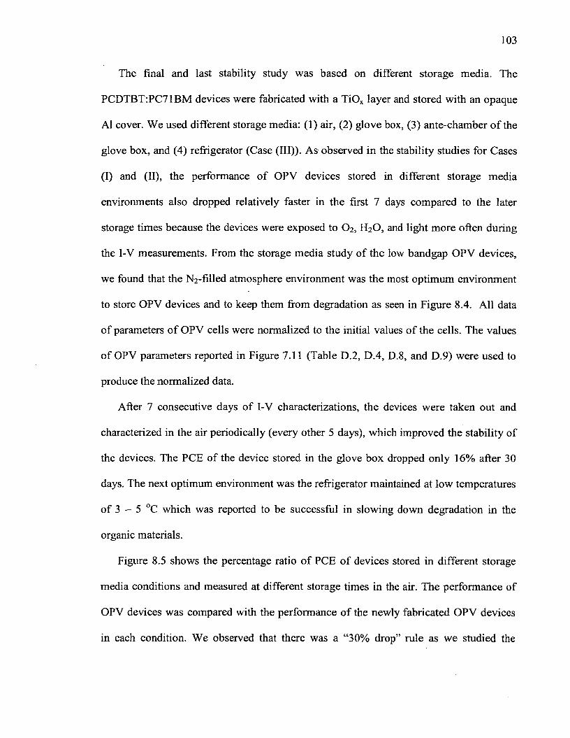
The final and last stability study was based on different storage media. The
PCDTBT:PC71BM devices were fabricated with a TiOx layer and stored with an opaque
Al cover. We used different storage media: (1) air, (2) glove box, (3) ante-chamber of the
glove box, and (4) refrigerator (Case (III)). As observed in the stability studies for Cases
(I) and (II), the performance of OPV devices stored in different storage media
environments also dropped relatively faster in the first 7 days compared to the later
storage times because the devices were exposed to O2 , H2 O, and light more often during
the I-V measurements. From the storage media study of the low bandgap OPV devices,
we found that the N2 -filled atmosphere environment was the most optimum environment
to store OPV devices and to keep them from degradation as seen in Figure 8.4. All data
of parameters of OPV cells were normalized to the initial values of the cells. The values
of OPV parameters reported in Figure 7.11 (Table D.2, D.4, D.8 , and D.9) were used to
produce the normalized data.
After 7 consecutive days of I-V characterizations, the devices were taken out and
characterized in the air periodically (every other 5 days), which improved the stability of
the devices. The PCE of the device stored in the glove box dropped only 16% after 30
days. The next optimum environment was the refrigerator maintained at low temperatures
of 3 - 5 °C which was reported to be successful in slowing down degradation in the
organic materials.
Figure 8.5 shows the percentage ratio of PCE of devices stored in different storage
media conditions and measured at different storage times in the air. The performance of
OPV devices was compared with the performance of the newly fabricated OPV devices
in each condition. We observed that there was a “30% drop” rule as we studied the
104
performance of PCDTBT:PC71BM devices based on the different storage media
conditions. The PCE value dropped the least (16%), when the device was stored in the
glove box, dropped at a higher amount of 42% for the device stored in a refrigerator, and
dropped at a rate of 75% for the device stored in an ante-chamber of the glove box. While
the PCE of the device stored in the air dropped 100% after 18 days. We concluded that
the N2-filled atmosphere is the best storage media to keep OPV devices from degradation.
And the degradation of the OPV device stored in the refrigerator was also relatively slow
due to the low temperatures and dark storage environment. The devices stored in the
ambient air and ante-chamber atmospheres degraded relatively fast due to the exposure to
O2 and H2 0.
1 0 0 -
■18% :
■o-8 0 -
-4 4 %
6 0 -
LL1oS: 4 0 -UiOo.
-7 7 %
Stability s tu d y rNv. Case (III)Different storage media —0 — Glove box —O— Refrigerator —O— Ante-chamber —V- Air
2 0 -
100%
PCDTBT:PC71BM with TiOx and an opaque At cover"
0 5 10 15 2 5 30 3520
Storage time (day)
Figure 8.5: The stability study based on different storage media conditions of low bandgap PCDTBT:PC71BM OPV devices stored in the air, a glove box, an ante-chamber, and a refrigerator (Case (III)). The devices were fabricated with a TiO, layer and stored with an opaque A1 cover.
A highly stable OPV device was obtained by using a combination of the TiOx layer as
the protection layer and an A1 cover stored in a N2-filled atmosphere. The stability of the
OPV devices stored inside the inert atmosphere was improved because the inert (oxygen-
free and moisture-free environment) conditions slow down degradation. The TiOx layer
acts as a diffusion barrier for oxygen which effectively further slows down the interaction
between the oxygen with the active layer. From this study on stabilization of OPV
devices with a TiOx layer, we learned, (1) the device efficiency decreases with an
increase in air and light exposure time, (2) a thin film of TiOx layer on top of the active
layer provides significant protection from degradation and (3) a higher rate of loss in cell
efficiency for the devices without a TiOx layer was noted when exposed to the combined
effect of light and oxygen, as compared to other devices with a TiOx layer. The
incorporation of a solution based TiOx layer into OPV devices is useful approach towards
reducing the sensitivity of such devices to oxygen and water vapor. However,
degradation still occurred for three reasons: ( 1 ) the organic materials decayed over time,
(2 ) the fabrication was not performed in a dust-free manufactured environment, and (3 )
the characterization was performed in air.
Another important issue is the stability of the morphological donor/acceptor phase
separation. The molecular order as well as the spatial dimensions of donor/acceptor
demixing over a period of storage time can impact OPV performance [22], Further phase
separation observed at a longer storage time might lead to a spatial donor/acceptor
distance exceeding the diffusion length of photogenerated excitons which results in loss
of the photocurrent [132], Progress in the encapsulation techniques in the OPV research
is important in improving the stability of OPV devices, but the improvement in the
morphological long-term stability is the key to OPV devices being competitive in the
market.
106
We believe that the stability and lifetime of our OPV devices are relatively stable and
excellent; although we cannot easily compare the stability of organic solar cells since its
evaluation method is not standardized. This implies that the polycrystalline TiOx plays an
important role as the electron collection layer, the hole blocking layer, air stability, high
performance, and as a long lifetime device. Minimizing exposure towards oxygen and
water during processing should in principle contribute considerably to an increased
lifetime of OPV cells. This can be achieved by working in a moisture free, inert
atmosphere.
We suggest several approaches for future work in improving the stability of the OPV
devices: (1) internal and (2) external approaches. The internal approach includes the use
of newly developed donor and acceptor materials that improve the photon absorption in
the near IR range, additional studies that optimize the solution based metal oxide
interfacial layer such as ZnOx and TiOx to improve the photo catalytic properties by
means of doping, the use additives to improve the solubility and the miscibility of the
donor and acceptor materials, etc. The external approach includes the use of
encapsulation techniques to protect the device from degradation. Another improvement
would be in the fabrication and characterization conditions in the laboratory. Performing
nanoscale multilayered BHJ OPV devices experiments in a non dust-free environment
will introduce impurities into the OPV device. Small amounts of impurity, even one part
in a thousand, in BHJ OPV cells can alter the electronic properties o f the device. In
addition, characterizing the OPV devices in the air assists in degradation due to exposure
to oxygen and moisture which is proven to accelerate the deterioration of the organic
materials and metal cathode oxidation.
In conclusion, we found that the TiOx layer effectively improved the stability the
OPV devices. The solution based TiOx material is an excellent interfacial layer and a
promising route in fabricating low cost and scalable long term stability in the OPV
devices. The lifetime of organic solar cells is a very important topic for the
commercialization of photovoltaic devices. We have demonstrated the application of the
TiOx protection layer internally in OPV cells. Our experimental results also show that the
sol-gel derived TiOx layer containing organic functionalities serves as an effective
passivation layer for protection from oxygen when excited by photons, where the photo
oxidation of the bound organic moieties causes oxygen gas scavenging. However,
degradation still occurs due to the imperfection of our processing, fabrication, and
characterization conditions (some were performed in air which unfortunately introduced
degradation issues) in our university laboratory. Multi-dimensional approaches must be
performed in order to significantly improve the stability of OPV devices. Those
approaches include the choice of internally smart materials (stable under storage, under
sunlight, and under reduction or oxidation conditions); the use of effective purification
methods; the choice of high glass-transition temperature (Tg) materials and structures
(stable under outdoor cooling or heating); a water and oxygen free fabrication technique
(for example, under a N2-filled glove box, for instance), or encapsulation techniques, etc.
In order to discover optimum performance, the stabilities need to be enhanced and must
become the foci of research efforts in OPV devices.
108
REFERENCES
[1] United Nations Environment Program (UNEP), “Global Environment Outlook (GEO) - 2000”, Earth-scan Publications Ltd., London (2000).
[2] J. Nelson, “The Physics of Solar Cells”, 1st ed., Imperial College Press (2003).
[3] M.I. Hoffert, K. Caldeira, A.K. Jain, E.F. Haites, L.D.D. Harvey, S.D. Potter, M.E. Schlesinger, S.H. Schneider, R.G. Watts, T.M.L. Wigley, and D.J. Wuebbles, Nature, 395, 881 (1998).
[4] M.A. Green, “Solar Cells: Operating Principles, Technology and System Applications”, Kensington: The University of New South Wales (1998).
[5] H. Akamatsu, H. Inokuchi, and Y. Matsunaga, Nature, 173, 168 (1954).
[6 ] C.W. Tang, Appl. Phys. Lett., 48, 183 (1986).
[7] The Nobel Prize in Chemistry 2000 was awarded jointly to Alan J. Heeger, Alan G. MacDiarmid and Hideki Shirakawa.
[8 ] M. Pope and C. E. Swenberg, “Electronic Processes in Organic Crystals and Polymers”, Oxford University, Press, USA, 2nd edition (1999).
[9] T. Stubinger and W. Brutting, J. Appl. Phys., 90, 3632 (2001).
[ 10] National Renewable Energy Laboratory (2011).
[11] (a) M. Gratzel, Inorg. Chem., 44, 6841 (2005); (b) Y. Chiba, A. Islam, Y. Watanabe, R. Komiya, N. Koide, and L. Han, Japanese J. Appl. Phys., 45, 638(2006).
[12] (a) M.C. Scharber, D. Muhlbacher, M. Koppe, P. Denk, C. Waldauf, A.J. Heeger, and C.J. Brabec, Adv. Mater., 18, 789 (2006); (b) J. You, L. Dou, K. Yoshimura, T. Kato, K. Ohya, T. Moriarty, K. Emery, C.-C. Chen, J. Gao, G. Li, and Y. Yang, Nat. Comm., DOI: 10.1038/ncomms2411, 1 (2013).
[13] D.W. Zhao, X.W. Sun, C.Y. Jiang, A.K.K. Kyaw, G.Q. Lo, and D.L. Kwong, Appl. Phys. Lett., 93, 083305 (2008).
[14] T. Jeranko, H. Tributsch, N.S. Sariciftci, and J.C. Hummelen, Sol. Energy Mater. Sol. Cells, 83, 247 (2004).
[15] H. Neugebauer, C.J. Brabec, J.C. Hummelen, and N.S. Sariciftci, Sol. Energy Mater. Sol. Cells, 61, 35 (2000).
109
[16] F.C. Krebs, J.E. Carle, N. Cruys-Bagger, M. Andersen, M.R. Lilliedal, M.A. Hammond, and S. Hvidt, Sol. Energy Mater. Sol. Cells, 8 6 , 499 (2005).
[17] M.O. Reese, A.J. Morfa, M.S. White, N. Kopidakis, S.E. Shaheen, G. Rumbles, and D.S. Ginley, Sol. Energy Mater. Sol. Cells, 92, 746 (2008).
[18] K. Lee, J.Y. Kim, S.H. Park, S.H. Kim, S. Cho, and A.J. Heeger, Adv. Mater., 19, 2445 (2007).
[19] S. Wakim, S. Beaupre, N. Blouin, B.-R. Aich, S. Rodman, R. Gaudiana, Y. Tao, and M. Leclerc, J. Mater. Chem., 19, 5351 (2009).
[20] T.M. Clarke and J.R. Durrant, Chem. Rev., 110, 6736 (2010).
[21] S.R. Cowan, A. Roy, and A.J. Heeger, Phys. Rev. B, 82, 245207 (2010).
[22] M. Jorgensen, K. Norrman, and F.C. Krebs, Sol. Energy Mater. Sol. Cells, 92, 6 8 6
(2008).
[23] J. Jo, S. Kim, S. Na, B. Yu, and D. Kim, Adv. Funct. Mater., 19, 8 6 6 (2009).
[24] B. Ray and M.A. Alam, Appl. Phys. Lett., 99, 033303 (2011).
[25] K. Kawano, R. Pacios, D. Poplavskyy, J. Nelson, D.D.C. Bradley, and J.R. Durrant, Sol. Energy Mater. Sol. Cells, 90, 3520 (2006).
[26] M. Wohlers, H. Wemer, D. Herein, T. Schedel-Niedrig, A. Bauer, and R. Schlogl, Synth. Met., 77, 299 (1996).
[27] A. Tapponnier, I. Biaggio, and P. Gunter, Appl. Phys. Lett., 8 6 , 112114 (2005).
[28] G. Koller, R.I.R. Blyth, S.A. Sardar, F.P. Netzer, and M.G. Ramsey, Appl. Phys. Lett., 76, 927 (2000).
[29] K. Seki, N. Hayashi, H. Oji, E. Ito, Y. Ouchi, and H. Ishii, Thin Solid Films, 393, 298 (2001).
[30] P. Dannetun, M. Boman, S. Stafstrom, W.R. Salaneck, R. Lazzaroni, C. Fredriksson, J.L. Bredas, R. Zamboni, and C. Taliani, J. Chem. Phys., 99, 664 (1993).
[31] J. Kim, J.-S. Kim, S.-W. Kwak, J.-S. Yu, Y. Jang, J. Jo, T.-M. Lee, and I. Kim, Appl. Phys. Lett., 101, 213304 (2012).
[32] K. Norrman, N.B. Larsen, and F.C. Krebs, Sol. Energy Mater. Sol. Cells, 90, 2793(2006).
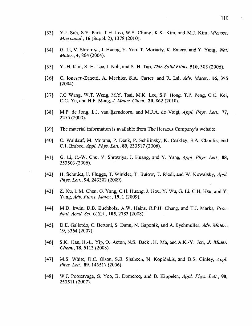
110
[33] Y.J. Suh, S.Y. Park, T.H. Lee, W.S. Chung, K.K. Kim, and M J. Kim, Microsc. Microanal., 16 (Suppl. 2), 1378 (2010).
[34] G. Li, V. Shrotriya, J. Huang, Y. Yao, T. Moriarty, K. Emery, and Y. Yang, Nat. Mater., 4, 864 (2004).
[35] Y.-H. Kim, S.-H. Lee, J. Noh, and S.-H. Tan, Thin Solid Films, 510, 305 (2006).
[36] C. Ionescu-Zanetti, A. Mechler, S.A. Carter, and R. Lai, Adv. Mater., 16, 385(2004).
[37] J.C Wang, W.T. Weng, M.Y. Tsai, M.K. Lee, S.F. Hong, T.P. Peng, C.C. Kei,C.C. Yu, and H.F. Meng, J. Mater. Chem., 20, 862 (2010).
[38] M.P. de Jong, L.J. van Ijzendoom, and M.J.A. de Voigt, Appl. Phys. Lett., 77, 2255 (2000).
[39] The material information is available from The Heraeus Company’s website.
[40] C. Waldauf, M. Morana, P. Denk, P. Schilinsky, K. Coakley, S.A. Choulis, andC.J. Brabec, Appl. Phys. Lett., 89, 233517 (2006).
[41] G. Li, C.-W. Chu, V. Shrotriya, J. Huang, and Y. Yang, Appl. Phys. Lett., 8 8 , 253503 (2006).
[42] H. Schmidt, F. Flugge, T. Winkler, T. Bulow, T. Riedl, and W. Kowalsky, Appl. Phys. Lett., 94, 243302 (2009).
[43] Z. Xu, L.M. Chen, G. Yang, C.H. Huang, J. Hou, Y. Wu, G. Li, C.H. Hsu, and Y. Yang, Adv. Funct. Mater., 19, 1 (2009).
[44] M.D. Irwin, D.B. Buchholz, A.W. Hains, R.P.H. Chang, and T.J. Marks, Proc. Natl. Acad. Sci. U.S.A., 105, 2783 (2008).
[45] D.E. Gallardo, C. Bertoni, S. Dunn, N. Gaponik, and A. Eychmuller, Adv. Mater., 19, 3364 (2007).
[46] S.K. Hau, H.-L. Yip, O. Acton, N.S. Baek , H. Ma, and A.K.-Y. Jen, J. Mater. Chem., 18, 5113 (2008).
[47] M.S. White, D.C. Olson, S.E. Shaheen, N. Kopidakis, and D.S. Ginley, Appl. Phys. Lett., 89, 143517 (2006).
[48] W.J. Potscavage, S. Yoo, B. Domercq, and B. Kippelen, Appl. Phys. Lett., 90, 253511 (2007).
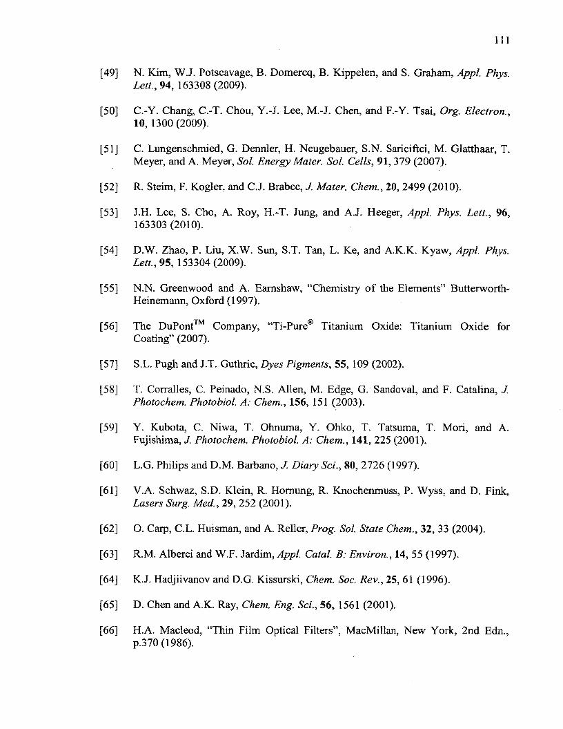
I l l
[49] N. Kim, W J. Potscavage, B. Domercq, B. Kippelen, and S. Graham, Appl. Phys. Lett., 94, 163308 (2009).
[50] C.-Y. Chang, C.-T. Chou, Y.-J. Lee, M.-J. Chen, and F.-Y. Tsai, Org. Electron., 10, 1300 (2009).
[51] C. Lungenschmied, G. Dennler, H. Neugebauer, S.N. Sariciftci, M. Glatthaar, T. Meyer, and A. Meyer, Sol. Energy Mater. Sol. Cells, 91, 379 (2007).
[52] R. Steim, F. Kogler, and C.J. Brabec, J. Mater. Chem., 20, 2499 (2010).
[53] J.H. Lee, S. Cho, A. Roy, H.-T. Jung, and A.J. Heeger, Appl. Phys. Lett., 96, 163303 (2010).
[54] D.W. Zhao, P. Liu, X.W. Sun, S.T. Tan, L. ICe, and A.K.K. Kyaw, Appl. Phys. Lett., 95, 153304 (2009).
[55] N.N. Greenwood and A. Eamshaw, “Chemistry of the Elements” Butterworth- Heinemann, Oxford (1997).
[56] The DuPont™ Company, “Ti-Pure® Titanium Oxide: Titanium Oxide for Coating” (2007).
[57] S.L. Pugh and J.T. Guthrie, Dyes Pigments, 55, 109 (2002).
[58] T. Corralles, C. Peinado, N.S. Allen, M. Edge, G. Sandoval, and F. Catalina, J. Photochem. Photobiol. A: Chem., 156, 151 (2003).
[59] Y. Kubota, C. Niwa, T. Ohnuma, Y. Ohko, T. Tatsuma, T. Mori, and A. Fujishima, J. Photochem. Photobiol. A: Chem., 141, 225 (2001).
[60] L.G. Philips and D.M. Barbano, J. Diary Sci., 80, 2726 (1997).
[61] V.A. Schwaz, S.D. Klein, R. Homung, R. Knochenmuss, P. Wyss, and D. Fink, Lasers Surg. Med., 29, 252 (2001).
[62] O. Carp, C.L. Huisman, and A. Reller, Prog. Sol. State Chem., 32, 33 (2004).
[63] R.M. Alberci and W.F. Jardim, Appl. Catal. B: Environ., 14, 55 (1997).
[64] K.J. Hadjiivanov and D.G. Kissurski, Chem. Soc. Rev., 25, 61 (1996).
[65] D. Chen and A.K. Ray, Chem. Eng. Sci., 56, 1561 (2001).
[6 6 ] H.A. Macleod, “Thin Film Optical Filters”, MacMillan, New York, 2nd Edn.,p.370 (1986).
112
[67] A. Fujishima and K. Honda, Nature, 238, 37 (1972).
[6 8 ] A.L. Linsebigler, G. Lu, and J.T. Yates, Jr., Chem. Rev., 95, 735 (1995).
[69] V.E. Henrich and P.A. Cox, “The Surface Science of Metal Oxides”, Cambridge University Press, Cambridge (1994).
[70] C. Noguera, “Physics and Chemistry of Oxide Surfaces”, Cambridge University Press, Cambridge (1996).
[71] B. O’Regan and M. Gratzel, Nature, 353, 737 (1991).
[72] U. Bach, D. Lupo, P. Comte, J.E. Moser, F. Weissortel, J. Salbeck, H. Spreitzer, and M. Gratzel, Nature, 395, 583 (1998).
[73] A.J. Breeze, Z. Schlesinger, S.A. Carter, and P.J. Brock, Phys. Rev. B, 64, 125205 (2001).
[74] P.A. van Hal, M.M. Wienk, J.M. Kroon, W.J.H. Verhees, L.H. Slooff, W.J.H. van Gennip, P. Jonkheijm, and R.A.J. Janssen, Adv. Mater., 15, 118 (2003).
[75] H. Hansel, H. Zettl, G. Krausch, R. Kisselev, M. Thelakkat, and H.W. Schmidt, Adv. Mater., 15, 2056 (2003).
[76] M. Thelakkat, C. Schmitz, and H.-W. Schmidt, Adv. Mater., 14, 577 (2002).
[77] J.Y. Kim, S.H. Kim, H.-H. Lee, K. Lee, W. Ma, X. Gong, and A.J. Heeger, Adv. Mater., 18, 572 (2006).
[78] U. Diebold, Surf. Sci. Rep., 48, 53 (2003).
[79] M. Gratzel, Nature, 414, 338 (2001).
[80] S.H. Kim, J.Y. Kim, S.H. Park, and K. Lee, Proc. SPIE-Int. Soc. Opt. Eng., 5937, 59371G1 (2005).
[81] D.H. Wang, S.H. Im, H.K. Lee, O.O. Park, and J.H. Park, J. Phys. Chem. C, 113, 17268 (2009).
[82] C.J. Ko, Y.K. Lin, F.C. Chen, and C.W. Chu, Appl. Phys. Lett., 90, 063509 (2007).
[83] H.J. Snaith, N.C. Greenham, and R.H. Friend, Adv. Mater., 16, 1640 (2004).
[84] S.H. Park, A. Roy, S. Beaupre, S. Cho, N. Coates, J.S. Moon, D. Moses, M. Leclerc, K. Lee, and A.J. Heeger, Nat. Photonics, 3, 297 (2009).
113
[85] A. Roy, S.H. Park, S. Cowan, M.H. Tong, S. Cho, K. Lee, and A.J. Heeger, Appl. Phys. Lett., 95, 013302 (2009).
[8 6 ] E.A. Katz, S. Gevorgyan, M.S. Orynbayev, and F.C. Krebs, Eur. Phys. J. Appl. Phys., 36, 307 (2006).
[87] J.K. Lee, N.E. Coates, S. Cho, N.S. Cho, D. Moses, G.C. Bazan, K. Lee, and A.J. Heeger, Appl. Phys. Lett., 92, 243308 (2008).
[8 8 ] S. Cho, K. Lee, and A.J. Heeger, Adv. Mater., 21, 1941 (2009).
[89] P. Boland, Jr., Dissertation, Old Dominion University (2012).
[90] J. Kim, G. Kim, Y. Choi, J. Lee, S.H. Park, and K. Lee, J. Appl. Phys., I l l , 114511 (2012).
[91] M. Kallala, C. Sanchez, and B. Cabane, Phys. Rev. E, 48, 3692 (1993).
[92] O. Bikondoa, C.L. Pang, R. Ithnin, C.A. Muryn, H. Onishi, and G. Thornton, Nat. Mater., 5, 189 (2006).
[93] L.-M. Chen, Z. Hong, G. Li, and Y. Yang, Adv. Mater., 21, 1434 (2009).
[94] J. Peet, M. L. Senatore, A. J. Heeger, and G.C. Bazan, Adv. Mater., 21, 1521(2009).
[95] Private discussion with Dr. H. Baumgart (2013).
[96] S. Marchaut and P.J.S. Foot, Polymer, 38, 1749 (1997).
[97] S. Hugger, R. Thomann, T. Heizel, and T. Thum-Albiecht, Colloid Polym. Sci., 282, 932 (2004).
[98] X. Yang, J. Loos, S.C. Veenstra, W.J.H. Verhees, M.M. Wienk, J.M. Kroon, M.A.J. Michels, and R.A.J. Janssen, Nano Lett., 5, 579 (2005).
[99] H. Kim, W.-W. So and S.-J. Moon, J. Korean Phys. Soc., 48, 441, (2006).
[100] V. D. Mihailetchi, H. Xie, B. de Boer, L. J. A. Koster, and P.W. M. Blom, Adv. Funct. Mater., 16, 699 (2006).
[101] W. Ma, C. Yang, X. Gong, K. Lee, and A.J. Heeger, Adv. Funct. Mater., 15 ,1617(2005).
[102] J. Clark, C. Silva, R.H. Friend, and F.C. Spano, Phys. Rev. Lett., 98, 206406(2007).
114
103] G. Li, V. Shrotriya, Y. Yao, and Y. Yang, J. Appl. Phys., 98, 043704 (2005).
104] H.Z. Yu, Synth. Met., 160, 2505 (2010).
105] C. Muller, T.A.M. Ferenczi, M. Campoy-Quiles, J.M. Frost, D.D.C. Bradley, P. Smith, N. Stingelin-Stutzmann, and J. Nelson, Adv. Mater., 20, 3510 (2008).
106] C.J. Brabec, S.E. Shaheen, T. Fromherz, F. Padinger, J.C. Hummelen, A. Dhanabalan, R.A.J. Janssen, and N. S. Sariciftci, Synth. Met., 121, 1517 (2001).
107] J. Nelson, Phys. Rev. B, 67, 155209 (2003).
108] J. M. J. Frechet and B. C. Thompson, Angew. Chem. Int. Ed., 47, 58 (2008).
109] T. Erb, U. Zhokhavets, G. Gobsch, R. Raleva, B. Stuhn, P. Schilinsky, C. Waldauf, and C.J. Brabec, Adv. Funct. Mater., 15, 1193 (2005).
110] Y. Zhao, Z. Xie, Y. Qu, Y. Geng, and L. Wang, Appl. Phys. Lett., 90, 043504(2007).
111] F. Padinger, R.S. Rittberger, and N.S. Sariciftci, Adv. Funct. Mater., 13, 85(2003).
112] S.J. Yoon, J.H. Park, H.K. Lee, and O.O. Park, Appl. Phys. Lett., 92, 143504(2008).
113] J. Nelson, J. Kirkpatrick, and P. Ravirajan, Phys. Rev. B, 69, 035337 (2004).
114] C. Yang, J.G. Hu, and A.J. Heeger, J. Am. Chem. Soc., 128, 12007 (2006).
115] N. Blouin, A. Michaud, and M. Leclerc, Adv. Mater., 19, 2295 (2007).
116] G. Lu, L. Li, and X. Yang, Small, 4, 601 (2008).
117] G. Kalita, M. Masahiro, W. Koichi, and M. Umeno, Solid-State Electron., 54, 447(2010).
118] A.J. Heeger, S. Kivelson, J.R. Schrieffer, and W.-P. Su, Rev. Mod. Phys., 60, 781 (1988).
119] M. Svensson, F. Zhang, S.C. Veenstra, W.J.H. Verhees, J.C. Hummelen, J.M. Kroon, O. Inganas, and M.R. Andersson, Adv. Mater. (Weinheim, Ger.), 15, 988(2003).
115
120] K.G. Jespersen, W. Beenken, Y. Zaushitsyn, A. Yartse, M. Anderson, T. Pullerits, and V. Sundstrom, J. Chem. Phys., 121, 12613 (2004).
121] N. Blouin, A. Michaud, D. Gendron, S. Wakim, E. Blair, R. Neagu-Plesu, M. Belletete, G. Durocher, Y. Tao, and M. Leclerc, J. Am. Chem. Soc., 130, 732(2008).
122] S. Cho, J.H. Seo, S.H. Park, S. Beaupre, M. Leclerc, and A.J. Heeger, Adv. Mater., 22, 1253 (2010).
123] J.H. Kim, J.H. Park, J.H. Lee, J.S. Kim, M. Sim, C. Shim, and K. Cho, J. Mater. Chem., 20, 7398 (2010).
124] J.S. Kim, J.H. Lee, J.H. Park, C. Shim, M. Sim, and K. Cho, Adv. Funct. Mater., 21,480 (2011).
125] D. Watters, J. Kinsley, H. Yi, T. Wang, A. Iraqi, and D. Lidzey, Org. Electron., 13, 1401 (2012).
126] L. Huo, J. Hou, S. Zhang, H.-Y. Chen, and Y. Yang, Angew. Chem. Int. Ed., 49, 1500(2010).
127] S.R. Cowan, R.A. Street, S. Cho, and A.J. Heeger, Phys. Rev. B, 83, 035205(2011).
128] S.-P. Yang, W.-G. Kong, B.-Y. Liu, W.-Y. Zheng, B.-M. Li, X.-H. Liu, and G.-S. Fu, Chin. Phys. Lett., 28, 128401 (2011).
129] J. H. Seo, H. Kim, and S. Cho, Phys. Chem. Chem. Phys., 14, 4062 (2012).
130] C. Shim, M. Kim, S.-G. Ihn, Y.S. Choi, Y. Kim, and K. Cho, Chem. Comm., 48, 7206 (2012).
131] T. Wang, A.J. Pearson, A.D.F. Dunbar, P.A. Staniec, D.C. Watters, H. Yi, A.J. Ryan, R.A.L. Jones, A. Iraqi, and D.G. Lidzey, Adv. Funct. Mater., 22, 1399 (2012).
132] T.-Y. Chu, S. Alem, S.-W. Tsang, S.-C. Tse, S. Wakim, J. Lu, G. Dennler, D. Waller, R. Gaudiana, and Y. Tao, Appl. Phys. Lett., 98, 253301 (2011).
133] L. Chang, H.W.A. Lademann, J.-B. Bonekamp, K. Meerholz, and A.J. Moule, Adv. Funct. Mater., 21, 1779 (2011).
134] S. Schuller, P. Schilinsky, J. Hauch, and C.J. Brabec, Appl. Phys. A, 79, 37(2004).
116
[135] L.J.A. Koster, V.D. Mihailetchi, and P.W.M. Blom, Appl. Phys. Lett., 88, 052104(2006).
[136] F.C. Krebs and K. Norrman, Prog. Photovolt: Res. Appl., 15, 697 (2007).
[137] J.A. Hauch, P. Schilinsky, S.A. Choulis, R. Childers, M. Biele, and C.J. Brabec, Sol. Energy Mater. Sol. Cells, 92,727 (2008).
[138] S.A. Gevorgyan and F.C. Krebs, Chem. Mater., 20, 4386 (2008).
[139] M.T. Lloyd, D.C. Olson, P. Lu, E. Fang, D.L. Moore, M.S. White, M.O. Reese,D.S. Ginley, and J.W.P. Hsu, J. Mater. Chem., 19, 7638 (2009).
[140] M.O. Reese, A.M. Nardes, B.L. Rupert, R.E. Larsen, D.C. Olson, M.T. Lloyd, S.E. Shaheen, D.S. Ginley, G. Rumbles, and N. Kopidakis, Adv. Funct. Mater., 20,3476(2010).
[141] R. Friend, R. Gymer, A. Holmes, J. Burroughes, R. Marks, C. Taliani, D. Bradley,D. Dos Santos, J. Bredas, M. Logdlund, and W. Salaneck, Nature, 397, 121 (1999).
[142] T.-Y. Chu, S. Alem, P.G. Verly, S. Wakim, J. Lu, Y. Tao, S. Beaupre, M. Leclerc, F. Belanger, D. Desilets, S. Rodman, D. Waller, and R. Gaudiana, Appl. Phys. Lett., 95, 063304 (2009).
[143] A. Bauer, T. Wahl, J. Hanisch, and E. Ahlswede, Appl. Phys. Lett., 100, 073307(2012).
[144] J. Li, S. Kim, S. Edington, J. Nedy, S. Cho, K. Lee, A.J. Heeger, M.C. Gupta, and J.T. Yates Jr., Sol. Energy Mater. Sol. Cells, 95, 1123 (2011).
[145] J. Schafferhans, A. Baumann, A. Wagenpfahl, C. Deibel, and V. Dyakonov, Org. Electron., 11, 1693 (2010).
[146] B. Liu, R.-Q Peng, L.-H. Zhao, L.-L. Chua, R.H. Friend, and P.K.H. Ho, Nat. Comm., 3, 1321 (2012).
[147] K. Norrman, S.A. Gevorgyan, and F.C. Krebs, ACS Appl. Mater. Interfaces, 1, 102 (2009).
[148] R. Pacios, A.J. Chatten, K. Kawano, J.R. Durrant, D.D.C. Bradley, and J. Nelson, Adv. Funct. Mater., 16, 2117 (2006).
[149] A. Hayakawa, O. Yoshikawa, T. Fujieda, K. Uehara, and S. Yoshikawa, Appl. Phys. Lett., 90, 163517 (2007).
117
150] A. Gadisa, M. Svensson, M.R. Andersson, and O. Inganas. Appl. Phys. Lett., 84, 1609(2004).
151] J.L. Bredas, D. Beljonne, V. Coropceanu, and J. Comil, Chem. Rev., 104, 4917(2004).
152] C. Piliego, T.W. Holcombe, J.D. Douglas, C.H. Woo, P.M. Beaujuge, and J.M.J. Frechet, J. Am. Chem. Soc., 132, 7595 (2010).
153] Z.M. Beiley, E.T. Hoke, R. Noriega, J. Dacuna, G.F. Burkhard, J.A. Bartelt, A. Salleo, M.F. Toney, and M.D. McGehee, Adv. Energy Mater., 1, 954 (2011).
154] C.H. Peters, I.T. Sachs-Quintana, W.R. Mateker, T. Heumueller, J. Rivnay, R. Noriega, Z.M. Beiley, E.T. Hoke, A. Salleo, and M.D. McGehee, Adv. Mater., 24, 663 (2012).
155] H. Neugebauer, C.J. Brabec, J.C. Hummelen, and N.S. Sariciftci, Sol. Energy Mater. Sol. Cells, 61, 35 (2000).
156] C. Noguera, “Physics and Chemistry of Oxide Surfaces”, Cambridge University Press, Cambridge (1996).
157] K. Norrman and F.C. Krebs, Sol. Energy Mater. Sol. Cells, 90, 213 (2006).
158] J. Schafferhans, A. Baumann, C. Deibel, and V. Dyakonov, Appl. Phys. Lett., 93, 093303 (2008).
159] M.S.A. Abdou, F.P. Orfino, Y. Son, and S. Holdcroft, J. Am. Chem. Soc., 119, 4518(1997).
160] R.W. Lof, M.A van Veenendaal, B. Koopmans, H.T. Jonkman, and G.A. Sawatzky, Phys. Rev. Lett., 6 8 , 3924 (1992).
161] A.T. Ram, Polym. Degrad. Stability, 29, 3 (1990).
162] M. Edge. N.S. Allen, T.S. Jewitt, and C.V. Horie, Polymer Degrad. Stability, 25, 345 (1989).
163] C.J. Brabec, S. Gowrisanker, J.J.M. Halls, D. Laird, S.J. Jia, and S.P. Williams, Adv. Mater., 22, 3839 (2010).
118
APPENDIX A
Materials Preparation and Fabrication OPV Devices
A.I. Preparation of ITO substrates
In OPV devices, the most commonly used anode which is pre-coated on glass, is
indium tin oxide (ITO). ITO is a composite solid thin film of indium oxide (1^ 0 3 ) and
tin oxide (SnOa), typically 90% In2 0 3 , 10% Sn0 2 by weight. In our experiment, an
excellent quality of ITO thin film was used. This ITO glass film has a high transmittance
(~ 90%) and a low sheet resistance (10 - 15 £!/□) and was purchased from NanoCS [1].
The low sheet resistance of electrode materials is essential to transport the
photogenerated carriers with little loss. The thickness of the ITO thin film was about 100
nm. Two parallel strips of high electrical performance polyimide tape of 6.35 mm wide
[2] were used to mask and protect the ITO thin film from the acidic nature of the etching
solution. Subsequently, the polymide tape was rubbed with a gentle pressure to make sure
that the tape adhered well on the ITO glass substrate. A conventional mixture solution of
5% of nitric acid (HN03), 20% of hydrochloric acid (HC1), and 75% of de-ionized (DI)
water (with a high resistivity of 18.2 MQ.cm) was used as the wet etching solution in
order to remove the exposed ITO films. The wet etching process was conducted at a
temperature of 80 °C for 60 - 90 s inside a fume hood environment.
Prior to depositing the solution of organic materials on the patterned ITO glass
substrate, a thorough cleaning of the substrate is mandatory to remove any native surface
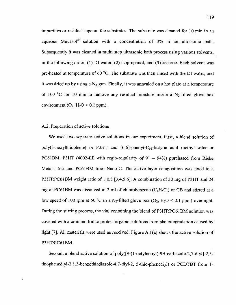
119
impurities or residual tape on the substrates. The substrate was cleaned for 10 min in an
aqueous Mucasol® solution with a concentration of 3% in an ultrasonic bath.
Subsequently it was cleaned in multi step ultrasonic bath process using various solvents,
in the following order: (1) DI water, (2) isopropanol, and (3) acetone. Each solvent was
pre-heated at temperature of 60 °C. The substrate was then rinsed with the DI water, and
it was dried up by using a N2 -gun. Finally, it was annealed on a hot plate at a temperature
of 100 °C for 10 min to remove any residual moisture inside a N2 -filled glove box
environment (O2 , H2 O < 0 . 1 ppm).
A.2. Preparation of active solutions
We used two separate active solutions in our experiment. First, a blend solution of
poly(3-hexylthiophene) or P3HT and [6 ,6 ]-phenyl-C6 i-butyric acid methyl ester or
PC61BM. P3HT (4002-EE with regio-regularity of 91 - 94%) purchased from Rieke
Metals, Inc. and PC61BM from Nano-C. The active layer composition was fixed to a
P3HT:PC61BM weight ratio of 1:0.8 [3,4,5,6 ]. A combination of 30 mg of P3HT and 24
mg of PC61BM was dissolved in 2 ml of chlorobenzene (C^HsCl) or CB and stirred at a
low speed of 100 rpm at 50 °C in a N2 -filled glove box (O2 , H2O < 0 . 1 ppm) overnight.
During the stirring process, the vial containing the blend of P3HT:PC61BM solution was
covered with aluminum foil to protect organic solutions from photodegradation caused by
light [7]. All materials were used as received. Figure A. 1(a) shows the active solution of
P3HTJPC61BM.
Second, a blend active solution of poly([9-(l-octylnonyl)-9H-carbazole-2,7-diyl]-2,5-
thiophenediyl-2,l,3-benzothiadiazole-4,7-diyl-2, 5-thio-phenediyl) or PCDTBT from 1-
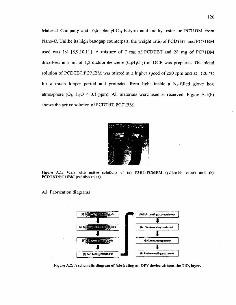
120
Material Company and [6 ,6 ]-phenyl-C7 i-butyric acid methyl ester or PC71BM from
Nano-C. Unlike its high bandgap counterpart, the weight ratio of PCDTBT and PC71BM
used was 1:4 [8,9,10,11]. A mixture of 7 mg of PCDTBT and 28 mg of PC71BM
dissolved in 2 ml of 1,2-dichlorobenzene (C6 H4 CI2) or DCB was prepared. The blend
solution of PCDTBT:PC71BM was stirred at a higher speed of 250 rpm and at 120 °C
for a much longer period and protected from light inside a N2 -filled glove box
atmosphere (O2 , H2 O < 0.1 ppm). All materials were used as received. Figure A. 1(b)
shows the active solution of PCDTBT:PC71BM.
Figure A.l: Vials with active solutions of (a) P3HT:PC61BM (yellowish color) and (b) PCDTBT:PC71BM (reddish color).
A3. Fabrication diagrams
(1) (5) Spin coating active polymer
4 4(2) QeaffiSgp^^^^gilljip slide (6) Pre-annealing treatment
4 413 ).fon^^gc^ jS frP S S (7) Aluminum deposition
4 4(4) Soft baking PEDOT:PSS ■ 1 (8) Post-a nneallng treatment
Figure A.2: A schematic diagram of fabricating an OPV device without the TiO* layer.
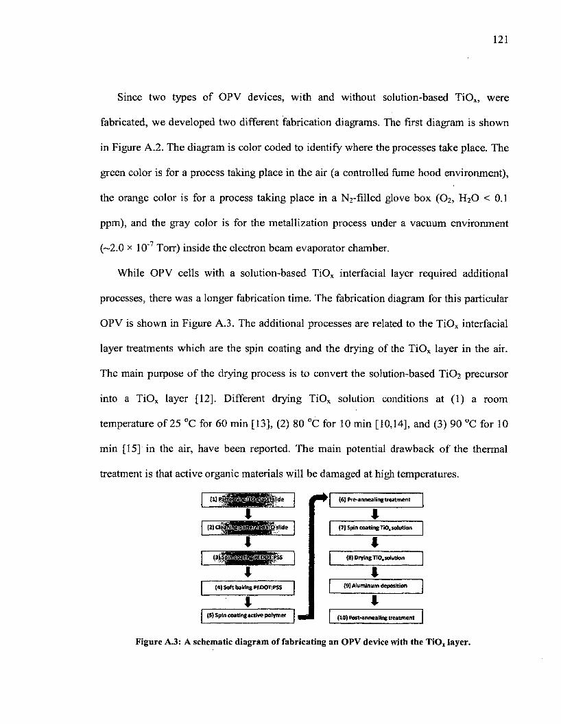
121
Since two types of OPV devices, with and without solution-based TiOx, were
fabricated, we developed two different fabrication diagrams. The first diagram is shown
in Figure A.2. The diagram is color coded to identify where the processes take place. The
green color is for a process taking place in the air (a controlled fiime hood environment),
the orange color is for a process taking place in a N2-filled glove box (O2 , H2 O < 0.1
ppm), and the gray color is for the metallization process under a vacuum environment
(—2.0 x 1 0 ' 7 Torr) inside the electron beam evaporator chamber.
While OPV cells with a solution-based TiOx interfacial layer required additional
processes, there was a longer fabrication time. The fabrication diagram for this particular
OPV is shown in Figure A.3. The additional processes are related to the TiOx interfacial
layer treatments which are the spin coating and the drying of the TiOx layer in the air.
The main purpose of the drying process is to convert the solution-based Ti0 2 precursor
into a TiOx layer [12]. Different drying TiOx solution conditions at (1) a room
temperature of 25 °C for 60 min [13], (2) 80 °C for 10 min [10,14], and (3) 90 °C for 10
min [15] in the air, have been reported. The main potential drawback of the thermal
treatment is that active organic materials will be damaged at high temperatures.
(1) (6) Pre-annealing treatment
I I(2) a S 8j P J g f f l B ' , M e (7) Spin coating TiO. solution
I I(8) DryingTiO.solution
I I(4) Soft baking PEOOT:PSS (9) Aluminum deposition
4 I(5) Spin coating active polymer ■J (10) Post-annealing treatment
Figure A.3: A schematic diagram of fabricating an OPV device with the TiOx layer.
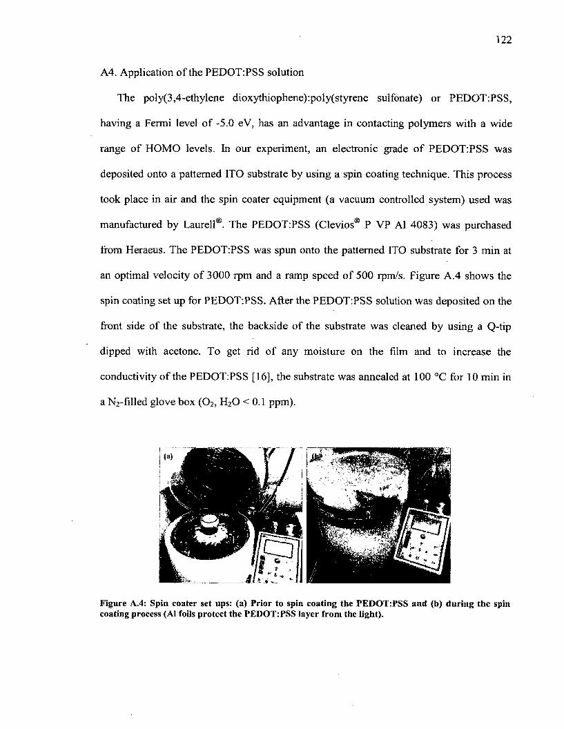
122
A4. Application of the PEDOT:PSS solution
The poly(3,4-ethylene dioxythiophene):poly(styrene sulfonate) or PEDOT:PSS,
having a Fermi level of -5.0 eV, has an advantage in contacting polymers with a wide
range of HOMO levels. In our experiment, an electronic grade of PEDOT:PSS was
deposited onto a patterned ITO substrate by using a spin coating technique. This process
took place in air and the spin coater equipment (a vacuum controlled system) used was
manufactured by Laurell®. The PEDOT:PSS (Clevios® P VP A1 4083) was purchased
from Heraeus. The PEDOT:PSS was spun onto the patterned ITO substrate for 3 min at
an optimal velocity of 3000 rpm and a ramp speed of 500 rpm/s. Figure A.4 shows the
spin coating set up for PEDOT.PSS. After the PEDOT:PSS solution was deposited on the
front side of the substrate, the backside of the substrate was cleaned by using a Q-tip
dipped with acetone. To get rid of any moisture on the film and to increase the
conductivity of the PEDOT:PSS [16], the substrate was annealed at 100 °C for 10 min in
a N2 -filled glove box (O2 , H2 O < 0.1 ppm).
Figure A.4: Spin coater set ups: (a) Prior to spin coating the PEDOT:PSS and (b) during the spin coating process (A1 foils protect the PEDOT:PSS layer from the light).
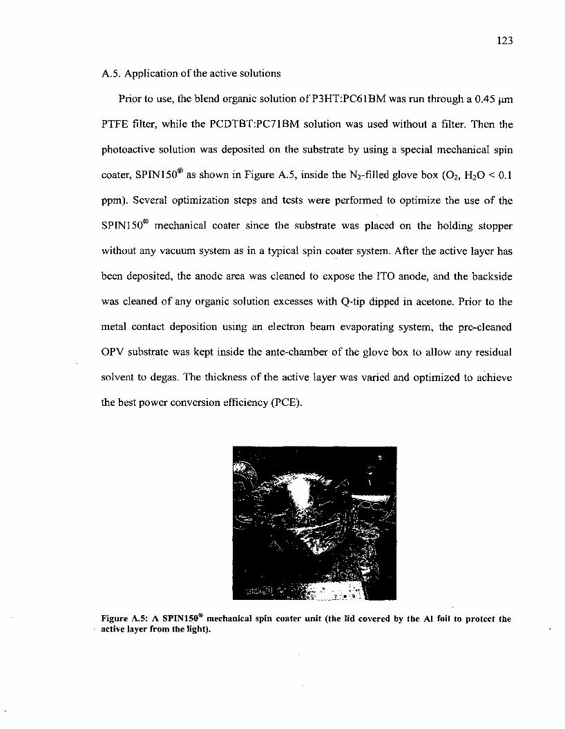
123
A.5. Application of the active solutions
Prior to use, the blend organic solution of P3HT:PC61BM was run through a 0.45 pm
PTFE filter, while the PCDTBT:PC71BM solution was used without a filter. Then the
photoactive solution was deposited on the substrate by using a special mechanical spin
coater, SPIN150® as shown in Figure A.5, inside the N2 -filled glove box (O2 , H2 O < 0.1
ppm). Several optimization steps and tests were performed to optimize the use of the
SPIN 150® mechanical coater since the substrate w'as placed on the holding stopper
without any vacuum system as in a typical spin coater system. After the active layer has
been deposited, the anode area was cleaned to expose the ITO anode, and the backside
was cleaned of any organic solution excesses with Q-tip dipped in acetone. Prior to the
metal contact deposition using an electron beam evaporating system, the pre-cleaned
OPV substrate was kept inside the ante-chamber of the glove box to allow any residual
solvent to degas. The thickness of the active layer was varied and optimized to achieve
the best power conversion efficiency (PCE).
Figure A.5: A SPIN150® mechanical spin coater unit (the lid covered by the A1 foil to protect the active layer from the light).
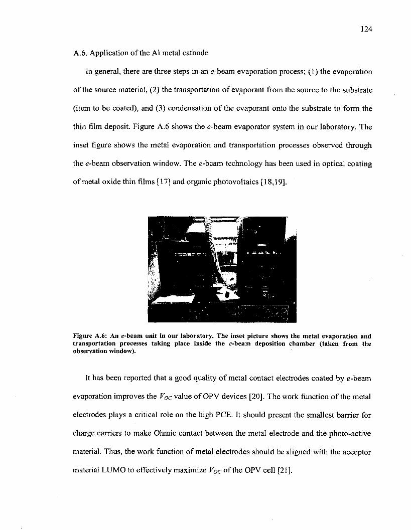
124
A.6 . Application of the A1 metal cathode
In general, there are three steps in an e-beam evaporation process; (1) the evaporation
of the source material, (2 ) the transportation of evaporant from the source to the substrate
(item to be coated), and (3) condensation of the evaporant onto the substrate to form the
thin film deposit. Figure A . 6 shows the e-beam evaporator system in our laboratory. The
inset figure shows the metal evaporation and transportation processes observed through
the e-beam observation window. The e-beam technology has been used in optical coating
of metal oxide thin films [17] and organic photovoltaics [18,19].
Figure A.6: An e-beam unit in our laboratory. The inset picture shows the metal evaporation and transportation processes taking place inside the e-beam deposition chamber (taken from the observation window).
It has been reported that a good quality of metal contact electrodes coated by e-beam
evaporation improves the V0c value of OPV devices [20]. The work function of the metal
electrodes plays a critical role on the high PCE. It should present the smallest barrier for
charge carriers to make Ohmic contact between the metal electrode and the photo-active
material. Thus, the work function of metal electrodes should be aligned with the acceptor
material LUMO to effectively maximize Vqc of the OPV cell [21].
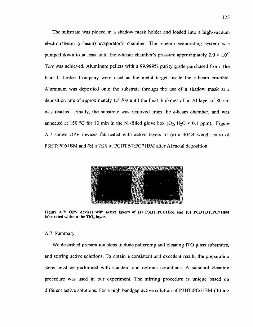
The substrate was placed in a shadow mask holder and loaded into a high-vacuum
electron'beam (e-beam) evaporator’s chamber. The e-beam evaporating system was
pumped down to at least until the e-beam chamber’s pressure approximately 2 . 0 >< 1 0 ' 7
Torr was achieved. Aluminum pellets with a 99.999% purity grade purchased from The
Kurt J. Lesker Company were used as the metal target inside the e-beam crucible.
Aluminum was deposited onto the substrate through the use of a shadow mask at a
deposition rate of approximately 1 .5 A/s until the final thickness of an A1 layer of 80 nm
was reached. Finally, the substrate was removed from the e-beam chamber, and was
annealed at 150 °C for 10 min in the N2 -filled glove box (O2 , H2 O <0.1 ppm). Figure
A.7 shows OPV devices fabricated with active layers of (a) a 30:24 weight ratio of
P3HT:PC61BM and (b) a 7:28 of PCDTBT:PC71BM after A1 metal deposition.
Figure A.7: OPV devices with active layers of (a) P3HT:PC61BM and (b) PCDTBT:PC71BM fabricated without the TiOx layer.
A.7. Summary
We described preparation steps include patterning and cleaning ITO glass substrates,
and stirring active solutions. To obtain a consistent and excellent result, the preparation
steps must be performed with standard and optimal conditions. A standard cleaning
procedure was used in our experiment. The stirring procedure is unique based on
different active solutions. For a high bandgap active solution of P3HT:PC61BM (30 mg
126
of P3HT and 24 mg of PC61BM in 2 mL chlorobenzene), a combination of low speed
stirring condition (100 rpm) and an annealing temperature of 50 °C was used. And for the
low bandgap of PCDTBT:PC71BM (7 mg of PCDTBT and 28 mg of PC71BM in 2 mL
1,2-dichlorobenzene), a combination of a higher stirring speed of 250 rpm and a
temperature of 120 °C was used.
Organic materials were deposited onto the substrate by means of spin coating. Since
organic materials are sensitive to degradation issues like O2 , H2 O, and light, the spin
coaters were covered with A1 coil to protect organic materials. The condition of the glove
box and the electron beam evaporator must be in an optimum quality to avoid any
contamination. A lot of efforts had been performed to maintain the glove box and
electron beam evaporator in a great working condition.
Two processing procedures were developed to fabricate device with and without the
TiOx layer. Introducing a TiOx layer as an interfacial layer between the organic materials
and the A1 cathode means additional processing procedures have to be optimized. A good
interfacial morphology between the TiOx layer-organic materials and the TiOx layer-Al
metal cathode plays a key role in the device performance and the stability of the device.
127
APPENDIX B
Optimization Processes
B.l. Introduction
The Jsc, Voc, FF, and PCE of the OPV devices can be enhanced by various
fabrication procedures (morphology control, buffer layers, processing conditions, etc.)
and the annealing treatments (pre- and post-annealing, etc.) [22,23]. For the OPV device
fabricated with a solution based buffer layer, it is important to obtain an excellent quality
of the buffer layer used at an optimum condition.
It must be kept in mind that most of the optimization of the OPV device is not well
understood. The optimization results varied from report to report and so far they have
been empirical. Tuning fabrication variables further is often required to improve the
morphology of the active layer and to ensure that efficient exciton dissociation results in
efficient charge separation and collection as well. Several external treatments have been
reported to be effective in optimizing native composite films.
B.2. Optimizing the active layer deposition
Spin coating is the most successful and widely employed method for the highly
reproducible fabrication of organic thin films with high structural uniformity [24], The
uniformity of the resulting thin film is affected and thus controlled mainly by the choice
of solvent [25]. The final thin film morphology will be determined the time allowed for
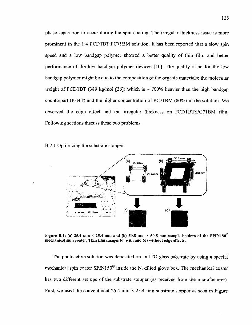
128
phase separation to occur during the spin coating. The irregular thickness issue is more
prominent in the 1:4 PCDTBT:PC71BM solution. It has been reported that a slow spin
speed and a low bandgap polymer showed a better quality of thin film and better
performance of the low bandgap polymer devices [10]. The quality issue for the low
bandgap polymer might be due to the composition of the organic materials; the molecular
weight of PCDTBT (389 kg/mol [26]) which is ~ 700% heavier than the high bandgap
counterpart (P3HT) and the higher concentration of PC71BM (80%) in the solution. We
observed the edge effect and the irregular thickness on PCDTBT:PC71BM film.
Following sections discuss these two problems.
B.2.1 Optimizing the substrate stopper
25.4 mm
Figure B.l: (a) 25.4 mm x 25.4 mm and (b) 50.8 mm * 50.8 mm sample holders of the SPIN 150® mechanical spin coater. Thin film images (c) with and (d) without edge effects.
The photoactive solution was deposited on an ITO glass substrate by using a special
mechanical spin coater SPIN150® inside the N2 -filled glove box. The mechanical coater
has two different set ups of the substrate stopper (as received from the manufacturer).
First, we used the conventional 25.4 mm x 25.4 mm substrate stopper as seen in Figure
B.l(a). After the active solution was spun on the substrate, we observed a significant
“edge effect” at every comer of the substrate as seen in Figure B.l(c). We observed that
the edge effect was caused by non-equilibrium morphologies due to the disturbance from
the four small cylindrical bars (as received from the manufacturer) functioned as
substrate stoppers. When the solution was spun, the planar motion caused by the
centrifugal force pushed the solution away from the center of the substrate. And the
solution that hit the bars did not made its way to escape the substrate; instead it was
pushed back and created the edge effect. The active solution concentrated at the edges
gets thicker and wider as the spin speed is slower, especially for the low bandgap
polymer solution. The widening edge effect has been observed to be overlap with the
active area of the OPV devices which caused a serious problem of the thickness
irregularity of the active layer across the substrate.
Secondly, we used the alternative set up which we had to incorporate a 50.8 mm *
50.8 mm glass substrate (did not come with the set up) as the base for the ITO glass
substrate, as seen in Figure B.l(b). After depositing the solution, as seen in Figure B.l(d),
we found that the deposited thin film is more uniform in thickness and more importantly,
there are no more edge effects. Unlike in the first setup, the active solution was spun on
the substrate without making any contact to any substrate stoppers of the SPIN150® spin
coater. A common defect in spin coated films is radial lines representing thickness
undulations (non uniform in the film thickness), referred to as striations [27], parallel to
the direction of the flow. Because of the flow in the spin coating process the instabilities
may lead to local differences in the surface tension at the top surface.
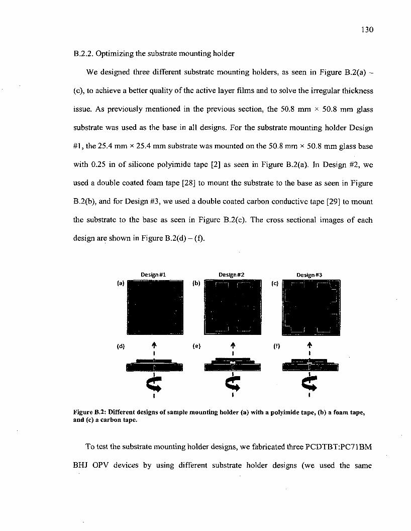
B.2.2. Optimizing the substrate mounting holder
We designed three different substrate mounting holders, as seen in Figure B.2(a) -
(c), to achieve a better quality of the active layer films and to solve the irregular thickness
issue. As previously mentioned in the previous section, the 50.8 mm x 50.8 mm glass
substrate was used as the base in all designs. For the substrate mounting holder Design
#1, the 25.4 mm x 25.4 mm substrate was mounted on the 50.8 mm x 50.8 mm glass base
with 0.25 in of silicone polyimide tape [2] as seen in Figure B.2(a). In Design #2, we
used a double coated foam tape [28] to mount the substrate to the base as seen in Figure
B.2(b), and for Design #3, we used a double coated carbon conductive tape [29] to mount
the substrate to the base as seen in Figure B.2(c). The cross sectional images of each
design are shown in Figure B.2(d) - (f).
Design #1 Design #2 Design #3
(d) * (e) * (f) *I I I
Figure B.2: Different designs of sample mounting holder (a) with a polyimide tape, (b) a foam tape, and (c) a carbon tape.
To test the substrate mounting holder designs, we fabricated three PCDTBT:PC71BM
BHJ OPV devices by using different substrate holder designs (we used the same
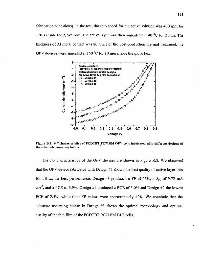
131
fabrication conditions). In the test, the spin speed for the active solution was 400 rpm for
120 s inside the glove box. The active layer was then annealed at 140 °C for 2 min. The
thickness of A1 metal contact was 80 ran. For the post-production thermal treatment, the
OPV devices were annealed at 150 °C for 10 min inside the glove box.
o
Eo<E
COca>■oc£3o
-1 -
-2
-3-I -4 -5-
-6 -
-7-
i —■—r Device structure:ITCWPEDOT:PSSfPCDTBT:PC71 BM/AI Different sample holder designs for active layer thin film deposition: —o —design #1 —O—design #2 —O— design #3
- 8 JO*0 *0 *0 _ _n-0 'JOT1
-9-i-JD" .oO'
~1' I ' ’ I ”1 I » 1....I'" I ..’ f-’T I r11
0.0 0.1 0.2 0.3 0.4 0.5 0.6 0.7 0.8 0.9Voltage (V)
Figure B.3: J-V characteristics of PCDTBT:PC71BM OPV cells fabricated with different designs of the substrate mounting holder.
The J-V characteristics of the OPV devices are shown in Figure B.3. We observed
that the OPV device fabricated with Design #3 shows the best quality of active layer thin
film; thus, the best performance. Design #3 produced a FF of 45%, a J$c o f 9.72 mA
cm'2, and a PCE of 3.9%. Design #1 produced a PCE of 3.0% and Design #2 the lowest
PCE of 2.5%, while their FF values were approximately 40%. We conclude that the
substrate mounting holder in Design #3 shows the optimal morphology and optimal
quality of the thin film of the PCDTBT.PC71BM BHJ cells.
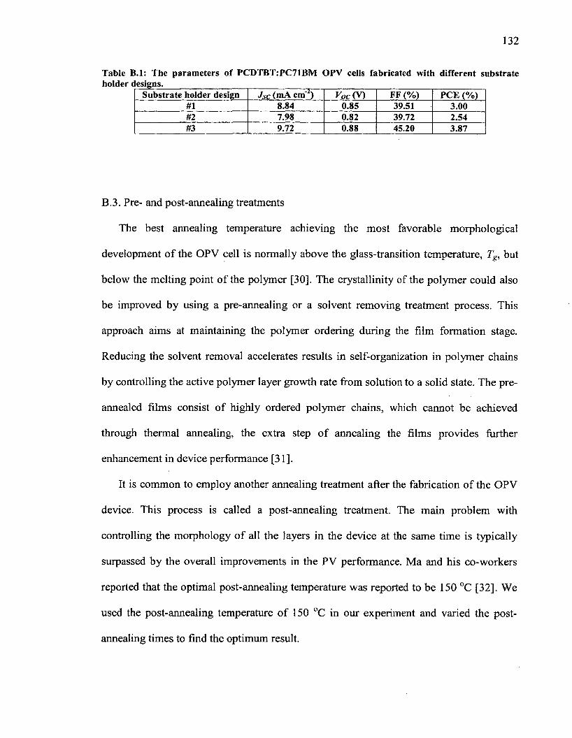
132
Table B.l: The parameters of PCDTBT:PC71BM OPV cells fabricated with different substrateholder designs.__________________ ^ __________________________________
Substrate holder design Jsc (mA cm'2) Voc (V) FF (%) PCE (%)#1 8.84 0.85 39.51 3.00#2 7.98 0.82 39.72 2.54#3 9.72 0.88 45.20 3.87
B.3. Pre- and post-annealing treatments
The best annealing temperature achieving the most favorable morphological
development of the OPV cell is normally above the glass-transition temperature, Tg, but
below the melting point of the polymer [30]. The crystallinity of the polymer could also
be improved by using a pre-annealing or a solvent removing treatment process. This
approach aims at maintaining the polymer ordering during the film formation stage.
Reducing the solvent removal accelerates results in self-organization in polymer chains
by controlling the active polymer layer growth rate from solution to a solid state. The pre
annealed films consist of highly ordered polymer chains, which cannot be achieved
through thermal annealing, the extra step of annealing the films provides further
enhancement in device performance [31].
It is common to employ another annealing treatment after the fabrication of the OPV
device. This process is called a post-annealing treatment. The main problem with
controlling the morphology of all the layers in the device at the same time is typically
surpassed by the overall improvements in the PV performance. Ma and his co-workers
reported that the optimal post-annealing temperature was reported to be 150 °C [32], We
used the post-annealing temperature of 150 °C in our experiment and varied the post
annealing times to find the optimum result.
133
B.4. Interfacial layer thickness
The thickness of the highly conductive interlayer can be tuned to optimize the optical
field distribution in the solar cell, and the increase in overall thickness of the devices
allows higher stability and a lower probability for short circuiting the device [33].
Interfacial phenomena are largely independent of the cell design but must specifically
accommodate the particular donor and acceptor materials being employed. In our study,
we used the solution based TiOx layer as an interfacial layer between the active layer and
the metal cathode. The optimal thickness of the TiOx film for OPV devices has been
reported to be in the range of 5 - 20 nm [34,35,36,37],
B.5. Summary
It is mandatory to perform optimization steps to achieve an optimum and a good
reproducible quality result of OPV devices. At present, the optimization results are
empirical and varied from report to report. We developed optimization steps based on the
following processing variables such as the active layer thickness, pre- and post-annealing
treatments. When a TiOx layer is introduced, additional optimization steps, the thickness
of TiOx layer and the TiOx solution drying condition, must be performed.
We developed a spin coating procedure for the low bandgap active solution of
PCDTBT:PC71BM since we observed a non-uniformity and an irregularity in the active
layer thickness. We observed that the quality issue for the low bandgap polymer might be
due to the composition of the organic materials; the molecular weight of PCDTBT and
the higher concentration of PC71BM (80%) in the solution. We developed several sample
holder mounting designs to solve the edge effect and the irregular thickness of the active

layer. We conclude that Design #3 with a conductive carbon tape was the best mounting
design that improve the quality of the active layer. We used Design #3 in depositing both
high and low bandgap active solutions of P3HT:PC61BM and PCDTBT:PC71BM in our
experiment.
135
APPENDIX C
Statistical Method
In our experiment, although all 8 OPV cells in an OPV device were fabricated at the
same processing condition, their qualities and performances might be different due to
random variability issues such as the complexity on how the bulk heterojunction
networks were formed on each OPV cell, the interface between the metal contact and the
organic layer, etc. Moreover, in addition to the random variability, the data indicate
among others a location effect affecting the outcome either due to mask design or process
design.
The I-V characterization of OPV cells was measured in the air. In OPV research, if n
measurements in a sample are denoted by x/, x2. ...., and x„, the sample mean, standard
deviation, and standard error of the population of the sample are defined as
By using Equations A.l and A.2, we determined the mean and standard deviation of the
cell’s OPV parameter. Error bars are a graphical representation of the variability of data
and are used on graphs to indicate the error, or uncertainty in a reported measurement.
- _ * i + * n + ......+ X n _ l X j (A.l)71 n
(A.2)
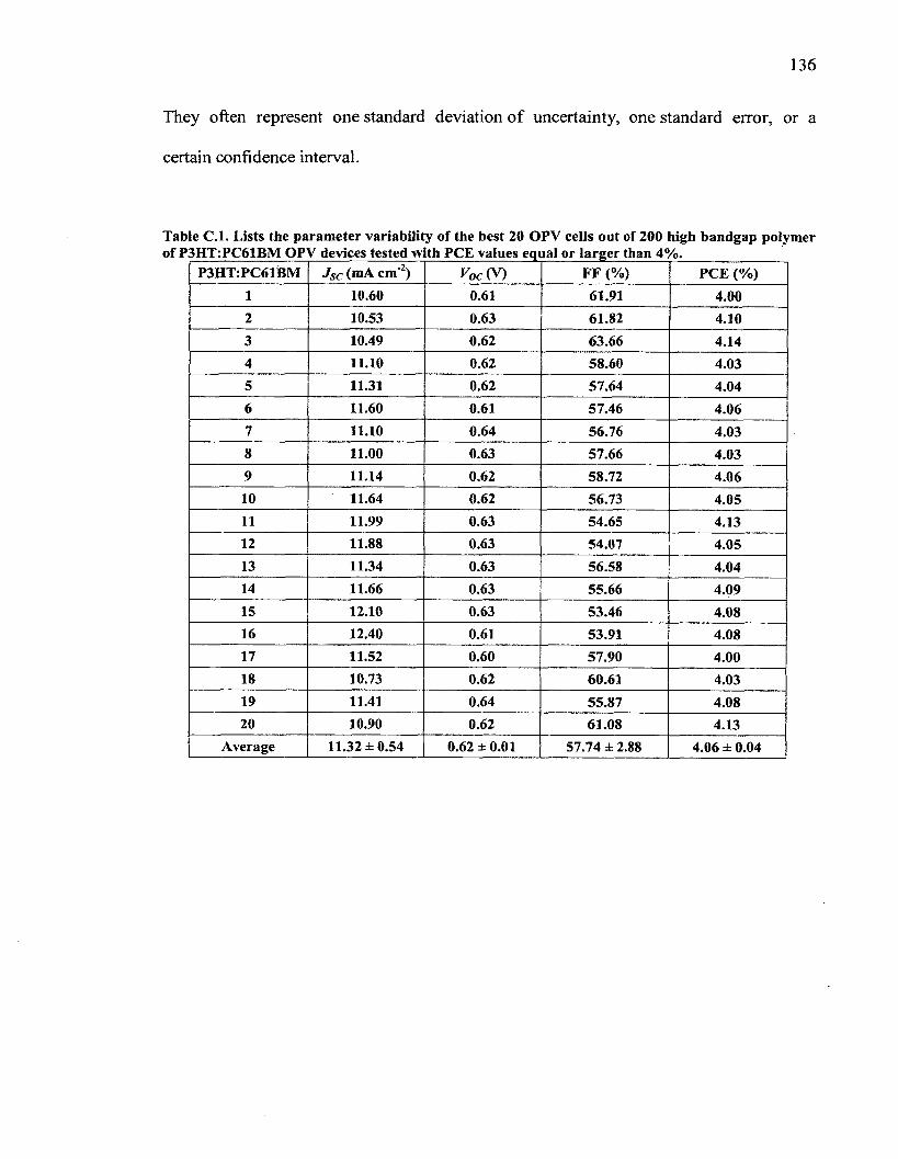
136
They often represent one standard deviation of uncertainty, one standard error, or a
certain confidence interval.
Table C.l. Lists the parameter variability of the best 20 OPV cells out of 200 high bandgap polymer of P3HT:PC61BM OPV devices tested with PCE values equal or larger than 4%.______________
P3HT:PC61BM Jsc (mA cm'2) t7oc (V) FF (%) PCE (%)1 10.60 0.61 61.91 4.002 10.53 0.63 61.82 4.103 10.49 0.62 63.66 4.144 11.10 0.62 58.60 4.035 11.31 0.62 57.64 4.046 11.60 0.61 57.46 4.067 11.10 0.64 56.76 4.038 11.00 0.63 57.66 4.039 11.14 0.62 58.72 4.0610 11.64 0.62 56.73 4.0511 11.99 0.63 54.65 4.1312 11.88 0.63 54.07 4.0513 11.34 0.63 56.58 4.0414 11.66 0.63 55.66 4.0915 12.10 0.63 53.46 4.0816 12.40 0.61 53.91 4.0817 11.52 0.60 57.90 4.0018 10.73 0.62 60.61 4.0319 11.41 0.64 55.87 4.0820 10.90 0.62 61.08 4.13
Average 11.32 ± 0.54 0.62 ± 0.01 57.74 ± 2.88 4.06 ± 0.04
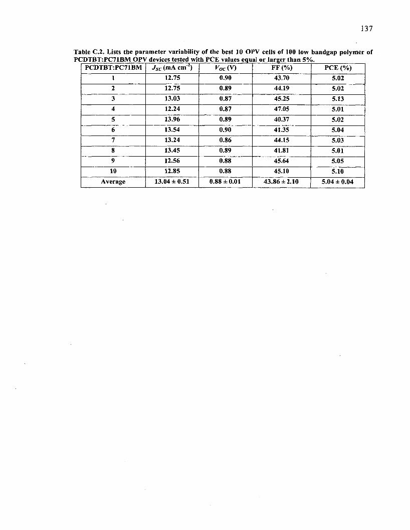
137
Table C.2. Lists the parameter variability of the best 10 OPV cells of 100 low bandgap polymer of PCDTBT:PC71BM OPV devices tested with PCE values equal or larger than 5%._______________
PCDTBT:PC71BM Jsc (mA cm'2) V o c M FF (%) PCE (%)1 12.75 0.90 43.70 5.022 12.75 0.89 44.19 5.023 13.03 0.87 45.25 5.134 12.24 0.87 47.05 5.015 13.96 0.89 40.37 5.026 13.54 0.90 41.35 5.047 13.24 0.86 44.15 5.038 13.45 0.89 41.81 5.019 12.56 0.88 45.64 5.0510 12.85 0.88 45.10 5.10
Average 13.04 ± 0.51 0.88 ± 0.01 43.86 ± 2.10 5.04 ± 0.04
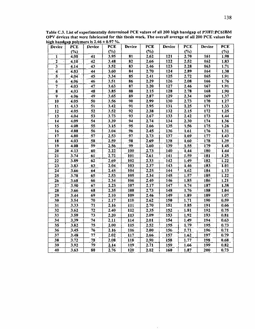
138
Table C.3. List of experimentally determined PCE values of all 200 high bandgap of P3HT:PC61BM OPV devices that were fabricated for this thesis work. The overall average of all 200 PCE values for
Device PCE(%)
Device PCE(%)
Device PCE(%)
Device PCE(%)
Device PCE(%)
1 4.00 41 3.95 81 2.62 121 2.70 161 1.982 4.10 42 3.48 82 2.66 122 2.52 162 1.833 4.14 43 3.52 83 2.46 123 2.28 163 1.714 4.03 44 3.60 84 2.70 124 2.89 164 1.385 4.04 45 3.34 85 2.41 125 2.72 165 1.916 4.06 46 3.51 86 2.29 126 2.08 166 1.767 4.03 47 3.63 87 2.20 127 2.46 167 1.918 4.03 48 3.85 88 2.15 128 2.78 168 1.909 4.06 49 3.65 89 2.87 129 2.34 169 1.3710 4.05 50 3.56 90 2.99 130 2.73 170 1.2711 4.13 51 3.42 91 2.95 131 2.25 171 1.3312 4.05 52 3.52 92 2.38 132 2.15 172 1.2513 4.04 53 3.73 93 2.67 133 2.42 173 1.4414 4.09 54 3.39 94 2.74 134 2.30 174 1.3615 4.08 55 3.15 95 2.66 135 1.56 175 1.2616 4.08 56 3.04 96 2.45 136 1.61 176 1.3117 4.00 57 2.53 97 2.73 137 1.69 177 1.4318 4.03 58 2.59 98 2.69 138 1.60 178 1.3919 4.08 59 2.56 99 2.60 139 1.55 179 1.4520 4.13 60 2.22 100 2.73 140 1.44 180 1.4421 3.74 61 2.72 101 2.61 141 1.59 181 1.2522 3.89 62 2.69 102 2.33 142 1.49 182 1.2223 3.83 63 2.04 103 2.37 143 1.46 183 1.0124 3.66 64 2.45 104 2.25 144 1.62 184 1.1325 3.78 65 2.53 105 2.34 145 1.57 185 1.2226 3.68 66 2.34 106 2.40 146 1.85 186 1.2127 3.50 67 2.23 107 2.17 147 1.74 187 1.3828 3.66 68 2.35 108 2.73 148 1.76 188 1.0429 3.44 69 2.10 109 2.46 149 1.89 189 1.0730 3.54 70 2.17 110 2.62 150 1.71 190 0.5931 3.33 71 2.16 111 2.70 151 1.85 191 0.6632 3.62 72 2.40 112 2.35 152 1.81 192 0.7533 3.59 73 2.20 113 2.09 153 1.92 193 0.8134 3.39 74 2.11 114 2.01 154 1.49 194 0.6335 3.82 75 2.00 115 2.52 155 1.79 195 0.7336 3.45 76 2.16 116 2.00 156 1.71 196 0.7137 3.48 77 2.02 117 2.66 157 1.62 197 0.7938 3.72 78 2.08 118 2.90 158 1.77 198 0.6839 3.92 79 2.14 119 2.71 159 1.66 199 0.8240 3.63 80 2.76 120 2.02 160 1.87 200 0.73
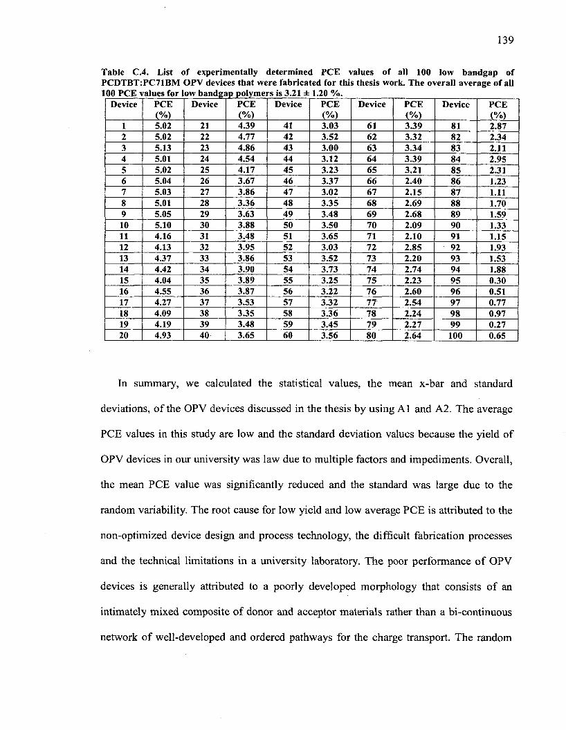
139
Table C.4. List of experimentally determined PCE values of all 100 low bandgap ofPCDTBT:PC71BM OPV devices that were fabricated for this thesis work. The overall average of all100 PCE values for low bandgap polymers is 3.21 ± 1.20 %. ________ __________________________
Device PCE(%)
Device PCE(%)
Device PCE(%)
Device PCE<%)
Device PCE(%)
1 5.02 21 4.39 41 3.03 61 3.39 81 2.872 5.02 22 4.77 42 3.52 62 3.32 82 2.343 5.13 23 4.86 43 3.00 63 3.34 83 2.114 5.01 24 4.54 44 3.12 64 3.39 84 2.955 5.02 25 4.17 45 3.23 65 3.21 85 2.316 5.04 26 3.67 46 3.37 66 2.40 86 1.237 5.03 27 3.86 47 3.02 67 2.15 87 1.118 5.01 28 3.36 48 3.35 68 2.69 88 1.709 5.05 29 3.63 49 3.48 69 2.68 89 1.5910 5.10 30 3.88 50 3.50 70 2.09 90 1.3311 4.16 31 3.48 51 3.65 71 2.10 91 1.1512 4.13 32 3.95 52 3.03 72 2.85 92 1.9313 4.37 33 3.86 53 3.52 73 2.20 93 1.5314 4.42 34 3.90 54 3.73 74 2.74 94 1.8815 4.04 35 3.89 55 3.25 75 2.23 95 0.3016 4.55 36 3.87 56 3.22 76 2.60 96 0.5117 4.27 37 3.53 57 3.32 77 2.54 97 0.7718 4.09 38 3.35 58 3.36 78 2.24 98 0.9719 4.19 39 3.48 59 3.45 79 2.27 99 0.2720 4.93 40 3.65 60 3.56 80 2.64 100 0.65
In summary, we calculated the statistical values, the mean x-bar and standard
deviations, of the OPV devices discussed in the thesis by using A1 and A2. The average
PCE values in this study are low and the standard deviation values because the yield of
OPV devices in our university was law due to multiple factors and impediments. Overall,
the mean PCE value was significantly reduced and the standard was large due to the
random variability. The root cause for low yield and low average PCE is attributed to the
non-optimized device design and process technology, the difficult fabrication processes
and the technical limitations in a university laboratory. The poor performance of OPV
devices is generally attributed to a poorly developed morphology that consists of an
intimately mixed composite of donor and acceptor materials rather than a bi-continuous
network of well-developed and ordered pathways for the charge transport. The random
variability in OPV cells in a device fabricated with similar processing steps and affected
by the experimental condition during the OPV fabrication results is still difficult to
control in our study.
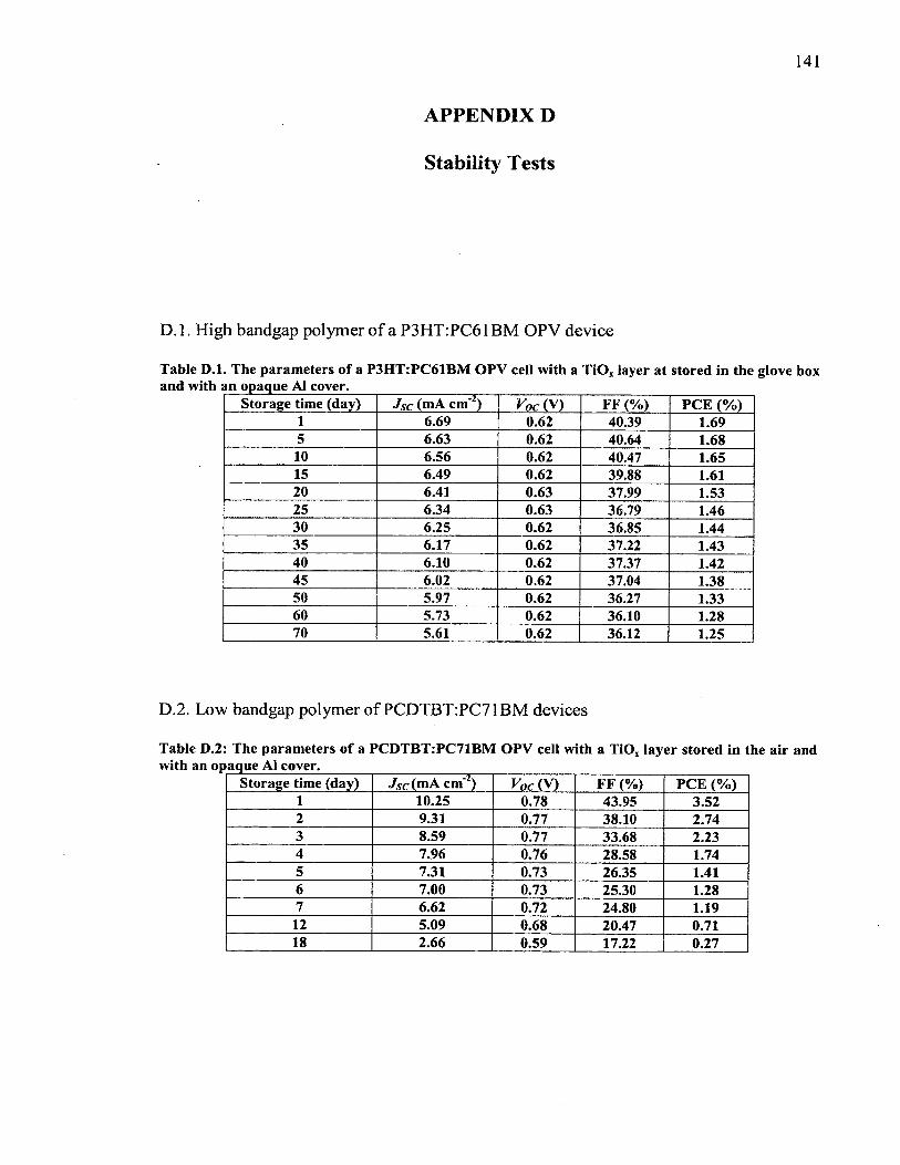
141
APPENDIX D
Stability Tests
D.l. High bandgap polymer of a P3HT:PC61BM OPV device
Table D.l. The parameters of a P3HT:PC61BM OPV cell with a TiO, layer at stored in the glove box and with an opaque A1 cover. ____________ __________________________________
Storage time (day) Jsc (mA cm'2) r 0c(V ) FF (%) PCE (%)1 6.69 0.62 40.39 1.695 6.63 0.62 40.64 1.6810 6.56 0.62 40.47 1.6515 6.49 0.62 39.88 1.6120 6.41 0.63 37.99 1.5325 6.34 0.63 36.79 1.4630 6.25 0.62 36.85 1.4435 6.17 0.62 37.22 1.4340 6.10 0.62 37.37 1.4245 6.02 0.62 37.04 1.3850 5.97 0.62 36.27 1.3360 5.73 0.62 36.10 1.2870 5.61 0.62 36.12 1.25
D.2. Low bandgap polymer of PCDTBT:PC71BM devices
Table D.2: The parameters of a PCDTBT:PC71BM OPV cell with a TiO, layer stored in the air and with an opaque A1 cover.__________________________________________________________
Storage time (day) / j C(mA cm'2) Voc (V) FF (%) PCE (%)1 10.25 0.78 43.95 3.522 9.31 0.77 38.10 2.743 8.59 0.77 33.68 2.234 7.96 0.76 28.58 1.745 7.31 0.73 26.35 1.416 7.00 0.73 25.30 1.287 6.62 0.72 24.80 1.1912 5.09 0.68 20.47 0.7118 2.66 0.59 17.22 0.27
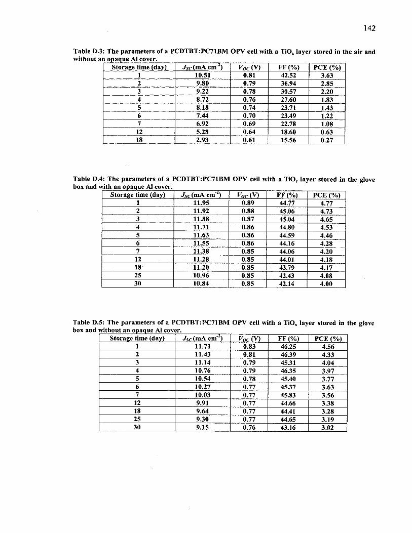
142
Table D.3: The parameters of a PCDTBT:PC71BM OPV cell with a TiO, layer stored in the air andwithout an opaque A1 cover. ____________________________ .____
Storage time (day) 7sc(mA cm ') Voc (V) FF (%) PCE (%)1 10.51 0.81 42.52 3.632 9.80 0.79 36.94 2.853 9.22 0.78 30.57 2.204 8.72 0.76 27.60 1.835 8.18 0.74 23.71 1.436 7.44 0.70 23.49 1.227 6.92 0.69 22.78 1.0812 5.28 0.64 18.60 0.6318 2.93 0.61 15.56 0.27
Table D.4: The parameters of a PCDTBT:PC71BM OPV cell with a TiO, layer stored in the glove box and with an opaque A1 cover.____________ ___ __________________________________
Storage time (day) Jsc (mA cm'2) Voc (V) FF (%) PCE (%)1 11.95 0.89 44.77 4.772 11.92 0.88 45.06 4.733 11.88 0.87 45.04 4.654 11.71 0.86 44.80 4.535 11.63 0.86 44.59 4.466 11.55 0.86 44.16 4.287 11.38 0.85 44.06 4.2012 11.28 0.85 44.01 4.1818 11.20 0.85 43.79 4.1725 10.96 0.85 42.43 4.0830 10.84 0.85 42.14 4.00
Table D.5: The parameters of a PCDTBT:PC71BM OPV cell with a TiOx layer stored in the glove box and without an opaque Al cover.__________ ______________________________________
Storage time (day) /vc(mA cm'2) Voc (V) FF (%) PCE (%)1 11.71 0.83 46.25 4.562 11.43 0.81 46.39 4.333 11.14 0.79 45.31 4.044 10.76 0.79 46.35 3.975 10.54 0.78 45.40 3.776 10.27 0.77 45.37 3.637 10.03 0.77 45.83 3.5612 9.91 0.77 44.66 3.3818 9.64 0.77 44.41 3.2825 9.30 0.77 44.65 3.1930 9.15 0.76 43.16 3.02
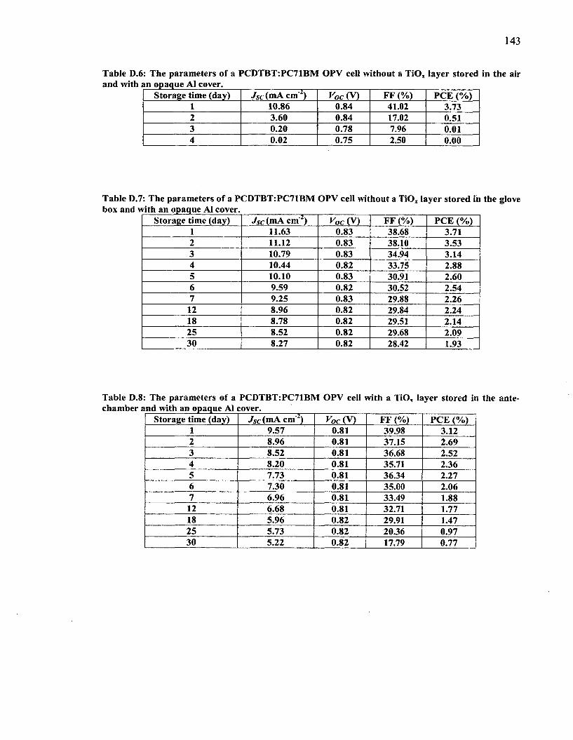
143
Table D.6: The parameters of a PCDTBT:PC71BM OPV cell without a TiO, layer stored in the airand with an opaque Al cover. ____________ ______________ _______________________
Storage time (day) /sc(m A cm'2) Voc (V) FF (%) PCE (%)1 10.86 0.84 41.02 3.732 3.60 0.84 17.02 0.513 0.20 0.78 7.96 0.014 0.02 0.75 2.50 0.00
Table D.7: The parameters of a PCDTBT:PC71BM OPV cell without a TiO* layer stored in the glove box and with an opaque Al cover.____________ ______________________________________
Storage time (day) 7Sc(mA cm'2) Voc (V) FF (%) PCE (%)1 11.63 0.83 38.68 3.712 11.12 0.83 38.10 3.533 10.79 0.83 34.94 3.144 10.44 0.82 33.75 2.885 10.10 0.83 30.91 2.606 9.59 0.82 30.52 2.547 9.25 0.83 29.88 2.2612 8.96 0.82 29.84 2.2418 8.78 0.82 29.51 2.1425 8.52 0.82 29.68 2.0930 8.27 0.82 28.42 1.93
Table D.8: The parameters of a PCDTBT:PC71BM OPV cell with a TiO, layer stored in the antechamber and with an opaque Al cover.______
Storage time (day) / s c ( m A cm'2) Voc (V) FF (%) PCE (%)1 9.57 0.81 39.98 3.122 8.96 0.81 37.15 2.693 8.52 0.81 36.68 2.524 8.20 0.81 35.71 2.365 7.73 0.81 36.34 2.276 7.30 0.81 35.00 2.067 6.96 0.81 33.49 1.8812 6.68 0.81 32.71 1.7718 5.96 0.82 29.91 1.4725 5.73 0.82 20.36 0.9730 5.22 0.82 17.79 0.77
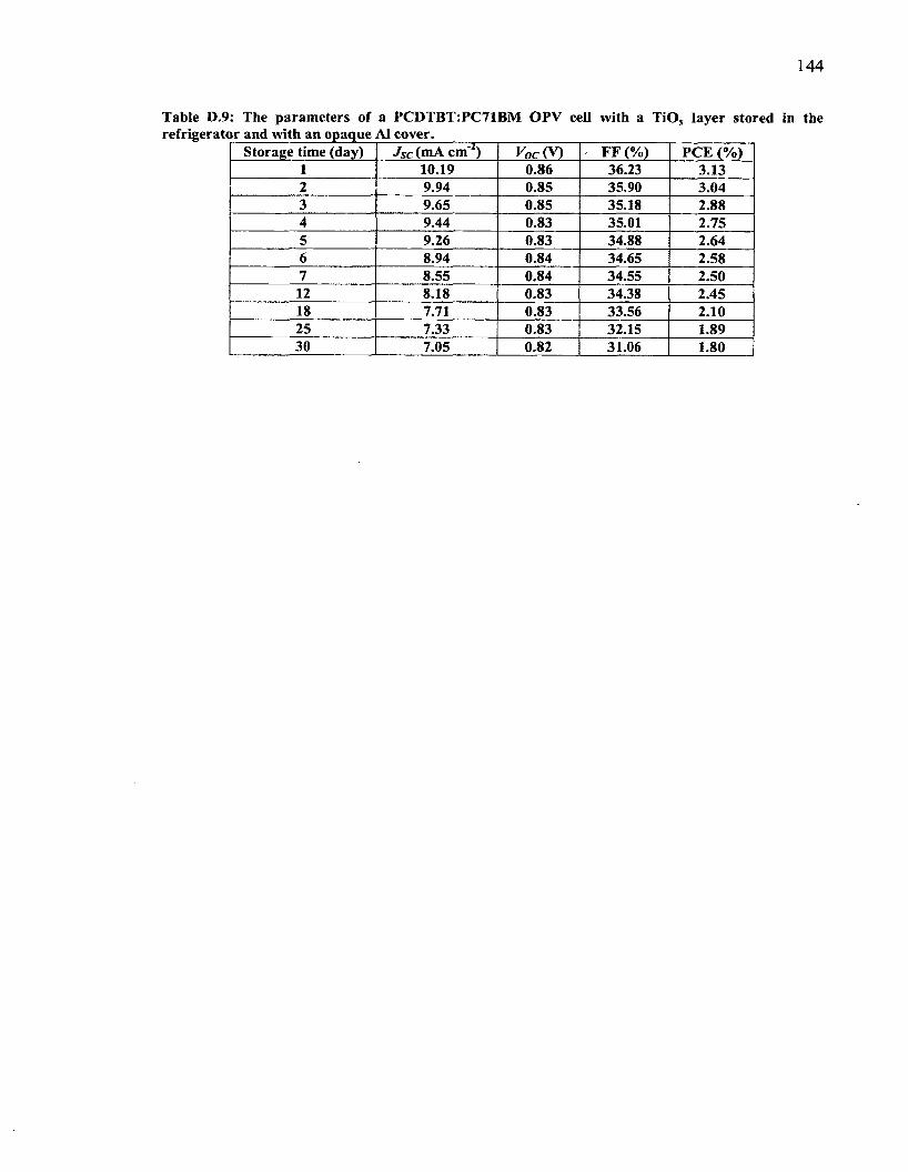
144
Table D.9: The parameters of a PCDTBT:PC71BM OPV cell with a TiO* layer stored in therefrigerator and with an opaque Al cover. __________ _______________________
Storage time (day) Jsc (mA cm'2) VocQf) FF (%) PCE (%)1 10.19 0.86 36.23 3.132 9.94 0.85 35.90 3.043 9.65 0.85 35.18 2.884 9.44 0.83 35.01 2.755 9.26 0.83 34.88 2.646 8.94 0.84 34.65 2.587 8.55 0.84 34.55 2.5012 8.18 0.83 34.38 2.4518 7.71 0.83 33.56 2.1025 7.33 0.83 32.15 1.8930 7.05 0.82 31.06 1.80
145
APPENDIX E
Copyrighted Materials
E. 1. M. Jorgensen, K. Norrman, and F.C. Krebs, “Stability/degradation of polymer solar
cells”, Sol. Energy Mater. Sol. Cells, 92, 686-714 (2008).
n sry iE R
'*** SdenceDirectS d h t t a r o A &£x:X ;£ l K tSESjCiS -*14
and Safer Ceils
ReviewS t a b i l i t y / d e g r a d a t i o n o f p o l y m e r s o l a r c e l l s
MiTkkel Jcreeracen*, Kion tNomrnxaou Frederik C. BwrcfeTr-*r«r^y /nAti-l-? Ps' M JV-y-grC rtv-£— A&. fSX-*X3?J£=££h CfaagS
KzacaS t£ 3*Gxti3 2 remind cs iraerff-nxJ 8-im .j JS2s. 4 lss= a t -jSB lrxk£h tQ Msdi S25AJfcurarl
edh-juo and-orjasi: u&r c3i dh-rittj it^wrintiau m i is £3b dark. lOw. m ob <uCnft fc> phzlzs^lzn fcitsJ -on !»<TTfgssc&aa&stari ssdj ®.Klkao. U^cpEradasdli&siEHacf dlnrej-3 H cazas2z rj g i xgJaa-mi-Bj i n u a t a s n d tilDEtiniasafej wri afcrialieeof&g A|mU2kn pfainoaa c sa Fat s x s sE d & zx ih a is ^ .z f& b bib nd ^ im atslgfatAgBr- lac n i r t , & a cu ra n i «3sknt3ts£m o f a d s l e r liaE cdb tieo ts g i u c t a n J p ^ i a cs k a *r£] Jy ^ ara t s p r r s r t d a d i t s ozifcdi.Eit
sal dscifa£m dzt*zibiicn a s docxzssL Vfrfltrrii G* errkirdcs Qa sSahttis iirrssfJ &a dzEcatjJ faCta ek&s a g rri. a a y i s f a liee , s p c & n 'ja i o f p riir; n m t ti i k 3 * 5 I'V-ffiurrs c » d k i d fgin-kr.il<f IE© EEsfir B.v?. AH mxrtd.
fcjL-A 'A t t y r . i a s a - S f t ^ f f l * t£3B r f k s t z z £ z x gfeg z z c j e £ v m d a r i m
Cortntfa
». ta i rc d x & a i . . , . . .......................................................................................... . . . . .................... . . . 637LI. ifamgjl t=a> g? A-Tcrri?!*!* btjysag c3». .. . . . . . 4 0
J. ff t i arjl A |i Jilr*rrao ............................... . . . . . . . . . . Ffffl2.1. ta in d is liE a ............................. . . . . . . _____ . . . . . . c s s22 OdTuccscfcn^iKBserfetaiettatoIt:-CW tinkz .. . . . ................ t£32 \ ftefcxStabtfn xdl d ^ k x c d & = b 3 3 cf jd ia ^ s ...................... • . . . . . €032 4. CLjKdzian at a fosdico t£ Qskp c a pnsandikaa . . . . . £57.22. fteia-assiriicB ic asrgxne eu£z jEi Ttc tanyttnyoHa Stzu ........................... ..................2A Cfta-iaa'S diTrxfiica c f ifto eg£& r.fcirrjip .. 0 2 ’11. Jqp-glsfgTk c f tin n n aimtr~ a . . . . ................................... .. . . . . £772A. UffTidate:Eifth:mWI'aTSSCxjtr . . . . . . . . . . .. . .. «7T29 Pdr-KrtfEi pcA fcr’KTye-Jt e'b rc^ .. . . . . . . . . . . . ct;2 Ifi 5tikaiT? aid ISk^vnn icpzifo ........................................... . . . . . . . ££%i l l . Ab siiis«& stdja**-aeijf oD» . . . . . tfH
3 - rfc*-«^j3 c rd a m l j n r i i f e f p A i c m k . . £99SI. icinslieiic*......................... . . ........................................................ . . . HE*32. SJ^rrfcfcijrj c m lm l a sd g ta tpfar t ^ s d e i a i i f e ? ......................... ........................................................................... f .ja
4 CSaeastasgiaB. aafcafo Err ia’astfg^an 0*3' eT tfaprdtira ..................... im4.1. Afelhdt httd ae i^3*E<isnfi£a . . . . . *CD
4.LI. Ssspte ttfciiK asaacszartt . . . . TCI4.12. A daasLxrimd p r a c d a r ........................................ . . , . to i-LL.T 3j»pct’:-aA g-. r.—.-g*~g C*a rsyjn.’y-gai Gfg^tra.................................... ............. , . . . . . . TfC
*Ca rtr y . n T x & x i Z s s . T d . > « ' - f c 7 T n r f a . - « « T r r K £-a£a iJk= s c&kd^safaset' eJsvJl fV U iyier.t
<7i2T<24ES.-*?fe*iosaiitr^ 3*9 Cteasr«*,r AJ1 nsbuc«cr=fi /•VrnTnmjV hH JiiniT im ’
146
E.2. K. Lee, J.Y. Kim, S.H. Park, S.H. Kim, S. Cho, and AJ. Heeger, “Air-Stable
Polymer Electronic Devices”, Adv. Mater., 19, 2445 (2007).
Air-Statb!c Polymer Electronic Devices**
V tz tm Z S m j t S t e a m T k r k - S u m /J t e r tC a ss S l u a s * ? C 3m . * n a < f t2 m J , f J t r j V r
paafeU i c isetiaifceal I s t e ^ ^ i n d ia?Ed - - <r< ^ dfcifco fcissi 31. aea&sjsSKLi r - aa£pitJfcSIf-TO E±p±si±2£23fa L c S B l^ O C M r a C K i l l i^
lifcik3m.Tite:iiltHBC20EeEKl2r<#pd3aE3<icr*3a|Eti2b « * « : » r f s n x a l n u t e f c iJQ a a j i t s c r ia k 'y k u f e f a rc fa cr - aS £ i;r to Cfcr t f g ; n h » c# a y & p ses3 e d t a ta p e r M u d sr s fcx-ibozo afcEraea ■laaS.icBfcrwflnEKBg tadjna aato fi xb wkaajswdto- iaatfiay aiia cajsSm,HKS rte^T K T r^T lT i o r fee t s q m & s t § $ m [. r ' : I fc r c w n n n s s l . o.C B B K ^xi3JtT “ adktfcd E ^ U l a r d y 6 b $fc!kea < S p d s M a v k s c f l S n ir r s . By fejfrr-Ag ^ a n t a f Y r s f c . - taka aLiik burr hetnas Iks sdfca favr ixd da. ! ^ n r t a « r i c ^ i c i g * 5 p ^ i a t r f c f l i - c r i l L eg t t e s f a ( 7 L E Q 4 j p J p j ’n a iT d L r z z .h fF3£&). b s f c s i r c f c B B t f t i z j i ^ r f c a s t i ptrrliiti ** gfekEij utfl t d k «'»* » - 4 ygr*;-jr> Mfc-w "Rb HCL fcssi Bzti a a ^ ^ tS ag e d $23Ea@B(8 isipa r ? r r a £ » ik a £ c l m £ B riJ c s x t n m i faoak&lrf feta- t i c s£ n * U re to d b a tO ts p a f r r s r t - tfc jz b y {3c t f r ^ r a ; o ft u p s i z ^ a J c f c r k n t a g ia a J t o a te i f s s x t b t o c n L r a e f
TSk: cfcpadbijba d l pi»ah<* A alct <s& is dictitisj 3 ad tad nrisiEi Id aaqiafebs 4rtz& Eg- idI^2 csa^j.t3 3 tti.ao jfc a o U c n m u i f c y a d a g * q £ c f g b o a d . a - o c L *t-— -•> A2c*5ft* Ca azzi? ia± fc jacfagng «s*aj &?3r*f artiSbrat fcrxiiia enjaMcSS cf JrzTfs&z cs&jo ratal to pdyas? C jm vZfc CSlai Ifcfcfcrca d S-f pa iatc hem reported s ib jrexauiBS .trsdU " AiksagJucdB. n> C 3 p g ^ - ~ a g g tk 3 i t c s i p C T o d fott a t f e a t r r d t e r j ta r* g 3 c*i ac^rtsci a.vi3L,..4tn Efcqr orK|£st& &.1 Ctfertcf -*p -r r n c»j rr-r«Ht iV i»rr—r vt fkjft-vr'n t-an rJ?tr>.
n Efe) l '2c* -c> U » a 17 fcsrst*t*eC3 rag te tr ;CgrT* C sc ^ jx td rE' } e «ka.r=l' A I (€a*»»
!t t -re—i i t .-r a rr .rg .g;. tz& t ta.asA' .v g» «rr-l QrHmr»|3 {S3J Ctar=ip>ES.1T2 ’Ctf*a
f 7'7! ta 3 S * ^ .r i0 2 ia > t.r^gr.v iw . f try »Sat^«=lE? 14c ?3» R=* f2 r r eii Ura-i.3 C=c=5i- (*03=5?.
Pk=B»Si£33- SzvacJraiCSa r^HPtt Ttr.'k. -.’ L^ a E=tndei
> tsgoD cuEarom os:,
a i i ? Tb u fa a E S U cr f a t d i *p£H i2f efcrafr-niefc.t £ f c a ilra ck rzk ^ X K C t c f * $ n r r d t x & z s s r £ n t ^ E 3 n 'd r a fT fa g a d r x ia a t z d K r i l s a U -
£ h lb ‘ l . a r f c t i f a « r c ^ i r r i D u t i k s r u L a i c Q m zii eactb- u i f c s 3 & 3 E k t f . C^zbs? C a i lB a :-a j o 4 s p o t a i g x d G td s o n ■ta ise a n c ^ te li tieiEsfl IMtnartag «t& Q c fx&ZpC • t j a k k b i k tZ z . ' e z m s z t c o ia « l c la f c r is i t z ) h t r ^ a i s i p z > t z H J B S .d r 2 f c i a » ,« l e t c s a r « c » c t 3 .Sgs fe tt-ianttf caracA d m Iflasgh.1 1 aa « z t B r z x c C fe i G l3 ± 3 2 0 :1 t u s. « n h ^ « t -=1 a c ^ s . t r z i a - f r a f e x t i* = * i b 3 l - ^ x £ d r d a S Z x i j g k z n d c cradzf^Gaa ct clfcSaaesbA izizjatf crf£ra i3cD- cSmzj " - - Zkrd'oas- fki LtnrpacdMei d? tRSS t*ia Os ps*a33 dEA=3 «aoLfafi33.to t s 2 OEtfiacpr^Kitiarxt^ crAaftg 2 e o u h J y & .osi* cfca fca la ag fe u ul''Knfrj « i^ c 3 .1 5 F f c a t v k c R r r u . t i K B o y t i l b E : TI3.- C isrracaB tsi yrrr^ J o d ? at tonut-i 4 jn a a fe ta *C r . Or: GaiajCaa c f oyrefasfra LOa'Jatr 0 3 ttoi c k t ia i& ss£u £j tx2 c n i i - Ers} «Jh Sc a bt£iOK £S u^sr ristearifcTfcii. 8?r tfc> v z i j S j g ft geCtiUaa-fciBd c i ^ l pr .T :7s tb d b c o a te k iM
tsaJ cyaHa csJ Cihts£M£ a C3aa(to irtwjitfc jjCZJ fcira o n t^^ & D js^p»cT 45aE^C3iiD ts*rD .aiaE d i2 traB E r is ^ ^ 'j^ 3Q3 . Drjcr .fcs Ft J tn iA . i a i n n tcifeaeai'asd c^^al i c s s r C x jF t th -J w z ta r s afcsnrfirztsi tstfc Ebc . c ic ic ; anrS-tTt. W w t r r t t f e t t o c C £ d ^ ia aaa s3C.^czate3B^.Ite tkrjEarrtto:i«»aCzfcjtx.fa.f^Grr C.
f a o ^ 3 b I t e b z r r k r ^ x i a * r ? s x a a r u f r ? c d z z b a ? d z t S i b t a T rutgrs^j^J ttopii<j£aatoS23sr(71.Jiai^- Qyclja liaxnslRl sriiilkaiapdrdLcitrrrrrf ■pEI^, R s v Ifc liA r? i i i d w u z J d s ik n £ s i3 itb r fc£ fe? e i^ i i s z > ( x t z t . ^ 3 C .W : ^bstT E Z J.T ir .S a z x J T T iQ v a s J Bf-TO, dJ TEsrc psFBEi Jo lie ncootfca'kriFaa t kj !£■• 5 iXJSh.UKlPjpi as4rrtzh!fP“
d s ^ ^ c s2$i t ix QR$er3KB3 tiS a £*a^-isdki^gUa c a J - ab^-'jarsatx £Et~cZ?x»i cflzr fcrr~&£ i< ^£>.^ tSlb b s ^ r S 3 G jd a a 5 f c c * « s i2 o a c i B 3 ir a c m ^ > iC K X ti . iS a lia D a a b - cEzaxlpd^aEKT atd d a '. .mak’ga s i St=k>izSc±3. c ^ c d t i a t I t o te*r<U C 2s a i . f a a ^ f e a s r s i d o l s f e i t t S z z t i p n fc u l r a l L a L a b a £ g c ix d c s ^ i i c a M ia s . !f c 3 S S B a t Cb: a l u d l i * aaU c n c ffc L E 3 7 £ A £ J 5 iS iu l d 1X 3 „ i i
t h e n . o t^ c S a . c t Q u e I d s itsam v i s f g a z s I x t i t sc x l i s l F k o ^ J b a c S e i l k z d k a a r s t i ^ s d rf'IT 'tv iu ^ zfca^ * p e / i iM tteETErtca T 3 c i^ L a l F L c r k r e c s p e nb h c . ^A cnd tsL O k s c s m t s o t i d A r (2 k s i I S T L t s & . i i s f f G t o 'Z-ecoS & d "TtLV favrj t p v« '.!W.ir-!lpr-d»t* ika FE.<s ^ z« b ^ s a £ r a » t a l f e i S iM iB in T r f ^ a r ; l i uCEUSL*. c r i s t i a c ^ 3 t t o B W *a Ca f r m . ff^s d s 'f!7 G k »i ^ u u A t y tb e T52Eb k r a i t f t a l t m « r i g fc3E .1 tiarT r
i;;^XrEJ3V'S7tc^^icBI£iri CA Cncsa-
E.3. J.Y. Kim, S.H. Kim, H.-H. Lee, K. Lee, W. Ma, X. Gong, and A.J. Heeger, “New
Architecture for High-Efficiency Polymer Photovoltaic Cells Using Solution-Based
Titanium Oxide as an Optical Spacer”, Adv. Mater., 18, 572 (2006).
New Architecture for High-Efficicncy Polymer Photovoltaic Cells Using Solnfloa-Based Titanium Oxide as an Optical Spacer**By/Ea SSsacg K tsa -S sa i f e c )3 sa , S1]aa>SSa (Lx, JtssBSSgfcc* t f r ° fTsnfi U a rg1 CSan;? aal Aim A t.t-jrfpj
f t E f a n i d ? c d j j H r t r f a s > | s ^ « r r £ 2 f a c r a a E g c i 2 r t c c S fa z s f c j f a d fczJizsJ. s i d u i r J icfaf-rfafl cm jff U-1 la gxeLtljs terrxacl Crjaahctkgcfc tryi>: j t o r’Vrlrr? ~~t t rJ c to * feswaarf rrH-it.srtim fa ocb =ad! fa* tc*£2 cn GnKa tnferfcfcar i r r f —ft r-^-T G i b n ~r~r,l ifa»0 D nr^_*->T i 'n ^ H tXdt-rih cnrnEra£a£ pr rna ifas fc=a nrti fa r-arrt i—--t <y!fa 3~S*Ci paarrgt-rritvt—i dflfacgaTt^'-joi. t£3P ezezCj f^jcfHErrrriifca z-'CTfrr-amrqprtr-j n d fa AAl L l ) AM rf r a-raj U±i dC*
ir C3t E tiiz tn l o ce=A c^atl"S!aIic£>zD In □ > o = z £ ± k ± = j . I f a e = d l a t o g r r c s Eto
o i c o l ^ i c J t t o a a ’ r i Cfa t s j f a a r S a f a s a c3 c rs rr j i ^ j t d i a i C a a j i 3 i i c 3 . c f crB -iik t'^s a z E O = r te j . t i
f ^ E i a A r > c $ p f a i n i d i t i c c i t o n t f a a d s s f a j i r z j E £ = > •cd fa a f au a = ± ii a a d ^ t r z iz c i rifcridhrfj l a
fctTt.’.-j fay=J cCh i jfofirre cl' ggm^gririy fcc cn be
pnrrd tfajci etotofa gy i« j L nfc fsffi -rgr '%^y^rrrr‘)y .-.Vflj —r~ r iT - i t csii HOHTCnXi COt c i i s a t i l c a i i s i n ® ) £ f c c f r t r d f a l 2 s £ Os? E d s - c e i a bggT H & cdi-C ssliri.»r a i l ib ire A t jf c r c ia f a a ta g i f a f f a r l r = 3 t C n - ts fc O fa a C fa a « ir - i - r r m fcd s?c= a ( f a Cam d i r * Crxfas cgKi±3 a t e P fa p& =x-i$ O d ibrzi s tfe r jc ia J r lla prrrtd^; a. lira to Od [^d^pocizjt n a a d h d j n La u i i L ix S rrn g p n t^ rr c f a i i z c f a
&C32sc3<1b3 tdcddJOCE 8cit=3i f :os2irri (tom Ito m3 fa tl csS C=dc<=flb£=3 Cgb, tfa iclcsQy cf Ck?
tfccG±zLjrlAi)dc±:ciar*icr? l a t f a a a i i sA ^ntj tcjxit.a'irfan t£ ifa gdTri ddxftd.^a cj Qcs efo c$ f™52sC d=5&lz*0:tl rirfajjb*7 Tta, a cdrfat^ to^Ctotfaacdffacrfaa) fcynr b bafa^ccnfa'atiifctfa c fc d lg g ra n jltm c l c c z to o <a a ^ faZ ssd iy t z t o r i 5£ ra» c j c t , CS3 c E to i c - i . i s e r a rhrdY gp-tafc t a f c p o - tfcrcd 0=31 l lb m iH D t m s dfcrtnsfc. a idJteirD «teb d fescaa Cn rriaa lin $$ricrdd5z c-gt r rrt c££- ct333L. “ l t d -t^Ldtd i r i = t n c = r a c l t a T Sx a j - i r H t r LepsCiEl to Gr&Cfcp wtera l^cr LV Attbb . aat-= T 2 id ^ 7 I c tfcc c te :fp !S n d r p k a d ! £ b c rn r to g t f e cT. [fa t.iedtrd Lgd- si'isCfa era to|fadzzc3a£ro3B£3fe
> Less p u tL ra . tE3 iitaph't s enfa Cn c£ 3 0 3 ifa CfaSizcE, c2 Efa s=Cn> fa,-=i tr ahnife crrra C2± iBeaaacf [fa lr»cz±J[35Citfa tfazfacgrnra b ttj pdy- araTo l r p 1 vim, 'fac^cr. ifa izzrcozj trtzed 'cdjh- tas c2 -Eta -th Uccidzy LtDCds tafcsd EiStot-r.
As aiucdJts rrpBsfa a t i rfi-rtJ tfa drtoa arfac?** tow-CEb Ifa £z& d -ijdidj? .tzdifcZrSti ^ — 7isdfafa:C:tupfejtriir S E f c g s n kktcczJtfa
cad/fa Ajdrrttzi .cs ttcCtfad b Cltsza Athrs£ktfa»XTdfa enSdrctar: «rcil C3=r b e b Cfa
H ® dea- D fT Cbr. '■& Bj Car.CUX i
cfc-dzg cf raatobfa: [ t±-£:z>€i iici*JS eaatotd atfa c ezrdcatri fad cdg? fas-CT f a CXZJg? t f a n fifa'. C3 fa 2 t ^ Z r i ra-tP -T ^^-rt rrrS r -rr t^ icrfagUUl-MDl {£?&; (fa uraMtaxzSfa cfaaa Ici ra: C3> Cfa Kaci. cZKTgr rf ifca cifacj^ trdal <±£rsfa cai 11 cral fafaciaT.Trfdfaa g p y ^ *
148
APPENDIX REFERENCES
[1] ITO coated glass (1.1 mm thick) is a product of The NanoCS Company.
[2] Kapton polyimide electrical tape is a product of The Tape Depot Company.
[3] S.-In Na, S.-S. Kim, S.-S. Kwon, J. Jo, J. Kim, T. Lee, and D.-Y. Kim, Appl.Phys. Lett., 91, 173509 (2007).
[4] R. Radbeh, E. Parbaile, A. Bouche, C. Di Bin, A. Moliton, V. Coudert, F. Rossignol, and B. Ratier, Nanotechnology, 21, 035201 (2010).
[5] N.D. Treat, M.A. Brady, G. Smith, M.F. Toney, E.J. Kramer, C.J. Hawker, and M.L. Chabinyc, Adv. Energy Mater., 1, 82 (2011).
[6 ] Y. Wang, S.W. Tong, X.F. Xu, B. Ozyilmaz, and K.P. Loh, Adv. Mater., 23, 1514(2011).
[7] J. Schafferhans, A. Baumann, A. Wagenpfahl, C. Deibel, and V. Dyakonov, Org. Electron., 11, 1693 (2010).
[8 ] C.H. Peters, I.T. Sachs-Quintana, J.P. Kastrop, S. Beaupre', M. Led ere, and M.D. McGehee, Adv. Energy Mater., 1, 491 (2011).
[9] M. Tong, N.E. Coates, D. Moses, A.J. Heeger, S. Beaupre, and M. Leclerc, Phys. Rev. B, 81, 125210(2010).
[10] S.H. Park, A. Roy, S. Beaupre, S. Cho, N. Coates, J.S. Moon, D. Moses, M. Leclerc, K. Lee, and A.J. Heeger, Nat. Photonics, 3, 297 (2009).
[11] J.-L. Bredas, J.E. Norton, J. Comil, and V. Coropceanu, Acct. Chem. Res., 42, 1691 (2009).
[12] P.A. van Hal, M.M. Wienk, J.M. Kroon, W.J.H. Verhees, L.H. Slooff, W.J.H. van Gennip, P. Jonkheijm, and R.A.J. Janssen, Adv. Mater., 15, 118 (2003).
[13] J.Y. Kim, S.H. Kim, H.-H. Lee, K. Lee, W. Ma, X. Gong, and A.J. Heeger, Adv. Mater., 18, 572 (2006).
[14] J.K. Lee, N.E. Coates, S. Cho, N.S. Cho, D. Moses, G.C. Bazan, K. Lee, and A.J. Heeger, Appl. Phys. Lett., 92, 243308 (2008).
[15] J. Li, S. Kim, S. Edington, J. Nedy, S. Cho, K. Lee, A.J. Heeger, M.C. Gupta, and J.T. Yates Jr., Sol. Energy Mater. Sol. Cells, 95, 1123 (2011).
[16] J. Huang, P. Miller, J. Mello, A. Mello, and D. Bradley, Synth. Met., 139, 569 (2003).
[17] R.W. Phillips and A. Argoitia, 48th Annual Technical Conference Proceedings of the Society of Vacuum Coaters, 145 (2005).
[18] M. Glatthaar, M. Niggemann, B. Zimmermann, P. Lewer, M. Riede, A. Hinsch, and J. Luther, Thin Solid Films, 491, 298 (2005).
[19] J. Kim, J.-S. Kim, S.-W. Kwak, J.-S. Yu, Y. Jang, J. Jo, T.-M. Lee, and I. Kim, Appl. Phys. Lett., 101, 213304 (2012).
[20] C. Zhang, S.W. Tong, C. Zhu, C. Jiang, E.T. Kang, and D.S.H. Chan, Appl. Phys. Lett., 94, 103305 (2009).
[21] Y.S. Eo, H.W. Rhee, B.D. Chin, and J.-W. Yu, Synth. Met., 159, 1910 (2009).
[22] D. Chirvase, J. Parisi, J.C. Hummelen, and V. Dyakonov, Nanotechnology, 15, 1317(2004).
[23] F. Padinger, R.S. Rittberger, and N.S. Sariciftci, Adv. Funct. Mater., 13, 85 (2003).
[24] K. Norrman, N.B. Larsen, and A. Ghanbari-Siahkali, Ann. Rep. Prog. Chem. Sect. C: Phys. Chem., 101, 174 (2005).
[25] R.A.L. Jones, “Polymers at Surfaces and Interfaces”, University Press, Cambridge (1999).
[26] Z. Li and C.R. McNeill, J. Appl. Phys., 109, 074513 (2011).
[27] D.P. Bimie, III, J. Mater. Res., 16, 1145 (2001).
[28] Double coated Scotch foam tape is a product of The 3M Tape Company.
[29] Double coated conductive tape is a product of The Ted Pella Tape Company.
[30] J. M. J. Frechet and B. C. Thompson, Angew. Chem. Int. Ed., 41, 58 (2008).
[31] T. Erb, U. Zhokhavets, G. Gobsch, R. Raleva, B. Stuhn, P. Schilinsky, C. Waldauf, and C.J. Brabec, Adv. Funct. Mater., 15, 1193 (2005).
[32] W. Ma, C. Yang, X. Gong, K. Lee, and A.J. Heeger, Adv. Funct. Mater., 15 ,1617 (2005).
150
[33] P.D. Andersen, J.C. Skarhoj, J.W. Andreasen, and F.C. Krebs, Opt. Mater., 31, 1007(2009).
[34] K. Lee, J.Y. Kim, S.H. Park, S.H. Kim, S. Cho, and A.J. Heeger, Adv. Mater., 19, 2445 (2007).
[35] D.H. Wang, S.H. Im, H.K. Lee, O.O. Park, and J.H. Park, J. Phys. Chem. C, 113, 17268(2009).
[36] A. Hayakawa, O. Yoshikawa, T. Fujieda, K. Uehara, and S. Yoshikawa, Appl. Phys. Lett., 90, 163517 (2007).
[37] A. Bauer, T. Wahl, J. Hanisch, and E. Ahlswede, Appl. Phys. Lett., 100, 073307(2012).
151
VITA
1730 Tulane Rd.KURNIAWAN FOE Norfolk, VA, 23518
EDUCATION• PhD., Electrical and Computer Engineering, Old Dominion University• M.S., Physics, Old Dominion University• M.Sc., Physics, University of Indonesia, Indonesia• B.Sc., Physics, University of Indonesia, Indonesia
HONOR AND AWARD• The best 5% top graduates, University of Indonesia, 1998.• Recipient of University Research for Graduate Education from Indonesian
government and USAID education program, 1998.• Old Dominion University Teaching and Research Assistantship (Department of
Physics): 2005 - 2008.• Old Dominion University Research Assistantship (Department o f Electrical and
Computer Engineering): 2008 - 2012.• Second prize for the poster presentation presented at Tidewater Virginia Chapter &
Washington, D.C area Chapter of Sigma Xi-10th Annual Student Research Poster Session, Christopher Newport University, 2008.
• Nominated for The Outstanding Graduate Teaching Assistant Award in Department of Electrical and Computer Engineering for Spring 2012.
• Selected to present a research poster at ODU Research Achievement Day 2012 “Application of nanoscale thin film titanium sub-oxide in high and low band-gap organic photovoltaics”.
PUBLICATION• K. Foe, D. Kusno, Y. Surya, “Amplitudo multikutub fotoproduksi pion pada daerah
resonansi delta”, Kumpulan Fisika Teori dan Fisika Nuklir, Himpunan Fisikawan Indonesia, FMIP, UGM (1998).
• K. Foe, “Pion photoproduction up to the second resonance region”, Proceedings of the 16th and 17th Annual Hampton University Graduate Studies, World Scientific Publishing Co. Pte. Ltd. (2004).
• K. Foe, P. Boland, Jr., G. Namkoong, D. Gu, H. Baumgart, and T.F. Abdel-Fattah, “Self-organized crystal growth of nanostructured ZnO morphologies by hydrothermal synthesis”, ECS Trans., 25, 3 (2009).
• K. Foe, P.M. Boland, D. Qii, H. Baumgart, T.M. Abdel-Fattah, M. Jeong, and G. Namkoong, "Controlled synthesis of ZnO nanospheres using hydrothermal process", ECS Trans., 33, 51 (2010).
[August 2013] [May 2006] [May 2000] [May 1998]
152
• K. Foe, H. Baumgart, T.M. Abdel-Fattah, and G. Namkoong, “Organic photovoltaics by using a nanoscale thin film of solution-based titanium sub-oxide”, ECS Conference Poster, (2012).
• K. Foe and G. Namkoong, “Aluminum cathodic thin film as a metal contact in organic solar cells”, Mid-Atlantic American Vacuum Society Conference Poster, (2012).
• K. Foe, T.M. Abdel-Fattah, H. Baumgart, D.-S. Lee, M. Jeong, and G. Namkoong, “Controlled synthesis of zinc oxide sphere using structure directing agents”, Thin Solid Films, 534, 76 (2013).
• K. Foe, M. Samson, T.M. Abdel-Fattah, and G. Namkoong, “Stability o f high bandgap P3HT:PCBM organic solar cells using TiOx interfacial layer”, International Journal o f Photoenergy (in progress).


