Embed Size (px)
Citation preview

Circuits and Systems, 2011, 2, 338-351 doi:10.4236/cs.2011.24047 Published Online October 2011 (http://www.scirp.org/journal/cs)
Copyright © 2011 SciRes. CS
Integrated Off-Line Ballast for High Brightness LEDs with Dimming Capability
Jorge Garcia, Antonio J. Calleja, Emilio L. Corominas, David Gacio, Lidia Campa, Ramón E. Díaz Department of Electrical Engineering, EEC-IEL Research Group, University of Oviedo, Asturias, Spain
E-mail: [email protected] Received June 14, 2011; revised July 11, 2011; accepted August 18, 2011
Abstract This paper presents an off-line integrated full ballast to supply a 35 W assembly of Power LEDs. The pro-posed solution integrates an input PFC stage (a flyback converter operating in DCM) and a DC-DC output converter (a buck converter) into a single switch power stage, operating with peak current control. As it will be shown, this control scheme maintains the current through the load constant, regardless of the instantane-ous value of the DC link voltage. This issue allows the use of a small capacitor for the DC link, which en-hances the overall system reliability. The complete ballast has full dimming capability, and all the analysis and design steps are presented, thus ensuring the fulfilling of the existing regulations. The novelty of the fi-nal solution comes from the simplicity and robustness of the control scheme in an integrated compact sin-gle-switch power stage. A final prototype of the ballast has been built and tested, and experimental results are shown in the last part of the paper. Finally, conclusions and future developments are shown. Keywords: High Brightness LEDs, Light Dimming, Electrolytic Capacitor Avoidance, Integration of Stages
1. Introduction At present, significant efforts are being performed in the development of lighting electronic systems, as one of the major research fields related to energy savings and sus-tainable development. Among other causes, this is due to the continuous improvement of High Brightness (HB) and Power LEDs as outstanding light sources [1-8]. In fact, these devices exhibit a continuous increase in its luminous efficiency and a high operating life and reli-ability. These features turn them the preferred device for an increasing number of applications [5-8].
Both the thermal and electrical behaviors of such de-vices make necessary the use of drivers with current lim-iting capability, in order to achieve stable operation The most efficient approach for this driver is the use of multi-stage Switch-Mode Power Supplies (SMPS) [9-19]. Figure 1 shows a typical block diagram of such a driver supplied from AC mains.
The overall components count of such drivers is rela-tively high, due the number of stages. Moreover, this scheme implies the use of a low ripple voltage DC link after the input Power Factor Correction (PFC) stage, co- mmonly provided by an electrolytic capacitor. As these devices have a relatively small operating life, it penalizes
the overall life span of the system [2,20-22]. In this paper, a novel complete integrated electronic
dimmer for Power LEDs is presented to overcome these drawbacks. The input stage of the proposed design oper-ates from AC mains and delivers energy to a DC bus. The output stage with the proposed peak current control provides a DC current to the assembly of LEDs, regard-less of the DC bus voltage. Thus, the DC bus voltage ripple can be significantly high, so the electrolytic ca-pacitor can be removed and substituted by a small ca-pacitance device. Provided that both power stages are single-switch topologies, the integration of the circuitry can be explored as an optimization strategy. As it will be shown in the present work, this integration is feasible, yielding to a final electronic driver with a single con
Figure 1. Block diagram of an offline electronic driver for Power LEDs.

J. GARCIA ET AL. 339
trolled switch, presenting a block diagram as the one shown in Figure 2. The proposed solution allows the use of a simple and reliable control method, particularly ef-fective in a circuit that avoids the use of electrolytic ca-pacitors [21,22]. This simplicity and robustness, along with the compact scheme inherent to integrated power stages, provides a new feasible solution for power LEDs drivers.
In addition, light dimming can also be studied as a key issue of the full ballast. The most used diming schemes, AM and PWM dimming, will be investigated applied to the resulting integrated topology. As it will be shown, AM dimming can be attained by simply changing the peak control reference, while PWM dimming can be car-ried out by modulating the HF switching scheme of the integrated switch.
This paper analyzes more deeply the basic scheme presented in [22]. The effects of the integration in both the waveforms and the size of the power switches is con-sidered. A revised design procedure is presented, and the design implications considering universal input line voltage condition are also presented. Both PWM and AM dimming schemes are also discussed in this paper.
The paper is organized as follows. Section 2 takes care of the power stage and the control strategy of the output converter. Later, Section 3 deals with the input PFC stage. Section 4 covers the topics related with the inte-gration of stages and the design constraints, as well as with the effects on the input Power Factor (PF) and cur-rent harmonics. After that, Section 5 summarizes a de-sign procedure for the full power operation of the driver. Section 6 deals with the experimental setup for the full power nominal operation of a built prototype, while sec-tion 7 takes care of both AM and PWM dimming proce-dures for the proposed topology. A final discussion on the extension of the design for universal AC input volt-age is carried out in Section 8, while Section 9 comments on the conclusions and future developments of this work. 2. The Output Stage Figure 3 shows the output stage, used in the full ballast
Figure 2. Block diagram of an integrated electronic driver for Power LEDs.
L
uc
load
iL
i DF
W
iS
DF
W
S
Figure 3. Scheme of the output stage presented in [21]. It is a reverse buck converter stage, but removing the output filter capacitor. The final circuit is formed by the inductor L, the freewheeling diode DFW and the controlled switch S. As it is shown, the current through the LEDs (modeled by the block called ‘load’) is the inductor current. Thus, ensuring a low AC ripple at the inductor current guarantees a proper current wave-form to supply the LEDs. 2.1. The Power Stage The operation of the converter is the same than in the usual buck converter. Although the output capacitor has been removed, the equivalent output characteristic of the LEDs assembly [23], resembles a voltage source, and thus the charging and discharging subintervals of the inductor can be considered at constant voltage [21,22]. This issue allows the usual analysis of the operation of the buck converter.
Thus, the expression of the inductor current, consider-ing Continuous Conduction Mode (CCM), can be calcu-lated as:
0 0C LEDsON
LLEDs
MAX ON ON
u ui t t
Li tu
i t T TL
T
t T
(1)
where i0 and iMAX are the initial and peak value of the inductor current, respectively, uC is the input voltage, uLEDs is the output voltage, L is the inductance, and TON and T are the turn-on time and the switching period of the switch S, respectively.
Obviously, the static gain expression of this converter can be defined as:
out LEDs ON
in C
V u Td
V u T (2)
where d is the duty ratio of the converter. Figure 4 shows the main theoretical waveforms of this
converter. Also, the current through the switch S, iS, can be easily
calculated:
Copyright © 2011 SciRes. CS

J. GARCIA ET AL.340
Figure 4. Main waveforms at the buck converter.
0 · 0
0
C LEDsON
S
ON
u ui t t
i t LT t
T
T
(3)
The average value of this input current in one high fre-quency switching period, iSAVG, can be obtained from (3):
0 ·2
MAXSAVG
i ii
d (4)
2.2. The Control Stage Different control strategies can be implemented to drive this stage. In order to supply properly the LEDs, an out-put current control mode must be considered. The pro-posed control method fixes the maximum current thro- ugh the switch and the turn-off time of the switch, TOFF. Obviously,
ON OFFT T T (5)
Considering (1) and (5), if TOFF and IMAX are fixed, the value of the current i0, and hence that of the current rip-ple through the LEDs, ΔiLEDs, is also fixed:
0 ·LEDsMAX LEDs OFF
ui i i T
L (6)
Thus, the iMAX - TOFF control ensures a maximum peak current value through the LEDs as well as a fixed current ripple through the LEDs. Notice how this assertion is true whatever the voltage uC is present (provided that uC is greater than uLEDs, and hence the inductor can be charged during TON). That is to say, for every value of uC greater than uLEDs, the control ensures a current wave-form of a fixed maximum value and ripple.
Another consequence of this control is that the turn-on time of the switch, TON, is not an independent variable of the system for the selected control scheme. From (2) and (5), TON can be expressed as:
·LEDsON OFF
C LEDs
uT
u u
Thus, TON depends on the input voltage, uC, and hence the switching frequency of the converter also depends on uC:
1 1
·C LEDs
ON OFF C OFF
u uf
T T T u T
(8)
In order to define the operation of the complete system it is interesting to express the average input current as a function of the input and output voltages as well as of the control parameters. From (4), (6) and (7), the expression of the average input current, iSAVG, can be rewritten as a function of iMAX, TOFF and uC, yielding to:
2
2
LEDsMAX OFF
LEDsSAVG
C
ui T uLi
u
(9)
So finally, it can be seen how the average input current is also a function of uC. 3. The Input Stage The input PFC stage is a flyback converter, operating in Discontinuous Conduction Mode (DCM). The schematic diagram of this stage is shown in Figure 5. Prior to the integration of both stages, an analysis of the main wave-forms must be carried out. The current flowing through the magnetizing inductor at the primary side of the fly-back transformer, iLF, can be expressed as:
· sin· 0
·
0
INPKONF
F
CPLF LFPK ONF ONF ONF d
S F
ONF d F
Vt t T
L
uNi t i t T T t T T
N L
T T t T
(10)
where VINPK·sin() is the line input voltage, considered constant during the switching period of the flyback stage, TF; LF is the magnetizing inductance at the primary side of the transformer; NP and NS are the turns ratio at the pri- mary and secondary side of the transformer, respectively;
LF
SF
VIN
DF
CNp:Ns
uC
u LF
iLF
T (7) Figure 5. Schematics of the flyback input stage.
Copyright © 2011 SciRes. CS

J. GARCIA ET AL.
Copyright © 2011 SciRes. CS
341
4. Dealing with the Integration TONF is the interval during which the switch SF is turned on, Td is the demagnetizing time of LF, uC is the output voltage of this stage, and iLFPK is the peak value of the current through the magnetizing inductor. This value can be described as:
Figure 7 depicts the resulting full ballast, with the pro-posed stages connected in series. Each stage has a con-trolled switch, represented by a MOSFET, with its sou- rce terminal connected to ground. The integration can be carried out by equaling the switching periods of both stages and their turn-on times:
sinINPKLFPK ONF
F
Vi T
L
(11)
; ONF ON FT T T T (18) Figure 6 depicts the voltage and current waveforms in the magnetizing inductor at the primary side of the transformer.
A scheme of the final ballast can be seen in Figure 8, while Figure 9 depicts the switching intervals of the in-tegrated ballast operation. When the integrated switch, SINT, is turned on (TON), the input current charges the magnetizing inductance of the primary side of the trans-former (Figure 9(a)). At the same time, the capacitor C provides the current that flows through the inductor L and through the load in the output converter. This inter-val corresponds to the turn-on intervals of the input and output stages.
On the other hand, the instant current waveform, iIN, at the input (line input current) can be easily obtained con-sidering (10):
sin
0,
0
INPKONF
IN F
ONF F
Vt t T
i t L
T t T
(12)
The average value of this input current in a switching period, iINAVG, can be calculated as:
After the current through inductor reaches iMAX, SINT is turned off. The magnetizing inductance at the primary side of the flyback transformer discharges through DF towards the capacitor (Figure 9(b)). Also, the free-wheeling diode DFW turns on, thus discharging L through the load. At a certain time after being started, the de-magnetizing of the flyback transformer ends up, and the diode DF turns off again (Figure 9(c)). Nevertheless, the output stage remains unchanged.
2sin
2INPK ONF
INAVGF F
V Ti
L T
(13)
The current in the secondary side of the transformer, that is to say, the forward current of the diode DF, can be expressed by (14):
The demagnetizing time, Td, can be expressed from (14):
sinINPK Sd
C P
V NT T
u N
iLF
TONF Td
TF
iLFPK
uLF VINPK·sin(
·uCNS
NP
ONF (15)
Thus, the average value of the output current in a swit- ching period, iDFAVG, can be calculated as:
sin
2INPK dP
DFAVG ONFF S F
V TNi T
L N
T (16)
From (15) and (16), this expression can be calculated as:
2 2 2sin
2INPK ONF
DFAVGF C F
V Ti
L u T
(17) Figure 6. Main waveforms in the magnetizing inductor at
the primary side of the transformer of the input stage.
2
2
0 0
0
ONF
CP PDF LFPK ONF ONF ONF d
S FS
ONF d F
t T
uN Ni t i t T T t T T
N LN
T T t T
(14)

J. GARCIA ET AL.342
L
load
iL
i DFW
iS
LF
SF
VIN
DF
CNp:Ns
uC
DF
W
S
u LF
iLF
Figure 7. Full ballast with the proposed stages.
Llo
ad
LF
SINT
VIN
DF
C
Np:Ns
uC
DFWiLF
D1
D2
iIN
iSINT
iD1
iD2
iDF
iL
uLF
uDSINT
u lo
ad
uL
A
B i DF
W
Figure 8. Full ballast with the integration of the stages.
L
load
LF
SINT
VIN
DF
C
Np:Ns
uC
DFW
D1D2
L
load
LF
SINT
VIN
DF
C
Np:Ns
uC DF
W
D1D2
L
load
LF
SINT
VIN
DF
C
Np:Ns
uC DFW
D1D2
a)
b)
c)
Figure 9. Switching modes of the integrated proposed driver.
In order to dimension the switches of the proposed topology, a study of the obtained waveforms has been carried out, taking into account the requirements for the new semiconductors after the integration, SINT, D1 and D2.
From the point of view of the current stresses, Figure 9(a) shows how the current flowing through SINT is the sum of the input switch (S in Figure 7) and output switch (SF in Figure 7) currents. Provided that the operation of
the independent stages is the one previously discussed (Figures 3 and 6), the main current waveforms of the proposed topology are depicted in Figure 10. In fact, as it can be seen, the peak current trough SINT, iSINTPK, is the sum of both peak currents:
SINTPK MAX LFPKi i i (19)
The current waveform through diode D1 is the same current waveform obtained for the input switch (S in Figure 7), whereas the current through D2 is the one ob- tained for the output switch (SF in Figure 7). The cur-rents through the rest of devices are the same that were obtained at the analysis of the input and output inde-pendent stages.
The analysis of the voltage waveforms is not so easy, as the voltage waveforms in D1 and D2 change depending on the relative value of the line instant voltage and the capacitor voltage, which in turn depends on the turns ratio, NP/NS. In order to simplify the study, it is assumed that:
P SN N (20)
Figure 10. Main current waveforms at the proposed topol-ogy.
Copyright © 2011 SciRes. CS

J. GARCIA ET AL. 343
This assumption will be justified later, in the design section. Depending on these relative values, two different conditions of the input line voltage are present. 4.1. Relative Values of VA and VB during the
Demagnetization Interval When SINT is turned on, D1 and D2 are forward biased, and no voltage requirement is obtained. However, once the main switch is turned off, the resulting waveforms depend on the line instant angle, .
While the flyback rectifying diode, DF, is directly bi-ased, the voltage at the anode of D2 (point A in Figure 8) is defined by:
· sin PA INPK
S
NV V u
N C (21)
On the other hand, the voltage at the anode of D1 (point B in Figure 8), can be expressed by:
B CV u (22)
as the diode DFW is directly biased, and thus withstands no voltage. Considering (20), (21) and (22), the relative values of VA and VB yield to:
· sin PA INPK C C B A
S
NV V u u V V V
N B (23)
This condition reversely biases the diode D1, which withstands the following voltage:
1 · sin 1PD AK INPK C
S
NV V
N
u (24)
On the other hand, diode D2 is directly biased, but with no current passing through. Provided that (20) is fulfilled, this condition is satisfied for every line instant. 4.2. Relative Values of VA and VB after the
Demagnetization Interval Once the demagnetization of the magnetizing inductance LF ends up, the value of VB is still represented by (22), but diode DF turns off, and the voltage at node A changes yielding to:
· sinA INPKV V (25)
Now, the relative values of VA and VB depend on the line input voltage instant. In fact, at high instant input voltage values, the following equation if fulfilled:
· sinINPK CV u
B
(26)
what yields again to the condition
AV V (27)
and diodes D1 and D2 remain as in the previous stage. However, for low instant input voltage (near the zero
crossing of the line voltage), the following equation is eventually satisfied:
· sinINPK CV u (28)
what yields to the opposite condition:
AV VB (29)
In this case, this condition reversely biases D2, that withstands a voltage given by:
1 ·sinD AK C INPKV u V (30)
In this case, D1 remains directly biased but without driving forward current.
Thus, depending of the relative values of the instant line rectified input voltage and the capacitor voltage, the state of the diodes D1 and D2 change. Figure 11(a) de-picts the voltage waveforms for high instant line voltage, given by (26), while Figure 11(b) shows the voltage waveforms for the alternate low instant line voltage con-dition, defined by (28).
The value of this capacitor, C, is the key parameter of the operation of the converter. This capacitance fixes the DC link voltage instant waveform. As the flyback input current is a function of this DC link voltage, the line in-put current depends also on the capacitance C. Thus, to properly design the ballast, the waveform of the capaci-tor voltage, as a function of the capacitance C, must be calculated. The average current in a switching period flowing into the capacitor C can be calculated. As can be seen, the input current of the capacitor is the output cur-rent of the input stage, and the output current of the ca-pacitor is the input current through the output stage.
CAVG DFAVG SAVGi i i (31)
Thus, from (9), (17) and (31): (32) Considering (5) and (18), this current can be expressed
as a function of the control parameters, iMAX and TOFF (33)
2 2 2 2·sin
2 2
LEDsMAX OFF
INPK ONF LEDsCAVG
F C F C
ui TV T uLi
L u T u
(32)
2 2 2
2
sin
22INPK LEDs LEDs LEDs
CAVG OFF MAX OFFCF C C LEDs
V u u ui T i
u LL u u u
T (33)
Copyright © 2011 SciRes. CS

J. GARCIA ET AL.344
VINPK·|sin(
·uCNS
NP
·uCNS
NP
-uLEDsuC
-uLEDs
uC
VINPK·|sin( ·uC-uCNS
NP
uC-VINPK·|sin(
TONF Td
TF
uLF VINPK·|sin(
·uCNS
NP
uLEDs
uSINT VINPK·|sin( ·uCNS
NP
uD2AK
uD1AK
uC
uL -uLEDsuC
-uLEDs
uFWAKuC
VINPK·|sin( ·uC-uCNS
NP
TONF Td
TF
VINPK·|sin(uC
uLF
uLEDs
uSINT
uD2AK
uD1AK
uC
uL
uFWAK
VINPK·|sin(
(a) (b)
Figure 11. Main voltage waveforms at the proposed topol-ogy. (a) High line instant input voltage condition. (b) Low line instant voltage condition.
The fundamental equation of a capacitor, combined with (33), yield to: (34)
This differential equation must be solved numerically. The time expression of the capacitor voltage can be solved as a function of the control parameters, iMAX and TOFF, and the capacitance C:
F C (35)
After the integration, the expression of the input line current as a function of the line angle can be expressed from (2), (8) and (13) as: (36)
Finally, substituting (35) in (36), the final expression of the input current value is found, what yields to the calculation of both the power factor and the input current harmonics.
5. Design Procedure for 115 VRMS-60 Hz Line Voltage
This section proposes thedriver, calculating the input current harmonics to verify if they fulfill the corresponding approach ideal components w
The selected input is the American input mains volt-age range, 115 VRMS-60 Hz, and an allowed variation of ±20% in the amplitude will be considered. At the final part of this section, once the rest of the components are designed, the rated voltage and current values of the main switches will be selected for this input condition. This will yield to a proper sizing of these devices. An additional discussion at the final part of the paper will consider the Universal input mains voltage range, and its effects on the design procedure. 5.1. Desired Operation Parameters The first thing to settle is the target load and its nominal operation point. In this case, a 32 W assembly of Power LEDs will be the target load. The selected device is the Luxeon LXK2-PW14-U00, from Lumileds Lighting [23]. To obtain such a power load, the selected assembly is formed by the series connection of 10 LEDs. In previous works, it has been demonstrated how the proposed con-trol scheme allows a proper operation of the system, re-gardless the evolution of the electric and thermal pa-rameters of the LEDs [21].
Thus, the rated electrical parameters of this load are:
, , ,C MAX OFu f i T
design procedure for a LED
regulations. In a first ill be considered.
32 W 32 V 1 A LEDs LEDs LEDsP u i (37)
where uLEDs is the total voltage drop of the assembly of LEDs.
The design current ripple has been selected as:
0 0.1 A 10% LEDs MAXi i i (38)
and, in order to keep the average forward value selected in (37), the values of iMAX and i0 are:
1.05 A2
LEDs
MAX LEDs
ii i (39)
0 0.95 A2
LEDs
LEDs
ii i (40)
2 2 2
2
sind 22π
d 2
LEDs OFFLEDs MAX
INPK LEDsCL OFF
CF C C LEDs
u Tu i
V uu Lf C T
uL u u u
(34)
2 2sin sin
2 2INPK ON INPK LEDs OFF
INAVGF F F C C LED
V T V ui
L T L u u u
s
T (36)
Copyright © 2011 SciRes. CS

J. GARCIA ET AL. 345
ribed in previous the values of TON, and hence of T and d, are a function of . Nevertheless, the averaged values of these parameters must be settled in order to start the design. Thus, the selected average sw ching q will be 1 kHz, du ratio w 0%:
(41)
th these initial design the rest of the circuit param be calculated. 5.2. Calculation of the Magnetic Com The value of the i or at the output stage can be ob-t f
As desc sections,
it fre uency 00 whereas the targetty ill be 5
0 kHz
Wi parameters, the values of eters can
ponents
nductained rom (6):
10 10 μs 5 μs OFFf T T
· 1.67 mHLEDsOFF
LEDs
uT
i (42)
Although this inductance is high, it must be noticed that the current ripple through the inductor will be very low. Th condition makes p l he design optimiza-tion of the magnetic device, thus maintaining low enough the po los s in this compone
The flyba er must now be calculated. Tensure the DCM, the demagnetizing time of the transformer, Td, m
it value of the turns ratio, P/N , that keeps DCM condition can be obtained:
L
is ossib e t
wer se nt. ck transform o
-ust fulfill:
d OFFT T (43)
From (15) and (43), the limN S
· sinONP
VTN·
INPK
S OFF CN T u
Taking into account (7),
(44)
·sin
· INPK
S C LEDs C
V
N u u uLEDsP uN
(45)
INPK
nsformer can be calculated considering the quation that expresses the average input power in a
switching period. Considering (36), the instant input power as a function of the line angle, , can be calculated as:
Notice how in (44) and (45) the VINPK value is the highest possible. For instance, considering the ±20% input line variation, in this case a 120% of V should be selected.
It can also be seen how prior to settle the turns ratio of the transformer, the limit values of uC must be calculated. Nevertheless, the magnetizing inductance at the primary
de of the trasie
2 2sin
2INPK ON
INF
V TP
L T
can be obtained: 2 2
I
4NPK ONV T
P
(47)
IN AVGFL T
If an efficiency of is considered, the maximum allowable value of the input inductor can be solved:
2 2
4
INPK ONIN AVG LEDs F
LEDs
V TP P L
P T
(48)
In this case VINPK value must be the smallest possible. For the aforementioned specification of ±20% input voltage variation, now a 80% of VINPK should be se-lected.
From (41) and (48), and considering = 0.85, the magnetizing inductor LF is: (43)
425 μH L 420 μHF FL (49)
5.3. Solution of the Equation of the Capacitor
Voltage
aches voltage values smaller th h the LEDs (obviously an impossible conditiogreater capacitance values, the system operates p
, as shown in Figure 12.
Equation (34) has been solved numerically for differ-
ent capacitor values. The obtained voltage waveforms at the capacitor, uC, have been plotted in Figure 12.
After analyzing the value of uC(), it has been verified that the minimum value of C that allows a correct opera-tion of the system is:
CMIN = 18 µF (50)
For lower values, uC() rean uLEDs, which would imply negative currents throug
n). For roperly,
and the larger the C value, the smaller the DC link volt-age ripple
2
(46)
And finally, the average input power in a line period Figure 12. Theoretical wavefouC, as a function of different capacitance values.
rms of the capacitor voltage,
Copyright © 2011 SciRes. CS

J. GARCIA ET AL.346
n is present for low C val-ues. To quantify this distortion, the values oTHD, as a function of C, have been calculated. 14
ion of C,
ul-lling of the corresponding standards must be verified.
nd the Energy Star Program Require-ments for Solid-State Lighting Products are applicable. The latter sets the minimum PF as 0.7 for reas 0.9 for commercial applications. The values corre-sp
tance value to verify th
lications, as the PF raises above 0.9. The theoretical current harvalue, as well as the limits prov
the maximum voltage values and C. This relationship, de-picted in Figure 17, can be used to size thit can be seen, in this case the maximum voltage value fo AX, is given by:
(51)
Although the output stage will operate properly for capacitance values greater than CMIN, the input current will present different shapes depending on C. Figure 13 plots this input current for different values of C. As can be seen, the current trends to be sinusoidal for high val-ues of C, while high distortio
f PF and Figure
plots both parameters as a function of C. The ampli-tudes of the line current harmonics, as a functhave been obtained, and they are shown in Figure 15.
In order to choose an appropriate value of C, the ffiFor this driver, both the limits provided by the IEC61000-3-2 a
sidential and
onding to the IEC61000-3-2 are given in Table 1. This table also shows the values of the theoretical current harmonics calculated for different C values. In bold let-ters are those values that fulfill the mentioned standard. As can be seen, the minimum capaci
e standards is C = 47 µF. Moreover, this capacitance value also fulfills the Energy Star standards for residen-tial and commercial app
monics for this capacitor ided by the standard are
depicted in Figure 16. Solving (34) also provides a relationship between
e capacitor. As
r the selected capacitor, uCM
81 VCMAXu
Figurre
e 13. Theoretical waveforms of the AC line input cur-nt, iIN, as a function of different capacitance values.
Figure 14. Theoretical values of PF (filled line) and THD(dotted line) of the input current, for different C va
lues.
Fig cu
ited by IE
ure 15. Theoretical values of the amplitudes of the linerrent harmonics for different capacitance values.
Table 1. Current harmonics of the input current lim
C-61000-3-2, and theoretical values for different C values.
Current Harmonics PF 1st 3rd 5th 7th 9th 11th to 39th
Standard (%) - 30·PF 10 7 5 3
Theor. (%)
13.2 6.57 3.43 ≤1.9
Theor. (%) C = 47 µF
0.926 96.1 25.4 (27.7) 9.65 4.06 1.79 ≤0.8
C = 18 µF 0.407 60. 36.8 (12.2) 28.8 24.2 21.1 ≤19
Theor. (%) C = 27 µF
0.774 87.5 37.3 (23.2) 22.4 14.9 10.4 ≤8.0
Theor. (%) C = 33 µF
0.850 91.9 33.2 (25.5) 17.2 9.80 5.88 ≤4.0
Theor. (%) C = 39 µF
0.892 94.3 29.5 (26.8)
1
Figure 16. Theoretical harmonics of the input current of the
lack). integrated ballast for the selected value of 47 µF (grey), and current harmonic limits given by IEC 61000-3-2 (b
Copyright © 2011 SciRes. CS

J. GARCIA ET AL. 347
Figure 17. Theoretical value of the peak (maximum) and valley (minimum) voltage values in a line period at capaci-tor C for different capacitance values.
Also, the final turns ratio of the transformer can be de-signed. Considering (45), for the selected value of C, the value of the turns ratio is:
3.1 4P
S
N
N (52)
5.4. Dimension of the Power Switches
From the above discussion, the values of the absolute maximum voltage and current values for the switches of the converter can be selected considering Figure 11. Considering (51) and (52), the maximum voltage at the drain of the integrated switch is given by:
_ 520 V PSINT MAX INPK CMAX
S
Nu V u
N (53)
The maximum reverse voltages in diodes D1 and D2 can also be calculated from Figure 11:
1 _ 1 438 VCMAX (54)
PD AK MAX INPK
S
Nu V u
N
(55)
Equations (53) and (54) have been calculated consid-ering the aforementioned ±20% input line variation. It must also be noticed that these calculations do not con-sider an input clamp voltage snubber to store the energy handled by the leakage inductance of the primary side of the transformer. This snubber rises up significantly the maximum drain voltage, usually around 20% - 25%, what must be considered in the final implementation. 6. Built Prototype and Experimental Results A built prototype of the integrated driver has been built and tested, for the stated load of 10 power LEDs con-
in the built prototype in steady state. Figure 18(a) de-picts the capacitor voltage, the voltage and current thro- ugh the LEDs, and the drain to source voltage at the switch SINT, for an input voltage of 100 V ( ≈ 50˚). Fig-ure 18(b) shows these waveforms for an input voltage of 162 V ( = 90˚)
The line frequency waveforms of the prototyp are
ine ycle, although the capacitor voltage, uC, presents a sig-
nificant voltage ripple. Figure 19(b) plots the experi-mental and theoretical waveforms of the capacitor volt-age, uC, and the line input current, iIN. As can be seen, the experimental waveforms are in good agreement with the expected values.
Table 2 shows the PF and the amplitude of the input current harmonics for both the theoretical and the ex-perimental waveforms. The experimental input current harmonics are depicted in Figure 20, along with the lim-its given by the IEC 61000-3-2 standard. As can be seen, the waveform fulfills these standards, although the ex-
men-l THD is 36%, while the theoretical THD is 25%. The
2 _ 81 V D AK MAX CMAXu u
nected in series. Figure 18 shows experimental waveforms measured
e shown in Figure 19(a). As can be seen, the current hrough the LEDs is kept constant through all the lt
c
perimental values of the current harmonics are slightly greater than the theoretical ones. In fact, the experita
(a) (b)
Fig ef the built prototype, at different line angles. (a) VIN = 100 V ( ≈ IN 50 V/div;
LEDs v; uDS: 200 V/div, iLEDs: 500 mA/div; time: 5 s/div).
ure 18. Main experimental high frequency wav orms in
50˚). (b) V: 20 V/di
= 162 V ( ≈ 90˚). (all traces: uC
u
(a) (b)
Figure 19. (a) Main experimental line frequency waveform(u and u : 50 V/div; u : 100 V/div; i : 1 A/div; i
s : C LEDs RECT LEDs IN
500 mA/div; time: 2 ms/div); (b) Comparison between theo-retical and experimental waveforms of uC and iIN (uC 20 V/div; iIN: 500 mA/div; time: 2 ms/div).
Copyright © 2011 SciRes. CS

J. GARCIA ET AL.348
Table 2. Theoretical vs. experimental values of the input current harmonics.
Current Harm. PF 1st 3rd 5th 7th 9th 11th to 39th
Standard (%) - 30·PF 10 7 5 3
Theor.(%) C = 47 µF
0.926 96.1 25.4
(27.7) 9.65 4.06 1.79 ≤0.8
Exp. (%) C = 47 µF
0.911 95.2 26.3
(27.7) 9.01 2.67 2.28 ≤2.47
Fth
igure 20. Experimental harmonics of the input current of
7. The Dimming Procedure As it has been mentioned before, both AM and PWM di
the main advan-tages and drawbacks of both strategies in the proposed ballast, and finally selects the best dimming optio 7.1. PWM Dimming Fo
ll
urrent through the LEDs and the line input current, both
that is to say without dimming, while Fi
ntee a correct filtering of the input cur- re
ing scheme, which yields to non-prac-tic
e integrated ballast for the selected value of 47 µF (grey), and current harmonic limits given by IEC 61000-3-2 (black) overall system efficiency is 85.8%, while the output po- wer is 31.2 W.
mming schemes can be carried out in the proposed integrated ballast. This section explains
n.
r the PWM dimming scheme, the basic idea is to modulate the operation of switch SINT at a low fixed fre-quency, with a duty ratio dDIM proportional to the output light level required. Thus, a PWM dimming scheme will be obtained at the output current waveform. As the pro-posed topology is an integrated circuit, with only one controlled switch, the PWM diming scheme can only be implemented by completely turning on and off the fuconverter. Thus, the dimming frequency is limited by the dynamic behavior of the whole ballast. The theoretical cin a line period, have been depicted in Figure 21. Figure 21(a) shows the theoretical line and LEDs currents at full power operation,
gure 21(b) shows the same waveforms if operated
under PWM dimming scheme (modulated with a low frequency). In fact, Figure 21(b) shows the typical PWM dimming current waveform. Notice how if this scheme is carried out, the input current would be pulsated at the dimming frequency (Figure 21(b)). Thus, the input EMI filter must guara
nt, at the dimming frequency rather than at the switch- ing frequency. In order to achieve a feasible driver, this dimming frequency should be high enough as to allow reasonable values for the EMI filter values. Figure 22 shows the LEDs current for a PWM scheme, by turning on and off the complete driver at a frequency of 500 Hz. As can be seen, the turn on and turn off transients seen in the current waveform prevent the use of higher frequen-cies for the dimm
al too bulky EMI filters. Figure 23 shows the main waveforms of the converter for different PWM dimming ratios. Particularly, Figure 23(a) shows the input current waveforms for those dimming ratios (100%, 50% and 10%). As can be seen, the pulsating input current wave-forms increase significantly the THD and decrease the PF to non-admissible values. Thus, this dimming scheme is not feasible for this topology.
(a) (b)
Figure 21. Current through the LEDs, iLEDs, and line input current, iIN, dimmin ; for a line period. (a) without PWM g(b) with PWM dimming.
Figure 22. Experimental waveforms of the current through the LEDs for PWM dimmed operation of converter (PWM dimming 100%, 50% and 10%). All traces 500 mA/div, 500 s/div.
Copyright © 2011 SciRes. CS

J. GARCIA ET AL. 349
(a) (b)
Figure 23. (a) Input AC line voltage, uLINE (50 V/div), input AC line current, iLINE (1 A/div), for different PWM dim-ming ratios (100%, 50% and 10%); time 2 ms/div. (b) DC link capacitor voltage, uC (50 V/div), for different PWM dimming ratios (100%, 50% and 10%); time 2 ms/div. 7.2. AM Dimming AM dimming scheme consists in changing the DC cur-rent level flowing through the LEDs. For this topology, it can be easily done by changing the peak current refer-ence of the control stage, in the high frequency switching
oltage. This yields to an input current and hence the THD dimming ratios. This
Hence, this dimming scheme is n as the best option.
scheme. As the output current level decreases, the output power level also decreases. As the power flows through the output through the DC link capacitor, that is loadedfrom the input stage at twice the line frequency, a smaller power output yields to a smaller voltage ripple in the DC ink capacitor vl
waveform with smaller harmonics, nd the PF increase for higher AM a
can be observed in Figures 24-26, where the main wave- forms of the proposed converter for AM diming ratios of 100%, 50% and 10%, respectively, are shown. It can be seen how the line input current is more sinusoidal as the diming ratio increases. It can also be seen how the volt- ge ripple in the DC link capacitor is also smaller for a
higher dimming ratios. lected for this applicatiose
8. Design Considerations for Universal Input
Voltage This section deals with an analysis of the effect in the design parameters when considering Universal input voltage range in the proposed ballast. To carry out an effective comparison, it is necessary to explore which are the design parameters affected by this input margin in-crease. In fact, the lower limit remains constant at 115 VRMS (–20%), while the higher voltage limit considered will be 230 VRMS (+20%). The frequency range consid-ered will be 50 - 60 Hz.
The main design parameters for American and Uni-versal input voltage ranges are presented in Table 3.
The values of the magnetizing inductance of the pri-mary side of the transformer, LF, and the bulk DC ca-pacitor, C, were calculated in (49) and (51) respectively for the minimum input voltage range, thus their design values are not affected by the input range increase. Analogously, the turns ratio can be calculated from (45) for the new input margin, but as the most restrictive con-dition comes from the smaller input voltage, this pa-rameter also remains constant.
However, the maximum capacitor voltage depends on the maximum input voltage range, and thus this value increases significantly for the one calculated for Ameri-can input range. A similar capacitor voltage plot (like the one depicted in Figure 17) can be calculated but for uni-versal input voltage, yielding to an increase in the ca-pacitor maximum voltage from 81 V to 130 V.
(a) (b)
Figures 24. Experimental waveforms for full power operation of converter (AM dimming 100%). (a) Gate to source voltage, UGS (20 V/div); drain to source voltage, UDS (200 V/div); LEDs forward current, iLEDs (500 mA/div) and LEDs volta ,
C (50 V/div); time 2 ms/div.
geuLEDs (20 V/div); time 5 s/div; (b) Input AC line voltage, uLINE (100 V/div), input AC line current, iLINE (500 mA/div), DC link capacitor voltage, u
(a) (b)
Figures 25. Experimental waveforms for 50% AM dimmed operation of converter (AM dimming 50%). (a) Gate to source voltage, UGS (20 V/div); drain to source voltage, UDS
(200 V/div); LEDs forward current, iLEDs (500 mA/div) and LEDs voltage, uLEDs (20 V/div); time 5 s/div; (b) Input AC line voltage, uLINE (50 V/div), input AC line current, iLINE (500 mA/div), DC link capacitor voltage, uC (50 V/div); time 2 ms/div.
Copyright © 2011 SciRes. CS
J. GARCIA ET AL.350
(a) (b)
LINE iLINE apacitor voltage, uC (50 V/div); time
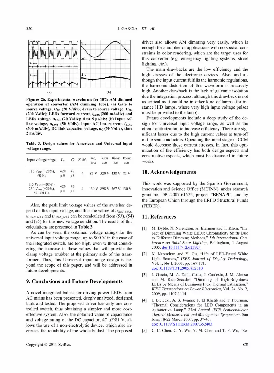
Figures 26. Experimental waveforms for 10% AM dimmed operation of converter (AM dimming 10%). (a) Gate to source voltage, UGS (20 V/div); drain to source voltage, UDS
(200 V/div); LEDs forward current, iLEDs (200 mA/div) and LEDs voltage, uLEDs (20 V/div); time 5 s/div; (b) Input AC ine voltage, u (50 V/div), input AC line current, l
(500 mA/div), DC link c2 ms/div. Table 3. Design values for American and Universal input voltage range.
Input voltage range. LF C NP/NS uC_
MAX uSINT
MAX uD1AK
MAX
uD2AK
MAX
115 VRMS (±20%), 60 Hz
420 H
47 F
4 81 V 520 V 438 V 81 V
115 VRMS (–20%) - 230 VRMS (+20%),
50 - 60 Hz.
420 H
47 F
4 130 V 898 V 767 V 130 V
Also, the peak limit voltage values of the switches de-
pend on this input voltage, and thus the values of uSINT_MAX, uD1AK_MAX and uD2AK_MAX can be recalculated from (53), (54) and (55) for this new voltage condition. The results of this calculations are presented in Table 3.
As can be seen, the obtained voltage ratings for the universal input voltage range, up to 900 V in the case of the integrated switch, are too high, even without consid-ering the increase in these values that will provide the
yo e of this paper, and will be addressed in ture developments.
DC capacitor, 47 µF/81 V, al- lo
sed
dri
waveform is relatively hi
ll as the ircuit optimization to increase efficiency. There are sig-
nificant losses due to the high current values at turn-off of the semiconductors. Operating the input stage in CCM would decrease those current stresses. In fact, this opti-mization of the efficiency has both design aspects and constructive aspects, which must be discussed in future works. 10. Acknowledgements This work was supported by the Spanish GovernmentInnovation r research
“Im-pact of Dimming White LEDs: Chromaticity Shifts Due to Different Dimming Methods,” 5th International Con- ference on Solid State Lighting, Bellingham, 1 August 2005. doi:10.1117/12.625924
clamp voltage snubber at the primary side of the trans-former. Thus, this Universal input range design is be-
nd the scopfu 9. Conclusions and Future Developments A novel integrated ballast for driving power LEDs from AC mains has been presented, deeply analyzed, designed, built and tested. The proposed driver has only one con-trolled switch, thus obtaining a simpler and more cost- effective system. Also, the obtained value of capacitance and voltage rating of the
ws the use of a non-electrolytic device, which also in- creases the reliability of the whole ballast. The propo
ver also allows AM dimming very easily, which is enough for a number of applications with no special con- straints in color rendering, which are the target uses for this converter (e.g. emergency lighting systems, street lighting, etc.).
The main drawbacks are the low efficiency and the high stresses of the electronic devices. Also, and al-though the input current fulfills the harmonic regulations, the harmonic distortion of this
gh. Another drawback is the lack of galvanic isolation due the integration process, although this drawback is not as critical as it could be in other kind of lamps (for in-stance HID lamps, where very high input voltage pulses must be provided to the lamp).
Future developments include a deep study of the de-sign for Universal input voltage range, as wec
, and Science Office (MCINN), unde
grant no. DPI-2007-61522, project “BENAPI”, and by the European Union through the ERFD Structural Funds (FEDER). 11. References 1] M. Dyble, N. Narendran, A. Bierman and T. Klein,[
[2] N. Narendran and Y. Gu, “Life of LED-Based White Light Sources,” IEEE Journal of Display Technology, Vol. 1, No 1, 2005, pp. 167-171. doi:10.1109/JDT.2005.852510
[3] J. Garcia, M. A. Dalla-Costa, J. Cardesin, J. M. Alonso and M. Rico-Secades, “Dimming of High-Brightness LEDs by Means of Luminous Flux Thermal Estimation,IEEE 24, No. 2,
” Transactions on Power Electronics, Vol.
2009, pp. 1107-1114.
[4] J. Bielecki, A. S. Jwania; F. El Khatib and T. Poorman, “Thermal Considerations for LED Components in an Automotive Lamp,” 23rd Annual IEEE Semiconductor Thermal Measurement and Management Symposium, San Jose, 18-22 March 2007, pp. 37-43. doi:10.1109/STHERM.2007.352403
[5] C. C. Chen, C. Y. Wu, Y. M. Chen and T. F. Wu, “Se-
Copyright © 2011 SciRes. CS

J. GARCIA ET AL.
Copyright © 2011 SciRes. CS
351
quential Color LED Backlight Driving System for LCD Panels,” IEEE Transactions on Power Electronics, Vol. 22, No. 3, 2007, pp. 919-925. doi:10.1109/TPEL.2007.897001
[6] M. Rico-Secades, A. J. Calleja, J. Ribas, E. L. Corominas, J. M. Alonso, J. Cardesín and J. García, “Evaluation of a Low-Cost Permanent Emergency Lighting System Based on High Efficiency LEDs,” IEEE Transactions on Indus-try Applications, Vol. 41, No. 5, 2005, pp. 1386-1390. doi:10.1109/TIA.2005.853389
[7] Y.-K. u, “Design Lo, K.-H. Wu, K.-J. Pai and H.-J. Chiand Implementation of RGB LED Drivers for LCD Back-light Modules,” IEEE Transactions on Industrial Elec-tronics, Vol. 56, No. 12, 2009, pp. 4862-4871. doi:10.1109/TIE.2009.2026771
[8] H.-J. Chiu, Y.-K. Lo, J.-T. Chen, S.-J. Cheng, C.-Y. Lin, and S.-C. Mou, “A High-Efficiency Dimmable LED Driver for Low-Power Lighting Applications,” IEEE Tran-sac- tions on Industrial Electronics, Vol. 57, No. 2, 2010, pp. 735-743. doi:10.1109/TIE.2009.2027251
tive Power Factor Correction Circuit for HB LED Driver,” IEEE Transactions on Power Electronics,
8 . 1410-1 .921184
[9] K. Zhou, J. G. Zhang, S. Yuvarajan and D. F. Weng, “Quasi-Ac
Vol. 23, No. 3doi:10.1109/TPEL.2008
, 200 , pp 415.
[ . a . a, J. Cardesin and A. J. Calleja, pe d r Conv i
Conference Rec d of the 2006 IEEE Industry Applica-n st IAS Annual Meeting, Tampa, 8-12 , 18
[11] Ch. Wong and Ch. K. Tse, “Isolated PFC Pre- Regulator for LED Lamps,” Proceedings of 34th Indus-
10] M Rico-Sec“ Tap
des, J GarciUsing d In
oructo erters as LED Dr vers,”
tions Confere ce 41 1October 2006 pp. 794- 00.
X. Qu, S.
trial Electronics Annual Conference, Orlando, 10-13 November 2008, pp. 1980-1987.
[12] Y. X. Qin, H. S. H. Chung, D. Y. Lin and S. Y. R. Hui, “Current Source Ballast for high Power Lighting Emitting Diodes without Electrolytic Capacitor,” Proceedings of 34th Industrial Electronics Annual Conference, Orlando, 10-13 November 2008, pp. 1968-1973,
[13] Y. Hu and M. M. Jovanovic, “LED Driver with Self- Adaptive Drive Voltage,” IEEE Transaction on Power Electronics, Vol. 23, No. 6, 2008, pp. 3116-3125. doi:10.1109/TPEL.2008.2004558
[14] Y. Fang; S.-H. Wong and L. L. Hok-Sun, “A Power Con- verter with Pulse-Level-Modulation Control for Driving High Brightness LEDs,” Proceedings of the Twenty-
Fourth Annual IEEE Applied Power Electronics and Ex- position Conference, Washington DC, 15-19 February 2009, pp. 577-581. doi:10.1109/APEC.2009.4802715
[15] D. Rand, B. Lehman and A. Shteynberg, “Issues, Models and Solutions for Triac Modulated Phase Dimming of LED Lamps,” Proceedings of the IEEE Power Electron-ics Specialists Conference 2007, Orlando, 17-21 June 2007, pp. 1398-1404.
[16] X. R. Xu and X. B. Wu, “High Dimming Ratio LED Driver with Fast Transient Boost Converter,” Proceed-ings of the IEEE Power Electronics Specialists Confer-ence 2008, Rhodes, 15-19 June 2008, pp. 4192-4195.
[17] N. Prathyusha and D. S. Zinger, “An Effective LED Dimming Approach,” 2004 IEEE Industry Applications Conference, 39th IAS Annual Meeting, Seattle, 3-7 Octo-ber 2004, pp. 1671-1676. doi:10.1109/IAS.2004.1348695
[18] D. Gacio, J. M. Alonso, J. Garcia, L. Campa, M. Crespo and M. Rico-Secades, “High Frequency PWM Dimming Technique for High Power Factor Converters in LED Lighting,” Proceedings of the Twenty-Fifth Annual IEEE Applied Power Electronics and Exposition Conference 2010, Palm Springs, 21-25 February 2010, pp. 743-749.
[19] D. Ram
Gacio, J. Alonso, J. Garcia, L. Campa, M. Crespo os and M. Rico-Secades, “PWM Series Dimming for
Drivers: The High Frequency ons on Industrial Electronics,
No. 99, p. 1. doi:
Slow-Dynamics HPF LED Approach,” IEEE Transacti
10.1109/TIE.2011.2130503
[20] L. Gu, X. Ruan, M. Xu and K. Yao, “Means of Eliminat-ing Electrolytic Capacitor in AC/DC Power Supplies for LED Lightings,” IEEE Transactions on Power Electron-ics, Vol. 24, No. 5, 2009, pp. 1399-1408. doi:10.1109/TPEL.2009.2016662
[21] J. Garcia, A. J. Calleja, E. L. Corominas, D. Gacio and J. ic Driver without Electrolytic Capacitor
tness LEDs,” 35th Annual Con-Ribas, “Electronfor Dimming High Brighference of the IEEE Industrial Electronics Society, Porto, 2-5 November 2009, pp. 3518-3513. doi:10.1109/IECON.2009.5415167
[22] J. Garcia, A. J. Calleja, E. L. Corominas, J. Ribas, L. Campa and R. E. Díaz, “Integrated Driver for Power LEDs,” 36th Annual Conference of the IEEE Industrial Electronics Society, Glendale, 2-5 November 2010, pp. 2578-2583. doi:10.1109/IECON.2010.5675150
[23] Luxeon LXK2 white LED datasheet, DS51, 2006. http://www.lumileds.com.


