Embed Size (px)
Citation preview

Intel® Quartus® Prime StandardEdition Handbook Volume 3Verification
Updated for Intel® Quartus® Prime Design Suite: 17.1
SubscribeSend Feedback
QPS5V3 | 2017.11.06Latest document on the web: PDF | HTML

Contents
1 Simulating Intel FPGA Designs.......................................................................................111.1 Simulator Support.................................................................................................111.2 Simulation Levels..................................................................................................121.3 HDL Support........................................................................................................ 121.4 Simulation Flows...................................................................................................131.5 Preparing for Simulation........................................................................................ 14
1.5.1 Compiling Simulation Models...................................................................... 141.6 Simulating Intel FPGA IP Cores............................................................................... 15
1.6.1 Generating IP Simulation Files.................................................................... 151.6.2 Scripting IP Simulation.............................................................................. 17
1.7 Using NativeLink Simulation (Intel Quartus Prime Standard Edition).............................241.7.1 Setting Up NativeLink Simulation (Intel Quartus Prime Standard Edition)..........251.7.2 Running RTL Simulation (NativeLink Flow)....................................................251.7.3 Running Gate-Level Simulation (NativeLink Flow).......................................... 26
1.8 Running a Simulation (Custom Flow)....................................................................... 261.9 Document Revision History.....................................................................................27
2 ModelSim - Intel FPGA Edition, ModelSim, and QuestaSim Support*..............................292.1 Quick Start Example (ModelSim with Verilog)............................................................292.2 ModelSim, ModelSim-Intel FPGA Edition, and QuestaSim Guidelines.............................30
2.2.1 Using ModelSim-Intel FPGA Edition Precompiled Libraries............................... 302.2.2 Disabling Timing Violation on Registers........................................................ 302.2.3 Passing Parameter Information from Verilog HDL to VHDL.............................. 312.2.4 Increasing Simulation Speed...................................................................... 312.2.5 Simulating Transport Delays....................................................................... 312.2.6 Viewing Simulation Messages..................................................................... 322.2.7 Generating Power Analysis Files.................................................................. 332.2.8 Viewing Simulation Waveforms................................................................... 332.2.9 Simulating with ModelSim-Intel FPGA Edition Waveform Editor........................34
2.3 ModelSim Simulation Setup Script Example.............................................................. 342.4 Unsupported Features........................................................................................... 352.5 Document Revision History.....................................................................................35
3 Synopsys VCS and VCS MX Support................................................................................373.1 Quick Start Example (VCS with Verilog)................................................................... 373.2 VCS and QuestaSim Guidelines...............................................................................37
3.2.1 Simulating Transport Delays....................................................................... 383.2.2 Disabling Timing Violation on Registers........................................................ 383.2.3 Generating Power Analysis Files.................................................................. 39
3.3 VCS Simulation Setup Script Example......................................................................393.4 Document Revision History.....................................................................................40
4 Cadence* Incisive Enterprise (IES) Support.................................................................. 414.1 Quick Start Example (NC-Verilog)............................................................................414.2 Cadence Incisive Enterprise (IES) Guidelines............................................................ 42
4.2.1 Using GUI or Command-Line Interfaces....................................................... 424.2.2 Elaborating Your Design.............................................................................424.2.3 Back-Annotating Simulation Timing Data (VHDL Only)....................................43
Contents
Intel® Quartus® Prime Standard Edition Handbook Volume 3 Verification2

4.2.4 Disabling Timing Violation on Registers........................................................ 434.2.5 Simulating Pulse Reject Delays................................................................... 434.2.6 Viewing Simulation Waveforms................................................................... 44
4.3 IES Simulation Setup Script Example.......................................................................444.4 Document Revision History.....................................................................................45
5 Aldec* Active-HDL and Riviera-PRO Support..................................................................465.1 Quick Start Example (Active-HDL VHDL).................................................................. 465.2 Aldec Active-HDL and Riviera-PRO Guidelines........................................................... 47
5.2.1 Compiling SystemVerilog Files.................................................................... 475.2.2 Simulating Transport Delays....................................................................... 475.2.3 Disabling Timing Violation on Registers........................................................ 47
5.3 Using Simulation Setup Scripts............................................................................... 485.4 Document Revision History.....................................................................................48
6 Design Debugging Using In-System Sources and Probes............................................... 496.1 Hardware and Software Requirements..................................................................... 516.2 Design Flow Using the In-System Sources and Probes Editor.......................................51
6.2.1 Instantiating the In-System Sources and Probes IP Core................................ 526.2.2 In-System Sources and Probes IP Core Parameters........................................53
6.3 Compiling the Design............................................................................................ 536.4 Running the In-System Sources and Probes Editor.................................................... 54
6.4.1 In-System Sources and Probes Editor GUI.................................................... 546.4.2 Programming Your Device With JTAG Chain Configuration...............................546.4.3 Instance Manager..................................................................................... 556.4.4 In-System Sources and Probes Editor Pane...................................................55
6.5 Tcl interface for the In-System Sources and Probes Editor.......................................... 576.6 Design Example: Dynamic PLL Reconfiguration......................................................... 596.7 Document Revision History.....................................................................................61
7 Timing Analysis Overview.............................................................................................. 637.1 Timing Analysis Overview.......................................................................................637.2 Timing Analyzer Terminology and Concepts.............................................................. 63
7.2.1 Timing Netlists and Timing Paths.................................................................637.2.2 Clock Setup Check.................................................................................... 667.2.3 Clock Hold Check...................................................................................... 677.2.4 Recovery and Removal Time.......................................................................687.2.5 Multicycle Paths........................................................................................ 697.2.6 Metastability............................................................................................ 707.2.7 Common Clock Path Pessimism Removal...................................................... 717.2.8 Clock-As-Data Analysis.............................................................................. 727.2.9 Multicycle Clock Setup Check and Hold Check Analysis................................... 747.2.10 Multicorner Analysis.................................................................................77
7.3 Document Revision History.....................................................................................78
8 The Intel Quartus Prime Timing Analyzer...................................................................... 798.1 Enhanced Timing Analysis for Intel Arria 10 Devices.................................................. 798.2 Recommended Flow for First Time Users.................................................................. 80
8.2.1 Creating and Setting Up your Design........................................................... 808.2.2 Specifying Timing Requirements................................................................. 808.2.3 Performing a Full Compilation..................................................................... 828.2.4 Verifying Timing........................................................................................83
Contents
Intel® Quartus® Prime Standard Edition Handbook Volume 3 Verification3

8.2.5 Analyzing Timing in Designs Compiled in Previous Versions.............................848.3 Timing Constraints................................................................................................84
8.3.1 Recommended Starting SDC Constraints...................................................... 848.3.2 Creating Clocks and Clock Constraints......................................................... 908.3.3 Creating I/O Requirements....................................................................... 1018.3.4 Creating Delay and Skew Constraints.........................................................1038.3.5 Creating Timing Exceptions...................................................................... 1078.3.6 A Sample Design with SDC File................................................................. 132
8.4 Running the Timing Analyzer................................................................................ 1338.4.1 Intel Quartus Prime Settings.....................................................................1358.4.2 SDC File Precedence................................................................................135
8.5 Understanding Results......................................................................................... 1368.5.1 Iterative Constraint Modification ...............................................................1368.5.2 Set Operating Conditions Dialog Box..........................................................1378.5.3 Report Timing (Dialog Box).......................................................................1398.5.4 Report CDC Viewer Command...................................................................1398.5.5 Analyzing Results with Report Timing.........................................................1468.5.6 Correlating Constraints to the Timing Report...............................................149
8.6 Constraining and Analyzing with Tcl Commands.......................................................1538.6.1 Collection Commands.............................................................................. 1538.6.2 Identifying the Intel Quartus Prime Software Executable from the SDC File..... 1568.6.3 Locating Timing Paths in Other Tools..........................................................157
8.7 Generating Timing Reports................................................................................... 1578.8 Document Revision History...................................................................................159
9 Power Analysis............................................................................................................ 1619.1 Types of Power Analyses...................................................................................... 162
9.1.1 Differences between the EPE and the Intel Quartus Prime Power Analyzer.......1629.2 Factors Affecting Power Consumption.....................................................................163
9.2.1 Device Selection..................................................................................... 1639.2.2 Environmental Conditions.........................................................................1649.2.3 Device Resource Usage............................................................................ 1659.2.4 Signal Activities...................................................................................... 165
9.3 Power Analyzer Flow............................................................................................1669.3.1 Operating Settings and Conditions.............................................................1669.3.2 Signal Activities Data Sources...................................................................167
9.4 Using Simulation Files in Modular Design Flows....................................................... 1689.4.1 Complete Design Simulation..................................................................... 1709.4.2 Modular Design Simulation....................................................................... 1709.4.3 Multiple Simulations on the Same Entity.....................................................1719.4.4 Overlapping Simulations...........................................................................1719.4.5 Partial Simulations.................................................................................. 1719.4.6 Node Name Matching Considerations .........................................................1729.4.7 Glitch Filtering........................................................................................ 1739.4.8 Node and Entity Assignments....................................................................1749.4.9 Default Toggle Rate Assignment................................................................ 1759.4.10 Vectorless Estimation.............................................................................175
9.5 Using the Power Analyzer.....................................................................................1769.5.1 Common Analysis Flows........................................................................... 1769.5.2 Using .vcd for Power Estimation................................................................ 176
9.6 Power Analyzer Compilation Report .......................................................................178
Contents
Intel® Quartus® Prime Standard Edition Handbook Volume 3 Verification4

9.7 Scripting Support................................................................................................1809.7.1 Running the Power Analyzer from the Command–Line.................................. 180
9.8 Document Revision History...................................................................................181
10 System Debugging Tools Overview............................................................................ 18310.1 System Debugging Tools Portfolio........................................................................ 183
10.1.1 System Debugging Tools Comparison....................................................... 18310.1.2 System-Level Debugging Infrastructure....................................................18410.1.3 Debugging Ecosystem............................................................................18410.1.4 Tools to Analyze RTL Nodes.....................................................................18510.1.5 Suggested On-Chip Debugging Tools for Common Debugging Features......... 18810.1.6 Stimulus-Capable Tools.......................................................................... 189
10.2 Document Revision History................................................................................. 191
11 Analyzing and Debugging Designs with System Console............................................ 19311.1 Introduction to System Console...........................................................................19311.2 Debugging Flow with the System Console............................................................. 19411.3 IP Cores that Interact with System Console...........................................................195
11.3.1 Services Provided through Debug Agents..................................................19511.4 Starting System Console.................................................................................... 196
11.4.1 Starting System Console from Nios II Command Shell................................ 19611.4.2 Starting Stand-Alone System Console...................................................... 19611.4.3 Starting System Console from Platform Designer (Standard)....................... 19611.4.4 Starting System Console from Intel Quartus Prime.....................................19711.4.5 Customizing Startup.............................................................................. 197
11.5 System Console GUI.......................................................................................... 19711.5.1 System Explorer Pane............................................................................ 198
11.6 System Console Commands................................................................................19911.7 Running System Console in Command-Line Mode.................................................. 20111.8 System Console Services....................................................................................202
11.8.1 Locating Available Services..................................................................... 20211.8.2 Opening and Closing Services................................................................. 20311.8.3 SLD Service..........................................................................................20311.8.4 In-System Sources and Probes Service.....................................................20411.8.5 Monitor Service.....................................................................................20611.8.6 Device Service...................................................................................... 20811.8.7 Design Service...................................................................................... 20911.8.8 Bytestream Service............................................................................... 21011.8.9 JTAG Debug Service...............................................................................211
11.9 Working with Toolkits......................................................................................... 21211.9.1 Convert your Dashboard Scripts to Toolkit API........................................... 21211.9.2 Creating a Toolkit Description File............................................................ 21211.9.3 Registering a Toolkit.............................................................................. 21311.9.4 Launching a Toolkit................................................................................21311.9.5 Matching Toolkits with IP Cores............................................................... 21411.9.6 Toolkit API............................................................................................214
11.10 ADC Toolkit.....................................................................................................25111.10.1 ADC Toolkit Terms................................................................................25411.10.2 Setting the Frequency of the Reference Signal........................................ 25411.10.3 Tuning the Signal Generator..................................................................25511.10.4 Running a Signal Quality Test................................................................ 257
Contents
Intel® Quartus® Prime Standard Edition Handbook Volume 3 Verification5

11.10.5 Running a Linearity Test....................................................................... 25811.10.6 ADC Toolkit Data Views.........................................................................258
11.11 System Console Examples and Tutorials..............................................................26111.11.1 Board Bring-Up with System Console Tutorial.......................................... 26111.11.2 Nios II Processor Example.....................................................................269
11.12 On-Board Intel FPGA Download Cable II Support................................................. 27011.13 About Using MATLAB and Simulink in a System Verification Flow ........................... 27011.14 Deprecated Commands.................................................................................... 27211.15 Document Revision History............................................................................... 273
12 Debugging Transceiver Links..................................................................................... 27412.1 Channel Manager.............................................................................................. 274
12.1.1 Channel Display Modes...........................................................................27612.2 Transceiver Debugging Flow Walkthrough............................................................. 27612.3 Configuring your System with Debugging Components........................................... 276
12.3.1 Adapting an Intel FPGA Design Example .................................................. 27612.3.2 Stratix V Debug System Configuration......................................................27912.3.3 Instantiating and Parameterizing Intel Arria 10 Debug IP cores....................285
12.4 Programming the Design into an Intel FPGA..........................................................28712.5 Loading the Design in the Transceiver Toolkit........................................................ 28812.6 Linking Hardware Resources............................................................................... 288
12.6.1 Linking One Design to One Device........................................................... 29112.6.2 Linking Two Designs to Two Devices.........................................................29112.6.3 Linking One Design on Two Devices......................................................... 29112.6.4 Linking Designs and Devices on Separate Boards....................................... 292
12.7 Verifying Hardware Connections.......................................................................... 29212.8 Identifying Transceiver Channels......................................................................... 292
12.8.1 Controlling Transceiver Channels............................................................. 29312.8.2 Creating Links.......................................................................................29312.8.3 Manually Creating a Transceiver Link........................................................293
12.9 Running Link Tests.............................................................................................29312.9.1 Running BER Tests.................................................................................29412.9.2 Signal Eye Margin Testing (Stratix V only).................................................29412.9.3 Running Custom Traffic Tests (Stratix V only) ........................................... 29612.9.4 Link Optimization Tests.......................................................................... 297
12.10 Controlling PMA Analog Settings........................................................................ 29712.11 User Interface Settings Reference...................................................................... 30012.12 Troubleshooting Common Errors........................................................................ 30412.13 Scripting API Reference.................................................................................... 304
12.13.1 Transceiver Toolkit Commands...............................................................30412.13.2 Data Pattern Generator Commands........................................................ 31112.13.3 Data Pattern Checker Commands...........................................................313
12.14 Document Revision History............................................................................... 314
13 Quick Design Debugging Using Signal Probe..............................................................31713.1 Design Flow Using Signal Probe...........................................................................317
13.1.1 Perform a Full Compilation......................................................................31713.1.2 Reserve Signal Probe Pins.......................................................................31813.1.3 Assign Signal Probe Sources................................................................... 31813.1.4 Add Registers Between Pipeline Paths and Signal Probe Pins........................31813.1.5 Perform a Signal Probe Compilation......................................................... 319
Contents
Intel® Quartus® Prime Standard Edition Handbook Volume 3 Verification6

13.1.6 Analyze the Results of a Signal Probe Compilation......................................31913.1.7 What a Signal Probe Compilation Does..................................................... 32013.1.8 Understanding the Results of a Signal Probe Compilation............................ 320
13.2 Scripting Support.............................................................................................. 32213.2.1 Making a Signal Probe Pin.......................................................................32213.2.2 Deleting a Signal Probe Pin..................................................................... 32213.2.3 Enabling a Signal Probe Pin.....................................................................32313.2.4 Disabling a Signal Probe Pin....................................................................32313.2.5 Performing a Signal Probe Compilation..................................................... 32313.2.6 Reserving Signal Probe Pins.................................................................... 32313.2.7 Adding Signal Probe Sources...................................................................32413.2.8 Assigning I/O Standards.........................................................................32413.2.9 Adding Registers for Pipelining................................................................ 32413.2.10 Running Signal Probe Immediately After a Full Compilation....................... 32513.2.11 Running Signal Probe Manually..............................................................32513.2.12 Enabling or Disabling All Signal Probe Routing......................................... 32513.2.13 Allowing Signal Probe to Modify Fitting Results.........................................325
13.3 Document Revision History................................................................................. 325
14 Design Debugging with the Signal Tap Logic Analyzer............................................... 32714.1 About the Signal Tap Logic Analyzer.....................................................................327
14.1.1 Hardware and Software Requirements......................................................32814.1.2 Open Standalone Signal Tap Logic Analyzer GUI........................................ 33014.1.3 Backward Compatibility with Previous Versions of Intel Quartus Prime
Software............................................................................................... 33014.2 Signal Tap Logic Analyzer Task Flow Overview....................................................... 330
14.2.1 Add the Signal Tap Logic Analyzer to Your Design.......................................33114.2.2 Configure the Signal Tap Logic Analyzer....................................................33114.2.3 Define Trigger Conditions........................................................................33214.2.4 Compile the Design................................................................................33214.2.5 Program the Target Device or Devices...................................................... 33214.2.6 Run the Signal Tap Logic Analyzer............................................................33214.2.7 View, Analyze, and Use Captured Data..................................................... 333
14.3 Configuring the Signal Tap Logic Analyzer............................................................. 33314.3.1 Assigning an Acquisition Clock.................................................................33314.3.2 Adding Signals to the Signal Tap File........................................................ 33414.3.3 Adding Signals with a Plug-In..................................................................33714.3.4 Adding Finite State Machine State Encoding Registers................................ 33814.3.5 Specify the Sample Depth.......................................................................33914.3.6 Capture Data to a Specific RAM Type........................................................33914.3.7 Select the Buffer Acquisition Mode........................................................... 34014.3.8 Specify the Pipeline Factor...................................................................... 34214.3.9 Using the Storage Qualifier Feature..........................................................34314.3.10 Manage Multiple Signal Tap Files and Configurations................................. 350
14.4 Defining Triggers............................................................................................... 35214.4.1 Basic Trigger Conditions......................................................................... 35214.4.2 Comparison Trigger Conditions................................................................ 35314.4.3 Advanced Trigger Conditions................................................................... 35514.4.4 Custom Trigger HDL Object.....................................................................35814.4.5 Trigger Condition Flow Control.................................................................36114.4.6 Specify Trigger Position.......................................................................... 372
Contents
Intel® Quartus® Prime Standard Edition Handbook Volume 3 Verification7

14.4.7 Create a Power-Up Trigger...................................................................... 37314.4.8 External Triggers................................................................................... 375
14.5 Compiling the Design.........................................................................................37614.5.1 Faster Compilations with Intel Quartus Prime Incremental Compilation......... 37614.5.2 Prevent Changes Requiring Recompilation.................................................37814.5.3 Incremental Route with Rapid Recompile.................................................. 37814.5.4 Timing Preservation with the Signal Tap Logic Analyzer...............................38014.5.5 Performance and Resource Considerations................................................ 380
14.6 Program the Target Device or Devices.................................................................. 38114.6.1 Ensure Setting Compatibility Between .stp and .sof Files.............................38214.6.2 Verify Whether You Need to Recompile Your Project....................................382
14.7 Running the Signal Tap Logic Analyzer..................................................................38214.7.1 Runtime Reconfigurable Options.............................................................. 38314.7.2 Signal Tap Status Messages.................................................................... 385
14.8 View, Analyze, and Use Captured Data................................................................. 38614.8.1 Capturing Data Using Segmented Buffers................................................. 38614.8.2 Differences in Pre-fill Write Behavior Between Different Acquisition Modes.....38714.8.3 Creating Mnemonics for Bit Patterns.........................................................38914.8.4 Automatic Mnemonics with a Plug-In........................................................38914.8.5 Locating a Node in the Design................................................................. 39014.8.6 Saving Captured Data............................................................................ 39014.8.7 Exporting Captured Data to Other File Formats..........................................39114.8.8 Creating a Signal Tap List File..................................................................391
14.9 Other Features..................................................................................................39114.9.1 Creating Signal Tap File from Design Instances..........................................39114.9.2 Using the Signal Tap MATLAB MEX Function to Capture Data........................39314.9.3 Using Signal Tap in a Lab Environment..................................................... 39514.9.4 Remote Debugging Using the Signal Tap Logic Analyzer.............................. 39514.9.5 Using the Signal Tap Logic Analyzer in Devices with Configuration
Bitstream Security..................................................................................39614.9.6 Monitor FPGA Resources Used by the Signal Tap Logic Analyzer................... 396
14.10 Design Example: Using Signal Tap Logic Analyzers............................................... 39614.11 Custom Triggering Flow Application Examples......................................................397
14.11.1 Design Example 1: Specifying a Custom Trigger Position........................... 39714.11.2 Design Example 2: Trigger When triggercond1 Occurs Ten Times
between triggercond2 and triggercond3.................................................... 39814.12 Signal Tap Scripting Support............................................................................. 399
14.12.1 Signal Tap Tcl Commands......................................................................39914.12.2 Signal Tap Command-Line Options......................................................... 399
14.13 Document Revision History............................................................................... 401
16 Debugging Single Event Upset Using the Fault Injection Debugger............................40316.1 Single Event Upset Mitigation..............................................................................40316.2 Hardware and Software Requirements..................................................................40416.3 Using the Fault Injection Debugger and Fault Injection IP Core................................ 404
16.3.1 Instantiating the Intel FPGA Fault Injection IP Core.................................... 40516.3.2 Defining Fault Injection Areas..................................................................40716.3.3 Using the Fault Injection Debugger.......................................................... 40816.3.4 Command-Line Interface........................................................................ 413
16.4 Document Revision History................................................................................. 417
Contents
Intel® Quartus® Prime Standard Edition Handbook Volume 3 Verification8

17 In-System Debugging Using External Logic Analyzers............................................... 41817.1 About the Intel Quartus Prime Logic Analyzer Interface.......................................... 41817.2 Choosing a Logic Analyzer.................................................................................. 418
17.2.1 Required Components............................................................................ 41917.3 Flow for Using the LAI........................................................................................42017.4 Working with LAI Files........................................................................................421
17.4.1 Configuring the File Core Parameters....................................................... 42117.4.2 Mapping the LAI File Pins to Available I/O Pins...........................................42117.4.3 Mapping Internal Signals to the LAI Banks................................................ 42217.4.4 Using the Node Finder............................................................................42217.4.5 Compiling Your Intel Quartus Prime Project............................................... 42217.4.6 Programming Your Intel-Supported Device Using the LAI............................ 423
17.5 Controlling the Active Bank During Runtime.......................................................... 42317.5.1 Acquiring Data on Your Logic Analyzer......................................................423
17.6 Using the LAI with Incremental Compilation.......................................................... 42317.7 Document Revision History................................................................................. 424
18 In-System Modification of Memory and Constants..................................................... 42518.1 About the In-System Memory Content Editor.........................................................42518.2 Design Flow Using the In-System Memory Content Editor....................................... 42518.3 Creating In-System Modifiable Memories and Constants......................................... 42618.4 Running the In-System Memory Content Editor..................................................... 426
18.4.1 Instance Manager..................................................................................42618.4.2 Editing Data Displayed in the Hex Editor Pane........................................... 42718.4.3 Importing and Exporting Memory Files..................................................... 42718.4.4 Scripting Support.................................................................................. 42718.4.5 Programming the Device with the In-System Memory Content Editor............42818.4.6 Example: Using the In-System Memory Content Editor with the Signal Tap
Logic Analyzer....................................................................................... 42818.5 Document Revision History................................................................................. 429
19 Design Debugging Using In-System Sources and Probes........................................... 43019.1 Hardware and Software Requirements..................................................................43219.2 Design Flow Using the In-System Sources and Probes Editor................................... 432
19.2.1 Instantiating the In-System Sources and Probes IP Core.............................43319.2.2 In-System Sources and Probes IP Core Parameters.................................... 434
19.3 Compiling the Design.........................................................................................43419.4 Running the In-System Sources and Probes Editor.................................................435
19.4.1 In-System Sources and Probes Editor GUI................................................ 43519.4.2 Programming Your Device With JTAG Chain Configuration........................... 43519.4.3 Instance Manager..................................................................................43619.4.4 In-System Sources and Probes Editor Pane............................................... 436
19.5 Tcl interface for the In-System Sources and Probes Editor.......................................43819.6 Design Example: Dynamic PLL Reconfiguration......................................................44019.7 Document Revision History................................................................................. 442
20 Programming Intel FPGA Devices.............................................................................. 44420.1 Programming Flow.............................................................................................444
20.1.1 Stand-Alone Intel Quartus Prime Programmer........................................... 44420.1.2 Optional Programming or Configuration Files............................................. 44520.1.3 Secondary Programming Files................................................................. 445
Contents
Intel® Quartus® Prime Standard Edition Handbook Volume 3 Verification9

20.2 Intel Quartus Prime Programmer Window............................................................. 44620.2.1 Editing the Details of an Unknown Device................................................. 44620.2.2 Setting Up Your Hardware.......................................................................44720.2.3 Setting the JTAG Hardware..................................................................... 44720.2.4 Using the JTAG Chain Debugger Tool........................................................ 447
20.3 Programming and Configuration Modes.................................................................44820.4 Design Security Keys......................................................................................... 44820.5 Convert Programming Files Dialog Box................................................................. 448
20.5.1 Debugging Your Configuration................................................................. 44920.5.2 Converting Programming Files for Partial Reconfiguration............................ 451
20.6 Flash Loaders................................................................................................... 45320.7 JTAG Debug Mode for Partial Reconfiguration.........................................................453
20.7.1 Configuring Partial Reconfiguration Bitstream in JTAG Debug Mode ..............45420.8 Verifying if Programming Files Correspond to a Compilation of the Same Source Files. 459
20.8.1 Obtaining Project Hash for Arria V, Stratix V, Cyclone V and Intel MAX 10Devices.................................................................................................459
20.8.2 Obtaining Project Hash for Intel Arria 10 Devices....................................... 45920.9 Scripting Support.............................................................................................. 460
20.9.1 The jtagconfig Debugging Tool.................................................................46020.9.2 Generating a Partial-Mask SRAM Object File using a Mask Settings File
and a SRAM Object File........................................................................... 46120.9.3 Generating Raw Binary File for Partial Reconfiguration using a .pmsf............ 461
20.10 Document Revision History............................................................................... 461
Contents
Intel® Quartus® Prime Standard Edition Handbook Volume 3 Verification10

1 Simulating Intel FPGA DesignsThis document describes simulating designs that target Intel FPGA devices. Simulationverifies design behavior before device programming. The Intel® Quartus® Primesoftware supports RTL- and gate-level design simulation in supported EDA simulators.Simulation involves setting up your simulator working environment, compilingsimulation model libraries, and running your simulation.
1.1 Simulator Support
The Intel Quartus Prime software supports specific EDA simulator versions for RTL andgate-level simulation.
Table 1. Supported Simulators
Vendor Simulator Version Platform
Aldec Active-HDL* 10.3 Windows
Aldec Riviera-PRO* 2016.10 Windows, Linux
Cadence Incisive Enterprise* 15.20 Linux
Mentor Graphics* ModelSim* - Intel FPGA Edition 10.5c Windows, Linux
Mentor Graphics ModelSim PE 10.5c Windows
Mentor Graphics ModelSim SE 10.5c Windows, Linux
Mentor Graphics QuestaSim* 10.5c Windows, Linux
Synopsys* VCS*VCS MX
2016,06-SP-1 Linux
Table 2. Supported Simulators
Vendor Simulator Version Platform
Aldec Active-HDL 10.3 Windows
Aldec Riviera-PRO 2015.10 Windows, Linux
Cadence Incisive Enterprise* 14.20 Linux
Mentor Graphics ModelSim - Intel FPGA Edition 10.5b Windows, Linux
Mentor Graphics ModelSim PE 10.4d Windows
Mentor Graphics ModelSim SE* 10.4d Windows, Linux
Mentor Graphics QuestaSim 10.4d Windows, Linux
Synopsys VCSVCS MX
2014,12-SP1 Linux
QPS5V3 | 2017.11.06
Intel Corporation. All rights reserved. Intel, the Intel logo, Altera, Arria, Cyclone, Enpirion, MAX, Nios, Quartusand Stratix words and logos are trademarks of Intel Corporation or its subsidiaries in the U.S. and/or othercountries. Intel warrants performance of its FPGA and semiconductor products to current specifications inaccordance with Intel's standard warranty, but reserves the right to make changes to any products and servicesat any time without notice. Intel assumes no responsibility or liability arising out of the application or use of anyinformation, product, or service described herein except as expressly agreed to in writing by Intel. Intelcustomers are advised to obtain the latest version of device specifications before relying on any publishedinformation and before placing orders for products or services.*Other names and brands may be claimed as the property of others.
ISO9001:2008Registered

1.2 Simulation Levels
The Intel Quartus Prime software supports RTL and gate-level simulation of IP cores insupported EDA simulators.
Table 3. Supported Simulation Levels
Simulation Level Description Simulation Input
RTL Cycle-accurate simulation using Verilog HDL,SystemVerilog, and VHDL design source code withsimulation models provided by Intel and other IPproviders.
• Design source/testbench• Intel simulation libraries• Intel FPGA IP plain text or IEEE
encrypted RTL models• IP simulation models• Intel FPGA IP functional simulation
models• Intel FPGA IP bus functional models• Platform Designer (Standard)-
generated models• Verification IP
Gate-level functional Simulation using a post-synthesis or post-fitfunctional netlist testing the post-synthesisfunctional netlist, or post-fit functional netlist.
• Testbench• Intel simulation libraries• Post-synthesis or post-fit functional
netlist• Intel FPGA IP bus functional models
Gate-level timing Simulation using a post-fit timing netlist, testingfunctional and timing performance. Supportedonly for the Arria® II GX/GZ,Cyclone® IV, MAX®
II, MAX V, and Stratix® IV device families.
• Testbench• Intel simulation libraries• Post-fit timing netlist• Post-fit Standard Delay Output File
(.sdo).
Note: Gate-level timing simulation of an entire design can be slow and should be avoided.Gate-level timing simulation is supported only for the Arria II GX/GZ,Cyclone IV, MAXII, MAX V, and Stratix IV device families.. Use Timing Analyzer static timing analysisrather than gate-level timing simulation.
1.3 HDL Support
The Intel Quartus Prime software provides the following HDL support for EDAsimulators.
1 Simulating Intel FPGA Designs
QPS5V3 | 2017.11.06
Intel® Quartus® Prime Standard Edition Handbook Volume 3 Verification12
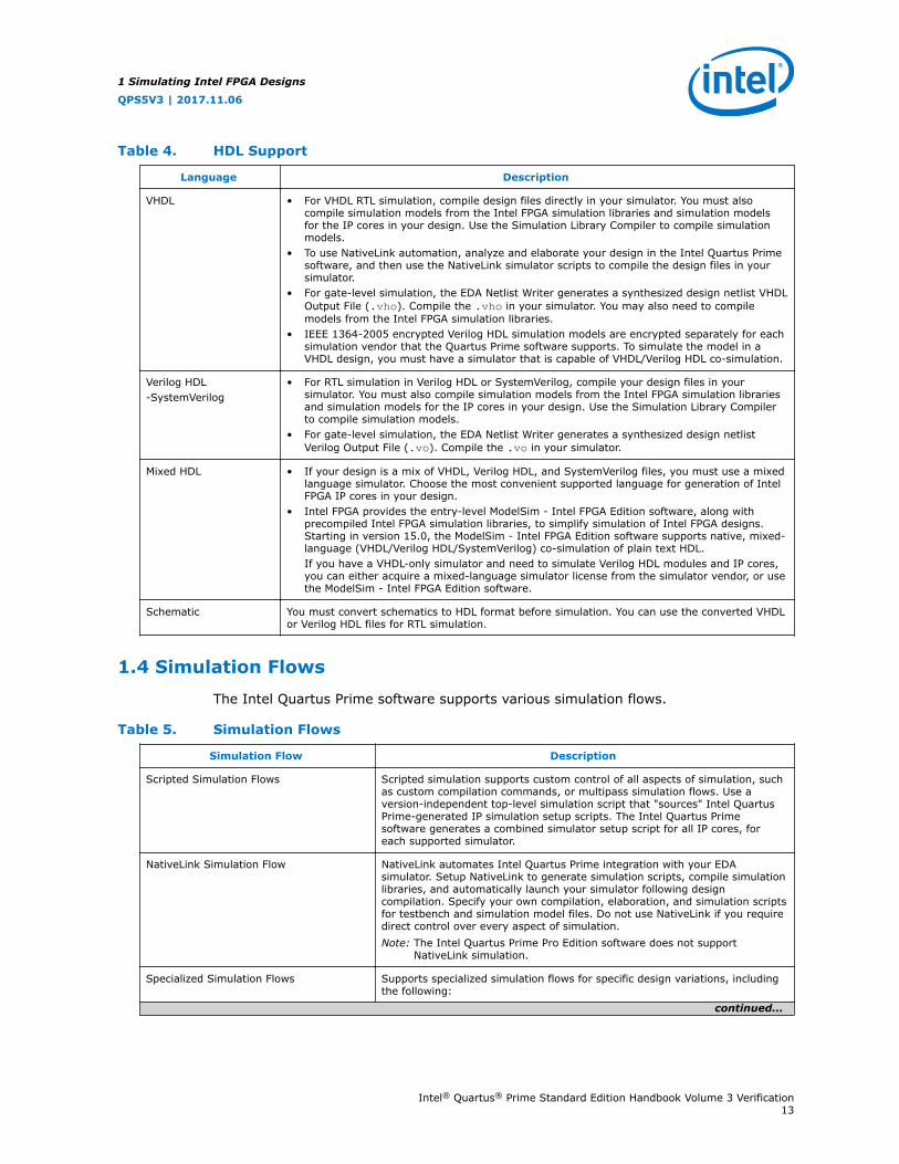
Table 4. HDL Support
Language Description
VHDL • For VHDL RTL simulation, compile design files directly in your simulator. You must alsocompile simulation models from the Intel FPGA simulation libraries and simulation modelsfor the IP cores in your design. Use the Simulation Library Compiler to compile simulationmodels.
• To use NativeLink automation, analyze and elaborate your design in the Intel Quartus Primesoftware, and then use the NativeLink simulator scripts to compile the design files in yoursimulator.
• For gate-level simulation, the EDA Netlist Writer generates a synthesized design netlist VHDLOutput File (.vho). Compile the .vho in your simulator. You may also need to compilemodels from the Intel FPGA simulation libraries.
• IEEE 1364-2005 encrypted Verilog HDL simulation models are encrypted separately for eachsimulation vendor that the Quartus Prime software supports. To simulate the model in aVHDL design, you must have a simulator that is capable of VHDL/Verilog HDL co-simulation.
Verilog HDL-SystemVerilog
• For RTL simulation in Verilog HDL or SystemVerilog, compile your design files in yoursimulator. You must also compile simulation models from the Intel FPGA simulation librariesand simulation models for the IP cores in your design. Use the Simulation Library Compilerto compile simulation models.
• For gate-level simulation, the EDA Netlist Writer generates a synthesized design netlistVerilog Output File (.vo). Compile the .vo in your simulator.
Mixed HDL • If your design is a mix of VHDL, Verilog HDL, and SystemVerilog files, you must use a mixedlanguage simulator. Choose the most convenient supported language for generation of IntelFPGA IP cores in your design.
• Intel FPGA provides the entry-level ModelSim - Intel FPGA Edition software, along withprecompiled Intel FPGA simulation libraries, to simplify simulation of Intel FPGA designs.Starting in version 15.0, the ModelSim - Intel FPGA Edition software supports native, mixed-language (VHDL/Verilog HDL/SystemVerilog) co-simulation of plain text HDL.If you have a VHDL-only simulator and need to simulate Verilog HDL modules and IP cores,you can either acquire a mixed-language simulator license from the simulator vendor, or usethe ModelSim - Intel FPGA Edition software.
Schematic You must convert schematics to HDL format before simulation. You can use the converted VHDLor Verilog HDL files for RTL simulation.
1.4 Simulation Flows
The Intel Quartus Prime software supports various simulation flows.
Table 5. Simulation Flows
Simulation Flow Description
Scripted Simulation Flows Scripted simulation supports custom control of all aspects of simulation, suchas custom compilation commands, or multipass simulation flows. Use aversion-independent top-level simulation script that "sources" Intel QuartusPrime-generated IP simulation setup scripts. The Intel Quartus Primesoftware generates a combined simulator setup script for all IP cores, foreach supported simulator.
NativeLink Simulation Flow NativeLink automates Intel Quartus Prime integration with your EDAsimulator. Setup NativeLink to generate simulation scripts, compile simulationlibraries, and automatically launch your simulator following designcompilation. Specify your own compilation, elaboration, and simulation scriptsfor testbench and simulation model files. Do not use NativeLink if you requiredirect control over every aspect of simulation.Note: The Intel Quartus Prime Pro Edition software does not support
NativeLink simulation.
Specialized Simulation Flows Supports specialized simulation flows for specific design variations, includingthe following:
continued...
1 Simulating Intel FPGA Designs
QPS5V3 | 2017.11.06
Intel® Quartus® Prime Standard Edition Handbook Volume 3 Verification13

Simulation Flow Description
• For simulation of example designs, refer to the documentation for theexample design or to the IP core user guide.
• For simulation of Platform Designer designs, refer to Creating a Systemwith Platform Designer (Standard) or Creating a System with PlatformDesigner.
• For simulation of designs that include the Nios® II embedded processor,refer to Simulating a Nios II Embedded Processor.
Related Links
• IP User Guide Documentation
• AN 351: Simulating Nios II Embedded Processors Designs
• Creating a System With Platform Designer (Standard)In Intel Quartus Prime Standard Edition Handbook Volume 3
1.5 Preparing for Simulation
Preparing for RTL or gate-level simulation involves compiling the RTL or gate-levelrepresentation of your design and testbench. You must also compile IP simulationmodels, models from the Intel FPGA simulation libraries, and any other model librariesrequired for your design.
1.5.1 Compiling Simulation Models
The Intel Quartus Prime software includes simulation models for all Intel FPGA IPcores. These models include IP functional simulation models, and device family-specific models in the <Intel Quartus Prime installation path>/eda/sim_lib directory. These models include IEEE encrypted Verilog HDL models for bothVerilog HDL and VHDL simulation.
Before running simulation, you must compile the appropriate simulation models fromthe Intel Quartus Prime simulation libraries using any of the following methods:
• Use the NativeLink feature to automatically compile your design, Intel FPGA IP,simulation model libraries, and testbench.
• To automatically compile all required simulation model libraries for your design inyour supported simulator, click Tools ➤ Launch Simulation Library Compiler.Specify options for your simulation tool, language, target device family, and outputlocation, and then click OK.
• Compile Intel Quartus Prime simulation models manually with your simulator.
Use the compiled simulation model libraries to simulate your design. Refer to yourEDA simulator's documentation for information about running simulation.
Note: The specified timescale precision must be within 1ps when using Intel Quartus Primesimulation models.
Related Links
Intel Quartus Prime Simulation ModelsIn Intel Quartus Prime Pro Edition Help
1 Simulating Intel FPGA Designs
QPS5V3 | 2017.11.06
Intel® Quartus® Prime Standard Edition Handbook Volume 3 Verification14

1.6 Simulating Intel FPGA IP Cores
The Intel Quartus Prime software supports IP core RTL simulation in specific EDAsimulators. IP generation creates simulation files, including the functional simulationmodel, any testbench (or example design), and vendor-specific simulator setup scriptsfor each IP core. Use the functional simulation model and any testbench or exampledesign for simulation. IP generation output may also include scripts to compile and runany testbench. The scripts list all models or libraries you require to simulate your IPcore.
The Intel Quartus Prime software provides integration with many simulators andsupports multiple simulation flows, including your own scripted and custom simulationflows. Whichever flow you choose, IP core simulation involves the following steps:
1. Generate simulation model, testbench (or example design), and simulator setupscript files.
2. Set up your simulator environment and any simulation scripts.
3. Compile simulation model libraries.
4. Run your simulator.
1.6.1 Generating IP Simulation Files
The Intel Quartus Prime software optionally generates the functional simulation model,any testbench (or example design), and vendor-specific simulator setup scripts whenyou generate an IP core. To control the generation of IP simulation files:
• To specify your supported simulator and options for IP simulation file generation,click Assignment ➤ Settings ➤ EDA Tool Settings ➤ Simulation.
• To parameterize a new IP variation, enable generation of simulation files, andgenerate the IP core synthesis and simulation files, click Tools ➤ IP Catalog.
• To edit parameters and regenerate synthesis or simulation files for an existing IPcore variation, click View ➤ Utility Windows ➤ Project Navigator ➤ IPComponents.
Table 6. Intel FPGA IP Simulation Files
File Type Description File Name
Simulator setupscripts
Vendor-specific scripts to compile, elaborate, and simulateIntel FPGA IP models and simulation model library files.Optionally, generate a simulator setup script for eachvendor that combines the individual IP core scripts into onefile. Source the combined script from your top-levelsimulation script to eliminate script maintenance.
<my_dir>/aldec/rivierapro_setup.tcl
<my_dir>/cadence/ncsim_setup.sh
<my_dir>/mentor/msim_setup.tcl
continued...
1 Simulating Intel FPGA Designs
QPS5V3 | 2017.11.06
Intel® Quartus® Prime Standard Edition Handbook Volume 3 Verification15
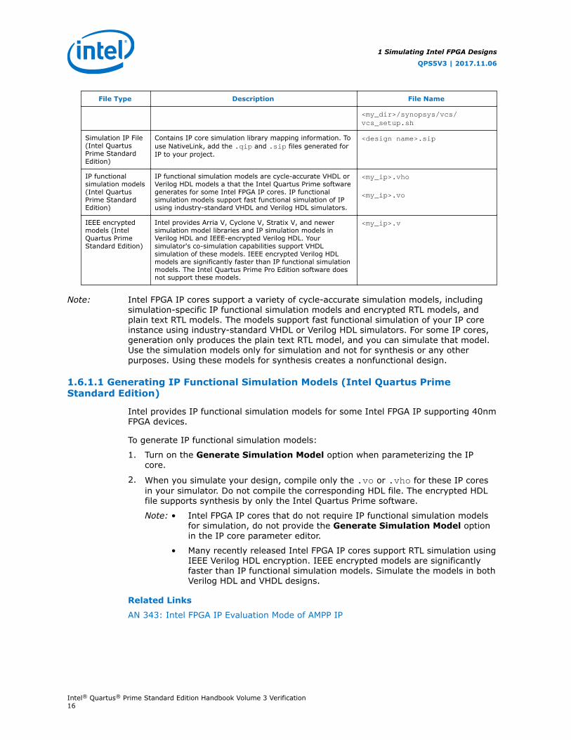
File Type Description File Name
<my_dir>/synopsys/vcs/vcs_setup.sh
Simulation IP File(Intel QuartusPrime StandardEdition)
Contains IP core simulation library mapping information. Touse NativeLink, add the .qip and .sip files generated forIP to your project.
<design name>.sip
IP functionalsimulation models(Intel QuartusPrime StandardEdition)
IP functional simulation models are cycle-accurate VHDL orVerilog HDL models a that the Intel Quartus Prime softwaregenerates for some Intel FPGA IP cores. IP functionalsimulation models support fast functional simulation of IPusing industry-standard VHDL and Verilog HDL simulators.
<my_ip>.vho
<my_ip>.vo
IEEE encryptedmodels (IntelQuartus PrimeStandard Edition)
Intel provides Arria V, Cyclone V, Stratix V, and newersimulation model libraries and IP simulation models inVerilog HDL and IEEE-encrypted Verilog HDL. Yoursimulator's co-simulation capabilities support VHDLsimulation of these models. IEEE encrypted Verilog HDLmodels are significantly faster than IP functional simulationmodels. The Intel Quartus Prime Pro Edition software doesnot support these models.
<my_ip>.v
Note: Intel FPGA IP cores support a variety of cycle-accurate simulation models, includingsimulation-specific IP functional simulation models and encrypted RTL models, andplain text RTL models. The models support fast functional simulation of your IP coreinstance using industry-standard VHDL or Verilog HDL simulators. For some IP cores,generation only produces the plain text RTL model, and you can simulate that model.Use the simulation models only for simulation and not for synthesis or any otherpurposes. Using these models for synthesis creates a nonfunctional design.
1.6.1.1 Generating IP Functional Simulation Models (Intel Quartus PrimeStandard Edition)
Intel provides IP functional simulation models for some Intel FPGA IP supporting 40nmFPGA devices.
To generate IP functional simulation models:
1. Turn on the Generate Simulation Model option when parameterizing the IPcore.
2. When you simulate your design, compile only the .vo or .vho for these IP coresin your simulator. Do not compile the corresponding HDL file. The encrypted HDLfile supports synthesis by only the Intel Quartus Prime software.
Note: • Intel FPGA IP cores that do not require IP functional simulation modelsfor simulation, do not provide the Generate Simulation Model optionin the IP core parameter editor.
• Many recently released Intel FPGA IP cores support RTL simulation usingIEEE Verilog HDL encryption. IEEE encrypted models are significantlyfaster than IP functional simulation models. Simulate the models in bothVerilog HDL and VHDL designs.
Related Links
AN 343: Intel FPGA IP Evaluation Mode of AMPP IP
1 Simulating Intel FPGA Designs
QPS5V3 | 2017.11.06
Intel® Quartus® Prime Standard Edition Handbook Volume 3 Verification16

1.6.2 Scripting IP Simulation
The Intel Quartus Prime software supports the use of scripts to automate simulationprocessing in your preferred simulation environment. Use the scripting methodologythat you prefer to control simulation.
Use a version-independent, top-level simulation script to control design, testbench,and IP core simulation. Because Intel Quartus Prime-generated simulation file namesmay change after IP upgrade or regeneration, your top-level simulation script must"source" the generated setup scripts, rather than using the generated setup scriptsdirectly. Follow these steps to generate or regenerate combined simulator setupscripts:
Figure 1. Incorporating Generated Simulator Setup Scripts into a Top-Level SimulationScript
Top-Level Simulation Script
Specify project-specific settings: TOP_LEVEL_NAME
Source the Combined IP Setup Simulator Script(e.g., source msim_setup.tcl)
ElaborateSimulate
Individual IPSimulation Scripts
Combined IPSimulator Script
(Includes Templates)
Click “Generate Simulator Script for IP”Additional compile and elaboration options
Compile design files:Use generated scripts to compile device librariesand IP filesCompile your design and testbench files
Add optional QSYS_SIMDIR variable
1. Click Project ➤ Upgrade IP Components ➤ Generate Simulator Script for IP(or run the ip-setup-simulation utility) to generate or regenerate a combinedsimulator setup script for all IP for each simulator.
2. Use the templates in the generated script to source the combined script in yourtop-level simulation script. Each simulator's combined script file contains arudimentary template that you adapt for integration of the setup script into a top-level simulation script.
This technique eliminates manual update of simulation scripts if you modify orupgrade the IP variation.
1.6.2.1 Generating a Combined Simulator Setup Script
Run the Generate Simulator Setup Script for IP command to generate a combinedsimulator setup script.
1 Simulating Intel FPGA Designs
QPS5V3 | 2017.11.06
Intel® Quartus® Prime Standard Edition Handbook Volume 3 Verification17

Source this combined script from a top-level simulation script. Click Tools ➤Generate Simulator Setup Script for IP (or use of the ip-setup-simulationutility at the command-line) to generate or update the combined scripts, after any ofthe following occur:
• IP core initial generation or regeneration with new parameters
• Intel Quartus Prime software version upgrade
• IP core version upgrade
To generate a combined simulator setup script for all project IP cores for eachsimulator:
1. Generate, regenerate, or upgrade one or more IP core. Refer to Generating IPCores or Upgrading IP Cores.
2. Click Tools ➤ Generate Simulator Setup Script for IP (or run the ip-setup-simulation utility). Specify the Output Directory and library compilationoptions. Click OK to generate the file. By default, the files generate into the /<project directory>/<simulator>/ directory using relative paths.
3. To incorporate the generated simulator setup script into your top-level simulationscript, refer to the template section in the generated simulator setup script as aguide to creating a top-level script:
a. Copy the specified template sections from the simulator-specific generatedscripts and paste them into a new top-level file.
b. Remove the comments at the beginning of each line from the copied templatesections.
c. Specify the customizations you require to match your design simulationrequirements, for example:
• Specify the TOP_LEVEL_NAME variable to the design’s simulation top-levelfile. The top-level entity of your simulation is often a testbench thatinstantiates your design. Then, your design instantiates IP cores orPlatform Designer systems. Set the value of TOP_LEVEL_NAME to the top-level entity.
• If necessary, set the QSYS_SIMDIR variable to point to the location of thegenerated IP simulation files.
• Compile the top-level HDL file (for example, a test program) and all otherfiles in the design.
• Specify any other changes, such as using the grep command-line utility tosearch a transcript file for error signatures, or e-mail a report.
4. Re-run Tools ➤ Generate Simulator Setup Script for IP (or ip-setup-simulation) after regeneration of an IP variation.
Table 7. Simulation Script Utilities
Utility Syntax
ip-setup-simulation generates acombined, version-independent simulationscript for all Intel FPGA IP cores in your project.The command also automates regeneration ofthe script after upgrading software or IPversions. Use the compile-to-work option to
ip-setup-simulation --quartus-project=<my proj> --output-directory=<my_dir> --use-relative-paths --compile-to-work
continued...
1 Simulating Intel FPGA Designs
QPS5V3 | 2017.11.06
Intel® Quartus® Prime Standard Edition Handbook Volume 3 Verification18

Utility Syntax
compile all simulation files into a single worklibrary if your simulation environment requires.Use the --use-relative-paths option touse relative paths whenever possible.
--use-relative-paths and --compile-to-work are optional. Forcommand-line help listing all options for these executables, type:<utility name> --help.
ip-make-simscript generates a combinedsimulation script for all IP cores that youspecify on the command line. Specify one ormore .spd files and an output directory in thecommand. Running the script compiles IPsimulation models into various simulationlibraries.
ip-make-simscript --spd=<ipA.spd,ipB.spd> --output-directory=<directory>
The following sections provide step-by-step instructions for sourcing each simulatorsetup script in your top-level simulation script.
1.6.2.2 Incorporating Simulator Setup Scripts from the Generated Template
You can incorporate generated IP core simulation scripts into a top-level simulationscript that controls simulation of your entire design. After running ip-setup-simulation use the following information to copy the template sections and modifythem for use in a new top-level script file.
1.6.2.2.1 Sourcing Aldec* Simulator Setup Scripts
Follow these steps to incorporate the generated Aldec simulation scripts into a top-level project simulation script.
1. The generated simulation script contains the following template lines. Cut andpaste these lines into a new file. For example, sim_top.tcl.
# # Start of template # # If the copied and modified template file is "aldec.do", run it as: # # vsim -c -do aldec.do # # # # Source the generated sim script # source rivierapro_setup.tcl # # Compile eda/sim_lib contents first # dev_com # # Override the top-level name (so that elab is useful) # set TOP_LEVEL_NAME top # # Compile the standalone IP. # com # # Compile the top-level # vlog -sv2k5 ../../top.sv # # Elaborate the design. # elab # # Run the simulation # run # # Report success to the shell # exit -code 0 # # End of template
2. Delete the first two characters of each line (comment and space):
# Start of template # If the copied and modified template file is "aldec.do", run it as: # vsim -c -do aldec.do # # Source the generated sim script source rivierapro_setup.tcl # Compile eda/sim_lib contents first dev_com # Override the top-level name (so that elab is useful) set TOP_LEVEL_NAME top # Compile the standalone IP.
1 Simulating Intel FPGA Designs
QPS5V3 | 2017.11.06
Intel® Quartus® Prime Standard Edition Handbook Volume 3 Verification19

com # Compile the top-level vlog -sv2k5 ../../top.sv # Elaborate the design. elab # Run the simulation run # Report success to the shell exit -code 0# End of template
3. Modify the TOP_LEVEL_NAME and compilation step appropriately, depending onthe simulation’s top-level file. For example:
set TOP_LEVEL_NAME sim_top vlog –sv2k5 ../../sim_top.sv
4. If necessary, add the QSYS_SIMDIR variable to point to the location of thegenerated IP simulation files. Specify any other changes that you require to matchyour design simulation requirements. The scripts offer variables to set compilationor simulation options. Refer to the generated script for details.
5. Run the new top-level script from the generated simulation directory:
vsim –c –do <path to sim_top>.tcl
1.6.2.2.2 Sourcing Cadence* Simulator Setup Scripts
Follow these steps to incorporate the generated Cadence IP simulation scripts into atop-level project simulation script.
1. The generated simulation script contains the following template lines. Cut andpaste these lines into a new file. For example, ncsim.sh.
# # Start of template # # If the copied and modified template file is "ncsim.sh", run it as: # # ./ncsim.sh # # # # Do the file copy, dev_com and com steps # source ncsim_setup.sh \ # SKIP_ELAB=1 \ # SKIP_SIM=1 # # # Compile the top level module # ncvlog -sv "$QSYS_SIMDIR/../top.sv" # # # Do the elaboration and sim steps # # Override the top-level name # # Override the sim options, so the simulation # # runs forever (until $finish()). # source ncsim_setup.sh \# SKIP_FILE_COPY=1 \ # SKIP_DEV_COM=1 \ # SKIP_COM=1 \ # TOP_LEVEL_NAME=top \ # USER_DEFINED_SIM_OPTIONS="" # # End of template
2. Delete the first two characters of each line (comment and space):
# Start of template # If the copied and modified template file is "ncsim.sh", run it as: # ./ncsim.sh # # Do the file copy, dev_com and com steps source ncsim_setup.sh \ SKIP_ELAB=1 \ SKIP_SIM=1
1 Simulating Intel FPGA Designs
QPS5V3 | 2017.11.06
Intel® Quartus® Prime Standard Edition Handbook Volume 3 Verification20

# Compile the top level module ncvlog -sv "$QSYS_SIMDIR/../top.sv" # Do the elaboration and sim steps # Override the top-level name # Override the sim options, so the simulation # runs forever (until $finish()). source ncsim_setup.sh \SKIP_FILE_COPY=1 \ SKIP_DEV_COM=1 \ SKIP_COM=1 \ TOP_LEVEL_NAME=top \ USER_DEFINED_SIM_OPTIONS="" # End of template
3. Modify the TOP_LEVEL_NAME and compilation step appropriately, depending onthe simulation’s top-level file. For example:
TOP_LEVEL_NAME=sim_top \ ncvlog -sv "$QSYS_SIMDIR/../top.sv"
4. If necessary, add the QSYS_SIMDIR variable to point to the location of thegenerated IP simulation files. Specify any other changes that you require to matchyour design simulation requirements. The scripts offer variables to set compilationor simulation options. Refer to the generated script for details.
5. Run the resulting top-level script from the generated simulation directory byspecifying the path to ncsim.sh.
1.6.2.2.3 Sourcing ModelSim* Simulator Setup Scripts
Follow these steps to incorporate the generated ModelSim IP simulation scripts into atop-level project simulation script.
1. The generated simulation script contains the following template lines. Cut andpaste these lines into a new file. For example, sim_top.tcl.
# # Start of template# # If the copied and modified template file is "mentor.do", run it# # as: vsim -c -do mentor.do # # # # Source the generated sim script# source msim_setup.tcl # # Compile eda/sim_lib contents first # dev_com # # Override the top-level name (so that elab is useful) # set TOP_LEVEL_NAME top # # Compile the standalone IP. # com # # Compile the top-level # vlog -sv ../../top.sv # # Elaborate the design. # elab # # Run the simulation # run -a # # Report success to the shell# exit -code 0 # # End of template
2. Delete the first two characters of each line (comment and space):
# Start of template# If the copied and modified template file is "mentor.do", run it# as: vsim -c -do mentor.do # # Source the generated sim script source msim_setup.tcl # Compile eda/sim_lib contents first dev_com
1 Simulating Intel FPGA Designs
QPS5V3 | 2017.11.06
Intel® Quartus® Prime Standard Edition Handbook Volume 3 Verification21

# Override the top-level name (so that elab is useful) set TOP_LEVEL_NAME top # Compile the standalone IP. com # Compile the top-level vlog -sv ../../top.sv # Elaborate the design. elab # Run the simulation run -a # Report success to the shellexit -code 0 # End of template
3. Modify the TOP_LEVEL_NAME and compilation step appropriately, depending onthe simulation’s top-level file. For example:
set TOP_LEVEL_NAME sim_top vlog -sv ../../sim_top.sv
4. If necessary, add the QSYS_SIMDIR variable to point to the location of thegenerated IP simulation files. Specify any other changes required to match yourdesign simulation requirements. The scripts offer variables to set compilation orsimulation options. Refer to the generated script for details.
5. Run the resulting top-level script from the generated simulation directory:
vsim –c –do <path to sim_top>.tcl
1.6.2.2.4 Sourcing VCS* Simulator Setup Scripts
Follow these steps to incorporate the generated Synopsys VCS simulation scripts intoa top-level project simulation script.
1. The generated simulation script contains these template lines. Cut and paste thelines preceding the “helper file” into a new executable file. For example,synopsys_vcs.f.
# # Start of template # # If the copied and modified template file is "vcs_sim.sh", run it # # as: ./vcs_sim.sh # # # # Override the top-level name # # specify a command file containing elaboration options # # (system verilog extension, and compile the top-level). # # Override the sim options, so the simulation # # runs forever (until $finish()). # source vcs_setup.sh \ # TOP_LEVEL_NAME=top \ # USER_DEFINED_ELAB_OPTIONS="'-f ../../../synopsys_vcs.f'" \ # USER_DEFINED_SIM_OPTIONS="" # # # helper file: synopsys_vcs.f # +systemverilogext+.sv # ../../../top.sv # # End of template
2. Delete the first two characters of each line (comment and space) for the vcs.shfile, as shown below:
# Start of template # If the copied and modified template file is "vcs_sim.sh", run it # as: ./vcs_sim.sh # # Override the top-level name # specify a command file containing elaboration options # (system verilog extension, and compile the top-level). # Override the sim options, so the simulation
1 Simulating Intel FPGA Designs
QPS5V3 | 2017.11.06
Intel® Quartus® Prime Standard Edition Handbook Volume 3 Verification22

# runs forever (until $finish()). source vcs_setup.sh \ TOP_LEVEL_NAME=top \ USER_DEFINED_ELAB_OPTIONS="'-f ../../../synopsys_vcs.f'" \USER_DEFINED_SIM_OPTIONS=""
3. Delete the first two characters of each line (comment and space) for thesynopsys_vcs.f file, as shown below:
# helper file: synopsys_vcs.f +systemverilogext+.sv ../../../top.sv# End of template
4. Modify the TOP_LEVEL_NAME and compilation step appropriately, depending onthe simulation’s top-level file. For example:
TOP_LEVEL_NAME=sim_top \
5. If necessary, add the QSYS_SIMDIR variable to point to the location of thegenerated IP simulation files. Specify any other changes required to match yourdesign simulation requirements. The scripts offer variables to set compilation orsimulation options. Refer to the generated script for details.
6. Run the resulting top-level script from the generated simulation directory byspecifying the path to vcs_sim.sh.
1.6.2.2.5 Sourcing VCS* MX Simulator Setup Scripts
Follow these steps to incorporate the generated Synopsys VCS MX simulation scriptsfor use in top-level project simulation scripts.
1. The generated simulation script contains these template lines. Cut and paste thelines preceding the “helper file” into a new executable file. For example,vcsmx.sh.
# # Start of template # # If the copied and modified template file is "vcsmx_sim.sh", run # # it as: ./vcsmx_sim.sh # # # # Do the file copy, dev_com and com steps # source vcsmx_setup.sh \ # SKIP_ELAB=1 \ # SKIP_SIM=1 # # # Compile the top level module vlogan +v2k +systemverilogext+.sv "$QSYS_SIMDIR/../top.sv" # # Do the elaboration and sim steps # # Override the top-level name # # Override the sim options, so the simulation runs # # forever (until $finish()). # source vcsmx_setup.sh \ # SKIP_FILE_COPY=1 \ # SKIP_DEV_COM=1 \ # SKIP_COM=1 \
1 Simulating Intel FPGA Designs
QPS5V3 | 2017.11.06
Intel® Quartus® Prime Standard Edition Handbook Volume 3 Verification23

# TOP_LEVEL_NAME="'-top top'" \ # USER_DEFINED_SIM_OPTIONS="" # # End of template
2. Delete the first two characters of each line (comment and space), as shownbelow:
# Start of template # If the copied and modified template file is "vcsmx_sim.sh", run # it as: ./vcsmx_sim.sh # # Do the file copy, dev_com and com steps source vcsmx_setup.sh \ SKIP_ELAB=1 \SKIP_SIM=1 # Compile the top level module vlogan +v2k +systemverilogext+.sv "$QSYS_SIMDIR/../top.sv" # Do the elaboration and sim steps # Override the top-level name # Override the sim options, so the simulation runs # forever (until $finish()). source vcsmx_setup.sh \ SKIP_FILE_COPY=1 \ SKIP_DEV_COM=1 \ SKIP_COM=1 \ TOP_LEVEL_NAME="'-top top'" \ USER_DEFINED_SIM_OPTIONS="" # End of template
3. Modify the TOP_LEVEL_NAME and compilation step appropriately, depending onthe simulation’s top-level file. For example:
TOP_LEVEL_NAME=”-top sim_top’” \
4. Make the appropriate changes to the compilation of the your top-level file, forexample:
vlogan +v2k +systemverilogext+.sv "$QSYS_SIMDIR/../sim_top.sv"
5. If necessary, add the QSYS_SIMDIR variable to point to the location of thegenerated IP simulation files. Specify any other changes required to match yourdesign simulation requirements. The scripts offer variables to set compilation orsimulation options. Refer to the generated script for details.
6. Run the resulting top-level script from the generated simulation directory byspecifying the path to vcsmx_sim.sh.
1.7 Using NativeLink Simulation (Intel Quartus Prime StandardEdition)
The NativeLink feature integrates your EDA simulator with the Intel Quartus PrimeStandard Edition software by automating the following:
• Generation of simulator-specific files and simulation scripts.
• Compilation of simulation libraries.
• Launches your simulator automatically following Intel Quartus Prime Analysis &Elaboration, Analysis & Synthesis, or after a full compilation.
1 Simulating Intel FPGA Designs
QPS5V3 | 2017.11.06
Intel® Quartus® Prime Standard Edition Handbook Volume 3 Verification24

Note: The Intel Quartus Prime Pro Edition does not support NativeLink simulation. If you useNativeLink for Intel Arria 10 devices in the Intel Quartus Prime Standard Edition, youmust add the .qsys file generated for the IP or Platform Designer (Standard) systemto your Intel Quartus Prime project. If you use NativeLink for any other supporteddevice family, you must add the .qip and .sip files to your project.
1.7.1 Setting Up NativeLink Simulation (Intel Quartus Prime StandardEdition)
Before running NativeLink simulation, specify settings for your simulator in the IntelQuartus Prime software.
To specify NativeLink settings in the Intel Quartus Prime Standard Edition software,follow these steps:
1. Open an Intel Quartus Prime Standard Edition project.
2. Click Tools > Options and specify the location of your simulator executable file.
Table 8. Execution Paths for EDA Simulators
Simulator Path
Mentor Graphics ModelSim-AE
<drive letter>:\<simulator install path>\win32aloem (Windows)/<simulator install path>/bin (Linux)
Mentor Graphics ModelSimMentor Graphics QuestaSim
<drive letter>:\<simulator install path>\win32 (Windows)<simulator install path>/bin (Linux)
Synopsys VCS/VCS MX <simulator install path>/bin (Linux)
Cadence Incisive Enterprise <simulator install path>/tools/bin (Linux)
Aldec Active-HDLAldec Riviera-PRO
<drive letter>:\<simulator install path>\bin (Windows)<simulator install path>/bin (Linux)
3. Click Assignments ➤ Settings and specify options on the Simulation page andthe More NativeLink Settings dialog box. Specify default options for simulationlibrary compilation, netlist and tool command script generation, and for launchingRTL or gate-level simulation automatically following compilation.
4. If your design includes a testbench, turn on Compile test bench. Click TestBenches to specify options for each testbench. Alternatively, turn on Use scriptto compile testbench and specify the script file.
5. To use a script to setup a simulation, turn on Use script to setup simulation.
1.7.2 Running RTL Simulation (NativeLink Flow)
To run RTL simulation using the NativeLink flow, follow these steps:
1 Simulating Intel FPGA Designs
QPS5V3 | 2017.11.06
Intel® Quartus® Prime Standard Edition Handbook Volume 3 Verification25

1. Set up the simulation environment.
2. Click Processing > Start > Analysis and Elaboration.
3. Click Tools > Run Simulation Tool > RTL Simulation.
NativeLink compiles simulation libraries and launches and runs your RTL simulatorautomatically according to the NativeLink settings.
4. Review and analyze the simulation results in your simulator. Correct any functionalerrors in your design. If necessary, re-simulate the design to verify correctbehavior.
1.7.3 Running Gate-Level Simulation (NativeLink Flow)
To run gate-level simulation with the NativeLink flow, follow these steps:
1. Prepare for simulation.
2. Set up the simulation environment. To generate only a functional (rather thantiming) gate-level netlist, click More EDA Netlist Writer Settings, and turn onGenerate netlist for functional simulation only.
3. To synthesize the design, follow one of these steps:
• To generate a post-fit functional or post-fit timing netlist and thenautomatically simulate your design according to your NativeLink settings, ClickProcessing > Start Compilation. Skip to step 6.
• To synthesize the design for post-synthesis functional simulation only, clickProcessing > Start > Start Analysis and Synthesis.
4. To generate the simulation netlist, click Start EDA Netlist Writer.
5. Click Tools > Run Simulation Tool > Gate Level Simulation.
6. Review and analyze the simulation results in your simulator. Correct anyunexpected or incorrect conditions found in your design. Simulate the design againuntil you verify correct behavior.
1.8 Running a Simulation (Custom Flow)
Use a custom simulation flow to support any of the following more complex simulationscenarios:
• Custom compilation, elaboration, or run commands for your design, IP, orsimulation library model files (for example, macros, debugging/optimizationoptions, simulator-specific elaboration or run-time options)
• Multi-pass simulation flows
• Flows that use dynamically generated simulation scripts
1 Simulating Intel FPGA Designs
QPS5V3 | 2017.11.06
Intel® Quartus® Prime Standard Edition Handbook Volume 3 Verification26

Use these to compile libraries and generate simulation scripts for custom simulationflows:
• NativeLink-generated scripts—use NativeLink only to generate simulation scripttemplates to develop your own custom scripts.
• Simulation Library Compiler—compile Intel FPGA simulation libraries for yourdevice, HDL, and simulator. Generate scripts to compile simulation libraries as partof your custom simulation flow. This tool does not compile your design, IP, ortestbench files.
• IP and Platform Designer (Standard) simulation scripts—use the scripts generatedfor Intel FPGA IP cores and Platform Designer (Standard) systems as templates tocreate simulation scripts. If your design includes multiple IP cores or PlatformDesigner (Standard) systems, you can combine the simulation scripts into a singlescript, manually or by using theip-make-simscript utility.
Use the following steps in a custom simulation flow:
1. Compile the design and testbench files in your simulator.
2. Run the simulation in your simulator.
Post-synthesis and post-fit gate-level simulations run significantly slower than RTLsimulation. Intel FPGA recommends that you verify your design using RTL simulationfor functionality and use the Timing Analyzer for timing. Timing simulation is notsupported for Arria V, Cyclone V, Stratix V, and newer families.
1.9 Document Revision History
This document has the following revision history.
Date Version Changes
2017.11.06 17.1.0 • Added Simulation Library Compiler details to Quick Start Example
2017.05.08 17.0.0 • Gate-level timing simulation limited to Arria II GX/GZ,Cyclone IV, MAX II, MAX V, andStratix IV device families.
2016.10.31 16.1.0 • Updated simulator support table with latest version information.• Clarified license requirements for mixed language simulation with VHDL.• Gate-level timing simulation limited to Stratix IV and Cyclone IV devices.
2016.05.02 16.0.0 • Noted limitations of NativeLink simulation.• Updated simulator support table with latest version information.
2015.11.02 15.1.0 • Added new Generating Version-Independent IP Simulation Scripts topic.• Added example IP simulation script templates for all supported simulators.• Added new Incorporating IP Simulation Scripts in Top-Level Scripts topic.• Updated simulator support table with latest version information.• Changed instances of Quartus II to Quartus Prime.
2015.05.04 15.0.0 • Updated simulator support table with latest.• Gate-level timing simulation limited to Stratix IV and Cyclone IV devices.• Added mixed language simulation support in the ModelSim - Intel FPGA Edition software.
2014.06.30 14.0.0 • Replaced MegaWizard Plug-In Manager information with IP Catalog.
May 2013 13.0.0 • Updated introductory section and system and IP file locations.
continued...
1 Simulating Intel FPGA Designs
QPS5V3 | 2017.11.06
Intel® Quartus® Prime Standard Edition Handbook Volume 3 Verification27

Date Version Changes
November 2012 12.1.0 • Revised chapter to reflect latest changes to other simulation documentation.
June 2012 12.0.0 • Reorganization of chapter to reflect various simulation flows.• Added NativeLink support for newer IP cores.
November 2011 11.1.0 • Added information about encrypted Altera simulation model files.• Added information about IP simulation and NativeLink.
Related Links
Documentation ArchiveFor previous versions of the Intel Quartus Prime Handbook, search thedocumentation archives.
1 Simulating Intel FPGA Designs
QPS5V3 | 2017.11.06
Intel® Quartus® Prime Standard Edition Handbook Volume 3 Verification28

2 ModelSim - Intel FPGA Edition, ModelSim, andQuestaSim Support*
You can include your supported EDA simulator in the Intel Quartus Prime design flow.This document provides guidelines for simulation of designs with ModelSim orQuestaSim software. The entry-level ModelSim - Intel FPGA Edition includesprecompiled simulation libraries.
Note: The latest version of theModelSim - Intel FPGA Edition software supports native,mixed-language (VHDL/Verilog HDL/SystemVerilog) co-simulation of plain text HDL. Ifyou have a VHDL-only simulator, you can use the ModelSim-Intel FPGA Editionsoftware to simulate Verilog HDL modules and IP cores. Alternatively, you canpurchase separate co-simulation software.
Related Links
• Simulating Designs on page 11
• Managing Intel Quartus Prime Projects
2.1 Quick Start Example (ModelSim with Verilog)
You can adapt the following RTL simulation example to get started quickly withModelSim:
1. To specify your EDA simulator and executable path, type the following Tcl packagecommand in the Intel Quartus Prime tcl shell window:
set_user_option -name EDA_TOOL_PATH_MODELSIM <modelsim executablepath>
set_global_assignment -name EDA_SIMULATION_TOOL "MODELSIM(verilog)"
2. Compile simulation model libraries using one of the following methods:
• Run NativeLink RTL simulation to compile required design files, simulationmodels, and run your simulator. Verify results in your simulator. If youcomplete this step you can ignore the remaining steps.
• To automatically compile all required simulation model libraries for your designin your supported simulator, click Tools ➤ Launch Simulation LibraryCompiler. Specify options for your simulation tool, language, target devicefamily, and output location, and then click OK.
• Type the following commands to create and map Intel FPGA simulationlibraries manually, and then compile the models manually:
vlib <lib1>_vervmap <lib1>_ver <lib1>_vervlog -work <lib1> <lib1>
QPS5V3 | 2017.11.06
Intel Corporation. All rights reserved. Intel, the Intel logo, Altera, Arria, Cyclone, Enpirion, MAX, Nios, Quartusand Stratix words and logos are trademarks of Intel Corporation or its subsidiaries in the U.S. and/or othercountries. Intel warrants performance of its FPGA and semiconductor products to current specifications inaccordance with Intel's standard warranty, but reserves the right to make changes to any products and servicesat any time without notice. Intel assumes no responsibility or liability arising out of the application or use of anyinformation, product, or service described herein except as expressly agreed to in writing by Intel. Intelcustomers are advised to obtain the latest version of device specifications before relying on any publishedinformation and before placing orders for products or services.*Other names and brands may be claimed as the property of others.
ISO9001:2008Registered

Use the compiled simulation model libraries during simulatation of your design.Refer to your EDA simulator's documentation for information about runningsimulation.
3. Compile your design and testbench files:
vlog -work work <design or testbench name>.v
4. Load the design:
vsim -L work -L <lib1>_ver -L <lib2>_ver work.<testbench name>
2.2 ModelSim, ModelSim-Intel FPGA Edition, and QuestaSimGuidelines
The following guidelines apply to simulation of designs in the ModelSim, ModelSim-Intel FPGA Edition, or QuestaSim software.
2.2.1 Using ModelSim-Intel FPGA Edition Precompiled Libraries
Precompiled libraries for both functional and gate-level simulations are provided forthe ModelSim-Intel FPGA Edition software. You should not compile these library filesbefore running a simulation. No precompiled libraries are provided for ModelSim orQuestaSim. You must compile the necessary libraries to perform functional or gate-level simulation with these tools.
The precompiled libraries provided in <install path>/altera/ must be compatiblewith the version of the Intel Quartus Prime software that creates the simulationnetlist. To verify compatibility of precompiled libraries with your version of the IntelQuartus Prime software, refer to the <install path>/altera/version.txt file. Thisfile indicates the Intel Quartus Prime software version and build of the precompiledlibraries.
Note: Encrypted simulation model files shipped with the Intel Quartus Prime softwareversion 10.1 and later can only be read by ModelSim-Intel FPGA Edition softwareversion 6.6c and later. These encrypted simulation model files are located at the<Intel Quartus Prime System directory>/quartus/eda/sim_lib/<mentor>directory.
2.2.2 Disabling Timing Violation on Registers
In certain situations, you may want to ignore timing violations on registers and disablethe “X” propagation that occurs. For example, this technique may be helpful toeliminate timing violations in internal synchronization registers in asynchronous clock-domain crossing. Intel Arria 10 devices do not support timing simulation. Intel Arria10 devices do not support timing simulation.
By default, the x_on_violation_option logic option is enabled for all designregisters, resulting in an output of “X” at timing violation. To disable “X” propagationat timing violations on a specific register, disable the x_on_violation_option logicoption for the specific register, as shown in the following example from the IntelQuartus Prime Settings File (.qsf).
set_instance_assignment -name X_ON_VIOLATION_OPTION OFF -to \<register_name>
2 ModelSim - Intel FPGA Edition, ModelSim, and QuestaSim Support*
QPS5V3 | 2017.11.06
Intel® Quartus® Prime Standard Edition Handbook Volume 3 Verification30

2.2.3 Passing Parameter Information from Verilog HDL to VHDL
You must use in-line parameters to pass values from Verilog HDL to VHDL.
By default, the x_on_violation_option logic option is enabled for all designregisters, resulting in an output of “X” at timing violation. To disable “X” propagationat timing violations on a specific register, disable the x_on_violation_option logicoption for the specific register, as shown in the following example from the IntelQuartus Prime Settings File (.qsf).
set_instance_assignment -name X_ON_VIOLATION_OPTION OFF -to \<register_name>
Example 1. In-line Parameter Passing Example
lpm_add_sub#(.lpm_width(12), .lpm_direction("Add"),.lpm_type("LPM_ADD_SUB"),.lpm_hint("ONE_INPUT_IS_CONSTANT=NO,CIN_USED=NO" ))
lpm_add_sub_component ( .dataa (dataa), .datab (datab), .result (sub_wire0));
Note: The sequence of the parameters depends on the sequence of the GENERIC in theVHDL component declaration.
2.2.4 Increasing Simulation Speed
By default, the ModelSim and QuestaSim software runs in a debug-optimized mode.
To run the ModelSim and QuestaSim software in speed-optimized mode, add thefollowing two vlog command-line switches. In this mode, module boundaries areflattened and loops are optimized, which eliminates levels of debugging hierarchy andmay result in faster simulation. This switch is not supported in the ModelSim-IntelFPGA Edition simulator.
vlog -fast -05
2.2.5 Simulating Transport Delays
By default, the ModelSim and QuestaSim software filter out all pulses that are shorterthan the propagation delay between primitives.
Turning on the transport delay options in the ModelSim and QuestaSim softwareprevents the simulator from filtering out these pulses. Intel Arria 10 devices do notsupport timing simulation.
2 ModelSim - Intel FPGA Edition, ModelSim, and QuestaSim Support*
QPS5V3 | 2017.11.06
Intel® Quartus® Prime Standard Edition Handbook Volume 3 Verification31

Table 9. Transport Delay Simulation Options (ModelSim and QuestaSim)
Option Description
+transport_path_delays Use when simulation pulses are shorter than the delay in a gate-level primitive. You mustinclude the +pulse_e/number and +pulse_r/number options.
+transport_int_delays Use when simulation pulses are shorter than the interconnect delay between gate-levelprimitives. You must include the +pulse_int_e/number and +pulse_int_r/numberoptions.
Note: The +transport_path_delays and +transport_path_delays options applyautomatically during NativeLink gate-level timing simulation. For more informationabout either of these options, refer to the ModelSim-Intel FPGA Edition CommandReference installed with the ModelSim and QuestaSim software.
The following ModelSim and QuestaSim software command shows the command linesyntax to perform a gate-level timing simulation with the device family library:
vsim -t 1ps -L stratixii -sdftyp /i1=filtref_vhd.sdo work.filtref_vhd_vec_tst \+transport_int_delays +transport_path_delays
2.2.6 Viewing Simulation Messages
ModelSim and QuestaSim error and warning messages are tagged with a vsim orvcom code. To determine the cause and resolution for a vsim or vcom error orwarning, use the verror command.
For example, ModelSim may return the following error:
# ** Error: C:/altera_trn/DUALPORT_TRY/simulation/modelsim/DUALPORT_TRY.vho(31): (vcom-1136) Unknown identifier "stratixiv"
In this case, type the following command:
verror 1136
The following description appears:
# vcom Message # 1136:# The specified name was referenced but was not found. This indicates# that either the name specified does not exist or is not visible at # this point in the code.
Note: If your design includes deep levels of hierarchy, and the Maintain hierarchy EDAtools option is turned on, this may result in a large number of module instances inpost-fit or post-map netlist. This condition can exceed the ModelSim-Intel FPGAEdition instance limitation.
To avoid exceeding any ModelSim-Intel FPGA Edition instance limit, turn off Maintainhierarchy to reduce the number of modules instances to 1 in the post-fit or post-mapnetlist. To acces this option, click Assignments ➤ Settings ➤ EDA Tool Settings ➤More Settings.
2 ModelSim - Intel FPGA Edition, ModelSim, and QuestaSim Support*
QPS5V3 | 2017.11.06
Intel® Quartus® Prime Standard Edition Handbook Volume 3 Verification32

2.2.7 Generating Power Analysis Files
To generate a timing Value Change Dump File (.vcd) for power analysis, you mustfirst generate a <filename>_dump_all_vcd_nodes.tcl script file in the IntelQuartus Prime software. You can then run the script from the ModelSim, QuestaSim,or ModelSim-Intel FPGA Edition software to generate a timing .vcd for use in the IntelQuartus Prime power analyzer.
To generate and use a .vcd for power analysis, follow these steps:
1. In the Intel Quartus Prime software, click Assignments ➤ Settings.
2. Under EDA Tool Settings, click Simulation.
3. Turn on Generate Value Change Dump file script, specify the type of outputsignals to include, and specify the top-level design instance name in yourtestbench. For example, if your top level design name is Top, and your testbenchwrapper calls Top as instance Top_inst, specify the top level design instancename as Top_inst.
4. Click Processing ➤ Start Compilation. The Compiler creates the<filename>_dump_all_vcd_nodes.tcl file, the ModelSim simulation<filename>_run_msim_gate_vhdl/verilog.do file (including the .vcdand .tcl execution lines). Use the <filename>_dump_all_vcd_nodes.tcl todump all of the signals that you expect for input back into the Power Analysis.
5. Elaborate and compile the design in your simulator.
6. Source the <filename>_run_msim_gate_vhdl/verilog.do file, and then runthe simulation. The simulator opens the .vcd file that contains the dumped signalfile transition information.
7. Stop the simulation if your testbench does not have a break point.
2.2.8 Viewing Simulation Waveforms
ModelSim-Intel FPGA Edition, ModelSim, and QuestaSim automatically generate aWave Log Format File (.wlf) following simulation. You can use the .wlf to generatea waveform view.
To view a waveform from a .wlf through ModelSim-Intel FPGA Edition, ModelSim, orQuestaSim, perform the following steps:
1. Type vsim at the command line. The ModelSim/QuestaSim or ModelSim-IntelFPGA Edition dialog box appears.
2. Click File ➤ Datasets. The Datasets Browser dialog box appears.
3. Click Open and select your .wlf.
4. Click Done.
5. In the Object browser, select the signals that you want to observe.
6. Click Add ➤ Wave, and then click Selected Signals.
2 ModelSim - Intel FPGA Edition, ModelSim, and QuestaSim Support*
QPS5V3 | 2017.11.06
Intel® Quartus® Prime Standard Edition Handbook Volume 3 Verification33
You must first convert the .vcd to a .wlf before you can view a waveform inModelSim-Intel FPGA Edition, ModelSim, or QuestaSim.
7. To convert the the .vcd to a .wlf, type the following at the command-line:
vcd2wlf <example>.vcd <example>.wlf
8. After conversion, view the .wlf waveform in ModelSim or QuestaSim.
2.2.9 Simulating with ModelSim-Intel FPGA Edition Waveform Editor
You can use the ModelSim-Intel FPGA Edition waveform editor as a simple method tocreate stimulus vectors for simulation. You can create this design stimulus viainteractive manipulation of waveforms from the wave window in ModelSim-Intel FPGAEdition. With the ModelSim-Intel FPGA Edition waveform editor, you can create andedit waveforms, drive simulation directly from created waveforms, and save createdwaveforms into a stimulus file.
Related Links
ModelSim Web Page
2.3 ModelSim Simulation Setup Script Example
The Intel Quartus Prime software can generate a msim_setup.tcl simulation setupscript for IP cores in your design. The script compiles the required device librarymodels, compiles the design files, and elaborates the design with or without simulatoroptimization. To run the script, type source msim_setup.tcl in the simulatorTranscript window.
Alternatively, if you are using the simulator at the command line, you can type thefollowing command:
vsim -c -do msim_setup.tcl
In this example the top-level-simulate.do custom top-level simulation scriptsets the hierarchy variable TOP_LEVEL_NAME to top_testbench for the design, andsets the variable QSYS_SIMDIR to the location of the generated simulation files.
# Set hierarchy variables used in the IP-generated filesset TOP_LEVEL_NAME "top_testbench"set QSYS_SIMDIR "./ip_top_sim" # Source generated simulation script which defines aliases used belowsource $QSYS_SIMDIR/mentor/msim_setup.tcl # dev_com alias compiles simulation libraries for device library filesdev_com# com alias compiles IP simulation or Qsys model files and/or Qsys model files in the correct ordercom # Compile top level testbench that instantiates your IPvlog -sv ./top_testbench.sv # elab alias elaborates the top-level design and testbenchelab# Run the full simulationrun - all
In this example, the top-level simulation files are stored in the same directory as theoriginal IP core, so this variable is set to the IP-generated directory structure. TheQSYS_SIMDIR variable provides the relative hierarchy path for the generated IP
2 ModelSim - Intel FPGA Edition, ModelSim, and QuestaSim Support*
QPS5V3 | 2017.11.06
Intel® Quartus® Prime Standard Edition Handbook Volume 3 Verification34

simulation files. The script calls the generated msim_setup.tcl script and uses thealias commands from the script to compile and elaborate the IP files required forsimulation along with the top-level simulation testbench. You can specify additionalsimulator elaboration command options when you run the elab command, forexample, elab +nowarnTFMPC. The last command run in the example starts thesimulation.
2.4 Unsupported Features
The Intel Quartus Prime software does not support the following ModelSim simulationfeatures:
• Intel Quartus Prime does not support companion licensing for ModelSim.
• The USB software guard is not supported by versions earlier than ModelSimsoftware version 5.8d.
• For ModelSim software versions prior to 5.5b, use the PCLS utility included withthe software to set up the license.
• Some versions of ModelSim and QuestaSim support SystemVerilog, PSLassertions, SystemC, and more. For more information about specific featuresupport, refer to Mentor Graphics literature
Related Links
ModelSim-Intel FPGA Edition Software Web Page
2.5 Document Revision History
Table 10. Document Revision History
Date Version Changes
2017.11.06 17.1.0 • Changed title to ModelSim - Intel FPGA Edition,ModelSim, and QuestaSim Support*
• Stated no support for Intel Arria 10 timing simulationin Simulating Transport Delays and Disabling TimingViolations on Registers topics.
• Added Simulation Library Compiler details andanother step to Quick Start Example
2016.10.31 16.1.0 • Implemented Intel rebranding.• Corrected load design syntax error.
2016.05.02 16.0.0 • Noted limitations of NativeLink simulation.• Added note about avoiding ModelSim - Intel FPGA
Edition instance limitations.
2015.11.02 15.1.0 Changed instances of Quartus II to Quartus Prime.
2015.05.04 15.0.0 • Added mixed language simulation support in theModelSim - Intel FPGA Edition software.
2014.06.30 14.0.0 • Replaced MegaWizard Plug-In Manager informationwith IP Catalog.
continued...
2 ModelSim - Intel FPGA Edition, ModelSim, and QuestaSim Support*
QPS5V3 | 2017.11.06
Intel® Quartus® Prime Standard Edition Handbook Volume 3 Verification35

Date Version Changes
November 2012 12.1.0 • Relocated general simulation information toSimulating Altera Designs.
June 2012 12.0.0 • Removed survey link.
November 2011 11.0.1 • Changed to new document template.
Related Links
Documentation ArchiveFor previous versions of the Intel Quartus Prime Handbook, search thedocumentation archives.
2 ModelSim - Intel FPGA Edition, ModelSim, and QuestaSim Support*
QPS5V3 | 2017.11.06
Intel® Quartus® Prime Standard Edition Handbook Volume 3 Verification36

3 Synopsys VCS and VCS MX SupportYou can include your supported EDA simulator in the Intel Quartus Prime design flow.This document provides guidelines for simulation of Intel Quartus Prime designs withthe Synopsys VCS or VCS MX software.
3.1 Quick Start Example (VCS with Verilog)
You can adapt the following RTL simulation example to get started quickly with VCS:
1. To specify your EDA simulator and executable path, type the following Tcl packagecommand in the Intel Quartus Prime tcl shell window:
set_user_option -name EDA_TOOL_PATH_VCS <VCS executable path>
set_global_assignment -name EDA_SIMULATION_TOOL "VCS"
2. Compile simulation model libraries using one of the following methods:
• Run NativeLink RTL simulation to compile required design files, simulationmodels, and run your simulator. Verify results in your simulator. If youcomplete this step you can ignore the remaining steps.
• To automatically compile all required simulation model libraries for your designin your supported simulator, click Tools ➤ Launch Simulation LibraryCompiler. Specify options for your simulation tool, language, target devicefamily, and output location, and then click OK.
Use the compiled simulation model libraries during simulatation of your design.Refer to your EDA simulator's documentation for information about runningsimulation.
3. Modify the simlib_comp.vcs file to specify your design and testbench files.
4. Type the following to run the VCS simulator:
vcs -R -file simlib_comp.vcs
3.2 VCS and QuestaSim Guidelines
The following guidelines apply to simulation of Intel FPGA designs in the VCS or VCSMX software:
QPS5V3 | 2017.11.06
Intel Corporation. All rights reserved. Intel, the Intel logo, Altera, Arria, Cyclone, Enpirion, MAX, Nios, Quartusand Stratix words and logos are trademarks of Intel Corporation or its subsidiaries in the U.S. and/or othercountries. Intel warrants performance of its FPGA and semiconductor products to current specifications inaccordance with Intel's standard warranty, but reserves the right to make changes to any products and servicesat any time without notice. Intel assumes no responsibility or liability arising out of the application or use of anyinformation, product, or service described herein except as expressly agreed to in writing by Intel. Intelcustomers are advised to obtain the latest version of device specifications before relying on any publishedinformation and before placing orders for products or services.*Other names and brands may be claimed as the property of others.
ISO9001:2008Registered

• Do not specify the -v option for altera_lnsim.sv because it defines asystemverilog package.
• Add -verilog and +verilog2001ext+.v options to make sure all .v files arecompiled as verilog 2001 files, and all other files are compiled as systemverilogfiles.
• Add the -lca option for Stratix V and later families because they include IEEE-encrypted simulation files for VCS and VCS MX.
• Add -timescale=1ps/1ps to ensure picosecond resolution.
3.2.1 Simulating Transport Delays
By default, the VCS and VCS MX software filter out all pulses that are shorter than thepropagation delay between primitives. Turning on the transport delay options in theVCS and VCS MX software prevents the simulator from filtering out these pulses. IntelArria 10 devices do not support timing simulation.
Table 11. Transport Delay Simulation Options (VCS and VCS MX)
Option Description
+transport_path_delays Use when simulation pulses are shorter than the delay in a gate-level primitive. You mustinclude the +pulse_e/number and +pulse_r/number options.
+transport_int_delays Use when simulation pulses are shorter than the interconnect delay between gate-levelprimitives. You must include the +pulse_int_e/number and +pulse_int_r/numberoptions.
Note: The +transport_path_delays and +transport_path_delays options applyautomatically during NativeLink gate-level timing simulation.
The following VCS and VCS MX software command runs a post-synthesis simulation:
vcs -R <testbench>.v <gate-level netlist>.v -v <Intel FPGA device family \library>.v +transport_int_delays +pulse_int_e/0 +pulse_int_r/0 \+transport_path_delays +pulse_e/0 +pulse_r/0
3.2.2 Disabling Timing Violation on Registers
In certain situations, you may want to ignore timing violations on registers and disablethe “X” propagation that occurs. For example, this technique may be helpful toeliminate timing violations in internal synchronization registers in asynchronous clock-domain crossing. Intel Arria 10 devices do not support timing simulation. Intel Arria10 devices do not support timing simulation.
By default, the x_on_violation_option logic option is enabled for all designregisters, resulting in an output of “X” at timing violation. To disable “X” propagationat timing violations on a specific register, disable the x_on_violation_option logicoption for the specific register, as shown in the following example from the IntelQuartus Prime Settings File (.qsf).
set_instance_assignment -name X_ON_VIOLATION_OPTION OFF -to \<register_name>
3 Synopsys VCS and VCS MX Support
QPS5V3 | 2017.11.06
Intel® Quartus® Prime Standard Edition Handbook Volume 3 Verification38

3.2.3 Generating Power Analysis Files
You can generate a Verilog Value Change Dump File (.vcd) for power analysis in theIntel Quartus Prime software, and then run the .vcd from the VCS software. Usethis .vcd for power analysis in the Intel Quartus Prime power analyzer.
To generate and use a .vcd for power analysis, follow these steps:
1. In the Intel Quartus Prime software, click Assignments ➤ Settings.
2. Under EDA Tool Settings, click Simulation.
3. Turn on Generate Value Change Dump file script, specify the type of outputsignals to include, and specify the top-level design instance name in yourtestbench.
4. Click Processing ➤ Start Compilation.
5. Use the following command to include the script in your testbench where thedesign under test (DUT) is instantiated:include <revision_name>_dump_all_vcd_nodes.v
Note: Include the script within the testbench module block. If you include thescript outside of the testbench module block, syntax errors occur duringcompilation.
6. Run the simulation with the VCS command. Exit the VCS software when thesimulation is finished and the <revision_name>.vcd file is generated in thesimulation directory.
3.3 VCS Simulation Setup Script Example
The Intel Quartus Prime software can generate a simulation setup script for IP cores inyour design. The scripts contain shell commands that compile the required simulationmodels in the correct order, elaborate the top-level design, and run the simulation for100 time units by default. You can run these scripts from a Linux command shell.
The scripts for VCS and VCS MX are vcs_setup.sh (for Verilog HDL or SystemVerilog)and vcsmx_setup.sh (combined Verilog HDL and SystemVerilog with VHDL). Readthe generated .sh script to see the variables that are available for override whensourcing the script or redefining directly if you edit the script. To set up the simulationfor a design, use the command-line to pass variable values to the shell script.
Example 2. Using Command-line to Pass Simulation Variables
sh vcsmx_setup.sh\USER_DEFINED_ELAB_OPTIONS=+rad\USER_DEFINED_SIM_OPTIONS=+vcs+lic+wait
Example 3. Example Top-Level Simulation Shell Script for VCS-MX
# Run generated script to compile libraries and IP simulation files# Skip elaboration and simulation of the IP variationsh ./ip_top_sim/synopsys/vcsmx/vcsmx_setup.sh SKIP_ELAB=1 SKIP_SIM=1 QSYS_SIMDIR="./ip_top_sim"#Compile top-level testbench that instantiates IPvlogan -sverilog ./top_testbench.sv
3 Synopsys VCS and VCS MX Support
QPS5V3 | 2017.11.06
Intel® Quartus® Prime Standard Edition Handbook Volume 3 Verification39

#Elaborate and simulate the top-level design vcs –lca –t ps <elaboration control options> top_testbenchsimv <simulation control options>
Example 4. Example Top-Level Simulation Shell Script for VCS
# Run script to compile libraries and IP simulation filessh ./ip_top_sim/synopsys/vcs/vcs_setup.sh TOP_LEVEL_NAME=”top_testbench”\# Pass VCS elaboration options to compile files and elaborate top-level passed to the script as the TOP_LEVEL_NAMEUSER_DEFINED_ELAB_OPTIONS="top_testbench.sv"\# Pass in simulation options and run the simulation for specified amount of time.USER_DEFINED_SIM_OPTIONS=”<simulation control options>
3.4 Document Revision History
Table 12. Document Revision History
Date Version Changes
2017.11.06 17.1.0 • Stated no support for Intel Arria 10 timing simulationin Simulating Transport Delays and Disabling TimingViolations on Registers topics.
• Added Simulation Library Compiler details andanother step to Quick Start Example
2016.05.02 16.0.0 • Noted limitations of NativeLink simulation.
2015.11.02 15.1.0 Changed instances of Quartus II to Intel Quartus Prime.
2014.06.30 14.0.0 • Replaced MegaWizard Plug-In Manager informationwith IP Catalog.
November 2012 12.1.0 • Relocated general simulation information toSimulating Altera Designs.
June 2012 12.0.0 • Removed survey link.
November 2011 11.0.1 • Changed to new document template.
Related Links
Documentation ArchiveFor previous versions of the Intel Quartus Prime Handbook, search thedocumentation archives.
3 Synopsys VCS and VCS MX Support
QPS5V3 | 2017.11.06
Intel® Quartus® Prime Standard Edition Handbook Volume 3 Verification40

4 Cadence* Incisive Enterprise (IES) SupportYou can include your supported EDA simulator in the Intel Quartus Primedesign flow.This chapter provides specific guidelines for simulation of Intel Quartus Prime designswith the Cadence Incisive Enterprise (IES) software.
4.1 Quick Start Example (NC-Verilog)
You can adapt the following RTL simulation example to get started quickly with IES:
1. Click View ➤ TCL Console to open the TCL Console.
2. To specify your EDA simulator and executable path, type the following Tcl packagecommand in the Intel Quartus Prime tcl shell window:
set_user_option -name EDA_TOOL_PATH_NCSIM <ncsim executable path>
set_global_assignment -name EDA_SIMULATION_TOOL "NC-Verilog(Verilog)"
3. Compile simulation model libraries using one of the following methods:
• Run NativeLink RTL simulation to compile required design files, simulationmodels, and run your simulator. Verify results in your simulator. If youcomplete this step you can ignore the remaining steps.
• To automatically compile all required simulation model libraries for your designin your supported simulator, click Tools ➤ Launch Simulation LibraryCompiler. Specify options for your simulation tool, language, target devicefamily, and output location, and then click OK.
• Map Intel FPGA simulation libraries by adding the following commands to acds.lib file:
include ${CDS_INST_DIR}/tools/inca/files/cds.libDEFINE <lib1>_ver <lib1_ver>
Then, compile Intel FPGA simulation models manually:
vlog -work <lib1_ver>
Use the compiled simulation model libraries during simulatation of your design.Refer to your EDA simulator's documentation for information about runningsimulation.
4. Elaborate your design and testbench with IES:
ncelab <work library>.<top-level entity name>
5. Run the simulation:
ncsim <work library>.<top-level entity name>
QPS5V3 | 2017.11.06
Intel Corporation. All rights reserved. Intel, the Intel logo, Altera, Arria, Cyclone, Enpirion, MAX, Nios, Quartusand Stratix words and logos are trademarks of Intel Corporation or its subsidiaries in the U.S. and/or othercountries. Intel warrants performance of its FPGA and semiconductor products to current specifications inaccordance with Intel's standard warranty, but reserves the right to make changes to any products and servicesat any time without notice. Intel assumes no responsibility or liability arising out of the application or use of anyinformation, product, or service described herein except as expressly agreed to in writing by Intel. Intelcustomers are advised to obtain the latest version of device specifications before relying on any publishedinformation and before placing orders for products or services.*Other names and brands may be claimed as the property of others.
ISO9001:2008Registered

4.2 Cadence Incisive Enterprise (IES) Guidelines
The following guidelines apply to simulation of Intel FPGA designs in the IES software:
• Do not specify the -v option for altera_lnsim.sv because it defines asystemverilog package.
• Add -verilog and +verilog2001ext+.v options to make sure all .v files arecompiled as verilog 2001 files, and all other files are compiled as systemverilogfiles.
• Add the -lca option for Stratix V and later families because they include IEEE-encrypted simulation files for IES.
• Add -timescale=1ps/1ps to ensure picosecond resolution.
4.2.1 Using GUI or Command-Line Interfaces
Intel FPGA supports both the IES GUI and command-line simulator interfaces.
To start the IES GUI, type nclaunch at a command prompt.
Table 13. Simulation Executables
Program Function
ncvlog
ncvhdl
ncvlog compiles your Verilog HDL code and performs syntax and static semantics checks.ncvhdl compiles your VHDL code and performs syntax and static semantics checks.
ncelab Elaborates the design hierarchy and determines signal connectivity.
ncsdfc Performs back-annotation for simulation with VHDL simulators.
ncsim Runs mixed-language simulation. This program is the simulation kernel that performsevent scheduling and executes the simulation code.
4.2.2 Elaborating Your Design
The simulator automatically reads the .sdo file during elaboration of the Intel QuartusPrime-generated Verilog HDL or SystemVerilog HDL netlist file. The ncelab commandrecognizes the embedded system task $sdf_annotate and automatically compilesand annotates the .sdo file by running ncsdfc automatically.
VHDL netlist files do not contain system task calls to locate your .sdf file; therefore,you must compile the standard .sdo file manually. Locate the .sdo file in the samedirectory where you run elaboration or simulation. Otherwise, the $sdf_annotatetask cannot reference the .sdo file correctly. If you are starting an elaboration orsimulation from a different directory, you can either comment out the$sdf_annotate and annotate the .sdo file with the GUI, or add the full path ofthe .sdo file.
Note: If you use NC-Sim for post-fit VHDL functional simulation of a Stratix V design thatincludes RAM, an elaboration error might occur if the component declarationparameters are not in the same order as the architecture parameters. Use the -namemap_mixgen option with the ncelab command to match the componentdeclaration parameter and architecture parameter names.
4 Cadence* Incisive Enterprise (IES) Support
QPS5V3 | 2017.11.06
Intel® Quartus® Prime Standard Edition Handbook Volume 3 Verification42

4.2.3 Back-Annotating Simulation Timing Data (VHDL Only)
You can back annotate timing information in a Standard Delay Output File (.sdo) forVHDL simulators. To back annotate the .sdo timing data at the command line, followthese steps:
1. To compile the .sdo with the ncsdfc program, type the following command at thecommand prompt. The ncsdfc program generates an <output name>.sdf.Xcompiled .sdo file
ncsdfc <project name>_vhd.sdo –output <output name>
Note: If you do not specify an output name, ncsdfc uses <project name>.sdo.X
2. Specify the compiled .sdf file for the project by adding the following command toan ASCII SDF command file for the project:
COMPILED_SDF_FILE = "<project name>.sdf.X" SCOPE = <instance path>
3. After compiling the .sdf file, type the following command to elaborate the design:
ncelab worklib.<project name>:entity –SDF_CMD_FILE <SDF Command File>
Example 5. Example SDF Command File
// SDF command file sdf_fileCOMPILED_SDF_FILE = "lpm_ram_dp_test_vhd.sdo.X",SCOPE = :tb,MTM_CONTROL = "TYPICAL",SCALE_FACTORS = "1.0:1.0:1.0",SCALE_TYPE = "FROM_MTM";
4.2.4 Disabling Timing Violation on Registers
In certain situations, you may want to ignore timing violations on registers and disablethe “X” propagation that occurs. For example, this technique may be helpful toeliminate timing violations in internal synchronization registers in asynchronous clock-domain crossing. Intel Arria 10 devices do not support timing simulation.
By default, the x_on_violation_option logic option is enabled for all designregisters, resulting in an output of “X” at timing violation. To disable “X” propagationat timing violations on a specific register, disable the x_on_violation_option logicoption for the specific register, as shown in the following example from the IntelQuartus Prime Settings File (.qsf).
set_instance_assignment -name X_ON_VIOLATION_OPTION OFF -to \<register_name>
4.2.5 Simulating Pulse Reject Delays
By default, the IES software filters out all pulses that are shorter than the propagationdelay between primitives. Setting the pulse reject delays options in the IES softwareprevents the simulation tool from filtering out these pulses. Use the following optionsto ensure that all signal pulses are seen in the simulation results.
4 Cadence* Incisive Enterprise (IES) Support
QPS5V3 | 2017.11.06
Intel® Quartus® Prime Standard Edition Handbook Volume 3 Verification43

Table 14. Pulse Reject Delay Options
Program Function
-PULSE_R Use when simulation pulses are shorter than the delay in a gate-level primitive. Theargument is the percentage of delay for pulse reject limit for the path
-PULSE_INT_R Use when simulation pulses are shorter than the interconnect delay between gate-levelprimitives. The argument is the percentage of delay for pulse reject limit for the path
4.2.6 Viewing Simulation Waveforms
IES generates a .trn file automatically following simulation. You can use the .trn forgenerating the SimVision waveform view.
To view a waveform from a .trn file through SimVision, follow these steps:
1. Type simvision at the command line. The Design Browser dialog box appears.
2. Click File ➤ Open Database and click the .trn file.
3. In the Design Browser dialog box, select the signals that you want to observefrom the Hierarchy.
4. Right-click the selected signals and click Send to Waveform Window.
You cannot view a waveform from a .vcd file in SimVision, and the .vcd filecannot be converted to a .trn file.
4.3 IES Simulation Setup Script Example
The Intel Quartus Prime software can generate a ncsim_setup.sh simulation setupscript for IP cores in your design. The script contains shell commands that compile therequired device libraries, IP, or Platform Designer (Standard) simulation models in thecorrect order. The script then elaborates the top-level design and runs the simulationfor 100 time units by default. You can run these scripts from a Linux command shell.To set up the simulation script for a design, you can use the command-line to passvariable values to the shell script.
Read the generated .sh script to see the variables that are available for you tooverride when you source the script or that you can redefine directly in thegenerated .sh script. For example, you can specify additional elaboration andsimulation options with the variables USER_DEFINED_ELAB_OPTIONS andUSER_DEFINED_SIM_OPTIONS.
Example 6. Example Top-Level Simulation Shell Script for Incisive (NCSIM)
# Run script to compile libraries and IP simulation files # Skip elaboration and simulation of the IP variationsh ./ip_top_sim/cadence/ncsim_setup.sh SKIP_ELAB=1 SKIP_SIM=1 QSYS_SIMDIR="./ip_top_sim"
#Compile the top-level testbench that instantiates your IPncvlog -sv ./top_testbench.sv#Elaborate and simulate the top-level design ncelab <elaboration control options> top_testbenchncsim <simulation control options> top_testbench
4 Cadence* Incisive Enterprise (IES) Support
QPS5V3 | 2017.11.06
Intel® Quartus® Prime Standard Edition Handbook Volume 3 Verification44

4.4 Document Revision History
Table 15. Document Revision History
Date Version Changes
2017.11.06 17.1.0 • Stated no support for Intel Arria 10 timing simulationin Simulating Transport Delays and Disabling TimingViolations on Registers topics.
• Added Simulation Library Compiler details andanother step to Quick Start Example
2016.05.02 16.0.0 • Noted limitations of NativeLink simulation.
2015.11.02 15.1.0 Changed instances of Quartus II to Intel Quartus Prime.
2014.08.18 14.0.a10.0 • Corrected incorrect references to VCS and VCS MX.
2014.06.30 14.0.0 • Replaced MegaWizard Plug-In Manager informationwith IP Catalog.
November 2012 12.1.0 • Relocated general simulation information toSimulating Altera Designs.
June 2012 12.0.0 • Removed survey link.
November 2011 11.0.1 • Changed to new document template.
Related Links
Documentation ArchiveFor previous versions of the Intel Quartus Prime Handbook, search thedocumentation archives.
4 Cadence* Incisive Enterprise (IES) Support
QPS5V3 | 2017.11.06
Intel® Quartus® Prime Standard Edition Handbook Volume 3 Verification45

5 Aldec* Active-HDL and Riviera-PRO SupportYou can include your supported EDA simulator in the Intel Quartus Prime design flow.This chapter provides specific guidelines for simulation of Intel Quartus Prime designswith the Aldec Active-HDL or Riviera-PRO software.
5.1 Quick Start Example (Active-HDL VHDL)
You can adapt the following RTL simulation example to get started quickly with Active-HDL:
1. To specify your EDA simulator and executable path, type the following Tcl packagecommand in the Intel Quartus Prime tcl shell window:
set_user_option -name EDA_TOOL_PATH_ACTIVEHDL <Active HDLexecutable path>
set_global_assignment -name EDA_SIMULATION_TOOL "Active-HDL(VHDL)"
2. Compile simulation model libraries using one of the following methods:
• Run NativeLink RTL simulation to compile required design files, simulationmodels, and run your simulator. Verify results in your simulator. If youcomplete this step you can ignore the remaining steps.
• To automatically compile all required simulation model libraries for your designin your supported simulator, click Tools ➤ Launch Simulation LibraryCompiler. Specify options for your simulation tool, language, target devicefamily, and output location, and then click OK.
• Compile Intel FPGA simulation models manually:
vlib <library1> <altera_library1> vcom -strict93 -dbg -work <library1> <lib1_component/pack.vhd> <lib1.vhd>
Use the compiled simulation model libraries during simulatation of your design.Refer to your EDA simulator's documentation for information about runningsimulation.
3. Open the Active-HDL simulator.
4. Create and open the workspace:
createdesign <workspace name> <workspace path>opendesign -a <workspace name>.adf
QPS5V3 | 2017.11.06
Intel Corporation. All rights reserved. Intel, the Intel logo, Altera, Arria, Cyclone, Enpirion, MAX, Nios, Quartusand Stratix words and logos are trademarks of Intel Corporation or its subsidiaries in the U.S. and/or othercountries. Intel warrants performance of its FPGA and semiconductor products to current specifications inaccordance with Intel's standard warranty, but reserves the right to make changes to any products and servicesat any time without notice. Intel assumes no responsibility or liability arising out of the application or use of anyinformation, product, or service described herein except as expressly agreed to in writing by Intel. Intelcustomers are advised to obtain the latest version of device specifications before relying on any publishedinformation and before placing orders for products or services.*Other names and brands may be claimed as the property of others.
ISO9001:2008Registered

5. Create the work library and compile the netlist and testbench files:
vlib workvcom -strict93 -dbg -work work <output netlist> <testbench file>
6. Load the design:
vsim +access+r -t 1ps +transport_int_delays +transport_path_delays \-L work -L <lib1> -L <lib2> work.<testbench module name>
7. Run the simulation in the Active-HDL simulator.
5.2 Aldec Active-HDL and Riviera-PRO Guidelines
The following guidelines apply to simulating Intel FPGA designs in the Active-HDL orRiviera-PRO software.
5.2.1 Compiling SystemVerilog Files
If your design includes multiple SystemVerilog files, you must compile the SystemVerilog files together with a single alog command. If you have Verilog files andSystemVerilog files in your design, you must first compile the Verilog files, and thencompile only the SystemVerilog files in the single alog command.
5.2.2 Simulating Transport Delays
By default, the Active-HDL or Riviera-PRO software filters out all pulses that areshorter than the propagation delay between primitives. Turning on the transportdelay options in the in the Active-HDL or Riviera-PRO software prevents the simulatorfrom filtering out these pulses. Intel Arria 10 devices do not support timing simulation.
Table 16. Transport Delay Simulation Options
Option Description
+transport_path_delays Use when simulation pulses are shorter than the delay in a gate-level primitive. You mustinclude the +pulse_e/number and +pulse_r/number options.
+transport_int_delays Use when simulation pulses are shorter than the interconnect delay between gate-levelprimitives. You must include the +pulse_int_e/number and +pulse_int_r/numberoptions.
Note: The +transport_path_delays and +transport_path_delays options applyautomatically during NativeLink gate-level timing simulation.
To perform a gate-level timing simulation with the device family library, type theActive-HDL command:
vsim -t 1ps -L stratixii -sdftyp /i1=filtref_vhd.sdo \ work.filtref_vhd_vec_tst +transport_int_delays +transport_path_delays
5.2.3 Disabling Timing Violation on Registers
In certain situations, you may want to ignore timing violations on registers and disablethe “X” propagation that occurs. For example, this technique may be helpful toeliminate timing violations in internal synchronization registers in asynchronous clock-domain crossing. Intel Arria 10 devices do not support timing simulation.
5 Aldec* Active-HDL and Riviera-PRO Support
QPS5V3 | 2017.11.06
Intel® Quartus® Prime Standard Edition Handbook Volume 3 Verification47

By default, the x_on_violation_option logic option is enabled for all designregisters, resulting in an output of “X” at timing violation. To disable “X” propagationat timing violations on a specific register, disable the x_on_violation_option logicoption for the specific register, as shown in the following example from the IntelQuartus Prime Settings File (.qsf).
set_instance_assignment -name X_ON_VIOLATION_OPTION OFF -to \<register_name>
5.3 Using Simulation Setup Scripts
The Intel Quartus Prime software generates the rivierapro_setup.tcl simulationsetup script for IP cores in your design. The use and content of the script file is similarto the msim_setup.tcl file used by the ModelSim simulator.
Related Links
Simulating IP Cores
5.4 Document Revision History
Table 17. Document Revision History
Date Version Changes
2017.11.06 17.1.0 • Stated no support for Intel Arria 10 timing simulationin Simulating Transport Delays and Disabling TimingViolations on Registers topics.
• Added Simulation Library Compiler details to QuickStart Example
2016.05.02 16.0.0 • Noted limitations of NativeLink simulation.
2015.11.02 15.1.0 Changed instances of Quartus II to Intel Quartus Prime.
2014.06.30 14.0.0 • Replaced MegaWizard Plug-In Manager informationwith IP Catalog.
November 2012 12.1.0 • Relocated general simulation information toSimulating Altera Designs.
June 2012 12.0.0 • Removed survey link.
November 2011 11.0.1 • Changed to new document template.
Related Links
Documentation ArchiveFor previous versions of the Intel Quartus Prime Handbook, search thedocumentation archives.
5 Aldec* Active-HDL and Riviera-PRO Support
QPS5V3 | 2017.11.06
Intel® Quartus® Prime Standard Edition Handbook Volume 3 Verification48

6 Design Debugging Using In-System Sources and ProbesThe Signal Tap Logic Analyzer and Signal Probe allow you to read or “tap” internallogic signals during run time as a way to debug your logic design.
Traditional debugging techniques often involve using an external pattern generator toexercise the logic and a logic analyzer to study the output waveforms during run time.
You can make the debugging cycle more efficient when you can drive any internalsignal manually within your design, which allows you to perform the following actions:
• Force the occurrence of trigger conditions set up in the Signal Tap Logic Analyzer
• Create simple test vectors to exercise your design without using external testequipment
• Dynamically control run time control signals with the JTAG chain
The In-System Sources and Probes Editor in the Intel Quartus Prime software extendsthe portfolio of verification tools, and allows you to easily control any internal signaland provides you with a completely dynamic debugging environment. Coupled witheither the Signal Tap Logic Analyzer or Signal Probe, the In-System Sources andProbes Editor gives you a powerful debugging environment in which to generatestimuli and solicit responses from your logic design.
The Virtual JTAG IP core and the In-System Memory Content Editor also give you thecapability to drive virtual inputs into your design. The Intel Quartus Prime softwareoffers a variety of on-chip debugging tools.
The In-System Sources and Probes Editor consists of the ALTSOURCE_PROBE IP coreand an interface to control the ALTSOURCE_PROBE IP core instances during run time.Each ALTSOURCE_PROBE IP core instance provides you with source output ports andprobe input ports, where source ports drive selected signals and probe ports sampleselected signals. When you compile your design, the ALTSOURCE_PROBE IP core setsup a register chain to either drive or sample the selected nodes in your logic design.During run time, the In-System Sources and Probes Editor uses a JTAG connection toshift data to and from the ALTSOURCE_PROBE IP core instances. The figure shows ablock diagram of the components that make up the In-System Sources and ProbesEditor.
QPS5V3 | 2017.11.06
Intel Corporation. All rights reserved. Intel, the Intel logo, Altera, Arria, Cyclone, Enpirion, MAX, Nios, Quartusand Stratix words and logos are trademarks of Intel Corporation or its subsidiaries in the U.S. and/or othercountries. Intel warrants performance of its FPGA and semiconductor products to current specifications inaccordance with Intel's standard warranty, but reserves the right to make changes to any products and servicesat any time without notice. Intel assumes no responsibility or liability arising out of the application or use of anyinformation, product, or service described herein except as expressly agreed to in writing by Intel. Intelcustomers are advised to obtain the latest version of device specifications before relying on any publishedinformation and before placing orders for products or services.*Other names and brands may be claimed as the property of others.
ISO9001:2008Registered

Figure 2. In-System Sources and Probes Editor Block Diagram
Design Logic
altsource_probeMegafunction
Probes Sources
JTAGController
FPGAProgramming
Hardware
Quartus PrimeSoftware
FPGA
D Q
D Q
The ALTSOURCE_PROBE IP core hides the detailed transactions between the JTAGcontroller and the registers instrumented in your design to give you a basic buildingblock for stimulating and probing your design. Additionally, the In-System Sources andProbes Editor provides single-cycle samples and single-cycle writes to selected logicnodes. You can use this feature to input simple virtual stimuli and to capture thecurrent value on instrumented nodes. Because the In-System Sources and ProbesEditor gives you access to logic nodes in your design, you can toggle the inputs of low-level components during the debugging process. If used in conjunction with the SignalTap Logic Analyzer, you can force trigger conditions to help isolate your problem andshorten your debugging process.
The In-System Sources and Probes Editor allows you to easily implement controlsignals in your design as virtual stimuli. This feature can be especially helpful forprototyping your design, such as in the following operations:
• Creating virtual push buttons
• Creating a virtual front panel to interface with your design
• Emulating external sensor data
• Monitoring and changing run time constants on the fly
The In-System Sources and Probes Editor supports Tcl commands that interface withall your ALTSOURCE_PROBE IP core instances to increase the level of automation.
6 Design Debugging Using In-System Sources and Probes
QPS5V3 | 2017.11.06
Intel® Quartus® Prime Standard Edition Handbook Volume 3 Verification50

Related Links
• System Debugging ToolsFor an overview and comparison of all the tools available in the Intel QuartusPrime software on-chip debugging tool suite
• System Debugging ToolsFor an overview and comparison of all the tools available in the Intel QuartusPrime software on-chip debugging tool suite
6.1 Hardware and Software Requirements
The following components are required to use the In-System Sources and ProbesEditor:
• Intel Quartus Prime software
or
• Intel Quartus Prime Lite Edition
• Download Cable (USB-BlasterTM download cable or ByteBlasterTM cable)
• Intel FPGA development kit or user design board with a JTAG connection to deviceunder test
The In-System Sources and Probes Editor supports the following device families:
• Arria® series
• Stratix® series
• Cyclone® series
• MAX® series
6.2 Design Flow Using the In-System Sources and Probes Editor
The In-System Sources and Probes Editor supports an RTL flow. Signals that you wantto view in the In-System Sources and Probes editor are connected to an instance ofthe In-System Sources and Probes IP core.
After you compile the design, you can control each instance via the In-SystemSources and Probes Editor pane or via a Tcl interface.
6 Design Debugging Using In-System Sources and Probes
QPS5V3 | 2017.11.06
Intel® Quartus® Prime Standard Edition Handbook Volume 3 Verification51
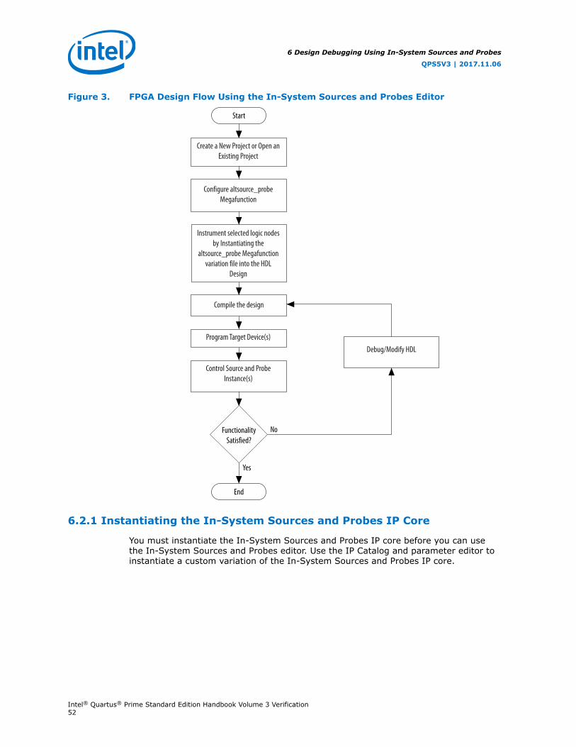
Figure 3. FPGA Design Flow Using the In-System Sources and Probes Editor
Yes
No
Start
End
FunctionalitySatisfied?
Create a New Project or Open an Existing Project
Configure altsource_probe Megafunction
Instrument selected logic nodes by Instantiating the
altsource_probe Megafunction variation file into the HDL
Design
Compile the design
Program Target Device(s)
Control Source and Probe Instance(s)
Debug/Modify HDL
6.2.1 Instantiating the In-System Sources and Probes IP Core
You must instantiate the In-System Sources and Probes IP core before you can usethe In-System Sources and Probes editor. Use the IP Catalog and parameter editor toinstantiate a custom variation of the In-System Sources and Probes IP core.
6 Design Debugging Using In-System Sources and Probes
QPS5V3 | 2017.11.06
Intel® Quartus® Prime Standard Edition Handbook Volume 3 Verification52

To configure the In-System Sources and Probes IP core, perform the following steps::
1. On the Tools menu, click Tools > IP Catalog.
2. Locate and double-click the In-System Sources and Probes IP core. The parametereditor appears.
3. Specify a name for your custom IP variation.
4. Specify the desired parameters for your custom IP variation. You can specify up toup to 512 bits for each source. Your design may include up to 128 instances of thisIP core.
5. Click Generate or Finish to generate IP core synthesis and simulation filesmatching your specifications. The parameter editor generates the necessaryvariation files and the instantiation template based on your specification. Use thegenerated template to instantiate the In-System Sources and Probes IP core inyour design.
Note: The In-System Sources and Probes Editor does not support simulation. Youmust remove the In-System Sources and Probes IP core before you create asimulation netlist.
6.2.2 In-System Sources and Probes IP Core Parameters
Use the template to instantiate the variation file in your design.
Table 18. In-System Sources and Probes IP Port Information
Port Name Required? Direction Comments
probe[] No Input The outputs from your design.
source_clk No Input Source Data is written synchronously to this clock. This input is requiredif you turn on Source Clock in the Advanced Options box in theparameter editor.
source_ena No Input Clock enable signal for source_clk. This input is required if specified inthe Advanced Options box in the parameter editor.
source[] No Output Used to drive inputs to user design.
You can include up to 128 instances of the in-system sources and probes IP core inyour design, if your device has available resources. Each instance of the IP core uses apair of registers per signal for the width of the widest port in the IP core. Additionally,there is some fixed overhead logic to accommodate communication between the IPcore instances and the JTAG controller. You can also specify an additional pair ofregisters per source port for synchronization.
You can use the Intel Quartus Prime incremental compilation feature to reducecompilation time. Incremental compilation allows you to organize your design intological partitions. During recompilation of a design, incremental compilation preservesthe compilation results and performance of unchanged partitions and reduces designiteration time by compiling only modified design partitions.
6.3 Compiling the Design
When you compile your design that includes the In-System Sources and ProbesIPcore, the In-System Sources and Probes and SLD Hub Controller IP core are added toyour compilation hierarchy automatically. These IP cores provide communicationbetween the JTAG controller and your instrumented logic.
6 Design Debugging Using In-System Sources and Probes
QPS5V3 | 2017.11.06
Intel® Quartus® Prime Standard Edition Handbook Volume 3 Verification53

You can modify the number of connections to your design by editing the In-SystemSources and Probes IP core. To open the design instance you want to modify in theparameter editor, double-click the instance in the Project Navigator. You can thenmodify the connections in the HDL source file. You must recompile your design afteryou make changes.
You can use the Intel Quartus Prime incremental compilation feature to reducecompilation design into logical partitions. During recompilation of a design,incremental compilation preserves the compilation results and performance ofunchanged partitions and reduces design iteration time by compiling only modifieddesign partitions.
6.4 Running the In-System Sources and Probes Editor
The In-System Sources and Probes Editor gives you control over allALTSOURCE_PROBE IP core instances within your design. The editor allows you toview all available run time controllable instances of the ALTSOURCE_PROBE IP core inyour design, provides a push-button interface to drive all your source nodes, andprovides a logging feature to store your probe and source data.
To run the In-System Sources and Probes Editor:
• On the Tools menu, click In-System Sources and Probes Editor.
6.4.1 In-System Sources and Probes Editor GUI
The In-System Sources and Probes Editor contains three panes:
• JTAG Chain Configuration—Allows you to specify programming hardware,device, and file settings that the In-System Sources and Probes Editor uses toprogram and acquire data from a device.
• Instance Manager—Displays information about the instances generated whenyou compile a design, and allows you to control data that the In-System Sourcesand Probes Editor acquires.
• In-System Sources and Probes Editor—Logs all data read from the selectedinstance and allows you to modify source data that is written to your device.
When you use the In-System Sources and Probes Editor, you do not need to open aIntel Quartus Prime software project. The In-System Sources and Probes Editorretrieves all instances of the ALTSOURCE_PROBE IP core by scanning the JTAG chainand sending a query to the device selected in the JTAG Chain Configuration pane.You can also use a previously saved configuration to run the In-System Sources andProbes Editor.
Each In-System Sources and Probes Editor pane can access theALTSOURCE_PROBE IP core instances in a single device. If you have more than onedevice containing IP core instances in a JTAG chain, you can launch multiple In-System Sources and Probes Editor panes to access the IP core instances in eachdevice.
6.4.2 Programming Your Device With JTAG Chain Configuration
After you compile your project, you must configure your FPGA before you use the In-System Sources and Probes Editor.
6 Design Debugging Using In-System Sources and Probes
QPS5V3 | 2017.11.06
Intel® Quartus® Prime Standard Edition Handbook Volume 3 Verification54

To configure a device to use with the In-System Sources and Probes Editor, performthe following steps:
1. Open the In-System Sources and Probes Editor.
2. In the JTAG Chain Configuration pane, point to Hardware, and then select thehardware communications device. You may be prompted to configure yourhardware; in this case, click Setup.
3. From the Device list, select the FPGA device to which you want to download thedesign (the device may be automatically detected). You may need to click ScanChain to detect your target device.
4. In the JTAG Chain Configuration pane, click to browse for the SRAM Object File(.sof) that includes the In-System Sources and Probes instance or instances.(The .sof may be automatically detected).
5. Click Program Device to program the target device.
6.4.3 Instance Manager
The Instance Manager pane provides a list of all ALTSOURCE_PROBE instances inthe design and allows you to configure how data is acquired from or written to thoseinstances.
The following buttons and sub-panes are provided in the Instance Manager pane:
• Read Probe Data—Samples the probe data in the selected instance and displaysthe probe data in the In-System Sources and Probes Editor pane.
• Continuously Read Probe Data—Continuously samples the probe data of theselected instance and displays the probe data in the In-System Sources andProbes Editor pane; you can modify the sample rate via the Probe readinterval setting.
• Stop Continuously Reading Probe Data—Cancels continuous sampling of theprobe of the selected instance.
• Read Source Data—Reads the data of the sources in the selected instances.
• Probe Read Interval—Displays the sample interval of all the In-System Sourcesand Probe instances in your design; you can modify the sample interval by clickingManual.
• Event Log—Controls the event log in the In-System Sources and ProbesEditor pane.
• Write Source Data—Allows you to manually or continuously write data to thesystem.
The status of each instance is also displayed beside each entry in the InstanceManager pane. The status indicates if the instance is Not running Offloading data,Updating data, or if an Unexpected JTAG communication error occurs. Thisstatus indicator provides information about the sources and probes instances in yourdesign.
6.4.4 In-System Sources and Probes Editor Pane
The In-System Sources and Probes Editor pane allows you to view data from allsources and probes in your design.
6 Design Debugging Using In-System Sources and Probes
QPS5V3 | 2017.11.06
Intel® Quartus® Prime Standard Edition Handbook Volume 3 Verification55

The data is organized according to the index number of the instance. The editorprovides an easy way to manage your signals, and allows you to rename signals orgroup them into buses. All data collected from in-system source and probe nodes isrecorded in the event log and you can view the data as a timing diagram.
6.4.4.1 Reading Probe Data
You can read data by selecting the ALTSOURCE_PROBE instance in the InstanceManager pane and clicking Read Probe Data.
This action produces a single sample of the probe data and updates the data columnof the selected index in the In-System Sources and Probes Editor pane. You cansave the data to an event log by turning on the Save data to event log option in theInstance Manager pane.
If you want to sample data from your probe instance continuously, in the InstanceManager pane, click the instance you want to read, and then click Continuouslyread probe data. While reading, the status of the active instance shows Unloading.You can read continuously from multiple instances.
You can access read data with the shortcut menus in the Instance Manager pane.
To adjust the probe read interval, in the Instance Manager pane, turn on theManual option in the Probe read interval sub-pane, and specify the sample rate inthe text field next to the Manual option. The maximum sample rate depends on yourcomputer setup. The actual sample rate is shown in the Current interval box. Youcan adjust the event log window buffer size in the Maximum Size box.
6.4.4.2 Writing Data
To modify the source data you want to write into the ALTSOURCE_PROBE instance,click the name field of the signal you want to change. For buses of signals, you candouble-click the data field and type the value you want to drive out to theALTSOURCE_PROBE instance. The In-System Sources and Probes Editor stores themodified source data values in a temporary buffer.
Modified values that are not written out to the ALTSOURCE_PROBE instances appear inred. To update the ALTSOURCE_PROBE instance, highlight the instance in theInstance Manager pane and click Write source data. The Write source datafunction is also available via the shortcut menus in the Instance Manager pane.
The In-System Sources and Probes Editor provides the option to continuously updateeach ALTSOURCE_PROBE instance. Continuous updating allows any modifications youmake to the source data buffer to also write immediately to the ALTSOURCE_PROBEinstances. To continuously update the ALTSOURCE_PROBE instances, change theWrite source data field from Manually to Continuously.
6.4.4.3 Organizing Data
The In-System Sources and Probes Editor pane allows you to group signals intobuses, and also allows you to modify the display options of the data buffer.
To create a group of signals, select the node names you want to group, right-click andselect Group. You can modify the display format in the Bus Display Format and theBus Bit order shortcut menus.
6 Design Debugging Using In-System Sources and Probes
QPS5V3 | 2017.11.06
Intel® Quartus® Prime Standard Edition Handbook Volume 3 Verification56

The In-System Sources and Probes Editor pane allows you to rename any signal.To rename a signal, double-click the name of the signal and type the new name.
The event log contains a record of the most recent samples. The buffer size isadjustable up to 128k samples. The time stamp for each sample is logged and isdisplayed above the event log of the active instance as you move your pointer overthe data samples.
You can save the changes that you make and the recorded data to a Sources andProbes File (.spf). To save changes, on the File menu, click Save. The file containsall the modifications you made to the signal groups, as well as the current data eventlog.
6.5 Tcl interface for the In-System Sources and Probes Editor
To support automation, the In-System Sources and Probes Editor supports theprocedures described in this chapter in the form of Tcl commands. The Tcl package forthe In-System Sources and Probes Editor is included by default when you runquartus_stp.
The Tcl interface for the In-System Sources and Probes Editor provides a powerfulplatform to help you debug your design. The Tcl interface is especially helpful fordebugging designs that require toggling multiple sets of control inputs. You cancombine multiple commands with a Tcl script to define a custom command set.
Table 19. In-System Sources and Probes Tcl Commands
Command Argument Description
start_insystem_source_probe
-device_name <device name>-hardware_name <hardware name>
Opens a handle to a device with the specifiedhardware.Call this command before starting anytransactions.
get_insystem_source_probe_instance_info
-device_name <device name>-hardware_name <hardware name>
Returns a list of all ALTSOURCE_PROBEinstances in your design. Each recordreturned is in the following format:{<instance Index>, <source width>, <probewidth>, <instance name>}
read_probe_data -instance_index <instance_index>-value_in_hex (optional)
Retrieves the current value of the probe.A string is returned that specifies the statusof each probe, with the MSB as the left-mostbit.
read_source_data -instance_index <instance_index>-value_in_hex (optional)
Retrieves the current value of the sources.A string is returned that specifies the statusof each source, with the MSB as the left-mostbit.
write_source_data -instance_index <instance_index>-value <value>-value_in_hex (optional)
Sets the value of the sources.A binary string is sent to the source ports,with the MSB as the left-most bit.
end_insystem_source_probe None Releases the JTAG chain.Issue this command when all transactions arefinished.
The example shows an excerpt from a Tcl script with procedures that control theALTSOURCE_PROBE instances of the design as shown in the figure below. Theexample design contains a DCFIFO with ALTSOURCE_PROBE instances to read from
6 Design Debugging Using In-System Sources and Probes
QPS5V3 | 2017.11.06
Intel® Quartus® Prime Standard Edition Handbook Volume 3 Verification57

and write to the DCFIFO. A set of control muxes are added to the design to control theflow of data to the DCFIFO between the input pins and the ALTSOURCE_PROBEinstances. A pulse generator is added to the read request and write request controllines to guarantee a single sample read or write. The ALTSOURCE_PROBE instances,when used with the script in the example below, provide visibility into the contents ofthe FIFO by performing single sample write and read operations and reporting thestate of the full and empty status flags.
Use the Tcl script in debugging situations to either empty or preload the FIFO in yourdesign. For example, you can use this feature to preload the FIFO to match a triggercondition you have set up within the Signal Tap Logic Analyzer.
Figure 4. DCFIFO Example Design Controlled by Tcl Script
Write_clock
write_reqdata[7..0]
write_clock
read_req
read_clock
wr_full
Q[7..0]
rd_empty
data_out
read_clocksource_read_sel
s_read_req
s_write_req
rd_req_in
wr_req_in
data_in[7..0]
altsource_probe(Instance 1)
altsource_probe(Instance 0)
source_write_sel
s_data[7..0]D Q
D Q
## Setup USB hardware - assumes only USB Blaster is installed and## an FPGA is the only device in the JTAG chainset usb [lindex [get_hardware_names] 0]set device_name [lindex [get_device_names -hardware_name $usb] 0]## write procedure : argument value is integerproc write {value} {global device_name usbvariable fullstart_insystem_source_probe -device_name $device_name -hardware_name $usb#read full flagset full [read_probe_data -instance_index 0]if {$full == 1} {end_insystem_source_probereturn "Write Buffer Full"}##toggle select line, drive value onto port, toggle enable##bits 7:0 of instance 0 is S_data[7:0]; bit 8 = S_write_req;##bit 9 = Source_write_sel##int2bits is custom procedure that returns a bitstring from an integer ## argument
6 Design Debugging Using In-System Sources and Probes
QPS5V3 | 2017.11.06
Intel® Quartus® Prime Standard Edition Handbook Volume 3 Verification58

write_source_data -instance_index 0 -value /[int2bits [expr 0x200 | $value]]write_source_data -instance_index 0 -value [int2bits [expr 0x300 | $value]]##clear transactionwrite_source_data -instance_index 0 -value 0end_insystem_source_probe}proc read {} {global device_name usbvariable emptystart_insystem_source_probe -device_name $device_name -hardware_name $usb##read empty flag : probe port[7:0] reads FIFO output; bit 8 reads empty_flagset empty [read_probe_data -instance_index 1]if {[regexp {1........} $empty]} { end_insystem_source_probereturn "FIFO empty" }## toggle select line for read transaction## Source_read_sel = bit 0; s_read_reg = bit 1## pulse read enable on DC FIFOwrite_source_data -instance_index 1 -value 0x1 -value_in_hexwrite_source_data -instance_index 1 -value 0x3 -value_in_hexset x [read_probe_data -instance_index 1 ]end_insystem_source_probereturn $x}
Related Links
• Tcl Scripting
• Intel Quartus Prime Settings File Manual
• Command Line Scripting
• Tcl Scripting
• Intel Quartus Prime Settings File Manual
• Command Line Scripting
6.6 Design Example: Dynamic PLL Reconfiguration
The In-System Sources and Probes Editor can help you create a virtual front panelduring the prototyping phase of your design. You can create relatively simple, highfunctioning designs of in a short amount of time. The following PLL reconfigurationexample demonstrates how to use the In-System Sources and Probes Editor toprovide a GUI to dynamically reconfigure a Stratix PLL.
Stratix PLLs allow you to dynamically update PLL coefficients during run time. Eachenhanced PLL within the Stratix device contains a register chain that allows you tomodify the pre-scale counters (m and n values), output divide counters, and delaycounters. In addition, the ALTPLL_RECONFIG IP core provides an easy interface toaccess the register chain counters. The ALTPLL_RECONFIG IP core provides a cachethat contains all modifiable PLL parameters. After you update all the PLL parameters inthe cache, the ALTPLL_RECONFIG IP core drives the PLL register chain to update thePLL with the updated parameters. The figure shows a Stratix-enhanced PLL withreconfigurable coefficients.
6 Design Debugging Using In-System Sources and Probes
QPS5V3 | 2017.11.06
Intel® Quartus® Prime Standard Edition Handbook Volume 3 Verification59
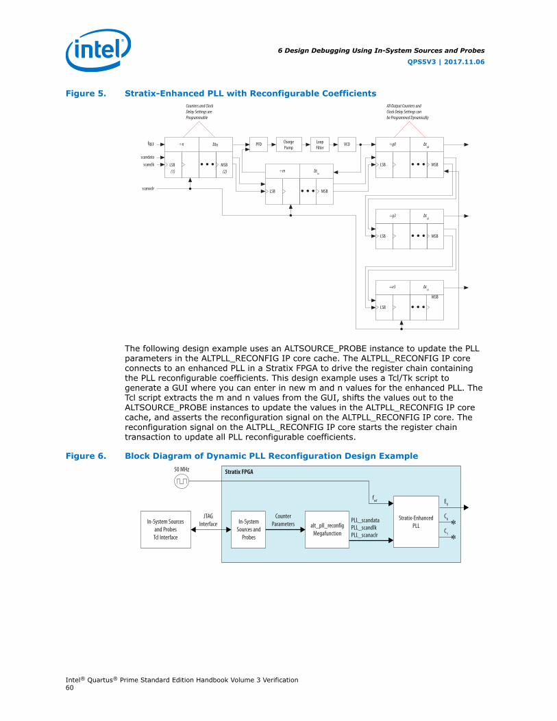
Figure 5. Stratix-Enhanced PLL with Reconfigurable Coefficients
÷n Δtn
Δtm
÷m
÷g0 Δtg0
÷e3 Δte3
÷g3 Δtg3
PFD VCOChargePump
LoopFilter
fREF
scandata
scanclk
scanaclr
Counters and ClockDelay Settings areProgrammable
All Output Counters andClock Delay Settings canbe Programmed Dynamically
LSB MSB
LSB MSB
LSB MSB
LSB MSB
LSB
MSB
(1) (2)
The following design example uses an ALTSOURCE_PROBE instance to update the PLLparameters in the ALTPLL_RECONFIG IP core cache. The ALTPLL_RECONFIG IP coreconnects to an enhanced PLL in a Stratix FPGA to drive the register chain containingthe PLL reconfigurable coefficients. This design example uses a Tcl/Tk script togenerate a GUI where you can enter in new m and n values for the enhanced PLL. TheTcl script extracts the m and n values from the GUI, shifts the values out to theALTSOURCE_PROBE instances to update the values in the ALTPLL_RECONFIG IP corecache, and asserts the reconfiguration signal on the ALTPLL_RECONFIG IP core. Thereconfiguration signal on the ALTPLL_RECONFIG IP core starts the register chaintransaction to update all PLL reconfigurable coefficients.
Figure 6. Block Diagram of Dynamic PLL Reconfiguration Design Example
In-System Sourcesand ProbesTcl Interface
JTAGInterface
CounterParameters
Stratix FPGA50 MHz
PLL_scandataPLL_scandlkPLL_scanaclr
E0
C0
C1
fref
Stratix-EnhancedPLLalt_pll_reconfig
Megafunction
In-SystemSources and
Probes
6 Design Debugging Using In-System Sources and Probes
QPS5V3 | 2017.11.06
Intel® Quartus® Prime Standard Edition Handbook Volume 3 Verification60

This design example was created using a Nios II Development Kit, Stratix Edition. Thefile sourceprobe_DE_dynamic_pll.zip contains all the necessary files for runningthis design example, including the following:
• Readme.txt—A text file that describes the files contained in the design exampleand provides instructions about running the Tk GUI shown in the figure below.
• Interactive_Reconfig.qar—The archived Intel Quartus Prime project for thisdesign example.
Figure 7. Interactive PLL Reconfiguration GUI Created with Tk and In-System Sourcesand Probes Tcl Package
Related Links
• On-chip Debugging Design Examplesto download the In-System Sources and Probes Example
• On-chip Debugging Design Examplesto download the In-System Sources and Probes Example
6.7 Document Revision History
Table 20. Document Revision History
Date Version Changes
2015.11.02 15.1.0 Changed instances of Quartus II to Intel Quartus Prime.
June 2014 14.0.0 Updated formatting.
June 2012 12.0.0 Removed survey link.
November 2011 10.1.1 Template update.
December 2010 10.1.0 Minor corrections. Changed to new document template.
July 2010 10.0.0 Minor corrections.
November 2009 9.1.0 • Removed references to obsolete devices.• Style changes.
March 2009 9.0.0 No change to content.
November 2008 8.1.0 Changed to 8-1/2 x 11 page size. No change to content.
May 2008 8.0.0 • Documented that this feature does not support simulation on page 17–5• Updated Figure 17–8 for Interactive PLL reconfiguration manager• Added hyperlinks to referenced documents throughout the chapter• Minor editorial updates
6 Design Debugging Using In-System Sources and Probes
QPS5V3 | 2017.11.06
Intel® Quartus® Prime Standard Edition Handbook Volume 3 Verification61

Related Links
Documentation ArchiveFor previous versions of the Intel Quartus Prime Handbook, search thedocumentation archives.
6 Design Debugging Using In-System Sources and Probes
QPS5V3 | 2017.11.06
Intel® Quartus® Prime Standard Edition Handbook Volume 3 Verification62

7 Timing Analysis Overview
7.1 Timing Analysis Overview
Comprehensive static timing analysis involves analysis of register-to-register, I/O, andasynchronous reset paths. Timing analysis with the Timing Analyzer uses datarequired times, data arrival times, and clock arrival times to verify circuit performanceand detect possible timing violations.
The Timing Analyzer determines the timing relationships that must be met for thedesign to correctly function, and checks arrival times against required times to verifytiming. This chapter is an overview of the concepts you need to know to analyze yourdesigns with the Timing Analyzer.
Related Links
The Intel Quartus PrimeTiming Analyzer on page 79For more information about the Timing Analyzer flow and Timing Analyzerexamples.
7.2 Timing Analyzer Terminology and Concepts
Table 21. Timing Analyzer Terminology
Term Definition
nodes Most basic timing netlist unit. Used to represent ports, pins, and registers.
cells Look-up tables (LUT), registers, digital signal processing (DSP) blocks, memoryblocks, input/output elements, and so on.Note: For Intel Stratix devices, the LUTs and registers are contained in logic
elements (LE) and modeled as cells.
pins Inputs or outputs of cells.
nets Connections between pins.
ports Top-level module inputs or outputs; for example, device pins.
clocks Abstract objects representing clock domains inside or outside of your design.
7.2.1 Timing Netlists and Timing Paths
The Timing Analyzer requires a timing netlist to perform timing analysis on anydesign. After you generate a timing netlist, the Timing Analyzer uses the data to helpdetermine the different design elements in your design and how to analyze timing.
7.2.1.1 The Timing Netlist
A sample design for which the Timing Analyzer generates a timing netlist equivalent.
QPS5V3 | 2017.11.06
Intel Corporation. All rights reserved. Intel, the Intel logo, Altera, Arria, Cyclone, Enpirion, MAX, Nios, Quartusand Stratix words and logos are trademarks of Intel Corporation or its subsidiaries in the U.S. and/or othercountries. Intel warrants performance of its FPGA and semiconductor products to current specifications inaccordance with Intel's standard warranty, but reserves the right to make changes to any products and servicesat any time without notice. Intel assumes no responsibility or liability arising out of the application or use of anyinformation, product, or service described herein except as expressly agreed to in writing by Intel. Intelcustomers are advised to obtain the latest version of device specifications before relying on any publishedinformation and before placing orders for products or services.*Other names and brands may be claimed as the property of others.
ISO9001:2008Registered

Figure 8. Sample Design
data1
data2
clk
reg1
reg2
and_inst
reg3
The timing netlist for the sample design shows how different design elements aredivided into cells, pins, nets, and ports.
Figure 9. The Timing Analyzer Netlist
reg2
data1
data2
clk clk~clkctrl
reg1
and_instreg3 data_out
combout
inclk0
datain
clkregout
regout
datac
datad
comboutdatain
CellsCell
Cell
Pin
Pin
outclk
Port
Port
NetNet
Net
7.2.1.2 Timing Paths
Timing paths connect two design nodes, such as the output of a register to the inputof another register.
7 Timing Analysis Overview
QPS5V3 | 2017.11.06
Intel® Quartus® Prime Standard Edition Handbook Volume 3 Verification64

Understanding the types of timing paths is important to timing closure andoptimization. The Timing Analyzer uses the following commonly analyzed paths:
• Edge paths—connections from ports-to-pins, from pins-to-pins, and from pins-to-ports.
• Clock paths—connections from device ports or internally generated clock pins tothe clock pin of a register.
• Data paths—connections from a port or the data output pin of a sequentialelement to a port or the data input pin of another sequential element.
• Asynchronous paths—connections from a port or asynchronous pins of anothersequential element such as an asynchronous reset or asynchronous clear.
Figure 10. Path Types Commonly Analyzed by the Timing Analyzer
CLRN
D Q
CLRN
D Q
clk
rst
Clock Path Data Path
Asynchronous Clear Path
data
In addition to identifying various paths in a design, the Timing Analyzer analyzes clockcharacteristics to compute the worst-case requirement between any two registers in asingle register-to-register path. You must constrain all clocks in your design beforeanalyzing clock characteristics.
7.2.1.3 Data and Clock Arrival Times
After the Timing Analyzer identifies the path type, it can report data and clock arrivaltimes at register pins.
The Timing Analyzer calculates data arrival time by adding the launch edge time to thedelay from the clock source to the clock pin of the source register, the micro clock-to-output delay ( µtCO) of the source register, and the delay from the source register’sdata output (Q) to the destination register’s data input (D).
The Timing Analyzer calculates data required time by adding the latch edge time tothe sum of all delays between the clock port and the clock pin of the destinationregister, including any clock port buffer delays, and subtracts the micro setup time( µtSU) of the destination register, where the µtSU is the intrinsic setup time of aninternal register in the FPGA.
Figure 11. Data Arrival and Data Required Times
D Q D Q
Data Arrival Time
Data Required Time
7 Timing Analysis Overview
QPS5V3 | 2017.11.06
Intel® Quartus® Prime Standard Edition Handbook Volume 3 Verification65

The basic calculations for data arrival and data required times including the launch andlatch edges.
Figure 12. Data Arrival and Data Required Time Equations
Data Arrival Time = Launch Edge + Source Clock Delay + µtCO + Register-to-Register Delay Data Required Time = Latch Edge + Destination Clock Delay – µtSU
7.2.1.4 Launch and Latch Edges
All timing relies on one or more clocks. In addition to analyzing paths, the TimingAnalyzer determines clock relationships for all register-to-register transfers in yourdesign.
The following figure shows the launch edge, which is the clock edge that sends dataout of a register or other sequential element, and acts as a source for the datatransfer. A latch edge is the active clock edge that captures data at the data port of aregister or other sequential element, acting as a destination for the data transfer. Inthis example, the launch edge sends the data from register reg1 at 0 ns, and theregister reg2 captures the data when triggered by the latch edge at 10 ns. The dataarrives at the destination register before the next latch edge.
Figure 13. Setup and Hold Relationship for Launch and Latch Edges 10ns Apart
Launch Clock
Latch Clock
0ns 10ns 20ns
Setup relationshipHold relationship
In timing analysis, and with the Timing Analyzer specifically, you create clockconstraints and assign those constraints to nodes in your design. These clockconstraints provide the structure required for repeatable data relationships. Theprimary relationships between clocks, in the same or different domains, are the setuprelationship and the hold relationship.
Note: If you do not constrain the clocks in your design, the Intel Quartus Prime softwareanalyzes in terms of a 1 GHz clock to maximize timing based Fitter effort. To ensurerealistic slack values, you must constrain all clocks in your design with real values.
7.2.2 Clock Setup Check
To perform a clock setup check, the Timing Analyzer determines a setup relationshipby analyzing each launch and latch edge for each register-to-register path.
For each latch edge at the destination register, the Timing Analyzer uses the closestprevious clock edge at the source register as the launch edge. The following figureshows two setup relationships, setup A and setup B. For the latch edge at 10 ns, theclosest clock that acts as a launch edge is at 3 ns and is labeled setup A. For the latchedge at 20 ns, the closest clock that acts as a launch edge is 19 ns and is labeledsetup B. TimQuest analyzes the most restrictive setup relationship, in this case setupB; if that relationship meets the design requirement, then setup A meets it by default.
7 Timing Analysis Overview
QPS5V3 | 2017.11.06
Intel® Quartus® Prime Standard Edition Handbook Volume 3 Verification66

Figure 14. Setup Check
Setup A Setup B
0 ns 8 ns 16 ns 24 ns 32 ns
Source Clock
Destination Clock
The Timing Analyzer reports the result of clock setup checks as slack values. Slack isthe margin by which a timing requirement is met or not met. Positive slack indicatesthe margin by which a requirement is met; negative slack indicates the margin bywhich a requirement is not met.
Figure 15. Clock Setup Slack for Internal Register-to-Register Paths
Clock Setup Slack = Data Required Time – Data Arrival TimeData Arrival Time = Launch Edge + Clock Network Delay to Source Register + µtCO + Register-to-Register DelayData Required Time = Latch Edge + Clock Network Delay to Destination Register – µtSU – Setup Uncertainty
The Timing Analyzer performs setup checks using the maximum delay whencalculating data arrival time, and minimum delay when calculating data required time.
Figure 16. Clock Setup Slack from Input Port to Internal Register
Clock Setup Slack = Data Required Time – Data Arrival Time Data Arrival Time = Launch Edge + Clock Network Delay + Input Maximum Delay + Port-to-Register DelayData Required Time = Latch Edge + Clock Network Delay to Destination Register – µtSU – Setup Uncertainty
Figure 17. Clock Setup Slack from Internal Register to Output Port
Clock Setup Slack = Data Required Time – Data Arrival TimeData Required Time = Latch Edge + Clock Network Delay to Output Port – Output Maximum DelayData Arrival Time = Launch Edge + Clock Network Delay to Source Register +µtCO + Register-to-Port Delay
7.2.3 Clock Hold Check
To perform a clock hold check, the Timing Analyzer determines a hold relationship foreach possible setup relationship that exists for all source and destination registerpairs. The Timing Analyzer checks all adjacent clock edges from all setup relationshipsto determine the hold relationships.
The Timing Analyzer performs two hold checks for each setup relationship. The firsthold check determines that the data launched by the current launch edge is notcaptured by the previous latch edge. The second hold check determines that the datalaunched by the next launch edge is not captured by the current latch edge. From thepossible hold relationships, the Timing Analyzer selects the hold relationship that isthe most restrictive. The most restrictive hold relationship is the hold relationship withthe smallest difference between the latch and launch edges and determines theminimum allowable delay for the register-to-register path. In the following example,the Timing Analyzer selects hold check A2 as the most restrictive hold relationship oftwo setup relationships, setup A and setup B, and their respective hold checks.
7 Timing Analysis Overview
QPS5V3 | 2017.11.06
Intel® Quartus® Prime Standard Edition Handbook Volume 3 Verification67

Figure 18. Setup and Hold Check Relationships
Setup A Setup B
0 ns 8 ns 16 ns 24 ns 32 ns
Source Clock
Destination Clock
HoldCheck A1
HoldCheck B2
HoldCheck A2
HoldCheck B1
Figure 19. Clock Hold Slack for Internal Register-to-Register Paths
Clock Hold Slack = Data Arrival Time – Data Required TimeData Arrival Time = Launch Edge + Clock Network Delay to Source Register + µtCO + Register-to-Register DelayData Required Time = Latch Edge + Clock Network Delay to Destination Register + µtH + Hold Uncertainty
The Timing Analyzer performs hold checks using the minimum delay when calculatingdata arrival time, and maximum delay when calculating data required time.
Figure 20. Clock Hold Slack Calculation from Input Port to Internal Register
Clock Hold Slack = Data Arrival Time – Data Required Time Data Arrival Time = Launch Edge + Clock Network Delay + Input Minimum Delay + Pin-to-Register DelayData Required Time = Latch Edge + Clock Network Delay to Destination Register + µtH
Figure 21. Clock Hold Slack Calculation from Internal Register to Output Port
Clock Hold Slack = Data Arrival Time – Data Required TimeData Arrival Time = Launch Edge + Clock Network Delay to Source Register + µtCO + Register-to-Pin DelayData Required Time = Latch Edge + Clock Network Delay – Output Minimum Delay
7.2.4 Recovery and Removal Time
Recovery time is the minimum length of time for the deassertion of an asynchronouscontrol signal relative to the next clock edge.
For example, signals such as clear and preset must be stable before the nextactive clock edge. The recovery slack calculation is similar to the clock setup slackcalculation, but it applies to asynchronous control signals.
Figure 22. Recovery Slack Calculation if the Asynchronous Control Signal is Registered
Recovery Slack Time = Data Required Time – Data Arrival TimeData Required Time = Latch Edge + Clock Network Delay to Destination Register – µtSU
Data Arrival Time = Launch Edge + Clock Network Delay to Source Register + µtCO + Register-to-Register Delay
Figure 23. Recovery Slack Calculation if the Asynchronous Control Signal is notRegistered
Recovery Slack Time = Data Required Time – Data Arrival TimeData Required Time = Latch Edge + Clock Network Delay to Destination Register – µtSU
Data Arrival Time = Launch Edge + Clock Network Delay + Input Maximum Delay + Port-to-Register Delay
7 Timing Analysis Overview
QPS5V3 | 2017.11.06
Intel® Quartus® Prime Standard Edition Handbook Volume 3 Verification68

Note: If the asynchronous reset signal is from a device I/O port, you must create an inputdelay constraint for the asynchronous reset port for the Timing Analyzer to performrecovery analysis on the path.
Removal time is the minimum length of time the deassertion of an asynchronouscontrol signal must be stable after the active clock edge. The Timing Analyzer removalslack calculation is similar to the clock hold slack calculation, but it appliesasynchronous control signals.
Figure 24. Removal Slack Calcuation if the Asynchronous Control Signal is RegisteredRemoval Slack Time = Data Arrival Time – Data Required TimeData Arrival Time = Launch Edge + Clock Network Delay to Source Register + µtCO of Source Register + Register-to-Register DelayData Required Time = Latch Edge + Clock Network Delay to Destination Register + µtH
Figure 25. Removal Slack Calculation if the Asynchronous Control Signal is notRegistered
Removal Slack Time = Data Arrival Time – Data Required TimeData Arrival Time = Launch Edge + Clock Network Delay + Input Minimum Delay of Pin + Minimum Pin-to-Register DelayData Required Time = Latch Edge + Clock Network Delay to Destination Register + µtH
If the asynchronous reset signal is from a device pin, you must assign the InputMinimum Delay timing assignment to the asynchronous reset pin for the TimingAnalyzer to perform removal analysis on the path.
7.2.5 Multicycle Paths
Multicycle paths are data paths that require a non-default setup and/or holdrelationship for proper analysis.
For example, a register may be required to capture data on every second or thirdrising clock edge. An example of a multicycle path between the input registers of amultiplier and an output register where the destination latches data on every otherclock edge.
Figure 26. Multicycle Path
2 Cycles
ENA
D Q
ENA
D Q
D Q
ENA
7 Timing Analysis Overview
QPS5V3 | 2017.11.06
Intel® Quartus® Prime Standard Edition Handbook Volume 3 Verification69

A register-to-register path used for the default setup and hold relationship, therespective timing diagrams for the source and destination clocks, and the defaultsetup and hold relationships, when the source clock, src_clk, has a period of 10 nsand the destination clock, dst_clk, has a period of 5 ns. The default setuprelationship is 5 ns; the default hold relationship is 0 ns.
Figure 27. Register-to-Register Path and Default Setup and Hold Timing Diagramreg reg
data_outdata_in
src_clk
dst_clk
D Q D Q
0 10 20 30
setuphold
To accommodate the system requirements you can modify the default setup and holdrelationships with a multicycle timing exception.
The actual setup relationship after you apply a multicycle timing exception. Theexception has a multicycle setup assignment of two to use the second occurring latchedge; in this example, to 10 ns from the default value of 5 ns.
Figure 28. Modified Setup Diagram new setup
default setup
0 10 20 30
Related Links
The Intel Quartus Prime Timing Analyzer on page 79For more information about creating exceptions with multicycle paths.
7.2.6 Metastability
Metastability problems can occur when a signal is transferred between circuitry inunrelated or asynchronous clock domains because the designer cannot guarantee thatthe signal will meet setup and hold time requirements.
7 Timing Analysis Overview
QPS5V3 | 2017.11.06
Intel® Quartus® Prime Standard Edition Handbook Volume 3 Verification70

To minimize the failures due to metastability, circuit designers typically use a sequenceof registers, also known as a synchronization register chain, or synchronizer, in thedestination clock domain to resynchronize the data signals to the new clock domain.
The mean time between failures (MTBF) is an estimate of the average time betweeninstances of failure due to metastability.
The Timing Analyzer analyzes the potential for metastability in your design and cancalculate the MTBF for synchronization register chains. The MTBF of the entire designis then estimated based on the synchronization chains it contains.
In addition to reporting synchronization register chains found in the design, the IntelQuartus Prime software also protects these registers from optimizations that mightnegatively impact MTBF, such as register duplication and logic retiming. The IntelQuartus Prime software can also optimize the MTBF of your design if the MTBF is toolow.
Related Links
• Understanding Metastability in FPGAsFor more information about metastability, its effects in FPGAs, and how MTBF iscalculated.
• Managing Metastability with the Intel Quartus Prime SoftwareFor more information about metastability analysis, reporting, and optimizationfeatures in the Intel Quartus Prime software.
7.2.7 Common Clock Path Pessimism Removal
Common clock path pessimism removal accounts for the minimum and maximumdelay variation associated with common clock paths during static timing analysis byadding the difference between the maximum and minimum delay value of thecommon clock path to the appropriate slack equation.
Minimum and maximum delay variation can occur when two different delay values areused for the same clock path. For example, in a simple setup analysis, the maximumclock path delay to the source register is used to determine the data arrival time. Theminimum clock path delay to the destination register is used to determine the datarequired time. However, if the clock path to the source register and to the destinationregister share a common clock path, both the maximum delay and the minimum delayare used to model the common clock path during timing analysis. The use of both theminimum delay and maximum delay results in an overly pessimistic analysis since twodifferent delay values, the maximum and minimum delays, cannot be used to modelthe same clock path.
Figure 29. Typical Register to Register Path
D Q
D Qclk
A
B
C
reg1
reg2
5.5 ns5.0 ns
2.2 ns2.0 ns
2.2 ns2.0 ns
3.2 ns3.0 ns
7 Timing Analysis Overview
QPS5V3 | 2017.11.06
Intel® Quartus® Prime Standard Edition Handbook Volume 3 Verification71

Segment A is the common clock path between reg1 and reg2. The minimum delay is5.0 ns; the maximum delay is 5.5 ns. The difference between the maximum andminimum delay value equals the common clock path pessimism removal value; in thiscase, the common clock path pessimism is 0.5 ns. The Timing Analyzer adds thecommon clock path pessimism removal value to the appropriate slack equation todetermine overall slack. Therefore, if the setup slack for the register-to-register pathin the example equals 0.7 ns without common clock path pessimism removal, theslack would be 1.2 ns with common clock path pessimism removal.
You can also use common clock path pessimism removal to determine the minimumpulse width of a register. A clock signal must meet a register’s minimum pulse widthrequirement to be recognized by the register. A minimum high time defines theminimum pulse width for a positive-edge triggered register. A minimum low timedefines the minimum pulse width for a negative-edge triggered register.
Clock pulses that violate the minimum pulse width of a register prevent data frombeing latched at the data pin of the register. To calculate the slack of the minimumpulse width, the Timing Analyzer subtracts the required minimum pulse width timefrom the actual minimum pulse width time. The Timing Analyzer determines the actualminimum pulse width time by the clock requirement you specified for the clock thatfeeds the clock port of the register. The Timing Analyzer determines the requiredminimum pulse width time by the maximum rise, minimum rise, maximum fall, andminimum fall times.
Figure 30. Required Minimum Pulse Width time for the High and Low Pulse
High PulseWidth
Low PulseWidth
Minimum and MaximumFall Arrival Times
Minimum andMaximum Rise
Rise Arrival Times
0.80.5
0.50.8
0.90.7
With common clock path pessimism, the minimum pulse width slack can be increasedby the smallest value of either the maximum rise time minus the minimum rise time,or the maximum fall time minus the minimum fall time. In the example, the slackvalue can be increased by 0.2 ns, which is the smallest value between 0.3 ns (0.8 ns – 0.5 ns) and 0.2 ns (0.9 ns – 0.7 ns).
Related Links
Timing Analyzer Page (Settings Dialog Box)For more information, refer to the Intel Quartus Prime Help.
7.2.8 Clock-As-Data Analysis
The majority of FPGA designs contain simple connections between any two nodesknown as either a data path or a clock path.
A data path is a connection between the output of a synchronous element to the inputof another synchronous element.
7 Timing Analysis Overview
QPS5V3 | 2017.11.06
Intel® Quartus® Prime Standard Edition Handbook Volume 3 Verification72

A clock is a connection to the clock pin of a synchronous element. However, for morecomplex FPGA designs, such as designs that use source-synchronous interfaces, thissimplified view is no longer sufficient. Clock-as-data analysis is performed in circuitswith elements such as clock dividers and DDR source-synchronous outputs.
The connection between the input clock port and output clock port can be treatedeither as a clock path or a data path. A design where the path from port clk_in toport clk_out is both a clock and a data path. The clock path is from the port clk_into the register reg_data clock pin. The data path is from port clk_in to the portclk_out.
Figure 31. Simplified Source Synchronous Output
D Q
clk_in clk_out
reg_data
With clock-as-data analysis, the Timing Analyzer provides a more accurate analysis ofthe path based on user constraints. For the clock path analysis, any phase shiftassociated with the phase-locked loop (PLL) is taken into consideration. For the datapath analysis, any phase shift associated with the PLL is taken into considerationrather than ignored.
The clock-as-data analysis also applies to internally generated clock dividers. Aninternally generated clock divider. In this figure, waveforms are for the inverterfeedback path, analyzed during timing analysis. The output of the divider register isused to determine the launch time and the clock port of the register is used todetermine the latch time.
Figure 32. Clock Divider
D Q
D Q
Launch Clock (2 T)
Data Arrival Time
Latch Clock (T)
7 Timing Analysis Overview
QPS5V3 | 2017.11.06
Intel® Quartus® Prime Standard Edition Handbook Volume 3 Verification73

7.2.9 Multicycle Clock Setup Check and Hold Check Analysis
You can modify the setup and hold relationship when you apply a multicycle exceptionto a register-to-register path.
Figure 33. Register-to-Register PathREG1 REG2
CombinationalLogic
SET SETD Q D Q
CLR CLR
CLK
Tclk1
TCO TSU / TH
Tdata
Tclk2
7.2.9.1 Multicycle Clock Setup
The setup relationship is defined as the number of clock periods between the latchedge and the launch edge. By default, the Timing Analyzer performs a single-cyclepath analysis, which results in the setup relationship being equal to one clock period(latch edge – launch edge). Applying a multicycle setup assignment, adjusts the setuprelationship by the multicycle setup value. The adjustment value may be negative.
An end multicycle setup assignment modifies the latch edge of the destination clock bymoving the latch edge the specified number of clock periods to the right of thedetermined default latch edge. The following figure shows various values of the endmulticycle setup (EMS) assignment and the resulting latch edge.
Figure 34. End Multicycle Setup Values-10 0 10 20
REG1.CLK
REG2.CLK
EMS = 2
EMS = 1(default)
EMS = 3
A start multicycle setup assignment modifies the launch edge of the source clock bymoving the launch edge the specified number of clock periods to the left of thedetermined default launch edge. A start multicycle setup (SMS) assignment withvarious values can result in a specific launch edge.
7 Timing Analysis Overview
QPS5V3 | 2017.11.06
Intel® Quartus® Prime Standard Edition Handbook Volume 3 Verification74
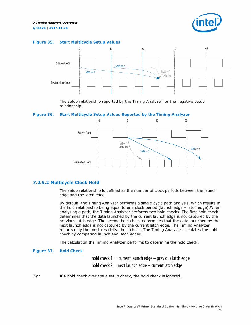
Figure 35. Start Multicycle Setup Values
Source Clock
Destination Clock
SMS = 1(Default)
SMS = 2
SMS = 3
0 10 20 30 40
The setup relationship reported by the Timing Analyzer for the negative setuprelationship.
Figure 36. Start Multicycle Setup Values Reported by the Timing Analyzer-10 0 10 20
Source Clock
Destination Clock
SMS = 2
SMS = 1(default) SMS = 3
7.2.9.2 Multicycle Clock Hold
The setup relationship is defined as the number of clock periods between the launchedge and the latch edge.
By default, the Timing Analyzer performs a single-cycle path analysis, which results inthe hold relationship being equal to one clock period (launch edge – latch edge).Whenanalyzing a path, the Timing Analyzer performs two hold checks. The first hold checkdetermines that the data launched by the current launch edge is not captured by theprevious latch edge. The second hold check determines that the data launched by thenext launch edge is not captured by the current latch edge. The Timing Analyzerreports only the most restrictive hold check. The Timing Analyzer calculates the holdcheck by comparing launch and latch edges.
The calculation the Timing Analyzer performs to determine the hold check.
Figure 37. Hold Check
hold check 1 = current launch edge – previous latch edgehold check 2 = next launch edge – current latch edge
Tip: If a hold check overlaps a setup check, the hold check is ignored.
7 Timing Analysis Overview
QPS5V3 | 2017.11.06
Intel® Quartus® Prime Standard Edition Handbook Volume 3 Verification75

A start multicycle hold assignment modifies the launch edge of the destination clockby moving the latch edge the specified number of clock periods to the right of thedetermined default launch edge. The following figure shows various values of the startmulticycle hold (SMH) assignment and the resulting launch edge.
Figure 38. Start Multicycle Hold Values-10 0 10 20
Source Clock
Destination Clock
SMH = 1SMH = 0(default) SMH = 2
An end multicycle hold assignment modifies the latch edge of the destination clock bymoving the latch edge the specific ed number of clock periods to the left of thedetermined default latch edge. The following figure shows various values of the endmulticycle hold (EMH) assignment and the resulting latch edge.
Figure 39. End Multicycle Hold Values
Source Clock
Destination Clock
EMH = 0(Default)
EMH = 2
EMH = 1
-20 -10 0 10 20
The hold relationship reported by the Timing Analyzer for the negative holdrelationship shown in the figure above would look like this:
Figure 40. End Multicycle Hold Values Reported by the Timing Analyzer
Source Clock
Destination Clock
EMH = 0(Default)
EMH = 2
EMH = 1
-10 0 10 20
7 Timing Analysis Overview
QPS5V3 | 2017.11.06
Intel® Quartus® Prime Standard Edition Handbook Volume 3 Verification76

7.2.10 Multicorner Analysis
The Timing Analyzer performs multicorner timing analysis to verify your design undera variety of operating conditions—such as voltage, process, and temperature—whileperforming static timing analysis.
To change the operating conditions or speed grade of the device used for timinganalysis, use the set_operating_conditions command.
If you specify an operating condition Tcl object, the -model, speed, -temperature,and -voltage options are optional. If you do not specify an operating condition Tclobject, the -model option is required; the -speed, -temperature, and -voltageoptions are optional.
Tip: To obtain a list of available operating conditions for the target device, use theget_available_operating_conditions -all command.
To ensure that no violations occur under various conditions during the deviceoperation, perform static timing analysis under all available operating conditions.
Table 22. Operating Conditions for Slow and Fast Models
Model Speed Grade Voltage Temperature
Slow Slowest speed grade indevice density
Vcc minimum supply (1) Maximum TJ (1)
Fast Fastest speed grade indevice density
Vcc maximum supply (1) Minimum TJ (1)
Note :1. Refer to the DC & Switching Characteristics chapter of the applicable device Handbook for Vcc and TJ.
values
In your design, you can set the operating conditions for to the slow timing model, witha voltage of 1100 mV, and temperature of 85° C with the following code:
set_operating_conditions -model slow -temperature 85 -voltage 1100
You can set the same operating conditions with a Tcl object:
set_operating_conditions 3_slow_1100mv_85c
The following block of code shows how to use the set_operating_conditionscommand to generate different reports for various operating conditions.
Example 7. Script Excerpt for Analysis of Various Operating Conditions
#Specify initial operating conditionsset_operating_conditions -model slow -speed 3 -grade c -temperature 85 -voltage 1100#Update the timing netlist with the initial conditionsupdate_timing_netlist#Perform reporting#Change initial operating conditions. Use a temperature of 0Cset_operating_conditions -model slow -speed 3 -grade c -temperature 0 -voltage 1100#Update the timing netlist with the new operating conditionupdate_timing_netlist#Perform reporting#Change initial operating conditions. Use a temperature of 0C and a model of
7 Timing Analysis Overview
QPS5V3 | 2017.11.06
Intel® Quartus® Prime Standard Edition Handbook Volume 3 Verification77

fastset_operating_conditions -model fast -speed 3 -grade c -temperature 0 -voltage 1100#Update the timing netlist with the new operating conditionupdate_timing_netlist#Perform reporting
Related Links
• set_operating_conditions
• get_available_operating_conditionsFor more information about the get_available_operating_conditionscommand
7.3 Document Revision History
Table 23. Document Revision History
Date Version Changes
2016.05.02 16.0.0 Corrected typo in Fig 6-14: Clock Hold Slack Calculation from Internal Register to Output Port
2015.11.02 15.1.0 Changed instances of Quartus II to Intel Quartus Prime.
2014.12.15 14.1.0 Moved Multicycle Clock Setup Check and Hold Check Analysis section from the Timing Analyzerchapter.
June 2014 14.0.0 Updated format
June 2012 12.0.0 Added social networking icons, minor text updates
November 2011 11.1.0 Initial release.
Related Links
Documentation ArchiveFor previous versions of the Intel Quartus Prime Handbook, search thedocumentation archives.
7 Timing Analysis Overview
QPS5V3 | 2017.11.06
Intel® Quartus® Prime Standard Edition Handbook Volume 3 Verification78

8 The Intel Quartus Prime Timing AnalyzerThe Intel Quartus Prime Timing Analyzer is a powerful ASIC-style timing analysis toolthat validates the timing performance of all logic in your design using an industry-standard constraint, analysis, and reporting methodology. Use the Timing AnalyzerGUI or command-line interface to constrain, analyze, and report results for all timingpaths in your design.
This document is organized to allow you to refer to specific subjects relating to theTiming Analyzer and timing analysis. The sections cover the following topics:
Enhanced Timing Analysis for Intel Arria 10 Devices on page 79
Recommended Flow for First Time Users on page 80
Timing Constraints on page 84
Running the Timing Analyzer on page 133
Understanding Results on page 136
Constraining and Analyzing with Tcl Commands on page 153
Generating Timing Reports on page 157
Document Revision History on page 159
Related Links
• Timing Analysis Overview on page 63
• Timing Analyzer Resource Center
• Intel FPGA Technical Training
8.1 Enhanced Timing Analysis for Intel Arria 10 Devices
The Timing Analyzer supports new timing algorithms for the Intel Arria 10 devicefamily which significantly improve the speed of the analysis.
These algorithms are enabled by default for Intel Arria 10 devices, and can be enabledfor earlier families with an assignment. The new analysis engine analyzes the timinggraph a fixed number of times. Previous Timing Analyzer analysis analyzed the timinggraph as many times as there were constraints in your Synopsys Design Constraint(SDC) file.
The new algorithms also support incremental timing analysis, which allows you tomodify a single block and re-analyze while maintaining a fully analyzed design.
You can turn on the new timing algorithms for use with Arria V, Cyclone V, and StratixV devices with the following QSF assignment:
set_global_assignment -name TIMEQUEST2 ON
QPS5V3 | 2017.11.06
Intel Corporation. All rights reserved. Intel, the Intel logo, Altera, Arria, Cyclone, Enpirion, MAX, Nios, Quartusand Stratix words and logos are trademarks of Intel Corporation or its subsidiaries in the U.S. and/or othercountries. Intel warrants performance of its FPGA and semiconductor products to current specifications inaccordance with Intel's standard warranty, but reserves the right to make changes to any products and servicesat any time without notice. Intel assumes no responsibility or liability arising out of the application or use of anyinformation, product, or service described herein except as expressly agreed to in writing by Intel. Intelcustomers are advised to obtain the latest version of device specifications before relying on any publishedinformation and before placing orders for products or services.*Other names and brands may be claimed as the property of others.
ISO9001:2008Registered

8.2 Recommended Flow for First Time Users
The Intel Quartus Prime Timing Analyzer performs constraint validation to timingverification as part of the compilation flow. Both the Timing Analyzer and the Fitteruse of constraints contained in a Synopsys Design Constraints (.sdc) file. Thefollowing flow is recommended if you have not created a project and do not have aSDC file with timing constraints for your design.
Figure 41. Design Flow with the Timing Analyzer
Create Quartus Prime Projectand Specify Design Files
Specify Timing Requirements
Perform Analysis & Synthesis
Compile Design and Verify Timing
8.2.1 Creating and Setting Up your Design
You must first create your project in the Intel Quartus Prime software. Include all thenecessary design files, including any existing Synopsys Design Constraints (.sdc)files, also referred to as SDC files, that contain timing constraints for your design.Some reference designs, or Intel FPGA or partner IP cores may already include one ormore SDC files.
All SDC files must be added to your project so that your constraints are processedwhen the Intel Quartus Prime software performs Fitting and Timing Analysis. Typicallyyou must create an SDC file to constrain your design.
Related Links
SDC File Precedence on page 135
8.2.2 Specifying Timing Requirements
Before running timing analysis with the Timing Analyzer, you must specify timingconstraints, describe the clock frequency requirements and other characteristics,timing exceptions, and I/O timing requirements of your design. You can use theTiming Analyzer Wizard to enter initial constraints for your design, and then refinetiming constraints with the Timing Analyzer GUI.
Both the Timing Analyzer and the Fitter use of constraints contained in a SynopsisDesign Constraints (.sdc) file.
8 The Intel Quartus Prime Timing Analyzer
QPS5V3 | 2017.11.06
Intel® Quartus® Prime Standard Edition Handbook Volume 3 Verification80

The constraints in the SDC file are read in sequence. You must first make a constraintbefore making any references to that constraint. For example, if a generated clockreferences a base clock, the base clock constraint must be made before the generatedclock constraint.
If you are new to timing analysis with the Timing Analyzer, you can use template filesincluded with the Intel Quartus Prime software and the interactive dialog boxes tocreate your initial SDC file. To use this method, refer to Performing an Initial Analysisand Synthesis.
If you are familiar with timing analysis, you can also create an SDC file in youpreferred text editor. Don't forget to include the SDC file in the project when you arefinished.
Related Links
• Creating a Constraint File from Intel Quartus Prime Templates with the IntelQuartus Prime Text Editor on page 82
For more information on using the <keyword keyref="qts-all" /> Text Editortemplates for SDC constraints.
• Identifying the Intel Quartus Prime Software Executable from the SDC File on page156
8.2.2.1 Performing an Initial Analysis and Synthesis
Perform Analysis and Synthesis on your design so that you can find design entrynames in the Node Finder to simplify creating constraints.
The Intel Quartus Prime software populates an internal database with design elementnames. You must synthesize your design in order for the Intel Quartus Prime softwareto assign names to your design elements, for example, pins, nodes, hierarchies, andtiming paths.
If you have already compiled your design, you do not need need to perform thesynthesis step again, because compiling the design automatically performssynthesis.You can either perform Analysis and Synthesis to create a post-mapdatabase, or perform a full compilation to create a post-fit database. Creating a post-map database is faster than a post-fit database, and is sufficient for creating initialtiming constraints.
Note: If you are using incremental compilation, you must merge your design partitions afterperforming Analysis and Synthesis to create a post-map database.
Note: When compiling for the Intel Arria 10 device family, the following commands arerequired to perform initial synthesis and enable you to use the Node Finder to findnames in your design:
quartus_map <design>quartus_fit <design> --floorplanquartus_sta <design> --post_map
When compiling for other devices, you can exclude the quartus_fit <design> --floorplan step:
quartus_map <design>quartus_sta <design> --post_map
8 The Intel Quartus Prime Timing Analyzer
QPS5V3 | 2017.11.06
Intel® Quartus® Prime Standard Edition Handbook Volume 3 Verification81

8.2.2.2 Creating a Constraint File from Intel Quartus Prime Templates with theIntel Quartus Prime Text Editor
You can create an SDC file from constraint templates in the Intel Quartus Primesoftware with the Intel Quartus Prime Text Editor, or with your preferred text editor.
1. On the File menu, click New.
2. In the New dialog box, select the Synopsys Design Constraints File type fromthe Other Files group. Click OK.
3. Right-click in the blank SDC file in the Intel Quartus Prime Text Editor, then clickInsert Constraint. Choose Clock Constraint followed by Set Clock Groupssince they are the most widely used constraints.The Intel Quartus Prime Text Editor displays a dialog box with interactive fields forcreating constraints. For example, the Create Clock dialog box shows you thewaveform for your create_clock constraint while you adjust the Period andRising and Falling waveform edge settings. The actual constraint is displayed inthe SDC command field. Click Insert to use the constraint in your SDC.
or
4. Click the Insert Template button on the text editor menu, or, right-click in theblank SDC file in the Intel Quartus Prime Text Editor, then click InsertTemplateTiming Analyzer.
a. In the Insert Template dialog box, expand the Timing Analyzer section,then expand the SDC Commands section.
b. Expand a command category, for example, Clocks.
c. Select a command. The SDC constraint appears in the Preview pane.
d. Click Insert to paste the SDC constraint into the blank SDC file you created instep 2.This creates a generic constraint for you to edit manually, replacing variablessuch as clock names, period, rising and falling edges, ports, etc.
5. Repeat as needed with other constraints, or click Close to close the InsertTemplate dialog box.
You can now use any of the standard features of the Intel Quartus Prime Text Editor tomodify the SDC file, or save the SDC file to edit in a text editor. Your SDC can besaved with the same name as the project, and generally should be stored in theproject directory.
Related Links
• Create Clocks Dialog Box
• Set Clock Groups Dialog BoxFor more information on Create Clocks and Set Clock Groups, refer to the IntelQuartus Prime Help.
8.2.3 Performing a Full Compilation
After creating initial timing constraints, compile your design.
8 The Intel Quartus Prime Timing Analyzer
QPS5V3 | 2017.11.06
Intel® Quartus® Prime Standard Edition Handbook Volume 3 Verification82

During a full compilation, the Fitter uses the Timing Analyzer repeatedly to performtiming analysis with your timing constraints. By default, the Fitter can stop early if itmeets your timing requirements, instead of attempting to achieve the maximumperformance. You can modify this by changing the Fitter effort settings in the IntelQuartus Prime software.
Related Links
• Analyzing Timing in Designs Compiled in Previous Versions on page 84For more information about importing databases compiled in previous versionsof the software.
• Fitter Settings Page (Settings Dialog Box)For more information about changing Fitter effort, refer to the Intel QuartusPrime Help.
8.2.4 Verifying Timing
The Timing Analyzer examines the timing paths in the design, calculates thepropagation delay along each path, checks for timing constraint violations, and reportstiming results as positive slack or negative slack. Negative slack indicates a timingviolation. If you encounter violations along timing paths, use the timing reports toanalyze your design and determine how best to optimize your design. If you modify,remove, or add constraints, you should perform a full compilation again. This iterativeprocess helps resolve timing violations in your design.
There is a recommended flow for constraining and analyzing your design within theTiming Analyzer, and each part of the flow has a corresponding Tcl command.
Figure 42. The Timing Analyzer Flow
Open Projectproject_open
Create Timing Netlistcreate_timing_netlist
Apply Timing Constraintsread_sdc
Update Timing Netlistupdate_timing_netlist
report_clock_transfersreport_min_pulse_width
report_net_timingreport_sdc
report_timingreport_clocks
report_ucp
Verify Static Timing AnalysisResults
8 The Intel Quartus Prime Timing Analyzer
QPS5V3 | 2017.11.06
Intel® Quartus® Prime Standard Edition Handbook Volume 3 Verification83

8.2.5 Analyzing Timing in Designs Compiled in Previous Versions
Performing a full compilation can be a lengthy process, however, once your designmeets timing you can export the design database for later use. This can includeoperations such as verification of subsequent timing models, or use in a later versionof the Intel Quartus Prime software.
When you re-open the project, the Intel Quartus Prime software opens the exporteddatabase from the export directory. You can then run Timing Analyzer on the designwithout having to recompile the project.
To export the database in the previous version of the Intel Quartus Prime software,click Project ➤ Export Database and select the export directory to contain theexported database.
To import a database in a later version of the Intel Quartus Prime software, click File➤ Open and select the Intel Quartus Prime Project file (.qpf) for the project.
Once you import the database, you can perform any Timing Analyzer functions on thedesign without recompiling.
8.3 Timing Constraints
Timing analysis in the Intel Quartus Prime software with the Timing Analyzer relies onconstraining your design to make it meet your timing requirements. When discussingthese constraints, they can be referred to as timing constraints, SDC constraints, orSDC commands interchangeably.
8.3.1 Recommended Starting SDC Constraints
Almost every beginning SDC file should contain the following four commands:
create_clock on page 84
derive_pll_clocks on page 85
derive_clock_uncertainty on page 86
SDC Constraint Creation Summary on page 86
set_clock_groups on page 86
Related Links
Creating a Constraint File from Intel Quartus Prime Templates with the Intel QuartusPrime Text Editor on page 82
8.3.1.1 create_clock
The first statements in a SDC file should be constraints for clocks, for example,constrain the external clocks coming into the FPGA with create_clock. An exampleof the basic syntax is:
create_clock -name sys_clk -period 8.0 [get_ports fpga_clk]
This command creates a clock called sys_clk with an 8ns period and applies it to theport called fpga_clk.
8 The Intel Quartus Prime Timing Analyzer
QPS5V3 | 2017.11.06
Intel® Quartus® Prime Standard Edition Handbook Volume 3 Verification84

Note: Both Tcl files and SDC files are case-sensitive, so make sure references to pins, ports,or nodes, such as fpga_clk match the case used in your design.
By default, the clock has a rising edge at time 0ns, and a 50% duty cycle, hence afalling edge at time 4ns. If you require a different duty cycle or to represent an offset,use the -waveform option, however, this is seldom necessary.
It is common to create a clock with the same name as the port it is applied to. In theexample above, this would be accomplished by:
create_clock -name fpga_clk -period 8.0 [get_ports fpga_clk]
There are now two unique objects called fpga_clk, a port in your design and a clockapplied to that port.
Note: In Tcl syntax, square brackets execute the command inside them, so [get_portsfpga_clk] executes a command that finds all ports in the design that matchfpga_clk and returns a collection of them. You can enter the command without usingthe get_ports collection command, as shown in the following example. There arebenefits to using collection commands, which are described in "Collection Commands".
create_clock -name sys_clk -period 8.0 fpga_clk
Repeat this process, using one create_clock command for each known clock cominginto your design. Later on you can use Report Unconstrained Paths to identify anyunconstrained clocks.
Note: Rather than typing constraints, users can enter constraints through the GUI. Afterlaunching Timing Analyzer, open the SDC file from Timing Analyzer or Intel QuartusPrime, place the cursor where you want to place the new constraint, and go to Edit ➤Insert Constraint, and choose the constraint.
Warning: Using the Constraints menu option in the Timing Analyzer GUI applies constraintsdirectly to the timing database, but makes no entry in the SDC file. An advanced usermay find reasons to do this, but if you are new to Timing Analyzer, Intel FPGArecommends entering your constraints directly into your SDC with the Edit ➤ InsertConstraint command.
Related Links
Creating Base Clocks on page 90
8.3.1.2 derive_pll_clocks
After the create_clock commands add the following command into your SDC file:
derive_pll_clocks
This command automatically creates a generated clock constraint on each output ofthe PLLs in your design..
When PLLs are created, you define how each PLL output is configured. Because of this,the Timing Analyzer can automatically constrain them, with the derive_pll_clockscommand.
8 The Intel Quartus Prime Timing Analyzer
QPS5V3 | 2017.11.06
Intel® Quartus® Prime Standard Edition Handbook Volume 3 Verification85

This command also creates other constraints. It constrains transceiver clocks. It addsmulticycles between LVDS SERDES and user logic.
The derive_pll_clocks command prints an Info message to show each generatedclock it creates.
If you are new to the Timing Analyzer, you may decide not to usederive_pll_clocks, and instead cut-and-paste each create_generated_clockassignment into the SDC file. There is nothing wrong with this, since the two areidentical. The problem is that when you modifiy a PLL setting, you must remember tochange its generated clock in the SDC file. Examples of this type of change includemodifying an existing output clock, adding a new PLL output, or making a change tothe PLL's hierarchy. Too many designers forget to modify the SDC file and spend timedebugging something that derive_pll_clocks would have updated automatically.
Related Links
• Creating Base Clocks on page 90
• Deriving PLL Clocks on page 96
8.3.1.3 derive_clock_uncertainty
Add the following command to your SDC file:
derive_clock_uncertainty
This command calculates clock-to-clock uncertainties within the FPGA, due tocharacteristics like PLL jitter, clock tree jitter, etc. This should be in all SDC files andthe Timing Analyzer generates a warning if this command is not found in your SDCfiles.
Related Links
Accounting for Clock Effect Characteristics on page 99
8.3.1.4 SDC Constraint Creation Summary
This example shows the SDC file for a sample design with two clocks.
create_clock -period 20.00 -name adc_clk [get_ports adc_clk]create_clock -period 8.00 -name sys_clk [get_ports sys_clk]
derive_pll_clocks
derive_clock_uncertainty
8.3.1.5 set_clock_groups
With the constraintsdiscusssed previously, most, if not all, of the clocks in the designare now constrained. In the Timing Analyzer, all clocks are related by default, and youmust indicate which clocks are not related. For example, if there are paths between an8ns clock and 10ns clock, even if the clocks are completely asynchronous, the TimingAnalyzer attempts to meet a 2ns setup relationship between these clocks unless youindicate that they are not related. The Timing Analyzer analyzes everything known,rather than assuming that all clocks are unrelated and requiring that you relate them.
8 The Intel Quartus Prime Timing Analyzer
QPS5V3 | 2017.11.06
Intel® Quartus® Prime Standard Edition Handbook Volume 3 Verification86

The SDC language has a powerful constraint for setting unrelated clocks calledset_clock_groups. A template for the the typical use of the set_clock_groupscommand is:
set_clock_groups -asynchronous -group {<clock1>...<clockn>} ... \ -group {<clocka>...<clockn>}
The set_clock_groups command does not actually group clocks. Since the TimingAnalyzer assumes all clocks are related by default, all clocks are effectively in one biggroup. Instead, the set_clock_groups command cuts timing between clocks indifferent groups.
There is no limit to the number of times you can specify a group option with -group{<group of clocks>}. When entering constraints through the GUI with Edit ➤Insert Constraint, the Set Clock Groups dialog box only permits two clock groups,but this is only a limitation of that dialog box. You can always manually add more intothe SDC file.
Any clock not listed in the assignment is related to all clocks. If you forget a clock, theTiming Analyzer acts conservatively and analyzes that clock in context with all otherdomains to which it connects.
The set_clock_groups command requires either the -asynchronous or -exclusive option. The -asynchronous flag means the clocks are both toggling, butnot in a way that can synchronously pass data. The -exclusive flag means theclocks do not toggle at the same time, and hence are mutually exclusive. An exampleof this might be a clock multiplexor that has two generated clock assignments on itsoutput. Since only one can toggle at a time, these clocks are -exclusive. TimingAnalyzer does not currently analyze crosstalk explicitly. Instead, the timing modelsuse extra guard bands to account for any potential crosstalk-induced delays. TimingAnalyzer treats the -asynchronous and -exclusive options the same.
A clock cannot be within multiple -group groupings in a single assignment, however,you can have multiple set_clock_groups assignments.
Another way to cut timing between clocks is to use set_false_path. To cut timingbetween sys_clk and dsp_clk, a user might enter:
set_false_path -from [get_clocks sys_clk] -to [get_clocksdsp_clk]
set_false_path -from [get_clocks dsp_clk] -to [sys_clk]
This works fine when there are only a few clocks, but quickly grows to a huge numberof assignments that are completely unreadable. In a simple design with three PLLsthat have multiple outputs, the set_clock_groups command can clearly show whichclocks are related in less than ten lines, while set_false_path may be over 50 linesand be very non-intuitive on what is being cut.
Related Links
• Creating Generated Clocks on page 94
• Relaxing Setup with set_multicyle_path on page 111
• Accounting for a Phase Shift on page 112
8 The Intel Quartus Prime Timing Analyzer
QPS5V3 | 2017.11.06
Intel® Quartus® Prime Standard Edition Handbook Volume 3 Verification87

8.3.1.5.1 Tips for Writing a set_clock_groups Constraint
Since derive_pll_clocks creates many of the clock names, you may not know all ofthe clock names to use in the clock groups.
A quick way to make this constraint is to use the SDC file you have created so far, withthe three basic constraints described in previous topics. Make sure you have added itto your project, then open the Timing Analyzer GUI.
In the Task panel of the Timing Analyzer, double-click Report Clocks. This readsyour existing SDC and applies it to your design, then reports all the clocks. From thatreport, highlight all of the clock names in the first column, and copy the names.
You have just copied all the clock names in your design in the exact format the TimingAnalyzer recognizes. Paste them into your SDC file to make a list of all clock names,one per line..
Format that list into the set_clock_groups command by cutting and pasting clocknames into appropriate groups. Then enter the following empty template in your SDCfile::
set_clock_groups -asynchronous -group { \ } \ -group { \ } \ -group { \} \ -group { \}
Cut and paste clocks into groups to define how they’re related, adding or removinggroups as necessary. Format to make the code readable.
Note: This command can be difficult to read on a single line. Instead, you should make useof the Tcl line continuation character "\". By putting a space after your last characterand then "\", the end-of-line character is escaped. (And be careful not to have anywhitespace after the escape character, or else the whitespace is read as the characterbeing escaped rather than the end-of-line character).
set_clock_groups -asynchronous \ -group {adc_clk \ the_adc_pll|altpll_component_autogenerated|pll|clk[0] \ the_adc_pll|altpll_component_autogenerated|pll|clk[1] \ the_adc_pll|altpll_component_autogenerated|pll|clk[2] \ } \ -group {sys_clk \ the_system_pll|altpll_component_autogenerated|pll|clk[0] \ the_system_pll|altpll_component_autogenerated|pll|clk[1] \ } \ -group {the_system_pll|altpll_component_autogenerated|pll|clk[2] \ }
Note: The last group has a PLL output system_pll|..|clk[2] while the input clock andother PLL outputs are in different groups. If PLLs are used, and the input clockfrequency is not related to the frequency of the PLL's outputs, they must be treatedasynchronously. Usually most outputs of a PLL are related and hence in the samegroup, but this is not a requirement, and depends on the requirements of your design.
8 The Intel Quartus Prime Timing Analyzer
QPS5V3 | 2017.11.06
Intel® Quartus® Prime Standard Edition Handbook Volume 3 Verification88

For designs with complex clocking, writing this constraint can be an iterative process.For example, a design with two DDR3 cores and high-speed transceivers could easilyhave thirty or more clocks. In those cases, you can just add the clocks you’ve created.Since clocks not in the command are still related to every clock, you areconservatively grouping what is known. If there are still failing paths in the designbetween unrelated clock domains, you can start adding in the new clock domains asnecessary. In this case, a large number of the clocks won't actually be in theset_clock_groups command, since they are either cut in the SDC file for the IPcore (such as the SDC files generated by the DDR3 cores), or they only connect toclock domains to which they are related.
For many designs, that is all that's necessary to constrain the core. Some commoncore constraints that are not be covered in this quick start section that user's do are:
• Add multicycles between registers which can be analyzed at a slower rate than thedefault analysis, in other words, increasing the time when data can be read, or'opening the window'. For example, a 10ns clock period has a 10ns setuprelationship. If the data changes at a slower rate, or perhaps the registers toggleat a slower rate due to a clock enable, then you should apply a multicycle thatrelaxes the setup relationship (opens the the window so that valid data can pass).This is a multiple of the clock period, making the setup relationship 20ns, 40ns,etc., while keeping the hold relationship at 0ns. These types of multicycles aregenerally applied to paths.
• The second common form of multicycle is when the user wants to advance thecycle in which data is read, or 'shift the window'. This generally occurs when yourdesign performs a small phase-shift on a clock. For example, if your design hastwo 10ns clocks exiting a PLL, but the second clock has a 0.5ns phase-shift, thedefault setup relationship from the main clock to the phase-shifted clock is 0.5nsand the hold relationship is -9.5ns. It is almost impossible to meet a 0.5ns setuprelationship, and most likely you intend the data to transfer in the next window.By adding a multicycle from the main clock to the phase-shifted clock, the setuprelationship becomes 10.5ns and the hold relationship becomes 0.5ns. Thismulticycle is generally applied between clocks and is something the user shouldthink about as soon as they do a small phase-shift on a clock. This type ofmulticycle is called shifting the window.
• Add a create_generated_clock to ripple clocks. When a register's outputdrives the clk port of another register, that is a ripple clock. Clocks do notpropagate through registers, so all ripple clocks must have acreate_generated_clock constraint applied to them for correct analysis.Unconstrained ripple clocks appear in the Report Unconstrained Paths report,so they are easily recognized. In general, ripple clocks should be avoided for manyreasons, and if possible, a clock enable should be used instead.
• Add a create_generated_clock to clock mux outputs. Without this, all clockspropagate through the mux and are related. Timing Analyzer analyze pathsdownstream from the mux where one clock input feeds the source register and theother clock input feeds the destination, and vice-versa. Although it could be valid,this is usually not preferred behavior. By putting create_generated_clockconstraints on the mux output, which relates them to the clocks coming into themux, you can correctly group these clocks with other clocks.
8 The Intel Quartus Prime Timing Analyzer
QPS5V3 | 2017.11.06
Intel® Quartus® Prime Standard Edition Handbook Volume 3 Verification89

8.3.2 Creating Clocks and Clock Constraints
Clocks specify timing requirements for synchronous transfers and guide the Fitteroptimization algorithms to achieve the best possible placement for your design. Youmust define all clocks and any associated clock characteristics, such as uncertainty orlatency. The Timing Analyzer supports SDC commands that accommodate variousclocking schemes such as:
• Base clocks
• Virtual clocks
• Multifrequency clocks
• Generated clocks
8.3.2.1 Creating Base Clocks
Base clocks are the primary input clocks to the device. Unlike clocks that aregenerated in the device (such as an on-chip PLL), base clocks are generated by off-chip oscillators or forwarded from an external device. Define base clocks at the top ofyour SDC file, because generated clocks and other constraints often reference baseclocks. The Timing Analyzer ignores any constraints that reference a clock that has notbeen defined.
Use the create_clock command to create a base clock. Use other constraints, suchas those described in Accounting for Clock Effect Characteristics, to specify clockcharacteristics such as uncertainty and latency.
The following examples show the most common uses of the create_clockconstraint:
create_clock Command
To specify a 100 MHz requirement on a clk_sys input clock port you would enter thefollowing in your SDC file:
create_clock -period 10 -name clk_sys [get_ports clk_sys]
100 MHz Shifted by 90 Degrees Clock Creation
This example creates a 10 ns clock with a 50% duty cycle that is phase shifted by90 degrees applied to port clk_sys. This type of clock definition is most commonlyused when the FPGA receives source synchronous, double-rate data that is center-aligned with respect to the clock.
create_clock -period 10 -waveform { 2.5 7.5 } [get_ports clk_sys]
Two Oscillators Driving the Same Clock Port
You can apply multiple clocks to the same target with the -add option. For example,to specify that the same clock input can be driven at two different frequencies, enterthe following commands in your SDC file:
create_clock -period 10 -name clk_100 [get_ports clk_sys]create_clock -period 5 -name clk_200 [get_ports clk_sys] -add
8 The Intel Quartus Prime Timing Analyzer
QPS5V3 | 2017.11.06
Intel® Quartus® Prime Standard Edition Handbook Volume 3 Verification90

Although it is not common to have more than two base clocks defined on a port, youcan define as many as are appropriate for your design, making sure you specify -addfor all clocks after the first.
Creating Multifrequency Clocks
You must create a multifrequency clock if your design has more than one clock sourcefeeding a single clock node in your design. The additional clock may act as a low-power clock, with a lower frequency than the primary clock. If your design usesmultifrequency clocks, use the set_clock_groups command to define clocks thatare exclusive.
To create multifrequency clocks, use the create_clock command with the -addoption to create multiple clocks on a clock node. You can create a 10 ns clock appliedto clock port clk, and then add an additional 15 ns clock to the same clock port. TheTiming Analyzer uses both clocks when it performs timing analysis.
create_clock –period 10 –name clock_primary –waveform { 0 5 } \ [get_ports clk]create_clock –period 15 –name clock_secondary –waveform { 0 7.5 } \ [get_ports clk] -add
Related Links
• Accounting for Clock Effect Characteristics on page 99
• create_clock
• get_portsFor more information about these commands, refer to Intel Quartus PrimeHelp.
8.3.2.1.1 Automatically Detecting Clocks and Creating Default Clock Constraints
To automatically create base clocks in your design, use the derive_clockscommand. The derive_clocks command is equivalent to using the create_clockcommand for each register or port feeding the clock pin of a register. Thederive_clocks command creates clock constraints on ports or registers to ensureevery register in your design has a clock constraints, and it applies one period to allbase clocks in your design.
You can have the Timing Analyzer create a base clock with a 100 Mhz requirement forunconstrained base clock nodes.
derive_clocks -period 10
Warning: Do not use the derive_clocks command for final timing sign-off; instead, youshould create clocks for all clock sources with the create_clock andcreate_generated_clock commands. If your design has more than a single clock,the derive_clocks command constrains all the clocks to the same specifiedfrequency. To achieve a thorough and realistic analysis of your design’s timingrequirements, you should make individual clock constraints for all clocks in yourdesign.
If you want to have some base clocks created automatically, you can use the -create_base_clocks option to derive_pll_clocks. With this option, thederive_pll_clocks command automatically creates base clocks for each PLL,
8 The Intel Quartus Prime Timing Analyzer
QPS5V3 | 2017.11.06
Intel® Quartus® Prime Standard Edition Handbook Volume 3 Verification91

based on the input frequency information specified when the PLL was instantiated. Thebase clocks are named matching the port names. This feature works for simple port-to-PLL connections. Base clocks are not automatically generated for complex PLLconnectivity, such as cascaded PLLs. You can also use the commandderive_pll_clocks -create_base_clocks to create the input clocks for all PLLinputs automatically.
Related Links
derive_clocksFor more information about this command, refer to Intel Quartus Prime Help.
8.3.2.2 Creating Virtual Clocks
A virtual clock is a clock that does not have a real source in the design or that doesnot interact directly with the design.
To create virtual clocks, use the create_clock command with no value specified forthe <targets> option.
This example defines a 100Mhz virtual clock because no target is specified.
create_clock -period 10 -name my_virt_clk
I/O Constraints with Virtual Clocks
Virtual clocks are most commonly used in I/O constraints; they represent the clock atthe external device connected to the FPGA.
For the output circuit shown in the following figure, you should use a base clock toconstrain the circuit in the FPGA, and a virtual clock to represent the clock driving theexternal device. Examples of the base clock, virtual clock, and output delayconstraints for such a circuit are shown below.
Figure 43. Virtual Clock Board Topology
FPGA External Device
system_clk virt_clk
reg_a reg_bdataout
datain
You can create a 10 ns virtual clock named virt_clk with a 50% duty cycle wherethe first rising edge occurs at 0 ns by adding the following code to your SDC file. Thevirtual clock is then used as the clock source for an output delay constraint.
Example 8. Virtual Clock
#create base clock for the designcreate_clock -period 5 [get_ports system_clk]#create the virtual clock for the external registercreate_clock -period 10 -name virt_clk
8 The Intel Quartus Prime Timing Analyzer
QPS5V3 | 2017.11.06
Intel® Quartus® Prime Standard Edition Handbook Volume 3 Verification92

#set the output delay referencing the virtual clockset_output_delay -clock virt_clk -max 1.5 [get_ports dataout]set_output_delay -clock virt_clk -min 0.0 [get_ports dataout]
Related Links
• set_input_delay
• set_output_delayFor more information about these commands, refer to Intel Quartus PrimeHelp.
8.3.2.2.1 Example of Specifying an I/O Interface Clock
To specify I/O interface uncertainty, you must create a virtual clock and constrain theinput and output ports with the set_input_delay and set_output_delaycommands that reference the virtual clock.
When the set_input_delay or set_output_delay commands reference a clockport or PLL output, the virtual clock allows the derive_clock_uncertaintycommand to apply separate clock uncertainties for internal clock transfers and I/Ointerface clock transfers
Create the virtual clock with the same properties as the original clock that is drivingthe I/O port.
Figure 44. I/O Interface Clock Specifications
FPGAExternal Devicedata_in
clk_in
Q Q
reg2
D
reg1D
100 MHz
Example 9. SDC Commands to Constrain the I/O Interface
# Create the base clock for the clock portcreate_clock -period 10 -name clk_in [get_ports clk_in]# Create a virtual clock with the same properties of the base clock# driving the source registercreate_clock -period 10 -name virt_clk_in# Create the input delay referencing the virtual clock and not the base# clock# DO NOT use set_input_delay -clock clk_in <delay value># [get_ports data_in]set_input_delay -clock virt_clk_in <delay value> [get_ports data_in]
8 The Intel Quartus Prime Timing Analyzer
QPS5V3 | 2017.11.06
Intel® Quartus® Prime Standard Edition Handbook Volume 3 Verification93

8.3.2.3 I/O Interface Uncertainty
Virtual clocks are recommended for I/O constraints because they most accuratelyrepresent the clocking topology of the design. An additional benefit is that you canspecify different uncertainty values on clocks that interface with external I/O ports andclocks that feed register-to-register paths inside the FPGA.
8.3.2.4 Creating Generated Clocks
Define generated clocks on any nodes in your design which modify the properties of aclock signal, including phase, frequency, offset, and duty cycle. Generated clocks aremost commonly used on the outputs of PLLs, on register clock dividers, clock muxes,and clocks forwarded to other devices from an FPGA output port, such as sourcesynchronous and memory interfaces. In the SDC file, create generated clocks after thebase clocks have been defined. Generated clocks automatically account for all clockdelays and clock latency to the generated clock target.
Use the create_generated_clock command to constrain generated clocks in yourdesign.
The -source option specifies the name of a node in the clock path which is used asreference for your generated clock. The source of the generated clock must be a nodein your design netlist and not the name of a previously defined clock. You can use anynode name on the clock path between the input clock pin of the target of thegenerated clock and the target node of its reference clock as the source node. A goodpractice is to specify the input clock pin of the target node as the source of your newgenerated clock. That way, the source of the generated clock is decoupled from thenaming and hierarchy of its clock source. If you change its clock source, you don'thave to edit the generated clock constraint.
If you have multiple base clocks feeding a node that is the source for a generatedclock, you must define multiple generated clocks. Each generated clock is associatedto one base clock using the -master_clock option in each generated clockstatement. In some cases, generated clocks are generated with combinational logic.Depending on how your clock-modifying logic is synthesized, the name can changefrom compile to compile. If the name changes after you write the generated clockconstraint, the generated clock is ignored because its target name no longer exists inthe design. To avoid this problem, use a synthesis attribute or synthesis assignment tokeep the final combinational node of the clock-modifying logic. Then use the keptname in your generated clock constraint. For details on keeping combinational nodesor wires, refer to the Implement as Output of Logic Cell logic option topic in IntelQuartus Prime Help.
When a generated clock is created on a node that ultimately feeds the data input of aregister, this creates a special case referred to as “clock-as-data”. Instances of clock-as-data are treated differently by Timing Analyzer. For example, when clock-as-data isused with DDR, both the rise and the fall of this clock need to be considered since it isa clock, and Timing Analyzer reports both rise and fall. With clock-as-data, the FromNode is treated as the target of the generated clock, and the Launch Clock is treatedas the generated clock. In the figure below, the first path is from toggle_clk(INVERTED) to clk, whereas the second path is from toggle_clk to clk. The slack inboth cases is slightly different due to the difference in rise and fall times along thepath; the ~5 ps difference can be seen in the Data Delay column. Only the path withthe lowest slack value need be considered. This would also be true if this were not aclock-as-data case, but normally Timing Analyzer only reports the worst-case pathbetween the two (rise and fall). In this example, if the generated clock were not
8 The Intel Quartus Prime Timing Analyzer
QPS5V3 | 2017.11.06
Intel® Quartus® Prime Standard Edition Handbook Volume 3 Verification94
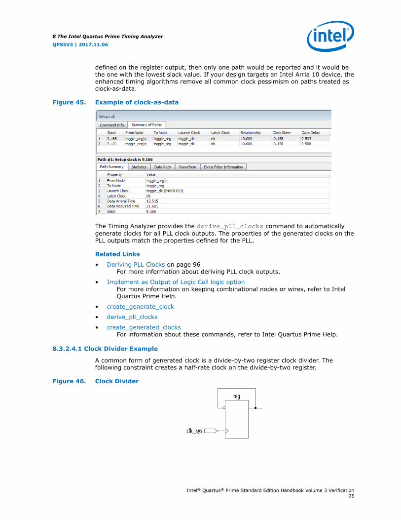
defined on the register output, then only one path would be reported and it would bethe one with the lowest slack value. If your design targets an Intel Arria 10 device, theenhanced timing algorithms remove all common clock pessimism on paths treated asclock-as-data.
Figure 45. Example of clock-as-data
The Timing Analyzer provides the derive_pll_clocks command to automaticallygenerate clocks for all PLL clock outputs. The properties of the generated clocks on thePLL outputs match the properties defined for the PLL.
Related Links
• Deriving PLL Clocks on page 96For more information about deriving PLL clock outputs.
• Implement as Output of Logic Cell logic optionFor more information on keeping combinational nodes or wires, refer to IntelQuartus Prime Help.
• create_generate_clock
• derive_pll_clocks
• create_generated_clocksFor information about these commands, refer to Intel Quartus Prime Help.
8.3.2.4.1 Clock Divider Example
A common form of generated clock is a divide-by-two register clock divider. Thefollowing constraint creates a half-rate clock on the divide-by-two register.
Figure 46. Clock Divider
reg
clk_sys
8 The Intel Quartus Prime Timing Analyzer
QPS5V3 | 2017.11.06
Intel® Quartus® Prime Standard Edition Handbook Volume 3 Verification95

Figure 47. Clock Divider Waveform
1 2 3 4 5 6 7 8Edges
clk_sys
clk_div_2
0 10 20 30Time
create_clock -period 10 -name clk_sys [get_ports clk_sys]create_generated_clock -name clk_div_2 -divide_by 2 -source \ [get_ports clk_sys] [get_pins reg|q]
Or in order to have the clock source be the clock pin of the register you can use:
create_clock -period 10 -name clk_sys [get_ports clk_sys]create_generated_clock -name clk_div_2 -divide_by 2 -source \ [get_pins reg|clk] [get_pins reg|q]
8.3.2.4.2 Clock Multiplexor Example
Another common form of generated clock is on the output of a clock mux. Onegenerated clock on the output is requred for each input clock. The SDC example alsoincludes the set_clock_groups command to indicate that the two generated clockscan never be active simultaneously in the design, so the Timing Analyzer does notanalyze cross-domain paths between the generated clocks on the output of the clockmux.
Figure 48. Clock Mux
clk_bclk_a mux_out
create_clock -name clock_a -period 10 [get_ports clk_a]create_clock -name clock_b -period 10 [get_ports clk_b]create_generated_clock -name clock_a_mux -source [get_ports clk_a] \ [get_pins clk_mux|mux_out]create_generated_clock -name clock_b_mux -source [get_ports clk_b] \ [get_pins clk_mux|mux_out] -addset_clock_groups -exclusive -group clock_a_mux -group clock_b_mux
8.3.2.5 Deriving PLL Clocks
Use the derive_pll_clocks command to direct the Timing Analyzer toautomatically search the timing netlist for all unconstrained PLL output clocks. Thederive_pll_clocks command detects your current PLL settings and automaticallycreates generated clocks on the outputs of every PLL by calling thecreate_generated_clock command.
Create Base Clock for PLL input Clock Ports
create_clock -period 10.0 -name fpga_sys_clk [get_ports fpga_sys_clk] \ derive_pll_clocks
8 The Intel Quartus Prime Timing Analyzer
QPS5V3 | 2017.11.06
Intel® Quartus® Prime Standard Edition Handbook Volume 3 Verification96

If your design contains transceivers, LVDS transmitters, or LVDS receivers, you mustuse the derive_pll_clocks command. The command automatically constrains thislogic in your design and creates timing exceptions for those blocks.
Include the derive_pll_clocks command in your SDC file after anycreate_clock command Each time the Timing Analyzer reads your SDC file, theappropriate generate clock is created for each PLL output clock pin. If a clock exists ona PLL output before running derive_pll_clocks, the pre-existing clock hasprecedence, and an auto-generated clock is not created for that PLL output.
A simple PLL design with a register-to-register path.
Figure 49. Simple PLL Design
reg_1 reg_2
pll_inclk pll_inst
dataout
The Timing Analyzer generates messages when you use the derive_pll_clockscommand to automatically constrain the PLL for a design similar to the previousimage.
Example 10. derive_pll_clocks Command Messages
Info:Info: Deriving PLL Clocks:Info: create_generated_clock -source pll_inst|altpll_component|pll|inclk[0] -divide_by 2 -namepll_inst|altpll_component|pll|clk[0] pll_inst|altpll_component|pll|clk[0]Info:
The input clock pin of the PLL is the node pll_inst|altpll_component|pll|inclk[0] which is used for the -source option. The name of the output clock of thePLL is the PLL output clock node, pll_inst|altpll_component|pll|clk[0].
If the PLL is in clock switchover mode, multiple clocks are created for the output clockof the PLL; one for the primary input clock (for example, inclk[0]), and one for thesecondary input clock (for example, inclk[1]). You should create exclusive clockgroups for the primary and secondary output clocks since they are not activesimultaneously.
Related Links
• Creating Clock Groups on page 97For more information about creating exclusive clock groups.
• derive_pll_clocks
• Derive PLL ClocksFor more information about the derive_pll_clocks command.
8.3.2.6 Creating Clock Groups
The Timing Analyzer assumes all clocks are related unless constrained otherwise.
8 The Intel Quartus Prime Timing Analyzer
QPS5V3 | 2017.11.06
Intel® Quartus® Prime Standard Edition Handbook Volume 3 Verification97

To specify clocks in your design that are exclusive or asynchronous, use theset_clock_groups command. The set_clock_groups command cuts timingbetween clocks in different groups, and performs the same analysis regardless ofwhether you specify -exclusive or -asynchronous. A group is defined with the -group option. The Timing Analyzer excludes the timing paths between clocks for eachof the separate groups.
The following tables show examples of various group options for theset_clock_groups command.
Table 24. set_clock_groups -group A
Dest\Source A B C D
A Analyzed Cut Cut Cut
B Cut Analyzed Analyzed Analyzed
C Cut Analyzed Analyzed Analyzed
D Cut Analyzed Analyzed Analyzed
Table 25. set_clock_groups -group {A B}
Dest\Source A B C D
A Analyzed Analyzed Cut Cut
B Analyzed Analyzed Cut Cut
C Cut Cut Analyzed Analyzed
D Cut Cut Analyzed Analyzed
Table 26. set_clock_groups -group A -group B
Dest\Source A B C D
A Analyzed Cut Cut Cut
B Cut Analyzed Cut Cut
C Cut Cut Analyzed Analyzed
D Cut Cut Analyzed Analyzed
Table 27. set_clock_groups -group {A C} -group {B D}
Dest\Source A B C D
A Analyzed Cut Analyzed Cut
B Cut Analyzed Cut Analyzed
C Analyzed Cut Analyzed Cut
D Cut Analyzed Cut Analyzed
Table 28. set_clock_groups -group {A C D}
Dest\Source A B C D
A Analyzed Cut Analyzed Analyzed
continued...
8 The Intel Quartus Prime Timing Analyzer
QPS5V3 | 2017.11.06
Intel® Quartus® Prime Standard Edition Handbook Volume 3 Verification98
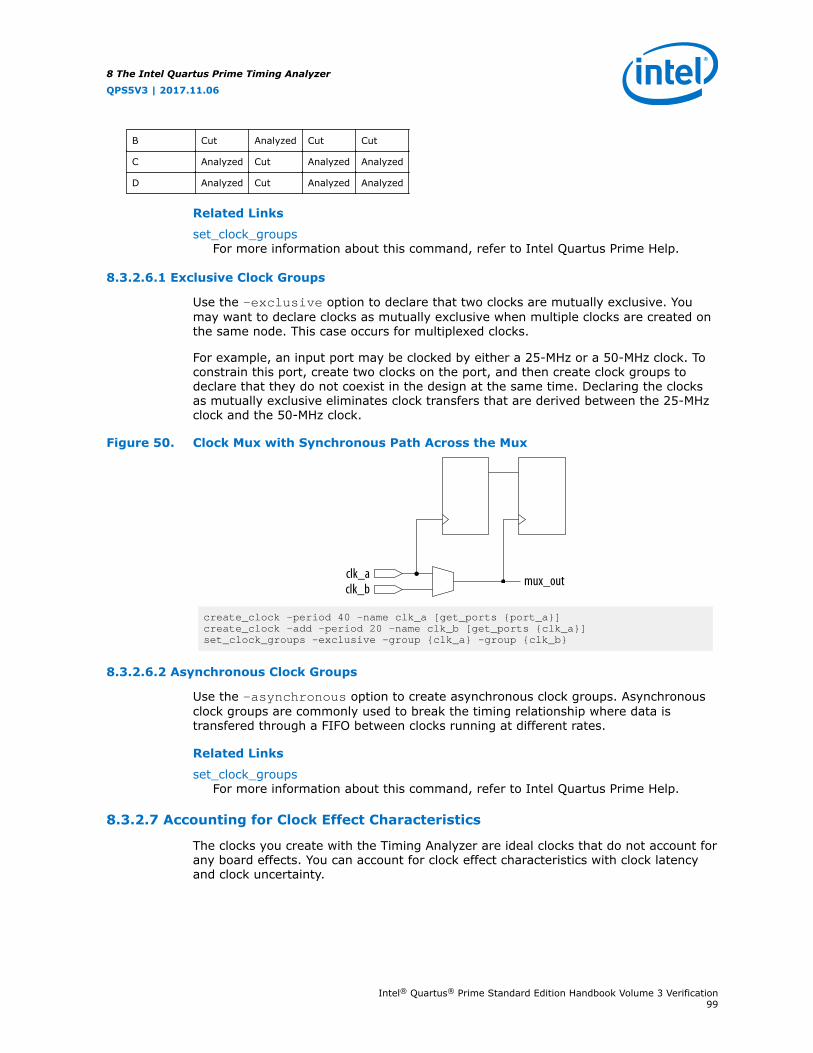
B Cut Analyzed Cut Cut
C Analyzed Cut Analyzed Analyzed
D Analyzed Cut Analyzed Analyzed
Related Links
set_clock_groupsFor more information about this command, refer to Intel Quartus Prime Help.
8.3.2.6.1 Exclusive Clock Groups
Use the -exclusive option to declare that two clocks are mutually exclusive. Youmay want to declare clocks as mutually exclusive when multiple clocks are created onthe same node. This case occurs for multiplexed clocks.
For example, an input port may be clocked by either a 25-MHz or a 50-MHz clock. Toconstrain this port, create two clocks on the port, and then create clock groups todeclare that they do not coexist in the design at the same time. Declaring the clocksas mutually exclusive eliminates clock transfers that are derived between the 25-MHzclock and the 50-MHz clock.
Figure 50. Clock Mux with Synchronous Path Across the Mux
clk_bclk_a mux_out
create_clock -period 40 -name clk_a [get_ports {port_a}]create_clock -add -period 20 -name clk_b [get_ports {clk_a}]set_clock_groups -exclusive -group {clk_a} -group {clk_b}
8.3.2.6.2 Asynchronous Clock Groups
Use the -asynchronous option to create asynchronous clock groups. Asynchronousclock groups are commonly used to break the timing relationship where data istransfered through a FIFO between clocks running at different rates.
Related Links
set_clock_groupsFor more information about this command, refer to Intel Quartus Prime Help.
8.3.2.7 Accounting for Clock Effect Characteristics
The clocks you create with the Timing Analyzer are ideal clocks that do not account forany board effects. You can account for clock effect characteristics with clock latencyand clock uncertainty.
8 The Intel Quartus Prime Timing Analyzer
QPS5V3 | 2017.11.06
Intel® Quartus® Prime Standard Edition Handbook Volume 3 Verification99

8.3.2.7.1 Clock Latency
There are two forms of clock latency, clock source latency and clock network latency.Source latency is the propagation delay from the origin of the clock to the clockdefinition point (for example, a clock port). Network latency is the propagation delayfrom a clock definition point to a register’s clock pin. The total latency at a register’sclock pin is the sum of the source and network latencies in the clock path.
To specify source latency to any clock ports in your design, use theset_clock_latency command.
Note: The Timing Analyzer automatically computes network latencies; therefore, you onlycan characterize source latency with the set_clock_latency command. You mustuse the -source option.
Related Links
set_clock_latencyFor more information about this command, refer to Intel Quartus Prime Help.
8.3.2.7.2 Clock Uncertainty
When clocks are created, they are ideal and have perfect edges. It is important to adduncertainty to those perfect edges, to mimic clock-level effects like jitter. You shouldinclude the derive_clock_uncertainty command in your SDC file so thatappropriate setup and hold uncertainties are automatically calculated and applied toall clock transfers in your design. If you don't include the command, the TimingAnalyzer performs it anyway; it is a critical part of constraining your design correctly.
The Timing Analyzer subtracts setup uncertainty from the data required time for eachapplicable path and adds the hold uncertainty to the data required time for eachapplicable path. This slightly reduces the setup and hold slack on each path.
The Timing Analyzer accounts for uncertainty clock effects for three types of clock-to-clock transfers; intraclock transfers, interclock transfers, and I/O interface clocktransfers.
• Intraclock transfers occur when the register-to-register transfer takes place in thedevice and the source and destination clocks come from the same PLL output pinor clock port.
• Interclock transfers occur when a register-to-register transfer takes place in thecore of the device and the source and destination clocks come from a different PLLoutput pin or clock port.
• I/O interface clock transfers occur when data transfers from an I/O port to thecore of the device or from the core of the device to the I/O port.
To manually specify clock uncertainty, use the set_clock_uncertainty command.You can specify the uncertainty separately for setup and hold. You can also specifyseparate values for rising and falling clock transitions, although this is not commonlyused. You can override the value that was automatically applied by thederive_clock_uncertainty command, or you can add to it.
The derive_clock_uncertainty command accounts for PLL clock jitter if the clockjitter on the input to a PLL is within the input jitter specification for PLL's in thespecified device. If the input clock jitter for the PLL exceeds the specification, you
8 The Intel Quartus Prime Timing Analyzer
QPS5V3 | 2017.11.06
Intel® Quartus® Prime Standard Edition Handbook Volume 3 Verification100

should add additional uncertainty to your PLL output clocks to account for excess jitterwith the set_clock_uncertainty -add command. Refer to the device handbookfor your device for jitter specifications.
Another example is to use set_clock_uncertainty -add to add uncertainty toaccount for peak-to-peak jitter from a board when the jitter exceeds the jitterspecification for that device. In this case you would add uncertainty to both setup andhold equal to 1/2 the jitter value:
set_clock_uncertainty –setup –to <clock name> \ -setup –add <p2p jitter/2>
set_clock_uncertainty –hold –enable_same_physical_edge –to <clock name> \ –add <p2p jitter/2>
There is a complex set of precedence rules for how the Timing Analyzer applies valuesfrom derive_clock_uncertainty and set_clock_uncertainty, which dependon the order the commands appear in your SDC files, and various options used withthe commands. The Help topics referred to below contain complete descriptions ofthese rules. These precedence rules are much simpler to understand and implement ifyou follow these recommendations:
• If you want to assign your own clock uncertainty values to any clock transfers, thebest practice is to put your set_clock_uncertainty exceptions after thederive_clock_uncertainty command in your SDC file.
• When you use the -add option for set_clock_uncertainty, the value youspecify is added to the value from derive_clock_uncertainty. If you don'tspecify -add, the value you specify replaces the value fromderive_clock_uncertainty.
Related Links
• set_clock_uncertainty
• derive_clock_uncertainty
• remove_clock_uncertaintyFor more information about these commands, refer to Intel Quartus PrimeHelp.
8.3.3 Creating I/O Requirements
The Timing Analyzer reviews setup and hold relationships for designs in which anexternal source interacts with a register internal to the design. The Timing Analyzersupports input and output external delay modeling with the set_input_delay andset_output_delay commands. You can specify the clock and minimum andmaximum arrival times relative to the clock.
You must specify timing requirements, including internal and external timingrequirements, before you fully analyze a design. With external timing requirementsspecified, the Timing Analyzer verifies the I/O interface, or periphery of the device,against any system specification.
8.3.3.1 Input Constraints
Input constraints allow you to specify all the external delays feeding into the device.Specify input requirements for all input ports in your design.
8 The Intel Quartus Prime Timing Analyzer
QPS5V3 | 2017.11.06
Intel® Quartus® Prime Standard Edition Handbook Volume 3 Verification101

You can use the set_input_delay command to specify external input delayrequirements. Use the -clock option to reference a virtual clock. Using a virtual clockallows the Timing Analyzer to correctly derive clock uncertainties for interclock andintraclock transfers. The virtual clock defines the launching clock for the input port.The Timing Analyzer automatically determines the latching clock inside the device thatcaptures the input data, because all clocks in the device are defined.
Figure 51. Input Delay
External Device FPGA
Oscillator
dd
cd_altrcd_ext
tco_ext
The calculation the Timing Analyzer performs to determine the typical input delay.
Figure 52. Input Delay Calculation
input delayMAX = (cd_extMAX – cd_altrMIN ) + tco_extMAX + ddMAX
input delayMIN = (cd_extMIN – cd_altrMAX ) + tco_extMIN + ddMIN
8.3.3.2 Output Constraints
Output constraints allow you to specify all external delays from the device for alloutput ports in your design.
You can use the set_output_delay command to specify external output delayrequirements. Use the -clock option to reference a virtual clock. The virtual clockdefines the latching clock for the output port. The Timing Analyzer automaticallydetermines the launching clock inside the device that launches the output data,because all clocks in the device are defined. The following figure is an example of anoutput delay referencing a virtual clock.
Figure 53. Output Delay
External DeviceFPGA
Oscillator
dd
cd_altr
cd_ext
tsu_ext/th_ext
The calculation the Timing Analyzer performs to determine the typical out delay.
8 The Intel Quartus Prime Timing Analyzer
QPS5V3 | 2017.11.06
Intel® Quartus® Prime Standard Edition Handbook Volume 3 Verification102

Figure 54. Output Delay Calculation
output delayMAX = ddMAX + tsu_ext + (cd_altrMAX – cd_extMIN )output delayMIN = (ddMIN – th_ext +(cd_altrMIN – cd_extMAX ))
Related Links
• set_intput_delay
• set_output_delayFor more information about these commands, refer to Intel Quartus PrimeHelp.
8.3.4 Creating Delay and Skew Constraints
The Timing Analyzer supports the Synopsys Design Constraint format for constrainingtiming for the ports in your design. These constraints allow the Timing Analyzer toperform a system static timing analysis that includes not only the device internaltiming, but also any external device timing and board timing parameters.
8.3.4.1 Advanced I/O Timing and Board Trace Model Delay
The Timing Analyzer can use advanced I/O timing and board trace model assignmentsto model I/O buffer delays in your design.
If you change any advanced I/O timing settings or board trace model assignments,recompile your design before you analyze timing, or use the -force_dat option toforce delay annotation when you create a timing netlist.
Example 11. Forcing Delay Annotation
create_timing_netlist -force_dat
Related Links
• Using Advanced I/O Timing
• I/O ManagementFor more information about advanced I/O timing.
8.3.4.2 Maximum Skew
To specify the maximum path-based skew requirements for registers and ports in thedesign and report the results of maximum skew analysis, use the set_max_skewcommand in conjunction with the report_max_skew command.
Use the set_max_skew constraint to perform maximum allowable skew analysisbetween sets of registers or ports. In order to constrain skew across multiple paths, allsuch paths must be defined within a single set_max_skew constraint.set_max_skew timing constraint is not affected by set_max_delay,set_min_delay, and set_multicycle_path but it does obey set_false_pathand set_clock_groups. If your design targets an Intel Arria 10 device, skewconstraints are not affected by set_clock_groups.
8 The Intel Quartus Prime Timing Analyzer
QPS5V3 | 2017.11.06
Intel® Quartus® Prime Standard Edition Handbook Volume 3 Verification103

Table 29. set_max_skew Options
Arguments Description
-h | -help Short help
-long_help Long help with examples and possible return values
-exclude <Tcl list> A Tcl list of parameters to exclude during skew analysis.This list can include one or more of the following: utsu,uth, utco, from_clock, to_clock,clock_uncertainty, ccpp, input_delay,output_delay, odv.Note: Not supported for Intel Arria 10 devices.
-fall_from_clock <names> Valid source clocks (string patterns are matched using Tclstring matching)
-fall_to_clock <names> Valid destination clocks (string patterns are matched usingTcl string matching)
-from <names>(1) Valid sources (string patterns are matched using Tcl stringmatching
-from_clock <names> Valid source clocks (string patterns are matched using Tclstring matching)
-get_skew_value_from_clock_period<src_clock_period|dst_clock_period|min_clock_period>
Option to interpret skew constraint as a multiple of the clockperiod
-include <Tcl list> Tcl list of parameters to include during skew analysis. Thislist can include one or more of the following: utsu, uth,utco, from_clock, to_clock, clock_uncertainty,ccpp, input_delay, output_delay, odv.Note: Not supported for Intel Arria 10 devices.
-rise_from_clock <names> Valid source clocks (string patterns are matched using Tclstring matching)
-rise_to_clock <names> Valid destination clocks (string patterns are matched usingTcl string matching)
-skew_value_multiplier <multiplier> Value by which the clock period should be multiplied tocompute skew requirement.
-to <names>(1) Valid destinations (string patterns are matched using Tclstring matching)
-to_clock <names> Valid destination clocks (string patterns are matched usingTcl string matching)
<skew> Required skew
Applying maximum skew constraints between clocks applies the constraint from allregister or ports driven by the clock specified with the -from option to all registers orports driven by the clock specified with the -to option.
Use the -include and -exclude options to include or exclude one or more of thefollowing: register micro parameters (utsu, uth, utco), clock arrival times(from_clock, to_clock), clock uncertainty (clock_uncertainty), common clockpath pessimism removal (ccpp), input and output delays (input_delay,
(1) Legal values for the -from and -to options are collections of clocks, registers, ports, pins, cellsor partitions in a design.
8 The Intel Quartus Prime Timing Analyzer
QPS5V3 | 2017.11.06
Intel® Quartus® Prime Standard Edition Handbook Volume 3 Verification104

output_delay) and on-die variation (odv). Max skew analysis can include dataarrival times, clock arrival times, register micro parameters, clock uncertainty, on-dievariation and ccpp removal. Among these, only ccpp removal is disabled during theFitter by default. When -include is used, those in the inclusion list are added to thedefault analysis. Similarly, when -exclude is used, those in the exclusion list areexcluded from the default analysis. When both the -include and -exclude optionsspecify the same parameter, that parameter is excluded.
Note: If your design targets an Intel Arria 10 device, -exclude and -include are notsupported.
Use -get_skew_value_from_clock_period to set the skew as a multiple of thelaunching or latching clock period, or whichever of the two has a smaller period. If thisoption is used, then -skew_value_multiplier must also be set, and the positionalskew option may not be set. If the set of skew paths is clocked by more than oneclock, Timing Analyzer uses the one with smallest period to compute the skewconstraint.
When this constraint is used, results of max skew analysis are displayed in the ReportMax Skew (report_max_skew) report from the Timing Analyzer. Since skew is definedbetween two or more paths, no results are displayed if the -from/-from_clock and-to/-to_clock filters satisfy less than two paths.
Related Links
• set_max_skew
• report_max_skewFor more information about these commands, refer to Intel Quartus PrimeHelp.
8.3.4.3 Net Delay
Use the set_net_delay command to set the net delays and perform minimum ormaximum timing analysis across nets.
The -from and -to options can be string patterns or pin, port, register, or netcollections. When pin or net collection is used, the collection should include outputpins or nets.
Table 30. set_net_delay Options
Arguments Description
-h | -help Short help
-long_help Long help with examples and possible return values
-from <names> Valid source pins, ports, registers or nets(string patterns arematched using Tcl string matching)
-get_value_from_clock_period<src_clock_period|dst_clock_period|min_clock_period|max_clock_period>
Option to interpret net delay constraint as a multiple of theclock period.
-max Specifies maximum delay
-min Specifies minimum delay
continued...
8 The Intel Quartus Prime Timing Analyzer
QPS5V3 | 2017.11.06
Intel® Quartus® Prime Standard Edition Handbook Volume 3 Verification105
Arguments Description
-to <names>(2) Valid destination pins, ports, registers or nets (stringpatterns are matched using Tcl string matching)
-value_multiplier <multiplier> Value by which the clock period should be multiplied tocompute net delay requirement.
<delay> Required delay
When you use the -min option, slack is calculated by looking at the minimum delay onthe edge. If you use -max option, slack is calculated with the maximum edge delay.
Use -get_skew_value_from_clock_period to set the net delay requirement as amultiple of the launching or latching clock period, or whichever of the two has asmaller or larger period. If this option is used, then -value_multiplier must alsobe set, and the positional delay option may not be set. If the set of nets is clocked bymore than one clock, Timing Analyzer uses the net with smallest period to computethe constraint for a -max constraint, and the largest period for a -min constraint. Ifthere are no clocks clocking the endpoints of the net (e.g. if the endpoints of the netsare not registers or constraint ports), then the net delay constraint is ignored.
Related Links
• set_net_delay
• report_net_delayFor more information about these commands, refer to Intel Quartus PrimeHelp.
8.3.4.4 Using create_timing_netlist
You can onfigure or load the timing netlist that the Timing Analyzer uses to calculatepath delay data.
Your design should have a timing netlist before running the Timing Analyzer . You canuse the Create Timing Netlist dialog box or the Create Timing Netlist command inthe Tasks pane. The command also generates Advanced I/O Timing reports if youturned on Enable Advanced I/O Timing in the Timing Analyzer page of theSettings dialog box.
Note: The timing netlist created is based on the initial configuration of the design. Anyconfiguration changes done by the design after the device enters user mode, forexample, dynamic transceiver reconfiguration, are not reflected in the timing netlist.This applies to all device families except transceivers on Intel Arria 10 devices with theMultiple Reconfiguration Profiles feature.
The following diagram shows how the Timing Analyzer interprets and classifies timingnetlist data for a sample design.
(2) If the -to option is unused or if the -to filter is a wildcard ( "*") character, all the output pinsand registers on timing netlist became valid destination points.
8 The Intel Quartus Prime Timing Analyzer
QPS5V3 | 2017.11.06
Intel® Quartus® Prime Standard Edition Handbook Volume 3 Verification106

Figure 55. How Timing Analyzer Interprets the Timing Netlist
8.3.5 Creating Timing Exceptions
Timing exceptions in the Timing Analyzer provide a way to modify the default timinganalysis behavior to match the analysis required by your design. Specify timingexceptions after clocks and input and output delay constraints because timingexceptions can modify the default analysis.
8.3.5.1 Precedence
If the same clock or node names occur in multiple timing exceptions, the followingorder of precedence applies:
1. False path
2. Minimum delays and maximum delays
3. Multicycle path
The false path timing exception has the highest precedence. Within each category,assignments to individual nodes have precedence over assignments to clocks. Forexceptions of the same type:
• having a -from <node> has the highest priority
• followed by the -to <node>
• then the -thru <node>
• then -from <clock>
• and lastly, a -to <clock>
An asterisk wildcard (*) for any of these options applies the same precedence as notspecifying the option at all. For example, -from a -to * is treated identically to -from a for as regards precedence.
Precedence example:
8 The Intel Quartus Prime Timing Analyzer
QPS5V3 | 2017.11.06
Intel® Quartus® Prime Standard Edition Handbook Volume 3 Verification107

1. set_max_delay 1 -from x -to y
2. set_max_delay 2 -from x
3. set_max_delay 3 -to y
The first exception would have higher priority than either of the other two, since itspecifies a -from (while #3 doesn't) and sepecifies a -to (while #2 doesn't). In theabsence of the first exception, the second exception would have higher priority thanthe third, since it specifies a -from, which the third does not. Finally, the remainingorder of precedence for additional exceptions is order-dependent, such that theassignments most recently created overwrite, or partially overwrite, earlierassignments.
set_net_delay or set_max_skew exceptions are analyzed independently ofminimum or maximum delays, or multicycle path constratints.
• The set_net_delay exception applies regardless the existance of aset_false_path exception, or set_clock_group exception, on the samenodes.
• The set_max_skew exception applies regardless of any set_clock_groupexception on the same nodes, but a set_false_path exception overrides aset_max_skew exception.
8.3.5.2 False Paths
Specifying a false path in your design removes the path from timing analysis.
Use the set_false_path command to specify false paths in your design. You canspecify either a point-to-point or clock-to-clock path as a false path. For example, apath you should specify as false path is a static configuration register that is writtenonce during power-up initialization, but does not change state again. Although signalsfrom static configuration registers often cross clock domains, you may not want tomake false path exceptions to a clock-to-clock path, because some data may transferacross clock domains. However, you can selectively make false path exceptions fromthe static configuration register to all endpoints.
To make false path exceptions from all registers beginning with A to all registersbeginning with B, use the following code in your SDC file.
set_false_path -from [get_pins A*] -to [get_pins B*]
The Timing Analyzer assumes all clocks are related unless you specify otherwise. Clockgroups are a more efficient way to make false path exceptions between clocks,compared to writing multiple set_false_path exceptions between every clocktransfer you want to eliminate.
Related Links
• Creating Clock Groups on page 97For more information about creating exclusive clock groups.
• set_false_pathFor more information about this command, refer to Intel Quartus Prime Help.
8 The Intel Quartus Prime Timing Analyzer
QPS5V3 | 2017.11.06
Intel® Quartus® Prime Standard Edition Handbook Volume 3 Verification108

8.3.5.3 Minimum and Maximum Delays
To specify an absolute minimum or maximum delay for a path, use theset_min_delay command or the set_max_delay commands, respectively.Specifying minimum and maximum delay directly overwrites existing setup and holdrelationships with the minimum and maximum values.
Use the set_max_delay and set_min_delay commands to create constraints forasynchronous signals that do not have a specific clock relationship in your design, butrequire a minimum and maximum path delay. You can create minimum and maximumdelay exceptions for port-to-port paths through the device without a register stage inthe path. If you use minimum and maximum delay exceptions to constrain the pathdelay, specify both the minimum and maximum delay of the path; do not constrainonly the minimum or maximum value.
If the source or destination node is clocked, the Timing Analyzer takes into accountthe clock paths, allowing more or less delay on the data path. If the source ordestination node has an input or output delay, that delay is also included in theminimum or maximum delay check.
If you specify a minimum or maximum delay between timing nodes, the delay appliesonly to the path between the two nodes. If you specify a minimum or maximum delayfor a clock, the delay applies to all paths where the source node or destination node isclocked by the clock.
You can create a minimum or maximum delay exception for an output port that doesnot have an output delay constraint. You cannot report timing for the paths associatedwith the output port; however, the Timing Analyzer reports any slack for the path inthe setup summary and hold summary reports. Because there is no clock associatedwith the output port, no clock is reported for timing paths associated with the outputport.
Note: To report timing with clock filters for output paths with minimum and maximum delayconstraints, you can set the output delay for the output port with a value of zero. Youcan use an existing clock from the design or a virtual clock as the clock reference.
Related Links
• set_max_delay
• set_min_delayFor more information about these commands, refer to Intel Quartus PrimeHelp.
8.3.5.4 Delay Annotation
To modify the default delay values used during timing analysis, use theset_annotated_delay and set_timing_derate commands. You must update thetiming netlist to see the results of these commands
To specify different operating conditions in a single SDC file, rather than havingmultiple SDC files that specify different operating conditions, use theset_annotated_delay -operating_conditions command.
Related Links
• set_timing_derate
8 The Intel Quartus Prime Timing Analyzer
QPS5V3 | 2017.11.06
Intel® Quartus® Prime Standard Edition Handbook Volume 3 Verification109

• set_annotated_delayFor more information about these commands, refer to the Intel Quartus PrimeHelp.
8.3.5.5 Multicycle Paths
By default, the Timing Analyzerr performs a single-cycle analysis, which is the mostrestrictive type of analysis. When analyzing a path, the setup launch and latch edgetimes are determined by finding the closest two active edges in the respectivewaveforms.
For a hold analysis, the timing analyzer analyzes the path against two timingconditions for every possible setup relationship, not just the worst-case setuprelationship. Therefore, the hold launch and latch times may be completely unrelatedto the setup launch and latch edges. The Timing Analyzer does not report negativesetup or hold relationships. When either a negative setup or a negative holdrelationship is calculated, the Timing Analyzer moves both the launch and latch edgessuch that the setup and hold relationship becomes positive.
A multicycle constraint adjusts setup or hold relationships by the specified number ofclock cycles based on the source (-start) or destination (-end) clock. An end setupmulticycle constraint of 2 extends the worst-case setup latch edge by one destinationclock period. If -start and -end values are not specified, the default constraint is -end.
Hold multicycle constraints are based on the default hold position (the default valueis 0). An end hold multicycle constraint of 1 effectively subtracts one destination clockperiod from the default hold latch edge.
When the objects are timing nodes, the multicycle constraint only applies to the pathbetween the two nodes. When an object is a clock, the multicycle constraint applies toall paths where the source node (-from) or destination node (-to) is clocked by theclock. When you adjust a setup relationship with a multicycle constraint, the holdrelationship is adjusted automatically.
You can use Timing Analyzer commands to modify either the launch or latch edgetimes that the uses to determine a setup relationship or hold relationship.
Table 31. Commands to Modify Edge Times
Command Description of Modification
set_multicycle_path -setup -end <value> Latch edge time of the setup relationship
set_multicycle_path -setup -start<value> Launch edge time of the setup relationship
set_multicycle_path -hold -end <value> Latch edge time of the hold relationship
set_multicycle_path -hold -start <value> Launch edge time of the hold relationship
8.3.5.6 Common Multicycle Variations
Multicycle exceptions adjust the timing requirements for a register-to-register path,allowing the Fitter to optimally place and route a design in a device. Multicycleexceptions also can reduce compilation time and improve the quality of results, andcan be used to change timing requirements. Two common multicycle variations arerelaxing setup to allow a slower data transfer rate, and altering the setup to accountfor a phase shift.
8 The Intel Quartus Prime Timing Analyzer
QPS5V3 | 2017.11.06
Intel® Quartus® Prime Standard Edition Handbook Volume 3 Verification110

8.3.5.6.1 Relaxing Setup with set_multicyle_path
A common type of multicycle exception occurs when the data transfer rate is slowerthan the clock cycle. Relaxing the setup relationship opens the window when data isaccepted as valid.
In this example, the source clock has a period of 10 ns, but a group of registers areenabled by a toggling clock, so they only toggle every other cycle. Since they are fedby a 10 ns clock, the Timing Analyzer reports a set up of 10 ns and a hold of 0 ns,However, since the data is transferring every other cycle, the relationships should beanalyzed as if the clock were operating at 20 ns, which would result in a setup of20 ns, while the hold remains 0 ns, in essence, extending the window of time whenthe data can be recognized.
The following pair of multicycle assignments relax the setup relationship by specifyingthe -setup value of N and the -hold value as N-1. You must specify the holdrelationship with a -hold assignment to prevent a positive hold requirement.
Relaxing Setup while Maintaining Hold
set_multicycle_path -setup -from src_reg* -to dst_reg* 2set_multicycle_path -hold -from src_reg* -to dst_reg* 1
Figure 56. Relaxing Setup by Multiple Cycles0 ns 10 ns 20 ns 30 ns
0 ns 10 ns 20 ns 30 ns
0 ns 10 ns 20 ns 30 ns
No Multicycles(Default Relationship)
Setup = 10 nsHold = 0 ns
Setup = 2Hold = 1
Setup = 20 nsHold = 0 ns
Setup = 3Hold = 2
Setup = 30 nsHold = 0 ns
This pattern can be extended to create larger setup relationships in order to easetiming closure requirements. A common use for this exception is when writing toasynchronous RAM across an I/O interface. The delay between address, data, and awrite enable may be several cycles. A multicycle exception to I/O ports can allow extratime for the address and data to resolve before the enable occurs.
You can relax the setup by three cycles with the following code in your SDC file.
8 The Intel Quartus Prime Timing Analyzer
QPS5V3 | 2017.11.06
Intel® Quartus® Prime Standard Edition Handbook Volume 3 Verification111

Three Cycle I/O Interface Exception
set_multicycle_path -setup -to [get_ports {SRAM_ADD[*] SRAM_DATA[*]} 3set_multicycle_path -hold -to [get_ports {SRAM_ADD[*] SRAM_DATA[*]} 2
8.3.5.6.2 Accounting for a Phase Shift
In this example, the design contains a PLL that performs a phase-shift on a clockwhose domain exchanges data with domains that do not experience the phase shift. Acommon example is when the destination clock is phase-shifted forward and thesource clock is not, the default setup relationship becomes that phase-shift, thusshifting the window when data is accepted as valid.
For example, the following code is a circumstance where a PLL phase-shifts one outputforward by a small amount, in this case 0.2 ns.
Cross Domain Phase-Shift
create_generated_clock -source pll|inclk[0] -name pll|clk[0] pll|clk[0]create_generated_clock -source pll|inclk[0] -name pll|clk[1] -phase 30 pll|clk[1]
The default setup relationship for this phase-shift is 0.2 ns, shown in Figure A,creating a scenario where the hold relationship is negative, which makes achievingtiming closure nearly impossible.
Figure 57. Phase-Shifted Setup and Hold-10 ns 0 ns 10 ns 20 ns
-10 ns 0 ns 10 ns 20 ns
No Multicycles(Default Relationship)
Setup = 0.2 nsHold = -9.8 ns
Setup = 2
Setup = 10.2 nsHold = 0.2 ns
Adding the following constraint in your SDC allows the data to transfer to the followingedge.
set_multicycle_path -setup -from [get_clocks clk_a] -to [get_clocks clk_b] 2
The hold relationship is derived from the setup relationship, making a multicyle holdconstraint unnecessary.
Related Links
• Same Frequency Clocks with Destination Clock Offset on page 121Refer to this topic for a more complete example.
• set_multicycle_pathFor more information about this command, refer to the Intel Quartus PrimeHelp.
8 The Intel Quartus Prime Timing Analyzer
QPS5V3 | 2017.11.06
Intel® Quartus® Prime Standard Edition Handbook Volume 3 Verification112

8.3.5.7 Examples of Basic Multicycle Exceptions
Each example explains how the multicycle exceptions affect the default setup and holdanalysis in the Timing Analyzer. The multicycle exceptions are applied to a simpleregister-to-register circuit. Both the source and destination clocks are set to 10 ns.
8.3.5.7.1 Default Settings
By default, the Timing Analyzer performs a single-cycle analysis to determine thesetup and hold checks. Also, by default, the Timing Analyzer sets the end multicyclesetup assignment value to one and the end multicycle hold assignment value to zero.
The source and the destination timing waveform for the source register anddestination register, respectively where HC1 and HC2 are hold checks one and two andSC is the setup check.
Figure 58. Default Timing Diagram-10 0 10 20
Current Launch
Current Latch
0 1 2
HC1 HC2SC
REG1.CLK
REG2.CLK
The calculation that the Timing Analyzer performs to determine the setup check.
Figure 59. Setup Check
setup check = current latch edge – closest previous launch edge = 10 ns – 0 ns = 10 ns
The most restrictive setup relationship with the default single-cycle analysis, that is, asetup relationship with an end multicycle setup assignment of one, is 10 ns.
The setup report for the default setup in the Timing Analyzer with the launch and latchedges highlighted.
8 The Intel Quartus Prime Timing Analyzer
QPS5V3 | 2017.11.06
Intel® Quartus® Prime Standard Edition Handbook Volume 3 Verification113

Figure 60. Setup Report
The calculation that the Timing Analyzer performs to determine the hold check. Bothhold checks are equivalent.
Figure 61. Hold Check
hold check 1 = current launch edge – previous latch edge = 0 ns – 0 ns = 0 ns hold check 2 = next launch edge – current latch edge = 10 ns – 10 ns = 0 ns
The most restrictive hold relationship with the default single-cycle analysis, that a holdrelationship with an end multicycle hold assignment of zero, is 0 ns.
The hold report for the default setup in the Timing Analyzer with the launch and latchedges highlighted.
8 The Intel Quartus Prime Timing Analyzer
QPS5V3 | 2017.11.06
Intel® Quartus® Prime Standard Edition Handbook Volume 3 Verification114

Figure 62. Hold Report
8.3.5.7.2 End Multicycle Setup = 2 and End Multicycle Hold = 0
In this example, the end multicycle setup assignment value is two, and the endmulticycle hold assignment value is zero.
Multicycle Exceptions
set_multicycle_path -from [get_clocks clk_src] -to [get_clocks clk_dst] \ -setup -end 2
8 The Intel Quartus Prime Timing Analyzer
QPS5V3 | 2017.11.06
Intel® Quartus® Prime Standard Edition Handbook Volume 3 Verification115

Note: An end multicycle hold value is not required because the default end multicycle holdvalue is zero.
In this example, the setup relationship is relaxed by a full clock period by moving thelatch edge to the next latch edge. The hold analysis is unchanged from the defaultsettings.
The setup timing diagram for the analysis that the Timing Analyzer performs. Thelatch edge is a clock cycle later than in the default single-cycle analysis.
Figure 63. Setup Timing Diagram
-10 0
0 1 2
10 20
SC
REG1.CLK
REG2.CLK
CurrentLaunch
CurrentLatch
The calculation that the Timing Analyzer performs to determine the setup check.
Figure 64. Setup Check
setup check = current latch edge – closest previous launch edge = 20 ns – 0 ns = 20 ns
The most restrictive setup relationship with an end multicycle setup assignment of twois 20 ns.
The setup report in the Timing Analyzer with the launch and latch edges highlighted.
8 The Intel Quartus Prime Timing Analyzer
QPS5V3 | 2017.11.06
Intel® Quartus® Prime Standard Edition Handbook Volume 3 Verification116

Figure 65. Setup Report
Because the multicycle hold latch and launch edges are the same as the results ofhold analysis with the default settings, the multicycle hold analysis in this example isequivalent to the single-cycle hold analysis. The hold checks are relative to the setupcheck. Usually, the Timing Analyzer performs hold checks on every possible setupcheck, not only on the most restrictive setup check edges.
Figure 66. Hold Timing DIagram-10 0 10 20
Current Launch
Current Latch
REG1.CLK
REG2.CLK
SCHC1Data HC2
The calculation that the Timing Analyzer performs to determine the hold check. Bothhold checks are equivalent.
8 The Intel Quartus Prime Timing Analyzer
QPS5V3 | 2017.11.06
Intel® Quartus® Prime Standard Edition Handbook Volume 3 Verification117

Figure 67.
hold check 1 = current launch edge – previous latch edge = 0 ns – 10 ns = –10 ns
hold check 2 = next launch edge – current latch edge = 10 ns – 20 ns = –10 ns
The most restrictive hold relationship with an end multicycle setup assignment valueof two and an end multicycle hold assignment value of zero is 10 ns.
The hold report for this example in the Timing Analyzer with the launch and latchedges highlighted.
Figure 68. Hold Report
8.3.5.7.3 End Multicycle Setup = 2 and End Multicycle Hold = 1
In this example, the end multicycle setup assignment value is two, and the endmulticycle hold assignment value is one.
Multicycle Exceptions
set_multicycle_path -from [get_clocks clk_src] -to [get_clocks clk_dst] \ -setup -end 2set_multicycle_path -from [get_clocks clk_src] -to [get_clocks clk_dst] -hold -end 1
In this example, the setup relationship is relaxed by two clock periods by moving thelatch edge to the left two clock periods. The hold relationship is relaxed by a fullperiod by moving the latch edge to the previous latch edge.
The setup timing diagram for the analysis that the Timing Analyzer performs.
8 The Intel Quartus Prime Timing Analyzer
QPS5V3 | 2017.11.06
Intel® Quartus® Prime Standard Edition Handbook Volume 3 Verification118

Figure 69. Setup Timing Diagram
-10 0
0 1 2
10 20
SC
SRC.CLK
DST.CLK
CurrentLaunch
CurrentLatch
The calculation that the Timing Analyzer performs to determine the setup check.
Figure 70. Setup Check
setup check = current latch edge – closest previous launch edge = 20 ns – 0 ns = 20 ns
The most restrictive hold relationship with an end multicycle setup assignment valueof two is 20 ns.
The setup report for this example in the Timing Analyzer with the launch and latchedges highlighted.
Figure 71. Setup Report
The timing diagram for the hold checks for this example. The hold checks are relativeto the setup check.
8 The Intel Quartus Prime Timing Analyzer
QPS5V3 | 2017.11.06
Intel® Quartus® Prime Standard Edition Handbook Volume 3 Verification119

Figure 72. Hold Timing Diagram
-10 0 10 20
SRC.CLK
DST.CLK
CurrentLaunch
CurrentLatch
SCHC1
HC2
The calculation that the Timing Analyzer performs to determine the hold check. Bothhold checks are equivalent.
Figure 73. Hold Check
hold check 1 = current launch edge – previous latch edge = 0 ns – 0 ns = 0 ns
hold check 2 = next launch edge – current latch edge = 10 ns – 10 ns = 0 ns
The most restrictive hold relationship with an end multicycle setup assignment valueof two and an end multicycle hold assignment value of one is 0 ns.
The hold report for this example in the Timing Analyzer with the launch and latchedges highlighted.
8 The Intel Quartus Prime Timing Analyzer
QPS5V3 | 2017.11.06
Intel® Quartus® Prime Standard Edition Handbook Volume 3 Verification120

Figure 74. Hold Report
8.3.5.8 Application of Multicycle Exceptions
This section shows the following examples of applications of multicycle exceptions.Each example explains how the multicycle exceptions affect the default setup and holdanalysis in the Timing Analyzer. All of the examples are between related clockdomains. If your design contains related clocks, such as PLL clocks, and pathsbetween related clock domains, you can apply multicycle constraints.
8.3.5.8.1 Same Frequency Clocks with Destination Clock Offset
In this example, the source and destination clocks have the same frequency, but thedestination clock is offset with a positive phase shift. Both the source and destinationclocks have a period of 10 ns. The destination clock has a positive phase shift of 2 nswith respect to the source clock.
An example of a design with same frequency clocks and a destination clock offset.
Figure 75. Same Frequency Clocks with Destination Clock OffsetREG1 REG2
CombinationalLogic
SET SETD Q D Q
CLR CLR
clk1
In
clk0
Out
The timing diagram for default setup check analysis that the Timing Analyzerperforms.
8 The Intel Quartus Prime Timing Analyzer
QPS5V3 | 2017.11.06
Intel® Quartus® Prime Standard Edition Handbook Volume 3 Verification121
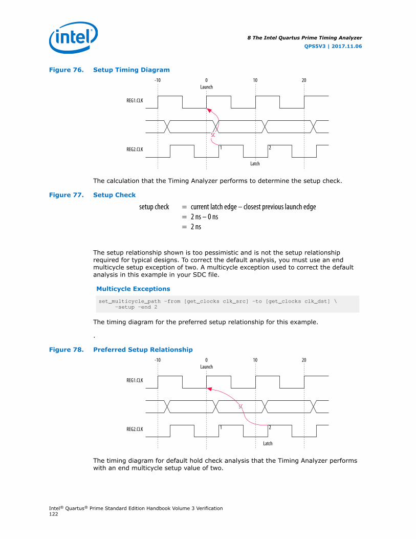
Figure 76. Setup Timing Diagram-10 0
1 2
10 20
REG1.CLK
REG2.CLK
Launch
Latch
SC
The calculation that the Timing Analyzer performs to determine the setup check.
Figure 77. Setup Check
setup check = current latch edge – closest previous launch edge = 2 ns – 0 ns = 2 ns
The setup relationship shown is too pessimistic and is not the setup relationshiprequired for typical designs. To correct the default analysis, you must use an endmulticycle setup exception of two. A multicycle exception used to correct the defaultanalysis in this example in your SDC file.
Multicycle Exceptions
set_multicycle_path -from [get_clocks clk_src] -to [get_clocks clk_dst] \ -setup -end 2
The timing diagram for the preferred setup relationship for this example.
.
Figure 78. Preferred Setup Relationship-10 0
1 2
10 20
REG1.CLK
REG2.CLK
Launch
Latch
SC
The timing diagram for default hold check analysis that the Timing Analyzer performswith an end multicycle setup value of two.
8 The Intel Quartus Prime Timing Analyzer
QPS5V3 | 2017.11.06
Intel® Quartus® Prime Standard Edition Handbook Volume 3 Verification122

Figure 79. Default Hold Check-10 0 10 20
REG1.CLK
REG2.CLK
CurrentLaunch
CurrentLatch
SCHC1 HC2
The calculation that the Timing Analyzer performs to determine the hold check.
Figure 80. Hold Check
hold check 1 = current launch edge – previous latch edge = 0 ns – 2 ns = –2 ns
hold check 2 = next launch edge – current latch edge = 10 ns – 12 ns = –2 ns
In this example, the default hold analysis returns the preferred hold requirements andno multicycle hold exceptions are required.
The associated setup and hold analysis if the phase shift is –2 ns. In this example, thedefault hold analysis is correct for the negative phase shift of 2 ns, and no multicycleexceptions are required.
Figure 81. Negative Phase Shift-10 0 10 20
REG1.CLK
REG2.CLK
CurrentLaunch
CurrentLatch
SCHC1 HC2
8 The Intel Quartus Prime Timing Analyzer
QPS5V3 | 2017.11.06
Intel® Quartus® Prime Standard Edition Handbook Volume 3 Verification123

8.3.5.8.2 Destination Clock Frequency is a Multiple of the Source Clock Frequency
In this example, the destination clock frequency value of 5 ns is an integer multiple ofthe source clock frequency of 10 ns. The destination clock frequency can be an integermultiple of the source clock frequency when a PLL is used to generate both clocks witha phase shift applied to the destination clock.
An example of a design where the destination clock frequency is a multiple of thesource clock frequency.
Figure 82. Destination Clock is Multiple of Source ClockREG1 REG2
CombinationalLogic
SET SETD Q D Q
CLR CLRclk
In
clk0
clk1
Out
The timing diagram for default setup check analysis that the Timing Analyzerperforms.
Figure 83. Setup Timing Diagram-10 0
1 2
10 20
REG1.CLK
REG2.CLK
Launch
Latch
SC
The calculation that the Timing Analyzer performs to determine the setup check.
Figure 84. Setup Check
setup check = current latch edge – closest previous launch edge = 5 ns – 0 ns = 5 ns
The setup relationship demonstrates that the data does not need to be captured atedge one, but can be captured at edge two; therefore, you can relax the setuprequirement. To correct the default analysis, you must shift the latch edge by oneclock period with an end multicycle setup exception of two. The multicycle exceptionassignment used to correct the default analysis in this example.
Multicycle Exceptions
set_multicycle_path -from [get_clocks clk_src] -to [get_clocks clk_dst] \ -setup -end 2
8 The Intel Quartus Prime Timing Analyzer
QPS5V3 | 2017.11.06
Intel® Quartus® Prime Standard Edition Handbook Volume 3 Verification124

The timing diagram for the preferred setup relationship for this example.
Figure 85. Preferred Setup Analysis-10 0
1 2
10 20
REG1.CLK
REG2.CLK
Launch
Latch
SC
The timing diagram for default hold check analysis performed by the Timing Analyzerwith an end multicycle setup value of two.
Figure 86. Default Hold Check-10 0 10 20
REG1.CLK
REG2.CLK
CurrentLaunch
CurrentLatch
SCHC1
HC2
The calculation that the Timing Analyzer performs to determine the hold check.
Figure 87. Hold Check
hold check 1 = current launch edge – previous latch edge = 0 ns – 5 ns = –5 ns
hold check 2 = next launch edge – current latch edge = 10 ns – 10 ns = 0 ns
In this example, hold check one is too restrictive. The data is launched by the edge at0 ns and should check against the data captured by the previous latch edge at 0 ns,which does not occur in hold check one. To correct the default analysis, you must usean end multicycle hold exception of one.
8 The Intel Quartus Prime Timing Analyzer
QPS5V3 | 2017.11.06
Intel® Quartus® Prime Standard Edition Handbook Volume 3 Verification125

8.3.5.8.3 Destination Clock Frequency is a Multiple of the Source Clock Frequency with anOffset
This example is a combination of the previous two examples. The destination clockfrequency is an integer multiple of the source clock frequency and the destinationclock has a positive phase shift. The destination clock frequency is 5 ns and the sourceclock frequency is 10 ns. The destination clock also has a positive offset of 2 ns withrespect to the source clock. The destination clock frequency can be an integer multipleof the source clock frequency with an offset when a PLL is used to generate bothclocks with a phase shift applied to the destination clock. The following example showsa design in which the destination clock frequency is a multiple of the source clockfrequency with an offset.
Figure 88. Destination Clock is Multiple of Source Clock with OffsetREG1 REG2
CombinationalLogic
SET SETD Q D Q
CLR CLRclk
In
clk0
clk1
Out
The timing diagram for the default setup check analysis the Timing Analyzer performs.
Figure 89. Setup Timing Diagram-10 0
1 2 3
10 20
REG1.CLK
REG2.CLK
Launch
Latch
SC
The calculation that the Timing Analyzer performs to determine the setup check.
Figure 90. Hold Check
setup check = current latch edge – closest previous launch edge = 2 ns – 0 ns = 2 ns
The setup relationship in this example demonstrates that the data does not need to becaptured at edge one, but can be captured at edge two; therefore, you can relax thesetup requirement. To correct the default analysis, you must shift the latch edge byone clock period with an end multicycle setup exception of three.
The multicycle exception code you can use to correct the default analysis in thisexample.
8 The Intel Quartus Prime Timing Analyzer
QPS5V3 | 2017.11.06
Intel® Quartus® Prime Standard Edition Handbook Volume 3 Verification126

Multicycle Exceptions
set_multicycle_path -from [get_clocks clk_src] -to [get_clocks clk_dst] \ -setup -end 3
The timing diagram for the preferred setup relationship for this example.
Figure 91. Preferred Setup Analysis
SC
-10 0
1 2 3
10 20
REG1.CLK
REG2.CLK
Launch
Latch
The timing diagram for default hold check analysis the Timing Analyzer performs withan end multicycle setup value of three.
Figure 92. Default Hold Check
SC
-10 0 10 20
REG1.CLK
REG2.CLK
CurrentLaunch
CurrentLatch
HC1HC2
The calculation that the Timing Analyzer performs to determine the hold check.
Figure 93. Hold Check
hold check 1 = current launch edge – previous latch edge = 0 ns – 5 ns = –5 ns
hold check 2 = next launch edge – current latch edge = 10 ns – 10 ns = 0 ns
8 The Intel Quartus Prime Timing Analyzer
QPS5V3 | 2017.11.06
Intel® Quartus® Prime Standard Edition Handbook Volume 3 Verification127

In this example, hold check one is too restrictive. The data is launched by the edge at0 ns and should check against the data captured by the previous latch edge at 2 ns,which does not occur in hold check one. To correct the default analysis, you must usean end multicycle hold exception of one.
8.3.5.8.4 Source Clock Frequency is a Multiple of the Destination Clock Frequency
In this example, the source clock frequency value of 5 ns is an integer multiple of thedestination clock frequency of 10 ns. The source clock frequency can be an integermultiple of the destination clock frequency when a PLL is used to generate both clocksand different multiplication and division factors are used.
An example of a design where the source clock frequency is a multiple of thedestination clock frequency.
Figure 94. Source Clock Frequency is Multiple of Destination Clock FrequencyREG1 REG2
CombinationalLogic
SET SETD Q D Q
CLR CLRclk
In
clk0
clk1
Out
The timing diagram for default setup check analysis performed by the Timing Analyzer.
Figure 95. Default Setup Check Analysis
SC
-10 0
2 1
10 20
REG1.CLK
REG2.CLK
Launch
Latch
The calculation that the Timing Analyzer performs to determine the setup check.
Figure 96. Setup Check
setup check = current latch edge – closest previous launch edge = 10 ns – 5 ns = 5 ns
The setup relationship shown demonstrates that the data launched at edge one doesnot need to be captured, and the data launched at edge two must be captured;therefore, you can relax the setup requirement. To correct the default analysis, youmust shift the launch edge by one clock period with a start multicycle setup exceptionof two.
8 The Intel Quartus Prime Timing Analyzer
QPS5V3 | 2017.11.06
Intel® Quartus® Prime Standard Edition Handbook Volume 3 Verification128

The multicycle exception code you can use to correct the default analysis in thisexample.
Multicycle Exceptions
set_multicycle_path -from [get_clocks clk_src] -to [get_clocks clk_dst] \ -setup -start 2
The timing diagram for the preferred setup relationship for this example.
Figure 97. Preferred Setup Check Analysis
SC
-10 0
2 1
10 20
REG1.CLK
REG2.CLK
Launch
Latch
The timing diagram for default hold check analysis the Timing Analyzer performs for astart multicycle setup value of two.
Figure 98. Default Hold Check
SC
-10 0 10 20
REG1.CLK
REG2.CLK
CurrentLaunch
CurrentLatch
HC1 HC2
The calculation that the Timing Analyzer performs to determine the hold check.
8 The Intel Quartus Prime Timing Analyzer
QPS5V3 | 2017.11.06
Intel® Quartus® Prime Standard Edition Handbook Volume 3 Verification129

Figure 99. Hold Check
hold check 1 = current launch edge – previous latch edge = 0 ns – 0 ns = 0 ns
hold check 2 = next launch edge – current latch edge = 5 ns – 10 ns = –5 ns
In this example, hold check two is too restrictive. The data is launched next by theedge at 10 ns and should check against the data captured by the current latch edge at10 ns, which does not occur in hold check two. To correct the default analysis, youmust use a start multicycle hold exception of one.
8.3.5.8.5 Source Clock Frequency is a Multiple of the Destination Clock Frequency with anOffset
In this example, the source clock frequency is an integer multiple of the destinationclock frequency and the destination clock has a positive phase offset. The source clockfrequency is 5 ns and destination clock frequency is 10 ns. The destination clock alsohas a positive offset of 2 ns with respect to the source clock. The source clockfrequency can be an integer multiple of the destination clock frequency with an offsetwhen a PLL is used to generate both clocks, different multiplication.
Figure 100. Source Clock Frequency is Multiple of Destination Clock Frequency with OffsetREG1 REG2
CombinationalLogic
SET SETD Q D Q
CLR CLRclk
In
clk0
clk1
Out
Timing diagram for default setup check analysis the Timing Analyzer performs.
Figure 101. Setup Timing Diagram
SC
-10 0
3 2 1
10 20
REG1.CLK
REG2.CLK
Launch
Latch
The calculation that the Timing Analyzer performs to determine the setup check.
8 The Intel Quartus Prime Timing Analyzer
QPS5V3 | 2017.11.06
Intel® Quartus® Prime Standard Edition Handbook Volume 3 Verification130

Figure 102. Setup Check
setup check = current latch edge – closest previous launch edge = 12 ns – 10 ns = 2 ns
The setup relationship in this example demonstrates that the data is not launched atedge one, and the data that is launched at edge three must be captured; therefore,you can relax the setup requirement. To correct the default analysis, you must shiftthe launch edge by two clock periods with a start multicycle setup exception of three.
The multicycle exception used to correct the default analysis in this example.
Multicycle Exceptions
set_multicycle_path -from [get_clocks clk_src] -to [get_clocks clk_dst] \ -setup -start 3
The timing diagram for the preferred setup relationship for this example.
Figure 103. Preferred Setup Check Analysis-10 0
3 2 1
10 20
REG1.CLK
REG2.CLK
Launch
Latch
SC
The timing diagram for default hold check analysis the Timing Analyzer performs for astart multicycle setup value of three.
Figure 104. Default Hold Check Analysis-10 0 10 20
REG1.CLK
REG2.CLK
CurrentLaunch
CurrentLatch
HC1
HC2
SC
The calculation that the Timing Analyzer performs to determine the hold check.
8 The Intel Quartus Prime Timing Analyzer
QPS5V3 | 2017.11.06
Intel® Quartus® Prime Standard Edition Handbook Volume 3 Verification131

Figure 105. Hold Check
hold check 1 = current launch edge – previous latch edge = 0 ns – 2 ns = –2 ns
hold check 2 = next launch edge – current latch edge = 5 ns – 12 ns = –7 ns
In this example, hold check two is too restrictive. The data is launched next by theedge at 10 ns and should check against the data captured by the current latch edge at12 ns, which does not occur in hold check two. To correct the default analysis, youmust use a start multicycle hold exception of one.
8.3.6 A Sample Design with SDC File
An example circuit that includes two clocks, a phase-locked loop (PLL), and othercommon synchronous design elements helps demonstrate how to constrain yourdesign with an SDC file.
Figure 106. Timing Analyzer Constraint Example
data1
data2
clk1
clk2
inst
inst1
inst2lpm_add_sub0 myfifo
altpll0
dataout
The following SDC file contains basic constraints for the example circuit.
Example 12. Basic SDC Constraints
# Create clock constraintscreate_clock -name clockone -period 10.000 [get_ports {clk1}]create_clock -name clocktwo -period 10.000 [get_ports {clk2}]# Create virtual clocks for input and output delay constraintscreate clock -name clockone_ext -period 10.000create clock -name clocktwo_ext -period 10.000derive_pll_clocks# derive clock uncertainty
8 The Intel Quartus Prime Timing Analyzer
QPS5V3 | 2017.11.06
Intel® Quartus® Prime Standard Edition Handbook Volume 3 Verification132

derive_clock_uncertainty# Specify that clockone and clocktwo are unrelated by assinging# them to seperate asynchronus groupsset_clock_groups \ -asynchronous \ -group {clockone} \ -group {clocktwo altpll0|altpll_component|auto_generated|pll1|clk[0]} # set input and output delaysset_input_delay -clock { clockone_ext } -max 4 [get_ports {data1}]set_input_delay -clock { clockone_ext } -min -1 [get_ports {data1}]set_input_delay -clock { clockone_ext } -max 4 [get_ports {data2}]set_input_delay -clock { clockone_ext } -min -1 [get_ports {data2}]set_output_delay -clock { clocktwo_ext } -max 6 [get_ports {dataout}]set_output_delay -clock { clocktwo_ext } -min -3 [get_ports {dataout}]
The SDC file contains the following basic constraints you should include for mostdesigns:
• Definitions of clockone and clocktwo as base clocks, and assignment of thosesettings to nodes in the design.
• Definitions of clockone_ext and clocktwo_ext as virtual clocks, whichrepresent clocks driving external devices interfacing with the FPGA.
• Automated derivation of generated clocks on PLL outputs.
• Derivation of clock uncertainty.
• Specification of two clock groups, the first containing clockone and its relatedclocks, the second containing clocktwo and its related clocks, and the thirdgroup containing the output of the PLL. This specification overrides the defaultanalysis of all clocks in the design as related to each other.
• Specification of input and output delays for the design.
Related Links
Asynchronous Clock Groups on page 99For more information about asynchronous clock groups.
8.4 Running the Timing Analyzer
When you compile a design, the Timing Analyzer automatically performs multi-cornersignoff timing analysis after the Fitter has finished.
• To open the Timing Analyzer GUI directly from the Intel Quartus Prime softwareGUI, click Timing Analyzer on the Tools menu.
• To peform or repeat multi-corner timing analysis from the Intel Quartus PrimeGUI, click Processing ➤ Start ➤ Start Timing Analyzer.
• To perform multi-corner timing analysis from a system command prompt, typequartus_sta <options><project_name>.
• To run the Timing Analyzer as a stand-alone GUI application, type the followingcommand at the command prompt:quartus_staw.
• To run the Timing Analyzer in interactive command-shell mode, type the followingcommand at a system command prompt: quartus_sta -s<options><project_name>.
8 The Intel Quartus Prime Timing Analyzer
QPS5V3 | 2017.11.06
Intel® Quartus® Prime Standard Edition Handbook Volume 3 Verification133

The following table lists the command-line options available for the quartus_staexecutable.
Table 32. Summary of Command-Line Options
Command-Line Option Description
-h | --help Provides help information on quartus_sta.
-t <script file> |--script=<script file>
Sources the <script file>.
-s | --shell Enters shell mode.
--tcl_eval <tcl command> Evaluates the Tcl command <tcl command>.
--do_report_timing For all clocks in the design, run the following commands:
report_timing -npaths 1 -to_clock $clockreport_timing -setup -npaths 1 -to_clock $clock report_timing -hold -npaths 1 -to_clock $clock report_timing -recovery -npaths 1 -to_clock $clock report_timing -removal -npaths 1 -to_clock $clock
--force_dat Forces an update of the project database with new delay information.
--lower_priority Lowers the computing priority of the quartus_sta process.
--post_map Uses the post-map database results.
--sdc=<SDC file> Specifies the SDC file to use.
--report_script=<script> Specifies a custom report script to call.
--speed=<value> Specifies the device speed grade used for timing analysis.
--tq2pt Generates temporary files to convert the Timing Analyzer SDC file(s) to a PrimeTimeSDC file.
-f <argument file> Specifies a file containing additional command-line arguments.
-c <revision name> | --rev=<revision_name>
Specifies which revision and its associated Intel Quartus Prime Settings File (.qsf) touse.
--multicorner Specifies that all slack summary reports be generated for both slow- and fast-corners.
--multicorner[=on|off] Turns off multicorner timing analysis.
--voltage=<value_in_mV> Specifies the device voltage, in mV used for timing analysis.
--temperature=<value_in_C>
Specifies the device temperature in degrees Celsius, used for timing analysis.
--parallel[=<num_processors>]
Specifies the number of computer processors to use on a multiprocessor system.
--64bit Enables 64-bit version of the executable.
Related Links
• Constraining and Analyzing with Tcl Commands on page 153For more information about using Tcl commands to constrain and analyze yourdesign
• Recommended Flow for First Time Users on page 80For more information about steps to perform before opening the TimingAnalyzer.
8 The Intel Quartus Prime Timing Analyzer
QPS5V3 | 2017.11.06
Intel® Quartus® Prime Standard Edition Handbook Volume 3 Verification134

8.4.1 Intel Quartus Prime Settings
Within the Intel Quartus Prime software, there are a number of quick steps for settingup your design with Timing Analyzer. You can modify the appropriate settings inAssignments ➤ Settings.
In the Settings dialog box, select Timing Analyzer in the Category list.
The Timing Analyzer settings page is where you specify the title and location for aSynopsis Design Constraint (SDC) file. The SDC file is an inudstry standard format forspecifying timing constraints. If no SDC file exists, you can create one based on theinstructions in this document. The Intel Quartus Prime software provides an SDCtemplate you can use to create your own.
The following Timing Analyzer options should be on by default:
• Enable multicorner timing analysis—Directs the Timing Analyzer to analyze all thetiming models of your FPGA against your constraints. This is required for finaltiming sign-off. Unchecked, only the slow timing model is be analyzed.
• Enable common clock path pessimism removal— Prevents timing analysis fromover-calculating the effects of On-Die Variation. This makes timing better, andthere really is no reason for this to be disabled.
• Report worst-case paths during compilation—This optional setting displayssummary of the worst paths in your timing report. This type of path analysis iscovered in more detail later in this document. While useful, this summary canincrease the size of the <project>.sta.rpt with all of these paths.
• Tcl script file for custom reports—This optional setting should prove useful later,allowing you to add custom reports to create a custom analysis. For example, ifyou are only working on a portion of the full FPGA, you may want additional timingreports that cover that hierarchy.
Note: In addition, certain values are set by default. The default duty-cycle is 50% and thedefault clock frequency is 1Ghz.
8.4.2 SDC File Precedence
The Fitter and the Timing Analyzer process SDC files in the order you specify in theIntel Quartus Prime Settings File (.qsf). You can add and remove SDC files toprocess and specify the order they are processed from the Assignments menu.
Click Settings, then Timing Analyzer and add or remove SDC files, or specify aprocessing order in the SDC files to include in the project box. When you create anew SDC file for a project, you must add it to the project for it to be read duringfitting and timing analysis. If you use the Intel Quartus Prime Text Editor to create anSDC file, the option to add it to the project is enabled by default when you save thefile. If you use any other editor to create an SDC file, you must remember to add it tothe project. If no SDC files are listed in the .qsf, the Intel Quartus Prime softwarelooks for an SDC named <current revision>.sdc in the project directory. Whenyou use IP from Intel, and some third-parties, the SDC files are often included in aproject through an intermediate file called a Intel Quartus Prime IP File (.qip).A .qip file points to all source files and constraints for a particular IP. If SDC files forIP blocks in your design are included through with a .qip, do not re-add themmanually. An SDC file can also be added from a Intel Quartus Prime IP File (.qip)included in the .qsf.
8 The Intel Quartus Prime Timing Analyzer
QPS5V3 | 2017.11.06
Intel® Quartus® Prime Standard Edition Handbook Volume 3 Verification135

Figure 107. .sdc File Order of Precedence
Is one or more .sdc file specified in the .qsf?
No
Yes
Does an .sdc named<current revision>.sdc
exist in the projectdirectory?
No
Yes
Analyze the design
Note: If you type the read_sdc command at the command line without any arguments, theTiming Analyzer reads constraints embedded in HDL files, then follows the SDC fileprecedence order.
The SDC file must contain only SDC commands that specify timing constraints. Thereare some techniques to control which constraints are applied during different parts ofthe compilation flow. Tcl commands to manipulate the timing netlist or control thecompilation must be in a separate Tcl script.
8.5 Understanding Results
Knowing how your constraints are displayed when analyzing a path is one of the mostimportant skills of timing analysis. This information completes your understanding oftiming analysis and lets you correlate the SDC input to the back-end analysis, anddetermine how the delays in the FPGA affect timing.
8.5.1 Iterative Constraint Modification
Sometimes it is useful to change an SDC constraint and reanalyze the timing results.This flow is particularly common when you are creating timing constraints and want toensure that constraints are applied appropriately during compilation and timinganalysis.
Use the following steps when you iteratvely modify constraints:
1. Open the Timing Analyzer
2. Generate the appropriate reports.
3. Analyze your results
4. Edit your SDC file and save
5. Double-click Reset Design
6. Generate the appropriate reports.
7. Analyze your results
8. Repeat steps 4-7 as necessary.
8 The Intel Quartus Prime Timing Analyzer
QPS5V3 | 2017.11.06
Intel® Quartus® Prime Standard Edition Handbook Volume 3 Verification136

Open the Timing Analyzer—It is most common to use this interactive approach inthe Timing Analyzer GUI. You can also use the command-line shell mode, but it doesnot include some of the time-saving automatic features in the GUI.
Generate the appropriate reports —Use the Report All Summaries task underMacros to generate setup, hold, recovery, and removal summaries, as well asminimum pulse width checks, and a list of all the defined clocks. These summariescover all constrained paths in your design. Especially when you are modifying orcorrecting constraints, you should also perform the Diagnostic task to create reportsto identify unconstrained parts of your design, or ignored constraints. Double-click anyof the report tasks to automatically run the three tasks under Netlist Setup if theyhaven't already run. One of those tasks reads all SDC files.
Analyze your results—When you are modifying or correcting constraints, review thereports to find any unexpected results. For example, a cross-domain path mightindicate that you forgot to cut a transfer by including a clock in a clock group.
Edit your SDC file and save it—Create or edit the appropriate constraints in yourSDC files. If you edit your SDC file in the Intel Quartus Prime Tex Editor, you canbenefit from tooltips showing constraint options, and dialog boxes that guide youwhen creating constraints.
Reset the design—Double click Reset Design task to remove all constraints fromyour design. Removing all constraints from your design prepares it to reread the SDCfiles, including your changes.
Be aware that this method just performs timing analysis using new constraints, butthe fit being analyzed has not changed. The place-and-route was performed with theold constraints, but you are analyzing with new constraints, so if something is failingtiming against these new constraints,you may need to run place-and-route again.
For example, the Fitter may concentrate on a very long path in your design, trying toclose timing. For example, you may realize that a path runs at a lower rate, and sohave added set_multicycle_path assignments to relax the relationship (open thewindow when data is valid). When you perform Timing Analyzer analysis iterativelywith these new multicycles, new paths replace the old. The new paths may have sub-optimal placement since the Fitter was concentrating on the previous paths when itran, because they were more critical. The iterative method is recommend for gettingyour SDC files correct, but you should perform a full compilation to see what the IntelQuartus Prime software can do with those constraints.
Related Links
Relaxing Setup with set_multicyle_path on page 111
8.5.2 Set Operating Conditions Dialog Box
You can select different operating conditions to analyze from those used to create theexisting timing netlist.
Operating conditions consist of voltage and temperature options that are usedtogether. You can run timing analysis for different delay models without having todelete the existing timing netlist. The Timing Analyzer supports multi-corner timinganalysis which you can turn on in the dialog box of the command you are performing.A control has been added to the Timing Analyzer UI where you can select operatingconditions and analyze timing for combinations of corners.
8 The Intel Quartus Prime Timing Analyzer
QPS5V3 | 2017.11.06
Intel® Quartus® Prime Standard Edition Handbook Volume 3 Verification137

Select a voltage/temperature combination and double-click Report Timing underCustom Reports in the Tasks pane.
Reports that fail timing appear in red type, reports that pass appear in black type.Reports that have not yet been run are in gold with a question mark (?). Selectinganother voltage/temperature combination creates a new report, but any reportspreviously run persist.
You can use the following context menu options to generate or regenerate reports inthe Report window:
• Regenerate—Regenerate the selected report.
• Generate in All Corners—Generate a timing report using all corners.
• Regenerate All Out of Date—Regenerate all reports.
• Delete All Out of Date—Flush all the reports that have been run to clear the wayfor new reports with modifications to timing.
8 The Intel Quartus Prime Timing Analyzer
QPS5V3 | 2017.11.06
Intel® Quartus® Prime Standard Edition Handbook Volume 3 Verification138

Each operating condition generates its own set of reports which appear in their ownfolders under the Reports list. Reports that have not yet been generated display a '?'icon in gold. As each report is generated, the folder is updated with the appropriateoutput.
Note: Reports for a corner not being generated persist until that particular operatingcondition is modifyed and a new report is created.
8.5.3 Report Timing (Dialog Box)
Once you are comfortable with the Report All Summaries command, the next tool inthe Timing Analyzer toolbox is Report Timing.
The Timing Analyzer displays reports in the Report pane, and is similar to a table ofcontents for all the reports created. Selecting any name in the Report panel displaysthat report in the main viewing pane.
The main viewing pane shows the Slack for every clock domain. Positive slack is good,saying these paths meet timing by that much. The End Point TNS stands for TotalNegative Slack, and is the sum of all slacks for each destination and can be used as arelative assessment of how much a domain is failing.
However, this is just a summary. To get details on any domain, you can right-click thatrow and select Report Timing….
The Report Timing dialog box appears, auto-filled with the Setup radio buttonselected and the To Clock box filled with the selected clock. This occurs because youwere viewing the Setup Summary report, and right-clicked on that particular clock.As such, the worst 10 paths where that is the destination clock were reported.You canmodify the settingsin various ways, such as increasing the number of paths to report,adding a Target filter, adding a From Clock, writing the report to a text file, etc.
Note that any report_timing command can be copied from the Console at thebottom into a user-created Tcl file, so that you can analyze specific paths again in thefuture without having to negotiate the Timing Analyzer UI. This is often done as usersbecome more comfortable with Timing Analyzer and find themselves analyzing thesame problematic parts of their design over and over, but is not required. Manycomplex designs successfully use Timing Analyzer as a diving tool, i.e. just startingwith summaries and diving down into the failing paths after each compile.
8.5.4 Report CDC Viewer Command
The Clock Domain Crossing (CDC) Viewer creates a graphical display which showseither setup, hold, recovery, or removal analysis of all clock transfers in your design.You open this report in the Timing Analyzer GUI by clicking Reports ➤ Diagnostic ➤Report CDC Viewer in the Timing Analyzer. This creates a folder of CDC Viewerreports, containing one report for each analysis type.
8 The Intel Quartus Prime Timing Analyzer
QPS5V3 | 2017.11.06
Intel® Quartus® Prime Standard Edition Handbook Volume 3 Verification139
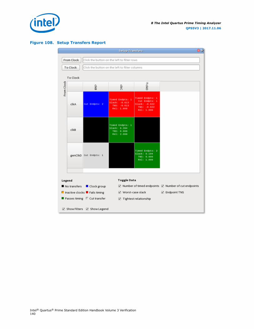
Figure 108. Setup Transfers Report
8 The Intel Quartus Prime Timing Analyzer
QPS5V3 | 2017.11.06
Intel® Quartus® Prime Standard Edition Handbook Volume 3 Verification140

Report Panels
The reports consists of:
• Filter boxes for filtering From Clock: and To Clock: values. Clicking on the FromClock: or To Clock: opens the Name Finder dialog box.
• A color coded grid which displays the clock transfer status. Status colors aredefined in the Legend.
— The clock headers list each clock with transfers in the design. If the name ofthe clock is too long, the display is truncated, but the full name can be seen ina tool tip or by resizing the clock header cell.
— Generated clocks are represented as children of the clock they are derivedfrom. A '+' icon next to a clock name indicates there are generated clocksassociated. Clicking on that clock header displays the generated clocksassociated with that clock.
• A Legend and Toggle Data section for controlling the grid display output.
• You can use the Show Filters and Show Legend controls to turn Filters andLegend on or off.
Transfer Cell Content
Each block in the grid is referred to as a transfer cell. Each transfer cell uses color andtext to display important details of the paths involved in a transfer. The color codingrepresents the following states:
• Black—No transfers. There are no paths crossing between the source anddestination clock of this cell.
• Green—Passes timing. All timing paths in this transfer, that have not been cut,meet their timing requirements.
• Red—Fails timing. One or more of the timing paths in the transfer do not meettheir timing requirements. If the transfer is between unrelated clocks, the pathslikely need to be synchronized by a synchronizer chain.
• Blue—Clock groups. The source and destination clocks of these transfers havebeen cut by means of asynchronous clock groups.
• Gray—Cut transfer. All paths in this transfer have been cut by false paths. Theresult of this is that these paths are not considered during timing analysis.
• Orange—Inactive clocks. One of the clocks involved in the transfer has beenmarked as an inactive clock (with the set_active_clocks command). Suchtransfers are ignored by the Timing Analyzer.
8 The Intel Quartus Prime Timing Analyzer
QPS5V3 | 2017.11.06
Intel® Quartus® Prime Standard Edition Handbook Volume 3 Verification141

The text in each transfer cell contains data specific to each transfer. Types of data ondisplay can be turned on or off with the Toggle Data boxes but you can mouse overany cell to see the full text. These data types are:
• Number of timed endpoints between clocks— The number of timed, endpoint-unique paths in the transfer. A path being “timed” means that it was analyzedduring timing analysis. Only paths with unique endpoints count towards this total.
• Number of cut endpoints between clocks— The number of cut endpoint-uniquepaths, instead of timed ones. These paths have been cut by either a false path orclock group assignment. Such paths are skipped during timing analysis.
• Worst-case slack between clocks— The worst-case slack among all endpoint-unique paths in the transfer.
• Total negative slack between clocks— The sum of all negative slacks among allendpoint-unique paths in this transfer.
• Tightest relationship between clocks— The lowest-valued setup / hold /recovery / removal relationship between the two clocks in this transfer, dependingon the analysis mode of the report
Transfer Cell Operations
Right-click menus allow you to perform operations on transfer cells and clock headers.When the operation is a Timing Analyzer report or SDC command, a dialog box opensprepopulated with the contents of the transfer cell.
Transfer cell operations include:
• Copy—Copies the contents of the transfer cell to the clipboard.
• Copy (include children)—Copies the name of the chose clock header, and thenames of each of its derived clocks. This option only appears for clock headerswith generated clocks.
• Report Timing—Not available for transfer cells with no valid paths (gray or blackcells).
• Report Endpoints—Not available for transfer cells with no cut paths (gray orblack cells).
• Report False Path—Not available for transfer cells with no valid paths (blackcells).
• Report Exceptions
• Report Exceptions (with clock groups)—Only available for clock grouptransfers (blue cells)
• Set False Path
• Set Multicycle Path
• Set Min Delay
• Set Max Delay
• Set Clock Uncertainty
Clock header operations include:
8 The Intel Quartus Prime Timing Analyzer
QPS5V3 | 2017.11.06
Intel® Quartus® Prime Standard Edition Handbook Volume 3 Verification142

• Copy—Copies the contents of the clock header to the clipboard.
• Expand/Collapse All Rows/Columns—Shows or hides all derived clocks in thegrid.
• Create Slack Histogram—Generates a slack histogram report for the selectedclock.
• Report Timing From/To Clock—Generates a timing report for the selectedclock. If the clock has not been expanded to display its derived clocks, all clocksderived from the selected clock are included in the timing report as well. Toprevent this, expand the clock before right-clicking it.
• Remove Clock(s)—Removes the selected clock from the design. If the clock hasnot been expanded, all clocks derived from the selected clock are also removed.
As with other Timing Analyzer reports, you may view CDC Viewer output in fourformats:
• A report panel in the Timing Analyzer
• Output in the Timing Analyzer Tcl console
• A plain-text file
• An HTML file that can be viewed in a web browser.
The Timing Analyzer report panel is the recommended format.
8.5.4.1 Report Custom CDC Viewer Command
Allows you to configure and display a customized report that creates a customizedclock domain crossing report to either a file, the Tcl console, or a report panel. Thisreport displays the results of setup, hold, recovery, and removal checks on clockdomain crossing transfers. You open this report in the Timing Analyzer by clickingReports ➤ Custom Reports ➤ Report Custom CDC Viewer.
Note: You can click the Pushpin button to keep the Report False Path, ReportTiming, and Report Endpoints dialog boxes open after you generate a report. Youcan use this feature to fine tune your report settings or quickly create additionalreports. You can click Close to close the dialog box at any time.
8 The Intel Quartus Prime Timing Analyzer
QPS5V3 | 2017.11.06
Intel® Quartus® Prime Standard Edition Handbook Volume 3 Verification143

Filter boxes for filtering From Clock: and To Clock: values. Clicking on the buttonsnext to each box opens the Name Finder dialog box.
Analysis Type
The CDC Viewer can analyze any combination of Setup, Hold, Recovery, orRemoval.
Scripting Information
Keyword: report_cdc_viewerSettings: -setup|-hold|-recovery|-removal
8 The Intel Quartus Prime Timing Analyzer
QPS5V3 | 2017.11.06
Intel® Quartus® Prime Standard Edition Handbook Volume 3 Verification144

Transfer Filtering
By default, all transfer types are included in CDC Viewer reports:
• Timed transfers—Passing or failing
• Fully cut transfers— Transfers where all paths are false paths.
• Clock groups
• Inactive clocks
You can use these options to narrow down which kinds of transfers to show, or byadding the desired transfer types as options: –timed, –fully_cut, –clock_groups, and –inactive. If none are specified, all transfer types are shown.
Scripting Information
Keyword: report_cdc_viewerSettings: -timed|-fully_cut|-clock_groups|-inactive
By default, only clocks are shown are clocks that launch or latch paths that arelaunched or latched by clocks other than themselves. Turning on Non-crossingtransfers shows clocks with transfers to or from themselves.
Scripting Information
Keyword: report_cdc_viewerSettings: -show_non_crossing
Note: In grid-formatted reports, clocks with non-crossing transfers are always shown as longas they have transfers between other clocks too.
If you specify a value in the Maximum slack limit box, only paths with slack lessthan the value are displayed. If this option is not included, paths of any slack valueare included in the report.
Scripting Information
Keyword: report_cdc_viewerSettings: -less_than_slack
Grid Options
In grid-formatted reports, the grid can be configured to display clocks as either a flatlist or in a hierarchy where generated clocks are displayed as children of the clock theyare derived from. Turn on Fold clocks on hierarchy to enable this nested display.
Scripting Information
Keyword: report_cdc_viewerSettings: -hierarchy
By default, clocks that launch or latch to no paths are not shown in grid-basedreports. You can show these clocks by turning on the Show empty transfers option.
Scripting Information
Keyword: report_cdc_viewerSettings: -show_empty
8 The Intel Quartus Prime Timing Analyzer
QPS5V3 | 2017.11.06
Intel® Quartus® Prime Standard Edition Handbook Volume 3 Verification145

Output
Allows you to specify where you want to save the report and how much detail youwant in the report. You can select one or more of the following settings:
• Report panel name— Directs the Timing Analyzer to generate a report panelwith the specified name. The default report name is Report Timing.
Scripting Information
Keyword: report_cdc_viewerSettings: -panel_name<reportname>
• Enable multi-corner reports— Allows you to enable or disable multi-cornertiming analysis. This option is on by default.
Scripting Information
Keyword: report_cdc_viewerSettings: -multi_corner
• File name— Directs the Timing Analyzer to save the report to your local disk as atext file with the specified file name. To save a report in HTML, end the filenamewith ".html".
Scripting Information
Keyword: report_cdc_viewerSettings: -file<filename>
• Format— Specifies that the generated report file is formatted as a list of clocktransfers rather than the default grid panel.
Scripting Information
Keyword: report_cdc_viewerSettings: -list
• Under File options you can specify whether the Timing Analyzer overwrites anexisting file (the default setting) or appends the content to an existing file.
Scripting Information
Keyword: report_cdc_viewerSettings: -append|-overwrite
• Console— Specifies whether the report appears as information messages in theConsole.
Scripting Information
Keyword: report_cdc_viewerSettings: -stdout
8.5.5 Analyzing Results with Report Timing
Report Timing is one of the most useful analysis tools in Timing Analyzer. Manydesigns require nothing but this command. In the Timing Analyzer, this command canbe accessed from the Tasks menu , from the Reports ➤ Custom Reports menu, orby right-clicking on nodes or assignments in Timing Analyzer.
8 The Intel Quartus Prime Timing Analyzer
QPS5V3 | 2017.11.06
Intel® Quartus® Prime Standard Edition Handbook Volume 3 Verification146
You can review all of the options for Report Timing by typing report_timing -long_help in the Timing Analyzer console.
Clocks
The From Clock and To Clock in the Clocks box are used to filter paths where theselected clock is used as the launch or latch. The pull-down menu allows you tochoose from existing clocks (although admittedly has a "limited view" for long clocknames).
Targets
The boxes in the Targets box are targets for the From Clock and To Clocksettings,and allow you to report paths with only particular endpoints. These are usually filledwith register names or I/O ports, and can be wildcarded. For example, you might usethe following to only report paths within a hierarchy of interest:
report_timing -from *|egress:egress_inst|* -to *|egress:egress_inst|* -(other options)
If the From, To, or Through boxes are empty, then the Timing Analyzer assumes youare refering to all possible targets in the device, which can also be represented with awildcard (*). The From and To options cover the majority of situations. TheThroughoption is used to limit the report for paths that pass through combinatorial logic, or aparticular pin on a cell. This is seldom used, and may not be very reliable due tocombinatorial node name changes during synthesis. Clicking the browse Browse boxafter each target opens the Name Finder dialog box to search for specific names.This is especially useful to make sure the name being entered matches nodes in thedesign, since the Name Finder can immediately show what matches a user'swildcard.
Analysis type
The Analysis type options are Setup, Hold, Recovery, or Removal.
Output
The Detail level, has the following options:
The first level is called Summary, and produces a report which only displayssummary information such as:
• Slack
• From Node
• To Node
• Launch Clock
• Latch Clock
• Relationship
• Clock Skew
• Data Delay
The Summary report is always reported with more detailed reports, so the user wouldchoose this if they want less info. A good use for summary detail is when writing thereport to a text file, where Summary can be quite brief.
8 The Intel Quartus Prime Timing Analyzer
QPS5V3 | 2017.11.06
Intel® Quartus® Prime Standard Edition Handbook Volume 3 Verification147

The next level is Path only. This report displays all the detailed information, exceptthe Data Path tab displays the clock tree as one line item. This is useful when youknow the clock tree is correct, details are not relevant. This is common for most pathswithin the FPGA. A useful data point is to look at the Clock Skew column in theSummary report, and if it's a small number, say less than +/-150ps, then the clocktree is well balanced between source and destination.
If there is clock skew, you should select the Full path option.. This breaks the clocktree out into explicit detail, showing every cell it goes through, including such thingsas the input buffer, PLL, global buffer (called CLKCTRL_), and any logic. If there isclock skew, this is where you can determine what is causing the clock skew in yourdesign. The Full path option is also recommended for I/O analysis, since only thesource clock or destination clock is inside the FPGA, and therefore its delay plays acritical role in meeting timing.
The Data Path tab of a detailed report gives the delay break-downs, but there is alsouseful information in the Path Summary and Statistics tabs, while the Waveformtab is useful to help visualize the Data Path analysis. I would suggest taking a fewminutes to look at these in the user's design. The whole analysis takes some time toget comfortable with, but hopefully is clear in what it's doing.
Enable multi corner reports allows you to enable or disable multi-corner timinganalysis. This option is on by default.
Report Timing also has the Report panel name, which displays the name used inTiming Analyzer's Report section. There is also an optional File name switch, whichallows you to write the information to a file. If you append .htm as a suffix, the TimingAnalyzer produces the report as HTML. The File options radio buttons allow you tochoose between Overwrite and Append when saving the file.
Paths
The default value for Report number of paths is 10. Two endpoints may have a lotof combinatorial logic between them and might have many different paths. Likewise, asingle destination may have hundreds of paths leading to it. Because of this, youmight list hundreds of paths, many of which have the same destination and mighthave the same source. By turning on Pairs only you can list only one path for eachpair of source and destination. An even more powerful way to filter the report is limitthe Maximum number of paths per endpoints. You can also filter paths by entering avalue in the Maximum slack limit field.
Tcl command
Finally, at the bottom is the Tcl commandfield, which displays the Tcl syntax of whatis run in Timing Analyzer. You can edit this directly before running the Report Timingcommand.
Note:
A useful addition is to addis the -false_path option to the command line string.With this option, only false paths are listed. A false path is any path where the launchand latch clock have been defined, but the path was cut with either aset_false_path assignment or set_clock_groups_assignment. Paths wherethe launch or latch clock was never constrained are not considered false paths. Thisoption is useful to see if a false path assignment worked and what paths it covers, or
8 The Intel Quartus Prime Timing Analyzer
QPS5V3 | 2017.11.06
Intel® Quartus® Prime Standard Edition Handbook Volume 3 Verification148

to look for paths between clock domains that should not exist. The Task window'sReport False Path custom report is nothing more than Report Timing with the -false_path flag enabled.
8.5.6 Correlating Constraints to the Timing Report
A critical part of timing analysis is how timing constraints appear in the ReportTiming analysis. Most constraints only affect the launch and latch edges. Specifically,create_clock and create_generated_clock create clocks with defaultrelationships. The command set_multicycle_path modifies those defaultrelationships, while set_max_delay and set_min_delay are low-level overridesthat explicitly tell Timing Analyzer what the launch and latch edges should be.
The following figures are from an example of the output of Report Timing on aparticular path.
Initially, the design features a clock driving the source and destination registers with aperiod of 10ns. This results in a setup relationship of 10ns (launch edge = 0ns, latchedge = 10ns) and hold relationship of 0ns (launch edge = 0ns, latch edge = 0ns) fromthe command:
create_clock -name clocktwo -period 10.000 [get_ports {clk2}]
8 The Intel Quartus Prime Timing Analyzer
QPS5V3 | 2017.11.06
Intel® Quartus® Prime Standard Edition Handbook Volume 3 Verification149

Figure 109. Setup Relationship 10ns, Hold Relationship 0ns
In the next figure, using set_multicycle_path adds multicycles to relax the setuprelationship, or open the window, making the setup relationship 20ns while the holdrelationship is still 0ns:
set_multicycle_path -from clocktwo -to clocktwo -setup -end 2set_multicycle_path -from clocktwo -to clocktwo -hold -end 1
8 The Intel Quartus Prime Timing Analyzer
QPS5V3 | 2017.11.06
Intel® Quartus® Prime Standard Edition Handbook Volume 3 Verification150

Figure 110. Setup Relationship 20ns
In the last figure, using the set_max_delay and set_min_delay constraints letsyou explicitly override the relationships. Note that the only thing changing for thesedifferent constraints is the Launch Edge Time and Latch Edge Times for setup and holdanalysis. Every other line item comes from delays inside the FPGA and are static for agiven fit. Whenever analyzing how your constraints affect the timing requirements,this is the place to look.
8 The Intel Quartus Prime Timing Analyzer
QPS5V3 | 2017.11.06
Intel® Quartus® Prime Standard Edition Handbook Volume 3 Verification151

Figure 111. Using set_max_delay and set_min_delay
For I/O, this all holds true except we must add in the -max and -min values. They aredisplayed as iExt or oExt in the Type column. An example would be an output portwith a set_output_delay -max 1.0 and set_output_delay -min -0.5:
Once again, the launch and latch edge times are determined by the clockrelationships, multicycles and possibly set_max_delay or set_min_delayconstraints. The value of set_output_delay is also added in as an oExt value. Foroutputs this value is part of the Data Required Path, since this is the external part ofthe analysis. The setup report on the left subtracts the -max value, making the setuprelationship harder to meet, since we want the Data Arrival Path to be shorter thanthe Data Required Path. The -min value is also subtracted, which is why a negativenumber makes hold timing more restrictive, since we want the Data Arrival Path tobe longer than the Data Required Path.
Related Links
Relaxing Setup with set_multicyle_path on page 111
8 The Intel Quartus Prime Timing Analyzer
QPS5V3 | 2017.11.06
Intel® Quartus® Prime Standard Edition Handbook Volume 3 Verification152

8.6 Constraining and Analyzing with Tcl Commands
You can use Tcl commands from the Intel Quartus Prime software Tcl ApplicationProgramming Interface (API) to constrain, analyze, and collect information for yourdesign. This section focuses on executing timing analysis tasks with Tcl commands;however, you can perform many of the same functions in the Timing Analyzer GUI.SDC commands are Tcl commands for constraining a design. SDC extensioncommands provide additional constraint methods and are specific to the TimingAnalyzer. Additional Timing Analyzer commands are available for controlling timinganalysis and reporting. These commands are contained in the following Tcl packagesavailable in the Intel Quartus Prime software:
• ::quartus::sta
• ::quartus::sdc
• ::quartus::sdc_ext
Related Links
• ::quartus::staFor more information about Timing Analyzer Tcl commands and a complete listof commands, refer to Intel Quartus Prime Help.
• ::quartus::sdcFor more information about standard SDC commands and a complete list ofcommands, refer to Intel Quartus Prime Help.
• ::quartus::sdc_extFor more information about Intel FPGA extensions of SDC commands and acomplete list of commands, refer to Intel Quartus Prime Help.
8.6.1 Collection Commands
The Timing Analyzer Tcl commands often return data in an object called a collection.In your Tcl scripts you can iterate over the values in collections to access datacontained in them. The software returns collections instead of Tcl lists becausecollections are more efficient than lists for large sets of data.
The Timing Analyzer supports collection commands that provide easy access to ports,pins, cells, or nodes in the design. Use collection commands with any constraints or Tclcommands specified in the Timing Analyzer.
Table 33. SDC Collection Commands
Command Description of the collection returned
all_clocks All clocks in the design.
all_inputs All input ports in the design.
all_outputs All output ports in the design.
all_registers All registers in the design.
get_cells Cells in the design. All cell names in the collection match the specified pattern. Wildcards can be usedto select multiple cells at the same time.
get_clocks Lists clocks in the design. When used as an argument to another command, such as the -from or -toof set_multicycle_path, each node in the clock represents all nodes clocked by the clocks in thecollection. The default uses the specific node (even if it is a clock) as the target of a command.
continued...
8 The Intel Quartus Prime Timing Analyzer
QPS5V3 | 2017.11.06
Intel® Quartus® Prime Standard Edition Handbook Volume 3 Verification153

Command Description of the collection returned
get_nets Nets in the design. All net names in the collection match the specified pattern. You can use wildcards toselect multiple nets at the same time.
get_pins Pins in the design. All pin names in the collection match the specified pattern. You can use wildcards toselect multiple pins at the same time.
get_ports Ports (design inputs and outputs) in the design.
You can also examine collections and experiment with collections using wildcards inthe Timing Analyzer by clicking Name Finder from the View menu.
8.6.1.1 Wildcard Characters
To apply constraints to many nodes in a design, use the “*” and “?” wildcardcharacters. The “*” wildcard character matches any string; the “?” wildcard charactermatches any single character.
If you make an assignment to node reg*, the Timing Analyzer searches for andapplies the assignment to all design nodes that match the prefix reg with any numberof following characters, such as reg, reg1, reg[2], regbank, and reg12bank.
If you make an assignment to a node specified as reg?, the Timing Analyzer searchesand applies the assignment to all design nodes that match the prefix reg and anysingle character following; for example, reg1, rega, and reg4.
8.6.1.2 Adding and Removing Collection Items
Wildcards used with collection commands define collection items identified by thecommand. For example, if a design contains registers named src0, src1, src2, anddst0, the collection command [get_registers src*] identifies registers src0,src1, and src2, but not register dst0. To identify register dst0, you must use anadditional command, [get_registers dst*]. To include dst0, you could alsospecify a collection command [get_registers {src* dst*}].
To modify collections, use the add_to_collection and remove_from_collectioncommands. The add_to_collection command allows you to add additional items toan existing collection.
add_to_collection Command
add_to_collection <first collection> <second collection>
Note: The add_to_collection command creates a new collection that is the union of thetwo specified collections.
The remove_from_collection command allows you to remove items from anexisting collection.
remove_from_collection Command
remove_from_collection <first collection> <second collection>
You can use the following code as an example for using add_to_collection foradding items to a collection.
8 The Intel Quartus Prime Timing Analyzer
QPS5V3 | 2017.11.06
Intel® Quartus® Prime Standard Edition Handbook Volume 3 Verification154

Adding Items to a Collection
#Setting up initial collection of registersset regs1 [get_registers a*]#Setting up initial collection of keepersset kprs1 [get_keepers b*]#Creating a new set of registers of $regs1 and $kprs1set regs_union [add_to_collection $kprs1 $regs1]#OR#Creating a new set of registers of $regs1 and b* #Note that the new collection appends only registers with name b*# not all keepersset regs_union [add_to_collection $regs1 b*]
In the Intel Quartus Prime software, keepers are I/O ports or registers. A SDC file thatincludes get_keepers can only be processed as part of the Timing Analyzer flow andis not compatible with third-party timing analysis flows.
Related Links
• add_to_collection
• remove_from_collectionFor more information about theadd_to_collection andremove_from_collection commands, refer to Intel Quartus Prime Help.
8.6.1.3 Getting Other Information about Collections
You can display the contents of a collection with the query_collection command.Use the -report_format option to return the contents in a format of one elementper line. The -list_format option returns the contents in a Tcl list.
query_collection -report_format -all $regs_union
Use the get_collection_size command to return the size of a collection; thenumber of items it contains. If your collection is in a variable named col, it is moreefficient to use set num_items [get_collection_size $col] than setnum_items [llength [query_collection -list_format $col]]
8.6.1.4 Using the get_pins Command
The get_pins command supports options that control the matching behavior of thewildcard character (*). Depending on the combination of options you use, you canmake the wildcard character (*) respect or ignore individual levels of hierarchy, whichare indicated by the pipe character (|). By default, the wildcard character (*) matchesonly a single level of hierarchy.
These examples filter the following node and pin names to illustrate function:
• foo (a hierarchy level named foo)
• foo|dataa (an input pin in the instance foo)
• foo|datab (an input pin in the instance foo)
• foo|bar (a combinational node named bar in the foo instance)
• foo|bar|datac (an input pin to the combinational node named bar)
• foo|bar|datad (an input pin to the combinational node bar)
8 The Intel Quartus Prime Timing Analyzer
QPS5V3 | 2017.11.06
Intel® Quartus® Prime Standard Edition Handbook Volume 3 Verification155

Table 34. Sample Search Strings and Search Results
Search String Search Result
get_pins *|dataa foo|dataa
get_pins *|datac <empty>(3)
get_pins *|*|datac foo|bar|datac
get_pins foo*|* foo|dataa, foo|datab
get_pins -hierarchical *|*|datac <empty>(3)
get_pins -hierarchical foo|* foo|dataa, foo|datab
get_pins -hierarchical *|datac foo|bar|datac
get_pins -hierarchical foo|*|datac <empty>(3)
get_pins -compatibility_mode *|datac foo|bar|datac (4)
get_pins -compatibility_mode *|*|datac foo|bar|datac
The default method separates hierarchy levels of instances from nodes and pins withthe pipe character (|). A match occurs when the levels of hierarchy match, and thestring values including wildcards match the instance and/or pin names. For example,the command get_pins <instance_name>|*|datac returns all the datac pinsfor registers in a given instance. However, the command get_pins *|datac returnsand empty collection because the levels of hierarchy do not match.
Use the -hierarchical matching scheme to return a collection of cells or pins in allhierarchies of your design.
For example, the command get_pins -hierarchical *|datac returns all thedatac pins for all registers in your design. However, the command get_pins -hierarchical *|*|datac returns an empty collection because more than one pipecharacter (|) is not supported.
The -compatibility_mode option returns collections matching wildcard stringsthrough any number of hierarchy levels. For example, an asterisk can match a pipecharacter when using -compatibility_mode.
8.6.2 Identifying the Intel Quartus Prime Software Executable from theSDC File
To identify which Intel Quartus Prime software executable is currently running you canuse the $::TimeQuestInfo(nameofexecutable) variable from within an SDC file.This technique is most commonly used when you want to use an overconstraint tocause the Fitter to work harder on a particular path or set of paths in the design.
(3) The search result is <empty> because the wildcard character (*) does not match more thanone hierarchy level, indicated by a pipe character (|), by default. This command would matchany pin named datac in instances at the top level of the design.
(4) When you use -compatibility_mode, pipe characters (|) are not treated as specialcharacters when used with wildcards.
8 The Intel Quartus Prime Timing Analyzer
QPS5V3 | 2017.11.06
Intel® Quartus® Prime Standard Edition Handbook Volume 3 Verification156

Identifying the Intel Quartus Prime Executable
#Identify which executable is running:set current_exe $::TimeQuestInfo(nameofexecutable)if { [string equal $current_exe "quartus_fit"] } { #Apply .sdc assignments for Fitter executable here} else { #Apply .sdc assignments for non-Fitter executables here}if { ! [string equal "quartus_sta" $::TimeQuestInfo(nameofexecutable)] } { #Apply .sdc assignments for non-TimeQuest executables here} else { #Apply .sdc assignments for TimeQuest executable here}
Examples of different executable names are quartus_map for Analysis & Synthesis,quartus_fit for Fitter, and quartus_sta for the Timing Analyzer.
8.6.3 Locating Timing Paths in Other Tools
You can locate paths and elements from the Timing Analyzer to other tools in the IntelQuartus Prime software.
Use the Locate or Locate Path command in the Timing Analyzer GUI or the locatecommand in the Tcl console in the Timing Analyzer GUI. Right-click most paths ornode names in the Timing Analyzer GUI to access the Locate or Locate Path options.
The following commands are examples of how to locate the ten paths with the worsttiming slack from Timing Analyzer to the Technology Map Veiwer and locate allports matching data* in the Chip Planner.
Example 13. Locating from the Timing Analyzer
# Locate in the Technology Map Viewer the ten paths with the worst slacklocate [get_timing_paths -npaths 10] -tmv# locate all ports that begin with data in the Chip Plannerlocate [get_ports data*] -chip
Related Links
locateFor more information on this command, refer to Intel Quartus Prime Help.
8.7 Generating Timing Reports
The Timing Analyzer provides real-time static timing analysis result reports. TheTiming Analyzer does not automatically generate most reports; you must create eachreport individually in the Timing Analyzer GUI or with command-line commands. Youcan customize in which report to display specific timing information, excluding fieldsthat are not required.
Some of the different command-line commands you can use to generate reports in theTiming Analyzer and the equivalent reports shown in the Timing Analyzer GUI.
8 The Intel Quartus Prime Timing Analyzer
QPS5V3 | 2017.11.06
Intel® Quartus® Prime Standard Edition Handbook Volume 3 Verification157

Table 35. Timing Analyzer Reports
Command-Line Command Report
report_timing Timing report
report_exceptions Exceptions report
report_clock_transfers Clock Transfers report
report_min_pulse_width Minimum Pulse Width report
report_ucp Unconstrained Paths report
During compilation, the Intel Quartus Prime software generates timing reports ondifferent timing areas in the design. You can configure various options for the TimingAnalyzer reports generated during compilation.
You can also use the TIMEQUEST_REPORT_WORST_CASE_TIMING_PATHS assignmentto generate a report of the worst-case timing paths for each clock domain. This reportcontains worst-case timing data for setup, hold, recovery, removal, and minimumpulse width checks.
Use the TIMEQUEST_REPORT_NUM_WORST_CASE_TIMING_PATHS assignment tospecify the number of paths to report for each clock domain.
An example of how to use the TIMEQUEST_REPORT_WORST_CASE_TIMING_PATHSand TIMEQUEST_REPORT_NUM_WORST_CASE_TIMING_PATHS assignments inthe .qsf to generate reports.
For more information about the options you can set to customize Timing Analyzerreports, refer to the Timing Analyzer page in Intel Quartus Prime Help.
For more information about timing closure recommendations, refer to the TimingClosure and Optimization page of the Intel Quartus Prime Handbook, Volume 2.
Generating Worst-Case Timing Reports
# Enable Worst-Case Timing Reportset_global_assignment -name TIMEQUEST_REPORT_WORST_CASE_TIMING_PATHS ON# Report 10 paths per clock domainset_global_assignment -name TIMEQUEST_REPORT_NUM_WORST_CASE_TIMING_PATHS 10
Fmax Summary Report panel
The Fmax Summary Report panel lists the maximum frequency of each clock in yourdesign. In some designs you may see a note indicating "Limit due to hold check.Typically, Fmax is not limited by hold checks, because they are often same-edgerelationships, and therefore independent of clock frequency, for example, launch = 0,latch = 0. However, if you have an inverted clock transfer, or a multicycle transfersuch as setup=2, hold=0, then the hold relationship is no longer a same-edge transferand changes as the clock frequency changes. The value in the Restricted Fmaxcolumn incorporates limits due to hold time checks in the situations describedpreviously, as well as minimum period and pulse width checks. If hold checks limit theFmax more than setup checks, that is indicated in the Note: column as "Limit due tohold check".
8 The Intel Quartus Prime Timing Analyzer
QPS5V3 | 2017.11.06
Intel® Quartus® Prime Standard Edition Handbook Volume 3 Verification158

Related Links
• ::quartus::staIn Intel Quartus Prime Help
• Timing Analyzer PageFor more information about the options you can set to customize TimingAnalyzer reports.
• Timing Closure and OptimizationIn Intel Quartus Prime Standard Edition Handbook Volume 2
8.8 Document Revision History
Table 36. Document Revision History
Date Version Changes
2015.11.02 15.1.0 • Changed instances of Quartus II to Quartus Prime.• Updated information on using Intel Arria 10 devices with enhanced timing algorithms.
2015.05.04 15.0.0 Added and updated contents in support of new timing algorithms for Arria 10:• Enhanced Timing Analysis for Arria 10• Maximum Skew (set_max_skew command)• Net Delay (set_net_delay command)• Create Generated Clocks (clock-as-data example)
2014.12.15 14.1.0 Major reorganization. Revised and added content to the following topic areas:• Timing Constraints• Create Clocks and Clock Constraints• Creating Generated Clocks• Creating Clock Groups• Clock Uncertainty• Running the Timing Analyzer• Generating Timing Reports• Understanding Results• Constraining and Analyzing with Tcl Commands
August 2014 14.0a10.0
Added command line compliation requirements for Arria 10 devices.
June 2014 14.0.0 • Minor updates.• Updated format.
November 2013 13.1.0 • Removed HardCopy device information.
June 2012 12.0.0 • Reorganized chapter.• Added “Creating a Constraint File from Intel Quartus Prime Templates with the Intel Quartus
Prime Text Editor” section on creating an SDC constraints file with the Insert Templatedialog box.
• Added “Identifying the Intel Quartus Prime Software Executable from the SDC File” section.• Revised multicycle exceptions section.
November 2011 11.1.0 • Consolidated content from the Best Practices for the Intel Quartus Prime Timing Analyzerchapter.
• Changed to new document template.
May 2011 11.0.0 • Updated to improve flow. Minor editorial updates.
December 2010 10.1.0 • Changed to new document template.• Revised and reorganized entire chapter.• Linked to Intel Quartus Prime Help.
continued...
8 The Intel Quartus Prime Timing Analyzer
QPS5V3 | 2017.11.06
Intel® Quartus® Prime Standard Edition Handbook Volume 3 Verification159

Date Version Changes
July 2010 10.0.0 Updated to link to content on SDC commands and the Timing Analyzer GUI in Intel QuartusPrime Help.
November 2009 9.1.0 Updated for the Intel Quartus Prime software version 9.1, including:• Added information about commands for adding and removing items from collections• Added information about the set_timing_derate and report_skew commands• Added information about worst-case timing reporting• Minor editorial updates
November 2008 8.1.0 Updated for the Intel Quartus Prime software version 8.1, including:• Added the following sections:
“set_net_delay” on page 7–42“Annotated Delay” on page 7–49“report_net_delay” on page 7–66
• Updated the descriptions of the -append and -file <name> options in tables throughoutthe chapter
• Updated entire chapter using 8½” × 11” chapter template• Minor editorial updates
Related Links
Documentation ArchiveFor previous versions of the Intel Quartus Prime Handbook, search thedocumentation archives.
8 The Intel Quartus Prime Timing Analyzer
QPS5V3 | 2017.11.06
Intel® Quartus® Prime Standard Edition Handbook Volume 3 Verification160

9 Power AnalysisThe Intel Quartus Prime Power Analysis tools allow you to estimate device powerconsumption accurately.
As designs grow larger and process technology continues to shrink, power becomes anincreasingly important design consideration. When designing a PCB, you mustestimate the power consumption of a device accurately to develop an appropriatepower budget, and to design the power supplies, voltage regulators, heat sink, andcooling system.
The following figure shows the Power Analysis tools ability to estimate powerconsumption from early design concept through design implementation.
Figure 112. Power Analysis From Design Concept Through Design Implementation
User InputQuartus Prime Design Profile
Placement and RoutingResults
SimulationResults
Early Power Estimator
Power Analysis Input
Estim
ation
Accu
racy
Power Analyzer
Design ImplementationDesign Concept
Lowe
rHi
gher
For the majority of the designs, the Power Analyzer and the EPE spreadsheet have thefollowing accuracy after the power models are final:
• Power Analyzer—±20% from silicon, assuming that the Power Analyzer uses theValue Change Dump File (.vcd) generated toggle rates.
• EPE spreadsheet— ±20% from the Power Analyzer results using .vcd generatedtoggle rates. 90% of EPE designs (using .vcd generated toggle rates exportedfrom PPPA) are within ±30% silicon.
The toggle rates are derived using the Power Analyzer with a .vcd file generated froma gate level simulation representative of the system operation.
QPS5V3 | 2017.11.06
Intel Corporation. All rights reserved. Intel, the Intel logo, Altera, Arria, Cyclone, Enpirion, MAX, Nios, Quartusand Stratix words and logos are trademarks of Intel Corporation or its subsidiaries in the U.S. and/or othercountries. Intel warrants performance of its FPGA and semiconductor products to current specifications inaccordance with Intel's standard warranty, but reserves the right to make changes to any products and servicesat any time without notice. Intel assumes no responsibility or liability arising out of the application or use of anyinformation, product, or service described herein except as expressly agreed to in writing by Intel. Intelcustomers are advised to obtain the latest version of device specifications before relying on any publishedinformation and before placing orders for products or services.*Other names and brands may be claimed as the property of others.
ISO9001:2008Registered

9.1 Types of Power Analyses
Understanding the uses of power analysis and the factors affecting power consumptionhelps you to use the Power Analyzer effectively. Power analysis meets the followingsignificant planning requirements:
• Thermal planning—Thermal power is the power that dissipates as heat from theFPGA. You must use a heatsink or fan to act as a cooling solution for your device.The cooling solution must be sufficient to dissipate the heat that the devicegenerates. The computed junction temperature must fall within normal devicespecifications.
• Power supply planning—Power supply is the power needed to run your device.Power supplies must provide adequate current to support device operation.
Note: For power supply planning, use the EPE at the early stages of your designcycle. Use the Power Analyzer reports when your design is complete to getan estimate of your design power requirement.
The two types of analyses are closely related because much of the power supplied tothe device dissipates as heat from the device; however, in some situations, the twotypes of analyses are not identical. For example, if you use terminated I/O standards,some of the power drawn from the power supply of the device dissipates intermination resistors rather than in the device.
Power analysis also addresses the activity of your design over time as a factor thatimpacts the power consumption of the device. The static power (PSTATIC) is the thermalpower dissipated on chip, independent of user clocks. PSTATIC includes the leakagepower from all FPGA functional blocks, except for I/O DC bias power and transceiverDC bias power, which are accounted for in the I/O and transceiver sections. Dynamicpower is the additional power consumption of the device due to signal activity ortoggling.
9.1.1 Differences between the EPE and the Intel Quartus Prime PowerAnalyzer
The following table lists the differences between the EPE and the Intel Quartus PrimePower Analyzer.
Table 37. Comparison of the EPE and Intel Quartus Prime Power Analyzer
Characteristic EPE Intel Quartus Prime PowerAnalyzer
Phase in the design cycle Any time, but it is recommended to use Intel Quartus PrimePower Analyzer for post-fit power analysis.
Post-fit
Tool requirements Spreadsheet program The Intel Quartus Primesoftware
Accuracy Medium Medium to very high
Data inputs • Resource usage estimates• Clock requirements• Environmental conditions• Toggle rate
• Post-fit design• Clock requirements• Signal activity defaults• Environmental conditions
continued...
9 Power Analysis
QPS5V3 | 2017.11.06
Intel® Quartus® Prime Standard Edition Handbook Volume 3 Verification162

Characteristic EPE Intel Quartus Prime PowerAnalyzer
• Register transfer level(RTL) simulation results(optional)
• Post-fit simulation results(optional)
• Signal activities per nodeor entity (optional)
Data outputs • Total thermal power dissipation• Thermal static power• Thermal dynamic power• Off-chip power dissipation• Current drawn from voltage supplies
• Total thermal power• Thermal static power• Thermal dynamic power• Thermal I/O power• Thermal power by design
hierarchy• Thermal power by block
type• Thermal power dissipation
by clock domain• Off-chip (non-thermal)
power dissipation• Device supply currents
The result of the Power Analyzer is only an estimation of power. Intel FPGA does notrecommend using the result as a specification. The purpose of the estimation is tohelp you establish guidelines for the power budget of your design. It is important thatyou verify the actual power during device operation as the information is sensitive tothe actual device design and the environmental operating conditions.
Note: The Power Analyzer does not include the transceiver power for features that can onlybe enabled through dynamic reconfiguration (DFE, ADCE/AEQ, Eye Viewer). Use theEPE to estimate the incremental power consumption by these features.
9.2 Factors Affecting Power Consumption
Understanding the following factors that affect power consumption allows you to usethe Power Analyzer and interpret its results effectively:
• Device Selection
• Environmental Conditions
• Device Resource Usage
• Signal Activities
9.2.1 Device Selection
Device families have different power characteristics. Many parameters affect thedevice family power consumption, including choice of process technology, supplyvoltage, electrical design, and device architecture.
(5) EPE and Power Analyzer outputs vary by device family. For more information, refer to thedevice-specific Early Power Estimators (EPE) and Power Analyzer Page and Power AnalyzerReports in the Intel Quartus Prime Help.
9 Power Analysis
QPS5V3 | 2017.11.06
Intel® Quartus® Prime Standard Edition Handbook Volume 3 Verification163

Power consumption also varies in a single device family. A larger device consumesmore static power than a smaller device in the same family because of its largertransistor count. Dynamic power can also increase with device size in devices thatemploy global routing architectures.
The choice of device package also affects the ability of the device to dissipate heat.This choice can impact your required cooling solution choice to comply to junctiontemperature constraints.
Process variation can affect power consumption. Process variation primarily impactsstatic power because sub-threshold leakage current varies exponentially with changesin transistor threshold voltage. Therefore, you must consult device specifications forstatic power and not rely on empirical observation. Process variation has a weak effecton dynamic power.
9.2.2 Environmental Conditions
Operating temperature primarily affects device static power consumption. Higherjunction temperatures result in higher static power consumption. The device thermalpower and cooling solution that you use must result in the device junctiontemperature remaining within the maximum operating range for the device. The mainenvironmental parameters affecting junction temperature are the cooling solution andambient temperature.
The following table lists the environmental conditions that could affect powerconsumption.
Table 38. Environmental Conditions that Could Affect Power Consumption
EnvironmentalConditions
Description
Airflow A measure of how quickly the device removes heated air from the vicinity of the device andreplaces it with air at ambient temperature.You can either specify airflow as “still air” when you are not using a fan, or as the linear feetper minute rating of the fan in the system. Higher airflow decreases thermal resistance.
Heat Sink and ThermalCompound
A heat sink allows more efficient heat transfer from the device to the surrounding areabecause of its large surface area exposed to the air. The thermal compound that interfaces theheat sink to the device also influences the rate of heat dissipation. The case-to-ambientthermal resistance (θCA) parameter describes the cooling capacity of the heat sink and thermalcompound employed at a given airflow. Larger heat sinks and more effective thermalcompounds reduce θCA.
Junction Temperature The junction temperature of a device is equal to:TJunction = TAmbient + PThermal · θJA
in which θJA is the total thermal resistance from the device transistors to the environment,having units of degrees Celsius per watt. The value θJA is equal to the sum of the junction-to-case (package) thermal resistance (θJC), and the case-to-ambient thermal resistance (θCA) ofyour cooling solution.
Board Thermal Model The junction-to-board thermal resistance (θJB) is the thermal resistance of the path throughthe board, having units of degrees Celsius per watt. To compute junction temperature, you canuse this board thermal model along with the board temperature, the top-of-chip θJA andambient temperatures.
9 Power Analysis
QPS5V3 | 2017.11.06
Intel® Quartus® Prime Standard Edition Handbook Volume 3 Verification164
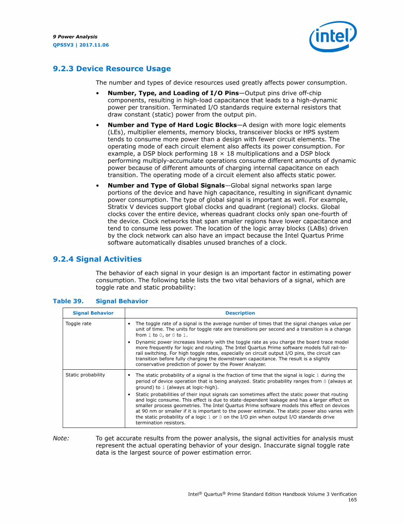
9.2.3 Device Resource Usage
The number and types of device resources used greatly affects power consumption.
• Number, Type, and Loading of I/O Pins—Output pins drive off-chipcomponents, resulting in high-load capacitance that leads to a high-dynamicpower per transition. Terminated I/O standards require external resistors thatdraw constant (static) power from the output pin.
• Number and Type of Hard Logic Blocks—A design with more logic elements(LEs), multiplier elements, memory blocks, transceiver blocks or HPS systemtends to consume more power than a design with fewer circuit elements. Theoperating mode of each circuit element also affects its power consumption. Forexample, a DSP block performing 18 × 18 multiplications and a DSP blockperforming multiply-accumulate operations consume different amounts of dynamicpower because of different amounts of charging internal capacitance on eachtransition. The operating mode of a circuit element also affects static power.
• Number and Type of Global Signals—Global signal networks span largeportions of the device and have high capacitance, resulting in significant dynamicpower consumption. The type of global signal is important as well. For example,Stratix V devices support global clocks and quadrant (regional) clocks. Globalclocks cover the entire device, whereas quadrant clocks only span one-fourth ofthe device. Clock networks that span smaller regions have lower capacitance andtend to consume less power. The location of the logic array blocks (LABs) drivenby the clock network can also have an impact because the Intel Quartus Primesoftware automatically disables unused branches of a clock.
9.2.4 Signal Activities
The behavior of each signal in your design is an important factor in estimating powerconsumption. The following table lists the two vital behaviors of a signal, which aretoggle rate and static probability:
Table 39. Signal Behavior
Signal Behavior Description
Toggle rate • The toggle rate of a signal is the average number of times that the signal changes value perunit of time. The units for toggle rate are transitions per second and a transition is a changefrom 1 to 0, or 0 to 1.
• Dynamic power increases linearly with the toggle rate as you charge the board trace modelmore frequently for logic and routing. The Intel Quartus Prime software models full rail-to-rail switching. For high toggle rates, especially on circuit output I/O pins, the circuit cantransition before fully charging the downstream capacitance. The result is a slightlyconservative prediction of power by the Power Analyzer.
Static probability • The static probability of a signal is the fraction of time that the signal is logic 1 during theperiod of device operation that is being analyzed. Static probability ranges from 0 (always atground) to 1 (always at logic-high).
• Static probabilities of their input signals can sometimes affect the static power that routingand logic consume. This effect is due to state-dependent leakage and has a larger effect onsmaller process geometries. The Intel Quartus Prime software models this effect on devicesat 90 nm or smaller if it is important to the power estimate. The static power also varies withthe static probability of a logic 1 or 0 on the I/O pin when output I/O standards drivetermination resistors.
Note: To get accurate results from the power analysis, the signal activities for analysis mustrepresent the actual operating behavior of your design. Inaccurate signal toggle ratedata is the largest source of power estimation error.
9 Power Analysis
QPS5V3 | 2017.11.06
Intel® Quartus® Prime Standard Edition Handbook Volume 3 Verification165

9.3 Power Analyzer Flow
The Power Analyzer supports accurate power estimations by allowing you to specifythe important design factors affecting power consumption. The following figure showsthe high-level Power Analyzer flow.
Figure 113. Power Analyzer High-Level Flow
Power AnalyzerOperatingConditions
User Design(Post-Fit)
Power AnalysisReport
SignalActivities
Operating condition specifications are available for only some device families. For more information, refer to “Performing Power Analysis with the Power Analyzer” in Quartus Prime Help.
To obtain accurate I/O power estimates, the Power Analyzer requires you to synthesizeyour design and then fit your design to the target device. You must specify theelectrical standard on each I/O cell and the board trace model on each I/O standard inyour design.
9.3.1 Operating Settings and Conditions
You can specify device power characteristics, operating voltage conditions, andoperating temperature conditions for power analysis in the Intel Quartus Primesoftware.
On the Operating Settings and Conditions page of the Settings dialog box, youcan specify whether the device has typical power consumption characteristics ormaximum power consumption characteristics.
On the Voltage page of the Settings dialog box, you can view the operating voltageconditions for each power rail in the device, and specify supply voltages for power railswith selectable supply voltages.
9 Power Analysis
QPS5V3 | 2017.11.06
Intel® Quartus® Prime Standard Edition Handbook Volume 3 Verification166

Note: The Intel Quartus Prime Fitter may override some of the supply voltages settingsspecified in this chapter. For example, supply voltages for some transceiver powersupplies depend on the data rate used. If the Fitter detects that voltage required isdifferent from the one specified in the Voltage page, it will automatically set thecorrect voltage for relevant rails. The Intel Quartus Prime Power Analyzer usesvoltages selected by the Fitter if they conflict with the settings specified in theVoltage page.
On the Temperature page of the Settings dialog box, you can specify the thermaloperating conditions of the device.
Related Links
• Operating Settings and Conditions Page (Settings Dialog Box)
• Voltage Page (Settings Dialog Box)
• Temperature Page (Settings Dialog Box)
9.3.2 Signal Activities Data Sources
The Power Analyzer provides a flexible framework for specifying signal activities. Theframework reflects the importance of using representative signal-activity data duringpower analysis. Use the following sources to provide information about signal activity:
• Simulation results
• User-entered node, entity, and clock assignments
• User-entered default toggle rate assignment
• Vectorless estimation
The Power Analyzer allows you to mix and match the signal-activity data sources on asignal-by-signal basis. The following figure shows the priority scheme applied to eachsignal.
Figure 114. Signal-Activity Data Source Priority Scheme
Node or entityassignment?
Simulationdata?
Is primaryinput?
Vectorless supported and
enabled?Use vectorless
estimation
Use defaultassignment
Use simulationdata
Use node orentity assignment
Start
Yes Yes Yes No
YesNoNoNo
9 Power Analysis
QPS5V3 | 2017.11.06
Intel® Quartus® Prime Standard Edition Handbook Volume 3 Verification167

9.3.2.1 Simulation Results
The Power Analyzer directly reads the waveforms generated by a design simulation.Static probability and toggle rate can be calculated for each signal from the simulationwaveform. Power analysis is most accurate when you use representative input stimulito generate simulations.
The Power Analyzer reads results generated by the following simulators:
• ModelSim
• ModelSim - Intel FPGA Edition
• QuestaSim
• Active-HDL
• NCSim
• VCS
• VCS MX
• Riviera-PRO
Signal activity and static probability information are derived from a Verilog ValueChange Dump File (.vcd). For more information, refer to Signal Activities on page165.
For third-party simulators, use the EDA Tool Settings to specify the GenerateValue Change Dump (VCD) file script option in the Simulation page of the Settingsdialog box. These scripts instruct the third-party simulators to generate a .vcd thatencodes the simulated waveforms. The Intel Quartus Prime Power Analyzer reads thisfile directly to derive the toggle rate and static probability data for each signal.
Third-party EDA simulators, other than those listed, can generate a .vcd that you canuse with the Power Analyzer. For those simulators, you must manually create asimulation script to generate the appropriate .vcd.
Note: You can use a .saf created for power analysis to optimize your design for powerduring fitting by utilizing the appropriate settings in the power optimization list,available from Assignments ➤ Settings ➤ Compiler Settings ➤ AdvancedSettings (Fitter).
9.4 Using Simulation Files in Modular Design Flows
A common design practice is to create modular or hierarchical designs in which youdevelop each design entity separately, and then instantiate these modules in a higher-level entity to form a complete design. You can perform simulation on a completedesign or on each module for verification. The Power Analyzer supports modulardesign flows when reading the signal activities from simulation files. The followingfigure shows an example of a modular design flow.
9 Power Analysis
QPS5V3 | 2017.11.06
Intel® Quartus® Prime Standard Edition Handbook Volume 3 Verification168

Figure 115. Modular Simulation Flow
ParameterInput
VideoProcessing
ColumnDriver
MemoryInterface
VideoSource
InterfaceTimingControl
system.vcdvideo_gizmo.vcdoutput_driver.vcdvideo_input.vcd
When specifying a simulation file (a .vcd), the software provides support to specifyan associated design entity name, such that the Power Analyzer imports the signalactivities derived from that file for the specified design entity. The Power Analyzer alsosupports the specification of multiple .vcd files for power analysis, with each havingan associated design entity name to enable the integration of partial designsimulations into a complete design power analysis. When specifying multiple .vcdfiles for your design, more than one simulation file can contain signal-activityinformation for the same signal.
Note: When you apply multiple .vcd files to the same design entity, the signal activity usedin the power analysis is the equal-weight arithmetic average of each .vcd.
Note: When you apply multiple simulation files to design entities at different levels in yourdesign hierarchy, the signal activity in the power analysis derives from the simulationfile that applies to the most specific design entity.
The following figure shows an example of a hierarchical design. The top-level moduleof your design, called Top, consists of three 8b/10b decoders, followed by a mux. Thesoftware then encodes the output of the mux to produce the final output of the top-level module. An error-handling module handles any 8b/10b decoding errors. The Topmodule contains the top-level entity of your design and any logic not defined as partof another module. The design file for the top-level module might be a wrapper for thehierarchical entities below it, or it might contain its own logic. The following usagescenarios show common ways that you can simulate your design and import the .vcdinto the Power Analyzer.
9 Power Analysis
QPS5V3 | 2017.11.06
Intel® Quartus® Prime Standard Edition Handbook Volume 3 Verification169

Figure 116. Example Hierarchical Design
8b10b_dec:decode1
8b10b_dec:decode2
8b10b_dec:decode3
8b10b_rxerr:err1
mux:mux1
8b10b_enc:encode1
Top
9.4.1 Complete Design Simulation
You can simulate the entire design and generate a .vcd from a third-party simulator.The Power Analyzer can then import the .vcd (specifying the top-level design). Theresulting power analysis uses the signal activities information from thegenerated .vcd, including those that apply to submodules, such as decode [1-3],err1, mux1, and encode1.
9.4.2 Modular Design Simulation
You can independently simulate of the top-level design, and then import all theresulting .vcd files into the Power Analyzer. For example, you can simulate the8b10b_dec independent of the entire design and mux, 8b10b_rxerr, and8b10b_enc. You can then import the .vcd files generated from each simulation byspecifying the appropriate instance name. For example, if the files produced by thesimulations are 8b10b_dec.vcd, 8b10b_enc.vcd, 8b10b_rxerr.vcd, andmux.vcd, you can use the import specifications in the following table:
Table 40. Import Specifications
File Name Entity
8b10b_dec.vcd Top|8b10b_dec:decode1
8b10b_dec.vcd Top|8b10b_dec:decode2
8b10b_dec.vcd Top|8b10b_dec:decode3
8b10b_rxerr.vcd Top|8b10b_rxerr:err1
8b10b_enc.vcd Top|8b10b_enc:encode1
mux.vcd Top|mux:mux1
The resulting power analysis applies the simulation vectors in each file to the assignedentity. Simulation provides signal activities for the pins and for the outputs offunctional blocks. If the inputs to an entity instance are input pins for the entire
9 Power Analysis
QPS5V3 | 2017.11.06
Intel® Quartus® Prime Standard Edition Handbook Volume 3 Verification170

design, the simulation file associated with that instance does not provide signalactivities for the inputs of that instance. For example, an input to an entity such asmux1 has its signal activity specified at the output of one of the decode entities.
9.4.3 Multiple Simulations on the Same Entity
You can perform multiple simulations of an entire design or specific modules of adesign. For example, in the process of verifying the top-level design, you can havethree different simulation testbenches: one for normal operation, and two for cornercases. Each of these simulations produces a separate .vcd. In this case, apply thedifferent .vcd file names to the same top-level entity, as shown in the following table.
Table 41. Multiple Simulation File Names and Entities
File Name Entity
normal.vcd Top
corner1.vcd Top
corner2.vcd Top
The resulting power analysis uses an arithmetic average of the signal activitiescalculated from each simulation file to obtain the final signal activities used. If a signalerr_out has a toggle rate of zero transition per second in normal.vcd, 50transitions per second in corner1.vcd, and 70 transitions per second incorner2.vcd, the final toggle rate in the power analysis is 40 transitions per second.
If you do not want the Power Analyzer to read information from multiple instances andtake an arithmetic average of the signal activities, use a .vcd that includes onlysignals from the instance that you care about.
9.4.4 Overlapping Simulations
You can perform a simulation on the entire design, and more exhaustive simulationson a submodule, such as 8b10b_rxerr. The following table lists the importspecification for overlapping simulations.
Table 42. Overlapping Simulation Import Specifications
File Name Entity
full_design.vcd Top
error_cases.vcd Top|8b10b_rxerr:err1
In this case, the software uses signal activities from error_cases.vcd for all thenodes in the generated .vcd and uses signal activities from full_design.vcd foronly those nodes that do not overlap with nodes in error_cases.vcd. In general,the more specific hierarchy (the most bottom-level module) derives signal activitiesfor overlapping nodes.
9.4.5 Partial Simulations
You can perform a simulation in which the entire simulation time is not applicable tosignal-activity calculation. For example, if you run a simulation for 10,000 clock cyclesand reset the chip for the first 2,000 clock cycles. If the Power Analyzer performs the
9 Power Analysis
QPS5V3 | 2017.11.06
Intel® Quartus® Prime Standard Edition Handbook Volume 3 Verification171
signal-activity calculation over all 10,000 cycles, the toggle rates are only 80% of theirsteady state value (because the chip is in reset for the first 20% of the simulation). Inthis case, you must specify the useful parts of the .vcd for power analysis. The LimitVCD Period option enables you to specify a start and end time when performingsignal-activity calculations.
9.4.5.1 Specifying Start and End Time when Performing Signal-ActivityCalculations using the Limit VCD Period Option
To specify a start and end time when performing signal-activity calculations using theLimit VCD period option, follow these steps:
1. In the Intel Quartus Prime software, on the Assignments menu, click Settings.
2. Under the Category list, click Power Analyzer Settings.
3. Turn on the Use input file(s) to initialize toggle rates and staticprobabilities during power analysis option.
4. Click Add.
5. In the File name and Entity fields, browse to the necessary files.
6. Under Simulation period, turn on VCD file and Limit VCD period options.
7. In the Start time and End time fields, specify the desired start and end time.
8. Click OK.
You can also use the following tcl or qsf assignment to specify .vcd files:
set_global_assignment -name POWER_INPUT_FILE_NAME "test.vcd" -section_id test.vcd
set_global_assignment -name POWER_INPUT_FILE_TYPE VCD -section_id test.vcd
set_global_assignment -name POWER_VCD_FILE_START_TIME "10 ns" -section_id test.vcd
set_global_assignment -name POWER_VCD_FILE_END_TIME "1000 ns" -section_id test.vcd
set_instance_assignment -name POWER_READ_INPUT_FILE test.vcd -to test_design
Related Links
• set_power_file_assignment
• Add/Edit Power Input File Dialog Box
9.4.6 Node Name Matching Considerations
Node name mismatches happen when you have .vcd applied to entities other thanthe top-level entity. In a modular design flow, the gate-level simulation files created indifferent Intel Quartus Prime projects might not match their node names with thecurrent Intel Quartus Prime project.
For example, you may have a file named 8b10b_enc.vcd, which the Intel QuartusPrime software generates in a separate project called 8b10b_enc while simulating the8b10b encoder. If you import the .vcd into another project called Top, you mightencounter name mismatches when applying the .vcd to the 8b10b_enc module inthe Top project. This mismatch happens because the Intel Quartus Prime softwaremight name all the combinational nodes in the 8b10b_enc.vcd differently than in theTop project.
9 Power Analysis
QPS5V3 | 2017.11.06
Intel® Quartus® Prime Standard Edition Handbook Volume 3 Verification172

You can avoid name mismatching with only RTL simulation data, in which registernames do not change, or with an incremental compilation flow that preserves nodenames along with a gate-level simulation.
Note: To ensure accuracy, Intel FPGA recommends that you use an incremental compilationflow to preserve the node names of your design.
9.4.7 Glitch Filtering
The Power Analyzer defines a glitch as two signal transitions so closely spaced in timethat the pulse, or glitch, occurs faster than the logic and routing circuitry can respond.The output of a transport delay model simulator contains glitches for some signals.The logic and routing structures of the device form a low-pass filter that filters outglitches that are tens to hundreds of picoseconds long, depending on the devicefamily.
Some third-party simulators use different models than the transport delay model asthe default model. Different models cause differences in signal activity and powerestimation. The inertial delay model, which is the ModelSim default model, filters outmore glitches than the transport delay model and usually yields a lower powerestimate.
Note: Intel FPGA recommends that you use the transport simulation model when using theIntel Quartus Prime software glitch filtering support with third-party simulators.Simulation glitch filtering has little effect if you use the inertial simulation model.
Glitch filtering in a simulator can also filter a glitch on one logic element (LE) (or othercircuit element) output from propagating to downstream circuit elements to ensurethat the glitch does not affect simulated results. Glitch filtering prevents a glitch onone signal from producing non-physical glitches on all downstream logic, which canresult in a signal toggle rate and a power estimate that are too high. Circuit elementsin which every input transition produces an output transition, including multipliers andlogic cells configured to implement XOR functions, are especially prone to glitches.Therefore, circuits with such functions can have power estimates that are too highwhen glitch filtering is not used.
Note: Intel FPGA recommends that you use the glitch filtering feature to obtain the mostaccurate power estimates. For .vcd files, the Power Analyzer flows support two levelsof glitch filtering.
9.4.7.1 Enabling Tool Based Glitch Filtering
To enable the first level of glitch filtering in the Intel Quartus Prime software forsupported third-party simulators, follow these steps:
1. On the Assignments menu, click Settings.
2. In the Category list, select Simulation under EDA Tool Settings.
3. Select the Tool name to use for the simulation.
4. Turn on Enable glitch filtering.
9.4.7.2 Enabling Glitch Filtering During Power Analysis
9 Power Analysis
QPS5V3 | 2017.11.06
Intel® Quartus® Prime Standard Edition Handbook Volume 3 Verification173
The second level of glitch filtering occurs while the Power Analyzer is reading the .vcdgenerated by a third-party simulator. To enable the second level of glitch filtering,follow these steps:
1. On the Assignments menu, click Settings.
2. In the Category list, select Power Analyzer Settings.
3. Under Input File(s), turn on Perform glitch filtering on VCD files.
The .vcd file reader performs filtering complementary to the filtering performedduring simulation and is often not as effective. While the .vcd file reader can removeglitches on logic blocks, the file reader cannot determine how a given glitch affectsdownstream logic and routing, and may eliminate the impact of the glitch completely.Filtering the glitches during simulation avoids switching downstream routing and logicautomatically.
Note: When running simulation for design verification (rather than to produce input to thePower Analyzer), Intel recommends that you turn off the glitch filtering option toproduce the most rigorous and conservative simulation from a functionality viewpoint.When performing simulation to produce input for the Power Analyzer, Intel FPGArecommends that you turn on the glitch filtering to produce the most accurate powerestimates.
9.4.8 Node and Entity Assignments
You can assign toggle rates and static probabilities to individual nodes and entities inthe design. These assignments have the highest priority, overriding data from all othersignal-activity sources.
You must use the Assignment Editor or Tcl commands to create the Power ToggleRate and Power Static Probability assignments. You can specify the power togglerate as an absolute toggle rate in transitions per second using the Power ToggleRate assignment, or you can use the Power Toggle Rate Percentage assignmentto specify a toggle rate relative to the clock domain of the assigned node for a morespecific assignment made in terms of hierarchy level.
Note: If you use the Power Toggle Rate Percentage assignment, and the node does nothave a clock domain, the Intel Quartus Prime software issues a warning and ignoresthe assignment.
Assigning toggle rates and static probabilities to individual nodes and entities isappropriate for signals in which you have knowledge of the signal or entity beinganalyzed. For example, if you know that a 100 MHz data bus or memory outputproduces data that is essentially random (uncorrelated in time), you can directly entera 0.5 static probability and a toggle rate of 50 million transitions per second.
The Power Analyzer treats bidirectional I/O pins differently. The combinational inputport and the output pad for a pin share the same name. However, those ports mightnot share the same signal activities. For reading signal-activity assignments, thePower Analyzer creates a distinct name <node_name~output> when configuring thebidirectional signal as an output and <node_name~result> when configuring thesignal as an input. For example, if a design has a bidirectional pin named MYPIN,assignments for the combinational input use the name MYPIN~result, and theassignments for the output pad use the name MYPIN~output.
9 Power Analysis
QPS5V3 | 2017.11.06
Intel® Quartus® Prime Standard Edition Handbook Volume 3 Verification174

Note: When you create the logic assignment in the Assignment Editor, you cannot find theMYPIN~result and MYPIN~output node names in the Node Finder. Therefore, tocreate the logic assignment, you must manually enter the two differentiating nodenames to create the assignment for the input and output port of the bidirectional pin.
9.4.8.1 Timing Assignments to Clock Nodes
For clock nodes, the Power Analyzer uses timing requirements to derive the togglerate when neither simulation data nor user-entered signal-activity data is available.fMAX requirements specify full cycles per second, but each cycle represents a risingtransition and a falling transition. For example, a clock fMAX requirement of 100 MHzcorresponds to 200 million transitions per second for the clock node.
9.4.9 Default Toggle Rate Assignment
You can specify a default toggle rate for primary inputs and other nodes in yourdesign. The Power Analyzer uses the default toggle rate when no other methodspecifies the signal-activity data.
The Power Analyzer specifies the toggle rate in absolute terms (transitions persecond), or as a fraction of the clock rate in effect for each node. The toggle rate for aclock derives from the timing settings for the clock. For example, if the Power Analyzerspecifies a clock with an fMAX constraint of 100 MHz and a default relative toggle rateof 20%, nodes in this clock domain transition in 20% of the clock periods, or 20million transitions occur per second. In some cases, the Power Analyzer cannotdetermine the clock domain for a node because either the Power Analyzer cannotdetermine a clock domain for the node, or the clock domain is ambiguous. Forexample, the Power Analyzer may not be able to determine a clock domain for a nodeif the user did not specify sufficient timing assignments. In these cases, the PowerAnalyzer substitutes and reports a toggle rate of zero.
9.4.10 Vectorless Estimation
For some device families, the Power Analyzer automatically derives estimates forsignal activity on nodes with no simulation or user-entered signal-activity data.Vectorless estimation statistically estimates the signal activity of a node based on thesignal activities of nodes feeding that node, and on the actual logic function that thenode implements. Vectorless estimation cannot derive signal activities for primaryinputs. Vectorless estimation is accurate for combinational nodes, but not forregistered nodes. Therefore, the Power Analyzer requires simulation data for at leastthe registered nodes and I/O nodes for accuracy.
The Power Analyzer Settings dialog box allows you to disable vectorless estimation.When turned on, vectorless estimation takes precedence over default toggle rates.Vectorless estimation does not override clock assignments.
To disable vectorless estimation, perform the following steps:
1. In the Intel Quartus Prime software, on the Assignments menu, click Settings.
2. In the Category list, select Power Analyzer Settings.
3. Turn off the Use vectorless estimation option.
9 Power Analysis
QPS5V3 | 2017.11.06
Intel® Quartus® Prime Standard Edition Handbook Volume 3 Verification175
9.5 Using the Power Analyzer
For flows that use the Power Analyzer, you must first synthesize your design, and thenfit it to the target device. You must either provide timing assignments for all the clocksin your design, or use a simulation-based flow to generate activity data. You mustspecify the I/O standard on each device input and output and the board trace modelon each output in your design.
9.5.1 Common Analysis Flows
You can use the analysis flows in this section with the Power Analyzer. However,vectorless activity estimation is only available for some device families.
9.5.1.1 Signal Activities from RTL (Functional) Simulation, Supplemented byVectorless Estimation
In the functional simulation flow, simulation provides toggle rates and staticprobabilities for all pins and registers in your design. Vectorless estimation fills in thevalues for all the combinational nodes between pins and registers, giving good results.This flow usually provides a compilation time benefit when you use the third-party RTLsimulator.
9.5.1.1.1 RTL Simulation Limitation
RTL simulation may not provide signal activities for all registers in the post-fittingnetlist because synthesis loses some register names. For example, synthesis mightautomatically transform state machines and counters, thus changing the names ofregisters in those structures.
9.5.1.2 Signal Activities from Vectorless Estimation and User-Supplied Input PinActivities
The vectorless estimation flow provides a low level of accuracy, because vectorlessestimation for registers is not entirely accurate.
9.5.1.3 Signal Activities from User Defaults Only
The user defaults only flow provides the lowest degree of accuracy.
9.5.2 Using .vcd for Power Estimation
Use a .vcd generated by your simulation tool as the source of activity data foraccurate power estimation. The simulation .vcd includes all the routing resources andthe exact logic array resource usage. Follow the documentation for your simulationtool to generate a .vcd during simulation. Specify the .vcd as the input to the PowerAnalyzer to estimate power for your design.
9.5.2.1 Generating a .vcd
In previous versions of the Intel Quartus Prime software, you could use either theIntel Quartus Prime simulator or an EDA simulator to perform your simulation. TheIntel Quartus Prime software no longer supports a built-in simulator, and you must usean EDA simulator to perform simulation. Use the .vcd as the input to the PowerAnalyzer to estimate power for your design.
9 Power Analysis
QPS5V3 | 2017.11.06
Intel® Quartus® Prime Standard Edition Handbook Volume 3 Verification176

To create a .vcd for your design, follow these steps:
1. On the Assignments menu, click Settings.
2. In the Category list, under EDA Tool Settings, click Simulation.
3. In the Tool name list, select your preferred EDA simulator.
4. In the Format for output netlist list, select Verilog HDL, or SystemVerilogHDL, or VHDL.
5. Turn on Generate Value Change Dump (VCD) file script.This option turns on the Map illegal HDL characters and Enable glitchfiltering options. The Map illegal HDL characters option ensures that all signalshave legal names and that signal toggle rates are available later in the PowerAnalyzer. The Enable glitch filtering option directs the EDA Netlist Writer toperform glitch filtering when generating VHDL Output Files, Verilog Output Files,and the corresponding Standard Delay Format Output Files for use with other EDAsimulation tools. This option is available regardless of whether or not you want togenerate .vcd scripts.
Note: When performing simulation using ModelSim, the +nospecify option for thevsim command disables the specify path delays and timing checksoption in ModelSim. By enabling glitch filtering on the Simulation page, thesimulation models include specified path delays. Thus, ModelSim might failto simulate a design if you enabled glitch filtering and specified the+nospecify option. Intel FPGA recommends that you remove the+nospecify option from the ModelSim vsim command to ensure accuratesimulation for power estimation.
6. Click Script Settings. Select the signals that you want to output to the .vcd.With All signals selected, the generated script instructs the third-party simulatorto write all connected output signals to the .vcd. With All signals exceptcombinational lcell outputs selected, the generated script tells the third-partysimulator to write all connected output signals to the .vcd, except logic cellcombinational outputs.
Note: The file can become extremely large if you write all output signals to the filebecause the file size depends on the number of output signals beingmonitored and the number of transitions that occur.
7. Click OK.
8. In the Design instance name box, type a name for your testbench.
9. Compile your design with the Intel Quartus Prime software and generate thenecessary EDA netlist and script that instructs the third-party simulator togenerate a.vcd.
10. Perform a simulation with the third-party EDA simulation tool. Call the generatedscript in the simulation tool before running the simulation. The simulation toolgenerates the .vcd and places it in the project directory.
9 Power Analysis
QPS5V3 | 2017.11.06
Intel® Quartus® Prime Standard Edition Handbook Volume 3 Verification177

9.5.2.1.1 Generating a .vcd from ModelSim Software
To generate a .vcd with the ModelSim software, follow these steps:
1. In the Intel Quartus Prime software, on the Assignments menu, click Settings.
2. In the Category list, under EDA Tool Settings, click Simulation.
3. In the Tool name list, select your preferred EDA simulator.
4. In the Format for output netlist list, select Verilog HDL, or SystemVerilogHDL, or VHDL.
5. Turn on Generate Value Change Dump (VCD) file script.
6. To generate the.vcd, perform a full compilation.
7. In the ModelSim software, compile the files necessary for simulation.
8. Load your design by clicking Start Simulation on the Tools menu, or use thevsim command.
9. Use the .vcd script created in 6 on page 178 using the following command:source <design>_dump_all_vcd_nodes.tcl
10. Run the simulation (for example, run 2000ns or run -all).
11. Quit the simulation using the quit -sim command, if required.
12. Exit the ModelSim software.If you do not exit the software, the ModelSim software might end the writingprocess of the .vcd improperly, resulting in a corrupt .vcd.
9.6 Power Analyzer Compilation Report
The following table list the items in the Compilation Report of the Power Analyzersection.
Section Description
Summary The Summary section of the report shows the estimated total thermal power consumption of yourdesign. This includes dynamic, static, and I/O thermal power consumption. The I/O thermal powerincludes the total I/O power drawn from the VCCIO and VCCPD power supplies and the power drawnfrom VCCINT in the I/O subsystem including I/O buffers and I/O registers. The report also includes aconfidence metric that reflects the overall quality of the data sources for the signal activities. Forexample, a Low power estimation confidence value reflects that you have provided insufficienttoggle rate data, or most of the signal-activity information used for power estimation is from defaultor vectorless estimation settings. For more information about the input data, refer to the PowerAnalyzer Confidence Metric report.
Settings The Settings section of the report shows the Power Analyzer settings information of your design,including the default input toggle rates, operating conditions, and other relevant setting information.
Simulation FilesRead
The Simulation Files Read section of the report lists the simulation output file that the .vcd used forpower estimation. This section also includes the file ID, file type, entity, VCD start time, VCD endtime, the unknown percentage, and the toggle percentage. The unknown percentage indicates theportion of the design module unused by the simulation vectors.
OperatingConditions Used
The Operating Conditions Used section of the report shows device characteristics, voltages,temperature, and cooling solution, if any, during the power estimation. This section also shows theentered junction temperature or auto-computed junction temperature during the power analysis.
Thermal PowerDissipated by Block
The Thermal Power Dissipated by Block section of the report shows estimated thermal dynamicpower and thermal static power consumption categorized by atoms. This information provides youwith estimated power consumption for each atom in your design.By default, this section does not contain any data, but you can turn on the report with the Writepower dissipation by block to report file option on the Power Analyzer Settings page.
continued...
9 Power Analysis
QPS5V3 | 2017.11.06
Intel® Quartus® Prime Standard Edition Handbook Volume 3 Verification178

Section Description
Thermal PowerDissipation by BlockType (DeviceResource Type)
This Thermal Power Dissipation by Block Type (Device Resource Type) section of the report showsthe estimated thermal dynamic power and thermal static power consumption categorized by blocktypes. This information is further categorized by estimated dynamic and static power and providesan average toggle rate by block type. Thermal power is the power dissipated as heat from the FPGAdevice.
Thermal PowerDissipation byHierarchy
This Thermal Power Dissipation by Hierarchy section of the report shows estimated thermal dynamicpower and thermal static power consumption categorized by design hierarchy. This information isfurther categorized by the dynamic and static power that was used by the blocks and routing in thathierarchy. This information is useful when locating modules with high power consumption in yourdesign.
Core DynamicThermal PowerDissipation by ClockDomain
The Core Dynamic Thermal Power Dissipation by Clock Domain section of the report shows theestimated total core dynamic power dissipation by each clock domain, which provides designs withestimated power consumption for each clock domain in the design. If the clock frequency for adomain is unspecified by a constraint, the clock frequency is listed as “unspecified.” For all thecombinational logic, the clock domain is listed as no clock with zero MHz.
Current Drawn fromVoltage Supplies
The Current Drawn from Voltage Supplies section of the report lists the current drawn from eachvoltage supply. The VCCIO and VCCPD voltage supplies are further categorized by I/O bank and byvoltage. This section also lists the minimum safe power supply size (current supply ability) for eachsupply voltage. Minimum current requirement can be higher than user mode current requirement incases in which the supply has a specific power up current requirement that goes beyond user moderequirement, such as the VCCPD power rail in Stratix III and Stratix IV devices, and the VCCIO powerrail in Stratix IV devices.The I/O thermal power dissipation on the summary page does not correlate directly to the powerdrawn from the VCCIO and VCCPD voltage supplies listed in this report. This is because the I/Othermal power dissipation value also includes portions of the VCCINT power, such as the I/O element(IOE) registers, which are modeled as I/O power, but do not draw from the VCCIO and VCCPDsupplies.The reported current drawn from the I/O Voltage Supplies (ICCIO and ICCPD) as reported in thePower Analyzer report includes any current drawn through the I/O into off-chip terminationresistors. This can result in ICCIO and ICCPD values that are higher than the reported I/O thermalpower, because this off-chip current dissipates as heat elsewhere and does not factor in thecalculation of device temperature. Therefore, total I/O thermal power does not equal the sum ofcurrent drawn from each VCCIO and VCCPD supply multiplied by VCCIO and VCCPD voltage.For SoC devices or for Arria V SoC and Cyclone V SoC devices, there is no standaloneICC_AUX_SHARED current drawn information. The ICC_AUX_SHARED is reported together withICC_AUX.
Confidence MetricDetails
The Confidence Metric is defined in terms of the total weight of signal activity data sources for bothcombinational and registered signals. Each signal has two data sources allocated to it; a toggle ratesource and a static probability source.The Confidence Metric Details section also indicates the quality of the signal toggle rate data tocompute a power estimate. The confidence metric is low if the signal toggle rate data comes frompoor predictors of real signal toggle rates in the device during an operation. Toggle rate data thatcomes from simulation, user-entered assignments on specific signals or entities are reliable. Togglerate data from default toggle rates (for example, 12.5% of the clock period) or vectorless estimationare relatively inaccurate. This section gives an overall confidence rating in the toggle rate data, fromlow to high. This section also summarizes how many pins, registers, and combinational nodesobtained their toggle rates from each of simulation, user entry, vectorless estimation, or defaulttoggle rate estimations. This detailed information helps you understand how to increase theconfidence metric, letting you determine your own confidence in the toggle rate data.
Signal Activities The Signal Activities section lists toggle rates and static probabilities assumed by power analysis forall signals with fan-out and pins. This section also lists the signal type (pin, registered, orcombinational) and the data source for the toggle rate and static probability. By default, this sectiondoes not contain any data, but you can turn on the report with the Write signal activities toreport file option on the Power Analyzer Settings page.Intel recommends that you keep the Write signal activities to report file option turned off for alarge design because of the large number of signals present. You can use the Assignment Editor tospecify that activities for individual nodes or entities are reported by assigning an on value to thosenodes for the Power Report Signal Activities assignment.
Messages The Messages section lists the messages that the Intel Quartus Prime software generates during theanalysis.
9 Power Analysis
QPS5V3 | 2017.11.06
Intel® Quartus® Prime Standard Edition Handbook Volume 3 Verification179

9.7 Scripting Support
You can run procedures and create settings described in this chapter in a Tcl script.You can also run some procedures at a command prompt. For more information aboutscripting command options, refer to the Intel Quartus Prime Command-Line and TclAPI Help browser. To run the Help browser, type the following command at thecommand prompt:
quartus_sh --qhelp ←
Related Links
• Tcl Scripting
• API Functions for Tcl
• Intel Quartus Prime Settings File Reference Manual
9.7.1 Running the Power Analyzer from the Command–Line
The executable to run the Power Analyzer is quartus_pow. For a complete listing ofall command–line options supported by quartus_pow, type the following command ata system command prompt:
quartus_pow --help ←
or-
quartus_sh --qhelp ←
The following lists the examples of using the quartus_pow executable. Type thecommand listed in the following section at a system command prompt. Theseexamples assume that operations are performed on Intel Quartus Prime project calledsample.
To instruct the Power Analyzer to generate a EPE File:
quartus_pow sample --output_epe=sample.csv ←
To instruct the Power Analyzer to generate a EPE File without performing thepower estimate:
quartus_pow sample --output_epe=sample.csv --estimate_power=off ←
To instruct the Power Analyzer to use a .vcd as input (sample.vcd):
quartus_pow sample --input_vcd=sample.vcd ←
To instruct the Power Analyzer to use two .vcd files as input files(sample1.vcd and sample2.vcd), perform glitch filtering on the .vcd and use adefault input I/O toggle rate of 10,000 transitions per second:
quartus_pow sample --input_vcd=sample1.vcd --input_vcd=sample2.vcd \--vcd_filter_glitches=on --\default_input_io_toggle_rate=10000transitions/s ←
9 Power Analysis
QPS5V3 | 2017.11.06
Intel® Quartus® Prime Standard Edition Handbook Volume 3 Verification180
To instruct the Power Analyzer to not use an input file, a default input I/Otoggle rate of 60%, no vectorless estimation, and a default toggle rate of20% on all remaining signals:
quartus_pow sample --no_input_file --default_input_io_toggle_rate=60% \--use_vectorless_estimation=off --default_toggle_rate=20% ←
Note: No command–line options are available to specify the information found on the PowerAnalyzer Settings Operating Conditions page. Use the Intel Quartus Prime GUI tospecify these options.
The quartus_pow executable creates a report file, <revision name>.pow.rpt. Youcan locate the report file in the main project directory. The report file contains thesame information in Power Analyzer Compilation Report on page 178.
9.8 Document Revision History
The following table lists the revision history for this chapter.
Date Version Changes
2017.05.08 17.0.0 Removed references to PowerPlay® name. Power analysis occurs in the Intel QuartusPrime Power Analyzer.
2015.11.02 15.1.0 Changed instances of Quartus II to Intel Quartus Prime.
2014.12.15 14.1.0 • Removed Signal Activities from Full Post-Fit Netlist (Timing) Simulation and SignalActivities from Full Post-Fit Netlist (Zero Delay) Simulation sections as these are nolonger supported.
• Updated location of Fitter Settings, Analysis & Synthesis Settings, and PhysicalSynthesis Optimizations to Compiler Settings.
2014.08.18 14.0a10.0 Updated "Current Drawn from Voltage Supplies" to clarify that for SoC devices or for ArriaV SoC and Cyclone V SoC devices, there is no standalone ICC_AUX_SHARED currentdrawn information. The ICC_AUX_SHARED is reported together with ICC_AUX.
November 2012 12.1.0 • Updated “Types of Power Analyses” on page 8–2, and “Confidence Metric Details” onpage 8–23.
• Added “Importance of .vcd” on page 8–20, and “Avoiding Power Estimation andHardware Measurement Mismatch” on page 8–24
June 2012 12.0.0 • Updated “Current Drawn from Voltage Supplies” on page 8–22.• Added “Using the HPS Power Calculator” on page 8–7.
November 2011 10.1.1 • Template update.• Minor editorial updates.
December 2010 10.1.0 • Added links to Intel Quartus Prime Help, removed redundant material.• Moved “Creating PowerPlay EPE Spreadsheets” to page 8–6.• Minor edits.
July 2010 10.0.0 • Removed references to the Intel Quartus Prime Simulator.• Updated Table 8–1 on page 8–6, Table 8–2 on page 8–13, and Table 8–3 on page 8–
14.• Updated Figure 8–3 on page 8–9, Figure 8–4 on page 8–10, and Figure 8–5 on page
8–12.
continued...
9 Power Analysis
QPS5V3 | 2017.11.06
Intel® Quartus® Prime Standard Edition Handbook Volume 3 Verification181

Date Version Changes
November 2009 9.1.0 • Updated “Creating PowerPlay EPE Spreadsheets” on page 8–6 and “SimulationResults” on page 8–10.
• Added “Signal Activities from Full Post-Fit Netlist (Zero Delay) Simulation” on page 8–19 and “Generating a .vcd from Full Post-Fit Netlist (Zero Delay) Simulation” on page8–21.
• Minor changes to “Generating a .vcd from ModelSim Software” on page 8–21.• Updated Figure 11–8 on page 11–24.
March 2009 9.0.0 • This chapter was chapter 11 in version 8.1.• Removed Figures 11-10, 11-11, 11-13, 11-14, and 11-17 from 8.1 version.
November 2008 8.1.0 • Updated for the Intel Quartus Prime software version 8.1.• Replaced Figure 11-3.• Replaced Figure 11-14.
May 2008 8.0.0 • Updated Figure 11–5.• Updated “Types of Power Analyses” on page 11–5.• Updated “Operating Conditions” on page 11–9.• Updated “PowerPlay Power Analyzer Compilation Report” on page 11–31.• Updated “Current Drawn from Voltage Supplies” on page 11–32.
Related Links
Documentation ArchiveFor previous versions of the Intel Quartus Prime Handbook, search thedocumentation archives.
9 Power Analysis
QPS5V3 | 2017.11.06
Intel® Quartus® Prime Standard Edition Handbook Volume 3 Verification182

10 System Debugging Tools OverviewThe Intel FPGA system debugging tools help you verify your FPGA designs. As yourproduct requirements continue to increase in complexity, the time you spend ondesign verification continues to rise. This chapter provides a quick overview of thetools available in the system debugging suite and discusses the criteria for selectingthe best tool for your design.
10.1 System Debugging Tools Portfolio
The Intel Quartus Prime software provides a portfolio of system debugging tools forreal-time verification of your design.
System debugging tools provide visibility by routing (or “tapping”) signals in yourdesign to debugging logic. The Compiler includes the debugging logic in your designand generates programming files that you download into the FPGA or CPLD foranalysis.
Each tool in the system debugging portfolio uses a combination of available memory,logic, and routing resources to assist in the debugging process. Because differentdesigns have different constraints and requirements, you can choose the tool thatmatches the specific requirements for your design, such as the number of spare pinsavailable or the amount of logic or memory resources remaining in the physicaldevice.
10.1.1 System Debugging Tools Comparison
Table 43. Debugging Tools Portfolio
Tool Description Typical Usage
System Console Provides real-time in-system debuggingcapabilities. Using System Console, you can readfrom and write to Memory Mapped components inour system without a processor or additionalsoftware.System Console uses a Tcl interpreter tocommunicate with hardware modules instantiatedin your design. You can use it with the TransceiverToolkit to monitor or debug your design.System Console uses Tcl as the fundamentalinfrastructure, so you can source scripts, setvariables, write procedures, and take advantage ofall the features of the Tcl scripting language.
You need to perform system-level debugging.For example, if you have an Avalon®-MM slaveor Avalon-ST interfaces, you can debug yourdesign at a transaction level.The tool supports JTAG connectivity and TCP/IPconnectivity to the FPGA you want to debug.
TransceiverToolkit
Allows you to test and tune transceiver link signalquality through a combination of metrics. AutoSweeping of physical medium attachment (PMA)settings allows you to quickly find an optimalsolution.
You need to debug or optimize signal integrity ofyour board layout even before the actual designto be run on the FPGA is ready.
continued...
QPS5V3 | 2017.11.06
Intel Corporation. All rights reserved. Intel, the Intel logo, Altera, Arria, Cyclone, Enpirion, MAX, Nios, Quartusand Stratix words and logos are trademarks of Intel Corporation or its subsidiaries in the U.S. and/or othercountries. Intel warrants performance of its FPGA and semiconductor products to current specifications inaccordance with Intel's standard warranty, but reserves the right to make changes to any products and servicesat any time without notice. Intel assumes no responsibility or liability arising out of the application or use of anyinformation, product, or service described herein except as expressly agreed to in writing by Intel. Intelcustomers are advised to obtain the latest version of device specifications before relying on any publishedinformation and before placing orders for products or services.*Other names and brands may be claimed as the property of others.
ISO9001:2008Registered

Tool Description Typical Usage
Signal Tap LogicAnalyzer
This logic analyzer uses FPGA resources to sampletest nodes and outputs the information to the IntelQuartus Prime software for display and analysis.
You have spare on-chip memory and you wantfunctional verification of your design running inhardware.
Signal Probe This tool incrementally routes internal signals toI/O pins while preserving results from your lastplace-and-routed design.
You have spare I/O pins and you would like tocheck the operation of a small set of control pinsusing either an external logic analyzer or anoscilloscope.
Logic AnalyzerInterface (LAI)
This tool multiplexes a larger set of signals to asmaller number of spare I/O pins. LAI allows youto select which signals are switched onto the I/Opins over a JTAG connection.
You have limited on-chip memory, and have alarge set of internal data buses that you wouldlike to verify using an external logic analyzer.Logic analyzer vendors, such as Tektronics andAgilent, provide integration with the tool toimprove the usability of the tool.
In-SystemSources andProbes
This utility provides an easy way to drive andsample logic values to and from internal nodesusing the JTAG interface.
You want to prototype a front panel with virtualbuttons for your FPGA design.
In-SystemMemoryContent Editor
This tool displays and allows you to edit on-chipmemory.
You would like to view and edit the contents ofon-chip memory that is not connected to a NiosII processor. You can also use the tool when youdo not want to have a Nios II debug core in yoursystem.
Virtual JTAGInterface
This megafunction allows you to communicate withthe JTAG interface so that you can develop yourown custom applications.
You have custom signals in your design that youwant to be able to communicate with.
10.1.2 System-Level Debugging Infrastructure
Intel FPGA on-chip debugging tools use the JTAG port to control and read-back datafrom debugging logic and signals under test. When your design includes multipledebugging blocks, all of the on-chip debugging tools share the JTAG resource.
Note: For System Console, you explicitly insert debug IP cores into your design to enabledebugging.
During compilation, the Intel Quartus Prime software identifies the debugging blocksthat use a JTAG interface and groups them under the System-Level Debugging Hub.This architecture allows you to instantiate multiple debugging tools in your design anduse them simultaneously. The System-Level Debugging Hub appears in the designhierarchy of your project as sld_hub:sld_hub_inst.
10.1.3 Debugging Ecosystem
The Intel Quartus Prime software allows you to use the debugging tools in tandem toexercise and analyze the logic under test and maximize closure. All debugging toolsenable you to read back information gathered from the design nodes connected to thedebugging logic.
Out of the set of debugging tools, the Signal Tap Logic Analyzer, the Logic AnalyzerInterface, and the Signal Probe feature are general purpose troubleshooting toolsoptimized for probing signals in your register transfer level (RTL) netlist. In-SystemSources and Probes, the Virtual JTAG Interface, System Console, Transceiver Toolkit,and In-System Memory Content Editor, allow you to read back data from breakpointsthat you define, and to input values into your design during runtime.
10 System Debugging Tools Overview
QPS5V3 | 2017.11.06
Intel® Quartus® Prime Standard Edition Handbook Volume 3 Verification184

Taken together, the set of on-chip debugging tools form a debugging ecosystem. Theset of tools can generate a stimulus to and solicit a response from the logic under test,providing a complete solution.
Figure 117. Debugging Ecosystem at Runtime
JTAG
FPGA
Quartus Prime Software Design Under Test
Virtual JTAG InterfaceTransceiver Toolkit
System ConsoleIn-System Sources and Probes
In-System Memory Content Editor
Signal TapLogic Analyzer Interface
Signal Probe
10.1.4 Tools to Analyze RTL Nodes
The Signal Tap Logic Analyzer, Signal Probe, and LAI are designed specifically forprobing and debugging RTL signals at system speed. These general-purpose analysistools enable you to tap and analyze any routable node from the FPGA or CPLD.
• If you have spare logic and memory resources, the Signal Tap Logic Analyzer isuseful for providing fast functional verification of your design running on actualhardware.
Note: The Signal Tap Logic Analyzer is not supported on CPLDs, because there areno memory resources available on these devices.
• Conversely, if logic and memory resources are tight and you require the largesample depths associated with external logic analyzers, both the LAI and theSignal Probe make it easy to view internal design signals using externalequipment.
10.1.4.1 Resource Usage
The most important selection criteria for these three tools are the remaining resourceson your device after implementing your design, and the number of spare pins.
Evaluate your debugging options early on in the design planning process to ensurethat you support the appropriate options in your board, your Intel Quartus Primeproject, and your design. Planning early can reduce time spent during debugging, andeliminates last minute changes to accommodate debug methodologies.
10 System Debugging Tools Overview
QPS5V3 | 2017.11.06
Intel® Quartus® Prime Standard Edition Handbook Volume 3 Verification185

Figure 118. Resource Usage per Debugging Tool
SignalProbe
Logic
Ana
lyzer
Inte
rface
Signal Tap
Logic
Memory
10.1.4.1.1 Overhead Logic
Any debugging tool that requires a JTAG connection requires SLD infrastructure logicfor communication with the JTAG interface and arbitration between instantiateddebugging modules. This overhead logic uses around 200 logic elements (LEs), a smallfraction of the resources available in any of the supported devices. All availabledebugging modules in your design share the overhead logic. Both the Signal Tap LogicAnalyzer and the LAI use a JTAG connection.
For Signal ProbeSignal Probe requires very few on-chip resources. Because it requires no JTAGconnection, Signal Probe uses no logic or memory resources. Signal Probe uses onlyrouting resources to route an internal signal to a debugging test point.
For Logic Analyzer InterfaceThe LAI requires a small amount of logic to implement the multiplexing functionbetween the signals under test, in addition to the SLD infrastructure logic. Because nodata samples are stored on the chip, the LAI uses no memory resources.
For Signal Tap Logic AnalyzerThe Signal Tap Logic Analyzer requires both logic and memory resources. The numberof logic resources used depends on the number of signals tapped and the complexityof the trigger logic. However, the amount of logic resources that the Signal Tap LogicAnalyzer uses is typically a small percentage of most designs.
A baseline configuration consisting of the SLD arbitration logic and a single node withbasic triggering logic contains approximately 300 to 400 Logic Elements (LEs). Eachadditional node you add to the baseline configuration adds about 11 LEs. Comparedwith logic resources, memory resources are a more important factor to consider foryour design. Memory usage can be significant and depends on how you configure yourSignal Tap Logic Analyzer instance to capture data and the sample depth that yourdesign requires for debugging. For the Signal Tap Logic Analyzer, there is the addedbenefit of requiring no external equipment, as all of the triggering logic and storage ison the chip.
10 System Debugging Tools Overview
QPS5V3 | 2017.11.06
Intel® Quartus® Prime Standard Edition Handbook Volume 3 Verification186

10.1.4.1.2 Resource Estimation
The resource estimation feature for the Signal Tap Logic Analyzer and the LAI allowsyou to quickly judge if enough on-chip resources are available before compiling thetool with your design.
Figure 119. Resource Estimator
10.1.4.2 Pin Usage
10.1.4.2.1 For Signal Probe
The ratio of the number of pins used to the number of signals tapped for the SignalProbe feature is one-to-one. Because this feature can consume free pins quickly, atypical application for this feature is routing control signals to spare pins fordebugging.
10.1.4.2.2 For Logic Analyzer Interface
The ratio of the number of pins used to the number of signals tapped for the LAI ismany-to-one. It can map up to 256 signals to each debugging pin, depending onavailable routing resources. The control of the active signals that are mapped to thespare I/O pins is performed via the JTAG port. The LAI is ideal for routing data busesto a set of test pins for analysis.
10.1.4.2.3 For Signal Tap Logic Analyzer
Other than the JTAG test pins, the Signal Tap Logic Analyzer uses no additional pins.All data is buffered using on-chip memory and communicated to the Signal Tap LogicAnalyzer GUI via the JTAG test port.
10.1.4.3 Usability Enhancements
The Signal Tap Logic Analyzer, Signal Probe, and LAI tools can be added to yourexisting design with minimal effects. With the node finder, you can find signals toroute to a debugging module without making any changes to your HDL files. SignalProbe inserts signals directly from your post-fit database. The Signal Tap LogicAnalyzer and LAI support inserting signals from both pre-synthesis and post-fitnetlists.
10.1.4.3.1 Incremental Compilation
All three tools allow you to find and configure your debugging setup quickly. Inaddition, the Intel Quartus Prime incremental compilation feature and the IntelQuartus Prime incremental routing feature allow for a fast turnaround time for yourprogramming file, increasing productivity and enabling fast debugging closure.
Both the LAI and Signal Tap Logic Analyzer support incremental compilation. Withincremental compilation, you can add a Signal Tap Logic Analyzer instance or an LAIinstance incrementally into your placed-and-routed design. This has the benefit ofboth preserving your timing and area optimizations from your existing design, and
10 System Debugging Tools Overview
QPS5V3 | 2017.11.06
Intel® Quartus® Prime Standard Edition Handbook Volume 3 Verification187

decreasing the overall compilation time when any changes are necessary during thedebugging process. With incremental compilation, you can save up to 70% compiletime of a full compilation.
10.1.4.3.2 Incremental Routing
Signal Probe uses the incremental routing feature. The incremental routing featureruns only the Fitter stage of the compilation. This leaves your compiled designuntouched, except for the newly routed node or nodes. With Signal Probe, you cansave as much as 90% compile time of a full compilation.
10.1.4.3.3 Automation Via Scripting
As another productivity enhancement, all tools in the on-chip debugging tool setsupport scripting via the quartus_stp Tcl package. For the Signal Tap Logic Analyzerand the LAI, scripting enables user-defined automation for data collection whiledebugging in the lab. The System Console includes a full Tcl interpreter for scripting.
10.1.4.3.4 Remote Debugging
You can perform remote debugging of your system with the Intel Quartus Primesoftware via the System Console. This feature allows you to debug equipmentdeployed in the field through an existing TCP/IP connection.
There are two Application Notes available to assist you.
• Application Note 624 describes how to set up your Nios II system to use theSystem Console to perform remote debugging.
• Application Note 693 describes how to set up your Intel FPGA SoC to use the SLDtools to perform remote debugging.
Related Links
• Application Note 624: Debugging with System Console over TCP/IP
• Application Note 693: Remote Debugging over TCP/IP for Intel FPGA SoC
10.1.5 Suggested On-Chip Debugging Tools for Common DebuggingFeatures
Table 44. Tools for Common Debugging Features (1)
Feature SignalProbe
Logic AnalyzerInterface
(LAI)
Signal TapLogic Analyzer
Description
Large SampleDepth
N/A X — An external logic analyzer used with the LAI has abigger buffer to store more captured data thanthe Signal Tap Logic Analyzer. No data is capturedor stored with Signal Probe.
Ease inDebugging TimingIssue
X X — External equipment, such as oscilloscopes andmixed signal oscilloscopes (MSOs), can be usedwith either LAI or Signal Probe. When used withthe LAI, external equipment provides you withaccess to timing mode, which allows you to debugcombined streams of data.
Minimal Effect onLogic Design
X X (2) X (2) The LAI adds minimal logic to a design, requiringfewer device resources. The Signal Tap LogicAnalyzer has little effect on the design, because it
continued...
10 System Debugging Tools Overview
QPS5V3 | 2017.11.06
Intel® Quartus® Prime Standard Edition Handbook Volume 3 Verification188

Feature SignalProbe
Logic AnalyzerInterface
(LAI)
Signal TapLogic Analyzer
Description
is set as a separate design partition. Signal Probeincrementally routes nodes to pins, not affectingthe design at all.
Short Compile andRecompile Time
X X (2) X (2) Signal Probe attaches incrementally routedsignals to previously reserved pins, requiring verylittle recompilation time to make changes tosource signal selections. The Signal TapLogic Analyzer and the LAI can refit their owndesign partitions to decrease recompilation time.
TriggeringCapability
N/A N/A X The Signal Tap Logic Analyzer offers triggeringcapabilities that are comparable to commerciallogic analyzers.
I/O Usage — — X No additional output pins are required with theSignal Tap Logic Analyzer. Both the LAI and SignalProbe require I/O pin assignments.
Acquisition Speed N/A — X The Signal Tap Logic Analyzer can acquire data atspeeds of over 200 MHz. The same acquisitionspeeds are obtainable with an external logicanalyzer used with the LAI, but might be limitedby signal integrity issues.
No JTAGConnectionRequired
X — X A FPGA design with the LAI requires an activeJTAG connection to a host running the IntelQuartus Prime software. Signal Probe and SignalTap do not require a host for debugging purposes.
No ExternalEquipmentRequired
— — X The Signal Tap Logic Analyzer logic is completelyinternal to the programmed FPGA device. Noextra equipment is required other than a JTAGconnection from a host running the Intel QuartusPrime software or the stand-alone Signal TapLogic Analyzer software. Signal Probe and the LAIrequire the use of external debugging equipment,such as multimeters, oscilloscopes, or logicanalyzers.
Notes to Table:1. • X indicates the recommended tools for the feature.
• — indicates that while the tool is available for that feature, that tool might not give the best results.• N/A indicates that the feature is not applicable for the selected tool.
2. When used with incremental compilation.
10.1.6 Stimulus-Capable Tools
The In-System Memory Content Editor, In-System Sources and Probes, and VirtualJTAG interface enable you to use the JTAG interface as a general-purposecommunication port.
Though you can use all three tools to achieve the same results, there are someconsiderations that make one tool easier to use in certain applications. In-SystemSources and Probes is ideal for toggling control signals. The In-System MemoryContent Editor is useful for inputting large sets of test data. Finally, the Virtual JTAGinterface is well suited for advanced users who want to develop their own customizedJTAG solution.
10 System Debugging Tools Overview
QPS5V3 | 2017.11.06
Intel® Quartus® Prime Standard Edition Handbook Volume 3 Verification189

System Console provides system-level debugging at a transaction level, such as withAvalon-MM slave or Avalon-ST interfaces. You can communicate to a chip throughJTAG and TCP/IP protocols. System Console uses a Tcl interpreter to communicatewith hardware modules that you instantiated into your design.
10.1.6.1 In-System Sources and Probes
In-System Sources and Probes is an easy way to access JTAG resources to both readand write to your design. You can start by instantiating a megafunction into your HDLcode. The megafunction contains source ports and probe ports for driving values intoand sampling values from the signals that are connected to the ports, respectively.Transaction details of the JTAG interface are abstracted away by the megafunction.During runtime, a GUI displays each source and probe port by instance and allows youto read from each probe port and drive to each source port. The GUI makes this toolideal for toggling a set of control signals during the debugging process.
10.1.6.1.1 Push Button Functionality
A good application of In-System Sources and Probes is to use the GUI as areplacement for the push buttons and LEDs used during the development phase of aproject. Furthermore, In-System Sources and Probes supports a set of scriptingcommands for reading and writing using quartus_stp. When used with the Tktoolkit, you can build your own graphical interfaces. This feature is ideal for building avirtual front panel during the prototyping phase of the design.
10.1.6.2 In-System Memory Content Editor
The In-System Memory Content Editor allows you to quickly view and modify memorycontent either through a GUI interface or through Tcl scripting commands. The In-System Memory Content Editor works by turning single-port RAM blocks into dual-portRAM blocks. One port is connected to your clock domain and data signals, and theother port is connected to the JTAG clock and data signals for editing or viewing.
10.1.6.2.1 Generate Test Vectors
Because you can modify a large set of data easily, a useful application for theIn-System Memory Content Editor is to generate test vectors for your design. Forexample, you can instantiate a free memory block, connect the output ports to thelogic under test (using the same clock as your logic under test on the system side),and create the glue logic for the address generation and control of the memory. Atruntime, you can modify the contents of the memory using either a script or theIn-System Memory Content Editor GUI and perform a burst transaction of the datacontents in the modified RAM block synchronous to the logic being tested.
10.1.6.3 Virtual JTAG Interface Megafunction
The Virtual JTAG Interface megafunction provides the finest level of granularity formanipulating the JTAG resource. This megafunction allows you to build your own JTAGscan chain by exposing all of the JTAG control signals and configuring your JTAGInstruction Registers (IRs) and JTAG Data Registers (DRs). During runtime, youcontrol the IR/DR chain through a Tcl API, or with System Console. This feature ismeant for users who have a thorough understanding of the JTAG interface and wantprecise control over the number and type of resources used.
10 System Debugging Tools Overview
QPS5V3 | 2017.11.06
Intel® Quartus® Prime Standard Edition Handbook Volume 3 Verification190

10.1.6.4 System Console
System Console is a framework that you can launch from the Intel Quartus Primesoftware to start services for performing various debugging tasks. System Consoleprovides you with Tcl scripts and a GUI to access the Platform Designer (Standard)system integration tool to perform low-level hardware debugging of your design, aswell as identify a module by its path, and open and close a connection to a PlatformDesigner (Standard) module. You can access your design at a system level forpurposes of loading, unloading, and transferring designs to multiple devices. Also,System Console supports the Tk toolkit for building graphical interfaces.
10.1.6.4.1 Test Signal Integrity
System Console also allows you to access commands that allow you to control howyou generate test patterns, as well as verify the accuracy of data generated by testpatterns. You can use JTAG debug commands in System Console to verify thefunctionality and signal integrity of your JTAG chain. You can test clock and resetsignals.
10.1.6.4.2 Board Bring-Up and Verification
You can use System Console to access programmable logic devices on yourdevelopment board, perform board bring-up, and perform verification. You can alsoaccess software running on a Nios II or Intel FPGA SoC processor, as well as accessmodules that produce or consume a stream of bytes.
10.1.6.4.3 Test Link Signal Integrity with Transceiver Toolkit
Transceiver Toolkit runs from the System Console framework, and allows you to runautomatic tests of your transceiver links for debugging and optimizing your transceiverdesigns. You can use the Transceiver Toolkit GUI to set up channel links in yourtransceiver devices and change parameters at runtime to measure signal integrity. Forselected devices, the Transceiver Toolkit can also run and display eye contour tests.
10.2 Document Revision History
Table 45. Document Revision History
Date Version Changes
2017.05.08 17.0.0 • Combined Altera JTAG Interfaceand Required Arbitration Logictopics into a new updated topicnamed System-Level DebuggingInfrastructure.
2015.11.02 15.1.0 Changed instances of Quartus II toIntel Quartus Prime.
June 2014 14.0.0 Added information that SystemConsole supports the Tk toolkit.
November 2013 13.1.0 Dita conversion. Added link to RemoteDebugging over TCP/IP for Altera SoCApplication Note.
June 2012 12.0.0 Maintenance release.
continued...
10 System Debugging Tools Overview
QPS5V3 | 2017.11.06
Intel® Quartus® Prime Standard Edition Handbook Volume 3 Verification191

Date Version Changes
November 2011 10.0.2 Maintenance release. Changed to newdocument template.
December 2010 10.0.1 Maintenance release. Changed to newdocument template.
July 2010 10.0.0 Initial release
Related Links
Documentation ArchiveFor previous versions of the Intel Quartus Prime Handbook, search thedocumentation archives.
10 System Debugging Tools Overview
QPS5V3 | 2017.11.06
Intel® Quartus® Prime Standard Edition Handbook Volume 3 Verification192

11 Analyzing and Debugging Designs with SystemConsole
11.1 Introduction to System Console
System Console provides visibility into your design and allows you to perform system-level debug on a FPGA at run-time. System Console performs tests on debug-enabledPlatform Designer (Standard) instantiated IP cores. A variety of debug servicesprovide read and write access to elements in your design. You can perform thefollowing tasks with System Console and the tools built on top of System Console:
• Bring up boards with both finalized and partially complete designs.
• Perform remote debug with internet access.
• Automate run-time verification through scripting across multiple devices in yoursystem.
• Test serial links with point-and-click configuration tuning in the Transceiver Toolkit.
• Debug memory interfaces with the External Memory Interface Toolkit.
• Integrate your debug IP into the debug platform.
• Test the performance of your ADC and analog chain on a Intel MAX 10 device withthe ADC Toolkit.
• Perform system verification with MATLAB/Simulink.
QPS5V3 | 2017.11.06
Intel Corporation. All rights reserved. Intel, the Intel logo, Altera, Arria, Cyclone, Enpirion, MAX, Nios, Quartusand Stratix words and logos are trademarks of Intel Corporation or its subsidiaries in the U.S. and/or othercountries. Intel warrants performance of its FPGA and semiconductor products to current specifications inaccordance with Intel's standard warranty, but reserves the right to make changes to any products and servicesat any time without notice. Intel assumes no responsibility or liability arising out of the application or use of anyinformation, product, or service described herein except as expressly agreed to in writing by Intel. Intelcustomers are advised to obtain the latest version of device specifications before relying on any publishedinformation and before placing orders for products or services.*Other names and brands may be claimed as the property of others.
ISO9001:2008Registered

Figure 120. System Console Tools(Tools) shows the applications that interact with System Console. The System Console API supports servicesthat access your design in operation. Some services have specific hardware requirements.
Tcl ConsoleTransceiver
Debug ToolkitADC Toolkit Bus Analyzer EMIF Toolkit Toolkit API
System Console Tcl(Command-Line Interface)
System Console GUI Interface
System Console
Ethernet Processor Master Bytestream Others
TCP/IP Nios II JTAG Master JTAG UART ISSP
Nios II withJTAG Debug
USB DebugMaster
Tools
API
HardwareRequirements
Note: Use debug links to connect the host to the target you are debugging.
Related Links
• Introduction to Intel Memory SolutionIn External Memory Interface Handbook Volume 1
• Debugging Transceiver Links on page 274
• Application Note 693: Remote Hardware Debugging over TCP/IP for Intel SoC
• Application Note 624: Debugging with System Console over TCP/IP
• White Paper 01208: Hardware in the Loop from the MATLAB/Simulink Environment
• System Console Online Training
11.2 Debugging Flow with the System Console
To use the System Console you perform a series of steps:
1. Add an IP Core to your Platform Designer (Standard) system.
2. Generate your Platform Designer (Standard) system.
3. Compile your design.
4. Connect a board and program the FPGA.
11 Analyzing and Debugging Designs with System Console
QPS5V3 | 2017.11.06
Intel® Quartus® Prime Standard Edition Handbook Volume 3 Verification194

5. Start System Console.
6. Locate and open a System Console service.
7. Perform debug operation(s) with the service.
8. Close the service.
11.3 IP Cores that Interact with System Console
System Console runs on your host computer and communicates with your runningdesign through debug agents. Debug agents are soft-logic embedded in some IP coresthat enable debug communication with the host computer.
You instantiate debug IP cores using the Platform Designer (Standard) IP Catalog.Some IP cores are enabled for debug by default, while you can enable debug for otherIP cores through options in the parameter editor. Some debug agents have multiplepurposes.
When you use IP cores with embedded debug in your design, you can make largeportions of the design accessible. Debug agents allow you to read and write tomemory and alter peripheral registers from the host computer.
Services associated with debug agents in the running design can open and close asneeded. System Console determines the communication protocol with the debugagent. The communication protocol determines the best board connection to use forcommand and data transmission.
The Programmable SRAM Object File (.sof) provides the System Console withchannel communication information. When System Console opens in the Intel QuartusPrime software or Platform Designer (Standard) while your design is open, anyexisting .sof is automatically found and linked to the detected running device. In acomplex system, you may need to link the design and device manually.
Related Links
WP-01170 System-Level Debugging and Monitoring of FPGA Designs
11.3.1 Services Provided through Debug Agents
By adding the appropriate debug agent to your design, System Console services canuse the associated capabilities of the debug agent.
Table 46. Common Services for System Console
Service Function Debug Agent Providing Service
master Access memory-mapped (Avalon-MM or AXI)slaves connected to the master interface.
• Nios II with debug• JTAG to Avalon Master Bridge• USB Debug Master
slave Allows the host to access a single slave withoutneeding to know the location of the slave in thehost's memory map. Any slave that is accessibleto a System Console master can provide thisservice.
• Nios II with debug• JTAG to Avalon Master Bridge• USB Debug Master
continued...
11 Analyzing and Debugging Designs with System Console
QPS5V3 | 2017.11.06
Intel® Quartus® Prime Standard Edition Handbook Volume 3 Verification195

Service Function Debug Agent Providing Service
If an SRAM Object File (.sof) is loaded, thenslaves controlled by a debug master provide theslave service.
processor • Start, stop, or step the processor.• Read and write processor registers.
Nios II with debug
JTAG UART The JTAG UART is an Avalon-MM slave device thatyou can use in conjunction with System Consoleto send and receive byte streams.
JTAG UART
Note: The following IP cores in the IP Catalog do not support VHDL simulation generation inthe current version of the Intel Quartus Prime software:
• JTAG Debug Link
• SLD Hub Controller System
• USB Debug Link
Related Links
• System Console Examples and Tutorials on page 261
• System Console Commands on page 199
11.4 Starting System Console
11.4.1 Starting System Console from Nios II Command Shell
1. On the Windows Start menu, click All Programs ➤ Intel ➤ Nios II EDS<version> ➤ Nios II<version> ➤ Command Shell..
2. Type system-console.
3. Type -- help for System Console help.
4. Type system-console --project_dir=<project directory> to point to adirectory that contains .qsf or .sof files.
11.4.2 Starting Stand-Alone System Console
You can get the stand-alone version of System Console as part of the Intel QuartusPrime software Programmer and Tools installer on the Altera website.
1. Navigate to the Download Center page and click the Additional Software tab.
2. On the Windows Start menu, click All Programs ➤ Intel FPGA <version> ➤Programmer and Tools ➤ System Console.
Related Links
Intel Download Center
11.4.3 Starting System Console from Platform Designer (Standard)
Click Tools ➤ System Console.
11 Analyzing and Debugging Designs with System Console
QPS5V3 | 2017.11.06
Intel® Quartus® Prime Standard Edition Handbook Volume 3 Verification196

11.4.4 Starting System Console from Intel Quartus Prime
Click Tools ➤ System Debugging Tools ➤ System Console.
11.4.5 Customizing Startup
You can customize your System Console environment, as follows:
• Add commands to the system_console_rc configuration file located at:
— <$HOME>/system_console/system_console_rc.tcl
The file in this location is the user configuration file, which only affects the ownerof the home directory.
• Specify your own design startup configuration file with the command-lineargument --rc_script=<path_to_script>, when you launch System Consolefrom the Nios II command shell.
• Use the system_console_rc.tcl file in combination with your customrc_script.tcl file. In this case, the system_console_rc.tcl file performsSystem Console actions, and the rc_script.tcl file performs your debuggingactions.
On startup, System Console automatically runs the Tcl commands in these files. Thecommands in the system_console_rc.tcl file run first, followed by the commandsin the rc_script.tcl file.
11.5 System Console GUI
The System Console GUI consists of a main window with multiple panes, and allowsyou to interact with the design currently running on the host computer.
• System Explorer—Displays the hierarchy of the System Console virtual filesystem in your design, including board connections, devices, designs, and scripts.
• Workspace—Displays available toolkits including the ADC Toolkit, TransceiverToolkit, Toolkits, GDB Server Control Panel, and Bus Analyzer. Click the Toolsmenu to launch applications.
• Tcl Console—A window that allows you to interact with your design using Tclscripts, for example, sourcing scripts, writing procedures, and using SystemConsole API.
• Messages—Displays status, warning, and error messages related to connectionsand debug actions.
11 Analyzing and Debugging Designs with System Console
QPS5V3 | 2017.11.06
Intel® Quartus® Prime Standard Edition Handbook Volume 3 Verification197

Figure 121. System Console GUI
11.5.1 System Explorer Pane
The System Explorer pane displays the virtual file system for all connecteddebugging IP cores, and contains the following information:
• Devices folder—Displays information about all devices connected to the SystemConsole.
• Scripts folder—Stores scripts for easy execution.
• Connections folder—Displays information about the board connections visible tothe System Console, such as Intel FPGA Download Cable. Multiple connections arepossible.
• Designs folder—Displays information about Intel Quartus Prime designsconnected to the System Console. Each design represents a loaded .sof file.
11 Analyzing and Debugging Designs with System Console
QPS5V3 | 2017.11.06
Intel® Quartus® Prime Standard Edition Handbook Volume 3 Verification198

The Devices folder contains a sub-folder for each device connected to the SystemConsole. Each device sub-folder contains a (link) folder, and may contain a (files)folder. The (link) folder shows debug agents (and other hardware) that SystemConsole can access. The (files) folder contains information about the design filesloaded from the Intel Quartus Prime project for the device.
Figure 122. System Explorer PaneThe figure shows the EP4SGX230 folder under the Device folder, which contains a (link) folder. The (link)folder contains a JTAG folder, which describes the active debug connections to this device, for example, JTAG,USB, Ethernet, and agents connected to the EP4SGX230 device via a JTAG connection.
• Folders with a context menu display a context menu icon. Right-click these foldersto view the context menu. For example, the Connections folder above shows acontext menu icon.
• Folders that have messages display a message icon. Mouse-over these folders toview the messages. For example, the Scripts folder in the example has amessage icon.
• Debug agents that sense the clock and reset state of the target show aninformation or error message with a clock status icon. The icon indicates whetherthe clock is running (information, green), stopped (error, red), or running but inreset (error, red). For example, the trace_system_jtag_link.h2t folder in thefigure has a running clock.
11.6 System Console Commands
The console commands enable testing. Use console commands to identify a service byits path, and to open and close the connection. The path that identifies a service isthe first argument to most System Console commands.
To initiate a service connection, do the following:
11 Analyzing and Debugging Designs with System Console
QPS5V3 | 2017.11.06
Intel® Quartus® Prime Standard Edition Handbook Volume 3 Verification199
1. Identify a service by specifying its path with the get_service_paths command.
2. Open a connection to the service with the claim_service command.
3. Use Tcl and System Console commands to test the connected device.
4. Close a connection to the service with the close_service command
Note: For all Tcl commands, the <format> argument must come first.
Table 47. System Console Commands
Command Arguments Function
get_service_types N/A Returns a list of service types that SystemConsole manages. Examples of service typesinclude master, bytestream, processor, sld,jtag_debug, device, and design.
get_service_paths • <service-type>• <device>—Returns
services in the samespecified device. Theargument can be a deviceor another service in thedevice.
• <hpath>—Returnsservices whose hpathstarts with the specifiedprefix.
• <type>—Returns serviceswhose debug typematches this value.Particularly useful whenopening slave services.
• <type>—Returns serviceson the same developmentboards as the argument.Specify a board service, orany other service on thesame board.
Allows you to filter the services which arereturned.
claim_service • <service-type>• <service-path>• <claim-group>• <claims>
Provides finer control of the portion of a serviceyou want to use.claim_service returns a new path whichrepresents a use of that service. Each use isindependent. Calling claim_service multipletimes returns different values each time, buteach allows access to the service until closed.
close_service • <service-type>• <service-path>
Closes the specified service type at the specifiedpath.
is_service_open • <service-type>• <service-type>
Returns 1 if the service type provided by thepath is open, 0 if the service type is closed.
get_services_to_add N/A Returns a list of all services that are instantiablewith the add_service command.
add_service • <service-type>• <instance-name>• optional-parameters
Adds a service of the specified service type withthe given instance name. Runget_services_to_add to retrieve a list ofinstantiable services. This command returns thepath where the service was added.
continued...
11 Analyzing and Debugging Designs with System Console
QPS5V3 | 2017.11.06
Intel® Quartus® Prime Standard Edition Handbook Volume 3 Verification200

Command Arguments Function
Run help add_service <service-type> to getspecific help about that service type, includingany parameters that might be required for thatservice.
add_service gdbserver • <Processor Service>• <port number>
Instantiates a gdbserver.
add_service tcp • <instance name>• <ip_addr>• <port_number>
Allows you to connect to a TCP/IP port thatprovides a debug link over ethernet. See AN693(Remote Hardware Debugging over TCP/IP forIntel FPGA SoC) for more information.
add_servicetransceiver_channel_rx
• <data_pattern_checker>• <path>• <transceiver path>• <transceiver channel
address>• <reconfig path>• <reconfig channel
address>
Instantiates a Transceiver Toolkit receiverchannel.
add_servicetransceiver_channel_tx
• <data_pattern_generator>
• <path>• <transceiver path>• <transceiver channel
address>• <reconfig path>• <reconfig channel
address>
Instantiates a Transceiver Toolkit transmitterchannel.
add_servicetransceiver_debug_link
• <transceiver_channel_txpath>
• <transceiver_channel_rxpath>
Instantiates a Transceiver Toolkit debug link.
get_version N/A Returns the current System Console version andbuild number.
get_claimed_services • <claim> For the given claim group, returns a list ofservices claimed. The returned list consists ofpairs of paths and service types. Each pair is oneclaimed service.
refresh_connections N/A Scans for available hardware and updates theavailable service paths if there have been anychanges.
send_message • <level>• <message>
Sends a message of the given level to themessage window. Available levels are info,warning, error, and debug.
Related Links
Remote Hardware Debugging over TCP/IP for SoC Devices
11.7 Running System Console in Command-Line Mode
You can run System Console in command line mode and either work interactively orrun a Tcl script. System Console prints the output in the console window.
11 Analyzing and Debugging Designs with System Console
QPS5V3 | 2017.11.06
Intel® Quartus® Prime Standard Edition Handbook Volume 3 Verification201
• --cli—Runs System Console in command-line mode.
• --project_dir=<project dir>—Directs System Console to the location ofyour hardware project. Also works in GUI mode.
• --script=<your script>.tcl—Directs System Console to run your Tcl script.
• --help— Lists all available commands. Typing --help <command name>provides the syntax and arguments of the command.
System Console provides command completion if you type the beginning letters of acommand and then press the Tab key.
11.8 System Console Services
Intel's System Console services provide access to hardware modules instantiated inyour FPGA. Services vary in the type of debug access they provide.
11.8.1 Locating Available Services
System Console uses a virtual file system to organize the available services, which issimilar to the /dev location on Linux systems. Board connection, device type, andIP names are all part of a service path. Instances of services are referred to by theirunique service path in the file system. To retrieve service paths for a particularservice, use the command get_service_paths <service-type>.
Example 14. Locating a Service Path
#We are interested in master services.set service_type "master"
#Get all the paths as a list.set master_service_paths [get_service_paths $service_type]
#We are interested in the first service in the list.set master_index 0
#The path of the first master.set master_path [lindex $master_service_paths $master_index]
#Or condense the above statements into one statement:set master_path [lindex [get_service_paths master] 0]
System Console commands require service paths to identify the service instance youwant to access. The paths for different components can change between runs ofSystem Console and between versions. Use the get_service_paths command toobtain service paths.
The string values of service paths change with different releases of the tool. Use themarker_node_info command to get information from the path.
System Console automatically discovers most services at startup. System Consoleautomatically scans for all JTAG and USB-based service instances and retrieves theirservice paths. System Console does not automatically discover some services, such asTCP/IP. Use add_service to inform System Console about those services.
11 Analyzing and Debugging Designs with System Console
QPS5V3 | 2017.11.06
Intel® Quartus® Prime Standard Edition Handbook Volume 3 Verification202
Example 15. Marker_node_info
Use the marker_node_info command to get information about the discoveredservices.
set slave_path [get_service_paths -type altera_avalon_uart.slave slave]array set uart_info [marker_node_info $slave_path]echo $uart_info(full_hpath)
11.8.2 Opening and Closing Services
After you have a service path to a particular service instance, you can access theservice for use.
The claim_service command directs System Console to start using a particularservice instance, and with no additional arguments, claims a service instance forexclusive use.
Example 16. Opening a Service
set service_type "master"set claim_path [claim_service $service_type $master_path mylib];#Claims service.
You can pass additional arguments to the claim_service command to direct SystemConsole to start accessing a particular portion of a service instance. For example, ifyou use the master service to access memory, then use claim_service to onlyaccess the address space between 0x0 and 0x1000. System Console then allowsother users to access other memory ranges, and denies access to the claimed memoryrange. The claim_service command returns a newly created service path that youcan use to access your claimed resources.
You can access a service after you open it. When you finish accessing a serviceinstance, use the close_service command to direct System Console to make thisresource available to other users.
Example 17. Closing a Service
close_service master $claim_path; #Closes the service.
11.8.3 SLD Service
The SLD Service shifts values into the instruction and data registers of SLD nodes andcaptures the previous value. When interacting with a SLD node, start by acquiringexclusive access to the node on an opened service.
Example 18. SLD Service
set timeout_in_ms 1000set lock_failed [sld_lock $sld_service_path $timeout_in_ms]
This code attempts to lock the selected SLD node. If it is already locked, sld_lockwaits for the specified timeout. Confirm the procedure returns non-zero beforeproceeding. Set the instruction register and capture the previous one:
if {$lock_failed} { return}
11 Analyzing and Debugging Designs with System Console
QPS5V3 | 2017.11.06
Intel® Quartus® Prime Standard Edition Handbook Volume 3 Verification203

set instr 7set delay_us 1000set capture [sld_access_ir $sld_service_path $instr $delay_us]
The 1000 microsecond delay guarantees that the following SLD command executesleast 1000 microseconds later. Data register access works the same way.
set data_bit_length 32set delay_us 1000set data_bytes [list 0xEF 0xBE 0xAD 0xDE]set capture [sld_access_dr $sld_service_path $data_bit_length $delay_us \$data_bytes]
Shift count is specified in bits, but the data content is specified as a list of bytes. Thecapture return value is also a list of bytes. Always unlock the SLD node once finishedwith the SLD service.
sld_unlock $sld_service_path
Related Links
Virtual JTAG IP Core User Guide
11.8.3.1 SLD Commands
Table 48. SLD Commands
Command Arguments Function
sld_access_ir <claim-path><ir-value><delay> (in µs)
Shifts the instruction value into the instruction register of the specifiednode. Returns the previous value of the instruction.If the <delay> parameter is non-zero, then the JTAG clock is paused forthis length of time after the access.
sld_access_dr <service-path><size_in_bits><delay-in-µs>,<list_of_byte_values>
Shifts the byte values into the data register of the SLD node up to the sizein bits specified.If the <delay> parameter is non-zero, then the JTAG clock is paused for atleast this length of time after the access.Returns the previous contents of the data register.
sld_lock <service-path><timeout-in-milliseconds>
Locks the SLD chain to guarantee exclusive access.Returns 0 if successful. If the SLD chain is already locked by another user,tries for <timeout>ms before throwing a Tcl error. You can use the catchcommand if you want to handle the error.
sld_unlock <service-path> Unlocks the SLD chain.
11.8.4 In-System Sources and Probes Service
The In-System Sources and Probes (ISSP) service provides scriptable access to thealtsource_probe IP core in a similar manner to using the In-System Sources andProbes Editor in the Intel Quartus Prime software.
Example 19. ISSP Service
Before you use the ISSP service, ensure your design works in the In-SystemSources and Probes Editor. In System Console, open the service for an ISSPinstance.
set issp_index 0set issp [lindex [get_service_paths issp] 0]set claimed_issp [claim_service issp $issp mylib]
11 Analyzing and Debugging Designs with System Console
QPS5V3 | 2017.11.06
Intel® Quartus® Prime Standard Edition Handbook Volume 3 Verification204

View information about this particular ISSP instance.
array set instance_info [issp_get_instance_info $claimed_issp]set source_width $instance_info(source_width)set probe_width $instance_info(probe_width)
The Intel Quartus Prime software reads probe data as a single bitstring of length equalto the probe width.
set all_probe_data [issp_read_probe_data $claimed_issp]
As an example, you can define the following procedure to extract an individual probeline's data.
proc get_probe_line_data {all_probe_data index} { set line_data [expr { ($all_probe_data >> $index) & 1 }] return $line_data}set initial_all_probe_data [issp_read_probe_data $claim_issp]set initial_line_0 [get_probe_line_data $initial_all_probe_data 0]set initial_line_5 [get_probe_line_data $initial_all_probe_data 5]# ...set final_all_probe_data [issp_read_probe_data $claimed_issp]set final_line_0 [get_probe_line_data $final_all_probe_data 0]
Similarly, the Intel Quartus Prime software writes source data as a single bitstring oflength equal to the source width.
set source_data 0xDEADBEEFissp_write_source_data $claimed_issp $source_data
The currently set source data can also be retrieved.
set current_source_data [issp_read_source_data $claimed_issp]
As an example, you can invert the data for a 32-bit wide source by doing thefollowing:
set current_source_data [issp_read_source_data $claimed_issp]set inverted_source_data [expr { $current_source_data ^ 0xFFFFFFFF }]issp_write_source_data $claimed_issp $inverted_source_data
11.8.4.1 In-System Sources and Probes Commands
Note: The valid values for ISSP claims include read_only, normal, and exclusive.
Table 49. In-System Sources and Probes Commands
Command Arguments Function
issp_get_instance_info <service-path> Returns a list of the configurations of the In-System Sources and Probesinstance, including:instance_index
instance_name
source_width
continued...
11 Analyzing and Debugging Designs with System Console
QPS5V3 | 2017.11.06
Intel® Quartus® Prime Standard Edition Handbook Volume 3 Verification205

Command Arguments Function
probe_width
issp_read_probe_data <service-path> Retrieves the current value of the probe input. A hex string is returnedrepresenting the probe port value.
issp_read_source_data <service-path> Retrieves the current value of the source output port. A hex string isreturned representing the source port value.
issp_write_source_data <service-path><source-value>
Sets values for the source output port. The value can be either a hexstring or a decimal value supported by the System Console Tclinterpreter.
11.8.5 Monitor Service
The monitor service builds on top of the master service to allow reads of Avalon-MMslaves at a regular interval. The service is fully software-based. The monitor servicerequires no extra soft-logic. This service streamlines the logic to do interval reads, andit offers better performance than exercising the master service manually for the reads.
Example 20. Monitor Service
Start by determining a master and a memory address range that you are interested inpolling continuously.
set master_index 0set master [lindex [get_service_paths master] $master_index]set address 0x2000set bytes_to_read 100set read_interval_ms 100
You can use the first master to read 100 bytes starting at address 0x2000 every 100milliseconds. Open the monitor service:
set monitor [lindex [get_service_paths monitor] 0]set claimed_monitor [claim_service monitor $monitor mylib]
Notice that the master service was not opened. The monitor service opens the masterservice automatically. Register the previously-defined address range and time intervalwith the monitor service:
monitor_add_range $claimed_monitor $master $address $bytes_to_readmonitor_set_interval $claimed_monitor $read_interval_ms
You can add more ranges. You must define the result at each interval:
global monitor_data_bufferset monitor_data_buffer [list]proc store_data {monitor master address bytes_to_read} { global monitor_data_buffer set data [monitor_read_data $claimed_monitor $master $address $bytes_to_read] lappend monitor_data_buffer $data}
The code example above, gathers the data and appends it with a global variable.monitor_read_data returns the range of data polled from the running design as alist. In this example, data will be a 100-element list. This list is then appended as asingle element in the monitor_data_buffer global list. If this procedure takes
11 Analyzing and Debugging Designs with System Console
QPS5V3 | 2017.11.06
Intel® Quartus® Prime Standard Edition Handbook Volume 3 Verification206

longer than the interval period, the monitor service may have to skip the next one ormore calls to the procedure. In this case, monitor_read_data will return the latestdata polled. Register this callback with the opened monitor service:
set callback [list store_data $claimed_monitor $master $address $bytes_to_read]monitor_set_callback $claimed_monitor $callback
Use the callback variable to call when the monitor finishes an interval. Startmonitoring:
monitor_set_enabled $claimed_monitor 1
Immediately, the monitor reads the specified ranges from the device and invokes thecallback at the specified interval. Check the contents of monitor_data_buffer toverify this. To turn off the monitor, use 0 instead of 1 in the above command.
11.8.5.1 Monitor Commands
You can use the Monitor commands to read many Avalon-MM slave memory locationsat a regular interval.
Under normal load, the monitor service reads the data after each interval and thencalls the callback. If the value you read is timing sensitive, you can use themonitor_get_read_interval command to read the exact time between theintervals at which the data was read.
Under heavy load, or with a callback that takes a long time to execute, the monitorservice skips some callbacks. If the registers you read do not have side effects (forexample, they read the total number of events since reset), skipping callbacks has noeffect on your code. The monitor_read_data command andmonitor_get_read_interval command are adequate for this scenario.
If the registers you read have side effects (for example, they return the number ofevents since the last read), you must have access to the data that was read, but forwhich the callback was skipped. The monitor_read_all_data andmonitor_get_all_read_intervals commands provide access to this data.
Table 50. Main Monitoring Commands
Command Arguments Function
monitor_add_range <service-path><target-path><address><size>
Adds a contiguous memory address into the monitored memory list.<service path> is the value returned when you opened the service.<target-path> argument is the name of a master service to read. Theaddress is within the address space of this service. <target-path> isreturned from [lindex [get_service_paths master] n] where nis the number of the master service.<address> and <size> are relative to the master service.
monitor_set_callback <service-path><Tcl-expression>
Defines a Tcl expression in a single string that will be evaluated after allthe memories monitored by this service are read. Typically, thisexpression should be specified as a Tcl procedure call with necessaryargument passed in.
continued...
11 Analyzing and Debugging Designs with System Console
QPS5V3 | 2017.11.06
Intel® Quartus® Prime Standard Edition Handbook Volume 3 Verification207

Command Arguments Function
monitor_set_interval <service-path><interval>
Specifies the frequency of the polling action by specifying the intervalbetween two memory reads. The actual polling frequency variesdepending on the system activity. The monitor service will try to keep itas close to this specification as possible.
monitor_get_interval <service-path> Returns the current interval set which specifies the frequency of thepolling action.
monitor_set_enabled <service-path><enable(1)/disable(0)>
Enables and disables monitoring. Memory read starts after this isenabled, and Tcl callback is evaluated after data is read.
Table 51. Monitor Callback Commands
Command Arguments Function
monitor_add_range <service-path><target-path><address> <size>
Adds contiguous memory addresses into the monitoredmemory list.The <target-path> argument is the name of a masterservice to read. The address is within the address spaceof this service.
monitor_set_callback <service-path><Tcl-expression>
Defines a Tcl expression in a single string that will beevaluated after all the memories monitored by thisservice are read. Typically, this expression should bespecified as a Tcl procedure call with necessaryargument passed in.
monitor_read_data <service-path><target-path><address> <size>
Returns a list of 8-bit values read from the most recentvalues read from device. The memory range specifiedmust be the same as the monitored memory range asdefined by monitor_add_range.
monitor_read_all_data <service-path><target-path><address> <size>
Returns a list of 8-bit values read from all recent valuesread from device since last Tcl callback. The memoryrange specified must be within the monitored memoryrange as defined by monitor_add_range.
monitor_get_read_interval <service-path><target-path><address> <size>
Returns the number of milliseconds between last twodata reads returned by monitor_read_data.
monitor_get_all_read_intervals <service-path><target-path><address> <size>
Returns a list of intervals in milliseconds between tworeads within the data returned bymonitor_read_all_data.
monitor_get_missing_event_count <service-path> Returns the number of callback events missed duringthe evaluation of last Tcl callback expression.
11.8.6 Device Service
The device service supports device-level actions.
Example 21. Programming
You can use the device service with Tcl scripting to perform device programming.
set device_index 0 ; #Device index for targetset device [lindex [get_service_paths device] $device_index]set sof_path [file join project_path output_files project_name.sof]device_download_sof $device $sof_path
11 Analyzing and Debugging Designs with System Console
QPS5V3 | 2017.11.06
Intel® Quartus® Prime Standard Edition Handbook Volume 3 Verification208

To program, all you need are the device service path and the file system path toa .sof. Ensure that no other service (e.g. master service) is open on the targetdevice or else the command fails. Afterwards, you may do the following to check thatthe design linked to the device is the same one programmed:
device_get_design $device
11.8.6.1 Device Commands
The device commands provide access to programmable logic devices on your board.Before you use these commands, identify the path to the programmable logic deviceon your board using the get_service_paths.
Table 52. Device Commands
Command Arguments Function
device_download_sof <service_path><sof-file-path>
Loads the specified .sof to the device specified by the path.
device_get_connections <service_path> Returns all connections which go to the device at the specified path.
device_get_design <device_path> Returns the design this device is currently linked to.
11.8.7 Design Service
You can use design service commands to work with Intel Quartus Prime designinformation.
Example 22. Load
When you open System Console from the Intel Quartus Prime software or PlatformDesigner (Standard), the current project's debug information is sourced automaticallyif the .sof has been built. In other situations, you can load manually.
set sof_path [file join project_dir output_files project_name.sof]set design [design_load $sof_path]
System Console is now aware that this particular .sof has been loaded.
Example 23. Linking
Once a .sof is loaded, System Console automatically links design information to theconnected device. The resultant link persists and you can choose to unlink or reusethe link on an equivalent device with the same .sof.
You can perform manual linking.
set device_index 0; # Device index for our targetset device [lindex [get_service_paths device] $device_index]design_link $design $device
Manually linking fails if the target device does not match the design service.
Linking fails even if the .sof programmed to the target is not the same as thedesign .sof.
11 Analyzing and Debugging Designs with System Console
QPS5V3 | 2017.11.06
Intel® Quartus® Prime Standard Edition Handbook Volume 3 Verification209

11.8.7.1 Design Service Commands
Design service commands load and work with your design at a system level.
Table 53. Design Service Commands
Command Arguments Function
design_load <quartus-project-path>,<sof-file-path>,or <qpf-file-path>
Loads a model of a Intel Quartus Prime design into SystemConsole. Returns the design path.For example, if your Intel Quartus Prime Project File (.qpf) is inc:/projects/loopback, type the following command:design_load {c:\projects\loopback\}
design_link <design-path><device-service-path>
Links a Intel Quartus Prime logical design with a physical device.For example, you can link a Intel Quartus Prime design called2c35_quartus_design to a 2c35 device. After you create thislink, System Console creates the appropriate correspondencesbetween the logical and physical submodules of the Intel QuartusPrime project.
design_extract_debug_files <design-path><zip-file-name>
Extracts debug files from a .sof to a zip file which can beemailed to Intel FPGA Support for analysis.You can specify a design path of {} to unlink a device and todisable auto linking for that device.
design_get_warnings <design-path> Gets the list of warnings for this design. If the design loadscorrectly, then an empty list returns.
11.8.8 Bytestream Service
The bytestream service provides access to modules that produce or consume a streamof bytes. Use the bytestream service to communicate directly to the IP core thatprovides bytestream interfaces, such as the Altera JTAG UART or the Avalon-ST JTAGinterface.
Example 24. Bytestream Service
The following code finds the bytestream service for your interface and opens it.
set bytestream_index 0set bytestream [lindex [get_service_paths bytestream] $bytestream_index]set claimed_bytestream [claim_service bytestream $bytestream mylib]
To specify the outgoing data as a list of bytes and send it through the opened service:
set payload [list 1 2 3 4 5 6 7 8]bytestream_send $claimed_bytestream $payload
Incoming data also comes as a list of bytes.
set incoming_data [list]while {[llength $incoming_data] ==0} { set incoming_data [bytestream_receive $claimed_bytestream 8]}
Close the service when done.
close_service bytestream $claimed_bytestream
11 Analyzing and Debugging Designs with System Console
QPS5V3 | 2017.11.06
Intel® Quartus® Prime Standard Edition Handbook Volume 3 Verification210

11.8.8.1 Bytestream Commands
Table 54. Bytestream Commands
Command Arguments Function
bytestream_send <service-path><values>
Sends the list of bytes to the specified bytestream service. Values argument isthe list of bytes to send.
bytestream_receive <service-path><length>
Returns a list of bytes currently available in the specified services receivequeue, up to the specified limit. Length argument is the maximum number ofbytes to receive.
11.8.9 JTAG Debug Service
The JTAG Debug service allows you to check the state of clocks and resets within yourdesign.
The following is a JTAG Debug design flow example.
1. To identify available JTAG Debug paths:
get_service_paths jtag_debug
2. To select a JTAG Debug path:
set jtag_debug_path [lindex [get_service_paths jtag_debug] 0]
3. To claim a JTAG Debug service path:
set claim_jtag_path [claim_service jtag_debug$jtag_debug_path mylib]
4. Running the JTAG Debug service:
jtag_debug_reset_system $claim_jtag_pathjtag_debug_loop $claim_jtag_path [list 1 2 3 4 5]
11.8.9.1 JTAG Debug Commands
JTAG Debug commands help debug the JTAG Chain connected to a device.
Table 55. JTAG Debug Commands
Command Argument Function
jtag_debug_loop <service-path><list_of_byte_values>
Loops the specified list of bytes through a loopback of tdi andtdo of a system-level debug (SLD) node. Returns the list of bytevalues in the order that they were received. Blocks until all bytesare received. Byte values have the 0x (hexadecimal) prefix andare delineated by spaces.
jtag_debug_sample_clock <service-path> Returns the value of the clock signal of the system clock thatdrives the module's system interface. The clock value is sampledasynchronously; consequently, you may need to sample the clockseveral times to guarantee that it is toggling.
continued...
11 Analyzing and Debugging Designs with System Console
QPS5V3 | 2017.11.06
Intel® Quartus® Prime Standard Edition Handbook Volume 3 Verification211

Command Argument Function
jtag_debug_sample_reset <service-path> Returns the value of the reset_n signal of the Avalon-ST JTAGInterface core. If reset_n is low (asserted), the value is 0 and ifreset_n is high (deasserted), the value is 1.
jtag_debug_sense_clock <service-path> Returns the result of a sticky bit that monitors for system clockactivity. If the clock has toggled since the last execution of thiscommand, the bit is 1. Returns true if the bit has ever toggledand otherwise returns false. The sticky bit is reset to 0 on read.
jtag_debug_reset_system <service-path> Issues a reset request to the specified service. Connectivitywithin your device determines which part of the system is reset.
11.9 Working with Toolkits
The Toolkit API allows you to create custom tools to visualize and interact with yourdesign debug data. The Toolkit API provides graphical widgets in the form of buttonsand text fields, which can leverage user input to interact with debug logic. You can useToolkit API with the Intel Quartus Prime software versions 14.1 and later. The ToolkitAPI is the successor to the Dashboard service.
Toolkits you create with the Toolkit API require the following files:
• XML file that describes the toolkit (.toolkit file).
• Tcl file that implements the toolkit GUI.
11.9.1 Convert your Dashboard Scripts to Toolkit API
Convert your Dashboard scripts to work with the Toolkit API by following these steps:
1. Create a .toolkit file.
2. Modify your dashboard script:
a. Remove the add_service dashboard <name of service> command.
b. Change dashboard_<command> to toolkit_<command>.
c. Change open_service to claim_service
For example:
open_service slave $path master_read_memory $path address count
becomes
set c [claim_service slave $path lib {}] master_read_memory $c address count
11.9.2 Creating a Toolkit Description File
A toolkit description file (.toolkit) is a XML file which provides the registration datafor a toolkit.
Include the following attributes in your toolkit description file:
11 Analyzing and Debugging Designs with System Console
QPS5V3 | 2017.11.06
Intel® Quartus® Prime Standard Edition Handbook Volume 3 Verification212

Table 56. Attributes in Toolkit Description File
Attribute name Purpose
name Internal toolkit file name.
displayName Toolkit display name to appear in the GUI.
addMenuItem Whether the System Console Tools ➤ Toolkits menu displays the toolkit.
Table 57. Toolkit child elements
Attribute name Purpose
description Description of the purpose of the toolkit.
file Path to .tcl file containing the toolkit implementation.
icon Path to icon to display as the toolkit launcher button in System ConsoleNote: The .png 64x64 format is preferred. If the icon does not take up the whole
space, ensure that the background is transparent.
requirement If the toolkit works with a particular type of hardware, this attribute specifies thedebug type name of the hardware. This attribute enables automatic discovery of thetoolkit.The syntax of a toolkit's debug type name is:• Name of the hw.tcl component.• dot.• Name of the interface within that component which the toolkit uses.For example: <hw.tcl name>.<interface name>.
Example 25. .toolkit Description File
<?xml version="1.0" encoding="UTF-8"?> <toolkit name="toolkit_example" displayName="Toolkit Example" addMenuItem="true"> <file> toolkit_example.tcl </file> </toolkit>
Related Links
Matching Toolkits with IP Cores on page 214
11.9.3 Registering a Toolkit
Use the toolkit_register command in the System Console to make your toolkitavailable. Remember to specify the path to the .toolkit file. Registering a toolkitdoes not create an instance of the toolkit GUI.
toolkit_register <toolkit_file>
11.9.4 Launching a Toolkit
With the System Console, you can launch pre-registered toolkits in a number of ways:
11 Analyzing and Debugging Designs with System Console
QPS5V3 | 2017.11.06
Intel® Quartus® Prime Standard Edition Handbook Volume 3 Verification213

• Click Tools ➤ Toolkits.
• Use the Toolkits tab. Each toolkit has a description, a detected hardware list, anda launch button.
• Use following command:
toolkit_open <.toolkit_file_name>
You can launch a toolkit in the context of a hardware resource associated with a toolkittype. If you use the command:
toolkit_open <toolkit_name> <context>
the toolkit Tcl can retrieve the context by typing
set context [toolkit_get_context]
Related Links
toolkit_get_context on page 225
11.9.5 Matching Toolkits with IP Cores
You can match your toolkit with any IP core:
• When searching for IP, the toolkit looks for debug markers and matches IP coresto the toolkit requirements. In the toolkit file, use the requirement attribute tospecify a debug type, as follows:
<requirement><type>debug.type-name</type></requirement
• Create debug assignments in the hw.tcl for an IP core. hw.tcl files areavailable when you load the design in System Console.
• System Console discovers debug markers from identifiers in the hardware andassociates with IP, without direct knowledge of the design.
11.9.6 Toolkit API
The Toolkit API service enables you to construct GUIs for visualizing and interactingwith debug data. The Toolkit API is a graphical pane for the layout of your graphicalwidgets, which include buttons and text fields. Widgets pull data from other SystemConsole services. Similarly, widgets use services to leverage user input to act ondebug logic in your design.
Properties
Widget properties can push and pull information to the user interface. Widgets haveproperties specific to their type. For example, when you click a button, the buttonproperty onClick performs an action. A label widget does not have the sameproperty, because the widget does not perform an action on click operation. However,both the button and label widgets have the text property to display text strings.
Layout
The Toolkit API service creates a widget hierarchy where the toolkit is at the top-level.The service implements group-type widgets that contain child widgets. Layoutproperties dictate layout actions that a parent performs on its children. For example,
11 Analyzing and Debugging Designs with System Console
QPS5V3 | 2017.11.06
Intel® Quartus® Prime Standard Edition Handbook Volume 3 Verification214

the expandableX property when set as True, expands the widget horizontally toencompass all of the available space. The visible property when set as True allowsa widget to display in the GUI.
User Input
Some widgets allow user interaction. For example, the textField widget is a textbox that allows user entries. Access the contents of the box with the text property. ATcl script can either get or set the contents of the textField widget with the textproperty.
Callbacks
Some widgets perform user-specified actions, referred to as callbacks. ThetextField widget has the onChange property, which is called when text contentschange. The button widget has the onClick property, which is called when you clicka button. Callbacks update widgets or interact with services based on the contents ofa text field, or the state of any other widget.
11.9.6.1 Customizing Toolkit API Widgets
Use the toolkit_set_property command to interact with the widgets that youinstantiate. The toolkit_set_property command is most useful when you changepart of the execution of a callback.
11.9.6.2 Toolkit API Script Examples
Example 26. Making the Toolkit Visible in System Console
Use the toolkit_set_property command to modify the visible property of theroot toolkit. Use the word self if a property is applied to the entire toolkit. In othercases, refer to the root toolkit using all.
toolkit_set_property self visible true
Example 27. Adding Widgets
Use the toolkit_add command to add widgets.
toolkit_add my_button button all
The following commands add a label widget my_label to the root toolkit. In the GUI,the label appears as Widget Label.
set name "my_label"set content "Widget Label"toolkit_add $name label alltoolkit_set_property $name text $content
In the GUI, the displayed text changes to the new value. Add one more label:
toolkit_add my_label_2 label alltoolkit_set_property my_label_2 text "Another label"
The new label appears to the right of the first label.
11 Analyzing and Debugging Designs with System Console
QPS5V3 | 2017.11.06
Intel® Quartus® Prime Standard Edition Handbook Volume 3 Verification215

To place the new label under the first, use the following command:
toolkit_set_property self itemsPerRow 1
Example 28. Gathering Input
To incorporate user input into your Toolkit API,
1. Create a text field using the following commands:
set name "my_text_field"set widget_type "textField"set parent "all"toolkit_add $name $widget_type $parent
2. The widget size is very small. To make the widget fill the horizontal space, use thefollowing command:
toolkit_set_property my_text_field expandableX true
3. Now, the text field is fully visible. You can type text into the field, on clicking. Toretrieve the contents of the field, use the following command:
set content [toolkit_get_property my_text_field text]puts $content
This command prints the contents into the console.
Example 29. Updating Widgets Upon User Events
When you use callbacks, the Toolkit API can also perform actions without interactivetyping:
1. Start by defining a procedure that updates the first label with the text fieldcontents:
proc update_my_label_with_my_text_field{ set content [toolkit_get_property my_text_field text] toolkit_set_property my_label text $content}
2. Run the update_my_label_with_my_text_field command in the Tcl Console.The first label now matches the text field contents.
3. Use the update_my_label_with_my_text_field command whenever the textfield changes:
toolkit_set_property my_text_field onChange update_my_label_with_my_text_field
The Toolkit executes the onChange property each time the text field changes. Theexecution of this property changes the first field to match what you type.
Example 30. Buttons
Use buttons to trigger actions.
1. To create a button that changes the second label:
proc append_to_my_label_2 {suffix} { set old_text [toolkit_get_property my_label_2 text] set new_text "${old_text}${suffix}" toolkit_set_property my_label_2 text $new_text }
11 Analyzing and Debugging Designs with System Console
QPS5V3 | 2017.11.06
Intel® Quartus® Prime Standard Edition Handbook Volume 3 Verification216
set text_to_append ", and more" toolkit_add my_button button all toolkit_set_property my_button onClick [append_to_my_label_2 $text_to_append]
2. Click the button to append some text to the second label.
Example 31. Groups
The property itemsPerRow dictates the laying out of widgets in a group. For morecomplicated layouts where the number of widgets per row is different, use nestedgroups. To add a new group with more widgets per row:
toolkit_add my_inner_group group alltoolkit_set_property my_inner_group itemsPerRow 2toolkit_add inner_button_1 button my_inner_grouptoolkit_add inner_button_2 button my_inner_group
These commands create a row with a group of two buttons. To make the nested groupmore seamless, remove the border with the group name using the followingcommands:
toolkit_set_property my_inner_group title ""
You can set the title property to any other string to ensure the display of the borderand title text.
Example 32. Tabs
Use tabs to manage widget visibility:
toolkit_add my_tabs tabbedGroup alltoolkit_set_property my_tabs expandableX truetoolkit_add my_tab_1 group my_tabstoolkit_add my_tab_2 group my_tabstoolkit_add tabbed_label_1 label my_tab_1toolkit_add tabbed_label_2 label my_tab_2toolkit_set_property tabbed_label_1 text "in the first tab"toolkit_set_property tabbed_label_2 text "in the second tab"
These commands add a set of two tabs, each with a group containing a label. Clickingon the tabs changes the displayed group/label.
11.9.6.3 Toolkit API GUI Example
Perform the following steps to register and launch a toolkit containing an interactiveGUI window.
1. Write a toolkit description file. For a working example, refer to Creating a ToolkitDescription File.
2. Generate a .tcl file using the text on Toolkit API GUI Example .tcl File.
3. Open the System Console.
4. Register your toolkit in the Tcl Console pane. Don't forget to include the relativepath to your file's location.
11 Analyzing and Debugging Designs with System Console
QPS5V3 | 2017.11.06
Intel® Quartus® Prime Standard Edition Handbook Volume 3 Verification217

Figure 123. Registering Your Toolkit
Register toolkit here
The Toolkit appears in the Toolkits tab
Figure 124. Toolkits Tab After Toolkit Example Registration
Link to launch instance
5. Click the Launch link.
A new tab appears, containing the widgets you specified in the TCL file.
11 Analyzing and Debugging Designs with System Console
QPS5V3 | 2017.11.06
Intel® Quartus® Prime Standard Edition Handbook Volume 3 Verification218
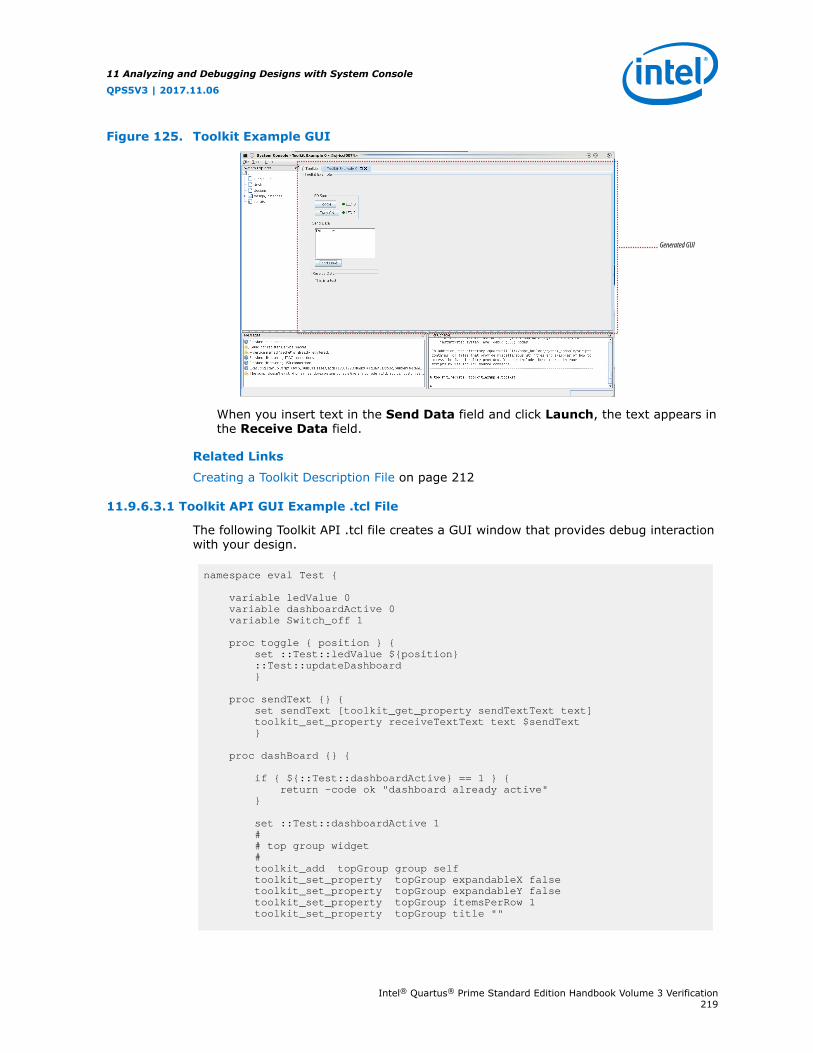
Figure 125. Toolkit Example GUI
Generated GUI
When you insert text in the Send Data field and click Launch, the text appears inthe Receive Data field.
Related Links
Creating a Toolkit Description File on page 212
11.9.6.3.1 Toolkit API GUI Example .tcl File
The following Toolkit API .tcl file creates a GUI window that provides debug interactionwith your design.
namespace eval Test {
variable ledValue 0 variable dashboardActive 0 variable Switch_off 1
proc toggle { position } { set ::Test::ledValue ${position} ::Test::updateDashboard } proc sendText {} { set sendText [toolkit_get_property sendTextText text] toolkit_set_property receiveTextText text $sendText }
proc dashBoard {} {
if { ${::Test::dashboardActive} == 1 } { return -code ok "dashboard already active" }
set ::Test::dashboardActive 1 # # top group widget # toolkit_add topGroup group self toolkit_set_property topGroup expandableX false toolkit_set_property topGroup expandableY false toolkit_set_property topGroup itemsPerRow 1 toolkit_set_property topGroup title ""
11 Analyzing and Debugging Designs with System Console
QPS5V3 | 2017.11.06
Intel® Quartus® Prime Standard Edition Handbook Volume 3 Verification219

# # leds group widget # toolkit_add ledsGroup group topGroup toolkit_set_property ledsGroup expandableX false toolkit_set_property ledsGroup expandableY false toolkit_set_property ledsGroup itemsPerRow 2 toolkit_set_property ledsGroup title "LED State"
# # leds widgets # toolkit_add led0Button button ledsGroup toolkit_set_property led0Button enabled true toolkit_set_property led0Button expandableX false toolkit_set_property led0Button expandableY false toolkit_set_property led0Button text "Toggle" toolkit_set_property led0Button onClick {::Test::toggle 1}
toolkit_add led0LED led ledsGroup toolkit_set_property led0LED expandableX false toolkit_set_property led0LED expandableY false toolkit_set_property led0LED text "LED 0" toolkit_set_property led0LED color "green_off"
toolkit_add led1Button button ledsGroup toolkit_set_property led1Button enabled true toolkit_set_property led1Button expandableX false toolkit_set_property led1Button expandableY false toolkit_set_property led1Button text "Turn ON" toolkit_set_property led1Button onClick {::Test::toggle 2}
toolkit_add led1LED led ledsGroup toolkit_set_property led1LED expandableX false toolkit_set_property led1LED expandableY false toolkit_set_property led1LED text "LED 1" toolkit_set_property led1LED color "green_off"
# # sendText widgets # toolkit_add sendTextGroup group topGroup toolkit_set_property sendTextGroup expandableX false toolkit_set_property sendTextGroup expandableY false toolkit_set_property sendTextGroup itemsPerRow 1 toolkit_set_property sendTextGroup title "Send Data"
toolkit_add sendTextText text sendTextGroup toolkit_set_property sendTextText expandableX false toolkit_set_property sendTextText expandableY false toolkit_set_property sendTextText preferredWidth 200 toolkit_set_property sendTextText preferredHeight 100 toolkit_set_property sendTextText editable true toolkit_set_property sendTextText htmlCapable false toolkit_set_property sendTextText text ""
toolkit_add sendTextButton button sendTextGroup toolkit_set_property sendTextButton enabled true toolkit_set_property sendTextButton expandableX false toolkit_set_property sendTextButton expandableY false toolkit_set_property sendTextButton text "Send Now" toolkit_set_property sendTextButton onClick {::Test::sendText}
# # receiveText widgets # toolkit_add receiveTextGroup group topGroup toolkit_set_property receiveTextGroup expandableX false toolkit_set_property receiveTextGroup expandableY false toolkit_set_property receiveTextGroup itemsPerRow 1
11 Analyzing and Debugging Designs with System Console
QPS5V3 | 2017.11.06
Intel® Quartus® Prime Standard Edition Handbook Volume 3 Verification220

toolkit_set_property receiveTextGroup title "Receive Data"
toolkit_add receiveTextText text receiveTextGroup toolkit_set_property receiveTextText expandableX false toolkit_set_property receiveTextText expandableY false toolkit_set_property receiveTextText preferredWidth 200 toolkit_set_property receiveTextText preferredHeight 100 toolkit_set_property receiveTextText editable false toolkit_set_property receiveTextText htmlCapable false toolkit_set_property receiveTextText text ""
return -code ok } proc updateDashboard {} {
if { ${::Test::dashboardActive} > 0 } {
toolkit_set_property ledsGroup title "LED State" if { [ expr ${::Test::ledValue} & 0x01 & \ ${::Test::Switch_off} ] } { toolkit_set_property led0LED color "green" set ::Test::Switch_off 0 } else { toolkit_set_property led0LED color "green_off" set ::Test::Switch_off 1 } if { [ expr ${::Test::ledValue} & 0x02 ] } { toolkit_set_property led1LED color "green" } else { toolkit_set_property led1LED color "green_off" } } }}::Test::dashBoard
11.9.6.4 Toolkit API Commands
Toolkit API commands run in the context of a unique toolkit instance.
toolkit_register on page 222
toolkit_open on page 223
get_quartus_ini on page 224
toolkit_get_context on page 225
toolkit_get_types on page 226
toolkit_get_properties on page 227
toolkit_add on page 228
toolkit_get_property on page 229
toolkit_set_property on page 230
toolkit_remove on page 231
toolkit_get_widget_dimensions on page 232
11 Analyzing and Debugging Designs with System Console
QPS5V3 | 2017.11.06
Intel® Quartus® Prime Standard Edition Handbook Volume 3 Verification221

11.9.6.4.1 toolkit_register
DescriptionPoint to the XML file that describes the plugin (.toolkit file) .
Usagetoolkit_register <toolkit_file>
ReturnsNo return value.
Arguments
<toolkit_file> Path to the toolkit definition file.
Example
toolkit_register /path/to/toolkit_example.toolkit
11 Analyzing and Debugging Designs with System Console
QPS5V3 | 2017.11.06
Intel® Quartus® Prime Standard Edition Handbook Volume 3 Verification222

11.9.6.4.2 toolkit_open
DescriptionOpens an instance of a toolkit in System Console.
Usagetoolkit_open <toolkit_id> [<context>]
ReturnsNo return value.
Arguments
<toolkit_id> Name of the toolkit type to open.
<context> An optional context, such as a service path for a hardware resource thatis associated with the toolkit that opens.
Example
toolkit_open my_toolkit_id
11 Analyzing and Debugging Designs with System Console
QPS5V3 | 2017.11.06
Intel® Quartus® Prime Standard Edition Handbook Volume 3 Verification223

11.9.6.4.3 get_quartus_ini
DescriptionReturns the value of an ini setting from the Intel Quartus Prime software .ini file.
Usageget_quartus_ini <ini> <type>
ReturnsValue of ini setting.
Arguments
<ini> Name of the Intel Quartus Prime software .ini setting.
<type> (Optional) Type of .ini setting. The known types are string andenabled. If the type is enabled, the value of the .ini setting returns 1, or0 if not enabled.
Example
set my_ini_enabled [get_quartus_ini my_ini enabled]
set my_ini_raw_value [get_quartus_ini my_ini]
11 Analyzing and Debugging Designs with System Console
QPS5V3 | 2017.11.06
Intel® Quartus® Prime Standard Edition Handbook Volume 3 Verification224

11.9.6.4.4 toolkit_get_context
DescriptionReturns the context that was specified when the toolkit was opened. If no context wasspecified, returns an empty string.
Usagetoolkit_get_context
ReturnsContext.
ArgumentsNo arguments.
Example
set context [toolkit_get_context]
11 Analyzing and Debugging Designs with System Console
QPS5V3 | 2017.11.06
Intel® Quartus® Prime Standard Edition Handbook Volume 3 Verification225

11.9.6.4.5 toolkit_get_types
DescriptionReturns a list of widget types.
Usagetoolkit_get_types
ReturnsList of widget types.
ArgumentsNo arguments.
Example
set widget_names [toolkit_get_types]
11 Analyzing and Debugging Designs with System Console
QPS5V3 | 2017.11.06
Intel® Quartus® Prime Standard Edition Handbook Volume 3 Verification226

11.9.6.4.6 toolkit_get_properties
DescriptionReturns a list of toolkit properties for a type of widget.
Usagetoolkit_get_properties <widgetType>
ReturnsList of toolkit properties.
Arguments
<widgetType> Type of widget.
Example
set widget_properties [toolkit_get_properties xyChart]
11 Analyzing and Debugging Designs with System Console
QPS5V3 | 2017.11.06
Intel® Quartus® Prime Standard Edition Handbook Volume 3 Verification227

11.9.6.4.7 toolkit_add
DescriptionAdds a widget to the current toolkit.
Usagetoolkit_add <id> <type><groupid>
ReturnsNo return value.
Arguments
<id> A unique ID for the widget being added.
<type> The type of widget that is being added.
<groupid> The ID for the parent group that will contain the new widget. Use selffor the toolkit base group.
Example
toolkit_add my_button button parentGroup
11 Analyzing and Debugging Designs with System Console
QPS5V3 | 2017.11.06
Intel® Quartus® Prime Standard Edition Handbook Volume 3 Verification228

11.9.6.4.8 toolkit_get_property
DescriptionReturns the property value for a specific widget.
Usagetoolkit_get_property <id> <propertyName>
ReturnsThe property value.
Arguments
<id> A unique ID for the widget being queried.
<propertyName> The name of the widget property.
Example
set enabled [toolkit_get_property my_button enabled]
11 Analyzing and Debugging Designs with System Console
QPS5V3 | 2017.11.06
Intel® Quartus® Prime Standard Edition Handbook Volume 3 Verification229

11.9.6.4.9 toolkit_set_property
DescriptionSets the property value for a specific widget.
Usagetoolkit_set_property <id><propertyName> <value>
ReturnsNo return value.
Arguments
<id> A unique ID for the widget being modified.
<propertyName> The name of the widget property being set.
<value> The new value for the widget property.
Example
toolkit_set_property my_button enabled 0
11 Analyzing and Debugging Designs with System Console
QPS5V3 | 2017.11.06
Intel® Quartus® Prime Standard Edition Handbook Volume 3 Verification230

11.9.6.4.10 toolkit_remove
DescriptionRemoves a widget from the specified toolkit.
Usagetoolkit_remove <id>
ReturnsNo return value.
Arguments
<id> A unique ID for the widget being removed.
Example
toolkit_remove my_button
11 Analyzing and Debugging Designs with System Console
QPS5V3 | 2017.11.06
Intel® Quartus® Prime Standard Edition Handbook Volume 3 Verification231

11.9.6.4.11 toolkit_get_widget_dimensions
DescriptionReturns the width and height of the specified widget.
Usagetoolkit_get_widget_dimensions <id>
ReturnsWidth and height of specified widget.
Arguments
<id> A unique ID for the widget being added.
Example
set dimensions [toolkit_get_widget_dimensions my_button]
11 Analyzing and Debugging Designs with System Console
QPS5V3 | 2017.11.06
Intel® Quartus® Prime Standard Edition Handbook Volume 3 Verification232

11.9.6.5 Toolkit API Properties
The following are the Toolkit API widget properties:
Widget Types and Properties on page 234
barChart Properties on page 235
button Properties on page 236
checkBox Properties on page 237
comboBox Properties on page 238
dial Properties on page 239
fileChooserButton Properties on page 240
group Properties on page 241
label Properties on page 242
led Properties on page 243
lineChart Properties on page 244
list Properties on page 245
pieChart Properties on page 246
table Properties on page 247
text Properties on page 248
textField Properties on page 249
timeChart Properties on page 250
xyChart Properties on page 251
11 Analyzing and Debugging Designs with System Console
QPS5V3 | 2017.11.06
Intel® Quartus® Prime Standard Edition Handbook Volume 3 Verification233

11.9.6.5.1 Widget Types and Properties
Table 58. Toolkit API Widget Types and Properties
Name Description
enabled Enables or disables the widget.
expandable Controls whether the widget is expandable.
expandableX Allows the widget to resize horizontally if there is spaceavailable in the cell where it resides.
expandableY Allows the widget to resize vertically if there is spaceavailable in the cell where it resides.
foregroundColor Sets the foreground color.
maxHeight If the widget's expandableY is set, this is the maximumheight in pixels that the widget can take.
minHeight If the widget's expandableY is set, this is the minimumheight in pixels that the widget can take.
maxWidth If the widget's expandableX is set, this is the maximumwidth in pixels that the widget can take.
minWidth If the widget's expandableX is set, this is the minimumwidth in pixels that the widget can take.
preferredHeight The height of the widget if expandableY is not set.
preferredWidth The width of the widget if expandableX is not set.
toolTip Implements a mouse-over tooltip.
visible Displays the widget.
11 Analyzing and Debugging Designs with System Console
QPS5V3 | 2017.11.06
Intel® Quartus® Prime Standard Edition Handbook Volume 3 Verification234

11.9.6.5.2 barChart Properties
Table 59. Toolkit API barChart Properties
Name Description
title Chart title.
labelX X-axis label text.
label X-axis label text.
range Y-axis value range. By default, it is auto range. Specifiy therange using a Tcl list, for example:[list lower_numerical_valueupper_numerical_value].
itemValue Specify the value using a Tcl list, for example:[list bar_category_str numerical_value].
11 Analyzing and Debugging Designs with System Console
QPS5V3 | 2017.11.06
Intel® Quartus® Prime Standard Edition Handbook Volume 3 Verification235

11.9.6.5.3 button Properties
Table 60. Toolkit API button Properties
Name Description
onClick Specifies the Tcl command to run every time you click thebutton. Usually the command is a proc.
text The text on the button.
11 Analyzing and Debugging Designs with System Console
QPS5V3 | 2017.11.06
Intel® Quartus® Prime Standard Edition Handbook Volume 3 Verification236

11.9.6.5.4 checkBox Properties
Table 61. Toolkit API checkBox Properties
Name Description
checked Specifies the state of the checkbox.
onClick Specifies the Tcl command to run every time you click thecheckbox. The command is usually a proc.
text The text on the checkbox.
11 Analyzing and Debugging Designs with System Console
QPS5V3 | 2017.11.06
Intel® Quartus® Prime Standard Edition Handbook Volume 3 Verification237

11.9.6.5.5 comboBox Properties
Table 62. Toolkit API comboBox Properties
Name Description
onChange A Tcl callback to run when the value of the combo boxchanges.
options A list of items to display in the combo box.
selectedItem The selected item in the combo box.
11 Analyzing and Debugging Designs with System Console
QPS5V3 | 2017.11.06
Intel® Quartus® Prime Standard Edition Handbook Volume 3 Verification238

11.9.6.5.6 dial Properties
Table 63. Toolkit API dial Properties
Name Description
max The maximum value that the dial can show.
min The minimum value that the dial can show.
ticksize The space between the different tick marks of the dial.
title The title of the dial.
value The value that the dial's needle marks. It must be betweenmin and max.
11 Analyzing and Debugging Designs with System Console
QPS5V3 | 2017.11.06
Intel® Quartus® Prime Standard Edition Handbook Volume 3 Verification239

11.9.6.5.7 fileChooserButton Properties
Table 64. Toolkit API fileChooserButton Properties
Name Description
text The text on the button.
onChoose A Tcl command that runs every time you click the button.The command is usually a proc.
title The title of the dialog box.
chooserButtonText The text of the dialog box approval button. Default value isOpen.
filter The file filter, based on extension. The filter supports onlyone extension. By default, the filter allows all file names.Specify the filter using the syntax [listfilter_description file_extension], for example:[list "Text Document (.txt)" "txt"].
mode Specifies what kind of files or directories you can select. Thedefault is files_only. Possible options are files_onlyand directories_only.
multiSelectionEnabled Controls whether you can select multiple files. Default valueis false.
paths This property is read-only. Returns a list of file pathsselected in the file chooser dialog box. The property is mostuseful when you use it within the onClick script, or insidea procedure that updates the result after the dialog boxcloses.
11 Analyzing and Debugging Designs with System Console
QPS5V3 | 2017.11.06
Intel® Quartus® Prime Standard Edition Handbook Volume 3 Verification240

11.9.6.5.8 group Properties
Table 65. Toolkit API group Properties
Name Description
itemsPerRow The number of widgets the group can position in one row,from left to right, before moving to the next row.
title The title of the group. Groups with a title can have a borderaround them, and setting an empty title removes theborder.
11 Analyzing and Debugging Designs with System Console
QPS5V3 | 2017.11.06
Intel® Quartus® Prime Standard Edition Handbook Volume 3 Verification241

11.9.6.5.9 label Properties
Table 66. Toolkit API label Properties
Name Description
text The text to show in the label.
11 Analyzing and Debugging Designs with System Console
QPS5V3 | 2017.11.06
Intel® Quartus® Prime Standard Edition Handbook Volume 3 Verification242

11.9.6.5.10 led Properties
Table 67. Toolkit API led Properties
Name Description
color The color of the LED. The options are: red_off, red,yellow_off, yellow, green_off, green, blue_off,blue, and black.
text The text to show next to the LED.
11 Analyzing and Debugging Designs with System Console
QPS5V3 | 2017.11.06
Intel® Quartus® Prime Standard Edition Handbook Volume 3 Verification243

11.9.6.5.11 lineChart Properties
Table 68. Toolkit API lineChart Properties
Name Description
title Chart title.
labelX X-axis label text.
labelY Y-axis label text.
range Y-axis value range. By default, it is auto range. Specify therange using a Tcl list, for example:[list lower_numerical_valueupper_numerical_value].
itemValue Item value. Specifiy the value using a Tcl list, for example:[list bar_category_str numerical_value].
11 Analyzing and Debugging Designs with System Console
QPS5V3 | 2017.11.06
Intel® Quartus® Prime Standard Edition Handbook Volume 3 Verification244

11.9.6.5.12 list Properties
Table 69. Toolkit API list Properties
Name Description
selected Index of the selected item in the combo box.
options List of options to display.
onChange A Tcl callback to run when the selected item in the listchanges.
11 Analyzing and Debugging Designs with System Console
QPS5V3 | 2017.11.06
Intel® Quartus® Prime Standard Edition Handbook Volume 3 Verification245

11.9.6.5.13 pieChart Properties
Table 70. Toolkit API pieChart Properties
Name Description
title Chart title.
itemValue Item value. Specified using a Tcl list, for example:[list bar_category_str numerical_value].
11 Analyzing and Debugging Designs with System Console
QPS5V3 | 2017.11.06
Intel® Quartus® Prime Standard Edition Handbook Volume 3 Verification246

11.9.6.5.14 table Properties
Table 71. Toolkit API table Properties
Name Description
columnCount The number of columns (Mandatory) (0, by default).
rowCount The number of rows (Mandatory) (0, by default).
headerReorderingAllowed Controls whether you can drag the columns (false, bydefault).
headerResizingAllowed Controls whether you can resize all column widths. (false,by default).Note: You can resize each column individually with the
columnWidthResizable property.
rowSorterEnabled Controls whether you can sort the cell values in a column(false, by default).
showGrid Controls whether to draw both horizontal and vertical lines(true, by default).
showHorizontalLines Controls whether to draw horizontal line (true, by default).
rowIndex Current row index. Zero-based. This value affects someproperties below (0, by default).
columnIndex Current column index. Zero-based. This value affects allcolumn specific properties below (0, by default).
cellText Specifies the text inside the cell given by the currentrowIndex and columnIndex (Empty, by default).
selectedRows Control or retrieve row selection.
columnHeader The text in the column header.
columnHeaders A list of names to define the columns for the table.
columnHorizontalAlignment The cell text alignment in the specified column. Supportedtypes are leading (default), left, center, right,trailing.
columnRowSorterType The type of sorting method. This is applicable only ifrowSorterEnabled is true. Each column has its ownsorting type. Possible types are string (default), int, andfloat.
columnWidth The number of pixels in the column width.
columnWidthResizable Controls whether the column width is resizable by you(false, by default).
contents The contents of the table as a list. For a table with columnsA, B, and C, the format of the list is {A1 B1 C1 A2 B2C2 ...}.
11 Analyzing and Debugging Designs with System Console
QPS5V3 | 2017.11.06
Intel® Quartus® Prime Standard Edition Handbook Volume 3 Verification247

11.9.6.5.15 text Properties
Table 72. Toolkit API text Properties
Name Description
editable Controls whether the text box is editable.
htmlCapable Controls whether the text box can format HTML.
text The text to show in the text box.
11 Analyzing and Debugging Designs with System Console
QPS5V3 | 2017.11.06
Intel® Quartus® Prime Standard Edition Handbook Volume 3 Verification248

11.9.6.5.16 textField Properties
Table 73. Toolkit API textField Properties
Name Description
editable Controls whether the text box is editable.
onChange A Tcl callback to run when you change the content of thetext box.
text The text in the text box.
11 Analyzing and Debugging Designs with System Console
QPS5V3 | 2017.11.06
Intel® Quartus® Prime Standard Edition Handbook Volume 3 Verification249

11.9.6.5.17 timeChart Properties
Table 74. Toolkit API timeChart Properties
Name Description
labelX The label for the X-axis.
labelY The label for the Y-axis.
latest The latest value in the series.
maximumItemCount The number of sample points to display in the historicrecord.
title The title of the chart.
range Sets the range for the chart. The range has the form {low,high}. The low/high values are doubles.
showLegend Specifies whether a legend for the series is shown in thegraph.
11 Analyzing and Debugging Designs with System Console
QPS5V3 | 2017.11.06
Intel® Quartus® Prime Standard Edition Handbook Volume 3 Verification250

11.9.6.5.18 xyChart Properties
Table 75. Toolkit API xyChart Properties
Name Properties
title Chart title.
labelX X-Axis label text.
labelY Y-Axis label text.
range Sets the range for the chart. The range is of the form{low, high}. The low/high values are doubles.
maximumItemCount Specifies the maximum number of data values to keep in adata series. This setting only affects new data in the chart.If you add more data values than the maximumItemCount,only the last maximumItemCount number of entries arekept.
series Adds a series of data to the chart. The first value in thespec is the identifier for the series. If the same identifier isset twice, the Toolkit API selects the most recent series. Ifthe identifier does not contain series data, that series isremoved from the chart. Specify the series in a Tcl list:{identifier, x-1 y-1, x-2 y-2}.
showLegend Sets whether a legend for the series appears in the graph.
11.10 ADC Toolkit
The ADC Toolkit is designed to work with Intel MAX 10 devices and helps youunderstand the performance of the analog signal chain as seen by the on-board ADChardware. The GUI displays the performance of the ADC using industry standardmetrics. You can export the collected data to a .csv file and process this raw datayourself. The ADC Toolkit is built on the System Console framework and can only beoperated using the GUI. There is no Tcl support for the tool.
Prerequisites for Using the ADC Toolkit
• Altera Modular ADC IP core
— External Reference Voltage if you select External in the Altera ModularADC IP parameters
• Reference signal
The ADC Toolkit needs a sine wave signal to be fed to the analog inputs. You need thecapability to precisely set the level and frequency of the reference signal. A high-precision sine wave is needed for accurate test results; however, there are usefulthings that can be read in Scope mode with any input signal.
To achieve the best testing results, the reference signal should have less distortionsthan the device ADC is able to resolve. If this is not the case, then you will be addingdistortions from the source into the resulting ADC distortion measurements. Thelimiting factor is based on hardware precision.
Note: When applying a sine wave, the ADC should sample at 2x the fundamental sine wavefrequency. There should be a low-pass filter, 3dB point set to the fundamentalfrequency.
11 Analyzing and Debugging Designs with System Console
QPS5V3 | 2017.11.06
Intel® Quartus® Prime Standard Edition Handbook Volume 3 Verification251

Configuring the Altera Modular ADC IP Core
The Altera Modular ADC IP core needs to be included in your design. You caninstantiate this IP core from the IP Catalog. When you configure this IP core in theParameter Editor, you need to enable the Debug Path option located under CoreConfiguration.
There are two limitations in the Intel Quartus Prime software v14.1 for the AlteraModular ADC IP core. The ADC Toolkit does not support the ADC control core onlyoption under Core Configuration. You must select a core variant that uses thestandard sequencer in order for the Altera Modular ADC IP core to work with ADCToolkit. Also, if an Avalon Master is not connected to the sequencer, you mustmanually start the sequencer before the ADC Toolkit will work.
Figure 126. Altera Modular ADC Core
Starting the ADC Toolkit
You can launch the ADC Toolkit from System Console. Before starting the ADC toolkit,you need to verify that your board is programmed. You can then load your .sof byclicking File ➤ Load Design. If System Console was started with an active project,your design is auto-loaded when you start System Console.
There are two methods to start the ADC Toolkit. Both methods require you to have aIntel MAX 10 device connected, programmed with a project, and linked to this project.However, the Launch command only shows up if these requirements are met. You canalways start the ADC Toolkit from the Tools menu, but if the above requirements arenot met, no connection will be made.
• Click Tools ➤ ADC Toolkit
• Alternatively, click Launch from the Toolkits tab. The path for the device isdisplayed above the Launch button.
Note: Only one ADC Toolkit enabled device can be connected at a time.
Upon starting the ADC Toolkit, an identifier path on the ADC Toolkit tab shows youwhich ADC on the device is being used for this instance of the ADC Toolkit.
11 Analyzing and Debugging Designs with System Console
QPS5V3 | 2017.11.06
Intel® Quartus® Prime Standard Edition Handbook Volume 3 Verification252

Figure 127. Launching ADC Toolkit
ADC Toolkit Flow
The ADC Toolkit GUI consists of four panels: Frequency Selection, Scope, SignalQuality, and Linearity.
1. Use the Frequency Selection panel to calculate the required sine wave frequencyfor proper signal quality testing. The ADC Toolkit will give you the nearest idealfrequency based on your desired reference signal frequency.
2. Use the Scope panel to tune your signal generator or inspect input signalcharacteristics.
3. Use the Signal Quality panel to test the performance of your ADC using industrystandard metrics.
4. Use the Linearity panel to test the linearity performance of your ADC and displaydifferential and integral non-linearity results.
Figure 128. ADC Toolkit GUI
Related Links
• Using the ADC Toolkit in Intel MAX 10 Devices online training
• Intel MAX 10 FPGA Device Overview
• Intel MAX 10 FPGA Device Datasheet
11 Analyzing and Debugging Designs with System Console
QPS5V3 | 2017.11.06
Intel® Quartus® Prime Standard Edition Handbook Volume 3 Verification253

• Intel MAX 10 FPGA Design Guidelines
• Intel MAX 10 Analog to Digital Converter User Guide
• Additional information about sampling frequencyNyquist sampling theorem and how it relates to the nominal sampling intervalrequired to avoid aliasing.
11.10.1 ADC Toolkit Terms
Table 76. ADC Toolkit Terms
Term Description
SNR The ratio of the output signal voltage level to the outputnoise level.
THD The ratio of the sum of powers of the harmonic frequencycomponents to the power of the fundamental/originalfrequency component.
SFDR Characterizes the ratio between the fundamental signal andthe highest spurious in the spectrum.
SINAD The ratio of the RMS value of the signal amplitude to theRMS value of all other spectral components, includingharmonics, but excluding DC.
ENOB The number of bits with which the ADC behaves.
DNL The maximum and minimum difference in the step widthbetween actual transfer function and the perfect transferfunction
INL The maximum vertical difference between the actual andthe ideal curve. It indicates the amount of deviation of theactual curve from the ideal transfer curve.
11.10.2 Setting the Frequency of the Reference Signal
You use the Frequency Selection panel to compute the required reference signalfrequency to run the ADC performance tests. The sine wave frequency is critical andaffects the validity of your test results.
11 Analyzing and Debugging Designs with System Console
QPS5V3 | 2017.11.06
Intel® Quartus® Prime Standard Edition Handbook Volume 3 Verification254

Figure 129. Frequency Selection Panel
To set the frequency of the reference signal:
1. On ADC Channel, select the ADC channel that you plan to test.The tool populates the Sample Size and Sample Frequency fields.
2. Enter the Desired Frequency. This is your desired frequency for testing. Youneed to complete this procedure to calculate the frequency that you set yoursignal generator to, which will differ depending on the type of test you want to dowith the ADC Toolkit.
3. Click Calculate.
• The closest frequency for valid testing near your desired frequency displaysunder both Signal Quality Test and Linearity Test.
• The nearest required sine wave frequencies are different for the signal qualitytest and linearity test.
4. Set your signal generator to the precise frequency given by the tool based on thetype of test you want to run.
11.10.3 Tuning the Signal Generator
You use the Scope panel to tune your signal generator in order to achieve the bestpossible performance from the ADC.
11 Analyzing and Debugging Designs with System Console
QPS5V3 | 2017.11.06
Intel® Quartus® Prime Standard Edition Handbook Volume 3 Verification255

Figure 130. Scope Mode Panel
To tune your signal generator:
1. On ADC Channel, select the ADC channel that you plan to test.
2. Enter your reference Sample Frequency (unless the tool can extract this valuefrom your IP).
3. Enter your Ref Voltage (unless the tool can extract this value from your IP).
4. Click Run.The tool will repeatedly capture a buffer worth of data and display the data as awaveform and display additional information under Signal Information.
5. Tune your signal generator to use the maximum dynamic range of the ADCwithout clipping. Avoid hitting 0 or 4095 because your signal will likely be clipping.Look at the displayed sine wave under Oscilloscope to see that the top andbottom peaks are evenly balanced to ensure you have selected the optimumvalue.
• For Intel MAX 10 devices, you want to get as close to Min Code = 0 and MaxCode = 4095 without actually hitting those values.
• The frequency should be set precisely to the value needed for testing suchthat coherent sampling is observed in the test window. Before movingforward, follow the suggested value for signal quality testing or linearitytesting, which is displayed next to the actual frequency that is detected.
• From the Raw Data tab, you can export your data as a .csv file.
Related Links
Additional information about coherent sampling vs window sampling
11 Analyzing and Debugging Designs with System Console
QPS5V3 | 2017.11.06
Intel® Quartus® Prime Standard Edition Handbook Volume 3 Verification256

11.10.4 Running a Signal Quality Test
The available performance metrics in signal quality test mode are the following: signalto noise ratio (SNR), total harmonic distortion (THD), spurious free dynamic range(SFDR), signal to noise and distortion ratio (SINAD), effective number of bits (ENOB),and a frequency response graph.The frequency response graph shows the signal,noise floor, and any spurs or harmonics.
The signal quality parameters are measurements relative to the carrier signal and notthe full scale of the ADC.
Before running a signal quality test, ensure that you have set up the frequency of thereference signal using Scope mode.
Figure 131. Signal Quality Panel
To run a signal quality test:
1. On ADC Channel, select the ADC channel that you plan to test.
2. Click Run.
From the Raw Data tab, you can export your data as a .csv file.
For signal quality tests, the signal must be coherently sampled. Based on the samplingrate and number of samples to test, specific input frequencies are required forcoherent sampling.The sample frequency for each channel is calculated based on theADC sequencer configuration.
Related Links
Additional information about dynamic parameters such as SNR, THD, etc
11 Analyzing and Debugging Designs with System Console
QPS5V3 | 2017.11.06
Intel® Quartus® Prime Standard Edition Handbook Volume 3 Verification257

11.10.5 Running a Linearity Test
The linearity test determines the linearity of the step sizes of each ADC code. It uses ahistogram testing method which requires sinusoidal inputs which are easier to sourcefrom signal generators and DACs than other test methods.
When using Linearity test mode, your reference signal must meet specificrequirements.
• The signal source covers the full code range of the ADC. Results improve if thetime spent at code end is equivalent, by tuning the reference signal in Scopemode.
• You have to make sure if using code ends that you are not clipping the signal.Look at the signal in Scope mode to see that it does not look flat at the top orbottom. It may be desirable to back away from code ends and test a smaller rangewithin the desired operating range of the ADC input signal.
• Choosing a frequency that is not an integer multiple of the sample rate and buffersize helps to ensure all code bins are filled relatively evenly to the probabilitydensity function of a sine wave. If an integer multiple is selected, some bins maybe skipped entirely while others are over populated. This makes the tests resultsinvalid. Use the frequency calculator feature to determine a good signal frequencynear your desired frequency.
To run a linearity test:
1. On ADC Channel, select the ADC channel that you plan to test.
2. Enter the test sample size in Burst Size. Larger samples increase the confidencein the test results.
3. Click Run.
• You can stop the test at anytime, as well as click Run again to continueadding to the aggregate data. To start fresh, click Reset after you stop a test.Anytime you change the input signal or channel, you should click Reset soyour results are correct for a particular input.
• There are three graphical views of the data: Histogram view, DNL view, andINL view.
• From the Raw Data tab, you can export your data as a .csv file.
11.10.6 ADC Toolkit Data Views
Histogram View
The Histogram view shows how often each code appears. The graph updates everyfew seconds as it collects data. You can use the Histogram view to quickly check ifyour test signal is set up appropriately.
11 Analyzing and Debugging Designs with System Console
QPS5V3 | 2017.11.06
Intel® Quartus® Prime Standard Edition Handbook Volume 3 Verification258

Figure 132. Example of Pure Sine Wave HistogramThe figure below shows the shape of a pure sine wave signal. Your reference signal should look similar.
If your reference signal is not a relatively smooth line, but has jagged edges withsome bins having a value of 0, and adjacent bins with a much higher value, then thetest signal frequency is not adequate. Use Scope mode to help choose a goodfrequency for linearity testing.
Figure 133. Examples of (Left) Poor Frequency Choice vs (Right) Good Frequency Choice
11 Analyzing and Debugging Designs with System Console
QPS5V3 | 2017.11.06
Intel® Quartus® Prime Standard Edition Handbook Volume 3 Verification259

Differential Non-linearity View
Figure 134. Example of Good Differential Non-linearity
The DNL view shows the currently collected data. Ideally, you want your data to look like a straight linethrough the 0 on the x-axis. When there are not enough samples of data, the line appears rough. The lineimproves as more data is collected and averaged.
Each point in the graph represents how many LSB values a particular code differs from the ideal step size of 1LSB. The Results box shows the highest positive and negative DNL values.
11 Analyzing and Debugging Designs with System Console
QPS5V3 | 2017.11.06
Intel® Quartus® Prime Standard Edition Handbook Volume 3 Verification260

Integral Non-linearity View
Figure 135. Example of Good Integral Non-linearity
The INL view shows currently collected data. Ideally, with a perfect ADC and enough samples, the graphappears as a straight line through 0 on the x-axis.
Each point in the graph represents how many LSB values a particular code differs from its expected point in thevoltage slope. The Results box shows the highest positive and negative INL values.
11.11 System Console Examples and Tutorials
Intel provides examples for performing board bring-up, creating a simple dashboard,and programming a Nios II processor. The System_Console.zip file contains designfiles for the board bring-up example. The Nios II Ethernet Standard .zip files containthe design files for the Nios II processor example.
Note: The instructions for these examples assume that you are familiar with the IntelQuartus Prime software, Tcl commands, and Platform Designer (Standard).
Related Links
On-Chip Debugging Design Examples WebsiteContains the design files for the example designs that you can download.
11.11.1 Board Bring-Up with System Console Tutorial
You can perform low-level hardware debugging of Platform Designer (Standard)systems with System Console. You can debug systems that include IP coresinstantiated in your Platform Designer (Standard) system or perform initial bring-up of
11 Analyzing and Debugging Designs with System Console
QPS5V3 | 2017.11.06
Intel® Quartus® Prime Standard Edition Handbook Volume 3 Verification261

your PCB. This board bring-up tutorial uses a Nios II Embedded Evaluation Kit (NEEK)board and USB cable. If you have a different development kit, you need to change thedevice and pin assignments to match your board and then recompile the design.
1. Setting Up the Board Bring-Up Design Example on page 262
2. Verifying Clock and Reset Signals on page 263
3. Verifying Memory and Other Peripheral Interfaces on page 263
4. Platform Designer (Standard) Modules for Board Bring-up Example on page 268
Related Links
Introduction to System Console on page 193
11.11.1.1 Setting Up the Board Bring-Up Design Example
To load the design example into the Intel Quartus Prime software and program yourdevice, perform the following steps:
1. Unzip the System_Console.zip file to your local hard drive.
2. In the Intel Quartus Prime software, click File ➤ Open Project and selectSystemconsole_design_example.qpf.
3. Change the device and pin assignments (LED, clock, and reset pins) in theSystemconsole_design_example.qsf file to match your board.
4. Click Processing ➤ Start Compilation
5. To program your device, follow these steps:
a. Click Tools ➤ Programmer.
b. Click Hardware Setup.
c. Click the Hardware Settings tab.
d. Under Currently selected hardware, click USB-Blaster, and click Close.
Note: If you do not see the USB-Blaster option, then your device was notdetected. Verify that the USB-Blaster driver is installed, your board ispowered on, and the USB cable is intact.
This design example uses a USB-Blaster cable. If you do not have a USB-Blaster cable and you are using a different cable type, then select your cablefrom the Currently selected hardware options.
e. Click Auto Detect, and then select your device.
f. Double-click your device under File.
g. Browse to your project folder and clickSystemconsole_design_example.sof in the subdirectory output_files.
h. Turn on the Program/Configure option.
i. Click Start.
j. Close the Programmer.
6. Click Tools > System Debugging Tools > System Console.
11 Analyzing and Debugging Designs with System Console
QPS5V3 | 2017.11.06
Intel® Quartus® Prime Standard Edition Handbook Volume 3 Verification262

Related Links
System_Console.zip fileContains the design files for this tutorial.
11.11.1.2 Verifying Clock and Reset Signals
You can use the System Explorer pane to verify clock and reset signals.
Open the appropriate node and check for either a green clock icon or a red clock icon.You can use JTAG Debug command to verify clock and reset signals.
Related Links
• System Explorer Pane on page 198
• JTAG Debug Commands on page 211
11.11.1.3 Verifying Memory and Other Peripheral Interfaces
The Avalon-MM service accesses memory-mapped slaves via a suitable Avalon-MMmaster, which can be controlled by the host. You can use Tcl commands to read andwrite to memory with a master service.
11.11.1.3.1 Locating and Opening the Master Service
#Select the master service type and check for available service paths.set service_paths [get_service_paths master]
#Set the master service path.set master_service_path [lindex $service_paths 0]
#Open the master service.set claim_path [claim_service master $master_service_path mylib]
11.11.1.3.2 Avalon-MM Slaves
The Address Map tab shows the address range for every Platform Designer(Standard) component. The Avalon-MM master communicates with slaves using theseaddresses.
The register maps for all Intel FPGA components are in their respective Data Sheets.
Figure 136. Address Map
Related Links
Data Sheets Website
Avalon-MM CommandsYou can read or write the Avalon-MM interfaces using the master read and writecommands. You can also use the master commands on slave services. If you areworking on a slave service, the address field can be a register. (6)
11 Analyzing and Debugging Designs with System Console
QPS5V3 | 2017.11.06
Intel® Quartus® Prime Standard Edition Handbook Volume 3 Verification263

Table 77. Avalon-MM Commands
Command Arguments Function
master_write_memory <service-path><address><list_of_byte_values>
Writes the specified list of byte values to thespecified service path and address.
master_write_8 <service-path><address><list_of_byte_values>
Writes the specified list of byte values to thespecified service path and address, using 8-bitaccesses.
master_write_16 <service-path><address><list_of_16_bit_words>
Writes the specified list of 16-bit values to thespecified service path and address, using 16-bitaccesses.
master_write_from_file <service-path><file-name><address>
Writes the entire contents of the file to the specifiedservice path and address. The file is treated as abinary file containing a stream of bytes.
master_write_32 <service-path><address><list_of_32_bit_words>
Writes the specified list of 32-bit values to thespecified service path and address, using 32-bitaccesses.
master_read_memory [-format <format>]<service-path><address><size_in_bytes>
Returns a list of read values in bytes. Memory readstarts at the specified base address.Note: The [-format <format>] is an optional
argument. Specifying this argument makesthis command accept data as 16 or 32-bit,instead as bytes. For example:
master_read_memory -format 16 <service_path> <addr> <count>
master_read_8 <service-path><address><size_in_bytes>
Returns a list of <size> bytes. Read from memorystarts at the specified base address, using 8-bitaccesses.
master_read_16 <service-path><address><size_in_multiples_of_16_bits>
Returns a list of <size> 16-bit values. Read frommemory starts at the specified base address, using16-bit accesses.
master_read_32 <service-path><address><size_in_multiples_of_32_bits>
Returns a list of <size> 32-bit values. Read frommemory starts at the specified base address, using32-bit accesses.
master_read_to_file <service-path><file-name><address><count>
Reads the number of bytes specified by <count>from the memory address specified and creates (oroverwrites) a file containing the values read. The fileis written as a binary file.
master_get_register_names <service-path> When a register map is defined, returns a list ofregister names in the slave.
Note: Using the 8, 16, or 32 versions of the master_read or master_write commands isless efficient than using the master_write_memory or master_read_memorycommands.
(6) Transfers performed in 16- and 32-bit sizes are packed in little-endian format.
11 Analyzing and Debugging Designs with System Console
QPS5V3 | 2017.11.06
Intel® Quartus® Prime Standard Edition Handbook Volume 3 Verification264

11.11.1.3.3 Testing the PIO component
In this example design, the PIO connects to the LEDs of the board. Test if thiscomponent is operating properly and the LEDs are connected, by driving the outputswith the Avalon-MM master.
Table 78. Register Map for the PIO Core
Offset Register Name R/W Fields
(n-1) ... 2 1 0
0 data read access R Data value currently on PIO inputs.
write access W New value to drive on PIO outputs.
1 direction R/W Individual direction control for each I/O port. A value of 0 sets the directionto input; 1 sets the direction to output.
2 interruptmask R/W IRQ enable/disable for each input port. Setting a bit to 1 enables interruptsfor the corresponding port.
3 edgecapture R/W Edge detection for each input port.
#Write the driver output values for the Parallel I/O component.set offset 0x0; #Register address offset.set value 0x7; #Only set bits 0, 1, and 2.master_write_8 $claim_path $offset $value
#Read back the register value.set offset 0x0set count 0x1master_read_8 $claim_path $offset $count
master_write_8 $claim_path 0x0 0x2; #Only set bit 1.
master_write_8 $claim_path 0x0 0xe; #Only set bits 1, 2, 3.
master_write_8 $claim_path 0x0 0x7; #Only set bits 0, 1, 2.
#Observe the LEDs turn on and off as you execute these Tcl commands.#The LED is on if the register value is zero and off if the register value is one.#LED 0, LED 1, and LED 2 connect to the PIO.#LED 3 connects to the interrupt signal of the CheckSum Accelerator.
11.11.1.3.4 Testing On-chip Memory
Test the memory with a recursive function that writes to incrementing memoryaddresses.
#Load the design example utility procedures for writing to memory.source set_memory_values.tcl
#Write to the on-chip memory.set base_address 0x80set write_length 0x80set value 0x5a5a5a5afill_memory $claim_path $base_address $write_length $value
#Verify the memory was written correctly.#This utility proc returns 0 if the memory range is not uniform with this value.verify_memory $claim_path $base_address $write_length $value
#Check that the memory is re-initialized when reset.#Trigger reset then observe verify_memory returns 0.
11 Analyzing and Debugging Designs with System Console
QPS5V3 | 2017.11.06
Intel® Quartus® Prime Standard Edition Handbook Volume 3 Verification265

set jtag_debug_path [lindex [get_service_paths jtag_debug] 0]set claim_jtag_debug_path [claim_service jtag_debug $jtag_debug_path mylib]jtag_debug_reset_system $claim_jtag_debug_path; #Reset the connected on-chip memory#peripheral.close_service jtag_debug $claim_jtag_debug_pathverify_memory $claim_path $base_address $write_length $value
#The on-chip memory component was parameterized to re-initialized to 0 on reset.#Check the actual value.master_read_8 $claim_path 0x0 0x1
11.11.1.3.5 Testing the Checksum Accelerator
The Checksum Accelerator calculates the checksum of a data buffer in memory. Itcalculates the value for a specified memory buffer, sets the DONE bit in the statusregister, and asserts the interrupt signal. You should only read the result from thecontroller when both the DONE bit and the interrupt signal are asserted. The hostshould assert the interrupt enable control bit in order to check the interrupt signal.
Table 79. Register Map for Checksum Component
Offset(Bytes)
Hexadecimalvalue (after
adding offset)
Register Access Bits (32 bits)
31-9 8 7-5 4 3 2 1 0
0 0x20 Status Read/Writeto clear
BUSY DONE
4 0x24 Address Read/Write Read Address
12 0x2C Length Read/Write Length in bytes
24 0x38 Control Read/Write FixedReadAddressBit
Interrupt Enable
GO INV Clear
28 0x3C Result Read Checksum result (upper 16 bits are zero)
1. #Pass the base address of the memory buffer Checksum Accelerator.set base_address 0x20set offset 4set address_reg [expr {$base_address + $offset}]set memory_address 0x80master_write_32 $claim_path $address_reg $memory_address
#Pass the memory buffer to the Checksum Accelerator.set length_reg [expr {$base_address + 12}]set length 0x20master_write_32 $claim_path $length_reg $length
#Write clear to status and control registers.#Status register:set status_reg $base_addressmaster_write_32 $claim_path $status_reg 0x0#Control register:set clear 0x1set control_reg [expr {$base_address + 24}]master_write_32 $claim_path $control_reg $clear
#Write GO to the control register.set go 0x8master_write_32 $claim_path $control_reg $go
#Cross check if the checksum DONE bit is set.master_read_32 $claim_path $status_reg 0x1
11 Analyzing and Debugging Designs with System Console
QPS5V3 | 2017.11.06
Intel® Quartus® Prime Standard Edition Handbook Volume 3 Verification266

#Is the DONE bit set?#If yes, check the result and you are finished with the board bring-up design example.set result_reg [expr {$base_address + 28}]master_read_16 $claim_path $result_reg 0x1
2. If the result is zero and the JTAG chain works properly, the clock and reset signalswork properly, and the memory works properly, then the problem is the ChecksumAccelerator component.
#Confirm if the DONE bit in the status register (bit 0)#and interrupt signal are asserted.#Status register:master_read_32 $claim_path $status_reg 0x1#Check DONE bit should return a one.
#Enable interrupt and go:set interrupt_and_go 0x18master_write_32 $claim_path $control_reg $interrupt_and_go
3. Check the control enable to see the interrupt signal. LED 3 (MSB) should be off.This indicates the interrupt signal is asserted.
4. You have narrowed down the problem to the data path. View the RTL to check thedata path.
5. Open the Checksum_transform.v file from your project folder.
• <unzip dir>/System_Console/ip/checksum_accelerator/checksum_accelerator.v
6. Notice that the data_out signal is grounded in Figure 137 on page 267(uncommented line 87 and comment line 88). Fix the problem.
7. Save the file and regenerate the Platform Designer (Standard) system.
8. Re-compile the design and reprogram your device.
9. Redo the above steps, starting with Verifying Memory and Other PeripheralInterfaces on page 263 or run the Tcl script included with this design example.
source set_memory_and_run_checksum.tcl
Figure 137. Checksum.v File
11 Analyzing and Debugging Designs with System Console
QPS5V3 | 2017.11.06
Intel® Quartus® Prime Standard Edition Handbook Volume 3 Verification267

11.11.1.4 Platform Designer (Standard) Modules for Board Bring-up Example
Figure 138. Platform Designer (Standard) Modules for Board Bring-up Example
The Platform Designer (Standard) design for this example includes the followingmodules:
• JTAG to Avalon Master Bridge—Provides System Console host access to thememory-mapped IP in the design via the JTAG interface.
• On-chip memory—Simplest type of memory for use in an FPGA-based embeddedsystem. The memory is implemented on the FPGA; consequently, externalconnections on the circuit board are not necessary.
• Parallel I/O (PIO) module—Provides a memory-mapped interface for sampling anddriving general I/O ports.
• Checksum Accelerator—Calculates the checksum of a data buffer in memory. TheChecksum Accelerator consists of the following:
— Checksum Calculator (checksum_transform.v)
— Read Master (slave.v)
— Checksum Controller (latency_aware_read_master.v)
11.11.1.4.1 Checksum Accelerator Functionality
The base address of the memory buffer and data length passes to the ChecksumController from a memory-mapped master. The Read Master continuously reads datafrom memory and passes the data to the Checksum Calculator. When the checksumcalculations finish, the Checksum Calculator issues a valid signal along with thechecksum result to the Checksum Controller. The Checksum Controller sets the DONEbit in the status register and also asserts the interrupt signal. You should only read theresult from the Checksum Controller when the DONE bit and interrupt signal areasserted.
11 Analyzing and Debugging Designs with System Console
QPS5V3 | 2017.11.06
Intel® Quartus® Prime Standard Edition Handbook Volume 3 Verification268
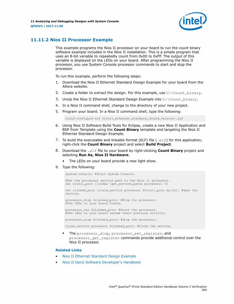
11.11.2 Nios II Processor Example
This example programs the Nios II processor on your board to run the count binarysoftware example included in the Nios II installation. This is a simple program thatuses an 8-bit variable to repeatedly count from 0x00 to 0xFF. The output of thisvariable is displayed on the LEDs on your board. After programming the Nios IIprocessor, you use System Console processor commands to start and stop theprocessor.
To run this example, perform the following steps:
1. Download the Nios II Ethernet Standard Design Example for your board from theAltera website.
2. Create a folder to extract the design. For this example, use C:\Count_binary.
3. Unzip the Nios II Ethernet Standard Design Example into C:\Count_binary.
4. In a Nios II command shell, change to the directory of your new project.
5. Program your board. In a Nios II command shell, type the following:
nios2-configure-sof niosii_ethernet_standard_<board_version>.sof
6. Using Nios II Software Build Tools for Eclipse, create a new Nios II Application andBSP from Template using the Count Binary template and targeting the Nios IIEthernet Standard Design Example.
7. To build the executable and linkable format (ELF) file (.elf) for this application,right-click the Count Binary project and select Build Project.
8. Download the .elf file to your board by right-clicking Count Binary project andselecting Run As, Nios II Hardware.
• The LEDs on your board provide a new light show.
9. Type the following:
system-console; #Start System Console.
#Set the processor service path to the Nios II processor.set niosii_proc [lindex [get_service_paths processor] 0]
set claimed_proc [claim_service processor $niosii_proc mylib]; #Open the service.
processor_stop $claimed_proc; #Stop the processor.#The LEDs on your board freeze.
processor_run $claimed_proc; #Start the processor.#The LEDs on your board resume their previous activity.
processor_stop $claimed_proc; #Stop the processor.
close_service processor $claimed_proc; #Close the service.
• The processor_step, processor_set_register, andprocessor_get_register commands provide additional control over theNios II processor.
Related Links
• Nios II Ethernet Standard Design Example
• Nios II Gen2 Software Developer's Handbook
11 Analyzing and Debugging Designs with System Console
QPS5V3 | 2017.11.06
Intel® Quartus® Prime Standard Edition Handbook Volume 3 Verification269

11.11.2.1 Processor Commands
Table 80. Processor Commands
Command (7) Arguments Function
processor_download_elf <service-path><elf-file-path>
Downloads the given Executable and Linking Format File(.elf) to memory using the master service associated with theprocessor. Sets the processor's program counter to the .elfentry point.
processor_in_debug_mode <service-path> Returns a non-zero value if the processor is in debug mode.
processor_reset <service-path> Resets the processor and places it in debug mode.
processor_run <service-path> Puts the processor into run mode.
processor_stop <service-path> Puts the processor into debug mode.
processor_step <service-path> Executes one assembly instruction.
processor_get_register_names <service-path> Returns a list with the names of all of the processor's accessibleregisters.
processor_get_register <service-path><register_name>
Returns the value of the specified register.
processor_set_register <service-path><register_name><value>
Sets the value of the specified register.
Related Links
Nios II Processor Example on page 269
11.12 On-Board Intel FPGA Download Cable II Support
System Console supports an On-Board Intel FPGA Download Cable II circuit via theUSB Debug Master IP component. This IP core supports the master service.
Not all Stratix V boards support the On-Board Intel FPGA Download Cable II. Forexample, the transceiver signal integrity board does not support the On-Board IntelFPGA Download Cable II.
11.13 About Using MATLAB and Simulink in a System VerificationFlow
You can test system development in System Console using MATLAB and Simulink, andset up a system verification flow using the Intel FPGA Hardware in the Loop (HIL)tools. In this approach, you deploy the design hardware to run in real time, andsimulate your system's surrounding components in a software environment. The HILapproach allows you to use the flexibility of software tools with the real-worldaccuracy and speed of hardware. You can gradually introduce more hardwarecomponents to your system verification testbench. This technique gives you more
(7) If your system includes a Nios II/f core with a data cache, it may complicate the debuggingprocess. If you suspect the Nios II/f core writes to memory from the data cache atnondeterministic intervals; thereby, overwriting data written by the System Console, you candisable the cache of the Nios II/f core while debugging.
11 Analyzing and Debugging Designs with System Console
QPS5V3 | 2017.11.06
Intel® Quartus® Prime Standard Edition Handbook Volume 3 Verification270

control over the integration process as you tune and validate your system. When yourfull system is integrated, the HIL approach allows you to provide stimuli via softwareto test your system under a variety of scenarios.
Advantages of HIL Approach
• Avoid long computational delays for algorithms with high processing rates
• API helps to control, debug, visualize, and verify FPGA designs all within theMATLAB environment
• FPGA results are read back by the MATLAB software for further analysis anddisplay
Required Tools and Components
• MATLAB software
• DSP Builder for Intel FPGAs software
• Intel Quartus Prime software
• Intel FPGA
Note: The DSP Builder for Intel FPGAs installation bundle includes the System ConsoleMATLAB API.
Figure 139. Hardware in the Loop Host-Target Setup
Supported MATLAB API Commands
You can perform your work from the MATLAB environment and leverage the capabilityof System Console to read and write to masters and slaves. By using the supportedMATLAB API commands, you do not have to launch the System Console software. Thesupported commands are the following:
• SystemConsole.refreshMasters;
• M = SystemConsole.openMaster(1);
• M.write (type, byte address, data);
• M.read (type, byte address, number of words);
• M.close
11 Analyzing and Debugging Designs with System Console
QPS5V3 | 2017.11.06
Intel® Quartus® Prime Standard Edition Handbook Volume 3 Verification271

Example 33. MATLAB API Script Example
SystemConsole.refreshMasters; %Investigate available targetsM = SystemConsole.openMaster(1); %Creates connection with FPGA target%%%%%%%% User Application %%%%%%%%%%%%....M.write('uint32',write_address,data); %Send data to FPGA target....data = M.read('uint32',read_address,size); %Read data from FPGA target....%%%%%%%%%%%%%%%%%%%%%%%%%%%%%%%%%%%%%%M.close; %Terminates connection to FPGA target
High-Level Flow
1. Install the DSP Builder for Intel FPGAs software so you have the necessarylibraries to enable this flow
2. Build your design using Simulink and the DSP Builder for Intel FPGAs libraries(DSP Builder for Intel FPGAs helps to convert the Simulink design to HDL)
3. Include Avalon-MM components in your design (DSP Builder for Intel FPGAs canport non-Avalon-MM components)
4. Include Signals and Control blocks in your design
5. Use boundary blocks to separate synthesizable and non-synthesizable logic
6. Integrate your DSP system in Platform Designer (Standard)
7. Program your Intel FPGA
8. Use the supported MATLAB API commands to interact with your Intel FPGA
Related Links
Hardware in the Loop from the MATLAB Simulink Environment white paper
11.14 Deprecated Commands
The table lists commands that have been deprecated. These commands are currentlysupported, but are targeted for removal from System Console.
Note: All dashboard_<name> commands are deprecated and replaced withtoolkit_<name> commands for Intel Quartus Prime software15.1, and later.
Table 81. Deprecated Commands
Command Arguments Function
open_service <service_type><service_path>
Opens the specified service type at the specified path.Calls to open_service may be replaced with calls to claim_service providing thatthe return value from claim_service is stored and used to access and close theservice.
11 Analyzing and Debugging Designs with System Console
QPS5V3 | 2017.11.06
Intel® Quartus® Prime Standard Edition Handbook Volume 3 Verification272

11.15 Document Revision History
Table 82. Document Revision History
Date Version Changes
2017.05.08 17.0.0 • Created topic Convert your Dashboard Scripts to Toolkit API.• Removed Registering the Service Example from Toolkit API Script Examples, and
added corresponding code snippet to Registering a Toolkit.• Moved .toolkit Description File Example under Creating a Toolkit Description File.• Renamed Toolkit API GUI Example .toolkit File to .toolkit Description File
Example.• Updated examples on Toolkit API to reflect current supported syntax.
2015.11.02 15.1.0 • Edits to Toolkit API content and command format.• Added Toolkit API design example.• Added graphic to Introduction to System Console.• Deprecated Dashboard.• Changed instances of Quartus II to Intel Quartus Prime.
October 2015 15.1.0 • Added content for Toolkit API— Required .toolkit and Tcl files— Registering and launching the toolkit— Toolkit discovery and matching toolkits to IP— Toolkit API commands table
May 2015 15.0.0 Added information about how to download and start System Console stand-alone.
December 2014 14.1.0 • Added overview and procedures for using ADC Toolkit on MAX 10 devices.• Added overview for using MATLAB/Simulink Environment with System Console for
system verification.
June 2014 14.0.0 Updated design examples for the following: board bring-up, dashboard service, NiosII processor, design service, device service, monitor service, bytestream service, SLDservice, and ISSP service.
November 2013 13.1.0 Re-organization of sections. Added high-level information with block diagram,workflow, SLD overview, use cases, and example Tcl scripts.
June 2013 13.0.0 Updated Tcl command tables. Added board bring-up design example. Removed SOPCBuilder content.
November 2012 12.1.0 Re-organization of content.
August 2012 12.0.1 Moved Transceiver Toolkit commands to Transceiver Toolkit chapter.
June 2012 12.0.0 Maintenance release. This chapter adds new System Console features.
November 2011 11.1.0 Maintenance release. This chapter adds new System Console features.
May 2011 11.0.0 Maintenance release. This chapter adds new System Console features.
December 2010 10.1.0 Maintenance release. This chapter adds new commands and references for Qsys.
July 2010 10.0.0 Initial release. Previously released as the System Console User Guide, which is beingobsoleted. This new chapter adds new commands.
Related Links
Documentation ArchiveFor previous versions of the Intel Quartus Prime Handbook, search thedocumentation archives.
11 Analyzing and Debugging Designs with System Console
QPS5V3 | 2017.11.06
Intel® Quartus® Prime Standard Edition Handbook Volume 3 Verification273

12 Debugging Transceiver LinksThe Transceiver Toolkit helps you optimize high-speed serial links in your board designby providing real-time control, monitoring, and debugging of the transceiver linksrunning on your board.
The Transceiver Toolkit allows you to:
• Control the transmitter or receiver channels to optimize transceiver settings andhardware features.
• Test bit-error rate (BER) while running multiple links at the target data rate.
• Run auto sweep tests to identify the best physical media attachment (PMA)settings for each link.
• For Stratix V devices, view the receiver horizontal and vertical eye margin duringtesting.
• Test multiple devices across multiple boards simultaneously.
Note: The Transceiver Toolkit runs from the System Console framework.
To launch the toolkit, click Tools ➤ System Debugging Tools ➤ TransceiverToolkit. Alternatively, you can run Tcl scripts from the command-line:
system-console --script=<name of script>
For an online demonstration using the Transceiver Toolkit to run a high-speed link testwith one of the design examples, refer to the Transceiver Toolkit Online Demo on theAltera website.
Related Links
• On-Chip Debugging Design Examples
• Transceiver Toolkit Online Demo
• Transceiver Toolkit for Intel Arria 10 Devices (OTCVRKITA10)26 Minutes Online Course
• Transceiver Toolkit for 28-nm Devices (OTCVR1100)39 Minutes Online Course
12.1 Channel Manager
The Channel Manager is the graphical component of the Transceiver Toolkit. TheChannel Manager allows you to configure and control transceiver channels and links,and adjust programmable analog settings to improve the signal integrity of the link.The Channel Manager is in the Workspace area of the System Console.
QPS5V3 | 2017.11.06
Intel Corporation. All rights reserved. Intel, the Intel logo, Altera, Arria, Cyclone, Enpirion, MAX, Nios, Quartusand Stratix words and logos are trademarks of Intel Corporation or its subsidiaries in the U.S. and/or othercountries. Intel warrants performance of its FPGA and semiconductor products to current specifications inaccordance with Intel's standard warranty, but reserves the right to make changes to any products and servicesat any time without notice. Intel assumes no responsibility or liability arising out of the application or use of anyinformation, product, or service described herein except as expressly agreed to in writing by Intel. Intelcustomers are advised to obtain the latest version of device specifications before relying on any publishedinformation and before placing orders for products or services.*Other names and brands may be claimed as the property of others.
ISO9001:2008Registered

The Channel Manager consists of three tabs:
• Transmitter Channels
• Receiver Channels
• Transceiver Links
Figure 140. Transceiver Links Tab of the Channel Manager
Channel Manager Functions
The Channel Manager simplifies actions such as:
• Copying and pasting settings—Copy, paste, import, and export PMA settings toand from channels.
• Importing and exporting settings— To export PMA settings to a text file, select arow in the Channel Manager. To apply the PMA settings from a text file, select oneor more rows in the Channel Manager. The PMA settings in the text file apply to asingle channel. When you import the PMA settings from a text file, you areduplicating one set of PMA settings for all the channels you select.
• Starting and stopping tests—The Channel Manager allows you to start and stoptests by right-clicking the channels. You can select two or more rows in theChannel Manager to start or stop test for multiple channels.
Related Links
• System Explorer Pane on page 198
• System Console GUI on page 197
• User Interface Settings Reference on page 300
12 Debugging Transceiver Links
QPS5V3 | 2017.11.06
Intel® Quartus® Prime Standard Edition Handbook Volume 3 Verification275

12.1.1 Channel Display Modes
The three channel display modes are:
• Current (default)—shows the current values from the device. Blue text indicatesthat the settings are live.
• Min/Max—shows the minimum and maximum values to be used in the autosweep.
• Best—shows the best tested values from the last completed auto sweep run.
Note: The Transmitter Channels tab only shows the Current display mode. TheTransceiver Toolkit requires both a transmitter channel and a receiver channel toperform Auto sweep tests.
12.2 Transceiver Debugging Flow Walkthrough
These steps describe the high-level process of debugging transceivers in your design.
1. Configuring your System with Debugging Components on page 276.
2. Programming the Design into an Intel FPGA on page 287.
3. Loading the Design in the Transceiver Toolkit on page 288.
4. Linking Hardware Resources on page 288.
5. Verifying Hardware Connections on page 292.
6. Identifying Transceiver Channels on page 292.
7. Running Link Tests on page 293 or Controlling PMA Analog Settings on page 297.
12.3 Configuring your System with Debugging Components
The configuration of the debugging system varies by device family.
12.3.1 Adapting an Intel FPGA Design Example
Design examples allow you to quickly test the functionality of the receiver andtransmitter channels in your design. You can modify and customize the designexamples to match your intended transceiver design and signal integrity developmentboard.
1. Download a design example from the On-Chip Debugging Design Examples pageof the Intel FPGA website.
2. Open the Intel Quartus Prime and click Project ➤ Restore Archived Project torestore the design example project archive.
3. Compare the development board and device specified in the readme.txt file withyour board and device:
Option Description
Same development board and samedevice
Directly program the device with the programming file included inthe example.
Same board, different device Choose the appropriate device and recompile the design.
12 Debugging Transceiver Links
QPS5V3 | 2017.11.06
Intel® Quartus® Prime Standard Edition Handbook Volume 3 Verification276

Option Description
Different board Edit the necessary pin assignments and recompile the designexample.
4. To recompile the design, you must make your modifications to the systemconfiguration in Platform Designer (Standard), regenerate in Platform Designer(Standard), and recompile the design in the Intel Quartus Prime software togenerate a new programming file.
Once you recompile your design, you can:
• Change the transceiver settings in the design examples and observe the effects ontransceiver link performance
• Isolate and verify the high-speed serial links without debugging other logic in yourdesign.
Refer to the readme.txt of each design example for more information.
12.3.1.1 Modifying Stratix V Design Examples
You can adapt Intel FPGA design examples to experiment with configurations thatmatch your own design. For example, you can change data rate, number of lanes,PCS-PMA width, FPGA-fabric interface width, or input reference clock frequency. Tomodify the design examples, change the IP core parameters and regenerate thesystem in Platform Designer (Standard). Next, update the top-level design file, andre-assign device I/O pins as necessary.
To modify a Stratix V design example PHY block to match your design, follow thesesteps:
1. Determine the number of channels your design requires.
2. Open the <project name>.qpf for the design example in the Intel Quartus Primesoftware.
3. Click Tools ➤ Platform Designer (Standard).
4. On the System Contents tab, right-click the PHY block and click Edit. Specifyoptions for the PHY block to match your design requirement for number of lanes,data rate, PCS-PMA width, FPGA-fabric interface width, and input reference clockfrequency.
5. Specify a multiple of the FPGA-fabric interface data width for Avalon DataSymbol Size. The available values are 8 or 10. Click Finish.
6. Delete any timing adapter from the design. The timing adaptors are not required.
7. From the IP Catalog, add one Data Pattern Generator and Data PatternChecker for each transmitter and receiver lane.
8. Right-click Data Pattern Generator and click Edit. Specify a value forST_DATA_W that matches the FPGA-fabric interface width.
9. Right-click Data Pattern Checker and click Edit. Specify a value forST_DATA_W that matches the FPGA-fabric interface width.
10. From the IP Catalog, add a Transceiver Reconfiguration Controller.
11. Right-click Transceiver Reconfiguration Controller and click Edit. Specify 2*number of lanes for the number of reconfigurations interfaces. Click finish.
12 Debugging Transceiver Links
QPS5V3 | 2017.11.06
Intel® Quartus® Prime Standard Edition Handbook Volume 3 Verification277

12. Create connections for the data pattern generator and data pattern checkercomponents. Right-click the net name in the System Contents tab and specifythe following connections.
From To
Block Name Net Name Block Name Net Name
clk_100 clk data_pattern_generator csr_clk
clk_100 clk_reset data_pattern_generator csr_clk_reset
master_0 master data_pattern_generator csr_slave
xcvr_*_phy_0 tx_clk_out0 data_pattern_generator pattern_out_clk
xcvr_*_phy_0 tx_parallel_data0 data_pattern_generator pattern_out
clk_100 clk data_pattern_checker csr_clk
clk_100 clk_reset data_pattern_checker csr_clk_reset
master_0 master data_pattern_checker csr_slave
xcvr_*_phy_0 rx_clk_out0 data_pattern_checker pattern_in_clk
xcvr_*_phy_0 rx_parallel_data0 data_pattern_checker pattern_in
13. Click System ➤ Assign Base Addresses.
14. Connect the reset port of timing adapters to clk_reset of clk_100.
15. To implement the changes to the system, click Generate ➤ Generate HDL.
16. If you modify the number of lanes in the PHY, you must update the top-level fileaccordingly. The following example shows Verilog HDL code for a two-channeldesign that declares input and output ports in the top-level design. The exampledesign includes the low latency PHY IP core. If you modify the PHY parameters,you must modify the top-level design with the correct port names. PlatformDesigner (Standard) displays an example of the PHY, click Generate ➤ HDLExample.
module low_latency_10g_1ch DUT ( input wire GXB_RXL11, input wire GXB_RXL12, output wire GXB_TXL11, output wire GXB_TX12 ); ..... low_latency_10g_1ch DUT ( ..... .xcvr_low_latency_phy_0_tx_serial_data_export ({GXB_TXL11, GXB_TXL12}), .xcvr_low_latency_phy_0_rx_serial_data_export ({GXB_RXL11, GXB_TXL12}), ..... );
17. From the Intel Quartus Prime software, click Assignments ➤ Pin Planner andupdate pin assignments to match your board.
18. Edit the design’s Synopsys Design Constraints (.sdc) to reflect the referenceclock change. Ignore the reset warning messages.
19. Click Start ➤ Start Compilation to recompile the design.
12 Debugging Transceiver Links
QPS5V3 | 2017.11.06
Intel® Quartus® Prime Standard Edition Handbook Volume 3 Verification278

12.3.1.1.1 Generating reconfig_clk from an Internal PLL
You can use an internal PLL to generate the reconfig_clk, by changing the PlatformDesigner (Standard) connections to delay offset cancellation until the generated clockis stable.
• If there is no free running clock within the required frequency range of thereconfiguration clock, add a PLL to the top-level of the design example. Thefrequency range varies depending on the device family. Refer to the device familydata sheet for your device.
• When using an internal PLL, hold off offset cancellation until the generated clock isstable. You do this by connecting the pll_locked signal of the internal PLL tothe .clk_clk_in_reset_n port of the Platform Designer (Standard) system,instead of the system_reset signal.
• Implement the filter logic, inverter, and synchronization to the reconfig_clkoutside of the Platform Designer (Standard) system with your own logic.
You can find the support solution in the Intel FPGA Knowledge Base. The solutionapplies to only Arria V, Cyclone V, Stratix IV GX/GT, and Stratix V devices.
12.3.2 Stratix V Debug System Configuration
For Stratix V designs, the Transceiver Toolkit configuration requires instantiation of theJTAG to Avalon Bridge and Reconfiguration Controller IP cores. Click Tools ➤ IPCatalog to parameterize, generate, and instantiate the following debuggingcomponents for Stratix V designs.
Table 83. Stratix V / 28nm Transceiver Toolkit IP Core Configuration
Component DebuggingFunctions
Parameterization Notes Connect To
Transceiver NativePHY
Supports alldebugging functions
• If Enable 10G PCS is enabled, 10G PCSprotocol mode must be set to basic on the10G PCS tab.
• Avalon-ST DataPattern Checker
• Avalon-ST DataPattern Generator
• JTAG to AvalonMaster Bridge
• Reconfigurationcontroller
Custom PHY Test all possibletransceiver paralleldata widths
• Set lanes, group size, serialization factor, datarate, and input clock frequency to match yourapplication.
• Turn on Avalon data interfaces.• Disable 8B/10B.• Set Word alignment mode to manual.• Disable rate match FIFO.• Disable byte ordering block.
• Avalon-ST DataPattern Checker
• Avalon-ST DataPattern Generator
• JTAG to AvalonMaster Bridge
• Reconfigurationcontroller
Low Latency PHY Test at more than8.5 Gbps in GTdevices or use ofPMA direct mode(such as when usingsix channels in onequad)
• Set Phase compensation FIFO mode toEMBEDDED above certain data rates and setto NONE for PMA direct mode.
• Turn on Avalon data interfaces.• Set serial loopback mode to enable serial
loopback controls in the toolkit.
• Avalon-ST DataPattern Checker
• Avalon-ST DataPattern Generator
• JTAG to AvalonMaster Bridge
• Reconfigurationcontroller
continued...
12 Debugging Transceiver Links
QPS5V3 | 2017.11.06
Intel® Quartus® Prime Standard Edition Handbook Volume 3 Verification279

Component DebuggingFunctions
Parameterization Notes Connect To
Intel-Avalon DataPattern Generator
Generates standarddata test patterns atAvalon-ST sourceports
• Select PRBS7, PRBS15, PRBS23, PRBS31,high frequency, or low frequency patterns.
• Turn on Enable Bypass interface forconnection to design logic.
• PHY input port• JTAG to Avalon
Master Bridge• Your design logic
Intel-Avalon DataPattern Checker
Validates incomingdata stream againsttest patternsaccepted on Avalonstreaming sink ports
Specify a value for ST_DATA_W that matches theFPGA-fabric interface width.
• PHY output port• JTAG to Avalon
Master Bridge
ReconfigurationController
Supports PMA controland other transceiversettings
• Connect the reconfiguration controller to• Connect reconfig_from_xcvr to
reconfig_to_xcvr.• Enable Analog controls.• Turn on Enable Eye Viewerblock to enable
signal eye analysis (Stratix V only)• Turn on Enable Bit Error Rate Block for BER
testing• Turn on Enable decision feedback equalizer
(DFE) block for link optimization• Enable DFE block
• PHY input port• JTAG to Avalon
Master Bridge
JTAG to Avalon MasterBridge
Accepts encodedstreams of byteswith transaction dataand initiates Avalon-MM transactions
N/A • PHY input port• Avalon-ST Data
Pattern Checker• Avalon-ST Data
Pattern Generator• Reconfiguration
Controller
12.3.2.1 Bit Error Rate Test Configuration (Stratix V)
Use the following configuration to perform bit rate error testing in Stratix V designs.
Figure 141. Bit Error Rate Test Configuration (Stratix V)
JTAG-to-AvalonMaster Bridge
Avalon-ST DataPattern Generator
Avalon-ST DataPattern Checker
Custom PHYIP Core
orLow-LatencyPHY IP Core
Your Design Logic
XCVR ReconfigController
12 Debugging Transceiver Links
QPS5V3 | 2017.11.06
Intel® Quartus® Prime Standard Edition Handbook Volume 3 Verification280
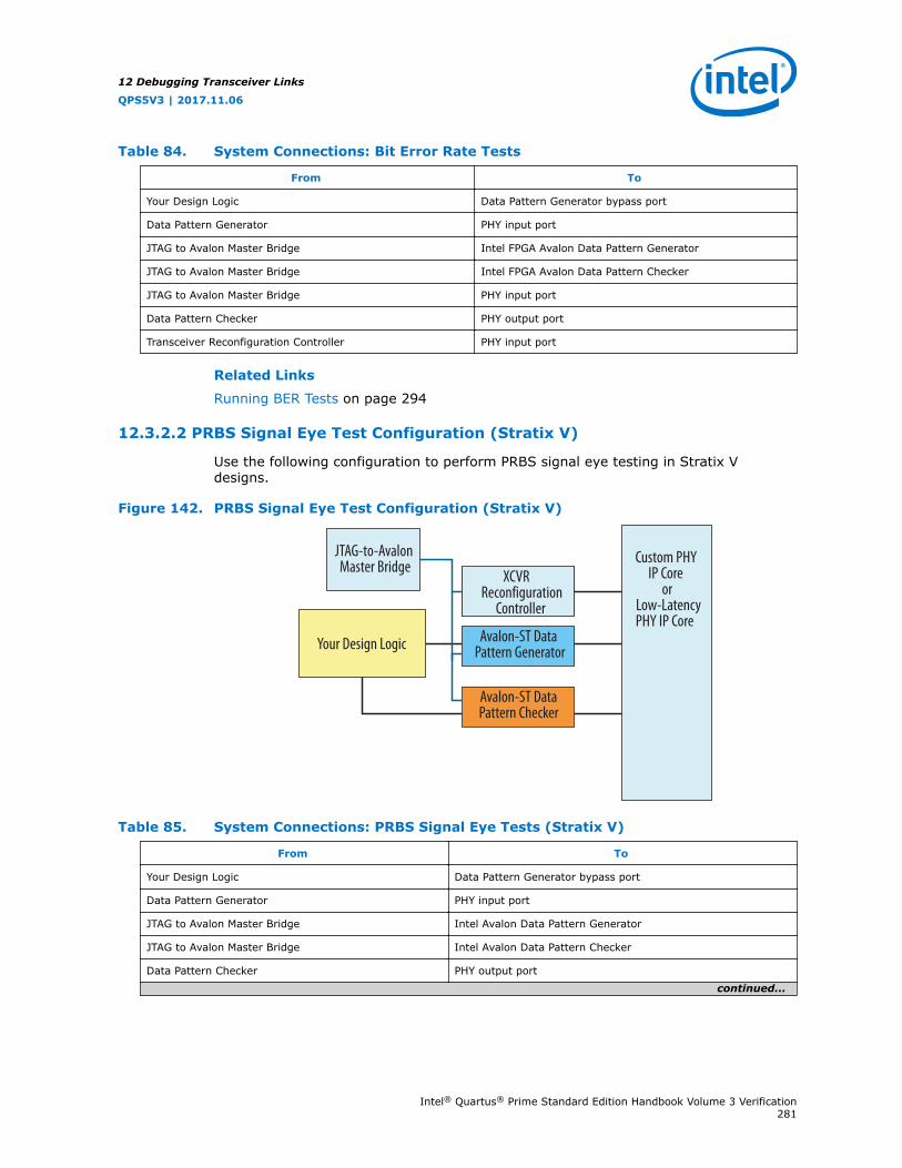
Table 84. System Connections: Bit Error Rate Tests
From To
Your Design Logic Data Pattern Generator bypass port
Data Pattern Generator PHY input port
JTAG to Avalon Master Bridge Intel FPGA Avalon Data Pattern Generator
JTAG to Avalon Master Bridge Intel FPGA Avalon Data Pattern Checker
JTAG to Avalon Master Bridge PHY input port
Data Pattern Checker PHY output port
Transceiver Reconfiguration Controller PHY input port
Related Links
Running BER Tests on page 294
12.3.2.2 PRBS Signal Eye Test Configuration (Stratix V)
Use the following configuration to perform PRBS signal eye testing in Stratix Vdesigns.
Figure 142. PRBS Signal Eye Test Configuration (Stratix V)
JTAG-to-AvalonMaster Bridge
Avalon-ST DataPattern Generator
Avalon-ST DataPattern Checker
Custom PHYIP Core
orLow-LatencyPHY IP Core
Your Design Logic
XCVR Reconfiguration
Controller
Table 85. System Connections: PRBS Signal Eye Tests (Stratix V)
From To
Your Design Logic Data Pattern Generator bypass port
Data Pattern Generator PHY input port
JTAG to Avalon Master Bridge Intel Avalon Data Pattern Generator
JTAG to Avalon Master Bridge Intel Avalon Data Pattern Checker
Data Pattern Checker PHY output port
continued...
12 Debugging Transceiver Links
QPS5V3 | 2017.11.06
Intel® Quartus® Prime Standard Edition Handbook Volume 3 Verification281

From To
JTAG to Avalon Master Bridge Transceiver Reconfiguration Controller
JTAG to Avalon Master Bridge PHY input port
Transceiver Reconfiguration Controller PHY input port
Related Links
Running PRBS Signal Eye Tests (Stratix V only) on page 295
12.3.2.2.1 Enabling Serial Bit Comparator Mode (Stratix V)
Serial bit comparator mode allows you to run Eye Viewer diagnostic features withany PRBS patterns or user-design data, without disrupting the data path. For Stratix Vdevices, you must enable Serial bit comparator mode.
To enable this mode for Stratix V devices, you must enable the following debuggingcomponent options when configuring the debugging system:
Table 86. Component Settings for Serial Bit Comparator Mode
Debugging Component Setting for Serial Bit Mode(8)
Transceiver Reconfiguration Controller Turn on Enable Eye Viewer block and Enable Bit Error Rate Block
Data Pattern Generator(9) Turn on Enable Bypass interface
Serial bit comparator mode is less accurate than Data pattern checker mode forsingle bit error checking. Do not use Serial bit comparator mode if you require anexact error rate. Use the Serial bit comparator mode for checking a large window oferror. The toolkit does not read the bit error counter in real-time because it readsthrough the memory-mapped interface. Serial bit comparator mode has the followinghardware limitations for Stratix V devices:
• Toolkit uses serial bit checker only on a single channel per reconfigurationcontroller at a time.
• When the serial bit checker is running on channel n, you can change only the VOD,pre-emphasis, DC gain, and Eye Viewer settings on that channel. Changing orenabling DFE or CTLE can cause corruption of the serial bit checker results.
• When the serial bit checker is running on a channel, you cannot change settingson any other channel on the same reconfiguration controller.
• When the serial bit checker is running on a channel, you cannot open any otherchannel in the Transceiver Toolkit.
• When the serial bit checker is running on a channel, you cannot copy PMA settingsfrom any channel on the same reconfiguration controller.
12.3.2.3 Custom Traffic Signal Eye Test Configuration (Stratix V)
Use the following configuration to perform custom traffic signal eye testing in Stratix Vdesigns.
(8) Settings in Table 86 on page 282 are supported in Stratix V devices only.
(9) Limited support for Data Pattern Generator or data pattern in Serial Bit Mode.
12 Debugging Transceiver Links
QPS5V3 | 2017.11.06
Intel® Quartus® Prime Standard Edition Handbook Volume 3 Verification282

Figure 143. System Configuration: Custom Traffic Signal Eye Tests (Stratix V)
JTAG-to-AvalonMaster Bridge Custom PHY
IP Coreor
Low-LatencyPHY IP Core
Your Design Logic(Custom Traffic)
XCVR Reconfiguration
Controller
Table 87. System Connections: Custom Traffic Signal Eye Tests (Stratix V)
From To
Your design logic with custom traffic PHY input port
JTAG to Avalon Master Bridge Transceiver Reconfiguration Controller
JTAG to Avalon Master Bridge PHY input port
Transceiver Reconfiguration Controller PHY input port
Related Links
Running Custom Traffic Tests (Stratix V only) on page 296
12.3.2.4 Link Optimization Test Configuration (Stratix V)
Use the following configuration for link optimization tests in Stratix V devices.
12 Debugging Transceiver Links
QPS5V3 | 2017.11.06
Intel® Quartus® Prime Standard Edition Handbook Volume 3 Verification283

Figure 144. System Configuration: Link Optimization Tests (Stratix V)
JTAG-to-AvalonMaster Bridge
Avalon-ST DataPattern Generator
Avalon-ST DataPattern Checker
Custom PHYIP Core
orLow-LatencyPHY IP Core
Your Design Logic
XCVR Reconfiguration
Controller
From To
Your Design Logic Data Pattern Generator bypass port
Data Pattern Generator PHY input port
JTAG to Avalon Master Bridge Altera Avalon Data Pattern Generator
JTAG to Avalon Master Bridge Altera Avalon Data Pattern Checker
Data Pattern Checker PHY output port
JTAG to Avalon Master Bridge Transceiver Reconfiguration Controller
JTAG to Avalon Master Bridge PHY input port
Transceiver Reconfiguration Controller PHY input port
Related Links
Running the Auto Sweep Test on page 297
12.3.2.5 PMA Analog Setting Control Configuration (Stratix V)
Use the following configuration to control PMA Analog settings in Stratix V designs.
12 Debugging Transceiver Links
QPS5V3 | 2017.11.06
Intel® Quartus® Prime Standard Edition Handbook Volume 3 Verification284

Figure 145. System Configuration: PMA Analog Setting Control (Stratix V)
JTAG-to-AvalonMaster Bridge Custom PHY
IP Coreor
Low-LatencyPHY IP Core
XCVR Reconfiguration
Controller
Table 88. System Connections: PMA Analog Setting Control (Stratix V)
From To
JTAG to Avalon Master Bridge Transceiver Reconfiguration Controller
JTAG to Avalon Master Bridge PHY input port
Transceiver Reconfiguration Controller PHY input port
Related Links
Controlling PMA Analog Settings on page 297
12.3.3 Instantiating and Parameterizing Intel Arria 10 Debug IP cores
To debug Intel Arria 10 designs with the Transceiver Toolkit, you must enabledebugging settings in Transceiver Intel FPGA IP cores. You can either activate thesesettings when you first instantiate these components, or modify your instance afterpreliminary compilation.
The IP cores that you modify are:
• Transceiver Native PHY
• Transceiver ATX PLL
• CMU PLL
• fPLL
12 Debugging Transceiver Links
QPS5V3 | 2017.11.06
Intel® Quartus® Prime Standard Edition Handbook Volume 3 Verification285

The parameters that you enable in the debug IP cores are:
Table 89. IP Cores and Debug SettingsFor more information about these parameters, refer to Debug Settings for Transceiver IP Cores.
IP Core Enabledynamicreconfiguration
Enable AlteraDebug MasterEndpoint
Enablecapabilityregisters
Enable controland statusregisters
Enable PRBSSoftaccumulators
Transceiver Native PHY Yes Yes Yes Yes Yes
Transceiver ATX PLL Yes Yes
CMU PLL Yes Yes
fPLL Yes Yes
For each transceiver IP core:
1. In the IP Components tab of the Project Navigator, right-click the IP instance,and click Edit in Parameter Editor.
2. Turn on debug settings as they appear in the IP Cores and Debug Settings tableabove.
Figure 146. Intel Arria 10 Transceiver Native PHY IP Core in the Parameter Editor
12 Debugging Transceiver Links
QPS5V3 | 2017.11.06
Intel® Quartus® Prime Standard Edition Handbook Volume 3 Verification286

Figure 147. Intel Arria 10 Transceiver ATX PLL Core in the Parameter Editor
3. Click Generate HDL.
After enabling parameters for all IPs in the design, recompile your project.
12.3.3.1 Debug Settings for Transceiver IP Cores
The table describes the settings that you turn on when preparing your transceiver fordebug:
Table 90. Intel FPGA IP Settings for Transceiver Debug
Setting Description
Enable Dynamic Reconfiguration Allows you to change the behavior of the transceiver channels and PLLs withoutpowering down the device
Enable Altera Debug MasterEndpoint
Allows you to access the transceiver and PLL registers through System Console.When you recompile your design, Intel Quartus Prime software inserts the ADME,debug fabric, and embedded logic during synthesis.
Enable capability registers Capability registers provide high level information about the configuration of thetransceiver channel
Enable control and statusregisters
Enables soft registers to read status signals and write control signals on the PHYinterface through the embedded debug.
Enable PRBS Soft Accumulators Enables soft logic for performing PRBS bit and error accumulation when you usethe hard PRBS generator and checker.
For more information about dynamic reconfiguration parameters on Intel Arria 10devices, refer to the Intel Arria 10 Transceiver PHY User Guide.
Related Links
Dynamic Reconfiguration ParametersIn Intel Arria 10 Transceiver PHY User Guide
12.4 Programming the Design into an Intel FPGA
After you include debug components in the design, compile, and generateprogramming files, you can program the design in the Intel FPGA.
12 Debugging Transceiver Links
QPS5V3 | 2017.11.06
Intel® Quartus® Prime Standard Edition Handbook Volume 3 Verification287

Related Links
Programming Intel FPGA Devices on page 444
12.5 Loading the Design in the Transceiver Toolkit
If the FPGA is already programmed with the project when loading, the TransceiverToolkit automatically links the design to the target hardware in the toolkit. The toolkitautomatically discovers links between transmitter and receiver of the same channel.
Before loading the device, ensure that you connect the hardware. The device and JTAGconnections appear in the Device and Connections folders of the System Explorerpane.
To load the design into the Transceiver Toolkit:
1. In the System Console, click File ➤ Load Design.
2. Select the .sof programming file for the transceiver design.
After loading the project, the designs and design instances folders in the SystemExplorer pane display information about the design, such as the design name and theblocks in the design that can communicate to the System Console.
Related Links
System Explorer Pane on page 198
12.6 Linking Hardware Resources
Linking the hardware resources maps the project you load to the target FPGA. If youload multiple design projects for multiple FPGAs, then linking indicates which of theprojects is in each of the FPGAs. The toolkit automatically discovers hardware anddesigns you connect. You can also manually link a design to connected hardwareresources in the System Explorer.
If you are using more than one Intel FPGA board, you can set up a test with multipledevices linked to the same design. This setup is useful if you want to perform a linktest between a transmitter and receiver on two separate devices. You can also loadmultiple Intel Quartus Prime projects and link between different systems. You canperform tests on separate and unrelated systems in a single Intel Quartus Primeinstance.
12 Debugging Transceiver Links
QPS5V3 | 2017.11.06
Intel® Quartus® Prime Standard Edition Handbook Volume 3 Verification288

Figure 148. One Channel Loopback Mode for Stratix V (28nm)
JTAG-to-AvalonMaster Bridge
Loopbackon board
Top-Level Design (FPGA)
Avalon-ST DataPattern Generator
Avalon-ST DataPattern Checker
Custom PHYIP Core
orLow-LatencyPHY IP Core
Transceiver Toolkithost computer
XCVRReconfiguration
Controller
Figure 149. One Channel Loopback Mode for Intel Arria 10devices
Transceiver ToolkitHost Computer
Top-Level Design (FPGA)
LoopbackOn Board
Hard PRBS GeneratorHard PRBS Checker
Altera Debug MasterEndpoint (ADME)
Transceiver Native PHY IP
12 Debugging Transceiver Links
QPS5V3 | 2017.11.06
Intel® Quartus® Prime Standard Edition Handbook Volume 3 Verification289

Figure 150. Four Channel Loopback Mode for Stratix V / 28nm
JTAG-to-AvalonMaster Bridge
Top-Level Design (FPGA)
Custom PHYIP Core
orLow-LatencyPHY IP Core
Transceiver Toolkithost computer
Avalon-ST DataPattern Generator
Avalon-ST DataPattern Checker
Avalon-ST DataPattern Generator
Avalon-ST DataPattern Checker
Avalon-ST DataPattern Generator
Avalon-ST DataPattern Checker
Avalon-ST DataPattern Generator
Avalon-ST DataPattern Checker
Loopbackon board
Loopbackon board
Loopbackon board
Loopbackon board
XCVRReconfiguration
Controller
12 Debugging Transceiver Links
QPS5V3 | 2017.11.06
Intel® Quartus® Prime Standard Edition Handbook Volume 3 Verification290

Figure 151. Four Channel Loopback Mode for Intel Arria 10devices
Transceiver ToolkitHost Computer
Top-Level Design (FPGA)
LoopbackOn Board
Hard PRBS Generator
Hard PRBS Checker
Altera Debug MasterEndpoint (ADME)
Transceiver Native PHY IP
LoopbackOn Board
Hard PRBS GeneratorHard PRBS Checker Loopback
On BoardHard PRBS GeneratorHard PRBS Checker
LoopbackOn Board
Hard PRBS GeneratorHard PRBS Checker
12.6.1 Linking One Design to One Device
To link one design to one device by one Intel FPGA Download Cable:
1. Load the design for your Intel Quartus Prime project.
2. If the design is not auto-linked, link each device to an appropriate design.
3. Create the link between channels on the device to test.
12.6.2 Linking Two Designs to Two Devices
To link two designs to two separate devices on the same board, connected by oneIntel FPGA Download Cable download cable:
1. Load the design for all the Intel Quartus Prime project files you need.
2. If the design does not auto-link, link each device to an appropriate design
3. Open the project for the second device.
4. Link the second device on the JTAG chain to the second design (unless the designauto-links).
5. Create a link between the channels on the devices you want to test.
12.6.3 Linking One Design on Two Devices
To link the same design on two separate devices, follow these steps:
12 Debugging Transceiver Links
QPS5V3 | 2017.11.06
Intel® Quartus® Prime Standard Edition Handbook Volume 3 Verification291

1. In the Transceiver Toolkit, open the .sof you are using on both devices.
2. Link the first device to this design instance.
3. Link the second device to the design.
4. Create a link between the channels on the devices you want to test.
12.6.4 Linking Designs and Devices on Separate Boards
To link two designs to two separate devices on separate boards that connect toseparate Intel FPGA Download Cables:
1. Load the design for all the Intel Quartus Prime project files you need.
2. If the design does not auto-link, link each device to an appropriate design.
3. Create the link between channels on the device to test.
4. Link the device connected to the second Intel FPGA Download Cable to the seconddesign.
5. Create a link between the channels on the devices you want to test.
12.7 Verifying Hardware Connections
Verifying hardware connections before you perform link tests saves time in the workflow. Use the toolkit to send data patterns and receive them correctly.
After you load the design and link the hardware:
1. Verify that the channels connect correctly and loop back properly on the hardware.
2. Verify that the RX is locked to Data.
3. Start the generator on the Transmitter Channel.
4. Start the checker on the Receiver Channel.
5. Verify you have Lock to Data, and the Bit Error Rate between the two is very lowor zero.
After you verify communication between transmitter and receiver, you can create alink between the two transceivers and perform Auto Sweep and Eye Viewer tests withthis pair.
Note: The Transceiver Toolkit can perform Eye Viewer tests only on Stratix V devices.
12.8 Identifying Transceiver Channels
Verify if the Transceiver Toolkit detects your channels correctly. The toolkit identifies achannel automatically whenever a receiver and transmitter share a transceiverchannel.
The Transceiver Toolkit automatically displays transmitter and receiver channels that itrecognizes on the Transmitter Channels and Receiver Channels tabs of theChannel Manager. You can also manually identify the transmitter and receiver in atransceiver channel, and create a link between the two for testing.
12 Debugging Transceiver Links
QPS5V3 | 2017.11.06
Intel® Quartus® Prime Standard Edition Handbook Volume 3 Verification292

12.8.1 Controlling Transceiver Channels
To adjust or monitor transmitter or receiver settings while the channels are running:
• In the Transmitter Channels tab, click Control Transmitter Channel
• In the Receiver Channels tab, click Control Receiver Channel.
• In the Transceiver Links tab, click Control Receiver Channel.
For example, you can transmit a data pattern across the transceiver link, and thenreport the signal quality of the data you receive.
12.8.2 Creating Links
The toolkit automatically creates links when a receiver and transmitter share atransceiver channel. You can also manually create and delete links betweentransmitter and receiver channels. You create links in the Setup dialog box.
Setup Dialog Box
Click Setup from the Channel Manager to open the Setup dialog box.
Table 91. Setup Dialog Box Menu
Command Name Description Enabled
Edit Transmitter Alias Starts the inline edit of the alias of the selected row. Only enabled if one rowis selected.
Edit Receiver Alias Starts the inline edit of the alias of the selected row. Only enabled if one rowis selected.
Edit Transceiver Link Alias Starts the inline edit of the alias of the selected row. Only enabled if one rowis selected.
Copy Copies the text of the selected rows to the clipboard. Thetext copied depends on the column clicked on. The textcopied to the clipboard is newline delimited.
Enabled if one or morerows are selected.
12.8.3 Manually Creating a Transceiver Link
Creating a link designates which Transmitter and Receiver channels connect physically.
To create a transceiver link with the Channel Manager:
1. Click Setup.
2. Select the generator and checker you want to control.
3. Select the transmitter and receiver pair you want to control.
4. Click Create Transceiver Link.
5. Click Close
The toolkit names the link automatically, but you can rename it using a link alias andgive the link a shorter, more meaningful name.
12.9 Running Link Tests
Once you identify the transceiver channels for debugging, you can run link tests. Usethe Transceiver Links tab to control link tests.
12 Debugging Transceiver Links
QPS5V3 | 2017.11.06
Intel® Quartus® Prime Standard Edition Handbook Volume 3 Verification293

When you run link tests, channel color highlights indicate the test status:
Table 92. Channel Color Highlights
Color Transmitter Channel Receiver Channel
Red Channel is closed or generator clock is notrunning.
Channel is closed or checker clock is not running.
Green Generator is sending a pattern. Checker is checking and data pattern is locked.
Neutral (same coloras background)
Channel is open, generator clock is running,and generator is not sending a pattern.
Channel is open, checker clock is running, andchecker is not checking.
Yellow N/A Checker is checking and data pattern is notlocked.
12.9.1 Running BER Tests
BER tests help you assess signal integrity. Follow these steps to run BER tests across atransceiver link:
1. In the Channel Manager, click Control Transceiver Link.
2. Specify a PRBS Test pattern
3. If your device supports setting a Checker mode, set to Data pattern checker.
4. Try different values of Reconfiguration, Generator, or Checker settings, ifavailable.
5. Click Start to run the pattern with your settings.
6. If your device supports error injection, you can click Inject Error to inject errorbits.
7. You can also Reset the counter, or Stop the test.
Note: Intel Arria 10 devices do not support Inject Error if you use the hard PRBSPattern Generator and Checker in the system configuration.
Related Links
Bit Error Rate Test Configuration (Stratix V) on page 280
12.9.2 Signal Eye Margin Testing (Stratix V only)
Stratix V includes Eye Viewer circuitry, that allows visualization of the horizontal andvertical eye margin at the receiver. For supported devices, use signal eye tests to tunethe PMA settings of your transceiver. This results in the best eye margin and BER athigh data rates. The toolkit disables signal eye testing for unsupported devices.
The Eye Viewer graph can display a bathtub curve, eye diagram representing eyemargin, or heat map display. The run list displays the statistics of each Eye Viewertest. When PMA settings are suitable, the bathtub curve is wide, with sharp slopesnear the edges. The curve is up to 30 units wide. If the bathtub is narrow, then thesignal quality is poor. The wider the bathtub curve, the wider the eye. The smaller thebathtub curve, the smaller the eye. The eye contour shows the estimated horizontaland vertical eye opening at the receiver.
You can right-click any of the test runs in the list, and then click Apply Settings toDevice to quickly apply that PMA setting to your device. You can also click Export,Import, or Create Report.
12 Debugging Transceiver Links
QPS5V3 | 2017.11.06
Intel® Quartus® Prime Standard Edition Handbook Volume 3 Verification294

Figure 152. Eye Viewer Settings and Status Showing Results of Two Test Runs
Figure 153. Heat Map Display and Bathtub Curve Through Eye
12.9.2.1 Running PRBS Signal Eye Tests (Stratix V only)
Run PRBS signal eye tests to visualize the estimated horizontal and vertical eyeopening at the receiver. After programming the FPGA with your debugging design,loading the design in the toolkit, and linking hardware, follow these steps to run PRBSsignal eye tests:
1. Click Setup.
a. Select the generator and checker you want to control.
b. Select the transmitter and receiver pair you want to control.
c. Click Create Transceiver Link and click Close.
2. Click Link Eye Viewer, and select Eye Viewer as the Test mode. The EyeViewer mode displays test results as a bathtub curve, heat map, or eye contourrepresenting bit error and phase offset data.
3. Specify the PRBS Test pattern and the Checker mode. Use Serial bitcomparator checker mode only for checking a large window of error with customtraffic.
12 Debugging Transceiver Links
QPS5V3 | 2017.11.06
Intel® Quartus® Prime Standard Edition Handbook Volume 3 Verification295

The checker mode option is only available after you turn on Enable Eye Viewerblock and Enable Bit Error Rate Block in the Reconfiguration Controllercomponent. (Stratix V designs only)
4. Specify Run length and Eye Viewer settings to control the test coverage andtype of Eye Viewer results displayed, respectively.
5. Click Start to run the pattern with your settings. Eye Viewer uses the currentchannel settings to start a phase sweep of the channel. The phase sweep runs 32iterations. As the run progresses, view the status under Eye Viewer status. Usethis diagram to compare PMA settings for the same channel and to choose thebest combination of PMA settings for a particular channel.
6. When the run completes, the chart displays the characteristics of each run. ClickStop to halt the test, change the PMA settings, and re-start the test. Click CreateReport to export data to a table format for further viewing.
Related Links
• PRBS Signal Eye Test Configuration (Stratix V) on page 281
• AN 678: High-Speed Link Tuning Using Signal Conditioning Circuitry
12.9.3 Running Custom Traffic Tests (Stratix V only)
After programming the FPGA with your debugging design, loading the design in thetoolkit, and linking hardware, follow these steps to run custom traffic tests:
1. In the Channel Manager, click Setup.
2. Select the associated reconfiguration controller.
3. Click Create Transceiver Link and click Close.
4. Click the Receiver Eye Viewer tab.
5. Select Eye Viewer as the Test mode. The Eye Viewer mode displays testresults as a bathtub curve, heat map, or eye contour representing bit error andphase offset data.
6. Specify the PRBS Test pattern.
7. For Checker mode, select Serial bit comparator.
The checker mode option is only available after you turn on Enable Eye Viewerblock and Enable Bit Error Rate Block for the Reconfiguration Controllercomponent.
8. Specify Run length and Eye Viewer settings to control the test coverage andtype of Eye Viewer results displayed, respectively.
9. Click Start to run the pattern with your settings. Eye Viewer uses the currentchannel settings to start a phase sweep of the channel. The phase sweep runs 32iterations. As the run progresses, view the status under Eye Viewer status.
10. When the run completes, the chart displays the characteristics of each run. ClickStop to halt the test, change the PMA settings, and re-start the test. Click CreateReport to export data to a table format for further viewing.
Related Links
Custom Traffic Signal Eye Test Configuration (Stratix V) on page 282
12 Debugging Transceiver Links
QPS5V3 | 2017.11.06
Intel® Quartus® Prime Standard Edition Handbook Volume 3 Verification296

12.9.4 Link Optimization Tests
The Transceiver Toolkit auto sweep test automatically sweeps PMA ranges to help youfind the best transceiver settings. The toolkit allows you to store a history of the testruns, and keep a record of the best PMA settings. Use the best settings that the toolkitdetermined in your final design to improve signal integrity.
12.9.4.1 Running the Auto Sweep Test
to run link optimization tests:
1. In the Transceiver Links tab, select the channel you want to control.
2. Click Link Auto Sweep.The Advanced tab appears with Auto sweep as Test mode.
3. Specify the PRBS Test pattern.
4. Specify Run length experiment with the Transmitter settings, and Receiversettings to control the test coverage and PMA settings, respectively.
5. Click Start to run all combinations of tests meeting the PMA parameter limits.When the run completes the chart is displayed and the characteristics of each runare listed in the run list.
6. You can click Stop to halt the test, change the PMA settings, and re-start the test.Click Create Report to export data to a table format for further viewing.
7. If you want to determine the best tap settings using decision feedbackequalization (DFE):
a. Set the DFE mode to Off.
b. Use Auto Sweep to find optimal PMA settings.
c. If BER = 0, use the best PMA settings achieved.
d. If BER > 0, use this PMA setting, and set the minimum and maximum valuesobtained from Auto Sweep to match this setting. Set the maximum DFE rangeto limits for each of the three DFE settings.
e. Run Create Report to view the results and determine which DFE setting hasthe best BER. Use these settings in conjunction with the PMA settings for thebest results.
Related Links
• Link Optimization Test Configuration (Stratix V) on page 283
• Instantiating and Parameterizing Intel Arria 10 Debug IP cores on page 285
12.9.4.2 TODO task
For the Altera Offline Compiler (AOC) to target a specific board package, you have toset the environment variable AOCL_BOARD_PACKAGE ROOT to point to the directorywhere you set up the board installation environment.
To set up the board environment, perform the following tasks:
12.10 Controlling PMA Analog Settings
The Transceiver Toolkit allows you to directly control PMA analog settings while the linkis running. To control PMA analog settings, follow these steps:
12 Debugging Transceiver Links
QPS5V3 | 2017.11.06
Intel® Quartus® Prime Standard Edition Handbook Volume 3 Verification297

1. In the Channel Manager, click Setup, and specify the following:
a. In the Transmitter Channels tab, define a transmitter without a generator,and click Create Transmitter Channel.
b. In the Receiver Channels tab, define a receiver without a generator, andclick Create Receiver Channel.
c. In the Transceiver Links tab, select the transmitter and receivers you wantto control, and click Create Transceiver Link.
d. Click Close.
2. Click Control Receiver Channel, Control Transmitter Channel, or ControlTransceiver Link to directly control the PMA settings while running.
Figure 154. Controlling Transmitter Channel
12 Debugging Transceiver Links
QPS5V3 | 2017.11.06
Intel® Quartus® Prime Standard Edition Handbook Volume 3 Verification298

Figure 155. Controlling Receiver Channel
12 Debugging Transceiver Links
QPS5V3 | 2017.11.06
Intel® Quartus® Prime Standard Edition Handbook Volume 3 Verification299

Figure 156. Controlling Transceiver Link
Related Links
• Instantiating and Parameterizing Intel Arria 10 Debug IP cores on page 285
• PMA Analog Setting Control Configuration (Stratix V) on page 284
• User Interface Settings Reference on page 300
12.11 User Interface Settings Reference
The Transceiver Toolkit user interface allows you to specify these settings:
Note: All the settings appear in the Transceiver Link control pane.
12 Debugging Transceiver Links
QPS5V3 | 2017.11.06
Intel® Quartus® Prime Standard Edition Handbook Volume 3 Verification300

Table 93. Transceiver Toolkit Control Pane Settings
Setting Description Control Pane
Alias Name you choose for the channel. Transmitter paneReceiver pane
Auto Sweep status Reports the current and best tested bits, errors, bit error rate, andcase count for the current Auto Sweep test.
Receiver pane
Bit error rate (BER) Specifies errors divided by bits tested since the last reset of thechecker.
Receiver pane
Channel address Logical address number of the transceiver channel. Transmitter paneReceiver pane
Data rate Data rate of the channel that appears in the project file, or data ratethe frequency detector measures.To use the frequency detector, turn on Enable Frequency Counterin the Data Pattern Checker IP core or Data Pattern Generator IPcore, regenerate the IP cores, and recompile the design.The measured data rate depends on the Avalon management clockfrequency that appears in the project file.If you make changes to your settings and want to sample the datarate again, click the Refresh button next to the Data rate
Transmitter paneReceiver pane
DC gain Circuitry that provides an equal boost to the incoming signal acrossthe frequency spectrum.
Receiver pane
DFE mode Decision feedback equalization (DFE) for improving signal quality.• Values 1-5 (Stratix V devices)• Values 1-11 (Intel Arria 10 devices)In Intel Arria 10 devices, DFE modes are Off, Manual andAdaptation Enabled. DFE in Adaptation Enabled modeautomatically tries to find the best tap values.In Stratix V devices DFE modes are Off, Manual, One-timeadaptive mode and Adaptation Enabled. Adaptation Enabled modeDFE automatically tries to find the best tap values.
Receiver pane
Enable word aligner(Stratix V only)
Forces the transceiver channel to align to the word you specify. Receiver pane
Equalization control Boosts the high-frequency gain of the incoming signal, therebycompensating for the low-pass filter effects of the physical medium.When you use this option with DFE, use DFE in Manual orAdaptation Enabled mode.In Stratix V devices, auto sweep supports AEQ one-time adaptation.
Receiver pane
Equalization mode For Intel Arria 10 devices, you can set Equalization Mode toManual or Triggered.In Stratix V devices, Adaptive equalization (AEQ) automaticallyevaluates and selects the best combination of equalizer settings andturns off Equalization Control. The one-time selection determinesthe best setting and stops searching. You can use AEQ for multiple,independently controlled receiver channels.
Receiver pane
Error rate limit Turns on or off error rate limits. Start checking after specifies thenumber of bits the toolkit waits before looking at the bit error rate(BER) for the next two checks.Bit error rate achieves below sets upper bit error rate limits. If theerror rate is better than the set error rate, the test ends.Bit error rate exceeds sets lower bit error rate limits. If the errorrate is worse than the set error rate, the test ends.
Receiver pane
Generator/Checkermode
Specifies Data pattern checker or Serial bit comparator for BERtests.
Receiver pane
continued...
12 Debugging Transceiver Links
QPS5V3 | 2017.11.06
Intel® Quartus® Prime Standard Edition Handbook Volume 3 Verification301
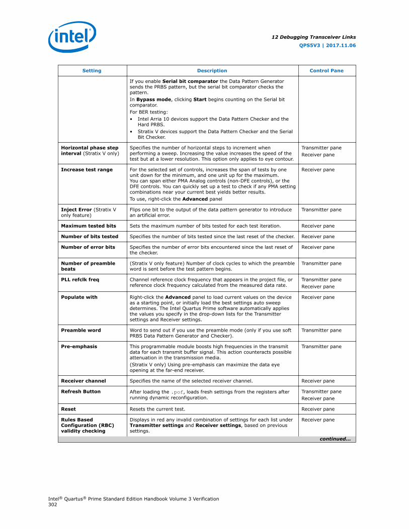
Setting Description Control Pane
If you enable Serial bit comparator the Data Pattern Generatorsends the PRBS pattern, but the serial bit comparator checks thepattern.In Bypass mode, clicking Start begins counting on the Serial bitcomparator.For BER testing:• Intel Arria 10 devices support the Data Pattern Checker and the
Hard PRBS.• Stratix V devices support the Data Pattern Checker and the Serial
Bit Checker.
Horizontal phase stepinterval (Stratix V only)
Specifies the number of horizontal steps to increment whenperforming a sweep. Increasing the value increases the speed of thetest but at a lower resolution. This option only applies to eye contour.
Transmitter paneReceiver pane
Increase test range For the selected set of controls, increases the span of tests by oneunit down for the minimum, and one unit up for the maximum.You can span either PMA Analog controls (non-DFE controls), or theDFE controls. You can quickly set up a test to check if any PMA settingcombinations near your current best yields better results.To use, right-click the Advanced panel
Receiver pane
Inject Error (Stratix Vonly feature)
Flips one bit to the output of the data pattern generator to introducean artificial error.
Transmitter pane
Maximum tested bits Sets the maximum number of bits tested for each test iteration. Receiver pane
Number of bits tested Specifies the number of bits tested since the last reset of the checker. Receiver pane
Number of error bits Specifies the number of error bits encountered since the last reset ofthe checker.
Receiver pane
Number of preamblebeats
(Stratix V only feature) Number of clock cycles to which the preambleword is sent before the test pattern begins.
Transmitter pane
PLL refclk freq Channel reference clock frequency that appears in the project file, orreference clock frequency calculated from the measured data rate.
Transmitter paneReceiver pane
Populate with Right-click the Advanced panel to load current values on the deviceas a starting point, or initially load the best settings auto sweepdetermines. The Intel Quartus Prime software automatically appliesthe values you specify in the drop-down lists for the Transmittersettings and Receiver settings.
Receiver pane
Preamble word Word to send out if you use the preamble mode (only if you use softPRBS Data Pattern Generator and Checker).
Transmitter pane
Pre-emphasis This programmable module boosts high frequencies in the transmitdata for each transmit buffer signal. This action counteracts possibleattenuation in the transmission media.(Stratix V only) Using pre-emphasis can maximize the data eyeopening at the far-end receiver.
Transmitter pane
Receiver channel Specifies the name of the selected receiver channel. Receiver pane
Refresh Button After loading the .pof, loads fresh settings from the registers afterrunning dynamic reconfiguration.
Transmitter paneReceiver pane
Reset Resets the current test. Receiver pane
Rules BasedConfiguration (RBC)validity checking
Displays in red any invalid combination of settings for each list underTransmitter settings and Receiver settings, based on previoussettings.
Receiver pane
continued...
12 Debugging Transceiver Links
QPS5V3 | 2017.11.06
Intel® Quartus® Prime Standard Edition Handbook Volume 3 Verification302

Setting Description Control Pane
When you enable this option, the settings appear in red to indicatethe current combination is invalid. This action avoids manually testinginvalid settings that you cannot compile for your design, and preventssetting the device into an invalid mode for extended periods of timeand potentially damaging the circuits.
Run length Sets coverage parameters for test runs. Transmitter paneReceiver pane
RX CDR PLL status(10) Shows the receiver in lock-to-reference (LTR) mode. When in auto-mode, if data cannot be locked, this signal alternates in LTD mode ifthe CDR is locked to data.
Receiver pane
RX CDR data status Shows the receiver in lock-to-data (LTD) mode. When in auto-mode,if data cannot be locked, the signal stays high when locked to dataand never switches.
Receiver pane
Serial loopback enabled Inserts a serial loopback before the buffers, allowing you to form alink on a transmitter and receiver pair on the same physical channelof the device.
Transmitter paneReceiver pane
Start Starts the pattern generator or checker on the channel to verifyincoming data.
Transmitter paneReceiver pane
Stop Stops generating patterns and testing the channel. Transmitter paneReceiver pane
Target bit error rate(Stratix V only)
Finds the contour edge of the bit error rate that you select. Thisoption only applies to eye contour mode.
Transmitter paneReceiver pane
Test mode Allows you to specify the test mode.Intel Arria 10 devices support Auto Sweep test mode only.Stratix V devices support:• Auto Sweep test mode• Eye Viewer test mode• Auto Sweep and Eye Viewer test mode
Receiver pane
Test pattern Test pattern sent by the transmitter channel. Intel Arria 10 devicessupport PRBS9, PRBS15, PRBS23, and PRBS31).Stratix V devices support PRBS7, PRBS15, PRBS23, PRBS31,LowFrequency, HighFrequency, and Bypass mode. The DataPattern Checker self-aligns both high and low frequency patterns. UseBypass mode to send user-design data.
Transmitter paneReceiver pane
Time limit Specifies the time limit unit and value to have a maximum boundstime limit for each test iteration
Receiver
Transmitter channel Specifies the name of the selected transmitter channel. Transmitter pane
TX/CMU PLL status Provides status of whether the transmitter channel PLL is locked tothe reference clock.
Transmitter pane
Use preamble uponstart
If turned on, sends the preamble word before the test pattern. Ifturned off, starts sending the test pattern immediately.
Transmitter pane
Vertical phase stepinterval (Stratix V only)
Specify the number of vertical steps to increment when performing asweep. Increasing the value increases the speed of the test but at alower resolution. This option only applies to the eye contour.
Transmitter paneReceiver pane
VOD control Programmable transmitter differential output voltage. Transmitter pane
(10) For Stratix V devices, the Phase Frequency Detector (PFD) is inactive in LTD mode. Therx_is_lockedtoref status signal turns on and off randomly, and is not significant in LTDmode.
12 Debugging Transceiver Links
QPS5V3 | 2017.11.06
Intel® Quartus® Prime Standard Edition Handbook Volume 3 Verification303

Related Links
Channel Manager on page 274
12.12 Troubleshooting Common Errors
Missing high-speed link pin connections
• Check if the pin connections to identify high-speed links (tx_p/n and rx_p/n) aremissing. When porting an older design to the latest version of the Intel QuartusPrime software, make sure that these connections exist after porting.
Reset Issues:
• Ensure that the reset input to the Transceiver Native PHY, Transceiver ResetController, and ATX PLL IP cores is not held active (1'b1). The Transceiver Toolkithighlights in red all the Transceiver Native PHY channels that you are setting up.
Unconnected reconfig_clk
• You must connect and drive the reconfig_clk input to the Transceiver NativePHY and ATX PLL IP cores. Otherwise, the toolkit does not display the transceiverlink channel.
12.13 Scripting API Reference
The Intel Quartus Prime software provides an API to access Transceiver Toolkitfunctions using Tcl commands, and script tasks such as linking device resources andidentifying high-speed serial links.
To save your project setup in a Tcl script for use in subsequent testing sessions:
1. Set up and define links that describe the entire physical system
2. Click Save Tcl Script to save the setup for future use.
You can also build a custom test routine script.
To run the scripts, double-click the script name in the System Explorer scripts folder.
To view a list of the available Tcl command descriptions from the Tcl Console window,including example usage:
1. In the Tcl console, type help help. The Console displays all Transceiver ToolkitTcl commands.
2. Type help <command name>. The Console displays the command description.
12.13.1 Transceiver Toolkit Commands
The following tables list the available Transceiver Toolkit scripting commands.
12 Debugging Transceiver Links
QPS5V3 | 2017.11.06
Intel® Quartus® Prime Standard Edition Handbook Volume 3 Verification304

Table 94. Transceiver Toolkit channel_rx Commands
Command Arguments Function
transceiver_channel_rx_get_data <service-path> Returns a list of the currentchecker data. The results are inthe order of number of bits,number of errors, and bit errorrate.
transceiver_channel_rx_get_dcgain <service-path> Gets the DC gain value on thereceiver channel.
transceiver_channel_rx_get_dfe_tap_value <service-path> <tapposition>
Gets the current tap value of thechannel you specify at the tapposition you specify.
transceiver_channel_rx_get_eqctrl <service-path> Gets the equalization controlvalue on the receiver channel.
transceiver_channel_rx_get_pattern <service-path> Returns the current data checkerpattern by name.
transceiver_channel_rx_has_dfe <service-path> Reports whether the channel youspecify has the DFE featureavailable.
transceiver_channel_rx_has_eye_viewer <service-path> (Stratix V only) Reports whetherthe Eye Viewer feature isavailable for the channel youspecify.
transceiver_channel_rx_is_checking <service-path> Returns non-zero if the checker isrunning.
transceiver_channel_rx_is_dfe_enabled <service-path> Reports whether the DFE featureis enabled on the channel youspecify.
transceiver_channel_rx_is_locked <service-path> Returns non-zero if the checker islocked onto the incoming data.
transceiver_channel_rx_reset_counters <service-path> Resets the bit and error countersinside the checker.
transceiver_channel_rx_reset <service-path> Resets the channel you specify.
transceiver_channel_rx_set_dcgain <service-path> <value> Sets the DC gain value on thereceiver channel.
transceiver_channel_rx_set_dfe_enabled <service-path> <disable(0)/enable(1)>
Enables or disables the DFEfeature on the channel youspecify.
transceiver_channel_rx_set_dfe_tap_value <service-path> <tapposition> <tap value>
Sets the current tap value of thechannel you specify at the tapposition you specify to the valueyou specify.
transceiver_channel_rx_set_dfe_adaptive <service-path> <adaptive-mode>
Sets DFE adaptation mode of thechannel you specify.
Value Description
0 off
1 adaptive
2 one-time adaptive
continued...
12 Debugging Transceiver Links
QPS5V3 | 2017.11.06
Intel® Quartus® Prime Standard Edition Handbook Volume 3 Verification305

Command Arguments Function
transceiver_channel_rx_set_eqctrl <service-path> <value> Sets the equalization controlvalue on the receiver channel.
transceiver_channel_rx_start_checking <service-path> Starts the checker.
transceiver_channel_rx_stop_checking <service-path> Stops the checker.
transceiver_channel_rx_get_eye_viewer_phase_step
<service-path> (Stratix V only) Gets the currentphase step of the channel youspecify.
transceiver_channel_rx_set_pattern <service-path> <pattern-name>
Sets the expected pattern to theone specified by the patternname.
transceiver_channel_rx_is_eye_viewer_enabled
<service-path> (Stratix V only) Reports whetherthe Eye Viewer feature is enabledon the channel you specify.
transceiver_channel_rx_set_eye_viewer_enabled
<service-path> <disable(0)/enable(1)>
(Stratix V only) Enables ordisables the Eye Viewer featureon the channel you specify.
transceiver_channel_rx_set_eye_viewer_phase_step
<service-path> <phase step> (Stratix V only) Sets the phasestep of the channel you specify.
transceiver_channel_rx_set_word_aligner_enabled
<service-path> <disable(0)/enable(1)>
Enables or disables the wordaligner of the channel youspecify.
transceiver_channel_rx_is_word_aligner_enabled
<service-path> <disable(0)/enable(1)>
Reports whether the word alignerfeature is enabled on the channelyou specify.
transceiver_channel_rx_is_locked <service-path> Returns non-zero if the checker islocked onto the incoming signal.
transceiver_channel_rx_is_rx_locked_to_data
<service-path> Returns 1 if transceiver is in lockto data (LTD) mode. Otherwise 0.
transceiver_channel_rx_is_rx_locked_to_ref
<service-path> Returns 1 if transceiver is in lockto reference (LTR) mode.Otherwise 0.
transceiver_channel_rx_has_eye_viewer_1d <service-path> (Stratix V only) Detects whetherthe eye viewer in <service-path>supports 1D-Eye Viewer mode.
transceiver_channel_rx_set_1deye_mode <service-path> <disable(0)/enable(1)>
(Stratix V only) Enables ordisables 1D-Eye Viewer mode.
transceiver_channel_rx_get_1deye_mode <service-path> (Stratix V only) Returns whether1D-Eye Viewer mode is on or off.
Table 95. Transceiver Toolkit channel_tx Commands
Command Arguments Function
transceiver_channel_tx_disable_preamble <service-path> Disables the preamble mode atthe beginning of generation.
transceiver_channel_tx_enable_preamble <service-path> Enables the preamble mode atthe beginning of generation.
transceiver_channel_tx_get_number_of_preamble_beats
<service-path> Returns the number of beats tosend out the preamble word.
transceiver_channel_tx_get_pattern <service-path> Returns the pattern.
continued...
12 Debugging Transceiver Links
QPS5V3 | 2017.11.06
Intel® Quartus® Prime Standard Edition Handbook Volume 3 Verification306

Command Arguments Function
transceiver_channel_tx_get_preamble_word <service-path> Returns the preamble word.
transceiver_channel_tx_get_preemph0t <service-path> Gets the pre-emphasis first pre-tap value on the transmitterchannel.
transceiver_channel_tx_get_preemph1t <service-path> Gets the pre-emphasis first post-tap value on the transmitterchannel.
transceiver_channel_tx_get_preemph2t <service-path> Gets the pre-emphasis secondpost-tap value on the transmitterchannel.
transceiver_channel_tx_get_preemph3t <service-path> Gets the pre-emphasis secondpre-tap value on the transmitterchannel.
transceiver_channel_tx_get_vodctrl <service-path> Gets the VOD control value on thetransmitter channel.
transceiver_channel_tx_inject_error <service-path> Injects a 1-bit error into thegenerator's output.
transceiver_channel_tx_is_generating <service-path> Returns non-zero if the generatoris running.
transceiver_channel_tx_is_preamble_enabled
<service-path> Returns non-zero if preamblemode is enabled.
transceiver_channel_tx_set_number_of_preamble_beats
<service-path> <number-of-preamble-beats>
Sets the number of beats to sendout the preamble word.
transceiver_channel_tx_set_pattern <service-path> <pattern-name>
Sets the output pattern to theone specified by the patternname.
transceiver_channel_tx_set_preamble_word <service-path> <preamble-word>
Sets the preamble word to besent out.
transceiver_channel_tx_set_preemph0t <service-path> <value> Sets the pre-emphasis first pre-tap value on the transmitterchannel.
transceiver_channel_tx_set_preemph1t <service-path> <value> Sets the pre-emphasis first post-tap value on the transmitterchannel.
transceiver_channel_tx_set_preemph2t <service-path> <value> Sets the pre-emphasis secondpost-tap value on the transmitterchannel.
transceiver_channel_tx_set_preemph3t <service-path> <value> Sets the pre-emphasis secondpre-tap value on the transmitterchannel.
transceiver_channel_tx_set_vodctrl <service-path> <vodctrlvalue>
Sets the VOD control value on thetransmitter channel.
transceiver_channel_tx_start_generation <service-path> Starts the generator.
transceiver_channel_tx_stop_generation <service-path> Stops the generator.
12 Debugging Transceiver Links
QPS5V3 | 2017.11.06
Intel® Quartus® Prime Standard Edition Handbook Volume 3 Verification307

Table 96. Transceiver Toolkit Transceiver Toolkit debug_link Commands
Command Arguments Function
transceiver_debug_link_get_pattern <service-path> Gets the pattern the link uses torun the test.
transceiver_debug_link_is_running <service-path> Returns non-zero if the test isrunning on the link.
transceiver_debug_link_set_pattern <service-path> <datapattern>
Sets the pattern the link uses torun the test.
transceiver_debug_link_start_running <service-path> Starts running a test with thecurrently selected test pattern.
transceiver_debug_link_stop_running <service-path> Stops running the test.
Table 97. Transceiver Toolkit reconfig_analog Commands
Command Arguments Function
transceiver_reconfig_analog_get_logical_channel_address
<service-path> Gets the transceiver logic channeladdress currently set.
transceiver_reconfig_analog_get_rx_dcgain
<service-path> Gets the DC gain value on thereceiver channel specified by thecurrent logic channel address.
transceiver_reconfig_analog_get_rx_eqctrl
<service-path> Gets the equalization control valueon the receiver channel specified bythe current logic channel address.
transceiver_reconfig_analog_get_tx_preemph0t
<service-path> Gets the pre-emphasis first pre-tapvalue on the transmitter channelspecified by the current logicchannel address.
transceiver_reconfig_analog_get_tx_preemph1t
<service-path> Gets the pre-emphasis first post-tap value on the transmitterchannel specified by the currentlogic channel address.
transceiver_reconfig_analog_get_tx_preemph2t
<service-path> Gets the pre-emphasis secondpost-tap value on the transmitterchannel specified by the currentlogic channel address.
transceiver_reconfig_analog_get_tx_vodctrl
<service-path> Gets the VOD control value on thetransmitter channel specified by thecurrent logic channel address.
transceiver_reconfig_analog_set_logical_channel_address
<service-path> <logic channeladdress>
Sets the transceiver logic channeladdress.
transceiver_reconfig_analog_set_rx_dcgain
<service-path> <dc_gainvalue>
Sets the DC gain value on thereceiver channel specified by thecurrent logic channel address
transceiver_reconfig_analog_set_rx_eqctrl
<service-path> <eqctrl value> Sets the equalization control valueon the receiver channel specified bythe current logic channel address.
transceiver_reconfig_analog_set_tx_preemph0t
<service-path> <value> Sets the pre-emphasis first pre-tapvalue on the transmitter channelspecified by the current logicchannel address.
continued...
12 Debugging Transceiver Links
QPS5V3 | 2017.11.06
Intel® Quartus® Prime Standard Edition Handbook Volume 3 Verification308

Command Arguments Function
transceiver_reconfig_analog_set_tx_preemph1t
<service-path> < value> Sets the pre-emphasis first post-tap value on the transmitterchannel specified by the currentlogic channel address.
transceiver_reconfig_analog_set_tx_preemph2t
<service-path> <value> Sets the pre-emphasis second post-tap value on the transmitterchannel specified by the currentlogic channel address.
transceiver_reconfig_analog_set_tx_vodctrl
<service-path> <vodctrl value> Sets the VOD control value on thetransmitter channel specified by thecurrent logic channel address.
.
Table 98. Transceiver Toolkit Decision Feedback Equalization (DFE) Commands
Command Arguments Function
alt_xcvr_reconfig_dfe_get_logical_channel_address
<service-path> Gets the logic channel addressthat otheralt_xcvr_reconfig_dfecommands use to apply.
alt_xcvr_reconfig_dfe_is_enabled <service-path> Reports whether the DFE featureis enabled on the previouslychannel you specify.
alt_xcvr_reconfig_dfe_set_enabled <service-path> <disable(0)/enable(1)>
Enables or disables the DFEfeature on the previously channelyou specify.
alt_xcvr_reconfig_dfe_set_logical_channel_address
<service-path> <logicchannel address>
(Stratix V only) Sets the logicchannel address that otheralt_xcvr_reconfig_eye_viewer commands use.
alt_xcvr_reconfig_dfe_set_tap_value <service-path> <tapposition> <tap value>
Sets the tap value at thepreviously channel you specify atspecified tap position and value.
Table 99. Transceiver Toolkit Eye Monitor Commands (Stratix V only)
Command Arguments Function
alt_xcvr_custom_is_word_aligner_enabled <service-path> <disable(0)/enable(1)>
Reports whether the word alignerfeature is enabled on thepreviously channel you specify.
alt_xcvr_custom_set_word_aligner_enabled <service-path> <disable(0)/enable(1)>
Enables or disables the wordaligner of the previously channelyou specify.
alt_xcvr_custom_is_rx_locked_to_data <service-path> Returns whether the receiver CDRis locked to data.
alt_xcvr_custom_is_rx_locked_to_ref <service-path> Returns whether the receiver CDRPLL is locked to the referenceclock.
alt_xcvr_custom_is_serial_loopback_enabled
<service-path> Returns whether the serialloopback mode of the previouslychannel you specify is enabled.
continued...
12 Debugging Transceiver Links
QPS5V3 | 2017.11.06
Intel® Quartus® Prime Standard Edition Handbook Volume 3 Verification309

Command Arguments Function
alt_xcvr_custom_set_serial_loopback_enabled
<service-path> <disable(0)/enable(1)>
Enables or disables the serialloopback mode of the previouslychannel you specify.
alt_xcvr_custom_is_tx_pll_locked <service-path> Returns whether the transmitterPLL is locked to the referenceclock.
alt_xcvr_reconfig_eye_viewer_get_logical_channel_address
<service-path> Gets the logic channel address onwhich otheralt_reconfig_eye_viewercommands use.
alt_xcvr_reconfig_eye_viewer_get_phase_step
<service-path> Gets the current phase step ofthe previously channel youspecify.
alt_xcvr_reconfig_eye_viewer_is_enabled <service-path> Reports whether the Eye Viewerfeature is enabled on thepreviously channel you specify.
alt_xcvr_reconfig_eye_viewer_set_enabled <service-path> <disable(0)/enable(1)>
Enables or disables the EyeViewer feature on the previouslychannel you specify.Setting a value of 2 enables bothEye Viewer and the Serial BitComparator.
alt_xcvr_reconfig_eye_viewer_set_logical_channel_address
<service-path> <logicchannel address>
Sets the logic channel addressthat otheralt_reconfig_eye_viewercommands use.
alt_xcvr_reconfig_eye_viewer_set_phase_step
<service-path> <phase step> Sets the phase step of thepreviously channel you specify.
alt_xcvr_reconfig_eye_viewer_has_ber_checker
<service-path> Detects whether the eye viewerpointed to by <service-path>supports the Serial BitComparator.
alt_xcvr_reconfig_eye_viewer_ber_checker_is_enabled
<service-path> Detects whether the Serial BitComparator is enabled.
alt_xcvr_reconfig_eye_viewer_ber_checker_start
<service-path> Starts the Serial Bit Comparatorcounters.
alt_xcvr_reconfig_eye_viewer_ber_checker_stop
<service-path> Stops the Serial Bit Comparatorcounters.
alt_xcvr_reconfig_eye_viewer_ber_checker_reset_counters
<service-path> Resets the Serial Bit Comparatorcounters.
alt_xcvr_reconfig_eye_viewer_ber_checker_is_running
<service-path> Reports whether the Serial BitComparator counters arecurrently running or not.
alt_xcvr_reconfig_eye_viewer_ber_checker_get_data
<service-path> Gets the current total bit, errorbit, and exception counts for theSerial Bit Comparator.
continued...
12 Debugging Transceiver Links
QPS5V3 | 2017.11.06
Intel® Quartus® Prime Standard Edition Handbook Volume 3 Verification310

Command Arguments Function
alt_xcvr_reconfig_eye_viewer_has_1deye <service-path> Detects whether the eye viewerpointed to by <service-path>supports 1D-Eye Viewer mode.
alt_xcvr_reconfig_eye_viewer_set_1deye_mode
<service-path> <disable(0)/enable(1)
Enables or disables 1D-EyeViewer mode.
alt_xcvr_reconfig_eye_viewer_get_1deye_mode
<service-path> Gets the enable or disabled stateof 1D-Eye Viewer mode.
Table 100. Channel Type Commands
Command Arguments Function
get_channel_type <service-path> <logical-channel-num>
Reports the detected type (GX/GT) of channel <logical-channel-num> for the reconfiguration block located at <service-path>.
set_channel_type <service-path> <logical-channel-num> <channel-type>
Overrides the detected channel type of channel <logical-channel-num> for the reconfiguration block located at <service-path> to thetype specified (0:GX, 1:GT).
Table 101. Loopback Commands
Command Arguments Function
loopback_get <service-path> Returns the value of a setting or result on the loopback channel. Available resultsinclude:• Status—running or stopped.• Bytes—number of bytes sent through the loopback channel.• Errors—number of errors reported by the loopback channel.• Seconds—number of seconds since the loopback channel was started.
loopback_set <service-path> Sets the value of a setting controlling the loopback channel. Some settings are onlysupported by particular channel types. Available settings include:• Timer—number of seconds for the test run.• Size—size of the test data.• Mode—mode of the test.
loopback_start <service-path> Starts sending data through the loopback channel.
loopback_stop <service-path> Stops sending data through the loopback channel.
12.13.2 Data Pattern Generator Commands
You can use Data Pattern Generator commands to control data patterns for debuggingtransceiver channels. You must instantiate the Data Pattern Generator component tosupport these commands.
Table 102. Soft Data Pattern Generator Commands
Command Arguments Function
data_pattern_generator_start <service-path> Starts the data pattern generator.
data_pattern_generator_stop <service-path> Stops the data pattern generator.
data_pattern_generator_is_generating <service-path> Returns non-zero if the generator isrunning.
data_pattern_generator_inject_error <service-path> Injects a 1-bit error into thegenerator output.
continued...
12 Debugging Transceiver Links
QPS5V3 | 2017.11.06
Intel® Quartus® Prime Standard Edition Handbook Volume 3 Verification311

Command Arguments Function
data_pattern_generator_set_pattern <service-path><pattern-name>
Sets the output pattern specified bythe <pattern-name>. In all, 6patterns are available, 4 are pseudo-random binary sequences (PRBS), 1 ishigh frequency and 1 is lowfrequency.The PRBS7, PRBS15, PRBS23,PRBS31, HF (outputs high frequency,constant pattern of alternating 0s and1s), and LF (outputs low frequency,constant pattern of 10b’1111100000for 10-bit symbols and 8b’11110000for 8-bit symbols) pattern names aredefined.PRBS files are clear text and you canmodify the PRBS files.
data_pattern_generator_get_pattern <service-path> Returns currently selected outputpattern.
data_pattern_generator_get_available_patterns <service-path> Returns a list of available datapatterns by name.
data_pattern_generator_enable_preamble <service-path> Enables the preamble mode at thebeginning of generation.
data_pattern_generator_disable_preamble <service-path> Disables the preamble mode at thebeginning of generation.
data_pattern_generator_is_preamble_enabled <service-path> Returns a non-zero value if preamblemode is enabled.
data_pattern_generator_set_preamble_word <preamble-word> Sets the preamble word (could be 32-bit or 40-bit).
data_pattern_generator_get_preamble_word <service-path> Gets the preamble word.
data_pattern_generator_set_preamble_beats <service-path><number-of-preamble- beats>
Sets the number of beats to send outin the preamble word.
data_pattern_generator_get_preamble_beats <service-path> Returns the currently set number ofbeats to send out in the preambleword.
data_pattern_generator_fcnter_start <service-path><max-cycles>
Sets the max cycle count and startsthe frequency counter.
data_pattern_generator_check_status <service-path> Queries the data pattern generatorfor current status. Returns a bitmapindicating the status, with bits definedas follows: [0]-enabled, [1]-bypassenabled, [2]-avalon, [3]-sink ready,[4]-source valid, and [5]-frequencycounter enabled.
data_pattern_generator_fcnter_report <service-path><force-stop>
Reports the current measured clockratio, stopping the counting firstdepending on <force-stop>.
Table 103. Hard Data Pattern Generator Commands
Command Arguments Function
hard_prbs_generator_start <service-path> Starts the specified generator.
hard_prbs_generator_stop <service-path> Stops the specified generator.
continued...
12 Debugging Transceiver Links
QPS5V3 | 2017.11.06
Intel® Quartus® Prime Standard Edition Handbook Volume 3 Verification312

Command Arguments Function
hard_prbs_generator_is_generating <service-path> Checks the generation status. Returns 1if generating, 0 otherwise.
hard_prbs_generator_set_pattern <service-path><pattern>
Sets the pattern of the specified hardPRBS generator to parameter pattern.
hard_prbs_generator_get_pattern <service-path> Returns the current pattern for a givenhard PRBS generator.
hard_prbs_generator_get_available_patterns <service-path> Returns the available patterns for a givenhard PRBS generator.
12.13.3 Data Pattern Checker Commands
You can use Data Pattern Checker commands to verify your generated data patterns.You must instantiate the Data Pattern Checker component to support thesecommands.
Table 104. Soft Data Pattern Checker Commands
Command Arguments Function
data_pattern_checker_start <service-path> Starts the data pattern checker.
data_pattern_checker_stop <service-path> Stops the data pattern checker.
data_pattern_checker_is_checking <service-path> Returns a non-zero value if the checkeris running.
data_pattern_checker_is_locked <service-path> Returns non-zero if the checker islocked onto the incoming data.
data_pattern_checker_set_pattern <service-path><pattern-name>
Sets the expected pattern to the onespecified by the <pattern-name>.
data_pattern_checker_get_pattern <service-path> Returns the currently selected expectedpattern by name.
data_pattern_checker_get_available_patterns <service-path> Returns a list of available data patternsby name.
data_pattern_checker_get_data <service-path> Returns a list of the current checkerdata. The results are in the followingorder: number of bits, number of errors,and bit error rate.
data_pattern_checker_reset_counters <service-path> Resets the bit and error counters insidethe checker.
data_pattern_checker_fcnter_start <service-path><max-cycles>
Sets the max cycle count and starts thefrequency counter.
data_pattern_checker_check_status <service-path><service-path>
Queries the data pattern checker forcurrent status. Returns a bitmapindicating status, with bits defined asfollows: [0]-enabled, [1]-locked, [2]-bypass enabled, [3]-avalon, [4]-sinkready, [5]-source valid, and [6]-frequency counter enabled.
data_pattern_checker_fcnter_report <service-path><force-stop>
Reports the current measured clockratio, stopping the counting firstdepending on <force-stop>.
12 Debugging Transceiver Links
QPS5V3 | 2017.11.06
Intel® Quartus® Prime Standard Edition Handbook Volume 3 Verification313

Table 105. Hard Data Pattern Checker Commands
Command Arguments Function
hard_prbs_checker_start <service-path> Starts the specified hard PRBS checker.
hard_prbs_checker_stop <service-path> Stops the specified hard PRBS checker.
hard_prbs_checker_is_checking <service-path> Checks the running status of the specifiedhard PRBS checker. Returns a non-zero valueif the checker is running.
hard_prbs_checker_set_pattern <service-path><pattern>
Sets the pattern of the specified hard PRBSchecker to parameter <pattern>.
hard_prbs_checker_get_pattern <service-path> Returns the current pattern for a given hardPRBS checker.
hard_prbs_checker_get_available_patterns <service-path> Returns the available patterns for a givenhard PRBS checker.
hard_prbs_checker_get_data <service-path> Returns the current bit and error count datafrom the specified hard PRBS checker.
hard_prbs_checker_reset_counters <service-path> Resets the bit and error counts of thespecified hard PRBS checker.
12.14 Document Revision History
Table 106. Document Revision History
Date Version Changes
2017.11.06 17.1.0 • Renamed EyeQ to Eye Viewer.• Updated topic "Transceiver Debugging Flow" and renamed to "Transceiver Debugging
Flow Walkthrough".• Updated instructions for instantiating and parameterizing Debug IP cores.
— Removed figure: "Altera Debug Master Endpoint Block Diagram".• Added step on programming designs as a part of the debugging flow.• Updated information about debugging transceiver links.
2016.10.31 16.1.0 • Removed EyeQ support for Intel Arria 10.• Renamed "Continuous Adaptation" to "Adaptation Enabled".
2015.11.02 15.1.0 Changed instances of Quartus II to Intel Quartus Prime.• Added description of new Refresh button.• Added description of VGA dialog box.• Added two tables in Transceiver Toolkit Commands section.
— Hard Data Pattern Generator Commands— Hard Data Pattern Checker Commands
• Separated Arria 10 and Stratix V system configuration steps.
continued...
12 Debugging Transceiver Links
QPS5V3 | 2017.11.06
Intel® Quartus® Prime Standard Edition Handbook Volume 3 Verification314

Date Version Changes
May 2015 15.0.0 • Added section about Implementation Differences Between Stratix V and Arria 10.• Added section about Recommended Flow for Arria 10 Transceiver Toolkit Design with
the Intel Quartus Prime Software.• Added section about Transceiver Toolkit Troubleshooting• Updated the following sections with information about using the Transceiver Toolkit
with Arria 10 devices:— Serial Bit Comparator Mode— Arria 10 Support and Limitations— Configuring BER Tests— Configuring PRBS Signal Eye Tests— Adapting Altera Design Examples— Modifying Design Examples— Configuring Custom Traffic Signal Eye Tests— Configuring Link Optimization Tests— Configuring PMA Analog Setting Control— Running BER Tests— Toolkit GUI Setting Reference
• Reworked Table: Transceiver Toolkit IP Core Configuration• Replaced Figure: EyeQ Settings and Status Showing Results of Two Test Runs with
Figure: EyeQ Settings and Status Showing Results of Three Test Runs.• Added Figure: Arria 10 Altera Debug Master Endpoint Block Diagram.• Added Figure: BER Test Configuration (Arria10/ Gen 10/ 20nm) Block Diagram.• Added Figure: PRBS Signal Test Configuration (Arria 10/ 20nm) Block Diagram.• Added Figure: Custom Traffic Signal Eye Test Configuration (Arria 10/ Gen 10/ 20nm)
Block Diagram.• Added Figure: PMA Analog Setting Control Configuration (Arria 10/ Gen 10/ 20nm)
Block Diagram.• Added Figure: One Channel Loopback Mode (Arria 10/ 20nm) Block Diagram.• Added Figure: Four Channel Loopback Mode (Arria 10/ Gen 10/ 20nm) Block Diagram.Software Version 15.0 Limitations• Transceiver Toolkit supports EyeQ for Arria 10 designs.• Supports optional hard acceleration for EyeQ. This allows for much faster EyeQ data
collection. Enable this in the Arria 10 Transceiver Native PHY IP core under theDynamic Configuration tab. Turn on Enable ODI acceleration logic.
December, 2014 14.1.0 • Added section about Arria 10 support and limitations.
June, 2014 14.0.0 • Updated GUI changes for Channel Manager with popup menus, IP Catalog, IntelQuartus Prime, and Qsys.
• Added ADME and JTAG debug link info for Arria 10.• Added instructions to run Tcl script from command line.• Added heat map display option.• Added procedure to use internal PLL to generate reconfig_clk.• Added note stating RX CDR PLL status can toggle in LTD mode.
November, 2013 13.1.0 • Reorganization and conversion to DITA.
May, 2013 13.0.0 • Added Conduit Mode Support, Serial Bit Comparator, Required Files and Tcl commandtables.
November, 2012 12.1.0 • Minor editorial updates. Added Tcl help information and removed Tcl command tables.Added 28-Gbps Transceiver support section.
August, 2012 12.0.1 • General reorganization and revised steps in modifying Altera example designs.
June, 2012 12.0.0 • Maintenance release for update of Transceiver Toolkit features.
November, 2011 11.1.0 • Maintenance release for update of Transceiver Toolkit features.
May, 2011 11.0.0 • Added new Tcl scenario.
continued...
12 Debugging Transceiver Links
QPS5V3 | 2017.11.06
Intel® Quartus® Prime Standard Edition Handbook Volume 3 Verification315

Date Version Changes
December, 2010 10.1.0 • Changed to new document template. Added new 10.1 release features.
August, 2010 10.0.1 • Corrected links.
July 2010 10.0.0 • Initial release.
Related Links
Documentation ArchiveFor previous versions of the Intel Quartus Prime Handbook, search thedocumentation archives.
12 Debugging Transceiver Links
QPS5V3 | 2017.11.06
Intel® Quartus® Prime Standard Edition Handbook Volume 3 Verification316

13 Quick Design Debugging Using Signal ProbeThe Signal Probe incremental routing feature helps reduce the hardware verificationprocess and time-to-market for system-on-a-programmable-chip (SOPC) designs.Easy access to internal device signals is important in the design or debugging process.The Signal Probe feature makes design verification more efficient by routing internalsignals to I/O pins quickly without affecting the design. When you start with a fullyrouted design, you can select and route signals for debugging to either previouslyreserved or currently unused I/O pins.
The Signal Probe feature supports the Arria series, Cyclone series, MAX II, and Stratixseries device families.
Related Links
System Debugging Tools Overview on page 183
13.1 Design Flow Using Signal Probe
The Signal Probe feature allows you to reserve available pins and route internal signalsto those reserved pins, while preserving the behavior of your design. Signal Probe isan effective debugging tool that provides visibility into your FPGA.
You can reserve pins for Signal Probe and assign I/O standards after a full compilation.Each Signal Probe-source to Signal Probe-pin connection is implemented as anengineering change order (ECO) that is applied to your netlist after a full compilation.
To route the internal signals to the device’s reserved pins for Signal Probe, performthe following tasks:
1. Perform a full compilation.
2. Reserve Signal Probe Pins.
3. Assign Signal Probe sources.
4. Add registers between pipeline paths and Signal Probe pins.
5. Perform a Signal Probe compilation.
6. Analyze the results of a Signal Probe compilation.
13.1.1 Perform a Full Compilation
You must complete a full compilation to generate an internal netlist containing a list ofinternal nodes to probe.
To perform a full compilation, on the Processing menu, click Start Compilation.
QPS5V3 | 2017.11.06
Intel Corporation. All rights reserved. Intel, the Intel logo, Altera, Arria, Cyclone, Enpirion, MAX, Nios, Quartusand Stratix words and logos are trademarks of Intel Corporation or its subsidiaries in the U.S. and/or othercountries. Intel warrants performance of its FPGA and semiconductor products to current specifications inaccordance with Intel's standard warranty, but reserves the right to make changes to any products and servicesat any time without notice. Intel assumes no responsibility or liability arising out of the application or use of anyinformation, product, or service described herein except as expressly agreed to in writing by Intel. Intelcustomers are advised to obtain the latest version of device specifications before relying on any publishedinformation and before placing orders for products or services.*Other names and brands may be claimed as the property of others.
ISO9001:2008Registered

13.1.2 Reserve Signal Probe Pins
Signal Probe pins can only be reserved after a full compilation. You can also probe anyunused I/Os of the device. Assigning sources is a simple process after reserving SignalProbe pins. The sources for Signal Probe pins are the internal nodes and registers inthe post-compilation netlist that you want to probe.
Note: Although you can reserve Signal Probe pins using many features within the IntelQuartus Prime software, including the Pin Planner and the Tcl interface, you shoulduse the Signal Probe Pins dialog box to create and edit your Signal Probe pins.
13.1.3 Assign Signal Probe Sources
A Signal Probe source can be any combinational node, register, or pin in your post-compilation netlist. To find a Signal Probe source, in the Node Finder, use the SignalProbe filter to remove all sources that cannot be probed. You might not be able to finda particular internal node because the node can be optimized away during synthesis,or the node cannot be routed to the Signal Probe pin. For example, you cannot probenodes and registers within Gigabit transceivers in Stratix IV devices because there areno physical routes available to the pins.
Note: To probe virtual I/O pins generated in low-level partitions in an incrementalcompilation flow, select the source of the logic that feeds the virtual pin as your SignalProbe source pin.
Because Signal Probe pins are implemented and routed as ECOs, turning the SignalProbe enable option on or off is the same as selecting Apply Selected Change orRestore Selected Change in the Change Manager window. If the Change Managerwindow is not visible at the bottom of your screen, on the View menu, point to UtilityWindows and click Change Manager.
Related Links
• Engineering Change Management with the Chip PlannerIn Intel Quartus Prime Standard Edition Handbook Volume 2
• Signal Probe Pins Dialog Box
• Add Signal Probe Pins Dialog BoxIn Intel Quartus Prime Help
13.1.4 Add Registers Between Pipeline Paths and Signal Probe Pins
You can specify the number of registers placed between a Signal Probe source and aSignal Probe pin. The registers synchronize data to a clock and control the latency ofthe Signal Probe outputs. The Signal Probe feature automatically inserts the numberof registers specified into the Signal Probe path.
The figure shows a single register between the Signal Probe source Reg_b_1 andSignal Probe Signal Probe_Output_2 output pin added to synchronize the databetween the two Signal Probe output pins.
13 Quick Design Debugging Using Signal Probe
QPS5V3 | 2017.11.06
Intel® Quartus® Prime Standard Edition Handbook Volume 3 Verification318

Note: When you add a register to a Signal Probe pin, the Signal Probe compilation attemptsto place the register to best meet timing requirements. You can place Signal Proberegisters either near the Signal Probe source to meet fMAX requirements, or near theI/O to meet tCO requirements.
Figure 157. Synchronizing Signal Probe Outputs with a Signal Probe Register
Reg_b_1
SignalProbePipelineRegister
SignalProbe_Output_1
SignalProbe_Output_2
D Q
DFF
Reg_b_2
D Q
DFF
D Q
D Q
DFF
Reg_a_1
D Q
DFFReg_a_2
Logic
Logic
Logic
Logic
In addition to clock input for pipeline registers, you can also specify a reset signal pinfor pipeline registers. To specify a reset pin for pipeline registers, use the Tcl commandmake_sp.
Related Links
Add Signal Probe Pins Dialog Box online helpInformation about how to pipeline an existing Signal Probe connection
13.1.5 Perform a Signal Probe Compilation
Perform a Signal Probe compilation to route your Signal Probe pins. A Signal Probecompilation saves and checks all netlist changes without recompiling the other parts ofthe design. A Signal Probe compilation takes a fraction of the time of a full compilationto finish. The design’s current placement and routing are preserved.
To perform a Signal Probe compilation, on the Processing menu, point to Start andclick Start Signal Probe Compilation.
13.1.6 Analyze the Results of a Signal Probe Compilation
After a Signal Probe compilation, the results are available in the compilation reportfile. Each Signal Probe pin is displayed in the Signal Probe Fitting Result page inthe Fitter section of the Compilation Report. To view the status of each Signal Probepin in the Signal Probe Pins dialog box, on the Tools menu, click Signal Probe Pins.
The status of each Signal Probe pin appears in the Change Manager window . If theChange Manager window is not visible at the bottom of your GUI, from the Viewmenu, point to Utility Windows and click Change Manager.
13 Quick Design Debugging Using Signal Probe
QPS5V3 | 2017.11.06
Intel® Quartus® Prime Standard Edition Handbook Volume 3 Verification319

Figure 158. Change Manager Window with Signal Probe Pins
To view the timing results of each successfully routed Signal Probe pin, on theProcessing menu, point to Start and click Start Timing Analysis.
Related Links
Engineering Change Management with the Chip Planner documentation
13.1.7 What a Signal Probe Compilation Does
After a full compilation, you can start a Signal Probe compilation either manually orautomatically. A Signal Probe compilation performs the following functions:
• Validates Signal Probe pins
• Validates your specified Signal Probe sources
• Adds registers into Signal Probe paths, if applicable
• Attempts to route from Signal Probe sources through registers to Signal Probepins
To run the Signal Probe compilation immediately after a full compilation, on the Toolsmenu, click Signal Probe Pins. In the Signal Probe Pins dialog box, click StartCheck & Save All Netlist Changes.
To run a Signal Probe compilation manually after a full compilation, on the Processingmenu, point to Start and click Start Signal Probe Compilation.
Note: You must run the Fitter before a Signal Probe compilation. The Fitter generates a listof all internal nodes that can serve as Signal Probe sources.
Turn the Signal Probe enable option on or off in the Signal Probe Pins dialog boxto enable or disable each Signal Probe pin.
13.1.8 Understanding the Results of a Signal Probe Compilation
After a Signal Probe compilation, the results appear in two sections of the compilationreport file. The fitting results and status of each Signal Probe pin appears in theSignal Probe Fitting Result screen in the Fitter section of the Compilation Report.
13 Quick Design Debugging Using Signal Probe
QPS5V3 | 2017.11.06
Intel® Quartus® Prime Standard Edition Handbook Volume 3 Verification320

Table 107. Status Values
Status Description
Routed Connected and routed successfully
Not Routed Not enabled
Failed to Route Failed routing during last Signal Probe compilation
Need to Compile Assignment changed since last Signal Probe compilation
Figure 159. Signal Probe Fitting Results Page in the Compilation Report Window
The Signal Probe source to output delays screen in the Timing Analysis section ofthe Compilation Report displays the timing results of each successfully routed SignalProbe pin.
Figure 160. Signal Probe Source to Output Delays Page in the Compilation Report Window
Note: After a Signal Probe compilation, the processing screen of the Messages window alsoprovides the results for each Signal Probe pin and displays slack information for eachsuccessfully routed Signal Probe pin.
13.1.8.1 Analyzing Signal Probe Routing Failures
A Signal Probe compilation can fail for any of the following reasons:
13 Quick Design Debugging Using Signal Probe
QPS5V3 | 2017.11.06
Intel® Quartus® Prime Standard Edition Handbook Volume 3 Verification321

• Route unavailable—the Signal Probe compilation failed to find a route from theSignal Probe source to the Signal Probe pin because of routing congestion.
• Invalid or nonexistent Signal Probe source—you entered a Signal Probesource that does not exist or is invalid.
• Unusable output pin—the output pin selected is found to be unusable.
Routing failures can occur if the Signal Probe pin’s I/O standard conflicts with otherI/O standards in the same I/O bank.
If routing congestion prevents a successful Signal Probe compilation, you can allowthe compiler to modify routing to the specified Signal Probe source. On the Toolsmenu, click Signal Probe Pins and turn on Modify latest fitting results duringSignal Probe compilation. This setting allows the Fitter to modify existing routingchannels used by your design.
Note: Turning on Modify latest fitting results during Signal Probe compilation canchange the performance of your design.
13.2 Scripting Support
You can also run some procedures at a command prompt. For detailed informationabout scripting command options, refer to the Intel Quartus Prime command-line andTcl API Help browser. To run the Help browser, type the following command at thecommand prompt:
quartus_sh --qhelp
Note: The Tcl commands in this section are part of the ::quartus::chip_planner IntelQuartus Prime Tcl API. Source or include the ::quartus::chip_planner Tclpackage in your scripts to make these commands available.
Related Links
• Tcl Scripting documentation
• Intel Quartus Prime Settings File Reference ManualInformation about all settings and constraints in the Intel Quartus Primesoftware
• Command-Line Scripting documentation
13.2.1 Making a Signal Probe Pin
To make a Signal Probe pin, type the following command:
make_sp [-h | -help] [-long_help] [-clk <clk>] [-io_std <io_std>] \-loc <loc> -pin_name <pin name> [-regs <regs>] [-reset <reset>] \-src_name <source name>
13.2.2 Deleting a Signal Probe Pin
To delete a Signal Probe pin, type the following Tcl command:
delete_sp [-h | -help] [-long_help] -pin_name <pin name>
13 Quick Design Debugging Using Signal Probe
QPS5V3 | 2017.11.06
Intel® Quartus® Prime Standard Edition Handbook Volume 3 Verification322

13.2.3 Enabling a Signal Probe Pin
To enable a Signal Probe pin, type the following Tcl command:
enable_sp [-h | -help] [-long_help] -pin_name <pin name>
13.2.4 Disabling a Signal Probe Pin
To disable a Signal Probe pin, type the following Tcl command:
disable_sp [-h | -help] [-long_help] -pin_name <pin name>
13.2.5 Performing a Signal Probe Compilation
To perform a Signal Probe compilation, type the following command:
quartus_sh --flow signalprobe <project name>
13.2.5.1 Script Example
The example shows a script that creates a Signal Probe pin called sp1 and connectsthe sp1 pin to source node reg1 in a project that was already compiled.
Creating a Signal Probe Pin Called sp1
package require ::quartus::chip_plannerproject_open projectread_netlistmake_sp -pin_name sp1 -src_name reg1check_netlist_and_saveproject_close
13.2.6 Reserving Signal Probe Pins
To reserve a Signal Probe pin, add the commands shown in the example to the IntelQuartus Prime Settings File (.qsf) for your project.
Reserving a Signal Probe Pin
set_location_assignment <location> -to <Signal Probe pin name>set_instance_assignment -name RESERVE_PIN \"AS SIGNALPROBE OUTPUT" -to <Signal Probe pin name>
Valid locations are pin location names, such as Pin_A3.
13.2.6.1 Common Problems When Reserving a Signal Probe Pin
If you cannot reserve a Signal Probe pin in the Intel Quartus Prime software, it is likelythat one of the following is true:
13 Quick Design Debugging Using Signal Probe
QPS5V3 | 2017.11.06
Intel® Quartus® Prime Standard Edition Handbook Volume 3 Verification323

• You have selected multiple pins.
• A compilation is running in the background. Wait until the compilation is completebefore reserving the pin.
• You have the Intel Quartus Prime Lite Edition software, in which the Signal Probefeature is not enabled by default.
• You have not set the pin reserve type to As Signal Probe Output. To reserve apin, on the Assignments menu, in the Assign Pins dialog box, select As SignalProbe Output.
• The pin is reserved from a previous compilation. During a compilation, the IntelQuartus Prime software reserves each pin on the targeted device. If you end theIntel Quartus Prime process during a compilation, for example, with the WindowsTask Manager End Process command or the UNIX kill command, perform afull recompilation before reserving pins as Signal Probe outputs.
• The pin does not support the Signal Probe feature. Select another pin.
• The current device family does not support the Signal Probe feature.
13.2.7 Adding Signal Probe Sources
To assign the node name to a Signal Probe pin, type the following Tcl command:
set_instance_assignment -name SIGNALPROBE_SOURCE <node name> \-to <signalprobe pin name>
The next command turns on Signal Probe routing. To turn off individual Signal Probepins, specify OFF instead of ON with the following command:
set_instance_assignment -name SIGNALPROBE_ENABLE ON \-to <Signal Probe pin name>
Related Links
• Signal Probe Pins Dialog Box online help
• Add Signal Probe Pins Dialog Box online helpInformation about how to pipeline an existing Signal Probe connection
13.2.8 Assigning I/O Standards
To assign an I/O standard to a pin, type the following Tcl command:
set_instance_assignment -name IO_STANDARD <I/O standard> -to <Signal Probe pin name>
Related Links
I/O Standards online help
13.2.9 Adding Registers for Pipelining
To add registers for pipelining, type the following Tcl command:
set_instance_assignment -name SIGNALPROBE_CLOCK <clock name> \-to <Signal Probe pin name>
13 Quick Design Debugging Using Signal Probe
QPS5V3 | 2017.11.06
Intel® Quartus® Prime Standard Edition Handbook Volume 3 Verification324

set_instance_assignment -name SIGNALPROBE_NUM_REGISTERS <number of registers> \-to <Signal Probe pin name>
13.2.10 Running Signal Probe Immediately After a Full Compilation
To run Signal Probe immediately after a full compilation, type the following Tclcommand:
set_global_assignment -name SIGNALPROBE_DURING_NORMAL_COMPILATION ON
13.2.11 Running Signal Probe Manually
To run Signal Probe as part of a scripted flow using Tcl, use the following in yourscript:
execute_flow -signalprobe
To perform a Signal Probe compilation interactively at a command prompt, type thefollowing command:
quartus_sh_fit --flow signalprobe <project name>
13.2.12 Enabling or Disabling All Signal Probe Routing
Use the Tcl command in the example to turn on or turn off Signal Probe routing. Whenusing this command, to turn Signal Probe routing on, specify ON. To turn Signal Proberouting off, specify OFF.
Turning Signal Probe On or Off with Tcl Commands
set spe [get_all_assignments -name SIGNALPROBE_ENABLE] \foreach_in_collection asgn $spe { set signalprobe_pin_name [lindex $asgn 2] set_instance_assignment -name SIGNALPROBE_ENABLE \-to $signalprobe_pin_name <ON|OFF> }
13.2.13 Allowing Signal Probe to Modify Fitting Results
To turn on Modify latest fitting results, type the following Tcl command:
set_global_assignment -name SIGNALPROBE_ALLOW_OVERUSE ON
13.3 Document Revision History
Table 108. Document Revision History
Date Version Changes
2015.11.02 15.1.0 Changed instances of Quartus II to Intel Quartus Prime.
June 2014 14.0.0 Dita conversion.
continued...
13 Quick Design Debugging Using Signal Probe
QPS5V3 | 2017.11.06
Intel® Quartus® Prime Standard Edition Handbook Volume 3 Verification325

Date Version Changes
May 2013 13.0.0 Changed sequence of flow to clarify that you need to performa full compilation before reserving Signal Probe pins. Affectedsections are “Debugging Using the Signal Probe Feature” onpage 12–1 and “Reserving Signal Probe Pins” on page 12–2.Moved “Performing a Full Compilation” on page 12–2 before“Reserving Signal Probe Pins” on page 12–2.
June 2012 12.0.0 Removed survey link.
November 2011 10.0.2 Template update.
December 2010 10.0.1 Changed to new document template.
July 2010 10.0.0 • Revised for new UI.• Removed section Signal Probe ECO flows• Removed support for Signal Probe pin preservation when
recompiling with incremental compilation turned on.• Removed outdated FAQ section.• Added links to Intel Quartus Prime Help for procedural
content.
November 2009 9.1.0 • Removed all references and procedures for APEX devices.• Style changes.
March 2009 9.0.0 • Removed the “Generate the Programming File” section• Removed unnecessary screenshots• Minor editorial updates
November 2008 8.1.0 • Modified description for preserving Signal Probeconnections when using Incremental Compilation
• Added plausible scenarios where Signal Probe connectionsare not reserved in the design
May 2008 8.0.0 • Added “Arria GX” to the list of supported devices• Removed the “On-Chip Debugging Tool Comparison” and
replaced with a reference to the Section V Overview onpage 13–1
• Added hyperlinks to referenced documents throughout thechapter
• Minor editorial updates
Related Links
Documentation ArchiveFor previous versions of the Intel Quartus Prime Handbook, search thedocumentation archives.
13 Quick Design Debugging Using Signal Probe
QPS5V3 | 2017.11.06
Intel® Quartus® Prime Standard Edition Handbook Volume 3 Verification326

14 Design Debugging with the Signal Tap Logic Analyzer
14.1 About the Signal Tap Logic Analyzer
The Signal Tap Logic Analyzer is a next-generation, system-level debugging tool thatcaptures and displays real-time signal behavior in an FPGA design. You can examinethe behavior of internal signals without using extra I/O pins, while the design isrunning at full speed on an FPGA.
The Signal Tap Logic Analyzer is scalable, easy to use, and available as a stand-alonepackage or with a software subscription.
The Signal Tap Logic Analyzer supports these features:
• Debug an FPGA design by probing the state of internal signals without the need ofexternal equipment.
• Define custom trigger-condition logic for greater accuracy and improved ability toisolate problems.
• Capture the state of internal nodes or I/O pins in the design without the need ofdesign file changes.
• Store all captured signal data in device memory until you are ready to read andanalyze it.
The Signal Tap Logic Analyzer supports the highest number of channels, largestsample depth, and fastest clock speeds of any logic analyzer in the programmablelogic market.
QPS5V3 | 2017.11.06
Intel Corporation. All rights reserved. Intel, the Intel logo, Altera, Arria, Cyclone, Enpirion, MAX, Nios, Quartusand Stratix words and logos are trademarks of Intel Corporation or its subsidiaries in the U.S. and/or othercountries. Intel warrants performance of its FPGA and semiconductor products to current specifications inaccordance with Intel's standard warranty, but reserves the right to make changes to any products and servicesat any time without notice. Intel assumes no responsibility or liability arising out of the application or use of anyinformation, product, or service described herein except as expressly agreed to in writing by Intel. Intelcustomers are advised to obtain the latest version of device specifications before relying on any publishedinformation and before placing orders for products or services.*Other names and brands may be claimed as the property of others.
ISO9001:2008Registered

Figure 161. Signal Tap Logic Analyzer Block Diagram
Design Logic
1 2 30
1 2 30
Signal TapInstances
Intel FPGAProgramming
Hardware
Quartus PrimeSoftware
Buffers (Device Memory)
FPGA Device
JTAGHub
Note to figure:
1. This diagram assumes that you compiled the Signal Tap Logic Analyzer with thedesign as a separate design partition using the Intel Quartus Prime incrementalcompilation feature. If you do not use incremental compilation, the Compilerintegrates the Signal Tap logic with the design.
This chapter is intended for any designer who wants to debug an FPGA design duringnormal device operation without the need for external lab equipment. Because theSignal Tap Logic Analyzer is similar to traditional external logic analyzers, familiaritywith external logic analyzer operations is helpful, but not necessary. To takeadvantage of faster compile times when making changes to the Signal Tap LogicAnalyzer, knowledge of the Intel Quartus Prime incremental compilation feature ishelpful.
14.1.1 Hardware and Software Requirements
You need the following hardware and software to perform logic analysis with theSignal Tap Logic Analyzer:
• Signal Tap Logic Analyzer software
• Download/upload cable
• Intel development kit or your design board with JTAG connection to device undertest
You can use the Signal Tap Logic Analyzer that is included with the following software:
• Intel Quartus Prime design software
• Intel Quartus Prime Lite Edition
Alternatively, use the Signal Tap Logic Analyzer standalone software and standaloneProgrammer software.
Note: The Intel Quartus Prime Lite Edition software does not support incrementalcompilation integration with the Signal Tap Logic Analyzer.
14 Design Debugging with the Signal Tap Logic Analyzer
QPS5V3 | 2017.11.06
Intel® Quartus® Prime Standard Edition Handbook Volume 3 Verification328
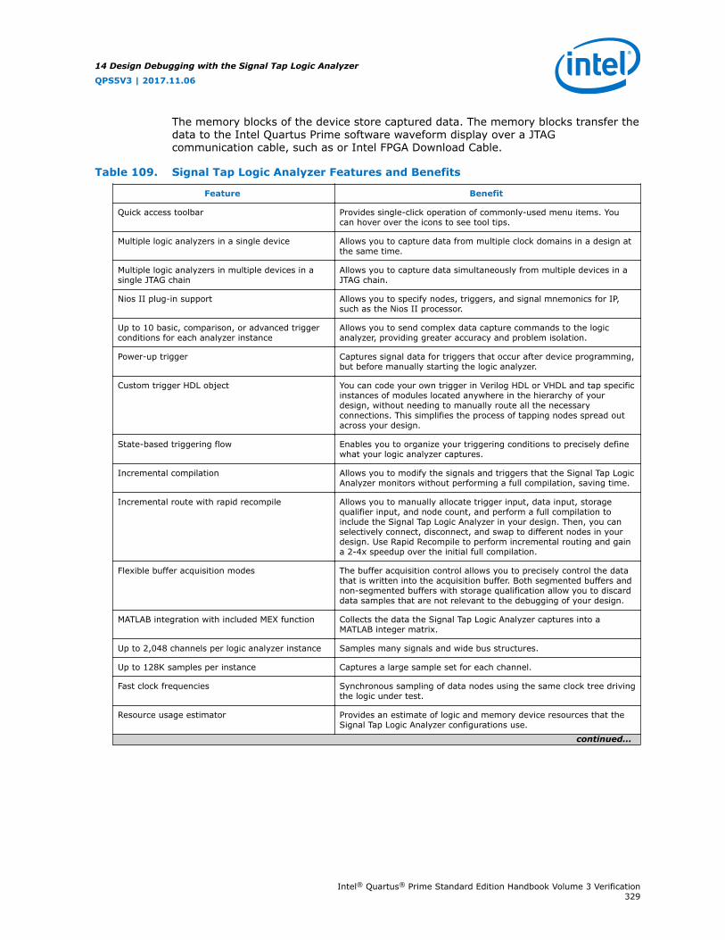
The memory blocks of the device store captured data. The memory blocks transfer thedata to the Intel Quartus Prime software waveform display over a JTAGcommunication cable, such as or Intel FPGA Download Cable.
Table 109. Signal Tap Logic Analyzer Features and Benefits
Feature Benefit
Quick access toolbar Provides single-click operation of commonly-used menu items. Youcan hover over the icons to see tool tips.
Multiple logic analyzers in a single device Allows you to capture data from multiple clock domains in a design atthe same time.
Multiple logic analyzers in multiple devices in asingle JTAG chain
Allows you to capture data simultaneously from multiple devices in aJTAG chain.
Nios II plug-in support Allows you to specify nodes, triggers, and signal mnemonics for IP,such as the Nios II processor.
Up to 10 basic, comparison, or advanced triggerconditions for each analyzer instance
Allows you to send complex data capture commands to the logicanalyzer, providing greater accuracy and problem isolation.
Power-up trigger Captures signal data for triggers that occur after device programming,but before manually starting the logic analyzer.
Custom trigger HDL object You can code your own trigger in Verilog HDL or VHDL and tap specificinstances of modules located anywhere in the hierarchy of yourdesign, without needing to manually route all the necessaryconnections. This simplifies the process of tapping nodes spread outacross your design.
State-based triggering flow Enables you to organize your triggering conditions to precisely definewhat your logic analyzer captures.
Incremental compilation Allows you to modify the signals and triggers that the Signal Tap LogicAnalyzer monitors without performing a full compilation, saving time.
Incremental route with rapid recompile Allows you to manually allocate trigger input, data input, storagequalifier input, and node count, and perform a full compilation toinclude the Signal Tap Logic Analyzer in your design. Then, you canselectively connect, disconnect, and swap to different nodes in yourdesign. Use Rapid Recompile to perform incremental routing and gaina 2-4x speedup over the initial full compilation.
Flexible buffer acquisition modes The buffer acquisition control allows you to precisely control the datathat is written into the acquisition buffer. Both segmented buffers andnon-segmented buffers with storage qualification allow you to discarddata samples that are not relevant to the debugging of your design.
MATLAB integration with included MEX function Collects the data the Signal Tap Logic Analyzer captures into aMATLAB integer matrix.
Up to 2,048 channels per logic analyzer instance Samples many signals and wide bus structures.
Up to 128K samples per instance Captures a large sample set for each channel.
Fast clock frequencies Synchronous sampling of data nodes using the same clock tree drivingthe logic under test.
Resource usage estimator Provides an estimate of logic and memory device resources that theSignal Tap Logic Analyzer configurations use.
continued...
14 Design Debugging with the Signal Tap Logic Analyzer
QPS5V3 | 2017.11.06
Intel® Quartus® Prime Standard Edition Handbook Volume 3 Verification329

Feature Benefit
No additional cost Intel Quartus Prime subscription and the Intel Quartus Prime LiteEdition include the Signal Tap Logic Analyzer.
Compatibility with other on-chip debuggingutilities
You can use the Signal Tap Logic Analyzer in tandem with any JTAG-based on-chip debugging tool, such as an In-System Memory Contenteditor, allowing you to change signal values in real-time while you arerunning an analysis with the Signal Tap Logic Analyzer.
Floating-Point Display Format To enable, click Edit ➤ Bus Display Format ➤ Floating-pointSupports:• Single-precision floating-point format IEEE754 Single (32-bit).• Double-precision floating-point format IEEE754 Double (64-bit).
Related Links
System Debugging Tools Overview on page 183
14.1.2 Open Standalone Signal Tap Logic Analyzer GUI
To open a new Signal Tap through the command-line, type:
quartus_stpw <stp_file.stp>
14.1.3 Backward Compatibility with Previous Versions of Intel QuartusPrime Software
When you open an .stp file created in a previous version of Intel Quartus Primesoftware in a newer version of the software, the .stp file cannot be opened in aprevious version of the Intel Quartus Prime software.
If you have a Intel Quartus Prime project file from a previous version of the software,you may have to update the .stp configuration file to recompile the project. You canupdate the configuration file by opening the Signal Tap Logic Analyzer. If you need toupdate your configuration, a prompt appears asking if you want to update the .stp tomatch the current version of the Intel Quartus Prime software.
14.2 Signal Tap Logic Analyzer Task Flow Overview
To use the Signal Tap Logic Analyzer to debug your design, you perform a number oftasks to add, configure, and run the logic analyzer.
14 Design Debugging with the Signal Tap Logic Analyzer
QPS5V3 | 2017.11.06
Intel® Quartus® Prime Standard Edition Handbook Volume 3 Verification330

Figure 162. Signal Tap Logic Analyzer Task Flow
End
Yes
NoFunctionalitySatisfied or Bug
Fixed?
Add Signal Tap Logic Analyzer to Design Instance
ConfigureSignal Tap Logic Analyzer
Program TargetDevice or Devices
View, Analyze, andUse Captured Data
Define Triggers
Run Signal Tap Logic Analyzer
Adjust Options, Triggers, or Both
Continue Debugging
RecompilationNecessary?
Yes
Create New Project orOpen Existing Project
NoCompile Design
No
14.2.1 Add the Signal Tap Logic Analyzer to Your Design
Create an .stp or create a parameterized HDL instance representation of the logicanalyzer using the IP Catalog and parameter editor. If you want to monitor multipleclock domains simultaneously, add additional instances of the logic analyzer to yourdesign, limited only by the available resources in your device.
14.2.2 Configure the Signal Tap Logic Analyzer
After you add the Signal Tap Logic Analyzer to your design, configure the logicanalyzer to monitor the signals you want.
You can add signals manually or use a plug-in, such as the Nios II processor plug-in,to add entire sets of associated signals for a particular IP.
Specify settings for the data capture buffer, such as its size, the method in which theSignal Tap Logic Analyzer captures and stores the data. If your device supportsmemory type selection, you can specify the memory type to use for the buffer.
14 Design Debugging with the Signal Tap Logic Analyzer
QPS5V3 | 2017.11.06
Intel® Quartus® Prime Standard Edition Handbook Volume 3 Verification331

Related Links
Configuring the Signal Tap Logic Analyzer on page 333
14.2.3 Define Trigger Conditions
To capture and store specific signal data, set up triggers that tell the logic analyzerunder what conditions to stop capturing data. The Signal Tap Logic Analyzer capturesdata continuously while the logic analyzer is running.
The Signal Tap Logic Analyzer allows you to define trigger conditions that range fromvery simple, such as the rising edge of a single signal, to very complex, involvinggroups of signals, extra logic, and multiple conditions. Power-Up Triggers allow you tocapture data from trigger events occurring immediately after the device enters user-mode after configuration.
Related Links
Defining Triggers on page 352
14.2.4 Compile the Design
Once you configure the .stp file and define trigger conditions, compile your projectincluding the logic analyzer in your design.
Note: Because you may need to change monitored signal nodes or adjust trigger settingsfrequently during debugging, Intel FPGA recommends that you use the incrementalcompilation feature built into the Signal Tap Logic Analyzer, along with Intel QuartusPrime incremental compilation, to reduce recompile times. You can also useIncremental Route with Rapid Recompile to reduce recompile times.
Related Links
Compiling the Design on page 376
14.2.5 Program the Target Device or Devices
When you debug a design with the Signal Tap Logic Analyzer, you can program atarget device directly from the .stp without using the Intel Quartus PrimeProgrammer. You can also program multiple devices with different designs andsimultaneously debug them.
Related Links
• Program the Target Device or Devices on page 381
• Manage Multiple Signal Tap Files and Configurations on page 350
14.2.6 Run the Signal Tap Logic Analyzer
In normal device operation, you control the logic analyzer through the JTAGconnection, specifying when to start looking for trigger conditions to begin capturingdata. With Runtime or Power-Up Triggers, read and transfer the captured data fromthe on-chip buffer to the .stp for analysis.
Related Links
Running the Signal Tap Logic Analyzer on page 382
14 Design Debugging with the Signal Tap Logic Analyzer
QPS5V3 | 2017.11.06
Intel® Quartus® Prime Standard Edition Handbook Volume 3 Verification332

14.2.7 View, Analyze, and Use Captured Data
The data you capture and read into the .stp file is available for analysis anddebugging. You can save the data for later analysis, or convert the data to otherformats for sharing and further study.
• To simplify reading and interpreting the signal data you capture, set up mnemonictables, either manually or with a plug-in.
• To speed up debugging, use the Locate feature in the Signal Tap node list tofind the locations of problem nodes in other tools in the Intel Quartus Primesoftware.
Related Links
View, Analyze, and Use Captured Data on page 386
14.3 Configuring the Signal Tap Logic Analyzer
You can configure instances of the Signal Tap Logic Analyzer in the SignalConfiguration pane of the Signal Tap Logic Analyzer window. Some settings aresimilar to those found on traditional external logic analyzers. Other settings are uniqueto the Signal Tap Logic Analyzer.
Figure 163. Signal Tap Logic Analyzer Signal Configuration Pane
Signal Configuration Pane
Note: You can adjust fewer settings with run-time trigger conditions than with power-uptrigger conditions.
14.3.1 Assigning an Acquisition Clock
To control how the Signal Tap Logic Analyzer acquires data you must assign a clocksignal. The logic analyzer samples data on every positive (rising) edge of theacquisition clock. The logic analyzer does not support sampling on the negative(falling) edge of the acquisition clock.
You can use any signal in your design as the acquisition clock. However, for bestresults in data acquisition, use a global, non-gated clock that is synchronous to thesignals under test. Using a gated clock as your acquisition clock can result inunexpected data that does not accurately reflect the behavior of your design. The Intel
14 Design Debugging with the Signal Tap Logic Analyzer
QPS5V3 | 2017.11.06
Intel® Quartus® Prime Standard Edition Handbook Volume 3 Verification333

Quartus Prime static timing analysis tools show the maximum acquisition clockfrequency at which you can run your design. To find the maximum frequency of thelogic analyzer clock, refer to the Timing Analysis section of the Compilation Report.
Caution: Be careful when using a recovered clock from a transceiver as an acquisition clock forthe Signal Tap Logic Analyzer. A recovered clock can cause incorrect or unexpectedbehavior, particularly when the transceiver recovered clock is the acquisition clock withthe power-up trigger feature.
If you do not assign an acquisition clock in the Signal Tap Logic Analyzer Editor, IntelQuartus Prime software automatically creates a clock pin calledauto_stp_external_clk. You must make a pin assignment to this pin, and makesure that a clock signal in your design drives the acquisition clock.
Related Links
• Adding Signals with a Plug-In on page 337
• Managing Device I/O PinsIn Intel Quartus Prime Standard Edition Handbook Volume 2
14.3.2 Adding Signals to the Signal Tap File
Add the signals that you want to monitor to the .stp node list. You can also selectsignals to define triggers. You can assign the following two signal types:
• Pre-synthesis—These signals exist after design elaboration, but before anysynthesis optimizations are done. This set of signals must reflect your RegisterTransfer Level (RTL) signals.
• Post-fitting—These signals exist after physical synthesis optimizations and place-and-route.
Note: If you are not using incremental compilation, add only pre-synthesis signals tothe .stp. Using pre-synthesis helps when you want to add a new node after youchange a design. After you perform Analysis and Elaboration, the source file changesappear in the Node Finder.
Intel Quartus Prime software does not limit the number of signals available formonitoring in the Signal Tap window waveform display. However, the number ofchannels available is directly proportional to the number of logic elements (LEs) oradaptive logic modules (ALMs) in the device. Therefore, there is a physical restrictionon the number of channels that are available for monitoring. Signals shown in bluetext are post-fit node names. Signals shown in black text are pre-synthesis nodenames.
After successful Analysis and Elaboration, invalid signals appear in red. Unless you arecertain that these signals are valid, remove them from the .stp file for correctoperation. The Signal Tap Status Indicator also indicates if an invalid node name existsin the .stp file.
You can tap signals if a routing resource (row or column interconnects) exists to routethe connection to the Signal Tap instance. For example, you cannot tap signals thatexist in the I/O element (IOE), because there are no direct routing resources from thesignal in an IOE to a core logic element. For input pins, you can tap the signal that isdriving a logic array block (LAB) from an IOE, or, for output pins, you can tap thesignal from the LAB that is driving an IOE.
14 Design Debugging with the Signal Tap Logic Analyzer
QPS5V3 | 2017.11.06
Intel® Quartus® Prime Standard Edition Handbook Volume 3 Verification334

Related Links
• Faster Compilations with Intel Quartus Prime Incremental Compilation on page376
• Setup Tab (Signal Tap Logic Analyzer)In Intel Quartus Prime Help
14.3.2.1 About Adding Pre-Synthesis Signals
When you add pre-synthesis signals, make all connections to the Signal Tap LogicAnalyzer before synthesis. The Compiler allocates logic and routing resources to makethe connection as if you changed your design files. For signals driving to and fromIOEs, pre-synthesis signal names coincide with the pin's signal names.
14.3.2.2 About Adding Post-Fit Signals
In the case of post-fit signals, connections that you make to the Signal Tap LogicAnalyzer are the signal names from the actual atoms in your post-fit netlist. You canonly make a connection if the signals are part of the existing post-fit netlist, andexisting routing resources are available from the signal of interest to the Signal TapLogic Analyzer.
In the case of post-fit output signals, tap the COMBOUT or REGOUT signal that drivesthe IOE block. For post-fit input signals, signals driving into the core logic coincidewith the pin's signal name.
Note: Because NOT-gate push back applies to any register that you tap, the signal from theatom may be inverted. You can check this by locating the signal in either the ResourceProperty Editor or the Technology Map Viewer. You can also use the Technology Mapviewer and the Resource Property Editor to find post-fit node names.
Related Links
Design Flow with the Netlist ViewersIn Intel Quartus Prime Standard Edition Handbook Volume 1
14.3.2.2.1 Assigning Data Signals Using the Technology Map Viewer
You can use the Technology Map Viewer to add post-fit signal names easily. To do so,launch the Technology Map Viewer (post-fitting) after compilation. When you find thedesired node, copy the node to either the active .stp for your design or a new .stp.
To launch the Technology Map Viewer, click Tools ➤ Netlist Viewers ➤ TechnologyMap Viewer (Post-Fitting) in the Intel Quartus Prime window.
14.3.2.3 Preserving Signals
The Intel Quartus Prime software optimizes the RTL signals during synthesis andplace-and-route. RTL signal names may not appear in the post-fit netlist afteroptimizations. For example, the compilation process can add tildes (~) to nets thatfan-out from a node, making it difficult to decipher which signal nets they actuallyrepresent.
14 Design Debugging with the Signal Tap Logic Analyzer
QPS5V3 | 2017.11.06
Intel® Quartus® Prime Standard Edition Handbook Volume 3 Verification335

The Intel Quartus Prime software provides synthesis attributes that prevent theCompiler to perform any optimization on the specified signals, allowing them to persistinto the post-fit netlist:
• keep—Prevents removal of combinational signals during optimization.
• preserve—Prevents removal of registers during optimization.
However, using preserving attributes can increase device resource utilization ordecrease timing performance.
Note: These processing results can cause problems when you use the incrementalcompilation flow with the Signal Tap Logic Analyzer. Because you can only add post-fitting signals to the Signal Tap Logic Analyzer in partitions of type post-fit, RTLsignals that you want to monitor may not be available, preventing their use. To avoidthis issue, use synthesis attributes to preserve signals during synthesis and place-and-route.
If you are debugging an IP core, such as the Nios II CPU or other encrypted IP, youmight need to preserve nodes from the core to keep available for debugging with theSignal Tap Logic Analyzer. Preserving nodes is often necessary when you use a plug-into add a group of signals for a particular IP.
If you use incremental compilation flow with the Signal Tap Logic Analyzer, pre-synthesis nodes may not be connected to the Signal Tap Logic Analyzer if the affectedpartition is of the post-fit type. Signal Tap issues a critical warning for all pre-synthesisnode names that it does not find in the post-fit netlist.
14.3.2.4 Node List Signal Use Options
When you add a signal to the node list, you can select options that specify how thelogic analyzer uses the signal.
To prevent a signal from triggering the analysis, disable the signal's Trigger Enableoption in the .stp file. This option is useful when you only want to see the signal'scaptured data.
You can turn off the ability to view data for a signal by disabling the Data Enablecolumn in the .stp file. This option is useful when you want to trigger on a signal, buthave no interest in viewing that signal's data.
Related Links
Defining Triggers on page 352
14.3.2.4.1 Disabling and Enabling a Signal Tap Instance
Disable and enable Signal Tap instances in the Instance Manager pane. Physicallyadding or removing instances requires recompilation after disabling and enabling aSignal Tap instance.
14.3.2.5 Untappable Signals
Not all the post-fitting signals in your design are available in the Signal Tap : post-fitting filter in the Node Finder dialog box.
14 Design Debugging with the Signal Tap Logic Analyzer
QPS5V3 | 2017.11.06
Intel® Quartus® Prime Standard Edition Handbook Volume 3 Verification336
You cannot tap any of the following signal types:
• Post-fit output pins—You cannot tap a post-fit output pin directly. To make anoutput signal visible, tap the register or buffer that drives the output pin. Thisincludes pins defined as bidirectional.
• Signals that are part of a carry chain—You cannot tap the carry out (cout0 orcout1) signal of a logic element. Due to architectural restrictions, the carry outsignal can only feed the carry in of another LE.
• JTAG Signals—You cannot tap the JTAG control (TCK, TDI, TDO, and TMS)signals.
• ALTGXB IP core—You cannot directly tap any ports of an ALTGXB instantiation.
• LVDS—You cannot tap the data output from a serializer/deserializer (SERDES)block.
• DQ, DQS Signals—You cannot directly tap the DQ or DQS signals in a DDR/DDRIIdesign.
14.3.3 Adding Signals with a Plug-In
Instead of adding individual or grouped signals through the Node Finder, you can usea plug-in to add groups of relevant signals of a particular type of IP. Besides easysignal addition, plug-ins provide features such as pre-designed mnemonic tables,useful for trigger creation and data viewing, as well as the ability to disassemble codein captured data. The Signal Tap Logic Analyzer comes with one plug-in for the Nios IIprocessor.
The Nios II plug-in, for example, creates one mnemonic table in the Setup tab andtwo tables in the Data tab:
• Nios II Instruction (Setup tab)—Capture all the required signals for triggeringon a selected instruction address.
• Nios II Instance Address (Data tab)—Display address of executed instructionsin hexadecimal format or as a programming symbol name if defined in an optionalExecutable and Linking Format (.elf) file.
• Nios II Disassembly (Data tab)—Display disassembled code from thecorresponding address.
To add signals to the .stp file using a plug-in, perform the following steps afterrunning Analysis and Elaboration on your design:
1. To ensure that all the required signals are available, in the Intel Quartus Primesoftware, click Assignments ➤ Settings ➤ Compiler Settings ➤ AdvancedSettings (Synthesis). Turn on Create debugging nodes for IP cores.All the signals included in the plug-in are added to the node list.
2. Right-click the node list. On the Add Nodes with Plug-In submenu, select theplug-in you want to use, such as the included plug-in named Nios II.The Select Hierarchy Level dialog box appears showing the IP hierarchy of yourdesign. If the IP for the selected plug-in does not exist in your design, a messageinforms you that you cannot use the selected plug-in.
3. Select the IP that contains the signals you want to monitor with the plug-in, andclick OK.
14 Design Debugging with the Signal Tap Logic Analyzer
QPS5V3 | 2017.11.06
Intel® Quartus® Prime Standard Edition Handbook Volume 3 Verification337

— If all the signals in the plug-in are available, a dialog box might appear,depending on the plug-in, where you can specify options for the plug-in.
4. With the Nios II plug-in, you can optionally select an .elf containing programsymbols from your Nios II Integrated Development Environment (IDE) softwaredesign. Specify options for the selected plug-in, and click OK.
Related Links
• Defining Triggers on page 352
• View, Analyze, and Use Captured Data on page 333
14.3.4 Adding Finite State Machine State Encoding Registers
Finding the signals to debug finite state machines (FSM) can be challenging. Findingnodes from the post-fit netlist may be impossible, since the Compiler may change oroptimize away FSM encoding signals. To find and map FSM signal values to the statenames that you specified in your HDL, you must perform an additional step.
The Signal Tap Logic Analyzer can detect FSMs in your compiled design. Theconfiguration automatically tracks the FSM state signals as well as state encodingthrough the compilation process.
To add all the FSM state signals to your logic analyzer with a single command Shortcutmenu commands allow you .
For each FSM added to your Signal Tap configuration, the FSM debugging feature addsa mnemonic table to map the signal values to the state enumeration that you providedin your source code. The mnemonic tables enable you to visualize state machinetransitions in the waveform viewer. The FSM debugging feature supports adding FSMsignals from both the pre-synthesis and post-fit netlists.
Figure 164. Decoded FSM MnemonicsThe waveform viewer with decoded signal values from a state machine added with the FSM debugging feature.
Related Links
State Machine HDL GuidelinesIn Intel Quartus Prime Standard Edition Handbook Volume 1
14.3.4.1 Modify and Restore Mnemonic Tables for State Machines
Edit any mnemonic table using the Mnemonic Table Setup dialog box. When youadd FSM state signals via the FSM debugging feature, the Signal Tap Logic AnalyzerGUI creates a mnemonic table using the format <StateSignalName>_table, whereStateSignalName is the name of the state signals that you have declared in yourRTL.
If you want to restore a mnemonic table that was modified, right-click anywhere in thenode list window and select Recreate State Machine Mnemonics. By default,restoring a mnemonic table overwrites the existing mnemonic table that you modified.To restore a FSM mnemonic table to a new record, turn off Overwrite existingmnemonic table in the Recreate State Machine Mnemonics dialog box.
14 Design Debugging with the Signal Tap Logic Analyzer
QPS5V3 | 2017.11.06
Intel® Quartus® Prime Standard Edition Handbook Volume 3 Verification338

Note: If you have added or deleted a signal from the FSM state signal group from within thesetup tab, delete the modified register group and add the FSM signals back again.
Related Links
Creating Mnemonics for Bit Patterns on page 389
14.3.4.2 Additional Considerations for State Machines in Signal Tap
• The Signal Tap configuration GUI recognizes state machines from your design onlyif you use Intel Quartus Prime Integrated Synthesis. Conversely, the state machinedebugging feature is not able to track the FSM signals or state encoding if you useother EDA synthesis tools.
• If you add post-fit FSM signals, the Signal Tap Logic Analyzer FSM debug featuremay not track all optimization changes that are a part of the compilation process.
• If the following two specific optimizations are enabled, the Signal Tap FSM debugfeature may not list mnemonic tables for state machines in the design:
— If you enabled the Physical Synthesis optimization, state registers may beresource balanced (register retiming) to improve fMAX. The FSM debug featuredoes not list post-fit FSM state registers if register retiming occurs.
— The FSM debugging feature does not list state signals that the Compilerpacked into RAM and DSP blocks during synthesis or Fitter optimizations.
• You can still use the FSM debugging feature to add pre-synthesis state signals.
Related Links
Enabling Physical Synthesis OptimizationIn Intel Quartus Prime Standard Edition Handbook Volume 1
14.3.5 Specify the Sample Depth
The Sample depth setting specifies the number of samples the Signal Tap LogicAnalyzer captures and stores, for each signal in the captured data buffer. To specifythe sample depth, select the desired number in the Sample Depth drop-down menu.The sample depth ranges from 0 to 128K.
If device memory resources are limited, you may not be able to successfully compileyour design with the sample buffer size you have selected. Try reducing the sampledepth to reduce resource usage.
Related Links
Signal Configuration Pane (View Menu) (Signal Tap Logic Analyzer)In Intel Quartus Prime Help
14.3.6 Capture Data to a Specific RAM Type
You have the option to select the RAM type where the Signal Tap Logic Analyzer storesacquisition data. Once you allocate the Signal Tap Logic Analyzer buffer to a particularRAM block, the entire RAM block becomes a dedicated resource for the logic analyzer.
RAM selection allows you to preserve a specific memory block for your design, andallocate another portion of memory for Signal Tap Logic Analyzer data acquisition.
14 Design Debugging with the Signal Tap Logic Analyzer
QPS5V3 | 2017.11.06
Intel® Quartus® Prime Standard Edition Handbook Volume 3 Verification339

For example, if your design has an application that requires a large block of memoryresources, such as a large instruction or data cache, you can use MLAB, M512, or M4kblocks for data acquisition and leave M9k blocks for the rest of your design.
To specify the RAM type to use for the Signal Tap Logic Analyzer buffer, go to theSignal Configuration pane in the Signal Tap window, and select one Ram typefrom the drop-down menu.
Use this feature only when the acquired data is smaller than the available memory ofthe RAM type that you selected. The amount of data appears in the Signal Tapresource estimator.
Related Links
Signal Configuration Pane (View Menu) (Signal Tap Logic Analyzer)In Intel Quartus Prime Help
14.3.7 Select the Buffer Acquisition Mode
When you specify how the logic analyzer organizes the captured data buffer, you canpotentially reduce the amount of memory that Signal Tap requires for data acquisition.
There are two types of acquisition buffer within the Signal Tap Logic Analyzer—a non-segmented (or circular) buffer and a segmented buffer.
• With a non-segmented buffer, the Signal Tap Logic Analyzer treats entire memoryspace as a single FIFO, continuously filling the buffer until the logic analyzerreaches a defined set of trigger conditions.
• With a segmented buffer, the memory space is split into separate buffers. Eachbuffer acts as a separate FIFO with its own set of trigger conditions, and behavesas a non-segmented buffer. Only a single buffer is active during an acquisition.The Signal Tap Logic Analyzer advances to the next segment after the triggercondition or conditions for the active segment has been reached.
When using a non-segmented buffer, you can use the storage qualification feature todetermine which samples are written into the acquisition buffer. Both the segmentedbuffers and the non-segmented buffer with the storage qualification feature help youmaximize the use of the available memory space.
Figure 165. Buffer Type Comparison in the Signal Tap Logic AnalyzerThe figure illustrates the differences between the two buffer types.
Newly CapturedData
Oldest Data Removed
Post-Trigger Pre-Trigger Center Trigger
1 1
AllTrigger Level
Segment 1 Segment 2 Segment 3 Segment 4
SegmentTrigger Level
1 1 ... 0 1 1 0 ... 0 1 1 1 ... 0 1 1 0 ... 0 1
0 0 1 0 0 1 0 1
SegmentTrigger Level
SegmentTrigger Level
1
(b) Segmented Buffer
(a) Circular Buffer
Both non-segmented and segmented buffers can use a preset trigger position (Pre-Trigger, Center Trigger, Post-Trigger). Alternatively, you can define a custom triggerposition using the State-Based Triggering tab. Refer to Specify Trigger Position formore details.
14 Design Debugging with the Signal Tap Logic Analyzer
QPS5V3 | 2017.11.06
Intel® Quartus® Prime Standard Edition Handbook Volume 3 Verification340

Notes to figure:
Related Links
• Specify Trigger Position on page 372
• Using the Storage Qualifier Feature on page 343
14.3.7.1 Non-Segmented Buffer
The non-segmented buffer is the default buffer type in the Signal Tap Logic Analyzer.
At runtime, the logic analyzer stores data in the buffer until the buffer fills up. Fromthat point on, new data overwrites the oldest data, until a specific trigger eventoccurs. The amount of data the buffer captures after the trigger event depends on theTrigger position setting:
• To capture most data before the trigger occurs, select Post trigger position fromthe list
• To capture most data after the trigger, select Pre trigger position.
• To center the trigger position in the data, select Center trigger position.
Alternatively, use the custom State-based triggering flow to define a custom triggerposition within the capture buffer.
Related Links
Specify Trigger Position on page 372
14.3.7.2 Segmented Buffer
In a segmented buffer, the acquisition memory is split into segments of even size, andyou define a set of trigger conditions for each segment. Each segment acts as a non-segmented buffer. A segmented buffer allows you to debug systems that containrelatively infrequent recurring events.
If you want to have separate trigger conditions for each of the segmented buffers, youmust use the state-based trigger flow. The figure shows an example of a segmentedbuffer system.
14 Design Debugging with the Signal Tap Logic Analyzer
QPS5V3 | 2017.11.06
Intel® Quartus® Prime Standard Edition Handbook Volume 3 Verification341

Figure 166. System that Generates Recurring EventsIn this design, you want to ensure that the correct data is written to the SRAM controller by monitoring theRDATA port whenever the address H'0F0F0F0F is sent into the RADDR port.
QDR SRAMController
WADDR[17..0]RADDR[17..0]
WDATA[35..0]RDATA[35..0]
CMD[1..0]
INCLK
A[17..0]Q[17..0]D[17..0]BWSn[1..0]RPSnWPSn
K, Kn
QDRSRAM
Reference Design Top-Level File
Stratix Device
PipelineRegisters
(Optional)
K_FB_OUTK_FB_IN
C, Cn
SRAM Interface Signals
With the buffer acquisition feature. you can monitor multiple read transactions fromthe SRAM device without running the Signal Tap Logic Analyzer again, because yousplit the memory to capture the same event multiple times, without wasting allocatedmemory. The buffer captures as many cycles as the number of segments you defineunder the Data settings in the Signal Configuration pane.
To enable and configure buffer acquisition, select Segmented in the Signal Tap LogicAnalyzer Editor and determine the number of segments to use. In the example in thefigure, selecting sixty-four 64-sample segments allows you to capture 64 read cycles.
14.3.8 Specify the Pipeline Factor
The Pipeline factor setting indicates the number of pipeline registers that you canadd to boost the fMAX of the Signal Tap Logic Analyzer. You can specify the pipelinefactor in the Signal Configuration pane. The pipeline factor ranges from 0 to 5, witha default value of 0.
You can also set the pipeline factor when you instantiate the Signal Tap Logic Analyzercomponent from your Platform Designer (Standard) system:
1. Double-click Signal Tap Logic Analyzer component in the IP Catalog.
2. Specify the Pipeline Factor, along with other parameter values.
14 Design Debugging with the Signal Tap Logic Analyzer
QPS5V3 | 2017.11.06
Intel® Quartus® Prime Standard Edition Handbook Volume 3 Verification342

Figure 167. Specifying the Pipeline Factor from Platform Designer (Standard)
Note: Setting the pipeline factor does not guarantee an increase in fMAX, as the pipelineregisters may not be in the critical paths.
14.3.9 Using the Storage Qualifier Feature
The Storage Qualifier feature allows you to filter out individual samples not relevant todebugging the design.
The Signal Tap Logic Analyzer offers a snapshot in time of the data stored in theacquisition buffers. By default, the Signal Tap Logic Analyzer writes into acquisitionmemory with data samples on every clock cycle. With a non-segmented buffer, thereis one data window that represents a comprehensive snapshot of the data stream.Conversely, segmented buffers use several smaller sampling windows spread out overmore time, with each sampling window representing a contiguous data set.
With analysis using acquisition buffers you can capture most functional errors in achosen signal set, provided adequate trigger conditions and a generous sample depthfor the acquisition. However, each data window can have a considerable amount ofunnecessary data; for example, long periods of idle signals between data bursts. Thedefault behavior in the Signal Tap Logic Analyzer doesn't discard the redundant samplebits.
The Storage Qualifier feature allows you to establish a condition that acts as a writeenable to the buffer during each clock cycle of data acquisition, thus allowing a moreefficient use of acquisition memory over a longer period of analysis.
Because you can create a discontinuity between any two samples in the buffer, theStorage Qualifier feature is equivalent to creating a custom segmented buffer in whichthe number and size of segment boundaries are adjustable.
Note: You can only use the Storage Qualifier feature with a non-segmented buffer. The IPCatalog flow only supports the Input Port mode for the Storage Qualifier feature.
14 Design Debugging with the Signal Tap Logic Analyzer
QPS5V3 | 2017.11.06
Intel® Quartus® Prime Standard Edition Handbook Volume 3 Verification343

Figure 168. Data Acquisition Using Different Modes of Controlling the Acquisition Buffer
Notes to figure:
1. Non-segmented buffers capture a fixed sample window of contiguous data.
2. Segmented buffers divide the buffer into fixed sized segments, with each segmenthaving an equal sample depth.
3. Storage Qualifier allows you to define a custom sampling window for eachsegment you create with a qualifying condition, thus potentially allowing a largertime scale of coverage.
There are six storage qualifier types available under the Storage Qualifier feature:
• Continuous (default) Turns the Storage Qualifier off.
• Input port
• Transitional
• Conditional
• Start/Stop
• State-based
14 Design Debugging with the Signal Tap Logic Analyzer
QPS5V3 | 2017.11.06
Intel® Quartus® Prime Standard Edition Handbook Volume 3 Verification344

Figure 169. Storage Qualifier Settings
Upon the start of an acquisition, the Signal Tap Logic Analyzer examines each clockcycle and writes the data into the buffer based upon the storage qualifier type andcondition. Acquisition stops when a defined set of trigger conditions occur.
The Signal Tap Logic Analyzer evaluates trigger conditions independently of storagequalifier conditions.
Related Links
Define Trigger Conditions on page 332
14.3.9.1 Input Port Mode
When using the Input port mode, the Signal Tap Logic Analyzer takes any signal fromyour design as an input. During acquisition, if the signal is high on the clock edge, theSignal Tap Logic Analyzer stores the data in the buffer. If the signal is low on the clockedge, the Logic Analyzer ignores the data sample. If you don't specify an internalnode, the Logic Analyzer creates and connects a pin to this input port.
If you are creating a Signal Tap Logic Analyzer instance through an .stp file, specifythe storage qualifier signal using the input port field located on the Setup tab. Youmust specify this port for your project to compile.
If you use the parameter editor, the storage qualification input port, if specified,appears in the generated instantiation template. You can then connect this port to asignal in your RTL.
14 Design Debugging with the Signal Tap Logic Analyzer
QPS5V3 | 2017.11.06
Intel® Quartus® Prime Standard Edition Handbook Volume 3 Verification345

Figure 170. Comparing Continuous and Input Port Capture Mode in Data Acquisition of aRecurring Data Pattern
• Continuous Mode:
• Input Port Storage Qualifier:
14.3.9.2 Transitional Mode
In Transitional mode, the Logic Analyzer monitors changes in a set of signals, andwrites new data in the acquisition buffer only when it detects a change. You select thesignals for monitoring using the check boxes in the Storage Qualifier column.
Figure 171. Transitional Storage Qualifier Setup
Select signals to monitor
Figure 172. Comparing Continuous and Transitional Capture Mode in Data Acquisition of aRecurring Data Pattern
• Continuous:
• Transitional mode:
14 Design Debugging with the Signal Tap Logic Analyzer
QPS5V3 | 2017.11.06
Intel® Quartus® Prime Standard Edition Handbook Volume 3 Verification346

14.3.9.3 Conditional Mode
In Conditional mode, the Signal Tap Logic Analyzer determines whether to store asample by evaluating a combinational function of predefined signals within the nodelist. The Signal Tap Logic Analyzer writes into the buffer during the clock cycles inwhich the condition you specify evaluates TRUE.
You can select either Basic AND, Basic OR, Comparison, or Advanced storagequalifier conditions. A Basic AND or Basic OR condition matches each signal to oneof the following:
• Don’t Care
• Low
• High
• Falling Edge
• Rising Edge
• Either Edge
If you specify a Basic AND storage qualifier condition for more than one signal, theSignal Tap Logic Analyzer evaluates the logical AND of the conditions.
You can specify any other combinational or relational operators with the enabled signalset for storage qualification through advanced storage conditions.
You can define storage qualification conditions similar to the manner in which youdefine trigger conditions.
Figure 173. Conditional Storage Qualifier SetupThe figure details the conditional storage qualifier setup in the .stp file.
Storage Enable Storage condition
If the signal is not enabled for storage, it can’t be part of the Storage Qualifier condition
14 Design Debugging with the Signal Tap Logic Analyzer
QPS5V3 | 2017.11.06
Intel® Quartus® Prime Standard Edition Handbook Volume 3 Verification347

Figure 174. Comparing Continuous and Conditional Capture Mode in Data Acquisition of aRecurring Data Pattern
The data pattern is the same in both cases.
• Continuous sampling capture mode:
• Conditional sampling capture mode:
Related Links
• Basic Trigger Conditions on page 352
• Comparison Trigger Conditions on page 353
• Advanced Trigger Conditions on page 355
14.3.9.4 Start/Stop Mode
The Start/Stop mode uses two sets of conditions, one to start data capture and one tostop data capture. If the start condition evaluates to TRUE, Signal Tap Logic Analyzerstores the buffer data every clock cycle until the stop condition evaluates to TRUE,which then pauses the data capture. The Logic Analyzer ignores additional startsignals received after the data capture starts. If both start and stop evaluate to TRUEat the same time, the Logic Analyzer captures a single cycle.
Note: You can force a trigger by pressing the Stop button if the buffer fails to fill tocompletion due to a stop condition.
Figure 175. Start/Stop Mode Storage Qualifier SetupStart condition Stop Condition
Storage Qualifier Enabled signals
14 Design Debugging with the Signal Tap Logic Analyzer
QPS5V3 | 2017.11.06
Intel® Quartus® Prime Standard Edition Handbook Volume 3 Verification348

Figure 176. Comparing Continuous and Start/Stop Acquisition Modes for a Recurring DataPattern
• Continuous Mode:
• Start/Stop Storage Qualifier:
14.3.9.5 State-Based
The State-based storage qualification mode is part of the State-based triggering flow.The state based triggering flow evaluates a conditional language to define how theSignal Tap Logic Analyzer writes data into the buffer. With the State-based triggerflow, you have command over boolean and relational operators to guide the executionflow for the target acquisition buffer.
When you enable the storage qualifier feature for the State-based flow, two additionalcommands become available: start_store and stop_store. These commands aresimilar to the Start/Stop capture conditions. Upon the start of acquisition, the SignalTap Logic Analyzer doesn't write data into the buffer until a start_store action isperformed. The stop_store command pauses the acquisition. If both start_storeand stop_store actions occur within the same clock cycle, the Logic Analyzer storesa single sample into the acquisition buffer.
Related Links
State-Based Triggering on page 363
14.3.9.6 Showing Data Discontinuities
When you turn on Record data discontinuities, the Signal Tap Logic Analyzer marksthe samples during which the acquisition paused from a storage qualifier. This markeris displayed in the waveform viewer after acquisition completes.
14.3.9.7 Disable Storage Qualifier
You can quickly turn off the storage qualifier with the Disable Storage Qualifieroption, and perform a continuous capture. This option is run-time reconfigurable.Changing storage qualifier mode from the Type field requires a recompilation of theproject.
14 Design Debugging with the Signal Tap Logic Analyzer
QPS5V3 | 2017.11.06
Intel® Quartus® Prime Standard Edition Handbook Volume 3 Verification349

Related Links
Runtime Reconfigurable Options on page 383
14.3.10 Manage Multiple Signal Tap Files and Configurations
You can debug different blocks in your design by grouping related monitoring signals.Likewise, you can use a group of signals to define multiple trigger conditions. Eachcombination of signals, capture settings, and trigger conditions determines a debugconfiguration, and one configuration can have zero or more associated data logs.
Signal Tap Logic Analyzer allows you to save debug configurations in more thanone .stp file. Alternatively, you can embed multiple configurations within thesame .stp file, and use the Data Log as a managing tool.
Note: Each .stp file is associated with a programming (.sof) file. To function correctly, thesettings in the .stp file you use at runtime must match Signal Tap settings inthe .sof file you use to program the device.
Related Links
Ensure Setting Compatibility Between .stp and .sof Files on page 382
14.3.10.1 Data Log Pane
The Data Log pane displays all Signal Tap configurations and data capture resultsstored within a single .stp file.
• To save the current configuration or capture in the Data Log—and .stp file, click
Edit ➤ Save to Data Log. Alternatively, click the Save to Data Log icon atthe top of the Data Log pane.
• To generate a log entry after every data capture, click Edit ➤ Enable Data Log.Alternatively, check the box at the top of the Data Log pane.
The Data Log displays its contents in a tree hierarchy. The active items display adifferent icon.
Table 110. Data Log Items
Item Icon Contains one ormore
Comments
Unselected Selected
Instance Signal Set
Signal Set Trigger The Signal Set changes whenever you add a newsignal to Signal Tap. After a change in the SignalSet, you need to recompile.
Trigger Capture Log A trigger changes when you change any triggercondition. These changes do not requirerecompilation.
Capture Log
The name on each entry displays the wall-clock time when Signal Tap Logic Analyzertriggered, and the time elapsed from start acquisition to trigger activation. You canrename entries so they make sense to you.
14 Design Debugging with the Signal Tap Logic Analyzer
QPS5V3 | 2017.11.06
Intel® Quartus® Prime Standard Edition Handbook Volume 3 Verification350

To switch between configurations, double-click an entry in the Data Log. As a result,the Setup tab updates to display the active signal list and trigger conditions.
Example 34. Simple Data Log
On this example, the Data Log displays one instance with three signal setconfigurations.
14.3.10.2 SOF Manager
The SOF Manager is in the JTAG Chain Configuration pane.
With the SOF Manager you can embed multiple SOFs into one .stp file. This actionlets you move the .stp file to a different location, either on the same computer oracross a network, without including the associated .sof separately. To embed a new
SOF in the .stp file, click the Attach SOF File icon .
Figure 177. SOF Manager
Attach SOF File Icon
As you switch between configurations in the Data Log, you can extract the SOF that iscompatible with that configuration.
To download the new SOF to the FPGA, click the Program Device icon in the SOFManager, after ensuring that the configuration of your .stp matches the designprogrammed into the target device.
Related Links
Data Log Pane on page 350
14 Design Debugging with the Signal Tap Logic Analyzer
QPS5V3 | 2017.11.06
Intel® Quartus® Prime Standard Edition Handbook Volume 3 Verification351

14.4 Defining Triggers
You specify various types of trigger conditions using the Signal Tap Logic Analyzer onthe Signal Configuration pane. When you start the Signal Tap Logic Analyzer, itsamples activity continuously from the monitored signals. The Signal Tap LogicAnalyzer “triggers”—that is, the logic analyzer stops and displays the data—when acondition or set of conditions that you specified have been reached.
14.4.1 Basic Trigger Conditions
If you select the Basic AND or Basic OR trigger type, you must specify the triggerpattern for each signal you added in the .stp. To specify the trigger pattern, right-click the Trigger Conditions column and click the desired pattern. Set the triggerpattern to any of the following conditions:
• Don’t Care
• Low
• High
• Falling Edge
• Rising Edge
• Either Edge
For buses, type a pattern in binary, or right-click and select Insert Value to enter thepattern in other number formats. Note that you can enter X to specify a set of “don’tcare” values in either your hexadecimal or your binary string. For signals in the .stpfile that have an associated mnemonic table, you can right-click and select an entryfrom the table to specify pre-defined conditions for the trigger.
When you add signals through plug-ins, you can create basic triggers using predefinedmnemonic table entries. For example, with the Nios II plug-in, if you specify an .elffile from your Nios II IDE design, you can type the name of a function from your NiosII code. The logic analyzer triggers when the Nios II instruction address matches theaddress of the code function name that you specify.
Data capture stops and the Logic Analyzer stores the data in the buffer when thelogical AND of all the signals for a given trigger condition evaluates to TRUE.
Related Links
View, Analyze, and Use Captured Data on page 386
14.4.1.1 Using the Basic OR Trigger Condition with Nested Groups
When you specify a set of signals as a nested group (group of groups) with the BasicOR trigger type, Signal Tap Logic Analyzer generates an advanced trigger condition.This condition sorts signals within groups to minimize the need to recompile yourdesign. As long as the parent-child relationships of nodes are kept constant, theadvanced trigger condition does not change. You can modify the sibling relationshipsof nodes and not need to recompile your design.
14 Design Debugging with the Signal Tap Logic Analyzer
QPS5V3 | 2017.11.06
Intel® Quartus® Prime Standard Edition Handbook Volume 3 Verification352

The evaluation precedence of a nested trigger condition starts at the bottom-level withthe leaf-groups. The Logic Analyzer uses the resulting logic value to compute theparent group’s logic value. If you manually set the value of a group, the logic value ofthe group's members doesn't influence the result of the group trigger. To create anested trigger condition:
1. Select Basic OR under Trigger Conditions.
2. In the Setup tab, select several nodes. Include groups in your selection.
3. Right-click the Setup tab and select Group.
4. Select the nested group and right-click to set a group trigger condition that appliesthe reduction AND, OR, NAND, NOR, XOR, XNOR, or logical TRUE or FALSE.
Note: You can only select OR and AND group trigger conditions for bottom-levelgroups (groups with no groups as children).
Figure 178. Applying Trigger Condition to Nested Group
14.4.2 Comparison Trigger Conditions
The Comparison trigger allows you to compare multiple grouped bits of a bus to anexpected integer value by specifying simple comparison conditions on the bus node.The Comparison trigger preserves all the trigger conditions that the Basic OR triggerincludes. You can use the Comparison trigger in combination with other triggers. Youcan also switch between Basic OR trigger and Comparison trigger at run-time,without the need for recompilation.
Signal Tap Logic Analyzer supports the following types of Comparison triggerconditions:
• Single-value comparison—compares a bus node’s value to a numeric value thatyou specify. Use one of these operands for comparison: >, >=, ==, <=, <.Returns 1 when the bus node matches the specified numeric value.
• Interval check—verifies whether a bus node’s value confines to an interval thatyou define. Returns 1 when the bus node's value lies within the specified boundedinterval.
14 Design Debugging with the Signal Tap Logic Analyzer
QPS5V3 | 2017.11.06
Intel® Quartus® Prime Standard Edition Handbook Volume 3 Verification353

Follow these rules when using the Comparison trigger condition:
• Apply the Comparison trigger only to bus nodes consisting of leaf nodes.
• Do not form sub-groups within a bus node.
• Do not enable or disable individual trigger nodes within a bus node.
• Do not specify comparison values (in case of single-value comparison) orboundary values (in case of interval check) exceeding the selected node’s bus-width.
14.4.2.1 Specifying the Comparison Trigger Conditions
Follow these steps to specify the Comparison trigger conditions:
1. From the Setup tab, select Comparison under Trigger Conditions.
2. Right-click the node in the trigger editor, and select Compare.
Figure 179. Selecting the Comparison Trigger Condition
Select Comparison from the Trigger Conditions list
Right-click your node and select Compare to set trigger condition values
3. Select the Comparison type from the Compare window.
— If you choose Single-value comparison as your comparison type, specifythe operand and value.
— If you choose Interval check as your comparison type, provide the lower andupper bound values for the interval.
You can also specify if you want to include or exclude the boundary values.
14 Design Debugging with the Signal Tap Logic Analyzer
QPS5V3 | 2017.11.06
Intel® Quartus® Prime Standard Edition Handbook Volume 3 Verification354

Figure 180. Specifying the Comparison ValuesCompares the bus node’s value to a specified numeric value
Verifies whether the bus node’s value confines to a specified bounded interval
Specify inclusion or exclusion of boundary values
4. Click OK. The trigger editor displays the resulting comparison expression in thegroup node condition text box.
Note: You can modify the comparison condition in the text box with a validexpression.
Figure 181. Resulting Comparison Condition in Text Box
Group node condition text box displayingthe resulting comparison expression
Modify the comparison condition in the text box with a valid expression
14.4.3 Advanced Trigger Conditions
To capture data for a given combination of conditions, build an advanced trigger. TheSignal Tap Logic Analyzer provides the Advanced Trigger tab, which helps you builda complex trigger expression using a GUI.
Open the Advanced Trigger tab by selecting Advanced in the Trigger Conditionsdrop-down menu.
14 Design Debugging with the Signal Tap Logic Analyzer
QPS5V3 | 2017.11.06
Intel® Quartus® Prime Standard Edition Handbook Volume 3 Verification355

Figure 182. Accessing the Advanced Trigger Condition Tab
Select Advanced from theTrigger Conditions List
Figure 183. Advanced Trigger Condition Tab
Node List Pane
Object Library Pane
Advanced Trigger Condition Editor Window
To build a complex trigger condition in an expression tree, drag-and-drop operatorsfrom the Object Library pane and the Node List pane into the Advanced TriggerConfiguration Editor window.
To configure the operators’ settings, double-click or right-click the operators that youplaced and click Properties.
Table 111. Advanced Triggering Operators
Category Name
Signal Detection Edge and Level Detector
Input Objects BitBit ValueBusBus Value
Comparison Less ThanLess Than or Equal ToEqualityInequalityGreater Than or Equal ToGreater Than
Bitwise Bitwise ComplementBitwise ANDBitwise ORBitwise XOR
Logical Logical NOTLogical ANDLogical ORLogical XOR
Reduction Reduction ANDReduction ORReduction XOR
Shift Left Shift
continued...
14 Design Debugging with the Signal Tap Logic Analyzer
QPS5V3 | 2017.11.06
Intel® Quartus® Prime Standard Edition Handbook Volume 3 Verification356

Category Name
Right Shift
Custom Trigger HDL
Adding many objects to the Advanced Trigger Condition Editor can make the workspace cluttered and difficult to read. To keep objects organized while you build youradvanced trigger condition, use the shortcut menu and select Arrange All Objects.Alternatively, use the Zoom-Out command to fit more objects into the AdvancedTrigger Condition Editor window.
14.4.3.1 Examples of Advanced Triggering Expressions
The following examples show how to use Advanced Triggering:
Figure 184. Bus outa Is Greater Than or Equal to Bus outbTrigger when bus outa is greater than or equal to outb.
Figure 185. Enable Signal Has a Rising EdgeTrigger when bus outa is greater than or equal to bus outb, and when the enable signal has a rising edge.
14 Design Debugging with the Signal Tap Logic Analyzer
QPS5V3 | 2017.11.06
Intel® Quartus® Prime Standard Edition Handbook Volume 3 Verification357

Figure 186. Bitwise AND OperationTrigger when bus outa is greater than or equal to bus outb, or when the enable signal has a rising edge. Or,when a bitwise AND operation has been performed between bus outc and bus outd, and all bits of the resultof that operation are equal to 1.
14.4.4 Custom Trigger HDL Object
Signal Tap Logic Analyzer allows you to use your own HDL module to create a customtrigger condition. You can use the Custom Trigger HDL object to simulate yourtriggering logic and ensure that the logic itself is not faulty. Additionally, you can tapinstances of modules anywhere in the hierarchy of your design, without having tomanually route all the necessary connections.
The Custom Trigger HDL object appears in the Object Library pane of the AdvancedTrigger editor.
Figure 187. Object Library
14.4.4.1 Using the Custom Trigger HDL Object
To define a custom trigger flow:
1. Select the trigger you want to edit.
2. Open the Advanced Trigger tab by selecting Advanced in the TriggerConditions drop-down menu.
3. Add to your project the HDL source file that contains the trigger module using theProject Navigator.
— Alternatively, append the HDL for your trigger module to a source file alreadyincluded in the project.
14 Design Debugging with the Signal Tap Logic Analyzer
QPS5V3 | 2017.11.06
Intel® Quartus® Prime Standard Edition Handbook Volume 3 Verification358

Figure 188. HDL Trigger in the Project Navigator
4. Implement the inputs and outputs that your Custom Trigger HDL module requires.
5. Drag in your Custom Trigger HDL object and connect the object’s data input busand result output bit to the final trigger result.
Figure 189. Custom Trigger HDL Object
6. Right-click your Custom Trigger HDL object and configure the object’s properties.
Figure 190. Configure Object Properties
7. Compile your design.
8. Acquire data with Signal Tap using your custom Trigger HDL object.
14 Design Debugging with the Signal Tap Logic Analyzer
QPS5V3 | 2017.11.06
Intel® Quartus® Prime Standard Edition Handbook Volume 3 Verification359

Example 35. Verilog HDL Triggers
The following trigger uses configuration bitstream:
module test_trigger ( input acq_clk, reset, input[3:0] data_in, input[1:0] pattern_in, output reg trigger_out ); always @(pattern_in) begin case (pattern_in) 2'b00: trigger_out = &data_in; 2'b01: trigger_out = |data_in; 2'b10: trigger_out = 1'b0; 2'b11: trigger_out = 1'b1; endcase endendmodule
This trigger does not have configuration bitstream:
module test_trigger_no_bs ( input acq_clk, reset, input[3:0] data_in, output reg trigger_out ); assign trigger_out = &data_in;endmodule
14.4.4.2 Required Inputs and Outputs of Custom Trigger HDL Module
Table 112. Custom Trigger HDL Module Required Inputs and Outputs
Name Description Input/Output Required/ Optional
acq_clk Acquisition clock that Signal Tap uses Input Required
reset Reset that Signal Tap uses when restarting acapture.
Input Required
data_in • Data input you connect in the AdvancedTrigger editor.
• Data your module uses to trigger.
Input Required
pattern_in • Module’s input for the configuration bitstreamproperty.
• Runtime configurable property that you canset from Signal Tap GUI to change thebehavior of your trigger logic.
Input Optional
trigger_out Output signal of your module that asserts whentrigger conditions met.
Output Required
14.4.4.3 Properties of Custom Trigger HDL Module
14 Design Debugging with the Signal Tap Logic Analyzer
QPS5V3 | 2017.11.06
Intel® Quartus® Prime Standard Edition Handbook Volume 3 Verification360

Table 113. Custom Trigger HDL Module Properties
Property Description
Custom HDL Module Name Module name of your triggering logic.
Configuration Bitstream • Allows you to create runtime-configurable trigger logic which canchange its behavior based upon the value of the configurationbitstream.
• The configuration bitstream property is read as binary, therefore itmust contain only the characters 1 and 0. The bit-width (number of1s and 0s) must match the pattern_in bit width.
• A blank configuration bitstream implies that your module does nothave a pattern_in input.
Pipeline Specifies the number of pipeline stages in your triggering logic.For example, if after receiving a triggering input the LA needs three clockcycles to assert the trigger output, you can denote a pipeline value ofthree.
14.4.5 Trigger Condition Flow Control
The Trigger Condition Flow allows you to define the relationship between a set oftriggering conditions. Signal Tap Logic Analyzer Signal Configuration pane offers twoflow control mechanisms for organizing trigger conditions:
• Sequential Triggering—default triggering flow. Sequential triggering allows youto define up to 10 triggering levels that must be satisfied before the acquisitionbuffer finishes capturing.
• State-Based Triggering—gives the greatest control over your acquisition buffer.Custom-based triggering allows you to organize trigger conditions into statesbased on a conditional flow that you define.
You can use sequential or state based triggering with either a segmented or a non-segmented buffer.
14.4.5.1 Sequential Triggering
Sequential triggering flow allows you to cascade up to 10 levels of triggeringconditions. Signal Tap Logic Analyzer sequentially evaluates each of the conditions.
When the last triggering condition evaluates to TRUE, the Signal Tap Logic Analyzertriggers the acquisition buffer. For segmented buffers, every acquisition segment afterthe first triggers on the last condition that you specified. Use the Simple SequentialTriggering feature with basic triggers, comparison triggers, advanced triggers, or amix of all three. The figure illustrates the simple sequential triggering flow for non-segmented and segmented buffers.
The external trigger is considered as trigger level 0. The external trigger must beevaluated before the main trigger levels are evaluated.
14 Design Debugging with the Signal Tap Logic Analyzer
QPS5V3 | 2017.11.06
Intel® Quartus® Prime Standard Edition Handbook Volume 3 Verification361
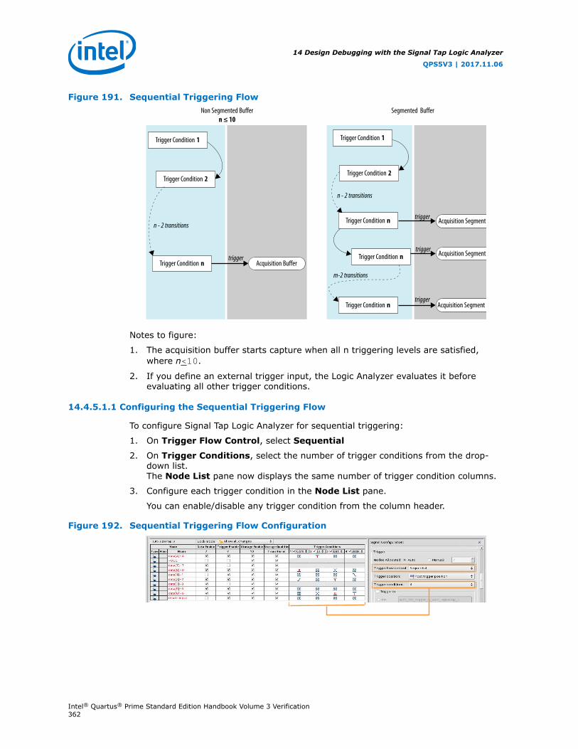
Figure 191. Sequential Triggering FlowSegmented BufferNon Segmented Buffer
n ≤ 10
Trigger Condition n
Trigger Condition 1
Trigger Condition 2
Trigger Condition 1
Trigger Condition 2
Trigger Condition n
Trigger Condition n
Trigger Condition n
n - 2 transitions
Acquisition Segment mtrigger
trigger
trigger
Acquisition Buffertrigger
n - 2 transitions
m-2 transitions
Acquisition Segment 2
Acquisition Segment 1
Notes to figure:
1. The acquisition buffer starts capture when all n triggering levels are satisfied,where n<10.
2. If you define an external trigger input, the Logic Analyzer evaluates it beforeevaluating all other trigger conditions.
14.4.5.1.1 Configuring the Sequential Triggering Flow
To configure Signal Tap Logic Analyzer for sequential triggering:
1. On Trigger Flow Control, select Sequential
2. On Trigger Conditions, select the number of trigger conditions from the drop-down list.The Node List pane now displays the same number of trigger condition columns.
3. Configure each trigger condition in the Node List pane.
You can enable/disable any trigger condition from the column header.
Figure 192. Sequential Triggering Flow Configuration
14 Design Debugging with the Signal Tap Logic Analyzer
QPS5V3 | 2017.11.06
Intel® Quartus® Prime Standard Edition Handbook Volume 3 Verification362

14.4.5.2 State-Based Triggering
With state-based triggering, a state diagram organizes the events that trigger theacquisition buffer. The states capture all actions that the acquisition buffer performs,and each state contains conditional expressions that define transition conditions.
Custom state-based triggering grants control over triggering condition arrangement,and allows for more efficient use of the space available in the acquisition buffer,because the Logic Analyzer only captures samples of interest.
To help you describe the relationship between triggering conditions, the state-basedtriggering flow provides tooltips within the flow GUI. Additionally, you can use theSignal Tap Trigger Flow Description Language, which is based upon conditionalexpressions.
Figure 193. State-Based Triggering Flow
n ≤ 20
Segmented Acquisition Buffer
First Acquisition Segment Next Acquisition Segment Next Acquisition Segment Last Acquisition Segment
Transition Condition: i
TC: j
TC: k
TC: l S: 2TCS: b S: 3
TCS: c
State: 1Trigger Condition Set: a
S: n (last state)TCS: d
segment_trigger segment_trigger segment_trigger segment_trigger
Notes to figure:
1. You can define up to 20 different states.
2. If you define an external trigger input, the logic analyzer evaluates it before anyconditions in the custom state-based triggering flow.
Each state allows you to define a set of conditional expressions. Each conditionalexpression is a Boolean expression that depends on a combination of triggeringconditions, counters, and status flags. You configure the triggering conditions withinthe Setup tab. The Signal Tap Logic Analyzer custom-based triggering flow providescounters and status flags.
Within each conditional expression you define a set of actions. Actions includetriggering the acquisition buffer to stop capture, a modification to either a counter orstatus flag, or a state transition.
Trigger actions can apply to either a single segment of a segmented acquisition bufferor to the entire non-segmented acquisition buffer. Each trigger action provides youwith an optional count that specifies the number of samples the buffer captures beforethe logic analyzer stops acquisition of the current segment. The count argumentallows you to control the amount of data the buffer captures before and after atriggering event occurs.
14 Design Debugging with the Signal Tap Logic Analyzer
QPS5V3 | 2017.11.06
Intel® Quartus® Prime Standard Edition Handbook Volume 3 Verification363

Resource manipulation actions allow you to increment and decrement counters or setand clear status flags. The logic analyzer uses counter and status flag resources asoptional inputs in conditional expressions. Counters and status flags are useful forcounting the number of occurrences of certain events and for aiding in triggering flowcontrol.
The state-based triggering flow allows you to capture a sequence of events that maynot necessarily be contiguous in time. For example, a communication transactionbetween two devices that includes a hand shaking protocol containing a sequence ofacknowledgements.
14.4.5.2.1 State-Based Triggering Flow Tab
The State-Based Trigger Flow tab is the control interface for the custom state-based triggering flow.
This tab is only available when you select State-Based on the Trigger Flow Controllist. If you specify Trigger Flow Control as Sequential, the State-Based TriggerFlow tab is not visible.
Figure 194. State-Based Triggering Flow Tab
The State-Based Trigger Flow tab contains three panes:
State Diagram Pane
The State Diagram pane provides a graphical overview of your triggering flow. thispane displays the number of available states and the state transitions. To adjust thenumber of available states, use the menu above the graphical overview.
14 Design Debugging with the Signal Tap Logic Analyzer
QPS5V3 | 2017.11.06
Intel® Quartus® Prime Standard Edition Handbook Volume 3 Verification364

State Machine Pane
The State Machine pane contains the text entry boxes where you define thetriggering flow and actions associated with each state.
• You can define the triggering flow using the Signal Tap Trigger Flow DescriptionLanguage, a simple language based on “if-else” conditional statements.
• Tooltips appear when you move the mouse over the cursor, to guide commandentry into the state boxes.
• The GUI provides a syntax check on your flow description in real-time andhighlights any errors in the text flow.
The State Machine description text boxes default to show one text box per state. Youcan also have the entire flow description shown in a single text field. This option canbe useful when copying and pasting a flow description from a template or an externaltext editor. To toggle between one window per state, or all states in one window,select the appropriate option under State Display mode.
Related Links
Signal Tap Trigger Flow Description Language on page 366
Resources Pane
The Resources pane allows you to declare status flags and counters for your CustomTriggering Flow's conditional expressions.
• You can increment/decrement counters or set/clear status flags within yourtriggering flow.
• You can specify up to 20 counters and 20 status flags.
• To initialize counter and status flags, right-click the row in the table and select SetInitial Value.
• To specify a counter width, right-click the counter in the table and select SetWidth.
• To assist in debugging your trigger flow specification, the logic analyzerdynamically updates counters and flag values after acquisition starts.
The Configurable at runtime settings allow you to control which options can changeat runtime without requiring a recompilation.
Table 114. Runtime Reconfigurable Settings, State-Based Triggering Flow
Setting Description
Destination of goto action Allows you to modify the destination of the state transition at runtime.
Comparison values Allows you to modify comparison values in Boolean expressions at runtime. Inaddition, you can modify the segment_trigger and trigger action post-fillcount argument at runtime.
Comparison operators Allows you to modify the operators in Boolean expressions at runtime.
Logical operators Allows you to modify the logical operators in Boolean expressions at runtime.
Related Links
• Performance and Resource Considerations on page 380
• Runtime Reconfigurable Options on page 383
14 Design Debugging with the Signal Tap Logic Analyzer
QPS5V3 | 2017.11.06
Intel® Quartus® Prime Standard Edition Handbook Volume 3 Verification365

14.4.5.2.2 Trigger Lock Mode
Trigger lock mode restricts changes to only the configuration settings that you specifyas Configurable at runtime. The runtime configurable settings for the CustomTrigger Flow tab are on by default.
Note: You may get some performance advantages by disabling some of the runtimeconfigurable options.
You can restrict changes to your Signal Tap configuration to include only the optionsthat do not require a recompilation. Trigger lock-mode allows you to make changesthat reflect immediately in the device.
1. On the Setup tab, point to Lock Mode and select Allow trigger conditionchanges only.
Figure 195. Allow Trigger Conditions Change Only
2. Modify the Trigger Flow conditions.
Incremental Route lock-mode restricts the GUI to only allow changes that require anIncremental Route compilation using Rapid Recompile. Use Rapid Recompile toperform incremental routing and gain a 2-4x speedup over the initial full compilation.
14.4.5.3 Signal Tap Trigger Flow Description Language
The Trigger Flow Description Language is based on a list of conditional expressions perstate to define a set of actions.
To describe the actions the Logic Analyzer evaluates when a state is reached, youfollow this syntax:
Syntax of Trigger Flow Description Language
state <state_label>: <action_list> if (<boolean_expression>) <action_list> [else if (<boolean_expression>) <action_list>] [else <action_list>]
• Non-terminals are delimited by "<>".
• Optional arguments are delimited by "[]"
• The priority for evaluation of conditional statements is from top to bottom.
• The Trigger Flow Description Language allows multiple else if conditions.
<state_label> on page 367
<boolean_expression> on page 367
<action_list> on page 368
14 Design Debugging with the Signal Tap Logic Analyzer
QPS5V3 | 2017.11.06
Intel® Quartus® Prime Standard Edition Handbook Volume 3 Verification366

Related Links
Custom Triggering Flow Application Examples on page 397
14.4.5.3.1 <state_label>
Identifies a given state. You use the state label to start describing the actions theLogic Analyzer evaluates once said state is reached. You can also use the state labelwith the goto command.
The state description header syntax is:state <state_label>
The description of a state ends with the beginning of another state or the end of thewhole trigger flow description.
14.4.5.3.2 <boolean_expression>
Collection of operators and operands that evaluate into a Boolean result. Theoperators can be logical or relational. Depending on the operator, the operand canreference a trigger condition, a counter and a register, or a numeric value. To group aset of operands within an expression, you use parentheses.
Table 115. Logical OperatorsLogical operators accept any boolean expression as an operand.
Operator Description Syntax
! NOT operator ! expr1
&& AND operator expr1 && expr2
|| OR operator expr1 || expr2
Table 116. Relational OperatorsYou use relational operators on counters or status flags.
Operator Description Syntax
> Greater than <identifier> > <numerical_value>
>= Greater than or Equalto
<identifier> >= <numerical_value>
== Equals <identifier> == <numerical_value>
!= Does not equal <identifier> != <numerical_value>
<= Less than or equal to <identifier> <= <numerical_value>
< Less than <identifier> < <numerical_value>
Notes to table:1. <identifier> indicates a counter or status flag.2. <numerical_value> indicates an integer.
14 Design Debugging with the Signal Tap Logic Analyzer
QPS5V3 | 2017.11.06
Intel® Quartus® Prime Standard Edition Handbook Volume 3 Verification367

Note: • The <boolean_expression> in an if statement can contain a single event ormultiple event conditions.
• When the boolean expression evaluates TRUE, the logic analyzer evaluates all thecommands in the <action_list> concurrently.
14.4.5.3.3 <action_list>
List of actions that the Logic Analyzer performs within a state once a condition issatisfied.
• Each action must end with a semicolon (;).
• If you specify more than one action within an if or an else if clause, you mustdelimit the action_list with begin and end tokens.
Possible actions include:
Resource Manipulation Action
The resources the trigger flow description uses can be either counters or status flags.
Table 117. Resource Manipulation Actions
Action Description Syntax
increment Increments a counter resource by 1 increment <counter_identifier>;
decrement Decrements a counter resource by 1 decrement <counter_identifier>;
reset Resets counter resource to initial value reset <counter_identifier>;
set Sets a status flag to 1 set <register_flag_identifier>;
clear Sets a status flag to 0 clear <register_flag_identifier>;
Buffer Control Actions
Actions that control the acquisition buffer.
Table 118. Buffer Control Actions
Action Description Syntax
trigger Stops the acquisition for the current buffer andends analysis. This command is required in everyflow definition.
trigger <post-fill_count>;
segment_trigger Available only in segmented acquisition mode.Ends acquisition of the current segment. Afterevaluating this command, the Signal Tap LogicAnalyzer starts acquiring from the next segment. Ifall segments are written, the Logic Analyzer
segment_trigger <post-fill_count>;
continued...
14 Design Debugging with the Signal Tap Logic Analyzer
QPS5V3 | 2017.11.06
Intel® Quartus® Prime Standard Edition Handbook Volume 3 Verification368

Action Description Syntax
overwrites the oldest segment with the latestsample. When a trigger action is evaluated theacquisition stops.
start_store Active only in state-based storage qualifier mode.Asserts the write_enable to the Signal Tapacquisition buffer.
start_store
stop_store Active only in state-based storage qualifier mode.De-asserts the write_enable signal to the SignalTap acquisition buffer.
stop_store
Both trigger and segment_trigger actions accept an optional post-fill_countargument.
Related Links
Post-fill Count on page 373
State Transition Action
Specifies the next state in the custom state control flow. The syntax is:goto <state_label>;
14.4.5.4 Using the State-Based Storage Qualifier Feature
Selecting a state-based storage qualifier type enables the start_store andstop_store actions. When you use these actions in conjunction with the expressionsof the State-based trigger flow, you get maximum flexibility to control data writteninto the acquisition buffer.
Note: You can only apply the start_store and stop_store commands to a non-segmented buffer.
The start_store and stop_store commands are similar to the start and stopconditions of the start/stop storage qualifier mode. If you enable storagequalification, Signal Tap Logic Analyzer doesn't write data into the acquisition bufferuntil the start_store command occurs. However, in the state-based storagequalifier type you must include a trigger command as part of the trigger flowdescription. This trigger command is necessary to complete the acquisition anddisplay the results on the waveform display.
14.4.5.4.1 Storage Qualification Feature for the State-Based Trigger Flow.
This trigger flow description contains three trigger conditions that happen at differenttimes after you click Start Analysis:
State 1: ST1: if ( condition1 ) start_store; else if ( condition2 ) trigger value; else if ( condition3 ) stop_store;
14 Design Debugging with the Signal Tap Logic Analyzer
QPS5V3 | 2017.11.06
Intel® Quartus® Prime Standard Edition Handbook Volume 3 Verification369

Figure 196. Capture Scenario for Storage Qualification with the State-Based Trigger Flow
When you apply the trigger flow to the scenario in the figure:
a b c Sample
n samples
m samples
Time Scale for data streamat the start of acquisition
Condition 1 occurs Condition 3 occursCondition 2 occurs
1. The Signal Tap Logic Analyzer does not write into the acquisition buffer untilCondition 1 occurs (sample a).
2. When Condition 2 occurs (sample b), the logic analyzer evaluates the triggervalue command, and continues to write into the buffer to finish the acquisition.
3. The trigger flow specifies a stop_store command at sample c, which occurs msamples after the trigger point.
4. If the data acquisition finishes the post-fill acquisition samples before Condition 3occurs, the logic analyzer finishes the acquisition and displays the contents of thewaveform. In this case, the capture ends if the post-fill count value is < m.
5. If the post-fill count value in the Trigger Flow description 1 is > m samples, thebuffer pauses acquisition indefinitely, provided there is no recurrence of Condition1 to trigger the logic analyzer to start capturing data again.
The Signal Tap Logic Analyzer continues to evaluate the stop_store andstart_store commands even after evaluating the trigger. If the acquisition paused,click Stop Analysis to manually stop and force the acquisition to trigger. You can usecounter values, flags, and the State diagram to help you perform the trigger flow. Thecounter values, flags, and the current state update in real-time during a dataacquisition.
Example 36. Real data acquisition of the previous scenario
Figure 197. Storage Qualification with Post-Fill Count Value Less than m (AcquisitionSuccessfully Completes)The data capture finishes successfully. It uses a buffer with a sample depth of 64, m = n = 10 , and post-fill count = 5.
14 Design Debugging with the Signal Tap Logic Analyzer
QPS5V3 | 2017.11.06
Intel® Quartus® Prime Standard Edition Handbook Volume 3 Verification370

Figure 198. Storage Qualification with Post-Fill Count Value Greater than m (AcquisitionIndefinitely Paused)The logic analyzer pauses indefinitely, even after a trigger condition occurs due to a stop_store condition.This scenario uses a sample depth of 64, with m = n = 10 and post-fill count = 15.
Figure 199. Waveform After Forcing the Analysis to Stop
14 Design Debugging with the Signal Tap Logic Analyzer
QPS5V3 | 2017.11.06
Intel® Quartus® Prime Standard Edition Handbook Volume 3 Verification371
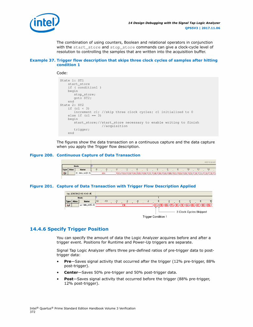
The combination of using counters, Boolean and relational operators in conjunctionwith the start_store and stop_store commands can give a clock-cycle level ofresolution to controlling the samples that are written into the acquisition buffer.
Example 37. Trigger flow description that skips three clock cycles of samples after hittingcondition 1
Code:
State 1: ST1 start_store if ( condition1 ) begin stop_store; goto ST2; endState 2: ST2 if (c1 < 3) increment c1; //skip three clock cycles; c1 initialized to 0 else if (c1 == 3) begin start_store;//start_store necessary to enable writing to finish //acquisition trigger; end
The figures show the data transaction on a continuous capture and the data capturewhen you apply the Trigger flow description.
Figure 200. Continuous Capture of Data Transaction
Figure 201. Capture of Data Transaction with Trigger Flow Description Applied
14.4.6 Specify Trigger Position
You can specify the amount of data the Logic Analyzer acquires before and after atrigger event. Positions for Runtime and Power-Up triggers are separate.
Signal Tap Logic Analyzer offers three pre-defined ratios of pre-trigger data to post-trigger data:
• Pre—Saves signal activity that occurred after the trigger (12% pre-trigger, 88%post-trigger).
• Center—Saves 50% pre-trigger and 50% post-trigger data.
• Post—Saves signal activity that occurred before the trigger (88% pre-trigger,12% post-trigger).
14 Design Debugging with the Signal Tap Logic Analyzer
QPS5V3 | 2017.11.06
Intel® Quartus® Prime Standard Edition Handbook Volume 3 Verification372

These pre-defined ratios apply to both non-segmented buffers and segmented buffers.
Related Links
State-Based Triggering on page 363
14.4.6.1 Post-fill Count
In a custom state-based triggering flow with the segment_trigger and triggerbuffer control actions, you can use the post-fill_count argument to specify acustom trigger position.
• If you do not use the post-fill_count argument, the trigger position for theaffected buffer defaults to the trigger position you specified in the Setup tab.
• In the trigger buffer control action (for non-segmented buffers), post-fill_count specifies the number of samples to capture before stopping dataacquisition.
• In the segment_trigger buffer control action (for segmented buffer), post-fill_count specifies a data segment.
Note: In the case of segment_trigger, acquisition of the current buffer stopsimmediately if a subsequent triggering action is issued in the next state,regardless of the current buffer's post-fill count. The Logic Analyzer discardsthe remaining unfilled post-count acquisitions in the current buffer, anddisplays them as grayed-out samples in the data window.
When the Signal Tap data window displays the captured data, the trigger positionappears as the number of post-count samples from the end of the acquisition segmentor buffer.
Sample Number of Trigger Position = (N – Post-Fill Count)
In this case, N is the sample depth of either the acquisition segment or non-segmented buffer.
Related Links
Buffer Control Actions on page 368
14.4.7 Create a Power-Up Trigger
Power-up triggers capture events that occur during device initialization, immediatelyafter you power or reset the FPGA.
The typical use of Signal Tap Logic Analyzer is triggering events that occur duringnormal device operation. You start an analysis manually once the target device is fullypowered on and the JTAG connection for the device is available. With Signal TapPower-Up Trigger feature, the Signal Tap Logic Analyzer captures data immediatelyafter device initialization.
You can add a different Power-Up Trigger to each logic analyzer instance in the SignalTap Instance Manager pane.
14 Design Debugging with the Signal Tap Logic Analyzer
QPS5V3 | 2017.11.06
Intel® Quartus® Prime Standard Edition Handbook Volume 3 Verification373

14.4.7.1 Enabling a Power-Up Trigger
To enable the Power-Up Trigger for a logic analyzer instance, right-click the instanceand click Enable Power-Up Trigger. Alternatively, click Edit ➤ Enable Power-UpTrigger.
Power-Up Trigger appears as a child instance below the name of the selected instance.The node list displays the default trigger conditions.
Figure 202. Enabling Power-Up Trigger in Signal Tap Logic Analyzer Editor
To disable a Power-Up Trigger, right-click the instance and click Disable Power-UpTrigger.
14.4.7.2 Manage and Configure Power-Up and Runtime Trigger Conditions
You can create basic, comparison, and advanced trigger conditions for your enabledPower-Up Trigger as you do with a Run-Time Trigger.
Since each instance now has two sets of trigger conditions—the Power-Up Trigger andthe Run-Time Trigger—you can differentiate between the two with color coding. Power-Up Trigger conditions that you can adjust are color coded light blue, while Run-TimeTrigger conditions you cannot adjust remain white.
To switch between the trigger conditions of the Power-Up Trigger and the Run-TimeTrigger, double-click the instance name or the Power-Up Trigger name in the InstanceManager.
You cannot make changes to Power-Up Trigger conditions that would normally requirea full recompile with Runtime Trigger conditions, such as adding signals, deletingsignals, or changing between basic, comparison, and advanced triggers. To applythese changes to the Power-Up Trigger conditions, first make the changes using theRuntime Trigger conditions.
Note: Any change made to the Power-Up Trigger conditions requires that you recompile theSignal Tap Logic Analyzer instance, even if a similar change to the Runtime Triggerconditions does not require a recompilation.
To copy trigger conditions from a Run-Time Trigger to a Power-Up Trigger or viceversa, right-click the trigger name in the Instance Manager and click DuplicateTrigger. Alternatively, select the trigger name and click Edit ➤ Duplicate Trigger.
You can also use In-System Sources and Probes in conjunction with the Signal TapLogic Analyzer to force trigger conditions. The In-System Sources and Probes featureallows you to drive and sample values on to selected nets over the JTAG chain.
14 Design Debugging with the Signal Tap Logic Analyzer
QPS5V3 | 2017.11.06
Intel® Quartus® Prime Standard Edition Handbook Volume 3 Verification374

Related Links
Design Debugging Using In-System Sources and Probes on page 49
14.4.8 External Triggers
To trigger Signal Tap Logic Analyzer from an external source, you can create anexternal trigger input.
The external trigger input behaves like trigger condition 1, in that it must evaluate toTRUE before the logic analyzer evaluates any other configured trigger conditions.
Signal Tap Logic Analyzer supplies a signal to trigger external devices or other logicanalyzer instances. These features allow you to synchronize external logic analysisequipment with the internal logic analyzer. Power-Up Triggers can use the externaltriggers feature, but they must use the same source or target signal as theirassociated Run-Time Trigger.
You can use external triggers to perform cross-triggering on a hard processor system(HPS):
• Use your processor debugger to configure the HPS to obey or disregard cross-trigger request from the FPGA, and to issue or not issue cross-trigger requests tothe FPGA.
• Use your processor debugger in combination with the Signal Tap external triggerfeature to develop a dynamic combination of cross-trigger behaviors.
• You can use the cross-triggering feature with the ARM Development Studio 5(DS-5) software to implement a system-level debugging solution for your IntelFPGA SoC.
Related Links
• FPGA-Adaptive Software Debug and Performance Analysis white paper
• Signal Configuration PaneIn Intel Quartus Prime Help
14.4.8.1 Using the Trigger Out of One Analyzer as the Trigger In of AnotherAnalyzer
An advanced feature of the Signal Tap Logic Analyzer is the ability to use theTrigger out of one analyzer as the Trigger in to another analyzer. This feature allowsyou to synchronize and debug events that occur across multiple clock domains.
To perform this operation, first turn on Trigger out for the source logic analyzerinstance. On the Instance list of the Trigger out trigger, select the targeted logicanalyzer instance. For example, if the instance named auto_signaltap_0 shouldtrigger auto_signaltap_1, select auto_signaltap_1|trigger_in .
Turning on Trigger out automatically enables the Trigger in of the targeted logicanalyzer instance and fills in the Instance field of the Trigger in trigger with theTrigger out signal from the source logic analyzer instance. In this example,auto_signaltap_0 is targeting auto_signaltap_1. The Trigger In Instance fieldof auto_signaltap_1 is automatically filled in with auto_signaltap_0|trigger_out.
14 Design Debugging with the Signal Tap Logic Analyzer
QPS5V3 | 2017.11.06
Intel® Quartus® Prime Standard Edition Handbook Volume 3 Verification375

14.5 Compiling the Design
To incorporate the Signal Tap logic in your design and enable the JTAG connection, youmust compile your project. When you add a .stp file to your project, the Signal TapLogic Analyzer becomes part of your design. When you debug your design with atraditional external logic analyzer, you must often make changes to the signals youwant to monitor as well as the trigger conditions.
Note: Because these adjustments require that you recompile your design when using theSignal Tap Logic Analyzer, use the Signal Tap Logic Analyzer feature along withincremental compilation in the Intel Quartus Prime software to reduce recompilationtime.
14.5.1 Faster Compilations with Intel Quartus Prime IncrementalCompilation
You can add a Signal Tap Logic Analyzer instance to your design without recompilingyour original source code. Incremental compilation enables you to preserve thesynthesis and fitting results of your original design.
When you compile your design including a .stp file, Intel Quartus Prime softwareautomatically adds the sld_signaltap and sld_hub entities to the compilationhierarchy. These two entities are the main components of the Signal Tap LogicAnalyzer, providing the trigger logic and JTAG interface required for operation.
Incremental compilation is also useful when you want to modify the configuration ofthe .stp file. For example, you can change the buffer sample depth or memory typewithout performing a full compilation. Instead, you only recompile the Signal Tap LogicAnalyzer, configured as its own design partition.
14.5.1.1 Enabling Incremental Compilation for Your Design
When enabled for your design, the Signal Tap Logic Analyzer is always a separatepartition. After the first compilation, you can use the Signal Tap Logic Analyzer toanalyze signals from the post-fit netlist. If your partitions are designed correctly,subsequent compilations due to Signal Tap Logic Analyzer settings take less time.
The netlist type for the top-level partition defaults to source. To take advantage ofincremental compilation, specify the Netlist types for the partitions you want to tap asPost-fit.
Related Links
Intel Quartus Prime Incremental Compilation for Hierarchical and Team-Based Designdocumentation
14 Design Debugging with the Signal Tap Logic Analyzer
QPS5V3 | 2017.11.06
Intel® Quartus® Prime Standard Edition Handbook Volume 3 Verification376

14.5.1.2 Using Incremental Compilation with the Signal Tap Logic Analyzer
The Signal Tap Logic Analyzer uses the incremental compilation flow by default. For allsignals that you want to connect to the Signal Tap Logic Analyzer from the post-fitnetlist:
1. In the Design Partitions window, set the netlist type of the partition that containsthe signals to Post-Fit, with a Fitter Preservation Level of Placement andRouting.
2. In the Node Finder, use the Signal Tap: post-fitting filter to add the signals ofinterest to your Signal Tap configuration file.
3. If you want to add signals from the pre-synthesis netlist, set the netlist type toSource File and use the Signal Tap: pre-synthesis filter in the Node Finder.Do not use the netlist type Post-Synthesis with the Signal Tap Logic Analyzer.
Caution: When using post-fit and pre-synthesis nodes:
• Read all incremental compilation guidelines to ensure the proper partitioning of aproject.
• To speed up compile time, use only post-fit nodes for partitions specified aspreservation-level post-fit.
• Do not mix pre-synthesis and post-fit nodes in any partition. If you must tap pre-synthesis nodes for a particular partition, make all tapped nodes in that partitionpre-synthesis nodes and change the netlist type to source in the design partitionswindow.
Node names can differ between a pre-synthesis netlist and a post-fit netlist. Ingeneral, registers and user input signals share common names between the twonetlists. During compilation, certain optimizations change the names of combinationalsignals in your RTL. If the type of node name chosen does not match the netlist type,the compiler may not be able to find the signal to connect to your Signal Tap LogicAnalyzer instance for analysis. The compiler issues a critical warning to alert you ofthis scenario. The signal that is not connected is tied to ground in the Signal Tapdata tab.
If you do use incremental compilation flow with the Signal Tap Logic Analyzer andsource file changes are necessary, be aware that you may have to remove compiler-generated post-fit net names. Source code changes force the affected partition to gothrough resynthesis. During synthesis, the compiler cannot find compiler-generatednet names from a previous compilation.
Note: Intel FPGA recommends using only registered and user-input signals as debuggingtaps in your .stp whenever possible.
Both registered and user-supplied input signals share common node names in the pre-synthesis and post-fit netlist. As a result, using only registered and user-suppliedinput signals in your .stp limits the changes you need to make to your Signal TapLogic Analyzer configuration.
You can check the nodes that are connected to each Signal Tap instance using the In-System Debugging compilation reports. These reports list each node name youselected to connect to a Signal Tap instance, the netlist type used for the particularconnection, and the actual node name used after compilation. If the incremental
14 Design Debugging with the Signal Tap Logic Analyzer
QPS5V3 | 2017.11.06
Intel® Quartus® Prime Standard Edition Handbook Volume 3 Verification377

compilation flow is not used, the In-System Debugging reports are located in theAnalysis & Synthesis folder. If the incremental compilation flow is used, this report islocated in the Partition Merge folder.
To verify that your original design was not modified, examine the messages in thePartition Merge section of the Compilation Report.
Unless you make changes to your design partitions that require recompilation, onlythe Signal Tap design partition is recompiled. If you make subsequent changes to onlythe .stp, only the Signal Tap design partition must be recompiled, reducing yourrecompilation time.
14.5.2 Prevent Changes Requiring Recompilation
Configure the .stp to prevent changes that normally require recompilation. To dothis, select a Lock mode from above the node list in the Setup tab. To lock yourconfiguration, choose Allow trigger condition changes only.
Figure 203. Allow Trigger Conditions Change Only
Related Links
Verify Whether You Need to Recompile Your Project on page 382
14.5.3 Incremental Route with Rapid Recompile
You can use Incremental Route with Rapid Recompile to decrease compilation times.After performing a full compilation on your design, you can use the Incremental Routeflow to achieve a 2-4x speedup over a flat compile. The Incremental Route flow is notcompatible with Partial Reconfiguration.
Intel Quartus Prime Standard Edition software supports Incremental Route with RapidRecompile for Arria V, Cyclone V, and Stratix V devices.
Related Links
Running Rapid RecompileIn Intel Quartus Prime Pro Edition Handbook Volume 1
14.5.3.1 Using the Incremental Route Flow
To use the Incremental Route flow:
1. Open your design and run Analysis & Elaboration (or a full compilation) to givenode visibility in Signal Tap.
2. Add Signal Tap to your design.
3. In the Signal Tap Signal Configuration pane, specify Manual in the NodesAllocated field for Trigger and Data nodes (and Storage Qualifier, if used).
14 Design Debugging with the Signal Tap Logic Analyzer
QPS5V3 | 2017.11.06
Intel® Quartus® Prime Standard Edition Handbook Volume 3 Verification378
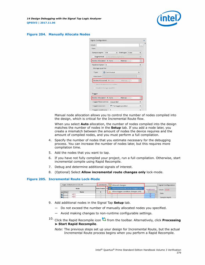
Figure 204. Manually Allocate Nodes
Manual node allocation allows you to control the number of nodes compiled intothe design, which is critical for the Incremental Route flow.
When you select Auto allocation, the number of nodes compiled into the designmatches the number of nodes in the Setup tab. If you add a node later, youcreate a mismatch between the amount of nodes the device requires and theamount of compiled nodes, and you must perform a full compilation.
4. Specify the number of nodes that you estimate necessary for the debuggingprocess. You can increase the number of nodes later, but this requires morecompilation time.
5. Add the nodes that you want to tap.
6. If you have not fully compiled your project, run a full compilation. Otherwise, startincremental compile using Rapid Recompile.
7. Debug and determine additional signals of interest.
8. (Optional) Select Allow incremental route changes only lock-mode.
Figure 205. Incremental Route Lock-Mode
9. Add additional nodes in the Signal Tap Setup tab.
— Do not exceed the number of manually allocated nodes you specified.
— Avoid making changes to non-runtime configurable settings.
10. Click the Rapid Recompile icon from the toolbar. Alternatively, click Processing➤ Start Rapid Recompile.
Note: The previous steps set up your design for Incremental Route, but the actualIncremental Route process begins when you perform a Rapid Recompile.
14 Design Debugging with the Signal Tap Logic Analyzer
QPS5V3 | 2017.11.06
Intel® Quartus® Prime Standard Edition Handbook Volume 3 Verification379

14.5.3.2 Tips to Achieve Maximum Speedup
• Basic AND (which applies to Storage Qualifier as well as trigger input) is thefastest for the Incremental Route flow.
• Basic OR is slower for the Incremental Route flow, but if you avoid changing theparent-child relationship of nodes within groups, you can minimize the impact oncompile time. You can change the sibling relationships of nodes.
— Basic OR and advanced triggers require re-synthesis when you change thenumber/names of tapped nodes.
• Use the Incremental Route lock-mode to avoid inadvertent changes requiring a fullcompilation.
14.5.4 Timing Preservation with the Signal Tap Logic Analyzer
In addition to verifying functionality, timing closure is one of the most crucialprocesses in successful operation of your design.
Note: When you compile a project with a Signal Tap Logic Analyzer without the use ofincremental compilation, you must add IP to your existing design. This addition oftenimpacts the existing placement, routing, and timing of your design. To minimize theeffect that the Signal Tap Logic Analyzer has on your design, use incrementalcompilation for your project. Incremental compilation is the default setting in newdesigns. You can easily enable incremental compilation in existing designs. When theSignal Tap Logic Analyzer is in a design partition, it has little to no affect on yourdesign.
For Intel Arria 10 devices, the Intel Quartus Prime Standard Edition software does notsupport timing preservation for post-fit taps with Rapid Recompile.
Use the following techniques to help maintain timing:
• Avoid adding critical path signals to your .stp.
• Minimize the number of combinational signals you add to your .stp, and addregisters whenever possible.
• Specify an fMAX constraint for each clock in your design.
Related Links
Timing Closure and OptimizationIn Intel Quartus Prime Standard Edition Handbook Volume 2
14.5.5 Performance and Resource Considerations
When you perform logic analysis of your design, you can see the necessary trade-offbetween runtime flexibility, timing performance, and resource usage.
The Signal Tap Logic Analyzer allows you to select runtime configurable parameters tobalance the need for runtime flexibility, speed, and area.
The default values of the runtime configurable parameters provide maximumflexibility, so you can complete debugging as quickly as possible; however, you canadjust these settings to determine whether there is a more appropriate configuration
14 Design Debugging with the Signal Tap Logic Analyzer
QPS5V3 | 2017.11.06
Intel® Quartus® Prime Standard Edition Handbook Volume 3 Verification380

for your design. Because performance results are design-dependent, try these optionsin different combinations until you achieve the desired balance between functionality,performance, and utilization.
14.5.5.1 Signal Tap Logic in Critical Path
If Signal Tap logic is part of your critical path, follow these tips to speed up theperformance of the Signal Tap Logic Analyzer:
• Disable runtime configurable options—Certain resources are allocated toaccommodate for runtime flexibility. If you use either advanced triggers or State-based triggering flow, disable runtime configurable parameters for a boost in fMAXof the Signal Tap logic.
— If you are using State-based triggering flow, try disabling the Goto statedestination option and performing a recompilation before disabling the otherruntime configurable options. The Goto state destination option has thegreatest impact on fMAX, as compared to the other runtime configurableoptions.
• Minimize the number of signals that have Trigger Enable selected—Bydefault, Signal Tap Logic Analyzer enable the Trigger Enable option for all signalsthat you add to the .stp file. For signals that you do not plan to use as triggers,turn this option off.
• Turn on Physical Synthesis for register retiming—If many (more than thenumber of inputs that fit in a LAB) enabled triggering signals fan-in logic to agate-based triggering condition (basic trigger condition or a logical reductionoperator in the advanced trigger tab), turn on Perform register retiming. Thiscan help balance combinational logic across LABs.
14.5.5.2 Signal Tap Logic Using Critical Resources
If your design is resource constrained, follow these tips to reduce the logic or memorythe Signal Tap Logic Analyzer uses:
• Disable runtime configurable options—Disabling runtime configurability foradvanced trigger conditions or runtime configurable options in the State-basedtriggering flow results in fewer LEs.
• Minimize the number of segments in the acquisition buffer—You can reducethe logic resources that the Signal Tap Logic Analyzer uses if you limit thesegments in your sampling buffer
• Disable the Data Enable for signals that you use only for triggering—Bydefault, Signal Tap Logic Analyzer enables data enable options for all signals.Turning off the data enable option for signals you use only as trigger inputs saveson memory resources.
14.6 Program the Target Device or Devices
After you add the Signal Tap Logic Analyzer to your project and re-compile, you canconfigure the FPGA target device.
If you want to debug multiple designs simultaneously, configure the device fromthe .stp instead of the Intel Quartus Prime Programmer. This allows you to openmore than one .stp file and program multiple devices.
14 Design Debugging with the Signal Tap Logic Analyzer
QPS5V3 | 2017.11.06
Intel® Quartus® Prime Standard Edition Handbook Volume 3 Verification381

14.6.1 Ensure Setting Compatibility Between .stp and .sof Files
A .stp file is compatible with a .sof file when the settings for the logic analyzer,such as the size of the capture buffer and the signals you use for monitoring ortriggering, match the programming settings of the target device. If the files are notcompatible, you can still program the device, but you cannot run or control the logicanalyzer from the Signal Tap Logic Analyzer Editor.
• To ensure programming compatibility, program your device with the .sof filegenerated in the most recent compilation.
• To check whether a particular .sof is compatible with the current Signal Tapconfiguration, attach the .sof to the SOF manager.
Note: When the Signal Tap Logic Analyzer detects incompatibility after the analysis starts,the Intel Quartus Prime software generates a system error message containing twoCRC values: the expected value and the value retrieved from the .stp instance on thedevice. The CRC value comes from all Signal Tap settings that affect the compilation.
Although having a Intel Quartus Prime project is not required when using an .stp, itis recommended. The project database contains information about the integrity of thecurrent Signal Tap Logic Analyzer session. Without the project database, there is noway to verify that the current .stp file matches the .sof file in the device. If youhave an .stp file that does not match the .sof file, the Signal Tap Logic Analyzer cancapture incorrect data.
Related Links
Manage Multiple Signal Tap Files and Configurations on page 350
14.6.2 Verify Whether You Need to Recompile Your Project
Before starting a debugging session, do not make any changes to the .stp settingsthat require recompiling the project.
To verify whether a change you made requires recompiling the project, check theSignal Tap status display at the top of the Instance Manager pane. This featureallows you to undo the change, so that you do not need to recompile your project.
Related Links
Prevent Changes Requiring Recompilation on page 378
14.7 Running the Signal Tap Logic Analyzer
Debugging Signal Tap Logic Analyzer is similar using an external logic analyzer. Youinitialize the logic analyzer by starting an analysis. When your trigger event occurs,the logic analyzer stores the captured data in the device's memory buffer, and thentransfers this data to the .stp file with the JTAG connection.
You can also perform the equivalent of a force trigger instruction that lets you viewthe captured data currently in the buffer without a trigger event occurring.
The flowchart shows how you operate the Signal Tap Logic Analyzer. indicates wherePower-Up and Runtime Trigger events occur and when captured data from theseevents is available for analysis.
14 Design Debugging with the Signal Tap Logic Analyzer
QPS5V3 | 2017.11.06
Intel® Quartus® Prime Standard Edition Handbook Volume 3 Verification382

Figure 206. Power-Up and Runtime Trigger Events Flowchart
Manually RunSignal Tap Logic Analyzer
Compile Design
Start
End
Yes
No
No
Yes
Yes
No
Program Device
No
Yes
Manually Read Data from Device
Trigger Occurred?
Analyze Data: Power-Upor Run-Time Trigger
Continue Debugging?Make Changes to Setup(If Needed)
Changes RequireRecompile?
Data Downloaded?
Manually Stop Analyzer
Possible Missed Trigger(Unless Power-UpTrigger Enabled)
You can also use In-System Sources and Probes in conjunction with the Signal TapLogic Analyzer to force trigger conditions. The In-System Sources and Probes featureallows you to drive and sample values on to selected signals over the JTAG chain.
Related Links
Design Debugging Using In-System Sources and Probes on page 49
14.7.1 Runtime Reconfigurable Options
When you use Runtime Trigger mode, you can change certain settings in the .stpwithout recompiling your design.
Table 119. Runtime Reconfigurable Features
Runtime Reconfigurable Setting Description
Basic Trigger Conditions and Basic StorageQualifier Conditions
You can change without recompiling all signals that have the Triggercondition turned on to any basic trigger condition value
Comparison Trigger Conditions and ComparisonStorage Qualifier Conditions
All the comparison operands, the comparison numeric values, and theinterval bound values are runtime-configurable.You can also switch from Comparison to Basic OR trigger at runtimewithout recompiling.
Advanced Trigger Conditions and AdvancedStorage Qualifier Conditions
Many operators include runtime configurable settings. For example, allcomparison operators are runtime-configurable. Configurable settingsappear with a white background in the block representation. Thisruntime reconfigurable option is turned on in the Object Propertiesdialog box.
Switching between a storage-qualified and acontinuous acquisition
Within any storage-qualified mode, you can switch to continuouscapture mode without recompiling the design. To enable this feature,turn on disable storage qualifier.
State-based trigger flow parameters Refer to Runtime Reconfigurable Settings, State-Based TriggeringFlow
14 Design Debugging with the Signal Tap Logic Analyzer
QPS5V3 | 2017.11.06
Intel® Quartus® Prime Standard Edition Handbook Volume 3 Verification383

Runtime Reconfigurable options can save time during the debugging cycle by allowingyou to cover a wider possible scenario of events without the need to recompile thedesign. You may experience a slight impact to the performance and logic utilization.You can turn off runtime re-configurability for advanced trigger conditions and thestate-based trigger flow parameters, boosting performance and decreasing areautilization.
To configure the .stp file to prevent changes that normally require recompilation inthe Setup tab, select Allow Trigger Condition changes only above the node list.
In Incremental Route lock mode, Allow incremental route changes only, limits tochanges that only require an Incremental Route compilation, and not a full compile.
This example illustrates a potential use case for Runtime Reconfigurable features, byproviding a storage qualified enabled State-based trigger flow description, andshowing how to modify the size of a capture window at runtime without a recompile.This example gives you equivalent functionality to a segmented buffer with a singletrigger condition where the segment sizes are runtime reconfigurable.
state ST1:if ( condition1 && (c1 <= m) )// each "segment" triggers on condition // 1begin // m = number of total "segments" start_store; increment c1; goto ST2:End
else (c1 > m ) // This else condition handles the last // segment.begin start_store Trigger (n-1)end
state ST2:if ( c2 >= n) //n = number of samples to capture in each //segment.begin reset c2; stop_store; goto ST1;end else (c2 < n)begin increment c2; goto ST2;end
Note: m x n must equal the sample depth to efficiently use the space in the sample buffer.
The next figure shows the segmented buffer that the trigger flow example describes.
Figure 207. Segmented Buffer Created with Storage Qualifier and State-Based TriggerTotal sample depth is fixed, where m x n must equal sample depth.
Segment 1
1 n
Segment 2
1 n
Segment m
1 n
14 Design Debugging with the Signal Tap Logic Analyzer
QPS5V3 | 2017.11.06
Intel® Quartus® Prime Standard Edition Handbook Volume 3 Verification384

During runtime, you can modify the values m and n. Changing the m and n values inthe trigger flow description adjust the segment boundaries without recompiling.
You can add states into the trigger flow description and selectively mask out specificstates and enable other ones at runtime with status flags.
This example is like the previous example with an additional state inserted. You usethis extra state to specify a different trigger condition that does not use the storagequalifier feature. You insert status flags into the conditional statements to control theexecution of the trigger flow.
state ST1 : if (condition2 && f1) // additional state added for a non-segmented // acquisition set f1 to enable state begin start_store; trigger end else if (! f1) goto ST2;state ST2: if ( (condition1 && (c1 <= m) && f2) // f2 status flag used to mask state. Set f2 // to enable begin start_store; increment c1; goto ST3: end else (c1 > m ) start_store Trigger (n-1) endstate ST3: if ( c2 >= n) begin reset c2; stop_store; goto ST1; end else (c2 < n) begin increment c2; goto ST2; end
14.7.2 Signal Tap Status Messages
The table describes the text messages that might appear in the Signal Tap StatusIndicator in the Instance Manager pane before, during, and after a data acquisition.Use these messages to monitor the state of the logic analyzer or what operation it isperforming.
Table 120. Text Messages in the Signal Tap Status Indicator
Message Message Description
Not running The Signal Tap Logic Analyzer is not running. There is no connection to a device orthe device is not configured.
(Power-Up Trigger) Waiting forclock (1)
The Signal Tap Logic Analyzer is performing a Runtime or Power-Up Triggeracquisition and is waiting for the clock signal to transition.
continued...
14 Design Debugging with the Signal Tap Logic Analyzer
QPS5V3 | 2017.11.06
Intel® Quartus® Prime Standard Edition Handbook Volume 3 Verification385

Message Message Description
Acquiring (Power-Up) pre-trigger data (1)
The trigger condition has not been evaluated yet. A full buffer of data is collected ifusing the non-segmented buffer acquisition mode and storage qualifier type iscontinuous.
Trigger In conditions met Trigger In condition has occurred. The Signal Tap Logic Analyzer is waiting for thecondition of the first trigger condition to occur. This can appear if Trigger In isspecified.
Waiting for (Power-up) trigger (1) The Signal Tap Logic Analyzer is now waiting for the trigger event to occur.
Trigger level <x> met The condition of trigger condition x has occurred. The Signal Tap Logic Analyzer iswaiting for the condition specified in condition x + 1 to occur.
Acquiring (power-up) post-trigger data (1)
The entire trigger event has occurred. The Signal Tap Logic Analyzer is acquiring thepost-trigger data. The amount of post-trigger data collected is you define between12%, 50%, and 88% when the non-segmented buffer acquisition mode is selected.
Offload acquired (Power-Up) data(1)
Data is being transmitted to the Intel Quartus Prime software through the JTAGchain.
Ready to acquire The Signal Tap Logic Analyzer is waiting for you to initialize the analyzer.
1. This message can appear for both Runtime and Power-Up Trigger events. When referring to a Power-Up Trigger, the text inparentheses is added.
Note: In segmented acquisition mode, pre-trigger and post-trigger do not apply.
14.8 View, Analyze, and Use Captured Data
Use the Signal Tap Logic Analyzer interface to examine the data you capturedmanually or using a trigger, and use your findings to debug your design.
When in the Data view, you can use the drag-to-zoom feature by left-clicking toisolate the data of interest.
14.8.1 Capturing Data Using Segmented Buffers
Segmented Acquisition buffers allow you to perform multiple captures with a separatetrigger condition for each acquisition segment. This feature allows you to capture arecurring event or sequence of events that span over a long period time efficiently.
Each acquisition segment acts as a non-segmented buffer, continuously capturing datawhen it is activated. When you run an analysis with the segmented buffer optionenabled, the Signal Tap Logic Analyzer performs back-to-back data captures for eachacquisition segment within your data buffer. You define the trigger flow, or the typeand order in which the trigger conditions evaluate for each buffer, either in theSequential trigger flow control or in the Custom State-based trigger flow control.
The following figure shows a segmented acquisition buffer with four segmentsrepresented as four separate non-segmented buffers.
14 Design Debugging with the Signal Tap Logic Analyzer
QPS5V3 | 2017.11.06
Intel® Quartus® Prime Standard Edition Handbook Volume 3 Verification386

Figure 208. Segmented Acquisition Buffer
0
1
1
Segment 1 Buffer
1
111
1
1
11
1 11
1
000
0
0
0
0 0
0
Trigger 1Post Pre
0
1
1
Segment 2 Buffer
1
111
1
1
11
1 11
1
000
0
0
0
0 0
0
Trigger 2Post Pre
0
1
1
Segment 3 Buffer
1
111
1
1
11
1 11
1
000
0
0
0
0 0
0
Trigger 3Post Pre
0
1
1
Segment 4 Buffer
1
111
1
1
11
1 11
1
000
0
0
0
0 0
0
Trigger 4Post Pre
The Signal Tap Logic Analyzer finishes an acquisition with a segment, and advances tothe next segment to start a new acquisition. Depending on when a trigger conditionoccurs, it may affect the way the data capture appears in the waveform viewer. Thefigure illustrates the data capture method. The Trigger markers—Trigger 1, Trigger 2,Trigger 3 and Trigger 4—refer to the evaluation of the segment_trigger andtrigger commands in the Custom State-based trigger flow. If you use a sequentialflow, the Trigger markers refer to trigger conditions specified within the Setup tab.
If the Segment 1 Buffer is the active segment and Trigger 1 occurs, the Signal TapLogic Analyzer starts evaluating Trigger 2 immediately. Data Acquisition for Segment 2buffer starts when either Segment Buffer 1 finishes its post-fill count, or when Trigger2 evaluates as TRUE, whichever condition occurs first. Thus, trigger conditionsassociated with the next buffer in the data capture sequence can preempt the post-fillcount of the current active buffer. This allows the Signal Tap Logic Analyzer toaccurately capture all the trigger conditions that have occurred. Unused samplesappear as a blank space in the waveform viewer.
The next figure shows an example of a capture using sequential flow control with thetrigger condition for each segment specified as Don’t Care.
Figure 209. Segmented Capture with Preemption of Acquisition Segments
Each segment before the last captures only one sample, because the next triggercondition immediately preempts capture of the current buffer. The trigger position forall segments is specified as pre-trigger (10% of the data is before the trigger conditionand 90% of the data is after the trigger position). Because the last segment startsimmediately with the trigger condition, the segment contains only post-trigger data.The three empty samples in the last segment are left over from the pre-triggersamples that the Signal Tap Logic Analyzer allocated to the buffer.
For the sequential trigger flow, the Trigger Position option applies to every segmentin the buffer. For maximum flexibility on defining the trigger position, use the customstate-based trigger flow. By adjusting the trigger position specific to your debuggingrequirements, you can help maximize the use of the allocated buffer space.
14.8.2 Differences in Pre-fill Write Behavior Between Different AcquisitionModes
The Signal Tap Logic Analyzer uses one of the following three modes when writing intothe acquisition memory:
14 Design Debugging with the Signal Tap Logic Analyzer
QPS5V3 | 2017.11.06
Intel® Quartus® Prime Standard Edition Handbook Volume 3 Verification387

• Non-segmented buffer
• Non-segmented buffer with a storage qualifier
• Segmented buffer
There are subtle differences in the amount of data captured immediately after runningthe Signal Tap Logic Analyzer and before any trigger conditions occur. A non-segmented buffer, running in continuous mode, completely fills the buffer withsampled data before evaluating any trigger conditions. Thus, a non-segmentedcapture without any storage qualification enabled always shows a waveform with a fullbuffer's worth of data captured.
Filling the buffer provides you with as much data as possible within the capturewindow. The buffer gets pre-filled with data samples prior to evaluating the triggercondition. As such, Signal Tap requires that the buffer be filled at least once beforeany data can be retrieved through the JTAG connection and prevents the buffer frombeing dumped during the first acquisition prior to a trigger condition when youperform a Stop Analysis.
For segmented buffers and non-segmented buffers using any storage qualificationmode, the Signal Tap Logic Analyzer immediately evaluates all trigger conditions whilewriting samples into the acquisition memory. This evaluation is especially importantwhen using any storage qualification on the data set. The logic analyzer may miss atrigger condition if it waits to capture a full buffer's worth of data before evaluatingany trigger conditions,
If the trigger event occurs on any data sample before the specified amount of pre-trigger data has occurred, then the Signal Tap Logic Analyzer triggers and beginsfilling memory with post-trigger data, regardless of the amount of pre-trigger data youspecify. For example, if you set the trigger position to 50% and set the logic analyzerto trigger on a processor reset, start the logic analyzer, and then power on your targetsystem, the logic analyzer triggers. However, the logic analyzer memory is filled onlywith post-trigger data, and not any pre-trigger data, because the trigger event, whichhas higher precedence than the capture of pre-trigger data, occurred before the pre-trigger condition was satisfied.
The figures for continuous data capture and conditional data capture show thedifference between a non-segmented buffer in continuous mode and a non-segmentedbuffer using a storage qualifier. The configuration of the logic analyzer waveformsbelow is a base trigger condition, sample depth of 64 bits, and Post trigger position.
Figure 210. Signal Tap Logic Analyzer Continuous Data Capture
In the continuous data capture, Trig1 occurs several times in the data buffer beforethe Signal Tap Logic Analyzer actually triggers. A full buffer's worth of data is capturedbefore the logic analyzer evaluates any trigger conditions. After the trigger conditionoccurs, the logic analyzer continues acquisition until it captures eight additionalsamples (12% of the buffer, as defined by the "post-trigger" position).
14 Design Debugging with the Signal Tap Logic Analyzer
QPS5V3 | 2017.11.06
Intel® Quartus® Prime Standard Edition Handbook Volume 3 Verification388

Figure 211. Signal Tap Logic Analyzer Conditional Data Capture
Note to figure:
1. Conditional capture, storage always enabled, post-fill count.
2. Signal Tap Logic Analyzer capture of a recurring pattern using a non-segmentedbuffer in conditional mode. The configuration of the logic analyzer is a basictrigger condition "Trig1" and sample depth of 64 bits. The Trigger in condition isDon't care, which means that every sample is captured.
In conditional capture the logic analyzer triggers immediately. As in continuouscapture, the logic analyzer completes the acquisition with eight samples, or 12% of64, the sample capacity of the acquisition buffer.
14.8.3 Creating Mnemonics for Bit Patterns
The mnemonic table feature allows you to assign a meaningful name to a set of bitpatterns, such as a bus. To create a mnemonic table, right-click in the Setup or Datatab of an .stp and click Mnemonic Table Setup. You create a mnemonic table byentering sets of bit patterns and specifying a label to represent each pattern. Onceyou have created a mnemonic table, assign the table to a group of signals. To assign amnemonic table, right-click on the group, click Bus Display Format and select thedesired mnemonic table.
You use the labels you create in a table in different ways on the Setup and Data tabs.On the Setup tab, you can create basic triggers with meaningful names by right-clicking an entry in the Trigger Conditions column and selecting a label from thetable you assigned to the signal group. On the Data tab, if any captured data matchesa bit pattern contained in an assigned mnemonic table, the signal group data isreplaced with the appropriate label, making it easy to see when expected datapatterns occur.
14.8.4 Automatic Mnemonics with a Plug-In
When you use a plug-in to add signals to an .stp, mnemonic tables for the addedsignals are automatically created and assigned to the signals defined in the plug-in. Toenable these mnemonic tables manually, right-click the name of the signal or signalgroup. On the Bus Display Format shortcut menu, then click the name of themnemonic table that matches the plug-in.
As an example, the Nios II plug-in helps you to monitor signal activity for your designas the code is executed. If you set up the logic analyzer to trigger on a function namein your Nios II code based on data from an .elf, you can see the function name inthe Instance Address signal group at the trigger sample, along with thecorresponding disassembled code in the Disassembly signal group, as shown in Figure 13–52. Captured data samples around the trigger are referenced as offsetaddresses from the trigger function name.
14 Design Debugging with the Signal Tap Logic Analyzer
QPS5V3 | 2017.11.06
Intel® Quartus® Prime Standard Edition Handbook Volume 3 Verification389

Figure 212. Data Tab when the Nios II Plug-In is Used
14.8.5 Locating a Node in the Design
When you find the source of an error in your design using the Signal Tap LogicAnalyzer, you can use the node locate feature to locate that signal in many of the toolsfound in the Intel Quartus Prime software, as well as in your design files. This lets youfind the source of the problem quickly so you can modify your design to correct theflaw. To locate a signal from the Signal Tap Logic Analyzer in one of the Intel QuartusPrime software tools or your design files, right-click the signal in the .stp, and clickLocate in <tool name>.
You can locate a signal from the node list with the following tools:
• Assignment Editor
• Pin Planner
• Timing Closure Floorplan
• Chip Planner
• Resource Property Editor
• Technology Map Viewer
• RTL Viewer
• Design File
14.8.6 Saving Captured Data
When you save a data capture, Signal Tap Logic Analyzer stores this data in theactive .stp file, and the Data Log adds the capture as a log entry under the currentconfiguration.
When analysis is set to Auto-run mode, the Logic Analyzer creates a separate entryin the Data Log to store the data captured each time the trigger occurred. This allowsyou to review the captured data for each trigger event.
The default name for a log is based time stamp when the Logic Analyzer acquired thedata. As a best practice, rename the data log with a more meaningful name.
The organization of logs is hierarchical; the Logic Analyzer groups similar logs ofcaptured data in trigger sets.
Related Links
Data Log Pane on page 350
14 Design Debugging with the Signal Tap Logic Analyzer
QPS5V3 | 2017.11.06
Intel® Quartus® Prime Standard Edition Handbook Volume 3 Verification390

14.8.7 Exporting Captured Data to Other File Formats
You can export captured data to the following file formats, for use with other EDAsimulation tools:
• Comma Separated Values File (.csv)
• Table File (.tbl)
• Value Change Dump File (.vcd)
• Vector Waveform File (.vwf)
• Graphics format files (.jpg, .bmp)
To export the captured data from Signal Tap Logic Analyzer, on the File menu, clickExport and specify the File Name, Export Format, and Clock Period.
14.8.8 Creating a Signal Tap List File
A .stp list file contains all the data the logic analyzer captures for a trigger event, intext format.
Each row of the list file corresponds to one captured sample in the buffer. Columnscorrespond to the value of each of the captured signals or signal groups for thatsample. If you defined a mnemonic table for the captured data, a matching entry fromthe table replaces the numerical values in the list.
The .stp list file is especially useful when combined with a plug-in that includesinstruction code disassembly. You can view the order of instruction code executionduring the same time period of the trigger event.
To create a .stp list file in the Intel Quartus Prime software, click File ➤ Create/Update ➤ Create Signal Tap List File.
Related Links
Adding Signals with a Plug-In on page 337
14.9 Other Features
The Signal Tap Logic Analyzer provides optional features not specific to a task flow.The following techniques may offer advantages in specific circumstances.
14.9.1 Creating Signal Tap File from Design Instances
In addition to providing GUI support for generation of .stp files, the Intel QuartusPrime software supports generation of a Signal Tap instance from logic defined in HDLsource files. This technique is helpful to modify runtime configurable triggerconditions, acquire data, and view acquired data on the data log via Signal Taputilities.
14.9.1.1 Creating a .stp File from a Design Instance
To generate a .stp file from parameterized HDL instances within your design:
14 Design Debugging with the Signal Tap Logic Analyzer
QPS5V3 | 2017.11.06
Intel® Quartus® Prime Standard Edition Handbook Volume 3 Verification391

1. Open or create an Intel Quartus Prime project that includes one or more HDLinstances of the Signal Tap logic analyzer.
2. Click Processing ➤ Start ➤ Start Analysis & Synthesis.
3. Click File ➤ Create/Update ➤ Create Signal Tap File from DesignInstance(s).
4. Specify a location for the .stp file that generates, and click Save.
Figure 213. Create Signal Tap File from Design Instances Dialog Box
Note: If your project contains partial reconfiguration partitions, the Create SignalTap File from Design Instance(s) dialog box displays a tree view of thePR partitions in the project. Select a partition from the view, and clickCreate Signal Tap file. The resultant .stp file that generates contains allHDL instances in the corresponding PR partition. The resultant .stp filedoes not include the instances in any nested partial reconfigurationpartition.
Figure 214. Selecting Partition for .stp File Generation
After successful .stp file creation, the Signal Tap Logic Analyzer appears. All thefields are read-only, except runtime-configurable trigger conditions.
14 Design Debugging with the Signal Tap Logic Analyzer
QPS5V3 | 2017.11.06
Intel® Quartus® Prime Standard Edition Handbook Volume 3 Verification392

Figure 215. Generated .stp File
Related Links
• Create Signal Tap File from Design InstancesIn Intel Quartus Prime Help
• Custom Trigger HDL Object on page 358
14.9.2 Using the Signal Tap MATLAB MEX Function to Capture Data
When you use MATLAB for DSP design, you can acquire data from the Signal Tap LogicAnalyzer directly into a matrix in the MATLAB environment by calling the MATLAB MEXfunction alt_signaltap_run, built into the Intel Quartus Prime software. If you usethe MATLAB MEX function in a loop, you can perform as many acquisitions in the sameamount of time as you can when using Signal Tap in the Intel Quartus Prime softwareenvironment.
Note: The Signal Tap MATLAB MEX function is available in the Windows* version and Linuxversion of the Intel Quartus Prime software. This function is compatible with MATLABRelease 14 Original Release Version 7 and later.
To set up the Intel Quartus Prime software and the MATLAB environment to performSignal Tap acquisitions:
1. In the Intel Quartus Prime software, create an .stp file.
2. In the node list in the Data tab of the Signal Tap Logic Analyzer Editor, organizethe signals and groups of signals into the order in which you want them to appearin the MATLAB matrix.
Each column of the imported matrix represents a single Signal Tap acquisitionsample, while each row represents a signal or group of signals in the order youdefined in the Data tab.
14 Design Debugging with the Signal Tap Logic Analyzer
QPS5V3 | 2017.11.06
Intel® Quartus® Prime Standard Edition Handbook Volume 3 Verification393

Note: Signal groups that the Signal Tap Logic Analyzer acquires and transfers intothe MATLAB MEX function have a width limit of 32 signals. To use theMATLAB MEX function with a bus or signal group that contains more than 32signals, split the group into smaller groups that do not exceed the limit.
3. Save the .stp file and compile your design. Program your device and run theSignal Tap Logic Analyzer to ensure your trigger conditions and signal acquisitionwork correctly.
4. In the MATLAB environment, add the Intel Quartus Prime binary directory to yourpath with the following command:
addpath <Quartus install directory>\win
You can view the help file for the MEX function by entering the following commandin MATLAB without any operators:
alt_signaltap_run
5. Use the MATLAB MEX function to open the JTAG connection to the device and runthe Signal Tap Logic Analyzer to acquire data. When you finish acquiring data,close the JTAG connection.
To open the JTAG connection and begin acquiring captured data directly into aMATLAB matrix called stp, use the following command:
stp = alt_signaltap_run \('<stp filename>'[,('signed'|'unsigned')[,'<instance names>'[, \'<signalset name>'[,'<trigger name>']]]]);
When capturing data, you must assign a filename, for example, <stp filename> asa requirement of the MATLAB MEX function. Other MATLAB MEX function optionsare described in the table:
Table 121. Signal Tap MATLAB MEX Function Options
Option Usage Description
signed
unsigned
'signed'
'unsigned'
The signed option turns signal group data into 32-bit two’s-complement signed integers. The MSB of the group asdefined in the Signal Tap Data tab is the sign bit. Theunsigned option keeps the data as an unsigned integer.The default is signed.
<instance name> 'auto_signaltap_0' Specify a Signal Tap instance if more than one instance isdefined. The default is the first instance in the .stp,auto_signaltap_0.
<signal set name><trigger name>
'my_signalset'
'my_trigger'
Specify the signal set and trigger from the Signal Tap datalog if multiple configurations are present in the .stp. Thedefault is the active signal set and trigger in the file.
During data acquisition, you can enable or disable verbose mode to see the statusof the logic analyzer. To enable or disable verbose mode, use the followingcommands:
alt_signaltap_run('VERBOSE_ON');-alt_signaltap_run('VERBOSE_OFF');
When you finish acquiring data, close the JTAG connection with the followingcommand:
alt_signaltap_run('END_CONNECTION');
14 Design Debugging with the Signal Tap Logic Analyzer
QPS5V3 | 2017.11.06
Intel® Quartus® Prime Standard Edition Handbook Volume 3 Verification394
For more information about the use of MATLAB MEX functions in MATLAB, refer tothe MATLAB Help.
14.9.3 Using Signal Tap in a Lab Environment
You can install a stand-alone version of the Signal Tap Logic Analyzer. This version isparticularly useful in a lab environment in which you do not have a workstation thatmeets the requirements for a complete Intel Quartus Prime installation, or if you donot have a license for a full installation of the Intel Quartus Prime software. Thestandalone version of the Signal Tap Logic Analyzer is included with and requires theIntel Quartus Prime stand-alone Programmer which is available from the Downloadspage of the Altera website.
14.9.4 Remote Debugging Using the Signal Tap Logic Analyzer
14.9.4.1 Debugging Using a Local PC and an SoC
You can use the System Console with Signal Tap Logic Analyzer to remote debug yourIntel FPGA SoC. This method requires one local PC, an existing TCP/IP connection, aprogramming device at the remote location, and an Intel FPGA SoC.
Related Links
Remote Hardware Debugging over TCP/IP
14.9.4.2 Debugging Using a Local PC and a Remote PC
You can use the Signal Tap Logic Analyzer to debug a design that is running on adevice attached to a PC in a remote location.
To perform a remote debugging session, you must have the following setup:
• The Intel Quartus Prime software installed on the local PC
• Stand-alone Signal Tap Logic Analyzer or the full version of the Intel QuartusPrime software installed on the remote PC
• Programming hardware connected to the device on the PCB at the remote location
• TCP/IP protocol connection
14.9.4.2.1 Equipment Setup
1. On the PC in the remote location, install the standalone version of the Signal TapLogic Analyzer, included in the Intel Quartus Prime stand-alone Programmer, orthe full version of the Intel Quartus Prime software.
2. Connect the remote computer to Intel programming hardware, such as the or IntelFPGA Download Cable.
3. On the local PC, install the full version of the Intel Quartus Prime software.
4. Connect the local PC to the remote PC across a LAN with the TCP/IP protocol.
14 Design Debugging with the Signal Tap Logic Analyzer
QPS5V3 | 2017.11.06
Intel® Quartus® Prime Standard Edition Handbook Volume 3 Verification395

14.9.5 Using the Signal Tap Logic Analyzer in Devices with ConfigurationBitstream Security
Certain device families support bitstream decryption during configuration using an on-device AES decryption engine. You can still use the Signal Tap Logic Analyzer toanalyze functional data within the FPGA. However, note that JTAG configuration is notpossible after the security key has been programmed into the device.
Intel FPGA recommends that you use an unencrypted bitstream during the prototypeand debugging phases of the design. Using an unencrypted bitstream allows you togenerate new programming files and reconfigure the device over the JTAG connectionduring the debugging cycle.
If you must use the Signal Tap Logic Analyzer with an encrypted bitstream, firstconfigure the device with an encrypted configuration file using Passive Serial (PS),Fast Passive Parallel (FPP), or Active Serial (AS) configuration modes. The design mustcontain at least one instance of the Signal Tap Logic Analyzer. After the FPGA isconfigured with a Signal Tap Logic Analyzer instance in the design, when you open theSignal Tap Logic Analyzer in the Intel Quartus Prime software, you then scan the chainand are ready to acquire data with the JTAG connection.
14.9.6 Monitor FPGA Resources Used by the Signal Tap Logic Analyzer
The Signal Tap Logic Analyzer has a built-in resource estimator that calculates thelogic resources and amount of memory that each logic analyzer instance uses.Furthermore, because the most demanding on-chip resource for the logic analyzer ismemory usage, the resource estimator reports the ratio of total RAM usage in yourdesign to the total amount of RAM available, given the results of the last compilation.The resource estimator provides a warning if a potential for a “no-fit” occurs.
You can see resource usage (by instance and total) in the columns of the InstanceManager pane of the Signal Tap Logic Analyzer Editor. Use this feature when youknow that your design is running low on resources.
The logic element value that the resource usage estimator reports may vary by asmuch as 10% from the actual resource usage.
14.10 Design Example: Using Signal Tap Logic Analyzers
The system in this example contains many components, including a Nios processor, adirect memory access (DMA) controller, on-chip memory, and an interface to externalSDRAM memory. After you press a button, the processor initiates a DMA transfer,which you analyze using the Signal Tap Logic Analyzer. In this example, the Niosprocessor executes a simple C program from on-chip memory and waits for you topress a button.
Related Links
AN 446: Debugging Nios II Systems with the Signal Tap Embedded Logic Analyzerapplication note
14 Design Debugging with the Signal Tap Logic Analyzer
QPS5V3 | 2017.11.06
Intel® Quartus® Prime Standard Edition Handbook Volume 3 Verification396

14.11 Custom Triggering Flow Application Examples
The custom triggering flow in the Signal Tap Logic Analyzer is most useful fororganizing a number of triggering conditions and for precise control over theacquisition buffer. This section provides two application examples for defining acustom triggering flow within the Signal Tap Logic Analyzer. Both examples can beeasily copied and pasted directly into the state machine description box by using thestate display mode All states in one window.
Related Links
On-chip Debugging Design Examples website
14.11.1 Design Example 1: Specifying a Custom Trigger Position
Actions to the acquisition buffer can accept an optional post-count argument. Thispost-count argument enables you to define a custom triggering position for eachsegment in the acquisition buffer.
The example shows how to apply a trigger position to all segments in the acquisitionbuffer. The example describes a triggering flow for an acquisition buffer split into foursegments. If each acquisition segment is 64 samples in depth, the trigger position foreach buffer will be at sample #34. The acquisition stops after all four segments arefilled once.
if (c1 == 3 && condition1) trigger 30;else if ( condition1 )begin segment_trigger 30; increment c1;end
Each segment acts as a non-segmented buffer that continuously updates the memorycontents with the signal values.
The Data tab displays the last acquisition before stopping the buffer as the lastsample number in the affected segment. The trigger position in the affected segmentis then defined by N – post count fill, where N is the number of samples persegment.
14 Design Debugging with the Signal Tap Logic Analyzer
QPS5V3 | 2017.11.06
Intel® Quartus® Prime Standard Edition Handbook Volume 3 Verification397

Figure 216. Specifying a Custom Trigger Position
0
1
1
111
1
1
11
1 11
1
1
000
0
0
0
0 0
0
Trigger
Sample #1
Post Count
Last Sample
14.11.2 Design Example 2: Trigger When triggercond1 Occurs Ten Timesbetween triggercond2 and triggercond3
The custom trigger flow description is often useful to count a sequence of eventsbefore triggering the acquisition buffer. The example shows such a sample flow. Thisexample uses three basic triggering conditions configured in the Signal Tap Setup tab.
This example triggers the acquisition buffer when condition1 occurs aftercondition3 and occurs ten times prior to condition3. If condition3 occurs priorto ten repetitions of condition1, the state machine transitions to a permanent waitstate.
state ST1:if ( condition2 )begin reset c1; goto ST2;endState ST2 :if ( condition1 ) increment c1;else if (condition3 && c1 < 10) goto ST3;else if ( condition3 && c1 >= 10) trigger;ST3:goto ST3;
14 Design Debugging with the Signal Tap Logic Analyzer
QPS5V3 | 2017.11.06
Intel® Quartus® Prime Standard Edition Handbook Volume 3 Verification398

14.12 Signal Tap Scripting Support
You can run procedures and make settings described in this chapter in a Tcl script. Youcan also run some procedures at a command prompt. For detailed information aboutscripting command options, refer to the Intel Quartus Prime Command-Line and TclAPI Help browser. To run the Help browser, type the following at the commandprompt:
quartus_sh --qhelp
Related Links
Tcl ScriptingIn Intel Quartus Prime Standard Edition Handbook Volume 2
14.12.1 Signal Tap Tcl Commands
The quartus_stp executable supports a Tcl interface that allows you to capture datawithout running the Intel Quartus Prime GUI. You cannot execute Signal Tap Tclcommands from within the Tcl console in the Intel Quartus Prime software. You mustrun them from the command-line with the quartus_stp executable. To execute a Tclfile that has Signal Tap Logic Analyzer Tcl commands, use the following command:
quartus_stp -t <Tcl file>
Example 38. Continuously capturing data
This excerpt shows commands you can use to continuously capture data. Once thecapture meets trigger condition e, the data is captured and stored in the data log.
# Open Signal Tap sessionopen_session -name stp1.stp
### Start acquisition of instances auto_signaltap_0 and### auto_signaltap_1 at the same time
# Calling run_multiple_end will start all instancesrun_multiple_start
run -instance auto_signaltap_0 -signal_set signal_set_1 -trigger \trigger_1 -data_log log_1 -timeout 5run -instance auto_signaltap_1 -signal_set signal_set_1 -trigger \trigger_1 -data_log log_1 -timeout 5
run_multiple_end
# Close Signal Tap sessionclose_session
Related Links
::quartus::stpIn Intel Quartus Prime Help
14.12.2 Signal Tap Command-Line Options
To compile your design with the Signal Tap Logic Analyzer using the command prompt,use the quartus_stp command. You can use the following options with thequartus_stp executable:
14 Design Debugging with the Signal Tap Logic Analyzer
QPS5V3 | 2017.11.06
Intel® Quartus® Prime Standard Edition Handbook Volume 3 Verification399

Table 122. quartus_stp Command-Line Options
Option Usage Description
--stp_file <stp_filename> Mandatory Specifies the name of the .stp file.
--enable Optional Creates assignments to the specified .stp in the .qsfand changes ENABLE_SIGNALTAP to ON. Includes SignalTap Logic Analyzer in the next compilation. If no .stp isspecified in the .qsf, the --stp_file option must beused. If omitted, the compiler uses the current value ofENABLE_SIGNALTAP in the .qsf file .
--disable Optional Removes the .stp reference from the .qsf and changesENABLE_SIGNALTAP to OFF. The Signal Tap LogicAnalyzer is removed from the design database the nexttime you compile your design. If the --disable optionis omitted, the current value of ENABLE_SIGNALTAP inthe .qsf is used.
--create_signaltap_hdl_file Optional Creates an .stp representing the Signal Tap instance.You must use the --stp_file option to create an .stp.Equivalent to the Create Signal Tap File from DesignInstance(s) command in the Intel Quartus Primesoftware.
The first example illustrates how to compile a design with the Signal Tap LogicAnalyzer at the command line.
quartus_stp filtref --stp_file stp1.stp --enablequartus_map filtref --source=filtref.bdf --family=CYCLONEquartus_fit filtref --part=EP1C12Q240C6 --fmax=80MHz --tsu=8nsquartus_asm filtref
The quartus_stp --stp_file stp1.stp --enable command creates the QSFvariable and instructs the Intel Quartus Prime software to compile the stp1.stp filewith your design. The --enable option must be applied for the Signal Tap LogicAnalyzer to compile into your design.
The example below shows how to create a new .stp after building the Signal TapLogic Analyzer instance with the IP Catalog.
quartus_stp filtref --create_signaltap_hdl_file --stp_file stp1.stp
Related Links
Command-Line ScriptingIn Intel Quartus Prime Standard Edition Handbook Volume 2
14 Design Debugging with the Signal Tap Logic Analyzer
QPS5V3 | 2017.11.06
Intel® Quartus® Prime Standard Edition Handbook Volume 3 Verification400

14.13 Document Revision History
Table 123. Document Revision History
Date Version Changes Made
2017.11.06 17.1.0 • Clarified information about the Data Log Pane.• Updated Figure: Data Log and renamed to Simple Data Log.• Added Figure: Accessing the Advanced Trigger Condition Tab.
2017.05.08 17.0.0 • Added: Open Standalone Signal Tap Logic Analyzer GUI.• Updated figures on Create Signal Tap File from Design
Instance(s).
2016.10.31 16.1.0 • Added: Create Signal Tap File from Design Instance(s).• Removed reference to unsupported Talkback feature.
2016.05.03 16.0.0 • Added: Specifying the Pipeline Factor• Added: Comparison Trigger Conditions
2015.11.02 15.1.0 Changed instances of Quartus II to Intel Quartus Prime.
2015.05.04 15.0.0 Added content for Floating Point Display Format in table: Signal TapLogic Analyzer Features and Benefits.
2014.12.15 14.1.0 Updated location of Fitter Settings, Analysis & Synthesis Settings,and Physical Synthesis Optimizations to Compiler Settings.
December 2014 14.1.0 • Added MAX 10 as supported device.• Removed Full Incremental Compilation setting and Post-Fit
(Strict) netlist type setting information.• Removed outdated GUI images from "Using Incremental
Compilation with the Signal Tap Logic Analyzer" section.
June 2014 14.0.0 • DITA conversion.• Replaced MegaWizard Plug-In Manager and Megafunction
content with IP Catalog and parameter editor content.• Added flows for custom trigger HDL object, Incremental Route
with Rapid Recompile, and nested groups with Basic OR.• GUI changes: toolbar, drag to zoom, disable/enable instance,
trigger log time-stamping.
November 2013 13.1.0 Removed HardCopy material. Added section on using cross-triggering with DS-5 tool and added link to white paper 01198.Added section on remote debugging an Altera SoC and added link toapplication note 693. Updated support for MEX function.
May 2013 13.0.0 • Added recommendation to use the state-based flow forsegmented buffers with separate trigger conditions, informationabout Basic OR trigger condition, and hard processor system(HPS) external triggers.
• Updated “Segmented Buffer” on page 13-17, Conditional Modeon page 13-21, Creating Basic Trigger Conditions on page 13-16,and Using External Triggers on page 13-48.
June 2012 12.0.0 Updated Figure 13–5 on page 13–16 and “Adding Signals to theSignal Tap File” on page 13–10.
November 2011 11.0.1 Template update.Minor editorial updates.
May 2011 11.0.0 Updated the requirement for the standalone Signal Tap software.
December 2010 10.0.1 Changed to new document template.
continued...
14 Design Debugging with the Signal Tap Logic Analyzer
QPS5V3 | 2017.11.06
Intel® Quartus® Prime Standard Edition Handbook Volume 3 Verification401

Date Version Changes Made
July 2010 10.0.0 • Add new acquisition buffer content to the “View, Analyze, andUse Captured Data” section.
• Added script sample for generating hexadecimal CRC values inprogrammed devices.
• Created cross references to Intel Quartus Prime Help forduplicated procedural content.
November 2009 9.1.0 No change to content.
March 2009 9.0.0 • Updated Table 13–1• Updated “Using Incremental Compilation with the Signal Tap
Logic Analyzer” on page 13–45• Added new Figure 13–33• Made minor editorial updates
November 2008 8.1.0 Updated for the Intel Quartus Prime software version 8.1 release:• Added new section “Using the Storage Qualifier Feature” on
page 14–25• Added description of start_store and stop_store
commands in section “Trigger Condition Flow Control” onpage 14–36
• Added new section “Runtime Reconfigurable Options” onpage 14–63
May 2008 8.0.0 Updated for the Intel Quartus Prime software version 8.0:• Added “Debugging Finite State machines” on page 14-24• Documented various GUI usability enhancements, including
improvements to the resource estimator, the bus find feature,and the dynamic display updates to the counter and flagresources in the State-based trigger flow control tab
• Added “Capturing Data Using Segmented Buffers” on page 14–16
• Added hyperlinks to referenced documents throughout thechapter
• Minor editorial updates
Related Links
Documentation ArchiveFor previous versions of the Intel Quartus Prime Handbook, search thedocumentation archives.
14 Design Debugging with the Signal Tap Logic Analyzer
QPS5V3 | 2017.11.06
Intel® Quartus® Prime Standard Edition Handbook Volume 3 Verification402

16 Debugging Single Event Upset Using the FaultInjection Debugger
You can detect and debug single event upset (SEU) using the Fault Injection Debuggerin the Intel Quartus Prime software. Use the debugger with the Intel FPGA FaultInjection IP core to inject errors into the configuration RAM (CRAM) of an Intel FPGAdevice.
The injected error simulates the soft errors that can occur during normal operationdue to SEUs. Since SEUs are rare events, and therefore difficult to test, you can usethe Fault Injection Debugger to induce intentional errors in the FPGA to test thesystem's response to these errors.
The Fault Injection Debugger is available for Intel Arria 10 and Stratix V familydevices. For assistance with support for Arria V or Cyclone V family devices, file aservice request using your myAltera account.
The Fault Injection Debugger provides the following benefits:
• Allows you to evaluate system response for mitigating single event functionalinterrupts (SEFI).
• Allows you to perform SEFI characterization, eliminating the need for entiresystem beam testing. Instead, you can limit the beam testing to failures in time(FIT)/Mb measurement at the device level.
• Scale FIT rates according to the SEFI characterization that is relevant to yourdesign architecture. You can randomly distribute fault injections throughout theentire device, or constrain them to specific functional areas to speed up testing.
• Optimize your design to reduce SEU-caused disruption.
Related Links
• myAltera Log In
• Single Event Upsets
• AN 737: SEU Detection and Recovery in Intel Arria 10 Devices
• Understanding Single Event Functional Interrupts in FPGA Designs White Paper
16.1 Single Event Upset Mitigation
Integrated circuits and programmable logic devices such as FPGAs are susceptible toSEUs. SEUs are random, nondestructive events, caused by two major sources: alphaparticles and neutrons from cosmic rays. Radiation can cause either the logic register,embedded memory bit, or a configuration RAM (CRAM) bit to flip its state, thusleading to unexpected device operation.
QPS5V3 | 2017.11.06
Intel Corporation. All rights reserved. Intel, the Intel logo, Altera, Arria, Cyclone, Enpirion, MAX, Nios, Quartusand Stratix words and logos are trademarks of Intel Corporation or its subsidiaries in the U.S. and/or othercountries. Intel warrants performance of its FPGA and semiconductor products to current specifications inaccordance with Intel's standard warranty, but reserves the right to make changes to any products and servicesat any time without notice. Intel assumes no responsibility or liability arising out of the application or use of anyinformation, product, or service described herein except as expressly agreed to in writing by Intel. Intelcustomers are advised to obtain the latest version of device specifications before relying on any publishedinformation and before placing orders for products or services.*Other names and brands may be claimed as the property of others.
ISO9001:2008Registered

Intel Arria 10, Arria V, Cyclone V, Stratix V and newer devices have the followingCRAM capabilities:
• Error Detection Cyclical Redundance Checking (EDCRC)
• Automatic correction of an upset CRAM (scrubbing)
• Ability to create an upset CRAM condition (fault injection)
For more information about SEU mitigation in Intel FPGA devices, refer to the SEUMitigation chapter in the respective device handbook.
Related Links
• SEU Mitigation in Intel Arria 10 Devices: Hierarchy Tagging Online Course
• Mitigating Single Event Upsets in Intel Arria 10 Devices Online Course
16.2 Hardware and Software Requirements
The following hardware and software is required to use the Fault Injection Debugger:
• Intel Quartus Prime software version 14.0 or later.
• FEATURE line in your Intel FPGA license that enables the Fault Injection IP core.For more information, contact your local Intel FPGA sales representative.
• Download cable (Intel FPGA Download Cable, Intel FPGA Download Cable II, IntelFPGA Ethernet Cable, or Intel FPGA Ethernet Cable II).
• Intel FPGA development kit or user designed board with a JTAG connection to thedevice under test.
• (Optional) FEATURE line in your Intel FPGA license that enables the Advanced SEUDetection IP core.
Related Links
Altera Website: Contact Us
16.3 Using the Fault Injection Debugger and Fault Injection IP Core
The Fault Injection Debugger works together with the Fault Injection IP core. First,you instantiate the IP core in your design, compile, and download the resultingconfiguration file into your device. Then, you run the Fault Injection Debugger fromwithin the Intel Quartus Prime software or from the command line to simulate softerrors.
• The Fault Injection Debugger allows you to operate fault injection experimentsinteractively or by batch commands, and allows you to specify the logical areas inyour design for fault injections.
• The command-line interface is useful for running the debugger via a script.
The Fault Injection Debugger communicates with the Fault Injection IP core via theJTAG interface. The Fault Injection IP accepts commands from the JTAG interface andreports status back through the JTAG interface.
Note: The Fault Injection IP core is implemented in soft logic in your device; therefore, youmust account for this logic usage in your design. One methodology is to characterizeyour design’s response to SEU in the lab and then omit the IP core from your finaldeployed design.
16 Debugging Single Event Upset Using the Fault Injection Debugger
QPS5V3 | 2017.11.06
Intel® Quartus® Prime Standard Edition Handbook Volume 3 Verification404

You use the Fault Injection IP core with the following IP cores:
• The Error Message Register (EMR) Unloader IP core, which reads and stores datafrom the hardened error detection circuitry in Intel FPGA devices.
• (Optional) The Advanced SEU Detection (ASD) IP core, which compares single-biterror locations to a sensitivity map during device operation to determine whethera soft error affects it.
Figure 217. Fault Injection Debugger Overview Block Diagram
Non-CriticalUser Logic
Command-LineInterface or
Fault InjectionDebugger User
Interface
Intel FPGA
Advanced SEUDetection IP (3)
Fault Injection IP(1)
CriticalUser Logic
Sensitivity MapHeader File (.smh)
JTAG
Notes:1. The fault Injection IP flips the bits of the targeted logic.2. The Fault Injection Debugger and Advanced SEU Detection IP use the same EMR Unloader instance.3. The Advanced SEU Detection IP core is optional.
Injected Error
Unused Logic
EMR Unloader IP(2)
Related Links
• About SMH Files on page 408
• AN 539: Test Methodology or Error Detection and Recovery using CRC in IntelFPGA Devices
• Instantiating the Intel FPGA Fault Injection IP Core on page 405
• About the EMR Unloader IP Core on page 406
• About the Advanced SEU Detection IP Core on page 407
16.3.1 Instantiating the Intel FPGA Fault Injection IP Core
The Fault Injection IP core does not require you to set any parameters. To use the IPcore, create a new IP instance, include it in your Platform Designer (Standard)system, and connect the signals as appropriate.
Note: You must use the Fault Injection IP core with the Error Message Register (EMR)Unloader IP core.
16 Debugging Single Event Upset Using the Fault Injection Debugger
QPS5V3 | 2017.11.06
Intel® Quartus® Prime Standard Edition Handbook Volume 3 Verification405
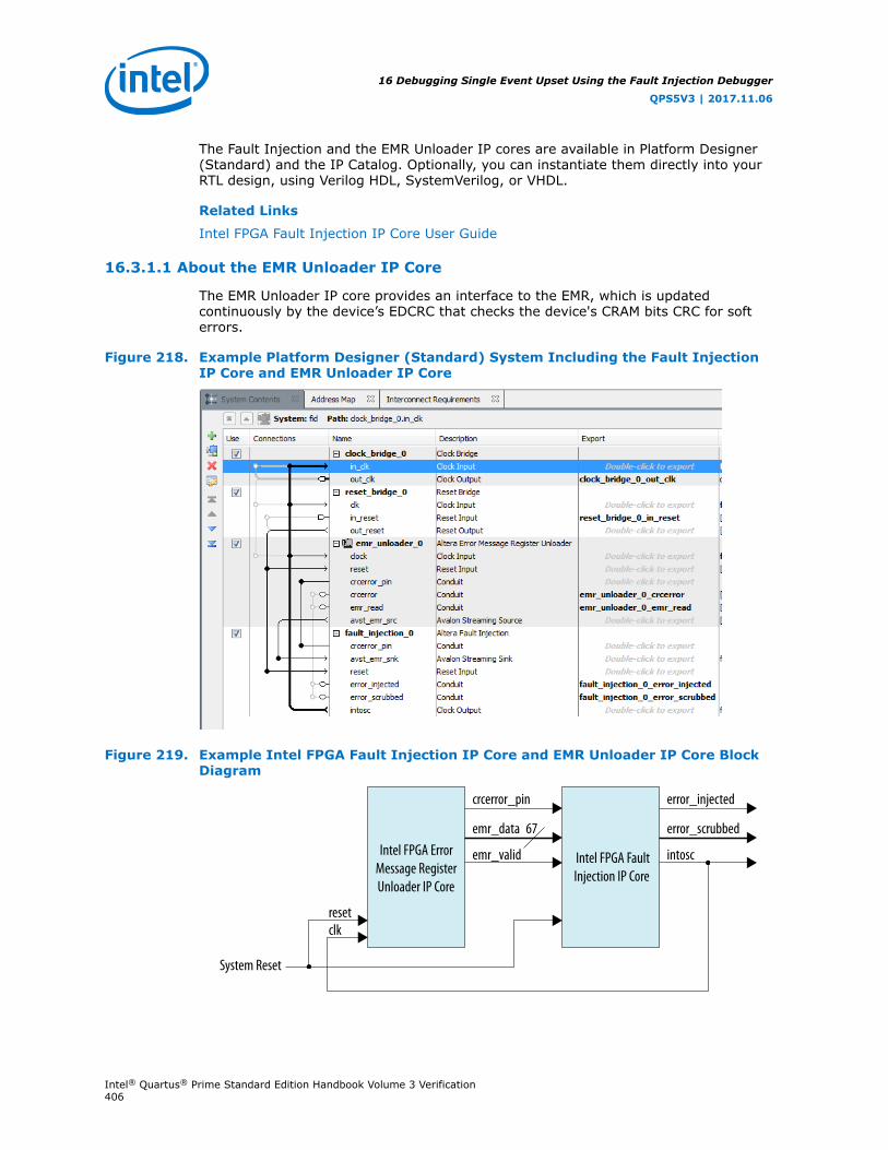
The Fault Injection and the EMR Unloader IP cores are available in Platform Designer(Standard) and the IP Catalog. Optionally, you can instantiate them directly into yourRTL design, using Verilog HDL, SystemVerilog, or VHDL.
Related Links
Intel FPGA Fault Injection IP Core User Guide
16.3.1.1 About the EMR Unloader IP Core
The EMR Unloader IP core provides an interface to the EMR, which is updatedcontinuously by the device’s EDCRC that checks the device's CRAM bits CRC for softerrors.
Figure 218. Example Platform Designer (Standard) System Including the Fault InjectionIP Core and EMR Unloader IP Core
Figure 219. Example Intel FPGA Fault Injection IP Core and EMR Unloader IP Core BlockDiagram
Intel FPGA ErrorMessage RegisterUnloader IP Core
Intel FPGA FaultInjection IP Core
crcerror_pin
emr_data
emr_valid
67
error_injected
error_scrubbed
intosc
clkreset
System Reset
16 Debugging Single Event Upset Using the Fault Injection Debugger
QPS5V3 | 2017.11.06
Intel® Quartus® Prime Standard Edition Handbook Volume 3 Verification406

Related Links
Intel FPGA Error Message Unloader IP Core User Guide
16.3.1.2 About the Advanced SEU Detection IP Core
Use the Advanced SEU Detection (ASD) IP core when SEU tolerance is a designconcern.
You must use the EMR Unloader IP core with the ASD IP core. Therefore, if you usethe ASD IP and the Fault Injection IP in the same design, they must share the EMRUnloader output via an Avalon-ST splitter component. The following figure shows aPlatform Designer (Standard) system in which an Avalon-ST splitter distributes theEMR contents to the ASD and Fault Injection IP cores.
Figure 220. Using the ASD and Fault Injection IP in the Same Platform Designer(Standard) System
Related Links
Intel FPGA Advanced SEU Detection IP Core User Guide
16.3.2 Defining Fault Injection Areas
You can define specific regions of the FPGA for fault injection using a Sensitivity MapHeader (.smh) file.
16 Debugging Single Event Upset Using the Fault Injection Debugger
QPS5V3 | 2017.11.06
Intel® Quartus® Prime Standard Edition Handbook Volume 3 Verification407

The SMH file stores the coordinates of the device CRAM bits, their assigned region(ASD Region), and criticality. During the design process you use hierarchy tagging tocreate the region. Then, during compilation, the Intel Quartus Prime Assemblergenerates the SMH file. The Fault Injection Debugger limits error injections to specificdevice regions you define in the SMH file.
16.3.2.1 Performing Hierarchy Tagging
You define the FPGA regions for testing by assigning an ASD Region to the location.You can specify an ASD Region value for any portion of your design hierarchy usingthe Design Partitions Window.
1. Choose Assignments ➤ Design Partitions Window.
2. Right-click anywhere in the header row and turn on ASD Region to display theASD Region column (if it is not already displayed).
3. Enter a value from 0 to 16 for any partition to assign it to a specific ASD Region.
— ASD region 0 is reserved to unused portions of the device. You can assign apartition to this region to specify it as non-critical..
— ASD region 1 is the default region. All used portions of the device are assignedto this region unless you explicitly change the ASD Region assignment.
16.3.2.2 About SMH Files
The SMH file contains the following information:
• If you are not using hierarchy tagging (i.e., the design has no explicit ASD Regionassignments in the design hierarchy), the SMH file lists every CRAM bit andindicates whether it is sensitive for the design.
• If you have performed hierarchy tagging and changed default ASD Regionassignments, the SMH file lists every CRAM bit and it's assigned ASD region.
The Fault Injection Debugger can limit injections to one or more specified regions.
Note: To direct the Assembler to generate an SMH file:
• Choose Assignments ➤ Device ➤ Device and Pin Options ➤ Error DetectionCRC.
• Turn on the Generate SEU sensitivity map file (.smh) option.
16.3.3 Using the Fault Injection Debugger
To use the Fault Injection Debugger, you connect to your device via the JTAG interface.Then, configure the device and perform fault injection.
To launch the Fault Injection Debugger, choose Tools ➤ Fault Injection Debuggerin the Intel Quartus Prime software.
Note: Configuring or programming the device is similar to the procedure used for theProgrammer or Signal Tap Logic Analyzer.
16 Debugging Single Event Upset Using the Fault Injection Debugger
QPS5V3 | 2017.11.06
Intel® Quartus® Prime Standard Edition Handbook Volume 3 Verification408

Figure 221. Fault Injection Debugger
To configure your JTAG chain:
1. Click Hardware Setup. The tool displays the programming hardware connectedto your computer.
2. Select the programming hardware you wish to use.
3. Click Close.
4. Click Auto Detect, which populates the device chain with the programmabledevices found in the JTAG chain.
Related Links
Targeted Fault Injection Feature on page 415
16.3.3.1 Configuring Your Device and the Fault Injection Debugger
The Fault Injection Debugger uses a .sof and (optionally) a Sensitivity Map Header(.smh) file.
The Software Object File (.sof) configures the FPGA. The .smh file defines thesensitivity of the CRAM bits in the device. If you do not provide an .smh file, the FaultInjection Debugger injects faults randomly throughout the CRAM bits.
To specify a .sof:
1. Select the FPGA you wish to configure in the Device chain box.
2. Click Select File.
3. Navigate to the .sof and click OK. The Fault Injection Debugger reads the .sof.
4. (Optional) Select the SMH file.
16 Debugging Single Event Upset Using the Fault Injection Debugger
QPS5V3 | 2017.11.06
Intel® Quartus® Prime Standard Edition Handbook Volume 3 Verification409

If you do not specify an SMH file, the Fault Injection Debugger injects faultsrandomly across the entire device. If you specify an SMH file, you can restrictinjections to the used areas of your device.
a. Right-click the device in the Device chain box and then click Select SMHFile.
b. Select your SMH file.
c. Click OK.
5. Turn on Program/Configure.
6. Click Start.
The Fault Injection Debugger configures the device using the .sof.
Figure 222. Context Menu for Selecting the SMH File
16.3.3.2 Constraining Regions for Fault Injection
After loading an SMH file, you can direct the Fault Injection Debugger to operate ononly specific ASD regions.
To specify the ASD region(s) in which to inject faults:
1. Right-click the FPGA in the Device chain box, and click Show DeviceSensitivity Map.
2. Select the ASD region(s) for fault injection.
16 Debugging Single Event Upset Using the Fault Injection Debugger
QPS5V3 | 2017.11.06
Intel® Quartus® Prime Standard Edition Handbook Volume 3 Verification410

Figure 223. Device Sensitivity Map Viewer
16.3.3.3 Specifying Error Types
You can specify various types of errors for injection.
• Single errors (SE)
• Double-adjacent errors (DAE)
• Uncorrectable multi-bit errors (EMBE)
Intel FPGA devices can self-correct single and double-adjacent errors if the scrubbingfeature is enabled. Intel FPGA devices cannot correct multi-bit errors. Refer to thechapter on mitigating SEUs for more information about debugging these errors.
You can specify the mixture of faults to inject and the injection time interval. Tospecify the injection time interval:
1. In the Fault Injection Debugger, choose Tools ➤ Options.
2. Drag the red controller to the mix of errors. Alternatively, you can specify the mixnumerically.
3. Specify the Injection interval time.
4. Click OK.
16 Debugging Single Event Upset Using the Fault Injection Debugger
QPS5V3 | 2017.11.06
Intel® Quartus® Prime Standard Edition Handbook Volume 3 Verification411

Figure 224. Specifying the Mixture of SEU Fault Types
Related Links
Mitigating Single Event Upset
16.3.3.4 Injecting Errors
You can inject errors in several modes:
• Inject one error on command
• Inject multiple errors on command
• Inject errors until commanded to stop
To inject these faults:
1. Turn on the Inject Fault option.
2. Choose whether you want to run error injection for a number of iterations or untilstopped:
• If you choose to run until stopped, the Fault Injection Debugger injects errorsat the interval specified in the Tools ➤ Options dialog box.
• If you want to run error injection for a specific number of iterations, enter thenumber.
3. Click Start.
Note: The Fault Injection Debugger runs for the specified number of iterations oruntil stopped.
The Intel Quartus Prime Messages window shows messages about the errors that areinjected. For additional information on the injected faults, click Read EMR. The FaultInjection Debugger reads the device's EMR and displays the contents in the Messageswindow.
16 Debugging Single Event Upset Using the Fault Injection Debugger
QPS5V3 | 2017.11.06
Intel® Quartus® Prime Standard Edition Handbook Volume 3 Verification412

Figure 225. Intel Quartus Prime Error Injection and EMR Content Messages
Error Information Readfrom the Device EMR
Error Injection Information
16.3.3.5 Recording Errors
You can record the location of any injected fault by noting the parameters reported inthe Intel Quartus Prime Messages window.
If, for example, an injected fault results in behavior you would like to replay, you cantarget that location for injection. You perform targeted injection using the FaultInjection Debugger command line interface.
16.3.3.6 Clearing Injected Errors
To restore the normal function of the FPGA, click Scrub. When you scrub an error, thedevice’s EDCRC functions are used to correct the errors. The scrub mechanism issimilar to that used during device operation.
16.3.4 Command-Line Interface
You can run the Fault Injection Debugger at the command line with the quartus_fidexecutable, which is useful if you want to perform fault injection from a script.
Table 124. Command line Arguments for Fault Injection
Short Argument Long Argument Description
c cable Specify programming hardware or cable. (Required)
i index Specify the active device to inject fault. (Required)
n number Specify the number of errors to inject. The default value is1. (Optional)
t time Interval time between injections. (Optional)
Note: Use quartus_fid --help to view all available options.
The following code provides examples using the Fault Injection Debugger command-line interface.
############################################## Find out which USB cables are available for this instance# The result shows that one cable is available, named "USB-Blaster"#$ quartus_fid --list . . . Info: Command: quartus_fid --list
16 Debugging Single Event Upset Using the Fault Injection Debugger
QPS5V3 | 2017.11.06
Intel® Quartus® Prime Standard Edition Handbook Volume 3 Verification413
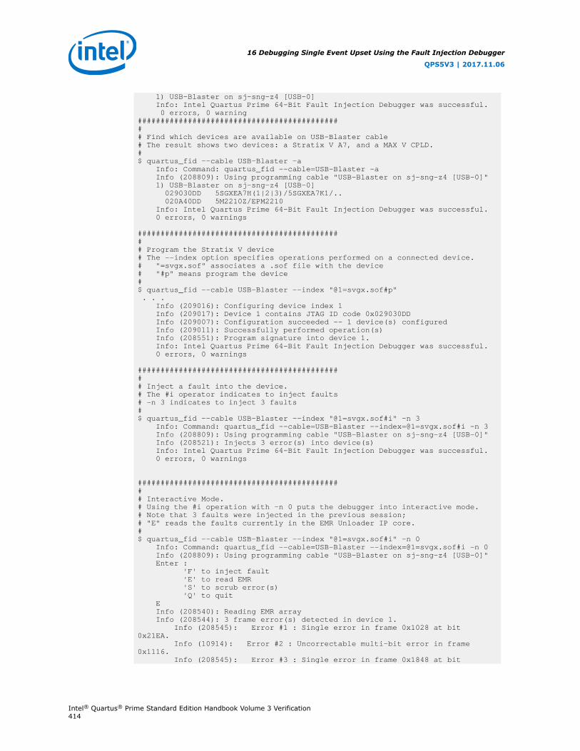
1) USB-Blaster on sj-sng-z4 [USB-0] Info: Intel Quartus Prime 64-Bit Fault Injection Debugger was successful. 0 errors, 0 warning############################################## Find which devices are available on USB-Blaster cable# The result shows two devices: a Stratix V A7, and a MAX V CPLD.#$ quartus_fid --cable USB-Blaster -a Info: Command: quartus_fid --cable=USB-Blaster -a Info (208809): Using programming cable "USB-Blaster on sj-sng-z4 [USB-0]" 1) USB-Blaster on sj-sng-z4 [USB-0] 029030DD 5SGXEA7H(1|2|3)/5SGXEA7K1/.. 020A40DD 5M2210Z/EPM2210 Info: Intel Quartus Prime 64-Bit Fault Injection Debugger was successful. 0 errors, 0 warnings
############################################## Program the Stratix V device# The --index option specifies operations performed on a connected device.# "=svgx.sof" associates a .sof file with the device# "#p" means program the device#$ quartus_fid --cable USB-Blaster --index "@1=svgx.sof#p" . . . Info (209016): Configuring device index 1 Info (209017): Device 1 contains JTAG ID code 0x029030DD Info (209007): Configuration succeeded -- 1 device(s) configured Info (209011): Successfully performed operation(s) Info (208551): Program signature into device 1. Info: Intel Quartus Prime 64-Bit Fault Injection Debugger was successful. 0 errors, 0 warnings
############################################## Inject a fault into the device.# The #i operator indicates to inject faults# -n 3 indicates to inject 3 faults#$ quartus_fid --cable USB-Blaster --index "@1=svgx.sof#i" -n 3 Info: Command: quartus_fid --cable=USB-Blaster --index=@1=svgx.sof#i -n 3 Info (208809): Using programming cable "USB-Blaster on sj-sng-z4 [USB-0]" Info (208521): Injects 3 error(s) into device(s) Info: Intel Quartus Prime 64-Bit Fault Injection Debugger was successful. 0 errors, 0 warnings
############################################## Interactive Mode.# Using the #i operation with -n 0 puts the debugger into interactive mode.# Note that 3 faults were injected in the previous session; # "E" reads the faults currently in the EMR Unloader IP core.#$ quartus_fid --cable USB-Blaster --index "@1=svgx.sof#i" -n 0 Info: Command: quartus_fid --cable=USB-Blaster --index=@1=svgx.sof#i -n 0 Info (208809): Using programming cable "USB-Blaster on sj-sng-z4 [USB-0]" Enter : 'F' to inject fault 'E' to read EMR 'S' to scrub error(s) 'Q' to quit E Info (208540): Reading EMR array Info (208544): 3 frame error(s) detected in device 1. Info (208545): Error #1 : Single error in frame 0x1028 at bit 0x21EA. Info (10914): Error #2 : Uncorrectable multi-bit error in frame 0x1116. Info (208545): Error #3 : Single error in frame 0x1848 at bit
16 Debugging Single Event Upset Using the Fault Injection Debugger
QPS5V3 | 2017.11.06
Intel® Quartus® Prime Standard Edition Handbook Volume 3 Verification414

0x128C. Enter : 'F' to inject fault 'E' to read EMR 'S' to scrub error(s) 'Q' to quit Q Info: Intel Quartus Prime 64-Bit Fault Injection Debugger was successful. 0 errors, 0 warnings Info: Peak virtual memory: 1522 megabytes Info: Processing ended: Mon Nov 3 18:50:00 2014 Info: Elapsed time: 00:00:29 Info: Total CPU time (on all processors): 00:00:13
16.3.4.1 Targeted Fault Injection Feature
The Fault Injection Debugger injects faults into the FPGA randomly. However, theTargeted Fault Injection feature allows you to inject faults into targeted locations inthe CRAM. This operation may be useful, for example, if you noted an SEU event andwant to test the FPGA or system response to the same event after modifying arecovery strategy.
Note: The Targeted Fault Injection feature is available only from the command line interface.
You can specify that errors are injected from the command line or in prompt mode.
Related Links
AN 539: Test Methodology or Error Detection and Recovery using CRC in Intel FPGADevices
16.3.4.1.1 Specifying an Error List From the Command Line
The Targeted Fault Injection feature allows you to specify an error list from thecommand line, as shown in the following example:
c:\Users\sng> quartus_fid -c 1 - i "@1= svgx.sof#i " -n 2 -user="@1=0x2274 0x05EF 0x2264 0x0500"Where:
c 1 indicates that the fpga is controlled by the first cable on your computer.
i "@1= svgx.sof#i " indicates that the first device in the chain is loaded with theobject file svgx.sof and will be injected with faults.
n 2 indicates that two faults will be injected.
user=”@1= 0x2274 0x05EF 0x2264 0x0500” is a user-specified list of faults tobe injected. In this example, device 1 has two faults: at frame 0x2274, bit 0x05EF andat frame 0x2264, bit 0x0500.
16.3.4.1.2 Specifying an Error List From Prompt Mode
You can operate the Targeted Fault Injection feature interactively by specifying thenumber of faults to be 0 (-n 0). The Fault Injection Debugger presents prompt modecommands and their descriptions.
16 Debugging Single Event Upset Using the Fault Injection Debugger
QPS5V3 | 2017.11.06
Intel® Quartus® Prime Standard Edition Handbook Volume 3 Verification415

Prompt Mode Command Description
F Inject a fault
E Read the EMR
S Scrub errors
Q Quit
In prompt mode, you can issue the F command alone to inject a single fault in arandom location in the device. In the following examples using the F command inprompt mode, three errors are injected.
F #3 0x12 0x34 0x56 0x78 * 0x9A 0xBC +
• Error 1 – Single bit error at frame 0x12, bit 0x34
• Error 2 – Uncorrectable error at frame 0x56, bit 0x78 (an * indicates a multi-biterror)
• Error 3 – Double-adjacent error at frame 0x9A, bit 0xBC (a + indicates a doublebit error)
F 0x12 0x34 0x56 0x78 *
One (default) error is injected:
Error 1 – Single bit error at frame 0x12, bit 0x34. Locations after the first frame/bitlocation are ignored.
F #3 0x12 0x34 0x56 0x78 * 0x9A 0xBC + 0xDE 0x00
Three errors are injected:
• Error 1 – Single bit error at frame 0x12, bit 0x34
• Error 2 – Uncorrectable error at frame 0x56, bit 0x78
• Error 3 – Double-adjacent error at frame 0x9A, bit 0xBC
• Locations after the first 3 frame/bit pairs are ignored
16.3.4.1.3 Determining CRAM Bit Locations
When the Fault Injection Debugger detects a CRAM EDCRC error, the Error MessageRegister (EMR) contains the syndrome, frame number, bit location, and error type(single, double, or multi-bit) of the detected CRAM error.
During system testing, save the EMR contents reported by the Fault InjectionDebugger when you detect an EDCRC fault.
Note: With the recorded EMR contents, you can supply the frame and bit numbers to theFault Injection Debugger to replay the errors noted during system testing, to furtherdesign, and characterize a system recovery response to that error.
Related Links
AN 539: Test Methodology or Error Detection and Recovery using CRC in Intel FPGADevices
16 Debugging Single Event Upset Using the Fault Injection Debugger
QPS5V3 | 2017.11.06
Intel® Quartus® Prime Standard Edition Handbook Volume 3 Verification416
16.3.4.2 Advanced Command-Line Options: ASD Regions and Error TypeWeighting
You can use the Fault Injection Debugger command-line interface to inject errors intoASD regions and weight the error types.
First, you specify the mix of error types (single bit, double adjacent, and multi-bituncorrectable) using the --weight <single errors>.<double adjacenterrors>.<multi-bit errors> option. For example, for a mix of 50% singleerrors, 30% double adjacent errors, and 20% multi-bit uncorrectable errors, use theoption --weight=50.30.20. Then, to target an ASD region, use the -smh option toinclude the SMH file and indicate the ASD region to target. For example:
$ quartus_fid --cable=USB-BlasterII --index "@1=svgx.sof#pi" --weight=100.0.0 --smh="@1=svgx.smh#2" --number=30
This example command:
• Programs the device and injects faults (pi string)
• Injects 100% single-bit faults (100.0.0)
• Injects only into ASD_REGION 2 (indicated by the #2)
• Injects 30 faults
16.4 Document Revision History
Table 125. Document Revision History
Date Version Changes
2015.11.02 15.1.0 Changed instances of Quartus II to Intel Quartus Prime.
2015.05.04 15.0.0 • Provided more detail on how to use the Fault InjectionDebugger throughout the document.
• Added more command-line examples.
2014.06.30 14.0.0 • Removed “Modifying the Quartus INI File” section.• Added “Targeted Fault Injection Feature” section.• Updated “Hardware and Software Requirements” section.
December 2012 2012.12.01 Preliminary release.
Related Links
Documentation ArchiveFor previous versions of the Intel Quartus Prime Handbook, search thedocumentation archives.
16 Debugging Single Event Upset Using the Fault Injection Debugger
QPS5V3 | 2017.11.06
Intel® Quartus® Prime Standard Edition Handbook Volume 3 Verification417

17 In-System Debugging Using External Logic Analyzers
17.1 About the Intel Quartus Prime Logic Analyzer Interface
The Intel Quartus Prime Logic Analyzer Interface (LAI) allows you to use an externallogic analyzer and a minimal number of Intel-supported device I/O pins to examinethe behavior of internal signals while your design is running at full speed on yourIntel-supported device.
The LAI connects a large set of internal device signals to a small number of outputpins. You can connect these output pins to an external logic analyzer for debuggingpurposes. In the Intel Quartus Prime LAI, the internal signals are grouped together,distributed to a user-configurable multiplexer, and then output to available I/O pins onyour Intel-supported device. Instead of having a one-to-one relationship betweeninternal signals and output pins, the Intel Quartus Prime LAI enables you to map manyinternal signals to a smaller number of output pins. The exact number of internalsignals that you can map to an output pin varies based on the multiplexer settings inthe Intel Quartus Prime LAI.
Note: The term “logic analyzer” when used in this document includes both logic analyzersand oscilloscopes equipped with digital channels, commonly referred to as mixedsignal analyzers or MSOs.
The LAI does not support Hard Processor System (HPS) I/Os.
Related Links
Device Support Center
17.2 Choosing a Logic Analyzer
The Intel Quartus Prime software offers the following two general purpose on-chipdebugging tools for debugging a large set of RTL signals from your design:
• The Signal Tap Logic Analyzer
• An external logic analyzer, which connects to internal signals in your Intel-supported device by using the Intel Quartus Prime LAI
Table 126. Comparing the Signal Tap Logic Analyzer with the Logic Analyzer Interface
Feature Description Recommended LogicAnalyzer
Sample Depth You have access to a wider sample depth with anexternal logic analyzer. In the Signal Tap LogicAnalyzer, the maximum sample depth is set to
LAI
continued...
QPS5V3 | 2017.11.06
Intel Corporation. All rights reserved. Intel, the Intel logo, Altera, Arria, Cyclone, Enpirion, MAX, Nios, Quartusand Stratix words and logos are trademarks of Intel Corporation or its subsidiaries in the U.S. and/or othercountries. Intel warrants performance of its FPGA and semiconductor products to current specifications inaccordance with Intel's standard warranty, but reserves the right to make changes to any products and servicesat any time without notice. Intel assumes no responsibility or liability arising out of the application or use of anyinformation, product, or service described herein except as expressly agreed to in writing by Intel. Intelcustomers are advised to obtain the latest version of device specifications before relying on any publishedinformation and before placing orders for products or services.*Other names and brands may be claimed as the property of others.
ISO9001:2008Registered

Feature Description Recommended LogicAnalyzer
128 Kb, which is a device constraint. However, withan external logic analyzer, there are no deviceconstraints, providing you a wider sample depth.
Debugging Timing Issues Using an external logic analyzer provides you withaccess to a “timing” mode, which enables you todebug combined streams of data.
LAI
Performance You frequently have limited routing resourcesavailable to place and route when you use the SignalTap Logic Analyzer with your design. An external logicanalyzer adds minimal logic, which removes resourcelimits on place-and-route.
LAI
Triggering Capability The Signal Tap Logic Analyzer offers triggeringcapabilities that are comparable to external logicanalyzers.
LAI or Signal Tap
Use of Output Pins Using the Signal Tap Logic Analyzer, no additionaloutput pins are required. Using an external logicanalyzer requires the use of additional output pins.
Signal Tap
Acquisition Speed With the Signal Tap Logic Analyzer, you can acquiredata at speeds of over 200 MHz. You can achieve thesame acquisition speeds with an external logicanalyzer; however, you must consider signal integrityissues.
Signal Tap
Related Links
System Debugging Tools Overview on page 183
17.2.1 Required Components
To perform analysis using the LAI you need the following components:
• Intel Quartus Prime software version 15.1 or later
• The device under test
• An external logic analyzer
• An Intel FPGA communications cable
• A cable to connect the Intel-supported device to the external logic analyzer
17 In-System Debugging Using External Logic Analyzers
QPS5V3 | 2017.11.06
Intel® Quartus® Prime Standard Edition Handbook Volume 3 Verification419

Figure 226. LAI and Hardware Setup
JTAG
(1)
(2)
FPGA
Connected toUnused FPGA Pins
LAI
FPGA ProgrammingHardware Quartus Prime Software
External Logic AnalyzerBoard
Notes to figure:
1. Configuration and control of the LAI using a computer loaded with the IntelQuartus Prime software via the JTAG port.
2. Configuration and control of the LAI using a third-party vendor logic analyzer viathe JTAG port. Support varies by vendor.
17.3 Flow for Using the LAI
Figure 227. LAI Workflow
Configure Logic AnalyzerInterface File
Create New LogicAnalyzer Interface File
Compile Project
Program Device
Control Output Pin
Debug Project
Start the Quartus Prime Software
Notes to figure:
1. Configuration and control of the LAI using a computer loaded with the IntelQuartus Prime software via the JTAG port.
2. Configuration and control of the LAI using a third-party vendor logic analyzer viathe JTAG port. Support varies by vendor.
17 In-System Debugging Using External Logic Analyzers
QPS5V3 | 2017.11.06
Intel® Quartus® Prime Standard Edition Handbook Volume 3 Verification420
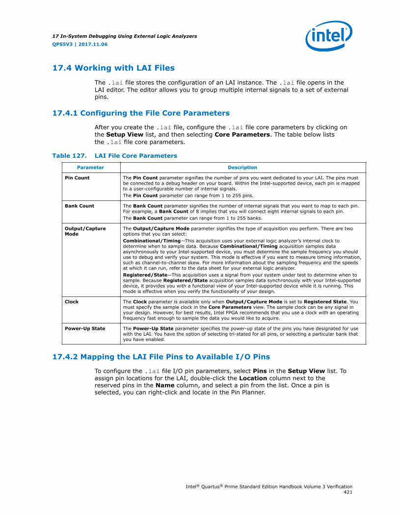
17.4 Working with LAI Files
The .lai file stores the configuration of an LAI instance. The .lai file opens in theLAI editor. The editor allows you to group multiple internal signals to a set of externalpins.
17.4.1 Configuring the File Core Parameters
After you create the .lai file, configure the .lai file core parameters by clicking onthe Setup View list, and then selecting Core Parameters. The table below liststhe .lai file core parameters.
Table 127. LAI File Core Parameters
Parameter Description
Pin Count The Pin Count parameter signifies the number of pins you want dedicated to your LAI. The pins mustbe connected to a debug header on your board. Within the Intel-supported device, each pin is mappedto a user-configurable number of internal signals.The Pin Count parameter can range from 1 to 255 pins.
Bank Count The Bank Count parameter signifies the number of internal signals that you want to map to each pin.For example, a Bank Count of 8 implies that you will connect eight internal signals to each pin.The Bank Count parameter can range from 1 to 255 banks.
Output/CaptureMode
The Output/Capture Mode parameter signifies the type of acquisition you perform. There are twooptions that you can select:Combinational/Timing—This acquisition uses your external logic analyzer’s internal clock todetermine when to sample data. Because Combinational/Timing acquisition samples dataasynchronously to your Intel-supported device, you must determine the sample frequency you shoulduse to debug and verify your system. This mode is effective if you want to measure timing information,such as channel-to-channel skew. For more information about the sampling frequency and the speedsat which it can run, refer to the data sheet for your external logic analyzer.Registered/State—This acquisition uses a signal from your system under test to determine when tosample. Because Registered/State acquisition samples data synchronously with your Intel-supporteddevice, it provides you with a functional view of your Intel-supported device while it is running. Thismode is effective when you verify the functionality of your design.
Clock The Clock parameter is available only when Output/Capture Mode is set to Registered State. Youmust specify the sample clock in the Core Parameters view. The sample clock can be any signal inyour design. However, for best results, Intel FPGA recommends that you use a clock with an operatingfrequency fast enough to sample the data you would like to acquire.
Power-Up State The Power-Up State parameter specifies the power-up state of the pins you have designated for usewith the LAI. You have the option of selecting tri-stated for all pins, or selecting a particular bank thatyou have enabled.
17.4.2 Mapping the LAI File Pins to Available I/O Pins
To configure the .lai file I/O pin parameters, select Pins in the Setup View list. Toassign pin locations for the LAI, double-click the Location column next to thereserved pins in the Name column, and select a pin from the list. Once a pin isselected, you can right-click and locate in the Pin Planner.
17 In-System Debugging Using External Logic Analyzers
QPS5V3 | 2017.11.06
Intel® Quartus® Prime Standard Edition Handbook Volume 3 Verification421

Figure 228. Mapping LAI file Pins
Related Links
Managing Device I/O PinsIn Intel Quartus Prime Standard Edition Volume 2
17.4.3 Mapping Internal Signals to the LAI Banks
After you have specified the number of banks to use in the Core Parameters settingspage, you must assign internal signals for each bank in the LAI. Click the Setup Viewarrow and select Bank n or All Banks.
To view all of your bank connections, click Setup View and select All Banks.
17.4.4 Using the Node Finder
Before making bank assignments, right click the Node list and select Add Nodes toopen the Node Finder. Find the signals that you want to acquire, then drag and dropthe signals from the Node Finder dialog box into the bank Setup View. When addingsignals, use Signal Tap: pre-synthesis for non-incrementally routed instances andSignal Tap: post-fitting for incrementally routed instances.
As you continue to make assignments in the bank Setup View, the schematic of yourLAI in the Logical View pane begins to reflect your changes. Continue makingassignments for each bank in the Setup View until you have added all of the internalsignals for which you wish to acquire data.
Related Links
Node Finder CommandIn Intel Quartus Prime Help
17.4.5 Compiling Your Intel Quartus Prime Project
After you save your .lai file, a dialog box prompts you to enable the Logic AnalyzerInterface instance for the active project. Alternatively, you can define the .lai fileyour project uses in the Global Project Settings dialog box. After specifying thename of your .lai file, compile your project.
To verify the Logic Analyzer Interface is properly compiled with your project, expandthe entity hierarchy in the Project Navigator. If the LAI is compiled with your design,the sld_hub and sld_multitap entities are shown in the Project Navigator.
17 In-System Debugging Using External Logic Analyzers
QPS5V3 | 2017.11.06
Intel® Quartus® Prime Standard Edition Handbook Volume 3 Verification422

Figure 229. Project Navigator
17.4.6 Programming Your Intel-Supported Device Using the LAI
After compilation completes, you must configure your Intel-supported device beforeusing the LAI.
You can use the LAI with multiple devices in your JTAG chain. Your JTAG chain can alsoconsist of devices that do not support the LAI or non-Intel, JTAG-compliant devices. Touse the LAI in more than one Intel-supported device, create an .lai file andconfigure an .lai file for each Intel-supported device that you want to analyze.
17.5 Controlling the Active Bank During Runtime
When you have programmed your Intel-supported device, you can control which bankyou map to the reserved .lai file output pins. To control which bank you map, in theschematic in the Logical View, right-click the bank and click Connect Bank.
Figure 230. Configuring Banks
17.5.1 Acquiring Data on Your Logic Analyzer
To acquire data on your logic analyzer, you must establish a connection between yourdevice and the external logic analyzer. For more information about this process and forguidelines about how to establish connections between debugging headers and logicanalyzers, refer to the documentation for your logic analyzer.
17.6 Using the LAI with Incremental Compilation
The Incremental Compilation feature in the Intel Quartus Prime software allows you topreserve the synthesis and fitting results of your design. This is an effective featurefor reducing compilation times if you only modify a portion of a design or you wish topreserve the optimization results from a previous compilation.
17 In-System Debugging Using External Logic Analyzers
QPS5V3 | 2017.11.06
Intel® Quartus® Prime Standard Edition Handbook Volume 3 Verification423

The Incremental Compilation feature is well suited for use with LAI since LAIcomprises a small portion of most designs. Because LAI consists of only a smallportion of your design, incremental compilation helps to minimize your compilationtime. Incremental compilation works best when you are only changing a small portionof your design. Incremental compilation yields an accurate representation of yourdesign behavior when changing the .lai file through multiple compilations.
17.7 Document Revision History
Table 128. Document Revision History
Date Version Changes
2017.05.08 17.0.0 • Updated figure: LAI Instance in Compilation Report.
2015.11.02 15.1.0 Changed instances of Quartus II to Intel Quartus Prime.
June 2014 14.0.0 • Dita conversion• Added limitation about HPS I/O support
June 2012 12.0.0 Removed survey link
November 2011 10.1.1 Changed to new document template
December 2010 10.1.0 • Minor editorial updates• Changed to new document template
August 2010 10.0.1 Corrected links
July 2010 10.0.0 • Created links to the Intel Quartus Prime Help• Editorial updates• Removed Referenced Documents section
November 2009 9.1.0 • Removed references to APEX devices• Editorial updates
March 2009 9.0.0 • Minor editorial updates• Removed Figures 15–4, 15–5, and 15–11 from 8.1 version
November 2008 8.1.0 Changed to 8-1/2 x 11 page size. No change to content
May 2008 8.0.0 • Updated device support list on page 15–3• Added links to referenced documents throughout the chapter• Added “Referenced Documents”• Added reference to Section V. In-System Debugging• Minor editorial updates
Related Links
Documentation ArchiveFor previous versions of the Intel Quartus Prime Handbook, search thedocumentation archives.
17 In-System Debugging Using External Logic Analyzers
QPS5V3 | 2017.11.06
Intel® Quartus® Prime Standard Edition Handbook Volume 3 Verification424

18 In-System Modification of Memory and Constants
18.1 About the In-System Memory Content Editor
The Intel Quartus Prime In-System Memory Content Editor allows to view and updatememories and constants with the JTAG port connection at runtime.
The In-System Memory Content Editor provides access to dense and complex FPGAdesigns through the JTAG interface. You can then identify, test, and resolve issues withyour design by testing changes to memory contents in the FPGA while your design isrunning.
When you use the In-System Memory Content Editor in conjunction with the SignalTap Logic Analyzer, you can view and debug your design in the hardware lab.
The ability to read data from memories and constants allows you to identify the sourceof problems. The write capability allows you to bypass functional issues by writingexpected data. For example, if a parity bit in your memory is incorrect, you can usethe In-System Memory Content Editor to write the correct parity bit values into yourRAM, allowing your system to continue functioning. To check the error handlingfunctionality of your design, you can intentionally write incorrect parity bit values intoyour RAM.
Related Links
• System Debugging Tools Overview on page 183
• Design Debugging with the Signal Tap Logic Analyzer on page 327
• Megafunctions/LPMList of the types of memories and constants currently supported by the IntelQuartus Prime software
18.2 Design Flow Using the In-System Memory Content Editor
To use the In-System Memory Content Editor, perform the following steps:
1. Identify the memories and constants that you want to access.
2. Edit the memories and constants to be run-time modifiable.
3. Perform a full compilation.
4. Program your device.
5. Launch the In-System Memory Content Editor.
QPS5V3 | 2017.11.06
Intel Corporation. All rights reserved. Intel, the Intel logo, Altera, Arria, Cyclone, Enpirion, MAX, Nios, Quartusand Stratix words and logos are trademarks of Intel Corporation or its subsidiaries in the U.S. and/or othercountries. Intel warrants performance of its FPGA and semiconductor products to current specifications inaccordance with Intel's standard warranty, but reserves the right to make changes to any products and servicesat any time without notice. Intel assumes no responsibility or liability arising out of the application or use of anyinformation, product, or service described herein except as expressly agreed to in writing by Intel. Intelcustomers are advised to obtain the latest version of device specifications before relying on any publishedinformation and before placing orders for products or services.*Other names and brands may be claimed as the property of others.
ISO9001:2008Registered

18.3 Creating In-System Modifiable Memories and Constants
When you specify that a memory or constant is run-time modifiable, the Intel QuartusPrime software changes the default implementation. A single-port RAM is converted toa dual-port RAM, and a constant is implemented in registers instead of look-up tables(LUTs). These changes enable run-time modification without changing the functionalityof your design.
If you instantiate a memory or constant IP core directly with ports and parameters inVHDL or Verilog HDL, add or modify the lpm_hint parameter as follows:
In VHDL code, add the following:
lpm_hint => "ENABLE_RUNTIME_MOD = YES, INSTANCE_NAME = <instantiation name>";
In Verilog HDL code, add the following:
defparam <megafunction instance name>.lpm_hint = "ENABLE_RUNTIME_MOD = YES, INSTANCE_NAME = <instantiation name>";
18.4 Running the In-System Memory Content Editor
The In-System Memory Content Editor has three separate panes: the InstanceManager, the JTAG Chain Configuration, and the Hex Editor.
The Instance Manager pane displays all available run-time modifiable memories andconstants in your FPGA device. The JTAG Chain Configuration pane allows you toprogram your FPGA and select the Intel FPGA device in the chain to update.
Using the In-System Memory Content Editor does not require that you open a project.The In-System Memory Content Editor retrieves all instances of run-time configurablememories and constants by scanning the JTAG chain and sending a query to thespecific device selected in the JTAG Chain Configuration pane.
If you have more than one device with in-system configurable memories or constantsin a JTAG chain, you can launch multiple In-System Memory Content Editors within theIntel Quartus Prime software to access the memories and constants in each of thedevices. Each In-System Memory Content Editor can access the in-system memoriesand constants in a single device.
18.4.1 Instance Manager
You can read and write to in-system memory with the Instance Manager pane.When you scan the JTAG chain to update the Instance Manager pane, you can viewa list of all run-time modifiable memories and constants in the design. The InstanceManager pane displays the Index, Instance, Status, Width, Depth, Type, and Mode ofeach element in the list.
Note: In addition to the buttons available in the Instance Manager pane, you can read andwrite data by selecting commands from the Processing menu, or the right-click menuin the Instance Manager pane or Hex Editor pane.
18 In-System Modification of Memory and Constants
QPS5V3 | 2017.11.06
Intel® Quartus® Prime Standard Edition Handbook Volume 3 Verification426

The status of each instance is also displayed beside each entry in the InstanceManager pane. The status indicates if the instance is Not running, Offloading data,or Updating data. The health monitor provides information about the status of theeditor.
The Intel Quartus Prime software assigns a different index number to each in-systemmemory and constant to distinguish between multiple instances of the same memoryor constant function. View the In-System Memory Content Editor Settings sectionof the Compilation Report to match an index number with the corresponding instanceID.
Related Links
Instance Manager PaneIn Intel Quartus Prime Help
18.4.2 Editing Data Displayed in the Hex Editor Pane
You can edit data read from your in-system memories and constants displayed in theHex Editor pane by typing values directly into the editor or by importing memoryfiles.
18.4.3 Importing and Exporting Memory Files
The In-System Memory Content Editor allows you to import and export data values formemories that have the In-System Updating feature enabled. Importing from a datafile enables you to quickly load an entire memory image. Exporting to a data fileenables you to save the contents of the memory for future use.
18.4.4 Scripting Support
The In-System Memory Content Editor supports reading and writing of memorycontents via a Tcl script or Tcl commands entered at a command prompt. For detailedinformation about scripting command options, refer to the Intel Quartus Primecommand-line and Tcl API Help browser.
To run the Help browser, type the following command at the command prompt:
quartus_sh --qhelp
18 In-System Modification of Memory and Constants
QPS5V3 | 2017.11.06
Intel® Quartus® Prime Standard Edition Handbook Volume 3 Verification427

The commonly used commands for the In-System Memory Content Editor are asfollows:
• Reading from memory:
read_content_from_memory[-content_in_hex]-instance_index <instance index>-start_address <starting address>-word_count <word count>
• Writing to memory:
write_content_to_memory
• Saving memory contents to a file:
save_content_from_memory_to_file
• Updating memory contents from a file:
update_content_to_memory_from_file
Related Links
• Tcl ScriptingIn Intel Quartus Prime Standard Edition Handbook Volume 2
• Command Line ScriptingIn Intel Quartus Prime Standard Edition Handbook Volume 2
• API Functions for TclIn Intel Quartus Prime Help
18.4.5 Programming the Device with the In-System Memory ContentEditor
If you make changes to your design, you can program the device from within the In-System Memory Content Editor.
18.4.6 Example: Using the In-System Memory Content Editor with theSignal Tap Logic Analyzer
The following scenario describes how you can use the In-System Updating of Memoryand Constants feature with the Signal Tap Logic Analyzer to efficiently debug yourdesign. You can use the In-System Memory Content Editor and the Signal Tap LogicAnalyzer simultaneously with the JTAG interface.
Scenario: After completing your FPGA design, you find that the characteristics of yourFIR filter design are not as expected.
1. To locate the source of the problem, change all your FIR filter coefficients to be in-system modifiable and instantiate the Signal Tap Logic Analyzer.
2. Using the Signal Tap Logic Analyzer to tap and trigger on internal design nodes,you find the FIR filter to be functioning outside of the expected cutoff frequency.
3. Using the In-System Memory Content Editor, you check the correctness of theFIR filter coefficients. Upon reading each coefficient, you discover that one of thecoefficients is incorrect.
4. Because your coefficients are in-system modifiable, you update the coefficientswith the correct data with the In-System Memory Content Editor.
18 In-System Modification of Memory and Constants
QPS5V3 | 2017.11.06
Intel® Quartus® Prime Standard Edition Handbook Volume 3 Verification428

In this scenario, you can quickly locate the source of the problem using both theIn-System Memory Content Editor and the Signal Tap Logic Analyzer. You can alsoverify the functionality of your device by changing the coefficient values beforemodifying the design source files.
You can also modify the coefficients with the In-System Memory Content Editor tovary the characteristics of the FIR filter, for example, filter attenuation, transitionbandwidth, cut-off frequency, and windowing function.
18.5 Document Revision History
Table 129. Document Revision History
Date Version Changes
2015.11.02 15.1.0 Changed instances of Quartus II to Intel Quartus Prime.
June 2014 14.0.0 • Dita conversion.• Removed references to megafunction and replaced with IP core.
June 2012 12.0.0 Removed survey link.
November 2011 10.0.3 Template update.
December 2010 10.0.2 Changed to new document template. No change to content.
August 2010 10.0.1 Corrected links
July 2010 10.0.0 • Inserted links to Intel Quartus Prime Help• Removed Reference Documents section
November 2009 9.1.0 • Delete references to APEX devices• Style changes
March 2009 9.0.0 No change to content
November 2008 8.1.0 Changed to 8-1/2 x 11 page size. No change to content.
May 2008 8.0.0 • Added reference to Section V. In-System Debugging in volume 3 ofthe Intel Quartus Prime Handbook on page 16-1
• Removed references to the Mercury device, as it is now consideredto be a “Mature” device
• Added links to referenced documents throughout document• Minor editorial updates
Related Links
Documentation ArchiveFor previous versions of the Intel Quartus Prime Handbook, search thedocumentation archives.
18 In-System Modification of Memory and Constants
QPS5V3 | 2017.11.06
Intel® Quartus® Prime Standard Edition Handbook Volume 3 Verification429

19 Design Debugging Using In-System Sources andProbes
The Signal Tap Logic Analyzer and Signal Probe allow you to read or “tap” internallogic signals during run time as a way to debug your logic design.
Traditional debugging techniques often involve using an external pattern generator toexercise the logic and a logic analyzer to study the output waveforms during run time.
You can make the debugging cycle more efficient when you can drive any internalsignal manually within your design, which allows you to perform the following actions:
• Force the occurrence of trigger conditions set up in the Signal Tap Logic Analyzer
• Create simple test vectors to exercise your design without using external testequipment
• Dynamically control run time control signals with the JTAG chain
The In-System Sources and Probes Editor in the Intel Quartus Prime software extendsthe portfolio of verification tools, and allows you to easily control any internal signaland provides you with a completely dynamic debugging environment. Coupled witheither the Signal Tap Logic Analyzer or Signal Probe, the In-System Sources andProbes Editor gives you a powerful debugging environment in which to generatestimuli and solicit responses from your logic design.
The Virtual JTAG IP core and the In-System Memory Content Editor also give you thecapability to drive virtual inputs into your design. The Intel Quartus Prime softwareoffers a variety of on-chip debugging tools.
The In-System Sources and Probes Editor consists of the ALTSOURCE_PROBE IP coreand an interface to control the ALTSOURCE_PROBE IP core instances during run time.Each ALTSOURCE_PROBE IP core instance provides you with source output ports andprobe input ports, where source ports drive selected signals and probe ports sampleselected signals. When you compile your design, the ALTSOURCE_PROBE IP core setsup a register chain to either drive or sample the selected nodes in your logic design.During run time, the In-System Sources and Probes Editor uses a JTAG connection toshift data to and from the ALTSOURCE_PROBE IP core instances. The figure shows ablock diagram of the components that make up the In-System Sources and ProbesEditor.
QPS5V3 | 2017.11.06
Intel Corporation. All rights reserved. Intel, the Intel logo, Altera, Arria, Cyclone, Enpirion, MAX, Nios, Quartusand Stratix words and logos are trademarks of Intel Corporation or its subsidiaries in the U.S. and/or othercountries. Intel warrants performance of its FPGA and semiconductor products to current specifications inaccordance with Intel's standard warranty, but reserves the right to make changes to any products and servicesat any time without notice. Intel assumes no responsibility or liability arising out of the application or use of anyinformation, product, or service described herein except as expressly agreed to in writing by Intel. Intelcustomers are advised to obtain the latest version of device specifications before relying on any publishedinformation and before placing orders for products or services.*Other names and brands may be claimed as the property of others.
ISO9001:2008Registered

Figure 231. In-System Sources and Probes Editor Block Diagram
Design Logic
altsource_probeMegafunction
Probes Sources
JTAGController
FPGAProgramming
Hardware
Quartus PrimeSoftware
FPGA
D Q
D Q
The ALTSOURCE_PROBE IP core hides the detailed transactions between the JTAGcontroller and the registers instrumented in your design to give you a basic buildingblock for stimulating and probing your design. Additionally, the In-System Sources andProbes Editor provides single-cycle samples and single-cycle writes to selected logicnodes. You can use this feature to input simple virtual stimuli and to capture thecurrent value on instrumented nodes. Because the In-System Sources and ProbesEditor gives you access to logic nodes in your design, you can toggle the inputs of low-level components during the debugging process. If used in conjunction with the SignalTap Logic Analyzer, you can force trigger conditions to help isolate your problem andshorten your debugging process.
The In-System Sources and Probes Editor allows you to easily implement controlsignals in your design as virtual stimuli. This feature can be especially helpful forprototyping your design, such as in the following operations:
• Creating virtual push buttons
• Creating a virtual front panel to interface with your design
• Emulating external sensor data
• Monitoring and changing run time constants on the fly
The In-System Sources and Probes Editor supports Tcl commands that interface withall your ALTSOURCE_PROBE IP core instances to increase the level of automation.
19 Design Debugging Using In-System Sources and Probes
QPS5V3 | 2017.11.06
Intel® Quartus® Prime Standard Edition Handbook Volume 3 Verification431

Related Links
• System Debugging ToolsFor an overview and comparison of all the tools available in the Intel QuartusPrime software on-chip debugging tool suite
• System Debugging ToolsFor an overview and comparison of all the tools available in the Intel QuartusPrime software on-chip debugging tool suite
19.1 Hardware and Software Requirements
The following components are required to use the In-System Sources and ProbesEditor:
• Intel Quartus Prime software
or
• Intel Quartus Prime Lite Edition
• Download Cable (USB-BlasterTM download cable or ByteBlasterTM cable)
• Intel FPGA development kit or user design board with a JTAG connection to deviceunder test
The In-System Sources and Probes Editor supports the following device families:
• Arria® series
• Stratix® series
• Cyclone® series
• MAX® series
19.2 Design Flow Using the In-System Sources and Probes Editor
The In-System Sources and Probes Editor supports an RTL flow. Signals that you wantto view in the In-System Sources and Probes editor are connected to an instance ofthe In-System Sources and Probes IP core.
After you compile the design, you can control each instance via the In-SystemSources and Probes Editor pane or via a Tcl interface.
19 Design Debugging Using In-System Sources and Probes
QPS5V3 | 2017.11.06
Intel® Quartus® Prime Standard Edition Handbook Volume 3 Verification432
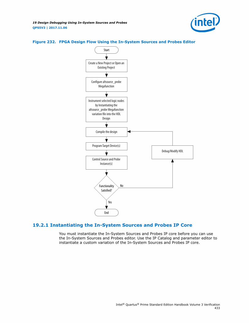
Figure 232. FPGA Design Flow Using the In-System Sources and Probes Editor
Yes
No
Start
End
FunctionalitySatisfied?
Create a New Project or Open an Existing Project
Configure altsource_probe Megafunction
Instrument selected logic nodes by Instantiating the
altsource_probe Megafunction variation file into the HDL
Design
Compile the design
Program Target Device(s)
Control Source and Probe Instance(s)
Debug/Modify HDL
19.2.1 Instantiating the In-System Sources and Probes IP Core
You must instantiate the In-System Sources and Probes IP core before you can usethe In-System Sources and Probes editor. Use the IP Catalog and parameter editor toinstantiate a custom variation of the In-System Sources and Probes IP core.
19 Design Debugging Using In-System Sources and Probes
QPS5V3 | 2017.11.06
Intel® Quartus® Prime Standard Edition Handbook Volume 3 Verification433
To configure the In-System Sources and Probes IP core, perform the following steps::
1. On the Tools menu, click Tools > IP Catalog.
2. Locate and double-click the In-System Sources and Probes IP core. The parametereditor appears.
3. Specify a name for your custom IP variation.
4. Specify the desired parameters for your custom IP variation. You can specify up toup to 512 bits for each source. Your design may include up to 128 instances of thisIP core.
5. Click Generate or Finish to generate IP core synthesis and simulation filesmatching your specifications. The parameter editor generates the necessaryvariation files and the instantiation template based on your specification. Use thegenerated template to instantiate the In-System Sources and Probes IP core inyour design.
Note: The In-System Sources and Probes Editor does not support simulation. Youmust remove the In-System Sources and Probes IP core before you create asimulation netlist.
19.2.2 In-System Sources and Probes IP Core Parameters
Use the template to instantiate the variation file in your design.
Table 130. In-System Sources and Probes IP Port Information
Port Name Required? Direction Comments
probe[] No Input The outputs from your design.
source_clk No Input Source Data is written synchronously to this clock. This input is requiredif you turn on Source Clock in the Advanced Options box in theparameter editor.
source_ena No Input Clock enable signal for source_clk. This input is required if specified inthe Advanced Options box in the parameter editor.
source[] No Output Used to drive inputs to user design.
You can include up to 128 instances of the in-system sources and probes IP core inyour design, if your device has available resources. Each instance of the IP core uses apair of registers per signal for the width of the widest port in the IP core. Additionally,there is some fixed overhead logic to accommodate communication between the IPcore instances and the JTAG controller. You can also specify an additional pair ofregisters per source port for synchronization.
You can use the Intel Quartus Prime incremental compilation feature to reducecompilation time. Incremental compilation allows you to organize your design intological partitions. During recompilation of a design, incremental compilation preservesthe compilation results and performance of unchanged partitions and reduces designiteration time by compiling only modified design partitions.
19.3 Compiling the Design
When you compile your design that includes the In-System Sources and ProbesIPcore, the In-System Sources and Probes and SLD Hub Controller IP core are added toyour compilation hierarchy automatically. These IP cores provide communicationbetween the JTAG controller and your instrumented logic.
19 Design Debugging Using In-System Sources and Probes
QPS5V3 | 2017.11.06
Intel® Quartus® Prime Standard Edition Handbook Volume 3 Verification434

You can modify the number of connections to your design by editing the In-SystemSources and Probes IP core. To open the design instance you want to modify in theparameter editor, double-click the instance in the Project Navigator. You can thenmodify the connections in the HDL source file. You must recompile your design afteryou make changes.
You can use the Intel Quartus Prime incremental compilation feature to reducecompilation design into logical partitions. During recompilation of a design,incremental compilation preserves the compilation results and performance ofunchanged partitions and reduces design iteration time by compiling only modifieddesign partitions.
19.4 Running the In-System Sources and Probes Editor
The In-System Sources and Probes Editor gives you control over allALTSOURCE_PROBE IP core instances within your design. The editor allows you toview all available run time controllable instances of the ALTSOURCE_PROBE IP core inyour design, provides a push-button interface to drive all your source nodes, andprovides a logging feature to store your probe and source data.
To run the In-System Sources and Probes Editor:
• On the Tools menu, click In-System Sources and Probes Editor.
19.4.1 In-System Sources and Probes Editor GUI
The In-System Sources and Probes Editor contains three panes:
• JTAG Chain Configuration—Allows you to specify programming hardware,device, and file settings that the In-System Sources and Probes Editor uses toprogram and acquire data from a device.
• Instance Manager—Displays information about the instances generated whenyou compile a design, and allows you to control data that the In-System Sourcesand Probes Editor acquires.
• In-System Sources and Probes Editor—Logs all data read from the selectedinstance and allows you to modify source data that is written to your device.
When you use the In-System Sources and Probes Editor, you do not need to open aIntel Quartus Prime software project. The In-System Sources and Probes Editorretrieves all instances of the ALTSOURCE_PROBE IP core by scanning the JTAG chainand sending a query to the device selected in the JTAG Chain Configuration pane.You can also use a previously saved configuration to run the In-System Sources andProbes Editor.
Each In-System Sources and Probes Editor pane can access theALTSOURCE_PROBE IP core instances in a single device. If you have more than onedevice containing IP core instances in a JTAG chain, you can launch multiple In-System Sources and Probes Editor panes to access the IP core instances in eachdevice.
19.4.2 Programming Your Device With JTAG Chain Configuration
After you compile your project, you must configure your FPGA before you use the In-System Sources and Probes Editor.
19 Design Debugging Using In-System Sources and Probes
QPS5V3 | 2017.11.06
Intel® Quartus® Prime Standard Edition Handbook Volume 3 Verification435

To configure a device to use with the In-System Sources and Probes Editor, performthe following steps:
1. Open the In-System Sources and Probes Editor.
2. In the JTAG Chain Configuration pane, point to Hardware, and then select thehardware communications device. You may be prompted to configure yourhardware; in this case, click Setup.
3. From the Device list, select the FPGA device to which you want to download thedesign (the device may be automatically detected). You may need to click ScanChain to detect your target device.
4. In the JTAG Chain Configuration pane, click to browse for the SRAM Object File(.sof) that includes the In-System Sources and Probes instance or instances.(The .sof may be automatically detected).
5. Click Program Device to program the target device.
19.4.3 Instance Manager
The Instance Manager pane provides a list of all ALTSOURCE_PROBE instances inthe design and allows you to configure how data is acquired from or written to thoseinstances.
The following buttons and sub-panes are provided in the Instance Manager pane:
• Read Probe Data—Samples the probe data in the selected instance and displaysthe probe data in the In-System Sources and Probes Editor pane.
• Continuously Read Probe Data—Continuously samples the probe data of theselected instance and displays the probe data in the In-System Sources andProbes Editor pane; you can modify the sample rate via the Probe readinterval setting.
• Stop Continuously Reading Probe Data—Cancels continuous sampling of theprobe of the selected instance.
• Read Source Data—Reads the data of the sources in the selected instances.
• Probe Read Interval—Displays the sample interval of all the In-System Sourcesand Probe instances in your design; you can modify the sample interval by clickingManual.
• Event Log—Controls the event log in the In-System Sources and ProbesEditor pane.
• Write Source Data—Allows you to manually or continuously write data to thesystem.
The status of each instance is also displayed beside each entry in the InstanceManager pane. The status indicates if the instance is Not running Offloading data,Updating data, or if an Unexpected JTAG communication error occurs. Thisstatus indicator provides information about the sources and probes instances in yourdesign.
19.4.4 In-System Sources and Probes Editor Pane
The In-System Sources and Probes Editor pane allows you to view data from allsources and probes in your design.
19 Design Debugging Using In-System Sources and Probes
QPS5V3 | 2017.11.06
Intel® Quartus® Prime Standard Edition Handbook Volume 3 Verification436

The data is organized according to the index number of the instance. The editorprovides an easy way to manage your signals, and allows you to rename signals orgroup them into buses. All data collected from in-system source and probe nodes isrecorded in the event log and you can view the data as a timing diagram.
19.4.4.1 Reading Probe Data
You can read data by selecting the ALTSOURCE_PROBE instance in the InstanceManager pane and clicking Read Probe Data.
This action produces a single sample of the probe data and updates the data columnof the selected index in the In-System Sources and Probes Editor pane. You cansave the data to an event log by turning on the Save data to event log option in theInstance Manager pane.
If you want to sample data from your probe instance continuously, in the InstanceManager pane, click the instance you want to read, and then click Continuouslyread probe data. While reading, the status of the active instance shows Unloading.You can read continuously from multiple instances.
You can access read data with the shortcut menus in the Instance Manager pane.
To adjust the probe read interval, in the Instance Manager pane, turn on theManual option in the Probe read interval sub-pane, and specify the sample rate inthe text field next to the Manual option. The maximum sample rate depends on yourcomputer setup. The actual sample rate is shown in the Current interval box. Youcan adjust the event log window buffer size in the Maximum Size box.
19.4.4.2 Writing Data
To modify the source data you want to write into the ALTSOURCE_PROBE instance,click the name field of the signal you want to change. For buses of signals, you candouble-click the data field and type the value you want to drive out to theALTSOURCE_PROBE instance. The In-System Sources and Probes Editor stores themodified source data values in a temporary buffer.
Modified values that are not written out to the ALTSOURCE_PROBE instances appear inred. To update the ALTSOURCE_PROBE instance, highlight the instance in theInstance Manager pane and click Write source data. The Write source datafunction is also available via the shortcut menus in the Instance Manager pane.
The In-System Sources and Probes Editor provides the option to continuously updateeach ALTSOURCE_PROBE instance. Continuous updating allows any modifications youmake to the source data buffer to also write immediately to the ALTSOURCE_PROBEinstances. To continuously update the ALTSOURCE_PROBE instances, change theWrite source data field from Manually to Continuously.
19.4.4.3 Organizing Data
The In-System Sources and Probes Editor pane allows you to group signals intobuses, and also allows you to modify the display options of the data buffer.
To create a group of signals, select the node names you want to group, right-click andselect Group. You can modify the display format in the Bus Display Format and theBus Bit order shortcut menus.
19 Design Debugging Using In-System Sources and Probes
QPS5V3 | 2017.11.06
Intel® Quartus® Prime Standard Edition Handbook Volume 3 Verification437

The In-System Sources and Probes Editor pane allows you to rename any signal.To rename a signal, double-click the name of the signal and type the new name.
The event log contains a record of the most recent samples. The buffer size isadjustable up to 128k samples. The time stamp for each sample is logged and isdisplayed above the event log of the active instance as you move your pointer overthe data samples.
You can save the changes that you make and the recorded data to a Sources andProbes File (.spf). To save changes, on the File menu, click Save. The file containsall the modifications you made to the signal groups, as well as the current data eventlog.
19.5 Tcl interface for the In-System Sources and Probes Editor
To support automation, the In-System Sources and Probes Editor supports theprocedures described in this chapter in the form of Tcl commands. The Tcl package forthe In-System Sources and Probes Editor is included by default when you runquartus_stp.
The Tcl interface for the In-System Sources and Probes Editor provides a powerfulplatform to help you debug your design. The Tcl interface is especially helpful fordebugging designs that require toggling multiple sets of control inputs. You cancombine multiple commands with a Tcl script to define a custom command set.
Table 131. In-System Sources and Probes Tcl Commands
Command Argument Description
start_insystem_source_probe
-device_name <device name>-hardware_name <hardware name>
Opens a handle to a device with the specifiedhardware.Call this command before starting anytransactions.
get_insystem_source_probe_instance_info
-device_name <device name>-hardware_name <hardware name>
Returns a list of all ALTSOURCE_PROBEinstances in your design. Each recordreturned is in the following format:{<instance Index>, <source width>, <probewidth>, <instance name>}
read_probe_data -instance_index <instance_index>-value_in_hex (optional)
Retrieves the current value of the probe.A string is returned that specifies the statusof each probe, with the MSB as the left-mostbit.
read_source_data -instance_index <instance_index>-value_in_hex (optional)
Retrieves the current value of the sources.A string is returned that specifies the statusof each source, with the MSB as the left-mostbit.
write_source_data -instance_index <instance_index>-value <value>-value_in_hex (optional)
Sets the value of the sources.A binary string is sent to the source ports,with the MSB as the left-most bit.
end_insystem_source_probe None Releases the JTAG chain.Issue this command when all transactions arefinished.
The example shows an excerpt from a Tcl script with procedures that control theALTSOURCE_PROBE instances of the design as shown in the figure below. Theexample design contains a DCFIFO with ALTSOURCE_PROBE instances to read from
19 Design Debugging Using In-System Sources and Probes
QPS5V3 | 2017.11.06
Intel® Quartus® Prime Standard Edition Handbook Volume 3 Verification438

and write to the DCFIFO. A set of control muxes are added to the design to control theflow of data to the DCFIFO between the input pins and the ALTSOURCE_PROBEinstances. A pulse generator is added to the read request and write request controllines to guarantee a single sample read or write. The ALTSOURCE_PROBE instances,when used with the script in the example below, provide visibility into the contents ofthe FIFO by performing single sample write and read operations and reporting thestate of the full and empty status flags.
Use the Tcl script in debugging situations to either empty or preload the FIFO in yourdesign. For example, you can use this feature to preload the FIFO to match a triggercondition you have set up within the Signal Tap Logic Analyzer.
Figure 233. DCFIFO Example Design Controlled by Tcl Script
Write_clock
write_reqdata[7..0]
write_clock
read_req
read_clock
wr_full
Q[7..0]
rd_empty
data_out
read_clocksource_read_sel
s_read_req
s_write_req
rd_req_in
wr_req_in
data_in[7..0]
altsource_probe(Instance 1)
altsource_probe(Instance 0)
source_write_sel
s_data[7..0]D Q
D Q
## Setup USB hardware - assumes only USB Blaster is installed and## an FPGA is the only device in the JTAG chainset usb [lindex [get_hardware_names] 0]set device_name [lindex [get_device_names -hardware_name $usb] 0]## write procedure : argument value is integerproc write {value} {global device_name usbvariable fullstart_insystem_source_probe -device_name $device_name -hardware_name $usb#read full flagset full [read_probe_data -instance_index 0]if {$full == 1} {end_insystem_source_probereturn "Write Buffer Full"}##toggle select line, drive value onto port, toggle enable##bits 7:0 of instance 0 is S_data[7:0]; bit 8 = S_write_req;##bit 9 = Source_write_sel##int2bits is custom procedure that returns a bitstring from an integer ## argument
19 Design Debugging Using In-System Sources and Probes
QPS5V3 | 2017.11.06
Intel® Quartus® Prime Standard Edition Handbook Volume 3 Verification439

write_source_data -instance_index 0 -value /[int2bits [expr 0x200 | $value]]write_source_data -instance_index 0 -value [int2bits [expr 0x300 | $value]]##clear transactionwrite_source_data -instance_index 0 -value 0end_insystem_source_probe}proc read {} {global device_name usbvariable emptystart_insystem_source_probe -device_name $device_name -hardware_name $usb##read empty flag : probe port[7:0] reads FIFO output; bit 8 reads empty_flagset empty [read_probe_data -instance_index 1]if {[regexp {1........} $empty]} { end_insystem_source_probereturn "FIFO empty" }## toggle select line for read transaction## Source_read_sel = bit 0; s_read_reg = bit 1## pulse read enable on DC FIFOwrite_source_data -instance_index 1 -value 0x1 -value_in_hexwrite_source_data -instance_index 1 -value 0x3 -value_in_hexset x [read_probe_data -instance_index 1 ]end_insystem_source_probereturn $x}
Related Links
• Tcl Scripting
• Intel Quartus Prime Settings File Manual
• Command Line Scripting
• Tcl Scripting
• Intel Quartus Prime Settings File Manual
• Command Line Scripting
19.6 Design Example: Dynamic PLL Reconfiguration
The In-System Sources and Probes Editor can help you create a virtual front panelduring the prototyping phase of your design. You can create relatively simple, highfunctioning designs of in a short amount of time. The following PLL reconfigurationexample demonstrates how to use the In-System Sources and Probes Editor toprovide a GUI to dynamically reconfigure a Stratix PLL.
Stratix PLLs allow you to dynamically update PLL coefficients during run time. Eachenhanced PLL within the Stratix device contains a register chain that allows you tomodify the pre-scale counters (m and n values), output divide counters, and delaycounters. In addition, the ALTPLL_RECONFIG IP core provides an easy interface toaccess the register chain counters. The ALTPLL_RECONFIG IP core provides a cachethat contains all modifiable PLL parameters. After you update all the PLL parameters inthe cache, the ALTPLL_RECONFIG IP core drives the PLL register chain to update thePLL with the updated parameters. The figure shows a Stratix-enhanced PLL withreconfigurable coefficients.
19 Design Debugging Using In-System Sources and Probes
QPS5V3 | 2017.11.06
Intel® Quartus® Prime Standard Edition Handbook Volume 3 Verification440

Figure 234. Stratix-Enhanced PLL with Reconfigurable Coefficients
÷n Δtn
Δtm
÷m
÷g0 Δtg0
÷e3 Δte3
÷g3 Δtg3
PFD VCOChargePump
LoopFilter
fREF
scandata
scanclk
scanaclr
Counters and ClockDelay Settings areProgrammable
All Output Counters andClock Delay Settings canbe Programmed Dynamically
LSB MSB
LSB MSB
LSB MSB
LSB MSB
LSB
MSB
(1) (2)
The following design example uses an ALTSOURCE_PROBE instance to update the PLLparameters in the ALTPLL_RECONFIG IP core cache. The ALTPLL_RECONFIG IP coreconnects to an enhanced PLL in a Stratix FPGA to drive the register chain containingthe PLL reconfigurable coefficients. This design example uses a Tcl/Tk script togenerate a GUI where you can enter in new m and n values for the enhanced PLL. TheTcl script extracts the m and n values from the GUI, shifts the values out to theALTSOURCE_PROBE instances to update the values in the ALTPLL_RECONFIG IP corecache, and asserts the reconfiguration signal on the ALTPLL_RECONFIG IP core. Thereconfiguration signal on the ALTPLL_RECONFIG IP core starts the register chaintransaction to update all PLL reconfigurable coefficients.
Figure 235. Block Diagram of Dynamic PLL Reconfiguration Design Example
In-System Sourcesand ProbesTcl Interface
JTAGInterface
CounterParameters
Stratix FPGA50 MHz
PLL_scandataPLL_scandlkPLL_scanaclr
E0
C0
C1
fref
Stratix-EnhancedPLLalt_pll_reconfig
Megafunction
In-SystemSources and
Probes
19 Design Debugging Using In-System Sources and Probes
QPS5V3 | 2017.11.06
Intel® Quartus® Prime Standard Edition Handbook Volume 3 Verification441
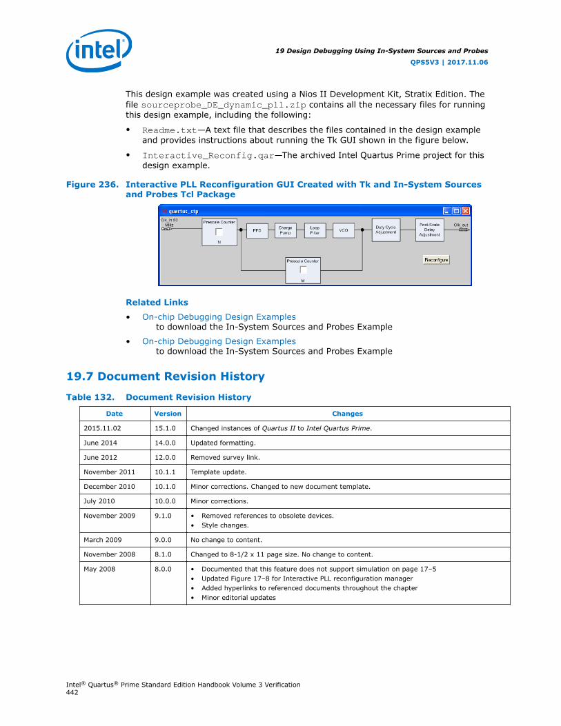
This design example was created using a Nios II Development Kit, Stratix Edition. Thefile sourceprobe_DE_dynamic_pll.zip contains all the necessary files for runningthis design example, including the following:
• Readme.txt—A text file that describes the files contained in the design exampleand provides instructions about running the Tk GUI shown in the figure below.
• Interactive_Reconfig.qar—The archived Intel Quartus Prime project for thisdesign example.
Figure 236. Interactive PLL Reconfiguration GUI Created with Tk and In-System Sourcesand Probes Tcl Package
Related Links
• On-chip Debugging Design Examplesto download the In-System Sources and Probes Example
• On-chip Debugging Design Examplesto download the In-System Sources and Probes Example
19.7 Document Revision History
Table 132. Document Revision History
Date Version Changes
2015.11.02 15.1.0 Changed instances of Quartus II to Intel Quartus Prime.
June 2014 14.0.0 Updated formatting.
June 2012 12.0.0 Removed survey link.
November 2011 10.1.1 Template update.
December 2010 10.1.0 Minor corrections. Changed to new document template.
July 2010 10.0.0 Minor corrections.
November 2009 9.1.0 • Removed references to obsolete devices.• Style changes.
March 2009 9.0.0 No change to content.
November 2008 8.1.0 Changed to 8-1/2 x 11 page size. No change to content.
May 2008 8.0.0 • Documented that this feature does not support simulation on page 17–5• Updated Figure 17–8 for Interactive PLL reconfiguration manager• Added hyperlinks to referenced documents throughout the chapter• Minor editorial updates
19 Design Debugging Using In-System Sources and Probes
QPS5V3 | 2017.11.06
Intel® Quartus® Prime Standard Edition Handbook Volume 3 Verification442

Related Links
Documentation ArchiveFor previous versions of the Intel Quartus Prime Handbook, search thedocumentation archives.
19 Design Debugging Using In-System Sources and Probes
QPS5V3 | 2017.11.06
Intel® Quartus® Prime Standard Edition Handbook Volume 3 Verification443

20 Programming Intel FPGA DevicesThe Intel Quartus Prime Programmer allows you to program and configure Intel FPGACPLD, FPGA, and configuration devices. After compiling your design, use the IntelQuartus Prime Programmer to program or configure your device, to test thefunctionality of the design on a circuit board.
20.1 Programming Flow
The main stages of programming your device are:
1. Compiling your design, such that the Intel Quartus Prime Assembler generates theprogramming or configuration file.
2. Converting the programming or configuration file to target your configurationdevice and, optionally, creating secondary programming files.
Table 133. Programming and Configuration File Format
File Format FPGA CPLD ConfigurationDevice
SerialConfiguration
Device
SRAM Object File (.sof) Yes — — —
Programmer Object File (.pof) — Yes Yes Yes
JEDEC JESD71 STAPL Format File (.jam) Yes Yes Yes —
Jam Byte Code File (.jbc) Yes Yes Yes —
3. Programming and configuring the FPGA, CPLD, or configuration device using theprogramming or configuration file with the Intel Quartus Prime Programmer.
20.1.1 Stand-Alone Intel Quartus Prime Programmer
Intel FPGA offers the free stand-alone Programmer, which has the same fullfunctionality as the Intel Quartus Prime Programmer in the Intel Quartus Primesoftware. The stand-alone Programmer is useful when programming your devices withanother workstation, so you do not need two full licenses. You can download thestand-alone Programmer from the Download Center on the Altera website.
Stand-Alone Programmer Memory Limitations
The stand-alone Programmer may use significant memory during the followingoperations:
• During auto-detect operations
• When the programming file is added to the flash
• During manual attachment of the flash into the Programmer window
QPS5V3 | 2017.11.06
Intel Corporation. All rights reserved. Intel, the Intel logo, Altera, Arria, Cyclone, Enpirion, MAX, Nios, Quartusand Stratix words and logos are trademarks of Intel Corporation or its subsidiaries in the U.S. and/or othercountries. Intel warrants performance of its FPGA and semiconductor products to current specifications inaccordance with Intel's standard warranty, but reserves the right to make changes to any products and servicesat any time without notice. Intel assumes no responsibility or liability arising out of the application or use of anyinformation, product, or service described herein except as expressly agreed to in writing by Intel. Intelcustomers are advised to obtain the latest version of device specifications before relying on any publishedinformation and before placing orders for products or services.*Other names and brands may be claimed as the property of others.
ISO9001:2008Registered

The 32-bit stand-alone Programmer can only use a limited amount of memory whenlaunched in 32-bit Windows. Note the following specific limitations of 32-bit stand-alone Programmer:
Table 134. Stand-Alone Programmer Memory Limitations
Application Maximum Flash Device Size Flash Device OperationUsing PFL
32-bit Stand-Alone Programmer Up to 512 Mb Single Flash Device
64-bit Stand-Alone Programmer Up to 2 Gb Multiple Flash Device
The stand-alone Programmer supports combination and/or conversion of Intel QuartusPrime programming files using the Convert Programming Files dialog box. You canconvert programming files, such as Mask Settings File (.msf), Partial-Mask SRAMObject File (.pmsf), SRAM Object Files (.sof), or Programmer Object Files (.pof)into other file formats that support device configuration schemes for Intel FPGAdevices.
Note the following device-specific file conversion limitations with use of the 32-bitstand-alone Programmer:
Table 135. Stand-Alone Programmer File Conversion Limitations
Programming File Conversion Device Support
32-bit Programming File Conversion All Supported Intel FPGA Devices Except IntelArria 10
64-bit Programming File Conversion All Supported Intel FPGA Devices
Related Links
Download Center
20.1.2 Optional Programming or Configuration Files
The Intel Quartus Prime software can generate optional programming or configurationfiles in various formats that you can use with programming tools other than the IntelQuartus Prime Programmer. When you compile a design in the Intel Quartus Primesoftware, the Assembler automatically generates either a .sof or .pof. TheAssembler also allows you to convert FPGA configuration files to programming files forconfiguration devices.
Related Links
AN 425: Using Command-Line Jam STAPL Solution for Device Programming
20.1.3 Secondary Programming Files
The Intel Quartus Prime software generates programming files in various formats foruse with different programming tools.
20 Programming Intel FPGA Devices
QPS5V3 | 2017.11.06
Intel® Quartus® Prime Standard Edition Handbook Volume 3 Verification445

Table 136. File Types Generated by the Intel Quartus Prime Software and Supported bythe Intel Quartus Prime Programmer
File Type Generated by the Intel QuartusPrime Software
Supported by the Intel QuartusPrime Programmer
.sof Yes Yes
.pof Yes Yes
.jam Yes Yes
.jbc Yes Yes
JTAG Indirect Configuration File (.jic) Yes Yes
Serial Vector Format File (.svf) Yes —
Hexadecimal (Intel-Format) Output File (.hexout) Yes —
Raw Binary File (.rbf) Yes Yes (11)
Raw Binary File for Partial Reconfiguration (.rbf) Yes Yes (12)
Tabular Text File (.ttf) Yes —
Raw Programming Data File (.rpd) Yes —
20.2 Intel Quartus Prime Programmer Window
The Intel Quartus Prime Programmer window allows you to:
• Add your programming and configuration files.
• Specify programming options and hardware.
• Start the programming or configuration of the device.
To open the Programmer window, click Tools ➤ Programmer. As you proceedthrough the programming flow, the Intel Quartus Prime Message window reports thestatus of each operation.
Related Links
Programmer Page (Options Dialog Box)In Intel Quartus Prime Help
20.2.1 Editing the Details of an Unknown Device
When the Intel Quartus Prime Programmer automatically detects devices with sharedJTAG IDs, the Programmer prompts you to specify the device in the JTAG chain. If theProgrammer does not prompt you to specify the device, you must manually add eachdevice in the JTAG chain to the Programmer, and define the instruction register lengthof each device.
(11) Raw Binary File (.rbf) is supported by the Intel Quartus Prime Programmer in Passive Serial(PS) configuration mode.
(12) Raw Binary File for Partial Reconfiguration (.rbf) is supported by the Intel Quartus PrimeProgrammer in JTAG debug mode.
20 Programming Intel FPGA Devices
QPS5V3 | 2017.11.06
Intel® Quartus® Prime Standard Edition Handbook Volume 3 Verification446

To edit the details of an unknown device, follow these steps:
1. Double-click the unknown device listed under the device column.
2. Click Edit.
3. Change the device Name.
4. Specify the Instruction register Length.
5. Click OK.
6. Save the .cdf file.
20.2.2 Setting Up Your Hardware
Before you can program or configure your device, you must have the correct hardwaresetup. The Intel Quartus Prime Programmer provides the flexibility to choose adownload cable or programming hardware.
20.2.3 Setting the JTAG Hardware
The JTAG server allows the Intel Quartus Prime Programmer to access the JTAGhardware. You can also access the JTAG download cable or programming hardwareconnected to a remote computer through the JTAG server of that computer. With theJTAG server, you can control the programming or configuration of devices from asingle computer through other computers at remote locations. The JTAG server usesthe TCP/IP communications protocol.
20.2.3.1 Running JTAG Daemon with Linux
The JTAGD daemon allows a remote machine to program or debug a board that isconnected to a Linux host over the network. The JTAGD daemon also allows multipleprograms to use JTAG resources at the same time. The JTAGD daemon is the Linuxversion of a JTAG server.
Run the JTAGD daemon to avoid:
• The JTAGD server from exiting after two minutes of idleness.
• The JTAGD server from not accepting connections from remote machines, whichmight lead to an intermittent failure.
To run JTAGD as a daemon, follow these steps:
1. Create an /etc/jtagd directory.
2. Set the permissions of this directory and the files in the directory to allow you tohave the read/write access.
3. Run jtagd (with no arguments) from your quartus/bin directory.
The JTAGD daemon is now running and does not terminate when you log off.
20.2.4 Using the JTAG Chain Debugger Tool
The JTAG Chain Debugger tool allows you to test the JTAG chain integrity and detectintermittent failures of the JTAG chain. In addition, the tool allows you to shift in JTAGinstructions and data through the JTAG interface, and step through the test accessport (TAP) controller state machine for debugging purposes. You access the tool byclicking Tools ➤ JTAG Chain Debugger on the Intel Quartus Prime software.
20 Programming Intel FPGA Devices
QPS5V3 | 2017.11.06
Intel® Quartus® Prime Standard Edition Handbook Volume 3 Verification447

20.3 Programming and Configuration Modes
The following table lists the programming and configuration modes supported by IntelFPGA devices.
Table 137. Programming and Configuration Modes
Configuration Mode Supportedby the Intel Quartus Prime
Programmer
FPGA CPLD ConfigurationDevice
Serial ConfigurationDevice
JTAG Yes Yes Yes —
Passive Serial (PS) Yes — — —
Active Serial (AS) Programming — — — Yes
Configuration via Protocol (CvP) Yes — — —
In-Socket Programming — Yes (except forMAX II CPLDs)
Yes Yes
Related Links
Configuration via Protocol (CvP) Implementation in V-series Intel FPGAs Devices UserGuide
Describes the CvP configuration mode.
20.4 Design Security Keys
The Intel Quartus Prime Programmer supports the generation of encryption keyprogramming files and encrypted configuration files for Intel FPGAs that support thedesign security feature. You can also use the Intel Quartus Prime Programmer toprogram the encryption key into the FPGA.
Related Links
AN 556: Using the Design Security Features in Intel FPGAs
20.5 Convert Programming Files Dialog Box
The Convert Programming Files dialog box in the Programmer allows you toconvert programming files from one file format to another. To access the ConvertProgramming Files dialog box, click File ➤ Convert Programming Files... on theIntel Quartus Prime software.
For example, to store the FPGA data in configuration devices, you can convertthe .sof data to another format, such as .pof, .hexout, .rbf, .rpd, or .jic, andthen program the configuration device.
You can also configure multiple devices with an external host, such as amicroprocessor or CPLD. For example, you can combine multiple .sof files intoone .pof file. To save time in subsequent conversions, click Save Conversion Setupto save your conversion specifications in a Conversion Setup File (.cof). Click OpenConversion Setup Data to load your .cof setup in the Convert ProgrammingFiles dialog box.
20 Programming Intel FPGA Devices
QPS5V3 | 2017.11.06
Intel® Quartus® Prime Standard Edition Handbook Volume 3 Verification448
Example 39. Conversion Setup File Contents
<?xml version="1.0" encoding="US-ASCII" standalone="yes"?><cof> <output_filename>output_file.pof</output_filename> <n_pages>1</n_pages> <width>1</width> <mode>14</mode> <sof_data> <user_name>Page_0</user_name> <page_flags>1</page_flags> <bit0> <sof_filename>/users/jbrossar/template/output_files/template_test.sof</sof_filename> </bit0> </sof_data> <version>7</version> <create_cvp_file>0</create_cvp_file> <create_hps_iocsr>0</create_hps_iocsr> <auto_create_rpd>0</auto_create_rpd> <options> <map_file>1</map_file> </options> <MAX10_device_options> <por>0</por> <io_pullup>1</io_pullup> <auto_reconfigure>1</auto_reconfigure> <isp_source>0</isp_source> <verify_protect>0</verify_protect> <epof>0</epof> <ufm_source>0</ufm_source> </MAX10_device_options> <advanced_options> <ignore_epcs_id_check>0</ignore_epcs_id_check> <ignore_condone_check>2</ignore_condone_check> <plc_adjustment>0</plc_adjustment> <post_chain_bitstream_pad_bytes>-1</post_chain_bitstream_pad_bytes> <post_device_bitstream_pad_bytes>-1</post_device_bitstream_pad_bytes> <bitslice_pre_padding>1</bitslice_pre_padding> </advanced_options></cof>
Related Links
Convert Programming Files Dialog BoxIn Intel Quartus Prime Help
20.5.1 Debugging Your Configuration
Use the Advanced option in the Convert Programming Files dialog box to debugyour configuration. You must choose the advanced settings that apply to your IntelFPGA device. You can direct the Intel Quartus Prime software to enable or disable anadvanced option by turning the option on or off in the Advanced Options dialog box.When you change settings in the Advanced Options dialog box, the changeaffects .pof, .jic, .rpd, and .rbf files.
The following table lists the Advanced Options settings in more detail:
Table 138. Advanced Options Settings
Option Setting Description
Disable EPCS ID check FPGA skips the EPCS silicon ID verification.Default setting is unavailable (EPCS ID check is enabled).
continued...
20 Programming Intel FPGA Devices
QPS5V3 | 2017.11.06
Intel® Quartus® Prime Standard Edition Handbook Volume 3 Verification449

Option Setting Description
Applies to the single- and multi-device AS configurationmodes on all FPGA devices.
Disable AS mode CONF_DONE error check FPGA skips the CONF_DONE error check.Default setting is unavailable (AS mode CONF_DONE errorcheck is enabled).Applies to single- and multi-device (AS) configurationmodes on all FPGA devices.The CONF_DONE error check is disabled by default forStratix V, Arria V, and Cyclone V devices for AS-PS multidevice configuration mode.
Program Length Count adjustment Specifies the offset you can apply to the computed PLC ofthe entire bitstream.Default setting is 0. The value must be an integer.Applies to single- and multi-device (AS) configurationmodes on all FPGA devices.
Post-chain bitstream pad bytes Specifies the number of pad bytes appended to the end ofan entire bitstream.Default value is set to 0 if the bitstream of the last device isuncompressed. Set to 2 if the bitstream of the last device iscompressed.
Post-device bitstream pad bytes Specifies the number of pad bytes appended to the end ofthe bitstream of a device.Default value is 0. No negative integer.Applies to all single-device configuration modes on all FPGAdevices.
Bitslice padding value Specifies the padding value used to prepare bitsliceconfiguration bitstreams, such that all bitslice configurationchains simultaneously receive their final configuration databit.Default value is 1. Valid setting is 0 or 1.Use only in 2, 4, and 8-bit PS configuration mode, when youuse an EPC device with the decompression feature enabled.Applies to all FPGA devices that support enhancedconfiguration devices.
The following table lists the symptoms you may encounter if a configuration fails, anddescribes the advanced options you must use to debug your configuration.
Failure Symptoms Disable EPCSID Check
Disable ASMode
CONF_DONEError Check
PLC Settings Post-ChainBitstream Pad
Bytes
Post-DeviceBitstream Pad
Bytes
BitslicePadding Value
Configurationfailure occurs aftera configurationcycle.
— Yes YesYes(13)
Yes (14) —
Decompressionfeature is enabled.
— Yes Yes Yes (13) Yes (14) —
Encryption featureis enabled.
— Yes Yes Yes (13) Yes (14) —
continued...
(13) Use only for multi-device chain
(14) Use only for single-device chain
20 Programming Intel FPGA Devices
QPS5V3 | 2017.11.06
Intel® Quartus® Prime Standard Edition Handbook Volume 3 Verification450

Failure Symptoms Disable EPCSID Check
Disable ASMode
CONF_DONEError Check
PLC Settings Post-ChainBitstream Pad
Bytes
Post-DeviceBitstream Pad
Bytes
BitslicePadding Value
CONF_DONE stayslow after aconfiguration cycle.
— Yes Yes (15) Yes (13) Yes (14) —
CONF_DONE goeshigh momentarilyafter aconfiguration cycle.
— Yes Yes (16) — — —
FPGA does notenter user modeeven thoughCONF_DONE goeshigh.
— — — Yes (13) Yes (14) —
Configurationfailure occurs atthe beginning of aconfiguration cycle.
Yes — — — — —
Newly introducedEPCS, such asEPCS128.
Yes — — — — —
Failure in .pofgeneration for EPCdevice using IntelQuartus PrimeConvertProgramming FileUtility when thedecompressionfeature is enabled.
— — — — — Yes
20.5.2 Converting Programming Files for Partial Reconfiguration
The Convert Programming File dialog box supports the following programming filegeneration and option for Partial Reconfiguration:
• Partial-Masked SRAM Object File (.pmsf) output file generation, with .msfand .sof as input files.
• .rbf for Partial Reconfiguration output file generation, with a .pmsf as the inputfile.
Note: The .rbf for Partial Reconfiguration file is only for Partial Reconfiguration.
• Providing the Enable decompression during Partial Reconfiguration option toenable the option bit for bitstream decompression during Partial Reconfiguration,when converting a full design .sof to any supported file type.
Related Links
Design Planning for Partial Reconfiguration
(15) Start with positive offset to the PLC settings
(16) Start with negative offset to the PLC settings
20 Programming Intel FPGA Devices
QPS5V3 | 2017.11.06
Intel® Quartus® Prime Standard Edition Handbook Volume 3 Verification451

20.5.2.1 Generating .pmsf using a .msf and a .sof
To generate the .pmsf in the Convert Programming Files dialog box, follow thesesteps:
1. In the Convert Programming Files dialog box, under the Programming filetype field, select Partial-Masked SRAM Object File (.pmsf).
2. In the File name field, specify the necessary output file name.
3. In the Input files to convert field, add necessary input files to convert. You canadd only a .msf and .sof.
4. Click Generate.
20.5.2.2 Generating .rbf for Partial Reconfiguration Using a .pmsf
After generating the .pmsf, convert the .pmsf to a .rbf for Partial Reconfiguration inthe Convert Programming Files dialog box.
To generate the .rbf for Partial Reconfiguration, follow these steps:
1. In the Convert Programming Files dialog box, in the Programming file typefield, select Raw Binary File for Partial Reconfiguration (.rbf).
2. In the File name field, specify the output file name.
3. In the Input files to convert field, add input files to convert. You can add onlya .pmsf.
4. After adding the .pmsf, select the .pmsf and click Properties. The PMSF FileProperties dialog box appears.
5. Make your selection either by turning on or turning off the following options:
— Compression option—This option enables compression on PartialReconfiguration bitstream. If you turn on this option, then you must turn onthe Enable decompression during Partial Reconfiguration option.
— Enable SCRUB mode option—The default of this option is based on AND/ORmode. This option is valid only when Partial Reconfiguration masks in yourdesign are not overlapped vertically. Otherwise, you cannot generate the .rbffor Partial Reconfiguration.
— Write memory contents option—This option is a workaround for initializedRAM/ROM in a Partial Reconfiguration region.
For more information about these option, refer to the Design Planning for PartialReconfiguration.
6. Click OK.
7. Click Generate.
20.5.2.3 Enable Decompression during Partial Reconfiguration Option
You can turn on the Enable decompression during Partial Reconfiguration optionin the SOF File Properties: Bitstream Encryption dialog box, which can beaccessed from the Convert Programming File dialog box. This option is availablewhen converting a .sof to any supported programming file types listed in Table 136on page 446.
20 Programming Intel FPGA Devices
QPS5V3 | 2017.11.06
Intel® Quartus® Prime Standard Edition Handbook Volume 3 Verification452

This option is hidden for other targeted devices that do not support PartialReconfiguration. To view this option in the SOF File Properties: BitstreamEncryption dialog box, the .sof must be targeted on an Intel FPGA device thatsupports Partial Reconfiguration.
If you turn on the Compression option when generating the .rbf for PartialReconfiguration, then you must turn on the Enable decompression during PartialReconfiguration option.
20.6 Flash Loaders
Parallel and serial configuration devices do not support the JTAG interface. However,you can use a flash loader to program configuration devices in-system via the JTAGinterface. You can use an FPGA as a bridge between the JTAG interface and theconfiguration device. The Intel Quartus Prime software supports parallel and serialflash loaders.
20.7 JTAG Debug Mode for Partial Reconfiguration
The JTAG debug mode allows you to configure partial reconfiguration bitstreamthrough the JTAG interface. Use this feature to debug PR bitstream and eventuallyhelping you in your PR design prototyping. This feature is available for internal andexternal host. Using the JTAG debug mode forces the Data Source Controller to be inx16 mode.
During JTAG debug operation, the JTAG command sent from the Intel Quartus PrimeProgrammer ignores and overrides most of the Partial Reconfiguration IP coreinterface signals (clk, pr_start, double_pr, data[], data_valid, anddata_read).
Note: The TCK is the main clock source for PR IP core during this operation.
You can view the status of Partial Reconfiguration operation in the messages box andthe Progress bar in the Intel Quartus Prime Programmer. The PR_DONE, PR_ERROR,and CRC_ERROR signals will be monitored during PR operation and reported in theMessages box at the end of the operation.
The Intel Quartus Prime Programmer can detect the number of PR_DONE instruction(s)in plain or compressed PR bitstream and, therefore, can handle single or double PRcycle accordingly. However, only single PR cycle is supported for encrypted PartialReconfiguration bitstream in JTAG debug mode (provided that the specified device isconfigured with the encrypted base bitstream which contains the PR IP core in thedesign).
Note: Configuring an incompatible PR bitstream to the specified device may corrupt yourdesign, including the routing path and the PR IP core placed in the static region. Whenthis issue occurs, the PR IP core stays in an undefined state, and the Intel QuartusPrime Programmer is unable to reset the IP core. As a result, the Intel Quartus PrimeProgrammer generates the following error when you try to configure a new PRbitstream:
20 Programming Intel FPGA Devices
QPS5V3 | 2017.11.06
Intel® Quartus® Prime Standard Edition Handbook Volume 3 Verification453

Error (12897): Partial Reconfiguration status: Can't reset the PR megafunction. This issue occurred because the design was corrupted by an incompatible PR bitstream in the previous PR operation. You must reconfigure the device with a good design.
20.7.1 Configuring Partial Reconfiguration Bitstream in JTAG Debug Mode
To configure the Partial Reconfiguration bitstream in JTAG debug mode, follow thesesteps:
1. In the Intel Quartus Prime Programmer GUI, right click a highlighted basebitstream (in .sof) and then click Add PR Programming File to add the PRbitstream (.rbf).
Figure 237. Adding PR Programming File
2. After adding thePR bitstream, you can change or delete the Partial Reconfigurationprogramming file by clicking Change PR Programming File or Delete PRProgramming File.
20 Programming Intel FPGA Devices
QPS5V3 | 2017.11.06
Intel® Quartus® Prime Standard Edition Handbook Volume 3 Verification454

Figure 238. Change PR Programming File or Delete PR Programming File
3. Click Start to configure the PR bitstream. The Intel Quartus Prime Programmergenerates an error message if the specified device does not contain the PR IP corein the design (you must instantiate the Partial Reconfiguration IP core in yourdesign to use the JTAG debug mode).
20 Programming Intel FPGA Devices
QPS5V3 | 2017.11.06
Intel® Quartus® Prime Standard Edition Handbook Volume 3 Verification455

Figure 239. Starting PR Bitstream Configuration
4. Configure the valid .rbf in JTAG debug mode with the Intel Quartus PrimeProgrammer.
20 Programming Intel FPGA Devices
QPS5V3 | 2017.11.06
Intel® Quartus® Prime Standard Edition Handbook Volume 3 Verification456

Figure 240. Configuring Valid .rbf
5. The JTAG debug mode is also supported if the PR IP core is pre-programmed onthe specified device.
20 Programming Intel FPGA Devices
QPS5V3 | 2017.11.06
Intel® Quartus® Prime Standard Edition Handbook Volume 3 Verification457

Figure 241. Partial Reconfiguration IP Core Successfully Pre-programmed
6. The Intel Quartus Prime Programmer reports error when you try to configure thecorrupted .rbf in JTAG debug mode.
Figure 242. Configuring Corrupted .rbf
20 Programming Intel FPGA Devices
QPS5V3 | 2017.11.06
Intel® Quartus® Prime Standard Edition Handbook Volume 3 Verification458

20.8 Verifying if Programming Files Correspond to a Compilation ofthe Same Source Files
Intel Quartus Prime programming files support the project hash property, which helpsyou determine if two or more programming files correspond to a compilation of thesame set of source files.
During compilation, the Intel Quartus Prime software produces an unique projecthash, and embeds this value in the programming files (.sof). The project hash isavailable for Arria V, Stratix V, Cyclone V, Intel MAX 10, and Intel Arria 10 devicefamilies.
The project hash does not change for different builds of the Intel Quartus Primesoftware, or when you install a software patch. However, if you upgrade any IP with adifferent build or patch, the project hash changes.
20.8.1 Obtaining Project Hash for Arria V, Stratix V, Cyclone V and IntelMAX 10 Devices
To obtain the project hash value of a .sof programming file for a design targeted toArria V, Stratix V, Cyclone V, and Intel MAX 10 devices, use the following command,which dumps out metadata information that includes the project hash.
quartus_cpf --info <sof-file-name>
Example 40. Output of Project Hash Extraction
In this example, the programming file name is cb_intosc.sof.
File: cb_intosc.sof File CRC: 0x0000 Creator: Quartus Prime Compiler Version 17.0.0 Internal Build 565 02/09/2017 SJ Standard Edition Comment: UNIX Device: 5SGSMD5K2F40 Data checksum: 0x02534E5A JTAG usercode: 0x02534E5A Project Hash: 0x556e737065636966696564
20.8.2 Obtaining Project Hash for Intel Arria 10 Devices
To obtain the project hash value of a .sof programming file for a design targeted toIntel Arria 10 devices, use the quartus_asm command-line executable(quartus_asm.exe in Windows) with the --project_hash option.
quartus_asm --project_hash <sof-file>
Example 41. Output of Project Hash Command
In this example, the programming file is one_wire.sof.
Info: *******************************************************************Info: Running Quartus Prime AssemblerInfo: Version 17.1.0 Build 569 08/23/2017 SJ Standard EditionInfo: Copyright (C) 2017 Intel Corporation. All rights reserved.Info: Your use of Intel Corporation's design tools, logic functionsInfo: and other software and tools, and its AMPP partner logicInfo: functions, and any output files from any of the foregoing
20 Programming Intel FPGA Devices
QPS5V3 | 2017.11.06
Intel® Quartus® Prime Standard Edition Handbook Volume 3 Verification459

Info: (including device programming or simulation files), and anyInfo: associated documentation or information are expressly subjectInfo: to the terms and conditions of the Intel Program LicenseInfo: Subscription Agreement, the Intel Quartus Prime License Agreement,Info: the Intel MegaCore Function License Agreement, or otherInfo: applicable license agreement, including, without limitation,Info: that your use is for the sole purpose of programming logicInfo: devices manufactured by Intel and sold by Intel or itsInfo: authorized distributors. Please refer to the applicableInfo: agreement for further details.Info: Processing started: Fri Aug 25 18:22:53 2017Info: Command: quartus_asm --project_hash one_wire.sofInfo: Quartus(args): one_wire.sofInfo: Using INI file /data/test_asm/dis_all/quartus.ini0x0e43694a1ffaf5da6088f900ffb0f7b6Info (23030): Evaluation of Tcl script /tools/quartuskit/17.1std/quartus/common/tcl/apps/qasm/project_hash.tcl was successfulInfo: Quartus Prime Assembler was successful. 0 errors, 0 warningsInfo: Peak virtual memory: 1123 megabytesInfo: Processing ended: Fri Aug 25 18:22:59 2017Info: Elapsed time: 00:00:06Info: Total CPU time (on all processors): 00:00:03
20.9 Scripting Support
In addition to the Intel Quartus Prime Programmer GUI, you can use the Intel QuartusPrime command-line executable quartus_pgm.exe (or quartus_pgm in Linux) toaccess programmer functionality from the command line and from scripts. Theprogrammer accepts .pof, .sof, and .jic programming or configuration filesand .cdf files.
The following example shows a command that programs a device:
quartus_pgm –c byteblasterII –m jtag –o bpv;design.pof ←
Where:
• -c byteblasterII specifies the Intel FPGA Parallel Port Cable download cable
• -m jtag specifies the JTAG programming mode
• -o bpv represents the blank-check, program, and verify operations
• design.pof represents the .pof used for the programming
The Programmer automatically executes the erase operation before programming thedevice.
For Linux terminal, use:
quartus_pgm –c byteblasterII –m jtag –o bpv\;design.pof
Related Links
About Intel Quartus Prime ScriptingIn Intel Quartus Prime Help
20.9.1 The jtagconfig Debugging Tool
You can use the jtagconfig command-line utility to check the devices in a JTAGchain and the user-defined devices. The jtagconfig command-line utility is similarto the auto detect operation in the Intel Quartus Prime Programmer.
20 Programming Intel FPGA Devices
QPS5V3 | 2017.11.06
Intel® Quartus® Prime Standard Edition Handbook Volume 3 Verification460

For more information about the jtagconfig utility, use the help available at thecommand prompt:
jtagconfig [–h | --help]
Note: The help switch does not reference the -n switch. The jtagconfig -n commandshows each node for each JTAG device.
Related Links
Command-Line ScriptingIn Intel Quartus Prime Standard Edition Handbook Volume 2
20.9.2 Generating a Partial-Mask SRAM Object File using a Mask SettingsFile and a SRAM Object File
You can generate a .pmsf with the quartus_cpf command by typing the followingcommand:
quartus_cpf -p <pr_revision.msf> <pr_revision.sof> <new_filename.pmsf>
20.9.3 Generating Raw Binary File for Partial Reconfiguration usinga .pmsf
You can generate a .rbf for Partial Reconfiguration with the quartus_cpf commandby typing the following command:
quartus_cpf –o foo.txt –c <pr_revision.pmsf> <pr_revision.rbf>
Note: You must run this command in the same directory where the files are located.
20.10 Document Revision History
Table 139. Document Revision History
Date Version Changes
2017.11.06 17.1.0 • Updated Project Hash feature.
2017.05.08 17.0.0 • Added Project Hash feature.
2015.11.02 15.1.0 Changed instances of Quartus II to Intel Quartus Prime.
2015.05.04 15.0.0 Added Conversion Setup File (.cof) description and example.
December 2014 14.1.0 Updated the Scripting Support section to include a Linux command to program adevice.
June 2014 14.0.0 • Added Running JTAG Daemon.• Removed Cyclone III and Stratix III devices references.• Removed MegaWizard Plug-In Manager references.• Updated Secondary Programming Files section to add notes about the Intel Quartus
Prime Programmer support for .rbf files.
November 2013 13.1.0 • Converted to DITA format.• Added JTAG Debug Mode for Partial Reconfiguration and Configuring Partial
Reconfiguration Bitstream in JTAG Debug Mode sections.
continued...
20 Programming Intel FPGA Devices
QPS5V3 | 2017.11.06
Intel® Quartus® Prime Standard Edition Handbook Volume 3 Verification461

Date Version Changes
November 2012 12.1.0 • Updated Table 18–3 on page 18–6, and Table 18–4 on page 18–8.• Added “Converting Programming Files for Partial Reconfiguration” on page 18–10,
“Generating .pmsf using a .msf and a .sof” on page 18–10, “Generating .rbf forPartial Reconfiguration Using a .pmsf” on page 18–12, “Enable Decompressionduring Partial Reconfiguration Option” on page 18–14
• Updated “Scripting Support” on page 18–15.
June 2012 12.0.0 • Updated Table 18–5 on page 18–8.• Updated “Intel Quartus Prime Programmer GUI” on page 18–3.
November 2011 11.1.0 • Updated “Configuration Modes” on page 18–5.• Added “Optional Programming or Configuration Files” on page 18–6.• Updated Table 18–2 on page 18–5.
May 2011 11.0.0 • Added links to Intel Quartus Prime Help.• Updated “Hardware Setup” on page 21–4 and “JTAG Chain Debugger Tool” on page
21–4.
December 2010 10.1.0 • Changed to new document template.• Updated “JTAG Chain Debugger Example” on page 20–4.• Added links to Intel Quartus Prime Help.• Reorganized chapter.
July 2010 10.0.0 • Added links to Intel Quartus Prime Help.• Deleted screen shots.
November 2009 9.1.0 No change to content.
March 2009 9.0.0 • Added a row to Table 21–4.• Changed references from “JTAG Chain Debug” to “JTAG Chain Debugger”.• Updated figures.
Related Links
Documentation ArchiveFor previous versions of the Intel Quartus Prime Handbook, search thedocumentation archives.
20 Programming Intel FPGA Devices
QPS5V3 | 2017.11.06
Intel® Quartus® Prime Standard Edition Handbook Volume 3 Verification462


