Embed Size (px)
Citation preview

Interlayer diffusion studies of a Laves phase exchange spring superlattice
This article has been downloaded from IOPscience. Please scroll down to see the full text article.
2011 J. Phys.: Condens. Matter 23 116001
(http://iopscience.iop.org/0953-8984/23/11/116001)
Download details:
IP Address: 159.226.35.188
The article was downloaded on 27/08/2011 at 07:25
Please note that terms and conditions apply.
View the table of contents for this issue, or go to the journal homepage for more
Home Search Collections Journals About Contact us My IOPscience

IOP PUBLISHING JOURNAL OF PHYSICS: CONDENSED MATTER
J. Phys.: Condens. Matter 23 (2011) 116001 (6pp) doi:10.1088/0953-8984/23/11/116001
Interlayer diffusion studies of a Lavesphase exchange spring superlatticeC Wang1,2, A Kohn3, S G Wang4,5 and R C C Ward4
1 Department of Materials, University of Oxford, Parks Road, Oxford OX1 3PH, UK2 Department of Chemistry and Chemical Engineering, Zaozhuang University,Shandong 277160, People’s Republic of China3 Department of Materials Engineering and the Ilse Katz Institute for Nanoscale Science andTechnology, Ben-Gurion University of the Negev, Beer-Sheva 84105, Israel4 Clarendon Laboratory, Department of Physics, University of Oxford, Oxford OX1 3PU, UK5 State Key Laboratory of Magnetism, Beijing National Laboratory for Condensed MatterPhysics, Institute of Physics, Chinese Academy of Sciences, Beijing 100190,People’s Republic of China
Received 15 November 2010, in final form 21 January 2011Published 28 February 2011Online at stacks.iop.org/JPhysCM/23/116001
AbstractRare earth Laves phase (RFe2) superlattice structures grown at different temperatures arestudied using x-ray reflectivity (XRR), x-ray diffraction, and transmission electron microscopy.The optimized molecular beam epitaxy growth condition is matched with the XRR simulation,showing minimum diffusion/roughness at the interfaces. Electron microscopy characterizationreveals that the epitaxial growth develops from initial 3D islands to a high quality superlatticestructure. Under this optimum growth condition, chemical analysis by electron energy lossspectroscopy with high spatial resolution is used to study the interface. The analysis shows thatthe interface roughness is between 0.6 and 0.8 nm and there is no significant interlayer diffusion.The locally sharp interface found in this work explains the success of simple structural modelsin predicting the magnetic reversal behavior of Laves exchange spring superlattices.
(Some figures in this article are in colour only in the electronic version)
1. Introduction
Exchange spring magnets, consisting of heterostructures ofhard and soft ferromagnetic components, have potentialapplication as high-performance permanent magnets dueto the combination of large saturation magnetization andanisotropy, along with the ability to engineer the magneticproperties [1–4]. Single crystal superlattices of the Lavesphases such as DyFe2/YFe2 or ErFe2/YFe2, where Dy(Er)Fe2
forms the hard layer and YFe2 the soft layer, have beenstudied as model systems for research into the propertiesof magnetic exchange springs [5–7]. The structure of theinterfaces between the hard and soft layers, i.e. the scale ofroughness or interdiffusion, is an important factor affectingthe overall magnetic performance. Recently, Bowden et al[8] studied theoretically the role of interlayer diffusion onthe magnetic properties of exchange springs by modeling 1Dand 2D structures. The results show that interlayer diffusionincreases the rigidity of the exchange springs and can change
dramatically the nature of magnetic reversal, so that a phasechange from negative to positive coercivity may result.
The extent of interlayer roughness or interdiffusion inLaves phases has been investigated previously using x-raydiffraction (XRD) and high resolution electron microscopy(HREM) techniques by Bentall et al [6] and Fitzsimmons et al[7]. Both concluded that the interfaces are not perfectly flat.High angle diffraction [6] and x-ray reflectivity (XRR) [7]analyses suggest that the average structural roughness is 1–2 nm. HREM images [6, 7] showed reasonably sharp interfacesover lateral length scales of tens of nanometers, but no detailedchemical mapping was attempted. The interface widthsderived from XRD analysis in [6] are at the top end of therange of values reported. For example, the concentrationprofile deduced from fitting the XRD data from a nominal(DyFe2 7 nm/YFe2 3 nm) superlattice in [6] suggested thatthe composition of the thinner layer never reached 100% YFe2
even at the center of the layer. Interface widths of 2 nmor higher could have severe implications for the magneticproperties of the exchange spring superlattice [8]. However,
0953-8984/11/116001+06$33.00 © 2011 IOP Publishing Ltd Printed in the UK & the USA1

J. Phys.: Condens. Matter 23 (2011) 116001 C Wang et al
our experience is that the magnetic behavior of Laves exchangespring superlattices can be rather well described by modelsbased on relatively sharp interfaces [9]. There is uncertainty,therefore, regarding the structural and chemical profiles ofthese superlattices which requires further studies, particularlyat the nanometer scale.
Therefore, the objective of the present work is todetermine the interface sharpness in Laves superlattices,differentiating between roughness and chemical intermixing,so that the theoretical predictions of the effect on theirmagnetic properties can be tested. First, we use XRR andXRD characterization techniques to optimize the molecularbeam epitaxy (MBE) growth conditions. On optimum samples,high angle annular dark-field (HAADF) scanning transmissionelectron microscopy (STEM) imaging is used for structuralcharacterization over both short and long lateral length scales.Finally, analysis to determine the localized interlayer diffusionis attempted using electron energy loss spectroscopy (EELS).
2. Experimental details
The Laves phase superlattices are prepared by MBEdeposition on epitaxially polished sapphire substrates of (1120)orientation with niobium buffer and iron seed layers, asdescribed in [6]. The Nb buffer grows epitaxially in (110)orientation on sapphire (1120), and the thin Fe seed is alsodeposited at elevated temperature (900 ◦C) and alloys with theNb to act as the template for epitaxial growth of the cubic Lavesphase in (110) orientation. The Laves phase grows in parallelorientation to the Nb, i.e. RFe2(110)[001] ‖ Nb(110)[001].
In order to ensure that superlattices of optimum structuralquality were analyzed by electron microscopy, a series of Lavessuperlattices (ErFe2 5 nm/YFe2 10 nm) × 20 was depositedat different substrate temperatures, including 500 ◦C (A),600 ◦C (B), 750 ◦C (C), and 850 ◦C (D). After twenty repeatsof the ErFe2/YFe2 bilayer, the sample was capped with aY layer to protect the superlattice from oxidation. Notethat the YFe2-rich superlattice composition was chosen asrepresentative of the exchange spring systems in which themagnetically soft component (here YFe2) dominates. Theseries of samples was characterized using in situ RHEED(reflection high angle electron diffraction) and ex situ XRR andhigh angle diffraction techniques. The XRD measurementswere made using a Philips two-circle diffractometer with agraphite monochromator in the diffracted beam configured forCu Kα radiation.
The sample with the best superlattice structure in termsof well-resolved XRD satellites and minimum interfacewidth in XRR was then characterized using STEM andEELS. In addition, in order to further investigate interlayerdiffusion, an additional sample was grown under similarconditions but with the thicknesses of the ErFe2 and YFe2
reversed, i.e. (ErFe210 nm/YFe2 5 nm) × 20. Cross-sectional TEM samples were prepared from these superlatticesby mechanical grinding and ion-milling. Subsequently, thesamples were examined using a JEOL JEM-3000F (fieldemission) microscope to acquire HAADF STEM images. Inthe STEM configuration, the EEL spectra can be collected at
high spatial resolution [10], so this technique was used to studythe chemical composition of the superlattices, focusing on theerbium M and yttrium L characteristic edges. The diameterof the electron probe is approximately 1 nm. The convergenceand collection semi-angles in STEM mode were 17.5 mrad and10 mrad, respectively. The energy dispersion employed was0.3 eV/channel with 1024 channels in total. The acquisitiontime for each spectrum was limited to 1 s in order to avoidbeam contamination and damage of the sample.
3. Results and discussion
3.1. X-ray reflectivity and RHEED results
The XRR scans for the sequence of superlattices grown atfour different substrate temperatures, TS = 500 ◦C, 600 ◦C,750 ◦C, 850 ◦C, are shown in figures 1(a)–(d) respectively.A well-defined periodic structure should give rise to a seriesof Bragg-like peaks in the reflectivity whose spacing isrelated to the thickness of the multilayer repeat unit (i.e. theErFe2/YFe2 bilayer). Such a series of reflections, someeight orders, is clearly visible in figure 1(b) (TS = 600 ◦C),where the measured reflectivity has been modeled using thecomputer simulation program xPOLLY [11] (figures 1(a), (c),(d) show only the measured data). In contrast, just twoBragg peaks are found in figure 1(c), TS = 750 ◦C, andnone from either of the samples grown at the two extremetemperatures. Both excessive interlayer diffusion, whichwould be more prevalent at higher growth temperatures, andsignificant interface roughness could account for the break-upof the periodic structure. These factors can be distinguishedmore readily in high angle diffraction studies, as describedin the section 3.2. Nevertheless, the XRR results do pointstrongly to an optimum growth temperature around 600 ◦C. Itis possible to extract values for the ‘interface widths’ in thissuperlattice by modeling the XRR data. The simulation, usingxPOLLY [11], of the reflectivity scan from the TS = 600 ◦Csample is shown in figure 1(b). On the basis of a model of auniform bilayer structure throughout the superlattice, a best fitis obtained using the following parameters: ErFe2 thickness =51 A, YFe2 thickness = 102 A, and ‘roughnesses’ (interfacewidths) = 6 A and 8 A respectively. This suggests, therefore,that the change in average composition from ErFe2 to YFe2
takes place over 4–6 atomic layers, equivalent to one or twounit cells. These values for interface width agree quite closelywith the best values found in previous works [6, 7].
The XRR modeling described above was carried out underthe assumption of a uniform superlattice structure. In factit was clear from in situ RHEED analysis in figure 2 thatthe initial growth mode of the Laves phase on the Nb–Feseed is 3D (island growth), giving rise to RHEED spots infigure 2(a) rather than streaks. Gradually, over the first fewbilayer repeats, the RHEED pattern changes to streaks infigure 2(b) as the surface becomes smooth on a lateral lengthscale greater than the electron coherence length. Similarbehavior has been reported previously for growth of singleLaves layers [12]. We found that the XRR simulations wererather insensitive to modification of the structure of the first few
2

J. Phys.: Condens. Matter 23 (2011) 116001 C Wang et al
Q (Å-1)
(b)N
orm
alis
ed r
efle
ctiv
ity (a)
No
rmal
ised
ref
lect
ivit
y (c)
No
rmal
ised
ref
lect
ivit
y (d)
No
rmal
ised
ref
lect
ivit
y
Q (Å-1)
Q (Å-1)Q (Å-1)
Figure 1. Low angle reflectivity scans for ErFe2/YFe2 superlattice structures grown at different temperatures. (a) Sample A was deposited at500 ◦C, (b) sample B at 600 ◦C, (c) sample C at 750 ◦C, and (d) sample D at 850 ◦C.
Figure 2. RHEED patterns during the growth along Nb/RFe2 [111]of sample B.
bilayers, presumably because these are buried deeply withinthe sample.
3.2. X-ray diffraction results
Further information on the superlattice structures was obtainedfrom the longitudinal (θ–2θ ) XRD scans, which are shown forthe four samples in figure 3. A series of satellite peaks fromthe superlattice can be distinguished around the RFe2 (220)reflection position (at 2θ = 35◦ approximately) in figures 3(a)–(c), which were obtained from the samples grown at the lowestthree temperatures. Only traces of the strongest satellitesremain in the XRD scan from the sample grown at 850 ◦C,figure 3(d).
Table 1. Full width half maxima, FWHM (�) of +1 and +2 ordersatellites and intensity of +1 satellite peak of the four samples.
Sample �+1 (deg) �+2 (deg) Intensity of +1 (arb. units)
A (500 ◦C) 0.26 0.27 134B (600 ◦C) 0.23 0.20 243C (750 ◦C) 0.11 0.10 164D (850 ◦C) — — 73
The trends in interface roughness and interdiffusion inthese samples can be deduced from a comparison of the peakheights and also the peak widths of the satellite reflections.Full width half maxima of the +1 and +2 satellite peaks,and the peak intensity of the +1 satellite, are given intable 1. The satellite intensities are highest for sample B,indicating that this sample has the best resolved superlatticestructure, in agreement with the XRR results. By comparison,sample A grown at lower temperature exhibits reduced satellitepeak intensities and uniformly broadened peaks, indicative ofconformal roughness of the interfaces [6, 13]. In the case ofsample C, grown at higher temperature, the peak heights areagain reduced but they remain narrow (in fact, narrower thanfor the optimum sample B). This is characteristic of interlayerdiffusion. For sample D at even higher growth temperature, theinterdiffusion is more extensive and only two weak satellitesremain.
3

J. Phys.: Condens. Matter 23 (2011) 116001 C Wang et al
Al2O3(1120)(b)
RFe2(220)
Nb(110)+1
+2-1
2Theta (degs)
2Theta (degs)2Theta (degs)
2Theta (degs)
Al2O3(1120)
RFe2(220)
(d)
Nb(110)+1
-1
(a)Al2O3(1120)
RFe2(220)
Nb(110)+1
-1 +2
Al2O3(1120)
RFe2(220)
(c)
Nb(110)+1
-1 +2In
tens
ity (
arb.
units
)
Inte
nsity
(ar
b.un
its)
Inte
nsity
(ar
b.un
its)
Inte
nsity
(ar
b.un
its)
Al2O3(1120)(b)
RFe2(220)
Nb(110)+1
+2-1
Al2O3(1120)Al2O3(1 0)(b)
RFe2(220)
Nb(110)+1
+2-1
Al2O3(1120)
RFe2(220)
(d)
Nb(110)+1
-1
Al2O3(1120)Al2O3(1120)
RFe2(220)
(d)
Nb(110)+1
-1
(a)Al2O3(1120)
RFe2(220)
Nb(110)+1
-1 +2
(a)Al2O3(1120)Al2O3(1120)
RFe2(220)
Nb(110)+1
-1 +2
Al2O3(1120)
RFe2(220)
(c)
Nb(110)+1
-1 +2
Al2O3(1120)Al2O3(1120)
RFe2(220)
(c)
Nb(110)+1
-1 +2
_ _
__
Figure 3. High angle θ–2θ x-ray scans for ErFe2/YFe2 superlattice structures grown at different temperatures. (a) Sample A at 500 ◦C,(b) sample B was deposited at 600 ◦C, (c) sample C at 750 ◦C, and (d) Sample D at 850 ◦C. The (220) superlattice reflection as well as severalorders of satellite reflections are present in all of the scans.
Thus the XRR and high angle XRD results are consistentwith a picture of conformal roughness present at relativelylow growth temperatures, with interdiffusion becomingincreasingly dominant as the growth temperature is raised. Thebest compromise is reached at TS ≈ 600 ◦C (sample B) and thissample was selected for detailed electron microscopy analysis.
3.3. TEM and EELS analyses
Figure 4 presents an HAADF STEM image, which showsan overview of the entire superlattice structure. In STEMmode [14], the contrast of an HAADF image is proportionalto approximately Z 1.7 (Z is the atomic number). ErFe2 layersappear bright compared to the YFe2 layers due to increasedinelastic electron scattering from the ErFe2 layers (atomicnumbers of Er and Y are 68 and 39, respectively). Thisdifference in intensity as well as the lack of delocalization dueto the inelastic scattering of electrons enables to determine theinterface position.
In the first five to seven bilayers, breakdown andinterruption were observed in many regions as highlightedby dashed boxes. Beyond that, the layers in the superlatticestructures are smooth and continuous, in agreement with theXRD observations. The breakdowns in growth arise fromthe initial 3D island growth mode of the RFe2 layers. Thehighlighted regions also show that within the first five to
Figure 4. HAADF STEM image obtained along the [214] zone axisof the substrates showing an overview of the superlattice structure ofsample B grown at 600 ◦C.
seven bilayers, the interfacial roughness profile is repeatedin these bilayers along the growth direction. This indicatesthat the roughness is conformal, again in agreement with theconclusions from the XRD reflectivity scans.
A high resolution HAADF STEM image of thesuperlattice structure taken from a smooth bilayer area isshown in figure 5(a) along the [214] zone axis of the substrate.The image shows contrast from atomic columns in both the
4
J. Phys.: Condens. Matter 23 (2011) 116001 C Wang et al
Gro
wth
dir
ecti
on
(a)
0
50
100
150
200
250
300
0 2 4 6 8 10 12 14
Inte
nsi
ty [
a.u
.]
nm
(b)
Figure 5. High resolution HAADF STEM image (a) obtained alongthe [214] zone axis of the sapphire substrate in a smooth grown areaof the superlattice structure of sample B. An intensity profile of theHAADF image is shown in (b) across the interfaces as denotedschematically by the red rectangle in (a). The intensity fractionsof 0.16 and 0.84 relative to the maximum intensity are marked byvertical lines in (b).
ErFe2 and YFe2 layers, indicating good epitaxial growth.However, the lattice interplanar spacing in the ErFe2 andYFe2 layers cannot be differentiated by this methodologydue to the similar lattice parameters of the two materials.The lattice parameters of YFe2 and ErFe2 are 0.735 nm and0.728 nm, respectively, namely a mismatch of around 1%,which equals approximately the measurement error in theseimages. We assume that the intensity profile of this Z -contrastimage reflects the change in chemical composition due to thecontrast mechanism of this image. Therefore, we fit an errorfunction to an intensity profile shown in figure 5(b) in order toestimate the degree of interdiffusion. This intensity profile wasmeasured across the interfaces as shown schematically by therectangle in figure 5(a). The chemical width of the interfaceis approximated as the distance between fractions of 0.84 and0.16 of the maximum intensity signal (these intensity valuesare highlighted by vertical lines in figure 5(b)). Using thisapproach, the interface region is estimated to be 0.6–0.8 nmwide (3–4 monolayers), namely a chemically sharp interface.
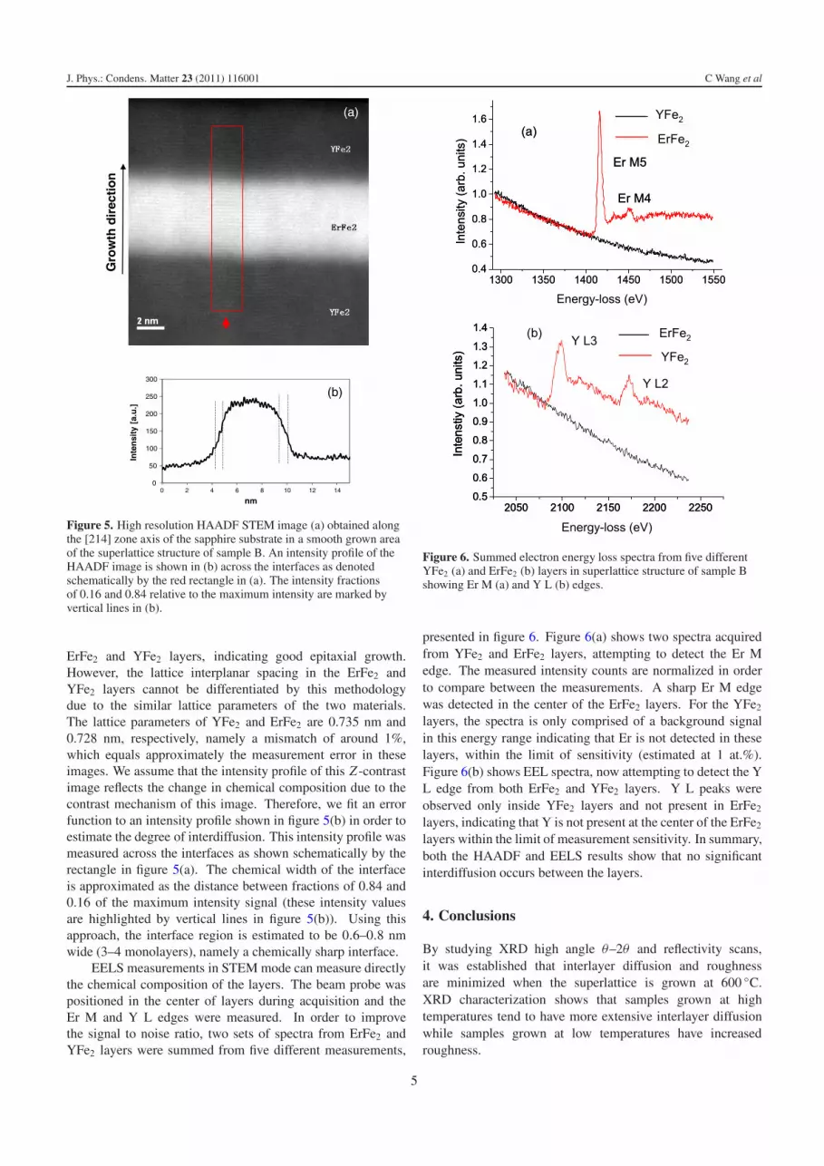
EELS measurements in STEM mode can measure directlythe chemical composition of the layers. The beam probe waspositioned in the center of layers during acquisition and theEr M and Y L edges were measured. In order to improvethe signal to noise ratio, two sets of spectra from ErFe2 andYFe2 layers were summed from five different measurements,
Figure 6. Summed electron energy loss spectra from five differentYFe2 (a) and ErFe2 (b) layers in superlattice structure of sample Bshowing Er M (a) and Y L (b) edges.
presented in figure 6. Figure 6(a) shows two spectra acquiredfrom YFe2 and ErFe2 layers, attempting to detect the Er Medge. The measured intensity counts are normalized in orderto compare between the measurements. A sharp Er M edgewas detected in the center of the ErFe2 layers. For the YFe2
layers, the spectra is only comprised of a background signalin this energy range indicating that Er is not detected in theselayers, within the limit of sensitivity (estimated at 1 at.%).Figure 6(b) shows EEL spectra, now attempting to detect the YL edge from both ErFe2 and YFe2 layers. Y L peaks wereobserved only inside YFe2 layers and not present in ErFe2
layers, indicating that Y is not present at the center of the ErFe2
layers within the limit of measurement sensitivity. In summary,both the HAADF and EELS results show that no significantinterdiffusion occurs between the layers.
4. Conclusions
By studying XRD high angle θ–2θ and reflectivity scans,it was established that interlayer diffusion and roughnessare minimized when the superlattice is grown at 600 ◦C.XRD characterization shows that samples grown at hightemperatures tend to have more extensive interlayer diffusionwhile samples grown at low temperatures have increasedroughness.
5

J. Phys.: Condens. Matter 23 (2011) 116001 C Wang et al
Structural characterization of the sample grown at 600 ◦Cwas undertaken by electron microscopy. STEM imagesshow that during the first five to seven layers, breakdownor diminished structures were found. The first layer wascompletely diffused, which is attributed to the initial highersubstrate temperature used to promote nucleation of the Lavesstructure. The STEM images show that after the initial3D growth interface, the islands grow laterally and becomeinterconnected, followed by smooth and continuous bilayers.The roughness in the first several bilayers is conformalagreeing with the conclusions of XRD analysis. Based on highresolution STEM images, chemical intermixing at the interfaceis estimated at ∼0.6–0.8 nm. We note again that the diameterof the electron probe is approximately 1 nm, indicating that theinterfaces are sharp. The chemical composition was measuredusing EELS, which did not detect diffusion to the center ofthe layers within the sensitivity limit. Based on these findings,we conclude that no significant diffusion occurs between thelayers of the sample. This conclusion does not agree with thework of Bentall et al [6], which revealed significant interlayerdiffusion in the thin layers of approximately 10% at the centerof the layer. These different conclusions could be due to theprevious XRD analysis [6] averaging the layer compositionover relatively large areas while the electron microscopymeasurements are spatially resolved at the nanometer scale.We stress that the locally sharp nature of the interfaces foundin this work explains why the experimental magnetizationmeasurements on Laves superlattices are consistent withcalculations based on idealized structures [9].
It is assumed in this work that the term ‘interdiffusion’refers in the present case to substitution of the rare earth(RE) elements in the Laves crystal structure. It is likely thatthe Fe atoms are also mobile, and could be involved in theRE diffusion process, but we cannot comment on the preciseatomic processes involved. The evidence shows that highergrowth temperatures tend to promote random occupancy of theRE sites, leading to a single XRD peak. The possibility ofdefects being introduced as a result of non-stoichiometry (dueto non-ideal flux control during MBE growth) has also to beconsidered. Providing the fluxes were maintained in the correctratio, off-stoichiometry in the interface regions would resultonly if the MBE shutter operations were not synchronizedexactly. Binary RE–Fe phase diagrams show that the Lavesphase can exist over a very small range of composition about1:2. If significant non-stoichiometry were present, inclusionsof secondary phases (RE metal and RFe3 respectively) would
form. We can say that these possible included phases are notdetected by XRD, nor the electron microscopy analysis.
This work presents localized chemical and structuralinformation on Laves superlattices for the first time, whichis helpful in guiding future MBE growth for engineering themagnetic properties of exchange spring superlattices. It isconcluded that any change in the magnetic reversal mechanismdue to interlayer diffusions should not be expected underoptimum growth conditions.
Acknowledgments
We are grateful to Keith Belcher for technical support andto the Engineering and Physical Sciences Research Council(EPSRC) for funding this research project. A K acknowledgesfinancial support of the UK Royal Academy of Engineering.S G W thanks the National Basic Research Program of Chinaunder Grant No. 2009CB929203 and the National NaturalScience Foundation of China under Grant No. 50972163 forfinancial support.
References
[1] Kneller E F and Hawig R 1991 IEEE Trans. Magn. 27 3588[2] Skomski R and Coey J M D 1993 Phys. Rev. B 48 15812[3] Fullerton E E, Jiang J S, Sowers C H, Pearson J E and
Bader S D 1998 Appl. Phys. Letts. 72 380[4] Suess D, Schrefl T, Dittrich R, Kirschner M, Dorfbauer F,
Hrkac G and Fidler J 2005 J. Magn. Magn. Mater. 290 551[5] Sawicki M, Bowden G J, de Groot P A J, Rainford B D,
Beaujour J-M L, Ward R C C and Wells M R 2000 Phys.Rev. B 62 5817
[6] Bentall M J, Ward R C C, Grier E J and Wells M R 2003J. Phys.: Condens. Matter 15 6493
[7] Fitzsimmons M R, Park S, Dumesnil D, Dufour C, Pynn R,Borchers J A, Rhyne J J and Mangin Ph 2006 Phys. Rev. B73 134413
[8] Bowden G J, Martin K N, Fox A, Rainford B D,Ward R C C and de Groot P A J 2008 J. Phys.: Condens.Matter 20 125223
[9] Bowden G J, Beaujour J-M L, Zhukov A A, Rainford B D,de Groot P A J, Ward R C C and Wells M R 2003 J. Appl.Phys. 93 6480
[10] Egerton R F 2007 Ultramicroscopy 107 575[11] Langridge S ISIS Rutherford Appleton Laboratory, UK[12] Mougin A, Dufour C, Maloufi N, Dumesnil K and
Mangin Ph 2001 Eur. Phys. J. B 19 289[13] McMorrow D F, Swaddling P P, Cowley R A, Ward R C C and
Wells M R 1996 J. Phys.: Condens. Matter 8 6553[14] Kirkland E J, Loane R F and Silcox J 1987 Ultramicroscopy
23 77
6


