Embed Size (px)
Citation preview

Springer Series in Solid-State Sciences 160
Introduction to Space Charge Effects in Semiconductors
Bearbeitet vonKarl W. Böer
1. Auflage 2012. Taschenbuch. xiii, 331 S. PaperbackISBN 978 3 642 26207 4
Format (B x L): 15,5 x 23,5 cmGewicht: 534 g
Weitere Fachgebiete > Physik, Astronomie > Elektrodynakmik, Optik > Halbleiter- undSupraleiterphysik
Zu Inhaltsverzeichnis
schnell und portofrei erhältlich bei
Die Online-Fachbuchhandlung beck-shop.de ist spezialisiert auf Fachbücher, insbesondere Recht, Steuern und Wirtschaft.Im Sortiment finden Sie alle Medien (Bücher, Zeitschriften, CDs, eBooks, etc.) aller Verlage. Ergänzt wird das Programmdurch Services wie Neuerscheinungsdienst oder Zusammenstellungen von Büchern zu Sonderpreisen. Der Shop führt mehr
als 8 Millionen Produkte.

1
Space Charges in Insulators
Summary. The space charges in insulators directly determine the built-in field andelectron energy distribution, as long as carrier transport can be neglected.
In this chapter we present a few arbitrarily introduced space-charge profilesand point out some of the basic resulting field and band edge distributionswith consequences to device applications.
1.1 Basic Electrostatic Relations
The basic electrostatic relations connect charges, forces, fields and potentialwith each other under static (as opposed to dynamic) conditions.
We start from the Coulomb relation describing the force between two fixedpoint charges, e1 and e2.
F = cue1e2r20
(1.1)
with r0 as the distance between the two charges. The units-related constantcu (in vacuo) is set, in the rational four-parameter system used in thisbook, to cu = 1/(4πε0) with the vacuum permittivity ε0 = 8.8543 ×10⁻¹⁴
(AsV−1cm−1 = Farad cm−1
). For e1 = e2 = e one obtains1
F =e2
4πε0r20=
{2.3× 10⁻¹⁶ dyn for r0 = 1 cm1 dyn for r0 � 1.5 A;
(1.2)
1 Since the force is measured in dyn = g cm s−2 (1 dyn is equivalent to the forceexerted by 1.0197 mg on its supporting surface), it is convenient to express themass in Ws3cm−2 with 1 Ws3cm−2= 10−7g.

2 1 Space Charges in Insulators
e is the elementary charge2(= 1.6022× 10⁻¹⁹As
). This force3 can be related
to an electric field, F , via4
F = eF ; (1.4)
hence one hasF =
e
4πε0r20(1.5)
as the (constant) field on the intersecting line between the two point chargesat distance r0 between these charges.
1.1.1 The Poisson Equation
When applying Gauss’ law, we can relate a region containing many chargedparticles (i.e., a space-charge region, neglecting the microscopic position ofeach individual particle), with � = ne, to the field on a closed surface (of anyshape) surrounding this space charge, and one obtains:
∮FdS =
∫�
ε0dV (1.6)
where V is the volume containing thespace charge ne with n the density ofcharged particles, and dS is an element of the enclosing surface. For a sphereof the radius r0 one can easily solve the closed surface integral
∮dS = 4πr20 ;
hence the field normal to such a sphere at its surface is
F =�V
4πε0r20= 1.44× 10⁻⁷ n (cm−3)
r20 (cm2)
( Vcm
)(1.7)
which, for a sphere of 1 cm radius results is a field5 of � 1.44×10⁻⁷n Vcm−1.The electric field is a vector that points from a positive to a negative
charge, i.e., it points inward, normal to the surface of this sphere when itscharge is negative. It decreases with increasing distance from the center ofthe sphere ∝ 1/r2. An electrostatic potential difference ψ1,2, which describes
2 The charge of an electron is (−e).3 It is interesting to recognize that the electrostatic force between two ions at a
distance of 1.5 A is ≈1 dyn, i.e., on an order of magnitude that is well within themeans of macroscopic sensors. This permits one to manipulate single atoms in anatomic force microscope.
4 The correct way to introduce the field–force relation is via a test charge in thelimit of zero charge:
F = lime→0
�F/e. (1.3)
5 It should be recognized that these fields are exceedingly large for uncompensatedcharges. For instance, when charging a sphere of 1 cm radius with only 1013 cm−3
electrons, one approaches already breakdown fields of the best insulators (a fewtimes 106 Vcm−1).

1.1 Basic Electrostatic Relations 3
the work required to move a positive test charge in this electric field from aposition r1 to r2 is defined as
ψ1,2 = −∫ r2
r1
Fdr. (1.8)
Since this work is defined to be negative when a positive test charge moves indirection of the field, 1.8 requires the (−) sign for r2 > r1.
When an electron is moved from r2 = ∞ to r1, one obtains the absoluteelectrostatic electron potential, which for the above given example is
ψn = −∫ ∞
r1
�V4πε0r2
dr = +�V
4πε0r1, (1.9)
or, for a sphere of 1 cm radius, is ψ � 0.1 μV for every excess electron on thesphere.
In general one has∮
FdS =∫
div FdV =∫
�
ε0dV , (1.10)
or,div F =
�
ε0, (1.11)
which is referred to as the Poisson equation. The relation between electricfield and electrostatic potential can be written in general form as
F = −gradψ = −∇ψ; (1.12)
hence, Poisson’s equation is often also given as
div gradψ = ∇2ψ = − �
ε0. (1.13)
This equation holds when the distance r to a probing charge is sufficientlylarge compared to the distance between individual charges of the space-chargeensemble, so that a homogeneous, smeared-out collective of charges acts onthe probing charge. The granular texture of the space charge can then beneglected.6
6 Modern devices become progressively smaller and represent typically a volumeon the order of 10−4 cm in diameter. With a carrier density of 1016 cm−3 theycontain a total of only 104 carriers in the bulk. In addition, the actual space-chargeregion has only a typical thickness of 10−5 cm and therefore contains less than1,000 charged defects with an average distance between these charges of 1/30 ofthe device dimension. Statistical fluctuations (∝ √
N/N) then become large. Forsmaller device dimensions, or lower space-charge densities, the granular textureof the charges can no longer be neglected. Here the continuum model is expectedto approach its limits, and must be replaced by an atomistic picture, the carriertransport by a ballistic rather then diffuse transport.

4 1 Space Charges in Insulators
In a semiconductor or insulator the force between two charges is reducedbecause of the shielding influence of the atoms between these charges. Such ashielding is described by the dielectric constant ε (more precisely by the staticdielectric constant εst here):
F =e2
4πεε0r2; (1.14)
hence, the relation between field and space charge within a semiconductor isgiven by
div F =�
εε0, (1.15)
and between electrostatic potential and space charge by
∇2ψ = − �
εε0. (1.16)
In the following chapters we will only use one relevant space coordinatebetween these charges. The relationship between space charge and field is thengiven by the one-dimensional Poisson equation
dFdx
=�
εε0. (1.17)
Such a field distribution determines the electrostatic potential distributionfor electrons via
dψ(x)dx
= − [F (x)− F (x = 0)] = −∫ x
0
�(ξ)εε0
dξ, (1.18)
with
ψ(x) =∫ x
d1
F (ξ)dξ. (1.19)
and for ξ = d1, the corresponding ψ(d1) serves as reference point for theelectrostatic potential.
In summary, we have shown that space-charge regions result in field inho-mogeneities. The importance of such field inhomogeneities lies in their abilityto influence the current through a semiconductor. With the ability to changespace charges by changing a bias, as we will see later, they provide the basisfor designing semiconducting devices.
Since a wide variety of space-charge distributions are found in semicon-ductors, many of which are of technical interest, we will first enumerate someof the basic types of these distributions and start with a catalogue of the in-terrelationships of various given �(x), resulting in corresponding distributionsof electric field F (x) and electrostatic potential ψ(x).

1.2 Fixed Space-Charge Distributions 5
Because of the common practice to plot the distribution of the band edgesfor devices, we will follow this habit throughout the following sections. Theband edge follows the electron potential ψn(x) and this relates to the electro-static potential as
Ec(x) = eψn(x) + c = −eψ(x) + const. (1.20)
1.2 Fixed Space-Charge Distributions
In the examples given in this section, the space-charge profiles are arbitrar-ily introduced as fixed, explicit functions of the independent coordinate (x).The space charge can be kept constant in an insulator that does not containfree carriers. Here all charges are assumed to be trapped in now charged latticedefects.
1.2.1 Sinusoidal Continuous Space-Charge Distribution
A simple sinusoidal space-charge double layer can be described by
�(x) =
{ea sin [2πx/d] for − d/2 ≤ x ≤ d/20 elsewhere
(1.21)
with d = d1 +d2 the width of the space charge layer; d1 and d2 are the widthsof the negative and positive regions of the space charge double layer (here,d1 = d2). The space charge profile is shown in Fig. 1.1a.
The corresponding field distribution is obtained by integration of (1.21),and assuming F (x = ±∞) = 0 as boundary conditions:
F (x) =
{−(ead) cos[2πx/d] for − d/2 ≤ x ≤ d/20 elsewhere;
(1.22)
it is shown in Fig. 1.1b, and presents a negative field with a symmetricalpeak; its maximum value lies at the position where the space charge changesits sign. The maximum field increases with increasing space-charge density eaand width d.
The corresponding electron energy (band edge) distribution is obtained bya second integration of 1.21, yielding with an assumed Ec(∞) = 0 as boundarycondition:
Ec(x) =
⎧⎪⎨
⎪⎩
e2ad2/(4εε0) for x < −d/2−e2ad2 sin [2πx/d] /(4εε0) for − d/2 ≤ x ≤ d/20 for x > d/2,
(1.23)
that is, a band edge step down of height ead2/(4εε0), as shown in Fig. 1.1c.

6 1 Space Charges in Insulators
Fig. 1.1. Sinusoidal space charge, and resulting electric field and electron energydistributions. Computed for a maximum charge density, a = 1016 cm−3, a widthd = 3 · 10−5 cm, and for a relative dielectric constant, ε = 10
Such behavior is typical: a space-charge double layer produces a fieldspike and a band edge step. For a (−+) sequence of the space charge withincreasing x (from left to right), the step is downward and the field spike isnegative. The reversed space charge sequence (+−) produces a positive fieldspike and a band edge step upward as shown in Fig. 1.2.
1.2.2 Abruptly Changing Space-Charge Distribution
All distributions of F and ψ are smooth when caused by the integration ofa smooth space-charge distribution. As will be shown in Sect. 2.1, however,the charge distributions change abruptly from one sign to the other in manysolids. A sinusoidal distribution with an abrupt change at x = 0 is thereforepresented as an example in Fig. 1.3, curve set a:
� =
⎧⎪⎪⎪⎨
⎪⎪⎪⎩
0 for x < −d/2−ea cos
(2πx
d
)for − d/2 ≤ x <0
ea cos(
2πxd
)for 0 ≤ x <d/2
0 for d/2 ≤ bx.
(1.24)
As a result, the field distribution is now given by a triangle and has asharp peak (i.e., an abrupt change in slope) at x = 0 with equal values of

1.2 Fixed Space-Charge Distributions 7
Fig. 1.2. Field extrema and band edge step signs depending on space-charge doublelayer sequence (computed as in Fig. 1.1)
the slope on either side. However, the potential distribution is still a smoothdistribution and its shape is rather similar to the one produced by a smoothrather than abrupt change of the space charge.
Another often observed form of the space-charge distribution can be ap-proximated by two step-functions:
� =
⎧⎪⎪⎨
⎪⎪⎩
0 for x < −d/2−ea for −d/2 ≤ x < 0ea for 0 ≤ x < d/20 for d/2 ≤ x.
(1.25)
We assume again d1 = d2 for a symmetrical distribution, as shown in Fig. 1.3a,curve b. Here the value of the field increases linearly in the range of constantspace-charge according to
F (x) = Fc − ea
εεox for− d/2 ≤ x < 0 (1.26)
F (x) = Fc +ea
εεox for 0 ≤ x < d/2 (1.27)
with the maximum value of the field Fc given by
Fc = −ead1
εεo, (1.28)
8 1 Space Charges in Insulators
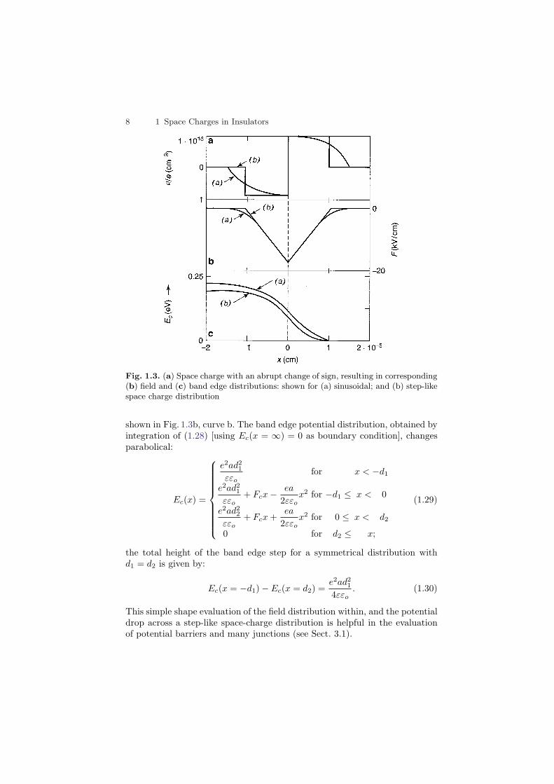
Fig. 1.3. (a) Space charge with an abrupt change of sign, resulting in corresponding(b) field and (c) band edge distributions: shown for (a) sinusoidal; and (b) step-likespace charge distribution
shown in Fig. 1.3b, curve b. The band edge potential distribution, obtained byintegration of (1.28) [using Ec(x = ∞) = 0 as boundary condition], changesparabolical:
Ec(x) =
⎧⎪⎪⎪⎪⎪⎪⎪⎪⎨
⎪⎪⎪⎪⎪⎪⎪⎪⎩
e2ad21
εεofor x < −d1
e2ad21
εεo+ Fcx− ea
2εεox2 for −d1 ≤ x < 0
e2ad22
εεo+ Fcx+
ea
2εεox2 for 0 ≤ x < d2
0 for d2 ≤ x;
(1.29)
the total height of the band edge step for a symmetrical distribution withd1 = d2 is given by:
Ec(x = −d1)− Ec(x = d2) =e2ad2
1
4εεo. (1.30)
This simple shape evaluation of the field distribution within, and the potentialdrop across a step-like space-charge distribution is helpful in the evaluationof potential barriers and many junctions (see Sect. 3.1).

1.2 Fixed Space-Charge Distributions 9
From (1.30) it is evident that a large potential drop (supporting a largeapplied voltage) can be obtained by either a large space-charge density ea ora wide space-charge width d. However, both quantities also cause a similarincrease in the maximum field Fc (1.28), which may become too large andconsequently could lead to an electrical breakdown of the device. An increaseof the potential step without the increase in Fc can be obtained by inserting aneutral layer between the two space-charge regions, as will be discussed below.
1.2.3 Space-Charge Double Layer with Neutral Interlayer
Under certain conditions (e.g., via appropriate doping profiles or through fieldquenching, described in Sect. 3.3), the two space-charge regions can be sepa-rated by an extended range of vanishing space charges (see Fig. 1.4a). In thischarge-neutral region the field remains constant (Fig. 1.4b), and the band edgestep increases linearly (Fig. 1.4c). Large potential drops can be achieved bysimply increasing the distance (x2−x1) between the two space-charge regions,
E(2)c − E(1)
c = Fc
[x2 − x1
2+d1
2+d2
2
], (1.31)
Fig. 1.4. (a) Step-like space-charge double layer with a neutral interlayer, resulting(b) a field distribution with constant center region and (c) a band edge change witha linear range in the middle distributions
10 1 Space Charges in Insulators
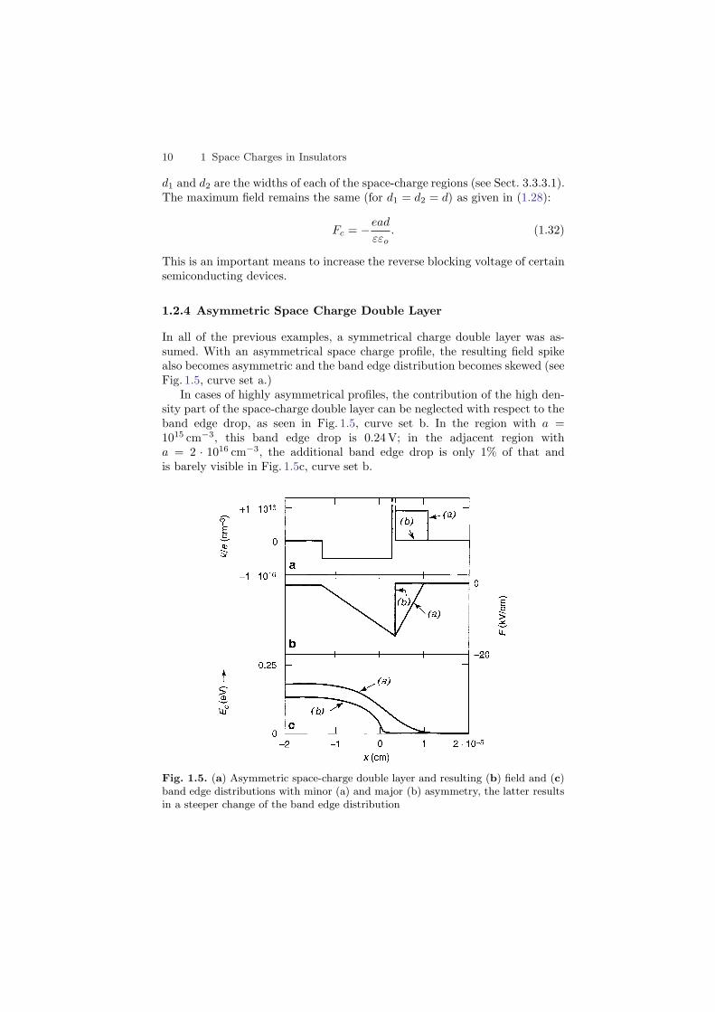
d1 and d2 are the widths of each of the space-charge regions (see Sect. 3.3.3.1).The maximum field remains the same (for d1 = d2 = d) as given in (1.28):
Fc = −eadεεo
. (1.32)
This is an important means to increase the reverse blocking voltage of certainsemiconducting devices.
1.2.4 Asymmetric Space Charge Double Layer
In all of the previous examples, a symmetrical charge double layer was as-sumed. With an asymmetrical space charge profile, the resulting field spikealso becomes asymmetric and the band edge distribution becomes skewed (seeFig. 1.5, curve set a.)
In cases of highly asymmetrical profiles, the contribution of the high den-sity part of the space-charge double layer can be neglected with respect to theband edge drop, as seen in Fig. 1.5, curve set b. In the region with a =1015 cm−3, this band edge drop is 0.24 V; in the adjacent region witha = 2 · 1016 cm−3, the additional band edge drop is only 1% of that andis barely visible in Fig. 1.5c, curve set b.
Fig. 1.5. (a) Asymmetric space-charge double layer and resulting (b) field and (c)band edge distributions with minor (a) and major (b) asymmetry, the latter resultsin a steeper change of the band edge distribution

1.2 Fixed Space-Charge Distributions 11
In actual semiconductor junctions the doping of p- and n-type parts of thejunction is usually asymmetric and the resulting space charge profile is simi-lar to such highly asymmetrical double layers. The results shown in Fig. 1.5,curve set b, with resulting field and band edge distributions in the low chargedensity region only, are often used as a reasonable approximation to describeasymmetrical junctions.
1.2.5 Single Space-Charge Layer
In all previous examples we have assumed total charge neutrality within thegiven solid, i.e., ∫ l2
−l1
�(x) dx = 0,
with l1 and l2 as the distance form the space-charge interface to the left or rightsemiconductor boundary (e.g., to its electrodes). If this neutrality conditionis not fulfilled within one solid (e.g., some of the compensating charges ofa semiconductor are located on the surface of the adjacent metal electrode),then the effective (net) space charge can be represented by a single layer withinthe bulk of the semiconductor.
Such a single space charge layer (Fig. 1.6a) causes a field-ramp as shownin Fig. 1.6b. Depending on the distance of this layer from the metal electrode
Fig. 1.6. (a) Single space-charge layer in the bulk with corresponding surface chargeon the left electrode and resulting in a (b) field ramp and a (c) linear band edgeslope in the field ramp region

12 1 Space Charges in Insulators
where the compensating charges7 are located, the band edge drop increasesin a manner similar to the example of an ordinary double layer with chargeseparations (1.31). In other words, the band edge increases parabolical (tothe left) in the region of the field-ramp and then linearly in the adjacentspace charge-free region toward the (left) electrode as shown in Fig. 1.6c. Thefield collapses at the surface of the left electrode due to the fact that it is asurface charge rather than a distributed space charge which would result in amore gradual decrease of F (x). This collapse is indicated by the dashed linein Fig. 1.6b.
For reasons of maintaining a constant field in the homogeneous part ofan actual semiconductor, a corresponding space charge separation with netcharges sitting on both electrodes, is always present for nonvanishing netcurrents (see Sect. 2.1.1).
1.2.6 Space-Charge Double Layer, Nonvanishing Net Charge
We now extend the previous example to a nonsymmetrical double layer witha remaining net charge. The net charge is compensated by surface charges onthe two electrodes. We assume that these surface charges are different in thetwo electrodes, resulting in a field distribution as shown in Fig. 1.7.
Fig. 1.7. (a) Asymmetrical space-charge double layer with asymmetric compensa-tion on the two electrode surfaces and corresponding (b) field distribution showingthe constant field range near the right electrode and (c) the band edge distributionwith the linear range again corresponding to the constant field range distributions
7 It is assumed that such charges are at the surface of the left electrode in thisexample and indicated by the “−” sign in Fig. 1.6a.

Exercise Problems 13
Such a space-charge distribution is quite common for asymmetricaljunctions with different conductivities in the adjacent bulk regions, hencecausing different, but constant, fields in these regions when a bias voltage isapplied. The major band edge drop usually occurs within the space-chargedouble layer, and the band edge drop8 in the adjacent bulk regions is consid-ered a series-resistance perturbation.
Summary and Emphasis
Eight arbitrarily introduced space charge profiles are discussed as idealizedexamples to demonstrate the typical behavior that can be observed in varioustypes of semiconductor devices. Though somewhat modified through the influ-ence of mobile carriers, the principal trend remains the same and determinesa number of device properties.
For instance, the field distribution in space charge double layers has usuallya triangular shape with its maximum value at the double layer interface. Theband edge shows a step.
If a diode is to be used at high bias conditions, a neutral interlayer betweenthe positive and negative space-charge layers is necessary to achieve a sufficientvoltage drop without running into breakdown fields.
Highly asymmetrical field and band edge distributions are common inasymmetrically doped pn-junctions. The potential drop in the highly doped(high space charge) region is usually negligible.
Series resistance effects, though undesired, are often a by-product of yetun-optimized solar cells or in some high-speed devices, e.g., in the base ofbipolar transistors.
A clear understanding of the interrelation between space-charge distribu-tion, the resulting field, and electron potential, corresponding to the bandedge distribution assists in the task of designing devices with improvedcharacteristics.
Exercise Problems
1.(e) Design an Si-diode with an n-type region, doped with 1016 cm−3 donorsand a p-type region with 1017 cm−3 acceptors with an appropriate in-terlayer in which the field cannot exceed 105 V cm−1 and which cansupport a reverse bias of 103 V. Assume an ideal step-like space charge.(a) How wide are the space charge layers in the n-type and p-type
regions?(b) How large are the voltage drops in both space charge regions?
8 Here enlarged for better clarity.
14 1 Space Charges in Insulators
(c) How thick must the neutral layer be?(d) How large is the voltage drop in the interlayer?
2.(r) List a number of semiconductor devices and classify them according tothe examples given in this chapter. Explain the idealization in respectto the actual device.
3.(e) Relate the electrostatic potential distribution, electrostatic electronpotential distribution, and band edge distribution for a given homo-junction; identify an external bias (applied voltage). Watch for propersign, and energy vs. potential denotation.
4. Design an idealized space-charge distribution of your own that repre-sents a typical semiconductor device. Insert typical space charge den-sity values and layer thickness. Give field distribution and voltage dropquantitatively.
5. Derive the equivalence of the mass in units of Ws3cm−2.

http://www.springer.com/978-3-642-02235-7