Embed Size (px)
Citation preview
ITG-3050 EV Board User Guide
Document Number: AN-ITG-3050EVB-00 Revision: 1.0 Release Date: 07/25/2011
InvenSense, Inc., 1197 Borregas Ave., Sunnyvale, Ca 94089, USA 1 AN-ITG-3050EVB-00
Tel: +1 (408) 988-7339 Fax: +1 (408) 988-8104 ©2011 InvenSense, Inc. All rights reserved.
Website: http//www.invensense.com
ITG-3050 3-Axis Evaluation Board User Guide
Revision 1.0

ITG-3050 EV Board User Guide
Document Number: AN-ITG-3050EVB-00 Revision: 1.0 Release Date: 07/25/2011
InvenSense, Inc., 1197 Borregas Ave., Sunnyvale, Ca 94089, USA 2 AN-ITG-3050EVB-00
Tel: +1 (408) 988-7339 Fax: +1 (408) 988-8104 ©2011 InvenSense, Inc. All rights reserved.
Website: http//www.invensense.com
CONTENTS
1. REVISION HISTORY ................................................................................................................................... 3
2. PURPOSE ................................................................................................................................................... 4
1. USAGE ························································································································· 4
2. RELATED DOCUMENTS ······································································································ 4
3. ITG-3050 3-AXIS EV BOARD OVERVIEW ................................................................................................ 5
3. ITG-3050 KEY FUNCTION AND PIN-OUTS ················································································ 6
4. ITG-3050 BUS CONNECTION ······························································································ 7
4. ITG-3050 3-AXIS EVB SCHEMATICS ........................................................................................................ 7
5. BILL OF MATERIALS ·········································································································· 8
6. POWER SUPPLY CONNECTIONS ··························································································· 8
7. ITG-3050 EVB CONNECTOR SIGNALS DESCRIPTION ··································································· 9
8. CONNECTING THE FSYNC LINE ·························································································· 10
9. SERIAL BUS LEVELS, SPEEDS AND TERMINATIONS ···································································· 11
5. DATA GATHERING OPTIONS ................................................................................................................. 11
10. CONNECTION TO ARM EVB ······························································································ 11
11. USE OF ITG-3050 WITHOUT ARM EVB BOARD ······································································· 11
6. SPECIAL INSTRUCTIONS ....................................................................................................................... 12
6.1 ELECTROSTATIC DISCHARGE SENSITIVITY ·············································································· 12
7. DIMENSION DRAWING ............................................................................................................................ 12

ITG-3050 EV Board User Guide
Document Number: AN-ITG-3050EVB-00 Revision: 1.0 Release Date: 07/25/2011
InvenSense, Inc., 1197 Borregas Ave., Sunnyvale, Ca 94089, USA 3 AN-ITG-3050EVB-00
Tel: +1 (408) 988-7339 Fax: +1 (408) 988-8104 ©2011 InvenSense, Inc. All rights reserved.
Website: http//www.invensense.com
1. Revision History
Date Revision Description
07/25/2011 1.0 Initial release

ITG-3050 EV Board User Guide
Document Number: AN-ITG-3050EVB-00 Revision: 1.0 Release Date: 07/25/2011
InvenSense, Inc., 1197 Borregas Ave., Sunnyvale, Ca 94089, USA 4 AN-ITG-3050EVB-00
Tel: +1 (408) 988-7339 Fax: +1 (408) 988-8104 ©2011 InvenSense, Inc. All rights reserved.
Website: http//www.invensense.com
2. Purpose
This document describes the hardware and circuitry on the ITG-3050™ 3-Axis Evaluation (EV) Board. It covers applying the EV board to a larger system, understanding key signals and circuit functions, hardware jumper settings, and port connectors.
1. Usage
This evaluation board provides three axes of motion sensing, comprised of:
X-, Y- and Z-Axis gyros with ±250°/sec, ±500°/sec, ±1000°/sec, ±2000°/sec selectable full-scale range.
Digital data measured using on-chip ADCs, is transmitted over an I²C interface. The Evaluation board may be used by itself using an I²C serial communications interface. Alternatively, it may be connected to InvenSense‟s ARM Evaluation Board (INVARMEVB) for connectivity to a host computer using USB interface.
2. Related Documents
The following documents are recommended for additional information regarding the products and systems described in this Application Note.
ITG-3050 Product Specification
ITG-3050 Register Map and Register Descriptions

ITG-3050 EV Board User Guide
Document Number: AN-ITG-3050EVB-00 Revision: 1.0 Release Date: 07/25/2011
InvenSense, Inc., 1197 Borregas Ave., Sunnyvale, Ca 94089, USA 5 AN-ITG-3050EVB-00
Tel: +1 (408) 988-7339 Fax: +1 (408) 988-8104 ©2011 InvenSense, Inc. All rights reserved.
Website: http//www.invensense.com
3. ITG-3050 3-Axis EV Board Overview
The ITG-3050 3-Axis EV Board contains the ITG-3050 Digital Motion Processing Unit. It contains a number of „solder-across‟ jumper points that permit several circuit configurations.
Refer to Figure 1. The EV Board is populated on its top side only for easy of measurement access. The 10x2 customer header connector is designed to connect with the InvenSense ARM Evaluation Board (INVARMEVB), which is a host microcontroller board useful for adapting the ITG-3050 3-Axis EV Board to a personal computer via its USB port.
Figure 1. Top side of the ITG-3050 3-Axis EV Board
The 5x2 extension factory header is intended for connecting additional devices to the EV Board, such as a camera image stabilization processor, or a digital-output compass, etc. The 3-pin power selection headers are used to select which voltage supply is fed to the ITG-3050.
Power Selection ITG-3050
Factory Header
User Header

ITG-3050 EV Board User Guide
Document Number: AN-ITG-3050EVB-00 Revision: 1.0 Release Date: 07/25/2011
InvenSense, Inc., 1197 Borregas Ave., Sunnyvale, Ca 94089, USA 6 AN-ITG-3050EVB-00
Tel: +1 (408) 988-7339 Fax: +1 (408) 988-8104 ©2011 InvenSense, Inc. All rights reserved.
Website: http//www.invensense.com
3. ITG-3050 Key Function and Pin-outs
The ITG-3050 EVB is a fully-tested evaluation board, providing for quick evaluation of the ITG-3050‟s X- , Y- , and Z-axis angular rate gyroscope. The ITG-3050 uses InvenSense‟s proprietary MEMS technology with vertically driven vibrating masses to produce a functionally complete, low-cost motion sensor. All required conditioning electronics are integrated into a single chip measuring 4 x 4 x 0.9mm. It incorporates X- , Y- and Z-axis low-pass filters and an EEPROM for on-chip factory calibration of the sensor. Factory trimmed scale factors eliminate the need for external active components and end-user calibration. A built-in Proportional-To-Absolute-Temperature (PTAT) sensor provides temperature compensation information. The product is lead-free and Green Compliant.
7 8 9 10 11 12
AU
X_
CL
VL
OG
IC
AD
0
RE
GO
UT
FS
YN
C
INT
13
18
17
16
15
14
NC
NC
NC
VDD
NC
GND
6
1
2
3
4
5
NC
NC
NC
AUX_DA
NC
CLKIN
24 23 22 21 20 19
RE
SV
CP
OU
T
RE
SV
CL
KO
UT
SC
L
SD
AITG-3050
Figure 2. ITG-3050 QFN Package (Top View) 24-pin 4mm x 4mm x 0.9mm
ITG-3050
+Z
+X
+Y
Figure 3. Orientation of Axes of Sensitivity and Polarity of Rotation
ITG-3050 EV Board User Guide
Document Number: AN-ITG-3050EVB-00 Revision: 1.0 Release Date: 07/25/2011
InvenSense, Inc., 1197 Borregas Ave., Sunnyvale, Ca 94089, USA 7 AN-ITG-3050EVB-00
Tel: +1 (408) 988-7339 Fax: +1 (408) 988-8104 ©2011 InvenSense, Inc. All rights reserved.
Website: http//www.invensense.com
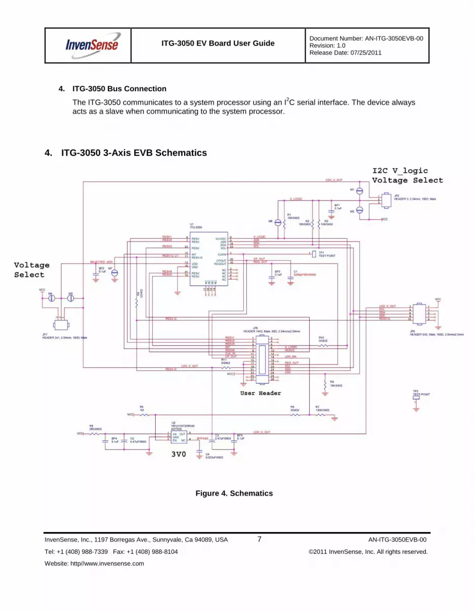
4. ITG-3050 Bus Connection
The ITG-3050 communicates to a system processor using an I2C serial interface. The device always
acts as a slave when communicating to the system processor.
4. ITG-3050 3-Axis EVB Schematics
Figure 4. Schematics

ITG-3050 EV Board User Guide
Document Number: AN-ITG-3050EVB-00 Revision: 1.0 Release Date: 07/25/2011
InvenSense, Inc., 1197 Borregas, Ave. Sunnyvale, CA 94089, USA 8 AN-ITG-3050EVB-00
Tel: +1 (408) 988-7339 Fax: +1 (408) 988-8104 ©2011 InvenSense, Inc. All rights reserved.
Website: http//www.invensense.com
5. Bill of Materials
Table 1. Bill of Materials
Item Quantity Reference Part PCB Footprint
1 5 BP1,BP2,BP3,BP4,BP5 0.1uF C0402
2 1 C1 2200pF/50V C0402
3 2 C2,C3 0.47uF/0603 C0603
4 1 C4 0.033uF C0402
6 4 JP1,JP3,JP4,JP5 Solder JP2P1_8X1_3S
7 2 JP2,JP7 HEADER 3, 80mil, 180D, Male J79\3S
8 1 JP6 HEADER 5X2, Male, 180D, 2.0mmx2.0mm SIP2X5N2
9 1 JP8 HEADER 14X2, Male, 90D, 2.54mmx2.54mm HDB2X14NRA
11 2 R4,R1 100K R0402
12 2 R3,R2 10K R0402
13 1 R5 1M R0402
14 1 R8 2R2/0603 R0603
17 1 U1 ITG-3050, 24-Lead QFN (4mm x 4mm x 0.9mm) QFN5_5S24P0_5T
18 1 U2 YB1210ST25R300 SOT235
6. Power Supply Connections
JP2 and JP7 are 3 header-pin plug-in jumpers which allow users to select between on-board LDO and external DC supply to the ITG-3050. For details, please refer Table 2. Power Selection Jumpers.
The on-board 3.0V LDO (Low-dropout voltage regulator) is a low-noise version with stable enable-disable profile. Its output is called 3V0 on the schematic, and using it will assure that the gyroscope and accelerometer performance will meet intended specifications.
Selecting the raw Vcc line to power the chip is generally done while designing and evaluating an embedded platform, where the host processor and related electronics needs full control over the motion processing chipset‟s power supply.
When user intends to use on board LDO 3V0 power, external Vcc must be provided with higher than 3.7V to ensure that the LDO works properly.
If user provides Vcc with 5V, JP2 and JP7 must be set as “1-2 short”. ITG-3050 VDD and VLOGIC operation range is 2.1V to 3.6V.

ITG-3050 EV Board User Guide
Document Number: AN-ITG-3050EVB-00 Revision: 1.0 Release Date: 07/25/2011
InvenSense, Inc., 1197 Borregas Ave., Sunnyvale, Ca 94089, USA 9 AN-ITG-3050EVB-00
Tel: +1 (408) 988-7339 Fax: +1 (408) 988-8104 ©2011 InvenSense, Inc. All rights reserved.
Website: http//www.invensense.com
7. ITG-3050 EVB connector signals description
Table 2. Power Selection Jumpers
JP2 Pin Number Signal description
1-2 short VLOGIC = 3V
2-3 short VLOGIC = Vcc (from external)
JP7 Pin Number Signal description
1-2 short VDD = 3V
2-3 short VDD = Vcc (from external)
Table 3. User Interface Connector Signals
JP8 Pin Number Signal description
1 Reserved
3 Reserved
5 Reserved
7 INT, INT output to controller
9 Reserved
11 CLK_I
13 CPOUT
15 GND
17 GND
19 3V
21 FSYNC
23 Receive power from ARM-7 Controller Board or external. It should be 5V,
with >200mA
25 NC
27 NC
2 NC
4 NC
6 NC
8 VLOGIC
10 Reserved
12 NC

ITG-3050 EV Board User Guide
Document Number: AN-ITG-3050EVB-00 Revision: 1.0 Release Date: 07/25/2011
InvenSense, Inc., 1197 Borregas Ave., Sunnyvale, Ca 94089, USA 10 AN-ITG-3050EVB-00
Tel: +1 (408) 988-7339 Fax: +1 (408) 988-8104 ©2011 InvenSense, Inc. All rights reserved.
Website: http//www.invensense.com
JP8 Pin Number Signal description
14 EVB on board LDO enable
16 NC
18 REGOUT
20 I²C SCL
22 I²C SDA
24 I²C Addr
26 NC
28 NC
Table 4. Extended Factory Connector
JP6 Pin Number Signal description
1 VCC, power from ARM-7 controller board or external power. It should be
5V, with >200mA
3 GND
5 NC
7 NC
9 NC
2 3V
4 I²C SCL
6 I²C SDA
8 I²C Addr
10 FSYNC
8. Connecting the FSYNC Line
The FSYNC line is intended for use in a camera‟s image-stabilization system. It is an input from the camera platform to the EV Board, and is intended to synchronize the ITG-3050‟s serial bus transfer with the master timing set by the camera system. FSYNC can originate from the host processor via JP8 pin-21, or from JP6 pin-10. There is no external pull-up termination for the FSYNC line.

ITG-3050 EV Board User Guide
Document Number: AN-ITG-3050EVB-00 Revision: 1.0 Release Date: 07/25/2011
InvenSense, Inc., 1197 Borregas Ave., Sunnyvale, Ca 94089, USA 11 AN-ITG-3050EVB-00
Tel: +1 (408) 988-7339 Fax: +1 (408) 988-8104 ©2011 InvenSense, Inc. All rights reserved.
Website: http//www.invensense.com
9. Serial bus Levels, Speeds and Terminations
The ITG-3050 supports I²C up to 400kHz serial clock rate. The I²C bus open drain pull up resisters are connected to either 3.0V or external provided Vcc (3V or 5V depend on user). The pull up level is selected by JP2. Please refer to Table 2. Power Selection Jumpers.
5. Data Gathering Options
The ITG-3050‟s Digital Sensor Data is available at the User Header. Alternatively, for connectivity with a host PC, an InvenSense ARM Processor Board may be used.
10. Connection to ARM EVB
For communications via USB to a host computer, the ITG-3050 EVB can be connected to InvenSense‟s ARM processor board, the INV-ARMEVB.
The photo below shows the connection of ITG-3050 to INV-ARMEVB. Connection between the two boards is made via the user header.
Figure 5. Connect ITG-3050 EVB to ARM Board
11. Use of ITG-3050 without ARM EVB board
I²C signals are available on JP8 and JP6. User can develop tools to communicate with the ITG-3050. There is no bus mode selection setting needed.

ITG-3050 EV Board User Guide
Document Number: AN-ITG-3050EVB-00 Revision: 1.0 Release Date: 07/25/2011
InvenSense, Inc., 1197 Borregas Ave., Sunnyvale, Ca 94089, USA 12 AN-ITG-3050EVB-00
Tel: +1 (408) 988-7339 Fax: +1 (408) 988-8104 ©2011 InvenSense, Inc. All rights reserved.
Website: http//www.invensense.com
6. Special Instructions
6.1 Electrostatic Discharge Sensitivity
The ITG-3050 gyro can be permanently damaged by an electrostatic discharge. ESD precautions for handling and storage are recommended.
7. Dimension Drawing
The ITG-3050 EV board is a 4 layer PCB with 32mm x 38mm dimension.
Figure 6. ITG-3050 EVB Dimensions

ITG-3050 EV Board User Guide
Document Number: AN-ITG-3050EVB-00 Revision: 1.0 Release Date: 07/25/2011
InvenSense, Inc., 1197 Borregas Ave., Sunnyvale, Ca 94089, USA 13 AN-ITG-3050EVB-00
Tel: +1 (408) 988-7339 Fax: +1 (408) 988-8104 ©2011 InvenSense, Inc. All rights reserved.
Website: http//www.invensense.com
This information furnished by InvenSense is believed to be accurate and reliable. However, no responsibility is assumed by InvenSense for its use, or for any infringements of patents or other rights of third parties that may result from its use. Specifications are subject to change without notice. InvenSense reserves the right to make changes to this product, including its circuits and software, in order to improve its design and/or performance, without prior notice. InvenSense makes no warranties, neither expressed nor implied, regarding the information and specifications contained in this document. InvenSense assumes no responsibility for any claims or damages arising from information contained in this document, or from the use of products and services detailed therein. This includes, but is not limited to, claims or damages based on the infringement of patents, copyrights, mask work and/or other intellectual property rights.
Certain intellectual property owned by InvenSense and described in this document is patent protected. No license is granted by implication or otherwise under any patent or patent rights of InvenSense. This publication supersedes and replaces all information previously supplied. Trademarks that are registered trademarks are the property of their respective companies. InvenSense sensors should not be used or sold in the development, storage, production or utilization of any conventional or mass-destructive weapons or for any other weapons or life threatening applications, as well as in any other life critical applications such as medical equipment, transportation, aerospace and nuclear instruments, undersea equipment, power plant equipment, disaster prevention and crime prevention equipment.
InvenSense® is a registered trademark of InvenSense, Inc. ITG-3050™ is a trademarks of InvenSense, Inc.
©2011 InvenSense, Inc. All rights reserved.


![NURSING BOARD[655]](https://img.pdfslide.net/doc/110x75/63189d221e5d335f8d0ad250/nursing-board655.jpg)


