Embed Size (px)
Citation preview
PROJECT REPORT ON
“DESIGN AND ANALYSIS OF FINFET AND ITS COMPARATIVE STUDY
WITH CMOS”
VLSI DOMAIN
Submitted in partial fulfilment of the requirements for the award of degree of
BACHELOR OF ENGINEERING
IN
ELECTRONICS AND COMMUNICATION ENGINEERING
VISVESVARAYA TECHNOLOGICAL UNIVERSITY, BELGAUM
SUBMITTED BY:
DEEPIKA N 1BM10EC028
KIRAN SINGH R 1BM10EC053
MOHAMMED MUDDASSER 1BM10EC062
MOHAMMED MUZAMMIL ULLA KHAN 1BM10EC063
Under the Guidance of,
KIRAN BAILEY
Assistant Professor
Department of Electronics and Communication Engineering
B.M.S COLLEGE OF ENGINEERING
(Autonomous College Affiliated to Visvesvaraya Technological University, Belgaum)
Bull Temple Road, Basavanagudi, Bangalore-560019

B.M.S COLLEGE OF ENGINEERING
(Autonomous College under VTU)
Department of Electronics and Communication Engineering
CERTIFICATE
This is to certify that the project entitled “Design and analysis of FINFET and
its comparative study with CMOS” is a bonafide work carried out by
Deepika N (USN:1BM10EC028), Kiran Singh R (USN:1BM10EC053),
Mohammed Muddasser (USN:1BM10EC062) and Mohammed
Muzammilulla Khan (USN: 1BM10EC063) in partial fulfillment for the award
of Bachelor of Engineering degree by VTU Belgaum, during the academic year
2013-2014.
Mrs.Kiran Bailey Dr.D .Seshachalam Dr.K.MallikarjunaBabu
Asst.Professor, ECE, BMSCE HOD, ECE, BMSCE,Principal
BMSCE
External Examination: Signature with date:
1.
2.

DESIGN AND ANALYSIS OF FINFET AND ITS COMPARATIVE STUDY WITH CMOS
Department of E&C, BMSCE Page i
Acknowledgement We have, as a team, put in a lot of effort in this project. However, it would not have been possible without the kind support and help of many individuals. We would like to extend our sincere thanks to all of them. We are highly indebted to Mrs. Kiran Bailey for her guidance and constant supervision as well as for providing necessary information regarding the project & also for her support in completing the project. We would like to express our gratitude towards the Department of Electronics & Communication, BMSCE, HOD Dr.D.Seshachalam and faculty for the kind co-operation and encouragement which have aided us in completion of this project. A special note is due to Mrs. Soumya Sunkara for giving us the necessary guidelines and the help offered whenever we needed any. We would also like to thank and appreciate the help we might have received from our batch mates during the course of the project development, and the like.
Team Members

DESIGN AND ANALYSIS OF FINFET AND ITS COMPARATIVE STUDY WITH CMOS
Department of E&C, BMSCE Page ii
Abstract In the past decades the semiconductor industry has dedicated great efforts to advance in the continuous reduction of electron device dimensions. Today, scaling also remains as one of the most important challenges from the technology viewpoint. The channel length of Field Effect Transistors (FETs) has passed from micrometers to tens of nanometers following the prediction of the well-known Moore’s law, and this tendency goes on now, i.e. More Moore trend. The reduction of transistor dimensions is essential to increase the performance while the active area of integrated circuits is reduced. However, scaling has drawbacks that have to be solved for each technology node. Among them, it can be highlighted the increase of short channel, parasitic, reliability and variability effects. To overcome the problems shown up in relation to scaling, new transistor architectures have to be investigated. One of the most widespread solutions available is the use of FinFETs. FinFET is the most promising double-gate transistor architecture to extend scaling over planar device. Multiple gates have better control over the SCEs. Particularly the FinFET technology provides superior scalability of the DG-MOSFETs compared to the planar MOSFET. It provides better performance compared to the bulk Si-CMOS technology. Fin-FETs are predicted as one of the best possible candidates to replace the bulk MOSFETs beyond 32nm regime due to their improved sub-threshold slope, reduced leakage current, better short-channel performance, and Compatible process flow with existing CMOS technologies. Here, we first review the FinFET process technology and compare with the CMOS technology. Then a simulated model is developed to describe the electrical characteristics of the FinFET transistor. The model is implemented into HSPICE simulator. The Synopsys HSPICE is to be used to simulate the circuit design. The new PTM (Predictive Technology Model) which is compatible with HSPICE is incorporated for simulation. These PTM are based on BSIM-CMG models, which is a dedicated model for multi gate devices. PTM provides accurate, customizable, and predictive model files for future transistor and interconnect technologies for IC Design. The PTM model of FinFET is simulated and analysed for its circuit functions. The characteristics of both conventional CMOS and FinFET are compared after their simulations and a comparative study of their performance is done. A Johnson Counter is implemented with the FinFET modelled, in HSPICE. The performance is simulated. The Counter performance for a conventional CMOS is known hence then the comparative study on their performance is done. Here a D-Flip Flop is initially designed and then the Counter is designed.
DESIGN AND ANALYSIS OF FINFET AND ITS COMPARATIVE STUDY WITH CMOS
Department of E&C, BMSCE Page iii
LIST OF ABBREVIATIONS
FinFET Fin-Field Effect Transistor
FET Field Effect Transistor
CMOS Complementary Metal Oxide Semiconductor
PTM Predictive Technology Model
VLSI Very Large Scale Integrated
Tsi Thickness of Silicon Oxide
SG Shorted-Gate
IG Independent-Gate
BPTM Berkeley Predictive Technology Model
SOI Silicon on Insulator
Leff Effective Length
Lgate Gate Length
Hfin Fin Height
Wfin Fin Thickness
LP Low Power
Ion Current On
Ioff Current Off
R Resistance
P-type Positive Type
N-type Negative Type

DESIGN AND ANALYSIS OF FINFET AND ITS COMPARATIVE STUDY WITH CMOS
Department of E&C, BMSCE Page iv
Contents
Chapter Title Page no
1 Introduction 1
1.1 FinFET structure analysis 2
1.2 Main features of FinFET 4
1.3 FinFET and its types 5
2 Comparison of FinFET technology with CMOS technology 7
2.1 Comparison of a traditional planar MOS device with 3D FinFET
7
2.2 Electrical Characteristics and Comparison 8
3 Predictive Technology Model(PTM) 13
3.1 PTM Card Model Acquisition 15
4 Simulation and Discussion 19
5 Conclusion and Future work 29
6 Reference 30
7 Appendices 31
DESIGN AND ANALYSIS OF FINFET AND ITS COMPARATIVE STUDY WITH CMOS
Department of E&C, BMSCE Page 1
Chapter 1
INTRODUCTION
In 1965, Gordon Moore wrote a paper entitled “Cramming more Components
onto Integrated Circuits” where he first proposed that transistor density on
chips would grow exponentially[1]. This became known as Moore's law.
Remarkably the industry has kept pace with this exponential growth for that
last four decades. There is however a problem with exponential growth: it
rapidly approaches infinity, while physical systems generally cannot run to
infinity. As Moore himself pointed out in 2003, “No exponential change of a
physical quantity can, however, continue forever”[2]. Most predictions are,
if trends continue, CMOS scaling can continue for only a decade or two. Many
experts are claiming that the practical limit will be near the 22 nm to 30 nm
node[3].
When we shrink further the size of the planar MOSFET technology several short
channel effects (SCEs) are produced. So instead of planar MOSFET technology,
DG-MOSFETs (Dual Gate) technology based on multiple gates have better
control over the SCEs. Particularly the FinFET technology provides superior
scalability of the DG-MOSFETs compared to the planar MOSFET. It provides
better performance compared to the bulk Si-CMOS technology. Because of its
compatibility with the recent CMOS technology FinFETs are seen to be strong
candidate for replacing the bulk or planar Si-CMOS technology from 22nm node
onwards. Due to their better controlling over sub- threshold leakage current
and current saturation FinFETs are advantageous for the high gain analog
applications and get better result in the RF applications[4].
Scaling planar CMOS to 10nm and below would be exceptionally difficult but not
completely impossible due to electrostatics, excessive leakages, mobility
DESIGN AND ANALYSIS OF FINFET AND ITS COMPARATIVE STUDY WITH CMOS
Department of E&C, BMSCE Page 2
degradation and many realistic fabrication issues. Particularly, control of
leakage in a Nano scale transistor would be critical to high performance chips
such as microprocessors. Non-planar MOSFETs provide potential advantages in
packing density, carrier transport, and device scalability[5].
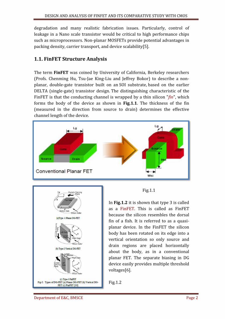
1.1. FinFET Structure Analysis
The term FinFET was coined by University of California, Berkeley researchers
(Profs. Chenming Hu, Tsu-Jae King-Liu and Jeffrey Bokor) to describe a non-
planar, double-gate transistor built on an SOI substrate, based on the earlier
DELTA (single-gate) transistor design. The distinguishing characteristic of the
FinFET is that the conducting channel is wrapped by a thin silicon "fin", which
forms the body of the device as shown in Fig.1.1. The thickness of the fin
(measured in the direction from source to drain) determines the effective
channel length of the device.
Fig.1.1
In Fig.1.2 it is shown that type 3 is called
as a FinFET. This is called as FinFET
because the silicon resembles the dorsal
fin of a fish. It is referred to as a quasi-
planar device. In the FinFET the silicon
body has been rotated on its edge into a
vertical orientation so only source and
drain regions are placed horizontally
about the body, as in a conventional
planar FET. The separate biasing in DG
device easily provides multiple threshold
voltages[6].
Fig.1.2
DESIGN AND ANALYSIS OF FINFET AND ITS COMPARATIVE STUDY WITH CMOS
Department of E&C, BMSCE Page 3
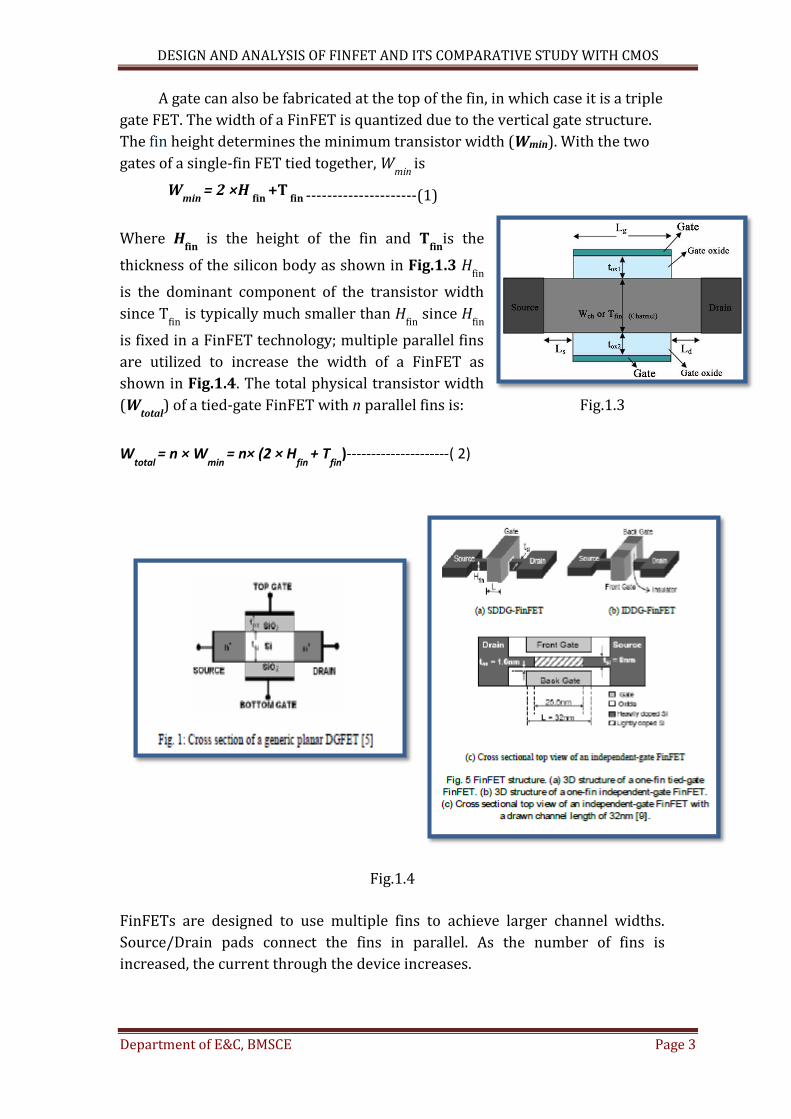
A gate can also be fabricated at the top of the fin, in which case it is a triple
gate FET. The width of a FinFET is quantized due to the vertical gate structure.
The fin height determines the minimum transistor width (Wmin). With the two
gates of a single-fin FET tied together, Wmin
is
Wmin
= 2 ×H fin
+T fin ---------------------(1)
Where Hfin
is the height of the fin and Tfin
is the
thickness of the silicon body as shown in Fig.1.3 Hfin
is the dominant component of the transistor width
since Tfin
is typically much smaller than Hfin
since Hfin
is fixed in a FinFET technology; multiple parallel fins
are utilized to increase the width of a FinFET as
shown in Fig.1.4. The total physical transistor width
(Wtotal
) of a tied-gate FinFET with n parallel fins is: Fig.1.3
Wtotal
= n × Wmin
= n× (2 × Hfin
+ Tfin
)---------------------( 2)
Fig.1.4
FinFETs are designed to use multiple fins to achieve larger channel widths.
Source/Drain pads connect the fins in parallel. As the number of fins is
increased, the current through the device increases.

DESIGN AND ANALYSIS OF FINFET AND ITS COMPARATIVE STUDY WITH CMOS
Department of E&C, BMSCE Page 4
1.2 Main features of FinFET:
1) Ultra-thin Si fin for suppression of short channel effects.
2) Raised source/drain to reduce parasitic resistance and improve current
drive .
3) Gate last process with low VT, high k gate dielectrics.
4) Symmetric gates yield great performance, but can built asymmetric gates
that target VT[8] .
The two vertical gates of a FinFET can be separated by depositing oxide on top
of the silicon fin, thereby forming an independent-gate FinFET.
An independent-gate FinFET (IG-FinFET) provides two different active modes
of operation with significantly different current characteristics determined by
the bias conditions. Alternatively, in the Single-Gate-Mode, one gate is biased
with the input signal while the other gate is disabled (disabled gate: biased with
VGND
in an N-type FinFET and with VDD
in a P-type FinFET).
The two gates are strongly coupled in the Dual of the two independent gates as
shown in Fig.1.5. In the Dual-Gate-Mode, the two gates are biased with the
same signal-Gate-Mode, thereby lowering the threshold voltage Vth
as compared
to the Single-Gate-Mode. The maximum drain current produced in the Dual-
Gate-Mode is therefore 2.6 times higher as compared to the Single-Gate-Mode
as shown in Fig.1.5. The switched gate capacitance of the FinFET is also halved
in the Single-Gate-Mode due to the disabled back gate[7].
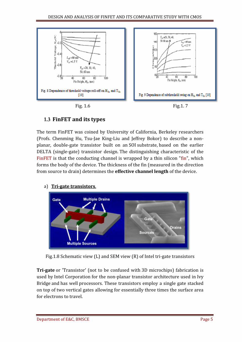
The drain current normalized by the channel width W at the same Vgs
is almost
independent of Hfin
while fixing Tfin
. The small differences in the normalized
drain current for devices with the same Hfin
and different Tfin
come from the threshold
voltage roll-off due to the increase in Tfin
. The
dependences of Vth
roll-off and sub threshold
swing S on Hfin
and Tfin
are shown in Figs.1.6
and 1.7.
Fig.1.5
DESIGN AND ANALYSIS OF FINFET AND ITS COMPARATIVE STUDY WITH CMOS
Department of E&C, BMSCE Page 5
Fig. 1.6 Fig.1. 7
1.3 FinFET and its types
The term FinFET was coined by University of California, Berkeley researchers
(Profs. Chenming Hu, Tsu-Jae King-Liu and Jeffrey Bokor) to describe a non-
planar, double-gate transistor built on an SOI substrate, based on the earlier
DELTA (single-gate) transistor design. The distinguishing characteristic of the
FinFET is that the conducting channel is wrapped by a thin silicon "fin", which
forms the body of the device. The thickness of the fin (measured in the direction
from source to drain) determines the effective channel length of the device.
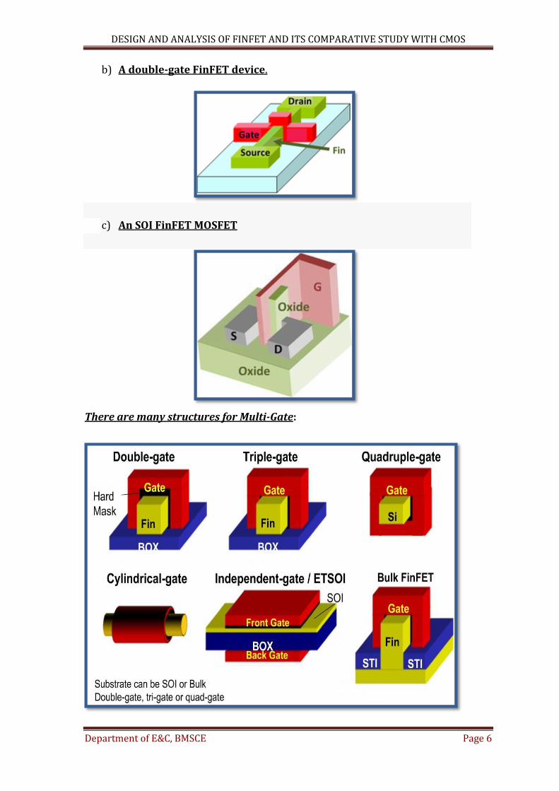
a) Tri-gate transistors.
Fig.1.8 Schematic view (L) and SEM view (R) of Intel tri-gate transistors
Tri-gate or 'Transistor’ (not to be confused with 3D microchips) fabrication is
used by Intel Corporation for the non-planar transistor architecture used in Ivy
Bridge and has well processors. These transistors employ a single gate stacked
on top of two vertical gates allowing for essentially three times the surface area
for electrons to travel.
DESIGN AND ANALYSIS OF FINFET AND ITS COMPARATIVE STUDY WITH CMOS
Department of E&C, BMSCE Page 6
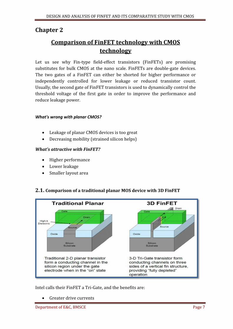
b) A double-gate FinFET device.
c) An SOI FinFET MOSFET
There are many structures for Multi-Gate:
DESIGN AND ANALYSIS OF FINFET AND ITS COMPARATIVE STUDY WITH CMOS
Department of E&C, BMSCE Page 7
Chapter 2
Comparison of FinFET technology with CMOS
technology
Let us see why Fin-type field-effect transistors (FinFETs) are promising
substitutes for bulk CMOS at the nano scale. FinFETs are double-gate devices.
The two gates of a FinFET can either be shorted for higher performance or
independently controlled for lower leakage or reduced transistor count.
Usually, the second gate of FinFET transistors is used to dynamically control the
threshold voltage of the first gate in order to improve the performance and
reduce leakage power.
What's wrong with planar CMOS?
Leakage of planar CMOS devices is too great
Decreasing mobility (strained silicon helps)
What's attractive with FinFET?
Higher performance
Lower leakage
Smaller layout area
2.1. Comparison of a traditional planar MOS device with 3D FinFET
Intel calls their FinFET a Tri-Gate, and the benefits are:
Greater drive currents

DESIGN AND ANALYSIS OF FINFET AND ITS COMPARATIVE STUDY WITH CMOS
Department of E&C, BMSCE Page 8
Lower switching voltages
Lower leakage currents
Lower power, 50%
Faster switching, 18-37%
Small wafer cost increase, 2-3% (Source: Mark Bohr, Intel Developer
Forum 2011)
2.2. Electrical characteristics and Comparison
a) Scaling.
The scaling of the MOSFET transistor has delivered astronomical increases in
transistor density and performance, leading to more chip functionality at higher
speeds. The main roadblock to continued success is the leakage phenomenon.
Increased leakage from decreased oxide thicknesses, higher substrate dopings,
and decreased channel lengths. A lowered threshold voltage to obtain better
performance at lowered operating voltages further exacerbates the leakage
problem and also reduces the noise margin. Moreover, the continued-shrinking
proximity of the source and drain reduces the effective control of the gate over
the channel, accentuating DIBL, drain-induced-barrier lowering.
• Scaling in MOSFETS
In 1965, Gordon Moore predicted the exponential growth of the number of transistors on an IC (Moore's Law). Transistor count doubled every year since invention Predicted >65,000 transistors by 1975!

DESIGN AND ANALYSIS OF FINFET AND ITS COMPARATIVE STUDY WITH CMOS
Department of E&C, BMSCE Page 9
b) Short-Channel effects
Short-Channel Devices A MOSFET device is considered to be short when the channel length is the same
order of magnitude as the depletion-layer widths (xdD, xdS) of the source and
drain junction.
As the channel length L is reduced to increase both the operation speed and the
number of components per chip, the so-called short-channel effects arise.
Short-Channel Effects The short-channel effects are attributed to two physical phenomena: (i) The limitation imposed on electron drift characteristics in the channel Off-state leakage current: IOFF (IDS at VGS = 0 and VDS = VDD) is one of the
most important device characteristics directly related to SCEs. The stand-by
power of a chip is determined by the combined IOFF of all the transistors, and
as such it must be minimized to integrate millions of transistors together. When
designing a transistor, not only ION, but also IOFF should be optimized. On the
other hand, IOFF, which is mainly due to diffusion current, degrades (increases)
with decreasing feature sizes. IOFF is one of the critical parameters that
determine the scalability of a given technology. Other parameters such as VT
roll-off and DIBL indirectly contribute to increasing the off-state leakage
current.
(ii) The modification of the threshold voltage due to the shortening channel length. VT roll-off: In order that the threshold condition is reached in an MOS capacitor,
we need to deplete the channel charge by applying a positive bias (for
nMOSFETs) until strong inversion occurs. In a short-channel MOSFET, the
depletion region has complicated 2-D geometry and the channel region is
influenced by the source/drain (S/D) as much as by the gate. Before there is any
positive bias on the gate, the channel is already depleted by the built-in
potential between the channel and S/D regions. This influence becomes
stronger when the p-n junctions between the S/D and the channel are reverse-
biased, giving rise to drain-induced barrier lowering (DIBL). As a result of this
undesirable coupling between the S/D region and the channel, which becomes
stronger as the gate length is reduced; VT is lower for a transistor with shorter
LG. This VT roll-off is typically measured in mV/nm.
The fluctuation of transistor characteristics on the same chip forces the circuit
design to become conservative to allow enough margin such that the circuit can
operate even with the worst case IOFF (shortest LG) and the worst case drive

DESIGN AND ANALYSIS OF FINFET AND ITS COMPARATIVE STUDY WITH CMOS
Department of E&C, BMSCE Page 10
current (longest LG). With a conservative design, we cannot take full advantage
of the shortest transistor, which has the highest drive current. Therefore, if a
very tight LG control is achieved, it will significantly benefit the circuit design.
In particular five different short-channel effects can be distinguished: 1. Drain-induced barrier lowering and punch through
2. Surface scattering
3. Velocity saturation
4. Impact ionization
5. Hot electrons
c) Power Analysis
Three mechanisms that govern the power consumption are observed.
1. Sub-threshold leakage power consumption in overdriven inverters is reduced
due to Vth control.
2. The use of a higher Vdd leads to higher short-circuit and leakage power
consumption in inverters.
3. Power consumption due to charging and discharging of capacitor due to slope
of input voltage and load capacitances.
EXAMPLE:
Comparing power consumption of Schmitt Trigger circuit
implemented using CMOS and FinFET
Schmitt Trigger
A Schmitt trigger is a high-performance circuit used to shape input pulses and
reduce noise. It responds to a slow-changing input pulse with a fast-changing
output transition. The voltage-transfer characteristics of the circuit show
different switching thresholds for positive and negative going input slope[9].
Consider the CMOS Schmitt trigger (CMOS-ST) shown in Fig.2.1.
Fig.2.1 CMOS Schmitt trigger
DESIGN AND ANALYSIS OF FINFET AND ITS COMPARATIVE STUDY WITH CMOS
Department of E&C, BMSCE Page 11
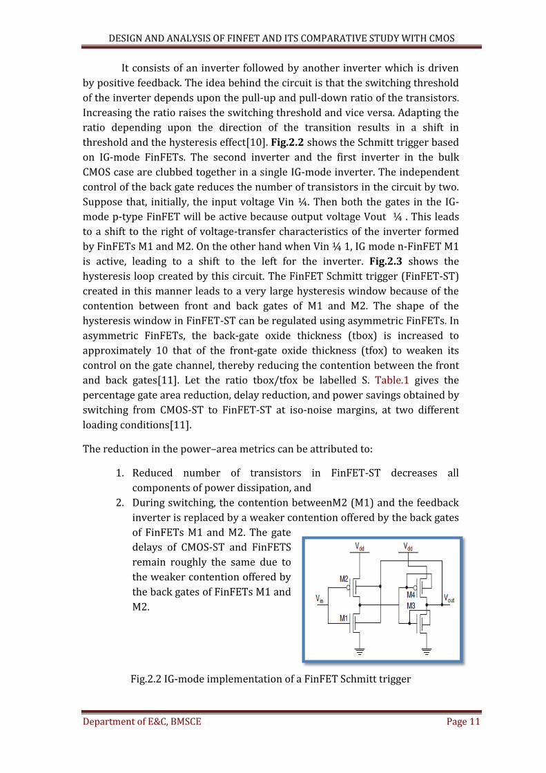
It consists of an inverter followed by another inverter which is driven
by positive feedback. The idea behind the circuit is that the switching threshold
of the inverter depends upon the pull-up and pull-down ratio of the transistors.
Increasing the ratio raises the switching threshold and vice versa. Adapting the
ratio depending upon the direction of the transition results in a shift in
threshold and the hysteresis effect[10]. Fig.2.2 shows the Schmitt trigger based
on IG-mode FinFETs. The second inverter and the first inverter in the bulk
CMOS case are clubbed together in a single IG-mode inverter. The independent
control of the back gate reduces the number of transistors in the circuit by two.
Suppose that, initially, the input voltage Vin ¼. Then both the gates in the IG-
mode p-type FinFET will be active because output voltage Vout ¼ . This leads
to a shift to the right of voltage-transfer characteristics of the inverter formed
by FinFETs M1 and M2. On the other hand when Vin ¼ 1, IG mode n-FinFET M1
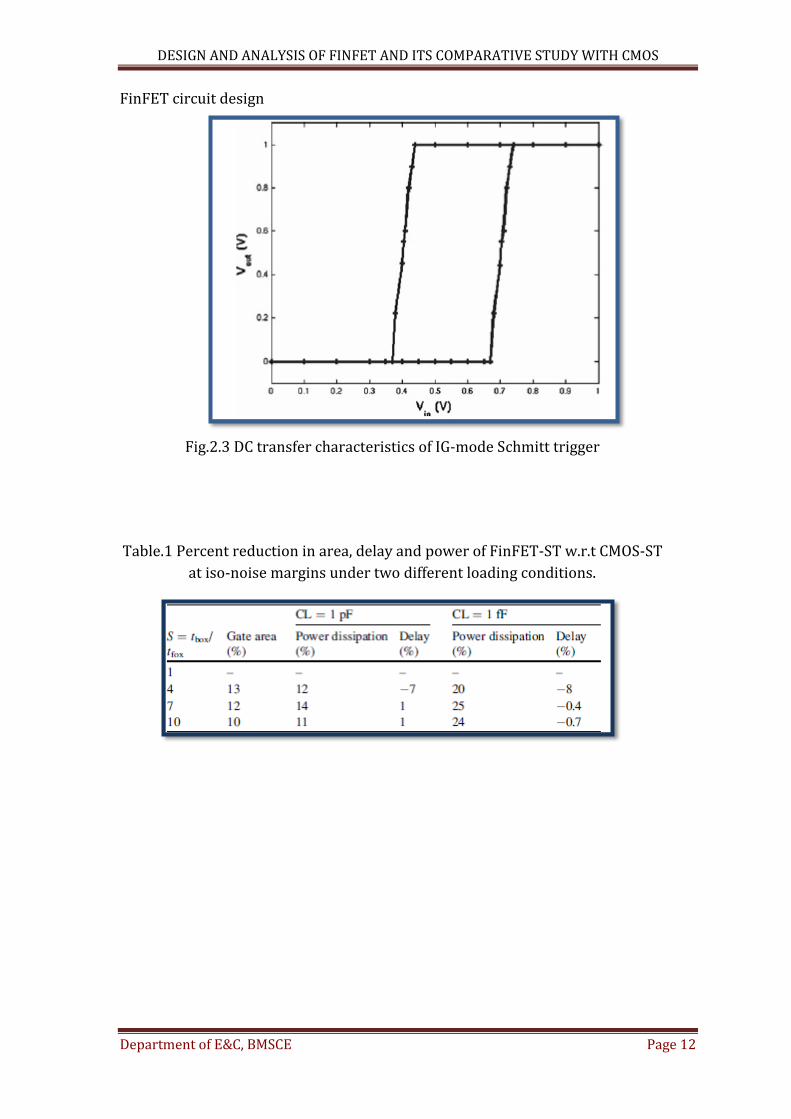
is active, leading to a shift to the left for the inverter. Fig.2.3 shows the
hysteresis loop created by this circuit. The FinFET Schmitt trigger (FinFET-ST)
created in this manner leads to a very large hysteresis window because of the
contention between front and back gates of M1 and M2. The shape of the
hysteresis window in FinFET-ST can be regulated using asymmetric FinFETs. In
asymmetric FinFETs, the back-gate oxide thickness (tbox) is increased to
approximately 10 that of the front-gate oxide thickness (tfox) to weaken its
control on the gate channel, thereby reducing the contention between the front
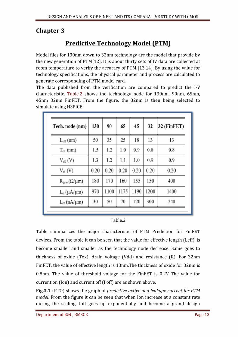
and back gates[11]. Let the ratio tbox/tfox be labelled S. Table.1 gives the
percentage gate area reduction, delay reduction, and power savings obtained by
switching from CMOS-ST to FinFET-ST at iso-noise margins, at two different
loading conditions[11].
The reduction in the power–area metrics can be attributed to:
1. Reduced number of transistors in FinFET-ST decreases all
components of power dissipation, and
2. During switching, the contention betweenM2 (M1) and the feedback
inverter is replaced by a weaker contention offered by the back gates
of FinFETs M1 and M2. The gate
delays of CMOS-ST and FinFETS
remain roughly the same due to
the weaker contention offered by
the back gates of FinFETs M1 and
M2.
Fig.2.2 IG-mode implementation of a FinFET Schmitt trigger
DESIGN AND ANALYSIS OF FINFET AND ITS COMPARATIVE STUDY WITH CMOS
Department of E&C, BMSCE Page 12
FinFET circuit design
Fig.2.3 DC transfer characteristics of IG-mode Schmitt trigger
Table.1 Percent reduction in area, delay and power of FinFET-ST w.r.t CMOS-ST
at iso-noise margins under two different loading conditions.
DESIGN AND ANALYSIS OF FINFET AND ITS COMPARATIVE STUDY WITH CMOS
Department of E&C, BMSCE Page 13
Chapter 3
Predictive Technology Model (PTM)
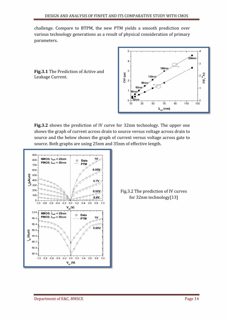
Model files for 130nm down to 32nm technology are the model that provide by
the new generation of PTM[12]. It is about thirty sets of IV data are collected at
room temperature to verify the accuracy of PTM [13,14]. By using the value for
technology specifications, the physical parameter and process are calculated to
generate corresponding of PTM model card.
The data published from the verification are compared to predict the I-V
characteristic. Table.2 shows the technology node for 130nm, 90nm, 65nm,
45nm 32nm FinFET. From the figure, the 32nm is then being selected to
simulate using HSPICE.
Table.2
Table summarizes the major characteristic of PTM Prediction for FinFET
devices. From the table it can be seen that the value for effective length (Leff), is
become smaller and smaller as the technology node decrease. Same goes to
thickness of oxide (Tox), drain voltage (Vdd) and resistance (R). For 32nm
FinFET, the value of effective length is 13nm.The thickness of oxide for 32nm is
0.8nm. The value of threshold voltage for the FinFET is 0.2V The value for
current on (Ion) and current off (I off) are as shown above.
Fig.3.1 (PTO) shows the graph of predictive active and leakage current for PTM
model. From the figure it can be seen that when Ion increase at a constant rate
during the scaling, Ioff goes up exponentially and become a grand design
DESIGN AND ANALYSIS OF FINFET AND ITS COMPARATIVE STUDY WITH CMOS
Department of E&C, BMSCE Page 14
challenge. Compare to BTPM, the new PTM yields a smooth prediction over
various technology generations as a result of physical consideration of primary
parameters.
Fig.3.1 The Prediction of Active and Leakage Current.
Fig.3.2 shows the prediction of IV curve for 32nm technology. The upper one
shows the graph of current across drain to source versus voltage across drain to
source and the below shows the graph of current versus voltage across gate to
source. Both graphs are using 25nm and 35nm of effective length.
Fig.3.2 The prediction of IV curves
for 32nm technology[13]
DESIGN AND ANALYSIS OF FINFET AND ITS COMPARATIVE STUDY WITH CMOS
Department of E&C, BMSCE Page 15
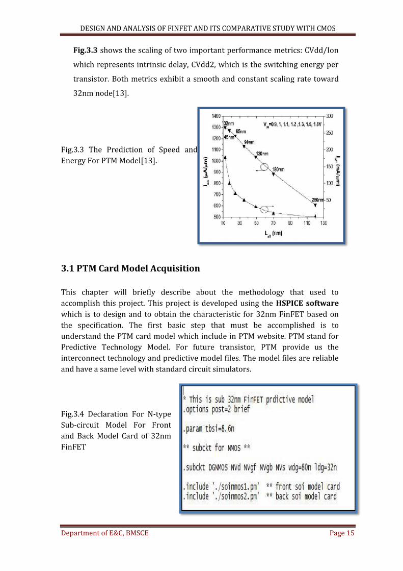
Fig.3.3 shows the scaling of two important performance metrics: CVdd/Ion
which represents intrinsic delay, CVdd2, which is the switching energy per
transistor. Both metrics exhibit a smooth and constant scaling rate toward
32nm node[13].
Fig.3.3 The Prediction of Speed and
Energy For PTM Model[13].
3.1 PTM Card Model Acquisition This chapter will briefly describe about the methodology that used to
accomplish this project. This project is developed using the HSPICE software
which is to design and to obtain the characteristic for 32nm FinFET based on
the specification. The first basic step that must be accomplished is to
understand the PTM card model which include in PTM website. PTM stand for
Predictive Technology Model. For future transistor, PTM provide us the
interconnect technology and predictive model files. The model files are reliable
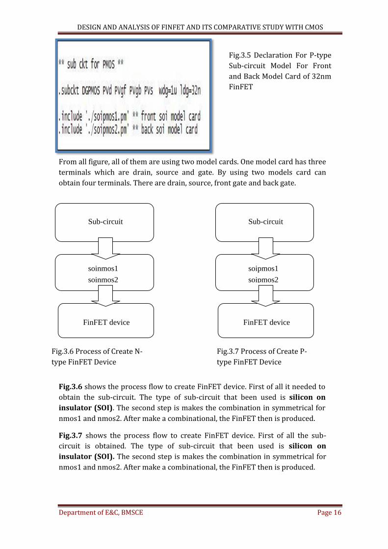
and have a same level with standard circuit simulators. Fig.3.4 Declaration For N-type
Sub-circuit Model For Front
and Back Model Card of 32nm
FinFET
DESIGN AND ANALYSIS OF FINFET AND ITS COMPARATIVE STUDY WITH CMOS
Department of E&C, BMSCE Page 16
From all figure, all of them are using two model cards. One model card has three
terminals which are drain, source and gate. By using two models card can
obtain four terminals. There are drain, source, front gate and back gate.
Fig.3.6 shows the process flow to create FinFET device. First of all it needed to
obtain the sub-circuit. The type of sub-circuit that been used is silicon on
insulator (SOI). The second step is makes the combination in symmetrical for
nmos1 and nmos2. After make a combinational, the FinFET then is produced.
Fig.3.7 shows the process flow to create FinFET device. First of all the sub-
circuit is obtained. The type of sub-circuit that been used is silicon on
insulator (SOI). The second step is makes the combination in symmetrical for
nmos1 and nmos2. After make a combinational, the FinFET then is produced.
Fig.3.5 Declaration For P-type
Sub-circuit Model For Front
and Back Model Card of 32nm
FinFET
S
u
b
-
c
i
r
c
u
i
t
s
o
i
n
m
o
s
1
s
o
i
n
m
o
s
2
S
u
b
S
u
b
-
c
i
r
c
u
i
t
c
i
r
c
u
i
t
F
E
T
d
e
v
i
c
e
FinFET device
soinmos1 soinmos2
Sub-circuit
S
u
b
-
c
i
r
c
u
i
t
s
o
i
n
m
o
s
1
s
o
i
n
m
o
s
2
S
u
b
S
u
b
-
c
i
r
c
u
i
t
c
i
r
c
u
i
t
F
E
T
d
e
v
i
c
e
FinFET device
soipmos1 soipmos2
Sub-circuit
Fig.3.6 Process of Create N-
type FinFET Device
Fig.3.7 Process of Create P-
type FinFET Device
DESIGN AND ANALYSIS OF FINFET AND ITS COMPARATIVE STUDY WITH CMOS
Department of E&C, BMSCE Page 17
PHASE 1 : IMPLEMENT MODEL CARD USING HSPICE SIMULATOR
Fig.3.8 Flow Chart For Phase One
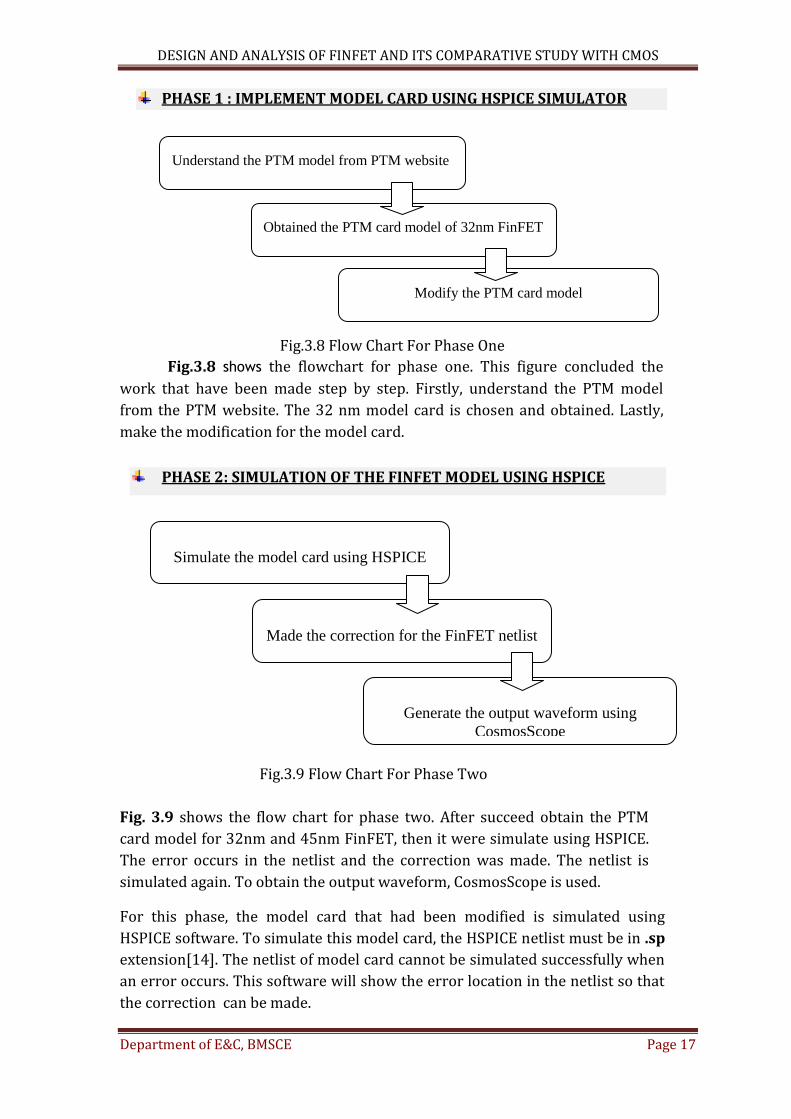
Fig.3.8 shows the flowchart for phase one. This figure concluded the
work that have been made step by step. Firstly, understand the PTM model
from the PTM website. The 32 nm model card is chosen and obtained. Lastly,
make the modification for the model card.
PHASE 2: SIMULATION OF THE FINFET MODEL USING HSPICE
Fig.3.9 Flow Chart For Phase Two
Fig. 3.9 shows the flow chart for phase two. After succeed obtain the PTM
card model for 32nm and 45nm FinFET, then it were simulate using HSPICE.
The error occurs in the netlist and the correction was made. The netlist is
simulated again. To obtain the output waveform, CosmosScope is used.
For this phase, the model card that had been modified is simulated using
HSPICE software. To simulate this model card, the HSPICE netlist must be in .sp
extension[14]. The netlist of model card cannot be simulated successfully when
an error occurs. This software will show the error location in the netlist so that
the correction can be made.
Understand the PTM model from PTM website
Obtained the PTM card model of 32nm FinFET
Modify the PTM card model
Simulate the model card using HSPICE
Made the correction for the FinFET netlist
Generate the output waveform using
CosmosScope
DESIGN AND ANALYSIS OF FINFET AND ITS COMPARATIVE STUDY WITH CMOS
Department of E&C, BMSCE Page 18
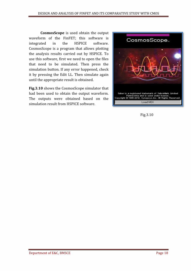
CosmosScope is used obtain the output
waveform of the FinFET; this software is
integrated in the HSPICE software.
CosmosScope is a program that allows plotting
the analysis results carried out by HSPICE. To
use this software, first we need to open the files
that need to be simulated. Then press the
simulation button. If any error happened, check
it by pressing the Edit LL. Then simulate again
until the appropriate result is obtained.
Fig.3.10 shows the CosmosScope simulator that
had been used to obtain the output waveform.
The outputs were obtained based on the
simulation result from HSPICE software.
Fig.3.10
DESIGN AND ANALYSIS OF FINFET AND ITS COMPARATIVE STUDY WITH CMOS
Department of E&C, BMSCE Page 19
Chapter 4
SIMULATION AND DISCUSSION
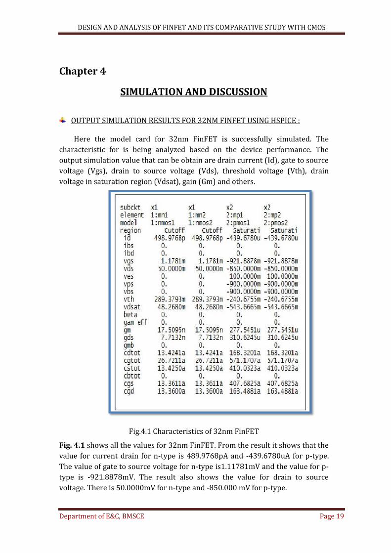
OUTPUT SIMULATION RESULTS FOR 32NM FINFET USING HSPICE :
Here the model card for 32nm FinFET is successfully simulated. The
characteristic for is being analyzed based on the device performance. The
output simulation value that can be obtain are drain current (Id), gate to source
voltage (Vgs), drain to source voltage (Vds), threshold voltage (Vth), drain
voltage in saturation region (Vdsat), gain (Gm) and others.
Fig.4.1 Characteristics of 32nm FinFET
Fig. 4.1 shows all the values for 32nm FinFET. From the result it shows that the
value for current drain for n-type is 489.9768pA and -439.6780uA for p-type.
The value of gate to source voltage for n-type is1.11781mV and the value for p-
type is -921.8878mV. The result also shows the value for drain to source
voltage. There is 50.0000mV for n-type and -850.000 mV for p-type.
DESIGN AND ANALYSIS OF FINFET AND ITS COMPARATIVE STUDY WITH CMOS
Department of E&C, BMSCE Page 20
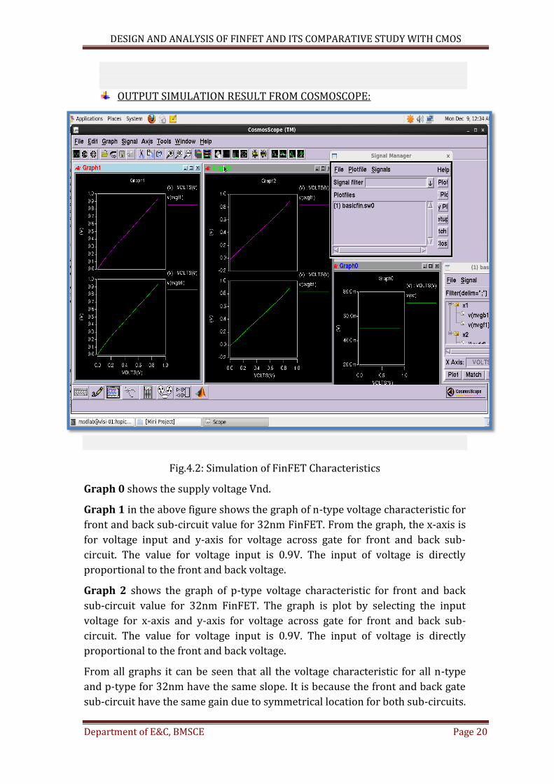
OUTPUT SIMULATION RESULT FROM COSMOSCOPE:
Fig.4.2: Simulation of FinFET Characteristics
Graph 0 shows the supply voltage Vnd.
Graph 1 in the above figure shows the graph of n-type voltage characteristic for
front and back sub-circuit value for 32nm FinFET. From the graph, the x-axis is
for voltage input and y-axis for voltage across gate for front and back sub-
circuit. The value for voltage input is 0.9V. The input of voltage is directly
proportional to the front and back voltage.
Graph 2 shows the graph of p-type voltage characteristic for front and back
sub-circuit value for 32nm FinFET. The graph is plot by selecting the input
voltage for x-axis and y-axis for voltage across gate for front and back sub-
circuit. The value for voltage input is 0.9V. The input of voltage is directly
proportional to the front and back voltage.
From all graphs it can be seen that all the voltage characteristic for all n-type
and p-type for 32nm have the same slope. It is because the front and back gate
sub-circuit have the same gain due to symmetrical location for both sub-circuits.
DESIGN AND ANALYSIS OF FINFET AND ITS COMPARATIVE STUDY WITH CMOS
Department of E&C, BMSCE Page 21
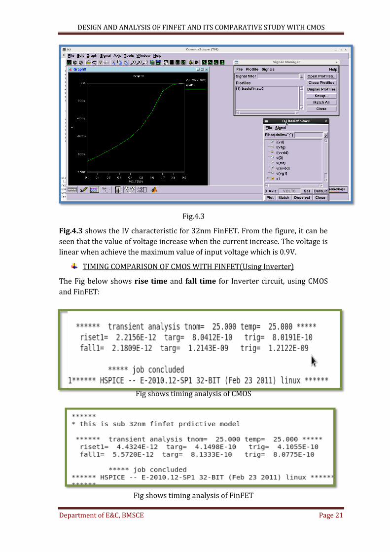
Fig.4.3
Fig.4.3 shows the IV characteristic for 32nm FinFET. From the figure, it can be
seen that the value of voltage increase when the current increase. The voltage is
linear when achieve the maximum value of input voltage which is 0.9V.
TIMING COMPARISON OF CMOS WITH FINFET(Using Inverter)
The Fig below shows rise time and fall time for Inverter circuit, using CMOS
and FinFET:
Fig shows timing analysis of CMOS
Fig shows timing analysis of FinFET
DESIGN AND ANALYSIS OF FINFET AND ITS COMPARATIVE STUDY WITH CMOS
Department of E&C, BMSCE Page 22
For CMOS:
Rise Time =2.215 ps
Fall Time =2.180 ps
For FinFET:
Rise Time = 4.432 ps
Fall Time = 5.572 ps
From this we can conclude that CMOS has faster rise and fall times when
compared to FinFET, hence FinFET is slower than CMOS.
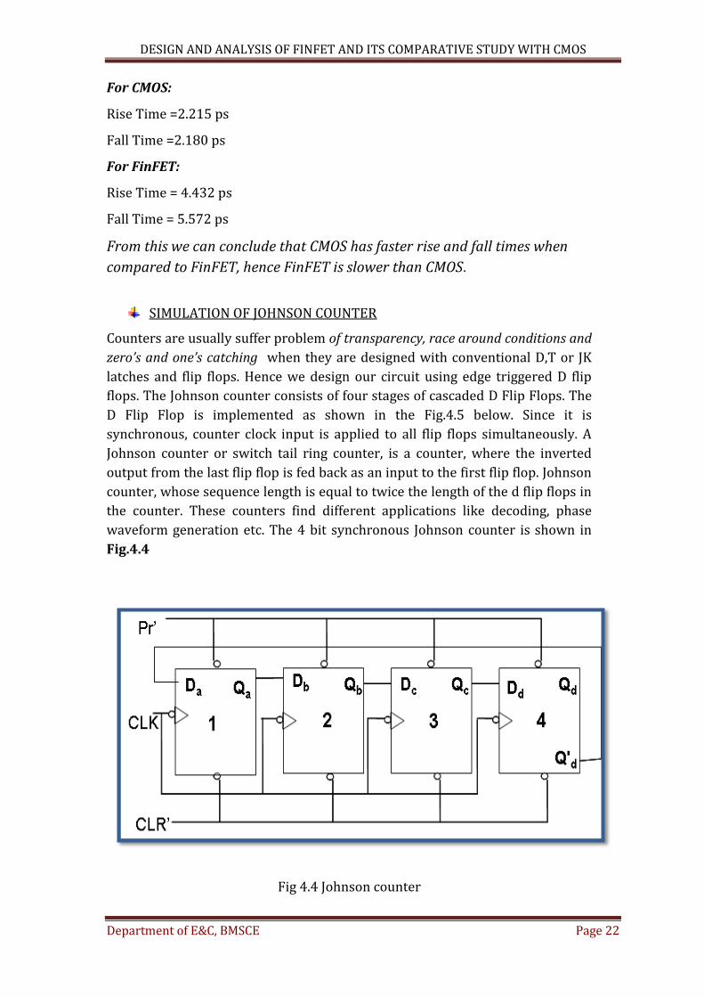
SIMULATION OF JOHNSON COUNTER
Counters are usually suffer problem of transparency, race around conditions and
zero’s and one’s catching when they are designed with conventional D,T or JK
latches and flip flops. Hence we design our circuit using edge triggered D flip
flops. The Johnson counter consists of four stages of cascaded D Flip Flops. The
D Flip Flop is implemented as shown in the Fig.4.5 below. Since it is
synchronous, counter clock input is applied to all flip flops simultaneously. A
Johnson counter or switch tail ring counter, is a counter, where the inverted
output from the last flip flop is fed back as an input to the first flip flop. Johnson
counter, whose sequence length is equal to twice the length of the d flip flops in
the counter. These counters find different applications like decoding, phase
waveform generation etc. The 4 bit synchronous Johnson counter is shown in
Fig.4.4
Fig 4.4 Johnson counter

DESIGN AND ANALYSIS OF FINFET AND ITS COMPARATIVE STUDY WITH CMOS
Department of E&C, BMSCE Page 23
In this counter, inversion of Q is fed back to
input D causes the counter to "count" in a
different way. Generally 4-bit Johnson counter
passes four logic 0s and then four logic 1s
thereby producing an 8-bit sequence pattern i.e.,
1000, 1100, 1110, 1111, 0111, 0011, 0001, 0000
and this is shown in the following table1 below.
To enable the counter according to desired
Sequence shown in table 1, first it is necessary
to clear all the flip-flops. Initially Q is ‘0 and
Qbar is ‘1’. The first clock shifts three 0s from
(Q0 Q1 Q2) to the right into (Q2 Q3 Q4).After
three clock pulses we have all 1s.So the output
of last flip flop i.e. Q is ‘1’ and Qbar is ‘0’.Thus we
start shifting 1s to that right, replacing the
zeros.
BASIC EDGE D FLIP FLOP IMPLEMENTATION USING FinFET:
The Basic Positive Edge triggered D Flip Flop is shown in figure 4.5 with its
truth table.
State Q0 Q1 Q2 Q4
0 0 0 0 0
1 1 0 0 0
2 1 1 0 0
3 1 1 1 0
4 1 1 1 1
5 0 1 1 1
6 0 0 1 1
7 0 0 0 1
Table shows the Truth Table
for a 4-bit Johnson counter.
Truth Table for Edge triggered D Flip Flop Figure 4.5
DESIGN AND ANALYSIS OF FINFET AND ITS COMPARATIVE STUDY WITH CMOS
Department of E&C, BMSCE Page 24
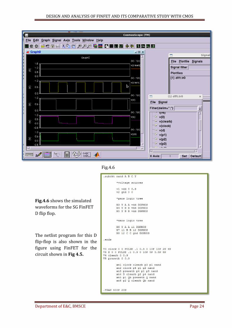
Fig.4.6 shows the simulated
waveforms for the SG FinFET
D flip flop.
The netlist program for this D
flip-flop is also shown in the
figure using FinFET for the
circuit shown in Fig 4.5.
Fig.4.6
DESIGN AND ANALYSIS OF FINFET AND ITS COMPARATIVE STUDY WITH CMOS
Department of E&C, BMSCE Page 25
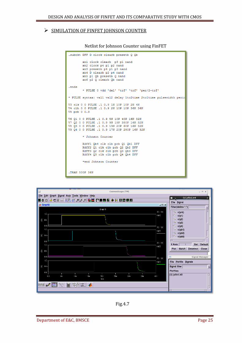
SIMULATION OF FINFET JOHNSON COUNTER
Netlist for Johnson Counter using FinFET
Fig.4.7

DESIGN AND ANALYSIS OF FINFET AND ITS COMPARATIVE STUDY WITH CMOS
Department of E&C, BMSCE Page 26
The power consumption and rise times for each flip flop are as shown below in
the figure for FinFET 32nm Technology.
Hence the average rise time for each flip flop = 0.205 ns.
Average fall time for each flip flop = 0.803ns
At a clock frequency of 250 MHz the average power consumption = 15.725
uW and peak power consumption = 635.86 uW.
From the Fig above the Static Power = 4.87 uW
Hence Dynamic Power consumption = 10.85 uW
Ptotal= Pstatic + Pdynamic
Pdynamic = Ptotal - Pstatic
DESIGN AND ANALYSIS OF FINFET AND ITS COMPARATIVE STUDY WITH CMOS
Department of E&C, BMSCE Page 27
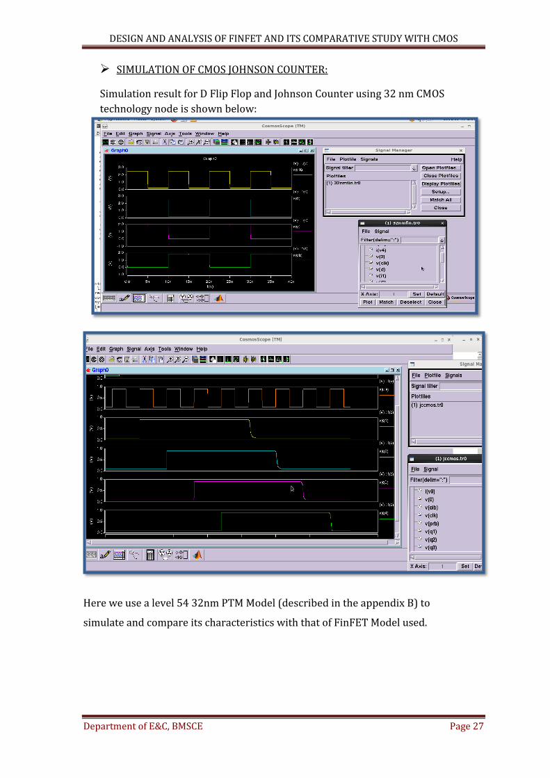
SIMULATION OF CMOS JOHNSON COUNTER:
Simulation result for D Flip Flop and Johnson Counter using 32 nm CMOS
technology node is shown below:
Here we use a level 54 32nm PTM Model (described in the appendix B) to
simulate and compare its characteristics with that of FinFET Model used.
DESIGN AND ANALYSIS OF FINFET AND ITS COMPARATIVE STUDY WITH CMOS
Department of E&C, BMSCE Page 28
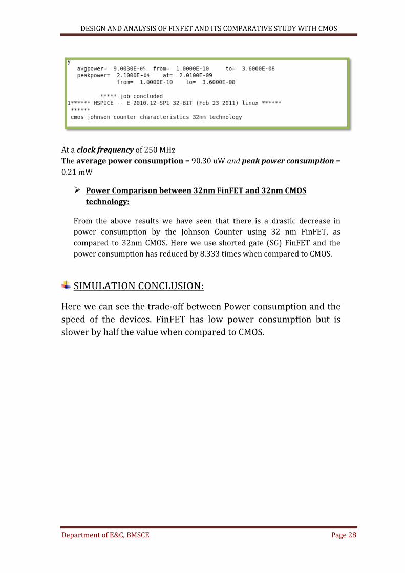
At a clock frequency of 250 MHz
The average power consumption = 90.30 uW and peak power consumption =
0.21 mW
Power Comparison between 32nm FinFET and 32nm CMOS
technology:
From the above results we have seen that there is a drastic decrease in
power consumption by the Johnson Counter using 32 nm FinFET, as
compared to 32nm CMOS. Here we use shorted gate (SG) FinFET and the
power consumption has reduced by 8.333 times when compared to CMOS.
SIMULATION CONCLUSION:
Here we can see the trade-off between Power consumption and the
speed of the devices. FinFET has low power consumption but is
slower by half the value when compared to CMOS.
DESIGN AND ANALYSIS OF FINFET AND ITS COMPARITIVE STUDY WITH CMOS
Department of E&C, BMSCE Page 29
Chapter 5
CONCLUSION AND FUTURE WORK
SUMMARY AND CONCLUSION
FinFET are the new challenge for new material nowadays. This project
focused on the modeling FinFET using PTM card. The FinFET model has been
developed by following the parameter from nano-scale design. The sub-circuit
model of FinFET is successfully constructed and the performance of the device
was analyzed. From the result, we can conclude that 32nm FinFET has lower
power consumption and better tradeoff between speed and performance with
an optimal Power Consumption. Hence 32nm FinFET has better performance
compared to 32nm CMOS.
The characteristics of both 32nm FinFET and 32nm CMOS are
successfully evaluated and investigated. In FinFET, when the nano-scale
decreases, the size of device become smaller and the performance of device is
much better. As the technology node is decreasing, the size of the device become
smaller and smaller. Smaller device occupy less space and also more efficiency.
FUTURE WORK
(i) Other PTM card model can be analyzed so that we can obtain more value
and performance of the device.
(ii) A in-depth analysis of various parameters such as Doping concentrations,
Gate sizing, oxide thickness etc … can all be studied and varied to get a better
performance in the device and hence TCAD modeling using these
characteristics can be done.
(iii) Other types of ‘MULTIGATE DEVICES’ can be simulated in HSPICE using
PTM Models. Also development of PTM models can also be undertaken.
(iv) HSPICE is one of the software that can be used to simulate PTM card
model for another device such as MOSFET, bulk CMOS, MuGFET of different
technology nodes and length, and hence the device specific for various
applications can be chosen.
DESIGN AND ANALYSIS OF FINFET AND ITS COMPARITIVE STUDY WITH CMOS
Department of E&C, BMSCE Page 30
Chapter 6
REFERENCES
1. G. E. Moore, “Cramming more Components onto Integrated Circuits,”
Electronics, vol. 38, no. 8, April 19, 1965.
2. Gordon E. Moore, “No Exponential is Forever: But 'Forever' Can Be
Delayed!”, Solid-State Circuits Conference, 2003. Digest of Technical
Papers. ISSCC. 2003 IEEE International, 2003, pgs. 20 - 23 vol.1
3. Scott E. Thompson, Robert S. Chau, TahirGhani, Kaizad Mistry,
SunitTyagi, and Mark T. Bohr, “In Search of 'Forever,' Continued
Transistor Scaling One New Material at a Time,” IEEE Transactions on
Semiconductor Manufacturing, Vol. 18, No. 1, February 2005, pgs. 26 – 36
4. Jovanović, T. Suligoj, P. Biljanović, L.K. Nanver, “FinFET technology for
wide-channel devices with ultra-thin silicon body”.
5. Bin Yu, Leland Chang*, Shibly Ahmed, Haihong Wang, Scott Bell, Chih-Yuh
Yang, Cyrus Tabery,Chau Ho, Qi Xiang, Tsu-Jae King*, Jeffrey Bokor,
Chenming Hu, Ming-Ren Lin, and David Kyser, “FinFET Scaling to 10nm
Gate Length,” IEEE-2002.
6. Nirmal, Vijaya Kumar and Sam Jabaraj, “Nand Gate Using FinFET for
Nanoscale Technology,” International Journal of Engineering Science and
Technology, Vol. 2(5), 2010, pp. 1351-1358.
7. Sherif A. Tawfik, Zhiyu Liu, and VolkanKursun, “Independent-Gate and
Tied-Gate FinFET SRAM Circuits: Design Guidelines for Reduced Area and
Enhanced Stability,” IEEE ICM, 2007.
8. http://www. techalone.com, Electronic seminar topic
9. ResveSaleh, Michael Benoit and Pete McCrorie - “Power distribution
planning”.
10. Sani R. Nassif – “Design for Variability in DSM Technologies”
11. Sung-Mo, Yusuf – “CMOS digital integrated circuits”
12. FinFET circuit modeling by Nor Hafizah Binti Roslan, Universiti
Teknologi Malaysia.
13. Yu Chao and Wei Zhao. New Generation of Predictive Technology Model for
Sub-45nm Design Exploration. Department of Electrical Engineering
Arizona State University;2006
14. Department of Electrical Engineering, Arizona State University.New
Generation of Predictive Technology Model for Sub-45nm Design
Exploration;2000 IEEE
15. Slide by Qin Zhang.FinFET,2005
16. HSPICE RF Tutorial, Version X, 2005.

DESIGN AND ANALYSIS OF FINFET AND ITS COMPARITIVE STUDY WITH CMOS
Department of E&C, BMSCE Page 31
APPENDICES
Netlist 32nm FinFET:
FINFET Johnson Counter characteristics 32nm technology
* This is sub 32nm FinFET predictive model
.options post=2 brief
.param tbsi=8.6n
** subckt for NMOS **
.subckt DGNMOS NVd NVgf NVgb NVs wdg=80n ldg=32n
.param pnch = 2e16
.param ptox = 1.4e-9
.param ptsi = 'tbsi'
.param ptbox = 1.4e-9
.param npvthf0 = 0.29
.param npvthb0 = 0.29
.param esi = 11.7
.param eox = 3.9
.param nlambda1 ='(-1)*(ptox/(ptbox+ptsi/(esi/eox)))'
.param nlambda2 ='(-1)*(ptbox/(ptox+ptsi/(esi/eox)))'
.param delta1 = 0.008
.param delta2 = 0.008
.param Voff2=-0.09
.param N = 0.2
.param Vt = 0.0259
.param Voff1 = 0.0
mn1 NVd NVgf1 NVs 0 nmos1 w='wdg/2' l='ldg'
+ as='wdg/2*2*ldg' ad='wdg/2*2*ldg'
+ ps='wdg/2+4*ldg' pd='wdg/2+4*ldg'
mn2 NVd NVgb1 NVs 0 nmos2 w='wdg/2' l='ldg'
+ as='wdg/2*2*ldg' ad='wdg/2*2*ldg'
+ ps='wdg/2+4*ldg' pd='wdg/2+4*ldg'
En1 NVgf NVgf1 VOL = 'nlambda1*(-
1*N*Vt*log(1+exp((((nlambda2*(npvthb0-(v(NVd)-
v(NVs))*delta2)+(npvthf0-(v(NVd)-v(NVs))*delta1))/(1-
(nlambda1*nlambda2))+Voff2)-(v(NVgb)-v(NVs))-
Voff1)/N/Vt))+N*Vt*log(1+exp((((nlambda2*(npvthb0-(v(NVd)-
v(NVs))*delta2)+(npvthf0-(v(NVd)-v(NVs))*delta1))/(1-
(nlambda1*nlambda2))+Voff2)-Voff1)/N/Vt))-1*N*Vt*log(1+exp(((-
1)*((nlambda2*(npvthb0-(v(NVd)-v(NVs))*delta2)+(npvthf0-(v(NVd)-
v(NVs))*delta1))/(1-(nlambda1*nlambda2))+Voff2)-
Voff1)/N/Vt))+N*Vt*log(1+exp((-Voff1)/N/Vt)))'
En2 NVgb NVgb1 VOL = 'nlambda2*(-
1*N*Vt*log(1+exp((((nlambda1*(npvthf0-(v(NVd)-
v(NVs))*delta1)+(npvthb0-(v(NVd)-v(NVs))*delta2))/(1-

DESIGN AND ANALYSIS OF FINFET AND ITS COMPARITIVE STUDY WITH CMOS
Department of E&C, BMSCE Page 32
(nlambda1*nlambda2))+Voff2)-(v(NVgf)-v(NVs))-
Voff1)/N/Vt))+N*Vt*log(1+exp((((nlambda1*(npvthf0-(v(NVd)-
v(NVs))*delta1)+(npvthb0-(v(NVd)-v(NVs))*delta2))/(1-
(nlambda1*nlambda2))+Voff2)-Voff1)/N/Vt))-1*N*Vt*log(1+exp(((-
1)*((nlambda1*(npvthf0-(v(NVd)-v(NVs))*delta1)+(npvthb0-(v(NVd)-
v(NVs))*delta2))/(1-(nlambda1*nlambda2))+Voff2)-
Voff1)/N/Vt))+N*Vt*log(1+exp((-Voff1)/N/Vt)))'
* bsimsoi3.2 model card
.model nmos1 nmos level = 57
+mobmod = 0 capmod = 2 shmod = 1
+soimod = 2 igcmod = 0 igbmod = 0
+dtoxcv = 0 llc = 0 lwc = 0 lwlc = 0
+wlc = 0 wwc = 0 wwlc = 0 tsi = 'ptsi/2'
+tox = ptox toxref = 1.4e-9 tbox = 5e-7 tnom = 27
+rbody = 1 rbsh = 0 rsh = 0 rhalo = 1e+015
+wint = 0 lint = 8.5e-9 wth0 = 0 ll = 0
+wl = 0 lln = 1 wln = 1 lw = 0
+ww = 0 lwn = 1 wwn = 1 lwl = 0
+wwl = 0 ln = 2e-006 xpart = 1 xj = 1e-008
+k1b = 0 k2b = 0 dk2b = 0 vbsa = 0.10
+aigc = 1 bigc = 1 cigc = 1 aigsd = 1
+bigsd = 1 cigsd = 1 nigc = 1 poxedge = 1 pigcd = 1
+vth0 = npvthf0 k1 = 0.00001 k1w1 = 0
+k1w2 = 0 k2 = 0.001 k3 = 0 k3b = 0
+kb1 = 1 w0 = 2.5e-6 nlx = 0
+nch = pnch nsub = 1e+015 ngate = 2e+020
+dvt0 = 0.002 dvt1 = 0.55 dvt2 = -0.032
+dvt0w = 0 dvt1w = 0 dvt2w = 0 eta0 = 0.006
+etab = 0 dsub = 1 voff = -0.15
nfactor = 2
+cdsc = 0.0005 cdscb = 0 cdscd = 0.001
cit = 0.00
+u0 = 1090 ua = 6e-010 ub = 1.3e-018 uc =
0
+prwg = 0 prwb = 0 wr = 1
rdsw = 300
+a0 = 1 ags = 0 a1 = 0 a2 =
0.99
+b0 = 0 b1 = 0 vsat =
1000000 keta = 0
+ketas = 0 dwg = 0 dwb = 0
dwbc = 0
+pclm = 0.12 pdiblc1 = 0.6 pdiblc2 =
0.06 pdiblcb = -0.005
+drout = 0.5 pvag = 0 delta = 0.02
alpha0 = 8e-009
+beta0 = 0 beta1 = 0 beta2 = 0.05
fbjtii = 0
+vdsatii0= 0.8 tii = -0.2 lii = 5e-
008 esatii = 1e+008
+sii0 = 0.5 sii1 = 0 sii2 = 0
siid = 0

DESIGN AND ANALYSIS OF FINFET AND ITS COMPARITIVE STUDY WITH CMOS
Department of E&C, BMSCE Page 33
+agidl = 2e-009 bgidl = 2e+009 ngidl = 0.5
ebg = 1.2
+vgb1 = 300 vgb2 = 17
+voxh = 5 deltavox= 0.005
+ntox = 1 ntun = 3.6 ndiode = 1
nrecf0 = 1.8
+nrecr0 = 1 isbjt = 3e-007 isdif = 3e-
008 isrec = 0.0005
+istun = 1e-008 vrec0 = 0.05 vtun0 = 5
nbjt = 1
+lbjt0 = 2e-007 vabjt = 10 aely = 0
ahli = 1e-015
+vevb = 0.075 vecb = 0.026
+cjswg = 5e-010 mjswg = 0.5 pbswg = 0.8 tt =
5e-010
+ldif0 = 0.001 cgeo = 0 cgso = 2.1e-
010 cgdo = 2.1e-010
+dlc = 0 dwc = 0 dlcb = 0
dlbg = 0
+fbody = 1 clc = 1e-007 cle = 0.6
cf = 1.24e-10
+csdmin = 2.5e-005 asd = 0.5 csdesw = 0
vsdfb = -0.8
+vsdth = -0.3 delvt = 0 acde = 0
moin = 15
+ckappa = 0.6 cgdl = 0 cgsl = 0
ndif = -1
+rth0 = 0 cth0 = 1e-005
+tpbswg = 0
+tcjswg = 0
+kt1 = -0.2 kt1l = 0 kt2 = -0.042
ute = -1.5
+ua1 = 1e-009 ub1 = -3.5e-019 uc1 = 0
prt = 0
+at = 53000 ntrecf = 0 ntrecr = 0
xbjt = 1
+xdif = 1 xrec = 1 xtun = 0
*+fnoimod = 1 tnoimod = 1 tnoia = 1 tnoib = 2.5 rnoia = 0.577
rnoib = 0.37
*+ntnoi = 1.0 em = 41000000 af = 1 ef = 1 kf = 0
*+noif = 1.0
+rgateMod = 2 rshg = 0.1 xrcrg1 = 12 xrcrG2 = 1
* bsimsoi3.2 model card
.model nmos2 nmos level = 57
+mobmod = 0 capmod = 2 shmod = 1
+soimod = 2 igcmod = 0 igbmod = 0
+dtoxcv = 0 llc = 0 lwc = 0 lwlc = 0
+wlc = 0 wwc = 0 wwlc = 0 tsi = 'ptsi/2'
+tox = ptbox toxref = 1.4e-9 tbox = 5e-7 tnom = 27
+rbody = 1 rbsh = 0 rsh = 0 rhalo = 1e+015
+wint = 0 lint = 8.5e-9 wth0 = 0 ll = 0
+wl = 0 lln = 1 wln = 1 lw = 0

DESIGN AND ANALYSIS OF FINFET AND ITS COMPARITIVE STUDY WITH CMOS
Department of E&C, BMSCE Page 34
+ww = 0 lwn = 1 wwn = 1 lwl = 0
+wwl = 0 ln = 2e-006 xpart = 1 xj = 1e-008
+k1b = 0 k2b = 0 dk2b = 0 vbsa = 0.10
+aigc = 1 bigc = 1 cigc = 1 aigsd = 1
+bigsd = 1 cigsd = 1 nigc = 1 poxedge = 1 pigcd = 1
+vth0 = npvthf0 k1 = 0.00001 k1w1 = 0
+k1w2 = 0 k2 = 0.001 k3 = 0 k3b = 0
+kb1 = 1 w0 = 2.5e-6 nlx = 0
+nch = pnch nsub = 1e+015 ngate = 2e+020
+dvt0 = 0.002 dvt1 = 0.55 dvt2 = -0.032
+dvt0w = 0 dvt1w = 0 dvt2w = 0 eta0 = 0.006
+etab = 0 dsub = 1 voff = -0.15
nfactor = 2
+cdsc = 0.0005 cdscb = 0 cdscd = 0.001
cit = 0.00
+u0 = 1090 ua = 6e-010 ub = 1.3e-018 uc =
0
+prwg = 0 prwb = 0 wr = 1
rdsw = 300
+a0 = 1 ags = 0 a1 = 0 a2 =
0.99
+b0 = 0 b1 = 0 vsat =
1000000 keta = 0
+ketas = 0 dwg = 0 dwb = 0
dwbc = 0
+pclm = 0.12 pdiblc1 = 0.6 pdiblc2 =
0.06 pdiblcb = -0.005
+drout = 0.5 pvag = 0 delta = 0.02
alpha0 = 8e-009
+beta0 = 0 beta1 = 0 beta2 = 0.05
fbjtii = 0
+vdsatii0= 0.8 tii = -0.2 lii = 5e-
008 esatii = 1e+008
+sii0 = 0.5 sii1 = 0 sii2 = 0
siid = 0
+agidl = 2e-009 bgidl = 2e+009 ngidl = 0.5
ebg = 1.2
+vgb1 = 300 vgb2 = 17
+voxh = 5 deltavox= 0.005
+ntox = 1 ntun = 3.6 ndiode = 1
nrecf0 = 1.8
+nrecr0 = 1 isbjt = 3e-007 isdif = 3e-
008 isrec = 0.0005
+istun = 1e-008 vrec0 = 0.05 vtun0 = 5
nbjt = 1
+lbjt0 = 2e-007 vabjt = 10 aely = 0
ahli = 1e-015
+vevb = 0.075 vecb = 0.026
+cjswg = 5e-010 mjswg = 0.5 pbswg = 0.8 tt =
5e-010
+ldif0 = 0.001 cgeo = 0 cgso = 2.1e-
010 cgdo = 2.1e-010
+dlc = 0 dwc = 0 dlcb = 0
dlbg = 0

DESIGN AND ANALYSIS OF FINFET AND ITS COMPARITIVE STUDY WITH CMOS
Department of E&C, BMSCE Page 35
+fbody = 1 clc = 1e-007 cle = 0.6
cf = 1.24e-10
+csdmin = 2.5e-005 asd = 0.5 csdesw = 0
vsdfb = -0.8
+vsdth = -0.3 delvt = 0 acde = 0
moin = 15
+ckappa = 0.6 cgdl = 0 cgsl = 0
ndif = -1
+rth0 = 0 cth0 = 1e-005
+tpbswg = 0
+tcjswg = 0
+kt1 = -0.2 kt1l = 0 kt2 = -0.042
ute = -1.5
+ua1 = 1e-009 ub1 = -3.5e-019 uc1 = 0
prt = 0
+at = 53000 ntrecf = 0 ntrecr = 0
xbjt = 1
+xdif = 1 xrec = 1 xtun = 0
*+fnoimod = 1 tnoimod = 1 tnoia = 1 tnoib = 2.5 rnoia = 0.577
rnoib = 0.37
*+ntnoi = 1.0 em = 41000000 af = 1 ef = 1 kf = 0
*+noif = 1.0
+rgateMod = 2 rshg = 0.1 xrcrg1 = 12 xrcrG2 = 1
.ends
** sub ckt for PMOS **
.subckt DGPMOS PVd PVgf PVgb PVs wdg=1u ldg=32n
.param pnch =2e16
.param ptox = 1.4e-9
.param ptsi = 'tbsi'
.param ptbox = 1.4e-9
.param ppvthf0 = -0.25
.param ppvthb0 = -0.25
.param esi = 11.7
.param eox = 3.9
.param plambda1 ='(-1)*(ptox/(ptbox+ptsi/(esi/eox)))'
.param plambda2 ='(-1)*(ptbox/(ptox+ptsi/(esi/eox)))'
.param pdelta1 = 0.008
.param pdelta2 = 0.008
.param Voff2 = 0.12
.param N = 0.2
.param Vt = 0.0259
.param Voff1 = 0.0
mp1 PVd PVgf1 PVs n1 pmos1 w='wdg/2' l='ldg'
+ as='wdg/2*2*ldg' ad='wdg/2*2*ldg'
+ ps='wdg/2+4*ldg' pd='wdg/2+4*ldg'
mp2 PVd PVgb1 PVs n1 pmos2 w='wdg/2' l='ldg'
+ as='wdg/2*2*ldg' ad='wdg/2*2*ldg'

DESIGN AND ANALYSIS OF FINFET AND ITS COMPARITIVE STUDY WITH CMOS
Department of E&C, BMSCE Page 36
+ ps='wdg/2+4*ldg' pd='wdg/2+4*ldg'
vvdd n1 0 1
Ep1 PVgf PVgf1 VOL = 'plambda1*(-1*(-1*N*Vt*log(1+exp((-
1*((plambda2*(ppvthb0-(v(PVd)-v(PVs))*pdelta2)+(ppvthf0-(v(PVd)-
v(PVs))*pdelta1))/(1-(plambda1*plambda2))+Voff2)+(v(PVgb)-
v(PVs))+Voff1)/N/Vt))+N*Vt*log(1+exp((-1*((plambda2*(ppvthb0-
(v(PVd)-v(PVs))*pdelta2)+(ppvthf0-(v(PVd)-v(PVs))*pdelta1))/(1-
(plambda1*plambda2))+Voff2)+Voff1)/N/Vt))-
1*N*Vt*log(1+exp((((plambda2*(ppvthb0-(v(PVd)-
v(PVs))*pdelta2)+(ppvthf0-(v(PVd)-v(PVs))*pdelta1))/(1-
(plambda1*plambda2))+Voff2)+Voff1)/N/Vt))+N*Vt*log(1+exp((Voff1)/N/V
t))))'
Ep2 PVgb PVgb1 VOL = 'plambda2*(-1*(-1*N*Vt*log(1+exp((-
1*((plambda1*(ppvthf0-(v(PVd)-v(PVs))*pdelta1)+(ppvthb0-(v(PVd)-
v(PVs))*pdelta2))/(1-(plambda1*plambda2))+Voff2)+(v(PVgf)-
v(PVs))+Voff1)/N/Vt))+N*Vt*log(1+exp((-1*((plambda1*(ppvthf0-
(v(PVd)-v(PVs))*pdelta1)+(ppvthb0-(v(PVd)-v(PVs))*pdelta2))/(1-
(plambda1*plambda2))+Voff2)+Voff1)/N/Vt))-
1*N*Vt*log(1+exp((((plambda1*(ppvthf0-(v(PVd)-
v(PVs))*pdelta1)+(ppvthb0-(v(PVd)-v(PVs))*pdelta2))/(1-
(plambda1*plambda2))+Voff2)+Voff1)/N/Vt))+N*Vt*log(1+exp((Voff1)/N/V
t))))'
* bsimsoi3.2 model card
.model pmos1 pmos level = 57
+mobmod = 0 capmod = 2 shmod = 1
+soimod = 2 igcmod = 0 igbmod = 0
+dtoxcv = 0 llc = 0 lwc = 0 lwlc = 0
+wlc = 0 wwc = 0 wwlc = 0 tsi = 'ptsi/2'
+tox = ptox toxref = 1.4e-009 tbox = 5e-007 tnom = 27
+rbody = 1 rbsh = 0 rsh = 0 rhalo = 1e+015
+wint = 0 lint = 0.85e-8 wth0 = 0 ll = 0
+wl = 0 lln = 1 wln = 1 lw = 0
+ww = 0 lwn = 1 wwn = 1 lwl = 0
+wwl = 0 ln = 2e-006 xpart = 1 xj = 1e-008
+k1b = 0 k2b = 0 dk2b = 0 vbsa = 0.10
+aigc = 1 bigc = 1 cigc = 1 aigsd = 1
+bigsd = 1 cigsd = 1 nigc = 1 poxedge = 1 pigcd = 1
+vth0 = ppvthf0 k1 = 0.00001 k1w1 = 0
+k1w2 = 0 k2 = -0.001 k3 = 0 k3b = 0
+kb1 = 1 w0 = 2.5e-6 nlx = 0
+nch = pnch nsub = 1e+015 ngate = 2e+020
+dvt0 = 0.0001 dvt1 = 0.53 dvt2 = -0.032
+dvt0w = 0 dvt1w = 0 dvt2w = 0 eta0 = 0.006
+etab = 0 dsub = 0.5 voff = -0.15
nfactor = 2
+cdsc = 0.0005 cdscb = 0 cdscd = 0.001
cit = 0
+u0 = 390 ua =0.8e-9 ub = 2.5e-018 uc =
-3e-11

DESIGN AND ANALYSIS OF FINFET AND ITS COMPARITIVE STUDY WITH CMOS
Department of E&C, BMSCE Page 37
+prwg = 0 prwb = 0 wr = 1
rdsw = 500
+a0 = 1.2 ags = 1e-20 a1 = 0
a2 = 1
+b0 = -1e-20 b1 = 0 vsat =
190000 keta = -0.047
+ketas = 0 dwg = 0 dwb = 0
dwbc = 0
+pclm = 0.55 pdiblc1 = 0.5 pdiblc2 = 0.0075
pdiblcb = 3.4e-8
+drout = 0.56 pvag = 1e-20 delta =
0.014 alpha0 = 0.074
+beta0 = 30 beta1 = 0 beta2 = 0.05
fbjtii = 0
+vdsatii0= 0.8 tii = -0.2 lii = 5e-008
esatii = 1e+008
+sii0 = 0.5 sii1 = 0 sii2 = 0
siid = 0
+agidl = 0.002 bgidl = 2.1e+009 ngidl = 0.5
ebg = 1.2
+vgb1 = 300 vgb2 = 17
+voxh = 5 deltavox= 0.005
+ntox = 1 ntun = 3.6 ndiode = 1
nrecf0 = 1.8
+nrecr0 = 1 isbjt = 3e-007 isdif = 3e-
008 isrec = 0.0005
+istun = 1e-008 vrec0 = 0.05 vtun0 = 5
nbjt = 1
+lbjt0 = 2e-007 vabjt = 10 aely = 0
ahli = 1e-015
+vevb = 0.075 vecb = 0.026
+cjswg = 5e-010 mjswg = 0.5 pbswg = 0.8 tt = 5e-010
+ldif0 = 0.001 cgeo = 0 cgso = 2.1e-
010 cgdo = 2.1e-010
+dlc = 0 dwc = 0 dlcb = 0
dlbg = 0
+fbody = 1 clc = 1e-007 cle = 0.6
cf = 1.24e-10
+csdmin = 2.5e-005 asd = 0.5 csdesw = 0
vsdfb = -0.8
+vsdth = -0.3 delvt = 0 acde = 0
moin = 15
+ckappa = 0.6 cgdl = 0 cgsl = 0
ndif = -1
+rth0 = 0 cth0 = 1e-005
+tpbswg = 0
+tcjswg = 0
+kt1 = -0.34 kt1l = 0 kt2 = -0.052
ute = -1.5
+ua1 = -1e-009 ub1 = 2e-018 uc1 = 0
prt = 0
+at = 33000 ntrecf = 0 ntrecr = 0
xbjt = 1
+xdif = 1 xrec = 1 xtun = 0

DESIGN AND ANALYSIS OF FINFET AND ITS COMPARITIVE STUDY WITH CMOS
Department of E&C, BMSCE Page 38
*+fnoimod = 1 tnoimod = 1 tnoia = 1 tnoib = 2.5 rnoia = 0.577
rnoib = 0.37
*+ntnoi = 1.0 em = 41000000 af = 1 ef = 1 kf = 0
*+noif = 1.0
+rgateMod = 2 rshg = 0.1 xrcrg1 = 12 xrcrG2 = 1
* bsimsoi3.2 model card
.model pmos2 pmos level = 57
+mobmod = 0 capmod = 2 shmod = 1
+soimod = 2 igcmod = 0 igbmod = 0
+dtoxcv = 0 llc = 0 lwc = 0 lwlc = 0
+wlc = 0 wwc = 0 wwlc = 0 tsi = 'ptsi/2'
+tox = ptbox toxref = 1.4e-009 tbox = 5e-007 tnom = 27
+rbody = 1 rbsh = 0 rsh = 0 rhalo = 1e+015
+wint = 0 lint = 0.85e-8 wth0 = 0 ll = 0
+wl = 0 lln = 1 wln = 1 lw = 0
+ww = 0 lwn = 1 wwn = 1 lwl = 0
+wwl = 0 ln = 2e-006 xpart = 1 xj = 1e-008
+k1b = 0 k2b = 0 dk2b = 0 vbsa = 0.10
+aigc = 1 bigc = 1 cigc = 1 aigsd = 1
+bigsd = 1 cigsd = 1 nigc = 1 poxedge = 1 pigcd = 1
+vth0 = ppvthf0 k1 = 0.00001 k1w1 = 0
+k1w2 = 0 k2 = -0.001 k3 = 0 k3b = 0
+kb1 = 1 w0 = 2.5e-6 nlx = 0
+nch = pnch nsub = 1e+015 ngate = 2e+020
+dvt0 = 0.0001 dvt1 = 0.53 dvt2 = -0.032
+dvt0w = 0 dvt1w = 0 dvt2w = 0 eta0 = 0.006
+etab = 0 dsub = 0.5 voff = -0.15
nfactor = 2
+cdsc = 0.0005 cdscb = 0 cdscd = 0.001
cit = 0
+u0 = 390 ua =0.8e-9 ub = 2.5e-018 uc =
-3e-11
+prwg = 0 prwb = 0 wr = 1
rdsw = 500
+a0 = 1.2 ags = 1e-20 a1 = 0
a2 = 1
+b0 = -1e-20 b1 = 0 vsat =
190000 keta = -0.047
+ketas = 0 dwg = 0 dwb = 0
dwbc = 0
+pclm = 0.55 pdiblc1 = 0.5 pdiblc2 = 0.0075
pdiblcb = 3.4e-8
+drout = 0.56 pvag = 1e-20 delta =
0.014 alpha0 = 0.074
+beta0 = 30 beta1 = 0 beta2 = 0.05
fbjtii = 0
+vdsatii0= 0.8 tii = -0.2 lii = 5e-008
esatii = 1e+008
+sii0 = 0.5 sii1 = 0 sii2 = 0
siid = 0

DESIGN AND ANALYSIS OF FINFET AND ITS COMPARITIVE STUDY WITH CMOS
Department of E&C, BMSCE Page 39
+agidl = 0.002 bgidl = 2.1e+009 ngidl = 0.5
ebg = 1.2
+vgb1 = 300 vgb2 = 17
+voxh = 5 deltavox= 0.005
+ntox = 1 ntun = 3.6 ndiode = 1
nrecf0 = 1.8
+nrecr0 = 1 isbjt = 3e-007 isdif = 3e-
008 isrec = 0.0005
+istun = 1e-008 vrec0 = 0.05 vtun0 = 5
nbjt = 1
+lbjt0 = 2e-007 vabjt = 10 aely = 0
ahli = 1e-015
+vevb = 0.075 vecb = 0.026
+cjswg = 5e-010 mjswg = 0.5 pbswg = 0.8 tt = 5e-010
+ldif0 = 0.001 cgeo = 0 cgso = 2.1e-
010 cgdo = 2.1e-010
+dlc = 0 dwc = 0 dlcb = 0
dlbg = 0
+fbody = 1 clc = 1e-007 cle = 0.6
cf = 1.24e-10
+csdmin = 2.5e-005 asd = 0.5 csdesw = 0
vsdfb = -0.8
+vsdth = -0.3 delvt = 0 acde = 0
moin = 15
+ckappa = 0.6 cgdl = 0 cgsl = 0
ndif = -1
+rth0 = 0 cth0 = 1e-005
+tpbswg = 0
+tcjswg = 0
+kt1 = -0.34 kt1l = 0 kt2 = -0.052
ute = -1.5
+ua1 = -1e-009 ub1 = 2e-018 uc1 = 0
prt = 0
+at = 33000 ntrecf = 0 ntrecr = 0
xbjt = 1
+xdif = 1 xrec = 1 xtun = 0
*+fnoimod = 1 tnoimod = 1 tnoia = 1 tnoib = 2.5 rnoia = 0.577
rnoib = 0.37
*+ntnoi = 1.0 em = 41000000 af = 1 ef = 1 kf = 0
*+noif = 1.0
+rgateMod = 2 rshg = 0.1 xrcrg1 = 12 xrcrG2 = 1
.ends
*To see the characteristics of FinFET
X1 nd vg1 vg1 0 DGNMOS
X2 nd vg1 vg1 nvdd DGPMOS
vvdd nvdd 0 0.9
vfg vg1 0 0
vd nd 0 0.05
.op
.dc vfg 0 0.9 0.1
.print i(vd)
.end

DESIGN AND ANALYSIS OF FINFET AND ITS COMPARITIVE STUDY WITH CMOS
Department of E&C, BMSCE Page 40
32NM CMOS TECHNOLOGY USED:
* PTM 32nm
.model nmos nmos level = 54
+version = 4.0 binunit = 1 paramchk= 1
mobmod = 0
+capmod = 2 igcmod = 1 igbmod = 1
geomod = 1
+diomod = 1 rdsmod = 0 rbodymod= 1
rgatemod= 1
+permod = 1 acnqsmod= 0 trnqsmod= 0
+tnom = 27 toxe = 1.4e-009 toxp = 0.8e-009
toxm = 1.4e-009
+dtox = 0.6e-9 epsrox = 3.9 wint = 0
lint = 8.5e-009
+ll = 0 wl = 0 lln = 1
wln = 1
+lw = 0 ww = 0 lwn = 1
wwn = 1
+lwl = 0 wwl = 0 xpart = 0
toxref = 1.4e-009
+vth0 = 0.42252 k1 = 0.5 k2 = 0.05
k3 = 0
+k3b = 0 w0 = 0.0e-006 dvt0 = 1
dvt1 = 0.95
+dvt2 = 0 dvt0w = 0 dvt1w = 0
dvt2w = 0
+dsub = 0.36 minv = 0.0 voffl = 0
dvtp0 = 0
+dvtp1 = 0.0 lpe0 = 0 lpeb = 0
xj = 5e-008
+ngate = 5e+020 ndep = 4.1e+018 nsd = 2e+020
phin = 0
+cdsc = 0.07 cdscb = 0 cdscd = 0.02
cit = 0
+voff = -0.09 nfactor = 1.5 eta0 = 0.035
etab = 0
+vfb = -1.0434 u0 = 0.039 ua = 0.6e-09
ub = 1.3e-018
+uc = -0e-011 vsat = 250000 a0 = 0
ags = 0e-020
+a1 = 0 a2 = 0.999999999 b0 = 0e-020
b1 = 0
+keta = 0.00 dwg = 0 dwb = 0
pclm = 0.001
+pdiblc1 = 0 pdiblc2 = 0.000000001 pdiblcb = 0.000
drout = 0.45
+pvag = 0e-020 delta = 0.0189 pscbe1 = 0.00e+000
pscbe2 = 1e-10
+fprout = 0.0 pdits = 0.12 pditsd = 0.00
pditsl = 0
+rsh = 0 rdsw = 200 rsw = 100
rdw = 100
+rdswmin = 0 rdwmin = 0 rswmin = 0
prwg = 0
+prwb = 0e-011 wr = 1 alpha0 = 0.074
alpha1 = 0.005

DESIGN AND ANALYSIS OF FINFET AND ITS COMPARITIVE STUDY WITH CMOS
Department of E&C, BMSCE Page 41
+beta0 = 30 agidl = 0.0002 bgidl = 2.1e+009
cgidl = 0.0002
+egidl = 0.8
+aigbacc = 0.012 bigbacc = 0.0028 cigbacc = 0.002
+nigbacc = 1e-8 aigbinv = 0.014 bigbinv = 0.004
cigbinv = 0.004
+eigbinv = 1.1 nigbinv = 1e-8 aigc = 0.012
bigc = 0.0028
+cigc = 0.002 aigsd = 0.012 bigsd = 0.0028
cigsd = 0.002
+nigc = 1e-8 poxedge = 1 pigcd = 1
ntox = 1
+xrcrg1 = 12 xrcrg2 = 5
+cgso = 2.1e-010 cgdo = 2.1e-010 cgbo = 2.56e-011
cgdl = 2.495e-10
+cgsl = 2.495e-10 ckappas = 0.01 ckappad = 0.01
acde = 1
+moin = 15 noff = 0.9 voffcv = 0.02
+kt1 = -0.37 kt1l = 0.0 kt2 = -0.042
ute = -1.5
+ua1 = 1e-009 ub1 = -3.5e-019 uc1 = 0 prt =
0
+at = 53000
+fnoimod = 1 tnoimod = 0
+jss = 0.0001 jsws = 1e-011 jswgs = 1e-010
njs = 1
+ijthsfwd= 0.01 ijthsrev= 0.001 bvs = 10
xjbvs = 1
+jsd = 0.0001 jswd = 1e-011 jswgd = 1e-010
njd = 1
+ijthdfwd= 0.01 ijthdrev= 0.001 bvd = 10
xjbvd = 1
+pbs = 1 cjs = 0.0005 mjs = 0.5
pbsws = 1
+cjsws = 5e-010 mjsws = 0.33 pbswgs = 1
cjswgs = 3e-010
+mjswgs = 0.33 pbd = 1 cjd = 0.0005
mjd = 0.5
+pbswd = 1 cjswd = 5e-010 mjswd = 0.33
pbswgd = 1
+cjswgd = 5e-010 mjswgd = 0.33 tpb = 0.005
tcj = 0.001
+tpbsw = 0.005 tcjsw = 0.001 tpbswg = 0.005
tcjswg = 0.001
+xtis = 3 xtid = 3
+dmcg = 0e-006 dmci = 0e-006 dmdg = 0e-006
dmcgt = 0e-007
+dwj = 0.0e-008 xgw = 0e-007 xgl = 0e-008
+rshg = 0.4 gbmin = 1e-010 rbpb = 5
rbpd = 15
+rbps = 15 rbdb = 15 rbsb = 15
ngcon = 1
* PTM 32nm PMOS

DESIGN AND ANALYSIS OF FINFET AND ITS COMPARITIVE STUDY WITH CMOS
Department of E&C, BMSCE Page 42
.model pmos pmos level = 54
+version = 4.0 binunit = 1 paramchk= 1
mobmod = 0
+capmod = 2 igcmod = 1 igbmod = 1
geomod = 1
+diomod = 1 rdsmod = 0 rbodymod= 1
rgatemod= 1
+permod = 1 acnqsmod= 0 trnqsmod= 0
+tnom = 27 toxe = 1.5e-009 toxp = 8e-010
toxm = 1.5e-009
+dtox = 7e-010 epsrox = 3.9 wint = 0e-009
lint = 8.5e-009
+ll = 0 wl = 0 lln = 1
wln = 1
+lw = 0 ww = 0 lwn = 1
wwn = 1
+lwl = 0 wwl = 0 xpart = 0
toxref = 1.5e-009
+vth0 = -0.41174 k1 = 0.5 k2 = 0.0
k3 = 0
+k3b = 0 w0 = 2.5e-006 dvt0 = 1
dvt1 = 0.95
+dvt2 = 0 dvt0w = 0 dvt1w = 0
dvt2w = 0
+dsub = 0.36 minv = 0.0 voffl = 0
dvtp0 = 0e-008
+dvtp1 = 0.0 lpe0 = 0e-008 lpeb = 0e-010
xj = 1.5e-008
+ngate = 5e+020 ndep = 3.5e+018 nsd = 2e+020
phin = 0
+cdsc = 0.05 cdscb = 0 cdscd = 0.02
cit = 0
+voff = -0.155 nfactor = 1.6 eta0 = 0.035
etab = 0
+vfb = 1.0642 u0 = 0.011337 ua = 8e-010
ub = 2.5e-018
+uc = 0 vsat = 76130 a0 = 0
ags = 0e-020
+a1 = 0 a2 = 0.999 b0 = -1e-020
b1 = 0
+keta = 0.0 dwg = 0 dwb = 0
pclm = 0.001
+pdiblc1 = 0.0 pdiblc2 = 0.0000001 pdiblcb = 0
drout = 0.45
+pvag = 0e-020 delta = 0.04 pscbe1 = 0e+00
pscbe2 = 1e-010
+fprout = 0.0 pdits = 0.15 pditsd = 0.0
pditsl = 0
+rsh = 0 rdsw = 300 rsw = 150
rdw = 150
+rdswmin = 0 rdwmin = 0 rswmin = 0
prwg = 0
+prwb = 0 wr = 1 alpha0 = 0.074
alpha1 = 0.005
+beta0 = 30 agidl = 0.0002 bgidl = 2.1e+009
cgidl = 0.0002
+egidl = 0.8

DESIGN AND ANALYSIS OF FINFET AND ITS COMPARITIVE STUDY WITH CMOS
Department of E&C, BMSCE Page 43
+aigbacc = 0.012 bigbacc = 0.0028 cigbacc = 0.002
+nigbacc = 1 aigbinv = 0.014 bigbinv = 0.004
cigbinv = 0.004
+eigbinv = 1.1 nigbinv = 3 aigc = 0.69
bigc = 0.0012
+cigc = 0.0008 aigsd = 0.0087 bigsd = 0.0012
cigsd = 0.0008
+nigc = 1 poxedge = 1 pigcd = 1
ntox = 1
+xrcrg1 = 12 xrcrg2 = 5
+cgso = 2.1e-010 cgdo = 2.1e-010 cgbo = 2.56e-011
cgdl = 1e-014
+cgsl = 1e-014 ckappas = 0.5 ckappad = 0.5
acde = 1
+moin = 15 noff = 0.9 voffcv = 0.02
+kt1 = -0.34 kt1l = 0 kt2 = -0.052
ute = -1.5
+ua1 = -1e-009 ub1 = 2e-018 uc1 = 0 prt = 0
+at = 33000
+fnoimod = 1 tnoimod = 0
+jss = 0.0001 jsws = 1e-011 jswgs = 1e-010
njs = 1
+ijthsfwd= 0.01 ijthsrev= 0.001 bvs = 10
xjbvs = 1
+jsd = 0.0001 jswd = 1e-011 jswgd = 1e-010
njd = 1
+ijthdfwd= 0.01 ijthdrev= 0.001 bvd = 10
xjbvd = 1
+pbs = 1 cjs = 0.0005 mjs = 0.5
pbsws = 1
+cjsws = 5e-010 mjsws = 0.33 pbswgs = 1
cjswgs = 3e-010
+mjswgs = 0.33 pbd = 1 cjd = 0.0005
mjd = 0.5
+pbswd = 1 cjswd = 5e-010 mjswd = 0.33
pbswgd = 1
+cjswgd = 5e-010 mjswgd = 0.33 tpb = 0.005
tcj = 0.001
+tpbsw = 0.005 tcjsw = 0.001 tpbswg = 0.005
tcjswg = 0.001
+xtis = 3 xtid = 3
+dmcg = 0e-006 dmci = 0e-006 dmdg = 0e-006
dmcgt = 0e-007
+dwj = 0e-008 xgw = 0e-007 xgl = 0e-008
+rshg = 0.4 gbmin = 1e-010 rbpb = 5
rbpd = 15
+rbps = 15 rbdb = 15 rbsb = 15
ngcon = 1

DESIGN AND ANALYSIS OF FINFET AND ITS COMPARITIVE STUDY WITH CMOS
Department of E&C, BMSCE Page 44
Johnson Counter Netlist program using FinFET:
FINFET Johnson Counter characteristics 32nm technology
*INVERTER ciruit
.subckt INV in nd
X1 nd in in gnd DGNMOS
X2 nd in in nvdd DGPMOS
.ends
*NAND circuit
.subckt nand A B C Y
*voltage sources
v1 vdd 0 0.9
v2 gnd 0 0
*pmos logic tree
X3 Y A A vdd DGPMOS
X4 Y B B vdd DGPMOS
X5 Y B B vdd DGPMOS
*nmos logic tree
X6 Y A A i1 DGNMOS
X7 i1 B B i2 DGNMOS
X8 i2 C C gnd DGNMOS
.ends
.subckt DFF D clock clearb presetb Q Qb
xn1 clock clearb p3 p1 nand
xn2 clock p4 p1 p2 nand
xn3 presetb p4 p1 p3 nand
xn4 D clearb p2 p4 nand
xn5 p1 Qb presetb Q nand
xn6 p2 Q clearb Qb nand
.ends
* PULSE 0 vdd 'del' 'trf' 'trf' 'per/2-trf'
* PULSE syntax: val1 val2 delay 1to2time 2to1time pulsewidth period
V3 clk 0 0 PULSE .1 0.9 1N 10P 10P 2N 4N
V4 clb 0 0 PULSE .1 0.9 2N 10P 10P 36N 36N
V5 prb 0 0.9
* Johnson Counter
Xdff1 Qb4 clk clb prb Q1 Qb1 DFF

DESIGN AND ANALYSIS OF FINFET AND ITS COMPARITIVE STUDY WITH CMOS
Department of E&C, BMSCE Page 45
Xdff2 Q1 clk clb prb Q2 Qb2 DFF
Xdff3 Q2 clk clb prb Q3 Qb3 DFF
Xdff4 Q3 clk clb prb Q4 Qb4 DFF
*end Johnson Counter
.TRAN 500P 36N
*Rise times
.MEASURE TRAN riset1 TRIG V(Q1) VAL = 0.09 RISE = 2
+ TARG V(Q1) VAL = .81 RISE = 2
.MEASURE TRAN riset2 TRIG V(Q2) VAL = 0.09 RISE = 2
+ TARG V(Q2) VAL = .81 RISE = 2
.MEASURE TRAN riset3 TRIG V(Q3) VAL = 0.09 RISE = 2
+ TARG V(Q3) VAL = .81 RISE = 2
.MEASURE TRAN riset4 TRIG V(Q4) VAL = 0.09 RISE = 2
+ TARG V(Q4) VAL = .81 RISE = 2
*Fall times
.MEASURE TRAN fall1 TRIG V(Q1) VAL = 0.81 FALL = 2
+ TARG V(Q1) VAL = .09 FALL = 2
.MEASURE TRAN fall2 TRIG V(Q2) VAL = 0.81 FALL = 2
+ TARG V(Q2) VAL = .09 FALL = 2
.MEASURE TRAN fall3 TRIG V(Q3) VAL = 0.81 FALL = 2
+ TARG V(Q3) VAL = .09 FALL = 2
.MEASURE TRAN fall4 TRIG V(Q4) VAL = 0.81 FALL = 2
+ TARG V(Q4) VAL = .09 FALL = 2
.print p(Xdff1) p(Xdff2) p(Xdff3) p(Xdff4) power * Power
dissipated in each flipflop
.print power
.meas tran avgpower AVG power from=1ns to=36ns *total avg tran
power
.meas tran peakpower MAX power from=1ns to=36ns
.option post=1
.end

DESIGN AND ANALYSIS OF FINFET AND ITS COMPARITIVE STUDY WITH CMOS
Department of E&C, BMSCE Page 46
Johnson Counter Netlist program using CMOS:
CMOS Johnson Counter characteristics 32nm technology
*technology - 32nm
*A,B are actual inputs
*Y is the actual output
*nominal vdd=0.9v
.subckt nand A B C Y
*voltage sources
v1 vdd 0 0.9
v2 gnd 0 0
*pmos logic tree
m3 Y A vdd vdd pmos
m4 Y B vdd vdd pmos
m5 Y C vdd vdd pmos
*nmos logic tree
m6 Y A i1 gnd nmos
m7 i1 B i2 gnd nmos
m8 i2 C gnd gnd nmos
.ends
.subckt DFF D clock clearb presetb Q Qb
xn1 clock clearb p3 p1 nand
xn2 clock p4 p1 p2 nand
xn3 presetb p4 p1 p3 nand
xn4 D clearb p2 p4 nand
xn5 p1 Qb presetb Q nand
xn6 p2 Q clearb Qb nand
.ends
V3 clk 0 0 PULSE .1 0.9 1N 10P 10P 2N 4N
V4 clb 0 0 PULSE .1 0.9 2N 10P 10P 36N 36N
V5 prb 0 0.9
V6 Q1 0 0 PULSE .1 0.9 5N 10P 40P 16N 32N
V7 Q2 0 0 PULSE .1 0.9 9N 15P 350P 16N 32N
V8 Q3 0 0 PULSE .1 0.9 13N 20P 60P 16N 32N
V9 Q4 0 0 PULSE .1 0.9 17N 20P 250P 16N 32N
* Johnson Counter
Xdff1 Qb4 clk clb prb Q1 Qb1 DFF
Xdff2 Q1 clk clb prb Q2 Qb2 DFF
Xdff3 Q2 clk clb prb Q3 Qb3 DFF

DESIGN AND ANALYSIS OF FINFET AND ITS COMPARITIVE STUDY WITH CMOS
Department of E&C, BMSCE Page 47
Xdff4 Q3 clk clb prb Q4 Qb4 DFF
*end Johnson Counter
.MEASURE TRAN riset1 TRIG V(Q1) VAL = 0.09 RISE = 2
+ TARG V(Q1) VAL = .81 RISE = 2
.MEASURE TRAN riset2 TRIG V(Q2) VAL = 0.09 RISE = 2
+ TARG V(Q2) VAL = .81 RISE = 2
.MEASURE TRAN riset3 TRIG V(Q3) VAL = 0.09 RISE = 2
+ TARG V(Q3) VAL = .81 RISE = 2
.MEASURE TRAN riset4 TRIG V(Q4) VAL = 0.09 RISE = 2
+ TARG V(Q4) VAL = .81 RISE = 2
*Fall times
.MEASURE TRAN fall1 TRIG V(Q1) VAL = 0.81 FALL = 2
+ TARG V(Q1) VAL = .09 FALL = 2
.MEASURE TRAN fall2 TRIG V(Q2) VAL = 0.81 FALL = 2
+ TARG V(Q2) VAL = .09 FALL = 2
.MEASURE TRAN fall3 TRIG V(Q3) VAL = 0.81 FALL = 2
+ TARG V(Q3) VAL = .09 FALL = 2
.MEASURE TRAN fall4 TRIG V(Q4) VAL = 0.81 FALL = 2
+ TARG V(Q4) VAL = .09 FALL = 2
.print P(clb) P(prb) power
.print power
.meas tran avgpower AVG power from=0.1ns to=36ns
.meas tran peakpower MAX power from=0.1ns to=36ns
.option post=1
.end


