Embed Size (px)
Citation preview

Edition 4/2015 July 8( August 2015
www.elektor-magazine.com
ektor LEARN • DESIGN • SHARE
2-GHz Active Differential Probe • A Raspberry Pi Wobbulator • Adding Connectors to a 3D Model • Apps with
Connections (1) • Arduino as I2C Slave • ARM Microcontrollers for Beginners (4): SERCOM • Audio T-Board •
BL600 e-BoB (3) • Cheap Accurate 12-V Battery Monitor • Connector Pinouts • Contact Soldering • Doepfer
E510 MIDI Keyboard Scanner • Electrifying Paintjob • ELPB-NG • MIDI Analyzer • Multi-Purpose 12-Key
Capacitive Keypad • Pelco-D Control for CCTV Cameras • PIC Assembler Crash Course (1) • Platino Solder
Station • Power Failure Audible Alarm • Reliability of Electrolytic Capacitors • Resistance Measurement
with the Arduino • Retronics Made in Germany • Signal Amplifier for USB Oscilloscope • SmartScope •
Solar Panel Voltage Converter for IoT Devices ... and more

p i cci Technology
See the BIG picture... and the important details too FIL OJC- OlJe I Id Ueep dl-HUIJ11-1 011 IIICIll uf y y ou Ldll LdIJI-U1 e 1011g VVdVell.-H 111J dl. 111dA11111.1111 Jd1111)1111g peel-.1. \--AIL/ Ube I-1 le
host computer and display to match your engineering needs. A large screen with high resolution delivers an overview of
you circuit behaviour, with zooming to examine every detail.
• Windows, Mac OS X or Linux PicoScope software
• Deep buffer memory to 2 GS • Fast sampling to 5 GS/s • Fast mode to capture infrequent glitches • 2, 4 or 8 Channels plus 16 digital channels on MSO models
Full software included as standard with serial bus decoding and analysis (CAN, LIN, RS232, I2C, I2S, SPI, FlexRay), segmented memory, mask testing, spectrum analysis, and software development kit (SDK) all as standard, with free software updates. Five years warranty.
• lesv•--,
MSO
Eight channels
Flexible resolution
F2-3. 3,11.21-1 =3 11•1211 .1(1, s a
fl 01 r, • • 1.010 .14,1/, r •Ir
: 1:11•.! ••• 'LP , 11 I T; I I I.:
' fl rl r:
s '\/\•' •
www.picotech.com/PS410
Edition 4/2015
Volume 41, No. 462 & 463
July & August 2015
ISSN 1947-3753 (USA / Canada distribution)
ISSN 1757-0875 (UK / ROW distribution)
www.elektor.com,
www.elektormagazine.com
Elektor Magazine, English ed on
is published 6 times a year by
Elektor International Media
78 York Street
London W1H 1DP, UK
Phone: (+44) (0)20 7692 8344
Head Office:
Elektor International Media by.
PO Box 11
NL-6114-ZG Susteren
The Netherlands
Phone: (+31) 46 4389444
Fax: (+31) 46 4370161
USA / Canada Memberships:
Elektor USA
P.O. Box 462228
Escondido, CA 92046
Phone: 800-269-6301
E-mail: [email protected]
Internet: www.elektor.com/member
UK / ROW Memberships:
Please use London address
E-mail: [email protected]
Internet: www.elektor.com/member
Advertising & Sponsoring:
Johan Dijk
Phone: +31 6 15894245
E-mail: [email protected]
www.elektor.com/advertising
Advertising rates and terms available on
request.
Copyright Notice
The circuits described in this magazine are for domestic
and educational use only. Ail drawings, photographs,
printed circuit board layouts, programmed integrated
circuits, disks, CD-ROMs, DVDs, software carriers, and
article texts published in our books and magazines
(other than third-party advertisements) are copyright
Elektor International Media b.v, and may not be repro-
duced or transmitted in any form or by any means,
including photocopying, scanning and recording, in
whole or in part without prior written permission from
the Publisher. Such written permission must also be
obtained before any part of this publication is stored
in a retrieval system of any nature. Patent protection
may exist in respect of circuits, devices, components
etc, described in this magazine. The Publisher does not
accept responsibility for failing to identify such pat-
ent(s) or other protection. The Publisher disclaims any
responsibility for the safe and proper function of read-
er-assembled projects based upon or from schematics,
descriptions or information published in or in relation
with Elektor magazine.
C) Elektor International Media b.v. 2015
Printed in the USA Printed in the Netherlands
1E> Fabled Schematics Recently I noticed an increase in the number of
Elektor readers enquiring how (on earth) one can
make it to publication of a project on these here
pages. Most enquiries did include a line or two
asking whether Elektor and/or its Editor employ a
closed circle of contributing authors, or if everything got designed by Labs?
On a few occasions, instead of replying with some guidelines for authors and their options
to join the publication process, I entered into correspondence with budding authors to
discover the origins of their 'closed circle' misconception. After a few emails and phone
calls the answer appeared to be: "all schematics printed in your articles have a uniform
look and feel, and basically the same applies to the texts. Also, most photos and other
illustrations look so professional they can only originate from Elektor staff."
All this can be dispelled, and is due solely to the way the Elektor's editors, graphic and lab
staffers, and even the printers, strive to bring you the highest possible quality.
We may well aim too high in this respect. Elektor's schematics are recognized from a
mile because of their consistent appearance these past 40 years. Although we do use the
"sheets" produced by CAD programs at the Labs level of a publication, these flat-looking
documents do not normally appear in Elektor magazine. Their purpose is to kick off the
internal PCB design process — which also marks the start of conversion to Elektor's house
style schematics. The latter function is human, meaning our drawing expert Mart Schroijen
is set to produce an attractive looking, lucid, and educational schematic for you. Mart wields
an immense custom-made symbol library, which is not for sale, lease or hire. He also spots
mistakes and inconsistencies in originals, even from Labs.
The perfection — if any — of this publication is apparent only, and should not withhold
you from entering projects and feature articles into the LEARN — DESIGN — SHARE cycle. In the
article acceptance phase, our focus is on content and ingenuity, rather than on text file
format, native language, or the schematics tool you happen to use. Ditto for your camera.
Let us enhance your input. For a few examples, inspect the articles in this edition marked
by the READER'S PROJECT tab in red. You're welcome!
Enjoy reading this edition
Jan Buiting, Editor-in-Chief
The Circuit
Editor-in-Chief:
Publisher:
Membership Manager:
Client Executive:
International Editorial Staff:
Laboratory Staff:
Graphic Design & Prepress:
Online Manager:
Jan Buiting
Don Akkermans
Raoul Morreau
Cindy Tijssen
Harry Baggen, Jaime González-Arintero,
Denis Meyer, Jens Nickel
Thijs Beckers, Ton Giesberts, Luc Lemmens,
Clemens Valens, Jan Visser
Giel Dols
Daniëlle Mertens
www.elektormagazine.com July &August 2015 3

Ell> THIS EDITION
\WA
H eni
Volume 41 - Edition 4/2015
No. 462 & 463 July & August 2015
6 Elektor Circuits & Connections
38 Industry: News & New Products
40 Industry: Reliability of Electrolytic Capacitors
44 Welcome to Elektor Labs
108 Elektor Store
DESIGN SHARE
9 Welcome to the LEARN section
10 From 8 to 32 Bits: ARM Microcontrollers for Beginners (4)
16 DesignSpark Mechanical CAD Tips & Tricks (1): Adding Connectors to a 3D Model
18 Review: SmartScope: Multi-Platform Measuring Instrument
22 PIC Assembler Crash Course (1)
Q & A: Contact Soldering
Apps with Connections (1)
28
30
36 Tips & Tricks: ATmega168 Oscillator Output; make Contact with Magnets
37 Peculiar Parts: Doepfer E510 MIDI Keyboard Scanner
LEARN Farm SHARE
46 Welcome to the DESIGN section
47 Signal Amplifier for USB Oscilloscope
48 Solar Panel Voltage Converter for IoT Devices
52 UART/RS232 Data Logger
58 BL600 e-BoB (3): smartBASIC programming
4 July &August 2015 www.elektormagazine.com
MIDI Analyzer
Although the demonstration firmware for this
project decodes MIDI (Musical Instrument
Digital Interface) messages and shows them
on a display, the software modules we use
lend themselves to a wide range of other
applications. Here we extend the familiar
Arduino / Elektor Extension Shield pair
into a module offering a MIDI input and
output. Its ECC allows it to be connected
to other microcontroller boards as well.
94
Audio T-board Reflecting on analog circuitry
that can be built on a
breadboard, what do you think
of a T-board with a small power
amplifier and preferably also with
a built-in speaker, so that you can
make any audio signals audible
immediately, without first having
to build a separate circuit and then
connecting some speakers to it?
for the Bluetooth Low Energy module
64 Multi-Purpose 12-Key Capacitive Keypad
71 Resistance Measurement with the Arduino
74 ELPB-NG: Prototyping Board Revisited
76 Sort-of Electronic Candle
76 Cheap Accurate 12-V Battery Monitor
77 Power Failure Audible Alarm

ulti-Purpose 12-Key Capacitive Keyboard There are several types of touch sensitive sensor based on principles including optical, magnetic, inductive and capacitive. Today however the most popular clearly is the capacitive touch sensor. Although several different ways of 'doing' capacitive sensing got developed over the past years, all measure a change in time constant of some sort of (RC) circuit due to a variable capacitor whose value is affected by a nearby object (like a fingertip). Here, we make software do a better job.
74 ELPB-NG
78 MIDI Analyzer
85 A Raspberry Pi Wobbulator
88 Pelco-D Control for CCTV Cameras
94 Audio T-Board
98 Platino Solder Station
103 Arduino as I2C Slave
104 2-GHz Active Differential Probe
ektor magazine
LEARN DESIGN
115 Welcome to the SHARE section
116 Escaped from the Labs: Electrifying Paintjob
118 What's Hot at Dot Labs
120 Escaped from the Labs: And Then Just a Bit of Software...
122 Gerard's Columns: Best Tech
123 Web Scouting: Connector Pinouts
124 Retronics: Made in Germany
128 Elektor World News
130 Play & Win: Hexadoku
Ell> NEXT EDITION VFD Shield for Arduino
This plug-on board contains four vacuum-fluorescent
display (VED) tubes with matching control electronics. Using
the specially developed software for the project, the display
doubles as a strain gauge, voltmeter or a counter.
AC Power Meter
Based on the ADS1115 A/D converter e-BoB, we designed a
measuring circuit with three power ranges from 0.1 W up
to over 2 kW, an electrically isolated output, and readout
via an Arduino.
Android I/O Board
In the next editions we describe a PCB that puts 22 I/O
ports at your disposal within an Android app. The board
can have contact with an Android smartphone or tablet via
Bluetooth, VVi-Fi or USB.
Edition 5 / 2015 covering September 8i. October is published
on August 15, 2015.
Delivery of printed copies to Gold members subject to transport.
Contents and article titles subject to change.
www.elektormagazine.com July &August 2015 5

Etéktor Circui Elektor breaks the
4cofiStraints of a magazine.
day m per's a community of active
e-engineers — from novic e
to professionals — eager:to
learn, make, design, and •
share surprising electronics..
•
J• IL•l
Elektor Post The e-inspiration weekly
Never monostable and with trigger signals
all over the contents, Elektor's dot-Post weekly
newsletter has the ability to ring in the weekend
with gossip, techtalk, stray bits, previews and news flashes.
And a project every other week.
w w w.elektor.co m/ne wsletter
o
o
¡ID Elektor TV
We're tubed too
No film set, suits, or Action! but you can rely on a camera rolling when-ever things start humming, booting, displaying or smoking at Labs, or
indeed any place or event our pre-senters find video compatible. Check out elektor.tv.
w w w.youtube.co m/ user/ElektorIM
• Elektor Labs
Learn, 1111- Design &Share
The techno creative center of Elektor that's
steeped in hard core electronics all the way from scribble to PCB, component and kit. Wide open and accessible through its own website, Labs is where projects large, small, analog, digital, new and old skool
are sketched, built, discussed, debugged and fine-tuned for replication and use by you.
w w w.elektor-labs.co m
- • Countries
4
00
Enthusiastic Members
rJa Elektor Community Become a member, Green or Gold
Membership of the Elektor Community is the surest way to enjoy classic electronics and
embedded technologies side by side, ranging from beginner to pro. With direct access to Elek-
tor Labs, forums, discounts, weekly newsletters, biweekly online projects, article archives, search
engines, and back articles Green and Gold Mem-Lbers have permanent priority seating. Go GREEN if you want the magazine front to back delivered online only, or GOLD for the sumptuous package
including printed copies.
w ww.elektor.com/memberships
Experts &
Elektor PCB Service Boards at your service
Forget the chemicals, get your electronic project to work as expected by ordering a ready-manufactured
circuit board. Fast turnaround, pure quality, worldwide shipping.
w w w.elektorpcbservice.co m
0 0 000
a
0 0
Elektor Academy Ride the learning curve
Webinars, seminars, courses, presen-
tations, workshops, lectures, in-company
trainings, DVDs, and demos are just a few of
the methods Elektor is using to spread the word about
electronics both at hobby and professional levels.
w w w.elektor-acade my.co m
•
6 July gust 2015 www.elektormagazine.com

e
Connections G
Authors Publications
Elektor Magazine Close to 1024 pages of
surprising electronics a year If you prefer to absorb electronics over
being absorbed, stick to reading Elektor's flagship product DMA'ed to you by their international
Fe ed itorial team. Whether arriving online or on paper
every magazine edition is packed with electronics all-sorts for you to enjoy and explore in your own time. Free! Sign up!
w ww.elektormagazine.com
Elektor Books & DVDs
E-Information Powerpacks
It's hard to find a field of
electronics not covered in
depth and with authority by the
products in our book and DVD
portfolio. From reference work
to programming course, 8-bit to
ARM, Antenna to Zener diode; it's
all there.
w w w.elektor.co m
Print Ti me
Elektor Web Store Fill your shopping cart Elektor has confidence in the products and
services generated by Labs, Magazine, and
selected business partners. That's why a brightly illuminated online retail store is open 24/7/365, with ordering and payment facilities for clients all over the world. An Aladdin's Cave of electronic parts and gizmos.
w ww.elektor.com
o
Luvu d•• 3 member toda !
GOLD €1.75 per week £1.27 / US $1.97
Elektor Annual DVD
I/ 6x Elektor Magazine (Print)
I/ 6x Elektor Magazine (Digital)
I/ Access to Elektor Archive
I/ Access to Elektor.LABS
I/ 10% Discount in Elektor Store
Elektor.POST Newsletter
I/ 25 Extra Elektor Projects
I/ Exclusive Offers
www.elektor.com/gold
GREEN €1.31 per week £0.97 / US $1.49
X Elektor Annual DVD
X 6x Elektor Magazine (Print)
I/ 6x Elektor Magazine (Digital)
I/ Access to Elektor Archive
I/ Access to Elektor.LABS
I/ 10% Discount in Elektor Store
Elektor.POST Newsletter
I/ 25 Extra Elektor Projects
I/ Exclusive Offers
www.elektor.com/green
X Elektor Annual DVD
X 6x Elektor Magazine (Print)
X 6x Elektor Magazine (Digital)
X Access to Elektor Archive
X Access to Elektor.LABS
X 10% Discount in Elektor Store
Elektor.POST Newsletter
I/ 25 Extra Elektor Projects
I/ Exclusive Offers
www.elektor.com/newsletter
azine.com Jul t 201

TraceME 2G 3G 40 LBS
LoRa
Beacon M)
Glonass GPRS
d" ‘
".
.;¡ " 7 1 111111111 ffl neb
LoRaTM' BLE M2M
; \••!( ;. ç .•\% . \\
zziee Y' ,
121../ E C. TIE -
migin M95rA -03- STD IY195FARO1A01
FA S2—W2042
SN'MP24912N4000189
IMEI.863071016649037
CE2200
Iridium Sensor
Bluetooth''
SMS
LoRa TM Internet of Things KCS has extended their successful TraceME product line with an advanced module, targeted for worldwide mobility in the Internet of Things era. The latest development of the TraceME GPS/GPRS Track and Trace module will combine the RF location based positioning solution with the LoRaTM technology. This combination offers 'smart objects' being even smarter, since LoRaTM enables long range, battery friendly communication in a wide variety of (M2M) applications. Supporting GPRS/SMS and optional 3G, Wi-Fi, Bluetooth LE, ANT/ANT+ and iBeaconTM provides easy integration with existing wireless networks and mobile apps. Other variants in the high/mid-range and budget-line will follow soon.
ANTI-THEFT module based on RF KCS TraceME product line offers an intelligent location based positioning solution for indoor and anti-theft applications.The solution is based on RF with an intelligent algorithm of measuring the propagation time of transmitted (proprietary protocol) signals. Unique features are: minimum size (46x21x6.5mm), weight (7 grams for fully equipped PCB) and a standby battery lifespan of more than 1.0 years.'Listen before talk' algorithm makes it practically impossible to locate the module, which secures the valuable vehicle or asset. Supporting GPRS/SMS and optional 3G, Wi-Fi, Btuetooth LE, ANT/ANT+ and iBeacon provide easy integration with existing wireless networks and mobile apps.
411 trademarks mentioned herein belong to their respective owners
Welcome to the LEARN section
By Jens Nickel
Machine code In this edition be-sides the popular series we're current-ly running on ARM microcontrollers we also have an inter-esting piece about programming Win-dows-Store apps, which can run on ei-ther PCs or Windows tablets. That is how-ever not all we have
for you under the heading of 'programming'. We are also starting out on a brand new As-sembly Language crash-course. You may think that with all today's slick software development environments and powerful proces-sors nobody in their right mind would choose or even need to write in Assembler. Here we point out some of the benefits of getting this close to the Metal. It gives you intimate control of registers at bit-level and allows optimal use of the proces-sor's resources, in short, you will get to find out what makes the processor tick. During the editing process for the course it brought back memories of when I was a geeky youth and just beginning to appreciate what these fascinating things called
microprocessors could do. It also reminded me of an idea I once had to make a small virtual machine, able to run the same bytecode on different micro-controller types to switch outputs really quickly. Who knows, I might get round to working on that some day...
CALLEWandlExam e
movlw
call
H' FF'
delayl
movlw H' 20'
movlw H ' AO '
call delayl
movlw WOO'
delayl movwf H'2C0
return
The Web Server board This weekend I took our Xmega-Webserver board out of the box where I keep some of the devel-opment tools I use at home. Actually I needed to port my Midi-Checker software (see article in this edition) to this board, but I was also beginning to feel the need to get back to work on the IoT. I didn't have too much time available to get the job done; the aim ini-tially was just to send some bytes over the network from the board to my new PC and back again. Luckily I found some programs for either end I had written about a year ago that would do the job admirably. It was going to be necessary to make a few modifications but it would be quicker than starting from scratch; I knew that the IP addresses of my home network were no longer valid. I managed to get the firmware to activate the TCP/IP module on the Xmega board (witnessed by the LEDs on the network socket) so
I fired up a network scanner on the PC to take a closer look... For some reason the TCP/IP module was nowhere to be found on the network. I sent out characters, tinkered around and made a few changes, all without success. After some head scratching I eventually zeroed in on the problem: The Xmega was using the wrong configuration data during initializa-tion of the TCP/IP module. The last time I used the program I had also con-figured an Elektor bus but for-got to change the value of the memory index pointer which read the configura-tion data from an array.
An appropriate comment at the corresponding program
instruction sure would have saved a whole lot of frustration...
Lesson learned: Don't get lazy when com-menting and documenting your software — you know it's going to save a whole lot of time in the long run, especially when making those quick and dirty patches! 11
(150275)
www.elektormagazine.com July 8f August 2015 9

DESIGN
The SERCOM module in I2C mode
From 8 to 32 bits: ARM Microcontrollers for Beginners (4)
By Viacheslav Gromov (Germany)
In this installment we return to the SERCOM module, this time configured as an I2C interface, and use it
to control an I2C port expander.
In the March &April issue of Elektor we saw the SERCOM module
in use as a U(S)ART. Now we will look at the second of the three
possible interfaces the module is able to implement, I2C. For
our first experiments with I2C we will use a readily-obtainable
low-cost device that is easy to control but which nevertheless
has a wide range of applications: the MCP23017 port expander,
offering 16 GPIOs. The MCP23017 is available to private cus-
tomers via most of the usual (online) component retailers.
SERCOM as I2C
The SERCOM module can be used as an I2C interface as well as
a U(S)ART. I2C is widely used and is best known for requiring
only two wires (see text box). Figure 1 shows the structure
of the SERCOM module in I2C mode: on the left, as a Master
and on the right as a Slave. The registers with names printed
using upper case are accessible from the CPU, while the regis-
ters whose names are in lower case are internal to the SERCOM
module and cannot be read from or written to by the CPU. In
I2C Master mode the SERCOM module has a BAUD register,
BAUD
baud rate generator
Master
ffl Tx DATA
o
> shift register
SCL
SDA
containing the settings for the baud rate generator shown below
it which generates the clock on the SCL line. The clock is also
fed to the shift register, which has the job of outputting the
data from the TxDATA register synchronously with the clock
signal, or likewise receiving data into the RxDATA register. It is
possible to apply a digital filter to the signal on the SDA input.
In Slave mode the SERCOM module also uses a shift register,
either to receive data from the Master or to send data to the
Master. In this mode it is the responsibility of the Master to
generate the clock and so the baud rate generator is not used.
The Slave must know, however, whether a given message is
intended for it or for another Slave. To this end it compares
an address received via the SDA input with its own address,
specified by ADDR and ADDRMASK.
There is one further special feature: the SERCOM module also
supports SMBus ('System Management Bus'), an extension of
the I2C bus protocol, and can for example send an ACK fully
automatically when it (as a Slave) receives a matching address
Slave
Tx DATA
o
SCL low hold
shift register
ADDR/A RMASK
Figure 1. The structure of the SERCOM module in I2C Master and Slave mode (all screenshots and block diagrams courtesy Atmel).
10 July &August 2015 www.elektormagazine.com
EXTENSION 1 HEADER
EXT1 la o O0 O0 O0 O0 • C O0 O0 O0
19 eh e
Figure 2. The circuit diagram for our I2C project. The optional 1.2 Id.2 pull-
up resistors should be fitted if communication does not function in the first
instance.
Figure 3. The circuit can be built on a breadboard.
byte. This saves code space and hence also the programmer's
time. It is also possible to configure a timeout such that if the
Master has to wait for more than a given time for an ACK from
a Slave during an operation, it will be aborted. The SERCOM
module offers a lot of flexibility in this mode regarding the
selection of clock sources and interrupts, which can for exam-
ple wake the CPU when the SERCOM module is addressed as
an I2C Slave. Further information can be found in the data-
sheet [1] starting at page 394.
I2C in action
Let's begin with an experiment using the I2C bus, in which
the SAM D20 will act as bus Master controlling the MCP23017
port expander. The circuit shown in Figure 2 can be built on
a breadboard and connected to the ARM board: the author's
construction is shown in Figure 3. Our goal, as in the second
part of this course, is to arrange to light the green LED by
pressing button SW1, the yellow LED by pressing SW2, and
the red LED by pressing both.
The first step is to learn about the port expander by reading its
datasheet [2]. Table 1 summarizes its most important regis-
ters, which we will be configuring later, along with the function
of each. The MCP23017 has two ports, GPIOA and GPIOB, and
a set of registers is provided for each of them. Values in the
MCP23017's registers are written to in the same way as many
other I2C interface devices: the first byte sent by the Master
is the internal address of the register to be accessed, and the
second is the value to be written.
To read a value from a register a data byte containing the
address of the register in question is sent to the device, but
without a stop bit at the end. Then a normal read operation is
initiated, beginning with a start bit just as for the write oper-
ation. The device then sends back to the Master the value
of the requested register and the Master completes the read
operation by sending a stop bit. In this pattern of operation,
where there are two start bits without an intervening stop
1 1
Name (where 'x' is A or B)
Address (Port A/ PortB)
Function
IODIRx Ox00/0x01
The I/O direction register, as its name suggests, is responsible for determining whether the I/O pins
are configured as inputs or outputs. If a bit in the register has the value 1, the corresponding pin
is configured as an input; if it has the value 0, the pin is configured as an output. When the IC is
powered up the register is set to OxFF, and so all GPIO pins are configured as inputs.
IPOLx Ox02/0x03 Setting a bit in the input polarity register to 1 means that the corresponding bit in the GPIOx register will
read as the inverse of the logic level on that pin (assuming the pin is configured as an input).
GPPUx Ox0C/Ox0D Setting a bit in this register ('GPIO pull-up') to 1 enables an internal pull-up resistor on the
corresponding pin.
GPIOx Ox12/0x13 The level on the pins of the GPIOx port can be read from or written to using this register, depending
on the state configured in the corresponding IODIRx register.
www.elektormagazine.com July &August 2015 11

ler M . FADDR ACK DATA (REG AMR) ACK
SLAVE ADDR ACK DATA NACK STOP
n MASTER
n SLAVE
Figure 4. Reading a byte from a register with address 'REG ADDR'.
bit, the second start bit that introduces the read operation is
called a 'repeated start'. This whole read operation is illus-
trated in Figure 4.
Now we know how to use the most important functions of the
MCP23017 we can move to the code. As the Application Note
on using the SAM D2O's I2C bus interface in Master mode [3]
makes clear, the ASF works in terms of so-called 'packets'.
A packet is a structure which is filled with the array of bytes
to be sent or bytes received, as well as a byte count and the
Slave address. Alongside the configuration functions, the ASF
I2C library includes five functions concerned with sending and
receiving data as follows.
• send one packet
• send one packet, but without a final stop bit
• receive one packet
• receive one packet, again without a final stop bit
• send a single stop bit
These functions are available in polled versions as well as call-
back versions. Packets are transmitted following the pattern
illustrated in Figure 5. If you open the project called 'First
program with I2C' [4] and look at the beginning of the main
file (after the header asfih is included, the symbolic constant
SLAVE_ADDRESS is defined, and the functions are prototyped)
you will see six arrays which are declared and initialized such
that when they are sent to the MCP23017 it will be correctly
configured.
The two pushbuttons are connected to GPBO and GPB1 and the
LEDs are connected to port GPA, and so all pins of port GPB are
configured as inverting inputs with pull-up resistors while all
pins of port GPA are configured as outputs. So, for example,
the array to configure the IPOLB register is declared as follows.
static uint8_t ipolb[2] = {
0x03, OxFF
1;
I2C Packet Write
I2C Packet Read Bit 0 Bit 1 Bit 2 Bit 3 Bit 4 Bit 5 Bit 6 Bi .
STARTI ADDRESS READ ACK
iirr Bit 11 Bit 12 Bit 13 Bit 14 Bit 15 Bit 16 Bit 17 Bit 18 Bit 19 Bit 20 Bit 21 Bit 22 Bit 23 Bit 24 Bit 25 Bit 26 Bit 27 Bit 28
DATA ACK DATA NACK STOP
Figure 5. The protocol for write and read commands.
Listing 1. Configuration function for the PC interface (as Bus Master).
struct i2c_master_module i2c_master_instance;
void configure_i2c(void) {
struct i2c_master_config config_i2c_master;
i2c_master_get_config_defaults(&config_i2c_master);
config_i2c_master.pinmux_pad0 = SERCOM2_PADO_DEFAULT;
config_i2c_master.pinmux_padl = SERCOM2_PADl_DEFAULT;
config_i2c_master.baud_rate = 100;
while(i2c_master_init( M2c_master_instance, SERCOM2, &config_i2c_master) !=
i2c_master_enable(&i2c_master_instance);
STATUS_OK);
12 July August 2015 www.elektormagazine.com

Q&A MI:1 M TIPS & TRICKS SOFTWARE
The PC protocol An PC bus includes a single Master and as many Slaves
as required connected together via a single data line
called SDA and a single clock called SCL. All devices are
connected in parallel to the same pair of lines. Typically the
Master might be a microcontroller and a Slave might be a
temperature sensor with an PC interface. The clock signal is
generated by the Master during a write or a read operation
at the selected clock frequency, and this determines the
timing of the data bits on the bus. Master and Slaves only
sample the state of the data line, and hence a data bit, on
specific edges (rising or falling) of the clock signal. While
the clock is the responsibility of the Master, all participants
on the bus can drive the data signal. As with many other
such bus systems, it is always the Master that initiates
a read or write operation, and so the Slaves cannot
communicate with one another independently.
The protocol is in essence standardized (see Figure 5): the
Master always starts a communication with a start bit, a
seven-bit address and finally a flag bit indicating a read or
write operation. The Slave whose address matches that sent
by the Master and hence knows that it is being talked to
confirms the receipt of this byte with an acknowledge (ACK)
bit. Thereafter the Master sends or receives (depending
on the state of the flag bit at the end of the first byte)
data bytes. If the Master is sending bytes, the Slave must
acknowledge each by sending an ACK bit; conversely, if the
Master is receiving bytes, it acknowledges the reception of
each by sending an ACK bit to the Slave. In the case of a
read operation, when the Master has received the required
number of bytes it tells the Slave by sending instead a
negative-acknowledge (NACK) bit. Immediately after that
it sends a stop bit. In the case of a write operation the
Master simply sends the stop bit after it has received the
acknowledgement from the Slave of the last transmitted
byte. It is also possible to combine write and read
operations: see Figure 4.
CMSIS
The term 'CMSIS' (which stands for 'Cortex Microcontroller
Software Interface Standard') comes up frequently
when discussing ARM Cortex microcontrollers. This is a
software library developed by ARM with the intention of
helping to standardize the programming of Cortex-based
microcontrollers, and hence making it easier to move from
one member of a microcontroller family to another, from
one IDE to another, or even from one manufacturer's device
to another. The standard includes libraries such as CMSIS-
CORE (for the processor core) CMSIS-DRIVER for interfaces
such as USB and PC, and the CMSIS-RTOS (real time
operating system) API. The CMSIS libraries can be found
in the ASF in the directory src/ASF/thirdparty, and the ARM
website provides a lot more information about CMSIS [6].
Best Scopes at the Best Prices Owon, Siglent, Rigol, Pico Technology and Teledyne LeCroy
Passport-Size PC Scopes $129+ Up to 200MHz bandwidth with 1GSa/s, high speed data streaming to 1MSa/s built-in 1GSa/s AWG/wfm gen PS2200A series
30MHz Scope $289 Remarkable 30MHz. 2 channel, 250MSals scope. 8-in color TFT-LCD and AutoScale function. FREE cany case' SDS5032E
50MHz Scope $399 50MHz 4ch scoçe .1 2 chanrel pric Up to 1Œiass rate 121're memory! "UltraVison" l?chnciogy la naa time wfm ramming. DS1054Z
60MHz Scope $349 Best selling 60MHz, 2 channel, 500fASa/s
scope with huge 10MSa memory. Includes FREE carry case! SDS6062V
70-1GHz Scopes $1189+ Selection of fast versatile 2 or 4 channel scopes, some with MS0 logic analysis. 12-bit precision. large memory. touch interface!
www.saelig.com
• Free Technical Support • Excellent Customer Service 12 / S ate ll ed i
unique alectronici
USB Add USB to your next project. It's easier than you might think!
DLP-USB1232H: USB 2.0 UART/FIFO
HIGH-SPEED
480Mb/s • Multipurpose: 7 interfaces
• Royalty-free, robust USB drivers
• No in-depth knowledge of USB required
• Standard 18-pin DIP interface; 0.6x1.26-inch footprint
DLP-I08-G 8-Channel Data Acquisition
Only $29.95!
• 8 I/0s: Digital I/O
Analog In
Temperature
• USB Port Powered
• Single-Byte Commands
8
DLP-I0R4 4-Channel Relay Cable
DLP-TH1b Temp/Humidity Cable
DLP-RFID1 HF RFID Reader/Writer
DLP-FPGA USB-to-Xilinx FPGA Module
Design
www.dIpdesign.com
www.elektormagazine.com July &August 2015 13

Listing 2. Declaration of the i2c_master_config structure.
struct i2c_master_config
/** Baud rate (in KHz) for I<SUP>2</SUP>C
operations in
* standard-mode, Fast-mode and Fast-mode Plus
Transfers,
* \ref i2c_master_baud_rate. */
uint32_t baud_rate;
/** GCLK generator to use as clock source. */
enum gclk_generator generator_source;
/** Bus hold time after start signal on data
Line. */
enum i2c_master_start_hold_time start_hold_time;
/** Unknown bus state \ref asfdoc_samO_sercom_
i2c_unknown_bus_timeout "timeout". */
uint16_t unknown_bus_state_timeout; 1;
/** Timeout for packet write to wait for slave.
*/
uint16_t buffer_timeout;
/** Set to keep module active in sleep modes. */
bool run_in_standby;
/** PAD® (SDA) pinmux. */
uint32_t pinmux_pad0;
/** PAD1 (SCL) pinmux. */
uint32_t pinmux_padl;
/** Set to enable SCL low time-out. */
bool scl_low_timeout;
/** Inactive bus time out. */
enum i2c_master_inactive_timeout
inactive_timeout;
Listing 3. The infinite loop in the main function.
while (true) {
i2c_master_write_packet_wait_no_stop(& 2c_master_instance, &gpiob_adress_packet);
i2c_master_read_packet_wait( M2c_master_instance, &gpiob_state_packet);
switch (gpiob_state[0])
case 0
break;
case 1
break;
case 2
break;
case 3
break;
: gpioa[1]
: gpioa[1]
: gpioa[1]
: gpioa[1]
= 0x00; //all LEDs are off
= 0x01; //green LED is on
= 0x02; //yellow LED is on
= 0x04; //red LED is on
1
i2c_master_write_packet_wait( M2c_master_instance, &gpioa_packet);
The first entry in the array gives the address of the register
concerned and the second gives the desired value. In this case,
the value OxFF configures all GPB pins as inverting. Two arrays
differ from this example in that they are just one byte long:
gpi ob_adress and gpi ob_state. These arrays are kept sep-
arate to make it easier subsequently to read the GPB inputs.
In principle simple byte variables could equally well have been
used here.
There follow several packet structures of type struct i2c_mas-
ter_packet. Next the instance structure i2c_master_i nstance
of type struct i2c_master_module is created, followed by the
Web Links
[1] www.atmel.com/images/Atme1-42129-SAM-D2O_Datasheet.pdf
[2] http://ww1.microchip.com/downloads/en/DeviceDoc/21952b.pdf
[3] http://www.atmel.com/Images/Atme1-42117-SAM-D20-I2C-Bus-Driver-SERCOM-I2C_Application-Note_AT03250.pdf
[4] http://www.elektor-magazine.com/150142
[5] http://forum.elektor.com/viewforum. php?f= 2698581
[6] http ://www.a rm.com/products/processors/cortex-m/cortex-microcontrol ler-softwa re-i nterface-sta nda rd. ph p
14 July &August 2015 www.elektormagazine.com
REVIEW TIPS & TRICKS SOFTWARE
configuration function for the I2C interface: see the fragment
shown in Listing 1. As usual the configuration function starts
with the declaration of the appropriate configuration structure
with struct i2c_master_config config_i2c_master. The
structure is then filled with the required settings. One handy
feature is that if you want to see the range of possible settings
(as well as the various elements of the structure), right-click
on the text i2c_master_config and a menu will open: if you
then click on the menu item 'Goto Implementation' you will be
taken to the file 12c_master.h' where the structure is defined:
see Listing 2. The definition is well commented, and so often
provides useful information. The same goes for many other
functions: for example in this case you can try it on the dec-
laration of the function i 2c_master_get_confi g_defaults .
Back to the configuration function, which follows the conven-
tional ASF pattern. First the configuration structure is declared,
and it is initialized using the 'Init' function to the default settings
for the SERCOM module. The structure i2c_master_instance
will subsequently be used to access the I2C interface. We simply
configure the pins for SDA (PA08) and SCL (PA09) by setting
the relevant structure elements, and the clock frequency is set
to 100 kHz. The settings in the structure can now be trans-
ferred to the SERCOM2 module in the usual way and finally
the interface can be activated.
Now we come to the main function. Here we first call the familiar
system_i ni t 0 function to initialize the whole processor and
then the I2C configuration function is called. The packet struc-
tures are now populated, each with their three parameters:
the address, the data, and the byte count. For example, for the
packet to initialize the IODIRA register the code is as follows.
iodira_packet.address = SLAVE_ADDRESS;
iodira_packet.data_length = 2;
iodira_packet.data = iodira;
When the three packets iodi ra_packet, ippolb_packet, and
gppub_packet have been populated each is sent to the Slave
over the I2C bus using the command i 2c_master_wri te_
packet_wai t (&12c_master_instance , &xxxxxx_packet),
which simply requires a pointer to the instance structure for
the interface and a pointer to the desired packet structure.
The code now enters an infinite loop (see Listing 3). Here
two commands are used to read the GPIOB register of the
MCP23017 as follows.
i2c_master_write_packet_wait_no_stop(& 2c_master_
instance, &gpiob_adress_packet);
i2c_master_read_packet_wait( M2c_master_instance,
&gpiob_state_packet);
The first of these commands sends the internal address of the
register to be accessed as a data byte (without a final stop
bit), and the second reads a data byte containing the register
value from the Slave and stores it in the array gpiob_state.
As you might expect, the read functions use the same param-
eters as the write functions. A switch-case block follows that
checks the value of the received byte and modifies the array
variable gpioa [1] according to the desired LED levels. The new
value representing these LED levels is then written into the
register in the Slave IC using the function i 2c_master_write_
packet_wait (&12c_master_instance, &gpioa_packet), and
as a result the outputs on port A will be set to the desired value
and so the LEDs will light as required. The polled version of
the I2C master library is used throughout the code, and this is
without doubt the most appropriate approach in this example.
The code can readily be tested by transferring it to the board.
We do not have space here to look at a project using the I2C
interface in Slave mode, but you can find out more at [5].
Until next time...
Until next time you will have the opportunity to investigate the
capabilities of the MCP23017 in more detail and develop your
own projects using the port expander: there is no real limit to
the possibilities. In the next installment we will look at (among
other things) how to use the analog-to-digital converter and
the analog comparator. 11
(150142)
Advertisement
The Easiest Way to Design Custom
Front Panels & Enclosures
You design it We machine it to your specifications using our FREE CAD software,
Front Panel Designer
and ship to you a professionally finished product, no minimum quantity required
• Cost effective prototypes and production runs with no setup charges
• Powder-coated and anodized finishes in various colors
• Select from aluminum, acrylic or provide your own material
• Standard lead time in 5 days or express manufacturing in 3 or 1 days
FRONT PANEL EXPRESS
FrontPanelExpress.com
www.elektormagazine.com July &August 2015 15

1551nOutline5 - Des ignSpa rk Mechanical (Read-only)
Deny Help :Resources
M M .
DesignSpark Mechanical
CAD Tips & Tricks (1) Adding Connectors to a 3D Model
By N eil G r u e n di n g (Canada)
Learn how to add PCB connectors to a DesignSpark Mechanical 3D model.
ri -e A -
M g 4
Chpboard Oner, Sketch 3 . Eck
Mucle
rucbrc
à I•r 1551nOutana Lei % 15511I Box
• L PCB Out me Keocrout
Same. Layers Setae.»
Options -Selection
<Co,
-
b t 31) e fie M U File lewd uowniceem
L. 19 KB modes o. P"'
Insert Investigate 0,
Cltrk tn spt a qprrindary selprttnn in h, dwthnnthrtnnk
Optima Scicolion Proprficn Pà1551nOulime >< (* PCB Outh ill(oteeput / Clickb seta secondaryselection tohe used Mthin othertools ! • i k - -
Figure 1. Initial 3D model.
It's a good idea to start any design with a 3D mechanical model
to determine the shape of the circuit board and to line up all of
the connectors. As an example, let's add a USB connector to
the PCB shown in Fi g ur e 1 that's inside of a Hammond Man-
ufacturing 1551 enclosure [1]. First we need to decide on a connector and find a STEP model
for it. I choose to use a Molex 56579-0576 [2] connector which
also has a variety of 3D models available for it so make sure
that you choose the STEP model so that DesignSpark Mechani-
cal can import it. Once you have a model you insert it into your
design by clicking on File icon in the Insert tab and following
the prompts. Next we will position the connector so that it's
on the top of the board and goes through the side of the case.
P o siti o ni n g t h e c o n n e ct or
The first thing we have to do is rotate the connector so that
it's parallel with the PCB and facing the right direction using
the Move tool from the Edit tab. Then disable the rest of the
model components in the Structure window by clearing their
check boxes. Next, click on the connector component in the
structure window to activate it and then zoom in until you see
the handle like in Fi g ur e 2.
1551n_Lormetlor 1 - DesignSpeek Mech.:trawl
Deurcel Diem He , Resources
,er 41 I:1
31) Chpboard °nag Sketch a Erb, I rtereect k. ie IMO." Downleett * -
Structve
iVf& 1551n comeclorr El 1551N Box
• [ PCB Men< Keepout 1-ornr,
D uœ_Conexter
OptIons - Move
(ienerel
IP . Create pregems
Maintain onentatice
ik.e.chfira ,IMaintainskerchocerrecterie
rOarraeo reerellPrevera'aer l1;¡055-1._eareersar MrPCB oaüe ,/
Drag erehandeb move ere xlected components
Murre
o
output e Bill of 13.
o i¡p 1z4
Matenals
0 -1 VI Component k .
Figure 2. Connector handle.
The handle is the red, green and blue arrows with the colored
arcs between them. If you click on one of the arrows you can
move the connector on that axis. Clicking on the arcs lets you
rotate the connector in that plane around the handle origin
which is the yellow sphere at the base of the handle. One really
nice feature of DesignSpark Mechanical is that once you start
moving a component, a little window pops up showing how
far you moved it and you can manually enter a value with the
keyboard. If you're moving in a straight line it will display the
distance in mm and if you rotate it the amount of rotation is
shown in degrees.
Next we need to line up the bottom of the connector to the
top side of the PCB with the Move tool. Enable the PCB in the
Structure window and then click on the connector so that its
handle is visible. Now click on the Anchor button (sphere with
two arrows) to pick a corner on the connector that will rest on
the PCB. To pick the corner instead of an edge just hover the
mouse pointer over the corner until you see a little blue circle
over the corner and then click on it.two
Now click the Up To button (arrow pointing to a cube) to tell the
Move tool how to move the connector. First, choose the direc-
tion you want to move using the anchor and then choose the
16 July &August 2015 www.elektormagazine.com Advertorial
REVIEW = W M.
DESIGNSPARK in collaboration with
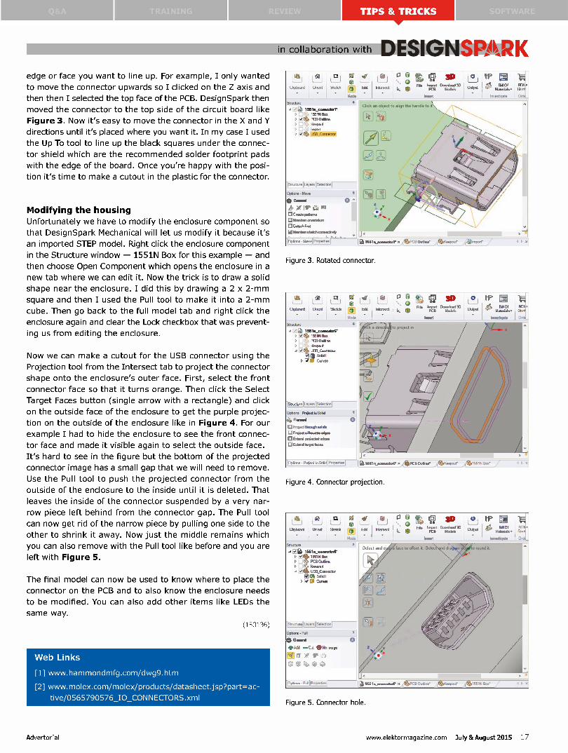
edge or face you want to line up. For example, I only wanted
to move the connector upwards so I clicked on the Z axis and
then then I selected the top face of the PCB. DesignSpark then
moved the connector to the top side of the circuit board like
Figure 3. Now it's easy to move the connector in the X and Y
directions until it's placed where you want it. In my case I used
the Up To tool to line up the black squares under the connec-
tor shield which are the recommended solder footprint pads
with the edge of the board. Once you're happy with the posi-
tion it's time to make a cutout in the plastic for the connector.
Modifying the housing
Unfortunately we have to modify the enclosure component so
that DesignSpark Mechanical will let us modify it because it's
an imported STEP model. Right click the enclosure component
in the Structure window — 1551N Box for this example — and
then choose Open Component which opens the enclosure in a
new tab where we can edit it. Now the trick is to draw a solid
shape near the enclosure. I did this by drawing a 2 x 2-mm
square and then I used the Pull tool to make it into a 2-mm
cube. Then go back to the full model tab and right click the
enclosure again and clear the Lock checkbox that was prevent-
ing us from editing the enclosure.
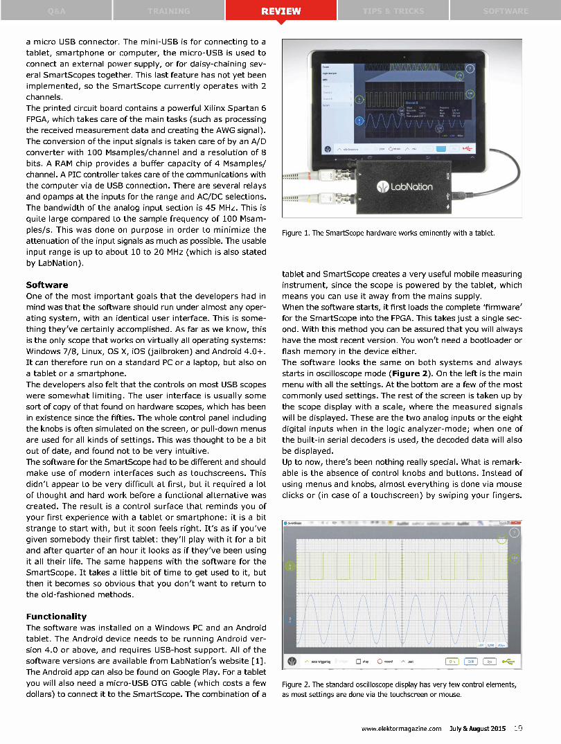
Now we can make a cutout for the USB connector using the
Projection tool from the Intersect tab to project the connector
shape onto the enclosure's outer face. First, select the front
connector face so that it turns orange. Then click the Select
Target Faces button (single arrow with a rectangle) and click
on the outside face of the enclosure to get the purple projec-
tion on the outside of the enclosure like in Figure 4. For our
example I had to hide the enclosure to see the front connec-
tor face and made it visible again to select the outside face.
It's hard to see in the figure but the bottom of the projected
connector image has a small gap that we will need to remove.
Use the Pull tool to push the projected connector from the
outside of the enclosure to the inside until it is deleted. That
leaves the inside of the connector suspended by a very nar-
row piece left behind from the connector gap. The Pull tool
can now get rid of the narrow piece by pulling one side to the
other to shrink it away. Now just the middle remains which
you can also remove with the Pull tool like before and you are
left with Figure 5.
The final model can now be used to know where to place the
connector on the PCB and to also know the enclosure needs
to be modified. You can also add other items like LEDs the
same way.
(150136)
Web Links
[1] www.hammondmfg.com/dwg9.htm
[2] www.molex.com/molex/products/datasheet.jsp?part=ac-
tive/0565790576 JO_CONNECTORS.xml
,Z1 Ci
(Apt° . inert Sketch
Structure
A e 1551n_coencetorr
lx 1551N Box
• if2, PCB Outline D r P irnport P U5B Connector
St muxelLayers ilSelectioni
Options -Move
0 General 1P
_I Maintain onentabon
—1 Detach first
¡j Maintain sketch connect. *
- •
10 Mose
End Intersect L.
File Import Download 3D PCB Models
Insert
• oa> â ,ge Bat Of RM. W WI Maim-Ws. (bird
Invesfinate I Or &
Click an object to align the handle to
,
EJCI
J< 1661 ,connactorr x PCB Outline ,ttaKeopoot
Figure 3. Rotated connector.
Urriboard Unent Sketch
5Irtrctine
• 1551n_co mooker
155IN Box
G , PCB Outline • ,
A e USB_Connec6x */ 3 Solid I
C) Curves
twcturee_axers liSelection
Ontions Prcjoot toSolid
Gemmel
] Prciect through solids
%red silk...cadges
7: &tend crowded ectoes
Extend target fac«
Oria" nn• - Prn,ert tn Said- Prop.-line
Import trld Intersect L. File PCB
Inset:
Figure 4. Connector projection.
to project in
Dosnload Models
o M
output Investigate
PCB Oodine ,teat wpoor 1e/1551N B.‘
ml n.rt Orda_
Let:nerd Orient Sketch
Structure
• 1551n_cormicabr
ey 1551N Bra
PCB Outline Kee ,r1
• USB_Ccenectcr
e 50101
eí Curves
Str vonIISdec ,
e lor Mode
Options -Pull
0 General
ir Add r» Cut O Nor,rrge
iIPL.
e
n 16filn_oe fflackar iStb PC8 Outline .(130(sepour ,(1 b1551N
Figure 5. Connector hole.
Advertorial www.elektormagazine.com July &August 2015 17

SmartScope: Multi-Platform Measuring I istrument Clever and distinctive USB scope By Harry Baggen (Elektor Netherlands Editorial)
Most USB oscilloscopes have been designed for use in combination with a Windows or Linux PC. The
SmartScope is an exception to this: it works just as well with an Android tablet, an iPad or an OS X
system. The software has been designed to make the user interface appear identical across all platforms.
We've tried one out on a PC and a tablet.
A fair number of (USB) oscilloscopes have previously been
reviewed and tested in Elektor. However, the SmartScope is a
measuring instrument that differs significantly from the com-
petition, in both hardware as well as software. Before we take
a closer look at the SmartScope, we'll first find out how this
project got started.
History
When electronic engineer Riemer Grootjans acquired a num-
ber of different USB scopes for use at work and at home, he
wasn't very pleased with these devices. He started to think
about designing one himself, which would have all the fea-
tures he expected of a USB scope: versatile, portable, easily
extended, and with an intuitive user interface. He started to
design the SmartScope along with two of his friends and set
up a Kickstarter campaign. Within a month their company
(LabNation) achieved over $300,000 of funding, which was
sufficient to start planning the production of these devices. A
lot of hard work was still ahead of them in the following few
months. Although the design for the hardware was completed
before the Kickstarter campaign, there turned out to be so
much demand for a sample buffer in the hardware that they
decided to create a completely new design. They succeeded
after many sleepless nights, and by the end of 2014, all of their
1500 backers had received their SmartScope (the production
started in August 2014).
Hardware
The hardware for the SmartScope consists of a small metal
enclosure (for good shielding), with a pair of full-sized BNC
connectors on the front for the analog inputs, and a 16-pin
header at the back, for the 8 digital inputs of the logic ana-
lyzer, 4 digital outputs, and the output of the built-in arbitrary
waveform generator (AWG). Also on the back are a mini and
18 July &August 2015 www.elektormagazine.com
a micro USB connector. The mini-USB is for connecting to a
tablet, smartphone or computer, the micro-USB is used to
connect an external power supply, or for daisy-chaining sev-
eral SmartScopes together. This last feature has not yet been
implemented, so the SmartScope currently operates with 2
channels.
The printed circuit board contains a powerful Xilinx Spartan 6
FPGA, which takes care of the main tasks (such as processing
the received measurement data and creating the AWG signal).
The conversion of the input signals is taken care of by an A/D
converter with 100 Msamples/channel and a resolution of 8
bits. A RAM chip provides a buffer capacity of 4 Msamples/
channel. A PIC controller takes care of the communications with
the computer via de USB connection. There are several relays
and opamps at the inputs for the range and AC/DC selections.
The bandwidth of the analog input section is 45 MHz. This is
quite large compared to the sample frequency of 100 Msam-
ples/s. This was done on purpose in order to minimize the
attenuation of the input signals as much as possible. The usable
input range is up to about 10 to 20 MHz (which is also stated
by LabNation).
Software
One of the most important goals that the developers had in
mind was that the software should run under almost any oper-
ating system, with an identical user interface. This is some-
thing they've certainly accomplished. As far as we know, this
is the only scope that works on virtually all operating systems:
Windows 7/8, Linux, OS X, iOS (jailbroken) and Android 4.0+.
It can therefore run on a standard PC or a laptop, but also on
a tablet or a smartphone.
The developers also felt that the controls on most USB scopes
were somewhat limiting. The user interface is usually some
sort of copy of that found on hardware scopes, which has been
in existence since the fifties. The whole control panel including
the knobs is often simulated on the screen, or pull-down menus
are used for all kinds of settings. This was thought to be a bit
out of date, and found not to be very intuitive.
The software for the SmartScope had to be different and should
make use of modern interfaces such as touchscreens. This
didn't appear to be very difficult at first, but it required a lot
of thought and hard work before a functional alternative was
created. The result is a control surface that reminds you of
your first experience with a tablet or smartphone: it is a bit
strange to start with, but it soon feels right. It's as if you've
given somebody their first tablet: they'll play with it for a bit
and after quarter of an hour it looks as if they've been using
it all their life. The same happens with the software for the
SmartScope. It takes a little bit of time to get used to it, but
then it becomes so obvious that you don't want to return to
the old-fashioned methods.
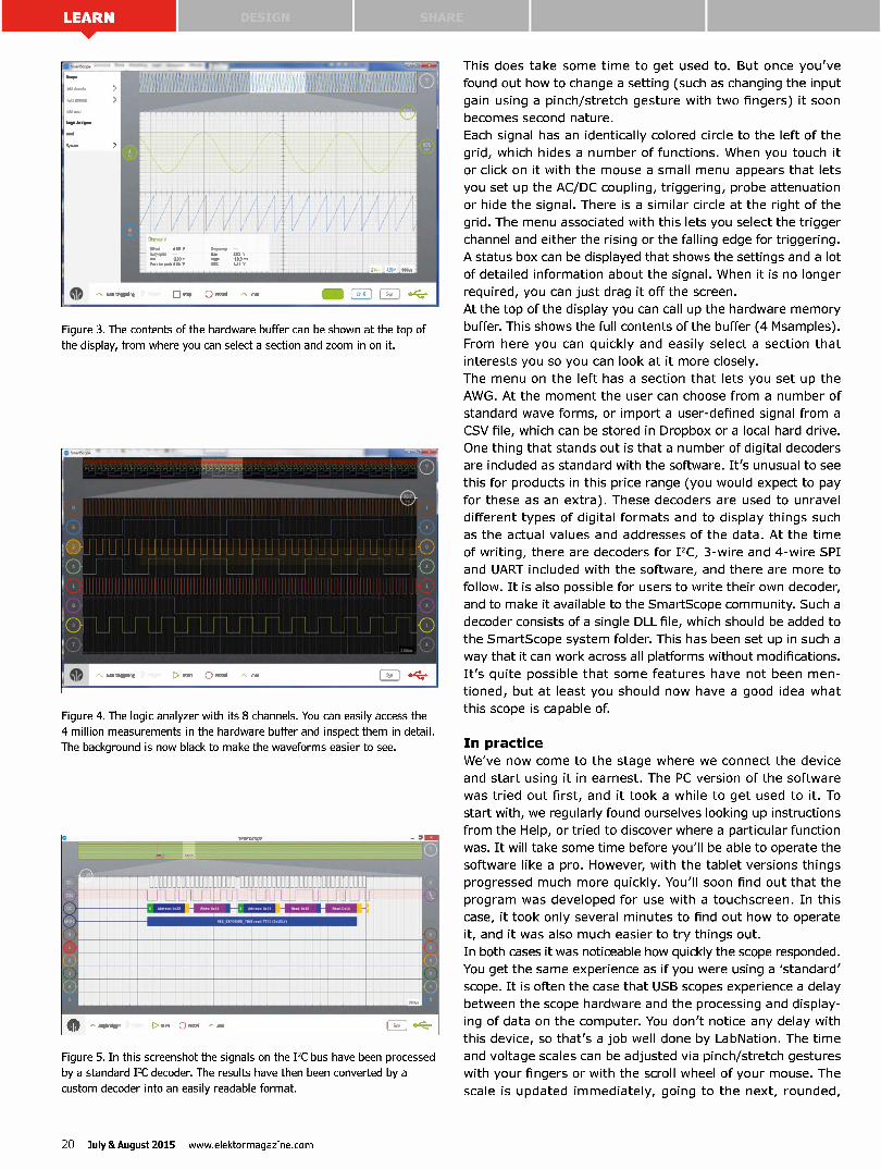
Functionality
The software was installed on a Windows PC and an Android
tablet. The Android device needs to be running Android ver-
sion 4.0 or above, and requires USB-host support. All of the
software versions are available from LabNation's website [1].
The Android app can also be found on Google Play. For a tablet
you will also need a micro-USB OTG cable (which costs a few
dollars) to connect it to the SmartScope. The combination of a
Figure 1. The SmartScope hardware works eminently with a tablet.
tablet and SmartScope creates a very useful mobile measuring
instrument, since the scope is powered by the tablet, which
means you can use it away from the mains supply.
When the software starts, it first loads the complete 'firmware'
for the SmartScope into the FPGA. This takes just a single sec-
ond. With this method you can be assured that you will always
have the most recent version. You won't need a bootloader or
flash memory in the device either.
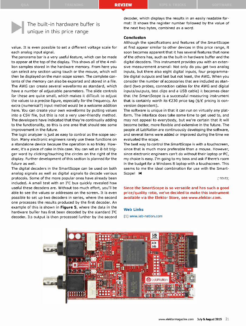
The software looks the same on both systems and always
starts in oscilloscope mode (Figure 2). On the left is the main
menu with all the settings. At the bottom are a few of the most
commonly used settings. The rest of the screen is taken up by
the scope display with a scale, where the measured signals
will be displayed. These are the two analog inputs or the eight
digital inputs when in the logic analyzer-mode; when one of
the built-in serial decoders is used, the decoded data will also
be displayed.
Up to now, there's been nothing really special. What is remark-
able is the absence of control knobs and buttons. Instead of
using menus and knobs, almost everything is done via mouse
clicks or (in case of a touchscreen) by swiping your fingers.
Figure 2. The standard oscilloscope display has very few control elements, as most settings are done via the touchscreen or mouse.
www.elektormagazine.com July &August 2015 19
,•••• • M u m
OM« V
hat cc ps1"1 05
iknotntgennt D rec. Alt
Figure 3. The contents of the hardware buffer can be shown at the top of the display, from where you can select a section and zoom in on it.
Figure 4. The logic analyzer with its 8 channels. You can easily access the 4 million measurements in the hardware buffer and inspect them in detail. The background is now black to make the waveforms easier to see.
CEZIZI -E =11-1:11 =1
, men C , rec,a
Figure 5. In this screenshot the signals on the I2C bus have been processed by a standard I2C decoder. The results have then been converted by a custom decoder into an easily readable format.
This does take some time to get used to. But once you've
found out how to change a setting (such as changing the input
gain using a pinch/stretch gesture with two fingers) it soon
becomes second nature.
Each signal has an identically colored circle to the left of the
grid, which hides a number of functions. When you touch it
or click on it with the mouse a small menu appears that lets
you set up the AC/DC coupling, triggering, probe attenuation
or hide the signal. There is a similar circle at the right of the
grid. The menu associated with this lets you select the trigger
channel and either the rising or the falling edge for triggering.
A status box can be displayed that shows the settings and a lot
of detailed information about the signal. When it is no longer
required, you can just drag it off the screen.
At the top of the display you can call up the hardware memory
buffer. This shows the full contents of the buffer (4 Msamples).
From here you can quickly and easily select a section that
interests you so you can look at it more closely.
The menu on the left has a section that lets you set up the
AWG. At the moment the user can choose from a number of
standard wave forms, or import a user-defined signal from a
CSV file, which can be stored in Dropbox or a local hard drive.
One thing that stands out is that a number of digital decoders
are included as standard with the software. It's unusual to see
this for products in this price range (you would expect to pay
for these as an extra). These decoders are used to unravel
different types of digital formats and to display things such
as the actual values and addresses of the data. At the time
of writing, there are decoders for I2C, 3-wire and 4-wire SPI
and UART included with the software, and there are more to
follow. It is also possible for users to write their own decoder,
and to make it available to the SmartScope community. Such a
decoder consists of a single DLL file, which should be added to
the SmartScope system folder. This has been set up in such a
way that it can work across all platforms without modifications.
It's quite possible that some features have not been men-
tioned, but at least you should now have a good idea what
this scope is capable of.
In practice
We've now come to the stage where we connect the device
and start using it in earnest. The PC version of the software
was tried out first, and it took a while to get used to it. To
start with, we regularly found ourselves looking up instructions
from the Help, or tried to discover where a particular function
was. It will take some time before you'll be able to operate the
software like a pro. However, with the tablet versions things
progressed much more quickly. You'll soon find out that the
program was developed for use with a touchscreen. In this
case, it took only several minutes to find out how to operate
it, and it was also much easier to try things out.
In both cases it was noticeable how quickly the scope responded.
You get the same experience as if you were using a 'standard'
scope. It is often the case that USB scopes experience a delay
between the scope hardware and the processing and display-
ing of data on the computer. You don't notice any delay with
this device, so that's a job well done by LabNation. The time
and voltage scales can be adjusted via pinch/stretch gestures
with your fingers or with the scroll wheel of your mouse. The
scale is updated immediately, going to the next, rounded,
20 July &August 2015 www.elektormagazine.com
The built-in hardware buffer is
unique in this price range
value. It is even possible to set a different voltage scale for
each analog input signal.
The panorama bar is a very useful feature, which can be made
to appear at the top of the display. This shows all of the 4 mil-
lion samples stored in the hardware memory. From here you
can select any section using touch or the mouse, which will
then be displayed on the main scope screen. The complete con-
tents of the memory can also be exported and stored in a file.
The AWG can create several waveforms as standard, which
have a number of adjustable parameters. The slide controls
for these are quite small, which makes it difficult to adjust
the values to a precise figure, especially for the frequency. An
extra (numerical?) input method would be a welcome addition
here. You can create your own waveforms by putting values
into a CSV file, but this is not a very user-friendly method.
The developers have indicated that they're continually adding
to the functionality, so this is one area that should see some
improvement in the future.
The logic analyzer is just as easy to control as the scope sec-
tion. Many electronic engineers rarely use these functions on
a standalone device because the operation is so tricky. How-
ever, it's a piece of cake in this case. You can set an 8-bit trig-
ger word by clicking/touching the circles on the right of the
display. Further development of this section is planned for the
future as well.
The digital decoders in the SmartScope can be used on both
analog signals as well as digital signals to decode various
protocols. Some of the more popular ones have already been
included. A small test with an I2C bus quickly revealed how
useful these decoders are. Without too much effort, you'll be
able to see the values or addresses on the screen. It is even
possible to set up two decoders in series, where the second
one processes the results produced by the first decoder. An
example of this is shown in Figure 5, where the data in the
hardware buffer has first been decoded by the standard I2C
decoder. Its output is then processed further by the second
decoder, which displays the results in an easily readable for-
mat: It shows the register number followed by the value of
the next two bytes, combined as a word.
Conclusion
Although the specifications and features of the SmartScope
at first appear similar to other devices in this price range, it
soon becomes apparent that it has several features that none
of the others has, such as the built-in hardware buffer and the
digital decoders. This instrument provides you with an exten-
sive measurement arsenal: Not only do you get two analog
inputs, but there also eight digital inputs, four programma-
ble digital outputs and last but not least, the AWG. When you
consider the number of accessories that are included as stan-
dard (two probes, connection cables for the AWG and digital
inputs/outputs, test clips and a USB cable) it becomes clear
that the SmartScope is a successful measuring instrument
that is certainly worth its €230 price tag ($/£ pricing is con-
version dependent).
The software is unique in that it can run on virtually any plat-
form. The interface does take some time to get used to, and
may not appeal to everybody, but we're certain that it will
become better, more flexible and extensive in the future. The
people at LabNation are continuously developing the software,
and several items were added or improved during the time we
evaluated the scope.
The best way to control the SmartScope is with a touchscreen,
since that is much more preferable than a mouse. However,
since electronic engineers can't do without their laptop or PC,
my choice is easy. I'm going to my boss and ask if there's room
in the budget for a Windows 8 laptop with a touchscreen. This
seems to me the ideal combination for use with the Smart-
Scope! k
(150153)
Since the SmartScope is so versatile and has such a good
price/quality ratio, we've decided to make this instrument
available via the Elektor Store, see www.elektor.com.
Web Links
[1] www.lab-nation.com
l• • • •q:-,- . (it e • • I ..
::,:•',.. -ff:111. :::1::_uS lq---Lij::— ••• ••
,.. 1Fr.eri. M., - -: ••• .i. e L--• E---. ,,-_- _;" e m.• ..... 111111111111x. :: ,.,... .E.
""«"1smartsco$ieri e r.:11 .m.u. 11111111iiiilliiiiIIIIIIIIIIilililll 1 -tli: - -1 .. :: I ••••• i • a ! 'g :41 . . . a .I.
- j .
, •. i, e L ......,.•,«. .- "' Z Zr ' -' --- - 14', tit r: • ..- - . z-.. _ .
P; • :e A.‘ • • • ' • 1 f«ri f o • 0 • Ira!
www.elektormagazine.com July &August 2015 21

ls'
e
I () W t.;
hc f
b c2.
b RTC
c ad0
cIrt -v
E' 00000001'
m ovw
Assembler (also called assembly lan-
guage; assembly code) is very much a
hardware-dependent programming lan-
guage and this in itself brings with it a
number of advantages and disadvantages.
When we use a high-level programming
language it's the compiler software that
determines how effectively the source
code is interpreted. In Assembler it's the
job of the programmer him or herself to
secure the most efficient outcome — both
in terms of code length and also execution
speed. This is because the conversion of
assembler code into machine language
(or hex code, as appropriate) is defined
very strictly.
Program length is a significant factor,
particularly when you are using a 'small'
microcontroller (a PIC10F200 for example
provides only 256 words of programming
memory). In complex calculations per-
formance can play a crucial role, since
under certain conditions a C compiler can
generate total nonsense. In cases like
this, where you need tight control over
the operation, it can even make sense
to process only certain vital parts of the
SEL ?1 G
IC® •.qt.gmbler
Course
Your first program in machine language
By Mir0SlaV Cina (Germany) [email protected]
In this day and age should we still be bothering
ourselves with Assembler? Absolutely yes in our
opinion; with 8-bit controllers it definitely pays
to keep our code short and snappy to maximize
execution speed. Our crash course — featuring a
small PIC controller — is based on the customary
mix of theory and practical matters.
program directly in Assembler. Here's
another advantage: for time-critical oper-
ations you can calculate pretty accurately
how many clock cycles (in other words
how long) an Assembler routine will take
to run.
Assembly language is also the best way
of getting to know your hardware right
down at detail level. Higher-level pro-
gramming languages tend to conceal the
actual operation of registers and similar
things from the programmer.
Nevertheless in Assembler you really
do end up doing everything yourself —
even multiplying two small numbers can
require some serious thinking.
Hard and software
For our course I have selected one of the
smallest PIC controllers, the PIC12F675
[1], a choice made having been involved
with PIC controllers from Microchip for
many years. The target price of this
microcontroller lies in the 1-euro/dollar/
pound range and for many simple appli-
cations this device is totally adequate.
For these experiments you will need
a PICkit2® programmer and a small
experimenter board (both of these are
frequently sold together as the PICkit2
starter kit). In the next part of the course
we'll see how you can produce a simple
experimenter board yourself. I should
mention you can naturally also use the
current PICkit3 programmer for this
course.
The software used comes gratis. In Win-
dows we can easily put together the
source text with the help of a text editor
(Notepad), and afterwards use the pro-
gram MPASM.exe (a constituent part of
the Microchip MPASM® suite) to assemble
it (in other words convert it into machine
language). The MPASM suite is in turn a
constituent part of the MPLAB IDE soft-
ware packages (IDE = Integrated Devel-
opment Environment). The MPLAB IDE
can be downloaded free from the Micro-
chip website [2].
The hex file produced after Assembling
is finally ported into the microcontroller
using the PICkit2 software. And that's it.
22 July &August 2015 www.elektormagazine.com PIC, PICKit and MPASM are registered trademarks of Microchip Inc.

The Registers
First of all we need to find out a little
about our microcontroller and learn a few
Assembler commands. Don't panic — the
first package of theory is easy to man-
age. With that out of the way, we can
now press on.
The PIC12F675 is an 8-bit microcontroller
from Microchip's 'midrange' family. The
microcontroller is available in a PDIP-8
package (other options exist). Six out of
its eight little legs are usable as gener-
al-purpose digital port pins (GPO to GP5).
GP3 can be used only as an input, with
the remaining pins being either inputs or
outputs. The chip includes 1024 words of
flash program memory plus 64 bytes of
SRAM for general (undefined) use and
128 bytes of [[PROM.
When you program in Assembler, you
need to involve yourself with registers,
which in this case are 1 byte-large mem-
ory modules having a specific logical
function. Some registers belong to the
core (kernel); for calculations these can
accommodate 8-bit values for instance,
or else they may provide information on
the state of the controller. Other regis-
ters have responsibility for the peripheral
blocks of the controller, such as the GPIO
register, which represents the status of
the inputs and outputs.
With PICs you always have (at least) four
core registers:
• W register
• Config register
• Option register (OPTION_REG)
• Status register (STATUS)
The 64 bytes-large SRAM is for unre-
stricted use, and almost all the regis-
ters are accessed at defined memory
addresses. Using an address that's 8 bits
long we can address a total of 256 mem-
ory locations. Looking at the so-called
memory map (Figure 1) you can spot
that not all 256 memory locations are in
fact available. Taking the status register
for example, this can be accessed not only
at address 03h but also at 83h.
On this map we can also see that the
GPIO register (which we are about to get
involved with) can be found at memory
location 05h. At the same time it can be
seen that the application memory (64
bytes) is accessed at memory addresses
20h to 5Fh.
The exceptions are registers that don't
have memory space. Included in these
exceptions are the Option register, also
the W register.
The W register is the 'register-in-chief'
of the microcontroller (W = working). All
arithmetic operations are performed using
the W register for instance.
The Status register is divided into indi-
vidual bits (see Figure 2). Crucial at this
stage is bit number 5 (RPO), the 'register
bank select bit'. This toggles between the
two memory banks; the bit has to be set
or cleared before you provide an address
as a parameter of a command that fol-
lows. Access to memory locations 80h
to FFh needs this bit to be set; if RPO =
0, then we are addressing memory loca-
tions 00h to 7Fh.
The Config register is used for flashing the
controller (described later on). It deter-
mines, for instance, whether the internal
oscillator of the controller is to be used.
At this stage we will skip the Option reg-
ister altogether. We shall now briefly con-
cern ourselves with three further registers
that, in contrast to the registers just men-
tioned, are responsible for peripherals.
TRISIO, GPIO and ANSEL
The TRISIO, GPIO and ANSEL registers
are used for I/O control. Right now the
only thing we need to know about the
ANSEL register is that for our initial exper-
iments we need to set it at 00h in order
to deactivate the analog functionality.
The TRISIO register controls the direction
of communication. Whether a port pin
functions as an input or output depends
on how the relevant bits of the TRISIO
register are set. Value 0 signifies out-
put, 1 is input. If the first bit is zero for
instance (written TRISIO<O> = 0), pin
GPO is used as an output.
The sole exception is, as already men-
tioned, port pin GP3 (this also has the
function MCLR = Master Clear), which
can be used only as an input. The rele-
vant bit of the TRISIO register is conse-
quently always 1.
We can manipulate the inputs and out-
puts directly with the help of the GPIO
register. A write action to the GPIO reg-
ister controls the pins configured as out-
puts directly; the inputs can be scanned
by taking a read action from the GPIO
register.
First com mands
Now it's time to get to know a few Assem-
bler commands (the basic commands, so
File Address
Indirect addr 11
TMRO
PCL
STATUS
FSR
GPIO
PCLATH
INTCON
PIR1
TMR1L
TMR1H
T1CON
CMCON
ADRESI-1(2)
ADCON0l2)
General Purpose Registers
EJtes
Bank 0
00h
01h 02h
03h
04h
05h
06h
07h
08h
09h
0Ah
013h
OCh
ODh
OEh
OFh
10h
11h
12h
13h
14h
15h
16h
17h
18h
19h
1Ah
1Bh
1Ch
1Dh
1Eh
1Fh
20h
5Fh eon
7Fh
File Address
Indirect addr.M
OPTION_REG
PCL
STATUS
FSR
TRISIO
PCLATH
INTCON
PIE1
PCON
OSCCAL
WPU
IOC
VRCON
EEDATA
EEADR
EECON1
EECON241)
ADRESLM
AN SE
accesses 20h-5Fh
Bank 1
8011
81h 82h
83h
8411
8511
8611
87h
8811
89h
8Ah
8Bh
8Ch
8Dh
8Eh
8Fh
9011
91h
92h
9311
9411
9511
96h
9711
9811
9911
9Ah
9Bh
9Ch
9Dh
9Eh
9Fh
AOh
DFh E0h
FFh
Unimplemented data memory locations, read as '0' 1: Not a physical register. 2: PIC12F675 only.
Figure 1. The memory map displays the addresses of the registers and memory locations available for undefined use.
IRP RP1 RPO TO PD
bit 7
DC I C
bit 0
Figure 2. The various bits of the Status register.
www.elektormagazine.com July &August 2015 23
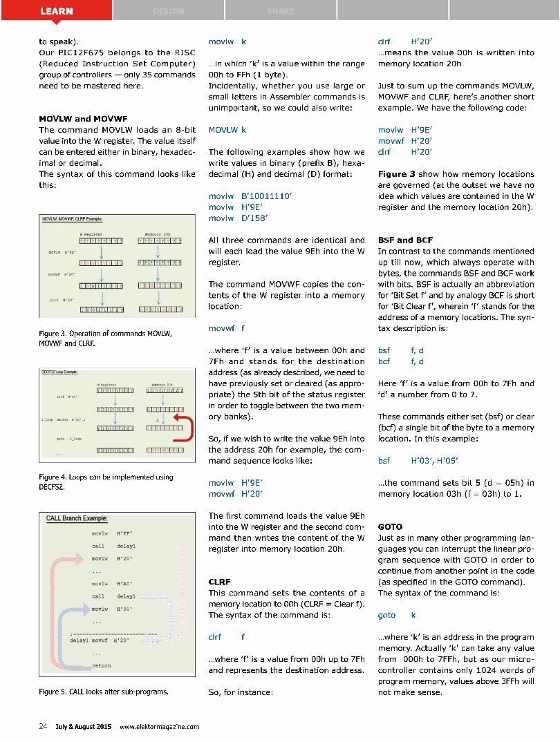
to speak).
Our PIC12F675 belongs to the RISC
(Reduced Instruction Set Computer)
group of controllers — only 35 commands
need to be mastered here.
MOVLW and MOV WF
The command MOVLW loads an 8-bit
value into the W register. The value itself
can be entered either in binary, hexadec-
imal or decimal.
The syntax of this command looks like
this:
MOVLW, MOVWF, CLRF Example:
M0010 119E'
movwf
clrf 11.20.
Ii lO lo II1I ii il
Addh hee 20h
iqq?pi ?pp'
111111111
111111
Figure 3. Operation of commands MOVLW, MOVWF and CLRF.
DECFSZLnopEtelple:
elrf 0.20'
l_loop dear. 0.20..1
go. i_leee
emplaces Address 20h
r 17171717171 71 71 l? 171717171A ?
l?U1117171U?1?1
FMEMEIFIFIMME
111111111
IIIIIIIII
1,1?1?1?1?1?1?11 P10101011.11 I
Figure 4. Loops can be implemented using DECFSZ.
Figure 5. CALL looks after sub-programs.
movlw k
...in which 'k' is a value within the range
00h to FFh (1 byte).
Incidentally, whether you use large or
small letters in Assembler commands is
unimportant, so we could also write:
The following examples show how we
write values in binary (prefix B), hexa-
decimal (H) and decimal (D) format:
movlw 6'10011110'
movlw H'9E'
movlw D'158'
All three commands are identical and
will each load the value 9Eh into the W
register.
The command MOVWF copies the con-
tents of the W register into a memory
location:
movwf f
...where 'f' is a value between 00h and
7Fh and stands for the destination
address (as already described, we need to
have previously set or cleared (as appro-
priate) the 5th bit of the status register
in order to toggle between the two mem-
ory banks).
So, if we wish to write the value 9Eh into
the address 20h for example, the com-
mand sequence looks like:
movlw H'9E'
movwf H'20'
The first command loads the value 9Eh
into the W register and the second com-
mand then writes the content of the W
register into memory location 20h.
CLRF
This command sets the contents of a
memory location to 00h (CLRF = Clear f).
The syntax of the command is:
clrf
...where 'f' is a value from 00h up to 7Fh
and represents the destination address.
So, for instance:
H'20'
...means the value 00h is written into
memory location 20h.
Just to sum up the commands MOVLW,
MOVWF and CLRF, here's another short
example. We have the following code:
movlw H'9E'
movwf H'20'
clrf H'20'
Figure 3 show how memory locations
are governed (at the outset we have no
idea which values are contained in the W
register and the memory location 20h).
BSF and BCF
In contrast to the commands mentioned
up till now, which always operate with
bytes, the commands BSF and BCF work
with bits. BSF is actually an abbreviation
for 'Bit Set f' and by analogy BCF is short
for 'Bit Clear f', wherein 'f' stands for the
address of a memory locations. The syn-
tax description is:
Here 'f' is a value from 00h to 7Fh and
'd' a number from 0 to 7.
These commands either set (bsf) or clear
(bcf) a single bit of the byte to a memory
location. In this example:
H'03', H'05'
...the command sets bit 5 (d = 05h) in
memory location 03h (f = 03h) to 1.
GOTO
Just as in many other programming lan-
guages you can interrupt the linear pro-
gram sequence with GOTO in order to
continue from another point in the code
(as specified in the GOTO command).
The syntax of the command is:
...where 'k' is an address in the program
memory. Actually 'k' can take any value
from 000h to 7FFh, but as our micro-
controller contains only 1024 words of
program memory, values above 3FFh will
not make sense.
24 July &August 2015 www.elektormagazine.com
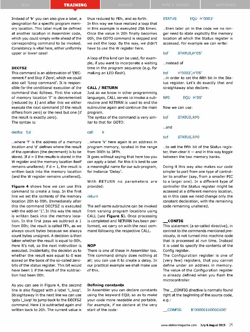
Instead of 'k' you can also give a label, a
designation for a specific program mem-
ory location. This label must be defined
at another location in Assembler code,
which you could simply write ahead of the
corresponding command to be invoked.
Consistency is vital here, either uniformly
upper or lower case!
DECFSZ
This command is an abbreviation of 'DEC-
rement F and Skip if Zero', which we could
also call 'Loop command'. It is respon-
sible for the conditional execution of the
command that follows. First the value
of memory location 'f' is decremented
(reduced by 1) and after this we either
execute the next command (if the result
differs from zero) or the next but one (if
the result is exactly zero).
The syntax is:
decfsz fid
...where 'f' is the address of a memory
location and 'd' defines where the result
of the operation (the decrement) is to be
stored. If d = 0 the results is stored in the
W register and the memory location itself
remains unaltered; if d = 1, the result is
written back into the memory location
(and the W register remains unaltered).
Figure 4 shows how we can use this
command to create a loop. In the first
line we set the contents of the memory
location 20h to 00h. Immediately after
this the command DECFSZ is executed
with the add-on '1'. In this way the result
is written back into the memory loca-
tion. In the first pass we subtract a 1
from 00h; the result is called FFh, as we
always count bytes because we always
count bytes unsigned. A decision is then
taken whether the result is equal to 00h.
Here it's not, so the next instruction is
executed. Incidentally, the decision as to
whether the result was equal to 0 was
scored on the basis of the so-called zero-
bits of the status register. This bit would
have been 1 if the result of the subtrac-
tion had been 00h.
As you can see in Figure 4, the second
line is also flagged with a label 'l_loop'.
Straightaway in the next line we can use
'goto l_loop' to jump back to the DECFSZ
command. Here 1 is subtracted again and
written back to 20h. The current value is
thus reduced to FEh, and so forth.
In this way we have realized a loop that
in this example is executed 256 times.
Once the value in 20h finally becomes
00h, the GOTO command is skipped and
we exit the loop. By the way, we didn't
have to use the W register here.
A loop of this kind can be used, for exam-
ple, if you want to incorporate a waiting
time in the program sequence (e.g. for
making an LED flash).
CALL / RETURN
Just as we know in other programming
languages, CALL serves to invoke a sub-
routine and RETURN is used to end the
subroutine again and continue the main
program.
The syntax of the command is very sim-
ilar to that for GOTO:
...where 'k' here again is an address in
program memory, located in the range
from 000h to 3FFh.
It goes without saying that here too you
can apply a label. For this it is best to use
a meaningful name for our sub-program,
for instance 'Delay'.
With RETURN no parameters are
provided:
The self-same subroutine can be invoked
from varying program locations using
CALL (see Figure 5). Once processing
is completed and RETURN has been per-
formed, we carry on with the next com-
mand following the respective CALL.
NOP
There is one of these in Assembler too.
This command simply does nothing at
all; you can use it to create a delay. In
our practical example we shall make use
of this.
Defining constants
In Assembler you can declare constants
using the keyword EQU, so as to make
your code more readable and portable.
For example, if we declare at the very
start of the code:
STATUS EQU H'0003'
...then later on in the code we no lon-
ger need to state explicitly the memory
location at which the Status register is
accessed. For example we can write:
STATUS,H'05'
...instead of
H'0003',H'05'
...in order to set the fifth bit in the Sta-
tus register. Let's do exactly that and
straightaway also declare:
Now we can use:
STATUS,RPO
...and
bcf STATUS,RPO
...to set the fifth bit of the Status regis-
ter, then clear it — and in this way toggle
between the two memory banks.
Doing it this way also makes our code
simpler to port from one type of control-
ler to another (say, from a smaller PIC
to a larger one). In a different type of
controller the Status register might be
accessed at a different memory location,
so in this case we need change only the
constant declaration, with the remaining
code remaining unaltered.
_ CONFIG
This statement (a so-called directive), in
contrast to the commands mentioned pre-
viously, is not turned into machine code
that is processed at run time. Instead
it is used to specify the contents of the
Config register.
The Configuration register is one of
(very few) registers, that you cannot
define under an address in memory.
The value of the Configuration register
is already defined when you flash the
microcontroller.
The CONFIG directive is normally found
right at the beginning of the source code,
e.g.:
CONFIG 6'00000110000100'
www.elektormagazine.com July &August 2015 25
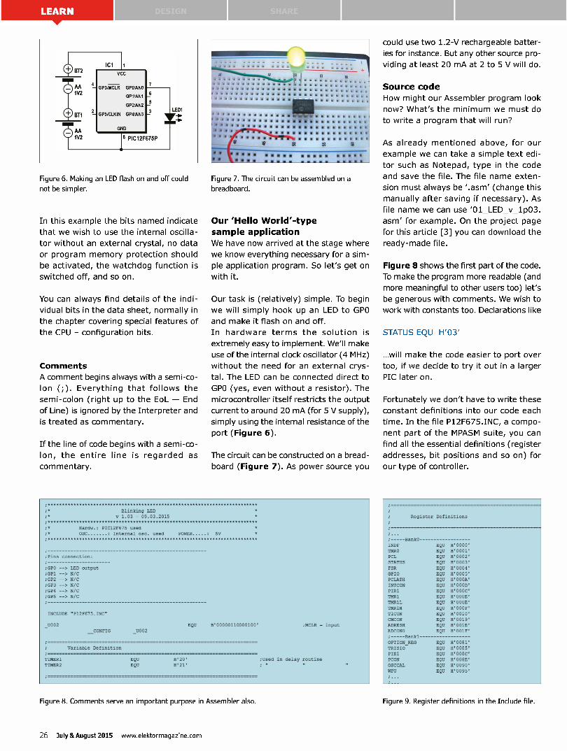
Figure 6. Making an LED flash on and off could not be simpler.
Figure 7. The circuit can be assembled on a breadboard.
In this example the bits named indicate
that we wish to use the internal oscilla-
tor without an external crystal, no data
or program memory protection should
be activated, the watchdog function is
switched off, and so on.
You can always find details of the indi-
vidual bits in the data sheet, normally in
the chapter covering special features of
the CPU - configuration bits.
Comments
A comment begins always with a semi-co-
lon (;). Everything that follows the
semi-colon (right up to the EoL — End
of Line) is ignored by the Interpreter and
is treated as commentary.
If the line of code begins with a semi-co-
lon, the entire line is regarded as
commentary.
• • • • • •
I •
OP •
e
Our 'Hello World'-type
sa mple application
We have now arrived at the stage where
we know everything necessary for a sim-
ple application program. So let's get on
with it.
Our task is (relatively) simple. To begin
we will simply hook up an LED to GPO
and make it flash on and off.
In hardware terms the solution is
extremely easy to implement. We'll make
use of the internal clock oscillator (4 MHz)
without the need for an external crys-
tal. The LED can be connected direct to
GPO (yes, even without a resistor). The
microcontroller itself restricts the output
current to around 20 mA (for 5 V supply),
simply using the internal resistance of the
port (Figure 6).
The circuit can be constructed on a bread-
board (Figure 7). As power source you
Blinking LED v 1.03 09.03.2015
;* Hardy.: PIC12F675 used
• Internal osc. used POWER • 5V
;Pins connection:
;GPO --> LED output
;GP1 --> N/C ;GP2 --> N/C
;GP3 --> N/C ;GP4 --> N/C
;GP5 --> N/C
INCLUDE "P12F675.INC"
_0002 EQU
CONFIG _U002
Variable Definition
TINERI
TINER2
B'00000110000100' ,MCLR - input
EQU
EQU
11.20 .
H'21 .
;Used in delay routine
Figure 8. Comments serve an important purpose in Assembler also.
could use two 1.2-V rechargeable batter-
ies for instance. But any other source pro-
viding at least 20 mA at 2 to 5 V will do.
Source code
How might our Assembler program look
now? What's the minimum we must do
to write a program that will run?
As already mentioned above, for our
example we can take a simple text edi-
tor such as Notepad, type in the code
and save the file. The file name exten-
sion must always be '.asm' (change this
manually after saving if necessary). As
file name we can use '01_LED_v_1p03.
asm' for example. On the project page
for this article [3] you can download the
ready-made file.
Figure 8 shows the first part of the code.
To make the program more readable (and
more meaningful to other users too) let's
be generous with comments. We wish to
work with constants too. Declarations like
STATUS EQU H'03'
will make the code easier to port over
too, if we decide to try it out in a larger
PIC later on.
Fortunately we don't have to write these
constant definitions into our code each
time. In the file P12F675.INC, a compo-
nent part of the MPASM suite, you can
find all the essential definitions (register
addresses, bit positions and so on) for
our type of controller.
RegiDter Dcfinitions
• Bank0
INDF EQU H'0000'
Trek° EQ17 H0001' PCL EQU H'0002' STATUS PQt1 N'0003'
FSR EOM H'0004'
GPIO DOW H'0005' PCLATD EQU H'000A . INTCON EQU H'00013 .
PIR1 EQU H'000C . TNR1 EQU H'000E .
M IL EQU H'000E . TURIN EQU H'000F'
11UON EQU H'0010' CMCON EQU H'0019'
ADRESE EQU H'001E' AnCONO EQU 11.001F .
Bankl
gIT 1 01- "G EQU 11'0081' EQU wooes. PIE1 EQU 11'000C . PCON EQU E'008E.
OSCCAI EQU H'0090'
WPU EQU H'0095'
Figure 9. Register definitions in the Include file.
26 July &August 2015 www.elektormagazine.com
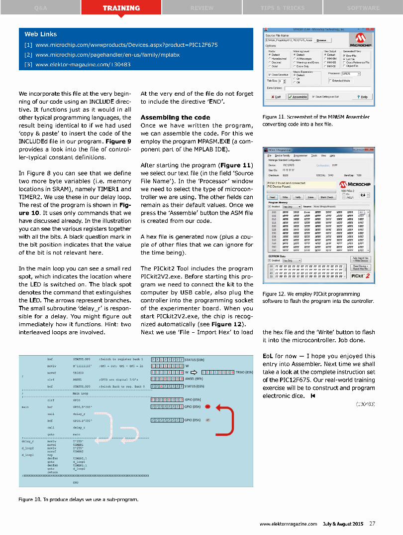
TIPS fit TRICKS
Web Links
[1] www.microchip.com/wwwproducts/Devices.aspx?product=PIC12F675
[2] www.microchip.com/pagehandler/en-us/family/mplabx
[3] www.elektor-magazine.com/130483
We incorporate this file at the very begin-
ning of our code using an INCLUDE direc-
tive. It functions just as it would in all
other typical programming languages, the
result being identical to if we had used
'copy 81 paste' to insert the code of the
INCLUDEd file in our program. Figure 9
provides a look into the file of control-
ler-typical constant definitions.
In Figure 8 you can see that we define
two more byte variables (i.e. memory
locations in SRAM), namely TIMER1 and
TIMER2. We use these in our delay loop.
The rest of the program is shown in Fig-
ure 10. It uses only commands that we
have discussed already. In the illustration
you can see the various registers together
with all the bits. A black question mark in
the bit position indicates that the value
of the bit is not relevant here.
In the main loop you can see a small red
spot, which indicates the location where
the LED is switched on. The black spot
denotes the command that extinguishes
the LED. The arrows represent branches.
The small subroutine 'delay_r' is respon-
sible for a delay. You might figure out
immediately how it functions. Hint: two
interleaved loops are involved.
At the very end of the file do not forget
to include the directive 'END'.
Assembling the code
Once we have written the program,
we can assemble the code. For this we
employ the program MPASM.EXE (a com-
ponent part of the MPLAB IDE).
After starting the program (Figure 11)
we select our text file (in the field 'Source
File Name'). In the 'Processor' window
we need to select the type of microcon-
troller we are using. The other fields can
remain as their default values. Once we
press the 'Assemble' button the ASM file
is created from our code.
A hex file is generated now (plus a cou-
ple of other files that we can ignore for
the time being).
The PICkit2 Tool includes the program
PICkit2V2.exe. Before starting this pro-
gram we need to connect the kit to the
computer by USB cable, also plug the
controller into the programming socket
of the experimenter board. When you
start PICkit2V2.exe, the chip is recog-
nized automatically (see Figure 12).
Next we use 'File - Import Hex' to load
bof
m ew
mould
clrf
bcf
STATOS,RPO
B.11111110'
TRISTO
ANSEL
STATOS,RPO
:Switch ro register Dank 1
:GPO out: G111 - GP5 - in
,GPIO are digital I/O ,
:Switch Back to reg. Bank 0
Rain Loop
. 1 n
delay_r
clrf
bet
. 11
Tef
. 11
go o
GPIO
GP M, D.000 •
delay_ r
GPIO, D. 000
delay_r
= vie 1).255 •
move/ TIMER'
d_loop2 movie D•255 .
move! TTML112
d loopl nop
decfsr TINER2,1
gota d_loopl
decfsr TIKER1, 1
go o d_loop2
return
»D(XXX)00(X:(30000CC013000 M M(YatICGOOCCOCOCCIOCODOCCOCIOCOC000000C000C0000000000(
END
1?1?1?1? Ii UM:111101 Fi Ii li 11 111 1111 0 10 10 10 in p i 01 1 01
pploPPP1?1?1
P1,1111 ,11 1-.,17111 -oppIrIt1
STATUS (03h)
W 1 4o
AN5F1(9F11)
SIATUS(03h)
Il ji F1 ililillil ti
GPIO (05h)
GPIO (05h) 1111
GPIO (05h)
TRSIO (85h)
Figure 11. Screenshot of the MPASM Assembler converting code into a hex file.
1111PICkit 2 Program
fi Delce Family Erogrammer look belp
Merge Swan, Coreg men
Devax_ TIC121675
tharlDa: IT IT FT IT
(Teem . 0E00
PICkit 2 found nntl rmnnaited
PIC De me Found,
MFF
O.., J44U t.ane
II lis.«,116-- 11 I Ingram lIa may
k Embed
000
008
010
018
020
028
090
038
040
060
038
1.0 *
C S. MICROCHIP VIM M at 2
u 25 Irj n un
50.111,0, INC « (E mer....0
3FFF
3,F
3FFF
any
331T 3FFF
3F ,
MIT
3F ,
3FFF
3FFF
3FFF
3111
311r
3FFF
3377
317T
3/11
Jr u
3TFT 18 ,
3FFF
3F ,
3T1T
3FF?
se w
3FTT
3FTT
3111
3111
3FFF
3FFT
rr
SETT
trrr
3FFF
3TTT
3FFT
3F1T
31,73,
3FFT
AFFT
3FFF
3TTT
3FFT
ittt
3FFF
3IFF
3FFF
3FFF
MIT
3TTF AFFF
9FFF
3FF
3E77
9FFF
3F11
lITT
3E77 31,1
3371
3 m
e n'
any
3TTT
31,11
3FTF
3121,
3I77 3F ,
3FFF
3
3FFT
3FFF
3FFF
3FFF
3FFF
3 m
3FFF
3e1T
B ORON M ee
Entered % Oda
00 IT IT 77 Ft T IT IT IT IT FT ir rr rr n n n -
rr rr er er Fr rr rr rr rr rr rr er rr rr '
20 FF FF FF FF FF Fr FT FF FT IT FF FT FF Fr FT FF
30 Fr FF FS FF Fr Fr Fr FF Fr FF Fr Fr FF FF Fr Fr -
heolreeelbe A.Mielbraie
BeetHmene
PICkit. 2
Figure 12. We employ PICkit programming software to flash the program into the controller.
the hex file and the 'Write' button to flash
it into the microcontroller. Job done.
EoL for now — I hope you enjoyed this
entry into Assembler. Next time we shall
take a look at the complete instruction set
of the PIC12F675. Our real-world training
exercise will be to construct and program
electronic dice. 11
(130483)
Figure 10. To produce delays we use a sub-program.
www.elektormagazine.com July &August 2015 27

DESIGN
By Jan Visser and Jaime González-Arintero
Some time ago the two of us did a few webinars adclres
electronics. Although these mini shows produced nic
could not attend the live events and requested wr
they are, printed, some tips for the tip of the sol
No lip-sync, just live (for better or worse)
Some time ago Jan V and Jaime G-A did a short series of
webinars addressing different topics: Jan explained, and Jaime
learned a lot. Feeling curious too?
Navigate to [po.st/soldersoldiers] to watch the entire session.
QFN's are frustrating to retlow-solder in home
labs due to tombstoning. Any advice to get these
tiny guys securely positioned using contact soldering
techniques?
A Although we'll address contactless soldering techniques
in an upcoming installment, this is an interesting question
that also involves the good old soldering iron! But first, let's
explain what "tombstoning" means. Figure 1 shows the effect
with an SMD resistor, since this way it's easier to understand:
the different reflow times of the pads the component sits on (i.e.
the solder paste on one pad melts before the other) produces
a torque, causing the component to tilt like a tombstone. Only
nice at Halloween!
-*?(Almost) Everything You Always Wanted to Know About...
ri
/f ropula ,questions about general
rdÈack, we realized that some of you simply
ersions of some of the questions. So here
iron.
With QFN's, the issue can get trickier. However, these packages
include a thermal/ground pad that may be very useful secure
them down on the PCB before soldering the pins. If we're lucky
enough, the pad on the PCB will have a hole (Figure 2).
Now, with a piece of Kapton tape we can easily fix the
component on the board, and solder it through the back of
the PCB, with the soldering iron tip in the hole. The Kapton
tape will easily withstand the temperature, and after that the
QFN will be perfectly fixed, so we can proceed to solder the
pins on the front side.
Any tips on using the drag method, please?
A Drag soldering is easy-peasy to experts, and frustrating
to newcomers. Preventing bridging in pins is quite
challenging, and some components may (literally) get fried if
we're not quick enough. The tip of a mini spoon can ease the
job (e.g. ]BC's C245-931 cartridge), since you'll be able to
"load" the tip with solder, and release it gradually. You may
need to experiment with the angle (as shown in Figure 3),
gently turning the tip as the solder is transferred to the pins.
To keep the solder fluid, apply flux generously and make sure
that the tip is not oxidized. Besides, lead-free solder has a
different viscosity, and may be more difficult for beginners
to handle.
Finding the right speed for the iron (across the pins) and the
solder feed can be tricky. Try feeding the solder slightly above
the tip, that is, not melting the solder right at the ede of the
tip, but one or two millimeters away.
28 July &August 2015 www.elektormagazine.com
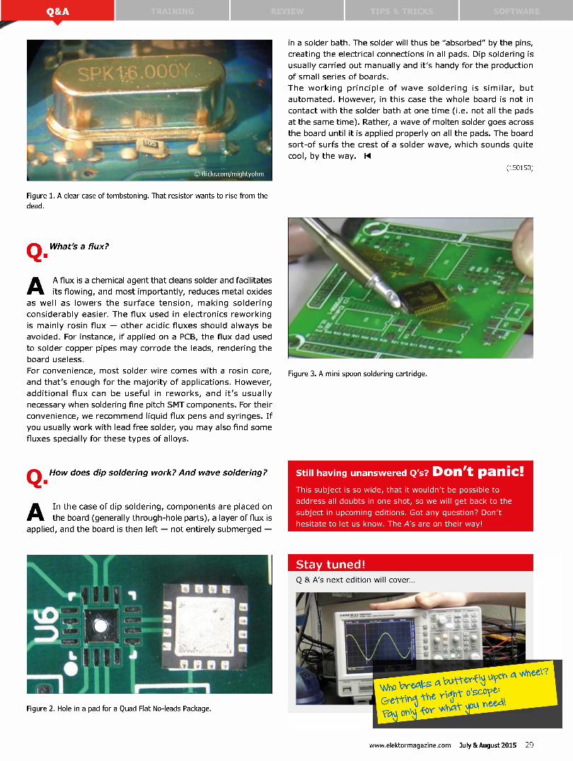
4
C) flickr.com/mightyohm
Figure 1. A clear case of tombstoning. That resistor wants to rise from the dead.
A What's a flux?
A A flux is a chemical agent that cleans solder and facilitates
its flowing, and most importantly, reduces metal oxides
as well as lowers the surface tension, making soldering
considerably easier. The flux used in electronics reworking
is mainly rosin flux — other acidic fluxes should always be
avoided. For instance, if applied on a PCB, the flux dad used
to solder copper pipes may corrode the leads, rendering the
board useless.
For convenience, most solder wire comes with a rosin core,
and that's enough for the majority of applications. However,
additional flux can be useful in reworks, and it's usually
necessary when soldering fine pitch SMT components. For their
convenience, we recommend liquid flux pens and syringes. If
you usually work with lead free solder, you may also find some
fluxes specially for these types of alloys.
How does dip soldering work? And wave soldering?
A In the case of dip soldering, components are placed on
the board (generally through-hole parts), a layer of flux is
applied, and the board is then left — not entirely submerged —
Figure 2. Hole in a pad for a Quad Flat No-leads Package.
in a solder bath. The solder will thus be "absorbed" by the pins,
creating the electrical connections in all pads. Dip soldering is
usually carried out manually and it's handy for the production
of small series of boards.
The working principle of wave soldering is similar, but
automated. However, in this case the whole board is not in
contact with the solder bath at one time (i.e. not all the pads
at the same time). Rather, a wave of molten solder goes across
the board until it is applied properly on all the pads. The board
sort-of surfs the crest of a solder wave, which sounds quite
cool, by the way. N
(150150)
Figure 3. A mini spoon soldering cartridge.
Still having unanswered Q's? Don't panic! This subject is so wide, that it wouldn't be possible to
address all doubts in one shot, so we will get back to the
subject in upcoming editions. Got any question? Don't
hesitate to let us know. The A's are on their way!
Sta tuned! Q & A's next edition will cover...
U 010Y-fAV.S A 1Qu\.tert\ U\70Y\ A \Wee?
&ettirl .the y'vent o'scove u 'Fe\ on\ -tor what
www.elektormagazine.com July &August 2015 29

DESIGN
IM11111111113111111 MB MI
MMBM MZ-Z-
Apps with Connections
% \15:0art 1
Windows app programming for electronics enthusiasts
•
By Dr. Veikko Krypczyk (Germany)
Apps — small applications with intuitive user interfaces, often designed for touchscreens — are all the
rage nowadays. Apps that run on tablets as well as desktop PCs can also be programmed for Windows
8.1. In the first article of this series we present a get-u-going guide for app programming, and in the
second article we show you how to control external hardware with an app.
eiWindows Phone
t" : is Windows RT
Figure 1. Operating systems for apps and their target platforms.
Nowadays apps are available for virtually
every sort of use and application area.
Before you start programming apps, it's
a good idea to learn more about the pos-
sible target platforms and resulting appli-
cation areas. In common language, apps
are small application programs for mobile
devices. The target operating systems for
apps are Android (Google), iOS (Apple),
Windows Phone and Windows 8.1 (both
Microsoft). Android and iOS run on smart-
phones as well as tablets, but Microsoft
has two different operating systems for
these two hardware platforms. Windows
Phone is intended for smartphones, while
Windows 8.1 RunTime is intended for tab-
lets. However, Windows 8.1 RunTime is
also available on all PCs (desktop or note-
Figure 2. The Start screen of Windows 8.1 is the "home base" for all apps. The user interface is always intuitive and based on the content; the software is only there for support. Example: a weather app (photo montage).
book) with a current version of the Win-
dows operating system, where it runs
more or less in parallel with the conven-
tional Windows desktop OS (Figure 1). A
characteristic feature of apps is that they
focus on a single task. The user interface
(UI) is always intuitive and designed for
touch operation. Along with functionality,
the design and user experience are criti-
cal factors (Figure 2). Windows 8.1 runs
not only on tablets but also on conven-
tional desktop and notebook PCs, which
allow external devices to be connected
(usually over USB).
With their focus on the essential content
and their modern design and user inter-
face, apps appear to be ideal for con-
trolling external electronic devices. For
instance, they can enable users to per-
form switching operations (output) or
monitor specific environmental param-
eters using sensors (input). All of this
should be done intuitively; the software is
only there for support. Microsoft plans to
expand the app concept for Windows 10,
with the aim of having a single application
for all device classes from smartphones
to desktop PCs.
30 July 8f August 2015 www.elektormagazine.com
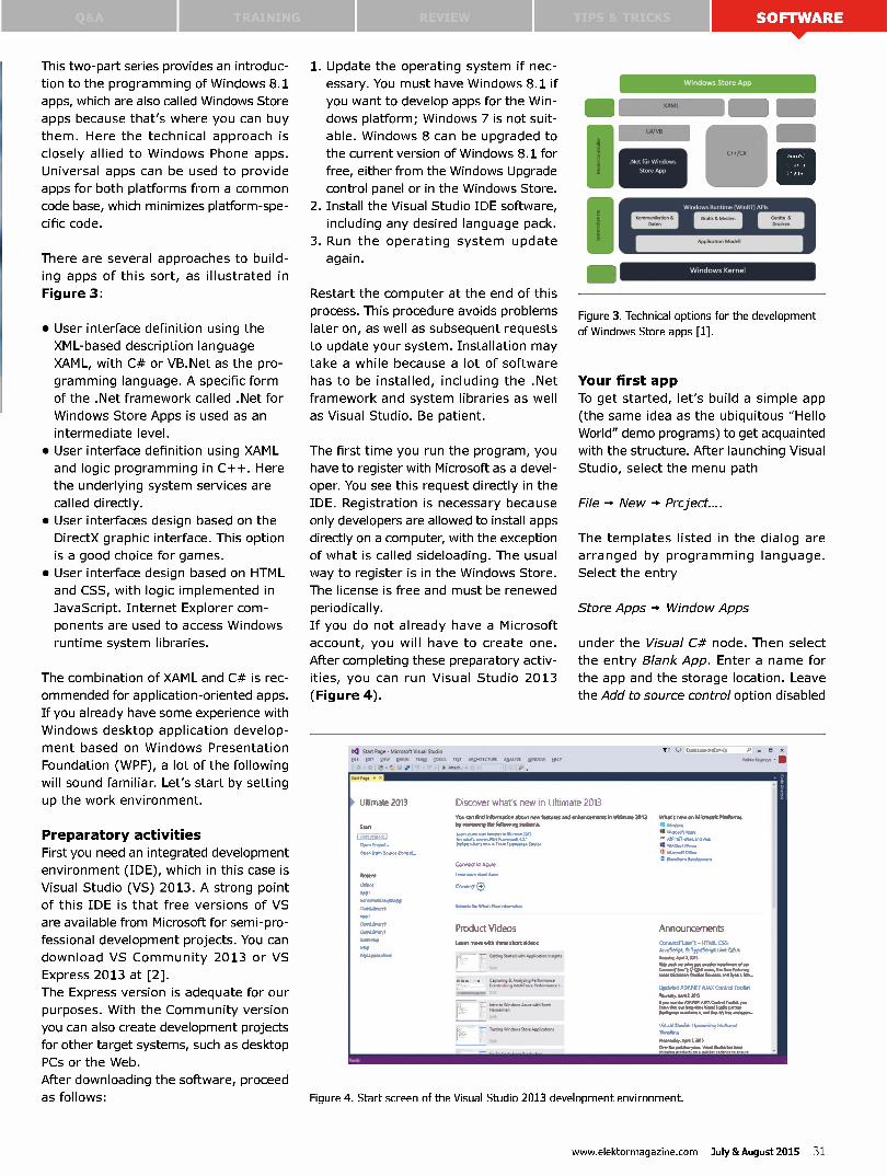
This two-part series provides an introduc-
tion to the programming of Windows 8.1
apps, which are also called Windows Store
apps because that's where you can buy
them. Here the technical approach is
closely allied to Windows Phone apps.
Universal apps can be used to provide
apps for both platforms from a common
code base, which minimizes platform-spe-
cific code.
There are several approaches to build-
ing apps of this sort, as illustrated in
Figure 3:
• User interface definition using the
XML-based description language
XAML, with C# or VB.Net as the pro-
gramming language. A specific form
of the .Net framework called .Net for
Windows Store Apps is used as an
intermediate level.
• User interface definition using XAML
and logic programming in C++. Here
the underlying system services are
called directly.
• User interfaces design based on the
DirectX graphic interface. This option
is a good choice for games.
• User interface design based on HTML
and CSS, with logic implemented in
JavaScript. Internet Explorer com-
ponents are used to access Windows
runtime system libraries.
The combination of XAML and C# is rec-
ommended for application-oriented apps.
If you already have some experience with
Windows desktop application develop-
ment based on Windows Presentation
Foundation (WPF), a lot of the following
will sound familiar. Let's start by setting
up the work environment.
Preparatory activities
First you need an integrated development
environment (IDE), which in this case is
Visual Studio (VS) 2013. A strong point
of this IDE is that free versions of VS
are available from Microsoft for semi-pro-
fessional development projects. You can
download VS Community 2013 or VS
Express 2013 at [2].
The Express version is adequate for our
purposes. With the Community version
you can also create development projects
for other target systems, such as desktop
PCs or the Web.
After downloading the software, proceed
as follows:
1. Update the operating system if nec-
essary. You must have Windows 8.1 if
you want to develop apps for the Win-
dows platform; Windows 7 is not suit-
able. Windows 8 can be upgraded to
the current version of Windows 8.1 for
free, either from the Windows Upgrade
control panel or in the Windows Store.
2. Install the Visual Studio IDE software,
including any desired language pack.
3. Run the operating system update
again.
Restart the computer at the end of this
process. This procedure avoids problems
later on, as well as subsequent requests
to update your system. Installation may
take a while because a lot of software
has to be installed, including the .Net
framework and system libraries as well
as Visual Studio. Be patient.
The first time you run the program, you
have to register with Microsoft as a devel-
oper. You see this request directly in the
IDE. Registration is necessary because
only developers are allowed to install apps
directly on a computer, with the exception
of what is called sideloading. The usual
way to register is in the Windows Store.
The license is free and must be renewed
periodically.
If you do not already have a Microsoft
account, you will have to create one.
After completing these preparatory activ-
ities, you can run Visual Studio 2013
(Figure 4).
Figure 3. Technical options for the development of Windows Store apps [1].
Your first app
To get started, let's build a simple app
(the same idea as the ubiquitous "Hello
World" demo programs) to get acquainted
with the structure. After launching Visual
Studio, select the menu path
File -› New -› Prcject....
The templates listed in the dialog are
arranged by programming language.
Select the entry
Store Apps -› Window Apps
under the Visual C# node. Then select
the entry Blank App. Enter a name for
the app and the storage location. Leave
the Add to source control option disabled
4 Start Page • Microsoft Visual Studio to LW eve ga m TEAO 1001.5 TOT •
•
- 0 x
Ultimate 2013
Recent
eldcf
AnalFortiametApp
.stixaryl
LnYix.xx.,
•,e
..FooPeewronl 7 Gating Steed xnh tx.4Xlee
• • C.. , ,,x •hx.ex'x'xx‘.
— Wine XXXer,auxt *eh X. Xxx<Xxo
Discover what's new in Ultimate 2013
Y. can find information about new features and enhancements in Ultimate 2013
by reviewing 11••• following sections.
Leenexou ne. Ite m .• um... On. See taxir, Iwo n • runnels/II
Connect O x.re
conned C)
kexxielneWhqsXx. rdormaton
Product Videos
Learn more with that short wdeos
T•gnq Stet Ax.xxxx
Whars new On t•eicrosoft
• m..••0.x.x..< ASP fer Me, and we
a
Announcements
Connect:'irvel: - 11,11_ C55 lavaScript & typeScript Live CP.
tunent,ere ane TM ow* wel.X.,x,extlebe . ..um al ow Cxxx1Orldret if C10.“ .... .• Idals Mo m, Davin Um ., end. 1.1.-
Updated ASP NEI AlAX Control Toollut
Thundox A.111203
koptem OcuelXvernputur 0.dexereu m a . . Oa rt. le• rd eon-
Wellmiday.,•,1 OU Oxa wa fe m. va st.e.
• '
Figure 4. Start screen of the Visual Studio 2013 development environment.
www.elektormagazine.com July &August 2015 31
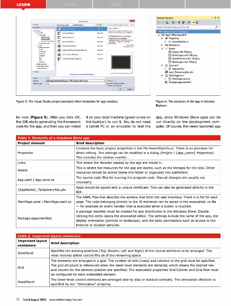
DESIGN
Solution Explorer
e Recent
• Metalled
• Visual Cn
a Meet App.
U' ..i Apo,
Waldo. ARK
Windows Ucktoo
r. Web
r Off ne/SharePoint
lightSoOsh
Poporbno
Silverlight
WCP
Worldlow
e Other Lanquagos
Olber Project Types
Online
tlenne. 491
locution DADropboinArt.beKArtikee.Windoen_0_1_RT,Aoo_OcktenTeil nc
;dew. 'twee Nei
1 MI Fronseerod..1.3
New Project
- Sort!. Vetuult ttt IE
n Hub Apo (Wintlonds)
ri (1.41 Agin (Winitorn)
▪ Soln Atsit (Window')
Class Lib , Witendone)
nfirHowt Runtime Component (W0dows)
d' i Unit TH. I anew
irj Lod. Ul lest Protect (Windinto)
a r k b. ..to itt o n n 1 1. n rtfan (L. t o is 1.
Vitus, Co
Vi sI C#
ViUWICI
Visual <a
WIo.ICU
Vinod re
Pnual
Sea, r led Templates (CtoleE) Pj
Ty , venal Cst
U Add ApplIcaton Insights to Protect
Merosoft recommends add , Agagalonabon Inm es telemetry to twiny., undentand and eptIm.e Peormonce.
team more nrreacy Statement
-I Kra. , I
(mute director, to. solobon
n Wdd to eoyrce control OK Camel
Figure 5. The Visual Studio project assistant offers templates for app creation.
for now (Figure 5). After you click OK,
the IDE starts generating the framework
code for the app, and then you can install
it on your local machine (green arrow on
the taskbar) to run it. You do not need
a tablet PC or an emulator to test the
- fr
Search Solution Explorer (Ctrkii)
Solution 'Appt (1 project)
• Appl (Windows 8.1)
A fr Properties CU AssemblyInfo.cs
.-U References
• Assets
Logo.scale-100.png
Smalllogo.scale-100.png
SplashScreen.scale-100.png
StoreLogo.scale-100.png
,▪ r.) App.xaml E ti App.xaml.cs
Appl_TemporaryKey.pfx
• ,lj MainPage.xaml
E ti MainPage.xaml.cs Package.appxmanifest
Figure 6. The structure of the app in Solution Explorer.
app, since Windows Store apps can be
run directly on the development com-
puter. Of course, the newly launched app
ments of a Windows Store ar i ll
Project element Brief description
Properties
Contains the basic project properties in the file AssemblyInfo.cs. There is no provision for
direct editing. The settings can be modified in a dialog (Project I {app_name} Properties).
This includes the version number.
Links This where the libraries needed by the app are linked in.
A ssets This is where the resources for the app are stored, such as the bitmaps for the tiles. Other
resources should be stored below this folder or organized into subfolders.
App.xaml I App.xaml.cs The source code files for running the program code. Manual changes are usually not
necessary.
{AppName}_TemporaryKey.pfx Apps should be signed with a unique certificate. This can also be generated directly in the
IDE.
MainPage.xaml I MainPage.xaml.cs
The XAML files that describe the screens that form the user interface. There is a file for each
page. The code belonging directly to the UI elements can be saved in the associated .cs file
— for example an event handler that is executed when a button is touched.
Package.appxmanifest
A package manifest must be created for app distribution in the Windows Store. Double-
clicking this entry opens the associated editor. The settings include the name of the app, the
display orientation (portrait or landscape), and the basic permissions such as access to the
Internet or location services.
Table 2. Important layout containers
Important layout
containers
DockPanel
Brief description
Specifies the docking positions (Top, Bottom, Left and Right) of the control elements to be arranged. The
most recently added control fills all of the remaining space.
Grid
The elements are arranged in a grid. The number of cells (rows) and columns in the grid must be specified.
The grid structure is referenced when the lower-level elements are declared, which means the desired row
and column for the element position are specified. The associated properties Grid.Column and Grid.Row must
be configured for each embedded element.
StackPanel The lower-level control elements are arranged side by side or stacked vertically. The orientation direction is
specified by the "Orientation" property.
32 July &August 2015 www.elektormagazine.com
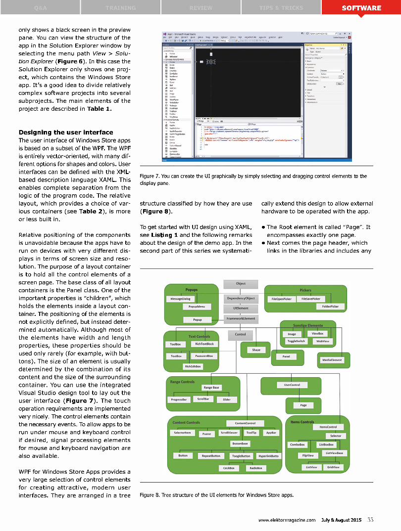
only shows a black screen in the preview
pane. You can view the structure of the
app in the Solution Explorer window by
selecting the menu path View > Solu-
tion Explorer (Figure 6). In this case the
Solution Explorer only shows one proj-
ect, which contains the Windows Store
app. It's a good idea to divide relatively
complex software projects into several
subprojects. The main elements of the
project are described in Table 1.
Designing the user interface
The user interface of Windows Store apps
is based on a subset of the WPF. The WPF
is entirely vector-oriented, with many dif-
ferent options for shapes and colors. User
interfaces can be defined with the XML-
based description language XAML. This
enables complete separation from the
logic of the program code. The relative
layout, which provides a choice of var-
ious containers (see Table 2), is more
or less built in.
Relative positioning of the components
is unavoidable because the apps have to
run on devices with very different dis-
plays in terms of screen size and reso-
lution. The purpose of a layout container
is to hold all the control elements of a
screen page. The base class of all layout
containers is the Panel class. One of the
important properties is "children", which
holds the elements inside a layout con-
tainer. The positioning of the elements is
not explicitly defined, but instead deter-
mined automatically. Although most of
the elements have width and length
properties, these properties should be
used only rarely (for example, with but-
tons). The size of an element is usually
determined by the combination of its
content and the size of the surrounding
container. You can use the integrated
Visual Studio design tool to lay out the
user interface (Figure 7). The touch
operation requirements are implemented
very nicely. The control elements contain
the necessary events. To allow apps to be
run under mouse and keyboard control
if desired, signal processing elements
for mouse and keyboard navigation are
also available.
WPF for Windows Store Apps provides a
very large selection of control elements
for creating attractive, modern user
interfaces. They are arranged in a tree
.4 3001 • »ouch Yoe, Stee to, tort ,Ired [POIKY ,,,Latoo out, moo, ouruo oLe 1,e0Or 313,
etemut.Lornutueet.enrreeeueLOOL Lore.. "
or torrood.-,r =erce,oeue, Lernoueseerueourr, ,,, to. tee, • Ispr
Le.
Figure 7. You can create the UI graphically by simply selecting and dragging control elements to the display pane.
structure classified by how they are use cally extend this design to allow external
(Figure 8).
To get started with UI design using XAML,
see Listing 1 and the following remarks
about the design of the demo app. In the
second part of this series we systemati-
hardware to be operated with the app.
• The Root element is called "Page". It
encompasses exactly one page.
• Next comes the page header, which
links in the libraries and includes any
Figure 8. Tree structure of the UI elements for Windows Store apps.
www.elektormagazine.com July &August 2015 33
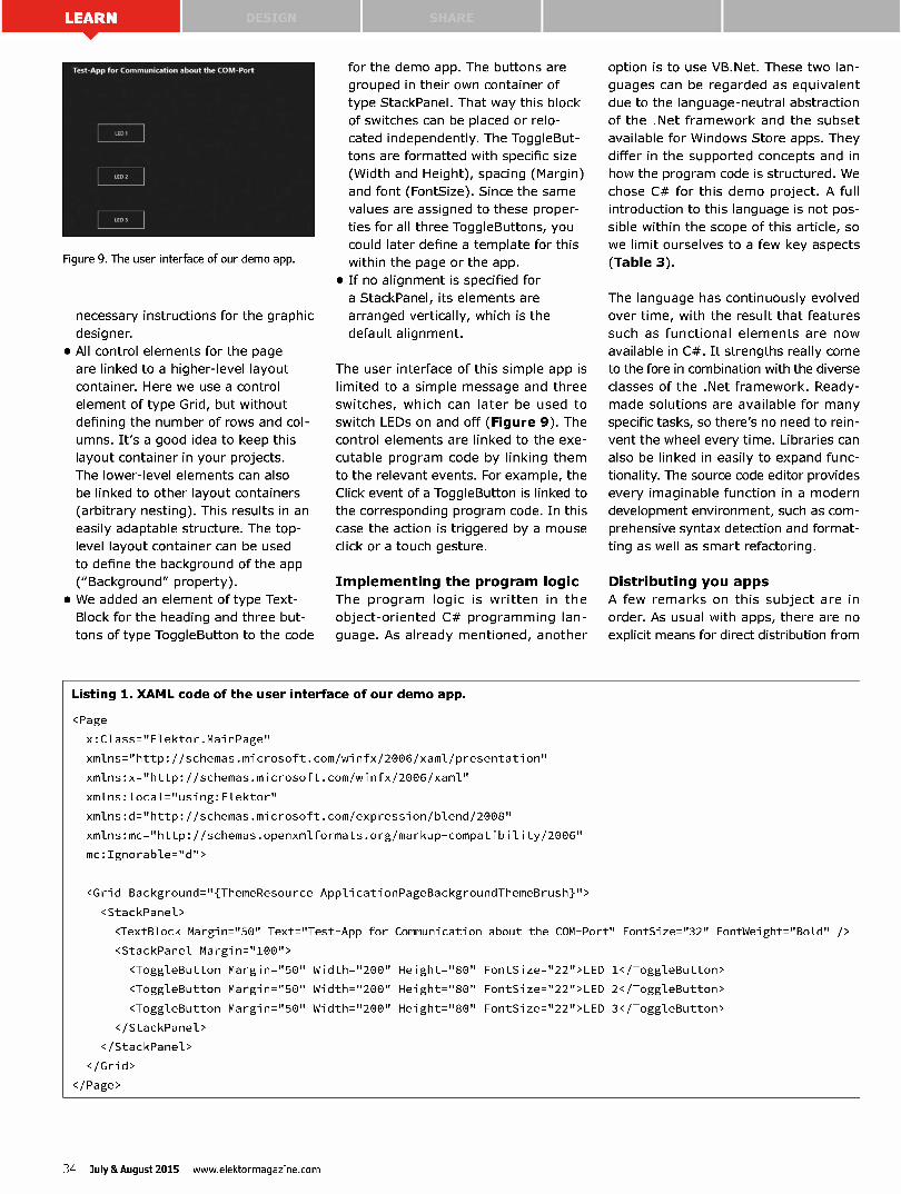
•1112; ffl SHARE
Test-App for Communication about the CONI-Port
LEO 1
LED
Figure 9. The user interface of our demo app.
necessary instructions for the graphic
designer.
• All control elements for the page
are linked to a higher-level layout
container. Here we use a control
element of type Grid, but without
defining the number of rows and col-
umns. It's a good idea to keep this
layout container in your projects.
The lower-level elements can also
be linked to other layout containers
(arbitrary nesting). This results in an
easily adaptable structure. The top-
level layout container can be used
to define the background of the app
("Background" property).
• We added an element of type Text-
Block for the heading and three but-
tons of type ToggleButton to the code
for the demo app. The buttons are
grouped in their own container of
type StackPanel. That way this block
of switches can be placed or relo-
cated independently. The ToggleBut-
tons are formatted with specific size
(Width and Height), spacing (Margin)
and font (FontSize). Since the same
values are assigned to these proper-
ties for all three ToggleButtons, you
could later define a template for this
within the page or the app.
• If no alignment is specified for
a StackPanel, its elements are
arranged vertically, which is the
default alignment.
The user interface of this simple app is
limited to a simple message and three
switches, which can later be used to
switch LEDs on and off (Figure 9). The
control elements are linked to the exe-
cutable program code by linking them
to the relevant events. For example, the
Click event of a ToggleButton is linked to
the corresponding program code. In this
case the action is triggered by a mouse
click or a touch gesture.
Implementing the progra m logic
The program logic is written in the
object-oriented C# programming lan-
guage. As already mentioned, another
option is to use VB.Net. These two lan-
guages can be regarded as equivalent
due to the language-neutral abstraction
of the .Net framework and the subset
available for Windows Store apps. They
differ in the supported concepts and in
how the program code is structured. We
chose C# for this demo project. A full
introduction to this language is not pos-
sible within the scope of this article, so
we limit ourselves to a few key aspects
(Table 3).
The language has continuously evolved
over time, with the result that features
such as functional elements are now
available in C#. It strengths really come
to the fore in combination with the diverse
classes of the .Net framework. Ready-
made solutions are available for many
specific tasks, so there's no need to rein-
vent the wheel every time. Libraries can
also be linked in easily to expand func-
tionality. The source code editor provides
every imaginable function in a modern
development environment, such as com-
prehensive syntax detection and format-
ting as well as smart refactoring.
Distributing you apps
A few remarks on this subject are in
order. As usual with apps, there are no
explicit means for direct distribution from
Listing 1. XAML code of the user interface of our demo app.
<Page
x:Class="Elektor.MainPage"
xmlns="http://schemas.microsoft.com/winfx/2006/xaml/presentation"
xmlns:x="http://schemas.microsoft.com/winfx/2006/xaml"
xmlns:local="using:Elektor"
xmlns:d="http://schemas.microsoft.com/expression/blend/2008"
xmlns:mc="http://schemas.openxmlformats.org/markup-compatibility/2006"
mc:Ignorable="d"›
<Grid Background="{ThemeResource ApplicationPageBackgroundThemeBrush}">
<StackPanel>
<TextBlock Margin="50" Text="Test-App for Communication about the COM-Port" FontSize="32" FontWeight="Bold"
<StackPanel Margin="100"›
<ToggleButton Margin="50" Width="200" Height="80" FontSize="22">LED 1</ToggleButton>
<ToggleButton Margin="50" Width="200" Height="80" FontSize="22">LED 2</ToggleButton>
<ToggleButton Margin="50" Width="200" Height="80" FontSize="22">LED 3</ToggleButton>
</StackPanel>
</StackPanel>
</Grid>
</Page>
/ >
34 July &August 2015 www.elektormagazine.com

developers to users. All apps have to be
installed from the App Store. Neverthe-
less, for testing you can use a develop-
ment license to enable installation on
other test computers in addition to the
development computer (which is what
we did). It is also possible to bypass the
App Store by using sideloading to distrib-
ute the apps to target devices. However,
once your app has left the test phase
and may be of interest to a larger audi-
ence, it should be made available in the
App Store. For this the app must comply
with a number of formal conditions, such
as making image resources available to
the app in a defined form and embed-
ding them in the right places (for dis-
playing the tiles, for example). Finally,
the app has to pass a final test run with
a Microsoft certification tool. After this
you should upload your app to the Win-
dows Store and provide the associated
formal data (age restrictions, privacy pro-
tection, license conditions and price). A
short while later Microsoft will send you
confirmation of acceptance, and your app
is available for all interested parties. It's
all easier than it sounds, and the process
is well documented at [3].
Conclusion and outlook
There's a lot more that could be said
about programming apps. Detailed infor-
mation is available in [1]. In the second
article of this series we describe how to
control external hardware over a virtual
COM port and USB, which should be very
interesting for electronics enthusiasts.
Our hardware platform for this is the
well-known Arduino Uno with the Elektor
Extension shield. On the software side we
have to deal with the difficulty that apps
actually run in a protected environment
called a sandbox, with very limited com-
munication options for security reasons.
But don't worry — we have found a way
around that!
(140411-I)
BRU MBOBB MI -M E MB WI MBB -111M MI M M -
Ma Z.
Table 3. Important language features of C#
Language construct
Keywords Syntax / Example
Comment in source code
One-line: /I Multi-line: /*...*/
/I This is a simple comment
/* This is a multi-line
comment */
Elementary data
types
byte
int float
double decimal
string
int quantity = 5;
string text = „character string";
Basic operations
+
- *
/
int total = addendl + addend2; float product = factorl * factor2;
Loop instructions
for loop
for ( int i = 0; i < upper limit; i++)
{ II loop body
}
while loop
while (condition == true)
{ II loop body
}
do loop
do
{ II loop body
} while (condition == true)
foreach loop
foreach (type variable of enumerated type)
{ II loop body
}
break
for ( int i = 0; i < upper limit; i++)
{ II loop body
} if (condition2 == true) break;
}
continue
for ( int i = 0; i < upper limit; i++)
{ II loop body } if (condition2 == true) continue;
}
Selection instructions
If
else if else
switch (...) case
If (a==3) a=5;
User-defined data types
struct
struct record
{ int age;
string name;
}
User-defined
classes class
class MyClass: BasicClass
{ int AnAttribute; private void AMethod(...)
{ ....
} }
Reference Documents 8( Web Links
[1] Huber, T. C.: Windows Store Apps with XAML and C#, Galileo Press, 2013.
[2] www.visualstudio.com/downloads/en-us/download-visual-studio-vs.aspx
[3] https://dev.windows.com/en-us/publish
www.elektormagazine.com July &August 2015 35

m min Tips and Tricks From readers for readers Here are some more neat solutions from our readers, sure to
make life a little easier for engineers and electronics tinkerers.
ATmega168 Oscillator output — From Burkhard Kainka ( Recently while developing an application usin
a Mega8 microcontroller I hit the memory buffers 4•0
memory full. Switching to the Mega168 went without
hitch and now I had 16 KB to play with. Whilst programmi
the fuses I was curious to notice an option which had previou
not been available on the Mega8 namely: 'Clock output
PORTB0'. With
frequency cou
hooked up to
it should now
possible to gut
check the accuracy
of the RC oscillator
without the need
for any additional
software. No sooner
said than done:
11059 kHz, oh
yes I was using an
external crystal for
the clock source.
After that I selected
the internal 8 MHz-
RC oscillator with a 1:8 prescaler, the reading was now 1001 kHz,
with some variability of the value after the decimal point. The
oscillator easily keeps within the specified 1 °A tolerance for this
clock source. The same experiment using the 128-kHz
/ oscillator showed significantly poorer accuracy.
STK500 I- I fx1
Program Fuses I LockElits I Advanced I Board I Auto I
F Brownout detection level at VCC-2.7 V; [BODLEVEL-4 col r Brown-out detection level at VCC-1.8 [BODLEVEL.110] r Brown-out detection disabled; IBODLEVEL.111] 17. Divide clock by 8 internally; [CKDIV&01 F Clock output on PORTE10: [CKOUT=0] 17 En Dock; Std-up the PWRDWN/RESET: S CK/14 CK + O rns; [CI( r Ext. Dock; Start-up time PWRDWN/RESET: 6 CK/14 CK + 4.1 ms; [CI r En Clock; Start.up the ROWN/RESET: 6 CK/14 CK + 65 ms; [D Int RC Osc. 8 MHz; Stad-up rime PWROWN/RESET 6 CK/14 CK + 0 r Int RC O. 8 MHz; Start-up time PWRDWN/RESET: 6 CK/14 CK + 4 F Int RC Oso. 8 MHz; Start-up the PWRDWN/RESET: 6 CK/14 CK + 6 r Int. RC CISC. 128kHz; Start-up urne PWRDWN/RESET: 6 CK/14 CK + F In RC OSC. 128kHz; Start-up time PWROWNIRESET, 6 CK/14 GK.* r Int RC 0. 128kHz; Start-up time PWRDWN/RESET: 6 CK/14 CK + r Ext. Low-Freq. Crystal; Start-up time PWRDWN/FIESET 1K CK/14 CK r E.t. Low-Fred Crustal: Start-uo time PWRDWN/IRESET: 1K CK/14 CK
..,1
[•:/- Auto Verify
Smart Wamings Program I Vri R d
Entering programming mode.. OK! Writing fuses .. OxF9, 005, Ox02.. OKI Reading fuses .. OxF9, Ox1)5, Ox02.. OK! Fuse bits verification.. OK Leaving programming mode. OK!
Make Contact with Magnets ( From Peter Bitzer
mie As a regular Elektor reader who can go way back to the
first edition in 1970 I have never seen this helpful hint in
print before: Standard battery recharger units are not usually
able to accommodate some common NiCd cells sizes such as
those with a diameter of 32.5 mm and a length of 90 mm. To
recharge these I used to use flying leads and croc clips to make
contact with the battery solder tags.
It was always a bit hit or miss and sometimes when I returned,
a croc clip might have pinged off, leaving the batteries only
partly charged.
The outer contact surfaces of battery electrodes are made of
steel; we can put this to good use... I'm sure everyone is famil-
iar with those small, low cost, very strong neodymium magnets
that you can pick up quite cheaply on the Internet (they come
in all shapes and sizes). The magnet's surface is electrically con-
ductive and they make really good contact pads for rechargeable
batteries (see photos).
The advantages are:
• Reliable contacts
• Less hassle
• No problem with croc clips springing off
• No need for a battery holder
• They also work on batteries without solder tags
• You save on clips (two batteries can be linked with one magnet).
14 (150135)
Got a neat solution for a tricky prob-
lem? Using components or tools in
ways they were never intended to
be used? Think your idea to solve
a problem is better than the usual
method? Have you discovered a work-
around that you want to share with us and fellow
makers? Don't hang around; write to us now,
for every tip we publish you'll earn 40 pounds!
f'ee
0.
36 July &August 2015 www.elektormagazine.com
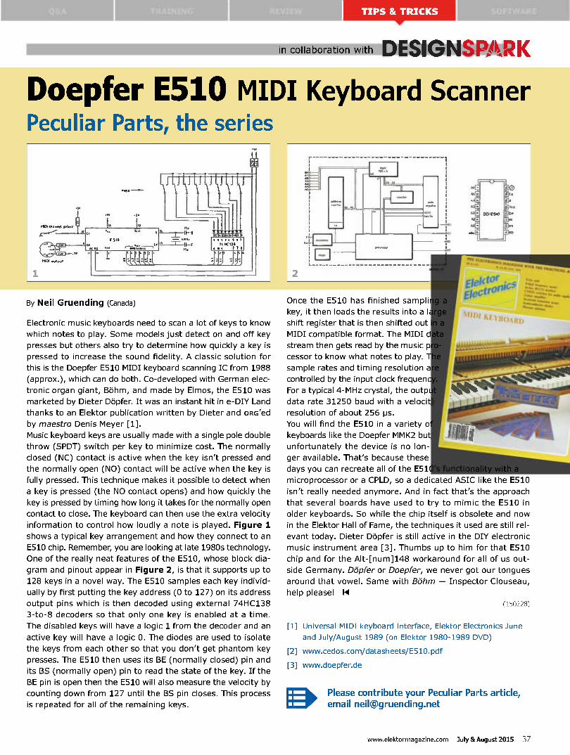
B M =
DESIGNSPARK in collaboration with
Doepfer E510 MIDI Keyboard Scanner Peculiar Parts, the series
By Neil Gruending (Canada)
Electronic music keyboards need to scan a lot of keys to know
which notes to play. Some models just detect on and off key
presses but others also try to determine how quickly a key is
pressed to increase the sound fidelity. A classic solution for
this is the Doepfer E510 MIDI keyboard scanning IC from 1988
(approx.), which can do both. Co-developed with German elec-
tronic organ giant, Bohm, and made by Elmos, the E510 was
marketed by Dieter Dopfer. It was an instant hit in e-DIY Land
thanks to an Elektor publication written by Dieter and oRG'ed
by maestro Denis Meyer [1].
Music keyboard keys are usually made with a single pole double
throw (SPDT) switch per key to minimize cost. The normally
closed (NC) contact is active when the key isn't pressed and
the normally open (NO) contact will be active when the key is
fully pressed. This technique makes it possible to detect when
a key is pressed (the NO contact opens) and how quickly the
key is pressed by timing how long it takes for the normally open
contact to close. The keyboard can then use the extra velocity
information to control how loudly a note is played. Figure 1
shows a typical key arrangement and how they connect to an
E510 chip. Remember, you are looking at late 1980s technology.
One of the really neat features of the E510, whose block dia-
gram and pinout appear in Figure 2, is that it supports up to
128 keys in a novel way. The E510 samples each key individ-
ually by first putting the key address (0 to 127) on its address
output pins which is then decoded using external 74HC138
3-to-8 decoders so that only one key is enabled at a time.
The disabled keys will have a logic 1 from the decoder and an
active key will have a logic 0. The diodes are used to isolate
the keys from each other so that you don't get phantom key
presses. The E510 then uses its BE (normally closed) pin and
its BS (normally open) pin to read the state of the key. If the
BE pin is open then the E510 will also measure the velocity by
counting down from 127 until the BS pin closes. This process
is repeated for all of the remaining keys.
11••
41.41.
Ray
rat riscraoifirm • buomekt wrnr PlAcncAt
ba...
Once the E510 has finished sampling a
key, it then loads the results into a larg
shift register that is then shifted out in
MIDI compatible format. The MIDI dat
stream then gets read by the music pro-
cessor to know what notes to play. The
sample rates and timing resolution are
controlled by the input clock frequency.
For a typical 4-MHz crystal, the output
data rate 31250 baud with a velocity
resolution of about 256 ps.
You will find the E510 in a variety of
keyboards like the Doepfer MMK2 but
unfortunately the device is no lon-
ger available. That's because these
days you can recreate all of the E510's functionality with a
microprocessor or a CPLD, so a dedicated ASIC like the E510
isn't really needed anymore. And in fact that's the approach
that several boards have used to try to mimic the E510 in
older keyboards. So while the chip itself is obsolete and now
in the Elektor Hall of Fame, the techniques it used are still rel-
evant today. Dieter Dopfer is still active in the DIY electronic
music instrument area [3]. Thumbs up to him for that E510
chip and for the Alt-[num]148 workaround for all of us out-
side Germany. Defer or Doepfer, we never got our tongues
around that vowel. Same with Bohm — Inspector Clouseau,
help please! 11
EiektOr_:„c
Electre'
(150228)
[1] Universal MIDI keyboard Interface, Elektor Electronics June
and July/August 1989 (on Elektor 1980-1989 DVD)
[2] www.cedos.com/datasheets/E510.pdf
[3] www.doepfer.de
Please contribute your Peculiar Parts article, email [email protected]
www.elektormagazine.com July &August 2015 37
Industry News I ARM Cortex-A9 Based Starter Kits for TZ2100 Two new starter kits from Toshiba, the RBTZ2100-1MA and RBTZ2100-2MA enable rapid development of applications using ApP Lite" processors.
The TZ2100 group supports enhanced audio and image data-mining, communications and security functions with a single-core ARM Cortex
A9 core and a clock rate up to 600 MHz. It is suitable
for a wide range of applications, such as small embed-
ded devices, handheld devices, industrial equipment and
gaming equipment for amusement arcades and casinos.
The RBTZ2100-1MA and RBTZ2100-2MA development
starter kits include reference boards and drivers that
allow devices to be effectively evaluated in their final
application environment. This can reduce the usage of
developer resources and shorten the overall develop-
ment schedule.
These kits help users to effectively evaluate function
and performance, and carry out advanced software
development. The RBTZ2100-1MA, fitted with 512MB
DDR3L SDRAM and 16MB SPI Flash ROM can use a Media
I/F for a camera or LCD panel and comes equipped
with a microSD slot and 10/100 LAN connector. The
RBTZ2100-2MA is capable of using an external bus I/F
and is equipped with 256 MB DDR3 SDRAM and 256 MB
Parallel Flash ROM, with an I2S connector for audio.
(150145-12) www.toshiba.semicon-storage.com
Wireless Power Receiver IDT's new P9027
magnetic induction
receiver offers 80
percent peak sys-
tem level efficiency
and improved
overall thermal
performance. The
high-efficiency
architecture
enables higher
power transfer
rates, translating
into shorter charge times for portable devices such as smartphones
and phablets.
Supporting the Wireless Power Consortium's Qi standard, the P9027 is
an 8-watt receiver featuring an ultra-compact solution size — approxi-
mately 37 square millimeters — and requiring six fewer capacitors than
competitive products. The result is less board space and a lower bill of
materials cost.
The device's proprietary alignment guide optimizes inductive coupling
with the transmitter to maximize coil-to-coil power efficiency. The 3 V
to 7 V adjustable output voltage range is capable of driving a variety of
downstream power management ICs, while proprietary foreign object
detection (FOD) ensures safe operation in the presence of metal objects.
(150145-9) www.idt.com
Small Cells for Use on Lamp Posts With demand for
cellular data con-
tinuing to rise and
outdoor small cells
seen as an essen-
tial element in the
long-term deliv-
ery of high-capac-
ity urban networks,
TTP has come up
with a new small
cell designed spe-
cifically for deploy-
ment on lamp posts. The use of lamp posts enables the acquisition of many
thousands of suitable sites through negotiation with a single city authority.
TTP's new eNodeB is simply fitted into a lamp post's standard photocell
socket, providing the quickest possible installation without any modifica-
tion to the lighting column or its power supply. And because the compact
design meets de minimis planning requirements, it also simplifies planning
consents. TTP's prototype eNodeB is based on the Freescale BSC9131 QorIQ
Qonverge processor and will be shown for the first time at Mobile World
Congress next month on the Freescale stand. It incorporates LTE Access Point
software from ip.access and has been demonstrated with the Quortus EPX
Core evolved packet core. It is targeted at 50-meter (150-ft) cells, supporting
up to 32 active users at downlink rates of up to 100 Mbps.
(150145-13) www.ttp.com
-',
ESC Boston May 6-7 ... NXP LPC Expresso Dey Boards ... NXP + Freescale = a Broader, More Power-
ful Portfolio ... Newark/ele ment14 says Giz mo 2 is Here ... Microchip's CAN Flexible Data-Rate Trans-
ceiver ... Saelig's New Picoammeters Toradex: Next Generation SoC addition to Apalis FlowPaw fro m
38 July 8f August 2015 www.elektormagazine.com

$49 Bluetooth Low Energy (BLE) Pioneer Development Kit from Cypress The EZ-BLE PRoC module integrates the programmability and ARM® Cortex®-MO core
of PRoC BLE, two crystals, an on-board chip antenna, metal shield and passive compo-
nents, all in a compact 10-mm x 10-mm x 1.8-mm form factor. Customers designing
with the module can apply to add the Bluetooth logo on their products by referring
to Cypress's Qualification Design Identification (QDID) 67366, a unique serial num-
ber assigned by the Bluetooth SIG. Additionally, the module is compliant to wireless
regulatory standards in the U.S., Canada, Japan, Korea and Europe.
Cypress has abstracted the Bluetooth Low Energy (BLE) protocol stack and profile
configuration into a royalty-free, GUI-based BLE component that can be dragged and
dropped into designs using Cypress's PSoC® CreatorTM integrated design environment
(IDE). PSoC Creator enables complete system design in a single tool.
The $49 BLE Pioneer Development Kit gives users easy access to the Cypress Blue-
tooth Low Energy devices, while maintaining the design footprint from the popular
PSoC 4 Pioneer kit. The development kit includes a USB Bluetooth Low Energy dongle
that pairs with the CySmart master emulation tool, converting a designer's Windows®
PC into a Bluetooth Low Energy debug environment. The EZ-BLE PRoC module can be
quickly and easily evaluated with the EZ-BLE PRoC Module Evaluation Board, which
plugs into the BLE Pioneer Development Kit.
(150273-1) www.cypress.com
Capacitors for Energy Harvesting Farnell element14 (US:
Newark element14) is
launching the Vishay hybrid
storage 196 HVC ENYCAPTM
capacitors which are porta-
ble, compact, and facilitate
high-energy storage.
Priced from £13.39 with
price breaks for higher
volumes the capacitors
have the industry's highest
energy density (13 Ws/g)
as well as polarized storage
capacitor with high capacitance (up to 90 F).
Ideal as a storage device for energy harvesting, the capacitors are an
alternative to rechargeable backup batteries as they can hold 70% of
their charge for as long as a month.
They support voltages ranging from 1.4 V (single cell) to 2.8 V / 4.2 V /
5.6 V/ 7.0 V / 8.4 V (multiple cells) and are available as stacked through-
hole (STH, radial), surface mount flat (SMF) and lay-flat configurations
(LPC) with wire and connectors.
Their low profile (2.5 mm) means they are the right size for portable
and compact designs.
Hybrid Storage 196 HVC ENYCAPTM Capacitors are part of Vishay's famous
Super 12 range and are available with next day delivery.
(150145-14) http://uk.farnell.com/vishay-126hvc-capacitors
Power,' 4 4 > Ground
10 0 mrn
Cypress EZ-BLETM FlRoC"1 Module Block Diagram
32 7118-1clir Crystst
PRoC BLE
24-MHz Crystal
Chit/ Antenna
2 SVV0/1 GPIO
14 SPI/ 41•1‘4> PC/
UART/ Cat:Sense/ AOC/
PWWGPIO
Cypress EZ-B LE PRoC Module with shield
•ir - Shield
4 Side View withoul Shield
1 8 de, M ME/ M1111,
12-watt Smart AC LED Module FuturoLighting's
new smart AC
LED module oper-
ates directly off
the 230 VAC net-
work. The module
integrates an AC
driver with high
PFC exceeding
0.97, offering On/
Off and dimming
functionality with
stand-by con-
sumption under
0.5 W. The module
was designed in several versions covering basic, triac dimmable, ana-
log dimmable and smart functionality. Dimensions of the module are
100 x 100 mm with a height of 5 mm for the basic version, and 25 mm
for the smart version.
It is claimed as the first integrated approach of an AC driver together
with movement sensor and smart behavior. Practically these modules
are electrically behaving as real incandescent bulb (resistive load). Smart
version offers corridor functionality with adjustable delay time, where
stand-by level can be adjusted from 0 to 80% through programming
interface directly on the module.
ChipAntefins
www.futurolighting.eu (150273-2)
DSPRobotics IFixit Tears Down Galaxy 86 ... SurfLight Technology in Vishay IR Emitters ... XcITAG
Goes Dyna mic ... Dual-Frequency NFC/EPC fro m EM Microelectronic ... Linear Technology 60V 4A
LED Driver ... Yugo Syste ms Ready for FPGA Debug ... Tektronix 45GHZ Optical Modualtion Analyser
www.elektormagazine.com July &August 2015 39

Industry Feature Article
Aluminum electrolytic capacitors (a.k.a.
'e-caps'; 'electrolytics') are vital to the
function of many electronic devices.
Ever-increasing requirements for ener-
gy-efficiency, the expanding utilization
of renewable energy, and the growth of
electronic content in modern automobiles
have driven the spread of these compo-
nents significantly over the past decades.
Construction and Manufacturing
Process of Electrolytic Capacitors
Aluminum electrolytic capacitors combine
voltage proofs ranging from several volts
to about 750 volts and a wide capacitance
range from 1 pF to above 1 F, while offer-
ing a compact size. A highly roughened
anode foil is being completely covered by
a thin dielectric layer and contacted by
an exact fitting cathode, the electrolyte
liquid. (Figure 1).
The manufacture process of e-caps com-
prises the following major production
steps:
• Etching — high purity aluminum
foils of thickness 20 — 100 pm
are the base material for the later
anode- and cathode foils. The etching
enlarges the total surface area of the
anode material up to a factor of 140
(Figure 2), compared to their geo-
metric surface.
• Forming — the anode foil bears the
dielectric layer of the e-cap and con-
sists of aluminum-oxide (A1203). It
is deposited on top of the roughened
anode foil by an electrochemical pro-
cess called anodic oxidation or form-
ing. The quality of the forming, i.e.
the homogeneous and complete cov-
Reliability of Electrolytic Capacitors
Anode foil (highly roughened Al-foil)
Anode
Dielectric Layer
Electrolyte
Paper Cathode foil (highly roughened Al-foil)
-_ (,) Cathode
Air Oxide Layer
Figure. 1. Construction of an aluminum electrolytic capacitor (simplified cross-section).
erage of the surface area is essential
for the high reliability of the compo-
nents during operation. The further
the forming voltage is above the
rated voltage, the smaller becomes
the probability of dielectric break-
down. Typical values for the ratio of
forming voltage vs. rated voltage of
Jianghai electrolytics range between
1.25 (low voltage) and 1.60 (high
voltage). The thickness of the dielec-
tric layer is approximately 1.4 nm/V;
this amounts to about 900 nm for an
e-cap with 450-V voltage proof (this
is less than 1/100 of the thickness of
a human hair).
• Slitting — the etched and formed foil
comes on so-called mother rolls of
about 50 cm width. By slitting, the
mother rolls are cut into the widths
needed for the anode and cathode
material.
• Winding — attachment of electrical
contact tabs to the foils (stitching,
cold welding) and winding of anode,
paper (spacer, multi-ply if needed),
and cathode foil.
• Impregnation — the pores of the
spacer paper in the wound cell and
the complete surface area of the
anode foil are covered by electrolyte,
the liquid cathode.
• Assembly of the capacitor wound
cell into the can, electrical connection
between contact tabs and soldering
or screw terminals and riveting of the
can for a tight seal.
• Post-forming ('Burn-in') to heal the
cut edges of the foil.
• 100 % in-line control of the vital
electrical parameters (capacitance,
dissipation factor, and leakage
current.
Figure 2 shows the electron micrograph
of the surface of an etched high voltage
anode foil. The homogeneous distribution
and the large free diameter of the etched
pits allow for good coverage by the oxide
layer and full access of the electrolyte to
the complete surface are of the anode foil.
Already at this early stage of the produc-
tion it is determined whether the resulting
e-cap will be suitable for demanding, pro-
40 July &August 2015 www.elektormagazine.com

By Dr. Arne Albertsen, Jianghai Europe Electronic Components GmbH
In many applications, lifetime and reliability of the electronics are directly linked to the corresponding
parameters of the electrolytics [4]. While a previous article of the author [1] elucidated the topic of
lifetime estimation for electrolytic capacitors, this article focuses on the reliability of electrolytics.
Figure 2. Top view of the etched anode foil.
fessional industrial applications with high
requirements to reliability, ripple current
capability, and long lifetime.
In particular, theb process steps 'form-
ing' and 'post forming' have great influ-
ence on the reliability of e-caps under
operation. Jianghai pursues the target of
maintaining a sufficiently high distance of
the forming voltage from the rated volt-
age and a reasonable dwell-time during
post-forming to ensure high reliability.
As the forming voltage is commonly not
indicated in the datasheets, the final user
of the components has a hard time to use
this parameter as a performance indica-
tor. By asking the e-cap supplier and by
comparing the leakage current ratings,
the end user may draw his conclusions
with respect to the design philosophy
of the e-cap manufacturer. In times of
rising material and energy prices, even
some well-known manufacturers resort
to lowering the forming voltages of run-
ning series. From a quality perspective,
Jianghai considers these 'cost-optimiza-
tion measures' being not acceptable.
Early Failures
Random Failures Wear-out Foa ms
Operafional Time
Figure 3. Failure Rate vs. Time - "Bathtub Curve".
Lifeti me vs. Reliability
Electrochemical aging mechanisms limit
the lifetime of e-caps to a value that can
be estimated depending on temperature,
ripple current and voltage during opera-
tion. During this lifetime, random failures
may occur at any time. The absolute num-
ber of these failures depends on the size
of the observed total lot. The existence of
random failures is usually not related to
the aging process, but it is rather the con-
sequence of hidden, internal weak spots
(e.g., in the spacer paper, the foil, or in
the vicinity of the electrical connections).
Often, these failures happen without any
pre-warning and end up in a short circuit.
Increased leakage currents as a result
of a damaged dielectric layer may lead
to such a big formation (that goes along
with the buildup of hydrogen gas) that
the overpressure opens the safety vent.
Then, the e-cap dries up and fails with
low capacitance.
The 100°h end measurement of capac-
itance, leakage current and [SR on all
produced components and the conduc-
tion of additional tests on samples drawn
from all mass production batches ensure
the high quality level of the products.
Hence, early failures in the application are
a rarely observed exemption [2].
There exist many definitions of the term
„reliability" and depending on whether
you ask a statistician, mathematician or
an engineer, you may obtain a different
answer. A common sense approach to
defining reliability could be: the probabil-
ity of an electronic device for satisfactorily
fulfilling the requirements of its mission
within a defined time period.
The typical time course of reliability
density for e-caps follows the so-called
'bathtub curve' [3]. The failure rate (FIT;
failures in time rate) À designates the
number of failures per unit time (failure
density, measurement unit FIT = failure
in time in 10-9 failures / hour.
The bathtub curve in Figure 3 shows
three distinct consecutive segments:
• the early failure period ('infant mor-
tality') with a decaying FIT rate À;
• the period within the normal life-
time has a constant FIT rate À that
describes the occurrence of random
failures;
• the final segment with increasing FIT
rates À that originate from wear-out
and changes beyond acceptable lim-
its at the end or after the end of the
regular lifetime.
Failure Modes and Mechanisms
The normal failure mode of a regularly
aged e-cap is a parametric failure due to
low capacitance or increased [SR (see
www.elektormagazine.com July &August 2015 41
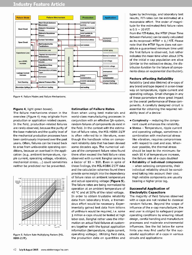
Industr Feature Article
Failure Mode Failure Mechanism
Short Circuit (between
Electrodes)
!Dielectric Breakdown Short Circuit 4 •
(Oxide)
Open Clretat
4
Capacitance Loss
tan d (ESP)
Increase
Dielecuk ereakd
(P e.")
Contact Tab broketi le _.
éad Contact to the— lt _ Terminations
Production
'wrinkled foil 1 metal particle
weak spat In oxide
layer
Electrolyte Loss
Thermal decompositfOlt of Electrolyte
Capacitance One (Mode)
Capacenes Drop (Cady:ode)
H Clecomposidon of Oxide Leakage Currant Leer
Increase Corrosion
°melee
IlElecireirts Spillage Internal Pressure /Use
Insuredent Seeing
metal particle In apacorpaper
Electrochemical R eaction
mechanical stress
bad contact
mechanical
OVOMVOSS
1101111alaging
4- 4
then», ovedead
41hallne contamination
41.[Irywtable electrolyte item
bad sealing
M elee V
OVOICUMellt
Lille/Ma COntarnMatiOn
Hoverload during
charge I discharge
Figure 4. Failure Modes and Failure Mechanisms.
Figure 4, light green boxes).
The failure mechanisms shown in the
overview (Figure 4) may originate from
production or application related causes.
In the field, production-related failures
are rarely observed, because the purity of
the base materials and the quality level of
the mechanical production processes have
been continuously improved over the past
years. Often, failures can be traced back
to arise from unfavorable operating con-
ditions, because an overload in the appli-
cation (e.g. ambient temperature, rip-
ple current, operating voltage, vibration,
mechanical stress, ...) could sometimes
neither be predicted nor be prevented.
siOr
1•••• ••• ~0
eel
M MIM M MI M MMI M MB• M
111111111111111•11U NÉ
IM M M M M M Mahlratilnir,d/A M M
ÉÈBREid erd
straugnmeswAmmiiii iie re r,d111111111111
6:-;,-se---• P e• ee —Immummimmummum
M UU M U U Iso
0)
OS OS 01 OS OS 0
Figure 5. Failure Rate Multiplying Factors (MIL HDBK-217F).
Esti mation of Failure Rates
Even when using best materials and
world-class manufacturing processes in
conjunction with an effective QA-system,
random failures of components do exist in
the field. In the context with the estima-
tion of failure rates, the MIL-HDBK-217F
is often referred to in literature, even
though the handbook relies on compo-
nent reliability data that has been devised
some decades ago. The numerical val-
ues of the component failure rates found
there often exceed the field failure rates
observed with current Jianghai series by
a factor of 10 - 100. Even in spite of
these findings, the MIL-HDBK-217F data
and the calculation schemes found there
provide some insight into the dependency
of failure rates on ambient temperature
and actual operating voltage (Figure 5).
The failure rates are being normalized to
operation at an ambient temperature of
40 °C and at 50°h of the rated voltage.
In order to obtain trustable reliability
data from laboratory trials, a tremen-
dous effort would be necessary. Exper-
imentally gained test data from billions
of unithours would be required, i.e. some
1 million e-caps should be tested at high
labor cost. Jianghai rather uses the infor-
mation on actual field failures at custom-
ers together with the typical application
information (temperature, ripple current,
operating voltage). Utilizing field data,
the production data on quantities and
types by technology, and laboratory test
results, FIT-rates can be estimated at a
reasonable effort. The order of magni-
tude for the estimated field failure rates
is 0.5 - 20 FIT.
From the FIT-Rates, the MTBF (Mean Time
Between Failures) can be easily calculated
as its reciprocal: MTBF = 1 / FIT. Please
note that the MTBF figure does not con-
stitute a guaranteed minimum time until
the first failure is observed, but rather
indicates the mean time when about 37°h
of the initial e-cap population are alive
(similar to the radioactive decay, the dis-
tribution function for the failure of compo-
nents obeys an exponential distribution).
Factors affecting Reliability
Reliability (and also lifetime) of e-caps of
any brand and type depend in a non-linear
way on temperature, ripple current and
operating voltage. Small changes in any
of these parameters show great impact
on the overall performance of these com-
ponents. A carefully designed circuit is
essential for obtaining the required reli-
ability level of a device:
• Complexity - reducing the compo-
nent count enhances the reliability.
• Stress - Temperature, ripple current
and operating voltage, sometimes in
combination with mechanical stress
like vibration, requires compromises
with respect to cost and size. When-
ever possible, the thermal stress
should be kept to the minimum: for
each 10 K of temperature increase,
the failure rate of e-caps doubles!
• Reliability of individual components
- when selecting components, their
individual reliability should be consid-
ered taking into account their cost.
High reliable components are usually
bearing a higher price tag.
Successful Application of
Electrolytic Capacitors
The majority of field failures observed
with e-caps are not related to classical
random failures. Beyond the scope of
influence of the e-cap manufacturer, the
end user is obliged to safeguard proper
operating conditions by ensuring robust
design, careful handling and manufacture
processes and moderate environmental
influences. See the list below for some
hints you may find useful for the suc-
cessful application of e-caps in various
circuits and applications:
42 July &August 2015 www.elektormagazine.com

Transport and Storage
E-cap cans (pure Aluminum) and e-cap
seal (rubber) are soft and elastic. Obvi-
ously damaged (indented) components
should thus not be utilized. Contamina-
tion by halines (in particular Bromide for
sterilizing oversea shipments) are regret-
tably often found. This applies both to
the shipment of individual components as
well as to the transport of finished goods.
Mounting and Assembly
Pushing, pulling or bending of the ter-
minals (in particular with radial e-caps)
has to be avoided. Severe damage to
the inner contacts of anode or cathode
foil may result.
Glue, molding compounds and lacquers
must be free from halines. In the vicin-
ity of the e-cap's seal, an opening to the
ambient should be maintained to prevent
the build-up of a microclimate in a con-
fined space beneath (risk of corrosion).
Conducting tracks shouldn't be routed
below any e-cap. Electrolytics must never
be used as a „handle" for a PCB.
Soldering
The soldering temperature limits speci-
fied by the manufacturer must be kept to
avoid damages (bulging, lifetime loss or
thermal destruction of the electrolyte).
This applies in particular to the process-
ing of SMT e-caps in a lead-free reflow
process (higher temperature soldering
profiles).
Operation
When switching on or off, voltage tran-
sients from inductive loads beyond the
forming or reverse voltage may occur.
Even if only applied once, these type tran-
sients cause permanent damage to the
electrolytic capacitor and must be avoided
by proper design.
Mechanical overstress during operation
(e.g., self-resonance) may cause break-
ing of connecting tabs. Gluing the e-caps
to the PCB or placing them at a different
location may solve the issue.
Any increase of ambient temperature by
10 K doubles the failure rate and halves
the lifetime. Placing e-caps away from
heat sources (heat sinks, power induc-
tors, ...) is thus beneficial.
Su m mary
By their individual reliability, aluminum
electrolytic capacitors influence the reli-
Company Profile
Jianghai Europe Electronic Components GmbH with office and warehouse in Krefeld
(Germany) supports the European customers of Nantong Jianghai Capacitor Co.,
Ltd. (Jianghai) in Nantong, China. Jianghai has been founded in 1958 at the
location of the present headquarters — about two hours by car north of Shanghai.
In the early years, Jianghai developed and produced specialty chemical products
(e.g., electrolyte solutions). In 1970, the production of electrolytic capacitors
was launched and during the following years, low and high voltage anode foil
production facilities complemented Jianghai's portfolio. Being the no. 1 producer in
China, Jianghai is one of the world's largest manufacturers of radial, snap-in and
screw terminal electrolytic capacitors.
Author
Dr. Arne Albertsen studied Physics with a focus on Applied
Physics at Kiel University, Germany. Following his diploma
(1992) and doctoral thesis (1994), both on stochastic
time series analysis from a biophysical membrane
transport system, he pursued an industrial career in plant
construction of specialized waste water treatment and
renewable energy generation technologies. In 2001, he
started to work with leading manufacturers of electronic
components like BCcomponents, Vishay, and KOA. He
worked in managing positions in design-in, sales, and
marketing for passive and active discrete components until
he joined Jianghai Europe Electronic Components in November 2008. In his current
position as Manager Sales and Marketing, Dr. Albertsen is responsible for the
support of European OEM accounts and distributors.
ability of the electronic devices they are
mounted in. A thorough knowledge of
some of the key parameters of these com-
ponents are necessary to ensure the reli-
able design of electronic devices.
The definition of reliability and the most
important influence factors on reliability
are explained. A collection of practical
hints helps as a guideline to the success-
ful application of electrolytic capacitors.
The applicability of the general guidelines
depends on the specific product type and
the particular application. Consultations
References
with the supplier are essential to get guid-
ance throughout the design project and
to confirm any estimates. N
(150250)
[1] Albertsen, A., Lebe lang und in Frieden! Hilfsmittel für eme praxisnahe Elko-Leb-
ensdauerabschâtzung, Elektronik Components 2009, 22-28 (2009).
[2] Both, J., Aluminium-Elektrolytkondensatoren, Teil 1 — Ripplestrom and Teil 2 —
[3]
Lebensdauerberechnung, BC Components, February 10, 2000.
Stiny, L., Handbuch passiver elektronischer Bauelemente, Franzis Verlag, Poing,
2007.
[4] Venet, P., A,. Lahyani, G. Grellet, A,. Ah-Jaco, Influence of aging on electrolytic
capacitors function in static converters: fault prediction method, Eur. Phys. J. AP
5, 71-83 (1999).
www.elektormagazine.com July &August 2015 43

e .1•7"
Welcome to Elektor Labs 1"1" Elektor Labs is the place where projects large, small, analog, digi-tal, new and old skool are sketched, built, discussed, debugged and fine-tuned for replication by you.
1
•
Our offer: Become Famous
Most engineers and budding authors we come across are just too modest. If they do not see the attraction and beauty of a design idea scribbled on a coaster and worked out later at home, others may, and should. Let Elektor Labs help you hone your design to perfection, let the editors assist with text &graph-ics, and reap the rewards by seeing your name in print in Elektor magazine's celebrated LABS section. Sure, we are happy to negotiate payment, but the actual remuneration will be fame 81 glory in elec-tronics land, and your name added to the long list of extremely successful e-authors. Our get-u-fa-mous formula also applies to book authors, blog-gers and video makers. Students and youngsters: being in publication is a current boost like no other in getting a job!
o
44 Jul
Our Facilities
00
• • •
We are sumptuously housed in three spacious rooms at Elektor House where we try unsuccess-fully to keep our solder jobs and prototypes off our computer desks. We have water, 218 volts electricity and coffee nearby. PCB milling, pro-
totype assembly, SMD reworking, audio testing, pizza cooking, and mechanical work are deferred to converted cellars in the basement.
ugust 2015 www.elektormagazine.com
• •
• •
o Our Experts and Designers
Besides experienced sup-port staff and BSc, MSc qualified engineers with a total working life in electronics of about 200 years, the Lab has access to Elektor's vast network of experts for consulta-tion, critical advice, and assistance with specialized assignments.
Our Standards
00 •
All projects and products going through the Labs pipeline are produced to high engi-neering standards. In practice, prototypes of projects labeled LABS in the magazine
l must be demonstrated to work to specifi-
Lcation on certified, calibrated test equip-ment available locally. BOMs and schemat-ics must match perfectly. Kits are sampled for completeness. We are ROHS compat-ible, lead free and comply with electrical safety standards applicable in our location. If engineering errors are found these will be put up for public notification.

e
Our Products Our products are visible in Elektor magazine, as well as on the Elektor.Labs and Elektor Store websites. The range includes text write-ups for editors, prototype photography, PCBs includ-ing SMD-prestuffed, PCB files, project software, programmed devices, semi-kits, tools, modules, videos, and service desk information.
Our History
The origins of Elektor Labs go back to the early 1970s when soldering and writing was a one-man, single-desk job. Ove the years Labs staff have not only witnessed the arrival of the transistor, the IC, the microcontroller, and the SMD, but actually jumped on these parts as soon as they were out of the profession-al-only woods. Once special branches, Audio Labs, Micro Labs, PCB Labs, and Mechani-cal have converged back again into a single activity.
rojects mis e rojects
0 0 0 0 0 0 0 0 Our Webinars The more talkative of our Lab engineers do not stop at testing prototypes, they happily share tech-nology related problems, insights, get-u-going information, and design skills on live camera at Elektot.tv. Labs' webinars are free to attend and
extremely interactive. They are announced in Elek-tor.POST, and webcast live from Elektor House in Holland. Do plug in!
Sharing Electronics Projects
Proposais In Progress Finished
Upload your own projects! On our very own Elektor-Labs website, you can share and showcase your ideas and project proposals to thousands of other electronic engineers. The site also allows you to follow other specialists' activities, supply comment, and so push the projects forward. Here's the best part, the top projects are eligible for processing in our test lab, in preparation for publication in Elektor magazine.
Who's this for? Although only members can log on to our Elektor. Labs website to publish projects and contributions, anyone can view along with the other projects. If you'd like to see your project published in Elektor magazine, which is published in four languages and read by tens of thousands of electronics specialists all over the world, then become a Green of Gold member (www.elektor.com/member) or log in as an existing member of our Elektor community!
zine.com July
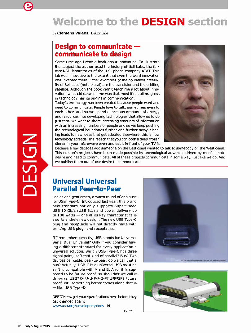
Alb
Welcome to the DESIGN iection By Clemens Valens, Elektor Labs
Design to communicate communicate to design Some time ago I read a book about innovation. To illustrate the subject the author used the history of Bell Labs, the for-mer R&D laboratories of the U.S. phone company AT&T. This lab was innovative to the extent that even the word innovation was invented there. Other examples of the boundless creativ-ity of Bell Labs (note plural) are the transistor and the orbiting satellite. Although the book didn't teach me a lot about inno-vation, what did dawn on me was that most if not all progress in technology has its origins in communication. Today's technology has been created because people want and need to communicate. People love to talk, sometimes even to each other, and so we spend enormous amounts of energy and resources into developing technologies that allow us to do just that. We want to share increasing amounts of information with an increasing numbers of people and so we keep pushing the technological boundaries further and further away. Shar-ing leads to new ideas that get adopted elsewhere, this is how technology spreads. The reason that you can cook a deep-frozen dinner in your microwave oven and eat it in front of your TV is because a few decades ago someone on the East coast wanted to talk to somebody on the West coast. This edition's projects have been made possible by technological advances driven by men's innate desire and need to communicate. All of these projects communicate in some way, just like we do. And we publish them out of our desire to communicate.
Universal Universal Parallel Peer-to-Peer Ladies and gentlemen, a warm round of applause for USB Type-C! Introduced last year, this brand new standard not only supports SuperSpeed USB 10 Gb/s (USB 3.1) and power delivery up to 100 watts — one of its key characteristics is also its entirely new design. The new USB Type-C plug and receptacle will not directly mate with existing USB plugs and receptacles.
If I remember correctly, USB stands for Universal Serial Bus. Universal? Only if you consider hav-ing a different standard for every application a universal solution. Serial? USB Type-C has three signal pairs, isn't that kind of parallel? Bus? Two devices per cable, peer-to-peer, do we call that a bus? Actually, USB-C is a universal USB solution as it is compatible with A and B. Also, it is sup-posed to be future proof, so shouldn't we call it Universal USB? Or U-U-P-P-2-P? U2P22P? Future proof until something better comes along that is — like USB Type-D...
DESIGNers, get your specifications here before they get changed again: www.usb.org/developers/docs li
(1502934)
46 July &August 2015 www.elektormagazine.com
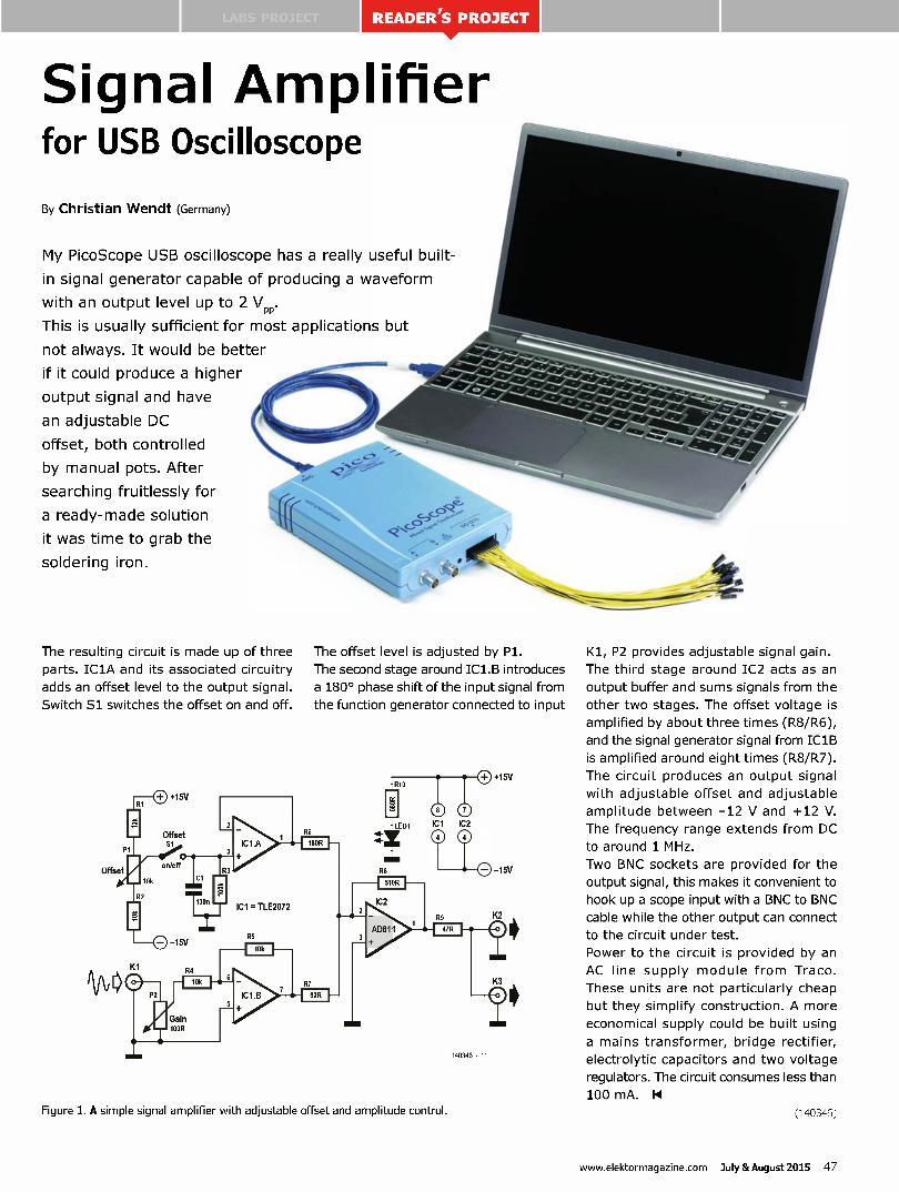
UI READER'S PROJECT
Signal Amplifier for USB Oscilloscope
By Christian Wendt (Germany)
My PicoScope USB oscilloscope has a really useful built-
in signal generator capable of producing a waveform
with an output level up to 2 Vpp .
This is usually sufficient for most applications but
not always. It would be better
if it could produce a higher
output signal and have
an adjustable DC
offset, both controlled
by manual pots. After
searching fruitlessly for
a ready-made solution
it was time to grab the
soldering iron.
The resulting circuit is made up of three
parts. IC1A and its associated circuitry
adds an offset level to the output signal.
Switch 51 switches the offset on and off.
The offset level is adjusted by Pl.
The second stage around IC1.13 introduces
a 180° phase shift of the input signal from
the function generator connected to input
Figure 1. A simple signal amplifier with adjustable offset and amplitude control.
da ge/.
40—
Kl, P2 provides adjustable signal gain.
The third stage around IC2 acts as an
output buffer and sums signals from the
other two stages. The offset voltage is
amplified by about three times (R8/R6),
and the signal generator signal from IC1B
is amplified around eight times (R8/R7).
The circuit produces an output signal
with adjustable offset and adjustable
amplitude between -12 V and +12 V.
The frequency range extends from DC
to around 1 MHz.
Two BNC sockets are provided for the
output signal, this makes it convenient to
hook up a scope input with a BNC to BNC
cable while the other output can connect
to the circuit under test.
Power to the circuit is provided by an
AC line supply module from Traco.
These units are not particularly cheap
but they simplify construction. A more
economical supply could be built using
a mains transformer, bridge rectifier,
electrolytic capacitors and two voltage
regulators. The circuit consumes less than
100 mA. 14
(140346)
www.elektormagazine.com July &August 2015 47

Solar Panel Voltage Converter for IoT Devices Yes we CAN exploit indoor lighting
By Sunil Malekar (Elektor India labs)
The goal of this microcontroller-free project is to
design a compact supply to power small indoor
IoT devices from a solar panel, indoors (!). A key
aspect of the project is its ability to operate from
an input source as weak as 7.5 pW so that a low cost
mini solar panel can be used. Not forgetting battery
backup and extremely compact size, all thanks to the
LTC3129 IC.
The Internet of Things (IoT) is said to
define a network of physical objects
embedded with electronics, software, sen-
sors and connectivity to provide services
by exchanging data with the connected
devices. It's also a globally interconnected
continuum of devices and objects and
things that emerged with the rise of cheap,
license free RFID technology. Alternatively
some consider the IoT as a scenario in
which objects, animals or people are pro-
vided with unique identifiers and the ability
to transfer data over a network without
requiring human-to-human or human-to-
computer interaction. Eloquent definitions
all, but Elektor's field being ronics,
we're interested in compon com-
ponents... what components?
Starring...
Among the key features of the
Types LTC3129 and LTC3 9-1
buck/boost converters
good old Linear Techno ogy
are a fixed 1.2-MHz opera
frequency, current mode c
trol, internal loop compens
tion, automatic Burst Mod
operation or low noise PW
mode, an accurate RUN pin
Main Features • Stores energy from indoor lighting
• Solar panel V.t 5 V typ., 42 pA
• Input power down to 7.5 pW usable
• 3.2 V typical out
• Choice of LTC3129 or LTC3129-1 converter IC,
• Easily configurable for many output voltages
• Optional backup battery
• Optional super-charge capacitor
• Ready-assembled unit with LTC3129-1 fitted, 3V3, MPPC mode.
board configurable for either
e programme, a power-gooa output
and an MPPC (maximum power point
control) function for optimizing power
transfer when operating from photovol-
taic cells. The full story is at [1] and [2].
Let's see what these devices can do if
it comes to powering IoT devices in an
eco-friendly way.
48 July &August 2015 www.elektormagazine.com

in collaboration with
MN,
Power to the IoT
(too)
The circuit shown in
Figure 1 exploits
the unique
ability of the
LTC3129 and
LTC3129-1 to
start up and
operate from an
input power source
as "weak" as 7.5
pW (microwatts) —
making them capable
of operating from small,
low-cost solar cells with
indoor light levels less
than 200 lux.
To make the low current
start-up possible, both the
LTC3129 and LTC3129-1 draw
a lousy two microamps of current
even less in shutdown) until three
conditions are satisfied:
• the voltage on the RUN pin must
exceed 1.22 V (typical);
DESIGNSPARK
• the voltage on the VIN pin must
exceed 1.9V (typical);
• Vc, (which is internally generated
from VIN but can also be supplied
externally) must exceed 2.25 V
(typical).
Until all three of these conditions are
satisfied, the part remains in a 'soft-shut-
down' or standby state, drawing just
2 pA. This allows a weak input source to
charge the input storage capacitor until
the voltage is high enough to satisfy
all three conditions, at which point the
LTC3129/LTC3129-1begins switching, and
V ow _ rises to regulation, provided the input
capacitor has sufficient stored energy.
The circuit features battery backup cir-
cuitry around BAT1 (sorry about the miss-
ing T). A CR2032 backup battery provides
power when solar power is insufficient.
The LTC3129 is used in this case, allow-
ing Vow _ to be programmed for 3.2 V to
better match the voltage of the coin cell.
With 5 V input from the solar panel on
connector K1 you can expect an output
C7 C9
470u 4u7 6V3
10p
R3 R4
RUN
Cl C2 Ll
1-4.--e—e 4eu-v—\--.1-17 1 22n 22n
4 12
15
6
2
3
R7
6
ce
7
R9 IRl2
ce ce
R10
C5
2u2
SW1 SW2
BST1 BST2
VIN VOUT LTC3129
RUN LTC3129-1 MPPC PGOOD
VS2/NC VS3/FB
NCNS1
VCC PWM
GND PGND
4
D1
li BAT54WS
3
5 3
10p —
5
8 C8
22u
R2
IC2
IC2.A
IC2.13
IC2 = SN74LVC2G04
7 CR2032 130560 - 11
Figure 1. At the heart of the converter is either an LTC3129 or an LTC3129-1 IC, depending on your choice. A number of components need to be configured as a function of the IC you decide to use. Hardly a microwatt of solar power is wasted in this circuit.
www.elektormagazine.com July &August 2015 49
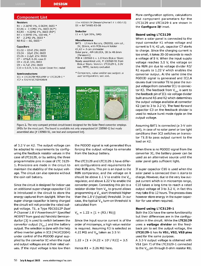
Corn sonent List Resistors R1 = 2.26MQ 1%, 0.063W, 0603 *
R2,R6 = 2.43MQ 1%, 0603 (R2*) R3,R5 = 4.22MQ 1%, 0603 (R5*)
R4 = 4.99MQ 1%, 100mW, * R7 = 2.2MQ 1%, 0603 *
R8-R12 = 0Q, 0603 *
Capacitors Cl,C2 = 22nF, 25V, 0603
C3,C4 = 10pF, 25V, 0603 C5,C6 = 2.2pF, 25V, 0603
C7 = 470pF, 6.3V, case D C8 = 22pF, 10V, 0603
C9 = 4.7pF, 25V, 0603 C10 = 0.47F, 5.5V, Super Capacitor, radial
Semiconductors
ICI = LTC3129EMSE#PBF or LTC3129-1 * IC2 = SN74LVC2GO4DBVR
Tl= FDC6312P (Newark/Farnell # 1700713) D1 = BAT54WS-E3-08
Inductor
Li = 4.7pH 20%, SMD
Miscellaneous BAT1 = Lithium Battery, CR2032, coin cell,
3V, 20mm, with PCB mount holder
Kl,K2 = 2-pin pinheader Solar panel, AM-1815CA, 58.1x 48.6mm
(Panasonic) PCB # 130560-1 v. 1.0 from Elektor Store
Ready assembled unit, # 130560-91 from Elektor Store. Version: LTC3129-1, 3.3V
out, MPPC, battery excluded.
* Component, value and/or use subject to user configuration; see text.
Figure 2. The very compact printed circuit board designed for the Solar Panel converter employs SMDs for the most part. The board is available not only unpopulated (# 130560-1) but ready assembled also (# 130560-91, see text and component list).
of 3.2 V on K2. The output voltage can
be adapted to requirements by config-
uring the feedback resistor values in the
case of LTC3129, or by setting the three
programmable pins in case of LTC 3129-
1. Provisions are made in the circuit to
maintain the stability of the output volt-
age. The circuit can also operate without
the coin cell battery.
Since the circuit is designed for indoor use
an additional super-charge capacitor C10
is introduced in the circuit to store the
energy captured from daylight. When the
super charge capacitor is being charged
the circuit will not provide the rated out-
put voltage. Ti, a Type FDC6312P Dual
P-Channel 1.8 V Powertrench® Specified
MOSFET from good old Fairchild Semicon-
ductor [3] is used to switch between the
convertor output (VouT ) and the battery
output. The selection is done with the help
of two inverter gates in IC2 (74LVC2G04)
under control of the PGOOD signal sup-
plied by the convertor IC when the input
and output voltages are at their rated val-
ues. If the input voltage is too low then
the PGOOD signal is not generated thus
forcing the output voltage to emanate
from the backup battery.
The LTC3129 and LTC3129-1 have differ-
ent configurations and requirements for
their RUN pins. This pin is an input to the
RUN comparator, and the voltage on it
should be above 1.1 V to enable the Vcc
regulator, and above 1.22 V to enable the
converter proper. Connecting this pin to a
resistor divider from VIN to ground allows
programming a VIN start threshold higher
than the 1.8 V (typical) threshold. In our
case, the typical VIN turn-on threshold is
calculated from
VIN = 1.22 x [1 + (R3 / Rin
Since the input source current is of the
order of microamps, a high value resistor
is required. Assuming R3 is selected as
4.22 MS2 and VIN taken as 3.5 V:
1.22 x [1 + (4.22 x 10⁶ / R1)] = 3.5
Hence R1 = 2.26 MS2 here.
More configuration options, calculations
and component parameters for the
LTC3129 and LTC3129-1 are shown in
the Configure It! inset.
Board using LTC3129
When a solar panel is connected to the
input connector K1 whose voltage and
current is 5 V, 42 pA, capacitor C7 starts
to charge. Since the charging current is
too small, it takes 20-30 seconds to reach
a voltage of 5 V. When the input supply
voltage reaches 3.5 V, the voltage on
the RUN pin due to voltage divider R3/
R1 equals to 1.22 V which enables the
converter output. At the same time the
PGOOD signal is generated and IC2.A
causes dual transistor Ti to pass the out-
put voltage from converter IC1 to connec-
tor K2. The feedback from VouT is sent to
the feedback pin of IC1 via voltage divider
built around R5 and R2 which determines
the output voltage available at connector
K2 (set to 3 to 3.2 V). The feed-forward
capacitor C3 on the feedback divider is
used to reduce burst mode ripple on the
output voltage.
Assuming BAT1 is connected (a 3-V coin
cell), in case of no solar panel or low light
conditions then IC2 switches on transis-
tor T1.8 to pass output current to the
load on K2.
When there is no PGOOD signal from the
converter IC, the battery power can be
used as an alternative source until the
solar panel gets sufficient light.
If super capacitor C10 is used when the
solar panel is connected then it starts to
charge. However, due to the very low out-
put current which is in microamps range,
C10 takes a long time to reach a rated
output voltage of 3 to 3.2 V, in fact this
may take 8 to 12 hours. The process does
however store energy in the super capac-
itor for use when required.
Board using LTC3129-1
Both the ICs have the same functionality
but their differences are in the configu-
ration in the circuit. While the LTC3129
uses a voltage divider on the feed-
back pin to set the output voltage, the
LTC3129-1 has its VS1, VS2, VS3 pins
used for the same purpose.
A 3.3-V output voltage is obtained with
VS1 (pin 7) of the LTC3129-1 connected
to the Vcc pin through 0-ohm resistor R8;
50 July &August 2015 www.elektormagazine.com
VS2 (pin 6) connected directly to ground;
and VS3 (pin 5) also connected to ground
but through resistor R2 using another
0-ohm resistor.
The MPPC pin is taken to Voo through
0-ohm resistor R10 as our functionality
requires an input source stronger than
10 mA. In case of other configuration and
input source this function can be used and
set by using voltage divider resistors R4
and R7 as discussed. Other functions like
battery backup and super-charge capac-
itor C10 are similar to the board with the
LTC3129.
Building and testing
Provided you have professional (SMD)
production equipment, or access to it,
the printed circuit board with its overlay
pictured in Figure 2 can be built using
either the LTC3129 or the LTC3129-1 with
their required components. That's why a
Component List is published here. Fully
respecting all 100 % DIY readers out there
we kindly advise however that the board
is also available ready-assembled through
the Elektor Store as item # 130560-91,
it's the LTC3129-1 version, MPPC mode,
10 mA min. in, 3.3 V, backup battery
not included.
Web Links
[1] LTC3129: www.linear.com/docs/42736
[2] LTC3129-1: www.linear.com/docs/42735
[3] FDC6312P: www.fairchildsemi.com/pf/FD/FDC6312P.html
The components marked * in the sche-
matic are optional and/or need to be
selected depending on the IC used. The
Feedback, RUN, and MPPC voltage divider
resistor values can vary depending on
your choice as well as on the input and
output supply.
In the case of the LTC3129-1, the output
can be configured up to 5 V just by chang-
ing the resistor configuration on VS1 and
VS2 pins of the IC. Be sure to fit either
R11 or R12, not both.
The use of a backup battery and the
super-charge capacitor depends on
requirements — the board can work with-
out them.
Waste Not Want Not
To power the board, a solar panel with an
output voltage rating up 5 V is connected
to K1 and the output load, to K2. By con-
necting a Sanyo AM-1815 solar panel, the
board can operate from indoor lighting,
and if super capacitor C10 is used a use-
ful charge gets built.
Let's consider charging at 35 pA "sto-
len" from a light source. If maintained
for 24 hours then it will give a cumula-
tive charge of almost 700 pAh, equal to
7 mA for 6 minutes or is almost 42 mA
for 1 minute.
Thus the power supply board is most
suitable in applications where the power
requirement of the devices is within the
above range, which should include many
IoT devices that need to wake up, respond
briefly and go to cybersleep again. Tell us
what you've in mind to power with this
circuit — IP address optional. 14
(130560)
Configure It! MPPC on LPC3129 and LPC3129-1
An MPPC (maximum power point control)
programming pin is common to both
LTC3129 variants. To enable the MPPC
functionality this pin is connected to a
resistor divider from VIN to ground. If the load on VouT exceeds
the capacity of the power source, MPPC action will reduce the
inductor current to regulate VIN to a voltage calculated as:
VIN = 1.175 x [1 + (R4 / R7)]
Assuming R4 = 4.99 MS2:
1.175 x [1 + (4.99 x 10⁶/ R7)] = 3.2 V
[1 + (4.99 x 10⁶ / R7)] = 2.9787 V
R7 = 2.13 MS2 •-zi 2.2 MS2
By setting the VIN regulation voltage appropriately, maximum
power transfer from the limited source is assured. Note this
pin is noise sensitive; therefore minimize PCB trace length
and stray capacitance.
In our example the supply is less than 10 mA and hence MPPC
is not used. The pin is connected to Vcc through R10 which is
a 0-ohm device. If you want MPPC though, remove R10 and
configure potential divider R4/R7.
Feedback signal on LTC3129
The feedback pin is a feedback Input to the Error Amplifier.
This pin is connected to a resistor divider from VouT to
ground. To get an output voltage of 3.2 V from our converter,
assuming R5 = 4.22 MS2 we calculate:
Vo,= 1.175 x [1 + (R5 / R2)]
R2 = 2.44 MS2 •-zi 2.43 MS2
Output voltage configurations on LTC3129-1
VS1, VS2 and VS3 are the output voltage select pins that
need to be connected either to the ground pin or to Voo for
programming the output voltage. These pins should not float
or go below ground. The configuration of these pins for the
desired voltage is given in the table below.
VS3 VS2 VS1 VOUT
0 0 0 2.5 V
0 0 VCC 3.3 V
0 VCC 0 4.1 V
0 VCC VCC 5 V
www.elektormagazine.com July &August 2015 51

LEARN SHAP
LJART/Fts 2 let; il lain
\ \ ir)i Data Loggêt 1 .rintir.i. ji IL
% Multi-level monitoring of serial streqrAis, 1 :1:111.11..1
t 4 1 * Ill 11 - .11.111.11.
• • 11. 11 11. 11. 1. 1111 1 0
\ \I \I\ \
"
t 4 1. t . » » O‘ • • ‘• V Ai t e Ni e «-
‘ 1 1 \ 1 \ \ 7‘
%, tit V ,I m v. v e s e x elt s
4‘ ".
By Thomas Schlott, Francisco Ramirez and Dr. Thomas Scherer
The universal asynchronous receiver/transmitter (UART) remains the favored means of transferring data
between hardware devices. The interface is very easy to use, with a wide range of converter chips from
which to choose. But when devices refuse to communicate correctly in test and development setups,
tracing the cause becomes a tricky business. Our UART data logger makes the task a breeze — it registers
bytes in both directions with millisecond accuracy. And its flexible connection options and electrical isolation
enable it to be hooked up without difficulty into serial data connections employing TTL or RS-232 levels.
Tracking down failure modes in electronic
systems can be a pig of a task when the
symptoms appear only occasionally or
cannot be reproduced a second time.
And when things go wrong, the 'dodgy'
data has long since vanished into the
Technical S ecification • Two serial inputs for bidirectional connections
• Inputs can have separate grounds
• Data transmission to PC via USB
• Operating power derived via USB
• User interface via commands from Terminal Program
• Baud rates up to 230 KBd
• Stores up to 900 data sets
• Data logging for up to 2:20 (h:mm)
• Temporal resolution 1 ms
proverbial 'bit bucket' or digital nirvana.
After the event, the only way of dis-
covering what on earth happened is to
capture whatever data is still available
and provide it with a timestamp (if this
is even feasible).
That's not the end of it either. If two
devices are connected together by serial
interfaces, bytes will pass in both direc-
tions. This means a serial data logger will,
in practice, require two data channels
simultaneously in order to monitor a bidi-
rectional serial connection of this kind (full
duplex) properly. And simply recording
the data will not suffice on its own, as we
52 July &August 2015 www.elektormagazine.com
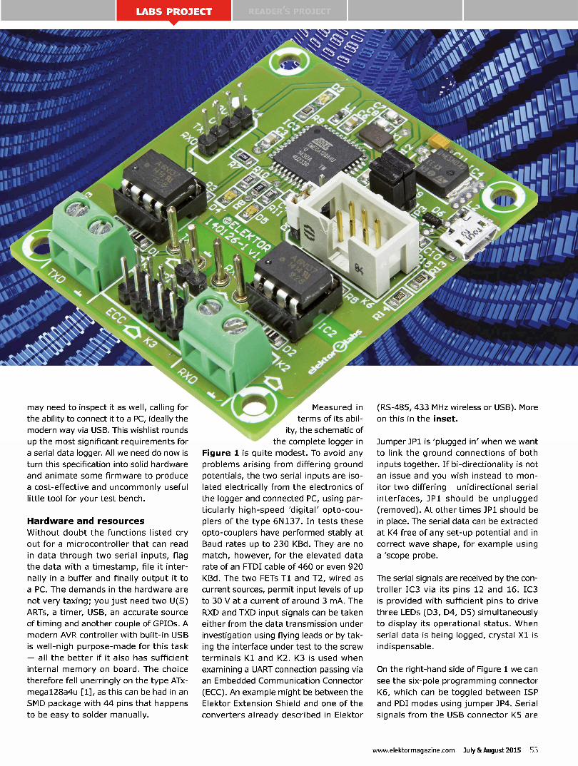
may need to inspect it as well, calling for
the ability to connect it to a PC, ideally the
modern way via USB. This wishlist rounds
up the most significant requirements for
a serial data logger. All we need do now is
turn this specification into solid hardware
and animate some firmware to produce
a cost-effective and uncommonly useful
little tool for your test bench.
Hardware and resources
Without doubt the functions listed cry
out for a microcontroller that can read
in data through two serial inputs, flag
the data with a timestamp, file it inter-
nally in a buffer and finally output it to
a PC. The demands in the hardware are
not very taxing; you just need two U(S)
ARTs, a timer, USB, an accurate source
of timing and another couple of GPIOs. A
modern AVR controller with built-in USB
is well-nigh purpose-made for this task
— all the better if it also has sufficient
internal memory on board. The choice
therefore fell unerringly on the type ATx-
mega128a4u [1], as this can be had in an
SMD package with 44 pins that happens
to be easy to solder manually.
r .. ,... C T
Measured in
terms of its abil-
ity, the schematic of
the complete logger in
Figure 1 is quite modest. To avoid any
problems arising from differing ground
potentials, the two serial inputs are iso-
lated electrically from the electronics of
the logger and connected PC, using par-
ticularly high-speed 'digital' opto-cou-
plers of the type 6N137. In tests these
opto-couplers have performed stably at
Baud rates up to 230 KBd. They are no
match, however, for the elevated data
rate of an FTDI cable of 460 or even 920
KBd. The two FETs Ti and T2, wired as
current sources, permit input levels of up
to 30 V at a current of around 3 mA. The
RXD and TXD input signals can be taken
either from the data transmission under
investigation using flying leads or by tak-
ing the interface under test to the screw
terminals K1 and K2. K3 is used when
examining a UART connection passing via
an Embedded Communication Connector
(ECC). An example might be between the
Elektor Extension Shield and one of the
converters already described in Elektor
ee 414 .ottet 1.0
111* "
.00 ;to 1-‘1\el 1 61 611-11
d art e l
er n/
w e/ /i n /14.4 0 Ï
(RS-485, 433 MHz wireless or USB). More
on this in the inset.
Jumper JP1 is 'plugged in' when we want
to link the ground connections of both
inputs together. If bi-directionality is not
an issue and you wish instead to mon-
itor two differing unidirectional serial
interfaces, JP1 should be unplugged
(removed). At other times JP1 should be
in place. The serial data can be extracted
at K4 free of any set-up potential and in
correct wave shape, for example using
a 'scope probe.
The serial signals are received by the con-
troller IC3 via its pins 12 and 16. IC3
is provided with sufficient pins to drive
three LEDs (D3, D4, D5) simultaneously
to display its operational status. When
serial data is being logged, crystal X1 is
indispensable.
On the right-hand side of Figure 1 we can
see the six-pole programming connector
K6, which can be toggled between ISP
and PDI modes using jumper JP4. Serial
signals from the USB connector K5 are
www.elektormagazine.com July &August 2015 53
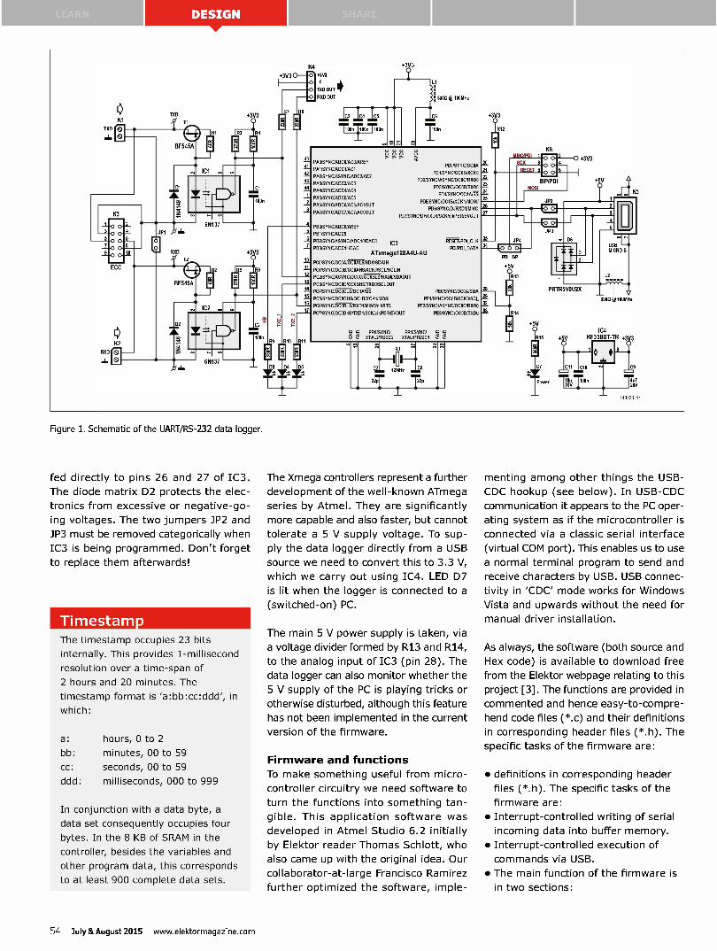
TXD
TXD
T1
K3
ECC
K2
RXD 111
BF545A
D1
.3V3 o R4
.3V3
Ci
ICI
Cl
100n
RXD
12
BF545A
D2
6N137
C2
13V3
K4 —%. I-3V3
0 0 à
O TXD OUT .y iRB o RXD OUT
40
41
42
43
44
4
10
11
12
6N137
e
E R19 0 10 Rh
14
15
16
.3V3
16330Q @ 100MHz PAO/SYNC/ADCO/ACO/AREF
PAl/SYNC/ADC1/AC1
PA2/SYNC/ASYNC/ADC2/AC2
PA3/SYNC/ADC3/AC3
PA4/SYNC/ADC4/AC4
PAS/SYNC/ADCS/AU
PA6/SYNC/ADC6/AC6/AC1OUT
PA7/SYNC/ADC7/AC7/ACOOUT
PDO/SYNC/OCOA
PD1/SYNC/OCOB/XCK0
PD2/SYNC/ASYNC/OCOC/RXDO
PD3/SYNC/OCOD/TXDO
PD4/SYNC/OC1A
PDSSYNC/OC1B/XCK1/MOSI/
PD6/SYNC/D-/RXD1/MISO
PD7/SYNC/D,ITXD1/SCK/cIkPER/EVOUT
PBO/SYNC/ADCB/AREF
PB1/SYNC/ADC9
PB2/SYNC/ASYNC/ADC10/DACO IC3 PB3/SYNC/ADC11/DAC1
ATxmega128A4U-AU
PCO/SYNC/OCOA/OCOALS/SDNSDAIN
PC1/SYN C/OCOB/OCOAHS/XCKO/SCUSCLIN
PC2/SYNC/ASYNC/OCOC/OCOBLS/RXDO/SDAOUT
PC3/SYNC/OCOD/OCOBHS/TXDO/SCLOUT
PC4/SYNC/ =CS/OC1A
PCSSYNC/OCOCHS/OC1B/XCK1/MOSI
PC6/SYNC/OCODLS/RXD1/MISO/cIkRTC
PC7/SYNC/OCODHS/TXD1/SCK/cIkPER/EVOUT
RESET/PDI_CLK
PDI/PDI_DATA
PEO/SYNC/OCOA/SDA
PE1/SYNC/OCOB/XCKO/SCL
PE2/SYNC/ASYNC/OCOC/RXDO
PE3/SYNC/OCOD/TXDO
PRO/ YNC/ PR1/ YNC/ g XTAL MOSC2 XTALlfTOSC1
X1
C7 2MH Ca
22 p1 I22 p
20
21
22
z 24
25
26
28
20
32
33
.3V3
â 2
PDI ISP
K6
.3V3
.5V
PRTR5VOU2X — 330Q @ 100MHz
IC4
Ris V KF33BDT-TR .3y3
Figure 1. Schematic of the UART/RS-232 data logger.
fed directly to pins 26 and 27 of IC3.
The diode matrix D2 protects the elec-
tronics from excessive or negative-go-
ing voltages. The two jumpers 3P2 and
3P3 must be removed categorically when
IC3 is being programmed. Don't forget
to replace them afterwards!
The timestamp occupies 23 bits
internally. This provides 1-millisecond
resolution over a time-span of
2 hours and 20 minutes. The
timestamp format is 'a:bb:cc:ddd', in
which:
a:
bb:
cc:
ddd:
hours, 0 to 2
minutes, 00 to 59
seconds, 00 to 59
milliseconds, 000 to 999
In conjunction with a data byte, a
data set consequently occupies four
bytes. In the 8 KB of SRAM in the
controller, besides the variables and
other program data, this corresponds
to at least 900 complete data sets.
The Xmega controllers represent a further
development of the well-known ATmega
series by Atmel. They are significantly
more capable and also faster, but cannot
tolerate a 5 V supply voltage. To sup-
ply the data logger directly from a USB
source we need to convert this to 3.3 V,
which we carry out using IC4. LED D7
is lit when the logger is connected to a
(switched-on) PC.
The main 5 V power supply is taken, via
a voltage divider formed by R13 and R14,
to the analog input of IC3 (pin 28). The
data logger can also monitor whether the
5 V supply of the PC is playing tricks or
otherwise disturbed, although this feature
has not been implemented in the current
version of the firmware.
Firmware and functions
To make something useful from micro-
controller circuitry we need software to
turn the functions into something tan-
gible. This application software was
developed in Atmel Studio 6.2 initially
by Elektor reader Thomas Schlott, who
also came up with the original idea. Our
collaborator-at-large Francisco Ramirez
further optimized the software, imple-
menting among other things the USB-
CDC hookup (see below). In USB-CDC
communication it appears to the PC oper-
ating system as if the microcontroller is
connected via a classic serial interface
(virtual COM port). This enables us to use
a normal terminal program to send and
receive characters by USB. USB connec-
tivity in 'CDC' mode works for Windows
Vista and upwards without the need for
manual driver installation.
As always, the software (both source and
Hex code) is available to download free
from the Elektor webpage relating to this
project [3]. The functions are provided in
commented and hence easy-to-compre-
hend code files (*.c) and their definitions
in corresponding header files (*.h). The
specific tasks of the firmware are:
• definitions in corresponding header
files (*.h). The specific tasks of the
firmware are:
• Interrupt-controlled writing of serial
incoming data into buffer memory.
• Interrupt-controlled execution of
commands via USB.
• The main function of the firmware is
in two sections:
54 July &August 2015 www.elektormagazine.com
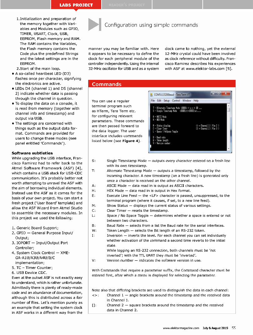
1.Initialization and preparation of
the memory together with Vari-
ables and Modules such as GPIO,
TIMER, USART, Clock, USB,
EEPROM, Flash memory and RAM.
The RAM contains the Variables,
the Flash memory contains the
Code plus the predefined Strings
and the latest settings are in the
EEPROM.
2.Start of the main loop.
• A so-called heartbeat LED (D3)
flashes once per character, signifying
the electronics are active.
• LEDs D4 (channel 1) and D5 (channel
2) indicate whether data is passing
through the channel in question.
• To display the data on a console, it
is read from memory (together with
channel info and timestamp) and
output via USB.
• The settings are concerned with
things such as the output data for-
mat. Commands are provided for
users to change these modes (see
panel entitled 'Commands').
Software subtleties
While upgrading the USB interface, Fran-
cisco Ramirez had to refer back to the
Atmel Software Framework (ASF) [4],
which contains a USB stack for USB-CDC
communication. It's probably better not
worth attempting to unravel the ASF with
the aim of borrowing individual elements.
Instead use the ASF as it comes for the
basis of your own project. You can start a
fresh project ('User Board' template) and
allow the ASF Wizard from Atmel Studio
to assemble the necessary modules. In
this project we used the following:
1. Generic Board Support;
2. GPIO — General Purpose Input/
Output;
3. IOPORT — Input/Output Port
Controller;
4. System Clock Control — XME-
GA-Al U/A3 U/A4 U/B/C
implementation;
5. TC — Timer Counter;
6. USB Device CDC.
Even at the outset ASF is not exactly easy
to understand, which is rather unfortunate.
Admittedly there is plenty of ready-made
code and an abundance of documentation,
although this is distributed across a fair
number of files. Let's mention purely as
an example that setting the system clock
in ASF works in a different way from the
Configuration using simple commands
manner you may be familiar with. Here
it appears to be necessary to define the
clock for each peripheral module of the
controller independently. Using the internal
32-MHz oscillator for USB and as a system
clock came to nothing, yet the external
12-MHz crystal could have been involved
as clock reference without difficulty. Fran-
cisco Ramirez describes his experiences
with ASF at www.elektor-labs.com [5].
Commands
You can use a regular
terminal program such
as HTerm, Tera Term etc.
for configuring relevant
parameters. These commands
are then passed forward to
the data logger. The user
interface includes commands
listed below (see Figure 4).
COM5:115200baud IrianA MI L
File Edit Setup Control Window Help
7 - Alterrate Tinestano Mde ‹,ü000.1> test al ... - Single Tinestanp Mode <00(101:t40002:e>....
- ASCII Mode H - HEX Mode
h - Status display C - Clear Titter L - Space 1 HoSpace Toggle
B - Baud rate P - Token length V - Version number
0 = Channel 1 I Pin 2 . Channel 2 t Pin
3
S: Single Timestamp Mode — outputs every character entered on a fresh line
with its own timestamp.
T: Alternate Timestamp Mode — outputs a timestamp, followed by the
incoming character. A new timestamp (on a fresh line) is generated only
once a character is received on the other channel.
A: ASCII Mode — data read in is output as ASCII characters.
H: HEX Mode — data read in is output in Hex format.
E: Execute Line Feed — the <LF> character is passed, unsuppressed, to the
terminal program (where it causes, if set, to a new line feed).
M: Show Status — displays the current status of various settings.
C: Clear Timer — resets the timestamp.
L: Space / No Space Toggle — determines whether a space is entered or not
between two characters.
B: Baud Rate — selects from a list the Baud rate for the serial interfaces.
W: Token Length — selects the Bit length of an RS-232 token.
Inversion — inverts the level. For each channel you can set individually
whether activation of the command a second time reverts to the initial
state.
While logging an RS-232 connection, both channels must be 'not
inverted'; with the TTL UART they must be 'inverted'.
V: Version number — indicates the software version in use.
With Commands that require a parameter suffix, the Command character must be
entered first, after which a menu is displayed for selecting the parameter.
Note also that differing brackets are used to distinguish the data in each channel:
<>: Channel 1 — angle brackets around the timestamp and the received data
in Channel 1.
[l: Channel 2 — square brackets around the timestamp and the received
data in Channel 2.
www.elektormagazine.com July &August 2015 55
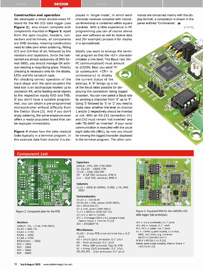
LEARN SHARE
Construction and operation
We developed a small double-sided PC
board for the RS-232 data logger (see
Figure 2), also shown complete with
components mounted in Figure 3. Apart
from the opto-coupler, headers, con-
nectors and terminals, all components
are SMD devices, meaning constructors
need to take care when soldering, fitting
IC3 and IC4 first of all, followed by the
resistors and capacitors. Since the last-
named are almost exclusively of SMD for-
mat 0805, you should manage OK with-
out needing a magnifying glass. Polarity
checking is necessary only for the diodes,
LEDs and the tantalum caps.
For checking correct operation of the
input stage with the opto-couplers the
best tool is an oscilloscope hooked up to
connector K4, while feeding serial signals
to the respective inputs RXD and TXD.
If you don't have a suitable program-
mer, you can obtain a pre-programmed
microcontroller without difficulty from
the Elektor Store [3]. And if you don't
enjoy soldering, the same emporium even
offers a ready-populated board that can
be deployed immediately.
Figure 4 shows how the data readout
looks typically in a terminal program. In
this example data from channel 2 is dis-
played in 'single mode', in which each
character received complete with individ-
ual timestamp is contained within square
brackets. With a little experience in PC
programming you can of course devise
your own software as well to receive data
and (for example) process it for display
in a spreadsheet.
Ideally you want to arrange the termi-
nal program so that the <LF> character
initiates a line feed. The Baud rate (for
PC communication!) must amount
to 115200. Next you send 'M'
(a subsequent <CR> is
unnecessary) to display
the current status of the
settings. A 'B' brings up a list
of the Baud rates possible for dis-
playing the connection being logged
onscreen. You can now select a Baud rate
by sending a character from '0' up to 'F'.
Using 'I' followed by '1' or '2' you need to
make clear whether the level on channel
1 and/or 2 respectively should be inverted
or not. With an RS-232 connection Chi.
and Ch2 must remain 'not inverted' and
with TTL-UART as 'inverted'. If your serial
communication is executed with the usual
eight data bits (8N1), by now you should
be viewing the logged character displayed
in the terminal program. The other com-
mands are concerned mainly with the dis-
play format; a compilation is shown in the
panel entitled 'Commands'. 11
(140126)
Component List
Figure 2. Component plan for the PCB.
Resistors
Default: 5%, .125W, SMD 0805) R1,R2 = 68S2 1%
R3,R5 = 270Q R4,R6 = 100Q
R7,R8 = 220Q R9,R10,R11 = 330Q
R12 = 10kS2 R13 = 33kS2
R14 = 56kS2 R15 = 680Q
Capacitors
Default: 10%, 50V, SMD 0805 Cl-C6,C10 = 100nF, X7R
C7,C8 = 22pF, COG/NPO C9 = 4.7pF 20V, tantalum, SMD A
C11 = 10pF 10V, tantalum, SMD A
Inductors
Ll,L2 = 330Q @ 100MHz, 0.08Q, 1.7A, SMD
0603
Semiconductors
D1,D2 = TS4148 RY D3,D4,D5 = LED, yellow (SMD 0805)
D6 - PRTR5VOU2X
D7 = LED, green (SMD 0805) T1,T2 = BF545A (SMD SOT23)
IC1,IC2 = 6N137 (DIP8) IC3 = ATxmega128A4U-AU, programmed,
Elektor Store # 140126-41 [3] IC4 = KF33BDT-TR
Miscellaneous
Kl,K2 = 2-way PCB screw terminal block, 0.2"
pitch K3 = 10-pin (2x5) pinheader, 0.1" pitch
K4 = 4-pin pinheader, 0.1" pitch
K5 = Micro USB connector, Type B, SMD K1 = 6-way (2x3) boxheader, 0.1" pitch
JP1,3P2,3P3 = 2-pin pinheader, 0.1" pitch
Figure 3. Populated PCB for the UART/RS-232 data logger (lab prototype).
3P4 = 3-pin pinheader, 0.1" pitch
3P1-3P4 = jumper, 0.1" pitch PC1-PC4 = solder pin 1.3mm
X1 = 12MHz quartz crystal, CL=18pF, SMD, 5x3.2mm, e.g. Abracon
ABM3-12.000MHZ-D2Y-T PCB # 140126-1 v1.0 [3]
Ready assembled module, Elektor Store #
140126-91 [3]
56 July 8f August 2015 www.elektormagazine.com

COM5:115200baud
FI FI
- ASCII hale H - HEX hale
- Status display C - Clear liner L - Space 1 NoSpace Toggle
- Baud rate U - Token length - version number
<> = Channel 1 ( Pin 2 1 II = Channel 2 ( Pin 3
latas a Olt Tstamp, ASCII ( Ox1F < CHB < Ox7F I, 19200 Bd, 8 Bit, SPC
tatas Sin Tstamp, ASCII ( loll < COB < Ox7F I, 19200 Bd, 8 Bit, SPC 10:06:32:381:g (0:06:32:SS9:j 10:06:33:102:j [0:06:33:118:h 10:06:33:293:g I0:06:33:397:j [0:06:33:193:g [0:06:33:613:j
Figure 4. Output display in Tera Term for data on Channel 2.
Web Links
[1] www.atmel.com/devices/ATXMEGA128A4U.aspx
[2] www.elektor-magazine.com/130155
[3] www.elektor-magazine.com/140126
[4] www.atmel.com/tools/avrsoftwareframework.aspx?tab=overview
[5] www.elektor-labs.com/contribution/from-the-lab-new-software. 14381. html
[6] www.elektor-magazine.com/140009
[7] www.elektor-magazine.com/130023
Data logging with the EC
The Embedded Communication
Connector (ECC) specified by Elektor
transfers TTL UART signals via two
pins of a 2x5-pole header connector.
The Elektor Extension Shield for the
Arduino Uno [6] is already equipped
with a header connector of this kind
and an adapter for the SAM-D20
Board from the ARM product line will
be available shortly. Using a flat cable
various communications modules can
be plugged into this header, including
the RS-485 converter [2] and 433-MHz
ISM radio module [7] already described,
as well as the UART/USB converter (in
this issue). An NFC gateway and further
modules will follow.
If you are interested in logging alone,
for instance the output from an Arduino
Uno, then you can simply hook the
Extension Shield direct to the data
logger using a flat cable. If you need
to monitor bi-directionally, you'll need
a Y-splitter for the signals, ideally one
equipped with three ECC connectors. A
printed circuit board for this has already
been designed in our labs. For their
first experiments our colleagues simply
knocked up the circuit shown here on
some perf board. The photo shows them
logging data exchanged between the
Arduino Uno and a PC (for this see the
'Learn' introductory page in this issue).
To do this the Y-splitter and data logger
combo were inserted in the hookup
between the Shield and the RS-485
converter.
www.elektormagazine.com July &August 2015 57

SHARE
Part 3
smartBASIC programming for the Bluetooth Low Energy module
By Jennifer Aubinais (France) [email protected]
La rd
HRM Proxi
Serial OT
61,00ZE -VW 00918 -8lE6I :al 00918,1d :01 33A ; PO- PINA
The aim of this series around the BL600 e-BoB is to make it easier to implement this remarkable
module for wireless communication with devices you design yourself. The fact it can be programmed in
smartBASIC is by no means the least of the BL600's qualities. In order to take full advantage of it, you do
need get used to handling the events that make smartBASIC so powerful.
Following on from the description of the
module's hardware and the tool needed
to use it, we're now going to take a look
at smartBASIC. This enables you to pro-
gram the BL600 using what Laird Technol-
ogies call "events". I recommend you read
their documentation [1]. As an application
example, I'm going to be using the coding
for our light-chaser from last month [2],
and more specifically managing the offset
time for turning the LEDs on and off and
the chaser movement direction - all using
these famous events. So in order to be
able to follow, it's best if you've read the
previous article. To go a bit further into
it, you'll find it best to have it to hand.
Then, as an example of using Bluetooth
communication, starting out from the
UART program that's already been men-
tioned, we're going to control a 3-color
LED. We'll intercept the characters send
by the smartphone to turn the RGB LED
on or off. This will give you the oppor-
tunity to use our eBOB-BL600 to control
a commercial 3-color lamp or string of
lights, for example. My BLE RGB Li te
program is available on Google Play [3].
Handlers in the light-chaser
Our chaser program in the previous arti-
cle (a simple for next loop for the tim-
ing, along with, for the LED chase, but-
ton position detection using an if con-
dition) did not exploit the possibilities
of the events in smartBASIC [see box].
This time, to do the same thing but more
cleverly, we're using handlers, i.e. event
managers.
We're going to be seeing two types of
events: counting/timing and the changing
state of a button. As much of the inter-
est of smartBASIC lies in managing such
events, it's essential to understand this
little program properly before moving on
to the next step.
The six LEDs connected to the eBoB-
BL600's outputs 3-12 (see circuit and
components list in last month's article
[2]) turn on and off in succession. In
the code in Listing 1, we're not going to
linger over the black section, described
in the previous issue of Elektor, but are
going to take a look at what's going on
in the red section of the code:
WAITEVENT
The command (or statement) WAITEVENT
makes it possible to run the event man-
ager. It's a sort of wait loop in which the
system scans for the presence of events.
This waiting stage is usually placed at the
end of the main program (main).
The events are coupled to the manag-
ers (handlers) by ON EVENT ... CALL
instructions, e.g. ONEVENT EVTMR() CALL
FuncTimer0, which means the Func-
Ti me r function is the handler for the
event EVTMR(). The event names are pre-
defined, but you can choose the names
of the handlers.
FuncTimere function
Here, we turn the LEDs on and off alter-
nately at intervals of 200 ms (an arbi-
58 July &August 2015 www.elektormagazine.com
trary value). To do this, we create an
event EVTMRO (EVTMR corresponds to a
timer event, 0 corresponds to the num-
ber of the timer we've chosen) which is
going to call the function FuncTimere
(this name is arbitrary) thanks to cou-
pling via the instruction ON EVENT EVTMR()
CALL FuncTimer0.
Timer 0 is started by:
TIMERSTART(0,10,0)
where 0 is the event number, the same
as in EVTMRO; 10 is the duration in ms of
the timer counter; and lastly 0 for non-it-
erative; 1 for iterative.
The offset between turning the LEDs
on and off is obtained by incrementing
a counter (in our example, led) which
turns one LED off and the next one on
depending on its value. When the counter
reaches the number of LEDs — for us,
that's 6 — it is reset to zero and the LED
sequence starts over.
At the end of FuncTimer0, timer 0 is
restarted, this time for 200 ms.
Changing direction, FuncTi me n
To reverse the direction of our chaser, all
we have to do is to decrement a counter
starting from the number of LEDs —
six, here — instead of incrementing it.
At each decrement, depending on the
counter value, one LED is turned off and
the previous one is lit. Once the counter
reaches zero, it is reset to 6 for a new
LED sequence. That's what we have done
here using Timer 1 with its event EVTMR1
and its handler FuncTimerl. We could
have achieved this more simply, but the
aim here is to demonstrate events.
//TIMERSTART(0 ,10,0)
led = 6
TIMERSTART(1,10,0)
Try these lines... When you save your
code, remember to delete the old pro-
gram in the BL600 (don't forget the
AT&F 1 command). Compile, transfer, and
run. You'll see that the chaser starts in
the other direction.
This example shows the simplicity of
using timers: we can run a timer for a sin-
gle (final parameter set to 0) or repeated
(final parameter set to 1) count; it pro-
duces an event which runs a function
[see box].
The "button" event
Before moving on, let's go back to the
original code:
Listing 1.
Dim led, rc
' /7 FUNCTION FuncTimer0()
PRINT "WAY + ";led;" \n"
IF (led
IF (led
IF (led
IF (led
IF (led
IF (led
== 0)
== 1)
== 2)
== 3)
== 4)
== 5)
THEN
THEN
THEN
THEN
THEN
THEN
: GpioWrite(12,0) : GpioWrite(3,1) : ENDIF
: GpioWrite(3,0) : GpioWrite(8,1) : ENDIF
: GpioWrite(8,0) : GpioWrite(9,1) : ENDIF
: GpioWrite(9,0) : GpioWrite(10,1) : ENDIF
: GpioWrite(10,0) : GpioWrite(11,1) : ENDIF
: GpioWrite(11,0) : GpioWrite(12,1) : ENDIF
led = led + 1
IF ( led >, 6) THEN : led = O : ENDIF
TIMERSTART(0,200,0)
ENDFUNC 1
/7
FUNCTION FuncTimerl()
PRINT "WAY - ";led;" \n"
IF (led == 6) THEN
IF (led == 5) THEN
IF (led == 4) THEN
IF (led == 3) THEN
IF (led == 2) THEN
IF (led == 1) THEN
led led - 1
IF ( led <= 0) THEN : led = 6 : ENDIF
TIMERSTART(1,200,0)
ENDFUNC 1
/7
FUNCTION Btn0Press()
PRINT "PRESS DOWN\n"
rc = GpioBindEvent(1,2,0)
TIMERCANCEL(0)
TIMERSTART(1,10,0)
ENDFUNC 1
FUNCTION Btn1Press()
PRINT "PRESS UP\n"
rc = GpioBindEvent(0,2,1)
TIMERCANCEL(1)
TIMERSTART(0,10,0)
ENDFUNC 1
' /7
: GpioWrite(3,0) : GpioWrite(12,1) : ENDIF
: GpioWrite(12,0) : GpioWrite(11,1) : ENDIF
: GpioWrite(11,0) : GpioWrite(10,1) : ENDIF
: GpioWrite(10,0) : GpioWrite(9,1) : ENDIF
: GpioWrite(9,0) : GpioWrite(8,1) : ENDIF
: GpioWrite(8,0) : GpioWrite(3,1) : ENDIF
ONEVENT
ONEVENT
ONEVENT
ONEVENT
EVTMRO CALL FuncTimer0
EVTMR1 CALL FuncTimerl
EVGPIOCHANO CALL Btn0Press
EVGPIOCHAN1 CALL Btn1Press
rc = GpioSetFunc(2,1,2)
rc = GpioBindEvent(0,2,1)
/7 init all GPIO at value Low
rc = GpioSetFunc(3,2,0)
rc = GpioSetFunc(8,2,0)
rc = GpioSetFunc(9,2,0)
rc = GpioSetFunc(10,2,0)
rc = GpioSetFunc(11,2,0)
rc = GpioSetFunc(12,2,0)
led =
TIMERSTART(0,10,0)
//led = 6
//TIMERSTART(1,10,0)
WAITEVENT
/7 Pin 3
/7 Pin 8
/7 Pin 9
// pin 10
// pin 11
// pin 12
www.elektormagazine.com July &August 2015 59
— CBUS4
CBUS3
CBUS2
CBUS1
CBUSO
RESET
USB
MOD1
.F5V
VCCIO
.3V3
GND
CTS
RI
DCD RXD BOB-FT232R DSR TXD
DTR e RTS
\ autorun CMD ota
iii
RX 12
TX 11
CTS 10
RTS BOB-BL600 9
VCC
GND
RES 2
PGM /GA
MOD2 44
- 1 =471:1 -11111111 -
4* • ' ++ e
470R 1 -1-0111 —e-1-•
— I 470R 4+
tricolor LED
133
• — 1 - 1 -11 --- - -150129 - 11
Figure 1. Experimental circuit for wireless control of a 3-color LED. Using the BL600 module, you can turn the LED on and off and choose the color using a smartphone.
Corn sonent List (LED RGB control)
Resistors R1-R4 = 470Q
Semiconductors D1 = LED, 3mm (select color) D2 = LED, RGB, common cathode
Miscellaneous Kl = pushbutton MOD1 = assembled FT232 e-BoB module, # 110553-91 (www.elektor.com) MOD2 = assembled BL600 e-BoB module, # 140270-91 (www.elektor.com)
Uti k •"'" 1UM, '
• MS M OO - Si N2 -05 FCC ID PIU M00
,93 ,8- BlS00
R 20: -35 n9
Figure 2. The circuit is easy to build on a solderless prototyping board.
TINIERSTART(0,10,0)
//led = 6
//TINIERSTART(1,10,0)
and take a look at the code in green in
Listing 1.
When the button connected to pin 2 is
pressed, an event EVGPIOCHANO occurs,
where EVGPIOCHAN represents "change
of state on one of the module inputs",
while 0 is the event number (chosen by
us). This event is handled in the Btn-
OP r ess function via the instruction
ONEVENT EVGPIOCHAN1 CALL Btn1Press.
After pin 2 has been declared as an input
by GpioSetFunc(2,1,2), GpioBindE-
vent (0,2,1) establishes for this pin a
link between the event and a transition
(see below).
Declaring pin 2 as an input
rc = GpioSetFunc(2,1,2)
nSigNum = 2: pin GPIO 2
nFunction = 1: port as input
nSubFunc = 2: internal pull-up resistor
"rc" is the code returned by the func-
tion, which is Ox0000 if everything goes
according to plan.
Declaring a link for an event to an
input level transition
rc = GpioBindEvent(0,2,1)
nEventNum = 0: event number: EVGPI-
OCHANO (the zero)
nSigNum = 2: pin GPIO 2
nPolarity = 1:0 for a Low-to-High
transition
1 for a High-to-Low transition
2 for a Low-to-High or High-to-Low
transition
"rc" is the code returned by the function,
which is 0 if the function has not encoun-
tered any problems.
When the button is pressed, the TIM-
ERSTART function (first parameter:
Event 1) runs the chaser code (in blue)
from output 12 to output 3. The reverse
happens when the button is released, the
TIMERSTART function (first parameter:
Event 0) runs the chaser code (in mauve)
from output 3 to output 12.
Three-color LED
Now you know how the events are han-
dled, it's time to get the BL600 e-BoB to
communicate with your phone via Blue-
tooth. The module is going to receive the
phone data, via Bluetooth Low Energy,
in order to light up the color(s) of the
3-color LED in the circuit in Figure 1.
Just like the light-chaser described last
60 July &August 2015 www.elektormagazine.com
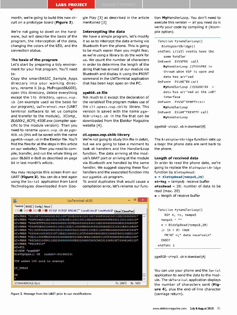
month, we're going to build this new cir-
cuit on a prototype board (Figure 2).
We're not going to dwell on the hard-
ware, but will describe the basis of the
program, the interception of the data,
changing the colors of the LED, and the
connection status.
The basis of the program
Let's start by preparing a tidy environ-
ment for your first program. You'll need
to:
Copy the smartBASIC_Sample_Apps
directory into your working direc-
tory, rename it (e.g. MyProjectBL600),
open this directory, delete everything
except the lib directory, upass.vsp.
sb (an example used as the basis for
our program), UwTermi nal. exe (UART
terminal software to let us compile
and transfer to the module), XComp_
BL600r2_8CF9 450Eexe (compiler spe-
cific to the module version). Then you
need to rename upass.vsp.sb as pgm-
RGB.sb (this will be saved with the name
pgmRGB-step®.sb in the Elektor file. You'll
find the files for all the steps in this article
on our website). Then you need to com-
pile, transfer, and run the whole thing on
your BL600 e-BoB as described on page
64 in last month's article.
You may recognize this screen from our
UART (Figure 3). You can do a test again
using the Serial application from Laird
Technologies downloaded from Goo-
gle Play [3] as described in the article
mentioned [2]
Intercepting the data We have a simple program, let's modify
it so as to intercept the data arriving via
Bluetooth from the phone. This is going
to be much easier than you might fear,
as we're using a library to do the work for
us. We count the number of characters
in order to determine the length of the
string that has arrived at our module via
Bluetooth and display it using the PRINT
command in the UWTerminal application
that has been kept open on the PC.
pgmRGB.sb file
Not much to it except the declaration of
the variables! The program makes use of
the cli .upass.vsp.sblib library. This
version is saved with the name pgm-
RGB-stepl sb in the file that can be
downloaded from the Elektor Magazine
website [4].
cli.upass.vsp.sblib library
We're not going to study this file in detail,
but we are going to take a moment to
look at handlers and the HandlerLoop
function. The data arriving at the mod-
ule's UART port or arriving at the module
via Bluetooth are handled by the same
handler. We suggest copying these four
handlers and the associated function into
our pgmRGB.sb program.
To avoid duplicates that would cause a
compilation error, let's rename our func-
UwTerminal v6.93 — K_ Telminal I BASIC' Corfu' About
_TS* DCDIII Rig' RTs1,7 DTRI7 BREAK r LocalEcho LineModerj ClearIClosePorti
.T+FWREI "0110873006002615011087300E002615011087300F0026150110D230000001"
.T+FWAH "00F634A515A5150110C920E11201100110D23000000000F634C115C1150110"
.T+FWRH "806OFFFF5202340004000100FB30020052430110D23000000000E8220060CD"
.T+FWRH "203FODE922340001100110CE211000FB00030002000A0DCC21C41SE6210600"
.T+FWRH "0110CF3006009001E5210060C920100D0110CE211000FB00060008004C545F"
.T+FWRH "5550415353CC21D715E62106000110CF3006009001E5210080C920100D0110"
.T+FWRH "CE211000FB00030002000A0DCC21ED15E62106000110CF3006009001E52100"
.T+FWRH "80C920100D0110D23000000000E8220080C920C90C01106910F72406160110"
.T+FWRH "FD10F510"
.T+FCL
.2+12124 "pgmRGB"
neVSpOpen() OK (uuhd1=-50196223)
SP added 126 uuld to scanrpt
T_UPASS
LCOM4:9603,N,8,1Ncr} Tx 26672 [fbr 11633
Figure 3. Message from the UART prior to our modifications.
tion MyHandlerLoop. You don't need to
execute this version — all you need do is
verify your code by compiling it (Xcom-
pile option).
function MyHandlerLoop()
BleVspUartBridge()
endfunc 1//all events have the
same handler
OnEvent EVVSPRX call
MyHandlerLoop //EVVSPRX is
thrown when VSP is open and
data has arrived
OnEvent EVUARTRX call
MyHandlerLoop //EVUARTRX =
data has arrived at the UART
interface
OnEvent EVVSPTXEMPTYcall
MyHandlerLoop
OnEvent EVUARTTXEMPTY call
MyHandlerLoop
pgmRGB-step2.sb in download [4]
The BleVspUartBridge function sets up
a loop: the phone data are sent back to
the phone.
Length of received data
In order to read the phone data, we're
going to replace the BleVspUartBridge
function by BleVspRead:
n = BleVspRead(tempo$,20)
strMsg = tempo$: receive buffer
nMaxRead = 20: number of data to be
read (max. 20)
n = length of receive buffer
function MyHandlerLoop()
DIM n, rc, tempo$
tempo$ =
n = BleVSpRead(tempo$,20)
IF (n > 0) THEN
PRINT n;" data receive\n"
ENDIF
endfunc 1
pgmRGB-step3.sb in download [4]
You can use your phone and the Serial
application to send the data to the mod-
ule. The UWTerminal application displays
the number of characters sent (Fig-
ure 4), plus the end-of-line character
(carriage return).
www.elektormagazine.com July &August 2015 61
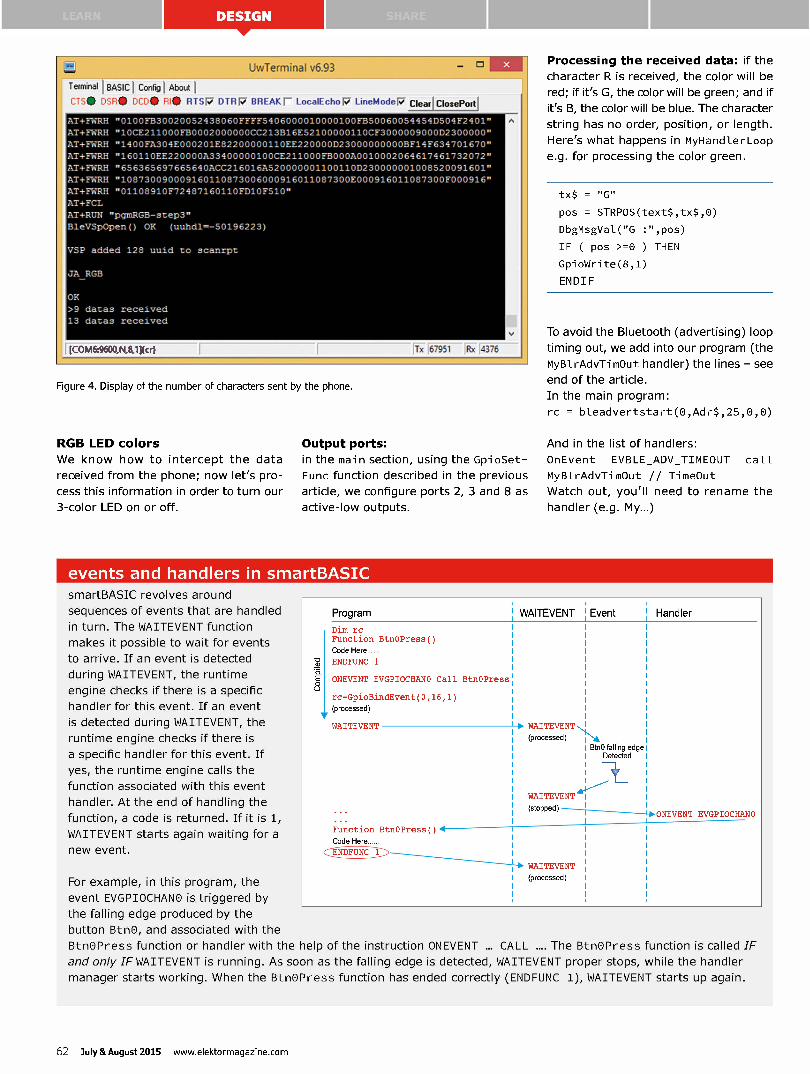
SHARE
UwTerminal v6.93 — X
Terminal I BASIC I Config I About I
[TS * D'F.f; • DU * H er RTSI7 DTRI7. BREAK E LocalEcho LineHodeFi Clear' ClosePoitI
.T+FWRH "0100F33002005243806OFFFF5406000010000100FB50060054454D504F2401"
• +KRIM '10CE211000F80002000000CC213B16E52100000110CF3000009000D2300000"
-T+FWAH '1400 M304E000201E82200000110KE220000D2300000000013F14F634701670"
• + MEW "160110EE220000A33400000100CE211000F8000A0010002064617461732072"
.T+FIIRK «656366697665640ACC216018A520000001100110D230000001008520091601"
.T+FWRH "108730090009160110873006000916011087300E000916011087300F000916"
-i+FWAH "01108910F72487160110FD10F510'
• +RUN "pgmKGB—step3"
zleVSpOpen() OK (uuhd1=-50196223)
SP added 128 maid to scanrpt
._RGB
0K
,9 datas received
,3 datas received
[COM6:9600,N,8,1]{crl Tx 67951 Fbc 4376
Figure 4. Display of the number of characters sent by the phone.
RGB LED colors We know how to intercept the data
received from the phone; now let's pro-
cess this information in order to turn our
3-color LED on or off.
Output ports:
in the main section, using the GpioSet-
Func function described in the previous
article, we configure ports 2, 3 and 8 as
active-low outputs.
Processing the received data: if the
character R is received, the color will be
red; if it's G, the color will be green; and if
it's B, the color will be blue. The character
string has no order, position, or length.
Here's what happens in MyHandlerLoop
e.g. for processing the color green.
tx$ = "G"
pos = STRPOS(text$,tx$,O)
DbgMsgVal("G :",pos)
IF ( pos >=0 ) THEN
GpioWrite(8,1)
ENDIF
To avoid the Bluetooth (advertising) loop
timing out, we add into our program (the
MyBlrAdvTimOut handler) the lines - see
end of the article.
In the main program:
rc = bleadvertstart(0,Adr$ ,25,0,0)
And in the list of handlers:
OnEvent EVBLE_ADV_TIMEOUT call
MyBlrAdvTimOut // TimeOut
Watch out, you'll need to rename the
handler (e.g. My...)
events and handlers in smartBASIC smartBASIC revolves around
sequences of events that are handled
in turn. The WAITEVENT function
makes it possible to wait for events
to arrive. If an event is detected
during WAITEVENT, the runtime
engine checks if there is a specific
handler for this event. If an event
is detected during WAITEVENT, the
runtime engine checks if there is
a specific handler for this event. If
yes, the runtime engine calls the
function associated with this event
handler. At the end of handling the
function, a code is returned. If it is 1,
WAITEVENT starts again waiting for a
new event.
For example, in this program, the
event EVGPIOCHANO is triggered by
the falling edge produced by the
button BtnO, and associated with the
Btn0Press function or handler with the help of the instruction ONEVENT ... CALL .... The Btn0Press function is called IF
and only IF WAITEVENT is running. As soon as the falling edge is detected, WAITEVENT proper stops, while the handler
manager starts working. When the Btn0Press function has ended correctly (ENDFUNC 1), WAITEVENT starts up again.
E 8
Program WAITEVENT Event Handler
Dim rc Function Btn0Press ( )
Code Here
ENDFUNC 1
ONEVENT EVGPIOCHANO Call Btn0Press
rc=GpioBindEvent ( 0, 16, 1 )
(processed) V WAITEVENT 10. WAITEVENT
(processed) NI NA, Btn0 falling edge Detected
WAITEVENT
(stopped) EVGP IOCHAN 0
Function Btn0Press ( ) 4
Code Here
(ENDFUNC
WAITEVENT
(processed)
62 July &August 2015 www.elektormagazine.com

In the functions:
// // This handler -is called when there is an advert timeout
'-function MyBlrAdvTimOut() as integer
if AdvMngrOnAdvTimeOut() == 0 then DbgMsg( "\nAdvert stopped via timeout" ) dim Adr$
Adr$= " rC =
bleadvertstart(0,Adr$,25,0,0) end -if
endfunc 1
pgmRGB-step4.sb in download [4]
Using the Seri al application from Laird
Technologies, you can send orders like:
R--, RGB, ---, GB-, and so on.
You can download my BLE RGB Lite pro-
gram on Google Play [3]. The source code
for this program (Figure 5) will be avail-
able on the Elektor site.
Connection status
A little bonus: we're going to light an
LED on output 12 of our module when it
is connected; this will be turned off when
the module is disconnected. Don't forget
the function for initializing port 12 as an
output in the main program - you know
how to do that now.
We're going to copy the Bluetooth mes-
sage handler from the cli . manager.
sblib library and create our own han-
dler, like this:
In the list of global variables:
'// Global Variable Declarations
7/********************************
dim hConnLast
In the list of handlers:
(Watch out, you'll need to rename the
handler, e.g. My...)
OnEvent EVBLEMSG
MyHandlerBleMsg
We'll add the MyHandlerBleMsg function.
When the message concerns a connec-
tion, we turn our LED on and when it
involves a disconnection, we turn our
LED off (code in red). Nothing very
complicated:
function MyHandlerBleMsg(BYVAL
nMsgId AS INTEGER, BYVAL nCtx
AS INTEGER) as integer
code here
select nMsgId
case BLE_EVBLEMSGID_CONNECT
DbgMsgVal(" --- Connect :
nCtx)
GpioWrite(12,1)
hConnLast = nCtx
ShowConnParms(nCtx)
case
BLE_EVBLEMSGID_DISCONNECT
DbgMsgVal(" --- Disconnect
nCtx)
GpioWrite(12,0)
code here
pgmRGB.sb in download [5]
MyBlrAdvTi mOut
The purpose of this handler is to re-launch
the possibility for connecting to our mod-
ule in Bluetooth following a timeout. To
do this, we're going to copy the default
handler from the cl -i .manager.sblib
library and create our own MyHandler-
BlrAdvTimOut handler. We've designed
it to re-launch the advertising, i.e. the
Bluetooth, via the following code:
rc = bleadvertstart(0,Adr$,25,0,0) 14
Acknowledgements:
Jennifer Gibbs (Laird Technologies); Philippe
(150129)
1:1 1111 * Ad e.2%• 15.2
BLE BLE RGB Lite
Disconnect
RED
GREEN
BLUE On
(c) Jennifer AUBINAIS 1.4
Figure 5. Screen from the BLE RGB application
available from Google Play.
Selection of topics
to be covered in future episodes of
this series on the BL600 e-Bob:
• Low Energy, 5 pA
• the I2C l SPI ports
• Bluetooth communication
• explanation of the remote wireless
thermometer program
• writing a program for Android
• writing a program for iOS
Weblinks:
[1] https://laird-ews-support.desk.com/?b_id=1945
[2] e-BoB BL600 I Elektor no. 442, March
www.elektor.com/150014
[3] https://play.google.com/
[4] www.elektor-magazine.com/150129
[5] e-BoB BL600 I Elektor no. 441, March
2015, p. 64
2015, p. 34
www.elektor-magazine.com/140270
[6] Bluetooth LE Wireless Thermometer
Elektor nos. 439-440, Jan. 8( Feb. 2015, p. 72
www.elektor-magazine.com/140190
www.elektormagazine.com July &August 2015 63
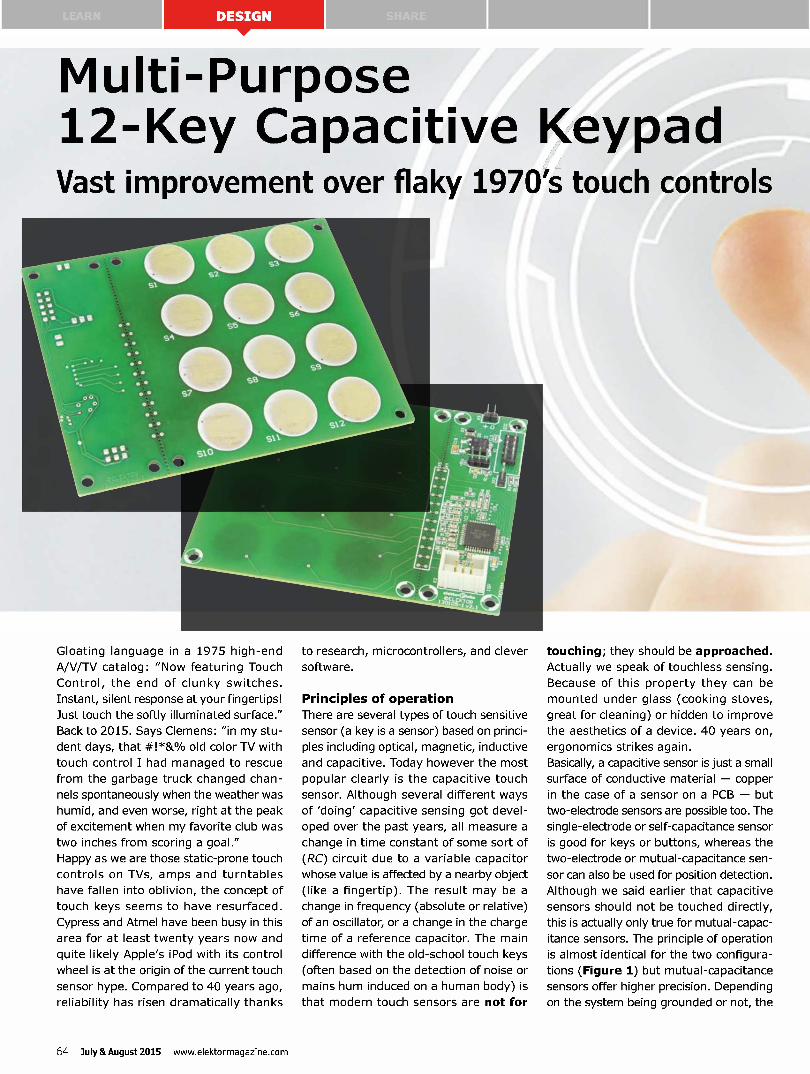
Multi-Purpose 12-Key Capacitive Keypad Vast improvement over flaky 1970's touch controls
to research, microcontrollers, and clever
software.
Gloating language in a 1975 high-end
A/V/TV catalog: "Now featuring Touch
Control, the end of clunky switches.
Instant, silent response at your fingertips!
Just touch the softly illuminated surface."
Back to 2015. Says Clemens: "in my stu-
dent days, that #!*&% old color TV with
touch control I had managed to rescue
from the garbage truck changed chan-
nels spontaneously when the weather was
humid, and even worse, right at the peak
of excitement when my favorite club was
two inches from scoring a goal."
Happy as we are those static-prone touch
controls on TVs, amps and turntables
have fallen into oblivion, the concept of
touch keys seems to have resurfaced.
Cypress and Atmel have been busy in this
area for at least twenty years now and
quite likely Apple's iPod with its control
wheel is at the origin of the current touch
sensor hype. Compared to 40 years ago,
reliability has risen dramatically thanks
Principles of operation
There are several types of touch sensitive
sensor (a key is a sensor) based on princi-
ples including optical, magnetic, inductive
and capacitive. Today however the most
popular clearly is the capacitive touch
sensor. Although several different ways
of 'doing' capacitive sensing got devel-
oped over the past years, all measure a
change in time constant of some sort of
(RC) circuit due to a variable capacitor
whose value is affected by a nearby object
(like a fingertip). The result may be a
change in frequency (absolute or relative)
of an oscillator, or a change in the charge
time of a reference capacitor. The main
difference with the old-school touch keys
(often based on the detection of noise or
mains hum induced on a human body) is
that modern touch sensors are not for
touching; they should be approached.
Actually we speak of touchless sensing.
Because of this property they can be
mounted under glass (cooking stoves,
great for cleaning) or hidden to improve
the aesthetics of a device. 40 years on,
ergonomics strikes again.
Basically, a capacitive sensor is just a small
surface of conductive material — copper
in the case of a sensor on a PCB — but
two-electrode sensors are possible too. The
single-electrode or self-capacitance sensor
is good for keys or buttons, whereas the
two-electrode or mutual-capacitance sen-
sor can also be used for position detection.
Although we said earlier that capacitive
sensors should not be touched directly,
this is actually only true for mutual-capac-
itance sensors. The principle of operation
is almost identical for the two configura-
tions (Figure 1) but mutual-capacitance
sensors offer higher precision. Depending
on the system being grounded or not, the
64 July &August 2015 www.elektormagazine.com
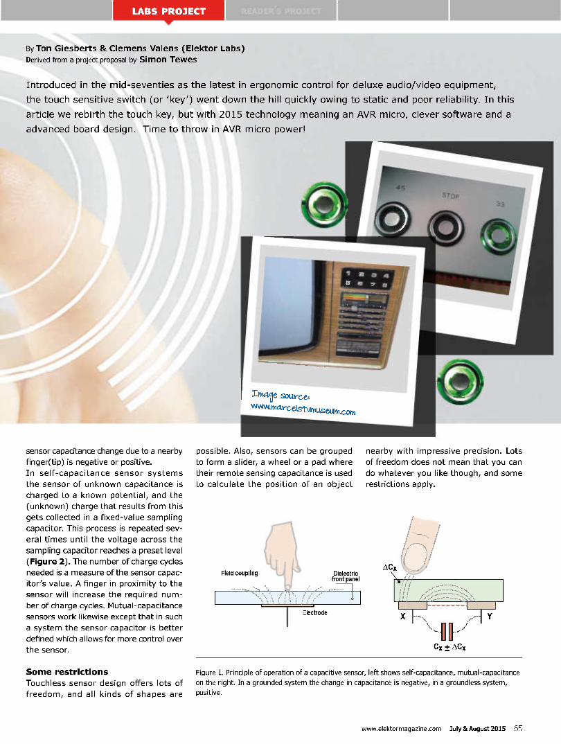
By Ton Giesberts 8( Clemens Valens (Elektor Labs)
Derived from a project proposal by Simon Tewes
Introduced in the mid-seventies as the latest in ergonomic control for deluxe audio/video equipment,
the touch sensitive switch (or 'key') went down the hill quickly owing to static and poor reliability. In this
article we rebirth the touch key, but with 2015 technology meaning an AVR micro, clever software and a
advanced board design. Time to throw in AVR micro power!
sensor capacitance change due to a nearby
finger(tip) is negative or positive.
In self-capacitance sensor systems
the sensor of unknown capacitance is
charged to a known potential, and the
(unknown) charge that results from this
gets collected in a fixed-value sampling
capacitor. This process is repeated sev-
eral times until the voltage across the
sampling capacitor reaches a preset level
(Figure 2). The number of charge cycles
needed is a measure of the sensor capac-
itor's value. A finger in proximity to the
sensor will increase the required num-
ber of charge cycles. Mutual-capacitance
sensors work likewise except that in such
a system the sensor capacitor is better
defined which allows for more control over
the sensor.
Some restrictions
Touchless sensor design offers lots of
freedom, and all kinds of shapes are
possible. Also, sensors can be grouped
to form a slider, a wheel or a pad where
their remote sensing capacitance is used
to calculate the position of an object
nearby with impressive precision. Lots
of freedom does not mean that you can
do whatever you like though, and some
restrictions apply.
Figure 1. Principle of operation of a capacitive sensor, left shows self-capacitance, mutual-capacitance on the right. In a grounded system the change in capacitance is negative, in a groundless system, positive.
www.elektormagazine.com July &August 2015 65
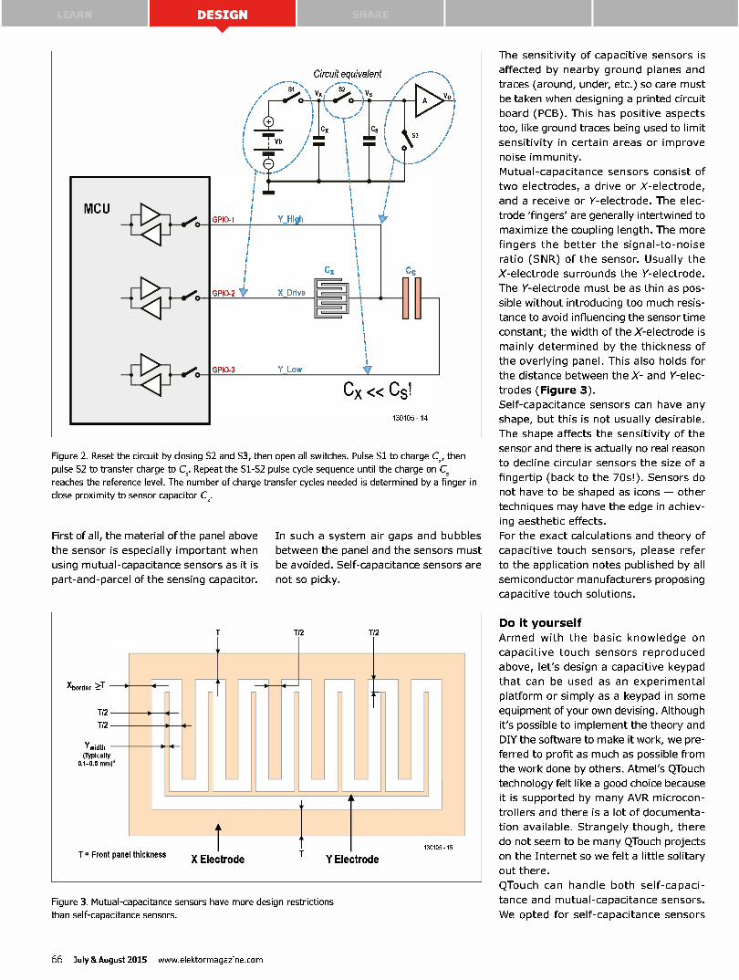
MC U
GP10-2 1r
Circuit equivalent
SI „x S2 Vs
°
7 Vb
Y_High
X_Drive
GP10-3
tit
tit
S3
Cx « Cs! 130105 - 14
•
v.\
Figure 2. Reset the circuit by closing S2 and S3, then open all switches. Pulse Si to charge Cx, then pulse S2 to transfer charge to C. Repeat the S1.-S2 pulse cycle sequence until the charge on Cs reaches the reference level. The number of charge transfer cycles needed is determined by a finger in close proximity to sensor capacitor C.
First of all, the material of the panel above
the sensor is especially important when
using mutual-capacitance sensors as it is
part-and-parcel of the sensing capacitor.
In such a system air gaps and bubbles
between the panel and the sensors must
be avoided. Self-capacitance sensors are
not so picky.
Xborder >T
1/2
1/2
Ywidth (Typically 0.1-0.5 mm)*
1/2 1/2
130105 - 15 T = Front panel thickness
X Electrode Y Electrode
Figure 3. Mutual-capacitance sensors have more design restrictions than self-capacitance sensors.
The sensitivity of capacitive sensors is
affected by nearby ground planes and
traces (around, under, etc.) so care must
be taken when designing a printed circuit
board (PCB). This has positive aspects
too, like ground traces being used to limit
sensitivity in certain areas or improve
noise immunity.
Mutual-capacitance sensors consist of
two electrodes, a drive or X-electrode,
and a receive or Y-electrode. The elec-
trode 'fingers' are generally intertwined to
maximize the coupling length. The more
fingers the better the signal-to-noise
ratio (SNR) of the sensor. Usually the
X-electrode surrounds the Y-electrode.
The Y-electrode must be as thin as pos-
sible without introducing too much resis-
tance to avoid influencing the sensor time
constant; the width of the X-electrode is
mainly determined by the thickness of
the overlying panel. This also holds for
the distance between the X- and Y-elec-
trodes (Figure 3).
Self-capacitance sensors can have any
shape, but this is not usually desirable.
The shape affects the sensitivity of the
sensor and there is actually no real reason
to decline circular sensors the size of a
fingertip (back to the 70s!). Sensors do
not have to be shaped as icons — other
techniques may have the edge in achiev-
ing aesthetic effects.
For the exact calculations and theory of
capacitive touch sensors, please refer
to the application notes published by all
semiconductor manufacturers proposing
capacitive touch solutions.
Do it yourself
Armed with the basic knowledge on
capacitive touch sensors reproduced
above, let's design a capacitive keypad
that can be used as an experimental
platform or simply as a keypad in some
equipment of your own devising. Although
it's possible to implement the theory and
DIY the software to make it work, we pre-
ferred to profit as much as possible from
the work done by others. Atmel's QTouch
technology felt like a good choice because
it is supported by many AVR microcon-
trollers and there is a lot of documenta-
tion available. Strangely though, there
do not seem to be many QTouch projects
on the Internet so we felt a little solitary
out there.
QTouch can handle both self-capaci-
tance and mutual-capacitance sensors.
We opted for self-capacitance sensors
66 July &August 2015 www.elektormagazine.com
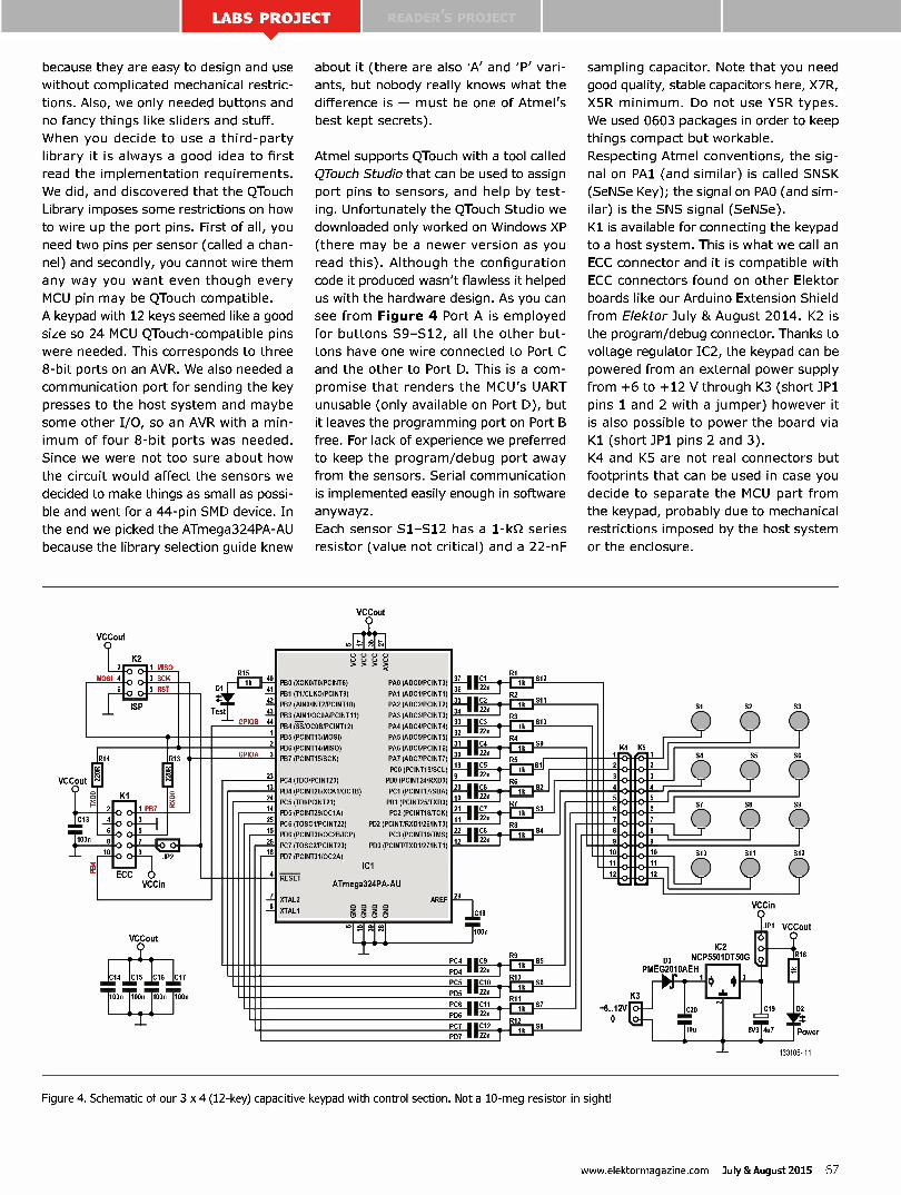
because they are easy to design and use
without complicated mechanical restric-
tions. Also, we only needed buttons and
no fancy things like sliders and stuff.
When you decide to use a third-party
library it is always a good idea to first
read the implementation requirements.
We did, and discovered that the QTouch
Library imposes some restrictions on how
to wire up the port pins. First of all, you
need two pins per sensor (called a chan-
nel) and secondly, you cannot wire them
any way you want even though every
MCU pin may be QTouch compatible.
A keypad with 12 keys seemed like a good
size so 24 MCU QTouch-compatible pins
were needed. This corresponds to three
8-bit ports on an AVR. We also needed a
communication port for sending the key
presses to the host system and maybe
some other I/O, so an AVR with a min-
imum of four 8-bit ports was needed.
Since we were not too sure about how
the circuit would affect the sensors we
decided to make things as small as possi-
ble and went for a 44-pin SMD device. In
the end we picked the ATmega324PA-AU
because the library selection guide knew
about it (there are also 'A' and 'P' vari-
ants, but nobody really knows what the
difference is — must be one of Atmel's
best kept secrets).
Atmel supports QTouch with a tool called
QTouch Studio that can be used to assign
port pins to sensors, and help by test-
ing. Unfortunately the QTouch Studio we
downloaded only worked on Windows XP
(there may be a newer version as you
read this). Although the configuration
code it produced wasn't flawless it helped
us with the hardware design. As you can
see from Figure 4 Port A is employed
for buttons S9-S12, all the other but-
tons have one wire connected to Port C
and the other to Port D. This is a com-
promise that renders the MCU's UART
unusable (only available on Port D), but
it leaves the programming port on Port B
free. For lack of experience we preferred
to keep the program/debug port away
from the sensors. Serial communication
is implemented easily enough in software
anywayz.
Each sensor S1-S12 has a 1-kg-2 series
resistor (value not critical) and a 22-nF
sampling capacitor. Note that you need
good quality, stable capacitors here, X7R,
X5R minimum. Do not use Y5R types.
We used 0603 packages in order to keep
things compact but workable.
Respecting Atmel conventions, the sig-
nal on PA1 (and similar) is called SNSK
(SeNSe Key); the signal on PAO (and sim-
ilar) is the SNS signal (SeNSe).
K1 is available for connecting the keypad
to a host system. This is what we call an
ECC connector and it is compatible with
ECC connectors found on other Elektor
boards like our Arduino Extension Shield
from Elektor July 81 August 2014. K2 is
the program/debug connector. Thanks to
voltage regulator IC2, the keypad can be
powered from an external power supply
from +6 to +12 V through K3 (short JP1
pins 1 and 2 with a jumper) however it
is also possible to power the board via
K1 (short JP1 pins 2 and 3).
K4 and K5 are not real connectors but
footprints that can be used in case you
decide to separate the MCU part from
the keypad, probably due to mechanical
restrictions imposed by the host system
or the enclosure.
VCCout
Ï K2 2 - 1 MISO 0 0
MOSI 4 3 SCK
I ISP
6 0 0 5 RST D1
Test
— GPIOB
41
42
43
44
2
3 R14
VCCout
1 13 P
T OOn
c:&
K1
0 0 o
6 0 0 8
10
R13
1 PB
3
5
GPIOA
9 0 0 JP2
ECC 610 VCCin
23
13
24
14
25
15
26
16
4
VCCout
14 C15 C16 C17
100n 100n 100n 100n
VCCout
n?e, PBO (XCKO/TO/PCINT8)
PB1 (T1/CLKO/PCINT9)
PB2 (AINO/INT2/PCINT10)
PB3 (AINVOCOA/PCINT11)
PB4 /0C0B/PCINT12)
PB5 (PCINT13/MOSI)
PB6 (PCINT14/MISO)
PB7 (PCINT15/SCK)
PC4 (TDO/PCINT20)
PD4 (PCINT28/XCK1/0C1B)
PC5 (TDI/PCINT21)
PD5 (PCINT29/0C1A)
PC6 (TOSC1/PCINT22)
PD6 (PCINT30/0C2B/ICP)
PC7 (TOSC2/PCINT23)
PD7 (PCINT31/0C2A)
RESET
XTAL2
)(TALI
PAO (ADCO/PCINTO)
PA1 (ADC1/PCINT1)
PA2 (ADC2/PCINT2)
PA3 (ADC3/PCINT3)
PA4 (ADC4/PCINT4)
PAS (ADC5/PCINT5)
PA6 (ADC6/PCINT6)
PA7 (ADC7/PCINT7)
PCO (PCINT16/SCL)
PDO (PCINT24/RXDO)
PC1 (PCINT17/SDA)
PD1 (PCINT25/TXDO)
PC2 (PCINT18/TCK)
PD2 (PCINT/RXD1/26/INTO)
PC3 (PCINT19/TMS)
PD3 (PCINT/TXD1/27/INT1)
ATmega324PA-AU
g g g c%
AREF
IC2'2In • R± S12
35 I C2 S11 34 II nflI
33 3 I C2;n R3 Ik S10
I R4 31 I C
30
19
9
20
22n
C5 22n
C6 22n
21 C7 22n
22 C8 22n
29
C18
ToOn PC4 I
PD4
PC5
PD5
PC6
PD6
PC7
PD7
C9 22n
C10 22n
R6
C11 22n
C12 22n
R11
S9
SIl
S2
3
K4 K5 1 7,
2 2
4 0
6
5
6
S7
8
9
10
11
12
o o o o o o o 0 0
o o o o o o o o
K3
+6...12V C,fl C19 D2
4
5
6
7
8
9
10
S1
S10 S11
2
D3 NCP5501DT5OG
PMEG2010AEH 3
VCCin
Jel VCCout
R16
o Power
130105- 11
Figure 4. Schematic of our 3 x 4 (12-key) capacitive keypad with control section. Not a 10-meg resistor in sight!
www.elektormagazine.com July &August 2015 67

LED D1 is available for debugging or of vias in these traces has been kept to
signaling purposes. If LED D2 is on, the a minimum.
board is likely powered.
3P2 can be shorted if an external Reset
signal is available on K1.
The MCU runs from its internal oscilla-
tor because timing precision is not very
important — this saved us a quartz
crystal.
The PCB (Figure 5) was designed for
the sensors to be on one side and the
components on the other, allowing easy
mounting of the board in an enclosure.
The traces from the sensors to the series
resistors are as thin as possible (within
reason) and placed as far away as possi-
ble from other traces and sensors. These
traces are part of the sensors and conse-
quently, sensitive to touch. The number
order to save you from pulling your hair
out, here is the QTouch setup procedure
in a condensed and hopefully clear form.
Setting up the software
Now we're getting to the hard part, 1. Download the QTouch library package
meaning the QTouch documentation from the Atmel website [1].
albeit rather abundant is confusing at the 2. Extract and open the Excel sheet
same time. Also, Atmel's website gives "Library_Selection_Guide.xls".
the impression that QTouch is old hat 3. Select the second sheet QTouch (we
whereas Atmel Studio proposes QTouch don't do QMatrix and we don't use an
updates almost every week. We have ATtiny)
QTouch for Atmel Studio installed, but 4. Select the MCU (ATmega324PA for us).
have not been able to figure out how to 5. Select "Max Num Channels" (12 in our
use it. Although this probably says more case, one channel per sensor).
about our patience than about the prod- 6. Select "Max Num Rotors/Sliders" (0,
uct, the fact remains that we had to get we don't have any).
an old Windows XP laptop out enabling 7. Select Toolchain (GCC because we use
us to check with QTouch Studio that our Atmel Studio).
sensor configuration was correct. So, in Now only one library remains left
Figure 5. Double-sided printed circuit board, designed with due consideration given to all parameters and requirements for 2015-style capacitive sensing with the help of a microcontroller.
Corn onent List
Resistors
Default: 5%, 0.1W, SMD 0603
R1-R12,R15,R16 = lkS2 R13,R14 = 220Q
Capacitors
Cl-C12 = 22nF 10% 50V, X7R, SMD 0603
C13-C18 = 100nF 5%, 16V, X7R, SMD 0603 C19 = 4.7pF 10%, 6.3V, SMD Case R (0805),
tantalum C20 = 10pF 10% 25V, X5R, SMD 1206
•
0000 CO U)
0006 • • • • • • • • •
• • • • • • • • •
• •
• • •
UI •
• • • •
• • • • •
• •
•••
Semiconductors
D1,D2 = LED, SMD 0805
D3 = PMEG2010AEH, SMD SOD-123F IC1 = ATmega324PA-AU, SMD TQFP-44, pro-
grammed, Elektor Store # 130105-41 IC2 = NCP5501DT50G, SMD DPAK 3
68 July 8f August 2015 www.elektormagazine.com
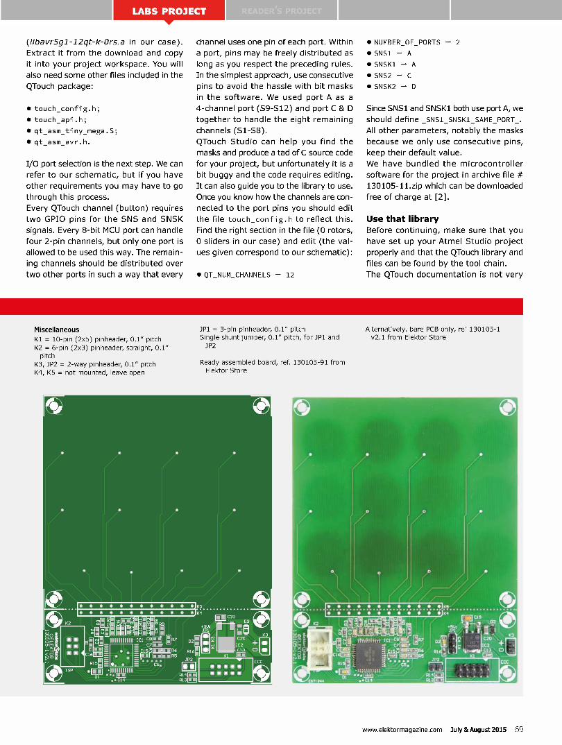
(libavr5g1-12qt-k-Ors.a in our case).
Extract it from the download and copy
it into your project workspace. You will
also need some other files included in the
QTouch package:
• touch_config.h;
• touch_api.h;
• qt_asm_tiny_mega.S;
• qt_asm_avr.h.
I/O port selection is the next step. We can
refer to our schematic, but if you have
other requirements you may have to go
through this process.
Every QTouch channel (button) requires
two GPIO pins for the SNS and SNSK
signals. Every 8-bit MCU port can handle
four 2-pin channels, but only one port is
allowed to be used this way. The remain-
ing channels should be distributed over
two other ports in such a way that every
Miscellaneous
K1 = 10-pin (2x5) pinheader, 0.1" pitch
K2 = 6-pin (2x3) pinheader, straight, 0.1" pitch
K3, 3P2 = 2-way pinheader, 0.1" pitch K4, K5 = not mounted, leave open
channel uses one pin of each port. Within
a port, pins may be freely distributed as
long as you respect the preceding rules.
In the simplest approach, use consecutive
pins to avoid the hassle with bit masks
in the software. We used port A as a
4-channel port (S9-S12) and port C 81 D
together to handle the eight remaining
channels (S1-S8).
QTouch Studio can help you find the
masks and produce a tad of C source code
for your project, but unfortunately it is a
bit buggy and the code requires editing.
It can also guide you to the library to use.
Once you know how the channels are con-
nected to the port pins you should edit
the file touch_config. h to reflect this.
Find the right section in the file (0 rotors,
0 sliders in our case) and edit (the val-
ues given correspond to our schematic):
• QT_NUM_CHANNELS — 12
3P1 = 3-pin pinheader, 0.1" pitch Single shunt jumper, 0.1" pitch, for 3P1 and
3P2
Ready assembled board, ref. 130105-91 from Elektor Store
o ;
P8
: 1
11111111111 ICI C01 111 10P7
= CI = • e
• • E •f• •11:26
.5LE.• • =•••••
•mmulde C5.
••
..•1 711
02
PI6
JP2
K 41 K4
CI9 03 0
P14 = P13 =
'"J5PL4 K3
C20
IC2 -I-CI3
ECC
• NUMBER_OF_PORTS — 2
• SNS1 — A
• SNSK1 — A
• SNS2 C
• SNSK2 — D
Since SNS1 and SNSK1 both use port A, we
should define _SNSl_SNSKl_SAME_PORT_.
All other parameters, notably the masks
because we only use consecutive pins,
keep their default value.
We have bundled the microcontroller
software for the project in archive file #
130105-11.zip which can be downloaded
free of charge at [2].
Use that library
Before continuing, make sure that you
have set up your Atmel Studio project
properly and that the QTouch library and
files can be found by the tool chain.
The QTouch documentation is not very
Alternatively, bare PCB only, ref 130105-1 v2.1 from Elektor Store
lc! cerae >7 C7 ''
Íng ..
••• L•ALeJ .•CI4
www.elektormagazine.com July &August 2015 69
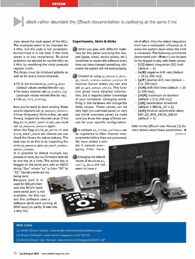
albeit rather abundant the QTouch documentation is confusing at the same time
clear about the clock speed of the MCU.
The examples seem to be intended for
4 MHz, but the code is not consistent.
Furthermore it is not clear if the clock
speed is of any importance. To avoid
problems we decided to run the MCU on
4 MHz by modifying the clock prescale
register CLKPR.
The library must be initialized globally as
well as for every button/channel:
• Fill in the structure qt_config_data
(default values worked fine for us);
• For every channel call qt_enable_key
(example values worked fine for us);
• Call qt_init_sensing.
Now you're ready to start sensing. Make
sure to regularly call qt_measure_sensors.
A timer firing every 25 ms is fine, we used
Timed. Inspect the returned value. If the
flag QTLIB_BURST_AGAIN is set, you must
call qt_measure_sensors again.
When the flags QTLIB_NO_ACTIVITY and
QTLIB_BURST_AGAIN are cleared you can
check the library for active buttons. The
best way to do this is by inspecting the
array qt_measure_data.qt_touch_status.
sensor_states.
It is possible to detect multiple key
presses at once, but our firmware defaults
to one key at a time. The active key is
flagged on the serial port with an ASCII
string "Sxx" where "xx" is from "00" to
"12". Key Up events are not
being sent.
Because port D is
used for QTouch chan-
nels the MCU's hard-
ware serial port is not
available. For this rea-
son the software uses a
software serial port running at
9600 baud (no parity, 8 data bits,
1 stop bit).
surements before they are
We have added a sim-
ple 4-sample aver-
aging filter here.
Changing the default
values of structure qt_
config_data did not
seem to have a
Experiments, hints & kinks
When you play with different mate-
rials for the panel overlying the key-
pad (glass, wood, acrylic plastic, etc.)
remember to restart the software every
time you have changed something, oth-
erwise the system will not work properly.
0 Instead of using qt_measure_data.
qt_touch_status.sensor_states to
discover button states you can also
call qt_get_sensor_delta. This func-
tion gives more detailed informa-
tion, but it requires better knowledge
of your hardware. Changing some-
thing in the hardware will change the
delta values. These values can be
very high (no overhead panel) or very
low (thick overhead panel) so make
sure you know the range of these val-
ues for your specific configuration.
A callback qt_filter_callback can
be registered to filter channel mea-
processed.
lot of effect. Only the detect integration
limit has a noticeable influence as it
slows the system down when the limit
is increased. The following commands
(terminated with <Enter>) can be sent
to the keypad to play with these values:
[ill] detect integration (DI) limit
(default = 4)
[n I N] negative drift rate (default
= 20 [x 200 ms])
[PI PI positive drift rate (default =
5 [x 200 ms])
[h I El] drift hold time (default = 20
[x 200 ms])
[m I M] maximum on duration
(default = O [x 200 ms])
U112] recalibration threshold
(default = RECAL_50 = 1)
[d I D] Positive recalibration delay
DEF_QT_POS_RECAL_DELAY
(default = 3)
Refer to the QTouch User Manual [3] for
more details about these parameters. 14
(130105-I)
-
Web Links
[1] Atmel QTouch Library: www.atmel.com/tools/qtouchlibrary.aspx
[2] Project Software: www.elektor-magazine.com/130105
[3] Atmel QTouch User manual: www.atmel.com/images/doc8207.pdf
70 July &August 2015 www.elektormagazine.com
UI READER'S PROJECT
Resistance Measurement with the Arduino Great for testing humidity sensors
By Burkhard Kainka (Germany)
Next to the oscilloscope,
the ohmmeter is the most
widely used T&M device in
the electronics lab. Using this
you can measure component
characteristics, trace wires,
find errors in circuits and
evaluate many types of sensor.
But a normal ohmmeter or
multimeter cannot always fulfill
the demands placed upon it,
for example when we need to measure
ts.d BASCOM-AVR [04 (2.0.744 - KliSabet.neidienana/no11Y
fà: Ed ft.«
11..
Irian Use., Wutnw
UhD Ohm/.be
Stb
Do Count - PORTS 3 • 1 DORR 3 • 1 Santa* SOO M eal - Unitue 10 CORD 3 • 0 De Count • Count -4- 1
Loop Uutal PlOb - 1 Or Count 1$ • 1 PnR1Te 3 - 1 DüRD - 1 Print nanint Locate I 1 Lod Couul. Ind ' •
Lend
Calculate Resastence 11 Count 4 Than Count • Count - 4 Reeintnnee • Count • 14 Resistance • Re :intone* • 40 P ri n t Prenetnnce Locate 2 . 1 Lod Ricaelaoce Ind • knha •
'nod
alternating current (AC). This is when a microcontroller can help.
Sure, another opportunity to use the Arduino Uno, our Extension Shield and Bascom!
The starting point for this project was
some newish resistive air humidity sen-
sors, whose resistance varies in the range
1 kg-2 to 10 MS2. The datasheet states
expressly that they must be measured
using AC. And that's precisely what a
regular ohm meter cannot do.
A representative example of these resis-
tive sensors (Figure 1) is the HCZ-
H8A(N), which you can obtain from Far-
nell, Conrad, Mantech and other suppliers.
The datasheet can be found here [1].
Normally these sensors are driven using
Figure 1. A resistive humidity sensor.
an AC voltage of 1 Veff . If you connect
them to a signal generator using a volt-
age divider, you can view the result very
clearly on the oscilloscope (Figure 2).
Put your hand close to the sensor and the
humidity increases; you can watch the
resistance fall and the signal voltage rise
at the input of the oscilloscope.
Why can't you use direct current (DC) for
this? The answer is all to do with polar-
ization. Water molecules, as you probably
know, have polar characteristics; in other
words they are more positive on one side
Figure 2. The first test.
and more negative on the other. Gradually
they will align according to the DC applied
and change resistance in the process.
The same effect arises when you mea-
sure the conductivity of water; here too
we must use only AC. A long time ago I
even observed this effect while measur-
ing the conductivity of wood as a function
of humidity. The resistance starts off low
and then rises slowly. A pair of stainless
steel nails pushed into damp wood even
behave something like a battery that
you can charge up. In those days I was
amazed. Since then, however, I found out
that this is the same principle you have
in dual-layer capacitors, also known as
supercapacitors or GoldCaps.
Resistance measurement
How do we get round the fact that micro-
controllers prefer DC? Or that handling
the huge measurement range involved
is no easy task for a 10-bit A-to-D con-
verter? Consequently thoughts turned
towards R-C elements and time measure-
www.elektor-magazine.com July &August 2015 71
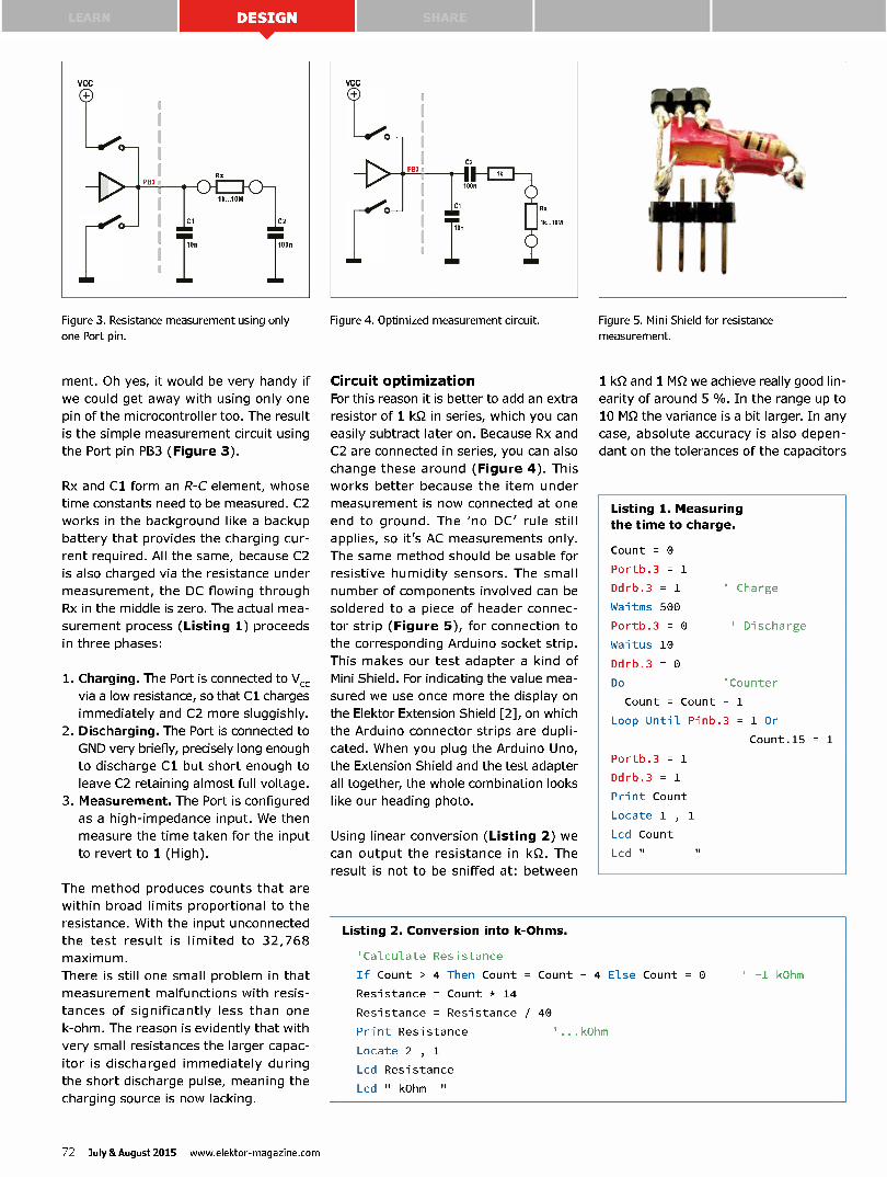
Figure 3. Resistance measurement using only one Port pin.
Figure 4. Optimized measurement circuit. Figure 5. Mini Shield for resistance measurement.
ment. Oh yes, it would be very handy if
we could get away with using only one
pin of the microcontroller too. The result
is the simple measurement circuit using
the Port pin PB3 (Figure 3).
Rx and Cl form an R-C element, whose
time constants need to be measured. C2
works in the background like a backup
battery that provides the charging cur-
rent required. All the same, because C2
is also charged via the resistance under
measurement, the DC flowing through
Rx in the middle is zero. The actual mea-
surement process (Listing 1) proceeds
in three phases:
1. Charging. The Port is connected to Vcc
via a low resistance, so that Cl charges
immediately and C2 more sluggishly.
2. Discharging. The Port is connected to
GND very briefly, precisely long enough
to discharge Cl but short enough to
leave C2 retaining almost full voltage.
3. Measurement. The Port is configured
as a high-impedance input. We then
measure the time taken for the input
to revert to 1 (High).
The method produces counts that are
within broad limits proportional to the
resistance. With the input unconnected
the test result is limited to 32,768
maximum.
There is still one small problem in that
measurement malfunctions with resis-
tances of significantly less than one
k-ohm. The reason is evidently that with
very small resistances the larger capac-
itor is discharged immediately during
the short discharge pulse, meaning the
charging source is now lacking.
Circuit opti mization
For this reason it is better to add an extra
resistor of 1 kg-2 in series, which you can
easily subtract later on. Because Rx and
C2 are connected in series, you can also
change these around (Figure 4). This
works better because the item under
measurement is now connected at one
end to ground. The 'no DC' rule still
applies, so it's AC measurements only.
The same method should be usable for
resistive humidity sensors. The small
number of components involved can be
soldered to a piece of header connec-
tor strip (Figure 5), for connection to
the corresponding Arduino socket strip.
This makes our test adapter a kind of
Mini Shield. For indicating the value mea-
sured we use once more the display on
the Elektor Extension Shield [2], on which
the Arduino connector strips are dupli-
cated. When you plug the Arduino Uno,
the Extension Shield and the test adapter
all together, the whole combination looks
like our heading photo.
Using linear conversion (Listing 2) we
can output the resistance in kg-2. The
result is not to be sniffed at: between
Listing 2. Conversion into k-Ohms.
'Calculate
If Count >
Resistance
Resistance
Resistance
4 Then Count Count
Count * 14
Resistance / 40
Print Resistance
Locate 2 , 1
Lcd Resistance
Lcd " kOhm "
1 kg-2 and 1 MS2 we achieve really good lin-
earity of around 5 Wo. In the range up to
10 MS2 the variance is a bit larger. In any
case, absolute accuracy is also depen-
dant on the tolerances of the capacitors
Listing 1. Measuring the time to charge.
Count =
Portb.3 = 1
Ddrb.3 = 1
Waitms 500
Portb.3 =
Waitus 10
Ddrb.3 =
Do
Count = Count
' Charge
' Discharge
'Counter
+ 1
Loop Until Pinb.3 = 1 Or
Count.15 1
Portb.3 = 1
Ddrb.3 = 1
Print Count
Locate 1 , 1
Lcd Count
Lcd "
4 Else Count 0 ' -1 kOhm
'...kOhm
72 July &August 2015 www.elektor-magazine.com
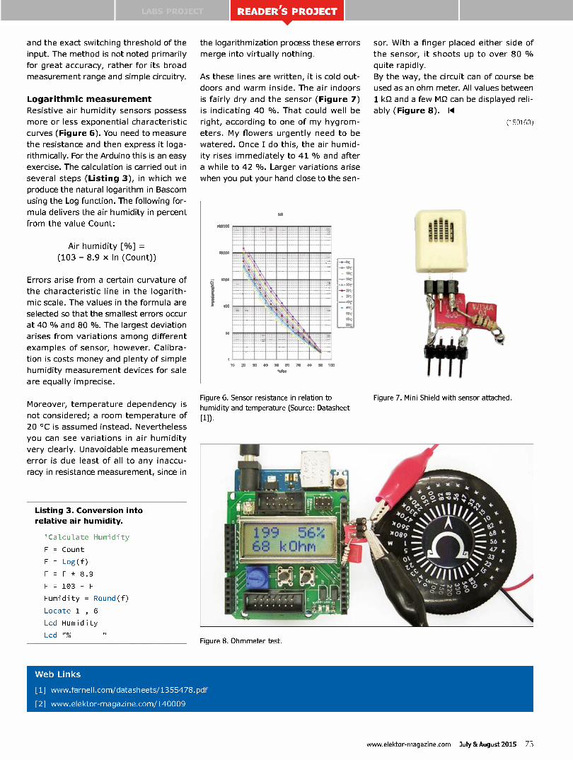
READER'S PROJECT
and the exact switching threshold of the
input. The method is not noted primarily
for great accuracy, rather for its broad
measurement range and simple circuitry.
Logarith mic measurement
Resistive air humidity sensors possess
more or less exponential characteristic
curves (Figure 6). You need to measure
the resistance and then express it loga-
rithmically. For the Arduino this is an easy
exercise. The calculation is carried out in
several steps (Listing 3), in which we
produce the natural logarithm in Bascom
using the Log function. The following for-
mula delivers the air humidity in percent
from the value Count:
Air humidity [°/0] =
(103 - 8.9 x In (Count))
Errors arise from a certain curvature of
the characteristic line in the logarith-
mic scale. The values in the formula are
selected so that the smallest errors occur
at 40 °h and 80 °h. The largest deviation
arises from variations among different
examples of sensor, however. Calibra-
tion is costs money and plenty of simple
humidity measurement devices for sale
are equally imprecise.
Moreover, temperature dependency is
not considered; a room temperature of
20 °C is assumed instead. Nevertheless
you can see variations in air humidity
very clearly. Unavoidable measurement
error is due least of all to any inaccu-
racy in resistance measurement, since in
Listing 3. Conversion into relative air humidity.
'Calculate Humidity
F = Count
F = Log(f)
F = F * 8.9
F = 103 - F
Humidity = Round(f)
Locate 1 , 6
Lcd Humidity
Lcd u%
the logarithmization process these errors
merge into virtually nothing.
As these lines are written, it is cold out-
doors and warm inside. The air indoors
is fairly dry and the sensor (Figure 7)
is indicating 40 °h. That could well be
right, according to one of my hygrom-
eters. My flowers urgently need to be
watered. Once I do this, the air humid-
ity rises immediately to 41 % and after
a while to 42 °h. Larger variations arise
when you put your hand close to the sen-
Figure 7. Mini Shield with sensor attached. Figure 6. Sensor resistance in relation to humidity and temperature (Source:
[1]).
Datasheet
sor. With a finger placed either side of
the sensor, it shoots up to over 80 %
quite rapidly.
By the way, the circuit can of course be
used as an ohm meter. All values between
1 kg-2 and a few MS2 can be displayed reli-
ably (Figure 8). 11
(150160)
Figure 8. Ohmmeter test.
Web Links
[1] www.farnell.com/datasheets/1355478.pdf
[2] www.elektor-magazine.com/140009
www.elektor-magazine.com July &August 2015 73
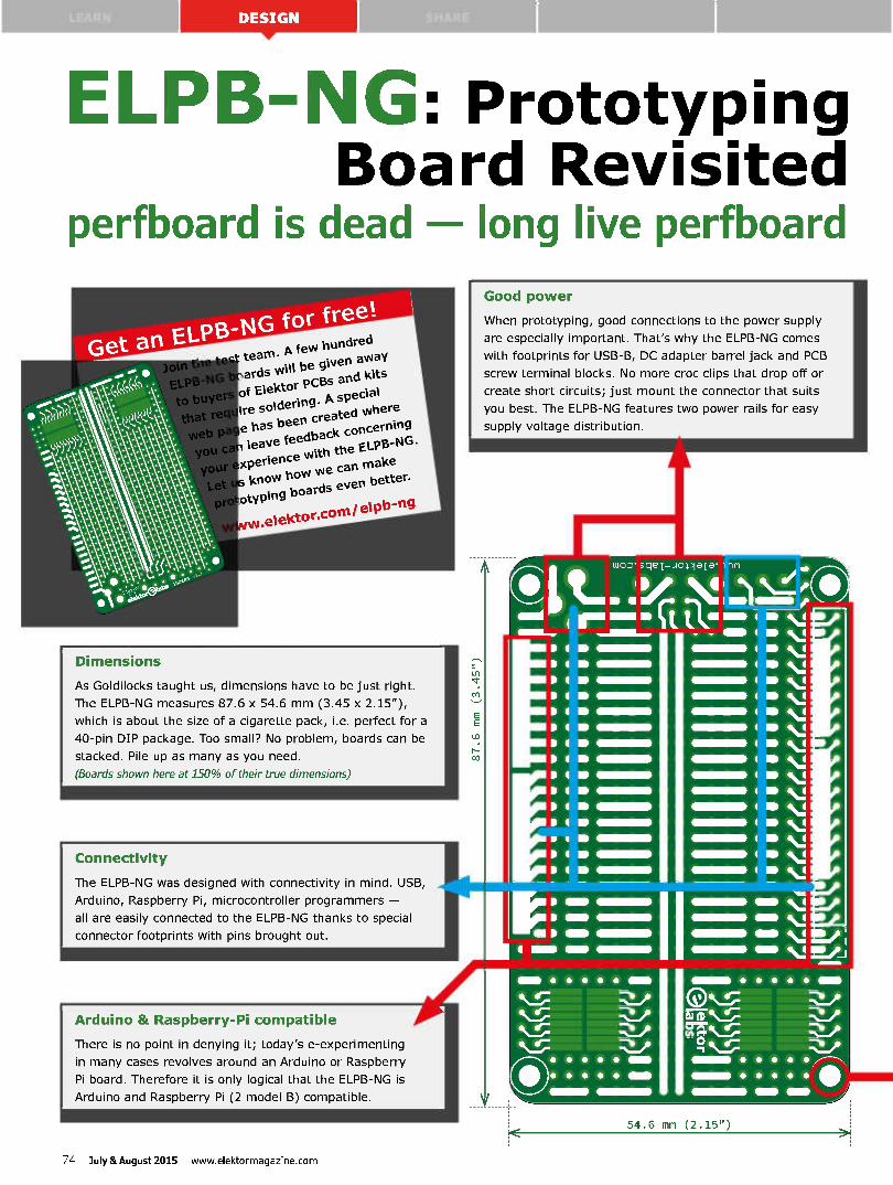
ELPB-NG: Prototyping Board Revisited
perfboard is dead long live perfboard
Get an ELPB-
....--7,1•• oin t team. A few hundred
ELPB-NG boards will be given away
of *. .. O buyers Elektor special
PCBs and kits
. has been create
require soldering. A
web page d where • u can leave feedback concerning
PB-NG. ur experience with the EL
et us know how we can Make
prototyping boards even better.
W.ellektor.cO M/ elpb-ng
Di mensions
As Goldilocks taught us, dimensions have to be just right.
The ELPB-NG measures 87.6 x 54.6 mm (3.45 x 2.15"),
which is about the size of a cigarette pack, i.e. perfect for a
40-pin DIP package. Too small? No problem, boards can be
stacked. Pile up as many as you need.
(Boards shown here at 150% of their true dimensions)
Connectivity
The ELPB-NG was designed with connectivity in mind. USB,
Arduino, Raspberry Pi, microcontroller programmers —
all are easily connected to the ELPB-NG thanks to special
connector footprints with pins brought out.
Arduino & Raspberry-Pi co mpatible
There is no point in denying it; today's e-experimenting
in many cases revolves around an Arduino or Raspberry
Pi board. Therefore it is only logical that the ELPB-NG is
Arduino and Raspberry Pi (2 model B) compatible.
Good po wer
When prototyping, good connections to the power supply
are especially important. That's why the ELPB-NG comes
with footprints for USB-B, DC adapter barrel jack and PCB
screw terminal blocks. No more croc clips that drop off or
create short circuits; just mount the connector that suits
you best. The ELPB-NG features two power rails for easy
supply voltage distribution.
Y
11103' ;get—Am./ale I
54.6 mm (2.15")
74 July &August 2015 www.elektormagazine.com
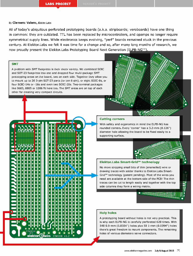
By Clemens Valens, Elektor.Labs
All of today's ubiquitous perforated prototyping boards (a.k.a. stripboards; veroboards) have one thing
in common: they are outdated. TTL has been replaced by microcontrollers, and opamps no longer require
symmetrical supply lines. While electronics keeps evolving, "perf" boards remained stuck in the previous
century. At Elektor.Labs we felt it was time for a change and so, after many long months of research, we
now proudly present the Elektor.Labs Prototyping Board Next Generation (ELPB-NGTM
SMT
A problem with SMT footprints is their sheer variety. We combined SOIC
and SOT-23 footprints into one and dropped four multi-package SMT
prototyping areas on the board, two on each side. Together they allow you
to mount up to 20 3-pin SOT-23 parts (or ten 6-pin), or eight SOIC-8s, or
four SOIC-14s or -16s and even two SOIC-20s. Two-terminal packages
like 0603, 0805 or 1206 fit here too. The SMT areas are on top of each
other for creating very compact circuits.
Cutting corners
With safety and ergonomics in mind the ELPB-NG has
rounded corners. Every 'corner' has a 3.2-mm (0.126")
diameter hole allowing the board to be fixed easily to a
supporting surface.
Elektor.Labs Smart-GridTM technology
No more stripping small bits of thin (enamelled) wire or
drawing traces with solder thanks to Elektor.Labs Smart-
Grid"' technology (patent pending). Most of the wires you
need are available at the bottom side of the PCB! The thin
traces can be cut to length easily and together with the top
side columns they form a wiring matrix.
Holy holes
A prototyping board without holes is not very practical. This
is why each ELPB-NG is carefully perforated 620 times. With
548 0.9-mm (0.0354") holes plus 58 1-mm (0.0394") holes
there's great freedom to mount components. The remaining
holes of various diameters serve connectors.
www.elektormagazine.com July &August 2015 75

Sort-Of Electronic Candle
By Victor Hugo Pachon (Colombia)
This simple circuit is a brave effort at
simulating a candle flame using an LED.
Generated by electronics only and using
just two AA or AAA batteries the simu-
lated flame avoids the nuisance of smoke
and the dangers of a real flame, particu-
larly if you forget to quench it before you
leave the room.
The little project along the schematic
in Figure 1 consists of a small micro-
controller type PIC12F675 suitably pro-
grammed to generate a PWM (pulse-
width modulation) signal which powers
a single LED, effectively varying the duty
cycle of the signal, resulting in intensity
control of the LED. To simulate a softly
flickering flame the PWM drive randomly
varies its value using a pseudo-random
bit sequence (PRBS) values. Each sig-
nal change occurs within a period small
enough to enable your spell-bound visi-
tors to note the change in LED brightness
as if staring into a little flame flickering
from a whiff of air (J' Like a Candle in
the Wind .r.r).
A simple little project like this proba-
bly does not need a dedicated PCB. The
PIC, LED and resistor are easily fitted on
a small piece of perfboard for inserting
into a short piece of PVC pipe with two
acrylic covers. The construction acts as
thick sort-of candle which also contains
the battery. Don't forget to paint the imi-
tation candle off-white, and add some
mystic symbols.
Although a big (5-mm) yellow LED from
the Ancient Parts drawer is suggested,
nothing should prevent you from using
other LEDs with different colors like
orange which also simulates a flame
rather well.
Now, we start talking software. Because
the light intensity and the voltage drop of
an LED varies with the model, you must
set the minimum and maximum levels of
the PWM signal for the LED light to a min-
imum with the lowest value generated by
the PRBS (0), and the maximum, to the
highest value generated (255). The PIC
3V
7 Ci
IC1
VDD
GP 0/AN 0
GP1/AN1NREF
GP2D'OCKMNT/AN2
GP3/MCLR
GP4F1.1G/OSC2/AN3
GPNT1CKI/OSC1
VSS
PIC12F675
150072 - 11
Figure 1. A strong contender for Simplest PIC Circuit Ever, this LED controller mimics a flickering candle flame.
firmware you can download at [1] allows
the times (i.e. PWM min/max values) to
be adjusted to get the proper range. In
particular, it's the asm (!) code file listing
you need to delve into. Also, if necessary,
adapt the value of current limiting resis-
tor R1, to get the light intensity at the
desired value. 14
(150072)
Web Link
[1] Project software:
www.elektormagazine.com/150072
ehttp://youtu.benKh8L83F3V8
Cheap Accurate 12-V Battery Monitor By Ramkumar Ramaswamy (India)
This little idea came about when I was
pondering an accurate way of constantly
measuring the voltage of each battery in
my solar battery bank. A lead-acid bat-
tery's voltage remains fairly constant as
it discharges. As shown in the Table,
a no-load voltage of 12.6 volts means
100°h charge but 12.2 volts means you're
down to 60°h. So it's desirable to have a
cheap method of adequate accuracy so
you can reliably keep a tab on each bat-
tery. "Cheap" suggests the many panel
displays available on eBay for under $2,
but the accuracy of these is usually not
better than 1-2% which sadly is not good
enough. Ask for 0.1 % accurate panel
meters and your spend will increase
dramatically.
The circuit shown in Figure 1 allows you
to go cheap and accurate. These panel
meters typically have three terminals:
GND (-); Vcc (+) and a measurement
input (T). The LM4040-10 precision volt-
76 July &August 2015 www.elektormagazine.com

READER'S PROJECT
age reference drops exactly 10 volts with
better than 0.1 % accuracy, and what is
left (i.e. anything above 10.00 V) is fed
to the measurement terminal of a 0-10 V
panel meter which then shows how your
battery is doing above 10 V. If the meter
reads 2.5 V, your battery is at 12.5 V.
Even if a doubtful design, the meter con-
tributes a tolerable error of 2°h of 2.5 V
or 0.05 V, and the LM4040 "contributes"
0.01 V maximum, so your error is not
more than 0.06 V. Good enough for the
purpose.
The 47- K-2 resistor ensures that the
LM4040-10 is fed with at least 60 micro-
amps required for it to work reliably. H
(150077)
Voltage State of Charge
12.6+ 100%
12.5 90%
12.42 80%
12.32 70%
12.20 60%
12.06 50%
11.9 40%
11.75 30%
11.58 20%
11.31 10%
10.5 0%
Figure 1. Thanks to 10-V precision reference DI, an el-cheapo digital voltmeter unit can be used to monitor a 12-V battery with good accuracy.
Power Failure Audible Alarm For RVs, motor homes and boats By Joachim Schriider (Germany)
It's often little things that make out-
door living more amenable. This circuit
makes it presence felt vociferously when
the fixed electricity supply fails or is cut.
Any skipper or RV (motor home) driver
whose solar or fuel cells do not deliver
sufficient mobile energy is often directed
towards coin-operated power points,
which are provided at many camping sites
and marinas for recharging the onboard
batteries. These power points are gener-
ally consumption-controlled and cut out
directly once the amount of power paid
for has been extracted.
Often the quantity of electricity bought
is unclear and even knowing your own
usage is a tough call. It can then happen
that the recharging supply shuts off and
instead of starting the next day replete
with power, your battery needs to feed
itself again.
Accordingly I constructed this small cir-
cuit, which beeps for a couple of sec-
onds when the AC power supply fails or
drops out. For the power supply (PSU)
we'll use a small 5 V switch-mode power
module (not shown here), which most
people will have in their box of bits. All
the time that AC power is present, the
switch-mode PSU will cheerfully produce
its +5 V. In the schematic shown in Fig-
ure 1 the chubby 1000 pF capacitor is
charged via the diode DI and the 220
S2 resistor. At the same time the 5 volts
are applied via the 1 kS2 resistor to the
base of the PNP transistor, so that it does
not conduct.
If the AC power is cut, killing the +5 V,
the transistor conducts, assisted by the
68 kS2 resistor. The capacitor now dis-
charges through the beeper and the tran-
sistor. The beeper makes a noisy account
of itself for around 5 s, depending on the
capacitor value and type of sounder used
(the duration can be extended of course
using a larger capacitor).
The complete circuit, as seen above, can
be built on a scrap of perf board (for
best fit in the case) and made shockproof
along with the switch-mode PSU inside a
plug-in wall-wart enclosure.
As soon as you have hooked up to a
coin-operated power point, you can
plug this gadget into a spare receptacle
(socket) in the motor home or boat and
receive a timely warning when the juice
fails. H
(140281)
Figure 1. This small circuit is connected to a 5 V switch-mode power supply and raises the alarm when the AC power fails.
www.elektormagazine.com July &August 2015 77
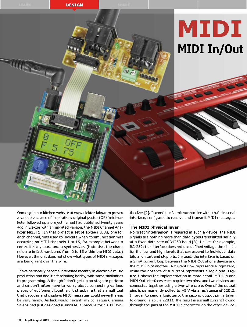
thesizer [2]. It consists of a microcontroller with a built-in serial
interface, configured to receive and transmit MIDI messages.
Once again our kitchen website at www.elektor-labs.com proves
a valuable source of inspiration: original poster (OP) 'midi-ra-
kete' followed up a project he had had published twenty years
ago in Elektor with an updated version, the MIDI Channel Ana-
lyzer MkII [1 ]. In that project a set of sixteen LEDs, one for
each channel, was used to indicate when communication was
occurring on MIDI channels 1 to 16, for example between a
controller keyboard and a synthesizer. (Note that the chan-
nels are in fact numbered from 0 to 15 within the MIDI data.)
However, the unit does not show what types of MIDI messages
are being sent over the wire.
I have personally become interested recently in electronic music
production and find it a fascinating hobby, with some similarities
to programming. Although I don't get up on stage to perform
and so don't often have to worry about connecting various
pieces of equipment together, it struck me that a small tool
that decodes and displays MIDI messages could nevertheless
be very handy. As luck would have it, my colleague Clemens
Valens had just designed a small MIDI module for his 32B syn-
The MIDI physical layer
No great 'intelligence' is required in such a device: the MIDI
signals are nothing more than data bytes transmitted serially
at a fixed data rate of 31250 baud [3]. Unlike, for example,
RS-232, the interface does not use defined voltage thresholds
for the low and high levels that correspond to individual data
bits and start and stop bits. Instead, the interface is based on
a 5 mA current loop between the MIDI Out of one device and
the MIDI In of another. A current flow represents a logic zero,
while the absence of a current represents a logic one. Fig-
ure 1 shows the implementation in more detail. MIDI In and
MIDI Out interfaces each require two pins, and two devices are
connected together using a two-wire cable. One of the output
pins is permanently pulled to +5 V via a resistance of 220 Q.
In order to send a logic zero, the second output pin is taken
to ground, also via 220 Q. The result is a small current flowing
through the pins of the MIDI In connector on the other device.
78 July &August 2015 www.elektormagazine.com
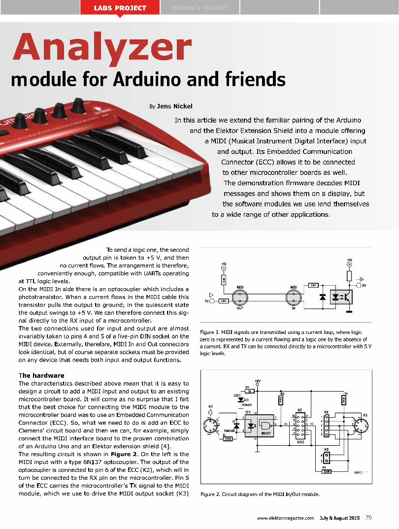
An _ module for Arduino and friends
By Jens Nickel
In this article we extend the familiar pairing of the Arduino
and the Elektor Extension Shield into a module offering
a MIDI (Musical Instrument Digital Interface) input
and output. Its Embedded Communication
Connector (ECC) allows it to be connected
to other microcontroller boards as well.
The demonstration firmware decodes MIDI
messages and shows them on a display, but
the software modules we use lend themselves
to a wide range of other applications.
To send a logic one, the second
output pin is taken to +5 V, and then
no current flows. The arrangement is therefore,
conveniently enough, compatible with UARTs operating
at TTL logic levels.
On the MIDI In side there is an optocoupler which includes a
phototransistor. When a current flows in the MIDI cable this
transistor pulls the output to ground; in the quiescent state
the output swings to +5 V. We can therefore connect this sig-
nal directly to the RX input of a microcontroller.
The two connections used for input and output are almost
invariably taken to pins 4 and 5 of a five-pin DIN socket on the
MIDI device. Externally, therefore, MIDI In and Out connectors
look identical, but of course separate sockets must be provided
on any device that needs both input and output functions.
The hard ware
The characteristics described above mean that it is easy to
design a circuit to add a MIDI input and output to an existing
microcontroller board. It will come as no surprise that I felt
that the best choice for connecting the MIDI module to the
microcontroller board was to use an Embedded Communication
Connector (ECC). So, what we need to do is add an ECC to
Clemens' circuit board and then we can, for example, simply
connect the MIDI interface board to the proven combination
of an Arduino Uno and an Elektor extension shield [4].
The resulting circuit is shown in Figure 2. On the left is the
MIDI input with a type 6N137 optocoupler. The output of the
optocoupler is connected to pin 6 of the ECC (K2), which will in
turn be connected to the RX pin on the microcontroller. Pin 5
of the ECC carries the microcontroller's TX signal to the MIDI
module, which we use to drive the MIDI output socket (K3)
Figure 1. MIDI signals are transmitted using a current loop, where logic zero is represented by a current flowing and a logic one by the absence of a current. RX and TX can be connected directly to a microcontroller with 5 V logic levels.
Figure 2. Circuit diagram of the MIDI In/Out module.
www.elektormagazine.com July &August 2015 79
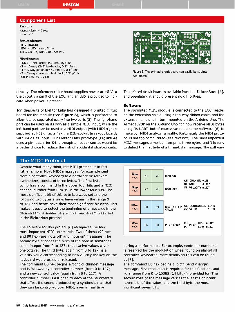
LEARN
o Resistors
R1,R2,R3,R4 = 220Q R5 = lkS2
Semiconductors
D1 = 1N4148 LED1 = LED, green, 3mm
IC1 = 6N137, DIP8 (incl. socket)
Miscellaneous
Kl,K3 = DIN socket, PCB mount, 180°
K2 = 10-way (2x5) boxheader, 0.1" pitch K4 = 5-way pinheader receptacle, 0.1" pitch
K5 = 2-way screw terminal block, 0.2" pitch PCB # 150169-1 v1.0
0 K4 K5
geese)
o
0 0
lun e , iieL erz
•• •,13 ECC — R2
R1 B M
IC1
III II e
• • • • 150169-1 • vi.0 • OELEKTOR • • • •
Figure 3. The printed circuit board can easily be cut into two pieces.
directly. The microcontroller board supplies power at +5 V to
the circuit via pin 9 of the [CC, and an LED is provided to indi-
cate when power is present.
Ton Giesberts of Elektor Labs has designed a printed circuit
board for the module (see Figure 3), which is perforated to
allow it to be separated easily into two parts [5]. The right-hand
part can be used on its own as a simple MIDI input, while the
left-hand part can be used as a MIDI output (with MIDI signals
supplied at K5) or as a flexible DIN-socket breakout board,
with K4 as its input. Our Elektor Labs prototype (Figure 4)
uses a pinheader for K4, although a header socket would be
a better choice to reduce the risk of accidental short-circuits.
The printed circuit board is available from the Elektor Store [6],
and populating it should present no difficulties.
Software
The populated MIDI module is connected to the [CC header
on the extension shield using a ten-way ribbon cable, and the
extension shield is in turn mounted on the Arduino Uno. The
ATmega328P on the Arduino Uno can now receive MIDI bytes
using its UART, but of course we need some software [6] to
make our MIDI analyzer a reality. Fortunately the MIDI proto-
col is not too complicated (see text box). The most important
MIDI messages almost all comprise three bytes, and it is easy
to detect the first byte of a three-byte message. The software
The MIDI Protocol Despite what many think, the MIDI protocol is in fact
rather simple. Most MIDI messages, for example sent
from a controller keyboard to a hardware or software
synthesizer, consist of three bytes. The first byte
comprises a command in the upper four bits and a MIDI
channel number from 0 to 15 in the lower four bits. The
most significant bit of this byte is always set and the
following two bytes always have values in the range 0
to 127 and hence have their most significant bit clear. This
makes it easy to detect the beginning of a message in the
data stream; a similar very simple mechanism was used
in the ElektorBus protocol.
The software for this project [6] recognizes the four
most important MIDI commands. Two of these (90 hex
and 80 hex) are 'note off' and 'note on' messages. The
second byte encodes the pitch of the note in semitones
as an integer from 0 to 127: thus twelve values cover
one octave. The third byte, again from 0 to 127, is a
velocity value corresponding to how quickly the key on the
keyboard was pressed or released.
The command BO hex begins a 'control change' message
and is followed by a controller number (from 0 to 127)
and a new control value (again from 0 to 127). A
controller number is assigned to each of the parameters
that affect the sound produced by a synthesizer so that
they can be controlled over MIDI, even in real time
90HEx
+ CH NT VE
80HEx + CH
NT VE
B0 HEX
+ CH CC CV I
E0 HEX PL PH
+ CH
NOTE ON
NOTE OFF
CH CHANNEL 0...15
NT NOTE 0...127
VE VELOCITY 0...127
CONTROLLER CC CONTROLLER 0...127 VALUE CV VALUE 0...127
PH HIGH 0...127 PITCH BEND PITCH
PL LOW 0...127
during a performance. For example, controller number 1
is reserved for the modulation wheel found on almost all
controller keyboards. More details on this can be found
at [8].
The command E0 hex begins a 'pitch bend change'
message. Fine resolution is required for this function, and
so a range from 0 to 16383 (14 bits) is provided for. The
second byte of the message carries the least significant
seven bits of the value, and the third byte the most
significant seven bits.
80 July &August 2015 www.elektormagazine.com
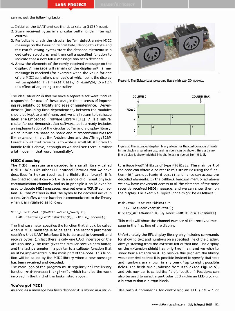
carries out the following tasks.
1. Initialize the UART and set the data rate to 31250 baud.
2. Store received bytes in a circular buffer under interrupt
control.
3. Periodically check the circular buffer; detect a new MIDI
message on the basis of its first byte; decode this byte and
the two following bytes; store the decoded elements in a
dedicated structure; and then call a specified function to
indicate that a new MIDI message has been decoded.
4. Show the elements of the newly-received message on the
display. A message will remain on the display until a new
message is received (for example when the value for one
of the MIDI controllers changes), at which point the display
will be updated. This makes it easy, for example, to watch
the effect of adjusting a controller.
The ideal situation is that we have a separate software module
responsible for each of these tasks, in the interests of improv-
ing reusability, portability and ease of maintenance. Depen-
dencies (including time-dependencies) between the modules
should be kept to a minimum, and we shall return to this issue
later. The Embedded Firmware Library (EFL) [7] is a natural
choice for our demonstration software, as it already includes
an implementation of the circular buffer and a display library,
which in turn are based on board and microcontroller files for
the extension shield, the Arduino Uno and the ATmega328P.
Essentially all that remains is to write a small MIDI library to
handle task 3 above, although as we shall see there is rather
a lot hidden in that word 'essentially'.
MIDI decoding
The MIDI messages are decoded in a small library called
MidiEFL.h/.c. Like other EFL protocol libraries that we have
described in Elektor (such as the ElektorBus library), it is
designed so that it can work with a range of different physical
communication channels, and so in principle it could even be
used to decode MIDI messages received over a TCP/IP connec-
tion. All that matters is that the bytes to be decoded arrive in
a circular buffer, whose location is communicated to the library
when it is initialized as follows:
MIDI_LibrarySetup(UARTInterface_Send, 0,
UARTInterface_GetRingbuffer(0), MIDIIn_Process);
The first parameter specifies the function that should be called
when a MIDI message is to be sent. The second parameter
specifies that UART interface 0 is to be used to transmit and
receive bytes. (In fact there is only one UART interface on the
Arduino Uno.) The third gives the circular receive data buffer,
and the last parameter is a pointer to a callback function that
must be implemented in the main part of the code. This func-
tion will be called by the MIDI library when a new message
has been received and decoded.
The main loop of the program must regularly call the library
function Mi di Protocol_Engi ne , which handles the work
involved in the third of the tasks listed above.
You've got MIDI
As soon as a message has been decoded it is stored in a struc-
Figure 4. The Elektor Labs prototype fitted with two DIN sockets.
COLUMN 0
ROW 0
1
2
COLUMN MAX
o
1 2
3 4 5
Figure 5. The extended display library allows for the configuration of fields in the display area where text and numbers can be shown. Here a three-line display is shown divided into six fields numbered from 0 to 5.
ture ReceivedMidiData of type MidiData. The main part of
the code can obtain a pointer to this structure using the func-
tion Midi_GetReceivedMidiData 0, and hence can access the
decoded elements. In the callback function mentioned above
we now have convenient access to all the elements of the most
recently received MIDI message, and we can show them on
the display. For example, typical code might be as follows:
MidiData* ReceivedMidiData =
MIDI_GetReceivedMidiData();
Display_WriteNumber(0, 0, ReceivedMidiData->Channel);
This code will show the channel number of the received mes-
sage in the first line of the display.
Unfortunately the EFL display library only includes commands
for showing text and numbers on a specified line of the display,
always starting from the extreme left of that line. The display
on the extension shield has only two lines, and we wish to
show four elements on it. To resolve this problem the library
was extended so that it is possible instead to specify that text
and numbers are shown in any one of up to eight possible
fields. The fields are numbered from 0 to 7 (see Figure 5),
and this number is called the field's 'position'. Positions can
also be used to select a particular LED within an LED block or
a button within a button block.
The output commands for controlling an LED (ON = 1 or
www.elektormagazine.com July &August 2015 81
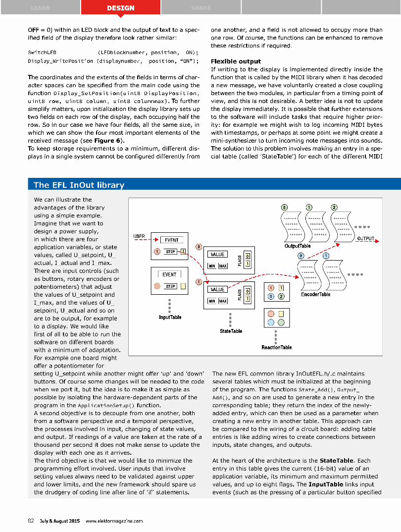
OFF = 0) within an LED block and the output of text to a spec-
ified field of the display therefore look rather similar:
SwitchLED (LEDblocknumber, position, ON);
Display_WritePosition (displaynumber, position, "ON");
The coordinates and the extents of the fields in terms of char-
acter spaces can be specified from the main code using the
function Display_SetPosition(uint8 DisplayPosition,
uint8 row, uint8 column, uint8 columnmax). To further
simplify matters, upon initialization the display library sets up
two fields on each row of the display, each occupying half the
row. So in our case we have four fields, all the same size, in
which we can show the four most important elements of the
received message (see Figure 6).
To keep storage requirements to a minimum, different dis-
plays in a single system cannot be configured differently from
one another, and a field is not allowed to occupy more than
one row. Of course, the functions can be enhanced to remove
these restrictions if required.
Flexible output
If writing to the display is implemented directly inside the
function that is called by the MIDI library when it has decoded
a new message, we have voluntarily created a close coupling
between the two modules, in particular from a timing point of
view, and this is not desirable. A better idea is not to update
the display immediately. It is possible that further extensions
to the software will include tasks that require higher prior-
ity: for example we might wish to log incoming MIDI bytes
with timestamps, or perhaps at some point we might create a
mini-synthesizer to turn incoming note messages into sounds.
The solution to this problem involves making an entry in a spe-
cial table (called 'StateTable') for each of the different MIDI
The EFL InOut librar
We can illustrate the
advantages of the library
using a simple example.
Imagine that we want to
design a power supply,
in which there are four
application variables, or state
values, called U_setpoint, U_
actual, I_actual and I_max.
There are input controls (such
as buttons, rotary encoders or
potentiometers) that adjust
the values of U_setpoint and
I_max, and the values of U_
setpoint, U_actual and so on
are to be output, for example
to a display. We would like
first of all to be able to run the
software on different boards
with a minimum of adaptation.
For example one board might
offer a potentiometer for
setting U_setpoint while another might offer 'up' and 'down'
buttons. Of course some changes will be needed to the code
when we port it, but the idea is to make it as simple as
possible by isolating the hardware-dependent parts of the
program in the ApplicationSetup() function.
A second objective is to decouple from one another, both
from a software perspective and a temporal perspective,
the processes involved in input, changing of state values,
and output. If readings of a value are taken at the rate of a
thousand per second it does not make sense to update the
display with each one as it arrives.
The third objective is that we would like to minimize the
programming effort involved. User inputs that involve
setting values always need to be validated against upper
and lower limits, and the new framework should spare us
the drudgery of coding line after line of 'if' statements.
USER -› EVENT
STEP HL
EVENT
o STEP
• • • •
InputTable
VALUE
MIN N
MAX
VALUE
MIN MAX
0
• • • •
StateTable
OutputTable
0 D 00 • • • •
ReactionTable
EncoderTable
• • • •
OUTPUT
The new EFL common library InOutEFL.h/.c maintains
several tables which must be initialized at the beginning
of the program. The functions State_Add(), Output_
Add (), and so on are used to generate a new entry in the
corresponding table; they return the index of the newly-
added entry, which can then be used as a parameter when
creating a new entry in another table. This approach can
be compared to the wiring of a circuit board: adding table
entries is like adding wires to create connections between
inputs, state changes, and outputs.
At the heart of the architecture is the StateTable. Each
entry in this table gives the current (16-bit) value of an
application variable, its minimum and maximum permitted
values, and up to eight flags. The InputTable links input
events (such as the pressing of a particular button specified
82 July &August 2015 www.elektormagazine.com
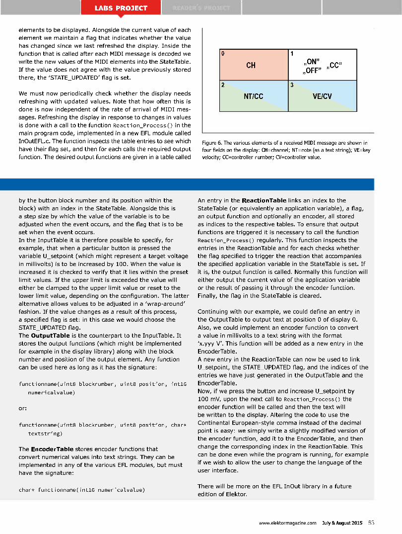
elements to be displayed. Alongside the current value of each
element we maintain a flag that indicates whether the value
has changed since we last refreshed the display. Inside the
function that is called after each MIDI message is decoded we
write the new values of the MIDI elements into the StateTable.
If the value does not agree with the value previously stored
there, the 'STATE_UPDATED' flag is set.
We must now periodically check whether the display needs
refreshing with updated values. Note that how often this is
done is now independent of the rate of arrival of MIDI mes-
sages. Refreshing the display in response to changes in values
is done with a call to the function Reaction_Process() in the
main program code, implemented in a new EFL module called
InOutEFL.c. The function inspects the table entries to see which
have their flag set, and then for each calls the required output
function. The desired output functions are given in a table called
o
CH
1 ON"
2
NT/CC
3
VE/CV
Figure 6. The various elements of a received MIDI message are shown in four fields on the display: CH=channel; NT=note (as a text string); VE=key velocity; CC=controller number; CV=controller value.
by the button block number and its position within the
block) with an index in the StateTable. Alongside this is
a step size by which the value of the variable is to be
adjusted when the event occurs, and the flag that is to be
set when the event occurs.
In the InputTable it is therefore possible to specify, for
example, that when a particular button is pressed the
variable U_setpoint (which might represent a target voltage
in millivolts) is to be increased by 100. When the value is
increased it is checked to verify that it lies within the preset
limit values. If the upper limit is exceeded the value will
either be clamped to the upper limit value or reset to the
lower limit value, depending on the configuration. The latter
alternative allows values to be adjusted in a 'wrap-around'
fashion. If the value changes as a result of this process,
a specified flag is set: in this case we would choose the
STATE_UPDATED flag.
The OutputTable is the counterpart to the InputTable. It
stores the output functions (which might be implemented
for example in the display library) along with the block
number and position of the output element. Any function
can be used here as long as it has the signature:
functionname(uint8 blocknumber, uint8 position, int16
numericalvalue)
or:
functionname(uint8 blocknumber, uint8 position, char*
textstring)
The EncoderTable stores encoder functions that
convert numerical values into text strings. They can be
implemented in any of the various EFL modules, but must
have the signature:
char* functionname(int16 numericalvalue)
An entry in the ReactionTable links an index to the
StateTable (or equivalently an application variable), a flag,
an output function and optionally an encoder, all stored
as indices to the respective tables. To ensure that output
functions are triggered it is necessary to call the function
Reaction_Process() regularly. This function inspects the
entries in the ReactionTable and for each checks whether
the flag specified to trigger the reaction that accompanies
the specified application variable in the StateTable is set. If
it is, the output function is called. Normally this function will
either output the current value of the application variable
or the result of passing it through the encoder function.
Finally, the flag in the StateTable is cleared.
Continuing with our example, we could define an entry in
the OutputTable to output text at position 0 of display O.
Also, we could implement an encoder function to convert
a value in millivolts to a text string with the format
'x.yyy V'. This function will be added as a new entry in the
EncoderTable.
A new entry in the ReactionTable can now be used to link
U_setpoint, the STATE_UPDATED flag, and the indices of the
entries we have just generated in the OutputTable and the
EncoderTable.
Now, if we press the button and increase U_setpoint by
100 mV, upon the next call to Reaction_Process() the
encoder function will be called and then the text will
be written to the display. Altering the code to use the
Continental European-style comma instead of the decimal
point is easy: we simply write a slightly modified version of
the encoder function, add it to the EncoderTable, and then
change the corresponding index in the ReactionTable. This
can be done even while the program is running, for example
if we wish to allow the user to change the language of the
user interface.
There will be more on the EFL InOut library in a future
edition of Elektor.
www.elektormagazine.com July &August 2015 83
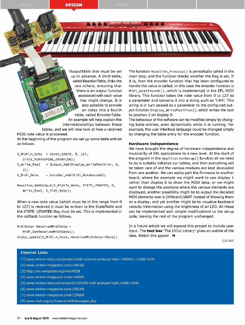
DESIGN
O_Write_Pos2
2);
E_Midi_Note
•11.
- - L Meeml6N0
—mem , ftmer. —
I illi'lltilL1111" OutputTable that must be set
up in advance. A third table,
called ReactionTable, links the
two others, ensuring that
there is an output function
• associated with each value
that might change. It is
• also possible to provide
an index into a fourth
table, called EncoderTable.
An example will help explain the
interrelationships between these
tables, and we will now look at how a received
MIDI note value is processed.
At the beginning of the program we set up some table entries
as follows.
S_MidiIn_Note = State_Add(0, 0, 127,
STATE_MINMAXMODE_OVERFLOW);
= Output_Add(Display_WritePosition, 0,
= Encoder_Add(Midi_NoteEncode);
Reaction_AddOutput(S_MidiIn_Note, STATE_UPDATED, 0_
Write_Pos2, E_Midi_Note);
When a new note value (which must be in the range from 0
to 127) is received it must be written to the StateTable and
the STATE_UPDATED flag must be set. This is implemented in
the callback function as follows.
MidiData* ReceivedMidiData =
Midi_GetReceivedMidiData();
State_Update(S_MidiIn_Note, ReceivedMidiData->Note);
The function Reaction_Process 0 is periodically called in the
main loop, and the function checks whether the flag is set. If
it is, then the encoder function that has been configured to
handle the value is called: in this case the encoder function is
Midi_NoteEncode(), which is implemented in the EFL MIDI
library. This function takes the note value from 0 to 127 as
a parameter and converts it into a string such as 'C#4'. This
string is in turn passed as a parameter to the configured out-
put function Di splay_WritePosition(), which writes the text
to position 2 on display O.
The behaviour of the software can be modified simply by chang-
ing table entries, even dynamically while it is running. For
example, the user interface language could be changed simply
by changing the table entry for the encoder function.
Hardware independence
We have brought the degree of hardware independence and
modularity of EFL applications to a new level. At the start of
the program in the ApplicationSetup() function all we need
to do is suitably initialize our tables, and then everything will
be taken care of and the various modules are kept decoupled
from one another. We can easily port the firmware to another
board, where for example we might want to use display 1
rather than display 0 to show the MIDI data, or we might
want to change the positions where the various elements are
displayed; another possibility might be to output the decoded
MIDI elements over a (different) UART instead of showing them
on a display; and yet another might be to visualize keyboard
velocity information using the brightness of an LED. All these
can be implemented with simple modifications to the setup
code, leaving the rest of the program unchanged.
In a future article we will expand this project to include user
input. The text box 'The InOut Library' gives an outline of the
idea. Watch this space! 11
(150169)
Internet Links
[1] www.elektor-labs.com/project/midi-channel-analyzer-mkii-140065-i.13380.html
[2] www.elektor-magazine.com/140182
[3] http://en.wikipedia.org/wiki/MIDI
[4] www.elektor-magazine.com/140009
[5] www.elektor-labs.com/project/150169-midi-analyzer-light.14481.html
[6] www.elektor-magazine.com/150169
[7] www.elektor-magazine.com/120668
[8] www.midi.org/techspecs/midimessages.php
84 July &August 2015 www.elektormagazine.com
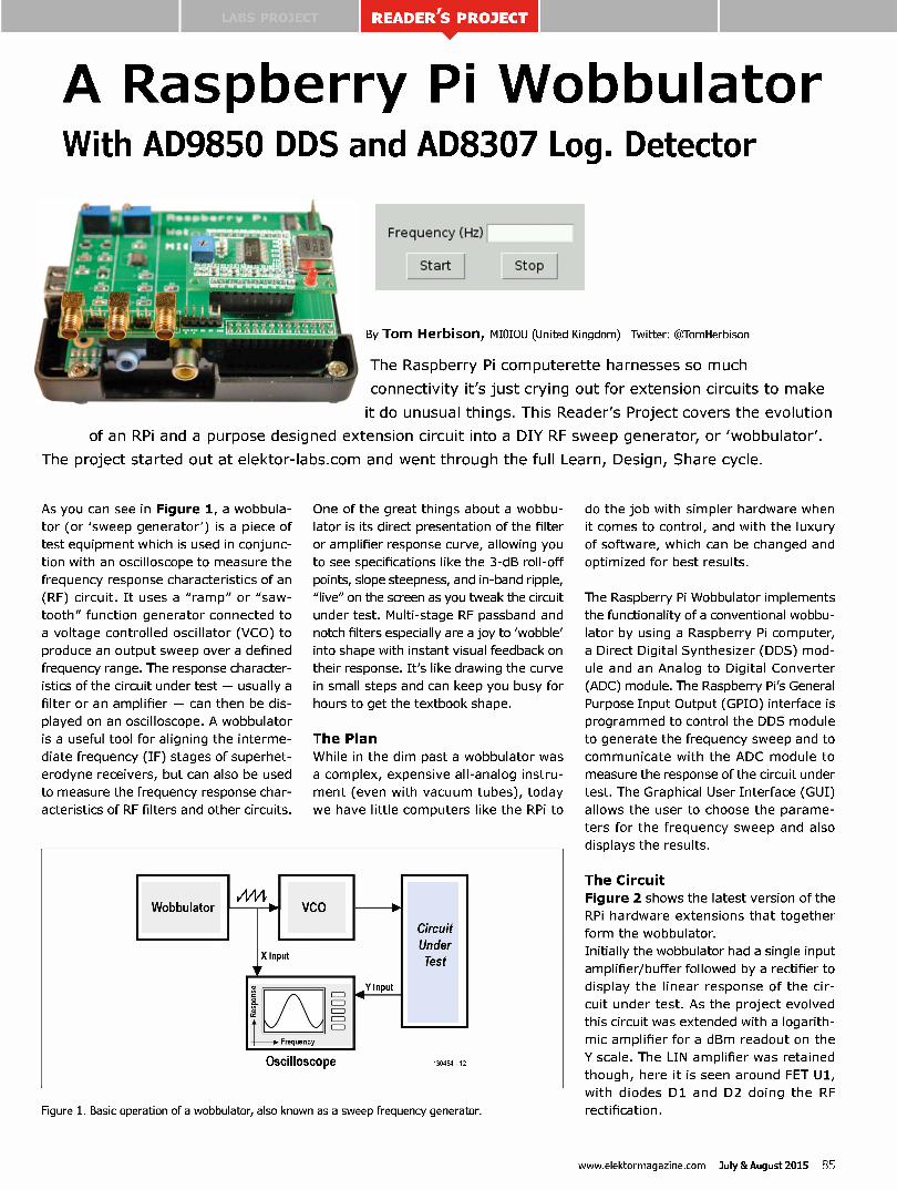
UI READER'S PROJECT
A Raspberry Pi Wobbulator With AD9850 DDS and AD8307 Log. Detector
Frequency (Hz)
Start Stop
By Tom Herbison, MIOIOU (United Kingdom) Twitter: @TomHerbison
The Raspberry Pi computerette harnesses so much
connectivity it's just crying out for extension circuits to make
it do unusual things. This Reader's Project covers the evolution
of an RPi and a purpose designed extension circuit into a DIY RF sweep generator, or 'wobbulator'.
The project started out at elektor-labs.com and went through the full Learn, Design, Share cycle.
As you can see in Figure 1, a wobbula-
tor (or 'sweep generator') is a piece of
test equipment which is used in conjunc-
tion with an oscilloscope to measure the
frequency response characteristics of an
(RF) circuit. It uses a "ramp" or "saw-
tooth" function generator connected to
a voltage controlled oscillator (VCO) to
produce an output sweep over a defined
frequency range. The response character-
istics of the circuit under test — usually a
filter or an amplifier — can then be dis-
played on an oscilloscope. A wobbulator
is a useful tool for aligning the interme-
diate frequency (IF) stages of superhet-
erodyne receivers, but can also be used
to measure the frequency response char-
acteristics of RF filters and other circuits.
Wobbulator
One of the great things about a wobbu-
lator is its direct presentation of the filter
or amplifier response curve, allowing you
to see specifications like the 3-dB roll-off
points, slope steepness, and in-band ripple,
"live" on the screen as you tweak the circuit
under test. Multi-stage RF passband and
notch filters especially are a joy to 'wobble'
into shape with instant visual feedback on
their response. It's like drawing the curve
in small steps and can keep you busy for
hours to get the textbook shape.
The Plan
While in the dim past a wobbulator was
a complex, expensive all-analog instru-
ment (even with vacuum tubes), today
we have little computers like the RPi to
AM - 1110- VCO
X Input
V
¡
I Frequency
Oscilloscope
Input 1111Y
Circuit
Under Test
130484 - 12
Figure 1. Basic operation of a wobbulator, also known as a sweep frequency generator.
do the job with simpler hardware when
it comes to control, and with the luxury
of software, which can be changed and
optimized for best results.
The Raspberry Pi Wobbulator implements
the functionality of a conventional wobbu-
lator by using a Raspberry Pi computer,
a Direct Digital Synthesizer (DDS) mod-
ule and an Analog to Digital Converter
(ADC) module. The Raspberry Pi's General
Purpose Input Output (GPIO) interface is
programmed to control the DDS module
to generate the frequency sweep and to
communicate with the ADC module to
measure the response of the circuit under
test. The Graphical User Interface (GUI)
allows the user to choose the parame-
ters for the frequency sweep and also
displays the results.
The Circuit
Figure 2 shows the latest version of the
RPi hardware extensions that together
form the wobbulator.
Initially the wobbulator had a single input
amplifier/buffer followed by a rectifier to
display the linear response of the cir-
cuit under test. As the project evolved
this circuit was extended with a logarith-
mic amplifier for a dBm readout on the
Y scale. The LIN amplifier was retained
though, here it is seen around FET Ul,
with diodes DI and D2 doing the RF
rectification.
www.elektormagazine.com July &August 2015 85
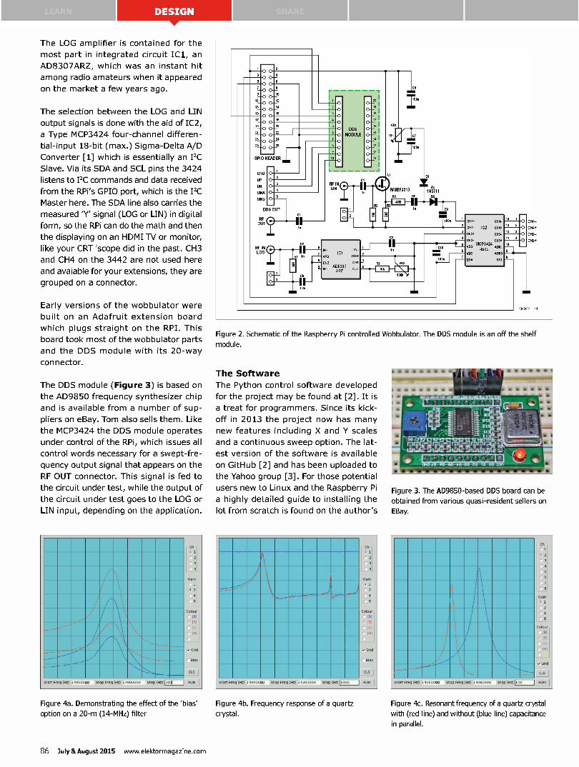
The LOG amplifier is contained for the
most part in integrated circuit IC1, an
AD8307ARZ, which was an instant hit
among radio amateurs when it appeared
on the market a few years ago.
The selection between the LOG and LIN
output signals is done with the aid of IC2,
a Type MCP3424 four-channel differen-
tial-input 18-bit (max.) Sigma-Delta A/D
Converter [1] which is essentially an I2C
Slave. Via its SDA and SCL pins the 3424
listens to I2C commands and data received
from the RPi's GPIO port, which is the I2C
Master here. The SDA line also carries the
measured 'Y' signal (LOG or LIN) in digital
form, so the RPi can do the math and then
the displaying on an HDMI TV or monitor,
like your CRT 'scope did in the past. CH3
and CH4 on the 3442 are not used here
and avaiable for your extensions, they are
grouped on a connector.
Early versions of the wobbulator were
built on an Adafruit extension board
which plugs straight on the RPI. This
board took most of the wobbulator parts
and the DDS module with its 20-way
connector.
The DDS module (Figure 3) is based on
the AD9850 frequency synthesizer chip
and is available from a number of sup-
pliers on eBay. Tom also sells them. Like
the MCP3424 the DDS module operates
under control of the RPi, which issues all
control words necessary for a swept-fre-
quency output signal that appears on the
RF OUT connector. This signal is fed to
the circuit under test, while the output of
the circuit under test goes to the LOG or
LIN input, depending on the application.
Lh
2
1
- 4
.4
Colour-
. rI11,1,
—
-_-- Gnd .___ —
--
--
---
.• sr
- - ----- —
- Ellas -----
start area Inn inusuouu Stop Stan (121) .09000. Step (.2) I2. .1 RUN
Figure 4a. Demonstrating the effect of the 'bias' option on a 20-m (14-MHz) filter
Figure 2. Schematic of the Raspberry Pi controlled Wobbulator. The DDS module is an off the shelf module.
The Software
The Python control software developed
for the project may be found at [2]. It is
a treat for programmers. Since its kick-
off in 2013 the project now has many
new features including X and Y scales
and a continuous sweep option. The lat-
est version of the software is available
on GitHub [2] and has been uploaded to
the Yahoo group [3]. For those potential
users new to Linux and the Raspberry Pi
a highly detailed guide to installing the
lot from scratch is found on the author's
eh-j
1
2
1
1]
Galn
- 2
I ' '
-Colour-
l- 181
sr Gnsl
alas
CLS
HUN
__...-- -.- -
Stop (Str)11.UUu
)
—
Start Fran (1.2) 14000000 StOp Frea (112) 14200000
Figure 4b. Frequency response of a quartz crystal.
P2 ri17- 71 -
all là1,1.:dn 5
Figure 3. The AD9850-based DDS board can be obtained from various quasi-resident sellers on EBay.
_--- -..
I
1
—
Ch
1
r- 3
II
- 2
r 4
Colo .-
- lel
. IN
Lj
1141
Start Frou (HZ) LAI/sun u Stop area (10 14usuuuu Stela (12)110u RUIS l
Figure 4c. Resonant frequency of a quartz crystal with (red line) and without (blue line) capacitance in parallel.
86 July &August 2015 www.elektormagazine.com

READER'S PROJECT
1 —
Lh
rG..alin
8
- Colour
- IBi
, f 111
God
_ —
,
BlaS
CLS
Start Frog (I.12) 1.40000UU Stop Freq (E12) 14 U. . Step (H2)11 .0 HUN
Figure 4d. Response of an RF filter measured on
CH1 (LIN).
blog [4] — look for the April 8, 2014
installment.
Conclusion
To check its operation the RPi Wobbula-
tor was used to 'sweep' a quartz crystal
and filters for the 20-m radio band (14
MHz). Some of the results can be seen in
the screendumps pictured in Figure 4.
Finally, this is a Reader's Project publica-
tion, meaning the project was not built
or tested at Elektor Labs. Rather than
describing the RPi Wobbulator in great
detail as a DIY project, the purpose of
this article is to alert you to the way it
got developed interactively by the author
using his blog and the Elektor Labs web-
site [5] where it got 5 out of 5 stars. After
designing a PCB for the design (Figure 5)
Tom progressed right up to offering kits
for the project, optionally with the DDS
generator module included. Talk to him via
his blog [4] or Twitter @TomHerbison. li
(130484)
[ila nns lp
500
25 0
12 5
0.0
g u‘s
250
625
7' 11.00 14.02 14.04 14 06 14.00 14 10 14 12 14 14 14 16 1418 14 20 Nit
ch,
Pain
2
Colour '0
Geld
Blas
Fast
CLS
dBm
Swett,
Start Freo (Hz) 1400 000 stop ml (Ht) 14400000 Step 011) 1000 RUN
[46 jlptinns 1p
2.000
1.800
1 600
1 400
v 1 200
1 000
0 800
600
40
0 200
J " itoo 14.02 14.04 14 06 1400 14 10 14 12 14 14 14 16 14.16 14 20
Hit
Colour • M:
Grld
Blas
Fast
r CLS
dBm
BsveeP
Start Fr, (IC) 1400 000 Stop req Bizl 14400000 step (He 1000 RUN
Figure 4e. 14-MHz filter analyzed using the LOG Figure 4f. 14-MHz filter analyzed using the LIN Y
(dBm) Y axis scale. axis scale.
Figure 5. Printed circuit boards for the RPi Wobbulator are available from the author.
Web Links
[1] MCP3424: www.microchip.com/wwwproducts/Devices.aspx?product=MCP3424
[2] RPi Wobbulator Software (Python 3): https://github.com/miOiou/
[3] Yahoo Group: http://groups.yahoo.com/neo/groups/rpiwobbulator/info
[4] Author's blog: www.asliceofraspberrypi.co.uk
[5] www.elektor-labs.com/project/raspberry-pi-wobbulator-130484-i.13612.html
Advertisement
el HAMMOND MANUFACTURING
Housings for Raspberry Pi, Arduino and many other bareboard computers • Enclosure • Platform
+ 44 1256 812812
The choice is yours. • Enclosure for all round protection
• Platform for all round access
• Design-specific versions for all popular models
• Visit hammondmfg.com for full details
www.elektormagazine.com July &August 2015 87

DESIGN
Pelco-D Control for
ased on the Elektor Platino
Pictures from video surveillance (CCTV) cameras have (alas) become familiar. Their
quality is often poor and often the cameras are fixed, in spite of the fact that they can
be pointed and adjusted remotely to obtain much better images. Which is exactly what I
aim to do using an Elektor Platino board. All that is needed is to be able to talk Pelco-D.
Figure 1. PTZ Cameras can be controlled with this keyboard and three-axis joystick.
zoom function allows the focal length of
the lens to be altered in order to better
distinguish or identify the subject. These
functions Pan, Tilt and Zoom are usually
abbreviated to their acronym P-T-Z. Other
parameters that may be changed are the
diaphragm or iris, the opening of which
determines the quantity of light admit-
ted through the lens, and the focus, for
obtaining the sharpest possible image.
In this article, we will discuss the P-T-Z
camera communication protocol. For this,
two programs were written for the Elektor
Platino board, and tested with two types
of P-T-Z dome cameras (Table 1).
The Pelco-D Protocol
A PTZ camera is usually driven from
a keyboard with a joystick (Figure 1)
A motorized dome camera can be moved
horizontally (pan) and vertically (tilt). The
using the Pelco protocol, from the name
of the American company Pelc° Corpora-
tion. This is a standard, used in cameras
as far afield as Buckingham Palace, the
Statue of Liberty, and the Presidential
Palace in Beijing.
In the Pelco-D protocol, there is a mas-
ter and numerous slaves: the master is
usually the keyboard/joystick panel, and
the cameras are the slaves. A Master can
communicate with up to 255 slaves. Each
slave has a unique address from 1 to 255.
As the master can only address one slave
at a time, this is a unicast protocol.
Physically, the messages are sent on a
serial two wire RS-485 bus. The speed
is usually 2400, 4800 or 9600 bauds. A
character is sent as eight bits, LSB first,
88 July &August 2015 www.elektormagazine.com

LABS PROJECT
with a start and stop bit and no parity bit.
Whether at Buckingham Palace or Bei-
jing, it is always the master which initi-
ates the communication, slaves may only
reply when commanded by the master.
They are doomed to a lonely existence, as
they are unable to communicate between
themselves.
A command in the Pelco-D protocol
consists of seven bytes (Table 2). The
address byte, the command and data
bytes are always framed with a SYNC
byte which marks the start of the useful
bytes, and a CKSUM byte which corre-
sponds to the checksum of bytes 2 to 6.
The DATA1 and DATA2 bytes may con-
tain from 8 to 16 bits of data. If a 16-bit
word is needed, DATA1 is the most sig-
nificant byte and DATA2 the least signif-
icant byte. For example, if DATA1 = $12
and DATA2 = $34, the sixteen bit word
is equal to $1234 (values preceded by a
'$' sign are texadecimal).
The checksum is a modulo-256 sum of
bytes 2 to 6. This is calculated by trun-
cating the intermediate and final results
to 8 bits.
Here is an example in binary to show
what happens if byte 2 = 0000 1010
(10, $0A), byte 3 = 1000 1000 (136,
$88), byte 4 = 1001 0000 (144, $9
byte 5 = 0000 0000 (0, $00)
byte 6 = 0010 0000 (32, $20)
www.elektormagazine.com July &Aug

LEARN
0000 1010 (byte 2)
1000 1000 + (byte 3)
1001 0010 (= $92), the result
is within 8 bits
1001 0000 + (octet 4)
1 0010 0010 (= $122), this value
needs 9 bits.
The modulo-256 operation truncates the
ninth bit, so we get 0010 0010 (= $22)
instead, and we continue our calculation
with this value:
Table 1. Specifications of the IP camera and the analog camera used in
this article. Both cameras may be configured
pelco_camera_osd_setup. The IP camera
software platino-pelco_2df7274-a_query.
IP Camera 1.3 Megapixels
with the software plati no-
may also be controlled by the
Model number 2DF7274-A
Lens focal length 4.3 mm - 86 mm
Optical zoom 86 / 4.3 = 20x
Firmware Version V5.2.4 build 141009
Analog Camera 650TVL
Model number SD6C23E-H
Lens Focal length 3.9 mm - 89.7 mm
Optical zoom 89.7 / 3.9 = 23x
Firmware Version V1.03.8.RHAHDV
Table 2. The Pelco-D protocol uses frames of seven bytes.
Byte Name Contents
1 SYNC 255 ($FF in hexadecimal), signals the start of a frame.
2 ADDR 1 to 255, the address of the camera.
3 CMND1 The command over two bytes.
4 CMND2
5 DATA1 The data over two bytes .
6 DATA2
7 CKSM Checksum for bytes 2 to 6.
Table 3.
activated
CMND1
For movement commands, bit 0 of CMND2 is always 0. A function is
if its bit is set to 1, and deactivated when that bit is reset to 0.
Bit 7 Bit 6 Bit 5 Bit 4 Bit 3 Bit 2 Bit 1 Bit 0
Sense 0 0 Auto Scan /
Manual Scan
Camera On/
Camera Off
Iris
Close
Iris
Open
Focus
Near
CMND2
Bit 7 Bit 6 Bit 5 Bit 4 Bit 3 Bit 2 Bit 1 Bit 0
Focus
Far
Zoom
Wide
Zoom
Tele Down Up Left Right 0
Tableau 4.
Some examples of move ment commands sent to camera 12 ($0C).
SYNC ADDR CMND1 CMND2 DATA]. DATA2 CKSUM
Pan Right,
Speed $25 $FF $0C $00 $02 $25 $00 $33
Motion Stop $FF $0C $00 $00 $00 $00 $33
Tilt Up,
Speed $20 $FF $0C $00 $08 $00 $20 $34
Motion Stop $FF $0C $00 $00 $00 $00 $33
Zoom Out (Wide) $FF $0C $00 $40 $00 $00 $4C
0010 0010 (= $22)
0000 0000 + (byte 5)
0010 0010 (= $22), the result
is within 8 bits
0010 0000 + (byte 6)
0100 0010 (= $42), the result
is within 8 bits
The checksum CKSUM is thus $42.
Zoom to the movement
com mands
The Pelco-D protocol uses two types of
command, movement commands (Pan,
Tilt, Zoom, Iris, Focus), recognized by
the value of bit 0 of the CMND2 byte
set to 0, and control commands which
allow advanced configuration (bit 0 of
CMND2 = 1).
The movement commands are shown in
Tables 3 and 4. A function is activated
if its corresponding bit is set to 1, and
deactivated if that bit is set to 0.
DATA1 allows the rotation speed of the
camera (Pan) to be set from 0 (slow) to
63 ($3F, fast). A value of 64 ($40) corre-
sponds to turbo speed. To stop the rota-
tion, the Left and Right bits can be set to
0 while keeping, if desired, the contents of
DATA1 unchanged. The horizontal rotation
speed (pan) usually varies from 0.1°/s to
80°/s (0.1°/s to 160°/s in manual control
mode for our two cameras).
DATA2 allows control of the vertical incli-
nation speed (Tilt) from 0 (slow) to 63
($3F, fast). There is no Turbo setting for
the vertical tilt. To stop it, the Down and
Up bits must be set to 0, while keep-
ing, if desired, the contents of DATA2
unchanged. The speed of vertical rota-
tion usually varies from 0.1°/s to 40°/s
(0.1°/s to 120°/s in manual control mode
for our two cameras).
Most Pelco devices are equipped with a
p h.,,,, ,,,,.. • -..„-,,..,;:.:•,,.,, ,Ilf 1,11-1111 tl ,11 '
- - . < :11; ,.) ,, .. 1 :r.,.,... t. ,I I, 11 1,1 10 .1. , •, .. / h lleboot*M !arm> -'----
Figure 2. The setup menu of the camera is
embedded in the camera picture, also known as
an On-Screen Display or OSD menu.
90 July &August 2015 www.elektormagazine.com
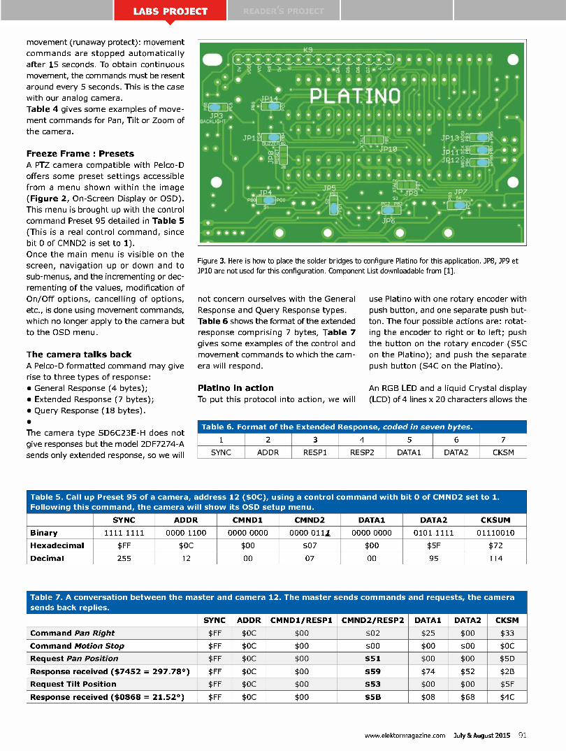
movement (runaway protect): movement
commands are stopped automatically
after 15 seconds. To obtain continuous
movement, the commands must be resent
around every 5 seconds. This is the case
with our analog camera.
Table 4 gives some examples of move-
ment commands for Pan, Tilt or Zoom of
the camera.
Freeze Fra me : Presets
A PTZ camera compatible with Pelco-D
offers some preset settings accessible
from a menu shown within the image
(Figure 2, On-Screen Display or OSD).
This menu is brought up with the control
command Preset 95 detailed in Table 5
(This is a real control command, since
bit 0 of CMND2 is set to 1).
Once the main menu is visible on the
screen, navigation up or down and to
sub-menus, and the incrementing or dec-
rementing of the values, modification of
On/Off options, cancelling of options,
etc., is done using movement commands,
which no longer apply to the camera but
to the OSD menu.
The ca mera talks back
A Pelco-D formatted command may give
rise to three types of response:
• General Response (4 bytes);
• Extended Response (7 bytes);
• Query Response (18 bytes).
•
The camera type SD6C23E-H does not
give responses but the model 2DF7274-A
sends only extended response, so we will
• - . • •
K9
•
• • • eimEr
JP3 . BACKLIGHT
•
• •
• •
•. JP./
• • • • • •
V; ? •2 2 2 fdi •
•
•
O O O O O • • •
PLATINO • • •
. • •JP10 •
JP13 r 1 •
jpjj L 1 • JR12,m. g •
• •
PC
e •
• •
• •
• • • JP9 SJ
•0 111.
• • • I • •I
•
JP.6
•
JP7 S4
• • •
•
•
Figure 3. Here is how to place the solder bridges to configure Platino for this application. JP8, JP9 et
JP10 are not used for this configuration. Component List downloadable from [1].
not concern ourselves with the General
Response and Query Response types.
Table 6 shows the format of the extended
response comprising 7 bytes, Table 7
gives some examples of the control and
movement commands to which the cam-
era will respond.
Platino in action
To put this protocol into action, we will
use Platino with one rotary encoder with
push button, and one separate push but-
ton. The four possible actions are: rotat-
ing the encoder to right or to left; push
the button on the rotary encoder (S5C
on the Platino); and push the separate
push button (S4C on the Platino).
An RGB LED and a liquid Crystal display
(LCD) of 4 lines x 20 characters allows the
Table 6. Format of the Extended Response, coded in seven bytes.
1 2 3 4 5 6 7
SYNC ADDR RESP1 RESP2 DATA1 DATA2 CKSM
Table 5. Call up
Following this
Preset 95 of a
command, the
SYNC
camera, address
camera will show
ADDR
12 ($0C), using a control command
its OSD setup menu.
CMND1 CMND2
with
DATA].
bit 0 of CMND2
DATA2
set to 1.
CKSUM
Binary 1111 1111 0000 1100 0000 0000 0000 0111. 0000 0000 0101 1111 01110010
Hexadecimal $FF $0C $00 $07 $00 $5F $72
Decimal 255 12 00 07 00 95 114
Table 7. A conversation between the master
sends back replies.
and camera 12. The master sends commands and requests, the camera
SYNC ADDR CMND1/RESP1 CMND2/RESP2 DATA]. DATA2 CKSM
Command Pan Right $FF $0C $00 $02 $25 $00 $33
Command Motion Stop $FF $0C $00 $00 $00 $00 $0C
Request Pan Position $FF $0C $00 1 $51 $00 $00 $5D
Response received ($7452 = 297.78°) $FF $0C $00 $59 $74 $52 $2B
Request Tilt Position $FF $0C $00 $53 $00 $00 $5F
Response received ($0868 = 21.52°) $FF $0C $00 $56 $08 $68 $4C
www.elektormagazine.com July &August 2015 91
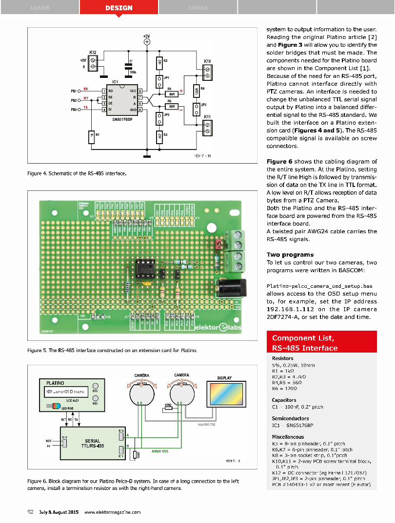
Figure 4. Schematic of the RS-485 interface.
• 0 F.r. 2 kififird 11,1„1,11 .4 r „,„„ 1,140111,000,01111,11;, le, •• 0011114•••*1110•• •001110111,0••••44b• —Amee.••ees
s.. • • lee 4 • • • •
• • • • • • • • •
• • •
6.0611111100011111hi **3110111000$14 • •
•••••*11100000
I • • •
d • • •
t • • • • • All •• • • • •-•-• • are el, • • • eo • • «
_11111111_0111_111_0_0_110.0 • • • • • • • ogr e -r47,-rdrur -1- ir e -re-r -vir
• v'm K7 r+! Z 74 7eil 6 e'
e • lektor Gla
e) • -,-••11108111t-O0 0 IDO s ••• •• • •041 1 •
• s '-11NOIK-30111411,. -• • • • • • • el111116v4, • • • • • tsill••• • , • tit, • • 1111111* • r • *eel. • • »le • •.001114 •
Figure 5. The RS-485 interface constructed on an extension card for Platino.
PLATINO
LCD 4x20
ffleLED RGB
S5C
S4C
R/T RX TX
CAMERA
K12 VCC
OV
SERIAL TTL/RS-485
K10
CAMERA
120Q
DISPLAY
AWG24 120Q
coax KK6 75Q
150117 - 12
Figure 6. Block diagram for our Platino Pelco-D system. In case of a long connection to the left camera, install a termination resistor as with the right-hand camera.
system to output information to the user.
Reading the original Platino article [2]
and Figure 3 will allow you to identify the
solder bridges that must be made. The
components needed for the Platino board
are shown in the Component List [1].
Because of the need for an RS-485 port,
Platino cannot interface directly with
PTZ cameras. An interface is needed to
change the unbalanced TTL serial signal
output by Platino into a balanced differ-
ential signal to the RS-485 standard. We
built the interface on a Platino exten-
sion card (Figures 4 and 5). The RS-485
compatible signal is available on screw
connectors.
Figure 6 shows the cabling diagram of
the entire system. At the Platino, setting
the R/T line High is followed by transmis-
sion of data on the TX line in TTL format.
A low level on R/T allows reception of data
bytes from a PTZ Camera.
Both the Platino and the RS-485 inter-
face board are powered from the RS-485
interface board.
A twisted pair AWG24 cable carries the
RS-485 signals.
Two progra ms
To let us control our two cameras, two
programs were written in BASCOM:
Platino-pelco_camera_osd_setup.bas
allows access to the OSD setup menu
to, for example, set the IP address
192.168.1.112 on the IP camera
2DF7274-A, or set the date and time.
Component List,
RS-485 Interface
Resistors
5%, 0.25W, lOmm R1 = lkS2
R2,R3 = 4.7kS2 R4,R5 = 56Q
R6 = 120Q
Capacitors
Cl = 100nF, 0.2" pitch
Semiconductors
IC1 = SN65176BP
Miscellaneous
K5 = 8-pin pinheader, 0.1" pitch
K6,K7 = 6-pin pinheader, 0.1" pitch K8 = 3-pin socket strip, 0.1"pitch
K10,K11 = 2-way PCB screw terminal block, 0.1" pitch
K12 = DC connector (eg Farnell 1217037) 3P1,3P2,3P3 = 2-pin pinheader, 0.1" pitch
PCB #140433-1 v2 or most recent (Elektor)
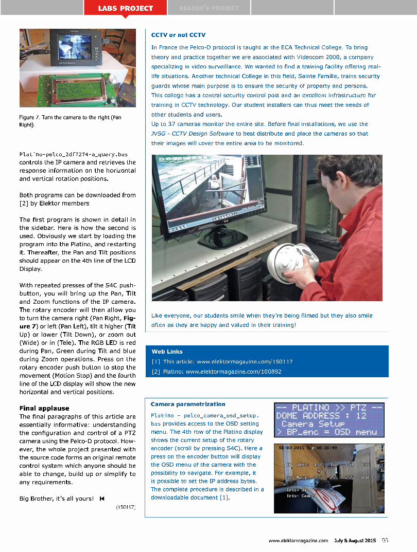
Figure 7. Turn the camera to the right (Pan
Right).
Plat no-pelco_2df7274-a_query. bas
controls the IP camera and retrieves the
response information on the horizontal
and vertical rotation positions.
Both programs can be downloaded from
[2] by Elektor members
The first program is shown in detail in
the sidebar. Here is how the second is
used. Obviously we start by loading the
program into the Platino, and restarting
it. Thereafter, the Pan and Tilt positions
should appear on the 4th line of the LCD
Display.
With repeated presses of the S4C push-
button, you will bring up the Pan, Tilt
and Zoom functions of the IP camera.
The rotary encoder will then allow you
to turn the camera right (Pan Right, Fig-
ure 7) or left (Pan Left), tilt it higher (Tilt
Up) or lower (Tilt Down), or zoom out
(Wide) or in (Tele). The RGB LED is red
during Pan, Green during Tilt and blue
during Zoom operations. Press on the
rotary encoder push button to stop the
movement (Motion Stop) and the fourth
line of the LCD display will show the new
horizontal and vertical positions.
Final applause
The final paragraphs of this article are
essentially informative: understanding
the configuration and control of a PTZ
camera using the Pelco-D protocol. How-
ever, the whole project presented with
the source code forms an original remote
control system which anyone should be
able to change, build up or simplify to
any requirements.
Big Brother, it's all yours! 11
(150117)
CCTV or not CCTV
In France the Pelco-D protocol is taught at the ECA Technical College. To bring
theory and practice together we are associated with Videocom 2000, a company
specializing in video surveillance. We wanted to find a training facility offering real-
life situations. Another technical College in this field, Sainte Famille, trains security
guards whose main purpose is to ensure the security of property and persons.
This college has a central security control post and an excellent infrastructure for
training in CCTV technology. Our student installers can thus meet the needs of
other students and users.
Up to 37 cameras monitor the entire site. Before final installations, we use the
JVSG - CCTV Design Software to best distribute and place the cameras so that
their images will cover the entire area to be monitored.
Like everyone, our students smile when they're being filmed but they also smile
often as they are happy and valued in their training!
Web Links
[1] This article: www.elektormagazine.com/150117
[2] Platino: www.elektormagazine.com/100892
Camera parametrization
Platino - pelco_camera_osd_setup.
bas provides access to the OSD setting
menu. The 4th row of the Platino display
shows the current setup of the rotary
encoder (scroll by pressing S4C). Here a
press on the encoder button will display
the OSD menu of the camera with the
possibility to navigate. For example, it
is possible to set the IP address bytes.
The complete procedure is described in a
downloadable document [1].
PLPTINO >> PTZ ' DOME PDDRESS : 12 Camera Setup BP_enc = OSD me'
www.elektormagazine.com July &August 2015 93
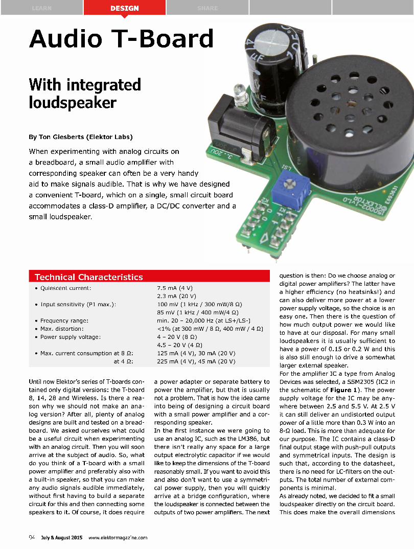
Audio T-Board
With integrated loudspeaker
By Ton Giesberts (Elektor Labs)
When experimenting with analog circuits on
a breadboard, a small audio amplifier with
corresponding speaker can often be a very handy
aid to make signals audible. That is why we have designed
a convenient T-board, which on a single, small circuit board
accommodates a class-D amplifier, a DC/DC converter and a
small loudspeaker.
'19M1' IME15 11-' • Quiescent current:
• Input sensitivity (P1 max.):
• Frequency range:
• Max. distortion:
• Power supply voltage:
• Max. current consumption at 8 52:
at 4 52:
7.5 mA (4 V)
2.3 mA (20 V)
100 mV (1 kHz / 300 mW/8 52)
85 mV (1 kHz / 400 mW/4 52)
min. 20 - 20,000 Hz (at LS+/LS-)
<1% (at 300 mW / 8 52, 400 mW / 4 52)
4 - 20 V (8 52)
4.5 - 20 V (4 52)
125 mA (4 V), 30 mA (20 V)
225 mA (4 V), 45 mA (20 V)
Until now Elektor's series of T-boards con-
tained only digital versions: the T-board
8, 14, 28 and Wireless. Is there a rea-
son why we should not make an ana-
log version? After all, plenty of analog
designs are built and tested on a bread-
board. We asked ourselves what could
be a useful circuit when experimenting
with an analog circuit. Then you will soon
arrive at the subject of audio. So, what
do you think of a T-board with a small
power amplifier and preferably also with
a built-in speaker, so that you can make
any audio signals audible immediately,
without first having to build a separate
circuit for this and then connecting some
speakers to it. Of course, it does require
a power adapter or separate battery to
power the amplifier, but that is usually
not a problem. That is how the idea came
into being of designing a circuit board
with a small power amplifier and a cor-
responding speaker.
In the first instance we were going to
use an analog IC, such as the LM386, but
there isn't really any space for a large
output electrolytic capacitor if we would
like to keep the dimensions of the T-board
reasonably small. If you want to avoid this
and also don't want to use a symmetri-
cal power supply, then you will quickly
arrive at a bridge configuration, where
the loudspeaker is connected between the
outputs of two power amplifiers. The next
question is then: Do we choose analog or
digital power amplifiers? The latter have
a higher efficiency (no heatsinks!) and
can also deliver more power at a lower
power supply voltage, so the choice is an
easy one. Then there is the question of
how much output power we would like
to have at our disposal. For many small
loudspeakers it is usually sufficient to
have a power of 0.15 or 0.2 W and this
is also still enough to drive a somewhat
larger external speaker.
For the amplifier IC a type from Analog
Devices was selected, a SSM2305 (IC2 in
the schematic of Figure 1). The power
supply voltage for the IC may be any-
where between 2.5 and 5.5 V. At 2.5 V
it can still deliver an undistorted output
power of a little more than 0.3 W into an
8-S2 load. This is more than adequate for
our purpose. The IC contains a class-D
final output stage with push-pull outputs
and symmetrical inputs. The design is
such that, according to the datasheet,
there is no need for LC-filters on the out-
puts. The total number of external com-
ponents is minimal.
As already noted, we decided to fit a small
loudspeaker directly on the circuit board.
This does make the overall dimensions
94 July &August 2015 www.elektormagazine.com
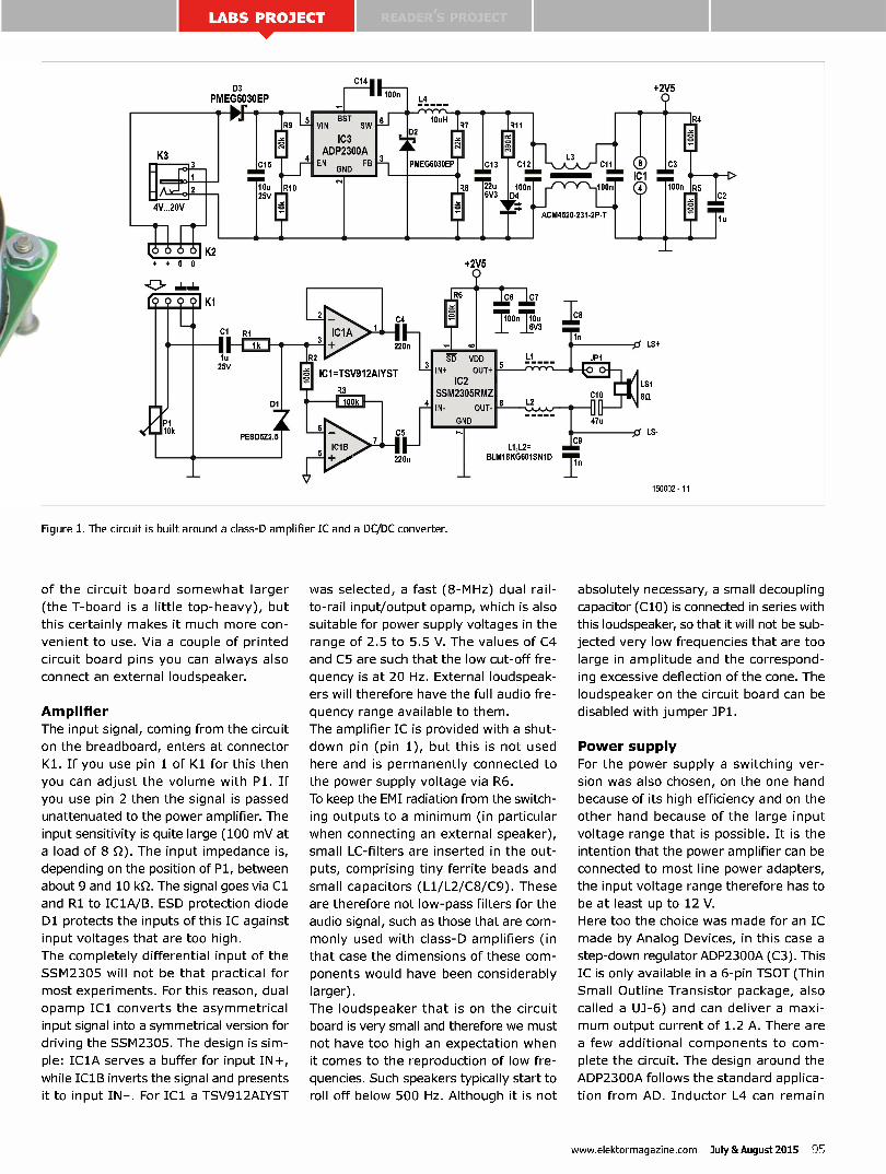
D3 PMEG6030EP
K3
AY— 2
V...20V
cZé 0 011(2 + 0
9
C15
10u R10 25V
C141
17-1H 7
BST VIN SW
IC3 ADP2300A EN FB
GND
L4
PMEG6030EP
C4
1C1=TSV912AlYST
C5
+2V5
SD VDD
IN+ OUT+
IC2 SSM2305RMZ
IN- OUT
GND
C7
C9 L1,L2=
BLM18KG601SN1D
L3 Á Á
ACM4520-231-2P-T
LS+
LS1
8O
LS-
150002 - 11
Figure 1. The circuit is built around a class-D amplifier IC and a DC/DC converter.
of the circuit board somewhat larger
(the T-board is a little top-heavy), but
this certainly makes it much more con-
venient to use. Via a couple of printed
circuit board pins you can always also
connect an external loudspeaker.
Amplifier
The input signal, coming from the circuit
on the breadboard, enters at connector
Kl. If you use pin 1 of K1 for this then
you can adjust the volume with pl. If
you use pin 2 then the signal is passed
unattenuated to the power amplifier. The
input sensitivity is quite large (100 mV at
a load of 8 S2). The input impedance is,
depending on the position of pl, between
about 9 and 10 kg-2. The signal goes via Cl
and R1 to IC1A/B. [SD protection diode
D1 protects the inputs of this IC against
input voltages that are too high.
The completely differential input of the
SSM2305 will not be that practical for
most experiments. For this reason, dual
opamp IC1 converts the asymmetrical
input signal into a symmetrical version for
driving the SSM2305. The design is sim-
ple: IC1A serves a buffer for input IN+,
while IC1B inverts the signal and presents
it to input IN-. For IC1 a T5V912AIY5T
was selected, a fast (8-MHz) dual rail-
to-rail input/output opamp, which is also
suitable for power supply voltages in the
range of 2.5 to 5.5 V. The values of C4
and C5 are such that the low cut-off fre-
quency is at 20 Hz. External loudspeak-
ers will therefore have the full audio fre-
quency range available to them.
The amplifier IC is provided with a shut-
down pin (pin 1), but this is not used
here and is permanently connected to
the power supply voltage via R6.
To keep the EMI radiation from the switch-
ing outputs to a minimum (in particular
when connecting an external speaker),
small LC-filters are inserted in the out-
puts, comprising tiny ferrite beads and
small capacitors (Ll/L2/C8/C9). These
are therefore not low-pass filters for the
audio signal, such as those that are com-
monly used with class-D amplifiers (in
that case the dimensions of these com-
ponents would have been considerably
larger).
The loudspeaker that is on the circuit
board is very small and therefore we must
not have too high an expectation when
it comes to the reproduction of low fre-
quencies. Such speakers typically start to
roll off below 500 Hz. Although it is not
absolutely necessary, a small decoupling
capacitor (C10) is connected in series with
this loudspeaker, so that it will not be sub-
jected very low frequencies that are too
large in amplitude and the correspond-
ing excessive deflection of the cone. The
loudspeaker on the circuit board can be
disabled with jumper 3P1.
Power supply
For the power supply a switching ver-
sion was also chosen, on the one hand
because of its high efficiency and on the
other hand because of the large input
voltage range that is possible. It is the
intention that the power amplifier can be
connected to most line power adapters,
the input voltage range therefore has to
be at least up to 12 V.
Here too the choice was made for an IC
made by Analog Devices, in this case a
step-down regulator ADP2300A (C3). This
IC is only available in a 6-pin TSOT (Thin
Small Outline Transistor package, also
called a U3-6) and can deliver a maxi-
mum output current of 1.2 A. There are
a few additional components to com-
plete the circuit. The design around the
ADP2300A follows the standard applica-
tion from AD. Inductor L4 can remain
www.elektormagazine.com July & August 2015 95
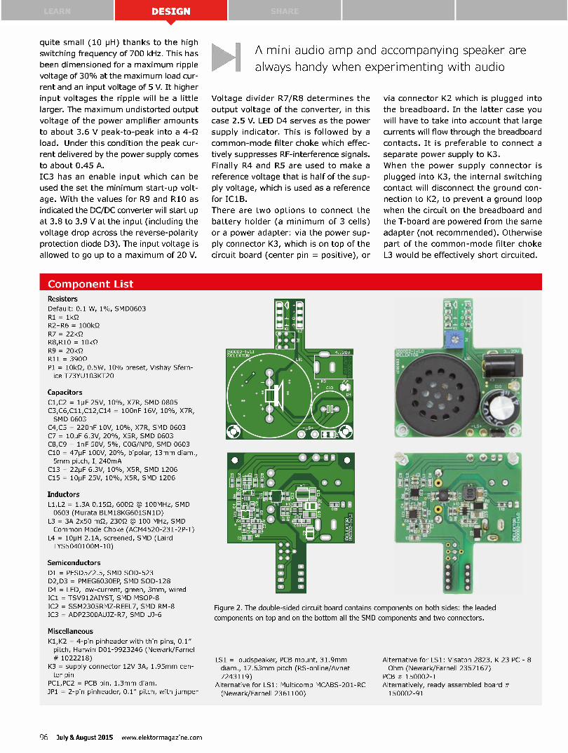
quite small (10 pH) thanks to the high
switching frequency of 700 kHz. This has
been dimensioned for a maximum ripple
voltage of 30°h at the maximum load cur-
rent and an input voltage of 5 V. It higher
input voltages the ripple will be a little
larger. The maximum undistorted output
voltage of the power amplifier amounts
to about 3.6 V peak-to-peak into a 4-S2
load. Under this condition the peak cur-
rent delivered by the power supply comes
to about 0.45 A.
IC3 has an enable input which can be
used the set the minimum start-up volt-
age. With the values for R9 and R10 as
indicated the DC/DC converter will start up
at 3.8 to 3.9 V at the input (including the
voltage drop across the reverse-polarity
protection diode D3). The input voltage is
allowed to go up to a maximum of 20 V.
A mini audio amp and accompanying speaker are
always handy when experimenting with audio
Voltage divider R7/R8 determines the
output voltage of the converter, in this
case 2.5 V. LED D4 serves as the power
supply indicator. This is followed by a
common-mode filter choke which effec-
tively suppresses RF-interference signals.
Finally R4 and R5 are used to make a
reference voltage that is half of the sup-
ply voltage, which is used as a reference
for IC1B.
There are two options to connect the
battery holder (a minimum of 3 cells)
or a power adapter: via the power sup-
ply connector K3, which is on top of the
circuit board (center pin = positive), or
via connector K2 which is plugged into
the breadboard. In the latter case you
will have to take into account that large
currents will flow through the breadboard
contacts. It is preferable to connect a
separate power supply to K3.
When the power supply connector is
plugged into K3, the internal switching
contact will disconnect the ground con-
nection to K2, to prevent a ground loop
when the circuit on the breadboard and
the T-board are powered from the same
adapter (not recommended). Otherwise
part of the common-mode filter choke
L3 would be effectively short circuited.
Corn sonent List Resistors Default: 0.1 W, 1%, SMD0603
R1 = lkS2 R2-R6 = 100kS2
R7 = 22kS2 R8,R10 = 10kS2
R9 = 20kS2 Rll = 390Q
P1 = 10kS2, 0.5W, 10% preset, Vishay Sfern-ice T73YU103KT20
Capacitors Cl,C2 = 1pF 25V, 10%, X7R, SMD 0805 C3,C6,C11,C12,C14 = 100nF 16V, 10%, X7R,
SMD 0603 C4,C5 = 220nF 10V, 10%, X7R, SMD 0603
C7 = 10pF 6.3V, 20%, X5R, SMD 0603 C8,C9 = 1nF 50V, 5%, COG/NPO, SMD 0603
C10 = 47pF 100V, 20%, bipolar, 13mm diam., 5mm pitch, Ir 240mA
C13 = 22pF 6.3V, 10%, X5R, SMD 1206 C15 = 10pF 25V, 10%, X5R, SMD 1206
Inductors Ll,L2 = 1.3A 0.15Q, 600Q @ 100MHz, SMD 0603 (Murata BLM18KG601SN1D)
L3 = 3A 2x50 mQ, 230Q @ 100 MHz, SMD Common Mode Choke (ACM4520-231-2P-T)
L4 = 10pH 2.1A, screened, SMD (Laird TYS5040100M-10)
Semiconductors D1 = PESD5Z2.5, SMD SOD-523 D2,D3 = PMEG6030EP, SMD SOD-128
D4 = LED, low-current, green, 3mm, wired IC1 = TSV912AIYST, SMD MSOP-8
IC2 = SSM2305RMZ-REEL7, SMD RM-8 IC3 = ADP2300AU3Z-R7, SMD U3-6
Miscellaneous Kl,K2 = 4-pin pinheader with thin pins, 0.1" pitch, Harwin D01-9923246 (Newark/Farnell
# 1022218) K3 = supply connector 12V 3A, 1.95mm cen-
ter pin PC1,PC2 = PCB pin, 1.3mm diam.
3P1 = 2-pin pinheader, 0.1" pitch, with jumper
Figure 2. The double-sided circuit board contains components on both sides: the leaded components on top and on the bottom all the SMD components and two connectors.
[Si = loudspeaker, PCB mount, 31.9mm diam., 17.53mm pitch (RS-online/Avnet
7243119) Alternative for LS1: Multicomp MCABS-201-RC
(Newark/Farnell 2361100)
Alternative for LS1: Visaton 2823, K 23 PC - 8 Ohm (Newark/Farnell 2357167)
PCB # 150002-1 Alternatively, ready assembled board #
150002-91
96 July 8f August 2015 www.elektormagazine.com
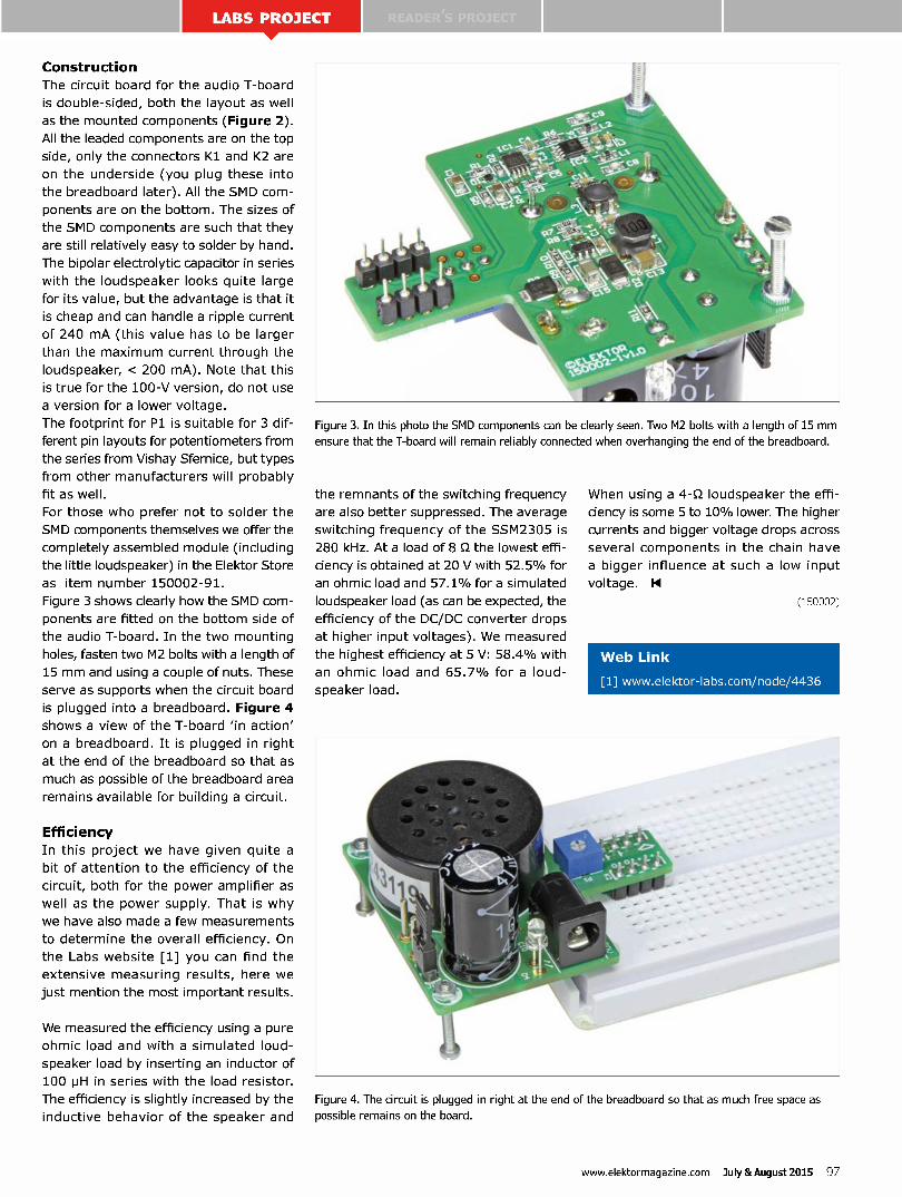
Construction
The circuit board for the audio T-board
is double-sided, both the layout as well
as the mounted components (Figure 2).
All the leaded components are on the top
side, only the connectors K1 and K2 are
on the underside (you plug these into
the breadboard later). All the SMD com-
ponents are on the bottom. The sizes of
the SMD components are such that they
are still relatively easy to solder by hand.
The bipolar electrolytic capacitor in series
with the loudspeaker looks quite large
for its value, but the advantage is that it
is cheap and can handle a ripple current
of 240 mA (this value has to be larger
than the maximum current through the
loudspeaker, < 200 mA). Note that this
is true for the 100-V version, do not use
a version for a lower voltage.
The footprint for P1 is suitable for 3 dif-
ferent pin layouts for potentiometers from
the series from Vishay Sfernice, but types
from other manufacturers will probably
fit as well.
For those who prefer not to solder the
SMD components themselves we offer the
completely assembled module (including
the little loudspeaker) in the Elektor Store
as item number 150002-91.
Figure 3 shows clearly how the SMD com-
ponents are fitted on the bottom side of
the audio T-board. In the two mounting
holes, fasten two M2 bolts with a length of
15 mm and using a couple of nuts. These
serve as supports when the circuit board
is plugged into a breadboard. Figure 4
shows a view of the T-board 'in action'
on a breadboard. It is plugged in right
at the end of the breadboard so that as
much as possible of the breadboard area
remains available for building a circuit.
Efficiency
In this project we have given quite a
bit of attention to the efficiency of the
circuit, both for the power amplifier as
well as the power supply. That is why
we have also made a few measurements
to determine the overall efficiency. On
the Labs website [1] you can find the
extensive measuring results, here we
just mention the most important results.
We measured the efficiency using a pure
ohmic load and with a simulated loud-
speaker load by inserting an inductor of
100 pH in series with the load resistor.
The efficiency is slightly increased by the
inductive behavior of the speaker and
Figure 3. In this photo the SMD components can be clearly seen. Two M2 bolts with a length of 15 mm ensure that the T-board will remain reliably connected when overhanging the end of the breadboard.
the remnants of the switching frequency
are also better suppressed. The average
switching frequency of the SSM2305 is
280 kHz. At a load of 8 S2 the lowest effi-
ciency is obtained at 20 V with 52.5°h for
an ohmic load and 57.1% for a simulated
loudspeaker load (as can be expected, the
efficiency of the DC/DC converter drops
at higher input voltages). We measured
the highest efficiency at 5 V: 58.4°h with
an ohmic load and 65.7°h for a loud-
speaker load.
in right at the end of the breadboard so that as much free space as Figure 4. The circuit is plugged possible remains on the board.
When using a 4-S2 loudspeaker the effi-
ciency is some 5 to 10°h lower. The higher
currents and bigger voltage drops across
several components in the chain have
a bigger influence at such a low input
voltage. 11
(150002)
Web Link
[1] www.elektor-labs.com/node/4436
www.elektormagazine.com July &August 2015 97

SHARE
An SMD solder station made from bits and pieces!
Platinoeweilider Station
IL "Itt
7EMP
PLATINO
PiCtUa TPTIF: 3I7F
SOLDER STATION
lektor labs
By Martin Kumm (Germany), Clemens Valens (Elektor Labs)
and Sunil Malekar (Elektor Labs India)
This experimenter's solder station
is built using the Elektor
Platino Controller board
and is both compact and low-cost. It uses an RT type of solder bit from Weller which has an integrated
temperature sensor and heating element. Altogether it makes a controllable and precise solder station,
ideal for soldering SMD components and more.
As modern component packages get
ever smaller the need to work with SMDs
becomes unavoidable. It shouldn't be too
much of a problem providing you have
access to the correct tools and soldering
equipment. A really thin soldering bit fit-
ted to a standard soldering iron is often
unsatisfactory; it results in only a small
proportion of the heat actually arriving
at the soldering point. This arrangement
means that the iron can only react quite
slowly to temperature drops at the bit
during soldering.
The answer is of course to use a mod-
ern (and expensive) SMD solder station.
The irons used in some of these stations
Ke Features • Power supply: 12 to 18 V DC, 5 A
• Elektor Platino with ATmega328P microcontroller
• 16 x 2 LC-Display
• Weller RT-type solder bit with a 3.5-mm-jack connector
• 3-pole jack socket to accept the 3.5-mm-Stereo jack plug
• Temperature select range from 90 °C to 450 °C
• Temperature regulation via Platino PWM signal
• Display showing actual and setup bit temperature
• Rotary encoder to select the setup temperature
have replaceable bits that incorporate the
heating element as well as a temperature
sensor. These integrated solder bits are
consumables and are therefore relatively
inexpensive compared to the cost of the
complete station.
Pick a bit
The tool manufacturer Weller offers a
complete arsenal of different types of
replacement solder bits. The model most
interesting to hackers wanting to make
their own solder station is the RT type
used with the WXMP MS soldering set.
These bits have a useful feature that sep-
arates them from the other types: the
bit connects via a standard 3.5 mm ste-
reo jack plug (Figure 1). The three con-
tacts supply the bit temperature sensor
information and also connections to the
built-in heating element. It also incor-
98 July &August 2015 www.elektormagazine.com
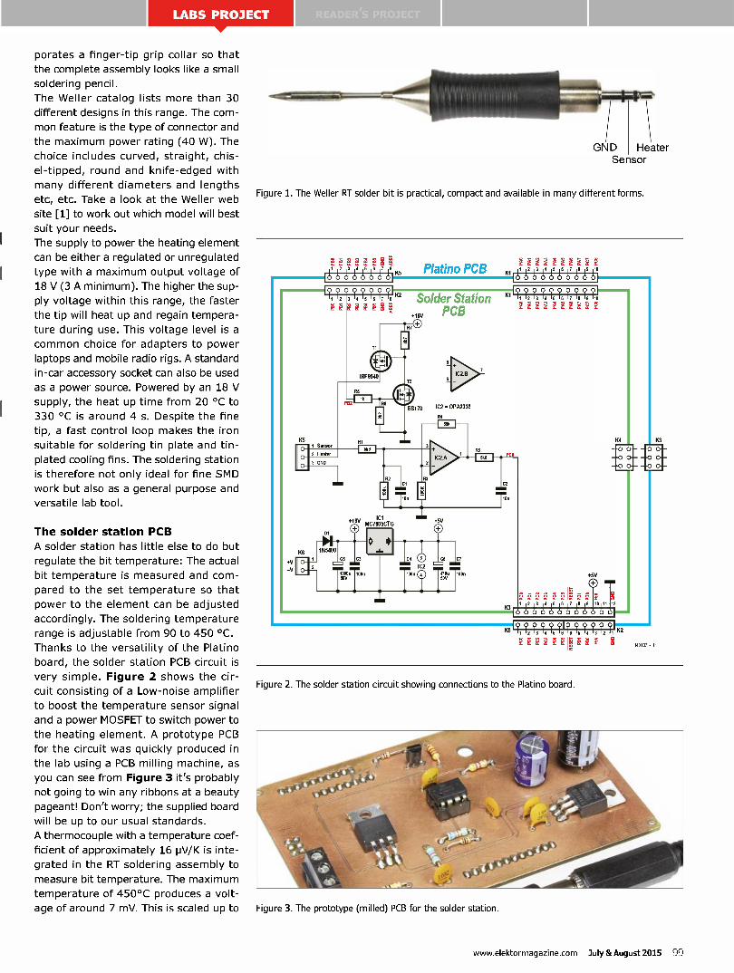
porates a finger-tip grip collar so that
the complete assembly looks like a small
soldering pencil.
The Weller catalog lists more than 30
different designs in this range. The com-
mon feature is the type of connector and
the maximum power rating (40 W). The
choice includes curved, straight, chis-
el-tipped, round and knife-edged with
many different diameters and lengths
etc, etc. Take a look at the Weller web
site [1] to work out which model will best
suit your needs.
The supply to power the heating element
can be either a regulated or unregulated
type with a maximum output voltage of
18 V (3 A minimum). The higher the sup-
ply voltage within this range, the faster
the tip will heat up and regain tempera-
ture during use. This voltage level is a
common choice for adapters to power
laptops and mobile radio rigs. A standard
in-car accessory socket can also be used
as a power source. Powered by an 18 V
supply, the heat up time from 20 °C to
330 °C is around 4 s. Despite the fine
tip, a fast control loop makes the iron
suitable for soldering tin plate and tin-
plated cooling fins. The soldering station
is therefore not only ideal for fine SMD
work but also as a general purpose and
versatile lab tool.
The solder station PCB
A solder station has little else to do but
regulate the bit temperature: The actual
bit temperature is measured and com-
pared to the set temperature so that
power to the element can be adjusted
accordingly. The soldering temperature
range is adjustable from 90 to 450 °C.
Thanks to the versatility of the Platino
board, the solder station PCB circuit is
very simple. Figure 2 shows the cir-
cuit consisting of a Low-noise amplifier
to boost the temperature sensor signal
and a power MOSFET to switch power to
the heating element. A prototype PCB
for the circuit was quickly produced in
the lab using a PCB milling machine, as
you can see from Figure 3 it's probably
not going to win any ribbons at a beauty
pageant! Don't worry; the supplied board
will be up to our usual standards.
A thermocouple with a temperature coef-
ficient of approximately 16 pV/K is inte-
grated in the RT soldering assembly to
measure bit temperature. The maximum
temperature of 450°C produces a volt-
age of around 7 mV. This is scaled up to
Figure 1. The Weller RT solder bit is practical, compact and available in many different forms.
Figure 2. The solder station circuit showing connections to the Platino board.
Figure 3. The prototype (milled) PCB for the solder station.
www.elektormagazine.com July &August 2015 99

Jumper Position
JP3 PC5
JP4 PBO
JP5 PB1
JP8 28
JP11 PB5
JP12 PB4
JP13 PB3
Semiconductors IC1 = ATmega328P-PU, programmed (Elektor Store # 140107-41)
Ti = BC547C
Component List, Platino* Resistors All 5%, 0.25W
R3 = 47S2 R4,R5,R6,R7,R10,R12 = 10kS2
Rll = 4.7kS2 P1 = 10kS2 trimpot, horizontal
Capacitors C5,C6 = 100nF, 0.2" pitch
Inductor Li = 10pH
Miscellaneous S5A = rotary encoder with integrated pushbutton
K2,K6 = 6-pin pinheader, 0.1" pitch, straight K3 = 6-way (2x3) pinheader socket, 0.1"
pitch, straight K5 = 8-way (2x3) pinheader socket, 0.1"
pitch, straight K9 = 16-way (2x3) pinheader socket, 0.1"
pitch, straight LCD1 = LCD, alphanumeric, 2x16** (Elektor
Store # 120061-74) DIP28-narrow IC socket
*See [3] for details on Platino. ** See ELPP: https://github.com/ElektorLabs/
PreferredParts
correspond to the 5 V maximum input
voltage of the AVR controller's analog
input. The opamp IC2.A performs this
signal multiplication. It's an OPA2336
which has a particularly low offset voltage
(typ. ±60 pV) and simple power supply
requirements. Resistors R4 and R3 set
the amplification factor to around 680.
Resistor R1 acts as an input current lim-
iter during the heating phase when the
full heating voltage appears at this input.
The networks formed by R1 with Cl and
R5 with C2 form low pass filters to filter
out any high frequency switching noise
spikes. The amplified and filtered sensor
Com • onent List Solder Station
Resistors All 5%, 0.25W
R1,R5 = 5.6kS2
R2 = 100kS2 R3 = 100Q
R4 = 68kS2 R6 = lkS2
R7 = 4.7kS2 R8 = 2.2kS2
Capacitors Cl,C2 = lOnF, 0.1" pitch C3,C4,C7 = 100nF, 0.2" pitch
C5 = 1000pF 50V, 0.3" pitch C6 = 470pF 50V, 0.2" pitch
Semiconductors D1 = 1N5408 Ti = IRF9540
T2 = B5170 IC1 = 7805
IC2 = OPA2336
Miscellaneous K2 = 8-pin pinheader, 0.1" pitch, straight
K3 = 12-pin pinheader, 0.1" pitch, straight
Kl,K4 = not used K5 = 3-way PCB screw terminal block, 0.2"
pitch K6 = 2-way PCB screw terminal block, 0.2"
pitch
DIP8 IC socket for IC2 Solder tip, Weller RT series [1]
3.5-mm stereo jack, cable socket Bopla case type 2616 (Newark/Farnell
127479)
100 July &August 2015 www.elektormagazine.com

voltage is output from K3-1 to PCO, an
ADC input of the Platino.
The switching signal controlling the heater
element is output from PB2 of the Platino
board which connects to connector K2-3. A
low-power N-channel MOSFET type BS170
(T2) controls the IRF9540 power MOSFET,
which can easily handle the 2.5 to 3 A
current (at a maximum voltage of 18 V)
flowing to the element. The 18 V sup-
ply voltage (which could also be 12 V or
15 V) connects to the 2-pin connector K6
on the solder station PCB. To simplify the
wiring, a 5 V regulator has been included
in design to power both the opamp and
Platino board. Connector K5 provides the
earth, heating element and sensor connec-
tions to the soldering pencil unit.
The Platino and its software
If you are not familiar with the Platino,
it's worth checking out its capabilities
described in this introductory article [3].
The amplified sensor signal connects to
the ADCO input on PCO (Pin 23) of the
Platino board where it gets converted to
a digital value. The PWM output signal
controlling power to the heating element
is produced by Timen. The PWM sig-
nal appears at the Timer output 0C1B,
connected with PB2 (Pin 16). The solder
bit setup temperature is selected using
the rotary encoder on the Platino while
the temperature values are shown on the
LCD. There are no critical timing con-
straints with this design so the control-
ler is clocked using its internal 8-MHz
oscillator.
The software for this project is written in
C and is quite straightforward. It is avail-
able as an Atmel-Studio4 project for the
ATmega328P.
At turn-on after hardware initialization a
greeting appears on the display and then
the software enters the main loop. Here
the bit temperature is read and compared
to the setup value (stored in [[PROM).
The mark/space ratio of the PWM signal
is adjusted according to whether the bit
temperature is too high or too low. The
algorithm uses a simple proportional-de-
rivative (PD) control loop. The value of
power to the heater is proportional to the
temperature difference between the actual
and setup values. The loop achieves a reg-
ulation accuracy of 3 to 4 °C.
To heat or not to heat
As long as the actual temperature of the
soldering bit is more than 5 °C below the
set temperature it is continuously sup-
plied with power. As the bit temperature
approaches the set value the power is
throttled back using pulse width modu-
lation (PWM). When the actual bit tem-
perature is above the set value (or when
a lower temperature is setup) the PWM
power signal switches off completely.
This ensures that the bit settles to the
correct temperature as quickly as possi-
ble. When the actual temperature is just
above the set temperature the PWM signal
will be modulated in increments of 1/7
(PWM=PWM-PWM/7).
To generate the PWM signal Timen1
is configured in 9-bit fast-PWM mode
together with Compare Register B. The
prescaler is set to divide by 256. This con-
figuration produces a low frequency PWM
signal that gives good temperature sta-
bility and accuracy. The PWM frequency
is calculated using:
PWM frequency = clock / (N x prescaler)
8 MHz / (512 x 256) = 62 Hz
with N = 512 for 9-bit fast PWM mode
(29 = 512)
NB: The PWM signal is turned off during
the times the temperature sensor output
is read. This is necessary because the
power signal to the heating element has
a connection with the sensor and makes
the sensor signal unreadable.
To ensure accurate measurement the
heater element signal is turned off
completely during sensor measure-
ment periods. Turning off the PWM sig-
nal directly before a measurement cycle
(OCR1B = 0), will allow some residual
noise spikes to interfere with the ADC
measurement. For this reason it's turned
off 7 ms before reading the ADC.
Sensor signals
With the temperature sensor connected,
the ADC output value at 50 °C is 67 and
at 450 °C 1020. With a temperature
range of 50 to 450 °C and an ADC range
from 67 to 1020 gives:
Table 2. The ATmega328P fuse settings.
Fuse
Low
High
Value
Oxe2
Oxd9
Extended Oxff
multiplier = (450 - 50) / (1020
- 67) = 0.419
An ADC value of 0 corresponds to a bit
temperature of around 30 °C. This indi-
cates we need to add an offset of 30 to
the formula:
temperature = temp_adc x 0.42 + 30
The driver for the rotary encoder deter-
mines its rotational information via con-
troller Pins PBO und PB1, a new set value
is entered into [[PROM when the knob
is pressed.
To save energy and prolong the solder
bit lifetime the software automatically
switches the iron to lower temperature
operation after approximately 15 minutes
use. The program doesn't know when
you are about to use the iron again so
just check the temperature on the dis-
play and press the rotary encoder switch
for full heat.
Build it, Test it... Solder-on!
The Elektor Platino PCB needs to be 'jum-
pered' in accordance with Table 1 (we
just used solder bridges). The template
shown is a useful aid here. First off you
can start mounting the components and
the LCD, next comes the rotary encoder
and the socket for the ATmega328P
microcontroller. Note that K9 (for the
LCD) and the rotary encoder at position
SSA are mounted on the other side of
the board.
Mounting all the components should not
present any problems. Connector strips
K2 and K3 are fitted from the solder side
of the board. Before soldering, plug them
into the Platino board connector strips,
this will ensure they are correctly aligned.
Web Links
[1] www.weller.de/en/Weller--Products.html?cat_id=ID151
[2] www.elektormagazine.com/140107
[3] www.elektormagazine.com/100892
[4] www.martin-kumm.de/smd_solder_station
www.elektormagazine.com July &August 2015 101
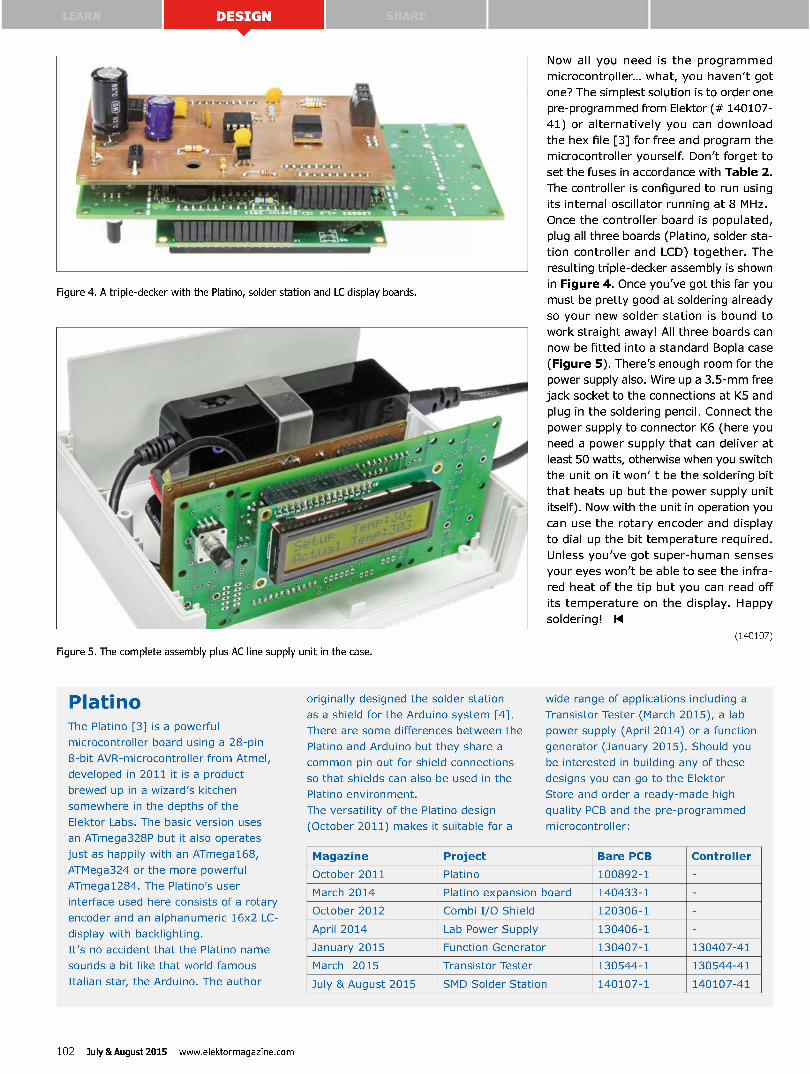
Figure 4. A triple-decker with the Platino, solder station and LC display boards.
Figure 5. The complete assembly plus AC line supply unit in the case.
Platino The Platino [3] is a powerful
microcontroller board using a 28-pin
8-bit AVR-microcontroller from Atmel,
developed in 2011 it is a product
brewed up in a wizard's kitchen
somewhere in the depths of the
Elektor Labs. The basic version uses
an ATmega328P but it also operates
just as happily with an ATmega168,
ATMega324 or the more powerful
ATmega1284. The Platino's user
interface used here consists of a rotary
encoder and an alphanumeric 16x2 LC-
display with backlighting.
It's no accident that the Platino name
sounds a bit like that world famous
Italian star, the Arduino. The author
originally designed the solder station
as a shield for the Arduino system [4].
There are some differences between the
Platino and Arduino but they share a
common pin out for shield connections
so that shields can also be used in the
Platino environment.
The versatility of the Platino design
(October 2011) makes it suitable for a
Now all you need is the programmed
microcontroller... what, you haven't got
one? The simplest solution is to order one
pre-programmed from Elektor (# 140107-
41) or alternatively you can download
the hex file [3] for free and program the
microcontroller yourself. Don't forget to
set the fuses in accordance with Table 2.
The controller is configured to run using
its internal oscillator running at 8 MHz.
Once the controller board is populated,
plug all three boards (Platino, solder sta-
tion controller and LCD) together. The
resulting triple-decker assembly is shown
in Figure 4. Once you've got this far you
must be pretty good at soldering already
so your new solder station is bound to
work straight away! All three boards can
now be fitted into a standard Bopla case
(Figure 5). There's enough room for the
power supply also. Wire up a 3.5-mm free
jack socket to the connections at K5 and
plug in the soldering pencil. Connect the
power supply to connector K6 (here you
need a power supply that can deliver at
least 50 watts, otherwise when you switch
the unit on it won' t be the soldering bit
that heats up but the power supply unit
itself). Now with the unit in operation you
can use the rotary encoder and display
to dial up the bit temperature required.
Unless you've got super-human senses
your eyes won't be able to see the infra-
red heat of the tip but you can read off
its temperature on the display. Happy
soldering! k
(140107)
wide range of applications including a
Transistor Tester (March 2015), a lab
power supply (April 2014) or a function
generator (January 2015). Should you
be interested in building any of these
designs you can go to the Elektor
Store and order a ready-made high
quality PCB and the pre-programmed
microcontroller:
Magazine Project Bare PCB Controller
October 2011 Platino 100892-1 -
March 2014 Platino expansion board 140433-1 -
October 2012 Combi I/O Shield 120306-1 -
April 2014 Lab Power Supply 130406-1 -
January 2015 Function Generator 130407-1 130407-41
March 2015 Transistor Tester 130544-1 130544-41
July & August 2015 SMD Solder Station 140107-1 140107-41
102 July & August 2015 www.elektormagazine.com
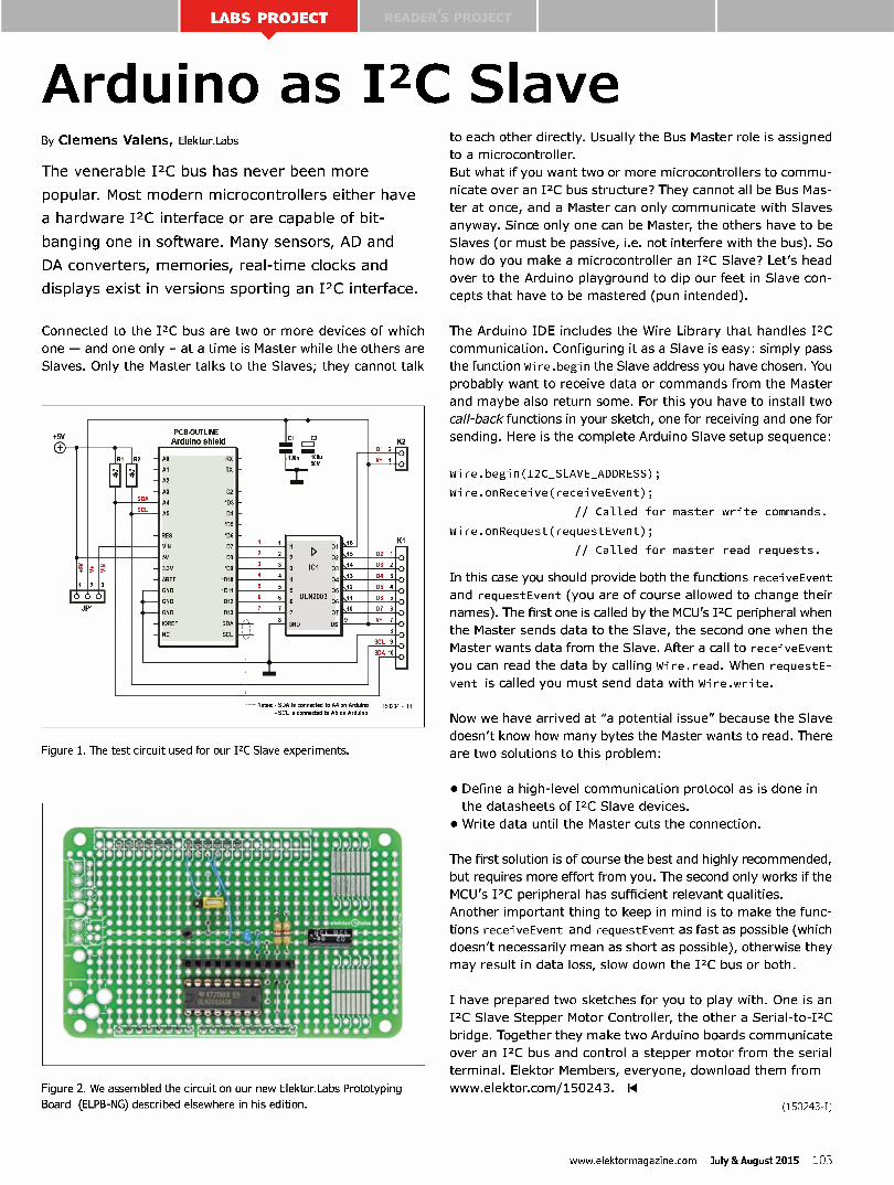
Arduino as I2C Slave By Clemens Valens, Elektor.Labs
The venerable I2C bus has never been more
popular. Most modern microcontrollers either have
a hardware I2C interface or are capable of bit-
banging one in software. Many sensors, AD and
DA converters, memories, real-time clocks and
displays exist in versions sporting an I2C interface.
Connected to the I2C bus are two or more devices of which
one — and one only - at a time is Master while the others are
Slaves. Only the Master talks to the Slaves; they cannot talk
.5V
R2
SDA
Kmeure Arduino shield
2
MC 13
JP1
AO RX
Al TX
A2
A3 D2
A4 'D3
5 D4
— RES
VIN
5V
— 3.3V
— AREF
GND
GND
GND
— IOREF
— NC
'D5
'D6
D7
DB
'D9
'DIO
DII
D12
D1
SDA
SCL *'5
15
16
17
I 00n I 10th,
50V
°o12
13 ICI 03
14 04
15 05 16 ULN2003 06
7 17 07
GND DS
,15
,14
,12
jI
o 2 K2
02 1
03 2
04 3
05 4
06 5
07 6
SCL
SDA 10
K1
[--- Notes: - SDA i connected to A4 on Arduino 150234 - 11 - SCL is connected to AS on Arduino
Figure 1. The test circuit used for our I2C Slave experiments.
Figure 2. We assembled the circuit on our new Elektor.Labs Prototyping Board (ELPB-NG) described elsewhere in his edition.
ifee4 '
q r- : : : : : : : 6 6 e • :_ e e,,e II 545 /5 à ee
r— i ;
to each other directly. Usually the Bus Master role is assigned
to a microcontroller.
But what if you want two or more microcontrollers to commu-
nicate over an I2C bus structure? They cannot all be Bus Mas-
ter at once, and a Master can only communicate with Slaves
anyway. Since only one can be Master, the others have to be
Slaves (or must be passive, i.e. not interfere with the bus). So
how do you make a microcontroller an I2C Slave? Let's head
over to the Arduino playground to dip our feet in Slave con-
cepts that have to be mastered (pun intended).
The Arduino IDE includes the Wire Library that handles I2C
communication. Configuring it as a Slave is easy: simply pass
the function Wi re. begi n the Slave address you have chosen. You
probably want to receive data or commands from the Master
and maybe also return some. For this you have to install two
call-back functions in your sketch, one for receiving and one for
sending. Here is the complete Arduino Slave setup sequence:
Wire.begin(I2C_SLAVE_ADDRESS);
Wire.onReceive(receiveEvent);
// Called for
Wire.onRequest(requestEvent);
// Called for
master
master
write commands.
read requests.
In this case you should provide both the functions receiveEvent
and requestEvent (you are of course allowed to change their
names). The first one is called by the MCU's I2C peripheral when
the Master sends data to the Slave, the second one when the
Master wants data from the Slave. After a call to receiveEvent
you can read the data by calling Wi re. read. When requestE-
vent is called you must send data with Wire.write.
Now we have arrived at "a potential issue" because the Slave
doesn't know how many bytes the Master wants to read. There
are two solutions to this problem:
• Define a high-level communication protocol as is done in
the datasheets of I2C Slave devices.
• Write data until the Master cuts the connection.
The first solution is of course the best and highly recommended,
but requires more effort from you. The second only works if the
MCU's I2C peripheral has sufficient relevant qualities.
Another important thing to keep in mind is to make the func-
tions receiveEvent and requestEvent as fast as possible (which
doesn't necessarily mean as short as possible), otherwise they
may result in data loss, slow down the I2C bus or both.
I have prepared two sketches for you to play with. One is an
I2C Slave Stepper Motor Controller, the other a Serial-to-I 2C
bridge. Together they make two Arduino boards communicate
over an I2C bus and control a stepper motor from the serial
terminal. Elektor Members, everyone, download them from
www.elektor.com/150243. li
(150243-I)
www.elektormagazine.com July &August 2015 103
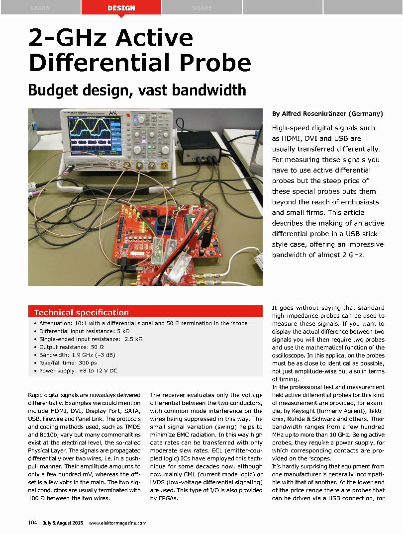
2-GHz Active Differential Probe Budget design, vast bandwidth
Technical s ecification • Attenuation: 10:1 with a differential signal and 50 52 termination in the 'scope
• Differential input resistance: 5 k5-2
• Single-ended input resistance: 2.5 k5-2
• Output resistance: 50 52
• Bandwidth: 1.9 GHz (-3 dB)
• Rise/fall time: 300 ps
• Power supply: ±8 to 12 V DC
Rapid digital signals are nowadays delivered
differentially. Examples we could mention
include HDMI, DVI, Display Port, SATA,
USB, Firewire and Panel Link. The protocols
and coding methods used, such as TMDS
and 8b10b, vary but many commonalities
exist at the electrical level, the so-called
Physical Layer. The signals are propagated
differentially over two wires, i.e. in a push-
pull manner. Their amplitude amounts to
only a few hundred mV, whereas the off-
set is a few volts in the main. The two sig-
nal conductors are usually terminated with
100 5-2 between the two wires.
The receiver evaluates only the voltage
differential between the two conductors,
with common-mode interference on the
wires being suppressed in this way. The
small signal variation (swing) helps to
minimize EMC radiation. In this way high
data rates can be transferred with only
moderate slew rates. ECL (emitter-cou-
pled logic) ICs have employed this tech-
nique for some decades now, although
now mainly CML (current mode logic) or
LVDS (low-voltage differential signaling)
are used. This type of I/O is also provided
by FPGAs.
By Alfred Rosenkrânzer (Germany)
High-speed digital signals such
as HDMI, DVI and USB are
usually transferred differentially.
For measuring these signals you
have to use active differential
probes but the steep price of
these special probes puts them
beyond the reach of enthusiasts
and small firms. This article
describes the making of an active
differential probe in a USB stick-
style case, offering an impressive
bandwidth of almost 2 GHz.
It goes without saying that standard
high-impedance probes can be used to
measure these signals. If you want to
display the actual difference between two
signals you will then require two probes
and use the mathematical function of the
oscilloscope. In this application the probes
must be as close to identical as possible,
not just amplitude-wise but also in terms
of timing.
In the professional test and measurement
field active differential probes for this kind
of measurement are provided, for exam-
ple, by Keysight (formerly Agilent), Tektr-
onix, Rohde &Schwarz and others. Their
bandwidth ranges from a few hundred
MHz up to more than 10 GHz. Being active
probes, they require a power supply, for
which corresponding contacts are pro-
vided on the 'scopes.
It's hardly surprising that equipment from
one manufacturer is generally incompati-
ble with that of another. At the lower end
of the price range there are probes that
can be driven via a USB connection, for
104 July & August 2015 www.elektormagazine.com
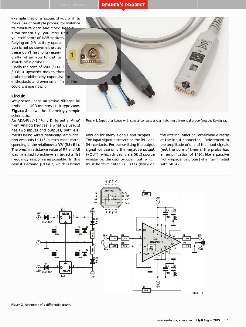
READER'S PROJECT
example that of a 'scope. If you wish to
make use of multiple probes, for instance
to measure data and clock signals
simultaneously, you may find
yourself short of USB sockets.
Relying on 9-V battery opera-
tion is not so clever either, as
these don't last long (espe- I
cially when you forget to I,
switch off a probe).
Finally the price of $900 / £600
/ €800 upwards makes these
probes prohibitively expensive for
enthusiasts and even small firms. This
could change now...
Circuit
We present here an active differential
probe in a USB memory stick-type case.
Figure 2 shows the disarmingly simple
schematic.
An ADA4927-1 'Fully Differential Amp'
from Analog Devices is what we use. It
has two inputs and outputs, both ele-
ments being wired identically. Amplifica-
tion amounts to 1/5 in each case, corre-
sponding to the relationship R7/ (R3+R4).
The precise resistance value of R7 and R8
was selected to achieve as broad a flat
frequency response as possible. In this
case it's around 1.9 GHz, which is broad
Figure 1. Input of a 'scope with special contacts and a matching differential probe (source: Keysight).
enough for many signals and 'scopes.
The input signal is present on the IN+ and
IN- contacts. For transmitting the output
signal we use only the negative output
(-OUT), which drives, via a 50 5-2 source
resistance, the oscilloscope input, which
must be terminated in 50 5-2 (ideally on
the internal function, otherwise directly
at the input connector). Referenced to
the amplitude of one of the input signals
(not the sum of them), the probe has
an amplification of 1/10, like a passive
high-impedance probe (when terminated
with 50 S2).
Figure 2. Schematic of a differential probe.
www.elektormagazine.com July &August 2015 105

Figure 3. Completed probe in a transparent USB case.
G13 0 +. ale 4) _ice IC3 kiik: Ami lip.à er,-.7,.e..../ -' M il", :,-;;;" :2411991]Ps keifflub
Ii-; euer-1--1. __ e'l m -ate ' -- -. --1 co lb 4. r4 • Aih. @.1111q; = a lied -, • +51‘ 41----5U- -d -
.Mej .-11" R6 en] C5 .0
The differential input impedance lies
around 4.6 kg-2. This appears very low
compared with a passive probe. How-
ever, high-speed signals are of very low
impedance (100 5-2), so we can get away
with this.
The unused output of the IC is taken to
TRI 3VA6
Out
ground via 100 5-2, in order to guarantee
a symmetrical load.
The IC has a V_OCM input, with which
you can equalize the offset of the IC.
Here, however, we shall refrain, as off-
set is compensated at the 'scope end.
Accordingly, we connect the pin to GND.
IC1
130538 - 12
L1
The shutdown input is connected to the
positive supply voltage and thus the IC
remains always active.
The IC has a so-called exposed pad (EP)
on its underside and this must be con-
nected to GND. Both supply voltages of
L1
C18 C6 L8 SD12K100
D1
8V2 D2
LED3 X
1N4004
V
C19 C7
22u 16V
L3
C22 C20
72u On 6V
C23 C21
nu 100n L4 16V
K3
L5
C26 C24
I C2u On 16V
27 C25
nu 100n L6 16V
K4
L7
C30 C28
7 12u I On 6V
C31 C29
22. 100n L8 16V
K1
K2
Figure 4. Schematic of benchtop PSU for powering probes.
106 July & August 2015 www.elektormagazine.com
READER'S PROJECT
IW Professional-quality differential probes are too expensive for enthusiasts and small firms
±5 V are blocked (decoupled) with two
capacitors to GND. They are produced
using two regular linear regulators, IC1
and IC2. D1 and D3 protect against
reverse polarity of the supply voltages.
D2 and D4 prevent the voltage regulator
from latching up should one voltage be
applied earlier than the other. Two LEDs
indicate readiness for operation.
Utterly simple though the circuit may be,
laying it out correctly is highly critical for
achieving the desired function.
The author uses a 4-layer board. The
top layer contains the signal connec-
tions, whilst the next layer is a continu-
ous ground plane acting as a reference
point. The two remaining layers serve for
the power supply. As mentioned earlier,
the IC has an exposed pad on its under-
side, as it must be connected to ground.
Since this is not easy for hobbyists to sol-
der, the author offers a fully assembled
and tested PC board.
The IC has two pairs of outputs. The links
located right next to the inputs (+ FB;
-FB) are used on R7 and R8 to close the
gain loop. The other two on the right
are used as outputs. The connections of
the two supply voltages above and below
are decoupled to ground as close as pos-
sible using two capacitors. Several vias
are used for both the supply voltage and
ground plane in order to keep inductance
as low as possible.
Mechanical matters
The PCB for the probe fits inside a trans-
parent USB case (Figure 3). The coax
cable with the BNC connector has its inner
conductor soldered to the Out pad and
the screen to the pad on the right of this.
The adjacent openings are to make it easy
to fix the co-ax using cable ties. At the
solder pads +9V, -9V and GND we sol-
der the power supply lead. After placing
the PCB in the case, we insert a 3-pin
stud connector into the openings on the
front side, after first removing the center
pin, and make solder connections to In +
and -. Into this 'receptacle' we insert the
counterparts onto which we can solder
short, thin wires to which in turn the sig-
nal wires are connected. This enables us
to mount the receptacle first and plug in
the probe later, so that you can switch
between several signals. If the receptacle
becomes worn out you can construct a
new one. Holding probes with two inputs
is rather impractical...
If you own several probes, you should
take care that the lengths of co-ax cable
used are identical. In this way you avoid
variations in transit time between probes
and possible false readings. Any residual
balancing can be compensated on most
'scopes (skew adjust).
For measurements of differential signals
the offset common to both signals is sup-
pressed, only the difference being dis-
played. If you want to measure the offset,
you can use a high-impedance probe or
ground one of the two inputs. You should,
however, pay attention to the relatively
low input resistance.
Power supply
Power supply for the probes can be pro-
vided from a laboratory power supply of
> ± 8V. The operation of a single probe
like this is straightforward but with sev-
eral probes in use the wiring becomes
a bit trickier and somewhat confusing.
Therefore, a suitable bench-top power
supply has been developed (Figure 4),
which can serve up to four probes cor-
responding to the four inputs maximum
of an oscilloscope. The connector device
selected is a 3-pin mini-DIN plug. This
prevents mismatching. The four outputs
have comprehensive internal filtering,
in order to minimize crosstalk from one
probe to another.
The power pack consists of a transformer
with two secondary windings, rectifiers,
capacitors and two linear regulators,
including the usual decoupling capacitors.
Two LEDs indicate operation of the two
internally isolated voltages, with a third
in the front panel showing that both volt-
ages are present (thanks to a zener diode
in series with the LED). Two diodes pre-
vent damage caused by reversed polar-
ity, which might be applied accidentally
to the output.
Both voltages are filtered with chokes and
capacitors before they reach the output
connector.
Sum ming up
For a relatively modest outlay you can
construct at home an active differential
probe with very high specifications (see
Figures 5 and 6), for a fraction of the
price of comparable commercial products.
It is of course necessary to use high-qual-
ity components as well as a well thought-
out PCB layout.
For readers who are interested the author
offers ready-to-use and tested PCB mod-
ules, also a kit consisting of case, RF cable
with BNC connector and power supply
lead with plug. Further information from:
(130538)
Figure 5. Frequency curve for the probe up to 3 GHz. The -3 dB point is located around 1.9 GHz.
0 Eitili M ég"
('-''''' I u I
te .
--, \
la Cilia '
e,
7
ri
Figure 6. Measuring a 300-MHz clock signal with a 2-GHz 'scope.
www.elektormagazine.com July &August 2015 107

C. welcome in your 4
p) I Ée] ze
-Lel : MI (.1 =
ONLINE STORE It's time for the fourth annual
Elektor Summer Sale. All
Summer long we will focus
on having all the best
deals for electronics
enthusiasts, especially
our members!
With the 2015 edition
of this annual
phenomenon fast
approaching, we aim to once again exceed
expectations. So kicking off on July 1st in
cooperation with our supplier Matrix, specifically for Elektor and for two weeks only, we
are offering a 50% discount off the entire Flowcode line!
Besides the usual classic deals, such as three for the price of two, some new and
surprising actions and offers will make your regular visits to our stores much more
exciting during the summer months!
Nowhere has more activity during summer than your Elektor Stores!
www.eleldor.comisummersale
Clemens Valens, Elektor Labs
Raspberry Pi Advanced Programming
Raspberry PI.
Pine,
IQ, work • Salptg,
Van,.
elektor Doyen Iblahrn
This book is about advanced programming of the Raspberry Pi computer using the Python programming language. The book explains in simple terms and with examples: how to configure the Raspberry Pi computer; how to install and use the Linux operating system and the desktop; how to write advanced programs using the Python programming language; how to use graphics in our programs and how to develop hardware based projects using the Raspberry Pi.
«Ne member price: £29.95 • €40.46 • US $46.00
Juntinait claab
Microcontroller Based Radio Telemetry Projects
This book is written for people who want to learn more about radio telemetry applications and microcontroller programming using the PIC18F series of microcontrollers. The design of a radio telemetry based mini weather station is considered as an example system in the book where the developed system can measure the temperature, humidity, atmospheric pressure, carbon monoxide level, nitrogen dioxide concentration, air quality level, wind direction wind speed and more.
member price: £26.95 • €35.96 • US $41.00
Elektor Bestsellers 1. GREEN Membership www.elektor.com/green-membership
2. Intel Edison Book www.elektor.com/edison-book
3. Arduino Sensor Kit www.elektor.com/arduino-sensor-kit
4. BL600 e-BoB www.elektor.com/bI600-e-bob
5. DVD Elektor 1980 through 1989 www.elektor.com/eighties
6. Mastering Microcontrollers www.elektor.com/mm-revised
7. BEEP Logic Probe www.elektor.com/beep
8. DVD Elektor 2014 www.elektor.com/dvd-2014
T-Board Audio Amplifier
The Elektor Stores welcome the first Analog edition to our ever growing family of T-Boards! We asked ourselves, what could be a useful circuit when experimenting with an analog design? Our first thought was audio. How about a little amplifier and speaker so no extra cables or 3,5 mm jacks need to be connected. Also no extra speaker has to be connected, all you need is on one little PCB. But to be honest, it's not really a T anymore... or is it?
-\e member price: £11.95 • €16.16 • US $19.00
www.eleldor.comirpi-book www.eleldor.comiradio-telemetry www.eleldor.comit-board-audio
108 July & August 2015 www.elektor-magazine.com

BOOKS CD/DVD DIY PROJECTS DEVELOPMENT TOOLS SALE
Projects Book = Great Price e Piccolino is a prototyping platform for building and
testing PIC microcontroller projects. All basic components
are on-board, and the pinheaders make it easy to add
additional parts. You can also connect expansion boards
to the headers. If you use specific components on a
regular basis you can simply design your own expansion
board. If you add headers on that board, multiple add-
on boards can be stacked onto one Piccolino. Without a
heatsink on its on-board voltage regulator, Piccolino can
about 100 mA to the headers.
Bert van Dam's book Piccolino — 30
Prcjects, Mods, Hacks and Extension
Boards contains 30 projects based on
the Piccolino. The clear descriptions along
ith circuit diagrams and photos will make
e building of these projects an enjoyable
perience!
1:1 1 > MEMBER PRICE: £44.47 • €60.67 • US $68.85
www.elektor.com/piccolino-bundle
Piccolino Bundle Limited time offer for GREEN and GOLD members: 19% Discount plus free shipping!
OBD USB KKL Diagnose-interface Suitable for OBD and OBD-2 vehicle diagnostics via K- and L-line on cars (12 V)!
Red Pitaya Open-source measurement and control tool at a great price!
The Three Fives Discrete 555 Timer Kit
The Bottle Builder Crazyflie 2.0 Combo Kit
This kit is a faithful and functional transistor-scale replica of the classic NE555 timer integrated circuit, one of the most classic, popular and all-round useful chips of all time. The kit is designed to resemble an integrated circuit, based around an extra-thick matte-finish printed circuit board. The stand is made of formed semi-rigid PVC foam which gives the circuit board eight legs in the shape of DIP-packaged integrated circuit pins.
-Ne member price: £26.95 • €35.96 • US $41.00
This massive compendium of tube amplifier designs presents an impressive gallery of tube amplifier projects described not just with a personal stance, but also humor, an open mind, good anecdotes, and an equally good emphasis on all the technical aspects of design and implementation. With every project, the focus is on what makes a particular amplifier "special" in terms of design or performance, which as we all know are not necessarily in agreement.
-Ne member price: £52.95 • €71.96 • US $81.00
Be amazed with the performance of this solderless Crazyflie 2.0 Kit! Our Crazyflie Nanocopter Combo Kit includes the crazy-cool LED Ring and the Crazyradio PA module! The Crazyflie 2.0 is a versatile flying development platform that only weighs 27g and fits in the palm of your hand. It's advanced functionalities make it ideal for developers and the Bluetooth LE capabilities make it easy to control using mobile, bluetooth enabled devices.
-Ne member price: £162.95 • €224.96 • US $252.00
www.eleldor.com/555-discrete-timer www.eleldor.com/bottle-builder www.eleldor.comicrazyffie-combo-kit
www.elektor-magazine.com July &August 2015 109

www.elektor.com
:14'à il 4TATE•la El ULYJ [s] ii: BY MARCEL ÊLOVEÓK0
Are you a newbie in the exciting world of (digital) electronics? Have you ever wondered what a microcontroller
is and what can be done with this mighty little chip? If you answered "yes", then this is one of the best
books for you. For me, as the owner of a first edition of this book, it was a really inspiring and eye-opening
experience. I had some previous experience with Arduino (and Atmel AVR chips in general), but it was usually
quite frustrating as there was no useful introductory book available. Until the day I got my hands on this
book, and everything changed. The book is masterfully written and I have really enjoyed the author's sense
of humor. After an introduction into the realm of Arduino (and microcontrollers in general) the author takes
us on an exciting tour of basic and more advanced features of microcontrollers (digital input and output,
A/D converter, interrupts). However, the microcontroller often needs to
communicate with various sensors and/or other microcontrollers. But "
don't worry: the secrets of several communication protocols (serial, SPI,
I2C, etc.) are revealed as well. All of this is accompanied with working program examples and
complete program listings.
I highly recommend this amazing book!
Read this review and more about this product at
www.eleldor.comimm-revised
Submit a review of your favorite Elektor product and qualify to win a €100 voucher for
redeeming in the Elektor Store.
For further information, please visit tte.
LLI WILLI W LLU 00000; 000001 Ci Li eeeee 0 0 0 0 0 J J IL LILL LL LL
50% OFF ALL
FLOVICODE SOFTWARE
VALID FR O M JULY 1ST UNTIL JULY 17TH
W W W.ELEKT OR.CO M/FLO WCODE
110 July & August 2015 www.elektor-magazine.com

BOOKS CD/DVD DIY PROJECTS DEVELOPMENT TOOLS SALE
OBD USB KKL Diagnose-interface
New in the Elektor Stores the K2L901 OBD USB KKL Diagnose-interface at a very
interesting price. Features a very s
transparent connector housing with
OBD-2 connector with gold-plated p
contacts. The cable outlet can be
rotated by 180 ° (by opening
the case) and three LEDs: USB
voltage, data send, receive data
are installed so that they can
always easily be seen, no matter
how the OBD connector has to
be plugged in. With the K2L901
diagnostic interface you can quickly
get into the vehicle diagnostics. It is simply
plugged into the OBD II connector in the car and
connected to the USB port of your computer. Functions available
based on what diagnostic software you install on your computer.
1.1. MEMBER PRICE: £11.95 • €16.16 • US $19.00
www.elektor.com/obd-usb-interface
Vanderveen Trans Tube Amplifiers
, :4
TRANS TUBE AMPLIFIERS
In this book Menno van der Veen describes one of his research projects focusing on the question of whether full compensation for distortion in tubes and output transformers is possible. A variety of methods have been developed with the aim of attaining this goal. One of them has largely been forgotten: transconductance, which means converting current into voltage or voltage into current. Menno van der Veen has breathed new life into this method.
member price: £21.95 • €26.96 • US $31.00
www.eleldor.comitransie
Mystery Product
We dare you ...
r
Piccolino Bundle Limited time offer for GREEN and GOLD members: 19% Discount plus free shipping!
OBD USB KKL Diagnose-interface Suitable for OBD and OBD-2 vehicle diagnostics via K- and L-line on cars (12 V)!
Red Pitaya Open-source measurement and control tool at a great price!
Tinkerforge Master Brick 2.1
ATSAM3S4C AU
14341 A
01011.1
New in the Elektor Store: Tinkerforge acclaimed Bricks and Bricklets! This Master Brick has four Bricklet ports and therefore is ideally suited for applications where many sensor Bricklets (also found in our Store) are being used. These can be directly controlled over the USB interface of the Master Brick. This way USB sensors, like temperature or humidity sensors, or USB actors like relays, can be created according to your individual needs.
member price: £21.95 • €26.96 • US $31.00
www.eleldor.comitinkerforge
www.elektor-magazine.com July &August 2015 111

www.elektoncom
:14•LoUn11:1111
eX 1E--1:ColJà4:U
* Il i, b. (SI tj, tis
Linear Audio 9
www.elektor.com/la9
NFC Gateway BoB www.elektor.com/nfc-bob
tibo Robot Kit
www.elektor.com/tibo
Raspberry Pi 2 Model B
www.elektor.com/rpi-2
GOLD Membership
www.elektor.com/gold
32B Synthesizer
www.elektor.com/j2b
Advanced Control Robotics
www.elektor.com/
robotics-book
Arduino Tutorial Kit
www.elektor.com/atk
Elektor Labs Ruler www.elektor.com/ruler
e ektor post: DON'T MISS OUT! Elektor. LABS
If You're Gonna DIY... DIY Electric
cr, re all Vie regc, be whet about clecoic kact.?.ket take a vavéleew motor and you're ready to burn rubber. Thts project Is stet In la early stages but If ,51.1 . el. why not help, Pre you, Idea, dpi and 'weer, and 1,4, had tan,
a, a Tr,la (okay, okay, man. or In,11._
(si Anal Tit OVU M .•.•
TechTheFuture
"
EWS
Ultra Low Power Wireless loT Platform TEXAS Instruments has announced the new SimpleLink ultra-low power
wireless MCU platform. The platform has been dmigned W use so little
energy e can be powered from harvested energy or will run for years on a coin cell. For versattlIty the platform supports multiple ,dreless
connectivity...
Continue reading__
OTA hits vacuu m: pre-order VanderVeen Trans Tube
Amplifier.; book Mentioning OT A mako engineers' faces brighten with fond memories of
the eon, days of the transconductance amplifier, a famous and widely
praised btt ot IC technology from the 1970s.
Continue reading...
Thu IBM, %once° and ARM loi Starter Kit The board is an upgrade tnom 01e preeous version which used a Cortex-
M3 processor running at 96 mell wIth 31 NB of RAM and 512 NB of flash
C11111.1,111ligAiklil ..r.•
Sal. 12C, ADC, DAC. PWM,I)ORT and GPI05.
Continue reading...
Over 100,000 people worldwide already receive our free Elektor.POST
newsletter in their inbox every Friday. It is packed full of the latest news
items, tips and trends from the world of electronics. If you do not already
have a .POST membership, sign up now and receive these extras:
• An exclusive free Elektor project worth €2.50 (£2.95 / US $4.00) every
second week
a Special offers in the Elektor Store
• A free Ebooks Inspiration Bundle valued at €32.95 (£28.95 / US $45.00)
REGISTEK TODAY, IT'S FREE
www.elektor.com/newsletter
Getting Started with the Intel Edison DVD Elektor 1980 through 1989 XMBC Mediaplayer including RPi 2B
atl t.
INTEL EDISON AND THE AR NI M BREAKOUT WARD
, „..
This book is a must have for all those with an active interest in the Internet of Things. 'Getting Started with the Intel Edison' focuses its attention on the Edison, a tiny computer, the size of a postage stamp, with a lot of power and built-in wireless communication capabilities. In 128 pages, renowned author Bert van Dam helps readers get up to speed with the Edison by making it accessible and easy to use. Explore the wonderful world of the Intel Edison now!
member price: £21.95 • €26.96 • US $31.00
Since 1975, Elektor magazine has been in the forefront of electronics and computer technology through the publication of repeatable, professionally designed circuits and projects. This dual-layer DVD-ROM contains all articles published in Elektor 's year volumes 1980 through 1989. The 2100+ articles are ordered chronologically by release date and arranged in alphabetical order. A global index allows you to search specific content across the whole DVD.
member price: £44.95 • €62.10 • US $70.00
After many, many... many requests, we finally gave in. But when we do it, we do it well! That's why the Elektor Store proudly presents her XMBC Mediaplayer based upon the new Raspberry Pi 2 B. It includes an HDMi cable, a 5V/2A microUSB charger and an 8 GB (class 10) Micro-SD. You can control it with your smartphone and it supports all protocols you'd expect to fully enjoy on your personal music, photo or movie collection. A complete plug 8, play mediacenter!
-\e member price: £45.95 • €62.96 • US $71.00
www.elektor.comiedison-book www.elektor.com/eighties www.elektor.comirpi-mediaplayer
112 July & August 2015 www.elektor-magazine.com

BOOKS CD/DVD DIY PROJECTS DEVELOPMENT TOOLS SALE
Red Pitaya Red Pitaya, the open source measurement
and control tool at the size of a credit card
can replace many expensive laboratory
measurement instruments. The Red Pitaya
unit is a network attached device based
on the Linux operating system. It includes
Radio Frequency signal acquisition and
generation technologies, FPGA, Digital
Signal Processing and CPU processing.
The Red Pitaya unit is equipped with
a Micro USB socket used for console
connection, a microSD slot, a R345 socket
for Ethernet connection and a USB socket
used for standard USB devices. This high
performance hardware now comes at a
totally surprising price tag.
1:I E > MEMBER PRICE: £155.95 • €215.10 • US $241.00
www.elektor.com/red-pitaya-instrument
Piccolino Bundle Limited time offer for GREEN and GOLD members: 19% Discount plus free shipping!
OBD USB KKL Diagnose-interface Suitable for OBD and OBD-2 vehicle diagnostics via K- and L-line on cars (12 V)!
Red Pitaya Open-source measurement and control tool at a great price!
Guita Sound and Tech u
É#Prol ar,d PC merfi
Masted
Surfa Tech'
Arduino
eektor -e fts- (*iektor
Raspberry Pi> I
TRANS TUBE AMPLIFIERS'
1›, Subprogr >,
eektor
TAKE YOUR PICK FROM MANY GREAT PRODUCTS!
W WW.ELEKTOR.COM/SUMMERSALE
5anotneure deali
THE BES DAILY OFFERS ALL SUMMER LONG
www.elektor-magazine.com July &August 2015 113
LEARN SHARE
lektor PCB Service if offered in collaboration with
Generate your own PCB using the Elektor PCB Service
s•.,•.:•,..,..,..1:,„ e • ,. •,•,•,_ • , .. • • • • el.
.r• 10111 1• 1 • ,• • . *C • • ••
• I ' • • • '
/1 . • • • • 1;1*,, , • e . • • ;...- •1•,. , •
• e , 4 ,• • t • • 1 0. . e •
.1.e... 1C ' t JD I/1 .1 ' • • e -•••• • -._ • .: . -1...
-- —
7 «. ." .1 I. ' I
--lb- 1• 1• . ' - : -1111,01 .1 -
71.-- i- •111 •• , I • •. • • •
'7 • •1 • • 1 ' • = 7; 7, • • '• • 8 1 • •1 •,•. • ,
... • 1 1:1 '1': - • •
• • 01111 'Dill • • ,111111 • • 1 1 • 1•1 •l• • • «l e SS S • ;I C .1. .1.1 • 1•1 •', elf!e'eri
• 1•I• 41,!,':•-• gm_ - • • •
• • • I•,,,, * r — _. , • • al ",•. , • I • • —,- - •
• • • l , ,. • • • - -• • •I • o' i
--..- - • • 1
7------ !• • 8
• . • • • • •
• I '
-411111.
-MIMS
High Quality
-It Oble-
-1110 —
id:«11
m m ••• MO •
C arC10..H
. de ginen el li 2j
-ciRcuns
O Reliable
da l ¿dl. cc Idre
r •
LC • ir
• al • I.
trurs-rs-ss
0° •
re-111111J
[11-81-1-81111 resee: trei
The Elektor PCB Service is the most extensive fully customized service for printed circuit board production in Europe.
With convenient online tools allowing you to visualize and analyze your design before you order and pay .
• For beginners, there is the NAKED-Prototype Service:
This produces single and double-sided PCBs without solder masks.
• For a more advanced service, there is the PCB Visualizer that shows you how your PCB will look after production,
with a PCB Checker performing a DRC for you and the PCB Configurator that lets you customize your order details.
Smart menus and select options guide you through the ordering process. You can see in advance exactly what our
machines can produce so there won't be any surprises!
E> So start your next project here:
www.elektorPCBservice.com
Welcome to tin- SHARE section
By Jaime González-Arintero [email protected]
while(1)( reinvent(yourself); ) An unbeatable expert in just one narrow field, or a Swiss knife with quick solutions for every case? To design engineers, specialization is key. But in other fields like service engi-neering, improvisa-tion and knowing a little bit about every-thing helps — a lot.
Although I am not an expert, I always say that we electronics engineers are more versatile since we end up knowing that bit extra about mechanics, photonics, chemistry, etc. without even noticing it. It's just a consequence of trying to stay up to date in these fast-moving areas. Some EE's are constantly reinventing themselves. But as we grow older, learning new things gets more difficult. The same seems to happen with companies. Some big, rigid, all-specialized enterprises are unable to diversify or cope with new trends, and eventually fizzle out. Like individuals, surviving companies always reinvent themselves.
At some point last week, browsing around I stum-bled on the blog of the American entrepreneur Steve Blank, who posted a memo that obviously made me smile. I highly recommend reading the entire article at [po.st/hpmemo], but in any case, here's a brief summary. In 1956, Provost at Stan-ford University, Frederick Terman wrote to one of his former students, William Hewlett. Fred asked for advice in the name of the US Army Signal Corps Advisory Board, since they were about to acquire their first computer for research purposes. Together with David Packard, Hewlett was the co-founder of the company that still bears their names. Hew-lett's reply was: "I have no personal knowledge of computers nor does anyone in our organization have any appreciable knowledge." Who would have thought that!
Already in the early 1960s, HP was an incredibly successful company specialized in test and mea-surement equipment. Packard wanted to get into the computer business, but Hewlett wasn't that supportive. It is said that Packard even made an
attempt to acquire fledgling Digital Equipment Company — without success. Curiously, in 1998 it was absorbed by Compaq, which in turn was acquired by HP in 2002; so Packard made it, at last! In any case, in 1966 HP introduced their first minicomputer, the 16-bit 2116A — more of an instrument controller than a computer. Two years later, their first programmable desktop calculator, the 9100A: more like a desktop computer than a calculator. After add-ing several (digital) products to its port-folio, in the 1970s HP became the world's largest technol-ogy vendor. Indeed, until at some point in 2013, it remained the world's leading PC manufacturer. Not bad for those guys without a clue about comput-ers, huh? But HP's reinvention never meant discon-tinuing its measure-ment instruments business, the activity that made the com-pany famous. Indeed, in 1999, HP spun off this division as Agi-lent. And last year, Agilent separated the
product lines once again, creating Key-sight Technologies, which now holds the electronics and radio division. And what about the gen-uine Hewlett-Pack-ard? After adverse times during the cri-sis, they seem to be reinventing them-selves yet again. Look what we have today: Memristors! 11
(150279)
nr LUUD VV11.11 pl W WI CILLCILIICU.
HP Memristors on a 300-mm wafer.
C) 2015 Hewlett-Packard Development
Company, LP
>I "It is not enough to be industrious; so are the ants.
What are you industrious about?" - Henry David Thoureau
Not a motherboard from a modern HP
workstation, my friend, but a couple of
boards recovered from a 1969 Type 3300A
function generator. Pic stolen with malice
aforethought from Jan Buiting's Retronics.
+6 dB to Jan! ©
C) David G. Hicks, The Museum of HP
Calculators [hpmuseum.org]
www.elektormagazine.com July &August 2015 115

Electrifying Paintjob
Bare Conductive is a young company that "designs and man-
ufactures technologies that connect any surface, object or
space to the digital world". They stepped into the hiatus where
design, technology and material innovation come together,
having developed an electrically conductive paint, Electric Paint
that enables you to "draw a circuit, cold solder a component
or turn any surface into a sensor".
Of course we had to try this out for ourselves and back it up
with some measurements. So we ordered a couple of tubes
and while waiting for UPS/FedEx etc. got mesmerized by ideas
of painting circuits on mugs, tables,
windows and huge glass doors using
LEDs and fancy sensors.
will be 55 S2 when the layer is 0 microns thick. It doesn't
matter how big the square is, as long as it's a square. As long
as the length and width increase or decrease equally, the total
resistance will not change.
Back to our measurements. There were only two LEDs con-
nected in series, which means they were accountable
for a voltage drop of about 5 V. Consequently the
remaining 7 V were wasted, the resulting heat
being dissipated by approximately 7 cms of
paint. At 20 mA that's just 140 milliwatts so
nothing getting hot, no worries there. A volt-
age drop of 7 V with
20 mA carried also
means a total resistance
of 350 5-2, or 50 S2 per cm.
\
photo
drawing any circuits, we put the paint
into a syringe. This wasn't really necessary, but we found
we could manage the amount of paint applied a little better
[photo 1]. We drew up a circuit with three duo LEDs found in
a drawer on a viewfoil sheet [photo 2] and used the paint to
connect a couple of thin leads to power the circuit [photo 3].
Especially this connection of the leads proved very delicate.
We waited an appropriate time for the paint to dry — it doesn't
conduct when wet — and then hooked up a lab power supply.
After setting the current limit to 20 mA we started turning up
the voltage. It took a staggering 12 V before the LEDs lit up
[photo 4].
Ok, so the paint was indeed conducting electricity, but it wasn't
exactly an MIT-grade superconductor. The specification sheet
states "Surface Resistivity 55 Q/Sq @ 50 microns". This some-
what odd description is elaborated further down in the data-
sheet. It means that when you paint a square, its resistance
The recommended maxi-
mum voltage that can be applied to the pal
is 12 volts, which did limit the number of LEDs in our tryout to
two. So painting a big surface with long lines, like a door and
applying roughly 100 LEDs... not a bright idea.
We moved on to do some rudimentary measurements. We laid
down a line of paint straight from the tube and measured its
resistance. Our results: roughly 80 S2 per cm of paint. That's
60% over the value from our first tryout. Ergo: consistency in
resistance could prove hard to achieve. Not unimportant either,
consider that that copper wire with a diameter of 0.5 mm
(AWG 24) has a resistance of approximately 80 mS2 per meter.
That's a huge difference!
For comparison, a colleague brought a tube of conductive glue,
recently bought on eBay. Not only did it stick much better (glue
vs paint), the conductivity was about 5 times better. Looking
116 July & August 2015 www.elektormagazine.com

u ESCAPED FROM THE LABS UPDATES
By Thijs Beckers (Elektor Labs)
At Elektor Labs we're not fearful of new technologies.
In fact, we try to keep a keen eye on things happening on the market. Lately Electric Paint popped a
buzz. Though not really a new concept, we decided to give it a quick try.
at its color, this glue probably contained a metal compound
as the conductive component, whereas Electric Paint seems
based on carbon by the looks of it.
The paint doesn't withstand folding well. Soft curves are ok,
but with hard bends it just breaks and the continuity is gone,
depending of course on layer thickness and substrate material.
A thin layer creates the most flexible result. And as you can see,
thin plastic is not the best substrate [photo 5]. Non-stretch-
able substrates are highly recommended.
So what's our verdict? We think Electric Paint is usable in appli-
cations where resistance is not that important. For example with
capacitive sensor setups. Or for very short distances, where
resistance doesn't build up with the length of the paint trail.
It is washable with water and soap, so make sure it stays dry.
In a way this makes sense, as hardly any electric circuit really
likes water. But don't expect it to be a substitute for copper
wire as its resistance is way too high. 11
(150230)
About the Author
Thijs Beckers joined
Elektor back in 2005
as a freshman in
the Dutch editorial
department,
immediately following
graduating for his BSc
degree in Electrical
Engineering. After
assisting in the English
editorial team for a
short time while also
part-timing for Elektor
Labs, he was appointed full time to the Elektor Labs team in
2014. He currently responsible for setting up the production
and ensuring the accurate manufacturing of Elektor Kits and
Modules. His personal interests are electronics design (with
a focus on audio-related electronics), loudspeaker design,
repairing electronics and (e-)drumming, where e-drumming
can be the ultimate combination of all three other interests.
www.elektormagazine.com July &August 2015 117

ooI Your e-creativity never fails to amaze us Adapt and Survive also applies to electronics. Let's have a look at
recycling an old phone's AC adapter and how to make a 'scope
useful for slow-changing events by making it hold its
horses. Besides, we'll be monitoring atmospheric
pressure, operating switches remotely and adding a
really precise RTC to our projects. It's all happening at
www.elektor-labs.com.
No Rush Most of the signals
work with on our da
basis just go by
fast we wouldn't eve
dream of interpre
ting them by oursel
ves without the help
of instrumentation.
In contrast some
events take place
pace, and funnily t
entirely suited to cap ure em. is r uino- ega
tage Tracker for Oscilloscopes allows you to monitor painfully
slowly changing events (like the charge or discharge of bat-
teries), expanding the tracking time up to 12 hours. Just slow
down and take it nice and easy!
It's Too Loud (This Time it Really is) "If it's too loud, you're too old," so they say. But sometimes you just have to be a
considerate neighbor, you may need to chill, take care of your ears, maybe you
roommate is having a siesta or you just don't want to get a hefty fine for dis-
turbing the peace! Whatever the reason, wouldn't it be really convenient if you
could monitor the ambient noise and show the level on a display to give some
visual feedback. This Arduino-based "Sound Level Traffic Light" makes use of a
3-pin bicolor LED to show color changes as the noise level exceeds three user
programmable thresholds: code green, orange or red.
Do You Believe in Reincarnation? At Elektor Labs we do! Reincarnation of old enclo-
sures, we mean. Bringing devices back to life is not
only cost-effective, but also useful and fun. This sim-
ple circuit may be used as a night light for hallways
or rooms, and it fits in the case of an old phone's
dapter. Being
red directly
an AC outlet
feature here
t allow wall
nting without
drilling.
118 July & August 2015 www.elektormagazine.com
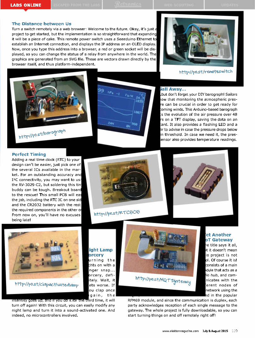
The Distance between Us Turn a switch remotely via a web browser: Welcome to the future. Okay, it's just
project to get started, but the implementation is so straightforward that expanding
it will be a piece of cake. This remote power switch uses a Seeeduino Ethernet to
establish an Internet connection, and displays the IP address on an OLED display.
Now, once you type this address into a browser, a red or green socket will be dis-
played, so you can change the status of a relay from anywhere in the world. The
graphics are generated from an SVG file. These are vectors drawn directly by the
browser itself, and thus platform-independent.
Perfect Timing Adding a real time clock (RTC) to your
design can't be easier, just pick one of
the several ICs available in the mar-
ket. For an outstanding accuracy an
I2C connectivity, you may want to us
the RV-3029-C2, but soldering this tin
buddy can be tough. Breakout board
to the rescue! This small PCB will ea
the job, including the RTC IC on one sid
and the CR2032 battery with the rest
the required components in the other o
From now on, you'll have no excuses
being late!
ight Lamp rcery urning the
hts on with a
nger snap...
rcery, defi-
itely. Wait, it
ets worse. If
ou clap once
gain, the
y u, I y ird time, it will
turn off again! With this circuit, you can easily modify any
night lamp and turn it into a sound-activated one. And
indeed, no microcontrollers involved.
Away... .but don't forget your DIY barograph! Sailors
ow that monitoring the atmospheric pres-
re can be crucial in order to get ready for
oming winds. This Arduino-based barograph
s the evolution of the air pressure over 48
rs on a TFT display, saving the data on an
ard. It also provides a flashing LED and a
r to advise in case the pressure drops below
n threshold. In case we need it, the pres-
ensor also provides temperature readings.
et Another T Gateway e title says it all,
t it doesn't mean
is project is not
ol. Of course it is!
onsists of a main
dule that acts as a
io hub, and com-
nicates with the
erent nodes of
network using the
d in the popular
RFM69 module, and since the communication is duplex, each
party acknowledges reception of each single message to the
gateway. The whole project is fully downloadable, so you can
start turning things on and off remotely right off!
www.elektormagazine.com July &August 2015 119
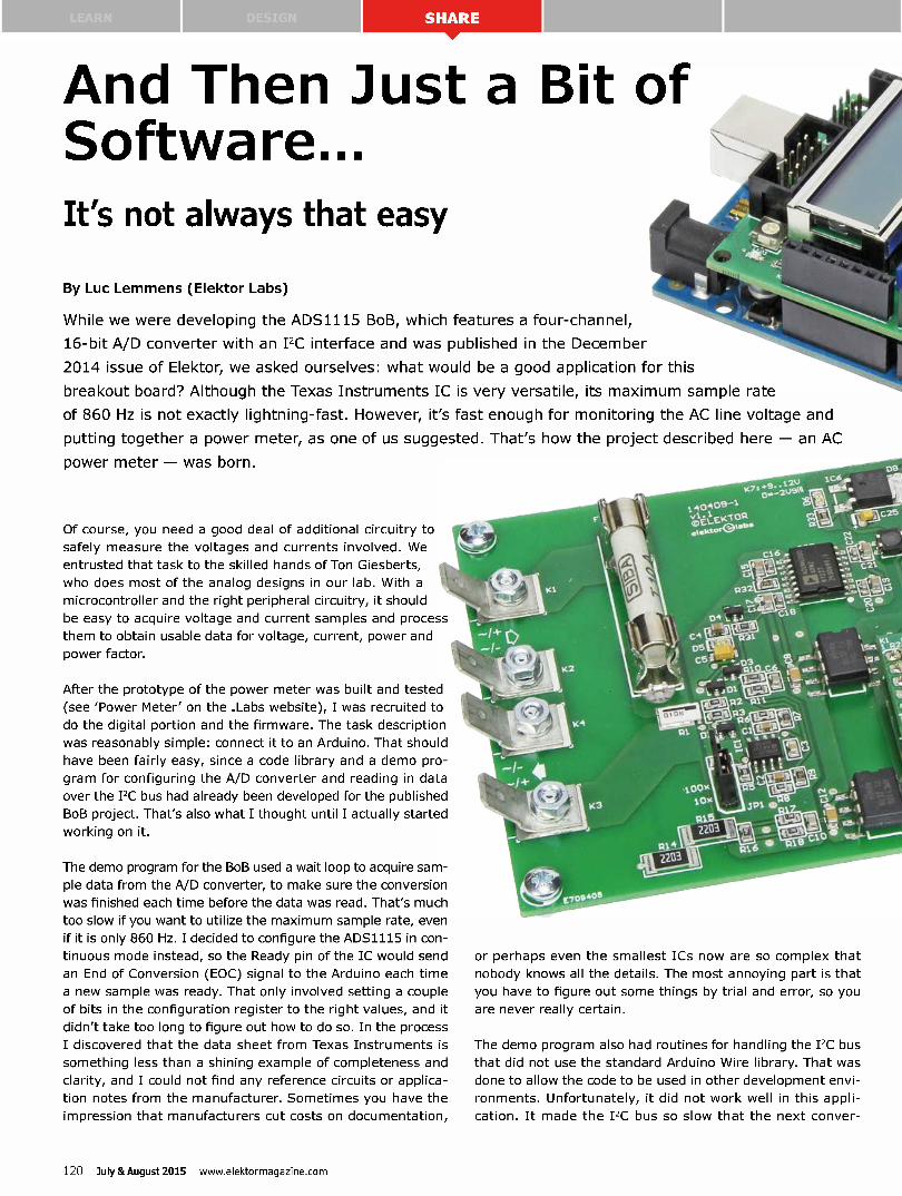
And Then Just a Bit of Software... It's not always that easy
BY Luc Lemmens (Elektbr Labs)
While we were developing the ADS1115 BoB, which features a four-channel,
16-bit A/D converter with an I2C interface and was published in the December
2014 issue of Elektor, we asked ourselves: what would be a good application for this
breakout board? Although the Texas Instruments IC is very versatile, its maximum sample rate
of 860 Hz is not exactly lightning-fast. However, it's fast enough for monitoring the AC line voltage and
putting together a power meter, as one of us suggested. That's how the project described here — an AC
power meter — was born.
Of course, you need a good deal of additional circuitry to
safely measure the voltages and currents involved. We
entrusted that task to the skilled hands of Ton Giesberts,
who does most of the analog designs in our lab. With a
microcontroller and the right peripheral circuitry, it should
be easy to acquire voltage and current samples and process
them to obtain usable data for voltage, current, power and
power factor.
After the prototype of the power meter was built and tested
(see 'Power Meter' on the .Labs website), I was recruited to
do the digital portion and the firmware. The task description
was reasonably simple: connect it to an Arduino. That should
have been fairly easy, since a code library and a demo pro-
gram for configuring the A/D converter and reading in data
over the I2C bus had already been developed for the published
BoB project. That's also what I thought until I actually started
working on it.
The demo program for the BoB used a wait loop to acquire sam-
ple data from the A/D converter, to make sure the conversion
was finished each time before the data was read. That's much
too slow if you want to utilize the maximum sample rate, even
if it is only 860 Hz. I decided to configure the ADS1115 in con-
tinuous mode instead, so the Ready pin of the IC would send
an End of Conversion (EOC) signal to the Arduino each time
a new sample was ready. That only involved setting a couple
of bits in the configuration register to the right values, and it
didn't take too long to figure out how to do so. In the process
I discovered that the data sheet from Texas Instruments is
something less than a shining example of completeness and
clarity, and I could not find any reference circuits or applica-
tion notes from the manufacturer. Sometimes you have the
impression that manufacturers cut costs on documentation,
or perhaps even the smallest ICs now are so complex that
nobody knows all the details. The most annoying part is that
you have to figure out some things by trial and error, so you
are never really certain.
The demo program also had routines for handling the I2C bus
that did not use the standard Arduino Wire library. That was
done to allow the code to be used in other development envi-
ronments. Unfortunately, it did not work well in this appli-
cation. It made the I2C bus so slow that the next conver-
120 July & August 2015 www.elektormagazine.com
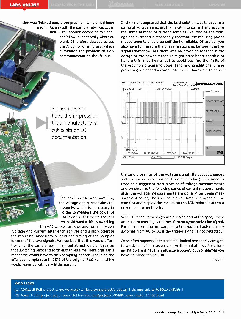
. c27 07 w.6
tritc7.6 .:2v9
Cz ., C7.
sion was finished before the previous sample had been
read in. As a result, the sample rate was cut in
half — still enough according to Shan-
non's Law, but not really what you
want. I therefore decided to use
the Arduino Wire library, which
eliminated the problem of slow
communication on the I2C bus. 4
Sometimes you
have the impression
that manufacturers
The next hurdle was sampling
the voltage and current simulta-
neously, which is necessary in
, order to measure the power of
AC signals. At first we thought
we could handle this by switching
the A/D converter back and forth between
voltage and current after each sample and simply tolerate
the resulting inaccuracy or shift the timing of the samples
for one of the two signals. We realized that this would effec-
tively cut the sample rate in half, but at first we didn't realize
that switching back and forth also takes time. Here again this
meant we would have to skip sampling periods, reducing the
effective sample rate to 25°h of the original 860 Hz — which
would leave us with very little margin.
In the end it appeared that the best solution was to acquire a
string of voltage samples, then switch to current and acquire
the same number of current samples. As long as the volt-
age and current are reasonably constant, the resulting power
measurements should be sufficiently reliable. Of course, you
also have to measure the phase relationship between the two
signals somehow, but there was no provision for that in the
design of the power meter. It might have been possible to
handle this in software, but to avoid pushing the limits of
the Arduino's processing power (and risking additional timing
problems) we added a comparator to the hardware to detect
HM01002 (HW Ox10180001; SW 05.457) 2015-03-19 1029 Auto-Trig./Complete
4'1 ROFIDEaSCH WAR2
TB: 200 µS T, 2 MS CH1: 1.6 V IOC, 2.5 MSa
r
Tim: (CH2)
ti: 911.60 ps
re .
t2: 963.60 [is
CH1.. 2 V
àt: 52.00 ps 1/ t: 19.23 kHz i
ICH2: 2 V t 17.60 VS
SAVE/RECALL
DEVICE SETTINGS
REFERENCES
TRACES
SCREENSHOTS
KEY
the zero crossings of the voltage signal. Its output changes
state on every zero crossing (from high to low). This signal is
used as a trigger to start a series of voltage measurements
and synchronize the following series of current measurements
after the voltage measurements are done. After these mea-
surement series, the Arduino is given time to process all the
samples and display the results on the LCD before it starts a
new measurement cycle.
With DC measurements (which are also part of the spec), there
are no zero crossings and therefore no synchronization signal.
For this reason, the firmware has a time-out that automatically
switches from AC to DC if the trigger signal is not detected.
As so often happens, in the end it all looked reasonably straight-
forward, but still not as easy as we thought at first. Redesign-
ing hardware is never an attractive option, but sometimes you
have no other choice. 14
(150287)
Web Links
[1] ADS1115 BoB project page: www.elektor-labs.com/project/practical-4-channel-adc-140169.14145.html
[2] Power Meter project page: www.elektor-labs.com/project/140409-power-meter.14409.html
www.elektormagazine.com July &August 2015 121

Best Tech By Gerard Fonte (USA)
When you design a new product it's always tempting
to use the newest and sexiest technology. It's fun and you
learn a lot and the product can be described as "incorporating
cutting-edge technology". It's a no-brainer. Right? Actually in
situations like this, it's important to use your brain and think
about the actual requirements of the product. You want to use
the best technology, which is usually not the newest technology.
Getting Tense
A few years ago my client wanted a hand-held tension
tester that would measure the force needed to extract an AC
plug from an AC socket. This was to be a commercial prod-
uct so price, performance and assembly were concerns. This
was a small company and the expected volume was in the low
100's per year. I put together a simple design using a couple of
opamps, a strain gauge, and an 8-bit micro that directly drove
a bare LCD display. It fitted into their existing case nicely. I
chose not to use SMT (surface-mount technology) because
they hadn't converted yet. I took extra time to route the PCB
(printed circuit board) with a single layer (which is almost
always possible with discrete components and user-defined
pins on the micro). I was also able to be very conservative and
use 0.020" (0.5 mm) traces and 0.030" (0.75 mm) spaces for
the PCB. The tension tester worked quite well, was inexpensive
and easy to build. It certainly wasn't high-tech and didn't look
very sophisticated. But, my client was happy.
A year or so later the same client chose a different
company to design an AC-power distortion meter. They wanted
a fairly basic tool that would fit into the same case and simply
display the main AC voltage and harmonic voltages. The other
group designed an elegant system with a high-end micro, a
separate, high-resolution analog-to-digital converter and exten-
sive front-end signal conditioning. In order to make it fit into
the case, they had to use very small SMT parts and a multi-
layer PCB board with traces that were nearly invisible. It used
complex FFT software and worked very well. But it was expen-
sive and difficult to service. The client wasn't happy — he told
me so. (However, I did get more work from him after that.) (I
would have tried a tunable, switched-capacitor-filter front-end
instead of an FFT.)
Paving the Road
The best technology is also a state of mind. You're fin-
ishing the basic software for your new application and you
have a lot of program space left over. So you decide to add an
extra function. After all, somebody will probably find a good
use for it and you will make a sale. It can't hurt can it? Except
at the next project meeting everybody wants to add some-
thing as well. So now there are lots of extras and the design
is considerably more complicated. With more complex soft-
ware there are more bugs. What's more, all future upgrades
will have to support all these new functions. You've also made
it more difficult to enhance your product by adding in all the
improvements already. And the instruction manual is bigger
which makes it less likely that the user will read it or be able
to find the necessary directions. Furthermore, the added com-
plexity makes the operation less intuitive. This results in more
customer support and more unhappy customers. Your good
intentions may not have the effects you expected.
The important point to remember when adding an
unnecessary function is not who will like it, but who will not
like it. The impact of any non-required operation should be
closely examined. You can't please everyone. And, pleasing
one person while irritating two is not a good business model.
The basic rules for content are: Rule 1: Always give the
customer what is necessary. (There are a surprising number
of products that fail this obvious requirement.) Rule 2: Usually
provide additional features that are clearly beneficial to the
large majority of users. Rule 3: Do not modify your design for
the small minority of users. The best technology is the one
that creates the largest number of sales. A happy customer is
a repeat customer (see above).
Being Needy
The truth is that most commercial products do not need
the latest and most advanced technology in order to succeed.
(Military, medical and aero-space applications are excepted.)
Generally, you only have to meet or slightly exceed the cur-
rent technology. Revolutionary products are those that use the
current technology in creative ways.
The belief that the original Apple Computer was highly
advanced technology is incorrect. The digital ICs were standard
parts that hobbyists were already using. Numerous personal
computers were already on the market: IMSAI, MITS, Scelbi.
Jobs and Wozniak succeeded by packaging software and hard-
ware into one single product. They brought the current tech-
nology into the home.
More recently, Ebay, Paypal, Facebook, Twitter and all
the other social media are imaginative uses for the internet,
but are not, in themselves, high-tech. Although it is true that
new technology may make the idea feasible. You can't have a
laser range-finder without a laser. But, lasers were around for
quite a while before someone used them to measure distance.
Force-fitting something new into your design generally
doesn't work. Take a step back and look for the best approach
rather than the newest. In short, it's not the technology that
is successful, it's the idea that is successful. 11
(150202)
122 July & August 2015 www.elektormagazine.com
W M =
Connector Pinouts Handy overviews By Harry Baggen (Editor, Elektor Netherlands)
WEB SCOUTING
Over the years there have probably been dozens of different types of connectors developed for
interconnecting electronic equipment and circuits. But how can you get the pinout data for a particular
connector? Fortunately, the Internet makes it fairly easy to find out how to wire various connectors and
what signals are present on the pins.
However, it can be handy to have a couple of addresses tucked
away somewhere, or in the favorites list of your browser, of
sites where you can find data for most connectors. That saves
a good deal of search effort, particularly with the more exotic
connector types.
A good starting point is The Hardware Book [1]. This site
claims to be have the Internet's largest free collection of con-
nector pinouts and cable descriptions. I haven't counted them
all, but the website does indeed have a sizeable collection.
Although the Hardware Book website may be a bit slow in add-
ing the latest specifications, such as USB 3.1 or HDMI 2.0, you
can find just about anything you can think of that is related to
electronics on the site. There are separate sections for audio,
video, computers, keyboards, game consoles, power supplies,
extension modules for all sorts of equipment and much more.
If you are looking for information about an Atari, Amiga or
Commodore, you can find it here. The layout of the website is
admittedly not polished, but what matters to us as electronics
enthusiasts is the content. When checking out all sorts of con-
nectors I occasionally encountered a page that did not work
(at least not any more), but that was rare.
Another handy site is Pinouts Guide [2]. It also has wealth of
information on all sorts of connectors. This is a Russian website
that originally had the address pinouts.ru, but fortunately all
the documentation is available in English as well as Russian.
Here as well you will find many computer connectors, as well
as connectors for video games, UPS devices, smartphones, GPS
receivers, audio and video equipment, cameras, and diagnos-
tic interfaces for vehicles (such as OBD-2). In addition to the
Hardware Book Weloarne to the lardware Cook. Internet's largest free collection d connector oinouts and cable deddstions.
Most popular pages Recent changes
'7-44e, Connectors
- VGA (1.61 • VGA (9) • Arx rower Suaa,V • Universal Sena, Sao (USS) • Vr. (V MS nor)
• SCANT - DIN Audio • Sa m SO. • 1111C • ca mMar a)
2014-04-14,
• shag Deer Mt Etesseterj
2014-11.4-Ort
• Xtes 360 NV( *) • sows ',no.) • hmiaa (a/S2 • ',PM (snit , rTre) freeman,/
2013-09-06(
AN it mints laws • elsystation I tretare/
2013 OS 10,
• 3.5 nos Av TeN re-enamel
2012-04-25:
• ¡SON SO Due 16141
CabIas
• Ethernet 10/100/100013ase-T Straight Thru
100Bace-la Crossover • Nullnwelsen (9-9) • nDte • Cisco Console (9)
• to la M u,. • ESDI cable
• Send Port Loop. , (9 Cheelelt)
• ISDN SO-Dus
cables
2012-02.0.:
• A MISS /Sa m ar/
2011.3-21,
• misamal Mminl An) (Cee.....)
pinout data, in many cases there is extra information about
the connector signals and relevant standards. This website is
augmented by user-provided information. Anyone who has
information about a connector not yet available on the site
can personally add the information using a convenient sub-
mission form.
The AllPinouts website [3] might have deserved the top rank-
ing for its enormous collection of connectors, but the way the
site is structured makes it difficult to find a particular connec-
tor. AllPinouts is a community project with freely available con-
tent in accordance with the GNU Free Documentation License
(GFDL), with information collected directly by the users. The
website is built as a sort of wiki, which means you have to
click through a number of sublevels to reach the information
you are looking for. On each page you stumble over various
adverts, often awkwardly placed, which makes everything very
inconvenient. However, you might find a connector here that
you cannot find on the other sites.
With these three addresses in your favorites list, you should
be in good shape to quickly track down the right pinout data
for your connectors.
(150290)
Web Links
[1] www.hardwarebook.info
[2] http://pinoutsguide.com or http://pinouts.ru
[3] www.allpinouts.org
PINOUTS.RU
V ] Computer hardware
4, Connectors of devices
Efirè Cables and adapters
CI] Plnouts by Vendor
V e Show connectors
All krown
Less than 7 pins
From 8 to 30 pins
connectors notits
There are 564 entries hound.
Ri u m = . 2
Í GROUND SIGNAL
2 pn MONO plug connector
1 GRou tp 81GIML
2 pn RCA plug connector
2 pit shgle row female connector
2 oil sngle row male connector
www.elektormagazine.com July &August 2015 123
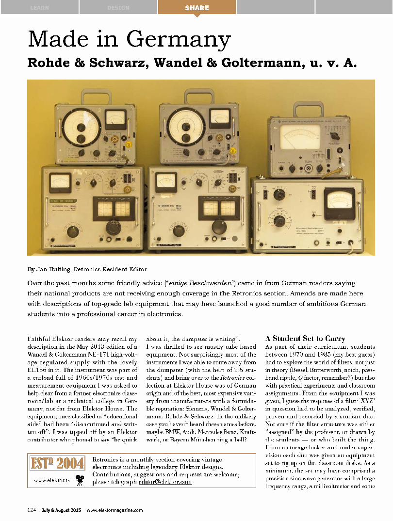
gEPU M
Made in Germany Rohde 85 Schwarz, Wandel & Goltermann, u. v. A.
By Jan Suiting, Retronics Resident Editor
Over the past months some friendly advice ("einige Beschwerdenl came in from German readers saying
their national products are not receiving enough coverage in the Retronics section. Amends are made here
with descriptions of top-grade lab equipment that may have launched a good number of ambitious German
students into a professional career in electronics.
Faithful Elektor readers may recall my description in the May 2013 edition of a Wandel Sz. Goltermann NE-171 high-volt-age regulated supply with the lovely EL156 in it. The instrument was part of a carload full of 1960s/1970s test and measurement equipment I was asked to help clear from a former electronics class-room/lab at a technical college in Ger-many, not far from Elektor House. The equipment, once classified as "educational aids" had been "discontinued and writ-ten off". I was tipped off by an Elektor contributor who phoned to say "be quick
about it, the dumpster is waiting". I was thrilled to see mostly tube based equipment. Not surprisingly most of the instruments I was able to route away from the dumpster (with the help of 2.5 stu-dents) and bring over to the Retronics col-lection at Elektor House was of German origin and of the best, most expensive vari-ety from manufacturers with a formida-ble reputation: Siemens, Wandel Sz. Golter-mann, Rohde Sz. Schwarz. In the unlikely case you haven't heard these names before, maybe BMW, Audi, Mercedes Benz, Kraft-werk, or Bayern Miinchen ring a bell?
ESP 2004 www.elektor.tv
Retronics is a monthly section covering vintage electronics including legendary Elektor designs. Contributions, suggestions and requests are welcome; please telegraph [email protected]
A Student Set to Carry As part of their curriculum, students between 1970 and 1985 (my best guess) had to explore the world of filters, not just in theory (Bessel, Butterworth, notch, pass-band ripple, Q factor, remember?) but also with practical experiments and classroom assignments. From the equipment I was given, I guess the response of a filter XYZ' in question had to be analyzed, verified, proven and recorded by a student duo. Not sure if the filter structure was either "assigned" by the professor, or drawn by the students — or who built the thing. From a storage locker and under super-vision each duo was given an equipment set to rig up on the classroom desks. As a minimum, the set may have comprised a precision sine wave generator with a large frequency range, a millivoltmeter and some
124 July & August 2015 www.elektormagazine.com
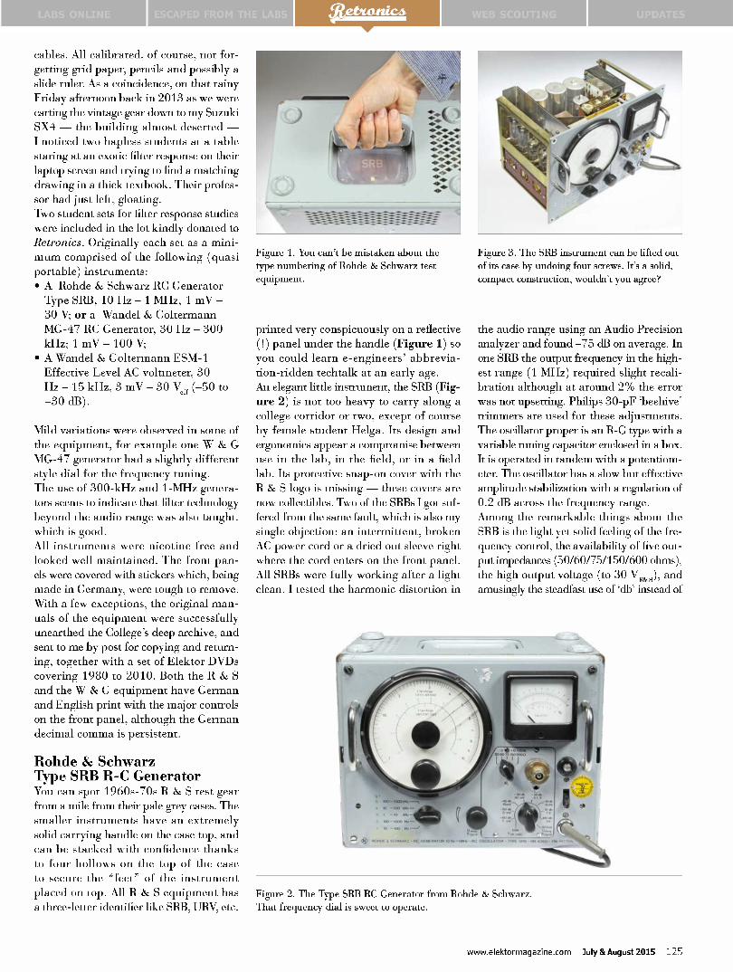
cables. All calibrated, of course, not for-getting grid paper, pencils and possibly a slide ruler. As a coincidence, on that rainy Friday afternoon back in 2013 as we were carting the vintage gear down to my Suzuki SX4 — the building almost deserted — I noticed two hapless students at a table staring at an exotic filter response on their laptop screen and trying to find a matching drawing in a thick textbook. Their profes-sor had just left, gloating. Two student sets for filter response studies were included in the lot kindly donated to Retronics. Originally each set as a mini-mum comprised of the following (quasi portable) instruments: • A Rohde Sz. Schwarz RC Generator Type SRB, 10 Hz - 1 MHz, 1 mV - 30 V; or a Wandel Sz. Goltermann MG-47 RC Generator, 30 Hz - 300 kHz; 1 mV - 100 V;
• A Wandel Sz. Goltermann ESM-1 Effective Level AC voltmeter, 30 Hz - 15 kHz, 3 mV - 30 Veff (-50 to +30 dB).
Mild variations were observed in some of the equipment, for example one W Sz. G MG-47 generator had a slightly different style dial for the frequency tuning. The use of 300-kHz and 1-MHz genera-tors seems to indicate that filter technology beyond the audio range was also taught, which is good. All instruments were nicotine free and looked well maintained. The front pan-els were covered with stickers which, being made in Germany, were tough to remove. With a few exceptions, the original man-uals of the equipment were successfully unearthed the College's deep archive, and sent to me by post for copying and return-ing, together with a set of Elektor DVDs covering 1980 to 2010. Both the R Sz. S and the W Sz. G equipment have German and English print with the major controls on the front panel, although the German decimal comma is persistent.
Rohde & Schwarz Type SRB R-C Generator You can spot 1960s-70s R Sz. S test gear from a mile from their pale grey cases. The smaller instruments have an extremely solid carrying handle on the case top, and can be stacked with confidence thanks to four hollows on the top of the case to secure the "feet" of the instrument placed on top. All R Sz. S equipment has a three-letter identifier like SRB, URV, etc.
"Weetteiff eigi-I-
Figure 1. You can't be mistaken about the type numbering of Rohde Se. Schwarz test equipment.
printed very conspicuously on a reflective (!) panel under the handle (Figure 1) so you could learn e-engineers' abbrevia-tion-ridden techtalk at an early age. An elegant little instrument, the SRB (Fig-ure 2) is not too heavy to carry along a college corridor or two, except of course by female student Helga. Its design and ergonomics appear a compromise between use in the lab, in the field, or in a field lab. Its protective snap-on cover with the R Sz. S logo is missing — these covers are now collectibles. Two of the SRBs I got suf-fered from the same fault, which is also my single objection: an intermittent, broken AC power cord or a dried out sleeve right where the cord enters on the front panel. All SRBs were fully working after a light clean. I tested the harmonic distortion in
Figure 3. The SRB instrument can be lifted out of its case by undoing four screws. It's a solid, compact construction, wouldn't you agree?
the audio range using an Audio Precision analyzer and found -75 dB on average. In one SRB the output frequency in the high-est range (1 MHz) required slight recali-bration although at around 2% the error was not upsetting. Philips 30-pF 'beehive' trimmers are used for these adjustments. The oscillator proper is an R-C type with a variable tuning capacitor enclosed in a box. It is operated in tandem with a potentiom-eter. The oscillator has a slow but effective amplitude stabilization with a regulation of 0.2 dB across the frequency range. Among the remarkable things about the SRB is the light yet solid feeling of the fre-quency control, the availability of five out-put impedances (50/60/75/150/600 ohms), the high output voltage (to 30 VR„,$), and amusingly the steadfast use of db' instead of
Figure 2. The Type SRB RC Generator from Rohde Se. Schwarz. That frequency dial is sweet to operate.
www.elektormagazine.com July &August 2015 125
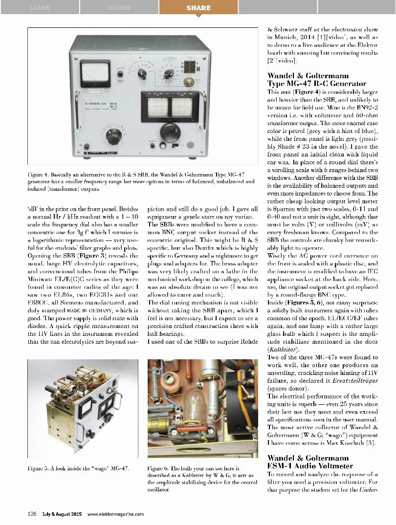
Figure 4. Basically an alternative to the R Se. S SRB, the Wandel & Goltermann Type MG-47 generator has a smaller frequency range but more options in terms of balanced, unbalanced and isolated (transformer) outputs.
'dB' in the print on the front panel. Besides a normal Hz / kHz readout with a 1 — 10 scale the frequency dial also has a smaller concentric one for lg f' which I surmise is a logarithmic representation — very use-ful for the students' filter graphs and plots. Opening the SRB (Figure 3) reveals the usual, large HV electrolytic capacitors, and conventional tubes from the Philips Miniwatt EL/E(C)C series as they were found in consumer radios of the age: I saw two EL86s, two ECC8 ls and one E88CC, all Siemens manufactured, and duly stamped MADE IN GERMANY, which is good. The power supply is solid state with diodes. A quick ripple measurement on the HV lines in the instrument revealed that the can electrolytics are beyond sus-
Figure 5. A look inside the "wago" MG-47.
picion and still do a good job. I gave all equipment a gentle start on my variac. The SRBs were modified to have a com-mon BNC output socket instead of the eccentric original. This might be R Sz. S specific, but also Dezifix which is highly specific to Germany and a nightmare to get plugs and adapters for. The brass adapter was very likely crafted on a lathe in the mechanical workshop at the college, which was an absolute dream to see (I was not allowed to enter and touch). The dial tuning mechanism is not visible without taking the SRB apart, which I feel is not necessary, but I expect to see a precision crafted construction there with ball bearings. I used one of the SRBs to surprise Rohde
Figure 6. The bulb your can see here is described as a Kaltleiter by W Se. G; it acts as the amplitude stabilizing device for the central oscillator.
Sz. Schwarz staff at the electronica show in Munich, 2014 [1] [video], as well as to demo to a live audience at the Elektor booth with amusing but convincing results [2] [video].
Wandel & Goltermann Type MG-47 R-C Generator This unit (Figure 4) is considerably larger and heavier than the SRB, and unlikely to be meant for field use. Mine is the BN92-2 version i.e. with voltmeter and 60-ohm transformer output. The stove enamel case color is petrol (grey with a hint of blue), while the front panel is light grey (possi-bly Shade # 23 in the novel). I gave the front panel an initial clean with liquid car wax. In place of a round dial there's a scrolling scale with 6 ranges behind two windows. Another difference with the SRB is the availability of balanced outputs and even more impedances to choose from. The rather cheap looking output level meter is Spartan with just two scales, 0-11 and 0-40 and not a unit in sight, although that must be volts (V) or millivolts (mV) as every freshman knows. Compared to the SRB the controls are chunky but remark-ably light to operate. Wisely the AC power cord entrance on the front is sealed with a plastic disc, and the instrument is modified to have an IEC appliance socket at the back side. Here, too, the original output socket got replaced by a round-flange BNC type. Inside (Figures 5, 6), not many surprises: a solidly built instrument again with tubes common of the epoch. EL/ECC/EF tubes again, and one lamp with a rather large glass bulb which I suspect is the ampli-tude stabilizer mentioned in the does (Kaltleiter). Two of the three MG-47s were found to work well, the other one produces an unsettling, crackling noise hinting of HV failure, so declared it Ersatzteiltráger (spares donor). The electrical performance of the work-ing units is superb — even 25 years since their last use they meet and even exceed all specifications seen in the user manual. The most active collector of Wandel Sz. Goltermann (W Sz. G; "wago") equipment I have come across is Max Koschuh [3].
Wandel & Goltermann ESM-1 Audio Voltmeter To record and analyze the response of a filter you need a precision voltmeter. For that purpose the student set for the Under-
126 July & August 2015 www.elektormagazine.com
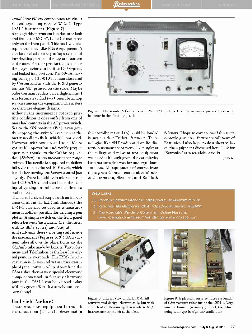
stand Your Filters course once taught at the college comprised a W Sz. G Type ESM- 1 instrument (Figure 7). Although this instrument has the same look and feel as the MG-47, it has German texts only on the front panel. This too is a table-top instrument. Like R Sz. S equipment, it can be stacked securely using a system of interlocking parts on the top and bottom of the case. For the operator's convenience the large meter can be tilted 30 degrees and locked into position. The 60-pA mov-ing coil type 137-8101 is manufactured by Gossen and as with the R Sz. S genera-tor, has db' printed on the scale. Maybe older German readers can enlighten me. I was fortunate to find two Gossen benchtop supplies among the equipment. The meters on them are elegant designs. Although the instrument I got is in pris-tine condition it does suffer from one of more bad contacts in the AC power switch. Set to the ON position (Em), even gen-tly rapping the switch lever causes the meter needle to flick, which is not good. However, with some care I was able to get stable operation and verify proper operation thanks to the Calibrate posi-tion (Eichen) on the measurement range switch. The needle is supposed to deflect full scale then to the red 10 V mark, which it did after turning the Eichen control just slightly. There is nothing in microcontrol-ler-LCD-A/D/A land that beats the feel-ing of getting an indicator needle on a scale mark. Thanks to its signal output with an imped-ance of about 15 kQ (unbalanced) the ESM- 1 can also be used as a measure-ment amplifier, possibly for driving a pen plotter. A simple switch on the front panel selects between 'instrument' (i.e. the meter with its db/V scales) and 'output'. And suddenly there's riveting stuff inside the instrument (Figures 8, 9)! C3m vac-uum tubes all over the place. Some say the C3g/m/o tube made by Lorenz, Valvo, Sie-mens and Telefunken, is the best low-sig-nal pentode ever made. The ESM- l's con-struction is classic and yet another exam-ple of pure craftsmanship. Apart from the C3m tubes there's zero special electronic components used, in fact any electronic part in the ESM-1 can be sourced today with no great effort. It's utterly unneces-sary though.
Und viele Andere! There was more equipment in the lab clearance than (a) can be described in
Figure 7. The Wandel & Goltermann ESM -1 30 Hz — 15 kHz audio voltmeter, pictured here with its meter in the tilted-up position.
this installment and (b) could be loaded in my car that Friday afternoon. Tech-nologies like SHF radio and audio dis-tortion measurement were also taught at the college and relevant test equipment was used, although given the complexity I am not sure this was for undergraduate students. All equipment of course from these great German companies: Wandel Sz. Goltermann, Siemens, and Rohde Sz.
Schwarz. I hope to cover some if this more esoteric gear in a future installment of Retronics. I also hope to do a short video on the equipment discussed here, look for Retronics' at www.elektor.tv.
(150232)
Web Links
[1] Rohde 8( Schwarz interview: https://youtu.be/AwwdW-mPYRk
[2] Retronics Hits electronica 2014: https://youtu.be/Yrqf3YLZAWY
[3] Max Koschuh's Wandel 8( Goltermann Online Museum: www.koschuh.com/museum/wandel_goltermann/wago.htm
Figure 8. Interior view of the ESM 1. All Figure 9: A pleasant surprise: there's a bunch conventional design, electronically, but with of C3m vacuum tubes inside the ESM-1. Very a touch of craftsmanship that made W Se. G much a Made in Germany product, the C3m instruments top notch at the time, today is a hype in high-end audio land.
www.elektormagazine.com July &August 2015 127

Elektor World News
Compiled by Beatriz Sousa
Summer Campaign Team has kicked off. Any ideas? On June 21 Elektor launches its traditional Summer Cam-paign. Market Director Germany, Ferdinand teWalvaart leads the Summer Campaign Team (SCT) with fellow Elektorians in it like Muhammed SOldit serving the mem-bers and Margriet Debeij serving our business clients and suppliers. Anyone who has an idea on crazy offers is welcome to contact them. If you take 30 minutes of scanning & scouting the world wide web, you will for sure find something you would like to buy. Bring that suggestion to us before you purchase and if the SCT can integrate it in the Summer Campaign, we will send you that product with 100% discount, limited to a maximum price of $/€/£200.
Revamped 'elektormagazine' website Elektor's activities this summer are not limited to huge pro-motions. We have just launched the new and improved web-site www.elektormagazine.com, where you can find all Elek-tor content under one roof. Elektor GREEN and GOLD mem-bers can access the vast archive of digital Elektor articles and magazines. If you are not a member you can read news and articles about your favorite electronic topics. With our improved search function, you can easily find the article(s) you are looking for. You can also select articles by favorite author, subject and much more. Check it out: www.elektor-magazine.com
READ ONLY MEMORY Elektor magazine and its parent publishing company boast a long and rich history. In this space we picture a gem from the past.
DIY CD Player In January 1992 Elektor presented the first CD player for home assembly. At that time the compact disc was already quite popular, but good CD players came with a hefty price tag. Thanks to intensive cooperation with Philips, one of the world's leading manufacturers of CD deck units, Elek-tor arranged for electronics stores to buy and retail a large number of ex-factory decks and associated control boards at a reasonable price. The magazine printed a fantastically detailed description of the first DIY CD player enabling many readers to make a start with the new
technology.
Ethics and electronics
Testing the waters — that's what the editorial staff of
Elektor's sister network www.techthefuture.com did these
past twelve months. Besides technology itself engineers
increasingly digest information about the effects of tech-
nology, real and potential, on societies and individuals.
Whether they like it or not, ever more companies and
designers are pulled into discussions between pessimists
("technology will kill natural human living!") and optimists
("technology will improve life immensely"). How far can
you go in changing people's life using electronics? Think
about smart cars (programming a car means deciding
beforehand if it will brake for ducks, besides children obvi-
ously). About life science: insurance companies are very
interested in electronic tools that stop people craving for
•
/e:«5 1:11>
PEOPLE NEWS • Sibe Jan Koster has joined the Elektor expert team and starts writing a book about STM32 Cortex
developing plans for a Turkish Summer Campaign with the help of Agent Manager Raoul Morreau • In Italy, Elektor
clients/sponsors in the winter to join Elektor than he did in the winter of 2014 • The book Ardumo in Control by teacher
Maarten Timmers Verhoeven is setting up a brand new Printing-on-Demand Service for members and book buyers outside
128 July & August 2015 www.elektormagazine.com

EXPERT PROFILE
at Tech the Future nicotine, but can one make that mandatory or what?
What do you think: should electronic engineers and
companies play a pro-active role discussing ethics
and electronics? Or should we leave that to politicians
and blindly follow what they and their voters seem to
decree? Join us on Tech The Future. Editor-in-Chief
Tessel Renzenbrink is keen to have your point of view.
You can contact her through Tessel.Renzenbrink@eim-
world.com or on twitter @ _Tessel. After the summer
Tessel will reshape her pioneer website with your input
into the platform where companies and engineers can
learn and share thoughts and actions concerning eth-
ics and electronics.
eft
•
• • • J
' "•'•
111
•
•
•
•
• • e
e • •
•• • • •
4 4. • a, •
- . • • - • • -
4e. e [e•
e- fs
- ,
«es
•
•
M4 micros • In Turkey, Elektor agent Cumhur Cakmak is
Publisher Antonio Cirella mobilized 7% more members and
Marc Friedheim was April's most pirated book (ggrrrrr) •
Europe to save enormously on shipping time and costs.
Elektor works closely together with more than 1,000 experts and authors for the publication of books, articles, DVDs, webinars and live events. In each installment of Elektor Word News we put one of them in the limelight.
audio and
Name: Rémy Mallard
Age: 48
Country: France
Education: Electronic Higher Education diploma (F2 A levels)
Publications: 3 technical books (FM radio, electronics for beginners, PIC for beginners),
several short works.
Training: Several courses in electronics applications
Who is Rémy Mallard?
I am 48 years old and have 6 children (five girls and a boy). I actually work in several activities: as a comedian/ VoA (Voice-over Artist), teacher in audiovisual/cinema school and elec-tronic developments (radio and studios domains).
What is your experience?
I have many years of win32 software writing, PIC develop-ments and audio devices repairs or mods, technical teaching in a large company and in school, radio and events animation.
Who is your biggest role model in electronics?
My father, my god-father and all folks out there who con-tributed to stimulate the desire to go on, even when all went down and produced smoke unwanted.
What will be the most key electronics development?
The ability for everyone to make their own devices we now have to buy manufactured. 3D printing is a way to this, and I'm surprised by what we can do with this sort of device. Tomorrow you'll be able to make your own phone or TV with any shape or color you want.
What topics will you be writing about in the future?
Don't really know about the subject, but if I have to write a new book, it will be targeted at beginners. It's a hard but very interesting job to keep words simple in the face of ever more technical objects.
Suppose Elektor gives you £100. What would you buy? Why?
I'll make electronic kits for beginners and supply them for free. Some people hesitate to start in electronics because they think they feel incapable, or because they lack money. A kind of 'impulse' is needed to help people take the next step.
What was THE development of electronics?
When I was young, I was fascinated by He-Ne Laser tubes (yes, the Ray of Death). Later, when Laser diodes became affordable, I decided to get some of them to give toys and musical instruments extra functionality. I now have more than 150 lasers. N
(150281)
www.elektormagazine.com July &August 2015 129

PLAY 8, WIN
The Original Elektorized Sudoku
Even if puzzle solving is not among your biggest talents you should have a go at cracking this edition's
Hexadoku. Don't feel pressed though since you have a good eight weeks for the assignment, and real
electronics engineers don't give up easily. Give it your best shot, find the solution in the gray boxes,
submit it to us by email, and you automatically enter the prize draw for one of five Elektor book vouchers.
The Hexadoku puzzle employs numbers in the hexadecimal
range 0 through F. In the diagram composed of 16 x 16 boxes,
enter numbers such that all hexadecimal numbers 0 through F
(that's 0-9 and A-F) occur once only in each row, once in each
column and in each of the 4x4 boxes (marked by the thicker
black lines). A number of clues are given in the puzzle and
these determine the start situation.
Correct entries received enter a prize draw. All you need to do
is send us the numbers in the gray boxes.
Solve Hexa doku and win! Correct solutions received from the entire Elektor readership automatically
enter a prize draw for five Elektor Book Vouchers worth $70.00 / £40.00
/ €50.00 each, which should encourage all Elektor readers to participate.
Participate! Before September 1, 2015, supply your name, street address
and the solution (the numbers in the gray boxes) by email to:
Prize winners The solution of the May & June 2015 Hexadoku is: 8205E.
The €50 / £40 / $70 book vouchers have been awarded to: Julian Muscat (Malta), Denis Moucharte (Belgium),
Philippe Monnard (Switzerland), Martin Kübel (Germany), and John Jones (USA).
Congratulations everyone!
E 9 1
D F C 0 1 6 B 8 4
B
F -- 1 0
B A 8 0
1 9 5 7 F 6 D
E
C
3 B
6
2 7 A S D 0
F 3 B 5 7
5 9 0 2
F 8 6 5 E C 9 D 2
2 0 F A 6 5 E D 1
8 l A 3
1 6 C D 2 E 4
3 E F D A C 5 8 6
8 4 1 E A 7 3 D 9
6 2 D A E
7 D 3 6 5 16 8 F C
A 4 9
6 5 A B 9 E 0 C 7 8 2 D F 1 3 4
3 E 2 8 A D 1 6 4 B F 9 0 C 5 7
14 7 C F 3 8 2 0 5 E A B 6 D 9
9 D F O 4 B 5 7 C 1 3 6 E 2 8 A
D 2 9 3 5 4 C 8 1 E 0 7 A B F 6
7 F 5 4 0 9 B 1 6 A C 2 3 D E 8
8 A 0 E D 6 2 3 F 9 5 B 1 4 7 C
B C 6 1 E 7 F A 3 4 D 8 2 9 0 5
4 8 B 2 6 5 A 0 D F 1 C 7 E 9 3
A 0 C 9 2 1 7 D B 3 8 E 4 5 6 F
5 6 1 F 3 C 9 E 2 7 4 0 8 A B D
E 3 D 7 8 F 4 B A 6 9 5 C 0 1 2
C 7 E 5 B 0 3 9 8 2 6 4 D F A 1
F9 3 A 7 2 6 4 E D B 1 5 8 C 0
O B 4 6 1 8 D F 5 C A 3 9 7 2 E
2 1 8 D C A E 5 9 0 7 F 6 3 4 B
The competition is not open to employees of Elektor International Media, its subsidiaries, licensees and/or associated publishing houses.
130 July & August 2015 www.elektormagazine.com

eXtreme Low Power MCUs Extend - Battery Life
Low Sleep Currents with Flexible
Wake-up Sources
• Sleep current down to 9 nA
• Brown-Out Reset down to 45 nA
• Real-Time Clock down to 400 nA
Low Dynamic Currents
✓ As low as 30 µA/MHz
✓ Power-efficient execution
Large Portfolio of XLP MCUs
• 8-100 pins, 4-128 KB Flash
• Wide selection of packages, including
chip scale packages
microchip :R D Ecor
....microchIpdirect.com
Battery-Friendly Features
• Enable battery lifetime > 20 years
• Operate down to 1.8V with self write
and analog functions
• Low-power supervisors for safe
operation (BOR, VVDT)
Flexible Peripheral Set
• Integrated USB, LCD, RTC and touch
sensing
• Eliminates costly external components
z
lerlA A fr14 1\ iCAl a cil
MICROCHIP www.microchip.com/xlp
The Microchip name and logo and the Microchip logo are registered trademarks of Microchip Technology Incorporated in the U.S.A. and other countries. All other trademarks are the property of their registered owners.
© 2015 Microchip Technology Inc. All rights reserved. DS00001746B. MEC2006Eng04/15

PROTEUS DESIGN SUITE VERSION
Featuring a brand new application framework, common parts database, live netlist and 3D visualisation, a built in debugging environment and a WYSIWYG Bill of Materials module, Proteus 8 is our most integrated and easy to use design system ever. Other features include:
. Hardware Accelerated Performance. . Automatic support for teardrop placement.
. Unique Thru-ViewTm Board Transparency. . Direct CADCAM, ODB++, IDF & PDF Output.
. BSDL and PADS ASCII library part import tools. . Integrated 3D Viewer with 3DS and DXF export.
. Integrated Shape Based Auto-router. . Mixed Mode SPICE Simulation Engine.
. Flexible Design Rule Management. . Co-Simulation of PIC, AVR, 8051 and ARM MCUs.
. Polygonal and Split Power Plane Support. . Direct Technical Support at no additional cost.
Version 8.3 will include support for MEAD data exchange via the STEP/IEES file formats
wwwww.labcenter.com
Labcenter Electronics Ltd 53-55 Main Street, Grassington, North Yorks, BD23 5AA Tel: +44 (0)1756 753440 Fax +44 (0)1756 752857 Email: [email protected]
labcenterA Mwww.labcentencom Elfe c t r o ni c m


