Embed Size (px)
Citation preview

Magnetic properties of nickel nanowires: Effect of deposition temperatureKafil M. Razeeb, Fernando M. F. Rhen, and Saibal Roy Citation: Journal of Applied Physics 105, 083922 (2009); doi: 10.1063/1.3109080 View online: http://dx.doi.org/10.1063/1.3109080 View Table of Contents: http://scitation.aip.org/content/aip/journal/jap/105/8?ver=pdfcov Published by the AIP Publishing Articles you may be interested in High temperature finite-size effects in the magnetic properties of Ni nanowires J. Appl. Phys. 112, 073906 (2012); 10.1063/1.4756038 Magnetic and structural properties of fcc/hcp bi-crystalline multilayer Co nanowire arrays prepared by controlledelectroplating J. Appl. Phys. 109, 083919 (2011); 10.1063/1.3553865 Angular dependence of magnetic properties in Ni nanowire arrays J. Appl. Phys. 106, 103903 (2009); 10.1063/1.3257242 X-ray diffraction analysis and magnetic behavior of amorphous Fe 15 Co 17 Ni 58 B 10 nanowires obtained byelectrochemical deposition J. Appl. Phys. 101, 09N102 (2007); 10.1063/1.2711700 Chain of ellipsoids approach to the magnetic nanowire J. Appl. Phys. 97, 084304 (2005); 10.1063/1.1882765
[This article is copyrighted as indicated in the article. Reuse of AIP content is subject to the terms at: http://scitation.aip.org/termsconditions. Downloaded to ] IP:
143.239.66.69 On: Mon, 13 Apr 2015 15:38:57

Magnetic properties of nickel nanowires: Effect of deposition temperatureKafil M. Razeeb, Fernando M. F. Rhen, and Saibal Roya�
Tyndall National Institute, Lee Maltings, Prospect Row, Cork, Ireland
�Received 25 July 2008; accepted 26 February 2009; published online 28 April 2009�
We have investigated the magnetic properties of electroplated nickel nanowires with very distinctnanostructures, which are obtained by simply changing the plating temperature of the electrolyte.Low temperature �40 °C� resulted in larger average grain size comparable to the diameter of thewires, whereas higher temperature �60 °C� revealed self-similar morphology composed ofnanogranules. For low temperature samples, a two stage magnetization process is evident in the easyaxis direction where grain size is comparable to wire diameter. In contrast, for high temperaturesamples, nanowires are formed by an agglomeration of particles with average diameter of about 22nm. In this case each individual particle behaves as a single domain and thereby magnetizationreversal occurs by the switching of an ensemble of randomly oriented particles and magnetizationsaturates quickly with applied field. In the present case, with the high density of disorder caused bythe self-similar morphology of the nanogranules, we suggest that the switching mechanism of themagnetization occurs by localized coherent rotation, resulting in lower coercivity. This delineatesfirst experimental evidence of three dimensional cooperative magnetic interactions among thenanogranules within self-similar morphology of nanowires in both parallel and perpendicular wireaxes. © 2009 American Institute of Physics. �DOI: 10.1063/1.3109080�
I. INTRODUCTION
Magnetic nanowires are a subject of topical interest dueto their potential application as high density data storage andmagnetic sensors and also due to their intricate magneticproperties. Among them, nickel nanowires were investigatedby several groups mainly focusing on the correlation be-tween the dimension of the wire and the hysteresisbehavior,1–3 effect of electrodeposition process parameterssuch as pH of the solution3 on crystallographic orientation,and micromagnetic simulation to investigate the magneticinteraction of the nanowires embedded inside hexagonalarrangements.4,5 However, the effect of deposition param-eters such as temperature of the electrolyte on the structuralmorphology of nanowires and how they influence the mag-netic properties were not studied in detail, though it wasreported that different bath temperatures allowed differentcrystal orientations inside the nanowires and resulted in dif-ferent grain sizes.6 Skomski et al. studied the effect of grainsize on the magnetic properties in polycrystalline nanowiresand proposed a model for magnetic phase diagram ofnanowires.7 Most of these nanowires have an average diam-eter ranging from 5 to 50 nm.8,9 This paper describes theeffect of deposition temperature on the grain morphology ofnickel nanowires and its influence on the magnetic propertiesof the nanowires embedded inside nanochannel alumina�NCA� templates which were not reported before.
II. EXPERIMENTAL
For deposition inside the pores of NCA templates, theone side of the template was first deposited with a conduc-tive 500 nm aluminum using evaporation method. Ohmic
contact to the substrate was made using Radionics silver con-ductive paint on, which has a volume resistivity of0.001 � cm when fully hardened. The schematic of Fig. 1shows the electroplating setup for the deposition of Ni nano-wires inside alumina templates. A bath comprising of53.643 g l−1 NiSO4·6H2O and 30 g l−1 H3BO3 was pre-pared. De-ionized water with resistivity �18 M� was usedto prepare the solution. The pH of the solution was adjustedto 2.5 with addition of H2SO4 and stirred at a constant rpm of660. The nickel nanowires were prepared inside the NCAtemplate having three different nominal pore diameters of200, 100, and 20 nm. The electrolyte temperature was main-tained at 40 and 60�0.2 °C to prepare two batches ofsamples �henceforth regarded as “low temperature” �40 °C�and “high temperature” �60 °C� samples� using an ETS D-4
a�Author to whom correspondence should be addressed. Tel.: �353 214904331; FAX: �353 21 4270271. Electronic mail: [email protected].
FIG. 1. �Color online� Schematic of electrodeposition setup for growing Ninanowires inside alumina templates.
JOURNAL OF APPLIED PHYSICS 105, 083922 �2009�
0021-8979/2009/105�8�/083922/7/$25.00 © 2009 American Institute of Physics105, 083922-1
[This article is copyrighted as indicated in the article. Reuse of AIP content is subject to the terms at: http://scitation.aip.org/termsconditions. Downloaded to ] IP:
143.239.66.69 On: Mon, 13 Apr 2015 15:38:57

Fuzzy IKA WERKE temperature controller. The bath wasoperated at a current density of 10 mA cm−2. After deposi-tion, the samples were thoroughly rinsed with de-ionized wa-ter and dried with nitrogen gun.
In terms of current efficiency, it is evident that the cur-rent efficiency is higher while depositing from high pH elec-trolyte at all cathode current densities.10 An investigationwas carried out to investigate the effect of pH on nickeldeposits. Increasing the electrolyte pH from 2 to 3.5 whileimproving the current efficiency was detrimental to the de-posit morphology. Cracking, curling, and the appearance of asecond phase, an oxide or hydroxide, also accompanied withthe increase in electrolyte pH. A low pH value of 2.0 didhave a high quality deposit when both the temperature andnickel �Ni2+� concentration were kept at 40 °C and 40 g l−1,respectively, but the current efficiency decreased to 71%.11
Therefore, the pH of the bath was set to 2.5 and it showedhigh quality of deposit.
The pore filling of nickel was investigated by HitachiS4000 scanning electron microscope �SEM�. Transmissionelectron microscope �TEM� was used to study the nanostruc-ture of the nickel wires. Cross section of the samples wasprepared by focused ion beam �FIB� milling for TEM obser-vation. The grain size distribution was obtained by countingand measuring the grain diameters from micrograph usingImageJ software. For further estimation of overall grain sizeand crystal orientation X-ray diffraction �XRD� measure-ments were carried out using a Philips PW3710 diffracto-meter with Cu K�1 radiation, having a wavelength of1.540 56 Å. The magnetic properties were investigated us-ing a MPMS XL5 Superconducting quantum interference de-vice �SQUID� with an applied field up to 5 T.
III. RESULTS AND DISCUSSION
Commercially available NCA samples named Anodisc™25 by Whatman plc© having three different nominal poresizes �200, 100, and 20 nm� called NCA200, NCA100, andNCA20, respectively, are used in the present study. In orderto measure the average pore size of NCAs, SEM imageswere analyzed with image analysis software named QUARTZ
PCI-IMAGE MEASUREMENT SYSTEM. For NCA200, the averagepore diameter on the “filtration side” is 209.4 nm whereasthat on the “reverse side” is 308.5 nm. There is a deviationfrom circularity for most of the pores.12 The average porediameter for NCA100 is found to be 112 nm on the filtrationside and 242 nm on the reverse side, whereas for NCA20 theaverage pore diameters on the filtration and the reverse sideare 30 nd 202 nm, respectively. This heterogeneity in thepore structure of the NCA is created by varying the processparameters during the fabrication of the membranes. Differ-ent anodizing voltages were applied to the pure aluminummetal substrate during the growth of the NCA; thus in effectlarge pores extend virtually through the whole bulk of theoxide, except for a thin layer at one end where small poresprevail.13 A long-range hexagonal arrangement of pores canbe established for the pores, though pentagonal and heptago-nal arrangements can also be observed. These arrangementsare due to the mechanism of the pore growth during anod-
ization of the aluminum substrate.14 Hexagonal arrangementsresults from the hcp basal plane of the starting aluminum foiland the attrition due to anodization, which starts from thecenter and the six corners of the hexagonal base. Pentagonalarrangement results when two of the surrounding pores arefused together and heptagonal arrangement can result when apore has suffered incomplete attrition compared to others.Barnard et al.15 calculated the width of the walls from theporosity data provided by the manufacturer assuming anideal hexagonal array of pores. The values obtained in thisway are only for the filtration side of the NCA and are com-pared with our observations from SEM. The thicknesses ofthe pore walls obtained in this study are in good agreementwith the theoretical values calculated by Barnard et al. whichreported 69, 50, and 15–18 nm for NCA200, NCA100, andNCA20 templates. However, on the reverse side, the averagethickness of the walls show different values of 112, 96, and92 nm for NCA200, NCA100, and NCA20 templates, re-spectively. To define the matrix of nanowires in alumina, thewidth of the pore wall is important since it actually revealswhat will be the separation among the nickel nanowires in-side the alumina matrix. In order to understand the magneticinteraction among the nickel nanowires, the separationamong the wires needs to be measured, which turns out to bethe width of the pore walls. Since, the amount of pentagonalarrangement within hexagonally arranged nanowires is�1%–2%,12,16 it can be ignored as an effect on the overallmagnetic behavior.
The effect of random disorder �from an ideally orderedhexagonal array� and surface morphology of nickel nano-wires on magnetic properties was investigated by severalgroups.17–19 It was shown by simulation that the random dis-order resulted in the requirement of higher magnetic field toreach saturation when compared to ideal hexagonal array.Due to the disorder in some places, the nanowires comecloser to each other and a dipole-dipole asymmetric interac-tion governs the requirement of larger magnetic field to reachsaturation and resulted in a reduced remanence, while coer-civity remained unchanged.17
While measuring magnetization process using SQUIDmagnetometer we measured the overall magnetic propertiesof any sample. Since the length of the branched filtration sideof the template is only 3–5 �m as opposed to the overall60 �m and as the aspect ratio �length/diameter� of the nano-wires is quite high ��200�, the influence of disorder of nano-wires on magnetic behavior is not evident in the magneticmeasurements. Furthermore, the effect of the random disor-der in the hexagonal arrangement and the deviation in thecircularity of the nickel nanowires on the overall magneticproperties are nullified in the present study due to the use ofthe same templates to fabricate these nanowires.
A. Electron microscopy
Figure 2�a� shows the SEM image of the nickel nano-wires embedded inside alumina after the template was par-tially removed by NaOH etching. The image was taken at a45° angle to the template. Figure 2�b� shows a typical SEMimage of the top of nickel nanowires fabricated at 40 °C
083922-2 Razeeb, Rhen, and Roy J. Appl. Phys. 105, 083922 �2009�
[This article is copyrighted as indicated in the article. Reuse of AIP content is subject to the terms at: http://scitation.aip.org/termsconditions. Downloaded to ] IP:
143.239.66.69 On: Mon, 13 Apr 2015 15:38:57
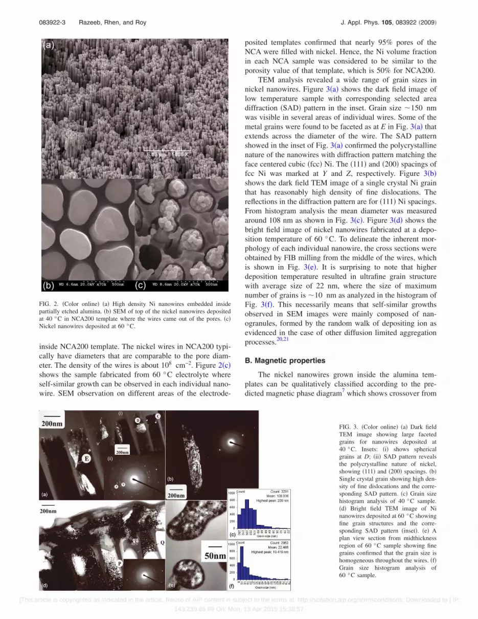
inside NCA200 template. The nickel wires in NCA200 typi-cally have diameters that are comparable to the pore diam-eter. The density of the wires is about 108 cm−2. Figure 2�c�shows the sample fabricated from 60 °C electrolyte whereself-similar growth can be observed in each individual nano-wire. SEM observation on different areas of the electrode-
posited templates confirmed that nearly 95% pores of theNCA were filled with nickel. Hence, the Ni volume fractionin each NCA sample was considered to be similar to theporosity value of that template, which is 50% for NCA200.
TEM analysis revealed a wide range of grain sizes innickel nanowires. Figure 3�a� shows the dark field image oflow temperature sample with corresponding selected areadiffraction �SAD� pattern in the inset. Grain size �150 nmwas visible in several areas of individual wires. Some of themetal grains were found to be faceted as at E in Fig. 3�a� thatextends across the diameter of the wire. The SAD patternshowed in the inset of Fig. 3�a� confirmed the polycrystallinenature of the nanowires with diffraction pattern matching theface centered cubic �fcc� Ni. The �111� and �200� spacings offcc Ni was marked at Y and Z, respectively. Figure 3�b�shows the dark field TEM image of a single crystal Ni grainthat has reasonably high density of fine dislocations. Thereflections in the diffraction pattern are for �111� Ni spacings.From histogram analysis the mean diameter was measuredaround 108 nm as shown in Fig. 3�c�. Figure 3�d� shows thebright field image of nickel nanowires fabricated at a depo-sition temperature of 60 °C. To delineate the inherent mor-phology of each individual nanowire, the cross sections wereobtained by FIB milling from the middle of the wires, whichis shown in Fig. 3�e�. It is surprising to note that higherdeposition temperature resulted in ultrafine grain structurewith average size of 22 nm, where the size of maximumnumber of grains is �10 nm as analyzed in the histogram ofFig. 3�f�. This necessarily means that self-similar growthsobserved in SEM images were mainly composed of nan-ogranules, formed by the random walk of depositing ion asevidenced in the case of other diffusion limited aggregationprocesses.20,21
B. Magnetic properties
The nickel nanowires grown inside the alumina tem-plates can be qualitatively classified according to the pre-dicted magnetic phase diagram7 which shows crossover from
FIG. 2. �Color online� �a� High density Ni nanowires embedded insidepartially etched alumina. �b� SEM of top of the nickel nanowires depositedat 40 °C in NCA200 template where the wires came out of the pores. �c�Nickel nanowires deposited at 60 °C.
FIG. 3. �Color online� �a� Dark fieldTEM image showing large facetedgrains for nanowires deposited at40 °C. Insets: �i� shows sphericalgrains at D; �ii� SAD pattern revealsthe polycrystalline nature of nickel,showing �111� and �200� spacings. �b�Single crystal grain showing high den-sity of fine dislocations and the corre-sponding SAD pattern. �c� Grain sizehistogram analysis of 40 °C sample.�d� Bright field TEM image of Ninanowires deposited at 60 °C showingfine grain structures and the corre-sponding SAD pattern �inset�. �e� Aplan view section from midthicknessregion of 60 °C sample showing finegrains confirmed that the grain size ishomogeneous throughout the wires. �f�Grain size histogram analysis of60 °C sample.
083922-3 Razeeb, Rhen, and Roy J. Appl. Phys. 105, 083922 �2009�
[This article is copyrighted as indicated in the article. Reuse of AIP content is subject to the terms at: http://scitation.aip.org/termsconditions. Downloaded to ] IP:
143.239.66.69 On: Mon, 13 Apr 2015 15:38:57

cooperative to noncooperative magnetic interactions with re-spect to their crystallite sizes and wire diameters. Accordingto the phase diagram, in the present work, wires deposited at40 °C should exhibit three dimensional noncooperative in-teractions because of their grain size ��108 nm� which iscomparable to the wire diameter and much higher than thedomain wall width, whereas samples plated at 60 °C aresupposed to show three dimensional cooperative interactions,which has average grain size of 22 nm, lower than the do-main wall width.
TEM and XRD results indicate that nickel nanowires arepolycrystalline as shown in Figs. 3 and 4. Therefore, themagnetocrystalline anisotropy contribution to the hystereticbehavior needed to be evaluated. The following equation wasused to determine the effect of magnetocrystalline anisotropycontribution in comparison to shape anisotropycontribution:22,23
Keff = pK1 + �pMs2�1 – 3p� , �1�
where p is the geometric packing density for ideal hexago-nally arranged array of pores, Keff is the effective anisotropyconstant, K1 is the magnetocrystalline anisotropy constant�for nickel it is −4.5�103 J m−3�, and Ms is the saturationmagnetization of nickel. For a hexagonal array ofnanowires:23
p =�
�2�3��Dp/Dcell�2. �2�
Here Dp is the pore diameter and Dcell is the hexagonal celldiameter. An illustration of the effect of the crystalline aniso-tropy in the effective anisotropy �Keff� is shown in Fig. 5 asa function of packing density of nickel nanowire in aluminamatrix. The solid line is solely determined by the shape an-isotropy and the influence of the crystal anisotropy shifts theline to lower or higher values assuming solely parallel orperpendicular crystal anisotropy with K1 value for bulknickel, that is, �111� plane parallel or perpendicular to thenanowire axis. So it can be concluded that the crystal aniso-tropy has little or no effect compared with that of the shapeanisotropy. This is due to the fact that in case of nickel nano-wires, the shape anisotropy constant �Ks=7.4�104 J m−3� isone order of magnitude greater than the crystalline aniso-tropy constant �K1=−4.5�103 J m−3� and opposite in sign.As a result the effective anisotropy field is only due to theshape anisotropy in the nickel nanowire matrix and can bewritten as Hkeff=Hks=2�Ms=242.057 kA m−1 �3041.7 Oe�.
The comparison between crystalline and magnetoelasticanisotropies is frequently used for continuous films and bulksample of Ni. In case of nanowire grown in porous template,the contribution to magnetoelastic anisotropy arises mainlyfrom the mismatch of thermal expansion coefficients of me-tallic nanowires and the ceramic/polymer matrix. These areapparent in reported samples measured from room tempera-ture to �5 K.19,24,25 In the present study all the magneticmeasurements were carried out at room temperature��300 K� generating negligible magnetoelastic anisotropycompared to lower temperature. However, the strain of thesamples fabricated at two different temperatures �40 and60 °C� was calculated from the slow scan XRD. Lattice ex-pansion or contraction is usually expressed in terms of�a /a0, where a0 is the lattice constant of the strain-free ma-terial. �a /a0 is related to macrostrain �mean strain� anddeformation stacking fault probability �� as �a /a0=+G��, where G is a constant depending on �hkl� and thestructure of the material.26 However, the occurrence of thedeformation faults in thin films is negligible.27 So, the sec-
FIG. 4. �Color online� Diffraction pattern of Ni nanowire electroplated at 40and 60 °C. Peaks correspond to fcc Ni.
FIG. 5. �Color online� Effective mag-netic anisotropy for nickel nanowirearray as a function of packing densityshowing small variation with andwithout crystal anisotropy.
083922-4 Razeeb, Rhen, and Roy J. Appl. Phys. 105, 083922 �2009�
[This article is copyrighted as indicated in the article. Reuse of AIP content is subject to the terms at: http://scitation.aip.org/termsconditions. Downloaded to ] IP:
143.239.66.69 On: Mon, 13 Apr 2015 15:38:57
ond term in the above equation can be ignored. The straincomponent n normal to the film surface can therefore becalculated directly from the lattice constants a and a0. Themacrostrain values obtained for low and high temperaturesamples are about �0.1% and hence we neglected the mag-netoelastic contribution to anisotropy in both cases.
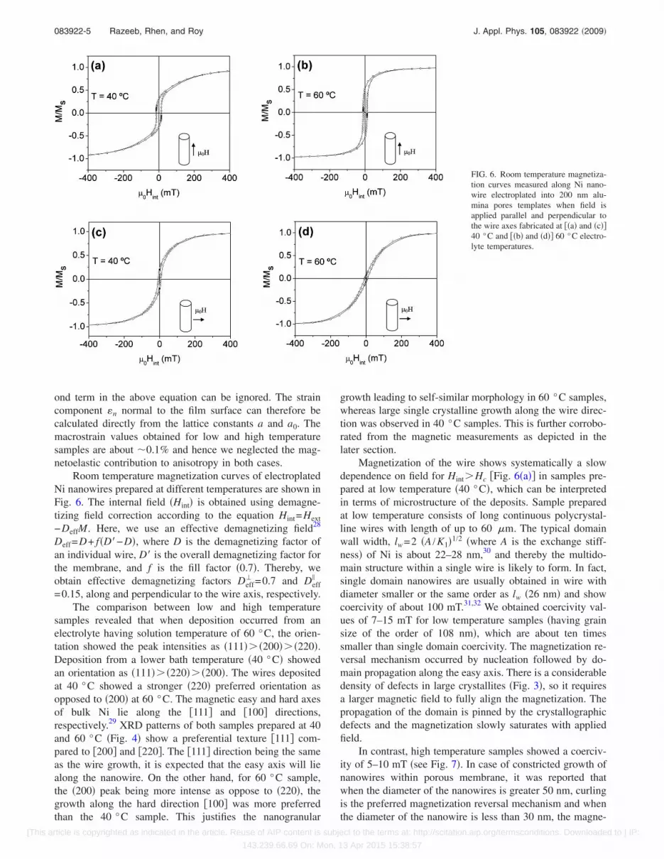
Room temperature magnetization curves of electroplatedNi nanowires prepared at different temperatures are shown inFig. 6. The internal field �Hint� is obtained using demagne-tizing field correction according to the equation Hint=Hext
−DeffM. Here, we use an effective demagnetizing field28
Deff=D+ f�D�−D�, where D is the demagnetizing factor ofan individual wire, D� is the overall demagnetizing factor forthe membrane, and f is the fill factor �0.7�. Thereby, weobtain effective demagnetizing factors Deff
� =0.7 and Deff�
=0.15, along and perpendicular to the wire axis, respectively.The comparison between low and high temperature
samples revealed that when deposition occurred from anelectrolyte having solution temperature of 60 °C, the orien-tation showed the peak intensities as �111� �200� �220�.Deposition from a lower bath temperature �40 °C� showedan orientation as �111� �220� �200�. The wires depositedat 40 °C showed a stronger �220� preferred orientation asopposed to �200� at 60 °C. The magnetic easy and hard axesof bulk Ni lie along the �111� and �100� directions,respectively.29 XRD patterns of both samples prepared at 40and 60 °C �Fig. 4� show a preferential texture �111� com-pared to �200� and �220�. The �111� direction being the sameas the wire growth, it is expected that the easy axis will liealong the nanowire. On the other hand, for 60 °C sample,the �200� peak being more intense as oppose to �220�, thegrowth along the hard direction �100� was more preferredthan the 40 °C sample. This justifies the nanogranular
growth leading to self-similar morphology in 60 °C samples,whereas large single crystalline growth along the wire direc-tion was observed in 40 °C samples. This is further corrobo-rated from the magnetic measurements as depicted in thelater section.
Magnetization of the wire shows systematically a slowdependence on field for HintHc �Fig. 6�a�� in samples pre-pared at low temperature �40 °C�, which can be interpretedin terms of microstructure of the deposits. Sample preparedat low temperature consists of long continuous polycrystal-line wires with length of up to 60 �m. The typical domainwall width, lw=2 �A /K1�1/2 �where A is the exchange stiff-ness� of Ni is about 22–28 nm,30 and thereby the multido-main structure within a single wire is likely to form. In fact,single domain nanowires are usually obtained in wire withdiameter smaller or the same order as lw �26 nm� and showcoercivity of about 100 mT.31,32 We obtained coercivity val-ues of 7–15 mT for low temperature samples �having grainsize of the order of 108 nm�, which are about ten timessmaller than single domain coercivity. The magnetization re-versal mechanism occurred by nucleation followed by do-main propagation along the easy axis. There is a considerabledensity of defects in large crystallites �Fig. 3�, so it requiresa larger magnetic field to fully align the magnetization. Thepropagation of the domain is pinned by the crystallographicdefects and the magnetization slowly saturates with appliedfield.
In contrast, high temperature samples showed a coerciv-ity of 5–10 mT �see Fig. 7�. In case of constricted growth ofnanowires within porous membrane, it was reported thatwhen the diameter of the nanowires is greater 50 nm, curlingis the preferred magnetization reversal mechanism and whenthe diameter of the nanowire is less than 30 nm, the magne-
FIG. 6. Room temperature magnetiza-tion curves measured along Ni nano-wire electroplated into 200 nm alu-mina pores templates when field isapplied parallel and perpendicular tothe wire axes fabricated at ��a� and �c��40 °C and ��b� and �d�� 60 °C electro-lyte temperatures.
083922-5 Razeeb, Rhen, and Roy J. Appl. Phys. 105, 083922 �2009�
[This article is copyrighted as indicated in the article. Reuse of AIP content is subject to the terms at: http://scitation.aip.org/termsconditions. Downloaded to ] IP:
143.239.66.69 On: Mon, 13 Apr 2015 15:38:57

tization reversal mechanism switches to coherent rotation.33
In high temperature samples the wires are formed by an ag-glomeration of particles with an average diameter of 22 nm�the maximum number of grains is �10 nm�, which is lowerthan domain wall size. In this case, the magnetic behaviorcan be understood in terms of an ensemble of fine particleswith relatively random easy axis orientation. Therefore, theswitching mechanism is supposed to occur by continuousrotation of magnetization as in a single domain particle.However, due to the imperfections caused by the nanostruc-tures, the reversal mode seems to be localized, which reducesthe coercivity.34 The localization length depends on the wirenanostructure, which goes to infinity for zero disorder andreversal mechanism leads to coherent rotation. In the presentcase, with the high density of disorder caused by the self-similar morphology of the nanogranules, we suggest that theswitching mechanism of the magnetization occurs by local-ized coherent rotation, resulting in lower coercivity. This canbe further corroborated by comparing the four hysteresisloop shown in the Fig. 6 where the low temperature sampleshowed two distinct hysteresis behaviors for field appliedparallel and perpendicular to the wire axis. A single stagemagnetization curve was obtained for perpendicular appliedfield compared to the two stage magnetization behavior incase of parallel applied field. On the other hand, in the 60 °C�high temperature� sample, for parallel and perpendicular ap-plied fields, the hysteresis curves showed surprising similar-ity where both the curves have single slope magnetization.This is due to the self-similar growth of nickel inside thewires, which again are composed of nanogranules havingaverage particle diameter of 22 nm comparable to the do-main wall width. These high temperature nickel wires com-posed of nanometric crystallites are believed to reduce theeffect of shape anisotropy as observed in high aspect rationanowires and resulted in comparable magnetization curvesfor field applied parallel and perpendicular to the wire axis.This delineates the first experimental evidence of three di-mensional cooperative magnetic interactions among the nan-ogranules within self-similar morphology of nanowires inboth parallel and perpendicular directions.
IV. CONCLUSIONS
In conclusion, we have fabricated nickel nanowires attwo different deposition temperatures which influenced thegrain structure of the nickel inside the nanowires. The crystalorientation was a function of deposition temperature as wellas pore diameter. Magnetic hysteretic behavior showed grainsize dependence. The propagation of the domain is pinned bythe defects and a two stage magnetization curve was ob-served for low temperature samples where the grain size iscomparable to the wire diameter. In case of high temperaturesamples, the grain size is comparable to the domain wall sizeof nickel, where an individual grain behaves as a single do-main and thereby the switching mechanism occurs by con-tinuous rotation of magnetization resulting in a single slope.
ACKNOWLEDGMENTS
This work is financially supported by Science Founda-tion Ireland �SFI� Principal Investigator �PI Grant No. 06/IN.1/I98� and Enterprise Ireland �EI� under the Industry LedResearch Programme �Grant No. ILRP/05/PEIG/7� in PowerElectronics. Dr. F.M.F. Rhen is currently with Physics De-partment, University of Limerick, Limerick, Ireland.
1T. M. Whitney, J. S. Jiang, P. C. Searson, and C. L. Chien, Science 261,1316 �1993�.
2K. Nielsch, R. B. Wehrspohn, J. Barthel, J. Kirschner, U. Gosele, S. F.Fischer, and H. Kronmuller, Appl. Phys. Lett. 79, 1360 �2001�.
3I. Z. Rahman, K. M. Razeeb, M. A. Rahman, and Md. Kamruzzaman, J.Magn. Magn. Mater. 262, 166 �2003�.
4I. Z. Rahman, A. Boboc, K. M. Razeeb, and M. A. Rahman, J. Magn.Magn. Mater. 290–291, 246 �2005�.
5R. Hertel, J. Magn. Magn. Mater. 249, 251 �2002�.6K. M. Razeeb and S. Roy, J. Appl. Phys. 103, 084302 �2008�.7R. Skomski, H. Zheng, M. Zheng, and D. J. Sellmyer, Phys. Rev. B 62,3900 �2000�.
8P. M. Paulus, F. Luis, M. Kröll, G. Schmid, and L. J. de Jongh, J. Magn.Magn. Mater. 224, 180 �2001�.
9D. J. Sellmyer, M. Zheng, and R. Skomski, J. Phys.: Condens. Matter 13,R433 �2001�.
10I. Epelboin, M. Joussellin, and R. Wiart, J. Electroanal. Chem. InterfacialElectrochem. 119, 61 �1981�.
11M. Holam and T. J. O’Keefe, Minerals Eng. 13�2�, 193 �2000�.12K. M. Razeeb, I. Z. Rahman, and M. A. Rahman, J. Metastable Nanocryst.
Mater. 17, 1 �2003�.13I. Z. Rahman, K. M. Razeeb, Md. Kamruzzaman, and M. Serantoni, J.
Mater. Process. Technol. 153–154, 811 �2004�.14J. P. O’Sullivan and G. C. Wood, Proc. R. Soc. London, Ser. A 317, 511
�1970�.15J. A. Barnard, N. Fujiwara, V. R. Inturi, J. D. Jarratt, T. W. Scharf, and J.
L. Weston, Appl. Phys. Lett. 69, 2758 �1996�.16K. M. Razeeb, Ph.D. thesis, University of Limerick, 2003.17M. Vázquez, M. Hernández-Vélez, K. Pirota, A. Asenjo, D. Navas, J.
Velázquez, P. Vargas, and C. Ramos, Eur. Phys. J. B 40, 489 �2004�.18M. Vázquez, K. Nielsch, P. Vargas, J. Velázquez, D. Navas, K. Pirota, M.
Hernández-Vélez, E. Vogel, J. Cartes, R. B. Wehrspohn, and U. Gösele,Physica B 343, 395 �2004�.
19H. Zeng, S. Michalski, R. D. Kirby, D. J. Sellmyer, L. Menon, and S.Bandyopadhyay, J. Phys.: Condens. Matter 14, 715 �2002�.
20S. Roy and D. Chakravorty, Appl. Phys. Lett. 59, 1415 �1991�.21S. Roy and D. Chakravorty, Phys. Rev. B 47, 3089 �1993�.22H. Schwanbeck and U. Schmidt, Electrochim. Acta 45, 4389 �2000�.23L. Cheng-Zhang and J. C. Lodder, J. Magn. Magn. Mater. 88, 236 �1990�.24D. Navas, K. R. Pirota, P. Mendoza Zelis, D. Velazquez, C. A. Ross, and
M. Vazquez, J. Appl. Phys. 103, 07D523 �2008�.25J. D. L. T. Medina, M. Darques, and L. Piraux, J. Phys. D 41, 032008
�2008�.
FIG. 7. �Color online� Coercivity dependence on pore diameter �nominal�and plating temperature.
083922-6 Razeeb, Rhen, and Roy J. Appl. Phys. 105, 083922 �2009�
[This article is copyrighted as indicated in the article. Reuse of AIP content is subject to the terms at: http://scitation.aip.org/termsconditions. Downloaded to ] IP:
143.239.66.69 On: Mon, 13 Apr 2015 15:38:57

26C. N. J. Wagner, A. S. Tetelman, and H. M. Otte, J. Appl. Phys. 33, 3080�1960�.
27M. Hecq, A. Hecq, and J. L. Langford, J. Appl. Phys. 53, 421 �1982�.28R. Skomski and J. M. D. Coey, Permanent Magnet �IOP, Bristol, 1999�.29J. Trygg, B. Johansson, O. Eriksson, and J. M. Wills, Phys. Rev. Lett. 75,
2871 �1995�.30M. E. Schabes, J. Magn. Magn. Mater. 95, 249 �1991�.31K. Nielsch, R. B. Wehrspohn, J. Barthel, J. Kirschner, S. F. Fischer, H.
Kronmuller, T. Schweinbock, D. Weiss, and U. Gosele, J. Magn. Magn.Mater. 249, 234 �2002�.
32A. Asenjo, M. Kaafar, D. Navas, and J. Vazquez, Appl. Phys. �Berl.� 100,023909 �2006�.
33G. C. Han, B. Y. Zong, P. Luo, and Y. H. Wu, J. Appl. Phys. 93, 9202�2003�.
34R. Skomski, H. Zeng, and D. J. Sellmyer, J. Magn. Magn. Mater. 249, 175�2002�.
083922-7 Razeeb, Rhen, and Roy J. Appl. Phys. 105, 083922 �2009�
[This article is copyrighted as indicated in the article. Reuse of AIP content is subject to the terms at: http://scitation.aip.org/termsconditions. Downloaded to ] IP:
143.239.66.69 On: Mon, 13 Apr 2015 15:38:57


![Resonance Raman investigation of transient photo-induced ligation changes in nickel porphyrins. [Nickel proto porphyrin, nickel octalthyl porphyrin]](https://img.pdfslide.net/doc/110x75/635522d1922cbb7c550c7104/resonance-raman-investigation-of-transient-photo-induced-ligation-changes-in-nickel.jpg)


