Embed Size (px)
Citation preview


ii
iii
Marina Mendes Sargento Domingues Perdigão
Research and Development on New Control Techniques for
Electronic Ballasts based on Magnetic Regulators
Ph. D. Thesis
Dissertação submetida para obtenção do grau de Doutor em Engenharia Electrotécnica, na especialidade Sistemas de Energia,
elaborada sob a orientação do Professor Eduardo de Sousa Saraiva, Professor Catedrático do Departamento de Engenharia
Electrotécnica e de Computadores da Faculdade de Ciências e Tecnologia da Universidade de Coimbra, e do Professor José Marcos
Alonso Álvarez, Professor Catedrático do Departamento de Ingeniería Eléctrica, Electrónica, de Computadores y de Sistemas da
Universidade de Oviedo.
September 2011

iv

v
To my father

vi
vii
ACKNOWLEDGEMENTS
It is with my deepest gratitude that I acknowledge the support and help of my supervisors. This
work would not have been possible without the guidance and support of Professor Eduardo
Saraiva and Professor J. Marcos Alonso. I wish to thank to Professor Marcos for his positive
thinking, and for making everything seem simple, especially when it was not. I am indebted to
Professor Eduardo who shared with me the value of tenacity and discipline in pursuing the
research objectives. To both of them I express my sincere gratitude.
I wish to thank my colleagues from the group GEDRE, Federal University of Santa Maria,
particularly to Marco Dalla Costa and Alysson Seidel, who supported me in my research.
I also would like to thank the support from all the Professors of the Industrial Electronics and
Lighting Group, University of Oviedo. I was welcomed and I felt as if I was a member of their
excellent research group since the very beginning. I am grateful to them for all their help,
support, interest and valuable hints.
In addition, I would like to thank Bruno Baptista and Heitor Marques, for their help and
contributions as members of the research team at the Instituto de Telecomunicações, and to many
of my colleagues from the Department of Electrical Engineering, ISEC, for their words of
encouragement.
My special gratitude is due to my mother, Isabel, and to Vasco for their patience and support,
but especially to my father, João, for his strength and belief. Finally, I would like to thank my
closest friends, for their support and encouragement.
The financial support from the Instituto de Telecomunicações and the doctoral degree grant
from the Fundação para a Ciência e Tecnologia are gratefully acknowledged.

viii
ix
ABSTRACT
Current lighting trends indicate the urgency for more efficient, flexible and controllable
systems. Highly-efficient fluorescent lamps are still expected to be a dominant, cost-effective
lighting solution in the following years and therefore, there is a clear opportunity to invest in the
development of new control techniques in this domain. The flexibility expected from modern
fluorescent lighting systems requires an intensive use of electronic ballasts, since this type of
electronic control offers higher levels of adaptability, not viable with traditional magnetic
ballasts. The purpose of the work presented in this Ph. D. Thesis is to propose and develop a new
control technique for fluorescent lamps based on a specific magnetic device known as magnetic
regulator.
Two different areas are explored: luminous flux regulation and multi-Watt operation. This
new control technique, whether specifically used for dimming purposes or for multiple lamp
operation, is based on a simple principle: controlling the electronic ballast circuit through the
variation of the resonant frequency, instead of varying the operating frequency of the inverter.
The technique is implemented by means of a dc-controlled magnetic element, which can be
simply described as a variable inductor or as a variable transformer. These devices have been
known from several decades; however, advances in the magnetic properties of the core materials
and a new interpretation of the already known former applications lead to this innovative and
useful technique for fluorescent lighting control.
In commercial dimmable electronic ballasts as well as in multi-Watt electronic ballasts, some
negative aspects may emerge, mainly related to the non-constant frequency operation. Not only
to avoid this drawback, but also due to some other limitations and shortcomings presented by
current dimming and universal control techniques, a research is carried out to validate the
effectiveness of using this novel magnetic control technique for similar purposes. Throughout this
Ph. D. Thesis several aspects related to this research will be presented and analysed. The work
will describe the theoretical development and practical implementation of magnetic control
techniques in prototype versions of magnetically-controlled electronic ballasts, as well as the
research steps involving these variable magnetic devices, from initial project and design, to
theoretical and behavioural analysis, and finally, simulation and prototype implementation.
Experimental results, retrieved from these proposals which validate the effectiveness and the
efficiency of this type of control, will be delivered throughout the thesis.

x
Key words: lighting, electronic ballast, fluorescent lamp, magnetic regulator, variable
inductance, resonant circuit.
xi
RESUMO
A tendência actual na iluminação indica urgência na utilização de sistemas mais eficientes,
mais flexíveis e mais controláveis. Num futuro próximo é previsível que as lâmpadas
fluorescentes de alta eficiência sejam a solução dominante em iluminação, devido à sua relação
custo-benefício antevendo-se uma oportunidade clara para o investimento no desenvolvimento de
novas formas de controlo neste domínio. A flexibilidade expectável dos sistemas modernos de
iluminação fluorescente requer o uso intensivo de balastros electrónicos, porque este tipo de
controlo electrónico oferece níveis mais elevados de adaptabilidade, que não são viáveis em
balastros magnéticos. O objectivo do trabalho apresentado nesta tese de doutoramento é propor
e desenvolver uma nova técnica de controlo para lâmpadas fluorescentes baseada num
dispositivo magnético específico, conhecido como regulador magnético.
São exploradas duas áreas diferentes: regulação de fluxo luminoso e funcionamento com
lâmpadas com diferentes valores de potência nominal (balastro multi-Watt ou universal). Esta
nova técnica de controlo, quer seja usada na regulação de fluxo luminoso quer no funcionamento
com lâmpadas com diferentes valores de potência nominal, é baseada num princípio simples: o
controlo do circuito do balastro electrónico usando a variação da frequência de ressonância, em
vez da variação da frequência de comutação do inversor. A técnica é implementada usando um
elemento magnético controlado por uma corrente contínua, que pode ser descrito, em termos
simples, como sendo uma indutância variável ou um transformador variável. Estes dispositivos
são conhecidos desde há algumas décadas; porém os avanços nas propriedades magnéticas dos
materiais magnéticos usados nos núcleos e uma nova interpretação das aplicações previamente
desenvolvidas, conduziram a esta nova e útil técnica para o controlo de lâmpadas fluorescentes.
Nos balastros electrónicos comerciais com capacidade de regulação do fluxo luminoso e
também em balastros electrónicos universais, podem surgir alguns aspectos negativos, a maioria
relacionada com o facto de se usar frequência de comutação variável. Não só para evitar esta
desvantagem, mas também algumas outras limitações das actuais técnicas comerciais de
controlo de fluxo luminoso e de controlo de balastros universais, foi desenvolvida investigação
com o objectivo de validar o uso desta nova técnica de controlo magnético em aplicações
similares. Ao longo desta tese de doutoramento são apresentados e analisados alguns aspectos
relacionados com esta investigação. O trabalho apresentado descreve o desenvolvimento teórico
e a realização experimental de técnicas de controlo magnético em versões protótipo de balastros

xii
electrónicos, bem como os passos de investigação relativos a estes dispositivos magnéticos,
desde a fase inicial de projecto, até à análise teórica e funcional e finalmente a realização de
protótipos.
Ao longo da tese são apresentados resultados experimentais que validam a adequação e
eficiência deste tipo de controlo.
Palavras chave: iluminação, balastro electrónico, lâmpada fluorescente, regulador
magnético, indutância variável, circuito ressonante.
xiii
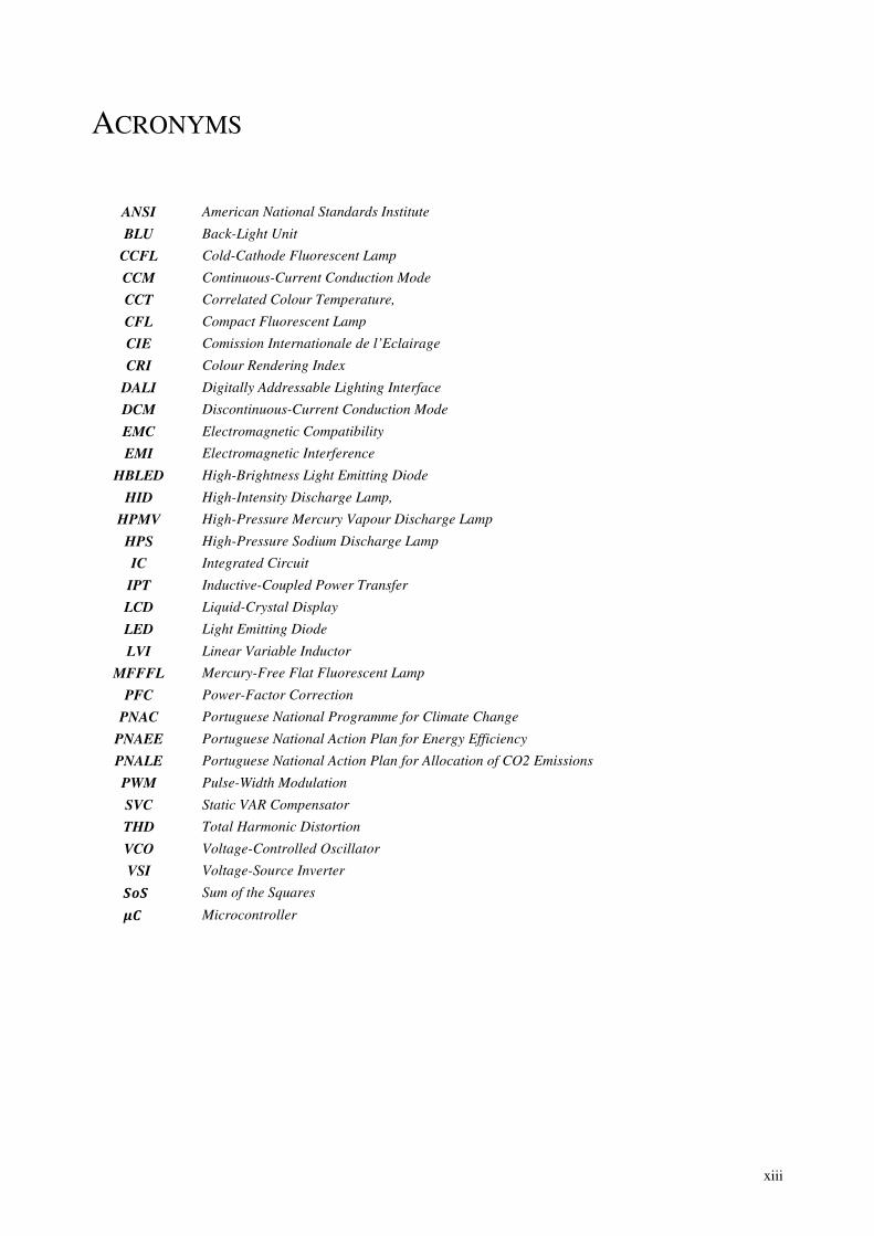
ACRONYMS
ANSI American National Standards Institute
BLU Back-Light Unit
CCFL Cold-Cathode Fluorescent Lamp
CCM Continuous-Current Conduction Mode
CCT Correlated Colour Temperature,
CFL Compact Fluorescent Lamp
CIE Comission Internationale de l’Eclairage
CRI Colour Rendering Index
DALI Digitally Addressable Lighting Interface
DCM Discontinuous-Current Conduction Mode
EMC Electromagnetic Compatibility
EMI Electromagnetic Interference
HBLED High-Brightness Light Emitting Diode
HID High-Intensity Discharge Lamp,
HPMV High-Pressure Mercury Vapour Discharge Lamp
HPS High-Pressure Sodium Discharge Lamp
IC Integrated Circuit
IPT Inductive-Coupled Power Transfer
LCD Liquid-Crystal Display
LED Light Emitting Diode
LVI Linear Variable Inductor
MFFFL Mercury-Free Flat Fluorescent Lamp
PFC Power-Factor Correction
PNAC Portuguese National Programme for Climate Change
PNAEE Portuguese National Action Plan for Energy Efficiency
PNALE Portuguese National Action Plan for Allocation of CO2 Emissions
PWM Pulse-Width Modulation
SVC Static VAR Compensator
THD Total Harmonic Distortion
VCO Voltage-Controlled Oscillator
VSI Voltage-Source Inverter Sum of the Squares Microcontroller

xiv
xv
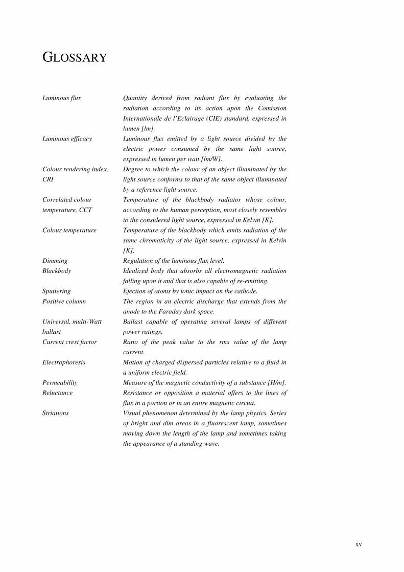
GLOSSARY
Luminous flux Quantity derived from radiant flux by evaluating the
radiation according to its action upon the Comission
Internationale de l’Eclairage (CIE) standard, expressed in
lumen [lm].
Luminous efficacy Luminous flux emitted by a light source divided by the
electric power consumed by the same light source,
expressed in lumen per watt [lm/W].
Colour rendering index,
CRI
Degree to which the colour of an object illuminated by the
light source conforms to that of the same object illuminated
by a reference light source.
Correlated colour
temperature, CCT
Temperature of the blackbody radiator whose colour,
according to the human perception, most closely resembles
to the considered light source, expressed in Kelvin [K].
Colour temperature Temperature of the blackbody which emits radiation of the
same chromaticity of the light source, expressed in Kelvin
[K].
Dimming Regulation of the luminous flux level.
Blackbody Idealized body that absorbs all electromagnetic radiation
falling upon it and that is also capable of re-emitting.
Sputtering Ejection of atoms by ionic impact on the cathode.
Positive column The region in an electric discharge that extends from the
anode to the Faraday dark space.
Universal, multi-Watt
ballast
Ballast capable of operating several lamps of different
power ratings.
Current crest factor Ratio of the peak value to the rms value of the lamp
current.
Electrophoresis Motion of charged dispersed particles relative to a fluid in
a uniform electric field.
Permeability Measure of the magnetic conductivity of a substance [H/m].
Reluctance Resistance or opposition a material offers to the lines of
flux in a portion or in an entire magnetic circuit.
Striations Visual phenomenon determined by the lamp physics. Series
of bright and dim areas in a fluorescent lamp, sometimes
moving down the length of the lamp and sometimes taking
the appearance of a standing wave.

xvi
xvii
SYMBOLS
Cross-sectional area [m2] Magnetization curve
; Magnetic flux density [T]; magnetic flux density vector or surface density of the magnetic flux
Residual flux density [T] Saturation flux density [T] Proportionality constant Parallel capacitor [F] Series capacitor [F] , ~∞ DC-blocking capacitance [F] Resonant capacitance [F]
; Surface element; vector with magnitude and direction normal to surface element [m2]
; Element of path length; vector with magnitude and direction of element of path of length [m]
Duty-cycle of the switches of the half-bridge inverter ; Inverter- switches anti-parallel diodes ! Ignition frequency of the half-bridge inverter [Hz]
Natural frequency [Hz] "# Preheat frequency of the half-bridge inverter [Hz]
Resonant frequency [Hz] ; $% Switching frequency, operating frequency; running frequency of the half-bridge inverter [Hz] &'( Resonant circuit voltage gain
; Magnetic field intensity [A/m]; magnetic field vector
) Coercive force [A/m] * %; % Resonant current of the half-bridge inverter [V]- rms value; instantaneous value + Small-signal lamp current perturbation [A] – rms value -; - Inverter-switches current [A] – instantaneous values * Discharge current [A] - rms value * Heating current [A] – rms value *. Higher lead wire current [A] – rms value *.. Lower lead wire current [A] – rms value *) Arc current [A] - rms value; also referred as /0 *) DC control current [A] *1"; 1" Lamp current [A] – rms value; also referred as /234; instantaneous value
*5 Resonant current [A]- rms value ; Magnetic path length [m] . Inductance, inductor, inductive filter [H] .) Variable inductor inductance; variable inductor differential inductance [H] .)*) Small-signal characteristic of the variable inductor . Differential inductance [H]
. Resonant inductance [H] . Saturable inductance [H]
xviii
-; - Half-bridge resonant inverter switches (MOSFETs) 6 Number of turns of a winding 6) Number of turns of the main winding of the variable inductor 6) Number of turns of each control winding of the variable inductor ) Arc power [W] - average value 55) Single-electrode power [W] - average value 1".) Dimming curve
1"; "1" Lamp power [W]- average value; instantaneous value
1"_8! Low-pass-filtered version of the instantaneous lamp power [W]
1"9 Average power offset (lamp model)[W]
:1" Small-signal lamp power perturbation [W]
; Permeance [Wb/A] < Quality factor =:1" Small-signal lamp resistance perturbation [Ω]
= Resistance, Resistor, Load [Ω] =55) Single-electrode resistance [Ω] =1" Lamp resistance [Ω] = Slope of the line fitted to the rms >/ characteristic of a tubular fluorescent lamp[Ω] ? Reluctance [A/Wb] @ Inverter output voltage [V] – rms value @ Voltage at the intersection of the line fitted to the rms >/ characteristic of a tubular fluorescent
lamp, with the voltage axis [V] @) DC input voltage of the half-bridge inverter [V] @ %,% Input resonant circuit voltage – rms value of the harmonic component n @ % Input voltage of the resonant circuit [V] @ Output voltage of the resonant circuit [V] @ %; 8 % Output voltage of the half-bridge inverter [V]- rms value; instantaneous value @1"; 81" Lamp voltage [V] – rms value; instantaneous value
@1" DC lamp voltage (lamp model)[V]
@"#; @ ! Lamp heating voltage [V]; lamp ignition voltage[V] – rms value
8.) Variable-inductor voltage [V] – instantaneous value
8A Small-signal lamp voltage perturbation [V] – rms value 8 Inverter output voltage [V]– instantaneous value 8 Integrator-capacitor voltage [V]– instantaneous value 8-; 8- Anti-parallel diode voltage [V] - instantaneous values 8&-; 8&- Rectangular-wave voltage sources 8 Inductive voltage [V] B % Impedance of the resonant circuit [Ω] B Incremental impedance [Ω] C Totalized flux or total ac flux linkage [Wb] D Time-changing magnetic flux [Wb] D % Input current phase of the resonant circuit [º] 9 Air permeability [H/m] Differential permeability [H/m]

xix
Permeability [H/m] Initial permeability [H/m] Relative permeability - dimensionless ( Angular frequency [rad/s] (1 Small-signal modulating angular frequency[rad/s] E Efficiency [%] F Ionization density the number of ion pairs per unit volume) G Ionization recombination time constant [s] H Impedance phase of the resonant circuit [º]

xx
xxi
CONTENTS
ACKNOWLEDGEMENTS ...................................................................................................................................... VII
ABSTRACT ................................................................................................................................................................ IX
RESUMO .................................................................................................................................................................... XI
ACRONYMS ........................................................................................................................................................... XIII
GLOSSARY .............................................................................................................................................................. XV
SYMBOLS ..............................................................................................................................................................XVII
CONTENTS ............................................................................................................................................................. XXI
LIST OF FIGURES ................................................................................................................................................ XXV
LIST OF TABLES ................................................................................................................................................ XXXI
INTRODUCTION TO LIGHTING SYSTEMS. MOTIVATION AND MAIN OBJECTIVES OF THE 1WORK ........................................................................................................................................................................ 1.1
1.1 LAMPS AND LIGHTING ..................................................................................................................................... 1.1
1.1.1 Radiation and light .............................................................................................................................. 1.1
1.1.2 Incandescence ..................................................................................................................................... 1.3
1.1.3 Luminescence ..................................................................................................................................... 1.4
1.1.4 General considerations on lighting efficiency .................................................................................. 1.11
1.2 FLUORESCENT LIGHTING SYSTEMS ................................................................................................................ 1.14
1.2.1 Fluorescent lamps ............................................................................................................................. 1.14
1.2.2 Low-frequency and high-frequency operation .................................................................................. 1.18
1.2.3 Electromagnetic ballasts ................................................................................................................... 1.22
1.2.4 Electronic ballasts ............................................................................................................................. 1.24
1.2.5 Control systems ................................................................................................................................ 1.28
1.2.6 Special types of fluorescent lamps .................................................................................................... 1.31
1.2.7 Fluorescent-lamp models .................................................................................................................. 1.33
1.2.7.1 Large-signal dynamic models ................................................................................................. 1.34
1.2.7.2 Small-signal dynamic models ................................................................................................. 1.40
1.3 DIMMING IN FLUORESCENT LIGHTING SYSTEMS............................................................................................ 1.43
1.3.1 Step dimming and continuous dimming ........................................................................................... 1.44
1.3.2 Dimming techniques ......................................................................................................................... 1.44
1.4 MOTIVATION AND MAIN OBJECTIVES OF THE WORK ..................................................................................... 1.50
1.4.1 Magnetic control in electronic ballasts ............................................................................................. 1.51
1.4.2 Outline of the work ........................................................................................................................... 1.54
xxii
REFERENCES ......................................................................................................................................................... 1.56
BIBLIOGRAPHY .................................................................................................................................................... 1.62
LITERATURE REVIEW ON MAGNETIC REGULATORS ........................................................................ 2.1 2
2.1 SATURABLE REACTORS AND MAGNETIC AMPLIFIERS ...................................................................................... 2.1
2.1.1 Fundamentals ...................................................................................................................................... 2.2
2.1.2 Operating principle ............................................................................................................................. 2.4
2.1.3 General applications and construction ................................................................................................ 2.9
2.2 MAGNETIC REGULATORS ............................................................................................................................... 2.10
2.2.1 Variable inductors ............................................................................................................................. 2.10
2.2.1.1 Fundamentals .......................................................................................................................... 2.10
2.2.1.2 Operating principle ................................................................................................................. 2.13
2.2.1.3 Variable inductor structures .................................................................................................... 2.17
2.2.2 Variable transformers ....................................................................................................................... 2.21
2.3 APPLICATIONS OF MAGNETIC REGULATORS .................................................................................................. 2.26
2.3.1 General applications ......................................................................................................................... 2.26
2.3.2 Magnetic control in electronic ballasts ............................................................................................. 2.34
2.3.2.1 Dimmable electronic ballasts .................................................................................................. 2.36
2.3.2.2 Universal electronic ballasts ................................................................................................... 2.38
REFERENCES ......................................................................................................................................................... 2.40
BIBLIOGRAPHY .................................................................................................................................................... 2.44
APPLICATION OF THE VARIABLE INDUCTOR TO THE CONTROL OF ELECTRONIC 3BALLASTS…. ........................................................................................................................................................... 3.1
3.1 MODELLING AND DESIGN OF VARIABLE INDUCTORS ....................................................................................... 3.1
3.1.1 Modelling issues and theorectical analysis ......................................................................................... 3.1
3.1.1.1 Reluctance model ...................................................................................................................... 3.4
3.1.1.2 Magnetic circuit analysis........................................................................................................... 3.6
3.1.1.3 Magnetization and permeability curves .................................................................................. 3.10
3.1.1.4 Non-linear inductance behaviour ............................................................................................ 3.11
3.1.2 Variable inductor simplified design procedure ................................................................................. 3.18
3.1.2.1 Design procedure .................................................................................................................... 3.18
3.1.2.2 Design example ....................................................................................................................... 3.20
3.2 VARIABLE INDUCTORS APPLIED TO DIMMABLE ELECTRONIC BALLASTS ...................................................... 3.23
3.2.1 Introduction to the proposed magnetic control technique ................................................................. 3.23
3.2.1.1 Half-bridge resonant ballast .................................................................................................... 3.23
3.2.1.2 Half-bridge resonant ballast analysis ...................................................................................... 3.26
3.2.1.3 Dimming curves, ZVS and soft-starting ................................................................................. 3.30
3.2.1.4 Fluorescent lamp modelling for the analysis of the proposed technique................................. 3.32
xxiii
3.2.2 Comparative analysis of resonant circuits with magnetic control ..................................................... 3.36
3.2.2.1 Theoretical analysis ................................................................................................................. 3.36
3.2.2.2 Simulation and experimental results ....................................................................................... 3.52
3.2.2.3 Design considerations regarding instability regions................................................................ 3.58
3.2.3 Comparative analysis of magnetic regulator topologies ................................................................... 3.64
3.2.3.1 T5 fluorescent lamp selection ................................................................................................. 3.64
3.2.3.2 Ballast configuration and resonant parameters ....................................................................... 3.66
3.2.3.3 Regulator topologies and core structures ................................................................................ 3.68
3.2.3.4 Regulators characterization, measurement setup and experimental results ............................. 3.71
3.3 VARIABLE-INDUCTOR MODELLING FOR DIMMING APPLICATIONS ................................................................ 3.84
3.3.1 Ballast prototype and experimental results ....................................................................................... 3.84
3.3.2 Matlab-Simulink model .................................................................................................................... 3.87
3.3.2.1 Dynamic-inductance model .................................................................................................... 3.87
3.3.2.2 Comparison between experimental and theoretical results ..................................................... 3.90
3.4 ELECTRODE OPERATION IN DIMMABLE ELECTRONIC BALLASTS WITH MAGNETIC CONTROL ....................... 3.91
3.4.1 Performance issues ........................................................................................................................... 3.91
3.4.1.1 Pre-heating and heating currents during dimming operation .................................................. 3.91
3.4.1.2 The SoS limits ......................................................................................................................... 3.92
3.4.2 Study of the proposed dimming technique under the SoS limits ...................................................... 3.95
3.4.2.1 Lamp selection, variable inductor prototype and characterization .......................................... 3.95
3.4.2.2 Commercial ballasts tests and prototype results under the SoS limits ..................................... 3.97
3.5 VARIABLE INDUCTORS APPLIED TO UNIVERSAL BALLASTS ......................................................................... 3.104
3.5.1 Introduction to the proposed magnetic control technique ............................................................... 3.104
3.5.2 Design procedure ............................................................................................................................ 3.105
3.5.3 Prototype implementation ............................................................................................................... 3.109
3.5.3.1 Variable inductor characterization and control ..................................................................... 3.109
3.5.3.2 General operating issues ....................................................................................................... 3.113
3.5.3.3 Experimental results .............................................................................................................. 3.115
3.5.4 Prototype implementation with digital control ............................................................................... 3.120
3.5.4.1 General description ............................................................................................................... 3.120
3.5.4.2 Electronic ballast experimental prototype ............................................................................. 3.122
3.5.4.3 Forward converter ................................................................................................................. 3.125
3.5.4.4 Control algorithm .................................................................................................................. 3.126
3.5.4.5 Experimental results .............................................................................................................. 3.127
3.5.5 Constant-frequency operation in universal ballasts with SoS compliance ...................................... 3.131
3.5.5.1 Electronic ballast schematic and proposed control technique ............................................... 3.131
3.5.5.2 Resonant circuit design ......................................................................................................... 3.133
3.5.5.2.1 Standard design procedure ............................................................................................... 3.133
3.5.5.2.2 Capacitance selection based on the SoS limits ................................................................. 3.134
3.5.5.2.3 Dual-parallel capacitor configuration ............................................................................... 3.136
xxiv
3.5.5.2.4 ZVS operation .................................................................................................................. 3.142
3.5.5.3 Electronic ballast experimental prototype ............................................................................. 3.142
3.5.5.4 Experimental results .............................................................................................................. 3.145
REFERENCES ....................................................................................................................................................... 3.153
BIBLIOGRAPHY .................................................................................................................................................. 3.157
APPLICATION OF THE VARIABLE TRANSFORMER TO THE CONTROL OF ELECTRONIC 4BALLASTS ................................................................................................................................................................ 4.1
4.1 INTRODUCTION TO THE PROPOSED MAGNETIC CONTROL TECHNIQUE ............................................................. 4.1
4.1.1 Isolated half-bridge resonant ballast ................................................................................................... 4.2
4.2 MODELLING AND CHARACTERIZATION OF VARIABLE TRANSFORMERS ........................................................... 4.3
4.2.1 Variable transformer strucutures, topologies and operating principle ................................................ 4.3
4.2.2 Variable transformer modelling .......................................................................................................... 4.7
4.2.2.1 Five-leg variable transformer modelling ................................................................................... 4.7
4.2.2.2 Parallel three-leg variable transformer modelling ................................................................... 4.13
4.2.3 Variable transformer characterization ............................................................................................... 4.17
4.3 LAMP OPERATION WITH A VARIABLE TRANSFORMER ................................................................................... 4.26
4.3.1 Analysis of the equivalent circuit with variable transformer ............................................................ 4.26
4.3.2 Experimental results using the five-leg variable transformer ........................................................... 4.29
4.4 VARIABLE TRANSFORMER APPLIED TO DIMMABLE ELECTRONIC BALLASTS ................................................. 4.32
4.4.1 Design procedure .............................................................................................................................. 4.33
4.4.2 Experimental results using the three-leg variable tranSformer ......................................................... 4.35
REFERENCES ......................................................................................................................................................... 4.43
CONCLUSIONS, CONTRIBUTIONS, AND FUTURE WORK ................................................................... 5.1 5
5.1 CONCLUSIONS AND CONTRIBUTIONS ............................................................................................................... 5.1
5.2 FUTURE WORK ................................................................................................................................................ 5.7
5.3 PUBLISHED PAPERS .......................................................................................................................................... 5.9
5.3.1 Journals ............................................................................................................................................... 5.9
5.3.2 International Conferences ................................................................................................................. 5.10
REFERENCES ......................................................................................................................................................... 5.13
APPENDIX A: OPERATION OF T5 FLUORESCENT LAMPS WITH COMMERCIAL BALLASTS ............... - 1 -
A.1 SELECTED LAMPS ................................................................................................................................................ - 1 -
A.2 CONDITIONS FOR PROPER ELECTRODE OPERATION .............................................................................................. - 2 -
A.3 EXPERIMENTAL SETUP ......................................................................................................................................... - 3 -
A.4 EXPERIMENTAL RESULTS ..................................................................................................................................... - 4 -
REFERENCES AND BIBLIOGRAPHY ............................................................................................................... - 16 -
APPENDIX B: MATHCAD FILES ....................................................................................................................... - 17 -
xxv
LIST OF FIGURES
Fig.1.1. The electromagnetic spectrum. ...................................................................................................................... 1.2
Fig.1.2. Incandescent and halogen lamps retrieved from the Philips Product Catalogue 2010 [1.4]. ......................... 1.4
Fig.1.3. Fluorescent lamps retrieved from the Philips Product Catalogue 2010 [1.4]. ................................................ 1.6
Fig.1.4. Low-pressure Sodium Lamp from the Osram Sylvania Product Catalogue [1.6]: SOX or SOX-E. .............. 1.6
Fig.1.5. High Discharge Lamps from the Osram Sylvania Product Catalogue [1.6]. .................................................. 1.8
Fig.1.6. LED lamps and High Brightness Power LEDs from large manufacturers: CREE, Philips and NICHIA. ... 1.10
Fig.1.7. LED lamps retrieved from the Philips Product Catalogue 2010 [1.4]. ......................................................... 1.10
Fig.1.8. Basic processes in the fluorescent lamp tube. .............................................................................................. 1.15
Fig.1.9. Negative differential or incremental resistance of a fluorescent lamp. ........................................................ 1.19
Fig.1.10. Low-frequency and high-frequency operation. .......................................................................................... 1.20
Fig.1.11. Dynamic voltage-current characteristics of a fluorescent lamp operated at various frequencies. .............. 1.21
Fig.1.12. Fluorescent-lamp typical waveforms and voltage-current characteristics: TL 20 W Osram...................... 1.22
Fig.1.13. Electronic ballast schematic. ...................................................................................................................... 1.25
Fig.1.14. Installation of a Digital Addressable Lighting Interface (DALI) system. .................................................. 1.30
Fig.1.15. Architecture of an electronic ballast with DALI [1.23]. ............................................................................. 1.31
Fig.1.16. High-frequency KL characteristics of a TL5 HE 35W fluorescent lamp at different power levels. ......... 1.36
Fig.1.17. Steady-state and small-signal behaviour: negative incremental impedance definition [1.58], [1.59]. ....... 1.41
Fig.1.18. Typical plot of the lamp incremental impedance in the complex plane [1.58]. .......................................... 1.42
Fig.1.19. Dimming control parameters: dc voltage, operating frequency and duty-cycle. ........................................ 1.45
Fig.1.20. Frequency control with IC IR21571. .......................................................................................................... 1.49
Fig.1.21. Dimming with Triac Phase Control............................................................................................................ 1.50
Fig.1.22. Magnetically-controlled electronic ballast schematic. ............................................................................... 1.52
Fig.1.23. Magnetically-controlled electronic ballasts. ............................................................................................... 1.53
Fig. 2.1. Typical magnetization curve for a soft magnetic material. ........................................................................... 2.3
Fig. 2.2. Hysteresis loop shapes for different magnetic materials. .............................................................................. 2.4
Fig. 2.3. Magnetic field paths in a saturable-core reactor. ........................................................................................... 2.5
Fig. 2.4. Magnetic field paths in a three-legged saturable-core reactor. ...................................................................... 2.6
Fig. 2.5. Magnetic field paths in a toroidal saturable-core reactor. ............................................................................. 2.7
Fig. 2.6. Half-wave magnetic amplifier circuit: flux control and output waveform characteristics. ........................... 2.8
Fig. 2.7. Flux linkage as a function of current, and inductance definitions [2.6]. ..................................................... 2.11
Fig. 2.8. Magnetic regulator: variable inductor. ........................................................................................................ 2.15
Fig. 2.9. Magnetic regulator: variable inductor [2.13], [2.16]. .................................................................................. 2.16
Fig. 2.10. Typical variable inductor small-signal characteristic ................................................................................ 2.17
Fig. 2.11. US Patents: Magnetic regulator structures and topologies. ....................................................................... 2.19
Fig. 2.12. US Patent 4766365: Self-Regulated Transformer-Inductor [2.18]. ........................................................... 2.22
Fig. 2.13. Magnetic regulator with additional windings: variable transformer [2.20]. .............................................. 2.24
xxvi
Fig. 2.14. Current sensor utilizing a LVI [2.22]. ....................................................................................................... 2.27
Fig. 2.15. Rectifier circuit with passive PFC with magnetic control. ........................................................................ 2.28
Fig. 2.16. Static Var Compensator based on a core controlled reactor [2.38]. .......................................................... 2.29
Fig. 2.17. Examples of resonant converters with magnetic control. .......................................................................... 2.31
Fig. 2.18. IPT system with a variable inductor-based compensation circuit [2.40]. .................................................. 2.32
Fig. 2.19. Single-stage flyback LED driver with energy-storage capacitor at the primary side and variable “boost” inductance [2.24]. ...................................................................................................................................................... 2.34
Fig. 2.20. High-Pressure Discharge Lamp Driver based on Inductor-Controlled Current-Sourcing Push-Pull Parallel-Resonance Inverter [2.14]. ........................................................................................................................................ 2.35
Fig. 2.21. Magnetically-controlled electronic ballasts: dimmable electronic ballast and universal ballast. .............. 2.36
Fig. 2.22. Striation phenomenon on tubular fluorescent lamps. ................................................................................ 2.37
Fig. 3.1. Variable inductor, [2.16]. .............................................................................................................................. 3.3
Fig. 3.2. Variable inductor modelling. ......................................................................................................................... 3.5
Fig. 3.3. Simplified reluctance model. ......................................................................................................................... 3.6
Fig. 3.4. Variable inductor magnetic structure: core geometry and magnetic behaviour. ........................................... 3.7
Fig. 3.5. Permeability and magnetization curves: material 3C85 from Philips. ........................................................ 3.11
Fig. 3.6. Non-linear region of the variable inductor. ................................................................................................ 3.12
Fig. 3.7. Differential inductance value for different levels of the dc control current with symmetric gap lengths. .. 3.15
Fig. 3.8. Differential inductance value for different levels of the dc control current with asymmetric gap lengths. . 3.16
Fig. 3.9. Prototype small-signal characteristic: two gapped EF25 cores with 3C85 material from Phillips, Ndc = 35, Nac = 68 and lg = 0.3mm .......................................................................................................................................... 3.17
Fig. 3.10. Differential inductance value for different levels of the dc control current. ............................................. 3.17
Fig. 3.11. EF25 core: dimensions and main characteristics. ...................................................................................... 3.21
Fig. 3.12. Variable-inductor small-signal characteristic and correspondent parameters. .......................................... 3.22
Fig. 3.13. Half-bridge resonant ballast: operating waveforms fs > fr [3.2]. ............................................................... 3.24
Fig. 3.14. Frequency-response characteristic of the resonant circuit and soft-start technique................................... 3.30
Fig. 3.15. Soft-starting process using the inductance as control parameter and dimming curve [3.5]. ..................... 3.32
Fig. 3.16. Lamp resistance models ............................................................................................................................ 3.33
Fig. 3.17. TLD 36 W Philips – fluorescent-lamp electric characteristics: linear interpolation of the lamp resistance. ................................................................................................................................................................................... 3.34
Fig. 3.18. T5 HE and HO Philips - fluorescent lamp electric characteristics. ........................................................... 3.35
Fig. 3.19. Half-bridge resonant inverter. ................................................................................................................... 3.37
Fig. 3.20. Half-bridge resonant inverter: equivalent circuits. .................................................................................... 3.38
Fig. 3.21. LCC-CII resonant equivalent circuit: mesh definition .............................................................................. 3.42
Fig. 3.22. CLL resonant equivalent circuit: mesh definition ..................................................................................... 3.45
Fig. 3.23. Comparative analysis: theoretical dimming curves and phase angle of the input filter current, as a function of the variable inductance, at 45 kHz, 50 kHz and 55 kHz. ...................................................................................... 3.51
Fig. 3.24. Electronic ballast MATLAB-Simulink implementation: LCC-CII resonant circuit. ................................ 3.54
Fig. 3.25. Simulation results for the electronic ballast MATLAB-Simulink implementation: LCC-CII resonant circuit. ........................................................................................................................................................................ 3.55
Fig. 3.26. Comparison between simulation results and theoretical results using MatCad: LCC-CII resonant circuit. ................................................................................................................................................................................... 3.55
xxvii
Fig. 3.27. Small-signal characterization of the variable inductor. ............................................................................. 3.56
Fig. 3.28. Experimental value of the magnetic regulator as a function of the dc current for the LC and LCC-CII circuit configurations. ................................................................................................................................................ 3.56
Fig. 3.29. Experimental results for the average lamp power and electrode power for the LC and LCC-CII circuit configurations. ........................................................................................................................................................... 3.57
Fig. 3.30. Oscillations in the experimental waveforms. ............................................................................................ 3.59
Fig. 3.31. Theoretical comparison between the previous and the proposed method: LC resonant circuit configuration. ................................................................................................................................................................................... 3.60
Fig. 3.32. Characterization of the magnetic regulator. .............................................................................................. 3.61
Fig. 3.33. Experimental results for the average input power, lamp power, arc power and electrode power for the new design. ....................................................................................................................................................................... 3.62
Fig. 3.34. Experimental results for the average lamp power and luminous flux for the new design. ........................ 3.62
Fig. 3.35. Experimental results for the converter efficiency for the new design. ...................................................... 3.63
Fig. 3.36. Waveforms of the inverter output voltage and resonant current at maximum and minimum average lamp power (25V/div; 0.4A/div; and 5 µs/div). ................................................................................................................. 3.63
Fig. 3.37. Master TL5 21W Philips: curve fitting to the Rlamp Parc - linear interpolation; theoretical dimming curves and phase angle of the resonant current for the LC circuit configuration. ................................................................. 3.67
Fig. 3.38. Magnetic regulator: variable inductor based on EFD core. ....................................................................... 3.69
Fig. 3.39. Magnetic regulator: variable inductor based on U core. ........................................................................... 3.70
Fig. 3.40. Core structures, dimensions and experimental prototypes: EFD20 and U15. ........................................... 3.71
Fig. 3.41. Small-signal characterization of the variable inductors. ........................................................................... 3.72
Fig. 3.42. Electronic ballast prototype: experimental setup for large-signal characterization. .................................. 3.73
Fig. 3.43. Experimental results for the TL5 HE 21W with commercial ballast: average lamp power, arc power and electrode power, as function of the control voltage. .................................................................................................. 3.76
Fig. 3.44. Experimental results for the TL5 HE 21W with electronic ballast prototype – EFD20: average lamp power, arc power and electrode power, as functions of the control parameters, and ballast efficiency as a function of the dc control current. .......................................................................................................................................................... 3.77
Fig. 3.45. Experimental results for the TL5 HE 21W with electronic ballast prototype – EFD20: ballast efficiency as a function of lamp power. .......................................................................................................................................... 3.78
Fig. 3.46. Comparison between dimming curves: theoretical and experimental results for the TL5 HE 21W with electronic ballast prototype: Vdc = 310V; Cp = 2.2nF; fs = 85kHz. .......................................................................... 3.78
Fig. 3.47. Experimental results for the TL5 HE 14W with electronic ballast prototype – EFD20: average lamp power, arc power and electrode power, as functions of the control parameters, and ballast efficiency as a function of the dc control current. .......................................................................................................................................................... 3.79
Fig. 3.48. Experimental waveforms for the TL5 HE 21W-EFD20 at nominal power, medium and at minimum power level, 85 KHz. ............................................................................................................................................................ 3.80
Fig. 3.49. Experimental results for the TL5 HE 14W with electronic ballast prototype – EFD20: totalized ac flux versus resonant current. ............................................................................................................................................. 3.81
Fig. 3.50. Experimental results for the TL5 HE 21W with electronic ballast prototype – U15: average lamp power, arc power and electrode power, as functions of the control parameters, and ballast efficiency as a function of the dc control current. .......................................................................................................................................................... 3.82
Fig. 3.51. Experimental waveforms for the TL5 HE 14/21W - U15 regulators ........................................................ 3.83
Fig. 3.52. Electronic ballast prototype: experimental setup for large-signal characterization. .................................. 3.85
Fig. 3.53. Comparison between the small-signal and large-signal characteristics of the prototypes based on the peak-to-peak average inductance value. ............................................................................................................................. 3.86
Fig. 3.54. Non-linear behaviour of the regulator prototype at Idc = 0A and 0.3A. .................................................... 3.87
xxviii
Fig. 3.55. Electronic ballast MATLAB-Simulink implementation: dynamic-inductance model. ............................. 3.89
Fig. 3.56. Comparison between experimental and simulation results. ...................................................................... 3.90
Fig. 3.57. Preheating techniques ................................................................................................................................ 3.92
Fig. 3.58. TL5 HO 39W Philips and TL5 HE 21W Philips theoretical analysis. ...................................................... 3.96
Fig. 3.59. Variable inductor ....................................................................................................................................... 3.97
Fig. 3.60. Graphical representation of the m lines for the TL5 HO 39W and the TL5 HE 21W with commercial ballasts. ...................................................................................................................................................................... 3.99
Fig. 3.61. Graphical representation of the m lines for the TL5 HO 39W with ballast prototype. ........................ 3.100
Fig. 3.62. Graphical representation of the m lines for the TL5 HE 21W with ballast prototype .......................... 3.100
Fig. 3.63. Changing the level of the m lines ......................................................................................................... 3.101
Fig. 3.64. Graphical representation of the m lines for the TL5 HE 21W with ballast prototype .......................... 3.102
Fig. 3.65. Experimental waveforms for the TL5 HO 39W-EFD20 at nominal power, medium and at minimum power level, 65 kHz............................................................................................................................................................ 3.103
Fig. 3.66. Experimental results for the TL5 HO 39W-EFD20 at nominal power, medium and at minimum power level, 65 kHz............................................................................................................................................................ 3.103
Fig. 3.67. Magnetically-controlled universal ballast: circuit schematic .................................................................. 3.105
Fig. 3.68. Flowchart of the design procedure for obtaining the suitable working parameters. ................................ 3.106
Fig. 3.69. Variable inductor. .................................................................................................................................... 3.109
Fig. 3.70. Variable inductor characterization. ......................................................................................................... 3.111
Fig. 3.71. Forward converter used for supplying the dc control current to the variable inductor. ........................... 3.112
Fig. 3.72. Lamp voltage versus lamp power for lamp detection purpose. ............................................................... 3.115
Fig. 3.73. Universal ballast prototype. ..................................................................................................................... 3.116
Fig. 3.74. Experimental results for the TLD 18W. .................................................................................................. 3.118
Fig. 3.75. Experimental results for the TLD 36W. .................................................................................................. 3.118
Fig. 3.76. Experimental results for the TLD 58W. .................................................................................................. 3.118
Fig. 3.77. Experimental results for the universal ballast vs. commercial ballasts. .................................................. 3.119
Fig. 3.78. Magnetically-controlled universal ballast with digital control: circuit schematic. .................................. 3.121
Fig. 3.79. Magnetically-controlled universal ballast with digital control: circuit schematic. .................................. 3.123
Fig. 3.80. Forward converter: circuit schematic. ..................................................................................................... 3.125
Fig. 3.81. Flowchart of the proposed control algorithm. ......................................................................................... 3.126
Fig. 3.82. Experimental results for the TLD 18W. .................................................................................................. 3.127
Fig. 3.83. Experimental results for the TLD 36W. .................................................................................................. 3.127
Fig. 3.84. Experimental results for the TLD 58W. .................................................................................................. 3.128
Fig. 3.85. Closed loop operation of the resonant inverter: average lamp power and switching frequency range for an input voltage variation from 250V to 350V. ........................................................................................................... 3.129
Fig. 3.86. Dynamic response of the resonant inverter for an input voltage step from 280 to 320 V - lamp under test: TLD 36W. The waveform corresponds to the output voltage of the lamp current sensor, which has a gain of 0.375mArms/mV (vertical scale: 500 mV/div, horiz. scale: 100 ms/div). ................................................................ 3.130
Fig. 3.87. Constant-frequency magnetically-controlled universal ballast with digital control: circuit schematic. .. 3.132
Fig. 3.88. Conventional equivalent circuit schematic. ............................................................................................. 3.135
Fig. 3.89. Equivalent circuit schematic. .................................................................................................................. 3.137
Fig. 3.90. Selection of Cp1. ...................................................................................................................................... 3.139
xxix
Fig. 3.91. ILH, ILL, ID currents considering both capacitors configurations: comparison with maximum limits. ....... 3.141
Fig. 3.92. Constant-frequency magnetically-controlled universal ballast with digital control: experimental prototype. ................................................................................................................................................................................. 3.143
Fig. 3.93. Variable inductor. .................................................................................................................................... 3.144
Fig. 3.94. Schematic of the dc-dc converter. ........................................................................................................... 3.144
Fig. 3.95. Schematic of the flyback converter. ........................................................................................................ 3.145
Fig. 3.96. Experimental results of the heating currents for all tested T5 fluorescent lamps. ................................... 3.146
Fig. 3.97. Lamp voltage and arc current waveforms at rated power........................................................................ 3.147
Fig. 3.98. Voltage and current at the input of the resonant circuit .......................................................................... 3.147
Fig. 3.99. Lamp voltage, arc current and lamp power waveforms at nominal power .............................................. 3.148
Fig. 3.100. Power, voltage and current waveforms at the input of the resonant circuit ........................................... 3.148
Fig. 3.101. Experimental waveforms for the T5 HE lamp series and the T5 HO lamp series: electrodes voltage, velectr, heating currents, iLH, iLL, and discharge current, iD. .................................................................................................. 3.149
Fig. 3.102. T5 HO 49W: integrator voltage, resonant current and control current waveforms at rated power: (1.744V/div, 0.25A/div, 0.249A/div, 21.35ms/div). ............................................................................................... 3.151
Fig. 3.103. Considerations on inductance values. ................................................................................................... 3.151
Fig. 4.1. Isolated half-bridge resonant ballast with an integrated variable transformer. .............................................. 4.2
Fig. 4.2. Variable transformer: five-leg structure and topology. ................................................................................. 4.4
Fig. 4.3. Variable transformer: parallel three-leg structure and topology. ................................................................... 4.6
Fig. 4.4. Variable transformer: five-leg structure and topology. ................................................................................. 4.9
Fig. 4.5. Duality theory.............................................................................................................................................. 4.10
Fig. 4.6. Proposed T inductance model. .................................................................................................................... 4.13
Fig. 4.7. Reluctance models. ..................................................................................................................................... 4.14
Fig. 4.8. Duality theory.............................................................................................................................................. 4.16
Fig. 4.9. Proposed T inductance model. .................................................................................................................... 4.17
Fig. 4.10. Variable transformers prototypes. ............................................................................................................. 4.18
Fig. 4.11. Thévenin equivalent of the proposed T inductance model. ....................................................................... 4.21
Fig. 4.12. Simplified variable transformer model. ..................................................................................................... 4.22
Fig. 4.13. Characterization of the three-leg variable transformer. ............................................................................. 4.25
Fig. 4.14. Half-bridge resonant inverter with variable transformer: equivalent circuit ............................................. 4.26
Fig. 4.15. Electronic ballast prototype ....................................................................................................................... 4.30
Fig. 4.16. Experimental waveforms at nominal power for the L18W/840 from Osram ............................................ 4.31
Fig. 4.17. 14W fluorescent lamp: curve fitting to the Rlamp Parc - linear interpolation; theoretical dimming curves. ................................................................................................................................................................................... 4.34
Fig. 4.18. Electronic ballast prototype. ...................................................................................................................... 4.36
Fig. 4.19. Experimental results for the FH 14W/840 from Osram with electronic ballast prototype: ballast input power, average lamp power, arc power and electrode power, and ballast efficiency as a function of the dc control current........................................................................................................................................................................ 4.38
Fig. 4.20. Experimental results for the FH 14W/840 from Osram at nominal power and at the lowest power level.4.39
Fig. 4.21. Experimental results for the FH 14W/840 from Osram: waveforms of the lamp voltage and arc current (100V/div, 0.5A/div, 5µs/div). .................................................................................................................................. 4.40
Fig. 4.22.Current in the primary side (CH1) and in the secondary side (CH2): 0.2 A/DIV, 5 µs/DIV. .................... 4.41

xxx
Fig. 4.23.Experimental value of the magnetic regulator as a function of the dc control current with lamp. ............. 4.42
xxxi
LIST OF TABLES
Table 3.1 Half-bridge resonant inverter analysis, [3.7]. ............................................................................................ 3.49
Table 3.2 Half-bridge resonant inverter parameters. ................................................................................................. 3.50
Table 3.3 Simulation parameters. .............................................................................................................................. 3.54
Table 3.4 New design parameters.............................................................................................................................. 3.60
Table 3.5 MASTER TL5 High Efficiency. ............................................................................................................... 3.66
Table 3.6 TL5 HE 21W Philips operated with PHILIPS HF-R 14-35 TL5 220-240. ............................................... 3.75
Table 3.7 Experimental results obtained with the EF25 prototype. ........................................................................... 3.86
Table 3.8 TL5 HO 39W Philips operated with PHILIPS HF-R 139 TL5 220-240. .................................................. 3.98
Table 3.9 SoS line parameters. ................................................................................................................................... 3.98
Table 3.10 Operating frequency and resonant circuit parameters for each lamp ....................................................... 3.99
Table 3.11 Lamp nominal characteristics at high-frequency. .................................................................................. 3.105
Table 3.12 Operating frequency and resonant circuit parameters for each lamp ..................................................... 3.108
Table 3.13 Variable inductor characteristics. .......................................................................................................... 3.110
Table 3.14 Design parameters of the forward converter. ........................................................................................ 3.112
Table 3.15 T8 Lamp voltage and current for two main manufacturers ................................................................... 3.114
Table 3.16 Power distribution and efficiency for the proposed converter ............................................................... 3.128
Table 3.17 Operating frequency and resonant circuit parameters for each lamp: theoretical values ....................... 3.134
Table 3.18 Nominal and Safe Operation conditions for TL5 Philips lamps at 25ºC: lamp voltage, discharge current, electrode resistance, SoS limits and maximum parallel capacitor ........................................................................... 3.136
Table 3.19 Quality and damping factors for Cpeq=4.4nF ......................................................................................... 3.140
Table 3.20 Quality and damping factors for Cpeq=3.3nF ......................................................................................... 3.141
Table 3.21 Experimental results for all T5 lamps .................................................................................................... 3.146
Table 3.22 Power rating of the ballast and tested lamps, experimental values of Lac and Idc .................................. 3.150
Table 4.1 Applying the duality theory. ...................................................................................................................... 4.11
Table 4.2 Open circuit and short circuit tests: inductance measurements for the five-leg transformer. .................... 4.19
Table 4.3 Open circuit and short circuit tests: inductance measurements for the three-leg transformer. .................. 4.20
Table 4.4 Model parameters for the five-leg transformer. ......................................................................................... 4.23
Table 4.5 Model parameters for the three-leg transformer. ....................................................................................... 4.23
Table 4.6 Lamp nominal characteristics at high-frequency and experimental measurements. .................................. 4.29
Table 4.7 Experimental measurements. ..................................................................................................................... 4.31
Table 4.8 Lamp nominal characteristics at high-frequency. ...................................................................................... 4.33

xxxii

xxxiii

INTRODUCTION TO LIGHTING SYSTEMS. 1MOTIVATION AND MAIN OBJECTIVES OF
THE WORK
In the present chapter, a succinct introduction to lamps and lighting is presented. Some
general considerations on lighting efficiency, essential light properties and definitions are
introduced. Due to the purpose of the developed work, the subject of fluorescent-lamp operation
and control is addressed along with a short introduction to conventional ballasts, electronic
ballasts and fluorescent-lamp models. The replacement of conventional ballasts by electronic
ballasts has come to confirm that the latter are effectively an efficient way of saving energy in
lighting systems. The fundamental requirements of typical fluorescent lighting systems controlled
by electronic ballasts are described. However, there are always new demands with respect to
their working possibilities. Electronic ballasts with additional control circuitry can provide
multi-lamp operation and dimming. This important feature allows the ballast to control the lamp
power and thereby the light output. The state of the art in fluorescent-lamp dimming techniques is
presented. Other features related to remote control of the lighting system are also referred.
Magnetic regulators are introduced as a new concept related to magnetic control in electronic
ballasts, for dimming and multi-Watt operation. The chapter ends with a brief description of this
type of control and sets the directions for the remaining chapters.
1.1 LAMPS AND LIGHTING
1.1.1 RADIATION AND LIGHT
Radiation describes any process in which energy travels through a medium or through space,
eventually being absorbed by another body. Light is considered to be a particular form of
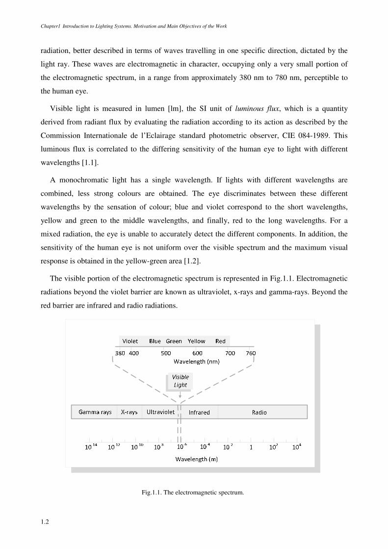
Chapter1 Introduction to Lighting Systems. Motivation and Main Objectives of the Work
1.2
radiation, better described in terms of waves travelling in one specific direction, dictated by the
light ray. These waves are electromagnetic in character, occupying only a very small portion of
the electromagnetic spectrum, in a range from approximately 380 nm to 780 nm, perceptible to
the human eye.
Visible light is measured in lumen [lm], the SI unit of luminous flux, which is a quantity
derived from radiant flux by evaluating the radiation according to its action as described by the
Commission Internationale de l’Eclairage standard photometric observer, CIE 084-1989. This
luminous flux is correlated to the differing sensitivity of the human eye to light with different
wavelengths [1.1].
A monochromatic light has a single wavelength. If lights with different wavelengths are
combined, less strong colours are obtained. The eye discriminates between these different
wavelengths by the sensation of colour; blue and violet correspond to the short wavelengths,
yellow and green to the middle wavelengths, and finally, red to the long wavelengths. For a
mixed radiation, the eye is unable to accurately detect the different components. In addition, the
sensitivity of the human eye is not uniform over the visible spectrum and the maximum visual
response is obtained in the yellow-green area [1.2].
The visible portion of the electromagnetic spectrum is represented in Fig.1.1. Electromagnetic
radiations beyond the violet barrier are known as ultraviolet, x-rays and gamma-rays. Beyond the
red barrier are infrared and radio radiations.
Fig.1.1. The electromagnetic spectrum.
Chapter1 Introduction to Lighting Systems. Motivation and Main Objectives of the Work
1.3
From an historical point of view, artificial light sources are typically classified according to
the mechanism which is used to produce light, the most common being incandescence and
luminescence.
Both mechanisms are the result of the same process: transitions between energy levels of
atoms, ions, molecules and solids. Whereas incandescence is the emission of light by a hot body,
especially solids, luminescence is used to describe the general process by which an excited
material emits light, not by a rise of temperature of the emitting body, but by the intervention of
an external agent. This excitation may usually be achieved with ultraviolet radiation, x-rays,
electrons, electric fields, or chemical energy. The colour or wavelength of the emitted light is
determined by the material, while the intensity depends on both the material and the input energy
[1.2], [1.3].
1.1.2 INCANDESCENCE
One of the first well-known examples of artificial light sources is the incandescent lamp. On
January 27, 1880, Thomas Edison received the historic patent claiming the principles of his
incandescent lamp, based on a filament of carbon of high resistance, which then led the way for
the universal domestic use of electric light [1.3].
Today’s typical incandescence mechanism can be simply described by an electric current
passing through a thin filament of solid tungsten or carbon, heating it to a temperature that
produces light. Even if incandescent lamps are still very common in daily life, their application is
limited according to their low luminous efficacy and rated lamp life. The luminous efficacy is the
quotient between the luminous flux emitted and the power consumed by the source, expressed in
lumen per watt [lm/W] [1.1].
Typically, larger wattage incandescent bulbs have a higher efficacy than smaller wattage
bulbs, around 20 lm/W; still most of the energy consumed is emitted and lost in heat, rather than
as visible light. Moreover, the estimated lamp life, around 1000 burning hours, is well below
other common light sources. Incandescent lamps are also limited by the rate of evaporation of the
tungsten filament. In conventional lamps, the bulb is normally filled with an inert gas such as
argon to reduce this evaporation.
In 1959, a special type of incandescent lamp became commercially available: halogen lamps.
In this type of lamps, the tungsten filament is sealed into a compact transparent envelope filled
with an inert gas and a small amount of a halogen. The purpose of the halogen is to prevent
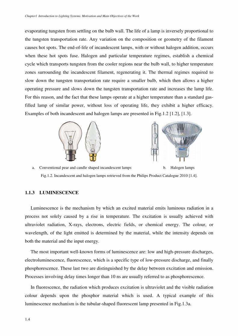
Chapter1 Introduction to Lighting Systems. Motivation and Main Objectives of the Work
1.4
evaporating tungsten from settling on the bulb wall. The life of a lamp is inversely proportional to
the tungsten transportation rate. Any variation on the composition or geometry of the filament
causes hot spots. The end-of-life of incandescent lamps, with or without halogen addition, occurs
when these hot spots fuse. Halogen and particular temperature regimes, establish a chemical
cycle which transports tungsten from the cooler regions near the bulb wall, to higher temperature
zones surrounding the incandescent filament, regenerating it. The thermal regimes required to
slow down the tungsten transportation rate require a smaller bulb, which then allows a higher
operating pressure and slows down the tungsten transportation rate and increases the lamp life.
For this reason, and the fact that these lamps operate at a higher temperature than a standard gas-
filled lamp of similar power, without loss of operating life, they exhibit a higher efficacy.
Examples of both incandescent and halogen lamps are presented in Fig.1.2 [1.2], [1.3].
a. Conventional pear and candle shaped incandescent lamps b. Halogen lamps
Fig.1.2. Incandescent and halogen lamps retrieved from the Philips Product Catalogue 2010 [1.4].
1.1.3 LUMINESCENCE
Luminescence is the mechanism by which an excited material emits luminous radiation in a
process not solely caused by a rise in temperature. The excitation is usually achieved with
ultraviolet radiation, X-rays, electrons, electric fields, or chemical energy. The colour, or
wavelength, of the light emitted is determined by the material, while the intensity depends on
both the material and the input energy.
The most important well-known forms of luminescence are: low and high-pressure discharges,
electroluminescence, fluorescence, which is a specific type of low-pressure discharge, and finally
phosphorescence. These last two are distinguished by the delay between excitation and emission.
Processes involving delay times longer than 10 ns are usually referred to as phosphorescence.
In fluorescence, the radiation which produces excitation is ultraviolet and the visible radiation
colour depends upon the phosphor material which is used. A typical example of this
luminescence mechanism is the tubular-shaped fluorescent lamp presented in Fig.1.3a.
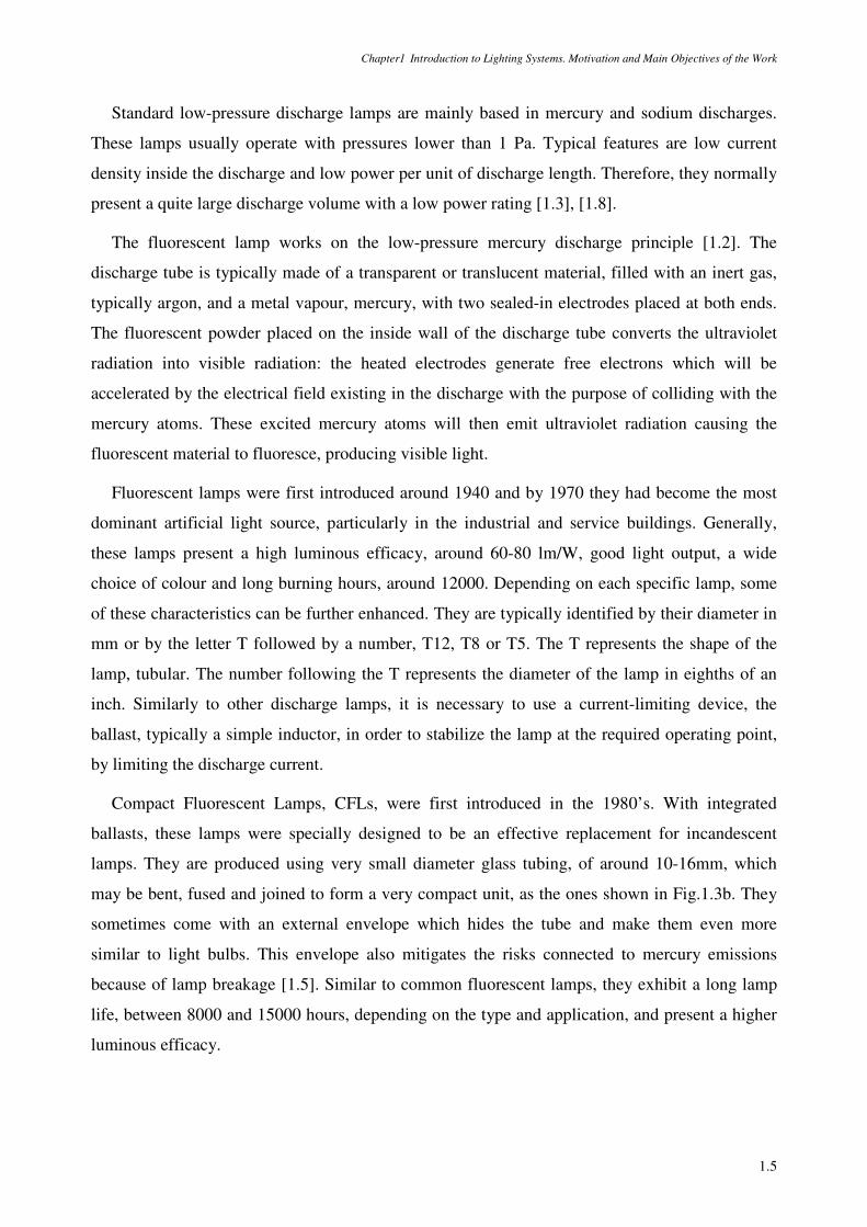
Chapter1 Introduction to Lighting Systems. Motivation and Main Objectives of the Work
1.5
Standard low-pressure discharge lamps are mainly based in mercury and sodium discharges.
These lamps usually operate with pressures lower than 1 Pa. Typical features are low current
density inside the discharge and low power per unit of discharge length. Therefore, they normally
present a quite large discharge volume with a low power rating [1.3], [1.8].
The fluorescent lamp works on the low-pressure mercury discharge principle [1.2]. The
discharge tube is typically made of a transparent or translucent material, filled with an inert gas,
typically argon, and a metal vapour, mercury, with two sealed-in electrodes placed at both ends.
The fluorescent powder placed on the inside wall of the discharge tube converts the ultraviolet
radiation into visible radiation: the heated electrodes generate free electrons which will be
accelerated by the electrical field existing in the discharge with the purpose of colliding with the
mercury atoms. These excited mercury atoms will then emit ultraviolet radiation causing the
fluorescent material to fluoresce, producing visible light.
Fluorescent lamps were first introduced around 1940 and by 1970 they had become the most
dominant artificial light source, particularly in the industrial and service buildings. Generally,
these lamps present a high luminous efficacy, around 60-80 lm/W, good light output, a wide
choice of colour and long burning hours, around 12000. Depending on each specific lamp, some
of these characteristics can be further enhanced. They are typically identified by their diameter in
mm or by the letter T followed by a number, T12, T8 or T5. The T represents the shape of the
lamp, tubular. The number following the T represents the diameter of the lamp in eighths of an
inch. Similarly to other discharge lamps, it is necessary to use a current-limiting device, the
ballast, typically a simple inductor, in order to stabilize the lamp at the required operating point,
by limiting the discharge current.
Compact Fluorescent Lamps, CFLs, were first introduced in the 1980’s. With integrated
ballasts, these lamps were specially designed to be an effective replacement for incandescent
lamps. They are produced using very small diameter glass tubing, of around 10-16mm, which
may be bent, fused and joined to form a very compact unit, as the ones shown in Fig.1.3b. They
sometimes come with an external envelope which hides the tube and make them even more
similar to light bulbs. This envelope also mitigates the risks connected to mercury emissions
because of lamp breakage [1.5]. Similar to common fluorescent lamps, they exhibit a long lamp
life, between 8000 and 15000 hours, depending on the type and application, and present a higher
luminous efficacy.
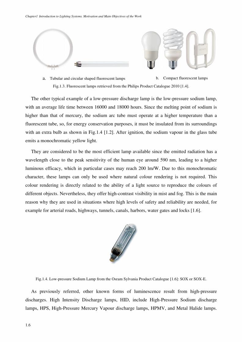
Chapter1 Introduction to Lighting Systems. Motivation and Main Objectives of the Work
1.6
a. Tubular and circular shaped fluorescent lamps b. Compact fluorescent lamps
Fig.1.3. Fluorescent lamps retrieved from the Philips Product Catalogue 2010 [1.4].
The other typical example of a low-pressure discharge lamp is the low-pressure sodium lamp,
with an average life time between 16000 and 18000 hours. Since the melting point of sodium is
higher than that of mercury, the sodium arc tube must operate at a higher temperature than a
fluorescent tube, so, for energy conservation purposes, it must be insulated from its surroundings
with an extra bulb as shown in Fig.1.4 [1.2]. After ignition, the sodium vapour in the glass tube
emits a monochromatic yellow light.
They are considered to be the most efficient lamp available since the emitted radiation has a
wavelength close to the peak sensitivity of the human eye around 590 nm, leading to a higher
luminous efficacy, which in particular cases may reach 200 lm/W. Due to this monochromatic
character, these lamps can only be used where natural colour rendering is not required. This
colour rendering is directly related to the ability of a light source to reproduce the colours of
different objects. Nevertheless, they offer high-contrast visibility in mist and fog. This is the main
reason why they are used in situations where high levels of safety and reliability are needed, for
example for arterial roads, highways, tunnels, canals, harbors, water gates and locks [1.6].
Fig.1.4. Low-pressure Sodium Lamp from the Osram Sylvania Product Catalogue [1.6]: SOX or SOX-E.
As previously referred, other known forms of luminescence result from high-pressure
discharges. High Intensity Discharge lamps, HID, include High-Pressure Sodium discharge
lamps, HPS, High-Pressure Mercury Vapour discharge lamps, HPMV, and Metal Halide lamps.
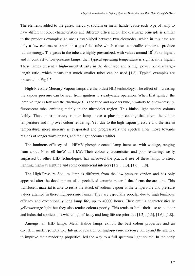
Chapter1 Introduction to Lighting Systems. Motivation and Main Objectives of the Work
1.7
The elements added to the gases, mercury, sodium or metal halide, cause each type of lamp to
have different colour characteristics and different efficiencies. The discharge principle is similar
to the previous examples: an arc is established between two electrodes, which in this case are
only a few centimetres apart, in a gas-filled tube which causes a metallic vapour to produce
radiant energy. The gases in the tube are highly pressurized, with values around 105 Pa or higher,
and in contrast to low-pressure lamps, their typical operating temperature is significantly higher.
These lamps present a high-current density in the discharge and a high power per discharge-
length ratio, which means that much smaller tubes can be used [1.8]. Typical examples are
presented in Fig.1.5.
High-Pressure Mercury Vapour lamps are the oldest HID technology. The effect of increasing
the vapour pressure can be seen from ignition to steady-state operation. When first ignited, the
lamp voltage is low and the discharge fills the tube and appears blue, similarly to a low-pressure
fluorescent tube, emitting mainly in the ultraviolet region. This bluish light renders colours
feebly. Thus, most mercury vapour lamps have a phosphor coating that alters the colour
temperature and improves colour rendering. Yet, due to the high vapour pressure and the rise in
temperature, more mercury is evaporated and progressively the spectral lines move towards
regions of longer wavelengths, and the light becomes whiter.
The luminous efficacy of a HPMV phosphor-coated lamp increases with wattage, ranging
from about 40 to 60 lm/W at 1 kW. Their colour characteristics and poor rendering, easily
surpassed by other HID technologies, has narrowed the practical use of these lamps to street
lighting, highway lighting and some commercial interiors [1.2], [1.3], [1.6], [1.8].
The High-Pressure Sodium lamp is different from the low-pressure version and has only
appeared after the development of a specialized ceramic material that forms the arc tube. This
translucent material is able to resist the attack of sodium vapour at the temperature and pressure
values attained in these high-pressure lamps. They are especially popular due to high luminous
efficacy and exceptionally long lamp life, up to 40000 hours. They emit a characteristically
yellow/orange light but they also render colours poorly. This tends to limit their use to outdoor
and industrial applications where high efficacy and long life are priorities [1.2], [1.3], [1.6], [1.8].
Amongst all HID lamps, Metal Halide lamps exhibit the best colour properties and an
excellent market penetration. Intensive research on high-pressure mercury lamps and the attempt
to improve their rendering properties, led the way to a full spectrum light source. In the early
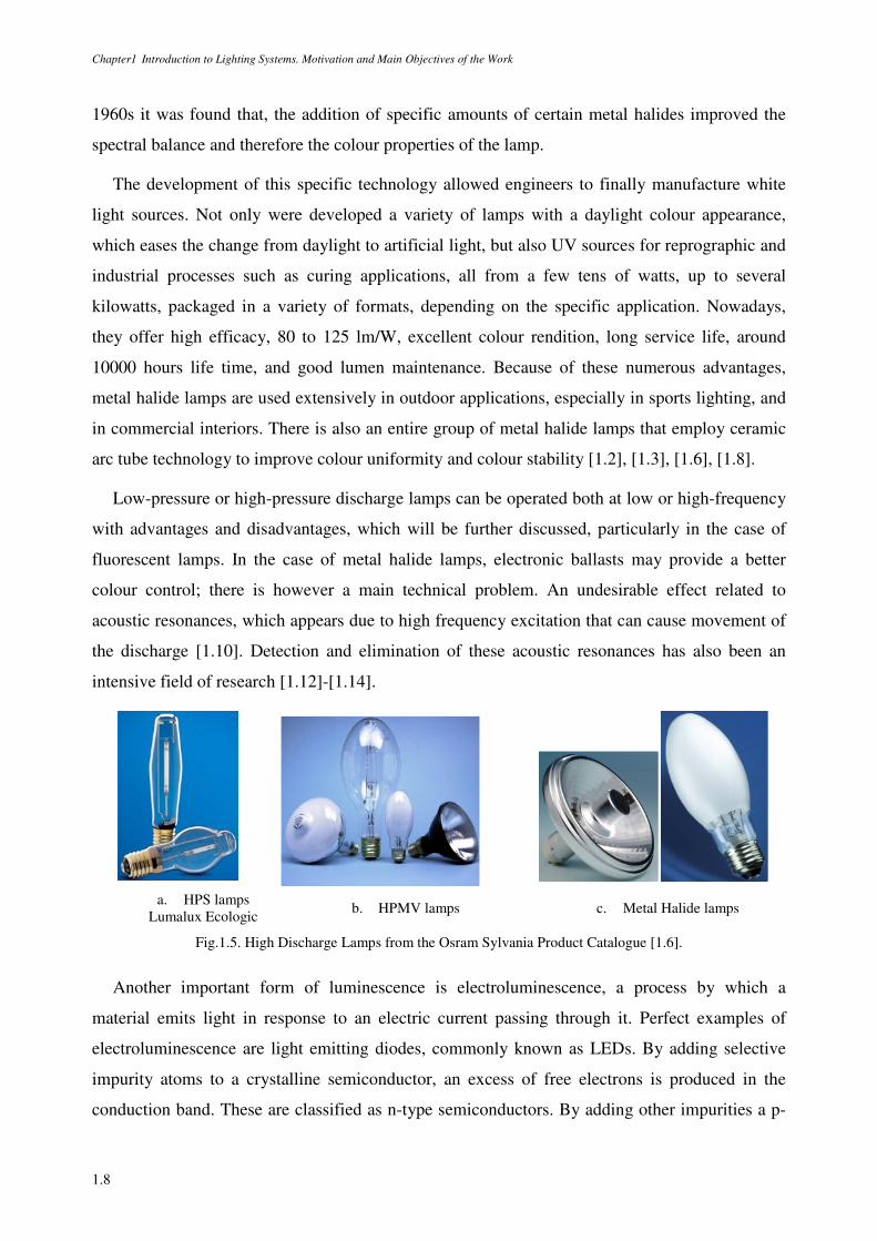
Chapter1 Introduction to Lighting Systems. Motivation and Main Objectives of the Work
1.8
1960s it was found that, the addition of specific amounts of certain metal halides improved the
spectral balance and therefore the colour properties of the lamp.
The development of this specific technology allowed engineers to finally manufacture white
light sources. Not only were developed a variety of lamps with a daylight colour appearance,
which eases the change from daylight to artificial light, but also UV sources for reprographic and
industrial processes such as curing applications, all from a few tens of watts, up to several
kilowatts, packaged in a variety of formats, depending on the specific application. Nowadays,
they offer high efficacy, 80 to 125 lm/W, excellent colour rendition, long service life, around
10000 hours life time, and good lumen maintenance. Because of these numerous advantages,
metal halide lamps are used extensively in outdoor applications, especially in sports lighting, and
in commercial interiors. There is also an entire group of metal halide lamps that employ ceramic
arc tube technology to improve colour uniformity and colour stability [1.2], [1.3], [1.6], [1.8].
Low-pressure or high-pressure discharge lamps can be operated both at low or high-frequency
with advantages and disadvantages, which will be further discussed, particularly in the case of
fluorescent lamps. In the case of metal halide lamps, electronic ballasts may provide a better
colour control; there is however a main technical problem. An undesirable effect related to
acoustic resonances, which appears due to high frequency excitation that can cause movement of
the discharge [1.10]. Detection and elimination of these acoustic resonances has also been an
intensive field of research [1.12]-[1.14].
a. HPS lamps
Lumalux Ecologic b. HPMV lamps c. Metal Halide lamps
Fig.1.5. High Discharge Lamps from the Osram Sylvania Product Catalogue [1.6].
Another important form of luminescence is electroluminescence, a process by which a
material emits light in response to an electric current passing through it. Perfect examples of
electroluminescence are light emitting diodes, commonly known as LEDs. By adding selective
impurity atoms to a crystalline semiconductor, an excess of free electrons is produced in the
conduction band. These are classified as n-type semiconductors. By adding other impurities a p-
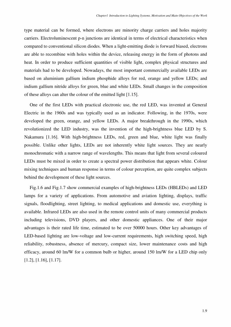
Chapter1 Introduction to Lighting Systems. Motivation and Main Objectives of the Work
1.9
type material can be formed, where electrons are minority charge carriers and holes majority
carriers. Electroluminescent p-n junctions are identical in terms of electrical characteristics when
compared to conventional silicon diodes. When a light-emitting diode is forward biased, electrons
are able to recombine with holes within the device, releasing energy in the form of photons and
heat. In order to produce sufficient quantities of visible light, complex physical structures and
materials had to be developed. Nowadays, the most important commercially available LEDs are
based on aluminium gallium indium phosphide alloys for red, orange and yellow LEDs; and
indium gallium nitride alloys for green, blue and white LEDs. Small changes in the composition
of these alloys can alter the colour of the emitted light [1.15].
One of the first LEDs with practical electronic use, the red LED, was invented at General
Electric in the 1960s and was typically used as an indicator. Following, in the 1970s, were
developed the green, orange, and yellow LEDs. A major breakthrough in the 1990s, which
revolutionized the LED industry, was the invention of the high-brightness blue LED by S.
Nakamura [1.16]. With high-brightness LEDs, red, green and blue, white light was finally
possible. Unlike other lights, LEDs are not inherently white light sources. They are nearly
monochromatic with a narrow range of wavelengths. This means that light from several coloured
LEDs must be mixed in order to create a spectral power distribution that appears white. Colour
mixing techniques and human response in terms of colour perception, are quite complex subjects
behind the development of these light sources.
Fig.1.6 and Fig.1.7 show commercial examples of high-brightness LEDs (HBLEDs) and LED
lamps for a variety of applications. From automotive and aviation lighting, displays, traffic
signals, floodlighting, street lighting, to medical applications and domestic use, everything is
available. Infrared LEDs are also used in the remote control units of many commercial products
including televisions, DVD players, and other domestic appliances. One of their major
advantages is their rated life time, estimated to be over 50000 hours. Other key advantages of
LED-based lighting are low-voltage and low-current requirements, high switching speed, high
reliability, robustness, absence of mercury, compact size, lower maintenance costs and high
efficacy, around 60 lm/W for a common bulb or higher, around 150 lm/W for a LED chip only
[1.2], [1.16], [1.17].
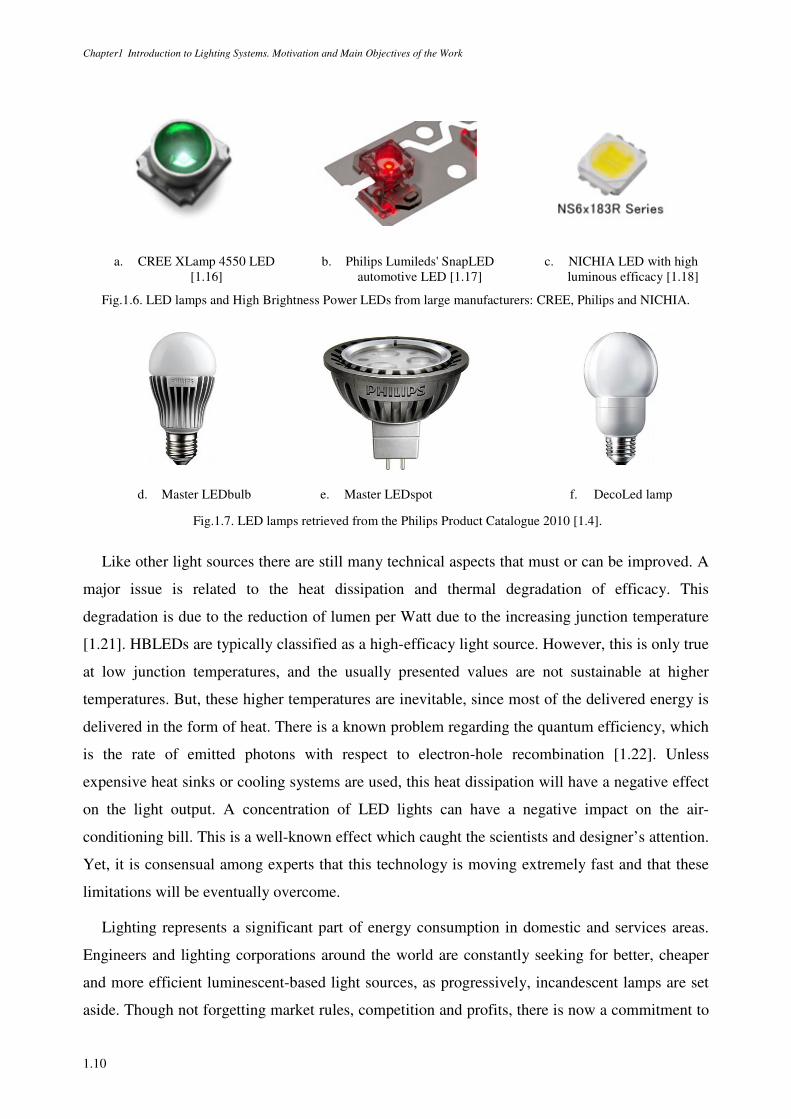
Chapter1 Introduction to Lighting Systems. Motivation and Main Objectives of the Work
1.10
a. CREE XLamp 4550 LED [1.16]
b. Philips Lumileds' SnapLED automotive LED [1.17]
c. NICHIA LED with high luminous efficacy [1.18]
Fig.1.6. LED lamps and High Brightness Power LEDs from large manufacturers: CREE, Philips and NICHIA.
d. Master LEDbulb e. Master LEDspot f. DecoLed lamp
Fig.1.7. LED lamps retrieved from the Philips Product Catalogue 2010 [1.4].
Like other light sources there are still many technical aspects that must or can be improved. A
major issue is related to the heat dissipation and thermal degradation of efficacy. This
degradation is due to the reduction of lumen per Watt due to the increasing junction temperature
[1.21]. HBLEDs are typically classified as a high-efficacy light source. However, this is only true
at low junction temperatures, and the usually presented values are not sustainable at higher
temperatures. But, these higher temperatures are inevitable, since most of the delivered energy is
delivered in the form of heat. There is a known problem regarding the quantum efficiency, which
is the rate of emitted photons with respect to electron-hole recombination [1.22]. Unless
expensive heat sinks or cooling systems are used, this heat dissipation will have a negative effect
on the light output. A concentration of LED lights can have a negative impact on the air-
conditioning bill. This is a well-known effect which caught the scientists and designer’s attention.
Yet, it is consensual among experts that this technology is moving extremely fast and that these
limitations will be eventually overcome.
Lighting represents a significant part of energy consumption in domestic and services areas.
Engineers and lighting corporations around the world are constantly seeking for better, cheaper
and more efficient luminescent-based light sources, as progressively, incandescent lamps are set
aside. Though not forgetting market rules, competition and profits, there is now a commitment to
Chapter1 Introduction to Lighting Systems. Motivation and Main Objectives of the Work
1.11
the search and development of a greener future. Promoting better energy efficiency in the lighting
field implies higher demands concerning energy efficiency requirements, particularly of building
regulations in the illumination domain. For the past years, regulations, standards, taxes, energy
labels, and other product-related measures are constantly being deliberated to ensure and deliver a
market transformation in lighting efficiency, thus contributing to a rapid transition to a clean
energy economy.
1.1.4 GENERAL CONSIDERATIONS ON LIGHTING EFFICIENCY
In December 2008, European Union leaders adopted a comprehensive package of measures to
reduce the EU’s contribution to global warming and ensure reliable and sufficient supplies of
energy. The Commission has adopted an Action Plan, which aimed at achieving a 20% reduction
in energy consumption by 2020. It includes measures to improve the energy performance of
products, buildings and services, to improve the yield of energy production and distribution, to
reduce the impact of transport on energy consumption, to facilitate financing and investments in
the sector, to encourage and consolidate rational energy consumption behaviour and to step up
international action on energy efficiency [1.5]. Several other countries not belonging to the EU,
are also implementing action plans for energy efficiency with an agenda depending on the
technological evolution, the evolution of the energy consumption and the development of the
economy. So in fact this is a world-wide trend.
In Portugal, since the entry into force of the Kyoto Protocol, legislation has been adopted
ensuring compliance with the commitments undertaken at international level. Both the PNAC
(Portuguese National Plan for Climate Change) and the PNALE (National Plan for the Allocation
of Emission Allowances) have as their object to implement the Kyoto target. More recently, and
also as a result of a European initiative, the PNAEE (National Action Plan for Energy Efficiency)
was approved, envisaging to reduce energy consumption through an annual increase of 1.1% in
energy efficiency until 2012, taking as reference the average final energy consumption between
2001 and 2005.
One of the measures, common to all European countries, consists on the ambitious program to
phase out low-efficiency incandescent lamps between September 2009 and the end of 2016. The
aim is to encourage the use of more energy efficient lighting alternatives in order to reduce the
primary energy consumption. This means using mainly luminescence-based light sources such as
Chapter1 Introduction to Lighting Systems. Motivation and Main Objectives of the Work
1.12
CFLs and LEDs. Nonetheless, and in spite of all the measurements and information campaigns,
the general population is somewhat sceptical to the phase-out of incandescent lamps.
One of the reasons why this occurs is directly related to the inscriptions present in the more
efficient light source alternative. Traditionally, with incandescent lamps, more light would mean
more watts. Nowadays the same quantity of light, for instance 750 lumens, can be produced by an
incandescent bulb using 60W, a halogen bulb using 42W, or a compact fluorescent lamp using
15W. This causes some confusion to the consumers, which manufacturers try to solve by giving
equivalence with incandescent bulbs, which in fact has become an unreliable and complicated
method of comparison between lamps having different energy efficiency. Since 2010
manufacturers are obligated to display the lumens offered by the light source at a larger font than
the display of watts. This is an attempt to familiarized people with lamp comparisons based on
their real performance and not their wattage.
Also, the purchase price difference between incandescent lamps and more efficient
alternatives constitutes a psychological barrier, even if the higher initial investment will be
retrieved due to long burning hours and higher luminous efficacy. Another discouraging factor
has been the somehow poor quality of the so-called economic lamps placed on the market
without being subject to quality requirements [1.5].
Another reason is related to the light source colour properties and consumers perception to
these properties. The lighting industry predominantly uses the colour rendering index (CRI). This
index measures the degree to which the colour of an object illuminated by the light source
conforms to that of the same object illuminated by a reference light source. In basic terms, it
gives an indication of the light source’s ability to make illuminated objects appear natural.
Another common index is the correlated colour temperature (CCT), often confused with the
colour temperature. Whereas the CCT is defined as the temperature of the blackbody radiator
whose colour, according to human perception, most closely resembles to the considered light
source; the colour temperature is simply the temperature of the blackbody which emits radiation
of the same chromaticity of the light source, technically according to the Colour Appearance
Modeling for Colour Management ratified by the CIE. Both terms are referred to in units of
absolute temperature, Kelvin [K]. A blackbody or a full radiator is defined as an idealized body
that absorbs all electromagnetic radiation falling upon it and is also capable of re-emitting. At
zero K, the blackbody emits no radiation. At room temperature, black bodies emit mostly at
infrared wavelengths, but as the temperature increases past a few hundred degrees, blackbodies
Chapter1 Introduction to Lighting Systems. Motivation and Main Objectives of the Work
1.13
start to emit at visible wavelengths, appearing red, orange, yellow, white, and blue with
increasing temperature, under a continuous spectral distribution. The CCT index is in fact a
physiological response, commonly used as an indication of the apparent “warmth” or “coolness”
of the light emitted by the source. Thus, a luminescence-based light source such as a cool white
fluorescent lamp, which emits radiation of a specific wavelength, has a CCT around 3500K and it
is perceived as a white source of light, whereas a HPS lamp, which presents a CCT of about
2000K appears yellow, and is perceived as a warmer light source.
These two metrics, CCT and CRI, are facing increased challenges and criticisms as new types
of light sources appear, particularly since LEDs are becoming more prevalent in the market [1.1],
[1.2], [1.7], [1.15].
These measures along with increasingly higher energy conservation concerns just confirm that
the money invested in this field of research has not stopped growing during the past-years.
Lighting companies are strongly encouraged and committed to develop efficient, cost-effective
and ecologically aware solutions in all the lighting domains. One of the most active fields of
research, besides LEDs and high-efficiency discharge lamps, is related to the efficient control of
operation of light sources.
Although LED technology caught the attention of scientists and of the general population,
with promising results regarding efficiency and rated lamp life, there are still large investments in
fluorescent lighting systems. High-frequency operated fluorescent tubes represent an alternative
cost-effective technology, with a widespread use in industrial and commercial buildings which is
still expected to prevail in the near future. One of the most obvious reasons corresponds to the
broader range of commercially-existing solutions, which fulfil the need of creating adaptable and
flexible environments. Currently, electronic ballasts are becoming inevitable in systems where
rational rules of energy utilization are to be implemented, and viewed as crucial elements in
economical and energy-efficient fluorescent lighting systems. With energy conservation concerns
becoming increasingly high, electronic ballast consumption has intensified. A number of factors
are contributing to this growth rate, including government regulations, lower prices and
innovative technologies, but mainly due to a set of specifications and additional functions which
are responsible for a more efficient electronic and digital control of the system, and particularly
of the lamp operation.
Until ten or fifteen years ago, the standard type of ballast used for office or industrial
fluorescent lighting systems was still the electromagnetic type, obviously with several well-
Chapter1 Introduction to Lighting Systems. Motivation and Main Objectives of the Work
1.14
known drawbacks, mainly related to low-frequency lamp operation. Typically, the overall
achievement in a suitable luminaire represents an energy reduction around 20-30% due to two
main factors: improved light output at high frequency operation, also eliminating visible flicker
and audible noise, and reduced power losses when compared to conventional electromagnetic
ballasts. These two factors, coupled with government policies, makes the upgrading of all ballasts
a cost-effective move, simultaneously pointing the solutions that could be adopted society-wide
to secure a swift transition to a clean energy economy, and lead the way to a better use of the
world finite, non-renewable natural resources.
1.2 FLUORESCENT LIGHTING SYSTEMS
1.2.1 FLUORESCENT LAMPS
Discharge lamps are usually more efficient than incandescent lamps because they radiate from
regions of higher temperature that can be reached with tungsten filaments. Discharges are also
more selective emitters than incandescent lamps, so less energy will be wasted in IR emission. As
previously stated, the tubular fluorescent lamp is a common example of a luminescent-based light
source and works on the low-pressure mercury discharge principle.
Like all discharges, the fluorescent lamp requires plasma which is a substance similar to gas in
which a certain portion of the particles are ionized. In fact, plasma can also be described as a
mixture of ions and electrons, electrically neutral on average together with another variety of
neutral or excited particles. This plasma is also referred to, as the positive column. The
fluorescent tube typically contains a mercury vapour at about 0.8 Pa and a rare gas, such as argon
at a pressure of typically 266 Pa or higher [1.2]. Two sealed-in electrodes are also placed at both
ends in order to provide an electrical connection to the plasma. Electrodeless connections are
possible and will be further discussed. The fluorescent material that covers the inside wall of the
tube, phosphor, is responsible for converting the UV radiation obtained from the discharge, into
visible radiation. The basic processes inside the tube can be observed in Fig.1.8 and can be
described as follows [1.2], [1.8]:
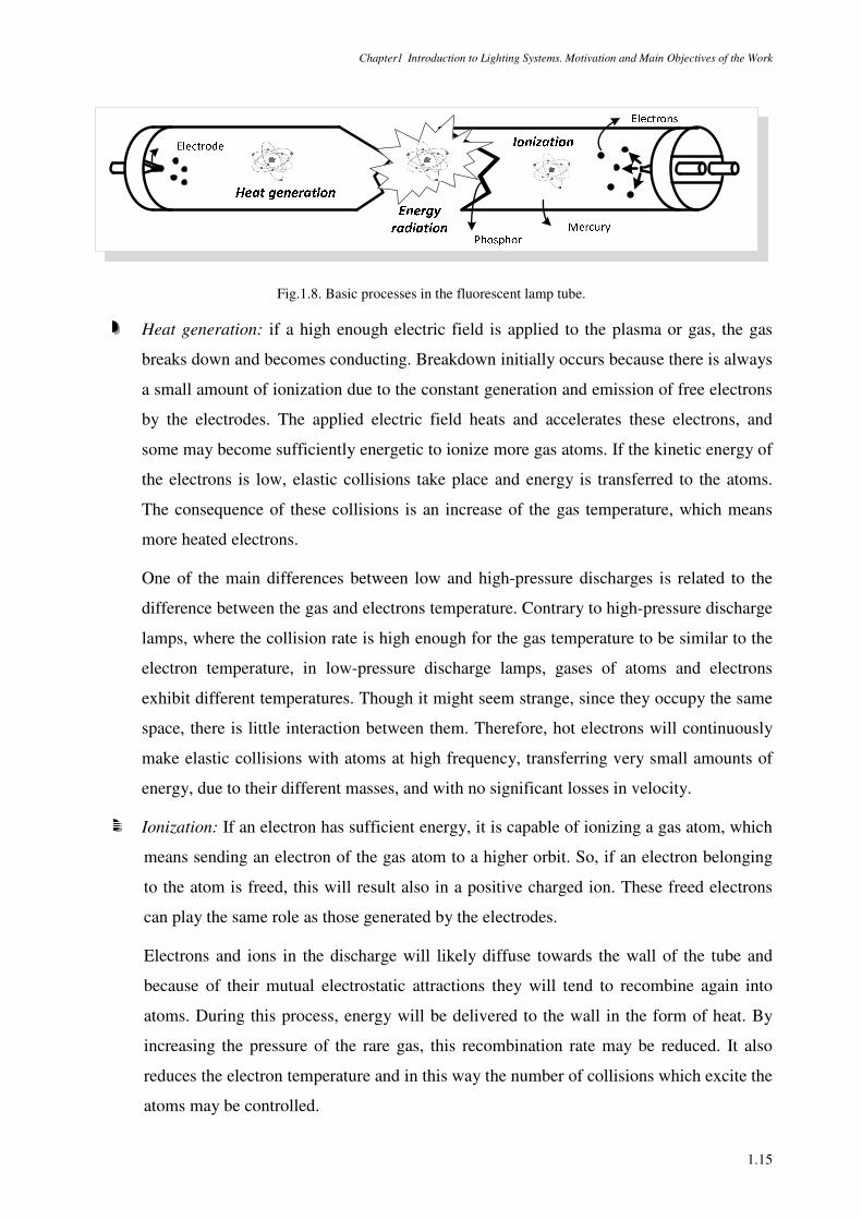
Chapter1 Introduction to Lighting Systems. Motivation and Main Objectives of the Work
1.15
Fig.1.8. Basic processes in the fluorescent lamp tube.
Heat generation: if a high enough electric field is applied to the plasma or gas, the gas
breaks down and becomes conducting. Breakdown initially occurs because there is always
a small amount of ionization due to the constant generation and emission of free electrons
by the electrodes. The applied electric field heats and accelerates these electrons, and
some may become sufficiently energetic to ionize more gas atoms. If the kinetic energy of
the electrons is low, elastic collisions take place and energy is transferred to the atoms.
The consequence of these collisions is an increase of the gas temperature, which means
more heated electrons.
One of the main differences between low and high-pressure discharges is related to the
difference between the gas and electrons temperature. Contrary to high-pressure discharge
lamps, where the collision rate is high enough for the gas temperature to be similar to the
electron temperature, in low-pressure discharge lamps, gases of atoms and electrons
exhibit different temperatures. Though it might seem strange, since they occupy the same
space, there is little interaction between them. Therefore, hot electrons will continuously
make elastic collisions with atoms at high frequency, transferring very small amounts of
energy, due to their different masses, and with no significant losses in velocity.
Ionization: If an electron has sufficient energy, it is capable of ionizing a gas atom, which
means sending an electron of the gas atom to a higher orbit. So, if an electron belonging
to the atom is freed, this will result also in a positive charged ion. These freed electrons
can play the same role as those generated by the electrodes.
Electrons and ions in the discharge will likely diffuse towards the wall of the tube and
because of their mutual electrostatic attractions they will tend to recombine again into
atoms. During this process, energy will be delivered to the wall in the form of heat. By
increasing the pressure of the rare gas, this recombination rate may be reduced. It also
reduces the electron temperature and in this way the number of collisions which excite the
atoms may be controlled.
Chapter1 Introduction to Lighting Systems. Motivation and Main Objectives of the Work
1.16
In order to maintain the discharge, the applied electric field must also be adequate so that
the electron temperature is high enough to provide sufficient ionizing collisions to replace
the electrons and ion losses. So, this whole process is very crucial, whether during
discharge ignition or normal running, because ionized atoms and electrons are necessary
to maintain the electrical current through the lamp.
Energy radiation: After collision, the freed electron of the gas atom which remains in a
higher orbit stays in an unstable condition. It tends to recover its original level, and during
this process it emits the absorbed energy primarily in the form of electromagnetic
radiation, mainly in the ultraviolet region, at the wavelengths of 254nm and 185nm,
which are both resonance radiation lines in the atomic spectrum of mercury. Only a very
small part of energy is directly converted into visible radiation. The remainder energy is
dissipated as heat in the form of losses in the plasma and in the electrodes.
There is an optimum mercury pressure for the operation of fluorescent lamps. The
mercury pressure has a strong influence in the electric arc. As the pressure is increased
from a low value, the efficiency increases because there is an increasing number of
mercury atoms that radiate. This electromagnetic radiation is then transformed into visible
light due to the phosphor coating existing in the inside wall of the tube. However not all
UV photons are converted into visible radiation. In a common T8 or T12 lamp the overall
conversion efficiency is about 40%.
Most of the gases, like air, are very good insulators at normal pressure and temperature. If
however, the voltage stress is sufficiently high, it may become partially conductive, which means
that a sufficient concentration of charged particles is present. If the voltage is sufficiently high,
complete electrical breakdown of the air will culminate in an electrical spark or arc. In
fluorescent tubes, this voltage stress or starting voltage is translated into an electric field strength
around 10V/cm, considering an optimum mercury pressure. This means 1000V for 1 meter of
tube, approximately. The auxiliary inert gases are also used to decrease this starting voltage.
Penning mixtures are special inert gas mixtures capable of providing very low starting voltages.
Narrower tubes have higher fields so the discharge length is shorter, but yet, CFLs tubes must be
folded to attain the recommended levels. In electrodeless lamps the constraint on lamp voltage no
longer applies, and this is the reason why they can be built in similar shapes to incandescent
lamps [1.2] [1.8].
Chapter1 Introduction to Lighting Systems. Motivation and Main Objectives of the Work
1.17
The efficiency of the fluorescent lamp depends on two processes: the conversion of the
electrical energy from the supply into UV radiation and the conversion of this UV radiation into
visible light. While the first is directly related to the discharge arc length, tube diameter, gas
mixture and pressure, mercury pressure and power loading of the tube (in watts per unit area of
discharge surface), the second one is related to the emission spectrum of the lamp, phosphor or
phosphor mixture used to obtain that spectrum and the efficiency of these phosphors.
Other aspects that contribute to lower efficiency and diminish the rated lamp life are related to
ambient temperature and cathodes operation.
The luminous flux of a low-pressure mercury lamp is determined by the mercury vapour
pressure, which in its turn is dependent on the temperature of the coldest spot in the lamp. During
the initial running of the lamp, the mercury vapour will re-condense at that coolest spot of the
tube as excess liquid mercury. For T12 and T8 the optimum cold spot temperature for maximum
efficiency or maximum light output is about 40º-45º C. For linear lamps operated horizontally the
coolest spot coincides with the bottom centre of the tube and the optimum temperature is
achieved when ambient air temperature is between 20º and 30º C. So, it is clear that ambient
temperature plays an important role in the lamp performance.
The design of the luminaire will also determine the actual air temperature adjacent to the tube
and therefore influences the temperature of the coolest region of the tube. CFLs typically run
hotter than linear tubes due to their higher wattage per unit area of the tube, so, they have a
tendency to operate at higher temperatures than the optimum ones. In these cases, an artificial
cool spot may be created, by having an extension of the tube away from the heat sources, the
electrodes or the discharge itself [1.2].
The TL5 lamp from Philips was also designed to reach its maximum flux at 35º C ambient
temperature in draught-free air when operated with an electronic ballast without additional
heating of the electrodes. Such ballast is called cut-off ballast. The temperature of 35º C is
considered to be the common ambient temperature inside the luminaire. The cold spot in these
lamps is situated behind the electrode at the stamp side: the so-called cold chamber. There will be
an evident depreciation of the luminous flux if the air temperature is higher than the
recommended value. For values higher than 70º C, the electric characteristics of the lamp will
change sharply which may have a damaging effect on the system lamp plus ballast. So, for those
reasons, the cold-spot temperature should not exceed 100º C. If however, high ambient
temperatures are impossible to avoid, a physical contact with the luminaire can create a second
Chapter1 Introduction to Lighting Systems. Motivation and Main Objectives of the Work
1.18
cold spot, turning the cold chamber obsolete. With this new cold spot the lamp can be brought to
optimum conditions. If however the opposite occurs, the ambient temperature is too low, a
standard solution is to cover the cold spot with an insulating material, thereby guaranteeing that
the optimum cold spot temperature is reached [1.19].
In order to maintain the discharge current, the electrons which return to the external circuit at
the anode must be replaced by electrons emitted by the cathode. The electrodes are also
responsible for replacing the electrons lost during the recombination process. So, they play a
crucial role in the lamp operation. The electrodes, usually small tungsten wires structures, are
heated by ion bombardment, and the probability that an electron will escape from the cathode
depends exponentially on its temperature and on its surface barrier which is called the work
function material. They are typically covered with low-work-function materials such as barium
oxide so that they can emit at relatively low temperatures with low evaporation rates. It is a fact
that high temperatures and low work function materials favour the thermionic emission [1.2].
The ignition process is a decisive factor in terms of electrode preservation with an immediate
effect on the lamp life. Before reaching the thermionic state, the electrons have to be extracted by
field emission. This means that initially the electric field must be very high for electrons to
escape. This high electric field causes ions to be accelerated towards the cathode, hitting it with
very high energy. This leads to loss of emitter material due to sputtering: ejection of atoms by ion
impact. In order to limit this effect and its impact on the average lamp life, the electrodes must be
pre-heated. For the same reason, repeated switching evidently shortens the lamp and these are the
reasons why the preheating process is extremely important to ensure a longer lamp life [1.9].
1.2.2 LOW-FREQUENCY AND HIGH-FREQUENCY OPERATION
Contrary to incandescent lamps, which can be directly connected to an appropriate power
supply, discharge lamps require a control circuit or ballast in order to insure proper starting and
stable operation. Fluorescent lamps can be operated on mains frequency, 50Hz or 60Hz or at
high-frequency, over 40kHz. In both situations, ballasts are used to limit the discharge current.
Plus, a high voltage is generally required to initiate the ionization process. If the supply voltage is
insufficient to provide ignition, some auxiliary circuits must be added to the system.
Prior to ignition, fluorescent lamps are typically characterized by almost infinite impedance.
After the gas breakdown, and when the rate of ionization exceeds the rate of loss of ions and
electrons due to the recombination process, the discharge current tends to grow rapidly. An
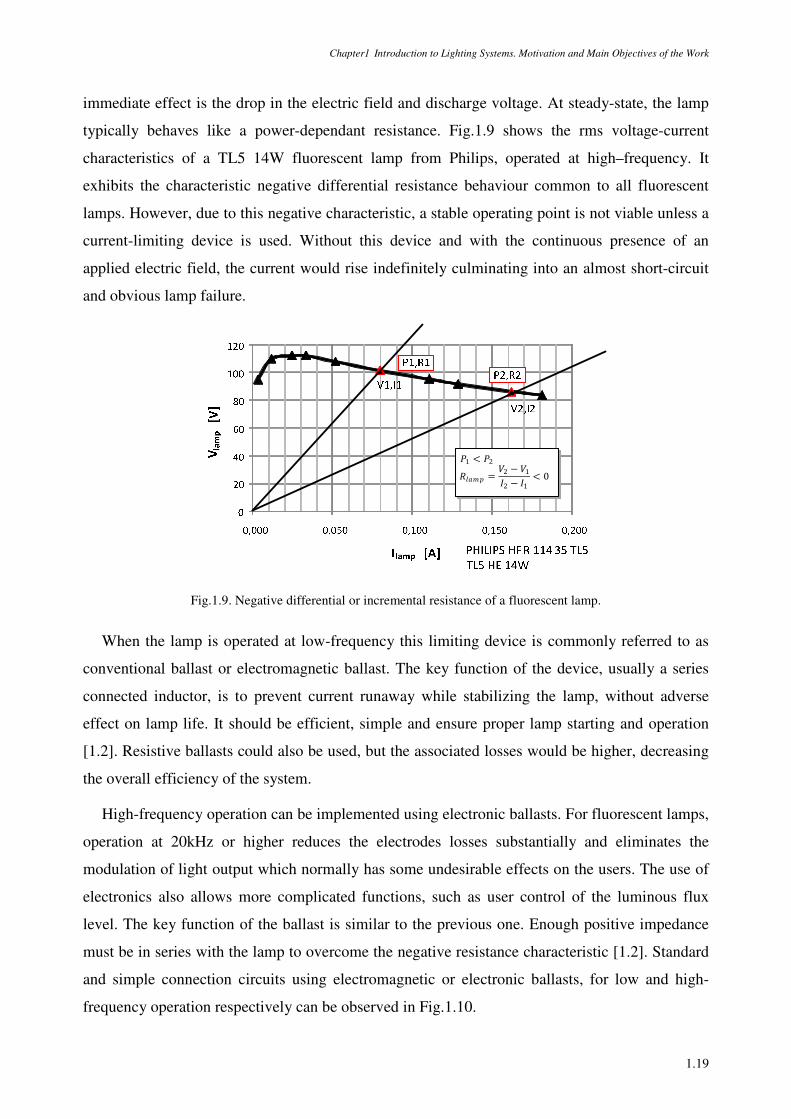
Chapter1 Introduction to Lighting Systems. Motivation and Main Objectives of the Work
1.19
immediate effect is the drop in the electric field and discharge voltage. At steady-state, the lamp
typically behaves like a power-dependant resistance. Fig.1.9 shows the rms voltage-current
characteristics of a TL5 14W fluorescent lamp from Philips, operated at high–frequency. It
exhibits the characteristic negative differential resistance behaviour common to all fluorescent
lamps. However, due to this negative characteristic, a stable operating point is not viable unless a
current-limiting device is used. Without this device and with the continuous presence of an
applied electric field, the current would rise indefinitely culminating into an almost short-circuit
and obvious lamp failure.
t1 < t2
vwxy = >2 − >1/2 − /1 < 0
Fig.1.9. Negative differential or incremental resistance of a fluorescent lamp.
When the lamp is operated at low-frequency this limiting device is commonly referred to as
conventional ballast or electromagnetic ballast. The key function of the device, usually a series
connected inductor, is to prevent current runaway while stabilizing the lamp, without adverse
effect on lamp life. It should be efficient, simple and ensure proper lamp starting and operation
[1.2]. Resistive ballasts could also be used, but the associated losses would be higher, decreasing
the overall efficiency of the system.
High-frequency operation can be implemented using electronic ballasts. For fluorescent lamps,
operation at 20kHz or higher reduces the electrodes losses substantially and eliminates the
modulation of light output which normally has some undesirable effects on the users. The use of
electronics also allows more complicated functions, such as user control of the luminous flux
level. The key function of the ballast is similar to the previous one. Enough positive impedance
must be in series with the lamp to overcome the negative resistance characteristic [1.2]. Standard
and simple connection circuits using electromagnetic or electronic ballasts, for low and high-
frequency operation respectively can be observed in Fig.1.10.
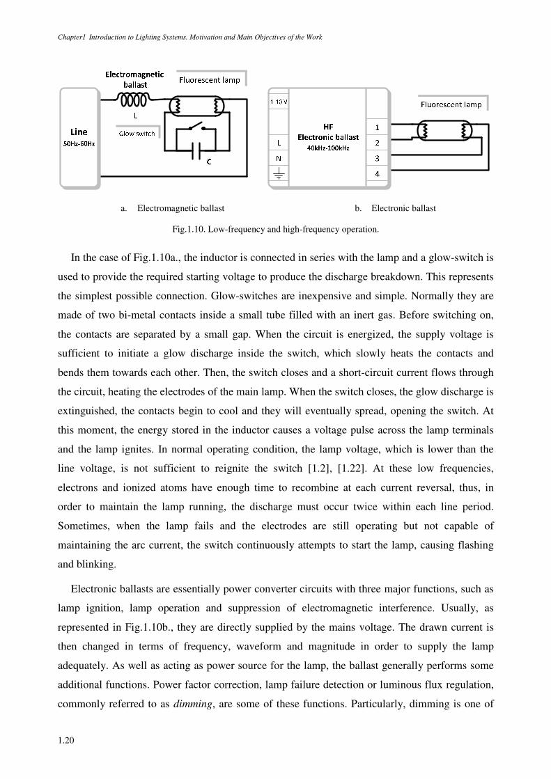
Chapter1 Introduction to Lighting Systems. Motivation and Main Objectives of the Work
1.20
a. Electromagnetic ballast b. Electronic ballast
Fig.1.10. Low-frequency and high-frequency operation.
In the case of Fig.1.10a., the inductor is connected in series with the lamp and a glow-switch is
used to provide the required starting voltage to produce the discharge breakdown. This represents
the simplest possible connection. Glow-switches are inexpensive and simple. Normally they are
made of two bi-metal contacts inside a small tube filled with an inert gas. Before switching on,
the contacts are separated by a small gap. When the circuit is energized, the supply voltage is
sufficient to initiate a glow discharge inside the switch, which slowly heats the contacts and
bends them towards each other. Then, the switch closes and a short-circuit current flows through
the circuit, heating the electrodes of the main lamp. When the switch closes, the glow discharge is
extinguished, the contacts begin to cool and they will eventually spread, opening the switch. At
this moment, the energy stored in the inductor causes a voltage pulse across the lamp terminals
and the lamp ignites. In normal operating condition, the lamp voltage, which is lower than the
line voltage, is not sufficient to reignite the switch [1.2], [1.22]. At these low frequencies,
electrons and ionized atoms have enough time to recombine at each current reversal, thus, in
order to maintain the lamp running, the discharge must occur twice within each line period.
Sometimes, when the lamp fails and the electrodes are still operating but not capable of
maintaining the arc current, the switch continuously attempts to start the lamp, causing flashing
and blinking.
Electronic ballasts are essentially power converter circuits with three major functions, such as
lamp ignition, lamp operation and suppression of electromagnetic interference. Usually, as
represented in Fig.1.10b., they are directly supplied by the mains voltage. The drawn current is
then changed in terms of frequency, waveform and magnitude in order to supply the lamp
adequately. As well as acting as power source for the lamp, the ballast generally performs some
additional functions. Power factor correction, lamp failure detection or luminous flux regulation,
commonly referred to as dimming, are some of these functions. Particularly, dimming is one of
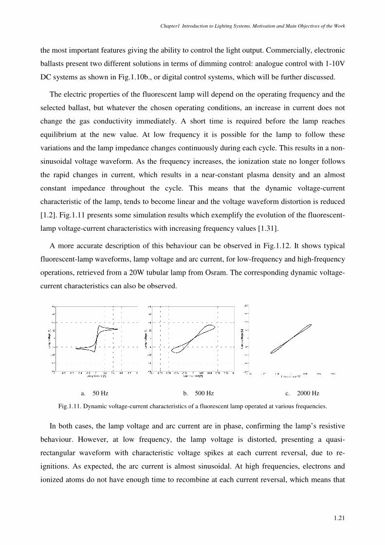
Chapter1 Introduction to Lighting Systems. Motivation and Main Objectives of the Work
1.21
the most important features giving the ability to control the light output. Commercially, electronic
ballasts present two different solutions in terms of dimming control: analogue control with 1-10V
DC systems as shown in Fig.1.10b., or digital control systems, which will be further discussed.
The electric properties of the fluorescent lamp will depend on the operating frequency and the
selected ballast, but whatever the chosen operating conditions, an increase in current does not
change the gas conductivity immediately. A short time is required before the lamp reaches
equilibrium at the new value. At low frequency it is possible for the lamp to follow these
variations and the lamp impedance changes continuously during each cycle. This results in a non-
sinusoidal voltage waveform. As the frequency increases, the ionization state no longer follows
the rapid changes in current, which results in a near-constant plasma density and an almost
constant impedance throughout the cycle. This means that the dynamic voltage-current
characteristic of the lamp, tends to become linear and the voltage waveform distortion is reduced
[1.2]. Fig.1.11 presents some simulation results which exemplify the evolution of the fluorescent-
lamp voltage-current characteristics with increasing frequency values [1.31].
A more accurate description of this behaviour can be observed in Fig.1.12. It shows typical
fluorescent-lamp waveforms, lamp voltage and arc current, for low-frequency and high-frequency
operations, retrieved from a 20W tubular lamp from Osram. The corresponding dynamic voltage-
current characteristics can also be observed.
a. 50 Hz b. 500 Hz c. 2000 Hz
Fig.1.11. Dynamic voltage-current characteristics of a fluorescent lamp operated at various frequencies.
In both cases, the lamp voltage and arc current are in phase, confirming the lamp’s resistive
behaviour. However, at low frequency, the lamp voltage is distorted, presenting a quasi-
rectangular waveform with characteristic voltage spikes at each current reversal, due to re-
ignitions. As expected, the arc current is almost sinusoidal. At high frequencies, electrons and
ionized atoms do not have enough time to recombine at each current reversal, which means that
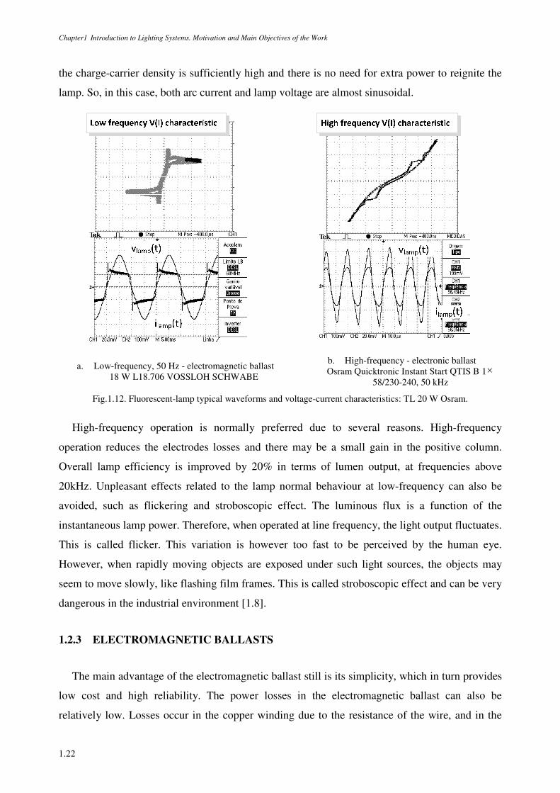
Chapter1 Introduction to Lighting Systems. Motivation and Main Objectives of the Work
1.22
the charge-carrier density is sufficiently high and there is no need for extra power to reignite the
lamp. So, in this case, both arc current and lamp voltage are almost sinusoidal.
a. Low-frequency, 50 Hz - electromagnetic ballast 18 W L18.706 VOSSLOH SCHWABE
b. High-frequency - electronic ballast Osram Quicktronic Instant Start QTIS B 1×
58/230-240, 50 kHz
Fig.1.12. Fluorescent-lamp typical waveforms and voltage-current characteristics: TL 20 W Osram.
High-frequency operation is normally preferred due to several reasons. High-frequency
operation reduces the electrodes losses and there may be a small gain in the positive column.
Overall lamp efficiency is improved by 20% in terms of lumen output, at frequencies above
20kHz. Unpleasant effects related to the lamp normal behaviour at low-frequency can also be
avoided, such as flickering and stroboscopic effect. The luminous flux is a function of the
instantaneous lamp power. Therefore, when operated at line frequency, the light output fluctuates.
This is called flicker. This variation is however too fast to be perceived by the human eye.
However, when rapidly moving objects are exposed under such light sources, the objects may
seem to move slowly, like flashing film frames. This is called stroboscopic effect and can be very
dangerous in the industrial environment [1.8].
1.2.3 ELECTROMAGNETIC BALLASTS
The main advantage of the electromagnetic ballast still is its simplicity, which in turn provides
low cost and high reliability. The power losses in the electromagnetic ballast can also be
relatively low. Losses occur in the copper winding due to the resistance of the wire, and in the
Chapter1 Introduction to Lighting Systems. Motivation and Main Objectives of the Work
1.23
iron core due to hysteresis, eddy currents and gap fringing losses, and increase with temperature.
This means that the design of the inductor will always be a compromise between size, shape,
performance and cost [1.2]. Naturally, other aspects and technical issues must be considered.
For instance, the reliability can be compromised if the matching between the supply voltage
and the lamp voltage is not carefully made. The dynamic sustaining voltage from the supply
throughout the cycle must exceed the instantaneous lamp voltage, guaranteeing re-ignition. A
supply voltage in the range of 100-120V restricts the use of the series inductor to lamps
exhibiting nominal voltages around 55V. For 220-240V supplies, a nominal lamp voltage in the
range of 70-145V generally gives satisfactory operation. In addition, all discharge lamps can only
withstand a limited drop in supply voltage, between 10-15%, before unstable operation and
extinction occurs [1.2].
Operation at line frequency, 50Hz or 60Hz, also means high size and weight for the passive
element, and susceptibility to light flickering and to the stroboscopic effect. This inductor also
produces a phase displacement between the supply voltage and the lamp current. Even if this
allows a higher sustaining voltage to be available at the start of each half-cycle, when compared
to resistive ballasts, it reduces the input power factor. Increasing the power factor implies using
large capacitors across the line input. In addition, the lamp voltage presents a high level of
harmonic distortion.
A simple ignition system based in glow-switches is not possible for lamps presenting higher
starting voltages. In these cases, the series inductor used to limit the discharge current can be
incorporated into an autotransformer to attain higher voltage pulses for lamp ignition. This
solution is very common in 120V-60Hz systems. In other cases, separate igniting transformers
are needed, offering electrical isolation and safety. The use of glow-switches also makes the life
of the lamp very dependent on the switching frequency. Electronic starters with controlled
electrode preheating are now more common [1.22]. This has a positive effect on lamp life, since
the ignition voltage pulse is only applied when the electrodes have reached the emission
temperature. This results in a more reliable lamp starting and minimizes the damages to the
electrodes, making the lamp less dependent on the switching cycle. There are also other cases
where the necessary preheat current and lamp starting voltage can be obtained from circuits using
resonant combinations of inductance and capacitance. Such circuits do not require starter
switches or power factor correction (PFC) [1.2].
Chapter1 Introduction to Lighting Systems. Motivation and Main Objectives of the Work
1.24
Fluorescent lamps characteristics also change throughout the lamp life, due to the natural
aging process. The initial matching between the ballast and the lamp may diverge from the
original optimum operating point. A latest aspect is related to the fact that electromagnetic
ballasts are unsuitable for emergency and automotive lighting, traditionally supplied in dc [1.8].
Since the development, and widespread commercialization and acceptance of electronic
ballasts, low-frequency operation has been slowly discarded. The large multiplicity of new and
practical functions proposed by electronic ballasts made conventional ballasts quite old-
fashioned. However, their simplicity, low-cost, recyclability, and long life may be hard to beat in
some applications, even considering all the benefits proposed by electronic ballasts. In [1.32] and
[1.33] low-loss magnetic ballasts for T5 fluorescent lamps are proposed. These lamps are
characterized by a high lamp voltage, and in some particular cases, low current. This is the reason
why they were conventionally manufactured for high-frequency operation. But the fact is that
these lamps present higher average life time than electronic ballasts, which are limited by the
present short lifetime of electrolytic capacitors, around 8 years. At a first glance, electromagnetic
ballasts were thought to be unsuitable. But in applications were concerns with energy saving,
maintenance, long life-time and recyclability are mandatory; they stand as a cost-effective
alternative. This is the case in systems were lower power versions of T5 lamps are used. These
lamps require a smaller ignition voltage, which can be easily solved through adequate electronic
starters. Besides, due to the low current, the magnetic conduction and core losses of the ballast
are greatly reduced. In addition, magnetic ballasts can last for tens of years and can be recycled
without creating the same amount of toxic and electronic waste as electronic ballasts do.
In particular cases, selecting electronic ballasts for replacing conventional ballasts may not be
a simple decision, even if high-frequency operation clearly gives higher values of luminous
output, eliminates flickering and overcomes the stroboscopic effect. The whole scenario must be
analysed, namely issues like losses, longevity, replacement and maintenance costs. Using
electronic ballasts in cases where there is no need for complicated additional features could lead
to an erroneous choice.
1.2.4 ELECTRONIC BALLASTS
In terms of lamp operation, electronic ballasts will naturally offer higher levels of
controllability due to the inclusion of different power converters in their configuration. There are
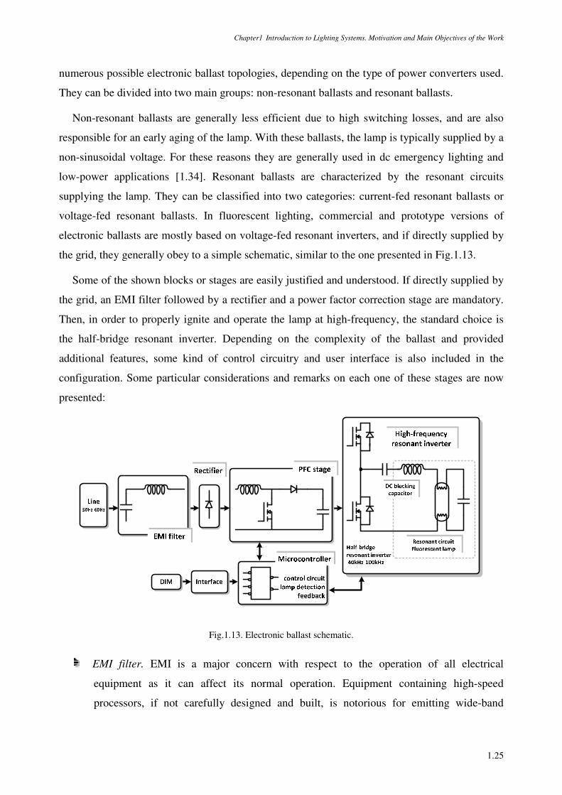
Chapter1 Introduction to Lighting Systems. Motivation and Main Objectives of the Work
1.25
numerous possible electronic ballast topologies, depending on the type of power converters used.
They can be divided into two main groups: non-resonant ballasts and resonant ballasts.
Non-resonant ballasts are generally less efficient due to high switching losses, and are also
responsible for an early aging of the lamp. With these ballasts, the lamp is typically supplied by a
non-sinusoidal voltage. For these reasons they are generally used in dc emergency lighting and
low-power applications [1.34]. Resonant ballasts are characterized by the resonant circuits
supplying the lamp. They can be classified into two categories: current-fed resonant ballasts or
voltage-fed resonant ballasts. In fluorescent lighting, commercial and prototype versions of
electronic ballasts are mostly based on voltage-fed resonant inverters, and if directly supplied by
the grid, they generally obey to a simple schematic, similar to the one presented in Fig.1.13.
Some of the shown blocks or stages are easily justified and understood. If directly supplied by
the grid, an EMI filter followed by a rectifier and a power factor correction stage are mandatory.
Then, in order to properly ignite and operate the lamp at high-frequency, the standard choice is
the half-bridge resonant inverter. Depending on the complexity of the ballast and provided
additional features, some kind of control circuitry and user interface is also included in the
configuration. Some particular considerations and remarks on each one of these stages are now
presented:
Fig.1.13. Electronic ballast schematic.
EMI filter. EMI is a major concern with respect to the operation of all electrical
equipment as it can affect its normal operation. Equipment containing high-speed
processors, if not carefully designed and built, is notorious for emitting wide-band
Chapter1 Introduction to Lighting Systems. Motivation and Main Objectives of the Work
1.26
electrical noise. On the other hand, it is also vulnerable to transient and surge voltages in
the mains network. There are similar concerns regarding high-frequency lighting. In this
case, there is a special concern regarding not only the electronic ballast, but the entire
system, ballast, wiring, lamp and luminaire. In order to ensure that all electric and
electronic equipment work correctly, the European Union has established some regulatory
standards regarding electromagnetic compatibility (EMC), and manufacturers have a duty
to provide equipment that does not cause undue interference and that is not unduly
affected by it. EMI filters must not only protect against mains transients, but also comply
with standards for harmonic currents emissions, and radiated and conducted interference
[1.22].
Rectifier and PFC stage. Electronic ballasts commonly use a full-bridge rectifier followed
by a filter capacitor to generate an adequate dc voltage for the inverter. This first stage
leads to high harmonics in the line current, low input power factor, and poor regulation.
In order to improve the consumption of electrical energy and to provide agreement with
power quality standards [1.35], electronic ballasts incorporate PFC techniques. An ideal
power-factor corrector stage should emulate a resistor on the supply side while
maintaining a fairly regulated output voltage. PFC techniques can be implemented using a
two-stage or single-stage approach [1.36].
Typically, in the two-stage approach, a switching-mode dc-dc converter precedes the
resonant inverter. The dc-dc converter can be operated in CCM (continuous current
mode), DCM (discontinuous current mode) or in the boundary of the two modes,
depending on the chosen control technique: peak current control, average current control,
hysteresis or borderline control [1.37]. Several topologies can be used, buck, buck-boost,
flyback (allows high-frequency electrical isolation) or boost converter; however this last
one is the most common adopted solution. This simple approach generally exhibits a
near-unit PF and may deal with a wide range of line input voltage variations. Nonetheless,
the main problem of the two-stage approach is the cost of the additional power stage. In
the single-stage approach, the PFC stage is combined with the high-frequency resonant
inverter, which means that one or more active power switches are shared by both
converters, leading to a lower component count and reduced cost. In [1.36] and [1.65]
distinctive integrated solutions are presented; the first one, an integrated boost, half-
bridge resonant inverter for multiple fluorescent lamps operation, and in the second one,
an integrated buck-boost current-fed resonant inverter for a CFL.
Chapter1 Introduction to Lighting Systems. Motivation and Main Objectives of the Work
1.27
High-frequency inverter and resonant circuit. These two stages are responsible for
transforming the switching converter characteristics from a voltage source into a current
source in order to ensure stable lamp operation at high frequency. As previously referred,
the standard choice is the parallel-loaded half-bridge resonant inverter. To benefit the
most of high-frequency operation, several aspects and technical issues must be considered
during the design project of the entire ballast and especially of the inverter. The first,
obviously, is the selection of the operating frequency. A high frequency will guarantee
higher levels of luminous output and lower size and weight of the resonant elements used
to stabilize the discharge. An initial lower boundary would be 20kHz, in order to avoid
audible frequencies. But, video, audio apparatus, computers, and lighting installations are
increasingly being operated with IR remote controls, using frequencies in the range of 30-
40kHz. This fact will increase this lower boundary. So, in effect, commercial ballasts for
fluorescent lamps typically operate between 40-100kHz. Higher levels of operating
frequencies would lead to higher switching losses in the power MOSFETs, decreasing the
overall efficiency of the ballast. Another important issue in the power control of the
inverter is the study of the phase angle of the input current of the resonant circuit. A
delayed current must be used in order to achieve zero voltage switching (ZVS) in the
bridge MOSFETs.
Other aspects directly related with these two stages are the control over the lamp or
discharge current waveforms and the lamp starting procedure. In order to ensure
maximum lamp life, it is important to drive the lamp with symmetrical alternating
currents, thus making use of both electrodes alternatively. A related important parameter
is the current crest factor, which is the ratio of the peak value to the rms value of the
lamp current. A value close to √2 implies that the lamp current waveform is equivalent to
a sine wave, which would correspond to the ideal situation. In order to avoid early aging
of the lamp it is usually recommended a lamp current crest factor lower than 1.7.
The starting procedure is typically controlled by the inverter. During the description of
the basic fluorescent lamp mechanisms it was referred the importance of the ignition
process. In classical fluorescent lamp tubes, the electrodes must be warmed up to the
emission temperature and no high-voltage should be applied until they reach the right
temperature level, thus avoiding sputtering damage. Once they reach that level, the
starting voltage can be applied to ignite the lamp [1.8]. Considering the half-bridge
parallel-loaded resonant inverter, the heating procedure and lamp voltage can both be
Chapter1 Introduction to Lighting Systems. Motivation and Main Objectives of the Work
1.28
controlled by slightly changing the operating frequency. If the circuit is operated in
inductive mode, thus ensuring soft-switching, a higher frequency results in a lower
voltage applied to the lamp, enough to pre-heat the electrodes when the lamp is still off. If
the frequency is then decreased from this higher value, resonance can be reached and a
high voltage can be applied to the lamp, guaranteeing its ignition [1.66]. To avoid
undesirable starting conditions, this voltage must also be limited to its minimum value.
This process, normally implemented with a closed-loop system, will further be addressed
in future chapters.
User interface, control and protection circuit. These stages contain all the necessary
sensors and intelligence to manage the mains input and lamp output functions of the
electronic ballast, such as the preheating and ignition process, lamp power control or
other additional control features, stop circuit or safety switch-off, output over-voltage or
over-current protection, end-of-life detection and lamp failure protection. Depending on
the complexity of the ballast or the pretended installed system, it can vary from very
simple circuits to more complex circuits involving microprocessors, which is now
common in most of the commercial solutions.
In the case of CFLs, the electronic ballast is retrofitted into the existing lamp socket. These
ballasts are similar to the previous ones but generally, in low-power versions, the PFC stage is
excluded from the ballast configuration, which results in a non-sinusoidal ballast current [1.2].
Electronic ballasts for multiple lamp operation can also be designed, by replicating the
combination resonant inductor plus lamp, and connecting them in parallel. Each lamp is
controlled separately, and failure of any one lamp will not affect the operation of others. There
are other solutions which replicate not only the resonant circuit but also the high-frequency
inverter [1.36]. Commercial ballasts typically present solutions for the simultaneous control of
two or four lamps.
1.2.5 CONTROL SYSTEMS
At the present time, lighting projects should be designed according to the worlds’ economic
circumstances, increasing budget limitations and increasing efficiency demands. In addition,
there is growing evidence that personal control over lighting is a key determinant for office-
workers environmental satisfaction and productivity. It is also clear that lighting requirements in
public, commercial, office buildings and even in residential houses change constantly. In fact,
Chapter1 Introduction to Lighting Systems. Motivation and Main Objectives of the Work
1.29
there is a real commercial need for safe, reliable, versatile equipment which simultaneously
avoids future costs and offers flexibility to the worker or consumer, and this is difficult to be
provided by conventional ballasts.
In most cases, the key for an intelligent, high-performance, light management in a local zone,
is the use of a more or less sophisticated control system. For an adequate task lighting or visual
comfort, messages for lamps switching and dimming must be transmitted from the user to the
electronic ballasts. These messages can be generated manually, through switches or transmitters,
or automatically, through light sensors, movement detectors or computer programs. Presently,
there are several options which make it possible to regulate more than fifty ballasts
simultaneously [1.4], [1.6].
The most common interface on the market is the analogue 1-10V DC dimming interface. In
this control system, the communication is unidirectional. The system tells, each ballast, what to
do, using the dc level imposed on the control circuit. This analogue interface, although sufficient
in most applications, has some major drawbacks: ballast feedback is not possible, there is a signal
degradation on long lines, the control only sets the lamp power level (switching must be done by
a separate control circuit) and there is a poor definition at minimum light levels (different ballasts
can give different light levels at the same control voltage).
In order to avoid some of these drawbacks and establish a new and simple alternative, some of
the leading European lighting companies started, almost two decades ago, to work on a new
digital interface. These companies were then followed by other lighting manufacturers and an
international standard for digital communication in lighting was developed: the DALI protocol.
This Digital Addressable Lighting Interface is now available for all T5 lamps and CFLs. The key
feature of this interface is the possibility to individually address all ballasts included in a lighting
system, by connecting them in parallel to a two wire control line. Since it is an open protocol, it is
also possible to interconnect ballasts from different manufacturers.
The DALI protocol supports a variety of commands, namely: light level setting (dimming),
remote switching (on/off), storing and recalling pre-set light levels (light scenes). These
commands can be addressed to a single ballast, to a group of ballasts or to all the ballasts
connected to the two mandatory control lines, to a maximum of 64 individual addresses, as
shown in Fig.1.14. Besides these commands, there are also query modes for problem diagnosis,
such as query status and query lamp failure. Additional commands are used for assigning
addresses and group numbers and there is also a category of reserved codes for future extensions
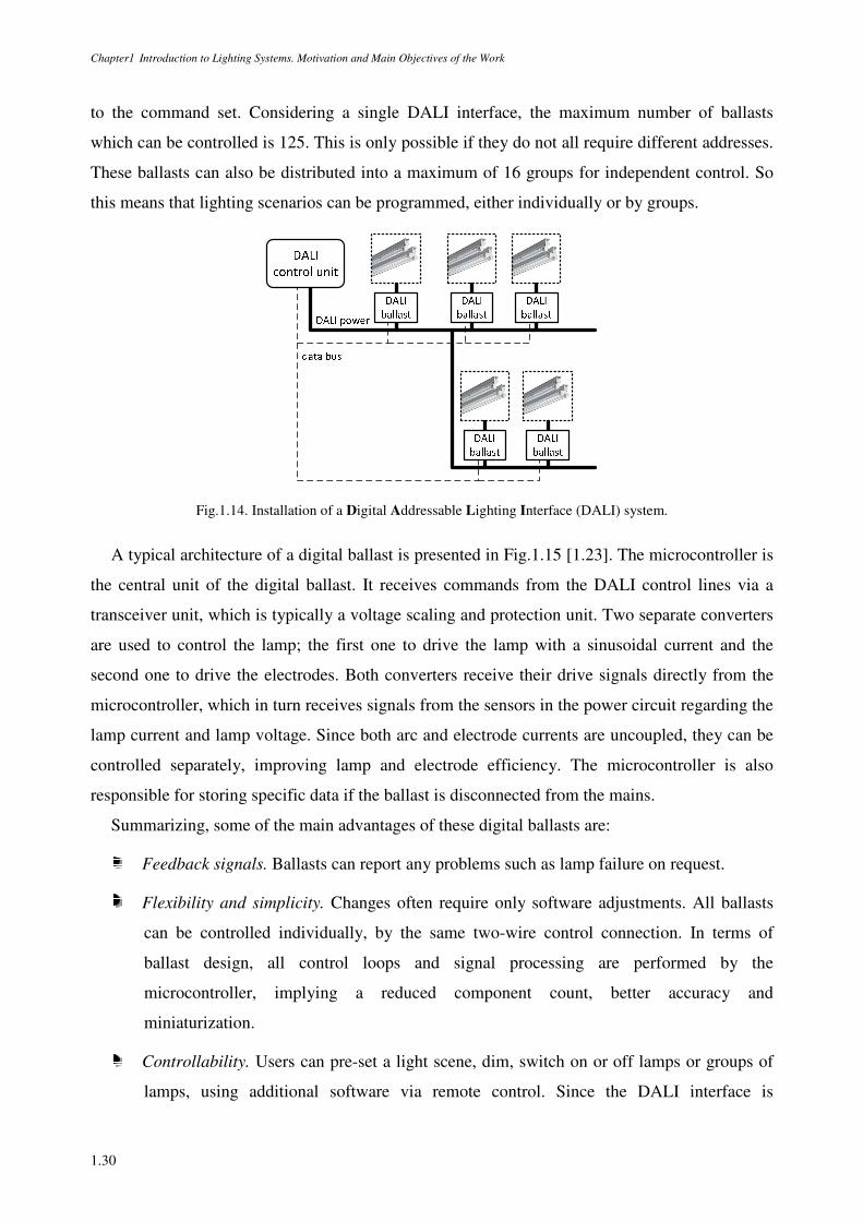
Chapter1 Introduction to Lighting Systems. Motivation and Main Objectives of the Work
1.30
to the command set. Considering a single DALI interface, the maximum number of ballasts
which can be controlled is 125. This is only possible if they do not all require different addresses.
These ballasts can also be distributed into a maximum of 16 groups for independent control. So
this means that lighting scenarios can be programmed, either individually or by groups.
Fig.1.14. Installation of a Digital Addressable Lighting Interface (DALI) system.
A typical architecture of a digital ballast is presented in Fig.1.15 [1.23]. The microcontroller is
the central unit of the digital ballast. It receives commands from the DALI control lines via a
transceiver unit, which is typically a voltage scaling and protection unit. Two separate converters
are used to control the lamp; the first one to drive the lamp with a sinusoidal current and the
second one to drive the electrodes. Both converters receive their drive signals directly from the
microcontroller, which in turn receives signals from the sensors in the power circuit regarding the
lamp current and lamp voltage. Since both arc and electrode currents are uncoupled, they can be
controlled separately, improving lamp and electrode efficiency. The microcontroller is also
responsible for storing specific data if the ballast is disconnected from the mains.
Summarizing, some of the main advantages of these digital ballasts are:
Feedback signals. Ballasts can report any problems such as lamp failure on request.
Flexibility and simplicity. Changes often require only software adjustments. All ballasts
can be controlled individually, by the same two-wire control connection. In terms of
ballast design, all control loops and signal processing are performed by the
microcontroller, implying a reduced component count, better accuracy and
miniaturization.
Controllability. Users can pre-set a light scene, dim, switch on or off lamps or groups of
lamps, using additional software via remote control. Since the DALI interface is
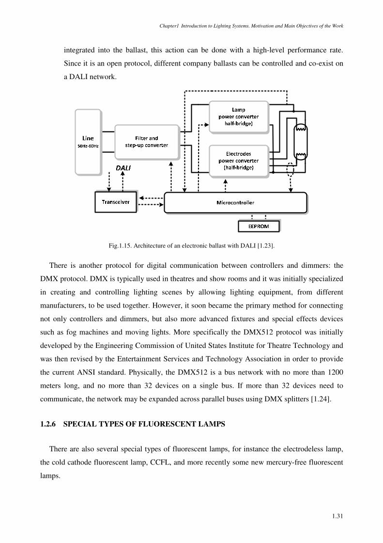
Chapter1 Introduction to Lighting Systems. Motivation and Main Objectives of the Work
1.31
integrated into the ballast, this action can be done with a high-level performance rate.
Since it is an open protocol, different company ballasts can be controlled and co-exist on
a DALI network.
Fig.1.15. Architecture of an electronic ballast with DALI [1.23].
There is another protocol for digital communication between controllers and dimmers: the
DMX protocol. DMX is typically used in theatres and show rooms and it was initially specialized
in creating and controlling lighting scenes by allowing lighting equipment, from different
manufacturers, to be used together. However, it soon became the primary method for connecting
not only controllers and dimmers, but also more advanced fixtures and special effects devices
such as fog machines and moving lights. More specifically the DMX512 protocol was initially
developed by the Engineering Commission of United States Institute for Theatre Technology and
was then revised by the Entertainment Services and Technology Association in order to provide
the current ANSI standard. Physically, the DMX512 is a bus network with no more than 1200
meters long, and no more than 32 devices on a single bus. If more than 32 devices need to
communicate, the network may be expanded across parallel buses using DMX splitters [1.24].
1.2.6 SPECIAL TYPES OF FLUORESCENT LAMPS
There are also several special types of fluorescent lamps, for instance the electrodeless lamp,
the cold cathode fluorescent lamp, CCFL, and more recently some new mercury-free fluorescent
lamps.
Chapter1 Introduction to Lighting Systems. Motivation and Main Objectives of the Work
1.32
The earliest electrodeless lamps were invented over 100 years ago by J. J. Thomson, Tesla and
others. However, the single commercially available electrodeless fluorescent lamp is based on an
induction discharge, which implies a magnetic coupling between the circuit and the plasma. This
is the reason why this lamp is commonly known as the induction lamp. Typically, a coil is
superposed on a tube with fluorescent coatings to convert the UV radiation into visible light. An
alternating current through that coil produces a magnetic field in the discharge space which then
produces an electric field, ultimately responsible for the discharge. The optimum operating
frequency of the system is in part determined by the efficiency of coupling energy from the coil
into the plasma and the EMI regulations [1.2], [1.25]. These lamps operate at very high
frequency, reaching even values of 1MHz, meaning that only over the past two decades, with the
advances in high-frequency power converters, was it possible for them to be a real cost-effective
alternative [1.27].
In fact, one of the main advantages of the electrodeless lamps is that all the problems
associated with electrodes are avoided. Starting can be instantaneous, therefore they can be
switched any number of times. They also have the possibility of providing higher power, since
there are no constraints regarding maximum electrode current and electrode losses. These factors
clearly increase their average lamp life, rated over 60000 hours. They can also work at lower
pressure levels, not recommended for regular fluorescent lamps since internal pressure reduction
results in high evaporation of the emissive material [1.26]. In terms of environmental related
issues, there are other advantages: easily recycled, less pollution, because instead of using liquid
mercury they use amalgam (solid mercury composition with other metals), easy to remove if the
lamp is recycled and finally a high average lamp life due to the absence of electrodes, which in
turn decreases maintenance and replacement costs.
Cold-cathode fluorescent lamps, CCFLs, whose electrodes are not preheated, are also
available and commonly used in backlight liquid crystal displays (LCDs) in TV and PC monitor
applications. Besides straight tubes, there are also U-tubes and L-tubes, for other different
applications. Cold-start ignition is obtained by applying an especially high initial voltage to the
lamp electrodes, which in turn must be very robust [1.22]. The cold-start lamp will ignite the
moment that this voltage is applied, and for this reason they are also referred to as instant start
lamps. In order to reduce, as much as possible, the ignition voltage, the two electrodes are
brought closer together by special construction features. Usually, a conductive strip connects both
electrodes, creating a local high electric-field strength for breakdown. Since these lamps operate
at lower current levels, it is possible to reduce the electrode heating losses in order to extend the
Chapter1 Introduction to Lighting Systems. Motivation and Main Objectives of the Work
1.33
life of the electrodes, so normally they have a higher average lamp life [1.28]. Typically CCFLs
are more efficient than comparable hot cathode fluorescent lamps. A disadvantage is related to
the eventual user exposition to the mains voltage: if one lamp end has already made contact
during the lamp insertion and the user touches the other end. For this reason, these lamps are
fitted with special caps. Even if high brightness LEDs are currently considered as an effective
alternative for backlight sources, CCFLs are still the main stream in large size LCDs. The key
reason is the manufacturing process of LEDs, which until now is not capable of producing
completely identical HBLEDs [1.29].
Environmental awareness intensified the development of new mercury-free fluorescent lamps.
Although the Xenon is one of the most promising candidates for mercury substitution, its
discharge tends to constrict, which drastically drops the lamp efficacy at high power [1.30].
Examples are mercury-free flat fluorescent lamps, MFFFL. These lamps are suitable for backlight
source applications. They present high colour saturation and contrast which improves the image
quality of LCDs. This technology however is still in the development stage [1.29].
1.2.7 FLUORESCENT-LAMP MODELS
Discharge-lamp modelling is an important domain in lighting related research. Numerical low-
pressure-discharge-lamp models, which accurately simulate the real behaviour of fluorescent
lamps, are extremely necessary from two points of view. Firstly it is important to translate the
physical mechanisms which occur inside the glass tube, in order to guide lamp manufacturers in
the search for more efficient light sources, and secondly it is also important to describe the
electrical terminal characteristics of these lamps in order to use this behaviour in the design and
conception of electronic control gear.
A wide literature search reveals that there are several types of fluorescent-lamp models.
Examples of models which are representative of the physical behaviour of the lamp can be found
in [1.39], [1.40] and [1.41]. These physical models generally involve the rate equations and
simplified assumptions on the electron energy distribution function [1.38]. They are usually quite
complex due to the complicated nature of the physical process itself. In [1.39], the proposed
physical model can be used to simulate any low-pressure mercury-buffer gas fluorescent lamp,
over a wide range of operating frequencies, by entering key lamp parameters. These parameters
are: length, radius, cold-spot temperature and buffer gas fill pressure. If this pressure is unknown,
a default value dependent on the lamp radius can be used. Even if the model can describe the
Chapter1 Introduction to Lighting Systems. Motivation and Main Objectives of the Work
1.34
lamp behaviour under transient conditions, it cannot correctly predict the breakdown stage.
Moreover, the model only considers the positive column, ignoring the electrodes behaviour. From
the electrical research engineer point of view, it is more attractive, or even simpler, to use
fluorescent-lamp models which are able to predict the electrical characteristics at the lamp
terminals, without entering the subject of complex physical equations. Such models are
preferably used to perform optimization studies in the design of electronic ballasts. Despite the
selected models, circuit-simulation programs such as SPICE or MATLAB-Simulink are the
commonly chosen implementation environments [1.39], [1.45], [1.56].
As previously described, fluorescent lamps are nonlinear light sources that in parts of the >/
characteristic exhibit a dynamic negative differential resistance behaviour: the rms value of the
lamp current increases with a slight decrease in rms value of the lamp voltage. This is the reason
why some researchers have used a fixed resistance model for simulating the fluorescent-lamp
behaviour. These models are based on the static characteristics of the lamp and they typically use
linear approximations. This is one of the simplest ways to model the lamp, but it has a clear
disadvantage, it can only be used to design electronic control gear at specific conditions, for
example at nominal power. In fact, in the normal operating range, the negative dynamic
resistance of the lamp is dependent on the average lamp power. Therefore, specific models which
vary the lamp resistance with the average lamp power are in fact the most suitable for the
majority of studies. It is a fact, however, that these models are purely based on the empirical
behaviour of the lamp, which means that they are only applicable over a narrow range of
operating conditions, centred mainly on the characteristics which are easily identified when
collecting the necessary data [1.39]. Consequently, most of these models are power-dependent
models, generally based on polynomial or exponential functions, applied using curve-fitting
techniques, which describe the lamp impedance or conductance behaviour of the lamp [1.42]-
[1.48]. A main goal should be the definition of a dynamic model capable of describing the lamp
behaviour at different frequencies, at different dimming levels and eventually under transient
conditions.
1.2.7.1 LARGE-SIGNAL DYNAMIC MODELS
One of the earliest models was proposed by U. Mader and P. Horn in 1992, and is commonly
known as the Mader-Horn model [1.42]. The model is based on the observation that in the full
process of creating visible light, the mechanisms occurring inside the tube are very fast except for
the generation of the ionized mercury atoms from the applied electric power. This mechanism has
Chapter1 Introduction to Lighting Systems. Motivation and Main Objectives of the Work
1.35
a conversion rate of approximately 1ms. So, in the model, the ionization density, |, is assumed to
be related to the instantaneous lamp power, y~, by a so-called "recent running average". In
terms of the Laplace transform, this relation can be defined using a first-order low-pass filter:
| = 11 + y~ (1.1)
where is a proportionality constant and is the ionization recombination time constant. The
previous equation can also be defined as follows:
y~ = 1 | + | (1.2)
In order to simplify this equation, the constant and the ionization density | are replaced by an
average lamp power, t~_~, which in fact is the low-pass-filtered version of the instantaneous
lamp power, y~:
t~_~ = 11 + y~ (1.3)
So, by measuring the KL characteristics of the lamp, at dc and at several high-frequency
values, using for instance, a commercial dimmable electronic ballast, it is possible to model these
curves trough a function describing the dependence of the lamp voltage to the lamp current (more
specifically the arc current), with the average lamp power as parameter, K = L, t~_~. An
example of theses curves can be seen in Fig.1.16. The analysis of these curves clearly reveals that
a different average lamp power will correspond to a different lamp resistance value. Besides, it is
also clear, that the high-frequency lamp characteristics are non-linear. The dc characteristic of the
lamp can be measured using a large variable resistor in series with the lamp supplied by a dc
voltage source with a voltage level which doubles the lamp voltage.
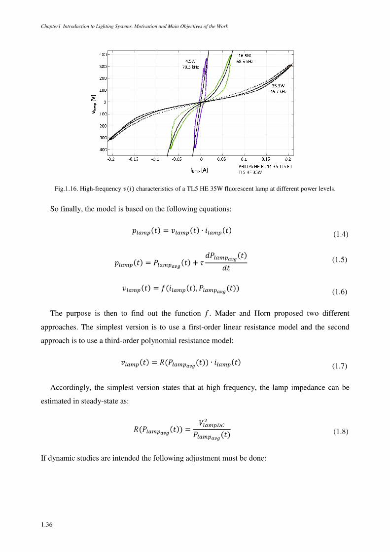
Chapter1 Introduction to Lighting Systems. Motivation and Main Objectives of the Work
1.36
Fig.1.16. High-frequency KL characteristics of a TL5 HE 35W fluorescent lamp at different power levels.
So finally, the model is based on the following equations:
y~ = K~ ∙ L~ (1.4)
y~ = t~ + t~ (1.5)
K~ = L~, t~ (1.6)
The purpose is then to find out the function . Mader and Horn proposed two different
approaches. The simplest version is to use a first-order linear resistance model and the second
approach is to use a third-order polynomial resistance model:
K~ = vt~ ∙ L~ (1.7)
Accordingly, the simplest version states that at high frequency, the lamp impedance can be
estimated in steady-state as:
vt~ = >~0t~ (1.8)
If dynamic studies are intended the following adjustment must be done:
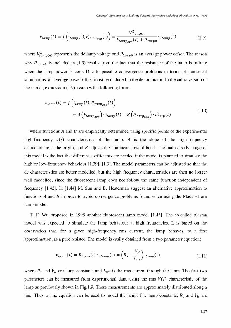
Chapter1 Introduction to Lighting Systems. Motivation and Main Objectives of the Work
1.37
K~ = L~, t~ = >~0t~ + t~ ∙ L~ (1.9)
where >~0 represents the dc lamp voltage and t~ is an average power offset. The reason
why t~ is included in (1.9) results from the fact that the resistance of the lamp is infinite
when the lamp power is zero. Due to possible convergence problems in terms of numerical
simulations, an average power offset must be included in the denominator. In the cubic version of
the model, expression (1.9) assumes the following form:
K~ = L~, t~= t~ ∙ L~ + t~ ∙ L~
(1.10)
where functions and are empirically determined using specific points of the experimental
high-frequency KL characteristics of the lamp. is the slope of the high-frequency
characteristic at the origin, and adjusts the nonlinear upward bend. The main disadvantage of
this model is the fact that different coefficients are needed if the model is planned to simulate the
high or low-frequency behaviour [1.39], [1.3]. The model parameters can be adjusted so that the
dc characteristics are better modelled, but the high frequency characteristics are then no longer
well modelled, since the fluorescent lamp does not follow the same function independent of
frequency [1.42]. In [1.44] M. Sun and B. Hesterman suggest an alternative approximation to
functions and in order to avoid convergence problems found when using the Mader–Horn
lamp model.
T. F. Wu proposed in 1995 another fluorescent-lamp model [1.43]. The so-called plasma
model was expected to simulate the lamp behaviour at high frequencies. It is based on the
observation that, for a given high-frequency rms current, the lamp behaves, to a first
approximation, as a pure resistor. The model is easily obtained from a two parameter equation:
K~ = v~ ∙ L~ = v4 + >/~2 L~ (1.11)
where v4 and > are lamp constants and /~2 is the rms current through the lamp. The first two
parameters can be measured from experimental data, using the rms >/ characteristic of the
lamp as previously shown in Fig.1.9. These measurements are approximately distributed along a
line. Thus, a line equation can be used to model the lamp. The lamp constants, v4 and > are
Chapter1 Introduction to Lighting Systems. Motivation and Main Objectives of the Work
1.38
respectively the slope of the line and the intersection of the line with the voltage axis. A
convergence problem is also present because the resistance of the lamp is infinite when the lamp
current is zero. Therefore, it is necessary to set an initial condition for the lamp current. In [1.45],
Ben- Yaakov states that this model cannot cope with a change of operating conditions, such as a
power level variation, during a given simulation run. In fact, the main problem of this model is
the fact that it only works in steady-state conditions and within a certain frequency range.
Evidently, there are multiple options for fluorescent-lamp models, all based in similar
observations but using better or more advanced curve fitting techniques. In [1.46], C. S. Moo
proposes a model with power and temperature dependence for high-frequency operation. As
previously referred, the electrical characteristics of the lamp are sensitive to temperature
variations. Considering an electronic ballast designed to operate in a wide temperature range,
having a model capable of coping with these changes is obviously an advantage. In [1.49], the
model presented by H. Cheng also includes the electrodes resistance. Models using the lamp
conductance are also extremely popular [1.47]. In [1.50] a cubic-spline interpolation-based
method for modelling the lamp dynamic conductance is proposed. This method is based on a
spline constructed of piecewise third-order polynomial which passes through a set of data points
without knowing the slopes. In [1.48] a comparison is proposed between different physical
models also based on the lamp dynamic conductance, by referring to theoretical exponential and
polynomial models. More recently, it is also possible to identify models which simultaneously
include physical and circuit equations. In [1.51] several equations are proposed which model the
thermal conduction and radiation losses, the electron temperature, the lamp resistance (as a
function of the electron temperature and the Boltzmann constant). A final circuit equation
considering a 50 Hz driving circuit (series electromagnetic ballast) is also proposed. After the
adjustable model constants are determined at 50 Hz, using a genetic algorithm, the model is then
applied to high-frequency operation with agreeing results.
In the case of CFLs similar techniques may be applied. The terminal electrical characteristics
of the lamp are measured and curve fitting techniques are used to process the data. The
implementation and verification of different CFL models can be found in [1.52]. An exponential
model which characterizes the rms >/ characteristic of a 42W CFL lamp and two physically-
based models, Mayr and Cassie models, are analysed. However, if the purpose is to conduct
performance analyses, the main concern is the behavioural impact of the widespread utilization of
such light sources on the grid. CFLs are considered to be harmonic sources due to the high level
of THD in the ac current. A typical electronic ballast circuit is the single-phase capacitor-filtered
Chapter1 Introduction to Lighting Systems. Motivation and Main Objectives of the Work
1.39
uncontrolled ac-dc converter, followed by a high-frequency inverter. So, the goal is not to model
the lamp itself but to provide a CFL harmonic model capable of simulating the power-quality
impact of these lamps in order to perform large-scale harmonic penetration impacts. Such models
can be found in [1.53], [1.54].
Modelling CCFLs is a different challenge. Physical and circuit models are also available.
Circuit models are normally preferred for steady-state analysis due to their simplicity. In [1.55], a
simple exponential model is used to characterize the rms >/ characteristic of the lamp.
However, these lamps are somehow different from tubular fluorescent lamps since the
mechanism of electron emission is different and since they operate at much higher voltage and
much lower current. This lower current, translated into low heating losses in the electrodes, is the
reason why it is possible to extend their life making them suitable for LCD devices. The required
high electrode voltage to cause breakdown is the key issue in some of these models and the
accuracy in predicting the electrode voltage drop will influence the model precision. As
mentioned in [1.56], the electrode voltage drop may be experimentally determined or
theoretically derived. D. Lin and W. Yan propose a simple, non-intrusive method to identify the
electrode voltage drop inside the CCFL, using the so-called lamp operating voltage method. The
measured lamp operating voltage is the sum of the electrodes voltages and the positive column
voltage. A genetic algorithm and a piecewise function are then used to estimate and to model the
optimal electrode voltage drop. The following assumptions are considered: contrary to the hot
cathode fluorescent lamp, where the electrode voltage is assumed as a constant value, the CCFL
shows a voltage which is a function of the discharge current, and that presents a specific shape
(combination of two parabola curves and one straight line). Finally, as in [1.51], the same authors
use physical and circuit equations to model the whole system, including now the modelling
function of the electrode voltage.
A distributed-circuit model of a CCFL back-light unit (BLU), for an LCD device, is proposed
in [1.57]. Simulation results are compared to a set of experimental results retrieved from a
physical system consisting of a CCFL BLU for a 42 inches LCD. The model consists of a circuit
model for the lamp itself, and uses capacitors and inductors to represent the parasitic elements of
the lamp, the coupling between the lamps and the coupling between the lamp and the frame of the
back-light unit. The lamp model is obtained using two current-controlled current sources. These
current sources are controlled by two additional sub-circuits, responsible for modelling the
heating and ignition effects, and three voltage-controlled variable resistors, responsible for
implementing the dc >/ characteristics of the lamp. The lamp model parameters are obtained
Chapter1 Introduction to Lighting Systems. Motivation and Main Objectives of the Work
1.40
through laboratory tests and the parasitic inductances and capacitances are calculated using a
three-dimensional electromagnetic solver.
1.2.7.2 SMALL-SIGNAL DYNAMIC MODELS
Small-signal models are normally used in analytical and simulation studies where the main
concern is the dynamic response and stability of the lamp-ballast system. With these models it is
possible to use the classical control theory and to apply stability criteria to verify whether the
system is stable or not. These models are focused in the characterization of the lamp small-signal
dynamic impedance, or more specifically, they are focused on the change of the lamp’s operating
point or on its negative incremental impedance.
The origin of these small-signal dynamic models relies on the model proposed by E. Deng and
S. Cuk in 1997 [1.58]. Deng and Cuk proposed to study the incremental impedance of fluorescent
lamps, in the frequency domain. As represented in Fig.1.17, the steady-state behaviour of the
lamp can be modelled by a linear resistance, represented by the straight lines A-O or B-O through
the origin which have a positive >/ slope. As observed by Ben-Yaakov et al in [1.59], for a fast
current change the resistance will remain the same. Fast current changes do not significantly alter
the density of carriers in the plasma and the resistance of the lamp remains constant. However if a
slow current change is considered, the density of the carriers changes and the resistance shifts: the
rms operating point will then move along the A-B line. The A-B curve, which has a negative
>// slope, helps to describe the small-signal change of an operating point or its incremental
behaviour. The response to this change is associated with a low-frequency time constant that
controls the rate at which the incremental impedance of the lamp is varying [1.59]. So, instead of
characterizing only the lamp steady-state behaviour, its slow dynamics may also be characterized
through its negative incremental impedance.
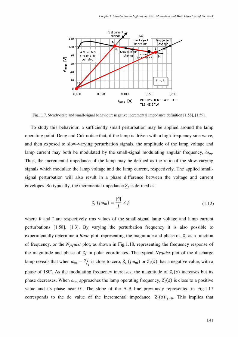
Chapter1 Introduction to Lighting Systems. Motivation and Main Objectives of the Work
1.41
t1 < t2
Fig.1.17. Steady-state and small-signal behaviour: negative incremental impedance definition [1.58], [1.59].
To study this behaviour, a sufficiently small perturbation may be applied around the lamp
operating point. Deng and Cuk notice that, if the lamp is driven with a high-frequency sine wave,
and then exposed to slow-varying perturbation signals, the amplitude of the lamp voltage and
lamp current may both be modulated by the small-signal modulating angular frequency, .
Thus, the incremental impedance of the lamp may be defined as the ratio of the slow-varying
signals which modulate the lamp voltage and the lamp current, respectively. The applied small-
signal perturbation will also result in a phase difference between the voltage and current
envelopes. So typically, the incremental impedance is defined as:
() = |K ||¡| ∠£ (1.12)
where K and ¡ are respectively rms values of the small-signal lamp voltage and lamp current
perturbations [1.58], [1.3]. By varying the perturbation frequency it is also possible to
experimentally determine a Bode plot, representing the magnitude and phase of as a function
of frequency, or the Nyquist plot, as shown in Fig.1.18, representing the frequency response of
the magnitude and phase of in polar coordinates. The typical Nyquist plot of the discharge
lamp reveals that when = ¤ is close to zero, () or (), has a negative value, with a
phase of 180º. As the modulating frequency increases, the magnitude of () increases but its
phase decreases. When approaches the lamp operating frequency, () is close to a positive
value and its phase near 0º. The slope of the A-B line previously represented in Fig.1.17
corresponds to the dc value of the incremental impedance, ()|4¥. This implies that
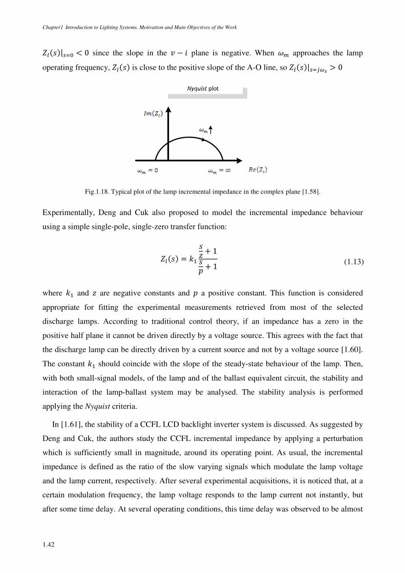
Chapter1 Introduction to Lighting Systems. Motivation and Main Objectives of the Work
1.42
()|4¥ < 0 since the slope in the K − L plane is negative. When approaches the lamp
operating frequency, () is close to the positive slope of the A-O line, so ()|4¥¦§¨ > 0
Fig.1.18. Typical plot of the lamp incremental impedance in the complex plane [1.58].
Experimentally, Deng and Cuk also proposed to model the incremental impedance behaviour
using a simple single-pole, single-zero transfer function:
() = ©ª« + 1y + 1 (1.13)
where ©ª and « are negative constants and y a positive constant. This function is considered
appropriate for fitting the experimental measurements retrieved from most of the selected
discharge lamps. According to traditional control theory, if an impedance has a zero in the
positive half plane it cannot be driven directly by a voltage source. This agrees with the fact that
the discharge lamp can be directly driven by a current source and not by a voltage source [1.60].
The constant ©ª should coincide with the slope of the steady-state behaviour of the lamp. Then,
with both small-signal models, of the lamp and of the ballast equivalent circuit, the stability and
interaction of the lamp-ballast system may be analysed. The stability analysis is performed
applying the Nyquist criteria.
In [1.61], the stability of a CCFL LCD backlight inverter system is discussed. As suggested by
Deng and Cuk, the authors study the CCFL incremental impedance by applying a perturbation
which is sufficiently small in magnitude, around its operating point. As usual, the incremental
impedance is defined as the ratio of the slow varying signals which modulate the lamp voltage
and the lamp current, respectively. After several experimental acquisitions, it is noticed that, at a
certain modulation frequency, the lamp voltage responds to the lamp current not instantly, but
after some time delay. At several operating conditions, this time delay was observed to be almost
Chapter1 Introduction to Lighting Systems. Motivation and Main Objectives of the Work
1.43
constant. Therefore, the authors concluded that this time delay is one of the characteristics of the
lamp and would be noticed on its incremental impedance at high frequencies. By studying the
phase of the incremental impedance, which is directly obtained from the observed time delay, and
the output impedance of the inverter, the authors verify the stability of the system. This study is
conducted at different operating frequencies, and with different resonant inverter parameters.
Similarly, in [1.62] and in [1.63] a small-signal stability analysis of CCFL systems is also
performed. The type of ballast is however different. In recent years, CCFL-ballast systems
normally include a piezoelectric transformer instead of a magnetic transformer (typically used for
isolation purposes and voltage matching). Particularly, in [1.62], it is analysed the implications of
the thermal operating conditions on the stability of such systems. In this case, the so-called
incremental impedance of the lamp is defined as the envelope impedance, which is also the ratio
of the envelope of the lamp voltage to the envelope of the lamp current, when the system is
driven by an AM modulated signal.
In [1.64] a method is proposed to characterize and evaluate the stability of a CFL-ballast
system in dimmed operation. Most of the models are only focused on the lamp small-signal
dynamic behaviour at nominal power level. This implies that the incremental impedance can only
be used to analyse the lamp-ballast interaction at nominal power. However, in dimming ballasts,
the interaction between lamp and ballast can also lead to system instability at reduced power
operation. So, it is also important to observe and verify eventual non-stable conditions at all
power levels. This is obviously an important application for these small-signal modelling
systems. This is the main concern in [1.64]. At each power level, the parameters of the single-
pole, single-zero model are obtained. The static gain, pole and zero values of the model are
calculated and fitted to a power dependent polynomial expression. In this case, instead of using
directly the small-signal impedance, a function of the small-signal variation of the lamp
equivalent resistance, v¬~, against the lamp power perturbation is used, t¬~. Through the
combination of the small-signal models of the lamp and ballast circuit, the small-signal lamp-
ballast system transfer function and corresponding loop gain are obtained. The stability analysis
is also performed applying the Nyquist criteria.
1.3 DIMMING IN FLUORESCENT LIGHTING SYSTEMS
Naturally, one of the most important features in modern lighting systems is the capability of
controlling the luminous flux level of a light source. It is now obvious that for an intelligent and
Chapter1 Introduction to Lighting Systems. Motivation and Main Objectives of the Work
1.44
cost-effective light-management system, a reduction of the power consumption is not synonym of
turning off the lights completely. Developing an efficient dimming technology, while
guaranteeing adequate task lighting and visual comfort, has been a determinant goal over the last
two decades for the lighting industry, especially in fluorescent lighting systems.
1.3.1 STEP DIMMING AND CONTINUOUS DIMMING
From the start, dimming was divided into two categories: continuous dimming and step
dimming. While the first is generally understood as a technology capable of dimming the lamp
from 100% of light output down to approximately 1%, without interruptions, the second one
provides a discrete reduction of the light output level according to some predetermined levels.
Typically step dimming systems are based on bi-level switching: 100% or 50% of light output,
with also the possibility of shutting down the lamp. Usually the control is provided by two
switches connected between the input mains and the ballast. Both switches must be on the same
phase for proper application of step functionality. In these applications, the lamp must be ignited
to either 100% output level or 50% output level without going first to the nominal power. These
ballasts generally have programmed-start circuitry to guarantee extended lamp life in frequent
switching applications, like those associated with the use of occupancy sensors or motion
detectors. It is clearly a system that provides specific light control and some energy savings, but
does not offer the same freedom that continuous dimming offers. Even if there is some research
on step-dimming, [1.68], and there are some specific products on the market for fluorescent
lighting systems [1.69], similar types of discrete dimming are more popular for HPS lamps for
street lighting and outdoor operation. So, in terms of fluorescent lighting and from the market
point of view, there is a clear preference for products allowing a broad range of control, and
smooth continuous dimming.
1.3.2 DIMMING TECHNIQUES
Except for very-low-power dimming levels, the lamp voltage does not change significantly.
This is a common behaviour to all fluorescent lamps. An obvious conclusion is the fact that the
lamp power, and consequently the luminous flux level, can simply be varied by controlling the
lamp current. So, up to now, the proposed dimming techniques use different control parameters
which have an immediate effect on the lamp current.
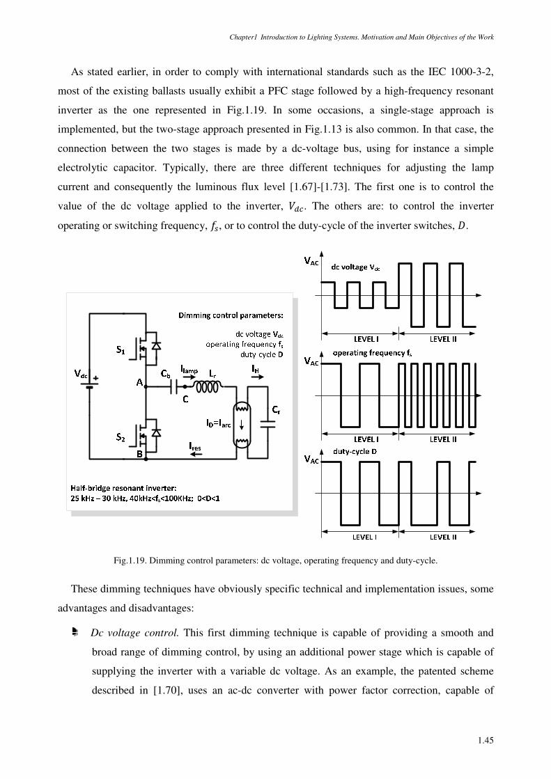
Chapter1 Introduction to Lighting Systems. Motivation and Main Objectives of the Work
1.45
As stated earlier, in order to comply with international standards such as the IEC 1000-3-2,
most of the existing ballasts usually exhibit a PFC stage followed by a high-frequency resonant
inverter as the one represented in Fig.1.19. In some occasions, a single-stage approach is
implemented, but the two-stage approach presented in Fig.1.13 is also common. In that case, the
connection between the two stages is made by a dc-voltage bus, using for instance a simple
electrolytic capacitor. Typically, there are three different techniques for adjusting the lamp
current and consequently the luminous flux level [1.67]-[1.73]. The first one is to control the
value of the dc voltage applied to the inverter, >. The others are: to control the inverter
operating or switching frequency, 4, or to control the duty-cycle of the inverter switches, ®.
Fig.1.19. Dimming control parameters: dc voltage, operating frequency and duty-cycle.
These dimming techniques have obviously specific technical and implementation issues, some
advantages and disadvantages:
Dc voltage control. This first dimming technique is capable of providing a smooth and
broad range of dimming control, by using an additional power stage which is capable of
supplying the inverter with a variable dc voltage. As an example, the patented scheme
described in [1.70], uses an ac-dc converter with power factor correction, capable of
Chapter1 Introduction to Lighting Systems. Motivation and Main Objectives of the Work
1.46
producing a variable dc output between 20V and 300V which is then applied to the
inverter. As stated, this converter may comprise a diode-bridge rectifier, followed by a
flyback converter or some similar solution which also enables PFC. A decreasing dc
voltage will result in a decreasing inverter output voltage, decreasing the lamp current,
and consequently, also decreasing the lamp power.
A major characteristic of this technique is the fact that the lamp current is roughly
proportional to the dc voltage, which gives an almost linear control over a wide lamp
power range. Also, the half-bridge inverter is operated at constant frequency and the
switches are operated at constant duty-cycle, around 0.5. The constant-frequency
operation makes the switching control and the EMI filter design easier, and the resonant
circuit can be optimized for a given type of lamp.
In addition, as stated in [1.67], the resonant circuit can be designed to operate with zero-
voltage switching (ZVS) under a fixed frequency, over a wide dimming range. ZVS is
desirable because it reduces the turn-on switching losses and minimizes the
electromagnetic interference from the power switches. The operating frequency is set at a
slightly higher value than the circuit resonant frequency, also minimizing the
consumption of reactive power.
A known limitation is the fact that it can be difficult to ensure good lamp soft-starting by
using only this control variable, if the electrodes are not separately heated. So, this
method can be, in some cases, an impractical commercial solution. Another observation is
the fact that, at low dimming levels, the voltage across the lamp will raise. So, low
operating dc voltages will correspond to a higher voltage at the lamp terminals. Since the
lamp will be operated near resonance the losses will be higher [1.72].
Duty-cycle control. The ideal duty-cycle of the switches ªand , should be slightly less
than 0.5 so that a small dead time (off-time for both switches) is available to avoid short-
circuiting the input [1.67], [1.70]. But, varying the duty-cycle of the switches allows
controlling the pulse width of the voltage waveform at the output of the inverter, which
means controlling its rms value and consequently providing a variable rms current
through the lamp. The advantage of this technique is the constant-frequency operation.
However it also presents some major drawbacks, one is the non-sinusoidal, asymmetrical
lamp current waveform [1.71]. Another drawback is the high harmonic content of the
modulated square waveform, which can also produce high EMI.
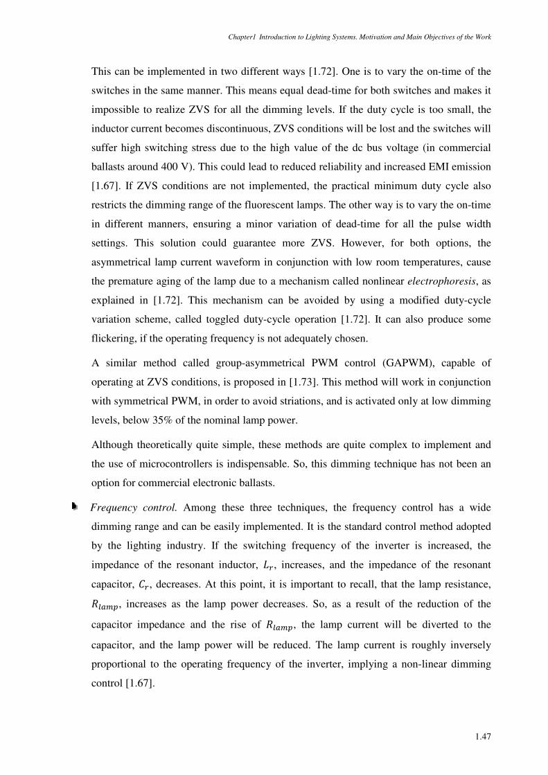
Chapter1 Introduction to Lighting Systems. Motivation and Main Objectives of the Work
1.47
This can be implemented in two different ways [1.72]. One is to vary the on-time of the
switches in the same manner. This means equal dead-time for both switches and makes it
impossible to realize ZVS for all the dimming levels. If the duty cycle is too small, the
inductor current becomes discontinuous, ZVS conditions will be lost and the switches will
suffer high switching stress due to the high value of the dc bus voltage (in commercial
ballasts around 400 V). This could lead to reduced reliability and increased EMI emission
[1.67]. If ZVS conditions are not implemented, the practical minimum duty cycle also
restricts the dimming range of the fluorescent lamps. The other way is to vary the on-time
in different manners, ensuring a minor variation of dead-time for all the pulse width
settings. This solution could guarantee more ZVS. However, for both options, the
asymmetrical lamp current waveform in conjunction with low room temperatures, cause
the premature aging of the lamp due to a mechanism called nonlinear electrophoresis, as
explained in [1.72]. This mechanism can be avoided by using a modified duty-cycle
variation scheme, called toggled duty-cycle operation [1.72]. It can also produce some
flickering, if the operating frequency is not adequately chosen.
A similar method called group-asymmetrical PWM control (GAPWM), capable of
operating at ZVS conditions, is proposed in [1.73]. This method will work in conjunction
with symmetrical PWM, in order to avoid striations, and is activated only at low dimming
levels, below 35% of the nominal lamp power.
Although theoretically quite simple, these methods are quite complex to implement and
the use of microcontrollers is indispensable. So, this dimming technique has not been an
option for commercial electronic ballasts.
Frequency control. Among these three techniques, the frequency control has a wide
dimming range and can be easily implemented. It is the standard control method adopted
by the lighting industry. If the switching frequency of the inverter is increased, the
impedance of the resonant inductor, ¯2, increases, and the impedance of the resonant
capacitor, 2, decreases. At this point, it is important to recall, that the lamp resistance,
v~, increases as the lamp power decreases. So, as a result of the reduction of the
capacitor impedance and the rise of v~, the lamp current will be diverted to the
capacitor, and the lamp power will be reduced. The lamp current is roughly inversely
proportional to the operating frequency of the inverter, implying a non-linear dimming
control [1.67].
Chapter1 Introduction to Lighting Systems. Motivation and Main Objectives of the Work
1.48
A major drawback is obviously the non-constant frequency operation. In order to achieve
low dimming levels, a wide frequency range is necessary (for commercial ballasts,
generally between 40kHz and 100kHz). This means that soft-switching is not easily
achieved over the entire switching range, particularly at low power levels. The switching
transients due to hard-switching will be responsible for high EMI. In these conditions, the
switching losses of the inverter will increase; which will have a negative effect on the
efficiency of the system [1.70]. So, compared to the dc voltage control, the global
efficiency of the ballast is typically lower [1.67], [1.71].
As already referred, a common concern regarding the application of these techniques is the
electrodes preheating process and their behaviour during the dimming operation. During the
preheating process, the voltage applied across the lamp must remain below a certain value, in
order to prevent the lamp to ignite prematurely [1.76]. If the ballast circuit is similar to the one
presented in Fig.1.19, the best method for soft-starting the lamp is to control the resonant-inverter
switching frequency. Initially, the frequency is set to a value higher than the natural-resonance
frequency of the tank; the electrodes heating current is then adjusted to the necessary value,
maintaining a lamp voltage much lower than the starting voltage. After a short period, for
example above 0.4s for TL5 lamps, the frequency is reduced until the starting voltage is obtained,
igniting the lamp [1.19].
There are several commercial IC’s which are designed to drive almost all types of
fluorescent-lamp ballasts. Most of them have externally programmable features such as preheat
time and frequency, controlled ignition and the so-called running mode operating frequency,
which provides a high degree of flexibility for the ballast design engineer. As examples two
controllers will be referred: the IR21571 and the IR21592, [1.74], [1.75]. The first one is not a
dimming ballast controller but it serves as an example of the available features which are
common in a dimming controller. They normally include protection features such as protection
from failure of a lamp to ignite, filament failures, low dc bus voltage, thermal overload, or lamp
failure during normal operation. As example, in Fig.1.20, it is presented the control sequence to
drive rapid start fluorescent lamps in the IR21571. The control sequence allows the run mode
operating frequency of the ballast to be higher than the ignition frequency. This control sequence
is recommended for lamp types where the ignition frequency is too close to the running
frequency to ensure proper lamp ignition for all production resonant LC component tolerances.
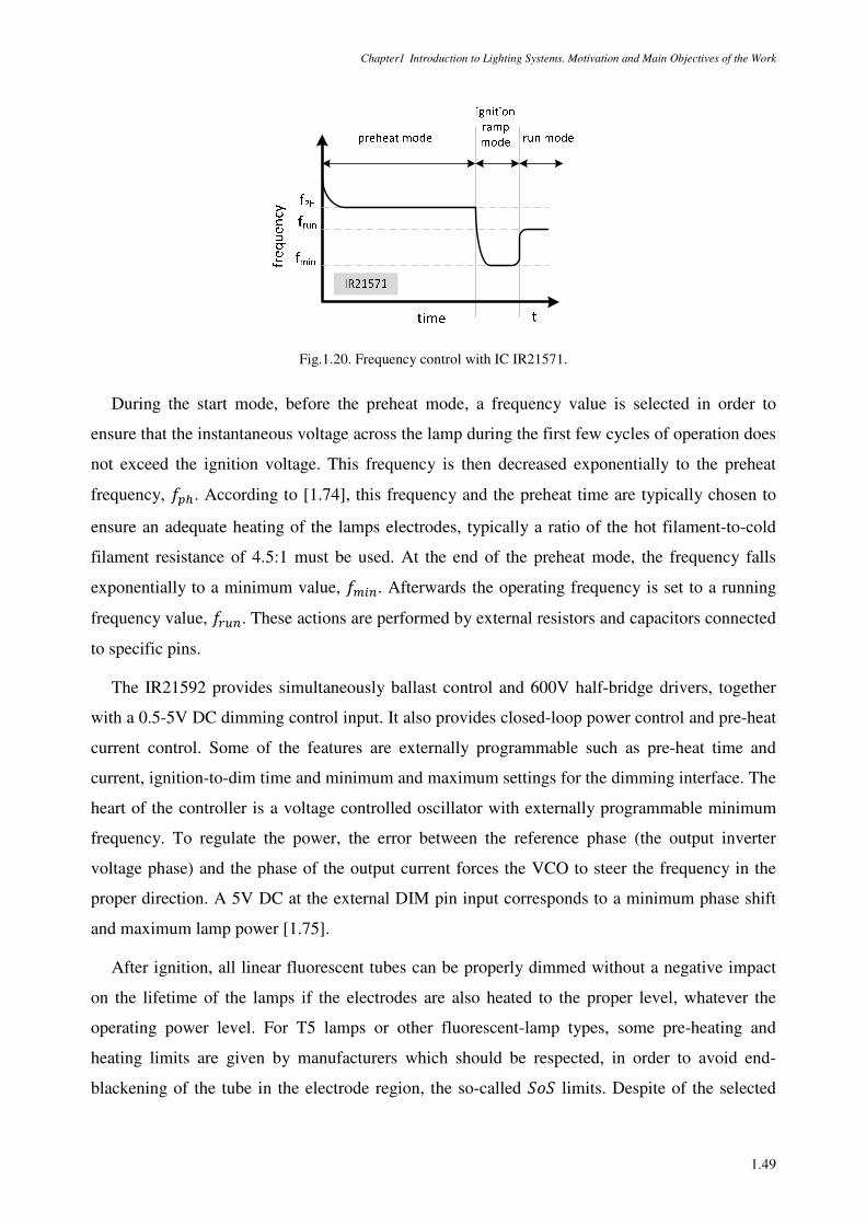
Chapter1 Introduction to Lighting Systems. Motivation and Main Objectives of the Work
1.49
Fig.1.20. Frequency control with IC IR21571.
During the start mode, before the preheat mode, a frequency value is selected in order to
ensure that the instantaneous voltage across the lamp during the first few cycles of operation does
not exceed the ignition voltage. This frequency is then decreased exponentially to the preheat
frequency, °. According to [1.74], this frequency and the preheat time are typically chosen to
ensure an adequate heating of the lamps electrodes, typically a ratio of the hot filament-to-cold
filament resistance of 4.5:1 must be used. At the end of the preheat mode, the frequency falls
exponentially to a minimum value, ±². Afterwards the operating frequency is set to a running
frequency value, 2³². These actions are performed by external resistors and capacitors connected
to specific pins.
The IR21592 provides simultaneously ballast control and 600V half-bridge drivers, together
with a 0.5-5V DC dimming control input. It also provides closed-loop power control and pre-heat
current control. Some of the features are externally programmable such as pre-heat time and
current, ignition-to-dim time and minimum and maximum settings for the dimming interface. The
heart of the controller is a voltage controlled oscillator with externally programmable minimum
frequency. To regulate the power, the error between the reference phase (the output inverter
voltage phase) and the phase of the output current forces the VCO to steer the frequency in the
proper direction. A 5V DC at the external DIM pin input corresponds to a minimum phase shift
and maximum lamp power [1.75].
After ignition, all linear fluorescent tubes can be properly dimmed without a negative impact
on the lifetime of the lamps if the electrodes are also heated to the proper level, whatever the
operating power level. For T5 lamps or other fluorescent-lamp types, some pre-heating and
heating limits are given by manufacturers which should be respected, in order to avoid end-
blackening of the tube in the electrode region, the so-called m limits. Despite of the selected
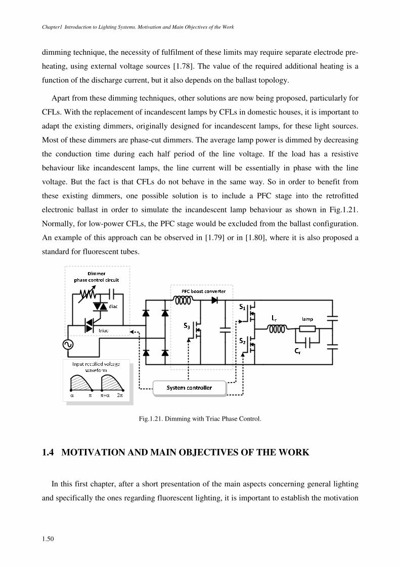
Chapter1 Introduction to Lighting Systems. Motivation and Main Objectives of the Work
1.50
dimming technique, the necessity of fulfilment of these limits may require separate electrode pre-
heating, using external voltage sources [1.78]. The value of the required additional heating is a
function of the discharge current, but it also depends on the ballast topology.
Apart from these dimming techniques, other solutions are now being proposed, particularly for
CFLs. With the replacement of incandescent lamps by CFLs in domestic houses, it is important to
adapt the existing dimmers, originally designed for incandescent lamps, for these light sources.
Most of these dimmers are phase-cut dimmers. The average lamp power is dimmed by decreasing
the conduction time during each half period of the line voltage. If the load has a resistive
behaviour like incandescent lamps, the line current will be essentially in phase with the line
voltage. But the fact is that CFLs do not behave in the same way. So in order to benefit from
these existing dimmers, one possible solution is to include a PFC stage into the retrofitted
electronic ballast in order to simulate the incandescent lamp behaviour as shown in Fig.1.21.
Normally, for low-power CFLs, the PFC stage would be excluded from the ballast configuration.
An example of this approach can be observed in [1.79] or in [1.80], where it is also proposed a
standard for fluorescent tubes.
Fig.1.21. Dimming with Triac Phase Control.
1.4 MOTIVATION AND MAIN OBJECTIVES OF THE WORK
In this first chapter, after a short presentation of the main aspects concerning general lighting
and specifically the ones regarding fluorescent lighting, it is important to establish the motivation
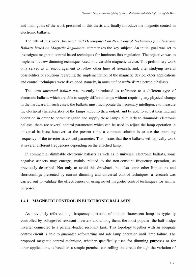
Chapter1 Introduction to Lighting Systems. Motivation and Main Objectives of the Work
1.51
and main goals of the work presented in this thesis and finally introduce the magnetic control in
electronic ballasts.
The title of this work, Research and Development on New Control Techniques for Electronic
Ballasts based on Magnetic Regulators, summarizes the key subject. An initial goal was set to
investigate magnetic-control based techniques for luminous flux regulation. The objective was to
implement a new dimming technique based on a variable magnetic device. This preliminary work
only served as an encouragement to follow other lines of research, and, after studying several
possibilities or solutions regarding the implementation of the magnetic device, other applications
and control techniques were developed, namely, in universal or multi-Watt electronic ballasts.
The term universal ballast was recently introduced as reference to a different type of
electronic ballasts which are able to supply different lamps without requiring any physical change
in the hardware. In such cases, the ballasts must incorporate the necessary intelligence to measure
the electrical characteristics of the lamps wired to their output, and be able to adjust their internal
operation in order to correctly ignite and supply these lamps. Similarly to dimmable electronic
ballasts, there are several control parameters which can be used to adjust the lamp operation in
universal ballasts; however, at the present time, a common solution is to use the operating
frequency of the inverter as control parameter. This means that these ballasts will typically work
at several different frequencies depending on the attached lamp.
In commercial dimmable electronic ballasts as well as in universal electronic ballasts, some
negative aspects may emerge, mainly related to the non-constant frequency operation, as
previously described. Not only to avoid this drawback, but also some other limitations and
shortcomings presented by current dimming and universal control techniques, a research was
carried out to validate the effectiveness of using novel magnetic control techniques for similar
purposes.
1.4.1 MAGNETIC CONTROL IN ELECTRONIC BALLASTS
As previously referred, high-frequency operation of tubular fluorescent lamps is typically
controlled by voltage-fed resonant inverters and among them, the most popular, the half-bridge
inverter connected to a parallel-loaded resonant tank. This topology together with an adequate
control circuit is able to guarantee soft-starting and safe lamp operation until lamp failure. The
proposed magnetic-control technique, whether specifically used for dimming purposes or for
other applications, is based on a simple premise: controlling the circuit through the variation of
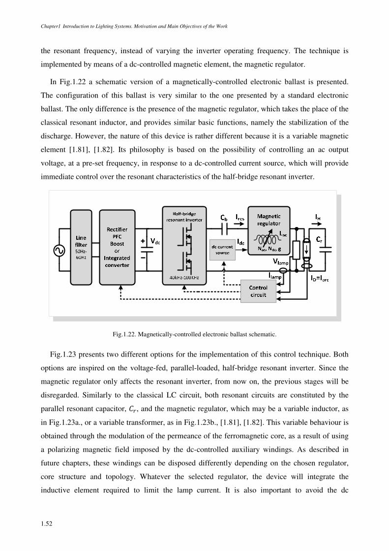
Chapter1 Introduction to Lighting Systems. Motivation and Main Objectives of the Work
1.52
the resonant frequency, instead of varying the inverter operating frequency. The technique is
implemented by means of a dc-controlled magnetic element, the magnetic regulator.
In Fig.1.22 a schematic version of a magnetically-controlled electronic ballast is presented.
The configuration of this ballast is very similar to the one presented by a standard electronic
ballast. The only difference is the presence of the magnetic regulator, which takes the place of the
classical resonant inductor, and provides similar basic functions, namely the stabilization of the
discharge. However, the nature of this device is rather different because it is a variable magnetic
element [1.81], [1.82]. Its philosophy is based on the possibility of controlling an ac output
voltage, at a pre-set frequency, in response to a dc-controlled current source, which will provide
immediate control over the resonant characteristics of the half-bridge resonant inverter.
Fig.1.22. Magnetically-controlled electronic ballast schematic.
Fig.1.23 presents two different options for the implementation of this control technique. Both
options are inspired on the voltage-fed, parallel-loaded, half-bridge resonant inverter. Since the
magnetic regulator only affects the resonant inverter, from now on, the previous stages will be
disregarded. Similarly to the classical LC circuit, both resonant circuits are constituted by the
parallel resonant capacitor, 2, and the magnetic regulator, which may be a variable inductor, as
in Fig.1.23a., or a variable transformer, as in Fig.1.23b., [1.81], [1.82]. This variable behaviour is
obtained through the modulation of the permeance of the ferromagnetic core, as a result of using
a polarizing magnetic field imposed by the dc-controlled auxiliary windings. As described in
future chapters, these windings can be disposed differently depending on the chosen regulator,
core structure and topology. Whatever the selected regulator, the device will integrate the
inductive element required to limit the lamp current. It is also important to avoid the dc
Chapter1 Introduction to Lighting Systems. Motivation and Main Objectives of the Work
1.53
component of the output voltage that is delivered by the inverter, avoiding any dc current
component to flow through the lamp. This task can easily be accomplished by a capacitor
connected in series to the lamp, referred to as the dc-blocking capacitor, ´. It is important to
guarantee that its capacitance is high enough in order to consider the capacitor voltage ripple
negligible.
a. Variable-inductor option b. Variable-transformer option
Fig.1.23. Magnetically-controlled electronic ballasts.
In the variable inductor version presented in Fig.1.23a., the regulator control windings are
used to modify the inductance of the ac winding, represented in series with the lamp. So, the
inductance value in the resonant circuit may be adjusted as desired, depending on the dc current
level circulating through those control windings. If the impedance of the resonant circuit is
changed, it is possible to control the operating point of the lamp as well as its power. Therefore, it
is possible to control the light output of the system. The lamp can also be isolated from the mains
voltage with the inclusion of a variable transformer in the half-bridge inverter, as presented in
Fig.1.23b. The variable behaviour of the resonant circuit will now depend on the transformer
equivalent circuit model together with the resonant capacitor. This behaviour will also be dictated
by the dc control windings included in the regulator structure. With this solution, it is possible to
provide electrical isolation in addition to the control of the lamp’s operating point. This can be a
useful combination for applications with CCFLs in LCD backlighting applications.
The magnetic regulator concept is not new, however applying the concept to electronic
ballasts is considered to be an innovative and promising technique. The work presented in this
thesis describes the theoretical development and practical implementation of magnetic control
techniques in prototype versions of magnetically-controlled electronic ballasts, as well as the
Chapter1 Introduction to Lighting Systems. Motivation and Main Objectives of the Work
1.54
research steps involving these variable magnetic devices, from initial project and design, to
theoretical and behavioural analysis, and finally, simulation and prototype implementation.
1.4.2 OUTLINE OF THE WORK
This Ph. D. Thesis is divided in five chapters. The first chapter provides an overview of the
lighting domain, namely the current state of the art of fluorescent lighting. The fundamental
requirements of typical fluorescent lighting systems controlled by electronic ballasts are
described. Additional features related to remote control of the lighting system are also referred.
The motivation of this research is then exposed and magnetic regulators are introduced as a new
concept related to magnetic control in electronic ballasts, for dimming and multi-Watt operation.
Chapter 2 starts with a succinct introduction to saturable-core reactors and magnetic
amplifiers. Some general considerations on different topologies and their behaviour are presented
together with some fundamental notions on magnetic material behaviour, mainly related to the
magnetization curve of the materials and hysteresis loop. Magnetic regulators are then
introduced. The fundamental principles of operation of variable inductors and variable
transformers are described while the basic laws of magnetism are recalled. The use of variable
inductors or variable transformers in resonant power converters is addressed in detail. The
chapter ends with a brief description of the proposed control techniques, for dimmable or
universal ballasts, and top advantages are pointed out.
The next two chapters are the core of this Ph. D. Thesis and are divided in variable inductor
ballast applications and variable transformer ballast applications.
Chapter 3 starts by describing the variable inductor modelling and design. It moves on to the
description of the flux regulation technique. A comparative analysis between resonant circuits,
different regulators structures, topologies and their effects on lamp operation is carried out.
Finally, the chapter describes the other proposed technique: magnetically-controlled universal
ballasts. The technique is explained and two different prototype versions are presented, the last
one with constant-frequency operation. A special attention regarding some critical issues related
to electrodes operation with these control techniques is also presented.
In Chapter 4 the variable transformer solution is presented as a step forward in magnetically-
controlled electronic ballasts. It is shown how the proposed technique takes advantage of the
magnetic behaviour of the device by integrating the magnetic component necessary to control the
lamp current while guaranteeing electrical isolation and constant-frequency operation. Two
Chapter1 Introduction to Lighting Systems. Motivation and Main Objectives of the Work
1.55
different variable transformer topologies are suggested, five-leg and three-leg, and a
comprehensive description of their behaviour, modelling and characterization, using a simple
methodology is also presented. The large-signal characterization of the three-leg variable
transformer is also presented.
Both Chapter 3 and Chapter 4 present a vast set of experimental results which validate the
proposed techniques. Prototype versions of magnetically-controlled electronic ballasts are
presented and the collected experimental results clearly show the adequate behaviour of the
selected fluorescent lamps under this type of magnetic control. Most of these results are based on
modern T5 lamps.
Finally, Chapter 5 presents the conclusions and main contributions related to the application of
magnetic regulators in electronic ballasts. The main achieved goals are emphasized,
optimizations issues are raised as future work and a special attention is paid on future lines of
research which includes other fields of applications.
Chapter1 Introduction to Lighting Systems. Motivation and Main Objectives of the Work
1.56
REFERENCES
[1.1] CIE, Commission Internationale de l´Eclairage, http://www.cie.co.at.
[1.2] J. R. Coaton and A. M. Marsden, “Lamps and Lighting”, 4th Edition, Arnold and Contributors 1997, ISBN:
0340646187.
[1.3] Javier Ribas Bueno, “Control optimizado de balastos electrónicos. Modelado estático y dinámico de
inversores resonantes y lámparas de descarga”, University of Oviedo, September 2001.
[1.4] Thomas Edison's Patent Application for the Light Bulb 1880,
http://www.ourdocuments.gov/doc.php?doc=46.
[1.5] Philips Product Catalogue 2010, http://www.lighting.philips.com.
[1.6] European Union portal, http://europa.eu/pol/ener/index_en.htm.
[1.7] Osram Sylvania Product Catalogue, http://www.osram.com.
[1.8] Lighting Research Center, http://www.lrc.rpi.edu/.
[1.9] Alonso, J. M., Rashid, Muhammad H., “Power Electronics Handbook, Chapter 22 Electronic Ballasts”,
Academic Press, Inc., 2001, ISBN: 978-0-12-581650-2.
[1.10] Buso, D.; Bhosle, S.; Zissis, G.; Mayhrofer, M.; Zudrell-Koch, S.; Severinsson, M.; Rydhem, A.; Ruscassie,
R.; "Predictive Evaluation of Fluorescent Lamp Lifetime," Industry Applications Society Annual Meeting,
2009. IAS 2009. IEEE, vol., no., pp.1-7, 4-8 Oct. 2009.
[1.11] Maussion, P.; Chhun, L.; Bhosle, S.; Zissis, G.; "Acoustic Resonance Characteristics in a High Pressure
Sodium Lamp," Industry Applications Society Annual Meeting, 2008. IAS '08. IEEE, vol., no., pp.1-4, 5-9
Oct. 2008.
[1.12] Kaiser, W.; Marques, R.P.; Correa, A.F.; "An Alternative Optical Method for Acoustic Resonance Detection
in HID Lamps," Industry Applications Society Annual Meeting, 2009. IAS 2009. IEEE, vol., no., pp.1-6, 4-8
Oct. 2009.
[1.13] Cheng, C.-A.; Lin, K.-J.; Kao, Y.-M.; "Acoustic-resonance-free electronic ballast for automotive HID
lamps," Electronics Letters, vol.44, no.17, pp.1027-1029, Aug. 14 2008.
[1.14] Garcia-Garcia, J.; Cardesin, J.; Ribas, J.; Calleja, A.J.; Rico-Secades, M.; Alonso, J.M.; Corominas, E.L.;
"Minimization of acoustic resonances in HID lamps: analysis and comparison of power harmonics content in
high frequency non-resonant inverters," Power Electronics, IEEE Transactions on , vol.20, no.6, pp. 1467-
1479, Nov. 2005.
[1.15] Lehman, Brad; “Introduction to LED Lighting Systems”, IEEE Energy Conversion Congress and Exposition,
ECCE 2010, Atlanta, Georgia, September, 2010.
[1.16] S. Nakamura, T. Mukai, M. Sengh, "Candela-class high-brightness InGan-AlGan double heterostructure blue
light-emitting diodes," Appl. Phys. Lett., 64(13):1687-9, 1994.
[1.17] CREE, http://www.cree.com.
[1.18] Philips Lumileds Products, http://www.philipslumileds.com.
[1.19] NICHIA LED Catalogue 2010, http://www.nichia.co.jp.
[1.20] Philips MASTER TL5 lamps, Philips 2006, Access in: Jan. 2011, http://www.lighting.philips.com.
Chapter1 Introduction to Lighting Systems. Motivation and Main Objectives of the Work
1.57
[1.21] Qin, Y.X.; Lin, D.Y.; Hui, S.Y.R.; "A Simple Method for Comparative Study on the Thermal Performance of
Light Emitting Diodes (LED) and Fluorescent Lamps," Applied Power Electronics Conference and
Exposition, 2009. APEC 2009. Twenty-Fourth Annual IEEE, vol., no., pp.152-158, 15-19 Feb. 2009.
[1.22] Buso, S.; Spiazzi, G.; Meneghini, M.; Meneghesso, G.; "Performance Degradation of High-Brightness Light
Emitting Diodes Under DC and Pulsed Bias," Device and Materials Reliability, IEEE Transactions on, vol.8,
no.2, pp.312-322, June 2008.
[1.23] Application guide to fluorescent gear, http://www.lighting.philips.com.
[1.24] ANSI E1.11-2008, Entertainment Technology - USITT DMX512-A - Asynchronous Serial Digital Data
Transmission Standard for Controlling Lighting Equipment and Accessories,
http://webstore.ansi.org/RecordDetail.aspx?sku=ANSI+E1.11-2008
[1.25] Tae-Eun Jang; Hee-Jun Kim; Hoon Kim; "Dimming Control Characteristics of Electrodeless Fluorescent
Lamps," Industrial Electronics, IEEE Transactions on , vol.56, no.1, pp.93-100, Jan. 2009.
[1.26] da Silva, M.F.; de P Lopes, J.; Chagas, N.B.; Seidel, A.R.; Costa, M.A.D.; do Prado, R.N.; "High power
factor dimmable lighting system for electrodeless fluorescent lamp," Power Electronics Electrical Drives
Automation and Motion (SPEEDAM), 2010 International Symposium on , vol., no., pp.379-384, 14-16 June
2010.
[1.27] Wonseok Oh; Kyumin Cho; Jaeeul Yeon; Kyungsang Yoo; "Fully digital controlled electronic ballast for
electrode-less lamps," Power Electronics Electrical Drives Automation and Motion (SPEEDAM), 2010
International Symposium on , vol., no., pp.363-367, 14-16 June 2010.
[1.28] Lin, D.Y.; Yan, W.; "Study and Modeling of Cold Cathode Fluorescent Lamps (CCFL)," Applied Power
Electronics Conference and Exposition, 2009. APEC 2009. Twenty-Fourth Annual IEEE, vol., no., pp.812-
818, 15-19 Feb. 2009.
[1.29] Ke, Yu-Lung; Chuang, Ying-Chun; Chuang, Hung-Shiang; Wu, Yuan-Kang; Chang, Chun-Chih; "Self-
excited electronic ballast for cold cathode fluorescent lamps," Industrial and Commercial Power Systems
Technical Conference (I&CPS), 2010 IEEE , vol., no., pp.1-6, 9-13 May 2010.
[1.30] Hirahaya, M.; Takeda, M.; Oka, K.; Toda, Y.; Motomura, H.; Jinno, M.; "Effect of the auxiliary external
electrode on xenon fluorescent lamp depending on its diameter," Plasma Science - Abstracts, 2009. ICOPS
2009. IEEE International Conference on, vol., no., pp.1-1, 1-5 June 2009.
[1.31] Perdigão, M.; Saraiva, E.S.; "Matlab-Simulink implementation of the Mader-Horn fluorescent-lamp model:
permissible range of the resistive lamp model," Industrial Technology, 2004. IEEE ICIT '04. 2004 IEEE
International Conference on, vol.1, no., pp. 492- 497 Vol. 1, 8-10 Dec. 2004
[1.32] Hui, S.Y.R.; Lin, D.Y.; Ng, W.M.; Yan, W.; "A “Class-A2” ultra-low-loss magnetic ballast for T5
fluorescent lamps," Applied Power Electronics Conference and Exposition (APEC), 2010 Twenty-Fifth
Annual IEEE, vol., no., pp.1346-1351, 21-25 Feb. 2010.
[1.33] Wai Man Ng, Deyan Lin and S.Y.R. Hui; “A Single Eco-Friendly Ultra-Low-Loss Magnetic Ballast Design
for a Wide Range of T5 High-Efficient Fluorescent Lamps”, Energy Conversion Congress & Exposition
(ECCE), IEEE, September 2010.
[1.34] Simões, A.S.; Silva, M.M.; Anunciada, A.V.; "A boost-type converter for DC-supply of fluorescent lamps,"
Industrial Electronics, IEEE Transactions on , vol.41, no.2, pp. 251- 255, Apr 1994
Chapter1 Introduction to Lighting Systems. Motivation and Main Objectives of the Work
1.58
[1.35] IEC 1000-3-2 (1995-03) standards on EMC, Part 3, Section 2: Limits for harmonic current emissions.
International Electrotechnical Commission, Geneva, Switzerland, April 1995.
[1.36] Ying-Chun Chuang; Chin-Sien Moo; Hsien-Wen Chen; Tsai-Fu Lin; "A Novel Single-Stage High-Power-
Factor Electronic Ballast With Boost Topology for Multiple Fluorescent Lamps," Industry Applications,
IEEE Transactions on , vol.45, no.1, pp.323-331, Jan.-Feb. 2009
[1.37] L. Rossetto, G. Spiazzi, P. Tenti, "Control techniques for power factor correction converters", Proc. of Power
Electronics, Motion Control (PEMC), 1310-1318, September 1994.
[1.38] Deyan Lin; Wei Yan; Zissis, G.; Hui, S.; "A simple physical low pressure discharge lamp model," Energy
Conversion Congress and Exposition, 2009. ECCE 2009. IEEE, vol., no., pp.2051-2058, 20-24 Sept. 2009.
[1.39] Holloway, A.J.; Tozer, R.C.; Stone, D.A.; "A Physically Based Fluorescent Lamp Model for a SPICE or a
Simulink Environment," Power Electronics, IEEE Transactions on, vol.24, no.9, pp.2101-2110, Sept. 2009.
[1.40] Ka Hong Loo; Moss, G.J.; Tozer, R.C.; Stone, D.A.; Jinno, M.; Devonshire, R.; "A dynamic collisional-
radiative model of a low-pressure mercury-argon discharge lamp: a physical approach to modeling
fluorescent lamps for circuit simulations," Power Electronics, IEEE Transactions on , vol.19, no.4, pp. 1117-
1129, July 2004.
[1.41] Zissis, G.; Buso, D.; "Using full physical model for fluorescent lamps in ballast engineering," Industry
Applications Conference, 2003. 38th IAS Annual Meeting. Conference Record of the, vol.1, no., pp. 537-
541 vol.1, 12-16 Oct. 2003.
[1.42] Mader, U.; Horn, P.; "A dynamic model for the electrical characteristics of fluorescent lamps," Industry
Applications Society Annual Meeting, 1992., Conference Record of the 1992 IEEE , vol., no., pp.1928-1934
vol.2, 4-9 Oct 1992.
[1.43] Wu, T.-F.; Hung, J.-C.; Yu, T.-H.; "A PSpice model for fluorescent lamps operated at high frequencies,"
Industrial Electronics, Control, and Instrumentation, 1995., Proceedings of the 1995 IEEE IECON 21st
International Conference on , vol.1, no., pp.359-364 vol.1, 6-10 Nov 1995.
[1.44] Sun, M.; Hesterman, B.L.; "PSpice high-frequency dynamic fluorescent lamp model," Power Electronics,
IEEE Transactions on , vol.13, no.2, pp.261-272, Mar 1998.
[1.45] Ben-Yaakov, S.; "Modeling the high-frequency behavior of a fluorescent lamp: a comment on “a PSpice
circuit model for low-pressure gaseous discharge lamps operating at high frequency”," Industrial Electronics,
IEEE Transactions on , vol.45, no.6, pp.947-950, Dec 1998.
[1.46] Moo, C.S.; Hsieh, Y.C.; Yen, H.C.; Lee, C.R.; "Fluorescent lamp model with power and temperature
dependence for high-frequency electronic ballasts," Industry Applications, IEEE Transactions on , vol.39,
no.1, pp. 121- 127, Jan/Feb 2003.
[1.47] Blanco, C.; Anton, J.C.; Robles, A.; Ferrero, F.J.; Campo, J.C.; Gonzalez, M.; Zissis, G.; "A Discharge Lamp
Model Based on Lamp Dynamic Conductance," Power Electronics, IEEE Transactions on , vol.22, no.3,
pp.727-734, May 2007.
[1.48] Blanco, C.; Anton, J.C.; Robles, A.; Ferrero, F.; Viera, J.C.; Bhosle, S.; Zissis, G.; "Comparison between
Different Discharge Lamp Models Based on Lamp Dynamic Conductance," Industry Applications Society
Annual Meeting, 2008. IAS '08. IEEE, vol., no., pp.1-6, 5-9 Oct. 2008.
Chapter1 Introduction to Lighting Systems. Motivation and Main Objectives of the Work
1.59
[1.49] Hung-Liang Cheng; Yung-Hsin Huang; "Design and Implementation of Dimmable Electronic Ballast for
Fluorescent Lamps Based on Power-Dependent Lamp Model," Plasma Science, IEEE Transactions on,
vol.38, no.7, pp.1644-1650, July 2010.
[1.50] Chang, G.W.; Liu, Y.J.; "A New Approach for Modeling Voltage–Current Characteristics of Fluorescent
Lamps," Power Delivery, IEEE Transactions on, vol.23, no.3, pp.1682-1684, July 2008.
[1.51] Lin, D.; Yan, W.; Hui, S. Y. R.; "Modeling of Dimmable Fluorescent Lamp Including the Tube Temperature
Effects," Industrial Electronics, IEEE Transactions on, vol., no.99, pp.1, 2011. (Early access)
[1.52] Shafi, M.A.; McMahon, R.A.; "Implementation and verification of CFL models for use in performance
analysis in high frequency electronic ballasts," Power Electronics, Machines and Drives, 2006. PEMD 2006.
The 3rd IET International Conference on, vol., no., pp.561-565, 4-6 April 2006.
[1.53] Wei, Z.; Watson, N.R.; Frater, L.P.; "Modelling of compact fluorescent lamps," Harmonics and Quality of
Power, 2008. ICHQP 2008. 13th International Conference on, vol., no., pp.1-6, Sept. 28 2008-Oct. 1 2008.
[1.54] Jing Yong; Liang Chen; Nassif, A.B.; Wilsun Xu; "A Frequency-Domain Harmonic Model for Compact
Fluorescent Lamps," Power Delivery, IEEE Transactions on, vol.25, no.2, pp.1182-1189, April 2010.
[1.55] Cherl-Jin, K.; Yoo Byeong-Kyu; Yoon Shin-Yong; Baek Soo-Hyun; "A Proper Impedance Model of CCFL
(Cold Cathode Fluorescent Lamp) Applied to the Display Unit," Electrical Machines and Systems, 2005.
ICEMS 2005. Proceedings of the Eighth International Conference on, vol.2, no., pp.1457-1460, 29-29 Sept.
2005.
[1.56] Deyan Lin; Wei Yan; "Modeling of Cold Cathode Fluorescent Lamps (CCFLs) With Realistic Electrode
Profile," Power Electronics, IEEE Transactions on, vol.25, no.3, pp.699-709, March 2010.
[1.57] Min Sup Song, Yong Kyu Park, Jae Joong Yun, Young Ho Hwang, Bongkoo Kang; “Distributed circuit
model for cold cathode fluorescent lamps in back-light unit of liquid crystal display,” Elsévier Journal,
Displays, vol. 31, issue 2, pp.104-110, April 2010.
[1.58] Deng, E.; Cuk, S.; "Negative incremental impedance and stability of fluorescent lamps," Applied Power
Electronics Conference and Exposition, 1997. APEC '97 Conference Proceedings 1997, Twelfth Annual,
vol.2, no., pp.1050-1056 vol.2, 23-27 Feb 1997.
[1.59] Ben-Yaakov, S.; Shvartsas, M.; Glozman, S.; "Statics and dynamics of fluorescent lamps operating at high
frequency: modeling and simulation," Industry Applications, IEEE Transactions on , vol.38, no.6, pp. 1486-
1492, Nov/Dec 2002.
[1.60] Glozman, S.; Ben-Yaakov, S.; "Dynamic interaction analysis of HF ballasts and fluorescent lamps based on
envelope simulation," Industry Applications, IEEE Transactions on, vol.37, no.5, pp.1531-1536, Sep/Oct
2001.
[1.61] Chang-Gyum Kim; Kyu-Chan Lee; Cho, B.H.; "Modeling of CCFL using lamp delay and stability analysis
of backlight inverter for large size LCD TV," Applied Power Electronics Conference and Exposition, 2005.
APEC 2005.
[1.62] Ben-Yaakov, S.; Peretz, M.M.; "Cold Cathode Fluorescent Lamps Driven by Piezoelectric Transformers:
Stability Conditions and Thermal Effect," Power Electronics, IEEE Transactions on, vol.22, no.3, pp.761-
768, May 2007.
[1.63] Spiazzi, G.; Buso, S.; "Small-Signal Analysis of Cold Cathode Fluorescent Lamp Ballasts," Power
Electronics, IEEE Transactions on, vol.22, no.3, pp.753-760, May 2007.
Chapter1 Introduction to Lighting Systems. Motivation and Main Objectives of the Work
1.60
[1.64] Diaz, R.E.; Ribas, J.; Calleja, A.J.; Alonso, J.M.; Garcia-Garcia, J.; "Small signal characterization of
fluorescent lamps in dimmed operation," Industrial Electronics, 2009. IECON '09. 35th Annual Conference
of IEEE, vol., no., pp.3563-3568, 3-5 Nov. 2009.
[1.65] Lam, J.; Jain, Praveen K.; "A Novel Single-Stage Dimmable Electronic Ballast with High Efficiency and
Unity Power Factor Using an Integrated Buck-boost Current Source Resonant Inverter," Applied Power
Electronics Conference, APEC 2007 - Twenty Second Annual IEEE , vol., no., pp.1309-1315, Feb. 25 2007-
March 1 2007.
[1.66] Zan Huang; Ribarich, T.; "A New Dimming Method for Highly Integrated Fluorescent Ballast," Applied
Power Electronics Conference and Exposition, 2009. APEC 2009. Twenty-Fourth Annual IEEE, vol., no.,
pp.1553-1557, 15-19 Feb. 2009.
[1.67] Tam, P.W.; Lee, S.T.S.; Hui, S.Y.R.; Chung, H.S.-H.; "Practical Evaluation of Dimming Control Methods
for Electronic Ballasts," Power Electronics, IEEE Transactions on, vol.21, no.6, pp.1769-1775, Nov. 2006.
[1.68] Haiyan Wang; Stankovic, A.V.; Nerone, L.; Kachmarik, D.; "A Novel Discrete Dimming Ballast for Linear
Fluorescent Lamps," Power Electronics, IEEE Transactions on , vol.24, no.6, pp.1453-1462, June 2009.
[1.69] Philips Advance Optanium® high-efficiency ballasts with step-dim capability,
http://www.lighting.philips.com.
[1.70] S. Y. R. Hui and H. S. H. Chung, “Dimming Control of Electronic Ballasts,” U.S. Patent 6 486 615, Nov. 26,
2002.
[1.71] Alonso, J.M.; Dalla Costa, M.A.; Rico-Secades, M.; Cardesin, J.; Garcia, J.; "Investigation of a New Control
Strategy for Electronic Ballasts Based on Variable Inductor," Industrial Electronics, IEEE Transactions on ,
vol.55, no.1, pp.3-10, Jan. 2008.
[1.72] Raiser, F.; "Dim the lights. Problems with lamp current control using a PWM signal," Industry Applications
Magazine, IEEE, vol.8, no.6, pp. 54- 59, Nov/Dec 2002.
[1.73] Guan-Chyun Hsieh; "Group-Asymmetrical PWM Control for Dimmable Fluorescent Lamp Ballast Without
Striation and Thermostat Effect," Power Electronics, IEEE Transactions on, vol.24, no.5, pp.1293-1303, May
2009.
[1.74] IR21571(S) Datasheet PD Nº 60179-I, International Rectifier, www.irf.com.
[1.75] IR21592(S) Datasheet PD Nº 60194 revD, International Rectifier, www.irf.com.
[1.76] Dorleijn, J.W.F.; Goud, L.H.; "Standardisation of the static resistances of fluorescent lamp cathodes and new
data for preheating," Industry Applications Conference, 2002. 37th IAS Annual Meeting. Conference Record
of the, vol.1, no., pp. 665- 672 vol.1, 2002.
[1.77] Goud, L.H.; Dorleijn, J.W.F.; "Standardized data for dimming of fluorescent lamps," Industry Applications
Conference, 2002. 37th IAS Annual Meeting. Conference Record of the, vol.1, no., pp. 673- 679 vol.1, 2002.
[1.78] Ballasts for tubular fluorescent lamps – Performance requirements, IEC 60921, 2006.
[1.79] Lam, J.; Jain, P.K.; "A novel dimmable electronic ballast for compact fluorescent lamps using phase-cut
incandescent lamp dimmers with wide dimming range and low dimming level lamp ignition capability,"
Applied Power Electronics Conference and Exposition (APEC), 2010 Twenty-Fifth Annual IEEE , vol., no.,
pp.2321-2327, 21-25 Feb. 2010.
Chapter1 Introduction to Lighting Systems. Motivation and Main Objectives of the Work
1.61
[1.80] Yu-Kai Chen; Yung-Chun Wu; Chau-Chung Song; Li-June Liu; "Design and implementation of dimmable
fluorescent lamps with TRIAC phase control," Industrial Technology, 2009. ICIT 2009. IEEE International
Conference on, vol., no., pp.1-6, 10-13 Feb. 2009.
[1.81] Medini, D.; Ben-Yaakov, S.; "A current-controlled variable-inductor for high frequency resonant power
circuits," Applied Power Electronics Conference and Exposition, 1994. APEC '94. Conference Proceedings
1994., Ninth Annual , vol., no., pp.219-225 vol.1, 13-17 Feb 1994
[1.82] Vollin, J.; Tan, F.D.; Cuk, S.M.; "Magnetic regulator modeling," Applied Power Electronics Conference and
Exposition, 1993. APEC '93. Conference Proceedings 1993, Eighth Annual, vol., no., pp.604-611, 7-11 Mar
1993.

Chapter1 Introduction to Lighting Systems. Motivation and Main Objectives of the Work
1.62
BIBLIOGRAPHY
[B1.1] J. R. Coaton and A. M. Marsden, “Lamps and Lighting”, 4th Edition, Arnold and Contributors 1997, ISBN:
0340646187.
[B1.2] Alonso, J. M., Rashid, Muhammad H., “Power Electronics Handbook, Chapter 22 Electronic Ballasts”,
Academic Press, Inc., 2001, ISBN: 978-0-12-581650-2.
[B1.3] Application guide to fluorescent gear, http://www.lighting.philips.com
LITERATURE REVIEW ON MAGNETIC 2REGULATORS
In the present chapter, the state of the art on magnetic regulators is presented. The chapter
starts with a succinct introduction to saturable-core reactors and magnetic amplifiers. Some
general considerations on different topologies and their behaviour are presented together with
some fundamental notions on magnetic material behaviour, mainly related to the magnetization
curve of the material and hysteresis loop. Magnetic regulators are then introduced. The
fundamental principles of operation of variable inductors and variable transformers are
described while the basic laws of magnetism are recalled. Since magnetic regulators in the form
of variable inductors or variable transformers have been the object of several patents and several
scientific papers, a general overview is presented. Typically, they all refer the device, or the
invention, as useful or industrially applicable. Due to the focus of the developed work, the subject
of their application to resonant power converters is addressed in detail. The chapter ends with a
brief description of magnetic control applied to electronic ballasts. Basic concepts behind the
proposed control techniques are underlined, whether they refer to dimmable or universal
ballasts, and leading advantages are pointed out.
2.1 SATURABLE REACTORS AND MAGNETIC AMPLIFIERS
A saturable reactor is an electromagnetic device which was invented late in the 19th century in
the United States, and was initially used for theatre lighting control. A practical application
related to radio telephone transmission, and some details on the device operating principle were
firstly reported in a technical paper in 1916 [2.1]. Years later, mainly as a result of a German
development program, it was used during and after the World War II, in the 1940’s and 50’s, as a
controlled switch in a variety of applications, especially aboard ships and aircrafts. These
applications included throttle controls on the main engines of ships; auxiliary equipments (current
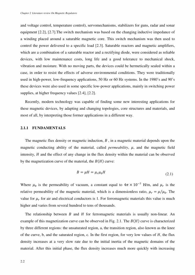
Chapter 2 Literature review On Magnetic Regulators
2.2
and voltage control, temperature control), servomechanisms, stabilizers for guns, radar and sonar
equipment [2.2], [2.7].The switch mechanism was based on the changing inductive impedance of
a winding placed around a saturable magnetic core. This switch mechanism was then used to
control the power delivered to a specific load [2.3]. Saturable reactors and magnetic amplifiers,
which are a combination of a saturable reactor and a rectifying diode, were considered as reliable
devices, with low maintenance costs, long life and a good tolerance to mechanical shock,
vibration and moisture. With no moving parts, the devices could be hermetically sealed within a
case, in order to resist the effects of adverse environmental conditions. They were traditionally
used in high-power, low-frequency applications, 50 Hz or 60 Hz systems. In the 1980’s and 90’s
these devices were also used in some specific low-power applications, mainly in switching power
supplies, at higher frequency values [2.4], [2.2].
Recently, modern technology was capable of finding some new interesting applications for
these magnetic devices, by adapting and changing topologies, core structures and materials, and
most of all, by interpreting those former applications in a different way.
2.1.1 FUNDAMENTALS
The magnetic flux density or magnetic induction, , in a magnetic material depends upon the
magnetic conducting ability of the material, called permeability, µ, and the magnetic field
intensity, ¶ and the effect of any change in the flux density within the material can be observed
by the magnetization curve of the material, the (¶) curve:
= µ¶ = µ2µ¶ (2.1)
Where µ is the permeability of vacuum, a constant equal to 4¸ × 10º» H/m, and µ2 is the
relative permeability of the magnetic material, which is a dimensionless ratio, µ2 = µ µ⁄ . The
value for µ2 for air and electrical conductors is 1. For ferromagnetic materials this value is much
higher and varies from several hundred to tens of thousands.
The relationship between and ¶ for ferromagnetic materials is usually non-linear. An
example of this magnetization curve can be observed in Fig. 2.1. The (¶) curve is characterized
by three different regions: the unsaturated region, a, the transition region, also known as the knee
of the curve, b, and the saturated region, c. In the first region, for very low values of ¶, the flux
density increases at a very slow rate due to the initial inertia of the magnetic domains of the
material. After this initial phase, the flux density increases much more quickly with increasing
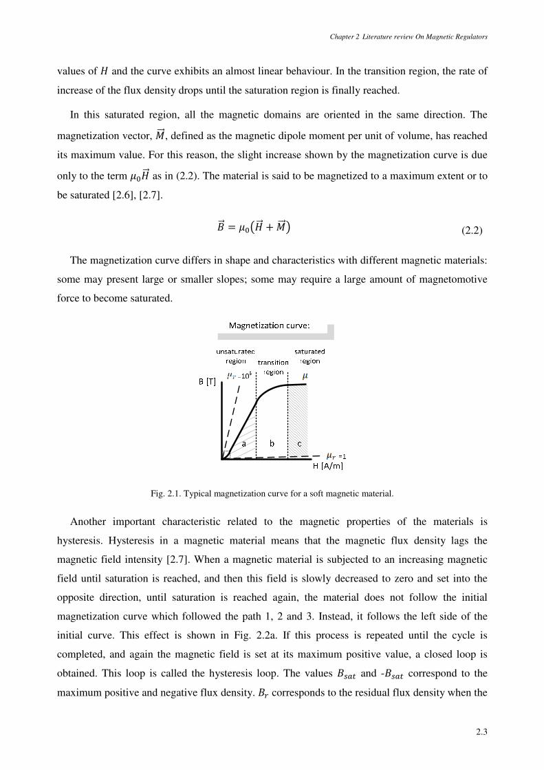
Chapter 2 Literature review On Magnetic Regulators
2.3
values of ¶ and the curve exhibits an almost linear behaviour. In the transition region, the rate of
increase of the flux density drops until the saturation region is finally reached.
In this saturated region, all the magnetic domains are oriented in the same direction. The
magnetization vector, ½, defined as the magnetic dipole moment per unit of volume, has reached
its maximum value. For this reason, the slight increase shown by the magnetization curve is due
only to the term µ¶ as in (2.2). The material is said to be magnetized to a maximum extent or to
be saturated [2.6], [2.7].
= µ¾¶ + ½¿ (2.2)
The magnetization curve differs in shape and characteristics with different magnetic materials:
some may present large or smaller slopes; some may require a large amount of magnetomotive
force to become saturated.
Fig. 2.1. Typical magnetization curve for a soft magnetic material.
Another important characteristic related to the magnetic properties of the materials is
hysteresis. Hysteresis in a magnetic material means that the magnetic flux density lags the
magnetic field intensity [2.7]. When a magnetic material is subjected to an increasing magnetic
field until saturation is reached, and then this field is slowly decreased to zero and set into the
opposite direction, until saturation is reached again, the material does not follow the initial
magnetization curve which followed the path 1, 2 and 3. Instead, it follows the left side of the
initial curve. This effect is shown in Fig. 2.2a. If this process is repeated until the cycle is
completed, and again the magnetic field is set at its maximum positive value, a closed loop is
obtained. This loop is called the hysteresis loop. The values 4~À and -4~À correspond to the
maximum positive and negative flux density. 2 corresponds to the residual flux density when the
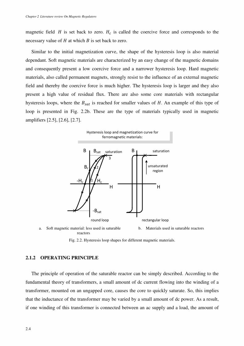
Chapter 2 Literature review On Magnetic Regulators
2.4
magnetic field ¶ is set back to zero. ¶ is called the coercive force and corresponds to the
necessary value of ¶ at which is set back to zero.
Similar to the initial magnetization curve, the shape of the hysteresis loop is also material
dependant. Soft magnetic materials are characterized by an easy change of the magnetic domains
and consequently present a low coercive force and a narrower hysteresis loop. Hard magnetic
materials, also called permanent magnets, strongly resist to the influence of an external magnetic
field and thereby the coercive force is much higher. The hysteresis loop is larger and they also
present a high value of residual flux. There are also some core materials with rectangular
hysteresis loops, where the 4~À is reached for smaller values of ¶. An example of this type of
loop is presented in Fig. 2.2b. These are the type of materials typically used in magnetic
amplifiers [2.5], [2.6], [2.7].
saturationB
H
unsaturated
region
saturationB
H
Hysteresis loop and magnetization curve for
ferromagnetic materials:
round loop rectangular loop
Bsat
-Bsat
2
1
3
-Hc Hc
Br
a. Soft magnetic material: less used in saturable
reactors b. Materials used in saturable reactors
Fig. 2.2. Hysteresis loop shapes for different magnetic materials.
2.1.2 OPERATING PRINCIPLE
The principle of operation of the saturable reactor can be simply described. According to the
fundamental theory of transformers, a small amount of dc current flowing into the winding of a
transformer, mounted on an ungapped core, causes the core to quickly saturate. So, this implies
that the inductance of the transformer may be varied by a small amount of dc power. As a result,
if one winding of this transformer is connected between an ac supply and a load, the amount of
Chapter 2 Literature review On Magnetic Regulators
2.5
power delivered to that load may be controlled by injecting a small amount of dc current in
another winding. In such cases, this transformer may also be called a saturable inductor [2.5].
An example of a simple circuit containing this device can be observed in Fig. 2.3. Two types
of magnetomotive forces will force a flux in the magnetic core: the dc magnetomotive force
created by the dc control current, constant in magnitude and direction, and the ac magnetomotive
force created by the ac voltage source which changes in magnitude and in direction. Due to its
cyclical operation, the ac magnetomotive force contributes to the saturation or desaturation of the
core. This results in a changing inductive reactance in the load winding. The dc magnetomotive
force, according to its value, aids or opposes the ac magnetomotive force in this action [2.7].
However, if the core presents a relatively rectangular ¶ loop, the change in the inductive
reactance can be made quite large and abrupt, since the core is easily saturated. Therefore the
device presents two operating modes: if the core is unsaturated, the ac winding inductance is
extremely high, capable of supporting a high voltage with a small load current; if the core is
saturated, the ac winding differential inductance will be low and the load current can easily flow
[2.2], [2.4]. At this point the magnetization in the core is as high as it can be, meaning that only a
residual amount of changing flux can be held by the core. So, in order to have an ideal switch, the
desirable operating point should correspond to the one where a small increase in the control
current causes a large increase in the output power, and a small decrease in the control current
causes a large decrease in the output power. In such conditions the saturable reactor is said to
present a bi-stable operation.
Fig. 2.3. Magnetic field paths in a saturable-core reactor.
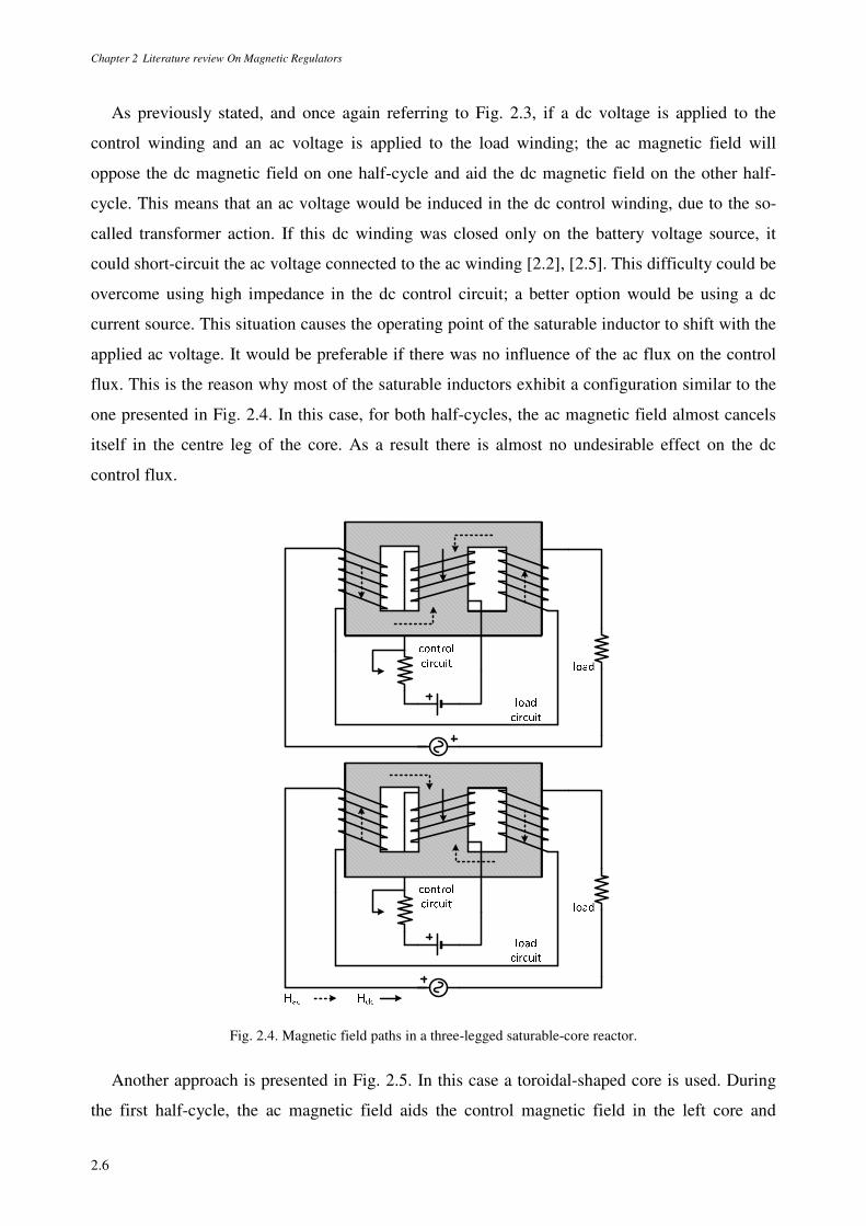
Chapter 2 Literature review On Magnetic Regulators
2.6
As previously stated, and once again referring to Fig. 2.3, if a dc voltage is applied to the
control winding and an ac voltage is applied to the load winding; the ac magnetic field will
oppose the dc magnetic field on one half-cycle and aid the dc magnetic field on the other half-
cycle. This means that an ac voltage would be induced in the dc control winding, due to the so-
called transformer action. If this dc winding was closed only on the battery voltage source, it
could short-circuit the ac voltage connected to the ac winding [2.2], [2.5]. This difficulty could be
overcome using high impedance in the dc control circuit; a better option would be using a dc
current source. This situation causes the operating point of the saturable inductor to shift with the
applied ac voltage. It would be preferable if there was no influence of the ac flux on the control
flux. This is the reason why most of the saturable inductors exhibit a configuration similar to the
one presented in Fig. 2.4. In this case, for both half-cycles, the ac magnetic field almost cancels
itself in the centre leg of the core. As a result there is almost no undesirable effect on the dc
control flux.
Fig. 2.4. Magnetic field paths in a three-legged saturable-core reactor.
Another approach is presented in Fig. 2.5. In this case a toroidal-shaped core is used. During
the first half-cycle, the ac magnetic field aids the control magnetic field in the left core and
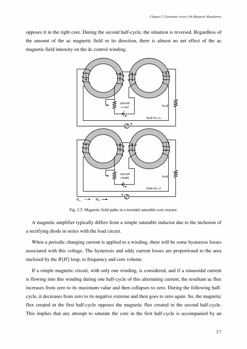
Chapter 2 Literature review On Magnetic Regulators
2.7
opposes it in the right core. During the second half-cycle, the situation is reversed. Regardless of
the amount of the ac magnetic field or its direction, there is almost no net effect of the ac
magnetic field intensity on the dc control winding.
Fig. 2.5. Magnetic field paths in a toroidal saturable-core reactor.
A magnetic amplifier typically differs from a simple saturable inductor due to the inclusion of
a rectifying diode in series with the load circuit.
When a periodic changing current is applied to a winding, there will be some hysteresis losses
associated with this voltage. The hysteresis and eddy current losses are proportional to the area
enclosed by the ¶ loop, to frequency and core volume.
If a simple magnetic circuit, with only one winding, is considered, and if a sinusoidal current
is flowing into this winding during one half-cycle of this alternating current, the resultant ac flux
increases from zero to its maximum value and then collapses to zero. During the following half-
cycle, it decreases from zero to its negative extreme and then goes to zero again. So, the magnetic
flux created in the first half-cycle opposes the magnetic flux created in the second half-cycle.
This implies that any attempt to saturate the core in the first half-cycle is accompanied by an
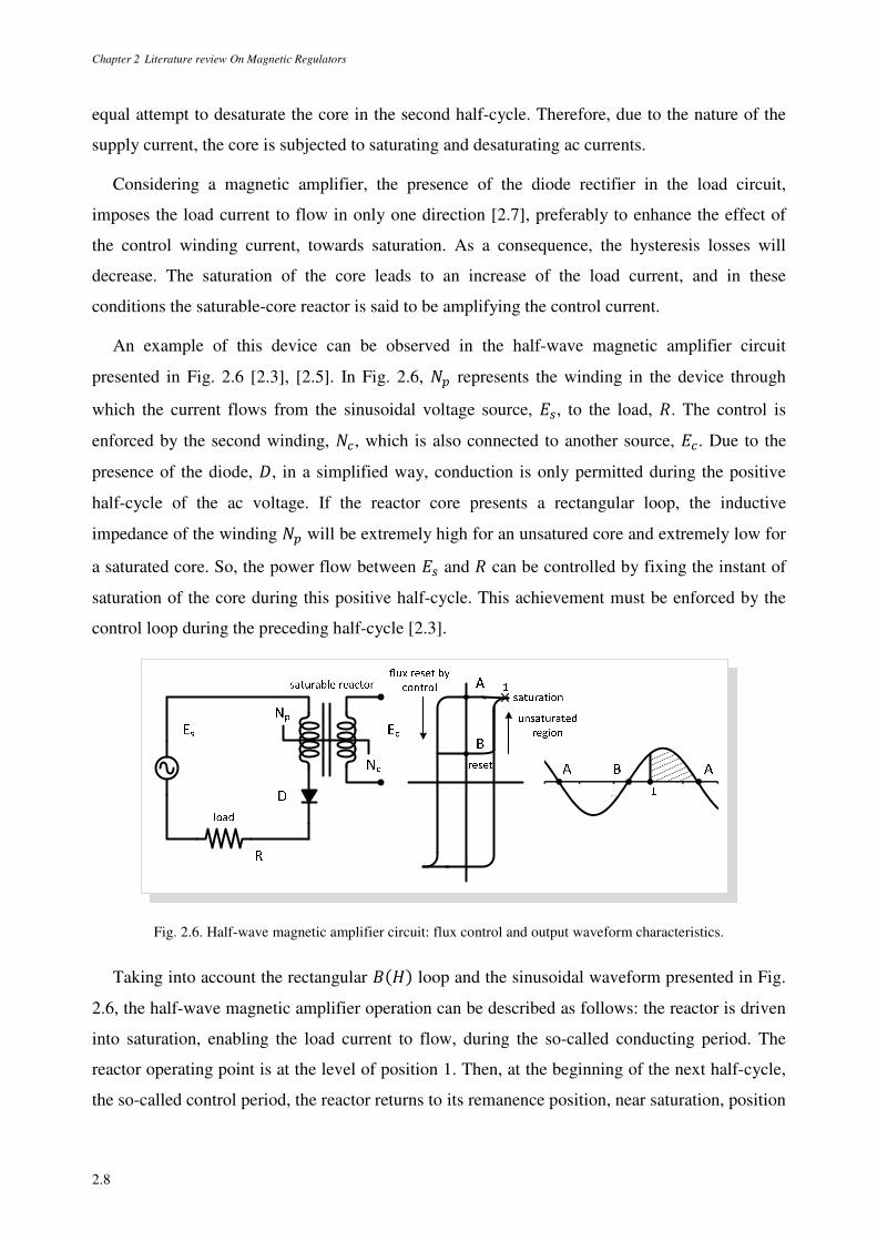
Chapter 2 Literature review On Magnetic Regulators
2.8
equal attempt to desaturate the core in the second half-cycle. Therefore, due to the nature of the
supply current, the core is subjected to saturating and desaturating ac currents.
Considering a magnetic amplifier, the presence of the diode rectifier in the load circuit,
imposes the load current to flow in only one direction [2.7], preferably to enhance the effect of
the control winding current, towards saturation. As a consequence, the hysteresis losses will
decrease. The saturation of the core leads to an increase of the load current, and in these
conditions the saturable-core reactor is said to be amplifying the control current.
An example of this device can be observed in the half-wave magnetic amplifier circuit
presented in Fig. 2.6 [2.3], [2.5]. In Fig. 2.6, Á represents the winding in the device through
which the current flows from the sinusoidal voltage source, Â4, to the load, v. The control is
enforced by the second winding, Á, which is also connected to another source, Â. Due to the
presence of the diode, ®, in a simplified way, conduction is only permitted during the positive
half-cycle of the ac voltage. If the reactor core presents a rectangular loop, the inductive
impedance of the winding Á will be extremely high for an unsatured core and extremely low for
a saturated core. So, the power flow between Â4 and v can be controlled by fixing the instant of
saturation of the core during this positive half-cycle. This achievement must be enforced by the
control loop during the preceding half-cycle [2.3].
10 15 20 25 30 35
Fig. 2.6. Half-wave magnetic amplifier circuit: flux control and output waveform characteristics.
Taking into account the rectangular ¶ loop and the sinusoidal waveform presented in Fig.
2.6, the half-wave magnetic amplifier operation can be described as follows: the reactor is driven
into saturation, enabling the load current to flow, during the so-called conducting period. The
reactor operating point is at the level of position 1. Then, at the beginning of the next half-cycle,
the so-called control period, the reactor returns to its remanence position, near saturation, position
Chapter 2 Literature review On Magnetic Regulators
2.9
A, and the diode rectifier becomes reversed biased. At this moment, the control source must set a
dc flux level capable of bringing the operating point from position A to position B. At the
beginning of the following half-cycle, the diode is once again forward biased and the ac voltage
source will cause the reactor to act in the same way, towards saturation.
2.1.3 GENERAL APPLICATIONS AND CONSTRUCTION
The half-wave magnetic amplifier circuit presented in Fig. 2.6 and much more complicated
versions had a phenomenal widespread use in the 1950’s. The magnetic amplifier or the simple
saturable reactor was intensively used in several fields, such as control, regulation and
instrumentation. This magnetic device was considered to be one of the most efficient and reliable
methods of controlling large amounts of power. It was especially designed to operate from ac
supply voltages, 50Hz or 60Hz and it was not expected to respond to frequencies higher than the
line-voltage frequency.
It was considered as a long-life, low-maintenance, simple controlled-switch, with no moving-
parts and contacts, which required only a very small amount of control power to actuate (high
power gain). Input and output were electrically isolated, it presented low internal power losses
(the only resistance present was the one associated to the windings), and could easily meet
vibration, acceleration and most importantly high-shock requirements, which was mandatory for
all equipment installed for the US Navy and other armed forces [2.3], [2.7].
In electric utilities, due to continuity of service requirements, the magnetic amplifier was
popularly used in magnetic-amplifier voltage and frequency regulators. It was also used for
power control in electric heaters, temperature-controlled ovens, overload detection systems,
speed control of dc motors and some special low-power applications [2.4], [2.5], [2.7].
Main aspects regarding construction were strongly related to the selection of the core material.
Examples of some of the required characteristics are as follows: minimum hysteresis and eddy
current losses, which would mean low resistivity and low coercive force (a lower ¶ implies less
control power to reset the core); high peak saturation density for large power-handling capacity;
quasi rectangular hysteresis loop for an improved switching action; and finally high stability of
the magnetic characteristics. In terms of core structures, a large selection was available: toroidal
or rectangular-laminated cores (U, E or I shape) were typically used.
Most of the previously referred applications are out-of-date. However, a clear understanding
of the operational behaviour of the saturable reactor or the magnetic amplifier, is essential to
Chapter 2 Literature review On Magnetic Regulators
2.10
demonstrate the flexibility of these magnetic devices. Selecting core materials with different
magnetic properties further increases this flexibility and other magnetic devices with different
operating capabilities are obtained. So, some of the prior applications have evolved and were
adapted to modern technology. New challenges and new control techniques have also appeared.
In the following sections, magnetic regulators are presented and some of their current
applications will be described.
2.2 MAGNETIC REGULATORS
The well-known bi-stable operation demands some special requirements regarding the
selection of the core material, namely selecting a core with a relatively rectangular ¶ loop.
However there is another option: it is possible to operate the saturable core reactor in the whole
range of the magnetization curve, using round loop, soft-saturation materials.
These regulators may be quite similar in terms of construction, but a different operating
principle is established. If these regulators are operated in the knee of the magnetization curve,
they may be referred to as one of two types: variable inductors or variable transformers,
depending on the number of ac windings. As it will be revealed throughout the remaining
sections, these regulators are quite similar to the classical saturable-core reactor, in terms of
construction. They exhibit multiple topologies depending on the selected core structures and
winding arrangements. The advantages related to the application of these regulators will be
pointed out.
2.2.1 VARIABLE INDUCTORS
2.2.1.1 FUNDAMENTALS
In order to describe the operating principle of the variable inductor it is important to recall the
fundamentals on inductance definition, as well as some of the basic laws of magnetic theory
which are strongly related. An inductor is a device for storing energy in a magnetic field. A
typical example is a loop or coil, while the inductance is the constant of the coil [2.6], [2.7].
A time-changing flux £ passing through a closed loop of wire creates an inductive voltage
across that wire. The relationship between the inductive voltage K± and the magnetic flux £
is given by Faraday’s law. If this winding has multiple turns, and each turn links the same
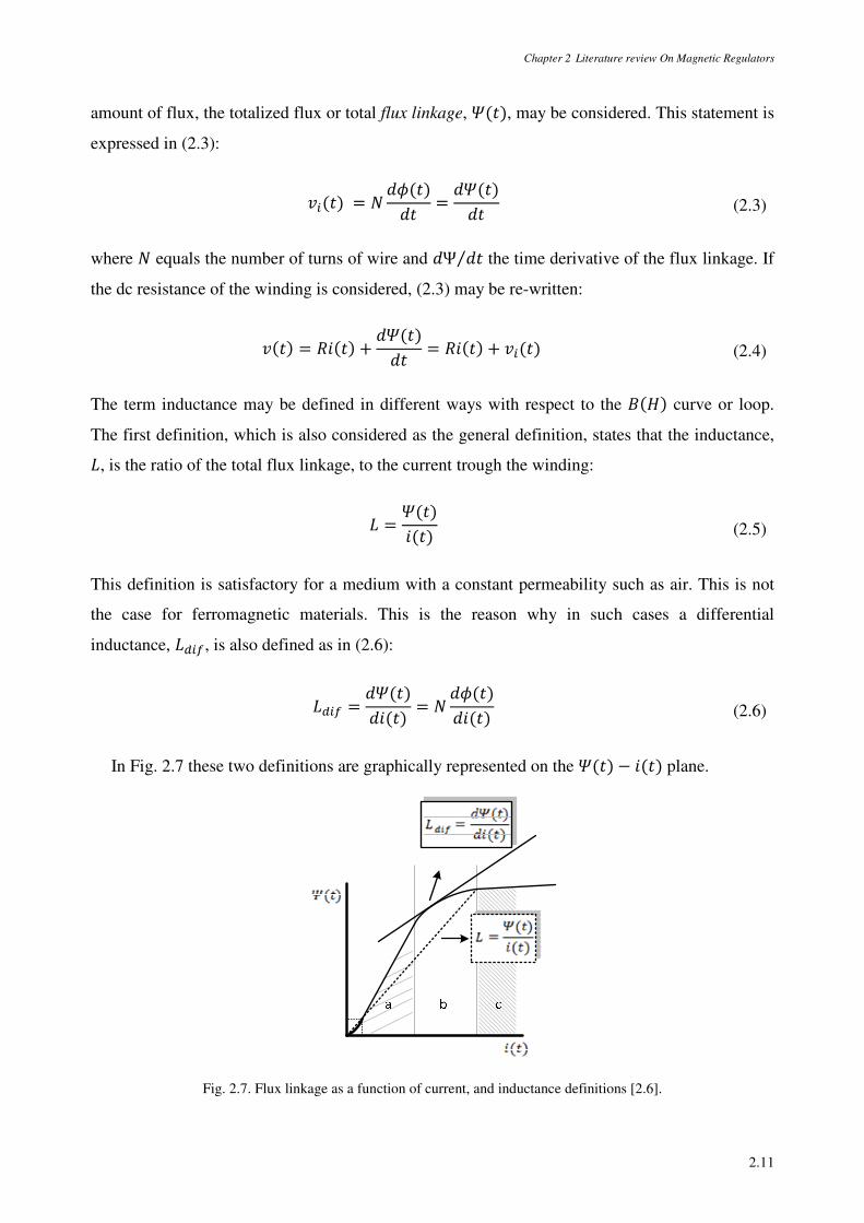
Chapter 2 Literature review On Magnetic Regulators
2.11
amount of flux, the totalized flux or total flux linkage, Ã, may be considered. This statement is
expressed in (2.3):
K± = Á £() = Ã() (2.3)
where Á equals the number of turns of wire and Ψ ⁄ the time derivative of the flux linkage. If
the dc resistance of the winding is considered, (2.3) may be re-written:
K() = vL() + Ã() = vL() + K±() (2.4)
The term inductance may be defined in different ways with respect to the (¶) curve or loop.
The first definition, which is also considered as the general definition, states that the inductance,
¯, is the ratio of the total flux linkage, to the current trough the winding:
¯ = Ã()L() (2.5)
This definition is satisfactory for a medium with a constant permeability such as air. This is not
the case for ferromagnetic materials. This is the reason why in such cases a differential
inductance, ¯±Å, is also defined as in (2.6):
¯±Å = Ã()L() = Á £()L() (2.6)
In Fig. 2.7 these two definitions are graphically represented on the Ã() − L() plane.
Fig. 2.7. Flux linkage as a function of current, and inductance definitions [2.6].
Chapter 2 Literature review On Magnetic Regulators
2.12
The magnetic field intensity, ¶, is defined by Ampère’s law. This law states that the integral
of the magnetic field intensity vector, ¶, around a closed path of length, , is equal to the total
current passing through the interior of the path. If the currents are carried by a winding with Á
turns, this law can be simply described by:
Æ ¶ ⋅ = ÁL (2.7)
where L is the current in each turn and is the infinitesimal element of path length. Both terms
in (2.7) are equivalent to a source called magnetomotive force (mmf), ℱ. If the magnetic path has
m windings, (2.7) can be rewritten as:
Æ ¶ ⋅ = É ÁÊLÊ
活 (2.8)
The scalar value of the magnetic flux £ passing trough a surface , is related to the magnetic
flux density by Gauss’s Law (2.9):
£ = Æ Ë ⋅ (2.9)
where the vector is the surface density of the magnetic flux and is the vector with direction
normal to surface element and magnitude equal to the area of . If the flux density is
uniform and perpendicular to the whole surface area , then (2.9) can be rewritten:
£ = (2.10)
The flux produced in a given material by a mmf also depends on the material’s resistance to
the flux, the reluctance of the material, ℛ, or on its permeance, Í, which is the inverse of the
reluctance. The reluctance will depend on the composition of the material and its physical
dimensions. A higher reluctance will imply a higher mmf in order to obtain a given magnetic
field. The reluctance associated to a magnetic path, of constant cross-section , considering an
homogeneous magnetic material, can be obtained by:
ℛ = µ¤ (2.11)
Chapter 2 Literature review On Magnetic Regulators
2.13
where is the magnetic path length and µ the permeability of the material.
If an air gap is included in a closed magnetic circuit, the total reluctance of the circuit is the
sum of both reluctances. However, the reluctance of the air will obviously be much higher, since
the relative permeability of the air is only 1. In those situations where the magnetic circuit is not
homogeneous, the apparent total permeability of the circuit is called effective permeability, µ3.
This permeability depends on the initial permeability, µ±, of the magnetic material, the
dimensions of the magnetic path and the air gap.
These considerations and the reluctance and permeance definitions are very important for the
description and understanding of the operating principle of the variable inductor. Taking into
account these definitions and previous equations, (2.5) can be rewritten:
¯ = Á£L = ÁL = Áµ¶¶ Á⁄ = Áµ = Áℛ = ÁÍ (2.12)
2.2.1.2 OPERATING PRINCIPLE
It is important to relate the magnetization curve with the concept of variable inductance. Using
(2.10), the totalized flux can be related with the magnetic flux density. Similarly, using (2.7) the
current in each turn can be related with the magnetic field intensity, in a simplified version:
à = Á£ = Á
L = ¶ Á⁄ (2.13)
Using a simple coordinate change, the graphic representation of the totalized flux versus current,
Ã(L), may be superposed to the magnetization curve of the material. By recalling the inductance
definition and particularly the differential inductance definition presented in (2.6), it is clear that
operating the regulator in the different regions of the magnetization curve has a significant effect
on the differential inductance of the ac winding placed on the magnetic core.
By using round loop, soft-saturation materials and operating the regulator on the transition
region or in the knee of the (¶) curve, a variable inductor is obtained. The inductance in this
region can vary between a maximum and minimum value, until saturation is reached.
In the late 1980’s, some authors named this device as a LVI, linear variable inductor or a
quasi-linear controllable inductor, referring its potential in high-frequency applications, [2.12],
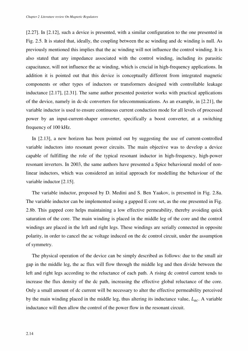
Chapter 2 Literature review On Magnetic Regulators
2.14
[2.27]. In [2.12], such a device is presented, with a similar configuration to the one presented in
Fig. 2.5. It is stated that, ideally, the coupling between the ac winding and dc winding is null. As
previously mentioned this implies that the ac winding will not influence the control winding. It is
also stated that any impedance associated with the control winding, including its parasitic
capacitance, will not influence the ac winding, which is crucial in high-frequency applications. In
addition it is pointed out that this device is conceptually different from integrated magnetic
components or other types of inductors or transformers designed with controllable leakage
inductance [2.17], [2.31]. The same author presented posterior works with practical applications
of the device, namely in dc-dc converters for telecommunications. As an example, in [2.21], the
variable inductor is used to ensure continuous current conduction mode for all levels of processed
power by an input-current-shaper converter, specifically a boost converter, at a switching
frequency of 100 kHz.
In [2.13], a new horizon has been pointed out by suggesting the use of current-controlled
variable inductors into resonant power circuits. The main objective was to develop a device
capable of fulfilling the role of the typical resonant inductor in high-frequency, high-power
resonant inverters. In 2003, the same authors have presented a Spice behavioural model of non-
linear inductors, which was considered an initial approach for modelling the behaviour of the
variable inductor [2.15].
The variable inductor, proposed by D. Medini and S. Ben Yaakov, is presented in Fig. 2.8a.
The variable inductor can be implemented using a gapped E core set, as the one presented in Fig.
2.8b. This gapped core helps maintaining a low effective permeability, thereby avoiding quick
saturation of the core. The main winding is placed in the middle leg of the core and the control
windings are placed in the left and right legs. These windings are serially connected in opposite
polarity, in order to cancel the ac voltage induced on the dc control circuit, under the assumption
of symmetry.
The physical operation of the device can be simply described as follows: due to the small air
gap in the middle leg, the ac flux will flow through the middle leg and then divide between the
left and right legs according to the reluctance of each path. A rising dc control current tends to
increase the flux density of the dc path, increasing the effective global reluctance of the core.
Only a small amount of dc current will be necessary to alter the effective permeability perceived
by the main winding placed in the middle leg, thus altering its inductance value, ¯~. A variable
inductance will then allow the control of the power flow in the resonant circuit.
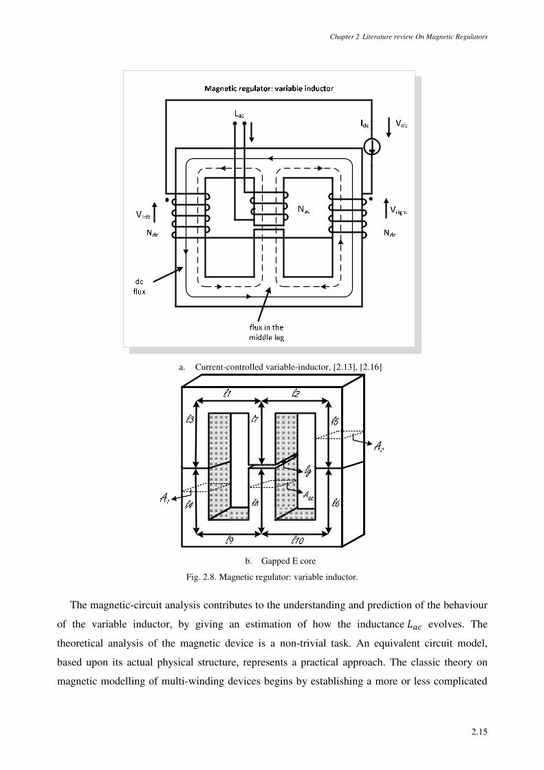
Chapter 2 Literature review On Magnetic Regulators
2.15
a. Current-controlled variable-inductor, [2.13], [2.16]
b. Gapped E core
Fig. 2.8. Magnetic regulator: variable inductor.
The magnetic-circuit analysis contributes to the understanding and prediction of the behaviour
of the variable inductor, by giving an estimation of how the inductance¯~ evolves. The
theoretical analysis of the magnetic device is a non-trivial task. An equivalent circuit model,
based upon its actual physical structure, represents a practical approach. The classic theory on
magnetic modelling of multi-winding devices begins by establishing a more or less complicated
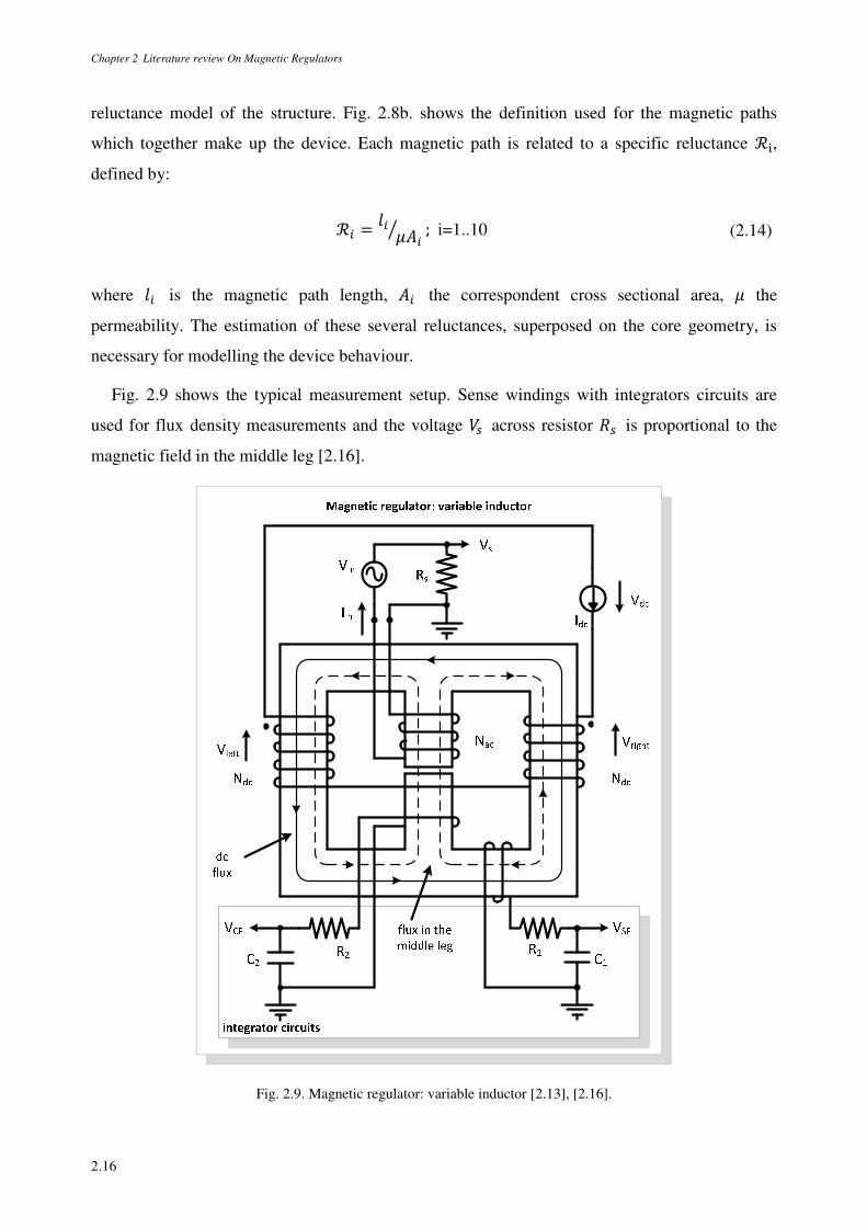
Chapter 2 Literature review On Magnetic Regulators
2.16
reluctance model of the structure. Fig. 2.8b. shows the definition used for the magnetic paths
which together make up the device. Each magnetic path is related to a specific reluctance ℛÎ, defined by:
ℛ± = ± µ±¤ ;i=1..10 (2.14)
where ± is the magnetic path length, ± the correspondent cross sectional area, µ the
permeability. The estimation of these several reluctances, superposed on the core geometry, is
necessary for modelling the device behaviour.
Fig. 2.9 shows the typical measurement setup. Sense windings with integrators circuits are
used for flux density measurements and the voltage >4 across resistor v4 is proportional to the
magnetic field in the middle leg [2.16].
Fig. 2.9. Magnetic regulator: variable inductor [2.13], [2.16].
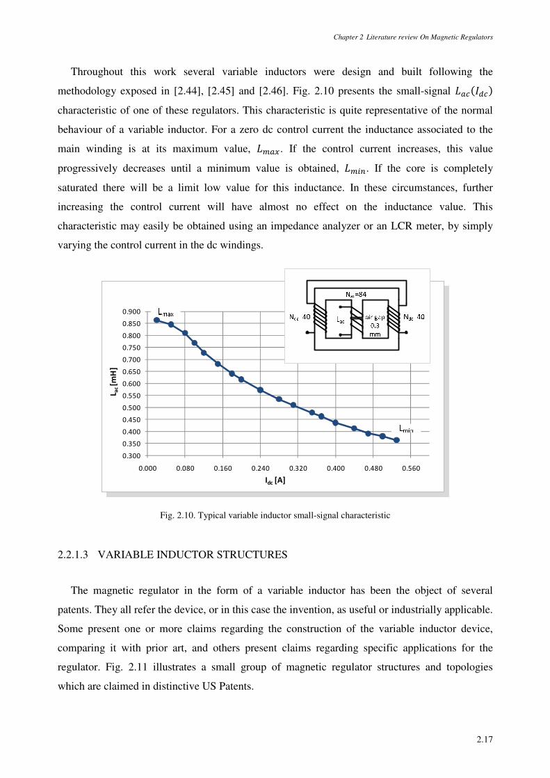
Chapter 2 Literature review On Magnetic Regulators
2.17
Throughout this work several variable inductors were design and built following the
methodology exposed in [2.44], [2.45] and [2.46]. Fig. 2.10 presents the small-signal ¯~(/)
characteristic of one of these regulators. This characteristic is quite representative of the normal
behaviour of a variable inductor. For a zero dc control current the inductance associated to the
main winding is at its maximum value, ¯~Ï. If the control current increases, this value
progressively decreases until a minimum value is obtained, ¯±². If the core is completely
saturated there will be a limit low value for this inductance. In these circumstances, further
increasing the control current will have almost no effect on the inductance value. This
characteristic may easily be obtained using an impedance analyzer or an LCR meter, by simply
varying the control current in the dc windings.
0.300
0.350
0.400
0.450
0.500
0.550
0.600
0.650
0.700
0.750
0.800
0.850
0.900
0.000 0.080 0.160 0.240 0.320 0.400 0.480 0.560
L ac[m
H]
Idc [A]
Fig. 2.10. Typical variable inductor small-signal characteristic
2.2.1.3 VARIABLE INDUCTOR STRUCTURES
The magnetic regulator in the form of a variable inductor has been the object of several
patents. They all refer the device, or in this case the invention, as useful or industrially applicable.
Some present one or more claims regarding the construction of the variable inductor device,
comparing it with prior art, and others present claims regarding specific applications for the
regulator. Fig. 2.11 illustrates a small group of magnetic regulator structures and topologies
which are claimed in distinctive US Patents.
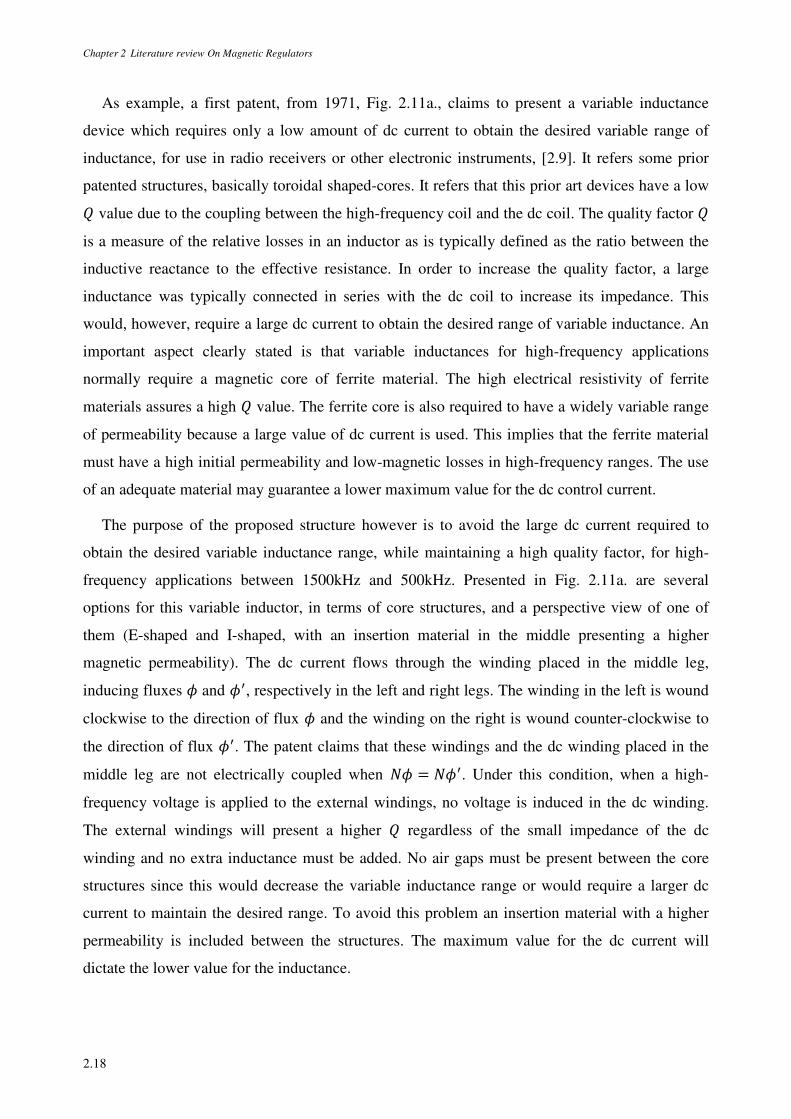
Chapter 2 Literature review On Magnetic Regulators
2.18
As example, a first patent, from 1971, Fig. 2.11a., claims to present a variable inductance
device which requires only a low amount of dc current to obtain the desired variable range of
inductance, for use in radio receivers or other electronic instruments, [2.9]. It refers some prior
patented structures, basically toroidal shaped-cores. It refers that this prior art devices have a low
Ð value due to the coupling between the high-frequency coil and the dc coil. The quality factor Ð
is a measure of the relative losses in an inductor as is typically defined as the ratio between the
inductive reactance to the effective resistance. In order to increase the quality factor, a large
inductance was typically connected in series with the dc coil to increase its impedance. This
would, however, require a large dc current to obtain the desired range of variable inductance. An
important aspect clearly stated is that variable inductances for high-frequency applications
normally require a magnetic core of ferrite material. The high electrical resistivity of ferrite
materials assures a high Ð value. The ferrite core is also required to have a widely variable range
of permeability because a large value of dc current is used. This implies that the ferrite material
must have a high initial permeability and low-magnetic losses in high-frequency ranges. The use
of an adequate material may guarantee a lower maximum value for the dc control current.
The purpose of the proposed structure however is to avoid the large dc current required to
obtain the desired variable inductance range, while maintaining a high quality factor, for high-
frequency applications between 1500kHz and 500kHz. Presented in Fig. 2.11a. are several
options for this variable inductor, in terms of core structures, and a perspective view of one of
them (E-shaped and I-shaped, with an insertion material in the middle presenting a higher
magnetic permeability). The dc current flows through the winding placed in the middle leg,
inducing fluxes £ and £Ñ, respectively in the left and right legs. The winding in the left is wound
clockwise to the direction of flux £ and the winding on the right is wound counter-clockwise to
the direction of flux £Ñ. The patent claims that these windings and the dc winding placed in the
middle leg are not electrically coupled when Á£ = Á£Ñ. Under this condition, when a high-
frequency voltage is applied to the external windings, no voltage is induced in the dc winding.
The external windings will present a higher Ð regardless of the small impedance of the dc
winding and no extra inductance must be added. No air gaps must be present between the core
structures since this would decrease the variable inductance range or would require a larger dc
current to maintain the desired range. To avoid this problem an insertion material with a higher
permeability is included between the structures. The maximum value for the dc current will
dictate the lower value for the inductance.
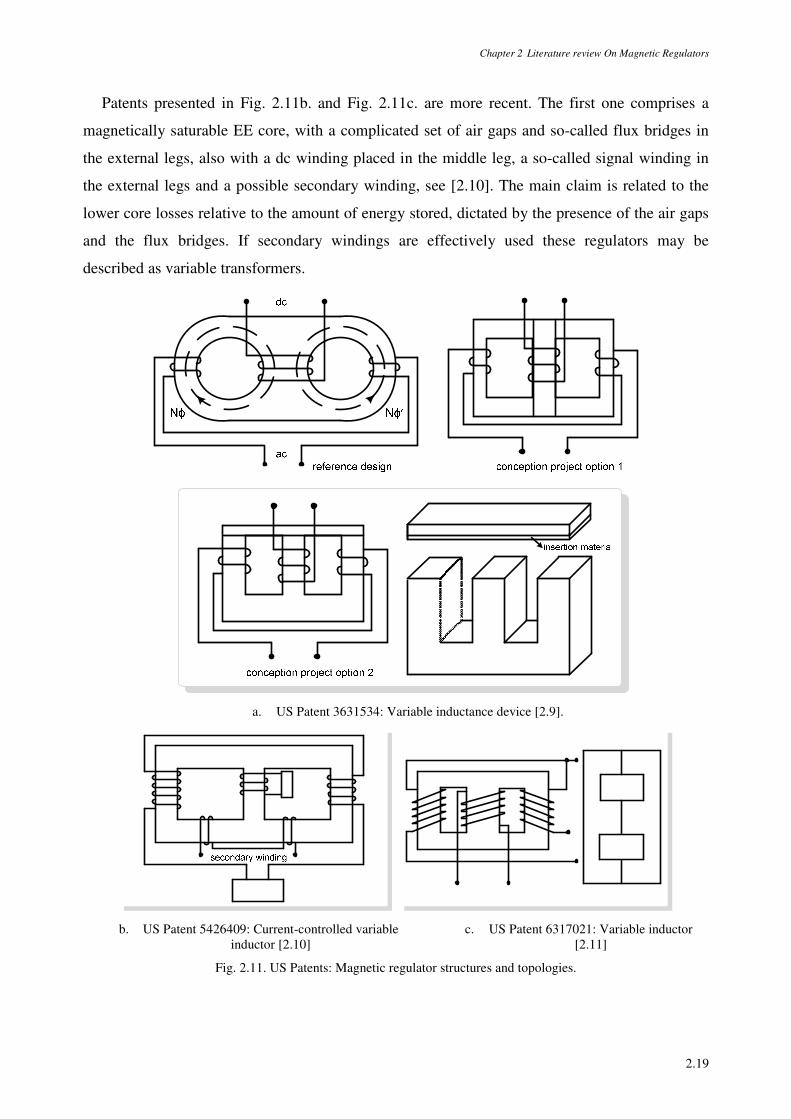
Chapter 2 Literature review On Magnetic Regulators
2.19
Patents presented in Fig. 2.11b. and Fig. 2.11c. are more recent. The first one comprises a
magnetically saturable EE core, with a complicated set of air gaps and so-called flux bridges in
the external legs, also with a dc winding placed in the middle leg, a so-called signal winding in
the external legs and a possible secondary winding, see [2.10]. The main claim is related to the
lower core losses relative to the amount of energy stored, dictated by the presence of the air gaps
and the flux bridges. If secondary windings are effectively used these regulators may be
described as variable transformers.
a. US Patent 3631534: Variable inductance device [2.9].
b. US Patent 5426409: Current-controlled variable
inductor [2.10] c. US Patent 6317021: Variable inductor
[2.11]
Fig. 2.11. US Patents: Magnetic regulator structures and topologies.
Chapter 2 Literature review On Magnetic Regulators
2.20
In the second one, the structure is based on EE core as well and the dc winding is also
mounted on the middle leg. The outer windings are connected in parallel and in such a way that
the magnetic flux arising from currents through the windings on the outer legs is cancelled in the
middle leg. So in this case, the dc control current through the middle winding is responsible for a
variable inductance across the outer windings, by changing the saturation level of the outer legs,
while the inductance across this dc control winding is substantially constant [2.11]. It is stated
that in a preferred embodiment, the magnetic cross-section of the centre leg must be equal or
somewhat larger than the sum of the magnetic cross-sections of the outer legs. It also refers prior
art, where as usual, the control winding is equally divided and mounted on the external legs,
serially-connected in opposite polarity, and the high-frequency winding is placed in the middle
leg. It refers some of the prior art limitations, such as low variable inductance range, high dc
control current range, non-symmetry and coupling between the ac and dc windings.
So, in conclusion, there are in fact several possible topologies and more or less complicated
core structures for the conception of these variable inductors. These reported patents are only a
small glimpse of possible solutions. Limitations and possibilities are associated with all of these
options, and obviously must be considered depending on the desired application. Some of these
limitations may be overcome, by selecting an appropriate core material.
As previously mentioned, a soft saturation material would be preferred. Ferrite cores saturate
rather abruptly, moreover the saturation flux density is a function of temperature. For Molyperm
(MPP) cores, the reduction in permeability as a function of flux is very gradual, so MPP is also a
soft saturation material. Nevertheless, one of the problems with MPP cores, is that they have
much higher losses than ferrites. Powdered iron cores saturate slightly harder than MPP and
while a variety of permeabilities are available, they are typically lower than MPP’s. This means
that a powered iron regulator would be larger than a device having the same inductance and
current capacity but built on a MPP core. However powdered iron cores are cheaper than MPP’s.
So in fact, all of this must be considered when choosing the core material. However ferrites are
still the typical solution, since they are made by a wide variety of vendors, in the necessary
shapes, E, I, U, EFD, E gapped cores, and workable frequency limits, which is not the case for
some of the other materials [2.5].
Chapter 2 Literature review On Magnetic Regulators
2.21
2.2.2 VARIABLE TRANSFORMERS
The inclusion of one or more secondary windings leads to a second type of magnetic
regulators: variable transformers [2.18], [2.19]. In [2.18], a US Patent from 1988, a self-regulated
transformer-inductor with air gaps is presented. The transformer is designed to carry out voltage
regulation by self-controlled absorption of reactive power. The inventors claimed that by
disposing additional windings on the magnetic core of a specific variable inductor, one could
obtain a voltage regulating apparatus both efficient and autonomous, or a transformer having the
ability to supply a load from an alternating current source, for example a capacitive source, while
carrying out efficiently and autonomously a regulation to compensate both the input voltage and
load variations.
The physical structure of this variable transformer is illustrated in Fig. 2.12. It is a three-leg
structure, with two central gaps of equal dimensions in the outer legs. An ac power source is
connected to the primary winding which is placed in the middle leg. The secondary winding is
also placed in the middle leg and is connected to a load, . There are two additional auxiliary
windings, connected in series and placed in the outer legs. These windings are also supplied by
the ac power source. Finally, two dc control windings, connected in series, are placed in the outer
legs. These dc windings are supplied by the ac current flowing through the auxiliary windings
which is then rectified by the diode bridge. An inductor of a fixed value may be connected in
parallel with the auxiliary windings, so that the amplitude of the ac current generated by the
power source is limited to its inductance value.
The operating principle can be described as follows: if the dc control current increases its
value, the core goes further into saturation, due to the increase of the reluctance of the external
magnetic path. This action results in a lower inductance value for the auxiliary and primary
windings and an increase of current in these three windings. It is therefore possible, within a
range of source currents, to regulate the ac voltage across them. The voltage across the secondary
winding, applied to the load, is determined by the ratio of the number of turns of the primary and
secondary windings.
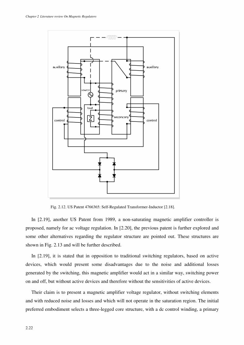
Chapter 2 Literature review On Magnetic Regulators
2.22
Fig. 2.12. US Patent 4766365: Self-Regulated Transformer-Inductor [2.18].
In [2.19], another US Patent from 1989, a non-saturating magnetic amplifier controller is
proposed, namely for ac voltage regulation. In [2.20], the previous patent is further explored and
some other alternatives regarding the regulator structure are pointed out. These structures are
shown in Fig. 2.13 and will be further described.
In [2.19], it is stated that in opposition to traditional switching regulators, based on active
devices, which would present some disadvantages due to the noise and additional losses
generated by the switching, this magnetic amplifier would act in a similar way, switching power
on and off, but without active devices and therefore without the sensitivities of active devices.
Their claim is to present a magnetic amplifier voltage regulator, without switching elements
and with reduced noise and losses and which will not operate in the saturation region. The initial
preferred embodiment selects a three-legged core structure, with a dc control winding, a primary
Chapter 2 Literature review On Magnetic Regulators
2.23
and secondary windings mounted on each one of these legs. The amplifier is operated without
driving the core into saturation and the primary and secondary legs may even contain an air gap.
The dc current will control the reluctance of the control leg relative to the reluctance of the
secondary leg. By controlling the relative reluctance, the amount of ac magnetic flux coupled to
the secondary winding may also be controlled, which in turn means controlling the output voltage
provided by the secondary winding.
In the case of [2.20] it is also recalled that in high-voltage power supplies there is an obvious
concern related to the switching losses, typically because some of these sources may operate at
high switching frequencies. Resonant switching techniques were developed with the aim of
reducing the switching losses, at these high frequencies, thereby reducing the size and weight of
many of its components. However, a key problem is the fact that these resonant converters
usually employ the operating frequency as a control parameter to regulate the output voltage.
With a variable operating frequency it is possible to modify the characteristics of the resonant
circuit and therefore control the output voltage. In some cases, the range of the operating
frequency may be extremely large, which has a negative impact on the design and construction of
the EMI filter which today is a basic requirement in power supplies [2.30].
In [2.20], another disadvantage is pointed out: in areas like avionics, or missile radars, there is
a necessity of increasing the operating frequency, not only to reduce size and power losses, but to
synchronize the operating frequency with a system clock. It is obviously impossible with a
variable operating frequency. An alternative would be, obviously, the magnetic regulator, due to
its variable inductance behaviour, or as pointed out by the author, a magnetic regulator exhibiting
an electronically-adjustable turns ratio. The regulator in question would behave as a simple
transformer, for each predetermined level of dc control current, or as a variable transformer for a
variable dc current, with a variable input-to-output conversion rate.
The physical structure of this magnetic regulator is illustrated in Fig. 2.13a. It is a four-leg
structure. The control windings, with the same number of turns, are wound around legs 1 and 2,
serially connected in opposite polarity. The induced voltages on these windings will have
opposite polarities and, under the assumption of symmetry, they should cancel each other. The
primary winding, is wound around leg 3 and finally, the secondary winding is wound around leg
4, which includes two small intentional air gaps. These windings may have a different number of
turns.
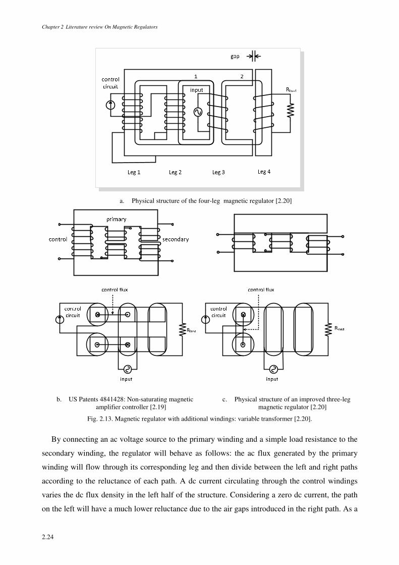
Chapter 2 Literature review On Magnetic Regulators
2.24
a. Physical structure of the four-leg magnetic regulator [2.20]
b. US Patents 4841428: Non-saturating magnetic
amplifier controller [2.19] c. Physical structure of an improved three-leg
magnetic regulator [2.20]
Fig. 2.13. Magnetic regulator with additional windings: variable transformer [2.20].
By connecting an ac voltage source to the primary winding and a simple load resistance to the
secondary winding, the regulator will behave as follows: the ac flux generated by the primary
winding will flow through its corresponding leg and then divide between the left and right paths
according to the reluctance of each path. A dc current circulating through the control windings
varies the dc flux density in the left half of the structure. Considering a zero dc current, the path
on the left will have a much lower reluctance due to the air gaps introduced in the right path. As a
Chapter 2 Literature review On Magnetic Regulators
2.25
result, the ac flux generated by the primary winding that links through the secondary will be
lower, thus little ac voltage will be induced in the secondary winding. If the dc current is large
enough to push the operating point towards saturation, the reluctance of the path to the left of the
primary, increases relatively to the reluctance of the path to the right, making it possible to
control the amount of the ac flux coupled with the secondary winding. In these conditions, the
voltage induced on the secondary will be equal to the primary voltage times the turns ratio of the
secondary to the primary, minus some voltage loss due to the leakage flux, which is somewhat
difficult to estimate.
In [2.20], the reluctance concept together with the duality theory is used to generate, first, the
magnetic equivalent circuit of the device and then, the inductances circuit model. Since the
equations that describe the magnetic circuit have the same form as those for the electrical circuit,
the method used to find the dual of an electrical circuit can also be applied to find the dual of a
magnetic circuit. The same techniques will be applied to the variable transformer devices that
were developed throughout the work, as described in future chapters.
Fig. 2.13b. shows two views of one of the possible structures suggested in [2.19]. It can be
done using two EI cores or two EE cores placed side by side. The magnetic path of the control
flux is also detailed. The control leg does not include an air gap as opposed to the primary leg
and the secondary leg. In the following description, although referred to as single legs, all legs
comprise parallel portions of the parallel core elements. The gap in the primary leg is optional,
however if present, it should be smaller than the gap in the secondary leg. This will result in a
higher reluctance of the secondary leg when compared to the primary and control legs. Also, the
cross section of the primary leg must be sufficiently larger than the cross section of the control
leg, so that, as the control leg approaches saturation, it does not significantly affect the permeance
of the primary leg. In fact, to take advantage of working at the knee of the ¶ curve, saturation
must be approached but not reached.
As stated in [2.20], the previous structure has a clear advantage over the four-leg structure. In
the four-leg structure, the magnetic paths through each control leg will have different reluctances
due to the greater distance between the primary (leg 3) and control leg 1, than between the
primary (leg 3) and control leg 2. This causes an ac voltage to appear across the control windings
which may be shorted using a capacitor. This places the control windings in parallel, forcing an
equal ac voltage in each. The fluxes through legs 1 and 2 are then forced to be equal at the
expense of having some circulating current in the control windings. The dc flux is contained for
the most part in the ungapped control legs whereby legs 3 and 4 are subject to insignificant dc
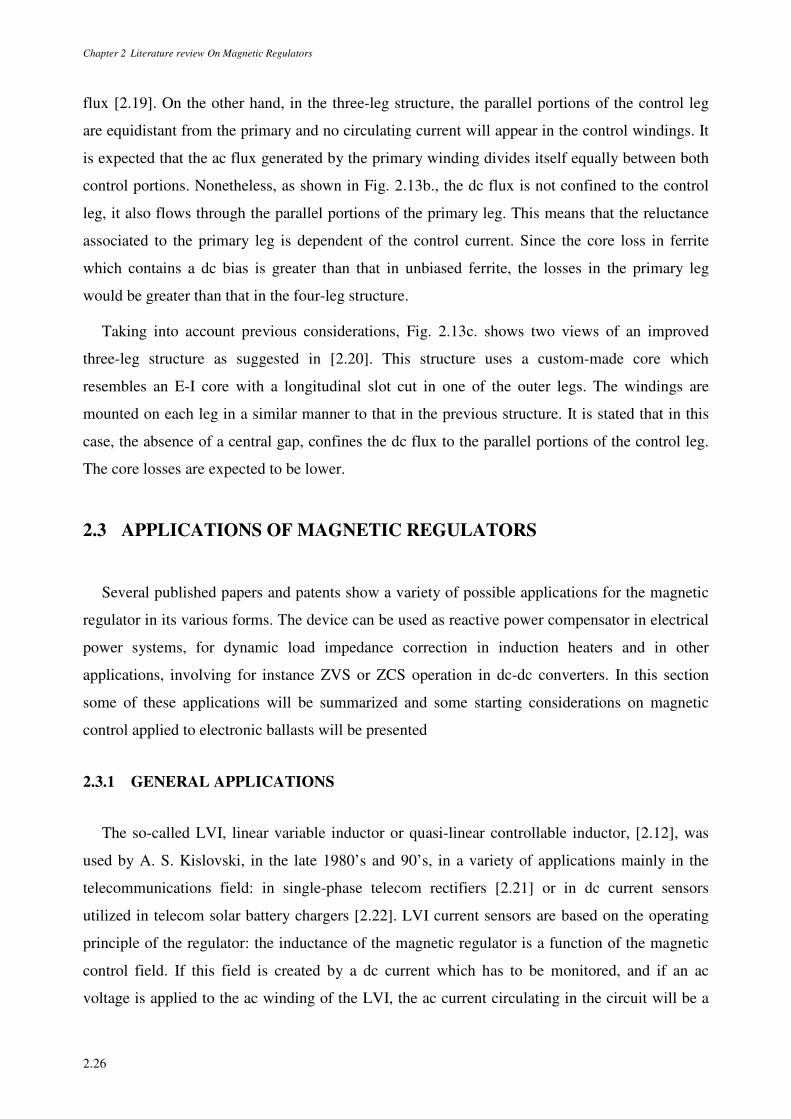
Chapter 2 Literature review On Magnetic Regulators
2.26
flux [2.19]. On the other hand, in the three-leg structure, the parallel portions of the control leg
are equidistant from the primary and no circulating current will appear in the control windings. It
is expected that the ac flux generated by the primary winding divides itself equally between both
control portions. Nonetheless, as shown in Fig. 2.13b., the dc flux is not confined to the control
leg, it also flows through the parallel portions of the primary leg. This means that the reluctance
associated to the primary leg is dependent of the control current. Since the core loss in ferrite
which contains a dc bias is greater than that in unbiased ferrite, the losses in the primary leg
would be greater than that in the four-leg structure.
Taking into account previous considerations, Fig. 2.13c. shows two views of an improved
three-leg structure as suggested in [2.20]. This structure uses a custom-made core which
resembles an E-I core with a longitudinal slot cut in one of the outer legs. The windings are
mounted on each leg in a similar manner to that in the previous structure. It is stated that in this
case, the absence of a central gap, confines the dc flux to the parallel portions of the control leg.
The core losses are expected to be lower.
2.3 APPLICATIONS OF MAGNETIC REGULATORS
Several published papers and patents show a variety of possible applications for the magnetic
regulator in its various forms. The device can be used as reactive power compensator in electrical
power systems, for dynamic load impedance correction in induction heaters and in other
applications, involving for instance ZVS or ZCS operation in dc-dc converters. In this section
some of these applications will be summarized and some starting considerations on magnetic
control applied to electronic ballasts will be presented
2.3.1 GENERAL APPLICATIONS
The so-called LVI, linear variable inductor or quasi-linear controllable inductor, [2.12], was
used by A. S. Kislovski, in the late 1980’s and 90’s, in a variety of applications mainly in the
telecommunications field: in single-phase telecom rectifiers [2.21] or in dc current sensors
utilized in telecom solar battery chargers [2.22]. LVI current sensors are based on the operating
principle of the regulator: the inductance of the magnetic regulator is a function of the magnetic
control field. If this field is created by a dc current which has to be monitored, and if an ac
voltage is applied to the ac winding of the LVI, the ac current circulating in the circuit will be a
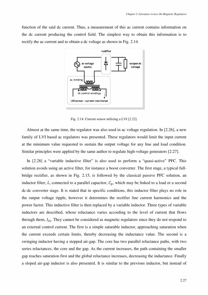
Chapter 2 Literature review On Magnetic Regulators
2.27
function of the said dc current. Thus, a measurement of this ac current contains information on
the dc current producing the control field. The simplest way to obtain this information is to
rectify the ac current and to obtain a dc voltage as shown in Fig. 2.14.
Fig. 2.14. Current sensor utilizing a LVI [2.22].
Almost at the same time, the regulator was also used in ac voltage regulation. In [2.26], a new
family of LVI based ac regulators was presented. These regulators would limit the input current
at the minimum value requested to sustain the output voltage for any line and load condition.
Similar principles were applied by the same author to regulate high-voltage generators [2.27].
In [2.28] a “variable inductive filter” is also used to perform a “quasi-active” PFC. This
solution avoids using an active filter, for instance a boost converter. The first stage, a typical full-
bridge rectifier, as shown in Fig. 2.15, is followed by the classical passive PFC solution, an
inductor filter, ¯, connected to a parallel capacitor, , which may be linked to a load or a second
dc-dc converter stage. It is stated that in specific conditions, this inductor filter plays no role in
the output voltage ripple, however it determines the rectifier line current harmonics and the
power factor. This inductive filter is then replaced by a variable inductor. Three types of variable
inductors are described, whose reluctance varies according to the level of current that flows
through them, /±². They cannot be considered as magnetic regulators since they do not respond to
an external control current. The first is a simple saturable inductor, approaching saturation when
the current exceeds certain limits, thereby decreasing the inductance value. The second is a
swinging inductor having a stepped air-gap. The core has two parallel reluctance paths, with two
series reluctances, the core and the gap. As the current increases, the path containing the smaller
gap reaches saturation first and the global reluctance increases, decreasing the inductance. Finally
a sloped air-gap inductor is also presented. It is similar to the previous inductor, but instead of
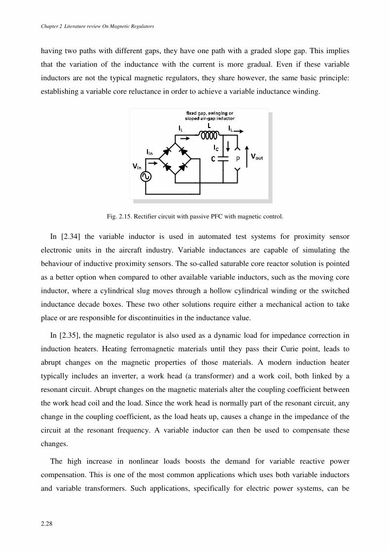
Chapter 2 Literature review On Magnetic Regulators
2.28
having two paths with different gaps, they have one path with a graded slope gap. This implies
that the variation of the inductance with the current is more gradual. Even if these variable
inductors are not the typical magnetic regulators, they share however, the same basic principle:
establishing a variable core reluctance in order to achieve a variable inductance winding.
Fig. 2.15. Rectifier circuit with passive PFC with magnetic control.
In [2.34] the variable inductor is used in automated test systems for proximity sensor
electronic units in the aircraft industry. Variable inductances are capable of simulating the
behaviour of inductive proximity sensors. The so-called saturable core reactor solution is pointed
as a better option when compared to other available variable inductors, such as the moving core
inductor, where a cylindrical slug moves through a hollow cylindrical winding or the switched
inductance decade boxes. These two other solutions require either a mechanical action to take
place or are responsible for discontinuities in the inductance value.
In [2.35], the magnetic regulator is also used as a dynamic load for impedance correction in
induction heaters. Heating ferromagnetic materials until they pass their Curie point, leads to
abrupt changes on the magnetic properties of those materials. A modern induction heater
typically includes an inverter, a work head (a transformer) and a work coil, both linked by a
resonant circuit. Abrupt changes on the magnetic materials alter the coupling coefficient between
the work head coil and the load. Since the work head is normally part of the resonant circuit, any
change in the coupling coefficient, as the load heats up, causes a change in the impedance of the
circuit at the resonant frequency. A variable inductor can then be used to compensate these
changes.
The high increase in nonlinear loads boosts the demand for variable reactive power
compensation. This is one of the most common applications which uses both variable inductors
and variable transformers. Such applications, specifically for electric power systems, can be
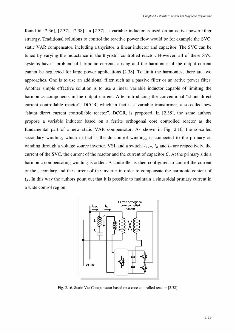
Chapter 2 Literature review On Magnetic Regulators
2.29
found in [2.36], [2.37], [2.38]. In [2.37], a variable inductor is used on an active power filter
strategy. Traditional solutions to control the reactive power flow would be for example the SVC,
static VAR compensator, including a thyristor, a linear inductor and capacitor. The SVC can be
tuned by varying the inductance in the thyristor controlled reactor. However, all of these SVC
systems have a problem of harmonic currents arising and the harmonics of the output current
cannot be neglected for large power applications [2.38]. To limit the harmonics, there are two
approaches. One is to use an additional filter such as a passive filter or an active power filter.
Another simple effective solution is to use a linear variable inductor capable of limiting the
harmonics components in the output current. After introducing the conventional “shunt direct
current controllable reactor”, DCCR, which in fact is a variable transformer, a so-called new
“shunt direct current controllable reactor”, DCCR, is proposed. In [2.38], the same authors
propose a variable inductor based on a ferrite orthogonal core controlled reactor as the
fundamental part of a new static VAR compensator. As shown in Fig. 2.16, the so-called
secondary winding, which in fact is the dc control winding, is connected to the primary ac
winding through a voltage source inverter, VSI, and a switch. LËÒ, LÓ and L are respectively, the
current of the SVC, the current of the reactor and the current of capacitor . At the primary side a
harmonic compensating winding is added. A controller is then configured to control the current
of the secondary and the current of the inverter in order to compensate the harmonic content of
LÓ. In this way the authors point out that it is possible to maintain a sinusoidal primary current in
a wide control region.
Fig. 2.16. Static Var Compensator based on a core controlled reactor [2.38].
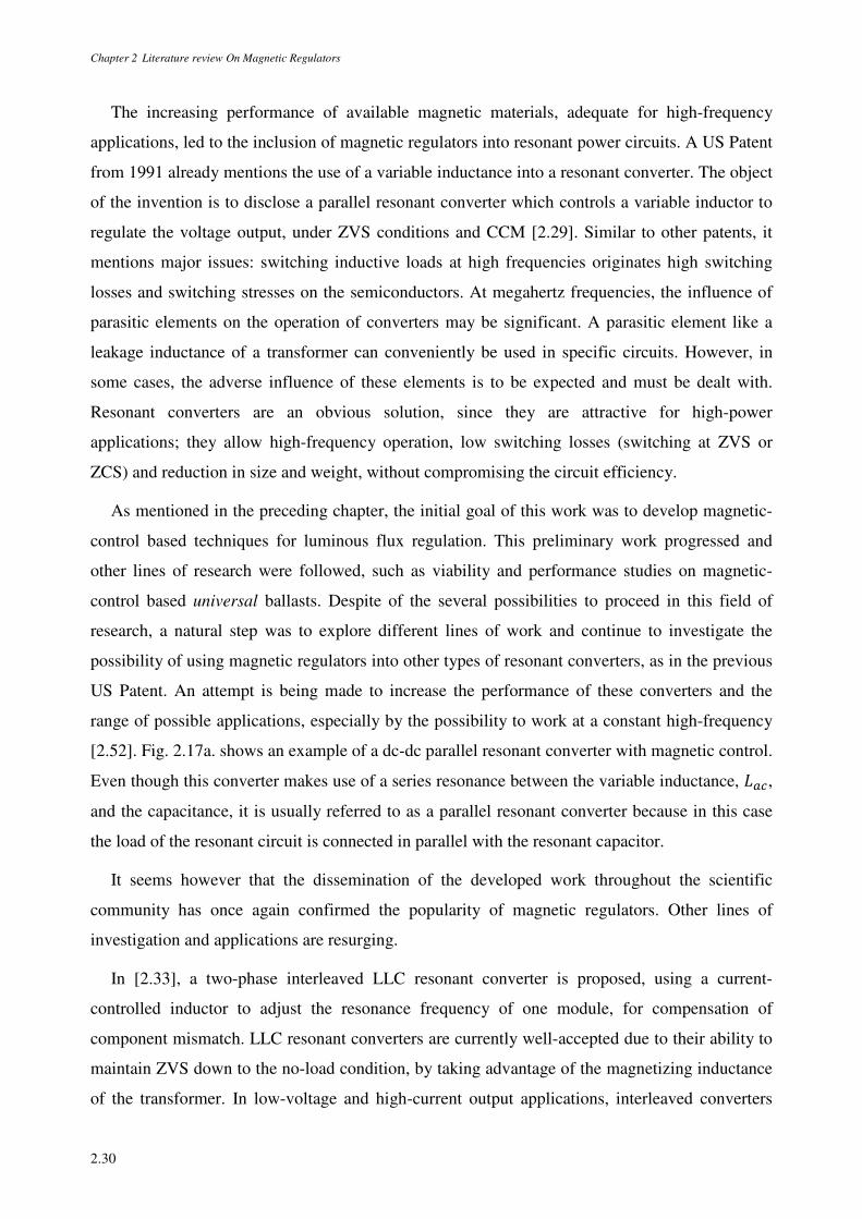
Chapter 2 Literature review On Magnetic Regulators
2.30
The increasing performance of available magnetic materials, adequate for high-frequency
applications, led to the inclusion of magnetic regulators into resonant power circuits. A US Patent
from 1991 already mentions the use of a variable inductance into a resonant converter. The object
of the invention is to disclose a parallel resonant converter which controls a variable inductor to
regulate the voltage output, under ZVS conditions and CCM [2.29]. Similar to other patents, it
mentions major issues: switching inductive loads at high frequencies originates high switching
losses and switching stresses on the semiconductors. At megahertz frequencies, the influence of
parasitic elements on the operation of converters may be significant. A parasitic element like a
leakage inductance of a transformer can conveniently be used in specific circuits. However, in
some cases, the adverse influence of these elements is to be expected and must be dealt with.
Resonant converters are an obvious solution, since they are attractive for high-power
applications; they allow high-frequency operation, low switching losses (switching at ZVS or
ZCS) and reduction in size and weight, without compromising the circuit efficiency.
As mentioned in the preceding chapter, the initial goal of this work was to develop magnetic-
control based techniques for luminous flux regulation. This preliminary work progressed and
other lines of research were followed, such as viability and performance studies on magnetic-
control based universal ballasts. Despite of the several possibilities to proceed in this field of
research, a natural step was to explore different lines of work and continue to investigate the
possibility of using magnetic regulators into other types of resonant converters, as in the previous
US Patent. An attempt is being made to increase the performance of these converters and the
range of possible applications, especially by the possibility to work at a constant high-frequency
[2.52]. Fig. 2.17a. shows an example of a dc-dc parallel resonant converter with magnetic control.
Even though this converter makes use of a series resonance between the variable inductance, ¯~,
and the capacitance, it is usually referred to as a parallel resonant converter because in this case
the load of the resonant circuit is connected in parallel with the resonant capacitor.
It seems however that the dissemination of the developed work throughout the scientific
community has once again confirmed the popularity of magnetic regulators. Other lines of
investigation and applications are resurging.
In [2.33], a two-phase interleaved LLC resonant converter is proposed, using a current-
controlled inductor to adjust the resonance frequency of one module, for compensation of
component mismatch. LLC resonant converters are currently well-accepted due to their ability to
maintain ZVS down to the no-load condition, by taking advantage of the magnetizing inductance
of the transformer. In low-voltage and high-current output applications, interleaved converters
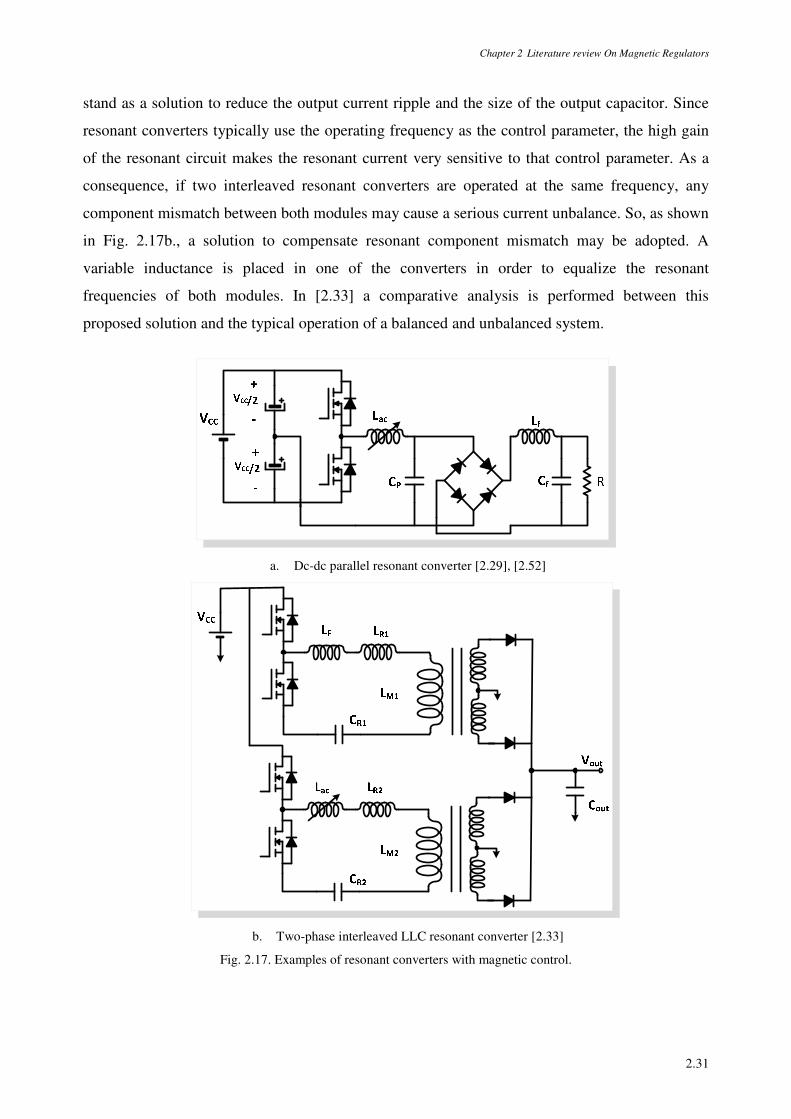
Chapter 2 Literature review On Magnetic Regulators
2.31
stand as a solution to reduce the output current ripple and the size of the output capacitor. Since
resonant converters typically use the operating frequency as the control parameter, the high gain
of the resonant circuit makes the resonant current very sensitive to that control parameter. As a
consequence, if two interleaved resonant converters are operated at the same frequency, any
component mismatch between both modules may cause a serious current unbalance. So, as shown
in Fig. 2.17b., a solution to compensate resonant component mismatch may be adopted. A
variable inductance is placed in one of the converters in order to equalize the resonant
frequencies of both modules. In [2.33] a comparative analysis is performed between this
proposed solution and the typical operation of a balanced and unbalanced system.
a. Dc-dc parallel resonant converter [2.29], [2.52]
b. Two-phase interleaved LLC resonant converter [2.33]
Fig. 2.17. Examples of resonant converters with magnetic control.
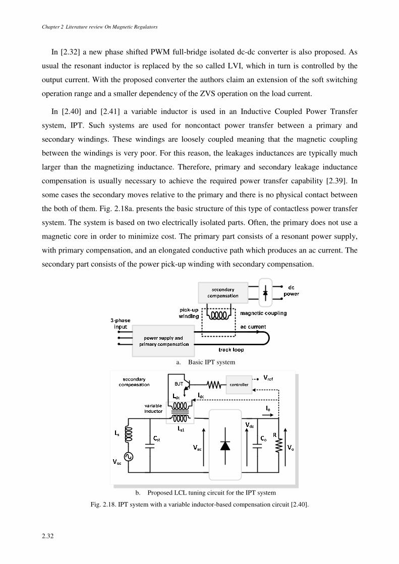
Chapter 2 Literature review On Magnetic Regulators
2.32
In [2.32] a new phase shifted PWM full-bridge isolated dc-dc converter is also proposed. As
usual the resonant inductor is replaced by the so called LVI, which in turn is controlled by the
output current. With the proposed converter the authors claim an extension of the soft switching
operation range and a smaller dependency of the ZVS operation on the load current.
In [2.40] and [2.41] a variable inductor is used in an Inductive Coupled Power Transfer
system, IPT. Such systems are used for noncontact power transfer between a primary and
secondary windings. These windings are loosely coupled meaning that the magnetic coupling
between the windings is very poor. For this reason, the leakages inductances are typically much
larger than the magnetizing inductance. Therefore, primary and secondary leakage inductance
compensation is usually necessary to achieve the required power transfer capability [2.39]. In
some cases the secondary moves relative to the primary and there is no physical contact between
the both of them. Fig. 2.18a. presents the basic structure of this type of contactless power transfer
system. The system is based on two electrically isolated parts. Often, the primary does not use a
magnetic core in order to minimize cost. The primary part consists of a resonant power supply,
with primary compensation, and an elongated conductive path which produces an ac current. The
secondary part consists of the power pick-up winding with secondary compensation.
a. Basic IPT system
b. Proposed LCL tuning circuit for the IPT system
Fig. 2.18. IPT system with a variable inductor-based compensation circuit [2.40].
Chapter 2 Literature review On Magnetic Regulators
2.33
Since the system is loosely coupled, the induced voltage in the secondary is usually unsuitable
for the direct use in applications. Secondary compensation or tuning is essential to provide a
constant dc power to the load. Typically an LC circuit is used, however in [2.40] and [2.41], an
LCL configuration is proposed. The major advantage of the proposed configuration is that one of
the inductances is in fact replaced by a magnetic regulator. Its inductance value is then varied
according to the output voltage feedback control signal, by means of a dynamic on-line
identification control algorithm. So, in fact, the variable inductor is used to control the power
flow from the secondary or pick-up winding to the load according to the desired output voltage.
Since the proposed circuit, represented in Fig. 2.18b., does not involve switching due to the
dynamic variation in the inductance ¯4ª, the voltage and current of the pick-up winding are kept
continuous. This minimizes waveform distortion and EMI. If the output voltage, >Ô, is higher than
the voltage reference, >23Å, the controller block generates a signal to increase the inductance
value, thereby detuning the circuit to lower the output voltage. On the contrary, if the output
voltage is lower than the reference voltage a reverse signal is generated, capable of decreasing the
inductance value, moving the circuit close to the tuned or resonance position thus increasing the
output voltage.
In [2.24] and in [2.25], a variable inductor is used in a PFC circuit for a LED driver. A two-
stage LED driver would normally consist of a PFC stage followed by a dc-dc converter. In this
case a single-stage solution is proposed as shown in Fig. 2.19: a single-stage ac-dc PFC flyback
LED driver with a variable “boost” inductance. Typically, the PFC stage operates in DCM, while
the flyback converter operates at a boundary mode. The design goal is to achieve a proper PFC
operation, which means that the line current has to meet the IEC 61000-3-2 Class C limits, and to
limit the bulk-capacitor voltage, >Õ, below 400V. This bulk capacitor, Õ, is typically used to
limit the output voltage ripple of the EMI filter and rectifier stage. To reduce this capacitor
voltage one terminal of the boost inductance, ¯~, is connected to a tap of the primary winding of
the transformer, thus providing a negative feedback. The problem pointed out by the authors
relates with the fact that as long as the instantaneous line voltage is lower than the voltage at the
tap, no current is drawn from the input, thus reducing the power factor and increasing the line-
current harmonics. This application is intended to operate with the universal line voltage (90-
270Vrms). Using a variable inductance it is possible to set it at high value, at high line voltage to
limit >Õ, and at a low value, at low line voltage to ensure DCM operation and a low THD. If a
constant boost inductance was used, at a low line voltage, the inductor would enter in CCM
around the peak line voltage and this would result in an increased THD. In [2.24] and [2.25] a
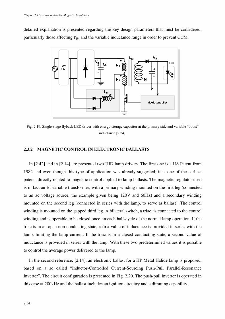
Chapter 2 Literature review On Magnetic Regulators
2.34
detailed explanation is presented regarding the key design parameters that must be considered,
particularly those affecting >Õ, and the variable inductance range in order to prevent CCM.
Fig. 2.19. Single-stage flyback LED driver with energy-storage capacitor at the primary side and variable “boost”
inductance [2.24].
2.3.2 MAGNETIC CONTROL IN ELECTRONIC BALLASTS
In [2.42] and in [2.14] are presented two HID lamp drivers. The first one is a US Patent from
1982 and even though this type of application was already suggested, it is one of the earliest
patents directly related to magnetic control applied to lamp ballasts. The magnetic regulator used
is in fact an EI variable transformer, with a primary winding mounted on the first leg (connected
to an ac voltage source, the example given being 120V and 60Hz) and a secondary winding
mounted on the second leg (connected in series with the lamp, to serve as ballast). The control
winding is mounted on the gapped third leg. A bilateral switch, a triac, is connected to the control
winding and is operable to be closed once, in each half-cycle of the normal lamp operation. If the
triac is in an open non-conducting state, a first value of inductance is provided in series with the
lamp, limiting the lamp current. If the triac is in a closed conducting state, a second value of
inductance is provided in series with the lamp. With these two predetermined values it is possible
to control the average power delivered to the lamp.
In the second reference, [2.14], an electronic ballast for a HP Metal Halide lamp is proposed,
based on a so called “Inductor-Controlled Current-Sourcing Push-Pull Parallel-Resonance
Inverter”. The circuit configuration is presented in Fig. 2.20. The push-pull inverter is operated in
this case at 200kHz and the ballast includes an ignition circuitry and a dimming capability.
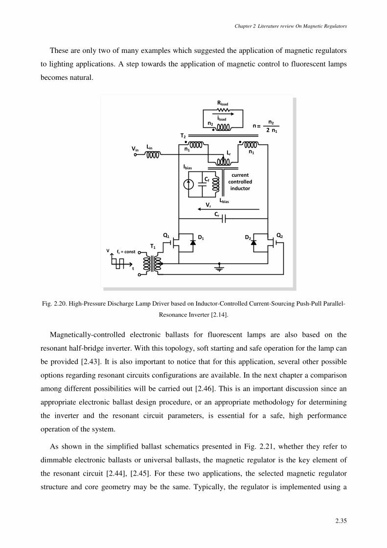
Chapter 2 Literature review On Magnetic Regulators
2.35
These are only two of many examples which suggested the application of magnetic regulators
to lighting applications. A step towards the application of magnetic control to fluorescent lamps
becomes natural.
Cf
Rload
n2iload
n2n
n12
n1n1
T2
LrLinVin
Ibias
LbiasVr
Cr
D1 D2Q1 Q2
fs = constV
t
current
controlled
inductor
T1
Fig. 2.20. High-Pressure Discharge Lamp Driver based on Inductor-Controlled Current-Sourcing Push-Pull Parallel-
Resonance Inverter [2.14].
Magnetically-controlled electronic ballasts for fluorescent lamps are also based on the
resonant half-bridge inverter. With this topology, soft starting and safe operation for the lamp can
be provided [2.43]. It is also important to notice that for this application, several other possible
options regarding resonant circuits configurations are available. In the next chapter a comparison
among different possibilities will be carried out [2.46]. This is an important discussion since an
appropriate electronic ballast design procedure, or an appropriate methodology for determining
the inverter and the resonant circuit parameters, is essential for a safe, high performance
operation of the system.
As shown in the simplified ballast schematics presented in Fig. 2.21, whether they refer to
dimmable electronic ballasts or universal ballasts, the magnetic regulator is the key element of
the resonant circuit [2.44], [2.45]. For these two applications, the selected magnetic regulator
structure and core geometry may be the same. Typically, the regulator is implemented using a
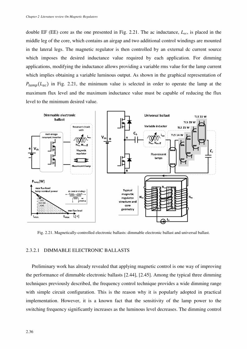
Chapter 2 Literature review On Magnetic Regulators
2.36
double EF (EE) core as the one presented in Fig. 2.21. The ac inductance, Lac, is placed in the
middle leg of the core, which contains an airgap and two additional control windings are mounted
in the lateral legs. The magnetic regulator is then controlled by an external dc current source
which imposes the desired inductance value required by each application. For dimming
applications, modifying the inductance allows providing a variable rms value for the lamp current
which implies obtaining a variable luminous output. As shown in the graphical representation of
t~¯~ in Fig. 2.21, the minimum value is selected in order to operate the lamp at the
maximum flux level and the maximum inductance value must be capable of reducing the flux
level to the minimum desired value.
Fig. 2.21. Magnetically-controlled electronic ballasts: dimmable electronic ballast and universal ballast.
2.3.2.1 DIMMABLE ELECTRONIC BALLASTS
Preliminary work has already revealed that applying magnetic control is one way of improving
the performance of dimmable electronic ballasts [2.44], [2.45]. Among the typical three dimming
techniques previously described, the frequency control technique provides a wide dimming range
with simple circuit configuration. This is the reason why it is popularly adopted in practical
implementation. However, it is a known fact that the sensitivity of the lamp power to the
switching frequency significantly increases as the luminous level decreases. The dimming control
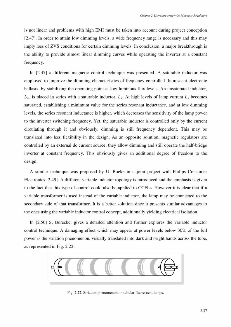
Chapter 2 Literature review On Magnetic Regulators
2.37
is not linear and problems with high EMI must be taken into account during project conception
[2.47]. In order to attain low dimming levels, a wide frequency range is necessary and this may
imply loss of ZVS conditions for certain dimming levels. In conclusion, a major breakthrough is
the ability to provide almost linear dimming curves while operating the inverter at a constant
frequency.
In [2.47] a different magnetic control technique was presented. A saturable inductor was
employed to improve the dimming characteristics of frequency-controlled fluorescent electronic
ballasts, by stabilizing the operating point at low luminous flux levels. An unsaturated inductor,
¯³, is placed in series with a saturable inductor, ¯4. At high levels of lamp current ¯4 becomes
saturated, establishing a minimum value for the series resonant inductance, and at low dimming
levels, the series resonant inductance is higher, which decreases the sensitivity of the lamp power
to the inverter switching frequency. Yet, the saturable inductor is controlled only by the current
circulating through it and obviously, dimming is still frequency dependent. This may be
translated into less flexibility in the design. As an opposite solution, magnetic regulators are
controlled by an external dc current source; they allow dimming and still operate the half-bridge
inverter at constant frequency. This obviously gives an additional degree of freedom to the
design.
A similar technique was proposed by U. Boeke in a joint project with Philips Consumer
Electronics [2.49]. A different variable inductor topology is introduced and the emphasis is given
to the fact that this type of control could also be applied to CCFLs. However it is clear that if a
variable transformer is used instead of the variable inductor, the lamp may be connected to the
secondary side of that transformer. It is a better solution since it presents similar advantages to
the ones using the variable inductor control concept, additionally yielding electrical isolation.
In [2.50] S. Boreckci gives a detailed attention and further explores the variable inductor
control technique. A damaging effect which may appear at power levels below 30% of the full
power is the striation phenomenon, visually translated into dark and bright bands across the tube,
as represented in Fig. 2.22.
Fig. 2.22. Striation phenomenon on tubular fluorescent lamps.
Chapter 2 Literature review On Magnetic Regulators
2.38
This phenomenon, which occurs at low power and/or at low temperature, is a common
concern in all existing dimming techniques. Striations are induced from ion oscillations; they
depend on the arc current, electron density, ambient temperature and gas pressure, composition of
the lamp plasma and also on the geometric scale of the tube. One way to control this phenomenon
is to inject a small amount of dc current into the lamp, although it might also shorten the
electrode life [2.51]. Once again, in [2.50], it is presented a new solution to prevent striations in
this type of magnetic dimming techniques, called the power density modulation (PDM). It
proposes to induce three different stages in each period of the arc current, by changing the level
of the dc control current and consequently the inductance value. The time interval for each
inductance value controls the average lamp power in each modulation period.
2.3.2.2 UNIVERSAL ELECTRONIC BALLASTS
Lighting requirements in public and commercial buildings may change enormously.
Nowadays a building can be built for one particular activity and after a few years or even months
have a total different purpose. Of course this translates into the need of a different lighting design
installation according to the new occupation. A key answer to solve possible limitations may be,
if from the start, the basic illumination system includes luminaires and electronic ballasts, which
can easily adapt to a new situation or environment. In fact there is a commercial need for safe,
reliable, versatile equipment which simultaneously avoids future costs and offers flexibility to the
consumer. Therefore universal ballasts have recently attracted the attention of manufacturers and
researchers due to the high increase in lamp types, mainly fluorescent, in terms of rated power,
shapes and electrical characteristics. There is a real profit to be expected from the spread out of
the use of this type of ballasts: luminaires manufacturers and retailers will benefit from lower
costs and reduced complexity in development, production and storage, if such equipment is
adopted. Facility managers will have more flexibility in dealing with their lighting installations.
As represented in Fig. 2.21 the main purpose is the ability to provide an electronic ballast
system, typically with digital control, capable of driving any lamp within a range of nominal
power ratings, while assuring safe operation. Like standard dimmable electronic ballasts,
conventional universal ballasts proposed up to now also use the inverter switching frequency as
the main control parameter, ensuring that each lamp is operated at nominal power. Nonetheless,
each lamp has its unique characteristics, its own starting and working voltage. Using the same
resonant tank with the switching frequency as the only control variable, involves a large range of
operating frequencies and does not ensure optimum working conditions. To overcome these
Chapter 2 Literature review On Magnetic Regulators
2.39
limitations, [2.55] suggests adapting the dc voltage that supplies the resonant inverter. An
additional converter with step-up and step-down characteristics is needed to perform this
operation. This converter must handle the total circuit power, decreasing overall efficiency. A US
Patent from 2000, [2.56], considers selectively changing simultaneously the switching frequency
and duty-cycle of the inverter signal. Varying the duty ratio of the switches allows controlling the
pulse width of the square waveform at the output of the inverter, which means controlling its rms
value and consequently provide a variable rms current to each lamp. The main disadvantage of
this control method resides in the asymmetrical lamp current waveform, which causes the
premature aging of the lamp due to a mechanism called non-linear electrophoresis. An
improvement was later presented in [2.57], where a boost converter is used as an input stage to
supply the half bridge resonant inverter. In this case, it is proposed a strategy based on the
variation of three control parameters: the dc output voltage of the boost stage, the duty-cycle and
switching frequency of the inverter.
An alternative control technique would be integrating the magnetic regulator into the universal
ballast. Through a dc control current it is given the ability to change and adapt the resonant
circuit, due to the variable inductance, to the working parameters imposed by each lamp. The
switching frequency may also be adjusted to allow the inverter to operate near the resonant
frequency, ensuring that the inverter stability and efficiency are close to their optimum. Using
magnetically-controlled ballasts, an additional degree of freedom in the optimization of the
working conditions for each lamp is obtained, without compromising the overall efficiency of the
circuit. Verifying the effectiveness of this control technique is one of the objectives of the
presented work.
Lamp detection techniques are also important in this type of ballasts. Any mismatch of ballast
and lamp power rating may damage the lamp or the ballast. However, after an accurate process of
lamp power recognition, the ballast control parameters may be selected properly. In [2.53] one of
these methods is proposed. It can differentiate the lamp power of T8 and T12, in the range of 18-
70W, by measuring the lamp voltage after the lamp ignition. With this method the electronic
ballast supplies the lamp at a fixed frequency during the detection period. Afterwards, this
voltage is stepped down and modified as a control signal to determine the switching frequency of
the inverter. In order to select and vary the switching frequency, a voltage controlled oscillator
together with some mapping functions, are used [2.54]. These methods can also be used in
magnetically-controlled ballasts.
Chapter 2 Literature review On Magnetic Regulators
2.40
REFERENCES
[2.1] Alexanderson, E.F.W.; Nixdorff, S.P.; "A Magnetic Amplifier for Radio Telephony," Proceedings of the
Institute of Radio Engineers, vol.4, no.2, pp. 101- 120, April 1916.
[2.2] AVCM Keith E. Glading, “Navy Electricity and Electronics Training Series, Module 8 – Introduction to
Amplifiers,” NAVEDTRA 14180, Naval Education and Training Professional Development and Technology
Center, 1998.
[2.3] Lufcy, C.W.; "A Survey of Magnetic Amplifiers," Proceedings of the IRE , vol.43, no.4, pp.404-413, April
1955.
[2.4] Bob Mammano, “Magnetic Amplifier Control for Simple, Low-Cost, Secondary Regulation”, Unitrode
Corporation, 1986.
[2.5] Ruben Lee, Leo Wilson and Charles E. Carter, Electronic Transformers and Circuits, 3rd ed. PSMA
Publication. John Wiley & Sons, 1988.
[2.6] Alex Van den Bossche, Vencislav Cekov Valchev, Inductors and transformers for Power Electronics, Taylor
& Francis Group, 2005.
[2.7] Paul Mali, Magnetic Amplifiers, Principles and Applications, John F. Rider Publisher, Inc., New York, 1960.
[2.8] Harada, K.; Ishihara, Y.; Todaka, T.; "A novel high power factor converter using a magnetic amplifier,"
Magnetics, IEEE Transactions on, vol.32, no.5, pp. 5013-5015, Sep 1996.
[2.9] Elichi Hirota, Yutaka Neichi, Minoru Sugimura, “Variable Inductance Device,” U.S. Patent 3 631 534, Dec.
28, 1971.
[2.10] Leopold J. Johnson, “Current Controlled Variable Inductor,” U.S. Patent 5 426 409, Jun. 20, 1995.
[2.11] Arian M. Jansen, “Variable Inductor,” U.S. Patent 6 317 021 B1, Nov. 13, 2001.
[2.12] Kislovski, A.S.; "Quasi-linear controllable inductor," Proceedings of the IEEE, vol.75, no.2, pp. 267- 269,
Feb. 1987.
[2.13] Medini, D.; Ben-Yaakov, S.; "A current-controlled variable-inductor for high frequency resonant power
circuits," Applied Power Electronics Conference and Exposition, 1994. APEC '94. Conference Proceedings
1994, Ninth Annual, vol., no., pp.219-225 vol.1, 13-17 Feb 1994.
[2.14] Gulko, M.; Medini, D.; Ben-Yaakov, S.; "Inductor-controlled current-sourcing resonant inverter and its
application as a high pressure discharge lamp driver," Applied Power Electronics Conference and Exposition,
1994. APEC '94. Conference Proceedings 1994, Ninth Annual, vol., no., pp.434-440 vol.1, 13-17 Feb 1994.
[2.15] Ben-Yaakov, S. and Peretz, M. M., "Simulation Bits: A SPICE Behavioral Model of Non-Linear Inductors,"
IEEE Power Electronics Society Newsletter, Fourth Quarter, pp.9-10 2003.
[2.16] Evgeny Rozanov and Sam Ben-Yaakov, “Analysis of current-controlled inductors by new SPICE behavioral
model”, HAIT Journal of Science and Engineering B, Volume 2, Issues 3-4, pp. 558-570, Holon Academic
Institute of Technology, 2005.
[2.17] Lu, Y.; Cheng, K.W.E.; Ho, S.L.; Pan, J.F.; Kwok, K.F.; Xue, X.D.; "A Transformer with Adjustable
Leakage Inductance," Electromagnetic Field Computation, 2006 12th Biennial IEEE Conference on, vol.,
no., pp.78.
[2.18] Bolduc Léonard, Parc Grégoire, “Self-regulated Transformer-inductor with Air gaps,” U.S. Patent 4 766 365,
Aug. 23, 1988.
Chapter 2 Literature review On Magnetic Regulators
2.41
[2.19] Robert D. Washburn and Robert F. McClanahan, “Non-saturating Magnetic Amplifier Controller,” U.S.
Patent 4 841 428, Jun. 20, 1989.
[2.20] Vollin, J.; Tan, F.D.; Cuk, S.M.; "Magnetic regulator modeling," Applied Power Electronics Conference and
Exposition, 1993. APEC '93. Conference Proceedings 1993, Eighth Annual , vol., no., pp.604-611, 7-11 Mar
1993.
[2.21] Kislovski, A.S.; "Linear variable inductor (LVI) in single-phase telecom rectifiers," Telecommunications
Energy Conference, 1995. INTELEC '95, 17th International, vol., no., pp.93-98, 29 Oct-1 Nov 1995.
[2.22] Kislovski, A.S.; "Linear variable inductor in DC current sensors utilized in telecom solar battery chargers,"
Telecommunications Energy Conference, 1989. INTELEC '89. Conference Proceedings, Eleventh
International, vol., no., pp.23.2/1-23.2/3 vol.2, 15-18 Oct 1989.
[2.23] Rozanov, E.; Ben-Yaakov, S.; "A SPICE behavioral model for current-controlled magnetic inductors,"
Electrical and Electronics Engineers in Israel, 2004. Proceedings. 2004 23rd IEEE Convention of, vol., no.,
pp. 338- 341, 6-7 Sept. 2004.
[2.24] Yuequan Hu; Huber, L.; Jovanovic, M.M.; "Universal-input single-stage PFC flyback with variable boost
inductance for high-brightness LED applications," Applied Power Electronics Conference and Exposition
(APEC), 2010 Twenty-Fifth Annual IEEE , vol., no., pp.203-209, 21-25 Feb. 2010.
[2.25] Hu, Y.; Huber, L.; Jovanovic, M.; "Single-Stage, Universal-Input AC/DC LED Driver with Current-
Controlled Variable PFC Boost Inductor," Power Electronics, IEEE Transactions on, vol. PP, no.99, pp.1-1,
Oct. 2010. (Early access)
[2.26] Bonanni, I.; "AC regulator controlled by LVI," Power Electronics and Applications, 1993, Fifth European
Conference on, vol., no., pp.101-105 vol.7, 13-16 Sep 1993.
[2.27] Bonanni, I.; Mandelli, E.; "High performances high voltage generator regulated by LVI," Applied Power
Electronics Conference and Exposition, 1990. APEC '90, Conference Proceedings 1990, Fifth Annual, vol.,
no., pp.323-329, 11-16 Mar 1990.
[2.28] Wolfle, W.H.; Hurley, W.G.; "Quasi-active power factor correction with a variable inductive filter: theory,
design and practice," Power Electronics, IEEE Transactions on , vol.18, no.1, pp. 248- 255, Jan 2003.
[2.29] Chu-Quon Lee, Kasemsan Siri, Anand K. Upadhyay, “Parallel Resonant Converter with Zero Voltage
Switching,” U.S. Patent 4 992 919, Feb. 12, 1991.
[2.30] Fischer, W.; Doebbelin, R.; Lindemann, A.; "Conducted EMI analysis of hard and soft switching arc welding
power supplies," Power Electronics and Applications, 2009. EPE '09. 13th European Conference on, vol.,
no., pp.1-10, 8-10 Sept. 2009.
[2.31] Pernia, A.M.; Lopera, J.M.; Prieto, M.J.; Nuno, F.; "Analysis and design of a new constant frequency control
for QRC and MRC based on magnetic elements modification," Power Electronics, IEEE Transactions on,
vol.13, no.2, pp.244-251, Mar 1998.
[2.32] Bakan, A.F.; "A new LVI assisted PSPWM DC-DC converter," Electrical and Electronics Engineering, 2009.
ELECO 2009. International Conference on, vol., no., pp.I-230-I-233, 5-8 Nov. 2009.
[2.33] Orietti, E.; Mattavelli, P.; Spiazzi, G.; Adragna, C.; Gattavari, G.; "Two-phase interleaved LLC resonant
converter with current-controlled inductor," Power Electronics Conference, 2009. COBEP '09. Brazilian,
vol., no., pp.298-304, Sept. 27 2009-Oct. 1 2009.
Chapter 2 Literature review On Magnetic Regulators
2.42
[2.34] Hooper, Rich; Guy, Bill; Perrault, Rick; "A current-controlled variable inductor," AUTOTESTCON, 2010
IEEE, vol., no., pp.1-4, 13-16 Sept. 2010.
[2.35] Sewell, H.I.; Stone, D.A.; Howe, D.; "Dynamic load impedance correction for induction heaters," Power
Electronics and Drive Systems, 1999. PEDS '99. Proceedings of the IEEE 1999 International Conference on,
vol.1, no., pp.110-115 vol.1, 1999.
[2.36] Huzayyin, A.A.; "Utilizing the nonlinearity of a magnetic core inductor as a source of variable reactive
power compensation in electric power systems," Student Paper, 2008 Annual IEEE Conference, vol., no.,
pp.1-4, 15-26 Feb. 2008.
[2.37] Mu Xianmin; Wang Jianze; Ji Yanchao; Wei Xiaoxia; Fu Xiangyun; "Novel Harmonic Free Single Phase
Variable Inductor Based on Active Power Filter Strategy," Power Electronics and Motion Control
Conference, 2006. IPEMC 2006. CES/IEEE 5th International, vol.3, no., pp.1-4, 14-16 Aug. 2006.
[2.38] Mu Xianmin; Zhang Suli; Wang Jianze; Ji Yanchao; Novel Static Var Compensator Based on Ferrite
Orthogonal Core Controlled Reactor," Industrial Technology, 2006. ICIT 2006. IEEE International
Conference on, vol., no., pp.1903-1907, 15-17 Dec. 2006.
[2.39] Stielau, O.H.; Covic, G.A.; "Design of loosely coupled inductive power transfer systems," Power System
Technology, 2000. Proceedings. PowerCon 2000. International Conference on, vol.1, no., pp.85-90 vol.1,
2000.
[2.40] Hsu, J.-U.W.; Hu, A.P.; Swain, A.; Xin Dai; Yue Sun; "A new contactless power pick-up with continuous
variable inductor control using magnetic amplifier," Power System Technology, 2006. PowerCon 2006.
International Conference on, vol., no., pp.1-8, 22-26 Oct. 2006.
[2.41] Hsu, J.-U.W.; Hu, A.P.; "Determining the variable inductance range for an LCL wireless power pick-up,"
Electron Devices and Solid-State Circuits, 2007. EDSSC 2007. IEEE Conference on, vol., no., pp.489-492,
20-22 Dec. 2007.
[2.42] Robert J. Spreadbury, “Discharge Device Ballast Component Which Provides Both Voltage Transformation
and Variable Inductance Reactance,” U.S. Patent, 4 350 934, Sep. 21, 1982.
[2.43] Alonso, J. M., Rashid, Muhammad H., “Power Electronics Handbook, Chapter 22 Electronic Ballasts”,
Academic Press, Inc., 2001, ISBN: 978-0-12-581650-2.
[2.44] Alonso, J.M.; Dalla-Costa, M.A.; Cardesin, J.; Garcia, J.; "Magnetic dimming of electronic ballasts,"
Electronics Letters, vol.41, no.12, pp. 718- 719, 9 June 2005.
[2.45] Alonso, J.M.; Dalla Costa, M.A.; Rico-Secades, M.; Cardesin, J.; Garcia, J.; "Investigation of a New Control
Strategy for Electronic Ballasts Based on Variable Inductor," Industrial Electronics, IEEE Transactions on ,
vol.55, no.1, pp.3-10, Jan. 2008.
[2.46] Perdigão, M.S.; Alonso, J.M.; Dalla Costa, M.A.; Saraiva, E.S.; "Comparative Analysis and Experiments of
Resonant Tanks for Magnetically Controlled Electronic Ballasts," Industrial Electronics, IEEE Transactions
on, vol.55, no.9, pp.3201-3211, Sept. 2008.
[2.47] Lee, S.T.S.; Chung, H.S.-H.; Hui, S.Y.; "Use of saturable inductor to improve the dimming characteristics of
frequency-controlled dimmable electronic ballasts," Power Electronics, IEEE Transactions on, vol.19, no.6,
pp. 1653- 1660, Nov. 2004.
Chapter 2 Literature review On Magnetic Regulators
2.43
[2.48] Perdigão, M.S.; Alonso, J.M.; Costa, M.A.D.; Saraiva, E.S.; "Using Magnetic Regulators for the
Optimization of Universal Ballasts," Power Electronics, IEEE Transactions on, vol.23, no.6, pp.3126-3134,
Nov. 2008.
[2.49] Boeke, U.; "Scalable fluorescent lamp driver using magnetic amplifiers," Power Electronics and
Applications, 2005 European Conference on, Sep. 2005.
[2.50] Borekci, S.; "Dimming Electronic Ballasts Without Striations," Industrial Electronics, IEEE Transactions on ,
vol.56, no.7, pp.2464-2468, July 2009.
[2.51] Tsai-Fu Wu; Yung-Chun Wu; Zing-Ying Su; , "Design considerations for single-stage electronic ballast with
dimming feature," Industry Applications, IEEE Transactions on, vol.37, no.5, pp.1537-1543, Sep/Oct 2001.
[2.52] Alonso, J.M.; Perdigão, M.S.; Gacio, D.; Campa, L.; Saraiva, E.S.; , "Magnetic control of DC-DC resonant
converters provides constant frequency operation," Electronics Letters , vol.46, no.6, pp.440-442, March 18
2010.
[2.53] L. M. Lee, S. Y. R. Hui, H. S. H. Chung, “An automatic lamp detection technique for electronic ballasts,”
Twentieth Annual IEEE Applied Power Electronics Conference and Exposition, 2005. APEC 2005, vol. 1,
pp. 575-581, Mar. 2005.
[2.54] S. Y. R. Hui and L. M. Lee, “Universal electronic ballast”, U.S. Patent 6 414 449, 2002.
[2.55] Busse, O.; Mayer, S.; Schemmel, B.; Storm, A.; "SEPIC converter to perform power factor correction in a
ballast for fluorescent lamps," Industry Applications Conference, 2005. Fortieth IAS Annual Meeting.
Conference Record of the 2005, vol.4, no., pp. 2770- 2774 Vol. 4, 2-6 Oct. 2005.
[2.56] Alexei Bogdan, “Programmable Universal Lighting System”, U.S. Patent 6 040 661, March 21, 2000.
[2.57] A. Bogdan; “Universal Ballast Control Circuit,” U.S. Patent 6 137 240, Oct. 2000.
Chapter 2 Literature review On Magnetic Regulators
2.44
BIBLIOGRAPHY
[B2.1] Ruben Lee, Leo Wilson and Charles E. Carter, “Electronic Transformers and Circuits”, 3rd ed. PSMA
Publication. John Wiley & Sons, 1988.
[B2.2] Alex Van den Bossche, Vencislav Cekov Valchev, “Inductors and transformers for Power Electronics”,
Taylor & Francis Group, 2005.
[B2.3] Paul Mali, “Magnetic Amplifiers, Principles and Applications”, John F. Rider Publisher, Inc., New York,
1960.
[B2.4] John D. Kraus, “Electromagnetics”, 4th Edition, McGraw-Hill International Editions, 1991.
[B2.5] Marian K. Kazimierczuk, Dariusz Czarkowski, “Resonant Power Converters”, John Wiley & Sons, Inc.,
1995.
APPLICATION OF THE VARIABLE 3INDUCTOR TO THE CONTROL OF
ELECTRONIC BALLASTS….
The present chapter reveals the main applications of the variable inductor. The chapter starts
by describing the variable inductor modelling and design. It continues with the description of the
proposed dimming technique. In magnetically-controlled electronic ballasts besides the classical
high-frequency half-bridge inverter, two additional elements are present: the magnetic regulator,
which replaces the typical resonant inductor, and the dc current source, to control this regulator.
The device acts as a variable inductance dependent on the dc control current. So, if the
inductance value of the resonant inductor is gradually increased, so will the impedance of the
resonant circuit and thereby the luminous flux may be controlled. A comparative analysis
between resonant circuits, different regulators structures, topologies and their effects on lamp
operation are studied. Finally, the chapter describes the other proposed technique: magnetically-
controlled universal ballasts. The technique is explained and two different prototype versions are
presented, the last one with constant-frequency operation. Critical issues related to electrodes
operation with these control techniques are also addressed in this chapter.
3.1 MODELLING AND DESIGN OF VARIABLE INDUCTORS
3.1.1 MODELLING ISSUES AND THEORECTICAL ANALYSIS
The theoretical and experimental study of the magnetic behaviour of variable inductors
constitutes an interesting scientific challenge, not only from the electronic ballast development
point of view, but also for other potential applications in power converters. Modelling is essential
for a correct understanding of the behaviour of these magnetic devices and represents a useful
tool for prototype design and development. The magnetic circuit analysis contributes to the
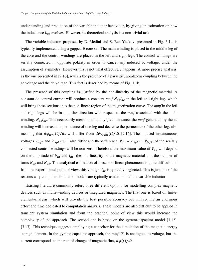
Chapter 3 Application of the Variable Inductor to the Control of Electronic Ballasts
3.2
understanding and prediction of the variable inductor behaviour, by giving an estimation on how
the inductance¯~ evolves. However, its theoretical analysis is a non-trivial task.
The variable inductor, proposed by D. Medini and S. Ben Yaakov, presented in Fig. 3.1a. is
typically implemented using a gapped E core set. The main winding is placed in the middle leg of
the core and the control windings are placed in the left and right legs. The control windings are
serially connected in opposite polarity in order to cancel any induced ac voltage, under the
assumption of symmetry. However this is not what effectively happens. A more precise analysis,
as the one presented in [2.16], reveals the presence of a parasitic, non-linear coupling between the
ac voltage and the dc voltage. This fact is described by means of Fig. 3.1b.
The presence of this coupling is justified by the non-linearity of the magnetic material. A
constant dc control current will produce a constant mmf Á/ in the left and right legs which
will bring these sections into the non-linear region of the magnetization curve. The mmf in the left
and right legs will be in opposite direction with respect to the mmf associated with the main
winding, Á~L~. This necessarily means that, at any given instance, the mmf generated by the ac
winding will increase the permeance of one leg and decrease the permeance of the other leg, also
meaning that £3ÅÀ() ⁄ will differ from £2±°À() ⁄ [2.16]. The induced instantaneous
voltages >3ÅÀ and >2±°À will also differ and the difference, > = >2±°À − >3ÅÀ, of the serially
connected control windings will be non-zero. Therefore, the maximum value of > will depend
on the amplitude of >±² and /, the non-linearity of the magnetic material and the number of
turns Á~ and Á. The analytical estimation of these non-linear phenomena is quite difficult and
from the experimental point of view, this voltage > is typically neglected. This is just one of the
reasons why computer simulation models are typically used to model the variable inductor.
Existing literature commonly refers three different options for modelling complex magnetic
devices such as multi-winding devices or integrated magnetics. The first one is based on finite-
element-analysis, which will provide the best possible accuracy but will require an enormous
effort and time dedicated to computation analysis. These models are also difficult to be applied in
transient system simulation and from the practical point of view this would increase the
complexity of the approach. The second one is based on the gyrator-capacitor model [3.12],
[3.13]. This technique suggests employing a capacitor for the simulation of the magnetic energy
storage element. In the gyrator-capacitor approach, the mmf, ℱ, is analogous to voltage, but the
current corresponds to the rate-of-change of magnetic flux, £() ⁄ .
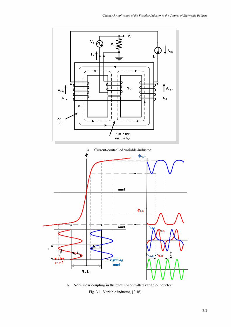
Chapter 3 Application of the Variable Inductor to the Control of Electronic Ballasts
3.3
a. Current-controlled variable-inductor
b. Non-linear coupling in the current-controlled variable-inductor
Fig. 3.1. Variable inductor, [2.16].
Chapter 3 Application of the Variable Inductor to the Control of Electronic Ballasts
3.4
The gyrator-capacitor approach is considered as one of the most effective; however it is
seldom used. Thus, the typical approach is the magnetic reluctance model. In this approach, the
mmf, ℱ, is also analogous to voltage, but in this case the magnetic flux is considered analogous to
current, instead of the rate-of-change of the magnetic flux. Since the flux produced by a mmf in a
material depends on the material’s resistance to the flux, more specifically, it depends on its
reluctance, this reluctance may be simply represented by a resistor. By doing this analogy any
electrical theorems or rules apply similarly. The easiest way to determine a reluctance model for a
coupled inductor is to impose zero current in all of the windings except one, and then imagine the
various paths that the magnetic flux could take to complete a closed loop back to the only
winding responsible for the mmf. Finally, the application of the principle of the duality to the
reluctance circuit, originates a permeance circuit which can then be transformed into an electrical
equivalent circuit containing inductances [3.14]. This inductances model will result into a more
or less complicated electric circuit, which may be integrated into more complex electric circuits
and then be used in computer simulation programs.
3.1.1.1 RELUCTANCE MODEL
The classic theory on magnetic modelling of multi-winding devices begins by establishing a
more or less complicated reluctance model of the structure. Fig. 3.2a. shows the definition used
for the magnetic paths which together make up the device. Each magnetic path is related to a
specific reluctance ℛ±, defined by:
ℛ± = ± µ±¤ ;i=1..10 (3.1)
where ± is the magnetic path length, AÎ the correspondent cross sectional area and μ the
permeability. Fig. 3.2b. shows the equivalent circuit reluctance model. The ac winding will
appear as a mmf source and in order to straightforward the structure, no dc mmf source is included
in the model. The effect of the control windings is in fact, already introduced in the model since
the dc control current affects the permeance and thereby the reluctance of the relevant path.
Particularly, the following quantities are defined:
Á~L±~ is the mmf source associated with the ac winding;
ℛª, ℛ, ℛ, ℛ×, ℛØ, ℛÙ, ℛ», ℛÚ, ℛÛ, ℛª are the reluctances of the magnetic paths
associated to the ac flux;
Chapter 3 Application of the Variable Inductor to the Control of Electronic Ballasts
3.5
a. Gapped E core b. Reluctance model
Fig. 3.2. Variable inductor modelling.
ℛªª is the reluctance of the magnetic path associated with the leakage flux (flux lines that
close in the air), and ℛ is the reluctance associated with the air gap.
The steps towards the final simplified model version presented in Fig. 3.3b. consider the
following simplifications:
ℛª = ℛª + ℛ + ℛ× + ℛÛ (3.2)
ℛª = ℛ + ℛØ + ℛÙ + ℛª (3.3)
ℛª× = ℛ» + ℛÚ (3.4)
ℛ3~Ê = ℛªª; ℛ = ℛª× (3.5)
ℛÏ = ℛª//ℛª (3.6)
ℛ is the reluctance of the magnetic path which will carry the common flux;
ℛÏ is the total sum of reluctances associated to the ac flux, which will depend on the
permeability of the control legs, and thus increase with decreasing control current.
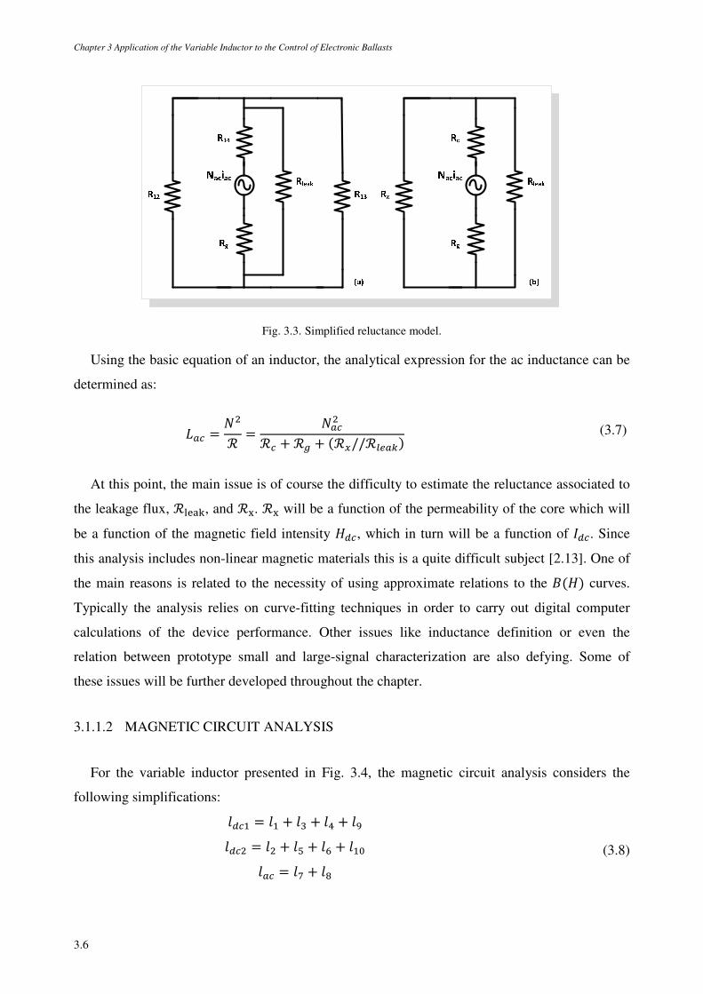
Chapter 3 Application of the Variable Inductor to the Control of Electronic Ballasts
3.6
Fig. 3.3. Simplified reluctance model.
Using the basic equation of an inductor, the analytical expression for the ac inductance can be
determined as:
¯~ = Áℛ = Á~ℛ + ℛ + (ℛÏ//ℛ3~Ê) (3.7)
At this point, the main issue is of course the difficulty to estimate the reluctance associated to
the leakage flux, ℛÜÝÞß, and ℛà. ℛà will be a function of the permeability of the core which will
be a function of the magnetic field intensity ¶, which in turn will be a function of /. Since
this analysis includes non-linear magnetic materials this is a quite difficult subject [2.13]. One of
the main reasons is related to the necessity of using approximate relations to the (¶) curves.
Typically the analysis relies on curve-fitting techniques in order to carry out digital computer
calculations of the device performance. Other issues like inductance definition or even the
relation between prototype small and large-signal characterization are also defying. Some of
these issues will be further developed throughout the chapter.
3.1.1.2 MAGNETIC CIRCUIT ANALYSIS
For the variable inductor presented in Fig. 3.4, the magnetic circuit analysis considers the
following simplifications:
ª = ª + + × + Û = + Ø + Ù + ª ~ = » + Ú
(3.8)
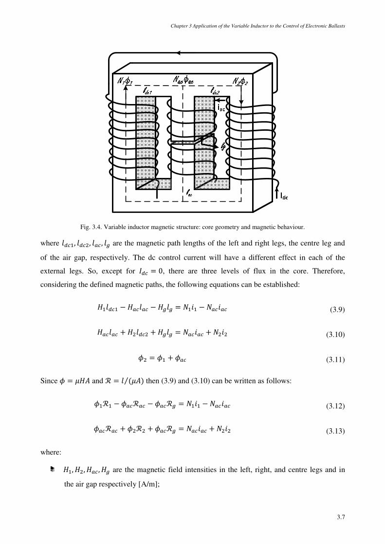
Chapter 3 Application of the Variable Inductor to the Control of Electronic Ballasts
3.7
Fig. 3.4. Variable inductor magnetic structure: core geometry and magnetic behaviour.
where ª, , ~, are the magnetic path lengths of the left and right legs, the centre leg and
of the air gap, respectively. The dc control current will have a different effect in each of the
external legs. So, except for / = 0, there are three levels of flux in the core. Therefore,
considering the defined magnetic paths, the following equations can be established:
¶ªª − ¶~~ − ¶ = ÁªLª − Á~L~ (3.9)
¶~~ + ¶ + ¶ = Á~L~ + ÁL (3.10)
£ = £ª + £~ (3.11)
Since £ = µ¶ and ℛ = (µ)⁄ then (3.9) and (3.10) can be written as follows:
£ªℛª − £~ℛ~ − £~ℛ = ÁªLª − Á~L~ (3.12)
£~ℛ~ + £ℛ + £~ℛ = Á~L~ + ÁL (3.13)
where:
¶ª, ¶, ¶~, ¶ are the magnetic field intensities in the left, right, and centre legs and in
the air gap respectively [A/m];
Chapter 3 Application of the Variable Inductor to the Control of Electronic Ballasts
3.8
Lª, L, L~are the currents in the left, right, and centre windings [A];
Áª, Á, Á~are the numbers of turns in the left, right and centre legs, respectively;
£ª, £, £~ are the magnetic fluxes in the left, right and centre legs, respectively [Wb];
ℛª, ℛ, ℛ~ are the reluctances of the left, right and centre legs, respectively;
ª, , ~ are the cross-section areas of the left, right and centre legs respectively [m2].
From (3.11), (3.12), and (3.13), £~ can be determined as:
£~ = ℛª(Á~L~ + ÁL) − ℛÁªLª + ℛÁ~L~ℛ¾ℛª + ℛ~ + ℛ¿ + ℛª¾ℛ~ + ℛ¿ (3.14)
Assuming symmetry, Áª = Á = Á, ª = = , ª = = , and Lª = L = /, (3.14)
results in:
£~ = ℛª(Á~L~ + Á/) − ℛÁ/ + ℛÁ~L~ℛ¾ℛª + ℛ~ + ℛ¿ + ℛª¾ℛ~ + ℛ¿= (ℛª − ℛ)Á/ + (ℛª + ℛ)Á~L~ℛ¾ℛª + ℛ~ + ℛ¿ + ℛª¾ℛ~ + ℛ¿
(3.15)
Physically, only when the ac current iÞá presents a zero value, may the reluctances of the left
and right legs be the same, ℛª = ℛ. Considering a positive and constant dc control current, a
non-zero positive ac current will result in a lower mmf for the left mesh, (3.9), when compared
with the mmf for the right mesh, (3.10). This issue was already referred to at the beginning of this
chapter. This behaviour will imply different levels for the magnetic field intensities, ¶ª and ¶,
which in turn will lead to different values for the reluctances ℛª and ℛ. Nevertheless, if the ac
mmf is less than 10% of the dc mmf, it would be possible to assume that the ac inductance would
depend essentially on the dc current level. The ratio Á~L~~Ï Á/¤ depends on the chosen
design parameters for the magnetic regulator.
From (3.9) and (3.10) the following relations may be observed:
¶ª + ¶ = 2Á/ (3.16)
(¶ª − ¶) − 2¶~~ − 2¶ = −2Á~L~ (3.17)
Chapter 3 Application of the Variable Inductor to the Control of Electronic Ballasts
3.9
Which implies that (¶ª − ¶) will depend on the ac current L~. For a variable inductor built with
two EF25 based cores, ~ = 2ª = 2 = 2, and since £ = , (3.11) can be rewritten:
ª + 2~ = (3.18)
Another important aspect to be considered is related to the practical implementation of the
variable inductor prototype. It is mandatory to use gapped E cores in order to have a proper
variable inductor behaviour. Yet, the prototype assembly may lead to the presence of undesirable
small lateral air gaps, ª and . Therefore, (3.16), (3.17) and (3.18) are rewritten as follows:
(¶ª + ¶) + ªμ ª + μ = 2Á/ (3.19)
(¶ª − ¶) − 2¶~~ − 2¶Ñ + ªμ ª − μ = −2Á~L~ (3.20)
ª + 2~ = (3.21)
where:
Ñ = + min¾ª, ¿ + ⪠− â2 (3.22)
At this point, in order to solve the system of equations formed by (3.16), (3.17) and (3.18) or
by (3.19), (3.20) and (3.21), the following functions must be known:
ª = (¶ª); = (¶);~ = (¶~) (3.23)
So, in fact, the magnetization curve (3.24) for the selected core material must be known
(¶) = µ ã µ±Å(¶)¶ (3.24)
where µ±Å is the differential or incremental permeability, defined as ¶¤ at each operating
point.
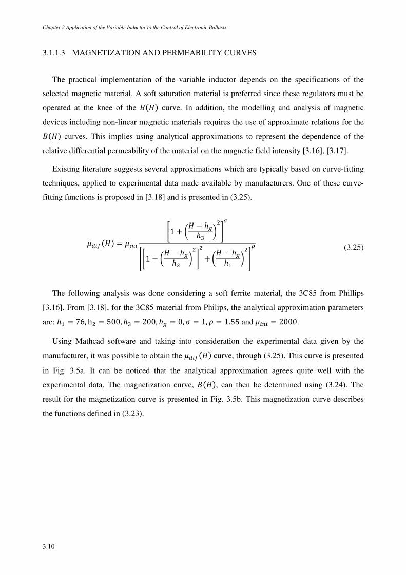
Chapter 3 Application of the Variable Inductor to the Control of Electronic Ballasts
3.10
3.1.1.3 MAGNETIZATION AND PERMEABILITY CURVES
The practical implementation of the variable inductor depends on the specifications of the
selected magnetic material. A soft saturation material is preferred since these regulators must be
operated at the knee of the (¶) curve. In addition, the modelling and analysis of magnetic
devices including non-linear magnetic materials requires the use of approximate relations for the
(¶) curves. This implies using analytical approximations to represent the dependence of the
relative differential permeability of the material on the magnetic field intensity [3.16], [3.17].
Existing literature suggests several approximations which are typically based on curve-fitting
techniques, applied to experimental data made available by manufacturers. One of these curve-
fitting functions is proposed in [3.18] and is presented in (3.25).
µ±Å(¶) = µ±²±ä1 + ¶ − ℎℎ æç
èä1 − ¶ − ℎℎ æ +¶ − ℎℎª éê (3.25)
The following analysis was done considering a soft ferrite material, the 3C85 from Phillips
[3.16]. From [3.18], for the 3C85 material from Philips, the analytical approximation parameters
are: ℎª = 76, h = 500, ℎ = 200, ℎ = 0, í = 1, | = 1.55 and µ±²± = 2000.
Using Mathcad software and taking into consideration the experimental data given by the
manufacturer, it was possible to obtain the µ±Å(¶) curve, through (3.25). This curve is presented
in Fig. 3.5a. It can be noticed that the analytical approximation agrees quite well with the
experimental data. The magnetization curve, (¶), can then be determined using (3.24). The
result for the magnetization curve is presented in Fig. 3.5b. This magnetization curve describes
the functions defined in (3.23).
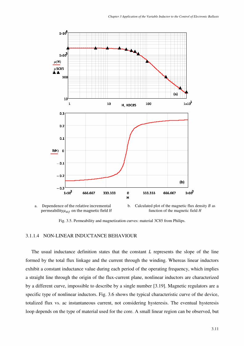
Chapter 3 Application of the Variable Inductor to the Control of Electronic Ballasts
3.11
a. Dependenceoftherelativeincrementalpermeabilityµ±Åonthemagneticfield¶ b. Calculated plot of the magnetic flux density as
function of the magnetic field ¶
Fig. 3.5. Permeability and magnetization curves: material 3C85 from Philips.
3.1.1.4 NON-LINEAR INDUCTANCE BEHAVIOUR
The usual inductance definition states that the constant ¯ represents the slope of the line
formed by the total flux linkage and the current through the winding. Whereas linear inductors
exhibit a constant inductance value during each period of the operating frequency, which implies
a straight line through the origin of the flux-current plane, nonlinear inductors are characterized
by a different curve, impossible to describe by a single number [3.19]. Magnetic regulators are a
specific type of nonlinear inductors. Fig. 3.6 shows the typical characteristic curve of the device,
totalized flux vs. ac instantaneous current, not considering hysteresis. The eventual hysteresis
loop depends on the type of material used for the core. A small linear region can be observed, but
Chapter 3 Application of the Variable Inductor to the Control of Electronic Ballasts
3.12
this behaviour is not maintained for the whole excitation range, meaning that the curve
corresponds effectively to a nonlinear inductor. These considerations are very important to define
an accurate value for the ac variable inductance, ¯~.
-1 -0.8 -0.6 -0.4 -0.2 0 0.2 0.4 0.6 0.8 1-1
-0.8
-0.6
-0.4
-0.2
0
0.2
0.4
0.6
0.8
1x 10
-3
ac instantaneous resonant current [A]
To
tali
zed
flu
x [
Wb
]
Fig. 3.6. Non-linear region of the variable inductor.
A simple analogy can be made: the voltage across a current-controlled variable inductor can
be expressed in the following form:
K = à = ÃLL L = ¯¾L¿ L (3.26)
Where:
¯L = ÃLL (3.27)
is called the differential inductance:
¯±Å = ÃL (3.28)
Taking (3.27) into account it is noticed that the regulator inductance is dependent both on the
amplitude of the ac current, L~, which flows through its ac winding and on the amplitude of the
dc control current, /. In fact the total ac flux linkage, Ã, can be defined as:
Chapter 3 Application of the Variable Inductor to the Control of Electronic Ballasts
3.13
Ã~ = / , L~ (3.29)
Therefore,
Ã~L = ðÃ~ð/ / + ðÃ~ðL~ L~ (3.30)
Considering a constant dc current level imposed on the variable inductor, equation (3.30) can
be simplified:
Ã~L = ðÃ~ðL~ L~ (3.31)
Using the basic inductance equation, ¯ = Á ℛ¤ , and considering the differential inductance
definition for non-linear inductors shown in (3.27), as well as equation (3.31), a first simplified
definition for the device ac differential inductance would be:
¯~ = ðÃ~ðL~ = ð£~Á~ðL~ = Á~ µ±Å~¾ + ~ + ¿ (3.32)
where + ~ + is the average path length of the magnetic field lines and µ±Å should be the
effective differential permeability for the variable inductor core and gaps. This µ±Å should
correspond to the corrected behaviour of the permeability curve given by the manufacturer,
processed, taking into account the three different levels of the flux density, ª = ¶ª; =¶; ~ = ¶~, at each instant, in addition to the core dimensions and air gap dimensions.
The differential permeability curve, µ±Å, should be similar to the one given by the
manufacturer, if an homogeneous material, non-gapped core was considered, in addition to a zero
dc control current. However, this is not the case. The main goal is to take advantage of the nature
of the regulator and thereby impose different control current levels on the device.
In order to obtain the differential inductance and simultaneously avoid the use of the corrected
permeability curve, requires the calculation of the total ac flux derivative, ðÃ~ by means of
imposing a small variation, ∆L~, in the instantaneous value of the ac resonant current: L~ + ∆L~
and L~ − ∆L~,. Hence, (3.32) results in:
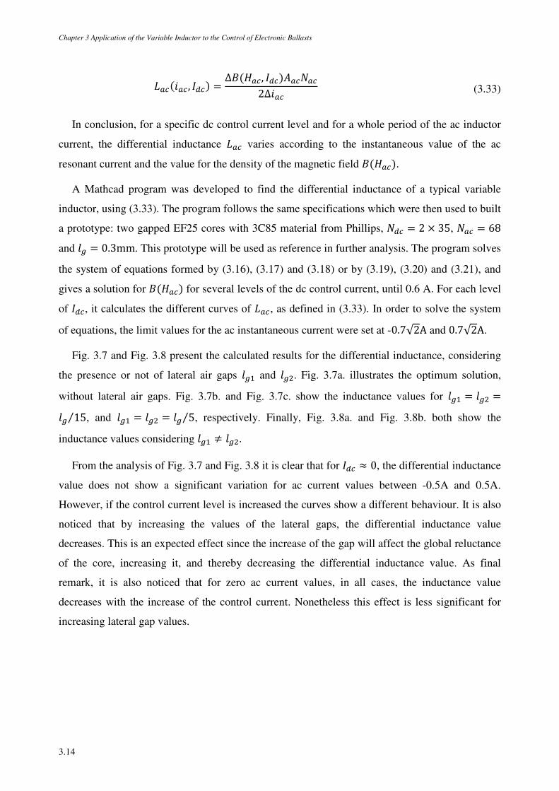
Chapter 3 Application of the Variable Inductor to the Control of Electronic Ballasts
3.14
¯~L~, / = ∆¶~, /~Á~2∆L~ (3.33)
In conclusion, for a specific dc control current level and for a whole period of the ac inductor
current, the differential inductance ¯~ varies according to the instantaneous value of the ac
resonant current and the value for the density of the magnetic field ¶~.
A Mathcad program was developed to find the differential inductance of a typical variable
inductor, using (3.33). The program follows the same specifications which were then used to built
a prototype: two gapped EF25 cores with 3C85 material from Phillips, Á = 2 × 35, Á~ = 68
and = 0.3mm. This prototype will be used as reference in further analysis. The program solves
the system of equations formed by (3.16), (3.17) and (3.18) or by (3.19), (3.20) and (3.21), and
gives a solution for ¶~ for several levels of the dc control current, until 0.6 A. For each level
of /, it calculates the different curves of ¯~, as defined in (3.33). In order to solve the system
of equations, the limit values for the ac instantaneous current were set at -0.7√2A and 0.7√2A.
Fig. 3.7 and Fig. 3.8 present the calculated results for the differential inductance, considering
the presence or not of lateral air gaps ª and . Fig. 3.7a. illustrates the optimum solution,
without lateral air gaps. Fig. 3.7b. and Fig. 3.7c. show the inductance values for ª = = 15⁄ , and ª = = 5⁄ , respectively. Finally, Fig. 3.8a. and Fig. 3.8b. both show the
inductance values considering ª ≠ .
From the analysis of Fig. 3.7 and Fig. 3.8 it is clear that for / ≈ 0, the differential inductance
value does not show a significant variation for ac current values between -0.5A and 0.5A.
However, if the control current level is increased the curves show a different behaviour. It is also
noticed that by increasing the values of the lateral gaps, the differential inductance value
decreases. This is an expected effect since the increase of the gap will affect the global reluctance
of the core, increasing it, and thereby decreasing the differential inductance value. As final
remark, it is also noticed that for zero ac current values, in all cases, the inductance value
decreases with the increase of the control current. Nonetheless this effect is less significant for
increasing lateral gap values.
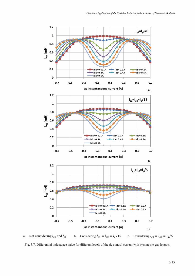
Chapter 3 Application of the Variable Inductor to the Control of Electronic Ballasts
3.15
0
0.2
0.4
0.6
0.8
1
1.2
-0.7 -0.5 -0.3 -0.1 0.1 0.3 0.5 0.7
L ac[m
H]
ac instantaneous current [A]
lg1=lg2=lg/5
Idc= 0.001A Idc= 0.1A Idc= 0.2A
Idc= 0.3A Idc= 0.4A Idc= 0.5A
Idc= 0.6A
0
0.2
0.4
0.6
0.8
1
1.2
-0.7 -0.5 -0.3 -0.1 0.1 0.3 0.5 0.7
L ac[m
H]
ac instantaneous current [A]
lg1=lg2=lg/15
Idc= 0.001A Idc= 0.1A Idc= 0.2A
Idc= 0.3A Idc= 0.4A Idc= 0.5A
Idc= 0.6A
0
0.2
0.4
0.6
0.8
1
1.2
-0.7 -0.5 -0.3 -0.1 0.1 0.3 0.5 0.7
L ac[m
H]
ac instantaneous current [A]
lg1=lg2=0
Idc= 0.001A Idc= 0.1A Idc= 0.2A
Idc= 0.3A Idc= 0.4A Idc= 0.5A
Idc= 0.6A
a. Not considering ª and b. Considering ª = = 15⁄ c. Considering ª = = 5⁄
Fig. 3.7. Differential inductance value for different levels of the dc control current with symmetric gap lengths.
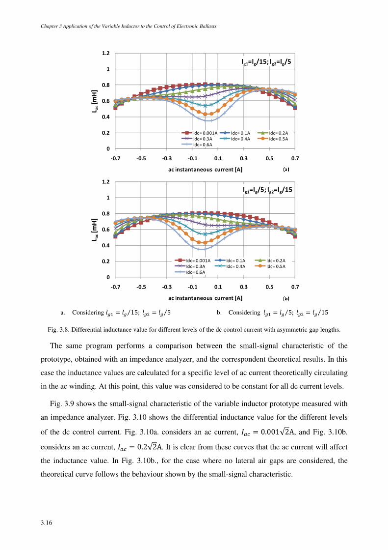
Chapter 3 Application of the Variable Inductor to the Control of Electronic Ballasts
3.16
0
0.2
0.4
0.6
0.8
1
1.2
-0.7 -0.5 -0.3 -0.1 0.1 0.3 0.5 0.7
L ac[m
H]
ac instantaneous current [A]
lg1=lg/15; lg2=lg/5
Idc= 0.001A Idc= 0.1A Idc= 0.2A
Idc= 0.3A Idc= 0.4A Idc= 0.5A
Idc= 0.6A
0
0.2
0.4
0.6
0.8
1
1.2
-0.7 -0.5 -0.3 -0.1 0.1 0.3 0.5 0.7
L ac[m
H]
ac instantaneous current [A]
lg1=lg/5; lg2=lg/15
Idc= 0.001A Idc= 0.1A Idc= 0.2A
Idc= 0.3A Idc= 0.4A Idc= 0.5A
Idc= 0.6A
a. Considering ª = 15; = 5⁄⁄ b. Consideringª = 5; = 15⁄⁄
Fig. 3.8. Differential inductance value for different levels of the dc control current with asymmetric gap lengths.
The same program performs a comparison between the small-signal characteristic of the
prototype, obtained with an impedance analyzer, and the correspondent theoretical results. In this
case the inductance values are calculated for a specific level of ac current theoretically circulating
in the ac winding. At this point, this value was considered to be constant for all dc current levels.
Fig. 3.9 shows the small-signal characteristic of the variable inductor prototype measured with
an impedance analyzer. Fig. 3.10 shows the differential inductance value for the different levels
of the dc control current. Fig. 3.10a. considers an ac current, /~ = 0.001√2A, and Fig. 3.10b.
considers an ac current, /~ = 0.2√2A. It is clear from these curves that the ac current will affect
the inductance value. In Fig. 3.10b., for the case where no lateral air gaps are considered, the
theoretical curve follows the behaviour shown by the small-signal characteristic.
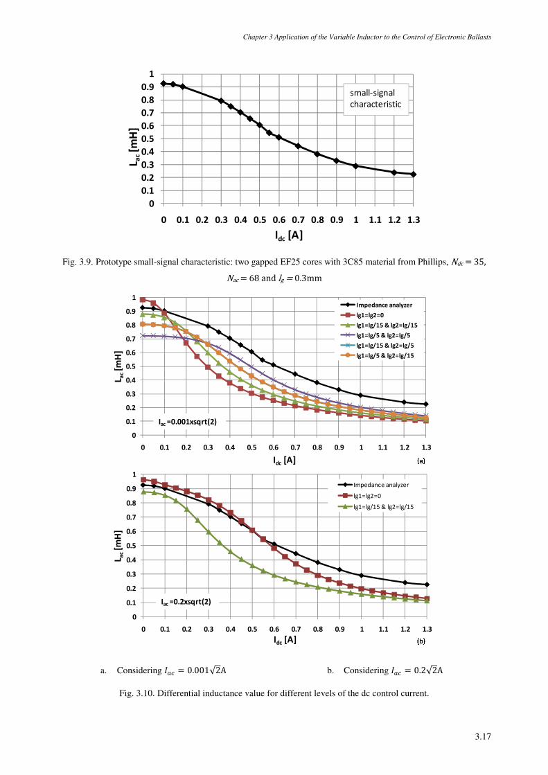
Chapter 3 Application of the Variable Inductor to the Control of Electronic Ballasts
3.17
0
0.1
0.2
0.3
0.4
0.5
0.6
0.7
0.8
0.9
1
0 0.1 0.2 0.3 0.4 0.5 0.6 0.7 0.8 0.9 1 1.1 1.2 1.3
L ac[m
H]
Idc [A]
small-signal
characteristic
Fig. 3.9. Prototype small-signal characteristic: two gapped EF25 cores with 3C85 material from Phillips, Ndc = 35, Nac = 68 and lg = 0.3mm
0
0.1
0.2
0.3
0.4
0.5
0.6
0.7
0.8
0.9
1
0 0.1 0.2 0.3 0.4 0.5 0.6 0.7 0.8 0.9 1 1.1 1.2 1.3
L ac[m
H]
Idc [A]
Impedance analyzer
lg1=lg2=0
lg1=lg/15 & lg2=lg/15
lg1=lg/5 & lg2=lg/5
lg1=lg/15 & lg2=lg/5
lg1=lg/5 & lg2=lg/15
Iac =0.001xsqrt(2)
0
0.1
0.2
0.3
0.4
0.5
0.6
0.7
0.8
0.9
1
0 0.1 0.2 0.3 0.4 0.5 0.6 0.7 0.8 0.9 1 1.1 1.2 1.3
L ac[m
H]
Idc [A]
Impedance analyzer
lg1=lg2=0
lg1=lg/15 & lg2=lg/15
Iac =0.2xsqrt(2)
a. Considering /~ = 0.001√2A b. Considering /~ = 0.2√2A
Fig. 3.10. Differential inductance value for different levels of the dc control current.
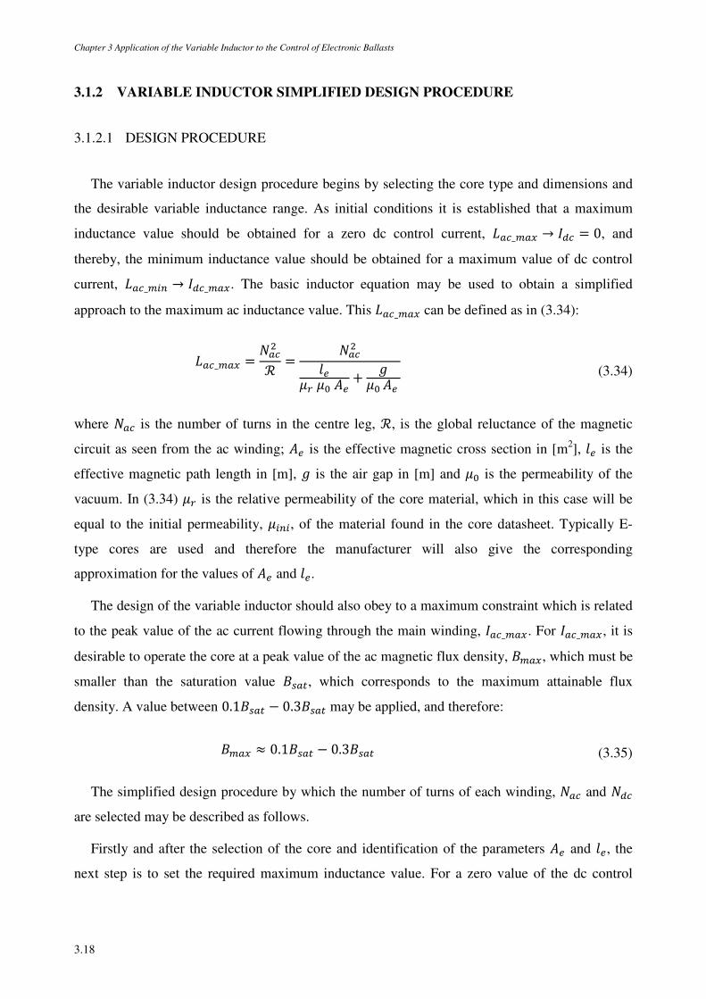
Chapter 3 Application of the Variable Inductor to the Control of Electronic Ballasts
3.18
3.1.2 VARIABLE INDUCTOR SIMPLIFIED DESIGN PROCEDURE
3.1.2.1 DESIGN PROCEDURE
The variable inductor design procedure begins by selecting the core type and dimensions and
the desirable variable inductance range. As initial conditions it is established that a maximum
inductance value should be obtained for a zero dc control current, ¯~_~Ï → / = 0, and
thereby, the minimum inductance value should be obtained for a maximum value of dc control
current, ¯~_±² → /_~Ï. The basic inductor equation may be used to obtain a simplified
approach to the maximum ac inductance value. This ¯~_~Ï can be defined as in (3.34):
¯~_~Ï = Á~ℛ = Á~
3µ2µ3 + õµ3
(3.34)
where Á~ is the number of turns in the centre leg, ℛ, is the global reluctance of the magnetic
circuit as seen from the ac winding; 3 is the effective magnetic cross section in [m2], 3 is the
effective magnetic path length in [m], õ is the air gap in [m] and µ is the permeability of the
vacuum. In (3.34) µ2 is the relative permeability of the core material, which in this case will be
equal to the initial permeability, µ±²±, of the material found in the core datasheet. Typically E-
type cores are used and therefore the manufacturer will also give the corresponding
approximation for the values of 3 and 3.
The design of the variable inductor should also obey to a maximum constraint which is related
to the peak value of the ac current flowing through the main winding, /~_~Ï. For /~_~Ï, it is
desirable to operate the core at a peak value of the ac magnetic flux density, ~Ï, which must be
smaller than the saturation value 4~À, which corresponds to the maximum attainable flux
density. A value between 0.14~À − 0.34~À may be applied, and therefore:
~Ï ≈ 0.14~À − 0.34~À (3.35)
The simplified design procedure by which the number of turns of each winding, Á~ and Á
are selected may be described as follows.
Firstly and after the selection of the core and identification of the parameters 3 and 3, the
next step is to set the required maximum inductance value. For a zero value of the dc control
Chapter 3 Application of the Variable Inductor to the Control of Electronic Ballasts
3.19
current, / = 0, the peak value of the ac magnetic flux density can be calculated, using the peak
value of the ac current, /~_~Ï, as follows:
~Ï = Á~ℛ3 /~_~Ï (3.36)
This implies that by using the condition established in (3.35) and the value previously set for
¯~_~Ï, (3.36) may be re-written as:
Á~ = ¯~_~Ï/~_~Ï~Ï3 (3.37)
This will immediately give the number of turns for the main ac winding. The air gap may then be
calculated as:
õ = µÁ~ 3¯~_~Ï − 3µ2 (3.38)
The diameter, ~, of the wire for the main winding may be selected using (3.39)
~ = ö4/~_~ϸ÷ (3.39)
where ÷ is the selected current density in [A/m2]. The diameter, , of the wire for the control
winding may be selected using (3.40)
= ö4/¸÷ (3.40)
The total winding occupation area will be given by the ac and dc winding occupation, ø, and
may be determined as follows:
ø = Á~¸ ~2 +Á¸ 2 (3.41)
The area available for the winding conductors may be defined as ù³úû, where úû is the core
window area and ù³ is the window utilization factor or fill factor. For variable inductors based on
Chapter 3 Application of the Variable Inductor to the Control of Electronic Ballasts
3.20
double-E cores, úû is considered as the area on one of the sides. In order to fit the windings into
the core window the following constraint must be obeyed:
ù³úû ≥ ø (3.42)
A typical value for the fill factor is ù³ = 0.2 − 0.3 [3.21].
Finally, the number of turns of each control winding, Á must be estimated. This estimation
is done considering that the external path of the EF25 core must reach saturation, for a stipulated
maximum value of the dc control current. Taking this into consideration leads to:
£ℛ3ÏÀ = 2Á/_~Ï (3.43)
where ℛ3ÏÀ is the reluctance of the external path of the core, which means the core without the
centre leg. /_~Ï is the maximum value of the dc control current, for which the minimum
inductance value is obtained. Equation (3.43) may be re-written as follows:
Á = 12 ©4~À3ÏÀµÊÕ¨ýµ/_~Ï (3.44)
where 3ÏÀ is the length of the external path of the core, ©4~À is the flux density in the external
path due to /_~Ï, for a zero ac current, and µÊÕ¨ý is the permeability of the core material in the
above mentioned conditions. For /_~Ï the core is expected to be near saturation, therefore the
permeability value should be in fact the permeability of the core at that point. The value of ©
from experimental observation at the laboratory should be around 80%.
The preceding equations represent a brief summary of the magnetic regulator design method.
This is in fact a simplified and approximate method. It is clear that the eventual core losses were
not considered during this design procedure. These losses will also depend on the level of the dc
control current.
3.1.2.2 DESIGN EXAMPLE
In this section the design procedure exposed previously will be illustrated by designing a
variable inductor prototype with a EF25 core. The core characteristics and dimensions are
presented in Fig. 3.11. The required values are available in the selected core datasheet.
Chapter 3 Application of the Variable Inductor to the Control of Electronic Ballasts
3.21
The variable inductor design begins by establishing the maximum inductance value, for
instance, ¯~_~Ï = 1mH. A maximum ac current level must also be defined: /~_~Ï = 0.6A.
This is considered an acceptable value considering the future applications of the prototype. The
maximum value for the control current is set at / = 1A and the maximum attainable flux
density at 4~À = 0.5T. Considering ~Ï = 0.24~À, which is within the limits defined in (3.35),
3 = 52 ∙ 10ºÙm, and using (3.37) it is possible to determine the number of ac turns, which
gives Á~ ≈ 115 turns.
Fig. 3.11. EF25 core: dimensions and main characteristics.
The number of turns in each dc control winding is determined using (3.44). For 0.84~À, µÊÕ¨ý is lower than the initial permeability of the core. For the selected core material
µ.ÚÕ¨ý=1800 approximately and µ = 4¸ ∙ 10º». With 3ÏÀ = 100mm and / = 1A, this gives
Á ≈ 35 turns.
After knowing the number of turns of the control and ac windings it is necessary to determine
the appropriate wire diameter and the window area occupation ø. With ÷ = 4A/m, ~ and
can be determined using (3.39) and (3.40) respectively. The window area occupation can
then be calculated through (3.41). Knowing that for this double E core, ø = 87mm, the fill
factor can be determined trough the condition defined in (3.42), giving ù³ ≈ 0.3. The next step is the calculation of the air gap through (3.38), where 3 = 58mm, which gives
õ ≈ 0.9mm. An overview of several core datasheets showed that this value was typically too
high for the available commercial cores. Thus, it was decided to use a more acceptable value, and
the airgap was set at õ = 0.3mm. It was then necessary to recalculate the number of turns in the
ac winding, again through (3.38), which resulted in Á~ ≈ 68 turns. With this new number of
turns the maximum magnetic flux density in the core was estimated to be within acceptable
limits. The fill factor was recalculated as ù³ ≈ 0.22 which was also considered as a more
acceptable value.
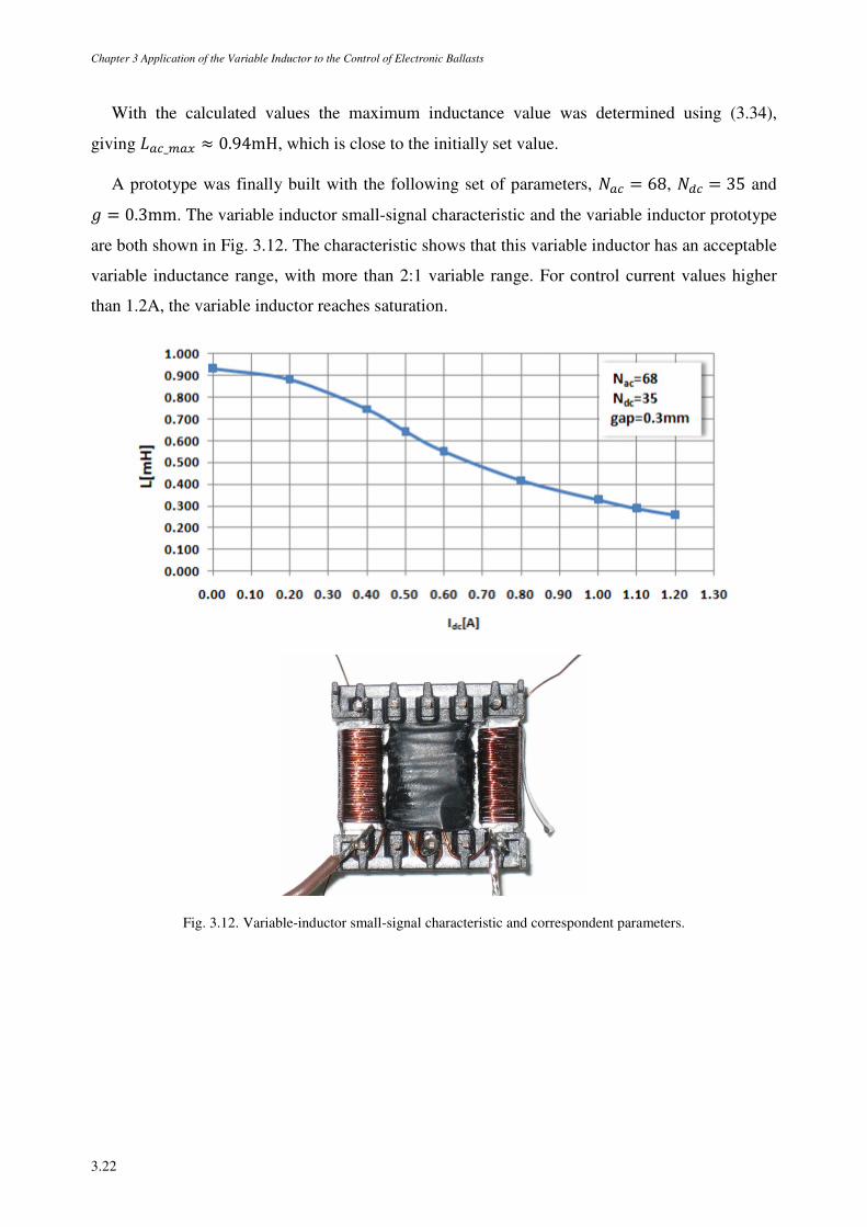
Chapter 3 Application of the Variable Inductor to the Control of Electronic Ballasts
3.22
With the calculated values the maximum inductance value was determined using (3.34),
giving ¯~_~Ï ≈ 0.94mH, which is close to the initially set value.
A prototype was finally built with the following set of parameters, Á~ = 68, Á = 35 and
õ = 0.3mm. The variable inductor small-signal characteristic and the variable inductor prototype
are both shown in Fig. 3.12. The characteristic shows that this variable inductor has an acceptable
variable inductance range, with more than 2:1 variable range. For control current values higher
than 1.2A, the variable inductor reaches saturation.
Fig. 3.12. Variable-inductor small-signal characteristic and correspondent parameters.
Chapter 3 Application of the Variable Inductor to the Control of Electronic Ballasts
3.23
3.2 VARIABLE INDUCTORS APPLIED TO DIMMABLE ELECTRONIC
BALLASTS
3.2.1 INTRODUCTION TO THE PROPOSED MAGNETIC CONTROL TECHNIQUE
3.2.1.1 HALF-BRIDGE RESONANT BALLAST
The voltage-source half-bridge inverter connected to a parallel-loaded resonant circuit is the
most common topology used as high-frequency inverter for electronic ballasts. This topology,
presented in Fig. 3.13a. guarantees proper ignition and safe lamp operation [3.1].
The operation of this type of ballast circuit may be described as follows: two bi-directional
switches and a dc voltage source, >, provide a square-wave voltage source that drives the
resonant circuit formed by ¯, and the fluorescent lamp. The load or the fluorescent lamp is
connected in parallel with the resonant capacitor, . Typically, the circuit is operated above
resonance. In this case, the bi-directional switches can simply be replaced by pn junction
MOSFETs, ½ª and ½, as shown in Fig. 3.13a., which already have intrinsic anti-parallel diodes,
®ª and ®. ½ª and ½ are driven by rectangular-wave voltages, Kª and K and are
alternately turned ON and OFF at the inverter switching frequency, 4. The duty-cycle, D, should
be slightly less than 50% to avoid cross conduction through the switches, due to the turn-off
delay. In Fig. 3.13a., ´ is a dc-blocking capacitor which prevents the dc current flow through the
lamp. The average voltage across ´ is equal to > 2⁄ . This capacitor can be connected either in
series with ¯, or in series with the lamp. It is also possible to include a transformer (or as it will
be further proposed, a variable transformer) in parallel with the lamp and . In this case the dc-
blocking capacitor must be placed in series with the resonant inductor, ¯. The resonant capacitor
may be located either on the primary or the secondary of the transformer. If placed on the
secondary the leakage inductance of the transformer is absorbed by the resonant inductance.
These aspects will be further discussed.
Typically, if the load or the lamp high-frequency equivalent resistance is much higher than the
reactance of the resonant capacitor, the current through the resonant inductor, ¯, and the switches,
½ª and ½, is almost independent of the load. If the load resistance increases, the voltage across
the resonant capacitor and the load also increases, causing the output power to increase. Fig.
3.13b. shows the typical operating waveforms for a constant load resistance, v, considering an
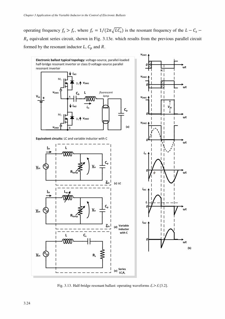
Chapter 3 Application of the Variable Inductor to the Control of Electronic Ballasts
3.24
operating frequency 4 > 2, where 2 = 1 (2¸¯4)⁄ is the resonant frequency of the ¯ − 4 −v4 equivalent series circuit, shown in Fig. 3.13e. which results from the previous parallel circuit
formed by the resonant inductor¯, and v.
vGM1
vGM2
vDM1
vDM2
iin
iM1
iM2
0
0
0
0
0
0
0
ωt
ωt
ωt
ωt
ωt
ωt
ωt
π
Vdc
Il
L
(c)
Rlamp
Vin
Cp
LC
Lac
(d)
Rlamp
Cp
Zin Variable
inductor
with C
Vdc
M1
M2
A
B
D1
D2
L fluorescent
lamp
Cp
(a)
iM1
iM2
vDM1
vDM2
vGM1
vGM2
iin
Electronic ballast typical topology: voltage-source, parallel-loaded
half-bridge resonant inverter or class D voltage-source parallel
resonant inverter
Equivalent circuits: LC and variable inductor with C
(b)
Cb
Zin
Vin
Vo
Vo
Iin
Iin
(e)Series
LCsRs
CsL
RsVin
Fig. 3.13. Half-bridge resonant ballast: operating waveforms fs > fr [3.2].
Chapter 3 Application of the Variable Inductor to the Control of Electronic Ballasts
3.25
The voltages across diodes ®ª and ®, K0ª and K0 and the currents through the switches
½ª and ½, Lª and L are presented in Fig. 3.13b.
The input voltage of the resonant circuit, K±², after the dc-blocking capacitor, is also a square-
wave, similar to K0, but with a zero dc average. Using the Fourier series this voltage can be
defined as follows:
K±² = É √2>±²,² sin =²¥ª,,...
É4 > 2¤
¸ sin²¥ª,,...
(3.45)
where >±²,² corresponds to the rms value of each harmonic.
For a constant dc input voltage, >, as long as the quality factor of the resonant circuit, Ð, is
sufficiently high (typically Ð > 2.5, the current through the resonant circuit, L±², also
represented in Fig. 3.13b. will be nearly sinusoidal. This implies that the fundamental component
of K±² will be dominant in the circuit. So, in the following circuit analysis only its fundamental
component, >±², with = 1, will be considered:
â>±²â = >±²,ª = >±² = 4> 2¤
¸ 1√2 = √2 > (3.46)
Considering the fundamental approximation, Fig. 3.13c. presents the equivalent half-bridge
inverter circuit, considering the power-dependant lamp resistance in series with ¯. Finally, Fig.
3.13d. presents the equivalent circuit considering the proposed magnetic control technique, where
the resonant inductance is replaced by the variable inductor. The presence of the variable inductor
results in the variable behaviour of the resonant circuit with an obvious impact on the power
delivered to the lamp.
The final remark is related to the turn-on and turn-off transitions of the switches and the range
of dead-time indicated by the shadow areas in Fig. 3.13b. The resonant current L±² is conducted
alternately by ½ª and ½. In Fig. 3.13b. £ represents the phase angle of the resonant current
relative to K±², and the resonant frequency, 2, is defined as the frequency at which the phase shift
is zero.
If the inverter is operated at an operating frequency 4 > 2, the phase angle of the resonant
current would be £ < 0. In this case the resonant circuit represents an inductive load and the
Chapter 3 Application of the Variable Inductor to the Control of Electronic Ballasts
3.26
current L±² lags the fundamental component of the voltage K±². Each MOSFET is switched OFF
when its current is positive but most importantly it is switched ON when its current is negative
and flows through its anti-parallel diode. In these conditions the switch begins to conduct at near
zero voltage, due to the conducting diode, which guarantees ZVS and negligible losses during the
turn-on transitions. On the contrary, if the inverter is eventually operated at an operating
frequency 4 < 2, the phase angle of the resonant current would be £ > 0 , in this case the
resonant circuit would behave as a capacitive load and the resonant current would lead the
fundamental component of the voltage K±². Operation below resonance is not recommended since
the anti-parallel diodes turn OFF at high L ¤ , causing high current spikes in the switches which
reduces efficiency and reliability [3.2].
3.2.1.2 HALF-BRIDGE RESONANT BALLAST ANALYSIS
In order to proceed with the theoretical analysis of the proposed dimming method, it is
relevant to describe the basic parameters and equations which characterize the general behaviour
of the parallel-loaded half-bridge inverter. Therefore, considering the equivalent circuit in Fig.
3.13c. the following parameters and equations are established.
The natural frequency, Ô:
Ô = 1¯ (3.47)
The base impedance or characteristic impedance, ´:
´ = ö (3.48)
The load quality factor at the natural frequency, Ð:
Ð = v~´ (3.49)
The resonant frequency that forms the boundary between capacitive and inductive loads, 2
2 = 1¯4 (3.50)
The load quality factor at the resonant frequency, Ð2:
Chapter 3 Application of the Variable Inductor to the Control of Electronic Ballasts
3.27
Ð2 = 2¯v4 (3.51)
Once again, ¯, 4 and v4 represent the equivalent series circuit which results from the parallel
circuit formed by the resonant inductor ¯, and v.
The input impedance of the resonant circuit is
±² = ¯ + v~ 1v~ + 1 (3.52)
If both real and imaginary parts are isolated, (3.52) can be rewritten:
±² = v~¾v~¿ + 1 + ¯ − v~ ¾v~¿ + 1 (3.53)
Finally, the phase angle of the resonant current can be defined as:
£±² = wõ 1±² ∙ 180¸ (3.54)
As referred, the resonant frequency, 2, is defined as the frequency at which the phase shift is
zero. Hence the ratio of the resonant frequency, 2, to the natural frequency, Ô is:
2Ô = ö1 − 1Ð m Ð ≥ 1 (3.55)
From (3.55) the following conclusions are drawn:
For Ð ≤ 1, the resonant frequency does not exist and the resonant circuit represents an
inductive load at any switching frequency
For Ð > 1, the ratio 2 Ô¤ increases with Ð. If the switching frequency 4 > 2 the
resonant circuit behaves as an inductive load and the resonant current lags the inverter
output voltage. This is obviously the desirable operating condition since ZVS is
guaranteed. If 4 < 2 the circuit behaves as a capacitive load and ZVS is lost.
Ð and Ð2 are related by the following equation, [3.2]:
Chapter 3 Application of the Variable Inductor to the Control of Electronic Ballasts
3.28
Ð2 = Ð 2Ô = Ð − 1 m Ð ≥ 1 (3.56)
This implies that if Ð ≫ 1 then Ð2 ≈ Ð.
The voltage gain of the circuit or the voltage transfer function can be defined, applying the
voltage divider rule, as:
= >Ô>±² =v~ 1v~ + 1
¯ + v~ 1v~ + 1= 1
1 − ¯ + ¯v~ (3.57)
(3.57) can be re-written:
= 11 − Ô + 1Ð Ô
(3.58)
The absolute value of the voltage gain can be defined as:
ââ = 1ö1 − ¯ + ¯v~ = 1
ö1 − Ô + 1Ð Ô
(3.59)
From (3.59) it can be observed that ââ = Ð when 4 Ô¤ = 1 and that
ââ → 11 − Ô w Ð → ∞
(3.60)
This implies that with an open circuit at the output, ââ increases from 1 to ∞ as 4 Ô¤ or
4 Ô¤ is increased from 0 to 1, and ââ decreases from ∞ to 0 as 4 Ô¤ increases from 1 to
∞.
The rms value of the output voltage can be obtained by:
Chapter 3 Application of the Variable Inductor to the Control of Electronic Ballasts
3.29
>Ô = >±² 1ö1 − ¯ + ¯v~
(3.61)
And the rms value of the output current by:
/Ô = >Ôv~ (3.62)
This implies that if the circuit is operated at 4 Ô¤ = 1, (3.62) can be re-written:
/Ô = >Ôv~ = >±²Ðv~ = >±²´ (3.63)
And the circuit will behave as a current source, and its value depends exclusively of the input
voltage and ´.
Finally, the output power can be easily obtained by:
tÔ = >Ôv~ (3.64)
Some of the previous conclusions and observations are the reason why this specific circuit is
typically adopted in electronic ballasts. Fig. 3.14 shows the frequency-response characteristic of
the resonant circuit as well as the commonly used soft-start technique. The frequency response
clearly shows that, around the natural frequency, a high voltage gain is obtained for a load high-
resistive value. If the load resistance value decreases, the voltage gain also decreases [2.43], [3.3].
The electrodes pre-heating process is guaranteed by means of a frequency-controlled soft-start
technique. As a first step, the operating frequency is adjusted to a value higher than the natural
frequency of the circuit. Prior to ignition, the lamp will exhibit an almost infinite impedance,
which can be translated into a high Ð, and the resonant current will flow through , heating the
electrodes. After a short period of time, the operating frequency is slightly reduced and the
resonant circuit will be able to generate the necessary high voltage spike for the lamp ignition. As
the lamp is ignited, the value of Ð drops, since the load reaches the nominal lamp resistance
value and the circuit is then capable of limiting the lamp current without any further change on
the operating frequency. This technique can be followed through points A, B and C, as
represented in Fig. 3.14.
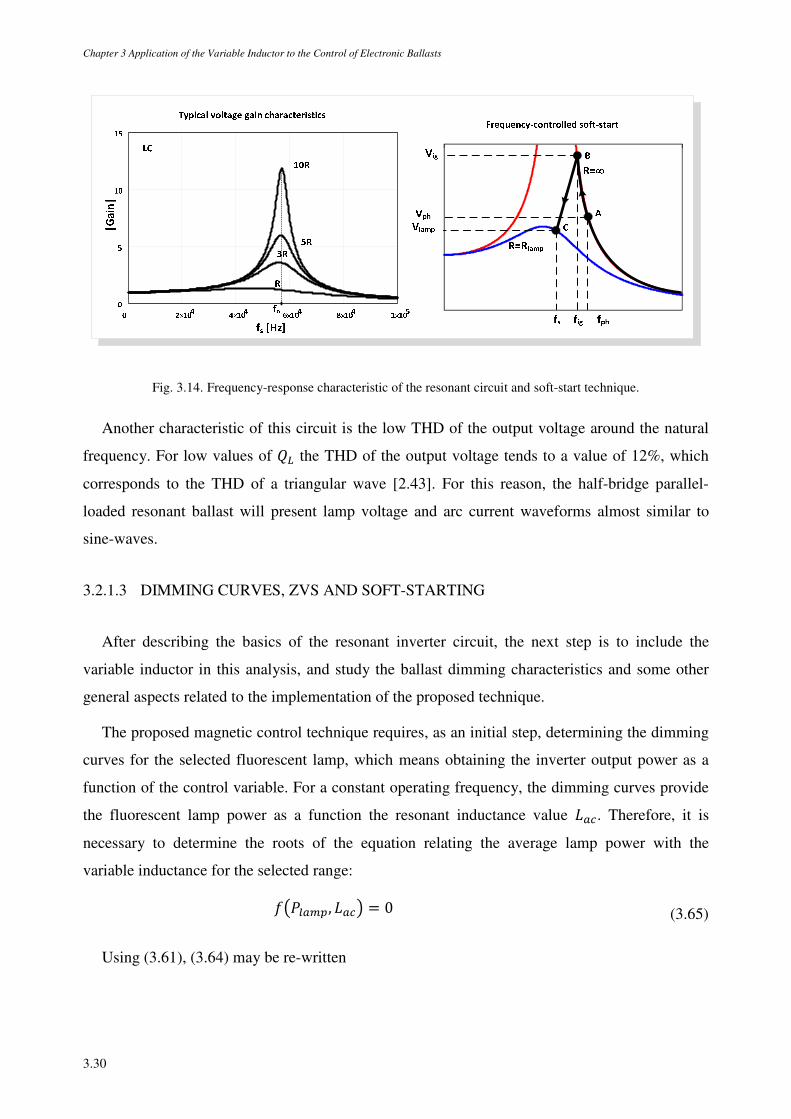
Chapter 3 Application of the Variable Inductor to the Control of Electronic Ballasts
3.30
Fig. 3.14. Frequency-response characteristic of the resonant circuit and soft-start technique.
Another characteristic of this circuit is the low THD of the output voltage around the natural
frequency. For low values of Ð the THD of the output voltage tends to a value of 12%, which
corresponds to the THD of a triangular wave [2.43]. For this reason, the half-bridge parallel-
loaded resonant ballast will present lamp voltage and arc current waveforms almost similar to
sine-waves.
3.2.1.3 DIMMING CURVES, ZVS AND SOFT-STARTING
After describing the basics of the resonant inverter circuit, the next step is to include the
variable inductor in this analysis, and study the ballast dimming characteristics and some other
general aspects related to the implementation of the proposed technique.
The proposed magnetic control technique requires, as an initial step, determining the dimming
curves for the selected fluorescent lamp, which means obtaining the inverter output power as a
function of the control variable. For a constant operating frequency, the dimming curves provide
the fluorescent lamp power as a function the resonant inductance value ¯~. Therefore, it is
necessary to determine the roots of the equation relating the average lamp power with the
variable inductance for the selected range:
¾t~, ¯~¿ = 0 (3.65)
Using (3.61), (3.64) may be re-written
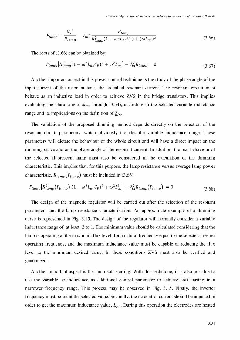
Chapter 3 Application of the Variable Inductor to the Control of Electronic Ballasts
3.31
t~ = >Ôv~ = >±² v~v~ 1 − ¯~ + ¯~ (3.66)
The roots of (3.66) can be obtained by:
t~v~ 1 − ¯~ + ¯~ − >±² v~ = 0 (3.67)
Another important aspect in this power control technique is the study of the phase angle of the
input current of the resonant tank, the so-called resonant current. The resonant circuit must
behave as an inductive load in order to achieve ZVS in the bridge transistors. This implies
evaluating the phase angle, £±², through (3.54), according to the selected variable inductance
range and its implications on the definition of ±².
The validation of the proposed dimming method depends directly on the selection of the
resonant circuit parameters, which obviously includes the variable inductance range. These
parameters will dictate the behaviour of the whole circuit and will have a direct impact on the
dimming curve and on the phase angle of the resonant current. In addition, the real behaviour of
the selected fluorescent lamp must also be considered in the calculation of the dimming
characteristic. This implies that, for this purpose, the lamp resistance versus average lamp power
characteristic, v~¾t~¿ must be included in (3.66):
t~v~ ¾t~¿ 1 − ¯~ + ¯~ − >±² v~¾t~¿ = 0 (3.68)
The design of the magnetic regulator will be carried out after the selection of the resonant
parameters and the lamp resistance characterization. An approximate example of a dimming
curve is represented in Fig. 3.15. The design of the regulator will normally consider a variable
inductance range of, at least, 2 to 1. The minimum value should be calculated considering that the
lamp is operating at the maximum flux level, for a natural frequency equal to the selected inverter
operating frequency, and the maximum inductance value must be capable of reducing the flux
level to the minimum desired value. In these conditions ZVS must also be verified and
guaranteed.
Another important aspect is the lamp soft-starting. With this technique, it is also possible to
use the variable ac inductance as additional control parameter to achieve soft-starting in a
narrower frequency range. This process may be observed in Fig. 3.15. Firstly, the inverter
frequency must be set at the selected value. Secondly, the dc control current should be adjusted in
order to get the maximum inductance value, ¯°. During this operation the electrodes are heated
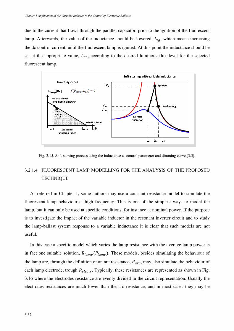
Chapter 3 Application of the Variable Inductor to the Control of Electronic Ballasts
3.32
due to the current that flows through the parallel capacitor, prior to the ignition of the fluorescent
lamp. Afterwards, the value of the inductance should be lowered, ¯±, which means increasing
the dc control current, until the fluorescent lamp is ignited. At this point the inductance should be
set at the appropriate value, ¯~, according to the desired luminous flux level for the selected
fluorescent lamp.
Fig. 3.15. Soft-starting process using the inductance as control parameter and dimming curve [3.5].
3.2.1.4 FLUORESCENT LAMP MODELLING FOR THE ANALYSIS OF THE PROPOSED
TECHNIQUE
As referred in Chapter 1, some authors may use a constant resistance model to simulate the
fluorescent-lamp behaviour at high frequency. This is one of the simplest ways to model the
lamp, but it can only be used at specific conditions, for instance at nominal power. If the purpose
is to investigate the impact of the variable inductor in the resonant inverter circuit and to study
the lamp-ballast system response to a variable inductance it is clear that such models are not
useful.
In this case a specific model which varies the lamp resistance with the average lamp power is
in fact one suitable solution, v~t~. These models, besides simulating the behaviour of
the lamp arc, through the definition of an arc resistance, v~2, may also simulate the behaviour of
each lamp electrode, trough v33À2. Typically, these resistances are represented as shown in Fig.
3.16 where the electrodes resistance are evenly divided in the circuit representation. Usually the
electrodes resistances are much lower than the arc resistance, and in most cases they may be
Chapter 3 Application of the Variable Inductor to the Control of Electronic Ballasts
3.33
neglected. Throughout this analysis, their influence will be neglected which implies considering
v~ ≈ v~2, in the following presentation, and therefore t~ ≈ t~2.
a. Complete model including electrodes effect b. Simplified model
Fig. 3.16. Lamp resistance models
As in classical approaches, the basic idea is to experimentally test the selected fluorescent
lamps and obtain their power-dependent model, in order to evaluate the possibilities of this
control method. The experimental work was carried out using several frequency-controlled
commercial ballasts. Several lamps were selected and tested, standard T8 fluorescent lamps as
well as the more efficient T5 fluorescent lamps. Initial theoretical and experimental analyses were
performed considering T8 lamps. However, more recently, additional tests and verifications were
done considering T5 lamps. A more detailed description of the collected data for these T5 lamps
can be observed in Appendix A.
As an example, some of the collected data will be presented. Typically for each lamp type, the
data are quite similar and independent of the elected manufacturer. Initially a T8 fluorescent lamp
was chosen, the TLD 36W from Philips. The lamp was tested at high frequency, using a standard
frequency-controlled electronic ballast, 1-10V DC dimming interface. As previously mentioned,
for this type of ballast different operating frequencies will correspond to different levels of
average lamp power. For each level, the rms values of the lamp voltage and arc or discharge
current were measured. Instead of measuring the lamp power, the average arc power was only
measured. This average arc power is easily measured multiplying the instantaneous lamp voltage
by the instantaneous discharge current and then applying a dc average function. The measured
data were then processed and analyzed in Mathcad as shown in Fig. 3.17.
Fig. 3.17a. presents the >~/~2 rms characteristics of the lamp. Fig. 3.17b and Fig. 3.17c.
present the rms values of the lamp voltage and discharge current for different values of the
average arc power and corresponding curve fitting. Neglecting the electrodes, the arc equivalent
resistance, v~2, or the power dependent lamp resistance, v~t~2, may be computed,
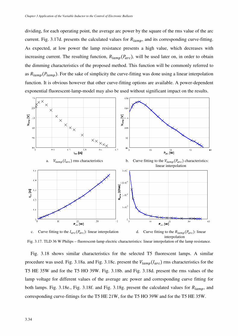
Chapter 3 Application of the Variable Inductor to the Control of Electronic Ballasts
3.34
dividing, for each operating point, the average arc power by the square of the rms value of the arc
current. Fig. 3.17d. presents the calculated values for v~, and its corresponding curve-fitting.
As expected, at low power the lamp resistance presents a high value, which decreases with
increasing current. The resulting function, v~t~2, will be used later on, in order to obtain
the dimming characteristics of the proposed method. This function will be commonly referred to
as v~t~. For the sake of simplicity the curve-fitting was done using a linear interpolation
function. It is obvious however that other curve-fitting options are available. A power-dependent
exponential fluorescent-lamp-model may also be used without significant impact on the results.
a. >~/~2 rms characteristics b. Curve fitting to the >~t~2 characteristics: linear interpolation
c. Curve fitting to the /~2t~2: linear interpolation d. Curve fitting to the v~t~2: linear interpolation
Fig. 3.17. TLD 36 W Philips – fluorescent-lamp electric characteristics: linear interpolation of the lamp resistance.
Fig. 3.18 shows similar characteristics for the selected T5 fluorescent lamps. A similar
procedure was used. Fig. 3.18a. and Fig. 3.18c. present the >~/~2 rms characteristics for the
T5 HE 35W and for the T5 HO 39W. Fig. 3.18b. and Fig. 3.18d. present the rms values of the
lamp voltage for different values of the average arc power and corresponding curve fitting for
both lamps. Fig. 3.18e., Fig. 3.18f. and Fig. 3.18g. present the calculated values for v~, and
corresponding curve-fittings for the T5 HE 21W, for the T5 HO 39W and for the T5 HE 35W.
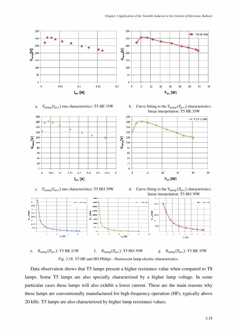
Chapter 3 Application of the Variable Inductor to the Control of Electronic Ballasts
3.35
a. >~/~2 rms characteristics: T5 HE 35W b. Curve fitting to the >~t~2 characteristics: linear interpolation: T5 HE 35W
c. >~/~2 rms characteristics: T5 HO 39W d. Curve fitting to the >~t~2 characteristics: linear interpolation: T5 HO 39W
e. v~t~2: T5 HE 21W f. v~t~2: T5 HO 39W g. v~t~2: T5 HE 35W
Fig. 3.18. T5 HE and HO Philips - fluorescent lamp electric characteristics.
Data observation shows that T5 lamps present a higher resistance value when compared to T8
lamps. Some T5 lamps are also specially characterized by a higher lamp voltage. In some
particular cases these lamps will also exhibit a lower current. These are the main reasons why
these lamps are conventionally manufactured for high-frequency operation (HF), typically above
20 kHz. T5 lamps are also characterized by higher lamp resistance values.
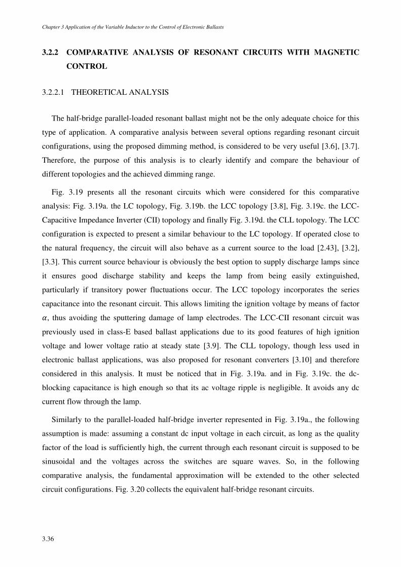
Chapter 3 Application of the Variable Inductor to the Control of Electronic Ballasts
3.36
3.2.2 COMPARATIVE ANALYSIS OF RESONANT CIRCUITS WITH MAGNETIC
CONTROL
3.2.2.1 THEORETICAL ANALYSIS
The half-bridge parallel-loaded resonant ballast might not be the only adequate choice for this
type of application. A comparative analysis between several options regarding resonant circuit
configurations, using the proposed dimming method, is considered to be very useful [3.6], [3.7].
Therefore, the purpose of this analysis is to clearly identify and compare the behaviour of
different topologies and the achieved dimming range.
Fig. 3.19 presents all the resonant circuits which were considered for this comparative
analysis: Fig. 3.19a. the LC topology, Fig. 3.19b. the LCC topology [3.8], Fig. 3.19c. the LCC-
Capacitive Impedance Inverter (CII) topology and finally Fig. 3.19d. the CLL topology. The LCC
configuration is expected to present a similar behaviour to the LC topology. If operated close to
the natural frequency, the circuit will also behave as a current source to the load [2.43], [3.2],
[3.3]. This current source behaviour is obviously the best option to supply discharge lamps since
it ensures good discharge stability and keeps the lamp from being easily extinguished,
particularly if transitory power fluctuations occur. The LCC topology incorporates the series
capacitance into the resonant circuit. This allows limiting the ignition voltage by means of factor , thus avoiding the sputtering damage of lamp electrodes. The LCC-CII resonant circuit was
previously used in class-E based ballast applications due to its good features of high ignition
voltage and lower voltage ratio at steady state [3.9]. The CLL topology, though less used in
electronic ballast applications, was also proposed for resonant converters [3.10] and therefore
considered in this analysis. It must be noticed that in Fig. 3.19a. and in Fig. 3.19c. the dc-
blocking capacitance is high enough so that its ac voltage ripple is negligible. It avoids any dc
current flow through the lamp.
Similarly to the parallel-loaded half-bridge inverter represented in Fig. 3.19a., the following
assumption is made: assuming a constant dc input voltage in each circuit, as long as the quality
factor of the load is sufficiently high, the current through each resonant circuit is supposed to be
sinusoidal and the voltages across the switches are square waves. So, in the following
comparative analysis, the fundamental approximation will be extended to the other selected
circuit configurations. Fig. 3.20 collects the equivalent half-bridge resonant circuits.
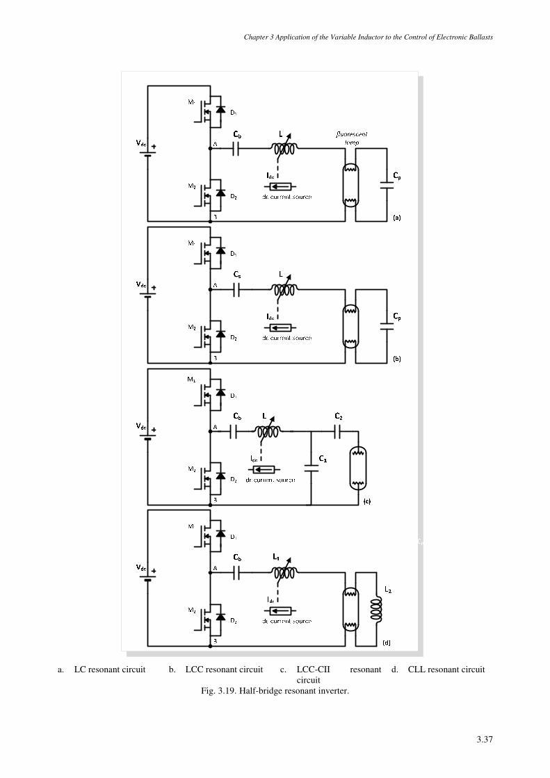
Chapter 3 Application of the Variable Inductor to the Control of Electronic Ballasts
3.37
a. LC resonant circuit b. LCC resonant circuit c. LCC-CII resonant circuit
d. CLL resonant circuit
Fig. 3.19. Half-bridge resonant inverter.
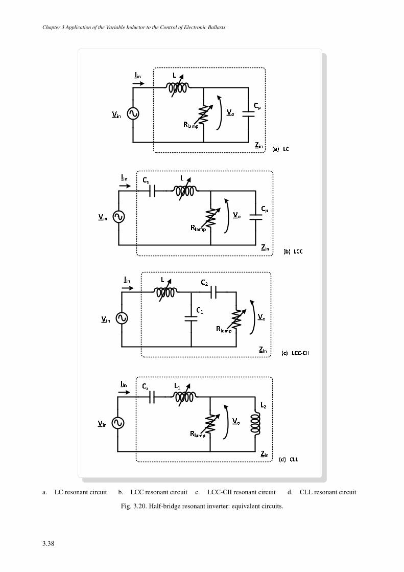
Chapter 3 Application of the Variable Inductor to the Control of Electronic Ballasts
3.38
a. LC resonant circuit b. LCC resonant circuit c. LCC-CII resonant circuit d. CLL resonant circuit
Fig. 3.20. Half-bridge resonant inverter: equivalent circuits.
Chapter 3 Application of the Variable Inductor to the Control of Electronic Ballasts
3.39
The proper design of the electronic ballast depends on the methodology employed for
determining the resonant circuit parameters. For instance, considering the LC topology, from
(3.59), the maximum voltage gain can be approximated by Ð at the natural frequency:
ââ = Ð when 4 Ô¤ = 1. This implies that:
Ð = v~´ = >~>±² ℎ 4 Ô¤ = 1 (3.69)
and (3.69) may be used in order to calculate the base impedance or characteristic impedance, ´.
Subsequently, if the desired operating frequency for the lamp is considered to be equal to the
natural frequency the values for the LC resonant circuit parameters may be calculated, using:
¯ = ´2¸4 w = 12¸´4 Lℎ 4 Ô¤ = 1 (3.70)
A similar procedure will be adopted for all topologies, taking into account each topology
voltage gain at the natural frequency.
LCC resonant circuit configuration:
Assuming the parameter definition in the equivalent circuit of the LCC resonant circuit
configuration, shown in Fig. 3.20b., the following relations and equations are established:
= 4 (3.71)
= 44 + (3.72)
= (3.73)
The natural frequency, Ô is:
Ô = 1√¯ (3.74)
The base impedance or characteristic impedance, ´ is:
Chapter 3 Application of the Variable Inductor to the Control of Electronic Ballasts
3.40
´ = ö (3.75)
The load quality factor at the natural frequency, Ð is:
Ð = v~´ (3.76)
The input impedance of the resonant circuit is:
±² = 1Ë + ¯ + v~ 1v~ + 1 (3.77)
If both real and imaginary parts are isolated, (3.77) can be rewritten:
±² = v~¾v~¿ + 1 + ¯ − 1Ë − v~ ¾v~¿ + 1 (3.78)
Similarly to the LC circuit, the phase angle of the resonant current can also be defined as:
£±² = wõ 1±² ∙ 180¸ (3.79)
As previously referred, the resonant frequency, 2, is defined as the frequency at which the
phase shift is zero. This resonance frequency depends on Ð and A [3.2]. Similar to the LC
configuration, if the switching frequency 4 > 2 the resonant circuit behaves as an inductive load
and the resonant current lags the inverter output voltage. This is obviously the desirable operating
condition since ZVS is guaranteed. If 4 < 2 the circuit behaves as capacitive load and ZVS is
lost.
The voltage gain of the circuit or the voltage transfer function can be defined, applying the
voltage divider rule, as:
= >Ô>±² =v~¾v~¿ + 1 − v~ ¾v~¿ + 1
v~¾v~¿ + 1 + ¯ − 1Ë − v~ ¾v~¿ + 1
(3.80)
(3.80) can be simplified:
Chapter 3 Application of the Variable Inductor to the Control of Electronic Ballasts
3.41
= 11 − ¯ + Ë + 1v~ ¯ − 1Ë
(3.81)
(3.81) can be re-written [3.2]:
= 11 + 1 − Ô + 1Ð Ô − Ô + 1
(3.82)
The absolute value of the voltage gain can be defined as:
ââ = 1ö1 − ¯ + + 1v~ ¯ − 1Ë =
= 1ö1 + 1 − Ô + 1Ð Ô − Ô + 1
(3.83)
The rms value of the output voltage can be obtained by:
>Ô = >±² 1ö1 − ¯ + + 1v~ ¯ − 1Ë
(3.84)
Using (3.71), (3.72) and (3.73), the voltage gain at 4 Ô¤ = 1 can be defined as:
ââ = 1ö 1Ð 1 + 1 = Ð
(3.85)
This implies that if the circuit is operated at 4 Ô¤ = 1, the output current can be defined as:
/Ô = >Ôv~ = ââ>±²v~ = Ð>±²v~ = >±²
(3.86)
And finally, the lamp power can be easily obtained by:
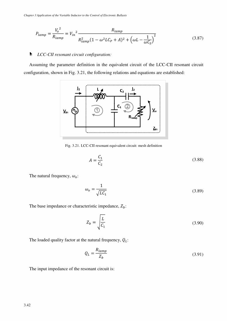
Chapter 3 Application of the Variable Inductor to the Control of Electronic Ballasts
3.42
t~ = >Ôv~ = >±² v~
v~ 1 − ¯ + + ¯ − 1Ë (3.87)
LCC-CII resonant circuit configuration:
Assuming the parameter definition in the equivalent circuit of the LCC-CII resonant circuit
configuration, shown in Fig. 3.21, the following relations and equations are established:
Fig. 3.21. LCC-CII resonant equivalent circuit: mesh definition
= ª (3.88)
The natural frequency, Ô:
Ô = 1¯ª (3.89)
The base impedance or characteristic impedance, ´:
´ = öª (3.90)
The loaded quality factor at the natural frequency, Ð:
Ð = v~´ (3.91)
The input impedance of the resonant circuit is:
Chapter 3 Application of the Variable Inductor to the Control of Electronic Ballasts
3.43
±² = ¯ +1ª v~ + 1
v~ + 1ª + 1 (3.92)
If both real and imaginary parts are isolated, (3.92) can be rewritten:
±² = v~¾v~ª¿ + ª + + ¯ − ª + + v~ª
¾v~ª¿ + ª +
(3.93)
Similarly to the LC circuit, the phase angle of the resonant current can also be defined as:
£±² = wõ 1±² ∙ 180¸ (3.94)
Using Kirchhoff’s laws for mesh 1:
>±² = ¯/ª + 1ª ¾/ª − /¿ = /ª ¯ − 1ª − / 1ª (3.95)
And mesh 2:
0 = / v~ + 1 + 1ª ¾/ − /ª¿= / v~ + 1 + 1ª − 1ª /ª
(3.96)
The output voltage can be obtained by:
>Ô = /v~ (3.97)
From (3.96): /ª/ = ª v~ + 1ª + 1 = ª + 1 + v~ª (3.98)
Using (3.98) in (3.95):
Chapter 3 Application of the Variable Inductor to the Control of Electronic Ballasts
3.44
>±² = /ª ¯ − 1ª − / 1ª == / ª + 1 + v~ª ¯ − 1ª − / 1ª == / ª + 1 + v~ª 1ª − 1ª+ ¯ ª + 1 + v~ª= / ª + v~ª 1ª + ¯ + ¯
(3.99)
If both real and imaginary parts are isolated, (3.99) can be rewritten:
>±²/ = v~1 − ¯ª+ ¯ ª + 1 − 1 (3.100)
Using (3.100), (3.97) can be rewritten:
>Ô = /v~ = v~v~1 − ¯ª+ ¯ ª + 1 − 1>±² (3.101)
The voltage gain of the circuit or the voltage transfer function can then be defined
= >Ô>±² = v~v~1 − ¯ª+ ¯ ª + 1 − 1 == 1
1 − ¯ª + 1v~ ¯ ª + 1 − 1 (3.102)
The absolute value of the voltage gain can be defined as:
ââ = 1ö1 − ¯ª + 1v~ ¯ + 1 − 1
(3.103)
Using (3.88), (3.89) and (3.90), the voltage gain at 4 Ô¤ = 1 can be defined as:
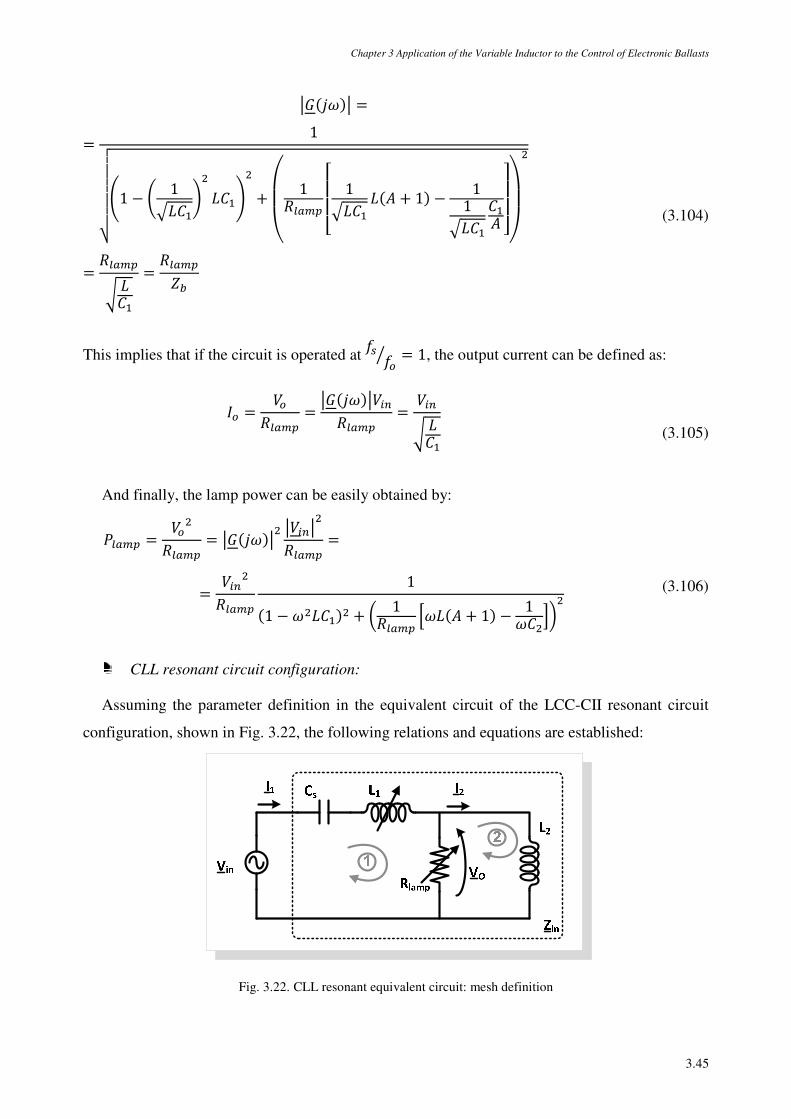
Chapter 3 Application of the Variable Inductor to the Control of Electronic Ballasts
3.45
ââ == 1
1 − 1¯ª ¯ª +
!"# 1v~ $%
%& 1¯ª ¯ + 1 − 11¯ªª '(()*+,
= v~ ª
= v~´ (3.104)
This implies that if the circuit is operated at 4 Ô¤ = 1, the output current can be defined as:
/Ô = >Ôv~ = ââ>±²v~ = >±² ª
(3.105)
And finally, the lamp power can be easily obtained by:
t~ = >Ôv~ = ââ â>±²â
v~ == >±²
v~1
1 − ¯ª + 1v~ ¯ + 1 − 1 (3.106)
CLL resonant circuit configuration:
Assuming the parameter definition in the equivalent circuit of the LCC-CII resonant circuit
configuration, shown in Fig. 3.22, the following relations and equations are established:
Fig. 3.22. CLL resonant equivalent circuit: mesh definition
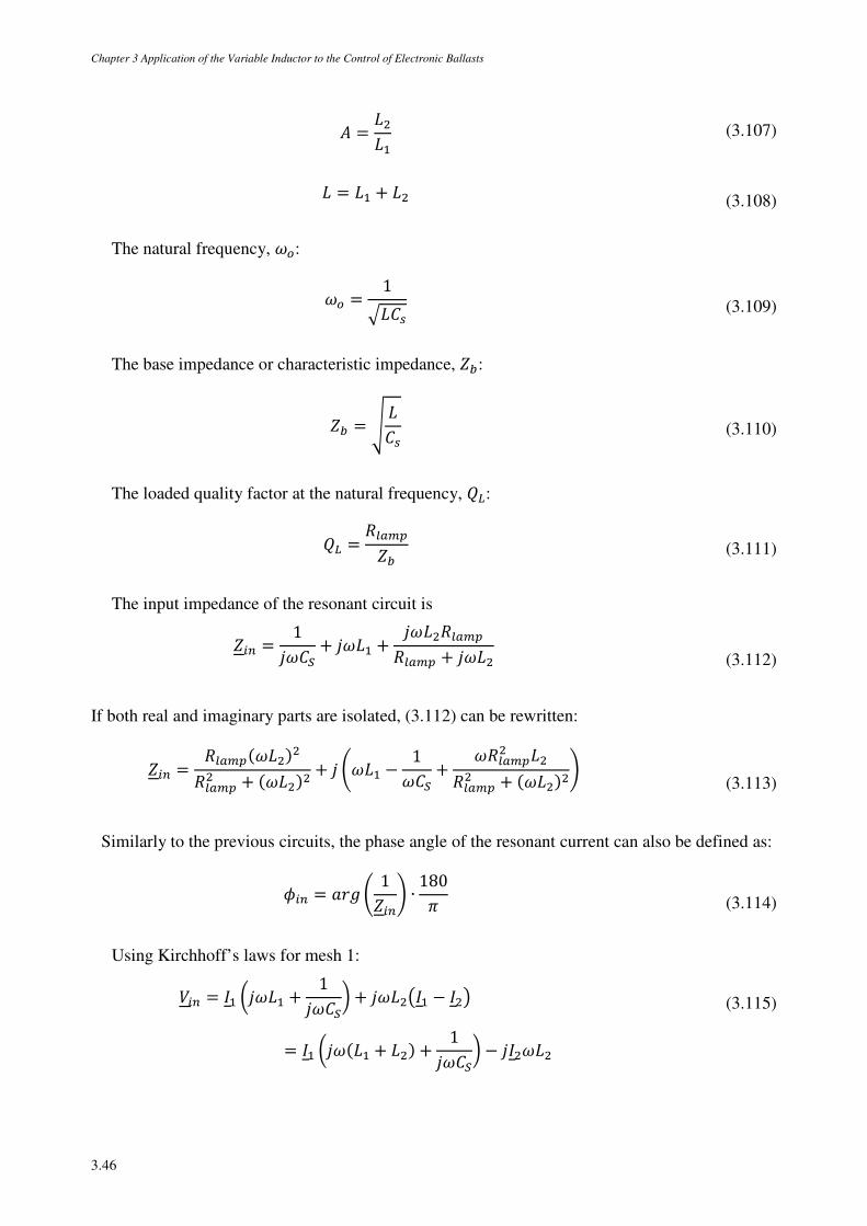
Chapter 3 Application of the Variable Inductor to the Control of Electronic Ballasts
3.46
= ¯¯ª (3.107)
¯ = ¯ª + ¯ (3.108)
The natural frequency, Ô:
Ô = 1¯4 (3.109)
The base impedance or characteristic impedance, ´:
´ = ö4 (3.110)
The loaded quality factor at the natural frequency, Ð:
Ð = v~´ (3.111)
The input impedance of the resonant circuit is
±² = 1Ë + ¯ª + ¯v~v~ + ¯ (3.112)
If both real and imaginary parts are isolated, (3.112) can be rewritten:
±² = v~¯v~ + ¯ + ¯ª − 1Ë + v~ ¯v~ + ¯
(3.113)
Similarly to the previous circuits, the phase angle of the resonant current can also be defined as:
£±² = wõ 1±² ∙ 180¸ (3.114)
Using Kirchhoff’s laws for mesh 1:
>±² = /ª ¯ª + 1Ë + ¯¾/ª − /¿= /ª ¯ª + ¯ + 1Ë − /¯
(3.115)
Chapter 3 Application of the Variable Inductor to the Control of Electronic Ballasts
3.47
And mesh 2:
0 = /v~ + ¯¾/ − /ª¿ (3.116)
The output voltage can be obtained by:
>Ô = /v~ (3.117)
From (3.116): /ª/ = v~ + ¯¯ = 1 − v~¯ (3.118)
Using (3.118) in (3.115)
>±² = / 1 − v~¯ ¯ª + ¯ − 1Ë − ¯ (3.119)
(3.119) can be rewritten:
>±²/ = v~¯ ¯ª + ¯ − 1Ë + ¯ª + ¯ − ¯ − 1Ë (3.120)
If current / is isolated then (3.120) can be rewritten:
/ = >±² 1v~¯ ¯ª + ¯ − 1Ë + ¯ª − 1Ë
(3.121)
Using (3.121), (3.117) can be rewritten:
>Ô = /v~ = >±² v~v~¯ ¯ª + ¯ − 1Ë + ¯ª − 1Ë (3.122)
The voltage gain of the circuit or the voltage transfer function can then be defined
= >Ô>±² = v~v~ 1 + ¯ª¯ − 1¯Ë + ¯ª − 1Ë (3.123)
The absolute value of the voltage gain can be defined as:
Chapter 3 Application of the Variable Inductor to the Control of Electronic Ballasts
3.48
ââ = 1ö1 + ¯ª¯ − 1¯Ë + 1v~ ¯ª − 1Ë
(3.124)
Using (3.107), (3.108), (3.109) and (3.110), the voltage gain at 4 Ô¤ = 1 can be defined as:
ââ = 1
!"#1 + − 1
1¯4 ¯Ë*+,
+ 1v~ $%
%& ¯ª¯4 − 11¯4 Ë'(()
= v~¯Ë¯ = 1 + v~Ë´¯ (3.125)
This implies that if the circuit is operated at 4 Ô¤ = 1, the output current can be defined as:
/Ô = >Ôv~ = ââ>±²v~ = 1 + Ë 4 >±²¯ (3.126)
And finally, the lamp power can be easily obtained by:
t~ = >Ôv~ = ââ â>±²â
v~ == >±²
v~1
1 + ¯ª¯ − 1¯Ë + 1v~ ¯ª − 1Ë (3.127)
Table 3.1 summarizes some of the key equations regarding each circuit configuration. The
numerical results that follow were obtained considering an input dc voltage, > = 150 V.
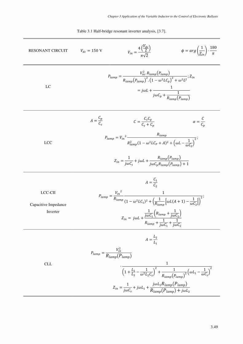
Chapter 3 Application of the Variable Inductor to the Control of Electronic Ballasts
3.49
Table 3.1 Half-bridge resonant inverter analysis, [3.7].
RESONANT CIRCUIT > = 150 V >±² = 4 >2 ¸√2 £ = wõ 1±² ⋅ 180¸
LC
t~ = >±² . v~¾t~¿v~¾t~¿. ¾1 − ¯¿ + ; ±²
= ¯ + 1 + 1v~¾t~¿
LCC
= 4 = 44 + =
t~ = >±² v~v~ 1 − ¯ + + ¯ − 1Ë ;
±² = 14 + ¯ + v~¾t~¿v~¾t~¿ + 1
LCC-CII
Capacitive Impedance
Inverter
= ª
t~ = >±²v~
11 − ¯ª + 1v~ ¯ + 1 − 1 ;
±² = ¯ +1ª v~ + 1
v~ + 1ª + 1
CLL
= ¯¯ª
t~ = >±²vwxy¾twxy¿∙ 1
1 + ¯ª¯ − 1¯4 + 1v~¾t~¿ ¯ª − 14
±² = 14 + ¯ª + ¯vwxy¾twxy¿vwxy¾twxy¿ + ¯
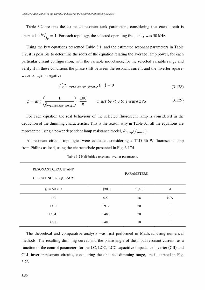
Chapter 3 Application of the Variable Inductor to the Control of Electronic Ballasts
3.50
Table 3.2 presents the estimated resonant tank parameters, considering that each circuit is
operated at 4 Ô¤ = 1. For each topology, the selected operating frequency was 50 kHz.
Using the key equations presented Table 3.1, and the estimated resonant parameters in Table
3.2, it is possible to determine the roots of the equation relating the average lamp power, for each
particular circuit configuration, with the variable inductance, for the selected variable range and
verify if in these conditions the phase shift between the resonant current and the inverter square-
wave voltaje is negative:
¾t~-.,-..,-../.00,.-- , ¯~¿ = 0 (3.128)
£ = wõ 1±²-.,-..,-../.00,.-- ⋅ 180¸ x1 2 < 0 m 1 > (3.129)
For each equation the real behaviour of the selected fluorescent lamp is considered in the
deduction of the dimming characteristic. This is the reason why in Table 3.1 all the equations are
represented using a power dependent lamp resistance model, v~¾t~¿.
All resonant circuits topologies were evaluated considering a TLD 36 W fluorescent lamp
from Philips as load, using the characteristic presented in Fig. 3.17d.
Table 3.2 Half-bridge resonant inverter parameters.
RESONANT CIRCUIT AND
OPERATING FREQUENCY PARAMETERS
4 = 50 kHz ¯ [mH] [nF]
LC 0.5 18 N/A
LCC 0.977 20 1
LCC-CII 0.488 20 1
CLL 0.488 10 1
The theoretical and comparative analysis was first performed in Mathcad using numerical
methods. The resulting dimming curves and the phase angle of the input resonant current, as a
function of the control parameter, for the LC, LCC, LCC capacitive impedance inverter (CII) and
CLL inverter resonant circuits, considering the obtained dimming range, are illustrated in Fig.
3.23.
Chapter 3 Application of the Variable Inductor to the Control of Electronic Ballasts
3.51
a. LC resonant circuit b. LCC resonant circuit c. LCC-CII resonant circuit d. CLL resonant circuit Fig. 3.23. Comparative analysis: theoretical dimming curves and phase angle of the input filter current, as a function of
the variable inductance, at 45 kHz, 50 kHz and 55 kHz.
Chapter 3 Application of the Variable Inductor to the Control of Electronic Ballasts
3.52
For the first three resonant circuits, the obtained dimming curves showed that almost linear
regulation can be obtained with this dimming method. Nevertheless, for higher values of the
switching frequency, and low dimming levels, there is a region with high ât~/¯~â. Therefore, operation in this region is not recommended and can even produce arc instabilities. If
a small ripple in the dc control current exists, the lamp power may oscillate between a maximum
and a minimum level. The small ripple may also appear due to the fact that the non-linearity of
the magnetic material leads to a non-linear coupling between the ac voltage and the control
winding voltage [2.16].
With respect to the phase angle of the resonant current, as can be seen from Fig. 3.23a., Fig.
3.23b. and Fig. 3.23c., the phase angle is negative within the whole dimming range, thus ensuring
the required ZVS operation. Regarding the CLL resonant circuit topology, this theoretical
analysis shows that, even if almost linear regulation is possible, ZVS is not ensured. This can be
clearly identified from the phase angle presented in Fig. 3.23d., which is always positive, for
= 1. For very restricted values of the constant, different from 1, which in turn corresponds to
a very small variation of the magnetic regulator, ZVS is restricted to a very small operating
region. The same analysis was performed considering the possibility of exchange places between
the inductance ¯ and the magnetic regulator, but the results were similar. For this reason this
resonant circuit topology will not be further considered.
3.2.2.2 SIMULATION AND EXPERIMENTAL RESULTS
MATLAB-Simulink implementation:
In spite of the importance of performance comparison, the purpose of this analysis was to
clearly identify the dimming range achieved by each topology, and then confirm these
results by practical implementation of a prototype. However, prior to the experimental
testing a simulation analysis was also made using MATLAB-Simulink tools.
In MATLAB-Simulink, models are hierarchical, so they can be built using both top-down
and bottom-up approaches. The system can be viewed at a high level and then, by double-
clicking the blocks, one can go down to see increasing levels of model detail. After
defining a model, it can be simulated using a menu of integration methods, either from the
Simulink menus or by entering commands in the MATLAB Command Window. Scope
and other display blocks allow seeing the simulation results while the simulation is
Chapter 3 Application of the Variable Inductor to the Control of Electronic Ballasts
3.53
running. The simulation results can also be put in the MATLAB workspace for post
processing and visualization.
The schematic of the electronic ballast circuit, for the LCC-CII topology, is presented in
Fig. 3.24. In Fig. 3.24a. the Scope block displays its inputs with respect to simulation
time. It displays the lamp voltage and the lamp arc current, the filtered lamp arc power
and the inverter voltage waveforms. The rms values of the lamp voltage, lamp arc current
and finally the lamp arc average power are also calculated and displayed. Once more the
electrodes effect is neglected in this simulation.
The fluorescent-lamp model is presented in Fig. 3.24b. The electronic ballast parameters
and the fluorescent-lamp model parameters are shown in Table 3.3. Fig. 3.25 presents
simulation results considering two different values for the magnetic regulator at the same
switching frequency. These results are similar to the theoretical Mathcad predictions, with
a lower average lamp power for a higher value of tank inductance. A comparative
analysis between the theoretical results obtained with Mathcad and the simulation results
obtained with MATLAB-Simulink is presented in Fig. 3.26. The simulated results
correspond to the operating points marked with a cross.
The measured lamp electric characteristics were introduced by means of a Lookup Table.
This lookup table approximates a one-dimensional function using the specified lookup
method. The Interpolation-Extrapolation was the chosen method; it performs linear
interpolation and extrapolation of the inputs. Arc current and lamp voltage are sensed and
multiplied. The resulting instantaneous power is then filtered in order to estimate the low-
pass filtered lamp arc power. The time constant of the filter is related to the ionization
constant of the arc discharge. With this filtered lamp arc power a value for the lamp arc
resistance is obtained. Lamp arc current is then generated by a controlled current source,
controlled by the multiplication of lamp voltage and lamp conductance.
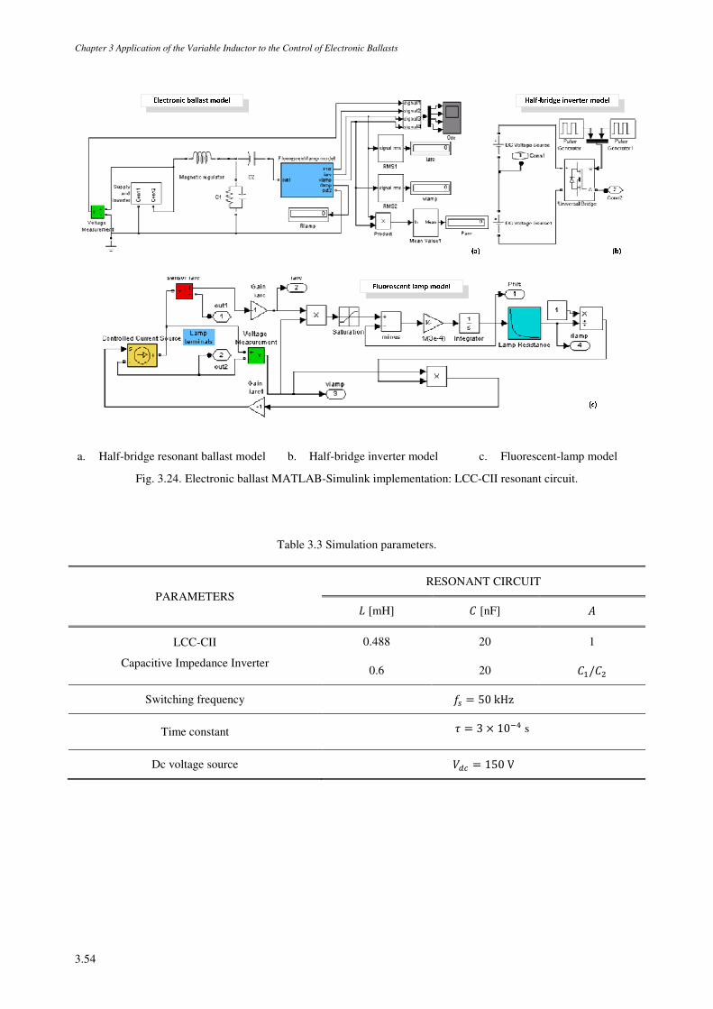
Chapter 3 Application of the Variable Inductor to the Control of Electronic Ballasts
3.54
a. Half-bridge resonant ballast model b. Half-bridge inverter model c. Fluorescent-lamp model
Fig. 3.24. Electronic ballast MATLAB-Simulink implementation: LCC-CII resonant circuit.
Table 3.3 Simulation parameters.
PARAMETERS RESONANT CIRCUIT
¯ [mH] [nF]
LCC-CII
Capacitive Impedance Inverter
0.488 20 1
0.6 20 ª/
Switching frequency 4 = 50 kHz
Time constant = 3 × 10º× s
Dc voltage source > = 150 V
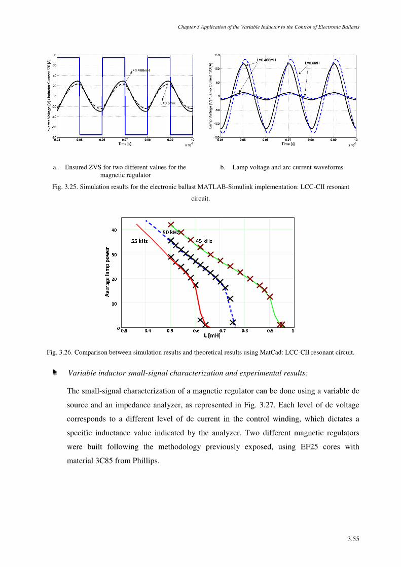
Chapter 3 Application of the Variable Inductor to the Control of Electronic Ballasts
3.55
a. Ensured ZVS for two different values for the magnetic regulator
b. Lamp voltage and arc current waveforms
Fig. 3.25. Simulation results for the electronic ballast MATLAB-Simulink implementation: LCC-CII resonant
circuit.
Fig. 3.26. Comparison between simulation results and theoretical results using MatCad: LCC-CII resonant circuit.
Variable inductor small-signal characterization and experimental results:
The small-signal characterization of a magnetic regulator can be done using a variable dc
source and an impedance analyzer, as represented in Fig. 3.27. Each level of dc voltage
corresponds to a different level of dc current in the control winding, which dictates a
specific inductance value indicated by the analyzer. Two different magnetic regulators
were built following the methodology previously exposed, using EF25 cores with
material 3C85 from Phillips.
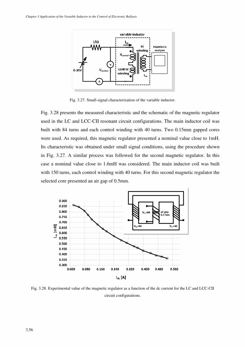
Chapter 3 Application of the Variable Inductor to the Control of Electronic Ballasts
3.56
Fig. 3.27. Small-signal characterization of the variable inductor.
Fig. 3.28 presents the measured characteristic and the schematic of the magnetic regulator
used in the LC and LCC-CII resonant circuit configurations. The main inductor coil was
built with 84 turns and each control winding with 40 turns. Two 0.15mm gapped cores
were used. As required, this magnetic regulator presented a nominal value close to 1mH.
Its characteristic was obtained under small signal conditions, using the procedure shown
in Fig. 3.27. A similar process was followed for the second magnetic regulator. In this
case a nominal value close to 1.6mH was considered. The main inductor coil was built
with 150 turns, each control winding with 40 turns. For this second magnetic regulator the
selected core presented an air gap of 0.5mm.
Fig. 3.28. Experimental value of the magnetic regulator as a function of the dc current for the LC and LCC-CII
circuit configurations.
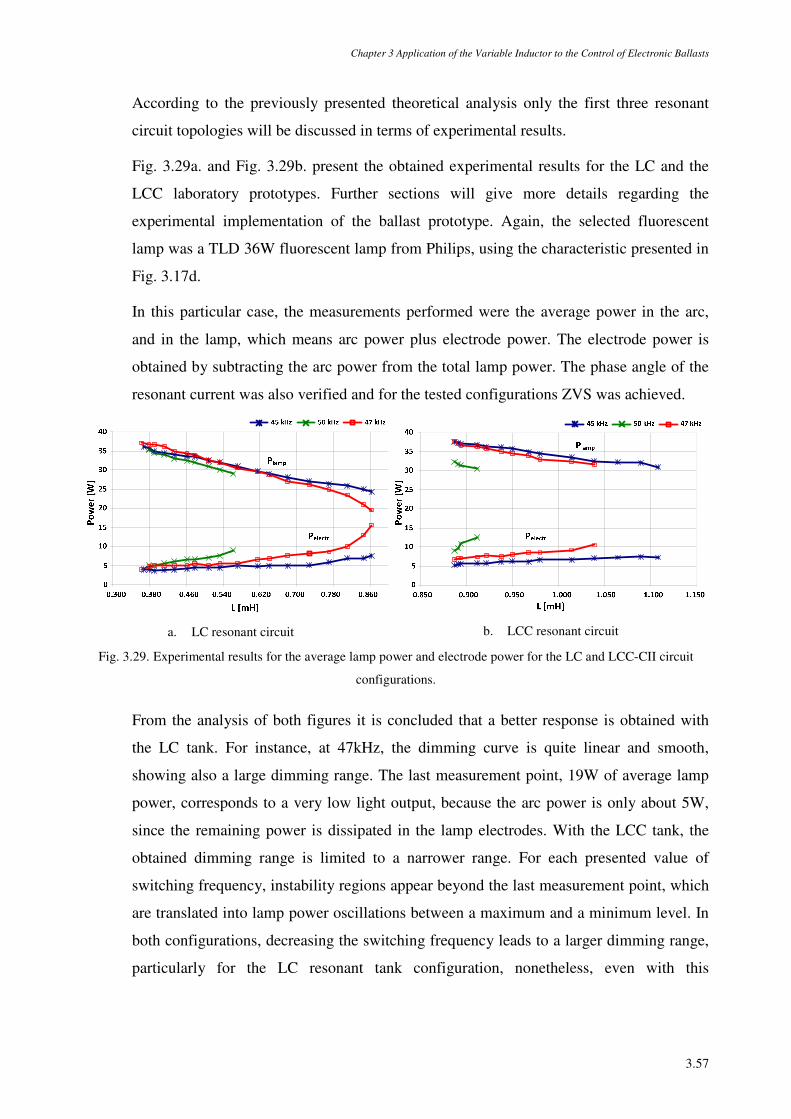
Chapter 3 Application of the Variable Inductor to the Control of Electronic Ballasts
3.57
According to the previously presented theoretical analysis only the first three resonant
circuit topologies will be discussed in terms of experimental results.
Fig. 3.29a. and Fig. 3.29b. present the obtained experimental results for the LC and the
LCC laboratory prototypes. Further sections will give more details regarding the
experimental implementation of the ballast prototype. Again, the selected fluorescent
lamp was a TLD 36W fluorescent lamp from Philips, using the characteristic presented in
Fig. 3.17d.
In this particular case, the measurements performed were the average power in the arc,
and in the lamp, which means arc power plus electrode power. The electrode power is
obtained by subtracting the arc power from the total lamp power. The phase angle of the
resonant current was also verified and for the tested configurations ZVS was achieved.
a. LC resonant circuit b. LCC resonant circuit
Fig. 3.29. Experimental results for the average lamp power and electrode power for the LC and LCC-CII circuit
configurations.
From the analysis of both figures it is concluded that a better response is obtained with
the LC tank. For instance, at 47kHz, the dimming curve is quite linear and smooth,
showing also a large dimming range. The last measurement point, 19W of average lamp
power, corresponds to a very low light output, because the arc power is only about 5W,
since the remaining power is dissipated in the lamp electrodes. With the LCC tank, the
obtained dimming range is limited to a narrower range. For each presented value of
switching frequency, instability regions appear beyond the last measurement point, which
are translated into lamp power oscillations between a maximum and a minimum level. In
both configurations, decreasing the switching frequency leads to a larger dimming range,
particularly for the LC resonant tank configuration, nonetheless, even with this
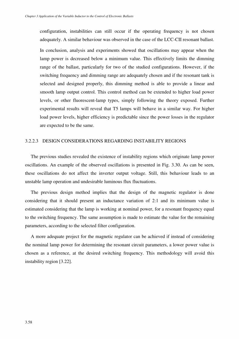
Chapter 3 Application of the Variable Inductor to the Control of Electronic Ballasts
3.58
configuration, instabilities can still occur if the operating frequency is not chosen
adequately. A similar behaviour was observed in the case of the LCC-CII resonant ballast.
In conclusion, analysis and experiments showed that oscillations may appear when the
lamp power is decreased below a minimum value. This effectively limits the dimming
range of the ballast, particularly for two of the studied configurations. However, if the
switching frequency and dimming range are adequately chosen and if the resonant tank is
selected and designed properly, this dimming method is able to provide a linear and
smooth lamp output control. This control method can be extended to higher load power
levels, or other fluorescent-lamp types, simply following the theory exposed. Further
experimental results will reveal that T5 lamps will behave in a similar way. For higher
load power levels, higher efficiency is predictable since the power losses in the regulator
are expected to be the same.
3.2.2.3 DESIGN CONSIDERATIONS REGARDING INSTABILITY REGIONS
The previous studies revealed the existence of instability regions which originate lamp power
oscillations. An example of the observed oscillations is presented in Fig. 3.30. As can be seen,
these oscillations do not affect the inverter output voltage. Still, this behaviour leads to an
unstable lamp operation and undesirable luminous flux fluctuations.
The previous design method implies that the design of the magnetic regulator is done
considering that it should present an inductance variation of 2:1 and its minimum value is
estimated considering that the lamp is working at nominal power, for a resonant frequency equal
to the switching frequency. The same assumption is made to estimate the value for the remaining
parameters, according to the selected filter configuration.
A more adequate project for the magnetic regulator can be achieved if instead of considering
the nominal lamp power for determining the resonant circuit parameters, a lower power value is
chosen as a reference, at the desired switching frequency. This methodology will avoid this
instability region [3.22].
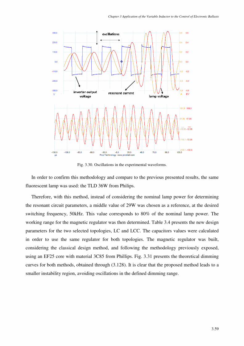
Chapter 3 Application of the Variable Inductor to the Control of Electronic Ballasts
3.59
Fig. 3.30. Oscillations in the experimental waveforms.
In order to confirm this methodology and compare to the previous presented results, the same
fluorescent lamp was used: the TLD 36W from Philips.
Therefore, with this method, instead of considering the nominal lamp power for determining
the resonant circuit parameters, a middle value of 29W was chosen as a reference, at the desired
switching frequency, 50kHz. This value corresponds to 80% of the nominal lamp power. The
working range for the magnetic regulator was then determined. Table 3.4 presents the new design
parameters for the two selected topologies, LC and LCC. The capacitors values were calculated
in order to use the same regulator for both topologies. The magnetic regulator was built,
considering the classical design method, and following the methodology previously exposed,
using an EF25 core with material 3C85 from Phillips. Fig. 3.31 presents the theoretical dimming
curves for both methods, obtained through (3.128). It is clear that the proposed method leads to a
smaller instability region, avoiding oscillations in the defined dimming range.
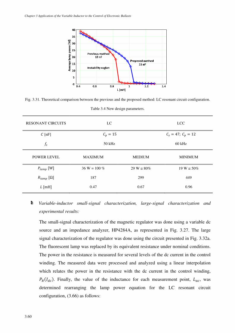
Chapter 3 Application of the Variable Inductor to the Control of Electronic Ballasts
3.60
Fig. 3.31. Theoretical comparison between the previous and the proposed method: LC resonant circuit configuration.
Table 3.4 New design parameters.
RESONANT CIRCUITS LC LCC
[nF] = 15 4 = 47; = 12
4 50 kHz 60 kHz
POWER LEVEL MAXIMUM MEDIUM MINIMUM
t~ [W] 36 W = 100 % 29 W ≅ 80% 19 W ≅ 50%
v~ [Ω] 187 299 449
¯ [mH] 0.47 0.67 0.96
Variable-inductor small-signal characterization, large-signal characterization and
experimental results:
The small-signal characterization of the magnetic regulator was done using a variable dc
source and an impedance analyzer, HP4284A, as represented in Fig. 3.27. The large
signal characterization of the regulator was done using the circuit presented in Fig. 3.32a.
The fluorescent lamp was replaced by its equivalent resistance under nominal conditions.
The power in the resistance is measured for several levels of the dc current in the control
winding. The measured data were processed and analyzed using a linear interpolation
which relates the power in the resistance with the dc current in the control winding,
tÓ/. Finally, the value of the inductance for each measurement point, ¯~, was
determined rearranging the lamp power equation for the LC resonant circuit
configuration, (3.66) as follows:
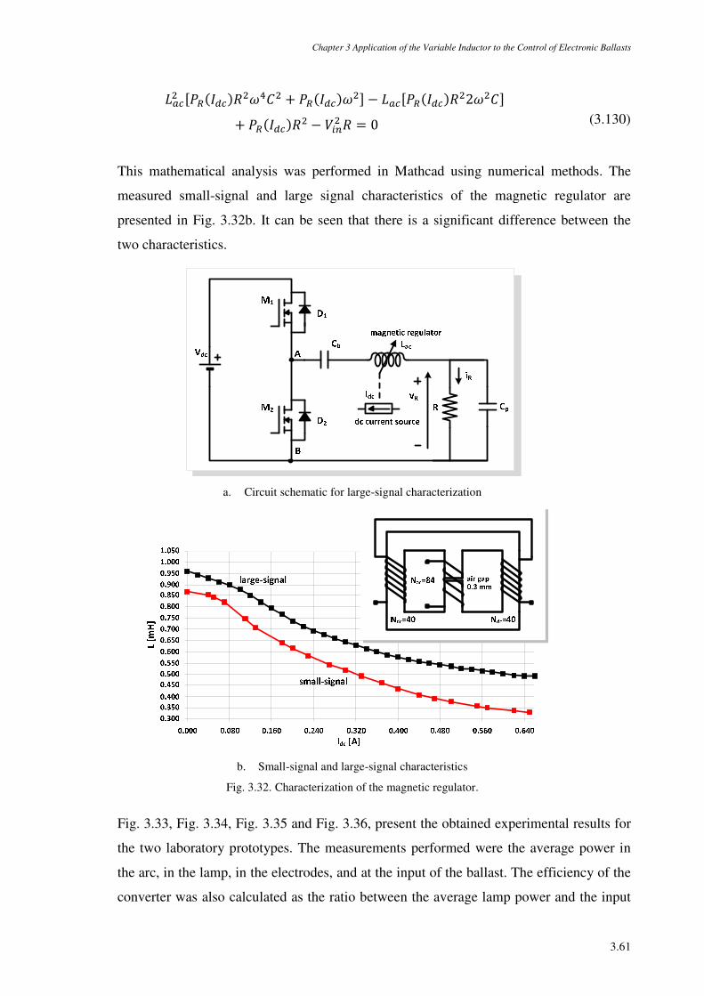
Chapter 3 Application of the Variable Inductor to the Control of Electronic Ballasts
3.61
¯~ [tÓ/v× + tÓ/] − ¯~[tÓ/v2]+ tÓ/v − >±² v = 0 (3.130)
This mathematical analysis was performed in Mathcad using numerical methods. The
measured small-signal and large signal characteristics of the magnetic regulator are
presented in Fig. 3.32b. It can be seen that there is a significant difference between the
two characteristics.
a. Circuit schematic for large-signal characterization
b. Small-signal and large-signal characteristics
Fig. 3.32. Characterization of the magnetic regulator.
Fig. 3.33, Fig. 3.34, Fig. 3.35 and Fig. 3.36, present the obtained experimental results for
the two laboratory prototypes. The measurements performed were the average power in
the arc, in the lamp, in the electrodes, and at the input of the ballast. The efficiency of the
converter was also calculated as the ratio between the average lamp power and the input
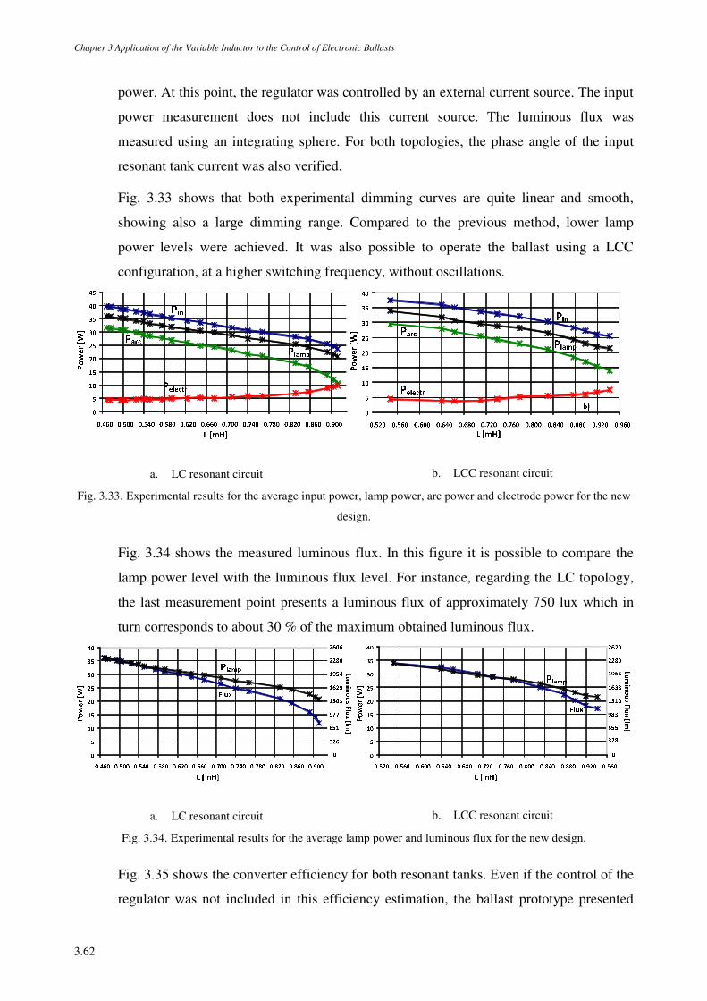
Chapter 3 Application of the Variable Inductor to the Control of Electronic Ballasts
3.62
power. At this point, the regulator was controlled by an external current source. The input
power measurement does not include this current source. The luminous flux was
measured using an integrating sphere. For both topologies, the phase angle of the input
resonant tank current was also verified.
Fig. 3.33 shows that both experimental dimming curves are quite linear and smooth,
showing also a large dimming range. Compared to the previous method, lower lamp
power levels were achieved. It was also possible to operate the ballast using a LCC
configuration, at a higher switching frequency, without oscillations.
a. LC resonant circuit b. LCC resonant circuit
Fig. 3.33. Experimental results for the average input power, lamp power, arc power and electrode power for the new
design.
Fig. 3.34 shows the measured luminous flux. In this figure it is possible to compare the
lamp power level with the luminous flux level. For instance, regarding the LC topology,
the last measurement point presents a luminous flux of approximately 750 lux which in
turn corresponds to about 30 % of the maximum obtained luminous flux.
a. LC resonant circuit b. LCC resonant circuit
Fig. 3.34. Experimental results for the average lamp power and luminous flux for the new design.
Fig. 3.35 shows the converter efficiency for both resonant tanks. Even if the control of the
regulator was not included in this efficiency estimation, the ballast prototype presented
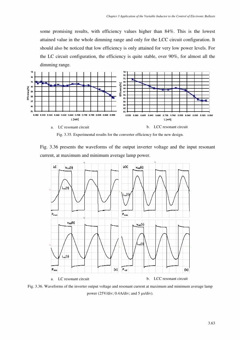
Chapter 3 Application of the Variable Inductor to the Control of Electronic Ballasts
3.63
some promising results, with efficiency values higher than 84%. This is the lowest
attained value in the whole dimming range and only for the LCC circuit configuration. It
should also be noticed that low efficiency is only attained for very low power levels. For
the LC circuit configuration, the efficiency is quite stable, over 90%, for almost all the
dimming range.
a. LC resonant circuit b. LCC resonant circuit
Fig. 3.35. Experimental results for the converter efficiency for the new design.
Fig. 3.36 presents the waveforms of the output inverter voltage and the input resonant
current, at maximum and minimum average lamp power.
a. LC resonant circuit b. LCC resonant circuit
Fig. 3.36. Waveforms of the inverter output voltage and resonant current at maximum and minimum average lamp
power (25V/div; 0.4A/div; and 5 µs/div).
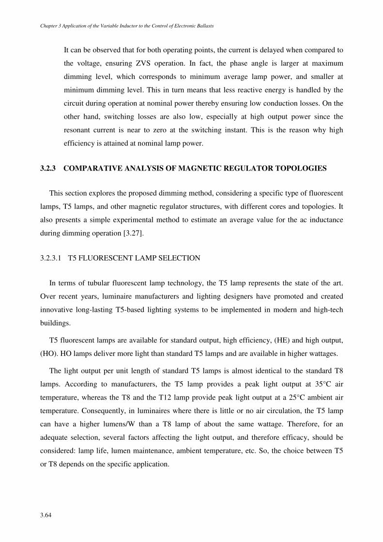
Chapter 3 Application of the Variable Inductor to the Control of Electronic Ballasts
3.64
It can be observed that for both operating points, the current is delayed when compared to
the voltage, ensuring ZVS operation. In fact, the phase angle is larger at maximum
dimming level, which corresponds to minimum average lamp power, and smaller at
minimum dimming level. This in turn means that less reactive energy is handled by the
circuit during operation at nominal power thereby ensuring low conduction losses. On the
other hand, switching losses are also low, especially at high output power since the
resonant current is near to zero at the switching instant. This is the reason why high
efficiency is attained at nominal lamp power.
3.2.3 COMPARATIVE ANALYSIS OF MAGNETIC REGULATOR TOPOLOGIES
This section explores the proposed dimming method, considering a specific type of fluorescent
lamps, T5 lamps, and other magnetic regulator structures, with different cores and topologies. It
also presents a simple experimental method to estimate an average value for the ac inductance
during dimming operation [3.27].
3.2.3.1 T5 FLUORESCENT LAMP SELECTION
In terms of tubular fluorescent lamp technology, the T5 lamp represents the state of the art.
Over recent years, luminaire manufacturers and lighting designers have promoted and created
innovative long-lasting T5-based lighting systems to be implemented in modern and high-tech
buildings.
T5 fluorescent lamps are available for standard output, high efficiency, (HE) and high output,
(HO). HO lamps deliver more light than standard T5 lamps and are available in higher wattages.
The light output per unit length of standard T5 lamps is almost identical to the standard T8
lamps. According to manufacturers, the T5 lamp provides a peak light output at 35°C air
temperature, whereas the T8 and the T12 lamp provide peak light output at a 25°C ambient air
temperature. Consequently, in luminaires where there is little or no air circulation, the T5 lamp
can have a higher lumens/W than a T8 lamp of about the same wattage. Therefore, for an
adequate selection, several factors affecting the light output, and therefore efficacy, should be
considered: lamp life, lumen maintenance, ambient temperature, etc. So, the choice between T5
or T8 depends on the specific application.
Chapter 3 Application of the Variable Inductor to the Control of Electronic Ballasts
3.65
Another important aspect is that compared to the larger T8 or T12 lamps, T5 lamps use less
material. Even if the efficacy of T5 lamps is considered to be equivalent to that of T8 lamps, their
compactness reduces the amount of materials used in their manufacturing, the potential for toxic
substance contamination, and packaging materials needed for shipment and sale. As a result, T5
lamps are considered to have less impact on the global environment than T8 lamps. In addition to
their smaller dimensions, T5 lamps have an improved phosphor coating that prevents mercury
from being absorbed into the phosphor and the bulb glass. This technology allows for reduced
mercury content in the lamp [3.26].
T5 lamps are specially characterized by a high lamp voltage, and in some particular cases, low
current. This is the reason why they are conventionally manufactured for high-frequency
operation, typically above 20kHz. Since maximum efficiency is only attained with this HF
operation, 50/60Hz operation is typically not recommended. This information makes the use of
electronic ballasts almost mandatory. Nevertheless, some authors have recently investigated the
use of low-frequency low-loss magnetic ballasts [3.24], [3.25].
The main argument is the fact that there will be an obvious health consequence due to
electronic waste accumulation in the environment, with other adverse impacts such as soil and
water pollution. Another argument which is also common, especially in LED-lighting based
systems is the fact that electronic ballasts are limited by the short life of the electrolytic
capacitors. So, of course the issue here is to point out more sustainable lighting technology. These
authors suggest the control of T5 28W lamps, which are the common replacement of T8 36W
lamps, with ultra-low-losses LC magnetic ballasts. Evidences show the possibility to ignite and
operate the 28W lamp at low frequency, with very small consequences in the lamp efficacy. The
fact is that there is an obvious advantage which is inherent to the low-current feature of this lamp,
which enables a significant reduction in both conduction and core losses in the magnetic ballast.
Nonetheless, the advantages of T5 with their small and compact luminaires, may turn the use of
heavy and bulky ballasts an impracticable solution. It is possible, however, that in special
circumstances, magnetic ballasts may stand as a correct choice but, their application will also
limit the possibility to control the lamp operation in terms of flux regulation and distant control.
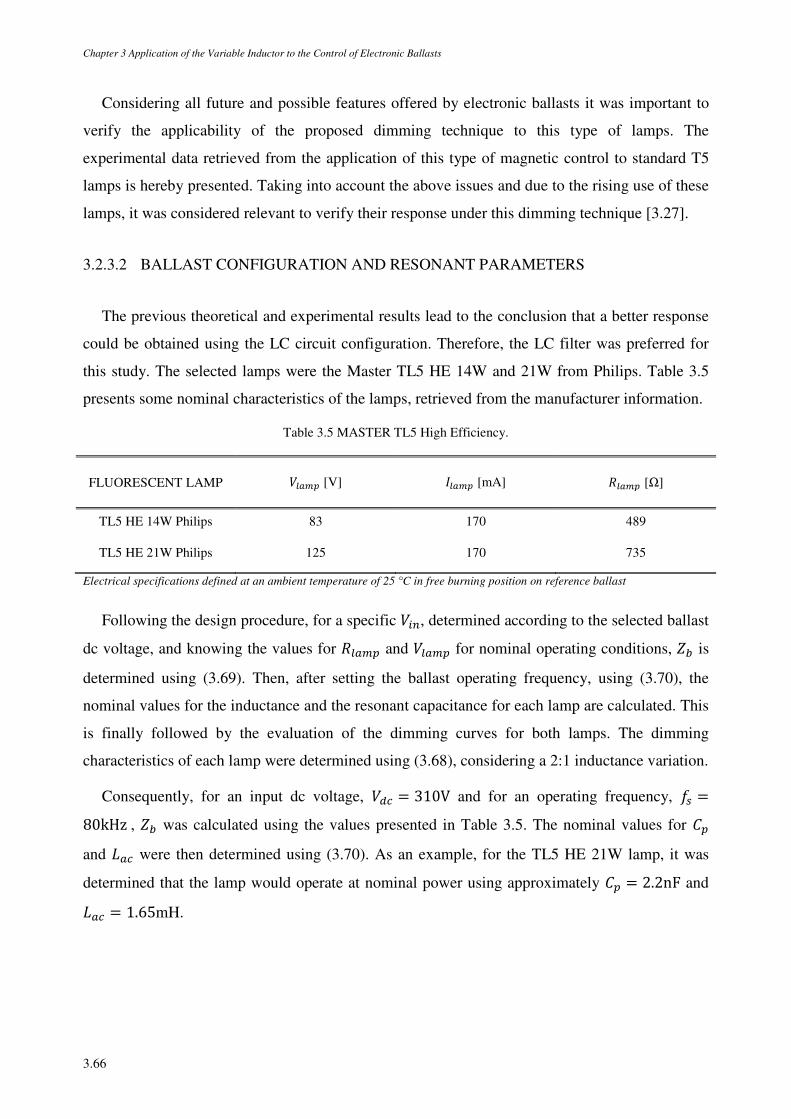
Chapter 3 Application of the Variable Inductor to the Control of Electronic Ballasts
3.66
Considering all future and possible features offered by electronic ballasts it was important to
verify the applicability of the proposed dimming technique to this type of lamps. The
experimental data retrieved from the application of this type of magnetic control to standard T5
lamps is hereby presented. Taking into account the above issues and due to the rising use of these
lamps, it was considered relevant to verify their response under this dimming technique [3.27].
3.2.3.2 BALLAST CONFIGURATION AND RESONANT PARAMETERS
The previous theoretical and experimental results lead to the conclusion that a better response
could be obtained using the LC circuit configuration. Therefore, the LC filter was preferred for
this study. The selected lamps were the Master TL5 HE 14W and 21W from Philips. Table 3.5
presents some nominal characteristics of the lamps, retrieved from the manufacturer information.
Table 3.5 MASTER TL5 High Efficiency.
FLUORESCENT LAMP >~ [V] /~ [mA] v~ [Ω]
TL5 HE 14W Philips 83 170 489
TL5 HE 21W Philips 125 170 735
Electrical specifications defined at an ambient temperature of 25 °C in free burning position on reference ballast
Following the design procedure, for a specific >±², determined according to the selected ballast
dc voltage, and knowing the values for v~ and >~ for nominal operating conditions, ´ is
determined using (3.69). Then, after setting the ballast operating frequency, using (3.70), the
nominal values for the inductance and the resonant capacitance for each lamp are calculated. This
is finally followed by the evaluation of the dimming curves for both lamps. The dimming
characteristics of each lamp were determined using (3.68), considering a 2:1 inductance variation.
Consequently, for an input dc voltage, > = 310V and for an operating frequency, 4 =80kHz , ´ was calculated using the values presented in Table 3.5. The nominal values for
and ¯~ were then determined using (3.70). As an example, for the TL5 HE 21W lamp, it was
determined that the lamp would operate at nominal power using approximately = 2.2nF and
¯~ = 1.65mH.
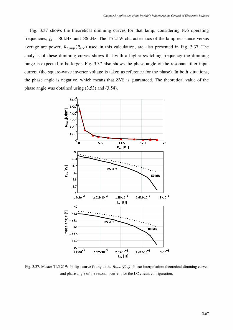
Chapter 3 Application of the Variable Inductor to the Control of Electronic Ballasts
3.67
Fig. 3.37 shows the theoretical dimming curves for that lamp, considering two operating
frequencies, 4 = 80kHz and 85kHz. The T5 21W characteristics of the lamp resistance versus
average arc power, v~t~2 used in this calculation, are also presented in Fig. 3.37. The
analysis of these dimming curves shows that with a higher switching frequency the dimming
range is expected to be larger. Fig. 3.37 also shows the phase angle of the resonant filter input
current (the square-wave inverter voltage is taken as reference for the phase). In both situations,
the phase angle is negative, which means that ZVS is guaranteed. The theoretical value of the
phase angle was obtained using (3.53) and (3.54).
Fig. 3.37. Master TL5 21W Philips: curve fitting to the Rlamp Parc - linear interpolation; theoretical dimming curves
and phase angle of the resonant current for the LC circuit configuration.
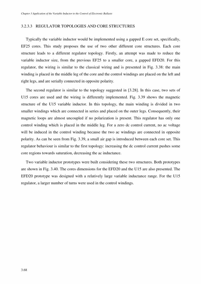
Chapter 3 Application of the Variable Inductor to the Control of Electronic Ballasts
3.68
3.2.3.3 REGULATOR TOPOLOGIES AND CORE STRUCTURES
Typically the variable inductor would be implemented using a gapped E core set, specifically,
EF25 cores. This study proposes the use of two other different core structures. Each core
structure leads to a different regulator topology. Firstly, an attempt was made to reduce the
variable inductor size, from the previous EF25 to a smaller core, a gapped EFD20. For this
regulator, the wiring is similar to the classical wiring and is presented in Fig. 3.38: the main
winding is placed in the middle leg of the core and the control windings are placed on the left and
right legs, and are serially connected in opposite polarity.
The second regulator is similar to the topology suggested in [3.28]. In this case, two sets of
U15 cores are used and the wiring is differently implemented. Fig. 3.39 shows the magnetic
structure of the U15 variable inductor. In this topology, the main winding is divided in two
smaller windings which are connected in series and placed on the outer legs. Consequently, their
magnetic loops are almost uncoupled if no polarization is present. This regulator has only one
control winding which is placed in the middle leg. For a zero dc control current, no ac voltage
will be induced in the control winding because the two ac windings are connected in opposite
polarity. As can be seen from Fig. 3.39, a small air gap is introduced between each core set. This
regulator behaviour is similar to the first topology: increasing the dc control current pushes some
core regions towards saturation, decreasing the ac inductance.
Two variable inductor prototypes were built considering these two structures. Both prototypes
are shown in Fig. 3.40. The cores dimensions for the EFD20 and the U15 are also presented. The
EFD20 prototype was designed with a relatively large variable inductance range. For the U15
regulator, a larger number of turns were used in the control windings.
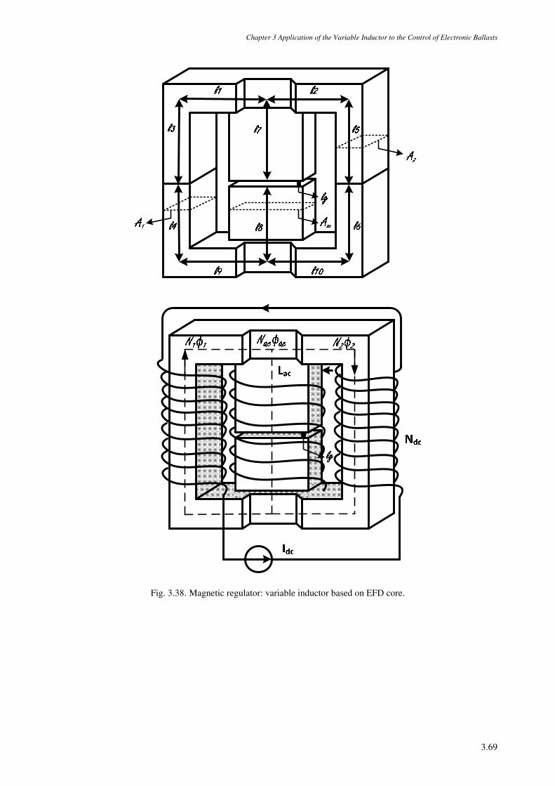
Chapter 3 Application of the Variable Inductor to the Control of Electronic Ballasts
3.69
Fig. 3.38. Magnetic regulator: variable inductor based on EFD core.
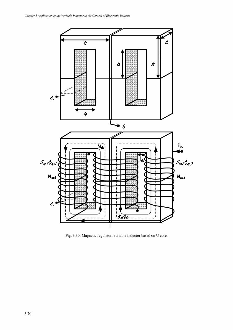
Chapter 3 Application of the Variable Inductor to the Control of Electronic Ballasts
3.70
Fig. 3.39. Magnetic regulator: variable inductor based on U core.
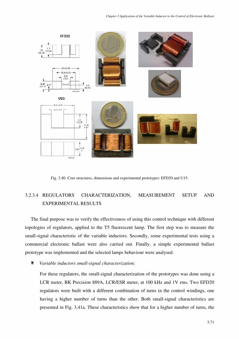
Chapter 3 Application of the Variable Inductor to the Control of Electronic Ballasts
3.71
Fig. 3.40. Core structures, dimensions and experimental prototypes: EFD20 and U15.
3.2.3.4 REGULATORS CHARACTERIZATION, MEASUREMENT SETUP AND
EXPERIMENTAL RESULTS
The final purpose was to verify the effectiveness of using this control technique with different
topologies of regulators, applied to the T5 fluorescent lamp. The first step was to measure the
small-signal characteristic of the variable inductors. Secondly, some experimental tests using a
commercial electronic ballast were also carried out. Finally, a simple experimental ballast
prototype was implemented and the selected lamps behaviour were analysed.
Variable inductors small-signal characterization:
For these regulators, the small-signal characterization of the prototypes was done using a
LCR meter, BK Precision 889A, LCR/ESR meter, at 100 kHz and 1V rms. Two EFD20
regulators were built with a different combination of turns in the control windings, one
having a higher number of turns than the other. Both small-signal characteristics are
presented in Fig. 3.41a. These characteristics show that for a higher number of turns, the
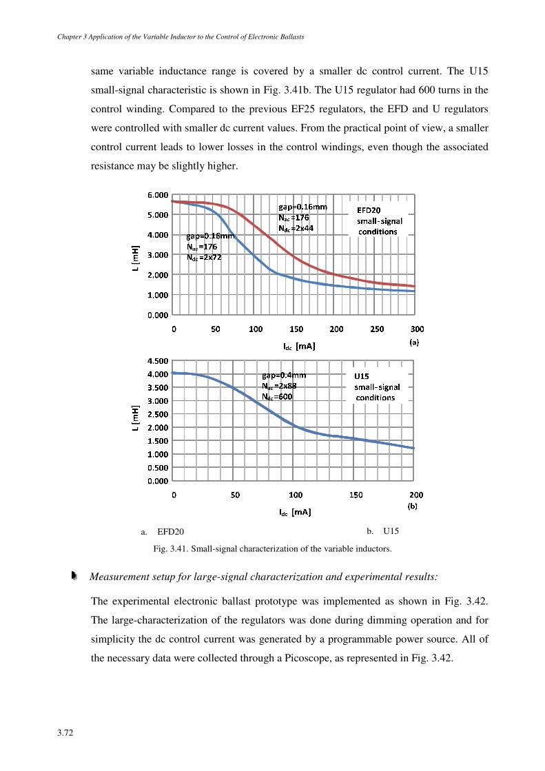
Chapter 3 Application of the Variable Inductor to the Control of Electronic Ballasts
3.72
same variable inductance range is covered by a smaller dc control current. The U15
small-signal characteristic is shown in Fig. 3.41b. The U15 regulator had 600 turns in the
control winding. Compared to the previous EF25 regulators, the EFD and U regulators
were controlled with smaller dc current values. From the practical point of view, a smaller
control current leads to lower losses in the control windings, even though the associated
resistance may be slightly higher.
a. EFD20 b. U15
Fig. 3.41. Small-signal characterization of the variable inductors.
Measurement setup for large-signal characterization and experimental results:
The experimental electronic ballast prototype was implemented as shown in Fig. 3.42.
The large-characterization of the regulators was done during dimming operation and for
simplicity the dc control current was generated by a programmable power source. All of
the necessary data were collected through a Picoscope, as represented in Fig. 3.42.
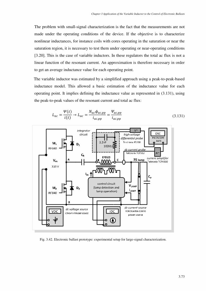
Chapter 3 Application of the Variable Inductor to the Control of Electronic Ballasts
3.73
The problem with small-signal characterization is the fact that the measurements are not
made under the operating conditions of the device. If the objective is to characterize
nonlinear inductances, for instance coils with cores operating in the saturation or near the
saturation region, it is necessary to test them under operating or near-operating conditions
[3.20]. This is the case of variable inductors. In these regulators the total ac flux is not a
linear function of the resonant current. An approximation is therefore necessary in order
to get an average inductance value for each operating point.
The variable inductor was estimated by a simplified approach using a peak-to-peak-based
inductance model. This allowed a basic estimation of the inductance value for each
operating point. It implies defining the inductance value as represented in (3.131), using
the peak-to-peak values of the resonant current and total ac flux:
¯~ = ÃL → ¯~ = Á~£~,L~, = Ã~,L~, (3.131)
Fig. 3.42. Electronic ballast prototype: experimental setup for large-signal characterization.
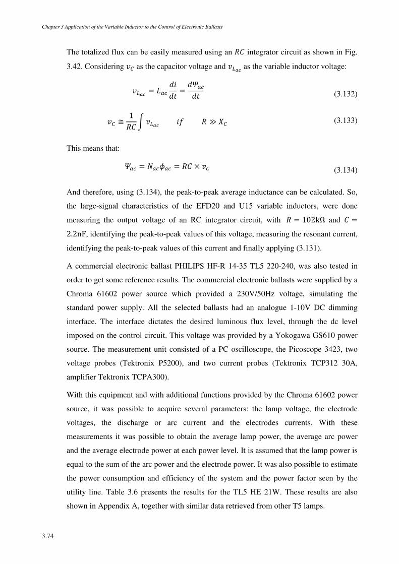
Chapter 3 Application of the Variable Inductor to the Control of Electronic Ballasts
3.74
The totalized flux can be easily measured using an v integrator circuit as shown in Fig.
3.42. Considering K as the capacitor voltage and K6 as the variable inductor voltage:
K6 = ¯~ L = Ã~ (3.132)
K ≅ 1v ã K6 L v ≫ 8 (3.133)
This means that:
Ã~ = Á~£~ = v × K (3.134)
And therefore, using (3.134), the peak-to-peak average inductance can be calculated. So,
the large-signal characteristics of the EFD20 and U15 variable inductors, were done
measuring the output voltage of an RC integrator circuit, with v = 102kΩ and =2.2nF, identifying the peak-to-peak values of this voltage, measuring the resonant current,
identifying the peak-to-peak values of this current and finally applying (3.131).
A commercial electronic ballast PHILIPS HF-R 14-35 TL5 220-240, was also tested in
order to get some reference results. The commercial electronic ballasts were supplied by a
Chroma 61602 power source which provided a 230V/50Hz voltage, simulating the
standard power supply. All the selected ballasts had an analogue 1-10V DC dimming
interface. The interface dictates the desired luminous flux level, through the dc level
imposed on the control circuit. This voltage was provided by a Yokogawa GS610 power
source. The measurement unit consisted of a PC oscilloscope, the Picoscope 3423, two
voltage probes (Tektronix P5200), and two current probes (Tektronix TCP312 30A,
amplifier Tektronix TCPA300).
With this equipment and with additional functions provided by the Chroma 61602 power
source, it was possible to acquire several parameters: the lamp voltage, the electrode
voltages, the discharge or arc current and the electrodes currents. With these
measurements it was possible to obtain the average lamp power, the average arc power
and the average electrode power at each power level. It is assumed that the lamp power is
equal to the sum of the arc power and the electrode power. It was also possible to estimate
the power consumption and efficiency of the system and the power factor seen by the
utility line. Table 3.6 presents the results for the TL5 HE 21W. These results are also
shown in Appendix A, together with similar data retrieved from other T5 lamps.
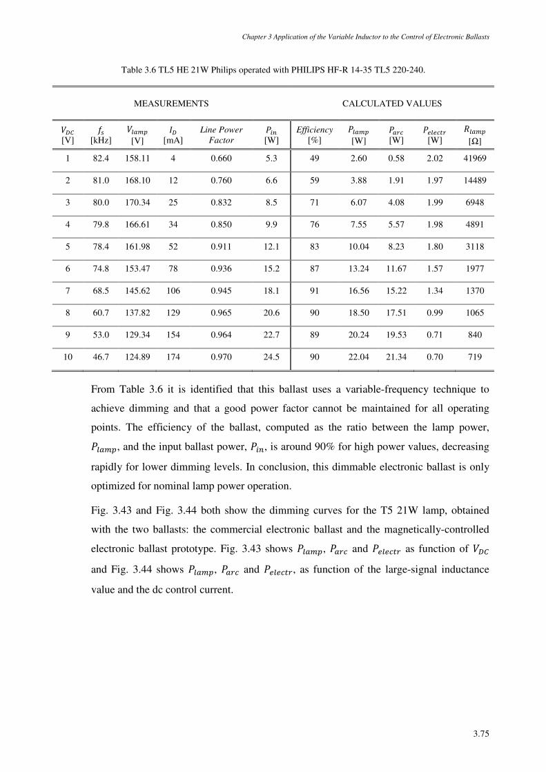
Chapter 3 Application of the Variable Inductor to the Control of Electronic Ballasts
3.75
Table 3.6 TL5 HE 21W Philips operated with PHILIPS HF-R 14-35 TL5 220-240.
MEASUREMENTS CALCULATED VALUES
>0 [V]
4 [kHz]
>~ [V]
/0
[mA] Line Power
Factor t±² [W]
Efficiency [%]
t~ [W]
t~2 [W]
t33À2
[W] v~
[Ω]
1 82.4 158.11 4 0.660 5.3 49 2.60 0.58 2.02 41969
2 81.0 168.10 12 0.760 6.6 59 3.88 1.91 1.97 14489
3 80.0 170.34 25 0.832 8.5 71 6.07 4.08 1.99 6948
4 79.8 166.61 34 0.850 9.9 76 7.55 5.57 1.98 4891
5 78.4 161.98 52 0.911 12.1 83 10.04 8.23 1.80 3118
6 74.8 153.47 78 0.936 15.2 87 13.24 11.67 1.57 1977
7 68.5 145.62 106 0.945 18.1 91 16.56 15.22 1.34 1370
8 60.7 137.82 129 0.965 20.6 90 18.50 17.51 0.99 1065
9 53.0 129.34 154 0.964 22.7 89 20.24 19.53 0.71 840
10 46.7 124.89 174 0.970 24.5 90 22.04 21.34 0.70 719
From Table 3.6 it is identified that this ballast uses a variable-frequency technique to
achieve dimming and that a good power factor cannot be maintained for all operating
points. The efficiency of the ballast, computed as the ratio between the lamp power,
t~, and the input ballast power, t±², is around 90% for high power values, decreasing
rapidly for lower dimming levels. In conclusion, this dimmable electronic ballast is only
optimized for nominal lamp power operation.
Fig. 3.43 and Fig. 3.44 both show the dimming curves for the T5 21W lamp, obtained
with the two ballasts: the commercial electronic ballast and the magnetically-controlled
electronic ballast prototype. Fig. 3.43 shows t~, t~2 and t33À2 as function of >0
and Fig. 3.44 shows t~, t~2 and t33À2, as function of the large-signal inductance
value and the dc control current.

Chapter 3 Application of the Variable Inductor to the Control of Electronic Ballasts
3.76
Fig. 3.43. Experimental results for the TL5 HE 21W with commercial ballast: average lamp power, arc power and
electrode power, as function of the control voltage.
The prototype data were obtained using the EFD20 regulator, using the following
parameters: > = 310V, = 2.2nF and 4 = 85kHz. Fig. 3.44 also shows the prototype
efficiency for all dimming levels. The observation of both figures clearly reveals that the
proposed magnetically-controlled prototype was also capable of dimming the lamp from
the rated power to a near zero power level. This control required an inductance range
between 1.9 and 3.1mH, which was guaranteed by a small control current variation,
approximately 140mA. Similar to the commercial ballast, a low electrode power was also
maintained during the whole operating range. This power, however, was not as low as to
damage the electrodes, due to low heating temperatures.
Another relevant issue is the efficiency of the ballast. Compared to the commercial ballast
the results were not disappointing, since these results were obtained with an early
prototype version. The ballast, at rated power, showed an efficiency value around 90%,
which is quite acceptable. Those values were maintained for higher power levels.
However, for low power levels, the efficiency of the ballast decreased. This can be better
observed in Fig. 3.45.
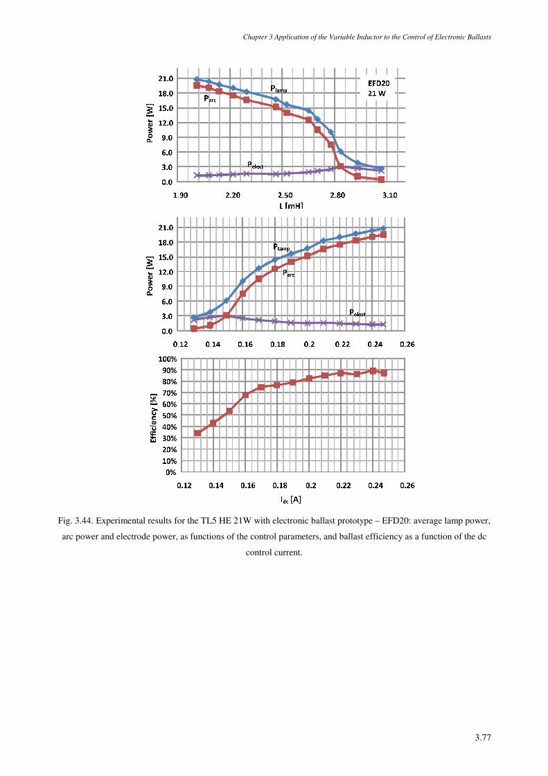
Chapter 3 Application of the Variable Inductor to the Control of Electronic Ballasts
3.77
Fig. 3.44. Experimental results for the TL5 HE 21W with electronic ballast prototype – EFD20: average lamp power,
arc power and electrode power, as functions of the control parameters, and ballast efficiency as a function of the dc
control current.
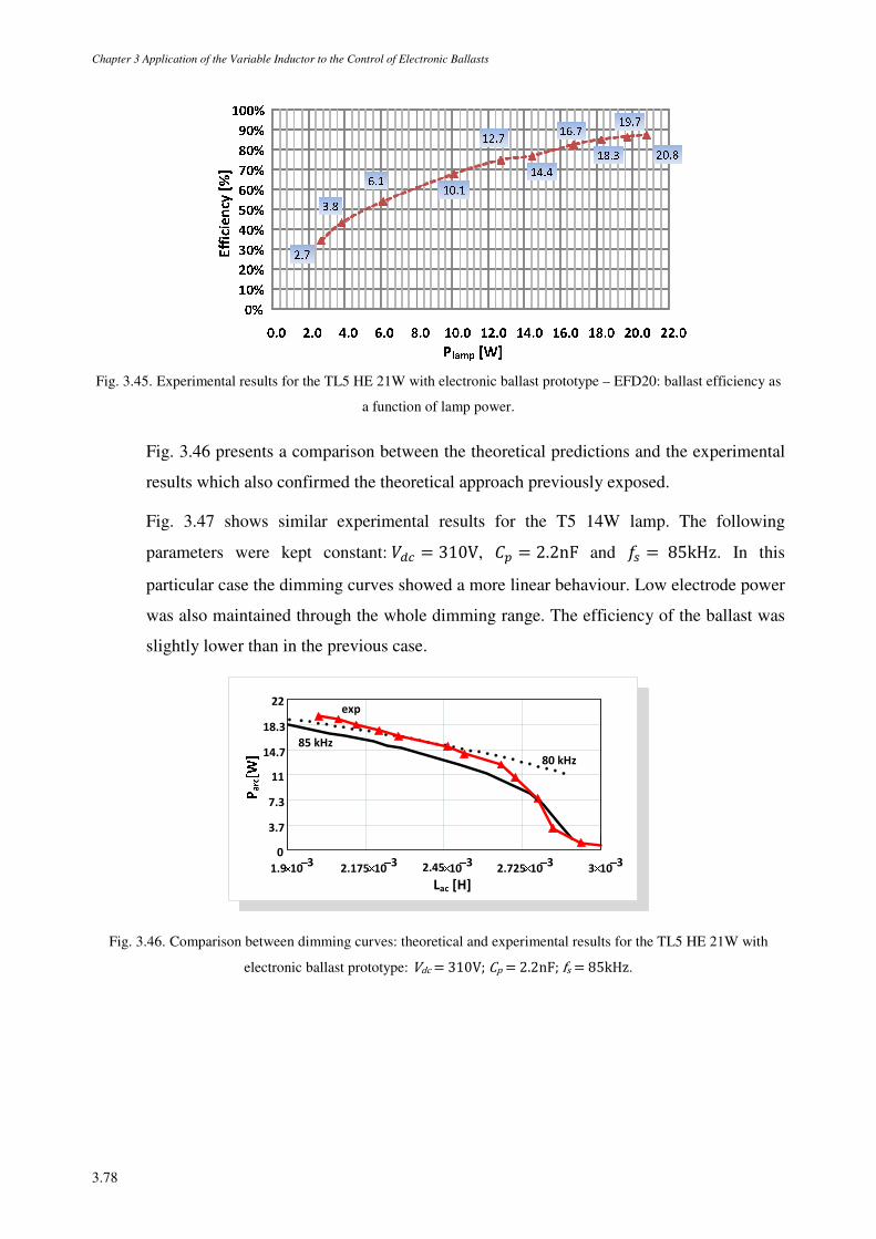
Chapter 3 Application of the Variable Inductor to the Control of Electronic Ballasts
3.78
Fig. 3.45. Experimental results for the TL5 HE 21W with electronic ballast prototype – EFD20: ballast efficiency as
a function of lamp power.
Fig. 3.46 presents a comparison between the theoretical predictions and the experimental
results which also confirmed the theoretical approach previously exposed.
Fig. 3.47 shows similar experimental results for the T5 14W lamp. The following
parameters were kept constant: > = 310V, = 2.2nF and 4 = 85kHz. In this
particular case the dimming curves showed a more linear behaviour. Low electrode power
was also maintained through the whole dimming range. The efficiency of the ballast was
slightly lower than in the previous case.
1.9 103
2.175 103 2.45 10
32.725 10
33 10
30
3.7
7.3
11
14.7
18.3
22
Lac [H]
80 kHz
85 kHz
exp
Fig. 3.46. Comparison between dimming curves: theoretical and experimental results for the TL5 HE 21W with
electronic ballast prototype: Vdc = 310V; Cp = 2.2nF; fs = 85kHz.
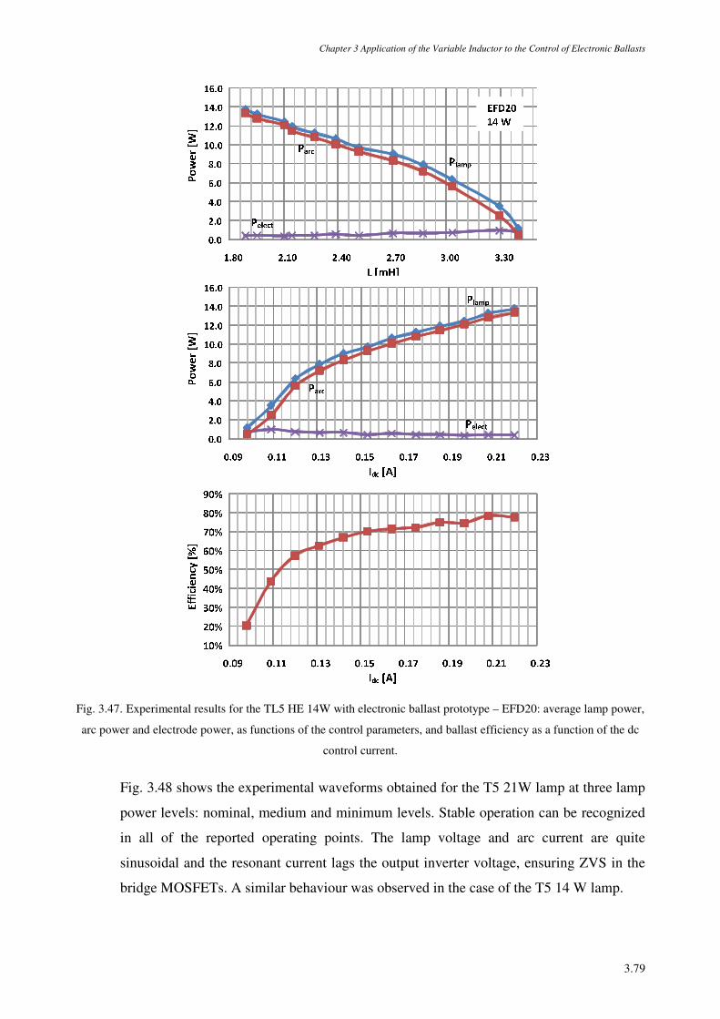
Chapter 3 Application of the Variable Inductor to the Control of Electronic Ballasts
3.79
Fig. 3.47. Experimental results for the TL5 HE 14W with electronic ballast prototype – EFD20: average lamp power,
arc power and electrode power, as functions of the control parameters, and ballast efficiency as a function of the dc
control current.
Fig. 3.48 shows the experimental waveforms obtained for the T5 21W lamp at three lamp
power levels: nominal, medium and minimum levels. Stable operation can be recognized
in all of the reported operating points. The lamp voltage and arc current are quite
sinusoidal and the resonant current lags the output inverter voltage, ensuring ZVS in the
bridge MOSFETs. A similar behaviour was observed in the case of the T5 14 W lamp.
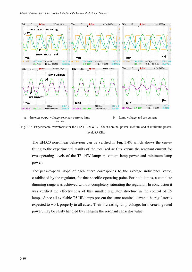
Chapter 3 Application of the Variable Inductor to the Control of Electronic Ballasts
3.80
a. Inverter output voltage, resonant current, lamp voltage
b. Lamp voltage and arc current
Fig. 3.48. Experimental waveforms for the TL5 HE 21W-EFD20 at nominal power, medium and at minimum power
level, 85 KHz.
The EFD20 non-linear behaviour can be verified in Fig. 3.49, which shows the curve-
fitting to the experimental results of the totalized ac flux versus the resonant current for
two operating levels of the T5 14W lamp: maximum lamp power and minimum lamp
power.
The peak-to-peak slope of each curve corresponds to the average inductance value,
established by the regulator, for that specific operating point. For both lamps, a complete
dimming range was achieved without completely saturating the regulator. In conclusion it
was verified the effectiveness of this smaller regulator structure in the control of T5
lamps. Since all available T5 HE lamps present the same nominal current, the regulator is
expected to work properly in all cases. Their increasing lamp voltage, for increasing rated
power, may be easily handled by changing the resonant capacitor value.
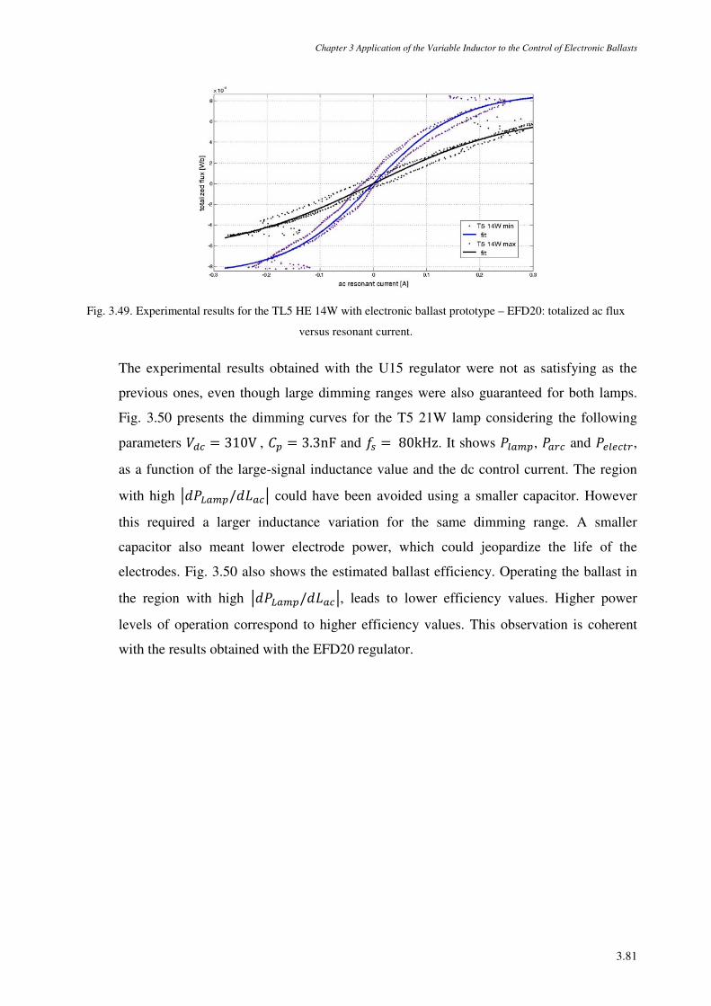
Chapter 3 Application of the Variable Inductor to the Control of Electronic Ballasts
3.81
Fig. 3.49. Experimental results for the TL5 HE 14W with electronic ballast prototype – EFD20: totalized ac flux
versus resonant current.
The experimental results obtained with the U15 regulator were not as satisfying as the
previous ones, even though large dimming ranges were also guaranteed for both lamps.
Fig. 3.50 presents the dimming curves for the T5 21W lamp considering the following
parameters > = 310V , = 3.3nF and 4 = 80kHz. It shows t~, t~2 and t33À2,
as a function of the large-signal inductance value and the dc control current. The region
with high ât~/¯~â could have been avoided using a smaller capacitor. However
this required a larger inductance variation for the same dimming range. A smaller
capacitor also meant lower electrode power, which could jeopardize the life of the
electrodes. Fig. 3.50 also shows the estimated ballast efficiency. Operating the ballast in
the region with high ât~/¯~â, leads to lower efficiency values. Higher power
levels of operation correspond to higher efficiency values. This observation is coherent
with the results obtained with the EFD20 regulator.
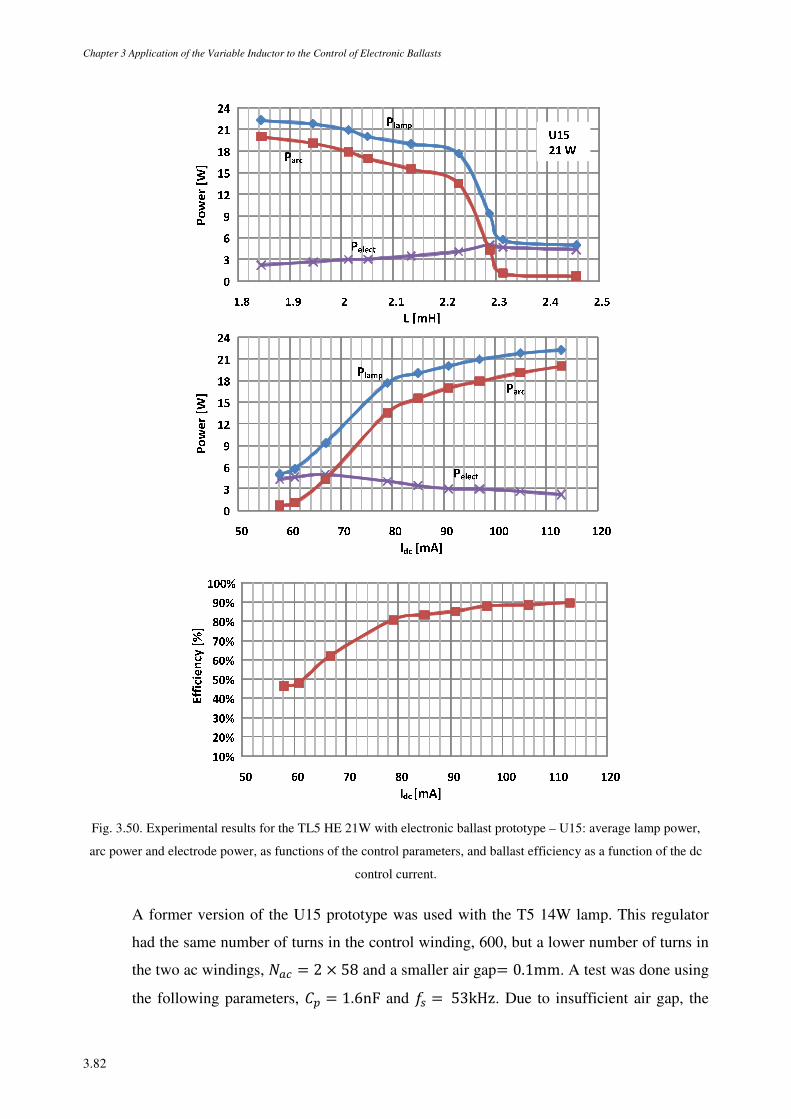
Chapter 3 Application of the Variable Inductor to the Control of Electronic Ballasts
3.82
Fig. 3.50. Experimental results for the TL5 HE 21W with electronic ballast prototype – U15: average lamp power,
arc power and electrode power, as functions of the control parameters, and ballast efficiency as a function of the dc
control current.
A former version of the U15 prototype was used with the T5 14W lamp. This regulator
had the same number of turns in the control winding, 600, but a lower number of turns in
the two ac windings, Á~ = 2 × 58 and a smaller air gap= 0.1mm. A test was done using
the following parameters, = 1.6nF and 4 = 53kHz. Due to insufficient air gap, the
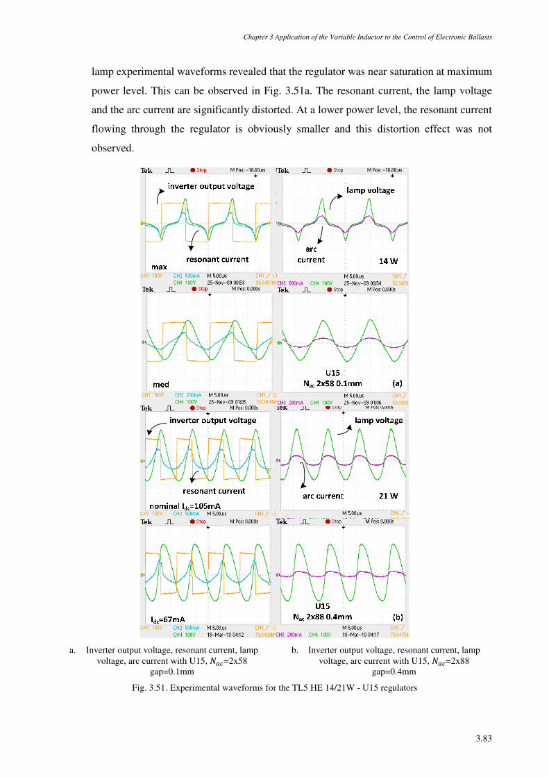
Chapter 3 Application of the Variable Inductor to the Control of Electronic Ballasts
3.83
lamp experimental waveforms revealed that the regulator was near saturation at maximum
power level. This can be observed in Fig. 3.51a. The resonant current, the lamp voltage
and the arc current are significantly distorted. At a lower power level, the resonant current
flowing through the regulator is obviously smaller and this distortion effect was not
observed.
a. Inverter output voltage, resonant current, lamp voltage, arc current with U15, Á~=2x58
gap=0.1mm
b. Inverter output voltage, resonant current, lamp voltage, arc current with U15, Á~=2x88
gap=0.4mm
Fig. 3.51. Experimental waveforms for the TL5 HE 14/21W - U15 regulators
Chapter 3 Application of the Variable Inductor to the Control of Electronic Ballasts
3.84
The waveforms presented in Fig. 3.51b, were obtained using the final version of the U15
regulator. They correspond to two operating points of the experimental results presented
in Fig. 3.50. More specifically, to the maximum power level of the 21W lamp and also to
a lower level. It was verified that a small asymmetry in the regulator, in terms of number
of ac turns had a great influence in the resonant current and lamp waveforms. This effect
was particularly observed at high power levels. Connecting the regulator in opposite
polarity showed that the small peak in the resonant current would appear in the other half
cycle, which would prove this asymmetry. The small offset in the waveforms, easily
observed in the lamp voltage at nominal power was also related to asymmetry issues.
Some of the disadvantages presented by the U15 regulator were due to the fact that this
variable inductor topology is built using four different U parts, which increases the
complexity of prototype assemblage and may easily lead to asymmetries. In addition, the
air gap is more difficult to control when compared to the EFD20 which are already
available in gapped versions.
The purpose of this study was to confirm if the proposed magnetic regulator topologies and
core structures were adequate for this dimming technique, applied to T5 lamps. With the data
collected from the two tested lamps, it was concluded that the smaller size EFD20 regulator
behaved as expected and no odd effects appeared in the experimental waveforms. The U15
regulator was clearly a solution harder to implement, for which small prototype faults showed a
negative influence in the lamp behaviour. Even though stable lamp operation was observed in
both circumstances the EFD20 showed more promising results.
3.3 VARIABLE-INDUCTOR MODELLING FOR DIMMING
APPLICATIONS
3.3.1 BALLAST PROTOTYPE AND EXPERIMENTAL RESULTS
In the following section, a dynamic-inductance model for magnetically-controlled electronic
ballasts simulations is proposed. The ballast model represents a useful tool for prototype design
and development. The variable-inductor model itself is based on the theoretical magnetic analysis
of the proposed variable inductor prototype and simulation results will be confronted with
experimental results retrieved from a magnetically-controlled dimmable ballast.
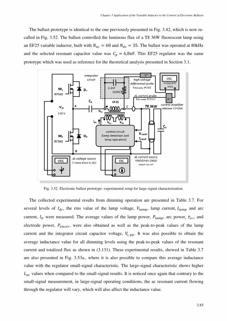
Chapter 3 Application of the Variable Inductor to the Control of Electronic Ballasts
3.85
The ballast prototype is identical to the one previously presented in Fig. 3.42, which is now re-
called in Fig. 3.52. The ballast controlled the luminous flux of a T8 36W fluorescent lamp using
an EF25 variable inductor, built with Á~ = 68 and Á = 35. The ballast was operated at 80kHz
and the selected resonant capacitor value was = 6,8nF. This EF25 regulator was the same
prototype which was used as reference for the theoretical analysis presented in Section 3.1.
Fig. 3.52. Electronic ballast prototype: experimental setup for large-signal characterization.
The collected experimental results from dimming operation are presented in Table 3.7. For
several levels of /, the rms value of the lamp voltage, >~, lamp current, /~ and arc
current, /0 were measured. The average values of the lamp power, t~, arc power, t~2, and
electrode power, t33À2, were also obtained as well as the peak-to-peak values of the lamp
current and the integrator circuit capacitor voltage, >_. It was also possible to obtain the
average inductance value for all dimming levels using the peak-to-peak values of the resonant
current and totalized flux as shown in (3.131). These experimental results, showed in Table 3.7
are also presented in Fig. 3.53a., where it is also possible to compare this average inductance
value with the regulator small-signal characteristic. The large-signal characteristic shows higher
¯~ values when compared to the small-signal results. It is noticed once again that contrary to the
small-signal measurement, in large-signal operating conditions, the ac resonant current flowing
through the regulator will vary, which will also affect the inductance value.
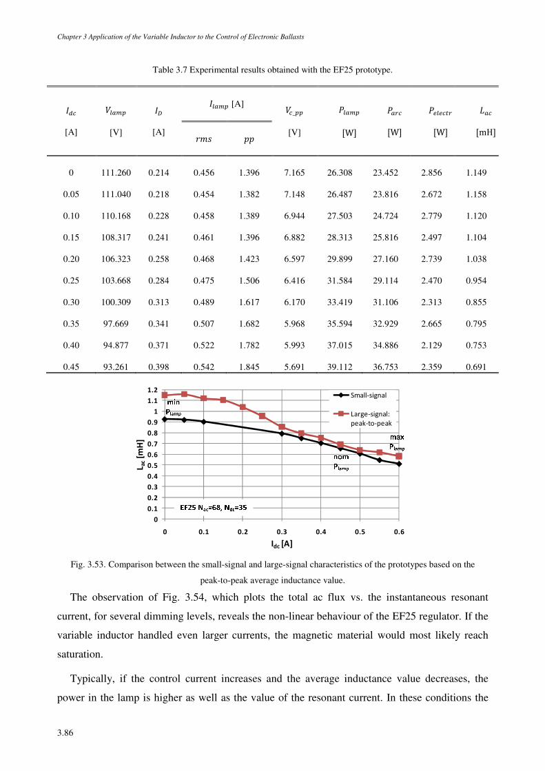
Chapter 3 Application of the Variable Inductor to the Control of Electronic Ballasts
3.86
Table 3.7 Experimental results obtained with the EF25 prototype.
/
[A]
>~
[V]
/0
[A]
/~ [A] >_
[V]
t~ [W]
t~2 [W]
t33À2 [W]
¯~ [mH] x yy
0 111.260 0.214 0.456 1.396 7.165 26.308 23.452 2.856 1.149
0.05 111.040 0.218 0.454 1.382 7.148 26.487 23.816 2.672 1.158
0.10 110.168 0.228 0.458 1.389 6.944 27.503 24.724 2.779 1.120
0.15 108.317 0.241 0.461 1.396 6.882 28.313 25.816 2.497 1.104
0.20 106.323 0.258 0.468 1.423 6.597 29.899 27.160 2.739 1.038
0.25 103.668 0.284 0.475 1.506 6.416 31.584 29.114 2.470 0.954
0.30 100.309 0.313 0.489 1.617 6.170 33.419 31.106 2.313 0.855
0.35 97.669 0.341 0.507 1.682 5.968 35.594 32.929 2.665 0.795
0.40 94.877 0.371 0.522 1.782 5.993 37.015 34.886 2.129 0.753
0.45 93.261 0.398 0.542 1.845 5.691 39.112 36.753 2.359 0.691
0
0.1
0.2
0.3
0.4
0.5
0.6
0.7
0.8
0.9
1
1.1
1.2
0 0.1 0.2 0.3 0.4 0.5 0.6
Lac[m
H]
Idc [A]
Small-signal
Large-signal:
peak-to-peak
Fig. 3.53. Comparison between the small-signal and large-signal characteristics of the prototypes based on the
peak-to-peak average inductance value.
The observation of Fig. 3.54, which plots the total ac flux vs. the instantaneous resonant
current, for several dimming levels, reveals the non-linear behaviour of the EF25 regulator. If the
variable inductor handled even larger currents, the magnetic material would most likely reach
saturation.
Typically, if the control current increases and the average inductance value decreases, the
power in the lamp is higher as well as the value of the resonant current. In these conditions the
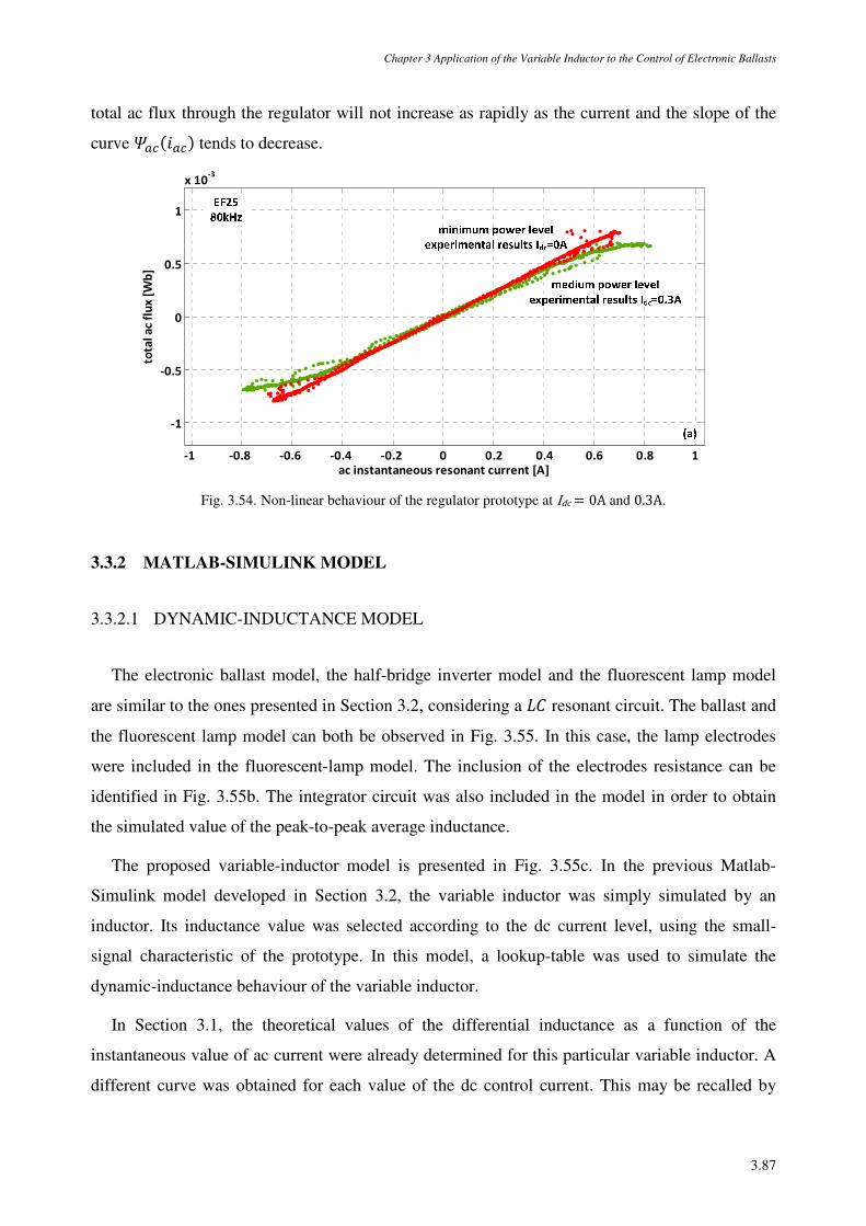
Chapter 3 Application of the Variable Inductor to the Control of Electronic Ballasts
3.87
total ac flux through the regulator will not increase as rapidly as the current and the slope of the
curve Ã~L~ tends to decrease.
-1 -0.8 -0.6 -0.4 -0.2 0 0.2 0.4 0.6 0.8 1
-1
-0.5
0
0.5
1
x 10-3
ac instantaneous resonant current [A]
tota
l a
c fl
ux
[W
b]
Fig. 3.54. Non-linear behaviour of the regulator prototype at Idc = 0A and 0.3A.
3.3.2 MATLAB-SIMULINK MODEL
3.3.2.1 DYNAMIC-INDUCTANCE MODEL
The electronic ballast model, the half-bridge inverter model and the fluorescent lamp model
are similar to the ones presented in Section 3.2, considering a ¯ resonant circuit. The ballast and
the fluorescent lamp model can both be observed in Fig. 3.55. In this case, the lamp electrodes
were included in the fluorescent-lamp model. The inclusion of the electrodes resistance can be
identified in Fig. 3.55b. The integrator circuit was also included in the model in order to obtain
the simulated value of the peak-to-peak average inductance.
The proposed variable-inductor model is presented in Fig. 3.55c. In the previous Matlab-
Simulink model developed in Section 3.2, the variable inductor was simply simulated by an
inductor. Its inductance value was selected according to the dc current level, using the small-
signal characteristic of the prototype. In this model, a lookup-table was used to simulate the
dynamic-inductance behaviour of the variable inductor.
In Section 3.1, the theoretical values of the differential inductance as a function of the
instantaneous value of ac current were already determined for this particular variable inductor. A
different curve was obtained for each value of the dc control current. This may be recalled by
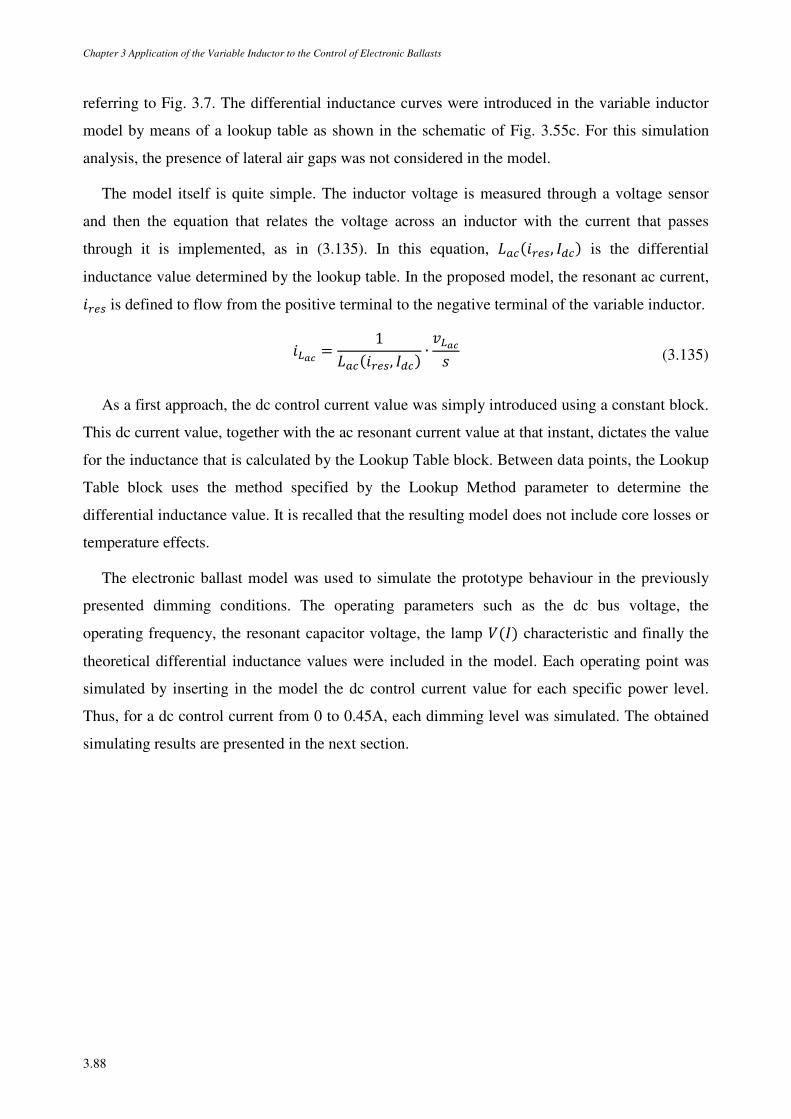
Chapter 3 Application of the Variable Inductor to the Control of Electronic Ballasts
3.88
referring to Fig. 3.7. The differential inductance curves were introduced in the variable inductor
model by means of a lookup table as shown in the schematic of Fig. 3.55c. For this simulation
analysis, the presence of lateral air gaps was not considered in the model.
The model itself is quite simple. The inductor voltage is measured through a voltage sensor
and then the equation that relates the voltage across an inductor with the current that passes
through it is implemented, as in (3.135). In this equation, ¯~L234, / is the differential
inductance value determined by the lookup table. In the proposed model, the resonant ac current,
L234 is defined to flow from the positive terminal to the negative terminal of the variable inductor.
L6 = 1¯~L234, / ∙ K6 (3.135)
As a first approach, the dc control current value was simply introduced using a constant block.
This dc current value, together with the ac resonant current value at that instant, dictates the value
for the inductance that is calculated by the Lookup Table block. Between data points, the Lookup
Table block uses the method specified by the Lookup Method parameter to determine the
differential inductance value. It is recalled that the resulting model does not include core losses or
temperature effects.
The electronic ballast model was used to simulate the prototype behaviour in the previously
presented dimming conditions. The operating parameters such as the dc bus voltage, the
operating frequency, the resonant capacitor voltage, the lamp >/ characteristic and finally the
theoretical differential inductance values were included in the model. Each operating point was
simulated by inserting in the model the dc control current value for each specific power level.
Thus, for a dc control current from 0 to 0.45A, each dimming level was simulated. The obtained
simulating results are presented in the next section.
Chapter 3 Application of the Variable Inductor to the Control of Electronic Ballasts
3.89
a. Half-bridge resonant ballast model b. Fluorescent-lamp model c. Variable-inductor model
Fig. 3.55. Electronic ballast MATLAB-Simulink implementation: dynamic-inductance model.
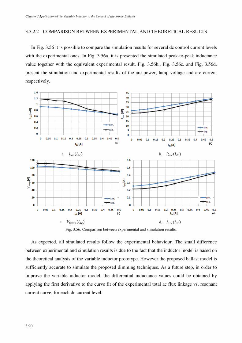
Chapter 3 Application of the Variable Inductor to the Control of Electronic Ballasts
3.90
3.3.2.2 COMPARISON BETWEEN EXPERIMENTAL AND THEORETICAL RESULTS
In Fig. 3.56 it is possible to compare the simulation results for several dc control current levels
with the experimental ones. In Fig. 3.56a. it is presented the simulated peak-to-peak inductance
value together with the equivalent experimental result. Fig. 3.56b., Fig. 3.56c. and Fig. 3.56d.
present the simulation and experimental results of the arc power, lamp voltage and arc current
respectively.
a. ¯~/ b. t~2/
c. >~/ d. /~2/
Fig. 3.56. Comparison between experimental and simulation results.
As expected, all simulated results follow the experimental behaviour. The small difference
between experimental and simulation results is due to the fact that the inductor model is based on
the theoretical analysis of the variable inductor prototype. However the proposed ballast model is
sufficiently accurate to simulate the proposed dimming techniques. As a future step, in order to
improve the variable inductor model, the differential inductance values could be obtained by
applying the first derivative to the curve fit of the experimental total ac flux linkage vs. resonant
current curve, for each dc current level.
Chapter 3 Application of the Variable Inductor to the Control of Electronic Ballasts
3.91
3.4 ELECTRODE OPERATION IN DIMMABLE ELECTRONIC
BALLASTS WITH MAGNETIC CONTROL
Tubular fluorescent lamps present restrictions that must be taken into account in the design of
any electronic ballast [3.30]. Presently, there are several regulations regarding ballast and
luminaire design. Issues regarding installation, environment, performance, operation conditions,
ignition and electrodes pre-heating are referred to in several IEC standards [3.31]-[3.34]. A key
issue when developing electronic ballasts for fluorescent lamps is to evaluate the physical
conditions of the fluorescent lamp electrodes during the lamp operation since, as stated in [3.29],
the lifetime of a fluorescent lamp is determined by the electrode operation. In order to ensure
sufficient electrode lifetime, its temperature should be kept within certain limits. Above a certain
temperature the electrodes will be too hot, leading to enhanced evaporation of the emissive
material and severe end-blackening. Below a certain temperature the electrodes will be too cold
and sputtering of the emitter will occur. Both situations may lead to an extremely short lamp life.
The purpose of the following study was to evaluate the electrodes operation under the proposed
control technique.
3.4.1 PERFORMANCE ISSUES
3.4.1.1 PRE-HEATING AND HEATING CURRENTS DURING DIMMING OPERATION
The ignition process is a decisive factor in terms of electrode preservation, with an immediate
effect on the lamp life. Avoiding the sputtering effect requires pre-heating the electrodes, which
will in turn increase the power losses. In addition, in order to avoid evaporation of the emissive
material, it is extremely important to maintain the electrodes temperatures at an appropriate level
during normal fluorescent-lamp operation. Thus, soft-starting, electrodes preheating, and safe
electrodes operation are critical aspects to be considered while developing new highly efficient
electronic ballasts [3.38].
A common way to guarantee adequate electrodes heating is through external heating sources
(North America practice) as represented in the simplified circuit shown in Fig. 3.57a. This is
quite customary in rapid-start circuits or warm-start circuits [3.33], and is currently the common
practice is most commercial ballasts. Depending on the internal impedance of these sources, the
arc current /0 will divide between the electrode wires. The higher lead wire current, /, will
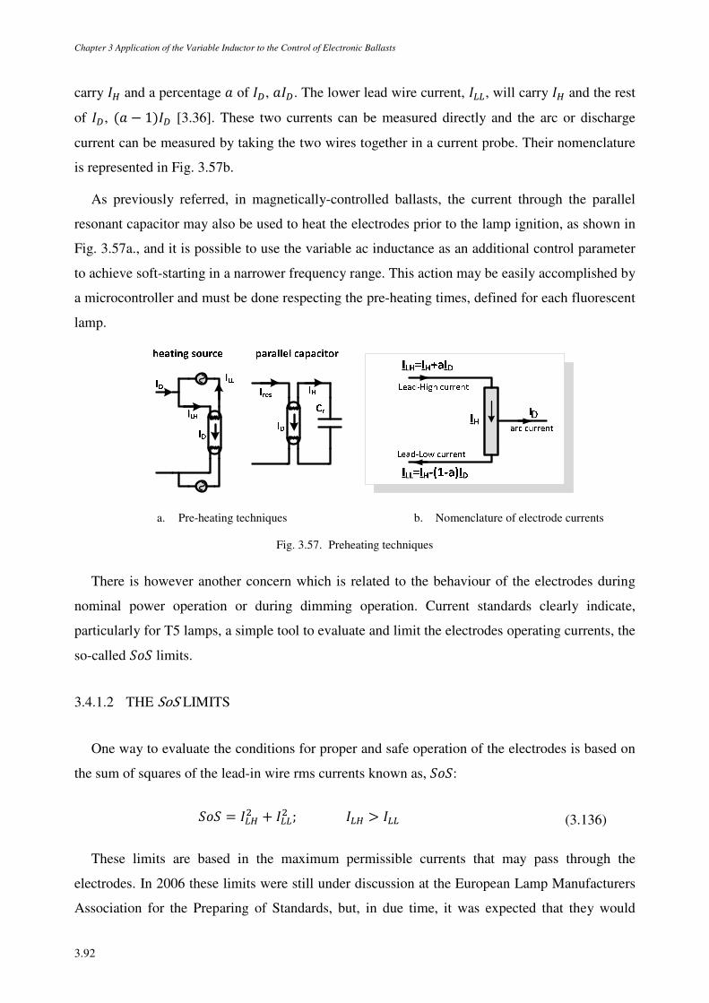
Chapter 3 Application of the Variable Inductor to the Control of Electronic Ballasts
3.92
carry / and a percentage w of /0, w/0. The lower lead wire current, /, will carry / and the rest
of /0, w − 1/0 [3.36]. These two currents can be measured directly and the arc or discharge
current can be measured by taking the two wires together in a current probe. Their nomenclature
is represented in Fig. 3.57b.
As previously referred, in magnetically-controlled ballasts, the current through the parallel
resonant capacitor may also be used to heat the electrodes prior to the lamp ignition, as shown in
Fig. 3.57a., and it is possible to use the variable ac inductance as an additional control parameter
to achieve soft-starting in a narrower frequency range. This action may be easily accomplished by
a microcontroller and must be done respecting the pre-heating times, defined for each fluorescent
lamp.
a. Pre-heating techniques b. Nomenclature of electrode currents
Fig. 3.57. Preheating techniques
There is however another concern which is related to the behaviour of the electrodes during
nominal power operation or during dimming operation. Current standards clearly indicate,
particularly for T5 lamps, a simple tool to evaluate and limit the electrodes operating currents, the
so-called m limits.
3.4.1.2 THE SoS LIMITS
One way to evaluate the conditions for proper and safe operation of the electrodes is based on
the sum of squares of the lead-in wire rms currents known as, m:
m = / + / ; / > / (3.136)
These limits are based in the maximum permissible currents that may pass through the
electrodes. In 2006 these limits were still under discussion at the European Lamp Manufacturers
Association for the Preparing of Standards, but, in due time, it was expected that they would
Chapter 3 Application of the Variable Inductor to the Control of Electronic Ballasts
3.93
result in new data in the relevant IEC standards [3.29]. These limits are now referred to in the
IEC 60081 international standard (recent edition 2010) [3.35].
The definition takes into account both electrodes currents, as defined in Fig. 3.57b. For each
rated lamp power, maximum limit values are defined for each of these currents, for nominal
power operation or dimming operation. In dimming operation, instead of having one m value
for each lamp, maximum, minimum and target m curves are defined for the whole dimming
range. Lighting engineers involved in standards preparation consider this definition as the
simplest and most unambiguous way to describe the requirements for the electrode conditions
during the dimming of fluorescent lamps [3.29], [3.35], [3.36].
The electrodes are designed in such a way that the lamp current can be varied around its rated
value within certain limits. The normal operation is therefore bounded by the minimum and
maximum discharge current, /0±² and /0~Ï values. Within these limits of the lamp current,
additional heating is not strictly required. If the lamp current is to be dimmed over a broader
range, it may be necessary to supply additional heating to the electrodes to maintain its optimum
temperature. This additional heating is only necessary to keep the cathode at a sufficiently high
temperature for thermionic emission. The amount of this additional heating power is determined
by the dissipation of the additional heating current through the electrodes. So, if the ballast does
include external heating sources, the currents in the lead-in wires / and / should also be kept
below the maximum values, /~Ï and /~Ï, given in [3.29], [3.34], [3.35].
The value of the required additional heating current is a function of the arc current, but it is
also dependent on the ballast circuit layout. Using a parallel-loaded resonant circuit, as shown in
Fig. 3.57a. there is an obvious phase-shift between these currents. However, the work which led
to this so-called m approach showed a linear dependency between the sum of the squared rms
lead currents to the electrode and the discharge current, where neither the phase shift between /0
and /, nor the distribution of the discharge current trough the leads, has an influence [3.36]. This
linear dependence establishes current boundary limits related to the m value. In some other
ballast circuits where the additional heating current is delivered by separate heating sources, it is
not clear through which lead-in wire will flow part of the lamp current. Nevertheless, whatever
the configuration, all these effects can be taken into account by measuring the currents through
the two lead-in wires to the electrode and calculating the sum of the rms squares of these two
currents as a function of the discharge current. If this definition is applied to magnetically-
controlled electronic ballasts, it becomes clear that /234 = / and / = /.
Chapter 3 Application of the Variable Inductor to the Control of Electronic Ballasts
3.94
The minimum sum of squares, m±², needed to keep the electrode just at a sufficient
temperature to prevent cathode sputtering in dimming operation, is defined by:
m±² = / + / > 8ª − :ª × /0 (3.137)
where 8ª and :ª are lamp parameters given by the manufacturer and depend on the discharge
current.
The overheating of the electrode is prevented in a similar way as for low temperatures by
giving values for a maximum m line:
m~Ï = / + / < 8 − : × /0 (3.138)
where 8 and : are also given by the manufacturer. However, in order to protect the electrodes
from overheating, three different regions of the cathodes must be protected: the hot spot region,
which is protected by the m~Ï description, the bare tungsten part, which is protected by a
maximum value of /, /~Ï and finally, the coated part, which is also protected by a
maximum value of /, /~Ï.
As in some applications both m boundaries can still be critical for the lamp performance, a
safe setting of the m values is given by the target m line:
mÀ~23À = / + / ≅ 8ª − « × :ª × /0 (3.139)
The deviating slope of this target line is described by the factor «. However this line has no
physical background and can be understood as merely indicative. The purpose of this target line
is to show how far above the critical minimal m line a ballast design should be positioned
without violating any maximum electrode heating criteria [3.36]. This maximum heating criteria
corresponds to the heating current that results in sufficient electrode heating without causing
accelerated end-blackening. In deep dimming mode the discharge current contribution is typically
neglected and the safe setting is based only on the considered maximum heating criteria.
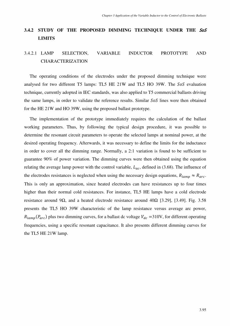
Chapter 3 Application of the Variable Inductor to the Control of Electronic Ballasts
3.95
3.4.2 STUDY OF THE PROPOSED DIMMING TECHNIQUE UNDER THE SSSSooooSSSS
LIMITS
3.4.2.1 LAMP SELECTION, VARIABLE INDUCTOR PROTOTYPE AND
CHARACTERIZATION
The operating conditions of the electrodes under the proposed dimming technique were
analysed for two different T5 lamps: TL5 HE 21W and TL5 HO 39W. The m evaluation
technique, currently adopted in IEC standards, was also applied to T5 commercial ballasts driving
the same lamps, in order to validate the reference results. Similar m lines were then obtained
for the HE 21W and HO 39W, using the proposed ballast prototype.
The implementation of the prototype immediately requires the calculation of the ballast
working parameters. Thus, by following the typical design procedure, it was possible to
determine the resonant circuit parameters to operate the selected lamps at nominal power, at the
desired operating frequency. Afterwards, it was necessary to define the limits for the inductance
in order to cover all the dimming range. Normally, a 2:1 variation is found to be sufficient to
guarantee 90% of power variation. The dimming curves were then obtained using the equation
relating the average lamp power with the control variable, ¯~, defined in (3.68). The influence of
the electrodes resistances is neglected when using the necessary design equations, v~ ≈ v~2.
This is only an approximation, since heated electrodes can have resistances up to four times
higher than their normal cold resistances. For instance, TL5 HE lamps have a cold electrode
resistance around 9Ω, and a heated electrode resistance around 40Ω [3.29], [3.49]. Fig. 3.58
presents the TL5 HO 39W characteristic of the lamp resistance versus average arc power,
v~t~2 plus two dimming curves, for a ballast dc voltage > =310V, for different operating
frequencies, using a specific resonant capacitance. It also presents different dimming curves for
the TL5 HE 21W lamp.
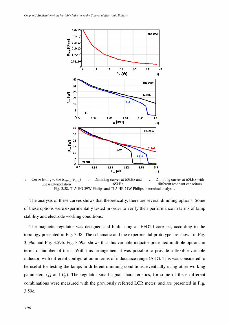
Chapter 3 Application of the Variable Inductor to the Control of Electronic Ballasts
3.96
a. Curve fitting to the v~t~2 linear interpolation
b. Dimming curves at 60kHz and 65kHz
c. Dimming curves at 65kHz with different resonant capacitors
Fig. 3.58. TL5 HO 39W Philips and TL5 HE 21W Philips theoretical analysis.
The analysis of these curves shows that theoretically, there are several dimming options. Some
of these options were experimentally tested in order to verify their performance in terms of lamp
stability and electrode working conditions.
The magnetic regulator was designed and built using an EFD20 core set, according to the
topology presented in Fig. 3.38. The schematic and the experimental prototype are shown in Fig.
3.59a. and Fig. 3.59b. Fig. 3.59a. shows that this variable inductor presented multiple options in
terms of number of turns. With this arrangement it was possible to provide a flexible variable
inductor, with different configuration in terms of inductance range (A-D). This was considered to
be useful for testing the lamps in different dimming conditions, eventually using other working
parameters (4 and ). The regulator small-signal characteristics, for some of these different
combinations were measured with the previously referred LCR meter, and are presented in Fig.
3.59c.
Chapter 3 Application of the Variable Inductor to the Control of Electronic Ballasts
3.97
a. Schematic b. Experimental prototype c. Small signal characteristics
Fig. 3.59. Variable inductor
3.4.2.2 COMMERCIAL BALLASTS TESTS AND PROTOTYPE RESULTS UNDER THE SoS LIMITS
Two commercial electronic ballasts, PHILIPS HF-R 14-35 TL5 220-240 and HF-R 139 TL5
220-2240, were used in order to obtain reference results related to the lamp operation and to
compare them to the IEC standard. For the TL5 HE 21W lamp, all the measurements performed
were already detailed in Table 3.6. It is noticed that this ballast is also capable of driving other T5
lamps, with different power ratings. The TL5 HO 39W lamp was tested in a similar way. The
obtained results are presented in Table 3.8. For both lamps, each electrode power was calculated,
multiplying the voltage across the electrode by the lead-in current. It was then assumed that the
corresponding lamp power would be equal to the sum of the arc power and twice the electrode
power. The analysis of Table 3.8 also shows that this ballast uses a variable-frequency technique
to achieve dimming and that a good power factor cannot be maintained for all operating points.
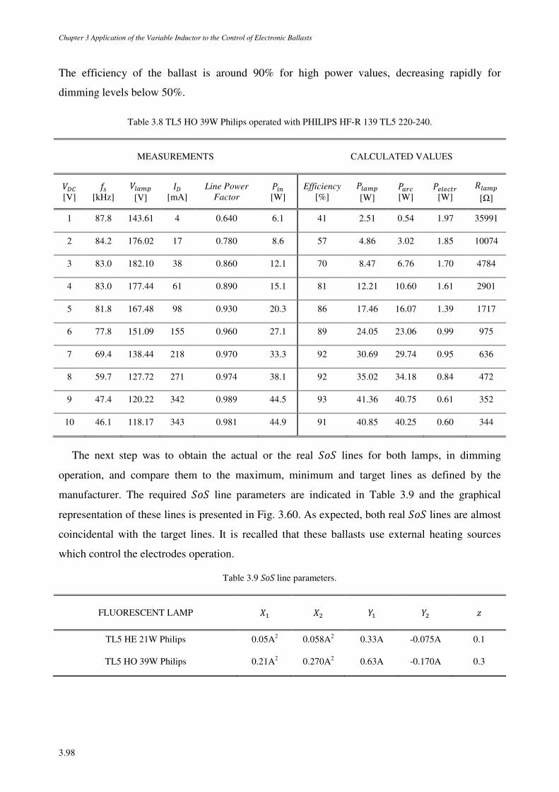
Chapter 3 Application of the Variable Inductor to the Control of Electronic Ballasts
3.98
The efficiency of the ballast is around 90% for high power values, decreasing rapidly for
dimming levels below 50%.
Table 3.8 TL5 HO 39W Philips operated with PHILIPS HF-R 139 TL5 220-240.
MEASUREMENTS CALCULATED VALUES
>0
[V] 4
[kHz] >~
[V] /0
[mA] Line Power
Factor t±²
[W] Efficiency
[%] t~
[W] t~2
[W] t33À2
[W] v~
[Ω]
1 87.8 143.61 4 0.640 6.1 41 2.51 0.54 1.97 35991
2 84.2 176.02 17 0.780 8.6 57 4.86 3.02 1.85 10074
3 83.0 182.10 38 0.860 12.1 70 8.47 6.76 1.70 4784
4 83.0 177.44 61 0.890 15.1 81 12.21 10.60 1.61 2901
5 81.8 167.48 98 0.930 20.3 86 17.46 16.07 1.39 1717
6 77.8 151.09 155 0.960 27.1 89 24.05 23.06 0.99 975
7 69.4 138.44 218 0.970 33.3 92 30.69 29.74 0.95 636
8 59.7 127.72 271 0.974 38.1 92 35.02 34.18 0.84 472
9 47.4 120.22 342 0.989 44.5 93 41.36 40.75 0.61 352
10 46.1 118.17 343 0.981 44.9 91 40.85 40.25 0.60 344
The next step was to obtain the actual or the real m lines for both lamps, in dimming
operation, and compare them to the maximum, minimum and target lines as defined by the
manufacturer. The required m line parameters are indicated in Table 3.9 and the graphical
representation of these lines is presented in Fig. 3.60. As expected, both real m lines are almost
coincidental with the target lines. It is recalled that these ballasts use external heating sources
which control the electrodes operation.
Table 3.9 SoS line parameters.
FLUORESCENT LAMP 8ª 8 :ª : «
TL5 HE 21W Philips 0.05A2 0.058A2 0.33A -0.075A 0.1
TL5 HO 39W Philips 0.21A2 0.270A2 0.63A -0.170A 0.3
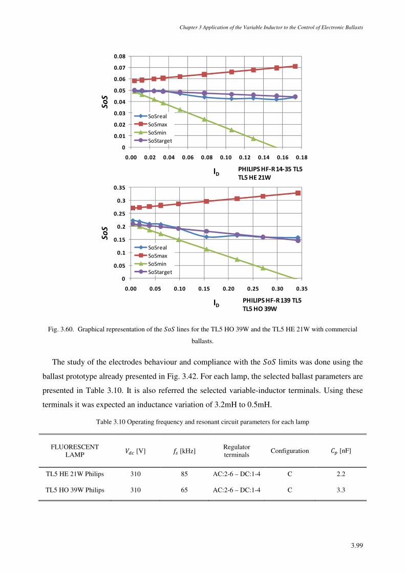
Chapter 3 Application of the Variable Inductor to the Control of Electronic Ballasts
3.99
0
0.01
0.02
0.03
0.04
0.05
0.06
0.07
0.08
0.00 0.02 0.04 0.06 0.08 0.10 0.12 0.14 0.16 0.18
SoS
ID
SoSreal
SoSmax
SoSmin
SoStarget
PHILIPS HF-R 14-35 TL5
TL5 HE 21W
0
0.05
0.1
0.15
0.2
0.25
0.3
0.35
0.00 0.05 0.10 0.15 0.20 0.25 0.30 0.35
SoS
ID
SoSreal
SoSmax
SoSmin
SoStarget
PHILIPS HF-R 139 TL5
TL5 HO 39W
Fig. 3.60. Graphical representation of the m lines for the TL5 HO 39W and the TL5 HE 21W with commercial
ballasts.
The study of the electrodes behaviour and compliance with the m limits was done using the
ballast prototype already presented in Fig. 3.42. For each lamp, the selected ballast parameters are
presented in Table 3.10. It is also referred the selected variable-inductor terminals. Using these
terminals it was expected an inductance variation of 3.2mH to 0.5mH.
Table 3.10 Operating frequency and resonant circuit parameters for each lamp
FLUORESCENT LAMP
> [V] 4 [kHz] Regulator terminals
Configuration [nF]
TL5 HE 21W Philips 310 85 AC:2-6 – DC:1-4 C 2.2
TL5 HO 39W Philips 310 65 AC:2-6 – DC:1-4 C 3.3
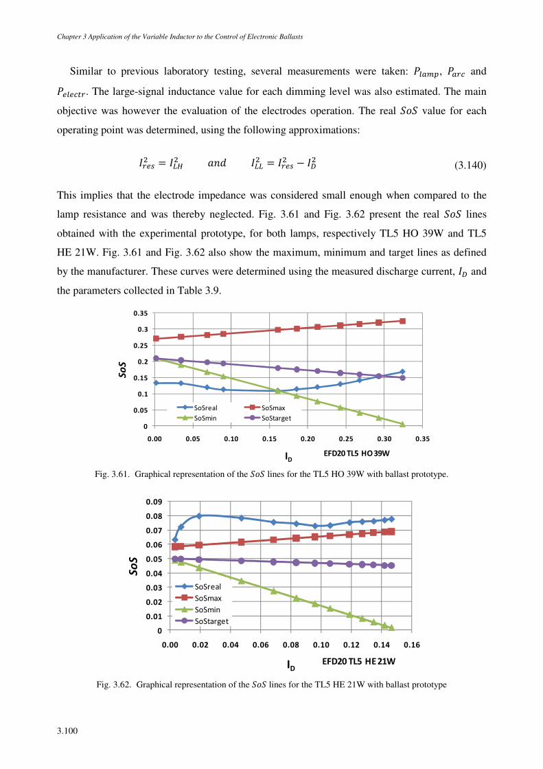
Chapter 3 Application of the Variable Inductor to the Control of Electronic Ballasts
3.100
Similar to previous laboratory testing, several measurements were taken: t~, t~2 and
t33À2. The large-signal inductance value for each dimming level was also estimated. The main
objective was however the evaluation of the electrodes operation. The real m value for each
operating point was determined, using the following approximations:
/234 = / w/ = /234 − /0 (3.140)
This implies that the electrode impedance was considered small enough when compared to the
lamp resistance and was thereby neglected. Fig. 3.61 and Fig. 3.62 present the real m lines
obtained with the experimental prototype, for both lamps, respectively TL5 HO 39W and TL5
HE 21W. Fig. 3.61 and Fig. 3.62 also show the maximum, minimum and target lines as defined
by the manufacturer. These curves were determined using the measured discharge current, /0 and
the parameters collected in Table 3.9.
0
0.05
0.1
0.15
0.2
0.25
0.3
0.35
0.00 0.05 0.10 0.15 0.20 0.25 0.30 0.35
SoS
ID
SoSreal SoSmax
SoSmin SoStarget
EFD20 TL5 HO 39W
Fig. 3.61. Graphical representation of the m lines for the TL5 HO 39W with ballast prototype.
0
0.01
0.02
0.03
0.04
0.05
0.06
0.07
0.08
0.09
0.00 0.02 0.04 0.06 0.08 0.10 0.12 0.14 0.16
SoS
ID
SoSreal
SoSmax
SoSmin
SoStarget
EFD20 TL5 HE 21W
Fig. 3.62. Graphical representation of the m lines for the TL5 HE 21W with ballast prototype
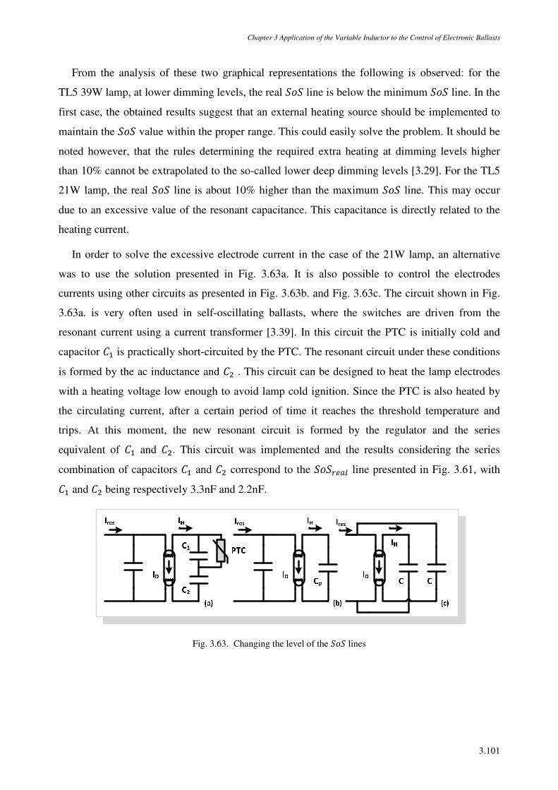
Chapter 3 Application of the Variable Inductor to the Control of Electronic Ballasts
3.101
From the analysis of these two graphical representations the following is observed: for the
TL5 39W lamp, at lower dimming levels, the real m line is below the minimum m line. In the
first case, the obtained results suggest that an external heating source should be implemented to
maintain the m value within the proper range. This could easily solve the problem. It should be
noted however, that the rules determining the required extra heating at dimming levels higher
than 10% cannot be extrapolated to the so-called lower deep dimming levels [3.29]. For the TL5
21W lamp, the real m line is about 10% higher than the maximum m line. This may occur
due to an excessive value of the resonant capacitance. This capacitance is directly related to the
heating current.
In order to solve the excessive electrode current in the case of the 21W lamp, an alternative
was to use the solution presented in Fig. 3.63a. It is also possible to control the electrodes
currents using other circuits as presented in Fig. 3.63b. and Fig. 3.63c. The circuit shown in Fig.
3.63a. is very often used in self-oscillating ballasts, where the switches are driven from the
resonant current using a current transformer [3.39]. In this circuit the PTC is initially cold and
capacitor ª is practically short-circuited by the PTC. The resonant circuit under these conditions
is formed by the ac inductance and . This circuit can be designed to heat the lamp electrodes
with a heating voltage low enough to avoid lamp cold ignition. Since the PTC is also heated by
the circulating current, after a certain period of time it reaches the threshold temperature and
trips. At this moment, the new resonant circuit is formed by the regulator and the series
equivalent of ª and . This circuit was implemented and the results considering the series
combination of capacitors ª and correspond to the m23~ line presented in Fig. 3.61, with
ª and being respectively 3.3nF and 2.2nF.
Fig. 3.63. Changing the level of the m lines
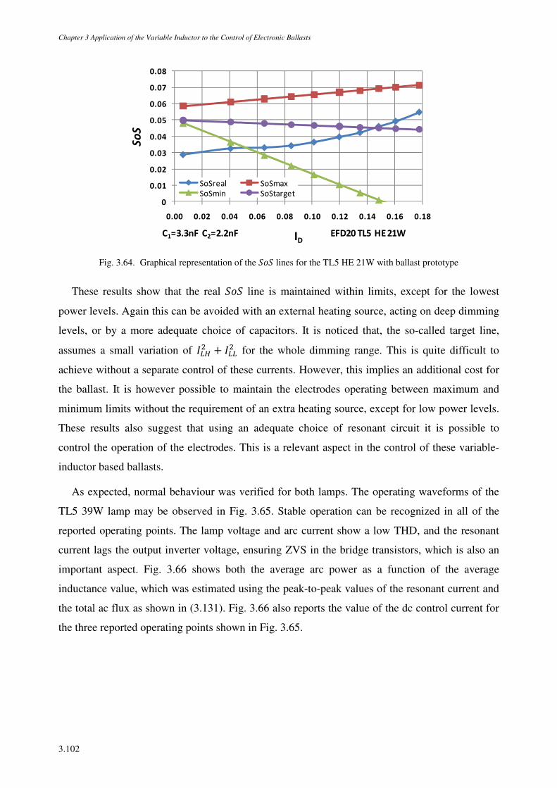
Chapter 3 Application of the Variable Inductor to the Control of Electronic Ballasts
3.102
0
0.01
0.02
0.03
0.04
0.05
0.06
0.07
0.08
0.00 0.02 0.04 0.06 0.08 0.10 0.12 0.14 0.16 0.18
SoS
ID
SoSreal SoSmax
SoSmin SoStarget
EFD20 TL5 HE 21WC1=3.3nF C2=2.2nF
Fig. 3.64. Graphical representation of the m lines for the TL5 HE 21W with ballast prototype
These results show that the real m line is maintained within limits, except for the lowest
power levels. Again this can be avoided with an external heating source, acting on deep dimming
levels, or by a more adequate choice of capacitors. It is noticed that, the so-called target line,
assumes a small variation of / + / for the whole dimming range. This is quite difficult to
achieve without a separate control of these currents. However, this implies an additional cost for
the ballast. It is however possible to maintain the electrodes operating between maximum and
minimum limits without the requirement of an extra heating source, except for low power levels.
These results also suggest that using an adequate choice of resonant circuit it is possible to
control the operation of the electrodes. This is a relevant aspect in the control of these variable-
inductor based ballasts.
As expected, normal behaviour was verified for both lamps. The operating waveforms of the
TL5 39W lamp may be observed in Fig. 3.65. Stable operation can be recognized in all of the
reported operating points. The lamp voltage and arc current show a low THD, and the resonant
current lags the output inverter voltage, ensuring ZVS in the bridge transistors, which is also an
important aspect. Fig. 3.66 shows both the average arc power as a function of the average
inductance value, which was estimated using the peak-to-peak values of the resonant current and
the total ac flux as shown in (3.131). Fig. 3.66 also reports the value of the dc control current for
the three reported operating points shown in Fig. 3.65.
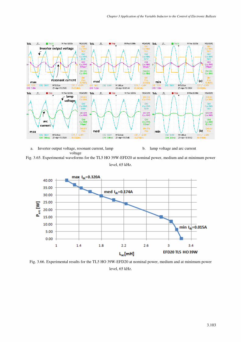
Chapter 3 Application of the Variable Inductor to the Control of Electronic Ballasts
3.103
a. Inverter output voltage, resonant current, lamp voltage
b. lamp voltage and arc current
Fig. 3.65. Experimental waveforms for the TL5 HO 39W-EFD20 at nominal power, medium and at minimum power
level, 65 kHz.
Fig. 3.66. Experimental results for the TL5 HO 39W-EFD20 at nominal power, medium and at minimum power
level, 65 kHz.
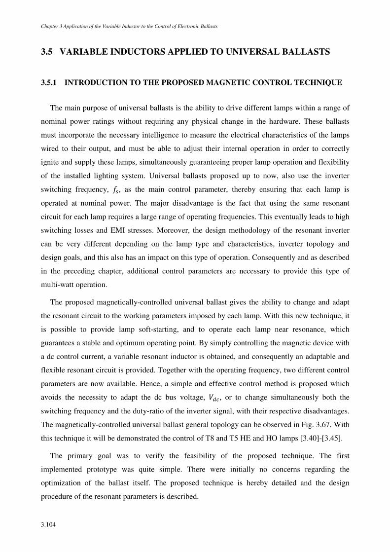
Chapter 3 Application of the Variable Inductor to the Control of Electronic Ballasts
3.104
3.5 VARIABLE INDUCTORS APPLIED TO UNIVERSAL BALLASTS
3.5.1 INTRODUCTION TO THE PROPOSED MAGNETIC CONTROL TECHNIQUE
The main purpose of universal ballasts is the ability to drive different lamps within a range of
nominal power ratings without requiring any physical change in the hardware. These ballasts
must incorporate the necessary intelligence to measure the electrical characteristics of the lamps
wired to their output, and must be able to adjust their internal operation in order to correctly
ignite and supply these lamps, simultaneously guaranteeing proper lamp operation and flexibility
of the installed lighting system. Universal ballasts proposed up to now, also use the inverter
switching frequency, 4, as the main control parameter, thereby ensuring that each lamp is
operated at nominal power. The major disadvantage is the fact that using the same resonant
circuit for each lamp requires a large range of operating frequencies. This eventually leads to high
switching losses and EMI stresses. Moreover, the design methodology of the resonant inverter
can be very different depending on the lamp type and characteristics, inverter topology and
design goals, and this also has an impact on this type of operation. Consequently and as described
in the preceding chapter, additional control parameters are necessary to provide this type of
multi-watt operation.
The proposed magnetically-controlled universal ballast gives the ability to change and adapt
the resonant circuit to the working parameters imposed by each lamp. With this new technique, it
is possible to provide lamp soft-starting, and to operate each lamp near resonance, which
guarantees a stable and optimum operating point. By simply controlling the magnetic device with
a dc control current, a variable resonant inductor is obtained, and consequently an adaptable and
flexible resonant circuit is provided. Together with the operating frequency, two different control
parameters are now available. Hence, a simple and effective control method is proposed which
avoids the necessity to adapt the dc bus voltage, >, or to change simultaneously both the
switching frequency and the duty-ratio of the inverter signal, with their respective disadvantages.
The magnetically-controlled universal ballast general topology can be observed in Fig. 3.67. With
this technique it will be demonstrated the control of T8 and T5 HE and HO lamps [3.40]-[3.45].
The primary goal was to verify the feasibility of the proposed technique. The first
implemented prototype was quite simple. There were initially no concerns regarding the
optimization of the ballast itself. The proposed technique is hereby detailed and the design
procedure of the resonant parameters is described.
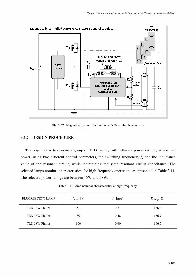
Chapter 3 Application of the Variable Inductor to the Control of Electronic Ballasts
3.105
Fig. 3.67. Magnetically-controlled universal ballast: circuit schematic
3.5.2 DESIGN PROCEDURE
The objective is to operate a group of TLD lamps, with different power ratings, at nominal
power, using two different control parameters, the switching frequency, 4 and the inductance
value of the resonant circuit, while maintaining the same resonant circuit capacitance. The
selected lamps nominal characteristics, for high-frequency operation, are presented in Table 3.11.
The selected power ratings are between 15W and 58W.
Table 3.11 Lamp nominal characteristics at high-frequency.
FLUORESCENT LAMP >~ [V] /0 [mA] v~ [Ω]
TLD 18W Philips 51 0.37 136.4
TLD 36W Philips 80 0.48 166.7
TLD 58W Philips 100 0.60 166.7
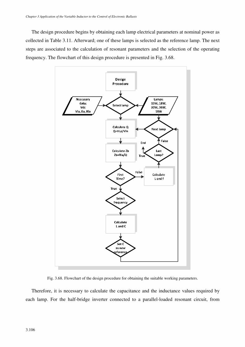
Chapter 3 Application of the Variable Inductor to the Control of Electronic Ballasts
3.106
The design procedure begins by obtaining each lamp electrical parameters at nominal power as
collected in Table 3.11. Afterward; one of these lamps is selected as the reference lamp. The next
steps are associated to the calculation of resonant parameters and the selection of the operating
frequency. The flowchart of this design procedure is presented in Fig. 3.68.
Fig. 3.68. Flowchart of the design procedure for obtaining the suitable working parameters.
Therefore, it is necessary to calculate the capacitance and the inductance values required by
each lamp. For the half-bridge inverter connected to a parallel-loaded resonant circuit, from
Chapter 3 Application of the Variable Inductor to the Control of Electronic Ballasts
3.107
(3.59) it can be observed that ââ = Ð when 4 Ô¤ = 1. In other words, the maximum
voltage gain can be approximated by Ð at the natural frequency, Ô, Ð being the normalized load,
as represented in (3.141). This equation can be used to calculate the base impedance of each
resonant circuit, ´, for each lamp, using the nominal values for the lamp voltage, >~, and the
lamp resistance, v~. So, as a first step, the estimation of the resonant filter parameters, ¯~ and
, is done considering that 4 = Ô, and Ô = 1 √¯¤ , using (3.141), (3.142), (3.143) and
(3.144).
Ð = >~>±² = v~´ ; m4 = Ô (3.141)
´ = ö ; m4 = Ô (3.142)
¯~ = ´2¸Ô (3.143)
= 12¸´Ô (3.144)
So, more precisely, the rms value of the lamp discharge or arc current, /0, can be defined as:
/0 = >~v~ (3.145)
It implies that if the circuit is operated at 4 = Ô, (3.145) can be re-written as follows:
/0 = >~v~ = >±²Ðv~ = >±²´ (3.146)
Therefore, the circuit will behave as a current source, and its value depends exclusively on the
input voltage and ´. After this first-time operation the desired operating frequency, 4, is
selected for this first lamp. Then, taking into account the preceding considerations, the
capacitance and inductance values for the selected lamp may be calculated by rewriting (3.143)
and (3.144), respectively:
¯~ = >±²2 ∙ ¸ ∙ 4 ∙ /0 (3.147)
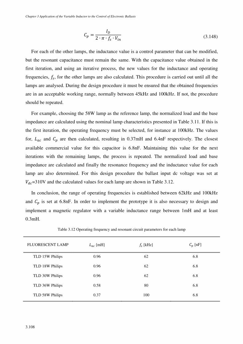
Chapter 3 Application of the Variable Inductor to the Control of Electronic Ballasts
3.108
= /02 ∙ ¸ ∙ 4 ∙ >±² (3.148)
For each of the other lamps, the inductance value is a control parameter that can be modified,
but the resonant capacitance must remain the same. With the capacitance value obtained in the
first iteration, and using an iterative process, the new values for the inductance and operating
frequencies, 4, for the other lamps are also calculated. This procedure is carried out until all the
lamps are analysed. During the design procedure it must be ensured that the obtained frequencies
are in an acceptable working range, normally between 45kHz and 100kHz. If not, the procedure
should be repeated.
For example, choosing the 58W lamp as the reference lamp, the normalized load and the base
impedance are calculated using the nominal lamp characteristics presented in Table 3.11. If this is
the first iteration, the operating frequency must be selected, for instance at 100kHz. The values
for, ¯~ and are then calculated, resulting in 0.37mH and 6.4nF respectively. The closest
available commercial value for this capacitor is 6.8nF. Maintaining this value for the next
iterations with the remaining lamps, the process is repeated. The normalized load and base
impedance are calculated and finally the resonance frequency and the inductance value for each
lamp are also determined. For this design procedure the ballast input dc voltage was set at
>=310V and the calculated values for each lamp are shown in Table 3.12.
In conclusion, the range of operating frequencies is established between 62kHz and 100kHz
and is set at 6.8nF. In order to implement the prototype it is also necessary to design and
implement a magnetic regulator with a variable inductance range between 1mH and at least
0.3mH.
Table 3.12 Operating frequency and resonant circuit parameters for each lamp
FLUORESCENT LAMP ¯~ [mH] 4 [kHz] [nF]
TLD 15W Philips 0.96 62 6.8
TLD 18W Philips 0.96 62 6.8
TLD 30W Philips 0.96 62 6.8
TLD 36W Philips 0.58 80 6.8
TLD 58W Philips 0.37 100 6.8
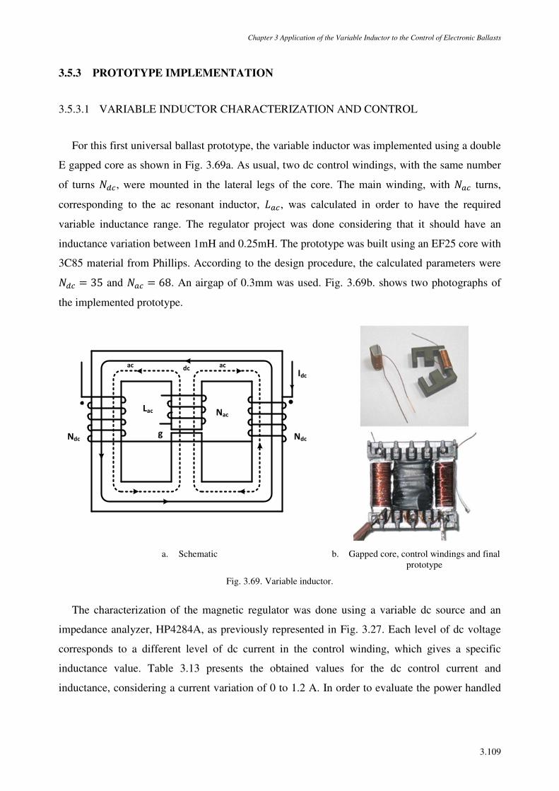
Chapter 3 Application of the Variable Inductor to the Control of Electronic Ballasts
3.109
3.5.3 PROTOTYPE IMPLEMENTATION
3.5.3.1 VARIABLE INDUCTOR CHARACTERIZATION AND CONTROL
For this first universal ballast prototype, the variable inductor was implemented using a double
E gapped core as shown in Fig. 3.69a. As usual, two dc control windings, with the same number
of turns Á, were mounted in the lateral legs of the core. The main winding, with Á~ turns,
corresponding to the ac resonant inductor, ¯~, was calculated in order to have the required
variable inductance range. The regulator project was done considering that it should have an
inductance variation between 1mH and 0.25mH. The prototype was built using an EF25 core with
3C85 material from Phillips. According to the design procedure, the calculated parameters were
Á = 35 and Á~ = 68. An airgap of 0.3mm was used. Fig. 3.69b. shows two photographs of
the implemented prototype.
Idc
Ndc Ndc
Nac
ac acdc
Lac
g
a. Schematic b. Gapped core, control windings and final prototype
Fig. 3.69. Variable inductor.
The characterization of the magnetic regulator was done using a variable dc source and an
impedance analyzer, HP4284A, as previously represented in Fig. 3.27. Each level of dc voltage
corresponds to a different level of dc current in the control winding, which gives a specific
inductance value. Table 3.13 presents the obtained values for the dc control current and
inductance, considering a current variation of 0 to 1.2 A. In order to evaluate the power handled
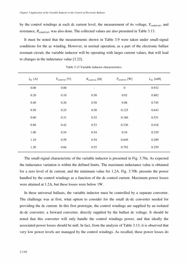
Chapter 3 Application of the Variable Inductor to the Control of Electronic Ballasts
3.110
by the control windings at each dc current level, the measurement of its voltage, >Ô²À2Ô, and
resistance, vÔ²À2Ô, was also done. The collected values are also presented in Table 3.13.
It must be noted that the measurements shown in Table 3.9 were taken under small-signal
conditions for the ac winding. However, in normal operation, as a part of the electronic ballast
resonant circuit, the variable inductor will be operating with larger current values, that will lead
to changes in the inductance value [3.22].
Table 3.13 Variable inductor characteristics.
/ [A] >Ô²À2Ô [V] vÔ²À2Ô [Ω] tÔ²À2Ô [W] ¯~ [mH]
0.00 0.00 - 0 0.932
0.20 0.10 0.50 0.02 0.882
0.40 0.20 0.50 0.08 0.745
0.50 0.25 0.50 0.125 0.643
0.60 0.31 0.52 0.186 0.551
0.80 0.42 0.53 0.336 0.418
1.00 0.54 0.54 0.54 0.329
1.10 0.59 0.54 0.649 0.289
1.20 0.66 0.55 0.792 0.259
The small-signal characteristic of the variable inductor is presented in Fig. 3.70a. As expected
the inductance variation is within the defined limits. The maximum inductance value is obtained
for a zero level of dc current, and the minimum value for 1.2A. Fig. 3.70b. presents the power
handled by the control windings as a function of the dc control current. Maximum power losses
were attained at 1.2A, but these losses were below 1W.
In these universal ballasts, the variable inductor must be controlled by a separate converter.
The challenge was at first, what option to consider for the small dc-dc converter needed for
providing the dc current. In this first prototype, the control windings are supplied by an isolated
dc-dc converter, a forward converter, directly supplied by the ballast dc voltage. It should be
noted that this converter will only handle the control windings power, and that ideally the
associated power losses should be null. In fact, from the analysis of Table 3.13, it is observed that
very low power levels are managed by the control windings. As recalled, these power losses do
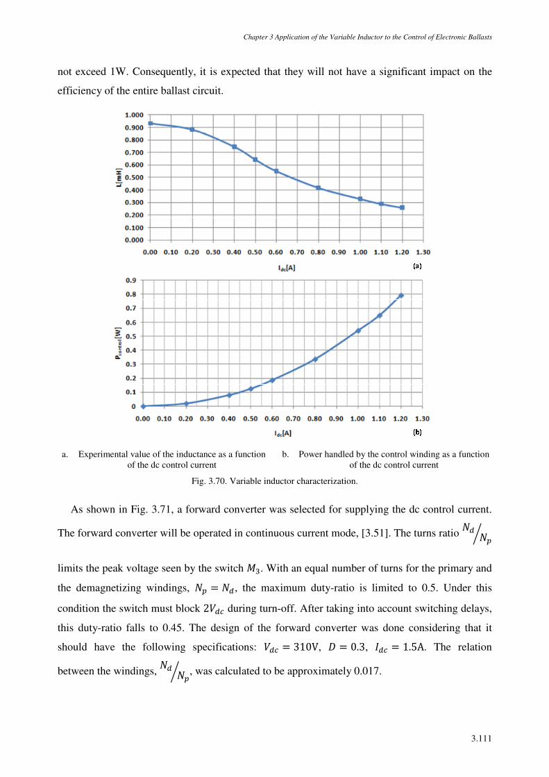
Chapter 3 Application of the Variable Inductor to the Control of Electronic Ballasts
3.111
not exceed 1W. Consequently, it is expected that they will not have a significant impact on the
efficiency of the entire ballast circuit.
a. Experimental value of the inductance as a function of the dc control current
b. Power handled by the control winding as a function of the dc control current
Fig. 3.70. Variable inductor characterization.
As shown in Fig. 3.71, a forward converter was selected for supplying the dc control current.
The forward converter will be operated in continuous current mode, [3.51]. The turns ratio Á Á;
limits the peak voltage seen by the switch ½. With an equal number of turns for the primary and
the demagnetizing windings, Á = Á, the maximum duty-ratio is limited to 0.5. Under this
condition the switch must block 2> during turn-off. After taking into account switching delays,
this duty-ratio falls to 0.45. The design of the forward converter was done considering that it
should have the following specifications: > = 310V, ® = 0.3, / = 1.5A. The relation
between the windings, Á Á; , was calculated to be approximately 0.017.
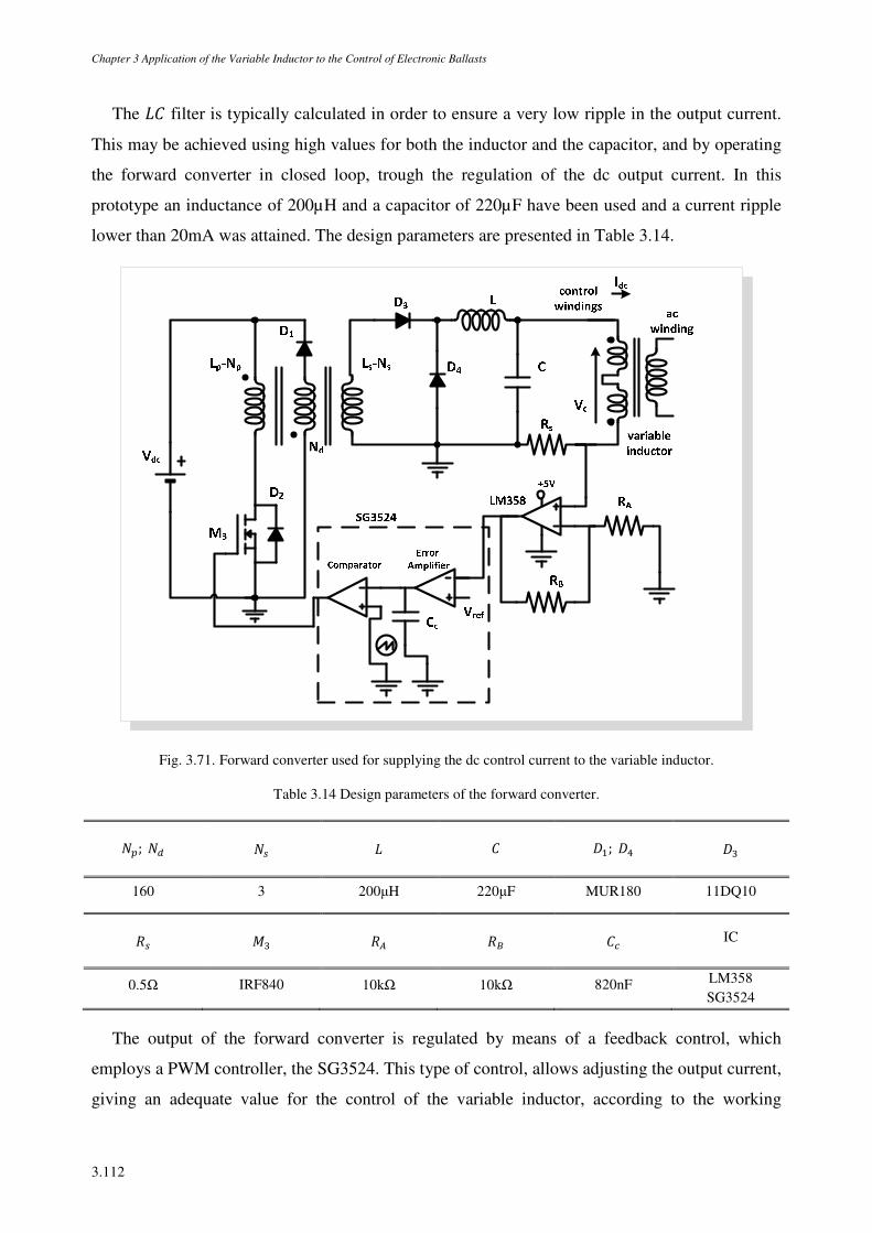
Chapter 3 Application of the Variable Inductor to the Control of Electronic Ballasts
3.112
The ¯ filter is typically calculated in order to ensure a very low ripple in the output current.
This may be achieved using high values for both the inductor and the capacitor, and by operating
the forward converter in closed loop, trough the regulation of the dc output current. In this
prototype an inductance of 200µH and a capacitor of 220µF have been used and a current ripple
lower than 20mA was attained. The design parameters are presented in Table 3.14.
Fig. 3.71. Forward converter used for supplying the dc control current to the variable inductor.
Table 3.14 Design parameters of the forward converter.
Á; Á Á4 ¯ ®ª; ®× ®
160 3 200µH 220µF MUR180 11DQ10
v4 ½ vû vÕ IC
0.5Ω IRF840 10kΩ 10kΩ 820nF LM358 SG3524
The output of the forward converter is regulated by means of a feedback control, which
employs a PWM controller, the SG3524. This type of control, allows adjusting the output current,
giving an adequate value for the control of the variable inductor, according to the working
Chapter 3 Application of the Variable Inductor to the Control of Electronic Ballasts
3.113
parameters imposed by each lamp. Fig. 3.71 shows that the output dc current of the converter is
sensed, through v4 , and then amplified, using the LM358 operational amplifier. This output
signal is fed to the transconductance error amplifier of the SG3524. Theoretically, a
transconductance amplifier is an equivalent voltage-controlled current source. It multiplies the
difference of the input voltages by a certain gain and generates a current into the output node. So,
this error amplifier produces an error feedback signal which is proportional to the difference
between the reference input voltage and the output voltage of the LM358 operational amplifier.
Its compensation network was chosen to be a shunt capacitor, acting as an integrator, since there
is no need of a fast response. Finally, the sawtooth waveform is compared with the error amplifier
output in an internal comparator at the selected switching frequency, to determine the duty-cycle
of the switch ½.
3.5.3.2 GENERAL OPERATING ISSUES
Previous to the description of the implemented prototype, it is relevant to discuss some of the
general operating issues. As mentioned, all the following requirements must be fulfilled: the lamp
must be ignited properly; the lamp operation must be stable at steady state; the lamp must be
operated as close to its rated power as possible, and the ballast efficiency with each lamp should
be as high as possible. The design procedure guarantees, from the start, that each lamp is properly
ignited and operated at rated power. Soft-starting concerns can be overcome by using the
common technique for electrodes pre-heating: the pre-heating process may be guaranteed by
means of a frequency-controlled soft-start technique or, as already described, a soft-starting
process using the variable inductance itself, may be used.
Another important issue is related to the power control of the electronic ballast: At first, it
implies the study of the phase angle of the input current of the resonant circuit for each case. If a
delayed current is enforced, it is possible to achieve ZVS in the bridge MOSFETs. Therefore, this
analysis must also be done. In addition, this phase analysis is important to ensure near-resonance
conditions.
Other concerns are related to the lamp identification. After ignition, the lamp voltage typically
falls to a lower operating voltage. If the lamp is not dimmed, this lamp voltage will remain more
or less constant under steady state conditions. In [2.53], a comparison of lamp characteristics of
major brand names is presented. It is stated that for all popular standard T8 fluorescent lamps,
with the same rated power, the lamp voltage as well as lamp currents, are almost identical. Yet,
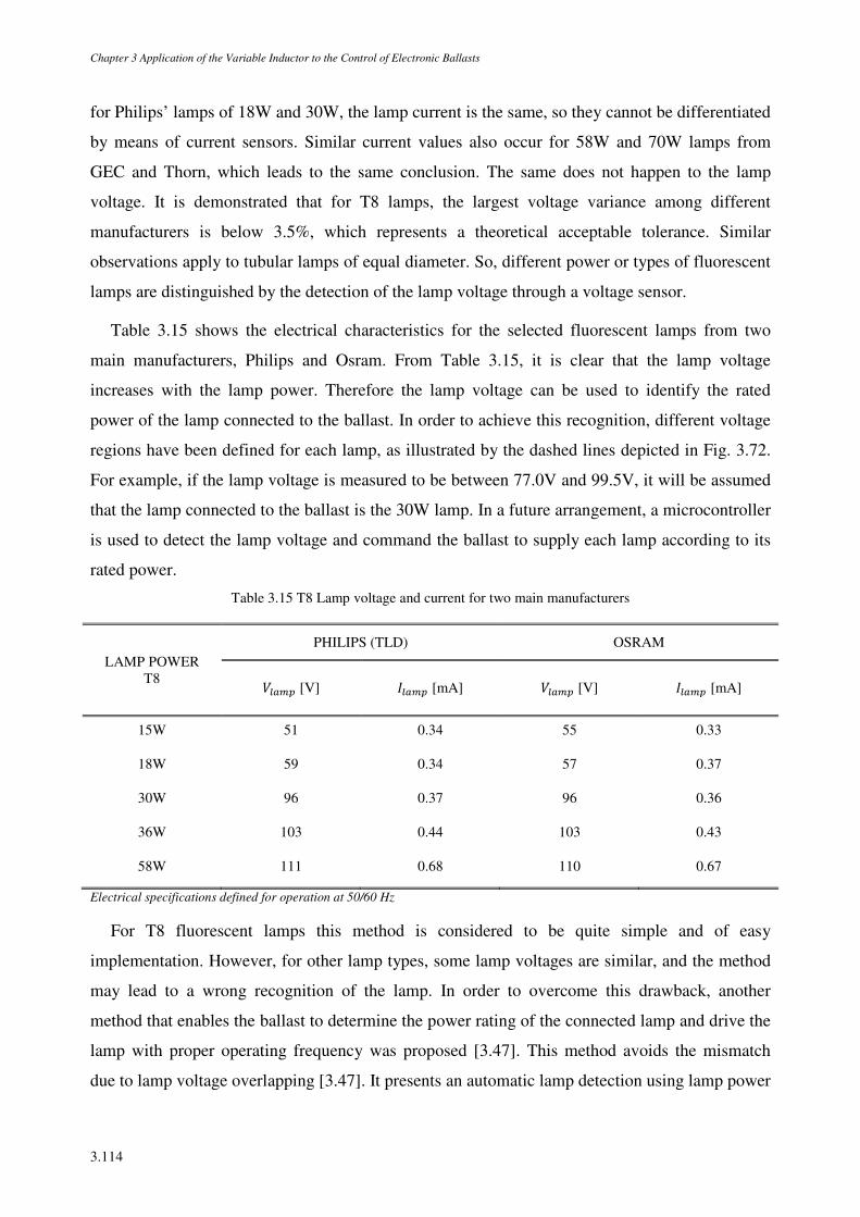
Chapter 3 Application of the Variable Inductor to the Control of Electronic Ballasts
3.114
for Philips’ lamps of 18W and 30W, the lamp current is the same, so they cannot be differentiated
by means of current sensors. Similar current values also occur for 58W and 70W lamps from
GEC and Thorn, which leads to the same conclusion. The same does not happen to the lamp
voltage. It is demonstrated that for T8 lamps, the largest voltage variance among different
manufacturers is below 3.5%, which represents a theoretical acceptable tolerance. Similar
observations apply to tubular lamps of equal diameter. So, different power or types of fluorescent
lamps are distinguished by the detection of the lamp voltage through a voltage sensor.
Table 3.15 shows the electrical characteristics for the selected fluorescent lamps from two
main manufacturers, Philips and Osram. From Table 3.15, it is clear that the lamp voltage
increases with the lamp power. Therefore the lamp voltage can be used to identify the rated
power of the lamp connected to the ballast. In order to achieve this recognition, different voltage
regions have been defined for each lamp, as illustrated by the dashed lines depicted in Fig. 3.72.
For example, if the lamp voltage is measured to be between 77.0V and 99.5V, it will be assumed
that the lamp connected to the ballast is the 30W lamp. In a future arrangement, a microcontroller
is used to detect the lamp voltage and command the ballast to supply each lamp according to its
rated power.
Table 3.15 T8 Lamp voltage and current for two main manufacturers
LAMP POWER T8
PHILIPS (TLD) OSRAM
>~ [V] /~ [mA] >~ [V] /~ [mA]
15W 51 0.34 55 0.33
18W 59 0.34 57 0.37
30W 96 0.37 96 0.36
36W 103 0.44 103 0.43
58W 111 0.68 110 0.67
Electrical specifications defined for operation at 50/60 Hz
For T8 fluorescent lamps this method is considered to be quite simple and of easy
implementation. However, for other lamp types, some lamp voltages are similar, and the method
may lead to a wrong recognition of the lamp. In order to overcome this drawback, another
method that enables the ballast to determine the power rating of the connected lamp and drive the
lamp with proper operating frequency was proposed [3.47]. This method avoids the mismatch
due to lamp voltage overlapping [3.47]. It presents an automatic lamp detection using lamp power
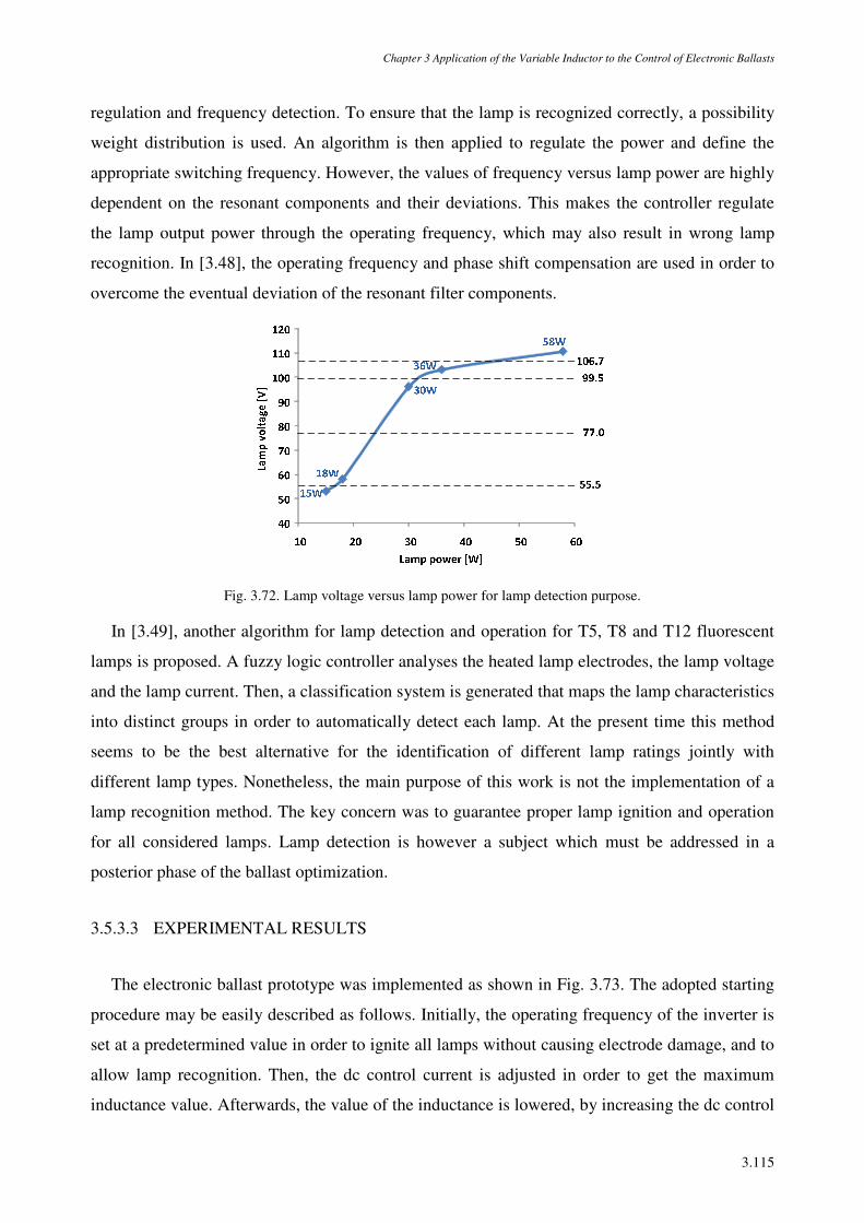
Chapter 3 Application of the Variable Inductor to the Control of Electronic Ballasts
3.115
regulation and frequency detection. To ensure that the lamp is recognized correctly, a possibility
weight distribution is used. An algorithm is then applied to regulate the power and define the
appropriate switching frequency. However, the values of frequency versus lamp power are highly
dependent on the resonant components and their deviations. This makes the controller regulate
the lamp output power through the operating frequency, which may also result in wrong lamp
recognition. In [3.48], the operating frequency and phase shift compensation are used in order to
overcome the eventual deviation of the resonant filter components.
Fig. 3.72. Lamp voltage versus lamp power for lamp detection purpose.
In [3.49], another algorithm for lamp detection and operation for T5, T8 and T12 fluorescent
lamps is proposed. A fuzzy logic controller analyses the heated lamp electrodes, the lamp voltage
and the lamp current. Then, a classification system is generated that maps the lamp characteristics
into distinct groups in order to automatically detect each lamp. At the present time this method
seems to be the best alternative for the identification of different lamp ratings jointly with
different lamp types. Nonetheless, the main purpose of this work is not the implementation of a
lamp recognition method. The key concern was to guarantee proper lamp ignition and operation
for all considered lamps. Lamp detection is however a subject which must be addressed in a
posterior phase of the ballast optimization.
3.5.3.3 EXPERIMENTAL RESULTS
The electronic ballast prototype was implemented as shown in Fig. 3.73. The adopted starting
procedure may be easily described as follows. Initially, the operating frequency of the inverter is
set at a predetermined value in order to ignite all lamps without causing electrode damage, and to
allow lamp recognition. Then, the dc control current is adjusted in order to get the maximum
inductance value. Afterwards, the value of the inductance is lowered, by increasing the dc control
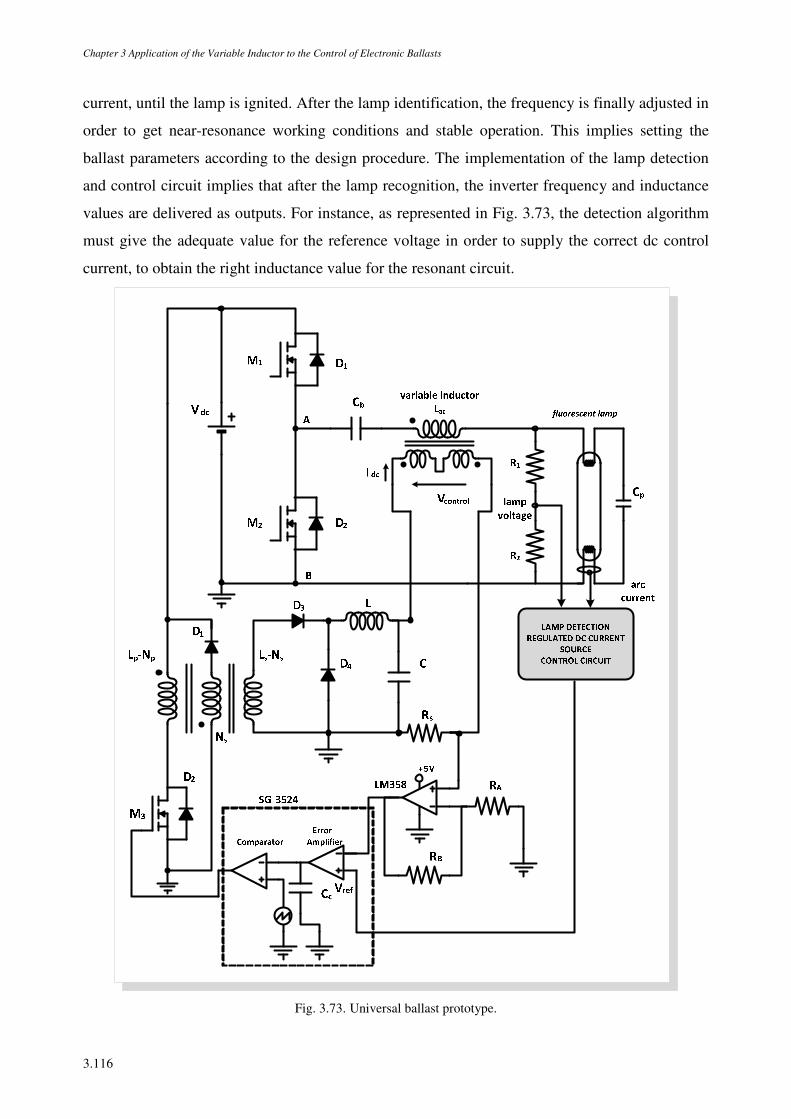
Chapter 3 Application of the Variable Inductor to the Control of Electronic Ballasts
3.116
current, until the lamp is ignited. After the lamp identification, the frequency is finally adjusted in
order to get near-resonance working conditions and stable operation. This implies setting the
ballast parameters according to the design procedure. The implementation of the lamp detection
and control circuit implies that after the lamp recognition, the inverter frequency and inductance
values are delivered as outputs. For instance, as represented in Fig. 3.73, the detection algorithm
must give the adequate value for the reference voltage in order to supply the correct dc control
current, to obtain the right inductance value for the resonant circuit.
Fig. 3.73. Universal ballast prototype.
Chapter 3 Application of the Variable Inductor to the Control of Electronic Ballasts
3.117
Fig. 3.74, Fig. 3.75 and Fig. 3.76 show the obtained experimental results for the laboratory
prototype, for three different fluorescent lamps, respectively, 18W, 36W and 58W. Fig. 3.74a.,
Fig. 3.75a. and Fig. 3.76a., present the resonant current and lamp voltage waveforms for each
lamp. Fig. 3.74b., Fig. 3.75b. and Fig. 3.76b., present the waveforms of the inverter output
voltage and the input resonant current for each lamp. This resonant current is also defined as
lamp current.
As an initial analysis, stable operation for each lamp can be recognized from Fig. 3.74a., Fig.
3.75a. and Fig. 3.76a. This was the main purpose for this ballast prototype. For the 18W lamp the
forward converter was off, since the necessary inductance value should be at its maximum. For
the 58W lamp some distortion can be observed in the resonant current, nevertheless, this did not
result in any working instability. The upper traces in Fig. 3.74a., Fig. 3.75a. and Fig. 3.76a.
correspond to the product of the lamp voltage waveform and the resonant current waveform; in
fact these upper traces represent the instantaneous lamp power. Similarly for Fig. 3.74b., In Fig.
3.75b. and Fig. 3.76b., the upper traces correspond to the instantaneous power delivered by the
inverter.
Similarly to the previous dimmable ballast prototypes, there are several important issues which
deal with the power control of the electronic ballast. This implies the study of the phase angle of
the input current of the resonant tank for each case. Therefore, the phase angle of the input
resonant tank current must be verified. Besides, this phase analysis is important to ensure near-
resonance conditions. This first prototype works in open loop, which means that after the
detection of the lamp power and setting of the lamp working parameters, the phase angle of the
input resonant tank current is not verified by the system. Therefore only experimental verification
was performed. From the analysis of Fig. 3.74b., In Fig. 3.75b. and Fig. 3.76b., which present the
waveforms of the inverter output voltage and the input resonant tank current for all three lamps, it
can be observed that the current lags the voltage, thus ensuring ZVS in the bridge transistors.
Once the inductance was adjusted for each lamp, there was no control loop to assure near-
resonance operation. This mode of operation is similar to the one found in typical commercial
ballasts where usually there is no phase detection to adjust the operation point. The inclusion of
phase detection in this prototype is also possible but it would increase the cost and complicate the
system. Experimental work has shown that there is no excessive variation of inductance in the
variable inductor provided that the dc current is regulated.
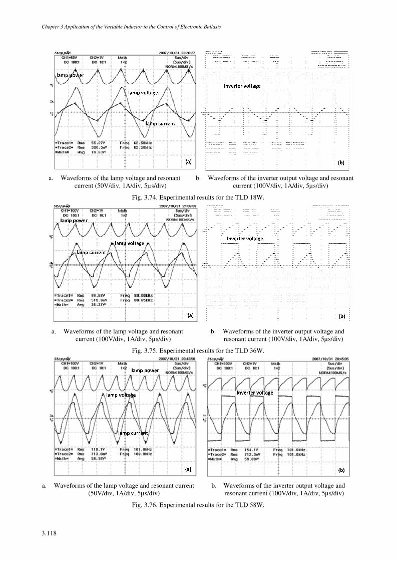
Chapter 3 Application of the Variable Inductor to the Control of Electronic Ballasts
3.118
a. Waveforms of the lamp voltage and resonant
current (50V/div, 1A/div, 5µs/div) b. Waveforms of the inverter output voltage and resonant
current (100V/div, 1A/div, 5µs/div)
Fig. 3.74. Experimental results for the TLD 18W.
a. Waveforms of the lamp voltage and resonant
current (100V/div, 1A/div, 5µs/div) b. Waveforms of the inverter output voltage and
resonant current (100V/div, 1A/div, 5µs/div)
Fig. 3.75. Experimental results for the TLD 36W.
a. Waveforms of the lamp voltage and resonant current
(50V/div, 1A/div, 5µs/div) b. Waveforms of the inverter output voltage and
resonant current (100V/div, 1A/div, 5µs/div)
Fig. 3.76. Experimental results for the TLD 58W.
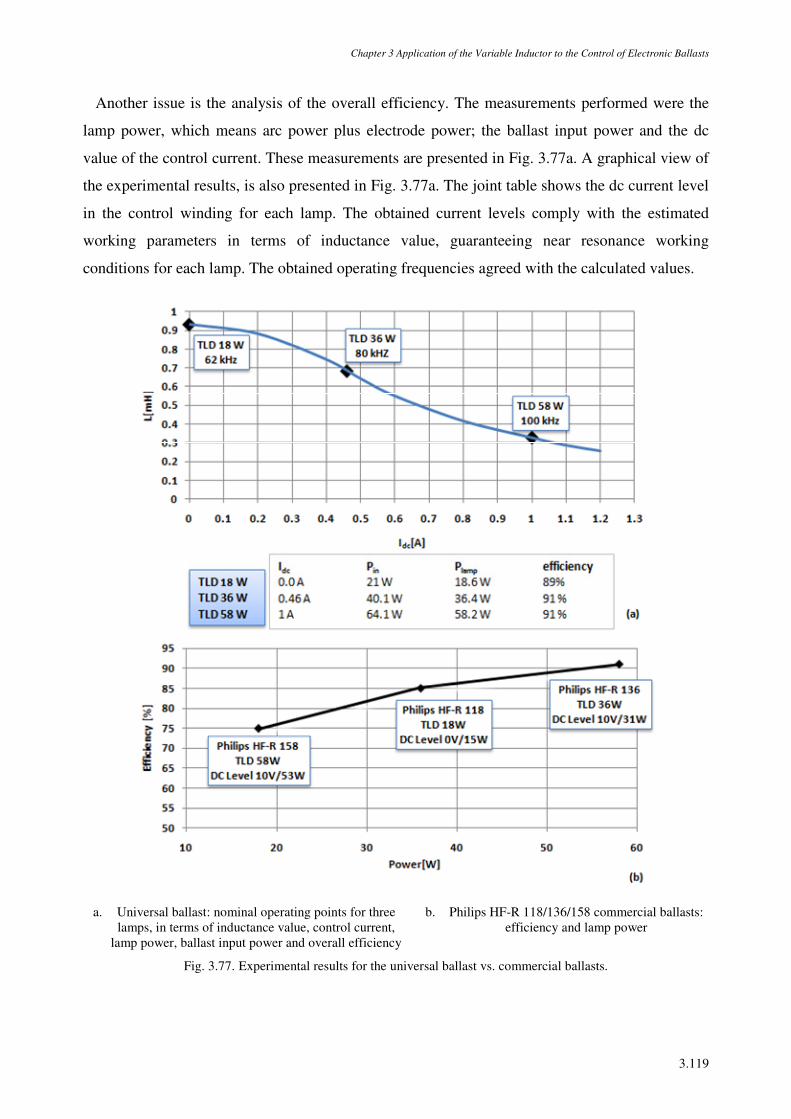
Chapter 3 Application of the Variable Inductor to the Control of Electronic Ballasts
3.119
Another issue is the analysis of the overall efficiency. The measurements performed were the
lamp power, which means arc power plus electrode power; the ballast input power and the dc
value of the control current. These measurements are presented in Fig. 3.77a. A graphical view of
the experimental results, is also presented in Fig. 3.77a. The joint table shows the dc current level
in the control winding for each lamp. The obtained current levels comply with the estimated
working parameters in terms of inductance value, guaranteeing near resonance working
conditions for each lamp. The obtained operating frequencies agreed with the calculated values.
a. Universal ballast: nominal operating points for three lamps, in terms of inductance value, control current,
lamp power, ballast input power and overall efficiency
b. Philips HF-R 118/136/158 commercial ballasts: efficiency and lamp power
Fig. 3.77. Experimental results for the universal ballast vs. commercial ballasts.
Chapter 3 Application of the Variable Inductor to the Control of Electronic Ballasts
3.120
The ballast efficiency, calculated as the ratio between the lamp power and the input power is
also shown in Fig. 3.77a. It is noted that this measured input power includes also the power
absorbed by the forward converter. From the analysis of the obtained values, it can be concluded
that high efficiency is guaranteed with this technique. However it is considered pertinent to
perform a comparison between the prototype results and the ones collected from three
commercial electronic ballasts from Philips. The efficiency of the commercial ballasts is
presented in Fig. 3.77b. A known technique in commercial ballasts is to operate the lamp at a
lower level than its rated power, since at high-frequencies a 10% higher luminous flux level is
expected. Nevertheless, for the 18W lamp the efficiency is below 80%. Comparing all the
collected data, it can be observed that the efficiency of the proposed magnetic control solution is
close to 90% for all fluorescent lamps. Nevertheless, it must be taken into account that the
commercial ballast includes the PFC stage, which contributes to the lowering of the efficiency.
As a conclusion, the proposed magnetically-controlled universal ballast can successfully
supply T8 fluorescent lamps ranging from 18W to 58W close to their nominal power maintaining
very good efficiency. However, in future work, the PFC stage should be included in the topology
in order to evaluate its impact in the global efficiency of the ballast.
3.5.4 PROTOTYPE IMPLEMENTATION WITH DIGITAL CONTROL
Digital control based on low-cost microcontrollers can be used in this type of ballasts without
an excessive cost penalty, and that will provide robust, flexible and reliable universal ballasts. In
fact, nowadays, it is almost mandatory the use of digital control to perform all the tasks requested
by this type of electronic ballasts. In this particular application, this includes the control of both
the half-bridge inverter used to supply the lamps and the forward converter which drives the
magnetic regulator. The main control parameters remain the same: the switching frequency and
the variable inductance. In the following description the emphasis will be put on the control of
the half-bridge inverter and on the universal ballast lamp control.
3.5.4.1 GENERAL DESCRIPTION
Fig. 3.78 shows the proposed schematic of the magnetically-controlled universal ballast with
digital control. In order to provide the necessary control capability a PSoC CY8C29466 digital
control circuit from Cypress was used. This circuit incorporates both analog and digital modules
along with a microprocessor and therefore most of additional peripheral units, such as operational
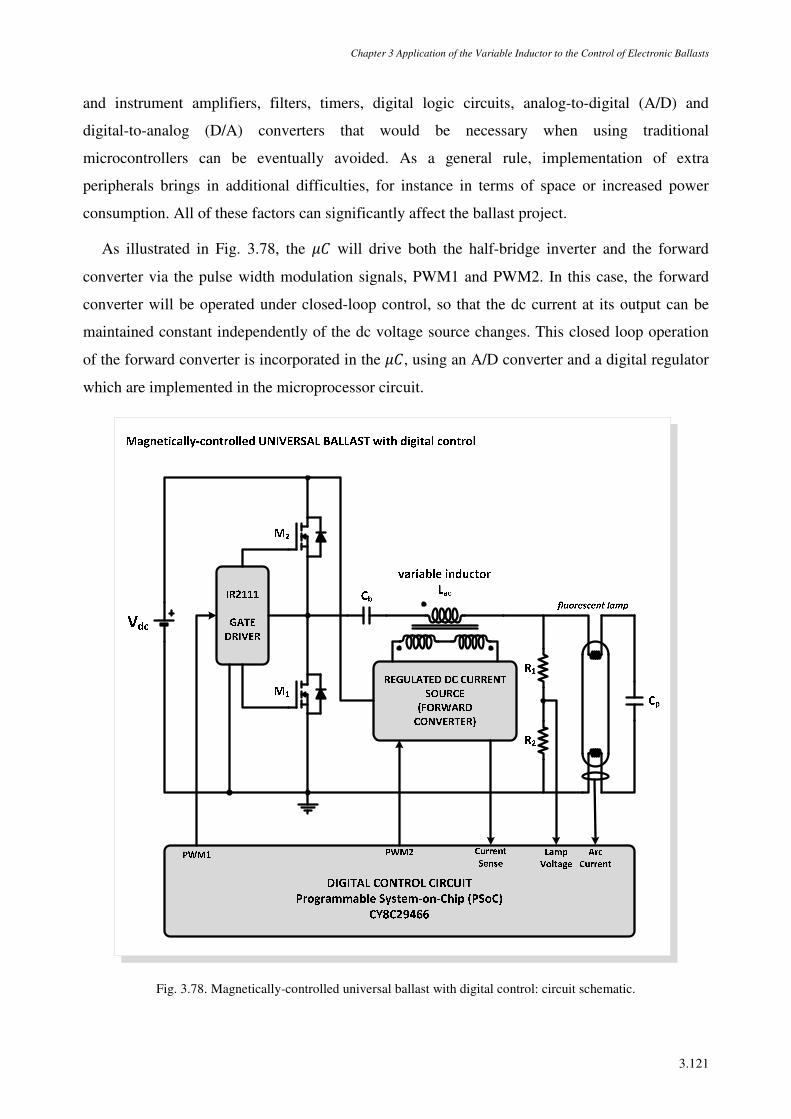
Chapter 3 Application of the Variable Inductor to the Control of Electronic Ballasts
3.121
and instrument amplifiers, filters, timers, digital logic circuits, analog-to-digital (A/D) and
digital-to-analog (D/A) converters that would be necessary when using traditional
microcontrollers can be eventually avoided. As a general rule, implementation of extra
peripherals brings in additional difficulties, for instance in terms of space or increased power
consumption. All of these factors can significantly affect the ballast project.
As illustrated in Fig. 3.78, the µ will drive both the half-bridge inverter and the forward
converter via the pulse width modulation signals, PWM1 and PWM2. In this case, the forward
converter will be operated under closed-loop control, so that the dc current at its output can be
maintained constant independently of the dc voltage source changes. This closed loop operation
of the forward converter is incorporated in the µ, using an A/D converter and a digital regulator
which are implemented in the microprocessor circuit.
Fig. 3.78. Magnetically-controlled universal ballast with digital control: circuit schematic.
Chapter 3 Application of the Variable Inductor to the Control of Electronic Ballasts
3.122
So, the basic idea proposed in this universal ballast is that the lamp power rating will be
detected by measuring some of the lamp electrical parameters, voltage, current or power.
Specifically, in order to detect the lamp type and to provide lamp power regulation, lamp voltage
and current are measured by using two A/D converters provided by the µ. Then, both switching
frequency and inductance will be changed so that the operation is adjusted close to the ¯~
circuit resonant frequency.
It is recalled that the reactive energy handled by the inverter will be lower if the operation is
close to the resonant frequency. Therefore, the rms value of the resonant current for a given
output power will also be lower, thus providing higher efficiency. On the other hand, in order to
attain a stable operation, it is important to have an open-circuit voltage at the operating point
sufficiently high to adapt to the lamp voltage and its possible perturbations. If the lamp voltage
becomes higher than the resonant circuit output voltage, the arc will extinguish. The maximum
open-circuit voltage of the resonant circuit is obtained by operating the inverter at the natural
resonant frequency. Thus, it is concluded that the operation close to the natural resonant
frequency will provide a better compromise between efficiency and stability.
3.5.4.2 ELECTRONIC BALLAST EXPERIMENTAL PROTOTYPE
Fig. 3.79a. illustrates the schematic diagram of the inverter stage, including the control
circuitry implemented by means of the CY8C29466.
A dual 8-bit A/D converter was used for the lamp voltage and current measurements. The
lamp voltage and arc current were used in the CPU program in order to perform the lamp
ignition, lamp detection and lamp current regulation. The dual A/D converter operates with an
internal clock (VC2) at 375kHz and the sampling time was adjusted to 3ms, which gives a
sampling frequency of 333Hz. Fig. 3.79b. shows the loop gain diagram of the inverter stage.
The VCO was implemented using a digital PWM module inside the CY8C29466, which
operates with an internal clock (VC1) running at 6MHz. The switching period is obtained from an
8-bit digital value, 8, as < = 8/6μs. The average resolution to control the switching frequency
with this VCO is about 1kHz per bit.
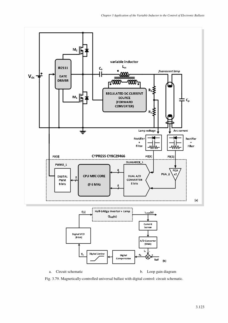
Chapter 3 Application of the Variable Inductor to the Control of Electronic Ballasts
3.123
a. Circuit schematic b. Loop gain diagram
Fig. 3.79. Magnetically-controlled universal ballast with digital control: circuit schematic.
Chapter 3 Application of the Variable Inductor to the Control of Electronic Ballasts
3.124
In some dc-supplied applications, such as indoor lighting in transportation (trains,
undergrounds, buses, etc.), electronic ballasts are supplied from a non-regulated dc input voltage,
with ±20% voltage excursions. Therefore, it was considered important to implement a lamp
power regulation strategy that could also assure the maximum lamp life. In other cases, when the
ballast is supplied from an ac line, the lamp power regulation can be used to simplify the input
power factor correction (PFC) stage by relaxing the output voltage constrains for this stage.
Closed loop operation of the ballast is also essential to compensate changes in other
parameters such as lamp impedance, clock frequency, resonant elements, etc. Therefore, in order
to control the lamp current in closed-loop operation for the different lamps, a non-linear
compensator was employed. The digital compensator implements the following algorithm:
<Ê = <ʺª + Lõ(ʺª) (3.149)
where <Ê represents the period of the inverter switching frequency in each iteration.
The operating frequency was always maintained above the resonant frequency of the resonant
circuit, thus ensuring ZVS operation. In this way, and due to the behaviour of the resonant circuit,
a decrease of the switching period will provide a decrease of the lamp current, and conversely, an
increase of the switching period will generate an increase of the lamp current. Therefore, as can
be inferred from (3.149), if for any reason the lamp current tends to decrease below the reference
level, the calculated error will be positive and the switching period is increased continuously, one
bit in each iteration, so that the lamp current will tend to increase due to the behaviour of the
resonant tank. The opposite action is taken when the lamp increases above the reference level;
then, the error is negative and the switching period is continuously decreased to reduce the lamp
current.
The switching frequency range was limited digitally to ± 20% around the nominal point, so
that the operation above resonant frequency was guaranteed. Laboratory tests showed that this
frequency range was sufficient to compensate bus voltage variations from 250 to 350 V, which is
sufficiently wide for this type of applications. The proposed compensator was tested with the
same lamps ranging from 15W to 58W, and has always obtained good static and dynamic results,
which will be proved through experimental data.
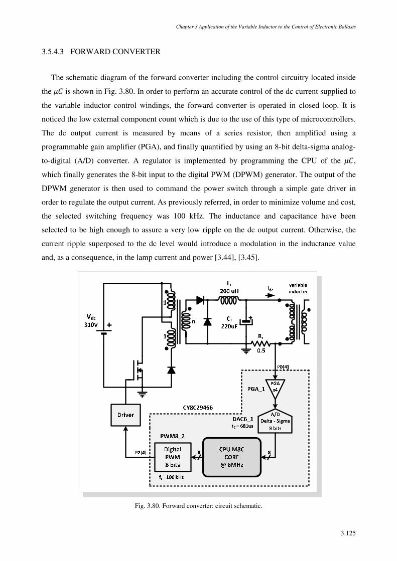
Chapter 3 Application of the Variable Inductor to the Control of Electronic Ballasts
3.125
3.5.4.3 FORWARD CONVERTER
The schematic diagram of the forward converter including the control circuitry located inside
the µ is shown in Fig. 3.80. In order to perform an accurate control of the dc current supplied to
the variable inductor control windings, the forward converter is operated in closed loop. It is
noticed the low external component count which is due to the use of this type of microcontrollers.
The dc output current is measured by means of a series resistor, then amplified using a
programmable gain amplifier (PGA), and finally quantified by using an 8-bit delta-sigma analog-
to-digital (A/D) converter. A regulator is implemented by programming the CPU of the µ,
which finally generates the 8-bit input to the digital PWM (DPWM) generator. The output of the
DPWM generator is then used to command the power switch through a simple gate driver in
order to regulate the output current. As previously referred, in order to minimize volume and cost,
the selected switching frequency was 100 kHz. The inductance and capacitance have been
selected to be high enough to assure a very low ripple on the dc output current. Otherwise, the
current ripple superposed to the dc level would introduce a modulation in the inductance value
and, as a consequence, in the lamp current and power [3.44], [3.45].
Fig. 3.80. Forward converter: circuit schematic.
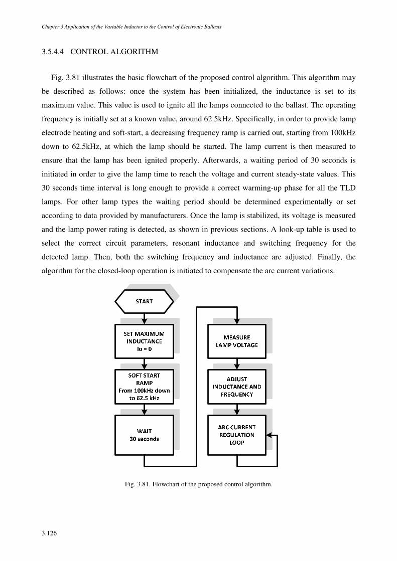
Chapter 3 Application of the Variable Inductor to the Control of Electronic Ballasts
3.126
3.5.4.4 CONTROL ALGORITHM
Fig. 3.81 illustrates the basic flowchart of the proposed control algorithm. This algorithm may
be described as follows: once the system has been initialized, the inductance is set to its
maximum value. This value is used to ignite all the lamps connected to the ballast. The operating
frequency is initially set at a known value, around 62.5kHz. Specifically, in order to provide lamp
electrode heating and soft-start, a decreasing frequency ramp is carried out, starting from 100kHz
down to 62.5kHz, at which the lamp should be started. The lamp current is then measured to
ensure that the lamp has been ignited properly. Afterwards, a waiting period of 30 seconds is
initiated in order to give the lamp time to reach the voltage and current steady-state values. This
30 seconds time interval is long enough to provide a correct warming-up phase for all the TLD
lamps. For other lamp types the waiting period should be determined experimentally or set
according to data provided by manufacturers. Once the lamp is stabilized, its voltage is measured
and the lamp power rating is detected, as shown in previous sections. A look-up table is used to
select the correct circuit parameters, resonant inductance and switching frequency for the
detected lamp. Then, both the switching frequency and inductance are adjusted. Finally, the
algorithm for the closed-loop operation is initiated to compensate the arc current variations.
Fig. 3.81. Flowchart of the proposed control algorithm.
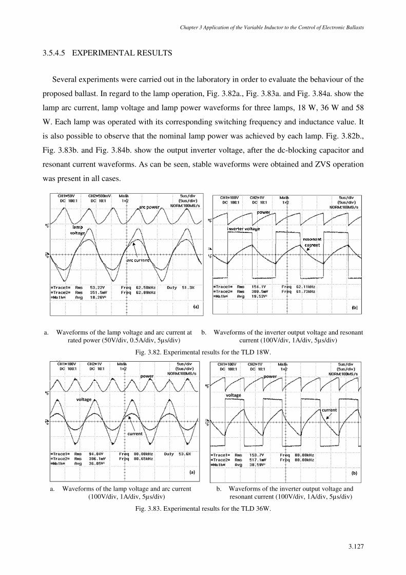
Chapter 3 Application of the Variable Inductor to the Control of Electronic Ballasts
3.127
3.5.4.5 EXPERIMENTAL RESULTS
Several experiments were carried out in the laboratory in order to evaluate the behaviour of the
proposed ballast. In regard to the lamp operation, Fig. 3.82a., Fig. 3.83a. and Fig. 3.84a. show the
lamp arc current, lamp voltage and lamp power waveforms for three lamps, 18 W, 36 W and 58
W. Each lamp was operated with its corresponding switching frequency and inductance value. It
is also possible to observe that the nominal lamp power was achieved by each lamp. Fig. 3.82b.,
Fig. 3.83b. and Fig. 3.84b. show the output inverter voltage, after the dc-blocking capacitor and
resonant current waveforms. As can be seen, stable waveforms were obtained and ZVS operation
was present in all cases.
a. Waveforms of the lamp voltage and arc current at
rated power (50V/div, 0.5A/div, 5µs/div) b. Waveforms of the inverter output voltage and resonant
current (100V/div, 1A/div, 5µs/div)
Fig. 3.82. Experimental results for the TLD 18W.
power
voltage
current
power
voltage
current
(a) (b)
a. Waveforms of the lamp voltage and arc current
(100V/div, 1A/div, 5µs/div) b. Waveforms of the inverter output voltage and
resonant current (100V/div, 1A/div, 5µs/div)
Fig. 3.83. Experimental results for the TLD 36W.
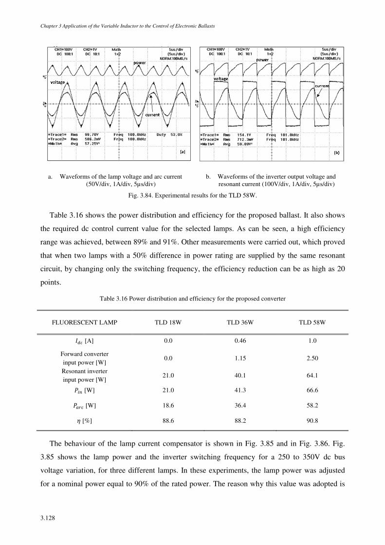
Chapter 3 Application of the Variable Inductor to the Control of Electronic Ballasts
3.128
a. Waveforms of the lamp voltage and arc current
(50V/div, 1A/div, 5µs/div) b. Waveforms of the inverter output voltage and
resonant current (100V/div, 1A/div, 5µs/div)
Fig. 3.84. Experimental results for the TLD 58W.
Table 3.16 shows the power distribution and efficiency for the proposed ballast. It also shows
the required dc control current value for the selected lamps. As can be seen, a high efficiency
range was achieved, between 89% and 91%. Other measurements were carried out, which proved
that when two lamps with a 50% difference in power rating are supplied by the same resonant
circuit, by changing only the switching frequency, the efficiency reduction can be as high as 20
points.
Table 3.16 Power distribution and efficiency for the proposed converter
FLUORESCENT LAMP TLD 18W TLD 36W TLD 58W
/ [A] 0.0 0.46 1.0
Forward converter input power [W]
0.0 1.15 2.50
Resonant inverter input power [W]
21.0 40.1 64.1
t±² [W] 21.0 41.3 66.6
t~2 [W] 18.6 36.4 58.2
? [%] 88.6 88.2 90.8
The behaviour of the lamp current compensator is shown in Fig. 3.85 and in Fig. 3.86. Fig.
3.85 shows the lamp power and the inverter switching frequency for a 250 to 350V dc bus
voltage variation, for three different lamps. In these experiments, the lamp power was adjusted
for a nominal power equal to 90% of the rated power. The reason why this value was adopted is
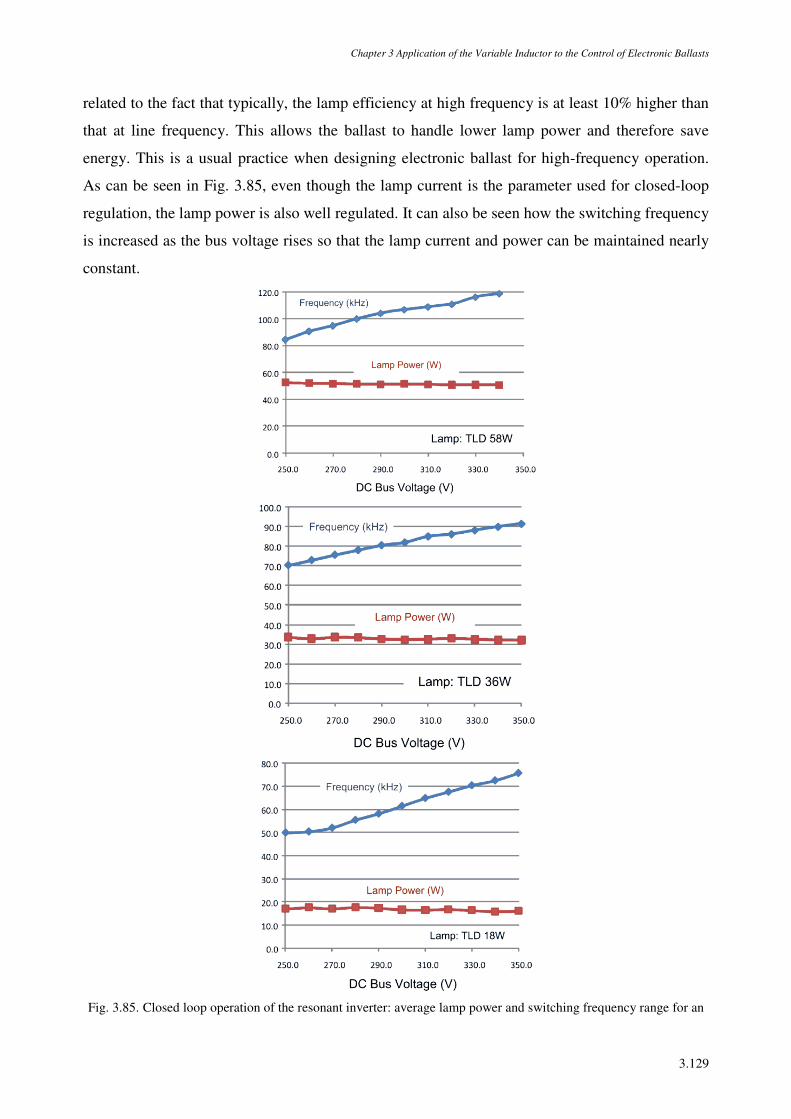
Chapter 3 Application of the Variable Inductor to the Control of Electronic Ballasts
3.129
related to the fact that typically, the lamp efficiency at high frequency is at least 10% higher than
that at line frequency. This allows the ballast to handle lower lamp power and therefore save
energy. This is a usual practice when designing electronic ballast for high-frequency operation.
As can be seen in Fig. 3.85, even though the lamp current is the parameter used for closed-loop
regulation, the lamp power is also well regulated. It can also be seen how the switching frequency
is increased as the bus voltage rises so that the lamp current and power can be maintained nearly
constant.
Fig. 3.85. Closed loop operation of the resonant inverter: average lamp power and switching frequency range for an
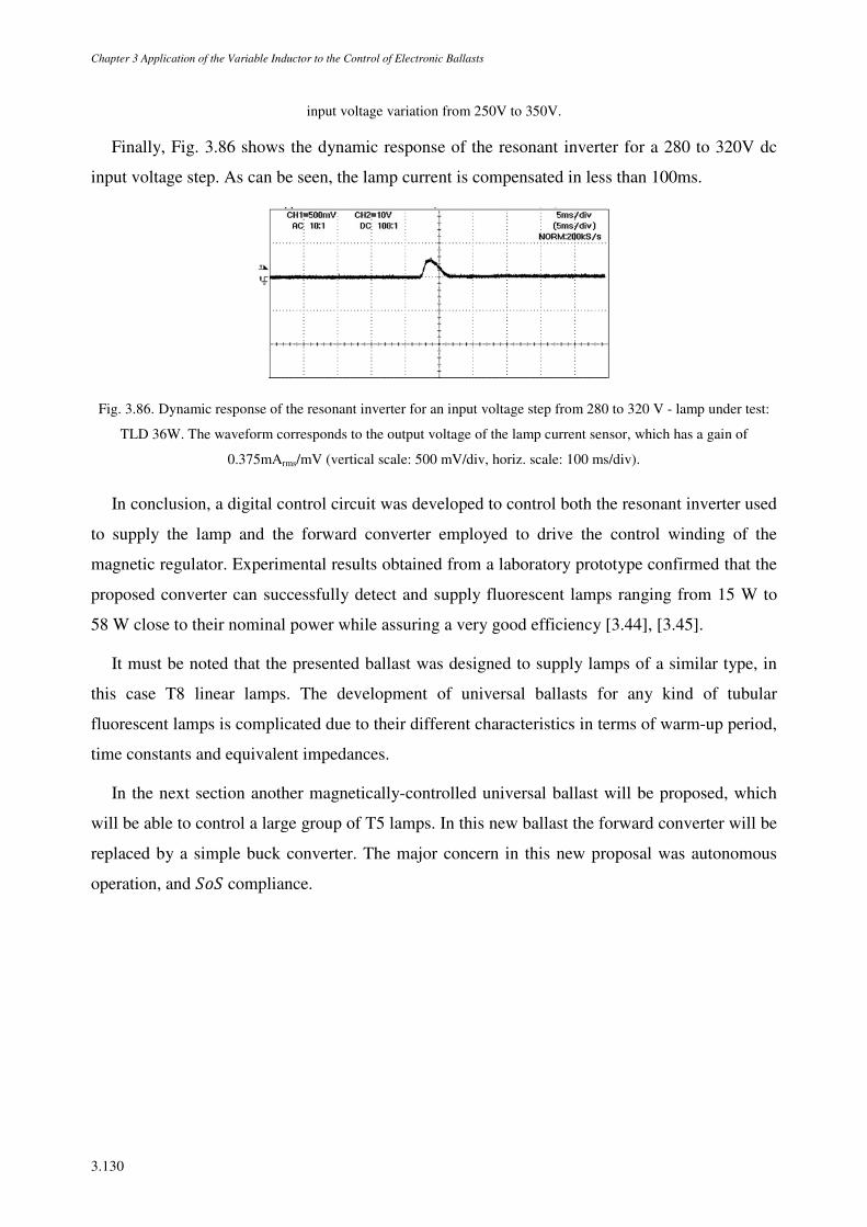
Chapter 3 Application of the Variable Inductor to the Control of Electronic Ballasts
3.130
input voltage variation from 250V to 350V.
Finally, Fig. 3.86 shows the dynamic response of the resonant inverter for a 280 to 320V dc
input voltage step. As can be seen, the lamp current is compensated in less than 100ms.
Fig. 3.86. Dynamic response of the resonant inverter for an input voltage step from 280 to 320 V - lamp under test:
TLD 36W. The waveform corresponds to the output voltage of the lamp current sensor, which has a gain of
0.375mArms/mV (vertical scale: 500 mV/div, horiz. scale: 100 ms/div).
In conclusion, a digital control circuit was developed to control both the resonant inverter used
to supply the lamp and the forward converter employed to drive the control winding of the
magnetic regulator. Experimental results obtained from a laboratory prototype confirmed that the
proposed converter can successfully detect and supply fluorescent lamps ranging from 15 W to
58 W close to their nominal power while assuring a very good efficiency [3.44], [3.45].
It must be noted that the presented ballast was designed to supply lamps of a similar type, in
this case T8 linear lamps. The development of universal ballasts for any kind of tubular
fluorescent lamps is complicated due to their different characteristics in terms of warm-up period,
time constants and equivalent impedances.
In the next section another magnetically-controlled universal ballast will be proposed, which
will be able to control a large group of T5 lamps. In this new ballast the forward converter will be
replaced by a simple buck converter. The major concern in this new proposal was autonomous
operation, and m compliance.
Chapter 3 Application of the Variable Inductor to the Control of Electronic Ballasts
3.131
3.5.5 CONSTANT-FREQUENCY OPERATION IN UNIVERSAL BALLASTS WITH
SoS COMPLIANCE
Another magnetically-controlled universal ballast prototype is hereby presented. This
digitally-controlled universal ballast was especially developed for T5 lamps in order to evaluate
the possibilities of this new control strategy. The ballast is capable of supplying tubular
fluorescent lamps in the range of 14W to 49W, HE series and HO series. It uses the same control
technique, yet, in this particular case, the ballast prototype will exhibit a constant-frequency
operation. Besides operating at constant frequency, this prototype guarantees safe-electrode
operation for all the lamps, which will result in a higher lamp-life. This was accomplished by a
strict control of the design procedure under the m limits.
Since this ballast is supplied by a dc-bus voltage and due to the relatively high complexity of
the proposed prototype, a digital control circuit was also developed to control the half-bridge
resonant inverter and the buck converter. This buck converter has the same function as the
preceding forward converter; it supplies the control windings of the magnetic regulator.
Finally, another objective was to move towards a completely autonomous ballast. An
additional converter was therefore used to supply the inverter gate drives and the buck converter.
This converter is connected to the dc bus voltage which also supplies the inverter.
3.5.5.1 ELECTRONIC BALLAST SCHEMATIC AND PROPOSED CONTROL
TECHNIQUE
Each T5 lamp was supplied by a voltage-fed resonant inverter connected to a parallel-loaded
resonant circuit, as shown in Fig. 3.87. The ballast requires two additional dc-dc converters and a
microcontroller unit, μ and functions similarly to the preceding prototypes. The two bi-
directional switches and the dc voltage source, >, provide a square-wave voltage source that
drives the resonant circuit formed by the magnetic regulator, with the variable inductance ¯~, the
resonant capacitor and the fluorescent lamp. The output lamp power is defined as in (3.150).
t~ = >~v~ = >±²v~v~ 1 − ¯~ + ¯~ (3.150)
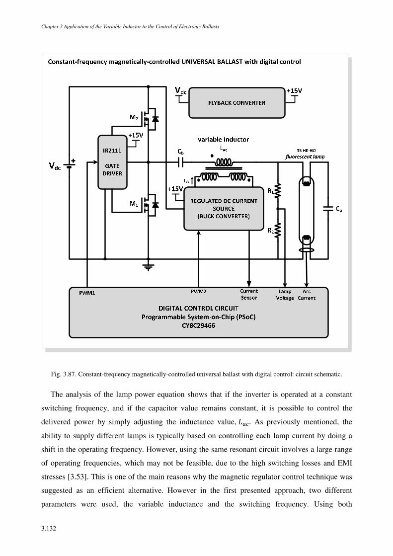
Chapter 3 Application of the Variable Inductor to the Control of Electronic Ballasts
3.132
Fig. 3.87. Constant-frequency magnetically-controlled universal ballast with digital control: circuit schematic.
The analysis of the lamp power equation shows that if the inverter is operated at a constant
switching frequency, and if the capacitor value remains constant, it is possible to control the
delivered power by simply adjusting the inductance value,¯~. As previously mentioned, the
ability to supply different lamps is typically based on controlling each lamp current by doing a
shift in the operating frequency. However, using the same resonant circuit involves a large range
of operating frequencies, which may not be feasible, due to the high switching losses and EMI
stresses [3.53]. This is one of the main reasons why the magnetic regulator control technique was
suggested as an efficient alternative. However in the first presented approach, two different
parameters were used, the variable inductance and the switching frequency. Using both
Chapter 3 Application of the Variable Inductor to the Control of Electronic Ballasts
3.133
parameters led to an acceptable operating frequency range. Therefore and contrary to previous
proposed ballast, where the delivered power was controlled by two different parameters, the
switching frequency and the variable inductance, this new prototype is capable of controlling
several lamps using only one control parameter.
The ballast operating procedure will be as usual: after the lamp recognition, a dc control
current, /, is delivered to the magnetic regulator which will then change its inductance
according to the estimated value for the attached lamp. The current / is supplied by a regulated
dc-current source, a dc-dc buck converter operating in continuous conduction mode. So, in fact,
the inductance variation is imposed by the output dc current of the converter, which is directly
connected to the control windings of the magnetic regulator. The μ has also the ability to
measure this dc current. The control of / itself, is done by adjusting the duty-cycle of a PWM
signal generated by the μ, and applied to the buck converter, according to a voltage reference,
>23Å. This voltage reference may be imposed manually, or by the μ according to the
implemented lamp detection method. As a suggestion this voltage reference could be defined
according to the methodology and the results obtained from the application of the fuzzy logic
algorithm proposed in [3.49].
As illustrated in Fig. 3.87, the voltage required for the gate driver and the buck converter, 15V,
is generated by a dc-dc flyback converter, powered by the ballast dc bus voltage, >. As in
previous cases, this ballast prototype is supplied at > = 310V. The flyback converter will
ensure electrical isolation between the power stage and the control stage of the ballast. This
isolation is also guaranteed by two additional optocouplers, one used in the dc-dc buck converter
and the other in the gate driver. At last, the gate driver, responsible for setting the inverter
switching frequency, 4, is also managed by the μ, during the preheating mode and at steady-
state conditions. As usual, the generated PWM signal will have a duty-cycle of approximately
50%, for an even aging of the lamp electrodes.
3.5.5.2 RESONANT CIRCUIT DESIGN
3.5.5.2.1 Standard design procedure
The primary goal is to operate all different TL5 lamps at nominal power while maintaining the
same switching frequency, 4 and the same resonant circuit capacitance. So, it is necessary to
calculate this capacitance and the inductance values required by each lamp. The circuit is
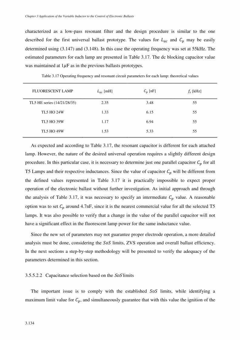
Chapter 3 Application of the Variable Inductor to the Control of Electronic Ballasts
3.134
characterized as a low-pass resonant filter and the design procedure is similar to the one
described for the first universal ballast prototype. The values for ¯~ and may be easily
determined using (3.147) and (3.148). In this case the operating frequency was set at 55kHz. The
estimated parameters for each lamp are presented in Table 3.17. The dc blocking capacitor value
was maintained at 1µF as in the previous ballasts prototypes.
Table 3.17 Operating frequency and resonant circuit parameters for each lamp: theoretical values
FLUORESCENT LAMP ¯~ [mH] [nF] 4 [kHz]
TL5 HE series (14/21/28/35) 2.35 3.48 55
TL5 HO 24W 1.33 6.15 55
TL5 HO 39W 1.17 6.94 55
TL5 HO 49W 1.53 5.33 55
As expected and according to Table 3.17, the resonant capacitor is different for each attached
lamp. However, the nature of the desired universal operation requires a slightly different design
procedure. In this particular case, it is necessary to determine just one parallel capacitor for all
T5 Lamps and their respective inductances. Since the value of capacitor will be different from
the defined values represented in Table 3.17 it is practically impossible to expect proper
operation of the electronic ballast without further investigation. As initial approach and through
the analysis of Table 3.17, it was necessary to specify an intermediate value. A reasonable
option was to set around 4.7nF, since it is the nearest commercial value for all the selected T5
lamps. It was also possible to verify that a change in the value of the parallel capacitor will not
have a significant effect in the fluorescent lamp power for the same inductance value.
Since the new set of parameters may not guarantee proper electrode operation, a more detailed
analysis must be done, considering the m limits, ZVS operation and overall ballast efficiency.
In the next sections a step-by-step methodology will be presented to verify the adequacy of the
parameters determined in this section.
3.5.5.2.2 Capacitance selection based on the SoS limits
The important issue is to comply with the established m limits, while identifying a
maximum limit value for , and simultaneously guarantee that with this value the ignition of the
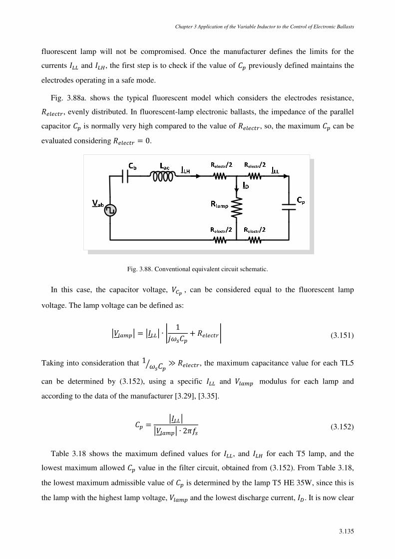
Chapter 3 Application of the Variable Inductor to the Control of Electronic Ballasts
3.135
fluorescent lamp will not be compromised. Once the manufacturer defines the limits for the
currents / and /, the first step is to check if the value of previously defined maintains the
electrodes operating in a safe mode.
Fig. 3.88a. shows the typical fluorescent model which considers the electrodes resistance,
v33À2, evenly distributed. In fluorescent-lamp electronic ballasts, the impedance of the parallel
capacitor is normally very high compared to the value of v33À2, so, the maximum can be
evaluated considering v33À2 = 0.
Fig. 3.88. Conventional equivalent circuit schematic.
In this case, the capacitor voltage, >@ , can be considered equal to the fluorescent lamp
voltage. The lamp voltage can be defined as:
â>~â = â/â ∙ A 14 + v33À2A (3.151)
Taking into consideration that 1 4¤ ≫ v33À2, the maximum capacitance value for each TL5
can be determined by (3.152), using a specific / and >~ modulus for each lamp and
according to the data of the manufacturer [3.29], [3.35].
= â/ââ>~â ∙ 2¸4 (3.152)
Table 3.18 shows the maximum defined values for /, and / for each T5 lamp, and the
lowest maximum allowed value in the filter circuit, obtained from (3.152). From Table 3.18,
the lowest maximum admissible value of is determined by the lamp T5 HE 35W, since this is
the lamp with the highest lamp voltage, >~ and the lowest discharge current, /0. It is now clear
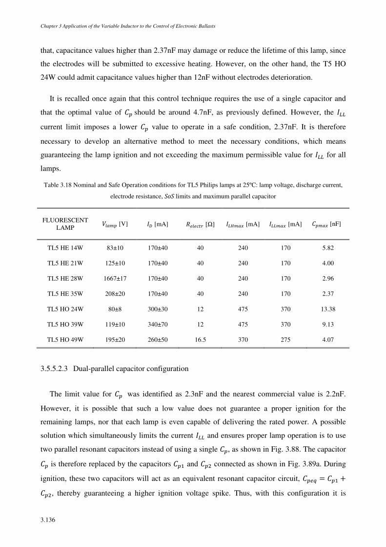
Chapter 3 Application of the Variable Inductor to the Control of Electronic Ballasts
3.136
that, capacitance values higher than 2.37nF may damage or reduce the lifetime of this lamp, since
the electrodes will be submitted to excessive heating. However, on the other hand, the T5 HO
24W could admit capacitance values higher than 12nF without electrodes deterioration.
It is recalled once again that this control technique requires the use of a single capacitor and
that the optimal value of should be around 4.7nF, as previously defined. However, the /
current limit imposes a lower value to operate in a safe condition, 2.37nF. It is therefore
necessary to develop an alternative method to meet the necessary conditions, which means
guaranteeing the lamp ignition and not exceeding the maximum permissible value for / for all
lamps.
Table 3.18 Nominal and Safe Operation conditions for TL5 Philips lamps at 25ºC: lamp voltage, discharge current,
electrode resistance, SoS limits and maximum parallel capacitor
FLUORESCENT LAMP
>~ [V] /0 [mA] v33À2 [Ω] /~Ï [mA] /~Ï [mA] ~Ï [nF] TL5 HE 14W 83±10 170±40 40 240 170 5.82
TL5 HE 21W 125±10 170±40 40 240 170 4.00
TL5 HE 28W 1667±17 170±40 40 240 170 2.96
TL5 HE 35W 208±20 170±40 40 240 170 2.37
TL5 HO 24W 80±8 300±30 12 475 370 13.38
TL5 HO 39W 119±10 340±70 12 475 370 9.13
TL5 HO 49W 195±20 260±50 16.5 370 275 4.07
3.5.5.2.3 Dual-parallel capacitor configuration
The limit value for was identified as 2.3nF and the nearest commercial value is 2.2nF.
However, it is possible that such a low value does not guarantee a proper ignition for the
remaining lamps, nor that each lamp is even capable of delivering the rated power. A possible
solution which simultaneously limits the current / and ensures proper lamp operation is to use
two parallel resonant capacitors instead of using a single , as shown in Fig. 3.88. The capacitor
is therefore replaced by the capacitors ª and connected as shown in Fig. 3.89a. During
ignition, these two capacitors will act as an equivalent resonant capacitor circuit, 3B = ª +, thereby guaranteeing a higher ignition voltage spike. Thus, with this configuration it is
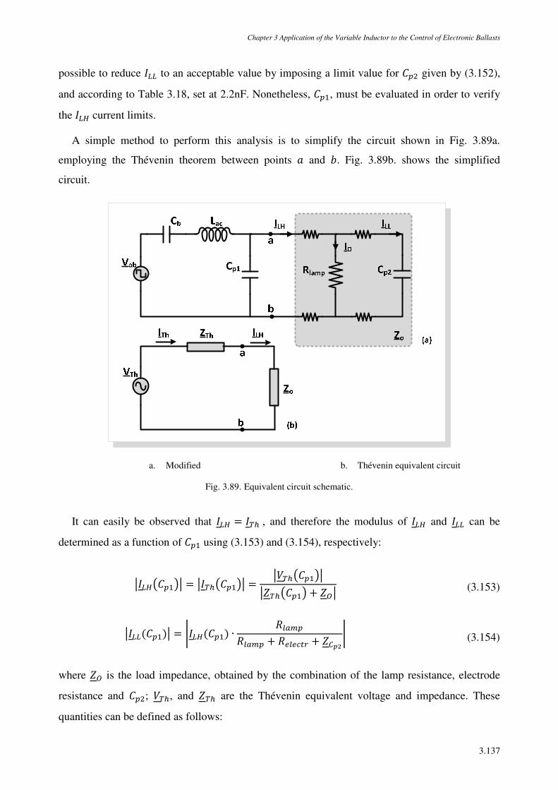
Chapter 3 Application of the Variable Inductor to the Control of Electronic Ballasts
3.137
possible to reduce / to an acceptable value by imposing a limit value for given by (3.152),
and according to Table 3.18, set at 2.2nF. Nonetheless, ª, must be evaluated in order to verify
the / current limits.
A simple method to perform this analysis is to simplify the circuit shown in Fig. 3.89a.
employing the Thévenin theorem between points w and 2. Fig. 3.89b. shows the simplified
circuit.
a. Modified b. Thévenin equivalent circuit
Fig. 3.89. Equivalent circuit schematic.
It can easily be observed that / = /C° , and therefore the modulus of / and / can be
determined as a function of ª using (3.153) and (3.154), respectively:
â/¾ª¿â = â/C°¾ª¿â = â>C°¾ª¿ââC°¾ª¿ + Dâ (3.153)
â/ªâ = A/ª ∙ v~v~ + v33À2 + @EA (3.154)
where D is the load impedance, obtained by the combination of the lamp resistance, electrode
resistance and ; >C°, and C° are the Thévenin equivalent voltage and impedance. These
quantities can be defined as follows:
Chapter 3 Application of the Variable Inductor to the Control of Electronic Ballasts
3.138
D = @E + v33À2 ∙ v~@E + v33À2 + v~ + v33À2 (3.155)
>C°ª = @F6 + G + @F ∙ >±² (3.156)
C°ª = ¾ + G¿6 + G + @F ∙ @F (3.157)
and where 6 = ¯~; G = 1 ´¤ ; @F = 1 ª¤ ; and finally @E = 1 ¤ .
Fig. 3.90a. shows the plots of / and / rms values as a function of ª and the current limits
imposed by the manufacturer. The minimum values for / and / are set by the T5 HE series.
The T5 HE 35W presents the highest lamp voltage and lowest discharge current. As a result, this
lamp presents the worst limiting conditions from the set of the selected T5 lamps.
Fig. 3.90b shows the plot of the resonant current phase as a function of ª. It is noted that the
resonant current phase is equal to the phase of the input admittance, 1/±². These plots assume
at the previously determined value, 2.2nF, v~ at the rated values of voltage and current
for the T5 HE 35W lamp, ¯~ as calculated in (3.147) and ´ at 1µF. From Fig. 3.90b it is
noticed that ZVS operation will not be put at risk for any possible value of ª, since the resonant
current phase will always be negative. Moreover, according to Fig. 3.90a. any value of ª may
be employed without exceeding the limits of / and / defined by the dotted lines. Thus, an
ideal value of ª may be selected, around 2.2nF, in order to obtain an equivalent capacitance,
3B = ª + , near 4.7nF, which corresponds to the ideal capacitance defined in the
traditional design methodology.
Experimental tests were performed with all T5 lamps which presented / and / values
according to the limits defined by the manufacturers. However, lamp voltage oscillations were
observed for the T5 HE 35W lamp using this set of ª and .
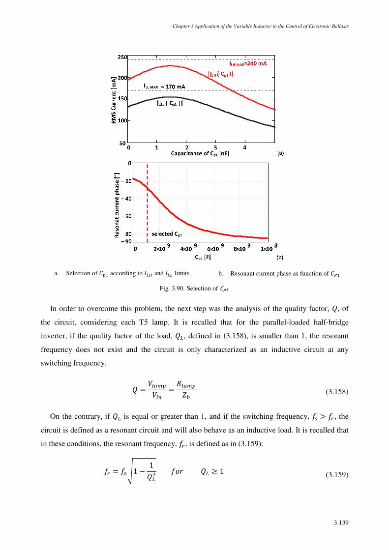
Chapter 3 Application of the Variable Inductor to the Control of Electronic Ballasts
3.139
a. Selection of ª according to / and / limits b. Resonant current phase as function of ª
Fig. 3.90. Selection of Cp1.
In order to overcome this problem, the next step was the analysis of the quality factor, Ð, of
the circuit, considering each T5 lamp. It is recalled that for the parallel-loaded half-bridge
inverter, if the quality factor of the load, Ð, defined in (3.158), is smaller than 1, the resonant
frequency does not exist and the circuit is only characterized as an inductive circuit at any
switching frequency.
Ð = >~>±² = v~´ (3.158)
On the contrary, if Ð is equal or greater than 1, and if the switching frequency, 4 > 2, the
circuit is defined as a resonant circuit and will also behave as an inductive load. It is recalled that
in these conditions, the resonant frequency, 2, is defined as in (3.159):
2 = Ôö1 − 1Ð m Ð ≥ 1 (3.159)
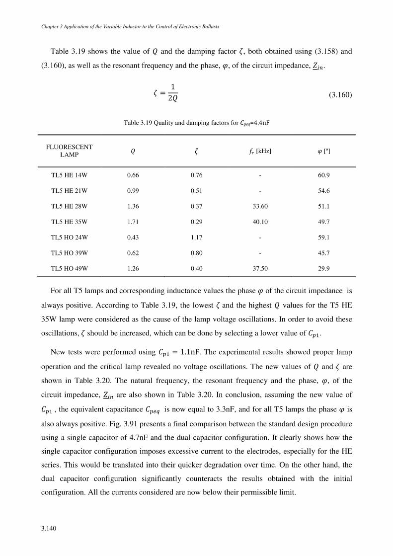
Chapter 3 Application of the Variable Inductor to the Control of Electronic Ballasts
3.140
Table 3.19 shows the value of Ð and the damping factor H, both obtained using (3.158) and
(3.160), as well as the resonant frequency and the phase, I, of the circuit impedance, ±².
H = 12Ð (3.160)
Table 3.19 Quality and damping factors for Cpeq=4.4nF
FLUORESCENT LAMP
Ð H 2 [kHz] I [º]
TL5 HE 14W 0.66 0.76 - 60.9
TL5 HE 21W 0.99 0.51 - 54.6
TL5 HE 28W 1.36 0.37 33.60 51.1
TL5 HE 35W 1.71 0.29 40.10 49.7
TL5 HO 24W 0.43 1.17 - 59.1
TL5 HO 39W 0.62 0.80 - 45.7
TL5 HO 49W 1.26 0.40 37.50 29.9
For all T5 lamps and corresponding inductance values the phase I of the circuit impedance is
always positive. According to Table 3.19, the lowest H and the highest Ð values for the T5 HE
35W lamp were considered as the cause of the lamp voltage oscillations. In order to avoid these
oscillations,H should be increased, which can be done by selecting a lower value of ª.
New tests were performed using ª = 1.1nF. The experimental results showed proper lamp
operation and the critical lamp revealed no voltage oscillations. The new values of Ð and H are
shown in Table 3.20. The natural frequency, the resonant frequency and the phase, I, of the
circuit impedance, ±² are also shown in Table 3.20. In conclusion, assuming the new value of
ª, the equivalent capacitance 3B is now equal to 3.3nF, and for all T5 lamps the phase I is
also always positive. Fig. 3.91 presents a final comparison between the standard design procedure
using a single capacitor of 4.7nF and the dual capacitor configuration. It clearly shows how the
single capacitor configuration imposes excessive current to the electrodes, especially for the HE
series. This would be translated into their quicker degradation over time. On the other hand, the
dual capacitor configuration significantly counteracts the results obtained with the initial
configuration. All the currents considered are now below their permissible limit.
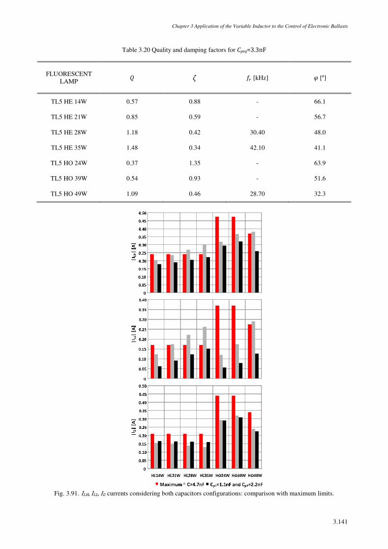
Chapter 3 Application of the Variable Inductor to the Control of Electronic Ballasts
3.141
Table 3.20 Quality and damping factors for Cpeq=3.3nF
FLUORESCENT LAMP
Ð H 2 [kHz] I [º]
TL5 HE 14W 0.57 0.88 - 66.1
TL5 HE 21W 0.85 0.59 - 56.7
TL5 HE 28W 1.18 0.42 30.40 48.0
TL5 HE 35W 1.48 0.34 42.10 41.1
TL5 HO 24W 0.37 1.35 - 63.9
TL5 HO 39W 0.54 0.93 - 51.6
TL5 HO 49W 1.09 0.46 28.70 32.3
Fig. 3.91. ILH, ILL, ID currents considering both capacitors configurations: comparison with maximum limits.
Chapter 3 Application of the Variable Inductor to the Control of Electronic Ballasts
3.142
3.5.5.2.4 ZVS operation
In order to guarantee ZVS operation, the traditional design procedure considers as a sufficient
condition to operate the half-bridge inverter at a frequency 4 above the resonant frequency of the
circuit. However, if Ð < 1, the filter will not behave as a resonant circuit, but simply as an
inductive circuit, and this principle cannot be applied. Despite of this behaviour, the inverter
circuit will keep ZVS operation, since the input circuit current also lags the inverter output
voltage, for an inductive load. In conclusion, the resonant frequency concept cannot be applied in
such cases and there will be no corresponding resonant frequency to be shown in Table 3.19 and
in Table 3.20 when Ð < 1.
Therefore, with the traditional method which uses the fundamental approximation, a quality
factor Ð ≥ 1 is enough to evaluate ZVS operation just for the T5 HE 28W, 35W and T5 HO
49W lamps. Although for some set of components this concept is not applicable, it is clear from
Table 3.20 that for all T5 lamps the phase I is also always positive, which implies a resonant
current with a negative phase, £±². However, for the T5 HE 14W, 21W, and T5 HO 24W and
39W the circuit behaves as an inductive load and this also justifies the ZVS operation. However,
in these cases, it is expected a less sinusoidal resonant current waveform.
3.5.5.3 ELECTRONIC BALLAST EXPERIMENTAL PROTOTYPE
Fig. 3.92 shows the ballast experimental prototype. The main driver, IR2111, also used in the
previous ballast, is responsible for the command of the half-bridge inverter. Since the supply
voltage of the IR2111 driver is 15V, the amplitude of the PWM signal generated by the μ had to
be adapted for the driver to work properly. This was accomplished using a HCLP3120 driver,
which grants electrical isolation from the power stage. A digital 16 bit PWM, PWM1, as
previously shown in Fig. 3.87, was applied to the gate driver in order to set the inverter switching
frequency, 4, at 55kHz according to the selected value. This PWM signal was generated by the
same μ, used in the previous section, PSoC CY8C29446. In order to block the dc component of
the input voltage of the filter, capacitor ´ was chosen to be 1µF and according to the previous
design procedure = 2.2nF and ª = 1.1nF. An integrator v circuit was also used to
estimate the large-signal inductance value for each lamp.
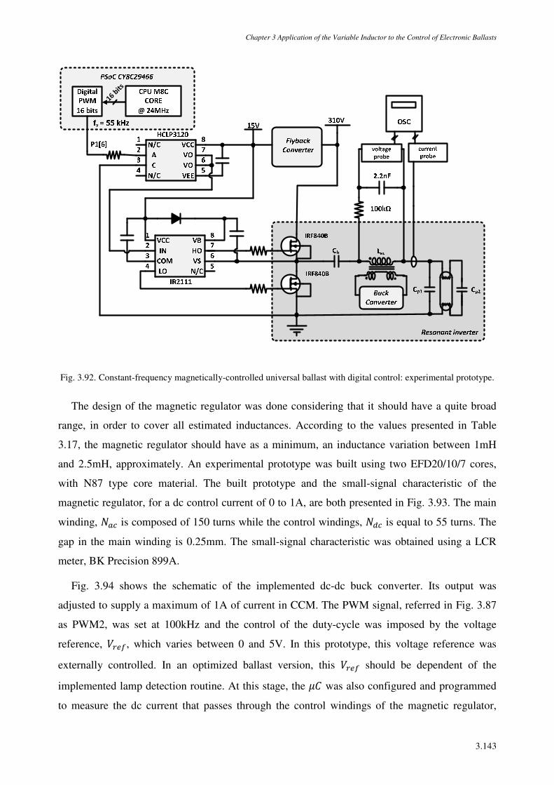
Chapter 3 Application of the Variable Inductor to the Control of Electronic Ballasts
3.143
16 bits
Fig. 3.92. Constant-frequency magnetically-controlled universal ballast with digital control: experimental prototype.
The design of the magnetic regulator was done considering that it should have a quite broad
range, in order to cover all estimated inductances. According to the values presented in Table
3.17, the magnetic regulator should have as a minimum, an inductance variation between 1mH
and 2.5mH, approximately. An experimental prototype was built using two EFD20/10/7 cores,
with N87 type core material. The built prototype and the small-signal characteristic of the
magnetic regulator, for a dc control current of 0 to 1A, are both presented in Fig. 3.93. The main
winding, Á~ is composed of 150 turns while the control windings, Á is equal to 55 turns. The
gap in the main winding is 0.25mm. The small-signal characteristic was obtained using a LCR
meter, BK Precision 899A.
Fig. 3.94 shows the schematic of the implemented dc-dc buck converter. Its output was
adjusted to supply a maximum of 1A of current in CCM. The PWM signal, referred in Fig. 3.87
as PWM2, was set at 100kHz and the control of the duty-cycle was imposed by the voltage
reference, >23Å, which varies between 0 and 5V. In this prototype, this voltage reference was
externally controlled. In an optimized ballast version, this >23Å should be dependent of the
implemented lamp detection routine. At this stage, the µ was also configured and programmed
to measure the dc current that passes through the control windings of the magnetic regulator,
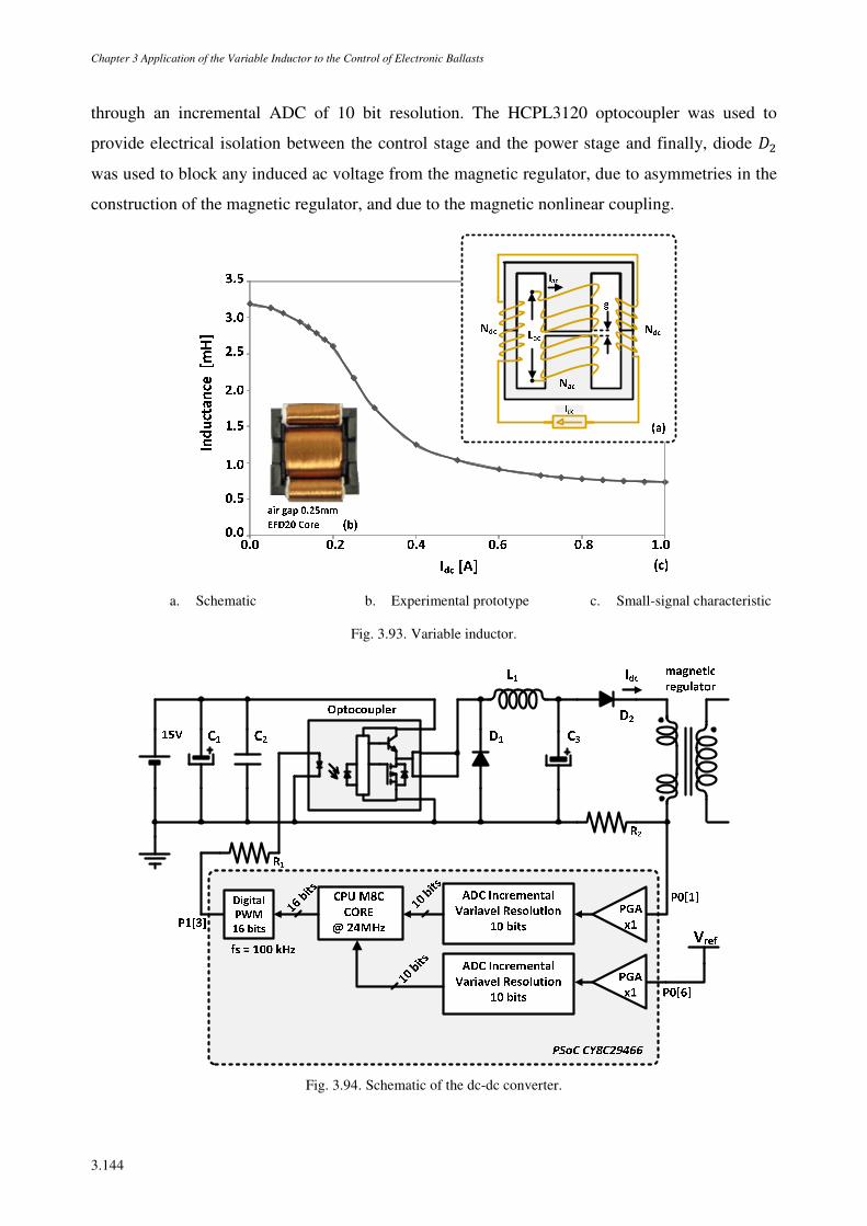
Chapter 3 Application of the Variable Inductor to the Control of Electronic Ballasts
3.144
through an incremental ADC of 10 bit resolution. The HCPL3120 optocoupler was used to
provide electrical isolation between the control stage and the power stage and finally, diode ®
was used to block any induced ac voltage from the magnetic regulator, due to asymmetries in the
construction of the magnetic regulator, and due to the magnetic nonlinear coupling.
a. Schematic b. Experimental prototype c. Small-signal characteristic
Fig. 3.93. Variable inductor.
Fig. 3.94. Schematic of the dc-dc converter.
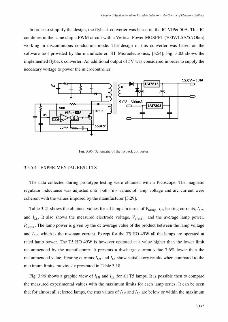
Chapter 3 Application of the Variable Inductor to the Control of Electronic Ballasts
3.145
In order to simplify the design, the flyback converter was based on the IC VIPer 50A. This IC
combines in the same chip a PWM circuit with a Vertical Power MOSFET (700V/1.5A/5.7Ohm)
working in discontinuous conduction mode. The design of this converter was based on the
software tool provided by the manufacturer, ST Microelectronics, [3.54]. Fig. 3.83 shows the
implemented flyback converter. An additional output of 5V was considered in order to supply the
necessary voltage to power the microcontroller.
Fig. 3.95. Schematic of the flyback converter.
3.5.5.4 EXPERIMENTAL RESULTS
The data collected during prototype testing were obtained with a Picoscope. The magnetic
regulator inductance was adjusted until both rms values of lamp voltage and arc current were
coherent with the values imposed by the manufacturer [3.29].
Table 3.21 shows the obtained values for all lamps in terms of >~, /0, heating currents, /,
and /. It also shows the measured electrode voltage, >33À2, and the average lamp power,
t~. The lamp power is given by the dc average value of the product between the lamp voltage
and /, which is the resonant current. Except for the T5 HO 49W all the lamps are operated at
rated lamp power. The T5 HO 49W is however operated at a value higher than the lower limit
recommended by the manufacturer. It presents a discharge current value 7.6% lower than the
recommended value. Heating currents / and / show satisfactory results when compared to the
maximum limits, previously presented in Table 3.18.
Fig. 3.96 shows a graphic view of / and / for all T5 lamps. It is possible then to compare
the measured experimental values with the maximum limits for each lamp series. It can be seen
that for almost all selected lamps, the rms values of / and / are below or within the maximum
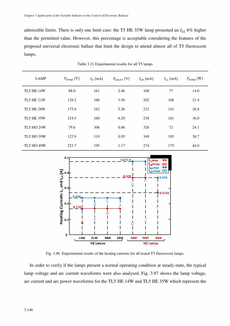
Chapter 3 Application of the Variable Inductor to the Control of Electronic Ballasts
3.146
admissible limits. There is only one limit case: the T5 HE 35W lamp presented an / 6% higher
than the permitted value. However, this percentage is acceptable considering the features of the
proposed universal electronic ballast that limit the design to attend almost all of T5 fluorescent
lamps.
Table 3.21 Experimental results for all T5 lamps
LAMP >~ [V] /0 [mA] >33À2 [V] / [mA] / [mA] t~ [W] TL5 HE 14W 88.0 161 2.46 168 77 14.0
TL5 HE 21W 129.2 166 3.50 202 108 21.4
TL5 HE 28W 175.6 162 5.26 221 141 28.8
TL5 HE 35W 219.5 160 6.29 238 181 36.0
TL5 HO 24W 79.6 306 0.86 326 72 24.1
TL5 HO 39W 122.9 319 0.95 349 105 38.7
TL5 HO 49W 223.7 195 1.17 274 175 44.0
Fig. 3.96. Experimental results of the heating currents for all tested T5 fluorescent lamps.
In order to verify if the lamps present a normal operating condition at steady-state, the typical
lamp voltage and arc current waveforms were also analysed. Fig. 3.97 shows the lamp voltage,
arc current and arc power waveforms for the TL5 HE 14W and TL5 HE 35W which represent the
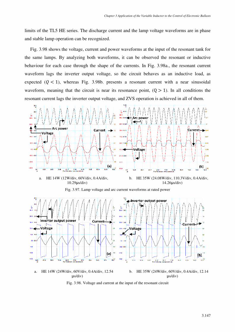
Chapter 3 Application of the Variable Inductor to the Control of Electronic Ballasts
3.147
limits of the TL5 HE series. The discharge current and the lamp voltage waveforms are in phase
and stable lamp operation can be recognized.
Fig. 3.98 shows the voltage, current and power waveforms at the input of the resonant tank for
the same lamps. By analyzing both waveforms, it can be observed the resonant or inductive
behaviour for each case through the shape of the currents. In Fig. 3.98a., the resonant current
waveform lags the inverter output voltage, so the circuit behaves as an inductive load, as
expected (Ð < 1), whereas Fig. 3.98b. presents a resonant current with a near sinusoidal
waveform, meaning that the circuit is near its resonance point, (Q > 1). In all conditions the
resonant current lags the inverter output voltage, and ZVS operation is achieved in all of them.
a. HE 14W (12W/div, 60V/div, 0.4A/div, 10.29µs/div)
b. HE 35W (24.08W/div, 110.3V/div, 0.4A/div, 14.26µs/div)
Fig. 3.97. Lamp voltage and arc current waveforms at rated power
a. HE 14W (24W/div, 60V/div, 0.4A/div, 12.54 µs/div)
b. HE 35W (24W/div, 60V/div, 0.4A/div, 12.14 µs/div)
Fig. 3.98. Voltage and current at the input of the resonant circuit
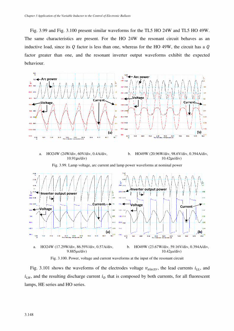
Chapter 3 Application of the Variable Inductor to the Control of Electronic Ballasts
3.148
Fig. 3.99 and Fig. 3.100 present similar waveforms for the TL5 HO 24W and TL5 HO 49W.
The same characteristics are present. For the HO 24W the resonant circuit behaves as an
inductive load, since its Ð factor is less than one, whereas for the HO 49W, the circuit has a Ð
factor greater than one, and the resonant inverter output waveforms exhibit the expected
behaviour.
a. HO24W (24W/div, 60V/div, 0.4A/div, 10.91µs/div)
b. HO49W (20.96W/div, 98.6V/div, 0.394A/div, 10.42µs/div)
Fig. 3.99. Lamp voltage, arc current and lamp power waveforms at nominal power
Current
Inverter output power
Voltage
(a)
Voltage Current
Inverter output power
(b)
a. HO24W (17.29W/div, 86.59V/div, 0.57A/div, 9.885µs/div)
b. HO49W (23.67W/div, 59.16V/div, 0.394A/div, 10.42µs/div)
Fig. 3.100. Power, voltage and current waveforms at the input of the resonant circuit
Fig. 3.101 shows the waveforms of the electrodes voltage K33À2, the lead currents L, and
L, and the resulting discharge current L0 that is composed by both currents, for all fluorescent
lamps, HE series and HO series.
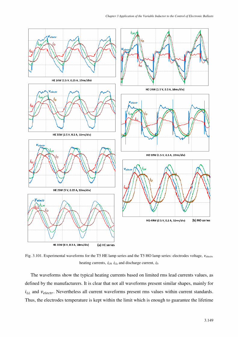
Chapter 3 Application of the Variable Inductor to the Control of Electronic Ballasts
3.149
Fig. 3.101. Experimental waveforms for the T5 HE lamp series and the T5 HO lamp series: electrodes voltage, velectr, heating currents, iLH, iLL, and discharge current, iD.
The waveforms show the typical heating currents based on limited rms lead currents values, as
defined by the manufacturers. It is clear that not all waveforms present similar shapes, mainly for
L and K33À2. Nevertheless all current waveforms present rms values within current standards.
Thus, the electrodes temperature is kept within the limit which is enough to guarantee the lifetime
Chapter 3 Application of the Variable Inductor to the Control of Electronic Ballasts
3.150
of the electrodes. As a result, the proposed design procedure and the ballast operation, both
guarantee a standard lifetime for the all selected T5 fluorescent lamps.
Table 3.22 presents the power ratings achieved by each tested lamp with the ballast prototype.
The values presented were considered as follows: t~ is the lamp power; t~2 is the discharge
power or arc power, given by the dc average value of the product between the lamp voltage and
the discharge current, /0; t33À2 is the total power loss in the lamp electrodes, given by the
average value of the product of the lamp electrode voltage by L; t±² is the dc input power of the
ballast, supplied by an external dc power source. The overall efficiency of the magnetically-
controlled ballast is given by the ratio between t~ and t±². The efficiency of the prototype
with each lamp rounds about 89%, which is fairly acceptable for this universal electronic ballast.
It is once again recognized that the T5 HO 49W does not reach its nominal lamp power, however
it still operates at a value higher than the minimum recommended power. With the implemented
prototype, a fine adjustment to the inductance of the magnetic regulator could be done but this
would take >~ over the maximum recommended voltage. Table 3.22 also presents the dc
control current value dictated by the operation of the buck converter and the experimental large-
signal inductance values for each attached lamp.
Table 3.22 Power rating of the ballast and tested lamps, experimental values of Lac and Idc
LAMP t±² [W] t~ [W] t~2 [W] t33À2 [W] ? [%] ¯~ [mH] / [A] TL5 HE 14W 17.3 14.0 13.9 0.72 81 2.63 0.2283
TL5 HE 21W 23.6 21.4 21.1 1.22 91 2.35 0.2595
TL5 HE 28W 31.0 28.8 28.0 2.09 93 2.54 0.2565
TL5 HE 35W 38.3 36.0 34.7 2.74 94 2.68 0.2692
TL5 HO 24W 28.3 24.1 24.21 0.45 85 1.10 0.6548
TL5 HO 39W 44.4 38.7 38.95 0.44 87 9.64 0.7863
TL5 HO 49W 48.1 44.0 43.2 1.17 92 1.89 0.5234
Fig. 3.102 presents the integrator voltage, K , the resonant current, L234 and the dc control
current waveforms at rated power for the T5 HO 49W, which has a small ripple component. In
these conditions the magnetic regulator was supplying the lamp with higher power rating. It is
recalled that the integrator circuit is used to measure the total ac flux in order to estimate the
inductance value for each operating point.
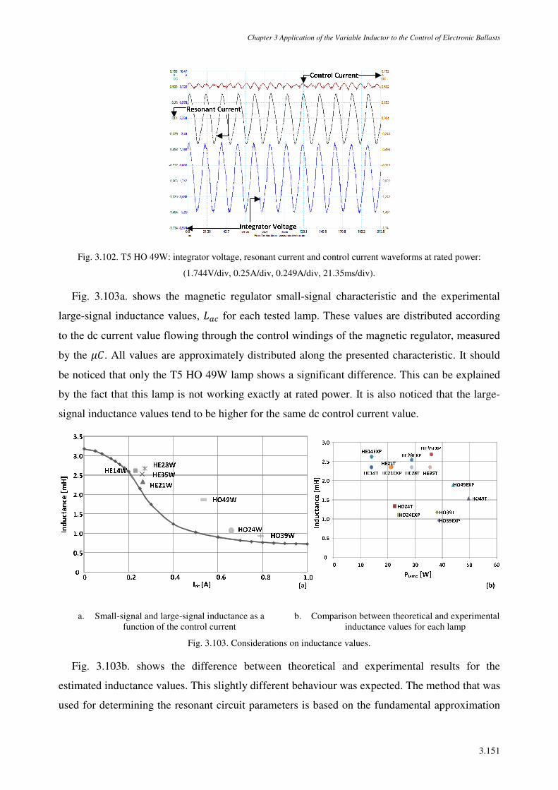
Chapter 3 Application of the Variable Inductor to the Control of Electronic Ballasts
3.151
Fig. 3.102. T5 HO 49W: integrator voltage, resonant current and control current waveforms at rated power:
(1.744V/div, 0.25A/div, 0.249A/div, 21.35ms/div).
Fig. 3.103a. shows the magnetic regulator small-signal characteristic and the experimental
large-signal inductance values, ¯~ for each tested lamp. These values are distributed according
to the dc current value flowing through the control windings of the magnetic regulator, measured
by the µ. All values are approximately distributed along the presented characteristic. It should
be noticed that only the T5 HO 49W lamp shows a significant difference. This can be explained
by the fact that this lamp is not working exactly at rated power. It is also noticed that the large-
signal inductance values tend to be higher for the same dc control current value.
a. Small-signal and large-signal inductance as a function of the control current
b. Comparison between theoretical and experimental inductance values for each lamp
Fig. 3.103. Considerations on inductance values.
Fig. 3.103b. shows the difference between theoretical and experimental results for the
estimated inductance values. This slightly different behaviour was expected. The method that was
used for determining the resonant circuit parameters is based on the fundamental approximation
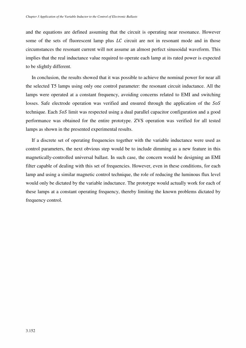
Chapter 3 Application of the Variable Inductor to the Control of Electronic Ballasts
3.152
and the equations are defined assuming that the circuit is operating near resonance. However
some of the sets of fluorescent lamp plus ¯ circuit are not in resonant mode and in those
circumstances the resonant current will not assume an almost perfect sinusoidal waveform. This
implies that the real inductance value required to operate each lamp at its rated power is expected
to be slightly different.
In conclusion, the results showed that it was possible to achieve the nominal power for near all
the selected T5 lamps using only one control parameter: the resonant circuit inductance. All the
lamps were operated at a constant frequency, avoiding concerns related to EMI and switching
losses. Safe electrode operation was verified and ensured through the application of the m
technique. Each m limit was respected using a dual parallel capacitor configuration and a good
performance was obtained for the entire prototype. ZVS operation was verified for all tested
lamps as shown in the presented experimental results.
If a discrete set of operating frequencies together with the variable inductance were used as
control parameters, the next obvious step would be to include dimming as a new feature in this
magnetically-controlled universal ballast. In such case, the concern would be designing an EMI
filter capable of dealing with this set of frequencies. However, even in these conditions, for each
lamp and using a similar magnetic control technique, the role of reducing the luminous flux level
would only be dictated by the variable inductance. The prototype would actually work for each of
these lamps at a constant operating frequency, thereby limiting the known problems dictated by
frequency control.
Chapter 3 Application of the Variable Inductor to the Control of Electronic Ballasts
3.153
REFERENCES
[3.1] Alonso, J. M., Rashid, Muhammad H., “Power Electronics Handbook, Chapter 22 Electronic Ballasts”,
Academic Press, Inc., 2001, ISBN: 978-0-12-581650-2.
[3.2] Marian K. Kazimierczuk, Dariusz Czarkowski, “Resonant Power Converters”, John Wiley & Sons, Inc.,
1995.
[3.3] M. S. Perdigão, “Estudos sobre balastros electrónicos”, Master Thesis, DEEC-FCTUC, October 2004.
[3.4] Alonso, J.M.; Dalla-Costa, M.A.; Cardesin, J.; Garcia, J.; "Magnetic dimming of electronic ballasts,"
Electronics Letters, vol.41, no.12, pp. 718- 719, 9 June 2005.
[3.5] Alonso, J.M.; Dalla Costa, M.A.; Rico-Secades, M.; Cardesin, J.; Garcia, J.; "Investigation of a New Control
Strategy for Electronic Ballasts Based on Variable Inductor," Industrial Electronics, IEEE Transactions on ,
vol.55, no.1, pp.3-10, Jan. 2008.
[3.6] Perdigão, M.S.; Saraiva, E.S.; Alonso, J.M.; Dalla Costa, M.A.; "Comparative Analysis and Experiments of
Resonant Tanks for Magnetically-Controlled Electronic Ballasts," Industrial Electronics, 2007. ISIE 2007.
IEEE International Symposium on, vol., no., pp.3041-3046, 4-7 June 2007.
[3.7] Perdigão, M.S.; Alonso, J.M.; Dalla Costa, M.A.; Saraiva, E.S.; "Comparative Analysis and Experiments of
Resonant Tanks for Magnetically Controlled Electronic Ballasts," Industrial Electronics, IEEE Transactions
on, vol.55, no.9, pp.3201-3211, Sept. 2008.
[3.8] Ponce, M.; Vazquez, R.; Arau, J.; "High power factor electronic ballast for compact fluorescent lamps based
in a class E amplifier with LCC resonant tank," Power Electronics Congress, 1998. CIEP 98. VI IEEE
International, vol., no., pp.22-28, 12-15 Oct 1998.
[3.9] Ponce, M.; Arau, J.; Alonso, J.M.; "Analysis of the class E amplifier with two current sources used as a high-
power-factor electronic ballast for fluorescent lamps," Applied Power Electronics Conference and
Exposition, 2000. APEC 2000. Fifteenth Annual IEEE, vol.1, no., pp.591-596 vol.1, 2000.
[3.10] Czarkowski, D.; Kazimierczuk, M.K.; "Phase-controlled CLL resonant converter," Applied Power
Electronics Conference and Exposition, 1993. APEC '93. Conference Proceedings 1993, Eighth Annual, vol.,
no., pp.432-438, 7-11 Mar 1993.
[3.11] Evgeny Rozanov and Sam Ben-Yaakov, “Analysis of current-controlled inductors by new SPICE behavioral
model”, HAIT Journal of Science and Engineering B, Volume 2, Issues 3-4, pp. 558-570, Holon Academic
Institute of Technology, 2005.
[3.12] Hamill, D.C.; "Gyrator-capacitor modeling: a better way of understanding magnetic components," Applied
Power Electronics Conference and Exposition, 1994. APEC '94. Conference Proceedings 1994. Ninth
Annual, vol., no., pp.326-332 vol.1, 13-17 Feb 1994.
[3.13] Qianhong Chen; Ligang Xu; Xinbo Ruan; Siu Chung Wong; Tse, C.K.; "Gyrator-Capacitor Simulation
Model of Nonlinear Magnetic Core," Applied Power Electronics Conference and Exposition, 2009. APEC
2009. Twenty-Fourth Annual IEEE, vol., no., pp.1740-1746, 15-19 Feb. 2009.
[3.14] Ludwig, G.W.; El-Hamamsy, S.-A.; "Coupled inductance and reluctance models of magnetic components,"
Power Electronics, IEEE Transactions on, vol.6, no.2, pp.240-250, Apr 1991.
Chapter 3 Application of the Variable Inductor to the Control of Electronic Ballasts
3.154
[3.15] Medini, D.; Ben-Yaakov, S.; "A current-controlled variable-inductor for high frequency resonant power
circuits," Applied Power Electronics Conference and Exposition, 1994. APEC '94. Conference Proceedings
1994. Ninth Annual, vol., no., pp.219-225 vol.1, 13-17 Feb 1994.
[3.16] Phillips, “3C85, Material grade specification”, Data sheet.
[3.17] J. Rivas, J. M. Zamarro, E. Martín and C. Pereira; “Simple Approximation for Magnetization Curves and
Hysteresis Loops”, IEEE Trans. Magnetics, vol. 17,Issue 4, pp. 1498-1502, July 1981.
[3.18] A. S. Kislovski, “Relative Incremental Permeability of Soft Ferrites as a Function of the Magnetic Field H:
An Analytic Approximation” Power Electronics Specialists Conference, PESC '96, 27th Annual IEEE, pp
1469-1475, June 1996.
[3.19] Leon O. Chua, “Linear and Non-linear Circuits”, McGraw-Hill Inc., US, 1987.
[3.20] Il'in, O. G. and Shenderovich, A. M., “Measurement of nonlinear inductances”, Journal on Measurement
Techniques, Springer New York, pp.775-776, vol. 8, Issue 8, 1965.
[3.21] Robert W. Erikson and Dragan Maksimovic, “Fundamentals of Power Electronics”, 2nd Edition, Springer,
January 2001.
[3.22] M. S. Perdigão, J. M. Alonso, Marco Dalla Costa, E. S. Saraiva, “Design Considerations for the Optimization
of Magnetically Dimmed Electronic Ballasts”, X Portuguese-Spanish Congress on Electrical Engineering,
XCLEE, 2007.
[3.23] M. S. Perdigão, E. S. Saraiva, J. M. Alonso, M. A. Dalla Costa, “Iluminação fluorescente: a garantia de
eficiência energética mediante novas técnicas de controlo para balastros electrónicos com dimming”, CLME
2008, Congresso Luso Moçambicano de Engenharia, Maputo, September 2008.
[3.24] Ng, W.; Lin, D.; Hui, R.; "Design of a Single Ultra-Low-Loss Magnetic Ballast for a Wide Range of T5
High-Efficiency Fluorescent Lamps," Industrial Electronics, IEEE Transactions, early access, March 2011.
[3.25] Hui, S.Y.; Lin, D.Y.; Ng, W.M.; Wei Yan; "A “Class-A2” Ultra-Low-Loss Magnetic Ballast for T5
Fluorescent Lamps—A New Trend for Sustainable Lighting Technology," Power Electronics, IEEE
Transactions on , vol.26, no.2, pp.622-629, Feb. 2011.
[3.26] T5 Fluorescent Systems, Lighting Research Center, Access in: April 2011, http://www.lrc.rpi.edu/.
[3.27] Perdigão, M.S.; Baptista, B.; Alonso, J.M.; Saraiva, E.S.; "Magnetic regulator topologies for dimmable
electronic ballasts," Industrial Electronics (ISIE), 2010 IEEE International Symposium on , vol., no., pp.921-
926, 4-7 July 2010.
[3.28] Boeke, U.; "Scalable fluorescent lamp driver using magnetic amplifiers," Power Electronics and
Applications, 2005 European Conference on, Sep. 2005.
[3.29] Philips MASTER TL5 lamps, Philips 2006, Access in: Jan. 2011, http://www.lighting.philips.com.
[3.30] Gules, R.; Santos, W.; Romaneli, E.; Andrea, C.; Annunziato, R.; "An Auxiliary Self-Oscillating Preheating
System for Self-Oscillating Fluorescent Lamp Electronic Ballast," Industrial Electronics, IEEE Transactions
on, March 2011. (Early access)
[3.31] Branas, C.; Azcondo, F.; Zane, R.; "Power-mode control of multiphase resonant electronic ballast," Industrial
Electronics, IEEE Transactions on, Febr. 2011. (Early access)
[3.32] International Electrotechnical Commission. Ballasts for tubular fluorescent lamps - Performance
requirements, IEC 60921, 2006.
Chapter 3 Application of the Variable Inductor to the Control of Electronic Ballasts
3.155
[3.33] International Electrotechnical Commission. AC supplied electronic ballasts for tubular fluorescent lamps -
Performance requirements, IEC 60929, 2006.
[3.34] IEC60081. Double-capped fluorescent lamps. Performance specifications. 2010.
[3.35] GE Lighting, T5 Long Last, linear fluorescent lamps, Datasheet, April 2009.
[3.36] Goud, L.H.; Dorleijn, J.W.F.; "Standardized data for dimming of fluorescent lamps," Industry Applications
Conference, 2002. 37th IAS Annual Meeting. Conference Record of the, vol.1, no., pp. 673- 679 vol.1, 2002.
[3.37] Dorleijn, J.W.F.; Goud, L.H.; "Standardisation of the static resistances of fluorescent lamp cathodes and new
data for preheating," Industry Applications Conference, 2002. 37th IAS Annual Meeting. Conference Record
of the , vol.1, no., pp. 665- 672 vol.1, 2002
[3.38] Robert Nachtrieb, Farheen Khan and John F. Waymouth, “Cathode fall measurements in fluorescent lamps”,
J. Phys. D: Appl. Phys, 38, pp 3226-3236, August 2005.
[3.39] Application Report: Electronic Ballasts for Fluorescent Lamps using BUL770/791 Transistors", Texas
Instruments, 1992
[3.40] Perdigão, M.S.; Alonso, J.M.; Dalla Costa, M.A.; Saraiva, E.S.; "Optimization of universal ballasts through
magnetic regulators," Applied Power Electronics Conference and Exposition, 2008. APEC 2008. Twenty-
Third Annual IEEE, vol., no., pp.1214-1220, 24-28 Feb. 2008.
[3.41] Perdigão, M.S.; Alonso, J.M.; Costa, M.A.D.; Saraiva, E.S.; "Using Magnetic Regulators for the
Optimization of Universal Ballasts," Power Electronics, IEEE Transactions on, vol.23, no.6, pp.3126-3134,
Nov. 2008.
[3.42] Perdigão, M.S.; E. S. Saraiva, J. M. Alonso, M. A. Dalla Costa; “Balastros Electrónicos Universais: Nova
Técnica de Controlo Baseada em Reguladores Magnéticos,” CBA 2008, Conferência Brasileira de
Automática September 2008.
[3.43] M. S. Perdigão, J. M. Alonso, J. Ribas, D. Gacio, E. S. Saraiva; “Universal Ballast: A flexible solution based
on magnetic regulator control concept,” Seminario Anual de Automática, Eletrónica Industrial e
Instrumentación, SAAEI’09, July 2009.
[3.44] Alonso, J.M.; Perdigão, M.S.; Ribas, J.; Gacio, D.; Saraiva, E.S.; "A digitally-controlled universal ballast
based on magnetic regulator and PSoC device," Industrial Electronics, 2009. ISIE 2009. IEEE International
Symposium on, vol., no., pp.2010-2015, 5-8 July 2009.
[3.45] Alonso, J. M.; Perdigao, M. S.; Ribas, J.; Gacio Vaquero, D.; Saraiva, E. S., "Optimizing Universal Ballasts
using Magnetic Regulators and Digital Control," Industrial Electronics, IEEE Transactions on , vol. PP,
no.99, pp.1, 0. (Early access)
[3.46] L. M. Lee, S. Y. R. Hui, H. S. H. Chung, “An automatic lamp detection technique for electronic ballasts,”
Twentieth Annual IEEE Applied Power Electronics Conference and Exposition, 2005. APEC 2005, vol. 1,
pp. 575-581, Mar. 2005.
[3.47] P. N. N. Ayudhya, S. Naetiladdanon, A. Sangswang, “Automatic Fluorescent Lamp Detection Technique for
Electronic Ballasts,” IEEE International Conference on Robotics and Biomimetics, 2008. ROBIO 2008.,
2009, vol. 1, pp. 1047-1052, Feb. 2009.
[3.48] P. N. N. Ayudhya, S. Naetiladdanon, A. Sangswang, “Automatic Fluorescent Lamp Detection for Electronic
Ballasts Based on Operating Frequency and Phase Shift Compensation,” IEEE International Symposium on
Industrial Electronics, 2009. ISIE 2009, vol. 1, pp. 53-58, July 2009.
Chapter 3 Application of the Variable Inductor to the Control of Electronic Ballasts
3.156
[3.49] L-M. Lee, S. Y. Hui, “Automatic Lamp Detection and Operation for Warm-Start Tubular Fluorescent
Lamps,” Power Electronics, IEEE Transactions on, vol. 24, no.12, pp. 2933 – 2941, Dec. 2009.
[3.50] Perdigão, M. S.; Baptista, B.; Marques, H.; Saraiva, E. S.; Alonso, J. M.; "On the use of magnetic regulators
in electronic ballasts," Universities Power Engineering Conference (UPEC), 2010 45th International , vol.,
no., pp.1-6, Aug. 31 2010-Sept. 3 2010.
[3.51] M. Brown, “The one-transistor forward converter”, Application Note AND8039/D, Semiconductor
Components Industries, LLC, Phoenix, AZ, Application Note AND8039/D, 2005.
[3.52] M. Qiao, P. Parto and R. Amirani, “Stabilize the Buck Converter with Transconductance Amplifier”,
Application Note AN1043, International Rectifier.
[3.53] Lam, J.C.W.; Jain, P.K.; "A Novel High-Power-Factor Single-Switch Electronic Ballast," Industry
Applications, IEEE Transactions on , vol.46, no.6, pp.2202-2211, Nov.-Dec. 2010
[3.54] ST Microelectronics, “VIPer Flyback Converter Design”, available in: www.st.com. Access in Sep. 2010,
2005.

Chapter 3 Application of the Variable Inductor to the Control of Electronic Ballasts
3.157
BIBLIOGRAPHY
[B3.1] Marian K. Kazimierczuk, Dariusz Czarkowski, “Resonant Power Converters”, John Wiley & Sons, Inc.,
1995.

Chapter 3 Application of the Variable Inductor to the Control of Electronic Ballasts
3.158
APPLICATION OF THE VARIABLE 4TRANSFORMER TO THE CONTROL OF
ELECTRONIC BALLASTS
In the present chapter the variable transformer solution is presented as a step forward in
magnetically-controlled electronic ballasts. The proposed technique takes advantage of the
magnetic behaviour of the device to provide a new flexible way for luminous flux regulation. By
integrating the magnetic component necessary to control the lamp current into a variable
transformer, output electrical isolation and constant-frequency operation are both guaranteed by
the proposed technique. Two different variable transformer topologies are suggested, five-leg
and three-leg, and a comprehensive description of their behaviour, modelling and
characterization, using a simple methodology is also presented. The modelling of the transformer
is implemented using duality transformations and partition of matrices techniques. Model
parameters are obtained from a combination of open-circuit and short-circuit tests. The large-
signal characterization of the three-leg variable transformer is also presented. Different
fluorescent lamps were selected to validate this new technique and experimental results clearly
show its adequate behaviour.
4.1 INTRODUCTION TO THE PROPOSED MAGNETIC CONTROL
TECHNIQUE
A step forward in this type of magnetic control led to the incorporation of variable
transformers into the classical electronic ballast topology. This is a quite different approach to
magnetically-controlled electronic ballasts since these magnetic regulators will be granting output
electrical isolation in addition to the control of the lamp operation [4.1]-[4.3].
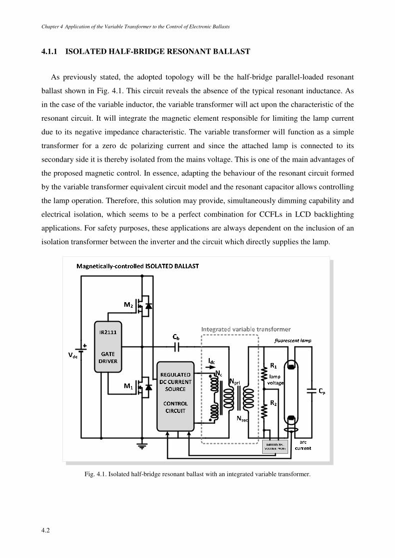
Chapter 4 Application of the Variable Transformer to the Control of Electronic Ballasts
4.2
4.1.1 ISOLATED HALF-BRIDGE RESONANT BALLAST
As previously stated, the adopted topology will be the half-bridge parallel-loaded resonant
ballast shown in Fig. 4.1. This circuit reveals the absence of the typical resonant inductance. As
in the case of the variable inductor, the variable transformer will act upon the characteristic of the
resonant circuit. It will integrate the magnetic element responsible for limiting the lamp current
due to its negative impedance characteristic. The variable transformer will function as a simple
transformer for a zero dc polarizing current and since the attached lamp is connected to its
secondary side it is thereby isolated from the mains voltage. This is one of the main advantages of
the proposed magnetic control. In essence, adapting the behaviour of the resonant circuit formed
by the variable transformer equivalent circuit model and the resonant capacitor allows controlling
the lamp operation. Therefore, this solution may provide, simultaneously dimming capability and
electrical isolation, which seems to be a perfect combination for CCFLs in LCD backlighting
applications. For safety purposes, these applications are always dependent on the inclusion of an
isolation transformer between the inverter and the circuit which directly supplies the lamp.
Fig. 4.1. Isolated half-bridge resonant ballast with an integrated variable transformer.
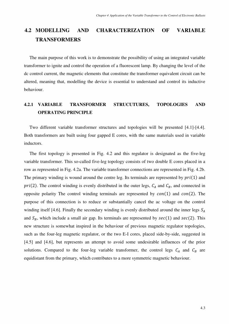
Chapter 4 Application of the Variable Transformer to the Control of Electronic Ballasts
4.3
4.2 MODELLING AND CHARACTERIZATION OF VARIABLE
TRANSFORMERS
The main purpose of this work is to demonstrate the possibility of using an integrated variable
transformer to ignite and control the operation of a fluorescent lamp. By changing the level of the
dc control current, the magnetic elements that constitute the transformer equivalent circuit can be
altered, meaning that, modelling the device is essential to understand and control its inductive
behaviour.
4.2.1 VARIABLE TRANSFORMER STRUCUTURES, TOPOLOGIES AND
OPERATING PRINCIPLE
Two different variable transformer structures and topologies will be presented [4.1]-[4.4].
Both transformers are built using four gapped E cores, with the same materials used in variable
inductors.
The first topology is presented in Fig. 4.2 and this regulator is designated as the five-leg
variable transformer. This so-called five-leg topology consists of two double E cores placed in a
row as represented in Fig. 4.2a. The variable transformer connections are represented in Fig. 4.2b.
The primary winding is wound around the centre leg. Its terminals are represented by yL1 and
yL2. The control winding is evenly distributed in the outer legs, û and Õ, and connected in
opposite polarity The control winding terminals are represented by Km1 and Km2. The
purpose of this connection is to reduce or substantially cancel the ac voltage on the control
winding itself [4.6]. Finally the secondary winding is evenly distributed around the inner legs û
and Õ, which include a small air gap. Its terminals are represented by K1 and K2. This
new structure is somewhat inspired in the behaviour of previous magnetic regulator topologies,
such as the four-leg magnetic regulator, or the two E-I cores, placed side-by-side, suggested in
[4.5] and [4.6], but represents an attempt to avoid some undesirable influences of the prior
solutions. Compared to the four-leg variable transformer, the control legs û and Õ are
equidistant from the primary, which contributes to a more symmetric magnetic behaviour.
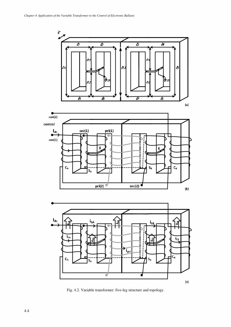
Chapter 4 Application of the Variable Transformer to the Control of Electronic Ballasts
4.4
Fig. 4.2. Variable transformer: five-leg structure and topology.
Chapter 4 Application of the Variable Transformer to the Control of Electronic Ballasts
4.5
Connecting the output inverter voltage to the primary terminals of the transformer, the ac flux
generated by the primary winding will flow through its corresponding leg and then divide
between the right and left paths. For a zero dc control current, and due to the presence of the
small air gap in legs û and Õ, this flux tends to be coupled to the control winding, in the outer
legs, with obviously lower reluctance. On the contrary, if the dc polarizing current has an
increasing non-zero value, the reluctances of these paths change and therefore the amount of
primary flux coupled to the secondary winding tends to increase, meaning that more voltage will
be developed across this winding. In conclusion, the basic principle of this magnetic regulator is
to provide the ability to control the leakages associated to the main magnetic circuit, increasing
the effective global reluctance of the outer legs of the transformer core. Therefore, this device
may be used for ballast purposes, since it enables the control of the power delivered to the lamp,
also providing another advantage besides electric isolation: it works at a constant switching
frequency.
The second topology is presented in Fig. 4.3 and this regulator is designated as the parallel
three-leg variable transformer. This so-called three-leg topology consists of two double E cores
placed in parallel and is inspired in the analysis presented in [4.5] and [4.11]. Fig. 4.3a. and Fig.
4.3b. present the left and right view of this variable transformer.
The control windings are wound around one of the outer legs of each core separately; serially
connected in opposite polarity and then placed side-by-side. The control winding terminals are
represented in Fig. 4.3 by ª and . The induced voltages on these windings have opposite
polarities and, under the assumption of symmetry should cancel each other. As explained in
[4.19], there will be a parasitic, non-linear coupling between the input voltage and the control
windings voltage, due to the non-linearity of the magnetic material. As a result, the control
windings only exhibit a negligible voltage with a frequency equal to twice the operating
frequency. The primary winding is wound around the centre legs of both cores. Its terminals are
represented by tª and t. Finally, the secondary winding is wound around the remaining outer
legs of both cores, which include a small air gap. The secondary winding terminal are also
represented in Fig. 4.3 by ª and .
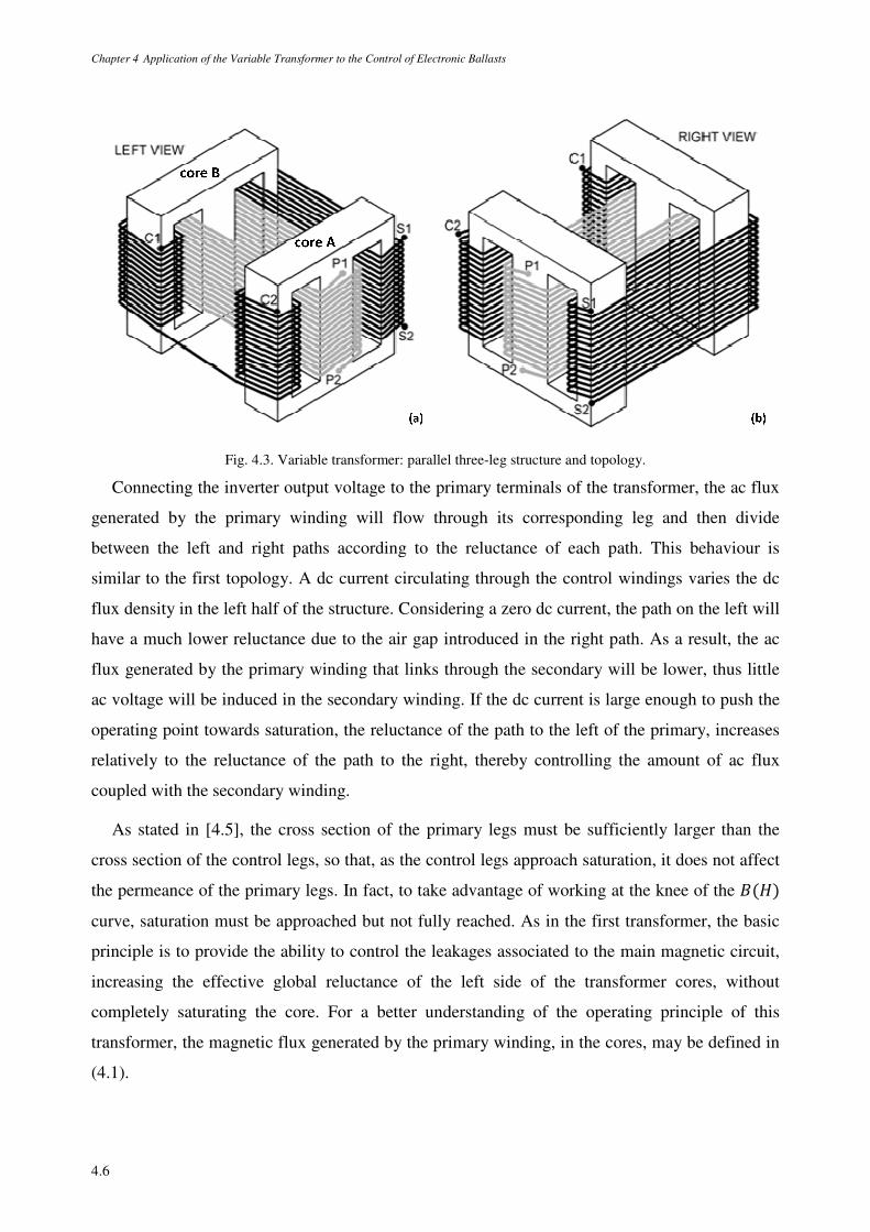
Chapter 4 Application of the Variable Transformer to the Control of Electronic Ballasts
4.6
Fig. 4.3. Variable transformer: parallel three-leg structure and topology.
Connecting the inverter output voltage to the primary terminals of the transformer, the ac flux
generated by the primary winding will flow through its corresponding leg and then divide
between the left and right paths according to the reluctance of each path. This behaviour is
similar to the first topology. A dc current circulating through the control windings varies the dc
flux density in the left half of the structure. Considering a zero dc current, the path on the left will
have a much lower reluctance due to the air gap introduced in the right path. As a result, the ac
flux generated by the primary winding that links through the secondary will be lower, thus little
ac voltage will be induced in the secondary winding. If the dc current is large enough to push the
operating point towards saturation, the reluctance of the path to the left of the primary, increases
relatively to the reluctance of the path to the right, thereby controlling the amount of ac flux
coupled with the secondary winding.
As stated in [4.5], the cross section of the primary legs must be sufficiently larger than the
cross section of the control legs, so that, as the control legs approach saturation, it does not affect
the permeance of the primary legs. In fact, to take advantage of working at the knee of the ¶
curve, saturation must be approached but not fully reached. As in the first transformer, the basic
principle is to provide the ability to control the leakages associated to the main magnetic circuit,
increasing the effective global reluctance of the left side of the transformer cores, without
completely saturating the core. For a better understanding of the operating principle of this
transformer, the magnetic flux generated by the primary winding, in the cores, may be defined in
(4.1).
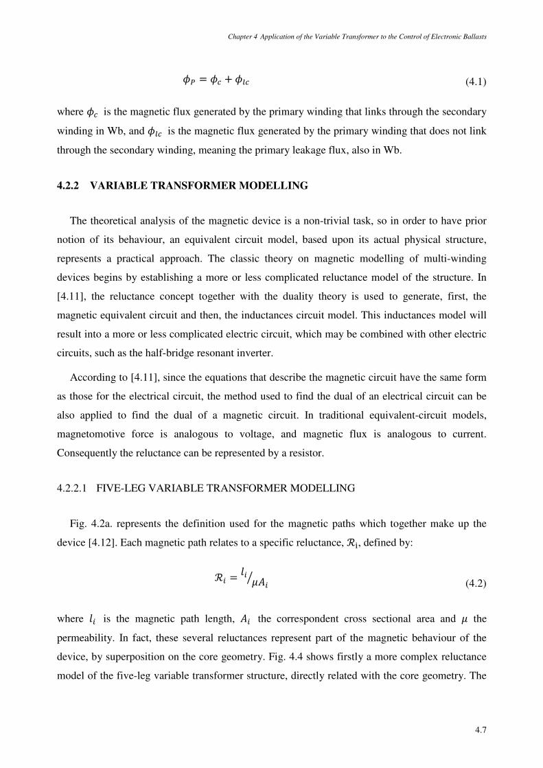
Chapter 4 Application of the Variable Transformer to the Control of Electronic Ballasts
4.7
£ = £ + £ (4.1)
where £ is the magnetic flux generated by the primary winding that links through the secondary
winding in Wb, and £ is the magnetic flux generated by the primary winding that does not link
through the secondary winding, meaning the primary leakage flux, also in Wb.
4.2.2 VARIABLE TRANSFORMER MODELLING
The theoretical analysis of the magnetic device is a non-trivial task, so in order to have prior
notion of its behaviour, an equivalent circuit model, based upon its actual physical structure,
represents a practical approach. The classic theory on magnetic modelling of multi-winding
devices begins by establishing a more or less complicated reluctance model of the structure. In
[4.11], the reluctance concept together with the duality theory is used to generate, first, the
magnetic equivalent circuit and then, the inductances circuit model. This inductances model will
result into a more or less complicated electric circuit, which may be combined with other electric
circuits, such as the half-bridge resonant inverter.
According to [4.11], since the equations that describe the magnetic circuit have the same form
as those for the electrical circuit, the method used to find the dual of an electrical circuit can be
also applied to find the dual of a magnetic circuit. In traditional equivalent-circuit models,
magnetomotive force is analogous to voltage, and magnetic flux is analogous to current.
Consequently the reluctance can be represented by a resistor.
4.2.2.1 FIVE-LEG VARIABLE TRANSFORMER MODELLING
Fig. 4.2a. represents the definition used for the magnetic paths which together make up the
device [4.12]. Each magnetic path relates to a specific reluctance, ℛÎ, defined by:
ℛ± = ± µ±¤ (4.2)
where ± is the magnetic path length, ± the correspondent cross sectional area and µ the
permeability. In fact, these several reluctances represent part of the magnetic behaviour of the
device, by superposition on the core geometry. Fig. 4.4 shows firstly a more complex reluctance
model of the five-leg variable transformer structure, directly related with the core geometry. The
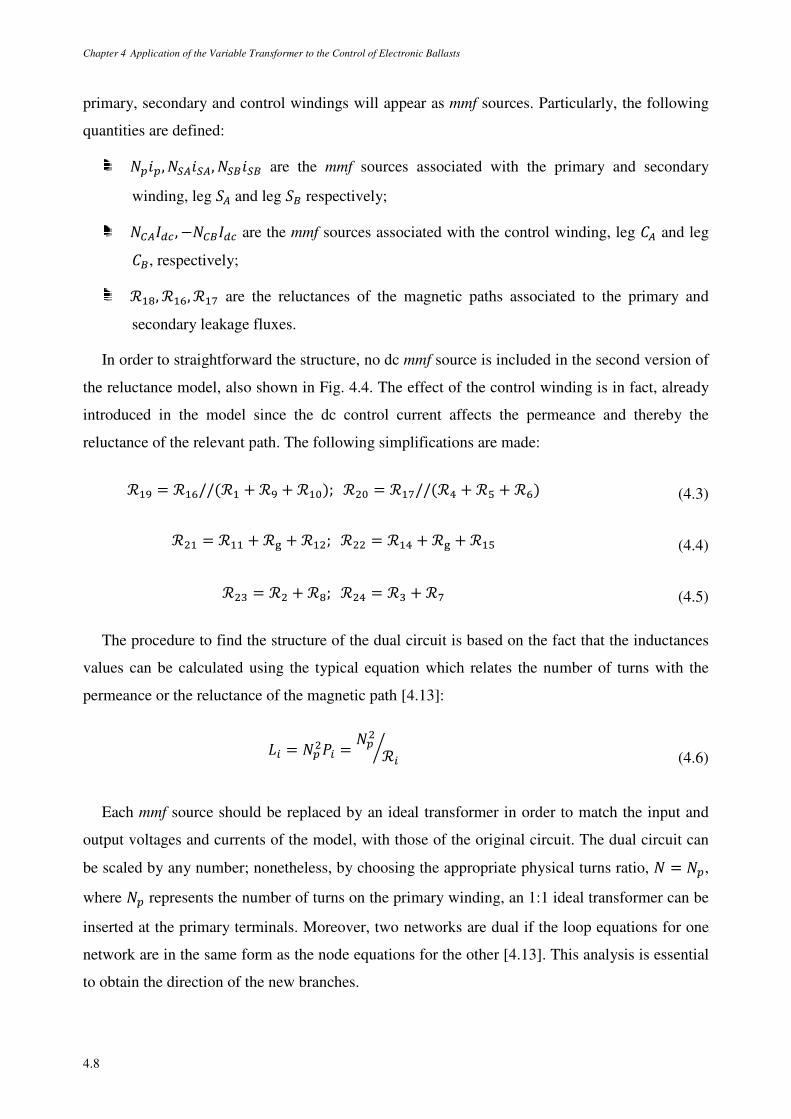
Chapter 4 Application of the Variable Transformer to the Control of Electronic Ballasts
4.8
primary, secondary and control windings will appear as mmf sources. Particularly, the following
quantities are defined:
ÁL, ÁËûLËû, ÁËÕLËÕ are the mmf sources associated with the primary and secondary
winding, leg û and leg Õ respectively;
Áû/ , −ÁÕ/ are the mmf sources associated with the control winding, leg û and leg
Õ, respectively;
ℛªÚ, ℛªÙ, ℛª» are the reluctances of the magnetic paths associated to the primary and
secondary leakage fluxes.
In order to straightforward the structure, no dc mmf source is included in the second version of
the reluctance model, also shown in Fig. 4.4. The effect of the control winding is in fact, already
introduced in the model since the dc control current affects the permeance and thereby the
reluctance of the relevant path. The following simplifications are made:
ℛªÛ = ℛªÙ//(ℛª + ℛÛ + ℛª); ℛ = ℛª»//(ℛ× + ℛØ + ℛÙ) (4.3)
ℛª = ℛªª + ℛL + ℛª; ℛ = ℛª× + ℛL + ℛªØ (4.4)
ℛ = ℛ + ℛÚ; ℛ× = ℛ + ℛ» (4.5)
The procedure to find the structure of the dual circuit is based on the fact that the inductances
values can be calculated using the typical equation which relates the number of turns with the
permeance or the reluctance of the magnetic path [4.13]:
¯± = Át± = Á ℛ±; (4.6)
Each mmf source should be replaced by an ideal transformer in order to match the input and
output voltages and currents of the model, with those of the original circuit. The dual circuit can
be scaled by any number; nonetheless, by choosing the appropriate physical turns ratio, Á = Á,
where Á represents the number of turns on the primary winding, an 1:1 ideal transformer can be
inserted at the primary terminals. Moreover, two networks are dual if the loop equations for one
network are in the same form as the node equations for the other [4.13]. This analysis is essential
to obtain the direction of the new branches.
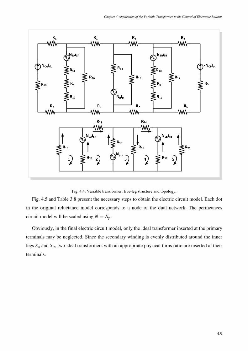
Chapter 4 Application of the Variable Transformer to the Control of Electronic Ballasts
4.9
Fig. 4.4. Variable transformer: five-leg structure and topology.
Fig. 4.5 and Table 3.8 present the necessary steps to obtain the electric circuit model. Each dot
in the original reluctance model corresponds to a node of the dual network. The permeances
circuit model will be scaled using Á = Á.
Obviously, in the final electric circuit model, only the ideal transformer inserted at the primary
terminals may be neglected. Since the secondary winding is evenly distributed around the inner
legs û and Õ, two ideal transformers with an appropriate physical turns ratio are inserted at their
terminals.
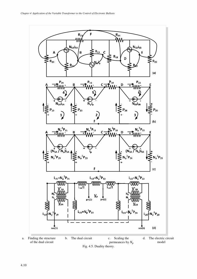
Chapter 4 Application of the Variable Transformer to the Control of Electronic Ballasts
4.10
a. Finding the structure
of the dual circuit b. The dual circuit c. Scaling the
permeances by Á d. The electric circuit
model Fig. 4.5. Duality theory.
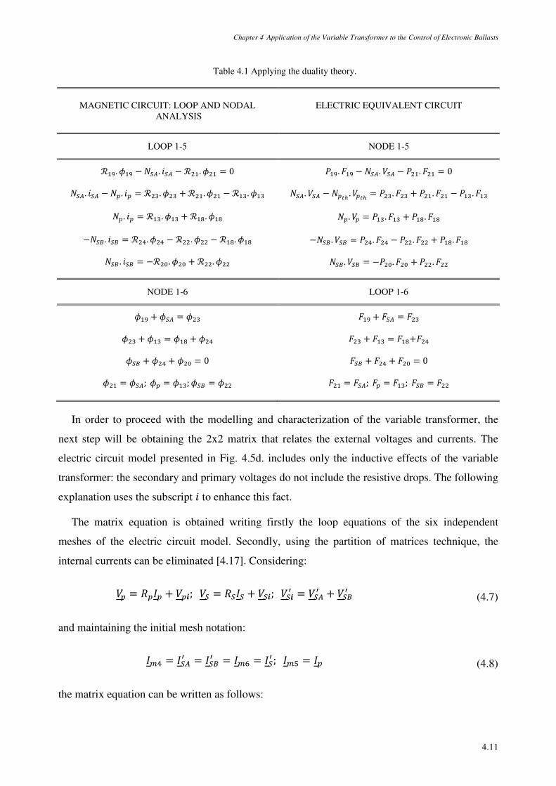
Chapter 4 Application of the Variable Transformer to the Control of Electronic Ballasts
4.11
Table 4.1 Applying the duality theory.
MAGNETIC CIRCUIT: LOOP AND NODAL ANALYSIS
ELECTRIC EQUIVALENT CIRCUIT
LOOP 1-5 NODE 1-5
ℛªÛ. £ªÛ − ÁËû. LËû − ℛª. £ª = 0
ÁËû. LËû − Á. L = ℛ. £ + ℛª. £ª − ℛª. £ª
Á. L = ℛª. £ª + ℛªÚ. £ªÚ
−ÁËÕ. LËÕ = ℛ×. £× − ℛ. £ − ℛªÚ. £ªÚ
ÁËÕ . LËÕ = −ℛ. £ + ℛ. £
tªÛ.MªÛ − ÁËû. >Ëû − tª.Mª = 0
ÁËû. >Ëû − ÁýN . >ýN = t.M + tª.Mª − tª.Mª
Á. > = tª.Mª + tªÚ.MªÚ
−ÁËÕ . >ËÕ = t×.M× − t.M + tªÚ.MªÚ
ÁËÕ. >ËÕ = −t.M + t.M
NODE 1-6 LOOP 1-6
£ªÛ + £Ëû = £
£ + £ª = £ªÚ + £×
£ËÕ + £× + £ = 0
£ª = £Ëû; £ = £ª; £ËÕ = £
MªÛ + MËû = M
M + Mª = MªÚ+M×
MËÕ + M× + M = 0
Mª = MËû; M = Mª; MËÕ = M
In order to proceed with the modelling and characterization of the variable transformer, the
next step will be obtaining the 2x2 matrix that relates the external voltages and currents. The
electric circuit model presented in Fig. 4.5d. includes only the inductive effects of the variable
transformer: the secondary and primary voltages do not include the resistive drops. The following
explanation uses the subscript L to enhance this fact.
The matrix equation is obtained writing firstly the loop equations of the six independent
meshes of the electric circuit model. Secondly, using the partition of matrices technique, the
internal currents can be eliminated [4.17]. Considering:
> = v/ + > ; >Ë = vË/Ë + >Ë ; >Ë Ñ = >ËûÑ + >ËÕÑ (4.7)
and maintaining the initial mesh notation:
/× = /ËûÑ = /ËÕÑ = /Ù = /ËÑ ; /Ø = / (4.8)
the matrix equation can be written as follows:
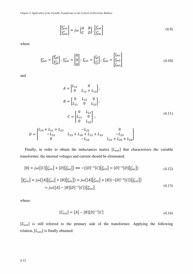
Chapter 4 Application of the Variable Transformer to the Control of Electronic Ballasts
4.12
ä>3ÏÀÑ>±²ÀÑ æ = . ® . ä/3ÏÀÑ
/±²ÀÑ æ (4.9)
where
>3ÏÀÑ = > >Ë Ñ ; >±²ÀÑ = è000é ;/3ÏÀÑ = //ËÑ ; /±²ÀÑ = O/ª//P (4.10)
and
= ¯ª 00 ¯ª + ¯ª ; = 0 ¯ª 0¯ª 0 ¯ ;
= è 0 ¯ª¯ª 00 ¯é;
® = è¯ªÛ + ¯ª + ¯ −¯ 0−¯ ¯ + ¯ªÚ + ¯ª + ¯× −¯×0 −¯× ¯ + ¯ + ¯×é
(4.11)
Finally, in order to obtain the inductances matrix [¯3ÏÀ] that characterizes the variable
transformer, the internal voltages and current should be eliminated:
[0] = ¾[]/3ÏÀÑ + [®]/±²ÀÑ ¿ ⟺ −([®]ºª[]/3ÏÀÑ = [®]ºª[®]/±²ÀÑ ) (4.12)
>3ÏÀÑ = ¾[]/3ÏÀÑ + []/±²ÀÑ ¿ = ¾[]/3ÏÀÑ + [](−[®]ºª[])/3ÏÀÑ ¿= ([]− [][®]ºª[])/3ÏÀÑ (4.13)
where:
[¯3ÏÀÑ ] = []− [][®]ºª[] (4.14)
[¯3ÏÀÑ ] is still referred to the primary side of the transformer. Applying the following
relation,[¯3ÏÀ] is finally obtained:
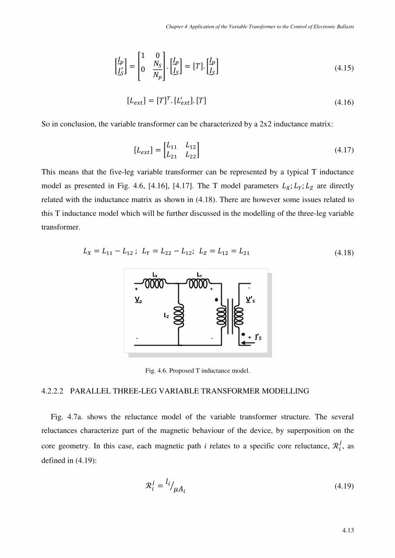
Chapter 4 Application of the Variable Transformer to the Control of Electronic Ballasts
4.13
//ËÑ = O1 00 ÁËÁ
P . //Ë = [<]. //Ë (4.15)
[¯3ÏÀ] = [<]C . [¯3ÏÀÑ ]. [<] (4.16)
So in conclusion, the variable transformer can be characterized by a 2x2 inductance matrix:
[¯3ÏÀ] = ¯ªª ¯ª¯ª ¯ (4.17)
This means that the five-leg variable transformer can be represented by a typical T inductance
model as presented in Fig. 4.6, [4.16], [4.17]. The T model parameters ¯R; ¯S; ¯T are directly
related with the inductance matrix as shown in (4.18). There are however some issues related to
this T inductance model which will be further discussed in the modelling of the three-leg variable
transformer.
¯R = ¯ªª − ¯ª; ¯S = ¯ − ¯ª; ¯T = ¯ª = ¯ª (4.18)
Fig. 4.6. Proposed T inductance model.
4.2.2.2 PARALLEL THREE-LEG VARIABLE TRANSFORMER MODELLING
Fig. 4.7a. shows the reluctance model of the variable transformer structure. The several
reluctances characterize part of the magnetic behaviour of the device, by superposition on the
core geometry. In this case, each magnetic path i relates to a specific core reluctance, ℛ±¦, as
defined in (4.19):
ℛ±¦ = ± µ±¤ (4.19)
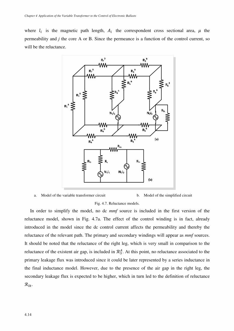
Chapter 4 Application of the Variable Transformer to the Control of Electronic Ballasts
4.14
where ± is the magnetic path length, ± the correspondent cross sectional area, µ the
permeability and j the core A or B. Since the permeance is a function of the control current, so
will be the reluctance.
a. Model of the variable transformer circuit b. Model of the simplified circuit
Fig. 4.7. Reluctance models.
In order to simplify the model, no dc mmf source is included in the first version of the
reluctance model, shown in Fig. 4.7a. The effect of the control winding is in fact, already
introduced in the model since the dc control current affects the permeability and thereby the
reluctance of the relevant path. The primary and secondary windings will appear as mmf sources.
It should be noted that the reluctance of the right leg, which is very small in comparison to the
reluctance of the existent air gap, is included in ℛû. At this point, no reluctance associated to the
primary leakage flux was introduced since it could be later represented by a series inductance in
the final inductance model. However, due to the presence of the air gap in the right leg, the
secondary leakage flux is expected to be higher, which in turn led to the definition of reluctance
ℛÊ.
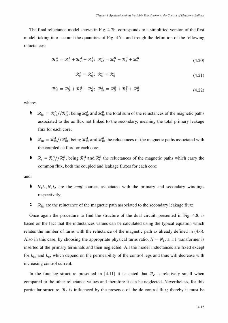
Chapter 4 Application of the Variable Transformer to the Control of Electronic Ballasts
4.15
The final reluctance model shown in Fig. 4.7b. corresponds to a simplified version of the first
model, taking into account the quantities of Fig. 4.7a. and trough the definition of the following
reluctances:
ℛû = ℛªû + ℛû + ℛ×û; ℛÕ = ℛªÕ + ℛÕ + ℛ×Õ (4.20)
ℛû = ℛÙû; ℛÕ = ℛÙÕ (4.21)
ℛû = ℛû + ℛØû + ℛû; ℛÕ = ℛÕ + ℛØÕ + ℛÕ (4.22)
where:
ℛ = ℛû //ℛÕ ; being ℛû andℛÕ the total sum of the reluctances of the magnetic paths
associated to the ac flux not linked to the secondary, meaning the total primary leakage
flux for each core;
ℛ = ℛû //ℛÕ ; being ℛû andℛÕ the reluctances of the magnetic paths associated with
the coupled ac flux for each core;
ℛ = ℛû//ℛÕ; being ℛûandℛÕ the reluctances of the magnetic paths which carry the
common flux, both the coupled and leakage fluxes for each core;
and:
ÁªLª, ÁL are the mmf sources associated with the primary and secondary windings
respectively;
ℛÊ are the reluctance of the magnetic path associated to the secondary leakage flux;
Once again the procedure to find the structure of the dual circuit, presented in Fig. 4.8, is
based on the fact that the inductances values can be calculated using the typical equation which
relates the number of turns with the reluctance of the magnetic path as already defined in (4.6).
Also in this case, by choosing the appropriate physical turns ratio, Á = Áª, a 1:1 transformer is
inserted at the primary terminals and then neglected. All the model inductances are fixed except
for ¯ and ¯, which depend on the permeability of the control legs and thus will decrease with
increasing control current.
In the four-leg structure presented in [4.11] it is stated that ℛ is relatively small when
compared to the other reluctance values and therefore it can be neglected. Nevertheless, for this
particular structure, ℛ is influenced by the presence of the dc control flux; thereby it must be
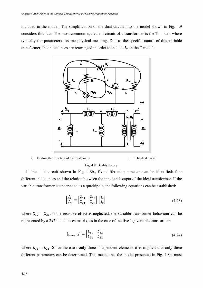
Chapter 4 Application of the Variable Transformer to the Control of Electronic Ballasts
4.16
included in the model. The simplification of the dual circuit into the model shown in Fig. 4.9
considers this fact. The most common equivalent circuit of a transformer is the T model, where
typically the parameters assume physical meaning. Due to the specific nature of this variable
transformer, the inductances are rearranged in order to include ¯ in the T model.
a. Finding the structure of the dual circuit b. The dual circuit
Fig. 4.8. Duality theory.
In the dual circuit shown in Fig. 4.8b., five different parameters can be identified: four
different inductances and the relation between the input and output of the ideal transformer. If the
variable transformer is understood as a quadripole, the following equations can be established:
>ª> = ªª ªª . /ª/ (4.23)
where ª = ª. If the resistive effect is neglected, the variable transformer behaviour can be
represented by a 2x2 inductances matrix, as in the case of the five-leg variable transformer:
[¯UVWÝÜ] = ¯ªª ¯ª¯ª ¯ (4.24)
where ¯ª = ¯ª. Since there are only three independent elements it is implicit that only three
different parameters can be determined. This means that the model presented in Fig. 4.8b. must
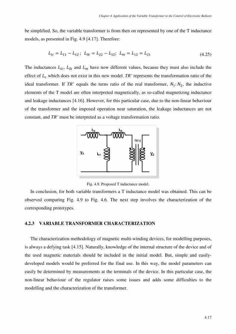
Chapter 4 Application of the Variable Transformer to the Control of Electronic Ballasts
4.17
be simplified. So, the variable transformer is from then on represented by one of the T inductance
models, as presented in Fig. 4.9 [4.17]. Therefore:
¯ = ¯ªª − ¯ª; ¯Ê = ¯ − ¯ª; ¯ = ¯ª = ¯ª (4.25)
The inductances ¯, ¯Ê and ¯ have now different values, because they must also include the
effect of ¯ which does not exist in this new model. TR’ represents the transformation ratio of the
ideal transformer. If TR’ equals the turns ratio of the real transformer, Áª:Á, the inductive
elements of the T model are often interpreted magnetically, as so-called magnetizing inductance
and leakage inductances [4.16]. However, for this particular case, due to the non-linear behaviour
of the transformer and the imposed operation near saturation, the leakage inductances are not
constant, and TR’ must be interpreted as a voltage transformation ratio.
Fig. 4.9. Proposed T inductance model.
In conclusion, for both variable transformers a T inductance model was obtained. This can be
observed comparing Fig. 4.9 to Fig. 4.6. The next step involves the characterization of the
corresponding prototypes.
4.2.3 VARIABLE TRANSFORMER CHARACTERIZATION
The characterization methodology of magnetic multi-winding devices, for modelling purposes,
is always a defying task [4.15]. Naturally, knowledge of the internal structure of the device and of
the used magnetic materials should be included in the initial model. But, simple and easily-
developed models would be preferred for the final use. In this way, the model parameters can
easily be determined by measurements at the terminals of the device. In this particular case, the
non-linear behaviour of the regulator raises some issues and adds some difficulties to the
modelling and the characterization of the transformer.
Chapter 4 Application of the Variable Transformer to the Control of Electronic Ballasts
4.18
The experimental prototype presented in Fig. 4.10a., the five-leg variable transformer, was
built using two EF25 ferrite cores, with Á = 100 turns, ÁËû = ÁËÕ = 50, and for each control
winding, Áû = ÁÕ = 80 turns. The experimental prototype presented in Fig. 4.10b., the
parallel three-leg variable transformer, was also built using two EF25 cores, with Áª = Á = 100
turns, and for each control winding Áá = 80 turns.
a. Five-leg b. Parallel three-leg
Fig. 4.10. Variable transformers prototypes.
To perform the experimental small-signal characterization of the magnetic devices several
measurements were taken by means of open-circuit and short-circuit tests. For both transformers,
the open-circuit test was done measuring firstly the primary open-circuit inductance, ¯ªªVá, with
the secondary open and vice-versa, measuring the secondary open-circuit inductance, ¯Vá with
the primary open. Similarly, for the same range of the dc control current, the short-circuit test was
done measuring firstly the primary short-circuit inductance, ¯ªáá, with the secondary short-
circuited and vice-versa, measuring the secondary short-circuit inductance, ¯áá with the primary
short circuited. These inductances were measured by an LCR meter (test conditions: 1Vrms,
1kHz), for a dc control current range between 0 and 0.6A in the case of the five-leg transformer
and for a dc control current range between 0 and 1 A, in the case of the three-leg transformer. For
the parallel three-leg transformer the secondary voltage in open-circuit was also measured. The
collected data is presented in Table 4.2 and in Table 4.3.
With the data collected Table 4.2 in and in Table 4.3, the T model inductances could be
determined using (4.26), (4.27), (4.28) and (4.29), for the five-leg prototype, and using (4.30);
(4.31); (4.32) and (4.33) for the three-leg prototype.
¯ªªÔ = ¯R + ¯T (4.26)
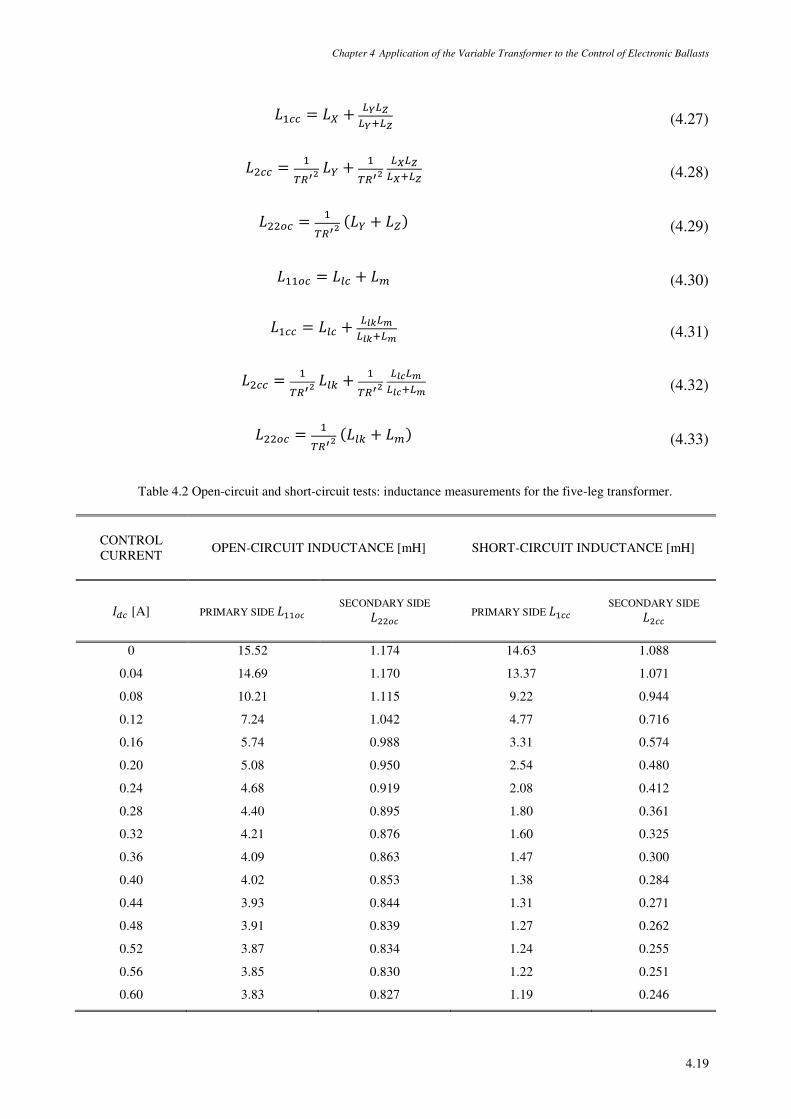
Chapter 4 Application of the Variable Transformer to the Control of Electronic Ballasts
4.19
¯ª = ¯R + XYXZY (4.27)
¯ = ªCÓ[E¯S + ªCÓ[E \Y\ZY (4.28)
¯Ô = ªCÓ[E(¯S + ¯T) (4.29)
¯ªªÔ = ¯ + ¯ (4.30)
¯ª = ¯ + ]^_]^Z_ (4.31)
¯ = ªCÓ[E¯Ê + ªCÓ[E ]6_]6Z_ (4.32)
¯Ô = ªCÓ[E(¯Ê + ¯) (4.33)
Table 4.2 Open-circuit and short-circuit tests: inductance measurements for the five-leg transformer.
CONTROL CURRENT
OPEN-CIRCUIT INDUCTANCE [mH] SHORT-CIRCUIT INDUCTANCE [mH]
/ [A] PRIMARY SIDE ¯ªªÔ SECONDARY SIDE ¯Ô
PRIMARY SIDE ¯ª SECONDARY SIDE ¯
0 15.52 1.174 14.63 1.088
0.04 14.69 1.170 13.37 1.071
0.08 10.21 1.115 9.22 0.944
0.12 7.24 1.042 4.77 0.716
0.16 5.74 0.988 3.31 0.574
0.20 5.08 0.950 2.54 0.480
0.24 4.68 0.919 2.08 0.412
0.28 4.40 0.895 1.80 0.361
0.32 4.21 0.876 1.60 0.325
0.36 4.09 0.863 1.47 0.300
0.40 4.02 0.853 1.38 0.284
0.44 3.93 0.844 1.31 0.271
0.48 3.91 0.839 1.27 0.262
0.52 3.87 0.834 1.24 0.255
0.56 3.85 0.830 1.22 0.251
0.60 3.83 0.827 1.19 0.246
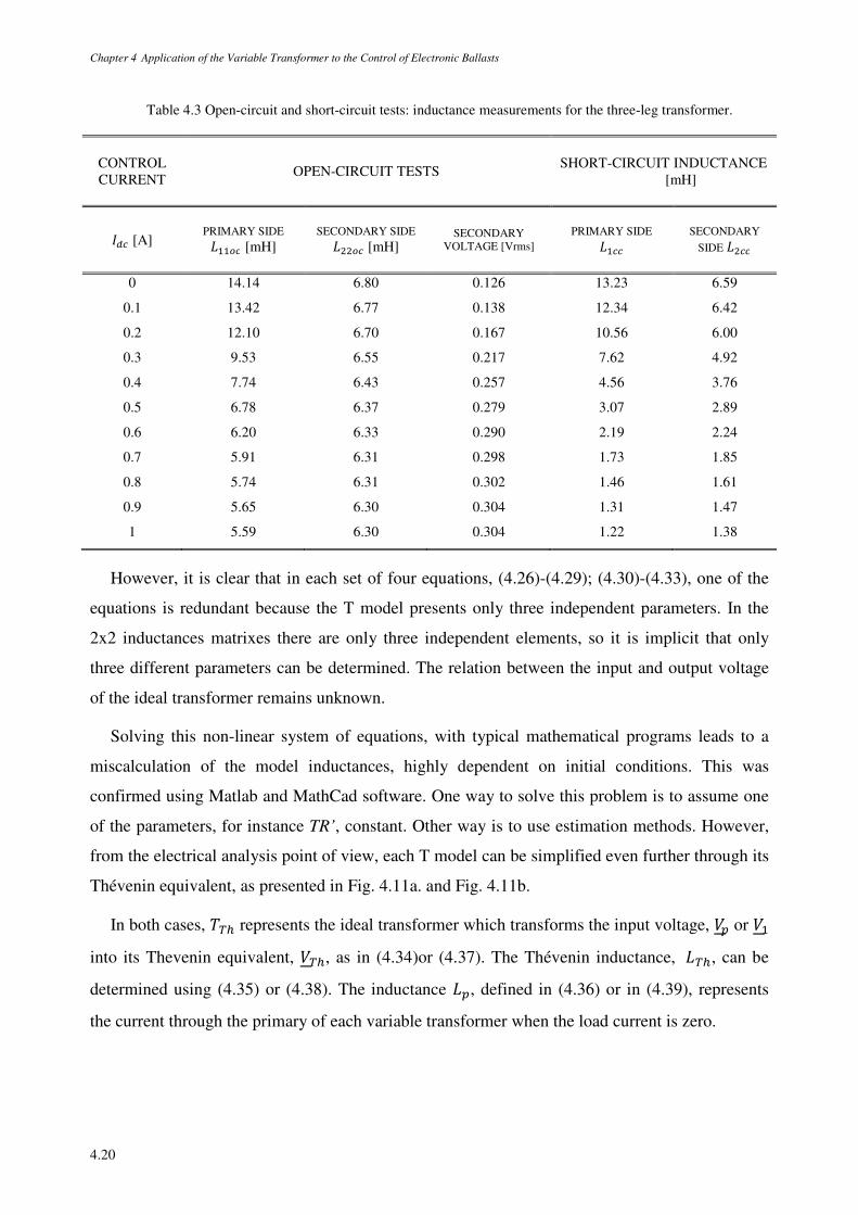
Chapter 4 Application of the Variable Transformer to the Control of Electronic Ballasts
4.20
Table 4.3 Open-circuit and short-circuit tests: inductance measurements for the three-leg transformer.
CONTROL CURRENT
OPEN-CIRCUIT TESTS SHORT-CIRCUIT INDUCTANCE
[mH]
/ [A] PRIMARY SIDE ¯ªªÔ [mH]
SECONDARY SIDE ¯Ô [mH] SECONDARY
VOLTAGE [Vrms] PRIMARY SIDE ¯ª
SECONDARY
SIDE ¯
0 14.14 6.80 0.126 13.23 6.59
0.1 13.42 6.77 0.138 12.34 6.42
0.2 12.10 6.70 0.167 10.56 6.00
0.3 9.53 6.55 0.217 7.62 4.92
0.4 7.74 6.43 0.257 4.56 3.76
0.5 6.78 6.37 0.279 3.07 2.89
0.6 6.20 6.33 0.290 2.19 2.24
0.7 5.91 6.31 0.298 1.73 1.85
0.8 5.74 6.31 0.302 1.46 1.61
0.9 5.65 6.30 0.304 1.31 1.47
1 5.59 6.30 0.304 1.22 1.38
However, it is clear that in each set of four equations, (4.26)-(4.29); (4.30)-(4.33), one of the
equations is redundant because the T model presents only three independent parameters. In the
2x2 inductances matrixes there are only three independent elements, so it is implicit that only
three different parameters can be determined. The relation between the input and output voltage
of the ideal transformer remains unknown.
Solving this non-linear system of equations, with typical mathematical programs leads to a
miscalculation of the model inductances, highly dependent on initial conditions. This was
confirmed using Matlab and MathCad software. One way to solve this problem is to assume one
of the parameters, for instance TR’, constant. Other way is to use estimation methods. However,
from the electrical analysis point of view, each T model can be simplified even further through its
Thévenin equivalent, as presented in Fig. 4.11a. and Fig. 4.11b.
In both cases, <C° represents the ideal transformer which transforms the input voltage, > or >ª
into its Thevenin equivalent, >C°, as in (4.34)or (4.37). The Thévenin inductance, ¯C°, can be
determined using (4.35) or (4.38). The inductance ¯, defined in (4.36) or in (4.39), represents
the current through the primary of each variable transformer when the load current is zero.
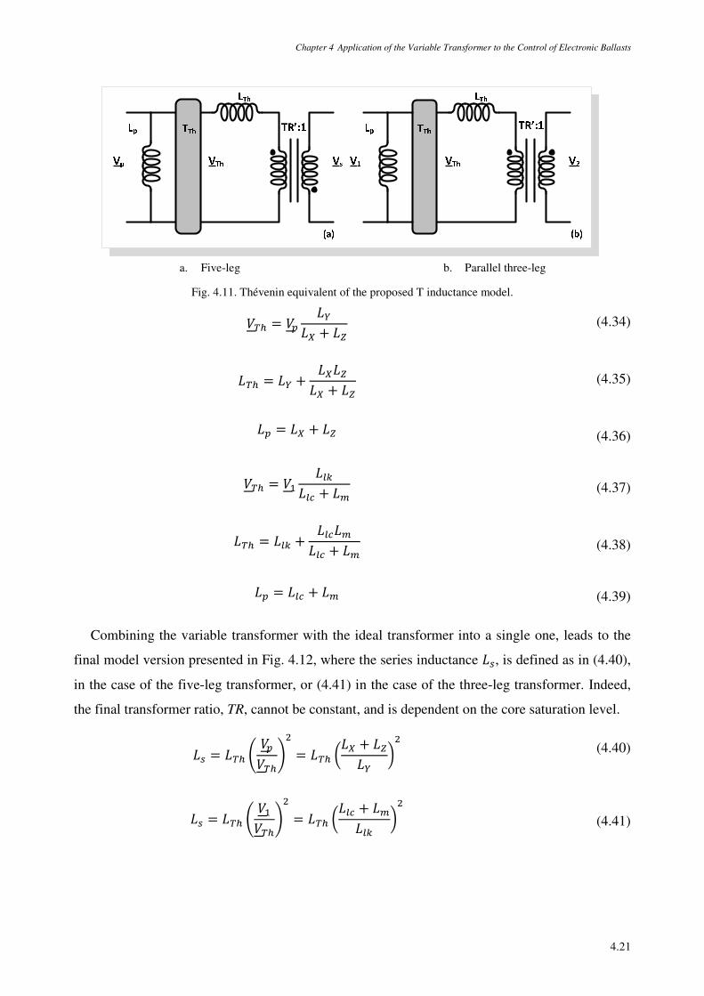
Chapter 4 Application of the Variable Transformer to the Control of Electronic Ballasts
4.21
a. Five-leg b. Parallel three-leg
Fig. 4.11. Thévenin equivalent of the proposed T inductance model.
>C° = > ¯S¯R + ¯T (4.34)
¯C° = ¯S + ¯R¯T¯R + ¯T (4.35)
¯ = ¯R + ¯T (4.36)
>C° = >ª ¯Ê¯ + ¯ (4.37)
¯C° = ¯Ê + ¯¯¯ + ¯ (4.38)
¯ = ¯ + ¯ (4.39)
Combining the variable transformer with the ideal transformer into a single one, leads to the
final model version presented in Fig. 4.12, where the series inductance ¯4, is defined as in (4.40),
in the case of the five-leg transformer, or (4.41) in the case of the three-leg transformer. Indeed,
the final transformer ratio, TR, cannot be constant, and is dependent on the core saturation level.
¯4 = ¯C° >>C° = ¯C° ¯R + ¯T¯S
(4.40)
¯4 = ¯C° >ª>C° = ¯C° ¯ + ¯¯Ê
(4.41)
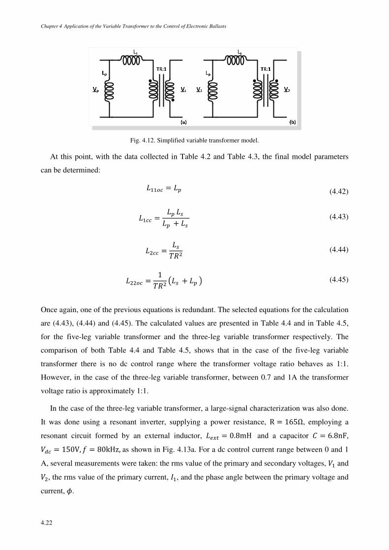
Chapter 4 Application of the Variable Transformer to the Control of Electronic Ballasts
4.22
Fig. 4.12. Simplified variable transformer model.
At this point, with the data collected in Table 4.2 and Table 4.3, the final model parameters
can be determined:
¯ªªÔ = ¯ (4.42)
¯ª = ¯¯4¯ + ¯4 (4.43)
¯ = ¯4<v (4.44)
¯Ô = 1<v ¾¯4 + ¯¿ (4.45)
Once again, one of the previous equations is redundant. The selected equations for the calculation
are (4.43), (4.44) and (4.45). The calculated values are presented in Table 4.4 and in Table 4.5,
for the five-leg variable transformer and the three-leg variable transformer respectively. The
comparison of both Table 4.4 and Table 4.5, shows that in the case of the five-leg variable
transformer there is no dc control range where the transformer voltage ratio behaves as 1:1.
However, in the case of the three-leg variable transformer, between 0.7 and 1A the transformer
voltage ratio is approximately 1:1.
In the case of the three-leg variable transformer, a large-signal characterization was also done.
It was done using a resonant inverter, supplying a power resistance, R = 165Ω, employing a
resonant circuit formed by an external inductor, ¯3ÏÀ = 0.8mH and a capacitor = 6.8nF,
> = 150V, = 80kHz,as shown in Fig. 4.13a. For a dc control current range between 0 and 1
A, several measurements were taken: the rms value of the primary and secondary voltages, >ª and
>, the rms value of the primary current, /ª, and the phase angle between the primary voltage and
current,£.
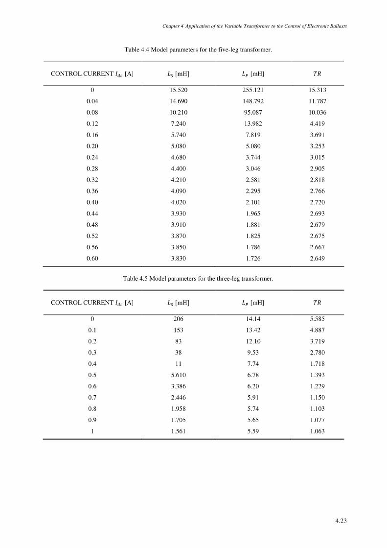
Chapter 4 Application of the Variable Transformer to the Control of Electronic Ballasts
4.23
Table 4.4 Model parameters for the five-leg transformer.
CONTROL CURRENT / [A] ¯Ë[mH] ¯ [mH] <v
0 15.520 255.121 15.313
0.04 14.690 148.792 11.787
0.08 10.210 95.087 10.036
0.12 7.240 13.982 4.419
0.16 5.740 7.819 3.691
0.20 5.080 5.080 3.253
0.24 4.680 3.744 3.015
0.28 4.400 3.046 2.905
0.32 4.210 2.581 2.818
0.36 4.090 2.295 2.766
0.40 4.020 2.101 2.720
0.44 3.930 1.965 2.693
0.48 3.910 1.881 2.679
0.52 3.870 1.825 2.675
0.56 3.850 1.786 2.667
0.60 3.830 1.726 2.649
Table 4.5 Model parameters for the three-leg transformer.
CONTROL CURRENT / [A] ¯Ë[mH] ¯ [mH] <v
0 206 14.14 5.585
0.1 153 13.42 4.887
0.2 83 12.10 3.719
0.3 38 9.53 2.780
0.4 11 7.74 1.718
0.5 5.610 6.78 1.393
0.6 3.386 6.20 1.229
0.7 2.446 5.91 1.150
0.8 1.958 5.74 1.103
0.9 1.705 5.65 1.077
1 1.561 5.59 1.063
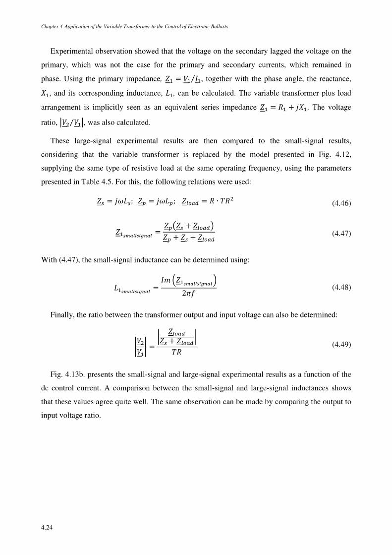
Chapter 4 Application of the Variable Transformer to the Control of Electronic Ballasts
4.24
Experimental observation showed that the voltage on the secondary lagged the voltage on the
primary, which was not the case for the primary and secondary currents, which remained in
phase. Using the primary impedance, ª = >ª /ª⁄ , together with the phase angle, the reactance, 8ª, and its corresponding inductance, ¯ª, can be calculated. The variable transformer plus load
arrangement is implicitly seen as an equivalent series impedance ª = vª + 8ª. The voltage
ratio, â> >ª⁄ â, was also calculated.
These large-signal experimental results are then compared to the small-signal results,
considering that the variable transformer is replaced by the model presented in Fig. 4.12,
supplying the same type of resistive load at the same operating frequency, using the parameters
presented in Table 4.5. For this, the following relations were used:
4 = ¯4; = ¯; Ô~ = v ∙ <v (4.46)
ª¨_]]¨`a] = ¾4 + Ô~¿ + 4 + Ô~ (4.47)
With (4.47), the small-signal inductance can be determined using:
¯ª¨_]]¨`a] = /x ª¨_]]¨`a]2¸ (4.48)
Finally, the ratio between the transformer output and input voltage can also be determined:
A>>ªA =b Ô~4 + Ô~b<v (4.49)
Fig. 4.13b. presents the small-signal and large-signal experimental results as a function of the
dc control current. A comparison between the small-signal and large-signal inductances shows
that these values agree quite well. The same observation can be made by comparing the output to
input voltage ratio.
Chapter 4 Application of the Variable Transformer to the Control of Electronic Ballasts
4.25
a. Circuit schematic for large-signal characterization
b. Comparison between small-signal and large-signal experimental values as a function of the dc control current
Fig. 4.13. Characterization of the three-leg variable transformer.
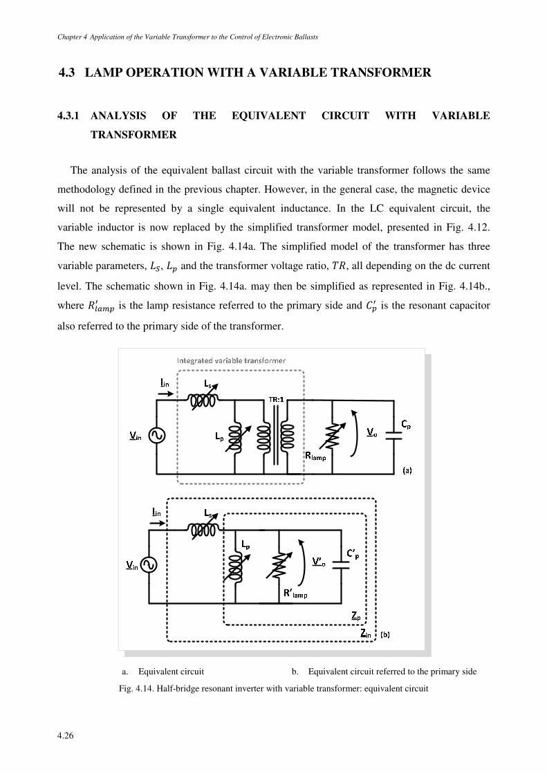
Chapter 4 Application of the Variable Transformer to the Control of Electronic Ballasts
4.26
4.3 LAMP OPERATION WITH A VARIABLE TRANSFORMER
4.3.1 ANALYSIS OF THE EQUIVALENT CIRCUIT WITH VARIABLE
TRANSFORMER
The analysis of the equivalent ballast circuit with the variable transformer follows the same
methodology defined in the previous chapter. However, in the general case, the magnetic device
will not be represented by a single equivalent inductance. In the LC equivalent circuit, the
variable inductor is now replaced by the simplified transformer model, presented in Fig. 4.12.
The new schematic is shown in Fig. 4.14a. The simplified model of the transformer has three
variable parameters, ¯Ë, ¯ and the transformer voltage ratio, <v, all depending on the dc current
level. The schematic shown in Fig. 4.14a. may then be simplified as represented in Fig. 4.14b.,
where v~Ñ is the lamp resistance referred to the primary side and Ñ is the resonant capacitor
also referred to the primary side of the transformer.
a. Equivalent circuit b. Equivalent circuit referred to the primary side
Fig. 4.14. Half-bridge resonant inverter with variable transformer: equivalent circuit
Chapter 4 Application of the Variable Transformer to the Control of Electronic Ballasts
4.27
v~Ñ and Ñ are defined as:
v~Ñ = v~<vwÑ = <v (4.50)
The parallel admittance : may be defined as:
: = 1 = 1¯ + 1v~Ñ + Ñ (4.51)
Therefore, the input impedance is defined as:
±² = ¯4 + (4.52)
±² = ¾¯¿v~Ñ + ¯v~Ñ ¾1 − ¯Ñ ¿v~Ñ ¾1 − ¯Ñ ¿ + ¾¯¿ + ¯4 (4.53)
If both real and imaginary parts are isolated, (4.53) can be rewritten:
v¾±²¿ = ¾¯¿v~Ñv~Ñ ¾1 − ¯Ñ ¿ + ¾¯¿ (4.54)
/x¾±²¿ = v~Ñ ¾1 − ¯Ñ ¿¾¯ + ¯4¿ + ¯¯4v~Ñ ¾1 − ¯Ñ ¿ + ¾¯¿ (4.55)
Similarly to the LC circuit, the phase angle of the resonant current can also be defined as:
£±² = wõ 1±² ∙ 180¸ (4.56)
The input current can be defined as:
/±² = >±²±² =>±²
1 + ¯4= >±²
1v~Ñ + Ñ − 1¯1 + ¯4¯ − ¯4Ñ + ¯4v~Ñ
(4.57)
The voltage gain of the circuit or the voltage transfer function referred to the primary can be
defined, applying the voltage divider rule, as:
Chapter 4 Application of the Variable Transformer to the Control of Electronic Ballasts
4.28
Ñ() = >ÔÑ>±² = ±² = ¯4 + = 11 + ¯4
= 11 + ¯4 −¯ + 1v~Ñ + Ñ
(4.58)
Equation (4.58) can be simplified:
′() = 11 + ¯4¯ − ¯4Ñ + ¯4v~Ñ
(4.59)
The absolute value of the voltage gain can be defined as:
â′()â = 1ö1 + ¯4¯ − ¯4Ñ + ¯4v~Ñ =
(4.60)
Therefore, the output voltage referred to the primary can be calculated as:
>ÔÑ = >±²1 + ¯4¯ − ¯4Ñ + ¯4v~Ñ
(4.61)
And finally, the value of the output voltage can be obtained by:
>Ô = >±²<v 1ö1 + ¯4¯ − ¯4Ñ + ¯4v~Ñ
(4.62)
In terms of ballast design procedure, the following step would be determining the resonant
capacitor value in order to operate a specific fluorescent lamp at nominal power. Therefore, using
the lamp high-frequency characteristics, at the selected operating frequency, the resonant
capacitor value can be calculated from (4.62) as follows:
= Ñ<v = 1¯4 O1 − ö >±²>Ô<v − ¯4v~Ñ P+ 1¯<v (4.63)
It is noticed that in (4.63), the values for ¯Ë, ¯ and the transformer voltage ratio, <v should
be defined according to the variable transformer dc current level, as shown in Table 4.4.
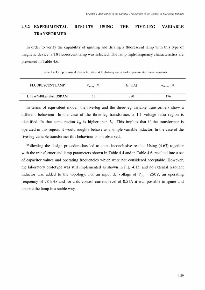
Chapter 4 Application of the Variable Transformer to the Control of Electronic Ballasts
4.29
4.3.2 EXPERIMENTAL RESULTS USING THE FIVE-LEG VARIABLE
TRANSFORMER
In order to verify the capability of igniting and driving a fluorescent lamp with this type of
magnetic device, a T8 fluorescent lamp was selected. The lamp high-frequency characteristics are
presented in Table 4.6.
Table 4.6 Lamp nominal characteristics at high-frequency and experimental measurements.
FLUORESCENT LAMP >~ [V] /0 [mA] v~ [Ω]
L 18W/840Lumilux OSRAM 55 280 196
In terms of equivalent model, the five-leg and the three-leg variable transformers show a
different behaviour. In the case of the three-leg transformer, a 1:1 voltage ratio region is
identified. In that same region ¯ is higher than ¯Ë. This implies that if the transformer is
operated in this region, it would roughly behave as a simple variable inductor. In the case of the
five-leg variable transformer this behaviour is not observed.
Following the design procedure has led to some inconclusive results. Using (4.63) together
with the transformer and lamp parameters shown in Table 4.4 and in Table 4.6, resulted into a set
of capacitor values and operating frequencies which were not considered acceptable. However,
the laboratory prototype was still implemented as shown in Fig. 4.15, and no external resonant
inductor was added to the topology. For an input dc voltage of > = 250V, an operating
frequency of 78 kHz and for a dc control current level of 0.51A it was possible to ignite and
operate the lamp in a stable way.
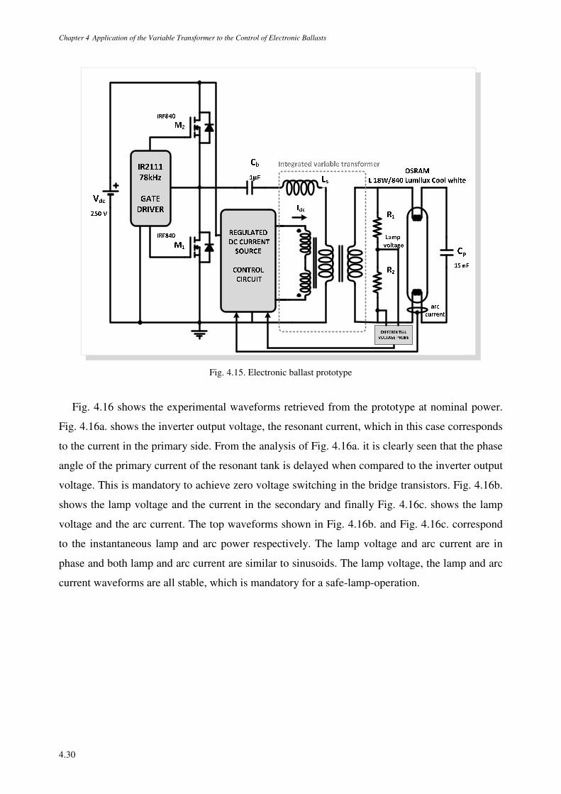
Chapter 4 Application of the Variable Transformer to the Control of Electronic Ballasts
4.30
Fig. 4.15. Electronic ballast prototype
Fig. 4.16 shows the experimental waveforms retrieved from the prototype at nominal power.
Fig. 4.16a. shows the inverter output voltage, the resonant current, which in this case corresponds
to the current in the primary side. From the analysis of Fig. 4.16a. it is clearly seen that the phase
angle of the primary current of the resonant tank is delayed when compared to the inverter output
voltage. This is mandatory to achieve zero voltage switching in the bridge transistors. Fig. 4.16b.
shows the lamp voltage and the current in the secondary and finally Fig. 4.16c. shows the lamp
voltage and the arc current. The top waveforms shown in Fig. 4.16b. and Fig. 4.16c. correspond
to the instantaneous lamp and arc power respectively. The lamp voltage and arc current are in
phase and both lamp and arc current are similar to sinusoids. The lamp voltage, the lamp and arc
current waveforms are all stable, which is mandatory for a safe-lamp-operation.
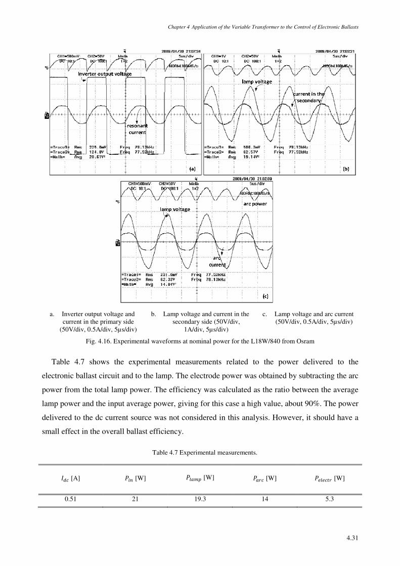
Chapter 4 Application of the Variable Transformer to the Control of Electronic Ballasts
4.31
a. Inverter output voltage and
current in the primary side (50V/div, 0.5A/div, 5µs/div)
b. Lamp voltage and current in the secondary side (50V/div,
1A/div, 5µs/div)
c. Lamp voltage and arc current (50V/div, 0.5A/div, 5µs/div)
Fig. 4.16. Experimental waveforms at nominal power for the L18W/840 from Osram
Table 4.7 shows the experimental measurements related to the power delivered to the
electronic ballast circuit and to the lamp. The electrode power was obtained by subtracting the arc
power from the total lamp power. The efficiency was calculated as the ratio between the average
lamp power and the input average power, giving for this case a high value, about 90%. The power
delivered to the dc current source was not considered in this analysis. However, it should have a
small effect in the overall ballast efficiency.
Table 4.7 Experimental measurements.
/ [A] t±² [W] t~ [W] t~2 [W] t33À2 [W]
0.51 21 19.3 14 5.3
Chapter 4 Application of the Variable Transformer to the Control of Electronic Ballasts
4.32
The obtained experimental results have clearly shown the possibility of using this type of
magnetic device to operate fluorescent lamps at nominal power. A stable operating point was
achieved; however the design procedure was not confirmed. It is possible that in this case, the
large-signal behaviour of the variable transformer differs from the small-signal behaviour, which
then introduces miscalculations into the design procedure. At this point, the five-leg transformer
was disregarded. The attention was then focused on the three-leg variable transformer. The final
objective was not only to operate the fluorescent lamp at nominal power but also to take
advantage of the integrated variable transformer to control the luminous flux level of the lamp.
The following work, involving isolated dimmable ballasts, has shown some promising results.
4.4 VARIABLE TRANSFORMER APPLIED TO DIMMABLE
ELECTRONIC BALLASTS
CCFL backlights are the most common backlight technology and are used in several types of
displays. High-brightness LEDs are also an effective alternative for backlight sources. While
CCFL backlights typically provide white light, LED backlights may supply either white light or a
mixture of red, green, and blue. However, LEDs may have very distinct electrical characteristics
depending on the technology (very different threshold voltages from 1.7 to 3.6V). In addition, all
LEDs have a small reverse breakdown voltage, around 5V. In addition, due to the manufacturing
process, LEDs are not identical. The small variation of electrical characteristics from one LED to
another may involve significant changes in the power circuit, especially in terms of maintaining
the power set in high levels of performance. Besides, high-efficiency LEDs are very sensitive to
voltage and operating current. Deviations from the operating point leads to a drastic reduction of
component life and output light quality (apparent colour change). For these reasons, CCFLs are
still the main stream in large size LCD backlighting systems [4.8]-[4.10]. For safety purposes,
these applications are always dependent on the inclusion of an isolation transformer between the
inverter and the circuit which directly supplies the lamp. The most common dimming method is
called burst dimming, where the CCFL is driven between no current and rated current, thereby
causing surge currents and hence reducing the lamp life [4.7]. Other methods are similar to the
most common ones; duty-ratio control, frequency and voltage control. This application can be
useful in this field of research since it presents similar advantages to the ones using the variable
inductor control concept, additionally yielding electrical isolation. It will be demonstrated that the
Chapter 4 Application of the Variable Transformer to the Control of Electronic Ballasts
4.33
proposed technique takes advantage of the device equivalent series inductance to provide a new
flexible way for lamp luminous flux regulation.
4.4.1 DESIGN PROCEDURE
The design procedure is similar to the procedure described in the previous chapter. It defines
the necessary limits for the inductance value in order to cover all the dimming range for the
selected lamp. These limits are then compared with the results obtained from the small-signal and
large-signal characterization of the transformer, verifying the applicability of the device.
Therefore, the first step is to determine the resonant-circuit parameters in order to operate the
lamp at nominal power and then obtain the corresponding dimming curve, using the equation
which relates the average lamp power with the control variable, for the LC resonant circuit
configuration:
t~v~ ¾t~¿(1 − ¯~) + ¯~ − >±² v~¾t~¿ = 0
(4.64)
For analysis, two T5 14W lamps were selected. Their electrical characteristics at nominal
power, retrieved from manufacturers’ data, are presented in Table 4.8 and can be considered quite
similar.
Table 4.8 Lamp nominal characteristics at high-frequency.
FLUORESCENT LAMP >~ [V] /0 [mA]
FH 14W/840 OSRAM 86 165
TL5 HE 14W PHILIPS 83 170
Fig. 4.17 illustrates the measured T5 14W characteristics of the lamp resistance versus average
arc power, v~(t~2). For an input voltage > = 310V and operating frequency 4 = 85kHz,
the resonant tank parameters were calculated to be approximately = 2.4nF and ¯ = 1.46mH
in order to operate the lamp at nominal power. Fig. 4.17 also presents two theoretical dimming
curves for the same values of input voltage, and operating frequency, but for two different and
commercial values of resonant capacitors, = 2.7nF or 3.3nF. From the analysis of these
dimming curves and comparing them with the equivalent small-signal or large-signal inductances
shown in Fig. 4.13b., it is concluded that by choosing a higher capacitor value, the necessary
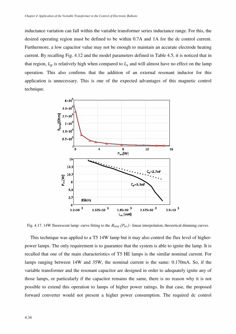
Chapter 4 Application of the Variable Transformer to the Control of Electronic Ballasts
4.34
inductance variation can fall within the variable transformer series inductance range. For this, the
desired operating region must be defined to be within 0.7A and 1A for the dc control current.
Furthermore, a low capacitor value may not be enough to maintain an accurate electrode heating
current. By recalling Fig. 4.12 and the model parameters defined in Table 4.5, it is noticed that in
that region, ¯ is relatively high when compared to ¯4 and will almost have no effect on the lamp
operation. This also confirms that the addition of an external resonant inductor for this
application is unnecessary. This is one of the expected advantages of this magnetic control
technique.
Fig. 4.17. 14W fluorescent lamp: curve fitting to the Rlamp(Parc) - linear interpolation; theoretical dimming curves.
This technique was applied to a T5 14W lamp but it may also control the flux level of higher-
power lamps. The only requirement is to guarantee that the system is able to ignite the lamp. It is
recalled that one of the main characteristics of T5 HE lamps is the similar nominal current. For
lamps ranging between 14W and 35W, the nominal current is the same: 0.170mA. So, if the
variable transformer and the resonant capacitor are designed in order to adequately ignite any of
those lamps, or particularly if the capacitor remains the same, there is no reason why it is not
possible to extend this operation to lamps of higher power ratings. In that case, the proposed
forward converter would not present a higher power consumption. The required dc control
Chapter 4 Application of the Variable Transformer to the Control of Electronic Ballasts
4.35
current should stay in exactly the same boundaries, since the several operating points of the
regulator would be similar. Theoretical and experimental observations have shown that, typically,
a 2:1 inductance variation is enough to cover the necessary dimming range for tubular fluorescent
lamps. This was valid for the variable inductor but it may also be applied to the variable
transformer. For higher-power lamps, additional turns could be included in the control windings
in order to obtain a smoother change in the series equivalent inductance.
A proper design must consider from the start the tolerances of the magnetic device and
capacitors. One of the advantages of using variable inductors and transformers in electronic
ballast applications is that with these regulators it is somewhat possible to minimize or
counterbalance the effect of the tolerances of the components, without compromising the whole
design project. The dc control current may be used to fine tune the inductance value if necessary.
Tolerances for inductances used in electronic ballasts can be as high as 20% for mass production.
This can give different lamp powers for each unit. When operating at closed loop with a variable
magnetic element, the inductance can be self-adjusted to the correct value, assuring a correct
lamp power for each operating point. The repeatability of the proposed solution is assured as long
as the variable component can be built with a range of variation wide enough to adapt each
design.
4.4.2 EXPERIMENTAL RESULTS USING THE THREE-LEG VARIABLE
TRANSFORMER
The final purpose of this work was to verify the effectiveness of using the variable transformer
in the development of this new dimming technique. The selected lamp was the FH 14W/840 from
Osram. The laboratory prototype, shown in Fig. 4.18, driven at an operating frequency, 4 =85kHz, was able to start and drive the lamp in a stable way, showing also quite linear and
smooth experimental dimming curves. Except for the presence of the variable transformer, the
prototype is similar to commercial solutions. For simplicity reasons, regarding the analysis of the
proposed technique, the typical blocks corresponding to the EMI filter and PFC stage were not
considered. It is clearly seen from Fig. 4.18 that no external resonant inductor was added to the
prototype. For the selected operating control range the variable transformer behaves like a
variable inductor, and similarly, increasing the control current decreases the value of ¯4.
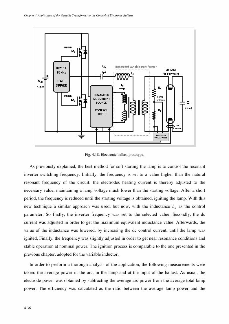
Chapter 4 Application of the Variable Transformer to the Control of Electronic Ballasts
4.36
Fig. 4.18. Electronic ballast prototype.
As previously explained, the best method for soft starting the lamp is to control the resonant
inverter switching frequency. Initially, the frequency is set to a value higher than the natural
resonant frequency of the circuit; the electrodes heating current is thereby adjusted to the
necessary value, maintaining a lamp voltage much lower than the starting voltage. After a short
period, the frequency is reduced until the starting voltage is obtained, igniting the lamp. With this
new technique a similar approach was used, but now, with the inductance ¯4 as the control
parameter. So firstly, the inverter frequency was set to the selected value. Secondly, the dc
current was adjusted in order to get the maximum equivalent inductance value. Afterwards, the
value of the inductance was lowered, by increasing the dc control current, until the lamp was
ignited. Finally, the frequency was slightly adjusted in order to get near resonance conditions and
stable operation at nominal power. The ignition process is comparable to the one presented in the
previous chapter, adopted for the variable inductor.
In order to perform a thorough analysis of the application, the following measurements were
taken: the average power in the arc, in the lamp and at the input of the ballast. As usual, the
electrode power was obtained by subtracting the average arc power from the average total lamp
power. The efficiency was calculated as the ratio between the average lamp power and the
Chapter 4 Application of the Variable Transformer to the Control of Electronic Ballasts
4.37
average input power. The main objective was to correlate the power delivered to the inverter to
the average lamp power consumption, and in doing so, the losses in the variable transformer itself
were considered. Of course if a commercial ballast prototype was developed, other stages (mains
filter, rectifier, PFC stage) should be considered. This is also valid for the converter used as dc
drive. The selected converter for the dc current source could be the same forward converter, as in
the previously proposed universal ballast, but other solutions could be implemented and
optimized to reduce the losses to a minimum level.
The above mentioned measurements are presented in Fig. 4.19. Almost constant electrode
power was guaranteed. The lowest efficiency operating point was, as expected, at a low power
level. For the remainder operating points, high efficiency is demonstrated. As referred in the
previous chapter, for a dc current output in the range of 0.4 and 1A, the power absorbed by the
forward converter stands between 1 and 2.5W. A closer analysis reveals that for the selected
diming range, only a small variation of 0.3A of the dc control current, was required. Increasing
the number of turns in the control windings of the variable transformer should enhance this effect.
The forward converter shows the maximum power consumption at 1A which means that at
nominal power the efficiency could drop to 6-8%. For lower lamp power levels, the effect would
be less significant since in order to obtain a higher inductance value it would be required a lower
value of dc current. However, at this point there was no immediate concern to optimize this dc
drive, as the main purpose was to verify the effectiveness of this new control technique.
A further issue regarding the power control of the electronic ballast is related to the inverter
switches operation, more specifically, zero voltage switching (ZVS) in the bridge MOSFETs. So
it is important to verify the phase angle of the primary current in relation to the output inverter
voltage. Fig. 4.20 presents the obtained experimental waveforms of the inverter output voltage,
current in the primary of the transformer, lamp voltage, also considered as the arc voltage, and
current in the secondary of the transformer, at nominal power and at the lowest power level.
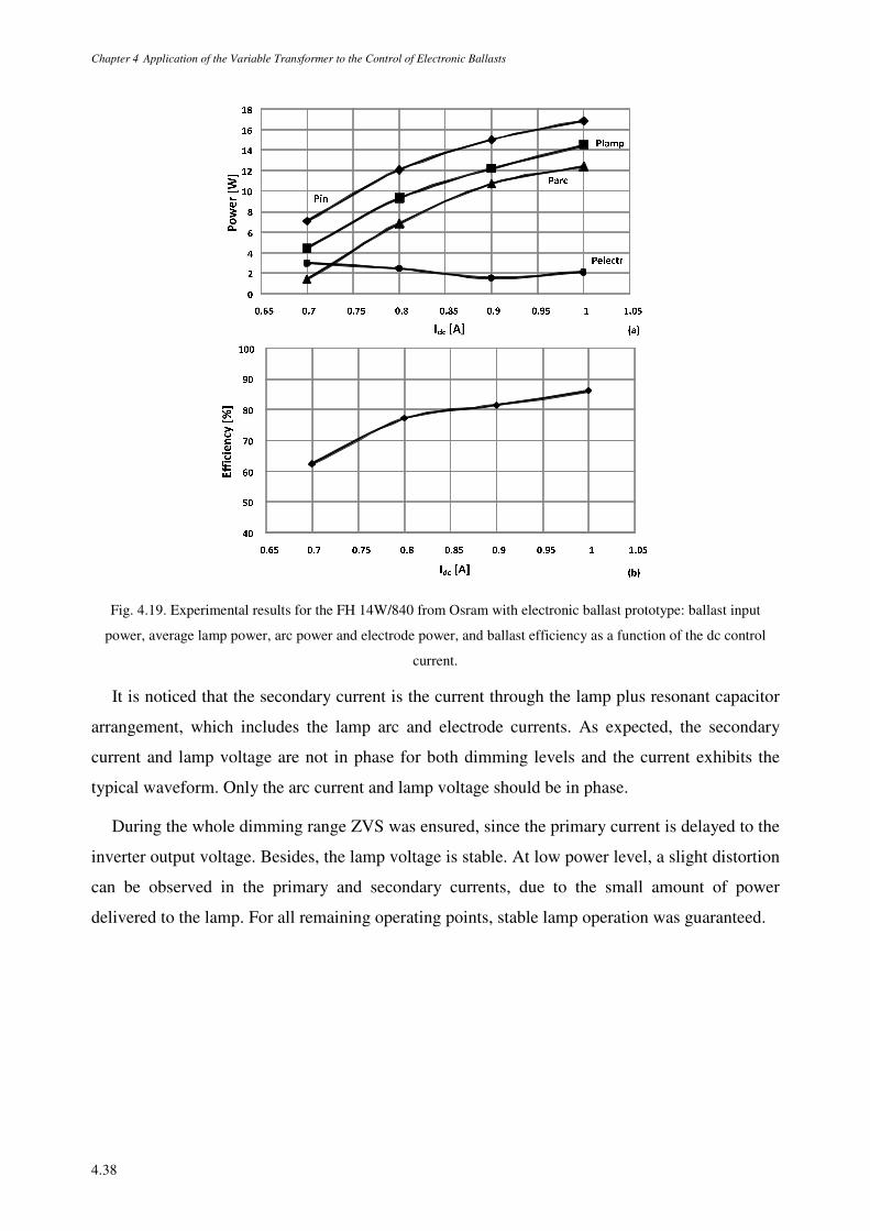
Chapter 4 Application of the Variable Transformer to the Control of Electronic Ballasts
4.38
Fig. 4.19. Experimental results for the FH 14W/840 from Osram with electronic ballast prototype: ballast input
power, average lamp power, arc power and electrode power, and ballast efficiency as a function of the dc control
current.
It is noticed that the secondary current is the current through the lamp plus resonant capacitor
arrangement, which includes the lamp arc and electrode currents. As expected, the secondary
current and lamp voltage are not in phase for both dimming levels and the current exhibits the
typical waveform. Only the arc current and lamp voltage should be in phase.
During the whole dimming range ZVS was ensured, since the primary current is delayed to the
inverter output voltage. Besides, the lamp voltage is stable. At low power level, a slight distortion
can be observed in the primary and secondary currents, due to the small amount of power
delivered to the lamp. For all remaining operating points, stable lamp operation was guaranteed.
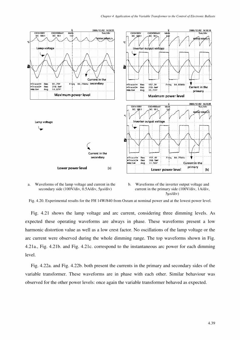
Chapter 4 Application of the Variable Transformer to the Control of Electronic Ballasts
4.39
a. Waveforms of the lamp voltage and current in the
secondary side (100V/div, 0.5A/div, 5µs/div)
b. Waveforms of the inverter output voltage and current in the primary side (100V/div, 1A/div,
5µs/div)
Fig. 4.20. Experimental results for the FH 14W/840 from Osram at nominal power and at the lowest power level.
Fig. 4.21 shows the lamp voltage and arc current, considering three dimming levels. As
expected these operating waveforms are always in phase. These waveforms present a low
harmonic distortion value as well as a low crest factor. No oscillations of the lamp voltage or the
arc current were observed during the whole dimming range. The top waveforms shown in Fig.
4.21a., Fig. 4.21b. and Fig. 4.21c. correspond to the instantaneous arc power for each dimming
level.
Fig. 4.22a. and Fig. 4.22b. both present the currents in the primary and secondary sides of the
variable transformer. These waveforms are in phase with each other. Similar behaviour was
observed for the other power levels: once again the variable transformer behaved as expected.
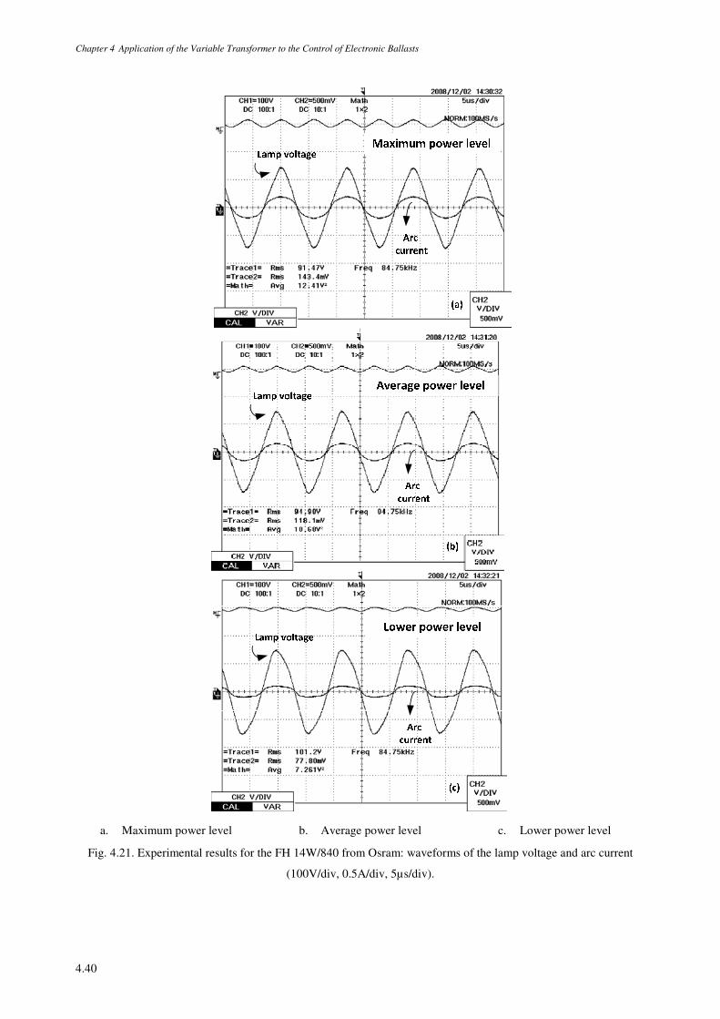
Chapter 4 Application of the Variable Transformer to the Control of Electronic Ballasts
4.40
a. Maximum power level b. Average power level c. Lower power level
Fig. 4.21. Experimental results for the FH 14W/840 from Osram: waveforms of the lamp voltage and arc current
(100V/div, 0.5A/div, 5µs/div).
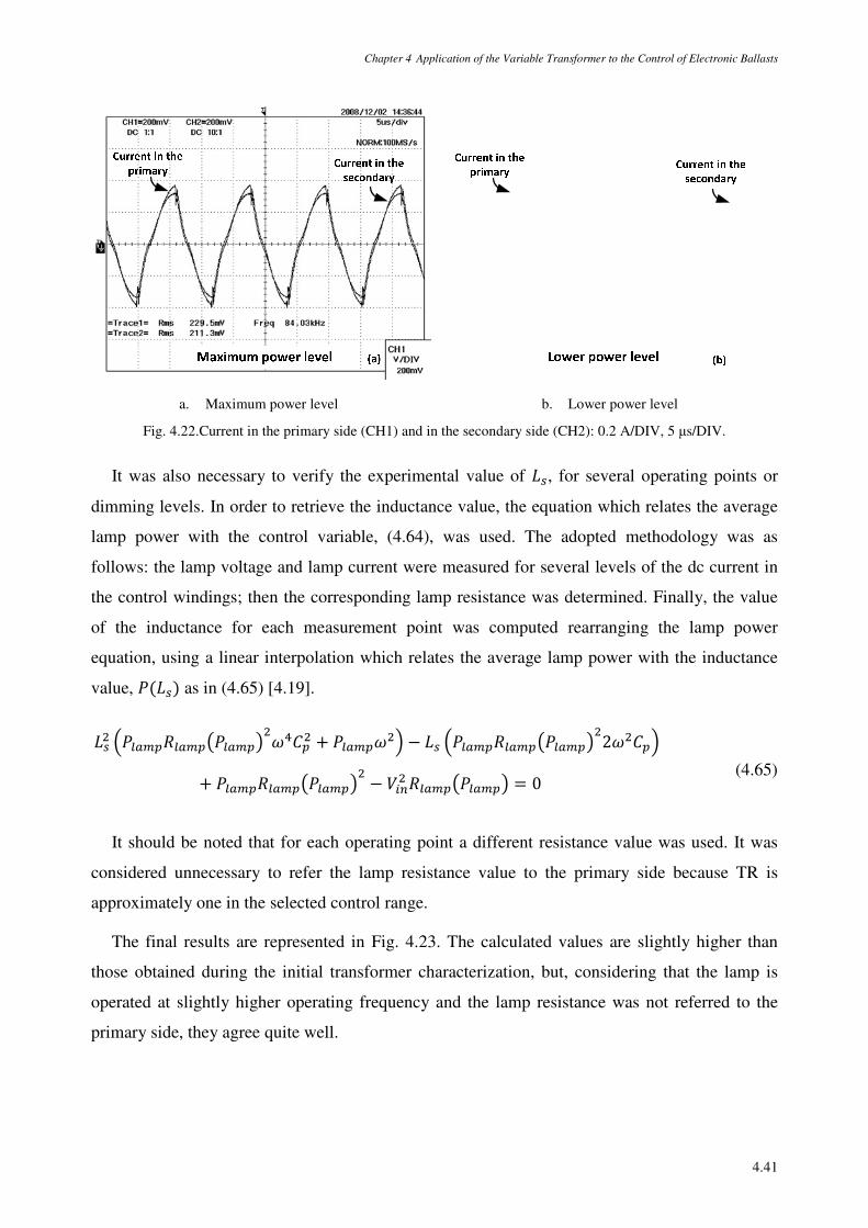
Chapter 4 Application of the Variable Transformer to the Control of Electronic Ballasts
4.41
a. Maximum power level b. Lower power level
Fig. 4.22.Current in the primary side (CH1) and in the secondary side (CH2): 0.2 A/DIV, 5 µs/DIV.
It was also necessary to verify the experimental value of ¯4, for several operating points or
dimming levels. In order to retrieve the inductance value, the equation which relates the average
lamp power with the control variable, (4.64), was used. The adopted methodology was as
follows: the lamp voltage and lamp current were measured for several levels of the dc current in
the control windings; then the corresponding lamp resistance was determined. Finally, the value
of the inductance for each measurement point was computed rearranging the lamp power
equation, using a linear interpolation which relates the average lamp power with the inductance
value, t¯4 as in (4.65) [4.19].
¯4 t~v~¾t~¿× + t~ − ¯4 t~v~¾t~¿2+ t~v~¾t~¿ − >±² v~¾t~¿ = 0
(4.65)
It should be noted that for each operating point a different resistance value was used. It was
considered unnecessary to refer the lamp resistance value to the primary side because TR is
approximately one in the selected control range.
The final results are represented in Fig. 4.23. The calculated values are slightly higher than
those obtained during the initial transformer characterization, but, considering that the lamp is
operated at slightly higher operating frequency and the lamp resistance was not referred to the
primary side, they agree quite well.
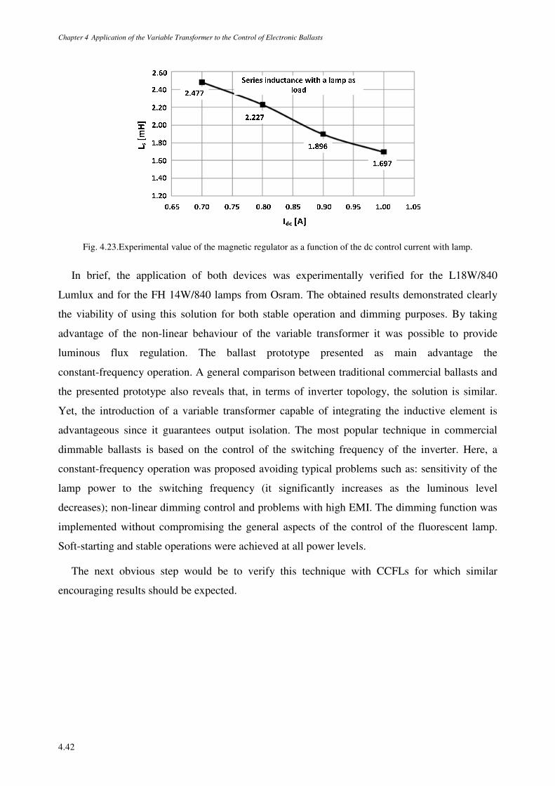
Chapter 4 Application of the Variable Transformer to the Control of Electronic Ballasts
4.42
Fig. 4.23.Experimental value of the magnetic regulator as a function of the dc control current with lamp.
In brief, the application of both devices was experimentally verified for the L18W/840
Lumlux and for the FH 14W/840 lamps from Osram. The obtained results demonstrated clearly
the viability of using this solution for both stable operation and dimming purposes. By taking
advantage of the non-linear behaviour of the variable transformer it was possible to provide
luminous flux regulation. The ballast prototype presented as main advantage the
constant-frequency operation. A general comparison between traditional commercial ballasts and
the presented prototype also reveals that, in terms of inverter topology, the solution is similar.
Yet, the introduction of a variable transformer capable of integrating the inductive element is
advantageous since it guarantees output isolation. The most popular technique in commercial
dimmable ballasts is based on the control of the switching frequency of the inverter. Here, a
constant-frequency operation was proposed avoiding typical problems such as: sensitivity of the
lamp power to the switching frequency (it significantly increases as the luminous level
decreases); non-linear dimming control and problems with high EMI. The dimming function was
implemented without compromising the general aspects of the control of the fluorescent lamp.
Soft-starting and stable operations were achieved at all power levels.
The next obvious step would be to verify this technique with CCFLs for which similar
encouraging results should be expected.
Chapter 4 Application of the Variable Transformer to the Control of Electronic Ballasts
4.43
REFERENCES
[4.1] Perdigão, M. S.; Alonso, J. M.; Saraiva, E. S.; “Magnetically-controlled dimming technique with isolated
output”, Electronics Letters vol. 45, Issue 14, July 2009 pp. 756-758.
[4.2] Perdigão, M.S.; Alonso, J.M.; Gacio, D.; Saraiva, E.S.; "Magnetically-controlled electronic ballasts with
isolated output: The variable transformer solution," Industrial Electronics, 2009. ISIE 2009. IEEE
International Symposium on , vol., no., pp.59-64, 5-8 July 2009.
[4.3] (Early access) Perdigao, M. S.; Alonso, J. M.; Gacio Vaquero, D.; Saraiva, E. S.; , "Magnetically-controlled
Electronic Ballasts with Isolated Output: The Variable Transformer Solution," Industrial Electronics, IEEE
Transactions on , vol.PP, no.99, pp.1, 0.
[4.4] Perdigão, M.S.; Alonso, J.M.; Saraiva, E.S.; "A new integrated variable transformer topology for electronic
ballasts," Industrial Electronics, 2009. IECON '09. 35th Annual Conference of IEEE, vol., no., pp.3484-3489,
3-5 Nov. 2009
[4.5] R. D. Washburn and R.F. McClanahan, “Non-saturating Magnetic Amplifier Controller”, U. S. Patent,
#4841428 June 20, 1989.
[4.6] Asensi, R.; Prieto, R.; Cobos, J.A.; Uceda, J.; “Modeling High-Frequency Multiwinding Magnetic
Components Using Finite-Element Analysis”, IEEE Transactions on Magnetics , Vol.43 , issue 10,
September 2007.
[4.7] Hwu, K. I. and Chen, Y. H., “A Novel Dimming Technique for Cold Cathode Fluorescent Lamp”, PEDS
2007, International Conference on Power Electronics and Drive Systems, pp. 1085-1090, 2007.
[4.8] Yu-Kang Lo; Kuan-Hung Wu; Kai-Jun Pai; Huang-Jen Chiu; "Design and Implementation of RGB LED
Drivers for LCD Backlight Modules," Industrial Electronics, IEEE Transactions on , vol.56, no.12, pp.4862-
4871, Dec. 2009.
[4.9] Ke, Yu-Lung; Chuang, Ying-Chun; Chuang, Hung-Shiang; Wu, Yuan-Kang; Chang, Chun-Chih; "Self-
excited electronic ballast for cold cathode fluorescent lamps," Industrial and Commercial Power Systems
Technical Conference (I&CPS), 2010 IEEE , vol., no., pp.1-6, 9-13 May 2010.
[4.10] Hau-Chen Yen; "Analysis of Balancing Driver for Multiple Cold Cathode Fluorescent Lamps," Industrial
Electronics, IEEE Transactions on , vol.57, no.4, pp.1354-1359, April 2010.
[4.11] Vollin, Jeff, F. Dong Tang, S. M. Cuk, “Magnetic Regulator Modeling”, APEC 1993, IEEE Applied Power
Electronics Conference, pp. 604-611.
[4.12] Mork, B.A.; "Five-legged wound-core transformer model: derivation, parameters, implementation and
evaluation, "Power Delivery, IEEE Transactions on , vol.14, no.4, pp.1519-1526, Oct 1999.
[4.13] Zhe Zhang, “Coupled-Inductor Magnetics in Power Electronics”, PhD Thesis, California Institute of
Technology, Pasadena, California, 1987.
[4.14] Ruben Lee, Leo Wilson, Charles E. Carter, “Electronic Transformers and Circuits”, Third Edition, PSMA
Publication, John Wiley & Sons.
[4.15] Basso, Christophe, “How to deal with Leakage Elements in Flyback Converters”, Motorola Application Note
AN1679, 1999.
Chapter 4 Application of the Variable Transformer to the Control of Electronic Ballasts
4.44
[4.16] Jan Deskur, “Models of magnetic circuits and their equivalent electrical diagrams”, COMPEL, The
International Journal for Computation and Mathematics in Electrical and Electronic Engineering, vol.18, nº4,
1999, pp.600-610.
[4.17] Charles V. Jones, “The Unified Theory of Electrical Machines”, Butterworth & Co. (Publishers) Ltd., 1967.
[4.18] J. M. Alonso; POWER ELECTRONICS HANDBOOK. Chapter 21: Electronic Ballasts. Editor: Muhammad
H. Rashid. Editorial: Academic Press. Canadá. 2001.
[4.19] Perdigão, M. S., J. M. Alonso, Marco Dalla Costa, E. S. Saraiva, “Design Considerations for the
Optimization of Magnetically Dimmed Electronic Ballasts”, X Portuguese-Spanish Congress on Electrical
Engineering, XCLEEE, Madeira, Portugal, July 2007.
[4.20] Evgeny Rozanov and Sam Ben-Yaakov, “Analysis of current-controlled inductors by new SPICE behavioral
model”, HAIT Journal of Science and Engineering B, Volume 2, Issues 3-4, pp. 558-570.
CONCLUSIONS, CONTRIBUTIONS, AND 5FUTURE WORK
This final chapter presents the conclusions and main contributions related to the application
of magnetic regulators to electronic ballasts. As conclusions, the main achieved goals will be
emphasized in this chapter and a special attention will be given to future work. A list of published
papers is presented at the end of the chapter.
5.1 CONCLUSIONS AND CONTRIBUTIONS
Highly-efficient fluorescent lamps are expected to be a dominant, cost-effective lighting
solution in the following years. The flexibility expected from modern fluorescent lighting
systems requires an intensive use of electronic ballasts, since this type of electronic control offers
higher levels of adaptability, not viable with traditional magnetic ballasts. For that reason, there is
a clear opportunity to invest and develop new control techniques for electronic ballasts, specially
dedicated to fluorescent lamps.
This Ph. D. Thesis proposed a set of new ballast control techniques which are based on a
magnetic device commonly referred as magnetic regulator. The presented work began with an
extensive research on fluorescent lighting systems. The operating principle and main
characteristics of fluorescent lamps and the fundamental requirements of these systems were
investigated and detailed in Chapter 1. Traditional luminous flux regulation techniques were
detailed and main advantages and disadvantages were pointed out. This was the starting point of
the subsequent work. Of course, it was also necessary to gather knowledge on magnetic
regulators. This device has been known from several decades; however, recently, modern
technology was capable of finding some new interesting applications, by adapting and changing
topologies, core structures and materials, and most of all, by interpreting those former
Chapter 5 Conclusions, Contributions, and Future Work
5.2
applications in a different way. This is in fact the novelty of the presented research: using this
regulator into a modern and useful application such as modern fluorescent lighting control.
In Chapter 2, an extensive literature review on magnetic regulators, describing the state of the
art on variable inductors and variable transformers was presented. This assessment is considered
very helpful for researchers inclined to investigate this subject. A vast list of applications of these
regulators was presented, and general aspects, related to the device operating principle and
construction, were also discussed. Chapter 2 ended with a brief description of magnetic control
applied to electronic ballasts. Basic concepts behind the proposed new control techniques were
underlined.
In the remaining chapters, the presentation, development and the validation of these novel
techniques were discussed. The work presented in this thesis was divided into two main areas:
variable inductors and variable transformers, with their corresponding applications for the control
of electronic ballasts. This supposed the development and presentation of several, new prototype
versions of dimmable electronic ballasts and universal electronic ballasts.
In conclusion, the work presented in this Ph. D. Thesis may be detailed as follows. The
published papers related to these contributions are shown in Section 5.3.
Variable-inductor based electronic ballasts:
A magnetically-controlled electronic ballast topology was proposed based on the half-
bridge parallel-loaded resonant inverter where the typical resonant inductor was
substituted by a variable inductor. The novelty of this proposal is the fact that this
variable inductor, controlled by a dc current, is able to modify the resonant circuit in order
to vary the rms values of the lamp current and thereby the luminous output. This new
dimming technique allows constant-frequency inverter operation, which compared to
typical commercial ballasts, based on a variable-frequency technique, is a breakthrough
since it avoids well know-disadvantages [J5.1].
Comparative analysis between resonant circuits, magnetic regulators structures and
topologies, clearly showed how this new control technique is effective, and does not
compromise the lamp operation. It was proved by a complete set of experimental results
that safe, reliable and stable operation was achieved, along with ZVS operation, and
promising efficiency levels [J5.2], [IC5.1], [IC5.2], [IC5.3], [IC5.7]. A simple study, for
T5 lamps, regarding electrode operation and compliance with recent IEC standards was
Chapter 5 Conclusions, Contributions, and Future Work
5.3
also carried out in order to validate this new dimming method [IC5.16]. Different
regulator structures and topologies were also tested with this dimming technique [IC5.15].
Another magnetic control technique was developed and presented for universal electronic
ballasts. There is a recent commercial demand of these ballasts which are able to supply
different lamps without requiring any physical change in the hardware. Similarly to the
previous dimmable electronic ballast, the variable inductor was used to adapt the
characteristics of the resonant circuit to each attached lamp. In these cases, the ballast
must incorporate the necessary intelligence to measure the electrical characteristics of the
lamps wired to their output, and must be able to adjust their internal operation in order to
correctly ignite and supply these lamps. The technique was previously exposed using a
forward converter to properly control the magnetic regulator [J5.3], [IC5.4], [IC5.8],
[IC5.10].
Universal ballasts are of a more complex nature. One of the challenges is the
identification of the lamp and the other the routine which is necessary to operate each
lamp at the appropriate power level. This implies the active control of all ballast
parameters. Digital control based on low-cost microcontrollers can be used in this type of
ballasts without an excessive cost penalty and all the required functions can be easily
implemented. It is also pointed out that the development of universal ballasts for any kind
of tubular fluorescent lamps is complicated due to their different characteristics in terms
of warm-up period, time constants and equivalent impedances. Using µ permits a higher
level of control of the system. Two different digital prototype versions were therefore
proposed. In the first one, dedicated to T8 lamps, besides the variable inductance, an
additional control parameter is used: the inverter switching frequency. The effectiveness
of the control technique is clearly demonstrated using a simple lamp identification
method, based on the measurement of the lamp voltage. The collected experimental
results showed all lamps were operated at nominal power with a stable operation [J5.7],
[IC5.12].
In the second proposed prototype, especially dedicated to T5 lamps, the ballast was
operated at constant-frequency and only the variable inductance was used as control
parameter. It is noticed that in this particular case the ballast is able to operate a large
number of T5 lamps, HE and HO. In addition, this second prototype was designed with
special concern regarding the electrodes operation. A simple resonant circuit design
Chapter 5 Conclusions, Contributions, and Future Work
5.4
procedure was presented and experimental results showed that external heating sources,
common in commercial ballasts, may be avoided. In this second proposal, the ballast
incorporates two other converters, a buck and a flyback converter, in order to properly
operate the magnetic regulator and to power the ballast using a single dc voltage source,
[IC5.18], [IC5.19].
Variable-transformer based electronic ballasts
In this case the variable inductor was replaced by a variable transformer. It was
demonstrated how the variable behaviour of the resonant circuit depends on the
transformer equivalent circuit model and resonant capacitor, which is also dictated by the
dc current flowing through the control windings included in the regulator structure. Two
new different variable transformer structures were proposed and analysed. The innovation
of this technique resides in the fact that, while simultaneously controlling the luminous
flux of the lamp, the ballast is capable of guaranteeing electric isolation. This is pointed
out as a useful combination for applications with CCFLs in LCD backlighting
applications [J5.4], [J5.6], [IC5.10], [IC5.14].
In addition to these ballast solutions, a special attention was given, throughout the work, to the
modelling, design, small-signal and large-signal characterization of variable inductors and
variable-transformers. Detailed examples were given. This analysis pointed out the importance of
these concepts and modelling techniques on the experimental application of these devices,
whether it is referred to electronic ballast applications or potentially new and different
technologies [IC5.5], [IC5.6], [IC5.13].
In conclusion, the main contributions may be detailed as follows:
An overall review was presented on general aspects regarding lighting, lighting efficiency
and fluorescent lighting systems.
An extensive literature review was provided on magnetic regulators with a special
emphasis on their known applications.
A new dimming technique was proposed and developed based on the variable inductor.
The technique was validated through experimental testing with a magnetically-controlled
electronic prototype, based on the parallel-loaded half-bridge resonant inverter, for T8
and T5 lamps, using EF25 and EFD20 based regulators. The ballast was operated at
Chapter 5 Conclusions, Contributions, and Future Work
5.5
constant-frequency and the lamp power was controlled by changing only the regulator
inductance. It was shown that with an appropriate selection of the ballasts parameters all
lamps could be dimmed from nominal power to a very low power level.
A theoretical comparison between several resonant circuits and their impact on the lamp
dimming operation was provided. Two ballast prototypes using an LC and LCC circuits
were tested. Experimental results with a T8 36W lamp, confirmed theoretical predictions.
It was demonstrated that with this new flux regulation technique, quasi linear regulation
can be obtained and ZVS operation could be guaranteed over the desired dimming range.
The T5 lamp dimming behaviour was also tested using two different variable inductors
prototypes with different winding connections. The two prototypes were based on two
different core structures the EFD20 and the U15 core [5.3]. The EFD20 regulator showed
better results, especially due to the complexity of the assemblage of the U15 regulator.
As example, the T5 HE 21W and T5 HO 39W electrodes behaviour was also tested under
the proposed dimming technique in order to verify its compliance with current standards,
based on the m limits. The obtained results were compared with the experimental
values retrieved from commercial dimmable-ballasts. Promising results were obtained
considering that no additional heating sources were included in the proposed ballast
layout. This aspect is considered quite relevant since this type of study is recent. IEC
standards referring the necessity of m compliance are recent (2010).
It was developed and proposed a new control technique based on the variable inductor for
universal ballasts applications.
It was demonstrated that it was possible to control the operation of multiple lamps with
different power ratings, T8 15W-58W using the variable inductance and the inverter
operating frequency as control parameters. A prototype with digital control based on a
PSoC CY8C29466 µ was developed. Experimental results were presented which
showed the proper behaviour of the ballast. All lamps were operated at nominal power
and ZVS operation was achieved in each case. The variable inductor was properly
controlled by a forward converter. The proposed ballast showed a high efficiency, around
90%.
Chapter 5 Conclusions, Contributions, and Future Work
5.6
It was also demonstrated the possibility to control the operation of a vast set of T5 HE and
HO lamps, ranging from 14W to 49W, with a similar digital ballast prototype, at constant
frequency. In this ballast, only the variable inductance was used as control parameter.
This is considered a major breakthrough. Currently, there is no commercial product
capable of simultaneously controlling all of these lamps. It was also developed a design
procedure which gave the ability of operating all lamps with compliance of the m
limits. A simple solution was proposed using two parallel capacitors, which act as a single
equivalent capacitance for proper lamp ignition. All T5 HE and HO lamps were operated
at nominal power, or in the case of the T5 HO 49W within the limits imposed by the
manufacturer, with safe electrode operation. In all circumstances ZVS was achieved in
the ballast inverter.
Two dc-dc converters were proposed for the control of the variable inductors: a forward
and a buck converter.
The forward converter was designed to be directly supplied by the dc bus voltage of the
ballast. It was demonstrated the low power consumption of the variable inductor. The
buck converter was integrated into the second digitally-controlled ballast, where an
additional converter (flyback) was used to lower the dc bus voltage level and supply the
buck-converter.
Large-signal characterization methods based on flux measurements and short-circuit and
open-circuit tests were adapted to the proposed variable inductors and variable
transformer prototypes, and tested under the proposed control techniques.
In the case of the variable inductor, it was proposed a simple definition for the calculation
of the inductance, using the peak-to-peak values of the resonant current and total ac flux,
measured during dimming operation. This model was tested with several variable
inductor prototypes.
A Matlab-Simulink electronic-ballast-dynamic model was developed, including the
fluorescent-lamp model and the variable-inductor model
A new control technique based on the variable transformer was proposed and developed,
which has the advantage of providing output isolation.
Chapter 5 Conclusions, Contributions, and Future Work
5.7
Two variable transformers were built and tested: the five-leg and the three-leg versions.
With the three-leg version it was demonstrated the possibility of dimming a T5 lamp and
simultaneously guarantee isolation between the lamp and the inverter circuit. This is
considered a benefit, and is essential for CCFLs control.
5.2 FUTURE WORK
The main subject of this work was to investigate new control techniques for electronic ballasts
based on magnetic regulators. The key objective in terms of future work would be continuing this
line of research and several options just naturally follow the work which was already presented
by pursuing an optimized version of the proposed ballast prototypes. This Ph. D Thesis validates
the proposed techniques but also points out some critical issues, revealed during the recollection
of experimental data, which deserve a more profound study.
Therefore, regarding ballast applications, it would be relevant to proceed in the following
directions:
In magnetically-controlled dimmable-electronic ballasts, the ballast is operated at
constant-frequency. The system was implemented in open loop. The technique was
validated by controlling the level of dc current in the control windings to operate the lamp
at the required power level. High-efficiency and ZVS operation was achieved. However,
with a phase-locked-loop circuit it would be possible to impose near resonance operation
for all dimming levels. This obviously could imply changing the operating frequency of
the ballast but would result in ballast-optimum-operation conditions for all dimming
levels. The impact of this near-resonance operation should be analysed.
The inclusion of PFC techniques in magnetically-controlled electronic ballasts is also a
possible line of research. The impact of additional converters in the system should be
analysed. In addition, when PFC stages are included in the ballast, integrated topologies
are occasionally used. These integrated topologies are characterized by sharing one of the
switches, for instance the boost switch with one of the half-bridge inverter switches. In
those circumstances, the operating frequency can no longer be used as control parameter
for dimming. Using an integrated topology with the presence of a variable inductor in the
system will avoid that disadvantage; however the behaviour of this new circuit should be
investigated.
Chapter 5 Conclusions, Contributions, and Future Work
5.8
It would be interesting to further investigate the cause of the eventual lamp instabilities. A
study on the dynamic behaviour of the ballast using small-signal dynamic lamp models
would be the direction to follow. The influence of the non-linear behaviour of the
magnetic regulator on the dynamic behaviour of the circuit should also be investigated.
This would determine with exactitude the limits for stable operation.
Analysis of the impact of striations in magnetically-controlled electronic ballasts. S.
Boreckci already presented a striation control technique for the proposed variable-
inductor based ballast. This new solution called power density modulation (PDM)
proposes to induce three different stages in each period of the arc current, by changing the
level of the dc control current and consequently the inductance value. The time interval
for each inductance value controls the average lamp power in each modulation period
[2.50]. The impact of this technique on the lamp behaviour should be further investigated.
Optimization of the proposed digital prototypes, especially regarding energy efficiency.
Investigation of other options for the dc-dc converter used to supply the magnetic
regulator dc control current. Selection of the most energy efficient converter in order to
reduce the power consumption of the ballast prototype.
Continuation of prototypes development, especially in terms of lamp recognition
techniques. Even if almost all lamps can be identified by the analysis of the lamp voltage,
a better solution to identify T12, T8 and T5 lamps has been proposed in [3.49]. A fuzzy
logic controller analyses the heated lamp electrodes, the lamp voltage and the lamp
current. Then, a classification system is generated that maps the lamp characteristics into
distinct groups in order to automatically detect each lamp. Adapting this detection method
to the proposed universal ballast prototypes would represent an improvement. The
possibility to extend the application to the other lamps types may also be considered as
other option.
At the moment, the proposed ballasts are divided in dimming operation and universal
operation. It would be relevant to investigate the possibility of combining these operations
into a single prototype version. The impact on the operation of the ballast should be
characterized. Eventual additional control parameters should be considered in this intent.
It would also be relevant to study the use of variable transformers in universal ballasts
applications and to perform a theoretical study and experimental analysis of the control of
CCFLs with variable transformers.
Chapter 5 Conclusions, Contributions, and Future Work
5.9
Some other issues are specifically related to the variable inductor and variable transformer
behaviour in order to better predict and understand their impact in the suggested application.
Therefore it would be pertinent to follow the subsequent lines of research:
Investigation of a more detailed design procedure regarding the design of the variable
inductor or the variable transformer, possibly including losses.
Modelling of variable inductors and variable transformers with finite element analysis,
FEA. 3D finite element modeling may be used to model the distribution of flux density
and to identify the region of saturation which is believed to result in the decrease in the
inductance of the variable inductor, or in the change of the parameters of the variable
transformer.
General applications for the variable inductor or the variable transformer were already
suggested in Chapter 2. Some of these applications resulted from the increasing attention
given to the proposed ballast applications and the new magnetic control techniques, due to the
several published results. This also served as motivation to follow different lines of research:
the operation of dc-dc resonant converters at constant frequency is one direction which was
already followed [J5.5], [IC5.17]. This work is expected to proceed.
Then again, some other alternatives are aligning, mainly regarding the use of variable
inductors in the luminous flux control of LED lamps. Another option would be to investigate
the possibility of using variable inductors to actively control the saturation level of buck-boost
inductors, in electric vehicles applications. Due to the large currents involved, it implies large-
signal characterization of variable inductors through more advance measurement techniques.
5.3 PUBLISHED PAPERS
5.3.1 JOURNALS
[J5.1] Alonso, J. Marcos, Perdigão M.S., Marco A. Dalla Costa, Eduardo S. Saraiva; “Empleo de Reguladores
Magnéticos en el Control de Balastos Electrónicos,” Revista Mundo Electrónico. Cetisa Editores, May
2007. ISSN-0300-3787
[J5.2] Perdigão, M.S.; Alonso, J.M.; Dalla Costa, M.A.; Saraiva, E.S.; "Comparative Analysis and Experiments
of Resonant Tanks for Magnetically Controlled Electronic Ballasts," Industrial Electronics, IEEE
Transactions on, vol.55, no.9, pp.3201-3211, Sept. 2008. IEEE JOURNALS, ISSN-0278-0046
Chapter 5 Conclusions, Contributions, and Future Work
5.10
URL: http://ieeexplore.ieee.org/stamp/stamp.jsp?tp=&arnumber=4558040&isnumber=4609005
[J5.3] Perdigão, M.S.; Alonso, J.M.; Costa, M.A.D.; Saraiva, E.S.; "Using Magnetic Regulators for the
Optimization of Universal Ballasts," Power Electronics, IEEE Transactions on, vol.23, no.6, pp.3126-
3134, Nov. 2008. IEEE JOURNALS, ISSN- 0885-8993
URL: http://ieeexplore.ieee.org/stamp/stamp.jsp?tp=&arnumber=4712527&isnumber=4712525
[J5.4] Perdigão, M.S.; Alonso, J.M.; Saraiva, E.S.; "Magnetically-controlled dimming technique with isolated
output," Electronics Letters, vol.45, no.14, pp.756 -758, July 2 2009. IET JOURNALS, ISSN-0013-5194
URL: http://ieeexplore.ieee.org/stamp/stamp.jsp?tp=&arnumber=5159729&isnumber=5159700
[J5.5] Alonso, J.M.; Perdigão, M.S.; Gacio, D.; Campa, L.; Saraiva, E.S.; "Magnetic control of DC-DC
resonant converters provides constant frequency operation," Electronics Letters , vol.46, no.6, pp.440-442,
March 18 2010. IET JOURNALS, ISSN-0013-5194
URL: http://ieeexplore.ieee.org/stamp/stamp.jsp?tp=&arnumber=5434635&isnumber=5434595
[J5.6] Perdigão, M. S.; Alonso, J. M.; Gacio Vaquero, D.; Saraiva, E. S.;"Magnetically-controlled Electronic
Ballasts with Isolated Output: The Variable Transformer Solution," Industrial Electronics, IEEE
Transactions on, vol., no., pp., December. 2010. IEEE JOURNALS, ISSN-0278-0046 – Early Access
URL: http://ieeexplore.ieee.org/stamp/stamp.jsp?tp=&arnumber=5675678&isnumber=4387790
[J5.7] J. Marcos Alonso, Perdigão, M.S.; Javier Ribas; David Gacio; Eduardo S. Saraiva;" Optimizing
Universal Ballasts using Magnetic Regulators and Digital Control," Industrial Electronics, IEEE
Transactions on, vol., no., pp., December. 2010. IEEE JOURNALS, ISSN-0278-0046 – Early Access
URL: http://ieeexplore.ieee.org/stamp/stamp.jsp?tp=&arnumber=5575415&isnumber=5873561
[J5.8] H. V. Marques, Á. R. Seidel, M. S. Perdigão, J. M. Alonso, E. S. Saraiva; “Constant-Frequency
Magnetically-Controlled Universal Ballast with SoS Compliance for TL5 Fluorescent Lamps” Power
Electronics, IEEE Transactions on. IEEE JOURNALS – Accepted for publication
[J5.9] J. Marcos Alonso, M. S. Perdigão, David Gacio, Antonio J. Calleja, Eduardo S. Saraiva; "Analysis,
Design and Experimentation on Constant-Frequency DC-DC Resonant Converters with Magnetic
Control" Power Electronics, IEEE Transactions on. IEEE JOURNALS – Accepted for publication
5.3.2 INTERNATIONAL CONFERENCES
[IC5.1] Perdigão, M.S.; Saraiva, E.S.; Alonso, J.M.; Dalla Costa, M.A.; "Comparative Analysis and Experiments
of Resonant Tanks for Magnetically-Controlled Electronic Ballasts," Industrial Electronics, 2007. ISIE
2007. IEEE International Symposium on, vol., no., pp.3041-3046, 4-7 June 2007.
URL: http://ieeexplore.ieee.org/stamp/stamp.jsp?tp=&arnumber=4375100&isnumber=4374555
Chapter 5 Conclusions, Contributions, and Future Work
5.11
[IC5.2] Perdigão, M.S.; J. M. Alonso; Marco Dalla Costa; E. S. Saraiva; “Design Considerations for the
Optimization of Magnetically Dimmed Electronic Ballasts,” X Portuguese-Spanish Congress on Electrical
Engineering, XCLEE, 5-7 July 2007.
[IC5.3] Perdigão M.S., E. S. Saraiva, J. M. Alonso, M. A. Dalla Costa, “Design Method to Prevent Instabilities in
Magnetically-controlled Electronic Ballasts,” CEE’07 International Conference on Electrical Engineering,
26-29 November 2007.
[IC5.4] Perdigão, M.S.; Alonso, J.M.; Dalla Costa, M.A.; Saraiva, E.S.; "Optimization of universal ballasts
through magnetic regulators," Applied Power Electronics Conference and Exposition, 2008. APEC 2008.
Twenty-Third Annual IEEE, vol., no., pp.1214-1220, 24-28 February 2008.
URL: http://ieeexplore.ieee.org/stamp/stamp.jsp?tp=&arnumber=4522877&isnumber=4522647
[IC5.5] Perdigão, M.S.; Alonso, J.M.; Dalla Costa, M.A.; Saraiva, E.S.; "A variable inductor
MATLAB/Simulink behavioral model for application in magnetically-controlled electronic ballasts,"
Power Electronics, Electrical Drives, Automation and Motion, 2008. SPEEDAM 2008. International
Symposium on , vol., no., pp.349-354, 11-13 June 2008.
URL: http://ieeexplore.ieee.org/stamp/stamp.jsp?tp=&arnumber=4581201&isnumber=4581062
[IC5.6] Perdigão, M.S.; Saraiva, E.S.; Alonso, J.M.; Cervi, M.; "The controllable non-linear reactor in electronic
ballasts applications: A behavioral analysis of the inductance as a function of both ac and dc bias
currents," Universities Power Engineering Conference, 2008. UPEC 2008. 43rd International, vol., no.,
pp.1-5, 1-4 September 2008.
URL: http://ieeexplore.ieee.org/stamp/stamp.jsp?tp=&arnumber=4651669&isnumber=4651429
[IC5.7] Perdigão, M.S.; E. S. Saraiva, J. M. Alonso, M. A. Dalla Costa; "Iluminação fluorescente: a garantia de
eficiência energética mediante novas técnicas de controlo para balastros electrónicos com dimming,"
CLME 2008, Congresso Luso Moçambicano de Engenharia, Maputo, September 2008, ISBN: 978-972-
8826-20-8.
[IC5.8] Perdigão, M.S.; E. S. Saraiva, J. M. Alonso, M. A. Dalla Costa; “Balastros Electrónicos Universais: Nova
Técnica de Controlo Baseada em Reguladores Magnéticos,” CBA 2008, Conferência Brasileira de
Automática September 2008.
[IC5.9] Perdigão, M.S.; Baptista, B.; Alonso, J.M.; Saraiva, E.S.; “Reguladores Magnéticos aplicados em
balastros electrónicos: a problemática da sua caracterização”, II Jornada Luso-Brasileira de Ensino e
Tecnologia em Engenharia – JLBE 2009, Febrruary 2009.
[IC5.10] M. S. Perdigão, J. M. Alonso, J. Ribas, D. Gacio, E. S. Saraiva; “Universal Ballast: A flexible solution
based on magnetic regulator control concept,” Seminario Anual de Automática, Eletrónica Industrial e
Instrumentación, SAAEI’09, July 2009.
Chapter 5 Conclusions, Contributions, and Future Work
5.12
[IC5.11] Perdigão, M.S.; Alonso, J.M.; Gacio, D.; Saraiva, E.S.; "Magnetically-controlled electronic ballasts with
isolated output: The variable transformer solution," Industrial Electronics, 2009. ISIE 2009. IEEE
International Symposium on , vol., no., pp.59-64, 5-8 July 2009.
URL: http://ieeexplore.ieee.org/stamp/stamp.jsp?tp=&arnumber=5214261&isnumber=5213059
[IC5.12] Alonso, J.M.; Perdigão, M.S.; Ribas, J.; Gacio, D.; Saraiva, E.S.; "A digitally-controlled universal ballast
based on magnetic regulator and PSoC device," Industrial Electronics, 2009. ISIE 2009. IEEE
International Symposium on, vol., no., pp.2010-2015, 5-8 July 2009.
URL: http://ieeexplore.ieee.org/stamp/stamp.jsp?tp=&arnumber=5215663&isnumber=5213059
[IC5.13] Perdigão, M.S.; Baptista, B.; Saraiva, E.S.; Alonso, J.M.; "A dynamic-inductance model for magnetically
controlled Electronic Ballasts," Universities Power Engineering Conference (UPEC), 2009 Proceedings of
the 44th International, vol., no., pp.1-5, 1-4 September 2009.
URL: http://ieeexplore.ieee.org/stamp/stamp.jsp?tp=&arnumber=5429496&isnumber=5429361
[IC5.14] Perdigão, M.S.; Alonso, J.M.; Saraiva, E.S.; "A new integrated variable transformer topology for
electronic ballasts," Industrial Electronics, 2009. IECON '09. 35th Annual Conference of IEEE, vol., no.,
pp.3484-3489, 3-5 November 2009.
URL: http://ieeexplore.ieee.org/stamp/stamp.jsp?tp=&arnumber=5415197&isnumber=5414636
[IC5.15] Perdigão, M. S.; Baptista, B.; Alonso, J. M.; Saraiva, E. S.; “Magnetic Regulator Topologies for
Dimmable Electronic Ballasts”, Industrial Electronics (ISIE), 2010 IEEE International Symposium
on, Issue Date: 4-7, Page(s): 921 - 926 July 2010.
URL: http://ieeexplore.ieee.org/stamp/stamp.jsp?tp=&arnumber=5637141&isnumber=5635477
[IC5.16] Perdigão, M. S.; Baptista, B.; Marques, H.; Alonso, J. M.; Saraiva, E. S.; “On the use of magnetic
regulators in electronic ballasts,” Universities Power Engineering Conference (UPEC), 2010 45th
International, Page(s): 1 – 6, 31 August to 3 September 2010.
URL: http://ieeexplore.ieee.org/stamp/stamp.jsp?tp=&arnumber=5649301&isnumber=5648789
[IC5.17] J. Marcos Alonso, Perdigão M. S., David Gacio, Lidia Campa and Eduardo Saraiva, “Achieving Constant
Frequency Operation in DC-DC Resonant Converters through Magnetic Control,” 2010 Energy
Conversion Congress and Exposition (ECCE), 2010 IEEE, Page(s): 2011 – 2018, 12-16 September 2010.
URL: http://ieeexplore.ieee.org/stamp/stamp.jsp?tp=&arnumber=5618109&isnumber=5617696
[IC5.18] Á. R. Seidel; Perdigão M. S.; H. V. Marques; J. M. Alonso; E. S. Saraiva; “Safe Electrode Operation In
Universal Electronic Ballasts”, COBEP2011, September 2011.
[IC5.19] H. V. Marques; Á. R. Seidel; Perdigão, M. S., J. M. Alonso; E. S. Saraiva; “Development of a Universal
Electronic Ballast for TL5 Lamps Using a Magnetic Regulator,” Industry Application Conference,
IAS2011, October 2011.
Chapter 5 Conclusions, Contributions, and Future Work
5.13
REFERENCES
[5.1] Borekci, S.; "Dimming Electronic Ballasts Without Striations," Industrial Electronics, IEEE Transactions on ,
vol.56, no.7, pp.2464-2468, July 2009.
[5.2] L-M. Lee, S. Y. Hui, “Automatic Lamp Detection and Operation for Warm-Start Tubular Fluorescent
Lamps,” IEEE Transactions on Power Electronics, vol. 24, pp. 2933 – 294, Dec. 2009.
[5.3] Boeke, U.; "Scalable fluorescent lamp driver using magnetic amplifiers," Power Electronics and
Applications, 2005 European Conference on, Sep. 2005.

Chapter 5 Conclusions, Contributions, and Future Work
5.14
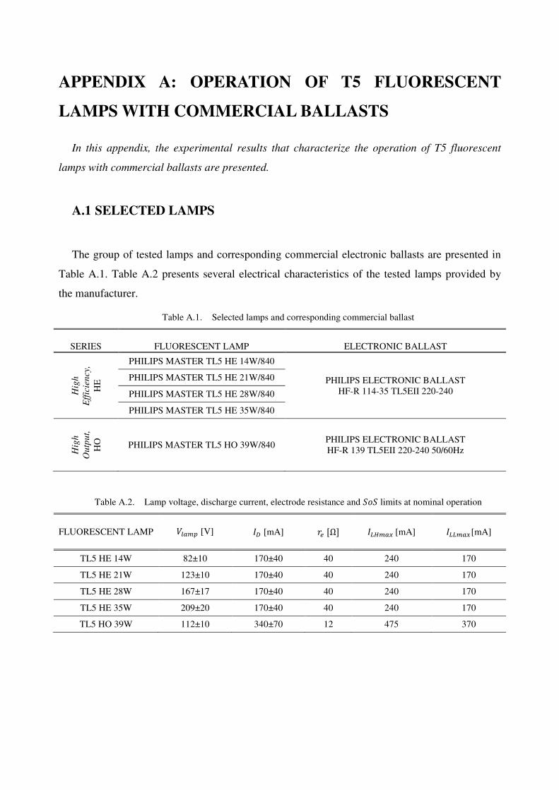
APPENDIX A: OPERATION OF T5 FLUORESCENT
LAMPS WITH COMMERCIAL BALLASTS
In this appendix, the experimental results that characterize the operation of T5 fluorescent
lamps with commercial ballasts are presented.
A.1 SELECTED LAMPS
The group of tested lamps and corresponding commercial electronic ballasts are presented in
Table A.1. Table A.2 presents several electrical characteristics of the tested lamps provided by
the manufacturer.
Table A.1. Selected lamps and corresponding commercial ballast
SERIES FLUORESCENT LAMP ELECTRONIC BALLAST
Hig
h
Eff
icie
ncy
,
HE
PHILIPS MASTER TL5 HE 14W/840
PHILIPS ELECTRONIC BALLAST HF-R 114-35 TL5EII 220-240
PHILIPS MASTER TL5 HE 21W/840
PHILIPS MASTER TL5 HE 28W/840
PHILIPS MASTER TL5 HE 35W/840
Hig
h
Ou
tpu
t,
HO
PHILIPS MASTER TL5 HO 39W/840 PHILIPS ELECTRONIC BALLAST HF-R 139 TL5EII 220-240 50/60Hz
Table A.2. Lamp voltage, discharge current, electrode resistance and m limits at nominal operation
FLUORESCENT LAMP >~ [V] /0 [mA] 3 [Ω] /~Ï[mA] /~Ï[mA]
TL5 HE 14W 82±10 170±40 40 240 170
TL5 HE 21W 123±10 170±40 40 240 170
TL5 HE 28W 167±17 170±40 40 240 170
TL5 HE 35W 209±20 170±40 40 240 170
TL5 HO 39W 112±10 340±70 12 475 370
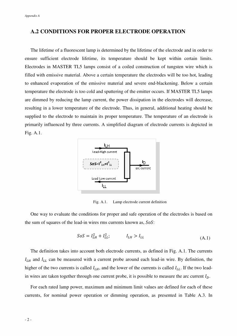
Appendix A
- 2 -
A.2 CONDITIONS FOR PROPER ELECTRODE OPERATION
The lifetime of a fluorescent lamp is determined by the lifetime of the electrode and in order to
ensure sufficient electrode lifetime, its temperature should be kept within certain limits.
Electrodes in MASTER TL5 lamps consist of a coiled construction of tungsten wire which is
filled with emissive material. Above a certain temperature the electrodes will be too hot, leading
to enhanced evaporation of the emissive material and severe end-blackening. Below a certain
temperature the electrode is too cold and sputtering of the emitter occurs. If MASTER TL5 lamps
are dimmed by reducing the lamp current, the power dissipation in the electrodes will decrease,
resulting in a lower temperature of the electrode. Thus, in general, additional heating should be
supplied to the electrode to maintain its proper temperature. The temperature of an electrode is
primarily influenced by three currents. A simplified diagram of electrode currents is depicted in
Fig. A.1.
Fig. A.1. Lamp electrode current definition
One way to evaluate the conditions for proper and safe operation of the electrodes is based on
the sum of squares of the lead-in wires rms currents known as, m:
m = / + / ; / > / (A.1)
The definition takes into account both electrode currents, as defined in Fig. A.1. The currents
/ and / can be measured with a current probe around each lead-in wire. By definition, the
higher of the two currents is called /, and the lower of the currents is called /. If the two lead-
in wires are taken together through one current probe, it is possible to measure the arc current /0.
For each rated lamp power, maximum and minimum limit values are defined for each of these
currents, for nominal power operation or dimming operation, as presented in Table A.3. In
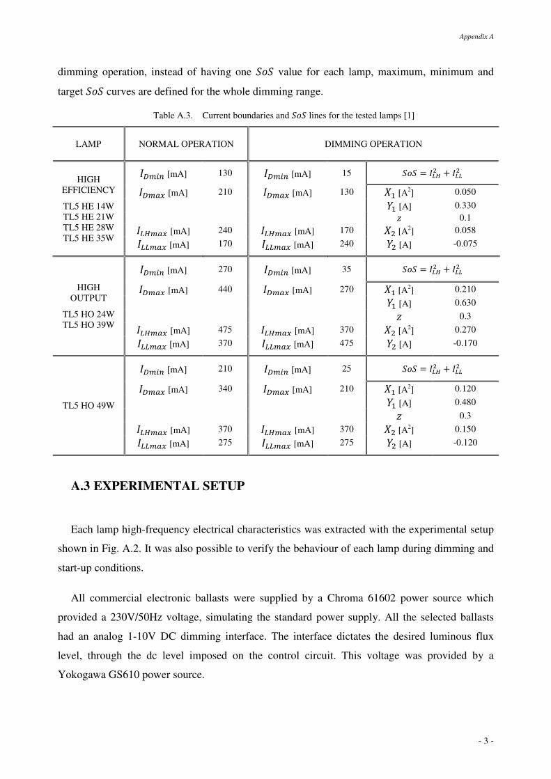
Appendix A
- 3 -
dimming operation, instead of having one m value for each lamp, maximum, minimum and
target m curves are defined for the whole dimming range.
Table A.3. Current boundaries and m lines for the tested lamps [1]
LAMP NORMAL OPERATION DIMMING OPERATION
HIGH EFFICIENCY
TL5 HE 14W TL5 HE 21W TL5 HE 28W TL5 HE 35W
/0±² [mA] 130 /0±² [mA] 15 m = / + /
/0~Ï [mA] 210 /0~Ï [mA] 130 8ª [A2] 0.050
:ª [A] 0.330 « 0.1 /~Ï [mA] 240 /~Ï [mA] 170 8 [A2] 0.058 /~Ï [mA] 170 /~Ï [mA] 240 : [A] -0.075
HIGH OUTPUT
TL5 HO 24W TL5 HO 39W
/0±² [mA] 270 /0±² [mA] 35 m = / + /
/0~Ï [mA] 440 /0~Ï [mA] 270 8ª [A2] 0.210
:ª [A] 0.630 « 0.3 /~Ï [mA] 475 /~Ï [mA] 370 8 [A2] 0.270 /~Ï [mA] 370 /~Ï [mA] 475 : [A] -0.170
TL5 HO 49W
/0±² [mA] 210 /0±² [mA] 25 m = / + /
/0~Ï [mA] 340 /0~Ï [mA] 210 8ª [A2] 0.120
:ª [A] 0.480 « 0.3 /~Ï [mA] 370 /~Ï [mA] 370 8 [A2] 0.150 /~Ï [mA] 275 /~Ï [mA] 275 : [A] -0.120
A.3 EXPERIMENTAL SETUP
Each lamp high-frequency electrical characteristics was extracted with the experimental setup
shown in Fig. A.2. It was also possible to verify the behaviour of each lamp during dimming and
start-up conditions.
All commercial electronic ballasts were supplied by a Chroma 61602 power source which
provided a 230V/50Hz voltage, simulating the standard power supply. All the selected ballasts
had an analog 1-10V DC dimming interface. The interface dictates the desired luminous flux
level, through the dc level imposed on the control circuit. This voltage was provided by a
Yokogawa GS610 power source.
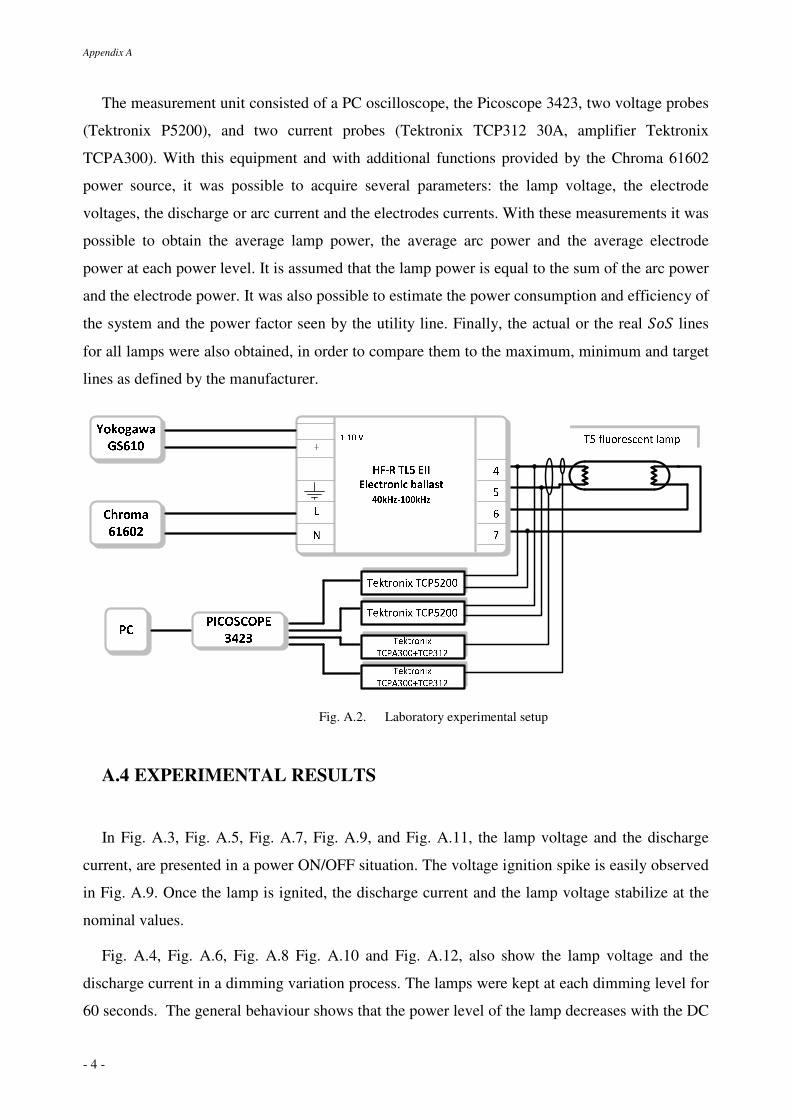
Appendix A
- 4 -
The measurement unit consisted of a PC oscilloscope, the Picoscope 3423, two voltage probes
(Tektronix P5200), and two current probes (Tektronix TCP312 30A, amplifier Tektronix
TCPA300). With this equipment and with additional functions provided by the Chroma 61602
power source, it was possible to acquire several parameters: the lamp voltage, the electrode
voltages, the discharge or arc current and the electrodes currents. With these measurements it was
possible to obtain the average lamp power, the average arc power and the average electrode
power at each power level. It is assumed that the lamp power is equal to the sum of the arc power
and the electrode power. It was also possible to estimate the power consumption and efficiency of
the system and the power factor seen by the utility line. Finally, the actual or the real m lines
for all lamps were also obtained, in order to compare them to the maximum, minimum and target
lines as defined by the manufacturer.
Fig. A.2. Laboratory experimental setup
A.4 EXPERIMENTAL RESULTS
In Fig. A.3, Fig. A.5, Fig. A.7, Fig. A.9, and Fig. A.11, the lamp voltage and the discharge
current, are presented in a power ON/OFF situation. The voltage ignition spike is easily observed
in Fig. A.9. Once the lamp is ignited, the discharge current and the lamp voltage stabilize at the
nominal values.
Fig. A.4, Fig. A.6, Fig. A.8 Fig. A.10 and Fig. A.12, also show the lamp voltage and the
discharge current in a dimming variation process. The lamps were kept at each dimming level for
60 seconds. The general behaviour shows that the power level of the lamp decreases with the DC
Appendix A
- 5 -
control voltage level. This fact is easily related to the decrease of the lamp current. Fig. A.12 also
shows that the lamp voltage remains almost constant during the dimming operation. This is also
valid for all the remaining lamps.
From the measurements and calculated values presented in Table A.4, Table A.5, Table A.6,
Table A.7, and Table A.8, it is identified that all ballasts use a variable-frequency technique to
achieve dimming and that a good power factor cannot be maintained for all operating points. The
efficiency of the ballasts, computed as the ratio between the lamp power, t~, and the input
ballast power, t±², is around 90% for high power values, decreasing rapidly for lower dimming
levels. In conclusion, these dimmable electronic ballasts are only optimized for nominal lamp
power operation.
Fig. A.13 presents the m lines determined for ech tested lamp, according with the parameters
given in Table A.2. For all tested lamps, the actual or real m lines are typically below the m
target line. It is recalled that typically these commercial ballasts use external heating sources
which control the electrodes operation.
Fig. A.14 shows the lamp power variation as a function of the discharge current, the lamp
voltage, the lamp resistance and the lamp operating frequency. Fig. A.15 shows the lamp
resistance variation as a function of the lamp power, the discharge current, the lamp voltage and
the lamp operating frequency.
Fig. A.16 shows the high frequency K(L) characteristic for three different lamps, at different
power levels.
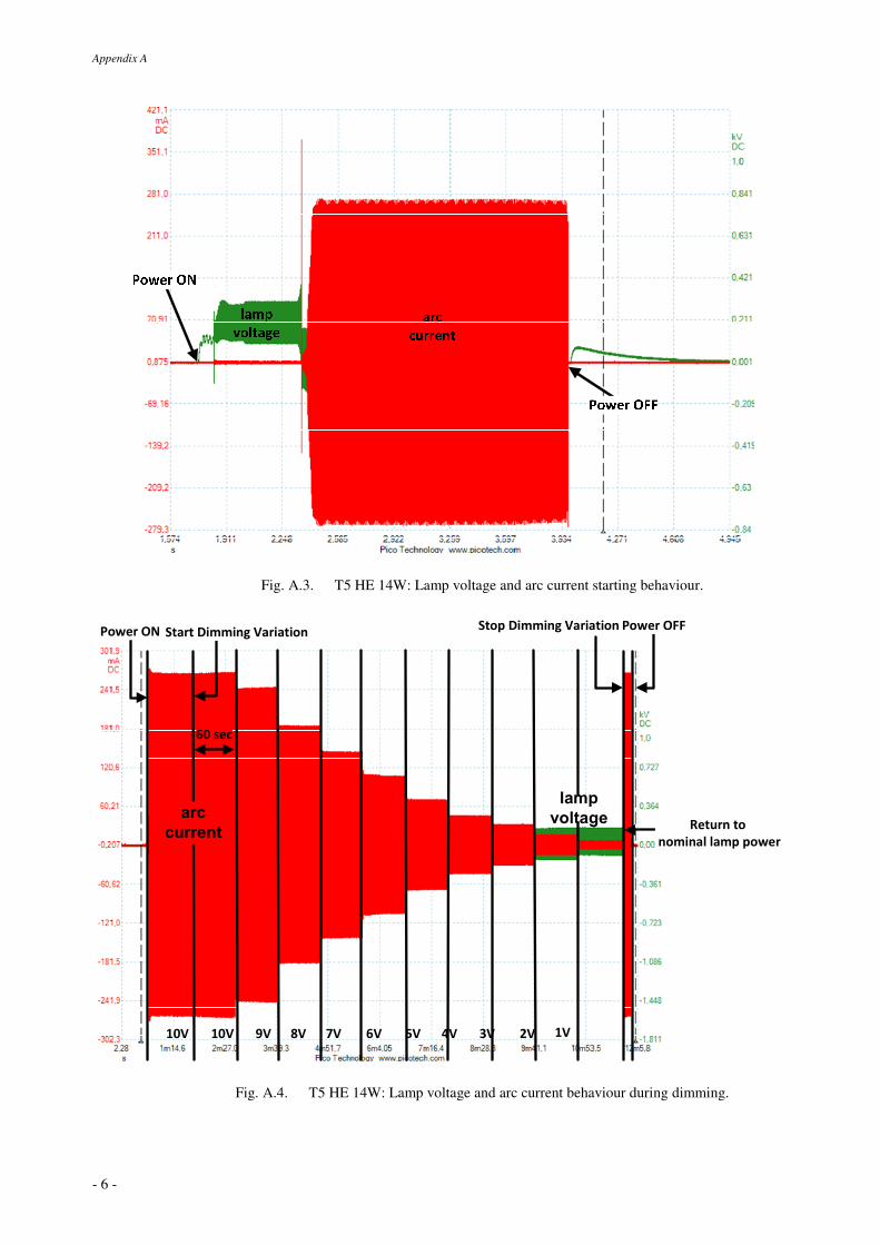
Appendix A
- 6 -
Fig. A.3. T5 HE 14W: Lamp voltage and arc current starting behaviour.
10V 9V 8V 7V 6V 5V 4V 3V 2V 1V
60 sec
10V
Power ON Start Dimming VariationStop Dimming Variation Power OFF
Return to
nominal lamp power
arc
current
lamp
voltage
Fig. A.4. T5 HE 14W: Lamp voltage and arc current behaviour during dimming.
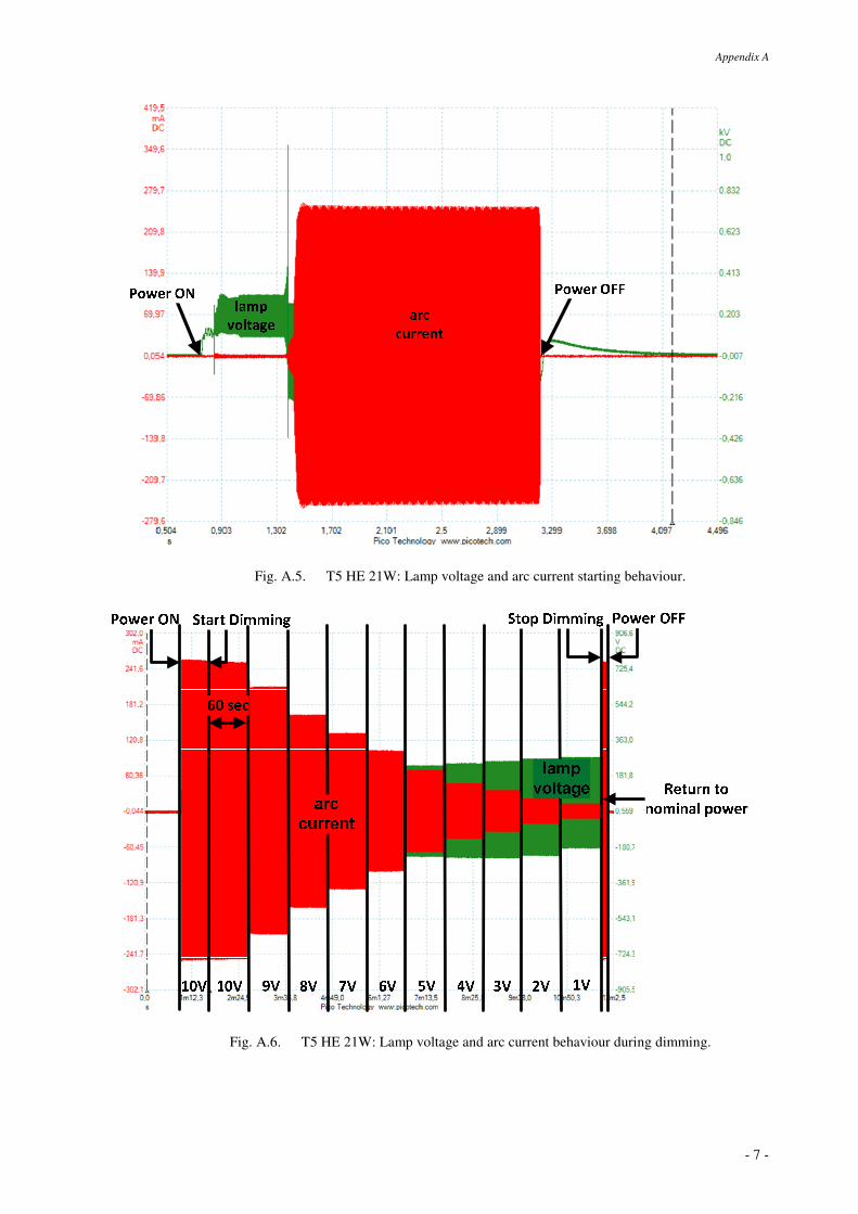
Appendix A
- 7 -
Fig. A.5. T5 HE 21W: Lamp voltage and arc current starting behaviour.
Fig. A.6. T5 HE 21W: Lamp voltage and arc current behaviour during dimming.
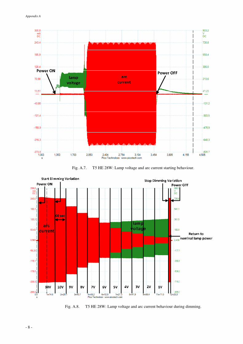
Appendix A
- 8 -
Fig. A.7. T5 HE 28W: Lamp voltage and arc current starting behaviour.
Fig. A.8. T5 HE 28W: Lamp voltage and arc current behaviour during dimming.
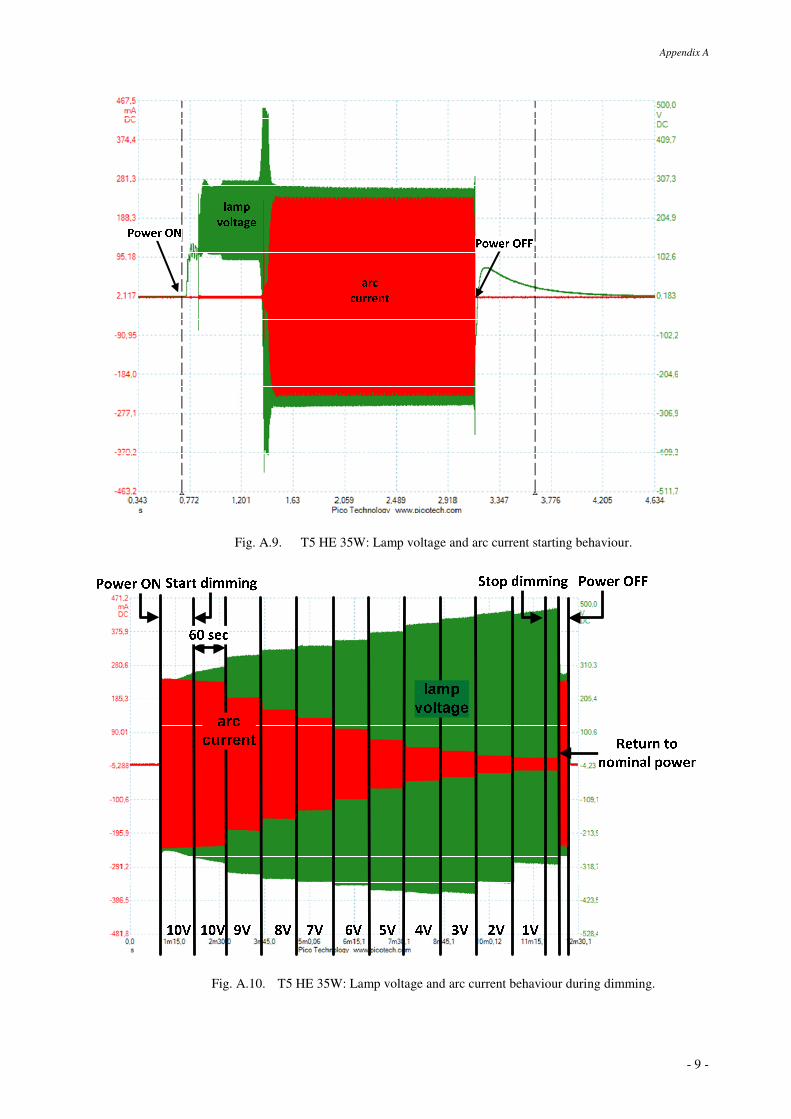
Appendix A
- 9 -
Fig. A.9. T5 HE 35W: Lamp voltage and arc current starting behaviour.
Fig. A.10. T5 HE 35W: Lamp voltage and arc current behaviour during dimming.
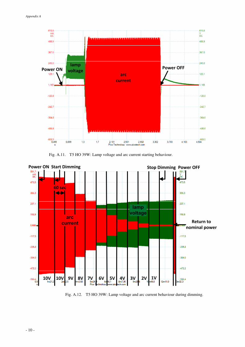
Appendix A
- 10 -
Power ONlamp
voltagePower OFF
arc
current
Fig. A.11. T5 HO 39W: Lamp voltage and arc current starting behaviour.
10V 9V 8V 7V 6V 5V 4V 3V 2V 1V10V
Power ON Start Dimming Stop Dimming Power OFF
Return to
nominal power
lamp
voltage
60 sec
arc
current
Fig. A.12. T5 HO 39W: Lamp voltage and arc current behaviour during dimming.
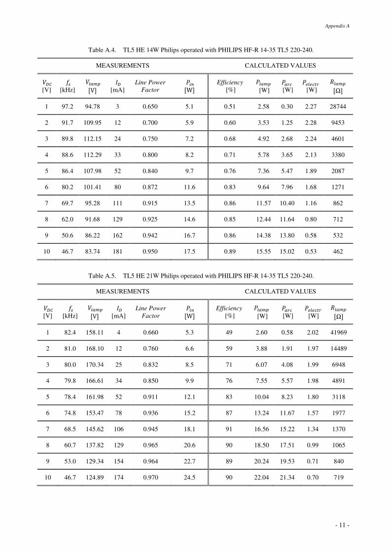
Appendix A
- 11 -
Table A.4. TL5 HE 14W Philips operated with PHILIPS HF-R 14-35 TL5 220-240.
MEASUREMENTS CALCULATED VALUES
>0 [V]
4 [kHz]
>~ [V] /0 [mA]
Line Power
Factor t±² [W] Efficiency
[%] t~
[W] t~2 [W]
t33À2
[W] v~ [Ω]
1 97.2 94.78 3 0.650 5.1 0.51 2.58 0.30 2.27 28744
2 91.7 109.95 12 0.700 5.9 0.60 3.53 1.25 2.28 9453
3 89.8 112.15 24 0.750 7.2 0.68 4.92 2.68 2.24 4601
4 88.6 112.29 33 0.800 8.2 0.71 5.78 3.65 2.13 3380
5 86.4 107.98 52 0.840 9.7 0.76 7.36 5.47 1.89 2087
6 80.2 101.41 80 0.872 11.6 0.83 9.64 7.96 1.68 1271
7 69.7 95.28 111 0.915 13.5 0.86 11.57 10.40 1.16 862
8 62.0 91.68 129 0.925 14.6 0.85 12.44 11.64 0.80 712
9 50.6 86.22 162 0.942 16.7 0.86 14.38 13.80 0.58 532
10 46.7 83.74 181 0.950 17.5 0.89 15.55 15.02 0.53 462
Table A.5. TL5 HE 21W Philips operated with PHILIPS HF-R 14-35 TL5 220-240.
MEASUREMENTS CALCULATED VALUES
>0 [V]
4 [kHz]
>~ [V] /0 [mA]
Line Power
Factor t±² [W] Efficiency
[%] t~
[W] t~2 [W]
t33À2
[W] v~ [Ω]
1 82.4 158.11 4 0.660 5.3 49 2.60 0.58 2.02 41969
2 81.0 168.10 12 0.760 6.6 59 3.88 1.91 1.97 14489
3 80.0 170.34 25 0.832 8.5 71 6.07 4.08 1.99 6948
4 79.8 166.61 34 0.850 9.9 76 7.55 5.57 1.98 4891
5 78.4 161.98 52 0.911 12.1 83 10.04 8.23 1.80 3118
6 74.8 153.47 78 0.936 15.2 87 13.24 11.67 1.57 1977
7 68.5 145.62 106 0.945 18.1 91 16.56 15.22 1.34 1370
8 60.7 137.82 129 0.965 20.6 90 18.50 17.51 0.99 1065
9 53.0 129.34 154 0.964 22.7 89 20.24 19.53 0.71 840
10 46.7 124.89 174 0.970 24.5 90 22.04 21.34 0.70 719
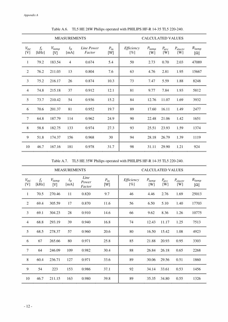
Appendix A
- 12 -
Table A.6. TL5 HE 28W Philips operated with PHILIPS HF-R 14-35 TL5 220-240.
MEASUREMENTS CALCULATED VALUES
>0 [V]
4 [kHz]
>~ [V] /0 [mA]
Line Power
Factor t±² [W] Efficiency
[%] t~
[W] t~2 [W]
t33À2
[W] v~ [Ω]
1 79.2 183.54 4 0.674 5.4 50 2.73 0.70 2.03 47089
2 76.2 211.03 13 0.804 7.6 63 4.76 2.81 1.95 15667
3 75.2 216.17 26 0.874 10.3 73 7.47 5.59 1.88 8248
4 74.8 215.18 37 0.912 12.1 81 9.77 7.84 1.93 5812
5 73.7 210.42 54 0.936 15.2 84 12.76 11.07 1.69 3932
6 70.6 201.37 81 0.952 19.7 89 17.60 16.11 1.49 2477
7 64.8 187.79 114 0.962 24.9 90 22.48 21.06 1.42 1651
8 58.8 182.75 133 0.974 27.3 93 25.51 23.93 1.59 1374
9 51.8 174.37 156 0.968 30 94 28.18 26.79 1.39 1119
10 46.7 167.16 181 0.978 31.7 98 31.11 29.90 1.21 924
Table A.7. TL5 HE 35W Philips operated with PHILIPS HF-R 14-35 TL5 220-240.
MEASUREMENTS CALCULATED VALUES
>0 [V]
4 [kHz]
>~ [V] /0 [mA]
Line
Power
Factor
t±² [W] Efficiency
[%] t~
[W] t~2 [W]
t33À2
[W] v~ [Ω]
1 70.5 270.46 11 0.820 9.7 46 4.46 2.76 1.69 25013
2 69.4 305.59 17 0.870 11.6 56 6.50 5.10 1.40 17703
3 69.1 304.23 28 0.910 14.6 66 9.62 8.36 1.26 10775
4 68.8 293.19 39 0.940 16.8 74 12.43 11.17 1.25 7513
5 68.5 278.37 57 0.960 20.6 80 16.50 15.42 1.08 4923
6 67 265.66 80 0.971 25.8 85 21.88 20.93 0.95 3303
7 64 246.09 109 0.982 30.4 88 26.84 26.18 0.65 2268
8 60.4 236.71 127 0.971 33.6 89 30.06 29.56 0.51 1860
9 54 223 153 0.986 37.1 92 34.14 33.61 0.53 1456
10 46.7 211.15 163 0.980 39.8 89 35.35 34.80 0.55 1326
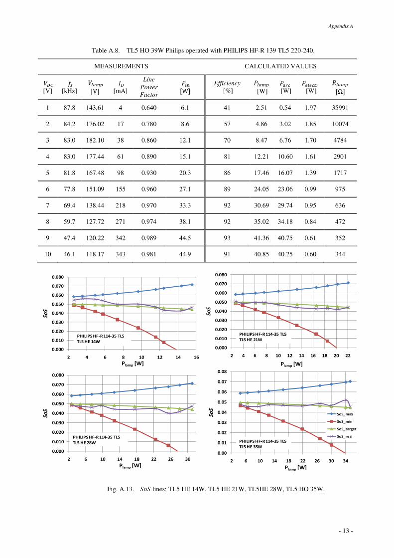
Appendix A
- 13 -
Table A.8. TL5 HO 39W Philips operated with PHILIPS HF-R 139 TL5 220-240.
MEASUREMENTS CALCULATED VALUES
>0 [V]
4 [kHz]
>~ [V] /0 [mA]
Line
Power
Factor
t±² [W] Efficiency
[%] t~
[W] t~2 [W]
t33À2
[W] v~ [Ω]
1 87.8 143,61 4 0.640 6.1 41 2.51 0.54 1.97 35991
2 84.2 176.02 17 0.780 8.6 57 4.86 3.02 1.85 10074
3 83.0 182.10 38 0.860 12.1 70 8.47 6.76 1.70 4784
4 83.0 177.44 61 0.890 15.1 81 12.21 10.60 1.61 2901
5 81.8 167.48 98 0.930 20.3 86 17.46 16.07 1.39 1717
6 77.8 151.09 155 0.960 27.1 89 24.05 23.06 0.99 975
7 69.4 138.44 218 0.970 33.3 92 30.69 29.74 0.95 636
8 59.7 127.72 271 0.974 38.1 92 35.02 34.18 0.84 472
9 47.4 120.22 342 0.989 44.5 93 41.36 40.75 0.61 352
10 46.1 118.17 343 0.981 44.9 91 40.85 40.25 0.60 344
0.000
0.010
0.020
0.030
0.040
0.050
0.060
0.070
0.080
2 4 6 8 10 12 14 16
SoS
Plamp [W]
PHILIPS HF-R 114-35 TL5
TL5 HE 14W
0.000
0.010
0.020
0.030
0.040
0.050
0.060
0.070
0.080
2 4 6 8 10 12 14 16 18 20 22
SoS
Plamp [W]
PHILIPS HF-R 114-35 TL5
TL5 HE 21W
0.000
0.010
0.020
0.030
0.040
0.050
0.060
0.070
0.080
2 6 10 14 18 22 26 30
SoS
Plamp [W]
PHILIPS HF-R 114-35 TL5
TL5 HE 28W
0.00
0.01
0.02
0.03
0.04
0.05
0.06
0.07
0.08
2 6 10 14 18 22 26 30 34
SoS
Plamp [W]
SoS_max
SoS_min
SoS_target
SoS_real
PHILIPS HF-R 114-35 TL5
TL5 HE 35W
Fig. A.13. m lines: TL5 HE 14W, TL5 HE 21W, TL5HE 28W, TL5 HO 35W.
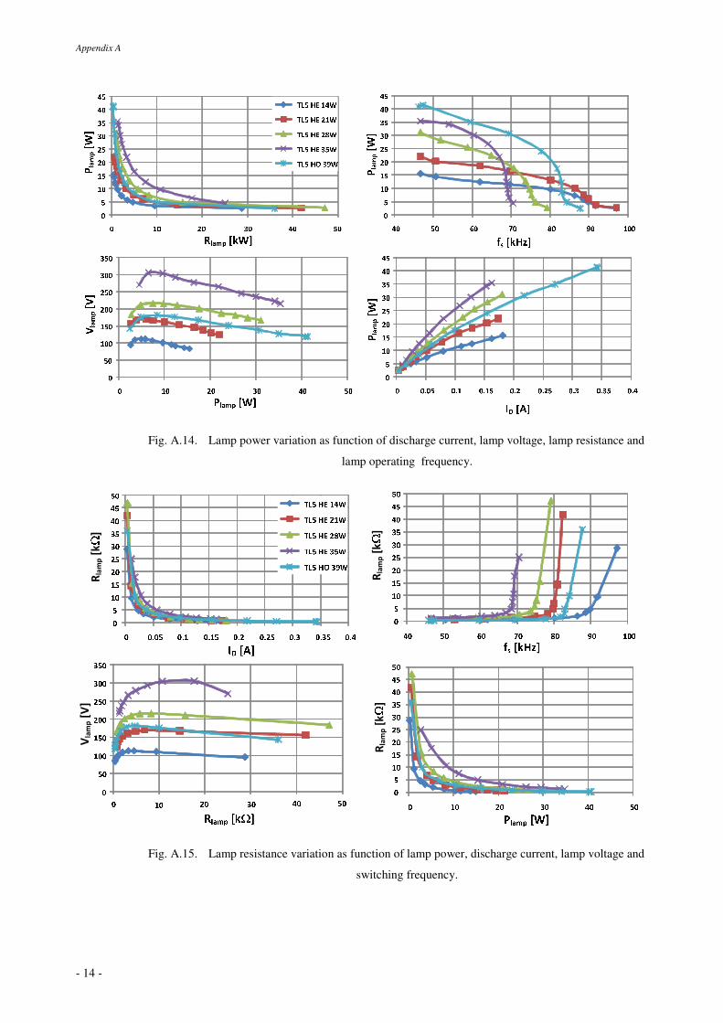
Appendix A
- 14 -
Fig. A.14. Lamp power variation as function of discharge current, lamp voltage, lamp resistance and
lamp operating frequency.
Rlamp[k
]
Rlamp[k
]Rlamp[k
]
Vlamp[V]
Fig. A.15. Lamp resistance variation as function of lamp power, discharge current, lamp voltage and
switching frequency.
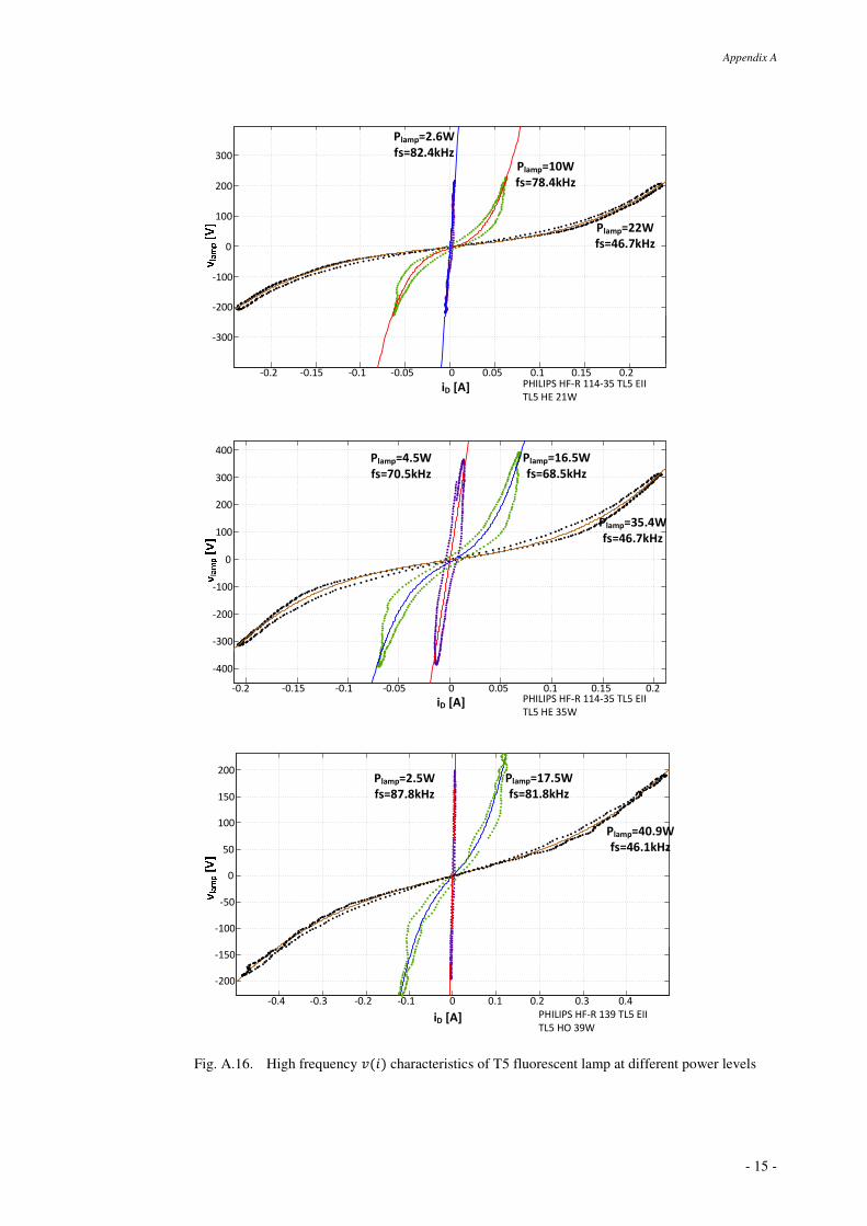
Appendix A
- 15 -
-0.2 -0.15 -0.1 -0.05 0 0.05 0.1 0.15 0.2
-400
-300
-200
-100
0
100
200
300
400
-0.4 -0.3 -0.2 -0.1 0 0.1 0.2 0.3 0.4
-200
-150
-100
-50
0
50
100
150
200
-0.2 -0.15 -0.1 -0.05 0 0.05 0.1 0.15 0.2
-300
-200
-100
0
100
200
300
iD [A]
iD [A]
iD [A]
PHILIPS HF-R 114-35 TL5 EII
TL5 HE 21W
PHILIPS HF-R 114-35 TL5 EII
TL5 HE 35W
PHILIPS HF-R 139 TL5 EII
TL5 HO 39W
Plamp=2.6W
fs=82.4kHzPlamp=10W
fs=78.4kHz
Plamp=22W
fs=46.7kHz
Plamp=4.5W
fs=70.5kHz
Plamp=16.5W
fs=68.5kHz
Plamp=35.4W
fs=46.7kHz
Plamp=2.5W
fs=87.8kHz
Plamp=17.5W
fs=81.8kHz
Plamp=40.9W
fs=46.1kHz
Fig. A.16. High frequency KL characteristics of T5 fluorescent lamp at different power levels

Appendix A
- 16 -
REFERENCES AND BIBLIOGRAPHY
[1]. Philips MASTER TL5 lamps, Philips 2006, Access in: Jan. 2011, http://www.lighting.philips.com
[2]. International Electrotechnical Commission. Ballasts for tubular fluorescent lamps - Performance
requirements, IEC 60921, 2006.
[3]. International Electrotechnical Commission. AC supplied electronic ballasts for tubular fluorescent lamps -
Performance requirements, IEC 60929, 2006.
[4]. IEC60081. Double-capped fluorescent lamps. Performance specifications. 2010.
[5]. GE Lighting, T5 Long Last, linear fluorescent lamps, Datasheet, April 2009.
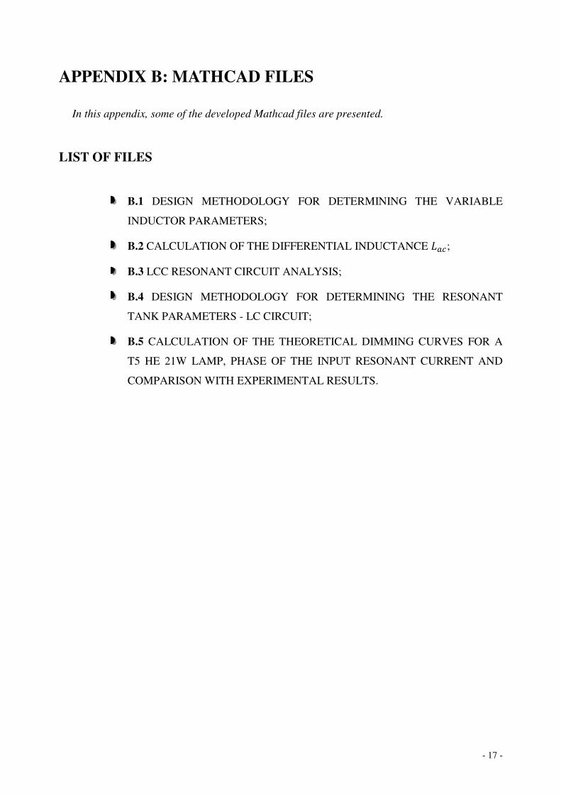
- 17 -
APPENDIX B: MATHCAD FILES
In this appendix, some of the developed Mathcad files are presented.
LIST OF FILES
B.1 DESIGN METHODOLOGY FOR DETERMINING THE VARIABLE
INDUCTOR PARAMETERS;
B.2 CALCULATION OF THE DIFFERENTIAL INDUCTANCE ¯~;
B.3 LCC RESONANT CIRCUIT ANALYSIS;
B.4 DESIGN METHODOLOGY FOR DETERMINING THE RESONANT
TANK PARAMETERS - LC CIRCUIT;
B.5 CALCULATION OF THE THEORETICAL DIMMING CURVES FOR A
T5 HE 21W LAMP, PHASE OF THE INPUT RESONANT CURRENT AND
COMPARISON WITH EXPERIMENTAL RESULTS.
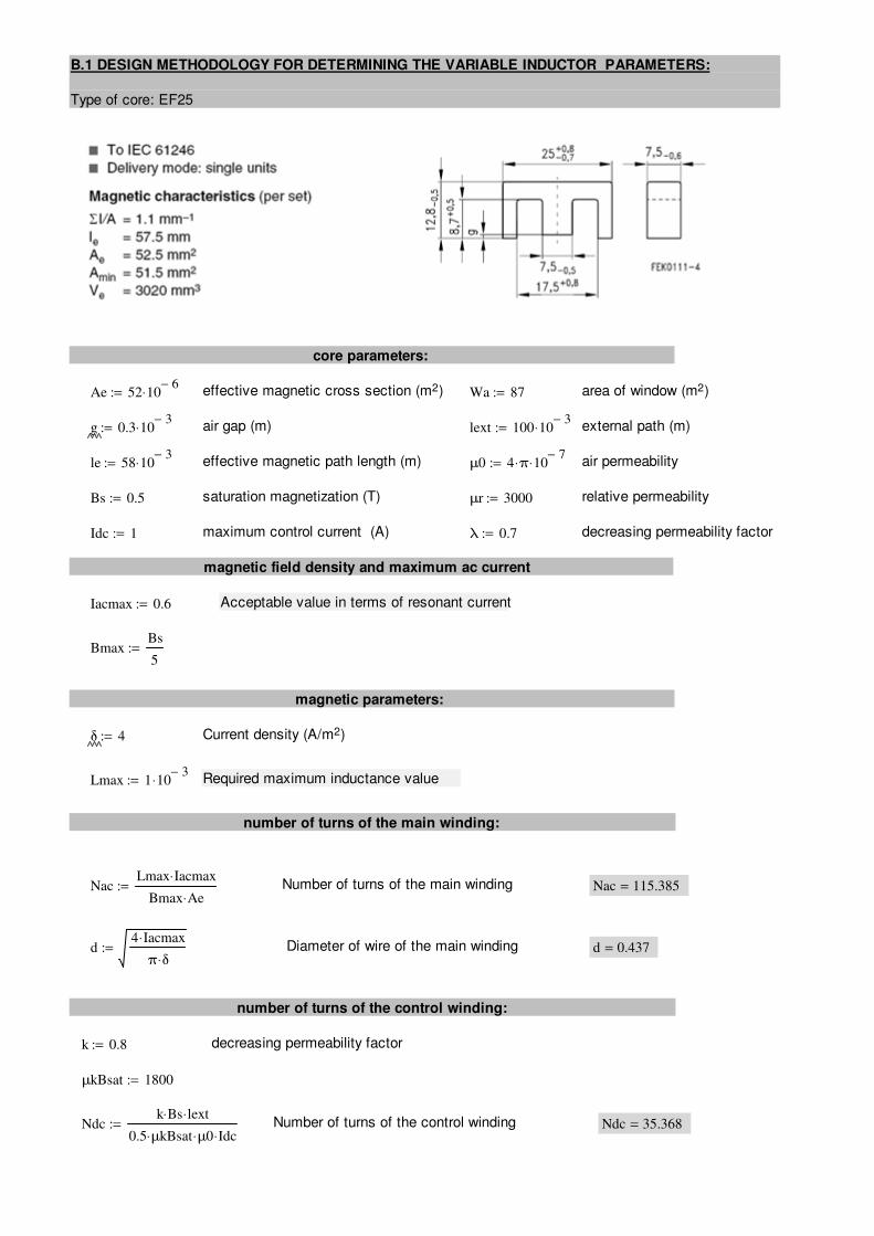
B.1 DESIGN METHODOLOGY FOR DETERMINING THE VARIABLE INDUCTOR PARAMETERS:
Type of core: EF25
core parameters:
Ae 52 106−
⋅:= effective magnetic cross section (m2) Wa 87:= area of window (m2)
g 0.3 103−
⋅:= air gap (m) lext 100 103−
⋅:= external path (m)
le 58 103−
⋅:= effective magnetic path length (m) μ0 4 π⋅ 107−
⋅:= air permeability
Bs 0.5:= saturation magnetization (T) μr 3000:= relative permeability
Idc 1:= maximum control current (A) λ 0.7:= decreasing permeability factor
magnetic field density and maximum ac current
Iacmax 0.6:= Acceptable value in terms of resonant current
BmaxBs
5:=
magnetic parameters:
δ 4:= Current density (A/m2)
Lmax 1 103−
⋅:= Required maximum inductance value
number of turns of the main winding:
NacLmax Iacmax⋅
Bmax Ae⋅:= Number of turns of the main winding Nac 115.385=
d4 Iacmax⋅
π δ⋅:= Diameter of wire of the main winding d 0.437=
number of turns of the control winding:
k 0.8:= decreasing permeability factor
μkBsat 1800:=
Ndck Bs⋅ lext⋅
0.5 μkBsat⋅ μ0⋅ Idc⋅:= Number of turns of the control winding Ndc 35.368=
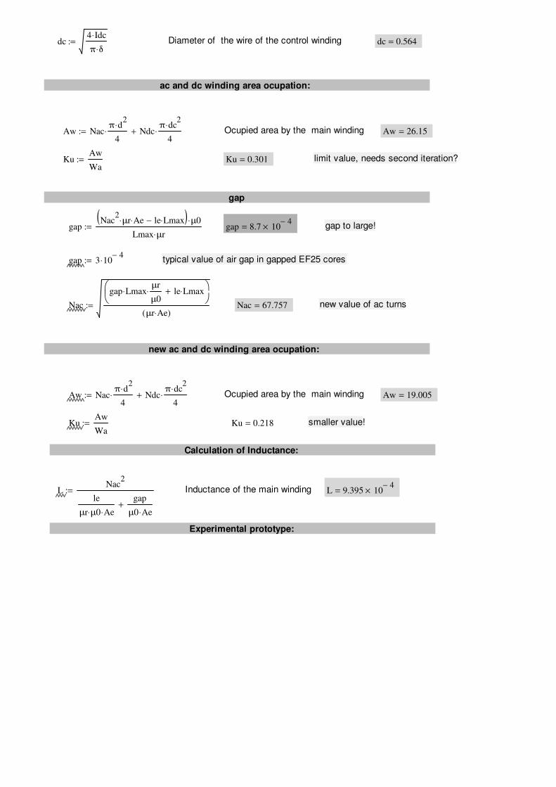
dc4 Idc⋅
π δ⋅:= Diameter of the wire of the control winding dc 0.564=
ac and dc winding area ocupation:
Aw Nacπ d
2⋅
4⋅ Ndc
π dc2
⋅
4⋅+:= Ocupied area by the main winding Aw 26.15=
KuAw
Wa:= Ku 0.301= limit value, needs second iteration?
gap
gapNac
2μr⋅ Ae⋅ le Lmax⋅−( ) μ0⋅
Lmax μr⋅:= gap 8.7 10
4−×= gap to large!
gap 3 104−
⋅:= typical value of air gap in gapped EF25 cores
Nac
gap Lmax⋅μr
μ0⋅ le Lmax⋅+
μr Ae⋅( ):= Nac 67.757= new value of ac turns
new ac and dc winding area ocupation:
Aw Nacπ d
2⋅
4⋅ Ndc
π dc2
⋅
4⋅+:= Ocupied area by the main winding Aw 19.005=
KuAw
Wa:= Ku 0.218= smaller value!
Calculation of Inductance:
LNac
2
le
μr μ0⋅ Ae⋅
gap
μ0 Ae⋅+
:= Inductance of the main winding L 9.395 104−
×=
Experimental prototype:
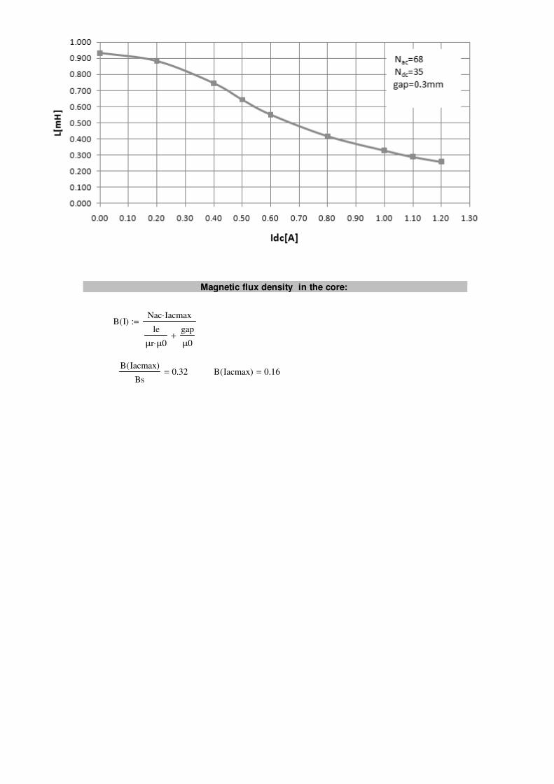
Magnetic flux density in the core:
B I( )Nac Iacmax⋅
le
μr μ0⋅
gap
μ0+
:=
B Iacmax( )
Bs0.32= B Iacmax( ) 0.16=
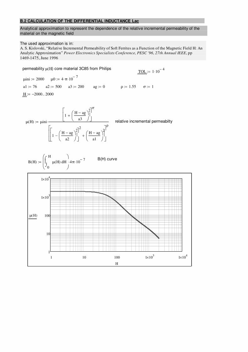
B.2 CALCULATION OF THE DIFFERENTIAL INDUCTANCE Lac
Analytical approximation to represent the dependence of the relative incremental permeability of the
material on the magnetic field
The used approximation is in:A. S. Kislovski, “Relative Incremental Permeability of Soft Ferrites as a Function of the Magnetic Field H: An
Analytic Approximation” Power Electronics Specialists Conference, PESC '96, 27th Annual IEEE, pp
1469-1475, June 1996
permeability µ(Η) core material 3C85 from PhilipsTOL 1 10
4−⋅:=
μini 2000:= μ0 4 π⋅ 107−
⋅:=
a1 76:= a2 500:= a3 200:= ag 0:= ρ 1.55:= σ 1:=
H 2000− 2000..:=
μ H( ) μini
1H ag−
a3
2
+
σ
1H ag−
a2
2
−
2
H ag−
a1
2
+
ρ⋅:= relative incremental permeabilty
B(H) curveB H( )
0
H
Hμ H( )⌠⌡
d
4⋅ π 107−
⋅:=
1 10 100 1 103
× 1 104
×
1
10
100
1 103
×
1 104
×
μ H( )
H
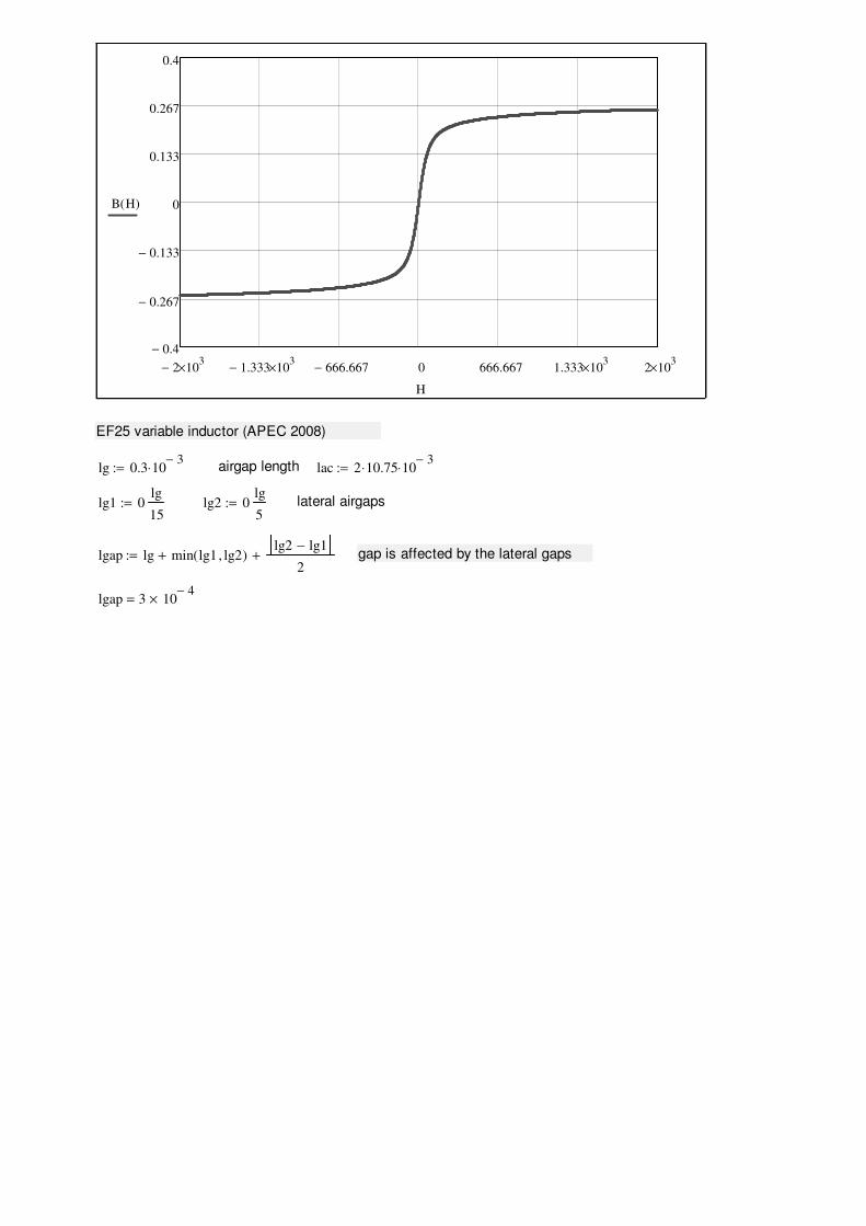
2− 103
× 1.333− 103
× 666.667− 0 666.667 1.333 103
× 2 103
×
0.4−
0.267−
0.133−
0
0.133
0.267
0.4
B H( )
H
EF25 variable inductor (APEC 2008)
lg 0.3 103−
⋅:= airgap length lac 2 10.75⋅ 103−
⋅:=
lg1 0lg
15:= lg2 0
lg
5:= lateral airgaps
lgap lg min lg1 lg2, ( )+lg2 lg1−
2+:= gap is affected by the lateral gaps
lgap 3 104−
×=
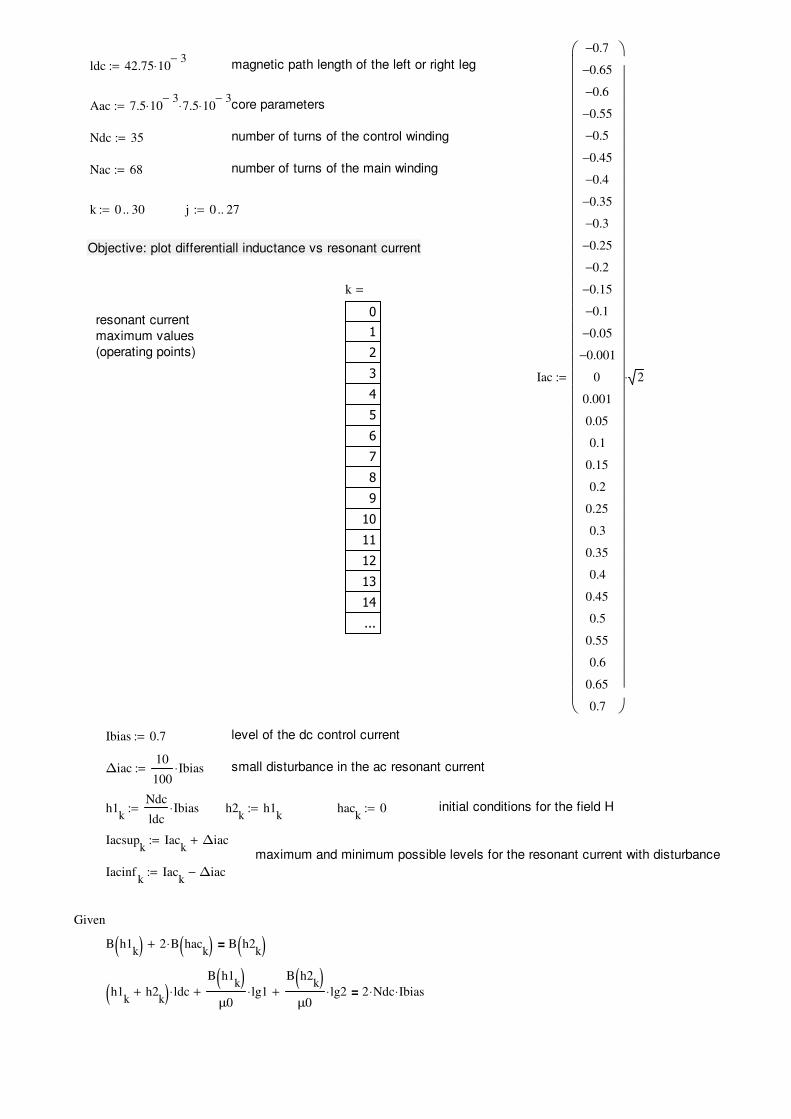
ldc 42.75 103−
⋅:= magnetic path length of the left or right leg
Aac 7.5 103−
⋅ 7.5⋅ 103−
⋅:= core parameters
Ndc 35:= number of turns of the control winding
Nac 68:= number of turns of the main winding
k 0 30..:= j 0 27..:=
Objective: plot differentiall inductance vs resonant current
k
0
1
2
3
4
5
6
7
8
9
10
11
12
13
14
...
=
resonant current
maximum values
(operating points)
Iac
0.7−
0.65−
0.6−
0.55−
0.5−
0.45−
0.4−
0.35−
0.3−
0.25−
0.2−
0.15−
0.1−
0.05−
0.001−
0
0.001
0.05
0.1
0.15
0.2
0.25
0.3
0.35
0.4
0.45
0.5
0.55
0.6
0.65
0.7
2⋅:=
Ibias 0.7:= level of the dc control current
∆iac10
100Ibias⋅:= small disturbance in the ac resonant current
h1k
Ndc
ldcIbias⋅:= h2
kh1
k:= hac
k0:= initial conditions for the field H
Iacsupk
Iack
∆iac+:=
maximum and minimum possible levels for the resonant current with disturbance
Iacinfk
Iack
∆iac−:=
Given
B h1k( ) 2 B hac
k( )⋅+ B h2k( )=
h1k
h2k
+( ) ldc⋅
B h1k( )
μ0lg1⋅+
B h2k( )
μ0lg2⋅+ 2 Ndc⋅ Ibias⋅=
( ) ( ) ( )
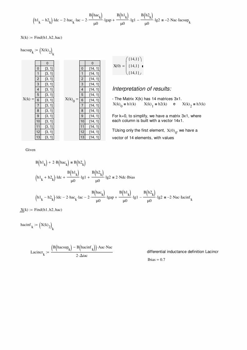
h1k
h2k
−( ) ldc⋅ 2 hack
⋅ lac⋅− 2
B hack( )
μ0⋅ lgap⋅−
B h1k( )
μ0lg1⋅+
B h2k( )
μ0lg2⋅− 2− Nac⋅ Iacsup
k⋅=
X k( ) Find h1 h2, hac, ( ):=
hacsupk
X k( )2( )
k:=
X 0( )
14,1
14,1
14,1
=
X k( )
0
0
1
2
3
4
5
6
7
8
9
10
11
12
13
[3, 1]
[3, 1]
[3, 1]
[3, 1]
[3, 1]
[3, 1]
[3, 1]
[3, 1]
[3, 1]
[3, 1]
[3, 1]
[3, 1]
[3, 1]
[3, 1]
= X k( )0
0
0
1
2
3
4
5
6
7
8
9
10
11
12
13
[14, 1]
[14, 1]
[14, 1]
[14, 1]
[14, 1]
[14, 1]
[14, 1]
[14, 1]
[14, 1]
[14, 1]
[14, 1]
[14, 1]
[14, 1]
[14, 1]
=
Interpretation of results:
- The Matrix X(k) has 14 matrices 3x1.
X k( )0
h1 k( )= X k( )1
h2 k( )= e X k( )2
h3 k( )=
For k=0, to simplify, we have a matrix 3x1, whereeach column is built with a vector 14x1.
TUsing only the first element, X 0( )0, we have a
vector of 14 elements, with values
Given
B h1k( ) 2 B hac
k( )⋅+ B h2k( )=
h1k
h2k
+( ) ldc⋅
B h1k( )
μ0lg1⋅+
B h2k( )
μ0lg2⋅+ 2 Ndc⋅ Ibias⋅=
h1k
h2k
−( ) ldc⋅ 2 hack
⋅ lac⋅− 2
B hack( )
μ0⋅ lgap⋅−
B h1k( )
μ0lg1⋅+
B h2k( )
μ0lg2⋅− 2− Nac⋅ Iacinf
k⋅=
X k( ) Find h1 h2, hac, ( ):=
hacinfk
X k( )2( )
k:=
Lacincrk
B hacsupk( ) B hacinf
k( )−( ) Aac⋅ Nac⋅
2 ∆iac⋅:= differential inductance definition Lacincr
Ibias 0.7=
Lacincr =
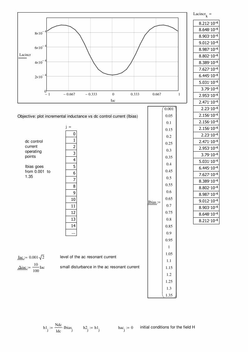
1− 0.667− 0.333− 0 0.333 0.667 10
2 104−
×
4 104−
×
6 104−
×
8 104−
×
Lacincr
Iac
Lacincrk
-48.212·10
-48.648·10
-48.903·10
-49.012·10
-48.987·10
-48.802·10
-48.389·10
-47.627·10
-46.445·10
-45.031·10
-43.79·10
-42.953·10
-42.471·10
-42.23·10
-42.156·10
-42.156·10
-42.156·10
-42.23·10
-42.471·10
-42.953·10
-43.79·10
-45.031·10
-46.445·10
-47.627·10
-48.389·10
-48.802·10
-48.987·10
-49.012·10
-48.903·10
-48.648·10
-48.212·10
=
Objective: plot incremental inductance vs dc control current (Ibias)
j
0
1
2
3
4
5
6
7
8
9
10
11
12
13
14
...
=
dc control
current
operating
points
Ibias goes
from 0.001 to
1.35
Ibias
0.001
0.05
0.1
0.15
0.2
0.25
0.3
0.35
0.4
0.45
0.5
0.55
0.6
0.65
0.7
0.75
0.8
0.85
0.9
0.95
1
1.05
1.1
1.15
1.2
1.25
1.3
1.35
:=
Iac 0.001 2⋅:= level of the ac resonant current
∆iac10
100Iac:= small disturbance in the ac resonant current
h1j
Ndc
ldcIbias
j⋅:= h2
jh1
j:= hac
j0:= initial conditions for the field H
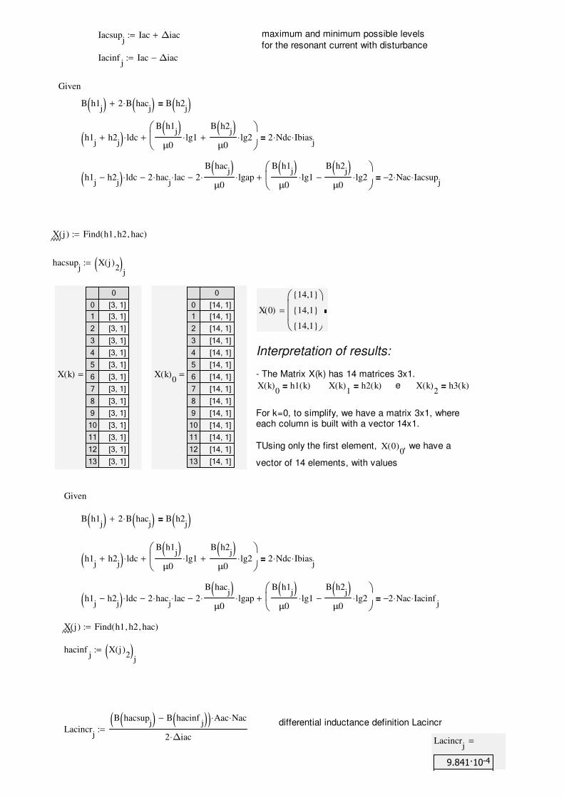
Iacsupj
Iac ∆iac+:= maximum and minimum possible levels
for the resonant current with disturbance
Iacinfj
Iac ∆iac−:=
Given
B h1j( ) 2 B hac
j( )⋅+ B h2j( )=
h1j
h2j
+( ) ldc⋅
B h1j( )
μ0lg1⋅
B h2j( )
μ0lg2⋅+
+ 2 Ndc⋅ Ibiasj
⋅=
h1j
h2j
−( ) ldc⋅ 2 hacj
⋅ lac⋅− 2
B hacj( )
μ0⋅ lgap⋅−
B h1j( )
μ0lg1⋅
B h2j( )
μ0lg2⋅−
+ 2− Nac⋅ Iacsupj
⋅=
X j( ) Find h1 h2, hac, ( ):=
hacsupj
X j( )2( )
j:=
X k( )
0
0
1
2
3
4
5
6
7
8
9
10
11
12
13
[3, 1]
[3, 1]
[3, 1]
[3, 1]
[3, 1]
[3, 1]
[3, 1]
[3, 1]
[3, 1]
[3, 1]
[3, 1]
[3, 1]
[3, 1]
[3, 1]
= X k( )0
0
0
1
2
3
4
5
6
7
8
9
10
11
12
13
[14, 1]
[14, 1]
[14, 1]
[14, 1]
[14, 1]
[14, 1]
[14, 1]
[14, 1]
[14, 1]
[14, 1]
[14, 1]
[14, 1]
[14, 1]
[14, 1]
=
X 0( )
14,1
14,1
14,1
=
Interpretation of results:
- The Matrix X(k) has 14 matrices 3x1.
X k( )0
h1 k( )= X k( )1
h2 k( )= e X k( )2
h3 k( )=
For k=0, to simplify, we have a matrix 3x1, whereeach column is built with a vector 14x1.
TUsing only the first element, X 0( )0, we have a
vector of 14 elements, with values
Given
B h1j( ) 2 B hac
j( )⋅+ B h2j( )=
h1j
h2j
+( ) ldc⋅
B h1j( )
μ0lg1⋅
B h2j( )
μ0lg2⋅+
+ 2 Ndc⋅ Ibiasj
⋅=
h1j
h2j
−( ) ldc⋅ 2 hacj
⋅ lac⋅− 2
B hacj( )
μ0⋅ lgap⋅−
B h1j( )
μ0lg1⋅
B h2j( )
μ0lg2⋅−
+ 2− Nac⋅ Iacinfj
⋅=
X j( ) Find h1 h2, hac, ( ):=
hacinfj
X j( )2( )
j:=
differential inductance definition LacincrLacincr
j
B hacsupj( ) B hacinf
j( )−( ) Aac⋅ Nac⋅
2 ∆iac⋅:=
Lacincrj
-49.841·10
=
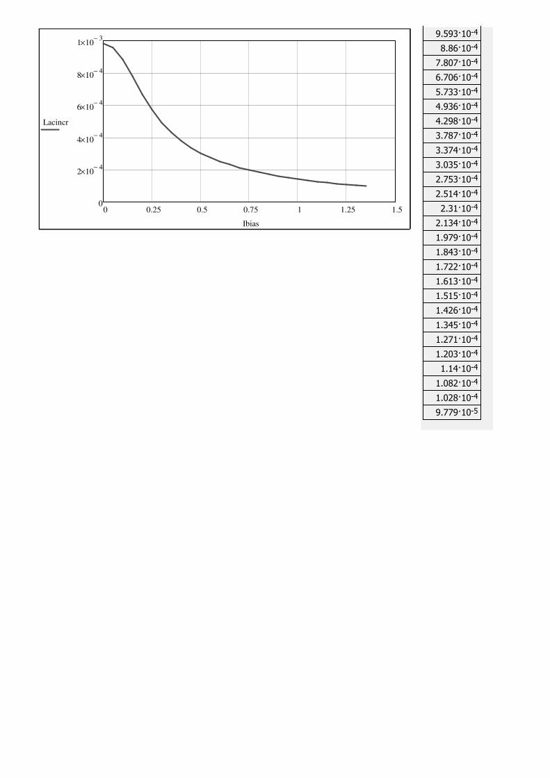
-49.593·10
-48.86·10
-47.807·10
-46.706·10
-45.733·10
-44.936·10
-44.298·10
-43.787·10
-43.374·10
-43.035·10
-42.753·10
-42.514·10
-42.31·10
-42.134·10
-41.979·10
-41.843·10
-41.722·10
-41.613·10
-41.515·10
-41.426·10
-41.345·10
-41.271·10
-41.203·10
-41.14·10
-41.082·10
-41.028·10
-59.779·10
0 0.25 0.5 0.75 1 1.25 1.50
2 104−
×
4 104−
×
6 104−
×
8 104−
×
1 103−
×
Lacincr
Ibias
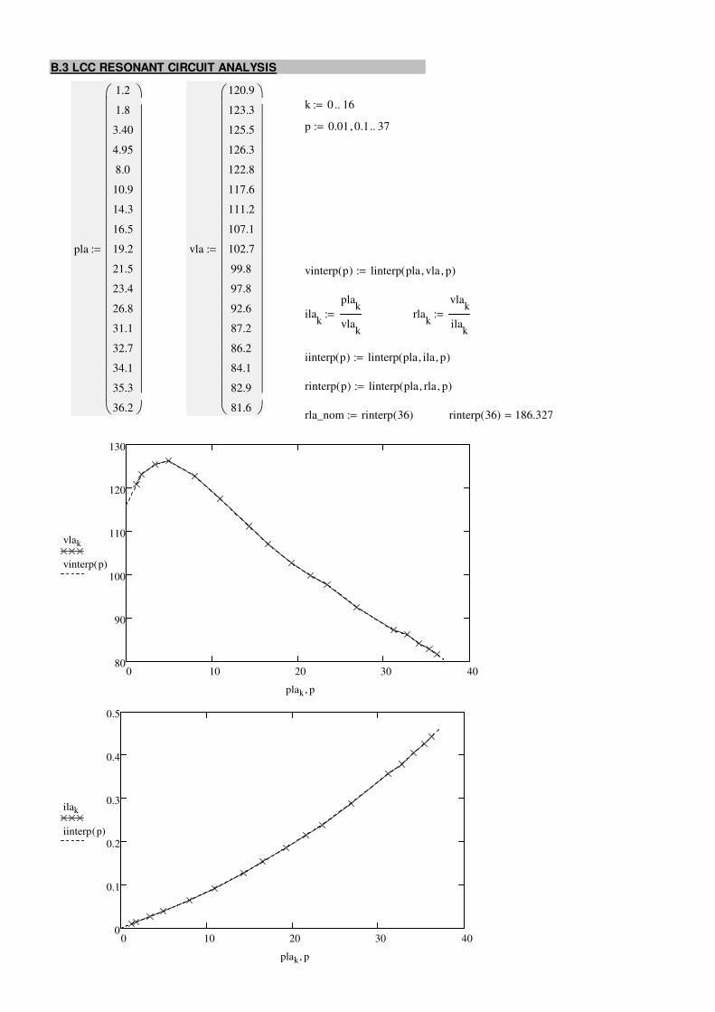
B.3 LCC RESONANT CIRCUIT ANALYSIS
k 0 16..:=
p 0.01 0.1, 37..:=
pla
1.2
1.8
3.40
4.95
8.0
10.9
14.3
16.5
19.2
21.5
23.4
26.8
31.1
32.7
34.1
35.3
36.2
:= vla
120.9
123.3
125.5
126.3
122.8
117.6
111.2
107.1
102.7
99.8
97.8
92.6
87.2
86.2
84.1
82.9
81.6
:=
vinterp p( ) linterp pla vla, p, ( ):=
ilak
plak
vlak
:= rlak
vlak
ilak
:=
iinterp p( ) linterp pla ila, p, ( ):=
rinterp p( ) linterp pla rla, p, ( ):=
rla_nom rinterp 36( ):= rinterp 36( ) 186.327=
0 10 20 30 4080
90
100
110
120
130
vlak
vinterp p( )
plak p,
0 10 20 30 400
0.1
0.2
0.3
0.4
0.5
ilak
iinterp p( )
plak p,
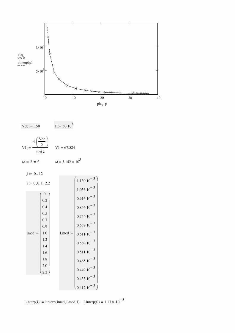
0 10 20 30 400
5 103
×
1 104
×
rlak
rinterp p( )
plak p,
Vdc 150:= f 50 103
⋅:=
V1
4Vdc
2
⋅
π 2⋅:= V1 67.524=
ω 2 π⋅ f⋅:= ω 3.142 105
×=
j 0 12..:=
i 0 0.1, 2.2..:=
imed
0
0.2
0.4
0.5
0.7
0.9
1.0
1.2
1.4
1.6
1.8
2.0
2.2
:= Lmed
1.130 103−
⋅
1.056 103−
⋅
0.916 103−
⋅
0.846 103−
⋅
0.744 103−
⋅
0.657 103−
⋅
0.611 103−
⋅
0.569 103−
⋅
0.511 103−
⋅
0.465 103−
⋅
0.449 103−
⋅
0.433 103−
⋅
0.412 103−
⋅
:=
Linterp i( ) linterp imed Lmed, i, ( ):= Linterp 0( ) 1.13 103−
×=
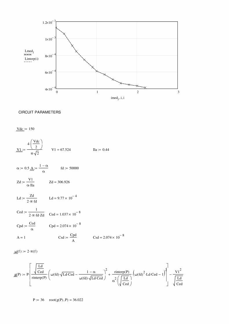
0 1 2 34 10
4−×
6 104−
×
8 104−
×
1 103−
×
1.2 103−
×
Lmedj
Linterp i( )
imedj i, i,
CIRCUIT PARAMETERS
Vdc 150:=
V1
4Vdc
2
⋅
π 2⋅:= V1 67.524= Ila 0.44:=
α 0.5:= A1 α−
α:= fd 50000:=
ZdV1
α Ila⋅:= Zd 306.926=
LdZd
2 π⋅ fd⋅:= Ld 9.77 10
4−×=
Ced1
2 π⋅ fd⋅ Zd⋅:=
Ced 1.037 108−
×=
CpdCed
α:= Cpd 2.074 10
8−×=
A 1= CsdCpd
A:= Csd 2.074 10
8−×=
ω f( ) 2 π⋅ f( ):=
g P( ) P
Ld
Ced
rinterp P( )ω fd( ) Ld Ced⋅⋅
1 α−
ω fd( ) Ld Ced⋅⋅−
2
⋅rinterp P( )
α2 Ld
Ced
⋅
ω fd( )2
Ld⋅ Ced⋅ 1−( )2
⋅+
⋅V1
2
Ld
Ced
−:=
P 36:= root g P( ) P, ( ) 36.022=
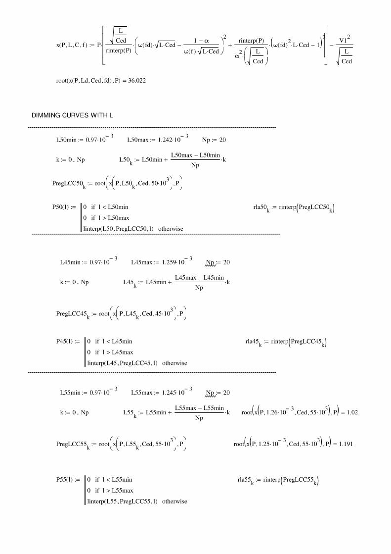
x P L, C, f, ( ) P
L
Ced
rinterp P( )ω fd( ) L Ced⋅⋅
1 α−
ω f( ) L Ced⋅⋅−
2
⋅rinterp P( )
α2 L
Ced
⋅
ω fd( )2
L⋅ Ced⋅ 1−( )2
⋅+
⋅V1
2
L
Ced
−:=
root x P Ld, Ced, fd, ( ) P, ( ) 36.022=
DIMMING CURVES WITH L
------------------------------------------------------------------------------------------------------------------------------
L50min 0.97 103−
⋅:= L50max 1.242 103−
⋅:= Np 20:=
k 0 Np..:= L50k
L50minL50max L50min−
Npk⋅+:=
PregLCC50k
root x P L50k
, Ced, 50 103
⋅,
P,
:=
P50 l( ) 0 l L50min<if
0 l L50max>if
linterp L50 PregLCC50, l, ( ) otherwise
:= rla50k
rinterp PregLCC50k( ):=
------------------------------------------------------------------------------------------------------------------------------
L45min 0.97 103−
⋅:= L45max 1.259 103−
⋅:= Np 20:=
k 0 Np..:= L45k
L45minL45max L45min−
Npk⋅+:=
PregLCC45k
root x P L45k
, Ced, 45 103
⋅,
P,
:=
P45 l( ) 0 l L45min<if
0 l L45max>if
linterp L45 PregLCC45, l, ( ) otherwise
:= rla45k
rinterp PregLCC45k( ):=
------------------------------------------------------------------------------------------------------------------------------
L55min 0.97 103−
⋅:= L55max 1.245 103−
⋅:= Np 20:=
k 0 Np..:= L55k
L55minL55max L55min−
Npk⋅+:= root x P 1.26 10
3−⋅, Ced, 55 10
3⋅, ( ) P, ( ) 1.02=
PregLCC55k
root x P L55k
, Ced, 55 103
⋅,
P,
:= root x P 1.25 103−
⋅, Ced, 55 103
⋅, ( ) P, ( ) 1.191=
P55 l( ) 0 l L55min<if
0 l L55max>if
linterp L55 PregLCC55, l, ( ) otherwise
:= rla55k
rinterp PregLCC55k( ):=
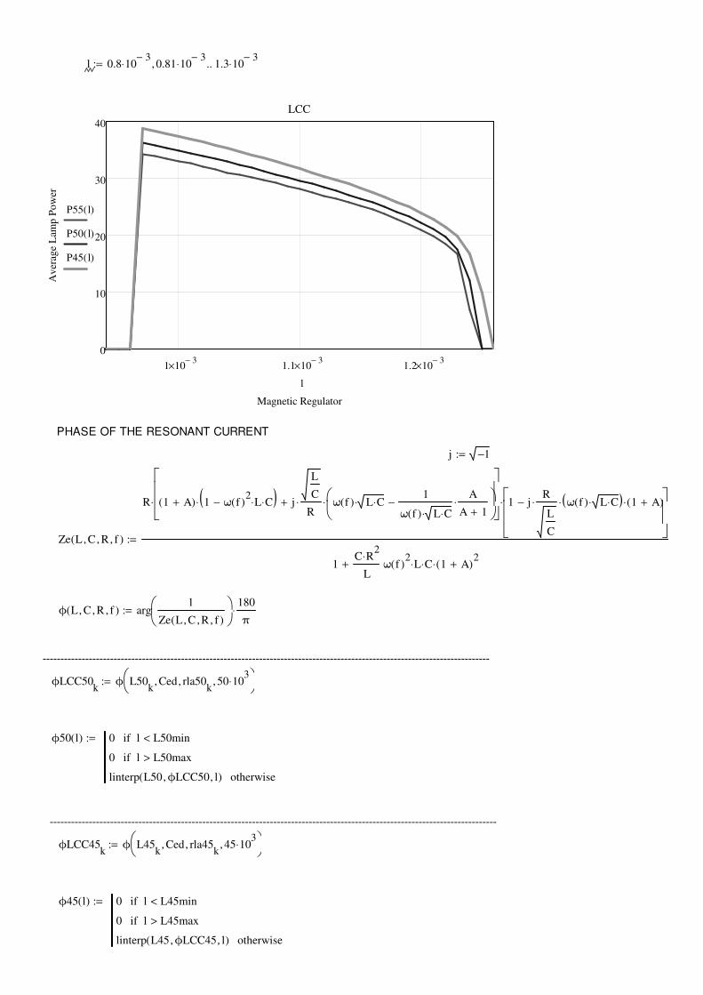
l 0.8 103−
⋅ 0.81 103−
⋅, 1.3 103−
⋅..:=
1 103−
× 1.1 103−
× 1.2 103−
×
0
10
20
30
40
LCC
Magnetic Regulator
Av
erag
e L
amp
Po
wer
P55 l( )
P50 l( )
P45 l( )
l
PHASE OF THE RESONANT CURRENT
j 1−:=
Ze L C, R, f, ( )
R 1 A+( ) 1 ω f( )2
L⋅ C⋅−( )⋅ j
L
C
R⋅ ω f( ) L C⋅⋅
1
ω f( ) L C⋅⋅
A
A 1+⋅−
⋅+
⋅ 1 jR
L
C
⋅ ω f( ) L C⋅⋅( )⋅ 1 A+( )⋅−
⋅
1C R
2⋅
Lω f( )
2L⋅ C⋅ 1 A+( )
2⋅+
:=
ϕ L C, R, f, ( ) arg1
Ze L C, R, f, ( )
180
π⋅:=
------------------------------------------------------------------------------------------------------------------------------
ϕLCC50k
ϕ L50k
Ced, rla50k
, 50 103
⋅,
:=
ϕ50 l( ) 0 l L50min<if
0 l L50max>if
linterp L50 ϕLCC50, l, ( ) otherwise
:=
------------------------------------------------------------------------------------------------------------------------------
ϕLCC45k
ϕ L45k
Ced, rla45k
, 45 103
⋅,
:=
ϕ45 l( ) 0 l L45min<if
0 l L45max>if
linterp L45 ϕLCC45, l, ( ) otherwise
:=
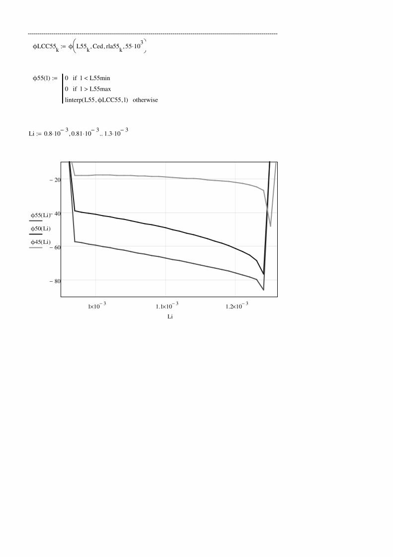
------------------------------------------------------------------------------------------------------------------------------
ϕLCC55k
ϕ L55k
Ced, rla55k
, 55 103
⋅,
:=
ϕ55 l( ) 0 l L55min<if
0 l L55max>if
linterp L55 ϕLCC55, l, ( ) otherwise
:=
Li 0.8 103−
⋅ 0.81 103−
⋅, 1.3 103−
⋅..:=
1 103−
× 1.1 103−
× 1.2 103−
×
80−
60−
40−
20−
ϕ55 Li( )
ϕ50 Li( )
ϕ45 Li( )
Li
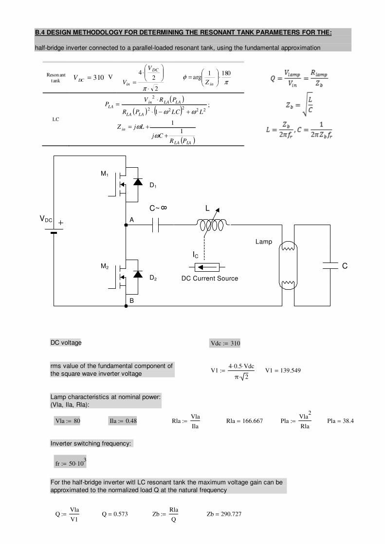
B.4 DESIGN METHODOLOGY FOR DETERMINING THE RESONANT TANK PARAMETERS FOR THE:
half-bridge inverter connected to a parallel-loaded resonant tank, using the fundamental approximation
Reson ant tank
310=DCV V
2
24
⋅
⋅
=π
DC
in
V
V πφ
1801arg ⋅
=
inZ
LC
( )
( ) ( ) 22222
2
1 LLCPR
PRVP
LALA
LALAinLA
ωω +−⋅
⋅= ;
( )LALA
in
PRCj
LjZ1
1
+
+=
ω
ω
C
VDC
M1
M2
A
B
D1
D2
L
IC
C~
8
DC Current Source
Lamp
DC voltage Vdc 310:=
rms value of the fundamental component of
the square wave inverter voltageV1
4 0.5⋅ Vdc⋅
π 2⋅:= V1 139.549=
Lamp characteristics at nominal power:
(Vla, Ila, Rla):
Vla 80:= Ila 0.48:= RlaVla
Ila:= Rla 166.667= Pla
Vla2
Rla:= Pla 38.4=
Inverter switching frequency:
fr 50 103
⋅:=
For the half-bridge inverter witl LC resonant tank the maximum voltage gain can be
approximated to the normalized load Q at the natural frequency
QVla
V1:= Q 0.573= Zb
Rla
Q:= Zb 290.727=
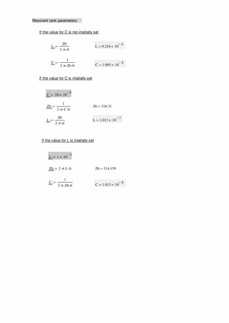
Resonant tank parameters:
If the value for C is not iniatially set
LZb
2 π⋅ fr⋅:= L 9.254 10
4−×=
C1
2 π⋅ Zb⋅ fr⋅:=
C 1.095 108−
×=
If the value for C is iniatially set
C 10 109−
×:=
Zb1
2 π⋅ C⋅ fr⋅:= Zb 318.31=
LZb
2 π⋅ fr⋅:= L 1.013 10
3−×=
If the value for L is iniatially set
L 1 103−
×:=
Zb 2 π⋅ L⋅ fr⋅:= Zb 314.159=
C1
2 π⋅ Zb⋅ fr⋅:=
C 1.013 108−
×=
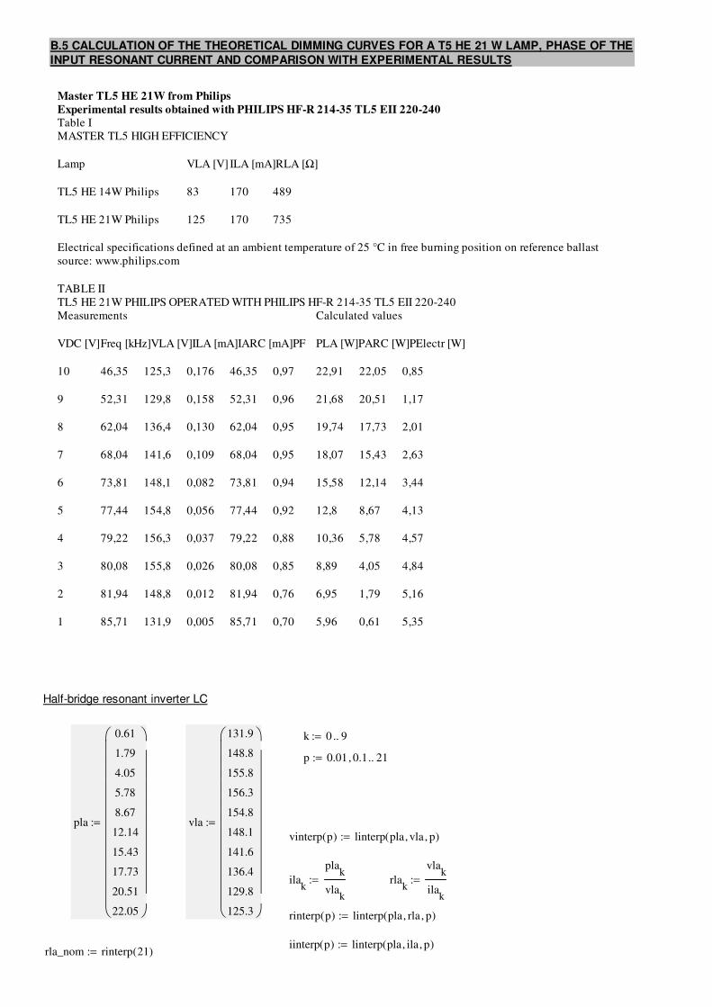
B.5 CALCULATION OF THE THEORETICAL DIMMING CURVES FOR A T5 HE 21 W LAMP, PHASE OF THE
INPUT RESONANT CURRENT AND COMPARISON WITH EXPERIMENTAL RESULTS
Master TL5 HE 21W from Philips
Experimental results obtained with PHILIPS HF-R 214-35 TL5 EII 220-240
Table I
MASTER TL5 HIGH EFFICIENCY
Lamp VLA [V] ILA [mA]RLA [Ω]
TL5 HE 14W Philips 83 170 489
TL5 HE 21W Philips 125 170 735
Electrical specifications defined at an ambient temperature of 25 °C in free burning position on reference ballast
source: www.philips.com
TABLE II
TL5 HE 21W PHILIPS OPERATED WITH PHILIPS HF-R 214-35 TL5 EII 220-240
Measurements Calculated values
VDC [V]Freq [kHz]VLA [V]ILA [mA]IARC [mA]PF PLA [W]PARC [W]PElectr [W]
10 46,35 125,3 0,176 46,35 0,97 22,91 22,05 0,85
9 52,31 129,8 0,158 52,31 0,96 21,68 20,51 1,17
8 62,04 136,4 0,130 62,04 0,95 19,74 17,73 2,01
7 68,04 141,6 0,109 68,04 0,95 18,07 15,43 2,63
6 73,81 148,1 0,082 73,81 0,94 15,58 12,14 3,44
5 77,44 154,8 0,056 77,44 0,92 12,8 8,67 4,13
4 79,22 156,3 0,037 79,22 0,88 10,36 5,78 4,57
3 80,08 155,8 0,026 80,08 0,85 8,89 4,05 4,84
2 81,94 148,8 0,012 81,94 0,76 6,95 1,79 5,16
1 85,71 131,9 0,005 85,71 0,70 5,96 0,61 5,35
Half-bridge resonant inverter LC
k 0 9..:=
p 0.01 0.1, 21..:=
pla
0.61
1.79
4.05
5.78
8.67
12.14
15.43
17.73
20.51
22.05
:= vla
131.9
148.8
155.8
156.3
154.8
148.1
141.6
136.4
129.8
125.3
:=
vinterp p( ) linterp pla vla, p, ( ):=
ilak
plak
vlak
:= rlak
vlak
ilak
:=
rinterp p( ) linterp pla rla, p, ( ):=
iinterp p( ) linterp pla ila, p, ( ):=rla_nom rinterp 21( ):=
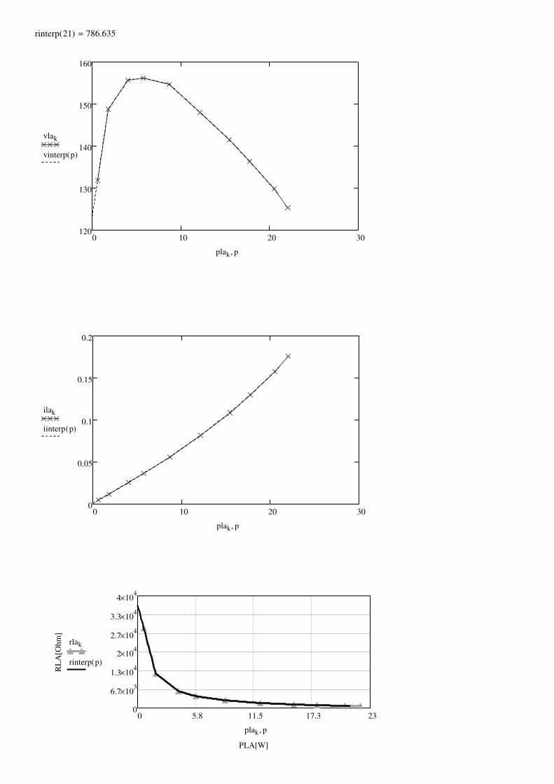
rinterp 21( ) 786.635=
0 10 20 30120
130
140
150
160
vlak
vinterp p( )
plak p,
0 10 20 300
0.05
0.1
0.15
0.2
ilak
iinterp p( )
plak p,
0 5.8 11.5 17.3 230
6.7 103
×
1.3 104
×
2 104
×
2.7 104
×
3.3 104
×
4 104
×
PLA[W]
RL
A[O
hm
]
rlak
rinterp p( )
plak p,
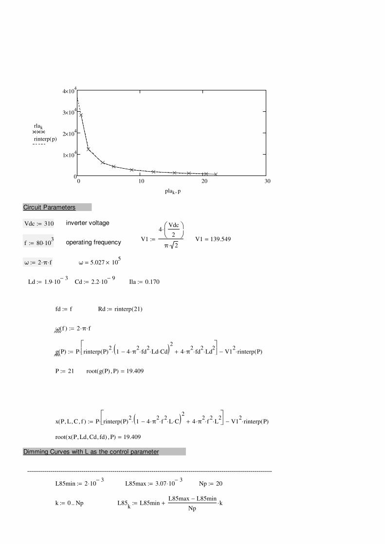
0 10 20 300
1 104
×
2 104
×
3 104
×
4 104
×
rlak
rinterp p( )
plak p,
Circuit Parameters
Vdc 310:= inverter voltage
V1
4Vdc
2
⋅
π 2⋅:= V1 139.549=
f 80 103
⋅:= operating frequency
ω 2 π⋅ f⋅:= ω 5.027 105
×=
Ld 1.9 103−
⋅:= Cd 2.2 109−
⋅:= Ila 0.170:=
fd f:= Rd rinterp 21( ):=
ω f( ) 2 π⋅ f⋅:=
g P( ) P rinterp P( )2
1 4 π2
⋅ fd2
⋅ Ld⋅ Cd⋅−( )2
⋅ 4 π2
⋅ fd2
⋅ Ld2
⋅+
⋅ V1
2rinterp P( )⋅−:=
P 21:= root g P( ) P, ( ) 19.409=
x P L, C, f, ( ) P rinterp P( )2
1 4 π2
⋅ f2
⋅ L⋅ C⋅−( )2
⋅ 4 π2
⋅ f2
⋅ L2
⋅+
⋅ V1
2rinterp P( )⋅−:=
root x P Ld, Cd, fd, ( ) P, ( ) 19.409=
Dimming Curves with L as the control parameter
------------------------------------------------------------------------------------------------------------------------------
L85min 2 103−
⋅:= L85max 3.07 103−
⋅:= Np 20:=
k 0 Np..:= L85k
L85minL85max L85min−
Npk⋅+:=
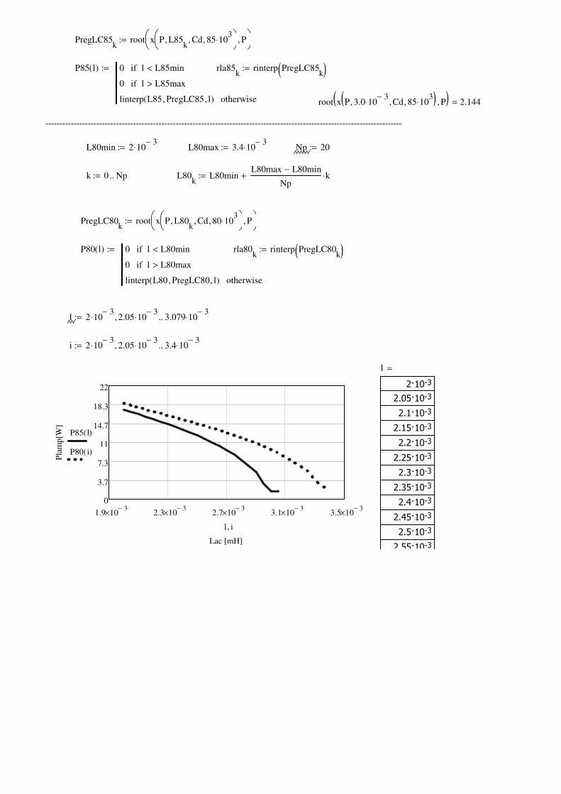
PregLC85k
root x P L85k
, Cd, 85 103
⋅,
P,
:=
P85 l( ) 0 l L85min<if
0 l L85max>if
linterp L85 PregLC85, l, ( ) otherwise
:= rla85k
rinterp PregLC85k( ):=
root x P 3.0 103−
⋅, Cd, 85 103
⋅, ( ) P, ( ) 2.144=
------------------------------------------------------------------------------------------------------------------------------
L80min 2 103−
⋅:= L80max 3.4 103−
⋅:= Np 20:=
k 0 Np..:= L80k
L80minL80max L80min−
Npk⋅+:=
PregLC80k
root x P L80k
, Cd, 80 103
⋅,
P,
:=
P80 l( ) 0 l L80min<if
0 l L80max>if
linterp L80 PregLC80, l, ( ) otherwise
:= rla80k
rinterp PregLC80k( ):=
l 2 103−
⋅ 2.05 103−
⋅, 3.079 103−
⋅..:=
i 2 103−
⋅ 2.05 103−
⋅, 3.4 103−
⋅..:=
l
-32·10
-32.05·10
-32.1·10
-32.15·10
-32.2·10
-32.25·10
-32.3·10
-32.35·10
-32.4·10
-32.45·10
-32.5·10
-32.55·10
=
1.9 103−
× 2.3 103−
× 2.7 103−
× 3.1 103−
× 3.5 103−
×
0
3.7
7.3
11
14.7
18.3
22
Lac [mH]
Pla
mp
[W]
P85 l( )
P80 i( )
l i,
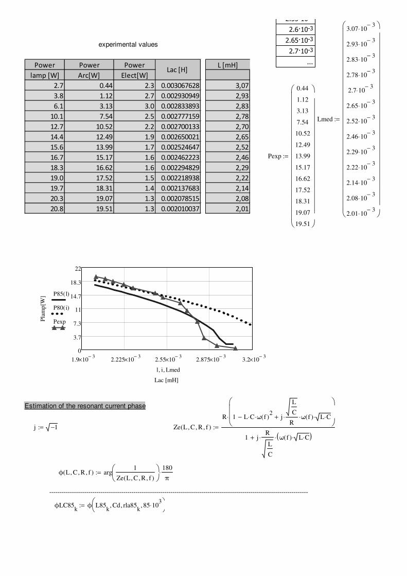
-32.55·10
-32.6·10
-32.65·10
-32.7·10
...
experimental values
Power Power Power
lamp [W] Arc[W] Elect[W]
2.7 0.44 2.3 0.003067628
3.8 1.12 2.7 0.002930949
6.1 3.13 3.0 0.002833893
10.1 7.54 2.5 0.002777159
12.7 10.52 2.2 0.002700133
14.4 12.49 1.9 0.002650021
15.6 13.99 1.7 0.002524647
16.7 15.17 1.6 0.002462223
18.3 16.62 1.6 0.002294829
19.0 17.52 1.5 0.002218938
19.7 18.31 1.4 0.002137683
20.3 19.07 1.3 0.002078515
20.8 19.51 1.3 0.002010037
Lac [H] L [mH]
3,07
2,93
2,83
2,78
2,70
2,65
2,52
2,46
2,29
2,22
2,14
2,08
2,01
Lmed
3.07 103−
⋅
2.93 103−
⋅
2.83 103−
⋅
2.78 103−
⋅
2.7 103−
⋅
2.65 103−
⋅
2.52 103−
⋅
2.46 103−
⋅
2.29 103−
⋅
2.22 103−
⋅
2.14 103−
⋅
2.08 103−
⋅
2.01 103−
⋅
:=
Pexp
0.44
1.12
3.13
7.54
10.52
12.49
13.99
15.17
16.62
17.52
18.31
19.07
19.51
:=
1.9 103−
× 2.225 103−
× 2.55 103−
× 2.875 103−
× 3.2 103−
×
0
3.7
7.3
11
14.7
18.3
22
Lac [mH]
Pla
mp
[W] P85 l( )
P80 i( )
Pexp
l i, Lmed,
Estimation of the resonant current phase
j 1−:= Ze L C, R, f, ( )
R 1 L C⋅ ω f( )2
⋅− j
L
C
R⋅ ω f( )⋅ L C⋅⋅+
⋅
1 jR
L
C
⋅ ω f( ) L C⋅⋅( )⋅+
:=
ϕ L C, R, f, ( ) arg1
Ze L C, R, f, ( )
180
π⋅:=
------------------------------------------------------------------------------------------------------------------------------
ϕLC85k
ϕ L85k
Cd, rla85k
, 85 103
⋅,
:=
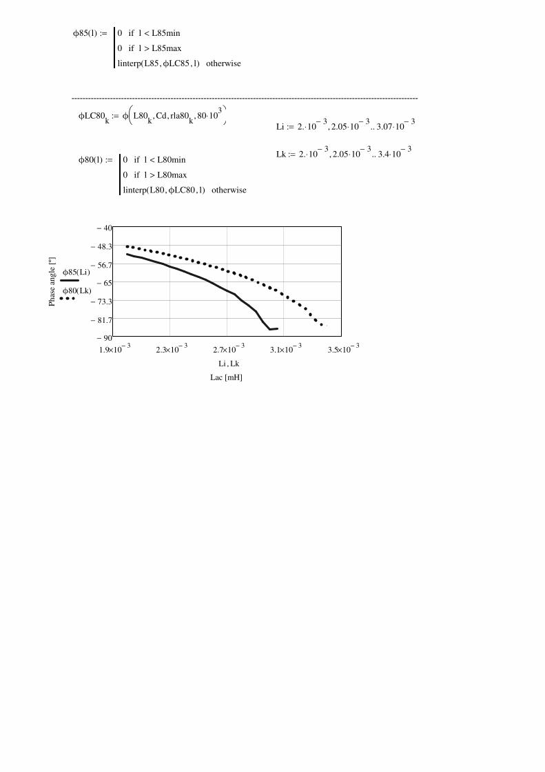
ϕ85 l( ) 0 l L85min<if
0 l L85max>if
linterp L85 ϕLC85, l, ( ) otherwise
:=
------------------------------------------------------------------------------------------------------------------------------
ϕLC80k
ϕ L80k
Cd, rla80k
, 80 103
⋅,
:=
Li 2. 103−
⋅ 2.05 103−
⋅, 3.07 103−
⋅..:=
Lk 2. 103−
⋅ 2.05 103−
⋅, 3.4 103−
⋅..:=ϕ80 l( ) 0 l L80min<if
0 l L80max>if
linterp L80 ϕLC80, l, ( ) otherwise
:=
1.9 103−
× 2.3 103−
× 2.7 103−
× 3.1 103−
× 3.5 103−
×
90−
81.7−
73.3−
65−
56.7−
48.3−
40−
Lac [mH]
Ph
ase
ang
le [
º]
ϕ85 Li( )
ϕ80 Lk( )
Li Lk,


