Embed Size (px)
Citation preview

www.elsevier.com/locate/jnoncrysol
Journal of Non-Crystalline Solids 352 (2006) 567–577
Mass transport in chalcogenide electrolyte films – materialsand applications
Michael N. Kozicki, Maria Mitkova *
Center for Solid State Electronics Research, Arizona State University, P.O. Box 6206, Tempe, AZ 85287-6206, USA
Available online 20 March 2006
Abstract
Certain metals can be added to thin films of chalcogenide glasses by photodissolution to create materials with unique morphology andproperties. When Ag is combined in this fashion with Ge–Se or Ge–S glasses, the resulting ternary contains a dispersed nanocrystallineAg2S(e) phase that has large quantities of mobile metal ions. The presence of these ions allows the ternaries to act as solid electrolytes. Ifan anode which has an oxidizable form of the ionic metal and an inert cathode are applied in contact with such a phase-separated elec-trolyte, an ion current can flow under an applied bias in excess of a few hundred millivolt. Electrons from the cathode reduce the excessmetal due to the ion flux and an electrodeposit forms on or in the electrolyte. Utilizing this effect, we developed programmable metal-lization cell (PMC) technology which offers new functionality for such materials. Based on mass transport driven by electrochemical pro-cesses, PMC technology may be applied in solid state electronics, integrated optics, microelectromechanical systems (MEMS), andmicrofluidics. This paper is a review of the unique materials aspects of thin film solid electrolytes formed by photodissolution of metalinto a chalcogenide base glass and the demonstrated applications of this technology.� 2006 Elsevier B.V. All rights reserved.
PACS: 61.43.Fs; 61.82.Rx; 66.10.Ed; 66.20.Dn
Keywords: Amorphous semiconductors
1. Introduction
Deposition electrochemistry has been an important partof the microelectronics industry for many years. For exam-ple, electroplating has been utilized in integrated circuitpackaging for decades and more recently in the processesused to make Cu wiring within the chips. Electrochemistrydeals with the relationship between electricity and chemicalchange. Electrons removed from atoms in the process ofoxidation create ions and these charged species are ableto move under the influence of an electric field in liquidor solid electrolytes. On receiving an electron, a displacedion is reduced and becomes an atom. In this situation,the net change brought about by electrochemistry is the
0022-3093/$ - see front matter � 2006 Elsevier B.V. All rights reserved.
doi:10.1016/j.jnoncrysol.2005.11.065
* Corresponding author. Tel.: +1 480 965 9481; fax: +1 480 965 8118.E-mail address: [email protected] (M. Mitkova).
redistribution of mass – the atoms are removed from onelocation and are deposited in another with ion transportin the electrolyte occurring in between. An ion current willonly occur in an electrolyte if an oxidizable electrode (theanode) is made positive with respect to an opposing elec-trode (the cathode) and sufficient bias is applied, typicallygreater than a few hundred millivolts [1]. The voltagethreshold effect is a result of the underlying electrochemis-try in that electrodeposition will only occur if the appliedvoltage is sufficient to overcome the chemical potential bar-rier at the electrode. The number of atoms moved anddeposited will correspond to the number of electrons thattake part in the process and these are supplied by the exter-nal circuit. The electrodeposited mass is therefore con-trolled by the total Faradaic charge (which takes part inthe electrochemical reaction) from the power supply [2].Each metal ion undergoing reduction is balanced bya metal atom becoming oxidized and this avoids the

568 M.N. Kozicki, M. Mitkova / Journal of Non-Crystalline Solids 352 (2006) 567–577
formation of an internal electric field due to the build up ofcharge which would ultimately cancel the applied field andstop the electrodeposition. Note that if the opposite elec-trode is electrochemically inert (not oxidizable), the electro-deposition process is reversible by much the same rules thatgovern growth except that we must reverse the polarity ofthe applied bias. When the electrodeposit is made positivewith respect to the original oxidizable electrode, it becomesthe new anode and will dissolve via oxidation. During thedissolution of the electrodeposit, the balance is maintainedby deposition of metal back onto the electrode where theexcess metal for the electrodeposition came from in the firstplace. Once the electrodeposit has been completely dis-solved, the process self-terminates. It is important to notethat it is the asymmetry of the structure that allows thedeposition/dissolution process to be cycled repeatedly.
The ability to redistribute metal mass within a structurein situ via the application of a voltage leads to a wide rangeof potential applications. Electrodeposition of a noblemetal such as Ag produces localized persistent but revers-
ible changes to materials parameters and these changescan be used to control system behavior. For example,deposition of mass can be used to decrease the resonant fre-quency of a vibrating element in a microelectromechanicalsystem (MEMS) [3]. The optical properties of the electro-deposits will obviously have a profound effect on the trans-mission and reflection of light and so optical switchesbecome a possibility using this technique [4]. Of course,electrical resistance will change radically when an electro-deposit with a resistivity in the tens of lX cm or lower isdeposited on or in a solid electrolyte which has a resistivitysome eight orders of magnitude higher; this leads to a myr-iad of applications in solid state electronics [5,6]. Finally,and perhaps most astonishingly, the morphology of a typ-ical electrodeposit leads to a large change in the wetting ofa surface, making it highly hydrophobic, and so the tech-nique could also be used in microvalves and other fluid/droplet control devices [7]. We have demonstrated all ofthese effects and summarize our results in this review toillustrate how new functionality of ionic glasses can beachieved using mass transport in solid electrolyte films.
2. Solid electrolyte structure
A variety of inorganic and organic materials canconduct ions to some extent but we typically focus in thecontext of electrochemical mass-transport devices on com-pounds of oxygen (O2), sulfur (S), and selenium (Se), prin-cipally because of their ability to withstand processing atelevated temperatures and high ion mobility at normaldevice operating temperatures. Combining these with cop-per (Cu) or silver (Ag) gives us binary electrolytes such asAg2S [8] or Cu2S [9]. Alternatively, we can react a transi-tion metal such as tungsten (W) with oxygen to form thetype of solid electrolyte that has been used in electrochro-mic devices [10]. Yet another approach is to combine chalc-ogens with other elements such as germanium to form a
base glass into which we can dissolve Cu or Ag. An exam-ple of a ternary electrolyte formed this way is Ag0.33-Ge0.20Se0.47 [11], which is essentially a glassy Ge-richbackbone mixed with an Ag2Se phase in the form of dis-persed nanoscale superionic regions. The distinctive nano-structure of this material and its sulfide counterpart leadsto a highly stable solid electrolyte that has high ion mobil-ity (as much as 10�3 cm2/V s) even though its resistivity isrelatively large (100 X cm or greater) [12]. The Ag–Ge–Seand Ag–Ge–S ternaries are of greatest interest to us inour work as they are easy to form as thin films on devicesand they exhibit good thermal stability in subsequent pro-cessing and during device operation. In our experience, theselenide electrolytes, which exhibit the highest ion mobility,are completely stable at processing temperatures up to200 �C and operating temperatures as high as 110 �Cwhereas the sulfide variants are capable of withstandingprocessing temperatures beyond 400 �C and will operateabove 150 �C without damage. The main drawbacks of sul-fide electrolytes is that the ion mobility is around a factorof 10 lower than that in the selenide ternaries and film stoi-chiometry is more difficult to control due to the high vaporpressure difference between Ge and S. Both these electro-lytes support fast electrodeposition growth rates and Agis relatively inert.
Extensive studies on the materials aspects of the ternarysystems of interest have been performed [13–15]. The nat-ure of glass formation was first established in theAg–Ge–Se glass system [13,14] and later investigated inAg–Ge–S glasses [15]. Using direct techniques such asmodulated differential scanning calorimetry (MDSC),Raman spectroscopy, and Mossbauer spectroscopy, itwas found that the materials are phase separated for thecase of chalcogen-rich ternaries in both systems and thatAg can replace a portion of Ge in Ge-rich compounds.
The amount of Ag that can be introduced into the chal-cogenide film due to photodissolution is larger than in thecase of bulk glasses and Ag incorporation is self-limiting[16]. We assume that the Ag concentration reaches satura-tion because of the limited number of free and under-coor-dinated Se atoms that are available for reaction with Ag toform the Ag2Se phase as described in [11].
Two approaches were used for the characterization ofthe diffusion products; (1) Raman spectroscopy, givinginformation about the evolution of the Ge-chalcogen back-bone following diffusion which remains amorphous, and(2) X-ray diffraction (XRD), to give information on theAg-containing products which turn out to be nanocrystal-line. In our studies of the Ag–Ge–Se system in bulk or thinfilm form, we have always found Ag chemically bonded.This fact has the important consequence that some Se isextracted from the initial Ge–Se backbone to react withthe diffused Ag. Thus, after chemical interaction theremaining chalcogenide glass backbone becomes Se defi-cient, yielding a Raman signature characteristic of Ge-richglass that is independent of the initial composition of thehost and its initial Raman scattering (Fig. 1). Following

100 200 300 400 500
0.0
20.0k
40.0k
60.0k
80.0k
100.0k
120.0k
Film resulting after photodiffusion
Ge40
Se60
Ge33
Se67
Ge30
Se70
Ge20
Se80
Inte
nsi
ty (
a.u
.)
Raman shift (cm-1)
Fig. 1. Raman spectra of undoped Ge–Se thin films of various compo-sitions and the spectrum of the material after Ag photodissolution.
20 30 50 60 70 80 90 100
2
4
6
8
10
(b)
(a)
` *
*
^
+
***++
***
No
rmal
ized
inte
nsi
ty (
a.u
.)
2 Theta (deg.)
20 30 40 50 60 700
50
100
150
200
(d)
(c)
(b)
(a)^
^
^
^
+
++
+
+
+
+
+
+
+
+
+
+
+
+++++
*
*
*
*
*
*
*
*
*
*
*
*
*
*
*
*
Inte
nsi
ty (
a.u
.)
2 Theta (Deg.)
40(a)
(b)
Fig. 2. XRD spectra of thin chalcogenide films photodiffused with Ag. (a)Initial host composition Ge20Se80 covered with Ag (a) and same film afterAg diffusion (b); * peaks of Ag; ^ peaks of aAg2Se; + peaks of bAg2Se. (b)Ge33Se67 doped with Ag and annealed at: (a) 85 �C for 15 min, (b) 85 �Cfor 120 min, (c) 150 �C for 15 min and (d) 150 �C for 120 min; * peaks ofAg8GeSe6; ^ peaks of aAg2Se; + peaks of bAg2Se.
M.N. Kozicki, M. Mitkova / Journal of Non-Crystalline Solids 352 (2006) 567–577 569
diffusion, the underlying molecular phase consists of face-sharing quasi one-dimensional ethane-like Ge2(Se1/2)6
chain fragments whose presence is manifested on theRaman spectra by the appearance of the mode at180 cm�1 [18] depicted in Fig. 1. The Raman spectrum ofthe resulting material shows a lower intensity ratio betweenthe modes at 180 cm�1 and the mode of the Ge-tetrahedralunits at 200 cm�1 compared to the intensity ratio of thesemodes for a Ge40Se60 glass film. This is an indication thatthe number of ethane-like units is lower than in Ge40Se60
glass. This is a result of the spontaneous reaction of Agwith some charged metastable states on the chalcogen[17] initiated by light illumination and with charged defectsoccurring at bond conversion [19]. The structure of the Ge–Se backbone formed after photodoping is depolymerized tosome extent due to the extraction of Se and formation ofcrystalline products. Because of this and the high stiffnessof the backbone, the organization of the photodiffusedglass does not change with low temperature annealing. Thisis different from the case of pure Ge–Se films [20] where thelocal stressed configurations with high free energy relaxthrough breaking the Ge–Ge bonds and the formation ofGe–Se corner-sharing units due to reaction with someSe–Se wrong bonds occurs.
The form in which Ag is included in the system wasinferred from XRD analysis since the diffusion productoccurs in a nanocrystalline form. XRD revealed a closedependence of the diffusion product composition on thecomposition of the host. Diffractions from both b-Ag2Se(orthorhombic) and a-Ag2Se (cubic) phases [21] wereobserved following diffusion of Ag in Ge20Se80 glass –Fig. 2(a), while in a more Ge-rich host, formation ofAg8GeSe6 takes place. An example of the Ag diffusionproducts for the case of a Ge33Se67 base glass is given inFig. 2(b). The unexpected presence of the high-temperaturecubic form of Ag2Se revealed by this study could be due tovolume restrictions as the Ag2Se forms during Ag photo-diffusion in the existing solid-state framework of the Ge–
Se backbone. The orthorhombic phase that is stable atroom temperature has a more loosely packed structurethan the cubic form and we suggest that the surroundinghosting glass restricts its expansion. Although a numberof floppy units are available in the initial structure of thehost, with the first inclusion of Ag and formation of Ag2Sethe structure becomes stiffer since it is depleted in selenium.So the internal space limitation acts in the same way as ele-vated pressure, stabilizing some clusters in the high-temper-ature cubic form of Ag2Se which has the closest packing.
One major part of our research on ternary solid electro-lytes addresses the issue of crystal size of the diffusion prod-ucts and how this factor depends on the hosting materialand on annealing at temperatures up to 150 �C. TheXRD spectra were taken at room temperature and theScherrer equation was used to estimate the particle sizeof the small crystals from the measured parameters of theirdiffraction peaks using the broadening at half the peakheight by

570 M.N. Kozicki, M. Mitkova / Journal of Non-Crystalline Solids 352 (2006) 567–577
t ¼ ð0:9kÞ=B cos h; ð1Þwhere t is crystallite size, k is X-ray wavelength, B is the fullwidth at half maximum of the peak, and h is the angle atfull width of half maximum. There is a clear tendency forthe nanocrystals to become larger with Ge content of thehost, becoming largest when the Ag is introduced into aGeSe2 glass, and subsequently decreasing in size for higherGe concentration. Fig. 3(a) and (b) illustrate the depen-dence of crystal size on composition and annealing condi-tions for Ge10.5Se42.3Ag47.2 and Ge22.1Se44.9Ag33 glasses.We suggest that this effect is related to the molecular clus-tering of the hosting glass. As noted by Feltz et al. [22] theevolution of molar volume with composition in GexSe1�x
system has a maximum at x = 0.33, i.e., for GeSe2 wherethe structure is less densified. The data collected by Fenget al. [23] confirm same structural evolution. Furthermore,there is evidence for the importance of the structural char-acteristics of the host and rigidity percolation in it [24].Although the lattice parameters of Ag2Se are smaller, in
Fig. 3. Size of different clusters found in annealed glasses with compo-sitions: (a) Ge10.5Se42.3Ag47.2 at the conditions shown in the figure. (b)Ge22.1Se44.9Ag33 at the conditions shown in the figure.
the cases when Ag8GeSe6 crystallizes in a more rigid back-bone its initial clusters are smaller than the Ag2Se clustersin a structure with a larger free volume and higher flexibil-ity of the host.
A final point of interest is the development of crystalgrowth at elevated temperatures. The conditions discussedin this work are relatively mild since our ultimate goal is todeduce information useful for the high-temperature pro-cessing of these materials. The extended anneal resultedin no observable change in the composition of the crystal-line products with time at the chosen temperatures. In thecase of the Ag2Se clusters, the crystalline phases are differ-ent from the surrounding material and we assume that theirgrowth is limited by atomic diffusion (to about 5–8% afterannealing), which is restricted due to the heterogeneouscharacter of the medium. In the case of formation ofAg8GeSe6 clusters, the growth is much more affected bythe annealing and their size changes by about 8–10%. Thissituation closely corresponds to homogeneous growth. Wesuggest that the adjacent clusters fuse with Ge atoms cross-linking the cluster edges and leading to formation of a com-mon structure combining the three elements.
We can estimate the distance, s, between the Ag2Se crys-tallites in the chalcogen-rich materials and therefore thethickness of Ge-rich material between them by assumingthat these regions are spherical and uniform in size and dis-persion, so that
s ¼ dðF �1=3v � 1Þ; ð2Þ
where d is the measured diameter of the crystalline Ag-richphase and Fv is the volume fraction of this phase. Since thevolume fraction of Ag2Se in Ag33Ge20Se47 is 0.57 (for amolar fraction of 0.63), the average spacing between theAg-rich regions is 0.2 times their diameter. So, for an aver-age Ag2Se crystallite diameter of 7.5 nm, we can expect anaverage separation of 1.5 nm. As we will see in Section 5 ofthis paper, this unique nanostructure is critical to the elec-trical characteristics of the electrolyte film. Here the ion-containing mixed conductor crystallites dominate the com-position and the films appear superionic, but the Ge-richmaterial in the interstices ensures that the film resistivityis relatively high.
3. Solid electrolyte formation
Our ternary electrolytes are typically formed in a twostep process in which a binary (Ge–Se or Ge–S) base glassis deposited first and then capped with a thin Ag film, thetwo layers being combined by photodissolution. The Gecontent of the binary ranges from 20 to 40 at.%, the exactchoice being dependent on the electrodeposit morphologyrequired (discussed later in this paper).
Photodiffusion from a thin surface film using ultravioletlight is a relatively simple way to add Ag to a binary baseglass at low temperature to form a uniform ternary electro-lyte in a highly controlled manner [25,26]. The process ofphotodissolution is driven by the formation of optically

0 10 20 30 400
20
40
60
80
100
O2
CSGe
Ag
Si
No
rm. i
nte
nsi
ty (
c/s
x eV
)
Sputtering time (min)
Fig. 4. AES determination of the relative change of the atomic concen-tration in Ge22S78:Ag after photoinduced diffusion; film profile on siliconsubstrate as a function of sputtering time.
M.N. Kozicki, M. Mitkova / Journal of Non-Crystalline Solids 352 (2006) 567–577 571
induced charged defects in the chalcogenide glass whichcreate an electric field. The light energy that drives thephotodissolution is absorbed at or near the interfacebetween the reacted and unreacted chalcogenide layer[27,28]. In this process, the holes are trapped by Ag, whileelectrons are shifted deeper into the chalcogenide film andtrapped there. The Ag species move in the doped chalcog-enides as positively charged ions [29,30]. The electric fieldformed by the negatively charged chalcogen atoms andpositively charged Ag+ ions is sufficient for them to over-come the energy barrier at the interface. So, the penetrationof the metal into the chalcogenide during photodoping isactually due to the difference in electrochemical potentials.We can consider the process to be similar to that occurringin a galvanic cell, in which case the more electropositivemetal is dissolved into the electrolyte due to an intercala-tion reaction [31,32]. The main reason that this reactionoccurs in chalcogenide glasses is that they possess relativelyrigid covalent bonds mixed with soft van der Waals inter-connections. This type of structure ensures the formationof voids and channels where the diffusing ions can migrateand be hosted.
The dissolution process described above results in theformation of bonds with the host matrix according to thereaction
C02 þ e� þAgþ ! C�1 Agþ ð3Þ
which describes the transition of an initially twofold cova-lently bonded chalcogenide atom (C0
2) into a C�1 chargedunit. This latter specie possesses only a single covalentbond and an excess electron that establishes an ionic bondwith the Ag+. The equation above shows the importance ofthe new C�1 Ag+ bonds in the intercalation product. Thepossible number of these bond-units is high as chalcogen-ide glasses are uniquely capable of forming a large numberof single C�1 centers under appropriate illumination. Thisnot only allows photodissolution to proceed so readilybut also results in the necessary structure for the solid elec-trolyte in which plentiful Ag+ ions are weakly held at alarge number of negatively charged chalcogen sites. Theions easily move from site to site under the influence ofan electric field and so the ion mobility is relatively high.
In our photodissolution process we typically use a UVsource wavelength of 405 nm and power density around5 mW/cm2 for a minimum of 10 min. The thickness ofAg film is kept to less than 25 nm to allow sufficient lightto penetrate to the interface to stimulate the photodissolu-tion process in a reasonable amount of time. Saturation ofthe base glass occurs when the diffusing Ag+ ions react withall available chalcogen atoms as discussed in the previoussection and so the concentration of Ag at saturation actu-ally depends on the amount of chalcogen in the base glass,reaching 47 at.% for a base glass with 80 at.% chalcogen[11]. Our data from Auger electron spectroscopy (AES)reveals that illumination using the minimum time causespenetration of the diffused Ag into the base glass to a depthof approximately 40 nm (see Fig. 4 for an example of a Ag
photodiffusion into a 50 nm thick film). If the photodisso-lution time is long (>10 min) so that the photodissolutionprocess is driven to completion, a 20 nm thick Ag film willcompletely saturate a 50 nm thick film of base glass, leav-ing an extremely thin and typically discontinuous metallicAg film on the surface which can be removed usingFe(NO3)3 solution. To avoid the excess Ag etching step,a thicker base glass film (e.g., 80 nm) could be used witha 15–20 nm silver film so that all Ag is driven from the sur-face but the entire film thickness would not be silver satu-rated in this case.
4. Electrochemical processes
As can be seen from the discussion on the nature of theelectrolyte above, only the positively charged ions are ableto move and the negative charge centers are fixed in theelectrolyte. This means that a charge imbalance (and asso-ciated electric field) will arise if reduced ions are notreplaced by the oxidation of metal at the anode whichunderscores the need for oxidizable metal at this electrode.Electrodeposition also requires an applied bias above aparticular threshold to overcome the effects of the cathodicbarrier. The intrinsic potential difference necessary to dothis is typically only a few hundred millivolt and this mustbe dropped across the polarized double layer at the cath-ode. The specific resistance of the polarized region is inthe order of 1010 X lm2 [1].
The ions nearest the electron-supplying cathode will bereduced first. Statistical non-uniformities in the ion concen-tration and in the topography of the electrode will tend topromote localized deposition or nucleation rather thanblanket plating on the cathode. However, even if multiplenuclei are formed, the one with the highest field and bestion supply will be favored for subsequent growth, extend-ing out from the cathode as a single metallic feature. The

Fig. 5. Atomic force microscope (AFM) analysis (3D topographical scan)of Ag electrodeposit grown on (a) Ag-saturated Ge20Se80. The growth iscontinuous and the maximum electrodeposit height is a few tens ofnanometer; (b) Ag-saturated Ge40Se60. The growth appears discontinuousand the maximum electrodeposit height is in the order of 100 nm.
572 M.N. Kozicki, M. Mitkova / Journal of Non-Crystalline Solids 352 (2006) 567–577
electrodeposition of metal on the cathode does not meanthat ions entering from the oxidizable anode have to travelthe entire length of the structure to replace those that arereduced. The ion closest to the reduced ion will move tothe vacated negative site on the hosting material and thoseupstream will do likewise, each filling the vacated site of theone downstream, until the last vacated space closest to theanode is filled by the incoming ion. So the ion current isactually a ripple effect, known in electrochemistry as acoordinated motion. Since the electrodeposit is physicallyconnected to the cathode, it can supply electrons for subse-quent ion reduction. So the growing electrodeposit willharvest ions from the electrolyte, plating them onto its sur-face to extend itself outwards from the cathode. This canlead to electrodeposits that are several hundred micronsin length. Since each ion deposited on the growing electro-deposit corresponds to one that has been removed from themetal source, the net effect is a shift of mass from the anodeto the cathode, even though in the initial stages, the electro-deposit is actually made up of reduced ions from the elec-trolyte itself.
Interestingly, even though we strive to create electrolyteswith the highest possible ion mobilities, it frequently is notthe mobility that is the growth rate limiting process. Thegrowth occurs at the cathode double layer and this is typ-ically only a few tens of nanometer wide so a few hundredmillivolt will create a field of 105 V/cm. This leads to aneffective ion velocity of 1 m/s if the mobility is 10�3 cm2/V s. We can expect the ions to arrive at the growing electro-deposit from the surrounding electrolyte at this rate, add-ing to it to propel its growth forward at a considerablevelocity. Clearly, a higher applied voltage would drivemore current and this would increase the growth rate butthere is the danger of exceeding the breakdown voltageof the surrounding dielectric (as well as transcending prac-tical operating limits of the system) if we go too high. Thekey is therefore to balance factors such as device dimen-sions and electrodeposit mass/volume with operationalrequirements such as speed and control voltage.
The general nature of the morphology of the electrode-posits that form on the surface of the solid electrolytescorresponds to those reported for diffusion-controlled pro-cesses such as diffusion-limited aggregation (DLA) [2].However, we were the first to note that the compositionof the solid electrolyte had a profound effect on the mor-phology of these deposits [4]. It is likely that the nucleationpoints from which the electrodeposits grow are related tothe presence of excess Ag ions on the electrolyte surfaceas the free energy for electrodeposit formation in theseregions will be lowest. In the case of Ge20Se80 glasses, theglass structure is floppy [33] and the illumination with lightwill likely cause considerable depolymerization of the Sechains [27]. As a result, a number of randomly distributedcharge defects can occur with which the photodiffused Agreacts to form substantial Ag2Se regions which act as nucleifor the formation of electrodeposits. This, coupled with thehigh Ag content of these films, is the reason that we
observe a great number of distributed Ag electrodepositswith microscale to nanoscale dimensions covering the sur-face of the films, as shown in the atomic force microscopeimage of Fig. 5(a). In the case of the Ge-rich glasses(Ge40Se60), we assume that Ag-containing units that serveas nucleation centers exist in the volume and surface ofthe film as three component structural units, similar tothose present in bulk material [13] in which Ag replacesGe in the building blocks with distorted rock salt structure.The occurrence of similar exchange reaction that formsAg-containing three component structural units followingAg diffusion has been observed in As2S3 films [34]. The for-mation of this structure will lead to regions of material thathave significantly different conductivity [35]. The result isgrowth of ‘isolated’ much larger electrodeposits [4] as illus-trated in Fig. 5(b).
5. Applications of mass transport in solid electrolytes
5.1. Patterning of the electrolyte
We have described the materials characteristics and for-mation techniques for the solid electrolytes in the previoussections but in order to apply them to devices and systems,they must be able to be patterned. Fortunately, a numberof options exist for the patterning of the electrolyte layer.
M.N. Kozicki, M. Mitkova / Journal of Non-Crystalline Solids 352 (2006) 567–577 573
The simplest method is lift-off, in which the photoresist isspun-on, exposed using an optical printer/aligner, anddeveloped prior to electrolyte deposition so that subsequentsolvent removal of the resist leaves only the electrolyte inthe developed regions. The other subtractive alternative isto pattern the resist after base glass/silver deposition anduse wet chemical or dry etching to remove the areas notcovered by resist. This should be done prior to photodisso-lution as it is easier to etch the bilayer than the ternary. Forexample, in wet etching, the Ag layer can be etched withFe(NO3)3 while the base glass will be etched with basicsolutions in which the pH is adjusted using phosphates aspointed out in [5,36]. In the case of dry etching, a physicaletch with Ar+ or CFþ3 can sputter away the thin silver and aCF4/O2 chemical etch will remove the base glass – bothmay be performed in a reactive ion etch system. The thirdalternative is to use the photodissolution step itself todefine the pattern in the electrolyte and remove the unex-posed regions using wet or dry chemistry, the ternary beingrelatively insoluble in the etchants used to remove thebilayer [37]. The main advantage of this latter approachis that no photoresist is required.
Two major categories of solid electrolyte devices havebeen investigated – lateral and vertical structures. In thelateral structures, the electrodes are coplanar on the surfaceof the electrolyte and the electrodeposit forms betweenthem on the surface of the film. For the vertical devices,the thin film of electrolyte is placed between the electrodesso that the electrodeposition is forced to occur within theglass. As we will see later in this section, the lateral arrange-ment is utilized when large electrodeposits are required toalter the physical properties of a surface, whereas the verti-cal structure is best suited to fast electrical switching as thedistance between the electrodes is governed by the electro-lyte film thickness and this can be in the order of tens ofnanometer or less.
5.2. Solid state memory
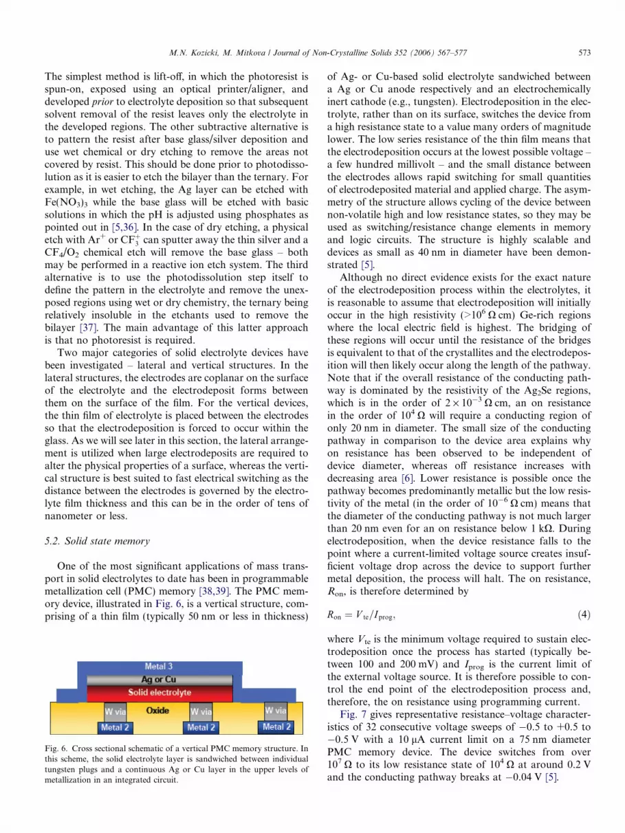
One of the most significant applications of mass trans-port in solid electrolytes to date has been in programmablemetallization cell (PMC) memory [38,39]. The PMC mem-ory device, illustrated in Fig. 6, is a vertical structure, com-prising of a thin film (typically 50 nm or less in thickness)
Fig. 6. Cross sectional schematic of a vertical PMC memory structure. Inthis scheme, the solid electrolyte layer is sandwiched between individualtungsten plugs and a continuous Ag or Cu layer in the upper levels ofmetallization in an integrated circuit.
of Ag- or Cu-based solid electrolyte sandwiched betweena Ag or Cu anode respectively and an electrochemicallyinert cathode (e.g., tungsten). Electrodeposition in the elec-trolyte, rather than on its surface, switches the device froma high resistance state to a value many orders of magnitudelower. The low series resistance of the thin film means thatthe electrodeposition occurs at the lowest possible voltage –a few hundred millivolt – and the small distance betweenthe electrodes allows rapid switching for small quantitiesof electrodeposited material and applied charge. The asym-metry of the structure allows cycling of the device betweennon-volatile high and low resistance states, so they may beused as switching/resistance change elements in memoryand logic circuits. The structure is highly scalable anddevices as small as 40 nm in diameter have been demon-strated [5].
Although no direct evidence exists for the exact natureof the electrodeposition process within the electrolytes, itis reasonable to assume that electrodeposition will initiallyoccur in the high resistivity (>106 X cm) Ge-rich regionswhere the local electric field is highest. The bridging ofthese regions will occur until the resistance of the bridgesis equivalent to that of the crystallites and the electrodepos-ition will then likely occur along the length of the pathway.Note that if the overall resistance of the conducting path-way is dominated by the resistivity of the Ag2Se regions,which is in the order of 2 · 10�3 X cm, an on resistancein the order of 104 X will require a conducting region ofonly 20 nm in diameter. The small size of the conductingpathway in comparison to the device area explains whyon resistance has been observed to be independent ofdevice diameter, whereas off resistance increases withdecreasing area [6]. Lower resistance is possible once thepathway becomes predominantly metallic but the low resis-tivity of the metal (in the order of 10�6 X cm) means thatthe diameter of the conducting pathway is not much largerthan 20 nm even for an on resistance below 1 kX. Duringelectrodeposition, when the device resistance falls to thepoint where a current-limited voltage source creates insuf-ficient voltage drop across the device to support furthermetal deposition, the process will halt. The on resistance,Ron, is therefore determined by
Ron ¼ V te=Iprog; ð4Þ
where Vte is the minimum voltage required to sustain elec-trodeposition once the process has started (typically be-tween 100 and 200 mV) and Iprog is the current limit ofthe external voltage source. It is therefore possible to con-trol the end point of the electrodeposition process and,therefore, the on resistance using programming current.
Fig. 7 gives representative resistance–voltage character-istics of 32 consecutive voltage sweeps of �0.5 to +0.5 to�0.5 V with a 10 lA current limit on a 75 nm diameterPMC memory device. The device switches from over107 X to its low resistance state of 104 X at around 0.2 Vand the conducting pathway breaks at �0.04 V [5].

Fig. 7. Resistance–voltage plot from a 75 nm Ag–Ge–Se device using 32voltage sweeps of �0.5 to +0.5 to �0.5 V with a 10 lA current limit. Thedevice switches from over 107 X to its low resistance state of 104 X around0.2 V and the conducting pathway breaks at �0.04 V.
0
5
10
15
20
25
30
35
40
0 4 8 10 12 14 16 18 20 22
Length (m)
Res
ista
nce
(Ω
)
2 6
Fig. 8. Programmed resistance vs. length (10 lm wide) for a 25 mAcurrent limit; different symbols represent data from different devicesamples.
574 M.N. Kozicki, M. Mitkova / Journal of Non-Crystalline Solids 352 (2006) 567–577
5.3. Programmable wiring
Silver electrodeposition can vastly alter the electricalresistance of the surface of a structure. Given the eightorders of magnitude difference in resistivity between theelectrolyte and thin film metallic Ag, it is possible to createwiring on regions that are initially essentially non-conduct-ing. We performed such a study early in our research intothis technique [40] and the results are briefly summarizedhere. This work involved a 50 nm thick Ag-doped sulfideelectrolyte on a thick oxide layer on silicon substrates, pat-terned into channels with large Ag contacts (100 · 100 lm)at the ends. The ‘off’ resistance, Roff, was a geometric func-tion of the channel dimensions, following:
Roff ¼ qL=dW þ Rp; ð5Þwhere q is the resistivity of the layer (in the mid 102 X cmrange) and d the thickness of the chalcogenide, L is thechannel’s length, W is the channel’s width and Rp is theeffective resistance at zero channel length and is mainlydue to electrode polarization (in the 108 to the low 109 Xrange for the electrode configuration used). A 10 · 10 lmdevice therefore exhibited an Roff around 1.5 GX. Fig. 8shows the results from a number of 10 lm wide devicesfor programming, using a 5 s voltage sweep from 0.5 to1.8 V with a 25 mA current limit. This produces a substan-tial surface electrodeposit with a resistance of around 1 X/lm of device length. The average contact resistance in thiscase is around 9 X.
5.4. Resonant frequency alteration
In situ frequency control of high Q microelectromechan-ical resonators is desirable as it is difficult to make struc-tures that have an accurately defined and maintainableresonant frequency due to nanoscale material/processingirregularities and environmental factors (oxidation, con-
densation, etc.). We have demonstrated a tunable MEMSresonator using our electrolyte-electrodeposit system [3],shown schematically in Fig. 9(a). The resonator testbed isactually a set of 1 lm thick suspended polycrystalline sili-con beams, ranging from 50 to 200 lm in length, with an80 nm thick film of Ag–Ge–Se (sub-saturated) electrolyteon their top surface. A silver electrode is formed at oneend and both ends have aluminum pads added to facilitatebonding/packaging for electrical characterization. Theelectrodeposit is made to form on the beam to change bothits vibrating mass and stiffness. For testing, the packageddevices were placed on a piezoelectric chuck and their res-onant frequency and Q-factor measured with the aid of alaser vibrometer before and after electrodeposition at1.5 V. The results for a 150 lm long beam with a resonantfrequency of 343 kHz are shown in Fig. 9(b) and indicate afrequency change of �3.27%, with an accompanying reduc-tion in Q-factor from 3300 to 1600 due to damping, for theelectrodeposition conditions used.
5.5. Control of surface wetting/valving
We have demonstrated that surface electrodepositioncan be used to control wetting, increasing water contactangle by over 20�, and that this in turn can be used to reg-ulate fluid flow through microchannels [7,41]. We fabri-cated a microvalve testbed by etching a 200 lm wide20 lm deep microchannel with inlet and outlet reservoirsin silicon substrates as shown in Fig. 10(a). The channelwas coated with a 50 nm thick Ag–Ge–Se solid electrolyteand Ag and Ni electrodes placed at a point between the res-ervoirs. A 10 V bias was sufficient to produce extendedelectrodeposit growth across the channel between the elec-trodes, as shown in Fig. 10(b), which is a scanning electron

Fig. 9. (a) Schematic of a single suspended beam test structure; (b) effect of electrodeposition on resonant frequency and Q-factor for a 150 lm long beamfollowing 1.5 V bias for 13 min (the inset is an electron micrograph of the structure following electrodeposition).
Fig. 10. (a) Schematic of testbed showing ‘microvalve’ between control electrodes; (b) scanning electron micrograph of electrodeposit on channel floor andwall. The bright features are the Ag electrodeposits; (c) demonstration of valving of pressure-driven flow in a microchannel. Top micrograph is the openvalve after 6 s of flow and the bottom micrograph the inhibited valve after 35 s of flow in the valve region (6 s delay from inlet to valve edge in both cases).The arrows mark the position of the fluid front.
M.N. Kozicki, M. Mitkova / Journal of Non-Crystalline Solids 352 (2006) 567–577 575
micrograph of an electrodeposit on the channel floor andwall. The bright features are the Ag electrodeposits andthe sloping wall of the channel is due to the anisotropicetch. The electrodeposited Ag, which has a high surfacearea fractal structure less than 1 lm high, changes thefluid–surface interaction since fluid flow in a microchannelis dominated by the nature of the channel surface. Thisincrease in effective hydrophobicity can be used to controlthe movement of the fluid. Fig. 10(c) illustrates pressuredriven DI water flow for open (no electrodeposit) and
inhibited (electrodeposit grown) valves 6 s after the fluidenters the valve region (12 s total flow time in the channel).As may be seen by the position of the markers (arrow), theflow has progressed to the outlet end of the valve in thistime and continues to flow, eventually filling the reservoir.In the inhibited valve case, in which the electrodeposit hasbeen grown across the channel using the conditionsdescribed above, after 6 s of flow in the channel from theinlet, the fluid front stops abruptly at the front edge ofthe valve region, demonstrating valving action.

Fig. 11. (a) Clear 50 lm wide (between the light-colored metal electrodes)element prior to application of bias; (b) dendritic Ag electrodeposit grownin element which reflects about 20% of incident light; (c) broadelectrodeposit, which reflects about 60% of incident light.
576 M.N. Kozicki, M. Mitkova / Journal of Non-Crystalline Solids 352 (2006) 567–577
5.6. Alteration of reflectance
Surface electrodeposition can be used to alter the reflec-tance of a surface as the optical properties of the metal areobviously radically different from those of the electrolytefilm. To demonstrate this, we created solid electrolyte(50 nm thick Ag–Ge–Se) patterns on thick oxide grownon silicon wafers, with wide electrodes at either end (Agand Ni). Before the application of a bias, the light is ableto pass through the thin film to be reflected by the substratewith little impediment, as shown in Fig. 11(a). After theelectrodeposit has been formed, the light is blocked/reflected from the grown metallic surface. Two examplesare given in Fig. 11(b) and (c) for 20% and 60% coveragerespectively [42]. These elements can be potentially usedas optical switches.
6. Conclusions
We have shown that the addition of a metal such as Agto a thin film of germanium chalcogenide base glass byphotodissolution creates a nano-phase separated materialwith unique and useful characteristics. The ternariesformed by photodissolution of metal from a surface filmare solid electrolytes, by virtue of the presence of a dis-persed superionic nanocrystalline phase, that are stableover a wide range of operating temperatures. These mate-rials can be used to transfer mass by oxidation of a metalsource and reduction of the metal ions at a supply of elec-trons and that this effect leads to new functionality of theglasses. We have demonstrated several of these new func-tions, the most significant being solid state non-volatilememory elements that switch rapidly at very low voltage
and current between widely spaced resistance states andpossess excellent cycling characteristics. We have alsoshown the utility of the technique in ‘programmable’ wiringin integrated circuits, the tuning of microelectromechanicalresonators, the control of fluid flow in microchannels, andthe control of light transmission/reflection in opticalelements. Such diversity of applications suggests that thesematerials could very well play a large part in a wide range offuture technologies and are therefore deserving of conti-nued study.
Acknowledgements
This work was sponsored by Axon Technologies Corp.The authors would like to acknowledge the invaluable con-tributions of J. Aberouette, P. Maroufkhani, M. Park,C. Gopalan, M. Balakrishnan, T.L. Alford and H.C.Kim to the experimental research described in this review.
References
[1] W.C. West, K. Sieradzki, B. Kardynal, M.N. Kozicki, J. Electro-chem. Soc. 145 (1998) 2971.
[2] S.R. Forrest, T.A. Witten Jr., J. Phys. A 12 (1972) L109.[3] S. Enderling, C.L. Brown III, M. Balakrishnan, J. Hedley, J.T.M.
Stevenson, S. Bond, C.C. Dunare, A.J. Harris, J.S. Burdess, M.Mitkova, M.N. Kozicki, A.J. Walton, Technical Digest of the 18thIEEE Conference on Micro Electro Mechanical Systems (MEMS2005), 2005, p. 159.
[4] M.N. Kozicki, M. Mitkova, J.P. Aberouette, Physica E 19 (2003) 161.[5] M.N. Kozicki, M. Park, M. Mitkova, IEEE Trans. Nanotechnol. 4
(2005) 331.[6] R. Symanczyk, M. Balakrishnan, C. Gopalan, T. Happ, M. Kozicki,
M. Kund, T. Mikolajick, M. Mitkova, M. Park, C. Pinnow, J.Robertson, K. Ufert, in: Proceedings of the Non-Volatile MemoryTechnology Symposium, San Diego, CA, November 2003, p. 17.
[7] M.N. Kozicki, P. Maroufkhani, M. Mitkova, Superlattices Microstr.34 (2004) 467.
[8] K. Terabe, T. Hasegawa, T. Nakayama, M. Aono, Nature 433 (2005)47.
[9] T. Sakamoto, H. Sunamura, H. Kawaura, T. Hasegawa, T. Nakay-ama, M. Aono, Appl. Phys. Lett. 82 (2003) 3032.
[10] A. Antonaia, M.C. Santoro, G. Fameli, T. Polichetti, Thin SolidFilms 426 (2003) 281.
[11] M.N. Kozicki, M. Mitkova, J. Zhu, M. Park, Microelectron. Eng. 63(2002) 155.
[12] T. Kawaguchi, S. Maruno, S.R. Elliott, J. Appl. Phys. 79 (1996) 9096.[13] M. Mitkova, Y. Wang, P. Boolchand, Phys. Rev. Lett. 83 (1999)
3848.[14] Y. Wang, M. Mitkova, D.G. Georgiev, S. Mamedov, P. Boolchand,
J. Phys.: Condens. Matter 15 (2003) S1573.[15] P. Boolchand, F. Wang, U. Vempati, M. Mitkova, M. Kozicki, Bull.
Am. Phys. Soc. 49 (2004) 826.[16] T. Kawaguchi, S. Maruno, J. Appl. Phys. 71 (1992) 2195.[17] K. Shimakawa, A. Kolobov, S.R. Elliott, Adv. Phys. 44 (1995) 475.[18] P. Boolchand, in: P. Boolchand (Ed.), Insulating, Semiconducting
Glasses, World Scientific, 2000, p. 214.[19] N.V. Bondar, N.A. Davydova, V.V. Tishchenko, M. Vlcek, J. Mol.
Struct. 555 (2000) 175.[20] Y. Wang, K. Tanaka, T. Nakaokan, K. Murase, J. Non-Cryst. Solids
299–302 (2002) 963.[21] M. Mitkova, M.N. Kozicki, J. Non-Cryst. Solids 299–302 (2002)
1023.[22] A. Feltz, H. Aust, A. Pelyer, J. Non-Cryst. Solids 55 (1983) 190.

M.N. Kozicki, M. Mitkova / Journal of Non-Crystalline Solids 352 (2006) 567–577 577
[23] X. Feng, W.J. Bresser, P. Boolchand, Phys. Rev. Lett. 78 (1997) 4422.[24] P. Boolchand, D.G. Georgiev, T. Qu, F. Wang, L. Cai, S. Chakrav-
arty, C. R. Chimie 5 (2002) 713.[25] N.A. Davydova, V.V. Tishchenko, J. Baran, M. Vlchek, J. Mol.
Struct. 450 (1998) 117.[26] T. Wagner, A. Mackova, V. Perina, E. Rauhala, A. Seppala, S.O.
Kasap, M. Frumar, Mir. Vlcek, Mil. Vlcek, J. Non-Cryst. Solids 299(2002) 1028.
[27] A.V. Kolobov, S.R. Elliott, Adv. Phys. 40 (1991) 625.[28] J.H.S. Rennie, S.R. Elliott, J. Non-Cryst. Solids 97&98 (1987) 1239.[29] A.V. Kolobov, S.R. Elliott, M.A. Taguirdzhanov, Philos. Mag. B 61
(1990) 857.[30] I.Z. Indutni, V.A. Danko, A.A. Kudryavtsev, E.V. Michailovskaya,
V.I. Minko, J. Non-Cryst. Solids 185 (1995) 176.[31] G. Kluge, Phys. Status Solidi (a) 101 (1987) 105.[32] A.V. Kolobov, G.E. Bedel’baeva, Philos. Mag. B 64 (1991) 21.[33] P. Boolchand, W. Bresser, Philos. Mag. B 80 (2000) 1757.
[34] J. Fick, B. Nicolas, C. Rivero, K. Elshot, R. Irwin, K.A. Richardson,M. Fisher, R. Vallee, Thin Solid Films 418 (2002) 215.
[35] T. Akai, S.W. Martin, F. Borsa, Phys. Rev. B 63 (2001). Art. No.024303.
[36] M.N. Kozicki, C. Gopalan, M. Balakrishnan, M. Park, M. Mitkova,in: Non-Volatile Memory Technology Symposium Orlando, FLUSA, 15–19 November 2004.
[37] M.N. Kozicki, S.W. Hsia, A.E. Owen, P.J.S. Ewen, J. Non-Cryst.Solids 137&138 (1991) 1341.
[38] M.N. Kozicki, US Patent 6,469,364, 2002.[39] M.N. Kozicki, M. Mitkova, US Patent 6,635,914, 2003.[40] M.N. Kozicki, M. Yun, L. Hilt, A. Singh, in: E.D. Wachsman et al.
(Eds.), Proceedings of the 1999 Symposium on Solid State IonicDevices, The Electrochemical Society, 1999, p. 1.
[41] M.N. Kozicki, P. Maroufkhani, M. Mitkova, in: Proceedings ofNanotech 2005, NSTI, Anaheim, CA, May 2005.
[42] J.P. Aberouette, Masters thesis, Arizona State University, 2002.


