Embed Size (px)
Citation preview

Citation: Wang, H.; Gao, S.; Kang, R.;
Guo, X.; Li, H. Mechanical
Load-Induced Atomic-Scale
Deformation Evolution and
Mechanism of SiC Polytypes Using
Molecular Dynamics Simulation.
Nanomaterials 2022, 12, 2489.
https://doi.org/10.3390/
nano12142489
Academic Editor: Jun Shimizu
Received: 6 July 2022
Accepted: 19 July 2022
Published: 20 July 2022
Publisher’s Note: MDPI stays neutral
with regard to jurisdictional claims in
published maps and institutional affil-
iations.
Copyright: © 2022 by the authors.
Licensee MDPI, Basel, Switzerland.
This article is an open access article
distributed under the terms and
conditions of the Creative Commons
Attribution (CC BY) license (https://
creativecommons.org/licenses/by/
4.0/).
nanomaterials
Article
Mechanical Load-Induced Atomic-Scale Deformation Evolutionand Mechanism of SiC Polytypes Using MolecularDynamics SimulationHaoxiang Wang, Shang Gao *, Renke Kang, Xiaoguang Guo and Honggang Li
Key Laboratory for Precision and Non-Traditional Machining Technology of Ministry of Education,Dalian University of Technology, Dalian 116024, China; [email protected] (H.W.);[email protected] (R.K.); [email protected] (X.G.); [email protected] (H.L.)* Correspondence: [email protected]; Tel.: +86-151-0408-8992
Abstract: Silicon carbide (SiC) is a promising semiconductor material for making high-performancepower electronics with higher withstand voltage and lower loss. The development of cost-effectivemachining technology for fabricating SiC wafers requires a complete understanding of the deforma-tion and removal mechanism. In this study, molecular dynamics (MD) simulations were carried outto investigate the origins of the differences in elastic–plastic deformation characteristics of the SiCpolytypes, including 3C-SiC, 4H-SiC and 6H-SiC, during nanoindentation. The atomic structures,pair correlation function and dislocation distribution during nanoindentation were extracted andanalyzed. The main factors that cause elastic–plastic deformation have been revealed. The simulationresults show that the deformation mechanisms of SiC polytypes are all dominated by amorphousphase transformation and dislocation behaviors. Most of the amorphous atoms recovered aftercompleted unload. Dislocation analysis shows that the dislocations of 3C-SiC are mainly perfectdislocations during loading, while the perfect dislocations in 4H-SiC and 6H-SiC are relatively few.In addition, 4H-SiC also formed two types of stacking faults.
Keywords: silicon carbide; molecular dynamics simulations; deformation mechanism; amorphousphase transformation; dislocation; stacking faults
1. Introduction
Silicon carbide (SiC) is a typical representative of the wide band-gap semiconductormaterial, which is also known as a third-generation semiconductor material. It has a highbreakdown electric field, high thermal conductivity, high saturation electron velocity, andhigh radiation resistance [1–3]. It is an important material for substrate and epitaxial inwafers. In addition, SiC also has a wide application prospect in the fields of optical mirrorsand biomedical devices [4,5]. At present, more than 250 kinds of SiC polytypes have beenfound, of which 3C-SiC, 4H-SiC, and 6H-SiC are the most widely used. The stackingsequence of the tetrahedrally bonded Si–C bilayers for 3C-SiC, 4H-SiC, and 6H-SiC areABC/ABC . . . , ABCB/ABCB . . . , and ABCACB/ABCACB . . . , respectively. The differentstacking sequence leads to different mechanical properties of SiC polytypes, which deter-mine various application situations. To ensure the reliability, durability, and performanceof SiC wafer or components, low surface roughness and low subsurface damage depthin nano-scale are necessary, which can be realized by ultra-precision machining, such asgrinding, lapping, and polishing [6,7]. Therefore, it is of great significance to deeply studythe elastic–plastic deformation mechanism of SiC single crystal in nano-scale.
Nanoindentation test is an important method to study the mechanical propertiesand deformation mechanism in nano-scale and has been widely used in brittle materials.Zhao et al. [8] researched the initial plastic deformation of 3C-SiC at room temperatureunder contact load by nanoindentation test and transmission electron microscope (TEM).
Nanomaterials 2022, 12, 2489. https://doi.org/10.3390/nano12142489 https://www.mdpi.com/journal/nanomaterials

Nanomaterials 2022, 12, 2489 2 of 14
Goel et al. [9] studied the nanomechanical response of 4H-SiC through a quasi-staticnanoindentation test, and the critical shear stress of elastic–plastic transition is about21 GPa. Pan et al. [10] compared the critical load of elastic–plastic transition between C-faceand Si-face in 6H-SiC. The results showed that the elastic–plastic transformation thresholdof the Si-face was lower. The above studies show that there are great differences in themechanical properties of SiC polytypes. However, the internal mechanism has not beenrevealed due to the limitations of the experimental scale and the observation accuracy ofin-situ TEM technology. The experimental observation results have difficulty ensuringthe reliability of the deformation mechanism at the nano-scale. Therefore, it is of vitalimportance to deeply explore the atomic-scale deformation mechanism of SiC polytypes.
Molecular dynamics (MD) can simulate the trajectory and interaction of all atomsin the model, so it can deeply reveal the deformation mechanism of SiC. Sun et al. [11]used MD simulation to research the formation mechanism of prismatic dislocation ringson (111) and (110) planes of 3C-SiC during nanoindentation. Zhu et al. [12] used the MDmethod to simulate the deformation of the diamond indenter during 3C-SiC indentation.Zhu et al. [13] also carried out the MD simulation of nanoindentation for 4H-SiC. Theyfound the structural phase transition to 3C-SiC and declared that the plastic deformationof 4H-SiC is affected by amorphization, dislocation glide and propagation, and stackingfault. Tian et al. [14] compared the nanoindentation characteristics of 4H-SiC and 6H-SiCon C-face and Si-face by MD simulation and experiment. The results show that the defor-mation mechanisms of 4H-SiC and 6H-SiC are almost the same. The hexagonal patternin the horizontal cross-section view is composed of two symmetrical triangles centeredon each other. These amorphous patterns may be caused by the gliding system of 4H-SiCand 6H-SiC. Besides, C-face is easier to form dislocations on the subsurface than on theSi-face. Wu et al. [15] used MD simulation to study the dislocation nucleation and evolu-tion mechanism of 6H-SiC on three main planes and found that there were differences inthe dislocation evolution mechanism of different crystal planes. Further, Wu et al. [16]systematically studied the amorphization and dislocation evolution mechanism of sin-gle crystal 6H-SiC in combination with the nanoindentation experiment, high-resolutiontransmission electron microscope (HRTEM), MD simulation, and generalized stackingfailure (GSF) energy surface analysis. The results show that the plastic deformation of6H-SiC under nanoindentation is affected by amorphization and dislocation. Amorphiza-tion corresponds to the first pop-in event, and dislocation nucleation and propagationcorrespond to the second pop-in event. Mishra and Szlufarsks [17] used MD simulationto determine whether 3C-SiC and under what conditions high-pressure phase transfor-mation (HPPT) can occur during nanoindentation. The results show that HPPT inducedby nanoindentation is unlikely to occur in 3C-SiC, and dislocation plasticity is the mostlikely mechanism of ductile deformation in 3C-SiC nanoindentation and nanomachining.Xue et al. [18] systematically studied the structural anisotropic deformation mechanism of4H-SiC Films on different planes through nanoindentation. MD simulation results showthat the formation of prismatic dislocation half-ring {1-100} on the base plane (0001) can beattributed to the interaction between a complete dislocation ring on the base plane and twocomplete dislocation rings on the prism plane, while prismatic dislocations circulate onthe (11-20) plane and the (1-100) plane is formed by a “lasso” mechanism. Wu et al. [19]systematically discussed the effect of oxide film on 6H-SiC deformation mechanism andmechanical properties through nanoindentation MD simulation. The results show that theamorphous layer on the surface of residual indentation mark is composed of amorphousSiO2 and SiC. Zhao et al. [20] studied the elastic–plastic deformation mechanism of 3C-SiCin spherical nanoindentation by MD simulation. The simulation results show that beforethe "pop-in" event related to plastic initiation, each indented-single crystal 3C-SiC will expe-rience a pure quasi-elastic deformation controlled by the formation of the amorphous phase.This amorphization process is completely reversible for small indentation depth. The aboveresearch has made great contributions to revealing the elastic–plastic deformation mecha-nism of SiC polytypes. However, the plastic deformation mechanism of SiC single crystal

Nanomaterials 2022, 12, 2489 3 of 14
is still controversial, including structural phase transitions and dislocation behaviors. Inaddition, there is no research to systematically compare the differences of elastic–plastic de-formation between SiC polytypes. These differences caused by the atomic-scale mechanismare especially still unknown and need to be deeply and systematically studied.
In this paper, the deformation properties of 3C-SiC, 4H-SiC, and 6H-SiC are comparedby MD simulation. The amorphous phase transition, dislocation evolution and stackingfaults of SiC polytypes are comprehensively analyzed before and after unloading. Theatomic-scale deformation mechanisms of the SiC polytypes are clarified, which will providea reference for the subsequent study of the damage evolution mechanism of SiC singlecrystal in nano-machining.
2. Materials and Methods2.1. Simulation Models
All MD simulations in this paper were performed in the Large-scale Atomic/MolecularMassively Parallel Simulator (LAMMPS) [21]. Figure 1 shows the model’s initial state,and the size of the SiC workpiece was 25 nm × 25 nm × 15 nm. The radius of thespherical diamond indenter was 5 nm and 1 nm from the upper surface of SiC. The pressingdirection was along the negative direction of Z-axis. The SiC workpiece w divided intothree parts [22]: boundary, thermostatic, and Newtonian. The thickness of the boundarylayer and thermostatic layer was 1 nm. The introduction of the thermostatic layer was toconduct the heat generated in the indentation process. The atomic velocity of this layerneeds to be scaled to keep the temperature in this area constant. The atoms in the boundarylayer remain stationary to reduce the boundary effect and eliminate the rigid motion ofthe model. Before indentation, the conjugate gradient (CG) method was used to minimizethe energy of all models, and then the canonical ensemble (NVT) was relaxed at 300 Kto simulate the nanoindentation experiment at room temperature. The micro-canonicalensemble (NVE) was used during the whole indentation process, and the atoms in theNewtonian layer abide by Newton’s second law [23]. 3C-SiC has the zinc blende structureand 4H-SiC and 6H-SiC have the wurtzite structure, as shown in Figure 1b–d. The mainparameters of the models are shown in Table 1.
Nanomaterials 2022, 12, x FOR PEER REVIEW 4 of 17
Figure 1. (a) MD simulation model of nanoindentation for three types of SiC single crystal: (b) 3C-SiC, (c) 4H-SiC, and (d) 6H-SiC, respectively.
Table 1. Main parameters of the simulation models.
Parameters Value Dimensions of specimens 25 nm × 25 nm × 15 nm
Radius of indenter 5 nm Number of atoms About 1,000,000
Lattice constants (Å) 3C-SiC: a = 4.360. 4H-SiC: a = 3.073, c = 10.053. 6H-SiC: a = 3.095, c = 15.170 Relaxation ensemble NVT
Ensemble NVE
2.2. Interatomic Potential Appropriate potentials are an important guarantee for MD simulation. Tersoff po-
tential [24] and Vashishta potential [25] are widely used in Si and C atomic simulations and have been successfully applied in monocrystalline nanoindentation simulation [11–20] and nanoscratching simulation [26]. Tersoff potential is mostly used in nano-cutting MD simulation of SiC, while Vashishta potential is more suitable for nanoindentation MD simulation [11,13,27–29]. Tersoff potential also has wide applications in describing
Figure 1. (a) MD simulation model of nanoindentation for three types of SiC single crystal: (b) 3C-SiC,(c) 4H-SiC, and (d) 6H-SiC, respectively.

Nanomaterials 2022, 12, 2489 4 of 14
Table 1. Main parameters of the simulation models.
Parameters Value
Dimensions of specimens 25 nm × 25 nm × 15 nmRadius of indenter 5 nmNumber of atoms About 1,000,000
Lattice constants (Å)3C-SiC: a = 4.360. 4H-SiC: a = 3.073, c = 10.053.
6H-SiC: a = 3.095, c = 15.170Relaxation ensemble NVT
Ensemble NVE
2.2. Interatomic Potential
Appropriate potentials are an important guarantee for MD simulation. Tersoff po-tential [24] and Vashishta potential [25] are widely used in Si and C atomic simulationsand have been successfully applied in monocrystalline nanoindentation simulation [11–20]and nanoscratching simulation [26]. Tersoff potential is mostly used in nano-cutting MDsimulation of SiC, while Vashishta potential is more suitable for nanoindentation MDsimulation [11,13,27–29]. Tersoff potential also has wide applications in describing inter-molecular interactions in multi-body MD simulation and is improved to ABOP potentialwith the further development by Erhart and Albe [30].
The total energy E of ABOP potential can be calculated as:
E = ∑i>j
fC(rij)[
VR(rij)−
bij + bji
2VA(rij)]
, (1)
where fC(r), bij, VR(r), and VA(r) are cutoff functions, bond-order, pairwise attractive contri-butions, and pairwise repulsive contributions.
The Vashishta potential consists of two- and three-body interactions and is given asEquations (2)–(4):
V = ∑i<j
V(2)ij(rij)+ ∑
i,j<kV(3)
ijk(rij, rik
)= ∑
i<j
( Hij
rηij +ZiZj
r e−r/λ − Dij2r4 e−r/ξ − Wij
r6
)+ ∑
i,j<k
(R(3)(rij, rik
)P(3)
(θjik
)) (2)
R(3)(rij, rik)= Bjik exp
(γ
rij − r0+
γ
rik − r0
)Θ(r0 − rij
)Θ(r0 − rik) (3)
R(3)(rij, rik)= Bjik exp
(γ
rij − r0+
γ
rik − r0
)Θ(r0 − rij
)Θ(r0 − rik), (4)
where Hij is the strength of the steric repulsion, Zi the effective charge, Dij the strength ofthe charge dipole attraction, Wij is the van der Waals interaction strength, ηij the exponentsof the steric repulsion term, rij = |ri – rj| is the distance between the ith atom at positionri and the jth atom at position rj, and λ is the screening lengths for Coulomb, ξ is thecharge-dipole terms, Bjik is the strength of the interaction, θjik is the angle formed by rij andrik, Cjik and θjik are constants, and Θ(r0 − rij) is the step function, respectively.
In this paper, Vashishta potential was applied for the C–C, Si–Si, and C–Si atomicinteraction in SiC, and ABOP potential was applied for the atomic interaction betweendiamond and SiC. The diamond indenter was set as a rigid body with no internal force.
2.3. Indentation Parameters
In order to simulate the process of ‘loading-maintaining-unloading’ in the nano inden-tation process, we divided the movement of the indenter into three parts. The sphericalindenter was firstly indented by 100 ps to the depth of 5 nm, then maintained by 10 ps,and last was unloaded 100 ps to the initial height, as shown in Figure 2. In order to save

Nanomaterials 2022, 12, 2489 5 of 14
simulation time, the moving speed of the indenter was 50 m/s, and the speed of 50 m/shas also been widely recognized in previous simulation studies [11–17]. The tip of theindenter used in the actual experiment (whether triangular cone or quadrangular cone) wasnano spherical. Therefore, the radius of the spherical indenter selected in this paper was5 nm. Indentation simulations were selected on the surfaces of (001), (0001) and (0001) for3C-SiC, 4H-SiC and 6H-SiC, respectively. See Table 2 for detailed indentation parameters.In addition, the periodic boundary condition was selected in X and Y directions, and thefree boundary condition was selected in the Z direction. The time step in the simulationwas set to 1 fs. The Open Visualization Tool (OVITO) was used to visually analyze theresults of the simulations [31]. The ‘identify diamond structure’ method in OVITO wasused to identify the atomic structure [32]. Dislocations were extracted by the function of‘dislocation analysis’ (DXA) [33]. Furthermore, coordination numbers were extracted bythe function of “coordination analysis” and the cutoff radius was set to 2.5 Å. The sphericalindenter was firstly indented by 100 ps at a constant speed of 50 m/s, then maintained by10 ps when the indentation depth reached 5 nm, and last unloaded by 100 ps at a speed of50 m/s, as shown in Figure 2. See Table 2 for detailed indentation parameters. In addition,the periodic boundary condition was selected in X and Y directions, and the free boundarycondition was selected in the Z direction. The time step in the simulation was set to 1 fs.
Nanomaterials 2022, 12, x FOR PEER REVIEW 6 of 17
by 10 ps when the indentation depth reached 5 nm, and last unloaded by 100 ps at a speed of 50 m/s, as shown in Figure 2. See Table 2 for detailed indentation parameters. In addi-tion, the periodic boundary condition was selected in X and Y directions, and the free boundary condition was selected in the Z direction. The time step in the simulation was set to 1 fs.
Figure 2. Motion parameter of diamond indenter.
Table 2. Main parameters of indenting.
Parameters Value Indentation depth 5 nm Indentation speed 50 m/s
Unload speed 50 m/s Indentation surface 3C-SiC: (0 0 1), 4H-SiC: (0 0 0 1), 6H-SiC: (0 0 0 1) Indenting direction 3C-SiC: [0 0 −1], 4H-SiC: [0 0 0 −1], 6H-SiC: [0 0 0 −1]
Equilibration temperature 300 K Timestep 1 fs
3. Results and Discussion 3.1. Amorphous Phase Transformation
Figure 3 is a cross-sectional view of SiC polytypes at completed load and completed unload. The chosen cross-sectional planes in this paper are (100) in 3C-SiC, (1-210) in 4H-SiC, and (1-210) in 6H-SiC, respectively. It can be observed from the figure that a thick amorphous phase is formed on the surface of loaded SiC polytypes. The specific compar-ison shows that the amorphous phase of 3C-SiC is mainly concentrated directly below the indentation, showing a V-shape. The amorphous phases of 4H-SiC and 6H-SiC tend to expand to the sides, especially 6H-SiC. After complete unload, the residual depth of in-dentation of the SiC polytypes rebounded by 1.5 nm, 1.8 nm, and 1.6 nm, respectively. The distribution depth of amorphous phase is greatly reduced. Interestingly, stacking faults are only observed in 4H-SiC, which will be analyzed in depth in Section 3.3.
Figure 2. Motion parameter of diamond indenter.
Table 2. Main parameters of indenting.
Parameters Value
Indentation depth 5 nmIndentation speed 50 m/s
Unload speed 50 m/sIndentation surface 3C-SiC: (0 0 1), 4H-SiC: (0 0 0 1), 6H-SiC: (0 0 0 1)Indenting direction 3C-SiC: [0 0 −1], 4H-SiC: [0 0 0 −1], 6H-SiC: [0 0 0 −1]
Equilibration temperature 300 KTimestep 1 fs
3. Results and Discussion3.1. Amorphous Phase Transformation
Figure 3 is a cross-sectional view of SiC polytypes at completed load and completedunload. The chosen cross-sectional planes in this paper are (100) in 3C-SiC, (1-210) in4H-SiC, and (1-210) in 6H-SiC, respectively. It can be observed from the figure that athick amorphous phase is formed on the surface of loaded SiC polytypes. The specificcomparison shows that the amorphous phase of 3C-SiC is mainly concentrated directlybelow the indentation, showing a V-shape. The amorphous phases of 4H-SiC and 6H-SiC

Nanomaterials 2022, 12, 2489 6 of 14
tend to expand to the sides, especially 6H-SiC. After complete unload, the residual depthof indentation of the SiC polytypes rebounded by 1.5 nm, 1.8 nm, and 1.6 nm, respectively.The distribution depth of amorphous phase is greatly reduced. Interestingly, stacking faultsare only observed in 4H-SiC, which will be analyzed in depth in Section 3.3.
Nanomaterials 2022, 12, x FOR PEER REVIEW 7 of 17
Figure 3. Cross-sectional view of nanoindentation for three types of SiC single crystal at completed load and completed unload. (a) (100) plane in 3C-SiC, (b) (1-210) plane in 4H-SiC, and (c) (1-210) plane in 6H-SiC, respectively.
At the atomic level, the pair correlation function (PDF, also known as the radial dis-tribution function) is an important method for analyzing the amorphization of crystals. PDF mainly characterizes the stacking state by the distance distribution between atoms, which is also known as g(r) function. The PDF between two particles is defined as follows:
( ) ( )24π d
=N r
g rr rρ
, (5)
where N(r) is the number of atoms within a distance of r and r + dr and ρ is the number density of atoms. Figure 4 shows the comparison of g(r) curves for perfect lattice and the lattice at completed load and completed unload. As shown in the figure, the first peaks of 3C-SiC and 4H-SiC appear at 1.88 Å, and the first peaks of 6H-SiC all appear at 1.90 Å, indicating that the Si–C bond lengths of zinc-blende and wurtzite are basically the same. Compared with the g(r) curve of perfect lattice, the g(r) curve of SiC polytypes at com-pleted load and completed unload shows a significant decrease in peak value, which means that the number of Si–C bonds of 1.88 Å is reduced. At the same time, the charac-teristic peak of the g(r) curve becomes wider, indicating that the bond length of the C–Si
Figure 3. Cross-sectional view of nanoindentation for three types of SiC single crystal at completedload and completed unload. (a) (100) plane in 3C-SiC, (b) (1-210) plane in 4H-SiC, and (c) (1-210)plane in 6H-SiC, respectively.
At the atomic level, the pair correlation function (PDF, also known as the radialdistribution function) is an important method for analyzing the amorphization of crystals.PDF mainly characterizes the stacking state by the distance distribution between atoms,which is also known as g(r) function. The PDF between two particles is defined as follows:
g(r) =N(r)
ρ4πr2dr, (5)
where N(r) is the number of atoms within a distance of r and r + dr and ρ is the numberdensity of atoms. Figure 4 shows the comparison of g(r) curves for perfect lattice and thelattice at completed load and completed unload. As shown in the figure, the first peaksof 3C-SiC and 4H-SiC appear at 1.88 Å, and the first peaks of 6H-SiC all appear at 1.90 Å,indicating that the Si–C bond lengths of zinc-blende and wurtzite are basically the same.Compared with the g(r) curve of perfect lattice, the g(r) curve of SiC polytypes at completed
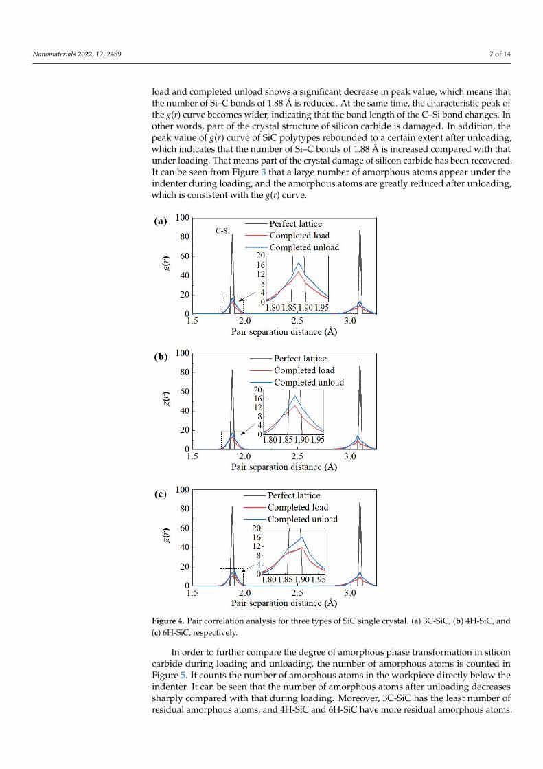
Nanomaterials 2022, 12, 2489 7 of 14
load and completed unload shows a significant decrease in peak value, which means thatthe number of Si–C bonds of 1.88 Å is reduced. At the same time, the characteristic peak ofthe g(r) curve becomes wider, indicating that the bond length of the C–Si bond changes. Inother words, part of the crystal structure of silicon carbide is damaged. In addition, thepeak value of g(r) curve of SiC polytypes rebounded to a certain extent after unloading,which indicates that the number of Si–C bonds of 1.88 Å is increased compared with thatunder loading. That means part of the crystal damage of silicon carbide has been recovered.It can be seen from Figure 3 that a large number of amorphous atoms appear under theindenter during loading, and the amorphous atoms are greatly reduced after unloading,which is consistent with the g(r) curve.
Nanomaterials 2022, 12, x FOR PEER REVIEW 8 of 17
bond changes. In other words, part of the crystal structure of silicon carbide is damaged. In addition, the peak value of g(r) curve of SiC polytypes rebounded to a certain extent after unloading, which indicates that the number of Si–C bonds of 1.88 Å is increased compared with that under loading. That means part of the crystal damage of silicon car-bide has been recovered. It can be seen from Figure 3 that a large number of amorphous atoms appear under the indenter during loading, and the amorphous atoms are greatly reduced after unloading, which is consistent with the g(r) curve.
Figure 4. Pair correlation analysis for three types of SiC single crystal. (a) 3C-SiC, (b) 4H-SiC, and (c) 6H-SiC, respectively.
In order to further compare the degree of amorphous phase transformation in silicon carbide during loading and unloading, the number of amorphous atoms is counted in Figure 5. It counts the number of amorphous atoms in the workpiece directly below the indenter. It can be seen that the number of amorphous atoms after unloading decreases sharply compared with that during loading. Moreover, 3C-SiC has the least number of residual amorphous atoms, and 4H-SiC and 6H-SiC have more residual amorphous at-oms.
Figure 4. Pair correlation analysis for three types of SiC single crystal. (a) 3C-SiC, (b) 4H-SiC, and(c) 6H-SiC, respectively.
In order to further compare the degree of amorphous phase transformation in siliconcarbide during loading and unloading, the number of amorphous atoms is counted inFigure 5. It counts the number of amorphous atoms in the workpiece directly below theindenter. It can be seen that the number of amorphous atoms after unloading decreasessharply compared with that during loading. Moreover, 3C-SiC has the least number ofresidual amorphous atoms, and 4H-SiC and 6H-SiC have more residual amorphous atoms.

Nanomaterials 2022, 12, 2489 8 of 14
Nanomaterials 2022, 12, x FOR PEER REVIEW 9 of 17
The formation of amorphous phase transformation has been fully proved in previous studies [12,13,16]. The elastic recovery after unloading will affect the material removal rate in processing, which is very worthy of further research. To further explain the elastic recovery, the atomic coordination numbers (CN) at completed load and completed unload are compared, as shown in Figure 6. The CN of silicon carbide with the perfect lattice is 4. The atoms with CN < 4 are mainly distributed on the surface of the model, which is caused by the lack of 1~2 coordination atoms on the surface. During loading, a large number of atoms with CN = 5 and 6 are concentrated in the plastic deformation zone under the in-denter. This is because the number of atoms in silicon carbide does not change under a high-pressure load, while the volume decreases and the atomic density increases in the plastic deformation zone, resulting in the increase of the number of atoms in the cutoff radius of the central atom. After unloading, elastic recovery and creep occur in the contact area of the indenter, and most atoms are restored to CN = 4. The change of CN often leads to amorphous phase transformation, which explains the reduction of amorphous atoms before and after unloading in Figure 5. In addition, the number of atoms with CN = 5 and 6 in 4H-SiC and 6H-SiC is significantly more than that in 3C-SiC after unloading. It is speculated that partial dislocations are more likely to cause an increase in atomic coordi-nation numbers, which is verified in Section 3.2.
Figure 5. The number of amorphous atoms for three types of SiC single crystal at completed load and completed unload.
Figure 5. The number of amorphous atoms for three types of SiC single crystal at completed loadand completed unload.
The formation of amorphous phase transformation has been fully proved in previousstudies [12,13,16]. The elastic recovery after unloading will affect the material removalrate in processing, which is very worthy of further research. To further explain the elasticrecovery, the atomic coordination numbers (CN) at completed load and completed unloadare compared, as shown in Figure 6. The CN of silicon carbide with the perfect lattice is 4.The atoms with CN < 4 are mainly distributed on the surface of the model, which is causedby the lack of 1~2 coordination atoms on the surface. During loading, a large numberof atoms with CN = 5 and 6 are concentrated in the plastic deformation zone under theindenter. This is because the number of atoms in silicon carbide does not change undera high-pressure load, while the volume decreases and the atomic density increases in theplastic deformation zone, resulting in the increase of the number of atoms in the cutoffradius of the central atom. After unloading, elastic recovery and creep occur in the contactarea of the indenter, and most atoms are restored to CN = 4. The change of CN oftenleads to amorphous phase transformation, which explains the reduction of amorphousatoms before and after unloading in Figure 5. In addition, the number of atoms with CN= 5 and 6 in 4H-SiC and 6H-SiC is significantly more than that in 3C-SiC after unloading.It is speculated that partial dislocations are more likely to cause an increase in atomiccoordination numbers, which is verified in Section 3.2.
Nanomaterials 2022, 12, x FOR PEER REVIEW 10 of 17
Figure 6. Coordination analysis for three types of SiC single crystal at completed load and com-pleted unload. (a) 3C-SiC, (b) 4H-SiC, and (c) 6H-SiC, respectively.
3.2. Dislocation Evolution Figure 3 shows that there are a large number of dislocations on the subsurface of
loaded SiC. The dislocations of 3C-SiC are mainly 1/2<110> perfect dislocations, which are scattered on both sides of the indentation, and only a small number of 1/2<110> partial dislocations exist at the edge of the amorphous layer. There are 1/3<1-210> perfect dislo-cations, 1/3<1-100> partial dislocations and 1/6<2-203> other dislocations in 4H-SiC and 6H-SiC at the same time. Among them, perfect dislocations are distributed on the sides of indentation, and partial dislocations and other dislocations are distributed in a disorderly manner. After complete unload, the area of dislocation distribution on the subsurface shrank to varying degrees. In order to study the dislocation evolution during indentation, the dislocation line lengths at different indentation depths during loading and unloading are counted, as shown in Figure 7. The dislocation evolution of 3C-SiC is dominated by perfect dislocation, which increases rapidly with the increase of loading, and tends to be stable after a small drop during unloading. The partial dislocation of 3C-SiC increases slowly during loading and almost remains unchanged during unloading. The perfect dis-locations of 4H-SiC and 6H-SiC account for a large proportion in the loading process. However, partial dislocations and other dislocations account for much more than perfect dislocations in the unloading process.
Figure 6. Coordination analysis for three types of SiC single crystal at completed load and completedunload. (a) 3C-SiC, (b) 4H-SiC, and (c) 6H-SiC, respectively.

Nanomaterials 2022, 12, 2489 9 of 14
3.2. Dislocation Evolution
Figure 3 shows that there are a large number of dislocations on the subsurface ofloaded SiC. The dislocations of 3C-SiC are mainly 1/2<110> perfect dislocations, whichare scattered on both sides of the indentation, and only a small number of 1/2<110>partial dislocations exist at the edge of the amorphous layer. There are 1/3<1-210> perfectdislocations, 1/3<1-100> partial dislocations and 1/6<2-203> other dislocations in 4H-SiCand 6H-SiC at the same time. Among them, perfect dislocations are distributed on thesides of indentation, and partial dislocations and other dislocations are distributed in adisorderly manner. After complete unload, the area of dislocation distribution on thesubsurface shrank to varying degrees. In order to study the dislocation evolution duringindentation, the dislocation line lengths at different indentation depths during loadingand unloading are counted, as shown in Figure 7. The dislocation evolution of 3C-SiC isdominated by perfect dislocation, which increases rapidly with the increase of loading, andtends to be stable after a small drop during unloading. The partial dislocation of 3C-SiCincreases slowly during loading and almost remains unchanged during unloading. Theperfect dislocations of 4H-SiC and 6H-SiC account for a large proportion in the loadingprocess. However, partial dislocations and other dislocations account for much more thanperfect dislocations in the unloading process.
Nanomaterials 2022, 12, x FOR PEER REVIEW 11 of 17
Figure 7. Dislocation line length of three types of SiC single crystal during loading and unloading process: (a) 3C-SiC, (b) 4H-SiC, and (c) 6H-SiC, respectively.
Different lattice stacking order leads to different dislocation evolution laws. Figures 8–10 show the dislocation evolution of SiC polytypes during loading. As can be seen from Figure 8a, the first dislocation appeared in 3C-SiC at h = 1.3 nm. 3C-SiC has only three perfect dislocations sliding along the {111} plane during h = 1.6–2.0 nm, and there is no overlap, as shown in Figure 8b,c. When h = 2.6 nm, the partial dislocations have occurred in the ellipse with the dotted line, as shown in Figure 8d. In addition, the perfect disloca-tion has the phenomenon of narrowing the sliding process. When the two ends of the perfect dislocation narrow and blend, it will become an independent prismatic dislocation loop separated from the damaged surface. The prismatic dislocation loop slides down-ward along the slip surface in the subsequent loading process, resulting in an increase in the damage depth. The dislocation evolution processes of 4H-SiC and 6H-SiC are similar. Except for perfect dislocations, a large number of partial dislocations on the (0001) plane and other dislocations on the {1-100} plane are formed on the subsurface, as shown in Figures 9 and 10. Combined with the dislocation distribution while completed load and unload shown in Figure 3, the dislocations of 4H-SiC and 6H-SiC sliding downward ac-count for a relatively small proportion, mainly sliding along the (0001) plane.
Figure 7. Dislocation line length of three types of SiC single crystal during loading and unloadingprocess: (a) 3C-SiC, (b) 4H-SiC, and (c) 6H-SiC, respectively.
Different lattice stacking order leads to different dislocation evolution laws. Figures 8–10show the dislocation evolution of SiC polytypes during loading. As can be seen fromFigure 8a, the first dislocation appeared in 3C-SiC at h = 1.3 nm. 3C-SiC has only threeperfect dislocations sliding along the {111} plane during h = 1.6–2.0 nm, and there is nooverlap, as shown in Figure 8b,c. When h = 2.6 nm, the partial dislocations have occurred inthe ellipse with the dotted line, as shown in Figure 8d. In addition, the perfect dislocation

Nanomaterials 2022, 12, 2489 10 of 14
has the phenomenon of narrowing the sliding process. When the two ends of the perfectdislocation narrow and blend, it will become an independent prismatic dislocation loopseparated from the damaged surface. The prismatic dislocation loop slides downwardalong the slip surface in the subsequent loading process, resulting in an increase in thedamage depth. The dislocation evolution processes of 4H-SiC and 6H-SiC are similar.Except for perfect dislocations, a large number of partial dislocations on the (0001) planeand other dislocations on the {1-100} plane are formed on the subsurface, as shown inFigures 9 and 10. Combined with the dislocation distribution while completed load andunload shown in Figure 3, the dislocations of 4H-SiC and 6H-SiC sliding downward accountfor a relatively small proportion, mainly sliding along the (0001) plane.
Nanomaterials 2022, 12, x FOR PEER REVIEW 12 of 17
Figure 8. Dislocation distribution of 3C-SiC at different indentation depths: (a) h = 1.3 nm, (b) h = 1.6 nm, (c) h = 2.0 nm, and (d) h = 2.6 nm, respectively.
Figure 9. Dislocation distribution of 4H-SiC at different indentation depths: (a) h = 1.3 nm, (b) h = 1.8 nm, (c) h = 2.0 nm, and (d) h = 2.5 nm, respectively.
Figure 8. Dislocation distribution of 3C-SiC at different indentation depths: (a) h = 1.3 nm,(b) h = 1.6 nm, (c) h = 2.0 nm, and (d) h = 2.6 nm, respectively.
Nanomaterials 2022, 12, x FOR PEER REVIEW 12 of 17
Figure 8. Dislocation distribution of 3C-SiC at different indentation depths: (a) h = 1.3 nm, (b) h = 1.6 nm, (c) h = 2.0 nm, and (d) h = 2.6 nm, respectively.
Figure 9. Dislocation distribution of 4H-SiC at different indentation depths: (a) h = 1.3 nm, (b) h = 1.8 nm, (c) h = 2.0 nm, and (d) h = 2.5 nm, respectively.
Figure 9. Dislocation distribution of 4H-SiC at different indentation depths: (a) h = 1.3 nm,(b) h = 1.8 nm, (c) h = 2.0 nm, and (d) h = 2.5 nm, respectively.

Nanomaterials 2022, 12, 2489 11 of 14Nanomaterials 2022, 12, x FOR PEER REVIEW 13 of 17
Figure 10. Dislocation distribution of 6H-SiC at different indentation depths: (a) h = 1.1 nm, (b) h = 1.6 nm, (c) h = 2.0 nm, and (d) h = 2.5 nm, respectively.
The differences in dislocation evolution mainly depend on the arrangement charac-teristics of crystal atoms and the direction of load. For 3C-SiC, because the {111} plane is the strong cleavage plane of 3C-SiC. The atoms along the {111} plane are densely arranged and are most prone to sliding behavior. With the increase of indentation depth, dislocation reactions on (11-1) and (111) planes were observed at h = 2.6 nm, accompanied by a small number of partial dislocations, circled with an elliptical dotted line in Figure 8. The dislo-cation transformation is carried out by dislocation decomposition and dislocation synthe-sis. The Burgers vector expression is as follows:
1/2[1 −1 0] = 1/6[1 −2 −1] + 1/6[2 −1 1] (6)
1/6[1 −2 −1] + 1/6[2 −1 1] + 1/2[0 1 −1] = 1/2[1 0 −1]. (7)
The above two dislocation transformation reactions are the process of energy reduction, indicating the possibility of dislocation transformation. The former occurs on the (11-1) plane, and the decomposed partial dislocations cross slip to become partial dislocations on the (111) plane. Then, the perfect dislocation 1/2[01-1] sliding on the (111) plane blends with the partial dislocation to form perfect dislocation 1/2[10-1]. In addition, the formation and downward slip of prismatic dislocation rings have also been reported in the study of sun et al. [11]. For 4H-SiC and 6H-SiC, because the pressing direction of the indenter is perpendicular to the (0001) cleavage plane, weakening the atomic sliding ability along the (0001) plane. Moreover, the {1-100} plane is the second cleavage plane of hexagonal silicon carbide. When the load is large, it can also produce atomic slip and form dislocations.
Figure 10. Dislocation distribution of 6H-SiC at different indentation depths: (a) h = 1.1 nm,(b) h = 1.6 nm, (c) h = 2.0 nm, and (d) h = 2.5 nm, respectively.
The differences in dislocation evolution mainly depend on the arrangement charac-teristics of crystal atoms and the direction of load. For 3C-SiC, because the {111} plane isthe strong cleavage plane of 3C-SiC. The atoms along the {111} plane are densely arrangedand are most prone to sliding behavior. With the increase of indentation depth, dislocationreactions on (11-1) and (111) planes were observed at h = 2.6 nm, accompanied by a smallnumber of partial dislocations, circled with an elliptical dotted line in Figure 8. The disloca-tion transformation is carried out by dislocation decomposition and dislocation synthesis.The Burgers vector expression is as follows:
1/2[1 −1 0] = 1/6[1 −2 −1] + 1/6[2 −1 1] (6)
1/6[1 −2 −1] + 1/6[2 −1 1] + 1/2[0 1 −1] = 1/2[1 0 −1]. (7)
The above two dislocation transformation reactions are the process of energy reduction,indicating the possibility of dislocation transformation. The former occurs on the (11-1)plane, and the decomposed partial dislocations cross slip to become partial dislocations onthe (111) plane. Then, the perfect dislocation 1/2[01-1] sliding on the (111) plane blendswith the partial dislocation to form perfect dislocation 1/2[10-1]. In addition, the formationand downward slip of prismatic dislocation rings have also been reported in the study ofsun et al. [11]. For 4H-SiC and 6H-SiC, because the pressing direction of the indenter isperpendicular to the (0001) cleavage plane, weakening the atomic sliding ability along the(0001) plane. Moreover, the {1-100} plane is the second cleavage plane of hexagonal siliconcarbide. When the load is large, it can also produce atomic slip and form dislocations.
3.3. Stacking Faults
Figure 3b shows that a large number of 3C cubic crystals and 2H hexagonal crystalsremained on the 4H-SiC subsurface after unloading. The change of atomic stacking indi-cates that stacking faults occur in 4H-SiC. On the (1-210) plane, stacking faults were locatedin the right region and the lower-left region of the indentation, respectively, accompaniedby 1/3<1-100> partial dislocations. By analyzing the sliding motion under the action ofdislocation, the generation mechanism of the above two kinds of stacking faults can beexplained, as shown in Figure 11. Figure 11a shows two rows of atoms of 4H-SiC on

Nanomaterials 2022, 12, 2489 12 of 14
the (1-210) plane, and its atomic stacking structure is ABCB. The atoms in the lower-leftregion of the indentation produce 1/3[-1010] dislocation under the action of the transverseextrusion component, as shown in Figure 11b. This dislocation makes the atoms stacked atposition C slip 1/3 of the lattice length in the directions of [-1000] and [10], about 1 Å. Theatomic position after sliding is directly below A, and the atomic stacking structure becomesABAB, which is a typical 2H hexagonal crystal. Similarly in Figure 11c, the atoms in theright region of the indentation are affected by 1/3[10-10] dislocation, causing the atomsstacked at position B to slide 1/3 of the lattice length in the [1000] and [0,1,2,3,4,5,6,7,8,9,10]directions. The atomic position after sliding is directly below A, and the atomic stackingstructure becomes ABC, which is a typical 3C cubic crystal.
Nanomaterials 2022, 12, x FOR PEER REVIEW 14 of 17
3.3. Stacking Faults Figure 3b shows that a large number of 3C cubic crystals and 2H hexagonal crystals
remained on the 4H-SiC subsurface after unloading. The change of atomic stacking indi-cates that stacking faults occur in 4H-SiC. On the (1-210) plane, stacking faults were lo-cated in the right region and the lower-left region of the indentation, respectively, accom-panied by 1/3<1-100> partial dislocations. By analyzing the sliding motion under the ac-tion of dislocation, the generation mechanism of the above two kinds of stacking faults can be explained, as shown in Figure 11. Figure 11a shows two rows of atoms of 4H-SiC on the (1-210) plane, and its atomic stacking structure is ABCB. The atoms in the lower-left region of the indentation produce 1/3[-1010] dislocation under the action of the trans-verse extrusion component, as shown in Figure 11b. This dislocation makes the atoms stacked at position C slip 1/3 of the lattice length in the directions of [-1000] and [0010], about 1 Å. The atomic position after sliding is directly below A, and the atomic stacking structure becomes ABAB, which is a typical 2H hexagonal crystal. Similarly in Figure 11c, the atoms in the right region of the indentation are affected by 1/3[10-10] dislocation, caus-ing the atoms stacked at position B to slide 1/3 of the lattice length in the [1000] and [00–10] directions. The atomic position after sliding is directly below A, and the atomic stack-ing structure becomes ABC, which is a typical 3C cubic crystal.
Figure 11. Schematic diagram of the stacking faults formation in 4H-SiC. (a) 4h hexagonal crystal structure, (b) 2H hexagonal crystal, and (c) 3C cubic crystal.
3.4. Temperature Figure 12 shows the temperature change curve of SiC polytypes during the indenta-
tion process. The temperature value in the figure is the average temperature of the whole workpiece. It can be seen that the temperature change trend of the three is the same, which increases with the increase of the pressing depth, and the temperature increases faster and faster. Before h = 4 nm, the temperature of 3C-SiC is slightly higher than that of 4H-SiC and 6H-SiC. However, after h = 4 nm, it is found that the temperature rise rate of 4H-SiC after is significantly faster than that of 3C-SiC and 6H-SiC. We speculate that this is be-cause the generation of stacking faults leads to the release of energy.
Figure 11. Schematic diagram of the stacking faults formation in 4H-SiC. (a) 4h hexagonal crystalstructure, (b) 2H hexagonal crystal, and (c) 3C cubic crystal.
3.4. Temperature
Figure 12 shows the temperature change curve of SiC polytypes during the indentationprocess. The temperature value in the figure is the average temperature of the wholeworkpiece. It can be seen that the temperature change trend of the three is the same, whichincreases with the increase of the pressing depth, and the temperature increases faster andfaster. Before h = 4 nm, the temperature of 3C-SiC is slightly higher than that of 4H-SiC and6H-SiC. However, after h = 4 nm, it is found that the temperature rise rate of 4H-SiC after issignificantly faster than that of 3C-SiC and 6H-SiC. We speculate that this is because thegeneration of stacking faults leads to the release of energy.
Nanomaterials 2022, 12, x FOR PEER REVIEW 15 of 17
Figure 12. Temperature of SiC polytypes during indentation.
4. Conclusions This work systematically compares the elastic–plastic deformation characteristics of
SiC polytypes by MD simulation, and mainly analyzes the characteristics and differences of amorphous phase transformation, dislocation evolution and stacking faults. The main conclusions are as follows: (1) The change of atomic coordination number caused by the high-pressure load is the
main reason for promoting amorphous phase transformation. The amorphous phase transformation runs through the whole process and recovers significantly after un-loading;
(2) The atomic slip in 3C-SiC is dominated by perfect dislocations and tends to develop into prismatic dislocation rings, while 4H-SiC and 6H-SiC are dominated by various dislocations;
(3) Two types of stacking faults occur in 4H-SiC, which are caused by partial disloca-tions.
Author Contributions: Conceptualization, H.W.; methodology, H.W. and S.G.; software, H.W. and X.G.; formal analysis, H.W. and S.G.; investigation, H.W. and H.L.; data curation, H.W.; writing—original draft preparation, H.W.; writing—review and editing, H.W. and S.G.; visualization, H.W.; supervision, R.K.; funding acquisition, R.K. and S.G. All authors have read and agreed to the pub-lished version of the manuscript.
Funding: This research is financially supported by the National Natural Science Foundation of China (Grant No. 51975091, 51991372, 51735004), and the National Key Research and Development Program of China (Grant No. 2018YFB1201804-1).
Institutional Review Board Statement: Not applicable.
Informed Consent Statement: Not applicable.
Data Availability Statement: Not applicable.
Acknowledgments: The authors would like to acknowledge the financial support from the National Natural Science Foundation of China and the National Key Research and Development Program of China.
Conflicts of Interest: The authors declare no conflict of interest.
References 1. Zhang, N.; Rao, Y.; Xu, N.; Maralani, A.; Pisano, A.P. Characterization of 4H-SiC Bipolar Junction Transistor at
High Temperatures. Mater. Sci. Forum 2014, 778–780, 1013−1016. https://doi.org/10.4028/www.scien-tific.net/MSF.778-780.1013.
2. Snead, L.L.; Nozawa, T.; Katoh, Y.; Byun, T.S.; Kondo, S.; Petti, D.A. Handbook of SiC properties for fuel perfor-mance modeling. J. Nucl. Mater. 2007, 371, 329–377. https://doi.org/10.1016/j.jnucmat.2007.05.016.
Figure 12. Temperature of SiC polytypes during indentation.

Nanomaterials 2022, 12, 2489 13 of 14
4. Conclusions
This work systematically compares the elastic–plastic deformation characteristics ofSiC polytypes by MD simulation, and mainly analyzes the characteristics and differencesof amorphous phase transformation, dislocation evolution and stacking faults. The mainconclusions are as follows:
(1) The change of atomic coordination number caused by the high-pressure load isthe main reason for promoting amorphous phase transformation. The amorphousphase transformation runs through the whole process and recovers significantlyafter unloading;
(2) The atomic slip in 3C-SiC is dominated by perfect dislocations and tends to de-velop into prismatic dislocation rings, while 4H-SiC and 6H-SiC are dominated byvarious dislocations;
(3) Two types of stacking faults occur in 4H-SiC, which are caused by partial dislocations.
Author Contributions: Conceptualization, H.W.; methodology, H.W. and S.G.; software, H.W.and X.G.; formal analysis, H.W. and S.G.; investigation, H.W. and H.L.; data curation, H.W.;writing—original draft preparation, H.W.; writing—review and editing, H.W. and S.G.; visualization,H.W.; supervision, R.K.; funding acquisition, R.K. and S.G. All authors have read and agreed to thepublished version of the manuscript.
Funding: This research is financially supported by the National Natural Science Foundation of China(Grant No. 51975091, 51991372, 51735004), and the National Key Research and Development Programof China (Grant No. 2018YFB1201804-1).
Institutional Review Board Statement: Not applicable.
Informed Consent Statement: Not applicable.
Data Availability Statement: Not applicable.
Acknowledgments: The authors would like to acknowledge the financial support from the NationalNatural Science Foundation of China and the National Key Research and Development Programof China.
Conflicts of Interest: The authors declare no conflict of interest.
References1. Zhang, N.; Rao, Y.; Xu, N.; Maralani, A.; Pisano, A.P. Characterization of 4H-SiC Bipolar Junction Transistor at High Temperatures.
Mater. Sci. Forum 2014, 778–780, 1013–1016. [CrossRef]2. Snead, L.L.; Nozawa, T.; Katoh, Y.; Byun, T.S.; Kondo, S.; Petti, D.A. Handbook of SiC properties for fuel performance modeling.
J. Nucl. Mater. 2007, 371, 329–377. [CrossRef]3. Li, F.; Roccaforte, F.; Greco, G.; Fiorenza, P.; La Via, F.; Pérez-Tomas, A.; Evans, J.E.; Fisher, C.A.; Monaghan, F.A.; Mawby, P.A.; et al.
Status and Prospects of Cubic Silicon Carbide Power Electronics Device Technology. Materials 2021, 14, 5831. [CrossRef]4. Zhou, T.; Xu, R.; Ruan, B.; He, Y.; Liang, Z.; Wang, X. Study on new method and mechanism of microcutting-etching of microlens
array on 6H-SiC mold by combining single point diamond turning with ion beam etching. J. Mater. Process. Technol. 2020,278, 116510. [CrossRef]
5. Fan, J.Y.; Wu, X.L.; Chu, P.K. Low-dimensional SiC nanostructures: Fabrication, luminescence, and electrical properties. Prog.Mater. Sci. 2006, 51, 983–1031. [CrossRef]
6. Xiao, Q.; He, X.L. Research on the Precision Machining on SiC. Adv. Mat. Res. 2014, 900, 601–604. [CrossRef]7. Huang, H.; Li, X.; Mu, D.; Lawn, B.R. Science and art of ductile grinding of brittle solids. Int. J. Mach. Tools Manuf. 2021,
161, 103675. [CrossRef]8. Zhao, X.; Langford, R.M.; Shapiro, I.P.; Xiao, P.; Pharr, G. Onset Plastic Deformation and Cracking Behavior of Silicon Carbide
under Contact Load at Room Temperature. J. Am. Ceram. Soc. 2011, 94, 3509–3514. [CrossRef]9. Goel, S.; Yan, J.; Luo, X.; Agrawal, A. Incipient plasticity in 4H-SiC during quasistatic nanoindentation. J. Mech. Behav. Biomed.
Mater. 2014, 34, 330–337. [CrossRef]10. Pan, J.; Yan, Q.; Li, W.; Zhang, X. A Nanomechanical Analysis of Deformation Characteristics of 6H-SiC Using an Indenter and
Abrasives in Different Fixed Methods. Micromachines 2019, 10, 332. [CrossRef]11. Sun, S.; Peng, X.; Xiang, H.; Huang, C.; Yang, B.; Gao, F.; Fu, T. Molecular dynamics simulation in single crystal 3C-SiC under
nanoindentation: Formation of prismatic loops. Ceram. Int. 2017, 43, 16313–16318. [CrossRef]

Nanomaterials 2022, 12, 2489 14 of 14
12. Zhu, B.; Zhao, D.; Tian, Y.; Wang, S.; Zhao, H.; Zhang, J. Study on the deformation mechanism of spherical diamond indenter andits influence on 3C-SiC sample during nanoindentation process via molecular dynamics simulation. Mater. Sci. Semicond. Process.2019, 90, 143–150. [CrossRef]
13. Zhu, B.; Zhao, D.; Zhao, H. A study of deformation behavior and phase transformation in 4H-SiC during nanoindentation processvia molecular dynamics simulation. Ceram. Int. 2019, 45, 5150–5157. [CrossRef]
14. Tian, Z.; Xu, X.; Jiang, F.; Lu, J.; Luo, Q.; Lin, J. Study on nanomechanical properties of 4H-SiC and 6H-SiC by molecular dynamicssimulations. Ceram. Int. 2019, 45, 21998–22006. [CrossRef]
15. Wu, Z.; Liu, W.; Zhang, L. Effect of structural anisotropy on the dislocation nucleation and evolution in 6H SiC under nanoinden-tation. Ceram. Int. 2019, 45, 14229–14237. [CrossRef]
16. Wu, Z.; Liu, W.; Zhang, L.; Lim, S. Amorphization and dislocation evolution mechanisms of single crystalline 6H-SiC. Acta Mater.2020, 182, 60–67. [CrossRef]
17. Mishra, M.; Szlufarska, I. Possibility of high-pressure transformation during nanoindentation of SiC. Acta Mater. 2009,57, 6156–6165. [CrossRef]
18. Xue, L.; Feng, G.; Wu, G.; Dong, F.; Liang, K.; Li, R.; Wang, S.; Liu, S. Study of deformation mechanism of structural anisotropy in4H–SiC film by nanoindentation. Mater. Sci. Semicond. Process. 2022, 146, 106671. [CrossRef]
19. Wu, Z.; Zhang, L. Mechanical properties and deformation mechanisms of surface-modified 6H-silicon carbide. J. Mater. Sci.Technol. 2021, 90, 58–65. [CrossRef]
20. Zhao, L.; Alam, M.; Zhang, J.; Janisch, R.; Hartmaier, A. Amorphization-governed elasto-plastic deformation under nanoindenta-tion in cubic (3C) silicon carbide. Ceram. Int. 2020, 46, 12470–12479. [CrossRef]
21. Plimpton, S. Fast Parallel Algorithms for Short-Range Molecular-Dynamics. J. Comput. Phys. 1995, 117, 1–19. [CrossRef]22. Belak, J.; Boercker, D.B.; Stowers, I.F. Simulation of Nanometer-Scale Deformation of Metallic and Ceramic Surfaces. MRS Bull.
1993, 18, 55–60. [CrossRef]23. Huang, C.; Peng, X.; Yang, B.; Xiang, H.; Sun, S.; Chen, X.; Li, Q.; Yin, D.; Fu, T. Anisotropy effects in diamond under
nanoindentation. Carbon 2018, 132, 606–615. [CrossRef]24. Tersoff, J. Modeling solid-state chemistry: Interatomic potentials for multicomponent systems. Phys. Rev. B 1989, 39, 5566–5568.
[CrossRef]25. Vashishta, P.; Kalia, R.; Nakano, K.A.; Rino, J.P. Interaction potential for silicon carbide: A molecular dynamics study of elastic
constants and vibrational density of states for crystalline and amorphous silicon carbide. J. Appl. Phys. 2007, 101, 103515.[CrossRef]
26. Meng, B.; Yuan, D.; Xu, S. Coupling effect on the removal mechanism and surface/subsurface characteristics of SiC duringgrinding process at the nanoscale. Ceram. Int. 2019, 45, 2483–2491. [CrossRef]
27. Mishra, M.; Szlufarska, I. Dislocation controlled wear in single crystal silicon carbide. J. Mater. Sci. 2012, 48, 1593–1603. [CrossRef]28. Xiao, G.; To, S.; Zhang, G. The mechanism of ductile deformation in ductile regime machining of 6H-SiC. Comput. Mater. Sci.
2015, 98, 178–188. [CrossRef]29. Kubo, A.; Nagao, S.; Umeno, Y. Molecular dynamics study of deformation and fracture in SiC with angular dependent potential
model. Comput. Mater. Sci. 2017, 139, 89–96. [CrossRef]30. Erhart, P.; Albe, K. Analytical potential for atomistic simulations of silicon, carbon, and silicon carbide. Phys. Rev. B 2005,
71, 035211. [CrossRef]31. Stukowski, A. Visualization and analysis of atomistic simulation data with OVITO–the Open Visualization Tool. Model. Simul.
Mater. Sci. Eng. 2010, 18, 015012. [CrossRef]32. Maras, E.; Trushin, O.; Stukowski, A.; Ala-Nissila, T.; Jónsson, H. Global transition path search for dislocation formation in Ge on
Si(001). Comput. Phys. Commun. 2016, 205, 13–21. [CrossRef]33. Stukowski, A.; Bulatov, V.V.; Arsenlis, A. Automated identification and indexing of dislocations in crystal interfaces. Model. Simul.
Mater. Sci. Eng. 2012, 20, 085007. [CrossRef]