Embed Size (px)
Citation preview

1
Memory Modem TM FTL Architecture for 1Xnm / 2Xnm MLC and TLC Nand Flash
August 21, 2012
Hanan Weingarten, CTO, DensBits Technologies

2
Outline
• Requirements
• 1xnm/2xnm TLC NAND Flash Reliability Challenges
• Reliability
• BER Vs Endurance Vs Retention
• Read / Program Disturbs
• Integrity
• “Ungraceful” power down
• DB3610 Memory Modem TM FTL Layered approach:
• Lower Layer – Physical level reliability
• Upper Layer – Memory management

3
Requirements
• Data Integrity and Reliability
• High Performance
• Throughput
• IOPs
• Low Power
• Mobile devices

4
1xnm/2xnm Reliability Challenges (1)
• Bit Error Rate (BER) Vs Endurance Vs Retention:
10-4
10-3
10-2
10-1
Endurance (P/E cycles)
Bit E
rror
Rate
BER Vs Endurance
No Retention
After Retention

5
1xnm/2xnm Reliability Challenges (2)
• BER Vs Endurance Vs Retention:
• BER can go as high as 5e-2
• Even without retention BER goes quickly up (1e-2)
• 4x-5x factor in BERs due to retention
• ECC requirements
• Near optimal reliability – close to theoretical bounds
• Perform both hard and soft decoding
• Optimal and high performance hard decoding

6
1xnm/2xnm Reliability Challenges (3)
• Retention effect:
• Lobe widening
• Lobe shift

7
1xnm/2xnm Reliability Challenges (4)
• Read Disturbs

8
1xnm/2xnm Integrity Challenges
• Power down scenarios
• Managed power off
• Required data-bases are stored prior to power down
• Sudden power off between transactions (graceful power off)
• All written data are recoverable through meta-data
• Sudden power off within a write transaction (ungraceful power loss)
• All data except for last (interrupted) transaction must be recovered
• Past data may be damaged due to interruption
Page 0 Page 1
Page 2
Page 3
Page 4
Page 5
LSB
CSB
MSB Lower triangle pages
9
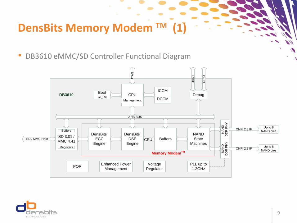
DensBits Memory Modem TM (1)
• DB3610 eMMC/SD Controller Functional Diagram
SD 3.01 /
MMC 4.41
Buffers
Registers
DensBits’
ECC
Engine
DensBits’
DSP
Engine
Buffers
NAND
State
Machines
NA
ND
DD
R P
HY
NA
ND
DD
R P
HY
Up to 8
NAND dies
Up to 8
NAND dies
CPU
Management
Boot
ROM
ICCM
DCCMDebug
PORPLL up to
1.2GHz
Voltage
Regulator
Enhanced Power
Management
AHB BUS
SD / MMC Host IF
ONFI 2.3 IF
ONFI 2.3 IF
CPU
JT
AG
UA
RT
GP
IO
DB3610
Memory ModemTM

10
TM
DB3610 Memory Modem TM (2)
• Memory ModemTM for Flash memories improving reliability, enabling smaller process nodes and more bits per cell
• Proprietary ECC
• Proprietary DSP
• Proprietary Management
DensBits Confidential
10
Joint DSP / ECC
DSP Program
DSP Read
ECC
Flash Tracking System
The Modem

11
DB3610 Memory Modem TM (3)
• FTL Layered approach
Higher Layer
Wear Leveling
Data Mapping
Bad Block handling
Lower Layer Virtual NAND dies Virtual erase blocks Virtual program pages
FTL

12
DB3610 Memory Modem TM (4)
• FTL Layered approach
• Lower layer
• Handles the data
• Responsible for presenting a reliable virtual FLASH to the upper layer
• Includes main parts of memory Modem TM :
– ECC flow
– DSP software
– Low-level memory management:
» Data allocation
» Damaged page recovery following “ungraceful” power-down

13
DB3610 Memory Modem TM (5)
• FTL Layered approach
• Upper Layer
• Handles control data
• Data mapping
• Wear leveling
• Data integrity issues:
– Bad blocks handling
– Power-down recovery – control data
– Scrubbing
• Metrics for lower layer to improve decisions
• ….

14
DB3610 Memory Modem TM (6) - ECC
• Features
• Configurable, input parameters (set via software):
• Block size: 0.5KB-8KB
• Code rate: 0.5 - 0.99
• Slim design / low power
• Hard and Soft decoding
• Hard decoding as standard operation, soft decoding at extreme, guaranteeing reliability with low latency
• Per each block size and code rate, near-optimal error correction
• Near Hamming bound (hard decoding theoretical limit)
• Near Shannon bound (soft decoding theoretical limit)

15
DensBits’ ECC – Hard Decoding
0.8 0.82 0.84 0.86 0.88 0.9 0.92 0.94 0.96 0.98 110
-4
10-3
10-2
10-1
100
Coding rate
Input
BE
R a
chie
vin
g o
utp
ut
BE
R <
10-1
5
Theoretical limit (Hamming bound)
DensBits' ECC - hard decoding
Block [Bytes]
Spare [Bytes]
Coding rate
8K 1445 0.85
8K 908 0.90
8K 706 0.92
8K 512 0.94
8K 440 0.95
8K 340 0.96
8K 256 0.97
2Xnm MLC, TLC
1Xnm MLC, TLC

16
DensBits’ ECC – Soft Decoding
0.8 0.82 0.84 0.86 0.88 0.9 0.92 0.94 0.96 0.98 110
-4
10-3
10-2
10-1
100
Coding rate
Input
BE
R a
chie
vin
g o
utp
ut
BE
R <
10-1
5
Theoretical limit (Shannon bound)
DensBits' ECC - soft decoding
BCH(24, 1024)
2Xnm MLC, TLC
1Xnm MLC, TLC
Block [Bytes]
Spare [Bytes]
Coding rate
8K 1445 0.85
8K 908 0.90
8K 706 0.92
8K 512 0.94
8K 440 0.95
8K 340 0.96
8K 256 0.97

17
ECC FTL Flow
• Most common flow will perform hard decode
• Enabled through hard decoding machinery
• High performance
• Rare occasion, following retention, may require soft decoding
• Performance price due to additional reads from flash memory

18
DB3610 Memory Modem TM (7) - DSP
• Optimized read parameters
• Optimization of read parameters minimizing the input BER for the ECC
• “Blind” threshold acquisition
• Optimization of performance through:
• Block-state tracking
• Continuous block state updates
• Optimization of program parameters, depending on block state, minimizing tPROG

19
DSP FTL Flow
• Read Flow:

20
DB3610 Memory Modem TM (8) – Data Allocation
• Different page types may have different reliability:
• Even / Odd pages
• MSB / CSB / LSB pages
• Data allocation can significantly improve data reliability :
• Striping / Interleaving
• Variable rate coding
• BER equalization
• X2 improvement in BER

21
DB3610 Memory Modem TM (9)
• Upper Layer – Data Mapping
• Hybrid block/page level mapping
• High IOPs
• Low WA
• Can be accommodated in an embedded system
• Wear leveling
• Other reliability considerations:
• SLC block allocation
22
Summary
• 1xnm / 2xnm NAND Flash controllers require a Memory Modem TM to obtain full reliability and performance
• A layered approach is a useful abstraction allowing handling various Failure mechanisms

23
The Future of NAND Flash Technology Extreme Reliability, Unparalleled Performance

24
Thank You!