Embed Size (px)
Citation preview
University of South FloridaScholar Commons
Graduate Theses and Dissertations Graduate School
4-6-2016
Microfluidically Reconfigurable Frequency-AgileRF Filters with Wide Frequency Tuning Range andHigh Power Handling CapabilityTimothy Joseph Palomo
Follow this and additional works at: http://scholarcommons.usf.edu/etd
Part of the Electromagnetics and Photonics Commons
This Dissertation is brought to you for free and open access by the Graduate School at Scholar Commons. It has been accepted for inclusion inGraduate Theses and Dissertations by an authorized administrator of Scholar Commons. For more information, please [email protected].
Scholar Commons CitationPalomo, Timothy Joseph, "Microfluidically Reconfigurable Frequency-Agile RF Filters with Wide Frequency Tuning Range and HighPower Handling Capability" (2016). Graduate Theses and Dissertations.http://scholarcommons.usf.edu/etd/6124
Microfluidically Reconfigurable Frequency-Agile RF Filters
with Wide Frequency Tuning Range and High Power Handling Capability
by
Timothy Palomo
A dissertation submitted in partial fulfillment
of the requirements for the of
Doctor of Philosophy
Department of Electrical Engineering
College of Engineering
University of South Florida
Major Professor: Gokhan Mumcu, Ph.D.
Thomas Weller, Ph.D.
Jing Wang, Ph.D.
Nathan Crane, Ph.D.
Paul Herzig, B.S.E.E.
Date of Approval:
March 25, 2016
Keywords: Tunable, Resonator, X-band,
Microstrip, High-power
Copyright © 2016, Timothy Palomo
DEDICATION
First of all, I would like to dedicate this dissertation to my mother, Ailen Delgado, and
my father, Eusebio Palomo. They have been role models since I was a kid, and they have
motivated me to follow my dreams and work hard to accomplish them. Thanks to them, I started
pre-school at the age of two years old, and they have always taught me the importance of
education. However, the most important principle I have learned from my parents is to never
give up. My mother’s kindness have taught me to love what I do, and to treat everyone the same,
while my father’s character has taught me to fight for everything I want. Second, I would like to
dedicate this dissertation to my grandparents, Nelia Baez and Jose Delgado, they have set an
example my entire life, and next to my parents they have been the first, and most important,
teachers in my life. To me, my grandparents have been more than just my family, they have been
my friends, my teachers, my guardians, my role models, among other things. I have always
looked up to my grandfather since he is the person that I admire the most for his character, his
correctness, his intelligence, and his physical condition.
Then, I would like to say thanks to the rest of my family, since they have all been an
important part in my life, both in my personal and professional growth. Specially, my
grandmother Maria Mesones, my siblings Ruben and Simone Palomo, my uncle Jose Delgado
Baez, my aunt Josmar Morales, my cousins Kevin and Johan Delgado and many others. Also, to
my girlfriend Jennyfer Sanchez who has loved me unconditionally and has supported me in
every step I have made to get to this point.

I would like to thanks my advisor Gokhan Mumcu, who has taught me as much as he
could in the field of RF and microwave area since I was still at the undergraduate level, and he
has motivated me every day of my young career to be better. Last, but not least, I would like
dedicate this dissertation to my home country Venezuela, to its beautiful beaches and mountains,
to its desert and jungles, and to everyone who is currently struggling and fighting to save the
country from its terrible social situation, and to bring back the country that helped me growth
and forged my character.
ACKNOWLEDGEMENTS
I first would like to acknowledge all the members of my committee, Dr. Thomas Weller,
Dr. Jing Wang, Dr. Nathan Crane, and Mr. Paul Herzig for their invaluable collaboration with
my dissertation defense, and for sharing their knowledge with me in this very important chapter
of my life. I can just say thanks for accommodating my defense in such a short notice. I would
like to acknowledge all the employees at the Nanotechnology Research and Education Center
(NREC) because they made possible for me to accomplish the fabrication of the devices
developed under this dissertation. I would also like to acknowledge Rogers Corp. for providing
me with plenty of material that was utilized throughout my doctoral studies. Last, but not least, I
would like to acknowledge the entire WAMI group at the University of South Florida because
they have shared this journey with me closer than nobody else, with some special mentions to
Abhishek Dey and Eduardo Rojas for all their collaborations through these years.
i
TABLE OF CONTENTS
LIST OF TABLES ....................................................................................................................... iii
LIST OF FIGURES ..................................................................................................................... iv
ABSTRACT ................................................................................................................................ vii
CHAPTER 1: INTRODUCTION ...................................................................................................1
1.1 Semiconductor Varactors ..............................................................................................2
1.2 Ferroelectric Varactors ..................................................................................................3
1.3 RF Micro-ElectroMechanical Systems (MEMS) Varactors and Switches ...................5
1.4 Evanescent Cavity Resonator Filters ............................................................................7
1.5 Microfluidically Reconfigurable Devices .....................................................................8
CHAPTER 2: WIDEBAND BAND-STOP X-BAND FILTER USING ELECTRICALLY
SMALL TIGHTLY COUPLED RESONATORS ..................................................................19
2.1 Filter Design ................................................................................................................19
2.2 Experimental Verification ...........................................................................................22
2.3 Concluding Remarks of Chapter 2 ..............................................................................24
CHAPTER 3: FREQUENCY-AGILE BANDPASS FILTER USING LIQUID METAL
TUNABLE BROADSIDE COUPLED SPLIT RING RESONATORS .................................26
3.1 Filter Design ................................................................................................................26
3.2 Experimental Verification ...........................................................................................30
3.3 Concluding Remarks of Chapter 3 ..............................................................................31
CHAPTER 4: HIGHLY RECONFIGURABLE BANDPASS FILTER USING
MICROFLUIDICALLY CONTROLLED METALLIZED GLASS PLATES ......................33
4.1 Filter Design ................................................................................................................33
4.2 Fabrication ..................................................................................................................38
4.3 Experimental Verification ...........................................................................................39
4.4 Concluding Remarks of Chapter 4 ..............................................................................39
CHAPTER 5: MICROFLUIDICALLY RECONFIGURABLE METALLIZED PLATE
LOADED FREQUENCY-AGILE RF BANDPASS FILTERS .............................................41
5.1 Filter Design ................................................................................................................41
5.1.1 Resonator Model ..........................................................................................41
5.1.2 External Qe and Coupling Coefficient .........................................................45
5.1.3 4th
Order Filter with Linear Resonator Arrangement ...................................47
ii
5.1.4 4th
Order Filter with Diagonal Resonator Arrangement ..............................48
5.2 Microfluidic Channel Design ..................................................................................... 49
5.3 Fabrication ................................................................................................................. 52
5.4 Experimental Verification ...........................................................................................54
5.4.1 4th
Order Filter with Linear Resonator Arrangement ...................................54
5.4.2 4th
Order Filter with Diagonal Resonator Arrangement ..............................56
5.5 Concluding Remarks of Chapter 5 ..............................................................................56
CHAPTER 6: WIDELY TUNABLE, LOW LOSS FILTERS USING
MICROFLUIDICALLY CONTROLLED VARIABLE LENGTH RESONATORS .............58
6.1 Resonator Design ........................................................................................................58
6.2 Filter Design ................................................................................................................62
6.3 Fabrication ..................................................................................................................67
6.4 Experimental Verification ...........................................................................................70
6.5 Power Handling Characterization ...............................................................................72
6.6 Concluding Remarks of Chapter 6 ..............................................................................75
CHAPTER 7: FUTURE WORK ..................................................................................................77
REFERENCES .............................................................................................................................81
APPENDIX A: MICROFLUIDIC CHANNEL FABRICATION .................................................88
A.1 Microfluidic Channel Design ......................................................................................88
A.2 Micromold Fabrication ..............................................................................................89
A.3 Polydimethylsiloxane (PDMS) Preparation ...............................................................92
A.4 Sealing the Channel (Bonding) ..................................................................................92
A.5 Selectively Metallized Plate Fabrication ....................................................................94
APPENDIX B: COPYRIGHT PERMISSIONS ...........................................................................95
ABOUT THE AUTHOR .............................................................................................. END PAGE
iii
LIST OF TABLES
Table 1 Thermal properties of the materials utilized ........................................................... 75
Table 2 Summary of filters realized through this dissertation ............................................. 76
iv
LIST OF FIGURES
Figure 1 Varactor based tunable bandpass filter .....................................................................2
Figure 2 Ferroelectric varactor based tunable bandpass filter ................................................4
Figure 3 Continuously tunable MEMS based filter ................................................................5
Figure 4 Discretely tunable RF MEMS based filter ...............................................................6
Figure 5 MEMS loaded evanescent-mode cavity resonator based filter ................................8
Figure 6 Microfluidically reconfigurable devices ...................................................................9
Figure 7 Microfluidically reconfigurable bandstop filter .....................................................10
Figure 8 Liquid metal electromagnetic band-gap .................................................................11
Figure 9 Liquid metal CPW bandpass filter .........................................................................12
Figure 10 Stopband filter ........................................................................................................20
Figure 11 Normalized reactance slope (X/Z0) as a function BCB film thickness and
signal line separation ...............................................................................................20
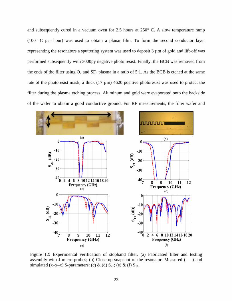
Figure 12 Experimental verification of stopband filter ...........................................................23
Figure 13 The tube based coupled line geometry and its equivalent multilayered strip
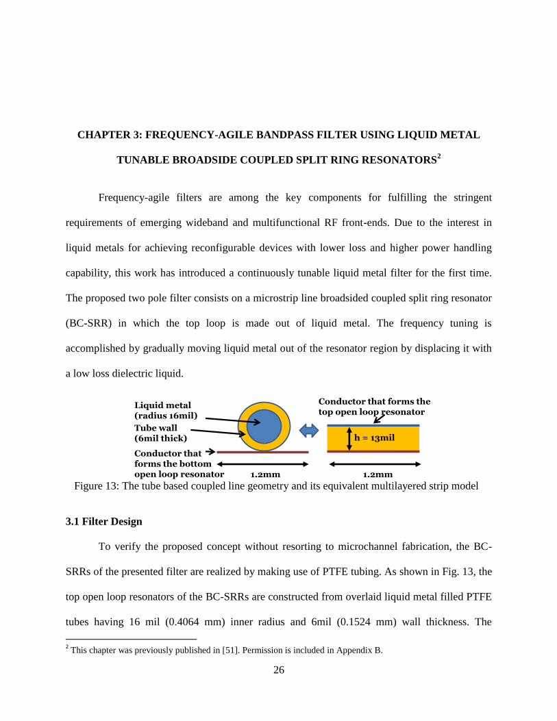
model ......................................................................................................................26
Figure 14 Liquid metal Qe and K extraction ...........................................................................27
Figure 15 Liquid metal filter ...................................................................................................30
Figure 16 Two-pole filter ........................................................................................................34
Figure 17 External quality factor (Qe) extraction ...................................................................35
Figure 18 Variation of coupling coefficient (K) .....................................................................36
v
Figure 19 Fabricated two-pole filter .......................................................................................38
Figure 20 Reconfigurable capacitive loaded microfluidically based resonator ......................42
Figure 21 External quality factor extraction and coupling coefficient for different
resonator arrangements ...........................................................................................43
Figure 22 Designed 4th
order filters with linear resonator arrangement .................................46
Figure 23 Designed 4th
order filters with diagonal resonator arrangement ............................48
Figure 24 Metallized plate and channel shapes investigated for the linear and
diagonal resonator arrangement .............................................................................50
Figure 25 Experimental characterization of the 4th
order bandpass filter with linear
resonator arrangement .............................................................................................53
Figure 26 Experimental characterization of the 4th
order bandpass filter with
diagonal resonator arrangement ..............................................................................55
Figure 27 Microfluidically reconfigurable half wavelength resonator ...................................59
Figure 28 External Qe extraction with tapping approach ........................................................61
Figure 29 External Qe extraction for capacitive coupling approach .......................................63
Figure 30 External Qe extraction for capacitive coupling approach with added
tuning stub ...............................................................................................................64
Figure 31 External Qe performance for three different approaches ........................................65
Figure 32 Coupling coefficient for different S values ............................................................65
Figure 33 Microfluidically reconfigurable half wavelength resonator filter ..........................66
Figure 34 Microfluidic channel fabrication ............................................................................68
Figure 35 Separated layers ......................................................................................................69
Figure 36 Experimental verification .......................................................................................71
Figure 37 Thermal simulations of the 4th
order bandpass filter with half wavelength
resonators for different input power levels at 2.5 GHz ..........................................73

vi
Figure 38 Power handling characterization of the 4th
order bandpass filter
utilizing half-wavelength resonators at the lowest resonator’s Qu
frequency of 2.5 GHz ..............................................................................................74
Figure 39 Piezo electric disk actuation proposed for future work ..........................................79
vii
ABSTRACT
Radio Frequency (RF) filters are among the key components of today’s multifunctional
devices and test equipment. However, the multifuctionality need significantly drives the required
filter number and causes large areas to be allocated for filters. To alleviate this issue, over the
recent years, reconfigurable filters have been proposed as an attractive alternative. Nevertheless,
existing reconfigurable filter technologies demonstrate degraded performances in terms of loss,
frequency tunability bandwidth, and power handling capability. This work investigates, for the
first time, microfluidic based reconfiguration techniques for implementation of RF bandpass
filters. Specifically, microfluidics is shown to provide mechanisms for achieving compact RF
bandpass filters that can exhibit low loss, high power handling, and high frequency tunability.
First, we present the utilization of liquid metals for realization of a frequency-agile microstrip
bandpass filters consisting of broadside coupled split ring resonator (BC-SRR). In this design
approach, one of the loops of the BC-SRR is realized from liquid metal to be able to
microfluidically change the resonator shape and associated resonance frequency. The filter
exhibits a 29% frequency tunable range from 870 MHz to 650 MHz, with insertion loss <3 dB,
over the entire frequency tuning range, for a fractional bandwidth (FBW) of 5%. To the best of
our knowledge, this filter design is the first in available literature that shows a continuously
frequency reconfigurable microfluidic RF band-pass filter. To overcome the oxidization and
lower conductivity issues associated with liquid metals and enhance the frequency tuning range
further, subsequently, we introduce a filter design technique in which microfluidically
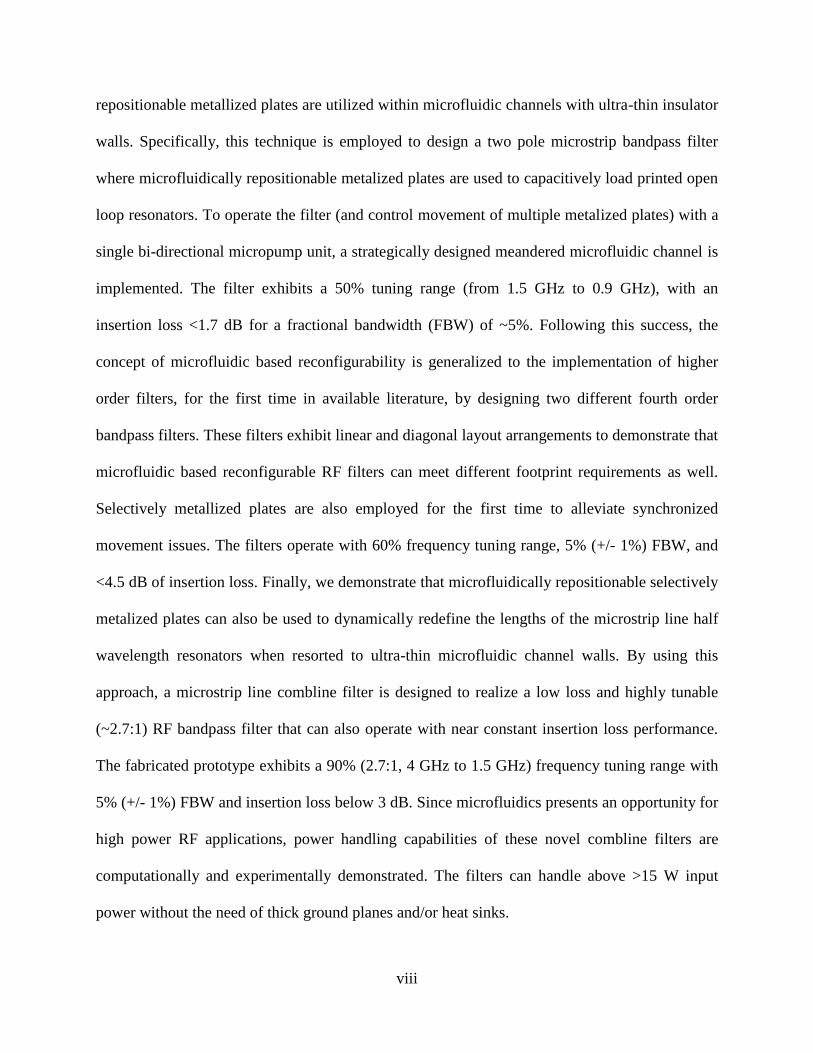
viii
repositionable metallized plates are utilized within microfluidic channels with ultra-thin insulator
walls. Specifically, this technique is employed to design a two pole microstrip bandpass filter
where microfluidically repositionable metalized plates are used to capacitively load printed open
loop resonators. To operate the filter (and control movement of multiple metalized plates) with a
single bi-directional micropump unit, a strategically designed meandered microfluidic channel is
implemented. The filter exhibits a 50% tuning range (from 1.5 GHz to 0.9 GHz), with an
insertion loss <1.7 dB for a fractional bandwidth (FBW) of ~5%. Following this success, the
concept of microfluidic based reconfigurability is generalized to the implementation of higher
order filters, for the first time in available literature, by designing two different fourth order
bandpass filters. These filters exhibit linear and diagonal layout arrangements to demonstrate that
microfluidic based reconfigurable RF filters can meet different footprint requirements as well.
Selectively metallized plates are also employed for the first time to alleviate synchronized
movement issues. The filters operate with 60% frequency tuning range, 5% (+/- 1%) FBW, and
<4.5 dB of insertion loss. Finally, we demonstrate that microfluidically repositionable selectively
metalized plates can also be used to dynamically redefine the lengths of the microstrip line half
wavelength resonators when resorted to ultra-thin microfluidic channel walls. By using this
approach, a microstrip line combline filter is designed to realize a low loss and highly tunable
(~2.7:1) RF bandpass filter that can also operate with near constant insertion loss performance.
The fabricated prototype exhibits a 90% (2.7:1, 4 GHz to 1.5 GHz) frequency tuning range with
5% (+/- 1%) FBW and insertion loss below 3 dB. Since microfluidics presents an opportunity for
high power RF applications, power handling capabilities of these novel combline filters are
computationally and experimentally demonstrated. The filters can handle above >15 W input
power without the need of thick ground planes and/or heat sinks.
1
CHAPTER 1: INTRODUCTION
In the recent years, the demand for compact multifunctional devices has increased
significantly. This has placed stringent restrictions in the size of RF front-ends, where filters tend
to represent a significant portion of the RF front-end, occupying large areas [1]. Also, with the
introduction of LTE bands, the amount of filters utilized in RF transmitter and receiver systems
has increased more than double and it is expected to continue on this trend [2]. Therefore,
reconfigurable filters have recently been presented as a promising alternative to replace the large
filter banks within RF front-ends [3]-[4]. Filters capable of handling high power level have
become of great interest due to increasing demand for base station and satellite communications
[5]. In addition, RF systems, like test equipment, require high-frequency and widely tunable
bandpass filters [6]. With reconfigurable filters the footprint needed could be reduced, and the
power consumption could be significantly improved. The existing literature on reconfigurable
filter technologies can be classified as “ferromagnetic resonances in yttrium iron garnet (YIG)
spheres” [7]-[9], “semiconductor varactors” [10]-[13], “ferroelectric varactors” [13]-[15], “RF
micro-electromechanical systems (MEMS) varactors and switches” [17]-[20], and “evanescent
mode cavity resonators” [21]-[23]. However, this literature also shows that achieving
reconfigurable filters that can simultaneously provide high frequency tuning range (i.e. 50%),
low loss, small footprint, and high power handling capability is still very challenging. To address
these issues, “microfluidically reconfigurable devices” has also recently attracted interest in
electromagnetics community. Therefore, to emphasize the novelty and importance of this
2
dissertation work, the following sub-sections present a detailed literature review of these existing
reconfigurable RF filter technologies:
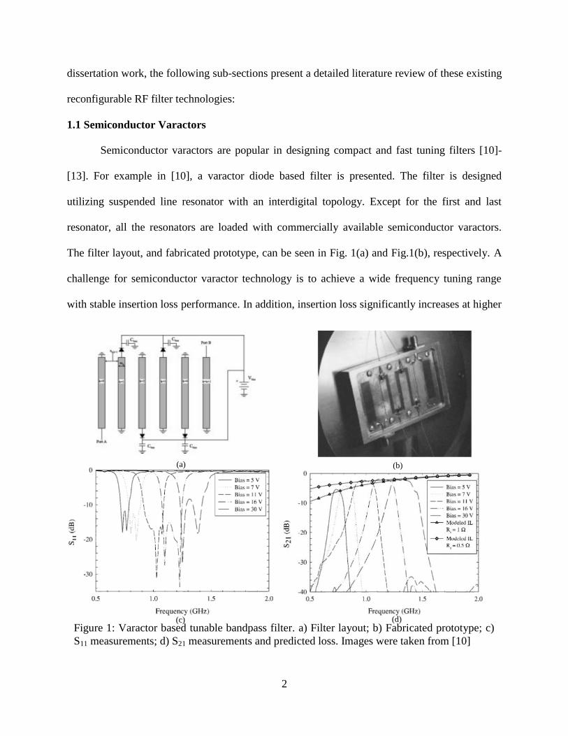
1.1 Semiconductor Varactors
Semiconductor varactors are popular in designing compact and fast tuning filters [10]-
[13]. For example in [10], a varactor diode based filter is presented. The filter is designed
utilizing suspended line resonator with an interdigital topology. Except for the first and last
resonator, all the resonators are loaded with commercially available semiconductor varactors.
The filter layout, and fabricated prototype, can be seen in Fig. 1(a) and Fig.1(b), respectively. A
challenge for semiconductor varactor technology is to achieve a wide frequency tuning range
with stable insertion loss performance. In addition, insertion loss significantly increases at higher
Figure 1: Varactor based tunable bandpass filter. a) Filter layout; b) Fabricated prototype; c)
S11 measurements; d) S21 measurements and predicted loss. Images were taken from [10]
(a) (b)
(c) (d)
3
frequency implementations due to the equivalent series resistances of varactors. For example the
shown filter presents a frequency tunable range of 60% (1.3 GHz to 0.7 GHz), however, the
fractional bandwidth and insertion loss remains relatively constant as 16% and <3 dB,
respectively, only within a small frequency tuning range range of 30% (1.3 GHz to 1 GHz). In
addition, 3dB insertion loss from a 16% wide fractional bandwidth implies a low resonator
quality factor and this is associated with the large series resistance (~1Ω) of the semiconductor
varactors (see Fig. 1(c) and (d)).
In general, filters loaded with semiconductor varactors exhibit a frequency tuning range
that is proportional to the capacitance variation range of the varactors. By using diodes with
higher capacitance variation (1.6 pF to 10 pF), reference [13] shows a 60% (2:1) tunable filter.
However, such varactors are not available at high frequencies (>1GHz) or exhibit high series
resistance. Consequently, the filter in reference [13] was designed at a lower frequency of 0.6
GHz. Hence, achieving low loss performance over a wide frequency tuning range (>50%) at
higher operational frequencies (>1GHz) remains a challenge in this technology.
1.2 Ferroelectric Varactors
Ferroelectric materials are attractive for obtaining RF reconfigurable devices as applied
external voltage across a ferroelectric material can reduce the value of its relative dielectric
constant. Hence, ferroelectric materials can be utilized to form capacitors that can change their
capacitance with applied bias voltage (i.e. ferroelectric varactors). Specifically, ferroelectric
varactors are found attractive for realizing reconfigurable filters at higher frequency bands (e.g.
X-band) since they exhibit better insertion loss and high power handling performances as
compared to semiconductor varactors. Nevertheless, existing filter examples in literature
demonstrate high level of insertion loss as a major limitation. In addition, frequency tuning
4
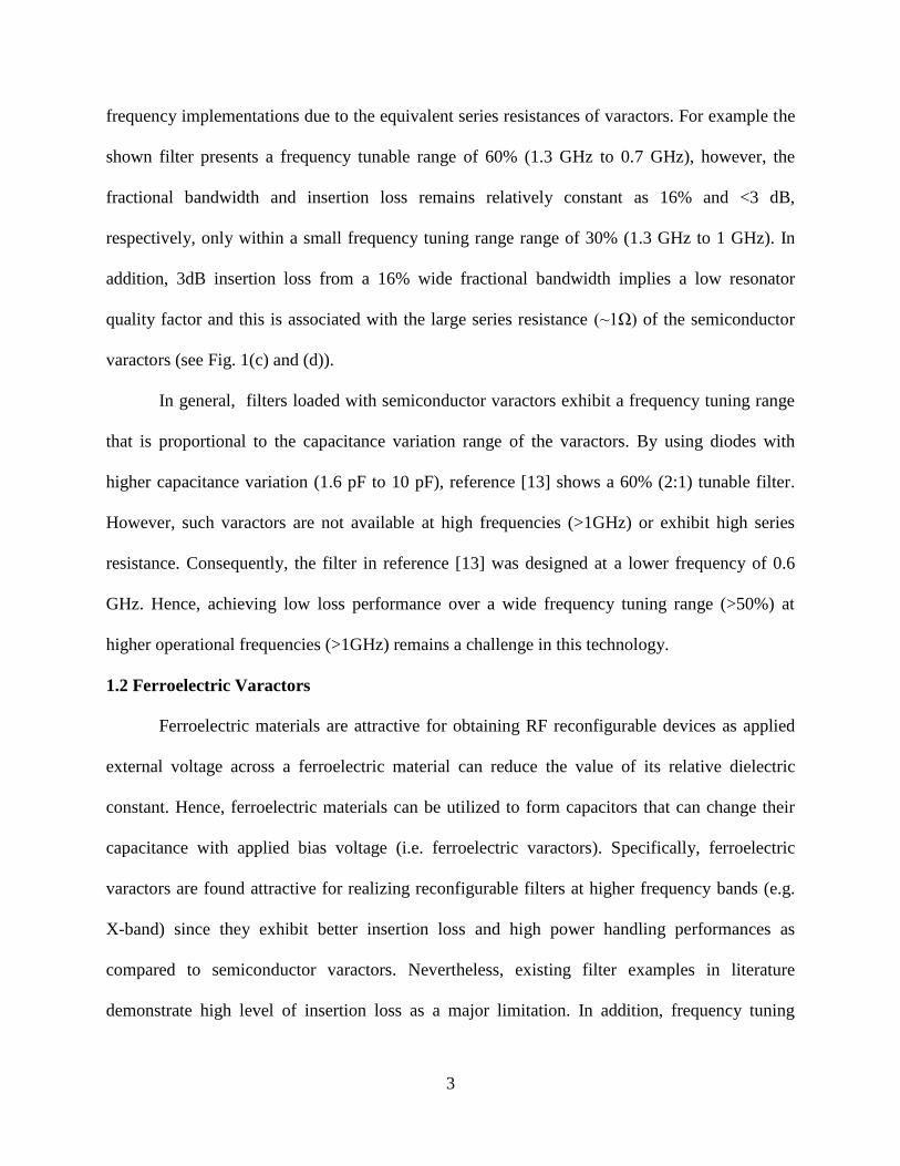
ranges are generally below 50%. As a typical example, we consider reference [15] that presents
the design of a quasi-elliptic ferroelectric tunable filter. The filter is enabled by open-loop
resonators loaded with high-Q ferroelectric barium strontium titanate (BST) varactors (Fig. 2(a)).
This 4th
order filter provides a 6% frequency tunable range centered at 8.35 GHz with an
insertion loss (IL) and return loss (RL) performances varying between 5.7 – 3.5 dB and 10.2 –
7.9 dB, respectively (Fig. 2(b)). The correspondent 1 dB FBW varies from 5.5% to 7.3%. The
overall footprint of the filter was measured as 5.7 x 5.5 mm2. As can be seen, ferroelectric
varactors allow for realization of this compact tunable filter. However, the insertion loss is
significantly high and frequency tuning range is very small due to the limited capacitance
variation in ferroelectric varactors.
S2
1(d
B)
Frequency (GHz)
S11
(dB
)
Frequency (GHz)
Figure 2: Ferroelectric varactor based tunable bandpass filter. a) Fabricated prototype; b) S11
measurements; c) S21 measurements and predicted loss. Images were taken from [15]
(a)
(b)
(c)
5
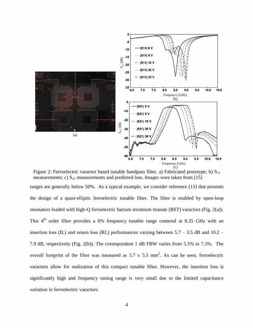
1.3 RF Micro-ElectroMechanical Systems (MEMS) Varactors and Switches
In order to further reduce the losses obtained from ferroelectric varactors, MEMS
technology has been utilized to obtain miniaturized low-loss frequency tunable filters at high
operational frequencies. As an example for the performance of MEMS technologies, we consider
reference [17] that presents a coplanar waveguide (CPW) MEMS based tunable filter. The filter
is formed by resorting to three CPW short-ended half-wavelength resonators loaded with high-Q
MEMS bridge capacitors. The capacitance obtained with MEMS technology is very small (in the
femto scale). Therefore, as shown in Fig. 3(a), to obtain the required capacitance value, to load
each resonator with 70fF, six bridges needed. As can be seen in Fig. 3(b), the filter was capable
of providing a frequency reconfigurable filter at 20 GHz with a low IL <4.15 dB with a constant
FBW of 7.5%. The tuning speed of the filter was characterized as 150 MHz per μs. However,
Figure 3: Continuously tunable MEMS based filter. a) Fabricated prototype; b) S21
measurements; c) S11
measurements and predicted loss. Images were taken from [17]
(a)
(b) (c)
6
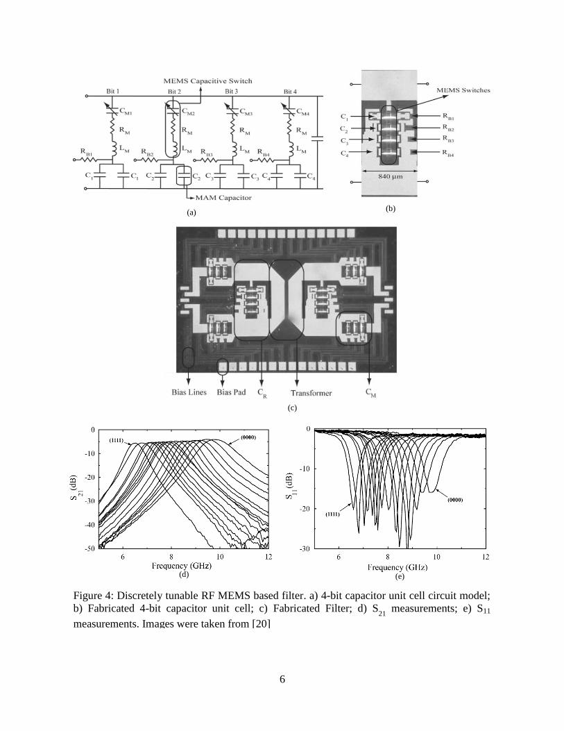
Figure 4: Discretely tunable RF MEMS based filter. a) 4-bit capacitor unit cell circuit model;
b) Fabricated 4-bit capacitor unit cell; c) Fabricated Filter; d) S21
measurements; e) S11
measurements. Images were taken from [20]
(a) (b)
(c)
(d) (e)
7
due to the limitations in capacitance variation of MEMS capacitors, a small frequency tuning
range (14%) was obtained. The continuous frequency tuning range of MEMS based filters is
generally small, therefore, filters employing discrete MEMS switches have also been proposed to
enlarge the frequency tuning range. As an example, we consider reference [20], where a
capacitor bank with four unit cells (see Fig. 4(a) for circuit model and Fig. 4(b) for fabricated) is
used as the digital tuning mechanism. In Fig. 4(a), CM, RM and LM represent the MEMS
capacitor, while RB represents the bias resistor. More specifically, this 4-bit differential filter
(Fig. 4(c)) is capable of tuning 44% (from 6.5 GHz to 10 GHz) in 16 different discrete states.
The insertion loss performance of the filter was measured to be <5.6 dB at the smallest frequency
of operation (Fig. 4(d)) with better than 16 dB return loss over the entire frequency range (Fig.
4(e)).
MEMS technology still presents several limitations in terms of continuous frequency
tuning range and poor power handling capabilities (~100 mW). In addition, MEMS capacitors
present a degraded performance in time. This makes their operational lifetime significantly
shorter than semiconductor and ferroelectric varactor technologies.
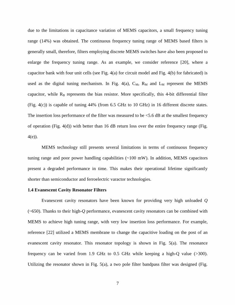
1.4 Evanescent Cavity Resonator Filters
Evanescent cavity resonators have been known for providing very high unloaded Q
(~650). Thanks to their high-Q performance, evanescent cavity resonators can be combined with
MEMS to achieve high tuning range, with very low insertion loss performance. For example,
reference [22] utilized a MEMS membrane to change the capacitive loading on the post of an
evanescent cavity resonator. This resonator topology is shown in Fig. 5(a). The resonance
frequency can be varied from 1.9 GHz to 0.5 GHz while keeping a high-Q value (>300).
Utilizing the resonator shown in Fig. 5(a), a two pole filter bandpass filter was designed (Fig.
8
5(b)). The filter performance, as shown in Fig. 5(c) and (d), is less than 3.5 dB of insertion loss
for a 0.7% FBW over 40% (4.71 GHz to 3.04 GHz) frequency tuning range. However, as
compared to printed microstrip line filters, the size of the filter is significantly large for a 4.5GHz
filter by being 42 × 18 mm2 . Also, since the tuning mechanism is based on MEMS, the
operational lifetime and mechanical stability remains an issue.
1.5 Microfluidically Reconfigurable Devices
Since the end of the 20th
century, and the beginning of the 21st century, microfluidics
have been utilized in a variety of areas such as medical research [24]-[30], cooling systems [31],
and optical devices/sensors [32]-[34], among others. It did not take long before microfluidics
S2
1(d
B)
Frequency (GHz) Frequency (GHz)
S1
1(d
B)
Figure 5: MEMS loaded evanescent-mode cavity resonator based filter. a) Tunable resonator;
b) Fabricated two-pole tunable filter; c) S21
measurements; d) S11 measurements. Images
were taken from [22]
(a) (b)
(d) (c)
9
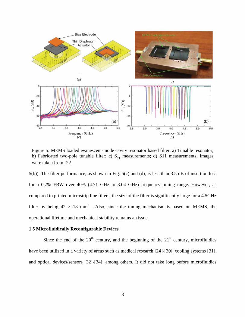
caught the interest of RF and microwave researchers [35]-[36]. More specifically, microfluidics
have been used to obtain a variety of RF devices such as antennas [37]-[40], frequency selective
surfaces [41]-[43], and beam steering [44]. Fig. 6 shows some of the fabricated devices. More
recent studies have shown that microfluidics can be utilized to accomplish reconfigurability in
RF filters [45]. Use of microfluidics in reconfigurable RF filters is especially attractive for
obtaining low-cost, low loss, and highly reconfigurable filters capable
Figure 6: Microfluidically reconfigurable devices. a) CPW folded slot antenna; b) Frequency
selective surface; c) Monopole array with beam-steering. Images (a), (b), and (c) were taken
from [37], [42], and [44] respectively.
(a)
(b)
(c)
10
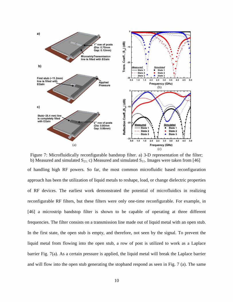
of handling high RF powers. So far, the most common microfluidic based reconfiguration
approach has been the utilization of liquid metals to reshape, load, or change dielectric properties
of RF devices. The earliest work demonstrated the potential of microfluidics in realizing
reconfigurable RF filters, but these filters were only one-time reconfigurable. For example, in
[46] a microstrip bandstop filter is shown to be capable of operating at three different
frequencies. The filter consists on a transmission line made out of liquid metal with an open stub.
In the first state, the open stub is empty, and therefore, not seen by the signal. To prevent the
liquid metal from flowing into the open stub, a row of post is utilized to work as a Laplace
barrier Fig. 7(a). As a certain pressure is applied, the liquid metal will break the Laplace barrier
and will flow into the open stub generating the stopband respond as seen in Fig. 7 (a). The same
Figure 7: Microfluidically reconfigurable bandstop filter. a) 3-D representation of the filter;
b) Measured and simulated S21; c) Measured and simulated S11. Images were taken from [46]
(a)
(b)
(c)
11
principle is utilized to divide the open stub in two regions (state 2 and state 3). Fig. 7 (b) and (c)
show the simulated and measured S21 and S11 responses, respectively. However, once the liquid
metal is flown to fill a channel it cannot be taken back to reverse the frequency reconfiguration
due to sticking of the liquid metal to the channel. A different approach to obtain a one-time
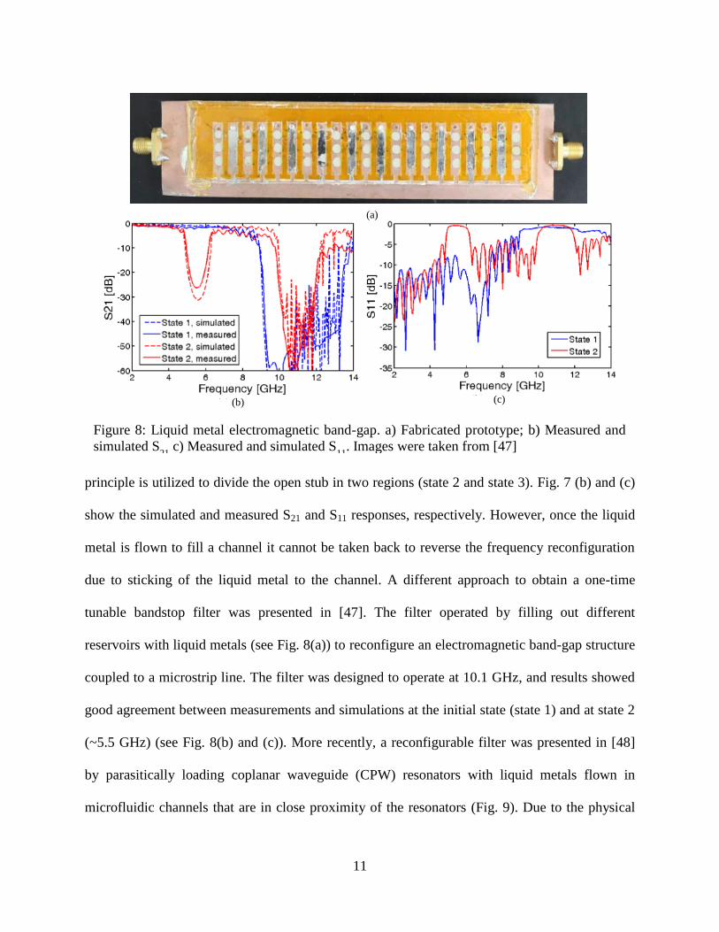
tunable bandstop filter was presented in [47]. The filter operated by filling out different
reservoirs with liquid metals (see Fig. 8(a)) to reconfigure an electromagnetic band-gap structure
coupled to a microstrip line. The filter was designed to operate at 10.1 GHz, and results showed
good agreement between measurements and simulations at the initial state (state 1) and at state 2
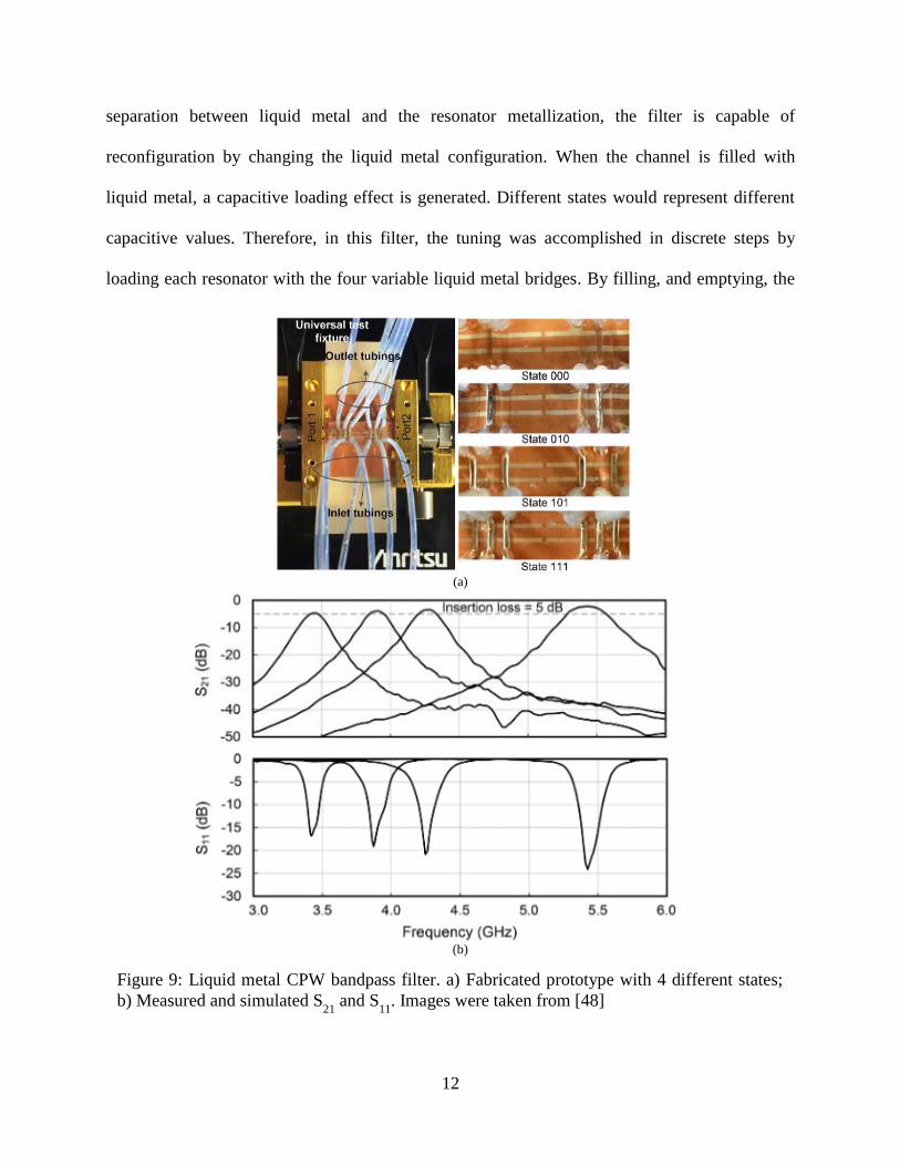
(~5.5 GHz) (see Fig. 8(b) and (c)). More recently, a reconfigurable filter was presented in [48]
by parasitically loading coplanar waveguide (CPW) resonators with liquid metals flown in
microfluidic channels that are in close proximity of the resonators (Fig. 9). Due to the physical
Figure 8: Liquid metal electromagnetic band-gap. a) Fabricated prototype; b) Measured and
simulated S21
c) Measured and simulated S11
. Images were taken from [47]
(a)
(b) (c)
12
separation between liquid metal and the resonator metallization, the filter is capable of
reconfiguration by changing the liquid metal configuration. When the channel is filled with
liquid metal, a capacitive loading effect is generated. Different states would represent different
capacitive values. Therefore, in this filter, the tuning was accomplished in discrete steps by
loading each resonator with the four variable liquid metal bridges. By filling, and emptying, the
Figure 9: Liquid metal CPW bandpass filter. a) Fabricated prototype with 4 different states;
b) Measured and simulated S21
and S11
. Images were taken from [48]
(a)
(b)
13
bridges, the filter in [48], was capable of providing a 47% discrete frequency tunable range
through four different states. The insertion loss performance was <5 dB with a relatively constant
FBW of 5% as can be seen in Fig. 9(b). It is also important to note that reliable actuation of
liquid metals is an on-going research effort and there is currently not a well-established solution.
Rapid oxidization of liquid metals (significantly severe for non-toxic liquid metal Galinstan)
causes them to stick to the channel walls irreversibly. Hence, life time of such filters are quite
limited unless the liquid metal volume in use periodically gets replenished with new liquid metal
volume free of oxidization [49].
Our research group has been a major contributor in the emerging area of microfluidically
reconfigurable RF filters. When this dissertation work started, microfluidic based reconfigurable
filters were at infancy with significant limitations, but with high promise for addressing the
limitation of the previously mentioned technologies. More specifically, microfluidic
reconfiguration was promising for obtaining widely tunable, low loss, and high power handling
RF filters. The following sections of this dissertation will detail our contributions in this area and
the evolution of our work throughout the last 4 years. Our initial work in [50] focused on
implementation and miniaturization of band-stop microstrip filters by utilizing thin film
fabrication procedures (such as benzocyclobutene (BCB)). It was found that thin-films can be
used to achieve significant capacitance enhancement. The initial work in [50] utilized this
capacitance enhancement to achieve a compact X-band filter with a wideband band-stop
response. From this work, it became obvious that if thin-film fabrication techniques are applied
for reconfigurable filters, a high frequency tuning range can be accomplished if a mechanism can
be utilized to alter this capacitance during the device operation. This motivated us to investigate
microfluidics potentially with thin film fabrication aspects. Our early work in microfluidically
14
reconfigurable RF filters dates back to 2013 [51] when one-time reconfigurable liquid metal
based RF filters were being introduced. In contrast, we have (to the best of our knowledge)
demonstrated for the first time the possibility of using microfluidics to realize frequency
reconfigurable RF filters. This demonstration was carried out by designing and implementing a
two-pole frequency-agile bandpass filter based on microfluidically reconfigurable broadside
coupled split ring resonators (BC-SRRs). In these resonators, the top loop was constructed from
liquid metal that can be flown inside Teflon microtubes. Hence, the resonance frequency of the
filter could be changed repetitively by redefining the shape of the top loop of the resonator. A
meandered microfluidic channel was also designed to be able to operate the filter with a single
bi-directional micropump unit. The filter was shown to provide a continuous frequency tuning
range from 650 to 870 MHz with a constant fractional bandwidth (FBW) of 5% and <3 dB of
insertion loss. The frequency tuning range of the filter was shown to be limited by the wall
thicknesses of the tubes as the wall thickness affects the capacitive coupling between the two
loops of a BC-SRR (i.e. capacitive loading of the resonator). In addition, the liquid metal based
construction (Galinstan or Mercury) caused a reliability issue due to the aforementioned issues.
For example, oxidization issue can be reduced by using mercury but its toxicity rules the
technology out from commercial applications. A non-toxic liquid metal is Galinstan, however it
oxidizes very fast and cause sticking within the tubes, potentially resulting in breakdowns in the
liquid metal volume. Although several techniques have been presented to prevent the oxidization
of Galinstan, such as covering the inside of the microfluidic channel with liquid Teflon solution
[52], none of the techniques had proven success to completely remove the oxidization problem
for a long device life time.
15
To overcome the limitations found with liquid metals, in [53] we took a major step by
replacing liquid metal volumes within microfluidic channels with metalized plates that can still
be moved within the channels. We demonstrated this novel technique by realizing a two pole
reconfigurable bandpass filter with open-loop resonators where the open ends were loaded with
microfluidically movable metalized plates. In this approach, the metalized plate acts as a
capacitive load at the open ends of the open loop resonator. By microfluidically repositioning the
metallized plate, the capacitive loading can be varied. To maximize the capacitance variation,
microfluidic channels were constructed by utilizing 25.4 μm thick Liquid Crystal Polymers
(LCP) in order to exhibit a very thin wall above the printed filter area. As compared to prior
liquid metal and tubed implementation, this novel two-pole bandpass filter exhibited a decrease
of ~1.3 dB to 1.7 dB improved insertion loss and a 50% frequency tuning range that is 60% more
than the previous implementation. The toxicity and oxidization drawbacks associated with liquid
metals were successfully addressed with the metalized plate approach.
The microfluidically reconfigurable metalized plate based filters exhibit multiple
resonators each having their own metalized plate. In order to use a single bi-directional
micropump, a single microfluidic channel was meandered over multiple resonators. This
necessitated to have a synchronized motion of multiple plates within the microfluidic channels.
Experiments performed with the two-pole filter mentioned above demonstrated that the
metalized plate technique can suffer from synchronization issue due to the customized
fabrication/placement of metalized plates. The synchronization issue is expected to be much
more challenging for higher order filters exhibiting several resonators. Therefore, in [54], we
introduced the concept of “microfluidically reconfigurable selectively metalized plates” to solve
the synchronization issues and applied this concept to realize higher (4th
) order bandpass filters.
16
To the best of knowledge, these were also the first higher order filters demonstrated with any
microfluidic reconfiguration technique. Moreover, we also demonstrated that selectively
metalized plate approach can be utilized for meeting different footprint requirements. A hybrid
(EM + Lumped) circuit model was utilized in design of these filters in contrast to lengthy full-
wave simulations employed for our prior filter designs. The filters were also controlled
electronically with external micropumps. To the best of our knowledge, all the previous literature
on microfluidic filters was done utilizing syringes, and no speed characterization can be found.
With this set-up speed characterizations were performed and novel microfluidic channel shapes
were introduced for speed improvements. The fabricated prototype was measured to provide a
5% (+/-1%) FBW over a 61% frequency tuning range with a worst case insertion loss of 4.5 dB.
Extending the frequency tuning range of open loop resonators that are loaded with
microfluidically repositionable metalized plates beyond 2:1 is possible. However, high level of
capacitive loading needed to lower the operational frequency of the resonator significantly
reduces the unloaded quality factor of the resonator (Qu) and therefore the filter’s insertion loss
performance. A traditional approach to solve this issue would be to employ resonators with
higher Qu factors and perform microfluidic based reconfigurable capacitive loading to tune the
resonance frequency. However, resonators employing higher Qu factors are volumetric (such as
evanescent cavity resonators and suspended microstrip line resonators) and therefore
significantly increases filter size. As an alternative solution, in our most recent work, we
introduce a novel approach for reconfiguration of conventional printed half wavelength
microstrip resonators using microfluidics. Specifically, by placing a microfluidically
repositionable selectively metalized plate on top of a conventional half wavelength microstrip
resonator, the physical length of the resonator is dynamically redefined. This is accomplished by
17
utilizing an ultra-thin channel wall between the plate metallization and printed resonator so that
an RF short is created. Since resonator is not externally loaded, the resonator exhibits a close to
constant Qu throughout the entire tuning range. To enlarge the frequency tuning range of the
resonator beyond 2:1, a transition between open ended and short ended half wavelength
microstrip resonators is also employed. By combining this two tuning approaches (i.e. extend the
length of the resonator and transition from open ended to short ended structure), a resonator
tunable over a wide frequency tuning range is accomplished. Utilizing this novel resonator, a 4th
order bandpass filter was designed at 4 GHz. The presented results show that the filter operates
with a 90% (2.7:1) tuning range, constant 5% FBW, and insertion loss performance less than <2
dB. To demonstrate that microfluidically reconfigurable filters are promising for high power RF
applications, power handling characterization of the filter was also performed. Experimental
results showed that this filter is capable of handling >15 W of input RF signal power at the
highest operation frequency which also represents the lowest unloaded quality factor within the
frequency tuning range. The power handling capability is limited by the highest temperature the
materials within its construction can withstand to. The power handling capabilities of the filter
can be significantly increased with addition of thicker ground planes, heat sinks, and/or by
utilization of ceramic substrates.
In the following chapters, the contributions of this dissertation will be detailed. These
contributions can be briefly summarized as:
First time realization of a microfluidically reconfigurable frequency-agile bandpass
filter.
Introduction of microfluidically controlled metallized plates technique to alleviate
reliability and high losses related to liquid metals.
18
First time realization of higher order (4th
order) microfludically reconfigurable
frequency-agile bandpass filters. These filters also show superior frequency tuning
(~2:1) and high power handling capability.
Introduction of a novel technique for synchronously tuning several resonators with a
microfludically repositionable selectively metallized plate.
Introduction of strategically designed microfluidic channel and selectively metalized
plate shapes for tuning speed improvement.
Introduction of a novel half wavelength microfluidically reconfigurable resonator
structure performing with close to constant unloaded quality factor across a very wide
frequency tuning range (2.7:1, 1.5 GHz to 4.0 GHz).
Realization of higher order frequency-agile bandpass filters with 90% frequency
tuning range exhibiting low and close to constant insertion loss performances.
Power handling characterization of microfluidically reconfigurable filters showing
capability for handling >15 W of power.
19
CHAPTER 2: WIDEBAND BAND-STOP X-BAND FILTER USING ELECTRICALLY
SMALL TIGHTLY COUPLED RESONATORS1
Filter size becomes especially important when the receive/transmit circuits of large
antenna arrays need to be tightly integrated. For this work, a critical performance requirement
was a very narrow footprint (<2.5 mm) for a bandstop filter in the X-band region with a broad
bandwidth of 25%. To address the contending size and bandwidth demand, the presented filter
employed electrically small capacitively-loaded open loop resonators over a 7 µm thin
Benzocyclobutene (BCB, εr=2.4, tanδ=0.0015) layer in order to bring them in close proximity of
the microstrip signal line and maximize the coupling. Consequently, a compact wideband band-
stop filter with a footprint of 15.7 x 2.5 mm2 (i.e. λ0/2 × λ0/13 at 9.2 GHz) was realized. The
fabricated filter demonstrated >25 dB IL from 8.1 GHz to 9.64 GHz. Moreover, it operated with
<1.5 dB measured IL within its passband (i.e. <7.3 GHz and >11.2 GHz) and satisfied the
desired selectivity criteria.
2.1 Filter Design
A microstrip implementation was utilized to be compatible with the desired installation
requirements. To keep the size and passband IL small, the substrate material was selected as
99.9% Alumina (Al2O3, εr=9.8, tanδ = 0.0004). The circuit layout of the band-stop filter
consisted of λg/4 separated resonators coupled to a uniform microstrip signal line. As detailed in
[55], the adjacent resonators are alternated on each side of the signal line to minimize their
mutual coupling (see Fig. 10). Since the selected substrate thickness of 0.508 mm results in a
1 This chapter was previously published in [50]. Permission is included in Appendix B.
20
0.4947 mm wide 50 Ω signal line, the width of the resonator footprints had to be <1 mm to meet
the overall filter width specification of 2.5 mm. In addition, the λg/4 separation limits the
maximum resonator length to 3.1 mm. To address this size limitation, we considered the spiral
(SR), split-ring (SRR), and capacitively-loaded open-loop resonators in an elongated rectangular
shape (see Fig. 10(b)) as potential choices of electrically small designs. The coupling coefficient
Resonator
7um BCB
Gold TL
0.508mm
Alumina
Rw
Rl
g
g
G
Tw
Fl
Fw
Sn
λg/4
Figure 10: Stopband filter. (a) Substrate stack-up; (b) Capacitively-loaded (14 fingers) open
loop resonator; (c) Filter layout. The dimensions (in µm) are: Tw=406, R
w=1100, R
l=3000,
g=24, G=167, Fw=2400, F
l=15700, S
1=401, S
2=160, S
3=165, S
4=23, S
5=48, λ
g/4=3100. The
signal line width is 406 µm.
(a) (b)
(c)
0
50
100
150
200
250
300
350
400
450
3
5
7
9
11
13
15
17
19
21
1.6 1.7 1.8 1.9 2 2.1 2.2 2.3
Sn
(μm
)
BC
B T
hic
kn
ess
(μ
m)
X/Zo (unitless)
Coupling Vs Thickness
Coupling Vs Spacing
X/Zo vs. BCB thickness for Sn = 0
X/Zo vs. Sn for 7um BCB
Figure 11: Normalized reactance slope (X/Z0) as a function BCB film thickness and signal line
separation.
21
studies with the conventional single layer realizations revealed that the desired 25% FBW was
unattainable regardless of which type of resonator was used. For example, a separation of 0.5 µm
between any resonator type and the signal line leads to a small coupling coefficient that can only
provide about 12% FBW. Consequently, a low loss thin film BCB layer was introduced between
the signal line and the resonators to increase the coupling by overlapping the resonators and the
signal line as shown in Fig. 10(c).
The performance evaluation of the resonators was carried out over a 20 µm-thick BCB
layer. For all resonators, it was found that the coupling was maximized as the line width of the
overlapping trace of the resonators (Tw) gets closer to that of the signal line. The layouts of the
resonators were modified to fit into the specified area of 3.1×1.5 mm2 and the one that provides
the highest amount of coupling with the signal line was selected for the implementation. The
normalized reactance slope (X/Z0 = f0/2Δf3dB, f0: resonance frequency and Δf3dB: 3dB IL
bandwidth of a loosely coupled resonator) was extracted using the Momentum suite of the
Agilent’s Advanced Design System (ADS). SR and SRR resonators were able to fit into the
given footprint area when smaller trace widths were utilized, however, this also resulted in larger
X/Z0 values implying a smaller coupling level. The area of the open-loop resonator was
miniaturized with the capacitive loading and by employing a trace width (Tw) that is slightly
narrower (i.e. 406 µm) than the signal line. With this configuration, the capacitively-loaded open
loop resonator was found to provide the smallest X/Z0 value.
Having decided on the resonator type, the thickness of the insulator was investigated to
realize the desired X/Z0 values. Fig. 11 presents the X/Z0 as a function of the insulator thickness
when the resonator is positioned directly above the signal line (Sn=0) for maximum coupling.
Since X/Z0 must be smaller than 1.8 for the desired 25% BW, it is observed that the BCB layer
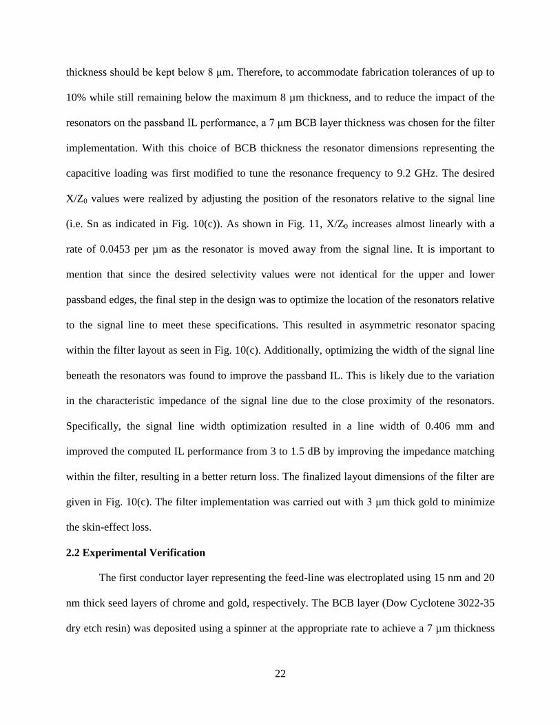
22
thickness should be kept below 8 μm. Therefore, to accommodate fabrication tolerances of up to
10% while still remaining below the maximum 8 µm thickness, and to reduce the impact of the
resonators on the passband IL performance, a 7 μm BCB layer thickness was chosen for the filter
implementation. With this choice of BCB thickness the resonator dimensions representing the
capacitive loading was first modified to tune the resonance frequency to 9.2 GHz. The desired
X/Z0 values were realized by adjusting the position of the resonators relative to the signal line
(i.e. Sn as indicated in Fig. 10(c)). As shown in Fig. 11, X/Z0 increases almost linearly with a
rate of 0.0453 per µm as the resonator is moved away from the signal line. It is important to
mention that since the desired selectivity values were not identical for the upper and lower
passband edges, the final step in the design was to optimize the location of the resonators relative
to the signal line to meet these specifications. This resulted in asymmetric resonator spacing
within the filter layout as seen in Fig. 10(c). Additionally, optimizing the width of the signal line
beneath the resonators was found to improve the passband IL. This is likely due to the variation
in the characteristic impedance of the signal line due to the close proximity of the resonators.
Specifically, the signal line width optimization resulted in a line width of 0.406 mm and
improved the computed IL performance from 3 to 1.5 dB by improving the impedance matching
within the filter, resulting in a better return loss. The finalized layout dimensions of the filter are
given in Fig. 10(c). The filter implementation was carried out with 3 μm thick gold to minimize
the skin-effect loss.
2.2 Experimental Verification
The first conductor layer representing the feed-line was electroplated using 15 nm and 20
nm thick seed layers of chrome and gold, respectively. The BCB layer (Dow Cyclotene 3022-35
dry etch resin) was deposited using a spinner at the appropriate rate to achieve a 7 µm thickness
23
and subsequently cured in a vacuum oven for 2.5 hours at 250° C. A slow temperature ramp
(100° C per hour) was used to obtain a planar film. To form the second conductor layer
representing the resonators a sputtering system was used to deposit 3 µm of gold and lift-off was
performed subsequently with 3000py negative photo resist. Finally, the BCB was removed from
the ends of the filter using O2 and SF6 plasma in a ratio of 5:1. As the BCB is etched at the same
rate of the photoresist mask, a thick (17 µm) 4620 positive photoresist was used to protect the
filter during the plasma etching process. Aluminum and gold were evaporated onto the backside
of the wafer to obtain a good conductive ground. For RF measurements, the filter wafer and
0 2 4 6 8 10 12 14 16 18 20-40
-30
-20
-10
0
Frequency (GHz)
S1
1 (
dB
)
7 8 9 10 11 12-40
-30
-20
-10
0
Frequency (GHz)
S1
1 (
dB
)
0 2 4 6 8 10 12 14 16 18 20-40
-30
-20
-10
0
Frequency (GHz)
S2
1 (
dB
)
7 8 9 10 11 12-40
-30
-20
-10
0
Frequency (GHz)
S2
1 (
dB
)
(a) (b)
(c) (d)
(e) (f)
Figure 12: Experimental verification of stopband filter. (a) Fabricated filter and testing
assembly with J-micro-probes; (b) Close-up snapshot of the resonator. Measured (–––) and
simulated (x–x–x) S-parameters: (c) & (d) S21; (e) & (f) S11.
24
Jmicro Technology probe points were attached to a brass carrier using silver epoxy and
interconnected using gold wire bonds. Fig. 12 (a) and (b) shows fabricated filter assembly and
close-up view of the resonator on top of the BCB layer.
As a consequence of using an insulator layer with a thickness comparable to that of the
conductor layer, a bulge was found to be formed along the length of the filter in the BCB layer
even though a slow temperature ramp was used for the curing. Profilometer measurements
revealed the height of this bulge to be ~3.5 µm higher than the nominal 7 µm BCB height on top
of the TL, with a width of ~0.5 µm. In order to accurately simulate this feature, the filter was
modeled using the full-wave electromagnetic solver Ansys HFSSv14 by approximating the BCB
surface and the overlaid resonators with small sections of rectangular planes. It was found that
the bulge in the BCB accounted for a 300 MHz shift in the frequency response. Accordingly,
future designs in need of wider bandwidths should consider an extra polishing step to planarize
the BCB layer prior to the resonator metallization.
As shown in Fig. 12(c), (d), (e), and (f), the simulated and measured data are in good
agreement. The measurements were performed using an Anritsu Lighting VNA and ground
signal ground Picoprobes by GGB Industries, Inc. The measured passband IL was <1.5 dB
below 7.3 GHz and above 11.2 GHz. The 3 dB IL bandwidth extended from 7.62 GHz to 10.37
GHz, with more than 25 dB rejection between 8.1 GHz and 9.64 GHz and a selectivity of >40dB
at both stop-band edges. Hence, the prototype successfully met the desired IL and selectivity
criteria by providing 25% FBW.
2.3 Concluding Remarks of Chapter 2
An electrically small coupled resonator X-band filter capable of exhibiting a 25%
fractional bandwidth band-stop response was presented. Different than the existing designs, a 7
25
µm thin BCB layer was utilized to bring the resonators within the close proximity of a microstrip
feed line to achieve the desired wideband response. The resonator shape was specifically
modified to minimize the width of the filter to 2.5 mm (i.e. λ0/13) at the center frequency of 9.2
GHz. The coupling level between the resonators and the signal line was presented as a function
of BCB thickness and resonator position. Layout analysis and optimizations have demonstrated
that the very thin BCB layer thickness results in variation in the optimum signal line width. In
addition, the planarization of the insulator surface is important for the accuracy of the measured
results. With this study it was found that high capacitance value can be obtained with a
multilayer approach by resorting to thin-film insulators. In the following chapters the realization
of multilayer filters, and the utilization of thin-film insulators, will be further extended to
reconfigurable RF filters.
26
CHAPTER 3: FREQUENCY-AGILE BANDPASS FILTER USING LIQUID METAL
TUNABLE BROADSIDE COUPLED SPLIT RING RESONATORS2
Frequency-agile filters are among the key components for fulfilling the stringent
requirements of emerging wideband and multifunctional RF front-ends. Due to the interest in
liquid metals for achieving reconfigurable devices with lower loss and higher power handling
capability, this work has introduced a continuously tunable liquid metal filter for the first time.
The proposed two pole filter consists on a microstrip line broadsided coupled split ring resonator
(BC-SRR) in which the top loop is made out of liquid metal. The frequency tuning is
accomplished by gradually moving liquid metal out of the resonator region by displacing it with
a low loss dielectric liquid.
3.1 Filter Design
To verify the proposed concept without resorting to microchannel fabrication, the BC-
SRRs of the presented filter are realized by making use of PTFE tubing. As shown in Fig. 13, the
top open loop resonators of the BC-SRRs are constructed from overlaid liquid metal filled PTFE
tubes having 16 mil (0.4064 mm) inner radius and 6mil (0.1524 mm) wall thickness. The
2 This chapter was previously published in [51]. Permission is included in Appendix B.
Figure 13: The tube based coupled line geometry and its equivalent multilayered strip model 1.2mm
Conductor that forms the bottom open loop resonator
Tube wall (6mil thick)
Liquid metal (radius 16mil)
h = 13mil
1.2mm
Conductor that forms the top open loop resonator
27
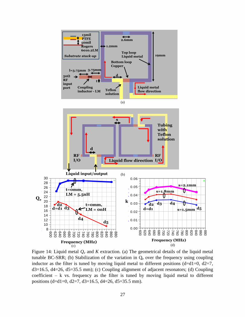
Figure 14: Liquid metal Qe and K extraction. (a) The geometrical details of the liquid metal
tunable BC-SRR; (b) Stabilization of the variation in Qe over the frequency using coupling
inductor as the filter is tuned by moving liquid metal to different positions (d=d1=0, d2=7,
d3=16.5, d4=26, d5=35.5 mm); (c) Coupling alignment of adjacent resonators; (d) Coupling
coefficient – k vs. frequency as the filter is tuned by moving liquid metal to different
positions (d=d1=0, d2=7, d3=16.5, d4=26, d5=35.5 mm).
d=d1
62
0
64
0
66
0
68
0
70
0
72
0
74
0
76
0
78
0
80
0
82
0
84
0
86
0
60
0
88
0
10
12
14
16
18
20
22
24
26
28
8
30
[f1,f2,f3,f4,f5]/1e6
[Qe
1,Q
e2
,Qe
3,Q
e4
,Qe
5]
(H
)
H
Frequency (MHz)
Qe
d2
d4
d3
d5
t=0mm,LM = 5.5nH
t=0mm, LM = 0nH
Bottom loop Copper
Top loopLiquid metal
2.6mm
Teflon solution
19mm
Coupling inductor - LM
3.75mm
t
Liquid metal flow direction
50mil Rogers 6010.2LM
13mil PTFE
Substrate stack-up
1.2mm
50ΩRFinputport
d
l=3.75mm
(a)
(b)
s
Liquid flow direction
Tubing withTeflon solution
RF I/O
RF I/O
Liquid input/output
d
620
640
660
680
700
720
740
760
780
800
820
840
860
600
880
0.01
0.02
0.03
0.04
0.05
0.00
0.06
[ (f1+f2)/2,(f3+f4)/2,(f5+f6)/2,(f7+f8)/2,(f9+f10)/2]/1e6
[k1
,k2
,k3
,k4
,k5
] (
H)
H
Frequency (MHz)
k
s=2.1mm
s=1.5mm
s=1.8mm
d2d=d1
d3 d4
d5
(c) (d)
28
bottom loop of the resonator is formed by a 50 Ω microstrip line with 1.2 mm width. The design
and parametric optimizations of this geometry through full wave electromagnetic simulation
software is computationally expensive and quite time consuming. In order to utilize the fast
planar circuit simulation tools (i.e. circuit schematics and Momentum) of Agilent Advanced
Design System (ADS), an equivalent multilayered strip model was employed by considering the
capacitance per unit length between the two conductor lines of the BC-SRR. Ignoring the
fringing fields, equating the capacitance per unit length of the two structures shown in Fig. 13
results in an equivalent thickness of h=11.5 mil for the multilayered strips. The resonance
frequency comparison between the full wave (Ansys HFSSv14) and the ADS model of a BC-
SRR resonator demonstrated that h=13 mil is more accurate for representing the resonance
frequency. Hence, the filter design was carried out by the equivalent model that represents the
liquid metal with a 1.2 mm wide line printed on a 13 mil (0.3302 mm) thick PTFE substrate
(εr=2.2, tanδ=0.0001).
Fig. 14 depicts the computational model of the BC-SRR with its substrate stack-up and
physical dimensions. The BC-SRR is square and its dimensions are adjusted such that its bottom
open loop resonates at about 850 MHz without the presence of the top loop. When the top loop is
completely filled up with liquid metal (i.e. d=0 mm), the proposed BC-SRR configuration
resonates at its lowest frequency of 630 MHz. This frequency is determined by the physical
separation between the loops of the BC-SRR and can be further reduced if tubes with thinner
walls or microfabrication techniques are utilized. Moving the liquid metal out of the resonator
area by displacing it with Teflon solution (εr=2.2) gradually shifts the resonance frequency to
that of the single loop resonator for d=35.5 mm.
29
The required external quality factor (Qe) and coupling coefficient (K) of a second order
Butterworth coupled resonator filter can be calculated from its lowpass lumped circuit prototype
(g0=g3=1, g1=g2=1.4142) as Qe = g0·g1/FBW = 28 and K=FBW/√(g1·g2)=0.0354 for a FBW of
5% [55]. Such a filter can exhibit a well-matched constant FBW performance only if Qe and K
are maintained relatively constant over the tuning range of its resonators. As depicted in Fig.
14(c), the Qe of the liquid metal based BC-SRR significantly decreases as it is tuned to higher
frequencies. This behavior is independent of the tapping location t. To stabilize the variation in
Qe over the tuning range, a lumped coupling inductor (LM) was introduced to the feed line as
shown in Fig. 14(c). The reactance of the inductor is proportional to the frequency and counter-
acts the reduction in Qe at higher frequencies. Parametric studies were carried out in ADS and a
tapping location of t=0 mm with LM=5.5 nH was determined to provide a relatively constant Qe
over the operational band. These studies were carried out by simultaneously considering five
different liquid metal locations (d=d1=0, d2=7, d3=16.5, d4=26, d5=35.5 mm) and these are
identified as data points in the design curves presented in Figures 14(c) and (d).
To achieve a relatively constant k over the frequency range, different resonator
alignments were initially considered. Among these, the 180o rotated alignment shown in Fig.
14(b) was found to satisfy the desired need. As depicted in Fig. 14(b), the separation between the
resonators was selected to be 1.8 mm to ensure that the minimum filter bandwidth was at least
5% over the tuning range. Specifically, the k is 0.035 at the edges and 0.04 at the middle of the
operation band. It should be noted that non-square resonator shapes can be potentially employed
possibly with lumped coupling capacitors to realize different tunable bandwidth characteristics
such as increasing/decreasing or constant absolute bandwidth. Such shape modifications may
also provide better Qe and K stability over frequency and they are currently being investigated.
30
Fig. 14(b) also demonstrates the proposed tubing layout of the filter. As seen, the frequency
tuning of the resonators can be simultaneously controlled using a single syringe pump or
micropump unit. This requires an accurately adjusted Teflon solution spacing between the liquid
metal volumes.
3.2 Experimental Verification
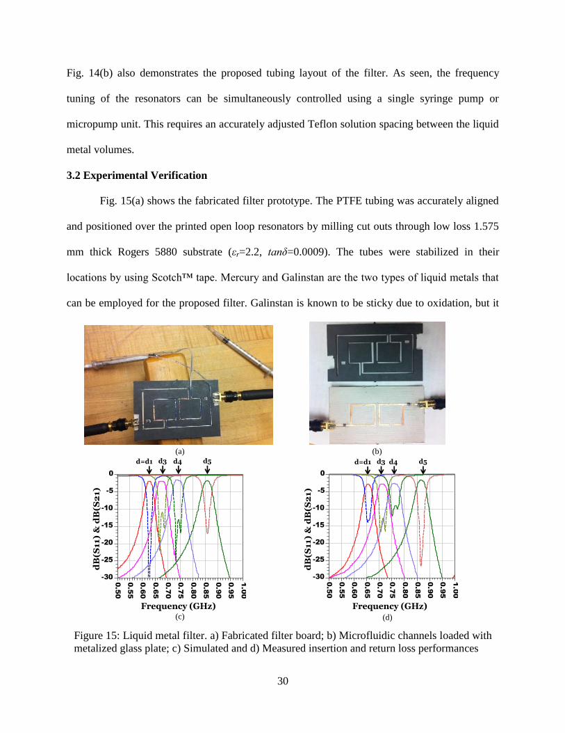
Fig. 15(a) shows the fabricated filter prototype. The PTFE tubing was accurately aligned
and positioned over the printed open loop resonators by milling cut outs through low loss 1.575
mm thick Rogers 5880 substrate (εr=2.2, tanδ=0.0009). The tubes were stabilized in their
locations by using Scotch™ tape. Mercury and Galinstan are the two types of liquid metals that
can be employed for the proposed filter. Galinstan is known to be sticky due to oxidation, but it
Figure 15: Liquid metal filter. a) Fabricated filter board; b) Microfluidic channels loaded with
metalized glass plate; c) Simulated and d) Measured insertion and return loss performances
(a) (b)
(c) (d)
d=d1 d3 d4 d5
Frequency (GHz)
dB
(S11)
& d
B(S
21)
0.55
0.60
0.65
0.70
0.75
0.80
0.85
0.90
0.95
0.50
1.00
-25
-20
-15
-10
-5
-30
0
freq, GHz
dB
(S
(2,1))
dB
(S
(1,1))
dB
(S
(4,3))
dB
(S
(3,3))
dB
(S
(6,5))
dB
(S
(5,5))
dB
(S
(8,7))
dB
(S
(7,7))
d=d1 d3 d4 d5
Frequency (GHz)
dB
(S11)
& d
B(S
21)
0.55
0.60
0.65
0.70
0.75
0.80
0.85
0.90
0.95
0.50
1.00
-25
-20
-15
-10
-5
-30
0
freq, GHz
dB
(S
(2,1))
dB
(S
(1,1))
dB
(S
(4,3))
dB
(S
(3,3))
dB
(S
(6,5))
dB
(S
(5,5))
dB
(S
(8,7))
dB
(S
(7,7))
31
can still be moved within the PTFE tubing with the aid of Teflon solution (AF 400S2-100-1, 1%
Teflon™ powdered resin dissolved in 3M FC-40, acquired from Dupont). Due to its non-
toxicity, Galinstan (σ=3.46×10⁶) was selected for the experimental verifications. The liquid
metal and Teflon solution was controlled by two syringes as depicted in Fig. 15(a). The ADS
simulations of the overall filter for various d values using the LM=5.5 nH coupling inductors
resulted in a return loss that is not well matched (<8 dB). To alleviate the issue, a parametric
sweep was carried out over the complete filter models. For t=0 mm, increasing the coupling
inductors to LM=12 nH was found to provide a return loss performance >10 dB over the whole
frequency range as shown in Fig. 15(c). The inductors were acquired from the Coilcraft 0805CS
series and were modeled to exhibit a Q of 50 at 850 MHz. The simulated insertion loss is about 2
dB throughout the operation band. Fig. 15(d) presents the measured performance of the filter.
For the filter prototype, LM=10 nH was experimentally determined to provide the best >10 dB
return loss performance. The measured filter responses are about 20 MHz higher than the
simulated data. The measured insertion loss is 3 dB at the lowest frequency. These slight
deviations in measurements can be associated with the imperfections in fabrication, unaccounted
loss of the PTFE tubing and the overlaid substrate used for guiding the tubing. The filter exhibits
a measured tunability from 650 to 870 MHz with near constant 5%, -3 dB, FBW. The footprint
of the resonators is about 20×40 mm2.
3.3 Concluding Remarks of Chapter 3
Frequency-agile filters based on liquid metal tunable BC-SRRs were presented. The
concept is demonstrated through a second order Butterworth filter prototype realized by using
PTFE tubing filled with Galinstan and Teflon solution. Specifically, a constant 5% FBW
bandpass filter tunable from 650 to 870 MHz was demonstrated to operate with <3 dB insertion
32
loss. The tunability range of these filters can be significantly extended using microfabrication
techniques to bring the liquid metal physically closer to the bottom open-loop resonator of the
BC-SRR. By using ultra-thin micro-channels, the tuning speeds can be less than milliseconds.
The piezoelectric based micropumps can be utilized for convenient control of the tuning
mechanism. The presented design is also suitable to be generalized to higher order tunable filters
that are controlled only with a single pump. Realization of these aspects will be presented in the
following chapters. However, it is important to mention that its tuning speed will be significantly
lower as compared with other type of tunable filters like piezoelectric or ferroelectric based. Also
due to its mechanical properties, lifetime of the filter can be compromised; therefore, in the
following chapter we demonstrate a filter with metallized plates instead of liquid metal to extend
its lifetime. Since the tunability is not based on any non-linear device, in future chapters we
demonstrate the high power capabilities of microfluidically based filters.
33
CHAPTER 4: HIGHLY RECONFIGURABLE BANDPASS FILTER USING
MICROFLUIDICALLY CONTROLED METALLIZED GLASS PLATES3
Even though liquid metal represents a strong alternative to accomplish reconfigurable RF
filters, it introduces several issues such as its toxicity, low reliability due to quick oxidization,
and high losses. To overcome these limitations, we resorted to a novel resonator arrangement
that allows for replacing the liquid metal by metallized glass plates. To enhance the capacitive
loading of the metallized glass plates, we also resorted to in-house built microfluidic channels
constructed from thin insulator walls. As expected, this channel construction increased the
frequency tuning range of the filter considerably as compared to prior liquid metal and tube base
approach.
4.1 Filter Design
Fig. 16(b) depicts the substrate stack-up used to construct the presented microfluidic
based reconfigurable filter. A two pole coupled resonator bandpass filter was realized to operate
at 1.5GHz utilizing the approach explained in [55]. The filter consisted of two open loop
microstrip resonators printed on a 1.27mm thick Rogers 6010.2LM board (εr = 10.2, tanδ =
0.0023). The dimensions of the resonator are shown in Fig. 16(a) and they were finalized by
utilizing the Momentum suite of Agilent Advanced Design System (ADS).
The tuning mechanism of the filter relied on moving a metallized glass plate over the
open ends of the resonators as illustrated in the layout shown in Fig. 16(c). The metalized glass
plate creates a capacitive loading effect across the open ends of the resonator and therefore 3 This chapter was previously published in [53]. Permission is included in Appendix B.
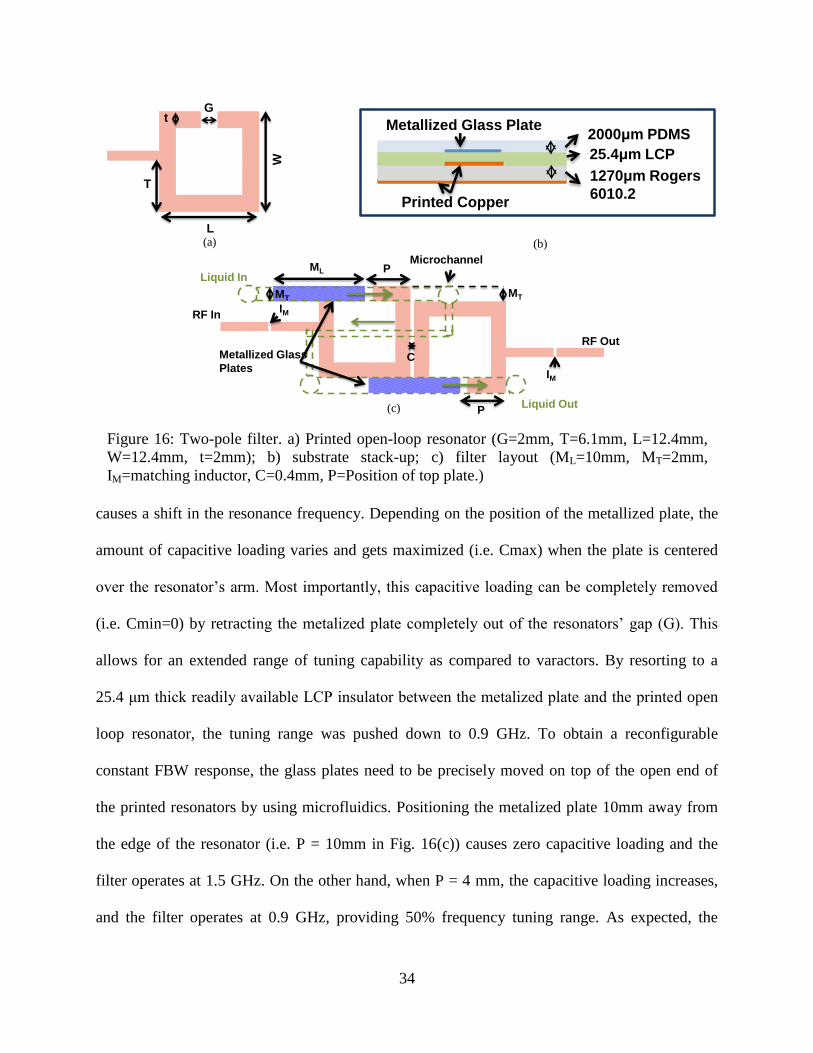
34
causes a shift in the resonance frequency. Depending on the position of the metallized plate, the
amount of capacitive loading varies and gets maximized (i.e. Cmax) when the plate is centered
over the resonator’s arm. Most importantly, this capacitive loading can be completely removed
(i.e. Cmin=0) by retracting the metalized plate completely out of the resonators’ gap (G). This
allows for an extended range of tuning capability as compared to varactors. By resorting to a
25.4 μm thick readily available LCP insulator between the metalized plate and the printed open
loop resonator, the tuning range was pushed down to 0.9 GHz. To obtain a reconfigurable
constant FBW response, the glass plates need to be precisely moved on top of the open end of
the printed resonators by using microfluidics. Positioning the metalized plate 10mm away from
the edge of the resonator (i.e. P = 10mm in Fig. 16(c)) causes zero capacitive loading and the
filter operates at 1.5 GHz. On the other hand, when P = 4 mm, the capacitive loading increases,
and the filter operates at 0.9 GHz, providing 50% frequency tuning range. As expected, the
Figure 16: Two-pole filter. a) Printed open-loop resonator (G=2mm, T=6.1mm, L=12.4mm,
W=12.4mm, t=2mm); b) substrate stack-up; c) filter layout (ML=10mm, MT=2mm,
IM=matching inductor, C=0.4mm, P=Position of top plate.)
(a) (b)
(c)
T
W
L
tG
Printed Copper
1270μm Rogers
6010.2
25.4μm LCP
2000μm PDMSMetallized Glass Plate
P
P
MT
C
ML
Microchannel
Metallized Glass
Plates
RF In
RF Out
IM
IM
Liquid In
MT
Liquid Out
35
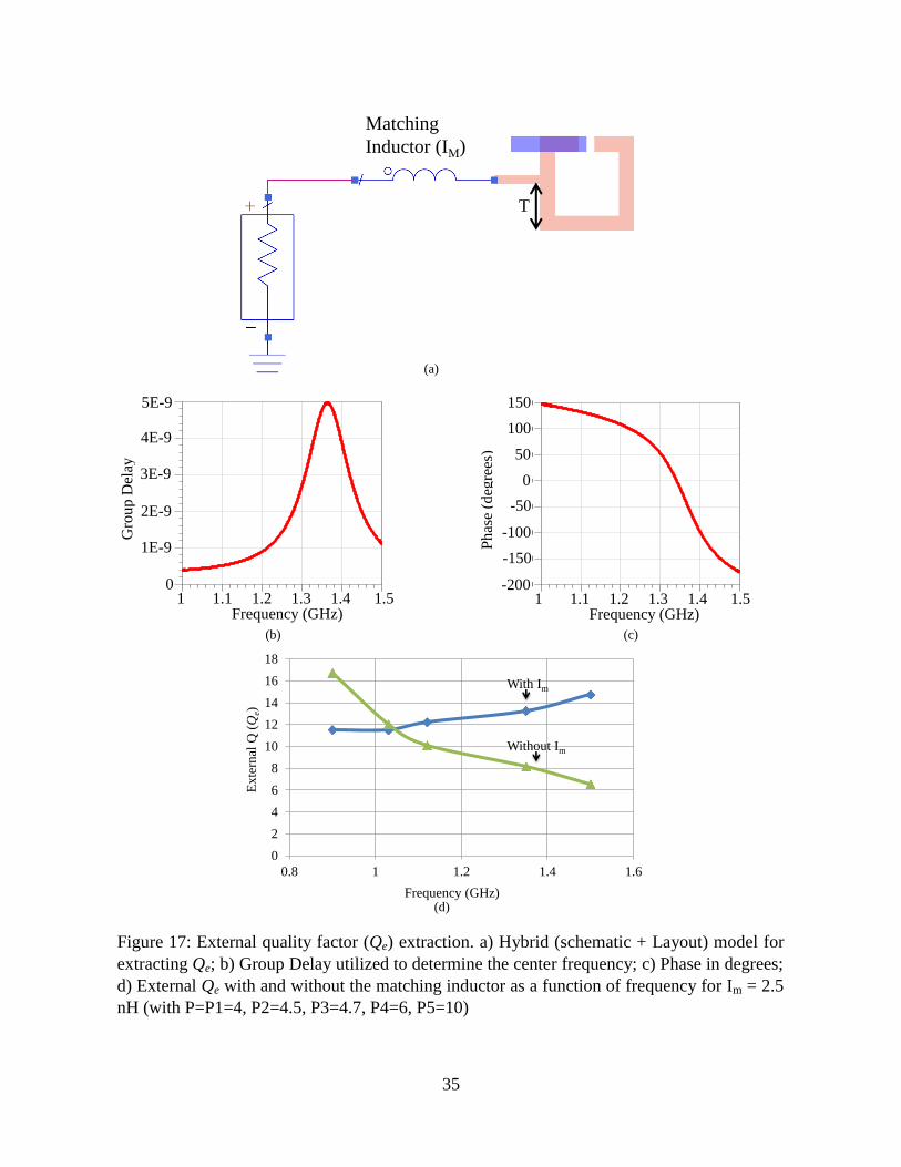
Figure 17: External quality factor (Qe) extraction. a) Hybrid (schematic + Layout) model for
extracting Qe; b) Group Delay utilized to determine the center frequency; c) Phase in degrees;
d) External Qe with and without the matching inductor as a function of frequency for Im = 2.5
nH (with P=P1=4, P2=4.5, P3=4.7, P4=6, P5=10)
0
2
4
6
8
10
12
14
16
18
0.8 1 1.2 1.4 1.6
Frequency (GHz)
Ex
tern
al Q
(Q
e)
With Im
Without Im
Matching
Inductor (IM)G
rou
p D
elay
Frequency (GHz) 1 1.1 1.2 1.3 1.4 1.5
5E-9
4E-9
3E-9
2E-9
1E-9
0
Ph
ase
(deg
rees
)
Frequency (GHz) 1 1.1 1.2 1.3 1.4 1.5
50
0
-50
-100
-150
-200
100
150
(a)
(b) (c)
(d)
T
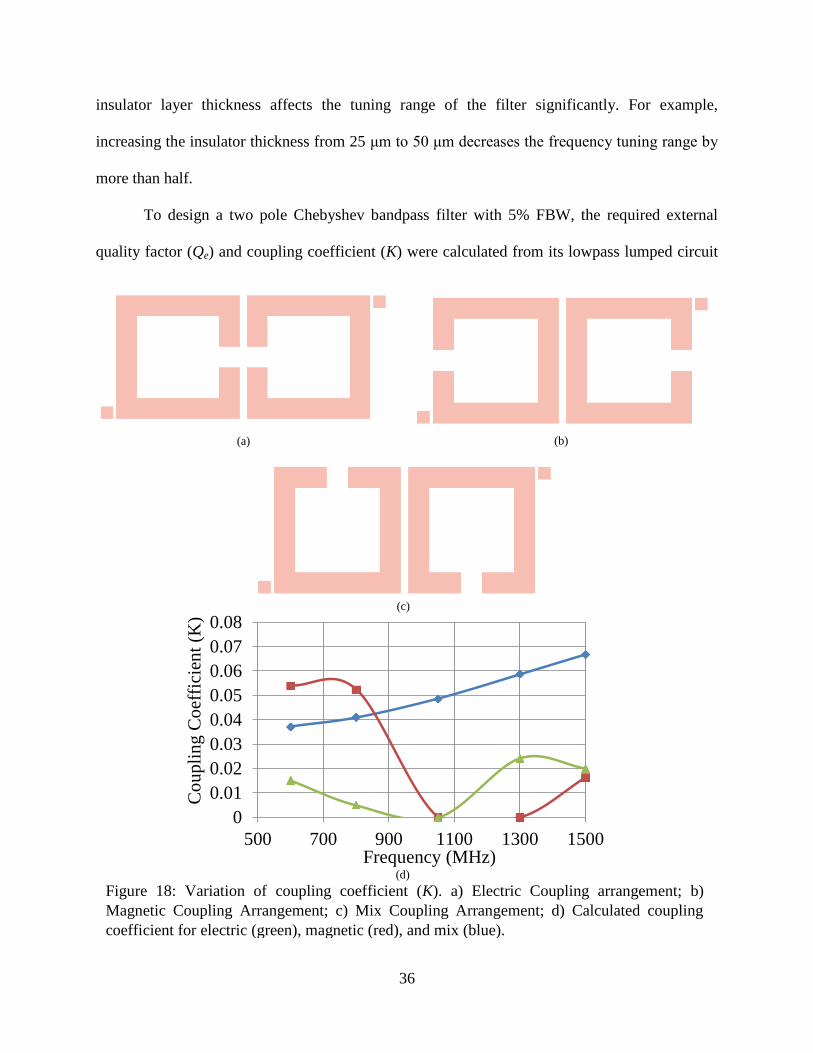
36
insulator layer thickness affects the tuning range of the filter significantly. For example,
increasing the insulator thickness from 25 μm to 50 μm decreases the frequency tuning range by
more than half.
To design a two pole Chebyshev bandpass filter with 5% FBW, the required external
quality factor (Qe) and coupling coefficient (K) were calculated from its lowpass lumped circuit
0
0.01
0.02
0.03
0.04
0.05
0.06
0.07
0.08
500 700 900 1100 1300 1500Frequency (MHz)
Co
up
lin
g C
oef
fici
ent
(K)
Figure 18: Variation of coupling coefficient (K). a) Electric Coupling arrangement; b)
Magnetic Coupling Arrangement; c) Mix Coupling Arrangement; d) Calculated coupling
coefficient for electric (green), magnetic (red), and mix (blue).
(a) (b)
(c)
(d)
37
prototype (g0=1, g1=0.6648, g2=0.5445, g3=1.2210) to be 13.296 and 0.0831, respectively. To
maintain a constant FBW, it is necessary to keep the Qe and K relatively constant over the
frequency tuning range. The ADS studies were carried out by simultaneously considering five
different metalized plate locations (P1 = 4, P2 = 4.5, P3 = 4.7, P4 = 6, P5 = 10 mm) and these
are identified as data points in the design curves presented in Figs. 8 and 9. Using the approach
explained in [55], which consist on using the S11 group delay (Fig. 17(b)) to determine the center
frequency and using the S11 phase (Fig. 17(c)) to determine the Qe with the equation 𝑄𝑒 =
𝑓0 𝑓∆+/−90𝑜⁄ , the tapping location that resulted in the required quality factor was found to be T=
6.1 mm as shown in Fig. 17(a). To stabilize the variation of Qe over the frequency tuning range,
a lumped inductor based coupling was utilized. The value of this inductor was determined by
utilizing an iterative approach involving ADS schematics and Momentum layouts. The value that
provided the nearly required coupling across the entire frequency range was found to be 2.5nH.
The ADS simulations of the overall filter for various P values using the 2.5 nH coupling
inductors resulted in a return loss that is not well matched (<8 dB). A parametric sweep was
carried out over the complete filter model. Increasing the coupling inductors to 7nH was found to
provide a return loss performance >10 dB over the whole frequency range. However, this
resulted in 8% constant FBW performance. Due to the proof-of-concept nature of the presented
work, no further optimizations were pursued to lower the FBW back to 5%. The IL was <1.3 dB
over the entire frequency tuning range.
To be able to tune both resonators simultaneously and utilize single pumping unit, a
meandered microfluidic channel layout was employed by shifting a resonator slightly down to
prevent overlaps (i.e. MT = 2 mm in Fig. 16(c)). The separation (C) that resulted in the required
resonator coupling was determined as 0.04 mm. Detailed curves depicting the variation of the
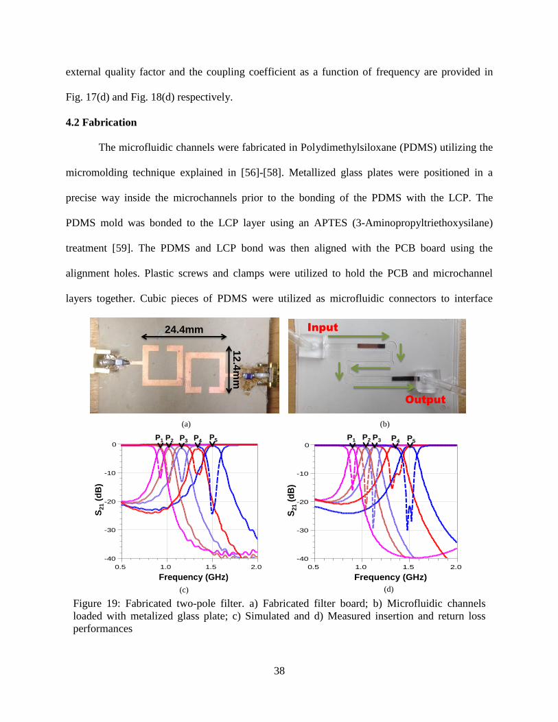
38
external quality factor and the coupling coefficient as a function of frequency are provided in
Fig. 17(d) and Fig. 18(d) respectively.
4.2 Fabrication
The microfluidic channels were fabricated in Polydimethylsiloxane (PDMS) utilizing the
micromolding technique explained in [56]-[58]. Metallized glass plates were positioned in a
precise way inside the microchannels prior to the bonding of the PDMS with the LCP. The
PDMS mold was bonded to the LCP layer using an APTES (3-Aminopropyltriethoxysilane)
treatment [59]. The PDMS and LCP bond was then aligned with the PCB board using the
alignment holes. Plastic screws and clamps were utilized to hold the PCB and microchannel
layers together. Cubic pieces of PDMS were utilized as microfluidic connectors to interface
Figure 19: Fabricated two-pole filter. a) Fabricated filter board; b) Microfluidic channels
loaded with metalized glass plate; c) Simulated and d) Measured insertion and return loss
performances
(a) (b)
(c) (d)
Input
Output
24.4mm1
2.4
mm
1.0 1.50.5 2.0
-30
-20
-10
-40
0
freq, GHz
dB(S
(4,3
))dB
(S(1
0,9)
)dB
(S(1
6,15
))dB
(S(2
2,21
))dB
(S(2
,1))
dB(S
(3,3
))dB
(S(9
,9))
dB(S
(15,
15))
dB(S
(21,
21))
dB(S
(1,1
))
Frequency (GHz)
S2
1(d
B)
P1 P2 P3 P4P5
Frequency (GHz)
S2
1(d
B)
1.0 1.50.5 2.0
-30
-20
-10
-40
0
freq, GHz
dB(S
(2,1
))dB
(S(4
,3))
dB(S
(6,5
))dB
(S(1
0,9)
)dB
(S(1
2,11
))dB
(S(1
,1))
dB(S
(3,3
))dB
(S(5
,5))
dB(S
(9,9
))dB
(S(1
1,11
))
P1 P2 P3 P4 P5
39
PTFE tubes with the microchannel. To move the plates inside the microchannels, a two syringe
system was implemented to flow Teflon solution inside the channels. The final filter stack-up, as
shown in Fig. 16(b), consisted of 1.27 mm thick PCB board, 25.4 μm thick LCP layer, and 2 mm
thick PDMS substrate with 250 μm deep and 2.1 mm wide microchannels with 1.9 mm wide
metallized glass plates. For a more detail explanation, refer to appendix A.
4.3 Experimental Verification
The layers of the fabricated filter assembly are shown in Fig. 19(a) and (b). 6.8 nH
Coilcraft inductors from the 0805CS series were utilized at the input and output of the filter. As
shown in Fig. 19(c) and (d), the measured insertion and return loss performances are in very
good agreement with the simulated results. A frequency tunability range of 50% (1.5 GHz to 0.9
GHz) was accomplished by moving the metallized glass plates a distance of 6mm (i.e. P1 to P5)
over the open loop resonators. The worst case insertion loss was found to be 1.7 dB at the lowest
frequency, which differs from the simulation results by 0.4 dB. The difference in IL, between
simulations and measurements, is due to the lower Q of the inductors (which was modeled as 50
in ADS simulations). The FBW was measured to vary between 8% and 10% from 0.9 GHz to 1.5
GHz. Increasing the number of poles of the filter will help to stabilize FBW variation as lower
coupling and external quality factors will be required. The overall footprint of the filter is 24.4 ×
12.4 mm2, which is 0.073 × 0.037 λ0
2 (λ0 = free space wavelength) at the lowest frequency.
4.4 Concluding Remarks of Chapter 4
A novel approach for realizing a compact, low-loss, and highly tunable bandpass filter
was presented by utilizing microfluidically controlled parasitic metalized glass plates. By
resorting to metallized glass plates, it provides a more reliable, highly tunable, non-toxic, and
low loss performance. Specifically, the bandpass filter provided 50% tuning range with almost

40
constant 8% FBW. In chapter 5, the microfluidic technique will be extended to higher order
bandpass filters. At the same time, integration with micropumps will be introduced for the first
time, and speed characterization will be performed.
41
CHAPTER 5: MICROFLUIDICALLY RECONFIGURABLE METALLIZED PLATE
LOADED FREQUENCY-AGILE RF BANDPASS FILTERS4
To extend the utilization of microfluidics to higher order bandpass filters, a 4 pole
frequency-agile bandpass filter was designed, fabricated, and tested. Two different filter
arrangements were studied to demonstrate that different footprint requirements can be met with
the proposed filter approach. To overcome the synchronization issues of multiple metalized
plates moving within a single meandered microfluidic channel (in order to use a single pump), a
selectively metallized plate implementation was introduced for the first time. In addition,
automation of the filters was obtained by introducing a micropump system. The speed of the
reconfigurable RF filter was characterized and improved by resorting to strategically designed
channel shapes.
5.1 Filter Design
5.1.1 Resonator Model
Fig. 20(a) depicts the substrate stack-up used to construct the presented microfluidic
based reconfigurable filters. A microfluidically repositionable metalized plate is placed in close
proximity to the gap of a traditional open loop resonator to achieve a variable capacitance based
frequency tuning mechanism. For a compact filter size, the open loop resonators were placed on
a high permittivity 1.27 mm thick Rogers 6010.2LM board (εr = 10.2, tanδ = 0.0023). The 0.3
mm thick microfluidic channel is located at the bottom surface of a 2 mm thick
Polydimethylsiloxane (PDMS, εr = 10.2, tanδ = 0.0023) polymer. The microfluidic channel with
4 This chapter was previously published in [54]. Permission is include in Appendix B.
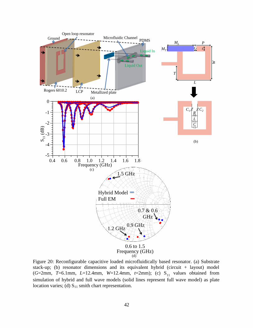
42
Frequency (GHz) 0.6 to 1.5
1.5 GHz
1.2 GHz 0.9 GHz
0.7 & 0.6
GHz
Hybrid Model
Full EM
Microfluidic Channel
Metallized plateLCP
Open loop resonatorGround
Rogers 6010.2
PDMS
Liquid In
Liquid Out
C2
L
R
C
C1
P
T
W
L
tGMT
ML
0.6 0.8 1.0 1.2 1.4 1.60.4 1.8
-4
-3
-2
-1
-5
0
freq, GHz
dB
(C
apacitanceextraction5..S
(2,2))
dB
(C
apacitanceextraction5..S
(1,1))
dB
(C
apacitanceextraction4..S
(2,2))
dB
(C
apacitanceextraction4..S
(1,1))
dB
(C
apacitanceextraction3..S
(2,2))
dB
(C
apacitanceextraction3..S
(1,1))
dB
(C
apacitanceextraction2..S
(1,1))
dB
(C
apacitanceextraction2..S
(2,2))
dB
(C
apacitanceextraction..S
(1,1))
dB
(C
apacitanceextraction..S
(2,2))
Frequency (GHz)0.4 0.6 0.8 1.0 1.2 1.4 1.6 1.8
0
-1
-2
-3
-4
-5
S11
(dB
)
Figure 20: Reconfigurable capacitive loaded microfluidically based resonator. (a) Substrate
stack-up; (b) resonator dimensions and its equivalent hybrid (circuit + layout) model
(G=2mm, T=6.1mm, L=12.4mm, W=12.4mm, t=2mm); (c) S11
values obtained from
simulation of hybrid and full wave models (solid lines represent full wave model) as plate
location varies; (d) S11 smith chart representation.
(a)
(b)
(c)
(d)
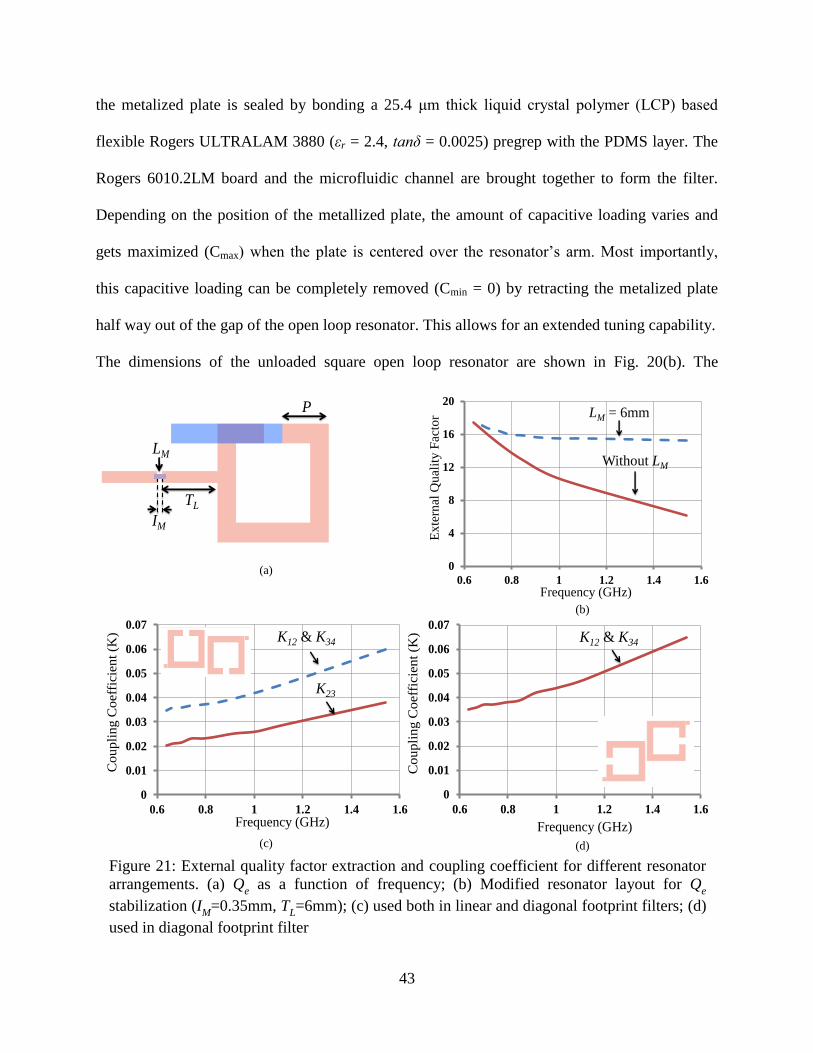
43
the metalized plate is sealed by bonding a 25.4 μm thick liquid crystal polymer (LCP) based
flexible Rogers ULTRALAM 3880 (εr = 2.4, tanδ = 0.0025) pregrep with the PDMS layer. The
Rogers 6010.2LM board and the microfluidic channel are brought together to form the filter.
Depending on the position of the metallized plate, the amount of capacitive loading varies and
gets maximized (Cmax) when the plate is centered over the resonator’s arm. Most importantly,
this capacitive loading can be completely removed (Cmin = 0) by retracting the metalized plate
half way out of the gap of the open loop resonator. This allows for an extended tuning capability.
The dimensions of the unloaded square open loop resonator are shown in Fig. 20(b). The
0
4
8
12
16
20
0.6 0.8 1 1.2 1.4 1.6
LM = 6mm
Without LM
Exte
rnal
Qu
alit
y F
acto
r
Frequency (GHz)
IM
TL
P
LM
0
0.01
0.02
0.03
0.04
0.05
0.06
0.07
0.6 0.8 1 1.2 1.4 1.6
K12 & K34
K23
Co
up
lin
g C
oeff
icie
nt
(K)
Frequency (GHz)
0
0.01
0.02
0.03
0.04
0.05
0.06
0.07
0.6 0.8 1 1.2 1.4 1.6
K12 & K34
Cou
pli
ng
Coeff
icie
nt
(K)
Frequency (GHz)
Figure 21: External quality factor extraction and coupling coefficient for different resonator
arrangements. (a) Qe as a function of frequency; (b) Modified resonator layout for Q
e
stabilization (IM
=0.35mm, TL=6mm); (c) used both in linear and diagonal footprint filters; (d)
used in diagonal footprint filter
(a)
(b)
(c) (d)
44
resonator is designed to operate at 1.5 GHz by utilizing the Momentum suite of Keysight
Advanced Design System (ADS) with the extraction approach outlined in [55]. Assuming that
the metalized plate completely fills the microfluidic channel and overlaps with the entire arm of
the resonator, the frequency tuning range can be determined to be from 0.61 GHz to 1.5 GHz.
Designing the filter across this wide (>2:1) frequency range to exhibit a predefined fractional
bandwidth (FBW) performance requires extensive number of full wave simulations to be carried
out with changing plate position and results in a time consuming procedure especially for higher
order filters. To alleviate this issue, a hybrid model that represents the metalized plate as a
lumped circuit network is utilized for design purposes as shown in Fig. 20(b). Since the
metalized plate can have a different overlap area on the open arms of the resonator, its
interaction with the resonator is represented with two series capacitors (i.e. C1 and C2). Due to
the selected resonator configuration, the metalized plate always completely covers the left arm of
the open loop resonator resulting in 𝐶1 = 𝜖 𝑀𝑡(𝐿 − 𝐺)/2ℎ, where Mt is the width of the plate, L
is the side length of the resonator, G is the width of the gap, h is the separation between the plate
and the resonator, and ϵ is the permittivity of the material between the plate and the resonator. C2
depends on the position of the plate and can be expressed as 𝐶2 = 𝜖 𝑀𝑡 ((𝐿 − 𝐺)/2 − 𝑃)/ℎ,,
where P denotes the distance between the plate and the right edge of the resonator. The parallel
RLC circuit in series with C1 and C2 represents the RF parasitics of the metalized plate located
between the open ends of the resonator. The values are initially approximated from the open
ended transmission line resonator equations [60]. Subsequently, the values are optimized to
match the S11 response of the resonator simulated using full-wave analysis when the metalized
plate completely overlaps with the resonator arm. The open loop resonator was full wave
simulated without the metalized plate by placing ports to the open ends of the resonator. The
45
hybrid model was formed in ADS schematic by combining the lumped circuit model with the
open end ports of the full wave simulated resonator. Fig. 20(c) and (d) shows that the full wave
simulations performed with metalized plate agree well with the equivalent hybrid model.
Throughout this paper, to keep the discussion brief, filter performance simulations and
experimental verifications are provided at 5 specific plate positions (P1 = 6 mm, P2 = 4.25 mm,
P3 = 3.5 mm, P4 = 2 mm and P5 = 0 mm).
5.1.2 External Qe and Coupling Coefficient
To proceed with design of a 4th
order Chebyshev bandpass filter with 5% FBW, the
required external quality factor (Qe) and coupling coefficient (K) values were calculated from the
corresponding low pass lumped element circuit prototype (g0 = 1, g1 = 0.7654, g2 = 1.8478, g3 =
1.8478, g4 = 0.7654, g5 = 1) as 15.308, K1,2 = K3,4 = 0.04204 and K2,3 = 0.02706, respectively
[55] (where a subscript integer i represents the resonator number). To maintain an almost
constant FBW, it is necessary to keep the Qe and K relatively stable over the tuning range. For
the filter implementation, the hybrid resonator model was utilized to extract the Qe and K using
the approach explained in [55]. As shown in Fig. 21(b), Qe decreases as the resonator is tuned to
higher frequency and this behavior is independent of the tapping location (T). To stabilize the
variation in Qe over the tuning range, a lumped coupling inductor LM was introduced to the feed
line as shown in Fig. 21(a) [51]. Through parametric studies, tapping location and the inductor
value were determined as T = 6 mm and LM = 6 nH, for TL = 6 mm, for a relatively flat Qe
response (Fig. 21(b)).
Two different resonator alignment configurations were found to provide stabilized K
variation over the wide tuning range as shown in Fig. 21(c) and (d). To prevent overlapping of
the metalized plate with the adjacent resonators, resonators were offset with respect to each other
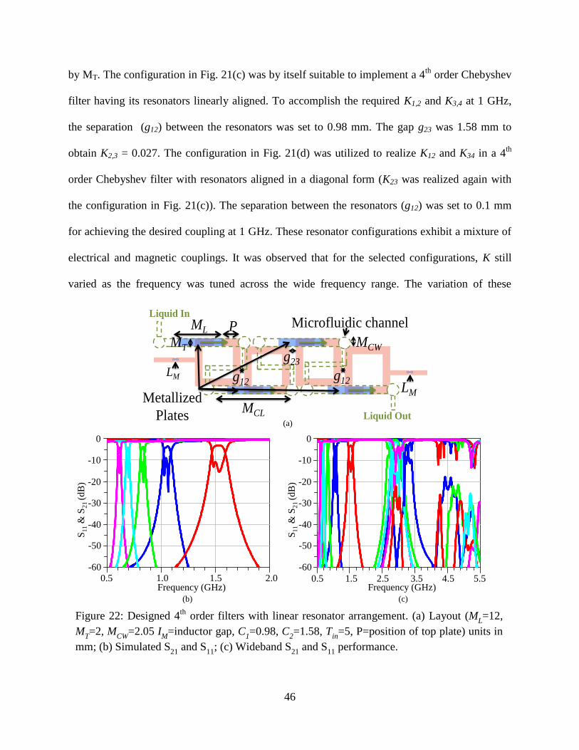
46
by MT. The configuration in Fig. 21(c) was by itself suitable to implement a 4th
order Chebyshev
filter having its resonators linearly aligned. To accomplish the required K1,2 and K3,4 at 1 GHz,
the separation (g12) between the resonators was set to 0.98 mm. The gap g23 was 1.58 mm to
obtain K2,3 = 0.027. The configuration in Fig. 21(d) was utilized to realize K12 and K34 in a 4th
order Chebyshev filter with resonators aligned in a diagonal form (K23 was realized again with
the configuration in Fig. 21(c)). The separation between the resonators (g12) was set to 0.1 mm
for achieving the desired coupling at 1 GHz. These resonator configurations exhibit a mixture of
electrical and magnetic couplings. It was observed that for the selected configurations, K still
varied as the frequency was tuned across the wide frequency range. The variation of these
0.5 1.0 1.5 2.0Frequency (GHz)
0
-10
-20
-30
-40
-50
-60
S11
& S
21
(d
B)
0.5 1.5 2.5 3.5 4.5 5.5Frequency (GHz)
0
-10
-20
-30
-40
-50
-60
S11
& S
21
(d
B)
MLMicrofluidic channel
Metallized
Plates
Liquid In
Liquid OutMCL
MCW
PMT
g12
g23
g12LM
LM
Figure 22: Designed 4th
order filters with linear resonator arrangement. (a) Layout (ML=12,
MT=2, M
CW=2.05 I
M=inductor gap, C
1=0.98, C
2=1.58, T
in=5, P=position of top plate) units in
mm; (b) Simulated S21
and S11
; (c) Wideband S21
and S11
performance.
(a)
(b) (c)
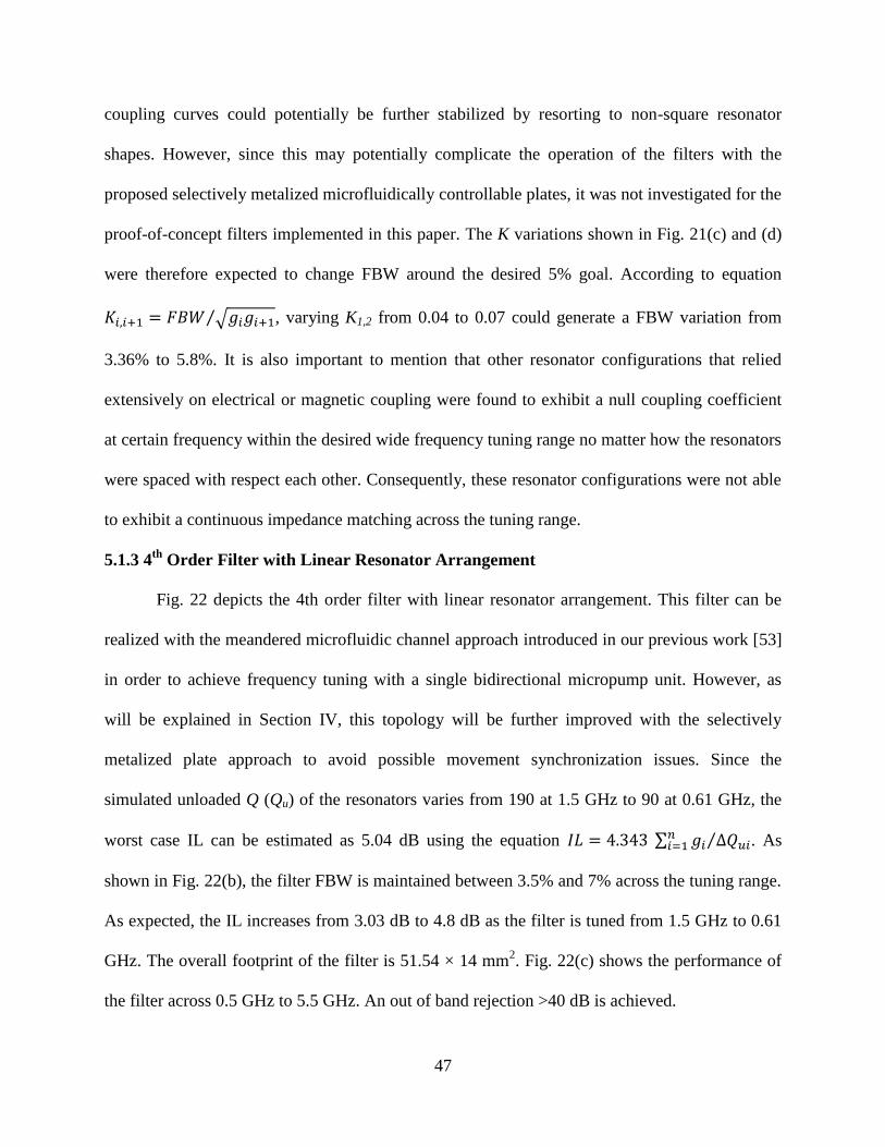
47
coupling curves could potentially be further stabilized by resorting to non-square resonator
shapes. However, since this may potentially complicate the operation of the filters with the
proposed selectively metalized microfluidically controllable plates, it was not investigated for the
proof-of-concept filters implemented in this paper. The K variations shown in Fig. 21(c) and (d)
were therefore expected to change FBW around the desired 5% goal. According to equation
𝐾𝑖,𝑖+1 = 𝐹𝐵𝑊 √𝑔𝑖𝑔𝑖+1⁄ , varying K1,2 from 0.04 to 0.07 could generate a FBW variation from
3.36% to 5.8%. It is also important to mention that other resonator configurations that relied
extensively on electrical or magnetic coupling were found to exhibit a null coupling coefficient
at certain frequency within the desired wide frequency tuning range no matter how the resonators
were spaced with respect each other. Consequently, these resonator configurations were not able
to exhibit a continuous impedance matching across the tuning range.
5.1.3 4th
Order Filter with Linear Resonator Arrangement
Fig. 22 depicts the 4th order filter with linear resonator arrangement. This filter can be
realized with the meandered microfluidic channel approach introduced in our previous work [53]
in order to achieve frequency tuning with a single bidirectional micropump unit. However, as
will be explained in Section IV, this topology will be further improved with the selectively
metalized plate approach to avoid possible movement synchronization issues. Since the
simulated unloaded Q (Qu) of the resonators varies from 190 at 1.5 GHz to 90 at 0.61 GHz, the
worst case IL can be estimated as 5.04 dB using the equation 𝐼𝐿 = 4.343 ∑ 𝑔𝑖 ∆𝑄𝑢𝑖⁄𝑛𝑖=1 . As
shown in Fig. 22(b), the filter FBW is maintained between 3.5% and 7% across the tuning range.
As expected, the IL increases from 3.03 dB to 4.8 dB as the filter is tuned from 1.5 GHz to 0.61
GHz. The overall footprint of the filter is 51.54 × 14 mm2. Fig. 22(c) shows the performance of
the filter across 0.5 GHz to 5.5 GHz. An out of band rejection >40 dB is achieved.
48
5.1.4 4th
Order Filter with Diagonal Resonator Arrangement
The 4th
order filter designed with the diagonal resonator arrangement is shown in Fig.
23(a). The design is based on the Qe and K study discussed in Section 5.1.2. Similar to the filter
with the linear resonator arrangement, this layout could also be operated with a meandered
microfluidic channel to use a single bi-directional pump unit as shown in Fig. 23(a). The filter
FBW is maintained between 3.5% and 7.2% across the tuning range. The IL increases from 3.03
Figure 23: Designed 4th
order filters with diagonal resonator arrangement. (a) Layout
(ML=12, MT=2, MCW=2.05, Roff=6, g12=0.1, g23=1.58) units in mm; (b) Simulated S21 and
S11; (c) Wideband S21 and S11 performance.
Liquid In
Liquid Out
Roff
Roff
MT
MT
ML
g12
g12
LM
LM
MCL
MCW
g23
0.5 1.0 1.5 2.0Frequency (GHz)
0
-10
-20
-30
-40
-50
-60
S11
& S
21
(d
B)
0.5 1.5 2.5 3.5 4.5 5.5Frequency (GHz)
0
-10
-20
-30
-40
-50
-60
S11
& S
21
(d
B)
(a)
(b) (c)
49
dB to 4.8 dB as the filter is tuned from 1.5 GHz to 0.61 GHz (Fig. 23(b)). The overall footprint
of the filter is 37.58 × 34.2 mm2. Fig. 23(c) shows the performance of the filter across 0.5 GHz to
5.5 GHz. An out of band rejection >40 dB is achieved.
5.2 Microfluidic Channel Design
Although the resonators of the designed filters can be simultaneously tuned with a single
pump due to the meandered microfluidic channel layout, utilizing a single meandered channel
presents potential reliability issues due to the synchronous movement needed from all the plates.
As an alternative, in contrast to our previous work [53], two novel microfluidic channel layouts
designed to operate with a selectively metalized plate were pursued for the device
implementation as shown in Fig. 24. Specifically, a rectangular wide microfluidic channel was
placed over the filter footprint consisting of linearly arranged resonators. The microfluidic
channel hosted a single 14 mm wide dielectric plate. This plate was selectively metallized on the
areas that will overlap with the resonators. Having the microfluidic channel as the same width of
the metallized plate, would not allow a continuous plate movement due to friction generated
between the channel walls and the plate walls. Also, as the plate area increase, the separation
between the microchannel walls and the selectively metallized plate needs to be increased to
reduce the friction. However, if the gap between the selectively metallized plate and the
microfluidic channel is too large, the fluid could flow through without moving the plate. To
determine the appropriate channel width, microfluidic channels presenting width of 20 μm, 30
μm, 40 μm, 50 μm, and 60 μm wider than the selectively metallized plate were fabricated. It was
determined that keeping the channel width 50 μm wider than the metallized plate would
minimize the friction generated between the channel walls and selectively metallized plate.
Therefore, the dimensions of the wide rectangular microfluidic channel were set to 14.05 x 30.4
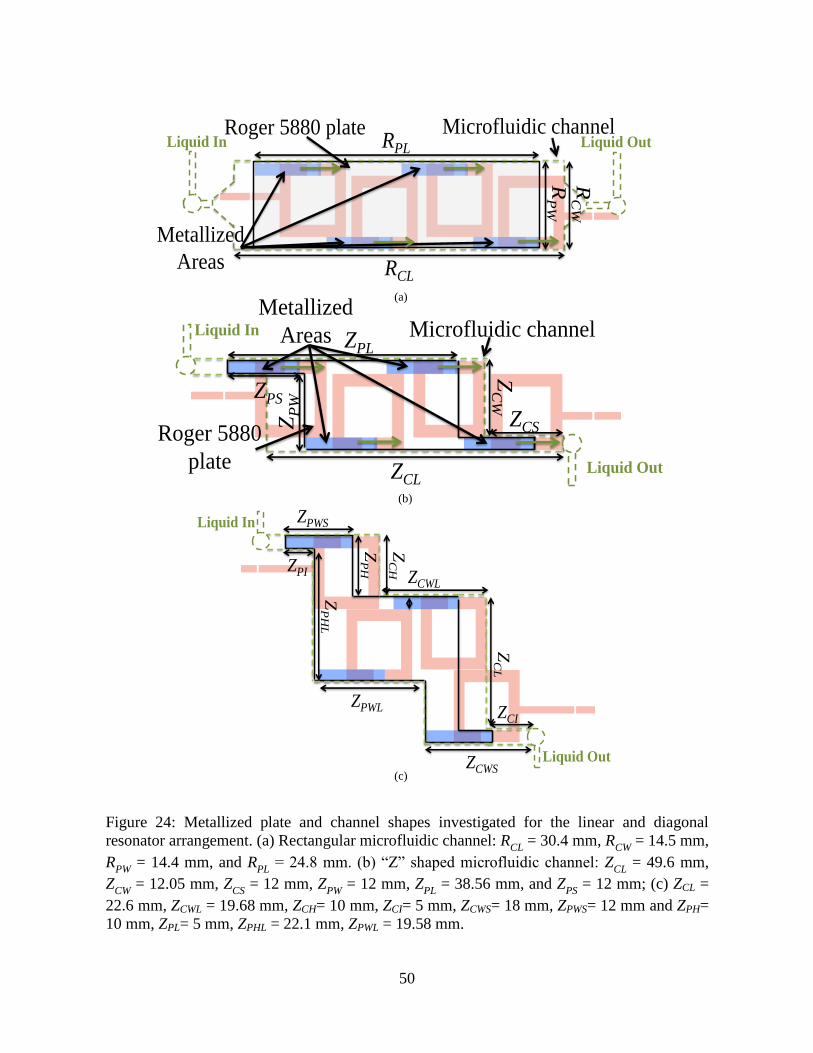
50
Metallized
Areas
Liquid In Liquid Out
RCL
RPL
RP
W
RC
W
Microfluidic channelRoger 5880 plate
Metallized
AreasLiquid In
Liquid Out
Microfluidic channel
Roger 5880
plate ZCL
ZC
W
ZCSZP
W
ZPL
ZPS
Liquid In
Liquid Out
ZPWS
ZPWL
ZP
H
ZP
HL
ZC
L
ZC
H
ZCWS
ZCWL
ZCI
ZPI
Figure 24: Metallized plate and channel shapes investigated for the linear and diagonal
resonator arrangement. (a) Rectangular microfluidic channel: RCL
= 30.4 mm, RCW
= 14.5 mm,
RPW
= 14.4 mm, and RPL
= 24.8 mm. (b) “Z” shaped microfluidic channel: ZCL
= 49.6 mm,
ZCW
= 12.05 mm, ZCS
= 12 mm, ZPW
= 12 mm, ZPL
= 38.56 mm, and ZPS
= 12 mm; (c) ZCL =
22.6 mm, ZCWL = 19.68 mm, ZCH= 10 mm, ZCI= 5 mm, ZCWS= 18 mm, ZPWS= 12 mm and ZPH=
10 mm, ZPL= 5 mm, ZPHL = 22.1 mm, ZPWL = 19.58 mm.
(a)
(b)
(c)
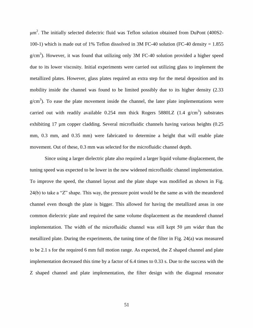
51
μm2. The initially selected dielectric fluid was Teflon solution obtained from DuPont (400S2-
100-1) which is made out of 1% Teflon dissolved in 3M FC-40 solution (FC-40 density = 1.855
g/cm3). However, it was found that utilizing only 3M FC-40 solution provided a higher speed
due to its lower viscosity. Initial experiments were carried out utilizing glass to implement the
metallized plates. However, glass plates required an extra step for the metal deposition and its
mobility inside the channel was found to be limited possibly due to its higher density (2.33
g/cm3). To ease the plate movement inside the channel, the later plate implementations were
carried out with readily available 0.254 mm thick Rogers 5880LZ (1.4 g/cm3) substrates
exhibiting 17 µm copper cladding. Several microfluidic channels having various heights (0.25
mm, 0.3 mm, and 0.35 mm) were fabricated to determine a height that will enable plate
movement. Out of these, 0.3 mm was selected for the microfluidic channel depth.
Since using a larger dielectric plate also required a larger liquid volume displacement, the
tuning speed was expected to be lower in the new widened microfluidic channel implementation.
To improve the speed, the channel layout and the plate shape was modified as shown in Fig.
24(b) to take a “Z” shape. This way, the pressure point would be the same as with the meandered
channel even though the plate is bigger. This allowed for having the metallized areas in one
common dielectric plate and required the same volume displacement as the meandered channel
implementation. The width of the microfluidic channel was still kept 50 μm wider than the
metallized plate. During the experiments, the tuning time of the filter in Fig. 24(a) was measured
to be 2.1 s for the required 6 mm full motion range. As expected, the Z shaped channel and plate
implementation decreased this time by a factor of 6.4 times to 0.33 s. Due to the success with the
Z shaped channel and plate implementation, the filter design with the diagonal resonator
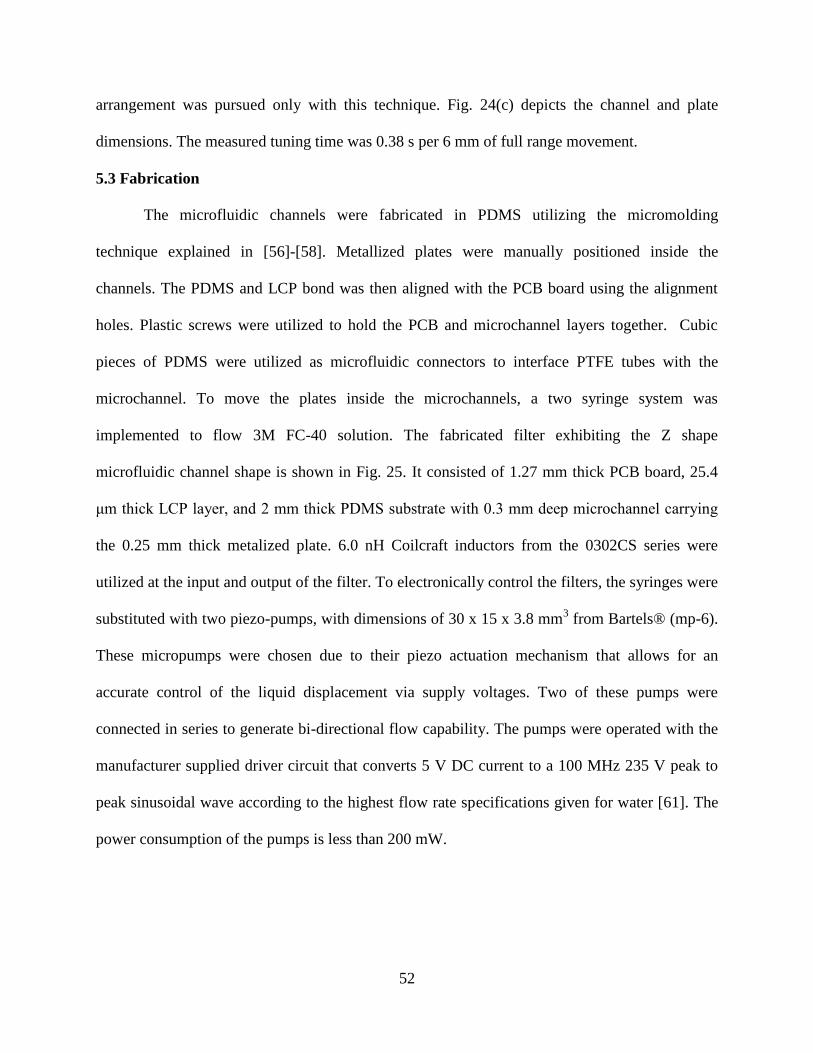
52
arrangement was pursued only with this technique. Fig. 24(c) depicts the channel and plate
dimensions. The measured tuning time was 0.38 s per 6 mm of full range movement.
5.3 Fabrication
The microfluidic channels were fabricated in PDMS utilizing the micromolding
technique explained in [56]-[58]. Metallized plates were manually positioned inside the
channels. The PDMS and LCP bond was then aligned with the PCB board using the alignment
holes. Plastic screws were utilized to hold the PCB and microchannel layers together. Cubic
pieces of PDMS were utilized as microfluidic connectors to interface PTFE tubes with the
microchannel. To move the plates inside the microchannels, a two syringe system was
implemented to flow 3M FC-40 solution. The fabricated filter exhibiting the Z shape
microfluidic channel shape is shown in Fig. 25. It consisted of 1.27 mm thick PCB board, 25.4
μm thick LCP layer, and 2 mm thick PDMS substrate with 0.3 mm deep microchannel carrying
the 0.25 mm thick metalized plate. 6.0 nH Coilcraft inductors from the 0302CS series were
utilized at the input and output of the filter. To electronically control the filters, the syringes were
substituted with two piezo-pumps, with dimensions of 30 x 15 x 3.8 mm3 from Bartels® (mp-6).
These micropumps were chosen due to their piezo actuation mechanism that allows for an
accurate control of the liquid displacement via supply voltages. Two of these pumps were
connected in series to generate bi-directional flow capability. The pumps were operated with the
manufacturer supplied driver circuit that converts 5 V DC current to a 100 MHz 235 V peak to
peak sinusoidal wave according to the highest flow rate specifications given for water [61]. The
power consumption of the pumps is less than 200 mW.
53
6mm
14
mm
51.54mm
Bartels MP-6
Micropumps
Input
Output
0.5 1.0 1.5 2.0Frequency (GHz)
0
-10
-20
-30
-40
-50
-60
S11
& S
21
(d
B)
0.5 1.0 1.5 2.0Frequency (GHz)
0
-10
-20
-30
-40
-50
-60
S11
& S
21
(d
B)
0.5 1.5 2.5 3.5 4.5 5.5Frequency (GHz)
0
-10
-20
-30
-40
-50
-60
S11
& S
21
(d
B)
Figure 25: Experimental characterization of the 4th
order bandpass filter with linear resonator
arrangement. (a) Fabricated filter board; (b) Complete system assembly including pump and
control units; (c) Simulated S21 and S11 performance with 58 µm thickness; (d) Measured
S21
and S11
performances; (e) Measured frequency response up to third harmonic.
(a)
(b)
(c)
(d) (e)
54
5.4 Experimental Verification
5.4.1 4th
Order Filter with Linear Resonator Arrangement
Fig. 25(a) and (b) depict the fabricated filter and the microfluidic control assembly. The
measured frequency tuning range was from 0.8 GHz to 1.5 GHz, close to being 2:1. Based on
simulation studies, this frequency tuning range was identified to correspond to a physical gap of
54 µm between the plate metallization and the printed loop. Hence, it was concluded that the
0.254 mm thick plate with 17 µm thick metallization floated on the top of the channel due to the
density difference of the dielectric fluid and the plate material. Future device fabrications should
consider the possible location of the plate within the channel and try to minimize the difference
between channel height and plate thickness through more finely sampled channel height
characterizations. Optimizing channel height and matching the densities of the plate with the
fluid will also minimize the orientation dependent tuning variation due to gravity. Simulated S21
and S11 data with the 54 μm gap is shown in Fig. 25(c) and agrees well with the measured data
shown in Fig. 25(d). The worst case IL is 4.5 dB at the lowest frequency. 0.2 dB difference
between simulations and measurements can potentially be due to the lower Q of the inductors
(which was modeled as 80 in ADS simulations) and losses added due to dielectric solution. The
FBW is measured to vary between 5% and 4% from 1.5 GHz to 0.8 GHz. Less variation in Qe
and K due to the smaller frequency tuning range results in a more stable FBW performance. The
overall footprint of the filter (excluding the pumps) is 51.54 × 14 mm2, which is 0.14259 ×
0.0387 λ02 (λ0 = free space wavelength) at the lowest frequency. Fig. 25(e) shows the wideband
frequency response. An out of band rejection >40 dB is realized up to the 2.6 GHz that is within
the vicinity of the second harmonic of the unloaded open loop resonator. The frequency tuning
time is 0.33 s, for the entire frequency range, with the “Z” shaped microfluidic channel and plate.
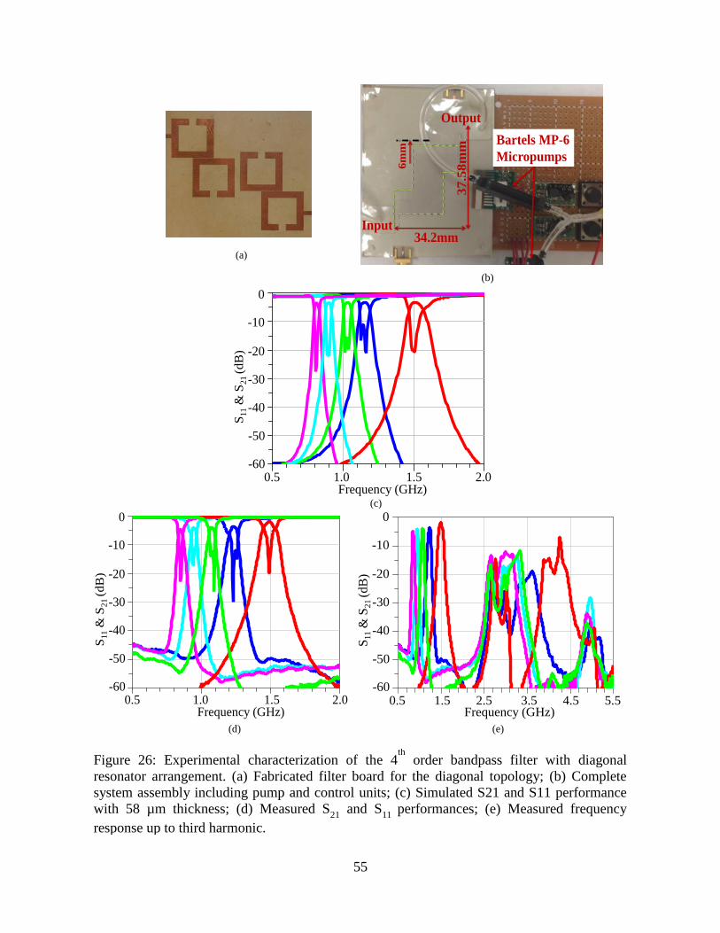
55
6m
m
34.2mm
Bartels MP-6
Micropumps
Input
Output
37
.58
mm
0.5 1.0 1.5 2.0Frequency (GHz)
0
-10
-20
-30
-40
-50
-60
S11
& S
21
(d
B)
0.5 1.0 1.5 2.0Frequency (GHz)
0
-10
-20
-30
-40
-50
-60
S11
& S
21
(d
B)
0.5 1.5 2.5 3.5 4.5 5.5Frequency (GHz)
0
-10
-20
-30
-40
-50
-60
S11
& S
21
(d
B)
Figure 26: Experimental characterization of the 4th
order bandpass filter with diagonal
resonator arrangement. (a) Fabricated filter board for the diagonal topology; (b) Complete
system assembly including pump and control units; (c) Simulated S21 and S11 performance
with 58 µm thickness; (d) Measured S21
and S11
performances; (e) Measured frequency
response up to third harmonic.
(a)
(b)
(c)
(d) (e)
56
The measured S21 and S11 performances for different channel implementations are identical and
therefore not shown for brevity.
5.4.2 4th
Order Filter with Diagonal Resonator Arrangement
Fig. 26(a) and (b) show the filter implementation for the diagonal configuration.
Simulated (with 54 µm plate and loop metallization separation) and measured results are in very
good agreement as can be seen in Fig. 26(c) and (d). The worst case IL is 4.5 dB and identical to
the filter with linear resonator arrangement. The tuning range is also identical and from 1.5 GHz
down to 0.8 GHz. The measured FBW varies between 5% and 4% over the entire frequency
tuning range. The overall footprint of the filter (excluding the pumps) is 37.58 × 34.2 mm2,
which is 0.10397 × 0.094612 λ02 at the lowest frequency. Fig. 26(e) shows the wideband
frequency response. An out of band rejection >40 dB is realized up to the 2.5 GHz that is within
the vicinity of the second harmonic of the unloaded open loop resonator. The tuning time is
slightly larger and 0.38 s for entire 6 mm plate motion. This is likely to be due to the
implementation with a larger plate mass.
5.5 Concluding Remarks of Chapter 5
A novel approach for realizing a compact, low-loss, and highly tunable high order
bandpass filter was presented by utilizing microfluidically controlled metalized plates. A thin
film based fabrication technique was employed to increase the capacitive loading and associated
frequency tuning range. The shape of the microfluidic channel and resonators are designed to
operate the filter with a single micropump unit with near constant fractional bandwidth
performance. Specifically, the presented bandpass filter example provided 60% tuning range
with almost constant 5% FBW. The tuning range of the filter can be further improved by
resorting to thinner insulators. However, this would generate a further decrease in the resonator’s
57
unloaded quality factor and, therefore, increase the insertion loss performance of the filter. As a
solution, in chapter 6, a novel resonator will be presented, and utilized to realize a 4th
order
bandpass filter. The resonator explained in chapter 6 will be capable of exhibiting constant
unloaded quality factor while providing a 90% (3:1) tuning range. Experimental
characterizations showed that the plate location within the depth of the microfluidic channel
must be accounted for in accurate modeling of these devices due to the use of thin insulators as
microfluidic channel walls. Therefore, in chapter 6, a more detailed fabrication of the
microchannel is presented. By utilizing a selectively metalized single plate to simultaneously
tune entire resonators of the filter, the issue of synchronization was solved and the reliability of
the filters were improved. Electronically controllable micropumps were also successfully added
into the system. The filter presented in this chapter provides a low-cost and compact alternative
to linear actuator based mechanically tuned filters.
58
CHAPTER 6: WIDELY TUNABLE, LOW LOSS FILTERS USING
MICROFLUIDICALLY CONTROLLED VARIABLE LENGTH RESONATORS
The capacitively loaded open loop resonator based microfluidic reconfigurable filters
have been shown to operate with ~2:1 tuning range and unloaded resonator quality factors (Qu)
ranging from 150 to 90. This performance is already better than varactor loaded reconfigurable
filters and scalable to higher operational frequencies. Extending the frequency tuning range of
the open loop resonator based filters is possible by resorting to thinner insulators for higher
capacitive loading. However, high level of capacitive loading that lowers the operational
frequency of the resonator also significantly reduces the unloaded quality factor (Qu) and
therefore the filter’s insertion loss performance. In this chapter, we investigate a new technique
for designing microfluidically reconfigurable filters that can simultaneously operate over a very
wide frequency tuning range and exhibit low insertion loss performance. In order to improve the
frequency tuning range and keep the unloaded quality factor of the resonators relatively stable,
the microfluidic reconfiguration approach is utilized for redefining the length of half wavelength
open ended microstrip resonators. These resonators typically present an unloaded quality factor
on the order of 200 and this is also considerably higher than the resonators investigated in the
previous chapters.
6.1 Resonator Design
A variable length half wavelength open ended microstrip resonator was designed by
resorting to microfluidics as the tuning mechanism. Tunable filters based on this type of
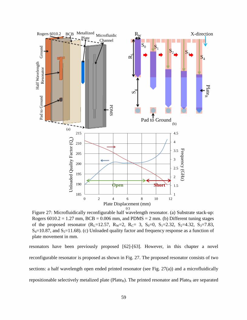
59
resonators have been previously proposed [62]-[63]. However, in this chapter a novel
reconfigurable resonator is proposed as shown in Fig. 27. The proposed resonator consists of two
sections: a half wavelength open ended printed resonator (see Fig. 27(a)) and a microfluidically
repositionable selectively metalized plate (PlateR). The printed resonator and PlateR are separated
Microfluidic
Channel
Metallized
Plate
PD
MS
Rogers 6010.2
Gro
und
Hal
f W
avel
eng
th
Res
on
ato
rP
ad t
o G
rou
nd
BCB
Figure 27: Microfluidically reconfigurable half wavelength resonator. (a) Substrate stack-up:
Rogers 6010.2 = 1.27 mm, BCB = 0.006 mm, and PDMS = 2 mm. (b) Different tuning stages
of the proposed resonator (RL=12.57, RW=2, RC= 3, S0=0, S1=2.32, S2=4.32, S3=7.83,
S4=10.87, and S5=11.68). (c) Unloaded quality factor and frequency response as a function of
plate movement in mm.
(a) (b)
(c)
Pad to Ground
S0 S1S2 S3
S4
Sg
RL
RW
Plate
R
1
1.5
2
2.5
3
3.5
4
4.5
185
190
195
200
205
210
215
0 2 4 6 8 10 12
Un
load
ed Q
ual
ity
Fac
tor
(Qu)
Freq
uen
cy (G
Hz)
Plate Displacement (mm)
X-direction
Open Short
60
by a 6 µm thick insulator. At the highest operational frequency, PlateR completely overlaps with
the printed resonator (see Fig. 27(b)). When PlateR is microfluidically moved in the X direction,
as shown in Fig. 27(b), the length of the resonator is enlarged and its resonance frequency is
decreased. Extending the physical length by a factor of 2 would reduce the resonance frequency
by half (2:1 tunability). However, since a small overlap needs to exist between the printed
resonator and PlateR to achieve an RF short based connection, extending the physical length of
the resonator provides a 1.7:1 frequency tuning range (As shown in Fig. 27 (c)). To further
enhance the frequency tuning range, a ground pad is positioned to be 9.875 mm away from the
bottom open end of the printed resonator (Fig. 27(a)). The pad to ground has been strategically
placed to cause an overlapping area with PlateR as the plate approaches its maximum
displacement. Thanks to the strong coupling between PlateR and the printed resonator, the overall
resonator transitions from an open ended half wavelength resonator into a short ended resonator.
Due to the capacitive nature of the overlapping area, the resonance frequency gets lowered by a
factor less than 2 (i.e. 1.6 as in Fig. 27(c)). The unloaded quality factor remains relatively the
same. Consequently, this novel reconfigurable resonator presents a frequency tuning range of
2.7:1 with close to constant unloaded quality factor.
Fig. 27(a) and (b) provide substrate stack-up and dimensions of the resonator,
respectively. For the filter design, the upper operational frequency is selected to be at 4 GHz.
Hence, the printed section of this resonator is a conventional half wavelength open ended
microstrip line designed to operate at a frequency of 4 GHz. Using a Rogers 6010.2 (εr = 10.2
tanδ = 0.0025) board, at 4 GHz (λg = 23.48 mm) the length of the resonator should be around
11.74 mm. However, the resonator is also loaded with microfluidic channel and plate. Hence,
full wave simulations in Momentum suite of the Agilent’s Advanced Design System (ADS) was
61
utilized to fine tune the length of the resonator to operate at the desired frequency of 4 GHz. The
length was determined to be 12.575 mm. The width of the resonator was set to 2 mm which
represents a low impedance microstrip line of 37.9 ohms. Using a low impedance line for the
resonator helps to keep a high unloaded quality factor of the resonators. Making the resonator
wider would increase the capacitance value between the top and bottom layers, however, at high
frequencies a wider resonator could radiate. As explained in previous chapters, PlateR is realized
on a 0.254 mm Rogers 5880LZ board (εr = 1.96 tanδ = 0.0009). A microfluidic channel was
made on the bottom face of a 2 mm thick PDMS layer to host PlateR. To seal the microfluidic
channel, once PlateR has been manually positioned inside, a 6 µm thick BCB insulator layer
(selected based on readily available materials) is utilized. The BCB layer is also utilized to bond
the top layer (Microfluidic channel + PlateR) to the bottom layer (Rogers 6010.2 board with
printed resonator). The BCB thickness defines the separation between the metalized plate and the
printed resonator. Fig. 27(b) depicts the plate movement over the resonator. From simulations it
RF
In
pu
t
TL
𝑍𝑖𝑛 = 𝑍0 + 𝑍2//𝑍3
Figure 28: External Qe extraction with tapping approach. a) Resonator layout (TL = 3 mm);
b) Resonator circuit (transmission line) model
(a) (b)
Reso
nato
r
Input TL
50 ohm
Source
L2
L3
Z2
Z3
Z0
Input
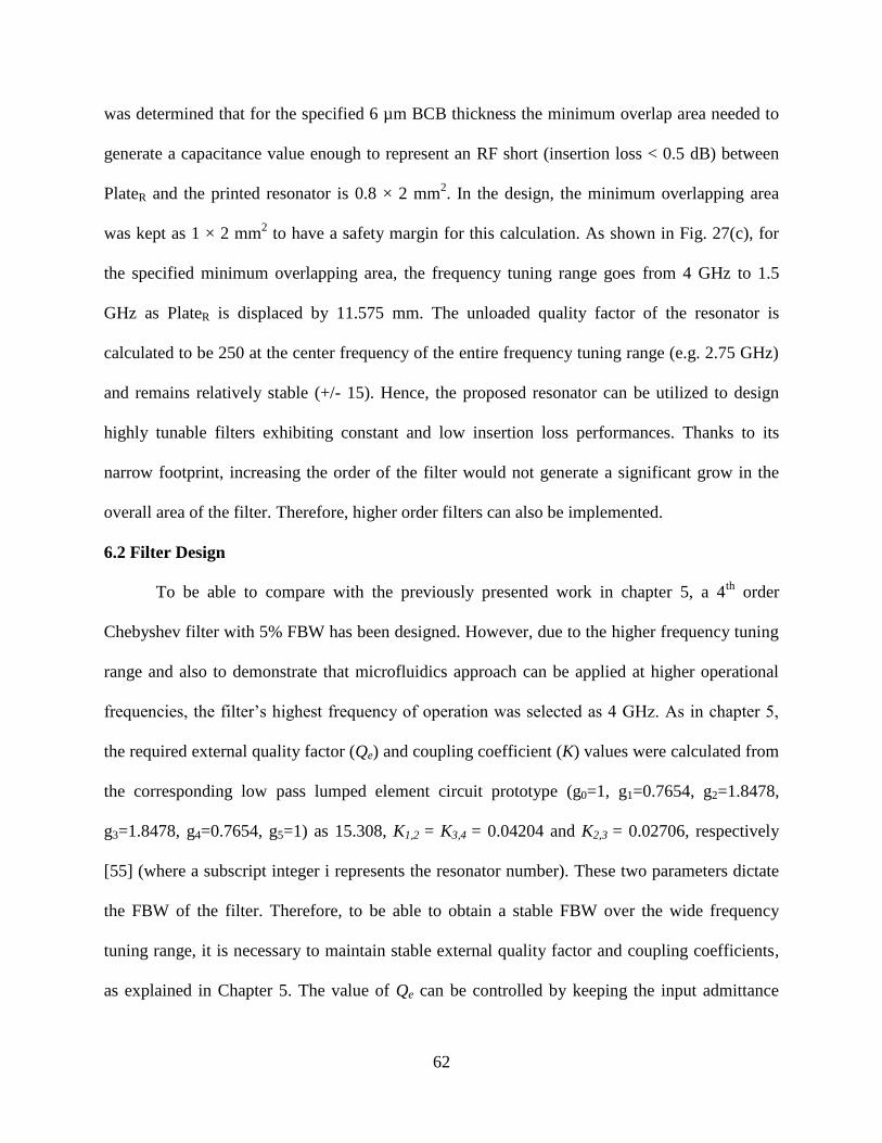
62
was determined that for the specified 6 µm BCB thickness the minimum overlap area needed to
generate a capacitance value enough to represent an RF short (insertion loss < 0.5 dB) between
PlateR and the printed resonator is 0.8 × 2 mm2. In the design, the minimum overlapping area
was kept as 1 × 2 mm2 to have a safety margin for this calculation. As shown in Fig. 27(c), for
the specified minimum overlapping area, the frequency tuning range goes from 4 GHz to 1.5
GHz as PlateR is displaced by 11.575 mm. The unloaded quality factor of the resonator is
calculated to be 250 at the center frequency of the entire frequency tuning range (e.g. 2.75 GHz)
and remains relatively stable (+/- 15). Hence, the proposed resonator can be utilized to design
highly tunable filters exhibiting constant and low insertion loss performances. Thanks to its
narrow footprint, increasing the order of the filter would not generate a significant grow in the
overall area of the filter. Therefore, higher order filters can also be implemented.
6.2 Filter Design
To be able to compare with the previously presented work in chapter 5, a 4th
order
Chebyshev filter with 5% FBW has been designed. However, due to the higher frequency tuning
range and also to demonstrate that microfluidics approach can be applied at higher operational
frequencies, the filter’s highest frequency of operation was selected as 4 GHz. As in chapter 5,
the required external quality factor (Qe) and coupling coefficient (K) values were calculated from
the corresponding low pass lumped element circuit prototype (g0=1, g1=0.7654, g2=1.8478,
g3=1.8478, g4=0.7654, g5=1) as 15.308, K1,2 = K3,4 = 0.04204 and K2,3 = 0.02706, respectively
[55] (where a subscript integer i represents the resonator number). These two parameters dictate
the FBW of the filter. Therefore, to be able to obtain a stable FBW over the wide frequency
tuning range, it is necessary to maintain stable external quality factor and coupling coefficients,
as explained in Chapter 5. The value of Qe can be controlled by keeping the input admittance
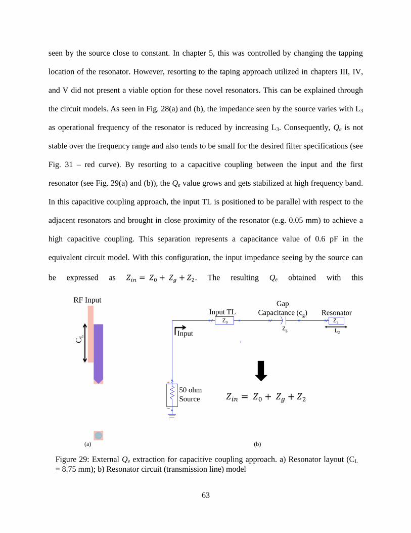
63
seen by the source close to constant. In chapter 5, this was controlled by changing the tapping
location of the resonator. However, resorting to the taping approach utilized in chapters III, IV,
and V did not present a viable option for these novel resonators. This can be explained through
the circuit models. As seen in Fig. 28(a) and (b), the impedance seen by the source varies with L3
as operational frequency of the resonator is reduced by increasing L3. Consequently, Qe is not
stable over the frequency range and also tends to be small for the desired filter specifications (see
Fig. 31 – red curve). By resorting to a capacitive coupling between the input and the first
resonator (see Fig. 29(a) and (b)), the Qe value grows and gets stabilized at high frequency band.
In this capacitive coupling approach, the input TL is positioned to be parallel with respect to the
adjacent resonators and brought in close proximity of the resonator (e.g. 0.05 mm) to achieve a
high capacitive coupling. This separation represents a capacitance value of 0.6 pF in the
equivalent circuit model. With this configuration, the input impedance seeing by the source can
be expressed as 𝑍𝑖𝑛 = 𝑍0 + 𝑍𝑔 + 𝑍2. The resulting Qe obtained with this
CL
RF Input
Figure 29: External Qe extraction for capacitive coupling approach. a) Resonator layout (CL
= 8.75 mm); b) Resonator circuit (transmission line) model
(a) (b)
𝑍𝑖𝑛 = 𝑍0 + 𝑍𝑔 + 𝑍2
ResonatorInput TLGap
Capacitance (cg)
50 ohm
Source
InputL2
Z0 Z2
Zg
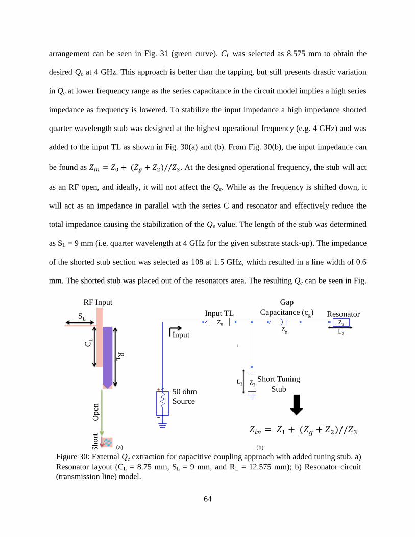
64
arrangement can be seen in Fig. 31 (green curve). CL was selected as 8.575 mm to obtain the
desired Qe at 4 GHz. This approach is better than the tapping, but still presents drastic variation
in Qe at lower frequency range as the series capacitance in the circuit model implies a high series
impedance as frequency is lowered. To stabilize the input impedance a high impedance shorted
quarter wavelength stub was designed at the highest operational frequency (e.g. 4 GHz) and was
added to the input TL as shown in Fig. 30(a) and (b). From Fig. 30(b), the input impedance can
be found as 𝑍𝑖𝑛 = 𝑍0 + (𝑍𝑔 + 𝑍2)//𝑍3. At the designed operational frequency, the stub will act
as an RF open, and ideally, it will not affect the Qe. While as the frequency is shifted down, it
will act as an impedance in parallel with the series C and resonator and effectively reduce the
total impedance causing the stabilization of the Qe value. The length of the stub was determined
as SL = 9 mm (i.e. quarter wavelength at 4 GHz for the given substrate stack-up). The impedance
of the shorted stub section was selected as 108 at 1.5 GHz, which resulted in a line width of 0.6
mm. The shorted stub was placed out of the resonators area. The resulting Qe can be seen in Fig.
𝑍𝑖𝑛 = 𝑍1 + (𝑍𝑔 + 𝑍2)//𝑍3
Input
ResonatorInput TL
Short Tuning
Stub50 ohm
Source
L2Zg
L3
Z0 Z2
Z3
Gap
Capacitance (cg)
RL
SL
CL
RF Input
Op
enS
ho
rt
Figure 30: External Qe extraction for capacitive coupling approach with added tuning stub. a)
Resonator layout (CL = 8.75 mm, SL = 9 mm, and RL = 12.575 mm); b) Resonator circuit
(transmission line) model.
(a) (b)
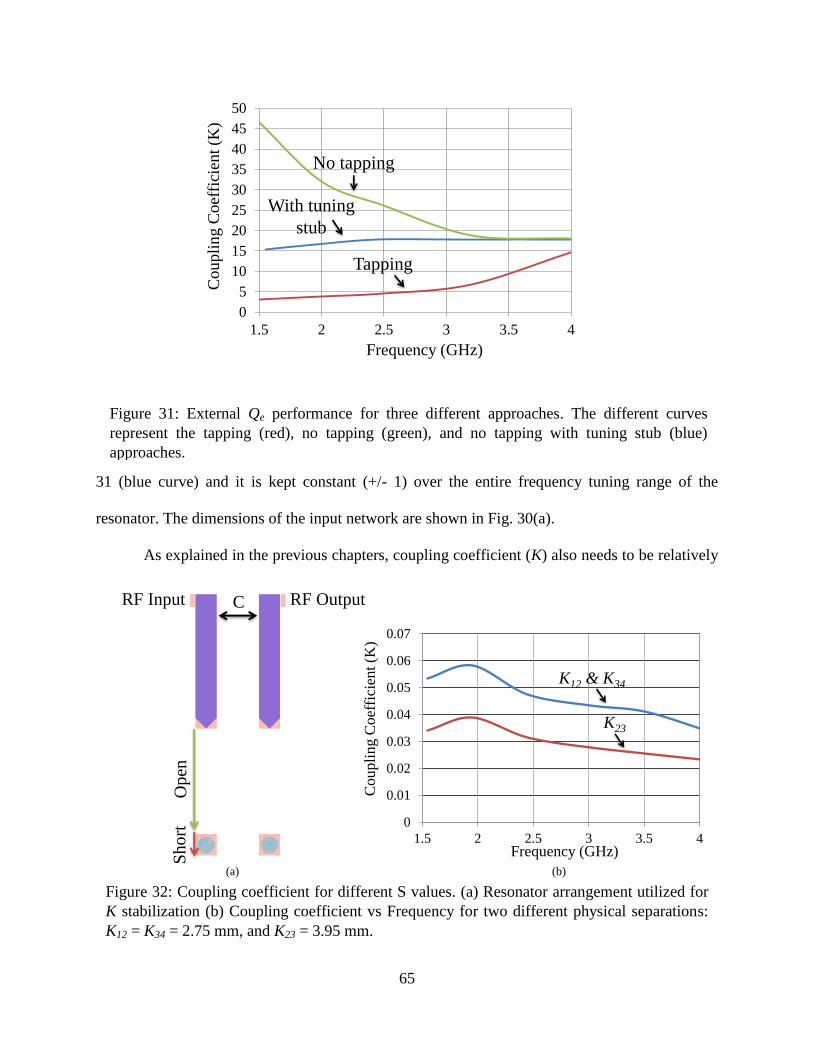
65
31 (blue curve) and it is kept constant (+/- 1) over the entire frequency tuning range of the
resonator. The dimensions of the input network are shown in Fig. 30(a).
As explained in the previous chapters, coupling coefficient (K) also needs to be relatively
Figure 31: External Qe performance for three different approaches. The different curves
represent the tapping (red), no tapping (green), and no tapping with tuning stub (blue)
approaches.
0
5
10
15
20
25
30
35
40
45
50
1.5 2 2.5 3 3.5 4
Co
up
lin
g C
oef
fici
ent
(K)
Frequency (GHz)
With tuning
stub
No tapping
Tapping
Figure 32: Coupling coefficient for different S values. (a) Resonator arrangement utilized for
K stabilization (b) Coupling coefficient vs Frequency for two different physical separations:
K12 = K34 = 2.75 mm, and K23 = 3.95 mm.
CRF Input RF Output
Open
Sh
ort
0
0.01
0.02
0.03
0.04
0.05
0.06
0.07
1.5 2 2.5 3 3.5 4
K12 & K34
K23
Co
up
lin
g C
oef
fici
ent
(K)
Frequency (GHz)
(a) (b)
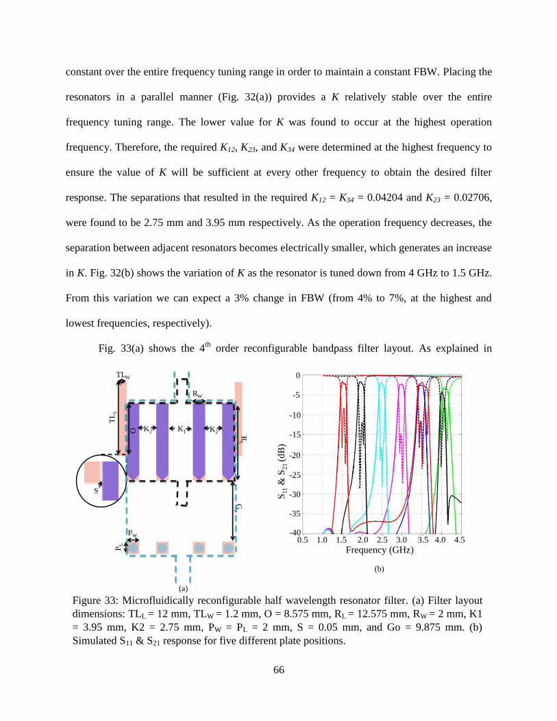
66
constant over the entire frequency tuning range in order to maintain a constant FBW. Placing the
resonators in a parallel manner (Fig. 32(a)) provides a K relatively stable over the entire
frequency tuning range. The lower value for K was found to occur at the highest operation
frequency. Therefore, the required K12, K23, and K34 were determined at the highest frequency to
ensure the value of K will be sufficient at every other frequency to obtain the desired filter
response. The separations that resulted in the required K12 = K34 = 0.04204 and K23 = 0.02706,
were found to be 2.75 mm and 3.95 mm respectively. As the operation frequency decreases, the
separation between adjacent resonators becomes electrically smaller, which generates an increase
in K. Fig. 32(b) shows the variation of K as the resonator is tuned down from 4 GHz to 1.5 GHz.
From this variation we can expect a 3% change in FBW (from 4% to 7%, at the highest and
lowest frequencies, respectively).
Fig. 33(a) shows the 4th
order reconfigurable bandpass filter layout. As explained in
Figure 33: Microfluidically reconfigurable half wavelength resonator filter. (a) Filter layout
dimensions: TLL = 12 mm, TLW = 1.2 mm, O = 8.575 mm, RL = 12.575 mm, RW = 2 mm, K1
= 3.95 mm, K2 = 2.75 mm, PW = PL = 2 mm, S = 0.05 mm, and Go = 9.875 mm. (b)
Simulated S11 & S21 response for five different plate positions.
(a)
(b)
K1K2 K2
S
TL
L
RL
TLW
RW
Go
PW
PL
O
0.5 1.0 1.5 2.0 2.5 3.0 3.5 4.0 4.5
0
-30
-20
-10
-40
Frequency (GHz)
S11
& S
21 (
dB
)
-5
-15
-25
-35
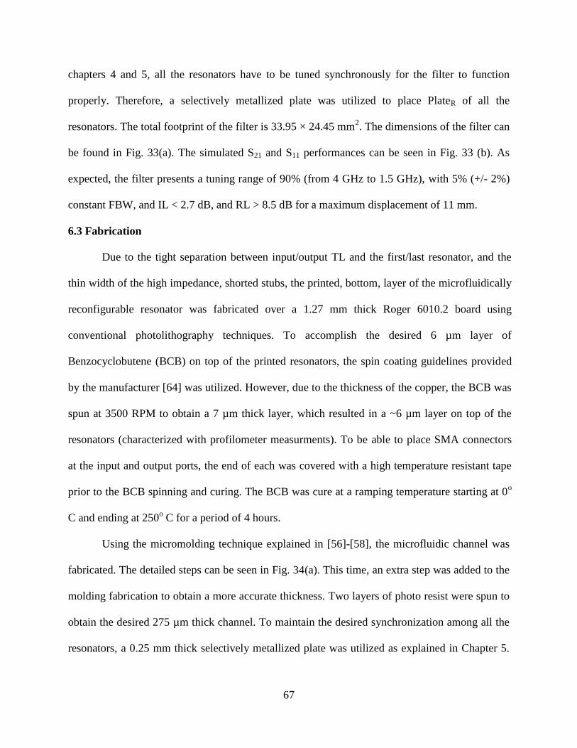
67
chapters 4 and 5, all the resonators have to be tuned synchronously for the filter to function
properly. Therefore, a selectively metallized plate was utilized to place PlateR of all the
resonators. The total footprint of the filter is 33.95 × 24.45 mm2. The dimensions of the filter can
be found in Fig. 33(a). The simulated S21 and S11 performances can be seen in Fig. 33 (b). As
expected, the filter presents a tuning range of 90% (from 4 GHz to 1.5 GHz), with 5% (+/- 2%)
constant FBW, and IL < 2.7 dB, and RL > 8.5 dB for a maximum displacement of 11 mm.
6.3 Fabrication
Due to the tight separation between input/output TL and the first/last resonator, and the
thin width of the high impedance, shorted stubs, the printed, bottom, layer of the microfluidically
reconfigurable resonator was fabricated over a 1.27 mm thick Roger 6010.2 board using
conventional photolithography techniques. To accomplish the desired 6 µm layer of
Benzocyclobutene (BCB) on top of the printed resonators, the spin coating guidelines provided
by the manufacturer [64] was utilized. However, due to the thickness of the copper, the BCB was
spun at 3500 RPM to obtain a 7 µm thick layer, which resulted in a ~6 µm layer on top of the
resonators (characterized with profilometer measurments). To be able to place SMA connectors
at the input and output ports, the end of each was covered with a high temperature resistant tape
prior to the BCB spinning and curing. The BCB was cure at a ramping temperature starting at 0o
C and ending at 250o C for a period of 4 hours.
Using the micromolding technique explained in [56]-[58], the microfluidic channel was
fabricated. The detailed steps can be seen in Fig. 34(a). This time, an extra step was added to the
molding fabrication to obtain a more accurate thickness. Two layers of photo resist were spun to
obtain the desired 275 µm thick channel. To maintain the desired synchronization among all the
resonators, a 0.25 mm thick selectively metallized plate was utilized as explained in Chapter 5.
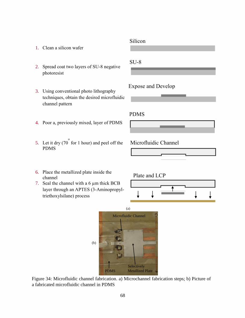
68
Silicon
1. Clean a silicon wafer
2. Spread coat two layers of SU-8 negative
photoresist
3. Using conventional photo lithography
techniques, obtain the desired microfluidic
channel pattern
4. Poor a, previously mixed, layer of PDMS
5. Let it dry (70o
for 1 hour) and peel off the
PDMS
6. Place the metallized plate inside the
channel
7. Seal the channel with a 6 µm thick BCB
layer through an APTES (3-Aminopropyl-
triethoxylsilane) process
SU-8
Expose and Develop
PDMS
Microfluidic Channel
Plate and LCP
Figure 34: Microfluidic channel fabrication. a) Microchannel fabrication steps; b) Picture of
a fabricated microfluidic channel in PDMS
(a)
(b)
Microfluidic Channel
Selectively
Metallized PlatePDMS
69
The dimensions of the selectively metallized plate, as well as the microfluidic channel, can be
seen in Fig. 35. To keep a relatively fast tuning speed, input and output channels were kept to 2
mm wide, and an extra section of the selectively metallized plate were added in the top and
bottom of the plate (Fig. 35(b)). To alleviate the fabrication process, the selectively metallized
plate was made in a 0.254 Rogers 5880LZ board (εr = 1.96, tanδ = 0.0009) using conventional
photolithography techniques, and it was placed inside the microfluidic channel manually prior to
sealing it. The microfluidic channel was sealed by bonding it with the BCB layer using an
CL
PL
PO
CO
PW
PL
PI
PO
Figure 35: Separated layers. a) Microfluidic channel and selectively metallized plate (PW =
7.25 mm, PL = 24 mm, PI = 2 mm, PO = 5 mm, CW = 7.3 mm, CL = 24.1 mm, CI = 2.1 mm,
and CO = 8 mm); b) Selectively metallized plate; c) Bottom plate with printed resonators.
(a)
(b)
(c)
70
APTES (3-Aminopropyltriethoxysilane) treatment [59]. To electronically control the filters, two
piezo-pumps, with dimensions of 30 x 15 x 3.8mm3 from Bartels® (mp-6) [61] were utilized.
These micropumps were chosen due to their piezo actuation mechanism that allows for an
accurate control of the liquid displacement via supply voltages. Two of these pumps were
connected in parallel to generate bi-directional flow capability. The pumps were operated with
the manufacturer supplied driver circuit that converts 5V DC current to a 100MHz 235V peak to
peak sinusoidal wave according to the highest flow rate specifications given for water [61]. The
power consumption of the pumps is less than 200 mW.
6.4 Experimental Verification
The fabricated prototype integrated with the pumping system can be seen in Fig. 36(a).
As expected, the tuning range of the filter was measured to be 2.7:1 from 4 GHz to 1.5 GHz.
Measured S11 and S21 performances can be seen in Fig. 36(b) and (c) and are in good agreement
with simulation results. The insertion loss was kept to be less than 3 dB over the entire frequency
tuning range with a return loss better than 9.7 dB. This represents an improvement of >1.5 dB in
insertion loss with respect to the open loop resonator filter presented in Chapter 5. A constant 5%
(+/- 2%) FBW was measured over the entire operational range of the filter. The out of band
rejection was >35 dB. However, since the half wavelength structure is kept over the entire
frequency range, the second harmonic of the filter is not suppressed, but it is shifted up in
frequency due to the shorting effect after a displacement > 9 mm. The overall dimensions of the
filter were measured as 34.975 x 38.01 mm2 excluding the pumping mechanism. The input and
output TL were extended by 11 mm to alleviate the measurement process. The tuning speed of
the filter was found to be, as expected, very close to the filter presented in chapter 5, thanks to
the selectively metallized plate approach, and it was measured as 2.5 MHz per ms. The slight
71
improvement in tuning speed is caused by the smaller size of the plate, which represents less
friction from the channel walls.
0.5 1.0 1.5 2.0 2.5 3.0 3.5 4.0 4.5
0
-30
-20
-10
-40
Frequency (GHz)
S11
& S
21 (
dB
)
-5
-15
-25
-35
0.5 2.0 4.0 6.0 8.0 10.0 12.0
0
-30
-20
-10
-40
Frequency (GHz)
S11
& S
21 (
dB
)
-5
-15
-25
-35
38
.01
mm
34.975 mm
Bartels M
P-6
Micro
pu
mp
s
Inp
ut
Ou
tpu
t
Figure 36: Experimental verification. a) Fabricated filter; b) Measured S11 and S21
performance; c) Wideband responses showing up to the filter’s third harmonic.
(a)
(b) (c)
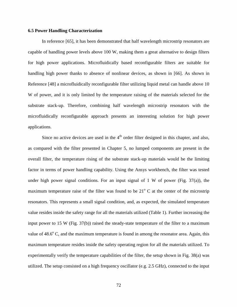
72
6.5 Power Handling Characterization
In reference [65], it has been demonstrated that half wavelength microstrip resonators are
capable of handling power levels above 100 W, making them a great alternative to design filters
for high power applications. Microfluidically based reconfigurable filters are suitable for
handling high power thanks to absence of nonlinear devices, as shown in [66]. As shown in
Reference [48] a microfluidically reconfigurable filter utilizing liquid metal can handle above 10
W of power, and it is only limited by the temperature raising of the materials selected for the
substrate stack-up. Therefore, combining half wavelength microstrip resonators with the
microfluidically reconfigurable approach presents an interesting solution for high power
applications.
Since no active devices are used in the 4th
order filter designed in this chapter, and also,
as compared with the filter presented in Chapter 5, no lumped components are present in the
overall filter, the temperature rising of the substrate stack-up materials would be the limiting
factor in terms of power handling capability. Using the Ansys workbench, the filter was tested
under high power signal conditions. For an input signal of 1 W of power (Fig. 37(a)), the
maximum temperature raise of the filter was found to be 21o C at the center of the microstrip
resonators. This represents a small signal condition, and, as expected, the simulated temperature
value resides inside the safety range for all the materials utilized (Table 1). Further increasing the
input power to 15 W (Fig. 37(b)) raised the steady-state temperature of the filter to a maximum
value of 48.6o C, and the maximum temperature is found in among the resonator area. Again, this
maximum temperature resides inside the safety operating region for all the materials utilized. To
experimentally verify the temperature capabilities of the filter, the setup shown in Fig. 38(a) was
utilized. The setup consisted on a high frequency oscillator (e.g. 2.5 GHz), connected to the input
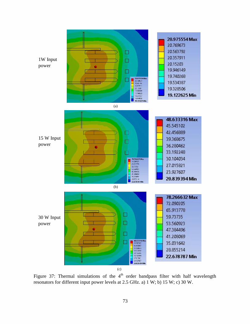
73
1W Input
power
15 W Input
power
30 W Input
power
Figure 37: Thermal simulations of the 4th
order bandpass filter with half wavelength
resonators for different input power levels at 2.5 GHz. a) 1 W; b) 15 W; c) 30 W.
(b)
(a)
(c)
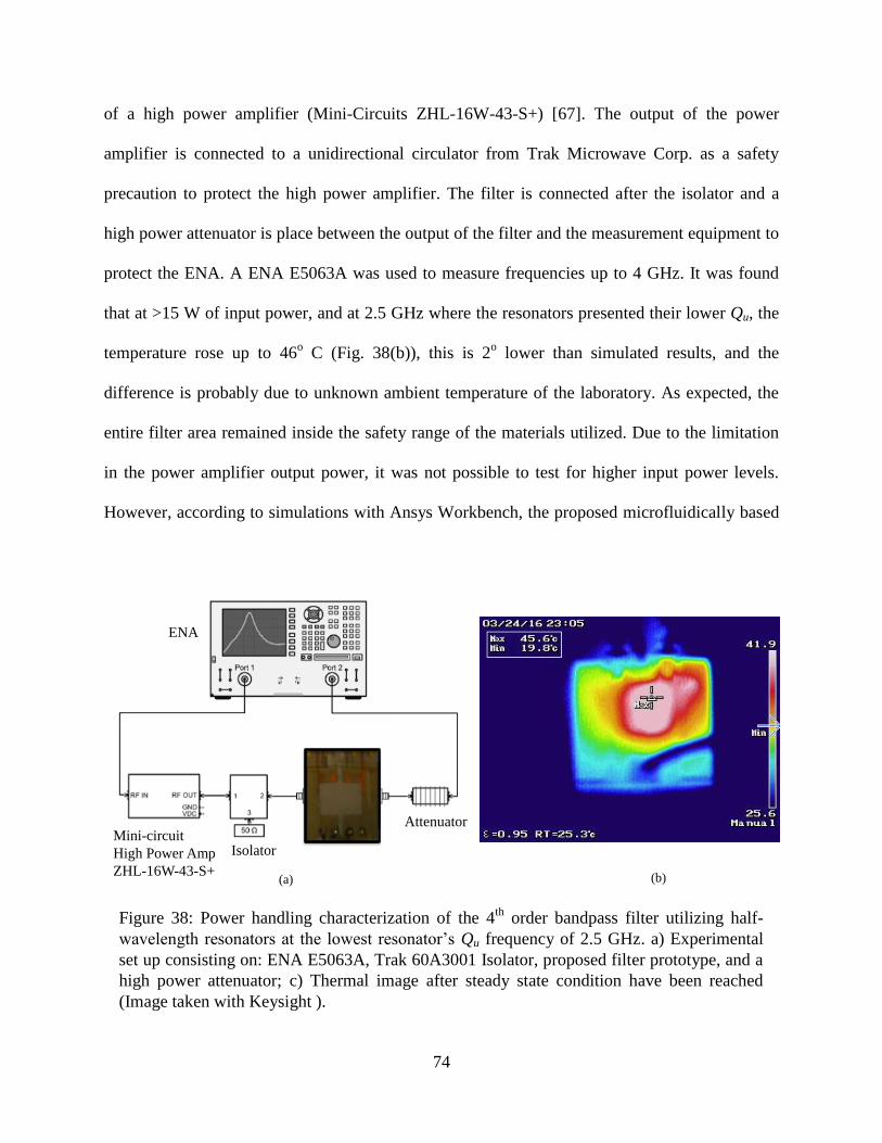
74
of a high power amplifier (Mini-Circuits ZHL-16W-43-S+) [67]. The output of the power
amplifier is connected to a unidirectional circulator from Trak Microwave Corp. as a safety
precaution to protect the high power amplifier. The filter is connected after the isolator and a
high power attenuator is place between the output of the filter and the measurement equipment to
protect the ENA. A ENA E5063A was used to measure frequencies up to 4 GHz. It was found
that at >15 W of input power, and at 2.5 GHz where the resonators presented their lower Qu, the
temperature rose up to 46o C (Fig. 38(b)), this is 2
o lower than simulated results, and the
difference is probably due to unknown ambient temperature of the laboratory. As expected, the
entire filter area remained inside the safety range of the materials utilized. Due to the limitation
in the power amplifier output power, it was not possible to test for higher input power levels.
However, according to simulations with Ansys Workbench, the proposed microfluidically based
Mini-circuit
High Power Amp
ZHL-16W-43-S+
Attenuator
Isolator
ENA
Figure 38: Power handling characterization of the 4th
order bandpass filter utilizing half-
wavelength resonators at the lowest resonator’s Qu frequency of 2.5 GHz. a) Experimental
set up consisting on: ENA E5063A, Trak 60A3001 Isolator, proposed filter prototype, and a
high power attenuator; c) Thermal image after steady state condition have been reached
(Image taken with Keysight ).
(a) (b)
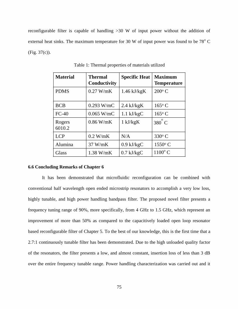
75
reconfigurable filter is capable of handling >30 W of input power without the addition of
external heat sinks. The maximum temperature for 30 W of input power was found to be 78o C
(Fig. 37(c)).
6.6 Concluding Remarks of Chapter 6
It has been demonstrated that microfluidic reconfiguration can be combined with
conventional half wavelength open ended microstrip resonators to accomplish a very low loss,
highly tunable, and high power handling bandpass filter. The proposed novel filter presents a
frequency tuning range of 90%, more specifically, from 4 GHz to 1.5 GHz, which represent an
improvement of more than 50% as compared to the capacitively loaded open loop resonator
based reconfigurable filter of Chapter 5. To the best of our knowledge, this is the first time that a
2.7:1 continuously tunable filter has been demonstrated. Due to the high unloaded quality factor
of the resonators, the filter presents a low, and almost constant, insertion loss of less than 3 dB
over the entire frequency tunable range. Power handling characterization was carried out and it
Material Thermal
Conductivity
Specific Heat Maximum
Temperature
PDMS 0.27 W/mK 1.46 kJ/kgK 200o C
BCB 0.293 W/mC 2.4 kJ/kgK 165o C
FC-40 0.065 W/mC 1.1 kJ/kgC 165o C
Rogers
6010.2
0.86 W/mK 1 kJ/kgK N/A
LCP 0.2 W/mK N/A 330o C
Alumina 37 W/mK 0.9 kJ/kgC 1550o C
Glass 1710o C
Table 1: Thermal properties of materials utilized
1.38 W/mK 0.7 kJ/kgC 1100o C
380o
C
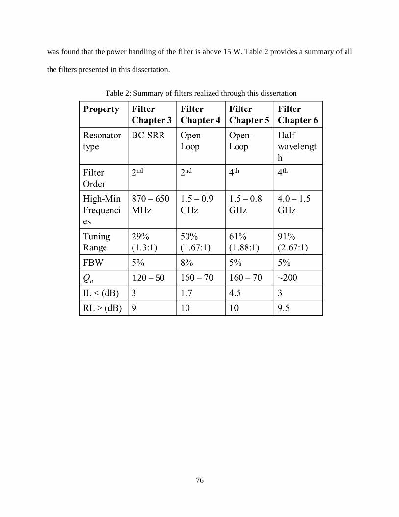
76
was found that the power handling of the filter is above 15 W. Table 2 provides a summary of all
the filters presented in this dissertation.
Table 2: Summary of filters realized through this dissertation
120 – 50
77
CHAPTER 7: FUTURE WORK
To further enhance the power handling capabilities resorting to a hard substrate based
configuration would be vital. As explained in Chapter 6, the temperature rising and thermal
conductivity of the materials is the limiting factor in terms of power handling capability of
microfluidics based reconfigurable filters. Most reconfigurable filters are limited, in their power
handling capability, by the third order intermodulation (TOI) point. Since no active devices are
utilized in microfluidically based RF reconfigurable filters, there is not TOI. The materials
utilized in the previous chapters present a poor temperature handling characteristic (e.g.
coefficient of thermal conductivity). In Table 2 the thermal characteristics of these materials
(Rogers 6010.2, BCB, and PDMS) are presented. As explained in chapter 6, the poorest thermal
conductor from this materials is the carrier fluid utilized (FC-40). However, improving the
thermal capacity of the material surrounding the fluid would help increase the maximum
temperature of operation of the filter. Therefore, replacing the PDMS with a material presenting
a higher thermal conductivity would be vital for very high power applications. Also, at high
temperatures, PDMS starts absorbing liquid, which would represent a major issue due to the
small volume of fluid required inside the channels. A solution to the above mentioned problems
could be replacing PDMS with glass, and therefore, preliminary studies have been done in this
aspect. However, the fabrication process time increase considerably due to the lengthy process of
etching glass. From preliminary studies, the etching rate of glass is ~10 µm per hour. At this rate,
it would take at least 25 hours to etch the desired channel. Also, most available photoresists
78
would be etched faster than the glass. One possible alternative would be using laser to etch the
glass, but the expensive pricing make it a not viable solution at this point. The addition of an
external heat sink could be valuable in terms of power handling capability of the filter since,
once again, its main limitation is only the temperature raising of the components, and the
dimensions of the filter are very small when compare to other available technologies.
Different type of resonators needs to be investigated to further expand the broad range of
possibilities that microfluidics have to offer toward obtaining RF bandpass reconfigurable filters.
Utilizing resonators with higher unloaded quality factor would provide a significant
improvement in terms of insertion loss (lower insertion loss) and power handling capability
(higher power handling), and therefore, should be investigated. Suspended line based resonators
have been known for providing a high unloaded quality factor. Therefore, the transition into
suspended line resonators would be vital to further decrease the insertion loss and increase the
power handling capability of microfluidically reconfigurable filters.
When comparing microfluidics to other available technologies, proposed reconfigurable
filters lack in terms of their tuning speed. So far, the studies carried out with microfluidic
reconfigurable filters presented a tuning speed of 2.12 MHz per ms, as compare to the tuning
speed presented by ferroelectric varactors (for example 2 MHz per µs). So far, the experiments
conducted on microfluidic reconfigurable devices have been done utilizing external micropumps
units, and therefore, the tuning speed of the filters is directly related to the micropump
capabilities in terms of flow rate. A detailed study on the micropumps could help to improve the
tuning speed significantly. In addition, the viscosity of the fluid utilized to move the metallized
plate inside the channel has a direct impact on the micropump functionality. So far the only
fluids studied have been Teflon solution and FC-40. Different carrier fluids could be further
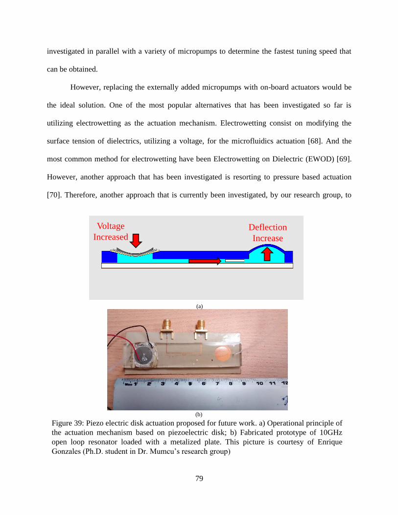
79
investigated in parallel with a variety of micropumps to determine the fastest tuning speed that
can be obtained.
However, replacing the externally added micropumps with on-board actuators would be
the ideal solution. One of the most popular alternatives that has been investigated so far is
utilizing electrowetting as the actuation mechanism. Electrowetting consist on modifying the
surface tension of dielectrics, utilizing a voltage, for the microfluidics actuation [68]. And the
most common method for electrowetting have been Electrowetting on Dielectric (EWOD) [69].
However, another approach that has been investigated is resorting to pressure based actuation
[70]. Therefore, another approach that is currently been investigated, by our research group, to
Deflection
Increase
Voltage
Increased
Figure 39: Piezo electric disk actuation proposed for future work. a) Operational principle of
the actuation mechanism based on piezoelectric disk; b) Fabricated prototype of 10GHz
open loop resonator loaded with a metalized plate. This picture is courtesy of Enrique
Gonzales (Ph.D. student in Dr. Mumcu’s research group)
(a)
(b)
80
replace the micropumps with in-chip actuators, and therefore, increase the tuning speed of
microfluidic based reconfigurable filters, is the utilization of a piezoelectric disks to provide
metallized plates backwards and forward motion capabilities. By making use of a sealed
microfluidic channel, it is possible to transfer the small deflection generated by a piezo electric
disk into motion. As shown in Fig. 39(a), as the voltage increases, the piezoelectric disk bends
downwards and push the plate inside the channel. A second reservoir is place in the opposite end
of the channel to absorb the motion (Fig. 39(a)). The proposed mechanism has been
experimentally verified to provide a short moving range of 3 mm with a <10 mm in diameter
piezo electric disk. Preliminary studies were carried out through a resonator at high frequencies
(10 GHz) to maintain the required motion range under the 3 mm range provided by the piezo
disk (Fig. 39(b)). Furthermore, the piezo electric disk could be positioned under the ground plane
(below the filter area) to maintain the footprint to that of the individual reconfigurable filter.
Since piezo-electric based actuation has been demonstrated to be fast, require low DC power and
the displacement range required by the microfluidic based filters has been shown to be small,
they present an interesting alternative for the necessary actuation mechanism.
81
REFERENCES
[1] G. M. Rebeiz, K. Entesari, I. C. Reines, S. J. Park, M. A. El-Tanani, A. Grichener, et al.,
"Tuning in to RF MEMS," Ieee Microwave Magazine, vol. 10, pp. 55-72, Oct 2009.
[2] P. Bahramzy, P. Olesen, P. Madsen, J. Bojer, S. C. Del Barrio, A. Tatomirescu, et al., "A
Tunable RF Front-End With Narrowband Antennas for Mobile Devices," Ieee
Transactions on Microwave Theory and Techniques, vol. 63, pp. 3300-3310, Oct 2015.
[3] J. Uher, and W. Hoefer, “Tunable microwave and millimeter-wave band-pass filters,”
Ieee Transactions on Microwave Theory and Techniques, vol. 39, no. 4, pp. 643-653,
April 1991.
[4] R. R. Mansour, F. X. Huang, S. Fouladi, W. D. Yan, and M. Nasr, "High-Q Tunable
Filters," Ieee Microwave Magazine, vol. 15, pp. 70-82, Jul-Aug 2014.
[5] G. C. Liang, D. Zhang, C. F. Shih, M. E. Johansson, and R. S. Withers, “High-power
high-temperature superconducting microstrip filters for cellular base-station
applications,” Ieee Transactions on Applied Superconductivity, vol. 5, no. 2, June 1995.
[6] S. H. Hou, J. H. Lang, A. H. Slocum, A. C. Weber, and J. R. White, “ A high-Q widely
tunable gigahertz electromagnetic cavity resonator,” Journal of Microelectromechanical
Systems, vol. 15, no. 6, pp. 1540-1545, December 2006.
[7] W. J. Keane, "Narrow-Band Yig Filters Aid Wide-Open Receivers," Microwaves, vol.
17, pp. 50-&, 1978.
[8] L. Young, and D. Weller, “A 500-to-1000 MHz magnetically tunable band-pass filter
using two YIG-disk resonators,” Ieee Transactions on Microwave Theory and
Thecniques, vol. MTT-15, no. 2, pp. 72-86, February 1967.
[9] Y. Murakami, T. Ohgihara, and T. Okamoto, “A 0.5-4.0-GHz tunable bandpass filter
using YIG film grown by LPE,” Ieee Transactions on Microwave Theory and
Techniques, vol. MTT-35, no. 12, pp. 1192-1198, December 1987.
[10] Y. Shu, J. Navarro, and K. Chang, “Electronically switchable and tunable coplanar
waveguided-slotline band-pass filter,” Ieee Transactions on Microwave Theory and
Techniques, vol. 39, no. 3, pp. 548-554, March 1991.
82
[11] A. R. Brown and G. M. Rebeiz, "A varactor-tuned RF filter," Ieee Transactions on
Microwave Theory and Techniques, vol. 48, pp. 1157-1160, Jul 2000.
[12] C. Li et. al,”A tunable high temperature superconducting bandpass filter realized using
semiconductor varactors,” Ieee Transactions on Applied Superconductivity, vol. 24, no. 5,
August 2014.
[13] J. S. Sun, N. Kaneda, Y. Baeyens, T. Itoh, and Y. K. Chen, "Multilayer Planar Tunable
Filter With Very Wide Tuning Bandwidth," Ieee Transactions on Microwave Theory and
Techniques, vol. 59, pp. 2864-2871, Nov 2011.
[14] I. Vendik, O. Vendik, V. Pleskachev, and M. Nikol’ski, “Tunable microwave filters using
ferroelectric materials,” Ieee transactions on Applied Superconductivity, vol. 13, no. 2,
pp. 716-719, June 2003.
[15] S. Courreges, Y. Li, Z. Y. Zhao, K. Choi, A. Hunt, and J. Papapolymerou, "A Low Loss
X-Band Quasi-Elliptic Ferroelectric Tunable Filter," Ieee Microwave and Wireless
Components Letters, vol. 19, pp. 203-205, Apr 2009.
[16] S. Courreges, Y. Li, Z. Zhao, K. Choi, A. Hunt, and J. Papapolymerou, “Two-pole X-
band-tunable ferroelectric filters with tunable center frequency, fractional bandwidth, and
return loss,” Ieee Transactions on Microwave Theory and Techniques, vol. 57, no. 12, pp.
2872-2881, December 2009.
[17] A. Abbaspour-Tamijani, L. Dussopt, and G. Rebeiz, “Miniature and tunable filters using
MEMS capacitors,” Ieee Transactions on Microwave Theory and Techniques, vol. 51, no.
7, pp. 1878-1885, July 2003.
[18] Y. Shim, Z. Z. Wu, and M. Rais-Zadeh, "A High-Performance Continuously Tunable
MEMS Bandpass Filter at 1 GHz," Ieee Transactions on Microwave Theory and
Techniques, vol. 60, pp. 2439-2447, Aug 2012.
[19] W. Irshad and D. Peroulis, "A 12-18 GHz electrostatically tunable liquid metal RF
MEMS resonator with quality factor of 1400-1840," in Microwave Symposium Digest
(MTT), 2011 IEEE MTT-S International, 2011, pp. 1-4.
[20] K. Entesari and G. M. Rebeiz, "A differential 4-bit 6.5-10-GHz RF MEMS tunable
filter," Ieee Transactions on Microwave Theory and Techniques, vol. 53, pp. 1103-1110,
Mar 2005.
[21] K. L. Chen, X. G. Liu, A. Kovacs, W. J. Chappell, and D. Peroulis, "Antibiased
Electrostatic RF MEMS Varactors and Tunable Filters," Ieee Transactions on Microwave
Theory and Techniques, vol. 58, pp. 3971-3981, Dec 2010.
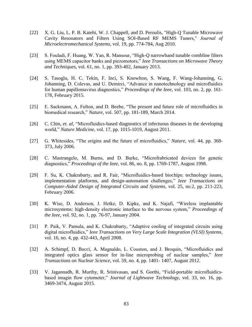
83
[22] X. G. Liu, L. P. B. Katehi, W. J. Chappell, and D. Peroulis, "High-Q Tunable Microwave
Cavity Resonators and Filters Using SOI-Based RF MEMS Tuners," Journal of
Microelectromechanical Systems, vol. 19, pp. 774-784, Aug 2010.
[23] S. Fouladi, F. Huang, W. Yan, R. Mansour, “High-Q narrowband tunable combline filters
using MEMS capacitor banks and piezomotors,” Ieee Transactions on Microwave Theory
and Techniques, vol. 61, no. 1, pp. 393-402, January 2013.
[24] S. Tasoglu, H. C. Tekin, F. Inci, S. Knowlton, S. Wang, F. Wang-Johanning, G.
Johanning, D. Colevas, and U. Demirci, “Advance in nanotechnology and microfluidics
for human papillomavirus diagnostics,” Proceedings of the Ieee, vol. 103, no. 2, pp. 161-
178, February 2015.
[25] E. Sackmann, A. Fulton, and D. Beebe, “The present and future role of microfluidics in
biomedical research,” Nature, vol. 507, pp. 181-189, March 2014.
[26] C. Chin, et. al, “Microfluidics-based diagnostics of infectuous diseases in the developing
world,” Nature Medicine, vol. 17, pp. 1015-1019, August 2011.
[27] G. Whitesides, “The origins and the future of microfluidics,” Nature, vol. 44, pp. 368-
373, July 2006.
[28] C. Mastrangelo, M. Burns, and D. Burke, “Microfrabricated devices for genetic
diagnostics,” Proceedings of the Ieee, vol. 86, no. 8, pp. 1769-1787, August 1998.
[29] F. Su, K. Chakrabarty, and R. Fair, “Microfluidics-based biochips: technology issues,
implementation platforms, and design-automation challenges,” Ieee Transactions on
Computer-Aided Design of Integrated Circuits and Systems, vol. 25, no.2, pp. 211-223,
February 2006.
[30] K. Wise, D. Anderson, J. Hetke, D. Kipke, and K. Najafi, “Wireless implantable
microsystems: high-density electronic interface to the nervous system,” Proceedings of
the Ieee, vol. 92, no. 1, pp. 76-97, January 2004.
[31] P. Paik, V. Pamula, and K. Chakrabarty, “Adaptive cooling of integrated circuits using
digital microfluidics,” Ieee Transactions on Very Large Scale Integration (VLSI) Systems,
vol. 16, no. 4, pp. 432-443, April 2008.
[32] A. Schimpf, D. Bucci, A. Magnaldo, L. Couston, and J. Broquin, “Microfluidics and
integrated optics glass sensor for in-line microprobing of nuclear samples,” Ieee
Transactions on Nuclear Science, vol. 59, no. 4, pp. 1401- 1407, August 2012.
[33] V. Jagannadh, R. Murthy, R. Srinivasan, and S. Gorthi, “Field-portable microfluidics-
based imagin flow cytometer,” Journal of Lightwave Technology, vol. 33, no. 16, pp.
3469-3474, August 2015.
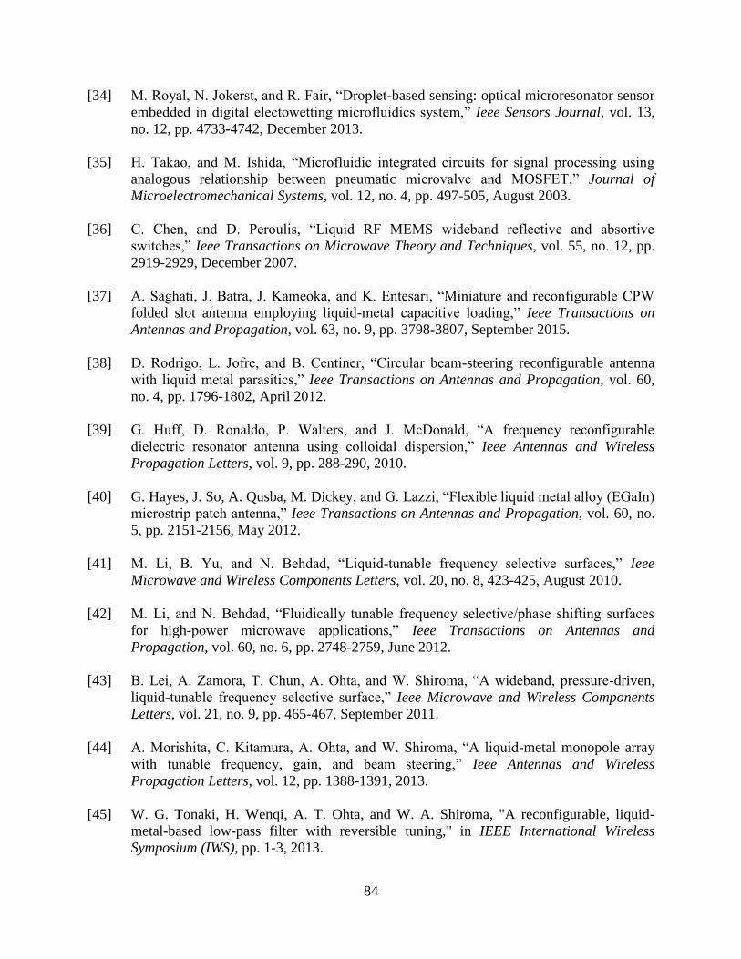
84
[34] M. Royal, N. Jokerst, and R. Fair, “Droplet-based sensing: optical microresonator sensor
embedded in digital electowetting microfluidics system,” Ieee Sensors Journal, vol. 13,
no. 12, pp. 4733-4742, December 2013.
[35] H. Takao, and M. Ishida, “Microfluidic integrated circuits for signal processing using
analogous relationship between pneumatic microvalve and MOSFET,” Journal of
Microelectromechanical Systems, vol. 12, no. 4, pp. 497-505, August 2003.
[36] C. Chen, and D. Peroulis, “Liquid RF MEMS wideband reflective and absortive
switches,” Ieee Transactions on Microwave Theory and Techniques, vol. 55, no. 12, pp.
2919-2929, December 2007.
[37] A. Saghati, J. Batra, J. Kameoka, and K. Entesari, “Miniature and reconfigurable CPW
folded slot antenna employing liquid-metal capacitive loading,” Ieee Transactions on
Antennas and Propagation, vol. 63, no. 9, pp. 3798-3807, September 2015.
[38] D. Rodrigo, L. Jofre, and B. Centiner, “Circular beam-steering reconfigurable antenna
with liquid metal parasitics,” Ieee Transactions on Antennas and Propagation, vol. 60,
no. 4, pp. 1796-1802, April 2012.
[39] G. Huff, D. Ronaldo, P. Walters, and J. McDonald, “A frequency reconfigurable
dielectric resonator antenna using colloidal dispersion,” Ieee Antennas and Wireless
Propagation Letters, vol. 9, pp. 288-290, 2010.
[40] G. Hayes, J. So, A. Qusba, M. Dickey, and G. Lazzi, “Flexible liquid metal alloy (EGaIn)
microstrip patch antenna,” Ieee Transactions on Antennas and Propagation, vol. 60, no.
5, pp. 2151-2156, May 2012.
[41] M. Li, B. Yu, and N. Behdad, “Liquid-tunable frequency selective surfaces,” Ieee
Microwave and Wireless Components Letters, vol. 20, no. 8, 423-425, August 2010.
[42] M. Li, and N. Behdad, “Fluidically tunable frequency selective/phase shifting surfaces
for high-power microwave applications,” Ieee Transactions on Antennas and
Propagation, vol. 60, no. 6, pp. 2748-2759, June 2012.
[43] B. Lei, A. Zamora, T. Chun, A. Ohta, and W. Shiroma, “A wideband, pressure-driven,
liquid-tunable frequency selective surface,” Ieee Microwave and Wireless Components
Letters, vol. 21, no. 9, pp. 465-467, September 2011.
[44] A. Morishita, C. Kitamura, A. Ohta, and W. Shiroma, “A liquid-metal monopole array
with tunable frequency, gain, and beam steering,” Ieee Antennas and Wireless
Propagation Letters, vol. 12, pp. 1388-1391, 2013.
[45] W. G. Tonaki, H. Wenqi, A. T. Ohta, and W. A. Shiroma, "A reconfigurable, liquid-
metal-based low-pass filter with reversible tuning," in IEEE International Wireless
Symposium (IWS), pp. 1-3, 2013.
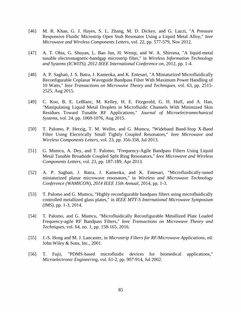
85
[46] M. R. Khan, G. J. Hayes, S. L. Zhang, M. D. Dickey, and G. Lazzi, "A Pressure
Responsive Fluidic Microstrip Open Stub Resonator Using a Liquid Metal Alloy," Ieee
Microwave and Wireless Components Letters, vol. 22, pp. 577-579, Nov 2012.
[47] A. T. Ohta, G. Shuyan, L. Bao Jun, H. Wenqi, and W. A. Shiroma, "A liquid-metal
tunable electromagnetic-bandgap microstrip filter," in Wireless Information Technology
and Systems (ICWITS), 2012 IEEE International Conference on, 2012, pp. 1-4.
[48] A. P. Saghati, J. S. Batra, J. Kameoka, and K. Entesari, "A Miniaturized Microfluidically
Reconfigurable Coplanar Waveguide Bandpass Filter With Maximum Power Handling of
10 Watts," Ieee Transactions on Microwave Theory and Techniques, vol. 63, pp. 2515-
2525, Aug 2015.
[49] C. Koo, B. E. LeBlanc, M. Kelley, H. E. Fitzgerald, G. H. Huff, and A. Han,
"Manipulating Liquid Metal Droplets in Microfluidic Channels With Minimized Skin
Residues Toward Tunable RF Applications," Journal of Microelectromechanical
Systems, vol. 24, pp. 1069-1076, Aug 2015.
[50] T. Palomo, P. Herzig, T. M. Weller, and G. Mumcu, "Wideband Band-Stop X-Band
Filter Using Electrically Small Tightly Coupled Resonators," Ieee Microwave and
Wireless Components Letters, vol. 23, pp. 356-358, Jul 2013.
[51] G. Mumcu, A. Dey, and T. Palomo, "Frequency-Agile Bandpass Filters Using Liquid
Metal Tunable Broadside Coupled Split Ring Resonators," Ieee Microwave and Wireless
Components Letters, vol. 23, pp. 187-189, Apr 2013.
[52] A. P. Saghati, J. Batra, J. Kameoka, and K. Entesari, "Microfluidically-tuned
miniaturized planar microwave resonators," in Wireless and Microwave Technology
Conference (WAMICON), 2014 IEEE 15th Annual, 2014, pp. 1-3.
[53] T. Palomo and G. Mumcu, "Highly reconfigurable bandpass filters using microfluidically
controlled metallized glass plates," in IEEE MTT-S International Microwave Symposium
(IMS), pp. 1-3, 2014.
[54] T. Palomo, and G. Mumcu, "Microfluidically Reconfigurable Metallized Plate Loaded
Frequency-agile RF Bandpass Filters," Ieee Transactions on Microwave Theory and
Techniques, vol. 64, no. 1, pp. 158-165, 2016.
[55] J.-S. Hong and M. J. Lancaster, in Microstrip Filters for RF/Microwave Applications, ed:
John Wiley & Sons, Inc., 2001.
[56] T. Fujii, "PDMS-based microfluidic devices for biomedical applications,"
Microelectronic Engineering, vol. 61-2, pp. 907-914, Jul 2002.
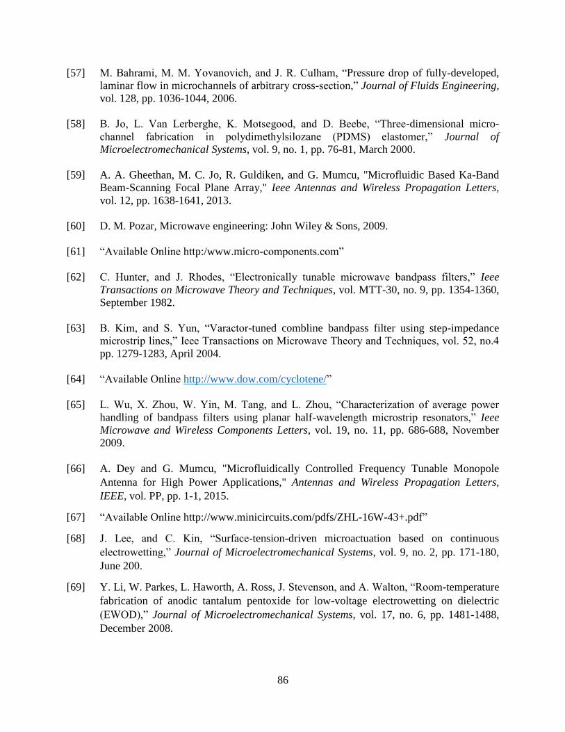
86
[57] M. Bahrami, M. M. Yovanovich, and J. R. Culham, “Pressure drop of fully-developed,
laminar flow in microchannels of arbitrary cross-section,” Journal of Fluids Engineering,
vol. 128, pp. 1036-1044, 2006.
[58] B. Jo, L. Van Lerberghe, K. Motsegood, and D. Beebe, “Three-dimensional micro-
channel fabrication in polydimethylsilozane (PDMS) elastomer,” Journal of
Microelectromechanical Systems, vol. 9, no. 1, pp. 76-81, March 2000.
[59] A. A. Gheethan, M. C. Jo, R. Guldiken, and G. Mumcu, "Microfluidic Based Ka-Band
Beam-Scanning Focal Plane Array," Ieee Antennas and Wireless Propagation Letters,
vol. 12, pp. 1638-1641, 2013.
[60] D. M. Pozar, Microwave engineering: John Wiley & Sons, 2009.
[61] “Available Online http:/www.micro-components.com”
[62] C. Hunter, and J. Rhodes, “Electronically tunable microwave bandpass filters,” Ieee
Transactions on Microwave Theory and Techniques, vol. MTT-30, no. 9, pp. 1354-1360,
September 1982.
[63] B. Kim, and S. Yun, “Varactor-tuned combline bandpass filter using step-impedance
microstrip lines,” Ieee Transactions on Microwave Theory and Techniques, vol. 52, no.4
pp. 1279-1283, April 2004.
[64] “Available Online http://www.dow.com/cyclotene/”
[65] L. Wu, X. Zhou, W. Yin, M. Tang, and L. Zhou, “Characterization of average power
handling of bandpass filters using planar half-wavelength microstrip resonators,” Ieee
Microwave and Wireless Components Letters, vol. 19, no. 11, pp. 686-688, November
2009.
[66] A. Dey and G. Mumcu, "Microfluidically Controlled Frequency Tunable Monopole
Antenna for High Power Applications," Antennas and Wireless Propagation Letters,
IEEE, vol. PP, pp. 1-1, 2015.
[67] “Available Online http://www.minicircuits.com/pdfs/ZHL-16W-43+.pdf”
[68] J. Lee, and C. Kin, “Surface-tension-driven microactuation based on continuous
electrowetting,” Journal of Microelectromechanical Systems, vol. 9, no. 2, pp. 171-180,
June 200.
[69] Y. Li, W. Parkes, L. Haworth, A. Ross, J. Stevenson, and A. Walton, “Room-temperature
fabrication of anodic tantalum pentoxide for low-voltage electrowetting on dielectric
(EWOD),” Journal of Microelectromechanical Systems, vol. 17, no. 6, pp. 1481-1488,
December 2008.
87
[70] E. Hallynck, and P. Bienstman, “Digital microfluidics with pressure-based actuation,”
Ieee Photonics Technology Letters, vol. 25, no. 17, pp. 1656-1659, September 2013.
[71] A. Gheethan, A. Dey, and G. Mumcu, “Passive feed network design for microfluidic
beam-scanning focal plane arrays and their performance evaluation,” Ieee Transactions
on Antennas and Propagation, vol. 63, no. 8, pp. 3452-3464, May 2015.
[72] “Available Online http://www.microchem.com/Prod-SU82000.htm”
[73] V. Sunkara, D. Park, H. Hwang, R. Chantiwas, S. Soper, and Y. Cho, “Simple room
temperature bonding of thermoplastics and poly(dimethylsiloxane),” Lab On a Chip, vol.
11, pp. 962-965, 2011.
[74] “Available Online http://www.dow.com/cyclotene/prod/302257.htm”
88
APPENDIX A: MICROFLUIDIC CHANNEL FABRICATION
Microfluidic channel fabrication has been previously presented in [56]-[58]. The overall
technique consist on fabricating a mold with the desire microchannel specification, to later pour
a commercially available elastomer (Polydimethylsiloxane) in its liquid form, and cure to
transition it into its solid state. After pilling of the solid elastomer, the desired microchannels will
be in the bottom face. The face containing the microchannels will be sealed with a commercially
available thin-film insulator to form the finalized microfluidic channel. In the following, a
detailed explanation on each of the steps of the microchannel fabrication is provided.
A.1 Microfluidic Channel Design
Initially, individual metallized plates were utilized and a meandered channel was
designed to host all the plates (e.g. 2 plates were used in chapter 4). At the beginning of this
dissertation, microfluidic channels were designed to have the same width as the metallized
plates. However, it was quickly learned that the plate would not move inside these channels due
to the high friction between the walls of the channel and the plate (e.g. channel got stuck). To
overcome this issue, a detailed characterization of the channel width was performed by our group
[71] by fabricating channels with widths slightly wider than the width of the metallized plates.
From these studies, it was found that if the microfluidic channel was too wide, the plate could tilt
inside of it causing it to get stuck and/or corrupt the performance of the filter. After fabricating
channels with 100 µm, 200 µm, 300 µm, 400 µm, and 500 µm wider than the metallized plate, it
was found that, with a 100 µm wider channel, the plate movement was smooth and repeatable.
89
A.2 Micromold Fabrication
The micromold design follows conventional photolithography techniques. To start a 5
inch diameter silicon wafer is cleaned by submerging it in acetone, isopropanol, and methanol.
After submerging it in methanol, it is necessary to rinse with deionized water and dry with
nitrogen, quickly after it has been rinsed. To remove any water drops left on the surface, the
wafer is placed in a hot plate at a high temperature (~160o) for at least 5 min. Once the wafer is
cleaned, the photo resist that will be utilized for the mold is spin coated. Originally, SU-8 2150
negative photoresist was selected as the mold material thanks to its thickness and sharp edge
profile. After placing the silicon wafer in the center of the spinner, the photo resist was added
starting at the center of the wafer, and progressively moving towards the edge. Adding between 3
to 4 cubic inches is enough to cover the entire wafer. The spinning recipe utilized to uniformly
coat the SU-8 2150 negative resist consisted on:
A) Spreading the photoresist over the silicon wafer (Step #1):
Spin for 10 seconds
Rate of 500 rpm
Acceleration rate of 100 rpm/s
B) Obtaining the desired thickness (Step #2):
Spin for 30 seconds
Spinning rate of 2000 rpm
Acceleration rate of 300 rpm/s
After the spinning process is finished, a soft bake on a level hot plate at a temperature of ~100o C
needs to be performed for about 60 min (may require longer time). To determine that the soft
baking time is satisfactory, the wafer is removed from the hot plate, cooled down to room
90
temperature, and replaced back on to the hot plate. In this second replacement, if wrinkles are
observed at the photoresist surface, the wafer needs to be left on the hot plate; otherwise it can be
utilized for the next step. In general, cool-down and heat-up process can be repeated frequently
until no wrinkles are observed when the wafer is on the hot plate. Utilizing this recipe, the
resultant SU-8 layer would be ~300 µm thick. For other thicknesses, the data sheet of SU-8 2000
can be referred to [72].
After the photoresist has been coated and soft baked, it can be defined by exposing the
unwanted area to UV light for a total energy of 800 mJ/cm2. Different thicknesses might require
different exposure energy (refer to [72] for the specific exposure dose). A post exposure bake of
30 min at 95o C is necessary. After one minute of post exposure bake, the image of the mask
should be visible on the wafer.
Later in our research, we determined that the microfluidic channel height was a crucial
parameter for the performance of the filters. Therefore, a more detailed study of the reversed
mold height (or microchannel depth) was performed. By resorting to a thinner, less viscous, SU-
8 resist (SU-8 2075) a more detailed characterization was possible by coating the SU-8 in two
layers instead of one. A first layer was coated at a low speed to obtain a thickness of ~200 µm.
On top of this layer, a second layer was coated at a high speed to obtain a thickness of ~75 µm.
The thickness of the second layer can be changed in steps as small as 5 µm. The procedure for
obtaining a 275 µm thick channel is as follows:
A) Layer #1
1) Spreading the photoresist on the silicon wafer (Step #1):
Spin for 10 s
Spinning at a rate of 500 rpm
91
Acceleration of 100 rpm/s
2) Obtaining the desired thickness (Step #2):
Spin for 40 s
Spinning at a rate of 1500 rpm
Acceleration of 500 rpm/s
After the first layer has been coated, wafer is soft baked on a hot plate for about 60 min. In order
to determine the baking time, follow the heat-up/cool-down procedure explained above.
B) Layer #2
1) Spreading the photoresist on the silicon wafer (Step #1):
Spin for 10 s
Spinning at a rate of 500 rpm
Acceleration of 100 rpm/s
2) Obtaining the desired thickness (Step #2):
Spin for 40 s
Spinning at a rate of 3000 rpm
Acceleration of 500 rpm/s
After the second layer has been coated, a shorter bake time of 10 min at 100o C is required.
However, the procedure of cooling down the wafer, and putting it back into the hot plate needs to
be performed to ensure the baking process is completed.
The final step in the reverse micromold fabrication is to immerse the wafer in an SU-8
developer to remove the unwanted (unexposed) photoresist. The developing time for the
specified thickness of ~300 µm was found to be 25 min. However, by using a Q-tip to peel off
the unwanted (unexposed) photoresist, the process could be speed up to under 20 min. It is
92
recommended to always use a Q-tip to clean up the edges of the mold towards the end of the
developing process.
A.3 Polydimethylsiloxane (PDMS) Preparation
To continue with the microchannel fabrication, the PDMS (SYLGARD® 184 silicone
elastomer kit) was mixed in a ratio of 10:1 with its curing agent. To obtain the desired 2 mm
thick PDMS layer, 20 g of PDMS were mixed with 2 g of the curing agent. To remove all the
trapped air bubbles, a degassed process was done. The degassed process consist on placing the
mixed PDMS under vacuum and bringing it back to atmosphere pressure several times, until no
bubbles are left in the mixing. The wafer, with the reverse micromold, needs to be placed inside
a 5 inch diameter petri dish, and the area surrounding the molded structure needs to be delimited
with aluminum foil. For larger molds, more grams of PMDS might be required. The mixed
PDMS was poured carefully on top of the reversed mold to avoid the generation of new air
bubbles. The petri dish was placed in the oven at 70o C for 25 min. It is also possible to cure the
PDMS at room temperature, but the curing time might take up to 48 hours.
Once the PDMS have been cured, it can be peeled off from the silicon wafer and the
resultant microchannel will be in the bottom surface. An X-ACTO knife can be used to remove
the extra unwanted PDMS.
A.4 Sealing the Channel (Bonding)
To complete the microchannel fabrication, it needs to be completely sealed with a thin-
film insulator. Early experiments were carried out by sealing the microfluidic channel with
readily available pregrep LCP (Rogers Corp), but later a thinner insulator Benzocyclobutene
(BCB) was utilized to replace the LCP. These materials are thermoplastic and therefore a
customized APTES (3-Aminopropyltriethoxysilane) based treatment that was previously used
93
for other thermoplastic material-PDMS bonding was utilized for the LCP/BCB-PDMS bonding
process. First, the general process will be outlined, and then specific details will be given for
each insulator.
The insulator substrate was treated with oxygen plasma for 30 s at a power level of ~60
W, and then merged in an aqueous solution of 2% v/v APTES for 20 min. The solution was
placed on a hot plate to increase its temperature up to 80o C. Parallel to this process, the PDMS
was treated with oxygen plasma at a power level of ~60 W. The activated insulator and the
PDMS were kept in conformal contact inside the oven at a temperature of 70o C for 10 min. It is
possible to seal the bond at room temperature, but high temperatures can help to strengthen it. A
more detailed explanation of this procedure can be found in [73].
LCP is a commercially available substrate with predefined thickness (Ultralam 3880 (εr
= 2.4, tanδ = 0.0025)). The pregrep form of LCP helps to obtain stronger bonds due to the
smooth surface. The thickness of the BCB (Cyclotene 3022-57, Dow Chemical Company) can be
customized through spin coating procedures. For this, BCB is spin coated over the desired
substrate (e.g. Rogers 6010.2). To obtain the required 6 µm layer of BCB, the recipe utilized
was:
Step 1 (Spreading the BCB):
Spin for 7 s
Spinning rate of 500 rpm
Acceleration rate of 200 rpm/s
Step 2 (Obtaining the desired thickness)
Spin for 40 s
Spinning rate of 4000 rpm
94
Acceleration rate of 1000 rpm/s
The input and output microstrip lines of the circuit should be covered with a high temperature
resistant tape to be able to make electrical connection to them afterwards and to avoid an extra
etching step at the end of the fabrication procedure. After spinning the BCB, it is necessary to
bake it for a period of 60 s at a temperature that can range from 80o C to 150
o C. After baking,
the thermal curing process requires a ramping temperature increase from 100o C to 250
o C for a
period of 3 hours. For more detail on BCB processing and thicknesses, manufacturer supplied
data sheet can be seen [74]. Once the BCB is cured (completely polymerized), the bonding
procedures explained above can be followed.
It is important to remember to open the inlet and outlet holes in the PDMS, and manually
insert the selectively metallized plate inside the microchannel prior to the bonding.
A.5 Selectively Metallized Plate Fabrication
Different substrates were originally tested to fabricate the selectively metallized plate.
Since the selected fluid was Teflon solution from DuPont (400S2-100-1), which consists of 1%
Teflon powder dissolved in 3M FC-40 solution, with a density of 1.855 g/cm3, the selectively
metallized plate was preferably fabricated in a substrate with a density value close to 1.855
g/cm3. Studies were carried out with silicon (2.33 g/cm
3) and quartz (2.65 g/cm
3) with little
successful movement due to their high density difference. Therefore, substrates such as PMMA
(1.18 g/cm3) and Rogers 5880LZ (1.4 g/cm
3) were investigated. Initial filter prototypes were
fabricated using PMMA, however, this required an extra step of metallization, which led us to
select 254 µm thick Rogers 5880LZ readily available with a 17 µm thick metallized layer.
Resorting to conventional photolithography techniques, the unwanted metal was removed.
95
APPENDIX B: COPYRIGHT PERMISSIONS
Below is permission for the use of the images in Figure 1
96
Below is permission for the use of images in Figure 2
97
Below is permission for the use of images in figure 3.
98
Below is permission for the use of images in figure 4.
99
Below is permission for the use of images in figure 5.
100
Below are permissions for the use of images in figure 6.
101
102
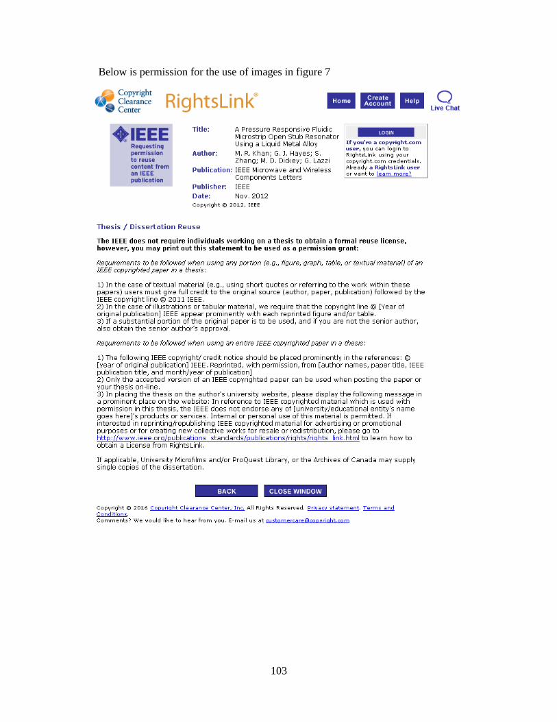
103
Below is permission for the use of images in figure 7
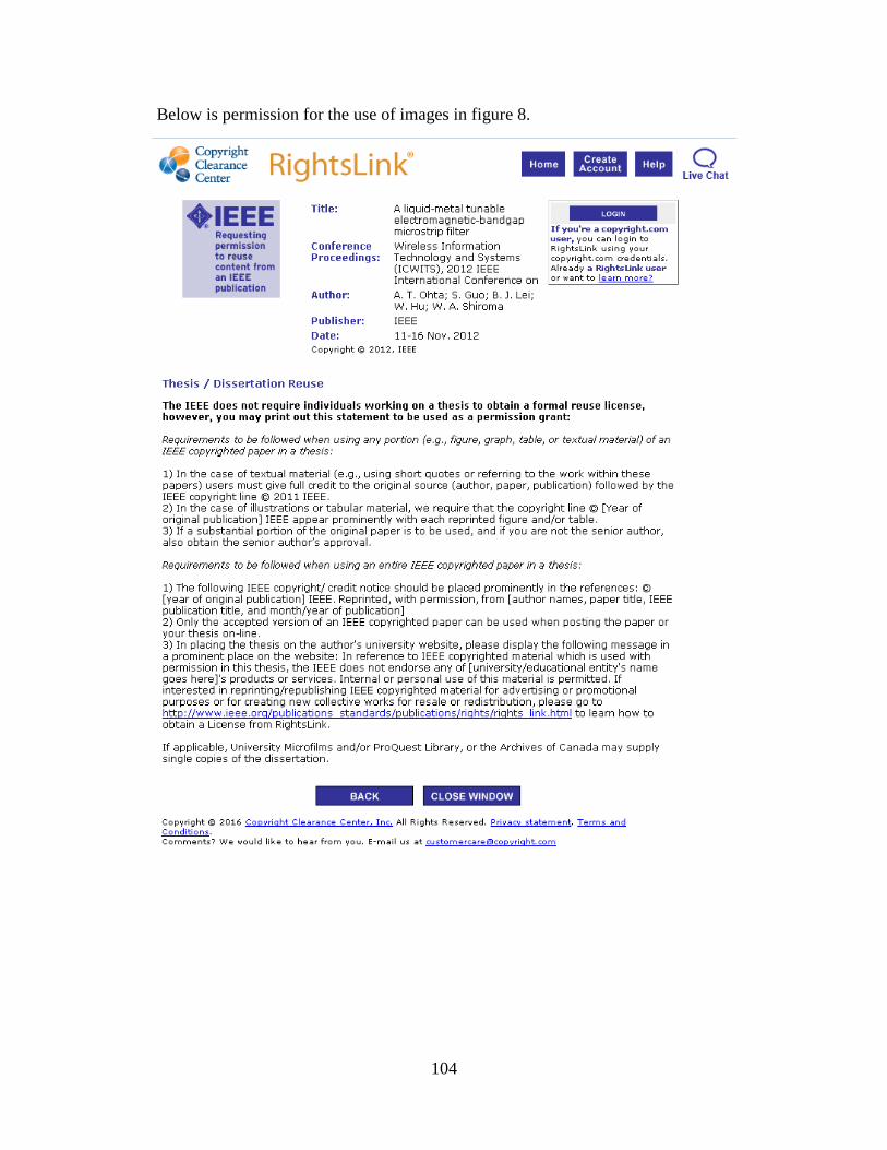
104
Below is permission for the use of images in figure 8.
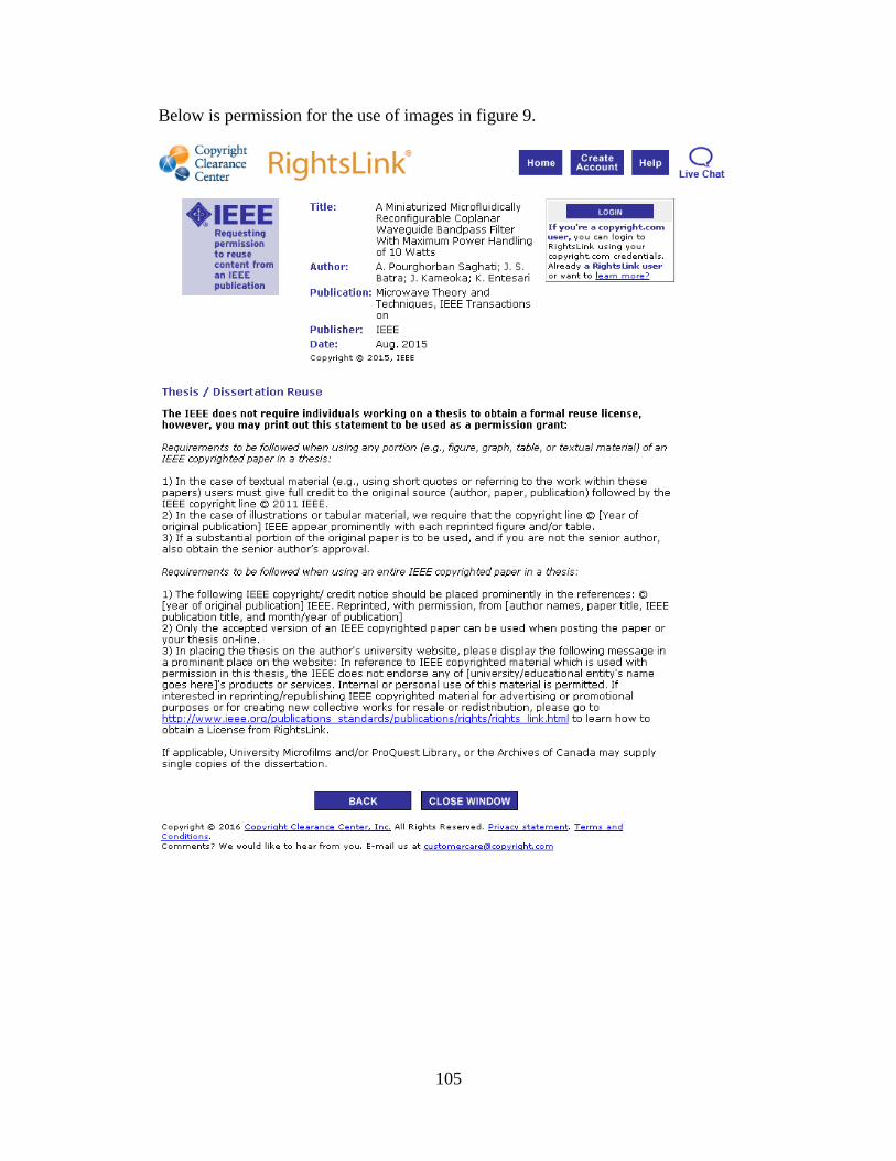
105
Below is permission for the use of images in figure 9.
106
Below is permission for the use of material in Chapter 2.

107
Below is permission for the use of material in Chapter 3.
108
Below is permission for the use of material in Chapter 4.
109
Below is permission for the use of material in Chapter 5.
ABOUT THE AUTHOR
Timothy Palomo was born in Maracay, Venezuela, on October 5th, 1990. He received the
B.S. and M.S. degrees in electrical engineering from University of South Florida, Florida, United
States, in 2011 and 2013, respectively.
He is currently a Ph.D. candidate at the University of South Florida with expected
graduation date May 2016. He has been a Research Assistant of the Center for Wireless and
Microwave Information Systems (WAMI) at the University of South Florida since 2011, and his
research has been focused on the development of highly reconfigurable RF filters through
microfluidic techniques. From May 2015 to December 2016, he has been a Design Engineer
Intern with Qorvo.
Mr. Palomo graduated from high school in 2007 as the best of his class. He was the
outstanding student of the USF’s electrical engineering department in 2011. He received the best
poster award in the USF research day competitions three straight years and was awarded
conference travel grants. Mr. Palomo also played tennis at the professional level in Venezuela
and was awarded a full scholarship by West Virginia University to pursue his career.


