Embed Size (px)
Citation preview
Microstructural, optical, and electrical characterization of semipolar„112̄2… gallium nitride grown by epitaxial lateral overgrowth
Tongtong Zhu,a� Carol F. Johnston, Menno J. Kappers, and Rachel A. OliverDepartment of Materials Science and Metallurgy, University of Cambridge, Pembroke Street, CambridgeCB2 3QZ, United Kingdom
�Received 9 July 2010; accepted 30 August 2010; published online 26 October 2010�
Semipolar �112̄2� gallium nitride �GaN� films have been grown on m-plane �11̄00� sapphire byepitaxial lateral overgrowth. Transmission electron microscopy �TEM� studies show that theinclination of the �0001� axis at 32° from the film surface combined with the high �0001� growth rateunder the reactor conditions used, allowed a low defect density �LDD� wing growing along �0001�to partially overgrow the highly defective window region and the other wing, resulting in acoalescence boundary, at which stacking faults and dislocations appear to terminate. Lowtemperature cathodoluminescence �CL� was performed to correlate the optical properties with thedifferent stages of the growth process. It is found that emission from the LDD wing is dominatedby near band edge recombination, whereas an emission band at 3.42 eV related to basal planestacking faults and a broad band from 3.15–3.38 eV possibly related to emission from prismaticstacking faults and partial dislocations were observed in the window region. Scanning capacitancemicroscopy �SCM� studies showed that almost the entire film is unintentionally n-doped. Bycorrelating the spatial variation in the unintentional doping to the overgrowth process, different
impurity incorporation rates between the �112̄2� and �0001� facets have been observed. Dislocationsof a or a+c type were found to bend over toward the growth direction in the LDD wing by TEMappear to be nonradiative by cross-sectional CL and SCM studies have revealed that they alsoimpact the local electrical properties. © 2010 American Institute of Physics.�doi:10.1063/1.3498813�
I. INTRODUCTION
Spontaneous and piezoelectric polarization induced elec-tric fields along the �0001� c-axis inherent in quantum wellstructures based on hexagonal gallium nitride �GaN� result inbending of the band structure and spatial separation of theelectron and hole wave functions in this direction, thus low-ering the optical efficiencies of light emitting devices.1
Growth of GaN in nonpolar �or semipolar� orientations offersa crystallographic solution to eliminate �or reduce� the inter-nal electric fields in optoelectronic devices and potentiallylead to higher light emission efficiencies.2,3
Heteroepitaxial growth of nonpolar a-plane �112̄0� and
m-plane �11̄00� GaN has been successful on sapphire sub-
strates �both �11̄02� r-plane4 and �11̄00� m-plane5� as well as
LiAlO2 �100�,6 ZnO �11̄00�,7 and SiC �11̄00�,8 respectively.
Semipolar �112̄2� GaN can be grown on m-plane sapphire9,10
and growth of �101̄1̄� GaN has been achieved on bulk GaNsubstrates.11 Light emitting diodes based on non- and semi-polar GaN have been demonstrated on bulk GaN substratessliced from thick c-plane GaN.12,13 However, they cannot beeasily commercialized due to the limited size and high costof the available substrates. Meanwhile, heteroepitaxial filmsgrown in these crystal orientations suffer from very high de-fect densities in comparison to conventional c-plane GaN,including basal plane stacking faults �BSFs�, prismatic stack-
ing faults �PSFs�, and partial dislocations �PDs� bounding theBSFs.14,15 Since PDs are likely to be nonradiative16 andBSFs luminesce,17 it is essential to reduce the defect densi-ties in order to realize the potential of semipolar optoelec-tronics at low cost. To reduce the defect density of the het-eroepitaxial films, SiNx interlayers,18 ScN interlayers,18,19
and epitaxial lateral overgrowth �ELOG�,20,21 have been em-ployed in the growth of nonpolar and semipolar GaN.
Previous cathodoluminescence �CL� investigations of
ELOG semipolar �112̄2� GaN by Gühne et al.20 have shownthat the densities of both dislocations and BSFs can be ef-fectively reduced. In this paper, low temperature CL andscanning capacitance microscopy �SCM� were used to inves-tigate the luminescence characteristics and unintentional
doping respectively of ELOG semipolar �112̄2� GaN in rela-tion to the microstructure. The impact of structural defects onthe microstructure has been elucidated by correlating differ-ent characterization techniques.
II. EXPERIMENTAL DETAILS
A semipolar �112̄2� GaN template with a thickness of
650 nm was initially grown on �11̄00� m-plane sapphire witha V/III ratio of 1310 at 1020 °C by metalorganic vapor-phase epitaxy in a 6�2 in. Thomas Swan close-coupledshowerhead reactor using trimethylgallium, silane �at 50ppm in hydrogen�, and ammonia as precursors and hydrogenas the carrier gas. Optical interferometry at 633 and 950 nma�Electronic mail: [email protected].
JOURNAL OF APPLIED PHYSICS 108, 083521 �2010�
0021-8979/2010/108�8�/083521/8/$30.00 © 2010 American Institute of Physics108, 083521-1
was used to monitor the growth. A 100 nm thick layer ofsilicon dioxide �SiO2� was deposited onto the GaN templateby e-beam evaporation. By using conventional wet-chemistry photolithography, the oxide layer was patterned
into stripes aligned parallel to the �11̄00� GaN direction. Themask stripes and window openings are both 5 �m wide.
Regrowth on the �112̄2� GaN template was carried out at1050 °C with a V/III ratio of 240 at 100 Torr. The micro-structure was examined by conventional transmission elec-tron microscopy �TEM� on a Philips CM30 operating at 300kV and cross-sectional TEM specimens were prepared bymechanical polishing followed by ion beam milling to elec-tron transparency. Scanning electron microscopy �SEM� andCL studies were performed at liquid helium temperature �7K� at 5 kV in a Philips XL30 equipped with a Gatan Mon-oCL4 system.
SCM is a technique based on contact-mode atomic forcemicroscopy �AFM�. By applying an alternating bias throughthe metal-coated tip to the semiconductor surface, accumu-lation, and depletion of the carriers within the semiconductorvary the tip-sample capacitance. The change in capacitancemeasured with the applied voltage gives information aboutthe carrier concentration �SCM amplitude data�, while thedifference in phase between the change in capacitance andthe applied voltage gives the carrier type �SCM phase data�.A more detailed description of the SCM technique is avail-able elsewhere.22,23
SCM studies were carried out on sample cross sectionswith a Veeco Dimension 3100 AFM with a commercial SCMapplication module. The cross-sectional sample was preparedby cleaving following the making of a scratch using a dia-mond scribe on the GaN surface perpendicular to the maskstripes. Sample grounding was achieved by soldering an in-dium contact to a scratch on the GaN surface. SCM dataanalysis was subsequently carried out using WSxM
freeware.24
III. RESULTS AND DISCUSSION
A. Cross-sectional TEM
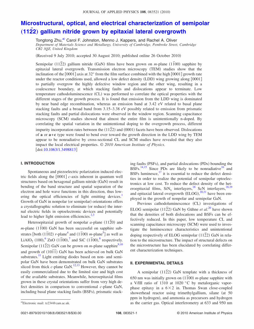
Cross-sectional TEM images of the coalesced semipolarELOG GaN are shown in Fig. 1. The image in Fig. 1�a� wastaken perpendicular to the mask stripe orientation �along
�11̄00� zone axis and with g=0002� showing the high den-sity of defects originating in the thin seed layer runningthrough the film at an acute angle of �58° with the substratein the region where there is no SiO2 mask, i.e., the windowregion. Convergent beam electron diffraction studies confirmthat the +c-axis �0001� is inclined at 32° to the substrate,hence the defects are confined to the basal �0001� plane. Thenumber of defects is drastically reduced above the SiO2
mask, i.e., in the so-called wing region. The two wings ‘A’and ‘B’ are labeled on Fig. 1 for clarity. Cross-sectional SEMstudies of an uncoalesced ELOG sample showed that the
ELOG growth process proceeds along �0001� and �112̄0�inclined facets and, in the later stages, �112̄2� facets parallelto the substrate. Therefore, the lateral overgrowth of the lowdefect density �LLD� wing �B� above the mask proceeded as
an inclined �0001� growth front until coalescence took place
with the �112̄0� facet of the highly dislocated neighboringwing �A�. Some lateral growth of the A wing occurred overthe mask as evidenced by the highly defective triangular areaabove the left side of the mask stripe in Fig. 1�a�. However,the relative growth rate of the A wing is much less than thatof the B wing and the former was overgrown by the latterdue to the inclination of the �0001� axis toward the filmsurface, forming a boundary at which dislocations appear toterminate. The defects as shown in Fig. 1�a� are visible with
g=0002, g=112̄0, and g=11̄00, so they could either be PDsor a+c threading dislocations �TDs�.19 By tilting the speci-
men 30° to a �112̄0� zone axis and using g=11̄00 �Fig. 1�b��,BSFs can be seen originating from the seed layer and propa-gating to the film surface. The B wing is mostly BSF-freeand the A wing has a high density of BSFs throughout. BothTEM images show that the B wing exhibits some short dis-location lines, implying that the dislocations present are in-clined to the TEM foil. The defect densities in the differentregions of the coalesced semipolar ELOG GaN layer weredetermined using plan-view TEM data and are presented inTable I. The ELOG process has reduced the dislocation den-sity as well as the BSF density in the B wing quite signifi-cantly, in good accordance with the values found by Gühneet al.20
To further investigate the dislocation segments seen inthe B wing, a cross-sectional TEM sample was prepared ap-
proximately along �11̄00� through the wing region. The TEM
FIG. 1. Cross-sectional TEM images of the coalesced semipolar ELOG
GaN �a� along �11̄00� using g=0002. The inclined dislocations visible could
either be PDs or a+c TDs. �b� Viewed along �112̄0� using g=11̄00, inwhich BSFs are in contrast.
TABLE I. Summary of defect densities of the coalesced semipolar ELOGGaN sample.
RegionBSF density
�cm−1�Dislocation density
�cm−2�
Template �3�105 �9�1010
Window �1.9�0.3��105 �4.4�0.5��109
Wing �5�3��103 �1.4�0.3��108
083521-2 Zhu et al. J. Appl. Phys. 108, 083521 �2010�
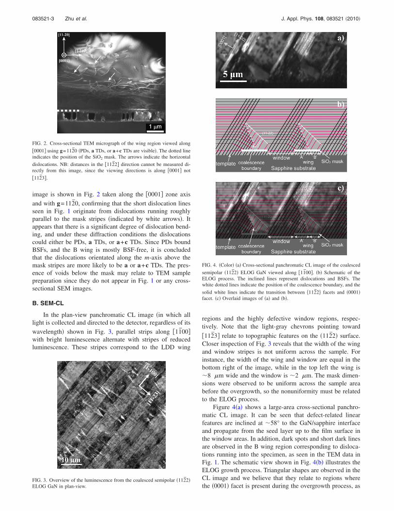
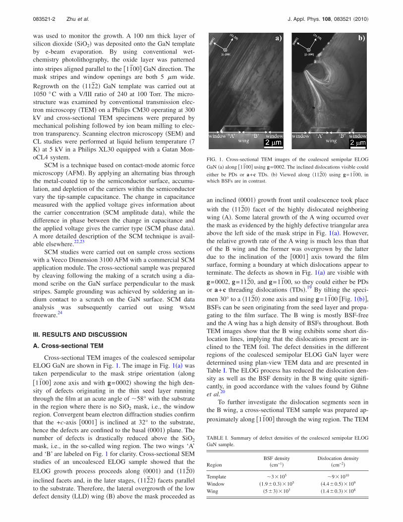
image is shown in Fig. 2 taken along the �0001� zone axis
and with g=112̄0, confirming that the short dislocation linesseen in Fig. 1 originate from dislocations running roughlyparallel to the mask stripes �indicated by white arrows�. Itappears that there is a significant degree of dislocation bend-ing, and under these diffraction conditions the dislocationscould either be PDs, a TDs, or a+c TDs. Since PDs boundBSFs, and the B wing is mostly BSF-free, it is concludedthat the dislocations orientated along the m-axis above themask stripes are more likely to be a or a+c TDs. The pres-ence of voids below the mask may relate to TEM samplepreparation since they do not appear in Fig. 1 or any cross-sectional SEM images.
B. SEM-CL
In the plan-view panchromatic CL image �in which alllight is collected and directed to the detector, regardless of its
wavelength� shown in Fig. 3, parallel strips along �11̄00�with bright luminescence alternate with stripes of reducedluminescence. These stripes correspond to the LDD wing
regions and the highly defective window regions, respec-tively. Note that the light-gray chevrons pointing toward
�112̄3� relate to topographic features on the �112̄2� surface.Closer inspection of Fig. 3 reveals that the width of the wingand window stripes is not uniform across the sample. Forinstance, the width of the wing and window are equal in thebottom right of the image, while in the top left the wing is�8 �m wide and the window is �2 �m. The mask dimen-sions were observed to be uniform across the sample areabefore the overgrowth, so the nonuniformity must be relatedto the ELOG process.
Figure 4�a� shows a large-area cross-sectional panchro-matic CL image. It can be seen that defect-related linearfeatures are inclined at �58° to the GaN/sapphire interfaceand propagate from the seed layer up to the film surface inthe window areas. In addition, dark spots and short dark linesare observed in the B wing region corresponding to disloca-tions running into the specimen, as seen in the TEM data inFig. 1. The schematic view shown in Fig. 4�b� illustrates theELOG growth process. Triangular shapes are observed in theCL image and we believe that they relate to regions wherethe �0001� facet is present during the overgrowth process, as
FIG. 2. Cross-sectional TEM micrograph of the wing region viewed along
�0001� using g=112̄0 �PDs, a TDs, or a+c TDs are visible�. The dotted lineindicates the position of the SiO2 mask. The arrows indicate the horizontal
dislocations. NB: distances in the �112̄2� direction cannot be measured di-rectly from this image, since the viewing directions is along �0001� not
�112̄3�.
FIG. 3. Overview of the luminescence from the coalesced semipolar �112̄2�ELOG GaN in plan-view.
FIG. 4. �Color� �a� Cross-sectional panchromatic CL image of the coalesced
semipolar �112̄2� ELOG GaN viewed along �11̄00�. �b� Schematic of theELOG process. The inclined lines represent dislocations and BSFs. Thewhite dotted lines indicate the position of the coalescence boundary, and the
solid white lines indicate the transition between 112̄2 facets and �0001�facet. �c� Overlaid images of �a� and �b�.
083521-3 Zhu et al. J. Appl. Phys. 108, 083521 �2010�
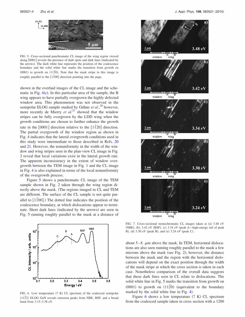
shown in the overlaid images of the CL image and the sche-matic in Fig. 4�c�. In this particular area of the sample, the Bwing appears to have partially overgrown the highly defectedwindow area. This phenomenon was not observed in thesemipolar ELOG sample studied by Gühne et al.,20 however,more recently de Mierry et al.21 showed that the windowstripes can be fully overgrown by the LDD wing when thegrowth conditions are chosen to further enhance the growth
rate in the �0001� direction relative to the �11̄20� direction.The partial overgrowth of the window region as shown inFig. 4 indicates that the lateral overgrowth conditions used inthis study were intermediate to those described in Refs. 20and 21. However, the nonuniformity in the width of the win-dow and wing stripes seen in the plan-view CL image in Fig.3 reveal that local variations exist in the lateral growth rate.The apparent inconsistency in the extent of window over-growth between the TEM image in Fig. 1 and the CL imagein Fig. 4 is also explained in terms of the local nonuniformityof the overgrowth process.
Figure 5 shows a panchromatic CL image of the TEMsample shown in Fig. 2 taken through the wing region di-rectly above the mask. �The regions imaged in CL and TEMare different. The surface of the CL sample is not quite par-
allel to �11̄00�.� The dotted line indicates the position of thecoalescence boundary, at which dislocations appear to termi-nate. Short dark lines �indicated by the arrows� are seen inFig. 5 running roughly parallel to the mask at a distance of
about 5–8 �m above the mask. In TEM, horizontal disloca-tions are also seen running roughly parallel to the mask a fewmicrons above the mask �see Fig. 2�; however, the distancebetween the mask and the region with the horizontal dislo-cations will depend on the exact position through the widthof the mask stripe at which the cross section is taken in eachcase. Nonetheless comparison of the overall data suggeststhat these dark lines seen in CL relate to dislocations. Thesolid white line in Fig. 5 marks the transition from growth on
�0001� to growth on �112̄0� �equivalent to the boundarymarked by the solid white line in Fig. 4�.
Figure 6 shows a low temperature �7 K� CL spectrumfrom the coalesced sample taken in cross section with a 1200
FIG. 5. Cross-sectional panchromatic CL image of the wing region viewedalong �0001� reveals the presence of dark spots and dark lines �indicated bythe arrows�. The dash white line represents the position of the coalescenceboundary and the solid white line marks the transition from growth on
�0001� to growth on �112̄0�. Note that the mask stripe in this image is
roughly parallel to the �11̄00� direction pointing into the page.
FIG. 6. Low temperature �7 K� CL spectrum of the coalesced semipolar
�112̄2� ELOG GaN reveals emission peaks from NBE, BSF, and a broadband from 3.15–3.38 eV.
FIG. 7. Cross-sectional monochromatic CL images taken at �a� 3.48 eV�NBE�, �b�, 3.42 eV �BSF�, �c� 3.34 eV �peak A—high-energy tail of peakB�, �d� 3.30 eV �peak B�, and �e� 3.24 eV �peak C�.
083521-4 Zhu et al. J. Appl. Phys. 108, 083521 �2010�
gr/mm grating and slit width of 0.25 mm �corresponding to abandpass of 6 meV� displayed on a logarithmic intensityscale. It reveals emission peaks at 3.48 and 3.42 eV, whichare associated with near band edge �NBE� emission and BSFluminescence, respectively. The broad band from 3.15–3.38eV could be related to donor-acceptor pair �DAP�recombination16 or to PSFs.17 Monochromatic CL images�collected light is sent through the spectrometer and dis-persed by a diffraction grating, only the selected range ofwavelengths can reach the detector� shown in Fig. 7 werethen taken at the same position of the sample as Fig. 4�a� at
the different peak energies of the NBE emission �3.48 eV�,BSFs emission �3.42 eV�, “peak A” �3.34 eV—high-energytail of peak B�, “peak B” �3.30 eV�, and “peak C” �3.24 eV�.
Figure 7�a� shows intense NBE emission across the wingregion. Some dark spots and short lines are visible in the Bwing region similar to those in the panchromatic image �seeFig. 4�, which we suggest are associated with nonradiativerecombination at dislocations. Linear features extending at�58° to the GaN/sapphire interface are observed in the im-age at the BSF emission of 3.42 eV �Fig. 7�b�� across thewindow region, where the TEM data showed the presence of
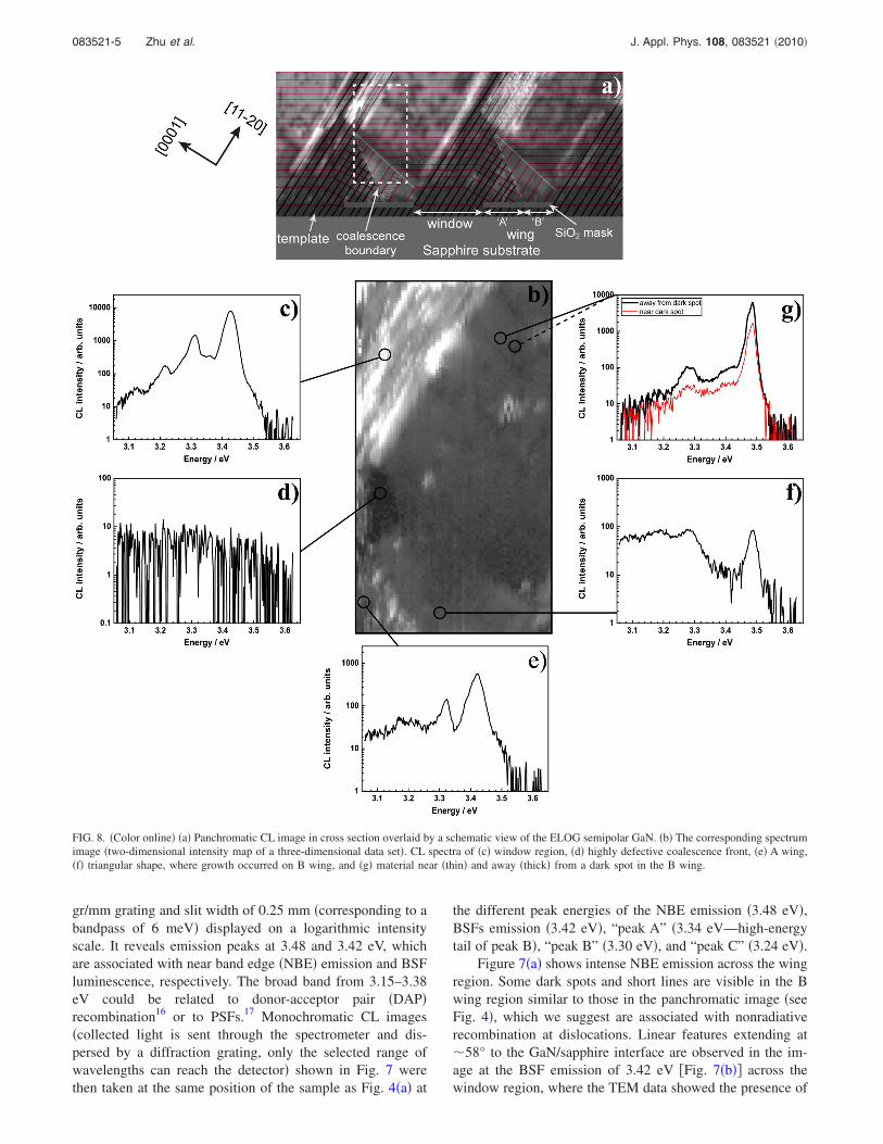
FIG. 8. �Color online� �a� Panchromatic CL image in cross section overlaid by a schematic view of the ELOG semipolar GaN. �b� The corresponding spectrumimage �two-dimensional intensity map of a three-dimensional data set�. CL spectra of �c� window region, �d� highly defective coalescence front, �e� A wing,�f� triangular shape, where growth occurred on B wing, and �g� material near �thin� and away �thick� from a dark spot in the B wing.
083521-5 Zhu et al. J. Appl. Phys. 108, 083521 �2010�
a high density of BSFs. BSFs are believed to behave likequantum well structures in GaN.25 However, such intenseemission as observed in Fig. 7�b� may correspond to bundlesof BSFs. No BSF emission is observed in the B wing regionas is expected from the TEM data, which suggests a very lowBSF density in this region.
Monochromatic CL images taken at energies of peaks A,B, and C are shown in Figs. 7�c�–7�e�. It is interesting to seethat the image at peak C �Fig. 7�e�� appears fairly similar tothe image at peak A �Fig. 7�c�� but with less intensity. Theimage at peak B in Fig. 7�d� exhibits shorter linear featuresin the window region and some bright spots in the B wing.We notice that those bright spots do not correlate generallywith the dark spots in the NBE emission �Fig. 7�a��. Liu etal.17 assigned emission peaks at �3.33 and 3.29 eV to PSFsand PDs bounding BSFs, respectively. In contrast, Gühne etal.20 argued that although these emission features may relateto the presence of BSFs, they observed the 3.29 eV emissionalso in the overgrown wing region where no PDs were seenby TEM. In agreement with Gühne et al.20 our data fromTEM and monochromatic CL also show that the B wing inour ELOG sample is mostly BSF-free, hence there are hardlyany PSFs or PDs. Therefore, while the majority of emissionpeaks A and B in the CL spectrum �Fig. 6� may relate to PSFand PD emission in the window region, the source of thebright spots at 3.30 eV in the wing region and the emissionpeak at 3.24 eV �peak C� remains unclear. They may relate topoint defects or impurities.16,17
To further investigate the luminescence properties in dif-ferent regions of the sample, spectrum imaging �in whicheach pixel of the image contains a spectrum recorded by acharge coupled device camera� was performed at the sameregion as Fig. 4�a� in cross section on the coalesced sample�Fig. 8�a��, over an area of 127�68 pixels with a step sizeof 150 nm �Fig. 8�b� shows a two-dimensional intensity mapof a three-dimensional data set�. Low temperature CL �7 K�spectra with logarithmic intensity scales at different spots areshown in Figs. 8�c�–8�g�.
�i� The spectrum from the window region is dominatedby strong BSF emission at 3.42 eV. The weak emis-sion peaks at 3.32 and 3.22 eV are associated withstacking faults and probably due to PSFs and PDs,respectively �Fig. 8�c��.
�ii� No luminescence band was observed near the coales-cence front �Fig. 8�d��. Such low emission could bedue to the presence of high density of defects, as con-firmed by TEM data in Fig. 1�a�.
�iii� It has been confirmed by TEM �Fig. 1�b�� that a highdensity of BSFs is present in the A wing, and as ex-pected strong emission from BSFs at 3.42 eV wasobserved in this region �Fig. 8�e��. The emission peakat 3.32 eV is believed to originate from PSFs and thesmall shift in emission energy from 3.34 eV �peak A�may be due to nonuniform strain in the sample, as wehave previously suggested for nonpolar ELOG GaN.26
�iv� The emission from the triangular shaped area abovethe coalescence boundary between the B and A wingsis shown in Fig. 8�f� and the spectrum is dominatedby a NBE emission and what appears to be a DAPband. This is consistent with the material having avery LDD.
�v� It appears that most of the B wing is dominated by theNBE recombination at 3.48 eV. A spectrum taken nearone of the dark spots seen in Fig. 8�a� is shown in Fig.8�g�, exhibiting much reduced CL intensity �by a fac-tor of 3.75� than the surrounding area, supporting thesuggestion that a or a+c TDs present in the B wingregion act as nonradiative recombination centers. Wealso observed a very weak band at �3.28 eV, whichis similar to the emission energy of peak B �Fig. 6�,but its origin is still not fully understood.
C. SCM
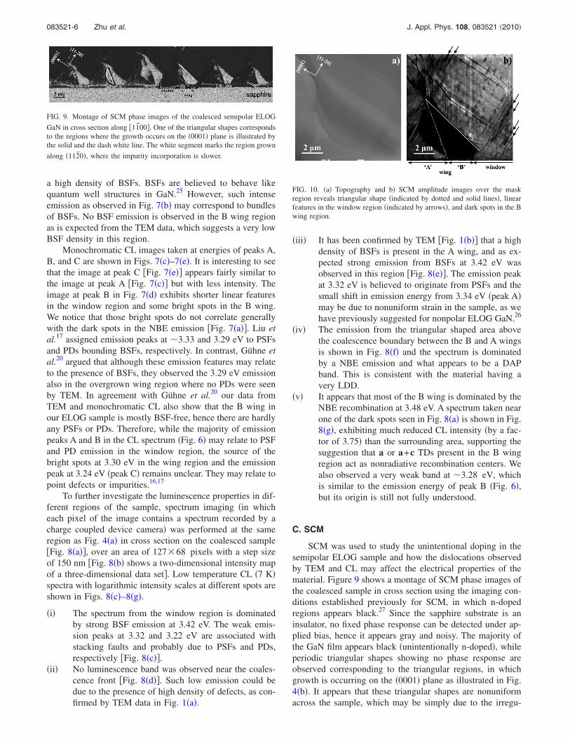
SCM was used to study the unintentional doping in thesemipolar ELOG sample and how the dislocations observedby TEM and CL may affect the electrical properties of thematerial. Figure 9 shows a montage of SCM phase images ofthe coalesced sample in cross section using the imaging con-ditions established previously for SCM, in which n-dopedregions appears black.27 Since the sapphire substrate is aninsulator, no fixed phase response can be detected under ap-plied bias, hence it appears gray and noisy. The majority ofthe GaN film appears black �unintentionally n-doped�, whileperiodic triangular shapes showing no phase response areobserved corresponding to the triangular regions, in whichgrowth is occurring on the �0001� plane as illustrated in Fig.4�b�. It appears that these triangular shapes are nonuniformacross the sample, which may be simply due to the irregu-
FIG. 9. Montage of SCM phase images of the coalesced semipolar ELOG
GaN in cross section along �11̄00�. One of the triangular shapes correspondsto the regions where the growth occurs on the �0001� plane is illustrated bythe solid and the dash white line. The white segment marks the region grown
along �112̄0�, where the impurity incorporation is slower.
FIG. 10. �a� Topography and b� SCM amplitude images over the maskregion reveals triangular shape �indicated by dotted and solid lines�, linearfeatures in the window region �indicated by arrows�, and dark spots in the Bwing region.
083521-6 Zhu et al. J. Appl. Phys. 108, 083521 �2010�
larity of the overgrowth process, as shown previously in theplan-view CL data in Fig. 3. Previous SCM studies onc-plane ELOG GaN have found that n-type dopant incorpo-ration on the �0001� facet is slower than the semipolar
112̄2 facets.28 Hence, slower dopant incorporation on the�0001� facet is also a likely explanation for the undoped tri-angles observed here, since if less impurity has been incor-porated, the carrier concentration may be too low to be de-tected by the SCM. Some additional features to the left ofsome of the triangles corresponding to areas with less unin-tentional doping are also observed in Fig. 9 �indicated by thewhite segment�, which may suggest that impurity incorpora-
tion is also slower on the �112̄0� facet, which would be con-sistent with our previous studies.29 Apart from the triangularfeatures and surrounding light-gray regions, the rest of theELOG sample contains unintentionally doped n-type mate-rial �dark contrast�. Even the thin GaN seed layer on whichthe SiO2 masking stripes were deposited is observed to beelectrically n-type. The n-type conductivity through most ofthe film corresponds well to the fact that impurities can be
easily incorporated onto 112̄2 facets. Other planar semipo-
lar �112̄2� GaN thin films grown in our laboratory also ex-hibit unintentional doping all the way from the GaN/sapphireinterface to the top surface �data not shown here�. In GaNgrown on c-plane and r-plane sapphire, unintentionaln-doping with carrier densities in excess of 1018 cm−3 hasbeen observed close to the GaN/sapphire interface, but theunintentional doping does not usually penetrate all the waythrough the film.29,30 Oxygen has been considered as themain source of unintentional doping, originated either fromdiffusion from the sapphire substrate or from incorporationof impurities during growth. In our semipolar ELOG mate-rial, however, additional silicon or oxygen donor impuritiesmay arise from the SiO2 mask during the high temperaturegrowth.
Figure 10 shows high magnification topographic andSCM amplitude images of the ELOG sample in cross sectiondirectly above the mask region. Linear features are observedin the SCM amplitude image �Fig. 10�b�� extending at about58° from the GaN/sapphire interface in the window regionand A wing, which may be related to impurity incorporationaround defects �such as BSFs and PDs� or small topographicsteps �Fig. 10�a��. Interestingly, there are some dark spotspresent in the B wing, and the average density ��1.2�0.4�
�108 cm−2� is similar to the density of dark spots in thesame region in the cross-sectional CL data ��9�1��107 cm−2� �Fig. 4�a��. Therefore, we suggest that thosedark spots observed in SCM relate to a or a+c TDs.
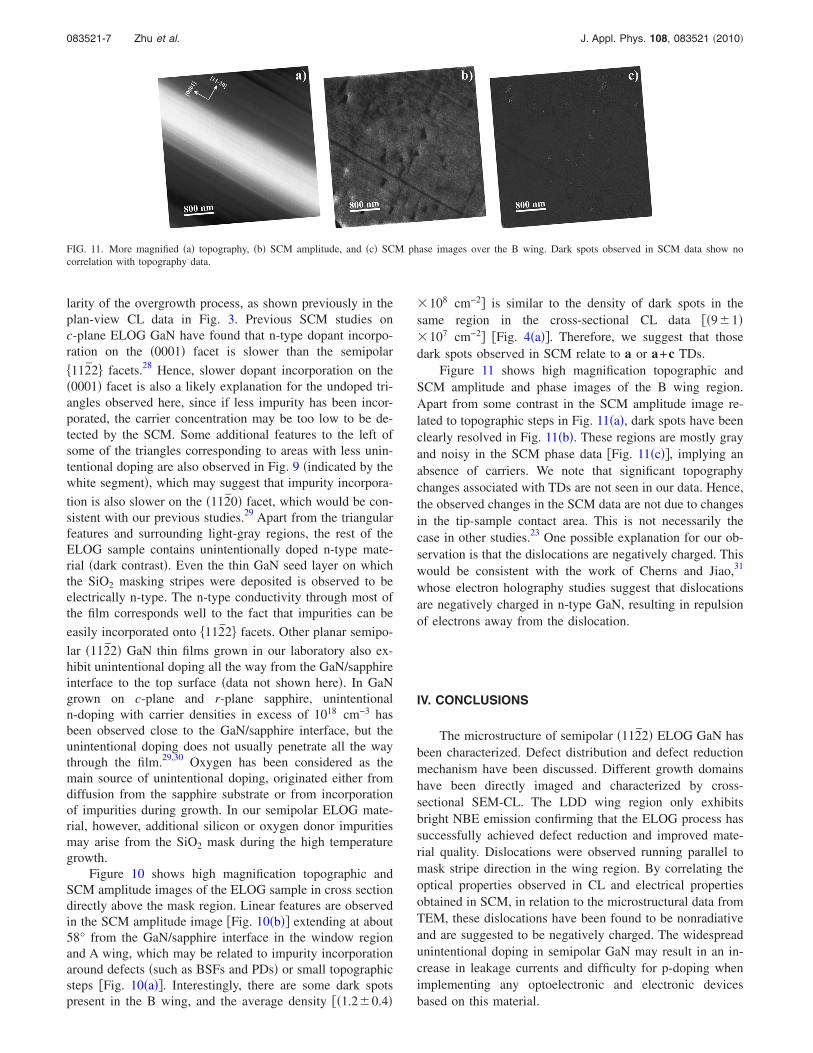
Figure 11 shows high magnification topographic andSCM amplitude and phase images of the B wing region.Apart from some contrast in the SCM amplitude image re-lated to topographic steps in Fig. 11�a�, dark spots have beenclearly resolved in Fig. 11�b�. These regions are mostly grayand noisy in the SCM phase data �Fig. 11�c��, implying anabsence of carriers. We note that significant topographychanges associated with TDs are not seen in our data. Hence,the observed changes in the SCM data are not due to changesin the tip-sample contact area. This is not necessarily thecase in other studies.23 One possible explanation for our ob-servation is that the dislocations are negatively charged. Thiswould be consistent with the work of Cherns and Jiao,31
whose electron holography studies suggest that dislocationsare negatively charged in n-type GaN, resulting in repulsionof electrons away from the dislocation.
IV. CONCLUSIONS
The microstructure of semipolar �112̄2� ELOG GaN hasbeen characterized. Defect distribution and defect reductionmechanism have been discussed. Different growth domainshave been directly imaged and characterized by cross-sectional SEM-CL. The LDD wing region only exhibitsbright NBE emission confirming that the ELOG process hassuccessfully achieved defect reduction and improved mate-rial quality. Dislocations were observed running parallel tomask stripe direction in the wing region. By correlating theoptical properties observed in CL and electrical propertiesobtained in SCM, in relation to the microstructural data fromTEM, these dislocations have been found to be nonradiativeand are suggested to be negatively charged. The widespreadunintentional doping in semipolar GaN may result in an in-crease in leakage currents and difficulty for p-doping whenimplementing any optoelectronic and electronic devicesbased on this material.
FIG. 11. More magnified �a� topography, �b� SCM amplitude, and �c� SCM phase images over the B wing. Dark spots observed in SCM data show nocorrelation with topography data.
083521-7 Zhu et al. J. Appl. Phys. 108, 083521 �2010�

ACKNOWLEDGMENTS
This work has been funded by the EPSRC �Grant No.EP/E035167/1�. R.A.O. would like to acknowledge fundingfrom the Royal Society.
1F. Bernardini, V. Fiorentini, and D. Vanderbilt, Phys. Rev. B 56, R10024�1997�.
2J. S. Speck and S. F. Chichibu, MRS Bull. 34, 304 �2009�.3H. Masui, S. Nakamura, S. P. DenBarrs, and U. K. Mishra, IEEE Trans.Electron Devices 57, 88 �2010�.
4M. D. Craven, S. H. Lim, F. Wu, J. S. Speck, and S. P. DenBaars, Appl.Phys. Lett. 81, 469 �2002�.
5R. Armitage and H. Hirayama, Appl. Phys. Lett. 92, 092121 �2008�.6P. Waltereit, O. Brandt, A. Trampert, H. T. Grahn, J. Menniger, M. Ram-steiner, M. Reiche, and K. H. Ploog, Nature �London� 406, 865 �2000�.
7A. Kobayashi, S. Kawano, Y. Kawaguchi, J. Ohta, and H. Fujioka, Appl.Phys. Lett. 90, 041908 �2007�.
8N. F. Gardner, J. C. Kim, J. J. Wierer, Y. C. Shen, and M. R. Krames,Appl. Phys. Lett. 86, 111101 �2005�.
9T. J. Baker, B. A. Haskell, F. Wu, J. S. Speck, and S. Nakamura, Jpn. J.Appl. Phys., Part 2 45, L154 �2006�.
10M. J. Kappers, J. Hollander, C. McAleese, C. F. Johnston, R. F. Broom, J.S. Barnard, M. E. Vickers, and C. J. Humphreys, J. Cryst. Growth 300,155 �2007�.
11H. Zhong, A. Tyagi, N. Fellows, F. Wu, R. B. Chung, M. Saito, K. Fujito,J. S. Speck, S. P. DenBaars, and S. Nakamura, Appl. Phys. Lett. 90,233504 �2007�.
12K. Iso, H. Yamada, H. Hirasawa, N. Fellows, M. Saito, K. Fujito, S. P.DenBaars, J. S. Speck, and S. Nakamura, Jpn. J. Appl. Phys., Part 2 46,L960 �2007�.
13H. Sato, A. Tyagi, H. Zhong, N. Fellows, R. B. Chung, M. Saito, K.Fujito, J. S. Speck, S. P. DenBaars, and S. Nakamura, Phys. Status Solidi�RRL� 1, 162 �2007�.
14D. N. Zakharov, Z. Liliental-Weber, B. Wagner, Z. J. Reitmeier, E. A.Preble, and R. F. Davis, Phys. Rev. B 71, 235334 �2005�.
15P. Vennéguès, Z. Bougrioua, and T. Guehne, Jpn. J. Appl. Phys., Part 1 46,4089 �2007�.
16P. P. Paskov, R. Schifano, B. Monemar, T. Paskova, S. Figge, and D.Hommel, J. Appl. Phys. 98, 093519 �2005�.
17R. Liu, A. Bell, F. A. Ponce, C. Q. Chen, J. W. Yang, and M. A. Khan,Appl. Phys. Lett. 86, 021908 �2005�.
18C. F. Johnston, M. J. Kappers, M. A. Moram, J. L. Hollander, and C. J.Humphreys, Phys. Status Solidi A 206, 1190 �2009�.
19C. F. Johnston, M. A. Moram, M. J. Kappers, and C. J. Humphreys, Appl.Phys. Lett. 94, 161109 �2009�.
20T. Gühne, Z. Bougrioua, P. Vennéguès, M. Leroux, and M. Albrecht, J.Appl. Phys. 101, 113101 �2007�.
21P. de Mierry, N. Kriouche, M. Nemoz, and G. Nataf, Appl. Phys. Lett. 94,191903 �2009�.
22C. C. Williams, Annu. Rev. Mater. Sci. 29, 471 �1999�.23R. A. Oliver, Rep. Prog. Phys. 71, 076501 �2008�.24I. Horcas, R. Fernandez, J. M. Gomez-Rodriguez, J. Colchero, J. Gomez-
Herrero, and A. M. Baro, Rev. Sci. Instrum. 78, 013705 �2007�.25Y. T. Rebane, Y. G. Shreter, and M. Albrecht, Phys. Status Solidi A 164,
141 �1997�.26M. Häberlen, T. J. Badcock, M. A. Moram, J. L. Hollander, M. J. Kappers,
P. Dawson, C. J. Humphreys, and R. A. Oliver, J. Appl. Phys. 108, 033523�2010�.
27J. Sumner, R. A. Oliver, M. J. Kappers, and C. J. Humphreys, Phys. StatusSolidi C 4, 2576 �2007�.
28J. Sumner, R. A. Oliver, M. J. Kappers, and C. J. Humphreys, J. Appl.Phys. 106, 104503 �2009�.
29T. Zhu, C. F. Johnston, M. Häberlen, M. J. Kappers, and R. A. Oliver, J.Appl. Phys. 107, 023503 �2010�.
30J. Sumner, R. A. Oliver, M. J. Kappers, and C. J. Humphreys, J. Vac. Sci.Technol. B 26, 611 �2008�.
31D. Cherns and C. G. Jiao, Phys. Rev. Lett. 87, 205504 �2001�.
083521-8 Zhu et al. J. Appl. Phys. 108, 083521 �2010�


