Embed Size (px)
Citation preview

3100
0401
04
ModiconA120 Series I/O ModulesUser Guide890 USE 109 00 Version 4.0

ii 890 USE 109 00 March 2003

Table of Contents
Safety Information . . . . . . . . . . . . . . . . . . . . . . . . . . . . . . . . . . . xv
About the Book . . . . . . . . . . . . . . . . . . . . . . . . . . . . . . . . . . . . .xvii
Chapter 1 Panel Software Options with A120 I/O Modules . . . . . . . . . . . .1Panel Software Option with A120 I/O Modules . . . . . . . . . . . . . . . . . . . . . . . . . . . 1
Chapter 2 Overview of the ADU 204/254 Analog Input Module . . . . . . . . .5At a Glance . . . . . . . . . . . . . . . . . . . . . . . . . . . . . . . . . . . . . . . . . . . . . . . . . . . . . . 5What is the ADU 204/254 Analog Input Module? . . . . . . . . . . . . . . . . . . . . . . . . . 6ADU 204/254 Analog Input Module Conversion Ranges . . . . . . . . . . . . . . . . . . . 7ADU 204/254 Analog Input Module Field Wiring and LED Displays . . . . . . . . . . 12ADU 204/254 Analog Input Module Noise Suppression DIP Switch. . . . . . . . . . 13ADU 204/254 Analog Input Module Calibration. . . . . . . . . . . . . . . . . . . . . . . . . . 14ADU 204/254 Analog Input Module Specifications . . . . . . . . . . . . . . . . . . . . . . . 17
Chapter 3 Overview of the ADU 205 Analog Input Module. . . . . . . . . . . . 19At a Glance . . . . . . . . . . . . . . . . . . . . . . . . . . . . . . . . . . . . . . . . . . . . . . . . . . . . . 19What is the ADU 205 Analog Input Module?. . . . . . . . . . . . . . . . . . . . . . . . . . . . 20ADU 205 Analog Input Module Conversion Ranges . . . . . . . . . . . . . . . . . . . . . . 21ADU 205 Analog Input Module Switch Settings . . . . . . . . . . . . . . . . . . . . . . . . . 24ADU 205 Analog Input Module Field Wiring . . . . . . . . . . . . . . . . . . . . . . . . . . . . 25ADU 205 Analog Input Module Calibration . . . . . . . . . . . . . . . . . . . . . . . . . . . . . 27ADU 205 Analog Input Module Specifications. . . . . . . . . . . . . . . . . . . . . . . . . . . 29
Chapter 4 Overview of the ADU 206/256 Analog Input Module . . . . . . . .31At a Glance . . . . . . . . . . . . . . . . . . . . . . . . . . . . . . . . . . . . . . . . . . . . . . . . . . . . . 31What is the ADU 206/256 Analog Input Module? . . . . . . . . . . . . . . . . . . . . . . . . 32ADU 206/256 Analog Input Module Conversion Ranges . . . . . . . . . . . . . . . . . . 33ADU 206/256 Analog Input Module Physical Characteristics . . . . . . . . . . . . . . . 36ADU 206/256 Analog Input Module Configuration . . . . . . . . . . . . . . . . . . . . . . . 38ADU 206/256 Analog Input Module Programming Modes . . . . . . . . . . . . . . . . . 40ADU 206/256 Analog Input Module Calibration. . . . . . . . . . . . . . . . . . . . . . . . . . 47ADU 206/256 Analog Input Module Specifications . . . . . . . . . . . . . . . . . . . . . . . 50
890 USE 109 00 March 2003 iii

Chapter 5 Overview of the ADU 210 Isolated Analog Input Module . . . . 53At a Glance . . . . . . . . . . . . . . . . . . . . . . . . . . . . . . . . . . . . . . . . . . . . . . . . . . . . . 53What is the ADU 210 Isolated Analog Input Module? . . . . . . . . . . . . . . . . . . . . . 54ADU 210 Isolated Analog Input Module Physical Characteristics . . . . . . . . . . . . 55Installing the ADU 210 Isolated Analog Input Module . . . . . . . . . . . . . . . . . . . . . 57ADU 210 Isolated Analog Input Module Operation . . . . . . . . . . . . . . . . . . . . . . . 59ADU 210 Isolated Analog Input Module Specifications . . . . . . . . . . . . . . . . . . . . 63
Chapter 6 Overview of the ADU 211/212 Universal Analog Input Module . . . . . . . . . . . . . . . . . . . . . . . . . . . . . . . . . . . . . . . . . . . . 65At a Glance . . . . . . . . . . . . . . . . . . . . . . . . . . . . . . . . . . . . . . . . . . . . . . . . . . . . . 65What is the ADU 211/212 Universal Analog Input Module? . . . . . . . . . . . . . . . . 66ADU 211/212 Universal Analog Input Module "J" Thermocouple Quick Start . . . 67ADU 211/212 Universal Analog Input Module Inputs. . . . . . . . . . . . . . . . . . . . . . 68ADU 211/212 Universal Analog Input Module Installation . . . . . . . . . . . . . . . . . . 69ADU 211/212 Universal Analog Input Module Switch Settings . . . . . . . . . . . . . . 70ADU 211/212 Universal Analog Input Module Field Wiring . . . . . . . . . . . . . . . . . 74ADU 211/212 Universal Analog Input Module Field Wiring Examples. . . . . . . . . 77ADU 211/212 Universal Analog Input Module Application Notes . . . . . . . . . . . . 84ADU 211/212 Universal Analog Input Module Configuration. . . . . . . . . . . . . . . . 87ADU 211/212 Universal Analog Input Module Output Registers . . . . . . . . . . . . . 88ADU 211/212 Universal Analog Input Module Input Registers . . . . . . . . . . . . . . 94Sequentially Reading ADU 211/212 Universal Analog Input Module Channel Data. . . . . . . . . . . . . . . . . . . . . . . . . . . . . . . . . . . . . . . . . . . . . . . . . . . . 96ADU 211/212 Universal Analog Input Module Troubleshooting. . . . . . . . . . . . . 103ADU 211/212 Universal Analog Input Module Specifications . . . . . . . . . . . . . . 105
Chapter 7 ADU 214 Analog Input Module . . . . . . . . . . . . . . . . . . . . . . . . 109At a Glance . . . . . . . . . . . . . . . . . . . . . . . . . . . . . . . . . . . . . . . . . . . . . . . . . . . . 109Overview of the ADU 214 Analog Input Module . . . . . . . . . . . . . . . . . . . . . . . . 110Conversion Values. . . . . . . . . . . . . . . . . . . . . . . . . . . . . . . . . . . . . . . . . . . . . . . 113Configuration - Concept . . . . . . . . . . . . . . . . . . . . . . . . . . . . . . . . . . . . . . . . . . . 123Installation . . . . . . . . . . . . . . . . . . . . . . . . . . . . . . . . . . . . . . . . . . . . . . . . . . . . . 130ADU 214 Input Module Specifications . . . . . . . . . . . . . . . . . . . . . . . . . . . . . . . . 133
Chapter 8 ADU 216 Analog Input Module . . . . . . . . . . . . . . . . . . . . . . . . 139At a Glance . . . . . . . . . . . . . . . . . . . . . . . . . . . . . . . . . . . . . . . . . . . . . . . . . . . . 139What Is the ADU 216 Analog Input Module? . . . . . . . . . . . . . . . . . . . . . . . . . . . 140ADU 216 Analog Input Module Conversion Ranges . . . . . . . . . . . . . . . . . . . . . 141ADU 216 Analog Input Module Physical Characteristics . . . . . . . . . . . . . . . . . . 142ADU 216 Analog Input Module Configuration . . . . . . . . . . . . . . . . . . . . . . . . . . 145ADU 216 Analog Input Module Programming Modes . . . . . . . . . . . . . . . . . . . . 147ADU 216 Analog Input Module Calibration . . . . . . . . . . . . . . . . . . . . . . . . . . . . 152ADU 216 Analog Input Module Specifications . . . . . . . . . . . . . . . . . . . . . . . . . . 154
iv 890 USE 109 00 March 2003

Chapter 9 Overview of the ADU 257 Analog Input Module. . . . . . . . . . . 155At a Glance . . . . . . . . . . . . . . . . . . . . . . . . . . . . . . . . . . . . . . . . . . . . . . . . . . . . 155What is the ADU 257 Analog Input Module?. . . . . . . . . . . . . . . . . . . . . . . . . . . 156ADU 257 Analog Input Module Physical Characteristics. . . . . . . . . . . . . . . . . . 157Installing the ADU 257 Analog Input Module. . . . . . . . . . . . . . . . . . . . . . . . . . . 159ADU 257 Isolated Analog Input Module Operation . . . . . . . . . . . . . . . . . . . . . . 161ADU 257 Analog Input Module Specifications. . . . . . . . . . . . . . . . . . . . . . . . . . 169
Chapter 10 AS-BDEA 203 Profibus-DP Coupler Module Description . . . 171At a Glance . . . . . . . . . . . . . . . . . . . . . . . . . . . . . . . . . . . . . . . . . . . . . . . . . . . . 171Configuration. . . . . . . . . . . . . . . . . . . . . . . . . . . . . . . . . . . . . . . . . . . . . . . . . . . 172Features and Functions. . . . . . . . . . . . . . . . . . . . . . . . . . . . . . . . . . . . . . . . . . . 176Diagnosis. . . . . . . . . . . . . . . . . . . . . . . . . . . . . . . . . . . . . . . . . . . . . . . . . . . . . . 178Technical Specifications . . . . . . . . . . . . . . . . . . . . . . . . . . . . . . . . . . . . . . . . . . 179
Chapter 11 BKF 201 (16W) & (64W) InterBus S Master Module . . . . . . . . 183At a Glance . . . . . . . . . . . . . . . . . . . . . . . . . . . . . . . . . . . . . . . . . . . . . . . . . . . . 183What Is the BKF 201 (16W) & (64W) InterBus S Master Module? . . . . . . . . . . 184Physical Characteristics of the BKF 201 (16W) & (64W) InterBus S Master Module. . . . . . . . . . . . . . . . . . . . . . . . . . . . . . . . . . . . . . . . . . . . . . . . . . 185Switch Settings for the BKF 201 . . . . . . . . . . . . . . . . . . . . . . . . . . . . . . . . . . . . 188Installation of the BKF 201 (16W) & (64W) Interbus Master Module . . . . . . . . 189Operation of the BKF 201 Master Module: I/O Map . . . . . . . . . . . . . . . . . . . . . 191Example of Hardware and I/O Mapping for the BKF 201 . . . . . . . . . . . . . . . . . 198Specifications . . . . . . . . . . . . . . . . . . . . . . . . . . . . . . . . . . . . . . . . . . . . . . . . . . 199
Chapter 12 BKF 202 InterBus S Slave Module . . . . . . . . . . . . . . . . . . . . .201At a Glance . . . . . . . . . . . . . . . . . . . . . . . . . . . . . . . . . . . . . . . . . . . . . . . . . . . . 201What Is the BKF 202 InterBus S Slave Module?. . . . . . . . . . . . . . . . . . . . . . . . 202Physical Characteristics of the BKF 202 InterBus S Slave Module. . . . . . . . . . 203Switch Settings for the BKF 202 InterBus S Slave Module. . . . . . . . . . . . . . . . 205Installation of the BKF 202 InterBus S Slave Module . . . . . . . . . . . . . . . . . . . . 206Operation of the BKF 202 InterBus S Slave Module. . . . . . . . . . . . . . . . . . . . . 209Specifications of the BKF 202 InterBus S Slave Module. . . . . . . . . . . . . . . . . . 212
Chapter 13 DAO 216 Discrete Output Module . . . . . . . . . . . . . . . . . . . . . . 213At a Glance . . . . . . . . . . . . . . . . . . . . . . . . . . . . . . . . . . . . . . . . . . . . . . . . . . . . 213What is the DAO 216 Discrete Output Module? . . . . . . . . . . . . . . . . . . . . . . . . 214DAO 216 Discrete Output Module Physical Characteristics . . . . . . . . . . . . . . . 215Protecting the DAO 216 Discrete Output Module from Inductive Back EMF. . . . . . . . . . . . . . . . . . . . . . . . . . . . . . . . . . . . . . . . . . . . . . . . . . . . . . . . . . 218DAO 216 Discrete Output Module Specifications . . . . . . . . . . . . . . . . . . . . . . . 219
Chapter 14 Overview of the DAP 204 Relay Output Module . . . . . . . . . .221At a Glance . . . . . . . . . . . . . . . . . . . . . . . . . . . . . . . . . . . . . . . . . . . . . . . . . . . . 221What is the DAP 204 Relay Output Module? . . . . . . . . . . . . . . . . . . . . . . . . . . 222
890 USE 109 00 March 2003 v

DAP 204 Relay Output Module LEDs . . . . . . . . . . . . . . . . . . . . . . . . . . . . . . . . 223DAP 204 Relay Output Module Field Wiring . . . . . . . . . . . . . . . . . . . . . . . . . . . 224Protecting the DAP 204 Relay Output Module from Inductive Back EMF . . . . . 225DAP 204 Relay Output Module Specifications. . . . . . . . . . . . . . . . . . . . . . . . . . 227
Chapter 15 Overview of the DAP 208/258 Relay Output Module. . . . . . . 231At a Glance . . . . . . . . . . . . . . . . . . . . . . . . . . . . . . . . . . . . . . . . . . . . . . . . . . . . 231What is the DAP 208/258 Relay Output Module? . . . . . . . . . . . . . . . . . . . . . . . 232DAP 208/258 Relay Output Module LEDs. . . . . . . . . . . . . . . . . . . . . . . . . . . . . 233DAP 208/258 Relay Output Module Field Wiring. . . . . . . . . . . . . . . . . . . . . . . . 234Protecting the DAP 208/258 Relay Output Module from Inductive Back EMF . . . . . . . . . . . . . . . . . . . . . . . . . . . . . . . . . . . . . . . . . . . . . . . . . . . . . . . . . . 235DAP 208/258 Relay Output Module Specifications . . . . . . . . . . . . . . . . . . . . . . 237
Chapter 16 Overview of the DAP 209 Output Module . . . . . . . . . . . . . . . 241At a Glance . . . . . . . . . . . . . . . . . . . . . . . . . . . . . . . . . . . . . . . . . . . . . . . . . . . . 241What is the DAP 209 Output Module?. . . . . . . . . . . . . . . . . . . . . . . . . . . . . . . . 242DAP 209 Output Module LEDs . . . . . . . . . . . . . . . . . . . . . . . . . . . . . . . . . . . . . 243DAP 209 Output Module Field Wiring . . . . . . . . . . . . . . . . . . . . . . . . . . . . . . . . 244DAP 209 Output Module Specifications. . . . . . . . . . . . . . . . . . . . . . . . . . . . . . . 245
Chapter 17 Overview of the DAP 210 Output Module . . . . . . . . . . . . . . . 247At a Glance . . . . . . . . . . . . . . . . . . . . . . . . . . . . . . . . . . . . . . . . . . . . . . . . . . . . 247DAP 210 Output Module LEDs . . . . . . . . . . . . . . . . . . . . . . . . . . . . . . . . . . . . . 248DAP 210 Output Module Field Wiring . . . . . . . . . . . . . . . . . . . . . . . . . . . . . . . . 249DAP 210 Output Module Specifications. . . . . . . . . . . . . . . . . . . . . . . . . . . . . . . 250What is the DAP 210 Output Module?. . . . . . . . . . . . . . . . . . . . . . . . . . . . . . . . 252
Chapter 18 Overview of the DAP 211 Combined I/O Module. . . . . . . . . . 253At a Glance . . . . . . . . . . . . . . . . . . . . . . . . . . . . . . . . . . . . . . . . . . . . . . . . . . . . 253What is the DAP 211 Combined I/O Module? . . . . . . . . . . . . . . . . . . . . . . . . . . 254DAP 211 Combined I/O Module Logical Input Routine . . . . . . . . . . . . . . . . . . . 255DAP 211 Combined I/O Module Error Checking Procedure for Output States. . . . . . . . . . . . . . . . . . . . . . . . . . . . . . . . . . . . . . . . . . . . . . . . . . . . . . . . . 256DAP 211 Combined I/O Module Setup Options. . . . . . . . . . . . . . . . . . . . . . . . . 257DAP 211 Combination I/O Module LEDs. . . . . . . . . . . . . . . . . . . . . . . . . . . . . . 258DAP 211 Combined I/O Module Field Wiring. . . . . . . . . . . . . . . . . . . . . . . . . . . 259DAP 211 Combined I/O Module Specifications . . . . . . . . . . . . . . . . . . . . . . . . . 260
Chapter 19 Overview of the DAP 212/252 Combined I/O Module . . . . . . 261At a Glance . . . . . . . . . . . . . . . . . . . . . . . . . . . . . . . . . . . . . . . . . . . . . . . . . . . . 261What is the DAP 212/252 Combined I/O Module?. . . . . . . . . . . . . . . . . . . . . . . 262DAP 212/252 Combined I/O Module LEDs . . . . . . . . . . . . . . . . . . . . . . . . . . . . 263DAP 212/252 Combined I/O Module Field Connections . . . . . . . . . . . . . . . . . . 264Protecting the DAP 212/252 Combined I/O Module from Inductive Back EMF . . . . . . . . . . . . . . . . . . . . . . . . . . . . . . . . . . . . . . . . . . . . . . . . . . . . . . . . . . 266DAP 212/252 Combined I/O Module Specifications . . . . . . . . . . . . . . . . . . . . . 268
vi 890 USE 109 00 March 2003
Chapter 20 Overview of the DAP 216/216N Discrete Output Module . . . 273At a Glance . . . . . . . . . . . . . . . . . . . . . . . . . . . . . . . . . . . . . . . . . . . . . . . . . . . . 273What is the DAP 216/216N Discrete Output Module?. . . . . . . . . . . . . . . . . . . . 274DAP 216/216N Discrete Output Module LEDs . . . . . . . . . . . . . . . . . . . . . . . . . 275DAP 216/216N Field Wiring . . . . . . . . . . . . . . . . . . . . . . . . . . . . . . . . . . . . . . . 276Resetting the DAP 216 Module After an Overload of Short Circuit . . . . . . . . . . 277Protecting the DAP 216/216N Discrete Output Module from Inductive Back EMF. . . . . . . . . . . . . . . . . . . . . . . . . . . . . . . . . . . . . . . . . . . . . . . . . . . . . . . . . . 278DAP 216N Discrete Output Module Differences . . . . . . . . . . . . . . . . . . . . . . . . 279DAP 216/216N Discrete Output Module Specifications . . . . . . . . . . . . . . . . . . 281
Chapter 21 Overview of the DAP 217 Discrete Output Module . . . . . . . .283At a Glance . . . . . . . . . . . . . . . . . . . . . . . . . . . . . . . . . . . . . . . . . . . . . . . . . . . . 283What is the DAP 217 Discrete Output Module? . . . . . . . . . . . . . . . . . . . . . . . . 284DAP 217 Discrete Output Module LEDs . . . . . . . . . . . . . . . . . . . . . . . . . . . . . . 285DAP 217 Discrete Output Module Field Wiring . . . . . . . . . . . . . . . . . . . . . . . . . 286Protecting the DAP 217 Discrete Output Module from Inductive Back EMF. . . . . . . . . . . . . . . . . . . . . . . . . . . . . . . . . . . . . . . . . . . . . . . . . . . . . . . . . . 288DAP 217 Discrete Output Module Specifications . . . . . . . . . . . . . . . . . . . . . . . 289
Chapter 22 Overview of the DAP 218 Output Module . . . . . . . . . . . . . . . .291At a Glance . . . . . . . . . . . . . . . . . . . . . . . . . . . . . . . . . . . . . . . . . . . . . . . . . . . . 291What is the DAP 218 Output Module? . . . . . . . . . . . . . . . . . . . . . . . . . . . . . . . 292DAP 218 Output Module LEDs . . . . . . . . . . . . . . . . . . . . . . . . . . . . . . . . . . . . . 293DAP 218 Output Module Field Wiring . . . . . . . . . . . . . . . . . . . . . . . . . . . . . . . . 294DAP 218 Output Module Specifications . . . . . . . . . . . . . . . . . . . . . . . . . . . . . . 295
Chapter 23 Overview of the DAP 220/250 Combined I/O Module . . . . . . 297At a Glance . . . . . . . . . . . . . . . . . . . . . . . . . . . . . . . . . . . . . . . . . . . . . . . . . . . . 297What is the DAP 220/250 Combined I/O Module . . . . . . . . . . . . . . . . . . . . . . . 298DAP 220/250 Combined I/O Module LEDs . . . . . . . . . . . . . . . . . . . . . . . . . . . . 299DAP 220/250 Combined I/O Module Field Wiring. . . . . . . . . . . . . . . . . . . . . . . 300DAP 220/250 Combined I/O Module Recovery After Error . . . . . . . . . . . . . . . . 302DAP 220/250 Combined I/O Module Specifications . . . . . . . . . . . . . . . . . . . . . 304
Chapter 24 Overview of the DAP 253 Combined I/O Module . . . . . . . . . . 307At a Glance . . . . . . . . . . . . . . . . . . . . . . . . . . . . . . . . . . . . . . . . . . . . . . . . . . . . 307What is the DAP 253 Combined I/O Module?. . . . . . . . . . . . . . . . . . . . . . . . . . 308DAP 253 Combined I/O Module LEDs . . . . . . . . . . . . . . . . . . . . . . . . . . . . . . . 309DAP 253 Combined I/O Module Field Wiring . . . . . . . . . . . . . . . . . . . . . . . . . . 310Protecting the DAP 253 Combined I/O Module from Inductive Back EMF . . . . 312DAP 253 Combined I/O Module Specifications. . . . . . . . . . . . . . . . . . . . . . . . . 314
Chapter 25 Overview of the DAP 292 Combined I/O Module . . . . . . . . . . 319At a Glance . . . . . . . . . . . . . . . . . . . . . . . . . . . . . . . . . . . . . . . . . . . . . . . . . . . . 319What is the DAP 292 Combined I/O Module?. . . . . . . . . . . . . . . . . . . . . . . . . . 320
890 USE 109 00 March 2003 vii

DAP 292 Combined I/O Module LEDs. . . . . . . . . . . . . . . . . . . . . . . . . . . . . . . . 321DAP 292 Combined I/O Module Field Wiring. . . . . . . . . . . . . . . . . . . . . . . . . . . 322Protecting the DAP 292 Combined I/O Module from Inductive Back EMF . . . . 324DAP 292 Combined I/O Module Specifications . . . . . . . . . . . . . . . . . . . . . . . . . 326
Chapter 26 DAU 202/252 Analog Output Module . . . . . . . . . . . . . . . . . . . 331At a Glance . . . . . . . . . . . . . . . . . . . . . . . . . . . . . . . . . . . . . . . . . . . . . . . . . . . . 331What Is the DAU 202/252 Analog Output Module? . . . . . . . . . . . . . . . . . . . . . . 332DAU 202/252 Analog Output Module Field Wiring. . . . . . . . . . . . . . . . . . . . . . . 334DAU 202/252 Analog Output Module Calibration . . . . . . . . . . . . . . . . . . . . . . . 335DAU 202/252 Analog Output Module Specifications . . . . . . . . . . . . . . . . . . . . . 337
Chapter 27 DAU 204 Analog Output Module. . . . . . . . . . . . . . . . . . . . . . . 339At a Glance . . . . . . . . . . . . . . . . . . . . . . . . . . . . . . . . . . . . . . . . . . . . . . . . . . . . 339What Is the DAU 204 Analog Output Module? . . . . . . . . . . . . . . . . . . . . . . . . . 341DAU 204 Analog Output Module Conversion Ranges. . . . . . . . . . . . . . . . . . . . 342DAU 204 Analog Output Module Special Features . . . . . . . . . . . . . . . . . . . . . . 343DAU 204 Analog Output Module Installation . . . . . . . . . . . . . . . . . . . . . . . . . . . 344DAU 204 Analog Output Module Switch Settings . . . . . . . . . . . . . . . . . . . . . . . 345DAU 204 Analog Output Module Field Wiring . . . . . . . . . . . . . . . . . . . . . . . . . . 348DAU 204 Analog Output Module Configuration . . . . . . . . . . . . . . . . . . . . . . . . . 353DAU 204 Analog Output Module Custom Calibration . . . . . . . . . . . . . . . . . . . . 358DAU 204 Analog Output Module Indicators . . . . . . . . . . . . . . . . . . . . . . . . . . . . 361DAU 204 Analog Output Module Specifications . . . . . . . . . . . . . . . . . . . . . . . . 364
Chapter 28 Overview of DAU 208 Analog Output Module . . . . . . . . . . . . 367At a Glance . . . . . . . . . . . . . . . . . . . . . . . . . . . . . . . . . . . . . . . . . . . . . . . . . . . . 367What is the DAU 208 Analog Output Module?. . . . . . . . . . . . . . . . . . . . . . . . . . 368DAU 208 Analog Output Module Conversion Ranges. . . . . . . . . . . . . . . . . . . . 369DAU 208 Analog Output Module Physical Characteristics . . . . . . . . . . . . . . . . 370DAU 208 Analog Output Module Configuration . . . . . . . . . . . . . . . . . . . . . . . . . 372DAU 208 Analog Output Module Field Wiring . . . . . . . . . . . . . . . . . . . . . . . . . . 373DAU 208 Analog Output Module Calibration . . . . . . . . . . . . . . . . . . . . . . . . . . . 374DAU 208 Analog Output Module Specifications . . . . . . . . . . . . . . . . . . . . . . . . 377
Chapter 29 DEA 202 InterBus S Interface Module . . . . . . . . . . . . . . . . . . 379At a Glance . . . . . . . . . . . . . . . . . . . . . . . . . . . . . . . . . . . . . . . . . . . . . . . . . . . . 379DEA 202 Features and Functions . . . . . . . . . . . . . . . . . . . . . . . . . . . . . . . . . . . 380Configuration of the DEA 202 . . . . . . . . . . . . . . . . . . . . . . . . . . . . . . . . . . . . . . 382DEA 202 LEDs. . . . . . . . . . . . . . . . . . . . . . . . . . . . . . . . . . . . . . . . . . . . . . . . . . 386DEA 202 Specifications . . . . . . . . . . . . . . . . . . . . . . . . . . . . . . . . . . . . . . . . . . . 387
Chapter 30 Overview of the DEO 216 Input Module . . . . . . . . . . . . . . . . . 389At a Glance . . . . . . . . . . . . . . . . . . . . . . . . . . . . . . . . . . . . . . . . . . . . . . . . . . . . 389What is the DEO 216 Input Module? . . . . . . . . . . . . . . . . . . . . . . . . . . . . . . . . . 390Specifications of the DEO 216 Input Module . . . . . . . . . . . . . . . . . . . . . . . . . . . 391
viii 890 USE 109 00 March 2003
Chapter 31 Overview of the DEP 208 Input Module . . . . . . . . . . . . . . . . . 393At a Glance . . . . . . . . . . . . . . . . . . . . . . . . . . . . . . . . . . . . . . . . . . . . . . . . . . . . 393What is the DEP 208 Input Module? . . . . . . . . . . . . . . . . . . . . . . . . . . . . . . . . . 394DEP 208 Input Module LEDs . . . . . . . . . . . . . . . . . . . . . . . . . . . . . . . . . . . . . . 395DEP 208 Input Module Field Wiring . . . . . . . . . . . . . . . . . . . . . . . . . . . . . . . . . 396Using the DEP 208 Input Module wilth Proximity Switches. . . . . . . . . . . . . . . . 397DEP 208 Input Module Specifications. . . . . . . . . . . . . . . . . . . . . . . . . . . . . . . . 398
Chapter 32 Overview of the DEP 209 Input Module . . . . . . . . . . . . . . . . . 399At a Glance . . . . . . . . . . . . . . . . . . . . . . . . . . . . . . . . . . . . . . . . . . . . . . . . . . . . 399What is the DEP 209 Input Module? . . . . . . . . . . . . . . . . . . . . . . . . . . . . . . . . . 400DEP 209 Input Module LEDs . . . . . . . . . . . . . . . . . . . . . . . . . . . . . . . . . . . . . . 401DEP 209 Input Module Field Wiring . . . . . . . . . . . . . . . . . . . . . . . . . . . . . . . . . 402Using the DEP 209 Input Module with Proximity Switches . . . . . . . . . . . . . . . . 403DEP 209 Input Module Specifications. . . . . . . . . . . . . . . . . . . . . . . . . . . . . . . . 404
Chapter 33 Overview of the DEP 210 Input Module . . . . . . . . . . . . . . . . . 405At a Glance . . . . . . . . . . . . . . . . . . . . . . . . . . . . . . . . . . . . . . . . . . . . . . . . . . . . 405What is the DEP 210 Input Module? . . . . . . . . . . . . . . . . . . . . . . . . . . . . . . . . . 406DEP 210 Input Module LEDs . . . . . . . . . . . . . . . . . . . . . . . . . . . . . . . . . . . . . . 407DEP 210 Input Module Field Wiring . . . . . . . . . . . . . . . . . . . . . . . . . . . . . . . . . 408DEP 210 Input Module Specifications. . . . . . . . . . . . . . . . . . . . . . . . . . . . . . . . 410
Chapter 34 Overview of the DEP 211 Input Module . . . . . . . . . . . . . . . . . 411At a Glance . . . . . . . . . . . . . . . . . . . . . . . . . . . . . . . . . . . . . . . . . . . . . . . . . . . . 411What is the DEP 211 Input Module? . . . . . . . . . . . . . . . . . . . . . . . . . . . . . . . . . 412DEP 211 Input Module LEDs . . . . . . . . . . . . . . . . . . . . . . . . . . . . . . . . . . . . . . 413DEP 211 Input Module Field Wiring . . . . . . . . . . . . . . . . . . . . . . . . . . . . . . . . . 414DEP 211 Input Module Specifications. . . . . . . . . . . . . . . . . . . . . . . . . . . . . . . . 416
Chapter 35 Overview of the DEP 214/254 Input Module . . . . . . . . . . . . . .417At a Glance . . . . . . . . . . . . . . . . . . . . . . . . . . . . . . . . . . . . . . . . . . . . . . . . . . . . 417What is the DEP 214/254 Input Module? . . . . . . . . . . . . . . . . . . . . . . . . . . . . . 418DEP 214/254 Input Module LEDs . . . . . . . . . . . . . . . . . . . . . . . . . . . . . . . . . . . 419DEP 214/254 Input Module Field Wiring . . . . . . . . . . . . . . . . . . . . . . . . . . . . . . 420DEP 214/254 Input Module Specifications . . . . . . . . . . . . . . . . . . . . . . . . . . . . 422
Chapter 36 Overview of the DEP 215 Input Module . . . . . . . . . . . . . . . . . 423At a Glance . . . . . . . . . . . . . . . . . . . . . . . . . . . . . . . . . . . . . . . . . . . . . . . . . . . . 423What is the DEP 215 Input Module? . . . . . . . . . . . . . . . . . . . . . . . . . . . . . . . . . 424DEP 215 Input Module LEDs . . . . . . . . . . . . . . . . . . . . . . . . . . . . . . . . . . . . . . 425DEP 215 Input Module Field Wiring . . . . . . . . . . . . . . . . . . . . . . . . . . . . . . . . . 426Unique True Low Characteristics of the DEP 215 Input Module. . . . . . . . . . . . 428DEP 215 Input Module Specifications. . . . . . . . . . . . . . . . . . . . . . . . . . . . . . . . 429
890 USE 109 00 March 2003 ix

Chapter 37 Overview of the DEP 216/256 Input Module . . . . . . . . . . . . . 431At a Glance . . . . . . . . . . . . . . . . . . . . . . . . . . . . . . . . . . . . . . . . . . . . . . . . . . . . 431What is the DEP 216/256 Input Module?. . . . . . . . . . . . . . . . . . . . . . . . . . . . . . 432DEP 216/256 Input Module LEDs . . . . . . . . . . . . . . . . . . . . . . . . . . . . . . . . . . . 433DEP 216/256 Input Module Field Wiring . . . . . . . . . . . . . . . . . . . . . . . . . . . . . . 434DEP 216/256 Input Module Specifications. . . . . . . . . . . . . . . . . . . . . . . . . . . . . 435
Chapter 38 Overview of the DEP 217 Input Module . . . . . . . . . . . . . . . . . 437At a Glance . . . . . . . . . . . . . . . . . . . . . . . . . . . . . . . . . . . . . . . . . . . . . . . . . . . . 437What is the DEP 217 Input Module? . . . . . . . . . . . . . . . . . . . . . . . . . . . . . . . . . 438DEP 217 Input Module LEDs. . . . . . . . . . . . . . . . . . . . . . . . . . . . . . . . . . . . . . . 439DEP 217 Input Module Field Wiring. . . . . . . . . . . . . . . . . . . . . . . . . . . . . . . . . . 440DEP 217 Input Module Specifications . . . . . . . . . . . . . . . . . . . . . . . . . . . . . . . . 441
Chapter 39 Overview of the DEP 218 Input Module . . . . . . . . . . . . . . . . . 443At a Glance . . . . . . . . . . . . . . . . . . . . . . . . . . . . . . . . . . . . . . . . . . . . . . . . . . . . 443What is the DEP 218 Input Module? . . . . . . . . . . . . . . . . . . . . . . . . . . . . . . . . . 444DEP 218 Input Module LEDs. . . . . . . . . . . . . . . . . . . . . . . . . . . . . . . . . . . . . . . 445DEP 218 Input Module Field Wiring. . . . . . . . . . . . . . . . . . . . . . . . . . . . . . . . . . 446DEP 218 Input Module Specifications . . . . . . . . . . . . . . . . . . . . . . . . . . . . . . . . 448
Chapter 40 Overview of the DEP 220 Input Module . . . . . . . . . . . . . . . . . 449At a Glance . . . . . . . . . . . . . . . . . . . . . . . . . . . . . . . . . . . . . . . . . . . . . . . . . . . . 449What is the DEP 220 Input Module? . . . . . . . . . . . . . . . . . . . . . . . . . . . . . . . . . 450DEP 220 Input Module LEDs. . . . . . . . . . . . . . . . . . . . . . . . . . . . . . . . . . . . . . . 451DEP 220 Input Module Field Wiring. . . . . . . . . . . . . . . . . . . . . . . . . . . . . . . . . . 452DEP 220 Input Module Specifications . . . . . . . . . . . . . . . . . . . . . . . . . . . . . . . . 454
Chapter 41 Overview of the DEP 257 Input Module . . . . . . . . . . . . . . . . . 455At a Glance . . . . . . . . . . . . . . . . . . . . . . . . . . . . . . . . . . . . . . . . . . . . . . . . . . . . 455What is the DEP 257 Input Module? . . . . . . . . . . . . . . . . . . . . . . . . . . . . . . . . . 456DEP 257 Input Module LEDs. . . . . . . . . . . . . . . . . . . . . . . . . . . . . . . . . . . . . . . 457DEP 257 Input Module Field Wiring. . . . . . . . . . . . . . . . . . . . . . . . . . . . . . . . . . 458DEP 257 Input Module Specifications . . . . . . . . . . . . . . . . . . . . . . . . . . . . . . . . 459
Chapter 42 Overview of the DEP 296 Input Module . . . . . . . . . . . . . . . . . 461At a Glance . . . . . . . . . . . . . . . . . . . . . . . . . . . . . . . . . . . . . . . . . . . . . . . . . . . . 461What is the DEP 296 Input Module? . . . . . . . . . . . . . . . . . . . . . . . . . . . . . . . . . 462DEP 296 Input Module LEDs. . . . . . . . . . . . . . . . . . . . . . . . . . . . . . . . . . . . . . . 463DEP 296 Input Module Field Wiring. . . . . . . . . . . . . . . . . . . . . . . . . . . . . . . . . . 464DEP 296 Input Module Specifications . . . . . . . . . . . . . . . . . . . . . . . . . . . . . . . . 466
Chapter 43 Overview of the DEP 297 Input Module . . . . . . . . . . . . . . . . . 467At a Glance . . . . . . . . . . . . . . . . . . . . . . . . . . . . . . . . . . . . . . . . . . . . . . . . . . . . 467What is the DEP 297 Input Module? . . . . . . . . . . . . . . . . . . . . . . . . . . . . . . . . . 468DEP 297 Input Module LEDs. . . . . . . . . . . . . . . . . . . . . . . . . . . . . . . . . . . . . . . 469DEP 297 Input Module Field Wiring. . . . . . . . . . . . . . . . . . . . . . . . . . . . . . . . . . 470
x 890 USE 109 00 March 2003

DEP297 Input Module Specifications . . . . . . . . . . . . . . . . . . . . . . . . . . . . . . . . 472
Chapter 44 Overview of the FRQ 204/254 Frequency Module . . . . . . . . .473At a Glance . . . . . . . . . . . . . . . . . . . . . . . . . . . . . . . . . . . . . . . . . . . . . . . . . . . . 473What is the FRQ 204/254 Frequency Module?. . . . . . . . . . . . . . . . . . . . . . . . . 474Physical Characteristics of the FRQ 204/254 Frequency Module. . . . . . . . . . . 475Operating Modes of the FRQ 204/254 Frequency Module . . . . . . . . . . . . . . . . 476Configuration of the FRQ 204/254 Frequency Module . . . . . . . . . . . . . . . . . . . 477Operation and LED Displays of the FRQ 204/254 Frequency Module . . . . . . . 481Specifications of the FRQ 204/254 Frequency Module. . . . . . . . . . . . . . . . . . . 482
Chapter 45 Overview of MOT 20X Motion Modules. . . . . . . . . . . . . . . . . . 487At a Glance . . . . . . . . . . . . . . . . . . . . . . . . . . . . . . . . . . . . . . . . . . . . . . . . . . . . 487What are the MOT 20X Modules?. . . . . . . . . . . . . . . . . . . . . . . . . . . . . . . . . . . 489Overview of the MOT 201 Motion Module. . . . . . . . . . . . . . . . . . . . . . . . . . . . . 490Overview of the MOT 202 Motion Module. . . . . . . . . . . . . . . . . . . . . . . . . . . . . 504MOT 20X Module System Information . . . . . . . . . . . . . . . . . . . . . . . . . . . . . . . 522MOT 20X Motion Module Specifications . . . . . . . . . . . . . . . . . . . . . . . . . . . . . . 525
Chapter 46 Overview of the VIC/VRC/CTR 2XX Counter Input Module . . . . . . . . . . . . . . . . . . . . . . . . . . . . . . . . . . . . . . . . . . . . 531At a Glance . . . . . . . . . . . . . . . . . . . . . . . . . . . . . . . . . . . . . . . . . . . . . . . . . . . . 531What is the VIC/VRC/CTR 2XX Counter Input Module?. . . . . . . . . . . . . . . . . . 532VIC/CRC/CTR 2XX Counter Input Module LEDs . . . . . . . . . . . . . . . . . . . . . . . 533Installation of the VRC/CTR 2XX Module . . . . . . . . . . . . . . . . . . . . . . . . . . . . . 535VIC/CRC/CTR 2XX Counter Input Module Field Wiring . . . . . . . . . . . . . . . . . . 536VIC/CRC/CTR 2XX Counter Input Module Configuration for 16-bit Compact Controllers . . . . . . . . . . . . . . . . . . . . . . . . . . . . . . . . . . . . . . . . . . . . . . . . . . . . . 537Troubleshooting. . . . . . . . . . . . . . . . . . . . . . . . . . . . . . . . . . . . . . . . . . . . . . . . . 546VIC/CRC/CTR 2XX Counter Input Module Specifications. . . . . . . . . . . . . . . . . 549VIC/CRC/CTR 2XX Counter Input Module for Compact 32-bit Controllers. . . . 551
Chapter 47 Overview of the ZAE 201 Counter/Positioner Module. . . . . . 555At a Glance . . . . . . . . . . . . . . . . . . . . . . . . . . . . . . . . . . . . . . . . . . . . . . . . . . . . 555
47.1 Overview of the ZAE 201 Counter/Positioner Module. . . . . . . . . . . . . . . . . . . . 556At a Glance . . . . . . . . . . . . . . . . . . . . . . . . . . . . . . . . . . . . . . . . . . . . . . . . . . . . 556What is the ZAE 201 Counter/Positioner Module? . . . . . . . . . . . . . . . . . . . . . . 557LED Indicator Displays of the ZAE 201 Counter/Positioner Module . . . . . . . . . 558Choosing Operating Mode and Input Voltage Level for the ZAE 201 Counter/Positioner Module . . . . . . . . . . . . . . . . . . . . . . . . . . . . . . . . . . . . . . . . . . . . . . . 559Operating States of the ZAE 201 Counter/Positioner Module. . . . . . . . . . . . . . 560Representing the ZAE 201 Data Blocks in the I/O Map . . . . . . . . . . . . . . . . . . 561
47.2 Using the ZAE 201 Counter/Positioner Module as a High-Speed Counter . . . . 563At a Glance . . . . . . . . . . . . . . . . . . . . . . . . . . . . . . . . . . . . . . . . . . . . . . . . . . . . 563Field Wiring the ZAE 201 for Counting Applications . . . . . . . . . . . . . . . . . . . . . 564Switch Settings for Using the ZAE 201 as a High-Speed Counter . . . . . . . . . . 567
890 USE 109 00 March 2003 xi

Overview of ZAE 201 Counter Mode Commands and States . . . . . . . . . . . . . . 568ZAE 201Counter Mode Commands. . . . . . . . . . . . . . . . . . . . . . . . . . . . . . . . . . 569Example: Using the ZAE 201 as a High-Speed Counter . . . . . . . . . . . . . . . . . . 572
47.3 Using the ZAE 201 Counter/Positioner Module as a Positioning Controller . . . 576At a Glance . . . . . . . . . . . . . . . . . . . . . . . . . . . . . . . . . . . . . . . . . . . . . . . . . . . . 576Field Wiring for ZAE 201 Positioning Applications. . . . . . . . . . . . . . . . . . . . . . . 577Switch Settings for Using the ZAE 201 as a Positioning Controller . . . . . . . . . . 580Overview of ZAE 201 Positioning Mode Commands and States. . . . . . . . . . . . 581The ZAE 201 Positioning Mode Commands . . . . . . . . . . . . . . . . . . . . . . . . . . . 582Example: Using the ZAE 201 Module as a Positioner . . . . . . . . . . . . . . . . . . . . 588
47.4 Specifications of the ZAE 201 Counter/Positioner Module . . . . . . . . . . . . . . . . 595Specifications of the ZAE 201 Counter/Positioner Module . . . . . . . . . . . . . . . . 595
Chapter 48 Overview of the ZAE 204 High-Speed Counter Module . . . . 599At a Glance . . . . . . . . . . . . . . . . . . . . . . . . . . . . . . . . . . . . . . . . . . . . . . . . . . . . 599What is the ZAE 204 High-Speed Counter Module? . . . . . . . . . . . . . . . . . . . . . 600Operating and Display Elements of the ZAE 204 High-Speed Counter Module . . . . . . . . . . . . . . . . . . . . . . . . . . . . . . . . . . . . . . . . . . . . . . . . . . . . . . . . 602Configuration of the ZAE 204 High-Speed Counter Module . . . . . . . . . . . . . . . 603Example Field Connections and Signal Addresses for the ZAE 204 Module . . . . . . . . . . . . . . . . . . . . . . . . . . . . . . . . . . . . . . . . . . . . . . . . . . . . . . . . 606Output Register Formats of the ZAE 204 Module . . . . . . . . . . . . . . . . . . . . . . . 609Input Register Formats of the ZAE 204 Module. . . . . . . . . . . . . . . . . . . . . . . . . 614Operation of the ZAE 204 Module . . . . . . . . . . . . . . . . . . . . . . . . . . . . . . . . . . . 617Specifications of the ZAE 204 High-Speed Counting Module . . . . . . . . . . . . . . 619
Appendices . . . . . . . . . . . . . . . . . . . . . . . . . . . . . . . . . . . . . . . . . . . . . . 623At a Glance . . . . . . . . . . . . . . . . . . . . . . . . . . . . . . . . . . . . . . . . . . . . . . . . . . . . 623
Appendix A IEC Wiring Diagrams for A120 I/O Modules. . . . . . . . . . . . . . 625At a Glance . . . . . . . . . . . . . . . . . . . . . . . . . . . . . . . . . . . . . . . . . . . . . . . . . . . . 625IEC Nomenclature Legend. . . . . . . . . . . . . . . . . . . . . . . . . . . . . . . . . . . . . . . . . 626IEC Wiring Diagrams for A120 Modules . . . . . . . . . . . . . . . . . . . . . . . . . . . . . . 627
Appendix B I/O Configuration with Concept . . . . . . . . . . . . . . . . . . . . . . . 671At a Glance . . . . . . . . . . . . . . . . . . . . . . . . . . . . . . . . . . . . . . . . . . . . . . . . . . . . 671Multiplexing I/O Data with Concept . . . . . . . . . . . . . . . . . . . . . . . . . . . . . . . . . . 672Configuring A120 Discrete Input Modules with Concept . . . . . . . . . . . . . . . . . . 673Configuring Discrete Output Modules with Concept . . . . . . . . . . . . . . . . . . . . . 676Configuring Discrete Combination Modules with Concept. . . . . . . . . . . . . . . . . 679Configuring Analog Input Modules with Concept . . . . . . . . . . . . . . . . . . . . . . . . 685Analog Output Modules . . . . . . . . . . . . . . . . . . . . . . . . . . . . . . . . . . . . . . . . . . . 718Intelligent Modules. . . . . . . . . . . . . . . . . . . . . . . . . . . . . . . . . . . . . . . . . . . . . . . 726Communication Interfaces . . . . . . . . . . . . . . . . . . . . . . . . . . . . . . . . . . . . . . . . . 736Concept I/O Map Status Words . . . . . . . . . . . . . . . . . . . . . . . . . . . . . . . . . . . . . 739
xii 890 USE 109 00 March 2003

Appendix C I/O Configuration of A120 Series I/O Modules with Modsoft . . . . . . . . . . . . . . . . . . . . . . . . . . . . . . . . . . . . . . . . . . . 745At a Glance . . . . . . . . . . . . . . . . . . . . . . . . . . . . . . . . . . . . . . . . . . . . . . . . . . . . 745Configuring A120 Discrete Input Modules with Modsoft . . . . . . . . . . . . . . . . . . 746Configuring A120 Discrete Output Modules with Modsoft. . . . . . . . . . . . . . . . . 747Configuring A120 Discrete Combination Modules with Modsoft . . . . . . . . . . . . 748Configuring A120 Analog Input Modules with Modsoft . . . . . . . . . . . . . . . . . . . 749Configuring A120 Analog Output Modules with Modsoft. . . . . . . . . . . . . . . . . . 750Configuring A120 Intelligent Modules with Modsoft . . . . . . . . . . . . . . . . . . . . . 751Configuring A120 Communication Interfaces with Modsoft. . . . . . . . . . . . . . . . 752
Appendix D Modsoft Application Examples for Selected A120 Series I/O Modules . . . . . . . . . . . . . . . . . . . . . . . . . . . . . . . . . . . . . . . . . . . 753At a Glance . . . . . . . . . . . . . . . . . . . . . . . . . . . . . . . . . . . . . . . . . . . . . . . . . . . . 753ADU 205 Application Example . . . . . . . . . . . . . . . . . . . . . . . . . . . . . . . . . . . . . 754DAU 204 Application Example . . . . . . . . . . . . . . . . . . . . . . . . . . . . . . . . . . . . . 757VRC/CTR 2xx (VIC2xx) Application Notes . . . . . . . . . . . . . . . . . . . . . . . . . . . . 760
Appendix E A120 Option Modules . . . . . . . . . . . . . . . . . . . . . . . . . . . . . . . . 769At a Glance . . . . . . . . . . . . . . . . . . . . . . . . . . . . . . . . . . . . . . . . . . . . . . . . . . . . 769SIM 203 Analog Simulator Module . . . . . . . . . . . . . . . . . . . . . . . . . . . . . . . . . . 770SIM 216 Binary Simulator Module. . . . . . . . . . . . . . . . . . . . . . . . . . . . . . . . . . . 774NUL 200 and 202 Modules . . . . . . . . . . . . . . . . . . . . . . . . . . . . . . . . . . . . . . . . 777
Appendix F Requirements for CE Compliance. . . . . . . . . . . . . . . . . . . . . . 779At a Glance . . . . . . . . . . . . . . . . . . . . . . . . . . . . . . . . . . . . . . . . . . . . . . . . . . . . 779CE Compliance Requirements for Compact 984 Group 1 . . . . . . . . . . . . . . . . 780CE Compliance Requirements for Compact 984 Group 2 . . . . . . . . . . . . . . . . 784
Appendix G Technical Assistance . . . . . . . . . . . . . . . . . . . . . . . . . . . . . . . . 789At a Glance . . . . . . . . . . . . . . . . . . . . . . . . . . . . . . . . . . . . . . . . . . . . . . . . . . . . 789Schneider Automation Customer Service Numbers . . . . . . . . . . . . . . . . . . . . . 790Installing the Loadables for A120 Series I/O Modules . . . . . . . . . . . . . . . . . . . 791
Index . . . . . . . . . . . . . . . . . . . . . . . . . . . . . . . . . . . . . . . . . . . . . xix
890 USE 109 00 March 2003 xiii

xiv 890 USE 109 00 March 2003

§
Safety InformationImportant Information
NOTICE Read these instructions carefully, and look at the equipment to become familiar with the device before trying to install, operate, or maintain it. The following special messages may appear throughout this documentation or on the equipment to warn of potential hazards or to call attention to information that clarifies or simplifies a procedure.
The addition of this symbol to a Danger or Warning safety label indicatesthat an electrical hazard exists, which will result in personal injury if theinstructions are not followed.This is the safety alert symbol. It is used to alert you to potential personalinjury hazards. Obey all safety messages that follow this symbol to avoidpossible injury or death.
DANGER indicates an imminently hazardous situation, which, if not avoided, will result in death, serious injury, or equipment damage.
DANGER
WARNINGWARNING indicates a potentially hazardous situation, which, if not avoided, can result in death, serious injury, or equipment damage.
CAUTIONCAUTION indicates a potentially hazardous situation, which, if not avoided, can result in injury or equipment damage.
890 USE 109 00 March 2003 xv

Safety Information
PLEASE NOTE Electrical equipment should be serviced only by qualified personnel. No responsi-bility is assumed by Schneider Electric for any consequences arising out of the use of this material. This document is not intended as an instruction manual for untrained persons.© 2003 Schneider Electric All Rights Reserved
xvi 890 USE 109 00 March 2003

About the Book
At a Glance
Document Scope This manual describes the functionality of the Modicon A120 Series I/O Modules.
Validity Note The data and illustrations found in this book are not binding. We reserve the right to modify our products in line with our policy of continuous product development. The information in this document is subject to change without notice and should not be construed as a commitment by Schneider Electric.
Related Documents
Title of Documentation
IEEE Std 518--1977, Guide for the Installation of Electrical Equipment to Minimize Electrical Noise Inputs to Controllers from External Sources
IEEE Std 142--1982, Recommended Practice for Grounding of Industrial and Commercial Power Systems
Noise Reduction Techniques in Electronic Systems, by Henry W. Ott; published by Wiley--Interscience of New York in 1976
890 USE 109 00 March 2003 xvii

About the Book
Product Related Warnings
Schneider Electric assumes no responsibility for any errors that may appear in this document. If you have any suggestions for improvements or amendments or have found errors in this publication, please notify us.No part of this document may be reproduced in any form or by any means, electronic or mechanical, including photocopying, without express written permission of Schneider Electric.
User Comments We welcome your comments about this document. You can reach us by e-mail at [email protected]
xviii 890 USE 109 00 March 2003

890 USE 109 00 March 2003
Panel Software Options with A120 I/O Modules
Panel Software Option with A120 I/O Modules
Overview This section describes Panel Software options for the A120 series I/O Modules, and related information.
Panel Software Support
The Compact Controllers may be configured, I/O Mapped, and programmed using either Concept panel software, full-feature Modsoft panel software or Modsoft Lite depending upon the model. Either software package may be installed on the Modicon P230, an IBM-AT, or compatible computer.Programming and configuration editors used for a Compact are similar to those used for other 984s, special I/O Map screens have been designed for A120 I/O modules.
1

Panel Software for A120
Concept (E984-258/265/275/285 Only)
Concept may be used with the E984-258/265/275/285 models. Concept contains Function Block Diagram (FBD) and Sequential Function Chart (SFC) programming languages as well as a subset of data types of the international IEC 1131-3 norm. Concept features the following: FBD depicts process data flow typically suited for discrete and continuous control
applications. SFC provides a graphical representation of the process. Instruction List is a text-based Boolean language used to build more complex
applications. EFB is a "C" tool kit that permits you to create custom function blocks. Structured Text is ideal to implement complex equations. Ladder Diagram (ladder logic) complies with the IEC 1131-3 ladder diagram
specification. LL984 inside Concept provides the same tools as Modsoft 984 ladder logic.Concept operates with either: Windows 98, Windows NT, or Windows 2000. The E984-258/265/275/285 models are supported by three different Concept software packages: Concept M (372 SPU 472 01vxx), Concept XL (372 SPU 474 01vxx), and Concept 984 XL (372 SPU 479 0x).
For a detailed description of Concept and its operations, see the Concept User Manual (840 USE 49300). Refer to I/O Configuration with Concept, p. 671, for a list of A120 I/O modules that are compatible with Concept.
Note: You must use Concept 2.1 or higher to operate the E984-258/265/275/285 models. Modsoft does not support these models.
CAUTION
Mode Malfunction Hazard
The output module Time Out States are only valid in a normal PLC stop state. Therefore, when the PLC powers down or goes into kernel mode, the outputs default to the modules fail safe state. The Time Out States are defined in the I/O Map modules parameter screens.
Failure to follow this precaution can result in injury or equipment damage.
2 890 USE 109 00 March 2003

Panel Software for A120
Modsoft Lite (A984-1xx, E984-24x/251/255 Only)
Modsoft Lite (371SPU921000) is provided on 3.5 inch diskettes. Standard panel software packages contain the following editors:
For a detailed description of Modsoft lite and its operations, see the Modsoft Lite Programmer User Manual (GM-MSLT-001).
Editor Description
Configuration Defines controller and communication parameters, allocates memory, accesses controller operations and specials (e.g., battery coil register, timer register, and time-of-day clock)
I/O Map Links discrete and register reference numbers to modules in the I/O subsystems. Defines I/O data types
Programmer Generates, edits, monitors ladder logic, and accesses controller
Transfer Loads programs from disk to controller, records 984 memory to disk, compares programs on disk and in memory
Print Generates hard copy of user logic program and prints user comments
Environment Defines default configurations for the panel software (e.g. printer setup, file locations)
890 USE 109 00 December 2002 3

Panel Software for A120
Modsoft-Full-Feature (A984-1xx, E984-24x/251/255 Only)
Modsoft full-feature (SW-MSxD-9SA) is an integrated software tool for programming, testing, and documenting application logic for 984 controllers. The full-feature Modsoft package includes all the editor functions available with Modsoft Lite along with enhanced features, including sequential function chart (SFC) and macros.Sequential Function Charting: SFC allows you to generate programs arranged in steps rather than a linear ladder logic sequence, this is especially suitable for sequential processes. A sequential function chart can solve multiple networks in a parallel link or one in a choice of several networks in a selective link. Logic is solved within a block until a specified transition event informs the CPU to move to the next step. SFC allows application software to be created in a format that more closely emulates an actual machining procedure or process flow; it can help improve system throughput by solving only those networks specified by transition events rather than moving linearly through each network in the program on every scan.Modsoft macros simplify the task of generating and updating large numbers of repetitive network structures. They allow you to create the repeating structure once, then specify the node values using macro parameters rather than standard 984 reference numbers. Each macro can contain up to 66 macro parameters-by using (*) wild card characters in your naming scheme, you can create thousands of parameters per macro.
For a detailed description of full-feature Modsoft and its operations, see the Modsoft Programmer User Manual (890 USE 115 00).For a list of A120 I/O modules that are compatible with Modsoft refer to I/O Configuration of A120 Series I/O Modules with Modsoft, p. 745
Note: If you are using full-feature Modsoft to develop application logic for a Compact system that will be using full Modsoft as its permanent programming software, you must be careful when dealing with SFC and macro ladder logic. You may develop your programs using the /p switch; this switch prevents you from creating SFC logic and does not reserve any registers or coils for SFC use-do not use macros in this case. Alternatively, you may develop programs with SFC and macros, then use the convert-to-file menu in Modsoft to produce an equivalent program in standard ladder logic that will run with other panel software.
4 890 USE 109 00 March 2003

890 USE 109 00 March 2003
Overview of the ADU 204/254 Analog Input Module
At a Glance
Purpose This chapter begins with an overview of the ADU 204/254 Analog Input Module. The chapter continues with discussions on field wiring, the noise suppression DIP switch, and calibration. Finally, the specifications are given, for the ADU 204/254 Analog Input Module.
What’s in this Chapter?
This chapter contains the following topics:
Topic Page
What is the ADU 204/254 Analog Input Module? 6
ADU 204/254 Analog Input Module Conversion Ranges 7
ADU 204/254 Analog Input Module Field Wiring and LED Displays 12
ADU 204/254 Analog Input Module Noise Suppression DIP Switch 13
ADU 204/254 Analog Input Module Calibration 14
ADU 204/254 Analog Input Module Specifications 17
5

ADU 204/254 Analog Input Module
What is the ADU 204/254 Analog Input Module?
Brief Product Description
The ADU 204/254 is a four-channel analog input module without opto-isolation. It performs dual-slope integrating A/D conversions, converting analog values into 12-bit digital values in the recommended range. It may be used in conjunction with either two-wire +/-500 mV sensor field devices or PT100 four-wire resistance temperature detector (RTD) field devices. The ADU 254 functions just like the ADU 204, except that the ADU 254 operates at extended temperature.
Note: Some A120 I/O modules (DEP 211/214/215/217, DAP211/217, ADU204/211/214/216, DAU204, VIC2xx, and MOT20x) require a loadable (SW-IODR-001) for proper operation when using certain PLCs (A984-1xx, E984-24x/251/255) with Modsoft.
Note: The ADU 254 model is available with conformal coating. The conformal coating model is ADU 254C, which meets Railway standard EN 50 155.
6 890 USE 109 00 March 2003

ADU 204/254 Analog Input Module
ADU 204/254 Analog Input Module Conversion Ranges
Introduction The ADU 204/254 is a four-channel analog input module without opto-isolation. It performs dual-slope integrating A/D conversions, converting analog values into 12-bit digital values in the recommended range. It may be used in conjunction with either two-wire +/-500 mV sensor field devices or PT100 four-wire resistance temperature detector (RTD) field devices. The ADU 254 functions just like the ADU 204, except that the ADU 254 operates at extended temperature.
Conversion Ranges
The PLC model determines the ranges. A table is provided below for each of the available ranges:When the module goes out of range--either over or under range--and then returns to a valid operating range, the module will resume proper operations, unless your out-of-range condition reaches or exceeds the safety range of +/-24 V.
Conversion table for A984-1xx and E984-24x/251/255
The following table gives the ranges for A984-1xx, E984-24x/251/255 PLC models:
Note: The ADU 254 model is available with conformal coating. The conformal coating model is ADU 254C, which meets Railway standard EN 50 155.
Input/Voltage Data Count (Decimal) Operating Results
less than or equal to +1 V 0 Under range
-0.99... -0.501 V 1... 2048
-500 mV...0 mV...
2049...4096...
up arrow...Recommended operating range...
+500 mV 6143 0
+0.501... +0.99 V 6144... 8191
greater than or equal to +1 V 8192 Over range
890 USE 109 00 March 2003 7

ADU 204/254 Analog Input Module
Conversion table for Pt 100 -200 degrees C to 850 degrees C for E984-258/265/275/285
The ranges for Pt 100 -200 degrees C to 850 degrees C for E984-258/265/275/285 PLC models are:
Conversion table for Pt 200 -200 degrees C to 250 degrees C for E984-258/265/275/285
The ranges for Pt 200 -200 degrees C to 250 degrees C for E984-258/265/275/285 PLC models are:
Temp(degreesC)
1.0degreesC
0.1degreesC
1.0degreesF
0.1degreesF
13-bit 15-bit+ sign
Measuring step/value range
less than -205
-32768 -32768 -32768 -32768 0 -32768 Under range
-200 -200 -2000 -328 -3280 3132 -7529 Nominal range0 0 0 +32 +320 4096 0
+850 +850 +8500 +1562 +15620 8191 32000
greater than +870
+32767 +32767 +32767 +32767 8191 +32767 Over range
Temp(degreesC)
1.0degreesC
0.1degreesC
1.0degreesF
0.1degreesF
13-bit 15-bit+ sign
Measuring step/value range
less than -205
-32768 -32768 -32768 -32768 0 -32768 Under range
-200 -200 -2000 -328 -3280 819 -25600 Nominal range0 0 0 +32 +320 4096 0
+250 +250 +2500 +482 +4820 8191 32000
greater than +256
+32767 +32767 +32767 +32767 8191 +32767 Over range
8 890 USE 109 00 March 2003

ADU 204/254 Analog Input Module
Conversion table for Ni 100 -60 degrees C to 250 degrees C for E984-258/265/275/285
The ranges for Ni 100 -60 degrees C to 250 degrees C for E984-258/265/275/285 PLC models are:
Conversion table for Ni 200 -60 degrees C to 150 degrees C for E984-258/265/275/285
The ranges for Ni 200 -60 degrees C to 150 degrees C for E984-258/265/275/285 PLC models are:
Temp(degreesC)
1.0degreesC
0.1degreesC
1.0degreesF
0.1degreesF
13-bit 15-bit+ sign
Measuring step/value range
less than -61
-32768 -32768 -32768 -32768 0 -32768 Under range
-60 -60 -600 -328 -3280 819 -25600 Nominal range0 0 0 +32 +320 4096 0
+250 +250 +2500 +482 +4820 8191 32000
greater than +256
+32767 +32767 +32767 +32767 8191 +32767 Over range
Temp(degreesC)
1.0degreesC
0.1degreesC
1.0degreesF
0.1degreesF
13-bit 15-bit+ sign
Measuring step/value range
less than -61
-32768 -32768 -32768 -32768 0 -32768 Under range
-60 -60 -600 -76 -760 2458 -12800 Nominal range0 0 0 +32 +320 4096 0
+150 +150 +1500 +302 +3020 8191 32000
greater than +151
+32767 +32767 +32767 +32767 8191 +32767 Over range
890 USE 109 00 March 2003 9

ADU 204/254 Analog Input Module
Conversion table for APt100 -200 degrees C to 600 degrees C for E984-258/265/275/285
The ranges for APt100 -200 degrees C to 600 degrees C for E984-258/265/275/285 PLC models are:
Conversion table for APt200 -200 degrees C to 250 degrees C for E984-258/265/275/285
The ranges for APt200 -200 degrees C to 250 degrees C for E984-258/265/275/285 PLC models are:
Temp(degreesC)
1.0degreesC
0.1degreesC
1.0degreesF
0.1degreesF
13-bit 15-bit+ sign
Measuring step/value range
less than -205
-32768 -32768 -32768 -32768 0 -32768 Under range
-200 -200 -2000 -328 -3280 2731 -10667 Nominal range0 0 0 +32 +320 4096 0
+600 +600 +6000 +1112 11120 8191 32000
greater than +614
+32767 +32767 +32767 +32767 8191 +32767 Over range
Temp(degreesC)
1.0degreesC
0.1degreesC
1.0degreesF
0.1degreesF
13-bit 15-bit+ sign
Measuring step/value range
less than -205
-32768 -32768 -32768 -32768 0 -32768 Under range
-200 -200 -2000 -328 -3280 819 -25600 Nominal range0 0 0 +32 +320 4096 0
+250 +250 +2500 +482 +4820 8191 32000
greater than +256
+32767 +32767 +32767 +32767 8191 +32767 Over range
10 890 USE 109 00 March 2003

ADU 204/254 Analog Input Module
Conversion table for R, 0 to 400 ohms for E984-258/265/275/285
The ranges for R, 0 to 400 ohms for E984-258/265/275/285 PLC models are:
The ADU 204/254 operates off the 5 V supply voltage provided internally over the I/O bus.
Resistance in ohms 13-bit 15-bit + sign Value range
0 0 0 Recommended nominal range100 2048 +8000
200 4096 +16000
399.902 8191 +32000
Greater than or equal to 400
8191 +32767 Over range
Note: In RTD applications, the internal precision source forces a 2.5 mA current through the resistance. For a PT 100 RTD, a range of 18.49... 390.25 ohms would correspond to -200... +850 degrees C; the values 80.31 ohms (-50 degrees C) to 194 ohms (+250 degrees C) are in the recommended range. Consult your RTD data book for the appropriate linearization equations for your field device.
WARNING
Unit Damage Hazard
Operation at an extreme out-of-range voltage--at or beyond +/-24 V--will cause permanent damage to the module.
Failure to follow this precaution can result in death, serious injury, or equipment damage.
890 USE 109 00 March 2003 11

ADU 204/254 Analog Input Module
ADU 204/254 Analog Input Module Field Wiring and LED Displays
Introduction The ADU 204/254 module may be field wired for any combination of RTD or 500 mV inputs at its four analog channels.
Wiring Diagram The following illustration is a wiring diagram and simplified schematic for the ADU 204/254 analog input module.
ADU 204/254 Analog Input Module LED
The ADU 204/254 has one green LED opposite terminal screw 1, used to indicate the presence of the 5 V power supply from the backplane.
Note: Unused inputs should always be jumpered. Therefore, jumper pins 3 ... 6 for channel 1, pins 7 ... 10 for channel 2, pins 14 ... 17 for channel 3, pins 18 ... 21 for channel 4.
I/O BusInterface
DualScaleA/D
MUX
MUX
MUX
MUX
REF5 Vdc
GreenLED
V
V
RTD
REDREDBLKBLK
REDREDBLKBLK
123456789
10111213141516171819202122
RTD
12 890 USE 109 00 March 2003

ADU 204/254 Analog Input Module
ADU 204/254 Analog Input Module Noise Suppression DIP Switch
Introduction A two-position DIP switch on the back of the ADU 204/254 can be set to protect the module from external noise interference.
Changing the Switch Setting
The factory setting is for 50 Hz voltage interferences. By alternating the switch position, you can set the device for 60 Hz noise suppression.The following illustration shows the noise suppression switch on the rear of the ADU 204/254.
LR
Position R on Switch 2 = 50 Hz Noise SuppressionPosition L on Switch 2 = 60 Hz Noise Suppression
Switch 1 is not used
890 USE 109 00 March 2003 13

ADU 204/254 Analog Input Module
ADU 204/254 Analog Input Module Calibration
Introduction By adjusting the two potentiometers on the top of the ADU 204/254, you can calibrate the four analog input channels to an accuracy of +/-3 counts over the recommended linear count range of the module (2049... 6143).
Calibrating the Analog Input Channels
The following illustration shows the location of the potentiometers on the ADU 204.
To adjust the potentiometers:
Potentiometers
14 890 USE 109 00 March 2003

ADU 204/254 Analog Input Module
Adjusting the Potentiometers
The following are the steps to adjust the potentiometers on the 204/254 Input Module:
Step Action
1 Stop your A984-1xx controller.
2 Using the DIP switch on the back of the module, set it for the desired noise suppression.
3 To calibrate all analog channels, install a precision 200 ohm (+/-1%) resistor across each input, as instructed below.Note: Make sure all jumper wires are the same length and resistor/wire connections are of high quality.
4 Identify the active input point by taking a precision multimeter and connecting it across each of the 200 ohm resistors. Only one point will display approximately 500 mV; the other three points will equal 0 mV. The identified point is the last point polled by the A/D converter, and is the only point presently outputting the 2.5 mA constant current source.
5 Having identified the active input point, use the precision Multimeter to adjust potentiometer "A" for a reading of 500 mV (+/-100 mV). This adjustment calibrates the internal 2.5 mA constant current source.
6 START the 984-1xx controller and enter the Online Reference screen to view the input values associated with the ADU 204:3XXX161433XXX261433XXX461433XXX36143You need one input data register per channel.
7 Adjust Potentiometer "B" for an input of 6143 (+/-3 counts). This adjustment sets up the overall A/D converter accuracy for all four inputs.
8 When you are satisfied with the readings on all channels, drop a bead of sealing varnish on each potentiometer to secure its setting.
890 USE 109 00 March 2003 15

ADU 204/254 Analog Input Module
9 The following illustration shows a 200 ohm resistor across each Input on the ADU 204.
Step Action
1
200 Ω
2
200 Ω
200 Ω
200 Ω
3
4
567
89
10
11
1213
1415
161718
1920
2122
16 890 USE 109 00 March 2003

ADU 204/254 Analog Input Module
ADU 204/254 Analog Input Module Specifications
Table of Specifications
The following table contains a list of ADU 204/254 specifications.
Module Topology Number of Channels 4
Isolation Non-isolated, channel-to-bus or channel-to-channel
Signal types supported Two-pole voltage inputs
Four-pole RTD inputs
Required Loadable SW-IODR-001
Power Supply Internally provided source 5 V, less than 50 mA from I/O bus
DIN Rail Grounding
Less than 0.1 ohms
Voltage Input Capabilities
Linear Measuring Range +/-0.5 V nominal
Channel over range delay 250 ms at +/-1 V, corresponding to the maximum negative or positive decimal value
Input Impedance greater than 10M ohms
Input Voltage 24 V maximum
Wire Size One wire 14 AWG
Two wires 20 AWG
RTD Input Capabilities
PT100 RTD Impedance Range
18.49 ... 390.26 ohms
Temperature Measuring Range
-200 ... +850 degrees C
Resolution 0.25 degrees C
A/D Conversion Conversion Time @4096 in 80 ms/input (max) @ 50 Hz suppression
@2048 in 66.6 ms/input (max) @ 60 Hz suppression
60 ms/input (max) @ 50 Hz suppression
50 ms/input (max) @ 60 Hz suppression
Resolution 12 bits recommended range (+1)
In-range Error Limit 0.4% of input value @ 0 ... 60 degrees C
Nonlinearity +/-2 counts @ 0 ... 60 degrees C
890 USE 109 00 March 2003 17

ADU 204/254 Analog Input Module
Environmental Characteristic
Operating Temperature 0 ... 60 degrees C for ADU 204 -40 ... +70 degrees C for ADU 254
I/O Map Register 3x/4x 4 in/0 out
Dimensions (WxHxD) 40.3 x 145 x 117.5 mm
1.6 x 5.6 x 4.5 in
Weight 220 g
.5 lb
Agency Approvals ADU204: VDE 0160; UL 508; CSA 22.2 No.142; and FM Class I, Div 2 Standards.
ADU254C: Railway standard EN 50 155; and European Directive EMC 89/336/EEC Standards. UL 508; CSA 22.2 No. 142; FM Class I, Div 2 pending.
18 890 USE 109 00 March 2003

890 USE 109 00 March 2003
Overview of the ADU 205 Analog Input Module
At a Glance
Purpose The purpose of this chapter is to describe the ADU 205 analog input module.
What’s in this Chapter?
This chapter contains the following topics:
Topic Page
What is the ADU 205 Analog Input Module? 20
ADU 205 Analog Input Module Conversion Ranges 21
ADU 205 Analog Input Module Switch Settings 24
ADU 205 Analog Input Module Field Wiring 25
ADU 205 Analog Input Module Calibration 27
ADU 205 Analog Input Module Specifications 29
19

ADU 205 Analog Input Module
What is the ADU 205 Analog Input Module?
Brief Product Description
The ADU 205 is a four-channel analog input module without opto-isolation. It performs dual-slope integrating A/D conversions, converting analog values into 12-bit digital values plus sign. It can handle either voltage inputs in the range of +/- 20 V or current inputs in the range of +/-40 mA. The linear input data range is from 2049 ... 6143.
20 890 USE 109 00 March 2003

ADU 205 Analog Input Module
ADU 205 Analog Input Module Conversion Ranges
Introduction The ADU 205 is a four-channel analog input module without isolation. It performs dual-slope integrating A/D conversions, converting analog values into 12-bit digital values plus sign. It can handle either voltage inputs in the range of +/- 20 V or current inputs in the range of +/-40 mA. The linear input data range is from 2049 ... 6143.The PLC model determines the available ranges. Refer to the tables below.
A984-1xx, E984-24x/251/255 PLC Models
A984-1xx, E984-24x/251/255 PLC Models
+/-20 mA, +/-40 mA for E984-258/265/275/285 PLC Models
+/-20 mA, +/-40 mA for E984-258/265/275/285 PLC Models
Input Signals
Voltage Current Data Count(Decimal)
Operating Results
<= -20 V <= -40 mA 0 Under Range
-19.99 ... -10.001 V -39.99 ... -20.1 mA 1 ... 2048
-10 V...0 V...+10 V
-20 mA...0 mA...+20 mA
2049...4096...6143
↑...Recommended operating range...↓
10.001 ... 19.99 V 20.1 ... 39.99 mA 6144 ... 8191
>= +20 V >= 40 mA 8192 Over range
Input current(mA)
12-bits 13-bits 16-bits 12-bits+ sign
15-bits+ sign
Range
<-20/-40 0 0 0 -4095 -32768 Under-range
-20/-40 0 0 0 -4095 -32000 Nominal range
0 2048 4096 32768 0 0
+20/+40 4095 8191 65520 +4095 +32000
>+20/+40 4095 8191 65520 +4095 +32767 Overrange
890 USE 109 00 March 2003 21

ADU 205 Analog Input Module
+/- 10 VDC, +/- 20 VDC for E984-258/265/275/285 PLC Models
+/- 10 VDC, +/- 20 VDC for E984-258/265/275/285 PLC Models
0 ... 10 VDC, 0 ... 20 VDC for E984-258/265/275/285 PLC Models
0 ... 10 VDC, 0 ... 20 VDC for E984-258/265/275/285 PLC Models
0 ... 20 mA for E984-258/265/275/285 PLC Models
0 ... 20 mA for E984-258/265/275/285 PLC Models
Input currentVDC
12-bits 13-bits 16-bits 12-bits+ sign
15-bits+ sign
Range
<-20/-40 0 0 0 -4095 -32768 Under-range
-10/-20 0 0 0 -4095 -32000 Nominal range
0 2048 4096 32768 0 0
+10/+20 4095 8191 65520 +4095 +32000
>+10/+20 4095 8191 65520 +4095 +32767 Overrange
Input currentVDC
12-bits 13-bits 16-bits 12-bits+ sign
15-bits+ sign
Range
< 0 0 0 0 -4095 -32768 Under-range
0 0 0 0 0 0 Nominal range
10/20 4095 8191 65520 +4095 +32000
>10/20 4095 8191 65520 +4095 +32767 Overrange
Input currentmA
12-bits 13-bits 16-bits 12-bits+ sign
15-bits+ sign
Range
< 0 0 0 0 -4095 -32768 Under-range
0 0 0 0 0 0 Nominal range
20 4095 8191 65520 +4095 +32000
>20 4095 8191 65520 +4095 +32767 Overrange
22 890 USE 109 00 March 2003

ADU 205 Analog Input Module
4 ... 20 mA for E984-258/265/275/285 PLC Models
4 ... 20 mA for E984-258/265/275/285 PLC Models
ADU 205 Operation
The ADU 205 operates off the 5 V supply voltage provided internally over the I/O bus.When the module goes out of range—either over or under range—and then returns to a valid operating range, the module will resume proper operations unless your out-of-range condition reaches or exceeds the safety range of +/-30 Vdc.
LED The ADU 205 has one green LED opposite terminal screw 1. This LED is used to indicate the presence of the 5 V power supply from the backplane.
Input currentmA
12-bits 13-bits 16-bits 12-bits+ sign
15-bits+ sign
Range
< 0 ... 2 0 0 0 0 0 Wire breakage
2.1 ... 3.61 0 0 0 0 -32768 Under-range
3.62 ... 3.99 0 0 0 0 Tolerable
4 0 0 0 0 0 Nominal range
20 4095 8191 65520 +4095 +32000
> 20 4095 8191 65520 +4095 +32767 Overrange
CAUTION
Do not operate at extreme ranges.
Operating at an extreme out-of-range voltage—at or beyond +/-30 Vdc—will cause permanent damage to the module.
Failure to follow this precaution can result in injury or equipment damage.
890 USE 109 00 March 2003 23
ADU 205 Analog Input Module
ADU 205 Analog Input Module Switch Settings
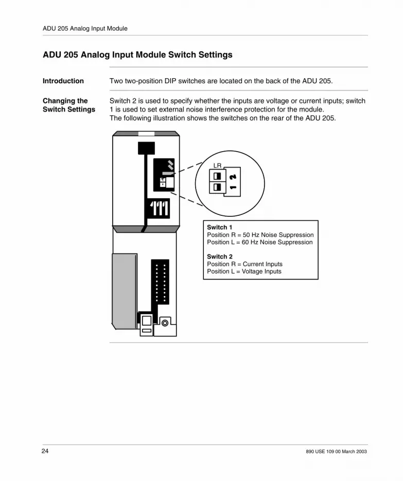
Introduction Two two-position DIP switches are located on the back of the ADU 205.
Changing the Switch Settings
Switch 2 is used to specify whether the inputs are voltage or current inputs; switch 1 is used to set external noise interference protection for the module.The following illustration shows the switches on the rear of the ADU 205.
LR
Switch 1Position R = 50 Hz Noise SuppressionPosition L = 60 Hz Noise Suppression
Switch 2Position R = Current InputsPosition L = Voltage Inputs
24 890 USE 109 00 March 2003

ADU 205 Analog Input Module
ADU 205 Analog Input Module Field Wiring
Introduction The module will be field wired differently, depending on whether the field device provides voltage or current inputs.
Wiring Diagram The following illustration is a wiring diagram and simplified schematic for the ADU 205 analog input module (voltage mode).
Voltage Input 1
Voltage Input 2
Voltage Input 4
V
V
V
1
101112131415161718192021
9
2345678
Voltage ModeI/O Bus
Interface
MUX
MUX
A/DCVTR
+5 VdcGreenLED
890 USE 109 00 March 2003 25

ADU 205 Analog Input Module
The following illustration is a wiring diagram and simplified schematic for the ADU 205 analog input module (current mode).
ADU 205 Analog Input Module LED
The ADU 205 has one green LED opposite terminal screw 1, used to indicate the presence of the 5 V power supply from the backplane.
Note: The jumpers at terminals 5-6, 9-10, 16-17, and 20-21 are factory set to reference the input source(s) to ground. If the source(s) that you use are already grounded, remove the associated jumper(s) to omit ground looping problems and possible module failure.
CAUTION
Operation Failure Hazard
When the installed jumpers reference a ground on the negative input and using a grounded power supply, the full loop supply voltage causes the module to fail. We recommend that you wire the loop supply to the negative input side of your module.
Failure to follow this precaution can result in injury or equipment damage.
GreenLED
+5 Vdc
I/O BusInterface
A/DCVTRMUX
MUX
123456789
1011121314151617
19
2122
20
18
Current Input 1
Current Input 2
Current Input 3
Current Input 4
26 890 USE 109 00 March 2003
ADU 205 Analog Input Module
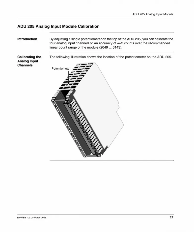
ADU 205 Analog Input Module Calibration
Introduction By adjusting a single potentiometer on the top of the ADU 205, you can calibrate the four analog input channels to an accuracy of +/-3 counts over the recommended linear count range of the module (2049 ... 6143).
Calibrating the Analog Input Channels
The following illustration shows the location of the potentiometer on the ADU 205.
Potentiometer
890 USE 109 00 March 2003 27

ADU 205 Analog Input Module
The following procedure is for voltage inputs. The process is nearly identical for current inputs, except that the input signals applied to each channel must be -20 mA, 0 mA, and +20 mA. To adjust the potentiometers:
Step Action
1 Using the DIP switch on the back of the module, set it for the desired noise suppression.
2 Calibrate analog channel 1 by wiring terminal 3 to the positive side, and terminals 5 and 6 to the negative side, of a voltage standard - as shown in the following figure.
3 Connect terminals 7, 9, 10, 14, 16, 17, 18, 20, and 21 to each other.
4 Set the voltage standard to +10 V and adjust the potentiometer until you get a reading of 6143 counts.
5 Set the voltage standard to -10 V, and adjust the potentiometer until you get a reading of 2049 +/-1 count.
6 Check the accuracy of your midrange setting by setting the voltage standard to 0 V; the reading should be at or within a count of 4096 counts. Then recheck your high range count by setting the voltage standard to +10 V; the reading should be within 3 counts of 6143.
7 Verify the calibration adjustment on the other three analog channels: for channel 2, wire terminals 7, 9, and 10 to the voltage standard; for channel 3, use terminals 14, 16, and 17; and for channel 4, use terminals 18, 20, and 21. If you make any fine tuning adjustments on any of these channels, verify their effects on channel 1.
8 When you are satisfied with the readings on all four channels, drop a bead of sealing varnish on the potentiometer to secure its setting.
= ±10 V ±2 mV V
3
5
6
28 890 USE 109 00 March 2003

ADU 205 Analog Input Module
ADU 205 Analog Input Module Specifications
Table of Specifications
The following table contains a list of system-specific specifications for the ADU 205 Analog Input Module.
The following table gives general specifications for the ADU 205 Analog Input Module.
Module Topology Number of Channels 4
Isolation Non-isolated, channel-to-bus or channel-to-channel
Signal types supported Two-pole voltage inputs
Power Supply Internally provided source 5 V, less than 50 mA from I/O bus
Voltage Input Capabilities
Linear Measuring Range Nominal +/-10 V
Maximum +/-19.99 V
Input Impedance 50 ohms
Absolute Maximum Input Voltage
+/-30 V
Wire Size One wire 14 AWG
Two wires 20 AWG
A/D Conversion Conversion Time Each input @ 4096 in
80 ms (max) @ 50 Hz
66.6 ms (max) @60 Hz
Each input @ 2048 in
60 ms (max) @ 50 Hz
50 ms (max) @ 60 Hz
Resolution 12 bits recommended range (+1)
In-range Error Limit 0.5% of input value @ 0... 60 degrees C
Nonlinearity +/-2 counts @ 0... 60 degrees C
Noise Suppression
Normal Mode Rejection 40 dB minimum
Common Mode Rejection 86 dB minimum
I/O Map Register 3x/4x 4 in/0 out
Dimensions (WxHxD)
40.3 x 145 x 117.5 mm
1.6 x 5.6 x 4.5 in
Weight 220 g
.5 lb.
Agency Approvals
ADU204: VDE 0160; UL 508; CSA 22.2 No.142; and FM Class I, Div 2 Standards.
VDE 0160; UL 508; CSA 22.2 No.142; and FM Class I, Div 2 Standards.
890 USE 109 00 March 2003 29

ADU 205 Analog Input Module
30 890 USE 109 00 March 2003

890 USE 109 00 March 2003
Overview of the ADU 206/256 Analog Input Module
At a Glance
Purpose The purpose of this chapter is to describe the ADU 206/256 analog input module.
What’s in this Chapter?
This chapter contains the following topics:
Topic Page
What is the ADU 206/256 Analog Input Module? 32
ADU 206/256 Analog Input Module Conversion Ranges 33
ADU 206/256 Analog Input Module Physical Characteristics 36
ADU 206/256 Analog Input Module Configuration 38
ADU 206/256 Analog Input Module Programming Modes 40
ADU 206/256 Analog Input Module Calibration 47
ADU 206/256 Analog Input Module Specifications 50
31

ADU 206/256 Analog Input Module
What is the ADU 206/256 Analog Input Module?
Brief Product Description
The ADU 206/256 is a four-channel analog input module with opto-isolation. It performs dual-slope integrating A/D conversions, converting analog input signals into digital values based on the principle of successive approximation. The ADU 256 functions just like the ADU 206, except that the ADU 256 operates at extended temperature.
Note: The ADU 256 model is available with conformal coating. The conformal coating model is ADU 256C, which meets Railway standard EN 50 155.
WARNING
The ADU 206/256 module will only operate properly when used with an A984, E984, or Micro 512/612 controller.
Failure to follow this precaution can result in death, serious injury, or equipment damage.
32 890 USE 109 00 March 2003

ADU 206/256 Analog Input Module
ADU 206/256 Analog Input Module Conversion Ranges
Introduction The ADU 206/256 is a four-channel analog input module with opto-isolation. It performs dual-slope integrating A/D conversions, converting analog input signals into digital values based on the principle of successive approximation. The ADU 256 functions just like the ADU 206, except that the ADU 256 operates at extended temperature.
Note: The ADU 256 model is available with conformal coating. The conformal coating model is ADU 256C, which meets Railway standard EN 50 155.
WARNING
Faulty operation.
The ADU 206/256 module will only operate properly when used with an A984, E984, or Micro 512/612 controller.
Failure to follow this precaution can result in death, serious injury, or equipment damage.
890 USE 109 00 March 2003 33

ADU 206/256 Analog Input Module
Conversion Ranges
The ADU 206/256 module has the following characteristics: Voltage/current input selection is made using jumpers; range values are set in the
software. Operates off the 5 V supply voltage provided internally over the I/O bus, along
with a user-supplied 24 VDC external power source. Resolution is 11 Bit + sign or 12 Bit, depending on the input range selected. Out-of-range status indication is software selectable. The PLC model determines the ranges. A table is provided below for each of the following: 0... 10 VDC/2... 10 VDC, 0... 20 mA/4... 20 mA for E984-258/265/275/285 +/-10 VDC/ +/-20 mA for E984-258/265/275/285
The following table lists the input ranges for voltage/current input selection.
The ranges for 0... 10 VDC/2... 10 VDC, 0... 20 mA/4... 20 mA for E984-258/265/275/285 PLC models are:
Note: See the Specifications section for the ranges for the A984-1xx, E984-24x/251/255 PLC models
Voltage Current
+/-1 V +/-20 mA
+/-10 V 4... 20 mA
0... 1 V 0... 20 mA
0... 10 V
0.2... 1 V
2... 10 V
Input voltage (VDC)
Current (mA)
12-bits 16-bits 11-bits + sign
15-bits + sign
Measuring step/value range
0 0 0 0 Under range
0 0 0 0 Neg. tolerance range
0/2 0/4 0 0 0 0 Nominal range
10 20 4000 64000 +2000 +32000
10.01... 20.02... 4001 64016 +2001 +32016 Pos. tolerance range
greater than/equal to10.24/10.19
greater than/equal to20.48/20.39
4095 65520 +2047 +32760 Over range
34 890 USE 109 00 March 2003
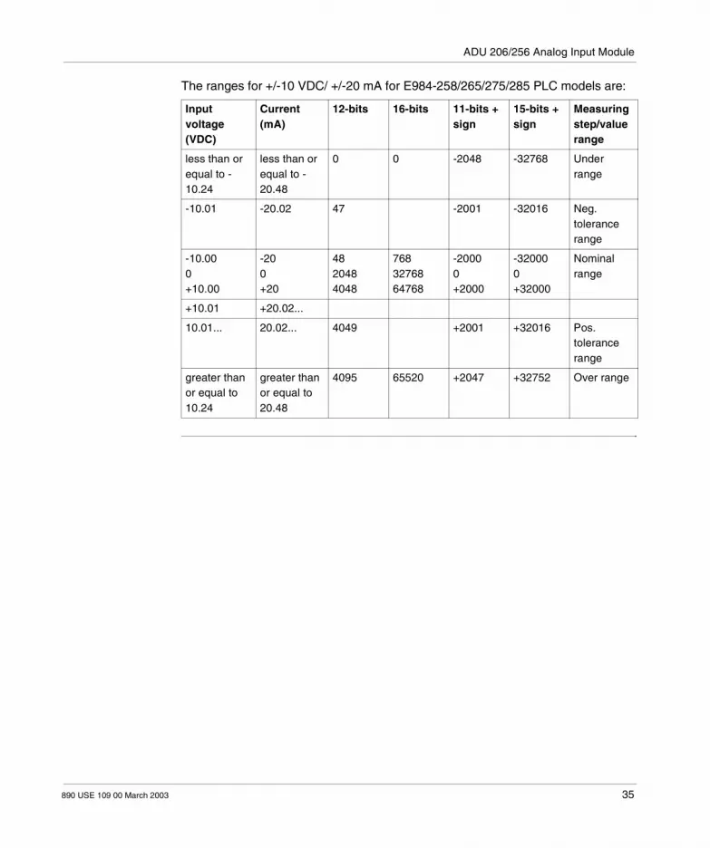
ADU 206/256 Analog Input Module
The ranges for +/-10 VDC/ +/-20 mA for E984-258/265/275/285 PLC models are:
Input voltage (VDC)
Current (mA)
12-bits 16-bits 11-bits + sign
15-bits + sign
Measuring step/value range
less than or equal to -10.24
less than or equal to -20.48
0 0 -2048 -32768 Under range
-10.01 -20.02 47 -2001 -32016 Neg. tolerance range
-10.000+10.00
-200+20
4820484048
7683276864768
-20000+2000
-320000+32000
Nominal range
+10.01 +20.02...
10.01... 20.02... 4049 +2001 +32016 Pos. tolerance range
greater than or equal to 10.24
greater than or equal to 20.48
4095 65520 +2047 +32752 Over range
890 USE 109 00 March 2003 35

ADU 206/256 Analog Input Module
ADU 206/256 Analog Input Module Physical Characteristics
Illustration The ADU 206/256 can be installed in any slot in the A120 subracks (DTA 200, 201, and 202). The module has bus contacts at the rear and peripheral connections on the front. The blank label, which fits in the module cover, can be filled in with relevant information (signal values, etc.) in the spaces provided.A front view with ADU 206 label is provided below.
ADU-206
1
23456789
1011
12131415161718192021
ADU 206U
1
2
Mready U
3
4
cardM22
36 890 USE 109 00 March 2003

ADU 206/256 Analog Input Module
LEDs The ADU 206/256 has two green LEDs: The LED opposite field wiring terminal #1 indicates the presence of 24 Vdc power
from the external source (ON = power supplied; OFF = power off. The LED opposite field wiring terminal #12 indicates the condition of the
processor/module (ON = fault-free operation; OFF = fault condition).
Simplified Schematic
A simplified schematic for the ADU 206/256 is provided below.
Note: The controller must be running for the READY LED to illuminate.
-15V 0V +15V +15V 0V -15V
MUX
REF
PA-RAMA/D
SERIAL
SOC3
5VBIT 14
BIT 13
BIT 12
BIT 11
BIT 0
+24VDC
1
3
2
GND
4
GN “ready”
GN
+15V
0V
-15V
1
10
2
9
3
4
5
6
7
8
11
12
13
14
15
16
17
18
19
20
21
22
890 USE 109 00 March 2003 37

ADU 206/256 Analog Input Module
ADU 206/256 Analog Input Module Configuration
Introduction The following items must be addressed when configuring the ADU 206/256: The module must be I/O mapped as five 3x input registers and one 4x output
register. Binary must be set for data type. Make connections and assignments of input addresses. Identify overall mode of operation, type of input, and error indication. Cabling guidelines.
Cabling Shielded, twisted pair cable (2 or 4 x 0.5mm per channel) should be used. All channels can be connected with a common shielded cable.
Connect shield to ground (GND) on one side with a short cable (less than 8 in). Observe a minimum distance of 20 in. between the module and power lines or
other sources of electrical disturbance.
Connection and Assignment of Input Addresses
Connection and Assignment for Current Inputs
For current inputs: Jumper 3-4 for input 1 Jumper 7-8 for input 2 Jumper 14-15 for input 3 Jumper 18-19 for input 4
Connection and Assignment for Voltage Inputs
For voltage inputs: Jumper 5-6 for input 1 Jumper 9-10 for input 2 Jumper 16-17 for input 3 Jumper 20-21 for input 4Corresponding input signal names or addresses can be entered on the blank label (supplied).
Note: Detailed Compact 984 cabling and installation instructions are found in the User Guide.
38 890 USE 109 00 March 2003

ADU 206/256 Analog Input Module
Wiring Diagram An ADU 206/256 wiring diagram and associated registers for inputs are provided below.
+24 VDCCOMMON
1
0.16 A
3XXXX + 1
3XXXX + 2
3XXXX + 3
3XXXX + 4
3
4
5
6
7
8
910
I1
I2
V1
V2
V3
V4
I3
I4
15
16
17
19
20
21
2
3
4
5
6
7
8
9
10
11
12
13
14
15
16
17
18
19
20
21
22
890 USE 109 00 March 2003 39

ADU 206/256 Analog Input Module
ADU 206/256 Analog Input Module Programming Modes
Introduction The ADU 206/256 is a four-channel analog input module. Its field connector is wired depending on the type of input to be measured, either voltage or current. Any of the four inputs can be either voltage or current, and any combination of the four may be used if levels are within the programmed range for the channel.The module can operate in one of several modes, and the input channel ranges are individually selectable. The mode and ranges are set by an I/O mapped 4x register.Five sequential 3x registers must also be I/O mapped. The first register is used to read module operating status, and the remainder contain data representing voltage or current levels at the four channel inputs. Channel input data is updated every 10 ms.
4x Control Register
The operating mode of the module and individual channel ranges are set using the lower 7 bits of the 4x register.Options are:
Bit Operating Mode Setting
000X Bipolar mode without overrange indication
001X Unipolar mode without overrange indication
002X Bipolar with offset and extended resolution without overrange indication
003X Unipolar with offset and extended resolution without overrange indication
004X Bipolar mode with overrange indication
005X Unipolar mode with overrange indication
006X Bipolar with offset and extended resolution with overrange indication
007X Unipolar with offset and extended resolution with overrange indication
Note: These values are in Hexadecimal.where the X value determines the individual channel range:1 = expanded voltage range (10 V)0 = normal voltage range (1 V)
40 890 USE 109 00 March 2003

ADU 206/256 Analog Input Module
The following diagram illustrates bits in the ADU 206/256 control word and their meanings.
0123456715 14 13 12 11 10 9 8
[15-7] Not Used
[6] If set, requests an indication inthe status word (input word 1) when the input to a
channel is above the top end (+ or -) of itsmeasurement range. [See the status word
description for more information.]
[5] If set, the module measures current orvoltage with an offset over a restricted range,
i.e., 4 ... 20 mA, 0.2 ... 1 V, or 2 ... 10 V.
[4] If set, the module measures currentor voltage in 12 bit unipolar mode.
[3] Defines the measuring range of Channel4. If = 1, the upper range will be 10 V. Must
be set to 0 for current mode operation.
[1] Defines the measuring range of Channel2. If = 1, the upper range will be 10 V. Must
be set to 0 for current mode operation.
[0] Defines the measuring range of Channel1. If set, the upper range will be 10 V. Must
be set to 0 for current mode operation.
[2] Defines the measuring range of Channel3. If = 1, the upper range will be 10 V. Must
be set to 0 for current mode operation.
890 USE 109 00 March 2003 41

ADU 206/256 Analog Input Module
4x Control Register Quick Reference
A quick reference diagram of the ADU 206/256 4x Control Register is provided below.
15 01234567891011121314
NOT USED
EXPANDED RANGE SELECT(Chs 1 ... 4; set to a “1” if over
1 V will be input.)
MODULE MODE SELECT
CH 4CH 3
CH 2CH 1
0011
BipolarUnipolarBipolar w/Offset and Ext ResUnipolar w/Offset and Ext Res
0101
1 Add this bit for overrangeconditions to be displayed inthe common 3x Stat Register
NOT USED
EXAMPLE:0 0 0 0 0 0 0 0 0 1 0 1 1 1 0 0
CH 3 and CH 4Expanded Ranges
Module set toUnipolar Mode
Overrange IndicationRequested
42 890 USE 109 00 March 2003

ADU 206/256 Analog Input Module
3X Status and Data Registers
The bit significance of the first 3x input register, which displays the module status, is displayed in the following illustration. The next four registers contain data represen-tative of the individual channel input values. Refer to the rest of the information in this map for more detail about the values that may be expected.Data values are the result of the type of input selected, the field connector wiring, the module operating mode selected, and the range selected for the channel (normal or expanded).
The following diagram illustrates bits in the ADU 206/256 status word and their meanings.
I/O Map Registers Data
3x Module status information
3x + 1 Input #1 data
3x + 2 Input #2 data
3x + 3 Input #3 data
3x + 4 Input #4 data
15 14 13 12 11 10 9 8 7 6 5 4 3 2 1 0
[7] Set until the processor within the module is ready. After theprocessor is operational this bit will be set if any of bits 0 - 3 of
the status word are set or if a processor fault occurs.
[6] Set if the external supply voltage to the module isdisconnected.
[5] Reflects the state of Bit 5 of the control word.
[4] Reflects the state of Bit 4 of the control word.
[3] If set, indicates that the input to Channel 4 has exceededthe anticipated +/- limit, or indicates an open circuit in
4 ... 20 mA operation (unipolar and bipolar with offset).
[2] If set, indicates that the input to Channel 3 has exceededthe anticipated +/- limit, or indicates an open circuit in
4 ... 20 mA operation (unipolar and bipolar with offset).
[1] If set, indicates that the input to Channel 2 has exceededthe anticipated +/- limit, or indicates an open circuit in4 ... 20mA operation (unipolar and bipolar with offset).
[0] If set, indicates that the input to Channel 1 has exceededthe anticipated +/- limit, or indicates an open circuit in4 ... 20mA operation (unipolar and bipolar with offset).
[15-8] Not Used
890 USE 109 00 March 2003 43

ADU 206/256 Analog Input Module
30xxx Status Register Quick Reference
A quick reference diagram of the ADU 206/256 30xxx Status Register is provided below.
15 14 13 12 11 10 9 8 7 6 5 4 3 2 1 0
NOT USED
CH 4CH 3
CH 2CH 1
OUT OF RANGE/OPEN CIRCUIT INDICATOR(Channels 1- 4)
MODULE OPERATING MODE
0 1 Unipolar0 0 Bipolar
1 0 Bipolar w/Offset and Ext Res1 1 Unipolar w/Offset and Ext Res
X Set if External Supply Bad
X Set on Fault
0 0 0 0 0 0 0 0 1 0 0 1 1 1 0 0
EXAMPLE:
NOT USED CH 3 and CH 4Out of Range
Unipolar Mode
External Supply OK
Fault Bit
44 890 USE 109 00 March 2003

ADU 206/256 Analog Input Module
Types of Modes and Their Functions
When power is first applied to the module, it will be in a state equivalent to all of the control bits being 0. As long as power to the unit is maintained, the operating mode of the module will be unchanged through a stop/start cycle.When the module goes out of range-either over or under range-and then returns to a valid operating range, the module will resume proper operations unless your out-of-range condition reaches or exceeds the safety range of +/-30 VDC.
Bipolar (000X, 004X)Bipolar mode is selected by setting the control word to the value 000X, where X defines the range of any channels used for voltage measurement. In this mode, if out of range indication is requested (control word = 004x), it will turn on at voltages/currents exceeding the +/- maximum value. Refer to status word description.The following table describes the current/voltage values in bipolar mode.
Unipolar (001X, 005X)This mode is selected by setting the control word to the value 001X, where X defines the range of any channels used for voltage measurements. In this mode, if overrange indication is requested (i.e., control word = 005X), it will turn on if an input exceeds the maximum range value. Refer to status word description. The following table describes the current/voltage values in unipolar mode.
Bipolar with Offset and Extended Resolution (002X, 006X)
WARNING
Extreme out-of-range voltage.
Operation at an extreme out-of-range voltage-at or beyond +/-30 VDC-will cause permanent damage to the module.
Failure to follow this precaution can result in death, serious injury, or equipment damage.
Current Normal Voltage Expanded Voltage Value
-20 mA -1 V -10 V 48
0 mA 0 V 0 V 2048
+20 mA +1 V +10 V 4048
Current Normal Voltage Expanded Voltage Value
0 mA 0 V 0 V 0
20 mA +1 V +10 V 4000
890 USE 109 00 March 2003 45
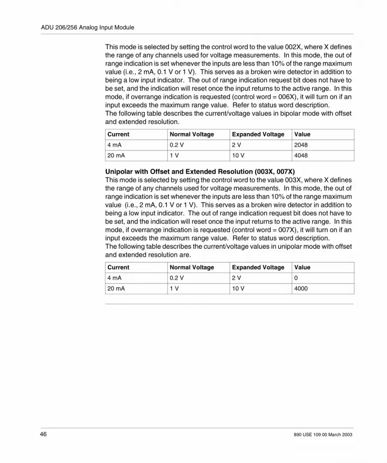
ADU 206/256 Analog Input Module
This mode is selected by setting the control word to the value 002X, where X defines the range of any channels used for voltage measurements. In this mode, the out of range indication is set whenever the inputs are less than 10% of the range maximum value (i.e., 2 mA, 0.1 V or 1 V). This serves as a broken wire detector in addition to being a low input indicator. The out of range indication request bit does not have to be set, and the indication will reset once the input returns to the active range. In this mode, if overrange indication is requested (control word = 006X), it will turn on if an input exceeds the maximum range value. Refer to status word description.The following table describes the current/voltage values in bipolar mode with offset and extended resolution.
Unipolar with Offset and Extended Resolution (003X, 007X)This mode is selected by setting the control word to the value 003X, where X defines the range of any channels used for voltage measurements. In this mode, the out of range indication is set whenever the inputs are less than 10% of the range maximum value (i.e., 2 mA, 0.1 V or 1 V). This serves as a broken wire detector in addition to being a low input indicator. The out of range indication request bit does not have to be set, and the indication will reset once the input returns to the active range. In this mode, if overrange indication is requested (control word = 007X), it will turn on if an input exceeds the maximum range value. Refer to status word description.The following table describes the current/voltage values in unipolar mode with offset and extended resolution are.
Current Normal Voltage Expanded Voltage Value
4 mA 0.2 V 2 V 2048
20 mA 1 V 10 V 4048
Current Normal Voltage Expanded Voltage Value
4 mA 0.2 V 2 V 0
20 mA 1 V 10 V 4000
46 890 USE 109 00 March 2003
ADU 206/256 Analog Input Module
ADU 206/256 Analog Input Module Calibration
Introduction By adjusting the two potentiometers located on the top of the ADU 206/256, you can independently calibrate both the normal and expanded ranges for the four input channels.
CAUTION
Return units requiring calibration.
Modicon recommends that units requiring recalibration be returned to the factory, since inaccuracies could be due to faulty components. However, users who wish to perform their own calibration should use the following procedure.
Failure to follow this precaution can result in injury or equipment damage.
890 USE 109 00 March 2003 47

ADU 206/256 Analog Input Module
Calibrating the Analog Input Channels
In the procedure that follows, R65 is used to calibrate the normal ranges, and R64 is used to calibrate the expanded ranges. Items required for calibration are: A 1 VDC Power Supply (+/-0.1 mV) A 10 VDC Power Supply (+/-1.0 mV) A voltmeter with appropriate scales and accuracy of 0.2... 0.5 parts/millionThe following illustration shows the location of the potentiometers on the ADU 206/256.
ADU-206
1
23456789
1011
12131415161718192021
ADU 206U
1
2
Mready U
3
4
cardM22
48 890 USE 109 00 March 2003

ADU 206/256 Analog Input Module
Adjusting the Potentiometers Procedure
Use the following procedure to adjust the potentiometers.
Step Action
1 Connect a 1 VDC source (+/-0.1 mV), verified with the voltmeter, to the four voltage inputs. Set the module for Unipolar mode and all channels for Normal range. Adjust R65 for a reading of 4000 counts on Channel 1. Channels 2... 4 should read 4000, +/-2 counts.
2 Set the module to Bipolar mode and check all channels for a reading of 4048 +/-2 counts.
3 Reverse the 1 VDC supply polarity and check all channels in Bipolar mode. All channels should read 48 +/-2 counts.
4 Set the module for Unipolar mode and all channels for Expanded range. Connect a 10 VDC source (+/-1.0 mV), verified with the voltmeter, to the four voltage inputs. Adjust R64 for a reading of 4000 counts on Channel 1. Channels 2 to 4 should read 4000, +/-2 counts.
5 Set the module to Bipolar mode and check all channels for a reading of 4048 +/-2 counts.
6 Reverse the 10 Vdc supply polarity and check all channels in Bipolar mode. All channels should read 48 +/-2 counts.
7 When satisfied with the readings on all four channels, drop a bead of sealing varnish on both potentiometers’ adjusting screws to secure their settings.
890 USE 109 00 March 2003 49
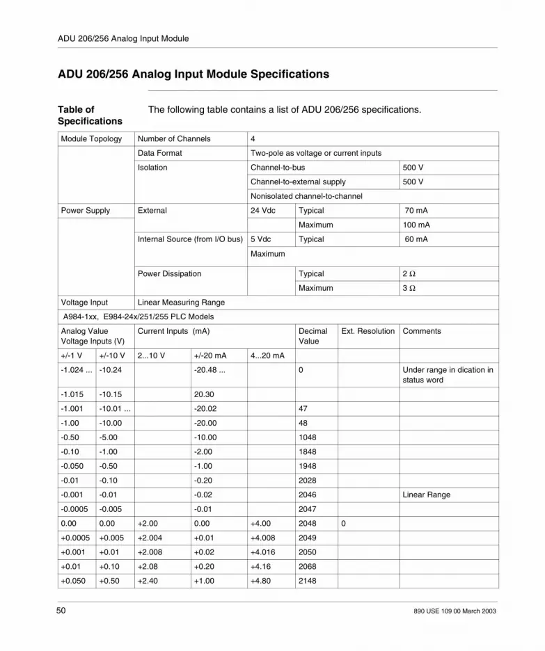
ADU 206/256 Analog Input Module
ADU 206/256 Analog Input Module Specifications
Table of Specifications
The following table contains a list of ADU 206/256 specifications.
Module Topology Number of Channels 4
Data Format Two-pole as voltage or current inputs
Isolation Channel-to-bus 500 V
Channel-to-external supply 500 V
Nonisolated channel-to-channel
Power Supply External 24 Vdc Typical 70 mA
Maximum 100 mA
Internal Source (from I/O bus) 5 Vdc Typical 60 mA
Maximum
Power Dissipation Typical 2 Ω
Maximum 3 Ω
Voltage Input Linear Measuring Range
A984-1xx, E984-24x/251/255 PLC Models
Analog ValueVoltage Inputs (V)
Current Inputs (mA) Decimal Value
Ext. Resolution Comments
+/-1 V +/-10 V 2...10 V +/-20 mA 4...20 mA
-1.024 ... -10.24 -20.48 ... 0 Under range in dication in status word
-1.015 -10.15 20.30
-1.001 -10.01 ... -20.02 47
-1.00 -10.00 -20.00 48
-0.50 -5.00 -10.00 1048
-0.10 -1.00 -2.00 1848
-0.050 -0.50 -1.00 1948
-0.01 -0.10 -0.20 2028
-0.001 -0.01 -0.02 2046 Linear Range
-0.0005 -0.005 -0.01 2047
0.00 0.00 +2.00 0.00 +4.00 2048 0
+0.0005 +0.005 +2.004 +0.01 +4.008 2049
+0.001 +0.01 +2.008 +0.02 +4.016 2050
+0.01 +0.10 +2.08 +0.20 +4.16 2068
+0.050 +0.50 +2.40 +1.00 +4.80 2148
50 890 USE 109 00 March 2003

ADU 206/256 Analog Input Module
+0.10 +1.00 +2.80 +2.00 +5.60 2248
+0.50 +5.00 +6.00 +10.00 +12.00 3048
+1.00 +10.00 +10.00 +20.00 +20.00 4048 4000
+1.015 ...
+10.15 ...
+10.155 ... +20.30 ... +20.30 ... Over range Indication in Status Word
+1.024 +10.24 +10.19 +20.47 +20.38 4095
Absolute Max. Input Voltage +/-30 V
Input Impedance greater than 1 M ohms
Wire Size One wire 14 AWG
Two wires 20 AWG
Current Input Capabilities
Linear Measuring Range See the table above
Absolute Maximum Input Current (continuous) 40 mA/input
Input Impedance 50 ohms
Wire Size One wire 14 AWG
Two wires 20 AWG
A/D Conversion Conversion Time ( maximum) 10 ms for all 4 inputs
Resolution 11 bits plus sign
In-range Error Limit Voltage Maxi mum 0.4% of input value @ 0 ... 60 degrees C
Current Maxi mum 0.56% of input value @ 0 ... 60 degrees C
EnvironmentalCharacteristics
Operating Temperature 0 ... 60 degrees C for ADU 206 -40 ... +70 degrees C for ADU 256
I/O Map Register 3x/4x 5 in/1 out
Noise Suppression Common Mode Rejection (minimum) 60 dB @ 1 kHz
Dimensions (W x H x D) 40.3 x 145 x 117.5 mm
1.6 x 5.6 x 4.5 in
Weight 330 g
0.725 lb
Agency Approvals ADU206: VDE 0160; UL 508; CSA 22.2 No.142; and FM Class I, Div 2 Standards.
ADU256C: Railway standard EN 50 155; European Directive EMC 89/336/EEC Standards. UL 508; CSA 22.2 No.142; and FM Class I, Div 2 pending.
890 USE 109 00 March 2003 51

ADU 206/256 Analog Input Module
52 890 USE 109 00 March 2003

890 USE 109 00 March 2003
Overview of the ADU 210 Isolated Analog Input Module
At a Glance
Purpose The purpose of this chapter is to describe the ADU 210 isolated analog input module.
What’s in this Chapter?
This chapter contains the following topics:
Topic Page
What is the ADU 210 Isolated Analog Input Module? 54
ADU 210 Isolated Analog Input Module Physical Characteristics 55
Installing the ADU 210 Isolated Analog Input Module 57
ADU 210 Isolated Analog Input Module Operation 59
ADU 210 Isolated Analog Input Module Specifications 63
53

ADU 210 Isolated Analog Input Module
What is the ADU 210 Isolated Analog Input Module?
Brief Product Description
The ADU 210 is a four-channel analog input module with opto-isolation. It performs analog-to-digital conversions using a delta-sigma conversion method, converting analog input signals into digital values. The ADU 210 module has the following characteristics: Voltage/Current input selection is made by appropriate wiring; the range values
are set via the panel software. Operates off the 5 V supply voltage provided internally over the I/O bus, along
with a user-supplied 24 VDC external power source. Provides 300 volts maximum channel-to-channel isolation. Provides a 15-bit + sign resolution. Errors are noted via the Concept I/O Map Status Word. Input selection and range can be set independently.Input ranges are:
Voltage Current
+/-10 V
0 ... 10 V
1 ... 5 V 4 ... 20 mA
0 ... 5 V 0 ... 20 mA
2 ... 10 V
+/-5 V +/-20 mA
54 890 USE 109 00 March 2003

ADU 210 Isolated Analog Input Module
ADU 210 Isolated Analog Input Module Physical Characteristics
Illustration The ADU 210 can be installed in any slot in the A120 subracks (DTA 200, 201, and 202). The module has bus contacts at the rear and peripheral connections on the front. The blank label, which fits in the module cover, can be filled in with relevant information (signal values, etc.) in the spaces provided.A front view with ADU 210 label is provided below.
ADU-210
123456789
1011
1213
1415
16171819202122
cardM
4
3
Mready| U
2
1
UU
ADU-210
890 USE 109 00 March 2003 55

ADU 210 Isolated Analog Input Module
LEDs The ADU 210 has two green LEDs.
Simplified Schematic
A simplified schematic for the ADU 210 is provided below.
LED# LED Name
Function
1 Power (U)
Pertains to the 24 VDC:ON = Power supply is availableOFF = Power supply is NOT available.
12 Ready Pertains to the processor operation:ON = Processor operating between the ADU 210 and the PLC without faultOFF = Fault in processor operation
A/D
serial
GN “ready”
80C31
TOTUSN
1
+ 5 V
PAB
PAB
+15 V
0 V
-15 V
GN “U”
Channel 2,3,4
First of 4 Input Circuits
23456789
10111213141516171819202122
U
1
2
3
4
M
MU PAB
56 890 USE 109 00 March 2003
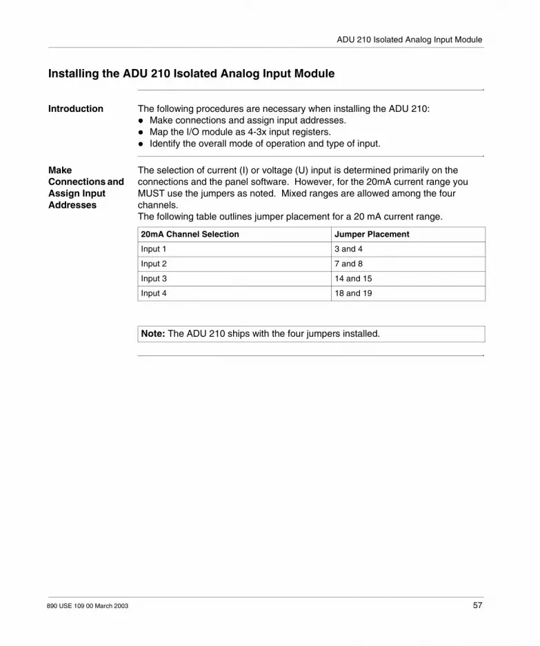
ADU 210 Isolated Analog Input Module
Installing the ADU 210 Isolated Analog Input Module
Introduction The following procedures are necessary when installing the ADU 210: Make connections and assign input addresses. Map the I/O module as 4-3x input registers. Identify the overall mode of operation and type of input.
Make Connections and Assign Input Addresses
The selection of current (I) or voltage (U) input is determined primarily on the connections and the panel software. However, for the 20mA current range you MUST use the jumpers as noted. Mixed ranges are allowed among the four channels.The following table outlines jumper placement for a 20 mA current range.
20mA Channel Selection Jumper Placement
Input 1 3 and 4
Input 2 7 and 8
Input 3 14 and 15
Input 4 18 and 19
Note: The ADU 210 ships with the four jumpers installed.
890 USE 109 00 March 2003 57

ADU 210 Isolated Analog Input Module
Wiring Diagram The following illustration is an ADU 210 wiring diagram.
ADU 210
ADU 210
+24 VDCCOMMON
0.16 A
I
I
I
IU
U
U
U1
2
3
4
345678910
151617
19
2120
123456789
1011
1213141516171819202122
UU
UU
1
2
3
4
M
M
card
123456
78910111213141516171819202122 AAppl*Apply Jumpers to select
20mA range per channel
inp
ut
inp
ut
ready
58 890 USE 109 00 March 2003

ADU 210 Isolated Analog Input Module
ADU 210 Isolated Analog Input Module Operation
Introduction The ADU 210 is a four-channel analog input module. Its field connector is wired depending on the type of input to be measured, either voltage or current. Any of the four inputs can be either voltage or current, and any combination of the four may be used if levels are within the programmed range for the channel.The module can operate in one of several modes, and the input channel ranges are individually selectable. The mode and ranges are set via the panel software. Channel input data is updated every 270mS. When power is first applied to the module, its inputs are inactive.
I/O Map The ADU 210 requires 4-3x input registers. These four registers contain data representative of the individual channel input values.
I/O Map Registers Data
3x Input #1 data
3x + 1 Input #2 data
3x + 2 Input #3 data
3x + 3 Input #4 data
Note: Inputs that are NOT used MUST be set to inactive. This avoids error messages and reduces the conversion time.
890 USE 109 00 March 2003 59

ADU 210 Isolated Analog Input Module
Error Detections and Limits
After system start-up a measured value remains 0, until the ADU 210 is addressed. Next, the ADU 210 displays a parameter error (-32 768) until the value is changed by selecting a valid range. Then the valid range is displayed. Changing the measuring range displays a parameter error (-32 768) in the following cycle, until the valid range is shown after subsequent cycles. It may take up to 300mS maximum.Input voltages (currents) of up to -1.6% of the rated value in unipolar mode and limiting value 0 result in a digital value (0) without causing an error. When input voltage (currents) fall below this limit an error results and a measured value (-32 767) is displayed.Negative input voltage (current) in unipolar mode and limiting value -1.6% produce an appropriate digital value (up to -512) without causing an error - up to a input voltage of -1.6% of the rated value. When the measured value falls below this limit an error results and a measured value (-32 767) is displayed.When measuring ranges with a 20% offset (live-zero) the error limit for value measure underflow is about 10% of the rated value. When errors occur simultaneously in several inputs the error with the lowest input number is displayed until debugged. Next, the error with the next highest input number is displayed and so on.When an input error occurs the transferred measured value of that input is set to the defined constants of:Transferred Measured Values after an Error Detection are listed in the following table.
Measured Values Descriptions
-32 768 Inactive input (invalid measuring range)
+32 767 Measuring range overflow
-32 767 Measuring range underflow
60 890 USE 109 00 March 2003

ADU 210 Isolated Analog Input Module
Conversions The following tables detail the various voltage and current conversions for the ADU 210 module.
The conversion values of voltage inputs are listed in the following table.
Note: Brackets denote range with limiting value -1.6%. No brackets denotes range with limiting value 0.
Analog value 0 ... 5 V
Analog value0 ... 10V
Analog value1 ... 5 V
Analog value2 ... 10 V
Analog value+/-5 V
Analog value+/-10 V
Decimal value
Notes
<-0.080 <-0.16 <+0.52 <+1.04 <-5.12 <-10.24 -32 767 underflow error
-5.119 ...-5.00
-10.239...-10.00
-32 766...-32 001
overload range
-0.08 ...-0.00
-0.16 ...-0.00
+0.52 ...+0.936 ...+0.99
+1.04 ..+1.87 ...+1.99
0 (-3 840)0 (-512)0 (-1)
overload range
-5.00 -10.00 -32 000 linear
-2.50 -5.00 -16 000 linear
-0.50 -1.00 -3 200 linear
-0.25 -0.50 -1 600 linear
-0.05 -0.10 -320 linear
-0.005 -0.01 -32 linear
-0.0025 -0.005 -16 linear
0 0 1 2 0 0 0 linear
0.0025 0.005 1.002 2.004 +0.0025 +0.005 +16 linear
0.005 0.01 1.004 2.008 +0.005 +0.01 +32 linear
0.05 0.10 1.04 2.08 +0.05 +0.10 +320 linear
0.25 0.50 1.20 2.40 +0.25 +0.50 +1 600 linear
0.50 1.00 1.40 2.80 +0.50 +1.00 +3 200 linear
2.50 5.00 3.00 6.00 +2.50 +5.00 +16 000 linear
5.00 10.00 5.00 10.00 +5.00 +10.00 +32 000 rated value
5.000...5.119
10.000...10.239
5.00...5.09
10.00...10.19
+5.000..+5.119
+10.00...+10.239
+32 001...+32 766
overload range
>5.12 >10.24 >5.09 >10.19 >+5.20 >+10.24 >+32 767 overflow error
890 USE 109 00 March 2003 61
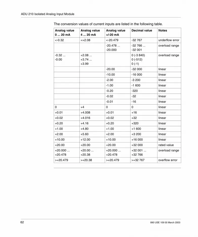
ADU 210 Isolated Analog Input Module
The conversion values of current inputs are listed in the following table.
Analog value0 ... 20 mA
Analog value4 ... 20 mA
Analog value+/-20 mA
Decimal value Notes
<-0.32 <+2.08 <-20.479 -32 767 underflow error
-20.478 ...-20.000
-32 766 ...-32 001
overload range
-0.32 ...-0.00
+2.08 ...+3.74 ...+3.99
0 (-3 840) 0 (-512)0 (-1)
overload range
-20.00 -32 000 linear
-10.00 -16 000 linear
-2.00 -3 200 linear
-1.00 -1 600 linear
-0.20 -320 linear
-0.02 -32 linear
-0.01 -16 linear
0 +4 0 0 linear
+0.01 +4.008 +0.01 +16 linear
+0.02 +4.016 +0.02 +32 linear
+0.20 +4.16 +0.20 +320 linear
+1.00 +4.80 +1.00 +1 600 linear
+2.00 +5.60 +2.00 +3 200 linear
+10.00 +12.00 +10.00 +16 000 linear
+20.00 +20.00 +20.00 +32 000 rated value
+20.000 ...+20.478
+20.00 ...+20.38
+20.000 ...+20.478
+32 001 ...+32 766
overload range
>+20.479 >+20.38 >+20.479 >+32 767 overflow error
62 890 USE 109 00 March 2003

ADU 210 Isolated Analog Input Module
ADU 210 Isolated Analog Input Module Specifications
Table of Specifications
The following table contains a list of specifications for the ADU 210 module.
Module Topology Number of channels 4
Data Format Unipolar and Bipolar as voltage or current inputs
Isolation channel to channel
300 Vdc maximum
Isolation channel to bus 500 Vac maximum
Power Supply Internal Source (from I/O bus)
5 VIO; 90mA maximum, 40mA typical
External 24 Vdc; 120 mA maximum, 60 mA typical
Power Dissipation 3Ω maximum, 2Ω typical
I/O Map Register 3x/4x 4 in/0 out
Voltage Inputs Linear Measuring Range Unipolar: 1 ... 5V, 0 ... 5V, 2 ... 10V, 0 ... 10VBipolar: +/-5V, +/-10V,
Input Impedance ≥ 1 M ohms
Resolution Brief Product Description, p. 54
Absolute accuracy error @ 25 degrees C
Maximum 0.1% of full scale
Absolute accuracy error @ 60 degrees C
Maximum 0.25% of full scale
Typical accuracy error ≤0.5 of above maximum error
Maximum overvoltage +/-30 V static (1 input for each module)+/-50 V dynamic for max. 100 ms
Conversion values ADU 210 Isolated Analog Input Module Operation, p. 59
Current Inputs Linear Measuring Range +/-20 mA (+/- 5 V),0 ... 20mA (0 ... 5 V),4 ... 20 mA (1 ... 5 V)
Input Impedance 250 ohms
Resolution Brief Product Description, p. 54
Absolute accuracy error @ 25 degrees C
Maximum 0.1% of full scale
Absolute accuracy error @ 60 degrees C
Maximum 0.25% of full scale
Typical accuracy error 0.5 of above maximum error
Critical values 48 mA, maximum overvoltage from 12 V
890 USE 109 00 March 2003 63

ADU 210 Isolated Analog Input Module
Conversion values ADU 210 Isolated Analog Input Module Operation, p. 59
Dynamic Characteristics of Inputs
Conversion time for all inputs
270 mS maximum
Time constant for HF suppression
0.4 mS typical
Interference voltage suppression (main suppression) for f=nx50 or 60Hz
n=1,2 ...
Common-mode rejection ≥105 dB
Processor/Memory
Processor Type Intel 80C31 (8-bit)
Memory 32 kByte EPROM for firmware
Physical Characteristics
Format 1 slot
Dimensions (W x H x D) 40.3 x 145 x 117.5 mm1.6 x 5.6 x 4.5 in
Weight 320 g, 0.710 lb.
Wire Size 1-14 AWG, 2-20 AWG
Environmental Characteristics
Operating Temperature 0 ... 60 degrees C
Agency Approvals VDE 0160; UL 508; CSA 22.2 No.142; and European Directive EMC 89/336/EEC (See Requirements for CE Compliance, p. 779) Standards
64 890 USE 109 00 March 2003

890 USE 109 00 March 2003
Overview of the ADU 211/212 Universal Analog Input Module
At a Glance
Purpose The purpose of this chapter is to describe the ADU 211/212 universal analog input module.
What’s in this Chapter?
This chapter contains the following topics:
Topic Page
What is the ADU 211/212 Universal Analog Input Module? 66
ADU 211/212 Universal Analog Input Module "J" Thermocouple Quick Start 67
ADU 211/212 Universal Analog Input Module Inputs 68
ADU 211/212 Universal Analog Input Module Installation 69
ADU 211/212 Universal Analog Input Module Switch Settings 70
ADU 211/212 Universal Analog Input Module Field Wiring 74
ADU 211/212 Universal Analog Input Module Field Wiring Examples 77
ADU 211/212 Universal Analog Input Module Application Notes 84
ADU 211/212 Universal Analog Input Module Configuration 87
ADU 211/212 Universal Analog Input Module Output Registers 88
ADU 211/212 Universal Analog Input Module Input Registers 94
Sequentially Reading ADU 211/212 Universal Analog Input Module Channel Data 96
ADU 211/212 Universal Analog Input Module Troubleshooting 103
ADU 211/212 Universal Analog Input Module Specifications 105
65

ADU 211/212 Universal Analog Input Module
What is the ADU 211/212 Universal Analog Input Module?
Brief Product Description
The ADU 211/212 Universal Analog Input Module is a highly versatile module that digitizes up to eight analog inputs into a Modicon Compact 984 or Micro PLC (programmable logic controller). The module accepts thermocouple, RTD (resistance temperature device), voltage, and current loop inputs, and (through automatic channel sequencing or ladder logic) provides these inputs to the PLC using only three 30XXX registers. Commands to the module are processed through three 40XXX registers.
Note: Some A120 I/O modules (DEP 211/214/215/217, DAP211/217, ADU204/211/214/216, DAU204, VIC2xx, and MOT20x) require a loadable (SW-IODR-001) for proper operation when using certain PLCs (A984-1xx, E984-24x/251/255) with Modsoft. Refer to Installing the Loadables for A120 Series I/O Modules, p. 791
CAUTION
Note difference between ADU 211 and ADU 212.
The difference between the ADU 211 and the ADU 212 is how they are powered. The ADU 211 requires a external 24 Vdc power supply and draws less than1 mA from the internal +5 Vdc. In contrast, the ADU 212 only draws power from the internal +5 Vdc (450 mA typical, 600 mA maximum) and does not require an external power supply.
Failure to follow this precaution can result in injury or equipment damage.
Note: For application specific concerns refer to ADU 211/212 Universal Analog Input Module Application Notes, p. 84
66 890 USE 109 00 March 2003

ADU 211/212 Universal Analog Input Module
ADU 211/212 Universal Analog Input Module "J" Thermocouple Quick Start
Introduction This section is provided as a reference only for users who are familiar with the ADU 211/212 module. Until you have become completely familiar with the ADU 211/212 module, do not try to follow these steps.
Procedure for "J" Thermocouple Quick Start
The following table describes the procedure for "J" Thermocouple Quick Start
Note: For application specific concerns, refer to ADU 211/212 Universal Analog Input Module Application Notes, p. 84
Step Action
1 Ensure that DIP switch poles 1, 3, and 9 (both top and bottom DIP switches) are turned ON (closed), while the others are turned OFF (open). This step configures the module for thermocouple inputs.
2 Attach a "J"-type thermocouple to the field wiring terminal block: connect the thermocouple white wire (+) to Terminal 2 and the red wire (-) to Terminal 3.
3 Install the ADU 211/212 in the rack. +24 VDC power and common need to be connected on the ADU 211.
4 I/O map the module slot as 30001-30003 and 40001-40003 BIN.
5 With the controller in RUN mode, in the panel software reference screen, configure the Control Words as follows: 40001 = 1660 HEX (degrees F display of "J" Thermocouple) 40002 = 0F6A HEX (internal cold junction compensation, 100 ms integration
time and Floating Point data format)
6 Display 30001 in Floating Point format and 30003 hex. The Registers should appear as: 30001 = Room temperature in degrees F 30003 = 8000 HEX, indicating valid data on Channel 1
890 USE 109 00 March 2003 67

ADU 211/212 Universal Analog Input Module
ADU 211/212 Universal Analog Input Module Inputs
Introduction Built into the module’s firmware are automatic calibration, linearization of thermocouple and RTD inputs, and internal diagnostic tests.
Channels The module provides two groups of four isolated input channels. Each group can be configured independently for: 100 ohms Platinum RTDs, 385 or 392 alpha Type J, K, T, E, R, S, or B thermocouples (ungrounded type) +/-0.050, 0.5, 2, 5, or 10 VDC inputs 4-20 or +/-20 mA current loops
Formats The module can provide data to the PLC in these formats: 12-bit (0 to 4095) signed 15-bit (-32768 to +32767) unsigned 16-bit (0 to 65535) IEEE 754 floating point
68 890 USE 109 00 March 2003

ADU 211/212 Universal Analog Input Module
ADU 211/212 Universal Analog Input Module Installation
Before You Install the Module
Before installing the ADU 211/212 module, you should: Set the DIP switches to correspond to your application. Field wire the module’s terminal block for your application.
Note: For application-specific concerns refer to ADU 211/212 Universal Analog Input Module Application Notes, p. 84
890 USE 109 00 March 2003 69

ADU 211/212 Universal Analog Input Module
ADU 211/212 Universal Analog Input Module Switch Settings
Introduction Before installing the ADU 211/212 module, you should: Set the DIP switches to correspond to your application. Field wire the module’s terminal block for your application.
70 890 USE 109 00 March 2003

ADU 211/212 Universal Analog Input Module
Setting the DIP Switches
Prepare the ADU 211/212 for operation by setting the DIP switches on the top and bottom of the module. In general, the switches on the top of the module configure Group 1, and the switches on the bottom of the module configure Group 2. See the following illustrations and tables for DIP switch locations and settings.A top view of the module -- the Group 1 DIP switch location -- is provided below.
A bottom view of the module -- the Group 2 DIP switch location -- is provided below.
890 USE 109 00 March 2003 71

ADU 211/212 Universal Analog Input Module
DIP Switch Settings
DIP switch settings for Groups 1 and 2 are listed in the following table.
DIP switch settings for external CJC* are listed in the following table.
For this type of application... Turn these DIP switch poles ON(ON = closed)
Thermocouple with internal CJC 1, 3, and 9 only
with external CJC* 1, 9 and see table below
Voltage +/-0.05, 0.5, 2.0, or 5.0 VDC 1, 3, and 9 only
+/-10.0 VDC 1 and 3 only
Current 1, 3, and 5 through 9**
RTD 2, 4, and 9 only
* You need external CJC (cold junction compensation) only if the ADU 211 will be operating under extreme temperatures.** If you want to use your own current shunts (instead of the internal shunts provided), see the table provided for that purpose later in this section.
For external CJC on this Group...
Turn this DIP switch pole ON...ON = closed
And turn these DIP switch poles OFFOFF = open
Group 1 4 on bottom 3 and 4 on top, and 3 on bottom
Group 2 4 on top 3 on top, and 3 and 4 on bottom
* If external CJC is needed, these settings for DIP switch poles 3 and 4 (only) take precedence. This is the only time when DIP switch settings for one group affect the other
Note: Only one Group may be configured with external Cold Junction Compensation (CJC). If external CJC is needed with both groups (e.g., when thermocouples are used with both groups), configure Group 1 for external CJC. The module will use the external CJC value from Group1 for both groups of thermocouples. See the Field Wiring examples for more information.
72 890 USE 109 00 March 2003

ADU 211/212 Universal Analog Input Module
Set the DIP switches as follows to disable the internal 250 ohm shunts.
To disable the shunt on this channel... Turn this DIP switch pole OFF.OFF = open
Group 1 DIP switch: 1 8
2 7
3 6
4 5
Group 2 DIP switch: 5 8
6 7
7 6
8 5
Note: For current applications, you should enable the internal 250 ohm current shunts, unless you want to connect your own.
890 USE 109 00 March 2003 73

ADU 211/212 Universal Analog Input Module
ADU 211/212 Universal Analog Input Module Field Wiring
Introduction Before installing the ADU 211/212 module, you should: Set the DIP switches to correspond to your application. Field wire the module’s terminal block for your application.
Field Wiring
Power, input, and output (I/O) wiring must be in accordance with Class 1, Division 2, wiring methods [Article 501-4 (b) of the National Electrical Code, NFPA 70] and accordance with the authority having jurisdiction.For field wiring, use shielded, twisted-pair cable (such as Belden 9418 for voltage and current applications), and ground each cable's shield wire at one end only. At the opposite end of each cable, tape the exposed shield wire to insulate it from electrical contact. A good shield wire ground is a rack assembly mounting bolt or stud.When wiring the terminal block, keep the length of the unshielded hookup wires as short as possible. Use 60/75 copper (Cu) for the power connections and 4.5 in-lb of torque for the set screws. See the table below for the terminal block assignments.
For an unused channel, you should short the unused channel's terminals (that is, run a wire from the channel's + terminal to the channel's - terminal).
WARNING
Possible Injury Hazard
When in hazardous location, turn off power before replacing or wiring modules.
Failure to follow this precaution can result in death, serious injury, or equipment damage.
Note: The ADU 211 requires power from an external 24 Vdc source to operate. The ADU 212 draws power from the A120 rack's +5 Vdc internal supply. Ensure that 450 mA of rack power is available for the ADU 212.
Note: The ADU 212 draws power from the A120 rack's +5 Vdc internal supply. Ensure that 450 mA of rack power is available for the ADU 212.
Note: For application specific concerns refer to the ADU 211/212 Universal Analog Input Module Application Notes, p. 84
74 890 USE 109 00 March 2003

ADU 211/212 Universal Analog Input Module
When configured for RTD operation, only one two-wire, three-wire, or four-wire RTD is allowed per group. Connect the sense lines to Channel 1 (for Group 1) or Channel 5 (for Group 2) only. Leave the other channels unconnected. For a four-wire RTD (the most accurate), the excitation line resistance should never exceed 40 ohms. For a three-wire RTD (the next most accurate), the excitation line resistance should never exceed 20 ohms. For a two-wire RTD (the least accurate), the excitation line resistance should be kept as low as possible.
After wiring the module, route all signal wires as far as possible from potential sources of electrical noise, such as motors, transformers, contactors, etc., (especially ac devices). As a general rule, allow 15.2 cm (6 in) of separation for every 120 V of power. Signal wires must never share the same conduit with ac wiring. Also, when you must route signal wires past ac wiring, do so at right angles.
CAUTION
Connection Hazard
If during installation you hear a high pitched audible sound, ensure that power and ground are properly wired.
Failure to follow this precaution can result in injury or equipment damage.
Note: For thermocouple wiring, the U.S. convention is to use red wire for negative, so when connecting thermocouples, always check the manufacturer’s color-coding tables.
890 USE 109 00 March 2003 75

ADU 211/212 Universal Analog Input Module
The following table lists the ADU 211/212 terminal block assignments.
ADU 211/212 Universal Analog Input Module LEDs
The ADU 211/212 module has two front-panel LEDs (light-emitting diodes). When ON, the Amber LED signifies that the module is powered-up and has passed power-up diagnostics, and the Green LED signifies that the module has established communication with the PLC and is ready to run. More information on the LEDs is provided in ADU 211/212 Universal Analog Input Module Troubleshooting, p. 103
Group Terminal Channel Function
One* 1 +24 Vdc External Power (required for the ADU 211): No connection (for the ADU 212)
2 1 TC, Voltage, Cur rent, or RTD Sense +
3 Channel 1 Common or RTD Sense -
4 2 TC, Voltage, or Current +
5 Channel 2 Common
6 4 TC, Voltage, or Current +
7 Channel 3 Common
8 4 TC, Voltage, or Current +
9 Channel 4 Common
10 Open TC circuit detection or RTD 200 micro A Ex citation +
11 External CJC Thermistor or RTD Excitation -
Two* 12 24 VDC Common required for the ADU 211; no connection for the ADU 212
13 5 TC, Voltage, Cur rent, or RTD Sense +
14 Channel 5 Common or RTD Sense -
15 6 TC, Voltage, or Current +
16 Channel 6 Common
17 7 TC, Voltage, or Current +
18 Channel 7 Common
19 8 TC, Voltage, or Current +
20 Channel 8 Common
21 Open TC circuit detection or RTD 200 micro A Ex citation +
22 External CJC Thermistor or RTD Excitation -
* Signal types may not be mixed within a group.
76 890 USE 109 00 March 2003

ADU 211/212 Universal Analog Input Module
ADU 211/212 Universal Analog Input Module Field Wiring Examples
Cautions and Warnings
CAUTION
Unit Failure Hazard
Do not run PLC without power applied to the ADU 211.
Failure to follow this precaution can result in injury or equipment damage.
WARNING
Unit Wear Hazard
It is not recommended to leave unpowered modules in the rack.
Failure to follow this precaution can result in death, serious injury, or equipment damage.
890 USE 109 00 March 2003 77

ADU 211/212 Universal Analog Input Module
Voltage and Thermocouple Combination
The following figure shows Group 1 configured for voltage and Group 2 configured for thermocouple inputs.
ADU 21X
Group 1 showingVoltage Configu-ration
Amber LEDGreen LED
Group 2 showingThermocouple Configuration with Open CircuitDetection
.5 A Slo-Blo Recommended
+24 VDC (ADU211 ONLY)
Channel 1
Channel 2
Channel 3
Channel 4
TC Channel 5
TC Channel 6
TC Channel 7
TC Channel 8
24 V Common (ADU211 ONLY)
+
+
+
+
+
+
+
+
NOTE: To detect an open thermocouple (TC) circuit, connect Terminal 10 (if Group 1) or Terminal 21 (if Group 2) to any TC+ channel. To detect individual open circuits, add 22-47 M· to each + side.
1234567891011
1213
14
151617
18192021
22
78 890 USE 109 00 March 2003

ADU 211/212 Universal Analog Input Module
Two Groups of Thermocouples with External CJC
The following illustration shows the module wired for thermocouples on both groups and external Cold Junction Compensation (CJC).
All thermocouples require CJC to work correctly. (RTDs do not require CJC.) In the ADU 211/212, CJC can be performed by the module internally. However, if the ADU 211/212 will be operating under extreme temperatures, or if remote sensing is needed, an external thermistor (a Betatherm 10K3A or equivalent) can be connected as shown to improve CJC accuracy. This external thermistor provides CJC for both Groups 1 and 2.When using external CJC with two groups of thermocouples, you should set bits 11 and 12 of Control Word 40XXX+1 to 1 (see ADU 211/212 Universal Analog Input Module Switch Settings for more information on proper CJC configuration).
ADU 21X
Group 1 showingThermocoupleConfigurationwith External CJCConfiguration
Amber LEDGreen LED
Group 2 showingThermocoupleConfigurationwith External CJCand Open Thermo-couple Detection
.5 A Slo-Blo Recommended
+24 VDC (ADU211 ONLY)
TC Channel 5
TC Channel 6
TC Channel 7
TC Channel 8
24 V Common (ADU211 ONLY)
+
+
+
+
NOTE: To detect an individual open thermocouple (TC) circuit, connect Terminal 10 (if Group 1) or Terminal 21 (if Group 2) to any TC + channel. To detect individual open circuits, add 22-47 M· to each + side.
TC Channel 1
TC Channel 2
TC Channel 3
TC Channel 4
+
+
+
+
Optional thermistor for both groups external Cold Junction Compensation (Betatherm 10K3A1 or equivalent)
1234567891011
1213
14151617
181920
21
22
890 USE 109 00 March 2003 79

ADU 211/212 Universal Analog Input Module
To set up the module to a single-ended mode for a group, voltage or current: Leave all of the signal connections for the group open (TB 1 ... 3, 5, 7 and 9 for
Group 1 or TB 1 ... 14, 16, 18 and 20 for Group 2). Open DIP switch 1 for the group (this floats the channel analog grounds). Close DIP switch 4 for the group (this places an analog module ground at TB 1
... 11 or TB 1 ... 22). Connect the group signal common ground to TB 1 ... 11 for group 1 or TB 1 ...
22 for Group 2.It is recommended that the entire module be utilized in either differential or single ended mode (common ground mode).
Note: The ADU 211/212 is a differential analog input module and, for most applications, this is the best operation mode for reasons of signal accuracy and noise reduction, but in some cases it maybe desirable to have single ended (common ground) operation for either one or both groups of channels to share a common ground.
80 890 USE 109 00 March 2003

ADU 211/212 Universal Analog Input Module
Three-wire RTD and Thermocouple Combination
The following illustration shows a three-wire RTD configuration for Group 1 and a thermocouple configuration for Group 2.
In this illustration, the RTD excitation current is sourced from Terminal 11 (Terminal 22 is used if Group 2 is configured for RTDs). For thermocouple configurations, the module can detect open thermocouple circuits with the addition of external pull-up resistors.
ADU 21X
Group 1 showingthree-wire RTDConfiguration
Amber LEDGreen LED
Group 2 showingThermocoupleConfiguration
.5 A Slo-Blo Recommended
+24 Vdc (ADU211 ONLY)
TC Channel 5
TC Channel 6
TC Channel 7
TC Channel 8
24 V Common (ADU211 ONLY)
Sense +1234567891011
1213
14151617
181920
21
22
+
-+
-+
-+
-
Sense -
Excitation +
Excitation -
890 USE 109 00 March 2003 81

ADU 211/212 Universal Analog Input Module
Two- and Three-wire Combination
The following illustration shows the ADU 211/212 wired for two-wire RTD operation in Group 1 and three-wire RTD operation in Group 2.
ADU 21X
Group 1 showingtwo-wire RTDConfiguration
Amber LEDGreen LED
Group 2 showingthree-wire RTDConfiguration
.5 A Slo-Blo Recommended
+24 Vdc (ADU211 ONLY)
24 V Common (ADU211 ONLY)
Sense +1234567891011
1213
14151617
18192021
22
Sense -
Excitation +
Excitation -
Sense +Sense -
Excitation +
Excitation -
82 890 USE 109 00 March 2003

ADU 211/212 Universal Analog Input Module
Current and Four-wire RTD Combination
The following illustration shows the ADU 211/212 wired for current in Group 1 and four-wire RTD operation in Group 2.
ADU 21X
Group 1 showingCurrentConfiguration
Amber LEDGreen LED
Group 2 showingfour-wire RTDConfiguration
.5 A Slo-Blo Recommended
+24 Vdc (ADU211 ONLY)
24 V Common (ADU211 ONLY)
1234567891011
1213
14151617
18192021
22
Sense +Sense -
Excitation +
Excitation -
+-
+-
+-
+-
890 USE 109 00 March 2003 83

ADU 211/212 Universal Analog Input Module
ADU 211/212 Universal Analog Input Module Application Notes
Introduction This section contains application notes and usage recommendations in the following categories: General Current and Voltage Ranges RTD Ranges Thermocouple Ranges
General Power the ADU 211/212 module from the same 24 Vdc power supply as the PLC, the unit has an approximate 2 times nominal (4 VA maximum) inrush current for approximately 10 ms during power up.
Do not leave the module unpowered in the PLC rack. Ensure the SVI.DAT DX loadable is installed and is the latest revision. Do not install or remove the module when the rack or module is powered. Use the on line help file for reference in the configuration screen by using <ALT
H>. Ensure correct units of measure are selected for temperature, e.g. degrees C or
degrees F. This configures all eight channels. Use the highest integration setting possible for your application, this ensures the
most stable and accurate readings. The following table lists integration time settings.
An asterisk in the rack ID indicates that the module is not correctly identified to the PLC; check DX loadable and module power.
A flashing green RUN LED means the module has not established communications with the PLC.
The signal inputs are optical/magnetic isolated from rack 500 V 25 micro A maximum at 60 Hz.
Channel to channel isolation is +/- 30 V at 68 dB typical. For unused voltage, current or thermocouple channels, short the positive to
negative terminals. For unused RTD channels, short the sense negative to sense positive terminals.
Field wiring blocks are not interchangeable due to power and ground, employ keys.
For operation at: 50 Hz 60 Hz
Set integration time to: 40 ms 33.3 ms
60 ms 50 ms
100 ms 100 ms
200 ms 200 ms
NOTE: Integration rates of less than 33.3 ms are not recommended.
84 890 USE 109 00 March 2003

ADU 211/212 Universal Analog Input Module
Observe good field wiring shield termination, typically only at the module end. In the temperature mode only, allow a warmup time of up to 10 minutes. During
warmup temperature readings from 0 to 10 degrees above actual thermocouple readings may be seen.
Current and Voltage Ranges
The ADU 211/212 module normally operates in a pseudo-differential mode. However, for some voltage sensing applications it may be preferred to configure for common ground. To set this mode of operation: open DIP SW1 for the group (this floats differential ground) close DIP SW4 for the group (this supplies a ground to TB1-11 for group 1 or
TB1-22 for group 2) connect all signal commons (grounds) to TB1-11 for group 1 or to TB1-22 for
group 2 As protection to the ADU 21X the module uses an active signal clamp that
engages when signal levels are 3-12.5 Vdc or . +12.5 Vdc. Resistance between input terminals will decrease as voltage levels increase in magnitude.
To reduce the effects of noise on field wiring, external capacitance may be added to the terminal block. A good capacitor for starters would be a 0.1 micro F 50 ... 100 V disc capacitor.
Use high quality 100 percent shielded twisted-pair field wiring, Belden 8760 or equal.
Resistance Temperature Detector (RTD) Range
Ensure that the format type is correctly selected, e.g. 2/4 or 3 wire mode. Ensure the total excitation lead resistance is under 10 ohms, in 3 and 4 wire
modes. Use high quality 100 percent shielded field wiring. The 250 ohms internal current shut resistors maybe used to test or simulate a
400 degrees C 392 alpha. RTD excitation current is -200 micro A typical, be aware of RTD self heating. The RTD and field wiring should be isolated and floating from system grounds,
etc.
890 USE 109 00 March 2003 85

ADU 211/212 Universal Analog Input Module
Thermocouple Range
Ensure the thermocouple type is correctly selected and that CJC is enabled. Verify thermocouple color coding and terminal block connections, because some
thermocouples use red for the negative lead. The 250 ohms internal current shut resistors maybe used to simulate a short
thermocouple thus yielding CJC/ambient rack temperature. Use isolated and shielded thermocouples whenever possible. The shield maybe
connected to the thermocouples negative lead. Only use thermocouple extension grade wire because other choices may
introduce additional thermocouple junctions. When possible, use a suitable thermocouple bead forming machine to weld the
thermocouple wire. Total system accuracy = Thermocouple A/D conversion accuracy + Cold Junction
Compensation (CJC) accuracy + thermocouple accuracy (available from the thermocouple manufacturer). The thermocouple A/D conversion accuracy and CJC accuracy specifications are in the last section of this chapter.Example - For a Type J thermocouple with +/- 0.5 C accuracy, the total system accuracy with internal CJC is:A/D conversion accuracy (Type J) +/-1.5 degrees C (+/-2.7 degrees F)+ CJC accuracy +/-1.7 degrees C (+/-3.0 degrees F)+ Thermocouple accuracy +/-0.5 degrees C (+/-0.9 degrees F)_______________________________________________________________Total system accuracy +/-3.7 degrees C (+/-6.6 degrees F)
For more than one thermocouple open detection circuit, external 22 M ohms ... 47 M ohms resistors must be used.
Open thermocouple wiring without open circuit detection resistors will read large over-range or under-range values due to the high input impedance of the ADU 21X. Open thermocouple wiring with open circuit detection resistors will yield a high positive reading.
The ADU 211/212 requires a warm-up period of about 10 minutes for readings to stabilize. Extreme variations in ambient temperature over short time causes module readings to drift as much as 10 degrees C.
Ensure correct units are selected for modes of temperature, e.g. degrees C or degrees F.
Do not select different temperature units for each channel or group, all channels must be either degrees C or degrees F.
86 890 USE 109 00 March 2003

ADU 211/212 Universal Analog Input Module
ADU 211/212 Universal Analog Input Module Configuration
Introduction The ADU 211/212 uses three 4x output registers and three 3x input registers, I/O mapped as binary (BIN) data. You can call up the built-in help screens at any time by highlighting "ADU 211" and then pressing <ALT><H> for more information about the module. Both the ADU 211 and ADU 212 are I/O mapped as an "ADU 211" module.
Note: For application-specific concerns refer to the ADU 211/212 Universal Analog Input Module Application Notes, p. 84
890 USE 109 00 March 2003 87

ADU 211/212 Universal Analog Input Module
ADU 211/212 Universal Analog Input Module Output Registers
Introduction The output registers control how the ADU 211/212 operates.The output registers for the ADU 211/212 are:
Control Word Register 4x is the control word. It is used to: Select the type of field device to be used in each of the terminal block groups. Manually set the input channel to be displayed or enable auto-sequencing
through all channels at a fixed interval. Select either Fahrenheit or Centigrade display. Enable the built-in test functions.Control Word 4x is defined in the illustrations that follow.The following figure illustrates Control Word 4x: Bits 1 ... 4 and 13 ... 16.
Register Function
4x Control Word
4x + 1 Control Word
4x + 2 Reserved for Future Use (do not use in user logic)
88 890 USE 109 00 March 2003

ADU 211/212 Universal Analog Input Module
Channel Select (Bits 1 ... 3)
These bits manually select the channel to be displayed in input registers 3x and 3x + 1. If auto-sequence is enabled (bit 4 = 1), it overrides these bit settings. When the auto-sequence bit is released (bit 4 = 0), the module returns to manual operation.
Auto-Sequence Enable (Bit 4)
This bit instructs the ADU 211/212 to automatically scan the input channels and present the data to the PLC at fixed intervals. When enabled (1), the module controls the active channel bits (bits 1 ... 3) of input register 3x + 2.
Temperature Unit Display (Bit 13)
If this bit is turned OFF (= 0), TC and RTD inputs will be displayed in degrees Centigrade. If this bit is turned ON (= 1), temperature data will be displayed in degrees Fahrenheit. Temperature data can be displayed in any data format, but it can only be displayed in degrees C or degrees F when in IEEE 754 floating point mode.The following illustration shows the control word 4x: bits 5 ... 8.
Note: For RTD applications, use only the data provided by Channel 1 (for Group 1) or Channel 5 (for Group 2); the module will use the other channels for its own calculations.
890 USE 109 00 March 2003 89

ADU 211/212 Universal Analog Input Module
The following illustration shows the control word 40XXX: bits 9 ... 12.
Input Type and Range Select (Bits 5 ... 8, Group 1; Bits 9 ... 12, Group 2)
Register 4x + 1 is a second control word, used to select: Data format Integration time CJC type RTD typeThe following figure illustrates the control word 40XXX + 1 - Bits 1 ... 4 and 11 ... 16.
90 890 USE 109 00 March 2003

ADU 211/212 Universal Analog Input Module
Data Format (Bits 1 and 2, Group 1; Bits 3 and 4, Group 2)
The data format you should select depends on your application. The available data formats are shown in the illustration(s) that follow.
CJC Type (Bit 11, Group 1; Bit 12, Group 2)
All thermocouples require Cold Junction Compensation (CJC) to work correctly. The only time you should select no CJC for a group is when you want to apply the CJC value of one group to the other, as explained in Section 6.3.3 for two groups of thermocouples with external CJC.
RTD Type (Bit 14) When configured for RTD operation, only one two-wire, three-wire, or four-wire RTD is allowed per group.The following illustration shows the control word 4x + 1 - Bits 5 ... 10.
890 USE 109 00 March 2003 91

ADU 211/212 Universal Analog Input Module
Integration Time (Bits 5 ... 7, Group 1; Bits 8 ... 10, Group2)
Shorter integration times should be used in areas with low electrical noise, and longer integration times should be used in areas with high electrical noise. Typically, 33.3 ms (minimum) is used with 60 Hz noise, and 40.0 ms (minimum) is used with 50 Hz noise.A211/212 display mode ranges are listed in the following table.
Range Display Modes
12-Bit 15/16-Bit IEEE 754 Floating Point (16-bit)
+/- 50 mVDC 4095 32767 5.0 E-02 VDC <- high value<- middle value<- low value
2048 0 0
0 -32768 -5.0 E-02
+/- 500 mVDC 4095 32767 0.5 VDC
2048 0 0
0 -32768 -0.5
+/- 2000 mVDC 4095 32767 2.0 VDC
2048 0 0
0 -32768 -2.0
+/- 5000 mVDC 4095 32767 5.0 VDC
2048 0 0
0 -32768 -5.0
+/- 10,000 mVDC
4095 32767 10.0 VDC
2048 0 0
0 -32768 -10.0
4 to 20 mA 4095 N/A N/A
2048
0
-20 to +20 mA N/A 32767 +2.0 E-02 A
0 0
-32768 -2.0 E-02
J Type 4095 65535 7.60 E02 de grees C 1.400 E03 de grees F
2048 32768 3.80 E02 7.16 E02
0 0 0 3.2 E01
K Type 4095 65535 1.000 E03 de grees C 1.832 E03 de grees F
2048 32768 5.00 E02 9.32 E02
0 0 0 3.2 E01
92 890 USE 109 00 March 2003

ADU 211/212 Universal Analog Input Module
T Type 4095 65535 4.00 E02 de grees C 7.52 E02 de grees F
2048 32768 1.50 E02 3.02 E02
0 0 -1.00 E02 -1.48 E02
E Type 4095 65535 1.000 E03 degrees C 1.832 E03 degrees F
2048 32768 5.00 E02 9.32 E02
0 0 0 3.2 E01
R Type 4095 65535 1.750 E03 degrees C 3.182 E03 degrees F
2048 32768 1.125 E03 2.057 E03
0 0 5.00 E02 9.32 E02
S Type 4095 65535 1.750 E03 degrees C 3.182 E03 degrees F
2048 32768 1.125 E03 2.057 E03
0 0 5.00 E02 9.32 E02
B Type 4095 65535 1.800 E03 degrees C 3.272 E03 degrees F
2048 32768 11.150 E03 2.102 E03
0 0 5.00 E02 9.32 E02
100 ohms RTD 385m
4095 65535 8.00 E02 de grees C 1.472 E03 degrees F
2048 32768 3.00 E02 5.72 E02
0 0 -2.00 E02 -3.28 E02
100 ohms RTD 392m
4095 65535 8.00 E02 de grees C 1.472 E03 degrees F
2048 32768 3.00 E02 5.72 E02
0 0 -2.00 E02 -3.28 E02
WARNING
Extreme out-of-range voltage.
Operating the ADU 21X at an extreme out-of-range voltage (many times greater than the specified range) can permanently damage the module.
Failure to follow this precaution can result in death, serious injury, or equipment damage.
890 USE 109 00 March 2003 93

ADU 211/212 Universal Analog Input Module
ADU 211/212 Universal Analog Input Module Input Registers
Introduction The input registers provide channel and status information to the PLC: The input registers for the ADU 211/212 are:
Status Word 3x + 2
This register is a module operating status word, used to: Inform the PLC which input channel is active Indicate range errors for each of the eight channels Monitor the auto-sequence mode Indicate module memory faults Indicate faults in module hardwareStatus word 3x + 2 is shown below:
Input Register Function
3x Read Data, Channels 1-8, Integer or IEEE 754 (LowWord)*
3x + 1 Read Data, Channels 1-8, IEEE 754 (High Word)*
3x + 2 Status Word
* Using IEEE 754 floating point notation requires two 3x input registers (3x and 3x + 1).
Active Channel
CH 1 = 0 0 0
CH 2 = 0 0 1
CH 3 = 0 1 0CH 4 = 0 1 1CH 5 = 1 0 0CH 6 = 1 0 1 CH 7 = 1 1 0CH 8 = 1 1 1
1516 14 13 12 11 10 9 8 7 6 5 4 3 2 1
CH8 CH7 CH6 CH5 CH4 CH3 CH2 CH1
1 = Auto Channel Sequence1 = Module Memory Fault
1 = Module Hardware Fault
Not Used
1 = Active Channel Data Valid
Range Error (1 = error)
94 890 USE 109 00 March 2003

ADU 211/212 Universal Analog Input Module
Read Data Registers 3x and 3x + 1
These registers display the data collected from the field source. Data from each channel may be displayed on demand (through ladder logic) or in auto-sequence mode by the ADU 211/212 module. See Sequentially Reading ADU 211/212 Universal Analog Input Module Channel Data, p. 96
Channel Range Error (Bits 4... 11)
These bits go ON (= 1) if the associated channel experiences one of these conditions: A thermocouple input is open (only if a pull-up resistor is used) or over- or under-
range an RTD input is over-range or has open excitation a 12-bit Current input is less than or equal to 3.6 mA or greater than 20 mA +2
percent minimum a signed 15-bit or IEEE 754 floating point Current input is less than -20 mA -2
percent minimum, or greater than 20 mA +2 percent minimum a Voltage input is over- or under-rangeAn input is out-of-range if it exceeds the specified range by at least 2 percent.
Auto-Sequence Mode (Bit 12)
The ADU 211/212 module can scan and display the data for each input channel automatically. Bit 12 monitors the auto-sequence mode: when ON (= 1), the module is cycling through the eight input channels at a fixed interval. See Sequentially Reading ADU 211/212 Universal Analog Input Module Channel Data, p. 96 for more information.
Module Memory Valid (Bit 13)
This bit is used to inform the PLC that the module has detected a memory parity/checksum error in its firmware. If this bit is OFF (0), all memory conditions are normal. If this bit is ever ON (1), the module’s data or configuration is in question and you should initiate a self-test, power cycle the module, or replace the module.
Module Error (Bit 14)
This bit is turned ON (1) when a hardware failure is detected within the module (the amber LED may also be flashing). If this bit is ON (1), the module must be power cycled. If the bit does not clear (0) after a power cycle, the module should be replaced.
Channel Data Ready (Bit 16)
If ON (1), the data from the active channel (identified in bits 1... 3) is ready to be read by the PLC. In Auto-Sequence Mode, the Channel Data Ready Bit cycles ON and OFF as new data values are written to the input registers. Any ladder logic acquiring data in the Auto-Sequence Mode should ensure that the Channel Data Ready Bit is set when data is read. See the following section for an application example.
890 USE 109 00 March 2003 95

ADU 211/212 Universal Analog Input Module
Sequentially Reading ADU 211/212 Universal Analog Input Module Channel Data
Auto Sequence Mode
Setting the Control Word 4x auto-sequence enable bit (bit 4) ON (1) causes the ADU 211/212 to scan all eight input channels at a fixed rate: every 240 msec (per channel) if the Group 1 integration time is 2, 5, 33.3, or 40 msec (total cycle time is 2 seconds); 520 ms if the integration time is longer (total cycle time is 4 seconds). The Channel Active bits (bits 1... 3) in Status Word 3x + 2 identify which channel the module is currently reading. Before accepting this data, you should verify that the Channel Data Ready Bit (bit 16) in Status Word 3x + 2 is ON (1). A ladder logic example is shown below. Register(s) 3x (and 3x + 1 for IEEE 754 Floating Point) provide the actual data to the processor for the channel being scanned.
User-Defined Scan Mode
Some users may prefer to read input channel data at a faster or slower rate than is provided by Auto-Sequence. For example, you may want to scan Channels 1... 4 only, and read Channels 5... 8 less frequently or directly. The ladder logic shown in Figure 39 through Figure 45 is one way to do this.
Note: For RTD applications, use only the data provided by Channel 1 (for Group 1) or Channel 5 (for Group 2); the module will use the other channels for its own calculations. Therefore, the Auto Sequence mode should not be used for RTD applications.
Note: In user-defined scan mode, the auto-sequence enable bit (bit 4) in Control Word 4x must be disabled (0).
Note: For application specific concerns refer to the ADU 211/212 Universal Analog Input Module Application Notes.
96 890 USE 109 00 March 2003

ADU 211/212 Universal Analog Input Module
Ladder Login Screen #1
Ladder Logic Screen #1 is shown below.
The first two rungs of ladder in Figure 39 can be used independently to sequence through the input channels. In this example, a T R move is shown. Note that the Source Table must be entered by the user; here, the desired configurations have been loaded into registers 40101. 40108. Each of these registers must contain the proper bit settings to select one of eight input channels on the ADU 21X, as well as to define the group range. In this example, the Type J thermocouple mode will be used. Loading 0662 hex into Control Word 40001 selects channel 3 and configures Groups 1 and 2 for Type J thermocouple. The corresponding binary bit pattern is 0000-0110-0110-0010. The appropriate words from the source table are transferred into register 40110.The contents of register 40110 are then block moved into Control Word 40001. This happens eight times, moving the eight predefined configuration words into Control Word 40001 of the ADU 211, effectively selecting and moving all eight input readings into holding registers.The remaining ladder shown (Figure 40 through Figure 45) illustrates a way to move validated data into independent holding registers. This lets you view and use all channel data at once. In this example, the processor continuously refreshes and loads validated data into the holding registers. In this fashion, ladder logic effectively de-multiplexes the ADU 211/212, making it appear as though each channel really had its own 3x data register.
00100
00102
00101
30003
0001
BLKM
#0001
40101
40109
T - > R
#0008
40110
40001
BLKM
#0001
00101
890 USE 109 00 March 2003 97

ADU 211/212 Universal Analog Input Module
Ladder Login Screen #2
Ladder Logic Screen #2 is shown below.
Register 30003 defines the ADU 211/212 Operating Status Word. Using the BLKM function to transfer this word into discrete outputs 00001... 00016 lets you monitor the Channel Active Bits and the Data Ready Bit. Properly decoding bits 00014... 00016 and the Data Ready bit 00001 lets you transfer register 30001 data (the data currently being read) into holding registers for each unique input channel. In this example, two consecutive words are moved for each channel, enabling you to display floating point data if desired. For all other data formats, you only need to move one word.In Ladder Logic Screen #3, the block move for Channel 1 uses three normally closed contacts, corresponding to the channel select bits (bits 00014... 00016). When these three bits are OFF (0), Channel 1 is the active channel. When the Data Ready bit is ON (1), the contents of registers 30001 and 30002 are moved into holding registers 40011 and 40012.
00016 00015 00014 00001
P
00016 00015 00014 00001
P
30001
40011
BLKM
#0002
30001
40013
BLKM
#0002
00017
00018
98 890 USE 109 00 March 2003

ADU 211/212 Universal Analog Input Module
Ladder Login Screen #3
Ladder Logic Screen #3 is shown below.
Ladder Login Screen #4
Ladder Logic Screen #4 is shown below.
00016 00015 00014 00001
P
00015 00014 0000100016
P
30001
30001
40011
40017
BLKM
BLKM
#0002
#0002
00019
00021
00016
00016
00015 00014 00001
00015 00014 00001
P
P
30001
40019
BLKM
#0002
30001
40021
BLKM
#0002
00021
00022
890 USE 109 00 March 2003 99

ADU 211/212 Universal Analog Input Module
Ladder Login Screen #5
Ladder Logic Screen #5 is shown below.
Ladder Login Screen #6
Ladder Logic Screen #6 is shown below.
00016 00015 00014 00001
P
P
00100
30001
40023
BLKM#0002
30001
40025
BLKM#0002
00023
0002400016 00015 00014 00001
0002500017
00018
00019
00020
00021
00022
00023
100 890 USE 109 00 March 2003

ADU 211/212 Universal Analog Input Module
Ladder Login Screen #7
Ladder Logic Screen #7 is shown below.
Source and Results
The source table and results of de-multiplexing are shown below.
The source table is shown above for this example in Registers 40101... 40108. The results of the demultiplexing are shown in Registers 40011, 40013, 40015, 40017, 40019, 40021, 40023, and 40025 for input Channels 1... 8, respectively. You can move the data to any eight consecutive registers for integer data formats. If floating point data is desired, then two consecutive destination registers are required for each input.
Format: Decimal Online Range: 1
890 USE 109 00 March 2003 101

ADU 211/212 Universal Analog Input Module
In this example, the ADU 211/212 was configured for Type J thermocouples as defined by register 40001. The demultiplexed holding registers for the eight input channels are displaying temperature in degrees Fahrenheit using the floating point data format.The ADU 21X is I/O mapped as: 30001-30003 input registers, 40001-40003 output registers, and binary. You can call up the built-in help screens at any time by highlighting "ADU 211" and then pressing <ALT><H> for more information about the module.
102 890 USE 109 00 March 2003

ADU 211/212 Universal Analog Input Module
ADU 211/212 Universal Analog Input Module Troubleshooting
Introduction This section provides instructions for detecting and correcting ADU 211/212 operating problems. The following topics are covered in this section: LEDs Invalid Data Testing the System Built-in Tests
Amber LEDs The amber LED on the front of the module provides module status information about the health of the module. A blinking amber LED indicates one of these faults: Module watchdog fault Module watchdog fault at startup Module RAM failure at startup Bus interface failure at startup Module ROM failure Module processor fault at startup General module errorIf the amber LED begins blinking, try restarting the ADU 21X. If the blinking continues, call Technical Support at 1-800-468-5342.
Green LEDs The green LED provides status information about the module’s readiness. After the module is powered up, the green LED should begin blinking. If not, check the power connections.After the module has established communications with the PLC, the green LED should stop blinking and remain ON. If not, ensure that the PLC has been powered up.
Note: Do not run PLC without power applied to the module.
Note: For application specific concerns refer to the ADU 211/212 Universal Analog Input Module Application Notes, p. 84
890 USE 109 00 March 2003 103
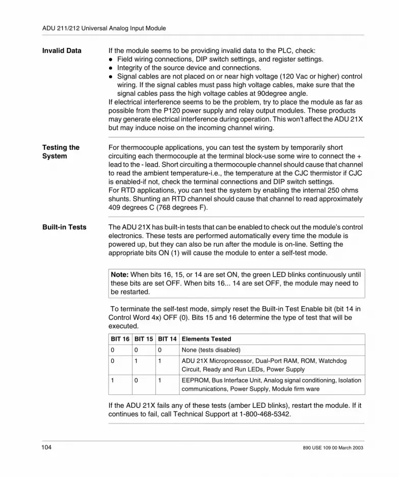
ADU 211/212 Universal Analog Input Module
Invalid Data If the module seems to be providing invalid data to the PLC, check: Field wiring connections, DIP switch settings, and register settings. Integrity of the source device and connections. Signal cables are not placed on or near high voltage (120 Vac or higher) control
wiring. If the signal cables must pass high voltage cables, make sure that the signal cables pass the high voltage cables at 90degree angle.
If electrical interference seems to be the problem, try to place the module as far as possible from the P120 power supply and relay output modules. These products may generate electrical interference during operation. This won’t affect the ADU 21X but may induce noise on the incoming channel wiring.
Testing the System
For thermocouple applications, you can test the system by temporarily short circuiting each thermocouple at the terminal block-use some wire to connect the + lead to the - lead. Short circuiting a thermocouple channel should cause that channel to read the ambient temperature-i.e., the temperature at the CJC thermistor if CJC is enabled-if not, check the terminal connections and DIP switch settings.For RTD applications, you can test the system by enabling the internal 250 ohms shunts. Shunting an RTD channel should cause that channel to read approximately 409 degrees C (768 degrees F).
Built-in Tests The ADU 21X has built-in tests that can be enabled to check out the module’s control electronics. These tests are performed automatically every time the module is powered up, but they can also be run after the module is on-line. Setting the appropriate bits ON (1) will cause the module to enter a self-test mode.
To terminate the self-test mode, simply reset the Built-in Test Enable bit (bit 14 in Control Word 4x) OFF (0). Bits 15 and 16 determine the type of test that will be executed.
If the ADU 21X fails any of these tests (amber LED blinks), restart the module. If it continues to fail, call Technical Support at 1-800-468-5342.
Note: When bits 16, 15, or 14 are set ON, the green LED blinks continuously until these bits are set OFF. When bits 16... 14 are set OFF, the module may need to be restarted.
BIT 16 BIT 15 BIT 14 Elements Tested
0 0 0 None (tests disabled)
0 1 1 ADU 21X Microprocessor, Dual-Port RAM, ROM, Watchdog Circuit, Ready and Run LEDs, Power Supply
1 0 1 EEPROM, Bus Interface Unit, Analog signal conditioning, Isolation communications, Power Supply, Module firm ware
104 890 USE 109 00 March 2003

ADU 211/212 Universal Analog Input Module
ADU 211/212 Universal Analog Input Module Specifications
Table of Specifications
The following table contains a list of ADU 211/212 specifications.
Module Topology Number of Inputs 8 (2 for RTD)
Number of Groups 2
Points/Group 4 (1 for RTD)
Isolation Channel-to-bus: 500 volts, 25 micro A max. leakage at 60 Hz. Channel-to-channel: +/- 30 Vdc max.
Required Loadable SW-IODR-001
Power Supplies Ext. Source Requirement
20-30 Vdc for the ADU 211: none for the ADU 212
Consumption 2.5 VA typical, 4.0 VA (167 mA at 24 Vdc nominal) maxi mum for the ADU 211
Power Dissipation 2.5 VA typical, 3.0 VA maxi mum for the ADU 212
Internal 5 V from PAB
less than 80 mA (TTL loading) for the ADU 211: 450 mA typical, 600 mA maximum for the ADU 212
DIN Rail Grounding less than 0.1 ohms
Input protection Analog multiplexer resident clamps and FETs
Input Impedance 10 M ohms typical
Signal Inputs Thermocouple
J: 0 to 760 degrees C (32 to 1400 degrees F)
K: 0 to 1000 degrees C (32 to 1832 degrees F)
T: -100 to 400 degrees C (-212 to 752 degrees F)
E: 0 to 1000 degrees C (32 to 1832 degrees F)
R: +500 to 1750 degrees C (932 to 3182 degrees F)
S: +500 to 1750 degrees C (932 to 3182 degrees F)
B: +500 to 1800 degrees C (932 to 3272 degrees F)
RTD 3- or 2/4-wire 100 ohms, 385 or 392 alpha
-200 to 800 degrees C
Voltage +/-50, 500, 2000, 5000, and 10,000 mVDC
Current 4-20 mA (12 bit)
+/- 20 mA (16-Bit and IEEE 754)
I/O Map Register 3x/4x 3 in/3 out
890 USE 109 00 March 2003 105

ADU 211/212 Universal Analog Input Module
Integer Resolution 1 part in 4096 counts (12-bit display) 1 part in +32767 to -32768 counts (16-bit)
IEEE754 FP resolution (engineering units)
Thermocouple: (use non-grounded type TCs)
0.7 degrees C or better
RTD: 0.15 degrees C or better
Voltage: 0.035 percent of full scale or better
Current: 0.035 percent of full scale or better
Accuracy Thermocouple at module with fixed 0 degrees C CJC
J: +/- 1.5 degrees C (2.7 degrees F)
K: +/- 2.0 degrees C (3.6 degrees F)
T: +/- 3.0 degrees C (5.4 degrees F)
E: +/- 1.2 degrees C (2.2 degrees F)
R: +/- 7.0 degrees C (12.5 degrees F)
S: +/- 7.0 degrees C (12.6 degrees F)
B: +/- 15.0 degrees C (27.0 degrees F)
RTD at module 100 ohms Platinum, 385 alpha: +/- 0.40 degrees C typical, +/- 1.0 degrees C maximum
100 ohms Platinum, 392 alpha: +/- 0.40 degrees C
Voltage at module 50 mVDC: +/- 0.40 percent of full scale
0.5, 2, 5 & 10 VDC: +/-0.11 percent of full scale
Current 4 to 20 mA: +/- 0.20 percent of full scale
+/- 20 mA: +/- 0.20 percent of full scale
Linearization Thermocouple: IPTS-68 Standard, NBS MN-125
RTD: JIS C 1604, DIN 43760 and IEC 751
Open Circuit Detect Thermocouple (external 22-47 M ohms resistors required for individual open circuit detection)
Cold Junction Compensation
10 k ohms internal or external thermistor or fixed value, +/-1.7 degrees C (3.1 degrees F) typical, +/-4.1 degrees C (7.4 degrees F) maximum accuracy
RTD Excitation 200 micro A typical
Signal Integration Time
2, 5, 33.3, 40, 50, 60, 100 and 200 msec (group selectable)
Single Channel Update Time
(Integration x 1.5) + 10.0 msec typical
106 890 USE 109 00 March 2003

ADU 211/212 Universal Analog Input Module
Common Mode Rejection
68 dB typical at 50 or 60 Hz with integration time set at greater than 100 msec
Calibration Automatic and continuous
Temperature Operating: 0 to 60 degrees C (32 to 140 degrees F)
Storage: -40 to 85 degrees C (-40 to 185 degrees F)
Relative Humidity 0 to 95 percent at 60 degrees C, non-condensing
Vibration 3 rotational axes 2G RMS, 10 to 57 Hz 15-minute scan (1 octave per minute)
Shock 30G for 11 msec, 1/2 sine, 3 orthogonal axes
Packaged Free Fall 3 feet (1 meter), 5 iterations each side
Cooling Free air convection
EMI Susceptibility 27 to 500 mHz 10 volt/meter (per subset IEC 801-3)
Fast Transient +/- 1.0 kV (per subset IEC 801-2)
Electrostatic discharge
8 kV, 10 discharges, no damage
Dimensions (W x H x D) 1.6 x 5.6 x 4.5 in. 40.3 x 145.0 x 117.5 mm
Weight 0.80 lb (360 g) max.
Power Connections 60/75 copper (Cu)
Torque 4.5 inch-pounds on set screws
Agency Approvals ADU 211 & ADU 212
UL 508; CSA 22.2 No.142; FM Class I, Div 2**; and European Directive EMC 89/336/EEC Standards
**This equipment is suitable for use in Class 1, Division 2, Groups A, B, C, and D, or non-hazardous locations only.
WARNING
Substitution Warning
Substitution of components may impair suitability for Class 1, Division 2.
Failure to follow this precaution can result in death, serious injury, or equipment damage.
890 USE 109 00 March 2003 107

ADU 211/212 Universal Analog Input Module
108 890 USE 109 00 March 2003

890 USE 109 00 March 2003
ADU 214 Analog Input Module
At a Glance
Purpose This Chapter gives an overview of the ADU 214 Analog Input Module. This is followed by the physical characteristics of the module; installation and configuration procedures; and, lastly, the specifications of the ADU 214 Module.
What’s in this Chapter?
This chapter contains the following topics:
WARNING
Operative Failure Alert
The ADU 214 module will only operate properly when used with an A984, E984, or Micro 512/612 controller.
Failure to follow this precaution can result in death, serious injury, or equipment damage.
Note: Some A120 I/O modules (DEP 211/214/215/217, DAP211/217, ADU204/211/214/216, DAU204, VIC2xx, and MOT20x) require a loadable (SW-IODR-001) for proper operation when using certain PLCs (A984-1xx, E984-24x/251/255) with Modsoft.
Topic Page
Overview of the ADU 214 Analog Input Module 110
Conversion Values 113
Configuration - Concept 123
Installation 130
ADU 214 Input Module Specifications 133
109

ADU 214 Analog Input Module
Overview of the ADU 214 Analog Input Module
Physical Characteristics
The ADU 214 module is used for measuring analog data, and provides up to 8 non-isolated inputs. The main characteristics of the module follow.Tip: This module is suitable for use on Compact 984 with memory size of 4K or more. Four 4-wire analog inputs. These inputs can be used for 2-wire measurement,
thus allowing up to 8 unipolar inputs, 4 bipolar voltage inputs, or combinations of both.
Several measuring ranges that may be individually selected and mixed for each input:
The following Measuring Ranges apply to the ADU 214 Analog Input Module.
The PLC model determines the available ranges. Refer to the tables in this chapter.
Voltage measurement 0 ... 0.5, 0 ... 1, 0 ... 5, 0 ... 10 V, 0.1 ... 0.5, 0.2 ... 1, 1 ... 5, 2 ... 10 V, 0.5, 1, 5, 10 V
Current measurement (External precision resistor required)
0 ... 5, 0 ... 10, 0 ... 20 mA, 1 ... 5, 2 ... 10, 4 ... 20 mA, 5, 10, 20 mA
RTD Temperature measurement -160/-60 ... +160 degrees C (resolution ≤ 0.02 degrees C) -200 ... +320 degrees C (resolution ≤ 0.04 degrees C) -200 ... +640 degrees C (resolution ≤ 0.08 degrees C)
Resistance measurement 0 ... 100, 0 ... 200, 0 ... 500 Ω,, 0 ... 1000, 0 ... 2000 Ω
Note: Only the 15 Bit + sign resolution is supported when using the E984-258/265/275/285 PLC models. The 12, 13 and 15 Bit + sign resolutions are all supported when using the A984-1xx, E984-24x/251/255 PLC models.
110 890 USE 109 00 March 2003

ADU 214 Analog Input Module
The following illustration is of the Front View and Label of the ADU 214 Module
Broken wire testing of all 4-wire lines and self-calibration using built-in reference resistances and reference voltages
Measuring ranges for voltage, current, temperature, and resistance can be set individually for each input
Switch-selectable 50 ... 60 Hz operation noise suppression
ADU 214ADU 214
123456789
1011
1213141516171819202122
1234567891011
1213141516171819202122
UU
UU
M
readyM
card
2
4
6
8
12
2134
43
56
6578
87
890 USE 109 00 March 2003 111

ADU 214 Analog Input Module
Simplified Schematic
The following is a simplified schematic for the ADU 214 Module.
LEDS The ADU 214 has two front panel LEDs: One green LED opposite Terminal 1 indicating the module is receiving 24 V
power One green LED opposite Terminal 12 indicating the module’s processor is
running
24 VDC
1,2
3,4
5,6
7,8
COMM
AGND
GN “U”
+15 V
-15 V
0 V
GN “Ready”
System Bus
0 V
2 of 8 Input Circuits -15V+15V
MUX +15V
REF
A/D
+ 5V
123456789
1011
1213141516171819202122
112 890 USE 109 00 March 2003
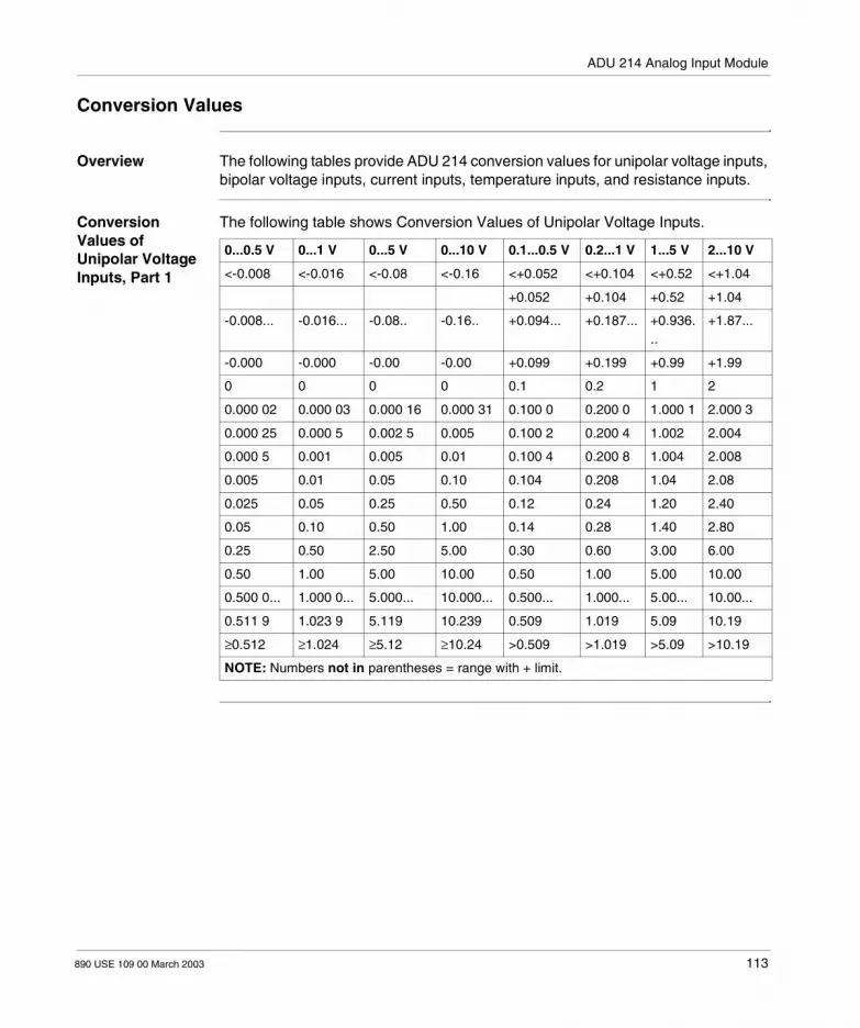
ADU 214 Analog Input Module
Conversion Values
Overview The following tables provide ADU 214 conversion values for unipolar voltage inputs, bipolar voltage inputs, current inputs, temperature inputs, and resistance inputs.
Conversion Values of Unipolar Voltage Inputs, Part 1
The following table shows Conversion Values of Unipolar Voltage Inputs.
0...0.5 V 0...1 V 0...5 V 0...10 V 0.1...0.5 V 0.2...1 V 1...5 V 2...10 V
<-0.008 <-0.016 <-0.08 <-0.16 <+0.052 <+0.104 <+0.52 <+1.04
+0.052 +0.104 +0.52 +1.04
-0.008... -0.016... -0.08.. -0.16.. +0.094... +0.187... +0.936...
+1.87...
-0.000 -0.000 -0.00 -0.00 +0.099 +0.199 +0.99 +1.99
0 0 0 0 0.1 0.2 1 2
0.000 02 0.000 03 0.000 16 0.000 31 0.100 0 0.200 0 1.000 1 2.000 3
0.000 25 0.000 5 0.002 5 0.005 0.100 2 0.200 4 1.002 2.004
0.000 5 0.001 0.005 0.01 0.100 4 0.200 8 1.004 2.008
0.005 0.01 0.05 0.10 0.104 0.208 1.04 2.08
0.025 0.05 0.25 0.50 0.12 0.24 1.20 2.40
0.05 0.10 0.50 1.00 0.14 0.28 1.40 2.80
0.25 0.50 2.50 5.00 0.30 0.60 3.00 6.00
0.50 1.00 5.00 10.00 0.50 1.00 5.00 10.00
0.500 0... 1.000 0... 5.000... 10.000... 0.500... 1.000... 5.00... 10.00...
0.511 9 1.023 9 5.119 10.239 0.509 1.019 5.09 10.19
≥0.512 ≥1.024 ≥5.12 ≥10.24 >0.509 >1.019 >5.09 >10.19
NOTE: Numbers not in parentheses = range with + limit.
890 USE 109 00 March 2003 113

ADU 214 Analog Input Module
Conversion Values of Unipolar Voltage Inputs, Part 2
Conversion Values of Unipolar Voltage Inputs continue in the following table.
15-BIT 13-BIT 12-BIT NOTES
-32,767 underflow error
0 (-3,840)0 (-512)0 (-1)
overload range
0+1+16+32+320+1 600+3 200+16 000+32 000
4096
8096
2048
4048
rated value
Linear Range
rated value
+32 001...+32 766 overload range
+32 767 8191 4095 overflow error
NOTE: Numbers in parentheses = range with ± limit.
114 890 USE 109 00 March 2003

ADU 214 Analog Input Module
Conversion Values of Bipolar Voltage Inputs, Part 1
The following table shows Conversion Values of Bipolar Voltage Inputs:
0.5 V 1 V 5 V 10 V
≤–0.512 ≤–1.024 ≤–5.12 ≤–10.24
–0.511 9 ... –1.023 ... –5.119 ... –10.239 ...
–0.500 0 –1.000 –5.000 –10.000
–0.50 –1.00 –5.00 –10.00
–0.25 –0.50 –2.50 –5.00
–0.05 –0.10 –0.50 –1.00
–0.025 –0.05 –0.25 –0.50
–0.005 –0.01 –0.05 –0.10
–0.000 5 –0.001 –0.005 –0.01
–0.000 25 –0.000 5 –0.002 5 –0.005
0 0 0 0
+0.000 02 +0.000 03 +0.000 16 +0.000 31
+0.000 25 +0.000 5 +0.002 5 +0.005
+0.000 5 +0.001 +0.005 +0.01
+0.005 +0.01 +0.05 +0.10
+0.025 +0.05 +0.25 +0.50
+0.05 +0.10 +0.50 +1.00
+0.25 +0.50 +2.50 +5.00
+0.50 +1.00 +5.00 +10.00
+0.500 0 ... +1.000 0 ... +5.000 ... +10.000 ...
+0.511 9 +1.023 9 +5.119 +10.239
≥+0.512 ≥+1.024 ≥+5.12 ≥+10.24
890 USE 109 00 March 2003 115

ADU 214 Analog Input Module
Conversion Values of Bipolar Voltage Inputs, Part 2
Conversion Values of Bipolar Voltage Inputs continue in the following table:
*15-BIT 13-BIT 12-BIT NOTES
–32 767 underflow error
-32 766 overload range
-32 001
-32 000 96 48 rated value
-16 000
-3 200
-1 600
-320
-32
-16
0 4096 2048 Linear Range
+1
+16
+32
+320
+1 600
+3 200
+16 000
+32 000 8096 4048 rated value
+32 001 ...
+32 766 overload range
+32 767 8191 4095 overflow error
Note: *Only the 15 Bit + sign resolution is supported when using the E984–258/265/275/285 PLC models. The 12, 13, and 15 Bit + sign resolutions are supported when using the A984–1xx, E984--24x/251/255 PLC models.
116 890 USE 109 00 March 2003

ADU 214 Analog Input Module
Conversion Values of Current Inputs, Part 1
The following table shows Conversion Values of Current Inputs:
0...10 mA 0...20 mA 2...10 mA 4...20 mA 20 mA
<–0.16 <–0.32 <+1.04 <+2.08 ≤–20.479
–20.478 ...
–20.000
+1.04 ... +2.08 ...
–0.16... –0.32... +1.87 ... +3.74 ...
–0.00 –0.00 +1.99 +3.99
–20.00
–10.00
–2.00
–1.00
–0.20
–0.02
–0.01
0 0 +2 +4 0
+0.005 +0.01 +2.004 +4.008 +0.01
+0.01 +0.02 +2.008 +4.016 +0.02
+0.1 +0.20 +2.08 +4.16 +0.20
+0.5 +1.00 +2.40 +4.80 +1.00
+1 +2.00 +2.80 +5.60 +2.00
+5 +10.00 +6.00 +12.00 +10.00
+10.0 +20.00 +10.00 +20.00 +20.00
+10.000... +20.000... +10.00... +20.00... +20.000...
+10.239 +20.478 +10.19 +20.38 +20.478
≥+10.24 ≥+20.479 >+10.19 >+20.38 ≥+20.479
890 USE 109 00 March 2003 117

ADU 214 Analog Input Module
Conversion Values of Current Inputs, Part 2
Conversion Values of Current Inputs continue in the following table:
*15-BIT 13-BIT 12-BIT NOTES
–32 767 underflow error
-32 766-32 0010 (-3 840)0 (-512)0 (-1)
overload range
-32 000 96 48 rated value
-16 000
-3 200
-1 600
-320
-32
-16
0 4096 2048 Linear Range
+1
+16
+32
+320
+1 600
+3 200
+16 000
+32 000 8096 4048 rated value
+32 001 ...
+32 766 overload range
+32 767 8191 4095 overflow error
NOTE: Numbers in parentheses = range with ± limit
Note: *Only the 15 Bit + sign resolution is supported when using the E984–258/265/275/285 PLC models. The 12, 13, and 15 Bit + sign resolutions are supported when using the A984–1xx, E984--24x/251/255 PLC models.
118 890 USE 109 00 March 2003

ADU 214 Analog Input Module
Conversion Values of Temperature Inputs, Part 1
The following table shows Conversion Values of Temperature Inputs:
-60 ... +160°C -160 ... +160°C -200 ... +320°C -200 ... +640°C
<–60 <–160 <–200 <–200
–160
–100 –200
–60 –60 –120
–50 –50 –100 –200
–16 –16 –32 –64
0 0 0 0
+0.005 +0.005 +0.01 +0.02
+0.08 +0.08 +0.16 +0.32
+0.16 +0.16 +0.32 +0.64
+8 +8 +16 +32
+16 +16 +32 +64
+80 +80 +160 +320
+160 +160 +320 +640
+160.005 ... +160.005 ... +320.01 ... +640.02 ...
+163.83 +163.83 +327.66 +655.32
≥+163.84 ≥+163.84 ≥+327.67 ≥+655.34
890 USE 109 00 March 2003 119

ADU 214 Analog Input Module
Conversion Values of Temperature Inputs, Part 2
Conversion Values of Temperature Inputs continue in the following table:
*15-BIT 13-BIT 12-BIT NOTES
–32 767 measuring range underflow (error)
-32 000 96 48 rated value
-22 000
-12 000
-10 000
-3 200
0 4096 2048 Linear Range
+1
+16
+32
+320
+1 600
+3 200
+16 000
+32 000 8096 4048 rated value
+32 001 ...
+32 766 overload range
+32 767 8191 4095 measuring range overflow error
Note: *Only the 15 Bit + sign resolution is supported when using the E984–258/265/275/285 PLC models. The 12, 13, and 15 Bit + sign resolutions are supported when using the A984–1xx, E984--24x/251/255 PLC models.
120 890 USE 109 00 March 2003

ADU 214 Analog Input Module
Conversion Values of Resistance Inputs, Part 1
The following table shows Conversion Values of Resistance Inputs:
0...100Ω 0...200Ω 0...500Ω 0...1000Ω 0...2000Ω
<–1.6 <–3.2 <–8 <–16 <–32
0...–1.6 0...–3.2 0...–8 0...–16 0...–32
0 0 0 0 0
0.003 0.006 0.015 0.03 0.06
0.05 0.1 0.25 0.5 1
0.1 0.2 0.5 1 2
1 2 5 10 20
5 10 25 50 100
10 20 50 100 200
50 100 250 500 1000
100 200 500 1000 2000
100.00 ... 200.00 ... 500.01 ... 1000.03 ... 2000.06 ...
102.39 204.78 511.97 1023.94 2047.88
≥102.40 ≥204.79 ≥511.98 ≥1023.97 ≥2047.94
890 USE 109 00 March 2003 121

ADU 214 Analog Input Module
Conversion Values of Resistance Inputs, Part 2
Conversion Values of Resistance Inputs continue in the following table:
*15-BIT 13-BIT 12-BIT NOTES
–32 767 underflow error
0 overload range
0 4096 2048 rated value
+1
+16
+32
+320
+1 600 linear range
+3 200
+16 000
+32 000 8096 4048 rated value
+32 001 ...
+32 766 overload range
+32 767 8191 4095 overflow error
NOTE: Numbers in parentheses = range with ± limit.
Note: *Only the 15 Bit + sign resolution is supported when using the E984–258/265/275/285 PLC models. The 12, 13, and 15 Bit + sign resolutions are supported when using the A984–1xx, E984--24x/251/255 PLC models.
122 890 USE 109 00 March 2003

ADU 214 Analog Input Module
Configuration - Concept
Configured Registers - Modsoft
The ADU 214 module requires two sequental 4X command registers and 3 sequental 3X status registers all Traffic Copped as BIN. Selecting a channel number higher than 8, or one already included in a channel pair measurement, will result in an ILLEGAL 4X COMMAND" bit to be set in the 3X register response.The following table shows Configured Registers for the ADU 214 Module.
4X output register commands, and resultant 3X register formats are: For unipolar measurements, select Channel 1 ... 8 and enter decimal 1 ... 28 for
the configuration code in register 4x + 1. For bipolar measurements, channel pairs are wired on the field connector, and
are also configured in pairs. Either channel of the pair may be selected. For these measurements, the even channel must be used in the 4x read command. The odd channel will be indicated not active or not valid in the 3x status register, and will display zero in its data register. For example, channel pairs are 1/2, 3/4, 5/6, and 7/8. To configure the top input for bipolar operation, select either 1 or 2 for the x value in the 50x command, and enter decimal 33 to 36 for the configuration code in register 4x + 1.
For RTD or resistance measurements, channel pairs are wired on the field connector and are also configured in pairs. Either channel of the pair may be selected. For these measurements, the even channel must be used in the 4x read command. The odd channel will be indicated not active or valid in the 3x status register, and will display zero in its data register. For example, channel pairs are 1/2, 3/4, 5/6, and 7/8. To configure the top input for these measurements, select either 1 or 2 for the x value in the 50x command, and enter decimal 64 ... 95 (RTD) or 96 ... 116 (Ω) for the configuration code in register 4x + 1.
If backplane or field power is lost, the module must be reconfigured.
Registers Contents
4x 50x Decimal, with x = Channel 1 ... 8
4x + 1 Configuration Command (Refer to Register Configuration Commands - Modes - Modsoft, p. 124)
3x Configure Command Response (see Invalid Commands - Modsoft, p. 127
3x ,+ 1 0
3x + 2 0
890 USE 109 00 March 2003 123
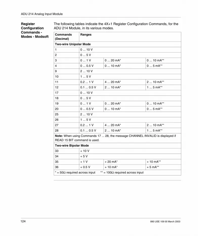
ADU 214 Analog Input Module
Register Configuration Commands - Modes - Modsoft
The following tables indicate the 4X+1 Register Configuration Commands, for the ADU 214 Module, in its various modes.
Commands (Decimal)
Ranges
Two-wire Unipolar Mode
1 0 ... 10 V
2 0 ... 5 V
3 0 ... 1 V 0 ... 20 mA* 0 ... 10 mA**
4 0 ... 0.5 V 0 ... 10 mA* 0 ... 5 mA**
9 2 ... 10 V
10 1 ... 5 V
11 0.2 ... 1 V 4 ... 20 mA* 2 ... 10 mA**
12 0.1 ... 0.5 V 2 ... 10 mA* 1 ... 5 mA**
17 0 ... 10 V
18 0 ... 5 V
19 0 ... 1 V 0 ... 20 mA* 0 ... 10 mA**
20 0 ... 0.5 V 0 ... 10 mA* 0 ... 5 mA**
25 2 ... 10 V
26 1 ... 5 V
27 0.2 ... 1 V 4 ... 20 mA* 2 ... 10 mA**
28 0.1 ... 0.5 V 2 ... 10 mA* 1 ... 5 mA**
Note: When using Commands 17 ... 28, the message CHANNEL INVALID is displayed if READ 15 BIT command is used.
Two-wire Bipolar Mode
33 + 10 V
34 + 5 V
35 + 1 V + 20 mA* + 10 mA**
36 + 0.5 V + 10 mA* + 5 mA**
* = 50Ω required across input ** = 100Ω required across input
124 890 USE 109 00 March 2003

ADU 214 Analog Input Module
Register Configuration Commands - Detectors - Modsoft
The table below gives Register Configuration Commands for the ADU 214 Module, by Four-Wire Temperature Detector.
Register Configuration Commands follow, for Two- and Three-wire Temperature detector - with wire compensation (10 Ω)
Four-wire Temperature detector
64 -60 ... +160 ο C with Ni 100
65 -160 ... +160 ο C with Pt 100
66 -200 ... +320 ο C with Pt 100
67 -200 ... +640 ο C with Pt 100
68 -60 ... +160 ο C with Ni 200
69 -169 ... +160 ο C with Pt 200
70 -200 ... +320 ο C with Pt 200
71 -200 ... +640 ο C with Pt 200
72 -60 ... +160 ο C with Ni 500
73 -160 ... +160 ο C with Pt 500
74 -200 ... +320 ο C with Pt 500
75 -200 ... +640 ο C with Pt 500
76 -60 ... +160 ο C with Ni 1000
77 -160 ... +160 ο C with Pt 1000
78 -200 ... +320 ο C with Pt 1000
79 -200 ... +640 ο C with Pt 1000
80 -60 ... +160 ο C with Ni 100
81 -160 ... +160 ο C with Pt 100
82 -200 ... +320 ο C with Pt 100
83 -200 ... +640 ο C with Pt 100
84 -60 ... +160 ο C with Ni 200
85 -160 ... +160 ο C with Pt 200
86 -200 ... +320 ο C with Pt 200
87 -200 ... +640 ο C with Pt 200
88 -60 ... +160 ο C with Ni 500
89 -160 ... +160 ο C with Pt 500
90 -200 ... +320 ο C with Pt 500
91 -200 ... +640 ο C with Pt 500
92 -60 ... +160 ο C with Ni 1000
93 -60 ... +160 ο C with Ni 100
890 USE 109 00 March 2003 125

ADU 214 Analog Input Module
Register Configuration Commands - Resistance Measuring - Modsoft
The following table provides Register Configuration Commands for the ADU 214 Module, by form of resistance measuring.
Register Configuration Commands - Read Values - Modsoft
The following table addresses Read Configuration Values for the ADU 214 Module.
Read Values Table appears next.
94 -200 ... +320 ο C with Pt 1000
95 -200 ... +640 ο C with Pt 1000
80 -60 ... +160 ο C with Ni 100
Four-wire Resistance measuring
96 0 ... 500 Ω
97 0 ... 500 Ω
98 0 ... 500 Ω
99 0 ... 1000 Ω
100 0 ... 2000 Ω
Two-wire Resistance measuring with wire compensation (10 Ω)
112 0 ... 100 Ω
113 0 ... 200 Ω
114 0 ... 500 Ω
115 0 ... 1000 Ω
116 0 ... 2000 Ω
Read Configuration
4X 4YX Decimal, with Y and X = Channels to be read (1 ... 8)
4X+1 Not used
3X Configure Command Response (Refer to Invalid Commands - Modsoft, p. 127)
3X+1 Channel X Configuration
3X+2 Channel Y Configuration
Read 12-bit Value
4X 4YX Decimal, with Y and X = Channels to be read (1 ... 8)
4X+1 Not used
3X Configure Command Response (Refer to Invalid Commands - Modsoft, p. 127)
3X+1 Channel X Measurement
3X+2 Channel Y Measurement
126 890 USE 109 00 March 2003

ADU 214 Analog Input Module
The Read Module Status table for the ADU 214 follows.
Invalid Commands - Modsoft
Invalid 4X register commands, and valid commands other than "READ MODULE STATUS" - that are issued when the module is not ready - result in the responses described below.The following is a table of invalid commands, for the ADU 214 Module.
Read 13-bit Value
4X 2YX Decimal, with Y and X = Channels to be read (1 ... 8)
4X+1 Not used
3X Measure Command Response (Refer to Invalid Commands - Modsoft, p. 127)
3X+1 Channel X Measurement
3X+2 Channel Y Measurement
Read 15-bit Value
4X 3YX Decimal, with Y and X = Channels to be read (1 ... 8)
4X+1 Not used
3X Measure Command Response (Refer to Invalid Commands - Modsoft, p. 127)
3X+1 Channel X Measurement
3X+2 Channel Y Measurement
Read Module Status
4X 000 Decimal
4X+1 Not used
3X Configure Command Response (Refer to Invalid Commands - Modsoft, p. 127)
3X+1 0
3X+2 0
Invalid Commands
3X General Status (Bits 9 - 16 only, Bits 1 - 8 = 0); refer to Invalid Commands - Modsoft, p. 127
3X+1 0
3X+2 0
890 USE 109 00 March 2003 127

ADU 214 Analog Input Module
The following figure represents the 3x Status Register.
The following illustration is the Configure Command Response for the ADU 214 Analog Module.
16 15 14 13 12 11 10 9 8 7 6 5 4 3 2 1
CONFIGURE OR MEASURECOMMAND RESPONSE*
1 = I/O Mapped Registers Not BIN1 = Illegal 4X+1 Configuration Command
1 = Module Not Active
1 = Module Not Installed
Not Used, Always Zero
Not Used, Always Zero
Not Used, Always Zero
1 = Illegal 4X+1 Command
* Refer to Figure 43 or 44
8 7 6 5 4 3 2 1
1 = Channel 1 Active
1 = Channel 2 Active
1 = Channel 3 Active
1 = Channel 4 Active
1 = Channel 5 Active
1 = Channel 6 Active
1 = Channel 7 Active
1 = Channel 8 Active
128 890 USE 109 00 March 2003

ADU 214 Analog Input Module
Next is the MEASURE COMMAND Response.
The following figure is the Data Input Register Structure for the ADU 214 Analog Module.
8 7 6 5 4 3 2 1
1 = 3X+1 Channel Overflow
1 = 3X+1 Channel Invalid
1 = 3X+2 Channel Overflow
1 = 3X+2 Channel Invalid
Not Used, Always 0
Not Used, Always 0
Not Used, Always 0
Not Used, Always 0
* For inactive channels: Overflow = 0, Invalid = 1
16 15 14 13 12 11 10 9 8 7 6 5 4 3 2 1
3x + 1 Data Input Register
3x + 2 Data Input Register
890 USE 109 00 March 2003 129
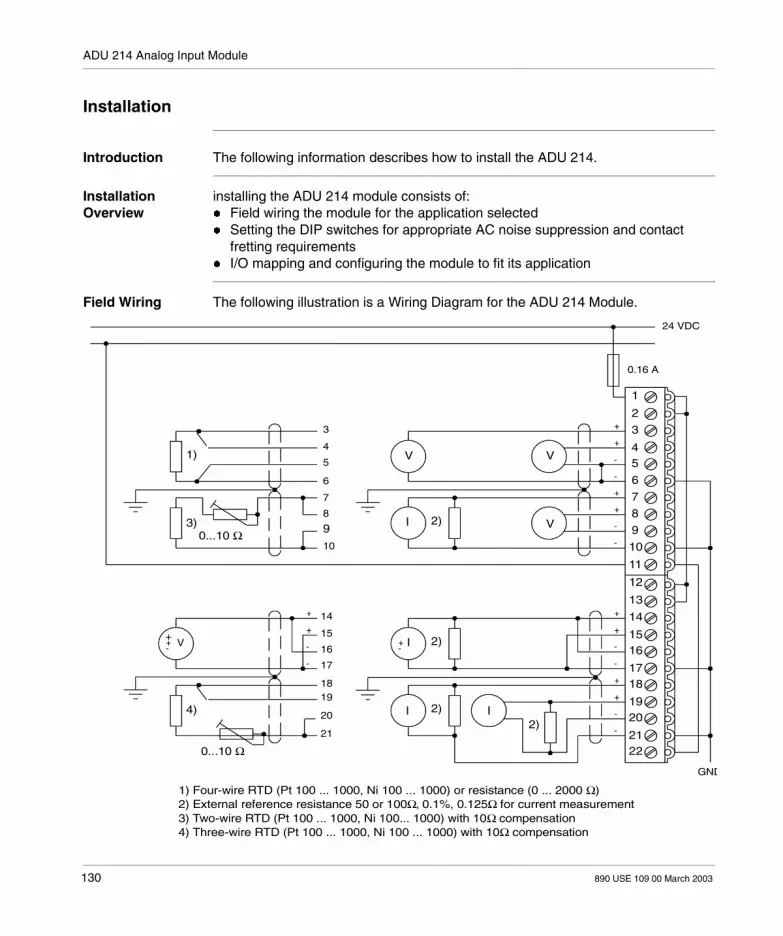
ADU 214 Analog Input Module
Installation
Introduction The following information describes how to install the ADU 214.
Installation Overview
installing the ADU 214 module consists of: Field wiring the module for the application selected Setting the DIP switches for appropriate AC noise suppression and contact
fretting requirements I/O mapping and configuring the module to fit its application
Field Wiring The following illustration is a Wiring Diagram for the ADU 214 Module.
1)
3) 2)
4)
0...10 Ω
V V
VI
I
I I2)
2)
2)+V
0...10 Ω
14
15
16
17
1819
20
21
GND
24 VDC
0.16 A
3
4
5
6
7
8
9
10
1
2
3
45
6
7
8
9
10
11
12
13
14
1516
1718
1920
2122
1) Four-wire RTD (Pt 100 ... 1000, Ni 100 ... 1000) or resistance (0 ... 2000 Ω)2) External reference resistance 50 or 100Ω, 0.1%, 0.125Ω for current measurement3) Two-wire RTD (Pt 100 ... 1000, Ni 100... 1000) with 10Ω compensation4) Three-wire RTD (Pt 100 ... 1000, Ni 100 ... 1000) with 10Ω compensation
130 890 USE 109 00 March 2003

ADU 214 Analog Input Module
Calibrating the Channel for RTD Configurations Procedure
To calibrate the channel for the RTD configurations with 10 Ω compensation.
Note: For general wiring and set-up instructions, refer to the 984-A120 Compact Programmable Controllers User Guide (GM-A984-PCS). Foil-shielded cables (2 or 4 x 0.5 mm twisted pair per channel) must be used for
connections. All channels can be run within one joint shielded cable. If RTD detectors are connected with 4 wires (e.g., Ni 100, Pt 100), conductors
for current and voltage path must be twisted in pairs. The connections between the shield and ground must be as short as possible
(<20 cm) at one end. If higher noise levels exist, the cable shield must be grounded at both ends.
The cable must be kept a minimum distance of >0.5 m away from power lines or similar sources of electrical interference.
When using two- or three-wire RTD configurations, the ADU 214 requires an external adjustable 10 Ω series resistor in the RTD loop. This compensates for the unknown lead resistance, since the normal compensatory lead pair is missing. To calibrate the channel for the RTD configurations with 10 Ω compensation (configuration commands 80-95 decimal), perform the steps in the following procedure.
Note: Refer to Configuration - Concept, p. 123 for information on how to select the two- or three-wire RTD operating mode.
Step Action
1 Set up the RTD loop with the adjustable 10 Ω in the circuit and short the end of the wire run.
2 Configure the appropriate ADU 214 channel for 0-100 Ω input (configuration command decimal 96).
3 Adjust the 10 Ω potentiometer for a channel input reading of 3200 in the 15-bit mode-i.e., read 15 BIT VALUE, or the 4x Function Code Register = 3YX.
890 USE 109 00 March 2003 131

ADU 214 Analog Input Module
Accuracy Errors For PT100 measurements, if lead resistance is known to be less than 1 Ω, the uncompensated 4-wire configuration commands 64 ... 79 may be used and the 10 Ω adjustable resistor left out of the circuit. No calibration is required, but the accuracy errors listed in the following table can be expected.Accuracy Errors
DIP Switch Settings
The following illustration shows the locations of the DIP Switches.
Noise Suppression (DIP Switch B1)
The ADU 216 provides suppression of ac power frequencies on the peripheral lines. The module is shipped with 50 Hz suppression, and can be switched to 60 Hz suppression with DIP switch B1.
Fretting (DIP Switch B2)
Fretting prevents an increase of contact resistance on peripheral connections. Fretting is accomplished by outputting 10 V across the contacts at defined time intervals. The resulting current (flowing for 1 ms) is limited to < 8 mA. The contacts of the active inputs are fretted cyclically every 30 min. The fretting process is selected with DIP switch B2.
Lead Resistance Error
1.0 Ω +2.605 C
0.10 Ω +0.255 C
0.01 Ω +0.0255 C
B2B1
OFF ONB1 50 Hz noise suppression (as shipped)
B1 60 Hz noise suppression
B2 Fretting switched on (as shipped)
B2 Fretting switched off
132 890 USE 109 00 March 2003

ADU 214 Analog Input Module
ADU 214 Input Module Specifications
Specifications The following information describes the ADU 214 Input Module specifications.The following table provides ADU 214 Specifications for: Power Supply; Required Loadable; Inputs; and I/O Map.
Power Supply
External Supply 24 Vdc typical 70 mA, maximum 150 mA
Internal Power Supply (via system bus)
5 Vdc typical 45 mA, maximum 100 mA
Power Dissipation 2 Ω typical, maximum 3 Ω
Required Loadable
SW-IODR-001 (See Requirements for CE Compliance, p. 779)
Inputs Number 4 Inputs (4-pole/2-pole) temperature/resistance 4 Inputs, two-wire current/voltage bipolar or 8 Inputs, two-wire current/voltage unipolar; inputs may be mixed
Potential Isolation Non-isolated, channel-to-channel
I/O Map Register 3x/4x 3 in/2 out
890 USE 109 00 March 2003 133

ADU 214 Analog Input Module
The following table shows the Voltage Measurements for the ADU 214 Module.
Voltage Measurement
Input Impedance >1 M Ω
Unipolar Measuring Ranges
0 ... 0.5 V, 0 ... 1 V, 0 ... 5 V, 0 ... 10 V, 0.1 ... 0.5 V, 0.2 ... 1 V, 1 ... 5 V, 2 ... 10 V
Bipolar Measuring Ranges
+0.5 V, +1 V, +5 V, +10 V
Resolution approx. 0.003% of final value, 15-bit plus sign
Measuring Fault at 25°C
For measuring ranges 0.5 V / 1 V
±0.02% of Measuring Range Final Value (MFV), ±0.15% of Measured Value (MV)
For measuring ranges 5 V/10 V
±0.01% of MFV, ±0.02% of MV
Measuring Fault at 0 ... 60°C
For measuring ranges 0.5 V/1 V
±0.10% of MFV, ±0.35% of MV
For measuring ranges 5 V/10 V
±0.02% of MFV, ±0.11% of MV
Typical Measuring Error
≤0.5 above maximal errors
Inphase Voltage Range (Differential input for voltage measuring) Voltage of each input against GND
≤+11 V
In-phase suppression ≥60 dB
Maximum Overvoltage Static (1 Input for each module)
+30 V (24V power supply ON) +20 V (24V power supply OFF)
Maximum Overvoltage Dynamic
+50 V for ≤100 ms
134 890 USE 109 00 March 2003
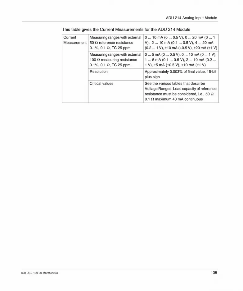
ADU 214 Analog Input Module
This table gives the Current Measurements for the ADU 214 Module
Current Measurement
Measuring ranges with external 50 Ω reference resistance 0.1%, 0.1 Ω, TC 25 ppm
0 ... 10 mA (0 ... 0.5 V), 0 ... 20 mA (0 ... 1 V), 2 ... 10 mA (0.1 ... 0.5 V), 4 ... 20 mA (0.2 ... 1 V), ±10 mA (+0.5 V), ±20 mA (±1 V)
Measuring ranges with external 100 Ω measuring resistance 0.1%, 0.1 Ω, TC 25 ppm
0 ... 5 mA (0 ... 0.5 V), 0 ... 10 mA (0 ... 1 V), 1 ... 5 mA (0.1 ... 0.5 V), 2 ... 10 mA (0.2 ... 1 V), ±5 mA (±0.5 V), ±10 mA (±1 V)
Resolution Approximately 0.003% of final value, 15-bit plus sign
Critical values See the various tables that descirbe Voltage Ranges. Load capacity of reference resistance must be considered, i.e., 50 Ω 0.1 Ω maximum 40 mA continuous
890 USE 109 00 March 2003 135

ADU 214 Analog Input Module
The following table describes Temperature Measurement for the ADU 214 Module
Temperature Measurement (RTD 4-wire wire)
Input impedance
>1 M Ω
Resolution < 0.012% of Final Value ≥ 13 Bit + sign
Measuring ranges with Pt 100 Pt 200, Pt 500, Pt 1000
-160 ... +160°C, resolution ≤0.02°C -200 ... +320°C, resolution ≤0.04°C -200 ... +640°C, resolution ≤0.08°C
Measuring ranges with Ni 100 Ni 200, Ni 500, Ni 1000
Measuring Fault at 25°C (excluding inaccuracy of detector) for measuring ranges -60 / -160 ... +160°C
with Pt 100 ... Pt 1000 ±0.35°C (= ±0.22 % of Measuring Range Final Value MFV)
with Ni 100 ... Ni 1000 for measuring range -200 ... +320°C
±0.3°C (= ±0.2 % of MFV)
with Pt 100 ... Pt 1000 for measuring range -200 ... +640°C
±0.5°C (= ±0.16 % of MFV)
with Pt 100 ... Pt1000 ±0.8°C (= ±0.13% of MFV)
Measuring Fault at 0 ... 60°C for measuring ranges -60 / -160 ... +160°C
with Pt 100, Ni 100 ±0.8°C (= ±0.5 % of MFV)
with Pt 200, Pt 500, Pt 1000
±0.65°C (= ±0.4 % of MFV)
with Ni 200 ±0.5°C (= ±0.32 % of MFV)
with Ni 500, Ni 1000 ±0.45°C (= ±0.3 % of MFV)
Measuring Fault at 0 ... 60°C for measuring range -200 ... +320°C
with Pt 100 ±1.1°C (= ±0.35 % of MFV)
with Pt 200 ±0.95°C (= ±0.3 % of MFV)
with Pt 500, Pt 1000 ±0.9°C (= ±0.28 % of MFV)
Measuring Fault at 0 ... 60°C for measuring range -200 ... +640°C
with Pt 100 ±1.6°C (= ±0.25 % of MFV)
with Pt 200 ±1.5°C (= ±0.23 % of MFV)
with Pt 500, Pt 1000 ±1.4°C (= ±0.22 % of MFV)
136 890 USE 109 00 March 2003

ADU 214 Analog Input Module
The following table displays Resistance Measurement (4-wire wire), for the ADU 214 Module.
The following table addresses various aspects of the ADU 214 Module: Input Characteristics; Connections; Weight; and Agency Approvals.
Resistance Measurement (4-wire wire)
Input Impedance >1 M Ω
Measuring Ranges 0 ... 100 Ω, 0 ... 200 Ω, 0 ... 500 Ω, 0 ... 1000 Ω, 0 ... 2000 Ω
Resolution ≤ 0.005% of final value, >14 Bit
Measuring Fault at 25°C for measuring range 100 ... 2000 Ω
±0.1% of Measuring Range Final Value (MFV)
Measuring Fault at 0 ... 60°C
for measuring range100 Ω
±0.30% of MFV
for measuring range200 Ω
±0.25% of MFV
for measuring range 500...2000 Ω
±0.20% of MFV
Constant current Approx. 1.5 mA for measuring range 0 ... 2000 Ω; approx. 2.5 mA for measuring ranges 0 ... 100 Ω, 0 ... 200 Ω, 0 ... 500 Ω 0 ... 1000 Ω
Dynamic Characteristics of Inputs
Conversion time for all 8 inputs 300 ms max
Input Delay Time constant for HF suppression
0.12 ms, typ
Measurement Integration Time 20 or 16.66 ms switchable
Selectable AC Power Interference Suppression for f = n x 50/ 60 Hz
n = 1, 2 ...push-pull interferences>60 dB (peak value of interference voltage and measuring voltage ≤ final value x 1.1)
Connections 4-wire Cable Length max. 50 m for voltage detector
2-wire Cable Length max. 100 m for voltage detector
4-wire Line Resistance max. 25 Ω for each conductor
4-wire Line Capacitance max. 10 nF for each conductor
Weight .5lb (.22kg)
Agency Approvals
UL 508; and CSA 22.2 No.142
890 USE 109 00 March 2003 137

ADU 214 Analog Input Module
138 890 USE 109 00 March 2003

890 USE 109 00 March 2003
ADU 216 Analog Input Module
At a Glance
Introduction This chapter describes the ADU 216 analog input module.
What’s in this Chapter?
This chapter contains the following topics:
Topic Page
What Is the ADU 216 Analog Input Module? 140
ADU 216 Analog Input Module Conversion Ranges 141
ADU 216 Analog Input Module Physical Characteristics 142
ADU 216 Analog Input Module Configuration 145
ADU 216 Analog Input Module Programming Modes 147
ADU 216 Analog Input Module Calibration 152
ADU 216 Analog Input Module Specifications 154
139

ADU 216 Analog Input Module
What Is the ADU 216 Analog Input Module?
Brief Product Description
The ADU 216 is an eight-channel analog input module with opto-isolation, designed to be used in thermocouple temperature and low-voltage measurement applications. It performs analog-to-digital conversions using a dual-slope integrating conversion method, converting analog input signals into digital values based on the principle of successive approximation.
The ADU 216 module has the following features: Operates off the 5 V supply voltage provided internally over the I/O bus, with no
user-supplied external power source required. 16-bit resolution All eight channels are periodically strobed with a 1 mA current pulse to detect and
report open circuits.
Note: Some A120 I/O modules (DEP 211/214/215/217, DAP211/217, ADU204/211/214/216, DAU204, VIC2xx, and MOT20x) require a loadable (SW—IODR—001) for proper operation when using certain PLCs (A984—1xx, E984—24x/251/255) with Modsoft.
Note: You may use an ADU 257 module with its DIP switch set to the ADU 216 mode. In this mode the ADU 257 module performs just like an ADU 216 module.
WARNING
Compatibility Warning
The ADU 216 module will operate properly only when used with an A984, E984, or Micro 512/612 controller.
Failure to follow this precaution can result in death, serious injury, or equipment damage.
140 890 USE 109 00 March 2003

ADU 216 Analog Input Module
ADU 216 Analog Input Module Conversion Ranges
Introduction The PLC model determines the ranges.
Conversion Ranges
A table is provided below for each of the following: A984-1xx and E984-24x/251/255 E984-258/265/275/285The ranges for A984-1xx and E984-24x/251/255 are listed below.
The ranges for A984-1xx and E984-24x/251/255 are listed below.
Selection of the correct input conversion algorithm is done via the application program and the 4x holding register that is I/O mapped to this module (see ADU 216 Analog Input Module Programming Modes, p. 147.
Signal Conversion Resolution
K Thermocouple (NiCrNi, IEC 584) 0.05 degrees C
J Thermocouple (FeCuNi, IEC 584) 0.05 degrees C
Unipolar voltage (linear) 1.11 micro V
Input (J TC degrees C)
Input (K TC degrees C)
Input (L TC C) Decimal Value 15bits+sign
Operating Results
<-210 <-270 <-200 0 Under range
-270 27368 Rated value range
-210 -210 28568
-200 -200 -200 28768
0 0 0 32768
+900 +900 +900 50768
+1200 +1200 56768
+1370 60168
>+1200 >+1370 >+900 +65535 Over range
Note: The ADU 216 module has open wire detection. If a channel is not wired, the READY (fault) LED will illuminate.
Note: The ADU 216 does not support bipolar mode.
890 USE 109 00 March 2003 141

ADU 216 Analog Input Module
ADU 216 Analog Input Module Physical Characteristics
Front View The ADU 216 can be installed in any slot in the A120 subracks (DTA 200, 201, and 202). The module has bus contacts at the rear and peripheral connections on the front. The blank label, which fits in the module cover, can be completed with information such as the signal values, etc., in the spaces provided.The following illustration shows a front view of the ADU 216 including the label.
AADU 216 ADU 216
1
2
91011
12
13
14
151617
1819
20
21
3
456
7
8
ready
1
2
3
4
5
6
7
run +AD592
-AD592
card
inp
ut
inp
ut
1
23
4
5
6
7
8
9
10
11
1213
14
1516
17
18
19
20
21228
22
142 890 USE 109 00 March 2003

ADU 216 Analog Input Module
LEDs The ADU 216 has two green LEDs. READY (fault): One LED opposite terminal #1, if on or flashing, indicates that the
on-board processor detected a fault condition, such as over range, open circuit, and so forth. For more information, see the Note.
RUN: One green LED opposite terminal #12, if on, indicates that the on-board processor was initialized properly and is operating normally (i.e., continuously resetting the watchdog timer controlling the LED), and that the PLC is communicating with the module.
Simplified Schematic
The following illustration is a simplified schematic for the ADU 216.
Note: Although the LED opposite terminal #1 is labeled READY, it actually indicates a fault condition. Note that this LED may be either green or red, but its function remains the same regardless of its color.
1 of 4 Input Circuits
Input 1
Input 2
Input 3
Input 4
AD592
Input 5
Input 6
Input 7
1
91011
12131415161718192021
2345678
0 V
+5 V
-5 V
0 V
+5 V
0 V
Reference Sensor(Cold Junction)
Current/VoltageConverter(ProtectiveCircuit)
CurrentSupply
MUX
-5 V 0 V +5 V
BrokenWireDetect
Difference
22
890 USE 109 00 March 2003 143

ADU 216 Analog Input Module
Block Diagram The following illustration is a block diagram for the ADU 216.
Green RUN
BrokenWireDefect
Green READY (fault) EPROM
+5 V
80C31 Watch-dog
Bit 14Bit 13Bit 12
Bit 11
Bit 0
Inter-face
-5 V 0 V +5 V -5 V 0 V +5 V
MUX Param.A/D
serial
Difference
Current/Voltage
144 890 USE 109 00 March 2003

ADU 216 Analog Input Module
ADU 216 Analog Input Module Configuration
Introduction The following items must be addressed when configuring the ADU 216: The module must be I/O Mapped as five 30XXX Input Registers and one 40XXX
Output/Control Register, and Binary data type. Make connections and assignments of input addresses. Identify overall mode of operation, type of input, and error indication. Cabling guidelines.
Note: You may not use both type J and type K thermocouples with the same module.
Note: The measured temperatures using type J or type K thermocouples must be higher than the reference sensor (cold junction) temperature to produce proper results.
890 USE 109 00 March 2003 145

ADU 216 Analog Input Module
Cabling Shielded, twisted pair cable (2 or 4 x 0.5mm per channel) should be used. All channels can be connected with a common shielded cable.
An ADU 216 wiring example and associated registers for inputs is provided below.
Note: Unused inputs must be short circuited (jumper supplied).
23456789
1011121314151617
19
22
AD
592
Group
3000x +1 Input 1
3000x +3 Input 3
3000x +2 Input 2
3000x +4 Input 4
3000x +1 Input 5
3000x +3 Input 7
3000x +2 Input 6
3000x +4 Input 8
1
2
I/O MapRegister
Input #
Equalizing Line
Cold Junction ADU 216
21
1
Cooper Twisted Pair
Note: Voltages induced into cables (noise, etc.) must not exceed + 0.5 V measured at the input terminal versus GND.
Note: The reference sensor (cold junction) is factory-installed between terminals 12 and 13. For greater distances between the ADU 216 and the object of temperature measurement, the sensor can also be mounted at the remote terminal as shown (remember to observe correct polarity). The cable should be shielded twisted-pair to reduce susceptibility to induced noise signals.
146 890 USE 109 00 March 2003

ADU 216 Analog Input Module
ADU 216 Analog Input Module Programming Modes
Raw Module Data The ADU 216 module provides unipolar data.Data modes are outlined below.
Binary Example relates to the module. Modsoft loadables may change these values.
General The ADU 216 is an 8-channel analog input module. The module operates in one of several modes, and the type of input signal that it processes is software selectable. The mode and signal type are set by the Traffic Copped 40XXX output register.Five sequential 30XXX registers must also be Traffic Copped. The first register is used to read module operating status, and the remainder contain data from four of the eight channel inputs (the control register determines which inputs are reflected in the 30XXX input registers). Channel input data is updated every 1.5 seconds.
Modes Unipolar
Full Scale 0 ... 65535 Dec0 ... FFFF Hex
Analog Value 0 ... 728.155 V
Value per Digit 1.11 micro V
BINARY EXAMPLES:
15 3 Unipolar012
0 0 011...
0 1 100...
=
=
6 x 1.11 µV= 6.66 µV
9 x 1.11 µV= 9.99 µV
890 USE 109 00 March 2003 147

ADU 216 Analog Input Module
40XXX Control Register
Bits in the ADU 216 control word and their meanings are shown in the following illustration.
Bits 2 ... 4 must not be changed during operation. However, bits 0 and 1 may be changed during operation. Bits 5 ... 15 must always be set to 0.
15 14 13 12 11 10 9 8 7 6 5 4 3 2 1 0
[15-5] Must always = 0
40XXX CONTROL WORD
Type K ThermocoupleType J ThermocoupleVoltage (linear)
001
011
001
Channel 8 = Input to terminals 20 & 21Channel 8 = Input from reference sensor
01
Data Registers 30XXX = Channel 1 to Channel 4Data Registers 30XXX = Channel 5 to Channel 8
01
0 0 0 0 0 0 0 00 0 1 0 1 0 1 1
Example:
Not Used Read Ch. 5...7 and referencesensor (Ch. 8)
Type J Thermocouple
Temperatures above andbelow reference
148 890 USE 109 00 March 2003

ADU 216 Analog Input Module
30XXX Status and Data Registers
The figure above (bits in the ADU 216 control word and their meanings) describes the bit significance of the first 30XXX input register which displays the module status. The next four registers contain data representative of the individual channel input values. Refer to Types of Modes and Their Functions, p. 151 for information on the values that may be expected.Data values are the result of the type of input signal selected and the module operating mode selected.
Channel #8 data can be either the result of the input signal applied to terminals 20 and 21, or the reference sensor (cold junction) connected to terminals 12 and 13 depending on the bit settings in the 40XXX control register. To use Channel #8 (30xxx + 4) as the reference sensor (cold junction) value, ensure Bits 0 and 1 are set to a one.
Traffic Cop Registers Data
30XXX Module Status Information
30XXX + 1 Ch #1 Data/Ch #5 Data
30XXX + 2 Ch #2 Data/Ch #6 Data
30XXX + 3 Ch #3 Data/Ch #7 Data
30XXX + 4 Ch #4 Data/Ch #8 Data
Note: The module scan rate is 1.5 seconds when you change the control word. It may take up to 1.5 seconds until the requested information is available in the status word. Therefore, the measured values taken within this time frame is invalid.
Note: The values of the 3x register(s) always reflect the reference sensor value (cold junction) of unused (jumpered) inputs.
890 USE 109 00 March 2003 149

ADU 216 Analog Input Module
Bits in the ADU 216 status word and their meanings are illustrated below.
The following figure shows the Bits in the ADU 216 Control Word and their meanings
15 14 13 12 11 10 9 8 7 6 5 4 3 2 1 0
[15-8] Not Used
3x Status Register
Module not ready/defectModule ready
01
Reference sensor connectedOpen circuit reference sensor or over temperature
01
All input channels connectedOpen circuit input channel or over temperature
01
Channel 1Channel 2
000
Channel 8 1 1 1
*Open circuit detected in
*NOTE: Only the lowest numbered channelwith an open circuit is displayed.
Channel 8 = Input to terminals 20 & 21Channel 8 = Input from reference sensor
01
Data Registers 30XXX +1... 30XXX +4 = Channel 1 to Channel 4Data Registers 30XXX +1... 30XXX +4 = Channel 5 to Channel 8
01
100
Data read is from Ch. 5... 7and reference sensor
Open circuit detectedin Channel 4
Reference sensor connected
Open circuit input channeldetected
Module ready
Not Used
0 00 0 0 0 0 0 1 1 00 1 1 1 1
150 890 USE 109 00 March 2003
ADU 216 Analog Input Module
Types of Modes and Their Functions
When power is first applied to the module, it will be in a state equivalent to that before power down. As long as power to the unit is maintained, the operating mode of the module will be unchanged through a stop/start cycle.When the module goes out of range-either over or under range-and then returns to a valid operating range, the module will resume proper operations unless your out-of-range condition reaches or exceeds the safe operating range of +30 VDC.
CAUTION
Unit Overload Hazard
We do not recommend measuring high ohmic voltage sources, because the ADU 216 may heat up the sensor.
Failure to follow this precaution can result in injury or equipment damage.
WARNING
Unit Damage Hazard
Operation at an extreme out-of-range voltage - at or beyond +30 Vdc - will cause permanent damage to the module.
Failure to follow this precaution can result in death, serious injury, or equipment damage.
890 USE 109 00 March 2003 151

ADU 216 Analog Input Module
ADU 216 Analog Input Module Calibration
Introduction
By adjusting the two potentiometers on the top of the ADU 216 module, you can calibrate the signal conversion of the eight input channels and the reference sensor. In this procedure, R76 is used to calibrate the input channels, and R79 is used to calibrate the compensation by the reference sensor. Items required for calibration are: A dc Power Supply (+ 72.8 mV) A precision thermometer
CAUTION
Calibration caution.
Modicon recommends that units requiring recalibration be returned to the factory, since inaccuracies could be due to faulty components. However, users who wish to perform their own calibration should use the following procedure.
Failure to follow this precaution can result in injury or equipment damage.
152 890 USE 109 00 March 2003

ADU 216 Analog Input Module
Calibrating the Analog Input Channels
The following illustration shows the location of the potentiometers on the ADU 216.
Procedure for Adjusting Potentiometers
The following is the procedure for adjusting the potentiometers:
R76R79
Step Action
1 Connect a DC source (+72.800 mV) to one input channel. Set the module for Voltage Input (linear). Adjust R76 for a reading of FFF2 Hex.
2 Set the module read the reference sensor input at Channel 8.
3 Measure the exact temperature of the AD592 reference sensor element.
4 Adjust the reading for Channel 8 with R79 to the temperature measured in Step 3 (divide the reading by 20 for the module resolution of 0.05 degrees C/digit).
890 USE 109 00 March 2003 153

ADU 216 Analog Input Module
ADU 216 Analog Input Module Specifications
Table of Specifications
The following table contains a list of ADU 216 specifications.
Module Topology
Number of Channels 8
Data Format Voltage or temperature value
Isolation Channel-to-Bus: +/- 300 Vdc Non-isolated channel-to-channel
Required Load able
SW-IODR-001
Power Supply Internal Source (from I/O bus) 5 Vdc, 100 mA typ., 150 mA max.
Power Dissipation 0.5 Ohm typical; 1 Ohm max.
Voltage and Thermocouple Input Capabilities
Linear Measuring Range Unipolar 0 to 72.8 mV (1.1 micro V/digit)
Ranges Type J: Ambient ... 1100degrees CType K: Ambient ... 1370 degrees C
Compensated Measuring Range
Type J, K Thermocouple; resolution 0.05 degrees C
Max. Input Impedance ≤ 500 ohms for Thermocouple and cold junction sensor
Cold Junction Sensor Type AD 592 CN, -26 degrees C ... +106 degrees C
Noise Voltage of the in put to Common
+/- 0.5 V maximum
Wire Size, Max. One wire: 14 AWG
Two wires: 20 AWG
I/O Map Register 3x/4x 5 in/1 out
A/D Conversion Conversion Time 1.5 seconds for all 8 inputs, maximum
Resolution 16-bit, unipolar
In-range Error Limit @ 25 degrees C ambient 0.1% of input value +/- 0.15 degrees C
@ 0 ... 60 degrees C ambient +/- 0.3% of input value +/- 0.75 degrees C (with calibration of compensation by reference sensor input)
Noise Suppression
Common Mode Rejection 55 dB @ 50 Hz, 60 Hz, 1 kHz minimum
Operating Temperature
0 ... 60 degrees C (32 ... 140 degrees F)
Relative Humidity
0 ... 95% (non-condensing) @ 60 degrees C
Dimensions W x H x D 40.3 x 145 x 117.5 mm (1.6 x 5.6 x 4.5 in)
Weight 330 g (.725 lb.)
Agency Approvals
UL 508; and CSA 22.2 No.142 Standards
154 890 USE 109 00 March 2003

890 USE 109 00 March 2003
Overview of the ADU 257 Analog Input Module
At a Glance
Purpose The purpose of this chapter is to describe the ADU 257 analog input module.
What’s in this Chapter?
This chapter contains the following topics:
Topic Page
What is the ADU 257 Analog Input Module? 156
ADU 257 Analog Input Module Physical Characteristics 157
Installing the ADU 257 Analog Input Module 159
ADU 257 Isolated Analog Input Module Operation 161
ADU 257 Analog Input Module Specifications 169
155

ADU 257 Analog Input Module
What is the ADU 257 Analog Input Module?
Brief Product Description
The ADU 257 is an eight-channel thermocouple or four-channel RTD input module with opto-isolation. The ADU 257 provides linearization for Thermocouples and Resistance Temperature Device inputs. The ADU 257 operates at extended temperature and has the following characteristics: Thermocouple types B,E,J,K,N,R,S,T are supported. RTD types Pt100,200,500,1000 American, Pt100,200,500,1000, and
Ni100,200,500,1000 are supported. 2-wire, 3-wire, 4-wire RTD connections are supported. Linear ranges include 0... 4000 Ohms and +/-100mV. 12-bit, 16-bit, 15-bit plus sign, and 32-bit resolutions are available for all inputs. Both Celsius and Fahrenheit temperature units are available. Factory installed CJC sensors (AD592) provide ambient temperature at the ADU
257s location. The CJC sensor temperature values are stored in two 3x input registers for your application needs.
Errors noted via the Concept I/O Map Status Word. The module may be used in two different modes via a DIP switch -- either as an
ADU 257, or as an ADU 216.
Input selection and range can be set independently via the panel software.
Note: The ADU 257 mode requires Concept 2.2 (or higher) panel software. The ADU 216 mode requires Modsoft 2.6.1 (or higher) panel software and the ADU 216.DAT Loadable (available on the Modicon.com website).
156 890 USE 109 00 March 2003

ADU 257 Analog Input Module
ADU 257 Analog Input Module Physical Characteristics
Illustration The ADU 257 can be installed in any I/O slot in the A120 subracks (DTA 200, 201, and 202). The module has bus contacts at the rear and peripheral connections on the front. The blank label, which fits in the module cover, can be filled in with relevant information (signal values, etc.) in the spaces provided. A front view with the ADU 257 label is provided below.
ADU 257 ADU 257
1
2
3
4
56
7
8
91011
12
13
14
15
1617
18
1920
21
fault
1
2
3
4
5
6
7
8
run +AD592
-AD592
card
inp
ut
inp
ut
1
2
3
4
5
6
78
9
10
1112
1314
15
16
17
18
19
20212222
890 USE 109 00 March 2003 157

ADU 257 Analog Input Module
LEDs The following table contains descriptions of the ADU 257 LEDs.
Block Diagram A block diagram for the ADU 257 is provided below.
LED# LED Name Color Function
1 Fault Red Pertains to a fault:ON= Fault detected (over range, under range, broken wire) OFF=No fault detected
12 Run Green Pertains to the processor operation:ON=Processor operating between the ADU 257 and the PLC without faultOFF=Fault in processor operation
1
2
3
4
5
6
7
AnalogInputs
CJC Input
Filter
Solid
State
Relays
Current Source
DC/DC
Analog
Supply
PABBackplane
DPM
Micro
ControllerMUX
Amp
ADC
Isolation
158 890 USE 109 00 March 2003
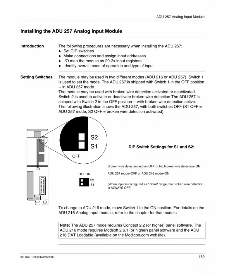
ADU 257 Analog Input Module
Installing the ADU 257 Analog Input Module
Introduction The following procedures are necessary when installing the ADU 257: Set DIP switches. Make connections and assign input addresses. I/O map the module as 20-3x input registers. Identify overall mode of operation and type of input.
Setting Switches The module may be used in two different modes (ADU 216 or ADU 257). Switch 1 is used to set the mode. The ADU 257 is shipped with Switch 1 in the OFF position -- in ADU 257 mode. The module may be used with broken wire detection activated or deactivated. Switch 2 is used to activate or deactivate broken wire detection.The ADU 257 is shipped with Switch 2 in the OFF position -- with broken wire detection active.The following illustration shows the ADU 257, with both switches OFF (S1 OFF = ADU 257 mode, S2 OFF = broken wire detection activated).
To change to ADU 216 mode, move Switch 1 to the ON position. For details on the ADU 216 Analog Input module, refer to the chapter for that module.
S2
S1
OFF
DIP Switch Settings for S1 and S2:
Broken wire detection active=OFF or No broken wire detection=ON
ADU 257 mode=OFF or ADU 216 mode=ON
(When input is configured as 100mV range, the broken wire detectionis ALWAYS OFF)
OFF ON
S2
S1
Note: The ADU 257 mode requires Concept 2.2 (or higher) panel software. The ADU 216 mode requires Modsoft 2.6.1 (or higher) panel software and the ADU 216.DAT Loadable (available on the Modicon.com website).
890 USE 109 00 March 2003 159
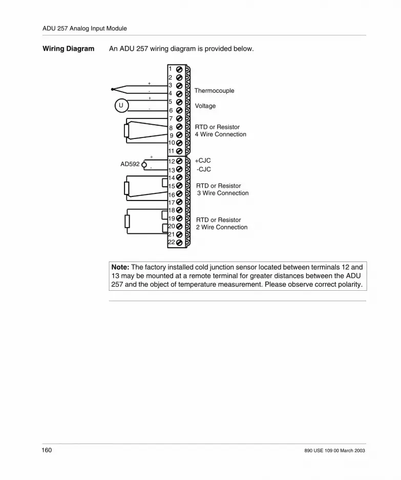
ADU 257 Analog Input Module
Wiring Diagram An ADU 257 wiring diagram is provided below.
Note: The factory installed cold junction sensor located between terminals 12 and 13 may be mounted at a remote terminal for greater distances between the ADU 257 and the object of temperature measurement. Please observe correct polarity.
1234567
89
1011
1213141516171819202122
AD592
U
Thermocouple
Voltage
RTD or Resistor4 Wire Connection
+CJC-CJC
RTD or Resistor3 Wire Connection
RTD or Resistor2 Wire Connection
160 890 USE 109 00 March 2003

ADU 257 Analog Input Module
ADU 257 Isolated Analog Input Module Operation
Introduction The ADU 257 is an eight-channel analog input module. Its field connector is wired depending on the type of input to be measured, either TC or RTD. Two connections are used per RTD; therefore, only four channels may be used. Otherwise, you have eight channels available for TC devices or linear measurements. Any of the inputs may be either TC, linear, or RTD, and any combination of the three may be used. The module can operate in one of several modes, and the input channel ranges are individually selectable. The mode and ranges are set via the panel software. Channel input data is updated every 800 ms. When power is first applied to the module, its inputs are inactive.
I/O Map The ADU 257 requires 20-3x input registers addressed in sequence, beginning with two module status 3x registers, 16 data channel 3x registers (channels 1... 8), and two cold junction sensor 3x registers
I/O Map Registers Data
3x Input status word
3x + 1 Input status word
3x + 2 Input #1 data (low word)
3x + 3 Input #1 data (high word)
...
.........
3x + 17 Input #8 data (low word)
3x + 18 Input #8 data (high word)
3x + 19 Input #9 data (cold junction sensor) (low word)
3x + 20 Input #9 data (cold junction sensor) (high word)
890 USE 109 00 March 2003 161

ADU 257 Analog Input Module
Conversions The following tables detail the various voltage and current conversions for the ADU 257 module.
0... 4000Ω 0... 4000Ω Range and Data Display Format
+/- 100mV Range and Data Display Format
Millivoltage 12 bit 16 bit 15 bit + sign high resolution
IEEE 754 floating point
Range
<+102.4mV +4095 +65535 +32767 +1.024 E02 Overrange
>+100mV... +102.4mV
+4095 +65535 +32001... +32766 +1.0 E02... +1.024 E02
Pos. tolerance range
+100mV +4095 +65535 +32000 +1.0 E02
0mV +2048 +32768 0 0 Nominal
-100mV 0 0 -32000 -1.0 E02
<-100mV... -102.4mV
0 0 -32001... -32766 <-1.0 E02... -102.4 E02
Neg. tolerance range
<-102.4mV 0 0 -32767 -1.024 E02 Underrange
Resistance 12 bit 16 bit 15 bit + sign high resolution
IEEE 754 floating point
Range
>4095Ω +4095 +65535 +32767 +4.096 E03 Overrange
>4000... 4095Ω
+4095 +65535 +32001... +32766 >+4.0 E03... +4.095 E03
Pos. tolerance range
4000Ω +4095 +65535 +32000 +4.0 E03 Nominal
0Ω 0 0 0 0
0 0 -2 -2.0 E00 Broken wire
162 890 USE 109 00 March 2003

ADU 257 Analog Input Module
IEC 751 Pt100,200,500,1000 -200... +850 C
IEC 751 Pt100,200,500,1000 -200... +850 C (-328... +1562 F) Range and Data Display Format
SAMA (US) Pt100,200,500,1000 -200... +650 C
SAMA (US) Pt100,200,500,1000 -200... +650 C (-328... +1112 F) Range and Data Display Format
RTD 12 bit 16 bit 15 bit + sign 0.1C (0.1F)
IEEE 754 floating point Range
>+850C (+1562F)
+4095 +65535 +8501 (+15621) 8.501 E02 (1.5621 E03) Overrange
+850C (+1562F)
+4095 +65535 +8500 (+15620) 8.500 E02 (1.562 E03)
0 (+32F) +780 +12483 0 (+320) 0 (3.20 E01) Nominal
-200C (-328F) 0 0 -2000 (-3280) -2.00 E02 (-3.28 E02)
<-200C (-328F)
0 0 -2001 (-3281) -2.001 E02 (-3.281 E02) Underrange
0 0 -2002 (-3282) -2.002 E02 (-3.282 E02) Broken wire
RTD 12 bit 16 bit 15 bit + sign 0.1C (0.1F)
IEEE 754 floating point
Range
>+600C (+1112F) +4095 +65535 +6001 (+11121) 6.001 E02 (1.113 E03)
Overrange
+600C (+1112F) +4095 +65535 +6000 (+11120) 6.000 E02 (1.112 E03)
0C (+32F) +1024 +16384 0 (+320) 0 (3.20 E01) Nominal
-200C (-328F) 0 0 -2000 (-3280) -2.00 E02 (-3.28 E02)
<-200C (-328F) 0 0 -2001 (-3281) -2.001 E02 (-3.281 E02)
Underrange
0 0 -2002 (-3282) -2.002 E02 (-3.282 E02)
Broken wire
890 USE 109 00 March 2003 163

ADU 257 Analog Input Module
DIN43760 Ni100,200,500,1000 -60... +250 C
DIN43760 Ni100,200,500,1000 -60... +250 C (-76... +482 F) Range and Data Display Format
Thermocouple Type R,S -50... +1768 C
Thermocouple Type R,S -50... +1768 C (-58... +3214.4 F) Range and Data Display Format
RTD 12 bit 16 bit 15 bit + sign 0.1C (0.1F)
IEEE 754 floating point
Range
>+250C (+482F) +4095 +65535 +2501 (+4821) 2.501 E02 (4.821 E02)
Overrange
+250C (+482F) +4095 +65535 +2500 (+4820) 2.500 E02 (4.820 E02)
0C (+32F) +793 +12684 0 (+320) 0 (3.20 E01) Nominal
-60C (-76F) 0 0 -600 (-760) -6.00 E01 (-7.6 E01)
<-60C (-76F) 0 0 -601 (-761) -6.01 E01 (-7.61 E01)
Underrange
0 0 -602 (-762) -6.02 E01 (-7.62 E01)
Broken wire
TC 12 bit 16 bit 15 bit + sign 0.1C (0.1F)
IEEE 754 floating point
Range
>+1768C (+3214.4F)
+4095 +65535 +17681 (+32146) 1.7681 E03 (3.2146 E03)
Overrange
+1768C (+3214.4F)
+4095 +65535 +17680 (+32144) 1.7680 E03 (3.2144 E02)
0C (+32F) +113 +1802 0 (+320) 0 (3.20 E01) Nominal
-50C (-58F) 0 0 -500 (-580) -5.00 E01 (-5.80 E01)
<-50C (-58F) 0 0 -501 (-582) -5.01 E01 (-5.82 E01)
Underrange
0 0 -502 (-584) -5.02 E01 (-5.84 E01)
Broken wire
164 890 USE 109 00 March 2003

ADU 257 Analog Input Module
Thermocouple Type B +50... +1800 C
Thermocouple Type B +50... +1800 C (+122... +3272 F) Range and Data Display Format
Thermocouple Type J -210... +1200 C
Thermocouple Type J -210... +1200 C (-346... +2192 F) Range and Data Display Format
TC 12 bit 16 bit 15 bit + sign 0.1C (0.1F)
IEEE 754 floating point
Range
>+1800C (+3272F)
+4095 +65535 +18001 (+32722) 1.8001 E03 (3.2722 E03)
Overrange
+1800C (+3272F) +4095 +65535 +18000 (+32720) 1.8000 E03 (3.2720 E03)
Nominal
50C (+122F) 0 0 +500 (+1220) 5.00 E01 (1.220 E02)
<50C (+122F) 0 0 +499 (+1218) 4.99 E01 (1.218 E02)
Underrange
0 0 +498 (+1216) 4.98 E01 (1.216 E02)
Broken wire
TC 12 bit 16 bit 15 bit + sign 0.1C (0.1F)
IEEE 754 floating point
Range
>+1200C (+2192F)
+4095 +65535 +12001 (+21922) 1.2001 E03 (2.1922 E03)
Overrange
+1200C (+2192F) +4095 +65535 +12000 (+21920) 1.2000 E03 (2.1920 E03)
0C (+32F) +610 +9761 0 (+320) 0 (3.20 E01) Nominal
-210C (-346F) 0 0 -2100 (-3460) -2.100 E02 (-3.460 E02)
<-210C (-346F) 0 0 -2101 (-3462) -2.101 E02 (-3.462 E02)
Underrange
0 0 -2102 (-3464) -2.102 E02 (-3.464 E02)
Broken wire
890 USE 109 00 March 2003 165

ADU 257 Analog Input Module
Thermocouple Type T -270... +400 C
Thermocouple Type T -270... +400 C (-454... +752 F) Range and Data Display Format
Thermocouple Type E -270... +1000 C
Thermocouple Type E -270... +1000 C (-454... +1832 F) Range and Data Display Format
TC 12 bit 16 bit 15 bit + sign 0.1C (0.1F)
IEEE 754 floating point
Range
>+400C (+752F) +4095 +65535 +4001 (+7522) 4.001 E02 (7.522 E02)
Overrange
+400C (+752F) +4095 +65535 +4000 (+7520) 4.000 E02 (7.520 E02)
0C (+32F) +1650 +26410 0 (+320) 0 (3.20 E01) Nominal
-270C (-454F) 0 0 -2700 (-4540) -2.700 E02 (-4.540 E02)
<-270C (-454F) 0 0 -2701 (-4542) -2.701 E02 (-4.542 E02)
Underrange
0 0 -2702 (-4544) -2.702 E02 (-4.544 E02)
Broken wire
TC 12 bit 16 bit 15 bit + sign 0.1C (0.1F)
IEEE 754 floating point
Range
>+1000C (+1832F)
+4095 +65535 +10001 (+18322) 1.0001 E03 (1.8322 E03)
Overrange
+1000C (+1832F) +4095 +65535 +1000 (+18320) 1.0000 E03 (1.8320 E03)
0C (+32F) +871 +13933 0 (+320) 0 (3.20 E01) Nominal
-270C (-454F) 0 0 -2700 (-4540) -2.700 E02 (-4.540 E02)
<-270C (-454F) 0 0 -2701 (-4542) -2.701 E02 (-4.542 E02)
Underrange
0 0 -2702 (-4544) -2.702 E02 (-4.544 E02)
Broken wire
166 890 USE 109 00 March 2003

ADU 257 Analog Input Module
Thermocouple Type K -270... +1372 C
Thermocouple Type K -270... +1372 C (-454... +2501.6 F) Range and Data Display Format
Thermocouple Type N -270... +1300 C
Thermocouple Type N -270... +1300 C (-454... +2372 F) Range and Data Display Format
TC 12 bit 16 bit 15 bit + sign 0.1C (0.1F)
IEEE 754 floating point
Range
>+1372C (+2501.6F)
+4095 +65535 +13721 (+25018) 1.3721 E03 (2.5018 E03)
Overrange
+1372C (+2501.6F)
+4095 +65535 +13720 (+25016) 1.3720 E03 (2.5016 E03)
0C (+32F) +673 +10776 0 (+320) 0 (3.20 E01) Nominal
-270C (-454F) 0 0 -2700 (-4540) -2.700 E02 (-4.540 E02)
<-270C (-454F) 0 0 -2701 (-4542) -2.701 E02 (-4.542 E02)
Underrange
0 0 -2702 (-4544) -2.702 E02 (-4.544 E02)
Broken wire
TC 12 bit 16 bit 15 bit + sign 0.1C (0.1F)
IEEE 754 floating point
Range
>+1300C (+2372F)
+4095 +65535 +13001 (+23722) 1.3001 E03 (2.3722 E03)
Overrange
+1300C (+2372F) +4095 +65535 +13000 (+23720) 1.3000 E03 (2.3720 E03)
0C (+32F) +704 +11270 0 (+320) 0 (3.20 E01) Nominal
-270C (-454F) 0 0 -2700 (-4540) -2.700 E02 (-4.540 E02)
<-270C (-454F) 0 0 -2701 (-4542) -2.701 E02 (-4.542 E02)
Underrange
0 0 -2702 (-4544) -2.702 E02 (-4.544 E02)
Broken wire
890 USE 109 00 March 2003 167

ADU 257 Analog Input Module
Cold Junction Sensor AD592 -25... +105 C
Cold Junction Sensor AD592 -25... +105 C (-13... +221 F) Range and Data Display Format
CJC 12 bit 16 bit 15 bit + sign 0.1C (0.1F)
IEEE 754 floating point
Range
>+125C (+257F) +4095 +65535 +1051 (+2212) 1.051 E02 (2.212 E02)
Overrange
+125C (+257F) +4095 +65535 +1050 (+2210) 1.050 E02 (2.210 E02)
0C (+32F) +683 +10923 0 (+320) 0 (3.20 E01) Nominal
-25C (-13F) 0 0 -250 (-130) -2.50 E01 (-1.30 E01)
<-25C (-13F) 0 0 -251 (-132) -2.51 E01 (-1.32 E01)
Underrange
0 0 -252 (-134) -2.52 E01 (-1.34 E01)
Broken wire
168 890 USE 109 00 March 2003

ADU 257 Analog Input Module
ADU 257 Analog Input Module Specifications
Table of Specifications
The following table contains a list of ADU 257 specifications.
Module Topology
Number of channels 8 TC, 4 RTD
Data Format TC, RTD, mV linear, Ohms linear inputs
Isolation test voltage channel to channel
400Vdc maximum via solid state relays
Isolation test voltage channel to bus
500Vac maximum
Isolation test voltage channel to earth
500Vac maximum
Power Supply Internal Source (from I/O bus) 5VIO; 120mA typical
I/O Map Register 3x/4x 20 in/0 out
TC Inputs TC types B,E,J,K,N,R,S,T
Linear Measuring Range +/-100mV
CJC sensor Factory installed reference sensor to terminals 12 and 13
Cold junction sensor type (factory installed)
AD 592 CN, -26 degrees C ... +106 degrees C
Overload protection +30Vdc continuously
Resolution 12Bits, 16Bits, 15Bits plus sign, 32Bits
Accuracy for TC ranges @ 0 ... 60 degrees C, includes CJC, offset, gain error
For J,K,N,E,T types:+/-2 degrees C +/-0.1 percent of reading (+/-1.5 degrees C for temp. less than 100) (assumes no delta between CJC and CJ sensor)
Accuracy for TC ranges @ 0 ... 60 degrees C, includes CJC, offset, gain error
For S,R,B types:+/-4 degrees C +/-0.1 percent of reading (assumes no delta between CJC and CJ sensor)
890 USE 109 00 March 2003 169

ADU 257 Analog Input Module
RTD Inputs RTD types 2/3/4 wire IEC Pt100/200/500/1000,2/3/4 wire American Pt100/200/500/1000,2/3/4 wire Ni100/200/500/1000
Linear Measuring Range 0 ... 4000 ohms
Overload protection +30Vdc continuously
Resolution 12Bits, 16Bits, 15Bits plus sign, 32Bits
Accuracy for RTD ranges @ 25 degrees C ambient temperature
0.5 degrees C
Accuracy for RTD ranges @ 60 degrees C ambient temperature
0.9 degrees C
Derating of accuracy for -25 ... +70 degrees C
1.25C
Dynamic Characteristics of Inputs
Conversion time for all inputs 800mS maximum
Interference voltage suppression (main suppression) for f=nx50 or 60Hz
n=1,2 ...
Common-mode rejection less than 110dB
Physical Characteristics
Format 1 slot
Dimensions (W x H x D) 40.3 x 145 x 117.5 mm1.6 x 5.6 x 4.5 in
Weight 320g, 0.710 lb
Wire Size 1-14AWG, 2-20AWG
Environmental Characteristics
Operating Temperature -40 ... +70 degrees C
Agency Approvals
ADU 257: VDE 0160; UL 508; CSA 22.2 No.142; and European Directive EMC 89/336/EEC (See Requirements for CE Compliance, p. 779) Standards
ADU 257C: VDE 0160; UL 508; CSA 22.2 No.142; and European Directive EMC 89/336/EEC (See Requirements for CE Compliance, p. 779) Standards
170 890 USE 109 00 March 2003

890 USE 109 00 March 2003
AS-BDEA 203 Profibus-DP Coupler Module Description
At a Glance
Overview This chapter describes the AS-BDEA Profibus-DP Coupler Module.
What’s in this Chapter?
This chapter contains the following topics:
Topic Page
Configuration 172
Features and Functions 176
Diagnosis 178
Technical Specifications 179
171

AS-BDEA 203 Profibus -DP
Configuration
Overview To configure the AS-BDEA the following tasks must be performed
Settings (Slave Address, Disconnection Behavior)
Slave Address-The slave address (node address) is to be set on the front panel "x10, x1" rotary switches. Addresses from 1 ... 99 are allowed (0=as shipped ).Disconnection Behavior- See the following figure for disconnection behavior. Switches S0 and S1are meaningless.
Off On
S3S2S1S0
S3S2S1S0
S3S2S1S0
S3S2S1S0
Forced cutoff
* As shipped
Firmware Standard*
Halt with value retention(outputs remain unchanged)
Reserved for AEG service specialists(Test bay setting)
Off On
172 890 USE 109 00 March 2003

AS-BDEA 203 Profibus -DP
I/O Expansion Limitations
Arbitrary I/O combinations are only possible with discrete I/O modules. Use of analog I/O modules restricts total data volume to a particular level. Total data volume is the sum of data from the PROFIBUS master to the AS–BDEA 203 (D out), and from the AS–BDEA 203 to the PROFIBUS master (D in).The feasibility of a particular combination can be verified with the followingtables. The first table lists data volume by respective module (D out / D in) in bytes.The data volume of all employed modules through the AS–BDEA 203 to the PROFIBUS master (D in sums) must </= 244 bytes.In accordance with the (D in) data volume, this table permits the data volume calculation for PROFIBUS master to AS–BDEA 203 (D out). With the second table the (D out) data volumes of all employed modules is to be checked against the max. permissible (D out) data volume.Data volume by module
Max permissible "D Out" data volume in respect to "D In" data volume.
Module D In Data Volume (Bytes)
D Out Data Volume (Bytes)
DEP 208, DEP 210, DEP 211 1 0
DAP 204, DAP 208, DAP 210 0 1
DAP 212, DAP 220, DAP 292 1 1
DEO 216, DEP 214, DEP 215, DEP 216, DEP 217, DEP 218, DEP 220, DEP 296, DEP 297, DEX 216
2 0
DAO 216, DAP 216, DAP 217, DAP 218, DAX 216 0 2
DAU 202 0 4
DAU 208 0 16
ADU 204, ADU 205 10 0
ADU 206,ADU 216 10 1
ADU 210 10 4
ADU 214 18 8
Data In Data volume Sums (Bytes) Max Data Out Volume Sums (Bytes)
241...244 144
233...240 152
225...232 160
217...224 168
209...216 176
0...208 184
890 USE 109 00 March 2003 173

AS-BDEA 203 Profibus -DP
Subtrack Mounting Slot
Enter system relevant power supply information in the label inlay.Noise immunity can be improved when by–pass capacitors are installed at the power supply module U and M terminals.
Power Supply Connection
Enter system relevant power supply information in the label inlay. Noise immunity can be improved when by–pass capacitors are installed at the power supply module U and M terminals.
CAUTION
The module’s integrated power supply is non–isolated. Improper connection, e.g. absence of the M2 connection, can lead to module destruction.
Failure to follow this precaution can result in injury or equipment damage.
UB (24 VDC)M2
1.25 A mediumtime-lag fuse
174 890 USE 109 00 March 2003

AS-BDEA 203 Profibus -DP
Profibus Connection
The PROFIBUS port utilizes varied Sub–D9 plug connectors: 490 NAD 911 02 for transmission rates up to 12 Mbps. PBS1 for transmission rates up to 500kbps.
The individual installation steps are to be carried out in adherence with the accompanying user documentation.
Pin
3
5
6
8
Signal
RxD/TxD-P
DGND
VP
RxD/TxD-N
Function
Receive/transmit data (+)
Signal ground
+5 VDC supply
Receive/transmit data negated (-)
Pin occupied
N/C
890 USE 109 00 March 2003 175

AS-BDEA 203 Profibus -DP
Features and Functions
Overview The AS–BDEA 203 is a PROFIBUS–DP coupling module adhering to DIN 19 245 Parts 1 and 3 with integrated (non–isolated) power supply. It is used to drive the remote I/O modules of the Modicon TSX Compact family. It provides a 5 VDC supply at 1.6 A for the modules on the parallel I/O bus.The AS–BDEA 203 can address a maximum of 18 I/O modules (288 I/Os) via the subracks DTA 200, DTA 201 or DTA 202. With the exception of intelligent modules, all analog and discrete Compact I/O modules can be employed. When analog modules are utilized, there is a particular total data volume which may not be exceeded.The device master data file from the 381 SWA 000 00 diskette must be utilized for AS-BDEA 203 configuration.
176 890 USE 109 00 March 2003

AS-BDEA 203 Profibus -DP
Features Standardized, isolated PROFIBUS Port Transmission rates of up to 12 Mbps Automatic adaptation to master transmission rate setting Slave address adjustment per rotary switch DIP switch adjustment of disconnection behavior
Functional Details
The AS–BDEA 203 serves as the coupling element between the PROFIBUS–DP and the internal I/O bus.The set disconnection behavior is activated by watchdog when PROFIBUS communication is interrupted longer then the supervision time set by the master. The AS–BDEA 203 collects messages from the associated modules and reports these further to the master as diagnostic information.
Profibus-DP
Sub-D9
RS-485
Identcode
Slave Address
Mode switchDC-DC Converter
+5 VDC +5 VDC
SPC3
I/O Bus ASIC
48 MHzClock
24 KBRAM
64 KBEPROM
Data Bus
INT
A8...A15
I/O Bus
Interfac
PowerSupply
AddressDecoder12 MHz
Clock
80C152Micro-
controller
Address Bus
+5 VDC
+5 VDC24 VDC
A0...A7
CPU
890 USE 109 00 March 2003 177
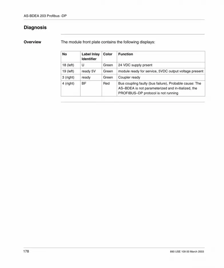
AS-BDEA 203 Profibus -DP
Diagnosis
Overview The module front plate contains the following displays:
No Label Inlay Identifier
Color Function
18 (left) U Green 24 VDC supply prsent
19 (left) ready 5V Green module ready for service, 5VDC output voltage present
3 (right) ready Green Coupler ready
4 (right) BF Red Bus coupling faulty (bus failure), Probable cause: The AS–BDEA is not parameterized and in-itialized, the PROFIBUS–DP protocol is not running
178 890 USE 109 00 March 2003

AS-BDEA 203 Profibus -DP
Technical Specifications
AS-BDEA 203 Assignment
Power Supply
Data Interface
Processor
Mechanical Design
System TSX Compact (A120, 984)
Module Area Slot 0 of DTA 200 primary backplane
Identicode Hex A203, entry through the device master data file type 381 SWA 000 00
External input voltage UB = 24 VDC, max. 0.85 A
Primary fusing 1.25 A medium time–lag fuse
Power on current 20 A, time constant = 1 ms
Tolerances, limiting values Refer to the TSX Compact User Manual, "Technical Specifications"
Reference potential M M2
Protective earth PE
Secondary voltage 5.15 VDC, max. 1.6 A, non–isolated
Buffering time Typically 5 ms for 24 VDC
Overload protection Through current limiting
Profibus-DP Through a potential–free RS–485 interface up to 12 Mbps
Pin assignments Refer to PROFIBUS Connection Figure
Back plane Parallel I/O bus, refer to TSX Compact User Manual, "Technical Specifications"
Processor type Intel 80C152 / 12 MHz
Data memory 32 KB RAM
Firmware 64 KB EPROM
Module Standard double–size module
Format 3 HE, 16 T
Weight Approx. 500 g
890 USE 109 00 March 2003 179

AS-BDEA 203 Profibus -DP
Connection Styles
Environmental Characteristics
Power Supply 5–pole screw/plug–in terminal block
Profibus Sub–D9 socket, matching to 490 NAD 911
Back plane 2 plug connectors 1/3 C30M, 1 socket connector 1/3 R30F
Regulations Meets VDE 0160, UL 508
System data Refer to TSX Compact User Manual, "Technical Specifica-tions"
Permissible ambient temperatures 0 ... +60 degrees C.
Power dissipation Typically 6 W
180 890 USE 109 00 March 2003

AS-BDEA 203 Profibus -DP
Profibus- DP Specifications for the AS-BDEA 203 on the Profibus-DP. Transmission Specifications
Bus Specifications
Operation
Nodes per bus Max. 32
Bus lengths, transmission rates
max 1.2 km at 9.6 kbps or at 19.2 Kbps or at 93.75 Kbs max 1 km at 187.5 Kbps max 0.5 km at 500 Kbps max 0.2 r at 1.5 Kbps max 0.1 km at 3 Mbps or at 6 Mbps or at 12 Mbps rigid
Bulk transmission media Shielded twisted pair (S–UTP)KAP PROFIB, PROFIBUS cable up to 12 Mbps, rigid
Connection interface Adhering to EIA RS–485
Cable termination As per Norm 390 / 220 / 390 W
Stub cabling None
Data security Hamming distance, HD = 4
Node type Slave
Node Addresses 1...99
DP Bus Byte Output
Output reference 0x (Boolean, packedOutput Reference 4x (Integer8, unpacked; Unsigned8, un-packed;RAW, packed e.g. ASCII)
DP Bus Byte Input
Input Reference 1x (Boolean, packed)Input Reference 3x (Integer8, unpacked; Unsigned8, un-packed; RAW, packed e.g. ASCII)
Bus Word Output
Output Reference 0x (Boolean)Output Reference 4x (Integer16 = Unsigned16 = RAW)
Bus Word Input
Input Reference 1x (Boolean)Input Reference 3x (Integer16 = Unsigned16 = RAW)
890 USE 109 00 March 2003 181

AS-BDEA 203 Profibus -DP
182 890 USE 109 00 March 2003

890 USE 109 00 March 2003
BKF 201 (16W) & (64W) InterBus S Master Module
At a Glance
Introduction The information in this chapter describes the BKF 201 (16W) & (64W) InterBus S Master Module.
What’s in this Chapter?
This chapter contains the following topics:
Topic Page
What Is the BKF 201 (16W) & (64W) InterBus S Master Module? 184
Physical Characteristics of the BKF 201 (16W) & (64W) InterBus S Master Module
185
Switch Settings for the BKF 201 188
Installation of the BKF 201 (16W) & (64W) Interbus Master Module 189
Operation of the BKF 201 Master Module: I/O Map 191
Example of Hardware and I/O Mapping for the BKF 201 198
Specifications 199
183

BKF 201 (16W) & (64W) InterBus S Master Module
What Is the BKF 201 (16W) & (64W) InterBus S Master Module?
Brief Product Description
The BKF 201 links the Compact PLC and the Remote bus nodes. The following lists describes the key features of the BKF 201: Up to 63 3x input register and 63 4x output register data words can be addressed
for a total of 126 TIOs (63 input TIOs and 63 output TIOs), with 16 Bits each within an Interbus frame
Supports up to 15 BKF 201 modules in the BKF 201 (16) (Ident Code 92) mode or up to 3 BKF 201 modules in the BKF 201 (64) (Indent Code 93) mode
Use and Programming for the BKF 201 is done via the RS 232C-port of the PLC, therefore saving a port on the BKF 201
All outputs are automatically set to 0 (zero) upon detection of configuration errors or other bus problems
A restart can be performed manually or automatically after error correction Changes to the Interbus S configuration are easy (Fast "Plug and Play") Monitoring of the module using a watchdog function Mode settings using two DIP switches The Interbus S status is shown via the modules LEDsInterbus loop nodes are not supported.Modules with Peripheral Communication Protocol (PCP) Channel (1, 2, and 4 PCP words within the Interbus loop) can be used in the BKF 201. However, the BKF 201 does not support the PCP Channel.
Note: Interbus loop nodes are not supported.
Note: Modbus with Peripheral Communication Protocol (PCP) Channel (1, 2, and 4 PCP words within the Interbus loop) can be used in the BKF 201. However, the BKF 201 does not support the PCP Channel.
184 890 USE 109 00 March 2003

BKF 201 (16W) & (64W) InterBus S Master Module
Physical Characteristics of the BKF 201 (16W) & (64W) InterBus S Master Module
Overview The following information describes the physical characteristics of the BKF 201.
Front View and Label
The following figure shows the front view of the BKF 201 and the label.
BKF 201
InterBus-Sremote bus
BKF 201
ready
IBS readyIBS runIBS error
module errorconfig. error
error 1
error 2error 4
error 8error 10error 20error 40error 80
card
890 USE 109 00 March 2003 185

BKF 201 (16W) & (64W) InterBus S Master Module
LEDs The following table describes the BKF 201 LED displays.
LED # LED Name Color Function
1 ready Green Module ready for service
3 IBS ready Green Interbus ready for service
4 IBS run Green Interbus transmission active
5 IBS error Red Interbus transmission error
6 Module error
Red Module error (on Interbus slave device)
7 config. error
Red The configuration changed during operation, or an error occurred during loading of the configuration.
1415161718192021
error 1error 2error 4error 8error 10error 20error 40error 80
Red Displays the physical number of the Interbus node with error condition (BCD, Node # = sum of error numbers displayed).* See also, the Front View and Label, p. 185. No display: Neither error nor node number can be found.
Note: *For example, if device#6 (node#6) has a error condition LED#15 (error 2) and LED#16 (error 4) turn red. Add the two together (error 2 + error 4= 6). This indicates that the error condition pertains to device#6 (node#6).
186 890 USE 109 00 March 2003

BKF 201 (16W) & (64W) InterBus S Master Module
Block Diagram of the BKF 201
The following figure describes the architecture of the BKF 201.
Compact PLC
CPU
Compact I/O Bus
Dual-Post-
1 KB
Controller80C320<
RS-485
RAM32KB
EPROM 64 KB
LED status displays, DIPs
InterBus-S (remote bus)
890 USE 109 00 March 2003 187
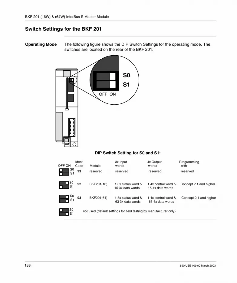
BKF 201 (16W) & (64W) InterBus S Master Module
Switch Settings for the BKF 201
Operating Mode The following figure shows the DIP Switch Settings for the operating mode. The switches are located on the rear of the BKF 201.
S0
S1
OFF ON
OFF ONS0S1
S0S1
S0S1
S0S1
DIP Switch Setting for S0 and S1:
99 reserved reserved reserved reserved
92 BKF201(16) 1 3x status word & 1 4x control word & Concept 2.1 and higher
93 BKF201(64) 1 3x status word & 1 4x control word & Concept 2.1 and higher
not used (default settings for field testing by manufacturer only)
Ident- 3x Input 4x Output Programming Code Module words words with
63 3x data words 63 4x data words
15 3x data words 15 4x data words
188 890 USE 109 00 March 2003

BKF 201 (16W) & (64W) InterBus S Master Module
Installation of the BKF 201 (16W) & (64W) Interbus Master Module
Overview The following information describes how to install the BKF 201.
Operating Mode If the operating mode for the BKF 201 module is set to BKF 201 (16) (Indent Code 92), the module can reside in any I/O slot in any backplane (DTA 201 or DTA 202). In contrast, if the operating mode for the BKF 201 module is set to BKF 201 (64) (Indent Code 93), the module can reside only in an I/O slot in the primary backplane (DTA 200).
Interbus Connection
Refer to the Interbus S Quantum 140 NOA 611 00 User Manual (P/N 840 USE 419 00). The following diagram shows the pin assignments as viewed from the solder side.
The following table shows the pinout assignments.
Socket Signal Function
1 DO Transmit data (+)
2 DI Receive data (+)
3 GND Reference ground
5 5 V Out For Fiber Optic Interface
6 DO Transmit data (-)
7 DI Receive data (-)
Note: When using branch interfaces, it is not possible to group and to handle errors (that is, turning off the branch in case of error). For example, a branch interface is useful when using a fiber-optic interface because most slaves do not provide power for this type of interface. Additionally, a branch interface is required to connect slaves to peripheral buses, or to install remote buses.
Interbusremote bus
9
8
7
6
5
4
3
2
1
Pin presentNo pin present
890 USE 109 00 March 2003 189

BKF 201 (16W) & (64W) InterBus S Master Module
Hardware Configuration of the BKF 201
The following figure illustrates an example BKF 201 hardware layout showing nodes.
BKF 201
Rem
ote
bus
Rem
ote
bus
170 BAM 096 00170 BAM 096 00170 BAM 096 00170 BAM 096 00
. . . . .
Node # 1
Node # 2
Rem
ote
bus
Node # 3 Node # 4 Node # 5
remote bus branch remote bus branch
Node # 6 (DEA Station)
DEA 202
Rem
ote
bus
Rem
ote
bus
BKI 601 DEP 608 DAP 608
Node # 7 Node # 8
Node # 10
Installationremote bus
Installationremote bus
Node # 9
DAP 664DAP 654DAP 664
190 890 USE 109 00 March 2003

BKF 201 (16W) & (64W) InterBus S Master Module
Operation of the BKF 201 Master Module: I/O Map
BKF 201(16) Operating Mode
The BKF 201(16) (Ident Code 92) module requires a total of 16 3x input registers and a total of 16 4x output registers. The first 3x input register is the Status Word and the following 3x input registers are Data Words starting with 3x+1 and ending with 3x+15. The first 4x output register is the Control Word and the following 4x output registers are Data Words starting with 4x+1 and ending with 4x+15. Refer to the other information in this map.
BKF 201(64) Operating Mode
The BKF 201(64) (Ident Code 93) module requires a total of 64 3x input registers and a total of 64 4x output registers. The first 3x input register is the Status Word and the following 3x input registers are Data Words starting with 3x+1 and ending with 3x+63. The first 4x output register is the Control Word and the following 4x output registers are Data Words starting with 4x+1 and ending with 4x+63. Refer to the other information in this map.
3x Input Registers
The following table describes the 3x Input Registers (1 3x Status Word & Up to 15 3x Data Words) or (1 3x Status Word & Up to 63 3x Data Words).
State RAM Bit 15-8 Bit 7-5 Bit 4-0
3xxxxx (Status Word)
Config. Checksum; see 3x Configuration Checksum Byte Structure (High Byte), p. 192
0not used
Status; see 3x Configuration Checksum Byte Structure (High Byte), p. 192
3xxxxx +1 Process data - Input word 1
3xxxxx +2 Process data - Input word 2
3xxxxx +3 Process data - Input word 3
3xxxxx +4 Process data - Input word 4
: :
3xxxxx + 15BKF201 (16)
Process data - Input word 15 BKF201 (16) mode
: :
3xxxxx + 15BKF201 (64)
Process data - Input word 63 BKF201 (64) mode
890 USE 109 00 March 2003 191

BKF 201 (16W) & (64W) InterBus S Master Module
3x Configuration Checksum Byte Structure (High Byte)
The following table describes the 3x Status Word, High Byte for Configuration Checksum Error #. For information about the meanings of the LEDs, see LEDs, p. 186.
Bit 15
Bit 14
Bit 13
Bit 12
Bit 11 Bit 10 Bit 9 Bit 8 Function
8 4 2 1 Decimal value of block 1 (max. 9), same meaning as LEDs #14 ... #17
80 40 20 10 Decimal value of block 2 (max. 90), same meaning as LEDs #18 ... #21
Note: For example, if device#6 (node#6) has a error condition, LED#15 (error 2) and LED#16 (error 4) turn red. Add the two together (error 2 + error 4= 6). This indicates that the error condition pertains to device#6 (node#6).
192 890 USE 109 00 March 2003
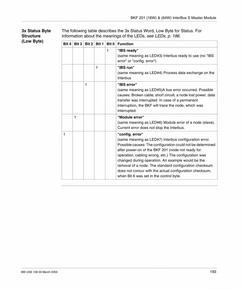
BKF 201 (16W) & (64W) InterBus S Master Module
3x Status Byte Structure (Low Byte)
The following table describes the 3x Status Word, Low Byte for Status. For information about the meanings of the LEDs, see LEDs, p. 186.
Bit 4 Bit 3 Bit 2 Bit 1 Bit 0 Function
1 "IBS ready"(same meaning as LED#3) Interbus ready to use (no "IBS error" or "config. error")
1 "IBS run"(same meaning as LED#4) Process data exchange on the Interbus
1 "IBS error"(same meaning as LED#5)A bus error occurred. Possible causes: Broken cable, short circuit, a node lost power, data transfer was interrupted. In case of a permanent interruption, the BKF will trace the node, which was interrupted.
1 "Module error"(same meaning as LED#6) Module error of a node (slave). Current error does not stop the Interbus.
1 "config. error"(same meaning as LED#7) Interbus configuration error. Possible causes: The configuration could not be determined after power-on of the BKF 201 (node not ready for operation, cabling wrong, etc.) The configuration was changed during operation. An example would be the removal of a node. The standard configuration checksum does not concur with the actual configuration checksum, when Bit 6 was set in the control byte.
890 USE 109 00 March 2003 193

BKF 201 (16W) & (64W) InterBus S Master Module
4x Output Registers
The following table describes the4x Output Registers (1 4x Control Word and up to 15 4x or (1 4x Control Word & up to 63 4x Data Words).
4x Standard Configuration Checksum Byte Structure (High Byte)
The following table describes the 4x Control Word, High Byte for Configuration Checksum.
State RAM Bit 15-8 Bit 7-0
4xxxxx (Control Word) Config. Checksum; see 4x Control Byte Structure (Low Byte), p. 195
Status; see 4x Control Byte Structure (Low Byte), p. 195
4xxxxx +1 Process data - Input word 1
4xxxxx +2 Process data - Input word 2
4xxxxx +3 Process data - Input word 3
4xxxxx +4 Process data - Input word 4
: :
4xxxxx + 15 BKF201 (16) Process data - Input word 15 BKF201 (16) mode
: :
: :
4xxxxx + 63 BKF201 (64) Process data - Input word 63 BKF201 (64) mode
Bit 15 Bit 14 Bit 13 Bit 12 Bit 11 Bit 10 Bit 9 Bit 8 Function
x x x x x x x x Enter your bus configuration checksum returned by the BKF 201 upon initialization into this register and set Bit 6 =1 (check config.) in (4x control word low byte) to compare configuration input (3x status config. check sum, high byte) to (4x control word low byte check sum). When they do not match Bit 4 (config. error) results in (3x status low byte).
194 890 USE 109 00 March 2003

BKF 201 (16W) & (64W) InterBus S Master Module
4x Control Byte Structure (Low Byte)
The following table shows the 4X Control Word, Low Byte for Control.
Bit 7 Bit 6 Bit 5 Bit 4 Bit 3 Bit 2 Bit 1 Bit 0 Function
0 Not used
1 "alarm-stop"Setting Bit 1 stops the Interbus immediately, and all outputs are set to zero. While this Bit is set, all other control bits have no effect. Inputs are held in last state.
1 "start-cycle"Starts the data transfer to the nodes. If the bit is cleared, no more data cycles are performed through the BKF master, and the outputs of the nodes are "frozen", meaning that the input information will stay resident in the signal memory. If alarm-stop Bit1=1, then the bus stops and all outputs are turned off.
1 "quit-error"Confirms errors occurred ("IBS error", "module error", "config. error"). Setting this bit permanently results in immediate error acknowledgment. Therefore, it should not be used during normal operation. When an error occurs and the network problem is corrected, this bit needs to be set to confirm and clear the error condition. If alarm-stop Bit1=1, then quit-error is not active.
0 Not used
1 1 "get-configuration"Determine new Interbus configuration. This is useful, if for example a node is removed/added to the Bus, meaning Bit 4 of status byte (config. error) = 1. When checking for a new configuration, all other bits must be = 0, except you must set Bit 3=1.
890 USE 109 00 March 2003 195

BKF 201 (16W) & (64W) InterBus S Master Module
1 "check-configuration"When Bit 6 is set, the BKF compares the checksum of the 4x control high byte and the standard configuration (3x status word, high byte checksum). In case of no match, the INTERBUS is stopped and Bit 4 (config. error) is set in the (3x status word, low byte for status). Make sure, the standard configuration checksum was entered into the (4x control word, high byte for standard config. checksum) prior to setting bit 6(check-config). The checksum is determined by reading the checksum of the actual configuration in the (3x status word, high byte checksum).
1 "show-configuration" Display of: Number of Interbus nodes, total number of Input/Output words, Identcode and the number of the process data words of the nodes in the signal memory (3x data words, up to 15 for BKF202(16) (Ident code 92), and up to 63 for BKF202(64) (ident code 93)). NOTE: All other bits must be=0.
Bit 7 Bit 6 Bit 5 Bit 4 Bit 3 Bit 2 Bit 1 Bit 0 Function
196 890 USE 109 00 March 2003

BKF 201 (16W) & (64W) InterBus S Master Module
Show Configuration
The following table is an example using the show configuration feature. This function is available only if the 4x control word bits are set as follows: Bit 7=1 (show configuration), Bit 1=0 (alarm-stop), Bit 2=0 (start-cycle)
State RAM Bit 15-8 Bit 7-5 Bit 4-0
3xxxxx (Status Word)
Config. Checksum; see 3x Status Byte Structure (Low Byte), p. 193
0(not used)
Status; see 3x Status Byte Structure (Low Byte), p. 193
3xxxxx +1 0 Number of IBS nodes (slaves)
3xxxxx +2 Number of process 3x input data words
Number of process 4x input data words
3xxxxx +3 Number of process data words of slave 1
Ident code of slave 1
3xxxxx +4 Number of process data words of slave 2
Ident code of slave 2
3xxxxx + 15BKF201 (16)
Number of process data words of slave 13
Ident code of slave 13
3xxxxx + 15BKF201 (64)
Number of process data words of slave 61
Ident code of slave 61
Note: The number of process data words also includes the Peripheral Communication Protocol (PCP) communication words, if slaves with PCP Channel are used. Unlike other Interbus masters, these PCP communication words are also reflected in the signal memory.
890 USE 109 00 March 2003 197

BKF 201 (16W) & (64W) InterBus S Master Module
Example of Hardware and I/O Mapping for the BKF 201
BKF 201 Module Using TIO Modules as Nodes
This is an example of how to use three TIO modules as nodes off the BKF 201 module. Notice the correlation between the hardware and I/O mapping structure shown in the tables that follow the figure.
The following tables show the data structure of the 3x input registers and 4x output registers, as well as the hardware configuration for the three TIO devices/nodes shown in the figure.The following table describes the 3x Input I/O Mapping Presentation.
The following table describes the 4x Output I/O Mapping Presentation.
Config. -checksum Status byte
Inputs 1 ... 16 of node 1
Inputs 1 ... 16 of node 3
Stand. config. -checksum Control byte
Outputs 1 ... 16 of node 1
Outputs 1 ... 16 of node 2
BKF 201
Rem
ote
bus
Node # 1 Node # 2 Node # 3In / Out (16 Bit each) Out(16 Bit) In (16 Bit)
198 890 USE 109 00 March 2003

BKF 201 (16W) & (64W) InterBus S Master Module
Specifications
Specifications The following table lists specifications for the BKF 201 (16W) & (64W) InterBus S Master Module.
Power supply
Internally through I/O-Bus 5VDC I/O Bus, 190mA typically, 250mA max. (w/o fiber-optic Interface)
Data Interface
Field bus as RS 485 port, non-isolated (150Ohm)
Processor
Processor type Dallas 80C320 / 32 MHz
Data memory 32KB RAM
Firmware 64KB EPROM
I/O Map
Register 3x/4x 16 in/16 out BKF-201 (16W)
64 in/64 out BKF-201 (64W)
Physical Structure
Module Standard-size module
Format I Slot
Weight 210 g
Type of Connection
Remote bus Sub-D9 socket (9 pins)
Backplane Plug connector1/3 C30M
Environmental Characteristics
Regulations VDE 0160, UL 508
Power dissipation 1.3W max., typically 1W
890 USE 109 00 March 2003 199

BKF 201 (16W) & (64W) InterBus S Master Module
200 890 USE 109 00 March 2003

890 USE 109 00 March 2003
BKF 202 InterBus S Slave Module
At a Glance
Introduction The purpose of this chapter is to describe the BKF 202 InterBus S slave Module.
What’s in this Chapter?
This chapter contains the following topics:
Topic Page
What Is the BKF 202 InterBus S Slave Module? 202
Physical Characteristics of the BKF 202 InterBus S Slave Module 203
Switch Settings for the BKF 202 InterBus S Slave Module 205
Installation of the BKF 202 InterBus S Slave Module 206
Operation of the BKF 202 InterBus S Slave Module 209
Specifications of the BKF 202 InterBus S Slave Module 212
201

BKF 202 InterBus S Slave Module
What Is the BKF 202 InterBus S Slave Module?
Brief Product Description
The BKF 202 links the Compact PLC and the Remote Bus nodes. The following list describes the key features of the BKF 201: Up to 15 3x input register and up to 15 4x output register data words can be
exchanged with an Interbus S master. Monitoring of the module using a watchdog function. Mode settings using a rotary switch and two DIP switches. The Interbus S status is shown via the module’s LEDs. Supports up to 15 BKF 202 modules in the BKF 202 (Indent Code 94) mode.
Note: The BKF 202 module does not support Peripheral Communication Protocol (PCP) channels.
202 890 USE 109 00 March 2003

BKF 202 InterBus S Slave Module
Physical Characteristics of the BKF 202 InterBus S Slave Module
Overview The following information describes the physical characteristics of the BKF 202.
Front View and Label
The following figure shows the front view of the BKF 202 and the label.
BKF 202
INTERBUS IN
OUT
BKF 202ready
BARCRD
card
890 USE 109 00 March 2003 203

BKF 202 InterBus S Slave Module
LED Displays The following table describes the LED displays for the BKF 202.
Block Diagram of the BKF 202
The following block diagram provides an overview of the BKF 202 architecture.
LED # LED Name
Color Function
1 READY Green Operating modeon: Current power for internal logic within the allowable range and the module has not been reset to modeoff: Current power missing or outside of the allowable range, or module has been reset
3 BA Green bus active on: Data telegrams are transmitted off: Data telegrams are not transmitted
4 RC Green Remote Bus Check on: incoming remote bus connection is correct and the Bus Reset of the Busmaster is inactiveoff. incoming remote bus connection is wrong/not corrected or the Bus Reset of the Bus Reset of the Busmaster is active
5 RD Red Remote Bus Disabled on: Extended remote bus is switched offoff: Extended remote bus is not turned off
Compact PLC
Compact I/O Bus
Dual-Port- 2 KB
Controller 80C32
SmPI SRE SRE
RAM32 KB
EPROM 64KB
LEDs, DIPs RS-485 RS-485
InterBus-S (remote bus)
IN Out
204 890 USE 109 00 March 2003

BKF 202 InterBus S Slave Module
Switch Settings for the BKF 202 InterBus S Slave Module
Operating Mode The following figure shows the Rotary Switch settings and the Dip Switch settings for the operating mode. The switches are located on the rear of the BKF 202.
S2
S0S1
Rotary Switch Settings for S2:Switch position Number of words
1 2 words2 4 words3 6 words4 8 words5 10 words6 12 words7 14 words8 16 words (15 data words)9 not used0 not used
OFF ONS0S1
S0S1
S0S1
S0S1
DIP Switch Setting for S0 and S1:
not used (default settings for field testing by manufacturer only)
reserved
94 BKF202 1 3x status word & 1 4x control word & Concept 2.1 and higher
reserved reserved reserved reserved reserved
Ident-Code Module
3x Input 4x Output Programming words words with
15 3x data words 15 4x data words
S2S0S1
5
09
8
6 7
123 4
890 USE 109 00 March 2003 205

BKF 202 InterBus S Slave Module
Installation of the BKF 202 InterBus S Slave Module
Overview The following information describes how to install the BKF 202.
Interbus Connection
The BKF 202 modules located at the inline sites on the Interbus remote bus cable have two connections. One connection is for the incoming bus cable; the other is for the outgoing bus cable. BKF 202 modules located at the end sites on the network cable have only one connection. This is for the incoming bus cable.You should have a complete cabling diagram for your network installation, showing the cable routing path and methods of securing the cables. It should identify incoming and outgoing cables at each BKF 202 module site.
Pin Placements The following figure shows the pin placements as viewed from the solder side.
1
2
3
4
5
6
7
8
9 6
7
8
95
4
3
2
1
Sub-D9 Port“in” (top)
Sub-D9 Port“out” (bottom) Pin present
No pin present
Pin Signal Meaning
1 DO Transmit data (+)2 DI Transmit data (+)3,4 GND reference ground5,8 (5 V Out) for Opto. Sub.6 DO Transmit data (-)7 DI Receive data (-)9* RBST Plug identifier
*) incoming remote bus = not used
206 890 USE 109 00 March 2003

BKF 202 InterBus S Slave Module
Cabling Modicon provides two prefabricated Interbus cables (170 MCI 101 00, 1m, 39 inches) and (170 MCI 007 00, 11.5cm, 4.5 inches). Each cable has two connectors for direct interconnection between two modules. Modicon also provides a connector kit (170 XTS 009 00) for use with user supplied cables. The kit contains one pin and one socket connector.Please note the following general requirements. The maximum remote bus cable length is 13 km (8mi.). The cable length between
two remote bus nodes must not exceed 400 m (1200 ft). The connectors for the outgoing bus are always pins, those for the incoming
remote bus are always sockets. Connect the cable shield to the connector. You need a 5 wire cable, twisted pair type, shielded cable for the remote bus. We
recommend a Belden 8103 cable or equivalen; this cable is available by the meter (KAB 3225 LI).
Wire the connectors of the remote bus cable as shown in the following figure.
The following tables show the pinouts for the Interbus cable construction. The information in the first table describes pinouts for an outgoing remote bus connection; the second table describes the pinouts for an incoming remote bus connection.
Pin Wire Color Connection outgoing remote bus
1 yellow DO: Data Out
2 grey DI: Data In
3 brown Common
4 GND: Reference conductor, fiber optic adapter
5 Vcc: Power supply for fiber optic adapter.
6 green DO_N: Data Out Negated
7 pink DI_N: Data In Negated
8 Vcc: Additional power supply for fiber optic adapter
9 Plug identification
Outgoing Remote Bus (pins) Incoming Remote Bus (sockets)
1
2
3
4
5
6
7
8
9
1
2
3
4
5
6
7
8
9
890 USE 109 00 March 2003 207

BKF 202 InterBus S Slave Module
Hardware Configuration of the BKF 202
The following figure illustrates an example BKF 202 hardware layout showing nodes.
Pin Wire Color Connection incoming remote bus
1 yellow DO: Data Out
2 grey DI: Data In
3 brown Common*
4 GND*: Reference conductor, fiber optic adapter
5 Vcc*: Power supply for fiber optic adapter.
6 green DO_N: Data Out Negated
7 pink DI_N: Data In Negated
8 Vcc*: Additional power supply for fiber optic adapter
9 (not used)
* = physically isolated
Rem
ote
bus
BKF 201or other PLC & Interbus S masters
CPU
BKF202
Rem
ote
bus
Peripheral devices from third parties (remote bus devices)
Substation with additional expansion racks
208 890 USE 109 00 March 2003

BKF 202 InterBus S Slave Module
Operation of the BKF 202 InterBus S Slave Module
I/O Map The BKF 202 module requires a total of 16 3x input registers and a total of 16 4x output registers. The first 3x input register is the Status Word, and the following 3x input registers are Data Words starting with 3x+1 and ending with 3x+15. The first 4x output register is the Control Word, and the following 4x output registers are Data Words starting with 4x+1 and ending with 4x+15. Refer to the other information in this map.
3x Input Registers
The following table describes the 3x Input Registers (1 3x Status Word & Up to 15 3x Data Words) or (1 3x Status Word & Up to 63 3x Data Words).
3x Status Word Byte Structure
The following table describes the 3x Status Word Byte Structure.
State RAM Bit 8-15 Bit 7-4 Bit 3 Bit 2 Bit 1 Bit 0
3xxxxx (Status Word)
Number of words; see Front View and Label, p. 203
0(not used)
RD RC BA
For more information, see 3x Status Word Byte Structure, p. 209
3xxxxx +1 Process data - Input word 1
3xxxxx +2 Process data - Input word 2
3xxxxx +3 Process data - Input word 3
3xxxxx +4 Process data - Input word 4
: :
3xxxxx + 15 Process data - Input word 15
State RAM Bit 7-4 Bit 3 Bit 2 Bit 1 Bit 0 Function
3xxxxx (Status Word)
0(not used)
1 BA; see LED Displays, p. 204
1 RC; seeseeLED Displays, p. 204
1 RD; see seeLED Displays, p. 204
890 USE 109 00 March 2003 209
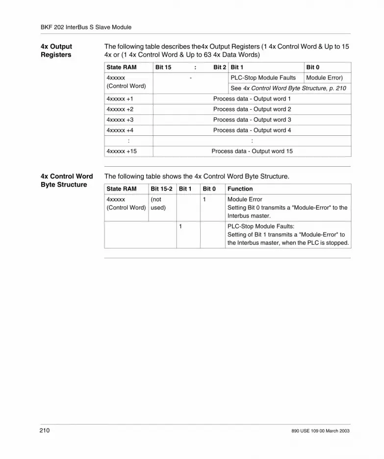
BKF 202 InterBus S Slave Module
4x Output Registers
The following table describes the4x Output Registers (1 4x Control Word & Up to 15 4x or (1 4x Control Word & Up to 63 4x Data Words)
4x Control Word Byte Structure
The following table shows the 4x Control Word Byte Structure.
State RAM Bit 15 : Bit 2 Bit 1 Bit 0
4xxxxx (Control Word)
- PLC-Stop Module Faults Module Error)
See 4x Control Word Byte Structure, p. 210
4xxxxx +1 Process data - Output word 1
4xxxxx +2 Process data - Output word 2
4xxxxx +3 Process data - Output word 3
4xxxxx +4 Process data - Output word 4
: :
4xxxxx +15 Process data - Output word 15
State RAM Bit 15-2 Bit 1 Bit 0 Function
4xxxxx (Control Word)
(not used)
1 Module ErrorSetting Bit 0 transmits a "Module-Error" to the Interbus master.
1 PLC-Stop Module Faults:Setting of Bit 1 transmits a "Module-Error" to the Interbus master, when the PLC is stopped.
210 890 USE 109 00 March 2003

BKF 202 InterBus S Slave Module
Interbus Bi-Directional Communication between the E984 PLC and the BKF 202 IBS Slave Module
The following figure shows the process data exchange between the PLC and the Interbus.
E984 PLC - OUT
Check word (4x)
Data word 1 (4x+1)
Data word 15 (4x+15)
2
0
BKF 202 - IN
1
2
15
16
E984 PLC-IN BKF 202-OUT
1
2
15
16
Data word 15 (3x+15)
2
Data word 1 (3x+1)
Status word (3x)
890 USE 109 00 March 2003 211

BKF 202 InterBus S Slave Module
Specifications of the BKF 202 InterBus S Slave Module
Specifications The following table lists specifications for the BKF 202 InterBus S Slave Module.
Power supply
Internally from I/O-Bus 5VDC, 300 mA max. (w/o fiber-optic Interface)
Data Interface
Field bus as RS 485 Interfaceremote in: potentialfree 150 Ohmremote out: potentialbound 150 Ohm
Processor
Processor type 80C32 16 MHz
Data memory 32KB RAM
Firmware 64KB EPROM
I/O Map
Register 3x/4x 16 in/16 out
Physical Characteristics
Module in standard-size case
Format I Slot
Weight 250 g
Type of Connection
Remote bus 9-pin DSUB socket/connector bar
Backplane Connector bar 1/3 C30M
Environmental Characteristics
Regulations VDE 0160, UL 508
Permissible ambient temperature 0 ... +60 degrees C.
Power dissipation max. 1.5W
Option Fiber-optic adapter
212 890 USE 109 00 March 2003

890 USE 109 00 March 2003
DAO 216 Discrete Output Module
At a Glance
Purpose The purpose of this chapter is to describe the DAO 216 discrete output module.
What’s in this Chapter?
This chapter contains the following topics:
Topic Page
What is the DAO 216 Discrete Output Module? 214
DAO 216 Discrete Output Module Physical Characteristics 215
Protecting the DAO 216 Discrete Output Module from Inductive Back EMF 218
DAO 216 Discrete Output Module Specifications 219
213

DAO 216 Discrete Output Module
What is the DAO 216 Discrete Output Module?
DAO 216 Discrete Output Module
The DAO 216 is a discrete output module with 16 independent 24 Vdc output circuits. It can drive relays, motor starters, pilot lamps, valves, solenoids and other similar loads. The module is structured in one group of 16 outputs. The outputs are not isolated.The DAO 216 can be installed in any slot in the A120 subracks (DTA 200, 201, and 202). The module has bus contacts at the rear and field connections on the front. The blank label, which fits in the module cover, can be filled in with relevant information (signal values, etc.) in the spaces provided. Refer to the diagram in LEDs, p. 215
WARNING
Operational Hazard
The DAO 216 module will only operate properly when used with an A984, E984, or Micro 512/612 controller.
Failure to follow this precaution can result in death, serious injury, or equipment damage.
214 890 USE 109 00 March 2003

DAO 216 Discrete Output Module
DAO 216 Discrete Output Module Physical Characteristics
LEDs The DAO 216 has 17 LEDs. One green LED opposite terminal screw #1 indicates presence of external working voltage to the 16 outputs (ON = voltage available; OFF = voltage not available). There are 16 red LEDs opposite terminal screws 3 ... 10 and 14 ... 21, indicating when ON that 24 Vdc is present at the adjacent discrete output.Front View and Fill-in Label of the DAO 216 Module
DAO 216
1
2
3
4
5
67
8
9
1011
1213
1415
1617
1819
2021
22card
M
M
9
10
11
12
13
14
1516
U
U
input1
2
3
4
5
6
7
8
DAO 216
890 USE 109 00 March 2003 215

DAO 216 Discrete Output Module
Simplified Schematic
Simplified Schematic for the DAO 216 Output Module
123456789
10111213141516171819202122
Green LED
15 V
OutputDriver D-Flop/8
Red LED
I/O BusInterface
24 VDC
24 V Common
Out1Out2Out3Out4Out5Out6Out7Out8
Out9Out10Out11Out12Out13Out14Out15Out16
*Terminal 11 should beconnected in the shortest pos-sible way to the functionalground. In case of connectionfailure compensating currentscan occur via M2>0V path, thatleads to the destruction of theprotective resistor.
216 890 USE 109 00 March 2003

DAO 216 Discrete Output Module
Wiring Diagram Wiring the DAO 216
24 VdcGND
4A
A1
A8
A9
A16
1
2
3
4
5
6
7
8
9
10
11
12
13
14
15
16
18
20
22
890 USE 109 00 March 2003 217
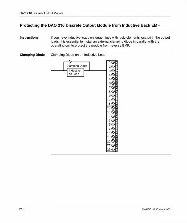
DAO 216 Discrete Output Module
Protecting the DAO 216 Discrete Output Module from Inductive Back EMF
Instructions If you have inductive loads on longer lines with logic elements located in the output loads, it is essential to install an external clamping diode in parallel with the operating coil to protect the module from reverse EMF.
Clamping Diode Clamping Diode on an Inductive Load
Clamping Diode
Inductivedc Load
1
2
345
6
7
89
1011
1213
1415
17
19
21
16
18
20
22
218 890 USE 109 00 March 2003

DAO 216 Discrete Output Module
DAO 216 Discrete Output Module Specifications
DAO 216 Specifications
The following table contains a list of DAO 216 specifications
Module Topology
Number of Outputs 16
Number of Groups 1
Points/Group 16
Isolation No isolation provided
Power Supplies External Source Requirement 24 Vdc (20 to 30 Vdc), 5 A @30 Vdc
Internally Provided Source 5 V from I/O bus, 30 mA max.
Internal Power Dissipation 5 W (typical)
Electrical Characteristics
Operating Mode True High
ON State Signal Level Source voltage minus 3 V
OFF State Signal Level 0 ... +2 V, less than 1mA
Load Current/Output 10 mA ... 500 mA
Max Load Current/Module 4 A
Response Time less than 1 msec.
Reverse-EMF Protection Built-in circuitry limits inductive spikes to a maximum of -15 V
Switch Capacity for Bulbs Max. 5 W (Surge current = Nor mal current x 10)
OFF-ON Operations 1000/hour for inductive load @ maximum load current
Wire Size/Terminal One wire = 14 AWG
Two wires = 20 AWG
I/O Map Discrete 1x/0x 0 in/16 out
Dimensions W x H x D 40.3 x 145 x 117.5mm (1.6 x 5.6 x 4.5 in)
Weight 250 g (.55 lb)
Agency Approval
VDE 0160; UL 508; CSA 22.2 No.142; and FM Class I, Div 2 Stan dards
890 USE 109 00 March 2003 219

DAO 216 Discrete Output Module
220 890 USE 109 00 March 2003

890 USE 109 00 March 2003
Overview of the DAP 204 Relay Output Module
At a Glance
Purpose The purpose of this chapter is to describe the DAP 204 Relay Output Module.
What’s in this Chapter?
This chapter contains the following topics:
Topic Page
What is the DAP 204 Relay Output Module? 222
DAP 204 Relay Output Module LEDs 223
DAP 204 Relay Output Module Field Wiring 224
Protecting the DAP 204 Relay Output Module from Inductive Back EMF 225
DAP 204 Relay Output Module Specifications 227
221

DAP 204 Relay Output Module
What is the DAP 204 Relay Output Module?
Brief Product Description
The DAP 204 is a four point relay output module. It utilizes logic signals within the PLC to activate four independent, individually isolated, normally open relay contacts. Source voltage for any output load may be 24 ... 154 Vdc or 24 ... 250 Vac. Wiring Diagram and Simplified Schematic for the DAP 204 Output Module
24 VDC
24 V CommonGreenLED
0.16A
Load1
Load2
Load3
Load4
Relay
RedLED
Opto-Coupler
I/O BusInterface
123
456789
1011
1213141516171819202122
V
V
V
V
Driver
222 890 USE 109 00 March 2003

DAP 204 Relay Output Module
DAP 204 Relay Output Module LEDs
LEDs The DAP 204 has five LEDs. One green LED opposite terminal screw 1 indicates the presence of relay coil voltage when ON. Four red LEDs opposite terminal screws 3, 7, 14, and 18 indicate when ON that the relay coils are energized at outputs 1 ... 4, respectively, and suggest that the contacts are closed and the loads energized. These LEDs are in parallel with the relay coils, not the load.
890 USE 109 00 March 2003 223

DAP 204 Relay Output Module
DAP 204 Relay Output Module Field Wiring
Introduction Field wiring to each output connects to a double screw terminal. This module requires power from an external 24 Vdc source to support the relay driver (even if all the outputs switch ac power).
DAP 204 Relay Output Module
A wiring diagram and simplified schematic for the DAP 204 relay output module is provided below.
24 VDC
24 V CommonGreenLED
0.16A
Load1
Load2
Load3
Load4
Relay
RedLED
Opto-Coupler
I/O BusInterface
123
456789
1011
1213141516171819202122
V
V
V
V
Driver
224 890 USE 109 00 March 2003

DAP 204 Relay Output Module
Protecting the DAP 204 Relay Output Module from Inductive Back EMF
Instructions In order to increase the service life of your contacts and protect the DAP 204 module from potential reverse-EMF damage, externally connect a clamping diode in parallel with each inductive dc load and externally connect an RC snubber circuit in parallel with each inductive ac load.
Illustration of Clamping Diode and Snubber Circuit
The following illustration is an example of clamping diode and snubber circuit on inductive loads.
24 V
230 V
Clamping Diode
InductiveDC Load
R C
1
23
4567
8
91011
1213
1415
17
19
2122
20
18
16
InductiveAC Load
− +
890 USE 109 00 March 2003 225

DAP 204 Relay Output Module
Suggested Component Values
The clamping diode forward current rating must be equal to or greater than load current. Diode PIV rating must be three or four times greater than supply voltage at 24 Vdc and 8 ... 10 times greater than supply voltage at 110 Vdc. The unpolarized (ac) snubber capacitor should have a voltage rating two or three times greater than the supply voltage. Values may be:
Snubber resistors may be 1 ... 3 ohms, 2 W. Resistor values should be increased up to 47 ohms, 1/2 W for RL exceeding 100 ohms.Operational range options are shown in the following diagram.
25 ... 70 mH .50 microF
70 ... 180 mH .25 microF
180 mH .10 microF
+Vcc = 140 VdcBDAP Contact
Load 1K ohm (Min) 20 Henries (Max)
Suppression Diode (1N4003)
RCL
Calculations:Given: Vcc = 140VdcI (Max) = .15 AThen: R(L)(Min) = 140/.15 = 1KohmSince L/R = .02 Sec, and R = 1KohmThen L(Max) = (.02) X 1000 = 20H
Voltage rating of diode = 1.5 X VccCurrent rating of diode = 2 X I (Max)Must be “slow,” rectifier, vs logic
RCL = Current Limiting Resistor (.5 Load R)Here, 470 ohmsIf carbon film, .25 watt,If metal film, .50 watt
A shows the consequences of ohmic load and L/R ratiosB shows the application of the suppression diodeC shows the application of a current limiting resistor in series with the diode to protect
the diode from contact bounce
A
B
C
226 890 USE 109 00 March 2003

DAP 204 Relay Output Module
DAP 204 Relay Output Module Specifications
DAP 204 Specifications
The following table contains a list of DAP 204 relay output module specifications.
Module Topology
Number of Relay Outputs
4
Number of Groups 4
Points/Group 1
Isolation Four individually isolated relay contacts
Power Supplies
External Source Requirement
24 Vdc, 150 mA maximum
Internally Provided Source
5 V from I/O bus @ 25 mA max.
Internal Power Dissipation
2 W (typical)
Electrical Characteristics
Output Voltage Ranges
24 ... 154 Vdc; 24 ... 250 Vac
Operating Mode Normally Open
Response Time 10 ms (typical)
Wire Size/Terminal One wire: 14 AWG
Two wires: 20 AWG
Environmental Characteristic
Operating Temperature
-25 ... +70 degrees C (-13 ... +158 degrees F)
Output Characteristics
Load Currents @ 230 Vac
2 A continuous (maximum, resistive load)
4 A instantaneous (maximum, resistive load)
1 A continuous (maximum, Cos = 0.5)
Load Current @ dc Working Voltage @ 24 Vdc
2 A continuous maximum (resistive load)
4 A instantaneous maximum (resistive load)
1 A continuous maximum (L/R* = 30 ms)
Working Voltage @ 60 Vdc
1 A continuous maximum (resistive load)
0.6 A maximum (L/R* = 30 ms)
Working Voltage @ 140 Vdc
0.3 A continuous (resistive load)
0.15 A (L/R* = 20 ms)
890 USE 109 00 March 2003 227

DAP 204 Relay Output Module
Wetting Current 5 mA for closed contacts
Leakage 1 mA
Internal Protective Circuitry
68 ohms +15 nF in parallel with each contact
* L = Load Inductance in Henries; R = Load Resistance in ohms
I/O Map Discrete 1x/0x 0 in/8 out
Service Life of Contacts
Mechanical switching cycles
20,000,000
Electric switching cycles
10,000,000 @ 230 Vac/0.2 A
(Resistive Loads) 7,000,000 @ 230 VAC / 0.5 A
8,000,000 (typical) @ 30 VDC / 2 A, with clamping diode
1,000,000 (typical) @ 60 VDC / 1 A, with clamping diode, 3000 cycles/hr max
Electric switching cycles
5,000,000 @ 230 Vac/0.5 A
(Inductive Loads, Cos = 0.5*)
Overload Protection
Should be provided externally
228 890 USE 109 00 March 2003

DAP 204 Relay Output Module
Service Life for Resistive Loads
The maximum number of switching cycles is reduced when inductive loads are encountered. Reference the load device manufacturer’s catalog for steady state and inrush VA ratings to determine the number of operations derating factor. If the frequency of operations is relatively high, use the inrush VA to calculate Cos f: Effective number of operations = # of operations (resistive load) x reduction factor:
107
8
6
4
2
106
8
6
4
2
0 0.2 0.6 1 1.4 1.8
# O
F O
PE
RA
TIO
NS
DEVICE RATING(kVA)
890 USE 109 00 March 2003 229
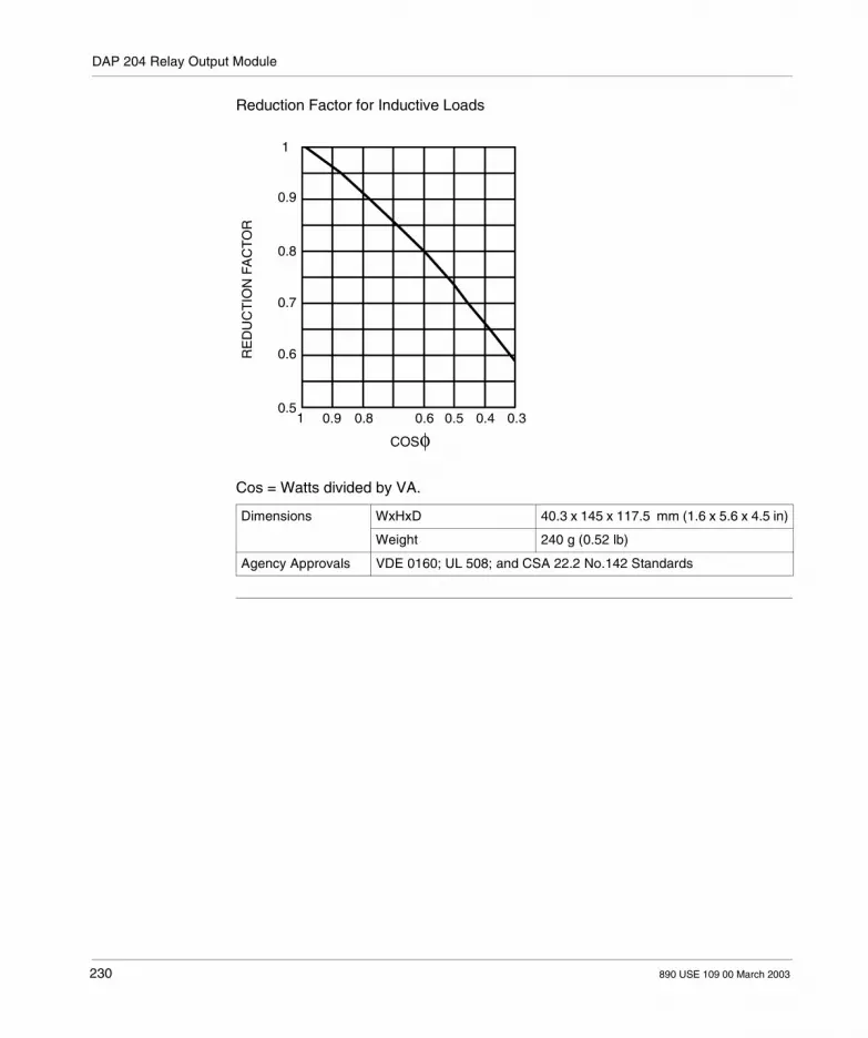
DAP 204 Relay Output Module
Reduction Factor for Inductive Loads
Cos = Watts divided by VA.
Dimensions WxHxD 40.3 x 145 x 117.5 mm (1.6 x 5.6 x 4.5 in)
Weight 240 g (0.52 lb)
Agency Approvals VDE 0160; UL 508; and CSA 22.2 No.142 Standards
0.9
1
0.8
0.7
0.6
0.51 0.9 0.8 0.6 0.5 0.4 0.3
COSφ
RE
DU
CT
ION
FA
CT
OR
230 890 USE 109 00 March 2003

890 USE 109 00 March 2003
Overview of the DAP 208/258 Relay Output Module
At a Glance
Purpose The purpose of this chapter is to describe the DAP 208/258 relay output module.
What’s in this Chapter?
This chapter contains the following topics:
Topic Page
What is the DAP 208/258 Relay Output Module? 232
DAP 208/258 Relay Output Module LEDs 233
DAP 208/258 Relay Output Module Field Wiring 234
Protecting the DAP 208/258 Relay Output Module from Inductive Back EMF 235
DAP 208/258 Relay Output Module Specifications 237
231

DAP 208/258 Relay Output Module
What is the DAP 208/258 Relay Output Module?
Brief Product Description
The DAP 208/258 is an eight point relay output module. It utilizes logic signals within the controller to activate eight individually isolated, normally open relay contacts. Source voltage for any output load may be 24 ... 154 Vdc or 24 ... 250 Vac.
232 890 USE 109 00 March 2003

DAP 208/258 Relay Output Module
DAP 208/258 Relay Output Module LEDs
LEDs The DAP 208/258 has nine LEDs. One green LED opposite terminal screw 1 indicates the presence of relay coil voltage when ON. Eight red LEDs opposite terminal screws 3, 5, 7, 9, 14, 16, 18, and 20 indicate when ON that the relay coils are energized at outputs 1 ... 8, respectively, and suggest that the contacts are closed and the loads energized. These LEDs are in parallel with the coils, not the load.
890 USE 109 00 March 2003 233
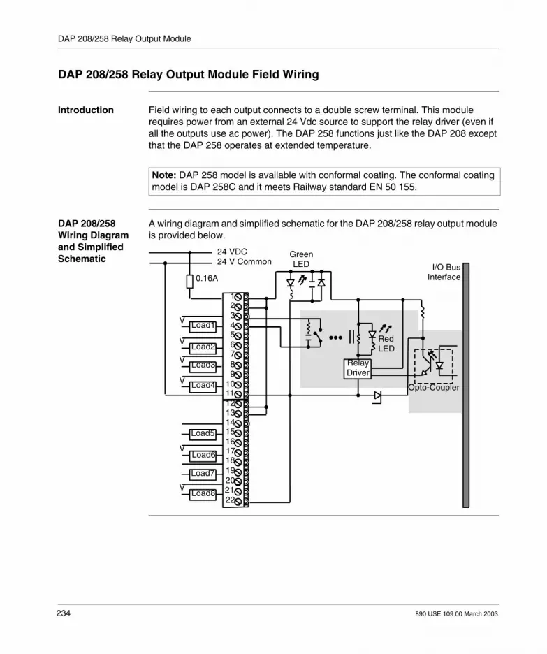
DAP 208/258 Relay Output Module
DAP 208/258 Relay Output Module Field Wiring
Introduction Field wiring to each output connects to a double screw terminal. This module requires power from an external 24 Vdc source to support the relay driver (even if all the outputs use ac power). The DAP 258 functions just like the DAP 208 except that the DAP 258 operates at extended temperature.
DAP 208/258 Wiring Diagram and Simplified Schematic
A wiring diagram and simplified schematic for the DAP 208/258 relay output module is provided below.
Note: DAP 258 model is available with conformal coating. The conformal coating model is DAP 258C and it meets Railway standard EN 50 155.
24 VDC24 V Common
0.16A
V
V
V
V
V
V
Load1
Load2
Load3
Load4
Load6
Load8
Load5
Load7
GreenLED
RelayDriver
RedLED
I/O BusInterface
Opto-Coupler
123456789
1011121314
16
18
20
22
15
17
19
21
234 890 USE 109 00 March 2003

DAP 208/258 Relay Output Module
Protecting the DAP 208/258 Relay Output Module from Inductive Back EMF
Instructions To increase the service life of your contacts and protect the DAP 208/258 module from potential reverse-EMF damage, externally connect a clamping diode in parallel with each inductive dc load and externally connect an RC snubber circuit in parallel with each inductive ac load.
Clamping Diode and Snubber Circuit
The following illustration is an example of clamping diode and snubber circuit on inductive loads.
24 V
230 V
Clamping Diode
Inductivedc Load
Inductiveac Load
1
23
456
7
8
9
1011
1213
1415
17
19
21
R C
_ +
16
18
20
22
890 USE 109 00 March 2003 235

DAP 208/258 Relay Output Module
Suggested Component Values
The clamping diode forward current rating must be equal to or greater than load current. Diode PIV rating must be three or four times greater than supply voltage at 24 Vdc and 8 ... 10 times greater than supply voltage at 110 Vdc. The unpolarized (ac) snubber capacitor should have a voltage rating two or three times greater than the supply voltage.Values may be:
Snubber resistors may be 1 ... 3 W, 2 W. Resistor values should be increased up to 47 ohms, 1/2 W for RL exceeding 100 ohms.Operational Range Options Using 140 Vdc Example
Load Inductance Capacitance
25 ... 70 mH .50 microF
70 ... 180 mH .25 microF
180 mH .10 microF
236 890 USE 109 00 March 2003

DAP 208/258 Relay Output Module
DAP 208/258 Relay Output Module Specifications
DAP 208/258 Tables and Diagrams
The following table contains a list of DAP 208/258 relay output module specifications.
Module Topology
Number of Relay Outputs 8
Number of Groups 8
Points/Group 1
Isolation Eight individually isolated relay contacts
Power Supplies External Source Requirement
24 Vdc, 150 mA maximum
Internally Provided Source 5 V, less than 60 mA from I/O bus
Internal Power Dissipation 2 W (typical)
Electrical Characteristics
Output Voltage Ranges 24 ... 154 Vdc; 24 ... 250 Vac
Operating Mode Normally Open
Response Time 10 ms (typical)
Wire Size/Terminal One wire: 14 AWG
Two wires: 20 AWG
Environmental Characteristic
Operating Temperature 0 ... 60 degrees C for DAP 208-40 ... +70 degrees C for DAP 258
Output Characteristics
Load Currents at 230 Vac 2 A continuous (maximum, resistive load)
4 A instantaneous (maximum, resistive load)
1 A continuous (maximum, Cos = 0.5)
Load Current at dc Working Voltage @ 24 Vdc
2 A continuous maximum (resistive load)
4 A instantaneous maximum (resistive load)
1 A continuous (maximum, Cos = 0.5)
Working Voltage @ 60 Vdc
1 A continuous maximum (resistive load)
0.6 A maximum (L/R* = 30 ms)
Working Voltage @ 140 Vdc
0.3 A continuous (resistive load)
0.15 A (L/R* = 20 ms)
Wetting Current 5 mA for closed contacts
890 USE 109 00 March 2003 237

DAP 208/258 Relay Output Module
Leakage 1 mA
Internal Protective Circuitry
68 ohms +15 nF in parallel with each contact
Overload Protection Should be provided externally
* L = Load Inductance in Henries; R = Load Resistance in ohms
I/O Map Discrete 1x/0x 0 in/8 out
Service Life of Contacts
Mechanical switching cycles
20,000,000
Electric switching cycles 10,000,000 @ 230 Vac/0.2 A
(Resistive Loads)
7,000,000 @ 230 VAC / 0.5 A
8,000,000 (typical) @ 30 VDC / 2 A, with clamping diode
1,000,000 (typical) @ 60 VDC / 1 A, with clamping diode, 3000 cycles/hr max
Electric switching cycles 5,000,000 @ 230 Vac/0.5 A
(Inductive Loads, Cos = 0.5)
238 890 USE 109 00 March 2003
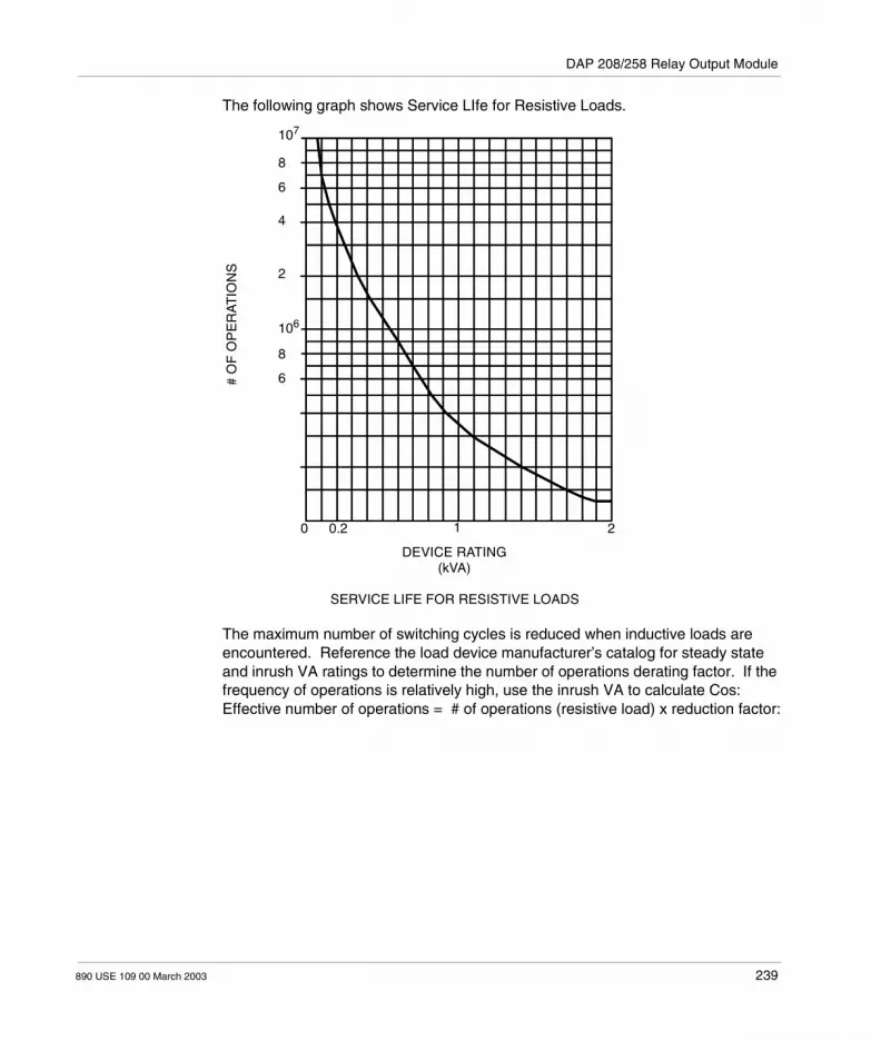
DAP 208/258 Relay Output Module
The following graph shows Service LIfe for Resistive Loads.
The maximum number of switching cycles is reduced when inductive loads are encountered. Reference the load device manufacturer’s catalog for steady state and inrush VA ratings to determine the number of operations derating factor. If the frequency of operations is relatively high, use the inrush VA to calculate Cos: Effective number of operations = # of operations (resistive load) x reduction factor:
107
8
6
4
2
106
6
8
0 0.2 1 2
DEVICE RATING(kVA)
SERVICE LIFE FOR RESISTIVE LOADS
# O
F O
PE
RA
TIO
NS
890 USE 109 00 March 2003 239

DAP 208/258 Relay Output Module
The chart below shows Reduction Factor for Inductive Loads.
Cos = Watts divided by VA.
Dimensions WxHxD 40.3 x 145 x 117.5 mm (1.6 x 5.6 x 4.5 in)
Weight 240 g (0.52 lb)
Agency Approvals
DAP 208: VDE 0160; UL 50; CSA 22.2 No.142; and FM Class I, Div 2 Standards
DAP 258C: Railway standard EN 50 155: EMC 89/336/EEC (See Requirements for CE Compliance, p. 779). UL 50; CSA 22.2 No.142; and FM Class I, Div 2 pending
1
0.9
0.8
0.7
0.6
0.51 0.9 0.8 0.7 0.6 0.5 0.4 0.3
RE
DU
CT
ION
FA
CT
OR
COSφREDUCTION FACTOR FOR INDUCTIVE LOADS
240 890 USE 109 00 March 2003

890 USE 109 00 March 2003
Overview of the DAP 209 Output Module
At a Glance
Purpose The purpose of this chapter is to describe the DAP 209 output module.
What’s in this Chapter?
This chapter contains the following topics:
Topic Page
What is the DAP 209 Output Module? 242
DAP 209 Output Module LEDs 243
DAP 209 Output Module Field Wiring 244
DAP 209 Output Module Specifications 245
241

DAP 209 Output Module
What is the DAP 209 Output Module?
Brief Product Description
The DAP 209 is a discrete output module with eight independent 120 Vac output circuits. It can drive relays, motor starters, pilot lamps, valves, solenoids and other similar loads of up to 1 A/channel. The module is structured in one group of eight outputs, each output electrically isolated from the I/O bus by an opto coupler.
242 890 USE 109 00 March 2003
DAP 209 Output Module
DAP 209 Output Module LEDs
LEDs The DAP 209 has nine LEDs. One green LED opposite terminal screw 1 indicates the presence of AC line voltage when ON. Eight red LEDs opposite terminal screws 3, 5, 7, 9, 14, 16, 18, and 20 indicate an AC ON condition for load at the field wiring side of the system for outputs 1 ... 8, respectively. Depending on local conditions, users may notice LEDs on unused outputs exhibiting a dim glow. To eliminate this condition, connect a 39K ohms, 1/2 W resistor from the unused output terminal to ac neutral.
890 USE 109 00 March 2003 243

DAP 209 Output Module
DAP 209 Output Module Field Wiring
Introduction The DAP 209 is a discrete output module with eight independent 120 Vac output circuits. It can drive relays, motor starters, pilot lamps, valves, solenoids and other similar loads of up to 1 A/channel. The module is structured in one group of eight outputs, each output electrically isolated from the I/O bus by an opto coupler.
Wiring Diagram for DAP 209
A wiring diagram and simplified schematic for the DAP 209 output module is provided below.
8AOut1
Out2
Out3
Out4
Out5
Out7
AC NeutralAC Hot Red
LEDFirst of 8
Output Circuits
Solid StateRelay
ZeroXing
OptoCoupler
Gnd
I/O BusInterface
GreenLED
123456789
1011121314
16
18
20
22
Out 6
Out 8
15
17
19
21
244 890 USE 109 00 March 2003

DAP 209 Output Module
DAP 209 Output Module Specifications
DAP 209 Tables of Specifications
The following tables contain DAP 209 output module specifications.
DAP 209 Load Current (Amps)@60 Degrees C, Ambient
Module Topology
Number of Outputs 8
Number of Groups 1
Points/Group 8
Isolation Optocoupler on each output point
Power Supplies
External Source Requirement 120 Vac
Internally Provided Source 5 V from I/O bus; 55 mA max.
Internal Power Dissipation 2 W (typical)
Electrical Characteristics
Working Voltage Range 85 ... 138 Vac continuous, 47 ... 63 Hz
Output Voltage 150 Vac RMS maximum for 10 s 200 Vac RMS maximum for 1 cycle
Operating Mode True High
OFF State Leakage Current 1.9 mA maximum
ON State Voltage Drop 1.5 Vac RMS maximum
Load Current Up to 1 A/channel 5 mA mini mum
Response Time 8.34 ms maximum @ 60 Hz
Wire Size/Terminal One wire: 14 AWG
Two wires: 20 AWG
I/O Map Discrete 1x/0x 0 in/8 out
Dimensions W x H x D 40.3 x 145 x 117.5 mm (1.6 x 5.6 x 4.5 in)
Weight 450 g (1 lb)
Agency Approvals
VDE 0160; UL 508; and CSA 22.2 No.142 Standards
Number of Outputs in Use Max. Allowable Load/Output @ 60 degrees, Ambient
8 0.6 A
6 0.67A
4 0.71 A
2 0.87 A
1 1.0 A
890 USE 109 00 March 2003 245

DAP 209 Output Module
DAP 209 1 A Load Current vs. Temperature
Number of Outputs @ 1 A Allowable Ambient Temperature
8 35 degrees C
6 40 degrees C
4 45 degrees C
2 51 degrees C
1 60 degrees C
246 890 USE 109 00 March 2003

890 USE 109 00 March 2003
Overview of the DAP 210 Output Module
At a Glance
Purpose The purpose of this chapter is to describe the DAP 210 output module.
What’s in this Chapter?
This chapter contains the following topics:
Topic Page
DAP 210 Output Module LEDs 248
DAP 210 Output Module Field Wiring 249
DAP 210 Output Module Specifications 250
What is the DAP 210 Output Module? 252
247

DAP 210 Output Module
DAP 210 Output Module LEDs
LEDs The DAP 210 has nine LEDs. One green LED opposite terminal screw 1 indicates the presence of system power to the module. Eight red LEDs opposite terminal screws 3, 5, 7, 9, 14, 16, 18, and 20 indicate that the output points have been enabled on the module’s logic side.
The following diagram illustrates bit assignment for the DAP 210 output module.
CAUTION
Operational Hazard
Each output group is fused to protect against catastrophic failure. For protection against triac failure, each output must be individually fused with a fast-acting fuse rated at 1.5 times user continuous current (fuse must not exceed 2 A).
Failure to follow this precaution can result in injury or equipment damage.
Not Used
Output #1
Output #2
Output #4
Output #6
Output #8
01234567815 14 13 11 10 912
Output #3
Output #5
Output #7
248 890 USE 109 00 March 2003
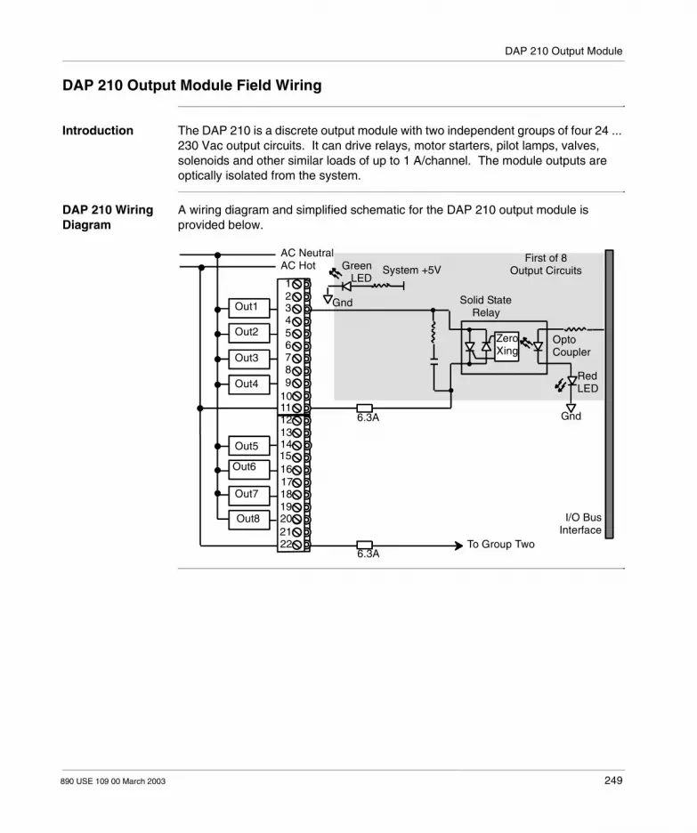
DAP 210 Output Module
DAP 210 Output Module Field Wiring
Introduction The DAP 210 is a discrete output module with two independent groups of four 24 ... 230 Vac output circuits. It can drive relays, motor starters, pilot lamps, valves, solenoids and other similar loads of up to 1 A/channel. The module outputs are optically isolated from the system.
DAP 210 Wiring Diagram
A wiring diagram and simplified schematic for the DAP 210 output module is provided below.
AC NeutralAC Hot
Out1
Out2
Out3
Out4
Out5
Out7
GreenLED
System +5V
Gnd
First of 8Output Circuits
Solid StateRelay
ZeroXing
OptoCoupler
RedLED
Gnd6.3A
6.3ATo Group Two
I/O BusInterface
123456789
1011121314
16
18
20
22
Out6
Out8
15
17
19
21
890 USE 109 00 March 2003 249

DAP 210 Output Module
DAP 210 Output Module Specifications
DAP 210 Specifications
The following table and illustrations contain DAP 210 output module specifications.
Module Topology
Number of Outputs 8
Number of Groups 2
Points/Group 4
Isolation Field to bus; 1500 Vac RMS @ 47 ... 63 Hz, 2500 Vdc, both for a period of 60 s without breakdown
Power Supplies
*External Source Requirement 24 ... 230 Vac, 47 ... 63 Hz
Internally Provided Source 5 V, less than 70 mA from the I/O bus
Power Dissipation 7.2 W with all points ON
Fusing (per group) One 250 Vac, 6.3 A time-lag fuse (Wickmann TR5-T Fuse; Modicon Part # 57-0110-000)
Electrical Characteristics
*Working Voltage Range 24 ... 230 Vac continuous, 47 ... 63 Hz
Maximum Output Voltage 300 Vac RMS maximum for 10 s 400 Vac RMS maximum for 1 cycle
Operating Mode True High
OFF State Leakage Current 3.75 mA maximum
ON State Voltage Drop 1.5 Vac RMS maximum
Maximum Load Current Up to 1.0 A/channel (see graph)
Maximum Surge Current 15 A/1 cycle, 1 surge/min maximum
Minimum Load Current 50 mA RMS
Response Time 8.34 ms maximum OFF to On and ON to OFF @ 60 Hz
Maximum Rate of Applied DV/DT
400 V/msec
Maximum Rate of Commutating DV/DT
5 V/micros
Wire Size/Terminal One wire: 14 AWG
Two wires: 20 AWG
I/O Map Discrete 1x/0x 0 in/8 out
Environmental Operating Temperature 0 ... 60 degrees C
Storage Temperature -40 ... +80 degrees C
Humidity 0 ... 95 percent relative humidity @ 0 ... 60 degrees C
250 890 USE 109 00 March 2003

DAP 210 Output Module
The graph below shows DAP 210 Power Output.
Dimensions W x H x D 40.3 x 145 x 117.5 mm (1.6 x 5.6 x 4.5 in)
Weight 1 lb (.45kg)
*Agency Approvals
VDE 0160; UL 508; CSA 22.2 No.142; and European Directive EMC 89/336/EEC (See Requirements for CE Compliance, p. 779) Standards
*The module is labelled both as a 24 VAC to 115 VAC or 24 VAC to 230 VAC. When used in a VDE 0160 environment the voltage range is reduced to 24 VAC to 115 VAC. When used in a non VDE 0160 environment the module meets specification IEC 1131; UL 508; and CSA 22.2 No.142 and operates over the full range of 24 VAC to 230 VAC.
890 USE 109 00 March 2003 251

DAP 210 Output Module
What is the DAP 210 Output Module?
Brief Product Description
The DAP 210 is a discrete output module with two independent groups of four 24 ... 230 Vac output circuits. It can drive relays, motor starters, pilot lamps, valves, solenoids and other similar loads of up to 1 A/channel. The module outputs are optically isolated from the system.
WARNING
Operational Hazard
The DAP 210 module will only operate properly when used with an A984, E984, or Micro 512/612 controller.
Failure to follow this precaution can result in death, serious injury, or equipment damage.
252 890 USE 109 00 March 2003

890 USE 109 00 March 2003
Overview of the DAP 211 Combined I/O Module
At a Glance
Purpose The purpose of this chapter is to describe the DAP 211 combined I/O module.
What’s in this Chapter?
This chapter contains the following topics:
Topic Page
What is the DAP 211 Combined I/O Module? 254
DAP 211 Combined I/O Module Logical Input Routine 255
DAP 211 Combined I/O Module Error Checking Procedure for Output States 256
DAP 211 Combined I/O Module Setup Options 257
DAP 211 Combination I/O Module LEDs 258
DAP 211 Combined I/O Module Field Wiring 259
DAP 211 Combined I/O Module Specifications 260
253
DAP 211 Combined I/O Module
What is the DAP 211 Combined I/O Module?
Brief Product Description
The DAP 211 is a 120 Vac, mixed I/O (4 binary isolated input points/4 binary isolated short-circuited protected Triac output points) module. An external operating voltage of 120 Vac for sensor supply (inputs) and an external working voltage of 120 Vac for the outputs must be provided.The DAP 211 module is unique in its design. It may be used in two different applications: 1. Non-voted (single) application, where the DAP 211 monitors its own outputs
using a single module.2. Voted (dual) application, where the output of the first DAP 211 is monitored
through an input of the second DAP 211 using a two-module configuration.When used for voted (dual) applications, such as clutch and brake, the modules operate in pairs. That is, the interconnection of two modules makes it possible for the output of the first module to be monitored through an input of the second module. This results in logical states.
Note: Some A120 I/O modules (DEP 211/214/215/217, DAP211/217, ADU204/211/214/216, DAU204, VIC2xx, and MOT20x) require a loadable (SW-IODR-001) for proper operation when using certain PLCs (A984-1xx, E984-24x/251/255) with Modsoft.
Note: This module corrects a current problem of false indication of inputs being in the on" state due to leakage currents in monitored output systems as applied in safety circuits like clutch and brake I/O circuits.
254 890 USE 109 00 March 2003

DAP 211 Combined I/O Module
DAP 211 Combined I/O Module Logical Input Routine
Logical States for Voted (Dual) Operations
The five possible outputs for module 1 appear at the top of the table. The five possible outputs for module 2 appear on the left side of the table. The input states for module 2 and module 1 appear in the center as noted.
For voted (dual) applications, ensure the two modules are wired as shown in DAP 211 Combined I/O Module Field Wiring. The logical states table is an absolute MUST in programming/configuration, since only those modules with a defined operating state have a "LOW-LOW" combination.
Module 1
Output States Triac On Triac as Diode AUX Broken Load Broken Triac Off
Module 2 Triac On Module2=HModule1=H
Module2=HModule1=H
Module2=LModule1=H
Module2=HModule1=H
Module2=HModule1=H
Triac as Diode Module2=HModule1=H
Module2=HModule1=H
Module2=HModule1=H
Module2=HModule1=H
Module2=HModule1=H
AUX Broken Module2=HModule1=L
Module2=HModule1=H
Module2=HModule1=H
Module2=LModule1=L
Module2=HModule1=H
Load Broken Module2=HModule1=H
Module2=HModule1=H
Module2=LModule1=L
Module2=HModule1=H
Module2=HModule1=H
Triac Off Module2=HModule1=H
Module2=HModule1=H
Module2=HModule1=H
Module2=HModule1=H
Module2=LModule1=L
KEY: H=High, L=Low, Triac On= Traic is on or defected (shorted), Triac as Diode= Triac is defected, works as a diode (any direction), AUX Broken= AUX connection between the 2 modules is broken, Load Broken= Load connection between the 2 modules is broken.
890 USE 109 00 March 2003 255

DAP 211 Combined I/O Module
DAP 211 Combined I/O Module Error Checking Procedure for Output States
Error Checking Procedure
Perform the following steps to ensure you have no output errors:
Step Action
1 Set all outputs to OFF. Input 1 and Input 2 must be low, if not you have an error.
2 Test Output 1: Output 1 is set to ON, Output 2 remains at OFF. Result Input 1 is HIGH (input 2 is not tested in this step), if not, you have an error.
3 Test Output 2: Output 2 is set to ON, Output 1 remains at OFF. Result Input 2 is HIGH (input 1 is not tested in this step), if not, you have an error.
4 Set all outputs to OFF: Input 1 and Input 2 must be low, if not, you have an error.
5 If no error, start the press.
256 890 USE 109 00 March 2003

DAP 211 Combined I/O Module
DAP 211 Combined I/O Module Setup Options
Setup Options The way you setup your DAP 211 depends upon the application. Refer to the wiring diagram for Non-Voted (Single) applications. This application requires one PLC and one DAP 211 module. Refer to the wiring diagram for Voted (Dual) applications. This application requires two PLCs and two DAP 211 modules.
890 USE 109 00 March 2003 257

DAP 211 Combined I/O Module
DAP 211 Combination I/O Module LEDs
LEDs The DAP 211 module has LEDs opposite terminal screws 1 ... 22.
A front view with DAP 211 label is provided below.
Location of LED Label Color Description
1 Ready Green Working voltage of 4 out puts:On: Working voltage existOff: No working voltage
3, 8, 14, 19 Out1 ... Out4 Red Output signals:On: Output=1Off: Output=0
5, 10, 16, 21 In1 ... In4 Red Input signals:On: Input=1Off: Input=0
DAP 211DAP 211
123456789
1011
1213141516171819202122
ready L1X1out 1out 1in 1L2X2out 2out 2in 2
123456789
10111213141516171819202122
L3X3out 3out 3in 3L4X4out 4out 4in 4
card
258 890 USE 109 00 March 2003

DAP 211 Combined I/O Module
DAP 211 Combined I/O Module Field Wiring
Setup Options The way you setup your DAP 211 depends upon the application. Non-voted (single) applications require one PLC and one DAP 211 module. Voted (dual) applications require two PLCs and two DAP 211 modules.
Wiring Diagrams for DAP 211
A DAP 211 wiring diagram for voted (dual) applications is provided below.
A DAP 211 wiring diagram for non-voted (single) applications is provided below.
DAP 211L
N
F
L
LINAUXOUTOUT
IN
LINAUXOUTOUT
IN
DAP 211
I/O-1
I/O-2
I/O-1
I/O-2
IN
IN
OUT
OUT
123456789
1011
123456789
1011
IN
IN
OUT
OUT
DAP 211
L
N
F
L
I/O-1
I/O-2
IN
IN
OUT
OUT
123456789
1011
LINAUXOUTOUT
IN
INLINAUXOUTOUT
890 USE 109 00 March 2003 259

DAP 211 Combined I/O Module
DAP 211 Combined I/O Module Specifications
Table of Specifications for DAP 211
The following table contains DAP 211 combined I/O module specifications.
Module Topology
Number of Inputs 4 (separated from logic through optical coupler)
Number of Triac Outputs 4
Number of Groups 4
Points/Group 1 in/1 out
Required Loadable (for Modsoft ONLY)
SW-IODR-001
Isolation One group is isolated from the other group. Within a group there is no isolation between inputs and outputs.
Power Supplies External Sensor Requirement 120 Vac
External Working Requirement 120 Vac
Internally Provided Source 5 V from I/O bus; 35 mA typical
Power Dissipation 5 W typical
Input Characteristics
Sensor Power Supply 120 Vac -15 percent, +10 percent @ 47 ... 63 Hz
Signal Rated Value 120 Vac
Input Delay 1 period
Type of Networking Potential isolation per group (group=1 input/1output)
Output Characteristics
Working Voltage 120 Vac -15 percent, +10 percent @ 47 ... 63 Hz for all 4 outputs
Allocation Short-circuit protection by internal fuse
Type of Networking Potential isolation per group (group=1 input/1output)
I/O Map Discrete 1x/0x 4 in/4 out
Environmental Characteristics
Operating Temperature 0 ... 60 degrees C
Dimensions WxHxD 40.3 x 145 x 117.5 mm (1.6 x 5.6 x 4.5 in)
Weight 190 g (.4 lb.)
Agency Approvals
VDE 0160; UL 508; CSA 22.2 No. 142, European Directive EMC 89/336/EEC (See Requirements for CE Compliance, p. 779) Standards
260 890 USE 109 00 March 2003

890 USE 109 00 March 2003
Overview of the DAP 212/252 Combined I/O Module
At a Glance
Purpose The purpose of this chapter is to describe the DAP 212/252 combined I/O module.
What’s in this Chapter?
This chapter contains the following topics:
Topic Page
What is the DAP 212/252 Combined I/O Module? 262
DAP 212/252 Combined I/O Module LEDs 263
DAP 212/252 Combined I/O Module Field Connections 264
Protecting the DAP 212/252 Combined I/O Module from Inductive Back EMF 266
DAP 212/252 Combined I/O Module Specifications 268
261

DAP 212/252 Combined I/O Module
What is the DAP 212/252 Combined I/O Module?
Brief Product Description
The DAP 212/252 is a 24 Vdc, mixed I/O (8 points in/4 relays out) module. It senses eight discrete input signals received by field sensing devices-such as pushbuttons, limit switches, or other 24 Vdc sources-and converts those signals into logic that can be used by the controller. It utilizes logic signals within the controller to activate four independent and individually isolated normally open relay contacts. The module requires power from an external 24 Vdc source to operate. The DAP 252 functions just like the DAP 212 except that the DAP 252 operates at extended temperature -40 ... +70 degrees C.
Note: DAP 252 model is available with conformal coating. The conformal coating model is DAP 252C and it meets Railway standard EN 50 155.
262 890 USE 109 00 March 2003

DAP 212/252 Combined I/O Module
DAP 212/252 Combined I/O Module LEDs
LEDs The DAP 212/252 module has two green LEDs opposite terminal screws 1 and 12; when one of these LEDs is ON, it indicates power available to the input or output points directly below it. Below terminal screw 1 are four red LEDs opposite terminal screws 3, 5, 7, and 9 indicating relay output points 1 ... 4, respectively. Below terminal screw 12 are eight red LEDs opposite terminal screws 14 ... 21 indicating inputs 1 ... 8, respectively.
890 USE 109 00 March 2003 263

DAP 212/252 Combined I/O Module
DAP 212/252 Combined I/O Module Field Connections
DAP 212/252 Wiring Diagram
A wiring diagram for the DAP 212/252 combined I/O module is provided below.
24 ... 110 VDC; 24 ... 250 VAC HOT24 ... 110 VDC; Common; 24...250 VAC Neutral24 VDC 24 V COMMON
24 VDC24 V COMMON
0.15A 4A 4A 0.15A
12
3
4
5
6
7
8
1
2
3
4
5
6
7
8
9
10
11
12
13
14
15
16
17
18
19
20
21
22
264 890 USE 109 00 March 2003

DAP 212/252 Combined I/O Module
Simplified Schematic
A simplified schematic for the DAP 212/252 combined I/O module is provided below.
REDFirst of 4 Output Circuits
PAB
PAB
RED
GREEN or AMBER
FIRST OF 8 INPUT CIRCUITS
GREEN or AMBER
24 VDC
Output 1
Output 2
Output 3
Output 4
24V Common
24 VDC
1
2
3
4
5
6
7
8 24V Common
1
2
3
4
56
7
8
9
1011
12
13
14
15
1617
18
19
20
2122
15nF
47Ω
890 USE 109 00 March 2003 265

DAP 212/252 Combined I/O Module
Protecting the DAP 212/252 Combined I/O Module from Inductive Back EMF
Instructions To increase the service life of the relay output contacts and protect the DAP 212/252 module from potential reverse-EMF damage, externally connect a clamping diode in parallel with each inductive dc load and externally connect an RC snubber circuit in parallel with each inductive ac load.
Illustration of Clamping Diode and Snubber Circuit
The following illustration is an example of clamping diode and snubber circuit on inductive loads.
24 V
230 V
Clamping Diode
InductiveDC Load
InductiveAC Load
R C
12
3
45
67
89
1011
1213
14
1516
1718
1920
2122
266 890 USE 109 00 March 2003
DAP 212/252 Combined I/O Module
Suggested Component Values
The clamping diode forward current rating must be equal to or greater than load current. Diode PIV rating must be three or four times greater than supply voltage at 24 Vdc and 8 ... 10 times greater than supply voltage at 110 Vdc. The unpolarized (ac) snubber capacitor should have a rating two or three times greater than the supply voltage.Values may be:
Snubber Values
Load Inductance Capacitance
25 ... 70 mH .50 microF
70 ... 180 mH .25 microF
180 mH .10 microF
Note: To I/O Map the DAP 252 module in Modsoft you must select DAP 212. Both modules share a host driver and have similar characteristics.
890 USE 109 00 March 2003 267

DAP 212/252 Combined I/O Module
DAP 212/252 Combined I/O Module Specifications
Module Specifications
The following tables and diagrams contain DAP 212/252 combined I/O module specifications.
Module Topology
Number of Inputs 8
Number of Relay Outputs 4
Number of Groups 2
Points/Group 8 in/4 out
Isolation Relay output contacts are individually isolated; the input group is isolated from the out put group
Power Supplies External Source Requirement
24 Vdc, 150 mA maximum
Internally Provided Source 5 V from I/O bus; 25 mA max.
Internal Power Dissipation 2 W (typical)
Input Characteristics
Working Voltage Range 20 ... 30 Vdc
Signal Rated Value +24 V
ON State Signal Level +12 V ... +30 V
OFF State Signal Level -2 V ... +5 V
Input Wetting Current 7 mA
Input Current 4 mA @ 24 V; 6 mA @ 37 V
Response Time 4 ms (typical) for DAP2127 ms (typical) for DAP252
Operating Mode True High
Wire Size/Terminal One wire: 14 AWG
Two wires: 20 AWG
Output Characteristics
Output Voltage Ranges 24 ... 110 Vdc; 24 ... 250 Vac
Operating Mode Normally Open
Response Time 10 ms (typical)
Wire Size/Terminal One wire: 14 AWG
Two wires: 20 AWG
Load Currents at 115/230 Vac
2 A continuous (maximum, resistive load)
4 A instantaneous (maximum, resistive load)
1 A continuous (maximum, Cos = 0.5)
Load Current at 24 Vdc 2 A continuous maximum (resistive load)
4 A instantaneous maximum (resistive load)
1 A continuous maximum (L/ R* = 30 ms)
268 890 USE 109 00 March 2003

DAP 212/252 Combined I/O Module
DAP 212/252 Specifications (continued)
Output Characteristics (continued)
Load Current at 60 Vdc 1 A continuous maximum (resistive load)
0.6 A maximum (L/R* = 30 ms)
Load Current at 110 Vdc 0.45 A continuous maximum (resistive load)
0.25 A maximum (L/R* = 30 ms)
Wetting Current 5 mA for closed contacts
Leakage 1 mA
Internal Protective Circuitry 68 ohms +15 nF in parallel with each contact
Overload Protection Should be provided externally
Environmental Characteristics
Operating Temperature 0 ... 60 degrees C for DAP212 -40 ... +70 degrees C for DAP252
I/O Map Discrete 1x/0x 8 in/4 out
* L = Load Inductance in H R = Load Resistance in ohms
Service Life of Relay Contacts
Mechanical switching cycles 20,000,000
Electric switching cycles (Re sistive Loads)
10,000,000 @ 230 VAC / 0.2 A 7,000,000 @ 230 VAC / 0.5 A, 8,000,000 (typical) @ 30 VDC / 2 A, with clamping diode, 1,000,000 (typical) @ 60 VDC / 1 A, with clamping diode, 3000 cycles/hr max
Electric switching cycles (In ductive Loads, Cos = 0.5)
5,000,000 @ 230 VAC / 0.5 A
890 USE 109 00 March 2003 269

DAP 212/252 Combined I/O Module
This chart shows the Service Life for Resistive Loads.
The maximum number of switching cycles is reduced when inductive loads are encountered. Reference the load device manufacturer’s catalog for steady state and inrush VA ratings to determine the number of operations derating factor. If the frequency of operations is relatively high, use the inrush VA to calculate Cos: Effective number of operations = # of operations (resistive load) x reduction factor:
Device Rating(KVA)
8
10
6
4
2
10
8
6
4
2
10 5
6
7
0 0.2 0.4 0.6 0.8 1 1.4 1.6 1.8 21.2
# O
F O
PE
RA
TIO
NS
270 890 USE 109 00 March 2003
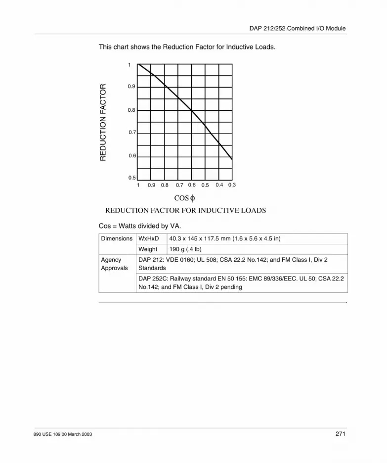
DAP 212/252 Combined I/O Module
This chart shows the Reduction Factor for Inductive Loads.
Cos = Watts divided by VA.
Dimensions WxHxD 40.3 x 145 x 117.5 mm (1.6 x 5.6 x 4.5 in)
Weight 190 g (.4 lb)
Agency Approvals
DAP 212: VDE 0160; UL 508; CSA 22.2 No.142; and FM Class I, Div 2 Standards
DAP 252C: Railway standard EN 50 155: EMC 89/336/EEC. UL 50; CSA 22.2 No.142; and FM Class I, Div 2 pending
REDUCTION FACTOR FOR INDUCTIVE LOADS
COS φ
1
0.9
0.8
0.7
0.6
0.51 0.9 0.8 0.7 0.6 0.5 0.4 0.3
RE
DU
CT
ION
FA
CT
OR
890 USE 109 00 March 2003 271

DAP 212/252 Combined I/O Module
272 890 USE 109 00 March 2003

890 USE 109 00 March 2003
Overview of the DAP 216/216N Discrete Output Module
At a Glance
Purpose The purpose of this chapter is to describe the DAP 216/216N discrete output module.
What’s in this Chapter?
This chapter contains the following topics:
Topic Page
What is the DAP 216/216N Discrete Output Module? 274
DAP 216/216N Discrete Output Module LEDs 275
DAP 216/216N Field Wiring 276
Resetting the DAP 216 Module After an Overload of Short Circuit 277
Protecting the DAP 216/216N Discrete Output Module from Inductive Back EMF
278
DAP 216N Discrete Output Module Differences 279
DAP 216/216N Discrete Output Module Specifications 281
273

DAP 216/216N Discrete Output Module
What is the DAP 216/216N Discrete Output Module?
Brief Product Description
The DAP 216/DAP216N is a discrete output module with 16 independent 24 Vdc output circuits. It can drive relays, motor starters, pilot lamps, valves, solenoids and other similar loads. The module is structured in two group of eight outputs, each output electrically opto-isolated from the I/O bus, and each group is protected against short circuit and overload.
Note: The AS-BDAP-216 has been enhanced. The enhancements have resulted in the AS-BDAP-216 being superseded by the AS-BDAP216N.
274 890 USE 109 00 March 2003

DAP 216/216N Discrete Output Module
DAP 216/216N Discrete Output Module LEDs
LEDs The DAP 216/DAP216N has 20 LEDs. Two green LEDs opposite terminal screws 1 and 12 indicate when ON that working voltage is available to the two groups of eight discrete outputs below them. Two amber LEDs opposite terminal screws 2 and 13 go ON to indicate a short circuit or overload problem in the output group below them. There are 16 red LEDs opposite terminal screws 3 ... 10 and 14 ... 21, indicating when ON that the adjacent discrete output is in an ON condition.
890 USE 109 00 March 2003 275

DAP 216/216N Discrete Output Module
DAP 216/216N Field Wiring
Wiring Diagram and Simplified Schematic for DAP 216/216N
A wiring diagram and simplifed schematic for the DAP 216/DAP216N is provided bleow.
24 VDC24 V Common
2A 2A
Reset AmberLED
FaultDetectionIsolation
I/O BusInterface
D-Flop/8
Opto-Coupler
OutputDriver
Red LED
Green LED
Out16
Out9
Out1Out2Out3Out4Out5Out6Out7Out8
1
1098
234567
11121314
16
18
20
22
Out10Out11Out12Out13Out14Out15
154
19
21
17
276 890 USE 109 00 March 2003

DAP 216/216N Discrete Output Module
Resetting the DAP 216 Module After an Overload of Short Circuit
Instructions A short circuit or overload condition will cause an output point to turn itself off. The degree of overcurrent that causes the device to shut off is determined by thermal characteristics unique to the individual point switching device. When overheated due to overload conditions, the device turns off to protect itself. The two amber LEDs display short circuit or overload conditions on the two discrete output groups. After you have taken corrective measures to remove the cause of the overload or short circuit, push the yellow reset button on the front of the module to reactivate it.
Front View of DAP 216/DAP 216N Module
A front view with DAP 216 label is provided below.
Note: No reset button exists on DAP 216N.
1
Reset ButtonDAP 216 Only
DAP 216
23
456
8
10
7
11
9
121314151617181920
2122
890 USE 109 00 March 2003 277

DAP 216/216N Discrete Output Module
Protecting the DAP 216/216N Discrete Output Module from Inductive Back EMF
Instructions If you have inductive loads on longer lines with logic elements located in the output loads, install an external clamping diode in parallel with the operating coil to protect the module from reverse EMF.
Clamping Diode on an Inductive Load
The following illustration is an example of clamping diode on inductive loads.
Suggested Component Values
The clamping diode forward current rating must be equal to or greater than load current. Diode PIV rating must be 70 ... 100 V.
Clamping Diode
Inductivedc Load
1
2345
6789
1011
1213
141516
18
20
22
17
19
21
278 890 USE 109 00 March 2003
DAP 216/216N Discrete Output Module
DAP 216N Discrete Output Module Differences
Introduction
1. The manual reset button of the BDAP-216 has been replaced by a solid state retry on a shorted output.
2. The module restarts field devices automatically when the output is set ON in the User Logic and the detected field over current condition is removed. Refer to the user logic example in the figure below if detection and manual reset is still desired.
3. You may now apply the full 0.5A per point for 4A per Group and 8A per Module. 4. The input impedance of the electronic circuity that handles the 24Vdc power for
the outputs was lowered to accommodate long runs of the power supply cable. As a result, the inrush current draw from the power supply is increased from about 6A for 2 microseconds to 54A for 12 microseconds. This increase, however, is well below the inrush current that the module draws from the external power supply when outputs are switched on.
Note: The AS-BDAP-216 has been enhanced. The enhancements have resulted in the AS-BDAP-216 being superseded by the AS-BDAP216N.
WARNING
Over Current Hazard.
In the event of an enabled output sensing an over current condition, the output will disable, until the over current condition is removed. The output will then re-enable itself, if still set ON in the logic program.
Failure to follow this precaution can result in death, serious injury, or equipment damage.
890 USE 109 00 March 2003 279

DAP 216/216N Discrete Output Module
User Logic Example
A user logic example to detect module overload condition is provided below.
Each Compact I/O Module returns a Health Bit to the controller when in use. This bit is a single bit in a register that shows the slot position of the module and its status. When the module is functioning correctly this bit is set to "1". User logic can be attached to the state of this bit to hold the logic associated with this module in an OFF condition until an operator pushes a switch to reactivate the user logic.In the illustration above, a STAT function is used to read 12 registers of which register 12 is the status word for the modules in the primary rack 1. The BDAP216N has been placed in slot number 5, so a SENS function block is used to sense bit 5 of this register. The output is tied to coil 0513 which turns OFF when the module becomes unhealthy. To trap this condition even if coil 0513 turns ON again, it is latched into coil 0514. This coil can then be used by the programmer as an enable/disable to ladder logic associated with the BDAP216N in this particular slot and particular process. The user logic is restarted by the operator pressing a button attached to input 1000X.
Note: The BDAP216N will automatically restart and reset the Health Bit when the overload condition is removed. This network only holds the reset condition of any user logic programmed OFF under the control of coil 0514 in the above example.
40001
STAT12
5
SENS01
40012
0513
0513 1000X
280 890 USE 109 00 March 2003

DAP 216/216N Discrete Output Module
DAP 216/216N Discrete Output Module Specifications
DAP 216/216N Specifications
The following table contains a list of the DAP 216/216N discrete output module specifications.
Module Topology
Number of Outputs 16
Number of Groups 2
Points/Group 8
Isolation Each point opto-isolated from the I/O bus Each output group isolated from the other
Power Supplies
External Source Requirement 24 Vdc
Internally Provided Source 5 V,less than 50 mA from the I/O bus
Internal Power Dissipation 1 W (typical)
Electrical Characteristics
Operating Mode True High
ON State Signal Level External supply -3V
OFF State Signal Level 0 ... +2 V, less than 1mA
Load Current/Output 0.5 A max.
Max Load Current/Group 2 A (DAP 216),4 A (DAP 216N)
Response Time less than 1 ms
Reverse-EMF Protection Clamping diode recommended across inductive loads.
Switch Capacity for Bulbs OFF-ON Operations at Maxi mum Power
5 W (surge current = normal current x 10) 1000/h (inductive load @ maximum load current) 100/s (resistive load) 8/s (max imum lamp load)
Wire Size/Terminal One wire: 14 AWG
Two wires: 20 AWG
I/O Map Discrete 1x/0x 0 in/16 out
Dimensions W x H x D 40.3 x 145 x 117.5 mm (1.6 x 5.6 x 4.5 in)
Weight 220 g (.5 lb)
Agency Approval
VDE 0160; UL 508; and cUL Standards
890 USE 109 00 March 2003 281

DAP 216/216N Discrete Output Module
282 890 USE 109 00 March 2003

890 USE 109 00 March 2003
Overview of the DAP 217 Discrete Output Module
At a Glance
Purpose The purpose of this chapter is to describe the DAP 217 discrete output module.
What’s in this Chapter?
This chapter contains the following topics:
Note: Some A120 I/O modules (DEP 211/214/215/217, DAP211/217, ADU204/211/214/216, DAU204, VIC2xx, and MOT20x) require a loadable (SW-IODR-001) for proper operation when using certain PLCs (A984-1xx, E984-24x/251/255) with Modsoft.
Topic Page
What is the DAP 217 Discrete Output Module? 284
DAP 217 Discrete Output Module LEDs 285
DAP 217 Discrete Output Module Field Wiring 286
Protecting the DAP 217 Discrete Output Module from Inductive Back EMF 288
DAP 217 Discrete Output Module Specifications 289
283

DAP 217 Discrete Output Module
What is the DAP 217 Discrete Output Module?
Brief Product Description
The DAP 217 is a discrete output module with 16 independent 5 ... 24 Vdc sink output circuits. It can operate relays, motor starters, pilot lamps, valves, solenoids and other similar loads. The module is structured in two group of eight outputs, each output electrically opto-isolated from the I/O bus.
284 890 USE 109 00 March 2003

DAP 217 Discrete Output Module
DAP 217 Discrete Output Module LEDs
LEDs The DAP 217 has 18 LEDs. Two green LEDs opposite terminal screws 1 and 12 indicate when ON that working voltage is available to the two groups of eight discrete outputs below them. There are 16 red LEDs opposite terminal screws 3 ... 10 and 14 ... 21, indicating when ON that the adjacent discrete output is in an ON condition.
890 USE 109 00 March 2003 285

DAP 217 Discrete Output Module
DAP 217 Discrete Output Module Field Wiring
Introduction The DAP 217 is a discrete output module with 16 independent 5 ... 24 Vdc sink output circuits. It can operate relays, motor starters, pilot lamps, valves, solenoids and other similar loads. The module is structured in two group of eight outputs, each output electrically opto-isolated from the I/O bus.
Simplified Schematic
A simplified schematic for the DAP 217 is provided below.
FIRST OF 16 INPUT CIRCUITS
PAB
Red
Green
1
2
3
4
5
6
7
8
9
10
11
12
13
14
15
16
17
19
21
48 Vdc
1
2
3
4
5
6
7
8
48 V COMM
48 Vdc
9
10
11
12
14
16
18
20
22
13
15
48 V COMM
286 890 USE 109 00 March 2003

DAP 217 Discrete Output Module
Wiring Diagram A wiring diagram for the DAP 217 is provided below.
48 Vdc48 V COMMON
0.15A
1
2
3
4
5
6
7
8
9
10
11
12
14
16
1
2
3
4
56
7
8
9
1011
12
13
14
15
1617
19
21
U
U
1
2
3
4
5
6
7
8
M
U
U
9
10
11
12
13
15
M
1
2
3
4
5
6
7
89
10
11
12
13
14
15
16
17
18
2021
22
DEP 297
Inp
ut
13
15
18
20
14
16
card22
19In
pu
t
890 USE 109 00 March 2003 287

DAP 217 Discrete Output Module
Protecting the DAP 217 Discrete Output Module from Inductive Back EMF
Instructions If you have inductive loads on longer lines with logic elements located in the output loads, install an external clamping diode in parallel with the operating coil to protect the module from reverse EMF.
Clamping Diode on an Inductive Load
The following illustration is an example of a clamping diode on an inductive load.
Suggested Component Values
The clamping diode forward current rating must be equal to or greater than load current. Diode PIV rating must be 70 ... 100 V.
Clamping Diode
InductiveDC Load
12
345
7
89
1011
6
1213
141516
18
1920
2122
17
288 890 USE 109 00 March 2003

DAP 217 Discrete Output Module
DAP 217 Discrete Output Module Specifications
DAP 217 Specifications
The following table contains a list of DAP 217 discrete output module specifications.
Module Topology
Number of Outputs 16
Number of Groups 2
Points/Group 8
Isolation Each point opto-isolated from the I/O bus Each output group isolated from the other
Required Loadable
SW-IODR-001 (See Requirements for CE Compliance, p. 779)
Power Supplies
External Source Requirement 5 ... 24 VDC
Internally Provided Source 5 V, 60 mA max. from the I/O bus
Internal Power Dissipation 3.5 W (typical)
Electrical Characteristics
Operating Mode True Low
Output OFF 5 Vdc (External Source)
Output ON less than or equal to 0.7V @ 4 mA
Load Current/Output 0.1 A up to 0.3 A when the total current of 0.8 A per group is not exceeded
Max Load Current/Group 0.8 A max.
Off State Leakage Current less than or equal to 100 mi croA/point
Response Time less than 1 ms
Reverse-EMF Protection Clamping diode recom mended across inductive loads.
Switch Capacity for Bulbs OFF-ON Operations at Maximum Power
Surge current = normal cur rent x 10 2/s (inductive load @ maximum load current) 100/s (resistive load) 8/s (maximum lamp load)
Wire Size/Terminal One wire: 14 AWG
Two wires: 20 AWG
I/O Map Discrete 1x/0x 0 in/16 out
Dimensions W x H x D 40.3 x 145 x 117.5 mm (1.6 x 5.6 x 4.5 in)
Weight 220 g (.5 lb)
Agency Approval
VDE 0160; UL 508; and CSA 22.2 No.142 Standards
890 USE 109 00 March 2003 289

DAP 217 Discrete Output Module
290 890 USE 109 00 March 2003
890 USE 109 00 March 2003
Overview of the DAP 218 Output Module
At a Glance
Purpose The purpose of this chapter is to describe the DAP 218 output module.
What’s in this Chapter?
This chapter contains the following topics:
Topic Page
What is the DAP 218 Output Module? 292
DAP 218 Output Module LEDs 293
DAP 218 Output Module Field Wiring 294
DAP 218 Output Module Specifications 295
291

DAP 218 Output Module
What is the DAP 218 Output Module?
Brief Product Description
The DAP 218 is a discrete output module with two independent groups of eight 24 ... 240 Vac output circuits. It can drive relays, motor starters, pilot lamps, valves, solenoids and other similar loads of up to 0.5 A/output. The module outputs are optically isolated from the system.
WARNING
Operational Hazard
The DAP 218 module will only operate properly when used with an A984, E984, or Micro 512/612 controller.
Failure to follow this precaution can result in death, serious injury, or equipment damage.
292 890 USE 109 00 March 2003

DAP 218 Output Module
DAP 218 Output Module LEDs
LEDs The DAP 218 has 17 LEDs. One green LED opposite terminal screw 1 indicates the presence of bus power to the module. Sixteen red LEDs opposite terminal screws 3 ... 10 and 14 ... 21 indicate that the output points have been enabled on the module’s logic side.
4x Bit Assignment
A bit assignment diagram for the DAP 218 output module is provided below.
CAUTION
Fuse Protection Hazard
Each output group is fused to protect against catastrophic failure. For protection against triac failure, each output must be individually fused with a 1 A fast-acting fuse.
Failure to follow this precaution can result in injury or equipment damage.
OUTPUT #1OUTPUT #2
OUTPUT #3OUTPUT #4
OUTPUT #5
OUTPUT #6
OUTPUT #7
OUTPUT #9
OUTPUT #8
OUTPUT #10
OUTPUT #12
OUTPUT #11
OUTPUT #13
OUTPUT #14
OUTPUT #15
OUTPUT #16
15 14 13 12 11 10 9 8 7 6 5 4 3 2 1 0
4x Bit Assignment
890 USE 109 00 March 2003 293

DAP 218 Output Module
DAP 218 Output Module Field Wiring
Introduction The DAP 218 is a discrete output module with two independent groups of eight 24 ... 240 Vac output circuits. It can drive relays, motor starters, pilot lamps, valves, solenoids and other similar loads of up to 0.5 A/output. The module outputs are optically isolated from the system.
Wiring Diagram and Simplified Schematic
A wiring diagram and simplified schematic for the DAP 218 is provided below.
Output 1
AC HotAC Neutral123456789
10111213141516171819202122
6.3A SloBlo
6.3A SloBlo
2345678
910111213141516
10Ω
.01 µF
Solid StateRelay
ZeroXing
OptoCoupler
Red
Gnd
To Group Two
O/R
5 Vdc
Green
I/O BusInterface
294 890 USE 109 00 March 2003

DAP 218 Output Module
DAP 218 Output Module Specifications
DAP 218 Table of Specifications
The following table contains a list of DAP 218 output module specifications.
Module Topology
Number of Outputs 16
Number of Groups 2
Points/Group 8
Isolation Field to bus; 1780 Vac RMS @ 47-63 Hz, or 2500 VDC, both for a period of 60 s without breakdown
Power Supplies
*External Source Requirement
24 ... 230 Vac, 47 ... 63 Hz
Internally Provided Source 5 Vdc from I/O bus; 175 mA maximum
Power Dissipation 13 W with all points ON
Fusing (per group) One 250 Vac, 6.3 A time-lag fuse (Wickmann TR5-T Fuse; Modicon Part # 57-0110-000)
Electrical Characteristics
*Working Voltage Range 24 ... 240 Vac continuous, 47 ... 63 Hz
Maximum Output Voltage 300 Vac RMS maximum for 10 s 400 Vac RMS maximum for 1 cycle
Operating Mode True High
OFF State Leakage Current 3.75 mA maximum
ON State Voltage Drop 1.5 Vac RMS maximum
Maximum Load Current Up to 0.5 A/channel
Maximum Surge Current 15 A/output, 1 cycle max., 1 surge/min
Minimum Load Current 30 mA RMS
Response Time 8.34 ms maximum OFF -> ON and ON -> OFF @ 60 Hz
Switch Point +/- 10 Vac of zero line crossing
Maximum Rate of Applied DV/DT 400 V/micros
Commutating DV/DT 5 V/micros
Wire Size/Terminal One wire: 14 AWG
Two wires: 20 AWG
I/O Map Discrete 1x/0x 0 in/16 out
Environmental Operating Temperature 0 ... 60 degrees C
Storage Temperature -40 ... +80 degrees C
Humidity 0 ... 93 perc ent relative humidity, noncondensing, @ 0 to 60 degrees C
890 USE 109 00 March 2003 295

DAP 218 Output Module
Illustration A DAP 218 power output graph is provided below.
Dimensions W x H x D 40.3 x 145 x 117.5 mm (1.6 x 5.6 x 4.5 in)
Weight 900 g (2 lb)
*Agency Approvals
VDE 0160; UL 508; and CSA 22.2 No.142 Standards; and European Directive EMC 89/336/EEC (See Requirements for CE Compliance, p. 779) Standards
*The module is labelled both as a 24 VAC to 115 VAC or 24 VAC to 230 VAC. When used in a VDE 0160 environment the voltage range is reduced to 24 VAC to 115 VAC. When used in a non VDE 0160 environment the module meets specification IEC 1131; UL 508: and CSA 22.2 No.142 and operates over the full range of 24 VAC to 230 VAC.
700
500
0
Load/Outputin mA
4 POINTS PER GROUP MAX
16 POINTS
50 60
Ambient Temperature in Degrees Centigrade
296 890 USE 109 00 March 2003

890 USE 109 00 March 2003
Overview of the DAP 220/250 Combined I/O Module
At a Glance
Purpose The purpose of this chapter is to describe the DAP 220/250 combined I/O module.
What’s in this Chapter?
This chapter contains the following topics:
Topic Page
What is the DAP 220/250 Combined I/O Module 298
DAP 220/250 Combined I/O Module LEDs 299
DAP 220/250 Combined I/O Module Field Wiring 300
DAP 220/250 Combined I/O Module Recovery After Error 302
DAP 220/250 Combined I/O Module Specifications 304
297

DAP 220/250 Combined I/O Module
What is the DAP 220/250 Combined I/O Module
Brief Product Description
The DAP 220/250 is a 24 Vdc, discrete mixed eight-point input/eight-point output module. The DAP 250 functions just like the DAP 220 except that the DAP 250 operates at extended temperature.
Note: DAP 250 model is available with conformal coating. The conformal coating model is DAP 250C and it meets Railway standard EN 50 155.
CAUTION
Equipment Hazard
Modicon recommends using two separate power sources with the DAP 220/250-one for outputs and one for inputs-in order to avoid electrical switching noise.
Failure to follow this precaution can result in injury or equipment damage.
Note: Inputs do not work if output supply is disconnected.
298 890 USE 109 00 March 2003

DAP 220/250 Combined I/O Module
DAP 220/250 Combined I/O Module LEDs
LEDs The DAP 220/250 module has 19 LED displays. It has two green LEDs, one opposite terminal screw 1, which indicates when ON that working voltage is available to the group of eight discrete outputs directly below it, and one opposite terminal screw 12, which indicates when ON that working voltage is available to the group of eight discrete inputs below it. There is also an amber LED opposite terminal screw 2 that goes ON to indicate a short circuit or overload problem in the output group below it.There are 16 red LEDs. Eight LEDs are opposite terminal screws 3 ... 10; when ON, they indicate that the discrete outputs adjacent them are in an ON condition, and eight opposite terminal screws 14 ... 21 which indicate when ON that the discrete inputs adjacent to them are in an ON condition.
WARNING
Operational Hazard
If the short/overload protection device in the DAP 220/250 senses an error condition, the module becomes "unhealthy." When Executive Software Prom Combination 1001, Revision B, is installed in the 984 C951 PCB, all other outputs will retain their last healthy status, except the shorted/overloaded channel, until the failure is cleared. If Prom Combination 1002 or higher is installed, the healthy outputs may be manipulated at will.
Failure to follow this precaution can result in death, serious injury, or equipment damage.
890 USE 109 00 March 2003 299

DAP 220/250 Combined I/O Module
DAP 220/250 Combined I/O Module Field Wiring
Introduction The DAP 220/250 is a 24 Vdc, discrete mixed eight-point input/eight-point output module. The DAP 250 functions just like the DAP 220 except that the DAP 250 operates at extended temperature.
Note: DAP 250 model is available with conformal coating. The conformal coating model is DAP 250C and it meets Railway standard EN 50 155.
CAUTION
Operational Hazard
Modicon recommends using two separate power sources with the DAP 220/250-one for outputs and one for inputs-in order to avoid electrical switching noise.
Failure to follow this precaution can result in injury or equipment damage.
Note: Inputs do not work if output supply is disconnected.
300 890 USE 109 00 March 2003
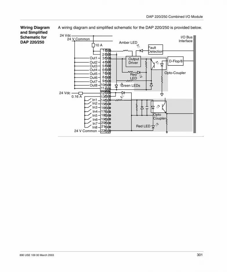
DAP 220/250 Combined I/O Module
Wiring Diagram and Simplified Schematic for DAP 220/250
A wiring diagram and simplified schematic for the DAP 220/250 is provided below.
24 Vdc24 V Common
10 A
24 Vdc0.16 A
Out1Out2Out3Out4Out5Out6Out7Out8
In1In2
In4
In6
In8
123456789
101112131415
17
19
21
Amber LED
FaultDetection
I/O BusInterface
D-Flop/8
Opto-Coupler
OutputDriver
RedLED
Green LEDs
Red LED
OptoCoupler
24 V Common
In3
In5
In7
18
16
20
22
890 USE 109 00 March 2003 301

DAP 220/250 Combined I/O Module
DAP 220/250 Combined I/O Module Recovery After Error
Instructions The protective device will eventually recover from the fail state if the cause of failure is removed, and the module will become healthy. If the error condition still exists, it will cause the module to shut down again. To avoid damage to the module, the logic shown in the following diagrams may be used to clear the failed output.
Ladder Logic Examples
The following diagram is a DAP 220/250 Ladder Logic Example for Prom Combination 1001.
40001
STAT
15
3
SENS3
40001
0
0
ADD40100
00099
00099
The STAT block will put the module health infor-mation for the 4 racks in registers 40012 ... 40015.
Coil 99 is turned ON when the module in Rack 2,Slot 3 becomes healthy.
If register 40100 is traffic copped to the DAP 220 inRack 2, Slot 3, when it becomes healthy again the 0in register 40100 will be written to the module.
302 890 USE 109 00 March 2003

DAP 220/250 Combined I/O Module
The following illustration is a DAP 220/250 Ladder Logic Example for Prom Combination 1002.
The STAT block will put the module health infor-mation for the 4 racks in registers 40012 ... 40015.
Coil 99 is turned OFF when the module in Rack 2,Slot 3 becomes unhealthy.
If register 40100 is traffic copped to the DAP 220 inRack 2, Slot 3, when it becomes unhealthy, the 0 inregister 40100 will be written to the module.
40001
STAT
15
3
SENS
40013
0
0
ADD40100
00099
00099
3
890 USE 109 00 March 2003 303

DAP 220/250 Combined I/O Module
DAP 220/250 Combined I/O Module Specifications
Table of Specifications for DAP 220/250
The following table contains a list of DAP 220/250 combined I/O module specifications.
Module Topology
Number of Inputs 8
Number of Outputs 8
Number of Groups 2
Points/Group 8
Isolation Each point opto-isolated from the I/O bus.
Power Supplies
External Source Requirement
20 ... 30 Vdc
Internal Source Requirement less than 60 mA @ 5 V from I/O bus
Internal Power Dissipation 2 W (typical)
Input Characteristics
ON State Signal Level +12 V ... +30 V
OFF State Signal Level -2 V ... +5 V
Input Wetting Current 7 mA @ 24 Vdc; 8.5 mA @ 30 Vdc
Response Time 4 ms (typical)
Operating Mode True High
Wire Size/Terminal One wire: 14 AWG
Two wires: 20 AWG
Output Characteristics
Operating Mode True High
ON State Signal Level External Supply - 0.4V
OFF State Signal Level 0 ... 2 V, less than 1mA
Load Current/Output 10 mA ... 2 A
Max Load Current/Group 8 A
Response Time less than 1 ms
Reverse EMF Protection Clamping diode recommended across inductive loads, or if load current exceeds 1A
Switch Capacity for Bulbs OFF -> ON Operations @ Maxi mum Power
10W (Max Surge Current = Nor mal Current x 10) 1000/hour inductive load 100/s resistive load 10/s bulb load
Wire Size/Terminal One wire: 14 AWG
Two wires: 20 AWG
EnvironmentalCharacteristics
Operating Temperature 0 ... 60 degrees C for DAP220 -40 ... +70 degrees C for DAP250
I/O Map Discrete 1x/0x 8 in/8 out
304 890 USE 109 00 March 2003

DAP 220/250 Combined I/O Module
Dimensions WxHxD 40.3 x 145 x 117.5 mm (1.6 x 5.6 x 4.5 in)
Weight 220 g (.48 lb.)
Agency Approvals
DAP 220: VDE 0160; UL 50; CSA 22.2 No.142; and FM Class I, Div 2 Standards
DAP 250C: Railway standard EN 50 155: EMC 89/336/EEC (See Requirements for CE Compliance, p. 779). UL 50; CSA 22.2 No.142; and FM Class I, Div 2 pending
890 USE 109 00 March 2003 305

DAP 220/250 Combined I/O Module
306 890 USE 109 00 March 2003

890 USE 109 00 March 2003
Overview of the DAP 253 Combined I/O Module
At a Glance
Purpose The purpose of this chapter is to describe the DAP 253 combined I/O module.
What’s in this Chapter?
This chapter contains the following topics:
Topic Page
What is the DAP 253 Combined I/O Module? 308
DAP 253 Combined I/O Module LEDs 309
DAP 253 Combined I/O Module Field Wiring 310
Protecting the DAP 253 Combined I/O Module from Inductive Back EMF 312
DAP 253 Combined I/O Module Specifications 314
307

DAP 253 Combined I/O Module
What is the DAP 253 Combined I/O Module?
Brief Product Description
The DAP 253 is an extended temperature, 110 Vdc +/-40 percent, eight-point isolated input/four-point relay output module. The full operational range of this module is 66 ... 154 Vdc for inputs. Relay voltage and current ratings are documented in the specifications of this module. It senses eight discrete input signals received by field sensing devices such as pushbuttons, limit switches, or other dc input sources and converts those signals into logic that can be used by the PLC. It utilizes logic signals within the PLC to activate four independent and individually isolated normally open relay contacts.The module requires power from an external 24 Vdc source to operate the relay outputs. The operating temperature range of this module, -25 ... +70 degrees C (-13 ... +158 degrees F), exceeds typical module operating temperatures of 0 ... 60 degrees C.
Note: The DAP 253 model is available with conformal coating. The conformal coating model is DAP 253C.
308 890 USE 109 00 March 2003

DAP 253 Combined I/O Module
DAP 253 Combined I/O Module LEDs
DAP 253 LEDs The DAP 253 module has two amber LEDs opposite terminal screws 1 and 12; when one of these LEDs is ON, it indicates power available to the input or output points directly below it. Below terminal screw 1 are four red LEDs opposite terminal screws 3, 5, 7, and 9 indicating the signal condition of relay output points 1 ... 4, respectively. Below terminal screw 12 are eight red LEDs opposite terminal screws 14 ... 21 indicating the signal condition of inputs 1 ... 8, respectively.A front view with DAP 253 label is provided below.
ou
tpu
t
1
inp
ut
DAP 253
U
U
1
2
3
4
M
U
U
1
2
3
4
5
6
7
8
M
card
1
2
3
4
5
6
78
9
10
11
12
13
14
15
16
17
18
19
20
21
22
DAP 253
2
3
4
56
7
8
9
10
11
12
13
14
15
16
17
18
19
20
21
22
890 USE 109 00 March 2003 309

DAP 253 Combined I/O Module
DAP 253 Combined I/O Module Field Wiring
Wiring Diagram for DAP 253
A wiring diagram for the DAP 253 combined I/O module is provided below.
24...154 Vdc; 24...250 Vac HOT24...154 Vdc Common; 24...250 Vac Neutral24 Vdc24 V Common
110 Vdc +/-40%dc COMMON
0.15A 0.15A4V 4V
Load1
Load2
Load3
Load4
1
2
34
5
6
78
1
2
3
4
56
7
8
9
1011
12
13
14
15
1617
18
1920
2122
310 890 USE 109 00 March 2003
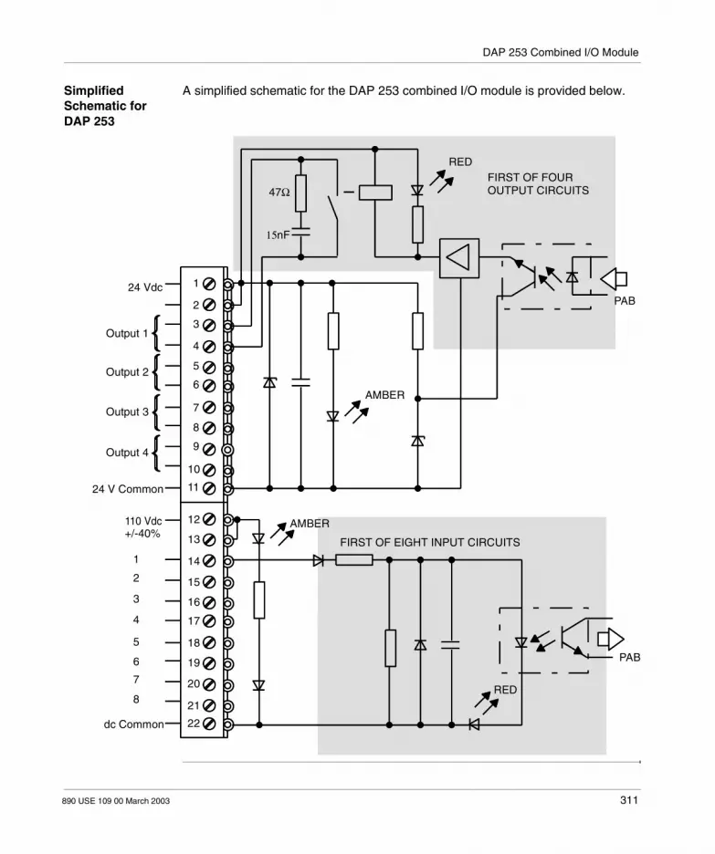
DAP 253 Combined I/O Module
Simplified Schematic for DAP 253
A simplified schematic for the DAP 253 combined I/O module is provided below.
47Ω
15nF
REDFIRST OF FOUROUTPUT CIRCUITS
PAB
AMBER
FIRST OF EIGHT INPUT CIRCUITS
AMBER
RED
dc Common
110 Vdc+/-40%
24 V Common
24 Vdc 1
2
3
4
5
6
7
8
9
10
11
12
13
14
15
16
17
18
19
20
21
22
Output 1
Output 2
Output 3
Output 4
1
2
3
4
5
6
7
8
PAB
890 USE 109 00 March 2003 311

DAP 253 Combined I/O Module
Protecting the DAP 253 Combined I/O Module from Inductive Back EMF
Instructions for DAP 253
In order to increase the service life of the relay output contacts and protect the DAP 253 module from potential reverse-EMF damage, externally connect a clamping diode in parallel with each inductive dc load and externally connect an RC snubber circuit in parallel with each inductive ac load.
Illustration of Clamping Diode and Snubber Circuit
The following illustration is an example of clamping diode and snubber circuit on inductive loads.
24 V
230 V
Clamping Diode
Inductive dc Load
R C
Inductiveac Load
123
45
67
89
1011
1213
1415161718192021
22
312 890 USE 109 00 March 2003

DAP 253 Combined I/O Module
Suggested Component Values
The clamping diode forward current rating must be equal to or greater than load current. Diode PIV rating must be three or four times greater than supply voltage at 24 Vdc and 8 ... 10 times greater than supply voltage at 110 Vdc. The unpolarized (ac) snubber capacitor should have a rating two or three times greater than the supply voltage.Values may be:
An example of Operational Range Options Using 140 Vdc is provided below.
Snubber resistors may be 1 ... 3 ohms, 2 W. Resistor values should be increased up to 47 ohms, 1/2 W for RL exceeding 100 ohms.
Snubber Values
Load Inductance Capacitance
25 ... 70 mH .50 microF
70 ... 180 mH .25 microF
180 mH .10 microF
+Vcc= 140 VdcBDAP Contact
Load 1K ohm (Min) 20 Henries (Max)
Suppression Diode (1N4003)
Calculations:Given: Vcc= 140VdcI (Max)= .15 AThen: R(L) (Min)= 140/.15=1KohmSince L/R=.02 Sec, and R=1KohmThen L(Max)= (.02) X 1000=20H
RCL
Voltage rating of diode = 1.5 X VccCurrent rating of diode = 2 X I (Max)Must be “slow”, rectifier, vs logic
RCL=Current Limiting Resistor (.5 Load R)Here, 470 ohmsIf carbon film, .25 watt,If metal film, .50 watt
A
B
C
A shows the consequences of ohmic load and L/R ratiosB shows the application of the suppression diodeC shows the application of a current limiting resistor in series with the diode to protect
the diode from contact bounce
Note: To I/O Map the DAP 253 module in Modsoft you must select DAP 212. Both modules share a host driver and have similar characteristics.
890 USE 109 00 March 2003 313

DAP 253 Combined I/O Module
DAP 253 Combined I/O Module Specifications
DAP 253 Specifications
The following tables and diagrams contain DAP 253 combined I/O module specifications.
Module Topology
Number of Inputs 8
Number of Relay Outputs 4
Number of Groups 1 in/4 out
Points/Group 8 in/1 out
Isolation Relay output contacts individually isolated Input group isolated from output group
Power Supplies
External Source Requirement
110 Vdc+40 percent, 20 mA @ 24 Vdc, 70 mA
Internally Provided Source 5 V from I/O bus @ 15 mA maxi mum
Internal Power Dissipation 2 W (typical)
Input Characteristics
Working Voltage Range 66 ... 154 Vdc
ON State Signal Level 55 ... 170 V
OFF State Signal Level -2 ... +10 V
Input Current 2.2 mA (typical) @ 110 Vdc
Response Time 6 ms (typical)
Operating Mode True High
Wire Size/Terminal One wire: 14 AWG
Two wires: 20 AWG
Environmental Characteristic
Operating Temperature -25 ... +70 degrees C (-13 ... +158 degrees F)
314 890 USE 109 00 March 2003

DAP 253 Combined I/O Module
DAP 253 Specifications (continued)
Output Characteristics
Output Voltage Ranges 24 ... 154 Vdc; 24 ... 250 Vac
Operating Mode Normally Open
Response Time 10 ms (typical)
Wire Size/Terminal One wire: 14 AWG
Two wires: 20 AWG
Load Currents @ 230 Vac 2 A continuous (maximum, resistive load) 4 A instantaneous (maximum, resistive load) 1 A continuous (maximum, Cos = 0.5) 1.5 A / 240 V max (AC11, VDE 0660, part 200)
Load Current @ 24 Vdc 2 A continuous maximum (resistive load) 4 A instantaneous maximum (resistive load) 1 A continuous maximum (L/R* = 30 ms) 1.5 A / 240 V max (DC11, VDE 0660, part 200)
Load Current @ 60 Vdc 1 A continuous maximum (resistive load) 0.6 A maximum (L/R* = 30 ms)
Load Current @ 140 Vdc 0.3 A continuous maximum (resistive load) 0.15 A maximum (L/R* = 20 ms)
Wetting Current 5 mA for closed contacts
Leakage 1 mA
Internal Protective Circuitry 68 ohms +15 microF in parallel with each contact
Overload Protection Should be provided externally
I/O Map Discrete 1x/0x 8 in/4 out
* L = Load Inductance in H; R = Load Resistance in ohms
Service Life of Relay Contacts
Mechanical switching cycles 20,000,000
Electric switching cycles (Resistive Loads)
7,000,000 @ 230 Vac/0.5 A 8,000,000 (typical) @ 30 Vdc/2 A, with clamping diode 1,000,000 (typical) @ 60 Vdc/1 A, with clamping diode, 3000 cycles/hr maximum
Electric switching cycles (Inductive Loads, Cos = 0.5)
5,000,000 @ 230 Vac/0.5 A
890 USE 109 00 March 2003 315

DAP 253 Combined I/O Module
Diagram of Service Life for Resistive Loads.
The maximum number of switching cycles is reduced when inductive loads are encountered. Reference the load device manufacturer’s catalog for steady state and inrush VA ratings to determine the number of operations derating factor. If the frequency of operations is relatively high, use the inrush VA to calculate Cos: Effective number of operations = # of operations (resistive load) x reduction factor:
# O
F O
PE
RA
TIO
NS
7
6
5
10
8
6
4
2
10
8
6
4
2
100 0.2 0.4 0.6 0.8 1 1.2 1.4 1.6 1.8 2
DEVICE RATING(kVA)
SERVICE LIFE FOR RESISTIVE LOADS
316 890 USE 109 00 March 2003

DAP 253 Combined I/O Module
Graph of Reduction Factor for Inductive Loads.
Cos = Watts divided by VA.
I/O Map Discrete 1x/0x 8 in/8 out
Dimensions WxHxD 40.3 x 145 x 117.5 mm (1.6 x 5.6 x 4.5 in)
Weight 240 g (.52 lb.)
Agency Approvals
DAP 253: European Directive EMC 89/336/EEC Standards
DAP 253C: Railway standard EN 50 155: European Directive EMC 89/336/EEC Standards.
RE
DU
CT
ION
FA
CT
OR
COSΦ
1
0.8
0.9
0.7
0.6
0.5
0.9
1
0.8 0.7 0.6 0.5 0.4 0.3
REDUCTION FACTOR FOR INDUCTIVE LOADS
890 USE 109 00 March 2003 317

DAP 253 Combined I/O Module
318 890 USE 109 00 March 2003
890 USE 109 00 March 2003
Overview of the DAP 292 Combined I/O Module
At a Glance
Purpose The purpose of this chapter is to describe the DAP 292 combined I/O module.
What’s in this Chapter?
This chapter contains the following topics:
Topic Page
What is the DAP 292 Combined I/O Module? 320
DAP 292 Combined I/O Module LEDs 321
DAP 292 Combined I/O Module Field Wiring 322
Protecting the DAP 292 Combined I/O Module from Inductive Back EMF 324
DAP 292 Combined I/O Module Specifications 326
319

DAP 292 Combined I/O Module
What is the DAP 292 Combined I/O Module?
Brief Product Description
The DAP 292 is a 60 Vdc, eight-point isolated input/four-point relay output module. It senses eight discrete input signals received by field sensing devices-such as pushbuttons, limit switches, or other 60 Vdc sources-and converts those signals into logic that can be used by the PLC.It utilizes logic signals within the PLC to activate four independent and individually isolated normally open relay contacts. The module requires power from an external 24 Vdc source to operate.
320 890 USE 109 00 March 2003

DAP 292 Combined I/O Module
DAP 292 Combined I/O Module LEDs
LEDs The DAP 292 module has two amber LEDs opposite terminal screws 1 and 12; when one of these LEDs is ON, it indicates power available to the input or output points directly below it. Below terminal screw 1 are four red LEDs opposite terminal screws 3, 5, 7, and 9 indicating the signal condition of relay output points 1 ... 4, respectively. Below terminal screw 12 are eight red LEDs opposite terminal screws 14 ... 21 indicating the signal condition of inputs 1 ... 8, respectively.A front view with DAP 292 label is provided below.
DAP 292
1
2
3
4
56
78
9
10
11
12
13
14
15
1617
18
19
20
2122
DAP 292
UU
M
U
U
M
card
1
2
3
4
5
67
8
1
2
3
4
inpu
tou
tput
1
2
34
56
7
8
6
9
10
1112
13
14
15
1617
18
19
20
21
22
890 USE 109 00 March 2003 321

DAP 292 Combined I/O Module
DAP 292 Combined I/O Module Field Wiring
Wiring Diagram for DAP 292
A wiring diagram for the DAP 292 combined I/O module is provided below.
24... 110 Vdc; 24...250 Vac HOT24... 110 Vdc Common; 24...250 Vac Neutral24 Vdc24 V COMMON60 Vdc60 V COMMON
0.15A 4A 4A 0.15A
O1
O2
O3
O4
12
34
567
8
9
1011
12
13
1415
16
1718
19
20
21
22
12
34
56
78
322 890 USE 109 00 March 2003

DAP 292 Combined I/O Module
Simplified Schematic for DAP 292
A simplified schematic for the DAP 292 combined I/O module is provided below.
47Ω
15nF
RED
FIRST OF FOUROUTPUT CIRCUITS
PAB
GREEN
24 Vdc
24 V Common
Output 1
Output 2
Output 3
Output 4
1
2
3
4
56
7
8
60 V Common
GREEN
RED
FIRST OF EIGHT INPUT CIRCUITS
PAB
60 Vdc
1
2
3
4
5
6
7
8
9
10
11
12
13
14
15
16
17
18
19
20
21
22
890 USE 109 00 March 2003 323

DAP 292 Combined I/O Module
Protecting the DAP 292 Combined I/O Module from Inductive Back EMF
Instructions In order to increase the service life of the relay output contacts and protect the DAP 292 module from potential reverse-EMF damage, externally connect a clamping diode in parallel with each inductive dc load and externally connect an RC snubber circuit in parallel with each inductive ac load.
Illustration of Clamping Diode and Snubber Circuit for DAP 292
The following illustration is an example of clamping diode and snubber circuit on inductive loads.
24 V
230 V
Clamping Diode
Inductivedc Load
Inductiveac Load
R C
12
3
456
7
8
11
109
1213
1415
1617
181920
21
22
324 890 USE 109 00 March 2003

DAP 292 Combined I/O Module
Suggested Component Values
The clamping diode forward current rating must be equal to or greater than load current. Diode PIV rating must be three or four times greater than supply voltage at 24 Vdc and 8 ... 10 times greater than supply voltage at 110 Vdc. The unpolarized (ac) snubber capacitor should have a rating two or three times greater than the supply voltage.Values may be:
Snubber resistors may be 1 ... 3 ohms, 2 W. Resistor values should be increased up to 47 ohms, 1/2 W for RL exceeding 100 ohms.
Snubber Values
Load Inductance Capacitance
25 ... 70 mH .50 microF
70 ... 180 mH .25 microF
180 mH .10 microF
Note: To I/O Map the DAP 292 module in Modsoft you must select DAP 212. Both modules share a host driver and have similar characteristics.
890 USE 109 00 March 2003 325

DAP 292 Combined I/O Module
DAP 292 Combined I/O Module Specifications
DAP 292 Tables and Diagrams
DAP 292 Specifications
Module Topology
Number of Inputs 8
Number of Relay Outputs 4
Number of Groups 2
Points/Group 8 in/4 out
Isolation Relay output contacts individually isolated Input group isolated from output group
Power Supplies External Source Requirement 60 Vdc, 150 mA maximum; 24 Vdc, 150 mA maximum
Internally Provided Source 5 Vdc from I/O bus; 25 mA maximum
Internal Power Dissipation 2 W (typical)
Input Characteristics
Working Voltage Range 60 Vdc
Signal Rated Value +60 V
ON State Signal Level 35 ... 70 V
OFF State Signal Level -4 ... +13 V
Input Current 7 mA at 60 V
Response Time 4 ms (typical)
Operating Mode True High
Wire Size/Terminal One wire: 14 AWG
Two wires: 20 AWG
326 890 USE 109 00 March 2003

DAP 292 Combined I/O Module
DAP 292 Specifications (continued)
Output Characteristics
Output Voltage Ranges 24 ... 110 Vdc; 24 ... 250 Vac
Operating Mode Normally Open
Response Time 10 ms (typical)
Wire Size/Terminal One wire: 14 AWG
Two wires: 20 AWG
Load Currents @ 230 Vac 2 A continuous (maximum, resistive load) 4 A instantaneous (maximum, resistive load) 1 A continuous (maximum, Cos = 0.5) 1.5 A/240 V max (AC11, VDE 0660, part 200)
Load Current @ 24 Vdc 2 A continuous maximum (resistive load) 4 A instantaneous max maximum (resistive load) 1 A continuous maximum (L/R* = 30 ms) 1.5 A/240 V max (DC11, VDE 0660, part 200)
Load Current @ 60 Vdc 1 A continuous maximum (resistive load) 0.6 A maximum (L/R* = 30 ms)
Load Current @ 110 Vdc 0.45 A continuous maximum (re resistive load) 0.25 A maximum (L/ R* = 30 ms)
Wetting Current 1 mA
Internal Protective Circuitry 68 ohms +15 microF in parallel with each contact
Overload Protection Should be provided externally
I/O Map Discrete 1x/0x 8 in/4 out
* L = Load Inductance in Henries; R = Load Resistance in Ohms
Service Life of Relay Contacts
Mechanical switching cycles 20,000,000
Electric switching cycles (Resistive Loads)
10,000,000 @ 230 Vac/0.2 A 7,000,000 @ 230 Vac/0.5 A 8,000,000 (typical) @ 30 Vdc/2 A, with clamping diode 1,000,000 (typical) @ 60 Vdc/1 A, with clamping diode, 3000 cycles/hr max
Electric switching cycles (Inductive Loads, Cos = 0.5)
5,000,000 @ 230 Vac/0.5 A
890 USE 109 00 March 2003 327

DAP 292 Combined I/O Module
Service Life for Resistive Loads
The maximum number of switching cycles is reduced when inductive loads are encountered. Reference the load device manufacturer’s catalog for steady state and inrush VA ratings to determine the number of operations derating factor. If the frequency of operations is relatively high, use the inrush VA to calculate Cos: Effective number of operations = # of operations (resistive load) x reduction factor:
# O
F O
PE
RA
TIO
NS
7
6
510.2 0.4 0.6 0.80 1.2 1.4 1.6 1.8 2
DEVICE RATING(kVA)
SERVICE LIFE FOR RESISTIVE LOADS
10
8
6
4
2
10
8
6
4
2
10
328 890 USE 109 00 March 2003

DAP 292 Combined I/O Module
Reduction Factor for Inductive Loads
Cos = Watts divided by VA.
I/O Map Discrete 1x/0x 8 in/8 out
Dimensions WxHxD 40.3 x 145 x 117.5 mm (1.6 x 5.6 x 4.5 in)
Weight 240 g (.52 lb.)
Agency Approvals DAP 253: European Directive EMC 89/336/EEC Standards
VDE 0160; UL 508; and CSA 22.2 No. 142 Standards.
RE
DU
CT
ION
FA
CT
OR
1
0.9
0.5
0.8
0.7
0.6
1 0.9 0.8 0.7 0.6 0.5 0.4 0.3
COSΦ
REDUCTION FACTOR FOR INDUCTIVE LOADS
890 USE 109 00 March 2003 329

DAP 292 Combined I/O Module
330 890 USE 109 00 March 2003

890 USE 109 00 March 2003
DAU 202/252 Analog Output Module
At a Glance
Introduction This chapter describes the DAU 202/252 analog output module.
What’s in this Chapter?
This chapter contains the following topics:
Topic Page
What Is the DAU 202/252 Analog Output Module? 332
DAU 202/252 Analog Output Module Field Wiring 334
DAU 202/252 Analog Output Module Calibration 335
DAU 202/252 Analog Output Module Specifications 337
331

DAU 202/252 Analog Output Module
What Is the DAU 202/252 Analog Output Module?
Brief Product Description
The DAU 202/252 is a two–channel analog output module. Each channel supports voltages in the range +10 ... -10 V and currents in the range +20 ... -20 mA. The operations of the DAU 202 and the DAU 252 are alike except for the DAU 252’s ability to operate at extended temperatures. The output channels can be isolated individually. The valid output data range is from 0 ... 4000.
Note: The DAU 252 model is available with conformal coating. The conformal coating model is DAU 252C, and it meets Railway standard EN 50 155.
332 890 USE 109 00 March 2003

DAU 202/252 Analog Output Module
Conversion Ranges
Different PLC models support different temperature ranges. The following tables present the different PLC models and describe the voltage and temperature ranges that they support.The following table lists operating information for the A984- 1XX and E984- 24x/251/255 PLC models.
The following table lists operating information for the E984-258/265/275/285 PLC models.
LEDs The DAU 202/252 has two green LED indicators on its front panel: If the LED opposite terminal screw 1 is ON, user-supplied voltage is present. If the LED opposite terminal screw 12 is ON, a D/A conversion has occurred.
Output Signals Voltage
Output Signals Current
Data Count (decimal
Operating Results
-10 V -20 mA 0 In Range
0 V 0 mA 2000
+10 V +20 mA 4000
0 V 0 mA 4001 Over Range
Voltage (VDC) Current (mA) 12-bits 15-bits + sign Range
10.24 ...-10.005
-20.48 ...-20.01
047
-32768-32016
Under-range
-10.000+10.00
-20.000+20.00
4820484048
-320000+32000
Nominal range
+10.005 ...+10.24
+20.01 ...+20.48
40494095
+32016+32752
Overrange
890 USE 109 00 March 2003 333

DAU 202/252 Analog Output Module
DAU 202/252 Analog Output Module Field Wiring
Introduction The DAU 202/252 can be field wired to two current output devices, to two voltage output devices, or to one current and one voltage device.
Wiring Diagram The following illustration is a wiring diagram and simplified schematic for the DAU 202/252 analog output module.
3456789
10
1
11
2
1213141516171819202122
24 Vdc24 V Common
0.16A
VR > 5 k Ω
OR
R < 500 Ω
VR > 5 k Ω
OR
R < 500 Ω24 Vdc
GreenLED 1
-15 VdcGreenLED 12
Data 12
Data 1D/AMUX
REF
I/O BusInterface
334 890 USE 109 00 March 2003

DAU 202/252 Analog Output Module
DAU 202/252 Analog Output Module Calibration
Introduction By adjusting the four potentiometers on the top of the DAU 202/252 module, you can calibrate the gain and offset on each of the two analog channels over the absolute count range of the module (0 ... 4000). The following illustration shows the location of the potentiometers on the ADU 202/252.
Gain Potentiometers
Channel 2-10 V adjustment
Channel 1-10 V adjustment
Channel 2+10 V adjustment
Channel 1+10 V adjustment
Offset Potentiometers
890 USE 109 00 March 2003 335

DAU 202/252 Analog Output Module
Procedure for Adjusting the Potentiometers
Use the following procedure to adjust the Potentiometers.t
Step Action
1 Wire terminal 4 to the positive side and terminal 5 to the negative side of a voltmeter for analog channel 1 (as shown in the following figure.)
2 Enter 4000 into the module output register and adjust the channel 1 gain potentiometer (+10 V adjustment) for a reading of +10 V on the meter.
3 Enter 0 into the module output register and adjust the channel 1 offset potentiometer (-10 V adjustment) for a reading of -10 V on the meter.
4 Check module operation by entering 2000 into the module output register. The meter reading should be 0 V.
5 To fine-tune the calibration adjustment, you may want to repeat steps 2 ... 4 until you have your best reading. If you are satisfied with the reading, drop a bead of sealing varnish on the two readjusted potentiometers.
6 To calibrate analog channel 2, wire terminal 15 to the positive side and terminal 16 to the negative side of the voltmeter, and repeat steps 2 ... 5 of this procedure, this time making the adjustments to the gain and offset potentiometers for channel 2.
M
M
4
5
15
16
336 890 USE 109 00 March 2003
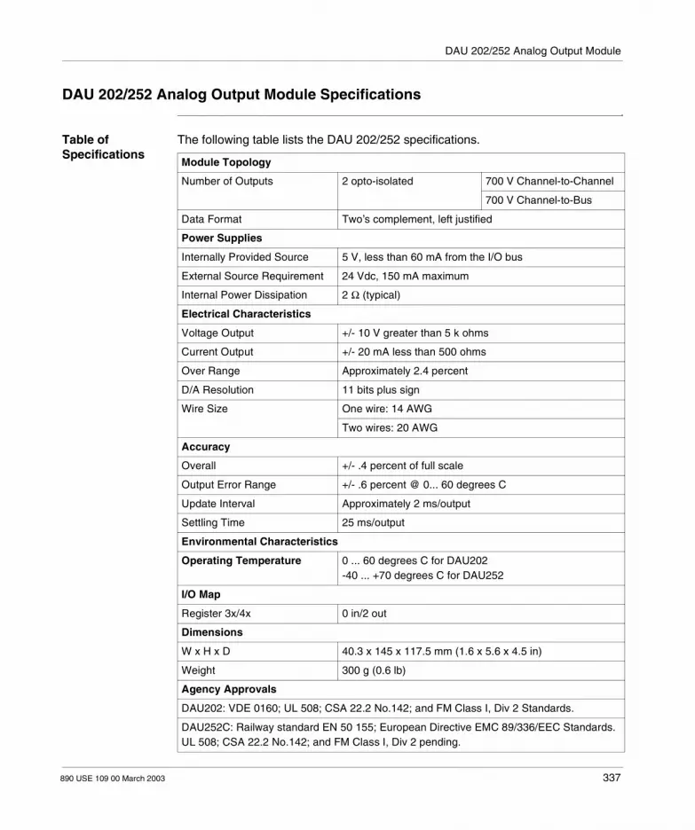
DAU 202/252 Analog Output Module
DAU 202/252 Analog Output Module Specifications
Table of Specifications
The following table lists the DAU 202/252 specifications.
Module Topology
Number of Outputs 2 opto-isolated 700 V Channel-to-Channel
700 V Channel-to-Bus
Data Format Two’s complement, left justified
Power Supplies
Internally Provided Source 5 V, less than 60 mA from the I/O bus
External Source Requirement 24 Vdc, 150 mA maximum
Internal Power Dissipation 2 Ω (typical)
Electrical Characteristics
Voltage Output +/- 10 V greater than 5 k ohms
Current Output +/- 20 mA less than 500 ohms
Over Range Approximately 2.4 percent
D/A Resolution 11 bits plus sign
Wire Size One wire: 14 AWG
Two wires: 20 AWG
Accuracy
Overall +/- .4 percent of full scale
Output Error Range +/- .6 percent @ 0... 60 degrees C
Update Interval Approximately 2 ms/output
Settling Time 25 ms/output
Environmental Characteristics
Operating Temperature 0 ... 60 degrees C for DAU202-40 ... +70 degrees C for DAU252
I/O Map
Register 3x/4x 0 in/2 out
Dimensions
W x H x D 40.3 x 145 x 117.5 mm (1.6 x 5.6 x 4.5 in)
Weight 300 g (0.6 lb)
Agency Approvals
DAU202: VDE 0160; UL 508; CSA 22.2 No.142; and FM Class I, Div 2 Standards.
DAU252C: Railway standard EN 50 155; European Directive EMC 89/336/EEC Standards. UL 508; CSA 22.2 No.142; and FM Class I, Div 2 pending.
890 USE 109 00 March 2003 337

DAU 202/252 Analog Output Module
338 890 USE 109 00 March 2003

890 USE 109 00 March 2003
DAU 204 Analog Output Module
At a Glance
Introduction This chapter describes the DAU 204 analog output module.
Note: Some A120 I/O modules (DEP 211/214/215/217, DAP211/217, ADU204/211/214/216, DAU204, VIC2xx, and MOT20x) require a loadable (SW-IODR-001) for proper operation if using certain PLCs (A984- -1xx, E984- -24x/251/255) with Modsoft.
WARNING
DAU 204 module must be powered when in rack.
Do not leave this module unpowered in the rack. This may affect the proper operation of the CPU and other I/O modules.
Failure to follow this precaution can result in death, serious injury, or equipment damage.
339

DAU 204 Analog Output Module
What’s in this Chapter?
This chapter contains the following topics:
Topic Page
What Is the DAU 204 Analog Output Module? 341
DAU 204 Analog Output Module Conversion Ranges 342
DAU 204 Analog Output Module Special Features 343
DAU 204 Analog Output Module Installation 344
DAU 204 Analog Output Module Switch Settings 345
DAU 204 Analog Output Module Field Wiring 348
DAU 204 Analog Output Module Configuration 353
DAU 204 Analog Output Module Custom Calibration 358
DAU 204 Analog Output Module Indicators 361
DAU 204 Analog Output Module Specifications 364
340 890 USE 109 00 March 2003

DAU 204 Analog Output Module
What Is the DAU 204 Analog Output Module?
Brief Product Description
The DAU 204 is a 4-channel analog output module designed to control adjustable frequency drives, positioning valves, dampers, and so forth. Each channel can provide either voltage or current loop output, in any one of the following ranges: 0 ... 1, 0 ... 5, or 0 ... 10 V and +/-1, +/- 5, or +/-10 V 4 ... 20 or 0 ... 20 mA (sourcing)
Note: For proper operation, the module requires power from an external source (250 mA @ 24 Vdc). If an external source is NOT used, the module pulls power from the internal bus and gives a false green LED indication.
890 USE 109 00 March 2003 341
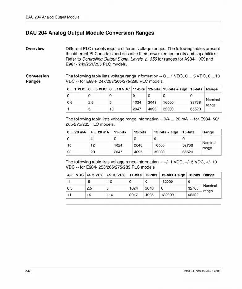
DAU 204 Analog Output Module
DAU 204 Analog Output Module Conversion Ranges
Overview Different PLC models require different voltage ranges. The following tables present the different PLC models and describe their power requirements and capabilities. Refer to Controlling Output Signal Levels, p. 356 for ranges for A984- 1XX and E984- 24x/251/255 PLC models.
Conversion Ranges
The following table lists voltage range information -- 0 ...1 VDC, 0 ... 5 VDC, 0 ...10 VDC -- for E984- 24x/258/265/275/285 PLC models.
The following table lists voltage range information -- 0/4 ... 20 mA -- for E984- 58/265/275/285 PLC models.
The following table lists voltage range information -- +/- 1 VDC, +/- 5 VDC, +/- 10 VDC -- for E984- 258/265/275/285 PLC models.
0 ... 1 VDC 0 ... 5 VDC 0 ... 10 VDC 11-bits 12-bits 15-bits + sign 16-bits Range
0 0 0 0 0 0 0Nominal range
0.5 2.5 5 1024 2048 16000 32768
1 5 10 2047 4095 32000 65520
0 ... 20 mA 4 ... 20 mA 11-bits 12-bits 15-bits + sign 16-bits Range
0 4 0 0 0 0Nominal range
10 12 1024 2048 16000 32768
20 20 2047 4095 32000 65520
+/- 1 VDC +/- 5 VDC +/- 10 VDC 11-bits 12-bits 15-bits + sign 16-bits Range
-1 -5 -10 0 0 -32000 0Nominal range
0.5 2.5 0 1024 2048 0 32768
+1 +5 +10 2047 4095 +32000 65520
342 890 USE 109 00 March 2003

DAU 204 Analog Output Module
DAU 204 Analog Output Module Special Features
Special Features The DAU 204 module provides the following features: 4 independently configurable channels (i.e., the DAU 204 can provide any
combination of voltage and current outputs) Group-to-group isolation (channel 1 and 2 are optically and magnetically isolated
from channels 3 and 4) to 500 Vac True 12-bit resolution (0 ... 4095) on all scales High accuracy (+/-0.2 percent of full scale @ 25 degrees C) Open current loop (broken wire) detection and warnings via LEDs and registers Software calibration (no potentiometers) Built-in diagnosticsAn additional special feature of the DAU 204 is the outputs. For detailed information, see Conversion Ranges, p. 342.The following figure shows a front view with the DAU 204 label.
Amber LEDGreen LED
Red LEDGreen LED
Red LEDGreen LED
Red LEDGreen LED
Red LEDGreen LED
DAU 204
123456789
1011
1213141516171819202122
DAU 204
readyrun
openactive
openactive
openactive
openactive
card
shield 1shield 2
shield 3
shield 4
U+I1
+U1
+I2
+U2
+I3
+U3
+I4
+U4
-I1
-U1
-I2
-U2
M
-I3
-U3
-I4
-U4
123456
87
91011
1213141516171819202122
890 USE 109 00 March 2003 343

DAU 204 Analog Output Module
DAU 204 Analog Output Module Installation
Overview The following information describes preparatory tasks to complete before you install the DAU 204.
Before You Install the Module
Before installing the DAU 204, be sure to complete the following items: Set the DIP switches. Field wire the terminal blocks.For detailed information about how to complete these tasks, see DAU 204 Analog Output Module Switch Settings, p. 345.
CAUTION
You must observe all rack and module power state requirements.
Never insert or remove the DAU 204 from the rack while the rack is powered up or while the module is connected to an external power source or active output device. Failure to observe this precaution can result in equipment damage.
Failure to follow this precaution can result in injury or equipment damage.
Note: After installing the DAU 204, you must load the DAU 204 software driver (SVI.DAT Rev 3, or higher) and set at least one output range via I/O Mapped register (40xxx+4). These registers are described in DAU 204 Analog Output Module Configuration, p. 353.
344 890 USE 109 00 March 2003

DAU 204 Analog Output Module
DAU 204 Analog Output Module Switch Settings
Overview Setting DIP switches must be done before the DAU 204 can be installed. The following information describes how to perform these tasks. For general information about setting DIP switches on the DAU 204, see DAU 204 Analog Output Module Installation, p. 344.
CAUTION
You must observe all rack and module power state requirements.
Never change DIP switch settings while the rack is powered or while the module is connected to an external power source or active field device. Failure to observe this precaution can cause unintended equipment operation.
Failure to follow this precaution can result in injury or equipment damage.
890 USE 109 00 March 2003 345

DAU 204 Analog Output Module
Setting DIP Switches
This procedure describes how the dip switches are set.
Step Action
1 With the DAU 204 not in the rack, find the DIP switches at the top and bottom of the module. (Both views are shown in the following illustrations. Note also that the DIP switches are visible through the vents.) The module ships in current mode.The following illustration is a bottom view of the module, showing the DIP switch for channels 3 and 4.
The following illustration is a top view of the module, showing the DIP switch for channels 1 and 2.
BOTTOM VIEW OF MODULE
PC Board
1 4
1 2 3 4
OFF (open)
ON (closed)
Ch. 3 output*Ch. 4 output*
*OFF OFF = Current output ON ON = Voltage output
Group 2 DIP Switch(Bottom of Module)
Other DIP switch setting mayproduce invalid output ranges.
Grounding Clip
PC Board
TOP VIEW OF MODULE
1 4
1 2 3 4
OFF (open)
ON (closed)
Ch. 2 output*Ch. 1 output*
*OFF OFF = Current output ON ON = Voltage output
Group 1 DIP Switch(Top of Module)
Other DIP switch settings mayproduce invalid output ranges.
346 890 USE 109 00 March 2003

DAU 204 Analog Output Module
Settings for Unused Channels
It is recommended that unused channels be set to voltage mode. This setting shuts off the red LED current loop error indicator and alarm bit. Alternatively, unused current output channels should be shorted. You must use both poles together to properly set a channel’s mode; not doing so will generate invalid results.
2 Select the output mode for each channel by properly setting the DIP switches (Refer to the preceding figures.)The DIP switch poles located at the top of the module control channels 1 and 2. The switches located on the bottom of the module control channels 3 and 4. Notice that channel 1 is set using poles 1 & 2, and channel 2 is set using poles 3 & 4; but channel 4 is set using poles 1 & 2, and channel 3 is set using poles 3 & 4.
Step Action
890 USE 109 00 March 2003 347
DAU 204 Analog Output Module
DAU 204 Analog Output Module Field Wiring
Introduction For this module, use 60/75 copper (Cu) for the power connections and 4.5 in-lb. of torque for the set screws.To prevent errors in field device operation, follow these guidelines: Use shielded, twisted-pair cable (such as Belden 9418). Ground the shield of each signal cable at the DAU 204 only. At the other end each
signal cable, peel back the shield and insulate it from contact with the signal-carrying wires.
Route each signal cable as far as possible from sources of electrical noise (such as motors, transformers, contactors and especially AC devices).
Route the signal cables in a conduit different from the AC and power cables. If the signal cables must cross AC or power cables, ensure that they cross at right
angles. When connecting field devices to the module, keep the unshielded portions of the
signal-carrying wires as short as possible.After wiring the terminal blocks, use the supplied keys to prevent the blocks from being switched inadvertently.
WARNING
Module must be powered while in rack.
Do not leave this module unpowered in the rack. This may affect the proper operation of the CPU and other I/O modules.
Failure to follow this precaution can result in death, serious injury, or equipment damage.
348 890 USE 109 00 March 2003
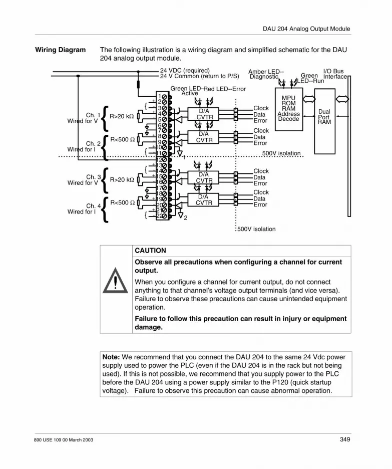
DAU 204 Analog Output Module
Wiring Diagram The following illustration is a wiring diagram and simplified schematic for the DAU 204 analog output module.
Ch. 1Wired for V
Ch. 2Wired for I
Ch. 3Wired for V
Ch. 4Wired for I
R>20 kΩ
R<500 Ω
R>20 kΩ
R<500 Ω
2
D/ACVTR
D/ACVTR
D/ACVTR
D/ACVTR
500V isolation
ClockDataError
ClockDataError
ClockDataError
ClockDataError
24 VDC (required)24 V Common (return to P/S)
500V isolation
Green LED--Active
Red LED--Error
Amber LED--Diagnostic Green
LED--Run
I/O BusInterface
MPUROMRAM
AddressDecode
DualPortRAM
123
56
4
789
10111213141516171819
2122
20
1
CAUTION
Observe all precautions when configuring a channel for current output.
When you configure a channel for current output, do not connect anything to that channel’s voltage output terminals (and vice versa). Failure to observe these precautions can cause unintended equipment operation.
Failure to follow this precaution can result in injury or equipment damage.
Note: We recommend that you connect the DAU 204 to the same 24 Vdc power supply used to power the PLC (even if the DAU 204 is in the rack but not being used). If this is not possible, we recommend that you supply power to the PLC before the DAU 204 using a power supply similar to the P120 (quick startup voltage). Failure to observe this precaution can cause abnormal operation.
890 USE 109 00 March 2003 349

DAU 204 Analog Output Module
The following table lists terminal descriptions.
Note: Ensure that voltage loads driven by the module can tolerate transients during rack and module startup. During startup, transients as great as 2 V may appear on the voltage output terminals for as long as 5 ms due to the characteristics of semiconductor devices. This does not occur with the module’s current output terminals.
Note: Terminals 3, 5, 9 and 11 (- current out, and - voltage out) are internally tied as a group. Terminals 14, 16, 20 and 22 (- current out, and - voltage out) are internally tied as a group. Be sure not to cross groups.
Note: You should short all unused current output terminals to disable the red current loop LEDs and alarm bits.
Terminal Channel Description
1 + 24Vdc (required)
2
1
+ current out- current out+ voltage out- voltage outshield 1
3
4
5
6
7
2
shield 2
8 + current out
9 - current out
10 + voltage out
11 - voltage out
12 24 V common
13
3
+ current out
14 - current out
15 + voltage out
16 - voltage out
17 shield 3
350 890 USE 109 00 March 2003

DAU 204 Analog Output Module
The following illustration is an example of the DAU 204 wired for voltage output on channels 1 and 3 and current output on channels 2 and 4.
The DIP switch settings for this configuration are shown in the following illustration.
18
4
shield 4
19 + current out
20 - current out
21 + voltage out
22 - voltage out
Terminal Channel Description
0.5 A Slo-Blo Fuse Recommended
+24 VDC (required)
Ch. 1 Voltage Out
Ch. 1 ShieldCh. 2 Shield
Ch. 2 Current Out
24 V Common
Ch. 3 Voltage Out
Ch. 4 Current Out
Ch. 3 ShieldCh. 4 Shield
123
456
78
91011
12
13141516171819202122
Group 1 DIP Switch(Top of Module)
Group 2 DIP Switch(Bottom of Module)
1 2 3 4
OFF (open = 0)
ON (closed = 1)
OFF (open = 0)
ON (closed = 1)1 2 3 4
890 USE 109 00 March 2003 351

DAU 204 Analog Output Module
An example of the DAU 204 wired for current output on all channels (1 through 4) is shown in the following illustration. Turn all DIP switch poles off for this configuration.
For example, to select current output for channels 1 and 3, and current output for channels 2 and 4, set the DIP switch poles as shown in the following illustration.
0.5 A Slo-Blo Fuse Recommended
=24 VDC (required)
Ch. 1 Current Out
Ch. 2 Current Out
Ch. 3 Current Out
Ch. 4 Current Out
Ch. 1 ShieldCh. 2 Shield
Ch. 3 ShieldCh. 4 Shield
24 V Common
12
3456789
1011
12
13141516171819202122
Group 1 DIP Switch(Top of Module)
Group 2 DIP Switch(Bottom of Module)
1 2 3 4 1 2 3 4
OFF (open = 0)
ON (closed = 1)
OFF (open = 0)
ON (closed = 1)
352 890 USE 109 00 March 2003

DAU 204 Analog Output Module
DAU 204 Analog Output Module Configuration
Introduction The DAU 204 is configured using the I/O map and its input and holding registers.
I/O Mapping The DAU 204 uses one 30xxx input register and six 40xxx output registers, I/O mapped as binary (BIN) data.
The registers and their functions used by the DAU 204 are shown in the table below, with more details following.
From the I/O Map screen in Modsoft, you can call up the built-in help screens by highlighting DAU 204 and pressing <ALT><H>.
Note: A software loadable driver (SVI.DAT, Revision 3, or higher) is required to operate this module.
Registers and their functions
30xxx Module status word
40xxx Channel 1 data, output signal levels, 12 bit
40xxx + 1 Channel 2 data, output signal levels, 12 bit
40xxx + 2 Channel 3 data, output signal levels, 12 bit
40xxx + 3 Channel 4 data, output signal levels, 12 bit
40xxx + 4 Control word 0, range select (NOT avail able for E984-258/265/275/285 PLCs)
40xxx + 5 Control word 1, fault state
890 USE 109 00 March 2003 353

DAU 204 Analog Output Module
Setting Output Ranges
Output register 40xxx + 4 controls the output range for each channel.
Note: When using E984-258/265/275/285 PLCs the output ranges are selected using the Parma ... screen in Concept, not the 4x+4 register.
Output Register 40XXX + 4 (range select)
16 15 14 13 12 11 10 9 8 7 6 5 4 3 2 1
Channel 4 Channel 3 Channel 2 Channel 1
Not Used
0 0 0 (0 hex) = 4...20 mA0 0 1 (1 hex) = 0...20 mA0 1 0 (2 hex) = 0...1 V0 1 1 (3 hex) = ±1 V1 0 0 (4 hex) = 0...5 V1 0 1 (5 hex) = ±5 V1 1 0 (6 hex) =0...10 V1 1 1 (7 hex) =±10 V
354 890 USE 109 00 March 2003

DAU 204 Analog Output Module
Enabling Hold-Last-Value
Bits 9 through 12 of output register 40xxx + 5 control how the DAU 204 responds to the following fault conditions: Communications with the PLC is lost for more than 1 second. The PLC is in stopped mode or power is lost.The following is an illustration of the Enable-Hold-Last-Value Register.
For example, if channel 1 is configured for 4 ... 20 mA operation, and bit 9 of register 40xxx + 5 is set to 0 (bottom of scale), channel 1 will output 4 mA if communication with the PLC is lost. However, if bit 9 were set to 1 (hold last value), channel 1 would output the same signal (value) that was output when communication was lost.
Bits 9...12 of Output Register 40XXX = 5 (enable hold-last-value)
calibration test mode calibration
16 15 14 13 12 11 10 9 8 7 6 5 4 3 2 1
Channel 1
Channel 2
Channel 3
Channel 4
1 = hold last value
0 = set to bottom of scale
Note: When using E984-258/265/275/285 PLCs the hold-last-value is selected using the Parma ... screen in Concept.
890 USE 109 00 March 2003 355

DAU 204 Analog Output Module
Controlling Output Signal Levels
Output registers 40xxx through 40xxx + 3 control the output signal levels on channels 1 through 4, respectively. The table below shows how the data in these registers correspond to the output signal for each output range. Register values above 4095 are treated as 4095.
A984-1xx, E984-24x/251/255 PLC Models
Register Value (decimal) Unipolar Voltage Output Signal
0 ... 1 V 0 ... 5 V 0 ... 10 V
0 0 0 0
2047 0.5 2.5 5
4095 1 5 10
Bipolar Voltage Output Signal
+/-1 V +/-5 V +/-10 V
0 -1 -5 -10
2047 0 0 0
4095 1 5 10
Current Output Signal
0 ... 20 mA 4 ... 20 mA
0 0 4
2047 10 12
4095 20 20
CAUTION
Operational Hazard
Before bringing field devices on-line, always ensure that you know the value in the registers that control each output channel so that the field devices do not begin operation without your understanding.
Failure to follow this precaution can result in injury or equipment damage.
356 890 USE 109 00 March 2003
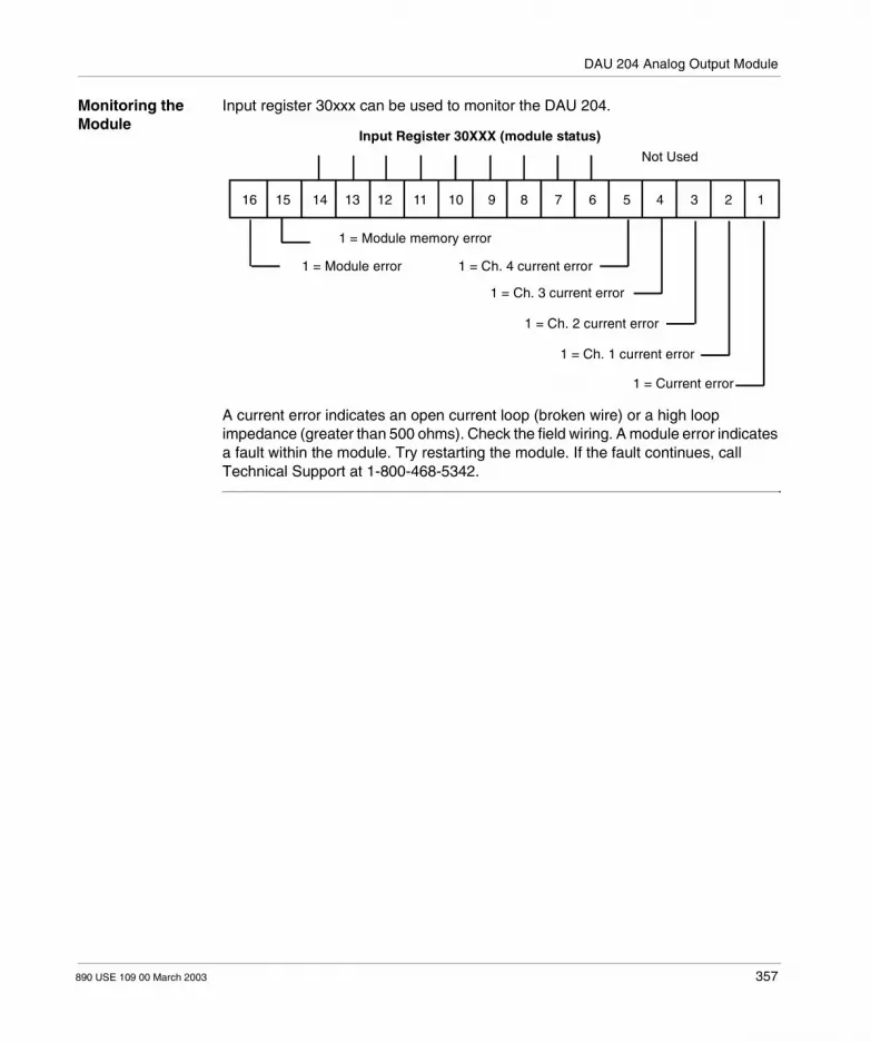
DAU 204 Analog Output Module
Monitoring the Module
Input register 30xxx can be used to monitor the DAU 204.
A current error indicates an open current loop (broken wire) or a high loop impedance (greater than 500 ohms). Check the field wiring. A module error indicates a fault within the module. Try restarting the module. If the fault continues, call Technical Support at 1-800-468-5342.
Input Register 30XXX (module status)
Not Used
16 15 14 13 12 11 10 9 8 7 6 5 4 3 2 1
1 = Module memory error
1 = Module error 1 = Ch. 4 current error
1 = Ch. 3 current error
1 = Ch. 2 current error
1 = Ch. 1 current error
1 = Current error
890 USE 109 00 March 2003 357

DAU 204 Analog Output Module
DAU 204 Analog Output Module Custom Calibration
Introduction This procedure is recommended for expert users only. All DAU 204 modules are carefully calibrated at the factory, so the procedure described below is needed only if you want to alter the module’s calibration for a special application. Depending on the accuracy desired, this procedure should take less than half an hour. To calibrate the DAU 204, the following materials are needed: Processor Rack Power supply Programming software (Modsoft) and computer Cable (preferably, shielded, twisted pair cable, such as Belden 9418) Multimeter with current measuring capability
Calibrating the Module
To calibrate the DAU 204 analog output module:
Step Action
1 Properly install and configure the module for the intended application See DAU 204 Analog Output Module Installation, p. 344 and Controlling Output Signal Levels, p. 356.
2 Set the output data register for the channel you want to calibrate to 4095 decimal (for example, to calibrate channel 1, set output register 40xxx to 4095).
3 Using the multimeter, measure the output for the channel being calibrated.
4 Using output register 40xxx + 5 (defined in the figure below), adjust the output upward or downward. Refer to the channel gain table below for the op codes to use. Note: When using E984-258/265/275/285 PLCs the channel calibration is selected using the Parma ... screen in Concept.
5 When the output equals the top of the desired range (for example, 20 mA for 4 ... 20 mA operation), set output register 40xxx + 5 to 0000 hex to stop the output movement.
6 Set the output data register for the channel you want to calibrate to 0 (for example, to calibrate channel 1, set output register 40xxx to 0).
7 Using output register 40xxx + 5, adjust the output upward or downward. Refer to the channel offset table below for the op codes to use.
8 When the output equals the bottom of the desired range (for example, 4 mA for 4 ... 20 mA operation), set output register 40xxx + 5 to 0000 hex to stop the output movement.
9 Repeat steps 2 through 8 until you’ve achieved the desire accuracy.Repeat these steps for each channel, as desired.To store the calibration in EEPROM, set output register 40xxx + 5 to 8011 hex.
358 890 USE 109 00 March 2003

DAU 204 Analog Output Module
Channel Calibration
The following is an illustration of the Channel calibration register.
Bits 1...8 of Output Register 40XXX + 5 (channel calibration)
test mode hold last value
16 15 14 13 12 11 10 9 8 7 6 5 4 3 2 1
1 = Store calibration
1 = Adjust output upward1 = Adjust output downward
1 = Calibrate gain (span)
1 = Calibrate offset (zero)
1 = Reset to normal defaults (within 10% of FS voltage range)
Calibrate Ch. 1 = 0 0 Calibrate Ch. 2 = 0 1 Calibrate Ch. 3 = 1 0 Calibrate Ch. 4 = 1 1
1 = Enable calibration
890 USE 109 00 March 2003 359

DAU 204 Analog Output Module
Code Tables The following table gives Op codes to adjust channel gain (span) upward or downward.
The following table gives Op codes to adjust channel offset (zero) upward or downward.
To return a channel to an uncalibrated state (before factory calibration i.e. within 10 percent of full scale of voltage range), set output register 40xxx + 5 to the appropriate op code shown in the table below.
Upward Downward
Channel 1 00A1 hexadecimal 0061 hexadecimal
Channel 2 00A3 hexadecimal 0063 hexadecimal
Channel 3 00A5 hexadecimal 0065 hexadecimal
Channel 4 00A7 hexadecimal 0067 hexadecimal
Op codes to adjust channel offset (zero) upward or downward
Upward Downward
Channel 1 0091 hexadecimal 0051 hexadecimal
Channel 2 0093 hexadecimal 0053 hexadecimal
Channel 3 0095 hexadecimal 0055 hexadecimal
Channel 4 0097 hexadecimal 0057 hexadecimal
Note: When you replace the module, you will need to perform this procedure again.
Op codes to return channel to uncalibrated state
Channel 1 0009 hexadecimal
Channel 2 000B hexadecimal
Channel 3 000D hexadecimal
Channel 4 000F hexadecimal
360 890 USE 109 00 March 2003

DAU 204 Analog Output Module
DAU 204 Analog Output Module Indicators
LEDs The DAU 204 analog output module has three types of LEDs: Amber LED -- provides information about the health of the module Green LEDs -- provide information about the readiness of the module Red LEDs -- provide information about the integrity of each channel (in current
mode only)This chapter explains how to use these and other diagnostic tools to determine the status of the DAU 204 module, and to identify and solve problems if necessary.
Amber LED The amber LED on the front of the module provides status information about the health of the module. A flashing amber LED indicates a fault in at least one of the following areas: Module Watchdog Circuit Fault Module Watchdog Circuit Fault at Startup Module RAM Failure at Startup Bus Interface Failure at Startup Module ROM Failure Module Processor Fault at Startup General Module ErrorIf the amber LED begins flashing, try restarting the module. If the flashing continues, call Technical Support at 1-800-468-5342.
890 USE 109 00 March 2003 361

DAU 204 Analog Output Module
Green LEDs The green LED at the top of the module provides status information about the module’s readiness. The remaining green LEDs provide status information about the activity on each channel.After the module is powered up, the green LED at the top of the module should begin flashing. If not, check the power source and connections.
Next, after the module has established communications with the PLC, the green LED at the top of the module should stop flashing and remain on. If not, ensure that the PLC has been powered up.The remaining green LEDs should remain on or flash quickly as data is sent over each channel. If these green LEDs ever go off, check the power source and connections.
Red LEDs The red LEDs provide status information about each channel’s integrity in current mode only. A flashing or steady red LED indicates an open current loop (broken wire) or a high loop impedance (greater than 500 ohms ). Red LEDs do not function in voltage mode.
Invalid Data If the module seems to be providing invalid output data: Check wiring connections and integrity, DIP switch settings, and register settings. Verify the integrity of the field device. Make sure the signal cables are not placed on or near high-voltage (120 Vac or
higher) cables. If the signal cables must cross high-voltage cables, ensure that the signal cables cross the high-voltage cables at right angles.
If electrical interference seems to be the problem, try placing the module as far as possible from power supplies and relay output modules. These products may generate electrical interference during operation. This interference would not affect the module but may induce noise on the channel wiring.
Note: The DAU 204 requires power from an external source (250 mA @ 24 Vdc) to operate. When an external source is NOT used the module pulls power from the internal bus gives a false green LED indication.
WARNING
Operational Hazard
Do not leave this module unpowered in the rack. This may affect the proper operation of the CPU and other I/O modules.
Failure to follow this precaution can result in death, serious injury, or equipment damage.
362 890 USE 109 00 March 2003

DAU 204 Analog Output Module
Built-in Tests The DAU 204 has built-in tests that are performed automatically when the module is powered up, but they can also be performed after the module is on-line by setting output register 40xxx +5 as shown in the built-in test register (below).
To stop the built-in tests, simply reset output register 40xxx + 5 to 0000 hexadecimal.
If the DAU 204 fails any of these tests (amber LED flashes), restart the module. If it continues to fail, call Technical Support at 1-800-468-5342.
Bits 13...15 of Output Register 40XXX + 5 (built-in tests)
calibrationcalibration hold last value
16 15 14 13 12 11 10 9 8 7 6 5 4 3 2 1
0 0 0 (0 hex) = No tests1 0 1 (5 hex) = Category 11 1 0 (6 hex) = Category 2 (DAU 204 must be in ±10 V mode)1 1 1 (7 hex) = Category 3 (DAU 204 must be in 4...20 mA mode)
CAUTION
Operational Hazard
Before performing these tests, disconnect any field devices from the DAU 204. Failure to observe this precaution can cause unintended equipment operation.
Failure to follow this precaution can result in injury or equipment damage.
Note: When bits 13, 14, or 15 of the output register 40xxx + 5 are set to 1, the green LED flashes continuously until these bits are reset to 0. After resetting these bits to 0, the module should be restarted.
Note: When using E984-258/265/275/285 PLCs the built-in tests are selected using the Parma ... screen in Concept.
890 USE 109 00 March 2003 363

DAU 204 Analog Output Module
DAU 204 Analog Output Module Specifications
Table of Specifications
The following table provides DAU 204 Specifications.
Module Topology Number of Channels 4
Number of Groups 2
Points per Group 2
Operating Voltage Ranges Bipolar +/-1, +/-5, +/-10 Vdc
Unipolar 0 ... 1, 0 .. 5, 0 ... 10 Vdc
Operating Current Ranges Unipolar 0 ... 20, 4 ... 20 mA
Power Supply External Supply 250 mA @ 24 Vdc
Internal Power Supply (via system bus)
less than 1 mA (TTL loading)
Required Loadable SW-IODR-001
Isolation Channel 1, 2 to Channel 3, 4 500 V @ 60 Hz
Channel to Bus 500 V @ 60 Hz
Channel 1 to 2 and 3 to 4 Not Isolated
Line/Load Impedance Voltage Output greater than or equal to 20,000 ohms
Current Output less than or equal to 500ohms, less than or equal to 50mH; No max. capacitance but can slew output
Resolution 12 bit (0 ... 4095)
Accuracy +/-0.200 percent Full Scale Reading @ 25 degrees C
Accuracy Drift w/Temperature
Current Output +/-0.002 percent FSR/ degrees C typical
+/-0.005 percent FSR/ degrees C maximum
Voltage Output +/-0.006 percent FSR/ degrees C typical
+/-0.0135 percent FSR/ degrees C maximum
Update Time 5 ms per channel maximum
Fault Detection Open current loop (broken wire in current mode)
MTBF 100,000 hours, minimum, @ 30 degrees C, ground base fixed
EMI Susceptance 27 ... 500 MHz, 10 V/m
Electrostatic Discharge 8 kV
364 890 USE 109 00 March 2003

DAU 204 Analog Output Module
Fast Transient (IEC 801-4) +/- 1.0 kV
Surge Withstand 2 kV (Transients, IEC 801-5)
Operating Conditions Temperature 0 ... 60 degrees C (32 ... 140 degrees F)
Humidity 95 percent RH noncondensing @ 60 degrees C
Chemical Interactions Can be damaged by strong alkaline (pH greater than 7) solutions
Vibration 10 ... 57 Hz @ 2 Gs
Storage Conditions Temperature -40 ... 85 degrees C (-40 ... 185 degrees F)
Free Fall 1 m (approx. 39 in)
I/O Map Register 3x/4x 1 in/6 out 1 in/5 out for (E984-258/265/275/285 Only)
Material Lexan (Enclosures and Bezels)
Space Required 1 A120 SMS rack slot
Dimensions (WxHxD) 40.3 x 145.0 x 117.5 mm
1.60 x 5.60 x 4.50 in
Weight, Maximum 453 g,
1 lb.
Agency Approvals UL 508; CUL; FM Class I, Div 2; and European Directive EMC 89/336/EEC (See Requirements for CE Compliance, p. 779) Standards
890 USE 109 00 March 2003 365

DAU 204 Analog Output Module
366 890 USE 109 00 March 2003

890 USE 109 00 March 2003
Overview of DAU 208 Analog Output Module
At a Glance
Purpose The purpose of this chapter is to describe the DAU 208 analog output module.
What’s in this Chapter?
This chapter contains the following topics:
Topic Page
What is the DAU 208 Analog Output Module? 368
DAU 208 Analog Output Module Conversion Ranges 369
DAU 208 Analog Output Module Physical Characteristics 370
DAU 208 Analog Output Module Configuration 372
DAU 208 Analog Output Module Field Wiring 373
DAU 208 Analog Output Module Calibration 374
DAU 208 Analog Output Module Specifications 377
367
DAU 208 Analog Output Module
What is the DAU 208 Analog Output Module?
Brief Product Description
The DAU 208 is an eight-channel +/-10 V analog output module with opto-isolation. Digital-to-analog conversions are performed by a single converter, sequentially multiplexed to the eight output circuits. Outputs are short circuit-proof, and reset themselves after the short is removed. The DAU 208 can be installed in any slot in the A120 subracks (DTA 200, 201, and 202). The module has bus contacts at the rear and peripheral connections on the front. The blank label, which fits in the module cover, can be filled in with relevant information (signal values, etc.) in the spaces provided.
WARNING
Operational Hazard
The DAU 208 module will only operate properly when used with an A984, E984, or Micro 512/612 controller.
Failure to follow this precaution can result in death, serious injury, or equipment damage.
368 890 USE 109 00 March 2003

DAU 208 Analog Output Module
DAU 208 Analog Output Module Conversion Ranges
Introduction The PLC model determines the available ranges. Refer to the table below. The ranges for the A984-1xx/24x/251/255 PLC models are in DAU 208 Analog Output Module Specifications, p. 377.
Conversion Ranges
+/- 10 VDC for E984–258/265/275/285 PLC Models
+/- 10 VDC for E984-258/265/275/285 PLC Models
+/- 10 VDC 12-bits 15-bits + sign Range
-10.24 ... 0 -32768 Under-range
-10.005 47 -32016
-10.00 48 -32000Nominal range0 2048 0
+10.00 4048 +32000
+10.005 ... 4049 +32016 Overrange
+10.24 4095 +32752
890 USE 109 00 March 2003 369
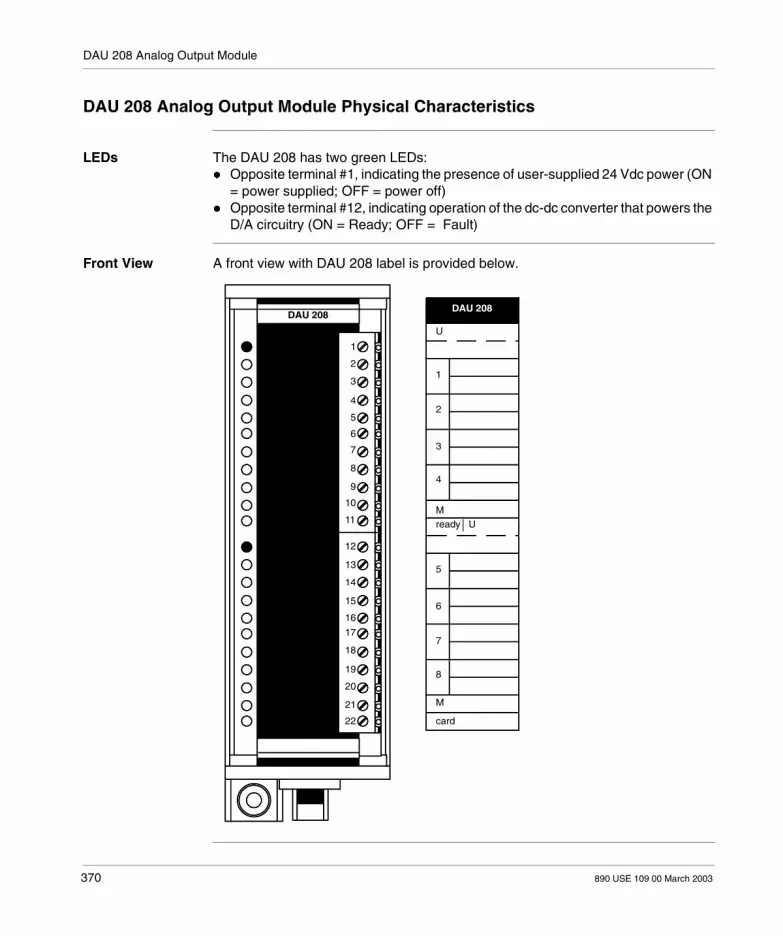
DAU 208 Analog Output Module
DAU 208 Analog Output Module Physical Characteristics
LEDs The DAU 208 has two green LEDs: Opposite terminal #1, indicating the presence of user-supplied 24 Vdc power (ON
= power supplied; OFF = power off) Opposite terminal #12, indicating operation of the dc-dc converter that powers the
D/A circuitry (ON = Ready; OFF = Fault)
Front View A front view with DAU 208 label is provided below.
1
2
3
4
5
6
7
8
9
10
11
12
13
14
15
16
17
21
20
18
19
22
DAU 208DAU 208
U
1
2
3
4
M
ready U
5
6
7
8
M
card
370 890 USE 109 00 March 2003

DAU 208 Analog Output Module
Simplified Schematic
The DAU 208 can be field wired to up to eight voltage output devices.
1
2
3
4
6
78
91011
1516
17
12
13
14
18
20
2122
19
5
-15 V +15 V
REF
-15 V O V +15 V6 V
PAB
PAB
PAB
BIT 11
BIT 0
SERIAL
MUX D/A
+15 V
0 V-15 V
GN
GN
+ 24
+V1
-
+ V2-+ V3-+ V4-
GND
+ 24
+V5
-
+ V6-+ V7-+ V8-
GND
V
V
890 USE 109 00 March 2003 371

DAU 208 Analog Output Module
DAU 208 Analog Output Module Configuration
I/O Mapping The DAU 208 must be I/O Mapped as eight 4x output registers, and BIN must be set for data type.
Cabling Shielded, twisted pair cable (2 or 4 x 0.5 mm/channel) should be used; all channels can be connected with a common shielded cable.
Connect shield to ground (GND) on one side with a short cable (less than 8 in.). Observe a minimum distance of 20 in between the module and power lines or
other sources of electrical disturbance.
Connection and Assignment of Output Addresses
Note: Detailed Compact 984 cabling and installation instructions are found in the 984—A120 Compact Programmable Controllers User Guide (890 USE 108 00 formerly GM-A984-PCS).
372 890 USE 109 00 March 2003

DAU 208 Analog Output Module
DAU 208 Analog Output Module Field Wiring
Wiring Diagram for DAU 208
After conversion by the DAU 208, words 1 ... 8 are shown as analog values at their respective addresses 1 ... 8, as shown in the following illustration.
+ 24 V
+ 24 VGND
0.16 A
V1
V2
V3
V4
V5
V6
V7
V8
1
2
4
1
5
6
7
8
9
10
11
12
13
14
15
16
17
18
19
12
20
21
22
3
890 USE 109 00 March 2003 373

DAU 208 Analog Output Module
DAU 208 Analog Output Module Calibration
Introduction
By adjusting the two potentiometers located on the top of the DAU 208 module, you can calibrate both the plus and minus ranges for the eight output channels.
CAUTION
Calibration Caution
Modicon recommends that units requiring recalibration be returned to the factory, since inaccuracies could be due to faulty components. However, users who wish to perform their own calibration should use the following procedure.
Failure to follow this precaution can result in injury or equipment damage.
374 890 USE 109 00 March 2003

DAU 208 Analog Output Module
Location of DAU 208 Potentiometers
The following illustration shows the location of the potentiometers on the DAU 208.
In this procedure, R4 is used to calibrate the plus output voltage ranges, and R3 is used to calibrate the negative ranges and the zero point. The third potentiometer mounted opposite R3 on a separate PCB is factory preset and should not be adjusted. Its purpose is to establish voltage outputs of the DC-DC supply that powers the module’s D/A converter.Items required for calibration are: A 3.3 kW Precision Register A Voltmeter with appropriate scale and accuracy of 0.2 ... 0.5 PPM.
R 4
R 3
890 USE 109 00 March 2003 375

DAU 208 Analog Output Module
Calibrating the Analog Output Channels
Take the following steps to calibrate the analog output channels.
Step Action
1 Connect the 3.3 k ohms Resistor across Channel 1. Connect the voltmeter across the 3.3 k ohms Resistor and load the Channel 1 register with 4048 decimal. Adjust R4 for a reading of +10 Vdc (+/- 0.5 mV) on the voltmeter.
2 Load the Channel 1 register with 48 decimal. Adjust R3 for a reading of -10 Vdc (+/- 0.5 mV) on the voltmeter.
3 Load the Channel 1 register with 2048 decimal. Adjust R3 for a reading of 0 Vdc (+/- 0.5 mV) on the voltmeter.
4 Move the resistor and voltmeter to the other channels and check outputs. Zero output points should be within +/- 2 mV, and +/-10 Vdc outputs within +/-7 mV.
5 When satisfied with the readings on all eight channels, drop a bead of sealing varnish on both potentiometers’ adjusting screws to secure their settings.
376 890 USE 109 00 March 2003

DAU 208 Analog Output Module
DAU 208 Analog Output Module Specifications
Table of Specifications
The following table contains a list of DAU 208 specifications.
Module Topology
Number of Out puts 8
Isolation Channel-to-Bus 700 Vdc
Channel-to-External Supply
700 Vdc
Voltage Output +/-10 V, greater than 3.3 k ohms
Maximum Load Current 3 mA
Max. Short Circuit Current 20 mA
Power Supply
External 24Vdc, 120 mA maximum
Internally Provided Source from I/O bus
5 Vdc, 30 mA maximum
Power Dissipation 3 Ω
Voltage Output Capabilities
Linear Measuring Range Conversion Values for the DAU208 A984-1xx, E984-24x/251/255 PLC Models Only
Analog Value Decimal Value Comments
-10.24 0
-10.00 48
-5.00 1048
-1.00 1848
-0.50 1948
-0.10 2028
-0.01 2046
-0.005 2047 LinearRange0.00 2048
+0.005 2049
+0.01 2050
+0.10 2068
+0.50 2148
+1.00 2248
+5.00 3048
+10.00 4048
+10.24 4095
890 USE 109 00 March 2003 377

DAU 208 Analog Output Module
A/D Conversion
Conversion Time for All Outputs
1 ms maximum
Resolution 11 bits plus sign
Overrange +/-2.4% (maximum +/-10.24 V)
Overall Error +/-0.1% @ 0 ... 605 C
I/O Map Register 1x/0x 0 in/8 out
Dimensions W x H x D 40.3 x 145 x 117.5 mm (1.6 x 5.6 x 4.5 in)
Weight 350 g (.77 lb.)
Agency Approvals
VDE 0160; UL 508; CSA 22.2 No.142 and FM Class I, Div 2 Standards
Note: If Power is removed from A984 or stopped, the outputs will go to a no output condition.
378 890 USE 109 00 March 2003
890 USE 109 00 March 2003
DEA 202 InterBus S Interface Module
At a Glance
Introduction This information in this chapter describes the DEA 202 InterBus S Interface Module.
What’s in this Chapter?
This chapter contains the following topics:
Topic Page
DEA 202 Features and Functions 380
Configuration of the DEA 202 382
DEA 202 LEDs 386
DEA 202 Specifications 387
379

DEA 202 InterBus S Interface Module
DEA 202 Features and Functions
Product Overview
The DEA-202 enables A120 series I/O modules to connect to the remote bus in an INTERBUS configuration. For the INTERBUS master, the DEA module is a remote node that can address up to 18 I/O modules (288 I/Os) via the subracks AS- HDTA200, AS- HDTA 201 or AS- HDTA 202.The DEA 202 comes with an integrated (non-isolated) power supply. It provides a 5 VDC supply at 1.6 A for the modules on the parallel I/O bus.The following figure shows the DEA 202 InterBus topology.
Features The following list identifies key features of the DEA 202. Coupling module with integrated power supply. With the exception of intelligent modules, all analog and discrete Compact I/O
modules can be employed. The DEA 202 requires 1 word of the packet length for private data. Consequently,
a maximum of 31 words remains available for use by the InterBus-S. DIP switch default adjustment: Disconnection behavior as well as status and
control word processing.
Functional Details
The module serves as the coupling element between the remote bus (CPU connection) and PAB (connection to the I/O modules). The undervoltage monitoring signal from the primary and secondary voltages is evaluated internally by the module.
DEA Station
DEA 202
Rem
ote
Bus
Rem
ote
Bus
380 890 USE 109 00 March 2003

DEA 202 InterBus S Interface Module
Watchdog The watchdog is a self-monitoring feature of the DEA. It consists of a monoflop with a delay time of about 320 ms. The DEA firmware performs an interrupt triggered control of the monoflop. After successfully powering on, which includes a successful EPROM check and initialization, the monoflop is triggered during program execution.The delay time of the monoflop cannot be changed. The green "ready" (watchdog) LED goes off if cycle times are greater than the monoflop’s delay time. This condition activates the disconnection behavior as determined by DIP switches S2 & S3.
Module Faults The DEA 202 collects messages from the associated modules and reports these to the master as module faults (refer to the "DEA 202 Status and Fault Messages" section of the InterBus-S Quantum 140 NOA 611 00 User Manual (P/N 840 USE 419 00).The following figure shows the DEA 202 front view and label.
AEG
DEA 202
18
202122
19
remote in
remote out Mo
dic
on
A12
0
U
PEMMcard
1819202122
DEA 202DEA 202
eareadyreadyBARCRD
in
out
card
24 V
DCready 5VU
890 USE 109 00 March 2003 381

DEA 202 InterBus S Interface Module
Configuration of the DEA 202
Overview The following information describes how to configure the DEA 202.
DIP Switch Location and Settings
The following figure shows the location and settings for the DIP switch.
Status Processing (S0)
The following figure shows the status processing switch settings.
Note: For DEA 202 operation with the 140 NAO 611 00, all DIP switches (S0 ... S3) must be in the "OFF" position.
ON
S3S2S1S0
OFF ON OFF ON
S3S2S1S0
S3S2S1S0Analog value processing
with status and parameter*Analog value processingwithout status and parameter
* As shipped
382 890 USE 109 00 March 2003

DEA 202 InterBus S Interface Module
Control Word Processing (S1)
The following figure shows the control word processing switch settings.
Disconnection Behavior (S2, S3)
The following figure shows the disconnection behavior switches and settings.
Subrack Mounting Slot
The module is installed in DTA 200 primary subrack slot 1-1/1-2.When installing the module, be sure to adhere to the installation steps that are included in the accompanying documentation: Inter-Bus- -S Quantum 140 NOA 611 00 User Manual (P/N 840 USE 419 00).
Compatible A120 I/O Modules
The following table lists the A120 I/O modules that are compatible with the DEA 202 module.
OFF ON OFF ON
S3S2S1S0
S3S2S1S0
DEA control word active.Required setting for 140 NOA 611 00.Output begins after bus initialization completion.*
* Delivery status
DEA control word inactiveRequired setting for 140 NOA 611 10
immediately after startup.and other Output begins
Note: S0 and S1 settings are meaningless.
OFF ON OFF ON
S3S2S1S0
S3S2
S0S1
S3S2
S0S1
S3S2
S0S1
Master defaults arein effect (no defaultsselected: All outputs are cutoff)*
Forced cutoffof all outputs
Halt with value retention(outputs remain unchanged)
Reserved for service specialists(Test bay setting)
* As shipped, required setting for operation with a 140 NOA 611 00.
Module Type Module Number
Discrete Input, 8 point DEP 208, DEP 209, DEP 210 and DEP 211
Discrete Input, 16 point DEP 214, DEP 215, DEP 216, DEP 217, DEP 218, DEP 220, DEP 254, DEP 256, DEP 257, DEP 296, DEP 297 and DEO 216,
Discrete Output, 4/8 point DAP 204, DAP 208, DAP 209, DAP 258 and DAP 210
Discrete Output, 16 point DAP 216, DAP 217, DAP 218 and DAO 216
890 USE 109 00 March 2003 383

DEA 202 InterBus S Interface Module
Power Supply Connection
The following figure shows a sample DEA 202 power supply connection. You enter the relevant power supply information in the label inlay.
Discrete Input/Output DAP 212, DAP 220, DAP 250, DAP 252, DAP 253 and DAP 292
Analog Output DAU 202, DAU 208 and DAU 252
Analog Input ADU 204, ADU 205, ADU 206, ADU 216*, ADU 210*, ADU 214* ADU 254 and ADU 256
* Although these modules are not available in Concept, they can still be used with the DEA 202.
Module Type Module Number
UB (24 VDC)M2
1.25 A mediumtime-lag fuse
1819
202122
Mo
dic
on
A12
0
20
1819
2122
U
PE
M
cardM
24 V
DCready5V U
384 890 USE 109 00 March 2003

DEA 202 InterBus S Interface Module
Note that the noise immunity can be improved if by-pass capacitors are installed at the power supply module U and M terminals.
InterBus-S Connection
Set up the connection according to the "Remote Bus Node Wiring" section of the InterBus-S 140 NOA 611 00 User Manual (P/N 840 USE 419 00).The following figure shows the remote bus port pin assignmentsas viewed from the solder side.
CAUTION
Improper connection danger.
The module’s integrated power supply is non-isolated. Improper connection (for example, absence of the M2 connection), can lead to module destruction.
Failure to follow this precaution can result in injury or equipment damage.
Pin present
No pin present
1
2
3
4
5
6
7
8
9
5
4
3
2
1
6
7
8
9
Sub-D9 “in” plug(top)
Sub-D9 “out” socket(bottom)
Pin Signal Function
1
*) Incoming remote bus = not used
235*679*
DODIGND
DODIRBST
Transmit data (+)Receive data (+)Signal ground(5 VDC Out) cannot be used externallyTransmit data (-)Receive data (-)Plug identifier
890 USE 109 00 March 2003 385

DEA 202 InterBus S Interface Module
DEA 202 LEDs
LED Displays The following table describes the LED displays, which are located on the module front plate.
No. Label Inlay Identifier
Color Function
18 (left) U Green 24 VDC supply present
19 (left) ready 5 V Green Module ready for service, 5 VDC output voltage present
3 (right) ready Green Coupler ready
4 (right) BA Green Transfer in progress
5 (right) RC Green "Remote bus check", remote bus input monitoring
6 (right) RD Red "Remote bus disabled", remote bus feed-through terminated (remote bus node diagnosis)
386 890 USE 109 00 March 2003
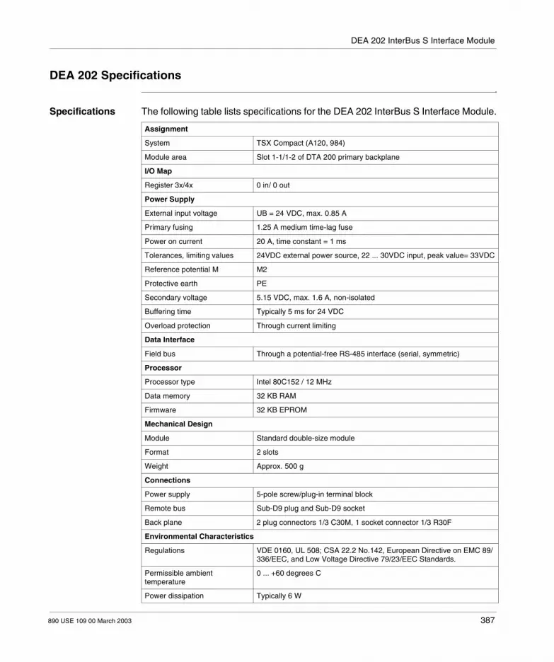
DEA 202 InterBus S Interface Module
DEA 202 Specifications
Specifications The following table lists specifications for the DEA 202 InterBus S Interface Module.
Assignment
System TSX Compact (A120, 984)
Module area Slot 1-1/1-2 of DTA 200 primary backplane
I/O Map
Register 3x/4x 0 in/ 0 out
Power Supply
External input voltage UB = 24 VDC, max. 0.85 A
Primary fusing 1.25 A medium time-lag fuse
Power on current 20 A, time constant = 1 ms
Tolerances, limiting values 24VDC external power source, 22 ... 30VDC input, peak value= 33VDC
Reference potential M M2
Protective earth PE
Secondary voltage 5.15 VDC, max. 1.6 A, non-isolated
Buffering time Typically 5 ms for 24 VDC
Overload protection Through current limiting
Data Interface
Field bus Through a potential-free RS-485 interface (serial, symmetric)
Processor
Processor type Intel 80C152 / 12 MHz
Data memory 32 KB RAM
Firmware 32 KB EPROM
Mechanical Design
Module Standard double-size module
Format 2 slots
Weight Approx. 500 g
Connections
Power supply 5-pole screw/plug-in terminal block
Remote bus Sub-D9 plug and Sub-D9 socket
Back plane 2 plug connectors 1/3 C30M, 1 socket connector 1/3 R30F
Environmental Characteristics
Regulations VDE 0160, UL 508; CSA 22.2 No.142, European Directive on EMC 89/336/EEC, and Low Voltage Directive 79/23/EEC Standards.
Permissible ambient temperature
0 ... +60 degrees C
Power dissipation Typically 6 W
890 USE 109 00 March 2003 387

DEA 202 InterBus S Interface Module
388 890 USE 109 00 March 2003
890 USE 109 00 March 2003
Overview of the DEO 216 Input Module
At a Glance
Purpose The purpose of this chapter is to describe the DEO 216 Input module.
What’s in this Chapter?
This chapter contains the following topics:
Topic Page
What is the DEO 216 Input Module? 390
Specifications of the DEO 216 Input Module 391
389
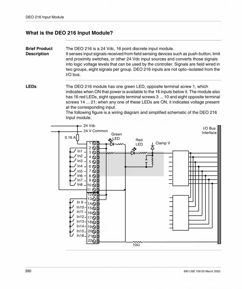
DEO 216 Input Module
What is the DEO 216 Input Module?
Brief Product Description
The DEO 216 is a 24 Vdc, 16 point discrete input module.It senses input signals received from field sensing devices such as push-button, limit and proximity switches, or other 24 Vdc input sources and converts those signals into logic voltage levels that can be used by the controller. Signals are field wired in two groups, eight signals per group. DEO 216 inputs are not opto–isolated from the I/O bus.
LEDs The DEO 216 module has one green LED, opposite terminal screw 1, which indicates when ON that power is available to the 16 inputs below it. The module also has 16 red LEDs, eight opposite terminal screws 3 ... 10 and eight opposite terminal screws 14 ... 21; when any one of these LEDs are ON, it indicates voltage present at the corresponding input.The following figure is a wiring diagram and simplified schematic of the DEO 216 Input module.
0.16 A
24 Vdc24 V Common
Green LED Red
LED Clamp V
I/O BusInterface
123456789
10111213141516171819202122
In1In2In3In4In5In6In7In8
In 9In10In11In12In13In14
In16In15
10Ω
390 890 USE 109 00 March 2003

DEO 216 Input Module
Specifications of the DEO 216 Input Module
Specifications for the DEO 216
The following table shows the specifications.
DEO216 Specifications
Module Topology Number of Inputs 16
Number of Groups 1
Points/Group 16
Isolation Not isolated from the I/O bus
Power Supplies External Source Requirement 20 ... 30 Vdc for eight inputs
Rated Signal Value +24 Vdc
Internally Provided Source 5 V, < 15 mA from I/O bus
Internal Power Dissipation 2 W (typical)
Electrical Characteristics
ON State Signal Level +12 ... 30 Vdc
OFF State Signal Level -2 ... +5 Vdc
ON State Input Current 7 mA @ 24 Vdc 8.5 mA @ 30 Vdc
Response Time 4 ms (typical)
Operating Mode True High
Wire Size/Terminal One wire: 14 AWG
Two wires: 20 AWG
I/O Map Discrete 1x/0x 16 in/0 out
Dimensions WxHxD 40.3 x 145 x 117.5 mm (1.6 x 5.6 x 4.5 in)
Weight 220 g (.5 lb)
Agency Approvals VDE 0160; UL 508; and CSA 22.2 No.142 Standards
890 USE 109 00 March 2003 391

DEO 216 Input Module
392 890 USE 109 00 March 2003

890 USE 109 00 March 2003
Overview of the DEP 208 Input Module
At a Glance
Purpose The purpose of this chapter is to describe the DEP 208 input module.
What’s in this Chapter?
This chapter contains the following topics:
Topic Page
What is the DEP 208 Input Module? 394
DEP 208 Input Module LEDs 395
DEP 208 Input Module Field Wiring 396
Using the DEP 208 Input Module wilth Proximity Switches 397
DEP 208 Input Module Specifications 398
393

DEP 208 Input Module
What is the DEP 208 Input Module?
Brief Product Description
The DEP 208 is a discrete input module with eight independent 230 Vac input circuits. It senses input signals from field sensing devices such as pushbuttons, limit or proximity switches, or other ac input sources and converts those signals into voltage signals that can be used by the PLC in a logic scan. Signals are field-wired in one group of eight inputs. Each input is opto-isolated from the I/O bus.
394 890 USE 109 00 March 2003

DEP 208 Input Module
DEP 208 Input Module LEDs
LEDs The DEP 208 has nine LEDs. One green LED opposite terminal screw 1 indicates the presence of 5 V from the I/O bus. Eight red LEDs opposite terminal screws 3, 5, 7, 9, 14, 16, 18, and 20 indicate that voltage is present at inputs 1 ... 8, respectively.
890 USE 109 00 March 2003 395

DEP 208 Input Module
DEP 208 Input Module Field Wiring
Introduction The DEP 208 is a discrete input module with eight independent 230 Vac input circuits. It senses input signals from field sensing devices such as pushbuttons, limit or proximity switches, or other ac input sources and converts those signals into voltage signals that can be used by the PLC in a logic scan. Signals are field-wired in one group of eight inputs. Each input is opto-isolated from the I/O bus.
Wiring Diagram and Simplified Schematic for DEP 208
A wiring diagram and simplified schematic for the DEP 208 input module is provided below.
ac Neutralac Hot
0.16 A
OptoCoupler
Red LED
I/O BusInterface
First of eightInput Circuits
Latch
Green LED
5 V
123456789
10111213141516171819202122
In1
In2
In3
In4
In5
In6
In7
In8
396 890 USE 109 00 March 2003

DEP 208 Input Module
Using the DEP 208 Input Module wilth Proximity Switches
Introduction The leakage current of two-wire proximity switches may be as high as 3 mA. Since the OFF current rating of the DEP 208 is .5 mA per input, two-wire proximity switches may trigger false inputs in the module. If you plan to use the DEP 208 in a proximity switch application, consider the following recommendations to prevent false inputs from occurring.
Existing Installations
To eliminate the possibility of false inputs, place a 10 kOhm resistor between neutral and each input terminal on the module to shunt off some of the current. See the diagram below.
New Installations Keep the above current ratings in mind when selecting proximity switches. Three-wire proximity switches have leakage current levels below .5 mA, and are recommended in order to avoid the need for the 10 kOhm resistor. The following diagram illustrates wiring the DEP 208 with a 10 kOhm Resistor.
ac Neutral
ac Hot
0.16 A Fuse
10 kΩ Resistor
Two-wire Proximity Switch
1
2
3
4
5
6
7
8
9
10
11
890 USE 109 00 March 2003 397

DEP 208 Input Module
DEP 208 Input Module Specifications
Table of Specifications for DEP 208
The following table contains a list of DEP 208 input module specifications.
Module Topology Number of Inputs 8
Number of Groups 1
Points/group 8
Isolation Optocoupler on each input point
Power Supplies External Source Requirement 230 Vac (+/- 15 percent), 47 ... 63 Hz
Internally Provided Source 5 V, less than 30 mA from the I/O bus
Internal Power Dissipation 2 W (typical)
Electrical Characteristics
Working Voltage Range 195 ... 265 Vac
ON Current Minimum 1 mA/input
OFF Current Maximum 0.5 mA/input
0 to 230 V Response Time 25 ms (typical)
230 to 0 V Response Time 50 ms (typical)
Operating Mode True High
Wire Size/Terminal One wire: 14 AWG
Two wires: 20 AWG
I/O Map Discrete 1x/ox 8 in/0 out
Dimensions WxHxD 40.3 x 145 x 117.5 mm (1.6 x 5.6 x 4.5 in)
Weight 220 g (.5 lb)
Agency Approvals VDE 0160; UL 508; and CSA 22.2 No.142 Standards
398 890 USE 109 00 March 2003
890 USE 109 00 March 2003
Overview of the DEP 209 Input Module
At a Glance
Purpose The purpose of this chapter is to describe the DEP 209 input module.
What’s in this Chapter?
This chapter contains the following topics:
Topic Page
What is the DEP 209 Input Module? 400
DEP 209 Input Module LEDs 401
DEP 209 Input Module Field Wiring 402
Using the DEP 209 Input Module with Proximity Switches 403
DEP 209 Input Module Specifications 404
399

DEP 209 Input Module
What is the DEP 209 Input Module?
Brief Product Description
The DEP 209 is a discrete input module with eight independent 120 Vac input circuits. It senses input signals from field sensing devices such as pushbuttons, limit or proximity switches, or other ac input sources and converts those signals into voltage signals that can be used by the controller in a logic scan. Signals are field-wired in one group of eight inputs. Each input is opto-isolated from the I/O bus.
400 890 USE 109 00 March 2003

DEP 209 Input Module
DEP 209 Input Module LEDs
LEDs The DEP 209 has nine LEDs. One green LED opposite terminal screw 1 indicates the presence of 5 V from the I/O bus. Eight red LEDs opposite terminal screws 3, 5, 7, 9, 14, 16, 18, and 20 indicate that voltage is present at inputs 1 ... 8, respectively.
890 USE 109 00 March 2003 401

DEP 209 Input Module
DEP 209 Input Module Field Wiring
Introduction The DEP 209 is a discrete input module with eight independent 120 Vac input circuits. It senses input signals from field sensing devices such as pushbuttons, limit or proximity switches, or other ac input sources and converts those signals into voltage signals that can be used by the controller in a logic scan. Signals are field-wired in one group of eight inputs. Each input is opto-isolated from the I/O bus.
Wiring Diagram and Simplified Schematic for DEP 209
A wiring diagram and simplified schematic for the DEP 209 input module is provided below.
ac Neutralac Hot
0.16 A
123456789
10111213141516171819202122
In1
In2
In3
In4
In5
In6
In7
In8
OptoCoupler
RedLED
I/O BusInterface
First of EightInput Circuits
Latch
GreenLED
5 V
402 890 USE 109 00 March 2003

DEP 209 Input Module
Using the DEP 209 Input Module with Proximity Switches
Introduction The leakage current of two-wire proximity switches may be as high as 3 mA. Since the OFF current rating of the DEP 209 is .5mA/input, two-wire proximity switches may trigger false inputs in the module. If you plan to use the DEP 209 in a proximity switch application, consider the following recommendations to prevent false inputs from occurring.
Existing Installations
To eliminate the possibility of false inputs, place a 10 kOhms resistor between neutral and each input terminal on the module to shunt some of the current.
New Installations Keep the above current ratings in mind when selecting proximity switches. Three-wire proximity switches have leakage current levels below .5 mA and are recommended in order to avoid the need for the 10 kOhms resistor. The following diagram illustrates wiring the DEP 209 with a 10 kOhm resistor.
ac Neutral
ac Hot
0.16 A Fuse
10 kΩ Resistor
Two-wire Proximity Switch
1
2
3
4
5
6
7
8
9
11
10
890 USE 109 00 March 2003 403

DEP 209 Input Module
DEP 209 Input Module Specifications
Table of Specifications
The following table contains a list of DEP 209 input module specifications.
Module Topology Number of Inputs 8
Number of Groups 1
Points/group 8
Isolation Optocoupler on each input
Power Supplies External Source Requirement 120 Vac (+/- 15 percent)
47 ... 63 Hz
Internally Provided Source from I/O bus 5 V; less than 30 mA
Internal Power Dissipation 2 W typical
Electrical Characteristics
Working Voltage Range 85 ... 138 Vac
ON Current Minimum 1 mA/input
OFF Current Maximum 0.5 mA/input
Response Time 0 to 230 V 25 ms typical
230 to 0 V 50 ms typical
Operating Mode True High
Wire Size/terminal One wire 14 AWG
Two wires 20 AWG
I/O Map Discrete 1x/0x 8 in/0 out
Dimensions W x H x D 40.3 x 145 x 117.5 mm
1.6 x 5.6 x 4.5 in
Weight 220 g
0.5 lb
Agency Approvals VDE 0160; UL 508; and CSA 22.2 No.142 Standards
404 890 USE 109 00 March 2003

890 USE 109 00 March 2003
Overview of the DEP 210 Input Module
At a Glance
Purpose The purpose of this chapter is to describe the DEP 210 input module.
What’s in this Chapter?
This chapter contains the following topics:
Topic Page
What is the DEP 210 Input Module? 406
DEP 210 Input Module LEDs 407
DEP 210 Input Module Field Wiring 408
DEP 210 Input Module Specifications 410
405

DEP 210 Input Module
What is the DEP 210 Input Module?
Brief Product Description
The DEP 210 is a 115 Vac, eight-point input module with 1.8 kV isolation between inputs and the bus. The module senses input signals received from field sensing devices such as pushbuttons, limit and proximity switches, or other 115 Vac input sources and converts those signals into logic voltage levels that can be used by the PLC. Signals are field wired in one group of eight signals. Inputs are opto-isolated from the system bus.
WARNING
Operational Hazard
The DEP 210 module will only operate properly when used with an A984, E984, or Micro 512/612 controller.
Failure to follow this precaution can result in death, serious injury, or equipment damage.
406 890 USE 109 00 March 2003

DEP 210 Input Module
DEP 210 Input Module LEDs
LEDs The DEP 210 module has one green LED opposite terminal screw 1. When this LED is ON, it indicates the presence of working voltage from the PLC. The module also has eight red LEDs, opposite terminal screws 3, 5, 7, 9, 14, 16, 18, and 20. When any one of these LEDs is ON, it indicates voltage present at the corresponding input. Location of the LEDs is shown in the figure below.A front view and fill-in labels of the DEP 210 is provided below.
DEP 210DEP 210
ready N1
2
3
4
56
7
8
9
1011
12
13
14
15
16
17
18
19
20
21
22
N
1
2
3
4
N
5
6
7
8
card
N
890 USE 109 00 March 2003 407

DEP 210 Input Module
DEP 210 Input Module Field Wiring
Introduction The DEP 210 is a 115 Vac, eight-point input module with 1.8 kV isolation between inputs and the bus. The module senses input signals received from field sensing devices such as pushbuttons, limit and proximity switches, or other 115 Vac input sources and converts those signals into logic voltage levels that can be used by the PLC. Signals are field wired in one group of eight signals. Inputs are opto-isolated from the system bus.
Wiring Diagram for DEP 210
A sample wiring diagram for the DEP 210 input module is provided below.
AC HOTAC NEUTRAL
0.2 A
1
2
3
4
5
6
7
8
9
10
11
12
13
14
15
16
18
19
17
20
21
22
Input 1
Input 2
Input 3
Input 4
Input 5
Input 6
Input 7
Input 8
408 890 USE 109 00 March 2003

DEP 210 Input Module
Simplified Schematic for DEP 210
A simplified schematic for the DEP 210 input module is provided below.
ac Neutral 1
2
3
4
56
7
8
9
10
11
12
13
14
15
16
17
18
19
20
21
22
FIRST OF EIGHT INPUT CIRCUITS
Red
PAB
PAB
Green
0 V
5 V
1
8
890 USE 109 00 March 2003 409

DEP 210 Input Module
DEP 210 Input Module Specifications
Table of Specifications for DEP 210
The following table contains a list of DEP 210 input module specifications.
Module Topology Number of Inputs 8
Number of Groups 1
Points/group 8
Isolation Optocoupler on each input
1.8 kV field-to-bus
Power Supplies External Source Requirement 115 Vac
Rated Signal Value 115 Vac
47 ... 65 Hz
Internally Provided Source from I/O bus
5 V
35 mA maximum
Internal Power Dissipation 3 W typical
Electrical Characteristics
ON State Signal Level 80 ... 132 Vac
OFF State Signal Level 0 ... 35 Vac
ON State Input Current 15.5 mA/input @ 115 Vac
6 mA @ 80 V, 20 mA @ 132 V
OFF State Input Current 3 mA maximum
Response Time ON 10 ms typical
OFF 40 ms typical
Operating Mode True High
Wire Size/terminal One wire 14 AWG
Two wires 20 AWG
I/O Map Discrete 1x/0x 8 in/0 out
Dimensions W x H x D 40.3 x 145 x 117.5 mm
1.6 x 5.6 x 4.5 in
Weight 250 g
0.55 lb
Agency Approvals VDE 0160; UL 508; and CSA 22.2 No.142 Standards
410 890 USE 109 00 March 2003

890 USE 109 00 March 2003
Overview of the DEP 211 Input Module
At a Glance
Purpose The purpose of this chapter is to describe the DEP 211 input module.
What’s in this Chapter?
This chapter contains the following topics:
Topic Page
What is the DEP 211 Input Module? 412
DEP 211 Input Module LEDs 413
DEP 211 Input Module Field Wiring 414
DEP 211 Input Module Specifications 416
411

DEP 211 Input Module
What is the DEP 211 Input Module?
Brief Product Description
The DEP 211 is a 115 Vac, eight-point isolated input module. The module senses input signals received from field devices such as pushbuttons, limit and proximity switches, or other 115 Vac sources and converts those signals into logic voltage levels that can be used by the controller. Signals are field wired in one group of eight signals. Inputs are isolated from the system bus and from one another.
Note: Some A120 I/O modules (DEP 211/214/215/217, DAP211/217, ADU204/211/214/216, DAU204, VIC2xx, and MOT20x) require a loadable (SW-IODR-001) for proper operation when using certain PLCs (A984-1xx, E984-24x/251/255) with Modsoft.
WARNING
Operational Hazard
The DEP 211 module will only operate properly when used with an A984, E984, or Micro 512/612 controller.
Failure to follow this precaution can result in death, serious injury, or equipment damage.
412 890 USE 109 00 March 2003

DEP 211 Input Module
DEP 211 Input Module LEDs
LEDs The DEP 211 module has one green LED opposite terminal screw 1. When this LED is ON, it indicates the presence of working voltage from the controller. The module also has 8 red LEDs, opposite terminal screws 3, 5, 7, 9, 14, 16, 18, and 20. When any one of these LEDs is ON, it indicates voltage present at the corresponding input. Location of the LEDs is shown in the figure below.A front view of the DEP 211 is provided below.
DEP 211
1
2
3
45
6
7
8
9
1011
12
1314
15
1617
18
19
20
2122
890 USE 109 00 March 2003 413

DEP 211 Input Module
DEP 211 Input Module Field Wiring
Introduction The DEP 211 is a 115 Vac, eight-point isolated input module. The module senses input signals received from field devices such as pushbuttons, limit and proximity switches, or other 115 Vac sources and converts those signals into logic voltage levels that can be used by the controller. Signals are field wired in one group of eight signals. Inputs are isolated from the system bus and from one another.
Wiring Diagram for DEP 211
A sample wiring diagram for the DEP 211 input module is provided below.
0.1 A 0.1 A 0.1 A 0.1 A
ac Hotac Neutral
Input 1
Input 2
Input 3
Input 4
Input 5
Input 6
Input 7
Input 8
1
2
3
4
5
6
7
8
9
10
11
12
13
14
15
16
17
18
19
20
21
22
414 890 USE 109 00 March 2003

DEP 211 Input Module
Simplified Schematic for DEP 211
A simplified schematic for the DEP 211 input module is provided below.
11
1
2
3
4
5
6
7
8
9
10
11
12
13
14
15
16
17
18
19
20
21
22
8
ac Neutral
FIRST OF EIGHT INPUT CIRCUITS
RedPAB
PAB
Green
5 V
0 V
890 USE 109 00 March 2003 415

DEP 211 Input Module
DEP 211 Input Module Specifications
Table of Specifications for DEP 211
The following table contains a list of DEP 211 input module specifications.
Module Topology Number of Inputs 8
Number of Groups 8
Points/group 1
Isolation Optocoupler on each input
1.8 kV between inputs
Power Supplies External Source Requirement None
Rated Signal Value 115 Vac, 47 ... 65 Hz
Internally Provided Source from I/O bus
5 V
35 mA maximum
Internal Power Dissipation 3 W typical
Electrical Characteristics
ON State Signal Level 80 ... 132 Vac
OFF State Signal Level 0 ... 35 Vac
ON State Input Current 15.5 mA/input @ 115 Vac
6 mA @ 80 V; 20 mA @ 132 V
OFF State Input Current 3 mA maximum
Response Time ON 10 ms typical
OFF 40 ms typical
Operating Mode True High
Wire Size/terminal One wire 14 AWG
Two wires 20 AWG
I/O Map Discrete 1x/0x 8 in/0 out
Dimensions W x H x D 40.3 x 145 x 117.5 mm
1.6 x 5.6 x 4.5 in
Weight 250 g
0.55 lb
Agency Approvals VDE 0160; UL 508; and CSA 22.2 No.142 Standards
416 890 USE 109 00 March 2003

890 USE 109 00 March 2003
Overview of the DEP 214/254 Input Module
At a Glance
Purpose The purpose of this chapter is to describe the DEP 214/254 input module.
What’s in this Chapter?
This chapter contains the following topics:
Topic Page
What is the DEP 214/254 Input Module? 418
DEP 214/254 Input Module LEDs 419
DEP 214/254 Input Module Field Wiring 420
DEP 214/254 Input Module Specifications 422
417

DEP 214/254 Input Module
What is the DEP 214/254 Input Module?
Brief Product Description
The DEP 214/254 is a 12 ... 60 Vdc 16-point discrete input module. It senses levels provided by field devices such as pushbuttons, limit and proximity switches, or other dc input sources, and converts those signals into logic voltage levels that can be used by the PLC. Signals are field wired in two groups, eight signals/group. Inputs are optically isolated from the system bus. The DEP 254 functions just like the DEP 214 except that the DEP 254 operates at extended temperature.
Note: Some A120 I/O modules (DEP 211/214/215/217, DAP211/217, ADU204/211/214/216, DAU204, VIC2xx, and MOT20x) require a loadable (SW-IODR-001) for proper operation when using certain PLCs (A984-1xx, E984-24x/251/255) with Modsoft.
Note: DEP 254 model is available with conformal coating. The conformal coating model is DEP 254C and it meets Railway standard EN 50 155.
418 890 USE 109 00 March 2003

DEP 214/254 Input Module
DEP 214/254 Input Module LEDs
LEDs The DEP 214/254 can be installed in any slot in the A120 subracks (DTA 200, 201, and 202). The module has bus contacts at the rear and peripheral connections on the front. The blank label, which fits in the module cover, can be filled in with relevant information (signal values, etc.) in the spaces provided.A front view with DEP 214 label is provided below.
DEP 214DEP 214
123456789
1011
1213141516171819202122
UU1
2345678MUU9101112
13141516Mcard
1
23456789
1011
1213
14151617
1819
202122
Inp
ut
Inp
ut
890 USE 109 00 March 2003 419

DEP 214/254 Input Module
DEP 214/254 Input Module Field Wiring
Introduction The DEP 214/254 is a 12 ... 60 Vdc 16-point discrete input module. It senses levels provided by field devices such as pushbuttons, limit and proximity switches, or other dc input sources, and converts those signals into logic voltage levels that can be used by the PLC. Signals are field wired in two groups, eight signals/group. Inputs are optically isolated from the system bus. The DEP 254 functions just like the DEP 214 except that the DEP 254 operates at extended temperature.
Wiring Diagram for DEP 214/254
A sample wiring diagram for the DEP 214/254 input module is provided below.
12 ... 60 VdcCommon
0.16 A0.16 A
I1
I8
I9
I16
12
3456789
1011
1213141516
18
20
22
DEP 214
123456789
101112131415
16
18
20
22
U
U12345678MU
U91011
13
15
M
inp
ut
17
19
21
12
14
16
card
17
19
21
420 890 USE 109 00 March 2003

DEP 214/254 Input Module
Simplified Schematic for DEP 214/254
A simplified schematic for the DEP 214/254 input module is provided below.
First of 16 Input Circuits
COMP
Green
Red
IK
12 ... 60 Vdc
I1
I8
12 ... 60 Vdc
I9
COM
COM
123456789
101112131415
17
19
21
16
18
20
22
890 USE 109 00 March 2003 421

DEP 214/254 Input Module
DEP 214/254 Input Module Specifications
Table of Specifications for DEP 214/254
The following table contains DEP 214/254 input specifications.
The following table lists DEP 214/254 switching levels.
DEP 214/254 Specifications (continued)
Module Topology Number of Inputs 16
Number of Groups 2
Points/group 8
Isolation Optocoupler on each input
Required Loadable SW-IODR-001
Power Supplies External Source Requirement 12 ... 60 Vdc for eight inputs
Internally Provided Source from I/O bus 5 V; 22 mA maximum
Signal Input 12 V 24 V 48 V 60 V
Signal Level OFF -0.6 ... +1.8 V -3 ... +5 V -6 ... +10 V -3 ... +9 V
Signal Level ON +9 ... +15 V +11 ... +30 V +33 ... +60 V +45 ... +75V
Current OFF -0.6 ... +1 mA -1.7 ... +2.9 mA -3.4 ... +2.5 mA -1.7 ... + 2.5mA
Current ON +5.1 ... +7.1 mA +6.0 ... +7.1 mA +2.0 ... +2.5 mA +2.0 ... +2.5mA
Reference Current less than or equal to 20 mA
less than or equal to 10 mA
less than or equal to 7 mA
less than or equal to 7 mA
ON State Input Current 7 mA @ 24 Vdc
8.5 mA @ 30 Vdc
Response Time 4 ms typical
Operating Mode True High
Wire Size/ terminal One wire 14 AWG
Two wires 20 AWG
Temperature Ambient Operating 0 ... 60 degrees C for DEP214-40 ... +70 degrees C for DEP254
I/O Map Discrete 1x/0x 16 in/0 out
Dimensions W x H x D 40.3 x 145 x 117.5 mm
1.6 x 5.6 x 4.5 in
Weight 260 g
0.57 lb
Agency Approvals
DEP214: VDE 0160; UL 508; and CSA 22.2 No.142 Standards.
DEP254C: Railway EN 50 155; EMC 89/336/EEC Standards. UL 508; CSA 22.2 No.142; FM Class I, Div 2 pending
422 890 USE 109 00 March 2003

890 USE 109 00 March 2003
Overview of the DEP 215 Input Module
At a Glance
Purpose The purpose of this chapter is to describe the DEP 215 input module.
What’s in this Chapter?
This chapter contains the following topics:
Topic Page
What is the DEP 215 Input Module? 424
DEP 215 Input Module LEDs 425
DEP 215 Input Module Field Wiring 426
Unique True Low Characteristics of the DEP 215 Input Module 428
DEP 215 Input Module Specifications 429
423

DEP 215 Input Module
What is the DEP 215 Input Module?
Brief Product Description
The DEP 215 is a TTL, 16-point discrete input module. It senses levels provided by field devices such as pushbuttons, limit and proximity switches, or other TTL input sources, and converts those signals into logic voltage levels that can be used by the PLC. Signals are field wired in two groups, eight signals/group. Inputs are opto-isolated from the system bus.
Note: Some A120 I/O modules (DEP 211/214/215/217, DAP211/217, ADU204/211/214/216, DAU204, VIC2xx, and MOT20x) require a loadable (SW-IODR-001) for proper operation when using certain PLCs (A984-1xx, E984-24x/251/255) with Modsoft.
424 890 USE 109 00 March 2003

DEP 215 Input Module
DEP 215 Input Module LEDs
LEDs The DEP 215 module has two green LEDs, opposite terminal screws 1 and 12. When one of these LEDs is ON, it indicates that power is available to the group directly below it. The module also has 16 red LEDs, eight opposite terminal screws 3 ... 10 and eight opposite terminal screws 14 ... 21; when any one of these LEDs are ON, it indicates a -1 ... +2 Vdc level present at the corresponding input.
890 USE 109 00 March 2003 425

DEP 215 Input Module
DEP 215 Input Module Field Wiring
Introduction The DEP 215 is a TTL, 16-point discrete input module. It senses levels provided by field devices such as pushbuttons, limit and proximity switches, or other TTL input sources, and converts those signals into logic voltage levels that can be used by the PLC. Signals are field wired in two groups, eight signals/group. Inputs are opto-isolated from the system bus.
Wiring Diagram for DEP 215
A sample wiring diagram for the DEP 215 input module is provided below.
5 VDC
5 V Common
0.16A 0.16A
In1
In2
In3
In4In5In6
In7In8
In9
In10
In11
In13
In15In16
1
234567
8
91011
1213
1415
16
18
20
22
In12
In14
17
19
21
426 890 USE 109 00 March 2003

DEP 215 Input Module
Simplified Schematic for DEP 215
A simplified schematic for the DEP 215 input module is provided below.
First of 16 Input CircuitsRed 5 V
I/O BusInterface
GreenGND
1
23
4
5
6789
1011
121314
15
161718
192021
22
890 USE 109 00 March 2003 427

DEP 215 Input Module
Unique True Low Characteristics of the DEP 215 Input Module
Introduction This section is intended for DEP 215 16-point TTL input module users who have installed or are otherwise familiar with 200, 500 or 800 Series I/O TTL input modules.
True Low Module These users should be aware that:
DEP 215 Input Module Layout
For example, refer to the module input layout in the following illustration.
If the DEP 215 were substituted for an older series TTL input module in a system and I/O Mapped as BCD, the four bottom inputs would be interpreted as an invalid decimal 12 by the PLC. Since this interpretation is a number greater than 9, the internal conversion result would be zero. A conventional module’s conversion value would be decimal 3. In this case, inverting all of the field device inputs to the DEP 215 or changing to a device with complementary outputs results in usable data.
Step Action
1 The DEP 215 is a True Low module; therefore: a HIGH (4 ... 5.5 Vdc) input level to the DEP 215 is read as a logic zero (0) by the
system PLC a low (-1 ... +2 Vdc) level is read as a logic 1
2 Conversely, other I/O family TTL input modules are traditionally True High; therefore: +5 Vdc input levels to other I/O family TTL input modules are read as logic 1 low or ground input levels are read as logic 0
CAUTION
Operational Hazard
Traffic Copping the DEP 215 as BCD and using input devices associated with other series traditional True High modules will cause the controller’s BCD conversion to produce unexpected results.
Failure to follow this precaution can result in injury or equipment damage.
COM
+5V
CONVENTIONAL
0
011 (LSB)
COM
+5V
1100 (LSB)
DEP 215
428 890 USE 109 00 March 2003

DEP 215 Input Module
DEP 215 Input Module Specifications
Table of Specifications for DEP 215
The following table contains DEP 215 input module specifications.
Module Topology Number of Inputs 16
Number of Groups 2
Points/group 8
Isolation Optocoupler on each input
Required Loadable SW-IODR-001 (See Requirements for CE Compliance, p. 779)
Power Supplies External Source Requirement 5 Vdc for eight inputs
Rated Signal Value Sinking device
Internally Provided Source from I/O bus 5 V; 25 mA maximum
Internal Power Dissipation 2 W typical
Electrical Characteristics
False Condition Signal Level 4 ... 5 Vdc
True Condition Signal Level -1 ... +2 Vdc
True Condition Input Current 3.5 mA @ 0 Vdc
Response Time 1 ms typical
Operating Mode True Low
Wire Size/terminal One wire 14 AWG
Two wires 20 AWG
I/O Map Discrete 1x/0x 16 in/0 out
Dimensions W x H x D 40.3 x 145 x 117.5 mm
1.6 x 5.6 x 4.5 in
Weight 220 g
0.5 lb.
Agency Approvals VDE 0160; UL 508; and CSA 22.2 No.142 Standards
890 USE 109 00 March 2003 429

DEP 215 Input Module
430 890 USE 109 00 March 2003

890 USE 109 00 March 2003
Overview of the DEP 216/256 Input Module
At a Glance
Purpose The purpose of this chapter is to describe the DEP 216/256 input module.
What’s in this Chapter?
This chapter contains the following topics:
Topic Page
What is the DEP 216/256 Input Module? 432
DEP 216/256 Input Module LEDs 433
DEP 216/256 Input Module Field Wiring 434
DEP 216/256 Input Module Specifications 435
431

DEP 216/256 Input Module
What is the DEP 216/256 Input Module?
Brief Product Description
The DEP 216/256 is a 24 Vdc, 16-point discrete input module. It senses input signals received from field sensing devices such as pushbuttons, limit and proximity switches, or other 24 Vdc input sources and converts those signals into logic voltage levels that can be used by the PLC. Signals are field wired in two groups, eight signals per group. Inputs are opto-isolated from the system bus. The DEP 256 functions just like the DEP 216 except that the DEP 256 operates at extended temperature.
Note: The DEP 256 model is available with conformal coating. The conformal coating model is DEP 256C and it meets Railway standard EN 50 155.
432 890 USE 109 00 March 2003

DEP 216/256 Input Module
DEP 216/256 Input Module LEDs
LEDs The DEP 216/256 module has two green LEDs, opposite terminal screws 1 and 12. When one of these LEDs is ON, it indicates that power is available to the eight inputs directly below it. The module also has 16 red LEDs, eight opposite terminal screws 3 ... 10 and eight opposite terminal screws 14 ... 21; when any one of these LEDs are ON, it indicates voltage present at the corresponding input.
890 USE 109 00 March 2003 433

DEP 216/256 Input Module
DEP 216/256 Input Module Field Wiring
Introduction The DEP 216/256 is a 24 Vdc, 16-point discrete input module. It senses input signals received from field sensing devices such as pushbuttons, limit and proximity switches, or other 24 Vdc input sources and converts those signals into logic voltage levels that can be used by the PLC. Signals are field wired in two groups, eight signals per group. Inputs are opto-isolated from the system bus. The DEP 256 functions just like the DEP 216 except that the DEP 256 operates at extended temperature.
Simplified Schematic for DEP 216/256
A simplified schematic for the DEP 216/256 input module is provided below.
24 Vdc
24 V Common0.16A Green
I/O BusInterface
5 V
First of 16Input Circuits
RedOpto
Coupler
GND
In1In2In3In4In5In6In7In8
In9In10
In12
In14
In16
123456789
1011121314
16
18
20
22
15
17
19
21
In11
In13
In15
434 890 USE 109 00 March 2003

DEP 216/256 Input Module
DEP 216/256 Input Module Specifications
Table of Specifications for DEP 216/256
The following table contains DEP 216/256 input module specifications.
Module Topology
Number of Inputs 16
Number of Groups 2
Points/group 8
Isolation Optocoupler on each input
Power Supplies
External Source Requirement 24 Vdc for eight inputs
Rated Signal Value 24 Vdc +25 percent/-15 percent
Internally Provided Source from I/O bus
5 V; 15 mA
Internal Power Dissipation 2 W typical
Electrical Characteristics
ON State Signal Level 12 ... 30 Vdc
OFF State Signal Level -2 ... +5 Vdc
ON State Input Current 7 mA @ 24 Vdc
8.5 mA @ 30 Vdc
Response Time 4 ms typical
Operating Mode True High
Wire Size/terminal One wire 14 AWG
Two wires 20 AWG
EnvironmentalCharacteristics
Operating Temperature 0 ... 60 degrees C for DEP216 -40 ... +70 degrees C for DEP256
I/O Map Discrete 1x/0x 16 in/0 out
Dimensions W x H x D 40.3 x 145 x 117.5 mm
1.6 x 5.6 x 4.5 in
Weight 220 g
0.5 lb
Agency Approvals
DEP216: VDE 0160; UL 508; CSA 22.2 No.142; and FM Class I, Div 2 Standards.
DEP256C: Railway standard EN 50 155; European Directive EMC 89/336/EEC. UL 508; CSA 22.2 No.142; and FM Class I, Div 2 pending.
890 USE 109 00 March 2003 435

DEP 216/256 Input Module
436 890 USE 109 00 March 2003

890 USE 109 00 March 2003
Overview of the DEP 217 Input Module
At a Glance
Purpose The purpose of this chapter is to describe the DEP 217 input module.
What’s in this Chapter?
This chapter contains the following topics:
Topic Page
What is the DEP 217 Input Module? 438
DEP 217 Input Module LEDs 439
DEP 217 Input Module Field Wiring 440
DEP 217 Input Module Specifications 441
437

DEP 217 Input Module
What is the DEP 217 Input Module?
Brief Product Description
The DEP 217 is a 24 Vdc, 16-point discrete true low input module. It senses levels provided by field devices such as pushbuttons, limit and proximity switches, or other 24 Vdc input sources and converts those signals into logic voltage levels that can be used by the PLC. Signals are field wired in two groups, eight signals/group. Inputs are opto-isolated from the system bus.
Note: Some A120 I/O modules (DEP 211/214/215/217, DAP211/217, ADU204/211/214/216, DAU204, VIC2xx, and MOT20x) require a loadable (SW-IODR-001) for proper operation when using certain PLCs (A984-1xx, E984-24x/251/255) with Modsoft.
Note: The DEP 217 is a true low module; therefore, a high (greater than or equal to external source minus 6Vdc) is read by the PLC as a logic 0. Conversely, a low (less than or equal to external source minus 12Vdc) is read by the PLC as a logic 1.
438 890 USE 109 00 March 2003
DEP 217 Input Module
DEP 217 Input Module LEDs
LEDs The DEP 217 module has two green LEDs, opposite terminal screws 1 and 12. When one of these LEDs is ON, it indicates that power is available to the group directly below it. The module also has 16 red LEDs, eight opposite terminal screws 3 ... 10 and eight opposite terminal screws 14 ... 21; when any one of these LEDs are ON, it indicates 3 external source minus 12 V at the corresponding input.
890 USE 109 00 March 2003 439

DEP 217 Input Module
DEP 217 Input Module Field Wiring
Introduction The DEP 217 is a 24 Vdc, 16-point discrete true low input module. It senses levels provided by field devices such as pushbuttons, limit and proximity switches, or other 24 Vdc input sources and converts those signals into logic voltage levels that can be used by the PLC. Signals are field wired in two groups, eight signals/group. Inputs are opto-isolated from the system bus.
Wiring Diagram and Simplified Schematic for DEP 217
A wiring diagram and simplified schematic for the DEP 217 input module is provided below.
Note: The DEP 217 is a true low module; therefore, a high (greater than or equal to external source minus 6Vdc) is read by the PLC as a logic 0. Conversely, a low (less than or equal to external source minus 12Vdc) is read by the PLC as a logic 1.
24 Vdc
24 V Common0.16 A First of 16 Input Circuits
Red
I/O BusInterface
5 V
GreenGND
In1In2In3In4In5In6In7In8
In9In10
In12In13In14In15In16
123456789
1011121314
16
18
20
22
15
17
19
21
In11
440 890 USE 109 00 March 2003

DEP 217 Input Module
DEP 217 Input Module Specifications
Table of Specifications for DEP 217
The following table contains DEP 217 input module specifications.
Module Topology Number of Inputs 16
Number of Groups 2
Points/group 8
Isolation Optocoupler on each input
Required Loadable SW-IODR-001 (See Requirements for CE Compliance, p. 779)
Power Supplies External Source Requirement 24 Vdc for eight inputs
Rated Signal Value Sinking device
Internally Provided Source from I/O bus
5 V; 25 mA
Internal Power Dissipation 3 W typical
Electrical Characteristics
False Condition Signal Level greater than or equal to external source minus 6 Vdc
True Condition Signal Level less than or equal to external source minus 12 Vdc
True Condition Input Current 7 mA @ 0 Vdc
Response Time 4 ms typical
Operating Mode True Low
Wire Size/ terminal
One wire 14 AWG
Two wires 20 AWG
I/O Map Discrete 1x/0x 16 in/0 out
Dimensions W x H x D 40.3 x 145 x 117.5 mm
1.6 x 5.6 x 4.5 in
Weight 220 g
0.5 lb.
Agency Approvals VDE 0160; UL 508; and CSA 22.2 No.142 Standards
890 USE 109 00 March 2003 441

DEP 217 Input Module
442 890 USE 109 00 March 2003

890 USE 109 00 March 2003
Overview of the DEP 218 Input Module
At a Glance
Purpose The purpose of this chapter is to describe the DEP 218 input module.
What’s in this Chapter?
This chapter contains the following topics:
Topic Page
What is the DEP 218 Input Module? 444
DEP 218 Input Module LEDs 445
DEP 218 Input Module Field Wiring 446
DEP 218 Input Module Specifications 448
443

DEP 218 Input Module
What is the DEP 218 Input Module?
Brief Product Description
The DEP 218 is a 115 Vac, 16-point input module with 1.8kV isolation between field devices and the bus. It senses input signals received from field sensing devices such as pushbuttons, limit and proximity switches, or other 115 Vac input sources and converts those signals into logic voltage levels that can be used by the controller. Signals are field wired in two groups, eight signals/group. Inputs are opto-isolated from the system bus.
WARNING
Operational Hazard
The DEP 218 module will only operate properly when used with an A984, E984, or Micro 512/612 controller.
Failure to follow this precaution can result in death, serious injury, or equipment damage.
Note: The DEP 218 is designed for capacitive loads. Without any discharge bypass resistor. When using field devices with resistive loads you should use 120K 1/4 Watt resistors (approximately) across the input terminals of the DEP 218. This allows accurate switching of phase firing type solid state sensors by ensuring that the capacitor discharges within the sensor required 50 milliseconds. If your application permits, a DEP 210 may be substituted for the DEP 218. The DEP 210 has an internal input discharge circuit.
444 890 USE 109 00 March 2003

DEP 218 Input Module
DEP 218 Input Module LEDs
LEDs The DEP 218 module has one green LED opposite terminal screw 1. When this LED is ON, it indicates the presence of working voltage from the power supply. The module also has 16 red LEDs, eight opposite terminal screws 3 ... 10 and eight opposite terminal screws 14 ... 21; when any one of these LEDs is ON, it indicates voltage present at the corresponding input.A front view and fill-in labels of the DEP 218 module is provided below.
DEP 218
1
2
3
4
5
6
7
8
9
10
11
12
13
14
15
16
17
18
19
20
21
DEP 218
ready N
N
1
2
3
4
5
6
7
8
N
N
9
10
11
12
13
14
15
16
card
22
890 USE 109 00 March 2003 445

DEP 218 Input Module
DEP 218 Input Module Field Wiring
Wiring Diagram for DEP 218
A sample wiring diagram for the DEP 218 input module is provided below.
ac Neutral
ac Hot
0.16 A 0.16 A
ac Hot
ac Neutral
Input 1
Input 2
Input 3
Input 4
Input 5
Input 6
Input 7
Input 8
Input 9
Input 10
Input 11
Input 12
Input 14
Input 16
1
2
3
4
5
6
7
8
9
10
11
12
13
14
15
16
17
19
21
18
20
22
Input 13
Input 15
446 890 USE 109 00 March 2003

DEP 218 Input Module
Simplified Schematic for DEP 218
A simplified schematic for the DEP 218 input module is provided below.
ac Neutral FIRST OF 16 INPUT CIRCUITS
RedPAB
5 V
0 V
Green
1
2
3
4
5
6
7
8
9
10
11
12
13
14
15
16
17
18
20
22
19
21
890 USE 109 00 March 2003 447

DEP 218 Input Module
DEP 218 Input Module Specifications
Table of Specifications for DEP 218
The following table contains DEP 218 input module specifications.
Module Topology
Number of Inputs 16
Number of Groups 2
Points/group 8
Isolation Optocoupler on each input point, 1.8 kV field-to-bus
Power Supplies External Source Requirement 115 Vac
Rated Signal Value 115 Vac
47 ... 65 Hz
Internally Provided Source from the I/O bus 5 V, less tghan 50 mA
Internal Power Dissipation 3 W typical
Electrical Characteristics
ON State Signal Level 80 ... 132 Vac
OFF State Signal Level 0 ... 35 Vac
ON State Input Current 15.5 mA/input @ 115 Vac
6 mA @ 80 V, 20 mA @ 132 V
OFF State Input Current 3 mA maximum
Response Time ON 10 ms typical
OFF 40 ms typical
Operating Mode True High
Wire Size/ terminal One wire 14 AWG
Two wires 20 AWG
I/O Map Discrete 1x/0x 16 in/0 out
Dimensions W x H x D 40.3 x 145 x 117.5 mm
1.6 x 5.6 x 4.5 in
Weight 300 g
0.66 lb
Agency Approvals
VDE 0160; UL 508; and CSA 22.2 No.142 Standards
448 890 USE 109 00 March 2003

890 USE 109 00 March 2003
Overview of the DEP 220 Input Module
At a Glance
Purpose The purpose of this chapter is to describe the DEP 220 input module.
What’s in this Chapter?
This chapter contains the following topics:
Topic Page
What is the DEP 220 Input Module? 450
DEP 220 Input Module LEDs 451
DEP 220 Input Module Field Wiring 452
DEP 220 Input Module Specifications 454
449

DEP 220 Input Module
What is the DEP 220 Input Module?
Brief Product Description
The DEP 220 is a 24 Vdc +25 percent/-15 percent, 16-point discrete input module similar to the DEP 216 module, with a much faster response time (0.5 ms). It senses input signals received from field sensing devices such as pushbuttons, limit and proximity switches, or other 24 Vdc input sources and converts those signals into logic voltage levels that can be used by the PLC. Signals are field wired in two groups, eight signals per group. Inputs are opt-isolated from the system bus.
CAUTION
Operational Hazard
Modicon recommends using two separate power sources with the DEP 220-one for outputs and one for inputs-in order to avoid electrical switching noise.
Failure to follow this precaution can result in injury or equipment damage.
Note: Inputs do not work if output supply is disconnected.
450 890 USE 109 00 March 2003

DEP 220 Input Module
DEP 220 Input Module LEDs
LEDs The DEP 220 module has two green LEDs, opposite terminal screws 1 and 12. When one of these LEDs is ON, it indicates that power available to the eight inputs directly below it. The module also has 16 red LEDs, eight opposite terminal screws 3 ... 10 and eight opposite terminal screws 14 ... 21; when any one of these LEDs are ON, it indicates voltage present at the corresponding input.
890 USE 109 00 March 2003 451

DEP 220 Input Module
DEP 220 Input Module Field Wiring
Introduction The DEP 220 is a 24 Vdc +25 percent/-15 percent, 16-point discrete input module similar to the DEP 216 module, with a much faster response time (0.5 ms). It senses input signals received from field sensing devices such as pushbuttons, limit and proximity switches, or other 24 Vdc input sources and converts those signals into logic voltage levels that can be used by the PLC. Signals are field wired in two groups, eight signals per group. Inputs are opto-isolated from the system bus.
CAUTION
Operational Hazard
Modicon recommends using two separate power sources with the DEP 220-one for outputs and one for inputs-in order to avoid electrical switching noise.
Failure to follow this precaution can result in injury or equipment damage.
Note: Inputs do not work if output supply is disconnected.
452 890 USE 109 00 March 2003

DEP 220 Input Module
Wiring Diagram and Simplified Schematic
A sample wiring diagram and simplified schematic for the DEP 220 input module is provided below.
24 Vdc
24 V Common
0.16 A Green
I/O BusInterface
5 V
Red
First of 16Input Circuits
OptoCoupler
GND
In1In2In3In4In5In6In7In8
In9In10
In12
In14
In16
123456789
101112131415161718192021
In 11
In 13
In15
22
890 USE 109 00 March 2003 453
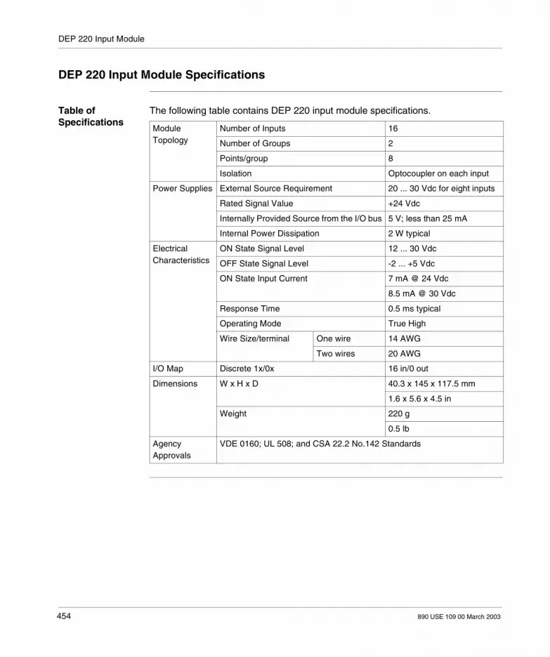
DEP 220 Input Module
DEP 220 Input Module Specifications
Table of Specifications
The following table contains DEP 220 input module specifications.
Module Topology
Number of Inputs 16
Number of Groups 2
Points/group 8
Isolation Optocoupler on each input
Power Supplies External Source Requirement 20 ... 30 Vdc for eight inputs
Rated Signal Value +24 Vdc
Internally Provided Source from the I/O bus 5 V; less than 25 mA
Internal Power Dissipation 2 W typical
Electrical Characteristics
ON State Signal Level 12 ... 30 Vdc
OFF State Signal Level -2 ... +5 Vdc
ON State Input Current 7 mA @ 24 Vdc
8.5 mA @ 30 Vdc
Response Time 0.5 ms typical
Operating Mode True High
Wire Size/terminal One wire 14 AWG
Two wires 20 AWG
I/O Map Discrete 1x/0x 16 in/0 out
Dimensions W x H x D 40.3 x 145 x 117.5 mm
1.6 x 5.6 x 4.5 in
Weight 220 g
0.5 lb
Agency Approvals
VDE 0160; UL 508; and CSA 22.2 No.142 Standards
454 890 USE 109 00 March 2003

890 USE 109 00 March 2003
Overview of the DEP 257 Input Module
At a Glance
Purpose The purpose of this chapter is to describe the DEP 257 input module.
What’s in this Chapter?
This chapter contains the following topics:
Topic Page
What is the DEP 257 Input Module? 456
DEP 257 Input Module LEDs 457
DEP 257 Input Module Field Wiring 458
DEP 257 Input Module Specifications 459
455

Abbreviated title of Chapter
What is the DEP 257 Input Module?
Brief Product Description
The DEP 257 is an extended temperature( -40 ... +705 C), 110 Vdc 40%, 16-point discrete input module. The full operational range of this module is 66 ... 154 Vdc. It senses input signals received from field sensing devices such as pushbuttons, limit and proximity switches, or other dc input sources and converts those signals into logic voltage levels that can be used by the PLC. Signals are field wired in two groups, eight signals per group. Inputs are opto-isolated from the system bus.
Note: The DEP 257 model is available with conformal coating. The conformal coating model is DEP 257C.
456 890 USE 109 00 March 2003

Abbreviated title of Chapter
DEP 257 Input Module LEDs
LEDs The DEP 257 module has two amber LEDs, opposite terminal screws 1 and 12. When one of these LEDs is ON, it indicates that power is available to the eight inputs directly below it. The module also has 16 red LEDs, eight opposite terminal screws 3 ... 10 and eight opposite terminal screws 14 ... 21; when any one of these LEDs are ON, it indicates voltage present at the corresponding input.
A front view with DEP 257 label is provided below.
CAUTION
Operational Hazard
Use of SIM 011 with DEP 257 is not allowed.
Failure to follow this precaution can result in injury or equipment damage.
Note: To I/O Map the DEP 257 module in Modsoft you must select DEP 216. Both modules share a host driver and have similar characteristics.
DEP 257
1234
6789
10
5
111213141516171819
2120
22
DEP 257123456789
101112131415161718
20
22
Inp
ut
Inp
ut
UU12345678MUU91011121314
16
card
1519
21
890 USE 109 00 March 2003 457

Abbreviated title of Chapter
DEP 257 Input Module Field Wiring
Introduction The DEP 257 is an extended temperature( -40 ... +70 degrees C), 110 Vdc +/-40 percent, 16-point discrete input module. The full operational range of this module is 66 ... 154 Vdc. It senses input signals received from field sensing devices such as pushbuttons, limit and proximity switches, or other dc input sources and converts those signals into logic voltage levels that can be used by the PLC. Signals are field wired in two groups, eight signals per group. Inputs are opto-isolated from the system bus.
Wiring Diagram and Simplified Schematic
A wiring diagram and simplified schematic for the DEP 257 input module is provided below.
Note: The DEP 257 model is available with conformal coating. The conformal coating model is DEP 257C.
110 Vdc±40%dc common
0.16 A 0.16 A
I/O BusInterface
First of 16 Input Circuits
GNRD
123456789
1011
121314
16
18
20
22
I1
I8
I16
15
17
19
21
458 890 USE 109 00 March 2003

Abbreviated title of Chapter
DEP 257 Input Module Specifications
Table of Specifications
The following table contains DEP 257 input module specifications.
Module Topology
Number of Inputs 16
Number of Groups 2
Points/group 8
Isolation Optocoupler on each input
Power Supplies External Source Requirement 110 Vdc +/-40 percent for each group of eight inputs
External Power 40 mA all points on
Rated Signal Value 66 ... 154 Vdc
Internally Provided Source from I/O bus
5 Vdc @ 25 mA
Internal Power Dissipation 3 W typical
Electrical Characteristics
ON State Signal Level 55 ... 170 Vdc
OFF State Signal Level -2 ... +10 Vdc
ON State Input Current 2.2 mA @ 110 Vdc
Response Time 6 ms typical
Sensor Supply 110 Vdc +/-40 percent for each group of 8 inputs each residual ripple max 20 percent
Wire Size/terminal One wire 14 AWG
Two wires 20 AWG
I/O Map Discrete 1x/0x 16 in/0 out
Environmental Extended Operating Temperature Range
-40 ... +70 degrees C
Dimensions W x H x D 40.3 x 145 x 117.5 mm
1.6 x 5.6 x 4.5 in
Weight 220 g
0.5 lb
Agency Approvals
DEP257: UL 508; cUL; CSA 22.2 No. 142; and European Directive EMC 89/336/EEC Standards
DEP257C: Railway standard EN 50 155; UL 508; cUL; CSA 22.2 No. 142; and European Directive EMC 89/336/EEC Standards
890 USE 109 00 March 2003 459

Abbreviated title of Chapter
460 890 USE 109 00 March 2003

890 USE 109 00 March 2003
Overview of the DEP 296 Input Module
At a Glance
Purpose The purpose of this chapter is to describe the DEP 296 input module.
What’s in this Chapter?
This chapter contains the following topics:
Topic Page
What is the DEP 296 Input Module? 462
DEP 296 Input Module LEDs 463
DEP 296 Input Module Field Wiring 464
DEP 296 Input Module Specifications 466
461

DEP 296 Input Module
What is the DEP 296 Input Module?
Brief Product Description
The DEP 296 is a 60 Vdc, 16-point isolated input module. It senses input signals received from field sensing devices such as pushbuttons, limit and proximity switches, or other 60 Vdc input sources and converts those signals into logic voltage levels that can be used by the PLC. Signals are field wired in two groups, eight signals/group. Inputs are opto-isolated from the system bus.
462 890 USE 109 00 March 2003

DEP 296 Input Module
DEP 296 Input Module LEDs
LEDs The DEP 296 module has two green LEDs, opposite terminal screws 1 and 12. When one of these LEDs is ON, it indicates that power is available to the eight inputs directly below it. The module also has 16 red LEDs, eight opposite terminal screws 3 ... 10 and eight opposite terminal screws 14 ... 21; when any one of these LEDs are ON, it indicates voltage present at the corresponding input. A front view with DEP 296 label is provided below.
DEP 296
1
2
3
4
5
6
7
8
9
1011
12
13
14
15
16
17
18
19
20
21
DEP 296
1
2
3
4
5
6
7
8
9
10
11
12
13
14
15
16
17
18
19
20
21
22
Inp
ut
Inp
ut
U
U
1
2
3
4
5
6
7
8
M
U
U
9
10
11
12
13
14
15
16
M22
890 USE 109 00 March 2003 463

DEP 296 Input Module
DEP 296 Input Module Field Wiring
Introduction The DEP 296 is a 60 Vdc, 16-point isolated input module. It senses input signals received from field sensing devices such as pushbuttons, limit and proximity switches, or other 60 Vdc input sources and converts those signals into logic voltage levels that can be used by the PLC. Signals are field wired in two groups, eight signals/group. Inputs are opto-isolated from the system bus.
Wiring Diagram A wiring diagram for the DEP 296 input module is provided below.
60 Vdc60 V COMMON
0.15A
DEP 296
1
2
3
4
5
6
7
8
9
10
11
12
13
14
1516
17
18
20
22
Inp
ut
Inp
ut
1
2
3
4
5
6
7
8
1
2
3
4
5
7
1
2
3
4
5
6
7
8
9
10
11
12
13
14
15
1617
18
20
22
U
U
1
2
3
4
5
6
7
8
M
U
U
9
10
11
12
13
15
M
19
21
6 14
16
19
21
464 890 USE 109 00 March 2003

DEP 296 Input Module
Simplified Schematic
A simplified schematic for the DEP 296 input module is provided below.
FIRST OF 16 INPUT CIRCUITS
PAB
Red
Green
60 Vdc
1
2
3
4
5
6
7
8
60 V COMM
60 Vdc
9
10
11
12
14
16
1
2
3
4
5
6
7
8
9
1011
12
13
14
15
16
17
19
21
13
15
18
20
2260 V COMM
890 USE 109 00 March 2003 465

DEP 296 Input Module
DEP 296 Input Module Specifications
Table of Specifications
The following table contains DEP 296 input module specifications.
Module Topology Number of Inputs 16
Number of Groups 2
Points/group 8
Isolation Optocoupler on each in put
Power Supplies External Source Requirement 60 Vdc
125 mA
Internally Provided Source from I/O bus 5 V
25 mA maximum
Internal Power Dissipation 4 W typical
Input Characteristics Rated Signal Value +60 Vdc
ON State Signal Level 35 ... 70 Vdc
OFF State Signal Level -4 ... +13 Vdc
ON State Input Current 7 mA @ 60 Vdc
Response Time 4 ms typical
Operating Mode True High
Wire Size/terminal One wire 14 AWG
Two wires 20 AWG
I/O Map Discrete 1x/0x 16 in/0 out
Dimensions W x H x D 40.3 x 145 x 117.5 mm
1.6 x 5.6 x 4.5 in
Weight 220 g
0.5 lb
Agency Approvals VDE 0160; UL 508; and CSA 22.2 No.142 Standards
466 890 USE 109 00 March 2003

890 USE 109 00 March 2003
Overview of the DEP 297 Input Module
At a Glance
Purpose The purpose of this chapter is to describe the DEP 297 input module.
What’s in this Chapter?
This chapter contains the following topics:
Topic Page
What is the DEP 297 Input Module? 468
DEP 297 Input Module LEDs 469
DEP 297 Input Module Field Wiring 470
DEP297 Input Module Specifications 472
467

DEP 297 Input Module
What is the DEP 297 Input Module?
Brief Product Description
The DEP 297 is a 48 Vdc, 16-point isolated input module. It senses input signals received from field sensing devices such as pushbuttons, limit and proximity switches, or other 48 Vdc input sources and converts those signals into logic voltage levels that can be used by the PLC. Signals are field wired in two groups, eight signals/group. Inputs are opto-isolated from the system bus.
Note: To I/O Map the DEP 297 module in Modsoft you must select DEP 216. Both modules share a host driver and have similar characteristics.
468 890 USE 109 00 March 2003

DEP 297 Input Module
DEP 297 Input Module LEDs
LEDs The DEP 297 module has two green LEDs, opposite terminal screws 1 and 12. When one of these LEDs is ON, it indicates that power is available to the eight inputs directly below it. The module also has 16 red LEDs, eight opposite terminal screws 3 ... 10 and eight opposite terminal screws 14 ... 21. When any one of these LEDs is ON, it indicates voltage present at the corresponding input.A front view with DEP 297 label is provided below.
DEP 297
1
2
3
4
56
7
8
9
10
11
12
13
14
15
1617
18
19
2021
Inp
ut
Inp
ut
U
U
1
2
3
4
5
6
7
8
M
U
U
9
10
11
12
13
14
15
16
card
DEP 297
1
2
3
4
5
6
7
8
9
1011
12
13
14
15
16
17
18
19
20
21M22 22
890 USE 109 00 March 2003 469
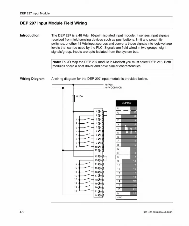
DEP 297 Input Module
DEP 297 Input Module Field Wiring
Introduction The DEP 297 is a 48 Vdc, 16-point isolated input module. It senses input signals received from field sensing devices such as pushbuttons, limit and proximity switches, or other 48 Vdc input sources and converts those signals into logic voltage levels that can be used by the PLC. Signals are field wired in two groups, eight signals/group. Inputs are opto-isolated from the system bus.
Wiring Diagram A wiring diagram for the DEP 297 input module is provided below.
Note: To I/O Map the DEP 297 module in Modsoft you must select DEP 216. Both modules share a host driver and have similar characteristics.
48 Vdc48 V COMMON
0.15A
1
2
3
4
5
6
7
8
9
10
11
12
14
16
1
2
3
4
56
7
8
9
1011
12
13
14
15
1617
19
21
U
U
1
2
3
4
5
6
7
8
M
U
U
9
10
11
12
13
15
M
1
2
3
4
5
6
7
89
10
11
12
13
14
15
16
17
18
2021
22
DEP 297
Inp
ut
18
20
22
14
16
card
13
15
19
470 890 USE 109 00 March 2003

DEP 297 Input Module
Simplified Schematic
A simplified schematic for the DEP 297 input module is provided below.
FIRST OF 16 INPUT CIRCUITS
PAB
Red
Green
1
2
3
4
5
6
7
8
9
10
11
12
13
14
15
16
17
19
21
48 Vdc
1
2
3
4
5
6
7
8
48 V COMM
48 Vdc
9
10
11
12
14
16
13
15
18
20
2248 V COMM
890 USE 109 00 March 2003 471

DEP 297 Input Module
DEP297 Input Module Specifications
Table of Specifications
The following table contains DEP 297 input module specifications.
Module Topology Number of Inputs 16
Number of Groups 2
Points/group 8
Isolation Optocoupler on each input
Power Supplies External Source Requirement 48 Vdc
125 mA
Internally Provided Source from I/O bus 5 V
25 mA maximum
Internal Power Dissipation 3 W typical
Input Characteristics Rated Signal Value +48 Vdc
ON State Signal Level 29 ... 56 Vdc
OFF State Signal Level -3 ... +10 Vdc
ON State Input Current 7 mA @ 48 Vdc
Response Time 4 ms typical
Operating Mode True High
Wire Size/terminal One wire 14 AWG
Two wires 20 AWG
I/O Map Discrete 1x/0x 16 in/0 out
Dimensions W x H x D 40.3 x 145 x 117.5 mm
1.6 x 5.6 x 4.5 in
Weight 220 g
0.5 lb
Agency Approvals VDE 0160; UL 508; and CSA 22.2 No.142 Standards
472 890 USE 109 00 March 2003

890 USE 109 00 March 2003
Overview of the FRQ 204/254 Frequency Module
At a Glance
Purpose The purpose of this chapter is to describe the FRQ 204/254 Frequency Module.
What’s in this Chapter?
This chapter contains the following topics:
Topic Page
What is the FRQ 204/254 Frequency Module? 474
Physical Characteristics of the FRQ 204/254 Frequency Module 475
Operating Modes of the FRQ 204/254 Frequency Module 476
Configuration of the FRQ 204/254 Frequency Module 477
Operation and LED Displays of the FRQ 204/254 Frequency Module 481
Specifications of the FRQ 204/254 Frequency Module 482
473

FRQ 204/254
What is the FRQ 204/254 Frequency Module?
Brief Product Description
The FRQ-204/254 serves the purpose of frequency and speed measurement for the Compact PLCs and has the following features: 4Frequency inputs for counting pulse voltages 5 VDC (TTL) or 24 VDC, Counting
frequency up to 1 kHz (1 x up to 50 kHz) 4fixed assigned semiconductor outputs 24 VDC, 0.5 A for Limit monitoring with:
Short–circuit and overload protection Switch–off with value saving Group indication of the overload/ short–circuit switch–off Group short–circuit signal Hardware reset for the acknowledgment of the overload
4process inputs 24 VDC for free use several LED indicators for function tracking and monitoring
The FRQ-204/254 can be inserted on any I/O slot in the subracks AS-HDTA-200, AS-HDTA-201 and AS-HDTA-202.The power supply is obtained: Internally with 5 VDC via the I/O bus Externally with 24 VDC for 24 V counter inputs, outputs and enable inputs If required, an addition externally with 5 VDC with 5 V input pulses.
Note: The FRQ 254 functions just like the FRQ 204 except that the FRQ 254 operates at extended temperature.
474 890 USE 109 00 March 2003

FRQ 204/254
Physical Characteristics of the FRQ 204/254 Frequency Module
Illustration The module a has bus connection on the rear and peripheral connection via screw/ plug–in terminals on the front. One of the enclosed fill–in labels is inserted in the detachable cover of the subrack near the viewing field for the LED indicators. System relevant data should be entered in the provided fields (e.g. signal names).
FRQ 204
Reset button
FRQ 204123456789
10111213141516171819202122
UU1*2*3*4*Mready U
12341234Mcard
123456789
10111213141516171819202122
inp
ut
ou
tpu
tfr
equ
ency
I>reset U
890 USE 109 00 March 2003 475

FRQ 204/254
Operating Modes of the FRQ 204/254 Frequency Module
FRQ 204/254 Operating Modes
The module comprises 4 independent hardware counters for the following operating modes: Frequency measurement <20 Hz, <1 kHz, <50 kHz Speed measurement <1 200 rev/min., <60 000 rev/min., <65 520 rev/min. The above mentioned operating modes and the required parameters should be defined in the parameters dialog screen of the panel software.This module is a I/O bus node with isolation to the process peripherals.In case of overload or short–circuit the corresponding output is switched off. The yellow LED indicates the overload. The reset button provides the acknowledgement. The outputs can be operated only when 24 V supply is available. When the module is inserted with voltage supply on (24 V and 5 V supply), all the outputs take 0 V position. The 4 discrete inputs (Input 1 ... 4 with LEDs) are available as free process inputs for your use. There is no functional assignment to the counter.
FRQ 204/254 Block Diagram
The following diagram describes the architecture of the FRQ 204/205 frequency module.
PAB
PAB
RESET
PROCESSOR
ProcessInputs
InputsCounter
Outputs
476 890 USE 109 00 March 2003

FRQ 204/254
Configuration of the FRQ 204/254 Frequency Module
I/O Mapping This modules uses 5 3x input registers as detailed here.
Note: Bits 4 ... 7 are high when the value is >= the upper limit. Bits 0 ... 3 are high when the value is <= the lower limit.
MSB LSB15 14 13 12 11 10 9 8 7 6 5 4 3 2 1 0
1 = Input 4 active (24 VDC)
1 = Input 3 active (24 VDC)
1 = Input 2 active (24 VDC)
1 = Input 1active (24 VDC)
1 = Channel 4 upper limiting value
1 = Channel 3 upper limiting value
1 = Channel 2 upper limiting value
1 = Channel 1 upper limiting value
1 = Channel 4 lower limiting value
1 = Channel 3 lower limiting value
1 = Channel 2 lower limiting value
1 = Channel 1 lower limiting value
Bits 12 ... 15 are not used
890 USE 109 00 March 2003 477

FRQ 204/254
The 3x register is shown below.
I/O Node Number Select the I/O slot number via the I/O map configuration and set the addressing of the 3x registers to be used.
Wiring For the counter input connection please use shielded cables, e.g. JE–LiYCY 2 x 2 x 0.5 mm2 (P/N E–Nr. 424 234 035). All counter inputs can be combined together in one common shielded cable, e.g. LiYrdf(Cgv)Y 5 x 2 x 0.5 mm2 (P/N E–No. 424 238 059)
The maximum cable length is 100 m The shield should be connected on one side with a short cable (<20 cm) to earth
ground. The cable shield should be grounded on both sides when higher noise levels are present.
The cable should not be combined together with supply lines or similar sources of electrical interference. Distance >0.5 m.
MSB
MSB
LSB
LSB
3x-register 5 (frequency/revolution data)
3x-register 2 (frequency/revolution data)
478 890 USE 109 00 March 2003

FRQ 204/254
Connection and Signal Address Assignment
The figure below illustrates a connection example for counter input F1 with 5 V input pulses (left) for systems with higher noise level (right).
(+5V)(+24V)(Common)
(+5V)(+24V)(Common)
(+24V)filtered
123456789
1011
1213141516171819202122
1213141516171819202122
123456789
1011
123456789
10111213141516171819202122
FRQ 204 2A 0.05A 2A 0.05A
U
F1
F3
F2
F4M
F1
F3
F2
F4M
UO1O2O3O4I1I2I3I4
UO1O2O3O4I1I2I3I4
UU1*2*3*4*M
12 341234
readyU
UI>reset
Mcard
inp
ut
ou
tpu
tfr
eq
uen
cy
Note: The example shows a 5 V pulse generator that requires a supply voltage of 24 VDC. Supply it from terminal 1.
890 USE 109 00 March 2003 479

FRQ 204/254
The following figure illustrates a connection example for counter input F1 with 24 V input pulses.
Note: The counter input F1 (TTL) is for the connection of 5 V sensor (max. 50 kHz).
(+24V)(Common)
2A
1
3456789
1011
21
3456789
1011
2
12
141516171819202122
1312
141516171819202122
13
UF1
F2
F3
F4
UO1O2O3O4I1I2I3I4
FRQ 204
UU1*2*3
*4
*M
12341234
ready
Mcard
UUI>reset
inp
ut
ou
tpu
tfr
equ
ency
480 890 USE 109 00 March 2003

FRQ 204/254
Operation and LED Displays of the FRQ 204/254 Frequency Module
Operation and LEDs
The module comes with the following LED indicators:
The red LED indicators show the level of voltage of input or output signal (1 or 0). Thus, the red LED goes on when the voltage level is high (1).Reset button: switches off the stored overload indication removes the reclosing lockout of the switched off (overloaded) outputs, when the
overload is no longer present switches the group short circuit signal again to 0.
Color and Name Use LED on LED off
1 x green "U" supply LED for 24 V counter inputs, outputs and process inputs:
supply is available supply is not available
1 x green "ready" LED for function Firmware initialization is completed, PAB interface enabled (backplane communication)
Module is not ready for operation
1 x yellow "(reset)" LED for overload or short–circuit of the outputs
short–circuit or overload on one or more outputs
faultless operation
4 x red "output 1 ... 4" LEDs for outputs outputs have "1" signal outputs have "0" signal
4 x red "input 1 ... 4" LEDs for free process inputs
signal on input signal on input
890 USE 109 00 March 2003 481

FRQ 204/254
Specifications of the FRQ 204/254 Frequency Module
FRQ 204/254 Power Supply
The following table describes the power supply.
FRQ 204/254 I/O Map
The following table describes the I/O map.
External Power Supply For: 24 Vdc, ca. 1.1 A Counter Inputs
Process Inputs
Outputs
5 Vdc, 20 mA Counter Inputs
Internal Power Source via I/O bus Maximum 5 V, 100 mA
Typical 75 mA
Power Loss Typical 1.3 W
Register 3x/4x 5 in / 0 out
482 890 USE 109 00 March 2003

FRQ 204/254
FRQ 204/254 Frequency Inputs
The following table describes the frequency inputs.
Quantity 4 for input pulses with 5 Vdc (TTL) or 24 Vdc
Type of Networking potential free (optical coupler) against I/O bus
Signal Level at 5 V (TTL) ON signal >= 2.3 V
OFF signal 0 ... 1 V
Input Current <= 2.5 mA each at 0 V (current sink)
Signal Level at 24 V (TTL) ON Signal 12 ... 30 V
OFF signal -2 ... +5 V
Input Current <= 6 mA each at 30 V (current source)
Signal Level at 24 V (TTL) ON signal 12 ... 30 V
OFF signal -2 ... +5 V
Input Current (current source) < 6 mA each at 30 V
Minimum Pulse Width 0.35 ms
Pulse Duty Factor 7:13 ... 1:1 ... 13:7, (13:7 = 65% : 35%)
Counting range 0 ... 32,767
Counting Frequency 1 kHz maximum (Input 1 with 5 V pulses 50 kHz maximum)
Accuracy (Time = 5) at:
5 Hz 0.5%Operating mode < 20 Hz
20 Hz 2%
25 Hz 4%
Operating mode < 1 Hz100 Hz 1%
1 kHz 0.1%
5 ... 50 kHz 0.05% Operating mode < 50 kHz
Accuracy (Time =1) ca. 10 times lower (use only for fast approximate measurements)
890 USE 109 00 March 2003 483

FRQ 204/254
FRQ 204/254 Process Inputs
The following table describes the process inputs.
FRQ 204/254 Semiconductor Outputs
The following table describes the semiconductor outputs.
Quantity 4
Type of Networking potential free (optical coupler) against I/O bus
Rated Signal Value 24 V
Signal Level HIGH Signal 12 ... 30 V
LOW signal -2 ... +5 V
Input Current 7 mA @ 24 V, 8.5 mA at 30 V
Input Delay 4 ms
Quantity 4
Technique with short–circuit and overload protection, Switch–off with value saving Group indication of the overload/ short–circuit switch–off Group short–circuit signal via I/O map status word, Hardware reset for the overload acknowledgement
Type of Networking potential free (optical coupler) against I/O bus
Consumer Connection Between output and reference potential M1
Working Voltage U US = 24 Vdc
Signal Logic Positive Logic
Signal Output Level 1 signal U = US - 0 ... 2 V
0 signal 0 ... +2 V, < 1 mA
Load Current/Output 500 mA maximum (Current source)
Starting Current for Incandescent Lamp Iein = 10 x IN, max. 5 W
Load Current for All Outputs 1 A maximum (due to 50% simultaneity factor)
Operating Delay < 1 ms
Circuit with Inductive Loads Clamping diode (suppressor diode) locally (parallel to the operating coil), absolutely necessary when contact elements are present in the output lines or the lines to the peripherals are very long.
Switching Cycles 1000 / h (0.28 / s) with inductive load and max. permissible current per output 100 / s with ohmic load 8 / s with 1.2 W lamp load
484 890 USE 109 00 March 2003

FRQ 204/254
FRQ 204/254 Physical Characteristics
The following table describes the physical characteristics.
FRQ 204/254 Type of Connection
The following table describes the connection type.
FRQ 204/254 Maximum Cable Lengths
The following table describes the maximum cable lengths.
FRQ 204/254 Environmental Characteristics
The following table describes the environmental characteristics.
FRQ 204/254 Agency Approvals
The following table describes the agency approvals.
Module Standard Size Case
Format 1 Slot
Weight 300 g
Process 2 Pluggable 11 Pole Screw/Plug-in Terminals
I/O Bus (Internal) 1/3 C30M
Counter Inputs max 100 m shielded (longer cables on request)
Outputs and Enable Inputs max. 400 m unshieldedmax 1000 m shielded
Operating Temperature 0 ... 60 C for FRQ204-40 ... +70 C for FRQ254
VDE 0160, UL 508; CSA 22.2 No.142, European Directive on EMC 89/336/EEC, and Low Voltage Directive 79/23/EEC Standards
890 USE 109 00 March 2003 485

FRQ 204/254
486 890 USE 109 00 March 2003

890 USE 109 00 March 2003
Overview of MOT 20X Motion Modules
At a Glance
Purpose The purpose of this chapter is to describe the MOT 20X Motion modules.
WARNING
Compatibility warning
The MOT 20X module will only operate properly when used with an A984, E984, or Micro 512/612 controller.
Failure to follow this precaution can result in death, serious injury, or equipment damage.
Note: The following A120 I/O modules require a loadable (SW--IODR--001) for proper operation when using certain PLCs (A984--1xx, E984--24x/251/255) with Modsoft: DEP 211/214/215/217 DAP211/217 ADU204/211/214/216 DAU204 VIC2xx MOT20x
487

MOT 20X Motion Modules
What’s in this Chapter?
This chapter contains the following topics:
Topic Page
What are the MOT 20X Modules? 489
Overview of the MOT 201 Motion Module 490
Overview of the MOT 202 Motion Module 504
MOT 20X Module System Information 522
MOT 20X Motion Module Specifications 525
488 890 USE 109 00 March 2003
MOT 20X Motion Modules
What are the MOT 20X Modules?
Brief Description The MOT 20x modules include the MOT 201 single-width I/O module (encoder only) and the MOT 202 double-width module (resolver and encoder). They are designed to provide single-axis motion control to the 984-A120 Series PLCs.The MOT 20x motion modules are designed to control a single axis of motion using advanced digital brushless motion control. This capability provides optimal control by eliminating potentiometer adjustments and analog velocity loops. These MOT modules are designed to operate with an A Series Compact 984 PLC-i.e., a Compact A984-120, -130, -131, -141, or -145.
The primary feedback used by the DNP servo system is position information from either a resolver or an encoder mounted to the motor. Velocity information is derived from the position information, rather than being received from a velocity transducer. This leads to some inaccuracies when using the DNP servo as a velocity controller. Small speed irregularities may result, particularly at slower speeds.
Related Publications
The following publications contain detailed information on the MOT 20X modules: Single-Axis Software System (SASS) Motion User Guide (GM-MOTN-001) Modicon Motion Development Software (MMDS) User Guide (GM-MMDS-002)
Note: The MOT 20X modules are designed to serve a variety of applications with great accuracy and speed, however certain applications might be outside their scope. Please consult Modicon for applications information if you intend to use the module specifically for precise velocity control.
890 USE 109 00 March 2003 489

MOT 20X Motion Modules
Overview of the MOT 201 Motion Module
Brief Description The MOT 201 is an encoder-only module contained in a single-width housing. It works with dc motors that use Cyberline drives and other types of dc and brushless drives from Gettys and other manufacturers. The module contains I/O to interface to the drive and the machine, including drive enable, drive fault, and a variety of user-configurable signals. The MOT 201 is not capable of commutating brushless motors.A front view of the MOT 201 Motion module is provided below.
MOT 201
U
drv fault
moving
in pos
comm
drv enabled
U1
M enc
5 VDC
U enc
N1
readyU
24VDC
1
5
3
4
2
M
modbus
7891011
1314
22
1516171819
+lim ok-lim okhomejog+jog-
brk/output
Inp
ut
490 890 USE 109 00 March 2003

MOT 20X Motion Modules
LEDs Fourteen LEDs are visible on the front panel to indicate various functions and conditions. Refer to the following diagram and table for the indicator positions, nomenclature and a brief explanation of their functions.
The following table describes the meaning of each front panel indicator.
U (POWER OK) Green Backplane power is present
Comm (MODBUS) Amber Blinking = RS-232 serial port communication link active
Moving Amber MOT is still commanding new positions for the motor
In pos Amber Difference between the target position and the actual motor position less than In Position Band parameter value
Drv fault (DRIVE FAULT)
Red A fault condition exists in the drive controlled by the MOT
Drv enabled (DRIVE ENABLED)
Amber Drive enable signal to the drive is active
Ready (MODULE OK)
Green MOT is operational. When not ON, a failure of the module has been detected. When blinking once every 3 s, module is in kernel mode and the executive must be downloaded
MOT 201
789
1011121314151617
19
21
23456
Power OKCommMovingIn pos
Drv fault
Drv enabled
Ready
24VdcInput 1Input 2Input 3
Input 5Output
890 USE 109 00 March 2003 491

MOT 20X Motion Modules
Connectors The MOT 201 has five connectors, J1 ... J5. The J1 and J2 connectors are located on the front of the module.
The J2 connector is a standard 9-pin, D-shell RS-232 serial port. Its operating mode and communications parameters are set via a DIP switch on the back of the unit (discussed later in this chapter).
24Vdc Green 24 Vdc for the I/O is present
Input 1 (+LIMIT OK) Red Motor has not reached the maximum limit for clockwise motion, or user-configured input 1 is active
Input 2 (- LIMIT OK) Red Motor has not reached the maximum limit for counterclockwise motion, or user-configured input 2 is active
Input 3 (HOME LIMIT)
Red Motor is not at the Home switch, or user-configured input 3 is active
Input 4 (JOG +) Red Jog + switch or user-configured input 4 is active
Input 5 (JOG -) Red Jog - switch or the user-configured input 5 is active
Output 1 (BRAKE) Red Brake control is active(brake released), or user-configured output 1 is active
MOT 201
789
1011
23
456
12
13141516
1718
2120
22
19
J2MODBUSCONNECTOR
j1
TERMINALS 7-11ANALOG OUTPUT,ENCODER POWERCONNECTOR
TERMINALS 12-22DISCRETE I/OCONNECTOR
492 890 USE 109 00 March 2003

MOT 20X Motion Modules
MOT 201 J1 Connector
The J1 connector is a 22-terminal screw I/O connector, as shown in the Discrete I/O, Analog Output, and Encoder Power wiring diagram below.
J1 discrete connections are listed in the following table.
INTERNAL TO MOTR>3KW
5Vdc5V COMMON
J1
D/A
REFI/O BUS
INTERFACE
5VREG
TO ENCODER CONNECTORS J4, J5NOTE:SEE SECTION NO TAG ALTERNATE POWER
GREEN
RED FIRST OFFIVEINPUTCIRCUITS
RED
24 Vdc24V COMMON
OUT 1
+LIM
-LIM
HOME
JOG+
JOG-
BRAKE
7
8
9
10
11
12
13
14
15
16
17
18
19
20
21
22
Pin # Function Pin # Function
1 ... 6 Not Used 15 +Travel limit/Aux in 1
7 Analog output 16 -Travel limit/Aux in 2
8 Analog output return 17 Home/Aux in 3
9 +5 Vdc 18 Jog+/Aux in 4
10 Encoder Power 19 Jog-/Aux in 5
11 Encoder power return 20 Aux 1 output/Brake
12 Not Used 21 24 Vdc common
13 24 Vdc power 22 24Vdc common
14 24 Vdc power
890 USE 109 00 March 2003 493
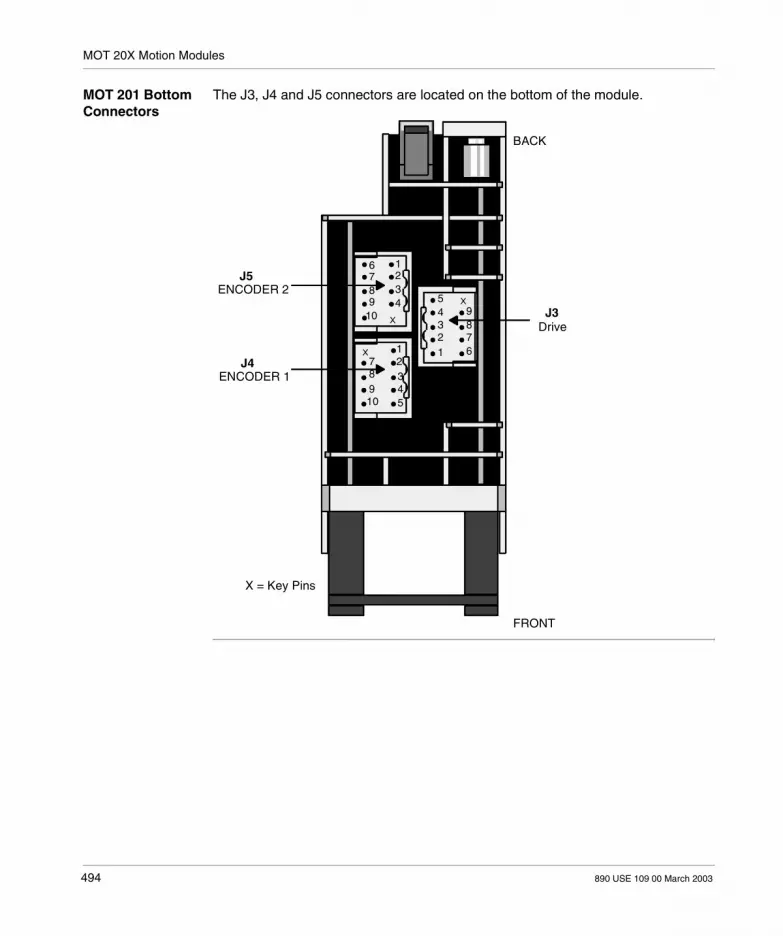
MOT 20X Motion Modules
MOT 201 Bottom Connectors
The J3, J4 and J5 connectors are located on the bottom of the module.
BACK
J3Drive
J5ENCODER 2
J4ENCODER 1
X = Key Pins
FRONT
6789
10
1234
10987 2
12
345
5432
6789
1
494 890 USE 109 00 March 2003

MOT 20X Motion Modules
MOT 201 J3 Connector
J3 is a 10-pin motor drive connector.
J3 drive connections are listed in the following table.
MOTOR DRIVE
>3KΩ
>3KΩ
+ VEL
- VEL
COMMON
FAULT
ENABLE
SHELL
J31
2
3
4
5
6
7
8
9
INTERNAL TO MOT
NC
NO
COM
I/O BUSINTERFACE
D/A
10K+5V
RED
YELLOW
Pin # Function W922 Cable Color
1 +Velocity command Black
2 Common White
3 -Velocity command Blue
4 Common Orange
5 Drive fault input Yellow
6 Drive enable contact (N.C.) Red
7 Drive enable contact (N.O.) Brown
8 Drive enable common Green
9 Common Purple
10 Key Gray
890 USE 109 00 March 2003 495

MOT 20X Motion Modules
MOT 201 J4 and J5 Connectors
J4 and J5 are 10-pin encoder feedback connections. The pins on these two connectors have nearly identical functionality (pins 5 and 6 are different).
J4 and J5 encoder feedback connections are listed in the following table.
Pin # Function
1 Encoder power
2 + Phase A
3 + Phase B
4 + Mark
5 Key (J5)
6 Key (J4)
7 - Phase A
8 - Phase B
9 - Mark
10 Encoder Power return
ENCODER 2
5V DIFF.ENCODER
5V DIFF.ENCODER
+V
0V
+V
0V
ENCODER 1
NOTE: B LEADS A.FOR CLOCKWISE(POSITIVE) MOTION
A+A-
B+
B-
M+M-
A+A-
B+
B-
M+M-
PCBJ5
6
7
8
9
10
7
8
9
10
1
2
3
4
1
2
3
4
5
J4
INTERNAL TO MOT
FROM J1
300Ω
220ΩFIRST OF SIX
ENCODER INPUTS
KEY = Pin 5
KEY = Pin 6
FRONT OF MODULEBOTTOM VIEW
496 890 USE 109 00 March 2003

MOT 20X Motion Modules
The Encoder Feedback Interface
The MOT 201 accepts feedback from one or two +5 V differential encoders. You may pick between the following two connection options: Option 1 uses an AS-W922-008 or AS-W922-015 generic cable, which is
terminated at one end and unterminated at the other to plug into either encoder connector on your module
Option 2 connects to the encoders through a cable and an optional AS-BR85-110 Breakout module.
An AS-W923 encoder breakout cable has a male DB25 connector at one end; the other end has two connectors to attach to the module’s two encoder connectors.
P2ENCODER #2
P3
ENCODER #2
ENCODER #1
POWER CONNECT
ENCODER #1
CHANNEL A+CHANNEL A-CHANNEL B+CHANNEL B-
MARKER -SHIELDPOWERCOM
MARKER +
CHANNEL A+CHANNEL A-CHANNEL B+CHANNEL B-
MARKER -SHIELDPOWERCOM
MARKER +
A+ P2-1A- P2-2B+ P2-3
B- P2-4M+ P2-5M- P2-6
SHIELD P2-7
POWER+ P2-8POWER COM P2-9
A+ P1-1A- P1-2B+ P1-3
B- P1-4M+ P1-5M- P1-6SHIELD P1-7
POWER+ P1-8POWER COM P1-9
+5V OUT P4-1+12V OUT P4-2
EXT PWR IN P4-3POWER COM P4-4 NOTE: WHEN POWER TO ENCODER IS
SUPPLIED ON J1 CONNECTOR, THISJUMPER MUST BE IN PLACE
P1
P4
890 USE 109 00 March 2003 497

MOT 20X Motion Modules
Encoder Connection Options
Cables and breakout modules are listed in the following table.
The breakout module is a DIN rail-mountable terminal block PCB assembly and accommodates discrete wiring from the encoder(s). It has a female DB25 connector for the cable attachment and the terminals are clearly marked with the appropriate encoder connections.
An external power supply is typically used with an encoder (see illustration below). However, when total encoder power (for one or two encoders) requires no more than 75 mA of power, you may use 5 Vdc power from the Compact 984 and thus eliminate the need for the external power supply.
Part Number Use Cable Description
AS-W921-XXX Drive Cyberline1000 to 10-position AMP Shielded MT Connector (008, 015)
AS-W922-XXX Generic 10-pin AMP Shielded MT Connector to Wires (008, 015)
AS-W923-XXX Encoder Break out Two 10-pin AMP Shielded MT Connectors to DB25 Connector (Y Cable) (003, 006)
AS-W955-XXX Modbus DB9 to DB25 (012, 025)
AS-W956-XXX Modbus DB9 to DB9 (012, 025)
AS-BR85-110 Breakout Module For use with AS-W923 cable
XXX stands for the cable length.
Note: When configuring feedback devices, remember that Channel 1 is not used by the MOT 201. Encoder 1 (J4) = Channel 2, and encoder 2 (J5) = Channel 3.
5VREG
POWER TO ENCODER
J1
7
8
9
11
10
NOTE:IF USING INTERNAL POWER YOU MUSTADD THESE EXTERNAL JUMPERS
498 890 USE 109 00 March 2003

MOT 20X Motion Modules
Discrete I/O The MOT 201 contains five discrete inputs and one discrete output. The inputs can be used as either user-defined discrete inputs or as predefined inputs. The discrete output as well as the inputs are controlled by the I/O command set. The register bit assignments are shown in the following diagram.
Discrete output bit definitions are shown in the following diagram.
Refer to the Single-Axis Software (SASS) Motion User Guide (GM-MOTN-001), for details on configuring the I/O.
Analog Output A +/- 10 V analog output is supplied via connector J1 on the front of the module. This output is configured by you via the analog output setup command; it is available for diagnostic purposes, or it can be placed under user program control.
Note: Module inputs 1 (+ Limit OK), 2 (- Limit OK) and 3 (NOT HOME) default to 1 (predefined) at power-up while inputs 4 (Jog +) and 5 (Jog -) default to 0 (discrete). Output 1 default condition is user-defined.
1 = + limit OK
1 = - limit OK1 = not home
1 = Jog -1 = Jog +
1 = Drive fault
1 2 3 4 5 6 7 8 9 10 11 12 13 14 15 16
1 2 3 4 5 6 7 8 9 10 11 12 13 14 15 16
1 = Brake
890 USE 109 00 March 2003 499

MOT 20X Motion Modules
The Motor Drive Interface
The interface to the motor drive from the MOT 201 consists of several digital and analog I/O signals: A drive enable signal A drive fault signal Velocity or current command signalsA form C relay is provided to enable the drive. A true high drive fault signal is accepted from the drive that must be held at ground to indicate a non-fault condition.A differential +/- 10 V analog signal is provided to control a dc drive. This signal can be software configured to be a velocity or current command. Connection for the motor drive is made to the module through the J3 connector.Two AS-W922 cables are available. They are terminated to plug into your module at one end and unterminated at the other end.
Note: Servo motor thermal overload switches should always be monitored to prevent equipment damage. The MOT 201 does not have a dedicated input for this function. Either a MOT 201 input or some other system input should be used in your system design to monitor this condition.
500 890 USE 109 00 March 2003

MOT 20X Motion Modules
The DIP Switch The MOT 201 has an RS-232 serial port to connect the module to an IBM PC (or compatible) running the Modicon Motion Development Software (MMDS). A two-position DIP switch is located on the rear panel of the module. SW1 is used to specify the module’s operating mode (984 or MMDS control). SW2 is used to specify the communication characteristics of the Modbus port upon power-up.The MOT 201 DIP switch settings are listed in the following table.
The MOT 201 DIP switch locations are shown in the following illustration.
DIP Switch Position Function
SW1 Left/Open (factory set) Compact 984 Controlled
Right/Closed MMDS Controlled
SW2 Left/Open (factory set) Programmed baud
Right/Closed Modbus Default
1 2OPEN CLOSED
DIP SWITCHAREA OF DETAIL
2 POSITIONDIP SWITCH
REAR OF MODULE
890 USE 109 00 March 2003 501

MOT 20X Motion Modules
Setting the Operating Mode with SW1
The SW1 setting determines which device can write to the MOT 201. The setting is read at power-up and selects either the MMDS or the Compact 984 to control the operation of the module. This mode selection is a safety feature that prevents you from accidentally issuing commands to the module using MMDS while it is being controlled by the Compact 984.The control priority (SW1) is as follows:1. When only MMDS is attached to the module, it has write privilege regardless of
the setting on SW1.2. When only the Compact 984 is communicating via Traffic Cop to the module, it
has write privilege regardless of the setting of SW1.3. When the Compact 984 has issued the local lockout command, it has write
privileges regardless of the setting of SW1 and whether or not MMDS is attached.4. When the local lockout command is not issued and both the Compact 984 and
MMDS are communicating to the module, the setting of SW1 controls which device has write privilege.
Setting the Modbus Communication Characteristics (SW2)
Switch#2 controls the Modbus communication characteristics. When the module is powered up, SW2 is read. When the switch is closed then the default characteristics are used. When the switch is open then the communication characteristics last saved in the module are used.Once communication characteristics are initialized, they may be changed at any time under software control only if SW2 is in the open position. Refer to Single-Axis Software System (SASS) Motion User Guide (GM-MOTN-001) for details. When SW2 is closed, the Modbus port default characteristics are as follows: 1 start bit 7 data bits 1 stop bit Even parity checking 9600 baud rate
Note: Either device may read (i.e. a GET command) at any time. However, reading the error log (a system command) is not allowed without write privilege because the log is lost once it is read. Refer to Single-Axis Software System (SASS) Motion User Guide (GM-MOTN-001) for details.
502 890 USE 109 00 March 2003

MOT 20X Motion Modules
Modbus Connections
The 9-pin serial modbus connections are listed in the following table.
The 25-pin serial modbus connections are listed in the following table.Modbus Connections for 25-Pin Serial.
Signal Computer Pin MOT Pin Signal Function
1NC 1NC Shield
TXD 2 3 RXD Serial data
RXD 3 2 TXD Serial data
GND 5 5 GND Ground
DTR 4 6 DSR Control line
DSR 6 4 DTR Control line
RTS *7 / 7* RTS Control line
CTS *8 / 8* CTS Control line
9NC 9NC +5 V Future Use
* These pins are jumpered (7 & 8) on both.
CAUTION
Ensure 5 V power is correct for the application.
Pin 9 supplies 5 V of power (75 mA). Make sure this is the correct pin for your application before wiring.
Failure to follow this precaution can result in injury or equipment damage.
Signal MOT Pin Computer Pin Signal Function
1NC 1NC Shield
TXD 2 2 RXD Serial data
RXD 3 3 TXD Serial data
GND 5 7 GND Ground
DTR 4 6 DSR Control line
DSR 6 20 DTR Control line
RTS *7 / 4* RTS Control line
CTS *8 / 5* CTS Control line
+5 V 9NC 9NC +5 Vdc Future Use
* These pins are jumpered, (7&8 on MOT, 4&5 on computer).
890 USE 109 00 March 2003 503
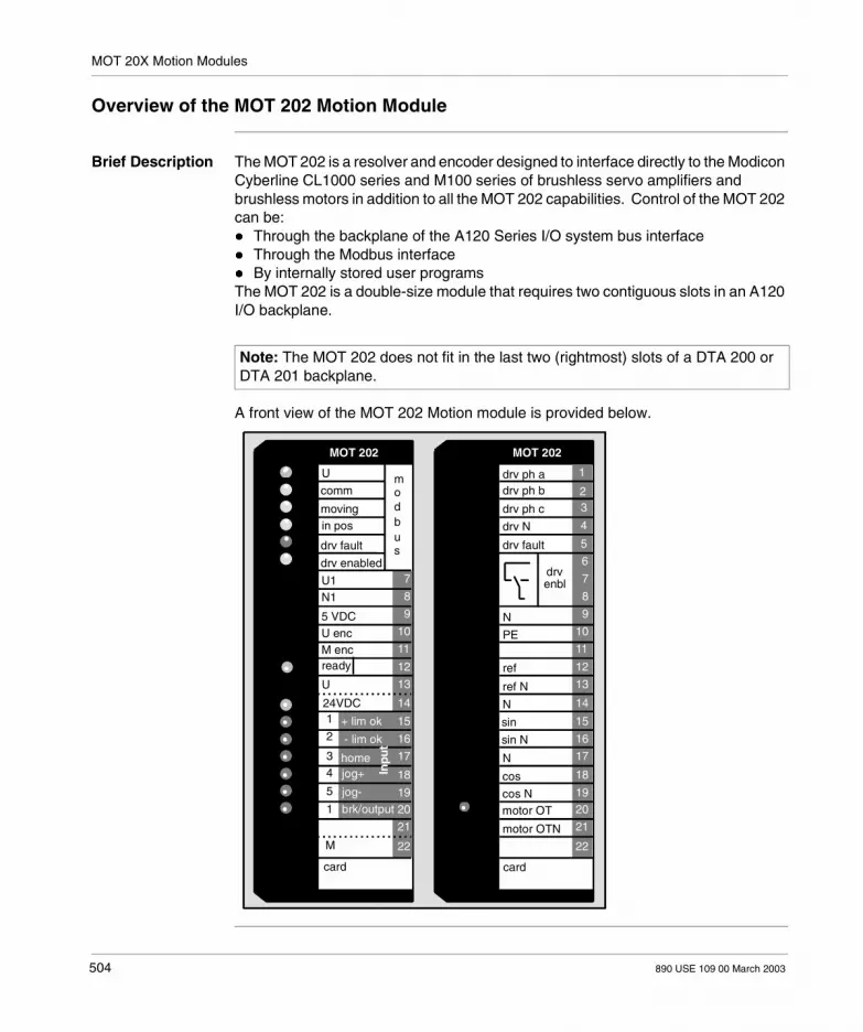
MOT 20X Motion Modules
Overview of the MOT 202 Motion Module
Brief Description The MOT 202 is a resolver and encoder designed to interface directly to the Modicon Cyberline CL1000 series and M100 series of brushless servo amplifiers and brushless motors in addition to all the MOT 202 capabilities. Control of the MOT 202 can be: Through the backplane of the A120 Series I/O system bus interface Through the Modbus interface By internally stored user programsThe MOT 202 is a double-size module that requires two contiguous slots in an A120 I/O backplane.
A front view of the MOT 202 Motion module is provided below.
Note: The MOT 202 does not fit in the last two (rightmost) slots of a DTA 200 or DTA 201 backplane.
MOT 202
U
comm
movingin pos
drv fault
drv enabled
U1N1
5 VDCU encM encready
U
24VDC1
2
3
4
5
1
M
card
modbus
7
8
9
10
11
13
14
15
16
17
18
1920
21
22
+ lim ok
- lim ok
homejog+
jog-
brk/output
Inp
ut
MOT 202
1
23
4
5
6
card
ref
ref N
N
sin
sin N
N
cos
cos Nmotor OT
motor OTN
N
PE
drvenbl
drv ph adrv ph b
drv ph c
drv fault
12
drv N
7
8
9
10
11
13
14
15
16
17
18
1920
21
22
12
504 890 USE 109 00 March 2003
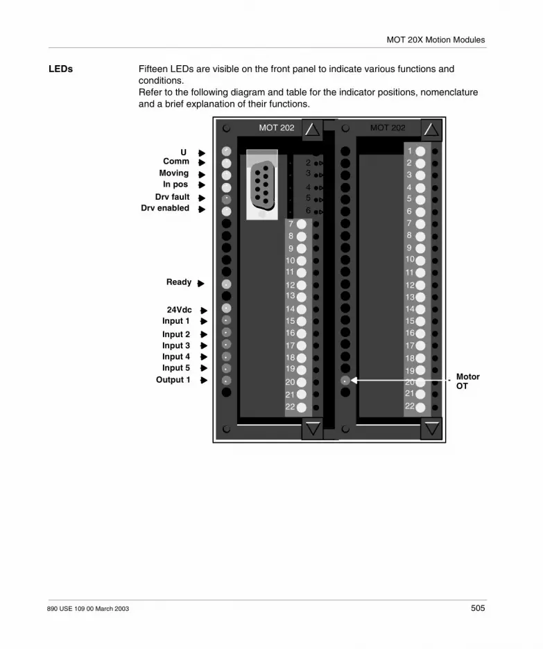
MOT 20X Motion Modules
LEDs Fifteen LEDs are visible on the front panel to indicate various functions and conditions. Refer to the following diagram and table for the indicator positions, nomenclature and a brief explanation of their functions.
MOT 202 MOT 202
UComm
MovingIn pos
Drv faultDrv enabled
Ready
24VdcInput 1
Input 2Input 3Input 4Input 5
Output 1 Motor
123
45
678
910
11
1213141516
17
18
192021
22
78
91011
1213
141516
171819
20
2122
23
45
6
OT
890 USE 109 00 March 2003 505

MOT 20X Motion Modules
Indicator Color Meaning
U (POWER OK) Green Backplane power is present
Comm (MODBUS) Amber Blinking = RS-232 serial port communication link active
Moving Amber MOT is still commanding new positions for the motor
In pos Amber Difference between the target position and the actual motor position less than In Position Band parameter value
Drv fault (DRIVE FAULT)
Red A fault condition exists in the drive controlled by the MOT
Drv enabled (DRIVE ENABLED)
Amber Drive enable signal to the drive is active
Ready (MODULE OK)
Green MOT is operational. When not ON, a failure of the module has been detected. When blinking once every 3 s, module is in kernel mode and the executive must be downloaded
24Vdc Green 24 Vdc for the I/O is present
Input 1 (+LIMIT OK) Red Motor has not reached the maximum limit for clockwise motion, or user-configured input 1 is active
Input 2 (- LIMIT OK) Red Motor has not reached the maximum limit for counterclockwise motion, or user-configured input 2 is active
Input 3 (HOME LIMIT)
Red Motor is not at the Home switch, or user-configured input 3 is active
Input 4 (JOG +) Red Jog + switch or user-configured input 4 is active
Input 5 (JOG -) Red Jog - switch or the user-configured input 5 is active
Output 1 (BRAKE) Red Brake control is active(brake released), or user-configured output 1 is active
Motor O.T. Red Motor over temperature condition
506 890 USE 109 00 March 2003
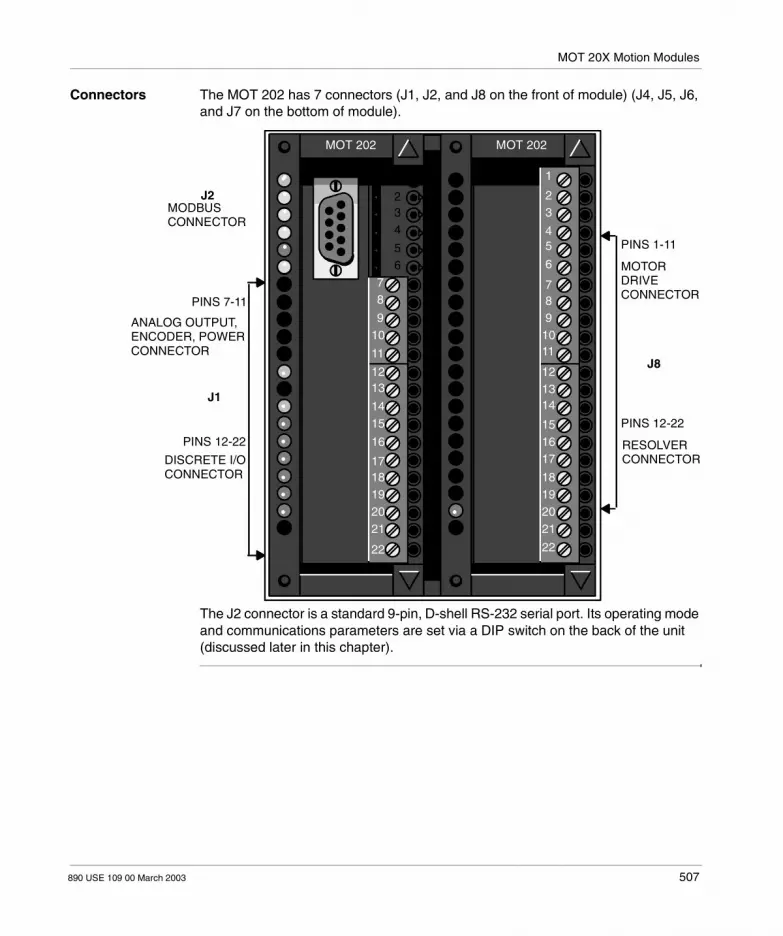
MOT 20X Motion Modules
Connectors The MOT 202 has 7 connectors (J1, J2, and J8 on the front of module) (J4, J5, J6, and J7 on the bottom of module).
The J2 connector is a standard 9-pin, D-shell RS-232 serial port. Its operating mode and communications parameters are set via a DIP switch on the back of the unit (discussed later in this chapter).
MOT 202
MOT 202 MOT 202
J2MODBUSCONNECTOR
PINS 7-11
ANALOG OUTPUT,ENCODER, POWERCONNECTOR
J1
PINS 12-22
DISCRETE I/OCONNECTOR
PINS 1-11
1
23
45
6
789
10
1011
121314
151617
18192021
22
MOTORDRIVECONNECTOR
J8
PINS 12-22
RESOLVERCONNECTOR
78
910
11
1213
1415
16
1718192021
22
234
56
890 USE 109 00 March 2003 507

MOT 20X Motion Modules
MOT 202 J1 Connector
The J1 connector is a 22-screw terminal I/O connector, as shown in the Discrete I/O, Analog Output, and Encoder Power wiring diagram below.
J1 discrete connections are listed in the following table.
Pin # Function Pin # Function
1 ... 6 Not Used 15 +Travel limit/Aux in1
7 Analog output 16 -Travel limit/Aux in 2
8 Analog output return 17 Home/Aux in 3
9 +5 Vdc 18 Jog+/Aux in 4
10 Encoder Power 19 Jog-/Aux in 5
11 Encoder power return 20 Aux 1 output/Brake
12 Not Used 21 24 Vdc common
13 24 Vdc power 22 24Vdc common
14 24 Vdc power
OUT 1
+LIM
- LIM
HOME
JOG+
JOG-
BRAKE
24 Vdc
24V COMMON RED
REDFIRST OFFIVEINPUTCIRCUITS
GREEN12
13
14
15
16
17
18
19
20
21
22
R>3KΩ J1
5Vdc5V COMMONINTERNAL TO MOT
7
8
9
10
11
5VREG
D/A
REF I/O BUSINTERFACE
TO ENCODER CONNECTORS J4,J5NOTE:SEE SECTION NO TAG ALTERNATE POWER
508 890 USE 109 00 March 2003

MOT 20X Motion Modules
MOT 202 J8 Connector
J8 is a 22-screw terminal connector that may be for the motor drive and resolver wiring. The top half of J8 (terminals 1 ... 11) is for motor wiring.
J8 drive connections are listed in the following table.
Pin # Function W922 Cable Color
1 +Velocity command Black
2 Common White
3 -Velocity command Blue
4 Common Orange
5 Drive fault input Yellow
6 Drive enable contact (N.C.) Red
7 Drive enable contact (N.O.) Brown
8 Drive enable common Green
9 Common Purple
10 Key Gray
MOTOR DRIVE>3KΩ TYP
PHASE A
PHASE B
PHASE C
COMMON
FAULT
ENABLE
J8
1
2
3
4
5
6
7
8
9
10
11
INTERNAL TO MOT
NC
NO
COM YELLOW
RED
+5V10K
D/A
D/A
I/O BUSINTERFACE
890 USE 109 00 March 2003 509

MOT 20X Motion Modules
Bottom Half J8 Connector
The bottom half of J8 (terminals 12 ... 22) is for resolver wiring.
Note: The J6 connector on the bottom of the module performs the same motor wiring function. If you are using an AS-W922 cable for motor drive wiring, use the J6 connector. If not, you can choose between J8 or J6.
J8 Pin # J7 Pin # Function
12 2 Reference output high
13 7 Reference output low
14 4 Shield
15 3 Sine input high
16 8 Sine input low
17 Shield
18 5 Cosine input high
19 10 Cosine input low
20 1 Motor O.T. input high
21 6 Motor O.T. input low
9 Not Used
RESOLVER
TT
REF +
REF -
SIN +
SIN -
COS +
COS -
12
13
14
15
16
17
18
19
20
21
22
INTERNAL TO MOT
7K
7K
3K 3K
+5V +5V
3K
+5V
RED
3.75 KHZ
I/O BUSINTERFACE
R/DCONVERTER
J8
510 890 USE 109 00 March 2003

MOT 20X Motion Modules
MOT 202 Bottom Connectors
The J4 ... J7 connectors are located on the bottom of the module.
Note: The J7 connector on the bottom of the module performs the same resolver wiring function as terminals 12 ... 22 on J8. If you are using an AS-W922 cable for resolver wiring, use the J7 connector. If not, you can choose between J8 or J7.
1234
678910 1
2345
9876
12345
8910
710
8x
76
54321
J5 ENCODER 2
J4 ENCODER 1
J6 DRIVE
J7 RESOLVER
X = Key Pins
FRONT
BACK
890 USE 109 00 March 2003 511
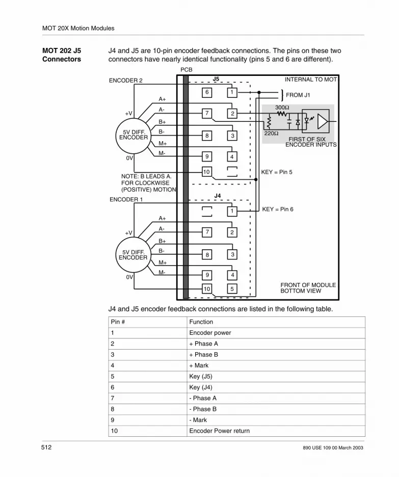
MOT 20X Motion Modules
MOT 202 J5 Connectors
J4 and J5 are 10-pin encoder feedback connections. The pins on these two connectors have nearly identical functionality (pins 5 and 6 are different).
J4 and J5 encoder feedback connections are listed in the following table.
Pin # Function
1 Encoder power
2 + Phase A
3 + Phase B
4 + Mark
5 Key (J5)
6 Key (J4)
7 - Phase A
8 - Phase B
9 - Mark
10 Encoder Power return
5V DIFF.ENCODER
5V DIFF.ENCODER
ENCODER 2
ENCODER 1
+V
+V
0V
0V
A+
A-
B+
M+
B-
M-
NOTE: B LEADS A.FOR CLOCKWISE(POSITIVE) MOTION
PCB
J5
6
7
8
9
10
1
2
3
4
J4
4
10
9
8
7
3
2
1
5
KEY = Pin 6
KEY = Pin 5
FRONT OF MODULEBOTTOM VIEW
220Ω
300Ω
FROM J1
FIRST OF SIXENCODER INPUTS
INTERNAL TO MOT
A+
A-
B+
M+
B-
M-
512 890 USE 109 00 March 2003

MOT 20X Motion Modules
MOT 202 J6 and J7 Connectors
J6 is a 10-pin connector that may be for the motor drive wiring.
Note: The first 11 terminal screws of the J8 connector on the front of the module perform the same motor wiring function. If you are using an AS-W922 cable for motor drive wiring, use the J6 connector. If not, you can choose between J8 or J6.
J6
1
2
3
4
5
6
7
8
9
10
INTERNAL TO MOT
NO
NC
COM YELLOW
RED10K +5
DA
DA
ENABLE
FAULT
COMMON
PHASE C
PHASE B
PHASE AMOTOR DRIVE>3K Ω TYP
I/OBUS INTERFACE
890 USE 109 00 March 2003 513

MOT 20X Motion Modules
J7 is a 10-pin connector that may be used for resolver wiring:
Note: The J7 performs the same resolver wiring function as terminals 12 ... 22 of the J8 connector on the front of the module. If you are using an AS-W922 cable for resolver wiring, use the J7 connector. If not, you can choose between J8 or J7.
RESOLVER
TT
REF +
SIN +
REF -
SIN -
COS +
COS -
J7Internal to Mot
7K
7K
R/DConverter
3K 3K
+5V +5V
3K
RED
+5V
3.75 KHZ
I/O BUSINTERFACE
2
7
4
38
5
10
1
6
514 890 USE 109 00 March 2003

MOT 20X Motion Modules
The Encoder Feedback Interface
The MOT 202 accepts feedback from one or two +5 V differential encoders. You may pick between the following two connection options: Option 1 uses an AS-W922-008 or AS-W922-015 generic cable, which is
terminated at one end and unterminated at the other to plug into either encoder connector on your module
Option 2 connects to the encoders through a cable and an optional AS-BR85-110 Breakout module.
An AS-W923 encoder breakout cable has a male DB25 connector at one end; the other end has two connectors to attach to the module’s two encoder connectors.
Encoder #2
Encoder #1
Encoder #2
Encoder #1
Power Connect
P2
P1
P4
Channel A+Channel A-Channel B+Channel B-
Marker +
Marker -Shield
Power
Com
Channel A+Channel A-Channel B+Channel B-
Marker -Shield
Com
Marker +
Power
NOTE: When power to encoder issupplied on J1 connector, thisjumper must be in place.
P3
A+A-B+B-M+M-ShieldPower +Power Com
A+
B+B-
M-
Power +Power Com
A-
M+
Shield
P2-1P2-2P2-3P2-4P2-5P2-6P2-7P2-8P2-9
P1-1
P1-3P1-4P1-5P1-6P1-7P1-8P1-9
P1-2
+5V Out+12V OutExt Pwr InPower Com
P4-1P4-2P4-3P4-4
890 USE 109 00 March 2003 515

MOT 20X Motion Modules
Cables and breakout modules are listed in the following table.
The breakout module is a DIN rail-mountable terminal block PCB assembly and accommodates discrete wiring from the encoder(s). It has a female DB25 connector for the cable attachment and the terminals are clearly marked with the appropriate encoder connections.An external power supply is typically used with an encoder (see illustration below). However, when total encoder power (for one or two encoders) requires no more than 75 mA of power, you may use 5 Vdc power from the Compact 984 and thus eliminate the need for the external power supply.
Part Number Use Cable Description
100-338-XXX Drive Cyberline1000 to Discrete Wires (008, 015)
AS-W921-XXX Drive Cyberline1000 to 10-position AMP Shielded MT Connector (008, 015)
AS-W922-XXX Generic 10-pin AMP Shielded MT Connector to Wires (008, 015)
AS-W923-XXX Encoder Breakout
Two 10-pin AMP Shielded MT Connectors to DB25 Connector (Y Cable) (003, 006)
AS-W955-XXX Modbus DB9 to DB25 (012, 025)
AS-W956-XXX Modbus DB9 to DB (012, 025)
AS-BR85-110 Breakout Module
For use with AS-W923 cable
XXX stands for the cable length.
J1
Power to Encoder
5VREG
NOTE:IF USING INTERNAL POWER YOU MUST
7
8
9
10
11
ADD THESE EXTERNAL JUMPERS.
516 890 USE 109 00 March 2003

MOT 20X Motion Modules
Discrete I/O The MOT 202 contains five discrete inputs and one discrete output. The inputs can be used as either user-defined discrete inputs or as predefined inputs. The discrete output as well as the inputs are controlled by the I/O command set. The register bit assignments are shown in the following diagram.
Discrete output bit definitions are shown in the following diagram.
Refer to the Single-Axis Software (SASS) Motion User Guide (GM-MOTN-001), for details on configuring the I/O.
Analog Output A +/- 10 V analog output is supplied via connector J1 on the front of the module. This output is configured by you via the analog output setup command; it is available for diagnostic purposes, or it can be placed under user program control.
Note: Module inputs 1 (+ Limit OK), 2 (- Limit OK) and 3 (NOT HOME) default to 1 (predefined) at power-up while inputs 4 (Jog +) and 5 (Jog -) default to 0 (discrete).
6 7 8 9 10 11 12 13 14 15 161 2 3 4 5
1 = Drive Fault
1 = Jog -1 = Jog +
1 = Not Home
1 = - Limit OK
1 = + Limit OK
1 2 3 4 5 6 7 8 9 10 11 12 13 14 15 16
1 = Brake
890 USE 109 00 March 2003 517

MOT 20X Motion Modules
The Motor Drive Interface
The interface to the motor drive from the MOT 202 consists of several digital and analog I/O signals: A drive enable signal A drive fault signal Three-phase current commandsA form C relay is provided to enable the drive. A true high drive fault signal is accepted from the drive that must be held at ground to indicate a non-fault condition.Three +10 V analog current commands are provided to control a three-phase brushless ac motor. For dc drives, only two of the three phases (phase A and phase C) are used. Connection for the motor drive may be made to the module through the connector on the bottom of the module (J6) or to the discrete wiring points on the front (J8) of the module.Two AS-W922 cables are available. They are terminated to plug into your module at one end and unterminated at the other end.
Resolver Feedback/Thermal Interface
The MOT 202 may use a resolver to provide feedback for the position, velocity and commutation of the motor. A resolver is essentially a rotary brushless transformer that provides absolute position information to the MOT. The MOT calculates an absolute position from the continuous signal of the resolver.The MOT provides a reference output to drive transmit mode resolvers. The drive signal is a 3.75 kHz, self-compensating sine wave. The amplitude of the reference is adjusted by the module (if necessary) at power-up to get returned signal strengths of approximately 2 Vrms at the sine and cosine inputs of the module.Connection for resolver feedback may be made to the module through the connector on the bottom of the module (use cable AS-W922-XXX) or to the discrete wiring points on the front of the module.
The module can also monitor motor temperature by means of a thermistor or thermostatic switch. The two-wire input recognizes a high impedance (greater than 3072 or open switch) as an over temperature condition. When the input is not used it must be shorted. The over-temperature fault is reported to MMDS or the Compact 984 as a drive fault. The over-temperature fault may be distinguished from a normal drive fault by observing the associated indicator on the front of the module.
Note: If the cable length between MOT and the resolver is more than 100 ft, please consult with Modicon.
518 890 USE 109 00 March 2003

MOT 20X Motion Modules
DIP Switches One two-position DIP switch is located on the rear panel of the module. SW1 determines the module’s mode of operation (984 or MMDS control). SW2 determines the communication characteristics of the Modbus port upon power up of the module.
The MOT 202 DIP switch locations are shown in the following illustration.
DIP Switch Position Function
SW1 Left/Open (factory set) Compact 984 Controlled
SW1 Right/Closed MMDS Controlled
SW2 Left/Open (factory set) Programmed baud
Right/Closed Modbus Default
OPEN CLOSE
DIP SWITCHArea of Detail
1
2
2 POSITIONDIP SWITCH
REAR OFMODULE
890 USE 109 00 March 2003 519

MOT 20X Motion Modules
Setting the Operating Mode with SW1
The SW1 setting determines which device can write to the MOT 202. The setting is read at power-up and selects either the MMDS or the Compact 984 to control the operation of the module. This mode selection is a safety feature that prevents you from accidentally issuing commands to the module using MMDS while it is being controlled by the Compact 984.The control priority (SW1) is as follows:1. When only MMDS is attached to the module, it has write privilege regardless of
the setting on SW1.2. When only the Compact 984 is communicating via Traffic Cop to the module, it
has write privilege regardless of the setting of SW1.3. When the Compact 984 has issued the local lockout command, it has write
privileges regardless of the setting of SW1 and whether or not MMDS is attached.4. When the local lockout command is not issued and both the Compact 984 and
MMDS are communicating to the module, the setting of SW1 controls which device has write privilege.
Setting the Modbus Communication Characteristics (SW2)
Switch#2 controls the Modbus communication characteristics. When the module is powered up, SW2 is read. When the switch is closed then the default characteristics are used. When the switch is open then the communication characteristics last saved in the module are used.Once communication characteristics are initialized, they may be changed at any time under software control only if SW2 is in the open position. Refer to Single-Axis Software System (SASS) Motion User Guide (GM-MOTN-001) for details. When SW2 is closed, the Modbus port default characteristics are as follows: 1 start bit 7 data bits 1 stop bit Even parity checking 9600 baud rate
Note: Either device may read (i.e. a GET command) at any time. However, reading the error log (a system command) is not allowed without write privilege because the log is lost once it is read. Refer to Single-Axis Software System (SASS) Motion User Guide (GM-MOTN-001) for details.
520 890 USE 109 00 March 2003

MOT 20X Motion Modules
The 9-pin serial modbus connections are listed in the following table.
The 25-pin serial modbus connections are listed in the following table.Modbus Connections for 25-Pin Serial
Signal Computer Pin MOT Pin Signal Function
1NC 1NC Shield
TXD 2 3 RXD Serial data
RXD 3 2 TXD Serial data
GND 5 5 GND Ground
DTR 4 6 DSR Control line
DSR 6 4 DTR Control line
RTS *7 / 7* RTS Control line
CTS *8 / 8* CTS Control line
9NC 9NC +5 V Future Use
* These pins are jumpered (7 & 8) on both.
CAUTION
Ensure 5 V power is correct for the application.
Pin 9 supplies 5 V of power (75 mA). Make sure this is the correct pin for your application before wiring.
Failure to follow this precaution can result in injury or equipment damage.
Signal MOT Pin Computer Pin Signal Function
1NC 1NC Shield
TXD 2 2 RXD Serial data
RXD 3 3 TXD Serial data
GND 5 7 GND Ground
DTR 4 6 DSR Control line
DSR 6 20 DTR Control line
RTS *7 / 4* RTS Control line
CTS *8 / 5* CTS Control line
+5 V 9NC 9NC +5 Vdc Future Use
* These pins are jumpered, (7&8 on MOT, 4&5 on computer).
890 USE 109 00 March 2003 521

MOT 20X Motion Modules
MOT 20X Module System Information
+EOT and -EOT Limits
The +EOT and -EOT normally closed limit switches indicate the Ends Of Travel so the MOT can stop the motor to avoid damage.
The following diagram illustrates a typical MOT 20X installation.
If either of these inputs becomes 0 volts (open in the line), the MOT will generate a fatal error.
DANGER
Mis-wiring Danger
When wiring, ensure that moving positive moves you towards the +, and negative motion moves you towards the -EOT.
Failure to follow this precaution will result in death, serious injury, or equipment damage.
Note: If you reach the limit switches, the MOT disables the drive and stops the motor. Otherwise system safety may be compromised.
MOTION MODULE
EOT SW HOME EOT SW
CYBERLINEDRIVE
BRUSHLESS MOTOR
522 890 USE 109 00 March 2003

MOT 20X Motion Modules
The MOT also has software programmable end-of-travel limits to provide over-travel protection. These programmable limits stop the drive and signal a non-fatal error. The end-of-travel limit switches provide backups for the software limits. The priority should be as follows: Use software limits as the primary end-of-travel limit. Allow tolerance so you read the software limits before striking the limit switches.
The hardware limit switches should be set outside the software limit switches. This ensures a safe system shut down and thus prevents any over shooting that may result in mechanical damage.You may use mechanical stops to limit motion and act as a fail-safe stop. These back up the software and hardware limit switches. Plan these as you do your mechanical design.
Home Limit By using a home limit switch, the MOT can send the machine to its home position. The machine is considered at home when it satisfies two conditions: Home limit switch open-this gives the approximate home position Encoder or resolver at zero position
Home works properly even if the machine holds the home switch open for several feedback revolutions. The MOT always finds the same zero. How it chooses the resolver (or encoder) zero depends on its approach. Home is the first feedback zero in the direction of the Home after the switch is open.
Flash Memory The MOT comes with a flash EEPROM that allows storage of application programs and configuration parameters, such as servo parameters, speed limits, etc. It will also accept firmware updates as firmware enhancements become available.
Note: If you don’t set the zero position properly, the software end-of-travel limits won’t be where expected.
Note: In order to ensure that your motor establishes the same home position each time, always home in the same direction. This approach gives you a reliable and consistent homing system. It is not completely dependent on a critical switch setting.
890 USE 109 00 March 2003 523

MOT 20X Motion Modules
Communications Protocol
Communications with the MOT is through six pairs of 4x and 3x registers (I/O mapped to the MOT), using a very rigid format. The first register sent is always the control register and the second register is always the command register. The first register returned is always the current status of the MOT, while the second register returned is always an echo of the command register. All remaining registers, data register 1... 4, are reserved for data and are used as necessary. For additional information refer to Single-Axis Software System (SASS) Motion User Guide (GM-MOTN-001).
On-line/Off-line Development (MMDS)
The Modicon Motion Development Software (MMDS Ver. # 3.00 or higher) is an on-line/off-line software package which runs on a user-supplied IBM PC or compatible computer. [MMDS is purchased separately.] MMDS lets you connect the computer with the MOT (through an RS-232 serial interface) to set parameters, check module diagnostics, and exercise the motor during initial system setup. It also lets you write motion programs and download them to the Compact 984 to be used with the MRTM loadable function block, or you can download into the MOT directly.
System Pre-Check
Do this before you apply power to the MOT system:
Releasing the MOT
The only way to release the MOT is to issue the release lockout command from the Compact 984. If a Set or Motion Command is issued while the Modbus is locked out (Compact 984 command), the MOT will reject the command and set a fault bit true.
Note: For I/O Map information refer to the 984-A120 Compact Programmable Controllers User Guide (890 USE 108 00).
Step Action
1 Check all wiring-compare your wiring to the previous wiring diagrams
2 Make sure the dc power is within the range specified for the MOT.
3 Inspect the motors and loads-Are the motors securely mounted? Is it safe to run the motors? If not, remove keys from motor shafts to disconnect the motors from their mechanical loads.
4 Be sure the Compact 984 is stopped-This prevents an accidental local lockout command issued from the Compact 984 which cannot be changed by the MMDS. The MMDS is not capable of changing this setting.
524 890 USE 109 00 March 2003

MOT 20X Motion Modules
MOT 20X Motion Module Specifications
Table of Specifications
The following table describes MOT 20X Motion Module Specifications
Module Topology, Required Loadable
The following section describes Module Topology and Required Loadable Specifications.
Power Supplies, DIN Rail Grounding
The following section describes Power Supplies and DIN Rail Grounding Specifications.
Module Topology Number of Discrete Inputs 5
Number of Discrete Outputs 1
Number of Analog Outputs 1
Required Loadable SW-IODR-001
Power Supplies I/O system bus 5 Vdc MOT 201 300 mA
MOT 202 600 mA
DIN Rail Grounding < 0.1 Ω
890 USE 109 00 March 2003 525

MOT 20X Motion Modules
Input/Outputs, Drive Interface
The following section describes Input/Outputs and Drive Interface Specifications.
Input/Outputs Digital Optically Isolated to 500 Vdc
Output drive capability 150 mA (using customer supplied 20 ... 28 Vdc, true high)
Input impedance 3.5 K Ω (ON @ 15 Vdc minimum, OFF @ 5 Vdc maximum, true high)
Analog Drive capability +/- 10 Vdc, 3 mA
Resolution 12 bits
Accuracy +/- 100 mVdc (without offsets)
+/- 50 mVdc (with offset)
Drive Interface Drive fault input True high, pulled up internally
Drive enable relay form C contacts, 30 Vdc @ 0.5 A resistive
dc motors (201/202)
Command signal +/- 10 Vdc @ 3 mA differential
Current or velocity command
Software selectable
Phasing Positive voltage for CW motion
ac motors (202 only)
Three phase current +/- 10 Vdc @ 3 mA
Command signal Summing to 0 +/- 0.1 Vdc
526 890 USE 109 00 March 2003

MOT 20X Motion Modules
Communications, Resolver Feedback
The following section describes Communications and Resolver Feedback Specifications.
Communications Modbus 1 RS-232 serial port interface
Baud rate 300 ... 9600, 9600 default, set by software (for ASCII only)
5 Vdc supply 75 mA maximum
Resolver Feedback
Resolver reference drive 3.75 +/- 0.05 kHz; 2 +/- 1.0 Vrms
100 mA RMS drive capability
200 mW maximum
Resolver sine/cosine inputs 7 K Ω impedance
Resolver resolution
14 bits to 1350 RPM
12 bits to 6000 RPM
with standard transmit style resolver
+/- 10 min of arc typical
System accuracy 16 bits to 300 RPM
+/- 15 min of arc maximum
System Repeatability +/- 3 min of arc
Cable length Consult Customer Service if over 100 ft
890 USE 109 00 March 2003 527

MOT 20X Motion Modules
Encoder Feedback
The following section describes Encoder Feedback Specifications.
Motion, Thermistor Resistance
The following section describes Motion and Thermistor Resistance Specifications.
Encoder Feedback
Differential signal 2 V minimum
Phase B leads A for CW motion
Input impedance 145 Ω nominal
Maximum encoder frequency
500 kHz square wave
350 ns minimum time be tween edges from phase A and B
Encoder feedback loss Detected on phase A and B differential signals. Loss of marker signal is not to be detected; results in failure to home the system
Resolution 4 times encoder line count
Marker Positive pulse for proper homing
Power for encoder from Compact 984
5 V nominal
4.4 V minimum
75 mA maximum
Power for encoder from external power supply
depends on encoder requirements
Cable length Consult Customer Service if over 300 ft
Motion Absolute positioning range 32 bit resolution, convertible to in, mm, or any other user-definable unit
Speed range 0 ... 6000 RPM
Thermistor Resistance (202 only)
Cold Resistance 1 K Ω maximum
Hot Resistance 5 K Ω maximum
528 890 USE 109 00 March 2003

MOT 20X Motion Modules
I/O Map, Dimensions
The following section describes I/O Map and Dimensions Specifications.
Agency Approvals, Environmental Characteristics
The following section describes Agency Approvals and Environmental Specifications.
I/O Map Register 3x/4x 6 in/6 out
Dimensions MOT201 (W x H x D) 40.3 x 145 x 117.5 mm
1.6x 5.6x 4.5 in
MOT 202 (W x H x D) 86.3 x 145 x 117.5 mm
3.4 x 5.6 x 4.5 in
MOT 201 Weight 0.36 kg
0.8 lb
MOT 202 Weight 0.61 kg
1.35 lb
Number of slots MOT 201 1
MOT 202 2
Breakout Module 7.6 x 13.5 x 11.4 mm
3.0 x 5.31 x 4.5 in*
Agency Approvals MOT 201 VDE 0160; UL 508; and CSA C22.2 No.142; and European Directive EMC 89/336/EEC Standards
MOT 202 VDE 0160; UL 508; and CSA C22.2 No.142 Standards
Environmental Characteristics
Temperature Operating 0 ... 60 degrees C
Storage -40 ... +85 degrees C
Humidity Operating 93 percent Rh at 60 degrees C, noncondensingStorage
Vibration 0.075 mm displacement amplitude
10 ... 57 Hz
1 g 57 ... 150 Hz
Note: The double-width MOT 202 module does not fit in the last two (rightmost) slots in the DTA 200 and DTA 201 backplanes. Select alternate slots in the backplane when mounting the MOT 202.
890 USE 109 00 March 2003 529

MOT 20X Motion Modules
530 890 USE 109 00 March 2003

890 USE 109 00 March 2003
Overview of the VIC/VRC/CTR 2XX Counter Input Module
At a Glance
Purpose The purpose of this chapter is to describe the VIC/VRC/CTR 2XX Counter Input Module.
What’s in this Chapter?
This chapter contains the following topics:
Topic Page
What is the VIC/VRC/CTR 2XX Counter Input Module? 532
VIC/CRC/CTR 2XX Counter Input Module LEDs 533
Installation of the VRC/CTR 2XX Module 535
VIC/CRC/CTR 2XX Counter Input Module Field Wiring 536
VIC/CRC/CTR 2XX Counter Input Module Configuration for 16-bit Compact Controllers
537
Troubleshooting 546
VIC/CRC/CTR 2XX Counter Input Module Specifications 549
VIC/CRC/CTR 2XX Counter Input Module for Compact 32-bit Controllers 551
531

VIC/VRC/CTR 2XX
What is the VIC/VRC/CTR 2XX Counter Input Module?
Brief Description
The VRC/CTR series of counter input modules allows you to directly connect up to four high speed pulse or four VRC inputs (flowmeters, positive displacement meters, ac waveforms, etc.) to a single module. The module uses input metering Device K Factor information, and can modify this value to compensate for wear or application abnormalities.The four VRC/CTR modules operate identically; each supports a different voltage input level.
Note: The BVIC-200, 205, 212, and 224 modules are now referred to as BVRC-200, BCTR-205, 212 and 224 respectively. The VRC200 is designed for use as a Variable Reluctance Counter to be used with AC signals. The Counter modules (CTR205/212/224) are designed for counting DC input signals at 5, 12 or 24 volts DC. The VRC and CTR modules are functionally the same as the original VIC modules except that they are powered off the 984’s power supply instead of an external supply. The VRC and CTR models numbers also tie in the modules’ applications more closely with their name.
VRC-200 VRC inputs (.025 to 36 Vac Peak typical)
CTR-205 5 Vdc
CTR-212 12 Vdc
CTR-224 24 Vdc
532 890 USE 109 00 March 2003

VIC/VRC/CTR 2XX
VIC/CRC/CTR 2XX Counter Input Module LEDs
Introduction The front of the VRC/CTR module has LED indicators that provide operational status, and incoming pulse annunciation.
LED Locations and Wiring of the VRC/CTR Module
The following diagram illustrates the LED locations and wiring of the VRC/CTR module.
Amber Module powered-up and passed power-up diagnostics
Green Module is configured
Red Input data present
VRC/CTR
Amber LED
Green LED
Channel 1 Red LED
Channel 2 Red LED
Channel 3 Red LED
Channel 4 Red LED
Channel 1+Channel 1-
Shield
Channel 2+Channel 2-
Shield
Channel 3+Channel 3-
Shield
Channel 4+Channel 4-
Shield
1
2
34
56
7
8
91011
12
13
14
15
1617
18
19
20
21
22
890 USE 109 00 March 2003 533

VIC/VRC/CTR 2XX
LED Locations and Wiring of the VIC200, 205, 212, and 212 Modules
The following diagram illustrates the LED locations and wiring ONLY of the VIC200, 205, 212, and 212 modules.
VIC2XX
Amber LED
Green LED
Channel 1 Red LED
Channel 2 Red LED
Channel 3 Red LED
Channel 4 Red LED
1
2
34
56
7
8
91011
12
13
14
15
1617
18
19
20
21
Channel 1+Channel 1-
Shield
Channel 2+Channel 2-
Shield
Channel 3+Channel 3-
Shield
Channel 4+Channel 4-
Shield
DC Common
250mA+20 to 30 Vdc
22
534 890 USE 109 00 March 2003

VIC/VRC/CTR 2XX
Installation of the VRC/CTR 2XX Module
Overview Installing Installing the VRC/CTR 2XX modules consists of: Field wiring the module for the application selected Configuring the module to fit its application
890 USE 109 00 March 2003 535

VIC/VRC/CTR 2XX
VIC/CRC/CTR 2XX Counter Input Module Field Wiring
Introduction The VRC/CTR module is capable of detecting extremely low voltage signals. It is very important that you minimize the amount of electrical interference that the module is exposed to. Also, exercise caution with low signal level wiring (turbine meters, pulse transducers etc.). Do not mix signal and power wiring, and ensure that signal wires cross power wiring at 90° angles.Cables connecting field devices to the VRC/CTR module should be limited to 100 ft (30.6 m) or less. Specifications for the cable should be equal to or exceed those of Belden #8760. Grounding of the shield and instrument wires should occur only at the VRC/CTR module end of the cable. Wiring to the incoming power terminals should be protected by a field-mounted, slow blow fuse rated at 250 mA.
536 890 USE 109 00 March 2003

VIC/VRC/CTR 2XX
VIC/CRC/CTR 2XX Counter Input Module Configuration for 16-bit Compact Controllers
Output Registers The VRC/CTR 2XX uses three 4x output registers and three 3x input registers, I/O mapped as BIN data type.
Factor Data Word This register is used to send into the module K or Meter factor data for each of the four input channels. Control Words 1 and 2 are used to load this factor data into the module.
K Factor Valid Data
Valid K factor values are integer numbers in the range 1 ... 65,535. K factor values are typically located on the meter housing, and should be entered exactly as seen on the housing. If you want data to be counted as engineering units, this is where the value would be entered.Factor data values loaded into each channel inform the module how many pulses to count before incrementing an on-board counter for each input channel. If a value is loaded into the K factor location, the module will provide information to the PLC based on each channel’s K factor.If a channel’s K factor is zero (0), the module will provide raw or unit counts to the PLC. To change this value, simply enter a new K factor value into the factor register and sets the respective bit in output register #2 (bits 13, 14, 15, or 16, respectively, for input channels 1, 2, 3, or 4).
Output Register Function
4x Factor Data Word
4x + 1 Control Word 1
4x + 2 Control Word 2
890 USE 109 00 March 2003 537

VIC/VRC/CTR 2XX
Meter Factor Valid Data
Meter factor values are used to apply a corrective offset or calibration value against a K factor. This feature allows a meter’s K factor value to be modified in the field. This is helpful because a meter or field device’s characteristics may change as it wears or accumulates material that affects its accuracy.Typical data used for meter factors are numbers from 0.0001 ... 1.9999, where 1.0000 means no error exists and no correction has been made. To load a Meter factor value, you must enter a five-digit number between 00001 ... 19999 into output register 1 and set the appropriate bit in output register 3 (control word 2). Do not enter a decimal point, since the module assumes a decimal point between the fourth and fifth digits (the meter factor value has an implied decimal to the right of the most significant digit.).This number is multiplied into the K factor value, with the result being used to form the C factor. Therefore, if you want to calculate the C factor manually,C factor = (K x M)/10,000The module as shipped from the factory defaults to a Meter factor of 10000 (unity gain). To change a Meter factor value, simply place the new value into the factor register and set the respective bit in output register 3, bits 1, 2, 3, or 4.
Control Word #1 (4x + 1)
This register is used to: Select the input to be read Clear input channel data Suspend an input channel’s counting and hold its value Load input channel K factor data
Input Channel Select (Control Word 1, bits 1 ... 4)
The following graphic shows the input channel select.
Only one of these bits may be ON at any time. If more than one of these bits is ON, only one channel will be displayed in the input data register. The order of Priority for determining which channel is displayed when multiple bits are ON is 1, 2, 3, and 4.
Note: If auto sequence is enabled, these bits are ignored.
16 16 23451015 14 13 12 9 8 7
Select Input Channel 4
Select Input Channel 2
11
Select Input Channel 3
Select Input Channel 1
538 890 USE 109 00 March 2003

VIC/VRC/CTR 2XX
Clear Channel Data (Control Word 1, bits 5 ... 8)
The following graphic shows the clear channel data.
To clear a specific channel’s count data, set the appropriate bit to ON (1). If a bit is set ON, that channel’s data will be reset and held to zero.
Channel Hold (Control Word 1, bits 9 ... 12)
The following graphic shows the channel hold.
To suspend counting and HOLD a channel at a value, set the appropriate bit ON (1). The VRC/CTR will suspend counting that channel and hold the value until the bit is released (0), at which time the channel will again monitor the incoming pulses.
16 16 23451015 14 13 12 9 8 711
Clear Channel 4 Data
Clear Channel 2 Data
Clear Channel 3 Data
Clear Channel 1 Data
CAUTION
Response speed.
The Channel Hold feature is not intended for immediate or instantaneous control. The ability or speed with which the VRC/CTR module is capable of holding a value depends on a number of factors: PLC scan time, incoming pulse speed, module activity, and the status of other channels. All of these factors may influence how fast the VRC/CTR module can respond to a HOLD request from the PLC.
Failure to follow this precaution can result in injury or equipment damage.
16 16 23451015 14 13 12 9 8 7
Channel 1 Disable (hold)
11
Channel 3 Disable (hold)
Channel 2 Disable (hold)
Channel 4 Disable (hold)
890 USE 109 00 March 2003 539

VIC/VRC/CTR 2XX
Load K Factor Data (Control Word 1, bits 13 ... 16)
The four bits shown below are used to load K factor data into the VRC/CTR module.
Control Word 2 (4x + 2)
This register is used to: Load input channel meter factor data Select the channel input data to be accumulated (counts or input frequency) Invoke automatic channel sequencing Select the factor (K, Meter, or C) to be displayed Select raw input frequency display
LOAD METER FACTOR DATA (Control Word 2, bits 1 ... 4)
These four bits load the meter factor data into the VRC/CTR module.
Frequency Mode (Control Word 2, bits 5 ... 8)
The module can display, accumulate, or totalize incoming counts, or it can display the data in rate or frequency. Setting bits 5 ... 8 to a 1 causes data frequency to be displayed.
16 16 23451015 14 13 12 9 8 7
Load Channel 1 K Factor Data
11
Load Channel 3 K Factor Data
Load Channel 2 K Factor Data
Load Channel 4 K Factor Data
16 16 23451015 14 13 12 9 8 7
Load Channel 4 Meter Factor Data
11
Load Channel 2 Meter Factor Data
Load Channel 3 Meter Factor Data
Load Channel 1 Meter Factor Data
16 16 23451015 14 13 12 9 8 7
Channel 4 Frequency Mode
11
Channel 2 Frequency Mode
Channel 3 Frequency Mode
Channel 1 Frequency Mode
540 890 USE 109 00 March 2003

VIC/VRC/CTR 2XX
Auto Scan (Control Word 2, bits 9 ... 16)
The VRC/CTR module has the ability to auto scan its input channels. This feature allows you to easily integrate the VRC/CTR module into the Compact 984 PLC system with minimal ladder programming.
Bit 9—Auto Sequence
By setting bit 9 ON (1), the module sequentially displays each of the four input channels to register 3x. The VRC/CTR module will sequence through each of the four channels on a 1/2 s time base (2 s total update of all four channels).
Bit 10—Display K Factor
By setting bit 10 ON (1), the module displays the K factor data for the enabled channel in input word 2. If this bit is OFF (0) and the display Meter factor bit is OFF, the module displays the calculated factor value (C Factor) for each channel in input word 2.
Bit 11—Display Meter Factor
By setting bit 11 ON (1), the module displays the Meter factor data for the enabled channel in input word 2. If this bit is OFF (0) and the display K factor bit is OFF, the module displays the calculated factor value (C Factor) for each channel in inputword 2.
Bits 12 ... 14—BITE (Built–in Test Enable)
Refer to Troubleshooting, p. 546 for BITE test information. Set these bits to 0 for normal information. Set to 1 for diagnostic test.
16 16 23451015 14 13 12 9 8 7
Auto Sequence
11
Display K Factor
Display Meter Factor
BITE 1
Not Used
Display Frequency
BITE 2
BITE Enable
Note: This bit will override the manual channel select bits (output word 2, bits 1 ... 4).
Note: Bit 15 of control word 2 is unused.
890 USE 109 00 March 2003 541

VIC/VRC/CTR 2XX
Bits 12 ... 14—Display Frequency
It may be desirable to see the raw frequency being delivered to one of the respective input channels. If bit 16 is set ON (1) and the module is in the rate mode, the data input register 1 will reflect raw frequency (Hz) being read at the respective input channel. The scaled rate and counting will continue in the background.
Input Registers The read field consists of three 3x words that provide data or status information to the Compact 984 processor.
Input Data (3x) Count data for all four channels is displayed in this register. Data may be displayed on demand (manually) or can be sequentially (automatically) displayed by the VRC/CTR module.
Factor Value (3x +1)
Register 2 is used to display K, Meter, or the C Factor values used by each channel of the VRC/CTR module. This register provides a means of verifying that the factor value loaded into each channel of the VRC/CTR module is correct. You must monitor the active channel bits to accurately determine each channel’s data at any given moment in time.
C Factor Data C Factor (Calculated Factor) is the result of the K factor being multiplied by the Meter factor and then being divided by 10,000 prior to being displayed to the PLC. Meter factor default is 10000 (unity) and K factor default is 0. When K and Meter factors are in their default state, the C factor will equal the raw frequency delivered to the VRC/CTR module by the flow meter.
Status Word (3x + 2)
This register is used to indicate: When an input channel data is valid When a channel count has rolled over Excessive signal input frequency to a channel Whether auto sequencing is selected Module hardware failure
Input Register Function
3x READ DATA
3x + 1 Factor Value
3x + 2 Status Word
542 890 USE 109 00 March 2003

VIC/VRC/CTR 2XX
Active Channel Status (Status Word, bits 1 ... 4)
Whenever one of these bits is ON (1), the data in the READ DATA word is valid.
Channel Rollover (Status Word, bits 5 ... 8)
The following figure shows the channel roll over bit settings.
Whenever any of these bits is ON (1), it indicates that the module has incremented the data past the 32,768 count mark for that respective channel. When any of the individual channels (1 ... 4) is at 32,767 and one more pulse is detected, the module will set the appropriate rollover bit ON (1) and clear the accumulated data (00000) for that channel.Any pulses that are detected after the rollover bit is set will continue to accumulate for that channel starting at (00000). After the rollover bit is set and the count continues, once the count reaches 16,384, the rollover bit will be reset to zero.The module resets each respective rollover bit to zero (0) whenever the count in a specific channel increments from 16,383 to 16,384.
Note: There will only be one bit on at any time.
16 16 23451015 14 13 12 9 8 7
Channel 4 Data Valid
11
Channel 2 Data Valid
Channel 3 Data Valid
Channel 1 Data Valid
16 16 23451015 14 13 12 9 8 7
Channel 4 Data Rollover
11
Channel 2 Data Rollover
Channel 3 Data Rollover
Channel 1 Data Rollover
890 USE 109 00 March 2003 543
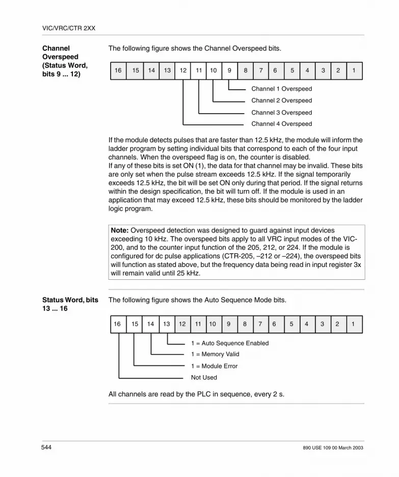
VIC/VRC/CTR 2XX
Channel Overspeed (Status Word, bits 9 ... 12)
The following figure shows the Channel Overspeed bits.
If the module detects pulses that are faster than 12.5 kHz, the module will inform the ladder program by setting individual bits that correspond to each of the four input channels. When the overspeed flag is on, the counter is disabled.If any of these bits is set ON (1), the data for that channel may be invalid. These bits are only set when the pulse stream exceeds 12.5 kHz. If the signal temporarily exceeds 12.5 kHz, the bit will be set ON only during that period. If the signal returns within the design specification, the bit will turn off. If the module is used in an application that may exceed 12.5 kHz, these bits should be monitored by the ladder logic program.
Status Word, bits 13 ... 16
The following figure shows the Auto Sequence Mode bits.
All channels are read by the PLC in sequence, every 2 s.
Note: Overspeed detection was designed to guard against input devices exceeding 10 kHz. The overspeed bits apply to all VRC input modes of the VIC-200, and to the counter input function of the 205, 212, or 224. If the module is configured for dc pulse applications (CTR-205, –212 or –224), the overspeed bits will function as stated above, but the frequency data being read in input register 3x will remain valid until 25 kHz.
16 16 23451015 14 13 12 9 8 7
Channel 1 Overspeed
11
Channel 3 Overspeed
Channel 2 Overspeed
Channel 4 Overspeed
16 16 23451015 14 13 12 9 8 7
1 = Auto Sequence Enabled
11
1 = Module Error
1 = Memory Valid
Not Used
544 890 USE 109 00 March 2003

VIC/VRC/CTR 2XX
Bit 14—Memory Valid
If bit 14 is detected in an OFF (0) state, the module’s data or configuration is in question. If this is the case, you may either initiate a self–test, power cycle the module, or replace the module.
Bit 15—Module Error
Bit 15 is set (1) when a hardware failure is detected within the module. If this bit is set, the module must be power cycled. If the bit does not clear after a power cycle, the module should be replaced.
Note: Bit #16 is not used.
890 USE 109 00 March 2003 545
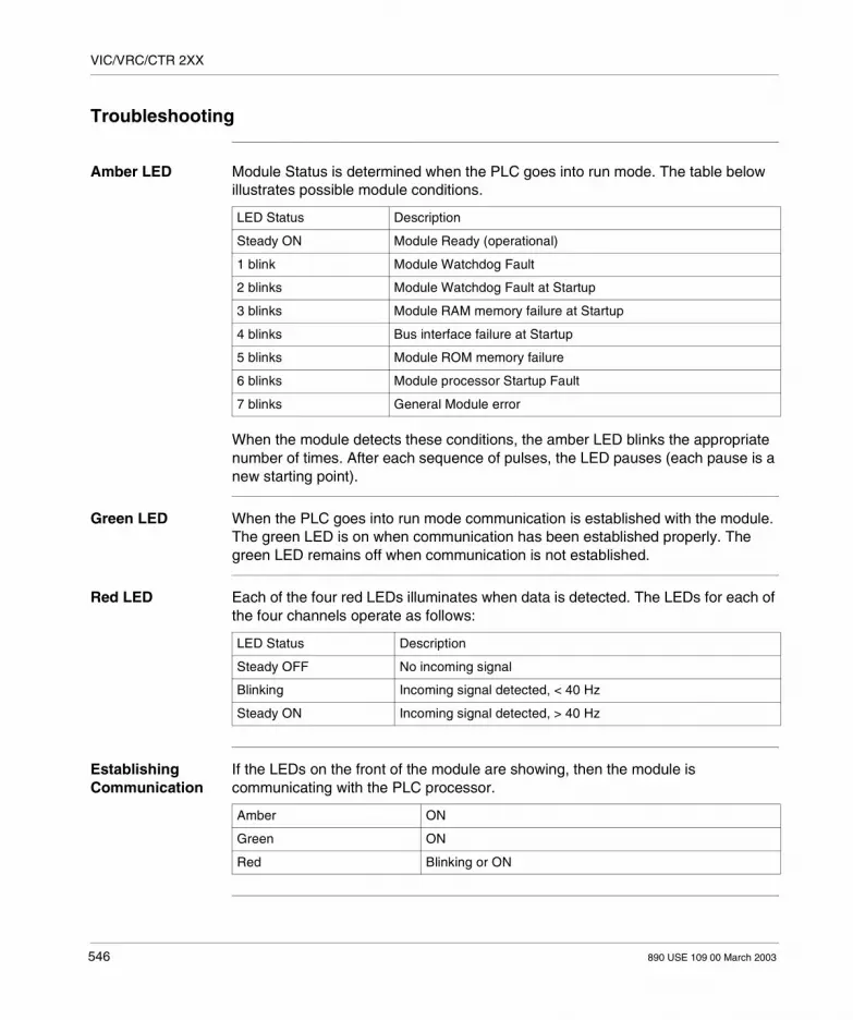
VIC/VRC/CTR 2XX
Troubleshooting
Amber LED Module Status is determined when the PLC goes into run mode. The table below illustrates possible module conditions.
When the module detects these conditions, the amber LED blinks the appropriate number of times. After each sequence of pulses, the LED pauses (each pause is a new starting point).
Green LED When the PLC goes into run mode communication is established with the module. The green LED is on when communication has been established properly. The green LED remains off when communication is not established.
Red LED Each of the four red LEDs illuminates when data is detected. The LEDs for each of the four channels operate as follows:
Establishing Communication
If the LEDs on the front of the module are showing, then the module is communicating with the PLC processor.
LED Status Description
Steady ON Module Ready (operational)
1 blink Module Watchdog Fault
2 blinks Module Watchdog Fault at Startup
3 blinks Module RAM memory failure at Startup
4 blinks Bus interface failure at Startup
5 blinks Module ROM memory failure
6 blinks Module processor Startup Fault
7 blinks General Module error
LED Status Description
Steady OFF No incoming signal
Blinking Incoming signal detected, < 40 Hz
Steady ON Incoming signal detected, > 40 Hz
Amber ON
Green ON
Red Blinking or ON
546 890 USE 109 00 March 2003

VIC/VRC/CTR 2XX
Steps after Establishing Communication
Refer to table below for steps after establishing communication:
Invalid Data The module is capable of measuring frequencies up to 25 kHz, and counting pulses up to 12.5kHz. The counter input mode stops counting inputs if the overspeed bits are set. This occurs at input frequencies over 12.5kHz.If the incoming cable must pass high voltage cables, make sure the signal cable passes the high voltage cable at 90. If electrical interference is being considered, attempt to locate the VRC/CTR module as far away as possible from the P120 power supply and relay output modules. These products may generate electrical interference during operation. This does not affect the VRC/CTR module but may induce pulses on incoming channel wiring.If the channel is configured for dc operation, the module is capable of counting up to 25 kHz. If the incoming signal is within specifications and data is still not correct, check that the data values loaded into each channel’s K and Meter factor values are correct. The K and Meter factor values are used to scale incoming signals for display purposes. These values are monitored in Read word 2 and are displayed whenever a channel is enabled and either bit 7 or 6 of Write word 3 are ON.
Overspeed VRC Inputs (Flowmeters, Variable Inputs, etc.)
The module is capable of detecting when incoming signals are exceeding the design limits of each channel. The module will detect when incoming signals exceed 12.5kHz and set one of four bits (Read word 3, bits 5 ... 8) for PLC use. These bits operate independently (i.e., if a channel exceeds 12.5 kHz, the remaining channels are not affected). If overspeed is detected, the respective channel will continue to operate, but the data is not guaranteed. If the incoming signal returns to less than 12.5 kHz, the overspeed bit will turn OFF.
Step Action
1 Monitor the status of READ Word 3 bits 13 ... 16 to determine what channel the module is displaying.
2 Check the front of the module to determine if the appropriate channel’s red LED is pulsing or ON.
3 If the above conditions are true, check to make sure the Clear Channel bit (Write Word 2, bits 8 ... 11) for the appropriate channel is not set.
4 Check that Hold Count bit (Write Word 2, bits 5 ... 8) for the appropriate channel is not set.
5 If these bits are OFF, check to make sure that the module’s self–test feature is not enabled (Write Word 3, bit 15 ON).
890 USE 109 00 March 2003 547

VIC/VRC/CTR 2XX
Overspeed Pulsed Inputs (Square Wave)
Each channel on the module is capable of being configured for dc operation on the VIC-205, 212, and 224 modules. When configured for dc operation, in the frequency input mode, each channel is capable of measuring frequencies up to 25kHz. In the frequency input mode the overspeed bits turn on at 12.5kHz, but the data is valid up to 25kHz.When configured for the counter input mode, the count value stops counting when the overspeed bits are turned on. The counter mode continues to count up to a pulse rate of 12.5kHz.
Overspeed Built–in Test Enable (BITE)
The VRC/CTR module has built–in diagnostics that can be enabled to check the module’s control electronics. These tests are automatically run each time the module is powered up but can also be run after the module is on–line. By selecting one of three test sequences and then setting this bit ON, the module enters a self–test mode.To terminate the self-test mode, reset the BITE Enable bit (0). Bits 13 and 14 determine the type of test that will be executed. Available tests and a brief explanation of what they accomplish are shown in the truth table below.
Currently, the red LED illuminates steady and the green LED flashes if the test is completed successfully. If a failure is detected, the error bit will illuminate and the red LED will blink.
Truth Table for BITE Tests
Bit 14 Bit 13 Bit 12 Description
OFF OFF OFF Test disabled
OFF ON ON Tests VRC/CTR Microprocessor, RAM, ROM, Ready and Run LEDs, 24 Vdc
ON OFF ON Tests EEPROM, Bus Interface, Internal timers, VRC electronics, Pulse indication, Frequency, and Software products
ON ON ON Overspeed and LED Indicators (requires external input from a calibrated signal generator)
Note: The two bits select the category of test in binary. If the BITE enable bit is ON, the module remains in self–test until the BITE enable bit is turned off. The enable bit and the category bits are currently only read once on entry to the BITE procedure. If you turn the bit OFF, the module will return to on line soon after the applicable test is completed. Allow 100 ms minimum for each test.
548 890 USE 109 00 March 2003

VIC/VRC/CTR 2XX
VIC/CRC/CTR 2XX Counter Input Module Specifications
Table of Specifications
The following table contains a list of VIC/CRC/CTR 2XX counter input module specifications.
Electrical Specifications
The following section describes Electrical Specifications.
Frequency Specifications
The following section describes Frequency Specifications.
VIC/VRC/CTR 2XX High Speed Input Specifications
Electrical Inputs/module 4
Isolation 30 Vdc
Supply Voltage for BVIC 2xx ONLY (24 Vdc power supply)
24 Vdc, +/-2.4Vdc
Signal Voltage Range
VIC/VRC-200 (VRC inputs)
.025 ... 36 Vac Peak typical
VIC/CTR-205 5 Vdc, +/-.5Vdc
Low <= 0.800, High >= 2.000 Vdc typical @ source Z < 10 ohms
VIC/CTR-212 12 Vdc, +/-1.2Vdc
Low <= .65 1.920,High >= 4.800 Vdc typical @ source Z < 10 ohms
VIC/CTR-224 24 Vdc, +/-2.4Vdc
Logic Low < 3.840, Log ic High > 9.600 Vdc typical @ source Z < 10 W
Frequency VIC/VRC Inputs 0 ... 10.0 kHz
VIC/VRC/CTR Vdc Inputs- Counter Mode 0 ... 10.0 kHz
VIC/VRC/CTR Vdc Inputs- Frequency Mode 0 ... 25.0 kHz
VIC/VRC/CTR Pulse Width 20 micros minimum
VIC/VRC/CTR Overspeed 12.5 kHz detection
890 USE 109 00 March 2003 549

VIC/VRC/CTR 2XX
Data Formats, Required Loadable
The following section describes Data Format and Required Loadable Specifications.
Power Required, DIN Rail Grounding
The following section Power Required and DIN Rail Grounding Specifications.
Environment, I/O Map
The following section describes Environment and I/O Map Specifications.
Dimensions and Agency Approvals
The following section describes Dimensions and Agency Approvals
Data Formats Accumulated, Scaled Accumulated, Rate (Hz) Scaled Rate
Accuracy VIC/ CTR-205, 212, 224
+/- 1 count over full range
VIC/VRC-200 +/- 0.1 percent of full scale, +/- 1 count
Required Loadable SW-IODR-001 (See Appendix B, file SVI.DAT)
Power Required VRC/CTR External Power Source None Required
VRC/CTR Internal Power Source from the backplane
275 mA @ 5 Vdc maxi mum
VIC External Power Source, Regulated or Unregulated
20 ... 30VVdc
VIC External Power Source, Typical 70mA @ 24VVdc
VIC Internal Power Source from the backplane
None Required
DIN Rail Grounding < 0.1Ohms
Environment Temperature Operational 0 ... 60 degrees C
32 ... 140 degrees F
Storage -40 ... +85 degrees C
-40 ... +185 degrees F
Humidity 0 ... 95 percent @ 60 degrees C, noncondensing
I/O Map Register 3x/4x 3 in/3 out
Dimensions W x H x D 40.6 x 142.2 x 114.3 mm
1.6 x 5.6 x 4.5 in
Weight 300 g
0.70 lb
Power Connections 60/75 copper (Cu)
Torque on set screws 0.5 in/lb
Agency Approvals VDE 0160; UL 508; CSA 22.2 No.142; FM Class I, Div 2 and European Directive EMC 89/336/EEC Standards
550 890 USE 109 00 March 2003

VIC/VRC/CTR 2XX
VIC/CRC/CTR 2XX Counter Input Module for Compact 32-bit Controllers
I/O Map Register In I/O map these modules are configured with nine 3x registers and one 4x register The 3x register assignements are as follows: 3x - Register 1: Input Status Word 3 3x - Register 2: Channel 1 Read Data 3x - Register 3: Channel 1 Factor Value 3x - Register 4: Channel 2 Read Data 3x - Register 5: Channel 2 Factor Value 3x - Register 6: Channel 3 Read Data 3x - Register 7: Channel 3 Factor Value 3x - Register 8 : Channel 4 Read Data 3x - Register 9 : Channel 4 Factor Value
3x Register 1 Input Status Word Bit Assigment
Factor value registers the display either K or M factor as selected in the I/O map parameter screen. The value entered in the parameter screen for the associated channel will be displayedReal data registers display either count or frequency as selected on the I/O map parameter screen.
16 15 14 13 12 11 10 9 8 7 6 5 4 3 2 1
1=Channel 1 Overspeed1=Channel 2 Overspeed1=Channel 3 Overspeed1=Channel 4 Overspeed1= Auto Sequence Enable1= Memory Valid
1= Module ErrorNot Used
1=Channel 1 Data Valid1=Channel 2 Data Valid
1=Channel 3 Data Valid1=Channel 4 Data Valid
1=Channel 1 Data Rollover1=Channel 2 Data Rollover1=Channel 3 Data Rollover1=Channel 4 Data Rollover
890 USE 109 00 March 2003 551
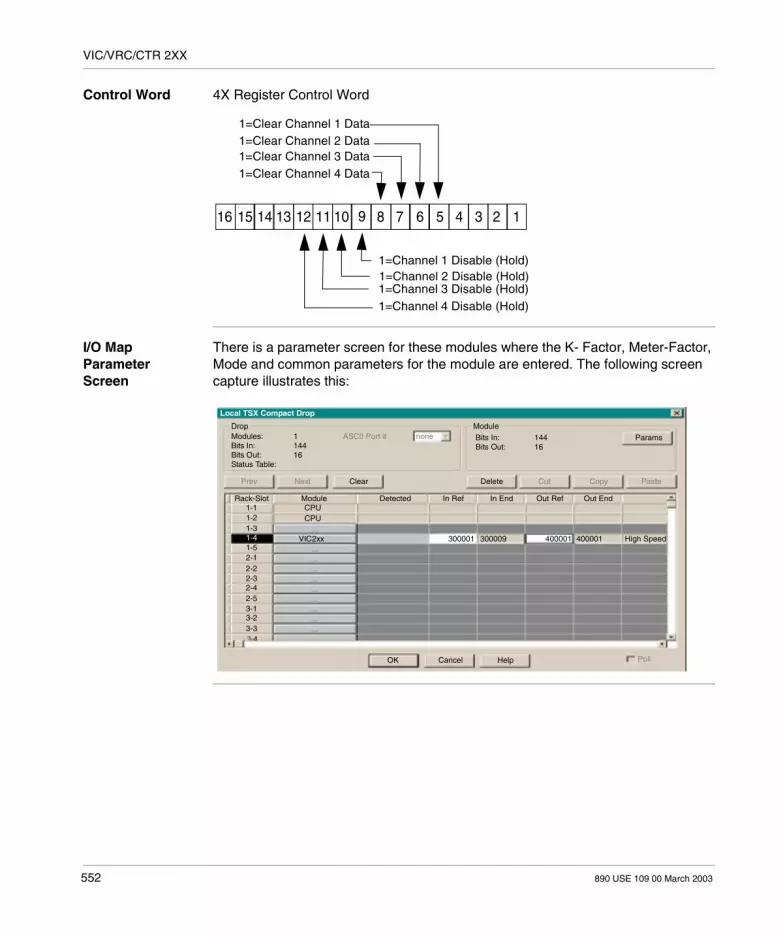
VIC/VRC/CTR 2XX
Control Word 4X Register Control Word
I/O Map Parameter Screen
There is a parameter screen for these modules where the K- Factor, Meter-Factor, Mode and common parameters for the module are entered. The following screen capture illustrates this:
16 15 14 13 12 11 10 9 8 7 6 5 4 3 2 1
1=Channel 1 Disable (Hold)1=Channel 2 Disable (Hold)1=Channel 3 Disable (Hold)1=Channel 4 Disable (Hold)
1=Clear Channel 1 Data1=Clear Channel 2 Data1=Clear Channel 3 Data1=Clear Channel 4 Data
Drop ModuleModules:Bits In:Bits Out:Status Table:
114416
ASCII Port # none Bits In:Bits Out:
14416
Params
Prev Next Clear Delete Cut Copy Paste
Rack-Slot Module Detected In Ref In End Out Ref Out End1-11-21-31-41-52-12-22-32-42-53-13-23-3
CPUCPU
VIC2xx 300001 300009 400001 400001 High Speed
OK Cancel Help Poll
Local TSX Compact Drop
552 890 USE 109 00 March 2003

VIC/VRC/CTR 2XX
Input Screen for K-Factor
Enter the K-Factor for each channel:
Input Sceen for Meter- Factor
Enter the Meter-Factor for each channel:
K-Factor Meter-Factor Mode Common
Valid range is 0 to 32767
Channel 1
Channel 2
Channel 3
Channel 4
1
1
1
1
OK Cancel
C 2xx 4-Channel High Speed Counter Module
VIC 2xx 4-ChannelHigh Speed Counter Module
K-Factor Meter-Factor Mode Common
Valid range is 1 to 19999
Channel 1
Channel 2
Channel 3
Channel 4
10000
10000
10000
10000
OK Cancel
VIC 2xx 4-Channel High Speed Counter Module
890 USE 109 00 March 2003 553

VIC/VRC/CTR 2XX
Input Screen Module Mode
For each channel, select either Counter or Frequency in the Real Data register:
Input Screen for Module Common Parameters
Select to display either K or M factor in the Factor Data registers This selection applies to a four channels:
K-Factor Meter-Factor Mode Common
Counter
Counter
Counter
Counter
Counter
Frequency
Channel 1
Channel 2
Channel 3
Channel 4
OK Cancel
VIC 2xx 4-Channel High Speed Counter Module
K-Factor Meter-Factor Mode Common
K-Factor
OK Cancel
VIC 2xx 4-Channel High Speed Counter Module
K-Factor
Meter-Factor
Additional data for allchannels displayed as:
554 890 USE 109 00 March 2003

890 USE 109 00 March 2003
Overview of the ZAE 201 Counter/Positioner Module
At a Glance
Purpose The purpose of this chapter is to describe the ZAE 201 Counter/Positioner Module.
What’s in this Chapter?
This chapter contains the following sections:
Section Topic Page
47.1 Overview of the ZAE 201 Counter/Positioner Module 556
47.2 Using the ZAE 201 Counter/Positioner Module as a High-Speed Counter
563
47.3 Using the ZAE 201 Counter/Positioner Module as a Positioning Controller
576
47.4 Specifications of the ZAE 201 Counter/Positioner Module 595
555

ZAE 201 Counter/Positioner Module
47.1 Overview of the ZAE 201 Counter/Positioner Module
At a Glance
Purpose This section provides an overview of the ZAE 201 Counter/Positioner Module.
What’s in this Section?
This section contains the following topics:
Topic Page
What is the ZAE 201 Counter/Positioner Module? 557
LED Indicator Displays of the ZAE 201 Counter/Positioner Module 558
Choosing Operating Mode and Input Voltage Level for the ZAE 201 Counter/Positioner Module
559
Operating States of the ZAE 201 Counter/Positioner Module 560
Representing the ZAE 201 Data Blocks in the I/O Map 561
556 890 USE 109 00 March 2003
ZAE 201 Counter/Positioner Module
What is the ZAE 201 Counter/Positioner Module?
Brief Product Description
The ZAE 201 is a dual-function, user-configurable module that can operate as either a high speed counter or to monitor a simple one–axis positioning application. The ZAE 201 has two output relays, the operation of which are specified when the module is parameterized for either counting or positioning functions. Operational power for the module is 24 Vdc, and position/count signals may be passed to the module as either 5 V (RS422 compatible) or 24 V inputs.In the counter mode, the unit acts as a high speed counter. Counting is started and stopped by activating and deactivating the count gate input. When counting (count gate activated), two output relays operate based on setup parameters passed to the unit prior to activating the count gate.In the positioning mode, the unit monitors a single–axis motion. This is accomplished by providing quadrature encoder inputs to the ZAE201. When a motion request is received, the unit will control the state of two output relays based on the current position relative to the commanded position. During motion, the state of two relay outputs are maintained such that speed can be controlled as the target position is approached. The specific operation of these relays is determined by setup parameters passed to the ZAE 201. Direction of motion and absolute speed are determined by other devices controlled through user logic.
890 USE 109 00 March 2003 557

ZAE 201 Counter/Positioner Module
LED Indicator Displays of the ZAE 201 Counter/Positioner Module
LED Indicators The ZAE 201 has seven LED indicators displayed on the front panel: The green LED opposite terminal screw 1 goes ON to indicate the presence of
the 24 V supply voltage The amber LED opposite terminal screw 2 may be used as an encoder power
monitor if you are using 24 V input signals; if you remove the jumper between terminal screws 1 and 2 and add a wire from the encoder supply, the LED will go ON to indicate a loss of power from the field device. Do not remove the jumper or use this LED with 5 V input signals.
The green LED opposite terminal screw 12 is the READY LED; its meaning is mode dependent. It goes ON in the positioner mode when the module has been completely parameterized and the reference point trip has been performed. It goes ON in the counter mode when the module has been completely parameterized.
The amber LED opposite terminal screw 13 is the RUN LED; its meaning is mode dependent. It goes ON in the positioner mode when a motion command is being executed. It goes ON in the counter mode when the module is parameterized and the counter gate is open.
The red LED opposite terminal screw 14 goes ON to indicate an FKE input active condition.
The two red LEDs opposite terminal screws 16 and 18 indicate the current condition of relays 1 and 2, respectively. When an LED is ON, its respective relay is closed; when an LED is OFF, its relay is open.
558 890 USE 109 00 March 2003

ZAE 201 Counter/Positioner Module
Choosing Operating Mode and Input Voltage Level for the ZAE 201 Counter/Positioner Module
Switch Location and Settings
The choices of operating mode and input voltage are set via DIP switches on the back of the module. The module can operate in only one mode and at only one input voltage at a time.
LR
B1
B2
B
3 B
4Input Voltage SettingPosition R on Switch B1 = 5 V inputsPosition L on Switch B1 = 24 V inputs
Operating Mode SettingsPosition R on Switch B2 = Position sensing modePosition L on Switch B2 = Counter mode
Activity Setting for FKE* InputPosition R on Switch B3 = FKE* input active LOWPosition L on Switch B3 = FKE* input active HIGH
* FKE = count gate or reference trip input, field wired at terminal screw # 14.
890 USE 109 00 March 2003 559

ZAE 201 Counter/Positioner Module
Operating States of the ZAE 201 Counter/Positioner Module
Operating States After a ZAE 201 module has been installed, its two output relays must be parameterized for counting or positioning functions. When the Compact-984 Controller is started and begins solving user logic, the ZAE 201 comes up in an initialized but nonfunctional state called NET IN. In order to bring the module into a READY state where it can function, information must be sent to the module identifying how the two relays are to be used and how the FKE input is to be interpreted. The process of sending this information to the module is called parameterization, and the specific parameters are dependent upon the module’s operating mode.At the beginning of each scan, the ZAE 201 places the latest status and counter or positioning data in its input data block. The controller uses this information to determine the next command for the module. Commands are stated in the output data block. If no new command is appropriate based on the current information in the input data block, the command byte in the output data block is set to 0.The ZAE 201’s maximum count cannot exceed 8,388,607. Typically, the command register in the output data block should be cleared at the start of a scan, allowing the user logic to define a new command as required. The command is passed to the module at the end–of–scan. Commands may be given only when the ZAE 201 is not busy, and a command must be consistent with the current state of the module. If either of these conditions is not met, an error will be returned in the input data block.The ZAE 201 can be reset to a NET IN state at any time. New information can then be passed to the module, thereby redefining the operating parameters before returning to the READY state.
560 890 USE 109 00 March 2003

ZAE 201 Counter/Positioner Module
Representing the ZAE 201 Data Blocks in the I/O Map
Overview The ZAE 201 is described in the Compact-984 I/O Map as a three-register bidirectional module. Three consecutive 3x input registers are used to store the three words in the input data block, and three consecutive 4x output registers are used to store the three words in the output data block.
Format of the Input Data Block
The first word in the (3x) input data block contains input data necessary for user logic to efficiently control the ZAE 201; it comprises three parts: A one–bit module busy flag A set of seven error condition bits A set of eight mode–specific module status bitsThe following diagram shows the first word in the input data block.
1 2 3 4 5 6 7 8 9 10 11 12 13 14 15 16
First Word in the Data Input Block
1 = module is busy0 = new command may be issued
Error Condition Bits0 0 0 0 0 0 1 = module health failure--replace the module 0 0 0 0 0 1 0 = module communication error stop and restart the 0 0 0 0 0 1 1 = module time-out error controller to clear 0 0 0 0 1 0 0 = invalid request in current mode 0 0 0 0 1 0 1 = invalid request in current state 0 0 0 0 1 1 0 = invalid state RAM pointer 0 0 0 0 1 1 1 = invalid parameter 0 0 0 1 0 0 0 = invalid target value 1 1 1 1 1 1 1 = invalid state error
* indicates that the bit value may be either 1 or 0 when the module is in this state.
Module Status BitsPositioner Mode0 0 0 0 * 1 0 0 = NET IN 0 0 0 0 * 1 0 1 = parameterized 1 * 1 1 * 1 1 1 = READY 0 0 0 0 * 1 1 1 = RUN fast 0 0 0 1 * 1 1 1 = RUN slow 0 0 1 1 * 1 1 1 = RUN hunting Counter Mode 0 0 0 0 * 0 0 0 = NET IN
0 0 * * 1 0 1 1 = RUN 0 0 * * 0 0 0 1 = READY
890 USE 109 00 March 2003 561

ZAE 201 Counter/Positioner Module
The second and third words in the input data block contain the latest count or position value, depending on the operating mode of the module. The second word contains the high order position or count, and the third word contains the low order. The following is an explanation of bits 10 ... 13 in the above illustration:
Format of the Output Data Block
The first 4x word in the output data block passes commands to the ZAE 201 module. It uses its low byte (bits 9 ... 16) to indicate the command type; the high byte (bits 1 ... 8) is not used. The command types and their output data block implemen-tations are mode dependent. The following table is an output data block representation of counter/positioner commands:
These commands initiate a process to be carried out by the module and causes the module to change state, sometimes permanently and sometimes temporarily.The second and third words in the output data block are command dependent. Sometimes they are used to pass needed information to the ZAE 201; other times they may not be used at all. Some commands require more information than can be stored in two words, and in these cases the second word is used as a pointer into state RAM where the requisite number of registers is accessed.
Bit 10 In position mode, a 1 in this bit indicates whether the motion is within the specified target range
Bit 11 The state of relay 2 at terminal 18
Bit 12 The state of relay 1 at terminal 16
Bit 13 The state of FKE input at terminal 14
Note: When in position mode the counts are 4 times those counts when in counter mode.
Operating Mode Command Hex Value Low Byte Bit Values
Counter parameterize 01 0 0 0 0 0 0 0 1
reset 02 0 0 0 0 0 0 1 0
clear current count 03 0 0 0 0 0 0 1 1
Positioner parameterize 01 0 0 0 0 0 0 0 1
reset 02 0 0 0 0 0 0 1 0
run reference 04 0 0 0 0 0 1 0 0
run reference + 05 0 0 0 0 0 1 0 1
go to target 06 0 0 0 0 0 1 1 0
562 890 USE 109 00 March 2003

ZAE 201 Counter/Positioner Module
47.2 Using the ZAE 201 Counter/Positioner Module as a High-Speed Counter
At a Glance
Purpose This section provides an overview of the using the ZAE 201 Counter/Positioner Module as a high-speed counter.
What’s in this Section?
This section contains the following topics:
Topic Page
Field Wiring the ZAE 201 for Counting Applications 564
Switch Settings for Using the ZAE 201 as a High-Speed Counter 567
Overview of ZAE 201 Counter Mode Commands and States 568
ZAE 201Counter Mode Commands 569
Example: Using the ZAE 201 as a High-Speed Counter 572
890 USE 109 00 March 2003 563

ZAE 201 Counter/Positioner Module
Field Wiring the ZAE 201 for Counting Applications
Field Wiring for Counting Applications
The ZAE 201 module can be field wired for counting applications in three different ways—for 5 V inputs and for 24 V inputs with or without the power monitor jumpered between terminals 1 and 2.
Wiring for Counting with 5 V Inputs
The ZAE 201 can be field wired for counting with 5 V inputs as shown below.
5 VPulse
Generator
External5 V Supply
+5 V
Count Pulse
CountPulseNegated
0 V0 V
+5 V
Count Gate
0.1A
Relay 1
Relay 2
123456789
10111213141516171819202122
Green
Amber
Red
VCC
VCC
VCC
I/O BusInterface
Green Ready
Amber Run
24 Vdc24 V Common
Red Count Gate
564 890 USE 109 00 March 2003

ZAE 201 Counter/Positioner Module
Wiring for Counting with 24 V Inputs
The ZAE 201 can be field wired for counting with 24 V inputs, with or without the power monitor jumpered between terminals 1 and 2 as shown below.
24 VPulse
Generator
24 VPulse
Generator
(a) - with Power Monitor
CountPulse
Count Gate
Relay 1
Relay 2
0.1A
123456789
10111213141516171819202122
Red
VCC
VCC
VCC
Amber
Green
Green Ready
Amber Run
Red Count Gate
I/O BusInterface
24 Vdc24 V Common
Green Ready
Amber Run
Red Count Gate
I/O BusInterface
Green
Amber
VCC
VCC
VCC
Red
24 Vdc
0.1A
Count Gate
Relay 1
Relay 2
1213141516171819202122
1110987654321
(b) - without Power Monitor
CountPulse
24 V Common
890 USE 109 00 March 2003 565

ZAE 201 Counter/Positioner Module
Facts About Field Wiring for Counting Applications
For 24 V operations, a pulse source for the count is field wired to terminal screw 3. For 5 V operations, a differential input is required; pulse source and pulse source must be field wired to terminal screws 3 and 4, respectively. This source is a series of pulses generated by the events being counted.The counter gate is field wired to terminal screw 14. This gate is used to control the counting operation. When the module is in the READY state and the count gate goes active, the current count held in the data input block is set to 0 and the module starts accumulating a new count.The two relays that will receive your counter control logic are wired at terminal screws 16 and 18. Counter control logic is very application specific. For example, relay 1 at terminal screw 16 might be connected to an indicator light that is programmed to turn ON when a specified count is reached; at the same time, relay 2 at terminal screw 18 might be used to modify some aspect of the operation being counted when some other count is reached.
Note: When the jumper between terminals 1 and 2 is removed and when both terminals are field wired, as they are in panel (a) of the previous figure, the amber LED opposite terminal 2 can be used as a power monitor for 24 V input signals. In all other cases, the jumper should be left installed, thus preventing the LED from turning on.
566 890 USE 109 00 March 2003

ZAE 201 Counter/Positioner Module
Switch Settings for Using the ZAE 201 as a High-Speed Counter
Procedure for Setting Switches
To set a ZAE 201 module up as a high speed counter:
Step Action
1 Place DIP switch B2 on the back of the module in the left (L) position.
2 Use DIP switch B1 to specify the desired input voltage at the count pulse inputs.
3 Use DIP switch B3 to specify whether the counter gate activity will be HIGH or LOW.
890 USE 109 00 March 2003 567

ZAE 201 Counter/Positioner Module
Overview of ZAE 201 Counter Mode Commands and States
Parameterization When the ZAE 201 has been installed as a counter module and the Compact-984 Controller has been powered up, the ZAE 201 comes up in a NET IN state. In the NET IN state, the module is able to accumulate pulse counts and store current count information in the second and third word of the input data block. The ZAE 201 must be given a set of counter mode parameters before the count gate and relays can operate.Two parameters—P1 and P2—must be passed to the module. These two parameters are the count values at which relay 1 and relay 2, respectively, are to be either opened or closed. A third bit of information must also be passed to the module defining how the relays are to operate when the count is equal to P1 or P2.
READY and RUN States
Once the module has been parameterized, it goes into a READY state, where it is prepared for normal counting functionality controlled by the counter gate input. When the counter gate is active, the module is in the RUN state where it proceeds with its counting operation.When the counter gate is not active, the module switches to the READY state where it stops counting and maintains the count that it has accumulated. Activating and deactivating the counter gate switches the module from READY to RUN and back.
RESET If you need to change the operating parameters without stopping the controller, you can put the module back into a NET IN state at any time by issuing a RESET command.
Single Count and Multiple Count Operations
The relays can operate in either single or multiple count operations.An example of a single count operation might be using the P1 parameter is set to define when relay 1 opens—when the specified count is reached, the relay opens and the count continues.An example of a multiple count operation might be a relay scheduled to open at a defined count and close when the count reaches 1.25 times the defined count. This operation will continue to open at every multiple of the defined parameter and close at every quarter multiple of that parameter.
568 890 USE 109 00 March 2003

ZAE 201 Counter/Positioner Module
ZAE 201Counter Mode Commands
Counter Mode Commands
There are three commands that can be used in the counter mode—parameterize, clear current count, and reset. These commands are implemented in the three-word output data block specified in the I/O Map for the ZAE 201.As described in the following table, not all commands are acceptable at all times to the module:
If a command is issued during a state that does not allow that command, an error is reported in the first word of the input data block.
Counter Mode Parameterize Command
The parameterize command implements the first two words in the output data block.
The second word contains an index into a table of five 4x registers in the controller’s state RAM. These five registers contain the information necessary to parameterize the module.The first register in the 4x table contains information that defines how the relays will be set and how they will react when the count is met:
State parameterize clear current counter reset
NET IN allowed allowed allowed
READY not allowed allowed* allowed
RUN not allowed not allowed allowed
* Allowed, but has no effect if the module has entered RUN state since being parameterized.
0 10 0 0 0 0
not used
First Word in the Output Data Block
Third Word in the Output Data Block Not Used
index pointer to a table of five 4x registers in state RAM
0
Second Word in the Output Data Block
Output Data Block Format: parameterize Command in Counter Mode
890 USE 109 00 March 2003 569
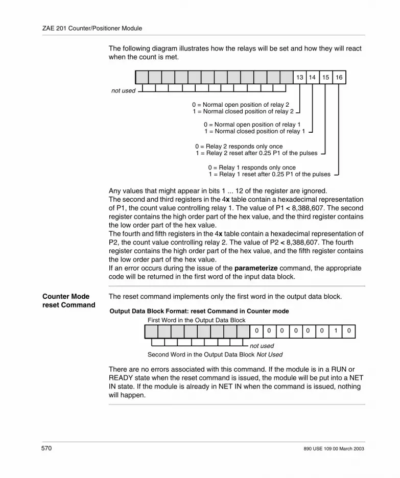
ZAE 201 Counter/Positioner Module
The following diagram illustrates how the relays will be set and how they will react when the count is met.
Any values that might appear in bits 1 ... 12 of the register are ignored.The second and third registers in the 4x table contain a hexadecimal representation of P1, the count value controlling relay 1. The value of P1 < 8,388,607. The second register contains the high order part of the hex value, and the third register contains the low order part of the hex value.The fourth and fifth registers in the 4x table contain a hexadecimal representation of P2, the count value controlling relay 2. The value of P2 < 8,388,607. The fourth register contains the high order part of the hex value, and the fifth register contains the low order part of the hex value.If an error occurs during the issue of the parameterize command, the appropriate code will be returned in the first word of the input data block.
Counter Mode reset Command
The reset command implements only the first word in the output data block.
There are no errors associated with this command. If the module is in a RUN or READY state when the reset command is issued, the module will be put into a NET IN state. If the module is already in NET IN when the command is issued, nothing will happen.
13 14 15 16
not used
0 = Normal open position of relay 21 = Normal closed position of relay 2
0 = Normal open position of relay 11 = Normal closed position of relay 1
0 = Relay 2 responds only once1 = Relay 2 reset after 0.25 P1 of the pulses
0 = Relay 1 responds only once1 = Relay 1 reset after 0.25 P1 of the pulses
0 0 0 0 0 0 01
not used
First Word in the Output Data Block
Second Word in the Output Data Block Not Used
Output Data Block Format: reset Command in Counter mode
570 890 USE 109 00 March 2003

ZAE 201 Counter/Positioner Module
Counter Mode clear current count Command
The clear current count command implements only the first word in the output data block, as shown in the graphic below.
The only potential error associated with this command will be flagged if you issue it while the module is in RUN mode.
0 0 0 0 0 0 1 1
First Word in the Output Data Block
Second and Third Words in the Output Data Block Not Usednot used
Output Data Block Format: clear current count Command in Counter Mode
890 USE 109 00 March 2003 571

ZAE 201 Counter/Positioner Module
Example: Using the ZAE 201 as a High-Speed Counter
Overview This system carries piece parts along a motor-driven conveyor line. The line continues to a diverting mechanism that sends parts to either the right (R) or left (L) into separate bins. The ZAE 201 Counter will enable the system to be controlled such that the gate will switch positions after every 4,000 pieces.The following diagram illustrates a conveyer system application example.
Counter Example DIP Switch Settings
Set the DIP switches on the back of the module for COUNTER mode, 5 V input voltage, and LOW activity on the count gate.The following diagram illustrates this procedure.
Motor Drive
Piece Parts
Gate Position A(Relay 1)
Gate Position B(Relay 2)
ProximitySensor
Gate Count
ActivityOperating Mode
Input Voltage
ON OFFR
B1
B2
B3
B4
572 890 USE 109 00 March 2003

ZAE 201 Counter/Positioner Module
Counter Example Traffic Cop Settings
Traffic cop the drop to support the system with the ZAE 201 high speed counter, a DAP 216 discrete output module, and a DEP 216 discrete input module:
Counter Example Coil Use
The following coils will be implemented in the example counting operation:
Service CommF1 F2 F3 F4 F5 F6 F7 F8 F9OFF
DelDrop Quit
TRAFFIC COP984-128/138/145 CONTROLLERS
Drop : 1 ( 1 ) Rack : 1Number Inputs : 64 Number Outputs : 64
DEP216 10001 - 10016 16 - IN 24VDC105104103102101
Slot TypeModule
984 PC -145 POWERSUPPLY 984 PC -145 POWERSUPPLY ZAE201 30001 - 30003 40001 - 40003 BIN COUNTER/POSITION DAP216 00001 - 00016 16 - OUT 24VDC
Input Output type DescriptionReference Numbers Data Module
Usage Coil Function
External (DAP 216) 00001 Control coil for gate position A (at DAP 216 terminal screw 3)
00002 Control coil for gate position B (at DAP 216 terminal screw 4)
00007 Control coil for the count gate, the FKE input (at terminal screw 14)
Internal 00017 Logic solve coil—when ON, ladder logic is being solved
External (DEP 216) 10009 State of Relay 1 output from ZAE 201
External (DEP 216) 10011 State of Relay 2 output from ZAE 201
890 USE 109 00 March 2003 573

ZAE 201 Counter/Positioner Module
Counter Example Parameterization
Go to the reference editor by pressing <ALT><F2>, and edit register values to parameterize the ZAE 201 high speed counter:
Set register 40002 to a decimal value of 50; this indicates a pointer to a block of five 4x registers starting at 40050. (Do not set values in register 40001 manually—this will be done by the user logic.)The values you set in the table registers indicate: Relays 1 and 2 are normally open and provide one–shot responses, since the
four least significant bits in register 40050 are all set to 0 The high order word value for relay 1, as expressed in register 40051, is 0 The low order word value for relay 1, as expressed in register 40052, is 4,000
(FA0 in hex) The high order word value for relay 2, as expressed in register 40053, is 0 The low order word value for relay 2, as expressed in register 40054, is 8,000
(1F40 in hex)These parameterizing values will cause Relays 1 and 2 to close at the count values of 4000 and 8000, respectively.
Service Comm Format Setting SmplASC Transfr FileI/O Ref E/D QuitF1 F2 F3 F4 Reference Data F6 F7 F8 F9OFF
Format : Binary Read from File Range :1 File :1 Page :0
400544005340052400514005040002 50
0
40000
8000
0
574 890 USE 109 00 March 2003

ZAE 201 Counter/Positioner Module
Counter Example Field Wiring Diagram
The discrete modules will be used to control the mechanics of the switching gate. Field wire the three A120 I/O modules like this:
Count Pulsesfrom ProxSwitch (5 Vdc)
A
A
5 VSupply
21
34567891011
21
345678910111213141516171819202122
1213141516171819202122
1213141516171819202122
21
34567891011
24 Vdc24 V Common
Gate A
Gate B
DAP 216DEP 216 ZAE 201
Count Gate
24 Vdc COM
24Vdc
890 USE 109 00 March 2003 575

ZAE 201 Counter/Positioner Module
47.3 Using the ZAE 201 Counter/Positioner Module as a Positioning Controller
At a Glance
Purpose This section provides an overview of the using the ZAE 201 Counter/Positioner Module as a positioning controller. The ZAE 201 does not control speed, but provides relay outputs that indicate when speed should be changed. The actual control of speed must be provided by the user (ladder or hardware) logic—the module itself does not control the speed. Similarly, the ZAE 201 does not control direction; this is also a function of user-defined logic (ladder or hardware).
What’s in this Section?
This section contains the following topics:
Topic Page
Field Wiring for ZAE 201 Positioning Applications 577
Switch Settings for Using the ZAE 201 as a Positioning Controller 580
Overview of ZAE 201 Positioning Mode Commands and States 581
The ZAE 201 Positioning Mode Commands 582
Example: Using the ZAE 201 Module as a Positioner 588
576 890 USE 109 00 March 2003

ZAE 201 Counter/Positioner Module
Field Wiring for ZAE 201 Positioning Applications
Field Wiring for Positioning Applications
The ZAE 201 module can be field wired for positioning applications in three different ways—for 24 V inputs with or without the power monitor jumpered between terminals 1 and 2, and for 5 V inputs.
Wiring a ZAE 201 Module for Positioning with 5 V Inputs
The ZAE 201 can be field wired for positioning applications with 5 V inputs as shown here.
The direction of motion and speed are user defined. The ZAE 201 provides relay outputs that indicate when speed should be changed.
Note: When the jumper between terminals 1 and 2 is removed and when both terminals are field wired, as they are in Figure 18 (a), the amber LED opposite terminal 2 can be used as a power monitor for 24 V input signals. In all other cases, the jumper should be left installed.
5 VPulse
Generator
External5 V Supply
+5 V
0 V0 V
+5 V
Quad1Quad1NQuad2Quad2N0 Ref0N Ref
123456789
1011
1415161718192021220.1A
Relay 1
Relay 2
Reference Trip
24 Vdc24 V Common
Red LEDs
Green LED
Amber LED
VCC
VCC
VCC
I/O BusInterface
Green Ready LED
Amber Run LED
Red ReferenceTrip LED
1213
890 USE 109 00 March 2003 577

ZAE 201 Counter/Positioner Module
Wiring a ZAE 201 Module for Positioning with 24 V Inputs
The ZAE 201 can be field wired for positioning applications with monitoring as shown in (a), and without (b).
123456789
10111213141516171819202122
123456789
10111213141516171819202122
Quad1
Quad2
0 Ref
Quad1
Quad2
0 Ref
Reference Trip
Relay 1
Relay 2
0.1A
Reference Trip
Relay 1
Relay 2
0.1A
Red LEDs
24 Vdc24 V Common
(b)
Green LED
Amber LED
I/O BusInterface
Green Ready
Amber Run
Red Reference Trip LED
VCC
VCC
VCC
I/O BusInterface
Green Ready
Amber Run
Red Reference Trip LED
VCC
24 Vdc24 V Common
(a)
Red LEDs
VCC
VCC
Green LED
Amber LED
24 VPulse
Generator
LED
LED
LED
LED
24 VPulse
Generator
578 890 USE 109 00 March 2003

ZAE 201 Counter/Positioner Module
Position Control For 24 V operations, a ZAE 201 positioning module requires three input signals from an incremental encoder to maintain absolute position—two quadrature pulse inputs connected at terminal screws 3 and 5 provide position and direction, and a third signal connected at terminal screw 7 provides a single pulse on every rotation of the encoder.For 5 V operations, differential inputs are required; a ZAE 201 positioning module must be wired at six terminal screws: Quad pulse 1 and quad pulse 1 at terminal screws 3 and 4, respectively Quad pulse 2 and quad pulse 2 at terminal screws 5 and 6, respectively The 0 reference and 0 reference at terminal screws 7 and 8, respectivelyThe pulse signal combined with the reference trip input at terminal screw 14 define 0 for the linear travel route being controlled by the module.The reference trip input is derived from the output of some type of proximity sensor placed at a position defined as 0. On command, the object under control is passed by the proximity switch. By logically ANDing the rotational pulse from the encoder with the signal from the proximity switch, you define 0 and maintain the position value of 0 within the module.Position control is handled by user-defined discrete logic that controls a drive motor based on information provided by the Compact-984 Controller. Relays 1 and 2 on the ZAE 201 module control motor speed in the following manner, depending on whether the parameterize command has been set for overlapping mode or alternating mode pulse reception:Overlapping Mode Both relays ON — fast speed Relay 1 OFF and relay 2 ON — slow speed Both relays OFF — stop drive motorAlternating Mode Relay 1 ON and relay 2 OFF — fast speed Relay 1 OFF and relay 2 ON — slow speed Both relays OFF — stop drive motorMotor direction must be controlled by other logic, typically by a discrete output module or ladder logic that drives a D/A converter—e.g., a DAU 202.
890 USE 109 00 March 2003 579

ZAE 201 Counter/Positioner Module
Switch Settings for Using the ZAE 201 as a Positioning Controller
Switch Settings To set a ZAE 201 module up as a one-axis positioning controller, place DIP switch B2 on the back of the module in the right (R) position, use DIP switch B1 to specify the desired input voltage at the encoder inputs, and use DIP switch B3 to specify whether the reference trip activity will be HIGH or LOW.The ZAE 201’s maximum allowable positions are limited to a range between -8,388,607 and +8,388,607.
Note: The ZAE 201 does not control speed, but provides relay outputs that indicate when speed should be changed. The actual control of speed must be provided by the user (ladder or hardware) logic-the module itself does not control the speed. Similarly, the ZAE 201 does not control direction; this is also a function of user-defined logic (ladder or hardware).
580 890 USE 109 00 March 2003

ZAE 201 Counter/Positioner Module
Overview of ZAE 201 Positioning Mode Commands and States
Parameterization When the ZAE 201 has been installed as a positioning module and the Compact-984 Controller has been powered up, the ZAE 201 comes up in a NET IN state. In the NET IN state, the module is unable to conduct any position control operations. It must be given a set of positioner mode parameters before it becomes a functioning module.The process involves the setting of three positioning parameters—P1, P2, and P3—which describe how the two relays will manage motor speed as the target position is approached, These parameters are unsigned numbers that refer to three different distances from the target position.For example, in overlapping mode, P1, P2, and P3 are values that must be defined based on the dynamics of the operation being controlled. When the distance from the target position reaches the value defined as P1, relay 1 is opened and the drive motor speed begins to be reduced. When the distance from the target position reaches the value defined as P2, relay 2 is opened and the drive motor is turned OFF; when the motor is turned OFF, the operation coasts to a stop. P3 defines an acceptable region on either side of the target position where you plan to stop the system.Two additional bits of information must be passed to the module during the parameterization process. The first specifies the relay operation as a function of P1 and P2; the other specifies the speed at which the reference point will be approached.
Running a Reference Point
After the ZAE 201 has been parameterized for positioning mode, the module is not yet able to perform motion control until it has undergone a procedure called running a reference point. This procedure defines the 0-point on the axis of travel. It requires the issuing of the run reference point command in the output data block in order to drive the system toward the 0-position (defined by a proximity sensor) and set the position value in the module to 0 when that point is reached.The direction of motion is totally user-controlled.
The READY State After you have completed running a reference point, the ZAE 201 module enters the READY state for positioning operations. At this point, motion control can be enacted by simply requesting that the module drive the system to a particular coordinate.
RESET If you need to change the operating parameters, you can put the module back into a NET IN state at any time by issuing a reset command.
890 USE 109 00 March 2003 581

ZAE 201 Counter/Positioner Module
The ZAE 201 Positioning Mode Commands
Overview As shown in the following table, there are five commands that can be used in the positioning mode—parameterize, reset, run reference point, run reference point +, and go to target. These commands are implemented in the three-word output data block specified in the I/O Map for the ZAE 201. Before ordering encoders, ensure they comply with the A, B, and Z pulses shown in the Specifications section.Not all commands are acceptable at all times to the module:The following table summarizes command and state compatibilities in positioner mode.
If a command is issued during a state that does not allow that command, an error is reported in the first word of the input data block.
Positioning Mode parameterize Command
The parameterize command implements the first two words in the output data block:Output Data Block Format: parameterize Command in Positioner Mode
The second word contains an index into a table of seven 4x registers in the controller’s state RAM. These seven registers contain the information necessary to parameterize the module.
State parameterize reset run ref run ref + go to target
NET IN allowed allowed not allowed not allowed not allowed
PARAM not allowed allowed allowed not allowed not allowed
READY not allowed allowed not allowed allowed allowed
RUN FAST not allowed allowed* not allowed not allowed not allowed
RUN SLOW not allowed allowed* not allowed not allowed not allowed
RUN HUNT not allowed allowed* not allowed not allowed not allowed
* Allowed but can cause current motion to stop by opening both relays.
0 0 10 0
First Word in the Output Data Block
not used
index pointer to a table of seven 4x registers in state RAM
Third Word in the Output Data Block Not Used
Second Word in the Output Data Block
0 0 0
582 890 USE 109 00 March 2003

ZAE 201 Counter/Positioner Module
4[x] Table The first register in the 4x table contains information that defines the operation of the relays during motion to a target position and the speed at which a run reference point is executed.The following diagram illustrates this procedure.
Any values that might appear in bits 1 ... 14 of the register are ignored.The second and third registers in the 4x table contain a hexadecimal number that defines P1—the distance from the target position at which the motor speed should slow down. The value of P1 < 8,288,607. The second register contains the high order part of the hex value; the third register contains the low order part of the hex value.The fourth and fifth registers in the 4x table contain a hexadecimal number that defines P2—the distance from the target position at which the motor should turn OFF. The value of P2 < 8,288,606. The fourth register contains the high order part of the hex value; the fifth register contains the low order part of the hex value.The sixth and seventh registers in the 4x table contain a hexadecimal number that defines P3—the distance from the target position that is deemed within acceptable tolerance of the desired position. The value of P3 < 8,288,605. The sixth register contains the high order part of the hex value; the seventh register contains the low order part of the hex value.
15 16
not used
0 = run reference point fast1 = run reference point slow
0 = Relays receiving pulses in overlapping mode1 = Relays receiving pulses in alternating mode
Relay 1
Relay 2
Relay 2
Overlapping Mode
P1 P2
890 USE 109 00 March 2003 583

ZAE 201 Counter/Positioner Module
Positioning Mode Motion Completion
Positioning Mode reset Command
The reset command implements only the first word in the output data block:
There are no errors associated with this command. If the module is in a RUN or READY state when the reset command is issued, the module will be put into a NET IN state. If the module is already in NET IN when the command is issued, nothing will happen.
CAUTION
Possible need to reset.
If the motion never achieves the target tolerance, the ZAE 201 will never report the motion completed—no further motion commands can be given without resetting the module.
Failure to follow this precaution can result in injury or equipment damage.
Note: The reset can be used as an emergency stop for any motion.
First Word in the Output Data Block
not used
0 01000 0 0
Second and Third Words in the Output Data Block Not Used
Output Data Block Format: reset Command in Positioner Mode
584 890 USE 109 00 March 2003
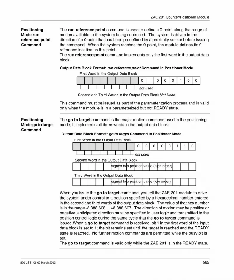
ZAE 201 Counter/Positioner Module
Positioning Mode run reference point Command
The run reference point command is used to define a 0-point along the range of motion available to the system being controlled. The system is driven in the direction of a 0-point that has been predefined by a proximity sensor before issuing the command. When the system reaches the 0-point, the module defines its 0 reference location as this point.The run reference point command implements only the first word in the output data block:
This command must be issued as part of the parameterization process and is valid only when the module is in a parameterized but not READY state.
Positioning Mode go to target Command
The go to target command is the major motion command used in the positioning mode; it implements all three words in the output data block:
When you issue the go to target command, you tell the ZAE 201 module to drive the system under control to a position specified by a hexadecimal number entered in the second and third words of the output data block. The value of that hex number is in the range -8,388,608 ... +8,388,607. The direction of motion may be positive or negative; anticipated direction must be specified in user logic and transmitted to the position control logic during the same cycle that the go to target command is issued.When a go to target command is received, bit 1 in the first word of the input data block is set to 1; the bit remains set until the target is reached and the READY state is reached. No further motion commands are permitted while the busy bit is set.The go to target command is valid only while the ZAE 201 is in the READY state.
0 001000
First Word in the Output Data Block
not used
Output Data Block Format: run reference point Command in Positioner Mode
Second and Third Words in the Output Data Block Not Used
First Word in the Output Data Block
Third Word in the Output Data Block
0 0110000
not used
signed hex position value (high order)
Output Data Block Format: go to target Command in Positioner Mode
signed hex position value (low order)
Second Word in the Output Data Block
890 USE 109 00 March 2003 585

ZAE 201 Counter/Positioner Module
Positioning Mode run reference point + Command
The run reference point + command implements all three words in the output data block:
When you issue the run reference point + command, you tell the ZAE 201 module to drive the system under control in a positive direction to a position specified by a hexadecimal number entered in the second and third words of the output data block. The value of that hex number is in the range -8,388,608 ... +8,388,607. In order for this command to be satisfied, the system under control must be driven through the 0 reference point.The run reference point + command is designed specifically for systems that continually return to the 0 reference point when driven in a positive direction—e.g., a continuous belt-driven machine. In this type of system, where all positions are defined as positive offsets of the predefined 0-point, the command may be used as an alternative to the go to target command for sending the system a target. If, for example, you want to move a system currently located at position 10,000 to target position 5,000, you may proceed to the target in either the positive or negative direction: To proceed in the negative direction, issue the go to target command to target
position 5,000:
First Word in the Output Data Block
Third Word in the Output Data Block
0 101000 0
signed hex position value (high order)
Output Data Block Format: run reference point + Command in Positioner Mode
Second Word in the Output Data Block
signed hex position value (low order)
10,000
0
5,000
586 890 USE 109 00 March 2003

ZAE 201 Counter/Positioner Module
To proceed in the positive direction, issue the run reference point + command to target position 5,000:
In the second case, the run reference point + command moves the system forward to the 0 reference point, resets the count to 0, then continues system movement positively to target position 5,000.When a run reference point + command is received, bit 1 in the first word of the input data block is set to 1; the bit remains set until the target is reached and the READY state is reached. No further motion commands are permitted while the busy bit is set.The run reference point + command is valid only while the ZAE 201 is in the READY state.
10,000
0
5,000
890 USE 109 00 March 2003 587

ZAE 201 Counter/Positioner Module
Example: Using the ZAE 201 Module as a Positioner
Positioning Example
The ZAE 201 module is used to control horizontal positioning in the following example. The system is a process line where printed circuit boards are dipped into a series of four tanks. In the positioning mode, the ZAE 201 carry the PCBs along the process line, position them over each of the four stations, and move them to the unload position at the end of the line. The example treats only the horizontal movement portion of the application; it does not treat vertical dipping motions.
Positioner Example DIP Switch Settings
Set the DIP switches on the back of the module for POSITION mode, 5 Vdc input voltage, and HIGH activity on the count gate:
Limit Switch Dip Tank Process Line
To Unload Bin
A CB D
Cleaning Bath Dryer Acid Bath Dryer
0 20,000 40,00030,00010,000
Gate Count
ActivityOperating Mode
Input Voltage
ON OFFL R
B1
B4
B2
B3
588 890 USE 109 00 March 2003

ZAE 201 Counter/Positioner Module
Positioner Example Traffic Cop Settings
Traffic cop the drop to support the system with the ZAE 201 positioning module with a DAU 202 analog output module and a DAP 220 24 Vdc combo I/O module:
Service Comm DelDrop QuitF1 F2 F3 F4 F5 F6 F7 F8 OFF F9
TRAFFIC COP984-120/130/145 CONTROLLERS
Drop :Number Inputs:
1 ( 1 )56
Rack :Number Outputs:
188
101102103104105
984984DAP220DAU202ZAE201
TypeModule
Slot Input OutputReference Numbers
TypeData
DescriptionModule
PLC-145PLC-1458-IN 8-OUT 24V2 CHANNEL D/APOSITION/HS COUNT
10001 - 10008 00001 - 00008 40150 - 4015130001 - 30003 40101 - 40103
BINBIN
890 USE 109 00 March 2003 589

ZAE 201 Counter/Positioner Module
Positioner Example Field Wiring Diagram
Field wire the two A120 I/O modules like this:
Positioning Example Ladder Logic
The following ladder logic program automatically parameterizes the module upon power-up and then repeatedly directs the motion: Relays 1 and 2 are normally open and provide one-shot responses, since the four
least significant bits in register 40120 are all set to 0 The high order byte value for P1—the distance from the target location at which
the motor drive will begin to slow the process—is expressed in register 40121 as 0
The low order byte value for P1 is expressed in register 40122 as 1,000 The high order byte value for P2—the distance from the target location at which
the motor drive will stop—is expressed in register 40123 as 0 The low order byte value for P2 is expressed in register 40124 as 500 The high order byte value for P3—the acceptable distance from the target
location—is expressed in register 40125 as 0 The low order byte value for P3 is expressed in register 40126 as 250
Positioning Example State RAM Values
The following values, initialized in State RAM, will enable the positioning example to operate using the logic, traffic cop, and module connections as described in the following tables.
24 Vdc24 V Common
Limit Switch
0.1A
DAP 220
Drive Unit withSupply Voltage
DAU 202 ZAE 201
24 Vdc24 V Common
QuadratureEncoder
123456789
10111213141516171819202122
123456789
10111213141516171819202122
1
91011
2345678
12131415161718192021
590 890 USE 109 00 March 2003
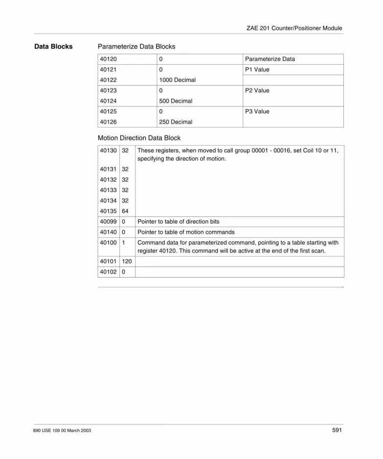
ZAE 201 Counter/Positioner Module
Data Blocks Parameterize Data Blocks
Motion Direction Data Block
40120 0 Parameterize Data
40121 0 P1 Value
40122 1000 Decimal
40123 0 P2 Value
40124 500 Decimal
40125 0 P3 Value
40126 250 Decimal
40130 32 These registers, when moved to call group 00001 - 00016, set Coil 10 or 11, specifying the direction of motion.
40131 32
40132 32
40133 32
40134 32
40135 64
40099 0 Pointer to table of direction bits
40140 0 Pointer to table of motion commands
40100 1 Command data for parameterized command, pointing to a table starting with register 40120. This command will be active at the end of the first scan.
40101 120
40102 0
890 USE 109 00 March 2003 591

ZAE 201 Counter/Positioner Module
Motor Speed, Direction, Motion Commands
Motor Speed And Direction Values
Motion Command Table
Positioning Example Network Diagrams
In the example shown here, the HOME proximity switch is simulated by disabling Coil 00001 and momentarily forcing it ON and then OFF, while the Run Reference Point command is being executed. This toggles the FKE input to the ZAE 201 via the DAP 220.
40160 4096 (+10 V) One of these values is moved to register 40150, which is I/O mapped to the DAU 202. The output of the DAU 202 will control the motor speed and direction. NOTE: The specific values used here are application-dependent.
40161 3072 (+5 V)
40162 2048 0
40163 1024 (-5 V)
40164 0 (-10 V)
40200 4 Run reference point command data
40201 0
40202 0
40203 6 Move to position 10,000 command data
40204 0
40205 2710 Hex
40206 6
40207 0 20,000
40208 4E20 Hex
40209 6
40210 0 30,000
40211 7530 Hex
40212 6
40213 0 40,000
40214 9C40 Hex
40215 6
40216 0 0
40217 0
592 890 USE 109 00 March 2003

ZAE 201 Counter/Positioner Module
Networks 1 and 2 The following diagram describes Networks 1 and 2.
NETWORK 1
1
3001
SENS1
00101
00101
00101
40099
6
SUB40002
0
1
ADD40099
0
0
ADD40100
NETWORK 2
Network 1 monitors the busy bit in status Register 30001.When the bit is on, a motion is in progress. A negativetransition indicates the end of a motion; a positive transitionindicates a new motion has started. If a new motion hasjust started, the command register is cleared. If the motioncommand has just completed, a check is made to see if theend of the motion table has been reached (40099 = 6); ifso, the pointer to the motion table is reset to 1.
Network 2 delays the positioning movement by 5 s after each newposition has been reached. Once the timer has timed out, the newposition values are moved into 40100 ... 40102.
00101
00102
00102
500
T.0140003
40200
40099
TBLK3
40099
1
SUB40140
40130
40140
TBLK1
40141
00001
BLKM1
Also in this network, position pointer 40099 and direction pointer 40140are incremented by 1 as part of the TBLK function block.
890 USE 109 00 March 2003 593

ZAE 201 Counter/Positioner Module
Networks 3 and 4 The following diagram describes Networks 3 and 4.
NETWORK 3
30001
00033
BLKM1
40162
40150
BLKM1
00010 00011 00043 00044
00010 00011 00043 00044
40160
0
SUB40150
40161
0
SUB40150
40163
0
SUB40150
00010 00011 00043 00044
Network 3 controls speed in the positive direction by movingthe value of 30001 to coils 33 ... 49. This is done to monitorbits 10 and 11 of the status word (R1 and R2), which areplaced in coils 43 and 44. When P1 and P2 are reached, thesystem will change speeds appropriately (normal speed to slowspeed, then slow speed to stop). Coils 10 and 11 define thedirection of motion.
The BLKM of registers 40162 ... 40150 assumes no motion willoccur. Subsequent logic sets up the appropriate speed.
Network 4 is similar to Network 3, but controls speed in thenegative direction.
00010 00011 00043 0004440164
0
SUB40150
NETWORK 4
594 890 USE 109 00 March 2003
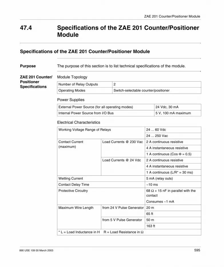
ZAE 201 Counter/Positioner Module
47.4 Specifications of the ZAE 201 Counter/Positioner Module
Specifications of the ZAE 201 Counter/Positioner Module
Purpose The purpose of this section is to list technical specifications of the module.
ZAE 201 Counter/Positioner Specifications
Module Topology
Power Supplies
Electrical Characteristics
Number of Relay Outputs 2
Operating Modes Switch-selectable counter/positioner
External Power Source (for all operating modes) 24 Vdc, 30 mA
Internal Power Source from I/O Bus 5 V, 100 mA maximum
Working Voltage Range of Relays 24 ... 60 Vdc
24 ... 250 Vac
Contact Current (maximum)
Load Currents @ 230 Vac 2 A continuous resistive
4 A instantaneous resistive
1 A continuous (Cos Φ = 0.5)
Load Currents @ 24 Vdc 2 A continuous resistive
4 A instantaneous resistive
1 A continuous (L/R* = 30 ms)
Wetting Current 5 mA (relay outs)
Contact Delay Time ~10 ms
Protective Circuitry 68 Ω + 15 nF in parallel with the contact
Consumes ~1 mA
Maximum Wire Length from 24 V Pulse Generator 20 m
65 ft
from 5 V Pulse Generator 50 m
163 ft
* L = Load Inductance in H R = Load Resistance in Ω
890 USE 109 00 March 2003 595

ZAE 201 Counter/Positioner Module
Input Characteristics
Relay Contact Service Life
I/O Map
Dimensions
Agency Approvals
5 V Input Selection Differential RS-422 12 V peak-to-peak maximum
400 mV peak-to-peak minimum
24 V Input Selection for 1 signal 12 ... 30 V
for 0 signal -2 ... +5 V
Maximum Count Frequency for 5 V input 500 kHz
for 24 V input 50 kHz
PNP Encoder Quadrature type Two-track plus marker signal
Count Gate/Reference Trip 1 = 12 Vdc (min)
0 = 5 Vdc (max)
Encoder Pulse Alignment See diagram below.
Duration > 10 ms
Rise Time N/A
Mechanical Switching Cycles 20,000,000
Electric Switching Cycles (Resistive Load)
@ 230 Vac/0.2 A 10,000,000
@ 230 Vac/0.5 A 7,000,000
@ 30 Vdc/2 A, clamping diode 8,000,000 (typical)
@ 60 Vdc/1 A with clamping diode
1,000,000 typical
3,000,000 maximum
3000 cycles/hr maximum
Electric Switching Cycles (Inductive Load, Cos Φ = 0.5)
@ 230 Vac/ 0.5 A 5,000,000
Register 3x/4x 3 in/3 out
W x H x D 40.3 x 145 x 117.5 mm
1.6 x 5.6 x 4.5 in
Weight 300 g
0.7 lb
VDE 0160; UL 508; CSA 22.2 No.142; and FM Class I, Div 2 Standards
596 890 USE 109 00 March 2003

ZAE 201 Counter/Positioner Module
Pulse Alignment of Encoders Used with the ZAE 201 Module
Encoders used with the ZAE 201 module should be ordered with the alignment of A, B and Z pulses as shown below.
A
B
IndexZ
Encoders used with the ZAE-201 module should be ordered withthe alignment of A, B + Z pulses as shown above.
890 USE 109 00 March 2003 597

ZAE 201 Counter/Positioner Module
598 890 USE 109 00 March 2003

890 USE 109 00 March 2003
Overview of the ZAE 204 High-Speed Counter Module
At a Glance
Purpose The purpose of this chapter is to describe the ZAE 204 High-Speed Counter Module.
What’s in this Chapter?
This chapter contains the following topics:
WARNING
Compatibility
The ZAE 204 module will only operate properly when used with an A984, E984, or Micro 512/612 controller.
Failure to follow this precaution can result in death, serious injury, or equipment damage.
Topic Page
What is the ZAE 204 High-Speed Counter Module? 600
Operating and Display Elements of the ZAE 204 High-Speed Counter Module 602
Configuration of the ZAE 204 High-Speed Counter Module 603
Example Field Connections and Signal Addresses for the ZAE 204 Module 606
Output Register Formats of the ZAE 204 Module 609
Input Register Formats of the ZAE 204 Module 614
Operation of the ZAE 204 Module 617
Specifications of the ZAE 204 High-Speed Counting Module 619
599

ZAE 204
What is the ZAE 204 High-Speed Counter Module?
Brief Product Overview
The ZAE 204 is a high speed counter module with the following characteristics: Four counter inputs for counting 5 Vdc (TTL) and 24 Vdc pulses; a counting range
of 5 decades; and a counting frequency of up to 1 kHz (channel 1 can operate up to 10 kHz)
Four 24 Vdc count enable inputs Four 24 Vdc semiconductor output switches, 0.5 A each, with short circuit/
overload protection and hardware resetPower required by the module is: 5 Vdc via the internal I/O bus 24 Vdc external supply for 24 V counting inputs, outputs, and enable inputsThe ZAE 204 can be installed in any slot in the A120 subracks (DTA 200, 201, and 202). The module has bus contacts at the rear and field connections on the front. The blank label, which fits in the module cover, can be filled in with relevant information (signal values, etc.) in the spaces provided. Refer to ZAE 204 Diagram, p. 601 below.The ZAE 204 is made up of 4 independent counters for the following modes: Event counter Repeat counter Differential counterThe above operating modes and the parameters required for them are preset by the user program. See Operation of the ZAE 204 Module, p. 617 for a description of these modes.
600 890 USE 109 00 March 2003

ZAE 204
ZAE 204 Diagram Any output that is overloaded or short-circuited is switched OFF, and is indicated by the amber fault LED (see next section (See Operating and Display Elements of the ZAE 204 High-Speed Counter Module, p. 602)). Correction is made by use of the RESET button as shown in the front view and label diagram below.
ZAE 204
RESETPUSHBUTTON
ZAE 204
U
Input
2
TTL
1
TTL
3
TTL
4
TTL
Mready U
1
23
4
1
2
3
4
M
card
Out
put
Gat
e
1
2
3
4
56
8
9
10
11
7
12
13
14
15
1617
19
20
21
22
18
890 USE 109 00 March 2003 601

ZAE 204
Operating and Display Elements of the ZAE 204 High-Speed Counter Module
ZAE 204 LEDs The ZAE 204 has eleven LEDs on the front of the module. From top to bottom, they are:
The RESET button is used to restore the operation of an output switch after the overload condition has been removed.
Color Type Function
Green Power External 24 Vdc—when lit, power ON; when off, power OFF
Green Ready When lit, indicates firmware initialization is complete and module is ready for service; when off, indicates start-up functions are not complete and module is not yet ready.Note: The PLC must be running for this LED to illuminate.
Amber Fault Indicates the presence of an overload or short-circuit at one or several output points. When lit, indicates an overload or short circuit; when off, no faults detected.
Red Output 1 ... 4 Located opposite terminal screws 14 ... 17. When lit, these LEDs indicate that the outputs are ON.
Red Gate 1 ...4 Located opposite terminal screws 18 ... 21. When lit, these LEDs indicate that the enable inputs (function gate) have a high signal level voltage applied to them.
602 890 USE 109 00 March 2003

ZAE 204
Configuration of the ZAE 204 High-Speed Counter Module
ZAE 204 Configuration Overview
The ZAE2 04 contains four independent 16–bit 1 kHz counters. In addition, channel 1 can be programmed to accept up to 10 kHz inputs. The ZAE 204 has several modes of operation. It can operate as four independent up or down counters, either one time or repetitively. Alternatively, channels 1 and 2 and/or channels 3 and 4 can operate together as differential counters. In this mode, a single count value is maintained for channel pairs.For the channel 1, 2 pair, input pulses at the channel 1 field connector cause this count value to increase, and input pulses at channel 2 cause the count value to decrease. The differential count value for the channel 1, 2 pair are returned to the location normally associated with channel 1. The channel 3, 4 pair works in a similar manner.An output is provided for each channel (pins 14 ... 17) to signal when the accumulated count at a particular channel has reached its programmed target, counted up to or counted down from 0. An input signal (pins 18 ... 21) is provided for each channel to enable the counting operation. The accumulation of counts on any channel can be controlled through the state of the enable input to the appropriate pin.
890 USE 109 00 March 2003 603

ZAE 204
ZAE 204 Field Side Connections
The module must be traffic copped as six 3x input registers and one 4x output register, as shown in the following field side connections diagram.
ZAE 204
Module power, 24 Vdc typical
Internally connected to Pin 1Input pulses for Channel 1 (24 Vdc)
Input pulses for Channel 1 (5 Vdc)
Input pulses for Channel 2 (24 Vdc) Input pulses for Channel 2 (5 Vdc)
Input pulses for Channel 3 (24 Vdc)Input pulses for Channel 3 (5 Vdc)
Input pulses for Channel 4 (24 Vdc)Input pulses for Channel 4 (5 Vdc)
Ground
Internally connected to Pin 1
Internally connected to Pin 1
Target count signal for Channel 1 (output)
Target count signal for Channel 2 (output)
Target count signal for Channel 3 (output)
Target count signal for Channel 4 (output)
Count control (count gate enable) for Channel 1 (input)
Count control (court gate enable) for Channel 2 (input)
Count control (count gate enable) for Channel 3 (input)
Count control (count gate enable) for Channel 4 (input)
Internally connected to Pin 11
1
2
3
4
5
6
7
8
9
10
11
12
13
14
15
16
17
18
19
20
21
22
604 890 USE 109 00 March 2003
ZAE 204
ZAE 204 Cabling Shielded, twisted pair cable (2 or 4 x 0.5 mm/channel) should be used. All channels can be connected with a common shielded cable. The maximum cable length is 100 m.
Connect shield to ground (GND) on one side with a short cable (< 8 in). Observe a minimum distance of 20 in between the module and power lines or
other sources of electrical disturbance.
890 USE 109 00 March 2003 605

ZAE 204
Example Field Connections and Signal Addresses for the ZAE 204 Module
Field Connection Diagrams
Three examples of ZAE 204 connections are provided: 5 V inputs (see 5 V Inputs Connection Example, p. 606); 5 V inputs on a noisy system (see 5 V Inputs, High Interference Connection
Example, p. 607); 24 V inputs (see 24 V Inputs Connection Example, p. 608).
5 V Inputs Connection Example
Example connections for 5 V inputs are shown below.
Note: Detailed Compact 984 cabling and installation instructions are found in the 984-A120 Compact Programmable Controllers User Guide (GM-A984-PCS).
5V
TTL
E1
E2
E3
E4
COM
24V
1
2
3
4
5
6
7
8
9
10
11
12
13
14
15
16
17
18
19
20
21
22
A1
A2
A3
A4
01
02
03
04
COM
606 890 USE 109 00 March 2003

ZAE 204
5 V Inputs, High Interference Connection Example
Example connections for 5 V inputs, on a system with a high interference level, are shown below.
24V Filtered
5V
TTL
COM
E1
E2
E3
E4
24V
COM
A1
A2
A3
A4
01
02
03
04
1
2
3
4
5
6
7
8
9
10
11
12
13
14
15
16
18
19
20
21
22
17
890 USE 109 00 March 2003 607

ZAE 204
24 V Inputs Connection Example
Example connections for 24 V inputs are shown below.
24VDC
24V
COM
E1
E2
E3
E4
COM
A1
A2
A3
A4
01
02
03
04
1
2
3
4
5
6
7
8
9
10
11
12
13
14
15
16
17
18
19
20
21
22
608 890 USE 109 00 March 2003

ZAE 204
Output Register Formats of the ZAE 204 Module
Overview The ZAE 204 is traffic copped for set up through a single 4YYYY word (BIN register). The content of this word is interpreted as a pointer to the first of eight 4x registers that contain the programmable operating parameters for each of the four counter channels. The format, of the eight words pointed to, appears in the following graphic, which shows the output register format for the ZAE 204 module.
I/O MAPREGISTER
40YYY XXX DATA = POINTER VALUE
MEMORY REGISTER DATA
COUNTER 1 MODE
COUNTER 2 MODE
COUNTER 3 MODE
COUNTER 4 MODE
COUNTER 4 TARGET
COUNTER 3 TARGET
COUNTER 2 TARGET
COUNTER 1 TARGET
4x
4x + 1
4x + 2
4x = 3
4x + 4
4x + 5
4x + 6
4x + 7
890 USE 109 00 March 2003 609

ZAE 204
The following figure shows the bits in the ZAE 204 mode control word and their meanings.
The target value is used in several ways. When up counting, the target value is the count at which the target value output for a channel will be on. When down counting, the target value is the value from which the counter counts down to zero. See Operating and Display Elements of the ZAE 204 High-Speed Counter Module, p. 602 for a more complete description.
15 14 13 12 11 10 9 8 7 6 5 4 3 2 1 0
[15-9] Not Used
[8] Mode set, must be toggled (setand then reset) to input the mode
control word data.[7] Not used.
[6] If set, requests counting up; otherwise,down counting.
[5] Defines the active level of “count achievedtarget” signal for the channel associated with this
request. If set = 1, target count output goes lowwhen count is achieved; if set = 0, target count goes
high when count is achieved.
[4] Defines the active level of “count gate” for the channelassociated with this request. If set, a high gate input allows
counting.
[3] If set, negative edge transitions are counted on thechannel associated with this request. N/A for 10kHz counts
[2] If set, requests operation at 10 kHz (only valid for Channel 1).
[1] If set, requests that the channel associated with this request and thenext channel operate in differential mode (only valid for channels 1 and 3).
[0] If set, requests repetitive counting; if = 0, continuous count.
MODE CONTROL WORD
610 890 USE 109 00 March 2003

ZAE 204
Caution
CAUTION
Chance of Incorrect Health Status Indication
Caution:Modicon 984 PLCs assert IORST, the I/O bus reset, when in STOP mode. This signal halts operation of the ZAE 204 internal microprocessor by forcing it to a reset condition. When I/O Mapping as required in STOP mode, the module will be indicated unhealthy by an asterisk in the I/O module display, and the module description will incorrectly read, "B8 ". This does not affect I/O Mapping, which may proceed as usual. When using a STAT block, module health is properly indicated when Executive Prom Combination #1003 or greater is installed in the 984. Parameters will have to be loaded (or reloaded) after going into RUN from STOP mode, and that 3x register data will be zeroed when going from STOP to RUN. Refer to the next figure (See ZAE 204 RUN/STOP Mode, p. 612).
Failure to follow this precaution can result in injury or equipment damage.
890 USE 109 00 March 2003 611

ZAE 204
ZAE 204 RUN/STOP Mode
To ensure that the ZAE 204 parameters are loaded after the PLC is set to RUN from STOP mode, the ZAE 204 RUN/STOP mode user logic, shown below, may be used..
NETWORK #1 / SEGMENT #1
0003
0003
0001
10
T.0140XXX
40YYY CTR 1 Mode40YYY + 1 CTR 1 Target40YYY + 2 CTR 2 Mode40YYY + 3 CTR 2 Target40YYY + 4 CTR 3 Mode40YYY + 5 CTR 3 Target40YYY + 6 CTR 4 Mode40YYY + 7 CTR 4 Target
NETWORK #2 / SEGMENT #1
P0001
40YYY
40ZZZ
MBIT 1
0002
N0002
MBIT 1
MBIT 1
MBIT 1
40ZZZ 40ZZZ+2 40ZZZ+4 40ZZZ+6
0008 0008 0008 0008
BLKM 8
612 890 USE 109 00 March 2003

ZAE 204
Operation of Networks in the RUN/STOP Mode User Logic Diagram
On the first scan, the timer in Network 1 is set to zero. The next scan starts the timer, set for 100 ms. When it times out, the output comes on and will activate the BLKM through the positive transition contact referenced to Coil 1. The values of the 8 fixed 40YYY registers are block moved into 8 40ZZZ registers, which is a table pointed to by the contents of the I/O mapped output register. These registers contain the mode and target data for the module. The mode registers in the 40YYY table must have bit 8 set to 1, as required, to load the parameters into the ZAE 204. On the following scan after the BLKM is solved, coil 2 goes OFF. Power is then passed through the negative transitional to the MBIT blocks, which set bit 8 to zero in each mode control register in the 40ZZZ table. When this is done, the module is ready to accept counts from external pulse generators.
890 USE 109 00 March 2003 613
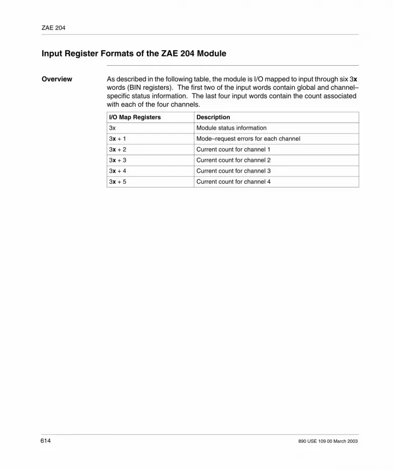
ZAE 204
Input Register Formats of the ZAE 204 Module
Overview As described in the following table, the module is I/O mapped to input through six 3x words (BIN registers). The first two of the input words contain global and channel–specific status information. The last four input words contain the count associated with each of the four channels.
I/O Map Registers Description
3x Module status information
3x + 1 Mode–request errors for each channel
3x + 2 Current count for channel 1
3x + 3 Current count for channel 2
3x + 4 Current count for channel 3
3x + 5 Current count for channel 4
614 890 USE 109 00 March 2003

ZAE 204
The following figure shows the meanings of the bits in the ZAE 204 RUN/STOP first input word..
The format for the second input word is:
15 14 13 12 11 10 9 8 7 6 5 4 3 2 1 0
[15] If set, indicates that communication with the module is nolonger possible. To correct, power cycle the module.
[14] If set, indicates that the module is unhealthy. The PLC has read thewrong personality in the slot I/O mapped to this module.
[13] If set, indicates that the pointer to the output data table is invalid.
[12] If set, indicates an overload of module output signals.
[11] If set, indicates that the input counts toChannel 4 have exceeded the target count.
[10] If set, indicates that the input counts to Channel3 have exceeded the target count.
[9] If set, indicates that the input counts toChannel 2 have exceeded the target count.
[8] If set, indicates that the input counts toChannel 1 have exceeded the target count.
[7] Signals when Channel 4 counterhas reached the target count.
[6] Signals when Channel 3 counterhas reached the target count.
[5] Signals when Channel 2 counterhas reached the target count.
[4] Signals when Channel 1 counterhas reached the target count.
[3] If set, indicates that the count gateinput for Channel 4 is 12 - 30 V.[2] If set, indicates that the count gate
input for Channel 3 is 12 - 30 V.[1] If set, indicates that the count gate
input for Channel 2 is 12 - 30 V.
[0] If set, indicates that the count gateinput for Channel 1 is 12 - 30 V.
FIRST INPUT WORD
15 14 13 12 11 10 9 8 7 6 5 4 3 2 1 0
Report error codefor Channel 4.
Report error codefor Channel 3.
Report error codefor Channel 2.
Report error codefor Channel 1.
SECOND INPUT WORD
890 USE 109 00 March 2003 615

ZAE 204
Each nibble of the second word contains a single digit identifying the type of error found while trying to program the module with the user instruction provided for that channel. The meaning of the error codes is as follows:
Error Code Meaning
0 No error
1 Differential and 10kHz operation requested on channel 1
2 Differential and repetitive mode requested on channels 1 or 3
3 10 kHz operation requested on channels 2, 3, or 4
4 Mode change requested on channels 2 or 4 while channels 1 or 3 (respectively) are set to differential operation
5 Differential operation requested on channels 2 or 4
6 An invalid target value has been specified
616 890 USE 109 00 March 2003
ZAE 204
Operation of the ZAE 204 Module
Overview The operation of the ZAE 204 is controlled through the 4x register output table (see Output Register Formats of the ZAE 204 Module, p. 609. To control the operation of the module through user logic, the logic must be designed to set up the desired operating mode and then toggle the mode change bit (bit 8) in the mode control word for a particular channel for one scan.If the bit is not cleared after one scan, the driver will continually attempt to change modes and reset the module (and count) based on the selected mode, thus not allowing the module to operate. Having set the desired mode of operation, the actual counting begins when the active level of the count gate for a channel based on bit 4 of the control word is asserted on the input terminal for the channel (pins 18 ... 21).An LED is associated with each of the count gate terminals (described previously) that will illuminate when the count gate has 24 V applied. If the count gate is deasserted, the counting is temporarily suspended until it is once again asserted. When a count operation is completed (count equals target or 0), the status bit in the first input word for that channel (bits 4 ... 7) is set. In addition, the signal on the output pin for the channel (pin 14 ... 17) is asserted to a level based in the state of bit 5 of the control word for the channel. An LED is associated with the output pin (described previously) that will illuminate. The ZAE 204 will continue to accumulate counts even though the count target has been reached. If this occurs it will be indicated by one of bits 8 ... 11 being set in the first input word depending on the particular channel.The actual operation of the module depends on the mode of operation chosen. The operating mode is chosen by the state of bits 0 ... 7 of the mode control word. However, all combinations of these bits are not allowed. Invalid combinations are sensed and reported in the second input word. The following describes the operation in each of the allowed modes.
One–time Operation
This is the default operation obtained by clearing all mode bits (0 ... 7) of the control word. In this mode, the module will count up or down (see bit 6 of the control word) once, and when the target value or 0 is reached, the input status and discrete outputs will reflect this. The module will continue to accumulate counts after this occurs. The counting process can be restarted by deasserting and reasserting the count gate input for the channel in question. In this mode, the maximum target value allowed is 32767.
Repetitive Operation
This mode is activated by setting bit 0 of the control word for the channel in question. This mode is similar to one-time operation except that the count process restarts when the target value is reached. The target achieved signal in the status input, the output discrete, and the LED are asserted and remain so for 25% of the next count cycle, or 20 ms minimum. In this mode, the maximum target value allowed is 32767.
890 USE 109 00 March 2003 617

ZAE 204
Differential Counter
This mode applies to channels 1 and 3 only and is activated by setting bit 1 in the control word. If differential mode is selected for channel 1, channels 1 and 2 operate together, and the accumulated count value is reported in the channel 1 input counter ( 3x + 2). In this mode, the pulses input to the channel 1 input increment the count, while those input to channel 2 decrement the count. This mode is only available to be programmed in channels 1 or 3. When differential mode is selected for Channel 3, Channels 3 and 4 operate together.The accumulated count value is reported in the Channel 3 input counter (3x + 4). Any attempt to use this mode in channels 2 or 4 will result in an error. Additionally, if a mode change to channel 2 or 4 is requested while channels 1 or 3 respectively are set to differential mode, an error will be reported. Selection of up or down counting (bit 6 of the control word) has no effect in this mode. The counting range is from -32767 ... +32768.
10 kHz Count In Channel 1
The default operation of the module is to accept input pulses at a maximum of 1 kHz. For channel 1 only, an option is available to accept up to 10 kHz pulses. This option is chosen by setting bit 2 of the control word for channel 1 to a 1. Choosing this option for any other channel will result in an error. Differential mode is not allowed. Only the 5 V input can be used, and only negative edge transitions are counted.
Note: If set to one–time operation, the counter associated with channel 1 will not continue to accumulate counts after target is reached.
618 890 USE 109 00 March 2003

ZAE 204
Specifications of the ZAE 204 High-Speed Counting Module
ZAE 204 Module Topology
The following table describes the module topology.
ZAE 204 Power Supplies
Power supply details:
ZAE 204 Counter Inputs
Counter input details
Number of Counting Inputs 4
Number of 24 Vdc Outputs 4
Number of Enable Inputs 4
Operating Mode High Speed Counter
Isolation Opto–coupler on each field point
External Power Source Load 24 Vdc Count Inputs, 25 mA maximum
Gate Inputs, 30 mA maximum
Outputs, 1 A maximum
5 Vdc Count Inputs, 10 mA maximum
Internal Power Source Load from I/O bus maximum 5 V, 100 mA
typical 75 mA
Quantity 4 for input pulses with 5 Vdc (TTL) or 24 Vdc
Signal Level at 5 V (TTL)
ON signal >= 2.3 V
OFF signal 0 ... 1 V
Input Current <= 2.5 mA each at 0 V (current sink)
Signal Level at 24 V (TTL)
ON signal 12 ... 30 V
OFF signal -2 ... +5 V
Input Current (current source) < 6 mA each at 30 V
Minimum 0 Pulse Width 0.35 ms
Allowable Mark-space Ratio 65/35 percent maximum
Counting range 0 ... 32,767 or -32,768 ... 0 ... +32,767, depending on operating mode
Counting Frequency 1 kHz maximum
Input 1 with 5 V pulses 10 kHz maximum
890 USE 109 00 March 2003 619

ZAE 204
ZAE 204 Enable Inputs (Gate)
Enable input details:
ZAE 204 Semiconductor Outputs
Semiconductor output details:
ZAE 204 Operating Frequency
Operating fequency details:
ZAE 204 I/O Map Register detail:
Quantity 4
Rated Signal Value 24 V
Signal Level HIGH Signal 12 ... 30 V
LOW signal -2 ... +5 V
Input Current 7 mA @ 24 V
Input Delay (contact bounce suppression) 4 ms
Input Rise Time N/A
Quantity 4
Working Voltage V US = 24 Vdc
Signal Language True High
Signal Output Level ON VS = 0 ... + 2 V
OFF 0 ... 2 V, < 1 mA
US = 20 ... 30 Vdc
Load Current/Output 500 mA maximum
Load Current for All Outputs 1 A maximum
Switching Delay < 1 ms
Power Dissipation 1.25 W
Inrush Current for Lamps 5 W maximum
Resistive Load 100/s
Inductive Load @ 500 mA 1000/hr
Bulb Load @ 1.2 W 8/s
@ 5 W 1000/hr
Registers 3x/4x 6 in/1 out
620 890 USE 109 00 March 2003

ZAE 204
Dimensions Dimensions details:
ZAE 204 Agency Approvals
Agency Approval details:
W x H x D mm 40.3 x 145 x 117.5
in 1.6 x 5.6 x 4.5
Weight g 300
lb 0.7
VDE 0160; UL 508; CSA 22.2 No. 142 and FM Class I, Div 2 Standards.
890 USE 109 00 March 2003 621

ZAE 204
622 890 USE 109 00 March 2003

Appendices
At a Glance
Purpose The following chapters contain material related to A120 I/O modules.
What’s in this Appendix?
The appendix contains the following chapters:
Chapter Chapter Name Page
A IEC Wiring Diagrams for A120 I/O Modules 625
B I/O Configuration with Concept 671
C I/O Configuration of A120 Series I/O Modules with Modsoft 745
D Modsoft Application Examples for Selected A120 Series I/O Modules
753
E A120 Option Modules 769
F Requirements for CE Compliance 779
G Technical Assistance 789
890 USE 109 00 March 2003 623

Appendices
624 890 USE 109 00 March 2003

890 USE 109 00 March 2003
IEC Wiring Diagrams for A120 I/O Modules
At a Glance
Introduction This chapter provides IEC-compliant wiring diagrams for the A120 Series I/O modules.
What’s in this Chapter?
This chapter contains the following topics:
Topic Page
IEC Nomenclature Legend 626
IEC Wiring Diagrams for A120 Modules 627
625

IEC Wiring Diagrams
IEC Nomenclature Legend
Legend The following table describes the IEC nomenclature used in the IEC wiring diagrams.
Nomenclature Description
U Voltage
I Current
M Common
PE Ground
L 230Vac or hot
US 24Vdc
UB Supply voltage for modules
US Working voltage for activating the actuators
N1 Supply 1
N2 Supply 2
E1 Input 1
A1 Output 1
EW1 Input 1 wiring
AW1 Output 1 wiring
F1 Automatic circuit breaker 1 or fuse
C1 Capacitor 1
V1 Isolation diode 1
R1 Resistor 1
G Gate
626 890 USE 109 00 March 2003

IEC Wiring Diagrams
IEC Wiring Diagrams for A120 Modules
Overview The following diagrams are IEC-compliant versions of the A120 diagrams shown throughout this manual.
ADU 204 IEC Wiring Diagram
The following figure is the IEC wiring diagram for the ADU 204.
U
U
U
U4
3
PT
100
PT
100
PT
100
PT
100
2
1
345678910
1415161718192021
1
2
3
4
123456789
10111213141516171819202122
890 USE 109 00 March 2003 627
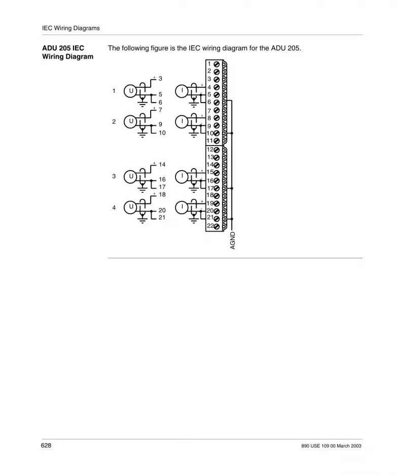
IEC Wiring Diagrams
ADU 205 IEC Wiring Diagram
The following figure is the IEC wiring diagram for the ADU 205.
U
U
U
U I
I
I
I1
2
3
4
3
567
910
14
161718
2021
AG
ND
123456
78910111213141516171819202122
628 890 USE 109 00 March 2003

IEC Wiring Diagrams
ADU 206 IEC Wiring Diagram
The following figure is the IEC wiring diagram for the ADU 206.
I
I
I
IU
U
U
U1
2
3
4
345678910
151617
192021
0.16A
UBM2
123456789
1011
1213141516171819202122
* For current inputs pleaseuse the enclosed Jumpers.jumpers
890 USE 109 00 March 2003 629

IEC Wiring Diagrams
ADU 210 IEC Wiring Diagram
The following figure is the IEC wiring diagram for the ADU 210.
I
I
I
I
U
U
U
U1
2
3
4
3456
78910
151617
192021
0.16A
+24 VDCCommon
123456789
10111213141516171819202122
* Apply Jumpers to select20mA range per channel.
630 890 USE 109 00 March 2003

IEC Wiring Diagrams
ADU 211/212 IEC Wiring Diagrams
The five figures that follow are all ADU 211/212 IEC wiring diagrams.The following figure is an ADU 211/212 IEC wiring diagram.
U
U
Ch 1
Ch 4
Ch 5
Ch 8
0.5 A Slo-Blo Recommended
+ 24 VDC (AS-BADU211 ONLY)24 V Common (AS-BADU211 ONLY)
Group 1 showingVoltageConfiguration
Group 2 showingThermocouple Configuration with OpenCircuit Detection
12345678910111213141415171819202122
890 USE 109 00 March 2003 631

IEC Wiring Diagrams
The following figure is an ADU 211/212 IEC wiring diagram.
TC
Optional thermistorfor both groupsexternal ColdJunctionCompensation(Betatherm 10K3A1or equivalent)
Ch 5
Ch 8
Ch 5
Ch 8
Group 2 showingThermocoupleConfigurationwith External CJCand Open Thermocouple
Group 1 showingThermocouplewith External CJCConfiguration
0.5 A Slo-Blo Recommended
+24 VDC (AS-BADU211 ONLY)+24 V Common (AS-BADU211 ONLY)
123456789
10111213141516171819202122 Detection
632 890 USE 109 00 March 2003

IEC Wiring Diagrams
The following figure is an ADU 211/212 IEC wiring diagram.
The following figure is an ADU 211/212 IEC wiring diagram.
+ 24 VDC (AS-BADU211 ONLY)24 V Common (AS-BADU211 ONLY)
0.5 A Slo-Blo Recommended
sencesence
ExcitationExcitation
Ch 5
Ch 8
Group 1 showingthree-wire RTDConfiguration
Group 2 showingThermocoupleConfiguration
123456789
10111213141516171819202122
+ 24 VDC (AS-BADU211 ONLY)24 V Common (AS-BADU211 ONLY)
0.5 A Slo-Blo Recommended
sencesence
ExcitationExcitation
sencesence
ExcitationExcitation
Group 1 showingtwo-wire RTDConfiguration
123456789
10111213141516171819202122
Group 2 showingthree-wire RTDConfiguration
890 USE 109 00 March 2003 633

IEC Wiring Diagrams
The following figure is an ADU 211/212 IEC wiring diagram.
+ 24 VDC (AS-BADU211 ONLY)24 V Common (AS-BADU211 ONLY)
0.5 A Slo-Blo Recommended
Ch 1
Ch 4
1
1
sencesence
Excitation
Group 1 showingCurrent Configuration
123456789
10111213141516171819202122
Group 2 showingfour-wire RTDConfiguration
634 890 USE 109 00 March 2003

IEC Wiring Diagrams
ADU 214 IEC Wiring Diagram
The following figure is the IEC wiring diagram for the ADU 214.
UBM2
0.16A
3)
2
4
1)
1)0 ... 10 Ohm
345678910
1
3
UU
I U2)
2
4
12
4
6
8
10
121314
16
18
20
22
8
U I5
I
82)
1) Resistance temperature detector Pt 100 ... 1000, Ni 100 ... 1000 or remote resistance detector 0 ... 2000 Ohm2) External reference resistance 50 or 100 Ohm, 0.1%, 0.125 W, Tk 253) See Voltage and Current measuring4) The common reference point “AGND” is internally connected to 0 V (reference potential of PLC).
2)
2)
6
7
3
5
7
9
11
15
17
19
21
890 USE 109 00 March 2003 635

IEC Wiring Diagrams
ADU 216 IEC Wiring Diagram
The following figure is the IEC wiring diagram for the ADU 216.
ADU 257 IEC Wiring Diagram
The following figure is the IEC wiring diagram for the ADU 257.
Equalizing lineCold junction
Cu-conductorADU 216
1
3
2
4
5
7A
D59
2
123456789
1011121314
16
18
20
22
6
8
15
17
19
21
AD592
Thermocouple
Voltage
RTD or Resistor
+CJC-CJC
3 Wire Connection
2 Wire Connection
4 Wire Connection
123456789
1011121314
16
18
20
22
+
+
15
17
19
21
636 890 USE 109 00 March 2003

IEC Wiring Diagrams
DAO 216 IEC Wiring Diagram
The following figure is the IEC wiring diagram for the DAO 216.
US = 24 VDC
M2
4A
Q1
Q8
Q9
Q16
123456789
101112131415161718192021
* Terminal 11 should be connected in the shortest possible way to thefunctional earth (hat rail). In case of connection failure compensatingcurrents can occur via M2→ 0 V path. These lead to the destruction ofthe protective resistor (R31).
22
890 USE 109 00 March 2003 637

IEC Wiring Diagrams
DAP 204 IEC Wiring Diagram
The following figure is the IEC wiring diagram for the DAP 204.
US = 24 ... 110 VDC / L = 24 ... 230 VACM4/NUB = 24 VDCM2
4 A
4 A 0.16 A
Q1
Q2
Q4
123456789
1011121314
16
18
20
22
638 890 USE 109 00 March 2003

IEC Wiring Diagrams
DAP 208 IEC Wiring Diagram
The following figure is IEC wiring diagram for the DAP 208.
US = 24 ... 110 VDC / L = 24 ... 230 VACM4/NUB = 24 VDCM2
4 A
4 A
4 A
4 A
0.16A
Q1
Q2
Q3
Q4
Q5
Q6
Q7
Q8
123456789
10111213141516171819202122
890 USE 109 00 March 2003 639

IEC Wiring Diagrams
DAP 210 IEC Wiring Diagram
The following figure is IEC wiring diagram for the DAP 210.
L = 24 ... 230 VACN
Q1
Q2
Q4
Q3
123456789
1011121314
16
18
20
22
640 890 USE 109 00 March 2003

IEC Wiring Diagrams
DAP 211 IEC Wiring Diagram
The following figure is the IEC wiring diagram for the DAP 211. Note that this diagram is for Voted (Dual) applications only. See DAP 211 Combined I/O Module Field Wiring, p. 259for more information.
DAP 211
DAP 211
L
N
F
L
LINAUX
OUTIN
OUT
LINAUX
OUTIN
OUT
OUT
OUT
OUT
OUT
IN
IN
IN
IN
I/O-1
I/O-2
I/O-1
I/O-2
123456789
1011
1213141516171819202122
890 USE 109 00 March 2003 641

IEC Wiring Diagrams
DAP 212 and DAP 292 IEC Wiring Diagram
The following figure is the IEC wiring diagram for the DAP 212 and the DAP 292.
US = 24 ... 110 VDC / L = 24 ... 230 VACM4/NUB2 = 24 VDCM2UB1 = 24 VDC at DAP 212; UB1 = 60 VDC at DAP 292M1
0.16
A
4 A
4 A 0.16A
Q1
Q2
Q3
Q4
11
123456789
1011121314
16
18
20
22
18
15
17
19
21
642 890 USE 109 00 March 2003
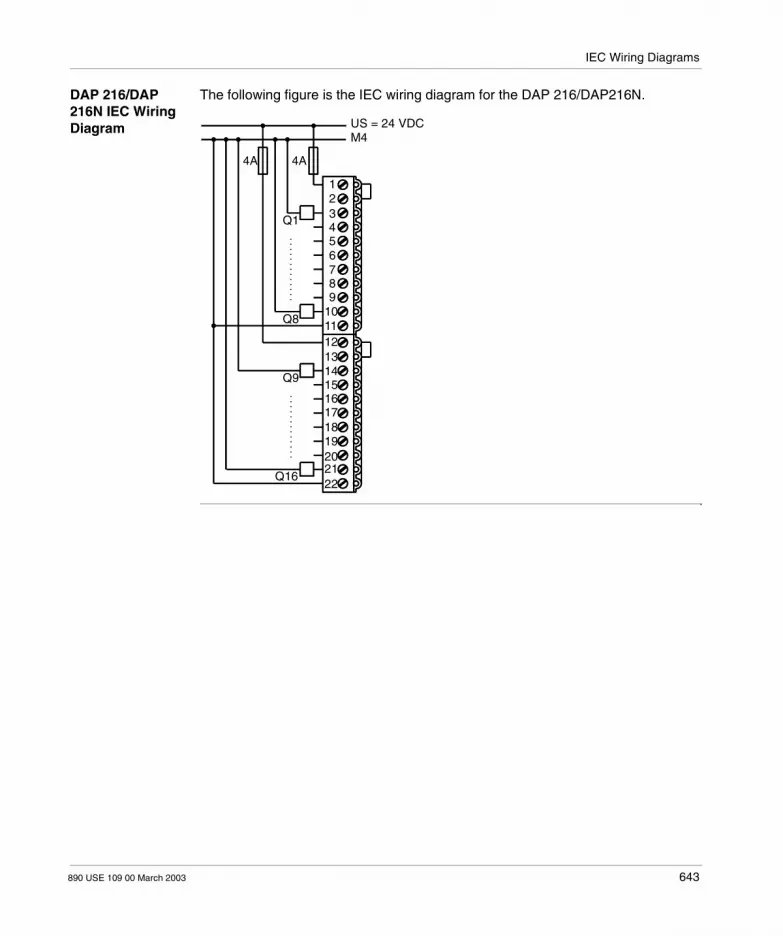
IEC Wiring Diagrams
DAP 216/DAP 216N IEC Wiring Diagram
The following figure is the IEC wiring diagram for the DAP 216/DAP216N.
US = 24 VDCM4
4A 4A
Q1
Q8
Q9
Q16
123456789
1011121314
16
18
20
22
. . .
. . .
. . .
. . .
. . .
. . .
. . .
. . .
. .
15
17
19
21
890 USE 109 00 March 2003 643

IEC Wiring Diagrams
DAP 217 IEC Wiring Diagram
The following figure is the IEC wiring diagram for the DAP 217.
US = 5 ... 24 VDCM4
1 A 1 A
A1
A8
A9
A16
123456789
1011121314
16
18
20
22
15
17
19
21
644 890 USE 109 00 March 2003

IEC Wiring Diagrams
DAP 218 IEC Wiring Diagram
The following figure is the IEC wiring diagram for the DAP 218.
L = 24 ... 115 VACN
Q1
Q8
Q16
. . .
. . .
. . .
. . .
.
1234567891011
121314
16
18
20
22
Q9 15
17
19
21
890 USE 109 00 March 2003 645

IEC Wiring Diagrams
DAP 220 IEC Wiring Diagram
The following figure is the IEC wiring diagram for the DAP 220.
US = 24 VDCM4UB = 24 VDCM1
0.16
A
10 A
Q1
Q8
I1
123456789
1011121314
16
18
20
22
18
15
17
19
21
646 890 USE 109 00 March 2003

IEC Wiring Diagrams
DAP 252 IEC Wiring Diagram
The following figure is the IEC wiring diagram for the DAP 252.
US = 24 ... 110 VDC / L = 24 ... 230 VACM4/NUB2 = 22 VDCM2UB1 = 24 VDCM1
0.16
A
4 A
4 A 0.16A
A1
A2
A3
A4
E1
123456789
1011
121314
16
18
20
22
E8
15
17
19
21
890 USE 109 00 March 2003 647

IEC Wiring Diagrams
DAP 253 IEC Wiring Diagram
The following figure is the IEC wiring diagram for the DAP 253.
US = 24 ... 110 VDC / L = 24 ... 230 VACM4/NUB2 = 24 VDCM2UB1 = 24 VDC at DAP 212; UB1 = 60 VDC at DAP 292M1
0.16
A
4 A
4 A 0.16A
Q1
Q2
Q3
Q4
I1
123456789
1011121314
16
18
20
22
18
15
17
19
21
648 890 USE 109 00 March 2003

IEC Wiring Diagrams
DAU 202 IEC Wiring Diagram
The following figure is the IEC wiring diagram for the DAU 202.
UB = 24 VDCM2
0.16A
U1
11
1
123456789
1011121314
16
18
20
22
U2
12
15
17
19
21
890 USE 109 00 March 2003 649

IEC Wiring Diagrams
DAU 204 IEC Wiring Diagram
The following figure is the IEC wiring diagram for the DAU 204.
24 VDC (required)24 V Common (return to P/S)
0.5 A
Channel 1
Channel 2
Channel 4
R>20k Ohm
R<500 Ohm
R<500 Ohm
123456789
1011121314
16
18
20
22
15
17
19
21
650 890 USE 109 00 March 2003

IEC Wiring Diagrams
DAU 208 IEC Wiring Diagram
The following figure is the IEC wiring diagram for the DAU 208.
UB = 24 VDCM2
0.16 A
1
4
2
3
8
U1
U2
U3
U4
U6
U8
123456789
1011121314
16
18
20
22
U5
U7
5
7
615
17
19
21
890 USE 109 00 March 2003 651

IEC Wiring Diagrams
DEO 216 IEC Wiring Diagram
The following figure is the IEC wiring diagram for the DEO 216.
UB = 24 VDCM2
0.16A
I1
I8
I9
I16
* Terminal 11 should be connected inthe shortest possible way to thefunctional earth (hat rail). In case ofconnection failure compensatingcurrents can occur via M2→ 0 V path,which lead to the destruction of the pro-tective resistor (R16).
123456789
10111213141516171819202122
652 890 USE 109 00 March 2003

IEC Wiring Diagrams
DEP 208 and DEP 210 IEC Wiring Diagram
The following figure is the IEC wiring diagram for both the DEP 208 and the DEP 210.
L = 230 VAC for DEP 208; L = 115 VAC for DEP 210N
0.16 A0.2 A
for DEP 208for DEP 210
I1
I2
I3
I4
I5
I7
123456789
1011
121314
16
18
20
22
16
18
15
17
19
21
890 USE 109 00 March 2003 653

IEC Wiring Diagrams
DEP 211 IEC Wiring Diagram
The following figure is the DEP 211 IEC wiring diagram.
L = 115 VACN
0.1A 0.1A 0.1A 0.1A
I4
I3
I2
I1
I5
I7
123456789
1011121314
16
18
20
22
16
18
15
17
19
21
654 890 USE 109 00 March 2003
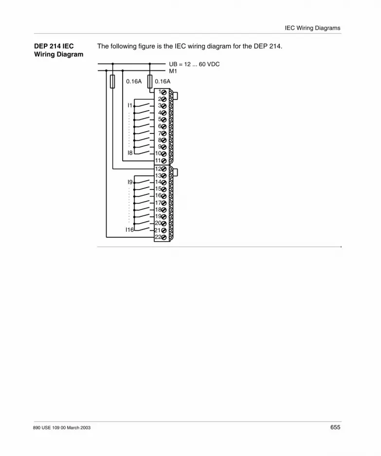
IEC Wiring Diagrams
DEP 214 IEC Wiring Diagram
The following figure is the IEC wiring diagram for the DEP 214.
UB = 12 ... 60 VDCM1
0.16A 0.16A
I1
I8
I9
I16
123456789
1011121314
16
18
20
22
15
17
19
21
890 USE 109 00 March 2003 655

IEC Wiring Diagrams
DEP 215 and DEP 217 IEC Wiring Diagram
The following figure is the IEC wiring diagram for both the DEP 215 and the DEP 217.
UB = 5 VDC at DEP 215; UB = 24 VDC at DEP 217M1
0.16A 0.16A
I1
I8
I9
I16
123456789
1011
121314
16
18
20
22
15
17
19
21
656 890 USE 109 00 March 2003

IEC Wiring Diagrams
DEP 216 and DEP 220 IEC Wiring Diagram
The following figure is the IEC wiring diagram for both the DEP 216 and the DEP 220.
UB = 24 VDCM1
0.16A 0.16A
I1
I8
I9
I16
1234567189
1011121314
16
18
20
22
15
17
19
21
890 USE 109 00 March 2003 657

IEC Wiring Diagrams
DEP 218 IEC Wiring Diagram
The following figure is the IEC wiring diagram for the DEP 218.
DEP 257 IEC Wiring Diagram
The following figure is the IEC wiring diagram for the DEP 257.
L = 115 VACN
0.2A
0.2A
I1I2I3I4I5I6I7I8
I9
I10
I12
I14
I16
123456789
1011121314
16
18
20
22
15
17
19
21
First of 16 Input Circuits
PAB
RDYE
U
E1
E8MU
E16M
E9
123456789
10111213
15
17
19
21
14
16
18
20
22
658 890 USE 109 00 March 2003

IEC Wiring Diagrams
DEP 296 and DEP 297 IEC Wiring Diagram
The following figure is the IEC wiring diagram for both the DEP 296 and the DEP 297.
UB = 60 VDC at DEP 296; UB = 48 VDC at DEP 297M1
0.16A 0.16A
I1
I8
I9
I16
123456789
1011121314
16
18
20
22
15
17
19
21
890 USE 109 00 March 2003 659

IEC Wiring Diagrams
MOT 201/202 IEC Wiring Diagram
The seven figures that follow are IEC wiring diagrams for the MOT 201, the MOT 202, or both (MOT 201/202), as specified in the introduction to each diagram. The following figure is an MOT 201/202 IEC wiring diagram.
R>3KΩ INTERNAL TO AS-BMOT
5Vdc5V COMMON
J1 REF
D/A
I/O BUSINTERFACE
5VREG
TO ENCODER CONNECTORS J4, J5NOTE:SEE SECTION NO TAG ALTERNATE POWER
+LIM
-LIM
HOME
JOG+
JOG-
BRAKE OUT 1
24 Vdc24v COMMON RED
GREEN
RED FIRST OFFIVEINPUTCIRCUITS
7
8
9
10
11
12
13
14
15
16
17
18
19
20
21
22
660 890 USE 109 00 March 2003

IEC Wiring Diagrams
The following figure is an MOT 201 (Motor Drive) IEC wiring diagram.
MOTOR DRIVE+VEL
INTERNAL TO AS-BMOT
I/O BUSINTERFACE
D/A
>3KΩ
>3KΩ
-VEL
COMMON
FAULT
ENABLE
SHELL
J31
2
3
4
5
6
7
8
10K+5V
RED
NC
NO
COM YELLOW
9
890 USE 109 00 March 2003 661
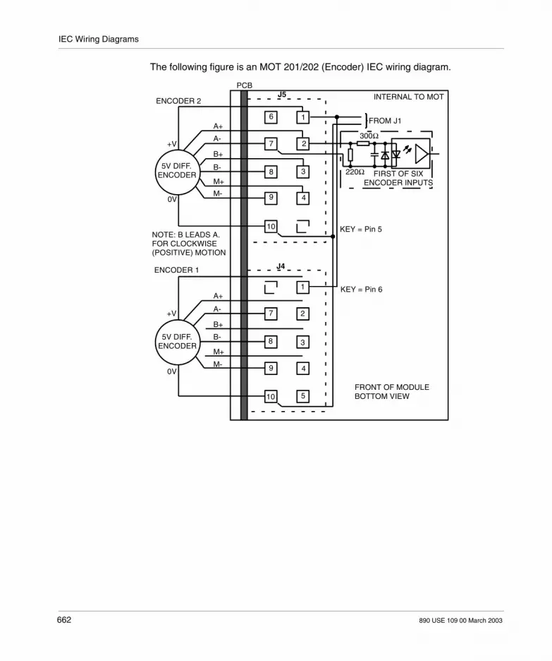
IEC Wiring Diagrams
The following figure is an MOT 201/202 (Encoder) IEC wiring diagram.
ENCODER 2
+V
5V DIFF.ENCODER
0V
+V
0V
5V DIFF.ENCODER
NOTE: B LEADS A.FOR CLOCKWISE(POSITIVE) MOTION
A+
A-
B+
B-
M+
M-
A+
A-
B+
B-
M+
M-
PCBJ5
J4
6
7
8
9
10
1
2
3
4
1
27
38
9 4
510
INTERNAL TO MOT
FROM J1
300Ω
220Ω FIRST OF SIXENCODER INPUTS
KEY = Pin 5
KEY = Pin 6
FRONT OF MODULEBOTTOM VIEW
ENCODER 1
662 890 USE 109 00 March 2003

IEC Wiring Diagrams
The following figure is an MOT 202 (Motor Drive) IEC wiring diagram.
MOTOR DRIVE
>3KΩ TYPPHASE A
PHASE B
PHASE C
COMMON
FAULT
ENABLE
J6
1
2
3
4
5
6
7
8
10
INTERNAL TO MOT
I/O BUSINTERFACE
D/A
D/A
NC
NO
COM
YELLOW
RED10K +5V
9
890 USE 109 00 March 2003 663

IEC Wiring Diagrams
The following figure is an MOT 202 (Resolver) IEC wiring diagram.
The following figure is an MOT 202 (Resolver) IEC wiring diagram.
RESOLVER
REF +
REF -
SIN +
SIN -
COS +
COS -
J72
7
4
3
8
5
10
6
INTERNAL TO MOT
1
7K
7K
R/DCONVERTER
I/O BUSINTERFACE
3.75 KHZ
+5V +5V
+5V
3K 3K
3K
RED
T T
RESOLVER
REF +
REF -
SIN +
SIN -
COS +
COS -
J8
19
INTERNAL TO MOT
7K
7K
R/DCONVERTER
I/O BUSINTERFACE
3.75 KHZ
+5V +5V+5V
3K 3K
3K
RED
T T21
12
13
14
15
16
17
18
20
22
664 890 USE 109 00 March 2003

IEC Wiring Diagrams
The following figure is an MOT 202 (Motor Driver) IEC wiring diagram.
INTERNAL TO MOTMOTOR DRIVE
>3KΩ TYPPHASE A
PHASE B
PHASE C
COMMON
FAULT
ENABLE
J8
1
2
3
4
5
6
7
8
9
10
11
NC
NO
COM YELLOW
RED
D/A
D/A
10K+5V
I/O BUSINTERFACE
890 USE 109 00 March 2003 665

IEC Wiring Diagrams
VRC/CTR 2xx IEC Wiring Diagram
The following figure is the IEC wiring diagram for the VRC/CTR 2xx.
+20 to 30 VDCDC Common
250 mA
Channel 1
Channel 2
Channel 4
123456789
10111213
15
17
19
21
Channel 3 14
16
18
20
22
666 890 USE 109 00 March 2003

IEC Wiring Diagrams
ZAE 201 IEC Wiring Diagram
Both of the following figures are IEC wiring diagrams for the ZAE 201. The following figure is a ZAE 201 IEC wiring diagram.
US/L1M4/NUBM2
4A 0.1A
+5V
0V
11N
5VN
U
123456789
1011121314
16
18
20
22
* with Attached Jumpers (as Delivered)
UE1
NMU
G1
Output 1
123456789
1011
15
121314
161718192021
4A 0.5A
Output 2Output 2
Output 1
US/L1
UBM2
M4/N
15
17
19
2122
890 USE 109 00 March 2003 667

IEC Wiring Diagrams
The following figure is a ZAE 201 IEC wiring diagram.
US/L1M4/NUBM2
4A 0.05A 4A 0.1A
+5V
0V
11N22N00N
5VN
U
G1
Output 1 Output 1
Output 2
* with Attached Jumpers (as Delivered)
123456789
1011
1213141516
18
20
22
17
19
21
UE1
2
0
NMU
G1
Output 2
US/L1M4/NUBM2
17
19
21
123456789
10111213141516
18
20
22
668 890 USE 109 00 March 2003

IEC Wiring Diagrams
ZAE 204 IEC Wiring Diagram
Both of the following figures are IEC wiring diagrams for the ZAE 204.The following figure is a ZAE 204 IEC wiring diagram.
UB5UB24M1
2A 0.05A 2A 0.05A
U
I1
I2
I3
I4M
UO1O2
O4
G2
G4
123456789
1011121314
16
18
20
22
I1
I2
I3
I4M
UO1O2O3O4G1G2G3
7
10
1213
1516171819202122
UB5
M1UB24
UB24filtered
O3
G1
G3
G421
15
17
19
123456
89
11
14
890 USE 109 00 March 2003 669

IEC Wiring Diagrams
The following figure is a ZAE 204 IEC wiring diagram.
UBM1
2A
U11
12
13
14
M
U01020304G1G2G3G4
123456789
10111213141516171819202122
670 890 USE 109 00 March 2003

890 USE 109 00 March 2003
I/O Configuration with Concept
At a Glance
Introduction This chapter describes how to configure A120 Series I/O modules with Concept.
What’s in this Chapter?
This chapter contains the following topics:
Note: When using Modsoft with certain A120 I/O modules you had to build ladder logic to multiplex the data into the PLC. This is no longer required when using Concept programming panel software for these I/O modules: ADU 214/216/211/212, VIC 2xx/VRC 2xx/CTR2xx.
Topic Page
Multiplexing I/O Data with Concept 672
Configuring A120 Discrete Input Modules with Concept 673
Configuring Discrete Output Modules with Concept 676
Configuring Discrete Combination Modules with Concept 679
Configuring Analog Input Modules with Concept 685
Analog Output Modules 718
Intelligent Modules 726
Communication Interfaces 736
Concept I/O Map Status Words 739
671

I/O Configuration with Concept
Multiplexing I/O Data with Concept
Overview If you use Modsoft to configure certain A120 I/O modules, you must build ladder logic to multiplex the data into the PLC. This is not required if you use Concept programming panel software for the following I/O modules: ADU214/216/211/212, VIC2xx/VRC2xx/CTR2xx.
672 890 USE 109 00 March 2003

I/O Configuration with Concept
Configuring A120 Discrete Input Modules with Concept
Discrete Input Modules
This following information describes how to configure these modules: DEO 216 16-point 24 Vdc Discrete Input DEP 208 8-point 230 Vac Discrete Input DEP 209 8-point 120 Vac Discrete Input DEP 210 8-point 115 Vac Isolated Discrete Input DEP 211 8-point 115 Vac Isolated Discrete Input DEP 214/254/254C 16-point 12 ... 60Vdc Discrete Input DEP 215 16-point 5 Vdc TTL Discrete Input DEP 216/256/256C 16-point 24 Vdc Discrete Input DEP 217 16-point 24 Vdc Discrete Input DEP 218 16-point 115 Vac Isolated Discrete Input DEP 220 16-point 24 Vdc Discrete Input DEP 257 16-point 110 Vdc Discrete Input DEP 296 16-point 60 Vdc Isolated Discrete Input DEP 297 16-point 48 Vdc Isolated Discrete Input DEP 284* 8-point 115 Vac Isolated Discrete Input*The DEP 284 is a "special", and therefore it is not included in this document.
I/O Configuration Using Concept 2.1 or Higher
Use the following procedure to configure the module.
Step Action
1 Select Configure from the menu.
2 Select I/O Map from the menu.
3 Click on Edit... The Local Common CPU Drop dialog appears.
4 Click on Module. The I/O Module Selection dialog appears.
5 Select DEPxxx and click on OK. A number and description appear.
6 In the In Ref field, enter 1x or 3x and press Enter. The software completes the In Ref and In End fields.
7 Click on Params... The Input Type dialog appears.
8 Select either Binary or BCD and click on OK.
890 USE 109 00 March 2003 673

I/O Configuration with Concept
AS-BDEO-216/ AS-BDEP 214/ 215/ 216/ 217/ 218/ 220/ 254(C)/ 256(C)/ 257(C)/ 296/ 297
The AS-BDEO-216 dialog box, which follows, is used with these modules: AS-BDEO-216/ AS-BDEP 214/ 215/ 216/ 217/ 218/ 220/ 254(C)/ 256(C)/ 257(C)/ 296/ 297.
Input Type: The Binary and BCD option buttons in the input type section require corresponding choices between 1x-/3x-references (i.e., in binary or BCD). The 1x-references are shown in binary.
Meanings for the AS-BDEO-216/ AS-BDEP 214/ 215/ 216/ 217/ 218/ 220/ 254(C)/ 256(C)/ 257(C)/ 296/ 297 Module Mapping
These modules require sixteen 1x-discrete inputs. A single 3x-input register can be mapped instead of sixteen 1x-discrete inputs (shown in the following figure).The following figure shows the 3x-register arrangement for the above-named modules.
Input Type
Binary BCD
OK Cancel Help
AS-BDEO216
MSB
#Input 1
15
#Input 16
LSB
3x-register 1
14 13 12 11 10 9 8 7 6 5 4 3 2 1 0
674 890 USE 109 00 March 2003

I/O Configuration with Concept
AS-BDEP 208/ 210/211
The AS-BDEP-208 dialog, shown in the following figure, is used with these modules: AS-BDEP 208/210/211.
Input Type: The Input Binary and BCD option buttons require a corresponding choice between 1x-/3x-references (i.e., in binary or BCD).
Meanings for the AS-BDEP 208/ 210/ 211 Module Mapping
These modules require eight 1x-discrete inputs. A single 3x-input register can be mapped instead of eight 1x-discrete inputs.The following figure shows the 3x-register arrangement for the above-named modules.
Change Address Format Display Procedure
Use the following steps to modify the address format display.
Input Type
Binary BCD
OK Cancel Help
AS-BDEP 208
Note: Concept provides three ways to display address formats. The default is standard (400001). To change the address format display, use the steps in Change Address Format Display Procedure, p. 675. All four formats apply to discrete, analog, and intelligent modules.
3x-register 1
MSB
#Input 1 #Input 8
LSB15 14 13 12 11 10 9 8 7 6 5 4 3 2 1 0
Bits 8 ... 15 are not used
Step Action
1 From the Main menu, select Options, then select Preferences.
2 Select standard (400001), separator (4:00001), or compact (4:1); then click OK.
890 USE 109 00 March 2003 675
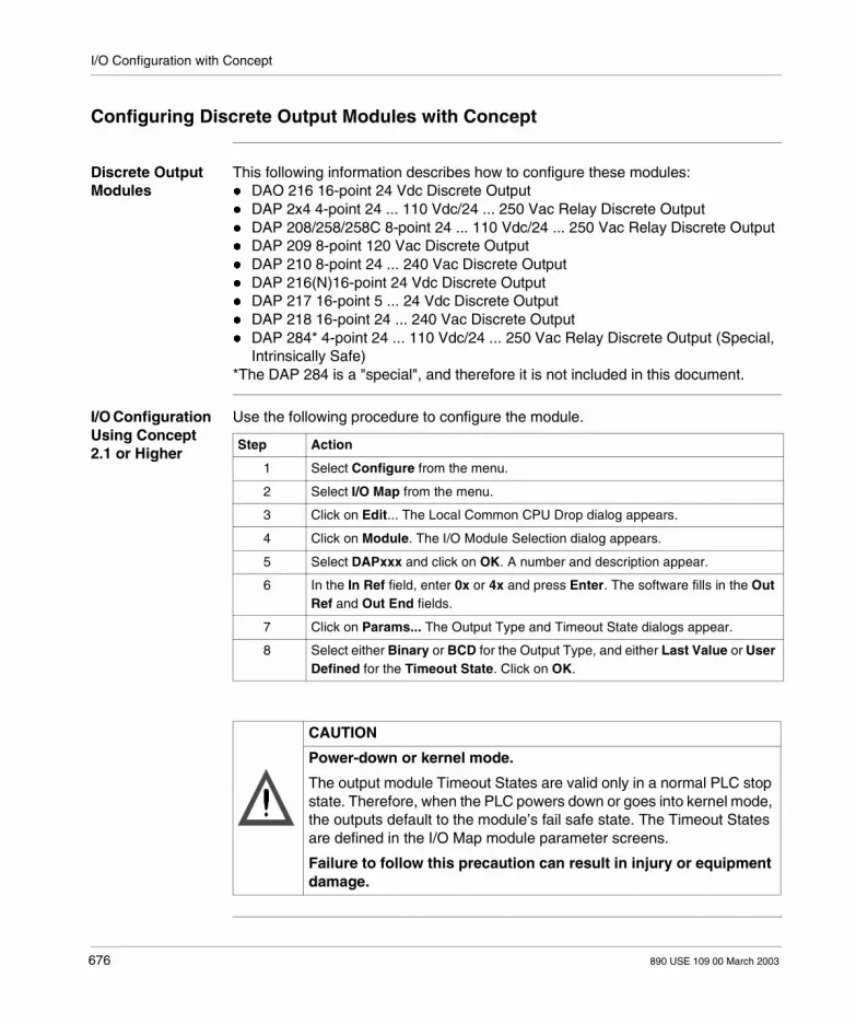
I/O Configuration with Concept
Configuring Discrete Output Modules with Concept
Discrete Output Modules
This following information describes how to configure these modules: DAO 216 16-point 24 Vdc Discrete Output DAP 2x4 4-point 24 ... 110 Vdc/24 ... 250 Vac Relay Discrete Output DAP 208/258/258C 8-point 24 ... 110 Vdc/24 ... 250 Vac Relay Discrete Output DAP 209 8-point 120 Vac Discrete Output DAP 210 8-point 24 ... 240 Vac Discrete Output DAP 216(N)16-point 24 Vdc Discrete Output DAP 217 16-point 5 ... 24 Vdc Discrete Output DAP 218 16-point 24 ... 240 Vac Discrete Output DAP 284* 4-point 24 ... 110 Vdc/24 ... 250 Vac Relay Discrete Output (Special,
Intrinsically Safe)*The DAP 284 is a "special", and therefore it is not included in this document.
I/O Configuration Using Concept 2.1 or Higher
Use the following procedure to configure the module.
Step Action
1 Select Configure from the menu.
2 Select I/O Map from the menu.
3 Click on Edit... The Local Common CPU Drop dialog appears.
4 Click on Module. The I/O Module Selection dialog appears.
5 Select DAPxxx and click on OK. A number and description appear.
6 In the In Ref field, enter 0x or 4x and press Enter. The software fills in the Out Ref and Out End fields.
7 Click on Params... The Output Type and Timeout State dialogs appear.
8 Select either Binary or BCD for the Output Type, and either Last Value or User Defined for the Timeout State. Click on OK.
CAUTION
Power-down or kernel mode.
The output module Timeout States are valid only in a normal PLC stop state. Therefore, when the PLC powers down or goes into kernel mode, the outputs default to the module’s fail safe state. The Timeout States are defined in the I/O Map module parameter screens.
Failure to follow this precaution can result in injury or equipment damage.
676 890 USE 109 00 March 2003

I/O Configuration with Concept
AS-BDAO-216/AS-DAP-216/N/217/218/209
The AS-BDA0-216 dialog box, which follows, isused with the following modules: AS-BDAO-216/ AS-DAP-216/N/ 217/ 218/209.
Output Type: The Binary and BCD option buttons require corresponding choices between 0x-/4x-references (i.e., in binary or BCD).Timeout State: The Compact timeout state only reflects a user program in stop mode.Activation of the Last Value option button causes the outputs to retain their last valid value upon user program stop. Activation of the User Defined option button causes the outputs to assume the value defined in the user-defined timeout state text field.User Defined: If the User Defined option button was activated, the corresponding hex value can be entered here.
Meanings for the AS-BDAO-216/ AS-DAP-216/N/217/218/209 Module Mapping
The AS-BDAO-216/ AS-DAP-216/N/ 217/ 218/209 modules require 16 0x-discrete outputs. The BCD button will alternatively require mapping to a 4x-output register.The following figure shows the AS-BDAO-216/ AS-DAP-216/N/ 217/ 218/209 4x register arrangement.
AS-BDAO216
Output Type
BCDBinary
Timeout State:
Last Value User Defined
User Defined Timeout State (In Hex.):
0000
OK Cancel Help
15 14 13 12 11 10 9 8 7 6 5 4 3 2 1 0 LSB
#Output 16#Output 1
MSB
4x-register 1
890 USE 109 00 March 2003 677

I/O Configuration with Concept
AS-BDAP-204 This AS-DBAP-204 dialog, which follows, is used with the following modules: AS-BDAP-204.
Output Type: The Binary and BCD option buttons require corresponding choices between 0x-/4x-references (i.e., in binary or BCD).Timeout State: The Compact timeout state only reflects a user program in stop mode.Activation of the Last Value option button causes the outputs to retain their last valid value upon user program stop.Activation of the User Defined option button causes the outputs to take on the value defined in the user-defined timeout state text field.User Defined: If the User Defined option button was activated, the corresponding hex value can be entered here.
Meanings for the AS-BDAP-204 Module Mapping
The AS-BDAP-204 module require four 0x-discrete outputs. The BCD option button will alternatively require mapping to a 4x-output register.The following diagram shows the AS-BDAP-204 4x-register arrangement.
AS-BDAP-204
Output Type
Binary BCD
Timeout State:
Last Value User Defined
User Defined Timeout State (In Hex.):
0000
OK Cancel Help
4x-register 1
MSB
Bits 4 ... 15 are not used #Output 1 #Output 4
LSB16 14 12 10 9 7 5 3 115 13 11 8 6 4 2
678 890 USE 109 00 March 2003

I/O Configuration with Concept
Configuring Discrete Combination Modules with Concept
Discrete Combination Modules
This follwoing information describes how to configure these modules: DAP 211 Monitored 4-point in/4-point out 120 Vac Combined I/O DAP 212/252/252C 8-point in/4-point out 24 Vdc Combined I/O DAP 220/250/250C 8-point in/8-point out 24 Vdc Combined I/O DAP 252 8-point in/4-point relay out 24 Vdc LT Combined I/O DAP 253 8-point in/4-point relay out 110 Vdc LT Combined I/O DAP 292 8-point in/4-point relay out 60 Vdc Combined I/O
I/O Configuration using Concept 2.1 or Higher
Use the following procedure to configure the module.
Step Action
1 Select Configure from the menu.
2 Select I/O Map from the menu.
3 Click on Edit... The Local Common CPU Drop dialog appears.
4 Click on Module. The I/O Module Selection dialog appears.
5 Select DAPxxx and click on OK. A number and description appear.
6 In the In Ref field, enter 1x or 3x and press Enter. The software completes the In Ref and In End fields.
7 In the Out Ref field, enter 0x or 4x and press Enter. The software completes the Out Ref and Out End fields.
8 Click on Params... The Output Type and Timeout State dialogs appear.
9 Select either Binary or BCD for the Output Type and either Last Value or User Defined for the Timeout State. Click on OK.
CAUTION
Power-down or kernel mode.
The output module Timeout States is valid only in a normal PLC stop state. Therefore, when the PLC powers down or goes into kernel mode, the outputs default to the module’s fail safe state. The Timeout States are defined on the I/O Map module parameter screens.
Failure to follow this precaution can result in injury or equipment damage.
890 USE 109 00 March 2003 679

I/O Configuration with Concept
AS-BDAP-211 The AS-BDAP-211dialog, which follows, is used with the following module: AS-BDAP-211
Output Type: The output Binary and BCD option buttons require corresponding choices between 0x-/4x-references (i.e., in binary or BCD).Input Type: The input Binary and BCD option buttons require corresponding choices between 1x-/3x-references (i.e., in binary or BCD).Timeout State: The Compact Timeout State only reflects a user program in stop mode.Activation of the Last Value option button causes the outputs to retain their last valid valueupon user program stop.Activation of the User Defined option button causes the outputs to take on the value defined in the user-defined timeout state text field.User Defined: If the User Defined option button was activated, the corresponding hex value can be entered here.
AS-BDAP211
Output Type
Input Type
Binary BCD
Binary BCD
Timeout State:
Last Value User Defined
User Defined Timeout State (In Hex.):
0000
OK HelpCancel
680 890 USE 109 00 March 2003

I/O Configuration with Concept
Meanings for the AS-BDAP-211 Module Mapping
The AS-BDAP-211 modules require four 1x-discrete inputs and four 0x-discrete outputs. The BCD option button will alternatively require mapping to a 4x-output register instead of four 0x–discrete outputs. A single 3x-input register can be mapped, instead of four 1x-discrete inputs (as shown in the following figures).The following figure shows the AS-BDAP-211 3x-register arrangement.
The following figure shows the AS-BDAP-211 4x-register arrangement.
AS-BDAP-212/ 252(C)/ 253/ 292
The AS-BDAP-212/252(C)/ 253/ 292 dialog box, which follows, is used with the following modules: AS-BDAP-212/ 252(C)/ 253/ 292.
3x-register 1
MSB LSB
Bits 4 ... 15 are not used #Input 1
15 13 11 9 8 6 4 2 014 12 10 7 5 3 1
4x-register 1
MSB LSB
Bits 4 ... 15 are not used #Output 1 #Output 4
15 13 11 9 7 5 3 114 12 10 8 6 4 2 0
Output TypeBinary BCD
Input TypeBinary BCD
Timeout State:
Last Value User Defined
User Defined Timeout State (In Hex):0000
OK Cancel Help
AS-BDAP2x2/253
890 USE 109 00 March 2003 681

I/O Configuration with Concept
Output Type: The output Binary and BCD option buttons require corresponding choices between 0x-/4x-references (i.e., in binary or BCD).Input Type: The input Binary and BCD option buttons require corresponding choices between 1x-/3x-references (i.e., in binary or BCD).Timeout State: The Compact Timeout State only reflects a user program in stop mode.Activation of the Last Value option button causes the outputs to retain their last valid value upon user program stop.Activation of the User Defined option button causes the outputs to assume the value defined in the user-defined timeout state text field.User Defined: If the User Defined option button was activated, the corresponding hex value can be entered here.
Meanings for the AS-BDAP-212/ 252(C)/ 253/ 292 Module Mapping
The AS-BDAP-212/ 252(C)/ 253/ 292 modules require eight 1x-discrete inputs and four 0x-discrete outputs. The BCD option button will alternatively require mapping to be made to a 4x-output register. A single 3x-input register can be mapped instead of eight 1x-discrete inputs. The following figure shows the AS-BDAP-212/252(C)/253/292 3x-register arrangement.
The following figure shows the AS-BDAP-212/ 252(C)/253/292 4x-register arrangement.
3x-register 1
MSB LSB
Bits 8 ... 15 are not used#Input 1 #Input 8
15 13 11 9 7 5 3 114 12 10 8 6 4 2 0
4x-register 1
Bits 4 ... 15 are not used
MSB LSB
#Output 1
15 13 11 9 7 5 3 114 12 10 8 6 4 2 0
682 890 USE 109 00 March 2003

I/O Configuration with Concept
AS-BDAP-220/ 252(C)
The AS-BDAP220/250(C) dialog, which follows, is used with the following modules: AS-BDAP-220/250(C).
Output Type: The output Binary and BCD option buttons require corresponding choices between 0x-/4x-references (i.e., in binary or BCD).Input Type: The input Binary and BCD option buttons require orresponding choices between 1x-/3x-references (i.e., in binary or BCD).Timeout State: The Compact Timeout State only reflects a user program in stop mode.Activation of the Last Value option button causes the outputs to retain their last valid value upon user program stop.Activation of the User Defined option button causes the outputs to take on the value defined in the user-defined timeout state text field.User Defined: If the User Defined option button was activated, the corresponding hex value can be entered here.
AS-BDAP220/250
Output Type
Binary BCD
Input TypeBinary BCD
Timeout State:
Last Value User Defined
User Defined Timeout State (In Hex):0000
OK Cancel Help
890 USE 109 00 March 2003 683

I/O Configuration with Concept
Meanings for the AS-BDAP-220/ 250(C) Module Mapping
The AS-BDAP-220/ 250(C) modules require eight 1x-discrete inputs and eight 0x-discrete outputs. The output BCD option button will alternatively require mapping to a 4x-output register. The input BCD option button will require a 3x-input register mapping (as shown in the following two figures).The following figure shows the AS-BDAP-220/ 250(C) 3x-register arrangement.
The following figure shows the AS-BDAP-220/ 250(C) 4x-register arrangement.
15 14 13 12 11 10 9 8 7 6 5 4 3 2 1 0 LSB
#Input 1 #Input 8
MSB
3x-register 1
Bits 8 ... 15 are not used
MSB
4x-register 1
#Output 1 #Output 8
LSB
Bits 8 ... 15 are not used
15 14 13 12 11 10 9 8 7 6 5 4 3 2 1 0
684 890 USE 109 00 March 2003

I/O Configuration with Concept
Configuring Analog Input Modules with Concept
Analog Input Modules
The following information describes how to configure these modules: ADU 204/254/254C 4–point Voltage/RTD Analog Input ADU 205 4–point Voltage/Current Analog Input ADU 206/256/256C 4–point Voltage/Current Isolated Analog Input ADU 210 4–point Voltage/Current Analog Input (Only supported in Concept 2.2
or higher) ADU 214 8–point Voltage/Current Isolated Analog Input (Only supported in
Concept 2.2 or higher) ADU 216 8–point Thermocouple Isolated Analog Input ADU 257/257C 8–point Millivolts/RTD/TC/Resistance Analog Input (Only
supported in Concept 2.2 or higher) ADU 282/282M* 2–point Analog Input (Special, Intrinsically Safe) ADU 284* 2-point Analog Input (Special, Intrinsically Safe) ADU 211/212 8–point Universal Isolated Analog Input (Not supported in Concept
2.1 or higher)*This is a "special", and therefore it is not included in this document.
I/O Configuration Using Concept 2.1 or Higher
Use the following procedure to configure the module.
Step Action
1 Select Configure from the menu.
2 Select I/O Map from the menu.
3 Click on Edit... The Local Common CPU Drop dialog appears.
4 Click on Module. The I/O Module Selection dialog appears.
5 Select ADUxxx and click on OK. A number and description appear.
6 In the In Ref field, enter 3x and press Enter. The software completes the In Ref and In End fields.
7 Click on Params... The applicable configuration dialog appears, depending on the selected module. Refer to the specific modules.
890 USE 109 00 March 2003 685

I/O Configuration with Concept
Configuring AS-BADU-204/ 254(C) Modules
The following information applies to the AS-BADU-204/254(C) modules.The AS-BADU-204/ 254(C) parameter dialog, which follows, is used for the analog modules AS–BADU–204/ 254(C).
Channel: The option buttons here allow the selection of individual channels for configuration, as follows: Channel 1 = Pins 3 ... 6 Channel 2 = Pins 7...10 Channel 3 = Pins 14 ... 17 Channel 4 = Pins 18 ... 21Channel–specific option panels are presented for each channel selection. Values entered for a channel are saved automatically when another channel is selected, and therefore are not lost during the definition of another channel.Channel Configuration: Measuring ranges and data formats for temperature measurement data transfer to the Compact PLC can be determined in this list box.The 1.0 C/F and 0.1 C/F option buttons allow a choice of measuring steps of either 1.0 or 0.1 degree (in Centigrade or Fahrenheit). This allows differing displays for the same measurement value, as shown in the following table.
1.0 degree Centigrade 0.1 degree Centigrade
-60 -600
200 2000
Channel:
Channel 1
Channel 2
Channel 3
Channel 4
AS-BADU204/254
Channel Configuration:
1.0 C 0.1 C 1.0 F 0.1 F 13-bit 15-bit+sign
Type:
Pt 100,-200 to 850
Pt 200,-200 to 250
Ni 100,-60 to 250
Ni 200,-60 to 150
APt100,-200 to 600
APt200,-200 to 250
R, 0 to 400 ohms
OK Cancel Help
686 890 USE 109 00 March 2003

I/O Configuration with Concept
The remaining option buttons 13–bit and 15-+sign (15–bit value + sign) determine the value range to be transferred.The tables that follow are present values for all configurable resistive temperature sensors, which are listed here: Pt 100, -200 to 850 Pt 200, -200 to 250 Ni 100, -60 to 250 Ni 200, -60 to 150 APt 100, -200 to 600 APt 200, -200 to 250 R, 0 to 400 ohmsPt 100-200 degrees C to 850 degrees C
Pt 200-200 degrees C to 250 degrees C
Ni 100-60 degrees C to 250 degrees C
Temp. (degrees C)
1.0 C 0.1 C 1.0 F 0.1 F 13-bit 15-bit + sign
Measuring step/value range
<-205 -32768 -32768 -32768 -32768 0 -32768 Under-range
-200 -200 -2000 -328 -3280 3132 -7529
Nominal range0 0 0 +32 +320 4096 0
+850 +850 +8500 +1562 +15620 8191 32000
>+870 +32767 +32767 +32767 +32767 8191 +32767 Overrange
Temp. (degrees C)
1.0 C 0.1 C 1.0 F 0.1 F 13-bit
15-bit + sign
Measuring step/value range
<-205 -32768 -32768 -32768 -32768 0 -32768 Under-range
-200 -200 -2000 -328 -3280 819 -25600
Nominal range0 0 0 +32 +320 4096 0
+250 +250 +2500 +482 +4820 8191 32000
>+256 +32767 +32767 +32767 +32767 8191 +32767 Overrange
Temp. (degrees C)
1.0 C 0.1 C 1.0 F 0.1 F 13-bit
15-bit + sign
Measuring step/value range
<-61 -32768 -32768 -32768 -32768 0 -32768 Under-range
-60 -60 -600 -76 -760 3113 -7680
Nominal range0 0 0 +32 +320 4096 0
+250 +250 +2500 +482 +4820 8191 32000
>+256 +32767 +32767 +32767 +32767 8191 +32767 Overrange
890 USE 109 00 March 2003 687

I/O Configuration with Concept
Ni 100-60 degrees C to 150 degrees C
APt 100-200 degrees C to 600 degrees C
APt 200-200 degrees C to 250 degrees C
R, 0 to 400 ohms
Temp. (degrees C)
1.0 C 0.1 C 1.0 F 0.1 F 13-bit
15-bit + sign
Measuring step/value range
<-61 -32768 -32768 -32768 -32768 0 -32768 Under-range
-60 -60 -600 -76 -760 2458 -12800
Nominal range0 0 0 +32 +320 4096 0
+150 +150 +1500 +302 +3020 8191 32000
>+151 +32767 +32767 +32767 +32767 8191 +32767 Overrange
Temp. (degrees C)
1.0 C 0.1 C 1.0 F 0.1 F 13-bit
15-bit + sign
Measuring step/value range
<-205 -32768 -32768 -32768 -32768 0 -32768 Under-range
-200 -200 -2000 -328 -3280 2731 -10667
Nominal range0 0 0 +32 +320 4096 0
+600 +600 +6000 +1112 +11120 8191 32000
>+614 +32767 +32767 +32767 +32767 8191 +32767 Overrange
Temp. (degrees C)
1.0 C 0.1 C 1.0 F 0.1 F 13-bit
15-bit + sign
Measuring step/value range
<-205 -32768 -32768 -32768 -32768 0 -32768 Under-range
-200 -200 -2000 -328 -3280 819 -25600
Nominal range0 0 0 +32 +320 4096 0
+250 +250 +2500 +482 +4820 8191 32000
>+256 +32767 +32767 +32767 +32767 8191 +32767 Overrange
Resistance in W 13-bit 15-bit + sign Value range
0 0 0
100 2048 +8000 Recommended
200 4096 +16000 nominal range
399.902 8191 +32000
>= 400 8191 +32767 Overrange
688 890 USE 109 00 March 2003

I/O Configuration with Concept
Type: In this section, an option button can be used to choose a resistive temperature sensor type for the selected channel, or a direct resistance measurement can be performed.
Meanings for the AS-BADU-204/254(C) Module Mapping
The AS-BADU-204/254(C) modules require four 3x-input registers addressed in sequence, beginning with channel 1 as shown here.
Note: The type R, 0 to 400 ohms button, only selects values whose size has been determined to be either 13–bit or 15–bit + sign through the appropriate option buttons.
Note: Refer toConcept I/O Map Status Words, p. 739.
3x-register 1 (channel 1)
3x-register 2 (channel 2)
3x-register 3 (channel 3)
3x-register 4 (channel 4)
MSB
MSB
MSB
MSB LSB
LSB
LSB
LSB
890 USE 109 00 March 2003 689

I/O Configuration with Concept
AS-BADU-205 The following information applies to the AS-BADU-205 module.The 20AS-BADU-205 parameter dialog, which follows, is valid for the analog module AS-BADU-205.
Resolution Mode: This list box defines the value range for all channels: 12-bit 12-bit + sign 13-bit 15-bit + sign 16-bitChannel 1 ... 4: The desired measuring ranges can be chosen in these list boxes.
The measuring ranges can be chosen from the following selections: +/- 20 VDC +/- 40 mA +/- 10 VDC +/- 20 mA 0 ... 20 mA 4 ... 20 mA 0 ... 10 VDC 0 ... 20 VDC
Note: The combination of current and voltage ranges is not allowed. Pay attention to the switches on the rear of the module.
+/- 20 V
+/- 40 mV+/- 10 V+/- 20 mV0...20 mA4...20 mA0...10 V0...20 V
Cancel Help
Channel 1: Channel 2: Channel 3: Channel 4:
+/- 20 V +/- 20 V +/- 20 V
Resolution Mode: 12-bit
AS-BADU 205
690 890 USE 109 00 March 2003

I/O Configuration with Concept
+/- 20 mA, +/- 40 mA
+/- 10 VDC, +/- 20 VDC
0 ... 10 VDC, 0 ... 20 VDC
0 ... 20 mA
Input current (mA)
12-bits 13-bits 16-bits 12-bits + sign
15-bits + sign
Range
<-20/-40 0 0 0 -4095 -32768 Under-range
-20/-40 0 0 0 -4095 -32000
Nominal range0 2048 4096 32768 0 0
+20/+40 4095 8191 65520 +4095 +32000
>+20/+40 4095 8191 65520 +4095 +32767 Overrange
Input voltage (VDC)
12-bits 13-bits 16-bits 12-bits + sign
15-bits + sign
Range
<-10/-20 0 0 0 -4095 -32768 Under-range
-10/-20 0 0 0 -4095 -32000
Nominal range0 2048 4096 32768 0 0
+10/+20 4095 8191 65520 +4095 +32000
>+10/+20 4095 8191 65520 +4095 +32767 Overrange
Input voltage (VDC)
12-bits 13-bits 16-bits 12-bits + sign
15-bits + sign
Range
< 0 0 0 0 -4095 -32768 Under-range
0 0 0 0 0 0 Nominal range
10/20 4095 8191 65520 +4095 +32000
>10/20 4095 8191 65520 +4095 +32767 Overrange
Input current (mA)
12-bits 13-bits 16-bits 12-bits + sign
15-bits + sign
Range
< 0 0 0 0 -4095 -32768 Under-range
0 0 0 0 0 0 Nominal range
20 4095 8191 65520 +4095 +32000
>20 4095 8191 65520 +4095 +32767 Overrange
890 USE 109 00 March 2003 691

I/O Configuration with Concept
4 ... 20 mA
Meanings for the AS-BADU-205 Module Mapping
The AS–BADU–205 module requires four 3x–input registers addressed in sequence, beginning with channel 1 (as shown in the following figure).
Input current (mA)
12-bits 13-bits
16-bits 12-bits + sign
15-bits + sign
Range
< 0 ... 2 0 0 0 0 0 Wire breakage
2.1 ... 3.61 0 0 0 0 -32768 Under-range
3.62 ... 3.99 0 0 0 0 Tolerable range
4 0 0 0 0 0 Nominal range
20 4095 8191 65520 +4095 +32000
>20 4095 8191 65520 +4095 +32767 Overrange
Note: Refer toConcept I/O Map Status Words, p. 739.
MSB
MSB
MSB
MSB
LSB
LSB
LSB
LSB
3x-register 1 (channel 1)
3x-register 2 (channel 2)
3x-register 3 (channel 3)
3x-register 4 (channel 4)
692 890 USE 109 00 March 2003

I/O Configuration with Concept
AS-BADU-206/ 256(C)
The following information describes the AS-BADU-206/256(C) modules.The AS-BADU-206/ 256(C) parameter dialog shown below is valid for the analog modules AS–BADU–256/ (C).
Overrange: Activation of the Overrange option button enables range exception monitoring. Any range exceptions then trigger a corresponding message within the first input status word (bits 0 ... 3).Open circuit: Activation of the Open circuit (wire breakage) option button enables open-circuit monitoring. Any subsequent error messages are then visible within the first input status word (bits 4 ... 7).Unipolar: Selection of the Unipolar option button restricts choices to the unipolar measuring ranges (e.g. 0 ... 20 mA/ 0 ... 10 V).Resolution: This list box defines the value range for all channels: 11-bit + sign 12-bit 15-bit + sign 16-bitChannel 1 ... 4: The measuring ranges for channels 1-4 can be chosen from the tables that follow.
AS-BADU206/256
Overrange Open circuit Unipolar
Resolution 12-Bit
Channel 1 Channel 2 Channel 3 Channel 4
+/- 1V/20 mA +/- 1V/20 mA +/- 1V/20 mA +/- 1V/20 mA
+/- 10V +/- 10V +/- 10V +/- 10V
0..1V/0...20 mA 0..1V/0...20 mA 0..1V/0...20 mA 0..1V/0...20 mA
0..10V 0..10V 0..10V 0..10V
0,2..1V/4...20 mA 0,2..1V/4...20 mA 0,2..1V/4...20 mA 0,2..1V/4...20 mA
2..10V 2..10V 2..10V 2..10V
OK Cancel Help
890 USE 109 00 March 2003 693

I/O Configuration with Concept
Measuring ranges 0 ... 10 VDC/2 ... 10 VDC, 0 ... 20 mA/4 ... 20 mA
Measuring ranges +/- 10 VDC/ +/- 20 mA
Voltage (VDC)
Current (mA)
12-bits 16-bits 11-bits + sign
15-bits + sign
Range
0 0 0 0 Under-range
0 0 0 0 Neg. tolerance range
0/2 0/4 0 0 0 0 Nominal range
10 20 4000 64000 +2000 +32000
10.01 ... 20.02 ... 4001 64016 +2001 +32016 Pos. tolerance range
>= 10.24/10.19
>= 20.48/20.39
4095 65520 +2047 +32760 Overrange
Voltage (VDC) Current (mA)
12-bits 16-bits 11-bits + sign
15-bits + sign
Range
<=-10.24 <=-20.48 0 0 -2048 -32768 Under-range
-10.01 -20.02 47 -2001 -32016 Neg. tolerance range
-10.000+10.00
-200+20
4820484048
7683276864768
-20000+2000
-320000+32000
Nominal range
+10.01 ... +20.02 ... 4049 +2001 +32016 Pos. tolerance range
>=10.24 >=20.48 4095 65520 +2047 +32752 Overrange
694 890 USE 109 00 March 2003

I/O Configuration with Concept
AS-BADU-206/ 256(C) Module Input Status Word
The AS–BADU–206/256 modules require five 3x–input registers addressed in sequence, beginning with the input status word, then channel. (Refer to the following two figures.)The following figure shows the AS-BADU-206/ 256(C) 3x module status word.
3x-register 1
MSB LSB15 14 13 12 11 10 9 8 7 6 5 4 3 2 1 0
reserved
1 = The module is not ready, or one ormore of the bits 1 ... 4 are set
1 = External supply voltage is notpresent
1 = Range exception for the current orvoltage ranges 4 ... 20 mA, 0.2 ... 1VDC, 2 ... 10 VDC
1 = 12-bit unipolar module setting forcurrent or voltage
Channel 4 measuring rangeover/underrunor wire breakage
Channel 3 measuring rangeover/underrunor wire breakage
Channel 2 measuring rangeover/underrunor wire breakage
Channel 1 measuring rangeover/underrunor wire breakage
890 USE 109 00 March 2003 695

I/O Configuration with Concept
Meanings for the AS-BADU-206/ 256(C)Module Mapping
The following figure shows the AS-BADU-206/ 256(C) 3x-register arrangement.
AS–BADU–210 The following information applies to the AS-BADU-210 module.The dialog, which follows, works with the analog module AS–BADU–210.
3x-register 1 (channel 1)
3x-register 3 (channel 2)
3x-register 4 (channel 3)
MSB
MSB
MSB
LSB
LSB
LSB
AS-BADU210
Channel 1 Channel 2 Channel 3 Channel 4
inactive
0...10V 0...10V 0...10V 0...10V
2...10V 2...10V 2...10V 2...10V
+/-10V +/-10V +/-10V +/-10V
0...5V(0...20mA)
inactive inactive inactive
0...5V(0...20mA) 0...5V(0...20mA)
0...5V(4...20mA) 0...5V(4...20mA) 0...5V(4...20mA)
+/-5V(+/-20mA) +/-5V(+/-20mA) +/-5V(+/-20mA)
limit < > 0 limit < > 0 limit < > 0 limit < > 0
OK Cancel Help
696 890 USE 109 00 March 2003

I/O Configuration with Concept
Channel 1 ... 4: For Chanel ... 4, use the following guidelines: Select inactive when channel is not used. Select limit < > 0 if you want to use the 1.6% rated value without causing an error
for uniplar ranges only.Use the information in the following tables to choose the measuring ranges for channels 1 to 4.Conversion Values of Voltage Inputs
Analog value 0 ... 5 V
Analog value 0 ... 10V
Analog value 1 ... 5 V
Analog value 2 ... 10 V
Analog value +/–5 V
Analog value +/–10 V
Decimal value
Notes
<-0.080 <-0.16 <+0.52 <+1.04 <-5.12 <-10.24 -32 767 underflow error
-5.119 ... -5.00
-10.239... -10.00
-32 766... -32 001
overload range
-0.08 ... -0.00
-0.16 ... -0.00
+0.52 ... +0.936 ... +0.99
+1.04 .. +1.87 ... +1.99
0 (-3 840) 0 (-512) 0 (-1)
overload range
-5.00 -10.00 -32 000 linear
-2.50 -5.00 -16 000 linear
-0.50 -1.00 -3 200 linear
-0.25 -0.50 -1 600 linear
-0.05 -0.10 -320 linear
-0.005 -0.01 -32 linear
-0.0025 -0.005 -16 linear
0 0 1 2 0 0 0 linear
0.0025 0.005 1.002 2.004 +0.0025 +0.005 +16 linear
0.005 0.01 1.004 2.008 +0.005 +0.01 +32 linear
0.05 0.10 1.04 2.08 +0.05 +0.10 +320 linear
0.25 0.50 1.20 2.40 +0.25 +0.50 +1 600 linear
0.50 1.00 1.40 2.80 +0.50 +1.00 +3 200 linear
2.50 5.00 3.00 6.00 +2.50 +5.00 +16 000 linear
5.00 10.00 5.00 10.00 +5.00 +10.00 +32 000 rated value
5.000... 5.119
10.000... 10.239
5.00... 5.09
10.00... 10.19
+5.000.. +5.119
+10.00... +10.239
+32 001... +32 766
overload range
>5.12 >10.24 >5.09 >10.19 >+5.20 >+10.24 >+32 767 overflow error
890 USE 109 00 March 2003 697

I/O Configuration with Concept
Conversion Values of Current Inputs
Note: Brackets denote range with limiting value –1.6%. No brackets denotes range with limiting value 0.
Analog value 0 ... 20 mA
Analog value 4 ... 20 mA
Analog value +/–20 mA
Decimal value Notes
<-0.32 <+2.08 <-20.479 -32 767 underflow error
-20.478 ... -20.000
-32 766 ... -32 001
overload range
-0.32 ... -0.00 +2.08 ... +3.74 ... +3.99
0 (-3 840) 0 (-512) 0 (-1)
overload range
-20.00 -32 000 linear
-10.00 -16 000 linear
-2.00 -3 200 linear
-1.00 -1 600 linear
-0.20 -320 linear
-0.02 -32 linear
-0.01 -16 linear
0 +4 0 0 linear
+0.01 +4.008 +0.01 +16 linear
+0.02 +4.016 +0.02 +32 linear
+0.20 +4.16 +0.20 +320 linear
+1.00 +4.80 +1.00 +1 600 linear
+2.00 +5.60 +2.00 +3 200 linear
+10.00 +12.00 +10.00 +16 000 linear
+20.00 +20.00 +20.00 +32 000 rated value
+20.000 ... +20.478
+20.00 ... +20.38 +20.000 ... +20.478
+32 001 ... +32 766
overload range
>+20.479 >+20.38 >+20.479 >+32 767 overflow error
Note: Brackets denote range with limiting value –1.6%. No brackets denotes range with limiting value 0.
698 890 USE 109 00 March 2003

I/O Configuration with Concept
Meanings for the AS–BADU–210 Module Mapping
The AS–BADU–210 module requires four 3x–input registers addressed in sequence, beginning with channel 1 as shown below.
AS–BADU–214 The following dialog is valid for the analog module AS–BADU–214.
Note: Refer to Concept I/O Map Status Words, p. 739 for Concept I/O Map Status Words.
3x-register 1 (channel 1)
3x-register 2 (channel 2)
3x-register 4 (channel 4)
MSB LSB
MSB
MSB
LSB
LSB
AS-BADU214
Channel 1/2 Channel 3/4 Channel 5/6 Channel 7/8
Channel 1 inactive Channel 2 inactive
V V+/- Pt Ni R
Channel 1 Channels 1/2 Channel 20...10V 2...10V0...5V 1...5V0...1V 0.2...1V0...0.5V 0.1...0.5V
0...10V 2...10V0...5V 1...5V0...1V 0.2...1V0...0.5V 0.1...0.5V
+/-10V+/-5V+/-1V
+/-0.5V
limit < > 0 limit < > 0
Sensor R(0) Temp. Range100 ohms -60...+160C200 ohms -160...+160C500 ohms -200...+320C
1000 ohms -200...+640C
Resistor Range0...100ohms0...200ohms0...500ohms
0...2000ohms
2-wire adjust
OK Cancel Help
890 USE 109 00 March 2003 699

I/O Configuration with Concept
Channel 1 ... 8: Bipolar measurements are configured in pairs. Either channel of the pair may be made inactive. Also, the 2–wire adjust is used for 2 or 3 wire 10 ohm compensation.The measuring ranges for channels 1 to 8 can be chosen in these sections.Conversion Values of Unipolar Voltage Inputs
0...0.5 V 0...1 V 0...5 V 0...10 V 0.1...0.5 V 0.2...1 V 1...5 V 2...10 V
< –0.008 < –0.016 < –0.08 < –0.16 < +0.052 < +0.104
< +0.52
< +1.04
+0.052 +0.104 +0.52 +1.04
–0.008 ... –0.016 ... –0.08 .. –0.16 .. +0.094 ... +0.187 ...
+0.936 ...
+1.87 ...
–0.000 –0.000 –0.00 –0.00 +0.099 +0.199 +0.99 +1.99
0 0 0 0 0.1 0.2 1 2
0.000 02 0.000 03 0.000 16 0.000 31 0.100 0 0.200 0 1.000 1
2.000 3
0.000 25 0.000 5 0.002 5 0.005 0.100 2 0.200 4 1.002 2.004
0.000 5 0.001 0.005 0.01 0.100 4 0.200 8 1.004 2.008
0.005 0.01 0.05 0.10 0.104 0.208 1.04 2.08
0.025 0.05 0.25 0.50 0.12 0.24 1.20 2.40
0.05 0.10 0.50 1.00 0.14 0.28 1.40 2.80
0.25 0.50 2.50 5.00 0.30 0.60 3.00 6.00
0.50 1.00 5.00 10.00 0.50 1.00 5.00 10.00
0.500 0 ... 1.000 0 ... 5.000 ... 10.000 ... 0.500 ... 1.000 ... 5.00 ... 10.00 ...
0.511 9 1.023 9 5.119 10.239 0.509 1.019 5.09 10.19
>=0.512 >=1.024 >=5.12 >=10.24 >0.509 >1.019 >5.09 >10.19
NOTE: Numbers not in parentheses = range with + limit.
700 890 USE 109 00 March 2003

I/O Configuration with Concept
Conversion Values of Unipolar Voltage Inputs (continued)
Conversion Values of Bipolar Voltage Inputs
15-BIT NOTES
–32,767 underflow error
0 (–3,840) overload range
0 (–512)
0 (–1)
0 rated value
+1
+16
+32
+320 Linear Range
+1 600
+3 200
+16 000
+32 000 rated value
+32 001 ...
+32 766 overload range
+32 767 overflow error
Note: Numbers in parentheses = range with + and - limit.
+/-0.5 V +/-1 V +/-5 V +/-10 V
<= –0.512 <= –1.024 <= –5.12 <= –10.24
–0.511 9 ... –1.023 ... –5.119 ... –10.239 ...
–0.500 0 –1.000 –5.000 –10.000
–0.50 –1.00 –5.00 –10.00
–0.25 –0.50 –2.50 –5.00
–0.05 –0.10 –0.50 –1.00
–0.025 –0.05 –0.25 –0.50
–0.005 –0.01 –0.05 –0.10
–0.000 5 –0.001 –0.005 –0.01
–0.000 25 –0.000 5 –0.002 5 –0.005
0 0 0 0
+0.000 02 +0.000 03 +0.000 16 +0.000 31
890 USE 109 00 March 2003 701

I/O Configuration with Concept
Conversion Values of Bipolar Voltage Inputs (continued)
+0.000 25 +0.000 5 +0.002 5 +0.005
+0.000 5 +0.001 +0.005 +0.01
+0.005 +0.01 +0.05 +0.10
+0.025 +0.05 +0.25 +0.50
+0.05 +0.10 +0.50 +1.00
+0.25 +0.50 +2.50 +5.00
+0.50 +1.00 +5.00 +10.00
+0.500 0 ... +1.000 0 ... +5.000 ... +10.000 ...
+0.511 9 +1.023 9 +5.119 +10.239
>= +0.512 >= +1.024 >= +5.12 >= +10.24
15-BIT NOTES
–32,767 underflow error
–32 766 overload range
–32 001
–32 000 rated value
–16 000
–3 200
–1 600
–320
–32
–16
0 linear range
+1
+16
+32
+320
+1 600
+3 200
+16 000
+32 000 rated value
+32 001 ...
+32 766 overload range
+32 767 overflow error
+/-0.5 V +/-1 V +/-5 V +/-10 V
702 890 USE 109 00 March 2003

I/O Configuration with Concept
Conversion Values of Current Inputs
0...10 mA 0...20 mA 2...10 mA 4...20 mA +20 mA
< –0.16 < –0.32 < +1.04 < +2.08 <= –20.479
–20.478 ...
–20.000
+1.04 ... +2.08 ...
–0.16... –0.32... +1.87 ... +3.74 ...
–0.00 –0.00 +1.99 +3.99
–20.00
–10.00
–2.00
–1.00
–0.20
–0.02
–0.01
0 0 +2 +4 0
+0.005 +0.01 +2.004 +4.008 +0.01
+0.01 +0.02 +2.008 +4.016 +0.02
+0.1 +0.20 +2.08 +4.16 +0.20
+0.5 +1.00 +2.40 +4.80 +1.00
+1 +2.00 +2.80 +5.60 +2.00
+5 +10.00 +6.00 +12.00 +10.00
+10.0 +20.00 +10.00 +20.00 +20.00
+10.000... +20.000... +10.00... +20.00... +20.000...
+10.239 +20.478 +10.19 +20.38 +20.478
>= +10.24 >= +20.479 > +10.19 > +20.38 >= +20.479
890 USE 109 00 March 2003 703
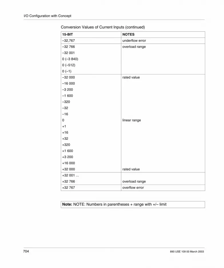
I/O Configuration with Concept
Conversion Values of Current Inputs (continued)
15-BIT NOTES
–32,767 underflow error
–32 766 overload range
–32 001
0 (–3 840)
0 (–512)
0 (–1)
–32 000 rated value
–16 000
–3 200
–1 600
–320
–32
–16
0 linear range
+1
+16
+32
+320
+1 600
+3 200
+16 000
+32 000 rated value
+32 001 ...
+32 766 overload range
+32 767 overflow error
Note: NOTE: Numbers in parentheses + range with +/– limit
704 890 USE 109 00 March 2003

I/O Configuration with Concept
Conversion Values of Temperature Inputs
Conversion Values of Temperature Inputs (continued)
-60 ... +160oC -160 ... +160oC -200 ... +320oC -200 ... +640oC
< –60 < –160 < –200 < –200
–160
–100 –200
–60 –60 –120
–50 –50 –100 –200
–16 –16 –32 –64
0 0 0 0
+0.005 +0.005 +0.01 +0.02
+0.08 +0.08 +0.16 +0.32
+0.16 +0.16 +0.32 +0.64
+8 +8 +16 +32
+16 +16 +32 +64
+80 +80 +160 +320
+160 +160 +320 +640
+160.005 ... +160.005 ... +320.01 ... +640.02 ...
+163.83 +163.83 +327.66 +655.32
>= +163.84 >= +163.84 >= +327.67 >= +655.34
15-BIT NOTES
–32,767 measuring range underflow (error)
–32 000 rated value
–22 000
–12 000
–10 000
–3 200
0 linear range
+1
+16
+32
+320
+1 600
+3 200
+16 000
890 USE 109 00 March 2003 705

I/O Configuration with Concept
Conversion Values for Resistance Inputs
Conversion Values of Resistance Inputs (continued)
+32 000 rated value
+32 001 ...
+32 766 overload range
+32 767 measuring range overflow error
0...100 Ω 0...200 Ω 0...500 Ω 0...1000 Ω 0...2000 W
< –1.6 < –3.2 < –8 < –16 < –32
0...–1.6 0...–3.2 0...–8 0...–16 0...–32
0 0 0 0 0
0.003 0.006 0.015 0.03 0.06
0.05 0.1 0.25 0.5 1
0.1 0.2 0.5 1 2
1 2 5 10 20
5 10 25 50 100
10 20 50 100 200
50 100 250 500 1000
100 200 500 1000 2000
100.00 ... 200.00 ... 500.01 ... 1000.03 ... 2000.06 ...
102.39 204.78 511.97 1023.94 2047.88
>= 102.40 >= 204.79 >= 511.98 >= 1023.97 >= 2047.94
15-BIT NOTES
–32 767 underflow error
0 overload range
0 rated value
+1
+16
+32
+320
+1 600 linear range
+3 200
+16 000
+32 000 rated value
15-BIT NOTES
706 890 USE 109 00 March 2003

I/O Configuration with Concept
Meanings for the AS–BADU–214 Module Mapping
The AS–BADU–214 module requires eight 3x–input registers addressed in sequence, beginning with channel 1 as shown in the figure below.
AS-BADU 216 8-point Thermocouple Isolated Analog Input
+32 001 ...
+32 766 overload range
+32 767 overflow error
15-BIT NOTES
Note: Refer to Concept I/O Map Status Words, p. 739 for Concept I/O Map Status Words.
3x-register 1 (channel 1)
MSB LSB
Note: This modules does not require any params... screens.
890 USE 109 00 March 2003 707

I/O Configuration with Concept
Meanings for the AS-BADU-216 Module Mapping
The AS–BADU–216 module requires five 3x–input registers, addressed in sequence beginning with the first register. Refer to ADU 216 Analog Input Module, p. 139 for details on the 3x status word for this module (as shown below.
The AS–BADU–216 module requires one 4x–output register, addressed in sequence beginning with the first register. Refer to ADU 216 Analog Input Module, p. 139 for details on the 4x control word for this module as shown below.
AS–BADU–257/257C
Note: Refer to Concept I/O Map Status Words, p. 739 for Concept I/O Map Status Words.
3x-register 1 (status word)3x-register 2 (input 1)
MSB
LSB
LSB
3x-register 5 (input 4)
4x-register 1 (control word)
MSB LSB
Note: The ADU 257 may operate in two different modes: either as a ADU 257 or as an ADU 216. This description ONLY applies the ADU 257 mode. For the ADU 216 description, refer to ADU 216 Analog Input Module, p. 139 or I/O Configuration of A120 Series I/O Modules with Modsoft, p. 745.
708 890 USE 109 00 March 2003

I/O Configuration with Concept
The following dialog is valid for the analog module AS–BADU–257.
Channel 1 ... 8: Cold junction compensation is selectable for the module. Eight thermocouple types are supported. Two RTD types with various resistances are supported. Two linear ranges are offered. Two temperature units are available. Either IEC or US platinum RTDs are supported. RTD connections allowed are 2, 3, 4–wire.Resolution: This list box defines the value range for all channels: 12-bit 16-bit 15-bit + sign 32-bit
AS-BADU257
Channel 1Channel 3Channel 5Channel 7
Channel 2Channel 4Channel 6Channel 8
Cold Junction
CelsiusFahrenheit
Type B Pt 100
Type E Pt 200Type J Pt 500
Type K Pt 1000Type N Ni 100Type R Ni 200Type S Ni 500Type T Ni 1000
+/-100mV linear 4k ohms
inactive
IEC Platinum
US Platinum
2/4 Wire3 Wire
Resolution Mode12-Bit
OK Cancel Help
890 USE 109 00 March 2003 709

I/O Configuration with Concept
The measuring ranges for channels 1 to 8 can be chosen in these sections.+/– 100mV Range and Data Display Format
0 ... 4000W Range and Data Display Format
IEC 751 Pt100,200,500,1000 –200 ... +850 C (–328 ... +1562 F) Range and Data Display Format
Millivoltage 12 bit 16 bit 15 bit + sign high resolution
IEEE 754 floating point
Range
<+102.4mV +4095 +65535 +32767 +1.024 E02 Overrange
>+100mV ...+102.4mV
+4095 +65535 +32001 ...+32766
+1.0 E02 ... +1.024 E02
Pos. tolerance range
+100mV +4095 +65535 +32000 +1.0 E02
0mV +2048 +32768 0 0 Nominal
–100mV 0 0 –32000 –1.0 E02
<–100mV ...–102.4mV
0 0 –32001 ...–32766
<–1.0 E02 ...–102.4 E02
Neg. tolerance range
<–102.4mV 0 0 –32767 –1.024 E02 Underrange
Resistance 12 bit 16 bit 15 bit + sign high resolution
IEEE 754 floating point
Range
>4095W +4095 +65535 +32767 +4.096 E03 Overrange
>4000 ...4095W
+4095 +65535 +32001 ...+32766
>+4.0 E03 ...+4.095 E03
Pos. tolerance range
4000W +4095 +65535 +32000 +4.0 E03 Nominal
0W 0 0 0 0
0 0 –2 –2.0 E00 Broken wire
RTD 12 bit 16 bit 15 bit + sign 0.1C (0.1F)
IEEE 754 floating point Range
>+850C (+1562F)
+4095 +65535 +8501 (+15621) 8.501 E02 (1.5621 E03) Overrange
+850C (+1562F)
+4095 +65535 +8500 (+15620) 8.500 E02 (1.562 E03)
0 (+32F) +780 +12483 0 (+320) 0 (3.20 E01) Nominal
–200C (–328F)
0 0 –2000 (–3280) –2.00 E02 (–3.28 E02)
<–200C (–328F)
0 0 –2001 (–3281) –2.001 E02 (–3.281 E02) Underrange
0 0 –2002 (–3282) –2.002 E02 (–3.282 E02) Broken wire
710 890 USE 109 00 March 2003

I/O Configuration with Concept
SAMA (US) Pt100,200,500,1000 –200 ... +650 C (–328 ... +1112 F) Range and Data Display Format
DIN43760 Ni100,200,500,1000 –60 ... +250 C (–76 ... +482 F) Range and Data Display Format
RTD 12 bit 16 bit 15 bit + sign 0.1C (0.1F)
IEEE 754 floating point
Range
>+600C (+1112F)
+4095 +65535 +6001 (+11121) 6.001 E02 (1.113 E03)
Overrange
+600C (+1112F) +4095 +65535 +6000 (+11120) 6.000 E02 (1.112 E03)
0C (+32F) +1024 +16384 0 (+320) 0 (3.20 E01) Nominal
–200C (–328F) 0 0 –2000 (–3280) –2.00 E02 (–3.28 E02)
<–200C (–328F) 0 0 –2001 (–3281) –2.001 E02 (–3.281 E02)
Underrange
0 0 –2002 (–3282) –2.002 E02 (–3.282 E02)
Broken wire
RTD 12 bit 16 bit 15 bit + sign 0.1C (0.1F)
IEEE 754 floating point
Range
>+250C (+482F) +4095 +65535 +2501 (+4821) 2.501 E02 (4.821 E02)
Overrange
+250C (+482F) +4095 +65535 +2500 (+4820) 2.500 E02 (4.820 E02)
0C (+32F) +793 +12684 0 (+320) 0 (3.20 E01) Nominal
–60C (–76F) 0 0 –600 (–760) –6.00 E01 (–7.6 E01)
<–60C (–76F) 0 0 –601 (–761) –6.01 E01 (–7.61 E01)
Underrange
0 0 –602 (–762) –6.02 E01 (–7.62 E01)
Broken wire
890 USE 109 00 March 2003 711

I/O Configuration with Concept
Thermocouple Type R,S –50 ... +1768 C (–58 ... +3214.4 F) Range and Data Display Format
Thermocouple Type B +50 ... +1800 C (+122 ... +3272 F) Range and Data Display Format
TC 12 bit 16 bit 15 bit + sign 0.1C (0.1F)
IEEE 754 floating point
Range
>+1768C (+3214.4F) +4095 +65535 +17681 (+32146)
1.7681 E03 (3.2146 E03)
Overrange
+1768C (+3214.4F) +4095 +65535 +17680 (+32144)
1.7680 E03 (3.2144 E02)
0C (+32F) +113 +1802 0 (+320) 0 (3.20 E01) Nominal
–50C (–58F) 0 0 –500 (–580) –5.00 E01 (–5.80 E01)
<–50C (–58F) 0 0 –501 (–582) –5.01 E01 (–5.82 E01)
Underrange
0 0 –502 (–584) –5.02 E01 (–5.84 E01)
Broken wire
TC 12 bit 16 bit 15 bit + sign 0.1C (0.1F)
IEEE 754 floating point
Range
>+1800C (+3272F) +4095 +65535 +18001 (+32722)
1.8001 E03 (3.2722 E03)
Overrange
+1800C (+3272F) +4095 +65535 +18000 (+32720)
1.8000 E03 (3.2720 E03)
Nominal
50C (+122F) 0 0 +500 (+1220) 5.00 E01 (1.220 E02)
<50C (+122F) 0 0 +499 (+1218) 4.99 E01 (1.218 E02)
Underrange
0 0 +498 (+1216) 4.98 E01 (1.216 E02)
Broken wire
712 890 USE 109 00 March 2003

I/O Configuration with Concept
Thermocouple Type J –210 ... +1200 C (–346 ... +2192 F) Range and Data Display Format
Thermocouple Type T –270 ... +400 C (–454 ... +752 F) Range and Data Display Format
TC 12 bit 16 bit 15 bit + sign 0.1C (0.1F)
IEEE 754 floating point
Range
>+1200C (+2192F) +4095 +65535 +12001 (+21922)
1.2001 E03 (2.1922 E03)
Overrange
+1200C (+2192F) +4095 +65535 +12000 (+21920)
1.2000 E03 (2.1920 E03)
0C (+32F) +610 +9761 0 (+320) 0 (3.20 E01) Nominal
–210C (–346F) 0 0 –2100 (–3460) –2.100 E02 (–3.460 E02)
<–210C (–346F) 0 0 –2101 (–3462) –2.101 E02 (–3.462 E02)
Underrange
0 0 –2102 (–3464) –2.102 E02 (–3.464 E02)
Broken wire
TC 12 bit 16 bit 15 bit + sign 0.1C (0.1F)
IEEE 754 floating point
Range
>+400C (+752F) +4095 +65535 +4001 (+7522) 4.001 E02 (7.522 E02)
Overrange
+400C (+752F) +4095 +65535 +4000 (+7520) 4.000 E02 (7.520 E02)
0C (+32F) +1650 +26410 0 (+320) 0 (3.20 E01) Nominal
–270C (–454F) 0 0 –2700 (–4540) –2.700 E02 (–4.540 E02)
<–270C (–454F) 0 0 –2701 (–4542) –2.701 E02 (–4.542 E02)
Underrange
0 0 –2702 (–4544) –2.702 E02 (–4.544 E02)
Broken wire
890 USE 109 00 March 2003 713

I/O Configuration with Concept
Thermocouple Type E –270 ... +1000 C (–454 ... +1832 F) Range and Data Display Format
Thermocouple Type K –270 ... +1372 C (–454 ... +2501.6 F) Range and Data Display Format
TC 12 bit 16 bit 15 bit + sign 0.1C (0.1F)
IEEE 754 floating point
Range
>+1000C (+1832F) +4095 +65535 +10001 (+18322)
1.0001 E03 (1.8322 E03)
Overrange
+1000C (+1832F) +4095 +65535 +1000 (+18320) 1.0000 E03 (1.8320 E03)
0C (+32F) +871 +13933 0 (+320) 0 (3.20 E01) Nominal
–270C (–454F) 0 0 –2700 (–4540) –2.700 E02 (–4.540 E02)
<–270C (–454F) 0 0 –2701 (–4542) –2.701 E02 (–4.542 E02)
Underrange
0 0 –2702 (–4544) –2.702 E02 (–4.544 E02)
Broken wire
TC 12 bit 16 bit 15 bit + sign 0.1C (0.1F)
IEEE 754 floating point
Range
>+1372C (+2501.6F) +4095 +65535 +13721 (+25018)
1.3721 E03 (2.5018 E03)
Overrange
+1372C (+2501.6F) +4095 +65535 +13720 (+25016)
1.3720 E03 (2.5016 E03)
0C (+32F) +673 +10776 0 (+320) 0 (3.20 E01) Nominal
–270C (–454F) 0 0 –2700 (–4540) –2.700 E02 (–4.540 E02)
<–270C (–454F) 0 0 –2701 (–4542) –2.701 E02 (–4.542 E02)
Underrange
0 0 –2702 (–4544) –2.702 E02 (–4.544 E02)
Broken wire
714 890 USE 109 00 March 2003
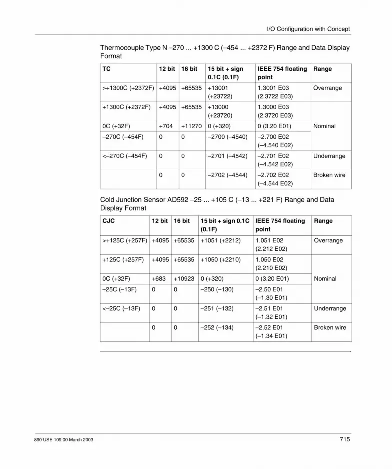
I/O Configuration with Concept
Thermocouple Type N –270 ... +1300 C (–454 ... +2372 F) Range and Data Display Format
Cold Junction Sensor AD592 –25 ... +105 C (–13 ... +221 F) Range and Data Display Format
TC 12 bit 16 bit 15 bit + sign 0.1C (0.1F)
IEEE 754 floating point
Range
>+1300C (+2372F) +4095 +65535 +13001 (+23722)
1.3001 E03 (2.3722 E03)
Overrange
+1300C (+2372F) +4095 +65535 +13000 (+23720)
1.3000 E03 (2.3720 E03)
0C (+32F) +704 +11270 0 (+320) 0 (3.20 E01) Nominal
–270C (–454F) 0 0 –2700 (–4540) –2.700 E02 (–4.540 E02)
<–270C (–454F) 0 0 –2701 (–4542) –2.701 E02 (–4.542 E02)
Underrange
0 0 –2702 (–4544) –2.702 E02 (–4.544 E02)
Broken wire
CJC 12 bit 16 bit 15 bit + sign 0.1C (0.1F)
IEEE 754 floating point
Range
>+125C (+257F) +4095 +65535 +1051 (+2212) 1.051 E02 (2.212 E02)
Overrange
+125C (+257F) +4095 +65535 +1050 (+2210) 1.050 E02 (2.210 E02)
0C (+32F) +683 +10923 0 (+320) 0 (3.20 E01) Nominal
–25C (–13F) 0 0 –250 (–130) –2.50 E01 (–1.30 E01)
<–25C (–13F) 0 0 –251 (–132) –2.51 E01 (–1.32 E01)
Underrange
0 0 –252 (–134) –2.52 E01 (–1.34 E01)
Broken wire
890 USE 109 00 March 2003 715

I/O Configuration with Concept
Meanings for the AS–BADU–257 Module Mapping
The AS–BADU–257 module requires twenty 3x–input registers addressed in sequence, beginning with two module status 3x registers, 16 data channel 3x registers (channels 1 ... 8), and two cold junction sensor 3x registers as shown below.
3x-register 1 (module status word)
3x-register 2 (module status word)
MSB
MSB
LSB
LSB
15 14 13 12 11 10 9 8 7 6 5 4 3 2 1 0
15 14 13 12 11 10 9 8 7 6 5 4 3 2 1 0
Ch4 Ch3 Ch2 Ch1
Ch8 Ch7 Ch6 Ch5
Chn The following errors apply to each channel:
Channel OK = 0000
Channel overrange error = 0001
Channel underrange error = 0010
Broken wire error = 0011
Invalid parameter error = 0100
Cold junction error = 0101 (applies to TC parameters ONLY)
(All others are reserved)
716 890 USE 109 00 March 2003

I/O Configuration with Concept
The following figure shows the AS-BADU-257 3x-register arrangement.
3x-register 3 (channel 1 data, low word)
3x-register 4 (channel 1 data, high word)
3x-register 17 (channel 8 data, low word)
3x-register 18 (channel 8 data, high word)
3x-register 20 (channel 9 data-cold junction sensor, high word)
MSB
MSB
MSB
MSB
MSB
LSB
LSB
LSB
LSB
LSB
890 USE 109 00 March 2003 717

I/O Configuration with Concept
Analog Output Modules
Analog Output Modules
The following information describes how to configure these modules: DAU 202/252/252C 2-point 24 Vdc Voltage/Current Analog Output DAU 204 4-point 24 Vdc Voltage/Current Analog Output DAU 208 8-point +/-10 Vdc Isolated Analog Output DAU 282* 2-point 24 Vdc Voltage/Current Analog Output (Special, Intrinsically
Safe)*The DAU 282 is a "special", and therefore it is not included in this document.
I/O Configuration using Concept 2.1 or Higher
Use the following procedure to configure the module.
Step Action
1 Select Configure from the menu.
2 Select I/O Map from the menu.
3 Click on Edit... The Local Common CPU Drop dialog appears.
4 Click on Module. The I/O Module Selection dialog appears.
5 Select DAU202/252/252C or DAU-208 and click on OK. A number and description appear.
6 In the In Ref field, enter 0x or 4x and press Enter. The software completes the Out Ref and Out End fields.
7 Click on Params... The appropriate configuration dialogs appear, depending on the module selected. Refer to the specific modules.
CAUTION
Power-down or kernel mode.
The output module Timeout States is valid only in a normal PLC stop state. Therefore, when the PLC powers down or goes into kernel mode, the outputs default to the module’s fail safe state. The Timeout States are defined on the I/O Map module parameter screens.
Failure to follow this precaution can result in injury or equipment damage.
718 890 USE 109 00 March 2003

I/O Configuration with Concept
AS-BDAU-202/ 252(C)
The following dialog is valid for the following modules: AS-BDAU-202/ 252(C).
Timeout State: The Compact Timeout State only reflects a user program in stop mode.Activation of the User Defined option button causes the outputs to take on the value defined in the user-defined timeout state text field.Last ValueActivation of the Last Value option button causes the outputs to retain their last valid value upon user program stop.User Defined:Activation of the User Defined option button causes the outputs to take on the hex values defined in the user-defined timeout state text fields Word 1/2. Resolution ModeThis list box defines the value range for all channels: 12-bit 15-bit + signMeasuring ranges +/- 10 VDC/ +/- 20 mA
Voltage (VDC) Current (mA) 12-bits 15-bits + sign Range
-10.24 ... -20.48 ... 0 -32768 Under-range
-10.005 -20.01 47 -32016
-10.00 -20.00 48 -32000
0 0 2048 0 Nominal range
+10.00 +20.00 4048 +32000
+10.005 ... +20.01 ... 4049 +32016 Overrange
+10.24 +20.48 4095 +32752
AS-BDAU2x2
Timeout State:
Last Value User Defined
User Defined Timeout State (In Hex):
Word 1 0000 Word 2 0000
Resolution 15-bit+sign
OK Cancel Help
890 USE 109 00 March 2003 719

I/O Configuration with Concept
Meanings for the AS-BDAU-202/ 252(C) Module Mapping
The AS-BDAU-202/ 252(C) modules require two 4x-output registers, as shown below.
AS-BDAU-204 This following dialog is valid for the analog module AS-BDAU-204.
Timeout StateThe Compact Timeout State only reflects a user program in stop mode.Activation of the Last Value option button causes the outputs to retain their last valid value upon user program stop.User Defined: Activation of the User Defined option button causes the 4 outputs to take on the hex values defined in the user-defined timeout state text fields Channel 1/4.
MSB
MSB LSB
LSB
4x-register 1 (channel 1)
4x-register 2 (channel 2)
AS-BDAU 204
Output
Override Last Value
Resolution
Range
Timeout State: Last Value User Defined
User Defined timeout State (In Hex.):
Channel 1: 0000 Channel 2: 0000 Channel 3: 0000 Channel 4: 0000
Set to Bottom of Scale Channel 1 Set to Bottom of Scale Channel 3
Set to Bottom of Scale Channel 2 Set to Bottom of Scale Channel 4
12-bit NoneBuilt-In Tests
Resolution Mode:
4 ... 20 mA
Channel 1: Channel 2:
4 ... 20 mA
Channel 3:
4 ... 20 mA
Channel 4:
4 ... 20 mA
OK Cancel Help
720 890 USE 109 00 March 2003

I/O Configuration with Concept
Override Last Value: Activation of the Set to Bottom of Scale Channel x option button causes channel x output to be set to the lowest value of the selected measuring range (Range) upon user program stop.Example: For a selected measuring range of 4 ... 20 mA the output will carry 4 mA upon user program stop, and thus guarantee a defined switch-off behavior.
Resolution Mode: This list box defines the output value range for all channels: 11-bit 12-bit 15-bit + sign 16-bitBuilt-In Tests: This list box can cause the execution of module built-in tests either automatically at power-up, or during on-line operation. The module’s green LED lights as long as no functional fault is determined.Selection of Category 2 (+/- 10 VDC) restricts the built-in tests exclusively to the +/- 10 VDC measuring range (Range).Selection of Category 3 (4 ... 20 mA) restricts the built-in tests exclusively to the 4 ... 20 mA measuring range (Range). "None" can be selected if the execution of built-in tests is not desired.Range:Measuring ranges for the individual channels can be chosen in these list boxes. 0 ... 1 VDC 0 ... 5 VDC 0 ... 10 VDC 0 ... 20 mA 4 ... 20 mA +/- 1 VDC +/- 5 VDC +/- 10 VDC0 ... 1 VDC, 0 ... 5 VDC, 0 ... 10 VDC
Note: Activation of the Set to Bottom of Scale option button disables any further alteration of the user-defined timeout state text field for the particular channel.
0 ... 1 VDC 0 ... 5 VDC 0 ... 10 VDC 11-bits 12-bits 15-bits + sign 16-bits Range
0 ... 1 VDC 0 ... 5 VDC 0 ... 10 VDC 11-bits 12-bits 15-bits + sign 16-bits Range
0 0 0 0 0 0 0
0.5 2.5 5 1024 2048 16000 32768 Nominal range
1 5 10 2047 4095 32000 65520
890 USE 109 00 March 2003 721

I/O Configuration with Concept
0/4 ... 20 mA
+/- 1 VDC, +/- 5 VDC, +/- 10 VDC
Meanings for the AS-BDAU-204 Module Mapping
The AS-BDAU-204 module requires one 3x-input register and five 4x-output registers. The 4x-output registers are addressed in sequence, beginning with channel 1. See the following figures.The following figure shows the AS-BDAU-204 3x-register arrangement.
0 ... 20 mA 4 ... 20 mA 11-bits 12-bits 15-bits + sign 16-bits Range
0 4 0 0 0 0
10 12 1024 2048 16000 32768 Nominal range
20 20 2047 4095 32000 65520
+/- 1 VDC +/- 5 VDC +/- 10 VDC 11-bits 12-bits 15-bits + sign 16-bits Range
-1 -5 -10 0 0 -32000 0
0.5 2.5 0 1024 2048 0 32768 Nominal range
+1 +5 +10 2047 4095 +32000 65520
15 14 13 12 11 10 9 8 7 6 5 4 3 2 1 0
1 = Memory fault
1 = Hardware fault
1 = Channel 4 current fault
1 = Channel 3 current fault
1 = Channel 2 current fault
1 = Channel 1 current fault
1 = Current fault (general message)
Bits 5 ... 13 are not used
MSB LSB
3x-register 1 (module status word)
722 890 USE 109 00 March 2003

I/O Configuration with Concept
The following figure shows the AS-BDAU-204 4x-register arrangement.
Runtime Control WordThe runtime control word supports the following calibration properties:
MSB
MSB
LSB
LSB
4x-register 1 (channel 1)
4x-register 4 (channel 4)
15 14 13 12 11 10 9 8 7 6 5 4 3 2 1 0
4x-register 5
MSB
1 = Calibration values were retained
1 = trim up
1 = trim down
1 = Calibration gain active
1 = Calibration offset (=0)
1 = Reset to default setting(10% current fluctuation)
1= Calibrating channel 1 = 0 01= Calibrating channel 2 = 0 11= Calibrating channel 3 = 1 01= Calibrating channel 4= 1 1
1= Calibration enabled
Bits 8 ... 14 are not used
LSB
890 USE 109 00 March 2003 723

I/O Configuration with Concept
AS-BDAU-208 The following dialog is valid for the analog module AS-BDAU-208.
Timeout StateThe Compact Timeout State only reflects a user program in stop mode.Activation of the Last Value option button causes the outputs to retain their last valid value upon user program stop.If the User Defined option button was activated, the 8 corresponding hex values can be entered here.User Defined:If the User Defined option button was activated in the timeout state section, the corresponding hex values can be entered in the text boxes 1/8, determining one value for each of the 8 output registers.Resolution ModeThis list box defines the output value range for all channels: 12-bit 15-bit + signMeasuring Range
AS-BDAU 208
Timeout State:
Last Value User Defined
User Defined Timeout State (In Hex.):
1. 2.
3.
5.
7.
4.
6.
8.
0000
0000
0000
0000
0000
0000
0000
0000
Resolution Mode: 15-bit+sign
OK Cancel Help
724 890 USE 109 00 March 2003

I/O Configuration with Concept
The +/- 10 VDC measuring range representation can be gathered from the following table:
Meanings for the AS-BDAU-208 Module Mapping
The AS-BDAU-208 module requires eight 4x-output registers. The 4x-output registers are addressed in sequence, beginning with channel 1 as shown below.
+/- 10 VDC 12-bits 15-bits + sign Range
-10.24 ... 0 -32768 Under-range
-10.005 47 -32016
-10.00 48 -32000
0 2048 0 Nominal range
+10.00 4048 +32000
+10.005 ... 4049 +32016 Overrange
+10.24 4095 +32752
MSB
MSB LSB
LSB
4x-register 1 (channel 1)
4x-register 8 (channel 8)
890 USE 109 00 March 2003 725

I/O Configuration with Concept
Intelligent Modules
Intelligent Modules
This section describes how to configure the following modules: FRQ-204/254 Frequency MOT 201 Motion -Encoder Only MOT 202 Motion-Resolver and Encoder VIC-2xx (Not supported in Concept 2.1 or higher) VRC 200/CTR 205/212/224 (Not supported in Concept 2.1 or higher) ZAE 201 Counter/Positioner
I/O Configuration of FRQ Modules using Concept 2.1 or Higher
Use the following procedure to configure the module.
I/O Configuration of Motion and Counter/Positioner Modules using Concept 2.1 or Higher
Use the following procedure to configure the module.
Step Action
1 Select Configure from the menu.
2 Select I/O Map from the menu.
3 Click on Edit... The Local Common CPU Drop dialog appears.
4 Click on Module. The I/O Module Selection dialog appears.
5 Select FRQ--204/205 and click on OK. A number and description appear.
6 In the In Ref field, enter 3x and press Enter. The software fills in the In Ref and In End fields.
7 Click on Params...
Step Action
1 Select Configure from the menu.
2 Select I/O Map from the menu.
3 Click on Edit... The Local Common CPU Drop dialog appears.
4 Click on Module. The I/O Module Selection dialog appears.
5 Select MOT--2X or ZAE--201 and click on OK. A number and description appear.
6 In the In Ref field, enter 3x and press Enter. The software fills in the In Ref and In End fields.
7 In the Out Ref field, enter 4x and press Enter. The software fills in the Out Ref and Out End fields.
8 Click on OK. (No Params are required for these modules.)
726 890 USE 109 00 March 2003

I/O Configuration with Concept
AS-BFRQ 204/ 254
The following dialog is valid for the AS-BFRQ 204/ 254 modules (frequency/revolution counters).
Channel 1 ... 4The individual channels are configured in the columns Channel 1 ... 4. Enter the desired counting frequency as offered (4 x <=1 kHz, 1 x <=50 kHz)ModeThe counting frequency can be selected in this section with the <=1 kHz or <=50 kHz option buttons.
Revolution counting mode is activated through the Revolution option button. Selecting the Revolution Mode changes the actual value received from Hz to rev/min.Activate the Falling Edge option button to trigger on the negative counting edge (1->0). The default setting is positive edge (0->1).Activation of the Inverse Output option button causes negation of both channel limit signals.
Note: Channel 1 can be alternatively driven with counting frequencies of up to 50 kHz.
0
Mode
Cancel
FRQ204/254
OK Help
0
Divide Factor
Lower Limit
Channel 1
<=1 kHz
<=50 kHz
Revolution
Falling Edge
Inverse Output
Mode
Channel 2
<=1 kHz
<=50 kHz
Revolution
Falling Edge
Inverse Output
Mode
Channel 3
<=1 kHz
<=50 kHz
Revolution
Falling Edge
Inverse Output
Mode
Channel 4
<=1 kHz
<=50 kHz
Revolution
Falling Edge
Inverse Output
Time
62.5 msec
125 msec
250 msec
500 msec
1000 msec
2000 msec
8000 msec
EM <= 20 Hz
Time
62.5 msec
125 msec
250 msec
500 msec
1000 msec
2000 msec
8000 msec
EM <= 20 Hz
Time
62.5 msec
125 msec
250 msec
500 msec
1000 msec
2000 msec
8000 msec
EM <= 20 Hz
Time
62.5 msec
125 msec
250 msec
500 msec
1000 msec
2000 msec
8000 msec
EM <= 20 Hz
0 Upper Limit
0
0
Divide Factor
Lower Limit
0 Upper Limit
0
0
Divide Factor
Lower Limit
0 Upper Limit
0
0
Divide Factor
Lower Limit
0 Upper Limit
890 USE 109 00 March 2003 727

I/O Configuration with Concept
FRQ204 Mode Configuration Example
TimeTime is the frequency of how often the counts are updated. The gating time for frequency/revolution measurements can be selected in this section. 62.5 msec 125 msec 250 msec 500 msec 1000 msec 2000 msec 8000 mesc EM <= 20 HzThe 62.5 to 8000 msec presets open the measurement window a corresponding period for input signal summation, which can then be converted into Hz or RPM units.The EM <= 20 Hz option button causes the measurement to be derived from the slope time rather than the gate time. This results in higher precision for frequencies up to 20 Hz or below 1200 RPM, which are achieved in a shorter gate-time period.Divide FactorThe divide factor actually divides your counts by the number you enter. A factor can be entered in this text field. The factor entered here is used for the connection of incremental encoders, sensors, or similar devices with high resolution, i.e. >1 count per revolution. As a value, the number of impulses per revolution has to be given. For example, if you have a 256 pulse/revolution encoder, then you would enter 256. The real frequency response speed is returned from the FRQ 204. The default value is 1. If you enter 0 it will be seen as a 1.Lower LimitThis establishes the lower limit of your range. The lower limiting threshold for minimum frequency or revolution monitoring (as well as wire breakage), can be entered in this text field. Values falling short of this preset value initiate status bits within the first input register (bits 0 ... 3), and in the status register of the drop station. Measurements continue and remain uninfluenced. When the lower limit is exceeded the corresponding module outputs are set.
Mode Selection Time (Gating Time)
Units of Measure
Actual Input Signal Value
Display Value Received
1kHz 1 ... 7 Hz 247 Hz 247
50kHz 1 ... 7 Hz 26780 Hz 26780
Revolution 1 ... 7 Rev/Min. 14820 Rev/Min. 14820
Revolution/50kHz 1 ... 7 Rev/Min. 29654 Rev/Min. 29654
1kHz 8 Hz 14.286 Hz 14286
Revolution 8 Rev/Min. 857.1 Rev/Min. 8571
728 890 USE 109 00 March 2003

I/O Configuration with Concept
Upper LimitThis establishes the upper limit of your range. The upper limiting threshold for maximum permissible frequency or revolution monitoring can be entered in this text field. Values falling short of this preset value initiate status bits within the first input register (bits 4 ... 7), and in the status register of the drop station. Measurements continue and remain uninfluenced. When the upper limit is exceeded the corresponding module outputs are set.
Meanings for the AS-BFRQ 204/ 254 Module Mapping
The frequency counting modules require five 3x-input registers, as shown in AS-BFRQ 204/ 2 Registers, p. 730 and AS-BFRQ 204/ 2 Registers, p. 730 below.
15 14 13 12 11 10 9 8 7 6 5 4 3 2 1 0 LSBMSB
1 = Channel 4 upper limiting value
1 = Channel 4 lower limiting value
1 = Input 4 active (24 VDC)
1 = Input 3 active (24 VDC)
1 = Input 2 active (24 VDC)
1 = Input 1 active (24 VDC)
1 = Channel 3 upper limiting value
1 = Channel 2 upper limiting value
1 = Channel 1 upper limiting value
1 = Channel 3 lower limiting value
1 = Channel 2 lower limiting value
1 = Channel 1 lower limiting value
Bits 12 ... 15 are not used
3x-register (status)
890 USE 109 00 March 2003 729

I/O Configuration with Concept
AS-BFRQ 204/ 2 Registers
The following figures shows the AS-BRFQ 204/254 3x-status register (top) and the AS-BFRQ 204/ 254 3x +1 ... +4 data register (bottom).
AS-BMOT-201/ 202
The AS-BMOT-201/ 202 modules require six 3x-input registers and six 4x-output registers.
Note: Refer toConcept I/O Map Status Words, p. 739 for Concept I/O Map Status Words.
LSBMSB
LSBMSB
...
...
...
3x-register +1 (frequency/revolution data)
3x-register +4 (frequency/revolution data)
Note: These modules do not require any params... screens.
730 890 USE 109 00 March 2003

I/O Configuration with Concept
Meanings for the AS-BMOT-201/ 202 Module Mapping
The following figure shows the AS-BMOT-201/ 202 3x-register arrangement.
15 14 13 12 11 10 9 8 7 6 5 4 3 2 1 0 LSBMSB
Servo on
Axis ready
Error
fault message(tolerance exceeded)
reserved
In Position
Serial master
Reserved (operating status)
Buffer assigned
reserved
Response type, bit 2
Response type, bit 1
Motion mode terminated
Motion mode active
Reserved (current limiting)
Reserved (trigger status)
3x-register 1 (status word)
890 USE 109 00 March 2003 731

I/O Configuration with Concept
The following figure shows the AS-BMOT-201/ 202 3x-register arrangement.
3x-register 2 (input data word 2)
3x-register 3 (input data word 3)
3x-register 6 (input data word 6)
LSBMSB
LSBMSB
LSBMSB
...
...
...
732 890 USE 109 00 March 2003

I/O Configuration with Concept
The following figure shows the AS-BMOT 201/ 202 4x-register arrangement.
15 14 13 12 11 10 9 8 7 6 5 4 3 2 1 0 LSBMSB
Motion halted
Halt
+ Limit OK / IN1
- Limit OK / IN2
Not in home position / IN3
Manual mode, positive / IN4
Fast stop
Pending command
Stop command
Response type, bit 2
Response type, bit 1
IN6
reserved
Manual mode, negative / IN5
Servo on
Fast command register
890 USE 109 00 March 2003 733

I/O Configuration with Concept
The following figure shows the S-BMOT-201/ 202 4x-register arrangement.
AS-BZAE-201
The AS-BZAE-201 module requires three 3x-input registers and three 4x-output registers.
Meanings for the AS-BZAE-201 Module Mapping
The following figure shows the AS-BZAE-201 3x-register arrangement.
4x-register 2 (output data word 2)
4x-register 3 (output data word 3)
4x-register 6 (output data word 6)
LSBMSB
LSBMSB
LSBMSB
...
...
...
Note: This module does not require any params... screens.
3x-register 1 (input 1)
3x-register 3 (input 3)
LSBMSB
LSBMSB
...
...
...
734 890 USE 109 00 March 2003

I/O Configuration with Concept
The following figure shows the AS-BZAE-201 4x-register arrangement.
4x-register 1 (output 1)
4x-register 3 (output 3)
LSBMSB
LSBMSB
...
...
...
890 USE 109 00 March 2003 735

I/O Configuration with Concept
Communication Interfaces
Communication Interfaces
This section describes how to configure the following modules: BKF-201 (16W)/BKF-201 (64W) Interbus S Master BKF-202 Interbus S Slave DEA-202 Interbus S Interface (No Mapping required) DEA-203253/243C Profibus DP Slave Module (No Mapping required) MVB-258/258A**The MVB-258/258A is a "special,"and therefore it is not included in this document.
I/O Configuration Using Concept 2.1 or Higher
Instructions for configuring the BKF-201 (16W) and BKF-201(64W) follow.
Step Action
1 Select Configure from the menu.
2 Select I/O Map from the menu.
3 Click on Edit... The Local Common CPU Drop dialog appears.
4 Click on Module. The I/O Module Selection dialog appears.
5 Select BKF and click on OK. A number and description appear.
6 In the In Ref field, enter 3x and press Enter. The software completes the In Ref and In End fields.
7 In the Out Ref field, enter 4x and press Enter. The software completes the Out Ref and Out End fields.
8 Click on Params... The Timeout State for Outputs on IBS dialog appears.)
9 Select either Set to Zero or Hold Last Value and click on OK.
736 890 USE 109 00 March 2003

I/O Configuration with Concept
AS-BBKF-201 / 202
The following dialog is used with the communication module AS-BBKF-201 (16 words/64 words). A different dialog box is used for AS–BBKF–202 (16 words); it is very similar.
Timeout state for outputs on IBSThe Compact timeout state only reflects a user program in stop mode.Activation of the Set to Zero option button causes outputs to be set to 0 upon user program stop, and thus guarantee a defined switch-off behavior.Activation of the Hold Last Value option button causes the outputs to retain their last valid value upon user program stop.
AS-BDAP211
Output Type
Input Type
Binary BCD
Binary BCD
Timeout State:
Last Value User Defined
User Defined Timeout State (In Hex.):
0000
OK HelpCancel
890 USE 109 00 March 2003 737

I/O Configuration with Concept
Meanings for the AS-BBKF-201/ 202 Module Mapping
The AS-BBKF-201 module requires 16 or 64 4x-output registers; the AS-BBKF-202 module requires 16 4x-output registers addressed in sequence, beginning with the first register (refer to the following figure(s). Refer to BKF 201 (16W) & (64W) InterBus S Master Module, p. 183 and BKF 202 InterBus S Slave Module, p. 201 for details about the 4x control word for these modules.The following figures show the AS-BBKF-201/202 3x-register arrangement.
The AS-BBKF-201 module requires 16 or 64 3x-input registers, the AS-BBKF-202 module requires 16 3x-input registers, addressed in sequence beginning with the first register (refer to the figure below). Refer to BKF 201 (16W) & (64W) InterBus S Master Module, p. 183 and BKF 202 InterBus S Slave Module, p. 201 for details on the 3x status word for these modules.
3x-register 1 (status word)
3x-register 2 (input 1)
MSB
MSB
LSB
LSB
3x-register 16/64 (input 15/63)
MSB
MSB LSB
LSB
4x-register 1 (control word)
4x-register 2 (output 1)
4x-register 16/64 (output 15/63)
738 890 USE 109 00 March 2003

I/O Configuration with Concept
Concept I/O Map Status Words
Status Words
The following lists the modules that provide Concept I/O Map Status Words. Most provide only an error flag, yet others provide additional error information. The following table shows I/O Map Status Word Error Flags and Additional Error Information.
Note: All other modules do not provide status word information.
I/O Module Error Flag Meaning (Refer to Figure 54)
Provides Additional Error Information
ADU204/254/254C Not applicable Yes. Refer to ADU 204/254/254(C) Status Word, p. 740.
ADU205 Not applicable Yes. Refer to ADU 205 Status Word, p. 740.
ADU206 1=Group signal when detail status information is available
ADU210 1=Group signal when detail status information is available
Yes. Refer to ADU 210 Status Word, p. 741.
ADU214 1=Group signal when detail status information is available
Yes. Refer to ADU 214 Status Word, p. 742.
ADU216 1=Group signal when detail status information is available
ADU257 1=Group signal when detail status information is available
Yes. Refer to ADU 257 Status Word, p. 743.
BKF201/202 1=Module error
DAP208/210/258/258C 1=Overload on one or more outputs
DAP220/250/250C 1=Power missing, or overload on one or more outputs
DAU202/252/252C 1=Error during generation of the internal +/-15V supply
DAU208/258 1=Error during generation of the internal +/-15V supply
FRQ204/254 1=Overflow of a counter or overload on one or more outputs
Yes. Refer to FRQ 204/254 Status Word, p. 743.
890 USE 109 00 March 2003 739
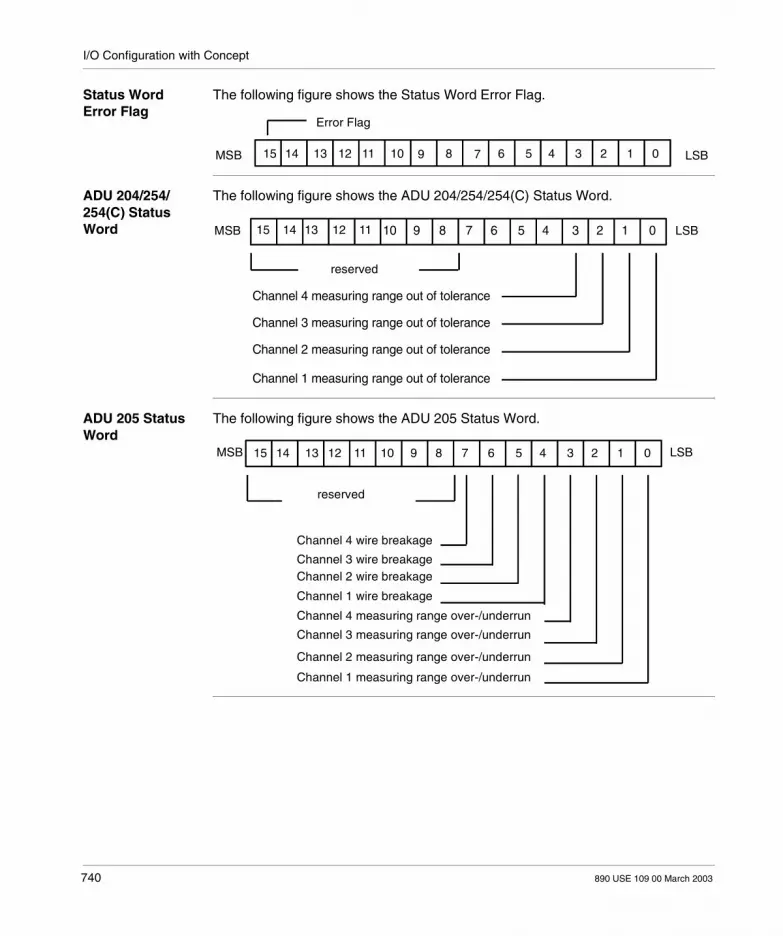
I/O Configuration with Concept
Status Word Error Flag
The following figure shows the Status Word Error Flag.
ADU 204/254/254(C) Status Word
The following figure shows the ADU 204/254/254(C) Status Word.
ADU 205 Status Word
The following figure shows the ADU 205 Status Word.
Error Flag
MSB LSB15 14 13 12 11 10 9 8 7 6 5 4 3 2 1 0
MSB LSB
reserved
15 14 13 12 11 10 9 8 7 6 5 4 3 2 1 0
Channel 4 measuring range out of tolerance
Channel 2 measuring range out of tolerance
Channel 1 measuring range out of tolerance
Channel 3 measuring range out of tolerance
reserved
MSB LSB15 14 13 12 11 10 9 8 7 6 5 4 3 2 1 0
Channel 4 wire breakage
Channel 3 wire breakageChannel 2 wire breakage
Channel 1 wire breakage
Channel 4 measuring range over-/underrun
Channel 3 measuring range over-/underrun
Channel 2 measuring range over-/underrun
Channel 1 measuring range over-/underrun
740 890 USE 109 00 March 2003

I/O Configuration with Concept
ADU 210 Status Word
The following figure shows the ADU 210 Status Word.
Error Flag
MSB LSB
reserved
Channel 1 error = 001Channel 2 error = 010Channel 3 error = 011Channel 4 error = 100
Parameter error = 001
Underrange or broken wire error = 101
Overrange error = 110
System error or power failed = 11111111
Bits 7 & 3 are not used
15 14 13 12 11 10 9 8 7 6 5 4 3 2 1 0
890 USE 109 00 March 2003 741

I/O Configuration with Concept
ADU 214 Status Word
The following figure shows the ADU 214 Status Word.
Error Flag
LSBMSB 15 91011121314 1 08 7 6 5 4 3 2
reserved
Channel 1 error = 0001Channel 2 error = 0010Channel 3 error = 0011Channel 4 error = 0100Channel 5 error = 0101Channel 6 error = 0110Channel 7 error = 0111Channel 8 error = 1000
Parameter error = 0001Channels 1,3,5,7 (for 2-wire voltage or current ONLY) error = 0010Channels 2,4,7,8 (for voltage or current ONLY)
Broken wire (2-wire or 4-wire RTD measurement ONLY) error = 0100Underrange, sensor short circuit, or broken wire (of any channel) error = 0101Overrange (of any channel) error = 0110Bipolar measurement (both channels MUST be configured as the same-measurement range) error = 0111
System error or power failed = 11111111
(channels 1,3,5,7 MUST be inactive) error = 0011
742 890 USE 109 00 March 2003

I/O Configuration with Concept
ADU 257 Status Word
The following figure shows the ADU 257 Status Word.
FRQ 204/254 Status Word
The following figure shows the FRQ 204/254 Status Word.
Error Flag
reservedreserved
Channel 9 status (cold junction sensor)
MSB LSB
Channel OK = 0000Channel overrange = 0001Channel underrange = 0010Broken Wire = 0011
(All others reserved)
No error in channels 1 ... 8 = 0Error in channels 1 ... 8 = 1
MSB LSB
reserved
1 = Outside the 20 Hz range
1 = System fault
1 = Output overload
1 = Channel 4 frequency overflow error
1 = Channel 3 frequency overflow error
1 = Channel 2 frequency overflow error
1 = Channel 1 frequency overflow error
Bit 7 is not used
15 14 13 12 11 10 9 8 7 6 5 4 3 2 01
890 USE 109 00 March 2003 743

I/O Configuration with Concept
744 890 USE 109 00 March 2003

890 USE 109 00 March 2003
I/O Configuration of A120 Series I/O Modules with Modsoft
At a Glance
Purpose This chapter describes the configuration of A120 Series I/O modules with Modsoft.
What’s in this Chapter?
This chapter contains the following topics:
Topic Page
Configuring A120 Discrete Input Modules with Modsoft 746
Configuring A120 Discrete Output Modules with Modsoft 747
Configuring A120 Discrete Combination Modules with Modsoft 748
Configuring A120 Analog Input Modules with Modsoft 749
Configuring A120 Analog Output Modules with Modsoft 750
Configuring A120 Intelligent Modules with Modsoft 751
Configuring A120 Communication Interfaces with Modsoft 752
745

I/O Configuration with Modsoft
Configuring A120 Discrete Input Modules with Modsoft
Discrete Input Modules
This following information describes how to configure the following modules: DEO 216 16-point 24 Vdc Discrete Input DEP 208 8-point 230 Vac Discrete Input DEP 209 8-point 120 Vac Discrete Input DEP 210 8-point 115 Vac Isolated Discrete Input DEP 211 8-point 115 Vac Isolated Discrete Input DEP 214 16-point 12 ... 60Vdc Discrete Input DEP 215 16-point 5 Vdc TTL Discrete Input DEP 216 16-point 24 Vdc Discrete Input DEP 217 16-point 24 Vdc Discrete Input DEP 218 16-point 115 Vac Isolated Discrete Input DEP 220 16-point 24 Vdc Discrete Input DEP 257 16-point 110 Vdc Discrete Input DEP 296 16-point 60 Vdc Isolated Discrete Input DEP 297 16-point 48 Vdc Isolated Discrete Input DEP 284* 8-point 115 Vac Isolated Discrete Input (Not supported in Modsoft 2.6
or lower)*The DEP 284 is a "special", and therefore it is not included in this document.
I/O Configuration Using Modsoft 2.6 or Lower
Use the following procedure to configure A120 discrete input modules using Modsoft.
Step Action
1 Select I/O Map (or press F4). This places you at rack 1, slot position 101...105.
2 Move the cursor to slot 104.
3 Hold the Shift key and press the ? key. This displays a list of possible I/O modules.
4 Select DEPxxx.
5 Enter the input reference 10001 and press the Enter key. The software automatically fills in the input range. If you are using a 3x register, the cursor automatically moves to Data Type.
6 Select either Binary or BCD and press the Enter key.
7 Choose Quit (or press F9). Escape to the Modsoft main menu.
8 Refer to individual module chapters for more information.
746 890 USE 109 00 March 2003
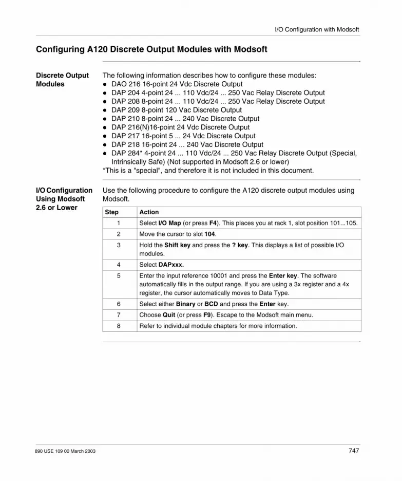
I/O Configuration with Modsoft
Configuring A120 Discrete Output Modules with Modsoft
Discrete Output Modules
The following information describes how to configure these modules: DAO 216 16-point 24 Vdc Discrete Output DAP 204 4-point 24 ... 110 Vdc/24 ... 250 Vac Relay Discrete Output DAP 208 8-point 24 ... 110 Vdc/24 ... 250 Vac Relay Discrete Output DAP 209 8-point 120 Vac Discrete Output DAP 210 8-point 24 ... 240 Vac Discrete Output DAP 216(N)16-point 24 Vdc Discrete Output DAP 217 16-point 5 ... 24 Vdc Discrete Output DAP 218 16-point 24 ... 240 Vac Discrete Output DAP 284* 4-point 24 ... 110 Vdc/24 ... 250 Vac Relay Discrete Output (Special,
Intrinsically Safe) (Not supported in Modsoft 2.6 or lower)*This is a "special", and therefore it is not included in this document.
I/O Configuration Using Modsoft 2.6 or Lower
Use the following procedure to configure the A120 discrete output modules using Modsoft.
Step Action
1 Select I/O Map (or press F4). This places you at rack 1, slot position 101...105.
2 Move the cursor to slot 104.
3 Hold the Shift key and press the ? key. This displays a list of possible I/O modules.
4 Select DAPxxx.
5 Enter the input reference 10001 and press the Enter key. The software automatically fills in the output range. If you are using a 3x register and a 4x register, the cursor automatically moves to Data Type.
6 Select either Binary or BCD and press the Enter key.
7 Choose Quit (or press F9). Escape to the Modsoft main menu.
8 Refer to individual module chapters for more information.
890 USE 109 00 March 2003 747

I/O Configuration with Modsoft
Configuring A120 Discrete Combination Modules with Modsoft
Discrete Combination Modules
The following information describes how to configure these modules: DAP 211 Monitored 4-point in/4-point out 120 Vac Combined I/O (Requires a
loadable (SW–IODR–001) for proper operation using certain PLCs (A984–1xx, E984–24x/251/255) with Modsoft. Refer to Installing the Loadables for A120 Series I/O Modules, p. 791 for details).
DAP 212 8-point in/4-point out 24 Vdc Combined I/O DAP 220 8-point in/8-point out 24 Vdc Combined I/O DAP 252 8-point in/4-point relay out 24 Vdc LT Combined I/O DAP 253 8-point in/4-point relay out 110 Vdc LT Combined I/O DAP 292 8-point in/4-point relay out 60 Vdc Combined I/O
I/O Configuration Using Modsoft 2.6 or Lower
Use the following procedure to configure A120 discrete output modules using Modsoft.
Step Action
1 Select I/O Map (or press F4). This places you at rack 1, slot position 101...105.
2 Move the cursor to slot 104.
3 Hold the Shift key and press the ? key. This displays a list of possible I/O modules.
4 Select DAPxxx.
5 Enter the input reference 10001 and press the Enter key. The software automatically fills in the input range.
6 Enter the output reference 0001 and press the Enter key. The software automatically fills in the input range. If you are using a 3x register and a 4x register, the cursor automatically moves to Data Type.
7 Select either Binary or BCD and press the Enter key.
8 Choose Quit (or press F9). Escape to the Modsoft main menu.
9 Refer to individual module chapters for more information.
748 890 USE 109 00 March 2003

I/O Configuration with Modsoft
Configuring A120 Analog Input Modules with Modsoft
Analog Input Modules
This section describes how to configure the following modules: ADU 204 4-point Voltage/RTD Analog Input ADU 205 4-point Voltage/Current Analog Input ADU 206 4-point Voltage/Current Isolated Analog Input ADU 210 4-point Voltage/Current Analog Input (Not supported in Modsoft) ADU 214 8-point Voltage/Current Isolated Analog Input ADU 216 8-point Thermocouple Isolated Analog Input ADU 257/257C 8-point Voltage/RTD/TC Analog Input (Not supported in Modsoft)
NOTE: If the ADU257s DIP switch is set to the ADU216 mode, the ADU257 operates just like an ADU216 module. Refer to Overview of the ADU 257 Analog Input Module, p. 155.
ADU 282/282M* 2-point Analog Input (Special, Intrinsically Safe) (Not supported in Modsoft 2.6 or lower).
ADU 284* 2-point Analog Input (Special, Intrinsically Safe) (Not supported in Modsoft 2.6 or lower)
ADU 211/212 8-point Universal Isolated Analog Input *This is a "special", and therefore it is not included in this document.
I/O Configuration Using Modsoft 2.6 or Lower
Use the following procedure to configure A120 discrete output modules using Modsoft.
Step Action
1 Select I/O Map (or press F4). This places you at rack 1, slot position 101...105.
2 Move the cursor to slot 104.
3 Hold the Shift key and press the ? key. This displays a list of possible I/O modules.
4 Select ADUxxx.
5 Enter the input reference 3x and press the Enter key. The software automatically fills in the input range.
6 Enter the output reference 4x and press the Enter key. The software automatically fills in the input range. If you are using a 3x register and a 4x register, the cursor automatically moves to Data Type.
7 Select either Binary or BCD and press the Enter key.
8 Choose Quit (or press F9). Escape to the Modsoft main menu.
9 Refer to individual module chapters for more information.
890 USE 109 00 March 2003 749

I/O Configuration with Modsoft
Configuring A120 Analog Output Modules with Modsoft
Analog Output Modules
This section describes how to configure the following modules: DAU 202 2-point 24 Vdc Voltage/Current Analog Output DAU 204 4-point 24 Vdc Voltage/Current Analog Output DAU 208 8-point +/-10 Vdc Isolated Analog Output DAU 282* 2-point 24 Vdc Voltage/Current Analog Output (Special, Intrinsically
Safe) (Not supported in Modsoft 2.6 or lower)*The DAU 282 is a "special", and therefore it is not included in this document.
I/O Configuration Using Modsoft 2.6 or Lower
Use the following procedure to configure A120 discrete output modules using Modsoft.
Step Action
1 Select I/O Map (or press F4). This places you at rack 1, slot position 101...105.
2 Move the cursor to slot 104.
3 Hold the Shift key and press the ? key. This displays a list of possible I/O modules.
4 Select DAUxxx.
5 Enter the output reference 4x and press the Enter key. The software automatically fills in the input range. If you are using a 4x register, the cursor automatically moves to Data Type.
6 Select either Binary or BCD and press the Enter key.
7 Choose Quit (or press F9). Escape to the Modsoft main menu.
8 Refer to individual module chapters for more information.
750 890 USE 109 00 March 2003

I/O Configuration with Modsoft
Configuring A120 Intelligent Modules with Modsoft
Intelligent Modules
This section describes how to configure the following modules: FRQ-204/254 Frequency (Not supported in Modsoft 2.6 or lower) MOT 201 Motion-Encoder Only MOT 202 Motion-Resolver and Encoder VIC-2xx High-Speed Input VRC 200/CTR 205/212/224 Variable Reluctance Counter/Counter ZAE 201 Counter/Positioner ZAE 204 High-Speed Counter
I/O Configuration Using Modsoft 2.6 or Lower
Use the following procedure to configure A120 discrete output modules using Modsoft.
Step Action
1 Select I/O Map (or press F4). This places you at rack 1, slot position 101...105.
2 Move the cursor to slot 104.
3 Hold the Shift key and press the ? key. This displays a list of possible I/O modules.
4 Select XXXxxx.
5 Enter the input reference 3x and press the Enter key. The software automatically fills in the input range.
6 Enter the output reference 4x and press the Enter key. The software automatically fills in the input range. If you are using a 3x register and a 4x register, the cursor automatically moves to Data Type.
7 Select either Binary or BCD and press the Enter key.
8 Choose Quit (or press F9). Escape to the Modsoft main menu.
9 Refer to individual module chapters for more information.
890 USE 109 00 March 2003 751

I/O Configuration with Modsoft
Configuring A120 Communication Interfaces with Modsoft
Communication Interfaces
The following communication interfaces are not supported in Modsoft 2.6 or lower: BKF-201 (16W)/BKF-201 (64W) Interbus S Master BKF-202 Interbus S Slave (Not supported in Modsoft 2.6 or lower) DEA-202 Interbus S Interface (Not supported in Modsoft 2.6 or lower) DEA-203/253/243C Profibus DP Slave Module (Not supported in Modsoft 2.6 or
lower) MVB-258/258A* (Not supported in Modsoft 2.6 or lower)*The MVB-258/258A is a "special", and therefore it is not included in this document.
I/O Configuration Using Modsoft 2.6 or Lower Note: The modules are not supported in Modsoft 2.6 or lower.
752 890 USE 109 00 March 2003

890 USE 109 00 March 2003
Modsoft Application Examples for Selected A120 Series I/O Modules
At a Glance
Purpose This chapter provides examples of how to use selected Series A120 I/O modules with Modsoft’s Ladder Logic.
What’s in this Chapter?
This chapter contains the following topics:
Topic Page
ADU 205 Application Example 754
DAU 204 Application Example 757
VRC/CTR 2xx (VIC2xx) Application Notes 760
753

Modsoft Application Examples
ADU 205 Application Example
Overview In many applications, analog signals are scaled to engineering units that indicate units such as I/O points,degrees C, gal/min, cm/s, etc. An operator may view the scaled analog input data via LED displays, screen displays on a monitor, or report printouts.
Temperature Example
For example, assume that the -10 ... +10 V signal is being used to represent a temperature between -40 ... +140 F. The following figure shows the Signal-to-Temperature Relationship.
To appropriately display this analog data as a temperature value, you can use an ADU 205 Analog Input module I/O Mapped as follows: 30001-30004 input registers and binary.
140
120
100
60
40
20
0
80
-20
-40
-10V2049
Analog Input Data+10V Module Configuration6143 Operating Range
Tem
p
754 890 USE 109 00 March 2003

Modsoft Application Examples
Field Wiring Illustration
The following information describes how to field wire the ADU 205. The information consists of a field wiring illustration and a procedure (see Procedure for Generating Logic, p. 756. The following figure illustrates how to field wire the ADU 205.
123456799
10111213141516171819202122
ADU 205
Voltage Source
890 USE 109 00 March 2003 755

Modsoft Application Examples
Procedure for Generating Logic
Use the following procedure to generate the ladder logic.
Step Action
1 Divide the temperature range, 180 degrees, by 4095. (180 / 4095 = .044)
2 Obtain the MUL block constant by multiplying the result by 10,000.(.044 x 10,000 = 440)
3 Generate the ladder logic to subtract the 2049 offset multiply the analog input by the constant; the high order result register will contain the range. Then subtract the Y-intercept, -40, to obtain the answer, as shown.
This logic generates the scaled value in register 40020 from the analog signal in 30001. Only the high order result of the MUL operation is used, and no compensation for round-off is used in this example.
30001 40001 40010
2049 440 40
SUB40001
MUL40001
SUB40020 (Minus sign)
756 890 USE 109 00 March 2003

Modsoft Application Examples
DAU 204 Application Example
How the Module Ramps Outputs through to the Full Scale
The figures in this map show a ladder logic program that uses 1 timer (register 40010) and 1 upcounter (register 40020) to decrement all 4 output channel registers of the DAU204 (registers 40001 through 40004). This is very easily done using block moves and 5 holding registers (registers 40011 through 40015). With the module configured for 4 ... 20 mA output on all four channels (0 in register 40005), each channel is decremented from the top of the scale (4095) to the bottom of the scale (0) in 5 second intervals. After each interval, the outputs are changed to different values, again for 5 seconds. The counter is then reset, which starts the sequence again.
Network 1 Example
The following figure illustrates the logic for Network 1.
Note: This is only an example showing how the module operates to ramp the outputs through the full scale. The ladder logic (four networks) are not required to operate the module.
00050
00051
00050
00050
00051
0006
UCTR
40020
0005
T1.0
40010
40020
00001
BLKM0001
890 USE 109 00 March 2003 757

Modsoft Application Examples
Network 2 Example
The following figure illustrates the logic for Network 2.
Network 3 Example
The following figure illustrates the logic for Network 3.
00016 00015 00014
40011
40001
BLKM0001
40011
40002
BLKM0001
40011
40003
BLKM0001
40011
40004
BLKM0001
40012
40001
BLKM0001
40012
40002
BLKM0001
40012
40003
BLKM0001
40012
40004
BLKM0001
00016 00015 00014
00016 00015 00014
00016 00015 00014
40013
40001
BLKM0001
40013
40002
BLKM0001
40013
40003
BLKM0001
40013
40004
BLKM0001
40014
40001
BLKM0001
40014
40002
BLKM0001
40014
40003
BLKM0001
40014
40004
BLKM0001
758 890 USE 109 00 March 2003

Modsoft Application Examples
Network 4 Example
The following figure illustrates the logic for Network 4.
Reference Data The following figure shows the reference data for the DAU 204 application example.
00016 00015 00014
00016 00015 00014
40015
40001
BLKM0001
40015
40002
BLKM0001
40015
40003
BLKM0001
40015
40004
BLKM0001
40011
40001
BLKM0001
40012
40002
BLKM0001
40014
40003
BLKM0001
40015
40004
BLKM0001
REFERENCE DATA
300014000140002400034000440005
00000000000000004095 Dec3072 Dec1027 Dec0 Dec0 Dec
40006 0 Dec
4001040020
40011400124001340014
1 Dec5 Dec
4095 Dec3072Dec2045 Dec1027 Dec
40015 0 Dec
890 USE 109 00 March 2003 759

Modsoft Application Examples
VRC/CTR 2xx (VIC2xx) Application Notes
Controlling the Module
The VRC/CTR module is structured to minimize the amount of I/O resources required to operate the module. A total of six registers, set up as two separate groups of three registers each (three 3x input and three 4x output registers) is the total amount of resources dedicated to the module. Note that some individual registers are designed for use within the ladder program as contacts or coils.Ladder Logic Example 1, p. 761, which follows, shows how to move data from a word format into a bit location for use as a contact or coil within the ladder program. (This is only one example. You can accomplish the same result differently.)In this example, the command will copy the data from input register 30152 (16 bits) into sixteen consecutive bit locations starting at output reference 00065. It will also copy 32 bit locations starting at output reference 81 and move the data into two (2) consecutive holding registers starting at 4005. Refer to the figures in Accompanying Bit Functions, p. 762 to see the bit functions that will be in place with Ladder Logic Example 1, p. 761.Some of the individual registers are designed for use within the ladder program as contacts or coils. With this ladder program, you can easily manipulate coils or simply monitor bits within the ladder program to control or monitor the VRC/CTR module.
760 890 USE 109 00 March 2003

Modsoft Application Examples
Ladder Logic Example 1
The following figure illustrates how to move data from a word format into a bit location for use as a contact or coil within the ladder program. This example assigns registers 30150 ... 30152 and 40050 ... 40052 to the VRC/CTR module.
In this figure, the command will copy the data from input register 30152 (16 bits) into sixteen consecutive bit locations starting at output reference 00065. It will also copy 32 bit locations starting at output reference 81 and move the data into two (2) consecutive holding registers starting at 40051.
Note: For consistency, it is recommended that the rung of logic illustrated in this figure be placed after all logic associated with the VRC/CTR module. This does not affect the module, but it may be important for consistent control of the module.
0x
VRC/CTRtoPLC
PLCtoVRC/CTR
30152
65
BLKM 1
81
40051
BLKM 2
890 USE 109 00 March 2003 761
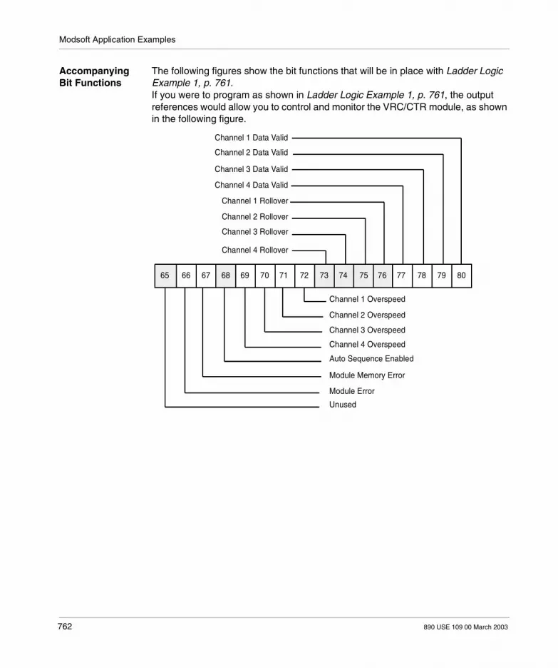
Modsoft Application Examples
Accompanying Bit Functions
The following figures show the bit functions that will be in place with Ladder Logic Example 1, p. 761.If you were to program as shown in Ladder Logic Example 1, p. 761, the output references would allow you to control and monitor the VRC/CTR module, as shown in the following figure.
Channel 1 Overspeed
Channel 2 Data Valid
Channel 3 Data Valid
Channel 4 Data Valid
Channel 1 Rollover
Channel 2 Rollover
Channel 3 Rollover
Channel 4 Rollover
Channel 1 Data Valid
Channel 2 Overspeed
Channel 3 Overspeed
Channel 4 Overspeed
Auto Sequence Enabled
Module Memory Error
Module Error
Unused
65 66 67 68 69 70 71 72 73 74 75 76 77 78 79 80
762 890 USE 109 00 March 2003

Modsoft Application Examples
The following figure depicts Output Register #2, VRC/CTR Control Word 1 (as it would appear if accompanying Ladder Logic Example 1, p. 761).
Select Channel 1
Select Channel 2
Select Channel 3
Select Channel 4
Clear Channel 1
Clear Channel 2
Clear Channel 3
Clear Channel 4
Hold Channel 1
Hold Channel 2
Hold Channel 3
Hold Channel 4Load Channel 1 K FactorLoad Channel 2 K FactorLoad Channel 3 K Factor
Load Channel 4 K Factor
81 82 83 84 85 86 87 88 89 90 91 92 93 94 95 96
890 USE 109 00 March 2003 763

Modsoft Application Examples
The following figure depicts Output Register #3, VRC/CTR Control Word 2 (accompanying (as it would appear if accompanying Ladder Logic Example 1, p. 761).
Factor Values The VRC/CTR module can accept K and Meter factor data to process the incoming pulse information.
K Factor The VRC/CTR module uses K factor information specific to the field device attached to each channel. K factor values may be any number from 1 ... 65,535, and are used in conjunction with the Meter factor value to calculate the incoming pulse information. Typically, the K factor number is imprinted on the side of the field device or listed in the documentation associated with the device.
Load Channel 1 M Factor
Load Channel 2 M Factor
Load Channel 3 M Factor
Load Channel 4 M Factor
Channel 1 Frequency (Hz)Channel 2 Frequency (Hz)
Channel 3 Frequency (Hz)
Channel 4 Frequency (Hz)
Auto Sequence Enable
Display K Factor
BITE Enabled
BITE Bit #1
Unused
Display Frequency
Display M Factor
BITE Bit #2
97 98 99 100 101 102 103 104 105 106 107 108 109 110 111 112
764 890 USE 109 00 March 2003
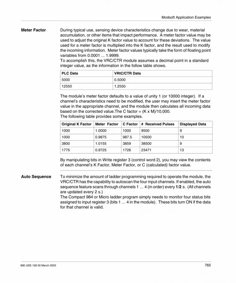
Modsoft Application Examples
Meter Factor During typical use, sensing device characteristics change due to wear, material accumulation, or other items that impact performance. A meter factor value may be used to adjust the original K factor value to account for these deviations. The value used for a meter factor is multiplied into the K factor, and the result used to modify the incoming information. Meter factor values typically take the form of floating point variables from 0.0001 ... 1.9999. To accomplish this, the VRC/CTR module assumes a decimal point in a standard integer value, as the information in the follow table shows.
The module’s meter factor defaults to a value of unity 1 (or 10000 integer). If a channel’s characteristics need to be modified, the user may insert the meter factor value in the appropriate channel, and the module then calculates all incoming data based on the corrected value.The C factor = (K x M)/10,000.The following table provides some examples.
By manipulating bits in Write register 3 (control word 2), you may view the contents of each channel’s K Factor, Meter Factor, or C (calculated) factor value.
Auto Sequence To minimize the amount of ladder programming required to operate the module, the VRC/CTR has the capability to autoscan the four input channels. If enabled, the auto sequence feature scans through channels 1 ... 4 (in order) every 1/2 s. (All channels are updated every 2 s.)The Compact 984 or Micro ladder program simply needs to monitor four status bits assigned to input register 3 (bits 1 ... 4 in the module). These bits turn ON if the data for that channel is valid.
PLC Data VRtC/CTR Data
5000 0.5000
12550 1.2550
Original K Factor Meter Factor C Factor # Received Pulses Displayed Data
1000 1.0000 1000 9500 9
1000 0.9875 987.5 10500 10
3800 1.0155 3859 38500 9
1775 0.9725 1726 23471 13
890 USE 109 00 March 2003 765
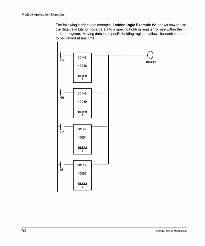
Modsoft Application Examples
The following ladder logic example, Ladder Logic Example #2, shows how to use the data valid bits to move data into a specific holding register for use within the ladder program. Moving data into specific holding registers allows for each channel to be viewed at any time.
0XXXx65
66
67
68
30149
40049
BLKM 1
30149
40051
BLKM 1
30149
40052
BLKM 1
30149
40048
BLKM 1
766 890 USE 109 00 March 2003

Modsoft Application Examples
[Please review the Controlling the Module, p. 760 and the Accompanying Bit Functions, p. 762 for more information about register operation.] By using these four valid data bits, the ladder program distinguishes which channel is displayed at any given moment in time. By moving the data that is displayed for each channel (based on the status of these bits) into specific registers for use by the program, the ladder program can better utilize the information in other sections of the ladder program.
Manual Operation
Manual selection of channels is controlled by four bits located in output word 2, VRC/CTR control word 1. By setting these bits ON or OFF, you may select a specific channel for monitoring. Using the above example (see Auto Sequence, p. 765), all you would need to do is program four (4) coils in the ladder program, as shown in the following figure.
Overspeed Bits It is recommended that the user monitor the overspeed bits in the ladder program. For the VRC–200 version of the module, the overspeed bits signal that the data from the module is potentially inaccurate. For these applications, it is recommended that the overspeed bits be monitored in ladder logic and flag an overspeed condition.
CONDITIONAL LOGIC
CONDITIONAL LOGIC
CONDITIONAL LOGIC
CONDITIONAL LOGIC
00080 00081 00082 00083
00082
00081
00080
00080 00081 00083
00080 00082 00083
00081 00082 00083
890 USE 109 00 March 2003 767

Modsoft Application Examples
768 890 USE 109 00 March 2003

890 USE 109 00 March 2003
A120 Option Modules
At a Glance
Introduction This chapter describes several A120 modules that are options.
What’s in this Chapter?
This chapter contains the following topics:
Topic Page
SIM 203 Analog Simulator Module 770
SIM 216 Binary Simulator Module 774
NUL 200 and 202 Modules 777
769

A120 Option Modules
SIM 203 Analog Simulator Module
General The SIM 203 simulator module is an A120 option that allows you, for instructional purposes, to generate two analog signals - 0 ... 1V or 0 ... 10V (toggle switch selectable) and to display one 10V output signal from a Compact 984 controller output module. The SIM 203 outputs interface to the controller through the ADU 204 and ADU 205 input modules.
Operation The design of the SIM 203 uses the same form factor as the standard A120 I/O modules do; however, the SIM 203 has no bus connection in back. The SIM 203 fits in any available slot in a DTA housing, and it can be mounted in any available I/O slot (in the same way that a standard A120 I/O module is mounted). The SIM 203 can also be mounted directly on a DIN rail. The SIM 203 has an interconnection cable that can be brought out either through the top or the bottom of the module cover. The individual cable wires can be connected to the corresponding terminal assignments of the ADU 204, ADU 205, or DAU 202. The module can also be connected to the analog terminals of a Modicon Micro model 612.
Note: The SIM 203 Module is a simulator module used for training purposes only. It is not a functional Compact 984 I/O module.Note that also for instructional purposes only, the DAU 202 module may be used to output an analog signal to the SIM 203 readout. For more information, see the Brief Product Description, p. 332.
770 890 USE 109 00 March 2003

A120 Option Modules
Design The following list and figure describe the structure of the SIM 203.The SIM 203 has the following principal parts: One output voltmeter (0 V ... +10 V) Two input potentiometers One toggle switch, which has the following two positions:
Toggle switch left position: 0 V ... +1 V (used with ADU 204’s PT100 slot) Toggle switch right position: 0 V ... +10 V (used with ADU 205’s 10 V slot)
The following figure shows the front view of the SIM 203 Module.
Voltmeter
Potentiometers
Toggle Switch
10
8
6
420 A0
0
0
5
5
Ala
Alb
10
10
SIM 203
1V 10V
AEG
890 USE 109 00 March 2003 771

A120 Option Modules
Wiring The SIM 203 module receives power from the 24 Vdc source on the controller. All of the units in the configuration must be properly grounded.The wiring diagram, which follows, shows the connections for the SIM 203.
violet
brown
red
blue
green
yellow
24 VDC common
Output 1 +
Output 2 +
P2
10 VRegulator
+10V
P1Voltage in to meter +
Voltage in to meter −
772 890 USE 109 00 March 2003

A120 Option Modules
Specifications The following table lists specifications of the SIM 203 option module.
Electrical Characteristics
Power Supply Voltage and Current Required 24 Vdc, 50 mA maximum
Signals to Controller 2 analog signals, selectable
Output 0 V ... +1 V
Input 0 V ... +10 V
Input Signal from Controller 1 analog signal: 0 V ... +10 V
Physical Characteristics
Module Standard A120 module form factor
Operating and Monitoring Devices 2 potentiometers, 1 toggle switch, 1 voltmeter
Connections Stripped wires, to be clamped to screw/clamp type terminals of A120 modules
Dimensions
W x H x D 40.3 x 145 x 117.5 mm (1.6 x 5.6 x 4.5 in)
890 USE 109 00 March 2003 773

A120 Option Modules
SIM 216 Binary Simulator Module
General For instructional purposes, the SIM 216 Binary Simulator module allows you to generate up to 16 binary input signals (24 Vdc) for Compact 984 controller modules. The SIM 216 outputs interface to the controller through the DEO 216 and DEP 216 input modules, and the DAP 212 and DAP 220 combined I/O modules.The SIM 216 module’s power load is 24 Vdc, and it contains a thermally controlled resistor fuse, which adopts high resistance if loads exceed 0.65A. The fuse reassumes low resistance if load is reduced.
Operation The design of the SIM 216 uses the same form factor as the standard A120 I/O modules do; however, the SIM 216 has no bus connection in back. The SIM 216 fits in any available slot in a DTA housing, and it can be mounted in any available I/O slot (in the same way that a standard A120 I/O module is mounted). The SIM 216 can also be mounted directly on a DIN rail.The SIM 216 has an interconnection cable that can be brought out either through the top or the bottom of the module cover. The cable terminates into two 11-pole screw/clamp-type terminals, to which the corresponding terminal assignments of the DEO 216, DEP 216, DAP 212, and DAP 220 are connected.
Design The following list and figure describe the structure of the SIM 216.The SIM 216 has the following principal parts (which are shown in the figure): 16 toggle switches, including 2 latched and 1 jog switch Two 11-pole terminal strips, numbered 1-11 and 12-22Note the two rows of removable cards alongside the toggle switches (refer to the figure). Use these cards to label the switches by function, voltage, input signal source, and so forth. It is suggested that you photocopy the original cards and use the photocopies to ensure a ready supply of labels.
Note: The SIM 216 Module is a simulator module used for training purposes only. It is not a functional Compact 984 I/O module.
774 890 USE 109 00 March 2003

A120 Option Modules
The following figure shows the SIM 216 front view and wiring terminals.
1
2
3
4
5
6
7
8
9
10
11
12
13
14
15
16
17
18
19
20
21
22
red blue
card card
SIM 216
1
2
3
4
5
6
7
8
9
10
11
12
13
14
15
16
890 USE 109 00 March 2003 775

A120 Option Modules
Wiring The SIM 216 module can receive power from the 24 Vdc source on the controller. Make sure that all units in the configuration are properly grounded.The wiring diagram, which follows, shows the connections for the SIM 216.
24 VDC (Red)
Common (Blue)
0.65A
1
2
1
5
7
8
4
3
6
9
10
11
12
13
14
15
16
ON/OFF SWITCH
80 cm
BinaryInput
1
2
3
4
5
6
7
8
9
10
11
12
13
14
15
16
17
18
19
20
21
22
776 890 USE 109 00 March 2003

A120 Option Modules
NUL 200 and 202 Modules
Design Two types of empty units, the NUL 200 and the NUL 202, are available. The design of these units uses the same form factor as the standard A120 I/O modules do. They fit in any available slot in a DTA housing, and allow you to prewire modules for future use.The following figure shows the NUL 200 and the NUL 202.
The NUL 200 Unit The NUL 200 is an empty unit that is used for the following: fixing cables not currently in use, field wiring reserve I/O slots, as a terminator, or as a rest for the snap-in front cover plate. It can be used in a partially configured DTA backplane, and it can be mounted in any available I/O slot, as does a standard A120 I/O module. The terminal screw connectors are all isolated from one another and from the I/O bus.
NUL 200 NUL 20212345678
109
11
12345678
109
111213141516171819202122
1213141516171819202122
890 USE 109 00 March 2003 777

A120 Option Modules
NUL 200 Specifications
The following table describes the NUL 200 specifications.
The NUL 202 Unit The NUL 202 is an empty unit that can be used for terminal multiplication. There are two groups of 11 terminal screws to terminate field wiring connections. The two internally combined groups may be used as connection multipliers for two potentials. The unit can be used in a partially configured DTA backplane, and it can be mounted in any available I/O slot as does a standard A120 I/O module.
NUL 202 Specifications
The following table describes the NUL 202 specifications.
Connectors 22 isolated terminal screws for field wire cross-sections; 0.25 ... 2.5 mm2
Maximum Voltage Between Adjacent Terminals < or = 50 V
Nonadjacent Terminals < 250 V
Connectors Two groups of 11 terminal screws for field wire distribution; 0.25 ... 2.5 mm2
Maximum Voltage < or = 50 V
Sum Current/Connector 10 A (maximum)
778 890 USE 109 00 March 2003
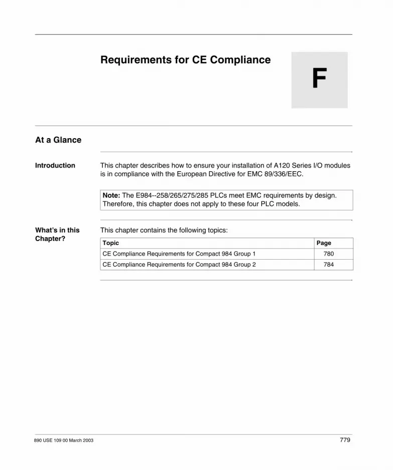
890 USE 109 00 March 2003
Requirements for CE Compliance
At a Glance
Introduction This chapter describes how to ensure your installation of A120 Series I/O modules is in compliance with the European Directive for EMC 89/336/EEC.
What’s in this Chapter?
This chapter contains the following topics:
Note: The E984--258/265/275/285 PLCs meet EMC requirements by design. Therefore, this chapter does not apply to these four PLC models.
Topic Page
CE Compliance Requirements for Compact 984 Group 1 780
CE Compliance Requirements for Compact 984 Group 2 784
779
CE Compliance
CE Compliance Requirements for Compact 984 Group 1
Group 1 Requirements
This section covers the installation requirements necessary to maintain compliance with the European Directive for EMC 89/336/EEC for certain (PC-A984-145, PC-E984-241, PC-E984-245, PC-E984-251, PC-E984-255, AS-BDAP-210, AS-BDAP-218, AS-BVIC-200, AS-BVIC-205, AS-BVIC-212, AS-BVIC-224, AS-BVRC-200, AS-BCTR-205, AS-BCTR-212, AS-BCTR-224, AS-BADU-211, AS-BADU-212, AS-BADU-204 and AS-BMOT-201) Compact 984 components.
The following requirements should be followed for installations complying with the CE marking: Use Braided Shielded Cable on all power supply, communications, and I/O lines.
Either the Modicon Grounding Bar (Modicon part number 043509693) or a compatible device may be used. The cable should have at least 80% shield coverage. When using the Grounding Bar, the Outer Diameter of the shield should be in the range of 0.189 ... 0.240 in (4.8 ... 6.0 mm).
All cable shields must be grounded using the clips on the Grounding Bar as shown below. Alternatively, the user may supply an equivalent low impedance RF ground clamp.
CPU/PS ground terminal ( ) must be left open as shown. Install braided earth ground as shown below from building earth ground to
grounding clip (or clips as required) and to backplane 0 Volt reference. Use the plastic faceplate supplied with the backplane to cover the front of
modules. If using a BMOT-201 module, all cables (Motor I/O Cable, Encoder Cable and I/
O Cable) exiting the BMOT-201 module must pass through a large Ferrite Bead (Steward part number 28 B2400-000).
Note: For details regarding specific I/O modules, please refer to the A120 Series I/O Modules User Guide (890 USE 109 00 formerly GM-A984-IOS).
780 890 USE 109 00 March 2003

CE Compliance
The following figure shows a schematic view of the CE compliance requirements.
Backplane
0V ReferenceExternal + Out24VDCPower - OutSupply
PositiveConductor
NegativeConductor
ShieldBraid
NoConnectionHere Flat Braid Cable .25in (6.3MM) or wider
Stripped Outer Jacket
Grounding Bar
3
2 Conductor CableWith Braided Shield
To Building Ground
CPU/PS I/O I/O BMOT201
+ 24Vin
- 24Vin
890 USE 109 00 March 2003 781

CE Compliance
The following figure depicts the CE compliance requirements.
DIN Rail
1
24
5
3
Insulation Removed inRegion Near Grounding Clip(Both Input and Output Cables)
Tie Wraps to HoldCables in GroundingClips
Flat Braid Cableto Earth Ground
ReferenceGround Point
782 890 USE 109 00 March 2003

CE Compliance
The following table is the Parts List for the Callout used in the two previous figures.
Callout Vendor (or equivalent)
Part Number Description Instructions
1 Modicon Shipped with backplane
Plastic Cover Installation is Required.
2 Flat Braid Cable .25in(6.3mm) or wider
3 Modicon 043509693 Grounding Bar All cable shields must be grounded.
4 Steward(Outside the United States call Livingston, Scotland at (0044) 1-506-414-200)
28 B2400-000 Ferrite Bead 1.37in(34.8mm) I.D.; 2.5in(63.5mm) O.D.; .44in(11.2mm) Thick
For a BMOT-201 ONLY: All cables (Motor I/O, Encoder and I/O cables) must pass through this large ferrite bead. Secure it with a tie wrap or equivalent.
5 Braided Shielded Cable. 80% shield coverage, # of conductor and gauge per user requirements.
890 USE 109 00 March 2003 783

CE Compliance
CE Compliance Requirements for Compact 984 Group 2
Group 2 Requirements
This section covers the installation requirements necessary to maintain compliance with the European Directive for EMC 89/336/EEC for certain (AS-HDTA-200, AS-HDTA-201, AS-HDTA-202, AS-BDAO-216, AS-BDAP-204, AS-BDAP-208, AS-BDAP-211, AS-BDAP-212, AS-BDAP-216, AS-BDAP-216N, AS-BDAP-217, AS-BDAP-220, AS-BDAP-250, AS-BDAP-252, AS-BDAP-292, AS-BDEO-216, AS-BDEP-208, AS-BDEP-210, AS-BDEP-211, AS-BDEP-214, AS-BDEP-215, AS-BDEP-216, AS-BDEP-217, AS-BDEP-218, AS-BDEP-220, AS-BDEP-257, AS-BDEP-254, AS-BDEP-296, AS-BDEP-297, AS-BADU-204, AS-BADU-205, AS-BADU-206, AS-BADU-210, AS–BADU–214, AS-BADU-216, AS-BADU-254, AS-BADU-256, AS-BADU-257, AS-BDAU-202, AS-BDAU-208, AS-BFRQ-204, AS-BBKF-201, AS-BZAE-201, AS-BZAE-204 and AS–BDEA–203) Compact 984 components. These particular modules operating voltages are Ub (24Vdc), working voltages Us (24Vdc/230Vac). The following requirements should be followed for installations complying with the CE marking: Install equipment following approved EMC practices, i.e., protective earthing and
functional earthing, connections with good conductivity, and grounding cables of sufficient cross section
Avoid all sources of electrical disturbance in proximity of the equipment, encapsulation with metallic walls
Use manufacturer approved cabling Use EMC compliant grounding of cable shielding (proper mechanical connection,
connection surface, clamps) Separate data and signal cable routing, which emit disturbances (e.g. power
cables with switching transients) Use the prescribed suppression filters and their competent installation
784 890 USE 109 00 March 2003

CE Compliance
Improvement of the EMC Stability on the Modules
To improve EMC stability on the modules, it is recommended that the U (voltage) and M (common) connections used here have as short as possible capacitive discharge from the terminal towards the functional earth. This is the purpose of the capacitive discharge terminal (GND 001), which is shown in the following figure. In an environment that has a high interference level, an increase of the capacity on the C1 from 2.2 nF to 22 nF is recommended.The following figure shows the use of the capacitive discharge terminal to improve EMC stability.
N
DTA 200 DTA 201/202
2.5 qmm
C1
Z2
≥ 2.5 qmm
≥ 6 qmm DTA 201 DTA 201/202
C1 Capacitive discharge terminal GND 001N Power supply modules CPU / DEA / ASP / P120Z2 Earthing cleat EDS 000Z3 Cable earthing bar CER 001
to M
of t
he p
ower
sup
ply
N1,
N2
...
890 USE 109 00 March 2003 785

CE Compliance
The following figure shows another view of the capacitive discharge terminal.
Earthing System of the Top Hat Rails and Modules
The earthing system of the 0 V on the rack is already preset when delivered. More details are described in Earthing System of the Shielded Cable Lines, p. 787 (the following section). To have noise-free operation, perform the following earthing system measures described in that section.
123456789
1011
22
12131415161718192021
I/O Module
M
U
F
U = 24 VDC F Automatic circuit breakerC1 Capacitive discharge terminal GND 001
M≥ 2.5 qmm Cu
C1
1 2 3 4 5 6 7 8
10 12 14 16
786 890 USE 109 00 March 2003
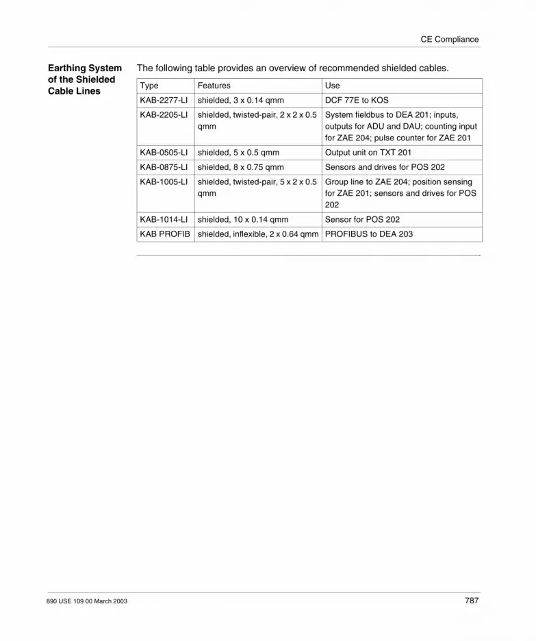
CE Compliance
Earthing System of the Shielded Cable Lines
The following table provides an overview of recommended shielded cables.
Type Features Use
KAB-2277-LI shielded, 3 x 0.14 qmm DCF 77E to KOS
KAB-2205-LI shielded, twisted-pair, 2 x 2 x 0.5 qmm
System fieldbus to DEA 201; inputs, outputs for ADU and DAU; counting input for ZAE 204; pulse counter for ZAE 201
KAB-0505-LI shielded, 5 x 0.5 qmm Output unit on TXT 201
KAB-0875-LI shielded, 8 x 0.75 qmm Sensors and drives for POS 202
KAB-1005-LI shielded, twisted-pair, 5 x 2 x 0.5 qmm
Group line to ZAE 204; position sensing for ZAE 201; sensors and drives for POS 202
KAB-1014-LI shielded, 10 x 0.14 qmm Sensor for POS 202
KAB PROFIB shielded, inflexible, 2 x 0.64 qmm PROFIBUS to DEA 203
890 USE 109 00 March 2003 787

CE Compliance
788 890 USE 109 00 March 2003

890 USE 109 00 March 2003
Technical Assistance
At a Glance
Purpose This chapter describes resources that may prove useful in the installation and troubleshooting of A120 series I/O modules.
What’s in this Chapter?
This chapter contains the following topics:
Topic Page
Schneider Automation Customer Service Numbers 790
Installing the Loadables for A120 Series I/O Modules 791
789

Technical Assistance
Schneider Automation Customer Service Numbers
Schneider Automation Telephone Numbers
Schneider Automation telephone numbers are as follows: To call us from anywhere in North America except from within the state of
Massachusetts: 1-(800)-468-5342 To call us from within Massachusetts or from outside North America: 1-(978)-975-
5001 To call us in Seligenstadt, Germany: (49) 6182 81 2900, or fax us at (49) 6182 81
2492When calling the Schneider Automation 800 telephone number, you will get a recording asking you to enter a one digit code for the type of service you request provided you use a touch tone telephone. The service categories and the extra digit responses for touch tone phones are:The service categories - and extra digit code responses for push-button phones - are:
1 Hardware or software technical support
2 Order entry, buying hardware or software
3 Modfax
4 Training/course registration inquiries
5 General information other than above.
Note: MODFAX: For available hardware data sheets, application notes, and software information. Recommended catalogue MC-FAX-DIR, which is the master of all available catalogues, (only twelve pages) lists all catalogues available on the MODFAX system.
Note: BBS (Schneider Automation’s Customer Service Bulletin Board): For Modsoft updates, conversion utilities, hardware and software help, field service bulletins, Modbus and Modbus Plus help, software revision levels, FLASH EXEC updates for Modicon equipment, and more. Parameters are up to 56.6k baud, no parity, 8 data, 1 stop, phone 1-(978)-975-9779.
790 890 USE 109 00 March 2003

Technical Assistance
Installing the Loadables for A120 Series I/O Modules
Overview The following information describes how to install loadables.
General Procedure
The SW-IODR-001 (Rev 1.20 or higher) loadable is available from the Customer Service Bulletin Board Service (978/975-9779). Note that all users of the A984- 1XX, Micro 512, and Micro 612 PLCs may be required to perform the following steps if a particular I/O module is not included in the module table.
Update the Modsoft GCNFA120.SYS File (If Less Than Ver. 2.1)
The following information must appear in the GCNFA120.SYS file in the Modsoft/Runtime directory, if the file version is less than Ver. 2.1. Edit your file accordingly. BMOT201,110,0,12,12,1-AXIS MOTN ,1, BMOT202,111,0,12,12,1-AXIS MOTN ,1, DEP211,17,0,1,0,8-I 110VAC ,0, DEP215,46,0,2,0,16-I 5VDC TTL ,0, DEP217,45,0,2,0,16-I 24VDC ,0, DEP214,20,0,2,0,16-I 10-60VDC ,0, DAP217,42,0,0,2,16-O 24VDC ,0, VIC2XX,120,0,6,6,COUNTER ,0, ADU211,118,0,6,6,8 CHN ANALOG ,0, ADU216,59,0,10,2,8 CHN A/D TC ,0, ADU214,36,0,6,4,4/8 CHN A/D ,1, ADU204,32,0,8,0,4 CHN 0.5V ,1, DAU204,117,0,2,12,4 CHN OUTPUT ,1, DAP211,10,0,1,1,4 MIXED I/O ROVAC ,0,
Step Action
1 From the Main Menu, select F-files to download.
2 Then select 0-loadables.
890 USE 109 00 March 2003 791

Technical Assistance
Procedure for Installing the SW-IODR-001 Loadable
Use the following steps to install the SW-IODR-001 Loadable.
Applicable File Names and Modules
The following table lists the file names for the modules to load in Procedure for Installing the SW-IODR-001 Loadable, p. 792.l
DX Loadable Configuration Files and File Names
The following table lists the configuration file names for the loadables to use in Procedure for Installing the SW-IODR-001 Loadable, p. 792.l
Step Action
1 Using Modsoft, from the OFFLINE Mode menu, select PROGRAM.
2 Once the program is loaded, select CONFIGuration.
3 From the Configuration Overview Screen, select LOADABLE.
4 To install the loadable, select DIRectory and enter the applicable file name, for example, drive:\MODSOFT\PROGRAM\SVI.DAT. The file names are listed in Applicable File Names and Modules, p. 792, immediately following this procedure.
5 Once the file is loaded, select EDIT, and then INSERT.
6 Select the applicable loadable, for example, #SVI. The names of the loadables are listed in DX Loadable Configuration Files and File Names, p. 792.
7 To load the program into the PLC, return to the Main Menu and select TRANSFER.
8 Select File to PLC. The loadable will now be installed in the PLC as part of the configuration and user logic.
File Name Module
BMOT.DAT BMOT20X
DSC1.DAT DEP211, 214,215, 217, and DAP217/211
SVI.DAT ADU211,VIC2XX, and DAU204
ADU216.DAT ADU216
ADU214.DAT ADU214
DX Loadable Configuration File File Name
#MOT BMOT.DAT
#DS1 DSC1.DAT
#SVI SVI.DAT
#216 ADU216.DAT
#214 ADU214.DAT
Note that the Rev, size, and opcode will vary from file to file.
792 890 USE 109 00 March 2003

AADU 204 4-point Voltage/RTD Analog Input Module
dip switches, 13ADU 204/254 4-point Voltage/RTD Analog Input Module, 6, 7
field wiring, 12simplified schematic, 12specifications, 17
ADU 205 4-point Voltage/Current Analog Input Module, 19
application example, 754calibration, 27field wiring, 25simplified schematic, 25specifications, 29
ADU 206/256 4-point Voltage/Current Isolated Analog Input
calibration, 47configuration, 38simplified schematic, 37specifications, 50wiring diagram, 39
ADU 210 4-point Voltage/Current Isolated Analog Input, 54
conversions, 61installation, 57operation, 59simplified schematic, 55specifications, 63wiring diagram, 58
890 USE 109 00 March 2003
ADU 211 8-point Universal Isolated Analog Input, 66, 105
application notes, 84configuration, 87dip switches, 69field wiring, 74quick start, 67troubleshooting, 103
ADU 212 8-point Universal Isolated Analog Input, 66
specifications, 105ADU 214 8-point Voltage/Current Isolated Analog Input, 110
configuration, 123dip switches, 132field wiring, 130simplified schematic, 112specifications, 133
ADU 216 8-point Thermocouple Isolated Analog Input, 140
calibration, 152configuration, 145programming modes, 147simplified schematic, 143wiring example, 146
ADU 257 8-point TC/RTD Isolated Analog Input
block diagram, 158installation, 159operation, 161specifications, 169wiring diagram, 160
xix

Index
analog input modulesADU 204, 6, 7ADU 205, 19ADU 210, 54ADU 211, 66ADU 214, 110ADU 216, 140ADU 257, 156
analog isolatedADU 211, 66ADU 214, 110ADU 216, 140
analog output modulesDAU 202, 332DAU 202/252, 332DAU 204 conversion ranges, 342Installing the DAU 204, 345installing the DAU 204, 344
application exampleADU 205 4-point Voltage/Current Analog Input Module, 754
application notesADU 211 8-point Universal Isolated Analog Input, 84CTR 205 High Speed Input Module, 760CTR 212 High Speed Input Module, 760CTR 224 High Speed Input Module, 760VRC 200 High Speed Input Module, 760
BBKF 201 interbus s master module
specifications, 199BKF 202 interbus s slave module
specifications, 212block diagram
ADU 257 8-point TC/RTD Isolated Analog Input, 158
Ccalibration
ADU 205 4-point Voltage/Current Analog Input Module, 27
xx
ADU 206/256 4-point Voltage/Current Isolated Analog Input, 47ADU 216 8-point Thermocouple Isolated Analog Input, 152DAU 204 4-point 24 Vdc Voltage/Current Analog Output, 358DAU 208 8-point +/-10 Vdc Isolated Analog Output, 374
Capacitive discharge terminalGND 001, 785
clear current count commandfor ZAE 201 counting operations, 571
combined I/O modulesDAP 211, 254DAP 212/252, 262DAP 220/250, 298DAP 253, 308DAP 292, 320
Concept, 2configuration
ADU 206/256 4-point Voltage/Current Isolated Analog Input, 38ADU 211 8-point Universal Isolated Analog Input, 87ADU 214 8-point Voltage/Current Isolated Analog Input, 123ADU 216 8-point Thermocouple Isolated Analog Input, 145DAU 204 4-point 24 Vdc Voltage/Current Analog Output, 353DAU 208 8-point +/-10 Vdc Isolated Analog Output, 372
conversionsADU 210 4-point Voltage/Current Isolated Analog Input, 61
counter moduleZAE 201, 567
counter/positioner modulesZAE 201, 557
CTR 205 High Speed Input Moduleapplication notes, 760troubleshooting, 546
CTR 212 High Speed Input Moduletroubleshooting, 546
890 USE 109 00 March 2003

Index
CTR 224 High Speed Input Moduleapplication notes, 760troubleshooting, 546
DDAO 216 16-point 24 Vdc Output Module, 214
simplified schematic, 216specifications, 219wiring diagram, 217
DAP 204 4-point 24...110 Vdc/24...250 Vac Relay Output, 222
simplified schematic, 224specifications, 227wiring diagram, 222, 224
DAP 208/258 8-point 24...110 Vdc/24...250 Vac Relay Output, 232
simplified schematic, 234specifications, 237wiring diagram, 234
DAP 209 8-point 120 Vac Discrete Output Module, 242
simplified schematic, 244specifications, 245wiring diagram, 244
DAP 210 8-point 24...230 Vac Discrete Output Module, 252
simplified schematic, 249specifications, 250wiring diagram, 249
DAP 211 4-point in/4-point out 120 Vac Combined I/O, 254
field connections, 259specifications, 260
DAP 212/252 8-point in/4-point out 24 Vdc Combined I/O, 262
specifications, 268DAP 212/252 8-point in/4-point relay out 24 Vdc LT Combined I/O
field connections, 264simplified schematic, 265
890 USE 109 00 March 2003
DAP 216 16-point 24 Vdc Discrete Output Module, 274
simplified schematic, 276specifications, 281wiring diagram, 276
DAP 217 16-point 5...24 Vdc Discrete Output Module
field connections, 287simplified schematic, 286specifications, 289
DAP 218 16-point 24...240 Vac Discrete Output, 292
simplified schematic, 294specifications, 295wiring diagram, 294
DAP 220/250 8-point in/8-point out 24 Vdc Combined I/O, 298
simplified schematic, 301specifications, 304wiring diagram, 301
DAP 253 8-point in/4-point relay out 110 Vdc LT Combined I/O, 308
field connections, 310simplified schematic, 311specifications, 314
DAP 292 8-point in/4-point relay out 60 Vdc Combined I/O, 320
field connections, 322simplified schematic, 323specifications, 326
DAP216N 16-point 24 Vdc Discrete Output Module, 274
simplified schematic, 276specifications, 281wiring diagram, 276
DAU 202/2522-point 24 Vdc Voltage/Current Analog Output, 332field-wiring, 334
DAU 204 4-point 24Vdc voltagecurrent analog output, 341
xxi

Index
DAU 204 4-point 24Vdc Voltage/Current/Analog Output
calibration, 358configuration, 353indicators, 361specifications, 364
DAU 208 8-point +/-10 Vdc Isolated Analog Output
calibration, 374configuration, 372field connections, 373simplified schematic, 371
DEA 202, 380DEA 202 InterBus S interface module
specifications, 387DEO 216 16-point 24 Vdc Discrete Input Module, 390
simplified schematic, 390specifications, 391wiring diagram, 390
DEP 208 8-point 230 Vac Discrete Input Module
simplified schematic, 396specifications, 398use with Proximity Switches, 397wiring diagram, 396
DEP 209 8-point 120 Vac Discrete Input Module, 400
simplified schematic, 402specifications, 404use with proximity switches, 403wiring diagram, 402
DEP 210 8-point 115 Vac Isolated Discrete Input, 406
field connections, 408simplified schematic, 409specifications, 410
DEP 211 8-point 115 Vac Isolated Discrete Input, 412
field connections, 414simplified schematic, 415specifications, 416
xxii
DEP 214/254 16-point 12...60 Vdc Discrete Input Module, 418
field connections, 420simplified schematic, 421specifications, 422
DEP 215 16-point 5Vdc TTL Discrete Input Module, 424
field connections, 426simplified schematic, 427specifications, 429
DEP 216 16-point 24 Vdc Discrete Input Module
wiring diagram, 434DEP 216/256 16-point 24 Vdc Discrete Input Module, 432
simplified schematic, 434specifications, 435
DEP 217 16-point 24 Vdc Discrete Input Module, 438
simplified schematic, 440specifications, 441wiring diagram, 440
DEP 218 16-point 115 Vac Isolated Discrete Input, 444
field connections, 446simplified schematic, 447specifications, 448
DEP 220 16-point 24 Vdc Discrete Input Module, 452
simplified schematic, 453specifications, 454wiring diagram, 453
DEP 257 16-point 110 Vdc Discrete Input Module, 457
simplified schematic, 458specifications, 459
DEP 296 16-point 60 Vdc Isolated Input Module, 463
field connections, 464simplified schematic, 465specifications, 466
DEP 297 16-point 48 Vdc Isolated Discrete Input Module, 469
field connections, 470simplified schematic, 471specifications, 472
890 USE 109 00 March 2003

Index
dip switchesADU 204 4-point Voltage/RTD Analog Input Module, 13ADU 211 8-point Universal Isolated Analog Input, 69ADU 214 8-point Voltage/Current Isolated Analog Input, 132
discrete input modulesDAP 212/252, 262DAP 220/250, 298DEO 216, 390DEP 209, 400DEP 214, 418DEP 216/256, 432DEP 217, 438DEP 220, 452DEP 257, 457
discrete isolatedDEP 210, 406DEP 211, 412DEP 218, 444DEP 296, 463
discrete output modulesDAO 216, 214DAP 209, 242DAP 210, 252DAP 216, 274DAP 218, 292
EE984-258/265/275/285 PLCs
Panel software requirements, 1EMC measures, 785end-of-travel limits
MOT 201 Motion Encoder, 522MOT 202 Motion Resolver/Encoder, 522
Ffield connections
DAP 211 4-point in/4-point out 120 Vac Combined I/O, 259DAP 212/252 8-point in/4-point relay out 24 Vdc LT Combined I/O, 264
890 USE 109 00 March 2003
DAP 217 16-point 5...24 Vdc Discrete Output Module, 287DAP 253 8-point in/4-point relay out 110 Vdc LT Combined I/O, 310DAP 292 8-point in/4-point relay out 60Vdc Combined I/O, 322DAU 208 8-point +/-10 Vdc Isolated Analog Output, 373DEP 210 8-point 115 Vac Isolated Discrete Input, 408DEP 211 8-point 115 Vac Isolated Discrete Input, 414DEP 214/254 16-point 12...60 Vdc Discrete Input Module, 420DEP 215 16-point 5 Vdc TTL Discrete Input Module, 426DEP 218 16-point 115 Vac Isolated Discrete Input, 446DEP 296 16-point 60 Vdc Isolated Input Module, 464DEP 297 16-point 48 Vdc Isolated Discrete Input Module, 470ZAE 204 High Speed Counter, 606
field wiringADU 204/254 4-point Voltage/RTD Analog Input Module, 12ADU 205 4-point Voltage/Current Analog Input Module, 25ADU 211 8-point Universal Isolated Analog Input, 74ADU 214 8-point Voltage/Current Isolated Analog Input, 130
flash EEPROMMOT 201 Motion Encoder, 523MOT 202 Motion Resolver/Encoder, 523
FRQ 204/254 frequency moduleConfiguration, 477general, 474operation and LEDs, 481Specifications, 482
xxiii

Index
GGND 001
Capacitive discharge terminal, 785go to target command
for ZAE 201 positioning operations, 585
Hhome limit
MOT 201 Motion Encoder, 523MOT 202 Motion Resolver/Encoder, 523
II/O map
ZAE 201 Counter/Positioner Module, 561indicators
DAU 204 4-point 24Vdc Voltage/Current Analog Output, 361
input modulesanalog, ADU 204, 6, 7analog, ADU 205, 19analog, ADU 206, 54analog, ADU 211, 66analog, ADU 214, 110analog, ADU 216, 140analog, ADU 257, 156DEO 216, 390discrete, 262, 308, 400, 418, 432, 438discrete,DEP 220, 452discrete,DEP 257, 457
installationADU 210 4-point Voltage/Current Isolated Analog Input, 57ADU 257 8-point TC/RTD Isolated Analog Input, 159
installation ofloadables, 791
InterBus S interface module, 380isolated analog
ADU 210, 54ADU 211, 66ADU 214, 110ADU 216, 140
xxiv
isolated discreteDEP 210, 406DEP 211, 412DEP 218, 444DEP 296, 463DEP 297, 469
LLEDs
ZAE 204 high speed counter module, 602
loadablesinstallation of, 791
loadables requiredADU 211, 66ADU 216, 156DAP 217, 6, 254, 283DEP 211, 412DEP 214, 418DEP 215, 424
MModsoft, 1, 3MOT 201 Motion Encoder
Analog Output, 499Connectors, 492Discrete I/O, 499Encoder Feedback Interface, 497end-of-travel limits, 522flash EEPROM, 523home limit, 523motion development software, 524Motor Drive Interface, 500The DIP Switch, 501
890 USE 109 00 March 2003

Index
MOT 202 Motion Resolver/EncoderAnalog Output, 517Connectors, 507DIP Switches, 519Discrete I/O, 517Encoder Feedback Interface, 515end-of-travel limits, 522flash EEPROM, 523home limit, 523motion development software, 524Motor Drive Interface, 518Resolver Feedback/Thermal Interface, 518specifications, 525
MOT 20X Motion Modules, 489motion development software
MOT 201 Motion Encoder, 524MOT 202 Motion Resolver/Encoder, 524
NNUL 200 Module, 777
specifications, 778NUL 202 Module, 777NUL 202Module
specifications, 778
Oone-axis positioning module
ZAE 201 Module, 580operation
ADU 210 4-point Voltage/Current Isolated Analog Input, 59, 161
operation and LEDsFRQ 204/254 frequency module, 481
output modules, 232discrete, 214, 242, 252, 274, 292relay, 222, 262, 308
PPanel software requirements
for A984-1xx/E984-24x/251/255 PLCs, 1
890 USE 109 00 March 2003
parameterize commandfor ZAE 201 counting operations, 569for ZAE 201 positioning operations, 582
programming modesADU 216 8-point Thermocouple Isolated Analog Input, 147
Qquick start
ADU 211 8-point Universal Isolated Analog Input, 67
Rrelay output modules, 232
DAP 204, 222DAP 212/252, 262DAP 253, 308
reset commandfor ZAE 201 counting operations, 570for ZAE 201 positioning operations, 584
run reference point + commandfor ZAE 201 positioning operations, 586
run reference point commandfor ZAE 201 positioning operations, 585
SShielded cable, 787Shielding, 787SIM 203 Analog Simulator Module, 770
specifications, 773wiring diagram, 772
SIM 216 Binary Simulator Modulewiring diagram, 776
simplified schematicADU 204 8-point Voltage/Current Isolated Analog Input, 112ADU 204/254 4-point Voltage/RTD Analog Input Module, 12ADU 205 4-point Voltage/Current Analog Input Module, 25
xxv

Index
ADU 206/256 4-point Voltage/Current Isolated Analog Input, 37ADU 210 4-point Voltage/Current Isolated Analog Input, 55ADU 216 8-point Thermocouple Isolated Analog Input, 143DAO 216 16-point 24 Vdc Output Module, 216DAP 204 4-point 24...110 Vdc/24...250 Vac Relay Output, 224DAP 208/258 8-point 24...110 Vdc/24...250 Vac Relay Output, 234DAP 209 8-point 120 Vac Discrete Output Module, 244DAP 210 8-point 24...240 Vac Discrete Output Module, 249DAP 216 16-point 24 Vdc Discrete Output Module, 276DAP 217 16-point 5...24 Vdc Discrete Output Module, 286DAP 218 16-point 24...240 Vac Discrete Output, 294DAP 220/250 8-point in/8-point out 24 Vdc Combined I/O, 301DAP 253 8-point in/4-point relay out 110 Vdc LT Combined I/O, 311DAP 292 8-point in/4-point relay out 60Vdc Combined I/O, 323DAP216N 16-point 24 Vdc Discrete Output Module, 276DAU 208 8-point +/-10 Vdc Isolated Analog Output, 371DEO 216 16-point 24 Vdc Discrete Input Module, 390DEP 208 8-point 230 Vac Discrete Input Module, 396DEP 209 8-point 120 Vac Discrete Input Module, 402DEP 210 8-point 115 Vac Isolated Discrete Input, 409DEP 211 8-point 115 Vac Isolated Discrete Input, 415DEP 214/254 16-point 12...60 Vdc Discrete Input Module, 421
xxvi
DEP 215 16-point 5 vdc TTL Discrete Input Module, 427DEP 216/256 16-point 24 Vdc Discrete Input Module, 434DEP 217 16-point 24 Vdc Discrete Input Module, 440DEP 218 16-point 115 Vac Isolated Discrete Input, 447DEP 220 16-point 24 Vdc Discrete Input Module, 453DEP 257 16-point 110 Vdc Discrete Input Module, 458DEP 296 16-point 60 Vdc Isolated Input Module, 465simplified schematic, 265
software requirements, 1specifications
ADU 204/254 4-point Voltage/RTD Analog Input Module, 17ADU 205 4-point Voltage/Current Analog Input Module, 29ADU 206/256 4-point Voltage/Current Isolated Analog Input, 50ADU 210 4-point Voltage/Current Isolated Analog Input, 63ADU 211 8-point Universal Isolated Analog Input Module, 105ADU 212 8-point Universal Isolated Analog Input Module, 105ADU 214 8-point Voltage/Current Isolated Analog Input, 133ADU 257 8-point TC/RTD Isolated Analog Input, 169BKF 202 interbus s slave module, 212DAO 216 16-point 24 Vdc Output Module, 219DAP 204 4-point 24...110 Vdc/24...250 Vac Relay Output, 227DAP 208/258 8-point 24...110 Vdc/24...250 Vac Relay Output, 237DAP 209 8-point 120 Vac Discrete Output Module, 245DAP 210 8-point 24...230 Vac Discrete Output Module, 250
890 USE 109 00 March 2003

Index
DAP 211 4-point in/4-point out 120 Vac Combined I/O, 260DAP 212/252 8-point in/4-point out 24 Vdc Combined I/O, 268DAP 216 16-point 24 Vdc Discrete Output Module, 281DAP 217 16-point 5...24 Vdc Discrete Output Module, 289DAP 218 16-point 24...240 Vac Discrete Output, 295DAP 220/250 8-point in/8-point out 24 Vdc Combined I/O, 304DAP 253 8-point in/4-point relay out 110 Vdc LT Combined I/O, 314DAP 292 8-point in/4-point relay out 60Vdc Combined I/O, 326DAP216N 16-point 24 Vdc Discrete Output Module, 281DAU 204 4-point 24Vdc Voltage/Current Analog Output, 364DEA 202 InterBus S interface module, 387DEO 216 16-point 24 Vdc Discrete Input Module, 391DEP 208 8-point 230 Vac Discrete Input Module, 398DEP 209 8-point 120 Vac Discrete Input Module, 404DEP 210 8-point 115 Vac Isolated Discrete Input, 410DEP 211 8-point 115 Vac Isolated Discrete Input, 416DEP 214/254 16-point 12...60 Vdc Discrete Input Module, 422DEP 215 16-point 5Vdc TTL Discrete Input Module, 429DEP 216/256 16-point 24 Vdc Discrete Input Module, 435DEP 217 16-point 24 Vdc Discrete Input Module, 441DEP 218 16-point 115 Vac Isolated Discrete Input, 448DEP 257 16-point 110 Vdc Discrete Input Module, 459
890 USE 109 00 March 2003
DEP 296 16-point 60 Vdc Isolated Input Module, 466DEP 297 16-point 48 Vdc Isolated Discrete Input Module, 472NUL 200 Module, 778NUL 202 Module, 778SIM 203 Analog Simulator Module, 773
Ttroubleshooting
ADU 211 8-point Universal Isolated Analog Input, 103CTR 205 High Speed Input Module, 546CTR 212 High Speed Input Module, 546CTR 224 High Speed Input Module, 546VRC 200 High Speed Input Module, 546
TTL input modulesDEP 215, 428
Uuse with Proximity Switches
DEP 208 8-point 230 Vac Discrete Input Module, 397DEP 209 8-point 120 Vac Discrete Input Module, 403
VVRC 200 High Speed Input Module
application notes, 760Installation, 536LED locations and module wiring, 533Specifications, 549troubleshooting, 546
Wwiring diagram
ADU 206/256 4-point Voltage/Current Isolated Analof Input, 39ADU 210 4-point Voltage/Current Isolated Analog Input, 58
xxvii

Index
DAO 216 16-point 24 Vdc Output Module, 217DAP 204 4-point 24...110 Vdc/24...250 Vac Relay Output, 224DAP 208/258 8-point 24...110 Vdc/24...250 Vac Relay Output, 234DAP 209 8-point 120 Vac Discrete Output Module, 244DAP 210 8-point 24...240 Vac Discrete Output Module, 249DAP 216 16-point 24 Vdc Discrete Output Module, 276DAP 218 16-point 24...240 Vac Discrete Output, 294DAP 220/250 8-point in/8-point out 24 Vdc Combined I/O, 301DAP216N 16-point 24 Vdc Discrete Output Module, 276DEO 216 16-point 24 Vdc Discrete Input Module, 390DEP 208 8-point 230 Vac Discrete Input Module, 396DEP 209 8-point 120 Vac Discrete Input Module, 402DEP 216 16-point 24 Vdc Discrete Input Module, 434DEP 217 16-point 24 Vdc Discrete Input Module, 440DEP 220 16-point 24 Vdc Discrete Input Module, 453SIM 203 Analog Simulator Module, 772SIM 216 Binary Simulator Module, 776
wiring exampleADU 216 8-point Thermocouple Isolated Analog Input, 146
ZZAE 201
counter module, 567counter/positioner modules, 557
ZAE 201 Counter/Positioner ModuleI/O map, 561input data block, 561output data block, 562Specifications, 595
xxviii
ZAE 201 Modulecounter example, 572Counter Mode commands, 569field wiring the counter for 24 V inputs, 565field wiring the counter for 5 V inputs, 564field wiring the positioner for 5 V inputs, 577for positioning operations, 581high speed counting, 567input data block, 560one-axis positioning module, 580output data block, 560parameterization
for positioning operations, 582parameterization for counting operations, 568, 569positioning example, 588READY state for counting operations, 568RESET for positioning operations, 581RESET state
for counting operations, 568RESET state for counting operations, 570RESET state for positioning operations, 584run reference point command for positioning operations, 581, 585RUN state for counting operations, 568The READY state for positioning operations, 581
ZAE 204 High Speed Counter, 599Configuration, 603field connections, 606Specifications, 619
ZAE 204 high speed counter moduleLEDs, 602
890 USE 109 00 March 2003