Embed Size (px)
Citation preview

Multimedia textbook
Zbyněk RAIDA, Dušan ČERNOHORSKÝ, Dalimil GALA, Stanislav GOŇA, Zdeněk NOVÁČEK,
Viktor OTEVŘEL, Václav MICHÁLEK, Vlastimil NAVRÁTIL, Tomáš URBANEC, Zbyněk ŠKVOR,
Petr POMĚNKA, Jiří ŠEBESTA, Geert VANDERSTEGEN, Bart VANDIJCK, Bert SOORS,
Jeroen SCHEVERNELS, Javier MARTÍN DEL VALLE, Martin ŠTUMPF, Vladimír ŠEDĚNKA,
Peter KOVÁCS, Jaroslav LÁČÍK, Jana JILKOVÁ, Zbyněk LUKEŠ, Michal POKORNÝ.
Copyright © 2010 FEEC VUT Brno All rights reserved.

Fig. 1.1 Navigation menu
Chapter 1: Multimedia textbook
Introduction
The life of today's society requires transmitting and receiving more and more data. Since the capacity of today's communication channels is not
sufficient, new channels in higher and higher frequency bands have to be built.
Design of electronic circuits, antennas and other systems, which are required to operate at frequencies of tens to hundreds gigahertz, is rather
difficult. This is given by the fact that phenomena at the above-specified frequencies are of wave nature, and therefore, all the analysis and
design have to be based on Maxwell equations in differential or integral form. Understanding phenomena, which are described by differential or
integral equations, makes usually troubles to students.
A relative complexity and abstractness of the mathematical description is the first cause of troubles (how can students imagine curl or divergence
operators, special integrals, etc.). Handling complex vector operations, one can hardly imagine their concrete sense and practical signification.
A relatively complicated and abstract nature of wave phenomena is the second cause of troubles (how can students imagine EM wave
propagation along the microstrip transmission line). Properties of studied phenomena and systems and their mutual relations cannot be observed
in a direct way, but only by the indirect one.
The electronic textbook we have in our hands now, tries to solve the above-described problems. The textbook is going to explain, using simple
examples, the practical signification of complicated mathematical operators. The textbook is going to visualize the studied phenomena in order to
build a right notion about their matter and their mutual relations. The textbook is going the ways of exploiting examined phenomena in the
engineering practice.
The textbook is conceived as a set of selected topics, which are harder understandable.
The electronic textbook is not a classical textbook describing the studied matter in a complex way. Our textbook assumes the reader, who is
equipped by the basic knowledge of electromagnetic field, who would like to improve this knowledge and apply it in the solution of practical
problems.
The content of the textbook is divided into six main topics if this introduction is not considered. Each topic is subdivided to subchapters. Within
each subchapter, the following layers can be found:
The layer A is conceived as a continuous text containing primarily the
verbal description of the studies phenomenon. The text is free of
complex mathematical expressions and hardly-understandable
derivations. The layer is aimed to reveal the matter of the phenomenon
as simply as possible. The layer is created for bachelor students
dominantly. If the reader is interested in the deeper description, he can
follow the link to the second level of the textbook (the layer B).
The layer B describes all the mathematical derivations and their detailed
discussions. Even this second layer is conceived as a continuous text,
which expects an experienced reader (typically the master student). The
chapters, which are thought by authors as relatively simple, contain all
the descriptions in the layer A; the layer B presents the same descriptions
in English. The reader, who does not understand the English text well,
can jump to the parallel Czech version in order to verify his correct
understanding of the English text.
The layer C offers the download of the numerical model of the studied
phenomenon in the form of m-files of MATLAB. The layer contains a
user's description of the numerical model. Thanks to the standard
Windows user interface of numerical models, the reader does not need to
work with the source code of the model.
The layer D contains the programmer's description of the numerical
model. Students can use m-files containing the computational kernel (the
code without the user’s interface), modify and extend them.
The layer E contains the numerical models of studied phenomena in the
form of JAVA applets. The applets can be viewed directly on the webpage without the necessity to buy MATLAB.
The layer F enables readers to test the proper understanding of studied phenomena. In the layer, pentads of questions are available, and
the reader is asked to select the correct answer. After answering the pentad of questions, the answers are evaluated. If the question is
answered incorrectly (or is not answered at all), the correct answer is displayed. The test is concluded by the complex evaluation.
The authors of the electronic textbook of electromagnetic waves and microwave techniques hope that the textbook becomes a useful tool
helping students to understand well principles of examined phenomena. This aim is conditioned by the continuous improvement and completion
of its contents, which are based on the recommendations of readers. Therefore, we kindly ask all the readers for their opinion on the textbook,
Copyright © 2010 FEEC VUT Brno All rights reserved.

for their comments of the form and contents and for their error warnings.
We thank the readers for their help and wish them a pleasant time with the textbook.
On behalf of the authors,
Zbynek Raida
Copyright © 2010 FEEC VUT Brno All rights reserved.

1.1 Before you start studying...
... we would like to give you some practical information, which can make reading the textbook simpler and more pleasant to you.
The textbook uses following markup languages: XHTML for text and MathML for equations. There is special SVG layer included as well. It is
used for better image description. Your browser should support at least XHTML+MathML, SVG support isn't necessary.
The textbook was carefully tested in web browsers Internet Explorer (8), Mozilla Firefox (3.5), Opera (v. 9.64), Google Chrome (2.0) and
Safari (4.0).
Tab. 1.1.1 Support in browsers
Support MSIE 8.0 Firefox 3.5 Opera 9.64 Chrome 2.0 Safari 4.0
XHTML yes yes yes yes yes
MathML yes* yes** yes no no
SVG no yes yes partial yes
* with MathPlayer plug-in
** you can get better support by installing STIX fonts
Reading the textbook, you might be refereed to another layer of the textbook (e.g., if you read the layer A and you would like to get more
detailed information provided in the layer B, you simply click to a respective link). Clicking the button "Back" of your browser or using the
navigation menu, you return back to the layer A.
The index of the textbook can work in two modes. The first mode is activated by clicking the highlighted text (the indexed term). That way, a
web page explaining the indexed term is opened. The reader can return back from the index by clicking the link "Back". We recommend to
prefer the button "Back" of the browser. If the reader is interested in a rather systematic reading of the contents of the index, he can enter the
index via the link Register in the menu item "Appendices".
Simpler terms can be explained by the bubble help. The bubble is displayed when the reader puts the cursor to the highlighted indexed term and
waits for a while. The functionality of the bubble help is dominantly influenced of the properties of the used browser (the bubble can disappear
after a certain time period, or the bubble can contain a part of the explanation text only). The Opera browser is recommended because the
whole text is displayed for the unlimited time. Firefox users can use "No Tooltip Timeout" add-on.
References of the recommended literature are based on the same principles. The systematic reading of references is available via the link
References in the menu item "Appendices".
Simulation programs, which are added to most chapters, are zipped. You have to save them on your disk and unzip them. That way, a separate
folder is created, which contains all the files of the program. Then, you have to start MATLAB and run the main m-file.
If you find some problems, do not hesitate and send us an email, please.
We wish you many successful clicks...
Copyright © 2010 FEEC VUT Brno All rights reserved.
Chapter 2: Propagation of electromagnetic waves
Introduction
When studying dynamic electromagnetic fields, we usually start with the propagation of waves in an infinite homogeneous medium, which is
supposed being linear and isotropic. In this situation, a single wave is propagating, which can be attenuated only is lossy medium is assumed.
Electromagnetic waves, which propagate in infinite homogeneous medium, can be classified according to their equiphase surface as planar,
cylindrical and spherical.
Plane waves can be observed in a long distance from the transmitting antenna. Plane wave propagation can be mathematically described by a
scalar differential equation in the Cartesian coordinate system.
Cylindrical wave propagates from an infinitely long direct wire, which is flown by a high-frequency current. Cylindrical wave propagation is
described by a scalar differential equation in the cylindrical coordinate system.
Spherical wave propagates from a point source. Spherical wave propagation is described by a vector differential equation in the spherical
coordinate system.
Propagation of the above-described waves is relatively well-understandable and well-imaginable. Even the mathematical relations describing
propagation of those waves are relatively simple, and moreover, the final equations are of a closed form (i.e., we get relatively simple formulae
which can be easily used for practical calculations). Therefore, those topics are not discussed in our electronic textbook.
Theoretical description of wave propagation in homogeneous medium is given in [1] and [2]. Practical relations for the solution of given
engineering tasks are in [3] at your disposal.
Examination of electromagnetic wave propagation complicates in the situation when some inhomogeneity appears in the medium. The
inhomogeneity can cause wave reflection, wave scattering or wave diffraction. Reflected (scattered, diffracted) waves interfere with incident
waves. In the surrounding of the inhomogeneity, regions with higher intensity (compared to the case without inhomogeneity) can appear
(primary wave and secondary one are of the same phase). Next, regions with very low intensity can be found (primary wave and secondary
one are of the opposite phase).
Therefore, computation of the wave propagation in an inhomogeneous medium is much more complicated than is a homogeneous one, and even
understanding the mathematical description and building a proper notion is much harder. Therefore, we are going to study the related
phenomena more in detail here.
In an inhomogeneous medium, its electric and magnetic parameters (permittivity, conductivity, permeability) change from a region to another
region. Moreover, variations of parameters can be continuous or discontinuous.
The discontinuous variation of parameters is characteristic for the surface of objects, i.e. for an medium containing conductive or dielectric (or
ferromagnetic) objects. In a real situation, buildings, trees, hills, cars, people or raindrops play the role of those objects. In our textbook, we start
to examine those phenomena in an example of a thin planar sheet, which neither reflects nor transmits the incident wave. We are speaking about
Fresnel diffraction and we describe it in chapter 2.1.
In the practical life, more realistic objects have to be considered. Including those considerations to our computations is enabled by the general
theory of diffraction, which is described in chapter 2.2. In this chapter, the diffraction on an infinitely long perfectly conducting circular cylinder
is discussed.
In chapter 2.3, geometric optics is introduced. Geometric optics is an efficient method for the computation of wave phenomena in more
complicated media. This method adopted the conception of wave propagation along beams. Comparing to the classical geometric optics, we can
compute the intensity variations and wave polarization for wave propagation in the medium with continuously changing parameters.
Chapter 2.4 deals with the geometric theory of diffraction (GTD). GDT extends the abilities of the geometric optics to the media with
discontinuous inhomogeneities. GTD solves interaction of beams and objects, and laws of geometric optics are modified in order to eliminate
obvious errors (intensity discontinuities on the border between the reflection and shade) on one hand, and to preserve advantages of the
geometric optics on the other hand (conception of beams).
All the section is closed by the examination of layered media (media consisting of several layers of different permittivity and different
thickness). Borders of layers are usually planar and parallel. Hence, the layered media consists of a certain number of plan-parallel layers. More
information is given in chapter 2.5.
Copyright © 2010 FEEC VUT Brno All rights reserved.
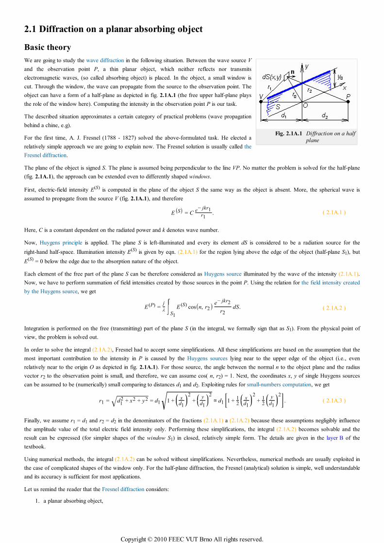
Fig. 2.1A.1 Diffraction on a half
plane
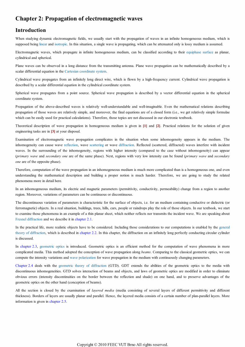
2.1 Diffraction on a planar absorbing object
Basic theory
We are going to study the wave diffraction in the following situation. Between the wave source V
and the observation point P, a thin planar object, which neither reflects nor transmits
electromagnetic waves, (so called absorbing object) is placed. In the object, a small window is
cut. Through the window, the wave can propagate from the source to the observation point. The
object can have a form of a half-plane as depicted in fig. 2.1A.1 (the free upper half-plane plays
the role of the window here). Computing the intensity in the observation point P is our task.
The described situation approximates a certain category of practical problems (wave propagation
behind a chine, e.g).
For the first time, A. J. Fresnel (1788 - 1827) solved the above-formulated task. He elected a
relatively simple approach we are going to explain now. The Fresnel solution is usually called the
Fresnel diffraction.
The plane of the object is signed S. The plane is assumed being perpendicular to the line VP. No matter the problem is solved for the half-plane
(fig. 2.1A.1), the approach can be extended even to differently shaped windows.
First, electric-field intensity E(S) is computed in the plane of the object S the same way as the object is absent. More, the spherical wave is
assumed to propagate from the source V (fig. 2.1A.1), and therefore
E(S) = Ce− jkr1
r1. ( 2.1A.1 )
Here, C is a constant dependent on the radiated power and k denotes wave number.
Now, Huygens principle is applied. The plane S is left-illuminated and every its element dS is considered to be a radiation source for the
right-hand half-space. Illumination intensity E(S) is given by eqn. (2.1A.1) for the region lying above the edge of the object (half-plane S1), but
E(S) = 0 below the edge due to the absorption nature of the object.
Each element of the free part of the plane S can be therefore considered as Huygens source illuminated by the wave of the intensity (2.1A.1).
Now, we have to perform summation of field intensities created by those sources in the point P. Using the relation for the field intensity created
by the Huygens source, we get
E (P) =j
λ
⌠⌡⎮⎮
S1
E (S) cos(n, r2) e− jkr2
r2dS. ( 2.1A.2 )
Integration is performed on the free (transmitting) part of the plane S (in the integral, we formally sign that as S1). From the physical point of
view, the problem is solved out.
In order to solve the integral (2.1A.2), Fresnel had to accept some simplifications. All these simplifications are based on the assumption that the
most important contribution to the intensity in P is caused by the Huygens sources lying near to the upper edge of the object (i.e., even
relatively near to the origin O as depicted in fig. 2.1A.1). For those source, the angle between the normal n to the object plane and the radius
vector r2 to the observation point is small, and therefore, we can assume cos( n, r2) = 1. Next, the coordinates x, y of single Huygens sources
can be assumed to be (numerically) small comparing to distances d1 and d2. Exploiting rules for small-numbers computation, we get
r1 = d12 + x2 + y2√ = d1 1 +
⎛⎝⎜
xd1
⎞⎠⎟
2+
⎛⎝⎜
y
d1
⎞⎠⎟
2
√ ≅ d1[1 + 12
⎛⎝⎜
xd1
⎞⎠⎟
2+ 1
2⎛⎝⎜
y
d1
⎞⎠⎟
2
]. ( 2.1A.3 )
Finally, we assume r1 = d1 and r2 = d2 in the denominators of the fractions (2.1A.1) a (2.1A.2) because these assumptions negligibly influence
the amplitude value of the total electric field intensity only. Performing these simplifications, the integral (2.1A.2) becomes solvable and the
result can be expressed (for simpler shapes of the window S1) in closed, relatively simple form. The details are given in the layer B of the
textbook.
Using numerical methods, the integral (2.1A.2) can be solved without simplifications. Nevertheless, numerical methods are usually exploited in
the case of complicated shapes of the window only. For the half-plane diffraction, the Fresnel (analytical) solution is simple, well understandable
and its accuracy is sufficient for most applications.
Let us remind the reader that the Fresnel diffraction considers:
a planar absorbing object,1.
Copyright © 2010 FEEC VUT Brno All rights reserved.
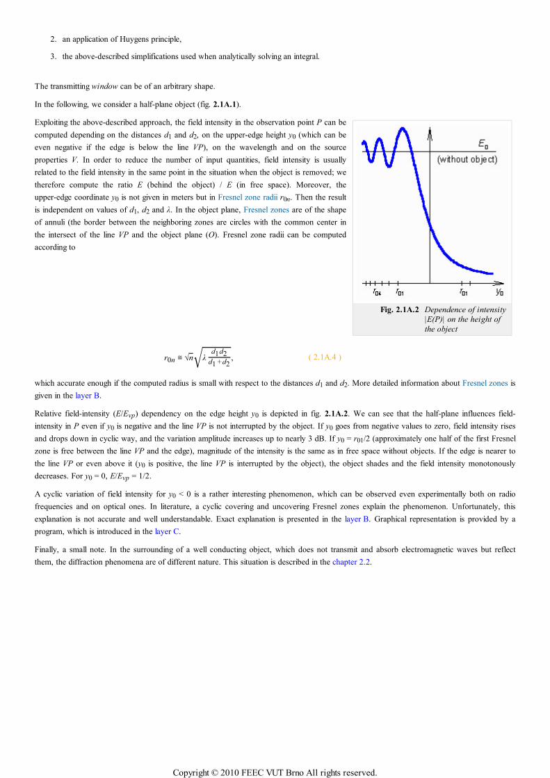
Fig. 2.1A.2 Dependence of intensity
|E(P)| on the height of
the object
an application of Huygens principle,2.
the above-described simplifications used when analytically solving an integral.3.
The transmitting window can be of an arbitrary shape.
In the following, we consider a half-plane object (fig. 2.1A.1).
Exploiting the above-described approach, the field intensity in the observation point P can be
computed depending on the distances d1 and d2, on the upper-edge height y0 (which can be
even negative if the edge is below the line VP), on the wavelength and on the source
properties V. In order to reduce the number of input quantities, field intensity is usually
related to the field intensity in the same point in the situation when the object is removed; we
therefore compute the ratio E (behind the object) / E (in free space). Moreover, the
upper-edge coordinate y0 is not given in meters but in Fresnel zone radii r0n. Then the result
is independent on values of d1, d2 and λ. In the object plane, Fresnel zones are of the shape
of annuli (the border between the neighboring zones are circles with the common center in
the intersect of the line VP and the object plane (O). Fresnel zone radii can be computed
according to
r0n ≅ n√ λd1d2
d1 +d2√ , ( 2.1A.4 )
which accurate enough if the computed radius is small with respect to the distances d1 and d2. More detailed information about Fresnel zones is
given in the layer B.
Relative field-intensity (E/Evp) dependency on the edge height y0 is depicted in fig. 2.1A.2. We can see that the half-plane influences field-
intensity in P even if y0 is negative and the line VP is not interrupted by the object. If y0 goes from negative values to zero, field intensity rises
and drops down in cyclic way, and the variation amplitude increases up to nearly 3 dB. If y0 = r01/2 (approximately one half of the first Fresnel
zone is free between the line VP and the edge), magnitude of the intensity is the same as in free space without objects. If the edge is nearer to
the line VP or even above it (y0 is positive, the line VP is interrupted by the object), the object shades and the field intensity monotonously
decreases. For y0 = 0, E/Evp = 1/2.
A cyclic variation of field intensity for y0 < 0 is a rather interesting phenomenon, which can be observed even experimentally both on radio
frequencies and on optical ones. In literature, a cyclic covering and uncovering Fresnel zones explain the phenomenon. Unfortunately, this
explanation is not accurate and well understandable. Exact explanation is presented in the layer B. Graphical representation is provided by a
program, which is introduced in the layer C.
Finally, a small note. In the surrounding of a well conducting object, which does not transmit and absorb electromagnetic waves but reflect
them, the diffraction phenomena are of different nature. This situation is described in the chapter 2.2.
Copyright © 2010 FEEC VUT Brno All rights reserved.
Fig. 2.1B.1 Half-plane
diffraction
2.1 Diffraction on a planar absorbing object
Advanced theory
Assume a planar object, which is perpendicular to the line VP (wave source - observation point)
and which is partially covered by a perfectly absorbing matter. The rest of the plane is free, and
therefore, waves can past through this area to the half-space containing the observation point P.
Computing field intensity in P is our task. Except of the marginal case (all the plane is free), we
deal with the diffraction task.
A classical solution of the above-formulated task was provided by Fresnel (Fresnel diffraction).
Fresnel assumed the planar obstacle (field intensity of its reverse side) as a wave source for the
half-plane containing the observation point P. Hence, Fresnel understood the planar obstacle as a
large planar antenna. Next, Fresnel expected the intensity on the reverse side being zero in points
covered by the absorbing matter and being non-zero (uninfluenced by the obstacle) in points
above the obstacle edge. Both the assumptions are inaccurate but the reality usually approaches
them. Thanks to this conception, the diffraction task is well solvable as two independent tasks: wave propagation from the source to the obstacle
plane and wave propagation from free regions of the plane to the observation point. That way, the obstacle was removed pro computations and
the result is influenced by the shape of free regions only.
In the basic theory, Fresnel solution for the half-plane obstacle (fig. 2.1B.1) was briefly presented.
Since spherical wave propagates from the source V, field intensity on the obstacle plain is
E(S) = Ce− jkr1
r1, ( 2.1B.1 )
where k is wave number, C is a constant dependent on a radiated power and a directivity factor of the transmitting antenna, and where the
distance r1 is given by r1 = d12 + x2 + y2√ . Symbols x, y denote coordinates of a point on the obstacle plane. Every point (x, y), or every
element dS = dxdy is left-illuminated by the intensity (2.1B.1) and it becomes (according to Huygens principle) the wave source for the
right-hand half-space. It contributes to the intensity in P by dE (P) =j
λE (S) cos(n, r) e− jkr
r dS.
Integrating all the contributions of the free part of the obstacle plane (i.e. -∞ < x < +∞, y0 < y < +∞) we yield the final intensity in P
E (P) =j
λ
⌠
⌡
⎮⎮⎮⎮⎮−∞
+∞
⌠⌡⎮⎮y0
+∞
E (S) cos(n, r2) e− jkr2
r2dydx. ( 2.1B.2 )
Let us note that changing the shape of the window in the obstacle plane changes integration limits only.
In order to finish the computations, Fresnel proposed some simplifications, which are characteristic to his approach. They are mostly based on
the assumption that the strongest contribution to the field intensity in P is given by elementary sources dxdy lying near to the line VP, i.e.
sources lying on coordinates specified by inequalities x << d1,2 and y << d1,2. Then, we can assume cos(n,r2) = 1, and in denominators r1 = d1,
r2 = d2. In phase terms, distances r1 and r2 have to be expressed more accuratelly
r1 = d12 + x2 + y2√ = d1 1 +
⎛⎝⎜
xd1
⎞⎠⎟
2+
⎛⎝⎜
y
d1
⎞⎠⎟
2
√ ≅ d1[1 + 12
⎛⎝⎜
xd1
⎞⎠⎟
2+ 1
2⎛⎝⎜
y
d1
⎞⎠⎟
2
]. ( 2.1B.3 )
Performing the described rearrangements, we get
E (P) = Cj
λ
⌠⌡⎮⎮y0
∞
⌠⌡
−∞
∞
exp(− jax2)exp(− jay2)dxd y( 2.1B.4 )
where
a = k2
d1 +d2d1d2
. ( 2.1B.5 )
Since in the integrand of (2.1B.4), every term is a function of a single variable, knowledge of the solution of the integral
⌠⌡exp(− jau2)du, u = x, y is sufficient. Substituting
Copyright © 2010 FEEC VUT Brno All rights reserved.
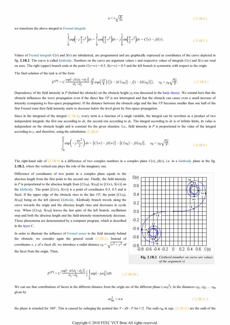
Fig. 2.1B.2 Clothoid (number on curve are values
of the argument v)
u = vπ2a√ ( 2.1B.6 )
we transform the above integral to Fresnel integrals
⌠⌡0
v
exp⎛⎝⎜− j
π
2v2⎞
⎠⎟dv = ⌠⌡0
v
cos⎛⎝⎜
π
2v2⎞
⎠⎟dv − j⌠⌡0
v
sin⎛⎝⎜
π
2v2⎞
⎠⎟dv = C(v) − jS(v). ( 2.1B.7 )
Values of Fresnel integrals C(v) and S(v) are tabularized, are programmed and are graphically expressed as coordinates of the curve depicted in
fig. 2.1B.2. The curve is called klothoidy. Numbers on the curve are argument values v and respective values of integrals C(v) and S(v) are read
on axes. The right (upper) branch ends at the point C(v=∞) = 0.5, S(v=∞) = 0.5 and the left branch is symmetric with respect to the origin.
The final solution of the task is of the form
E (P) = Cexp[− jk(d1 +d2)]
d1 +d2
2√4 exp(
jπ
4 )[1 − 2C(v0)] − j[1 − 2S(v0)], v0 = y02aπ√ . ( 2.1B.8 )
Dependency of the field intensity in P (behind the obstacle) on the obstacle height y0 was discussed in the basic theory. We remind here that the
obstacle influences the wave propagation even if the direct line VP is not interrupted and that the obstacle can cause even a small increase of
intensity (comparing to free-space propagation). If the distance between the obstacle edge and the line VP becomes smaller than one half of the
first Fresnel zone then field intensity starts to decrease below the level given by free-space propagation.
Since in the integrand of the integral (2.1B.4), every term is a function of a single variable, the integral can be rewritten as a product of two
independent integrals: the first one according to dx, the second one according to dy. The integral according to dx is of infinite limits, its value is
independent on the obstacle height and is constant for the given situation. I.e., field intensity in P is proportional to the value of the integral
according to y, and therefore, using the substitution (2.1B.6)
⌠⌡⎮v0
∞
exp(− jπv2
2 )dv = [C(∞) − jS(∞)] − [C(v0) − jS(v0)], v0 = y02aπ√ .
( 2.1B.9 )
The right-hand side of (2.1B.9) is a difference of two complex numbers in a complex plane C(v), jS(v), i.e. in a klothoidy plane in the fig.
2.1B.2, where the vertical axis plays the role of the imaginary one.
Difference of coordinates of two points in a complex plane equals to the
abscissa length from the first point to the second one. Finally, the field intensity
in P is proportional to the abscissa length from [C(v0), S(v0)] to [C(∞), S(∞)] on
the klothoidy. The point [C(∞), S(∞)] is a point of coordinates 0.5, 0.5 and is
fixed. If the upper edge of the obstacle rises to the line VP, the point [C(v0),
S(v0)] being on the left (down) klothoidy. Klothoidy branch travels along the
curve towards the origin and the abscissa length rises and decreases in cyclic
way. When [C(v0), S(v0)] leaves the last spire of the left branch, oscillations
stop and both the abscissa length and the field-intensity monotonously decrease.
These phenomena are demonstrated by a computer program, which is described
in the layer C.
In order to illustrate the influence of Fresnel zones to the field intensity behind
the obstacle, we consider again the general result (2.1B.2). Instead of
coordinates x, y of a facet dS, we introduce a radial distance r0 = x2 + y2√ of
the facet from the origin. Then,
E (P) = Cexp[− jk(d1 +d2)]
d1 +d2
j
λ⌠⌡S
exp(− jar02)dS. ( 2.1B.10 )
We can see that contributions of facets in the different distance from the origin are of the different phase (-ar02). In the distances r01, r02, ... r0n
given by
ar0n2 = n π ( 2.1B.11 )
the phase is retarded for 180°. This is caused by enlarging the pointed line V - dS - P for l /2. The radii r0n in eqn. (2.1B.11) are the radii of the
Copyright © 2010 FEEC VUT Brno All rights reserved.

external border of given Fresnel zones. Substituting a from (2.1B.5) to (2.1B.11), we get a result, which is identical with (2.1A.4).
The fact that the phase of contributions of neighboring Fresnel zones (on the plane S) differs for 180° has got interesting causes. Let us imagine
that the absorbing obstacle cover all the plane S. To this covered plane, a circular window with the center in O and with the arbitrary radius r0 is
cut. Though this window, wave propagates to the point P. Computing intensity E(P), we use eqn. (2.1B.10) and thanks to the rational symmetry
of the window, we perform integration on S (over window) in polar coordinates: dS = r0 djdr0:
E (P) = Cexp[− jk(d1 +d2)]
d1d2
j
λ
⌠
⌡⎮⎮⎮0
r0
⌠⌡0
2π
r0 exp(− jar02)dφdr0 . ( 2.1B.12 )
The integral is easily solvable using the substitution r02 = r. Inscribing by
E0 = Cexp[− jk(d1 +d2)]
d1d2( 2.1B.13 )
the free-space field intensity in P, following results are obtained for different window radii r0:
Tab. 2.1B.1 Intensity values for different window radios
Window radio r0 Zones Intensity E(P)
∞ All the space free E0
0.58 r01 Apart of the 1st Fresnel zone free E0
r01 All the 1st Fresnel zone free 2E0
r02 The 1st Fresnel zone and the 2nd one free 0
Observing results, we might conclude that field intensity E0 we measure in P without the obstacle present, is created by contributions of a free
part of the first Fresnel zone and that contributions of the rest of S mutually eliminate. Unfortunately, the conclusion is not correct (we cannot
determine the part of Fresnel zone producing the contributions which are not eliminated). On the other hand, covering single zones can suppress
the mutual elimination and field intensity can be increased in P that way. Covering all the even Fresnel zones (all the odd ones) yields E(P) = ∞.
Such coverage acts as a burning glass, which focuses the wave to point P.
Copyright © 2010 FEEC VUT Brno All rights reserved.

2.1 Diffraction on a planar absorbing object
Matlab program
The program computes attenuation caused by a thin obstacle, and Fresnel zones radii.
First, the path of Matlab has to be set to the folder Fresnel. The program is run using the m-file fresdif. Passing the introductory window of
the program, the reader is asked for input parameters (frequency, distance of the obstacle from the source and the observation point). Choosing
the button Display manually , the height of the obstacle can be changed manually by the scrollbar, and the changing transmition can be
observed. Choosing the button Display automatically , transmition changes without user interaction. If one of the above-described two buttons
is chosen, a new window is opened. In the upper-left corner, a clothoid is displayed. In the upper-right corner, the dependency of the
attenuation on the ratio H/r1 (distance between the obstacle edge and the line VP over the first Fresnel zone radius) is depicted. In the down left
corner, a sequential covering of Fresnel zones is shown, and in the down right corner, important parameters of the task are listed. Moreover, we
can find here the button Finish (which ends the program) and the button Again (which enables to input new data and perform new
computation).
Copyright © 2010 FEEC VUT Brno All rights reserved.
2.1 Diffraction on a planar absorbing object
Developing Matlab
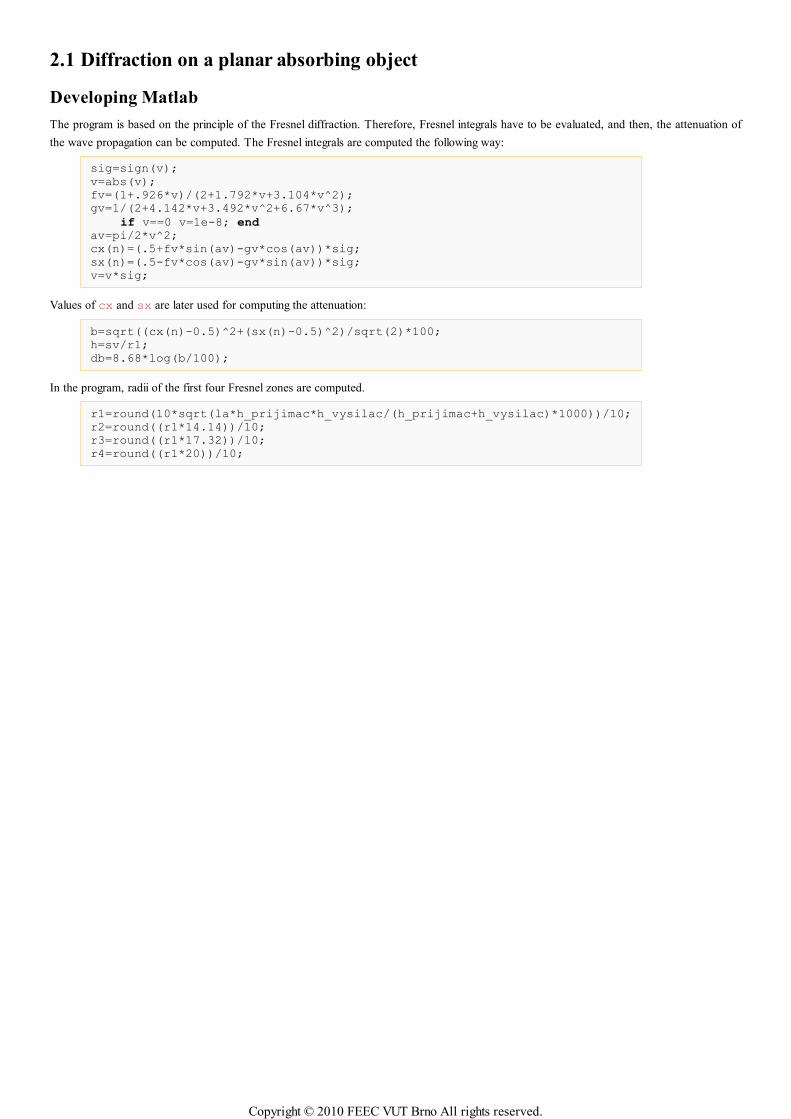
The program is based on the principle of the Fresnel diffraction. Therefore, Fresnel integrals have to be evaluated, and then, the attenuation of
the wave propagation can be computed. The Fresnel integrals are computed the following way:
sig=sign(v);v=abs(v);fv=(1+.926*v)/(2+1.792*v+3.104*v^2);gv=1/(2+4.142*v+3.492*v^2+6.67*v^3);
if v==0 v=1e-8; endav=pi/2*v^2;cx(n)=(.5+fv*sin(av)-gv*cos(av))*sig;sx(n)=(.5-fv*cos(av)-gv*sin(av))*sig;v=v*sig;
Values of cx and sx are later used for computing the attenuation:
b=sqrt((cx(n)-0.5)^2+(sx(n)-0.5)^2)/sqrt(2)*100;h=sv/r1;db=8.68*log(b/100);
In the program, radii of the first four Fresnel zones are computed.
r1=round(10*sqrt(la*h_prijimac*h_vysilac/(h_prijimac+h_vysilac)*1000))/10;r2=round((r1*14.14))/10;r3=round((r1*17.32))/10;r4=round((r1*20))/10;
Copyright © 2010 FEEC VUT Brno All rights reserved.

2.1 Diffraction on a planar absorbing object
Java applet
Copyright © 2010 FEEC VUT Brno All rights reserved.

2.1 Diffraction on a planar absorbing object
Quiz
Answer these questions to get feedback on how well you understand the course. Only one of the answers is correct. You don't have to answer
every question. If you don't know the answer you can just leave it blank (default option: “I won't answer this question”) and this won't affect
your score. Answering correctly will add 2 points to your score but on the other hand you'll lose 1 point if your answer is wrong. The
questions are divided in groups of five questions.
Press See result after you have finished answering.
Displaying questions 1..10 of 10:
Question 1
Fresnel diffraction describes a wave phenomenon caused by …
Possible answers for question 1:
… planar perfectly electrically conductive obstacle between transmitter and receiver.
… planar perfectly absorbing obstacle between transmitter and receiver.
… cylindrical dielectric obstacle between transmitter and receiver.
I won't answer this question
Question 2
Applying Huygens principle to the solution of Fresnel diffraction …
Possible answers for question 2:
… surface currents on the obstacle, which is induced by the incident wave, is computed as the source of the secondary wave.
… does not produce the solution of the problem.
… each elementary surface over the obstacle, which is illuminated by the incident wave,becomes the source of the secondary wave.
I won't answer this question
Question 3
Inserting an obstacle between the transmitter and the receiver …
Possible answers for question 3:
… field intensity at the receiver can never be higher compared to the situation without any obstacle.
… field intensity at the receiver can be even higher compared to the situation without any obstacle.
… does not significantly influences wave propagation.
I won't answer this question
Question 4
Field intensity at the receiver depends on …
Possible answers for question 4:
… the distance between the top of the obstacle and the join between the transmitter and the receiver.
… electromagnetic parameters of the obstacle.
… frequency of the electromagnetic wave.
I won't answer this question
Question 5
In the practical life, Fresnel diffraction …
Copyright © 2010 FEEC VUT Brno All rights reserved.

Possible answers for question 5:
… can be used when modeling transversally long and longitudinally narrow obstacles.
… can be used when modeling wave propagation through walls of buildings.
… cannot be used.
I won't answer this question
Question 6
When the top of the obstacle touches the join between the transmitter and the receiver …
Possible answers for question 6:
… field intensity at the receiver is the same compared to the intensity without any obstacle.
… field intensity at the receiver is higher compared to the intensity without any obstacle.
… field intensity at the receiver is one half compared to the intensity without any obstacle.
I won't answer this question
Question 7
The first Fresnel zone is given by the circle on the plane, which is perpendicular to the join between the transmitter and the
receiver.
Possible answers for question 7:
The distance transmitter - circumference of the circle - receiver is half wavelength longer compared to the distance transmitter -
receiver.
Radius of the circle equals to the distance between the transmitter and the receiver.
The distance transmitter - circumference of the circle - receiver is one wavelength longer compared to the distance transmitter -
receiver.
I won't answer this question
Question 8
When all the even (odd) Fresnel zones are covered …
Possible answers for question 8:
… zero field intensity can appear at the receiver.
… theoretically infinite field intensity can appear at the receiver.
… nothing can be said about the field intensity at the receiver.
I won't answer this question
Question 9
Fresnel integrals can be evaluated …
Possible answers for question 9:
… analytically.
… cannot be evaluated due strong singularities.
… numerically.
I won't answer this question
Question 10
When explaining Fresnel diffraction, we assume the propagation of …
Copyright © 2010 FEEC VUT Brno All rights reserved.

Possible answers for question 10:
… a planar wave.
… a spherical wave.
… cylindrical wave.
I won't answer this question
Copyright © 2010 FEEC VUT Brno All rights reserved.
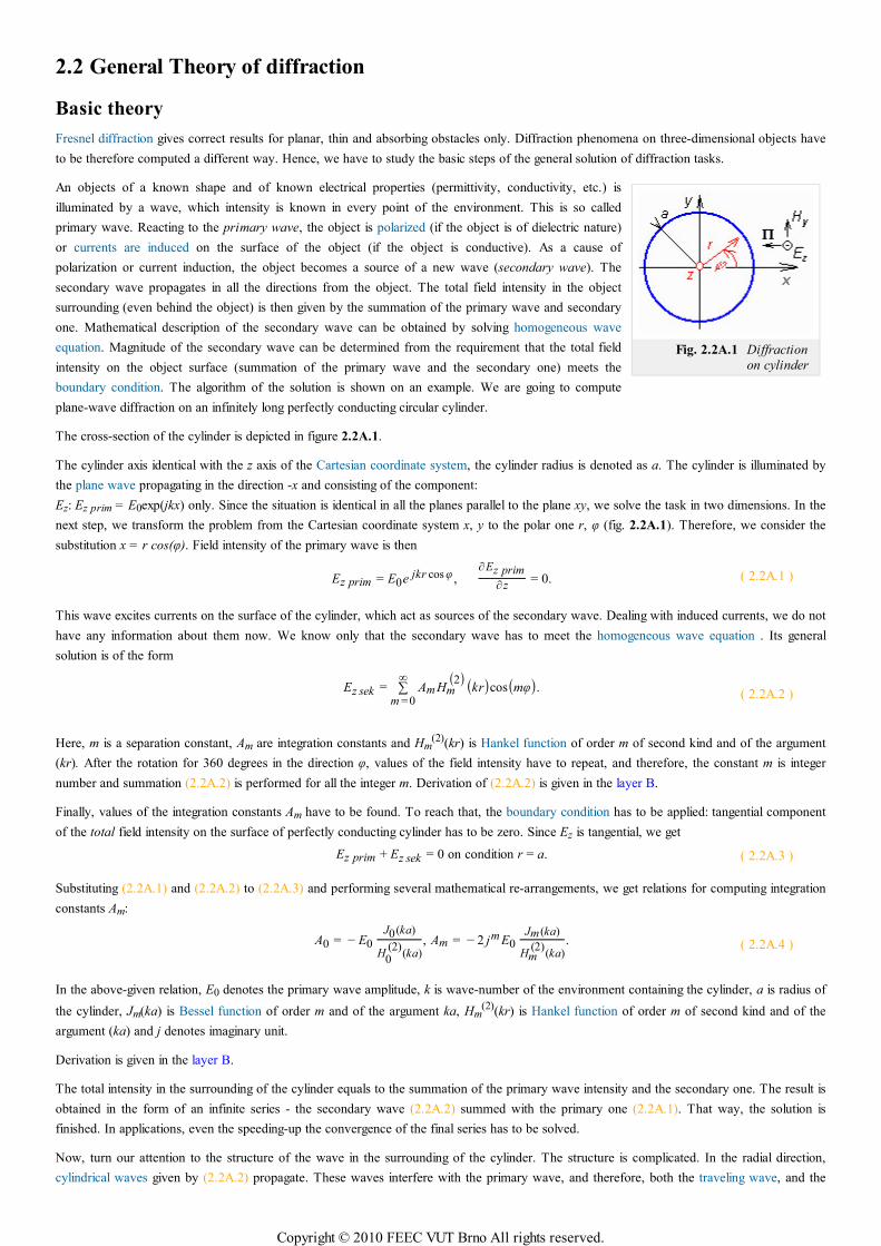
Fig. 2.2A.1 Diffraction
on cylinder
2.2 General Theory of diffraction
Basic theory
Fresnel diffraction gives correct results for planar, thin and absorbing obstacles only. Diffraction phenomena on three-dimensional objects have
to be therefore computed a different way. Hence, we have to study the basic steps of the general solution of diffraction tasks.
An objects of a known shape and of known electrical properties (permittivity, conductivity, etc.) is
illuminated by a wave, which intensity is known in every point of the environment. This is so called
primary wave. Reacting to the primary wave, the object is polarized (if the object is of dielectric nature)
or currents are induced on the surface of the object (if the object is conductive). As a cause of
polarization or current induction, the object becomes a source of a new wave (secondary wave). The
secondary wave propagates in all the directions from the object. The total field intensity in the object
surrounding (even behind the object) is then given by the summation of the primary wave and secondary
one. Mathematical description of the secondary wave can be obtained by solving homogeneous wave
equation. Magnitude of the secondary wave can be determined from the requirement that the total field
intensity on the object surface (summation of the primary wave and the secondary one) meets the
boundary condition. The algorithm of the solution is shown on an example. We are going to compute
plane-wave diffraction on an infinitely long perfectly conducting circular cylinder.
The cross-section of the cylinder is depicted in figure 2.2A.1.
The cylinder axis identical with the z axis of the Cartesian coordinate system, the cylinder radius is denoted as a. The cylinder is illuminated by
the plane wave propagating in the direction -x and consisting of the component:
Ez: Ez prim = E0exp(jkx) only. Since the situation is identical in all the planes parallel to the plane xy, we solve the task in two dimensions. In the
next step, we transform the problem from the Cartesian coordinate system x, y to the polar one r, φ (fig. 2.2A.1). Therefore, we consider the
substitution x = r cos(φ). Field intensity of the primary wave is then
Ez prim = E0e jkr cos φ , ∂Ez prim
∂ z= 0. ( 2.2A.1 )
This wave excites currents on the surface of the cylinder, which act as sources of the secondary wave. Dealing with induced currents, we do not
have any information about them now. We know only that the secondary wave has to meet the homogeneous wave equation . Its general
solution is of the form
Ez sek = ∑m =0
∞Am Hm
(2)(kr)cos(mφ).( 2.2A.2 )
Here, m is a separation constant, Am are integration constants and Hm(2)(kr) is Hankel function of order m of second kind and of the argument
(kr). After the rotation for 360 degrees in the direction φ, values of the field intensity have to repeat, and therefore, the constant m is integer
number and summation (2.2A.2) is performed for all the integer m. Derivation of (2.2A.2) is given in the layer B.
Finally, values of the integration constants Am have to be found. To reach that, the boundary condition has to be applied: tangential component
of the total field intensity on the surface of perfectly conducting cylinder has to be zero. Since Ez is tangential, we get
Ez prim + Ez sek = 0 on condition r = a. ( 2.2A.3 )
Substituting (2.2A.1) and (2.2A.2) to (2.2A.3) and performing several mathematical re-arrangements, we get relations for computing integration
constants Am:
A0 = − E0
J0(ka)
H0(2)
(ka), Am = − 2 jm E0
Jm (ka)
Hm(2)
(ka). ( 2.2A.4 )
In the above-given relation, E0 denotes the primary wave amplitude, k is wave-number of the environment containing the cylinder, a is radius of
the cylinder, Jm(ka) is Bessel function of order m and of the argument ka, Hm(2)(kr) is Hankel function of order m of second kind and of the
argument (ka) and j denotes imaginary unit.
Derivation is given in the layer B.
The total intensity in the surrounding of the cylinder equals to the summation of the primary wave intensity and the secondary one. The result is
obtained in the form of an infinite series - the secondary wave (2.2A.2) summed with the primary one (2.2A.1). That way, the solution is
finished. In applications, even the speeding-up the convergence of the final series has to be solved.
Now, turn our attention to the structure of the wave in the surrounding of the cylinder. The structure is complicated. In the radial direction,
cylindrical waves given by (2.2A.2) propagate. These waves interfere with the primary wave, and therefore, both the traveling wave, and the
Copyright © 2010 FEEC VUT Brno All rights reserved.
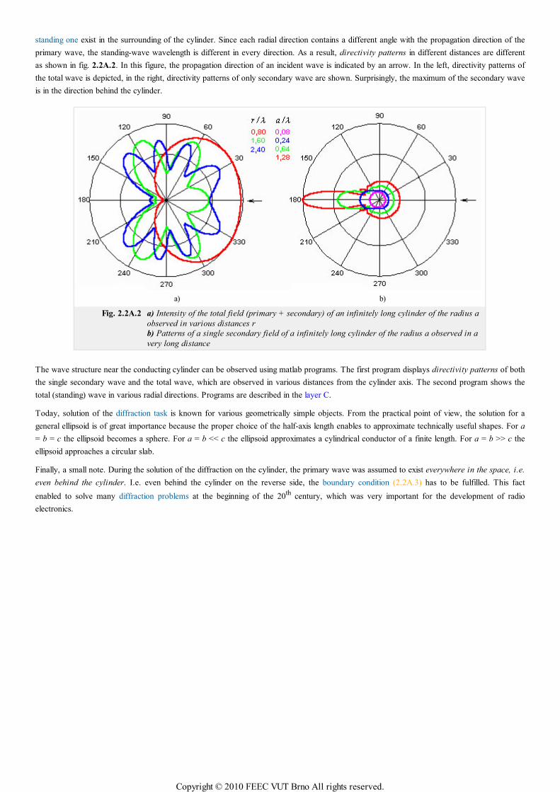
standing one exist in the surrounding of the cylinder. Since each radial direction contains a different angle with the propagation direction of the
primary wave, the standing-wave wavelength is different in every direction. As a result, directivity patterns in different distances are different
as shown in fig. 2.2A.2. In this figure, the propagation direction of an incident wave is indicated by an arrow. In the left, directivity patterns of
the total wave is depicted, in the right, directivity patterns of only secondary wave are shown. Surprisingly, the maximum of the secondary wave
is in the direction behind the cylinder.
a) b)
Fig. 2.2A.2 a) Intensity of the total field (primary + secondary) of an infinitely long cylinder of the radius a
observed in various distances r
b) Patterns of a single secondary field of a infinitely long cylinder of the radius a observed in a
very long distance
The wave structure near the conducting cylinder can be observed using matlab programs. The first program displays directivity patterns of both
the single secondary wave and the total wave, which are observed in various distances from the cylinder axis. The second program shows the
total (standing) wave in various radial directions. Programs are described in the layer C.
Today, solution of the diffraction task is known for various geometrically simple objects. From the practical point of view, the solution for a
general ellipsoid is of great importance because the proper choice of the half-axis length enables to approximate technically useful shapes. For a
= b = c the ellipsoid becomes a sphere. For a = b << c the ellipsoid approximates a cylindrical conductor of a finite length. For a = b >> c the
ellipsoid approaches a circular slab.
Finally, a small note. During the solution of the diffraction on the cylinder, the primary wave was assumed to exist everywhere in the space, i.e.
even behind the cylinder. I.e. even behind the cylinder on the reverse side, the boundary condition (2.2A.3) has to be fulfilled. This fact
enabled to solve many diffraction problems at the beginning of the 20th century, which was very important for the development of radio
electronics.
Copyright © 2010 FEEC VUT Brno All rights reserved.
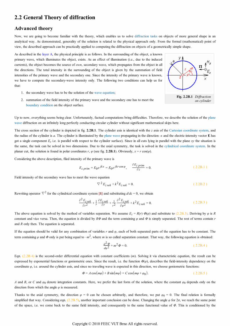
Fig. 2.2B.1 Diffraction
on cylinder
2.2 General Theory of diffraction
Advanced theory
Now, we are going to become familiar with the theory, which enables us to solve diffraction tasks on objects of more general shape in an
analytical way. As demonstrated, generality of the solution is related to the physical approach only. From the formal (mathematical) point of
view, the described approach can be practically applied to computing the diffraction on objects of a geometrically simple shape.
As described in the layer A, the physical principle is as follows. In the surrounding of the object, a known
primary wave, which illuminates the object, exists. As an effect of illumination (i.e., due to the induced
currents), the object becomes the source of own, secondary wave, which propagates from the object in all
the directions. The total intensity in the surrounding of the object is given by the summation of field
intensities of the primary wave and the secondary one. Since the intensity of the primary wave is known,
we have to compute the secondary-wave intensity only. The following two conditions can help us for
that:
the secondary wave has to be the solution of the wave equation;1.
summation of the field intensity of the primary wave and the secondary one has to meet the
boundary condition on the object surface.
2.
Up to now, everything seems being clear. Unfortunately, factual computations bring difficulties. Therefore, we describe the solution of the plane
wave diffraction on an infinitely long perfectly conducting circular cylinder without significant mathematical skips here.
The cross section of the cylinder is depicted in fig. 2.2B.1. The cylinder axis is identical with the z axis of the Cartesian coordinate system, and
the radius of the cylinder is a. The cylinder is illuminated by the plane wave propagating in the direction -x and the electric-intensity vector E has
got a single component Ez i.e. is parallel with respect to the cylinder surface). Since in all cuts lying in parallel with the plane xy the situation is
the same, the task can be solved in two dimensions. Due to the axial symmetry, the task is solved in the cylindrical coordinate system. In the
planar cut, the solution is found in polar coordinates r, φ (see fig. 2.2B.1). Obviously, x = r cos(φ).
Considering the above description, filed intensity of the primary wave is
Ez prim = E0e jkx = E0e jkr cos φ , ∂Ez prim
∂ z= 0. ( 2.2B.1 )
Field intensity of the secondary wave has to meet the wave equation
∇2 Ez sek + k 2Ez sek = 0. ( 2.2B.2 )
Rewriting operator ∇2 for the cylindrical coordinate system [1] and substituting d/dz = 0, we obtain
∂2 Ez sek
∂r2+
1r
∂Ez sek∂r
+1
r2
∂2 Ez sek
∂φ2+ k 2Ez sek = 0. ( 2.2B.3 )
The above equation is solved by the method of variables separation. We assume Ez = R(r) Φ(φ) and substitute to (2.2B.3). Deriving by φ is R
constant and vice versa. Then, the equation is divided by RΦ and the term containing φ and Φ is simply separated. The rest of terms contain r
and R only then. The equation is separated.
If the equation should be valid for any combination of variables r and φ, each of both separated parts of the equation has to be constant. The
term containing φ and Φ only is put being equal to –m2, where m is so called separation constant. That way, the following equation is obtained:
d 2Φ
dφ2+ m2Φ = 0. ( 2.2B.4 )
Eqn. (2.2B.4) is the second-order differential equation with constant coefficients (m). Solving it via characteristic equation, the result can be
expressed by exponential functions or goniometric ones. Since the result, i.e. the function Φ(φ), describes the field-intensity dependency on the
coordinate φ, i.e. around the cylinder axis, and since no traveling wave is expected in this direction, we choose goniometric functions:
Φ = A cos(mφ) + B sin(mφ) = C cos(mφ + φ0). ( 2.2B.5 )
A and B, or C and φ0 denote integration constants. Here, we prefer the last form of the solution, where the constant φ0 depends only on the
direction from which the angle φ is measured.
Thanks to the axial symmetry, the direction φ = 0 can be chosen arbitrarily, and therefore, we put φ0 = 0. The final relation is formally
simplified that way. Considering eqn. (2.2B.5), another important conclusion can be done. Changing the angle φ for 2π, we reach the same point
of the space, i.e. we come back to the same field intensity, and consequently to the same functional value of Φ. This is conditioned by the
Copyright © 2010 FEEC VUT Brno All rights reserved.
requirement that the separation constant m is integer number.
Now, turn our attention to the second part of the eqn. (2.2B.3), which contains variables r and R. This second part is of the form
r2
Rd 2R
dR2+
rR
dRdr
− m2 + k 2r2 = 0. ( 2.2B.6 )
Substituting ρ = kr and performing simple rearrangements, we get Bessel equation:
d 2R
dρ2+
1ρ
dRdρ
+ (1 −m2
ρ2 )R = 0. ( 2.2B.7 )
Since the constant m is integer number, the solution of Bessel equation is a linear combination of Bessel and Neumann functions or linear
combination of Hankel functions of the first kind or of the second kind. Since the function R describes field-intensity dependency on the radial
coordinate r (the direction outwards the cylinder), and in that direction the wave propagates, we choose Hankel functions. Since Hankel
functions of the first kind describe the wave from the infinity to its source and Hankel function of the second kind describes the wave
propagating outwards the source, we choose the second-kind function only. Combining the solution of (2.2B.4) and (2.2B.7), we yield the
general integral of the equation (2.2B.3):
Ez sek = AHm(2)(kr)cos(mφ). ( 2.2B.8 )
Eqn. (2.2B.3) is fulfilled by the solution of (2.2B.8) for each integer m. Since the right value of m unknown this time, we have to admit all the
possible values of the separation constant m and even the arbitrary linear combination of those solutions. The final result of solving (2.2B.3) can
be expressed in the form of an infinite series
Ez sek = ∑m = 0
∞Am Hm
(2)(kr)cos(mφ).( 2.2B.9 )
The result (2.2B.9) can be understood as a set of the infinite number of waves propagating outwards the cylinder, which mutually interfere into
the secondary wave. Each summand of the series (2.2B.9) represents one of these partial waves. These waves differ in their amplitudes
(unknown coefficient Am), in their dependency on the radial distance r (the coefficient Hm(2)(kr) depends on m) and also in their dependency on
φ, i.e. on the direction outwards the cylinder. The wave with m = 0 propagates in all the directions with the same amplitude cos(mφ) = cos(0) =
1 = const., the wave with m = 1 exhibits eight-like directivity pattern (maximum for j = 0, π; zero amplitude for φ = ±π/2), etc.
At this moment, the solution seems to become complicated. But, thanks to the infinite series (2.2B.9), the solution can be successfully finished.
Properly choosing coefficients Am we can enforce the series (2.2B.9) to meet in its whole those boundary conditions, which have to be met on
the surface of the object (the situation is conformable to Fourier series: a proper choice of Fourier coefficients enables us to express an arbitrary
time course of the signal).
If perfectly conducting and infinitely long cylinder is assumed, than the boundary condition is formulated in a simple way: the tangential
component of the total-field intensity has to be zero on the surface. Since our wave consists of the component Ez only, which is parallel to the
surface, we get
Ez prim + Ez sek = 0 on condition r = a. ( 2.2B.10 )
Substituting from (2.2B.1) and (2.2B.9), we get
E0 exp( jka cos φ) + ∑m = 0
∞Am Hm
(2)(ka)cos(mφ) = 0.( 2.2B.11 )
From the above equation, unknown coefficients Am have to be computed. Unfortunately, a single equation of an infinite number of coefficients
is at our disposal. In similar situations, the method of inexplicit coefficients ([1], [4]) can help us. This method requires all the addends (both in
our case) in eqn. (2.2B.11) being expressed by a series of the same type (in our case, by a series containing terms cos(mφ). If this requirement
is satisfied then m = 0, 1, 2, ... ∞ are sequentially substituted to the equation, and that way, the single equation comes to the set of the infinite
number of equations for coefficients Am.
Fortunately, we know that
exp( jka cos φ) = J0(ka) + ∑m =1
∞2 jm Jm(ka)cos(mφ),
( 2.2B.12 )
which enables us to expand the primary wave to the series consisting of term of the type cos(mφ). The series is substituted to (2.2B.11), and
coefficients at cos(φ), cos(2φ), cos(3φ),... are sequentially compared. That way, following relations are obtained:
E0J0(ka) = − A0H0(2)(ka), 2 jm E0Jm(ka) = − Am Hm
(2)(ka) ( 2.2B.13 )
Copyright © 2010 FEEC VUT Brno All rights reserved.
and consequently
A0 = − E0
J0(ka)
H0(2)
(ka), Am = − 2 jm E0
Jm(ka)
Hm(2)
(ka). ( 2.2B.14 )
That way, the analytical solution of our task is finished. First, coefficients Am are evaluated, and then, the secondary wave is given by the series
(2.2B.9). The total-field intensity in the cylinder surrounding is obtained by adding field intensities of the secondary wave (2.2B.9) and the
primary one (2.2B.1).
Finally, let us remind conditions of the successful operation of the method. First, the object shape has to be simple; its surface has to be identical
with a plane in such coordinate system, where the wave equation (2.2B.2) can be solved. Second, the primary wave has to be expanded into the
series of the same type, which is given by the solution of the wave equation. Finally, the secondary-wave series has to exhibit the satisfactory
convergence. The convergence is rather problematic in situations, when object dimensions are several-orders larger than the wavelength. E.g., if
computing the diffraction of very short waves on the surface of the globe, then the satisfactorily accurate expression of the secondary wave
requires addition of tens and hundreds millions of addends in some regions.
Today, the solution of the diffraction task is known for various simple objects: sphere, cylinder (spherical elliptical, parabolic) and for general
ellipsoid; the proper choice of the half-axis length enables to approximate technically useful shapes. For a = b = c the ellipsoid becomes a sphere.
For a = b << c the ellipsoid approximates a cylindrical conductor of a finite length. For a = b >> c the ellipsoid approaches a circular slab.
The structure of the wave was briefly commented in the layer A. In the surrounding of the cylinder, both the traveling wave and the standing
one exist. The standing wave is created by the interference of the primary wave and the secondary one. Since both the waves are of the
different propagation direction and since event the phase velocities of both the waves are different, the wavelengths of the standing wave are in
different directions different too. Surprisingly, the secondary wave exhibits the highest intensity in the direction behind the cylinder. If the radius
of the cylinder is smaller than approx. 1/10 of the wavelength, the the influence of the cylinder to the primary wave is negligible. In detail, the
structure of waves can be studied using computer programs (see the layer C). The first program displays field intensity of the secondary wave
and of the total one in polar coordinates in the form of directivity patterns. Field intensities in various directions in a constant distance from the
cylinder axis can be observed. The second program shows the distribution of field intensities along radial lines in different directions. A more
detailed description is given in the layer C.
Finally, a brief note on the solution of the diffraction task in the situation, when the conductivity of the cylinder is not infinite or if a dielectric
cylinder is analyzed. In that case, the wave equation (2.2B.2) has to be solved even inside the cylinder. There, waves do not propagate and the
standing wave appears there. Therefore, we do not use Hankel functions the solution of he wave equation, but Bessel and Neumann functions
are exploited. Since for r = 0 (on the cylinder axis) the value of Neumann function approaches infinity whereas the field intensity has to be
finite, we have to eliminate this function. In analogy to (2.2B.9), we can write for the region inside the cylinder:
Esek uvnit ř te č = ∑m = 0
∞Bm Jm(kr)cos(mφ).
( 2.2B.15 )
The coefficients can be determined using the boundary condition
Esek uvnit ř te č = Esek vn ě te č + Eprim te č . ( 2.2B.16 )
Even here all the intensities have to be expressed in the form of series of the same type, and the method of inexplicit coefficients [4] has to be
applied. Since two infinite sets of unknown coefficients (Am, Bm) appear here, the only condition (2.2B.16) is insufficient. The solution has to be
repeated even for magnetic field including the proper boundary condition.
Copyright © 2010 FEEC VUT Brno All rights reserved.

2.2 General Theory of diffraction
Matlab program
The program serves for computing and displaying the secondary (diffraction) field and the total field in the surrounding of the circular
conducting cylinder, which is illuminated by a plane wave.
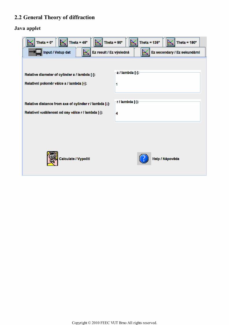
First, a path of matlab has to be directed to the folder Gen_diffraction. The program runs using the m-file valec. After the introductory
window disappears, the program asks for the input of data for computation. We have to give the relative cylinder radius a/λ and the distance of
the observation point d/λ. Then, the computation is started (the computation takes longer time, and therefore, an indicator of the computation
progress is used). When the computation is over, distribution of the primary field and the secondary one in the surrounding of the cylinder is
displayed in the plane, which is perpendicular to the cylinder axis.
Then, buttons for finishing the program Finish and for starting a new run of the program with new input data Again appear. In five
directions, dependency of the secondary wave and the total one on the distance from the cylinder axis are shown. Field intensity E=f(r) is
displayed for a direction, which is opposite to the direction of the incident wave propagation, and then by steps 45° until the direction of the
propagation of the incident wave is met.
Copyright © 2010 FEEC VUT Brno All rights reserved.

2.2 General Theory of diffraction
Developing Matlab
The program is based on the general theory of diffraction. We suppose that the object (cylinder) is illuminated by a wave of known intensity
(primary wave). Thanks to this wave, the cylinder becomes the source of other waves (secondary wave). The total wave is created by the
interference of the primary wave and the secondary one.
User has to introduce two parameters to the input of the program: a (relative radius of the cylinder a/λ) and r (relative distance from the
cylinder axis r/λ). Field intensity of the primary wave is then programmed by the following way:
Ezprim(theta) = cos(2*pi*r*cos((theta-1)*pi/180))+...
+j*sin(2*pi*r*cos((theta-1 )*pi/180));
Here r is a constant, a equals to a/λ , theta varies from 0° to 180°. theta is used even as an index of an array, its values have to be from
the interval from to . The result is symmetrical with respect to the horizontal axis, and therefore, there is no need of computing to 360°.
Next, the secondary wave intensity is computed according to
Ez sek = ∑m = 0
∞Am Hm
(2)(kr)cos(mφ).( 2.2D.1 )
In our situation, we limit the value of m by 150.
First, the term for m = 0 is computed:
Ezsekk = A0*besselh(0,2,2*pi*r)*cos(0);
where
A0 = -besselj(0,2*pi*a)/besselh(0,2,2*pi*a)
A cycle for computing Ezsekk is of the form:
for m=1:60+x
Am(theta) = -2*j^m*besselj(m,2*pi*a)/besselh(m,2,2*pi*a);
Ezsek(theta) = Ezsekk+Am(theta)*besselh(m,2,2*pi*r)*...*cos(m*(theta-
1)*pi/180);
end
Summing Ezprim and Ezsek, the intensity Ezvyst is obtained, which is displayed together with Ezsek in charts Ezsek=f(theta) and
Ezvysl=f(theta).
The second part of the program computes the same dependencies, but cuts of the distribution of the secondary wave and the total one on the
distance from the cylinder axis in given directions theta are displayed. For given direction, theta is a constant and r/λ is changed. The
computation algorithm stays the same and only variables are changed. As a result, five charts for theta = (0, 45, 90, 135, 180)° containing
Ezsek and Ezvyslare displayed.
Note: Programs are called in the following order:
Valec.m – Inform.m – Zadanivalec.m – Vypocetvalec.m – Vypocetrezy.m
Copyright © 2010 FEEC VUT Brno All rights reserved.
2.2 General Theory of diffraction
Java applet
Copyright © 2010 FEEC VUT Brno All rights reserved.

2.2 General Theory of diffraction
Quiz
Answer these questions to get feedback on how well you understand the course. Only one of the answers is correct. You don't have to answer
every question. If you don't know the answer you can just leave it blank (default option: “I won't answer this question”) and this won't affect
your score. Answering correctly will add 2 points to your score but on the other hand you'll lose 1 point if your answer is wrong. The
questions are divided in groups of five questions.
Press See result after you have finished answering.
Displaying questions 1..5 of 5:
Question 1
In case a dielectric cylinder is illuminated by a primary electromagnetic wave …
Possible answers for question 1:
… conductive currents are induced on the surface of the cylinder, and a secondary wave is radiated.
… the dielectrics is polarized and a secondary wave is radiated.
… the cylinder absorbs the primary wave.
I won't answer this question
Question 2
The secondary wave that is radiated by currents induced on a perfectly electrically conductive cylinder is described by …
Possible answers for question 2:
… a homogeneous wave equation in Cartesian coordinates.
… the first Maxwell equation.
… a homogeneous wave equation expressed in terms of Hankel functions.
I won't answer this question
Question 3
In the surrounding of the cylinder …
Possible answers for question 3:
… both the traveling waves and the standing ones appear.
… only traveling waves appear.
… only standing waves appear.
I won't answer this question
Question 4
In the analysis, boundary conditions …
Possible answers for question 4:
… are considered in order to determine integration constants in the general solution.
… are not considered.
… are considered in order to determine the amplitude of the primary wave.
I won't answer this question
Question 5
When evaluating integration constants in the analytical solution …
Copyright © 2010 FEEC VUT Brno All rights reserved.

Possible answers for question 5:
… the method of variables separation is applied.
… the method of inexplicit coefficients is used.
… the method per partes is applied.
I won't answer this question
Copyright © 2010 FEEC VUT Brno All rights reserved.
2.3 Geometrical optics
Basic theory
Fresnel theory of diffraction is simple, but using it, we can analyze thin planar obstacles only. General theory, which was described in
chapter 2.2, is formally rather complicated, and only geometrically simple objects can be handled with. Therefore, alternative ways of the
analysis were sought out. Geometric theory of diffraction (GTD) belongs to those ways: GTD numerically computes even rather complicated
situations. Before explaining the matter of GTD, the basic terms of geometrical optics (GO) are introduced to the reader.
Today's geometrical optics is an efficient tool for solving wave phenomena (wave propagation) in complex media. GO is not limited to the range
of optical frequencies, and it can be used even for radio waves. From the classical geometrical optics, the idea of wave propagation along beams
was adopted. Moreover, GO is able to compute not only wave trajectories but too changes of field intensities and polarization of waves during
propagation. The theory of GO is based on the following two assumptions:
Wavelength is small, and therefore, wave number k is high.1.
The wave is observed far away from the source. Whereas the wave amplitude changes slowly in the propagation direction, phase varies
quickly. The sense of this requirement can be perceived using the following illustration example.
We are interested in the propagation of the spherical wave in the distance of 10 wavelengths from the source. If the distance is
increased for one half of the wavelength, i.e. for 5 %, the intensity amplitude decreases for 5 % too, but the phase changes for π radians
(a significant change).
2.
We start the explanation of geometrical optics by modifying the relation for the intensity of electromagnetic field. Instead of E = Em exp(-jkr),
we write
E = Em exp[− jk0L(x, y, z)]. ( 2.3A.1 )
In the exponent, we have in all the situations k0 = ω (ε0 µ0)1/2 and the parameters of the medium are included in the function L. We simply
understand that L(x, y, z) = const is equation of equiphase surface (wave surface) and that the vector grad L is of the direction, which is
perpendicular to equiphase surface, i.e. of the propagation direction.
The relation (2.3A.1) is substituted to Maxwell equations. Assuming that the wave number k is high, relatively complicated rearrangements yield
||grad L||2
= n2 , ( 2.3A.2 )
where
n = k / k0 = εrel µrel√ ( 2.3A.3 )
denotes the refractive index of the medium.
Eqn. (2.3A.2) is called the basic equation of geometrical optics. The function L(x,y,z) is called the eiconale. It is the scalar function of
coordinates. The vector grad L is of the direction of spherical wave propagation in every point. The curve, which tangent is of the direction of
grad Lis every point, is called the beam. The beam is of the direction of the steepest change of phase in every point, and it is of the direction of
Poynting vector too (i.e. of the direction of the energy flow). In an inhomogeneous medium, beams can be curved and eqn. (2.3A.2) is the
differential equation of beams.
For practical computations of beams, the form of (2.3A.2) is not suitable. Therefore, the following relations are used for computing beam
trajectories:
∂∂s
⎛⎝n∂ x∂ s
⎞⎠ =∂n∂ x
, ∂∂s (n
∂ y
∂s ) =∂n∂ y
, ∂∂s
⎛⎝n∂ z∂s
⎞⎠ =∂n∂ z
, ( 2.3A.4 )
⎛⎝∂ x∂ s
⎞⎠2
+ (∂ y
∂s )2
+⎛⎝∂ z
∂s⎞⎠
2= 1. ( 2.3A.5 )
The variable s is curvilinear coordinate along the beam. Details are given in the layer B including the derivation and an illustrative example.
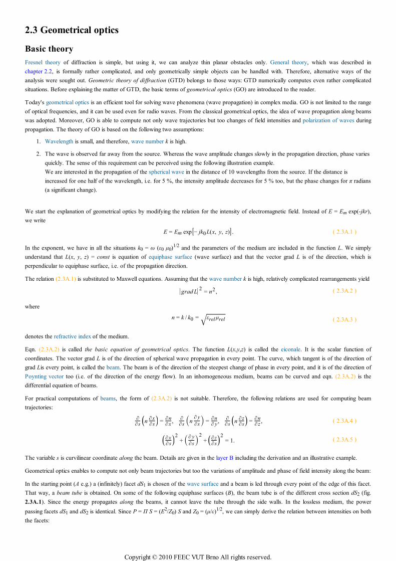
Geometrical optics enables to compute not only beam trajectories but too the variations of amplitude and phase of field intensity along the beam:
In the starting point (A e.g.) a (infinitely) facet dS1 is chosen of the wave surface and a beam is led through every point of the edge of this facet.
That way, a beam tube is obtained. On some of the following equiphase surfaces (B), the beam tube is of the different cross section dS2 (fig.
2.3A.1). Since the energy propagates along the beams, it cannot leave the tube through the side walls. In the lossless medium, the power
passing facets dS1 and dS2 is identical. Since P = Π S = (E2/Z0) S and Z0 = (µ/ε)1/2, we can simply derive the relation between intensities on both
the facets:
Copyright © 2010 FEEC VUT Brno All rights reserved.

Fig. 2.3A.1 Beam tube
ε1µ1√ ||E1
||2
dS1 =ε2µ2√ ||E2
||2
dS2 . ( 2.3A.6 )
Phase of field intensity in B can be computed using eiconale, resp. using eqns. (2.3A.1) or (2.3A.2). If the eiconale is of the value LA at the
beginning of the trajectory A, then in B (which has to be located at the same beam)
LB = LA + ⌠⌡A
B
n ds. ( 2.3A.7 )
Integration is done along the beam.
Eqn. (2.3A.6) is not valid in regions, where the beams cut (infinitely high field intensity would be
obtained). Such situation can be met in the focus and on the surface called caustics (see
layer B).
In more complicated cases, beams in different transversal planes are of different curvature radii
of their wave surfaces. In such situations, (2.3A.6) is not valid. Nevertheless, the intensity can
be computed (see layer B).
Copyright © 2010 FEEC VUT Brno All rights reserved.
2.3 Geometrical optics
Advanced theory
Today&s geometrical optics (GO) enables to examine the propagation of electromagnetic waves even in complex inhomogeneous media of a
given type. As the classical geometrical optics, GO is based on the notion that waves propagate along beams, which can be even curvilinear
now. GO is based on the exact mathematical theory coming out Maxwell equations and enabling to compute not only wave trajectories but too
variation of magnitude and phase of field intensity and wave polarization. Moreover, the method is well-understandable thanks to the simple
notion of beams.
As already described in the layer A, theory of geometrical optics is based on the following two assumptions:
Wave number k is high (so that some terms containing the higher power of k in the denominator can be neglected during mathematical
rearrangements). This assumption predetermines geometrical optics to the applications in the area of optical frequencies. Since the wave
number is not needed being extremely high, the method can be used even for radio frequencies.
1.
The wave is examined in a relatively long distance from the source. In such distance, wave amplitude varies slowly whereas the wave
phase changes quickly (for 2π for every wavelength).
2.
In the following, our attention is focused in the media exhibiting a continuous variation permittivity and permeability. The media are assumed to
be lossless. Refractive index of the medium
n =εµ
ε0 µ0√ = εr µr√ ( 2.3B.1 )
is a real number and is a function of the position (x, y, z). Symbol s denotes the coordinate (curvilinear in general), which is measured along the
direction of propagation.
Investigating the wave propagation in a homogeneous medium, wave number k = k0(εrµr)1/2 = k0n and the propagation direction are usually
known. E.g., the following relation is valid for the field intensity of a plane wave
E = E0 exp(− jks) (s is in the propagation direction) ( 2.3B.2a )
On the part of the trajectory ds, the phase changes for
dφ = kds = k0nds. ( 2.3B.2b )
In the coordinate system x, y, z, the propagation direction need not to be identical with the direction of a coordinate axis. We usually solve this
situation by considering the wave number k as a vector oriented to the propagation direction. Its components kx, ky, kz, to the directions of
coordinate axes are wave numbers in the directions x, y, z. In two arbitrarily located points A, B, which coordinates differ for dx, dy, dz, the
phases differ for
dφ = kx dx + kyd y + kzdz. ( 2.3B.3 )
Geometrical optics does not suppose any a priori knowledge of the direction of wave propagation, because it is different in different points (in
the medium of a variable refractive index). In parallel with (2.3B.2), we use
E = Em exp[− jk0L(x, y, z)] ( 2.3B.4a )
dφ = k0dL, ( 2.3B.4b )
where the distance is not explicitly present. The quantity L is a scalar function of coordinates x, y, z, it is called eiconale and it determines the
phase of field intensity in every point. Comparing (2.3A.4b) and (2.3A.2b) shows that on the infinitely short path ds (where n = const), is
dL = nds. ( 2.3B.5 )
Considering (2.3A.4), equation L = const is the equation of a plane, where wave is of the same phase, i.e. the equation of a wave surface.
Vector grad L is of the direction of the steepest variation of the eiconale (i.e., even of the phase), and this is the direction of wave propagation.
For example:
dLds
= ||grad L||
and according to (2.3A.5) is
dLds
= n,
and therefore
Copyright © 2010 FEEC VUT Brno All rights reserved.
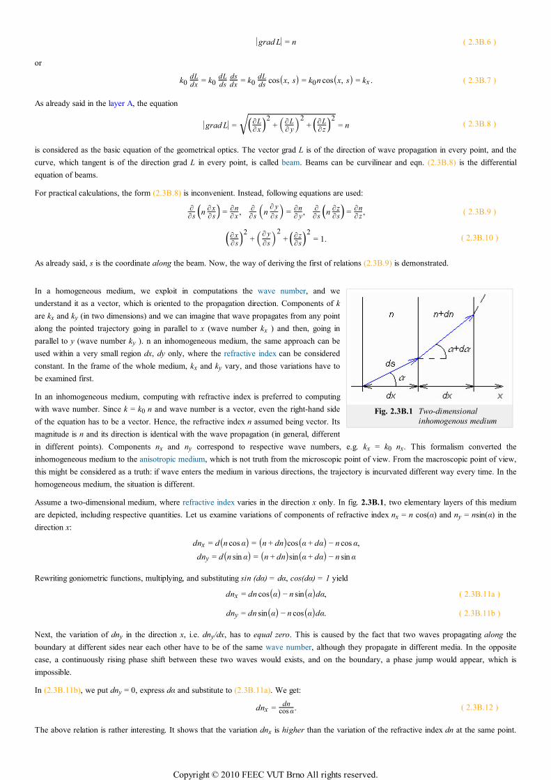
Fig. 2.3B.1 Two-dimensional
inhomogenous medium
||grad L|| = n ( 2.3B.6 )
or
k0dLdx
= k0dLds
dsdx
= k0dLds
cos(x, s) = k0n cos(x, s) = kx . ( 2.3B.7 )
As already said in the layer A, the equation
||grad L|| =⎛⎝∂L
∂ x⎞⎠
2+ (∂ L
∂ y)2+
⎛⎝∂ L∂ z
⎞⎠2
√ = n ( 2.3B.8 )
is considered as the basic equation of the geometrical optics. The vector grad L is of the direction of wave propagation in every point, and the
curve, which tangent is of the direction grad L in every point, is called beam. Beams can be curvilinear and eqn. (2.3B.8) is the differential
equation of beams.
For practical calculations, the form (2.3B.8) is inconvenient. Instead, following equations are used:
∂∂s
⎛⎝n∂ x∂ s
⎞⎠ =∂n∂ x
, ∂∂s (n
∂ y
∂s ) =∂n∂ y
, ∂∂s
⎛⎝n∂ z∂s
⎞⎠ =∂n∂ z
, ( 2.3B.9 )
⎛⎝∂ x∂ s
⎞⎠2
+ (∂ y
∂s )2
+⎛⎝∂ z
∂s⎞⎠
2= 1. ( 2.3B.10 )
As already said, s is the coordinate along the beam. Now, the way of deriving the first of relations (2.3B.9) is demonstrated.
In a homogeneous medium, we exploit in computations the wave number, and we
understand it as a vector, which is oriented to the propagation direction. Components of k
are kx and ky (in two dimensions) and we can imagine that wave propagates from any point
along the pointed trajectory going in parallel to x (wave number kx ) and then, going in
parallel to y (wave number ky ). n an inhomogeneous medium, the same approach can be
used within a very small region dx, dy only, where the refractive index can be considered
constant. In the frame of the whole medium, kx and ky vary, and those variations have to
be examined first.
In an inhomogeneous medium, computing with refractive index is preferred to computing
with wave number. Since k = k0 n and wave number is a vector, even the right-hand side
of the equation has to be a vector. Hence, the refractive index n assumed being vector. Its
magnitude is n and its direction is identical with the wave propagation (in general, different
in different points). Components nx and ny correspond to respective wave numbers, e.g. kx = k0 nx. This formalism converted the
inhomogeneous medium to the anisotropic medium, which is not truth from the microscopic point of view. From the macroscopic point of view,
this might be considered as a truth: if wave enters the medium in various directions, the trajectory is incurvated different way every time. In the
homogeneous medium, the situation is different.
Assume a two-dimensional medium, where refractive index varies in the direction x only. In fig. 2.3B.1, two elementary layers of this medium
are depicted, including respective quantities. Let us examine variations of components of refractive index nx = n cos(α) and ny = nsin(α) in the
direction x:
dnx = d(n cos α) = (n + dn)cos(α + dα) − n cos α,
dny = d(n sin α) = (n + dn)sin(α + dα) − n sin α
Rewriting goniometric functions, multiplying, and substituting sin (dα) = dα, cos(dα) = 1 yield
dnx = dn cos(α) − n sin(α)dα, ( 2.3B.11a )
dny = dn sin(α) − n cos(α)dα. ( 2.3B.11b )
Next, the variation of dny in the direction x, i.e. dny/dx, has to equal zero. This is caused by the fact that two waves propagating along the
boundary at different sides near each other have to be of the same wave number, although they propagate in different media. In the opposite
case, a continuously rising phase shift between these two waves would exists, and on the boundary, a phase jump would appear, which is
impossible.
In (2.3B.11b), we put dny = 0, express dα and substitute to (2.3B.11a). We get:
dnx =dn
cos α. ( 2.3B.12 )
The above relation is rather interesting. It shows that the variation dnx is higher than the variation of the refractive index dn at the same point.
Copyright © 2010 FEEC VUT Brno All rights reserved.
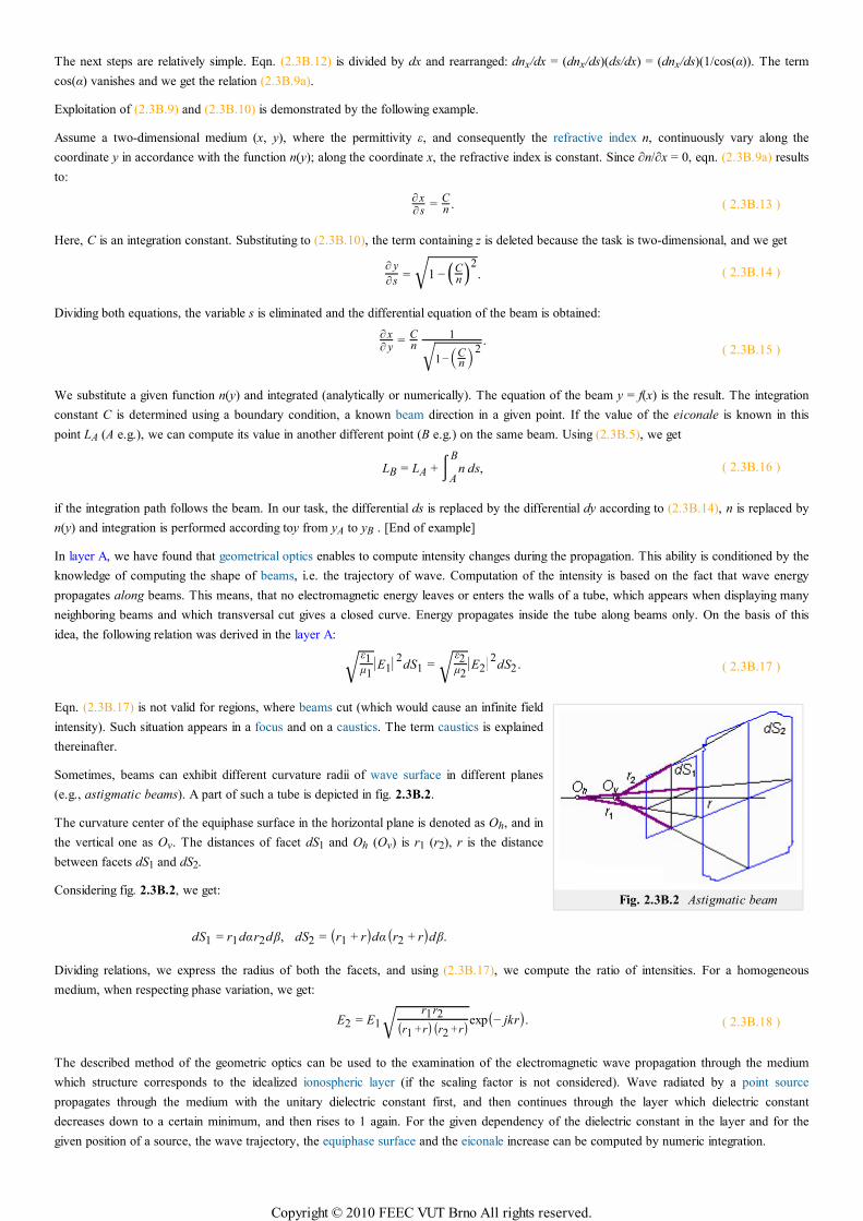
Fig. 2.3B.2 Astigmatic beam
The next steps are relatively simple. Eqn. (2.3B.12) is divided by dx and rearranged: dnx/dx = (dnx/ds)(ds/dx) = (dnx/ds)(1/cos(α)). The term
cos(α) vanishes and we get the relation (2.3B.9a).
Exploitation of (2.3B.9) and (2.3B.10) is demonstrated by the following example.
Assume a two-dimensional medium (x, y), where the permittivity ε, and consequently the refractive index n, continuously vary along the
coordinate y in accordance with the function n(y); along the coordinate x, the refractive index is constant. Since ∂n/∂x = 0, eqn. (2.3B.9a) results
to:
∂ x∂ s
=Cn . ( 2.3B.13 )
Here, C is an integration constant. Substituting to (2.3B.10), the term containing z is deleted because the task is two-dimensional, and we get
∂ y
∂s= 1 −
⎛⎝Cn
⎞⎠2
√ . ( 2.3B.14 )
Dividing both equations, the variable s is eliminated and the differential equation of the beam is obtained:
∂ x∂ y
=Cn
1
1−(Cn )2√
.( 2.3B.15 )
We substitute a given function n(y) and integrated (analytically or numerically). The equation of the beam y = f(x) is the result. The integration
constant C is determined using a boundary condition, a known beam direction in a given point. If the value of the eiconale is known in this
point LA (A e.g.), we can compute its value in another different point (B e.g.) on the same beam. Using (2.3B.5), we get
LB = LA + ⌠⌡A
Bn ds, ( 2.3B.16 )
if the integration path follows the beam. In our task, the differential ds is replaced by the differential dy according to (2.3B.14), n is replaced by
n(y) and integration is performed according toy from yA to yB . [End of example]
In layer A, we have found that geometrical optics enables to compute intensity changes during the propagation. This ability is conditioned by the
knowledge of computing the shape of beams, i.e. the trajectory of wave. Computation of the intensity is based on the fact that wave energy
propagates along beams. This means, that no electromagnetic energy leaves or enters the walls of a tube, which appears when displaying many
neighboring beams and which transversal cut gives a closed curve. Energy propagates inside the tube along beams only. On the basis of this
idea, the following relation was derived in the layer A:
ε1µ1√ ||E1
||2
dS1 =ε2µ2√ ||E2
||2
dS2 . ( 2.3B.17 )
Eqn. (2.3B.17) is not valid for regions, where beams cut (which would cause an infinite field
intensity). Such situation appears in a focus and on a caustics. The term caustics is explained
thereinafter.
Sometimes, beams can exhibit different curvature radii of wave surface in different planes
(e.g., astigmatic beams). A part of such a tube is depicted in fig. 2.3B.2.
The curvature center of the equiphase surface in the horizontal plane is denoted as Oh, and in
the vertical one as Ov. The distances of facet dS1 and Oh (Ov) is r1 (r2), r is the distance
between facets dS1 and dS2.
Considering fig. 2.3B.2, we get:
dS1 = r1dα r2dβ, dS2 = (r1 + r)dα (r2 + r)dβ.
Dividing relations, we express the radius of both the facets, and using (2.3B.17), we compute the ratio of intensities. For a homogeneous
medium, when respecting phase variation, we get:
E2 = E1
r1r2
(r1 +r) (r2 +r)√ exp(− jkr). ( 2.3B.18 )
The described method of the geometric optics can be used to the examination of the electromagnetic wave propagation through the medium
which structure corresponds to the idealized ionospheric layer (if the scaling factor is not considered). Wave radiated by a point source
propagates through the medium with the unitary dielectric constant first, and then continues through the layer which dielectric constant
decreases down to a certain minimum, and then rises to 1 again. For the given dependency of the dielectric constant in the layer and for the
given position of a source, the wave trajectory, the equiphase surface and the eiconale increase can be computed by numeric integration.
Copyright © 2010 FEEC VUT Brno All rights reserved.

Below the layer, where several waves are propagating (due to the trajectory curvature), the direction of the propagation, field intensity and
eiconale (phase) can be computed for each wave. Computations show that beams return back by nice curls in a certain part of space. Tops of
the curls can be connected by an imaginary spline, which is not crossed by any beam, and in a close vicinity of which (below) two neighboring
beams intersect. This spline (or a surface in space) is called caustics.
Copyright © 2010 FEEC VUT Brno All rights reserved.

2.3 Geometrical optics
Quiz
Answer these questions to get feedback on how well you understand the course. Only one of the answers is correct. You don't have to answer
every question. If you don't know the answer you can just leave it blank (default option: “I won't answer this question”) and this won't affect
your score. Answering correctly will add 2 points to your score but on the other hand you'll lose 1 point if your answer is wrong. The
questions are divided in groups of five questions.
Press See result after you have finished answering.
Displaying questions 1..5 of 5:
Question 1
Geometrical optics is a method for wave propagation modeling that …
Possible answers for question 1:
… is applicable at optical frequencies only
… can be used both at optical frequencies and at radio frequencies.
… works properly at any frequency without limitations
I won't answer this question
Question 2
Geometrical optics enables to compute …
Possible answers for question 2:
… an angle of incidence and an angle of reflection of a beam only.
… wave propagation in case the phase of the wave does not need to be considered.
… wave trajectories, intensity variations, and polarization properties.
I won't answer this question
Question 3
The basic equation of geometrical optics tells us that …
Possible answers for question 3:
… the squared refractivity index equals to the squared gradient of the eiconale.
… the refractivity index equals to the square root of permittivity and permeability product.
… the angle of incidence equals to the angle of reflection.
I won't answer this question
Question 4
The beam tube was introduced in order to …
Possible answers for question 4:
… compute intensity variations of the propagating wave.
… define the finite space where the beam energy is concentrated.
… model polarization properties of propagating waves.
I won't answer this question
Question 5
Computations of intensity variations in geometrical optics are conditioned by …
Copyright © 2010 FEEC VUT Brno All rights reserved.

Possible answers for question 5:
… wave propagation in a homogeneous medium.
… the knowledge of wave trajectories.
… the knowledge of phase distribution.
I won't answer this question
Copyright © 2010 FEEC VUT Brno All rights reserved.
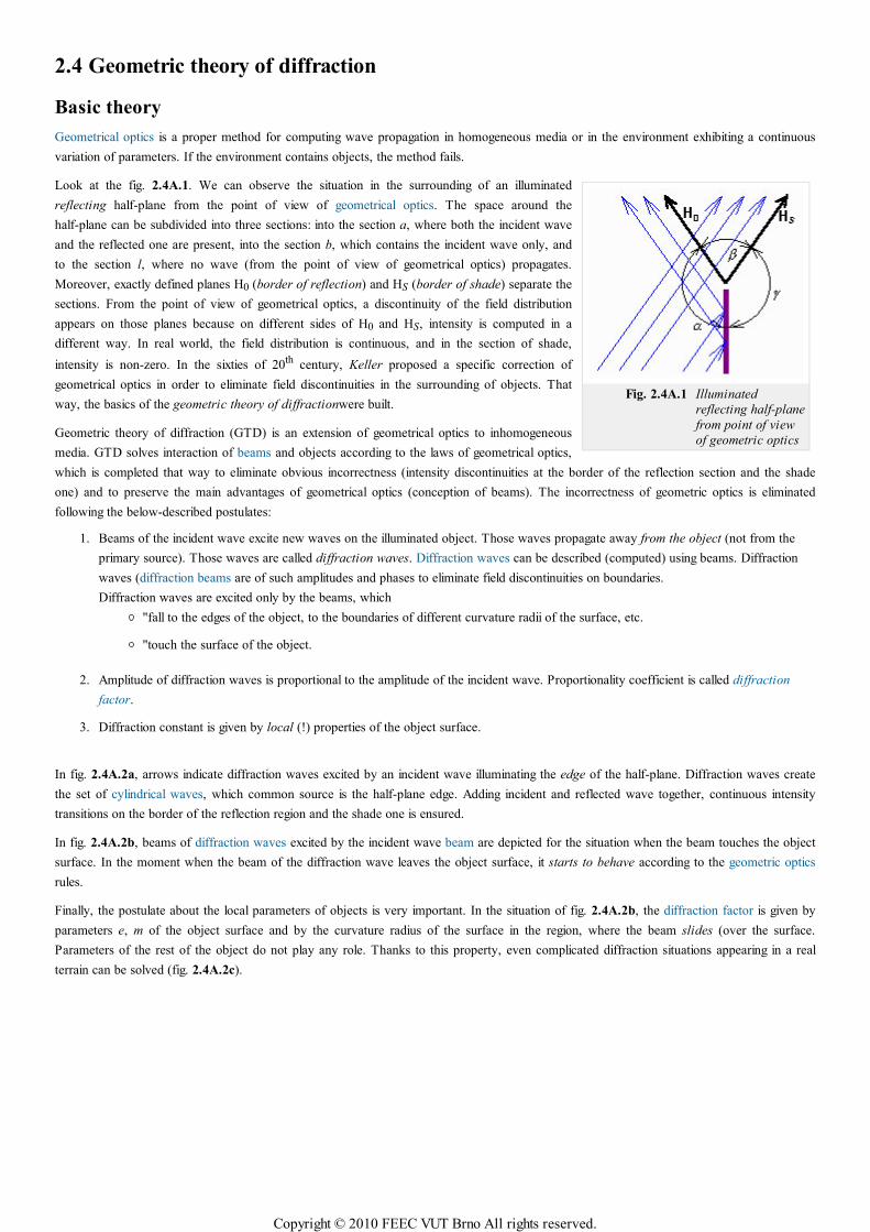
Fig. 2.4A.1 Illuminated
reflecting half-plane
from point of view
of geometric optics
2.4 Geometric theory of diffraction
Basic theory
Geometrical optics is a proper method for computing wave propagation in homogeneous media or in the environment exhibiting a continuous
variation of parameters. If the environment contains objects, the method fails.
Look at the fig. 2.4A.1. We can observe the situation in the surrounding of an illuminated
reflecting half-plane from the point of view of geometrical optics. The space around the
half-plane can be subdivided into three sections: into the section a, where both the incident wave
and the reflected one are present, into the section b, which contains the incident wave only, and
to the section l, where no wave (from the point of view of geometrical optics) propagates.
Moreover, exactly defined planes H0 (border of reflection) and HS (border of shade) separate the
sections. From the point of view of geometrical optics, a discontinuity of the field distribution
appears on those planes because on different sides of H0 and HS, intensity is computed in a
different way. In real world, the field distribution is continuous, and in the section of shade,
intensity is non-zero. In the sixties of 20th century, Keller proposed a specific correction of
geometrical optics in order to eliminate field discontinuities in the surrounding of objects. That
way, the basics of the geometric theory of diffractionwere built.
Geometric theory of diffraction (GTD) is an extension of geometrical optics to inhomogeneous
media. GTD solves interaction of beams and objects according to the laws of geometrical optics,
which is completed that way to eliminate obvious incorrectness (intensity discontinuities at the border of the reflection section and the shade
one) and to preserve the main advantages of geometrical optics (conception of beams). The incorrectness of geometric optics is eliminated
following the below-described postulates:
Beams of the incident wave excite new waves on the illuminated object. Those waves propagate away from the object (not from the
primary source). Those waves are called diffraction waves. Diffraction waves can be described (computed) using beams. Diffraction
waves (diffraction beams are of such amplitudes and phases to eliminate field discontinuities on boundaries.
Diffraction waves are excited only by the beams, which
"fall to the edges of the object, to the boundaries of different curvature radii of the surface, etc.
"touch the surface of the object.
1.
Amplitude of diffraction waves is proportional to the amplitude of the incident wave. Proportionality coefficient is called diffraction
factor.
2.
Diffraction constant is given by local (!) properties of the object surface.3.
In fig. 2.4A.2a, arrows indicate diffraction waves excited by an incident wave illuminating the edge of the half-plane. Diffraction waves create
the set of cylindrical waves, which common source is the half-plane edge. Adding incident and reflected wave together, continuous intensity
transitions on the border of the reflection region and the shade one is ensured.
In fig. 2.4A.2b, beams of diffraction waves excited by the incident wave beam are depicted for the situation when the beam touches the object
surface. In the moment when the beam of the diffraction wave leaves the object surface, it starts to behave according to the geometric optics
rules.
Finally, the postulate about the local parameters of objects is very important. In the situation of fig. 2.4A.2b, the diffraction factor is given by
parameters e, m of the object surface and by the curvature radius of the surface in the region, where the beam slides (over the surface.
Parameters of the rest of the object do not play any role. Thanks to this property, even complicated diffraction situations appearing in a real
terrain can be solved (fig. 2.4A.2c).
Copyright © 2010 FEEC VUT Brno All rights reserved.
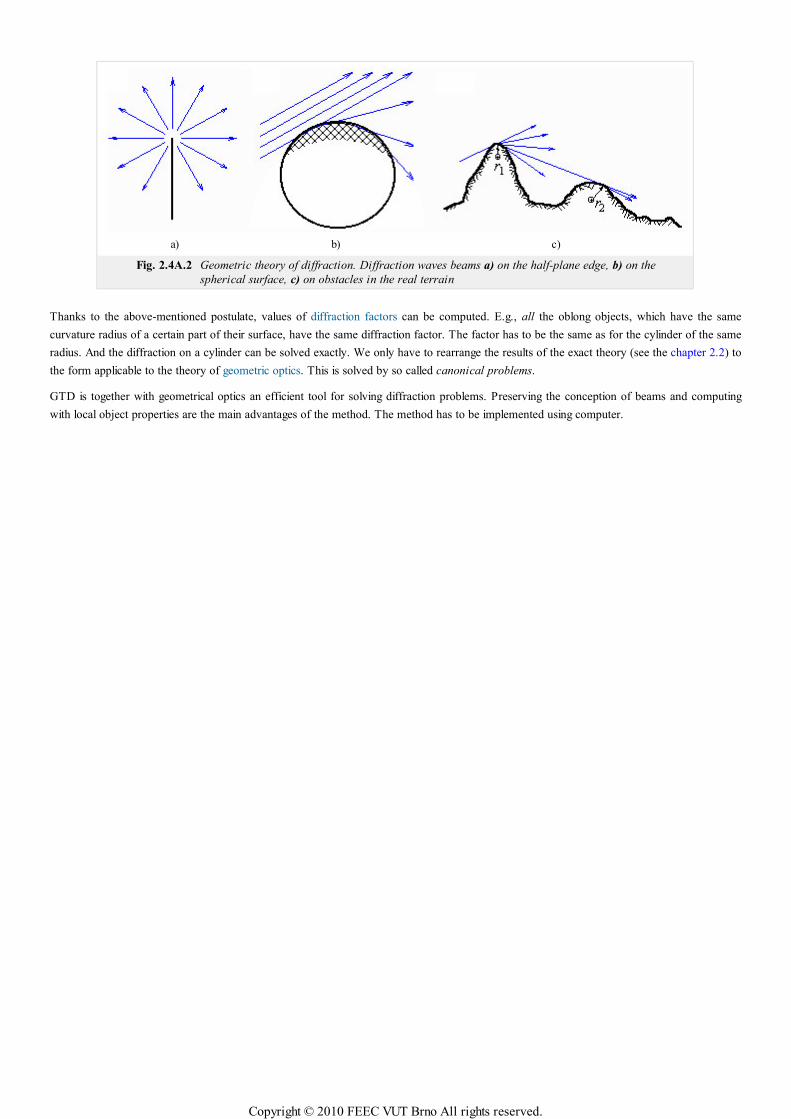
a) b) c)
Fig. 2.4A.2 Geometric theory of diffraction. Diffraction waves beams a) on the half-plane edge, b) on the
spherical surface, c) on obstacles in the real terrain
Thanks to the above-mentioned postulate, values of diffraction factors can be computed. E.g., all the oblong objects, which have the same
curvature radius of a certain part of their surface, have the same diffraction factor. The factor has to be the same as for the cylinder of the same
radius. And the diffraction on a cylinder can be solved exactly. We only have to rearrange the results of the exact theory (see the chapter 2.2) to
the form applicable to the theory of geometric optics. This is solved by so called canonical problems.
GTD is together with geometrical optics an efficient tool for solving diffraction problems. Preserving the conception of beams and computing
with local object properties are the main advantages of the method. The method has to be implemented using computer.
Copyright © 2010 FEEC VUT Brno All rights reserved.

2.4 Geometric theory of diffraction
Quiz
Answer these questions to get feedback on how well you understand the course. Only one of the answers is correct. You don't have to answer
every question. If you don't know the answer you can just leave it blank (default option: “I won't answer this question”) and this won't affect
your score. Answering correctly will add 2 points to your score but on the other hand you'll lose 1 point if your answer is wrong. The
questions are divided in groups of five questions.
Press See result after you have finished answering.
Displaying questions 1..5 of 5:
Question 1
GTD …
Possible answers for question 1:
… explains the diffraction phenomena using a simple Euclidian geometry.
… is an original interpretation of Huygens’ principle.
… enables to apply the principles of geometrical optics to wave propagation modeling in an inhomogeneous environment.
I won't answer this question
Question 2
In GTD, diffraction waves are assumed to be …
Possible answers for question 2:
… radiated by the currents on the obstacle to eliminate field discontinuities at boundaries.
… negligible – otherwise the wave theory of diffraction has to be applied.
… dominant – other waves can be therefore neglected.
I won't answer this question
Question 3
Diffraction factor is dominantly determined …
Possible answers for question 3:
… by the contrast between the permittivity of the obstacle and surrounding.
… by the local properties of the obstacle.
… by the angle of incidence.
I won't answer this question
Question 4
In the practical life, GTD …
Possible answers for question 4:
… enables to model the wave diffraction on hills, e.g..
… is not applicable.
… can be used at very low frequencies only.
I won't answer this question
Question 5
Diffraction waves are excited …
Copyright © 2010 FEEC VUT Brno All rights reserved.

Possible answers for question 5:
… by all the incident beams.
… by beams in a sufficient distance form edges.
… by beams contacting the obstacle surface at edges.
I won't answer this question
Copyright © 2010 FEEC VUT Brno All rights reserved.
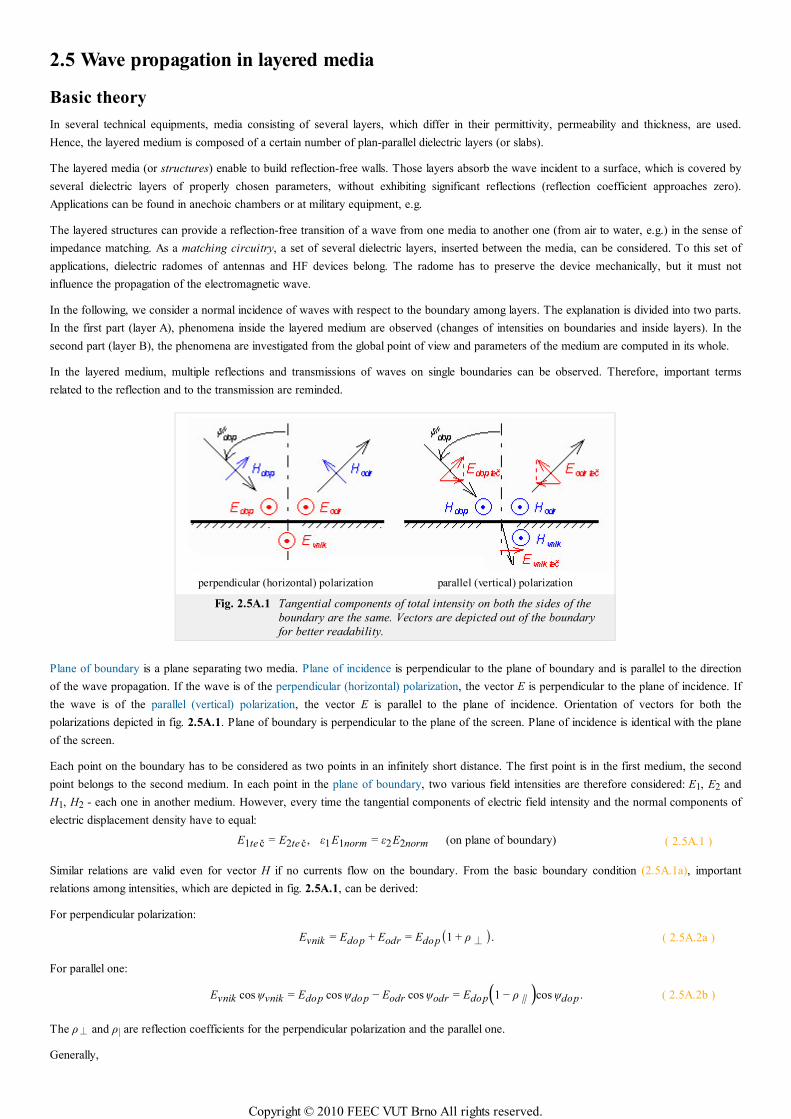
2.5 Wave propagation in layered media
Basic theory
In several technical equipments, media consisting of several layers, which differ in their permittivity, permeability and thickness, are used.
Hence, the layered medium is composed of a certain number of plan-parallel dielectric layers (or slabs).
The layered media (or structures) enable to build reflection-free walls. Those layers absorb the wave incident to a surface, which is covered by
several dielectric layers of properly chosen parameters, without exhibiting significant reflections (reflection coefficient approaches zero).
Applications can be found in anechoic chambers or at military equipment, e.g.
The layered structures can provide a reflection-free transition of a wave from one media to another one (from air to water, e.g.) in the sense of
impedance matching. As a matching circuitry, a set of several dielectric layers, inserted between the media, can be considered. To this set of
applications, dielectric radomes of antennas and HF devices belong. The radome has to preserve the device mechanically, but it must not
influence the propagation of the electromagnetic wave.
In the following, we consider a normal incidence of waves with respect to the boundary among layers. The explanation is divided into two parts.
In the first part (layer A), phenomena inside the layered medium are observed (changes of intensities on boundaries and inside layers). In the
second part (layer B), the phenomena are investigated from the global point of view and parameters of the medium are computed in its whole.
In the layered medium, multiple reflections and transmissions of waves on single boundaries can be observed. Therefore, important terms
related to the reflection and to the transmission are reminded.
perpendicular (horizontal) polarization parallel (vertical) polarization
Fig. 2.5A.1 Tangential components of total intensity on both the sides of the
boundary are the same. Vectors are depicted out of the boundary
for better readability.
Plane of boundary is a plane separating two media. Plane of incidence is perpendicular to the plane of boundary and is parallel to the direction
of the wave propagation. If the wave is of the perpendicular (horizontal) polarization, the vector E is perpendicular to the plane of incidence. If
the wave is of the parallel (vertical) polarization, the vector E is parallel to the plane of incidence. Orientation of vectors for both the
polarizations depicted in fig. 2.5A.1. Plane of boundary is perpendicular to the plane of the screen. Plane of incidence is identical with the plane
of the screen.
Each point on the boundary has to be considered as two points in an infinitely short distance. The first point is in the first medium, the second
point belongs to the second medium. In each point in the plane of boundary, two various field intensities are therefore considered: E1, E2 and
H1, H2 - each one in another medium. However, every time the tangential components of electric field intensity and the normal components of
electric displacement density have to equal:
E1te č = E2te č, ε1E1norm = ε2E2norm (on plane of boundary) ( 2.5A.1 )
Similar relations are valid even for vector H if no currents flow on the boundary. From the basic boundary condition (2.5A.1a), important
relations among intensities, which are depicted in fig. 2.5A.1, can be derived:
For perpendicular polarization:
Evnik = Edop + Eodr = Edop(1 + ρ⊥ ). ( 2.5A.2a )
For parallel one:
Evnik cos ψvnik = Edop cos ψdop − Eodr cos ψodr = Edop⎛⎝1 − ρ∥
⎞⎠cos ψdop . ( 2.5A.2b )
The ρ⊥ and ρ| are reflection coefficients for the perpendicular polarization and the parallel one.
Generally,
Copyright © 2010 FEEC VUT Brno All rights reserved.
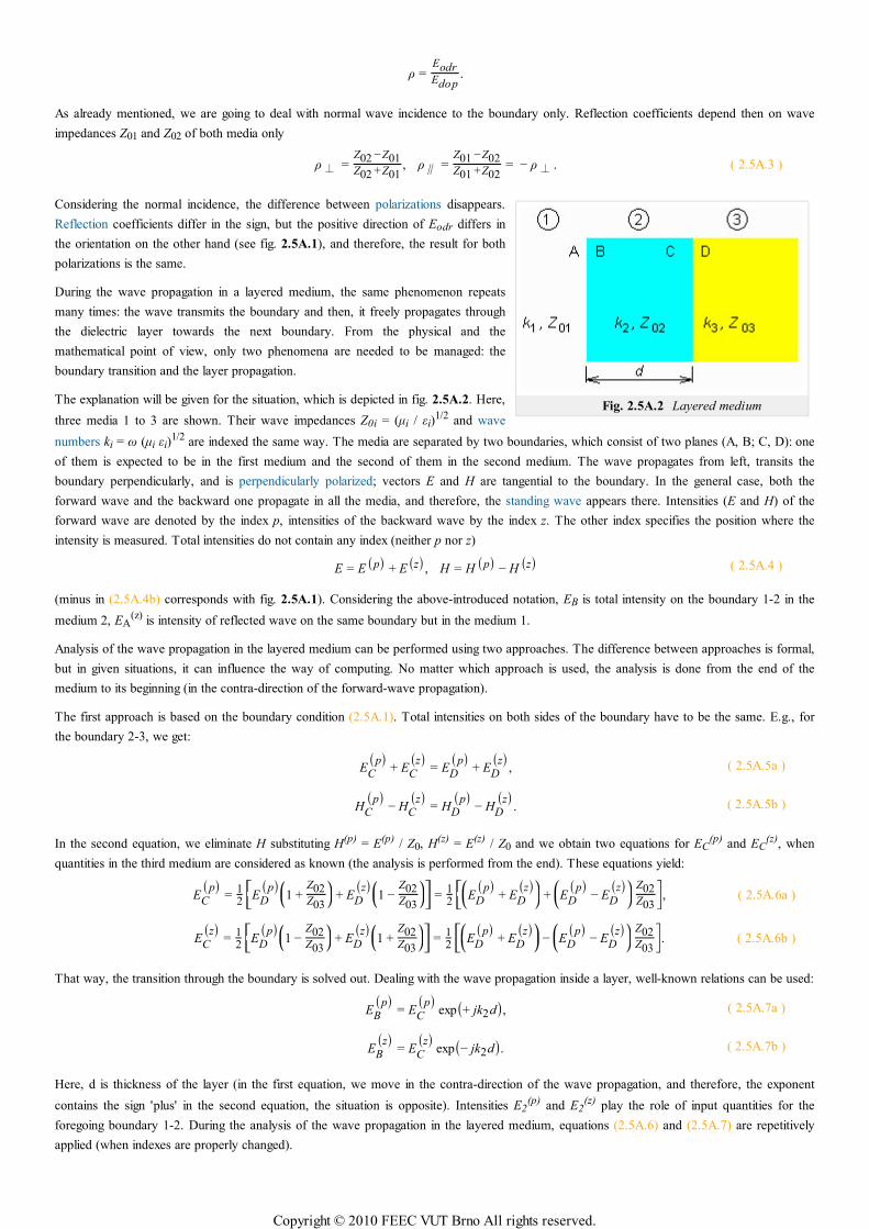
Fig. 2.5A.2 Layered medium
ρ =EodrEdop
.
As already mentioned, we are going to deal with normal wave incidence to the boundary only. Reflection coefficients depend then on wave
impedances Z01 and Z02 of both media only
ρ⊥ =Z02 −Z01Z02 +Z01
, ρ∥ =Z01 −Z02Z01 +Z02
= − ρ⊥ . ( 2.5A.3 )
Considering the normal incidence, the difference between polarizations disappears.
Reflection coefficients differ in the sign, but the positive direction of Eodr differs in
the orientation on the other hand (see fig. 2.5A.1), and therefore, the result for both
polarizations is the same.
During the wave propagation in a layered medium, the same phenomenon repeats
many times: the wave transmits the boundary and then, it freely propagates through
the dielectric layer towards the next boundary. From the physical and the
mathematical point of view, only two phenomena are needed to be managed: the
boundary transition and the layer propagation.
The explanation will be given for the situation, which is depicted in fig. 2.5A.2. Here,
three media 1 to 3 are shown. Their wave impedances Z0i = (µi / εi)1/2 and wave
numbers ki = ω (µi εi)1/2 are indexed the same way. The media are separated by two boundaries, which consist of two planes (A, B; C, D): one
of them is expected to be in the first medium and the second of them in the second medium. The wave propagates from left, transits the
boundary perpendicularly, and is perpendicularly polarized; vectors E and H are tangential to the boundary. In the general case, both the
forward wave and the backward one propagate in all the media, and therefore, the standing wave appears there. Intensities (E and H) of the
forward wave are denoted by the index p, intensities of the backward wave by the index z. The other index specifies the position where the
intensity is measured. Total intensities do not contain any index (neither p nor z)
E = E(p) + E(z), H = H (p) − H (z) ( 2.5A.4 )
(minus in (2.5A.4b) corresponds with fig. 2.5A.1). Considering the above-introduced notation, EB is total intensity on the boundary 1-2 in the
medium 2, EA(z) is intensity of reflected wave on the same boundary but in the medium 1.
Analysis of the wave propagation in the layered medium can be performed using two approaches. The difference between approaches is formal,
but in given situations, it can influence the way of computing. No matter which approach is used, the analysis is done from the end of the
medium to its beginning (in the contra-direction of the forward-wave propagation).
The first approach is based on the boundary condition (2.5A.1). Total intensities on both sides of the boundary have to be the same. E.g., for
the boundary 2-3, we get:
EC(p)
+ EC(z)
= ED(p)
+ ED(z)
, ( 2.5A.5a )
HC(p)
− HC(z)
= HD(p)
− HD(z)
. ( 2.5A.5b )
In the second equation, we eliminate H substituting H(p) = E(p) / Z0, H(z) = E(z) / Z0 and we obtain two equations for EC(p) and EC
(z), when
quantities in the third medium are considered as known (the analysis is performed from the end). These equations yield:
EC(p)
=12
⎡⎣⎢ED
(p)⎛⎝⎜1 +
Z02Z03
⎞⎠⎟ + ED
(z)⎛⎝⎜1 −
Z02Z03
⎞⎠⎟⎤⎦⎥ =
12
⎡⎣⎢⎛⎝⎜ED
(p)+ ED
(z)⎞⎠⎟ +
⎛⎝⎜ED
(p)− ED
(z)⎞⎠⎟
Z02Z03
⎤⎦⎥, ( 2.5A.6a )
EC(z)
=12
⎡⎣⎢E
D(p)⎛
⎝⎜1 −Z02Z03
⎞⎠⎟ + E
D(z)⎛
⎝⎜1 +Z02Z03
⎞⎠⎟⎤⎦⎥ =
12
⎡⎣⎢⎛⎝⎜E
D(p)
+ ED(z)⎞
⎠⎟ −⎛⎝⎜E
D(p)
− ED(z)⎞
⎠⎟Z02Z03
⎤⎦⎥. ( 2.5A.6b )
That way, the transition through the boundary is solved out. Dealing with the wave propagation inside a layer, well-known relations can be used:
EB(p)
= EC(p)
exp(+ jk2d), ( 2.5A.7a )
EB(z)
= EC(z)
exp(− jk2d). ( 2.5A.7b )
Here, d is thickness of the layer (in the first equation, we move in the contra-direction of the wave propagation, and therefore, the exponent
contains the sign 'plus' in the second equation, the situation is opposite). Intensities E2(p) and E2
(z) play the role of input quantities for the
foregoing boundary 1-2. During the analysis of the wave propagation in the layered medium, equations (2.5A.6) and (2.5A.7) are repetitively
applied (when indexes are properly changed).
Copyright © 2010 FEEC VUT Brno All rights reserved.
Whenever inside the layer, total field intensities can be computed substituting the coordinate of the observation point instead of the thickness d
to (2.5A.7). Subsequently, (2.5A.4) is used. Reflection coefficient and standing wave ratio (in an arbitrary point) can be computed as:
ρ =E(z)
E(p), PSV =
1+ ρ
1− ρ. ( 2.5A.8 )
The question is, why the analysis is performed from the end of the medium to its beginning when the field intensity is usually known at its
beginning. The reason is given by the physical matter of the fact. Relations in the medium depend on the ending of the medium. Eqns. (2.5A.6)
and (2.5A.7) formally enables us to perform the analysis from the beginning of the medium to its end, but in a real situation, even if the total
field intensity is known at the beginning, we are not able to decompose it to the forward-wave intensity and the backward-wave one. And both
these intensities play their roles in eqns. (2.5A.6) and (2.5A.7). On the contrary, the situation at the end of the medium is quite different.
Eliminating special situations, the structure is usually ended by free space or perfectly conducting plane. In the case of free space, there is no
reflected wave at the end (E(z) = 0) and a single intensity E(p) has to be known for the computations. If the medium is ended by a conducting
wall, we know that E(z) = -E(p), and again, a single intensity has to be known. This intensity can elected as unitary one and the computation is
performed towards the known intensity at the input. Then, all the intensities are recomputed by a proper ration (all the relations are linear).
The second approach to the analysis of layered media is based on the transformation of reflection coefficient. This approach is well known from
the analysis of the cascade of transmission lines. In both the cases, the situation is quite the same: several lines (media), which are arranged into
the cascade, are of their own characteristic (wave) impedance Z0 and their own length (thickness) d. Voltages and currents on the transmission
line are related to field intensities E and H in an dielectric medium.
The solution consists of the following steps. First, reflection coefficient on the last boundary in the last but one medium (see fig. 2.5A.2) is
computed:
ρC =Z03 −Z02Z03 +Z02
. ( 2.5A.9 )
Reflection coefficient is recomputed to the beginning of the last but one medium, to the plane B:
ρB = ρC exp(−2 jkd). ( 2.5A.10 )
In order to compute reflection coefficient on the plane A, impedance on the plane B has to be determined first:
ZB = Z021+ ρB1− ρB
( 2.5A.11 )
and consequently, reflection coefficient on A can be obtained:
ρA =ZB −Z01ZB +Z01
. ( 2.5A.12 )
If the structure consists of more layers, then the described computations are repeated considering the proper exchange of indexes.
This part of the solution has to be again led from the end of the structure to its beginning. Field intensities can be computed then in an arbitrary
direction from a known intensity to unknown ones. If the total electric field intensity is known on the plane A (EA), e.g., we decompose it to the
intensities of the forward wave and the backward one first. Since
EA(p)
+ EA(z)
= EA(p)
+ ρA EA(p)
= EA ,
we get
EA(p)
=EA
1+ ρA, E
A(z)
= EA(p)
ρA . ( 2.5A.13 )
The same decomposition can be done in an arbitrary medium (layer) when properly changing indexes. In order to evaluate field intensities inside
the structure, the boundary condition (2.5A.1) and the expansion (2.5A.13) are applied. E.g.
EB = EA , EB(p)
=EB
(1+ ρB), E
B(z)
= EB(p)
ρB.
Using (2.5A.7), we compute EC(p) and EC
(z) and consequently the final EC, etc. The intensities can be evaluated using (after a small
rearrangement) equations (2.5A.5) or (2.5A.6).
Another way of the analysis of the layered medium is described in the layer B. In this part of the textbook, even more detailed information
about the application of layered structures is given.
Copyright © 2010 FEEC VUT Brno All rights reserved.
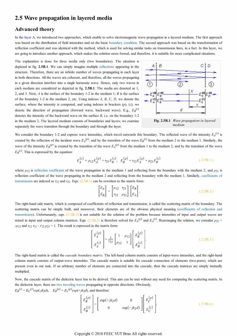
Fig. 2.5B.1 Wave propagation in layered
medium
2.5 Wave propagation in layered media
Advanced theory
In the layer A, we introduced two approaches, which enable to solve electromagnetic wave propagation in a layered medium. The first approach
was based on the distribution of field intensities and on the basic boundary condition. The second approach was based on the transformation of
reflection coefficient and was identical with the method, which is used for solving similar tasks on transmission lines, in a fact. In this layer, we
are going to introduce another approach, which makes the solution more formal, and therefore, it is suitable for more complicated situations.
The explanation is done for three media only (two boundaries). The situation is
depicted in fig. 2.5B.1. We can simply imagine multiple reflections appearing in the
structure. Therefore, there are an infinite number of waves propagating in each layer
in both directions. All the waves are coherent, and therefore, all the waves propagating
in a given direction interfere into a single harmonic wave. Hence, only two waves in
each medium are considered as depicted in fig. 2.5B.1. The media are denoted as 1,
2, and 3. Next, A is the surface of the boundary 1-2 in the medium 1; B is the surface
of the boundary 1-2 in the medium 2, etc. Using indexes A, B, C, D, we denote the
surface, where the intensity is computed, and using indexes in brackets (p), (z), we
denote the direction of propagation (forward wave, backward wave). E.g., EB(z)
denotes the intensity of the backward wave on the surface B, i.e. on the boundary 1-2
in the medium 2. The layered medium consists of boundaries and layers; we examine
separately the wave transition through the boundary and through the layer.
We consider the boundary 1-2 and express wave intensities, which travel outwards this boundary. The reflected wave of the intensity EA(z) is
created by the reflection of the incident wave EA(p), and by the transition of the wave EB
(z) from the medium 2 to the medium 1. Similarly, the
wave of the intensity EB(p) is created by the transition of the wave EA
(p) from the medium 1 to the medium 2, and by the transition of the wave
EB(z). This is expressed by the equation:
EA(z)
= ρ12EA(p)
+ τ21EB(z)
, EB(p)
= τ12EA(p)
+ ρ21EB(z) ( 2.5B.1 )
where ρ12 is reflection coefficient of the wave propagation in the medium 1 and reflecting from the boundary with the medium 2, and ρ21 is
reflection coefficient of the wave propagating in the medium 2 and reflecting from the boundary with the medium 1. Similarly, coefficients of
transmission are indexed as τ12 and τ21. Eqn. (2.5B.1) can be rewritten to the matrix form:
[EA
EB] = [ρ12 τ21
τ12 ρ21] [EB
EA]. ( 2.5B.2 )
The right-hand side matrix, which is composed of coefficients of reflection and transmission, is called the scattering matrix of the boundary. The
scattering matrix can be simply built, and moreover, their elements are of the obvious physical meaning (coefficients of reflection and
transmission). Unfortunately, eqn. (2.5B.2) is not suitable for the solution of the problem because intensities of input and output waves are
mixed in input and output column matrices. Eqn. (2.5B.2) is therefore solved for EA(p) and EA
(z). Rearranging the relation, we consider ρ21 =
-ρ12 and τ12 τ21 - r12 ρ21 = 1. The result is expressed in the matrix form:
⎡
⎣
⎢⎢⎢⎢
EA(p)
EA(z)
⎤
⎦
⎥⎥⎥⎥
=1
τ12 [1 ρ12
ρ12 1 ]
⎡
⎣
⎢⎢⎢⎢
EB(p)
EB(z)
⎤
⎦
⎥⎥⎥⎥. ( 2.5B.3 )
The right-hand matrix is called the cascade boundary matrix. The left-hand column matrix consists of input-wave intensities, and the right-hand
column matrix consists of output-wave intensities. The cascade matrix is suitable for cascade connection of elements (two-ports), which are
present even in our task. If an arbitrary number of elements are connected into the cascade, then the cascade matrices are simply mutually
multiplied.
Now, the cascade matrix of the dielectric layer has to be derived. This aim can be met without any need for computing the scattering matrix. In
the dielectric layer, there are two traveling waves propagating in opposite directions. Obviously,
EB(z) = EC
(z)exp(-jk2d), EB(p) = EC
(p)exp(+jk2d), and therefore
⎡
⎣
⎢⎢⎢⎢
EB(p)
EB(z)
⎤
⎦
⎥⎥⎥⎥
=
⎡
⎣
⎢⎢
exp(+ jk2d) 0
0 exp(− jk2d)
⎤
⎦
⎥⎥
⎡
⎣
⎢⎢⎢⎢
EC(p)
EC(z)
⎤
⎦
⎥⎥⎥⎥, ( 2.5B.4 )
Copyright © 2010 FEEC VUT Brno All rights reserved.
where k2 is wave number in the second medium.
In the system of plan-parallel layers, single boundaries and layers are lined in parallel way. The final equation can be therefore obtained by
multiplying respective matrices. For the situation from fig. 2.5B.1, we get:
⎡
⎣
⎢⎢⎢⎢
EA(p)
EA(z)
⎤
⎦
⎥⎥⎥⎥
=1
τ12 [1 ρ12
ρ12 1 ]
⎡
⎣
⎢⎢
exp(+ jk2d) 0
0 exp(− jk2d)
⎤
⎦
⎥⎥
1τ23 [
1 ρ23
ρ23 1 ]
⎡
⎣
⎢⎢⎢
ED(p)
0
⎤
⎦
⎥⎥⎥. ( 2.5B.5 )
The final result supposes a traveling wave in the third medium. In the opposite case, the intensity ED(z) appears in the last column matrix. The
way of extending the principle to an arbitrary number of layers is obvious.
Rewriting (2.5B.5), we get:
EA(p)
=e jk2d + ρ12 ρ23e− jk2d
τ12τ23ED
(p), E
A(z)
=ρ12e jk2d + ρ23e− jk2d
τ12τ23ED
(p). ( 2.5B.6 )
The ratio EA(z)/ EA
(p) gives the real value of the reflection coefficient on the boundary 1-2. The ratio ED(p)/ EA
(p) equals to the total
transmission coefficient. Both the quantities can be computed using the last equations.
Let us note that in the case of the normal incidence of a perpendicularly polarized wave to a single boundary (no reflected wave can exists
behind that), following relations are valid for the reflection coefficient and the transmission one:
ρ⊥ =Z02 −Z01Z02 +Z01
, τ⊥ = 1 + ρ⊥ =2Z02
Z02 +Z01. ( 2.5B.7 )
The described method is suitable for more complicated structures. Common tasks can be numerically solved using Smith chart or directly
considering boundary conditions on the boundary (see layer A.)
As already mentioned in the introduction, provision of the reflection-free transition of the electromagnetic wave from one medium to another
one is an example of the application of layered media. Such requirement can appear when exciting waves in the ground or in the other media,
when exciting waves in human body, at dielectric radomes of antennas, etc.; the wave is required to enter the medium and to exit it with the
same intensity and the same equiphase surface. Covering the boundary between the media by one or several dielectric layers of exactly given
permittivity and thickness can fulfill the requirement. The layers play the role of the matching circuitry (transformer) in analogy to the
transmission line. In both the cases, electromagnetic wave propagates in the structure. On the transmission line, voltages and currents represent
the wave. In the dielectric layer, the wave is represented by electric-field intensity and magnetic-field intensity. Voltage U corresponds to electric
intensity E, and current I corresponds to magnetic intensity H. Characteristic impedance of the transmission line corresponds to wave impedance
of the medium (layer). The difference between the above-described cases is hidden in the structure of circuits. On the transmission line,
matching circuitry could consist not only of cascade-connected segments of the transmission line but too of parallel or serial shunts. Matching
layers can be connected in cascade only. The reason for that is fundamental. In the part of the transmission line, where the parallel reactance is
connected, a current jump appears (a part of current flows to the reactance). In the layered equivalent, a jump of magnetic-field intensity should
appear in the respective part of the boundary. This is impossible from the physical point of view (it contradicts the basic boundary condition). In
general, jump of magnetic-field intensity H can appear on the boundary if electric current is admitted. Then, the boundary condition is of the
form n × H1 = K + n × H2. Indexes distinguish between the first medium and the second one, vector products of the normal n result in
tangential components and K [A m-1] is surface density of electric current on the boundary. In practical life, this solution can be used. However,
the elected technology has to admit the flow of electric currents on the surface of the boundary.
Routinely, we can design matching circuits consisting of a single one-quarter-wavelength thick dielectric layer or of a first dielectric layer of a
given thickness plus of a second one, which is one-quarter-wavelength thick. No matter whether segments of the transmission line or dielectric
layers are used. If efficient, Smith chart can be used.
The above-described matching circuits can be modeled by the computer program, which is described in the layer C. The program cannot be
used for the design of those circuits, it analyses a circuitry of given parameters (permittivity, thickness of layers) and computes the distribution
of E and H in layers, reflection coefficient and standing wave ratio in various points of the structure. Observing numerical values, the circuit
operation can be investigated. The matching circuits can consists of up to four dielectric layers. The operation of the circuitry can be observed in
a wider frequency band.
Frequency filters are another application area of layered media. As a basic element, the half-wavelength-thick dielectric layer is used. This layer
(in analogy with the half-wavelength-long transmission line) transforms intensities and impedances in the ratio 1:1. Other words, the wave
reflected at the beginning of the layer cancels out with the wave reflected from the end of layer. If the incident wave is of different frequency
(the layer is not half-wavelength thick), the total cancellation does not appear. The layer reflects the part of energy, and therefore, the
transmitted energy is lower. In front of the layer, the standing wave appears.
In the practical life, filters are composed of several half-wavelength-thick layers, which are mutually separated by layers of another permittivity
Copyright © 2010 FEEC VUT Brno All rights reserved.

and thickness (l/4, e.g.).
Properties of layered structures as filters can be demonstrated by another program in the layer C. In this layer, even the more detailed
description of the program is given.
Copyright © 2010 FEEC VUT Brno All rights reserved.

2.5 Wave propagation in layered media
Matlab program
The program simulates the wave transition through several plan-parallel dielectric layers (through several boundaries).
First, the path of Matlab has to be set to the directory Layers. The program is run via the m-file vrstvy. Closing the introductory window,
you are asked to provide input parameters: the number of media (incl. the input medium and the output one), the central frequency (where the
distributions of the electric field intensity and the magnetic one are computed), and the bandwidth (where the frequency course of the reflection
coefficient, of the standing wave ratio and of the power transmittance Pout / Pin are computed).
Confirming the number of layers, the menu for specifying parameters of the media is updated. The user is asked for the length and the dielectric
constant of the layer. If a new layer is added, parameters of the previously specified layers are preserved. Pushing the button Calculate , the
computation is started. In case some parameters are improperly specified, input lines to be corrected are shown in red. Results are displayed in a
new window. The user can consequently modify the number of layers and the parameters of layers, and can compare newly computed results
with previously calculated ones. Pushing the button Close graphs , the windows with results can be closed. The button End ends the
program.
Two charts in a single window graphically represent results. The upper chart displays the distribution of the electric field intensity (blue) and the
magnetic one (green). In the last layer, a unitary value of electric field intensity is assumed, and the last layer is expected to be completed by a
reflection-free termination (i.e., no reflected wave exists in the last layer on any frequency). The lower chart displays frequency course of
reflection coefficient ρ (blue), of transmittance (red), and of standing wave ration (green, the scale on the next axis). If the graphical results are
not needed more, the user can return back to the previous window, finish the program, insert new parameters or repeat the calculation.
Copyright © 2010 FEEC VUT Brno All rights reserved.
2.5 Wave propagation in layered media
Developing Matlab
Subprograms of the main program layers.m read the input quantities and send them to the computational kernel compute.m. Here, the
basic quantities (wavelength, e.g.) are computed first, using elementary relations:
lambda0 = 300/f*1000;k0 = 2*pi/lambda0;Z0 = 120*pi./sqrt(e);K = k0*sqrt(e);Lambda = 2*pi./k;
Second, reflection coefficient is computed for the central frequency in the m-file compu_v.m:
First, characteristic impedance is determined
Z0 = 120*pi./sqrt(e);
1.
Second, impedance at the beginning of all the layers is computed:
for i=(I):-1:1
Zvrch=Z0(i)*(cos(k(i)*l(i))+sqrt(-1)*Z0(i)/Z(i+1)*sin(k(i)*
(l(i))));
Zspod=(Z0(i)/Z(i+1)*cos(k(i)*l(i))+sqrt(-1)*sin(k(i)*(l(i))));
Z(i)=Zvrch/Zspod;
end
2.
Next, reflection coefficient on the boundaries can be determined:
for i=I:-1:1
ro(i)=(Z(i+1)-Z0(i))/(Z(i+1)+Z0(i));
end
3.
Finally, standing wave ratio in layers is computed:
for i=I:-1:1
PSV(i)=(1+abs(ro(i)))/(1-abs(ro(i)));
end
4.
Inside the layers, intensities of forward and backward waves are computed the following way:
Edop(i)= Edop(i+1)*exp(-sqrt(-1)*k(cislo_vrstvy(i))*...(pole_vzd(i)-pole_vzd(i+1)));Eodr(i)= Eodr(i+1)*exp(sqrt(-1)*k(cislo_vrstvy(i))*...(pole_vzd(i)-pole_vzd(i+1)));
The total electric-field intensity is computed by adding intensities of forward and backward waves:
E(i)=Edop(i)+Eodr(i);
Transmitting the boundary between two layers:
Edop(i)=E(i)/(1+ro(cislo_vrstvy(i)));Eodr(i)=ro(cislo_vrstvy(i))/(1+ro(cislo_vrstvy(i)))*E(i);E(i)=Edop(i)+Eodr(i);
Magnetic-field intensity can be computed as:
H(i)=(Edop(i)-Eodr(i))/Z0(cislo_vrstvy(i));
Transmittance is given then by the relation:
T=1-(abs(ro(1)))^2;
Frequency course of standing wave ratio, transmittance and reflection coefficient is computed using the above-given relations.
Copyright © 2010 FEEC VUT Brno All rights reserved.

2.5 Wave propagation in layered media
Java applet
Copyright © 2010 FEEC VUT Brno All rights reserved.

2.5 Wave propagation in layered media
Quiz
Answer these questions to get feedback on how well you understand the course. Only one of the answers is correct. You don't have to answer
every question. If you don't know the answer you can just leave it blank (default option: “I won't answer this question”) and this won't affect
your score. Answering correctly will add 2 points to your score but on the other hand you'll lose 1 point if your answer is wrong. The
questions are divided in groups of five questions.
Press See result after you have finished answering.
Displaying questions 1..5 of 5:
Question 1
If the vector of the intensity of electric field is perpendicular to the plane of incidence, then …
Possible answers for question 1:
… cannot say anything about the wave polarization.
… we speak about the wave of parallel polarization.
… we speak about the perpendicularly polarized wave.
I won't answer this question
Question 2
Wave impedance of a layer Depends on …
Possible answers for question 2:
… permittivity and permeability of the layer.
… permittivity and permeability of the layer, and is influenced by the parameters of neighboring layers.
… permittivity, permeability and thickness of the layer.
I won't answer this question
Question 3
In case of the perpendicular incidence of the electromagnetic wave …
Possible answers for question 3:
… the wave goes through layers without any reflection.
… there is no difference between perpendicular and parallel polarization.
… we have to distinguish between polarizations.
I won't answer this question
Question 4
Designing the matching circuits …
Possible answers for question 4:
… we can apply layers as parts of transmission lines in a cascade.
… we can apply layers the same way as parts of transmission lines (incl. shunts).
… we cannot apply layers.
I won't answer this question
Question 5
Analyzing wave propagation in a layered media, we have assumed the wave is …
Copyright © 2010 FEEC VUT Brno All rights reserved.

Possible answers for question 5:
… planar.
… spherical.
… cylindrical.
I won't answer this question
Copyright © 2010 FEEC VUT Brno All rights reserved.
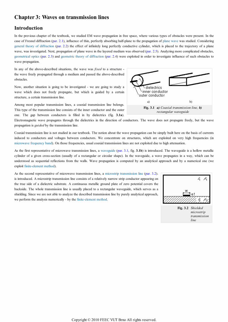
a) b)
Fig. 3.1 a) Coaxial transmission line, b)
rectangular waveguide
Fig. 3.2 Shielded
microstrip
transmission
line
Chapter 3: Waves on transmission lines
Introduction
In the previous chapter of the textbook, we studied EM wave propagation in free space, where various types of obstacles were present. In the
case of Fresnel diffraction (par. 2.1), influence of thin, perfectly absorbing half-plane to the propagation of plane wave was studied. Considering
general theory of diffraction (par. 2.2) the effect of infinitely long perfectly conductive cylinder, which is placed to the trajectory of a plane
wave, was investigated. Next, propagation of plane wave in the layered medium was observed (par. 2.5). Analyzing more complicated obstacles,
geometrical optics (par. 2.3) and geometric theory of diffraction (par. 2.4) were exploited in order to investigate influence of such obstacles to
wave propagation.
In any of the above-described situations, the wave was fixed to a structure -
the wave freely propagated through a medium and passed the above-described
obstacles.
Now, another situation is going to be investigated - we are going to study a
wave which does not freely propagate, but which is guided by a certain
structure, a certain transmission line.
Among most popular transmission lines, a coaxial transmission line belongs.
This type of the transmission line consists of the inner conductor and the outer
one. The gap between conductors is filled in by dielectrics (fig. 3.1a).
Electromagnetic wave propagates through the dielectrics in the direction of conductors. The wave does not propagate freely, but the wave
propagation is guided by the transmission line.
Coaxial transmission line is not studied in our textbook. The notion about the wave propagation can be simply built here on the basis of currents
induced to conductors and voltages between conductors. We concentrate on structures, which are exploited on very high frequencies (in
microwave frequency band). On those frequencies, usual coaxial transmission lines are not exploited due to high attenuation.
As the first representative of microwave transmission lines, a waveguide (par. 3.1, fig. 3.1b) is introduced. The waveguide is a hollow metallic
cylinder of a given cross-section (usually of a rectangular or circular shape). In the waveguide, a wave propagates in a way, which can be
understood as sequential reflections from the walls. Wave propagation is computed by an analytical approach and by a numerical one (we
exploit finite-element method).
As the second representative of microwave transmission lines, a microstrip transmission line (par. 3.2).
is introduced. A microstrip transmission line consists of a relatively narrow strip conductor appearing on
the true side of a dielectric substrate. A continuous metallic ground plate of zero potential covers the
backside. The whole transmission line is usually placed to a rectangular waveguide, which serves as a
shielding. Since we are not able to analyze the described transmission line by purely analytical approach,
we perform the analysis numerically - by the finite-element method.
Copyright © 2010 FEEC VUT Brno All rights reserved.
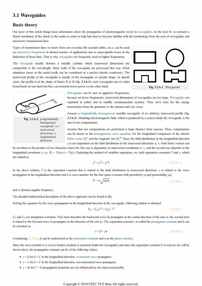
Fig. 3.1A.1 Waveguides
Fig. 3.1A.2 Longitudinally
homogenous
waveguide. u,v:
transversal
directions, z:
longitudinal
direction.
3.1 Waveguides
Basic theory
Our layer of this article brings basic information about the propagation of electromagnetic waves in waveguides. In the layer B, we present a
Dutch translation of the article to the reader in order to help him (her) to become familiar with the terminology from the area of waveguides and
microwave transmission lines.
Types of transmission lines we know from our everyday life (coaxial cables, etc.), can be used
on microwave frequencies in limited number of applications due to unacceptable losses in the
dielectrics of those lines. That is why waveguides are frequently used on higher frequencies.
The waveguide usually denotes a metallic cylinder which transversal dimensions are
comparable to the wavelength. Inner walls of the waveguide are processed that way which
minimizes losses in the metal (walls can be considered as a perfect electric conductor). The
transversal profile of the waveguide is usually of the rectangular or circular shape. In special
cases, the profile is of the shape of letters Π or H (fig. 3.1A.1); such waveguides are of wider
broad-band on one hand but they can transmit lower power on the other hand.
Waveguides can be met on gigahertz frequencies,
because on lower frequencies, transversal dimensions of waveguides are too large. Waveguides are
exploited in radars and in satellite communication systems. They serve here for the energy
transmission from the generator to the antenna and vice versa.
Assume a longitudinally homogeneous metallic waveguide of an arbitrary transversal profile (fig.
3.1A.2). Modeling electromagnetic field, which is produced by a source inside the waveguide, is the
aim of our computations.
Assume that our computations are performed is large distance from sources. Then, computations
can be based on the homogeneous wave equations for the longitudinal component of the electric
Hertz vector Πze and the magnetic one Πz
m. Since the field distribution in the longitudinal direction
z is not dependent on the field distribution in the transversal directions u, v, both Hertz vectors can
be rewritten as the product of two functions where the first one is dependent on transversal coordinates u, v, and the second one depends on the
longitudinal coordinate z, i.e. Πz = T1(u,v) × T2(z). Exploiting the method of variables separation, we yield separation constants Γ and γ, which
are related as
γ2 + k 2 = Γ 2 . ( 3.1A.1 )
In the above relation, Γ is the separation constant that is related to the field distribution in transversal directions, γ is related to the wave
propagation in the longitudinal direction and k is wave-number for the free space (vacuum with permitivity ε0 and permeability µ0)
k = ω µ0ε0√ ( 3.1A.2 )
and ω denotes angular frequency.
The detailed mathematical description of the above approach can be found in [1].
Solving the equation for the wave propagation in the longitudinal direction in the waveguide, following relation is obtained
T2 = C1eγz + C2e−γz ( 3.1A.3 )
C1 and C2 are integration constants. First term describes the backward wave (it propagates in the contra-direction of the axis z), the second term
is related to the forward wave (it propagates in the direction of the axis z). The separation constant γ is called the propagation constant and it can
be rewritten as
γ = β + jα. ( 3.1A.4 )
Considering (3.1A.4), β can be understood as the attenuation constant and α as the phase constant.
Since the wave-number k is real (a lossless medium is assumed inside the waveguide) and since the separation constant G is real too (as will be
shown later), the propagation constant can be of the following values:
γ = β for k < Γ in the longitudinal direction, evanescent wave propagates;
γ = α for k > Γ in the longitudinal direction, non-attenuated wave propagates;
γ = jk for Γ = 0 propagation properties are not influenced by the transversal profile.
Copyright © 2010 FEEC VUT Brno All rights reserved.
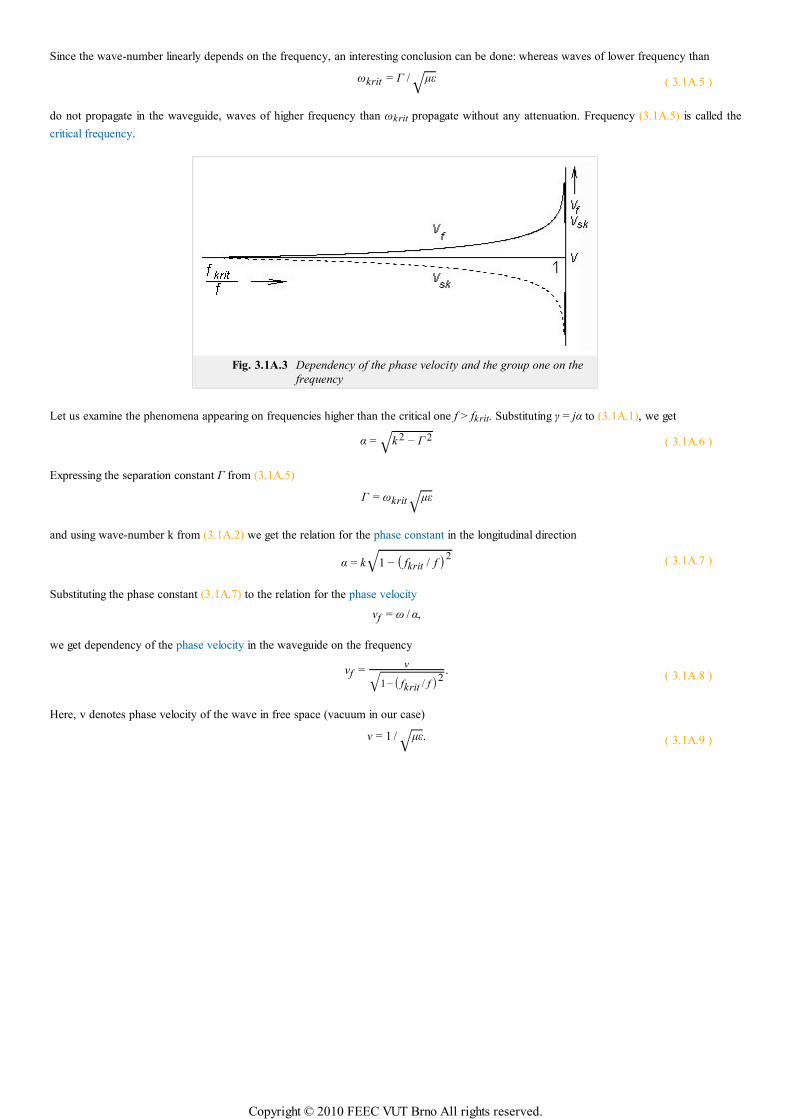
Since the wave-number linearly depends on the frequency, an interesting conclusion can be done: whereas waves of lower frequency than
ωkrit = Γ / µε√ ( 3.1A.5 )
do not propagate in the waveguide, waves of higher frequency than ωkrit propagate without any attenuation. Frequency (3.1A.5) is called the
critical frequency.
Fig. 3.1A.3 Dependency of the phase velocity and the group one on the
frequency
Let us examine the phenomena appearing on frequencies higher than the critical one f > fkrit. Substituting γ = jα to (3.1A.1), we get
α = k 2 − Γ 2√ ( 3.1A.6 )
Expressing the separation constant Γ from (3.1A.5)
Γ = ωkrit µε√
and using wave-number k from (3.1A.2) we get the relation for the phase constant in the longitudinal direction
α = k 1 − ( fkrit / f )2√ ( 3.1A.7 )
Substituting the phase constant (3.1A.7) to the relation for the phase velocity
vf = ω / α,
we get dependency of the phase velocity in the waveguide on the frequency
vf =v
1−( fkrit / f )2√.
( 3.1A.8 )
Here, v denotes phase velocity of the wave in free space (vacuum in our case)
v = 1 / µε√ . ( 3.1A.9 )
Copyright © 2010 FEEC VUT Brno All rights reserved.
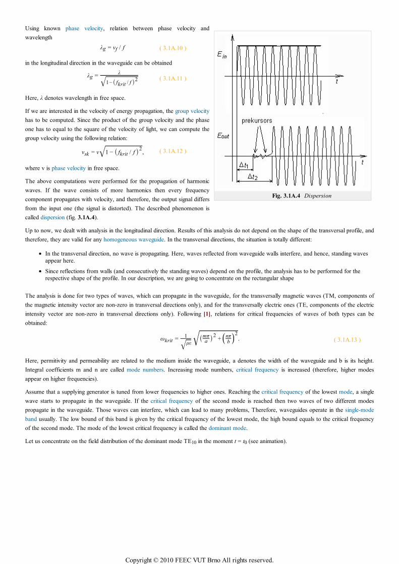
Fig. 3.1A.4 Dispersion
Using known phase velocity, relation between phase velocity and
wavelength
λg = vf / f ( 3.1A.10 )
in the longitudinal direction in the waveguide can be obtained
λg =λ
1−( fkrit / f )2√ ( 3.1A.11 )
Here, λ denotes wavelength in free space.
If we are interested in the velocity of energy propagation, the group velocity
has to be computed. Since the product of the group velocity and the phase
one has to equal to the square of the velocity of light, we can compute the
group velocity using the following relation:
vsk = v 1 − ( fkrit / f )2√ , ( 3.1A.12 )
where v is phase velocity in free space.
The above computations were performed for the propagation of harmonic
waves. If the wave consists of more harmonics then every frequency
component propagates with velocity, and therefore, the output signal differs
from the input one (the signal is distorted). The described phenomenon is
called dispersion (fig. 3.1A.4).
Up to now, we dealt with analysis in the longitudinal direction. Results of this analysis do not depend on the shape of the transversal profile, and
therefore, they are valid for any homogeneous waveguide. In the transversal directions, the situation is totally different:
In the transversal direction, no wave is propagating. Here, waves reflected from waveguide walls interfere, and hence, standing waves
appear here.
Since reflections from walls (and consecutively the standing waves) depend on the profile, the analysis has to be performed for the
respective shape of the profile. In our description, we are going to concentrate on the rectangular shape
The analysis is done for two types of waves, which can propagate in the waveguide, for the transversally magnetic waves (TM, components of
the magnetic intensity vector are non-zero in transversal directions only), and for the transversally electric ones (TE, components of the electric
intensity vector are non-zero in transversal directions only). Following [1], relations for critical frequencies of waves of both types can be
obtained:
ωkrit =1
µε√(mπ
a )2+
⎛⎝nπb
⎞⎠2
√ . ( 3.1A.13 )
Here, permitivity and permeability are related to the medium inside the waveguide, a denotes the width of the waveguide and b is its height.
Integral coefficients m and n are called mode numbers. Increasing mode numbers, critical frequency is increased (therefore, higher modes
appear on higher frequencies).
Assume that a supplying generator is tuned from lower frequencies to higher ones. Reaching the critical frequency of the lowest mode, a single
wave starts to propagate in the waveguide. If the critical frequency of the second mode is reached then two waves of two different modes
propagate in the waveguide. Those waves can interfere, which can lead to many problems, Therefore, waveguides operate in the single-mode
band usually. The low bound of this band is given by the critical frequency of the lowest mode, the high bound equals to the critical frequency
of the second mode. The mode of the lowest critical frequency is called the dominant mode.
Let us concentrate on the field distribution of the dominant mode TE10 in the moment t = t0 (see animation).
Copyright © 2010 FEEC VUT Brno All rights reserved.
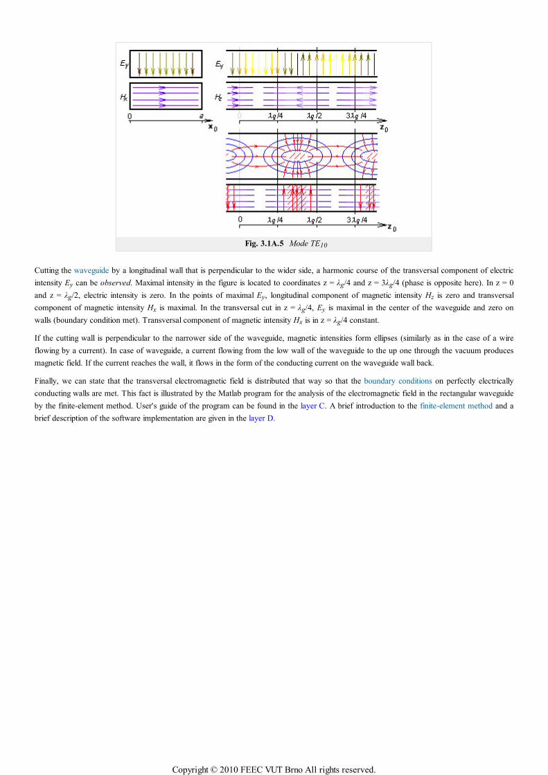
Fig. 3.1A.5 Mode TE10
Cutting the waveguide by a longitudinal wall that is perpendicular to the wider side, a harmonic course of the transversal component of electric
intensity Ey can be observed. Maximal intensity in the figure is located to coordinates z = λg/4 and z = 3λg/4 (phase is opposite here). In z = 0
and z = λg/2, electric intensity is zero. In the points of maximal Ey, longitudinal component of magnetic intensity Hz is zero and transversal
component of magnetic intensity Hx is maximal. In the transversal cut in z = λg/4, Ey is maximal in the center of the waveguide and zero on
walls (boundary condition met). Transversal component of magnetic intensity Hx is in z = λg/4 constant.
If the cutting wall is perpendicular to the narrower side of the waveguide, magnetic intensities form ellipses (similarly as in the case of a wire
flowing by a current). In case of waveguide, a current flowing from the low wall of the waveguide to the up one through the vacuum produces
magnetic field. If the current reaches the wall, it flows in the form of the conducting current on the waveguide wall back.
Finally, we can state that the transversal electromagnetic field is distributed that way so that the boundary conditions on perfectly electrically
conducting walls are met. This fact is illustrated by the Matlab program for the analysis of the electromagnetic field in the rectangular waveguide
by the finite-element method. User's guide of the program can be found in the layer C. A brief introduction to the finite-element method and a
brief description of the software implementation are given in the layer D.
Copyright © 2010 FEEC VUT Brno All rights reserved.
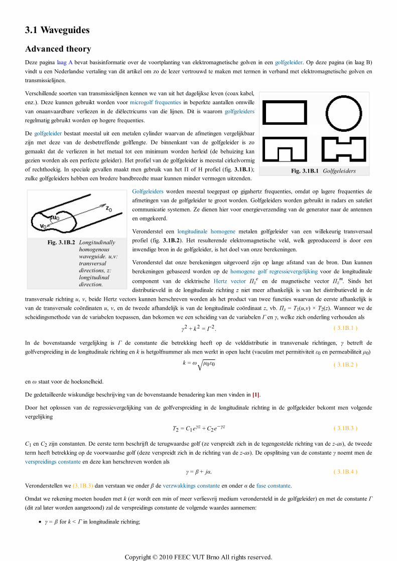
Fig. 3.1B.1 Golfgeleiders
Fig. 3.1B.2 Longitudinally
homogenous
waveguide. u,v:
transversal
directions, z:
longitudinal
direction.
3.1 Waveguides
Advanced theory
Deze pagina laag A bevat basisinformatie over de voortplanting van elektromagnetische golven in een golfgeleider. Op deze pagina (in laag B)
vindt u een Nederlandse vertaling van dit artikel om zo de lezer vertrouwd te maken met termen in verband met elektromagnetische golven en
transmissielijnen.
Verschillende soorten van transmissielijnen kennen we van uit het dagelijkse leven (coax kabel,
enz.). Deze kunnen gebruikt worden voor microgolf frequenties in beperkte aantallen omwille
van onaanvaardbare verliezen in de diëlectricums van die lijnen. Dit is waarom golfgeleiders
regelmatig gebruikt worden op hogere frequenties.
De golfgeleider bestaat meestal uit een metalen cylinder waarvan de afmetingen vergelijkbaar
zijn met deze van de desbetreffende golflengte. De binnenkant van de golfgeleider is zo
gemaakt dat de verliezen in het metaal tot een minimum worden herleid (de behuizing kan
gezien worden als een perfecte geleider). Het profiel van de golfgeleider is meestal cirkelvormig
of rechthoekig. In speciale gevallen maakt men gebruik van het Π of H profiel (fig. 3.1B.1);
zulke golfgeleiders hebben een bredere bandbreedte maar kunnen minder vermogen uitzenden.
Golfgeleiders worden meestal toegepast op gigahertz frequenties, omdat op lagere frequenties de
afmetingen van de golfgeleider te groot worden. Golfgeleiders worden gebruikt in radars en sateliet
communicatie systemen. Ze dienen hier voor energieverzending van de generator naar de antennen
en omgekeerd.
Veronderstel een longitudinale homogene metalen golfgeleider van een willekeurig transversaal
profiel (fig. 3.1B.2). Het resulterende elektromagnetische veld, welk geproduceerd is door een
inwendige bron in de golfgeleider, is het doel van onze berekeningen.
Veronderstel dat onze berekeningen uitgevoerd zijn op lange afstand van de bron. Dan kunnen
berekeningen gebaseerd worden op de homogene golf regressievergelijking voor de longitudinale
component van de elektrische Hertz vector Πze en de magnetische vector Πz
m. Sinds het
distributieveld in de longitudinale richting z niet meer afhankelijk is van het distributieveld in de
transversale richting u, v, beide Hertz vectors kunnen herschreven worden als het product van twee functies waarvan de eerste afhankelijk is
van de transversale coördinaten u, v, en de tweede afhandelijk is van de longitudinale coördinaat z, vb. Πz = T1(u,v) × T2(z). Wanneer we de
scheidingsmethode van de variabelen toepassen, dan bekomen we een scheiding van de variabelen Γ en γ, welke zich onderling verhouden als
γ2 + k 2 = Γ 2 . ( 3.1B.1 )
In de bovenstaande vergelijking is Γ de constante die betrekking heeft op de velddistributie in transversale richtingen, γ betreft de
golfverspreiding in de longitudinale richting en k is hetgolfnummer als men werkt in open lucht (vacuüm met permitiviteit ε0 en permeabiliteit µ0)
k = ω µ0ε0√ ( 3.1B.2 )
en ω staat voor de hoeksnelheid.
De gedetailleerde wiskundige beschrijving van de bovenstaande benadering kan men vinden in [1].
Door het oplossen van de regressievergelijking van de golfverspreiding in de longitudinale richting in de golfgeleider bekomt men volgende
vergelijking
T2 = C1eγz + C2e−γz ( 3.1B.3 )
C1 en C2 zijn constanten. De eerste term beschrijft de terugwaardse golf (ze verspreidt zich in de tegengestelde richting van de z-as), de tweede
term heeft betrekking op de voorwaardse golf (deze verspreidt zich in de richting van de z-as). De opsplitsing van de constante γ noemt men de
verspreidings constante en deze kan herschreven worden als
γ = β + jα. ( 3.1B.4 )
Veronderstellen we (3.1B.3) dan verstaan we onder β de verzwakkings constante en onder α de fase constante.
Omdat we rekening moeten houden met k (er wordt een min of meer verliesvrij medium verondersteld in de golfgeleider) en met de constante Γ
(dit zal later worden aangetoond) zal de verspreidings constante de volgende waardes aannemen:
γ = β for k < Γ in longitudinale richting;
Copyright © 2010 FEEC VUT Brno All rights reserved.
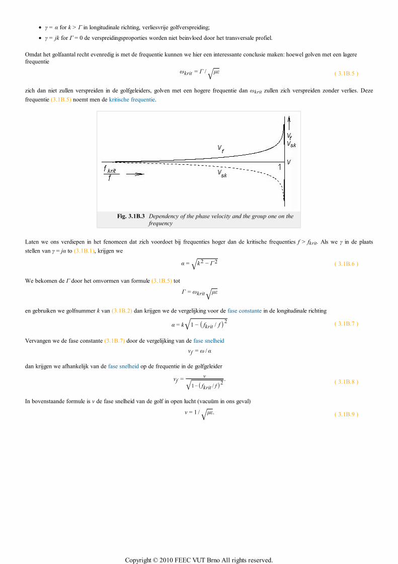
γ = α for k > Γ in longitudinale richting, verliesvrije golfverspreiding;
γ = jk for Γ = 0 de verspreidingsproporties worden niet beinvloed door het transversale profiel.
Omdat het golfaantal recht evenredig is met de frequentie kunnen we hier een interessante conclusie maken: hoewel golven met een lagere
frequentie
ωkrit = Γ / µε√ ( 3.1B.5 )
zich dan niet zullen verspreiden in de golfgeleiders, golven met een hogere frequentie dan ωkrit zullen zich verspreiden zonder verlies. Deze
frequentie (3.1B.5) noemt men de kritische frequentie.
Fig. 3.1B.3 Dependency of the phase velocity and the group one on the
frequency
Laten we ons verdiepen in het fenomeen dat zich voordoet bij frequenties hoger dan de kritische frequenties f > fkrit. Als we γ in de plaats
stellen van γ = jα to (3.1B.1), krijgen we
α = k 2 − Γ 2√ ( 3.1B.6 )
We bekomen de Γ door het omvormen van formule (3.1B.5) tot
Γ = ωkrit µε√
en gebruiken we golfnummer k van (3.1B.2) dan krijgen we de vergelijking voor de fase constante in de longitudinale richting
α = k 1 − ( fkrit / f )2√ ( 3.1B.7 )
Vervangen we de fase constante (3.1B.7) door de vergelijking van de fase snelheid
vf = ω / α
dan krijgen we afhankelijk van de fase snelheid op de frequentie in de golfgeleider
vf =v
1−( fkrit / f )2√.
( 3.1B.8 )
In bovenstaande formule is v de fase snelheid van de golf in open lucht (vacuüm in ons geval)
v = 1 / µε√ . ( 3.1B.9 )
Copyright © 2010 FEEC VUT Brno All rights reserved.
Fig. 3.1B.4 Dispersion
Gebruiken we de gekende fase snelheid, dan staat de verhouding tussen de
fasesnelheid en de golflengte
λg = vf / f ( 3.1B.10 )
in de longitudinale richting in de golfgeleider hier onder beschreven
λg =λ
1−( fkrit / f )2√ ( 3.1B.11 )
Hier bedoelt men met λ de golflengte in open lucht.
Als we de snelheid van de energieverspreiding willen kennen, zullen we
eerst de groep snelheid moeten berekenen. Als het product van de groep
snelheid en de fase gelijk moet zijn aan het kwadraat van de snelheid van
het licht, dan kunnen we de groep snelheid berekenen aan de hand van de
volgende vergelijking:
vsk = v 1 − ( fkrit / f )2√ , ( 3.1B.12 )
hier is v de fase snelheid in open lucht.
De bovenstaande berekeningen werden verricht voor de verspreiding van
harmonische golven. Men spreekt van spreiding (fig. 3.1B.4) als iedere golf
uit meerdere harmonische bestaat dan elke frequentie component verspreid
én als het uitgangssignaal van het ingangssignaal (vervorming) verschilt..
Tot nu toe hebben we enkel geanalyseerd in de longitudinale richting. Deze resultaten hangen niet van de vorm van het transversale profiel af en
zijn geldig voor elke homogene golfgeleider. In de transversale richtingen is de situatie totaal anders:
In de transversale richting verspreidt de golf zich niet. De golf wordt gereflecteerd tegen de binnenkant van de golfgeleider, hierdoor
ontstaan er staande golven.
Omdat de reflecties afhangen van het profiel van de golfgeleider zal de analyse gedaan worden aan de respectievelijke vorm van het
profiel. In onze beschrijving gaan we gebruik maken van een rechthoekige vorm.
De analyse is gedaan voor twee soorten golven, welke zich kunnen verspreiden in de golfgeleiders. Voor de transversale magnetische golf (TM,
componenten van de magnetische intensiteitsvector zijn niet gelijk aan nul in de transversale richting), en voor de transversale elektrische golf
(TE, componenten van de elektrische intensiteitsvector zijn niet gelijk aan nul in de transversale richtingen). Volgende [1], vergelijking voor
kritische golf frequenties van beide types kunnen herschreven worden als:
ωkrit =1
µε√(mπ
a )2+
⎛⎝nπb
⎞⎠2
√ . ( 3.1B.13 )
Hier zijn de permitiviteit en de permeabiliteit verwant aan het medium in de golfgeleider. a staat hier voor de breedte en b voor de hoogte. De
integrale coëfficienten m en n worden de mode nummers genoemd. Door het verhogen van de mode nummers zal ook de kritische frequentie
verhogen (hoge modes komen voor bij hogere frequenties).
Veronderstel dat een voedende generator is afgesteld van lage naar hoge frequenties. Als de kritische frequentie van de laagste mode bereikt
wordt, dan zal één enkele golf zich voortbewegen in de golfgeleider. Als de kritische frequentie van de tweede mode bereikt wordt zullen er zich
twee golven (elk van een verschillende mode) verspreiden in de golfgeleider. Deze golven kunnen in elkaar overlopen wat tot vele problemen
kan leiden. Daarom functioneren golfgeleiders meestal in de single-mode band. De ondergrens van deze band wordt gegeven door de kritische
frequentie van de laagste mode, de bovengrens is gelijk aan de kritische frequentie van de tweede mode. De mode van de laagste kritische
frequentie noemt men de dominante mode.
Laten we ons nu verdiepen in de veldverdeling van de dominante mode TE10 op het moment t = t0 (zie animatie).
Copyright © 2010 FEEC VUT Brno All rights reserved.
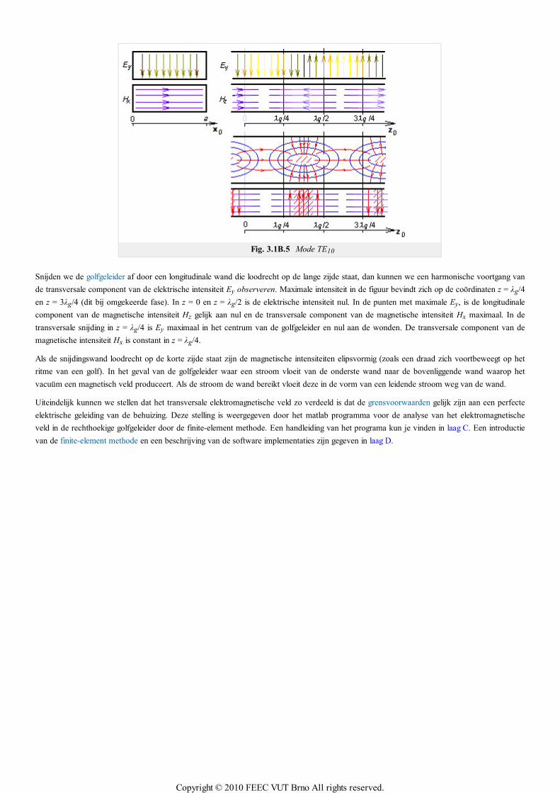
Fig. 3.1B.5 Mode TE10
Snijden we de golfgeleider af door een longitudinale wand die loodrecht op de lange zijde staat, dan kunnen we een harmonische voortgang van
de transversale component van de elektrische intensiteit Ey observeren. Maximale intensiteit in de figuur bevindt zich op de coördinaten z = λg/4
en z = 3λg/4 (dit bij omgekeerde fase). In z = 0 en z = λg/2 is de elektrische intensiteit nul. In de punten met maximale Ey, is de longitudinale
component van de magnetische intensiteit Hz gelijk aan nul en de transversale component van de magnetische intensiteit Hx maximaal. In de
transversale snijding in z = λg/4 is Ey maximaal in het centrum van de golfgeleider en nul aan de wonden. De transversale component van de
magnetische intensiteit Hx is constant in z = λg/4.
Als de snijdingswand loodrecht op de korte zijde staat zijn de magnetische intensiteiten elipsvormig (zoals een draad zich voortbeweegt op het
ritme van een golf). In het geval van de golfgeleider waar een stroom vloeit van de onderste wand naar de bovenliggende wand waarop het
vacuüm een magnetisch veld produceert. Als de stroom de wand bereikt vloeit deze in de vorm van een leidende stroom weg van de wand.
Uiteindelijk kunnen we stellen dat het transversale elektromagnetische veld zo verdeeld is dat de grensvoorwaarden gelijk zijn aan een perfecte
elektrische geleiding van de behuizing. Deze stelling is weergegeven door het matlab programma voor de analyse van het elektromagnetische
veld in de rechthoekige golfgeleider door de finite-element methode. Een handleiding van het programa kun je vinden in laag C. Een introductie
van de finite-element methode en een beschrijving van de software implementaties zijn gegeven in laag D.
Copyright © 2010 FEEC VUT Brno All rights reserved.

3.1 Waveguides
Matlab program
A rectangular waveguide R100 (dimensions 22.86 mm x 10.16 mm) is analyzed by the Matlab program waveguide.m. This program (plus all
the necessary additional m-files) is available here. We run Matlab and set the path to the folder Waveguide. Writing waveguide to the
command window of Matlab, the program is started. Handling program can be subdivided to following steps:
Number of rectangular bi-elements, sampling the waveguide cross section in the direction x, is written to the input line number of
elements in x, and number of bi-elements in y is written to the input line number of elements in y. If transversally electric modes are
going to be computed, the button Modes TE has to be pressed. If transversally magnetic modes are going to be computed, the button
Modes TM has to be pressed.
1.
If the elected analysis is finished, a dialog containing the input line Mode number appears. The lowest mode is denoted as "1", higher
modes are numbered by rising integer index (modes are sorted according to the value of the critical frequency). Pressing the button
Draw , three graphical windows are opened: the first one displays distribution of the longitudinal component, the second one and the
third one display transversal components of field intensities.
2.
Program is finished by pressing the button End .3.
Program waveguide analyzes EM field distribution in a waveguide by the finite-element method. A brief description of this method is given in
the layer D.
Copyright © 2010 FEEC VUT Brno All rights reserved.
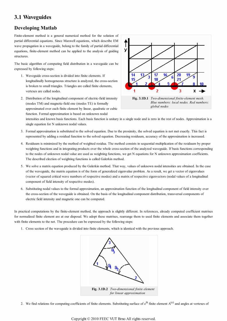
Fig. 3.1D.1 Two-dimensional finite-element mesh.
Blue numbers: local nodes. Red numbers:
global nodes
3.1 Waveguides
Developing Matlab
Finite-element method is a general numerical method for the solution of
partial differential equations. Since Maxwell equations, which describe EM
wave propagation in a waveguide, belong to the family of partial differential
equations, finite-element method can be applied to the analysis of guiding
structures.
The basic algorithm of computing field distribution in a waveguide can be
expressed by following steps:
Waveguide cross-section is divided into finite elements. If
longitudinally homogeneous structure is analyzed, the cross-section
is broken to small triangles. Triangles are called finite elements,
vertexes are called nodes.
1.
Distribution of the longitudinal component of electric-field intensity
(modes TM) and magnetic-field one (modes TE) is formally
approximated over each finite element by linear, quadratic or cubic
function. Formal approximation is based on unknown nodal
intensities and known basis functions. Each basis function is unitary in a single node and is zero in the rest of nodes. Approximation is a
single equation for N unknown nodal values.
2.
Formal approximation is substituted to the solved equation. Due to the proximity, the solved equation is not met exactly. This fact is
represented by adding a residual function to the solved equation. Decreasing residuum, accuracy of the approximation is increased.
3.
Residuum is minimized by the method of weighted residua. The method consists in sequential multiplication of the residuum by proper
weighting functions and in integrating products over the whole cross-section of the analyzed waveguide. If basis functions corresponding
to the nodes of unknown nodal value are used as weighting functions, we get N equations for N unknown approximation coefficients.
The described election of weighting functions is called Galerkin method.
4.
We solve a matrix equation produced by the Galerkin method. That way, values of unknown nodal intensities are obtained. In the case
of the waveguide, the matrix equation is of the form of generalized eigenvalue problem. As a result, we get a vector of eigenvalues
(vector of squared critical wave numbers of respective modes) and a matrix of respective eigenvectors (nodal values of a longitudinal
component of field intensity of respective modes).
5.
Substituting nodal values to the formal approximation, an approximation function of the longitudinal component of field intensity over
the cross-section of the waveguide is obtained. On the basis of the longitudinal component distribution, transversal components of
electric field intensity and magnetic one can be computed.
6.
In practical computations by the finite-element method, the approach is slightly different. In references, already computed coefficient matrixes
for normalized finite element are at our disposal. We adopt these matrixes, rearrange them to used finite elements and associate them together
with finite elements to the net. The procedure can be expressed by the following steps:
Cross section of the waveguide is divided into finite elements, which is identical with the previous approach.
Fig. 3.1D.2 Two-dimensional finite element
for linear approximation
1.
We find relations for computing coefficients of finite elements. Substituting surface of eth finite element A(e) and angles at vertexes of2.
Copyright © 2010 FEEC VUT Brno All rights reserved.
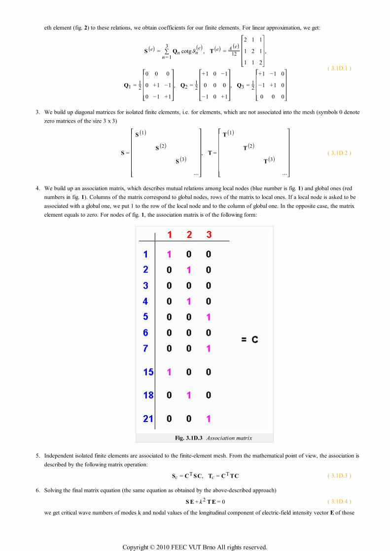
eth element (fig. 2) to these relations, we obtain coefficients for our finite elements. For linear approximation, we get:
S(e) = ∑n =1
3Qn cotg ϑn
(e), T(e) =
A(e)12
⎡
⎣
⎢⎢⎢⎢
2 1 1
1 2 1
1 1 2
⎤
⎦
⎥⎥⎥⎥,
Q1 =12
⎡
⎣
⎢⎢⎢⎢
0 0 0
0 +1 −1
0 −1 +1
⎤
⎦
⎥⎥⎥⎥, Q2 =
12
⎡
⎣
⎢⎢⎢⎢
+1 0 −1
0 0 0
−1 0 +1
⎤
⎦
⎥⎥⎥⎥, Q3 =
12
⎡
⎣
⎢⎢⎢⎢
+1 −1 0
−1 +1 0
0 0 0
⎤
⎦
⎥⎥⎥⎥
( 3.1D.1 )
We build up diagonal matrices for isolated finite elements, i.e. for elements, which are not associated into the mesh (symbols 0 denote
zero matrices of the size 3 x 3)
S =
⎡
⎣
⎢⎢⎢⎢⎢⎢⎢⎢
S(1)
S(2)
S(3)
...
⎤
⎦
⎥⎥⎥⎥⎥⎥⎥⎥
, T =
⎡
⎣
⎢⎢⎢⎢⎢⎢⎢⎢
T(1)
T(2)
T(3)
...
⎤
⎦
⎥⎥⎥⎥⎥⎥⎥⎥
( 3.1D.2 )
3.
We build up an association matrix, which describes mutual relations among local nodes (blue number is fig. 1) and global ones (red
numbers in fig. 1). Columns of the matrix correspond to global nodes, rows of the matrix to local ones. If a local node is asked to be
associated with a global one, we put 1 to the row of the local node and to the column of global one. In the opposite case, the matrix
element equals to zero. For nodes of fig. 1, the association matrix is of the following form:
Fig. 3.1D.3 Association matrix
4.
Independent isolated finite elements are associated to the finite-element mesh. From the mathematical point of view, the association is
described by the following matrix operation:
Sc = CT S C, Tc = CT T C ( 3.1D.3 )
5.
Solving the final matrix equation (the same equation as obtained by the above-described approach)
SE + k 2 TE = 0 ( 3.1D.4 )
we get critical wave numbers of modes k and nodal values of the longitudinal component of electric-field intensity vector E of those
6.
Copyright © 2010 FEEC VUT Brno All rights reserved.
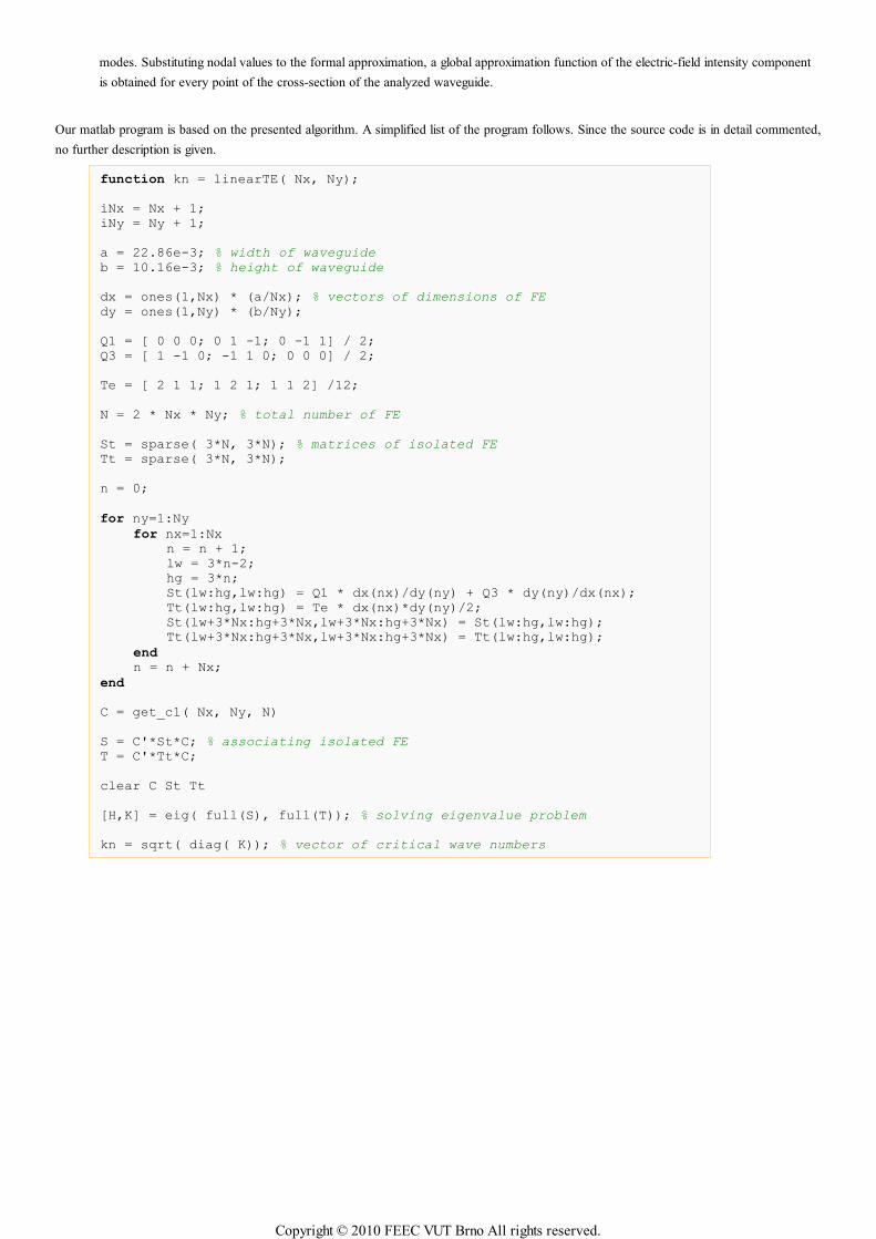
modes. Substituting nodal values to the formal approximation, a global approximation function of the electric-field intensity component
is obtained for every point of the cross-section of the analyzed waveguide.
Our matlab program is based on the presented algorithm. A simplified list of the program follows. Since the source code is in detail commented,
no further description is given.
function kn = linearTE( Nx, Ny);
iNx = Nx + 1;iNy = Ny + 1;
a = 22.86e-3; % width of waveguideb = 10.16e-3; % height of waveguide
dx = ones(1,Nx) * (a/Nx); % vectors of dimensions of FEdy = ones(1,Ny) * (b/Ny);
Q1 = [ 0 0 0; 0 1 -1; 0 -1 1] / 2;Q3 = [ 1 -1 0; -1 1 0; 0 0 0] / 2;
Te = [ 2 1 1; 1 2 1; 1 1 2] /12;
N = 2 * Nx * Ny; % total number of FE
St = sparse( 3*N, 3*N); % matrices of isolated FETt = sparse( 3*N, 3*N);
n = 0;
for ny=1:Nyfor nx=1:Nx
n = n + 1;lw = 3*n-2;hg = 3*n;St(lw:hg,lw:hg) = Q1 * dx(nx)/dy(ny) + Q3 * dy(ny)/dx(nx);Tt(lw:hg,lw:hg) = Te * dx(nx)*dy(ny)/2;St(lw+3*Nx:hg+3*Nx,lw+3*Nx:hg+3*Nx) = St(lw:hg,lw:hg);Tt(lw+3*Nx:hg+3*Nx,lw+3*Nx:hg+3*Nx) = Tt(lw:hg,lw:hg);
end
n = n + Nx;end
C = get_c1( Nx, Ny, N)
S = C'*St*C; % associating isolated FET = C'*Tt*C;
clear C St Tt
[H,K] = eig( full(S), full(T)); % solving eigenvalue problem
kn = sqrt( diag( K)); % vector of critical wave numbers
Copyright © 2010 FEEC VUT Brno All rights reserved.

3.1 Waveguides
Java applet
Copyright © 2010 FEEC VUT Brno All rights reserved.

3.1 Waveguides
Quiz
Answer these questions to get feedback on how well you understand the course. Only one of the answers is correct. You don't have to answer
every question. If you don't know the answer you can just leave it blank (default option: “I won't answer this question”) and this won't affect
your score. Answering correctly will add 2 points to your score but on the other hand you'll lose 1 point if your answer is wrong. The
questions are divided in groups of five questions.
Press See result after you have finished answering.
Displaying questions 1..10 of 10:
Question 1
The wave propagation inside a waveguide can be described by …
Possible answers for question 1:
… beams propagating in parallel to the walls of the structure.
… successive reflections of the propagating waves from the walls of the guiding structure.
… the diffusion of the electromagnetic energy deeper and deeper to the guiding structure.
I won't answer this question
Question 2
Waveguides are used at higher frequencies because …
Possible answers for question 2:
… the length of the waveguide has to be related to the wavelength (at lower frequencies, the waveguide is too long).
… losses in metallic walls are too high at lower frequencies.
… the cross section of the waveguide has to be related to the wavelength (at lower frequencies, the waveguide cross section is very
large).
I won't answer this question
Question 3
Electromagnetic energy propagates through the waveguide …
Possible answers for question 3:
… if its frequency is higher than the critical one.
… anytime.
… if its frequency is lower than the critical one.
I won't answer this question
Question 4
The propagation constant …
Possible answers for question 4:
… describes the changes of wave amplitude and phase when propagating in the waveguide.
… is not used in relation to the waveguides.
… is used to formulate excitation conditions for the waveguides.
I won't answer this question
Question 5
Energy transmission on the waveguide is described by …
Copyright © 2010 FEEC VUT Brno All rights reserved.

Possible answers for question 5:
… the phase velocity.
… the group velocity.
… velocity of light.
I won't answer this question
Question 6
In the waveguide, electromagnetic waves can propagate in different constellations (so called modes). When increasing
operation frequency …
Possible answers for question 6:
… more and more modes appear in the waveguide – higher modes propagate at higher frequencies.
… a single mode propagates in the waveguide – if a higher mode is excited, a lower mode is suppressed.
… no wave propagates due to the enormous attenuation.
I won't answer this question
Question 7
The dominant mode is the mode …
Possible answers for question 7:
… of the highest energy.
… of the strongest field intensity.
… of the lowest critical frequency.
I won't answer this question
Question 8
In the waveguide …
Possible answers for question 8:
… transversally electromagnetic modes can propagate.
… transversally electric OR transversally magnetic modes can propagate.
… transversally electric AND transversally magnetic modes can propagate.
I won't answer this question
Question 9
When analyzing the waveguide by finite elements …
Possible answers for question 9:
… partial differential equations are solved by replacing derivatives by differences.
… integral equations are solved by a rather complicated way.
… the error of the approximate solution is minimized by the Galerkin method.
I won't answer this question
Question 10
Finite elements provide eigenvalues and eigenvectors:
Possible answers for question 10:
Eigenvalues are related to the critical wave numbers of modes, eigenvectors are not of any use.
Eigenvalues are related to the critical wave numbers of modes, and eigenvectors to the field distribution of modes.
Eigenvectors are related to the critical wave numbers of modes, and eigenvalues to the field distribution of modes.
I won't answer this question
Copyright © 2010 FEEC VUT Brno All rights reserved.

Copyright © 2010 FEEC VUT Brno All rights reserved.
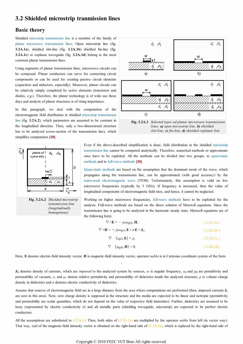
Fig. 3.2A.1 Selected types od planar microwave transmission
lines: a) open microstrip line, b) shielded
slot-line, c) fin-line, d) shielded coplanar line
Fig. 3.2A.2 Shielded microstrip
transmission line
(longitudinally
homogenous)
3.2 Shielded microstrip tranmission lines
Basic theory
Shielded microstrip transmission line is a member of the family of
planar microwave transmission lines. Open microstrip line (fig.
3.2A.1a), shielded slot-line (fig. 3.2A.1b) shielded fin-line (fig.
3.2A.1c) or coplanar waveguide (fig. 3.2A.1d) belong to the most
common planar transmission lines.
Using segments of planar transmission lines, microwave circuits can
be composed. Planar conductors can serve for connecting circuit
components or can be used for creating passive circuit elements
(capacitors and inductors, especially). Moreover, planar circuits can
be relatively simply completed by active elements (transistors and
diodes, e.g.). Therefore, the planar technology is of wide use these
days and analysis of planar structures is of rising importance.
In this paragraph, we deal with the computation of the
electromagnetic field distribution in shielded microstrip transmission
line (fig. 3.2A.2), which parameters are assumed to be constant in
the longitudinal direction. Then, only a two-dimensional structure
has to be analyzed (cross-section of the transmission line), which
simplifies computation [20].
Even if the above-described simplification is done, field distribution in the shielded microstrip
transmission line cannot be computed analytically. Therefore, numerical methods or approximate
ones have to be exploited. All the methods can be divided into two groups, to quasi-static
methods and to full-wave methods [20].
Quasi-static methods are based on the assumption that the dominant mode of the wave, which
propagates along the transmission line, can be approximated (with good accuracy) by the
transversal electromagnetic wave (TEM). Unfortunately, this assumption is valid on low
microwave frequencies (typically by 5 GHz). If frequency is increased, then the value of
longitudinal components of electromagnetic field rises, and hence, it cannot be neglected.
Working on higher microwave frequencies, full-wave methods have to be exploited for the
analysis. Full-wave methods are based on the direct solution of Maxwell equations. Since the
transmission line is going to be analyzed in the harmonic steady state, Maxwell equations are of
the following form:
∇×E = − jωµ0 µr H, ( 3.2A.1a )
∇×H = + jωε0εr E + σ E + Js , ( 3.2A.1b )
∇ ⋅ (ε0εr E) = ρ, ( 3.2A.1c )
∇ ⋅ (µ0 µr H) = 0. ( 3.2A.1d )
Here, E denotes electric-field intensity vector, H is magnetic-field intensity vector, operator nabla is in Cartesian coordinate system of the form
,
JS denotes density of currents, which are imposed to the analyzed system by sources, ω is angular frequency, ε0 and µ0 are permittivity and
permeability of vacuum, εr and µr denote relative permittivity and permeability of dielectrics inside the analyzed structure, ρ is volume charge
density in dielectrics and σ denotes electric conductivity of dielectrics.
Assume that sources of electromagnetic field are in a large distance from the area where computations are performed (then, imposed currents Js
are zero in this area). Next, zero charge density is supposed in the structure and the media are expected to be linear and isotropic (permittivity
and permeability are scalar quantities, which do not depend on the value of respective field intensities). Further, dielectrics are assumed to be
lossy (represented by electric conductivity σ) and all metallic parts (shielding waveguide, microstrip) are expected to be perfect electric
conductors.
All the assumptions are substituted to (3.2A.1). Then, both sides of (3.2A.1a) are multiplied by the operator nabla from left (in vector way).
That way, curl of the magnetic-field intensity vector is obtained on the right-hand side of (3.2A.1a), which is replaced by the right-hand side of
Copyright © 2010 FEEC VUT Brno All rights reserved.
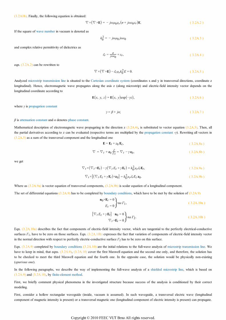
(3.2A1b). Finally, the following equation is obtained:
∇×(∇×E) = − jωµ0 µr(σ + jωε0εr)E. ( 3.2A.2 )
If the square of wave number in vacuum is denoted as
k02 = − jωµ0 jωε0 ( 3.2A.3 )
and complex relative permittivity of dielectrics as
εr =σ
jωε0+ εr, ( 3.2A.4 )
eqn. (3.2A.2) can be rewritten to
∇×(∇×E) − εr µrk02E = 0. ( 3.2A.5 )
Analyzed microstrip transmission line is situated to the Cartesian coordinate system (coordinates x and y in transversal directions, coordinate z
longitudinal). Hence, electromagnetic wave propagates along the axis z (along microstrip) and electric-field intensity vector depends on the
longitudinal coordinate according to
E(x, y, z) = E(x, y)exp(−γz), ( 3.2A.6 )
where γ is propagation constant
γ = β + jα; ( 3.2A.7 )
β is attenuation constant and α denotes phase constant.
Mathematical description of electromagnetic wave propagating in the direction z (3.2A.6), is substituted to vector equation (3.2A.5). Then, all
the partial derivatives according to z can be evaluated (respective terms are multiplied by the propagation constant -γ). Rewriting all vectors in
(3.2A.5) as a sum of the transversal component and the longitudinal one
E = Et + z0 Ez, ( 3.2A.8a )
∇ =∇t + z0∂
∂ z=∇t − γ z0 , ( 3.2A.8b )
we get
∇t ×(∇t ×Et) − γ(∇t Ez + γEt) = k02 µrεrEt , ( 3.2A.9a )
∇t ×[(∇t Ez + γEt)×z0] = k02 µrεrEz z0 . ( 3.2A.9b )
Where as (3.2A.9a) is vector equation of transversal components, (3.2A.9b) is scalar equation of a longitudinal component.
The set of differential equations (3.2A.9) has to be completed by boundary conditions, which have to be met by the solution of (3.2A.9)
n0×Et = 0
Ez = 0na Γ1 , ( 3.2A.10a )
[∇t Ez + γEt] ⋅n0 = 0
∇t ×Et = 0na Γ2. ( 3.2A.10b )
Eqn. (3.2A.10a) describes the fact that components of electric-field intensity vector, which are tangential to the perfectly electrical-conductive
surfaces Γ1, have to be zero on those surfaces. Eqn. (3.2A.10b) expresses the fact that variation of components of electric-field intensity vector
in the normal direction with respect to perfectly electric-conductive surface Γ2 has to be zero on this surface.
Eqn. (3.2A.9) completed by boundary conditions (3.2A.10) are the initial relations to the full-wave analysis of microstrip transmission line. We
have to keep in mind, that eqns. (3.2A.9), (3.2A.10) cover the first Maxwell equation and the second one only, and therefore, the solution has
to be checked to meet the third Maxwell equation and the fourth one. In the opposite case, the solution would be physically non-existing
(spurious one).
In the following paragraphs, we describe the way of implementing the full-wave analysis of a shielded microstrip line, which is based on
(3.2A.9) and (3.2A.10), by finite-element method.
First, we briefly comment physical phenomena in the investigated structure because success of the analysis is conditioned by their correct
modeling.
First, consider a hollow rectangular waveguide (inside, vacuum is assumed). In such waveguide, a transversal electric wave (longitudinal
component of magnetic intensity is present) or a transversal magnetic one (longitudinal component of electric intensity is present) can propagate.
Copyright © 2010 FEEC VUT Brno All rights reserved.
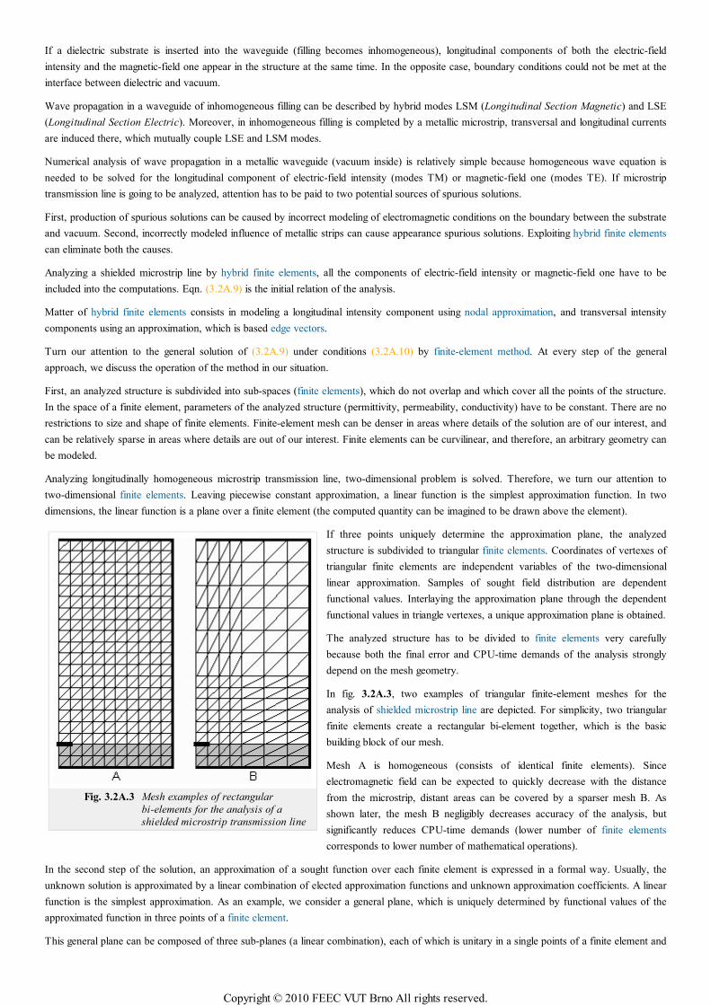
Fig. 3.2A.3 Mesh examples of rectangular
bi-elements for the analysis of a
shielded microstrip transmission line
If a dielectric substrate is inserted into the waveguide (filling becomes inhomogeneous), longitudinal components of both the electric-field
intensity and the magnetic-field one appear in the structure at the same time. In the opposite case, boundary conditions could not be met at the
interface between dielectric and vacuum.
Wave propagation in a waveguide of inhomogeneous filling can be described by hybrid modes LSM (Longitudinal Section Magnetic) and LSE
(Longitudinal Section Electric). Moreover, in inhomogeneous filling is completed by a metallic microstrip, transversal and longitudinal currents
are induced there, which mutually couple LSE and LSM modes.
Numerical analysis of wave propagation in a metallic waveguide (vacuum inside) is relatively simple because homogeneous wave equation is
needed to be solved for the longitudinal component of electric-field intensity (modes TM) or magnetic-field one (modes TE). If microstrip
transmission line is going to be analyzed, attention has to be paid to two potential sources of spurious solutions.
First, production of spurious solutions can be caused by incorrect modeling of electromagnetic conditions on the boundary between the substrate
and vacuum. Second, incorrectly modeled influence of metallic strips can cause appearance spurious solutions. Exploiting hybrid finite elements
can eliminate both the causes.
Analyzing a shielded microstrip line by hybrid finite elements, all the components of electric-field intensity or magnetic-field one have to be
included into the computations. Eqn. (3.2A.9) is the initial relation of the analysis.
Matter of hybrid finite elements consists in modeling a longitudinal intensity component using nodal approximation, and transversal intensity
components using an approximation, which is based edge vectors.
Turn our attention to the general solution of (3.2A.9) under conditions (3.2A.10) by finite-element method. At every step of the general
approach, we discuss the operation of the method in our situation.
First, an analyzed structure is subdivided into sub-spaces (finite elements), which do not overlap and which cover all the points of the structure.
In the space of a finite element, parameters of the analyzed structure (permittivity, permeability, conductivity) have to be constant. There are no
restrictions to size and shape of finite elements. Finite-element mesh can be denser in areas where details of the solution are of our interest, and
can be relatively sparse in areas where details are out of our interest. Finite elements can be curvilinear, and therefore, an arbitrary geometry can
be modeled.
Analyzing longitudinally homogeneous microstrip transmission line, two-dimensional problem is solved. Therefore, we turn our attention to
two-dimensional finite elements. Leaving piecewise constant approximation, a linear function is the simplest approximation function. In two
dimensions, the linear function is a plane over a finite element (the computed quantity can be imagined to be drawn above the element).
If three points uniquely determine the approximation plane, the analyzed
structure is subdivided to triangular finite elements. Coordinates of vertexes of
triangular finite elements are independent variables of the two-dimensional
linear approximation. Samples of sought field distribution are dependent
functional values. Interlaying the approximation plane through the dependent
functional values in triangle vertexes, a unique approximation plane is obtained.
The analyzed structure has to be divided to finite elements very carefully
because both the final error and CPU-time demands of the analysis strongly
depend on the mesh geometry.
In fig. 3.2A.3, two examples of triangular finite-element meshes for the
analysis of shielded microstrip line are depicted. For simplicity, two triangular
finite elements create a rectangular bi-element together, which is the basic
building block of our mesh.
Mesh A is homogeneous (consists of identical finite elements). Since
electromagnetic field can be expected to quickly decrease with the distance
from the microstrip, distant areas can be covered by a sparser mesh B. As
shown later, the mesh B negligibly decreases accuracy of the analysis, but
significantly reduces CPU-time demands (lower number of finite elements
corresponds to lower number of mathematical operations).
In the second step of the solution, an approximation of a sought function over each finite element is expressed in a formal way. Usually, the
unknown solution is approximated by a linear combination of elected approximation functions and unknown approximation coefficients. A linear
function is the simplest approximation. As an example, we consider a general plane, which is uniquely determined by functional values of the
approximated function in three points of a finite element.
This general plane can be composed of three sub-planes (a linear combination), each of which is unitary in a single points of a finite element and
Copyright © 2010 FEEC VUT Brno All rights reserved.
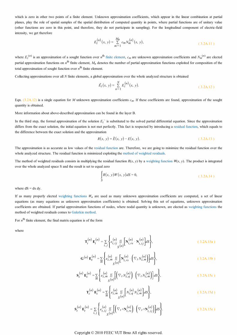
which is zero in other two points of a finite element. Unknown approximation coefficients, which appear in the linear combination at partial
planes, play the role of spatial samples of the spatial distribution of computed quantity in points, where partial functions are of unitary value
(other functions are zero in this point, and therefore, they do not participate in sampling). For the longitudinal component of electric-field
intensity, we get therefore
Ez(n)(x, y) ≈ ∑
m = 1
Mncm Nm
(n)(x, y), ( 3.2A.11 )
where Ez(n) is an approximation of a sought function over nth finite element, cm are unknown approximation coefficients and Nm
(n) are elected
partial approximation functions on nth finite element, Mn denotes the number of partial approximation functions exploited for composition of the
total approximation of sought function over nth finite element.
Collecting approximations over all N finite elements, a global approximation over the whole analyzed structure is obtained
Ez(x, y) ≈ ∑n = 1
NEz
(n)(x, y).( 3.2A.12 )
Eqn. (3.2A.12) is a single equation for M unknown approximation coefficients cm. If these coefficients are found, approximation of the sought
quantity is obtained.
More information about above-described approximation can be found in the layer B.
In the third step, the formal approximation of the solution Ez~ is substituted to the solved partial differential equation. Since the approximation
differs from the exact solution, the initial equation is not met perfectly. This fact is respected by introducing a residual function, which equals to
the difference between the exact solution and the approximation
R(x, y) = E(x, y) − E(x, y). ( 3.2A.13 )
The approximation is as accurate as low values of the residual function are. Therefore, we are going to minimize the residual function over the
whole analyzed structure. The residual function is minimized exploiting the method of weighted residuals.
The method of weighted residuals consists in multiplying the residual function R(x, y) by a weighting function W(x, y). The product is integrated
over the whole analyzed space S and the result is set to equal zero
⌠⌡S
R(x, y)W(x, y)dS = 0, ( 3.2A.14 )
where dS = dx dy.
If as many properly elected weighting functions Wn are used as many unknown approximation coefficients are computed, a set of linear
equations (as many equations as unknown approximation coefficients) is obtained. Solving this set of equations, unknown approximation
coefficients are obtained. If partial approximation functions of nodes, where nodal quantity is unknown, are elected as weighting functions the
method of weighted residuals comes to Galerkin method.
For nth finite element, the final matrix equation is of the form
where
Tt(n)
Et(n)
= ∑i, j
⎧⎨⎩⎪⎪
et, i j(n) ∬
S (n)
⎡⎣⎢Nt, rs
(n) ⋅Nt, i j(n)⎤
⎦⎥dS
⎫⎬⎭⎪⎪
, ( 3.2A.15a )
G(n) Ez(n)
= ∑m
⎧⎨⎩⎪⎪
ez, m(n)∬
S (n)
⎡⎣⎢Nt, rs
(n)⋅
⎛⎝⎜∇t Nz, m
(n)⎞⎠⎟⎤⎦⎥dS
⎫⎬⎭⎪⎪
, ( 3.2A.15b )
Sz(n)
Ez(n)
= ∑m
⎧⎨⎩⎪⎪
ez, m(n)∬
S (n)
⎡⎣⎢⎛⎝⎜∇t Nz, q
(n)⎞⎠⎟ ⋅
⎛⎝⎜∇t Nz, m
(n)⎞⎠⎟⎤⎦⎥ dS
⎫⎬⎭⎪⎪
, ( 3.2A.15c )
Tz(n)
Ez(n)
= ∑m
⎧⎨⎩⎪⎪
ez, m(n)∬
S (n)
⎡⎣⎢Nz, q
(n)Nz, m
(n)⎤⎦⎥ dS
⎫⎬⎭⎪⎪
, ( 3.2A.15d )
St(n)
Et(n)
= ∑i, j
⎧⎨⎩⎪⎪
et, i j(n)∬
S (n)
⎡⎣⎢⎛⎝⎜∇t ×N
t, rs(n)⎞
⎠⎟ ⋅⎛⎝⎜∇t ×N
t, i j(n)⎞
⎠⎟⎤⎦⎥dS
⎫⎬⎭⎪⎪
. ( 3.2A.15e )
Copyright © 2010 FEEC VUT Brno All rights reserved.
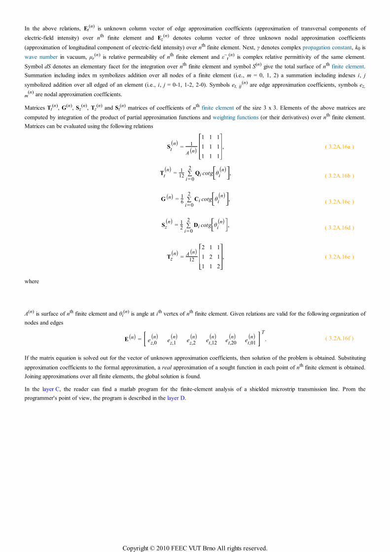
In the above relations, Et(n) is unknown column vector of edge approximation coefficients (approximation of transversal components of
electric-field intensity) over nth finite element and Ez(n) denotes column vector of three unknown nodal approximation coefficients
(approximation of longitudinal component of electric-field intensity) over nth finite element. Next, γ denotes complex propagation constant, k0 is
wave number in vacuum, µr(n) is relative permeability of nth finite element and ε~
r(n) is complex relative permittivity of the same element.
Symbol dS denotes an elementary facet for the integration over nth finite element and symbol S(n) give the total surface of nth finite element.
Summation including index m symbolizes addition over all nodes of a finite element (i.e., m = 0, 1, 2) a summation including indexes i, j
symbolized addition over all edged of an element (i.e., i, j = 0-1, 1-2, 2-0). Symbols et, ij(n) are edge approximation coefficients, symbols ez,
m(n) are nodal approximation coefficients.
Matrices Tt(n), G(n), Sz
(n), Tz(n) and St
(n) matrices of coefficients of nth finite element of the size 3 x 3. Elements of the above matrices are
computed by integration of the product of partial approximation functions and weighting functions (or their derivatives) over nth finite element.
Matrices can be evaluated using the following relations
St(n)
=1
A(n)
⎡
⎣
⎢⎢⎢
1 1 1
1 1 1
1 1 1
⎤
⎦
⎥⎥⎥, ( 3.2A.16a )
Tt(n)
=1
12∑
i = 0
2Qi cotg
⎡⎣⎢θi
(n)⎤⎦⎥,
( 3.2A.16b )
G(n) =16
∑i = 0
2Ci cotg
⎡⎣⎢θi
(n)⎤⎦⎥, ( 3.2A.16c )
Sz(n)
=12
∑i= 0
2Di cotg
⎡⎣⎢θi
(n)⎤⎦⎥, ( 3.2A.16d )
Tz(n)
=A(n)
12
⎡
⎣
⎢⎢⎢
2 1 1
1 2 1
1 1 2
⎤
⎦
⎥⎥⎥, ( 3.2A.16e )
where
A(n) is surface of nth finite element and θi(n) is angle at ith vertex of nth finite element. Given relations are valid for the following organization of
nodes and edges
E(n) = [ ez,0(n)
ez,1(n)
ez,2(n)
et,12(n)
et,20(n)
et,01(n) ]
T
. ( 3.2A.16f )
If the matrix equation is solved out for the vector of unknown approximation coefficients, then solution of the problem is obtained. Substituting
approximation coefficients to the formal approximation, a real approximation of a sought function in each point of nth finite element is obtained.
Joining approximations over all finite elements, the global solution is found.
In the layer C, the reader can find a matlab program for the finite-element analysis of a shielded microstrip transmission line. Prom the
programmer's point of view, the program is described in the layer D.
Copyright © 2010 FEEC VUT Brno All rights reserved.
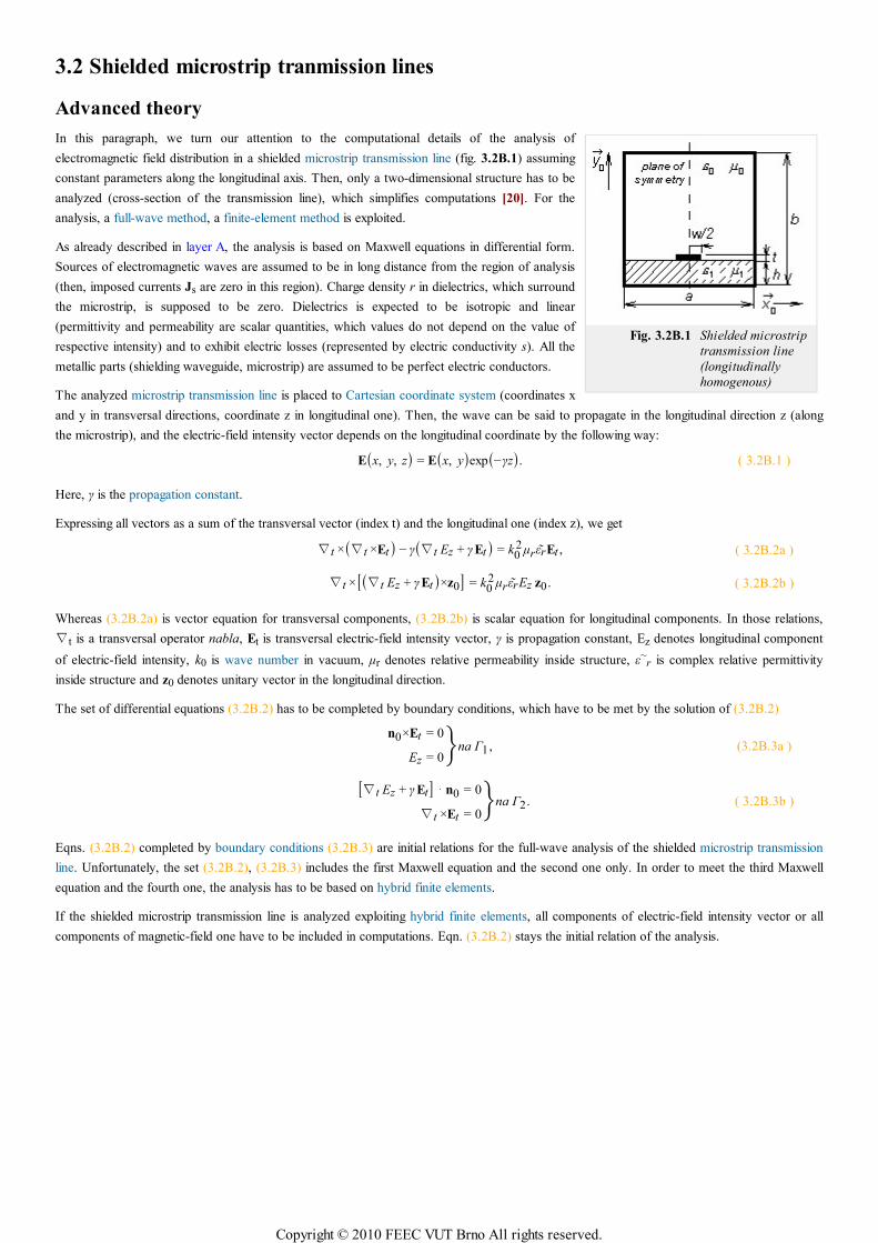
Fig. 3.2B.1 Shielded microstrip
transmission line
(longitudinally
homogenous)
3.2 Shielded microstrip tranmission lines
Advanced theory
In this paragraph, we turn our attention to the computational details of the analysis of
electromagnetic field distribution in a shielded microstrip transmission line (fig. 3.2B.1) assuming
constant parameters along the longitudinal axis. Then, only a two-dimensional structure has to be
analyzed (cross-section of the transmission line), which simplifies computations [20]. For the
analysis, a full-wave method, a finite-element method is exploited.
As already described in layer A, the analysis is based on Maxwell equations in differential form.
Sources of electromagnetic waves are assumed to be in long distance from the region of analysis
(then, imposed currents Js are zero in this region). Charge density r in dielectrics, which surround
the microstrip, is supposed to be zero. Dielectrics is expected to be isotropic and linear
(permittivity and permeability are scalar quantities, which values do not depend on the value of
respective intensity) and to exhibit electric losses (represented by electric conductivity s). All the
metallic parts (shielding waveguide, microstrip) are assumed to be perfect electric conductors.
The analyzed microstrip transmission line is placed to Cartesian coordinate system (coordinates x
and y in transversal directions, coordinate z in longitudinal one). Then, the wave can be said to propagate in the longitudinal direction z (along
the microstrip), and the electric-field intensity vector depends on the longitudinal coordinate by the following way:
E(x, y, z) = E(x, y)exp(−γz). ( 3.2B.1 )
Here, γ is the propagation constant.
Expressing all vectors as a sum of the transversal vector (index t) and the longitudinal one (index z), we get
∇t ×(∇t ×Et) − γ(∇t Ez + γEt) = k02 µrεrEt , ( 3.2B.2a )
∇t ×[(∇t Ez + γEt)×z0] = k02 µrεrEz z0 . ( 3.2B.2b )
Whereas (3.2B.2a) is vector equation for transversal components, (3.2B.2b) is scalar equation for longitudinal components. In those relations,
∇t is a transversal operator nabla, Et is transversal electric-field intensity vector, γ is propagation constant, Ez denotes longitudinal component
of electric-field intensity, k0 is wave number in vacuum, µr denotes relative permeability inside structure, ε~r is complex relative permittivity
inside structure and z0 denotes unitary vector in the longitudinal direction.
The set of differential equations (3.2B.2) has to be completed by boundary conditions, which have to be met by the solution of (3.2B.2)
n0×Et = 0
Ez = 0na Γ1 , (3.2B.3a )
[∇t Ez + γEt] ⋅n0 = 0
∇t ×Et = 0na Γ2. ( 3.2B.3b )
Eqns. (3.2B.2) completed by boundary conditions (3.2B.3) are initial relations for the full-wave analysis of the shielded microstrip transmission
line. Unfortunately, the set (3.2B.2), (3.2B.3) includes the first Maxwell equation and the second one only. In order to meet the third Maxwell
equation and the fourth one, the analysis has to be based on hybrid finite elements.
If the shielded microstrip transmission line is analyzed exploiting hybrid finite elements, all components of electric-field intensity vector or all
components of magnetic-field one have to be included in computations. Eqn. (3.2B.2) stays the initial relation of the analysis.
Copyright © 2010 FEEC VUT Brno All rights reserved.
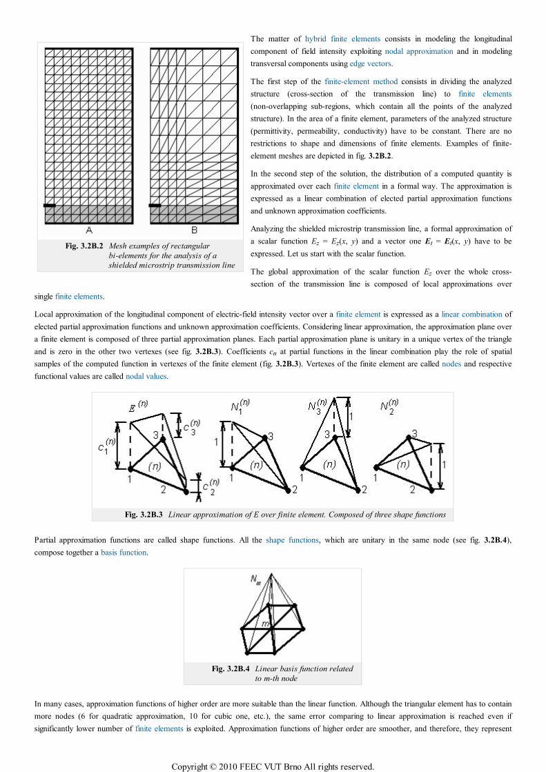
Fig. 3.2B.2 Mesh examples of rectangular
bi-elements for the analysis of a
shielded microstrip transmission line
The matter of hybrid finite elements consists in modeling the longitudinal
component of field intensity exploiting nodal approximation and in modeling
transversal components using edge vectors.
The first step of the finite-element method consists in dividing the analyzed
structure (cross-section of the transmission line) to finite elements
(non-overlapping sub-regions, which contain all the points of the analyzed
structure). In the area of a finite element, parameters of the analyzed structure
(permittivity, permeability, conductivity) have to be constant. There are no
restrictions to shape and dimensions of finite elements. Examples of finite-
element meshes are depicted in fig. 3.2B.2.
In the second step of the solution, the distribution of a computed quantity is
approximated over each finite element in a formal way. The approximation is
expressed as a linear combination of elected partial approximation functions
and unknown approximation coefficients.
Analyzing the shielded microstrip transmission line, a formal approximation of
a scalar function Ez = Ez(x, y) and a vector one Et = Et(x, y) have to be
expressed. Let us start with the scalar function.
The global approximation of the scalar function Ez over the whole cross-
section of the transmission line is composed of local approximations over
single finite elements.
Local approximation of the longitudinal component of electric-field intensity vector over a finite element is expressed as a linear combination of
elected partial approximation functions and unknown approximation coefficients. Considering linear approximation, the approximation plane over
a finite element is composed of three partial approximation planes. Each partial approximation plane is unitary in a unique vertex of the triangle
and is zero in the other two vertexes (see fig. 3.2B.3). Coefficients cn at partial functions in the linear combination play the role of spatial
samples of the computed function in vertexes of the finite element (fig. 3.2B.3). Vertexes of the finite element are called nodes and respective
functional values are called nodal values.
Fig. 3.2B.3 Linear approximation of E over finite element. Composed of three shape functions
Partial approximation functions are called shape functions. All the shape functions, which are unitary in the same node (see fig. 3.2B.4),
compose together a basis function.
Fig. 3.2B.4 Linear basis function related
to m-th node
In many cases, approximation functions of higher order are more suitable than the linear function. Although the triangular element has to contain
more nodes (6 for quadratic approximation, 10 for cubic one, etc.), the same error comparing to linear approximation is reached even if
significantly lower number of finite elements is exploited. Approximation functions of higher order are smoother, and therefore, they represent
Copyright © 2010 FEEC VUT Brno All rights reserved.
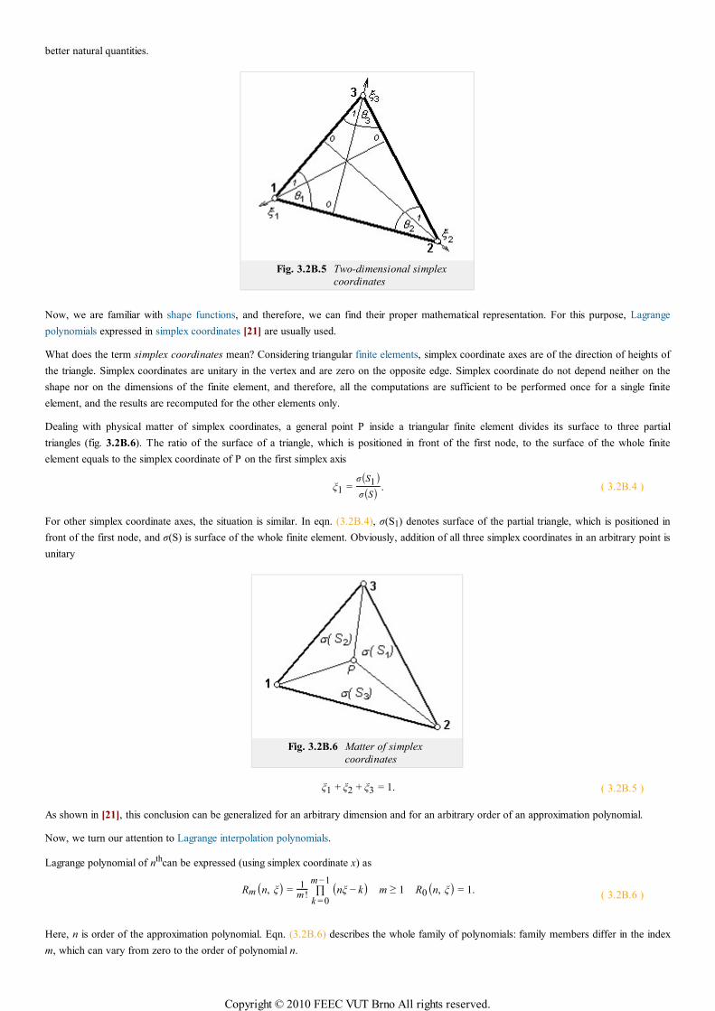
better natural quantities.
Fig. 3.2B.5 Two-dimensional simplex
coordinates
Now, we are familiar with shape functions, and therefore, we can find their proper mathematical representation. For this purpose, Lagrange
polynomials expressed in simplex coordinates [21] are usually used.
What does the term simplex coordinates mean? Considering triangular finite elements, simplex coordinate axes are of the direction of heights of
the triangle. Simplex coordinates are unitary in the vertex and are zero on the opposite edge. Simplex coordinate do not depend neither on the
shape nor on the dimensions of the finite element, and therefore, all the computations are sufficient to be performed once for a single finite
element, and the results are recomputed for the other elements only.
Dealing with physical matter of simplex coordinates, a general point P inside a triangular finite element divides its surface to three partial
triangles (fig. 3.2B.6). The ratio of the surface of a triangle, which is positioned in front of the first node, to the surface of the whole finite
element equals to the simplex coordinate of P on the first simplex axis
ξ1 =σ(S1)σ(S)
. ( 3.2B.4 )
For other simplex coordinate axes, the situation is similar. In eqn. (3.2B.4), σ(S1) denotes surface of the partial triangle, which is positioned in
front of the first node, and σ(S) is surface of the whole finite element. Obviously, addition of all three simplex coordinates in an arbitrary point is
unitary
Fig. 3.2B.6 Matter of simplex
coordinates
ξ1 + ξ2 + ξ3 = 1. ( 3.2B.5 )
As shown in [21], this conclusion can be generalized for an arbitrary dimension and for an arbitrary order of an approximation polynomial.
Now, we turn our attention to Lagrange interpolation polynomials.
Lagrange polynomial of nthcan be expressed (using simplex coordinate x) as
Rm(n, ξ) =1
m !∏
k =0
m −1(nξ − k) m ≥ 1 R0(n, ξ) = 1.
( 3.2B.6 )
Here, n is order of the approximation polynomial. Eqn. (3.2B.6) describes the whole family of polynomials: family members differ in the index
m, which can vary from zero to the order of polynomial n.
Copyright © 2010 FEEC VUT Brno All rights reserved.
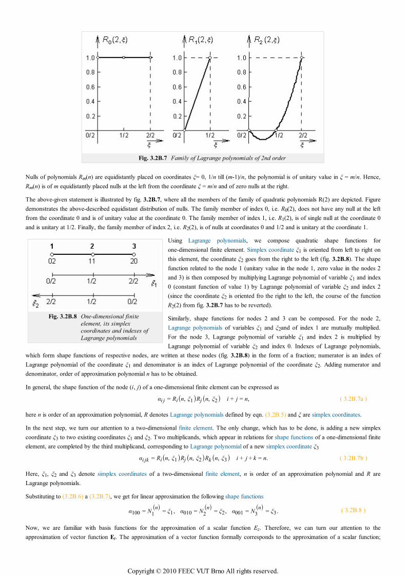
Fig. 3.2B.8 One-dimensional finite
element, its simplex
coordinates and indexes of
Lagrange polynomials
Fig. 3.2B.7 Family of Lagrange polynomials of 2nd order
Nulls of polynomials Rm(n) are equidistantly placed on coordinates ξ= 0, 1/n till (m-1)/n, the polynomial is of unitary value in ξ = m/n. Hence,
Rm(n) is of m equidistantly placed nulls at the left from the coordinate ξ = m/n and of zero nulls at the right.
The above-given statement is illustrated by fig. 3.2B.7, where all the members of the family of quadratic polynomials R(2) are depicted. Figure
demonstrates the above-described equidistant distribution of nulls. The family member of index 0, i.e. R0(2), does not have any null at the left
from the coordinate 0 and is of unitary value at the coordinate 0. The family member of index 1, i.e. R1(2), is of single null at the coordinate 0
and is unitary at 1/2. Finally, the family member of index 2, i.e. R2(2), is of nulls at coordinates 0 and 1/2 and is unitary at the coordinate 1.
Using Lagrange polynomials, we compose quadratic shape functions for
one-dimensional finite element. Simplex coordinate ξ1 is oriented from left to right on
this element, the coordinate ξ2 goes from the right to the left (fig. 3.2B.8). The shape
function related to the node 1 (unitary value in the node 1, zero value in the nodes 2
and 3) is then composed by multiplying Lagrange polynomial of variable ξ1 and index
0 (constant function of value 1) by Lagrange polynomial of variable ξ2 and index 2
(since the coordinate ξ2 is oriented fro the right to the left, the course of the function
R2(2) from fig. 3.2B.7 has to be reverted).
Similarly, shape functions for nodes 2 and 3 can be composed. For the node 2,
Lagrange polynomials of variables ξ1 and ξ2and of index 1 are mutually multiplied.
For the node 3, Lagrange polynomial of variable ξ1 and index 2 is multiplied by
Lagrange polynomial of variable ξ2 and index 0. Indexes of Lagrange polynomials,
which form shape functions of respective nodes, are written at these nodes (fig. 3.2B.8) in the form of a fraction; numerator is an index of
Lagrange polynomial of the coordinate ξ1 and denominator is an index of Lagrange polynomial of the coordinate ξ2. Adding numerator and
denominator, order of approximation polynomial n has to be obtained.
In general, the shape function of the node (i, j) of a one-dimensional finite element can be expressed as
αi j = Ri(n, ξ1)Rj(n, ξ2) i + j = n, ( 3.2B.7a )
here n is order of an approximation polynomial, R denotes Lagrange polynomials defined by eqn. (3.2B.5) and ξ are simplex coordinates.
In the next step, we turn our attention to a two-dimensional finite element. The only change, which has to be done, is adding a new simplex
coordinate ξ3 to two existing coordinates ξ1 and ξ2. Two multiplicands, which appear in relations for shape functions of a one-dimensional finite
element, are completed by the third multiplicand, corresponding to Lagrange polynomial of a new simplex coordinate ξ3
αi jk = Ri(n, ξ1)Rj(n, ξ2)Rk (n, ξ3) i + j + k = n. ( 3.2B.7b )
Here, ξ1, ξ2 and ξ3 denote simplex coordinates of a two-dimensional finite element, n is order of an approximation polynomial and R are
Lagrange polynomials.
Substituting to (3.2B.6) a (3.2B.7), we get for linear approximation the following shape functions
α100 = N1(n)
= ξ1 , α010 = N2(n)
= ξ2, α001 = N3(n)
= ξ3. ( 3.2B.8 )
Now, we are familiar with basis functions for the approximation of a scalar function Ez. Therefore, we can turn our attention to the
approximation of vector function Et. The approximation of a vector function formally corresponds to the approximation of a scalar function;
Copyright © 2010 FEEC VUT Brno All rights reserved.
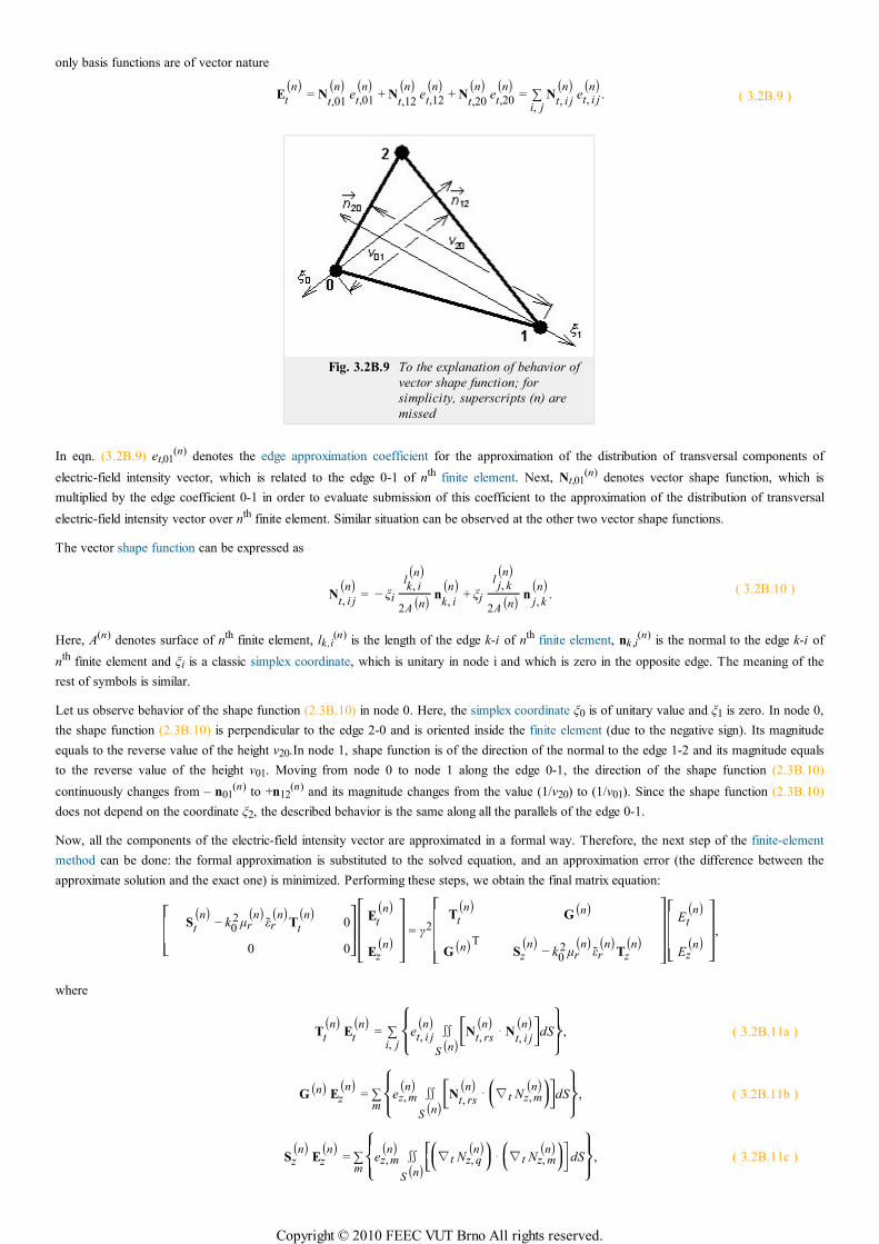
only basis functions are of vector nature
Et(n)
= Nt,01(n)
et,01(n)
+ Nt,12(n)
et,12(n)
+ Nt,20(n)
et,20(n)
= ∑i, j
Nt, i j(n)
et, i j(n)
. ( 3.2B.9 )
Fig. 3.2B.9 To the explanation of behavior of
vector shape function; for
simplicity, superscripts (n) are
missed
In eqn. (3.2B.9) et,01(n) denotes the edge approximation coefficient for the approximation of the distribution of transversal components of
electric-field intensity vector, which is related to the edge 0-1 of nth finite element. Next, Nt,01(n) denotes vector shape function, which is
multiplied by the edge coefficient 0-1 in order to evaluate submission of this coefficient to the approximation of the distribution of transversal
electric-field intensity vector over nth finite element. Similar situation can be observed at the other two vector shape functions.
The vector shape function can be expressed as
Nt, i j(n)
= − ξi
lk, i(n)
2A(n)n
k, i
(n)+ ξj
lj, k(n)
2A(n)n
j, k
(n). ( 3.2B.10 )
Here, A(n) denotes surface of nth finite element, lk,i(n) is the length of the edge k-i of nth finite element, nk ,i
(n) is the normal to the edge k-i of
nth finite element and ξi is a classic simplex coordinate, which is unitary in node i and which is zero in the opposite edge. The meaning of the
rest of symbols is similar.
Let us observe behavior of the shape function (2.3B.10) in node 0. Here, the simplex coordinate ξ0 is of unitary value and ξ1 is zero. In node 0,
the shape function (2.3B.10) is perpendicular to the edge 2-0 and is oriented inside the finite element (due to the negative sign). Its magnitude
equals to the reverse value of the height v20.In node 1, shape function is of the direction of the normal to the edge 1-2 and its magnitude equals
to the reverse value of the height v01. Moving from node 0 to node 1 along the edge 0-1, the direction of the shape function (2.3B.10)
continuously changes from – n01(n) to +n12
(n) and its magnitude changes from the value (1/v20) to (1/v01). Since the shape function (2.3B.10)
does not depend on the coordinate ξ2, the described behavior is the same along all the parallels of the edge 0-1.
Now, all the components of the electric-field intensity vector are approximated in a formal way. Therefore, the next step of the finite-element
method can be done: the formal approximation is substituted to the solved equation, and an approximation error (the difference between the
approximate solution and the exact one) is minimized. Performing these steps, we obtain the final matrix equation:
⎡
⎣
⎢⎢⎢
St(n)
− k02 µr
(n)εr
(n)T
t(n)
0
0 0
⎤
⎦
⎥⎥⎥
⎡
⎣
⎢⎢⎢⎢
Et(n)
Ez(n)
⎤
⎦
⎥⎥⎥⎥
= γ2
⎡
⎣
⎢⎢⎢⎢
Tt(n)
G(n)
G(n)TSz
(n)− k0
2 µr(n)
εr(n)
Tz(n)
⎤
⎦
⎥⎥⎥⎥
⎡
⎣
⎢⎢⎢⎢
Et(n)
Ez(n)
⎤
⎦
⎥⎥⎥⎥,
where
Tt(n)
Et(n)
= ∑i, j
⎧⎨⎩⎪⎪
et, i j(n) ∬
S (n)
⎡⎣⎢Nt, rs
(n) ⋅Nt, i j(n)⎤
⎦⎥dS
⎫⎬⎭⎪⎪
, ( 3.2B.11a )
G(n) Ez(n)
= ∑m
⎧⎨⎩⎪⎪
ez, m(n) ∬
S (n)
⎡⎣⎢Nt, rs
(n) ⋅⎛⎝⎜∇t Nz, m
(n)⎞⎠⎟⎤⎦⎥dS
⎫⎬⎭⎪⎪
, ( 3.2B.11b )
Sz(n)
Ez(n)
= ∑m
⎧⎨⎩⎪⎪
ez, m(n)∬
S (n)
⎡⎣⎢⎛⎝⎜∇t Nz, q
(n)⎞⎠⎟ ⋅
⎛⎝⎜∇t Nz, m
(n)⎞⎠⎟⎤⎦⎥ dS
⎫⎬⎭⎪⎪
, ( 3.2B.11c )
Copyright © 2010 FEEC VUT Brno All rights reserved.
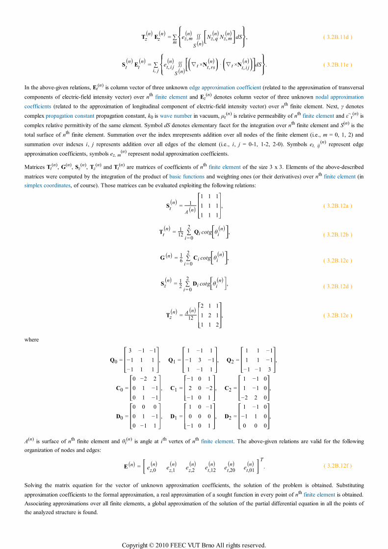
Tz(n)
Ez(n)
= ∑m
⎧⎨⎩
⎪⎪
ez, m(n) ∬
S (n)
⎡⎣⎢Nz, q
(n)Nz, m
(n)⎤⎦⎥ dS
⎫⎬⎭
⎪⎪
, ( 3.2B.11d )
St(n)
Et(n)
= ∑i, j
⎧⎨⎩⎪⎪
et, i j(n) ∬
S (n)
⎡⎣⎢⎛⎝⎜∇t ×N
t, rs(n)⎞
⎠⎟ ⋅⎛⎝⎜∇t ×N
t, i j(n)⎞
⎠⎟⎤⎦⎥dS
⎫⎬⎭⎪⎪
. ( 3.2B.11e )
In the above-given relations, Et(n) is column vector of three unknown edge approximation coefficient (related to the approximation of transversal
components of electric-field intensity vector) over nth finite element and Ez(n) denotes column vector of three unknown nodal approximation
coefficients (related to the approximation of longitudinal component of electric-field intensity vector) over nth finite element. Next, γ denotes
complex propagation constant propagation constant, k0 is wave number in vacuum, µr(n) is relative permeability of nth finite element and ε~
r(n) is
complex relative permittivity of the same element. Symbol dS denotes elementary facet for the integration over nth finite element and S(n) is the
total surface of nth finite element. Summation over the index mrepresents addition over all nodes of the finite element (i.e., m = 0, 1, 2) and
summation over indexes i, j represents addition over all edges of the element (i.e., i, j = 0-1, 1-2, 2-0). Symbols et, ij(n) represent edge
approximation coefficients, symbols ez, m(n) represent nodal approximation coefficients.
Matrices Tt(n), G(n), Sz
(n), Tz(n) and Tt
(n) are matrices of coefficients of nth finite element of the size 3 x 3. Elements of the above-described
matrices were computed by the integration of the product of basic functions and weighting ones (or their derivatives) over nth finite element (in
simplex coordinates, of course). Those matrices can be evaluated exploiting the following relations:
St(n)
=1
A(n)
⎡
⎣
⎢⎢⎢
1 1 1
1 1 1
1 1 1
⎤
⎦
⎥⎥⎥, ( 3.2B.12a )
Tt(n)
=1
12∑
i = 0
2Qi cotg
⎡⎣⎢θi
(n)⎤⎦⎥,
( 3.2B.12b )
G(n) =16
∑i = 0
2Ci cotg
⎡⎣⎢θi
(n)⎤⎦⎥,
( 3.2B.12c )
Sz(n)
=12
∑i= 0
2Di cotg
⎡⎣⎢θi
(n)⎤⎦⎥,
( 3.2B.12d )
Tz(n)
=A(n)
12
⎡
⎣
⎢⎢⎢
2 1 1
1 2 1
1 1 2
⎤
⎦
⎥⎥⎥, ( 3.2B.12e )
where
Q0 =
⎡
⎣
⎢⎢⎢
3 −1 −1
−1 1 1
−1 1 1
⎤
⎦
⎥⎥⎥, Q1 =
⎡
⎣
⎢⎢⎢
1 −1 1
−1 3 −1
1 −1 1
⎤
⎦
⎥⎥⎥, Q2 =
⎡
⎣
⎢⎢⎢
1 1 −1
1 1 −1
−1 −1 3
⎤
⎦
⎥⎥⎥,
C0 =
⎡
⎣
⎢⎢⎢
0 −2 2
0 1 −1
0 1 −1
⎤
⎦
⎥⎥⎥, C1 =
⎡
⎣
⎢⎢⎢
−1 0 1
2 0 −2
−1 0 1
⎤
⎦
⎥⎥⎥, C2 =
⎡
⎣
⎢⎢⎢
1 −1 0
1 −1 0
−2 2 0
⎤
⎦
⎥⎥⎥,
D0 =
⎡
⎣
⎢⎢⎢
0 0 0
0 1 −1
0 −1 1
⎤
⎦
⎥⎥⎥, D1 =
⎡
⎣
⎢⎢⎢
1 0 −1
0 0 0
−1 0 1
⎤
⎦
⎥⎥⎥, D2 =
⎡
⎣
⎢⎢⎢
1 −1 0
−1 1 0
0 0 0
⎤
⎦
⎥⎥⎥,
A(n) is surface of nth finite element and θi(n) is angle at ith vertex of nth finite element. The above-given relations are valid for the following
organization of nodes and edges:
E(n) = [ ez,0(n)
ez,1(n)
ez,2(n)
et,12(n)
et,20(n)
et,01(n) ]
T
. ( 3.2B.12f )
Solving the matrix equation for the vector of unknown approximation coefficients, the solution of the problem is obtained. Substituting
approximation coefficients to the formal approximation, a real approximation of a sought function in every point of nth finite element is obtained.
Associating approximations over all finite elements, a global approximation of the solution of the partial differential equation in all the points of
the analyzed structure is found.
Copyright © 2010 FEEC VUT Brno All rights reserved.

In layer C, a matlab program analyzing a shielded microstrip transmission line by the described finite-element method is introduced. A practical
programmer's description is given in the layer D.
Copyright © 2010 FEEC VUT Brno All rights reserved.
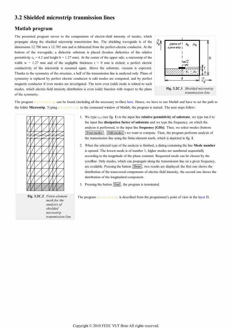
Fig. 3.2C.1 Shielded microstrip
transmission line
Fig. 3.2C.2 Finite-element
mesh for the
analysis of
shielded
microstrip
transmission line
3.2 Shielded microstrip tranmission lines
Matlab program
The presented program serves to the computation of electric-field intensity of modes, which
propagate along the shielded microstrip transmission line. The shielding waveguide is of the
dimensions 12.700 mm x 12.705 mm and is fabricated from the perfect-electric conductor. At the
bottom of the waveguide, a dielectric substrate is placed (lossless dielectrics of the relative
permittivity εr = 4.2 and height h = 1.27 mm). At the center of the upper side, a microstrip of the
width w = 1.27 mm and of the negligible thickness t ≈ 0 mm is etched; a perfect electric
conductivity of the microstrip is assumed again. Above the substrate, vacuum is expected.
Thanks to the symmetry of the structure, a half of the transmission line is analyzed only. Plane of
symmetry is replaced by perfect electric conductor is odd modes are computed, and by perfect
magnetic conductor if even modes are investigated. The term even (odd) mode is related to such
modes, which electric-field intensity distribution is even (odd) function with respect to the plane
of the symmetry.
The program microstrip can be found (including all the necessary m-files) here. Hence, we have to run Matlab and have to set the path to
the folder Microstrip. Typing microstrip to the command window of Matlab, the program is started. The next steps follow:
We type εr1 (see fig. 1) to the input line relative permittivity of substrate, we type tan δ to
the input line dissipation factor of substrate and we type the frequency, on which the
analysis is performed, to the input line frequency [GHz]. Then, we select modes (buttons
Even modes , Odd modes ) we want to compute. Then, the program performs analysis of
the transmission line using the finite-element mesh, which is depicted in fig. 2.
1.
When the selected type of the analysis is finished, a dialog containing the line Mode number
is opened. The lowest mode is of number 1, higher modes are numbered sequentially
according to the magnitude of the phase constant. Requested mode can be chosen by the
scrollbar. Only modes, which can propagate along the transmission line on a given frequency,
are available. Pressing the button Draw , two results are displayed: the first one shows the
distribution of the transversal components of electric-field intensity, the second one shows the
distribution of the longitudinal component.
2.
Pressing the button End , the program is terminated.3.
The program microstrip is described from the programmer's point of view in the layer D.
Copyright © 2010 FEEC VUT Brno All rights reserved.
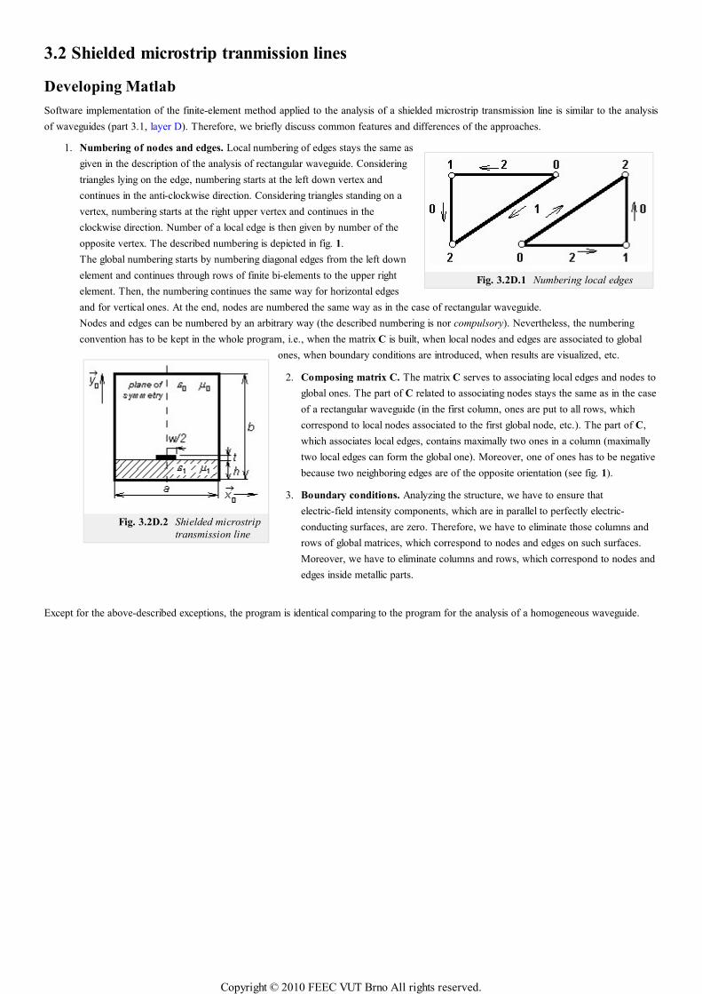
Fig. 3.2D.1 Numbering local edges
Fig. 3.2D.2 Shielded microstrip
transmission line
3.2 Shielded microstrip tranmission lines
Developing Matlab
Software implementation of the finite-element method applied to the analysis of a shielded microstrip transmission line is similar to the analysis
of waveguides (part 3.1, layer D). Therefore, we briefly discuss common features and differences of the approaches.
Numbering of nodes and edges. Local numbering of edges stays the same as
given in the description of the analysis of rectangular waveguide. Considering
triangles lying on the edge, numbering starts at the left down vertex and
continues in the anti-clockwise direction. Considering triangles standing on a
vertex, numbering starts at the right upper vertex and continues in the
clockwise direction. Number of a local edge is then given by number of the
opposite vertex. The described numbering is depicted in fig. 1.
The global numbering starts by numbering diagonal edges from the left down
element and continues through rows of finite bi-elements to the upper right
element. Then, the numbering continues the same way for horizontal edges
and for vertical ones. At the end, nodes are numbered the same way as in the case of rectangular waveguide.
Nodes and edges can be numbered by an arbitrary way (the described numbering is nor compulsory). Nevertheless, the numbering
convention has to be kept in the whole program, i.e., when the matrix C is built, when local nodes and edges are associated to global
ones, when boundary conditions are introduced, when results are visualized, etc.
1.
Composing matrix C. The matrix C serves to associating local edges and nodes to
global ones. The part of C related to associating nodes stays the same as in the case
of a rectangular waveguide (in the first column, ones are put to all rows, which
correspond to local nodes associated to the first global node, etc.). The part of C,
which associates local edges, contains maximally two ones in a column (maximally
two local edges can form the global one). Moreover, one of ones has to be negative
because two neighboring edges are of the opposite orientation (see fig. 1).
2.
Boundary conditions. Analyzing the structure, we have to ensure that
electric-field intensity components, which are in parallel to perfectly electric-
conducting surfaces, are zero. Therefore, we have to eliminate those columns and
rows of global matrices, which correspond to nodes and edges on such surfaces.
Moreover, we have to eliminate columns and rows, which correspond to nodes and
edges inside metallic parts.
3.
Except for the above-described exceptions, the program is identical comparing to the program for the analysis of a homogeneous waveguide.
Copyright © 2010 FEEC VUT Brno All rights reserved.
3.2 Shielded microstrip tranmission lines
Java applet
Copyright © 2010 FEEC VUT Brno All rights reserved.

3.2 Shielded microstrip tranmission lines
Quiz
Answer these questions to get feedback on how well you understand the course. Only one of the answers is correct. You don't have to answer
every question. If you don't know the answer you can just leave it blank (default option: “I won't answer this question”) and this won't affect
your score. Answering correctly will add 2 points to your score but on the other hand you'll lose 1 point if your answer is wrong. The
questions are divided in groups of five questions.
Press See result after you have finished answering.
Displaying questions 1..5 of 5:
Question 1
In the shielded microstrip transmission line, hybrid modes can propagate. Those modes …
Possible answers for question 1:
… are created by the mutual coupling of transversal electric and magnetic modes.
… are a special form of the transversally electromagnetic wave (the structure looks like a coaxial transmission line).
… are created by the mutual coupling of longitudinal section electric and magnetic modes.
I won't answer this question
Question 2
When analyzing microstrip transmission lines …
Possible answers for question 2:
… non-simplified Maxwell equations have to be considered.
Maxwell equations are not needed – computing current on the microstrip is satisfactory.
Maxwell equations can be simplified – longitudinal components have to be considered only.
I won't answer this question
Question 3
Analyzing microstrip transmission lines by finite elements …
Possible answers for question 3:
… there is no difference compared to the analysis of the hollow waveguide.
… transversal field components have to be approximated by edge elements to preserve field continuity at boundaries of dielectrics.
… longitudinal field components have to be approximated by edge elements to preserve field continuity at boundaries of dielectrics.
I won't answer this question
Question 4
Speaking about finite elements spatial distribution of field components can be approximated by the linear combination of…
Possible answers for question 4:
… known basis functions and unknown coefficients.
… known basis functions and unknown time expansions.
… eigenvalues and eigenvectors.
I won't answer this question
Question 5
The critical frequency of the dominant mode of a shielded planar transmission line …
Copyright © 2010 FEEC VUT Brno All rights reserved.

Possible answers for question 5:
… is zero, the mode IS EXACTLY the transversally electromagnetic wave.
… is higher compared to the hollow waveguide of the same dimension.
… is zero, the mode LOOKS LIKE the transversally electromagnetic wave.
I won't answer this question
Copyright © 2010 FEEC VUT Brno All rights reserved.

Chapter 4: Antennas
Introduction
Antennas can be considered as one of the most important parts of the radio-communication chain because antennas transform an
electromagnetic wave propagating along the transmission line to the wave propagating in free-space and vice versa. Consequently, antenna
parameters (directivity pattern, impedance, gain) significantly influence final properties of the radio link.
In this chapter, an overview of antennas and technical details of their design and exploitation are not presented. We consider these topics as well
understandable and well described in the existing literature (in [1] , e.g.). We turn our attention to the principles of radiation and to the ways of
its mathematical modeling.
The initial paper describes the modeling of a wire dipole by the method of moments. Using this method, a current distribution on the antenna is
computed as a primarily quantity. If the current distribution is known, all the other parameters can be computed. The complete description is
given in the layer A. In the layer B, a Dutch translation of the layer A is given.
The second paper deals with the analysis of wire antennas consisting of more elements. We become familiar with the method of induced
electromotoric forces, which enables to compute properties of not only self-standing dipoles but too their mutual coupling.
Even the third paper is devoted to the analysis of wire antennas consisting of more elements. Our attention is turned to Yagi antenna and to its
analysis by the method of moments. Comparing papers 2 and 3, the reader can compare both the approaches.
In the fourth paper and in the fifth paper, wire antennas are left and the attention is turned to microstrip antennas. First, a microstrip dipole is
analyzed using one-dimensional method of moments. Second, a patch antenna analyzed by two-dimensional method of moments.
Analysis of microstrip antennas is much more complicated compared to the analysis of wire antennas. This is given by the fact that microstrip
antennas are manufactured exploiting dielectric substrates, and therefore, analysis methods have to respect fulfilling continuity conditions on the
boundary of two media.
Copyright © 2010 FEEC VUT Brno All rights reserved.
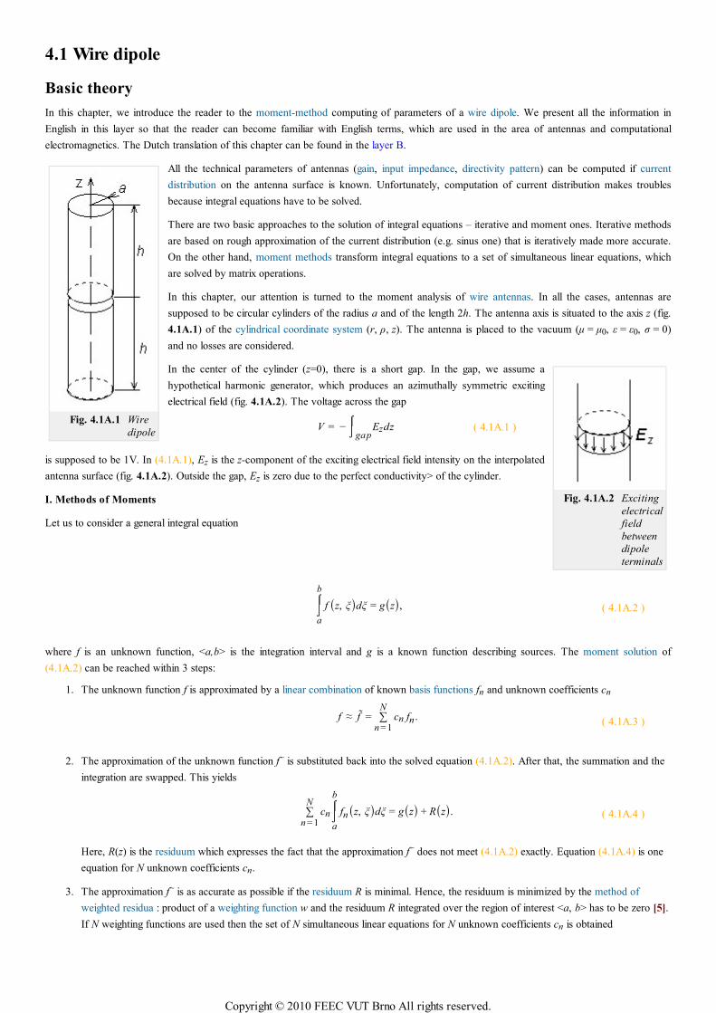
Fig. 4.1A.1 Wire
dipole
Fig. 4.1A.2 Exciting
electrical
field
between
dipole
terminals
4.1 Wire dipole
Basic theory
In this chapter, we introduce the reader to the moment-method computing of parameters of a wire dipole. We present all the information in
English in this layer so that the reader can become familiar with English terms, which are used in the area of antennas and computational
electromagnetics. The Dutch translation of this chapter can be found in the layer B.
All the technical parameters of antennas (gain, input impedance, directivity pattern) can be computed if current
distribution on the antenna surface is known. Unfortunately, computation of current distribution makes troubles
because integral equations have to be solved.
There are two basic approaches to the solution of integral equations – iterative and moment ones. Iterative methods
are based on rough approximation of the current distribution (e.g. sinus one) that is iteratively made more accurate.
On the other hand, moment methods transform integral equations to a set of simultaneous linear equations, which
are solved by matrix operations.
In this chapter, our attention is turned to the moment analysis of wire antennas. In all the cases, antennas are
supposed to be circular cylinders of the radius a and of the length 2h. The antenna axis is situated to the axis z (fig.
4.1A.1) of the cylindrical coordinate system (r, ρ, z). The antenna is placed to the vacuum (µ = µ0, ε = ε0, σ = 0)
and no losses are considered.
In the center of the cylinder (z=0), there is a short gap. In the gap, we assume a
hypothetical harmonic generator, which produces an azimuthally symmetric exciting
electrical field (fig. 4.1A.2). The voltage across the gap
V = − ⌠⌡gapEzdz ( 4.1A.1 )
is supposed to be 1V. In (4.1A.1), Ez is the z-component of the exciting electrical field intensity on the interpolated
antenna surface (fig. 4.1A.2). Outside the gap, Ez is zero due to the perfect conductivity> of the cylinder.
I. Methods of Moments
Let us to consider a general integral equation
⌠⌡a
b
f (z, ξ)dξ = g(z), ( 4.1A.2 )
where f is an unknown function, <a,b> is the integration interval and g is a known function describing sources. The moment solution of
(4.1A.2) can be reached within 3 steps:
The unknown function f is approximated by a linear combination of known basis functions fn and unknown coefficients cn
f ≈ f = ∑n = 1
Ncn fn .
( 4.1A.3 )
1.
The approximation of the unknown function f~ is substituted back into the solved equation (4.1A.2). After that, the summation and the
integration are swapped. This yields
∑n = 1
Ncn
⌠⌡a
b
fn(z, ξ)dξ = g(z) + R(z). ( 4.1A.4 )
Here, R(z) is the residuum which expresses the fact that the approximation f~ does not meet (4.1A.2) exactly. Equation (4.1A.4) is one
equation for N unknown coefficients cn.
2.
The approximation f~ is as accurate as possible if the residuum R is minimal. Hence, the residuum is minimized by the method of
weighted residua : product of a weighting function w and the residuum R integrated over the region of interest <a, b> has to be zero [5].
If N weighting functions are used then the set of N simultaneous linear equations for N unknown coefficients cn is obtained
3.
Copyright © 2010 FEEC VUT Brno All rights reserved.
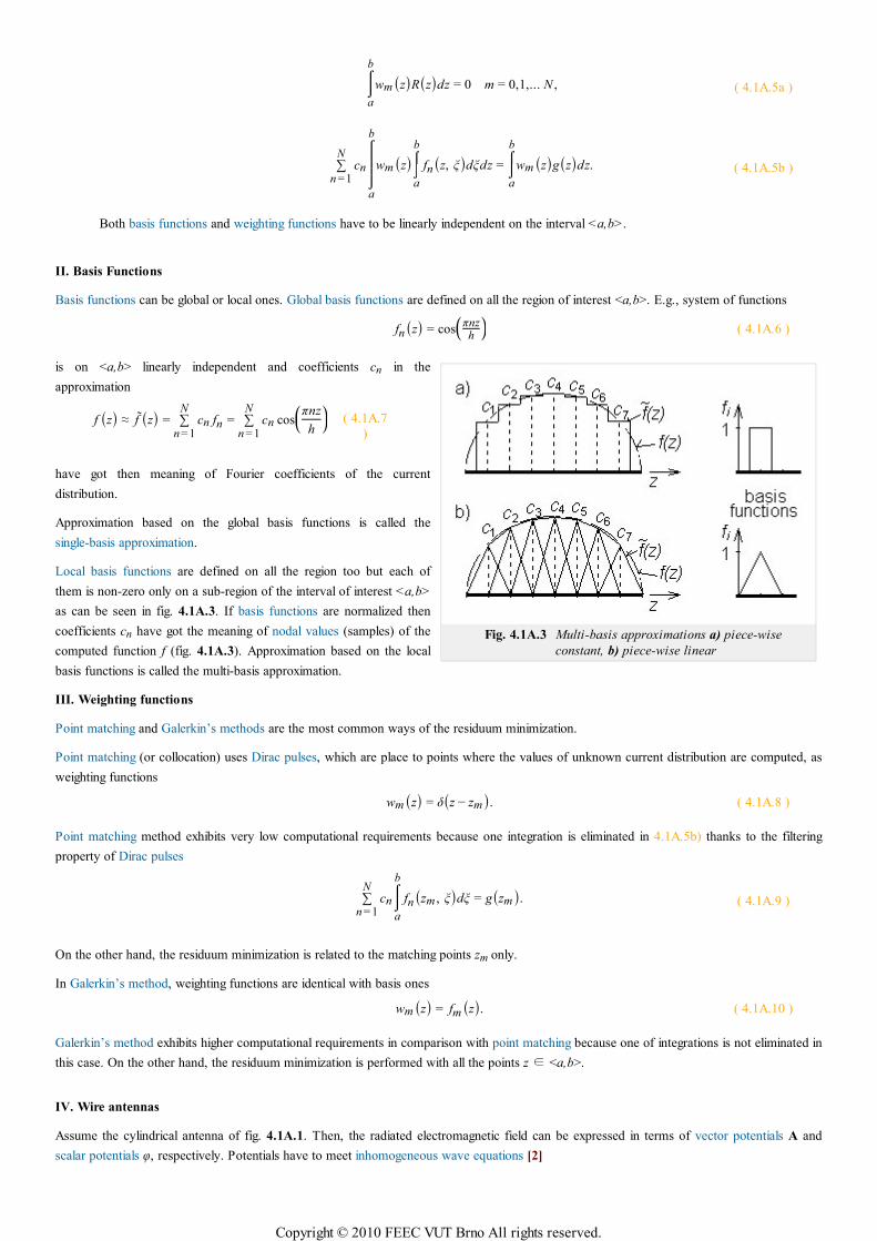
Fig. 4.1A.3 Multi-basis approximations a) piece-wise
constant, b) piece-wise linear
⌠⌡a
b
wm(z)R(z)dz = 0 m = 0,1,... N , ( 4.1A.5a )
∑n =1
Ncn
⌠
⌡⎮⎮⎮a
b
wm(z)⌠⌡a
b
fn(z, ξ)dξdz = ⌠⌡a
b
wm(z)g(z)dz. ( 4.1A.5b )
Both basis functions and weighting functions have to be linearly independent on the interval <a,b>.
II. Basis Functions
Basis functions can be global or local ones. Global basis functions are defined on all the region of interest <a,b>. E.g., system of functions
fn(z) = cos⎛⎝πnz
h⎞⎠ ( 4.1A.6 )
is on <a,b> linearly independent and coefficients cn in the
approximation
f (z) ≈ f (z) = ∑n = 1
Ncn fn = ∑
n = 1
Ncn cos
⎛⎝⎜
πnz
h
⎞⎠⎟ ( 4.1A.7
)
have got then meaning of Fourier coefficients of the current
distribution.
Approximation based on the global basis functions is called the
single-basis approximation.
Local basis functions are defined on all the region too but each of
them is non-zero only on a sub-region of the interval of interest <a,b>
as can be seen in fig. 4.1A.3. If basis functions are normalized then
coefficients cn have got the meaning of nodal values (samples) of the
computed function f (fig. 4.1A.3). Approximation based on the local
basis functions is called the multi-basis approximation.
III. Weighting functions
Point matching and Galerkin’s methods are the most common ways of the residuum minimization.
Point matching (or collocation) uses Dirac pulses, which are place to points where the values of unknown current distribution are computed, as
weighting functions
wm(z) = δ(z − zm). ( 4.1A.8 )
Point matching method exhibits very low computational requirements because one integration is eliminated in 4.1A.5b) thanks to the filtering
property of Dirac pulses
∑n = 1
Ncn
⌠⌡a
b
fn(zm , ξ)dξ = g(zm). ( 4.1A.9 )
On the other hand, the residuum minimization is related to the matching points zm only.
In Galerkin’s method, weighting functions are identical with basis ones
wm(z) = fm(z). ( 4.1A.10 )
Galerkin’s method exhibits higher computational requirements in comparison with point matching because one of integrations is not eliminated in
this case. On the other hand, the residuum minimization is performed with all the points z ∈ <a,b>.
IV. Wire antennas
Assume the cylindrical antenna of fig. 4.1A.1. Then, the radiated electromagnetic field can be expressed in terms of vector potentials A and
scalar potentials φ, respectively. Potentials have to meet inhomogeneous wave equations [2]
Copyright © 2010 FEEC VUT Brno All rights reserved.
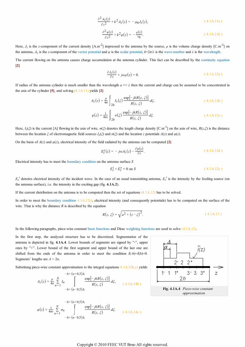
Fig. 4.1A.4 Piece-wise constant
approximation
∂2 Az(z)∂ z2
+ k 2 Az(z) = − µ0 Jz(z), ( 4.1A.11a )
∂2 φ(z)∂ z2
+ k 2φ(z) = −ρ(z)ε0
. ( 4.1A.11b )
Here, Jz is the z-component of the current density [A.m-2] impressed to the antenna by the source, ρ is the volume charge density [C.m-3] on
the antenna, Az is the z-component of the vector potential and φ is the scalar potential, k=2π/λ is the wave-number and λ is the wavelength.
The current flowing on the antenna causes charge accumulation at the antenna cylinder. This fact can be described by the continuity equation
[2]
∂ Jz(z)∂ z
+ jωρ(z) = 0. ( 4.1A.12a )
If radius of the antenna cylinder is much smaller than the wavelength a << λ then the current and charge can be assumed to be concentrated in
the axis of the cylinder [5], and solving (4.1A.11) yields [2]
Az(z) =µ
4π
⌠⌡⎮⎮
2h
Iz(ξ) exp[− jkR(z, ξ)]R(z, ξ) dξ, ( 4.1A.12b )
φ(z) =1
4πε
⌠⌡⎮⎮
2h
σ(ξ) exp[− jkR(z, ξ)]R(z, ξ) dξ. ( 4.1A.12c )
Here, Iz(ξ) is the current [A] flowing in the axis of wire, σ(ξ) denotes the length charge density [C.m-1] on the axis of wire, R(z,ξ) is the distance
between the location ξ of electromagnetic field sources Iz(ξ) and σ(ξ) and the location z potentials A(z) and φ(z).
On the basis of A(z) and φ(z), electrical intensity of the field radiated by the antenna can be computed [2]
Ezs(z) = − jωAz(z) −
∂φ(z)∂ z
. ( 4.1A.12d )
Electrical intensity has to meet the boundary condition on the antenna surface S
Ezi + Ez
s = 0 on S ( 4.1A.12e )
Ezi denotes electrical intensity of the incident wave. In the case of an usual transmitting antenna, Ez
i is the intensity by the feeding source (on
the antenna surface), i.e. the intensity in the exciting gap (fig. 4.1A.2).
If the current distribution on the antenna is to be computed then the set of equations (4.1A.12) has to be solved.
In order to meet the boundary condition 4.1A.12e), electrical intensity (and consequently potentials) has to be computed on the surface of the
wire. That is why the distance R is described by the equation
R(z, ξ) = a2 + (z − ξ)2√ . ( 4.1A.13 )
In the following paragraphs, piece-wise constant basis functions and Dirac weighting functions are used to solve (4.1A.12).
In the first step, the analyzed structure has to be discretized. Segmentation of the
antenna is depicted in fig. 4.1A.4. Lower bounds of segments are signed by ”-”, upper
ones by ”+”. Lower bound of the first segment and upper bound of the last one are
shifted from the ends of the antenna in order to meet the condition I(-h)=I(h)=0.
Segments’ lengths are ∆ = 2α.
Substitung piece-wise constant approximation to the integral equations 4.1A.12b,c) yields
Az(z) ≈µ
4π∑
n = 1
NIn
⌠⌡⎮⎮
−h+(n−0,5)∆
−h+(n+0,5)∆
exp[− jkR(z, ξ)]R(z, ξ) dξ,
( 4.1A.14b )
φ(z) ≈1
4πε∑
n =1
Nσn
⌠⌡⎮⎮
−h+(n−0,5)∆
−h+(n+0,5)∆
exp[− jkR(z, ξ)]R(z, ξ) dξ.
( 4.1A.14c )
Copyright © 2010 FEEC VUT Brno All rights reserved.
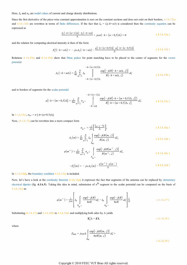
Here, In and σn are nodal values of current and charge density distributions.
Since the first derivative of the piece-wise constant approximation is zero on the constant sections and does not exist on their borders, 4.1A.12a)
and 4.1A.12d) are rewritten in terms of finite differences. If the fact that In = Iz(-h+n∆) is considered then the continuity equation can be
expressed as
Iz(−h+(n+1)∆)− Iz(−h+n∆)∆
+ jωσ(−h + (n + 0,5)∆) ≈ 0 ( 4.1A.15a )
and the relation for computing electrical intensity is then of the form
Ezs(−h + n∆) ≈ − jωAz(−h + n∆) −
φ[−h+(n+0,5)∆]−φ[−h+(n−0,5)∆]∆
. ( 4.1A.15d )
Relations 4.1A.15a) and 4.1A.15d) show that Dirac pulses for point matching have to be placed to the center of segments for the vector
potential
Az(−h + m∆) ≈µ
4π∑
n =1
NIn
⌠⌡⎮⎮
−h+(n−0,5)∆
−h+(n+0,5)∆
exp[− jkR(−h + m∆, ξ)]R(−h + m∆, ξ) dξ
( 4.1A.15b )
and to borders of segments for the scalar potential
φ[−h + (m + 0,5)∆] ≈1
4πε∑
n =1
Nσ
n +⌠⌡⎮⎮
−h+n∆
−h+(n+1)∆
exp− jkR[−h + (m + 0,5)∆, ξ]R[−h + (m + 0,5)∆, ξ] dξ. ( 4.1A.15c )
In 4.1A.15c), σn+ = σ [-h+(n+0.5)∆].
Now, (4.1A.15) can be rewritten into a more compact form
σn + ≈
−1jω
⎡⎣⎢
In+1 − In
∆
⎤⎦⎥, ( 4.1A.16a )
Az(m) ≈µ
4π∑
n =1
NIn
⌠⌡⎮⎮∆n
exp[− jkR(m, ξ)]R(m, ξ) dξ,
( 4.1A.16b )
φ(m + ) ≈1
4πε∑
n = 1
Nσ
n +⌠⌡⎮⎮
∆n +
exp[− jkR(m + , ξ)]R(m + , ξ) dξ,
( 4.1A.16c )
−Ezi(m) ≈ − jωAz(m) −
φ(m + )−φ(m − )∆
. ( 4.1A.16d )
In 4.1A.16d), the boundary condition 4.1A.12e) is included.
Now, let’s have a look at the continuity theorem 4.1A.16a); it expresses the fact that segments of the antenna can be replaced by elementary
electrical dipoles (fig. 4.1A.5). Taking this idea in mind, submission of nth segment to the scalar potential can be computed on the basis of
4.1A.16c) as
φ(m + ) =1
jωε
⎡
⎣
⎢⎢⎢⎢In
⌠⌡⎮⎮
∆n +
exp(− jkR)4πR
dξ − In⌠⌡⎮⎮
∆n −
exp(− jkR)4πR
dξ
⎤
⎦
⎥⎥⎥⎥1∆
. ( 4.1A.17 )
Substituting (4.1A.17) and 4.1A.16b) to 4.1A.16d) and multiplying both sides by ∆ yields
Ezi∆ = ZI, ( 4.1A.18 )
where
Zmn = jωµ∆⌠⌡⎮⎮∆n
exp[− jkR(m, ξ)]4πR(m, ξ) dξ +
( 4.1A.19 )
Copyright © 2010 FEEC VUT Brno All rights reserved.
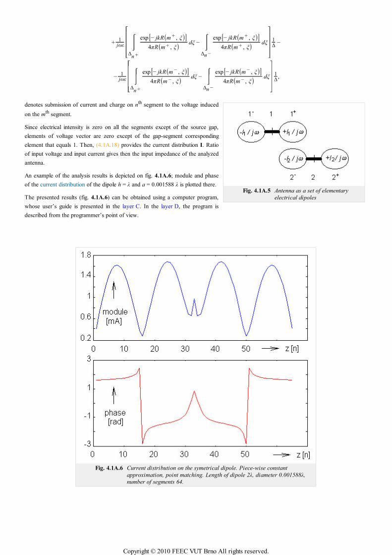
Fig. 4.1A.5 Antenna as a set of elementary
electrical dipoles
+1
jωε
⎡
⎣
⎢⎢⎢⎢⌠⌡⎮⎮
∆n +
exp[− jkR(m + , ξ)]4πR(m + , ξ) dξ −
⌠⌡⎮⎮
∆n −
exp[− jkR(m + , ξ)]4πR(m + , ξ) dξ
⎤
⎦
⎥⎥⎥⎥1∆
−
−1
jωε
⎡
⎣
⎢⎢⎢⎢⌠⌡⎮⎮
∆n +
exp[− jkR(m − , ξ)]4πR(m − , ξ) dξ −
⌠⌡⎮⎮
∆n −
exp[− jkR(m − , ξ)]4πR(m − , ξ) dξ
⎤
⎦
⎥⎥⎥⎥1∆
,
denotes submission of current and charge on nth segment to the voltage induced
on the mth segment.
Since electrical intensity is zero on all the segments except of the source gap,
elements of voltage vector are zero except of the gap-segment corresponding
element that equals 1. Then, (4.1A.18) provides the current distribution I. Ratio
of input voltage and input current gives then the input impedance of the analyzed
antenna.
An example of the analysis results is depicted on fig. 4.1A.6; module and phase
of the current distribution of the dipole h = λ and a = 0.001588 λ is plotted there.
The presented results (fig. 4.1A.6) can be obtained using a computer program,
whose user’s guide is presented in the layer C. In the layer D, the program is
described from the programmer’s point of view.
Fig. 4.1A.6 Current distribution on the symetrical dipole. Piece-wise constant
approximation, point matching. Length of dipole 2λ, diameter 0.001588λ,
number of segments 64.
Copyright © 2010 FEEC VUT Brno All rights reserved.
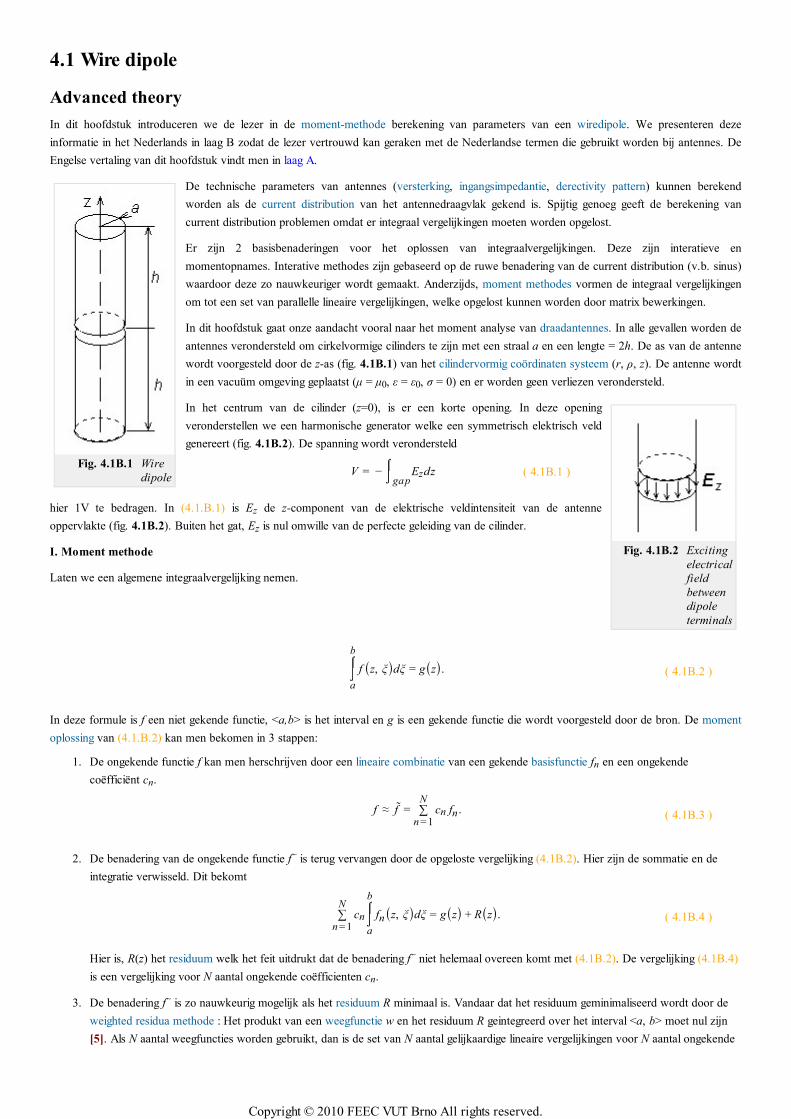
Fig. 4.1B.1 Wire
dipole
Fig. 4.1B.2 Exciting
electrical
field
between
dipole
terminals
4.1 Wire dipole
Advanced theory
In dit hoofdstuk introduceren we de lezer in de moment-methode berekening van parameters van een wiredipole. We presenteren deze
informatie in het Nederlands in laag B zodat de lezer vertrouwd kan geraken met de Nederlandse termen die gebruikt worden bij antennes. De
Engelse vertaling van dit hoofdstuk vindt men in laag A.
De technische parameters van antennes (versterking, ingangsimpedantie, derectivity pattern) kunnen berekend
worden als de current distribution van het antennedraagvlak gekend is. Spijtig genoeg geeft de berekening van
current distribution problemen omdat er integraal vergelijkingen moeten worden opgelost.
Er zijn 2 basisbenaderingen voor het oplossen van integraalvergelijkingen. Deze zijn interatieve en
momentopnames. Interative methodes zijn gebaseerd op de ruwe benadering van de current distribution (v.b. sinus)
waardoor deze zo nauwkeuriger wordt gemaakt. Anderzijds, moment methodes vormen de integraal vergelijkingen
om tot een set van parallelle lineaire vergelijkingen, welke opgelost kunnen worden door matrix bewerkingen.
In dit hoofdstuk gaat onze aandacht vooral naar het moment analyse van draadantennes. In alle gevallen worden de
antennes verondersteld om cirkelvormige cilinders te zijn met een straal a en een lengte = 2h. De as van de antenne
wordt voorgesteld door de z-as (fig. 4.1B.1) van het cilindervormig coördinaten systeem (r, ρ, z). De antenne wordt
in een vacuüm omgeving geplaatst (µ = µ0, ε = ε0, σ = 0) en er worden geen verliezen verondersteld.
In het centrum van de cilinder (z=0), is er een korte opening. In deze opening
veronderstellen we een harmonische generator welke een symmetrisch elektrisch veld
genereert (fig. 4.1B.2). De spanning wordt verondersteld
V = − ⌠⌡gapEzdz ( 4.1B.1 )
hier 1V te bedragen. In (4.1.B.1) is Ez de z-component van de elektrische veldintensiteit van de antenne
oppervlakte (fig. 4.1B.2). Buiten het gat, Ez is nul omwille van de perfecte geleiding van de cilinder.
I. Moment methode
Laten we een algemene integraalvergelijking nemen.
⌠⌡a
b
f (z, ξ)dξ = g(z). ( 4.1B.2 )
In deze formule is f een niet gekende functie, <a,b> is het interval en g is een gekende functie die wordt voorgesteld door de bron. De moment
oplossing van (4.1.B.2) kan men bekomen in 3 stappen:
De ongekende functie f kan men herschrijven door een lineaire combinatie van een gekende basisfunctie fn en een ongekende
coëfficiënt cn.
f ≈ f = ∑n = 1
Ncn fn . ( 4.1B.3 )
1.
De benadering van de ongekende functie f~ is terug vervangen door de opgeloste vergelijking (4.1B.2). Hier zijn de sommatie en de
integratie verwisseld. Dit bekomt
∑n = 1
Ncn
⌠⌡a
b
fn(z, ξ)dξ = g(z) + R(z). ( 4.1B.4 )
Hier is, R(z) het residuum welk het feit uitdrukt dat de benadering f~ niet helemaal overeen komt met (4.1B.2). De vergelijking (4.1B.4)
is een vergelijking voor N aantal ongekende coëfficienten cn.
2.
De benadering f~ is zo nauwkeurig mogelijk als het residuum R minimaal is. Vandaar dat het residuum geminimaliseerd wordt door de
weighted residua methode : Het produkt van een weegfunctie w en het residuum R geintegreerd over het interval <a, b> moet nul zijn
[5]. Als N aantal weegfuncties worden gebruikt, dan is de set van N aantal gelijkaardige lineaire vergelijkingen voor N aantal ongekende
3.
Copyright © 2010 FEEC VUT Brno All rights reserved.
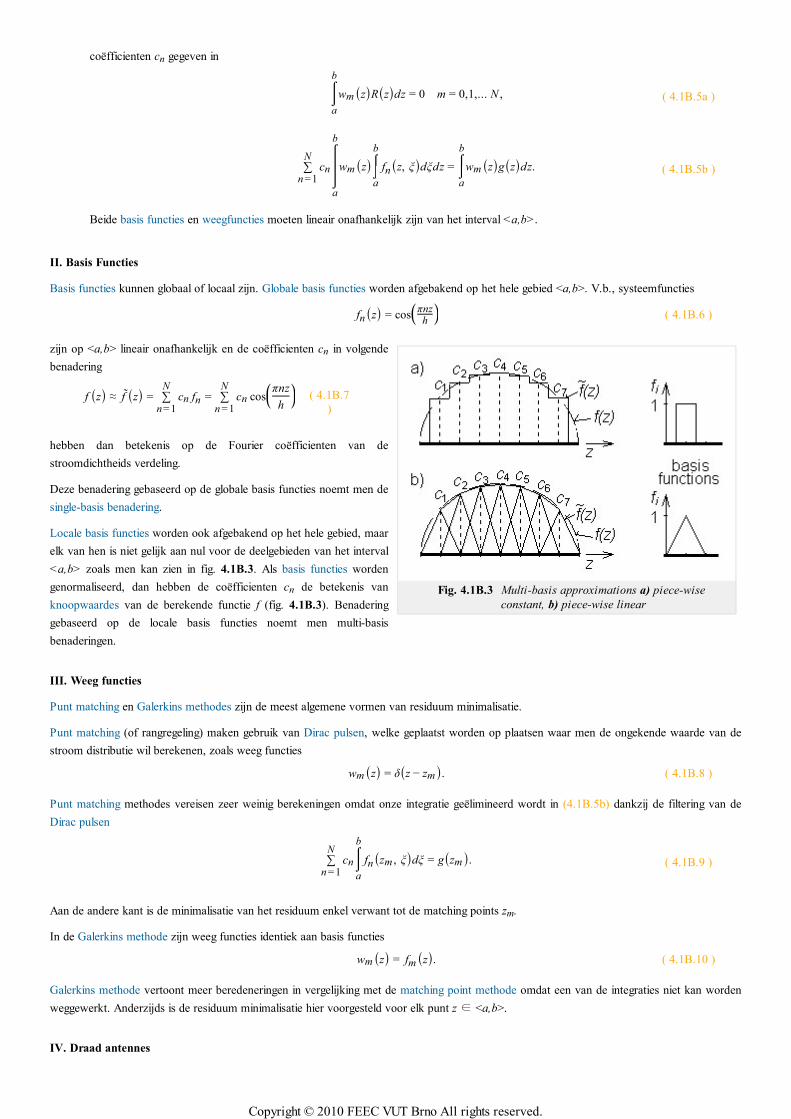
Fig. 4.1B.3 Multi-basis approximations a) piece-wise
constant, b) piece-wise linear
coëfficienten cn gegeven in
⌠⌡a
b
wm(z)R(z)dz = 0 m = 0,1,... N , ( 4.1B.5a )
∑n =1
Ncn
⌠
⌡⎮⎮⎮a
b
wm(z)⌠⌡a
b
fn(z, ξ)dξdz = ⌠⌡a
b
wm(z)g(z)dz. ( 4.1B.5b )
Beide basis functies en weegfuncties moeten lineair onafhankelijk zijn van het interval <a,b>.
II. Basis Functies
Basis functies kunnen globaal of locaal zijn. Globale basis functies worden afgebakend op het hele gebied <a,b>. V.b., systeemfuncties
fn(z) = cos⎛⎝πnz
h⎞⎠ ( 4.1B.6 )
zijn op <a,b> lineair onafhankelijk en de coëfficienten cn in volgende
benadering
f (z) ≈ f (z) = ∑n = 1
Ncn fn = ∑
n = 1
Ncn cos
⎛⎝⎜
πnz
h
⎞⎠⎟ ( 4.1B.7
)
hebben dan betekenis op de Fourier coëfficienten van de
stroomdichtheids verdeling.
Deze benadering gebaseerd op de globale basis functies noemt men de
single-basis benadering.
Locale basis functies worden ook afgebakend op het hele gebied, maar
elk van hen is niet gelijk aan nul voor de deelgebieden van het interval
<a,b> zoals men kan zien in fig. 4.1B.3. Als basis functies worden
genormaliseerd, dan hebben de coëfficienten cn de betekenis van
knoopwaardes van de berekende functie f (fig. 4.1B.3). Benadering
gebaseerd op de locale basis functies noemt men multi-basis
benaderingen.
III. Weeg functies
Punt matching en Galerkins methodes zijn de meest algemene vormen van residuum minimalisatie.
Punt matching (of rangregeling) maken gebruik van Dirac pulsen, welke geplaatst worden op plaatsen waar men de ongekende waarde van de
stroom distributie wil berekenen, zoals weeg functies
wm(z) = δ(z − zm). ( 4.1B.8 )
Punt matching methodes vereisen zeer weinig berekeningen omdat onze integratie geëlimineerd wordt in (4.1B.5b) dankzij de filtering van de
Dirac pulsen
∑n = 1
Ncn
⌠⌡a
b
fn(zm , ξ)dξ = g(zm). ( 4.1B.9 )
Aan de andere kant is de minimalisatie van het residuum enkel verwant tot de matching points zm.
In de Galerkins methode zijn weeg functies identiek aan basis functies
wm(z) = fm(z). ( 4.1B.10 )
Galerkins methode vertoont meer beredeneringen in vergelijking met de matching point methode omdat een van de integraties niet kan worden
weggewerkt. Anderzijds is de residuum minimalisatie hier voorgesteld voor elk punt z ∈ <a,b>.
IV. Draad antennes
Copyright © 2010 FEEC VUT Brno All rights reserved.
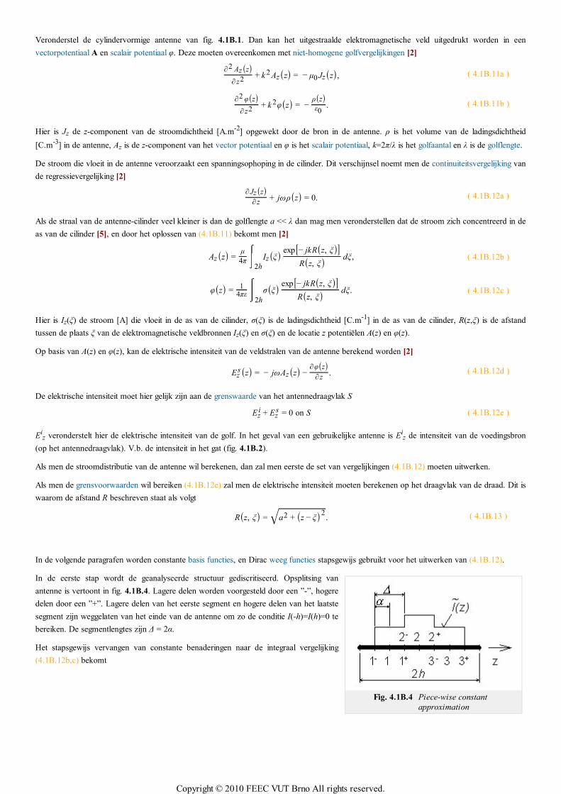
Fig. 4.1B.4 Piece-wise constant
approximation
Veronderstel de cylindervormige antenne van fig. 4.1B.1. Dan kan het uitgestraalde elektromagnetische veld uitgedrukt worden in een
vectorpotentiaal A en scalair potentiaal φ. Deze moeten overeenkomen met niet-homogene golfvergelijkingen [2]
∂2 Az(z)∂ z2
+ k 2 Az(z) = − µ0 Jz(z), ( 4.1B.11a )
∂2 φ(z)∂ z2
+ k 2φ(z) = −ρ(z)ε0
. ( 4.1B.11b )
Hier is Jz de z-component van de stroomdichtheid [A.m-2] opgewekt door de bron in de antenne. ρ is het volume van de ladingsdichtheid
[C.m-3] in de antenne, Az is de z-component van het vector potentiaal en φ is het scalair potentiaal, k=2π/λ is het golfaantal en λ is de golflengte.
De stroom die vloeit in de antenne veroorzaakt een spanningsophoping in de cilinder. Dit verschijnsel noemt men de continuiteitsvergelijking van
de regressievergelijking [2]
∂ Jz(z)∂ z
+ jωρ(z) = 0. ( 4.1B.12a )
Als de straal van de antenne-cilinder veel kleiner is dan de golflengte a << λ dan mag men veronderstellen dat de stroom zich concentreerd in de
as van de cilinder [5], en door het oplossen van (4.1B.11) bekomt men [2]
Az(z) =µ
4π
⌠⌡⎮⎮
2h
Iz(ξ) exp[− jkR(z, ξ)]R(z, ξ) dξ, ( 4.1B.12b )
φ(z) =1
4πε
⌠⌡⎮⎮
2h
σ(ξ) exp[− jkR(z, ξ)]R(z, ξ) dξ. ( 4.1B.12c )
Hier is Iz(ξ) de stroom [A] die vloeit in de as van de cilinder, σ(ξ) is de ladingsdichtheid [C.m-1] in de as van de cilinder, R(z,ξ) is de afstand
tussen de plaats ξ van de elektromagnetische veldbronnen Iz(ξ) en σ(ξ) en de locatie z potentiëlen A(z) en φ(z).
Op basis van A(z) en φ(z), kan de elektrische intensiteit van de veldstralen van de antenne berekend worden [2]
Ezs(z) = − jωAz(z) −
∂φ(z)∂ z
. ( 4.1B.12d )
De elektrische intensiteit moet hier gelijk zijn aan de grenswaarde van het antennedraagvlak S
Ezi + Ez
s = 0 on S ( 4.1B.12e )
Eiz veronderstelt hier de elektrische intensiteit van de golf. In het geval van een gebruikelijke antenne is Ei
z de intensiteit van de voedingsbron
(op het antennedraagvlak). V.b. de intensiteit in het gat (fig. 4.1B.2).
Als men de stroomdistributie van de antenne wil berekenen, dan zal men eerste de set van vergelijkingen (4.1B.12) moeten uitwerken.
Als men de grensvoorwaarden wil bereiken (4.1B.12e) zal men de elektrische intensiteit moeten berekenen op het draagvlak van de draad. Dit is
waarom de afstand R beschreven staat als volgt
R(z, ξ) = a2 + (z − ξ)2√ . ( 4.1B.13 )
In de volgende paragrafen worden constante basis functies, en Dirac weeg functies stapsgewijs gebruikt voor het uitwerken van (4.1B.12).
In de eerste stap wordt de geanalyseerde structuur gediscritiseerd. Opsplitsing van
antenne is vertoont in fig. 4.1B.4. Lagere delen worden voorgesteld door een ”-”, hogere
delen door een ”+”. Lagere delen van het eerste segment en hogere delen van het laatste
segment zijn weggelaten van het einde van de antenne om zo de conditie I(-h)=I(h)=0 te
bereiken. De segmentlengtes zijn ∆ = 2α.
Het stapsgewijs vervangen van constante benaderingen naar de integraal vergelijking
(4.1B.12b,c) bekomt
Copyright © 2010 FEEC VUT Brno All rights reserved.
Az(z) ≈µ
4π∑
n = 1
NIn
⌠⌡⎮⎮
−h+(n−0,5)∆
−h+(n+0,5)∆
exp[− jkR(z, ξ)]R(z, ξ) dξ,
( 4.1B.14b )
φ(z) ≈1
4πε∑
n =1
Nσn
⌠⌡⎮⎮
−h+(n−0,5)∆
−h+(n+0,5)∆
exp[− jkR(z, ξ)]R(z, ξ) dξ.
( 4.1B.14c )
In en σn zijn knoopwaardes van de stroomladings dichtheid distributie.
Omdat de eerste afleiding van de stapsgewijze constante benadering nul is voor de constante secties en niet bestaat in de grensgevallen, zijn
(4.1B.12a) en (4.1B.12d) herschreven in termen van eindige verschillen. In het geval dat In = Iz(-h+n∆) wordt dan verondersteld dat de
continuiteitsvergelijking als volgt kan worden uitgedrukt
Iz(−h+(n+1)∆)− Iz(−h+n∆)∆
+ jωσ(−h + (n + 0,5)∆) ≈ 0 ( 4.1B.15a )
en de relatie voor het berekenen van elektrische intensiteit is dan van de vorm
Ezs(−h + n∆) ≈ − jωAz(−h + n∆) −
φ[−h+(n+0,5)∆]−φ[−h+(n−0,5)∆]∆
. ( 4.1B.15d )
De relaties (4.1B.15a) en (4.1B.15d) tonen on dat de Dirac pulsen voor punt matching in het centrum van de segmenten worden geplaatst voor
het vector potentiaal
Az(−h + m∆) ≈µ
4π∑
n =1
NIn
⌠⌡⎮⎮
−h+(n−0,5)∆
−h+(n+0,5)∆
exp[− jkR(−h + m∆, ξ)]R(−h + m∆, ξ) dξ
( 4.1B.15b )
en de grensen van de segmenten voor het scalair potentiaal
φ[−h + (m + 0,5)∆] ≈1
4πε∑
n =1
Nσ
n +⌠⌡⎮⎮
−h+n∆
−h+(n+1)∆
exp− jkR[−h + (m + 0,5)∆, ξ]R[−h + (m + 0,5)∆, ξ] dξ. ( 4.1B.15c )
In (4.1B.15c), σn+ = σ [-h+(n+0.5)∆].
(4.1B.15) kan men herschrijven in een compactere vorm
σn + ≈
−1jω
⎡⎣⎢
In+1 − In
∆
⎤⎦⎥, ( 4.1B.16a )
Az(m) ≈µ
4π∑
n = 1
NIn
⌠⌡⎮⎮∆n
exp[− jkR(m, ξ)]R(m, ξ) dξ
( 4.1B.16b )
φ(m + ) ≈1
4πε∑
n = 1
Nσ
n +⌠⌡⎮⎮
∆n +
exp[− jkR(m + , ξ)]R(m + , ξ) dξ,
( 4.1B.16c )
−Ezi(m) ≈ − jωAz(m) −
φ(m + )−φ(m − )∆
. ( 4.1B.16d )
In (4.1B.16d), is de randvoorwaarde (4.1B.12e) opgenomen.
Laten we nu een kijkje nemen op de continuiteitsvergelijking (4.1B.16a); het drukt het feit uit dat genmenten van de antenne vervangen kunnen
worden door elementaire elektrische dipolen (fig. 4.1B.5). Dit in gedachten genomen, productie van het nth segment van het scalair potentiaal
kan berekend worden op basis van (4.1B.16c)
Copyright © 2010 FEEC VUT Brno All rights reserved.
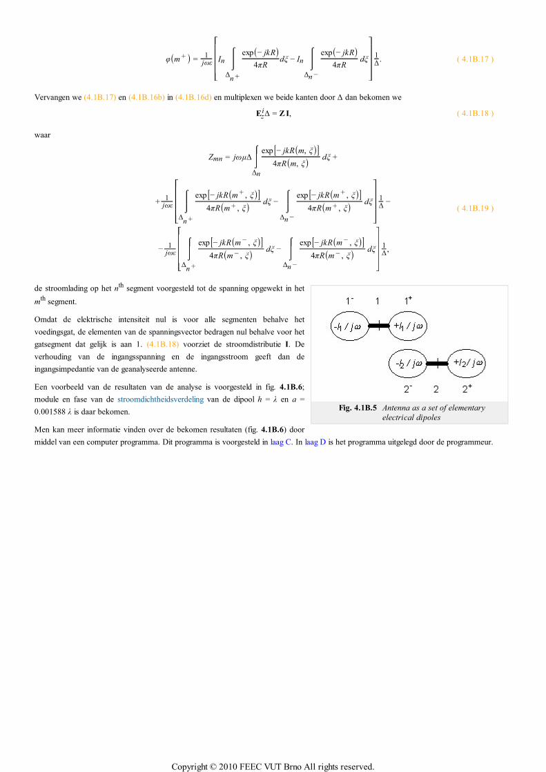
Fig. 4.1B.5 Antenna as a set of elementary
electrical dipoles
φ(m + ) =1
jωε
⎡
⎣
⎢⎢⎢⎢In
⌠⌡⎮⎮
∆n +
exp(− jkR)4πR
dξ − In⌠⌡⎮⎮
∆n −
exp(− jkR)4πR
dξ
⎤
⎦
⎥⎥⎥⎥1∆
. ( 4.1B.17 )
Vervangen we (4.1B.17) en (4.1B.16b) in (4.1B.16d) en multiplexen we beide kanten door ∆ dan bekomen we
Ezi∆ = ZI, ( 4.1B.18 )
waar
Zmn = jωµ∆⌠⌡⎮⎮∆n
exp[− jkR(m, ξ)]4πR(m, ξ) dξ +
+1
jωε
⎡
⎣
⎢⎢⎢⎢⌠⌡⎮⎮
∆n +
exp[− jkR(m + , ξ)]4πR(m + , ξ) dξ −
⌠⌡⎮⎮
∆n −
exp[− jkR(m + , ξ)]4πR(m + , ξ) dξ
⎤
⎦
⎥⎥⎥⎥1∆
−
−1
jωε
⎡
⎣
⎢⎢⎢⎢⌠⌡⎮⎮
∆n +
exp[− jkR(m − , ξ)]4πR(m − , ξ) dξ −
⌠⌡⎮⎮
∆n −
exp[− jkR(m − , ξ)]4πR(m − , ξ) dξ
⎤
⎦
⎥⎥⎥⎥1∆
,
( 4.1B.19 )
de stroomlading op het nth segment voorgesteld tot de spanning opgewekt in het
mth segment.
Omdat de elektrische intensiteit nul is voor alle segmenten behalve het
voedingsgat, de elementen van de spanningsvector bedragen nul behalve voor het
gatsegment dat gelijk is aan 1. (4.1B.18) voorziet de stroomdistributie I. De
verhouding van de ingangsspanning en de ingangsstroom geeft dan de
ingangsimpedantie van de geanalyseerde antenne.
Een voorbeeld van de resultaten van de analyse is voorgesteld in fig. 4.1B.6;
module en fase van de stroomdichtheidsverdeling van de dipool h = λ en a =
0.001588 λ is daar bekomen.
Men kan meer informatie vinden over de bekomen resultaten (fig. 4.1B.6) door
middel van een computer programma. Dit programma is voorgesteld in laag C. In laag D is het programma uitgelegd door de programmeur.
Copyright © 2010 FEEC VUT Brno All rights reserved.
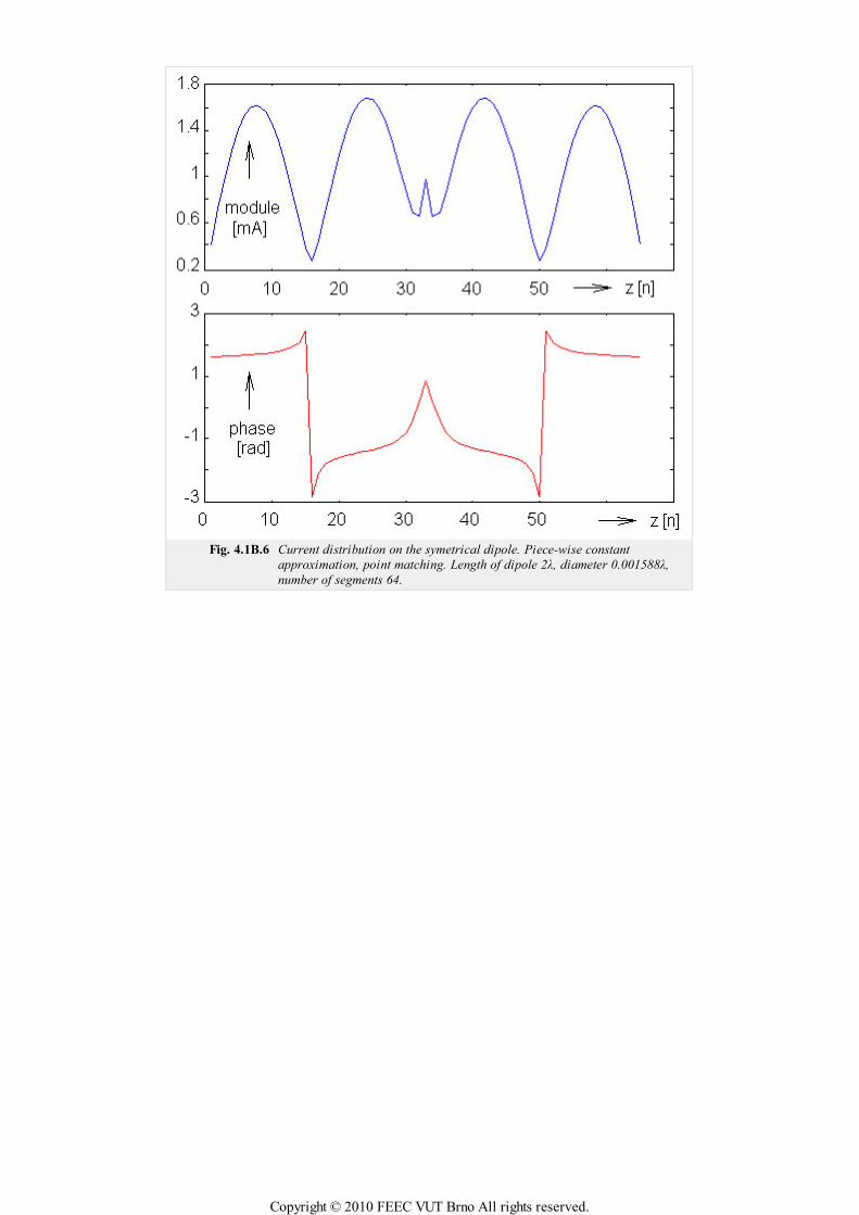
Fig. 4.1B.6 Current distribution on the symetrical dipole. Piece-wise constant
approximation, point matching. Length of dipole 2λ, diameter 0.001588λ,
number of segments 64.
Copyright © 2010 FEEC VUT Brno All rights reserved.

4.1 Wire dipole
Matlab program
The computer program, accompanying the paper about the moment analysis of a wire dipole is available here. The program is of very simple
user's interface. We run Matlab and set the path to the folder Dipol. In the command window, the basic m-file dipol.m has to be run and the
appearing form has to be filled in. In the form, we type the length of the dipole (related to wavelength) and the radius of the dipole (related to
wavelength). The program prints input impedance of the dipole. In two independent windows, current distribution on the antenna and directivity
pattern are plotted.
The program considers the fixed number of discretization segments (N = 33). The excitation gap is assumed in the middle of the wire.
Copyright © 2010 FEEC VUT Brno All rights reserved.

4.1 Wire dipole
Developing Matlab
The Matlab program for the analysis of wire antennas by the method of moments can be written relatively simply.
In the first step, the integral
ψ =⌠
⌡⎮⎮
∆
[exp(− jkR)4πR ] dξ ( 4.1D.1 )
is numerically evaluated for all the possible mutual distances between segments of the discretized antenna. In Matlab syntax:
alpha = 0.5*delta; % one half of the segment's length
psi = zeros( 1, N+1); % numerical integration
for m=1:(N+1)
x = (m-1)*delta;
psi(m) = quadl( 'green', -alpha, alpha, 1e-5, [], x, a, k);
end
psi = psi/delta;
In the above-given source code, quadl denotes the standard Matlab function, which performs numeric integration. Next, green is a string
corresponding to the name of the m-file, which contains the integrated function. Symbols -alpha and alpha denotes integration limits, 1e-5
is the allowed integration error, and z, a, k are parameters (z is the distance between the source segment and the observation one, a denotes
radius of the antenna wire and k is wave-number).
The integrated function is programmed by the following way:
function out = green(ksi, z, a, k)
R = sqrt( a^2 + (z-ksi)^2); % ksi ∈ (-∆/2; +∆/2)out = exp(-j*k*R)/(4*pi*R); % Green's function
When integrals for all the possible distances between segments are evaluated, the impedance matrix can be built:
for m = 1:A
for n = m:N
dist = abs(m-n); % distance between source and destination
hlp = 2*psi(1+dist) - psi(1+abs(dist-1)) - psi(1+abs(dist+1));
Z(m,n) = j*omega*mi*del*psi(1+dist) + hlp/(j*omega*epsilon*del);
Z(n,m) = Z(m,n); % matrix is symmetrical
end
end
In the above-given list, mi and epsilon are permeability and permittivity of vacuum, omega denotes angular frequency and j is imaginary
unit.
In the final step, the impedance matrix is inverted. The column of the inverted matrix, which corresponds to the excitation gap, directly provides
nodal values of the current distribution on the antenna.
Copyright © 2010 FEEC VUT Brno All rights reserved.

4.1 Wire dipole
Java applet
Copyright © 2010 FEEC VUT Brno All rights reserved.

4.1 Wire dipole
Quiz
Answer these questions to get feedback on how well you understand the course. Only one of the answers is correct. You don't have to answer
every question. If you don't know the answer you can just leave it blank (default option: “I won't answer this question”) and this won't affect
your score. Answering correctly will add 2 points to your score but on the other hand you'll lose 1 point if your answer is wrong. The
questions are divided in groups of five questions.
Press See result after you have finished answering.
Displaying questions 1..10 of 10:
Question 1
The wire dipole is an antenna, which can be characterized by the following statement:
Possible answers for question 1:
The antenna can be build from linear segments of an arbitrary radius.
The radius of the antenna wire is much smaller than the antenna length and the wavelength.
The antenna is built from an arbitrary copper wire.
I won't answer this question
Question 2
The moment method…
Possible answers for question 2:
… exploits time instants for evaluating Maxwell equations in the integral form.
… is a general numeric method for solving Maxwell equations.
… is a numeric technique for solving Maxwell equations in the integral form.
I won't answer this question
Question 3
Directivity pattern of the antenna …
Possible answers for question 3:
… gives magnitude of field intensity of the radiated wave for all the angles in the specified plane.
… describes geometry of a wire antenna (directions to which antenna wires are oriented).
… gives an information about polarization of the radiated wave.
I won't answer this question
Question 4
Input impedance of the antenna …
Possible answers for question 4:
… is an impedance at the input of an antenna amplifier (if no amplifier is connected to the antenna, then the input impedance is zero).
… is an impedance, which can be measured on input terminals of the antenna.
… does not depend on the power radiated by the antenna.
I won't answer this question
Question 5
Basis functions …
Copyright © 2010 FEEC VUT Brno All rights reserved.

Possible answers for question 5:
… describe the location (the basis) of the antenna.
… are used for the approximation of current distribution in selected points along the antenna wire.
… are used for the approximation of current distribution in all the points along the antenna wire.
I won't answer this question
Question 6
Method of weighted residua …
Possible answers for question 6:
… is used for minimizing the difference between the numeric solution of Maxwell equations and the exact field distribution.
… is exploited for matching a wire antenna (minimizing residual reflections on a feeder).
… is a special case of Galerkin method.
I won't answer this question
Question 7
Impedance matrix in the moment analysis of the antenna …
Possible answers for question 7:
… consists of input impedances of the antenna for different radii (rows) and different lengths (columns).
… contains self-impedances of antenna segments on the diagonal and mutual impedances of segments out of the diagonal.
… consists of input impedances for different time instants and different directions of arrival of the incident wave.
I won't answer this question
Question 8
Sidelobes appear in the directivity pattern of the symmetric dipole if the antenna length …
Possible answers for question 8:
… l > 1.2 λ, λ denotes wavelength.
… 0.6 λ ≤ l ≤ 0.7 λ, λ denotes wavelength.
… l ≤ 0.5 λ, λ denotes wavelength.
I won't answer this question
Question 9
Input impedance of the symmetric dipole is purely real (the radius a = 10-3
λ and λ denotes wavelength, the number of
discretization segments N = 33) …
Possible answers for question 9:
… for l = 0.485 λ.
… for l = 0.462 λ.
… for l = 0.473 λ.
I won't answer this question
Question 10
If the number of discretization segments in the moment analysis of a wire antenna is increased then …
Copyright © 2010 FEEC VUT Brno All rights reserved.

Possible answers for question 10:
… accuracy of results decreases.
… accuracy of results raises.
… accuracy of results is not influenced.
I won't answer this question
Copyright © 2010 FEEC VUT Brno All rights reserved.
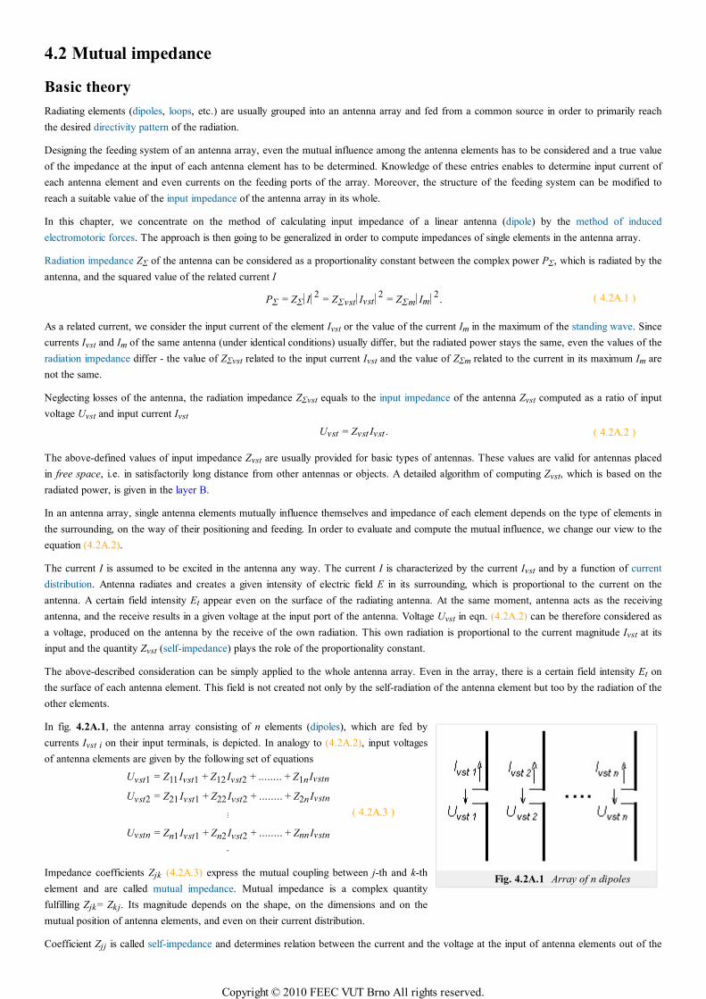
Fig. 4.2A.1 Array of n dipoles
4.2 Mutual impedance
Basic theory
Radiating elements (dipoles, loops, etc.) are usually grouped into an antenna array and fed from a common source in order to primarily reach
the desired directivity pattern of the radiation.
Designing the feeding system of an antenna array, even the mutual influence among the antenna elements has to be considered and a true value
of the impedance at the input of each antenna element has to be determined. Knowledge of these entries enables to determine input current of
each antenna element and even currents on the feeding ports of the array. Moreover, the structure of the feeding system can be modified to
reach a suitable value of the input impedance of the antenna array in its whole.
In this chapter, we concentrate on the method of calculating input impedance of a linear antenna (dipole) by the method of induced
electromotoric forces. The approach is then going to be generalized in order to compute impedances of single elements in the antenna array.
Radiation impedance ZΣ of the antenna can be considered as a proportionality constant between the complex power PΣ, which is radiated by the
antenna, and the squared value of the related current I
PΣ = ZΣ||I ||
2= ZΣvst
||Ivst ||2
= ZΣm||Im ||
2. ( 4.2A.1 )
As a related current, we consider the input current of the element Ivst or the value of the current Im in the maximum of the standing wave. Since
currents Ivst and Im of the same antenna (under identical conditions) usually differ, but the radiated power stays the same, even the values of the
radiation impedance differ - the value of ZΣvst related to the input current Ivst and the value of ZΣm related to the current in its maximum Im are
not the same.
Neglecting losses of the antenna, the radiation impedance ZΣvst equals to the input impedance of the antenna Zvst computed as a ratio of input
voltage Uvst and input current Ivst
Uvst = Zvst Ivst . ( 4.2A.2 )
The above-defined values of input impedance Zvst are usually provided for basic types of antennas. These values are valid for antennas placed
in free space, i.e. in satisfactorily long distance from other antennas or objects. A detailed algorithm of computing Zvst, which is based on the
radiated power, is given in the layer B.
In an antenna array, single antenna elements mutually influence themselves and impedance of each element depends on the type of elements in
the surrounding, on the way of their positioning and feeding. In order to evaluate and compute the mutual influence, we change our view to the
equation (4.2A.2).
The current I is assumed to be excited in the antenna any way. The current I is characterized by the current Ivst and by a function of current
distribution. Antenna radiates and creates a given intensity of electric field E in its surrounding, which is proportional to the current on the
antenna. A certain field intensity Et appear even on the surface of the radiating antenna. At the same moment, antenna acts as the receiving
antenna, and the receive results in a given voltage at the input port of the antenna. Voltage Uvst in eqn. (4.2A.2) can be therefore considered as
a voltage, produced on the antenna by the receive of the own radiation. This own radiation is proportional to the current magnitude Ivst at its
input and the quantity Zvst (self-impedance) plays the role of the proportionality constant.
The above-described consideration can be simply applied to the whole antenna array. Even in the array, there is a certain field intensity Et on
the surface of each antenna element. This field is not created not only by the self-radiation of the antenna element but too by the radiation of the
other elements.
In fig. 4.2A.1, the antenna array consisting of n elements (dipoles), which are fed by
currents Ivst i on their input terminals, is depicted. In analogy to (4.2A.2), input voltages
of antenna elements are given by the following set of equations
Uvst1 = Z11 Ivst1 + Z12 Ivst2 + ........ + Z1n Ivstn
Uvst2 = Z21 Ivst1 + Z22 Ivst2 + ........ + Z2n Ivstn
⋮
Uvstn = Zn1 Ivst1 + Zn2 Ivst2 + ........ + Znn Ivstn
.
( 4.2A.3 )
Impedance coefficients Zjk (4.2A.3) express the mutual coupling between j-th and k-th
element and are called mutual impedance. Mutual impedance is a complex quantity
fulfilling Zjk= Zkj. Its magnitude depends on the shape, on the dimensions and on the
mutual position of antenna elements, and even on their current distribution.
Coefficient Zjj is called self-impedance and determines relation between the current and the voltage at the input of antenna elements out of the
Copyright © 2010 FEEC VUT Brno All rights reserved.
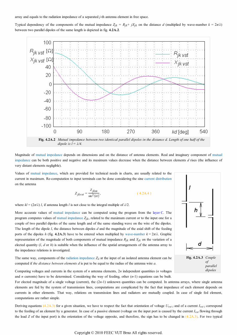
Fig. 4.2A.3 Couple
of
parallel
dipoles
array and equals to the radiation impedance of a separated j-th antenna element in free space.
Typical dependency of the components of the mutual impedance Zjk = Rjk+ jXjk on the distance d (multiplied by wave-number k = 2π/λ)
between two parallel dipoles of the same length is depicted in fig. 4.2A.2.
Fig. 4.2A.2 Mutual impedance between two identical parallel dipoles in the distance d. Length of one half of the
dipole is l = λ/4.
Magnitude of mutual impedance depends on dimensions and on the distance of antenna elements. Real and imaginary component of mutual
impedance can be both positive and negative and its maximum values decrease when the distance between elements d rises (the influence of
very distant elements negligible).
Values of mutual impedance, which are provided for technical needs in charts, are usually related to the
current in maximum. Re-computation to input terminals can be done considering the sine current distribution
on the antenna
Z jkvst =Z jkm
sin2(kl), ( 4.2A.4 )
where kl = (2π/λ) l, if antenna length l is not close to the integral multiple of λ/2.
More accurate values of mutual impedance can be computed using the program from the layer C. The
program computes values of mutual impedance Zjk, related to the maximum current or to the input one for a
couple of two parallel dipoles of the same length and of the same standing wave on the wire of the dipoles.
The length of the dipole l, the distance between dipoles d and the magnitude of the axial shift of the feeding
ports of the dipoles h (fig. 4.2A.3) have to be entered when multiplied by wave-number k = 2π/λ. Graphic
representation of the magnitude of both components of mutual impedance Rjk and Xjk on the variation of a
elected quantity (l, d or h) is suitable when the influence of the spatial arrangements of the antenna array to
the impedance relations is investigated.
The same way, components of the radiation impedance Zii at the input of an isolated antenna element can be
computed if the distance between elements d is put to be equal to the radius of the antenna wire a.
Computing voltages and currents in the system of n antenna elements, 2n independent quantities (n voltages
and n currents) have to be determined. Considering the way of feeding, other (n-1) equations can be built.
For elected magnitude of a single voltage (current), the (2n-1) unknown quantities can be computed. In antenna arrays, where single antenna
elements are fed by the system of transmission lines, computations are complicated by the fact that impedance of each element depends on
currents in other elements. That way, relations on transmission lines and radiators are mutually coupled. In case of single fed element,
computations are rather simple.
Deriving equations (4.2A.3) for a given situation, we have to respect the fact that orientation of voltage Uvst i and of a current Ivst i correspond
to the feeding of an element by a generator. In case of a passive element (voltage on the input port is caused by the current Ivst flowing through
the load Z of the input port) is the orientation of the voltage opposite, and therefore, the sign has to be changed in (4.2A.3). For two typical
Copyright © 2010 FEEC VUT Brno All rights reserved.
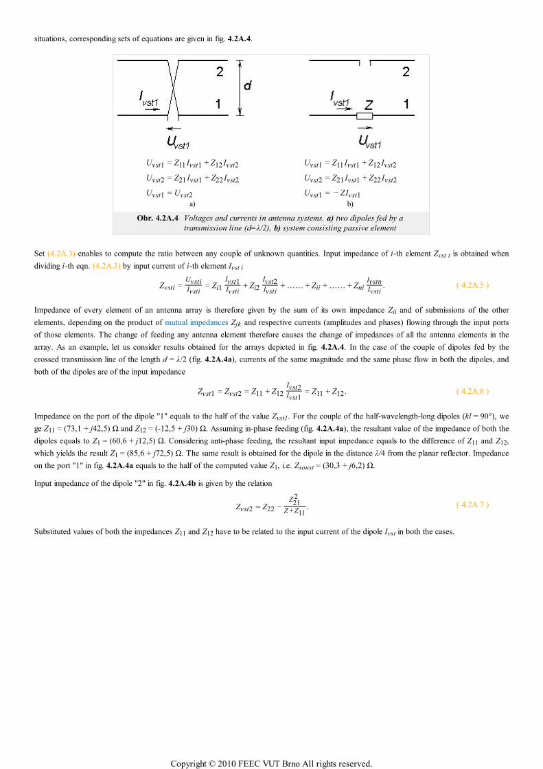
situations, corresponding sets of equations are given in fig. 4.2A.4.
Uvst1 = Z11 Ivst1 + Z12 Ivst2
Uvst2 = Z21 Ivst1 + Z22 Ivst2
Uvst1 = Uvst2
a)
Uvst1 = Z11 Ivst1 + Z12 Ivst2
Uvst2 = Z21 Ivst1 + Z22 Ivst2
Uvst1 = − ZIvst1
b)
Obr. 4.2A.4 Voltages and currents in antenna systems. a) two dipoles fed by a
transmission line (d=λ/2), b) system consisting passive element
Set (4.2A.3) enables to compute the ratio between any couple of unknown quantities. Input impedance of i-th element Zvst i is obtained when
dividing i-th eqn. (4.2A.3) by input current of i-th element Ivst i
Zvsti =UvstiIvsti
= Zi1
Ivst1Ivsti
+ Zi2
Ivst2Ivsti
+ …… + Zii + …… + ZniIvstnIvsti
. ( 4.2A.5 )
Impedance of every element of an antenna array is therefore given by the sum of its own impedance Zii and of submissions of the other
elements, depending on the product of mutual impedances Zjk and respective currents (amplitudes and phases) flowing through the input ports
of those elements. The change of feeding any antenna element therefore causes the change of impedances of all the antenna elements in the
array. As an example, let us consider results obtained for the arrays depicted in fig. 4.2A.4. In the case of the couple of dipoles fed by the
crossed transmission line of the length d = λ/2 (fig. 4.2A.4a), currents of the same magnitude and the same phase flow in both the dipoles, and
both of the dipoles are of the input impedance
Zvst1 = Zvst2 = Z11 + Z12
Ivst2Ivst1
= Z11 + Z12. ( 4.2A.6 )
Impedance on the port of the dipole "1" equals to the half of the value Zvst1. For the couple of the half-wavelength-long dipoles (kl = 90°), we
ge Z11 = (73,1 + j42,5) Ω and Z12 = (-12,5 + j30) Ω. Assuming in-phase feeding (fig. 4.2A.4a), the resultant value of the impedance of both the
dipoles equals to Z1 = (60,6 + j12,5) Ω. Considering anti-phase feeding, the resultant input impedance equals to the difference of Z11 and Z12,
which yields the result Z1 = (85,6 + j72,5) Ω. The same result is obtained for the dipole in the distance λ/4 from the planar reflector. Impedance
on the port "1" in fig. 4.2A.4a equals to the half of the computed value Z1, i.e. Zsoust = (30,3 + j6,2) Ω.
Input impedance of the dipole "2" in fig. 4.2A.4b is given by the relation
Zvst2 = Z22 −Z
212
Z +Z11. ( 4.2A.7 )
Substituted values of both the impedances Z11 and Z12 have to be related to the input current of the dipole Ivst in both the cases.
Copyright © 2010 FEEC VUT Brno All rights reserved.
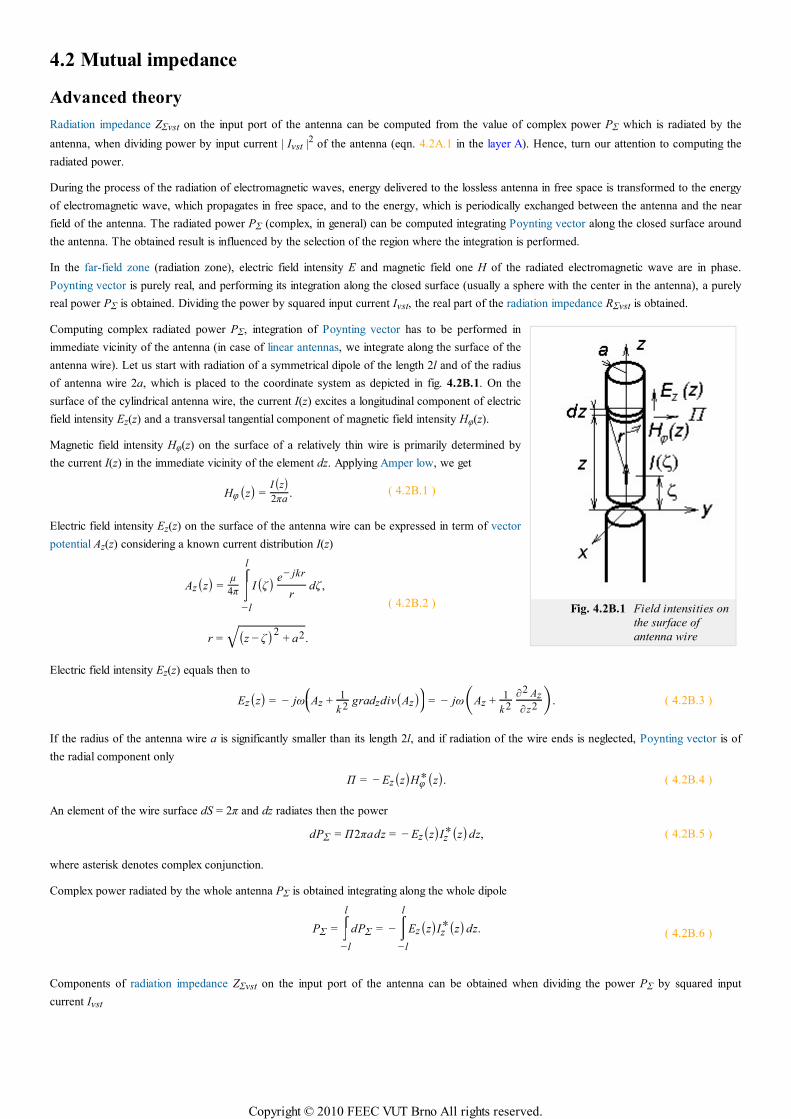
Fig. 4.2B.1 Field intensities on
the surface of
antenna wire
4.2 Mutual impedance
Advanced theory
Radiation impedance ZΣvst on the input port of the antenna can be computed from the value of complex power PΣ which is radiated by the
antenna, when dividing power by input current | Ivst |2 of the antenna (eqn. 4.2A.1 in the layer A). Hence, turn our attention to computing the
radiated power.
During the process of the radiation of electromagnetic waves, energy delivered to the lossless antenna in free space is transformed to the energy
of electromagnetic wave, which propagates in free space, and to the energy, which is periodically exchanged between the antenna and the near
field of the antenna. The radiated power PΣ (complex, in general) can be computed integrating Poynting vector along the closed surface around
the antenna. The obtained result is influenced by the selection of the region where the integration is performed.
In the far-field zone (radiation zone), electric field intensity E and magnetic field one H of the radiated electromagnetic wave are in phase.
Poynting vector is purely real, and performing its integration along the closed surface (usually a sphere with the center in the antenna), a purely
real power PΣ is obtained. Dividing the power by squared input current Ivst, the real part of the radiation impedance RΣvst is obtained.
Computing complex radiated power PΣ, integration of Poynting vector has to be performed in
immediate vicinity of the antenna (in case of linear antennas, we integrate along the surface of the
antenna wire). Let us start with radiation of a symmetrical dipole of the length 2l and of the radius
of antenna wire 2a, which is placed to the coordinate system as depicted in fig. 4.2B.1. On the
surface of the cylindrical antenna wire, the current I(z) excites a longitudinal component of electric
field intensity Ez(z) and a transversal tangential component of magnetic field intensity Hφ(z).
Magnetic field intensity Hφ(z) on the surface of a relatively thin wire is primarily determined by
the current I(z) in the immediate vicinity of the element dz. Applying Amper low, we get
Hφ(z) =I(z)2πa
. ( 4.2B.1 )
Electric field intensity Ez(z) on the surface of the antenna wire can be expressed in term of vector
potential Az(z) considering a known current distribution I(z)
Az(z) =µ
4π
⌠⌡⎮− l
l
I(ζ ) e− jkr
rdζ ,
r = (z − ζ )2+ a2√ .
( 4.2B.2 )
Electric field intensity Ez(z) equals then to
Ez(z) = − jω⎛⎝⎜Az +
1
k 2gradzdiv(Az)⎞
⎠⎟ = − jω(Az +1
k 2
∂2 Az
∂ z2 ). ( 4.2B.3 )
If the radius of the antenna wire a is significantly smaller than its length 2l, and if radiation of the wire ends is neglected, Poynting vector is of
the radial component only
Π = − Ez(z)Hφ∗(z). ( 4.2B.4 )
An element of the wire surface dS = 2π and dz radiates then the power
dPΣ = Π2πa dz = − Ez(z)Iz∗(z) dz, ( 4.2B.5 )
where asterisk denotes complex conjunction.
Complex power radiated by the whole antenna PΣ is obtained integrating along the whole dipole
PΣ = ⌠⌡−l
l
dPΣ = − ⌠⌡− l
l
Ez(z)Iz∗(z) dz. ( 4.2B.6 )
Components of radiation impedance ZΣvst on the input port of the antenna can be obtained when dividing the power PΣ by squared input
current Ivst
Copyright © 2010 FEEC VUT Brno All rights reserved.
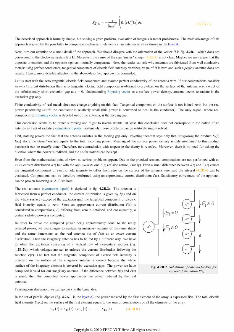
Fig. 4.2B.2 Substition of antenna feeding for
current distribution I'(z)
ZΣvst = −1
||Ivst ||2
⌠⌡− l
l
Ez(z)I1∗(z) dz. ( 4.2B.7 )
The described approach is formally simple, but solving a given problem, evaluation of integrals is rather problematic. The main advantage of this
approach is given by the possibility to compute impedances of elements in an antenna array as shown in the layer A.
Now, turn our attention to a small detail of the approach. We should disagree with the orientation of the vector Π in fig. 4.2B.1, which does not
correspond to the clockwise system E x H. Moreover, the cause of the sign "minus" in eqn. (4.2B.4) is not clear. Maybe, we may argue that the
opposite orientation and the opposite sign can mutually compensate. Next, the reader can ask why antennas are fabricated from well-conductive
metals: using perfect conductors, tangential component of electric field intensity vanishes, value of Π is zero and such a perfect antenna does not
radiate. Hence, more detailed attention to the above-described approach is demanded.
Let us start with the zero tangential electric field component and assume perfect conductivity of the antenna wire. If our computations consider
an exact current distribution then zero tangential electric field component is obtained everywhere on the surface of the antenna wire except of
the infinitesimally short excitation gap at z = 0. Understanding Poynting vector as a surface power density, antenna seems to radiate in the
excitation gap only.
Finite conductivity of real metals does not change anything on this fact. Tangential component on the surface is not indeed zero, but the real
power penetrating inside the conductor is relatively small (this power is converted to heat in the conductor). The only region, where real
component of Poynting vector is directed out of the antenna, is the feeding gap.
This conclusion seems to be rather surprising and might to invoke doubts. At least, this conclusion does not correspond to the notion of an
antenna as a set of radiating elementary dipoles. Fortunately, these problems can be relatively simply solved.
First, nothing proves the fact that the antenna radiates in the feeding gap only. Poynting theorem says only that integrating the product Et(z)
H(z) along the closed surface equals to the total incoming power. Meaning of the surface power density is only attributed to this product
because it can be usually done. Therefore, no contradiction with respect to the theory is revealed. Moreover, there is no need for asking the
question where the power is radiated, and the so-far notions can be kept.
Even from the mathematical point of view, no serious problems appear. Due to the practical reasons, computations are not performed with an
exact current distribution I(z) but with the approximate one I'(z) (of sine nature, usually). Even a small difference between I(z) and I '(z) causes
the tangential component of electric field intensity to differ from zero on the surface of the antenna wire, and the integral (4.2B.6) can be
evaluated. Computations can be therefore performed using an approximate current distribution I'(z). Satisfactory correctness of the approach
can be proven following A. A. Pistolkors:
The real antenna (symmetric dipole) is depicted in fig. 4.2B.2a. The antenna is
fabricated from a perfect conductor, the current distribution is given by I(z) and on
the whole surface (except of the excitation gap) the tangential component of electric
field intensity equals to zero. Since an approximate current distribution I'(z) is
considered in computations, Et differing from zero is obtained, and consequently, a
certain radiated power is computed.
In order to prove the computed power being approximately equal to the really
radiated power, we can imagine to analyze an imaginary antenna of the same shape
and the same dimensions as the real antenna but of I'(z) as an exact current
distribution. Then the imaginary antenna has to be fed by a different way. We have
to admit the excitation consisting of a vertical row of elementary sources (fig.
4.2B.2b), which voltages are set to enforce the current distribution following the
function I'(z). The fact that the tangential component of electric field intensity is
non-zero on the surface of the imaginary antenna is correct because the whole
surface of the imaginary antenna is covered by excitation gaps. The power we have
computed is valid for our imaginary antenna. If the difference between I(z) and I'(z)
is small, then the computed power approaches the power radiated by the real
antenna.
Finishing our discussion, we can go back to the basic idea.
In the set of parallel dipoles (fig. 4.2A.1 in the layer A), the power radiated by the first element of the array is expressed first. The total electric
field intensity Ez1(z) on the surface of the first element equals to the sum of contributions of all the elements of the array
Ez1(z) = E11(z) + E12(z) + …… + E1n(z). ( 4.2B.8 )
Copyright © 2010 FEEC VUT Brno All rights reserved.

Power PΣ1 radiated by the first element is obtained when substituting to eqn. (4.2B.6). Formal rearrangement yields the relation
PΣ1 = − ⌠⌡− l
l
[E11(z)I1∗(z) + E12(z)I1
∗(z) + …… + E1n(z)I1∗(z)] dz =
= Ivst1∗
⎡
⎣
⎢⎢⎢− Ivst1⌠⌡⎮⎮−l
l
E11(z)Ivst1
I1∗(z)
I1vst∗ dz − Ivst2
⌠⌡⎮⎮−l
l
E12(z)Ivst2
I1∗(z)
I1vst∗ dz − …… − Ivstn
⌠⌡⎮⎮− l
l
E1n(z)Ivstn
I1∗(z)
I1vst∗ dz
⎤
⎦
⎥⎥⎥
.
( 4.2B.9 )
Integrals
Z jk =⌠⌡⎮⎮−l
l
E jk (z)Ivstk
Ij∗(z)
Ivst j∗ ( 4.2B.10 )
are called mutual impedances and are given in Ohms. Thanks to the formal rearrangement, integrals (4.2B.10) do not depend on the magnitudes
of currents in antenna elements because the field intensity Ejk excited on the surface of j-th element by the radiation of k-th element is
proportional to the current Ivst k in k-th element of the antenna array.
For parallel dipoles, results of the integration in (4.2B.10) are expressed in the form of tabulated functions (integral sine, integral cosine). In
order to get numerical values of mutual impedance components Zjk, computer program described in the layer C can be used. Results describe
coupling between the couple of parallel dipoles of the same length 2l, which is related to the maximal current Imax. Values Zjk vst, which are
related to the input current of the dipole, are obtained performing re-computing according to eqn. (4.2A.4) in the layer A.
Dependency of the magnitude of the components of mutual impedance on the distance between dipoles was already demonstrated in the layer A
(fig. 4.2A.2) for the couple of parallel symmetric dipoles with a standing current way. Negative values of the mutual impedances Rjk and Xjk
express the fact that for a given spatial arrangement, radiation of k-th element reduces the magnitude of real or imaginary part of the power PΣj
which is radiated by j-th element of the antenna array. Decreasing magnitude of mutual impedance for long distances corresponds to the
decrease of the electric field intensity Ejk for increasing distance.
Exploiting eqn. (4.2B.10), self-impedance of a stand-alone antenna element Zjj can be computed if the distance between elements d is set to the
value of the radius of the antenna wire a. This approach corresponds to the situation described when deriving eqn. (4.2B.7): we considered
electric field intensity on he surface of j-th antenna wire Ejj excited by a current flowing through the axis of the same wire.
The method of induced electromotoric forces enables to compute the radiated power, and consequently the values of mutual impedances even
in the case of non-parallel antenna wires. Then, we have to respect a different spatial orientation of vectors of electric field intensity Ejk with
respect to the surface of j-th antenna wire. Decomposing vector Ejk to respective components and exploiting more general expression for the
power contribution dPΣ, we obtain formally more complicated relations. That way, coupling between crossed wires of a turnstile antenna and
further situations can be solved.
Copyright © 2010 FEEC VUT Brno All rights reserved.

4.2 Mutual impedance
Matlab program
The program computes real and imaginary part of the mutual impedance of antennas depending on the length of the dipole l, on the shift
between the centers of the dipoles h and on the distance of the dipole axes d. Parameters are entered to the program multiplied by the
wave-number, i.e. as kl, kh and kd.
First the path of Matlab has to be redirected to the folder Impedance. The program is run calling the m-file vzimp.m. Leaving the
introductory window, which brings the basic information about the program and which serves for the selection of a chart to be displayed (which
variable is going to vary), values of kl, kh and kd have to be entered. The type of entered parameters depends on the setting in the introductory
window (which chart is going to be displayed and which variable is going to vary). For the varying variable, its minimum value and its maximum
one have to be given. Pushing the button Compute (if one of values is swept), a new window is opened, where the course of the real part and
the imaginary one of the mutual impedance is depicted with respect to the selected varying parameter.
The button Exit serves for finishing the program and the button Back can be used for a new run of the program.
Copyright © 2010 FEEC VUT Brno All rights reserved.
4.2 Mutual impedance
Developing Matlab
Following relations can be derived for computing mutual impedance Z12 of two dipoles. Real part of the mutual impedance R12 is given by:
R12 = 15(K1 sin q + L1 cos q) + [K2 sin(q + 2p) + L2 cos(q + 2p)] + [K3 sin(q − 2p) + L3 cos(q − 2p)]. ( 4.2D.1 )
Imaginary part of the mutual impedance X12 can be expressed as:
X12 = 15(M1 sin q + N1 cos q) + [M2 sin(q + 2p) + N2 cos(q + 2p)] + [M3 sin(q − 2p) + N3 cos(q − 2p)], ( 4.2D.2 )
where
K1 = 2[2 f2(δ, q) − f2(δ, q + p) − f2(δ, q − p)]L1 = 2[2 f3(δ, q) − f3(δ, q + p) − f3(δ, q − p)]K2 = f2(δ, q) − 2 f2(δ, q + p) + f2(δ, q + 2p)L2 = f3(δ, q) − 2 f3(δ, q + p) + f3(δ, q + 2p)K3 = f2(δ, q) − 2 f2(δ, q − p) + f2(δ, q − 2p)L3 = f3(δ, q) − 2 f3(δ, q − p) + f3(δ, q − 2p)M1 = 2[2 f4(δ, q) − f4(δ, q + p) − f4(δ, q − p)]N1 = − 2[2 f1(δ, q) − f1(δ, q + p) − f1(δ, q − p)]M2 = f4(δ, q) − 2 f4(δ, q + p) + f4(δ, q + 2p)N2 = − f1(δ, q) + 2 f1(δ, q + p) − f4(δ, q + 2p)M3 = f4(δ, q) − 2 f4(δ, q − p) + f4(δ, q − 2p)N3 = − f1(δ, q) + 2 f1(δ, q − p) − f3(δ, q − 2p)
⎫
⎬
⎭
⎪⎪⎪⎪⎪⎪⎪⎪⎪⎪⎪⎪⎪⎪⎪⎪⎪⎪⎪⎪⎪⎪⎪⎪⎪⎪
. ( 4.2D.3 )
In these relations, variables given by the user p, q, δ are present:
p = kl q = kh δ = kd. ( 4.2D.4 )
Finally, we have to define the following functions:
f1(δ, u) = sin⎛⎝⎜ u2 + δ2√ + u
⎞⎠⎟ + sin
⎛⎝⎜ u2 + δ2√ − u
⎞⎠⎟
f2(δ, u) = sin⎛⎝⎜ u2 + δ2√ + u
⎞⎠⎟ − sin
⎛⎝⎜ u2 + δ2√ − u
⎞⎠⎟
f3(δ, u) = cos⎛⎝⎜ u2 + δ2√ + u
⎞⎠⎟ + cos
⎛⎝⎜ u2 + δ2√ − u
⎞⎠⎟
f4(δ, u) = cos⎛⎝⎜ u2 + δ2√ + u
⎞⎠⎟ − cos
⎛⎝⎜ u2 + δ2√ − u
⎞⎠⎟
⎫
⎬
⎭
⎪⎪⎪⎪⎪⎪⎪⎪⎪⎪
. ( 4.2D.5 )
Here, u is a parameter, which changes according to the variable, which is used in our relations.
The above-given relations are programmed. We do not present here the transcription into the Matlab syntax due to the worse readability. In the
program one of the parameters kl, kh or kd vary.
Copyright © 2010 FEEC VUT Brno All rights reserved.

4.2 Mutual impedance
Java applet
Copyright © 2010 FEEC VUT Brno All rights reserved.

4.2 Mutual impedance
Quiz
Answer these questions to get feedback on how well you understand the course. Only one of the answers is correct. You don't have to answer
every question. If you don't know the answer you can just leave it blank (default option: “I won't answer this question”) and this won't affect
your score. Answering correctly will add 2 points to your score but on the other hand you'll lose 1 point if your answer is wrong. The
questions are divided in groups of five questions.
Press See result after you have finished answering.
Displaying questions 1..5 of 5:
Question 1
Mutual impedance between two dipoles …
Possible answers for question 1:
… is the difference between input impedances of those two dipoles.
… quantifies the contribution of the current on the first dipole to the voltage induced on the second dipole.
… can be neglected in practical computations.
I won't answer this question
Question 2
Mutual impedance between two dipoles depends on …
Possible answers for question 2:
… the distance of those two dipoles and the wavelength.
… the distance, but is independent on the wavelength.
… the distance and the input impedance of the dipoles.
I won't answer this question
Question 3
Input impedance of the dipole in the array is influenced by …
Possible answers for question 3:
… input impedances of neighboring dipoles and their currents.
… mutual impedances of neighboring dipoles and their currents.
… the linear combination if input impedances and mutual ones.
I won't answer this question
Question 4
Mutual impedance between the first dipole and the second one …
Possible answers for question 4:
… can equal (under special conditions) to the mutual impedance between the second dipole and the first one.
… can never equal to the mutual impedance between the second dipole and the first one.
… equals any time to the mutual impedance between the second dipole and the first one.
I won't answer this question
Question 5
The method of electromagnetic forces can be applied …
Copyright © 2010 FEEC VUT Brno All rights reserved.

Possible answers for question 5:
… when dipoles are parallel.
… to an arbitrary array consisting of arbitrary antennas.
… to the array of arbitrarily oriented dipoles.
I won't answer this question
Copyright © 2010 FEEC VUT Brno All rights reserved.
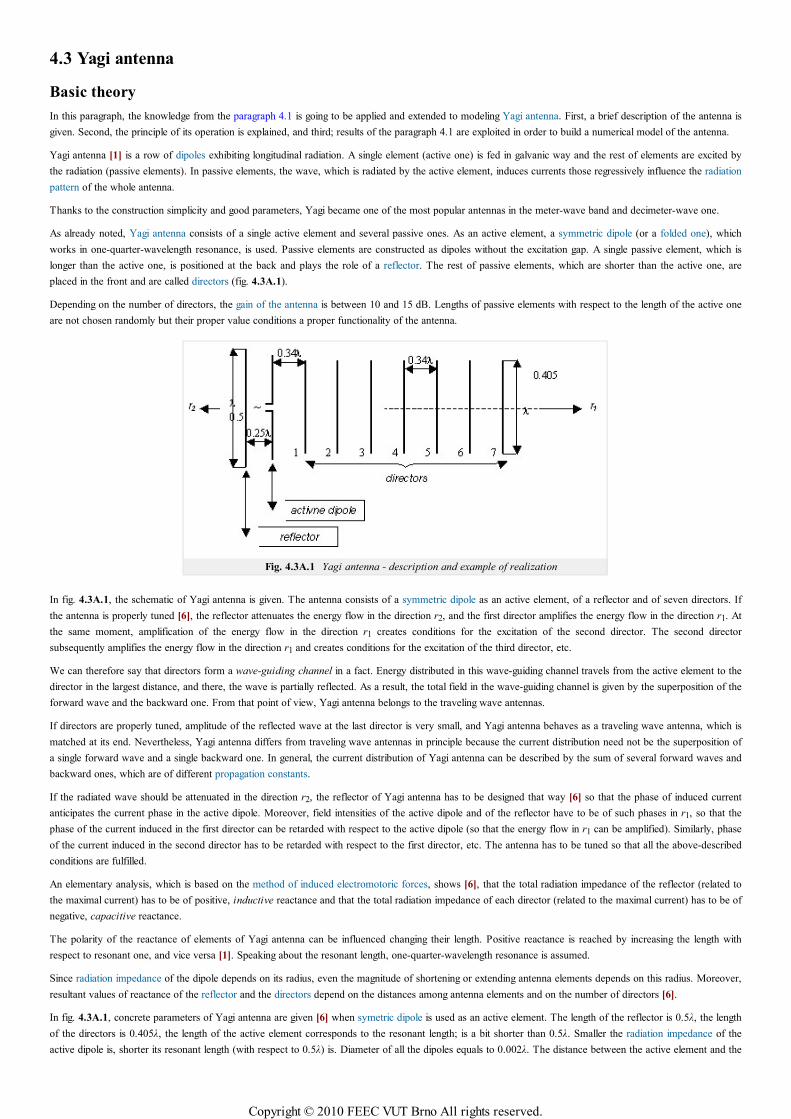
4.3 Yagi antenna
Basic theory
In this paragraph, the knowledge from the paragraph 4.1 is going to be applied and extended to modeling Yagi antenna. First, a brief description of the antenna is
given. Second, the principle of its operation is explained, and third; results of the paragraph 4.1 are exploited in order to build a numerical model of the antenna.
Yagi antenna [1] is a row of dipoles exhibiting longitudinal radiation. A single element (active one) is fed in galvanic way and the rest of elements are excited by
the radiation (passive elements). In passive elements, the wave, which is radiated by the active element, induces currents those regressively influence the radiation
pattern of the whole antenna.
Thanks to the construction simplicity and good parameters, Yagi became one of the most popular antennas in the meter-wave band and decimeter-wave one.
As already noted, Yagi antenna consists of a single active element and several passive ones. As an active element, a symmetric dipole (or a folded one), which
works in one-quarter-wavelength resonance, is used. Passive elements are constructed as dipoles without the excitation gap. A single passive element, which is
longer than the active one, is positioned at the back and plays the role of a reflector. The rest of passive elements, which are shorter than the active one, are
placed in the front and are called directors (fig. 4.3A.1).
Depending on the number of directors, the gain of the antenna is between 10 and 15 dB. Lengths of passive elements with respect to the length of the active one
are not chosen randomly but their proper value conditions a proper functionality of the antenna.
Fig. 4.3A.1 Yagi antenna - description and example of realization
In fig. 4.3A.1, the schematic of Yagi antenna is given. The antenna consists of a symmetric dipole as an active element, of a reflector and of seven directors. If
the antenna is properly tuned [6], the reflector attenuates the energy flow in the direction r2, and the first director amplifies the energy flow in the direction r1. At
the same moment, amplification of the energy flow in the direction r1 creates conditions for the excitation of the second director. The second director
subsequently amplifies the energy flow in the direction r1 and creates conditions for the excitation of the third director, etc.
We can therefore say that directors form a wave-guiding channel in a fact. Energy distributed in this wave-guiding channel travels from the active element to the
director in the largest distance, and there, the wave is partially reflected. As a result, the total field in the wave-guiding channel is given by the superposition of the
forward wave and the backward one. From that point of view, Yagi antenna belongs to the traveling wave antennas.
If directors are properly tuned, amplitude of the reflected wave at the last director is very small, and Yagi antenna behaves as a traveling wave antenna, which is
matched at its end. Nevertheless, Yagi antenna differs from traveling wave antennas in principle because the current distribution need not be the superposition of
a single forward wave and a single backward one. In general, the current distribution of Yagi antenna can be described by the sum of several forward waves and
backward ones, which are of different propagation constants.
If the radiated wave should be attenuated in the direction r2, the reflector of Yagi antenna has to be designed that way [6] so that the phase of induced current
anticipates the current phase in the active dipole. Moreover, field intensities of the active dipole and of the reflector have to be of such phases in r1, so that the
phase of the current induced in the first director can be retarded with respect to the active dipole (so that the energy flow in r1 can be amplified). Similarly, phase
of the current induced in the second director has to be retarded with respect to the first director, etc. The antenna has to be tuned so that all the above-described
conditions are fulfilled.
An elementary analysis, which is based on the method of induced electromotoric forces, shows [6], that the total radiation impedance of the reflector (related to
the maximal current) has to be of positive, inductive reactance and that the total radiation impedance of each director (related to the maximal current) has to be of
negative, capacitive reactance.
The polarity of the reactance of elements of Yagi antenna can be influenced changing their length. Positive reactance is reached by increasing the length with
respect to resonant one, and vice versa [1]. Speaking about the resonant length, one-quarter-wavelength resonance is assumed.
Since radiation impedance of the dipole depends on its radius, even the magnitude of shortening or extending antenna elements depends on this radius. Moreover,
resultant values of reactance of the reflector and the directors depend on the distances among antenna elements and on the number of directors [6].
In fig. 4.3A.1, concrete parameters of Yagi antenna are given [6] when symetric dipole is used as an active element. The length of the reflector is 0.5λ, the length
of the directors is 0.405λ, the length of the active element corresponds to the resonant length; is a bit shorter than 0.5λ. Smaller the radiation impedance of the
active dipole is, shorter its resonant length (with respect to 0.5λ) is. Diameter of all the dipoles equals to 0.002λ. The distance between the active element and the
Copyright © 2010 FEEC VUT Brno All rights reserved.

reflector equals to 0.25λ, the distance between the active element and the first director is 0.34λ, and the distance among directors equals to 0.34λ.
Yagi antenna is very popular these days. There are many technical realizations of this antenna, which differ in the number of directors, distances among antenna
elements and lengths of those elements. In most cases, the number of elements, distances and lengths are determined experimentally. Nevertheless, today's
computers and advanced numerical techniques enable to develop efficient computer programs for modeling and optimizing Yagi antennas on a PC. This topic is
going to be investigated in the next paragraphs. In order to fully understand the explanation, the theory presented in the paragraph 4.1 has to be studied.
Before starting the numerical analysis of Yagi antenna, several simplifications are introduced [7]:
Antenna is situated in a lossless medium.1.
Antenna elements are fabricated from the perfect electric conductor.2.
Currents and charges are concentrated on the axes of antenna wires.3.
Each antenna element (reflector, dipole, directors) is divided into segments of the same length.4.
Current distribution on antenna elements is approximated using piecewise constant functions.5.
As a consequence of the assumption 2, the tangential component of electric field intensity has to be zero on each antenna segment except of the excitation gap.
Obviously, field on the surface of each antenna segment is influenced not only by currents and charges of the respective antenna element but too by currents and
charges of other antenna elements. This it the main difference compared to a simple dipole analysis in the paragraph 4.1.
Nevertheless, the main steps of building the impedance matrix of Yagi antenna are done in analogy with the wire antenna approach. Therefore, modifications of
the computational algorithm are described here only.
Computing impedance matrix of the stand-alone active antenna element, relations described in paragraph 4.1 can be directly applied. In case of two different
antenna elements, the mutual impedance of segments is computed a similar way; moreover the mutual distance of antenna elements has to be included to the
computation of the distance between two respective segments.
Using matrices of mutual impedances and second Kirchhoff low, the following set of linear matrix equations is obtained for Yagi antenna:
Reflector: [0] = [Zrr][Ir] + [Zrd ][Id] + [Zr1][I1] + [Zr2][I2] + … + [Zrn][In],
Active dipole: [U0] = [Zdr][Ir] + [Zdd ][Id] + [Zd1][I1] + [Zd2][I2] + … + [Zdn][In],
First director: [0] = [Z1r][Ir] + [Z1d ][Id] + [Z11][I1] + [Z12][I2] + … + [Z1n][In],
The n-th director: [0] = [Znr][Ir] + [Znd ][Id] + [Zn1][I1] + [Zn2][I2] + … + [Znn][In],
( 4.3A.1 )
here, [Ir] and [Id] are vectors of currents in the reflector and in the active dipole, [I1], [I2], ..., [In] are vectors of currents in the first director, in the second one,
up to the n-th one. Next, [Zrr], [Zdd], [Z11], [Z22], ... , [Znn] are impedance matrices containing mutual impedances of segments belonging to a given element
(reflector, active element, first director, second director up to the n-th director), [Zrd] denotes the matrix of mutual impedances between segments of the reflector
and the active dipole, [Zd1], ..., [Zdn] are matrices of mutual impedances between segments of the active dipole and directors, [Zr1], ..., [Zrn] denote matrices of
mutual impedances between segments of the reflector and directors, [Zik] is matrix of mutual impedances between segments of i-th and k-th director, [0] is zero
vector, the vector [U0] contains a single non-zero element corresponding to the voltage in the excitation gap of the active dipole.
Considering the principle of the reciprocity, following relations can be obtained:
[Zrd] = [Zdr]T
, [Zdn] = [Znd ]T
, [Zrn] = [Znr]T
, [Zik ] = [Zki]T
, [Zrr] = [Zrr]T
, [Zdd ] = [Zdd ]T
, [Z11] = [Z11]T
, …, [Znn] = [Znn]T
[Zdd] = [Zdd]T, [Z11] = [Z11]T, ... , [Znn] = [Znn]T,
Here, T denotes the matrix transposition.
The size of vectors of current distribution on respective antenna elements [Ir], [Id], [I1], ..., [In] equals to the number of segments, the element is divided for. The
matrix of self-impedances of antenna elements [Zrr], [Zdd], [Z11], ..., [Znn] are square matrices, which size corresponds to the number of segments again.
Matrices [Zrd], [Zdn], [Zrn] and [Zik] can be in general rectangular and are of the size R x D, D x N and R x N, where R is the number of segments of the
reflector, D is the number of segments of the active dipole and N is the number of segments of the n-th director.
The set of equations (4.3A.1) can be rewritten to a more compact form:
[Z][I] = [U] ( 4.3A.2 )
where
[Z] =
⎡
⎣
⎢⎢⎢⎢⎢⎢⎢⎢⎢
[Zrr] [Zrd] [Zr1] … [Zrn]
[Zdr]
[Z1r]
[Znr] [Znd ] [Zn1] [Znn]
⎤
⎦
⎥⎥⎥⎥⎥⎥⎥⎥⎥
, [I] =
⎡
⎣
⎢⎢⎢⎢⎢⎢⎢⎢⎢
[Ir]
[Id]
[I1]
[In]
⎤
⎦
⎥⎥⎥⎥⎥⎥⎥⎥⎥
, [U] =
⎡
⎣
⎢⎢⎢⎢⎢⎢⎢⎢⎢
[0]
[U0]
[0]
[0]
⎤
⎦
⎥⎥⎥⎥⎥⎥⎥⎥⎥
( 4.3A.3 )
Copyright © 2010 FEEC VUT Brno All rights reserved.
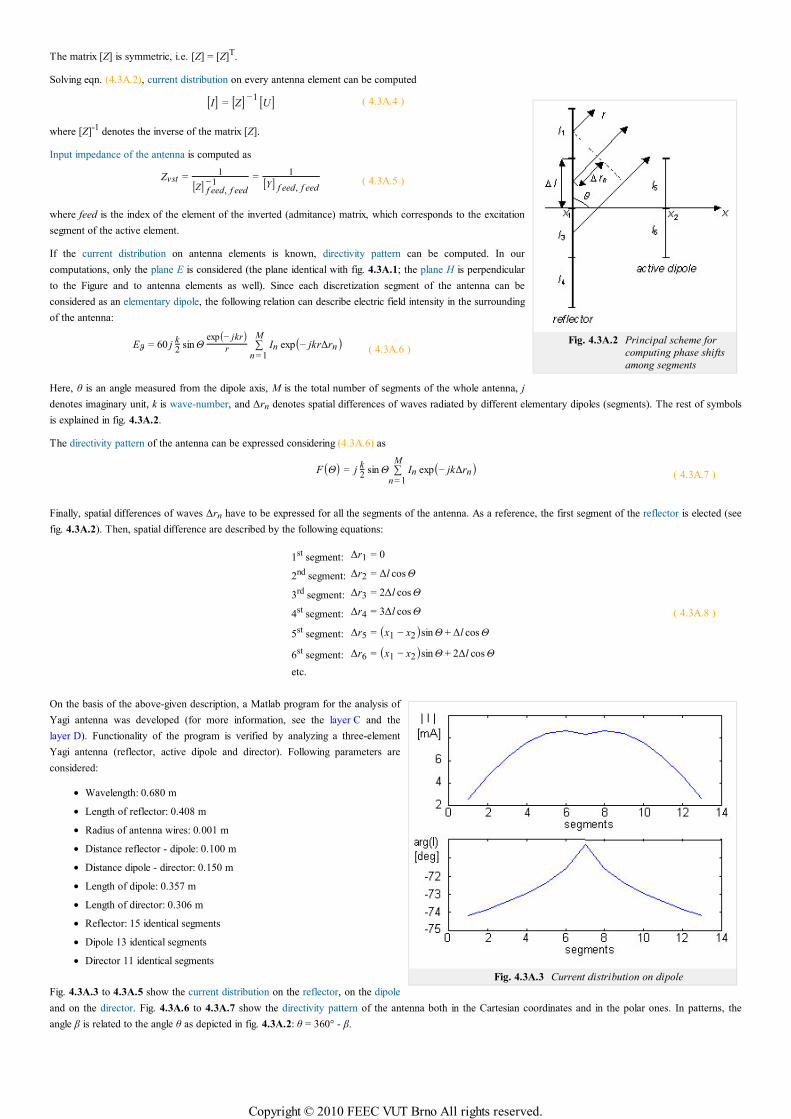
Fig. 4.3A.2 Principal scheme for
computing phase shifts
among segments
Fig. 4.3A.3 Current distribution on dipole
The matrix [Z] is symmetric, i.e. [Z] = [Z]T.
Solving eqn. (4.3A.2), current distribution on every antenna element can be computed
[I] = [Z]−1
[U] ( 4.3A.4 )
where [Z]-1 denotes the inverse of the matrix [Z].
Input impedance of the antenna is computed as
Zvst =1
[Z] f eed, f eed−1
=1
[Y] f eed, f eed( 4.3A.5 )
where feed is the index of the element of the inverted (admitance) matrix, which corresponds to the excitation
segment of the active element.
If the current distribution on antenna elements is known, directivity pattern can be computed. In our
computations, only the plane E is considered (the plane identical with fig. 4.3A.1; the plane H is perpendicular
to the Figure and to antenna elements as well). Since each discretization segment of the antenna can be
considered as an elementary dipole, the following relation can describe electric field intensity in the surrounding
of the antenna:
Eϑ = 60 jk2
sin Θexp(− jkr)
r ∑n = 1
MIn exp(− jkr∆rn) ( 4.3A.6 )
Here, θ is an angle measured from the dipole axis, M is the total number of segments of the whole antenna, j
denotes imaginary unit, k is wave-number, and ∆rn denotes spatial differences of waves radiated by different elementary dipoles (segments). The rest of symbols
is explained in fig. 4.3A.2.
The directivity pattern of the antenna can be expressed considering (4.3A.6) as
F(Θ) = jk2
sin Θ ∑n = 1
MIn exp(− jk∆rn) ( 4.3A.7 )
Finally, spatial differences of waves ∆rn have to be expressed for all the segments of the antenna. As a reference, the first segment of the reflector is elected (see
fig. 4.3A.2). Then, spatial difference are described by the following equations:
1st segment: ∆r1 = 0
2nd segment: ∆r2 = ∆l cos Θ
3rd segment: ∆r3 = 2∆l cos Θ
4st segment: ∆r4 = 3∆l cos Θ
5st segment: ∆r5 = (x1 − x2)sin Θ + ∆l cos Θ
6st segment: ∆r6 = (x1 − x2)sin Θ + 2∆l cos Θ
etc.
( 4.3A.8 )
On the basis of the above-given description, a Matlab program for the analysis of
Yagi antenna was developed (for more information, see the layer C and the
layer D). Functionality of the program is verified by analyzing a three-element
Yagi antenna (reflector, active dipole and director). Following parameters are
considered:
Wavelength: 0.680 m
Length of reflector: 0.408 m
Radius of antenna wires: 0.001 m
Distance reflector - dipole: 0.100 m
Distance dipole - director: 0.150 m
Length of dipole: 0.357 m
Length of director: 0.306 m
Reflector: 15 identical segments
Dipole 13 identical segments
Director 11 identical segments
Fig. 4.3A.3 to 4.3A.5 show the current distribution on the reflector, on the dipole
and on the director. Fig. 4.3A.6 to 4.3A.7 show the directivity pattern of the antenna both in the Cartesian coordinates and in the polar ones. In patterns, the
angle β is related to the angle θ as depicted in fig. 4.3A.2: θ = 360° - β.
Copyright © 2010 FEEC VUT Brno All rights reserved.
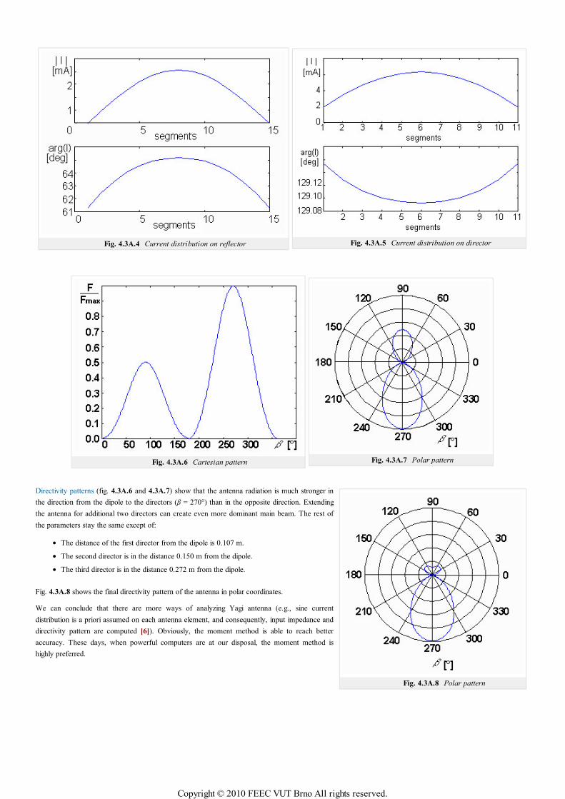
Fig. 4.3A.8 Polar pattern
Fig. 4.3A.4 Current distribution on reflector Fig. 4.3A.5 Current distribution on director
Fig. 4.3A.6 Cartesian pattern Fig. 4.3A.7 Polar pattern
Directivity patterns (fig. 4.3A.6 and 4.3A.7) show that the antenna radiation is much stronger in
the direction from the dipole to the directors (β = 270°) than in the opposite direction. Extending
the antenna for additional two directors can create even more dominant main beam. The rest of
the parameters stay the same except of:
The distance of the first director from the dipole is 0.107 m.
The second director is in the distance 0.150 m from the dipole.
The third director is in the distance 0.272 m from the dipole.
Fig. 4.3A.8 shows the final directivity pattern of the antenna in polar coordinates.
We can conclude that there are more ways of analyzing Yagi antenna (e.g., sine current
distribution is a priori assumed on each antenna element, and consequently, input impedance and
directivity pattern are computed [6]). Obviously, the moment method is able to reach better
accuracy. These days, when powerful computers are at our disposal, the moment method is
highly preferred.
Copyright © 2010 FEEC VUT Brno All rights reserved.

4.3 Yagi antenna
Matlab program
In this layer, we present a user's guide to the program for the analysis of Yagi antenna (the programmer's guide can be found in the layer D).
The program is started by entering Yagi_Gui_Master to the command window of Matlab (path is set to folder Yagi). Menu items of the
main form are of the following meaning:
Wavelength wavelength of the supplying voltage;
Radius radius of the wire of antenna elements;
Reflector length length of the whole reflector;
Reflector-dipole distance between the reflector and the active dipole;
Number of
elements
the number of segments to which the reflector is going to be divided (odd number required);
Difference 1 the number of segments for which the active element is shorter than the reflector;
Difference 2 the number of segments for which the directors are shorter than the reflector;
Input element index of the feeding segment of the active dipole in the complete current vector (an information item,
which cannot be edited);
Number of
elements
the total number of antenna elements;
Dipole-director the distance between the active dipole and the nearest director;
Director-director the distance between two neighboring directors;
Dipole length the length of the active dipole (an information item, which cannot be edited);
Director lengths the length of all the directors (an information item, which cannot be edited).
Pressing the button OK on the main form, the computation is started. Respective charts (current distribution, directivity pattern) are
sequentially displayed in a single form after pressing the key Enter .
Pressing the button Apply on the main form, information items display values of real lengths (recomputed from the number of segments) of
the active dipole and directors, and the value of the index of the excitation segment. If needed, the number of segments of antenna elements can
be changed before starting the computations.
Pressing the button Cancel on the main form, the program is terminated.
When the computations are finished, the actual value of input impedance is printed in the header of the main form. In charts of directivity
patterns, the angle 270° corresponds to the direction from the dipole to the directors, the angle 90° corresponds to the direction from the dipole
to the reflector.
Since the graphic interface of the program does not support the setting of individual distances among directors, a more general function
Yagi_Antenna has to be used as a stand-alone program. for this purpose. When this m-function is started, parameters N and feed have to
be given (their meaning is explained in the layer D). The m-function returns the input impedance of the antenna. Further parameters can be
changed in the source code of the function. Individual distances among antenna elements are set indirectly changing their coordinates with
respect to the active dipole (the positive orientation goes from the dipole to the reflector). Respective charts (current distribution, directivity
pattern) are sequentially displayed in a single form after pressing the key Enter .
Copyright © 2010 FEEC VUT Brno All rights reserved.

4.3 Yagi antenna
Developing Matlab
In this paragraph, the moment analysis of Yagi antenna is described from the programmer's point of view. The description assumes the
knowledge of the description presented in the paragraph 4.1 and in the layer A of this chapter.
The program consists of files Yagi_Gui_Master.mat and Yagi_Gui_Master.m , which create the form of the user's interface, of
Yagi_Antena_OK_Master.m, which is an reaction to pressing the button OK in the main form, of
Yagi_Antena_Apply_Master.m, which is an reaction to pressing Apply and of Yagi_Antenna_Slave.m, which is responsible for
all the computations.
First, we explain the meaning of symbols appearing in the source code:
delta is the segment length,alfa is one half of the segment length,
k denotes wave-number,
M is the number of antenna elements,N is the number of segments to which the reflector is divided,
epsilon denotes permittivity of vacuum,omega denotes angular frequency,
j is imaginary unit,Z denotes impedance matrix,
Y is admittance matrix,
I is the vector of currents,feed is the index of the excitation segment,
diff(1) is the number of segments, for which the active dipole is shorter than the reflector,diff(2) is the number of segments, for which the directors are shorter than the reflector,
beta is an angle given by β = 360° - θ (see the layer A – fig. 4.3A.2) and
F denotes directivity pattern of the antenna.
Now, we turn our attention to the basic blocks of the program.
First, [exp(-jkr)/(4πr)] is numerically integrated to all the possible distances among segments of both a single antenna element and different
antenna elements of Yagi antenna (see paragraph 4.1, the layer D).
Second, results of numerical (vector psi) are composed into the impedance matrix. Individual sub-matrices [Zrr], [Zdd], [Z11], [Z22], ..., [Znn]
are composed the similar way as described in the paragraph 4.1, the layer D.
On the basis of a known impedance matrix, the admittance matrix can be computed
Y = inv(Z);
current distribution on antenna elements can be obtained
for m=1:(N-2*diff(1)) % current distribution of the dipoleI(m)=Y(m+N,feed);n(m)=m;
end
for m=1:N % current distribution of the reflectorI(m)=Y(m,feed);n(m)=m;
end
for o=3:Mfor m=1:(N-2*diff(2)) % current distribution of directors
Id(m)=Y(2*N-2*diff(1)+m+(o-3)*(N-2*diff(2)),feed);u(m)=m;
end
end
input impedance can be evaluated
1/Y(feed,feed)
and directivity pattern can be computed.
All the above-given parameters of the antenna can be computed for an arbitrary wavelength of the excitation voltage, for an arbitrary length of
the reflector, for arbitrary distances reflector - active dipole, active dipole - director and director - director (the way of individual setting of the
distance among directors is described in the layer C), for an arbitrary radius of antenna wire, for an arbitrary number of antenna elements and
Copyright © 2010 FEEC VUT Brno All rights reserved.

for an arbitrary number of segments to which antenna elements are divided. The length of the active dipole is for diff(1) segments shorter
than the length of the reflector, the length of each director is for diff(2) segments shorter than the length of the reflector. Magnitude of the
feeding voltage is normalized. The radius of antenna elements has to be properly chosen in order to meet conditions ensuring functionality of the
method (see the layer A). More details are given in the source code of the program in the form of comments.
Copyright © 2010 FEEC VUT Brno All rights reserved.

4.3 Yagi antenna
Java applet
Copyright © 2010 FEEC VUT Brno All rights reserved.

4.3 Yagi antenna
Quiz
Answer these questions to get feedback on how well you understand the course. Only one of the answers is correct. You don't have to answer
every question. If you don't know the answer you can just leave it blank (default option: “I won't answer this question”) and this won't affect
your score. Answering correctly will add 2 points to your score but on the other hand you'll lose 1 point if your answer is wrong. The
questions are divided in groups of five questions.
Press See result after you have finished answering.
Displaying questions 1..10 of 10:
Question 1
Yagi antenna consists of…:
Possible answers for question 1:
… an active dipole, of a reflector and of several directors.
… an active dipole and of several directors (one of them is longer than the dipole, several of them are shorter).
… several active dipoles, of a reflector and of several directors.
I won't answer this question
Question 2
The directors of Yagi antenna are excited by electromagnetic wave, and induced currents. The directors…
Possible answers for question 2:
… influence gain of the antenna.
… concentrate the antenna radiation into one half-space only.
… influence all the parameters of the antenna (gain, directivity pattern, input impedance).
I won't answer this question
Question 3
Depending on the number of directors, the gain of Yagi antenna is usually in the interval …
Possible answers for question 3:
… 5 to 9 db.
… 10 to 15 db.
… 16 to 20 db.
I won't answer this question
Question 4
The lobes in the directivity pattern of Yagi antenna appear …
Possible answers for question 4:
… both in front of reflector and even behind the reflector.
… in front of reflector only.
… behind the reflector only.
I won't answer this question
Question 5
If Yagi antenna is analyzed by the method of moments, mutual- and self-impedances of antenna segments …
Copyright © 2010 FEEC VUT Brno All rights reserved.

Possible answers for question 5:
… of the active dipole appear in the impedance matrix; the influence of the reflector and directors are neglected.
… of the active dipole appear in the impedance matrix; the influence of the reflector and directors is incorporated to the analysis by
the method of electromagnetic forces.
… of all the wires (active dipole, directors, reflector) appear in the impedance matrix.
I won't answer this question
Question 6
A Yagi antenna is said to have a power gain over a dipole antenna for the same frequency band because …
Possible answers for question 6:
… it radiates more power than a dipole.
… it concentrates the radiation in one direction.
… it can be used for more than one band.
I won't answer this question
Question 7
The maximum radiation from a three element Yagi antenna is …
Possible answers for question 7:
… in the direction of the reflector end of the boom.
… in the direction of the director end of the boom.
… at right angles to the boom.
I won't answer this question
Question 8
If the distance between the reflector and the active dipole decreases, the module of the current distribution of the reflector …
Possible answers for question 8:
… increases.
… decreases.
… is not affected.
I won't answer this question
Question 9
In this diagram the item U, V & X correspond to respectively the …
Possible answers for question 9:
… boom, driven element & reflector.
… driven element, reflector & director.
… boom, reflector & director.
I won't answer this question
Question 10
Copyright © 2010 FEEC VUT Brno All rights reserved.

Changing λ (the wavelength of the supplying voltage) between 0 & 1 affects the directivity pattern …
Possible answers for question 10:
… more than changing λ between 1 & 2.
… less than changing λ between 1 & 2.
… almost the same amount as changing λ between 1 & 2.
I won't answer this question
Copyright © 2010 FEEC VUT Brno All rights reserved.
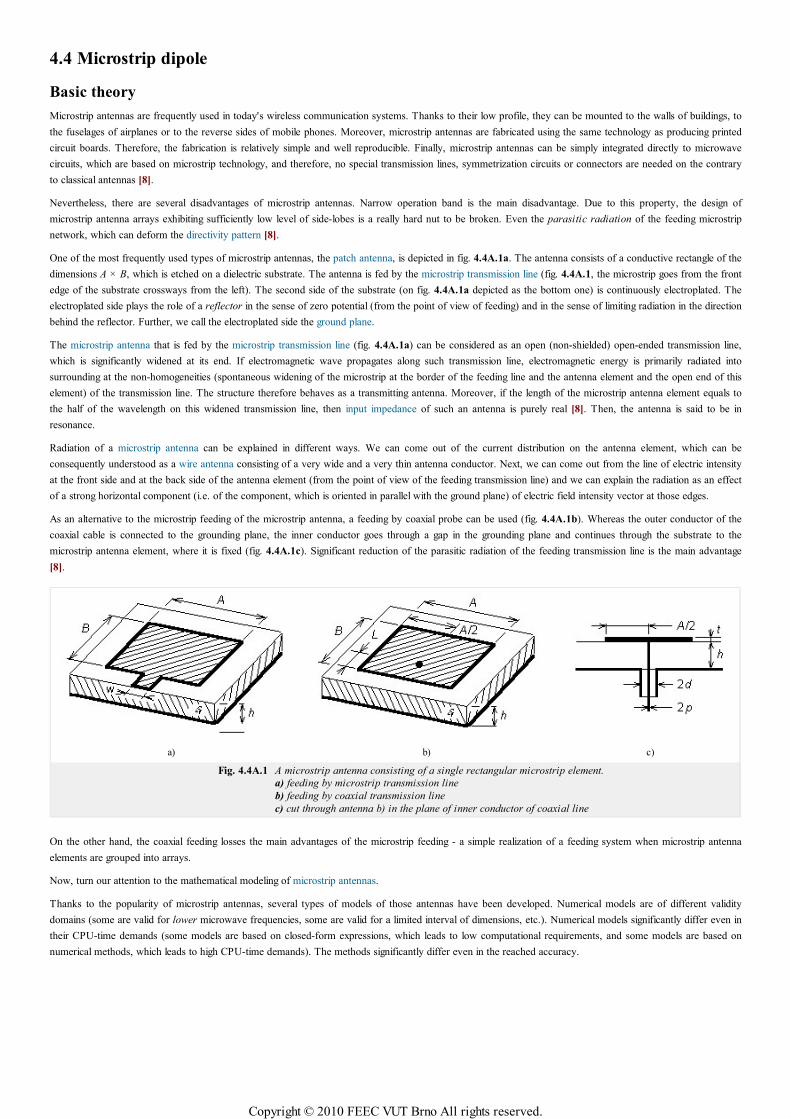
4.4 Microstrip dipole
Basic theory
Microstrip antennas are frequently used in today's wireless communication systems. Thanks to their low profile, they can be mounted to the walls of buildings, to
the fuselages of airplanes or to the reverse sides of mobile phones. Moreover, microstrip antennas are fabricated using the same technology as producing printed
circuit boards. Therefore, the fabrication is relatively simple and well reproducible. Finally, microstrip antennas can be simply integrated directly to microwave
circuits, which are based on microstrip technology, and therefore, no special transmission lines, symmetrization circuits or connectors are needed on the contrary
to classical antennas [8].
Nevertheless, there are several disadvantages of microstrip antennas. Narrow operation band is the main disadvantage. Due to this property, the design of
microstrip antenna arrays exhibiting sufficiently low level of side-lobes is a really hard nut to be broken. Even the parasitic radiation of the feeding microstrip
network, which can deform the directivity pattern [8].
One of the most frequently used types of microstrip antennas, the patch antenna, is depicted in fig. 4.4A.1a. The antenna consists of a conductive rectangle of the
dimensions A × B, which is etched on a dielectric substrate. The antenna is fed by the microstrip transmission line (fig. 4.4A.1, the microstrip goes from the front
edge of the substrate crossways from the left). The second side of the substrate (on fig. 4.4A.1a depicted as the bottom one) is continuously electroplated. The
electroplated side plays the role of a reflector in the sense of zero potential (from the point of view of feeding) and in the sense of limiting radiation in the direction
behind the reflector. Further, we call the electroplated side the ground plane.
The microstrip antenna that is fed by the microstrip transmission line (fig. 4.4A.1a) can be considered as an open (non-shielded) open-ended transmission line,
which is significantly widened at its end. If electromagnetic wave propagates along such transmission line, electromagnetic energy is primarily radiated into
surrounding at the non-homogeneities (spontaneous widening of the microstrip at the border of the feeding line and the antenna element and the open end of this
element) of the transmission line. The structure therefore behaves as a transmitting antenna. Moreover, if the length of the microstrip antenna element equals to
the half of the wavelength on this widened transmission line, then input impedance of such an antenna is purely real [8]. Then, the antenna is said to be in
resonance.
Radiation of a microstrip antenna can be explained in different ways. We can come out of the current distribution on the antenna element, which can be
consequently understood as a wire antenna consisting of a very wide and a very thin antenna conductor. Next, we can come out from the line of electric intensity
at the front side and at the back side of the antenna element (from the point of view of the feeding transmission line) and we can explain the radiation as an effect
of a strong horizontal component (i.e. of the component, which is oriented in parallel with the ground plane) of electric field intensity vector at those edges.
As an alternative to the microstrip feeding of the microstrip antenna, a feeding by coaxial probe can be used (fig. 4.4A.1b). Whereas the outer conductor of the
coaxial cable is connected to the grounding plane, the inner conductor goes through a gap in the grounding plane and continues through the substrate to the
microstrip antenna element, where it is fixed (fig. 4.4A.1c). Significant reduction of the parasitic radiation of the feeding transmission line is the main advantage
[8].
a) b) c)
Fig. 4.4A.1 A microstrip antenna consisting of a single rectangular microstrip element.
a) feeding by microstrip transmission line
b) feeding by coaxial transmission line
c) cut through antenna b) in the plane of inner conductor of coaxial line
On the other hand, the coaxial feeding losses the main advantages of the microstrip feeding - a simple realization of a feeding system when microstrip antenna
elements are grouped into arrays.
Now, turn our attention to the mathematical modeling of microstrip antennas.
Thanks to the popularity of microstrip antennas, several types of models of those antennas have been developed. Numerical models are of different validity
domains (some are valid for lower microwave frequencies, some are valid for a limited interval of dimensions, etc.). Numerical models significantly differ even in
their CPU-time demands (some models are based on closed-form expressions, which leads to low computational requirements, and some models are based on
numerical methods, which leads to high CPU-time demands). The methods significantly differ even in the reached accuracy.
Copyright © 2010 FEEC VUT Brno All rights reserved.
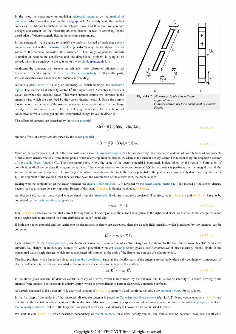
a) b)
Fig. 4.4A.2 Microstrip dipole plus reflector.
a) global view
b) discretization net for x component of current
density
In the next, we concentrate on modeling microstrip antennas by the method of
moments, which was described in the paragraph 4.1. As already said, the method
comes out of Maxwell equations in the integral form, and therefore, we compute
voltages and currents on the microstrip antenna element instead of searching for the
distribution of electromagnetic field in the antenna surrounding.
In this paragraph, we are going to simplify the analysis. Instead of analyzing a patch
antenna, we deal with a microstrip dipole (fig. 4.4A.2) only. At the dipole, a small
width of the antenna microstrip B is assumed. Then, only longitudinal currents
(direction x) need to be considered and one-dimensional problem is going to be
solved, which is an analogy to the solution of a wire dipole (paragraph 4.1)
Analyzing the antenna, we assume an infinitely wide substrate, infinitely small
thickness of metallic layers t ≈ 0, perfect electric conductivity of all metallic parts,
lossless dielectrics and vacuum in the antenna surrounding.
Assume a plane wave of an angular frequency ω, which impinges the microstrip
dipole. The electric field intensity vector EI (the upper index I denotes the incident
wave) describes the incident wave. This wave induces conductive currents in the
antenna wire, which are described by the current density vector J. Since the current
has to be zero at the ends of the microstrip dipole, a charge described by the charge
density ρ is accumulated here. In the following half-wave, the orientation of
conductive currents is changed and the accumulated charge leaves the dipole [9].
The effects of currents are described by the vector potential
A(r) =∬S
GA(r||r0)⋅ J(r0)dS0 ( 4.4A.1a )
and the effects of charges are described by the scalar potential
V(r) =∬S
GV(r||r0)ρ(r0)dS0 . ( 4.4A.1b )
Value of the vector potential A(r) in the observation pint r on the microstrip dipole can be computed by the consecutive addition of contributions of components
of the current density vector J from all the points of the microstrip antenna element r0 whereas the current density vector J is multiplied by the respective column
of the dyadic Green function GA. The observation point, where the value of the vector potential is computed, is determined by the vector r. Summation of
contributions of all the currents flowing on the surface of the antenna element to the vector potential A(r) in the point r is performed by the integral over all the
surface of the microstrip dipole S. The source points, where currents contributing to the vector potential to the point r are consecutively determined by the vector
r0. The argument of the dyadic Green function r|r0 shows the contribution of the current in r0 the potential in r.
Dealing with the computation of the scalar potential, the dyadic Green function GA is replaced by the scalar Green function GV, and instead of the current density
vector, the scalar charge density r appears. Except of this, eqn. (4.4A.1b) is identical with eqn. (4.4A.1a).
As already said, current density and charge density on the microstrip dipole are mutually associated. Therefore, eqns. (4.4A.1a) and (4.4A.1b) have to be
completed by the continuity theorem given by
− jωρ =∇ ⋅ J. ( 4.4A.1c )
Eqn. (4.4A.1c) expresses the fact that current flowing from a closed region (see the current divergence as the right-hand side) has to equal to the charge reduction
in this region within one second (see time derivative at the left-hand side).
If both the vector potential and the scalar one on the microstrip dipole are expressed, then the electric field intensity, which is radiated by the antenna, can be
computed
ES = − jω A −∇V . ( 4.4A.1d )
Time derivative of the vector potential jωA describes a dynamic contribution of electric charge on the dipole to the transmitted wave (electric conductive
currents, i.e. charges in motion, are sources of vector potential). Gradient scalar potential gives a static contributionof electric charge on the dipole to the
transmitted wave (static charges, which are concentrated this moment at the ends of the dipole, are sources of scalar potential).
The final problem, which has to be solved, are boundary conditions. Since all the metallic parts of the antenna are perfectly electrically conductive, components of
electric field intensity, which are tangential to the antenna surface, have to be zero on this surface
n0×ES = − n0×EI. ( 4.4A.1e )
In the above-given relation, ES denotes electric intensity of a wave, which is transmitted by the antenna, and EI is electric intensity of a wave, arriving to the
antenna from outside. The vector n0 is unitary vector, which is perpendicular to perfect electrically conductive surfaces.
As already explained in the paragraph 4.1, analytical solution of (4.4A.1) is unknown, and therefore, we utilize the moment method for its solution.
In the first step of the analysis of the microstrip dipole, the antenna is placed to Cartesian coordinate system (fig. 4.4A.2). Next, vector equations (4.4A.1) are
rewritten in the elected coordinate system to the scalar form. Moreover, we assume a special case when moving on the surface of the microstrip dipole (thanks to
the boundary conditions, value of the tangential component of electric field intensity is known, which can be used further).
We start at eqn. (4.4A.1a), which describes dependency of vector potential on current density vector. The mutual relation between those two quantities is
Copyright © 2010 FEEC VUT Brno All rights reserved.
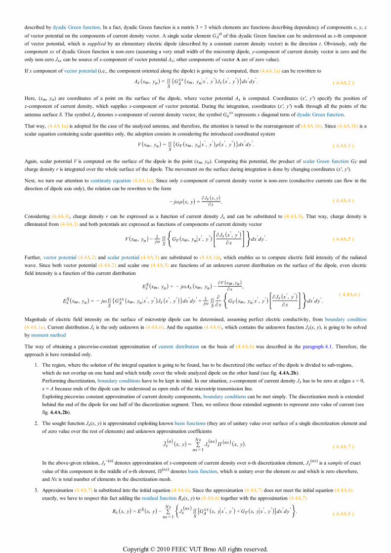
described by dyadic Green function. In a fact, dyadic Green function is a matrix 3 × 3 which elements are functions describing dependency of components x, y, z
of vector potential on the components of current density vector. A single scalar element GAst of this dyadic Green function can be understood as s-th component
of vector potential, which is supplied by an elementary electric dipole (described by a constant current density vector) in the direction t. Obviously, only the
component xx of dyadic Green function is non-zero (assuming a very small width of the microstrip dipole, y-component of current density vector is zero and the
only non-zero Jxx can be source of x-component of vector potential Ax; other components of vector A are of zero value).
If x component of vector potential (i.e., the component oriented along the dipole) is going to be computed, then (4.4A.1a) can be rewritten to
Ax (xm , yn) =∬S
GAxx (xm , yn
||x′, y ′)Jx (x ′, y ′)dx ′d y ′. ( 4.4A.2 )
Here, (xm, yn) are coordinates of a point on the surface of the dipole, where vector potential Ax is computed. Coordinates (x', y') specify the position of
x-component of current density, which supplies x-component of vector potential. During the integration, coordinates (x', y') walk through all the points of the
antenna surface S. The symbol Jx denotes x-component of current density vector, the symbol Gaxx represents x diagonal term of dyadic Green function.
That way, (4.4A.1a) is adopted for the case of the analyzed antenna, and therefore, the attention is turned to the rearrangement of (4.4A.1b). Since (4.4A.1b) is a
scalar equation containing scalar quantities only, the adoption consists in considering the introduced coordinated system
V(xm , yn) =∬S
GV(xm , yn||x
′, y ′)ρ(x ′, y ′)dx ′d y ′. ( 4.4A.3 )
Again, scalar potential V is computed on the surface of the dipole in the point (xm, yn). Computing this potential, the product of scalar Green function GV and
charge density r is integrated over the whole surface of the dipole. The movement on the surface during integration is done by changing coordinates (x', y').
Next, we turn our attention to continuity equation (4.4A.1c). Since only x-component of current density vector is non-zero (conductive currents can flow in the
direction of dipole axis only), the relation can be rewritten to the form
− jωρ(x, y) =∂ Jx (x, y)
∂ x. ( 4.4A.4 )
Considering (4.4A.4), charge density r can be expressed as a function of current density Jx and can be substituted to (4.4A.3). That way, charge density is
elliminated from (4.4A.3) and both potentials are expressed as functions of components of current density vector
V(xm , yn) −1jω∬S GV(xm , yn
||x′, y ′)[∂ Jx (x ′, y ′)
∂ x ]dx ′dy ′. ( 4.4A.5 )
Further, vector potential (4.4A.2) and scalar potential (4.4A.5) are substituted to (4.4A.1d), which enables us to compute electric field intensity of the radiated
wave. Since both vector potential (4.4A.2) and scalar one (4.4A.5) are functions of an unknown current distribution on the surface of the dipole, even electric
field intensity is a function of this current distribution
ExS(xm , yn) = − jωAx (xm , yn) −
∂V(xm , yn)∂ x
,
ExS(xm , yn) = − jω∬
SGA
xx (xm , yn||x
′, y ′)Jx (x ′, y ′)dx ′d y ′ +1jω∬S
∂
∂ x GV(xm , yn||x
′, y ′)[∂ Jx (x ′, y ′)∂ x ]dx ′d y ′.
( 4.4A.6 )
Magnitude of electric field intensity on the surface of microstrip dipole can be determined, assuming perfect electric conductivity, from boundary condition
(4.4A.1e). Current distribution Jx is the only unknown in (4.4A.6). And the equation (4.4A.6), which contains the unknown function Jx(x, y), is going to be solved
by moment method
The way of obtaining a piecewise-constant approximation of current distribution on the basis of (4.4A.6) was described in the paragraph 4.1. Therefore, the
approach is here reminded only.
The region, where the solution of the integral equation is going to be found, has to be discretized (the surface of the dipole is divided to sub-regions,
which do not overlap on one hand and which totally cover the whole analyzed dipole on the other hand (see fig. 4.4A.2b).
Performing discretization, boundary conditions have to be kept in mind. In our situation, x-component of current density Jx has to be zero at edges x = 0,
x = A because ends of the dipole can be understood as open ends of the microstrip transmission line.
Exploiting piecewise constant approximation of current density components, boundary conditions can be met simply. The discretization mesh is extended
behind the end of the dipole for one half of the discretization segment. Then, we enforce those extended segments to represent zero value of current (see
fig. 4.4A.2b).
1.
The sought function Jx(x, y) is approximated exploiting known basis functions (they are of unitary value over surface of a single discretization element and
of zero value over the rest of elements) and unknown approximation coefficients
Jx(n)(x, y) = ∑
nx = 1
N xJx
(nx)Π (nx)(x, y). ( 4.4A.7 )
In the above-given relation, Jx~(n) denotes approximation of x-component of current density over n-th discretization element, Jx
(nx) is a sample of exact
value of this component in the middle of n-th element, Π(nx) denotes basis function, which is unitary over the element nx and which is zero elsewhere,
and Nx is total number of elements in the discretization mesh.
2.
Approximation (4.4A.7) is substituted into the initial equation (4.4A.6). Since the approximation (4.4A.7) does not meet the initial equation (4.4A.6)
exactly, we have to respect this fact adding the residual function Rx(x, y) to (4.4A.6) together with the approximation (4.4A.7)
Rx (x, y) = ES(x, y) − ∑nx = 1
N x
Jx(nx)∬
S[GA
xx (x, y||x′, y ′) + G V(x, y||x
′, y ′)]dx ′d y ′. ( 4.4A.8 )
3.
Copyright © 2010 FEEC VUT Brno All rights reserved.
In these relations, GAxx is x diagonal term of dyadic Green function and using G¯V, partial derivative of scalar Green function is expressed.
Since basis functions Π are unitary over a respective element and are zero elsewhere, they do not have any representation in the above-given relations.
Next, integration and summation were swapped, and the approximation coefficients Jxnx were moved in front of the integral thank so their constant
character.
Residual function Rx(x, y) is going to be minimized. Lower values of the residual function are, closer our solution to the exact solution is. Minimization is
done by the method of weighted residuals
∬S
Wx (x, y)Rx (x, y)dxd y = 0. ( 4.4A.9 )
Here, Rx denotes the residual function computed according to (4.4A.8). The symbol Wx represents properly elected weighting functions. Weighting is
done by Dirac pulses in order to eliminate one of integrations thanks to the filtering property
∬S
δ(x − xm , y − yn)Rx (x, y)dx dy = Rx (xm , yn). ( 4.4A.10 )
Accuracy of the method, which performs weighting by Dirac pulses, cannot be very good because the error is not minimized globally in the whole
analyzed region but only in points, where Dirac pulses are of non-zero value (we operate with moments of residual function only).
4.
Using the same number of weighting functions as the number of unknown approximation coefficients is, we obtain the set of N linear equations for N
unknown coefficients. Solving this set of equations, we obtain unknown values of approximation coefficients, and therefore, approximation of the current
distribution on the microstrip dipole can be composed. Considering known current distribution, the desired technical parameters of the antenna (input
impedance, gain or directivity pattern) can be computed.
5.
The whole algorithm described by the above points is given in detail in the layer B and in [10], [11]. Replacing all the derivatives by central differences in the
above-given algorithm, we obtain a matrix equation
Ux = Zxx Ix . ( 4.4A.11 )
In this equation, Ux is column vector of voltages in the direction x on discretization elements. This voltage is computed by multiplying x-component of electric
field intensity by x-size of the discretization element
Ux (m, n) = Ex (m, n)a. ( 4.4A.12 )
The symbol a denotes the height of the discretization element (i.e. the size in the direction x).
Since the microstrip dipole is supposed to be fabricated from perfect electric conductor (voltage on this conductor is zero), the vector of voltages is filled in by
zeros only except of elements relating to the excitation gap.
Next, Ix is column vector of currents in the direction x, which is unknown this moment for us. Elements of Ix are related to the component of current density Jx
as follows
Ix (m, n) = Jx (m, n)B ( 4.4A.13 )
(B is the width of the dipole, and consequently the width of the discretization element). Impedance matrix Zxx describes contribution of currents Ix and
contribution of charge densities ρ (expressed from continuity equation (4.4A.4) using x-components of current density Jx on elements) to voltages Ux on those
elements. Elements of the impedance matrix Zxx are known (see the layer B)
Zxx (m, n) =jωa
BΓ
Axx (m, n) +
1jωaB [ΓV(m + , n + ) − ΓV(m − , n + ) − ΓV(m + , n − ) + ΓV(m − , n − )]. (4.4A.14 )
In order to evaluate the impedance matrix Zxx, values of integrals of Green functions ΓAxx and ΓV over the surface of the discretization element have to be
computed for various distances between the source elements (over its surface, current distribution and charge one are integrated) and the observation one (on its
surface, electric intensity is computed. Description of the numeric computation of those integrals in Matlab is given in the layer D.
Matlab program, which performs analysis of the microstrip dipole by the moment method, is described from user's point of view in the layer C. Here, we provide
only illustration results obtained by the program.
For simplicity, the substrate between the dipole and the reflector is assumed to be of the same
parameters as vacuum. If the dipole length equals to one half of wavelength and if the dipole
width is B = λ/1000, following values of input impedance are obtained (in the first row of the
table, the number of discretization elements to which antenna is subdivided is given):
Tab. 4.4A.1 Input impedance for different number of discretization
elements
N 10 20 30 40
Rvst [Ω] 95.2 97.3 98.0 98.4
Xvst [Ω] 72.4 73.6 74.7 75.5
The results show the method to exhibit good stability with respect to the number of discretization
elements. Moreover, the input impedance of the microstrip dipole with the reflector computed by
moment method, is close to the results of analytical computations (sinusoidal current distribution
Jx a wire dipole over an infinite planar reflector assumed). For a single wire dipole, radiation
resistance of the antenna (related to the input) equals to RΣ= 85.6 Ω.
Copyright © 2010 FEEC VUT Brno All rights reserved.

Fig. 4.4A.3 Current distribution on
half-wavelength symmetric microstrip
dipole with planar reflector in the
distance of one quarter of wavelength.
Distribution computed for 40 cells.
Investigating approximation of the distribution of x-component of the current along the microstrip
dipole, we can show that depicting approximation coefficients from the vector Ix into a chart.
That way, we obtain a course which is close to a sinusoidal current distribution (see fig. 4.4A.3).
Copyright © 2010 FEEC VUT Brno All rights reserved.
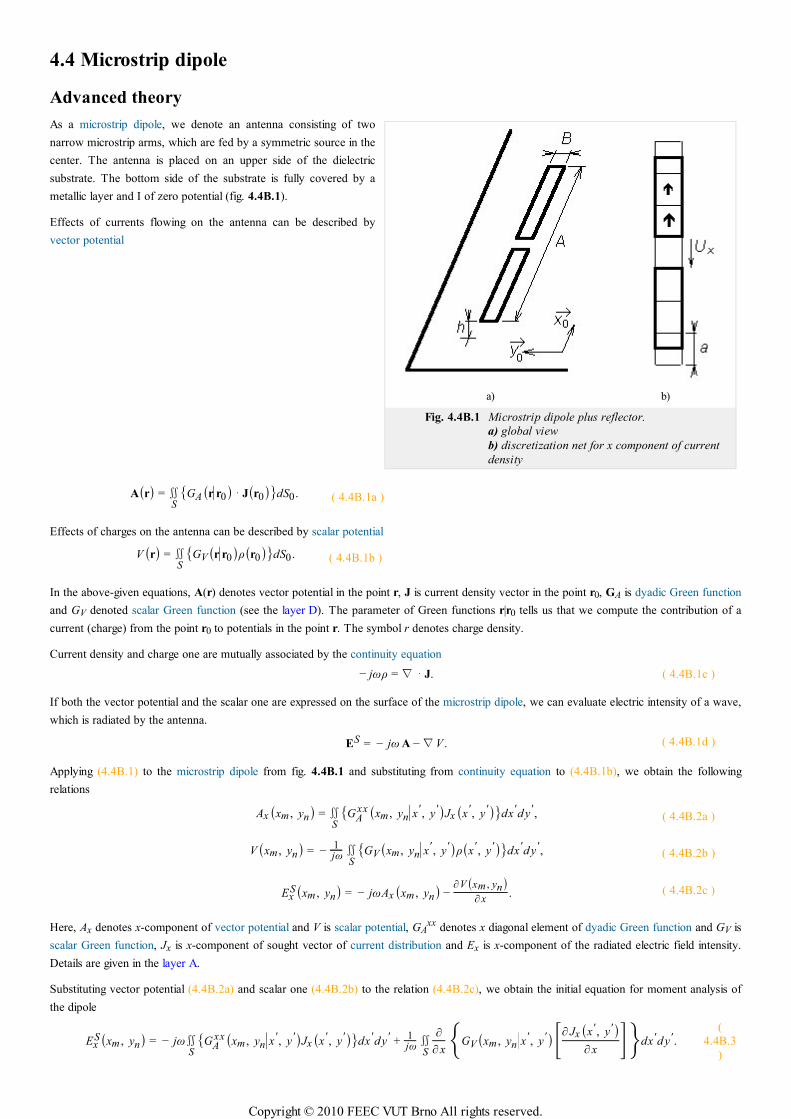
a) b)
Fig. 4.4B.1 Microstrip dipole plus reflector.
a) global view
b) discretization net for x component of current
density
4.4 Microstrip dipole
Advanced theory
As a microstrip dipole, we denote an antenna consisting of two
narrow microstrip arms, which are fed by a symmetric source in the
center. The antenna is placed on an upper side of the dielectric
substrate. The bottom side of the substrate is fully covered by a
metallic layer and I of zero potential (fig. 4.4B.1).
Effects of currents flowing on the antenna can be described by
vector potential
A(r) =∬S
GA(r||r0)⋅ J(r0)dS0 . ( 4.4B.1a )
Effects of charges on the antenna can be described by scalar potential
V(r) =∬S
GV(r||r0)ρ(r0)dS0 . ( 4.4B.1b )
In the above-given equations, A(r) denotes vector potential in the point r, J is current density vector in the point r0, GA is dyadic Green function
and GV denoted scalar Green function (see the layer D). The parameter of Green functions r|r0 tells us that we compute the contribution of a
current (charge) from the point r0 to potentials in the point r. The symbol r denotes charge density.
Current density and charge one are mutually associated by the continuity equation
− jωρ =∇ ⋅ J. ( 4.4B.1c )
If both the vector potential and the scalar one are expressed on the surface of the microstrip dipole, we can evaluate electric intensity of a wave,
which is radiated by the antenna.
ES = − jωA −∇V . ( 4.4B.1d )
Applying (4.4B.1) to the microstrip dipole from fig. 4.4B.1 and substituting from continuity equation to (4.4B.1b), we obtain the following
relations
Ax (xm , yn) =∬S
GAxx (xm , yn
||x
′, y ′)Jx (x ′, y ′)dx ′d y ′, ( 4.4B.2a )
V(xm , yn) = −1jω∬
SGV(xm , yn
||x
′, y ′)ρ(x ′, y ′)dx ′d y ′, ( 4.4B.2b )
ExS(xm , yn) = − jωAx (xm , yn) −
∂V(xm , yn)∂ x
. ( 4.4B.2c )
Here, Ax denotes x-component of vector potential and V is scalar potential, GAxx denotes x diagonal element of dyadic Green function and GV is
scalar Green function, Jx is x-component of sought vector of current distribution and Ex is x-component of the radiated electric field intensity.
Details are given in the layer A.
Substituting vector potential (4.4B.2a) and scalar one (4.4B.2b) to the relation (4.4B.2c), we obtain the initial equation for moment analysis of
the dipole
ExS(xm , yn) = − jω∬
SGA
xx (xm , yn||x
′, y ′)Jx (x ′, y ′)dx ′dy ′ +1jω∬
S
∂
∂ x GV(xm , yn||x
′, y ′)[∂ Jx (x ′, y ′)∂ x ]dx ′d y ′.
(
4.4B.3
)
Copyright © 2010 FEEC VUT Brno All rights reserved.
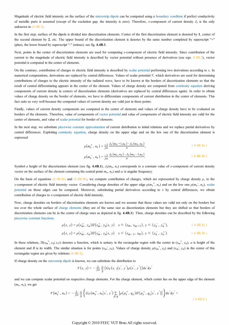
Magnitude of electric field intensity on the surface of the microstrip dipole can be computed using a boundary condition if perfect conductivity
of metallic parts is assumed (except of the excitation gap, the intensity is zero). Therefore, x-component of current density Jx is the only
unknown in (4.4B.3).
In the first step, surface of the dipole is divided into discretization elements. Center of the first discretization element is denoted by 1, center of
the second element by 2, etc. The upper bound of the discretization element is denotes by the same number completed by superscript "+"
(plus), the lower bound by superscript "-" (minus); see fig. 4.4B.1.
Next, points in the center of discretization elements are used for computing x-component of electric field intensity. Since contribution of the
current to the magnitude of electric field intensity is described by vector potential without presence of derivatives (see eqn. 4.4B.2), vector
potential is computed in the center of elements.
On the contrary, contribution of charges to electric field intensity is described by scalar potential performing two derivations according to x. In
numerical computations, derivations are replaced by central differences. Values of scalar potential V, which derivatives are used for determining
contributions of charges to the electric intensity of the radiated wave, have to be known at the borders of discretization elements so that the
result of central differentiating appears in the center of the element. Values of charge density are computed from continuity equation deriving
components of current density in centers of discretization elements (derivatives are replaced by central differences again). In order to obtain
values of charge density on the border of elements, we have to differentiate components of current distribution in the center of elements. This
fact suits us very well because the computed values of current density are valid just in these points.
Finally, values of current density components are computed in the center of elements and values of charge density have to be evaluated on
borders of the elements. Therefore, value of components of vector potential and value of components of electric field intensity are valid for the
center of elements, and value of scalar potential for border of elements.
In the next step, we substitute piecewise constant approximation of current distribution to initial relations and we replace partial derivatives by
central differences. Exploiting continuity equation, charge density on the upper edge and on the low one of the discretization element is
expressed
ρ(mx+ , nx ) =
−1jω
Jx (mx +1,nx )− Jx (mx , nx )a , ( 4.4B.4a )
ρ(mx− , nx ) =
−1jω
Jx (mx , nx )− Jx (mx −1,nx )a . ( 4.4B.4b )
Symbol a height of the discretization element (see fig. 4.4B.1), Jx(mx, nx) corresponds to a constant value of x-component of current density
vector on the surface of the element containing the central point mx, nx) and ω is angular frequency.
On the basis of equations (4.4B.4a) and (4.4B.4b), we compute contribution of charges, which are represented by charge density ρ, to the
x-component of electric field intensity vector. Considering charge densities of the upper edge ρ(mx+, nx) and on the low one ρ(mx
-, nx), scalar
potential on those edges can be computed. Moreover, substituting partial derivatives according to x by central differences, we obtain
contribution of charges to x-component of electric field intensity.
Now, charge densities on borders of discretization elements are known and we assume that those values are valid not only on the borders but
too over the whole surface of charge elements (they are of the same size as discretization elements but they are shifted so that borders of
discretization elements can be in the center of charge ones as depicted in fig. 4.4B.1). Then, charge densities can be described by the following
piecewise constant functions
ρ(x, y) = ρ(xm+ , yn)Π(xm
+ , yn||x, y) x∈ (xm , xm +1), y∈ (yn
− , yn+ ), ( 4.4B.5a )
ρ(x, y) = ρ(xm− , yn)Π(xm
− , yn||x, y) x∈ (xm −1, xm), y∈ (yn
− , yn+ ). ( 4.4B.5b )
In these relations, Π(xm+, yn| x,y) denotes a function, which is unitary in the rectangular region with the center in (xm
+, yn), a is height of the
element and B is its width. The similar situation is for points (xm-, yn). Values of charge density ρ(xm
+, yn) and (xm-, yn) in the center of this
rectangular region are given by relations (4.4B.5).
If charge density on the microstrip dipole is known, we can substitute the distribution to
V(x, y) = −1jω∬
SGV(x, y||x
′, y ′)ρ(x ′, y ′)dx ′dy ′
and we can compute scalar potential on respective charge elements. For the charge element, which center lies on the upper edge of the element
(mx, nx), we get
V(mx+ , nx ) = −
1jω∬
S GV(mx+ , nx
||x
′, y ′) ∑p, q
[ρ(px+ , qx )Π(px
+ , qx||x
′, y ′)]dx ′dy ′ =
( 4.4B.6 )
Copyright © 2010 FEEC VUT Brno All rights reserved.
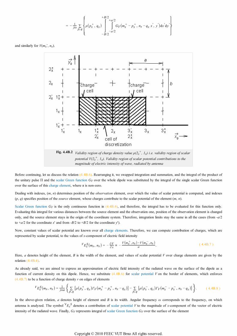
= −1jω ∑
p, q
⎧
⎨
⎩
⎪⎪⎪⎪
ρ(px+ , qx )
⌠
⌡
⎮⎮⎮
−B/2
+B/2
⌠⌡
−a /2
+a /2
GV(mx+ − px
+ , nx − qx||x
′, y ′)dx ′dy ′
⎫
⎬
⎭
⎪⎪⎪⎪
and similarly for V(mx-, nx).
Fig. 4.4B.2 Validity region of charge density value ρ(2x+, 1x) i.e. validity region of scalar
potential V(2x+, 1x). Validity region of scalar potential contributions to the
magnitude of electric intensity of wave, radiated by antenna
Before continuing, let us discuss the relation (4.4B.6). Rearranging it, we swapped integration and summation, and the integral of the product of
the unitary pulse Π and the scalar Green function GV over the whole dipole was substituted by the integral of the single scalar Green function
over the surface of this charge element, where π is non-zero.
Dealing with indexes, (m, n) determines position of the observation element, over which the value of scalar potential is computed, and indexes
(p, q) specifies position of the source element, whose charges contribute to the scalar potential of the element (m, n).
Scalar Green function GV is the only continuous function in (4.4B.6), and therefore, the integral has to be evaluated for this function only.
Evaluating this integral for various distances between the source element and the observation one, position of the observation element is changed
only, and the source element stays in the origin of the coordinate system. Therefore, integration limits stay the same in all the cases (from -a/2
to +a/2 for the coordinate x' and from -B/2 to +B/2 for the coordinate y').
Now, constant values of scalar potential are known over all charge elements. Therefore, we can compute contribution of charges, which are
represented by scalar potential, to the values of x-component of electric field intensity
V ExS(mx , nx ) = −
∂V∂ x
≅ −V(mx
+ , nx )−V(mx− , nx )
a . ( 4.4B.7 )
Here, a denotes height of the element, B is the width of the element, and values of scalar potential V over charge elements are given by the
relation (4.4B.6).
As already said, we are aimed to express an approximation of electric field intensity of the radiated wave on the surface of the dipole as a
function of current density on this dipole. Hence, we substitute (4.4B.6) for scalar potential V on the border of elements, which enforces
(4.4B.7) to be a function of charge density r on edges of elements
V ExS(mx , nx ) =
1jωa ∑
p, q[ρ(px
+ , qx )ΓV(mx+ − px
+ , nx − qx )] − ∑p, q
[ρ(px− , qx )ΓV(mx
− − px− , nx − qx )]. ( 4.4B.8 )
In the above-given relation, a denotes height of element and B is its width. Angular frequency ω corresponds to the frequency, on which
antenna is analyzed. The symbol VExS denotes a contribution of scalar potential V to the magnitude of x-component of the vector of electric
intensity of the radiated wave. Finally, GV represents integral of scalar Green function GV over the surface of the element
Copyright © 2010 FEEC VUT Brno All rights reserved.
ΓV(m − p, n − q) =⌠
⌡
⎮⎮⎮
−B/2
+B/2
⌠⌡
−a/2
+a/2
GV(m − p, n − q||x′, y ′)dx ′dy ′. ( 4.4B.9 )
As the next step in expressing electric field intensity as a function of current density, values of charge density from (4.4B.5) are substituted to
(4.4B.8)
V ExS(mx , nx ) = +
1
ω2a2∑p, q
[Jx (px + 1,qx ) − Jx (px , qx )]ΓV(mx+ − px
+ , nx − qx ) −
−1
ω2a2∑
p, q[Jx (px , qx ) − Jx (px − 1,qx )]ΓV(mx
− − px− , nx − qx ).
( 4.4B.10 )
The relation describes the contribution to the component of the vector of electric field intensity using unknown values of the component of
current distribution vector Jx and known coefficients ΓV, given by (4.4B.9). From the point of view of scalar potential, the aim was reached,
and therefore, the attention is turned to the vector potential.
In order to evaluate the contribution of the current to the electric field intensity, we have to compute vector potential substituting piecewise
constant approximation of current density to (4.4B.2a)
Ax (mx , nx ) =∬S GA
xx (mx , nx||x
′, y ′) ∑p, q
[Jx (px , qx )Π(px , qx||x
′, y ′)]dx ′dy ′
= ∑p, q
⎧
⎨
⎩
⎪⎪⎪⎪
Jx (px , qx )⌠
⌡
⎮⎮⎮
−B/2
+B/2
⌠⌡
−a /2
+a /2
GAxx (mx − px , nx − qx
||x
′, y ′)dx ′dy ′
⎫
⎬
⎭
⎪⎪⎪⎪
= ∑p, q
Jx (px , qx )ΓAxx (mx − px , nx − qx )
. ( 4.4B.11 )
In the above-given relation,
ΓAxx (m − p, n − q) =
⌠
⌡
⎮⎮⎮
−B/2
+B/2
⌠⌡
−a/2
+a/2
GAxx (m − p, n − q||x
′, y ′)dx ′dy ′. ( 4.4B.12 )
Next, a is height of the discretization element and B is its width. GAxx denotes x diagonal component of dyadic Green function. Function
Π(px, qx| x',y') is unitary over an element with the center in the point (px, qx) and is zero elsewhere. Values Jx represent piecewise constant
current density in the element mesh (px, qx).
During derivation, integration and summation were swapped, and integral over the whole dipole surface S was replaced by the integral over a
single element (due to multiplying by Π the integrand is non-zero over a single discretization element only).
Finally, substituting vector potential to (4.4B.3) and replacing derivatives of scalar potential by contributions (4.4B.10), we obtain the final
equation
ExS(mx , nx ) = − jω ∑
p, qJx (px , qx )ΓA
xx (mx − px , nx − qx ) +
+1
ω2a2∑p, q
[Jx (px + 1,qx ) − Jx (px , qx )]ΓV(mx+ − px
+ , nx − qx ) −
−1
ω2a2∑p, q
[Jx (px , qx ) − Jx (px − 1,qx )]ΓV(mx− − px
− , nx − qx ).
( 4.4B.13 )
Since eqn. (4.4B.13) is rather complicated, we rewrite it into a matrix form
Ux = Zxx Ix . ( 4.4B.14 )
Here, Ux is column vector of voltages in the direction x over elements. Voltages are computed by multiplying x-component of electric field
intensity by x-dimension of the discretization element
Ux (m, n) = Ex (m, n)a. ( 4.4B.15 )
The symbol a denotes height of the discretization element (i.e. the element dimension in the direction x).
Since the microstrip dipole is assumed to be fabricated form perfect electric conductor, the vector of voltages consists of zeros only (except of
excitation elements).
Copyright © 2010 FEEC VUT Brno All rights reserved.

Next, Ix is column vector of unknown current in the direction x. Elements of Ix are related to current density Jx by the equation
Ix (m, n) = Jx (m, n)B ( 4.4B.16 )
(B is width of the dipole, and therefore, even the width of the discretization element). Impedance matrix Zxx describes contributions of currents
Ixx and contributions of charge densities r to voltages Ux over elements. Single elements of the impedance matrix Zxx are obtained comparing
(4.4B.13) to (4.4B.16)
Zxx (m, n) =jωa
BΓ
Axx (m, n) +
1jωaB [ΓV(m + , n + ) − ΓV(m − , n + ) − ΓV(m + , n − ) + ΓV(m − , n − )]. ( 4.4B.17 )
In order to evaluate impedance matrix Zxx, we have to know values of integrals of Green functions over the surface of the discretization element
for different distances between source elements and observation ones. Numerical computation of those integrals is described in the layer D.
The Matlab program for the analysis of the microstrip dipole by the moment method is described in the layer C from user's point of view.
Copyright © 2010 FEEC VUT Brno All rights reserved.

4.4 Microstrip dipole
Matlab program
The program, which accompanies the paragraph dealing with moment analysis of the microstrip dipole, is of simple user's interface. First the
path of Matlab has to be redirected to the folder M_dipol. Then in the command window of Matlab, the basic m-file mdipol.m has to be run,
and an appearing form has to be filled in. In the form, the operation frequency of the antenna, length a width of the dipole, height and relative
permittivity of the dielectric substrate have to be given. Then, the program prints the input impedance of the dipole, and in an independent
window, current distribution on the dipole is drawn.
The program uses a fixed number of discretization elements (N = 33), the excitation gap is positioned to the center of the dipole.
Copyright © 2010 FEEC VUT Brno All rights reserved.
4.4 Microstrip dipole
Developing Matlab
Since we became familiar with theoretical basis of the moment analysis of the microstrip dipole in the layer A (and the layer B), we can turn our
attention to the software implementation of the analysis in Matlab.
First, we take care for the numerical evaluation of integrals of Green functions.
For simplicity, we introduce a variable, which expresses the distance between the actual position of the source of waves (x’, y’) and the actual
observation point (xm,yn) on the surface of the dipole
δ = (xm − x ′)2+ (yn − y ′)2√ . ( 4.4D.1 )
Using the distance δ the x diagonal component of dyadic Green function is of the form [12]
GAxx (δ) =
µ
4π exp[− jk0r0(δ)]
r0(δ) −exp[− jk0r1(δ)]
r1(δ) , ( 4.4D.2 )
where
k0 = ω µ0ε0√ ( 4.4D.3 )
denotes wave-number in the vacuum (µ0 and ε0 are permeability and permittivity of the vacuum and ω is angular frequency of the wave we are
working with). Next, distances r0 and r1 can be described by the relation
ri2(δ) = δ2 + (2ih)2
, ( 4.4D.4 )
where δ is the distance between the source and observation point on the surface of the antenna element and h is the height of the substrate.
Scalar Green function can be described by the following relation [12]
GV(δ) =1−η
4πε [exp(− jk0r0)r0
− (1 + η) ∑i = 1
∞ (−η)i−1exp(− jk0ri)ri ], ( 4.4D.5 )
where
η =εr −1
εr +1( 4.4D.6 )
and the rest of symbols is of the same meaning as described in layers A and B. Let us notice the infinite sum in the relation (4.4D.5). If the
dielectrics between the ground plane and the microstrip dipole is replaced by the vacuum, the sum consists of a single non-zero summand
(substituting εr = 1 to (4.4D.6) yields η = 0, and only the zero power of zero differs from zero). Increasing the value of the permittivity, the
coefficient h approaches one, and the value of summands decreases relatively slowly (the decrease is caused by the increasing value of ri).
Therefore, the number of summands has to be increased when relative permittivity rises. The following table illustrates the situation:
Tab. 4.4D.1 Number of summands for different
permittivity values
εr 2 4 6 9
i 9 16 23 33
Here, i denotes an index of the second addend in the summation (4.4D.5), which modulus is lower than 0.01 (considered parameters: f = 3
GHz, δ = 0 mm, h = 1.5 mm)
Green functions (4.4D.2) and (4.4D.5) are not of general validity. They can be used for a microstrip structure consisting of a ground plane, of a
homogeneous dielectric substrate and of a microstrip antenna element only. Moreover, those relations can be utilized for a very low distance
between sources of EM field and observation points, where electric field intensity is computed. Since we compute electric field intensity on the
surface of the microstrip antenna element, the distance between sources and observation points is satisfactorily short for exploiting (4.4D.2) and
(4.4D.5).
Now, when mathematic description of Green functions is known to us, we can start their integration over the whole surface of a discretization
element. Since analytic solution of those integrals is unknown, we perform that in a numeric way. The numeric integration does not cause any
problems if the source element differs from the destination one. In the opposite case (when computing contributions of currents and charges on
the element to the electric field intensity on the same element), the problem of singularity of the integrated function appears. If the source point
and the destination one are identical then their distance δ is zero (4.4D.1). As obvious from (4.4D.4), even the distance r0, which is present in
Copyright © 2010 FEEC VUT Brno All rights reserved.
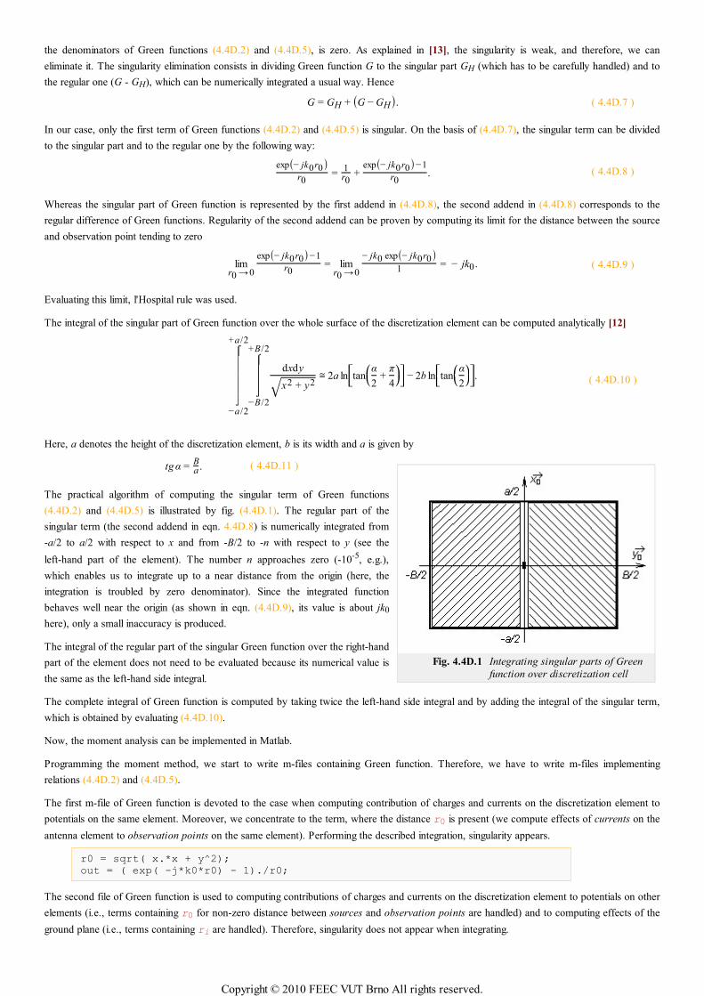
Fig. 4.4D.1 Integrating singular parts of Green
function over discretization cell
the denominators of Green functions (4.4D.2) and (4.4D.5), is zero. As explained in [13], the singularity is weak, and therefore, we can
eliminate it. The singularity elimination consists in dividing Green function G to the singular part GH (which has to be carefully handled) and to
the regular one (G - GH), which can be numerically integrated a usual way. Hence
G = GH + (G − GH). ( 4.4D.7 )
In our case, only the first term of Green functions (4.4D.2) and (4.4D.5) is singular. On the basis of (4.4D.7), the singular term can be divided
to the singular part and to the regular one by the following way:
exp(− jk0r0)r0
=1r0
+exp(− jk0r0)−1
r0. ( 4.4D.8 )
Whereas the singular part of Green function is represented by the first addend in (4.4D.8), the second addend in (4.4D.8) corresponds to the
regular difference of Green functions. Regularity of the second addend can be proven by computing its limit for the distance between the source
and observation point tending to zero
limr0 → 0
exp(− jk0r0)−1
r0= lim
r0 →0
− jk0 exp(− jk0r0)1
= − jk0 . ( 4.4D.9 )
Evaluating this limit, l'Hospital rule was used.
The integral of the singular part of Green function over the whole surface of the discretization element can be computed analytically [12]
⌠
⌡
⎮⎮⎮⎮⎮⎮⎮−a /2
+a /2
⌠
⌡⎮⎮⎮⎮
−B/2
+B/2
dxdy
x2 + y2√≅ 2a ln
⎡⎣⎢tan
⎛⎝⎜
α
2+
π
4
⎞⎠⎟⎤⎦⎥ − 2b ln
⎡⎣⎢tan
⎛⎝⎜
α
2
⎞⎠⎟⎤⎦⎥. ( 4.4D.10 )
Here, a denotes the height of the discretization element, b is its width and a is given by
tg α =Ba . ( 4.4D.11 )
The practical algorithm of computing the singular term of Green functions
(4.4D.2) and (4.4D.5) is illustrated by fig. (4.4D.1). The regular part of the
singular term (the second addend in eqn. 4.4D.8) is numerically integrated from
-a/2 to a/2 with respect to x and from -B/2 to -n with respect to y (see the
left-hand part of the element). The number n approaches zero (-10-5, e.g.),
which enables us to integrate up to a near distance from the origin (here, the
integration is troubled by zero denominator). Since the integrated function
behaves well near the origin (as shown in eqn. (4.4D.9), its value is about jk0
here), only a small inaccuracy is produced.
The integral of the regular part of the singular Green function over the right-hand
part of the element does not need to be evaluated because its numerical value is
the same as the left-hand side integral.
The complete integral of Green function is computed by taking twice the left-hand side integral and by adding the integral of the singular term,
which is obtained by evaluating (4.4D.10).
Now, the moment analysis can be implemented in Matlab.
Programming the moment method, we start to write m-files containing Green function. Therefore, we have to write m-files implementing
relations (4.4D.2) and (4.4D.5).
The first m-file of Green function is devoted to the case when computing contribution of charges and currents on the discretization element to
potentials on the same element. Moreover, we concentrate to the term, where the distance r0 is present (we compute effects of currents on the
antenna element to observation points on the same element). Performing the described integration, singularity appears.
r0 = sqrt( x.*x + y^2);
out = ( exp( -j*k0*r0) - 1)./r0;
The second file of Green function is used to computing contributions of charges and currents on the discretization element to potentials on other
elements (i.e., terms containing r0 for non-zero distance between sources and observation points are handled) and to computing effects of the
ground plane (i.e., terms containing ri are handled). Therefore, singularity does not appear when integrating.
Copyright © 2010 FEEC VUT Brno All rights reserved.

r1 = sqrt( (x+xdis).*(x+xdis) + y^2 + (2*i*h)^2); out = exp( -j*k0*r1)./r1;
In the above-given source code, x and y denote the position of a source. Sources are assumed on an element, which center corresponds to the
origin of the coordinate system (0, 0). The distance between the center of the observation element and the center of the source element in
x-direction is given by the parameter xdis. The parameter h denotes the distance between the dipole and the reflector, and k0 is wave-number
in vacuum (where the antenna is placed).
Integrating Green function, parameters x and y vary over the whole surface of the observation element. Parameters xdis, h and k0 are
constant during integration. Nevertheless values of constant parameters have to be passed on m-files of Green functions. Passing on is
implemented by declaring xdis, h and k0 as global variables. Then, content of these variables is visible from any m-file of the program.
Global variables are declared by typing
global h k0 xdis i
both at the beginning of the main m-file and at the beginning of all m-files, which exploit these variables.
Finally, integration variables x and y are passed on m-files as parameters in their headers:
function out = regular( x, y)
Now, Green functions are ready to integration over the whole surface of the element, and therefore, the main m-file can be written. After initial
declarations (determining frequency, antenna dimensions, and the discretization mesh), a cycle over all the possible distances of discretization
elements is programmed. For each distance, we evaluate integrals of Green functions and we store them to the array psi. The first index of
psi indicates the distance between the source element and the observation one in x-direction, the second index can be up to the value Ne
(integral of the term of Green function, which contains the distance rn). The whole cycle can be of the following form:
psi = zeros( Nx+2, Ne);
for m=1:(Nx+2)
xdis = (m-1)*a; % horizontal distance of element centers
if m==1
psi(m,1) = 2*dblquad('singular', -a/2, +a/2, 1e-10, B/2, 1e-3,
'quad');
psi(m,1) = psi(m,1) + stt;
else
i = 0;
psi(m,1) = dblquad('regular', -a/2, +a/2, -B/2, B/2, 1e-3, 'quad');
end
for i=1:Ne
psi(m,i+1) = dblquad('regular', -a/2, +a/2, -B/2, B/2, 1e-3,
'quad');
end
end
The above-given source code shows that the singular function is integrated in such a case only, when the source discretization element and the
observation one are identical (m = 1) and when the effect of the reflector is not handled.
As already explained, the singular Green function is numerically integrated up to the close distance of the singularity (i.e., up to the distance
10-10 meters), and then, the value of the analytically computed integral of the singular part (4.4D.10) is added
alp = atan( b/a);
stt = 2*a*log( tan( alp/2+pi/4)) - 2*b*log( tan( alp/2));
The double integral is numerically evaluated using the standard Matlab function dblquad. The first parameter is the string containing the name
of the m-file, where he integrated function is implemented. Integration limits of the first integration variable are the second parameter and the
third one (the variable has to be the first parameter in the header of the m-file containing the integrated function). Integration limits of the second
integration variable are the fourth parameter and the fifth one (the variable has to be the second parameter in the header of the m-file containing
the integrated function).
The sixth parameter of dblquad can be used for determining accuracy of numeric integration, and the last parameter can specify the algorithm
of numeric integration.
When integrals of Green functions are evaluated for all the possible distances between elements, the impedance matrix Zxx (4.4A.14, 4.4B.17)
can be composed. Composing can be performed by the following source code:
G = ( psi(:,1) - psi(:,2))/(4*pi);
cf1 = (1-eta)/(j*omg*ep0*epr*a*B);
cf2 = j*omg*mi0*a/B;
Copyright © 2010 FEEC VUT Brno All rights reserved.

% relation betw. currents and voltages
ix = 0;
Zxx = zeros( Nx, Nx);
for m=1:Nx % over observation elements in x
ix = ix + 1; iy = 0;
for o=1:Nx % over source elements in x
dx = abs( m-o); % distance source - observation
iy = iy + 1;
hlp = 2*psi( 1+dx,1) - psi( 1+abs(dx+1),1) - psi( 1+abs(dx-1), 1);
for i=1:Ne
inc = ( 2*psi(1+dx,i+1)-psi(1+abs(dx+1),i+1)-psi(1+abs(dx-
1),i+1)); hlp = hlp - (1+eta)*(-eta)^(i-1)*inc;
end
Zxx(ix,iy) = cf1*hlp/(4*pi) + cf2*G(1+dx,1);
end
end
The source code corresponds to relations (4.4A.14) and (4.4B.17).
Inverting the impedance matrix, admitance matrix is obtained. If excitation voltage 1 V is assumed, elements of the admitance matrix directly
equal to currents on the microstrip dipole. Inverting the element of the admitance matrix, which corresponds to the excitation element, input
impedance of the antenna is obtained.
Copyright © 2010 FEEC VUT Brno All rights reserved.

4.4 Microstrip dipole
Java applet
Copyright © 2010 FEEC VUT Brno All rights reserved.

4.4 Microstrip dipole
Quiz
Answer these questions to get feedback on how well you understand the course. Only one of the answers is correct. You don't have to answer
every question. If you don't know the answer you can just leave it blank (default option: “I won't answer this question”) and this won't affect
your score. Answering correctly will add 2 points to your score but on the other hand you'll lose 1 point if your answer is wrong. The
questions are divided in groups of five questions.
Press See result after you have finished answering.
Displaying questions 1..10 of 10:
Question 1
Microstrip dipole etched on a microwave substrate …
Possible answers for question 1:
… behaves the same way as a wire dipole completed by a plane reflector in vacuum.
… exhibits rather complicated behavior due to the wave reflections on the boundary of the dielectric substrate and the vacuum.
… behaves the same way as a wire dipole completed by a plane reflector in free space, which permittivity equals to the arithmetic
average of the permittivity of vacuum and the permittivity of the substrate.
I won't answer this question
Question 2
Green functions describe how …
Possible answers for question 2:
… currents contribute to vector potential and charges contribute to scalar potential.
… current distribution on the antenna influences the directivity pattern.
… current distribution contributes to input impedance of the antenna.
I won't answer this question
Question 3
Dyadic Green function …
Possible answers for question 3:
… and Green function are two names for the same thing.
… is 3 x 3 matrix of functions relating contributions of current density components to vector potential components.
… is 3 x 3 matrix of functions for anisotropic non-linear substrates only.
I won't answer this question
Question 4
Continuity theorem …
Possible answers for question 4:
… relates charges and currents on the dipole.
… expresses the fact that electromagnetic wave is continuously radiated by the antenna.
… explains the continuity of current distribution.
I won't answer this question
Question 5
If the frequency of the microstrip dipole antenna decreases, the phase interval of the current distribution of the microstrip
dipole antenna …
Copyright © 2010 FEEC VUT Brno All rights reserved.

Possible answers for question 5:
… decreases too.
… increases.
… is not much affected.
I won't answer this question
Question 6
If the heigth of the substrate (of the microstrip dipole antenna) is decreased below its default value 10 [in the applet on
layer E], then the module of the current distribution of the microstrip dipole …
Possible answers for question 6:
… decreases too.
… increases.
… is not much affected.
I won't answer this question
Question 7
At the ends of a half-wave dipole the …
Possible answers for question 7:
… voltage and current are both high.
… voltage is high and current is low.
… voltage is low and current is high.
I won't answer this question
Question 8
A circular microstrip antenna element has a radius of 60 mm with εr = 2.0 and thickness t = 2.0 mm. The lowest mode giving
a maximum in the radiation pattern in the broadside direction (normal to the plane of the disc) has a frequency fr of …
Possible answers for question 8:
… 1.003 GHz.
… 1.036 GHz.
… 1.069 GHz.
I won't answer this question
Question 9
In the design described in the above question, the patch is excited by a 50Ω coaxial probe feed at a point along a radial line
where the calculated Rin = 50Ω. The inner conductor of the coaxial feed has a radius of 1 mm. The required capacitive
element C in series with the probe to make the antenna resonant is approximately …
Possible answers for question 9:
… 15.37 pF.
… 100.31 pF.
… non of the above.
I won't answer this question
Question 10
The microstrip antenna is in resonance when the length of the microstrip element equals to …
Copyright © 2010 FEEC VUT Brno All rights reserved.

Possible answers for question 10:
… the double of the wavelength on the widened transmission line.
… the wavelength on the widened transmission line.
… the half of the wavelength on the widened transmission line.
I won't answer this question
Copyright © 2010 FEEC VUT Brno All rights reserved.
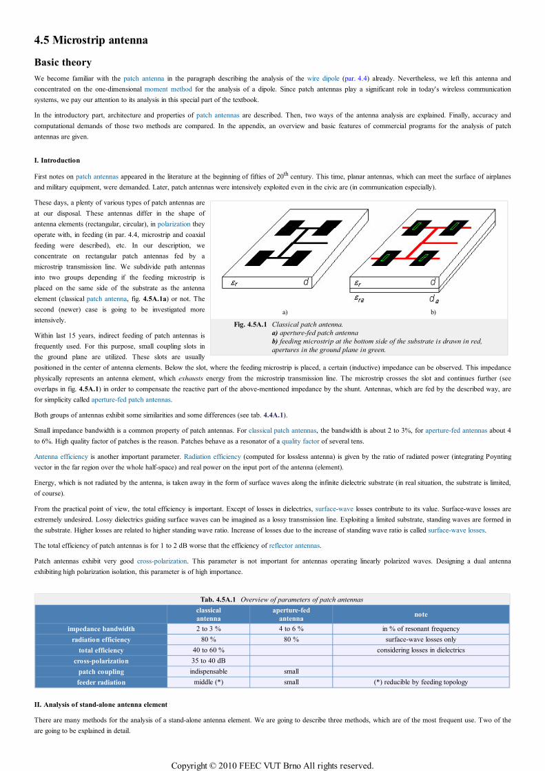
a) b)
Fig. 4.5A.1 Classical patch antenna.
a) aperture-fed patch antenna
b) feeding microstrip at the bottom side of the substrate is drawn in red,
apertures in the ground plane in green.
4.5 Microstrip antenna
Basic theory
We become familiar with the patch antenna in the paragraph describing the analysis of the wire dipole (par. 4.4) already. Nevertheless, we left this antenna and
concentrated on the one-dimensional moment method for the analysis of a dipole. Since patch antennas play a significant role in today's wireless communication
systems, we pay our attention to its analysis in this special part of the textbook.
In the introductory part, architecture and properties of patch antennas are described. Then, two ways of the antenna analysis are explained. Finally, accuracy and
computational demands of those two methods are compared. In the appendix, an overview and basic features of commercial programs for the analysis of patch
antennas are given.
I. Introduction
First notes on patch antennas appeared in the literature at the beginning of fifties of 20th century. This time, planar antennas, which can meet the surface of airplanes
and military equipment, were demanded. Later, patch antennas were intensively exploited even in the civic are (in communication especially).
These days, a plenty of various types of patch antennas are
at our disposal. These antennas differ in the shape of
antenna elements (rectangular, circular), in polarization they
operate with, in feeding (in par. 4.4, microstrip and coaxial
feeding were described), etc. In our description, we
concentrate on rectangular patch antennas fed by a
microstrip transmission line. We subdivide path antennas
into two groups depending if the feeding microstrip is
placed on the same side of the substrate as the antenna
element (classical patch antenna, fig. 4.5A.1a) or not. The
second (newer) case is going to be investigated more
intensively.
Within last 15 years, indirect feeding of patch antennas is
frequently used. For this purpose, small coupling slots in
the ground plane are utilized. These slots are usually
positioned in the center of antenna elements. Below the slot, where the feeding microstrip is placed, a certain (inductive) impedance can be observed. This impedance
physically represents an antenna element, which exhausts energy from the microstrip transmission line. The microstrip crosses the slot and continues further (see
overlaps in fig. 4.5A.1) in order to compensate the reactive part of the above-mentioned impedance by the shunt. Antennas, which are fed by the described way, are
for simplicity called aperture-fed patch antennas.
Both groups of antennas exhibit some similarities and some differences (see tab. 4.4A.1).
Small impedance bandwidth is a common property of patch antennas. For classical patch antennas, the bandwidth is about 2 to 3%, for aperture-fed antennas about 4
to 6%. High quality factor of patches is the reason. Patches behave as a resonator of a quality factor of several tens.
Antenna efficiency is another important parameter. Radiation efficiency (computed for lossless antenna) is given by the ratio of radiated power (integrating Poynting
vector in the far region over the whole half-space) and real power on the input port of the antenna (element).
Energy, which is not radiated by the antenna, is taken away in the form of surface waves along the infinite dielectric substrate (in real situation, the substrate is limited,
of course).
From the practical point of view, the total efficiency is important. Except of losses in dielectrics, surface-wave losses contribute to its value. Surface-wave losses are
extremely undesired. Lossy dielectrics guiding surface waves can be imagined as a lossy transmission line. Exploiting a limited substrate, standing waves are formed in
the substrate. Higher losses are related to higher standing wave ratio. Increase of losses due to the increase of standing wave ratio is called surface-wave losses.
The total efficiency of patch antennas is for 1 to 2 dB worse that the efficiency of reflector antennas.
Patch antennas exhibit very good cross-polarization. This parameter is not important for antennas operating linearly polarized waves. Designing a dual antenna
exhibiting high polarization isolation, this parameter is of high importance.
Tab. 4.5A.1 Overview of parameters of patch antennas
classical
antenna
aperture-fed
antennanote
impedance bandwidth 2 to 3 % 4 to 6 % in % of resonant frequency
radiation efficiency 80 % 80 % surface-wave losses only
total efficiency 40 to 60 % considering losses in dielectrics
cross-polarization 35 to 40 dB
patch coupling indispensable small
feeder radiation middle (*) small (*) reducible by feeding topology
II. Analysis of stand-alone antenna element
There are many methods for the analysis of a stand-alone antenna element. We are going to describe three methods, which are of the most frequent use. Two of the
are going to be explained in detail.
Copyright © 2010 FEEC VUT Brno All rights reserved.
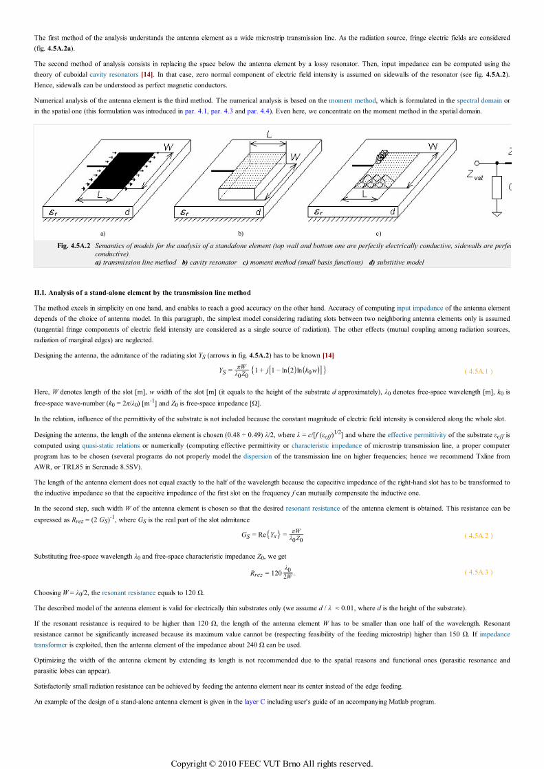
The first method of the analysis understands the antenna element as a wide microstrip transmission line. As the radiation source, fringe electric fields are considered
(fig. 4.5A.2a).
The second method of analysis consists in replacing the space below the antenna element by a lossy resonator. Then, input impedance can be computed using the
theory of cuboidal cavity resonators [14]. In that case, zero normal component of electric field intensity is assumed on sidewalls of the resonator (see fig. 4.5A.2).
Hence, sidewalls can be understood as perfect magnetic conductors.
Numerical analysis of the antenna element is the third method. The numerical analysis is based on the moment method, which is formulated in the spectral domain or
in the spatial one (this formulation was introduced in par. 4.1, par. 4.3 and par. 4.4). Even here, we concentrate on the moment method in the spatial domain.
a) b) c)
Fig. 4.5A.2 Semantics of models for the analysis of a standalone element (top wall and bottom one are perfectly electrically conductive, sidewalls are perfectly magnetically
conductive).
a) transmission line method b) cavity resonator c) moment method (small basis functions) d) substitive model
II.I. Analysis of a stand-alone element by the transmission line method
The method excels in simplicity on one hand, and enables to reach a good accuracy on the other hand. Accuracy of computing input impedance of the antenna element
depends of the choice of antenna model. In this paragraph, the simplest model considering radiating slots between two neighboring antenna elements only is assumed
(tangential fringe components of electric field intensity are considered as a single source of radiation). The other effects (mutual coupling among radiation sources,
radiation of marginal edges) are neglected.
Designing the antenna, the admitance of the radiating slot YS (arrows in fig. 4.5A.2) has to be known [14]
YS =πW
λ0Z01 + j[1 − ln(2)ln(k0w)] ( 4.5A.1 )
Here, W denotes length of the slot [m], w width of the slot [m] (it equals to the height of the substrate d approximately), λ0 denotes free-space wavelength [m], k0 is
free-space wave-number (k0 = 2π/λ0) [m-1] and Z0 is free-space impedance [Ω].
In the relation, influence of the permittivity of the substrate is not included because the constant magnitude of electric field intensity is considered along the whole slot.
Designing the antenna, the length of the antenna element is chosen (0.48 ÷ 0.49) λ/2, where λ = c/[f (εeff)1/2] and where the effective permittivity of the substrate εeff is
computed using quasi-static relations or numerically (computing effective permittivity or characteristic impedance of microstrip transmission line, a proper computer
program has to be chosen (several programs do not properly model the dispersion of the transmission line on higher frequencies; hence we recommend Txline from
AWR, or TRL85 in Serenade 8.5SV).
The length of the antenna element does not equal exactly to the half of the wavelength because the capacitive impedance of the right-hand slot has to be transformed to
the inductive impedance so that the capacitive impedance of the first slot on the frequency f can mutually compensate the inductive one.
In the second step, such width W of the antenna element is chosen so that the desired resonant resistance of the antenna element is obtained. This resistance can be
expressed as Rrez = (2 GS)-1, where GS is the real part of the slot admitance
GS = ReYs =πW
λ0Z0( 4.5A.2 )
Substituting free-space wavelength λ0 and free-space characteristic impedance Z0, we get
Rrez = 120λ02W
. ( 4.5A.3 )
Choosing W = λ0/2, the resonant resistance equals to 120 Ω.
The described model of the antenna element is valid for electrically thin substrates only (we assume d / λ ≈ 0.01, where d is the height of the substrate).
If the resonant resistance is required to be higher than 120 Ω, the length of the antenna element W has to be smaller than one half of the wavelength. Resonant
resistance cannot be significantly increased because its maximum value cannot be (respecting feasibility of the feeding microstrip) higher than 150 Ω. If impedance
transformer is exploited, then the antenna element of the impedance about 240 Ω can be used.
Optimizing the width of the antenna element by extending its length is not recommended due to the spatial reasons and functional ones (parasitic resonance and
parasitic lobes can appear).
Satisfactorily small radiation resistance can be achieved by feeding the antenna element near its center instead of the edge feeding.
An example of the design of a stand-alone antenna element is given in the layer C including user's guide of an accompanying Matlab program.
Copyright © 2010 FEEC VUT Brno All rights reserved.
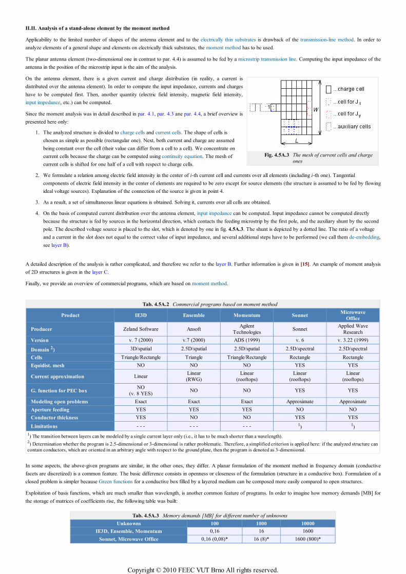
Fig. 4.5A.3 The mesh of current cells and charge
ones
II.II. Analysis of a stand-alone element by the moment method
Applicability to the limited number of shapes of the antenna element and to the electrically thin substrates is drawback of the transmission-line method. In order to
analyze elements of a general shape and elements on electrically thick substrates, the moment method has to be used.
The planar antenna element (two-dimensional one in contrast to par. 4.4) is assumed to be fed by a microstrip transmission line. Computing the input impedance of the
antenna in the position of the microstrip input is the aim of the analysis.
On the antenna element, there is a given current and charge distribution (in reality, a current is
distributed over the antenna element). In order to compute the input impedance, currents and charges
have to be computed first. Then, another quantity (electric field intensity, magnetic field intensity,
input impedance, etc.) can be computed.
Since the moment analysis was in detail described in par. 4.1, par. 4.3 ane par. 4.4, a brief overview is
presented here only:
The analyzed structure is divided to charge cells and current cells. The shape of cells is
chosen as simple as possible (rectangular one). Next, both current and charge are assumed
being constant over the cell (their value can differ from a cell to a cell). We concentrate on
current cells because the charge can be computed using continuity equation. The mesh of
current cells is shifted for one half of a cell with respect to charge cells.
1.
We formulate a relation among electric field intensity in the center of i-th current cell and currents over all elements (including i-th one). Tangential
components of electric field intensity in the center of elements are required to be zero except for source elements (the structure is assumed to be fed by flowing
ideal voltage sources). Explanation of the connection of the source is given in point 4.
2.
As a result, a set of simultaneous linear equations is obtained. Solving it, currents over all cells are obtained.3.
On the basis of computed current distribution over the antenna element, input impedance can be computed. Input impedance cannot be computed directly
because the structure is fed by sources in the horizontal direction, which contacts the feeding microstrip by the first pole, and the auxiliary shunt by the second
pole. The described voltage source is placed to the slot, which is denoted by one in fig. 4.5A.3. The shunt is depicted by a dotted line. The ratio of a voltage
and a current in the slot does not equal to the correct value of input impedance, and several additional steps have to be performed (we call them de-embedding,
see layer B).
4.
A detailed description of the analysis is rather complicated, and therefore we refer to the layer B. Further information is given in [15]. An example of moment analysis
of 2D structures is given in the layer C.
Finally, we provide an overview of commercial programs, which are based on moment method.
Tab. 4.5A.2 Commercial programs based on moment method
Product IE3D Ensemble Momentum SonnetMicrowave
Office
Producer Zeland Software AnsoftAgilent
TechnologiesSonnet
Applied Wave
Research
Version v. 7 (2000) v.7 (2000) ADS (1999) v. 6 v. 3.22 (1999)
Domain 2) 3D/spatial 2.5D/spatial 2.5D/spatial 2.5D/spectral 2.5D/spectral
Cells Triangle/Rectangle Triangle Triangle/Rectangle Rectangle Rectangle
Equidist. mesh NO NO NO YES YES
Current approximation LinearLinear
(RWG)
Linear
(rooftops)
Linear
(rooftops)
Linear
(rooftops)
G. function for PEC boxNO
(v. 8 YES)NO NO YES YES
Modeling open problems Exact Exact Exact Approximate Approximate
Aperture feeding YES YES YES NO NO
Conductor thickness YES NO NO YES YES
Limitations - - - - - - - - - 1) 1)
1) The transition between layers can be modeled by a single current layer only (i.e., it has to be much shorter than a wavelength).
2) Determination whether the program is 2.5-dimensional or 3-dimensional is rather problematic. Therefore, a simplified criterion is applied here: if the analyzed structure can
contain conductors, which are oriented in an arbitrary angle with respect to the ground plane, then the program is denoted as 3-dimensional.
In some aspects, the above-given programs are similar, in the other ones, they differ. A planar formulation of the moment method in frequency domain (conductive
facets are discretized) is a common feature. The basic difference consists in openness or closeness of the formulation (structure in a conductive box). Formulation of a
closed problem is simpler because Green functions for a conductive box filled by a layered medium can be composed more easily compared to open structures.
Exploitation of basis functions, which are much smaller than wavelength, is another common feature of programs. In order to imagine how memory demands [MB] for
the storage of matrices of coefficients rise, the following table was built:
Tab. 4.5A.3 Memory demands [MB] for different number of unknowns
Unknowns 100 1000 10000
IE3D, Ensemble, Momentum 0,16 16 1600
Sonnet, Microwave Office 0,16 (0,08)* 16 (8)* 1600 (800)*
Copyright © 2010 FEEC VUT Brno All rights reserved.

* lossless structure
A significant difference among programs is hidden in the type of the domain, where the problem is formulated. Whereas the programs, which are based on the spatial
version of the moment method, can use rectangular cells, the spectral-domain programs allow a homogeneous mesh of rectangular elements only, which leads to an
enormous size of resultant matrices. Therefore, Sonnet and Microwave Office utilize the technique of sub-domains, which are formed by summing contributions of
elementary cells. Programs Sonnet and Microwave Office exploit FFT algorithm to accelerate double summations, which replace computation of double integral in the
spectral method. The difference between Sonnet and Microwave Office is in the type of FFT: Microwave Office admits the total number of elements to be a product
of prime numbers, Sonnet is limited to the power of two due to the use of standard FFT.
Programs Sonnet and Microwave Office are advantageous (compared to space-domain programs) in real matrices of coefficients for lossless structures (twice larger
problems can be solved, and moreover, the problem is solved twice more quickly thanks to the use of real arithmetic).
All the above-described programs provide similar possibilities from the point of view of fullwave analysis. Of course, there are differences is the speed of programs. In
general, programs based on the spatial moment method exhibit higher speed than those based on the spectral version of the method. More complicated development of
programs is a price which has to be paid for that.
Simple and well-throughout user's interface is another very important feature of programs. From that point of view, Microwave Office is very popular.
Copyright © 2010 FEEC VUT Brno All rights reserved.
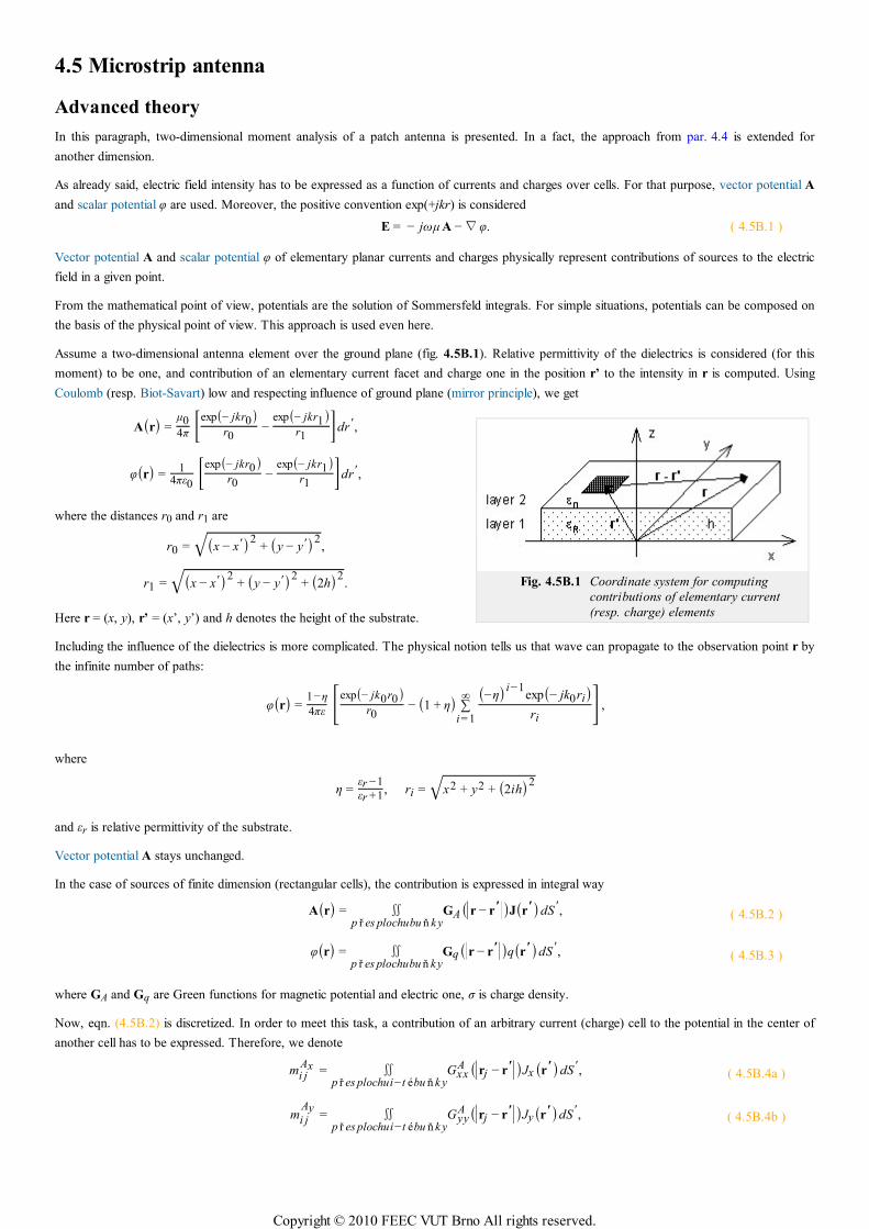
Fig. 4.5B.1 Coordinate system for computing
contributions of elementary current
(resp. charge) elements
4.5 Microstrip antenna
Advanced theory
In this paragraph, two-dimensional moment analysis of a patch antenna is presented. In a fact, the approach from par. 4.4 is extended for
another dimension.
As already said, electric field intensity has to be expressed as a function of currents and charges over cells. For that purpose, vector potential A
and scalar potential φ are used. Moreover, the positive convention exp(+jkr) is considered
E = − jωµ A −∇φ. ( 4.5B.1 )
Vector potential A and scalar potential φ of elementary planar currents and charges physically represent contributions of sources to the electric
field in a given point.
From the mathematical point of view, potentials are the solution of Sommersfeld integrals. For simple situations, potentials can be composed on
the basis of the physical point of view. This approach is used even here.
Assume a two-dimensional antenna element over the ground plane (fig. 4.5B.1). Relative permittivity of the dielectrics is considered (for this
moment) to be one, and contribution of an elementary current facet and charge one in the position r’ to the intensity in r is computed. Using
Coulomb (resp. Biot-Savart) low and respecting influence of ground plane (mirror principle), we get
A(r) =µ04π [
exp(− jkr0)r0
−exp(− jkr1)
r1 ]dr ′,
φ(r) =1
4πε0 [exp(− jkr0)
r0−
exp(− jkr1)r1 ]dr ′,
where the distances r0 and r1 are
r0 = (x − x ′)2+ (y − y ′)2√ ,
r1 = (x − x ′)2+ (y − y ′)2
+ (2h)2√ .
Here r = (x, y), r’ = (x’, y’) and h denotes the height of the substrate.
Including the influence of the dielectrics is more complicated. The physical notion tells us that wave can propagate to the observation point r by
the infinite number of paths:
φ(r) =1−η
4πε [exp(− jk0r0)r0
− (1 + η) ∑i= 1
∞ (−η)i−1exp(− jk0ri)ri ],
where
η =εr −1
εr +1, ri = x2 + y2 + (2ih)2√
and εr is relative permittivity of the substrate.
Vector potential A stays unchanged.
In the case of sources of finite dimension (rectangular cells), the contribution is expressed in integral way
A(r) = ∬p ř es plochu bu ň ky
GA(||r − r ′ ||)J(r′) dS ′, ( 4.5B.2 )
φ(r) = ∬p ř es plochu bu ň ky
Gq(||r − r′ ||)q(r ′) dS ′, ( 4.5B.3 )
where GA and Gq are Green functions for magnetic potential and electric one, σ is charge density.
Now, eqn. (4.5B.2) is discretized. In order to meet this task, a contribution of an arbitrary current (charge) cell to the potential in the center of
another cell has to be expressed. Therefore, we denote
mi jAx = ∬
p ř es plochu i− t é bu ň k yGxx
A (||rj − r′ ||)Jx (r ′) dS ′, ( 4.5B.4a )
mi j
Ay= ∬
p ř es plochu i− t é bu ň k yGyy
A (||rj − r′ ||)Jy(r ′) dS ′, ( 4.5B.4b )
Copyright © 2010 FEEC VUT Brno All rights reserved.
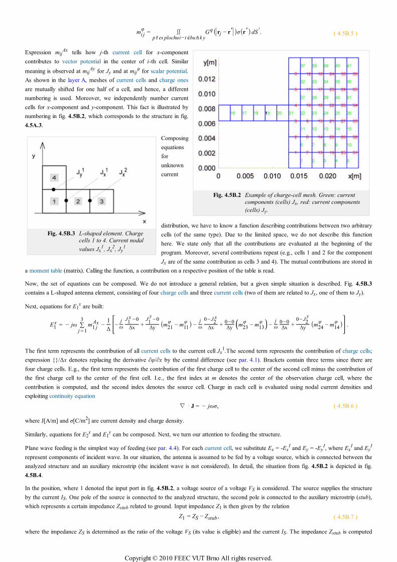
Fig. 4.5B.2 Example of charge-cell mesh. Green: current
components (cells) Jx, red: current components
(cells) Jy.
Fig. 4.5B.3 L-shaped element. Charge
cells 1 to 4. Current nodal
values Jx1, Jx
2, Jy1
mi jφ
= ∬p ř es plochu i− t é bu ň k y
Gq(||rj − r′ ||)σ(r ′) dS ′. ( 4.5B.5 )
Expression mijAx tells how j-th current cell for x-component
contributes to vector potential in the center of i-th cell. Similar
meaning is observed at mijAy for Jy and at mij
φ for scalar potential.
As shown in the layer A, meshes of current cells and charge ones
are mutually shifted for one half of a cell, and hence, a different
numbering is used. Moreover, we independently number current
cells for x-component and y-component. This fact is illustrated by
numbering in fig. 4.5B.2, which corresponds to the structure in fig.
4.5A.3.
Composing
equations
for
unknown
current
distribution, we have to know a function describing contributions between two arbitrary
cells (of the same type). Due to the limited space, we do not describe this function
here. We state only that all the contributions are evaluated at the beginning of the
program. Moreover, several contributions repeat (e.g., cells 1 and 2 for the component
Jx are of the same contribution as cells 3 and 4). The mutual contributions are stored in
a moment table (matrix). Calling the function, a contribution on a respective position of the table is read.
Now, the set of equations can be composed. We do not introduce a general relation, but a given simple situation is described. Fig. 4.5B.3
contains a L-shaped antenna element, consisting of four charge cells and three current cells (two of them are related to Jx, one of them to Jy).
Next, equations for E1x are built:
E1x = − jω ∑
j = 1
3m
1 jAx −
1
∆[−j
ω
J1x −0
∆x+
J1y
−0
∆y (m21φ
− m11φ ) −
j
ω
0− J2x
∆x+
0−0∆y
⎛⎝m23φ
− m13φ ⎞⎠ −
j
ω0−0∆x
+0− J
2y
∆y (m24φ
− m14φ )].
The first term represents the contribution of all current cells to the current cell Jx1.The second term represents the contribution of charge cells;
expression /∆x denotes replacing the derivative ∂φ/∂x by the central difference (see par. 4.1). Brackets contain three terms since there are
four charge cells. E.g., the first term represents the contribution of the first charge cell to the center of the second cell minus the contribution of
the first charge cell to the center of the first cell. I.e., the first index at m denotes the center of the observation charge cell, where the
contribution is computed, and the second index denotes the source cell. Charge in each cell is evaluated using nodal current densities and
exploiting continuity equation
∇ ⋅ J = − jωσ, ( 4.5B.6 )
where J[A/m] and σ[C/m2] are current density and charge density.
Similarly, equations for E2x and E1
y can be composed. Next, we turn our attention to feeding the structure.
Plane wave feeding is the simplest way of feeding (see par. 4.4). For each current cell, we substitute Ex = -ExI and Ey = -Ey
I, where ExI and Ey
I
represent components of incident wave. In our situation, the antenna is assumed to be fed by a voltage source, which is connected between the
analyzed structure and an auxiliary microstrip (the incident wave is not considered). In detail, the situation from fig. 4.5B.2 is depicted in fig.
4.5B.4.
In the position, where 1 denoted the input port in fig. 4.5B.2, a voltage source of a voltage VS is considered. The source supplies the structure
by the current IS. One pole of the source is connected to the analyzed structure, the second pole is connected to the auxiliary microstrip (stub),
which represents a certain impedance Zstub related to ground. Input impedance Z1 is then given by the relation
Z1 = ZS − Zstub , ( 4.5B.7 )
where the impedance ZS is determined as the ratio of the voltage VS (its value is eligible) and the current IS. The impedance Zstub is computed
Copyright © 2010 FEEC VUT Brno All rights reserved.
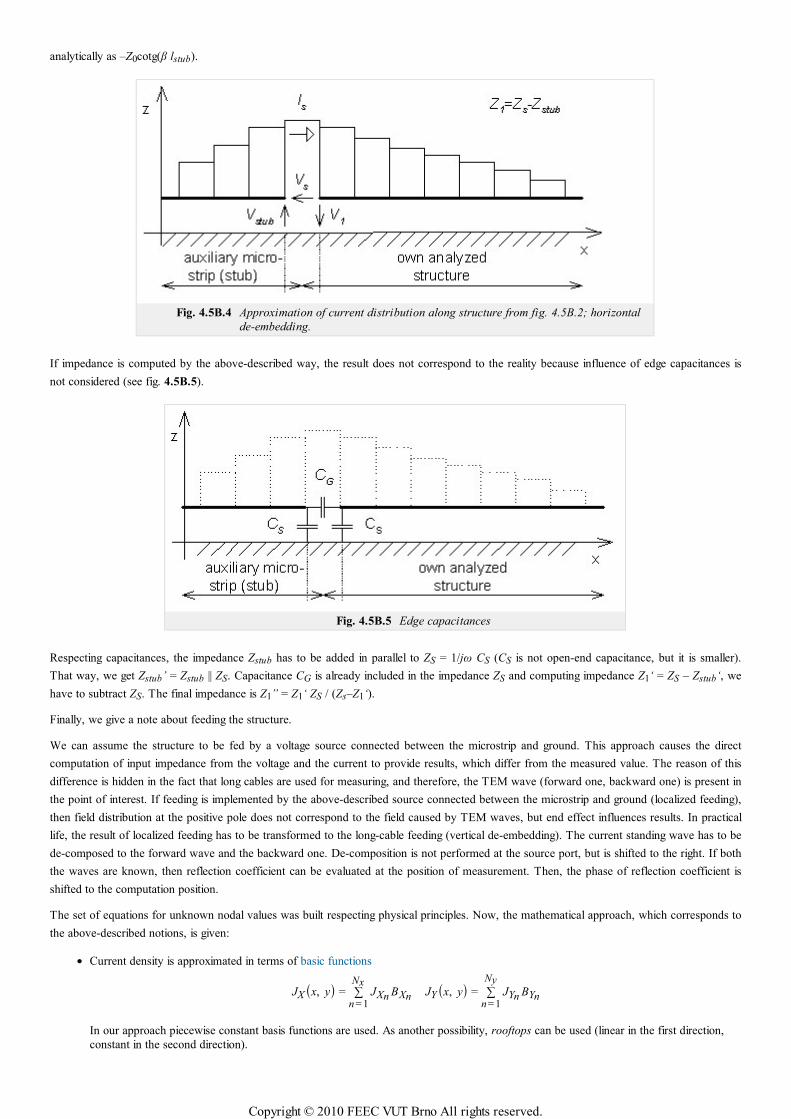
analytically as –Z0cotg(β lstub).
Fig. 4.5B.4 Approximation of current distribution along structure from fig. 4.5B.2; horizontal
de-embedding.
If impedance is computed by the above-described way, the result does not correspond to the reality because influence of edge capacitances is
not considered (see fig. 4.5B.5).
Fig. 4.5B.5 Edge capacitances
Respecting capacitances, the impedance Zstub has to be added in parallel to ZS = 1/jω CS (CS is not open-end capacitance, but it is smaller).
That way, we get Zstub’ = Zstub || ZS. Capacitance CG is already included in the impedance ZS and computing impedance Z1‘ = ZS – Zstub‘, we
have to subtract ZS. The final impedance is Z1” = Z1‘ ZS / (Zs–Z1‘).
Finally, we give a note about feeding the structure.
We can assume the structure to be fed by a voltage source connected between the microstrip and ground. This approach causes the direct
computation of input impedance from the voltage and the current to provide results, which differ from the measured value. The reason of this
difference is hidden in the fact that long cables are used for measuring, and therefore, the TEM wave (forward one, backward one) is present in
the point of interest. If feeding is implemented by the above-described source connected between the microstrip and ground (localized feeding),
then field distribution at the positive pole does not correspond to the field caused by TEM waves, but end effect influences results. In practical
life, the result of localized feeding has to be transformed to the long-cable feeding (vertical de-embedding). The current standing wave has to be
de-composed to the forward wave and the backward one. De-composition is not performed at the source port, but is shifted to the right. If both
the waves are known, then reflection coefficient can be evaluated at the position of measurement. Then, the phase of reflection coefficient is
shifted to the computation position.
The set of equations for unknown nodal values was built respecting physical principles. Now, the mathematical approach, which corresponds to
the above-described notions, is given:
Current density is approximated in terms of basic functions
JX(x, y) = ∑n = 1
NxJXn BXn JY(x, y) = ∑
n = 1
NyJYn BYn
In our approach piecewise constant basis functions are used. As another possibility, rooftops can be used (linear in the first direction,
constant in the second direction).
Copyright © 2010 FEEC VUT Brno All rights reserved.
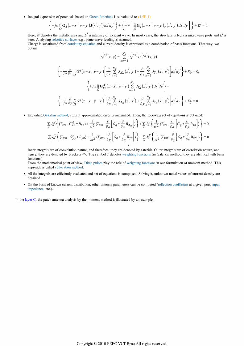
Integral expression of potentials based on Green functions is substituted to (4.5B.1)
− jω∬Ω
GA(x − x ′, y − y ′)J(x ′, y ′) dx ′d y ′ + −∇[∬Ω Gq(x − x ′, y − y ′)ρ(x ′, y ′) dx ′d y ′] + EI = 0.
Here, W denotes the metallic area and EI is intensity of incident wave. In most cases, the structure is fed via microwave ports and EI is
zero. Analyzing selective surfaces e.g., plane-wave feeding is assumed.
Charge is substituted from continuity equation and current density is expressed as a combination of basis functions. That way, we
obtain
Jx(n)(x, y) = ∑
nx =1
NxJx
(nx)Π (nx)(x, y)
⎧⎨⎩−1jω
∂∂ x∬Ω
Gq(x − x ′, y − y ′) ⎡⎣⎢
∂
∂ x∑
n = 1
NxJXn (x ′, y ′) +
∂
∂ y∑
n = 1
NyJYn (x ′, y ′)
⎤⎦⎥dx ′d y ′
⎫⎬⎭ + EXI = 0,
⎧⎨⎩+ jω∬Ω
GyyA (x − x ′, y − y ′) ∑
n = 1
NyJYn (x ′, y ′) dx ′d y ′
⎫⎬⎭ −
⎧⎨⎩−1jω
∂∂ y∬Ω
Gq(x − x ′, y − y ′) ⎡⎣⎢
∂
∂ x∑
n =1
NxJXn (x ′, y ′) +
∂
∂ y∑
n = 1
NyJYn (x ′, y ′)
⎤⎦⎥dx ′d y ′
⎫⎬⎭ + EYI = 0.
Exploiting Galerkin method, current approximation error is minimized. Then, the following set of equations is obtained:
∑n
JnX⟨Txm , Gxx
A* Bxn⟩ +
1
ω2⟨Txm ,
∂
∂ x
⎡⎣⎢Gq *
∂
∂ xBXn
⎤⎦⎥⟩ + ∑
nJn
Y 1
ω2⟨Txm ,
∂
∂ x [Gq *∂
∂ yByn]⟩ = 0,
∑n
JnX⟨Tym , Gyy
A* Byn⟩ +
1
ω2⟨Tym ,
∂
∂ y [Gq *∂
∂ yByn]⟩ + ∑
nJn
X 1
ω2⟨Tym ,
∂
∂ y
⎡⎣⎢Gq *
∂
∂ xBxn
⎤⎦⎥⟩ = 0
.
Inner integrals are of convolution nature, and therefore, they are denoted by asterisk. Outer integrals are of correlation nature, and
hence, they are denoted by brackets <>. The symbol T denotes weighting functions (in Galerkin method, they are identical with basis
functions).
From the mathematical point of view, Dirac pulses play the role of weighting functions in our formulation of moment method. This
approach is called collocation method.
All the integrals are efficiently evaluated and set of equations is composed. Solving it, unknown nodal values of current density are
obtained.
On the basis of known current distribution, other antenna parameters can be computed (reflection coefficient at a given port, input
impedance, etc.).
In the layer C, the patch antenna analysis by the moment method is illustrated by an example.
Copyright © 2010 FEEC VUT Brno All rights reserved.
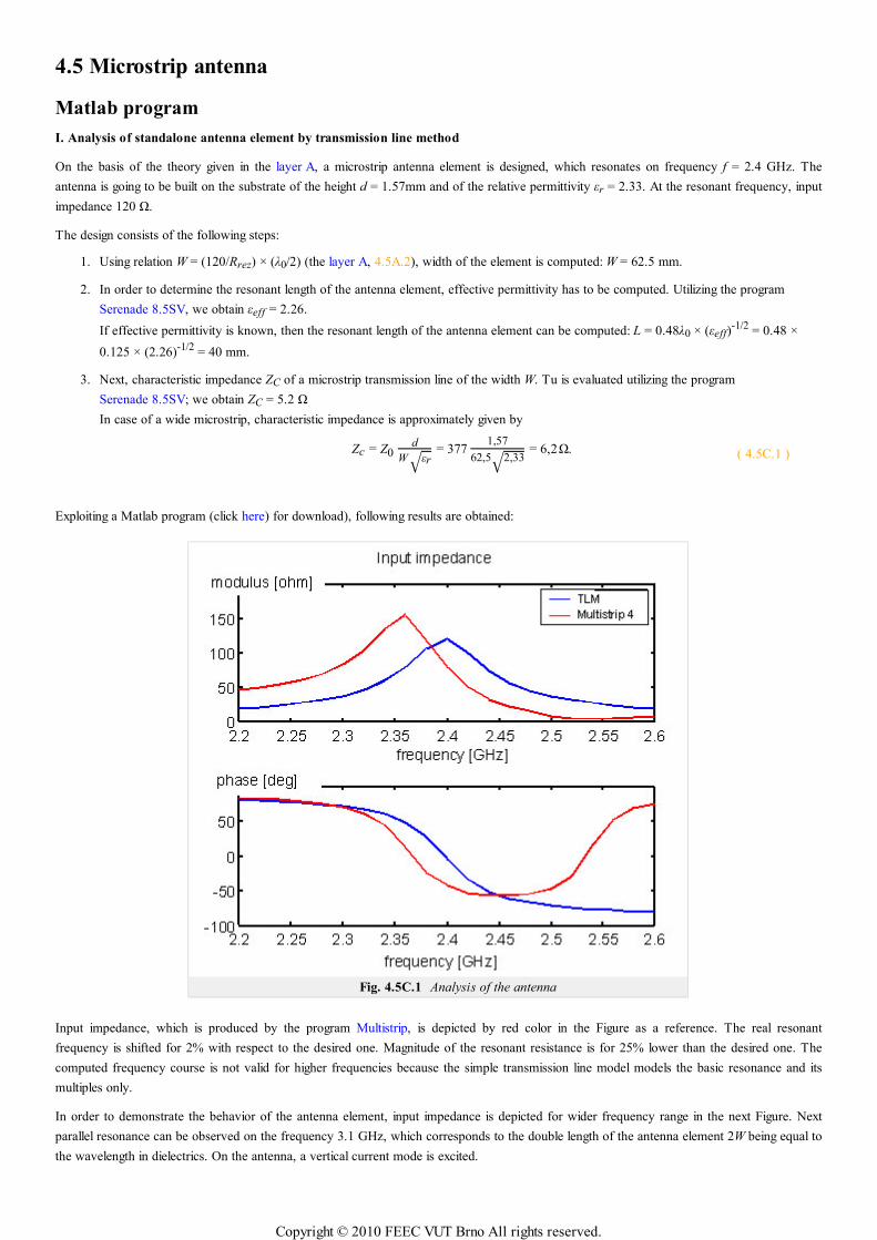
4.5 Microstrip antenna
Matlab program
I. Analysis of standalone antenna element by transmission line method
On the basis of the theory given in the layer A, a microstrip antenna element is designed, which resonates on frequency f = 2.4 GHz. The
antenna is going to be built on the substrate of the height d = 1.57mm and of the relative permittivity εr = 2.33. At the resonant frequency, input
impedance 120 Ω.
The design consists of the following steps:
Using relation W = (120/Rrez) × (λ0/2) (the layer A, 4.5A.2), width of the element is computed: W = 62.5 mm.1.
In order to determine the resonant length of the antenna element, effective permittivity has to be computed. Utilizing the program
Serenade 8.5SV, we obtain εeff = 2.26.
If effective permittivity is known, then the resonant length of the antenna element can be computed: L = 0.48λ0 × (εeff)-1/2 = 0.48 ×
0.125 × (2.26)-1/2 = 40 mm.
2.
Next, characteristic impedance ZC of a microstrip transmission line of the width W. Tu is evaluated utilizing the program
Serenade 8.5SV; we obtain ZC = 5.2 Ω
In case of a wide microstrip, characteristic impedance is approximately given by
Zc = Z0d
W εr√= 377
1,57
62,5 2,33√= 6,2 Ω. ( 4.5C.1 )
3.
Exploiting a Matlab program (click here) for download), following results are obtained:
Fig. 4.5C.1 Analysis of the antenna
Input impedance, which is produced by the program Multistrip, is depicted by red color in the Figure as a reference. The real resonant
frequency is shifted for 2% with respect to the desired one. Magnitude of the resonant resistance is for 25% lower than the desired one. The
computed frequency course is not valid for higher frequencies because the simple transmission line model models the basic resonance and its
multiples only.
In order to demonstrate the behavior of the antenna element, input impedance is depicted for wider frequency range in the next Figure. Next
parallel resonance can be observed on the frequency 3.1 GHz, which corresponds to the double length of the antenna element 2W being equal to
the wavelength in dielectrics. On the antenna, a vertical current mode is excited.
Copyright © 2010 FEEC VUT Brno All rights reserved.
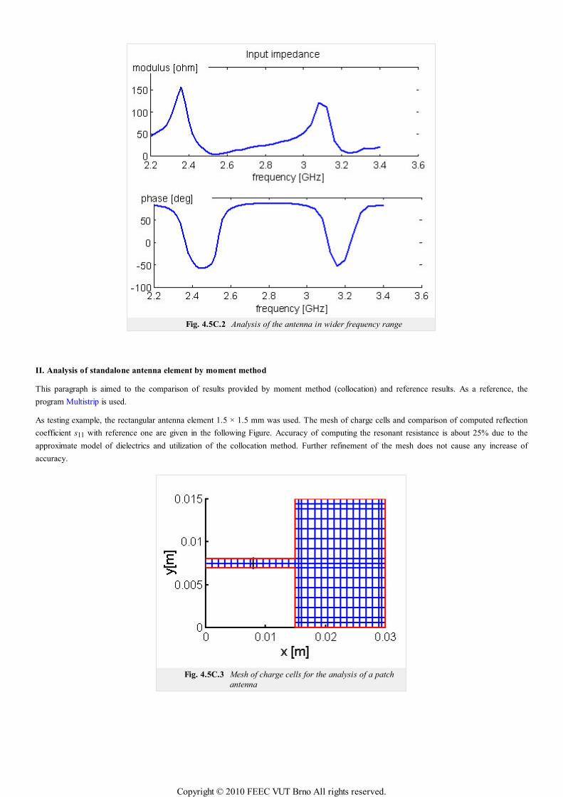
Fig. 4.5C.2 Analysis of the antenna in wider frequency range
II. Analysis of standalone antenna element by moment method
This paragraph is aimed to the comparison of results provided by moment method (collocation) and reference results. As a reference, the
program Multistrip is used.
As testing example, the rectangular antenna element 1.5 × 1.5 mm was used. The mesh of charge cells and comparison of computed reflection
coefficient s11 with reference one are given in the following Figure. Accuracy of computing the resonant resistance is about 25% due to the
approximate model of dielectrics and utilization of the collocation method. Further refinement of the mesh does not cause any increase of
accuracy.
Fig. 4.5C.3 Mesh of charge cells for the analysis of a patch
antenna
Copyright © 2010 FEEC VUT Brno All rights reserved.
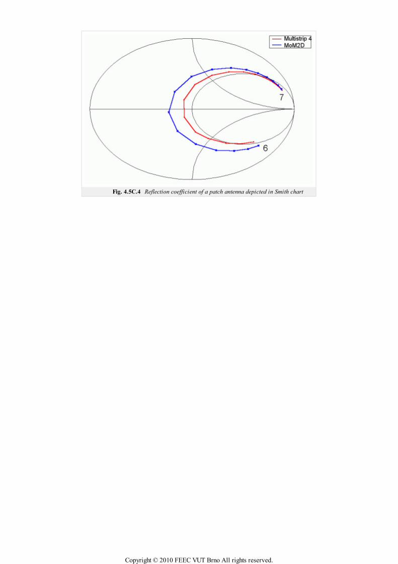
Fig. 4.5C.4 Reflection coefficient of a patch antenna depicted in Smith chart
Copyright © 2010 FEEC VUT Brno All rights reserved.
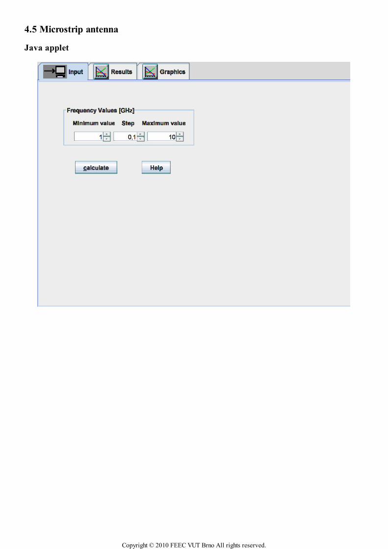
4.5 Microstrip antenna
Java applet
Copyright © 2010 FEEC VUT Brno All rights reserved.

4.5 Microstrip antenna
Quiz
Answer these questions to get feedback on how well you understand the course. Only one of the answers is correct. You don't have to answer
every question. If you don't know the answer you can just leave it blank (default option: “I won't answer this question”) and this won't affect
your score. Answering correctly will add 2 points to your score but on the other hand you'll lose 1 point if your answer is wrong. The
questions are divided in groups of five questions.
Press See result after you have finished answering.
Displaying questions 1..10 of 10:
Question 1
The aperture-fed patch antenna consists of …
Possible answers for question 1:
… the patch and the coaxial probe in the role of feeding.
… the patch and the aperture of the horn antenna in the role of the primarily radiator.
… the microstrip on the bottom, the slot in the middle, and the patch on the top.
I won't answer this question
Question 2
The patch antenna excels in …
Possible answers for question 2:
… low profile and low fabrication costs.
… low fabrication costs, and very high efficiency.
… high gain.
I won't answer this question
Question 3
The simplified analysis of the patch antenna …
Possible answers for question 3:
… considers the patch only – the antenna behaves like a wide dipole.
… assumes the antenna behaves like a dielectric resonator (non-radiating structure).
… cannot be performed – full-wave methods have to be applied.
I won't answer this question
Question 4
Surface waves degrade antenna parameters …
Possible answers for question 4:
… in case the dielectric constant of the substrate is high, and the frequency is high also.
… in case the height of the substrate is negligible compared to the wavelength.
… any time – they cannot be satisfactorily suppressed.
I won't answer this question
Question 5
Increasing the dielectric constant of the substrate …
Copyright © 2010 FEEC VUT Brno All rights reserved.

Possible answers for question 5:
… the antenna is smaller, and its parameters are not influenced.
… the antenna is smaller, and the bandwidth is narrower.
… the bandwidth is narrower, the dimensions are not influenced.
I won't answer this question
Question 6
Microstrip feeding of the microstrip antenna …
Possible answers for question 6:
… is hard to be fabricated.
… does not influence the radiation pattern of the antenna.
… simplifies the construction of antenna arrays.
I won't answer this question
Question 7
Dealing with the dimensions of the rectangular patch …
Possible answers for question 7:
… the width should equal to half wavelength on the substrate, and the length is unimportant.
… both the width and the length should equal to half wavelength on the substrate.
… the length should equal to half wavelength on the substrate, and the width is unimportant.
I won't answer this question
Question 8
Green functions for layered media …
Possible answers for question 8:
… can be exactly expressed in the closed form.
… have to be approximated (limited validity) for the practical use.
… are not used when analyzing patch antennas.
I won't answer this question
Question 9
Moment method analysis of the patch antenna …
Possible answers for question 9:
… can be performed in two dimensions when feeding is mapped to the plane of the patch.
… has to be carried out as the three-dimensional problem.
… is naturally a two-dimensional problem.
I won't answer this question
Question 10
In the moment method analysis of the patch antenna …
Possible answers for question 10:
… a single mesh is used both for x-components and for y-components.
… no meshing is needed.
… two meshes have to be used (the first one for x-components, the second one for y-components).
I won't answer this question
Copyright © 2010 FEEC VUT Brno All rights reserved.

Copyright © 2010 FEEC VUT Brno All rights reserved.
4.6 Multi-band patch antennas
Basic theory
Introduction
Telecommunication technology is one of technical fields with great interest in military, professional and also civil sphere. Due to commercial
exploitation of complex electrical devices (e.g. mobile phones), new requirements on their properties appear all the time. Engineers are
compelled to develop novel solutions they match the increasing demands on both their technical parameters and physical dimensions. Miniature
antennas of modern communication devices have to be able to receive and transmit electromagnetic waves in different frequency bands related
to different communication services.
The characteristics and analysis of single-band patch antenna was discussed in the previous chapter of the textbook. Now we turn our attention
to patch antennas with multi-band properties. First, basic practices for obtaining multi-band resonances of patch antennas are introduced.
Second, the modal analysis in the design of planar antennas is discussed. In layer B, example of a simple dual-band patch antenna and its
computational model in Ansoft HFSS and CST Microwave Studio is presented. Via this chapter, we get a short overview about multi-band
patch antennas and learn about their design. Beside this, we become familiar with two well-known simulation softwares.
Basic types of multi-band patch antennas
There are countless numbers of approaches how to obtain multi-band resonance of planar antennas. As example we can name the stacked patch
configuration, patches with slots and cuts of different shapes, antennas with shorting pins or PIFAs (planar inverted-F antennas). The mentioned
types of antennas are depicted in fig. 4.6A.1.
Considering the polarization, multi-band antennas can have parallel or orthogonal polarization in working frequency ranges. The orthogonal
polarization is preferred in systems with polarization diversity.
a) b)
c) d)
Fig. 4.6A.1 Selected types of multi-band planar antennas: stacked patch (a), rectangular patch with slots (b),
antenna with shorting pin (c), PIFA (d).
Let us now describe the working principle of antennas from fig. 4.6A.1.
In the case of stacked patch, the lower metallic patch is fed directly via connector (obviously coaxial probe) and the upper metallic patch is in
parasitic coupling with the lower one. The configuration has two resonant frequencies – the lower one is given by the dimensions of the lower
Copyright © 2010 FEEC VUT Brno All rights reserved.
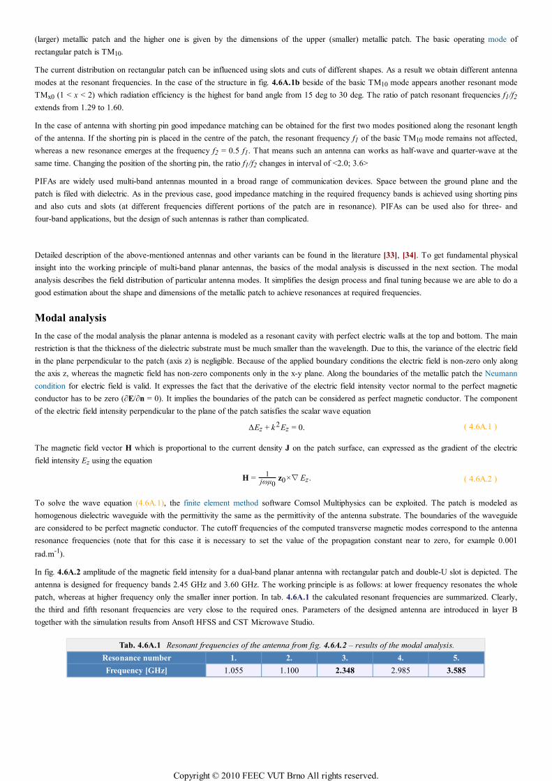
(larger) metallic patch and the higher one is given by the dimensions of the upper (smaller) metallic patch. The basic operating mode of
rectangular patch is TM10.
The current distribution on rectangular patch can be influenced using slots and cuts of different shapes. As a result we obtain different antenna
modes at the resonant frequencies. In the case of the structure in fig. 4.6A.1b beside of the basic TM10 mode appears another resonant mode
TMx0 (1 < x < 2) which radiation efficiency is the highest for band angle from 15 deg to 30 deg. The ratio of patch resonant frequencies f1/f2
extends from 1.29 to 1.60.
In the case of antenna with shorting pin good impedance matching can be obtained for the first two modes positioned along the resonant length
of the antenna. If the shorting pin is placed in the centre of the patch, the resonant frequency f1 of the basic TM10 mode remains not affected,
whereas a new resonance emerges at the frequency f2 = 0.5 f1. That means such an antenna can works as half-wave and quarter-wave at the
same time. Changing the position of the shorting pin, the ratio f1/f2 changes in interval of <2.0; 3.6>
PIFAs are widely used multi-band antennas mounted in a broad range of communication devices. Space between the ground plane and the
patch is filed with dielectric. As in the previous case, good impedance matching in the required frequency bands is achieved using shorting pins
and also cuts and slots (at different frequencies different portions of the patch are in resonance). PIFAs can be used also for three- and
four-band applications, but the design of such antennas is rather than complicated.
Detailed description of the above-mentioned antennas and other variants can be found in the literature [33], [34]. To get fundamental physical
insight into the working principle of multi-band planar antennas, the basics of the modal analysis is discussed in the next section. The modal
analysis describes the field distribution of particular antenna modes. It simplifies the design process and final tuning because we are able to do a
good estimation about the shape and dimensions of the metallic patch to achieve resonances at required frequencies.
Modal analysis
In the case of the modal analysis the planar antenna is modeled as a resonant cavity with perfect electric walls at the top and bottom. The main
restriction is that the thickness of the dielectric substrate must be much smaller than the wavelength. Due to this, the variance of the electric field
in the plane perpendicular to the patch (axis z) is negligible. Because of the applied boundary conditions the electric field is non-zero only along
the axis z, whereas the magnetic field has non-zero components only in the x-y plane. Along the boundaries of the metallic patch the Neumann
condition for electric field is valid. It expresses the fact that the derivative of the electric field intensity vector normal to the perfect magnetic
conductor has to be zero (∂E/∂n = 0). It implies the boundaries of the patch can be considered as perfect magnetic conductor. The component
of the electric field intensity perpendicular to the plane of the patch satisfies the scalar wave equation
∆Ez + k 2Ez = 0. ( 4.6A.1 )
The magnetic field vector H which is proportional to the current density J on the patch surface, can expressed as the gradient of the electric
field intensity Ez using the equation
H =1
jωµ0z0×∇Ez. ( 4.6A.2 )
To solve the wave equation (4.6A.1), the finite element method software Comsol Multiphysics can be exploited. The patch is modeled as
homogenous dielectric waveguide with the permittivity the same as the permittivity of the antenna substrate. The boundaries of the waveguide
are considered to be perfect magnetic conductor. The cutoff frequencies of the computed transverse magnetic modes correspond to the antenna
resonance frequencies (note that for this case it is necessary to set the value of the propagation constant near to zero, for example 0.001
rad.m-1).
In fig. 4.6A.2 amplitude of the magnetic field intensity for a dual-band planar antenna with rectangular patch and double-U slot is depicted. The
antenna is designed for frequency bands 2.45 GHz and 3.60 GHz. The working principle is as follows: at lower frequency resonates the whole
patch, whereas at higher frequency only the smaller inner portion. In tab. 4.6A.1 the calculated resonant frequencies are summarized. Clearly,
the third and fifth resonant frequencies are very close to the required ones. Parameters of the designed antenna are introduced in layer B
together with the simulation results from Ansoft HFSS and CST Microwave Studio.
Tab. 4.6A.1 Resonant frequencies of the antenna from fig. 4.6A.2 – results of the modal analysis.
Resonance number 1. 2. 3. 4. 5.
Frequency [GHz] 1.055 1.100 2.348 2.985 3.585
Copyright © 2010 FEEC VUT Brno All rights reserved.
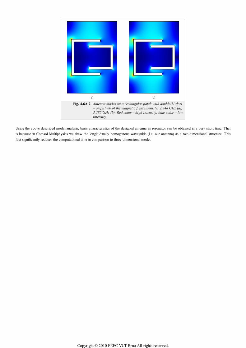
a) b)
Fig. 4.6A.2 Antenna modes on a rectangular patch with double-U slots
– amplitude of the magnetic field intensity: 2.348 GHz (a),
3.585 GHz (b). Red color – high intensity, blue color – low
intensity.
Using the above described modal analysis, basic characteristics of the designed antenna as resonator can be obtained in a very short time. That
is because in Comsol Multiphysics we draw the longitudinally homogenous waveguide (i.e. our antenna) as a two-dimensional structure. This
fact significantly reduces the computational time in comparison to three-dimensional model.
Copyright © 2010 FEEC VUT Brno All rights reserved.
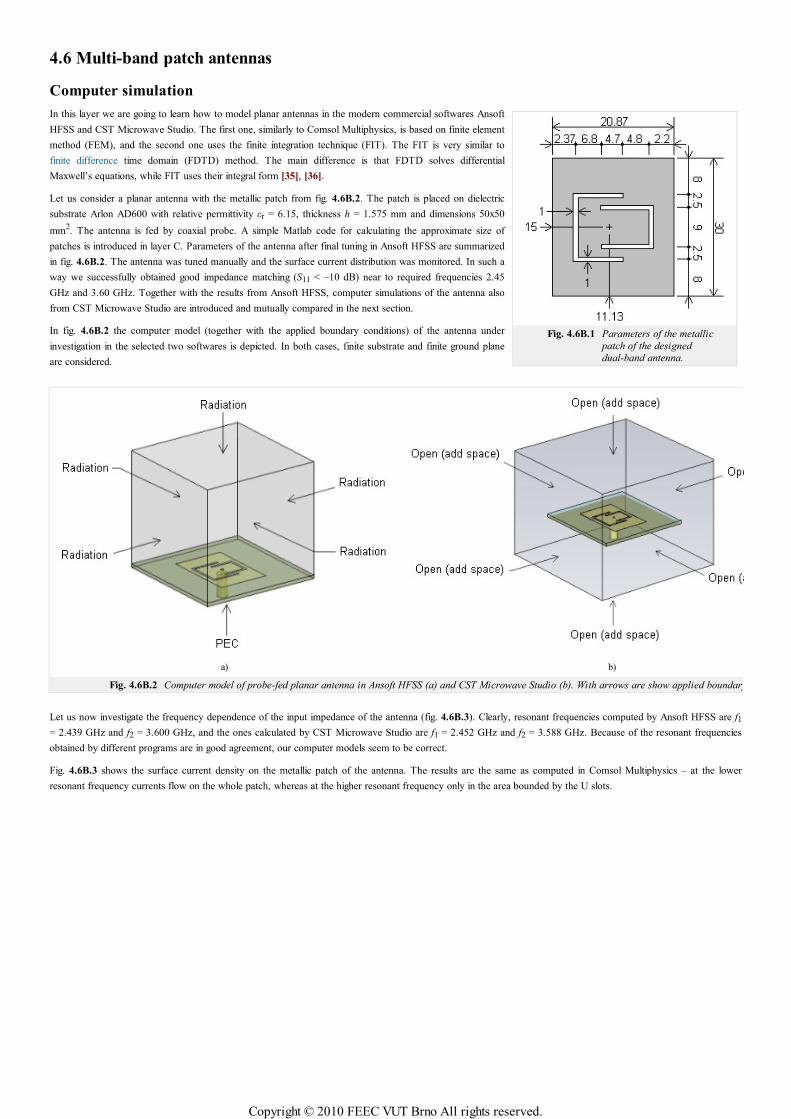
Fig. 4.6B.1 Parameters of the metallic
patch of the designed
dual-band antenna.
4.6 Multi-band patch antennas
Computer simulation
In this layer we are going to learn how to model planar antennas in the modern commercial softwares Ansoft
HFSS and CST Microwave Studio. The first one, similarly to Comsol Multiphysics, is based on finite element
method (FEM), and the second one uses the finite integration technique (FIT). The FIT is very similar to
finite difference time domain (FDTD) method. The main difference is that FDTD solves differential
Maxwell’s equations, while FIT uses their integral form [35], [36].
Let us consider a planar antenna with the metallic patch from fig. 4.6B.2. The patch is placed on dielectric
substrate Arlon AD600 with relative permittivity εr = 6.15, thickness h = 1.575 mm and dimensions 50x50
mm2. The antenna is fed by coaxial probe. A simple Matlab code for calculating the approximate size of
patches is introduced in layer C. Parameters of the antenna after final tuning in Ansoft HFSS are summarized
in fig. 4.6B.2. The antenna was tuned manually and the surface current distribution was monitored. In such a
way we successfully obtained good impedance matching (S11 < –10 dB) near to required frequencies 2.45
GHz and 3.60 GHz. Together with the results from Ansoft HFSS, computer simulations of the antenna also
from CST Microwave Studio are introduced and mutually compared in the next section.
In fig. 4.6B.2 the computer model (together with the applied boundary conditions) of the antenna under
investigation in the selected two softwares is depicted. In both cases, finite substrate and finite ground plane
are considered.
a) b)
Fig. 4.6B.2 Computer model of probe-fed planar antenna in Ansoft HFSS (a) and CST Microwave Studio (b). With arrows are show applied boundary conditions.
Let us now investigate the frequency dependence of the input impedance of the antenna (fig. 4.6B.3). Clearly, resonant frequencies computed by Ansoft HFSS are f1
= 2.439 GHz and f2 = 3.600 GHz, and the ones calculated by CST Microwave Studio are f1 = 2.452 GHz and f2 = 3.588 GHz. Because of the resonant frequencies
obtained by different programs are in good agreement, our computer models seem to be correct.
Fig. 4.6B.3 shows the surface current density on the metallic patch of the antenna. The results are the same as computed in Comsol Multiphysics – at the lower
resonant frequency currents flow on the whole patch, whereas at the higher resonant frequency only in the area bounded by the U slots.
Copyright © 2010 FEEC VUT Brno All rights reserved.
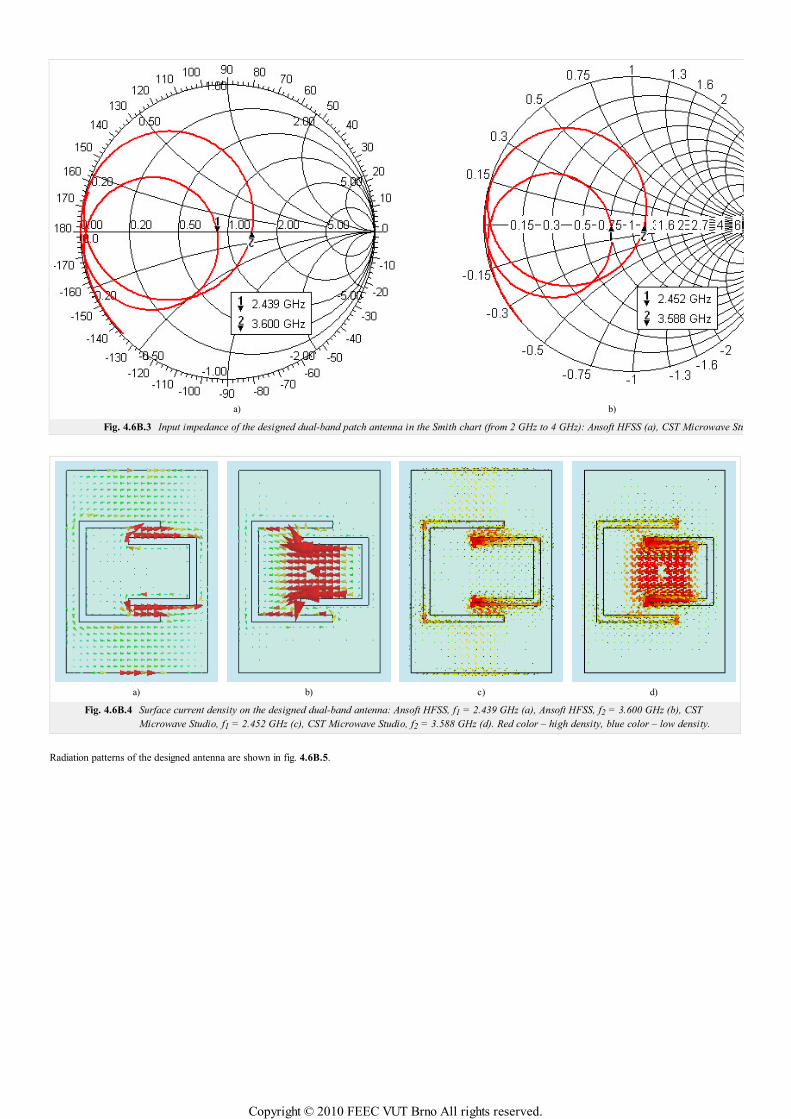
a) b)
Fig. 4.6B.3 Input impedance of the designed dual-band patch antenna in the Smith chart (from 2 GHz to 4 GHz): Ansoft HFSS (a), CST Microwave Studio (b).
a) b) c) d)
Fig. 4.6B.4 Surface current density on the designed dual-band antenna: Ansoft HFSS, f1 = 2.439 GHz (a), Ansoft HFSS, f2 = 3.600 GHz (b), CST
Microwave Studio, f1 = 2.452 GHz (c), CST Microwave Studio, f2 = 3.588 GHz (d). Red color – high density, blue color – low density.
Radiation patterns of the designed antenna are shown in fig. 4.6B.5.
Copyright © 2010 FEEC VUT Brno All rights reserved.
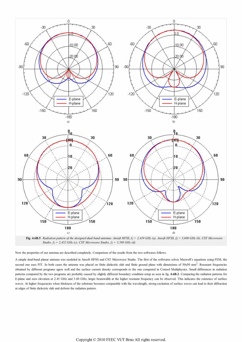
a) b)
c) d)
Fig. 4.6B.5 Radiation pattern of the designed dual-band antenna: Ansoft HFSS, f1 = 2,439 GHz (a), Ansoft HFSS, f2 = 3,600 GHz (b), CST Microwave
Studio, f1 = 2,452 GHz (c), CST Microwave Studio, f2 = 3,588 GHz (d).
Now the properties of our antenna are described completely. Comparison of the results from the two softwares follows.
A simple dual-band planar antenna was modeled in Ansoft HFSS and CST Microwave Studio. The first of the softwares solves Maxwell’s equations using FEM, the
second one uses FIT. In both cases the antenna was placed on finite dielectric slab and finite ground plane with dimensions of 50x50 mm2. Resonant frequencies
obtained by different programs agree well and the surface current density corresponds to the one computed in Comsol Multiphysics. Small differences in radiation
patterns computed by the two programs are probably caused by slightly different boundary condition setup as seen in fig. 4.6B.2. Comparing the radiation patterns for
E-plane and zero elevation at 2.45 GHz and 3.60 GHz, larger beamwidth at the higher resonant frequency can be observed. This indicates the existence of surface
waves. At higher frequencies when thickness of the substrate becomes comparable with the wavelength, strong excitation of surface waves can lead to their diffraction
at edges of finite dielectric slab and deform the radiation pattern.
Copyright © 2010 FEEC VUT Brno All rights reserved.

4.6 Multi-band patch antennas
Matlab program
Program (patchant.m) calculates the approximate size of metallic patch and position of coaxial probe for planar antenna. The input parameters
are the frequency f [GHz], thickness of the dielectric slab h [mm], relative permittivity eps [-] and input impedance Ri [Ohm].
Copyright © 2010 FEEC VUT Brno All rights reserved.

4.6 Multi-band patch antennas
Quiz
Answer these questions to get feedback on how well you understand the course. Only one of the answers is correct. You don't have to answer
every question. If you don't know the answer you can just leave it blank (default option: “I won't answer this question”) and this won't affect
your score. Answering correctly will add 2 points to your score but on the other hand you'll lose 1 point if your answer is wrong. The
questions are divided in groups of five questions.
Press See result after you have finished answering.
Displaying questions 1..5 of 5:
Question 1
Polarization of an antenna is given by the orientation of …
Possible answers for question 1:
… E-plane.
… H-plane.
… Poynting vector.
I won't answer this question
Question 2
If the transmitter antenna is polarized vertically and the receiver antenna is polarized horizontally, then the signal level at the
connector of the receiver antenna (considering zero cross-polarization) is …
Possible answers for question 2:
… the same as for parallel polarized antennas.
… 3 dB less than for parallel polarized antennas.
… zero.
I won't answer this question
Question 3
Dirichlet condition says that …
Possible answers for question 3:
… the component of electric field intensity tangential to the perfect electric conductor (PEC), is zero.
… the component of electric field intensity perpendicular to the perfect electric conductor (PEC), is zero.
… the component of magnetic field intensity tangential to the perfect electric conductor (PEC), is zero.
I won't answer this question
Question 4
In the Smith chart, a circle with centre [1, 0j] and point [0.5, 0j] on its perimeter circumscribes the area where …
Possible answers for question 4:
… the input impedance of the antenna is purely real.
… the antenna is in resonance.
… the standing wave ratio at the antenna connector is smaller or equal to 2.
I won't answer this question
Question 5
Diffraction of surface waves at the edges of dielectric slab results in …
Copyright © 2010 FEEC VUT Brno All rights reserved.

Possible answers for question 5:
… enhancement of antenna efficiency.
… enhancement of antenna bandwidth.
… deformations of directivity pattern, deterioration of front-to-back ratio, lower antenna gain, etc.
I won't answer this question
Copyright © 2010 FEEC VUT Brno All rights reserved.
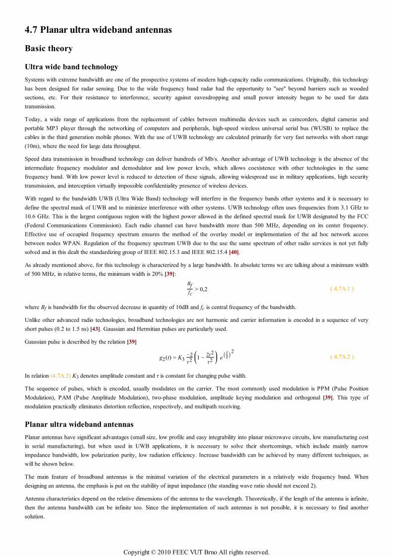
4.7 Planar ultra wideband antennas
Basic theory
Ultra wide band technology
Systems with extreme bandwidth are one of the prospective systems of modern high-capacity radio communications. Originally, this technology
has been designed for radar sensing. Due to the wide frequency band radar had the opportunity to "see" beyond barriers such as wooded
sections, etc. For their resistance to interference, security against eavesdropping and small power intensity began to be used for data
transmission.
Today, a wide range of applications from the replacement of cables between multimedia devices such as camcorders, digital cameras and
portable MP3 player through the networking of computers and peripherals, high-speed wireless universal serial bus (WUSB) to replace the
cables in the third generation mobile phones. With the use of UWB technology are calculated primarily for very fast networks with short range
(10m), where the need for large data throughput.
Speed data transmission in broadband technology can deliver hundreds of Mb/s. Another advantage of UWB technology is the absence of the
intermediate frequency modulator and demodulator and low power levels, which allows coexistence with other technologies in the same
frequency band. With low power level is reduced to detection of these signals, allowing widespread use in military applications, high security
transmission, and interception virtually impossible confidentiality presence of wireless devices.
With regard to the bandwidth UWB (Ultra Wide Band) technology will interfere in the frequency bands other systems and it is necessary to
define the spectral mask of UWB and to minimize interference with other systems. UWB technology often uses frequencies from 3.1 GHz to
10.6 GHz. This is the largest contiguous region with the highest power allowed in the defined spectral mask for UWB designated by the FCC
(Federal Communications Commission). Each radio channel can have bandwidth more than 500 MHz, depending on its center frequency.
Effective use of occupied frequency spectrum ensures the method of the overlay model or implementation of the ad hoc network access
between nodes WPAN. Regulation of the frequency spectrum UWB due to the use the same spectrum of other radio services is not yet fully
solved and in this dealt the standardizing group of IEEE 802.15.3 and IEEE 802.15.4 [40].
As already mentioned above, for this technology is characterized by a large bandwidth. In absolute terms we are talking about a minimum width
of 500 MHz, in relative terms, the minimum width is 20% [39]:
Bf
fc> 0,2 ( 4.7A.1 )
where Bf is bandwidth for the observed decrease in quantity of 10dB and fc is central frequency of the bandwidth.
Unlike other advanced radio technologies, broadband technologies are not harmonic and carrier information is encoded in a sequence of very
short pulses (0.2 to 1.5 ns) [43]. Gaussian and Hermitian pulses are particularly used.
Gaussian pulse is described by the relation [39]
g2(t) = K3−2
τ 2
⎛⎝⎜1 −
2t2
τ2
⎞⎠⎟ e( t
τ)2
( 4.7A.2 )
In relation (4.7A.2) K3 denotes amplitude constant and τ is constant for changing pulse width.
The sequence of pulses, which is encoded, usually modulates on the carrier. The most commonly used modulation is PPM (Pulse Position
Modulation), PAM (Pulse Amplitude Modulation), two-phase modulation, amplitude keying modulation and orthogonal [39]. This type of
modulation practically eliminates distortion reflection, respectively, and multipath receiving.
Planar ultra wideband antennas
Planar antennas have significant advantages (small size, low profile and easy integrability into planar microwave circuits, low manufacturing cost
in serial manufacturing), but when used in UWB applications, it is necessary to solve their shortcomings, which include mainly narrow
impedance bandwidth, low polarization purity, low radiation efficiency. Increase bandwidth can be achieved by many different techniques, as
will be shown below.
The main feature of broadband antennas is the minimal variation of the electrical parameters in a relatively wide frequency band. When
designing an antenna, the emphasis is put on the stability of input impedance (the standing wave ratio should not exceed 2).
Antenna characteristics depend on the relative dimensions of the antenna to the wavelength. Theoretically, if the length of the antenna is infinite,
then the antenna bandwidth can be infinite too. Since the implementation of such antennas is not possible, it is necessary to find another
solution.
Copyright © 2010 FEEC VUT Brno All rights reserved.
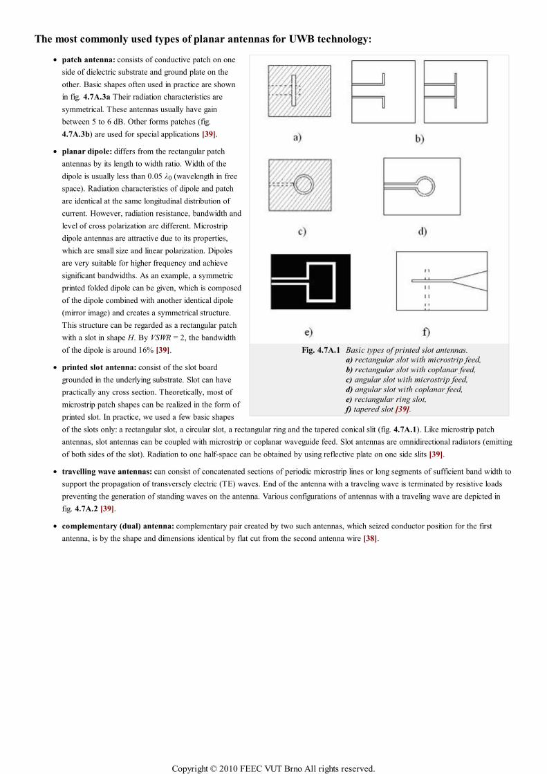
Fig. 4.7A.1 Basic types of printed slot antennas.
a) rectangular slot with microstrip feed,
b) rectangular slot with coplanar feed,
c) angular slot with microstrip feed,
d) angular slot with coplanar feed,
e) rectangular ring slot,
f) tapered slot [39].
The most commonly used types of planar antennas for UWB technology:
patch antenna: consists of conductive patch on one
side of dielectric substrate and ground plate on the
other. Basic shapes often used in practice are shown
in fig. 4.7A.3a Their radiation characteristics are
symmetrical. These antennas usually have gain
between 5 to 6 dB. Other forms patches (fig.
4.7A.3b) are used for special applications [39].
planar dipole: differs from the rectangular patch
antennas by its length to width ratio. Width of the
dipole is usually less than 0.05 λ0 (wavelength in free
space). Radiation characteristics of dipole and patch
are identical at the same longitudinal distribution of
current. However, radiation resistance, bandwidth and
level of cross polarization are different. Microstrip
dipole antennas are attractive due to its properties,
which are small size and linear polarization. Dipoles
are very suitable for higher frequency and achieve
significant bandwidths. As an example, a symmetric
printed folded dipole can be given, which is composed
of the dipole combined with another identical dipole
(mirror image) and creates a symmetrical structure.
This structure can be regarded as a rectangular patch
with a slot in shape H. By VSWR = 2, the bandwidth
of the dipole is around 16% [39].
printed slot antenna: consist of the slot board
grounded in the underlying substrate. Slot can have
practically any cross section. Theoretically, most of
microstrip patch shapes can be realized in the form of
printed slot. In practice, we used a few basic shapes
of the slots only: a rectangular slot, a circular slot, a rectangular ring and the tapered conical slit (fig. 4.7A.1). Like microstrip patch
antennas, slot antennas can be coupled with microstrip or coplanar waveguide feed. Slot antennas are omnidirectional radiators (emitting
of both sides of the slot). Radiation to one half-space can be obtained by using reflective plate on one side slits [39].
travelling wave antennas: can consist of concatenated sections of periodic microstrip lines or long segments of sufficient band width to
support the propagation of transversely electric (TE) waves. End of the antenna with a traveling wave is terminated by resistive loads
preventing the generation of standing waves on the antenna. Various configurations of antennas with a traveling wave are depicted in
fig. 4.7A.2 [39].
complementary (dual) antenna: complementary pair created by two such antennas, which seized conductor position for the first
antenna, is by the shape and dimensions identical by flat cut from the second antenna wire [38].
Copyright © 2010 FEEC VUT Brno All rights reserved.
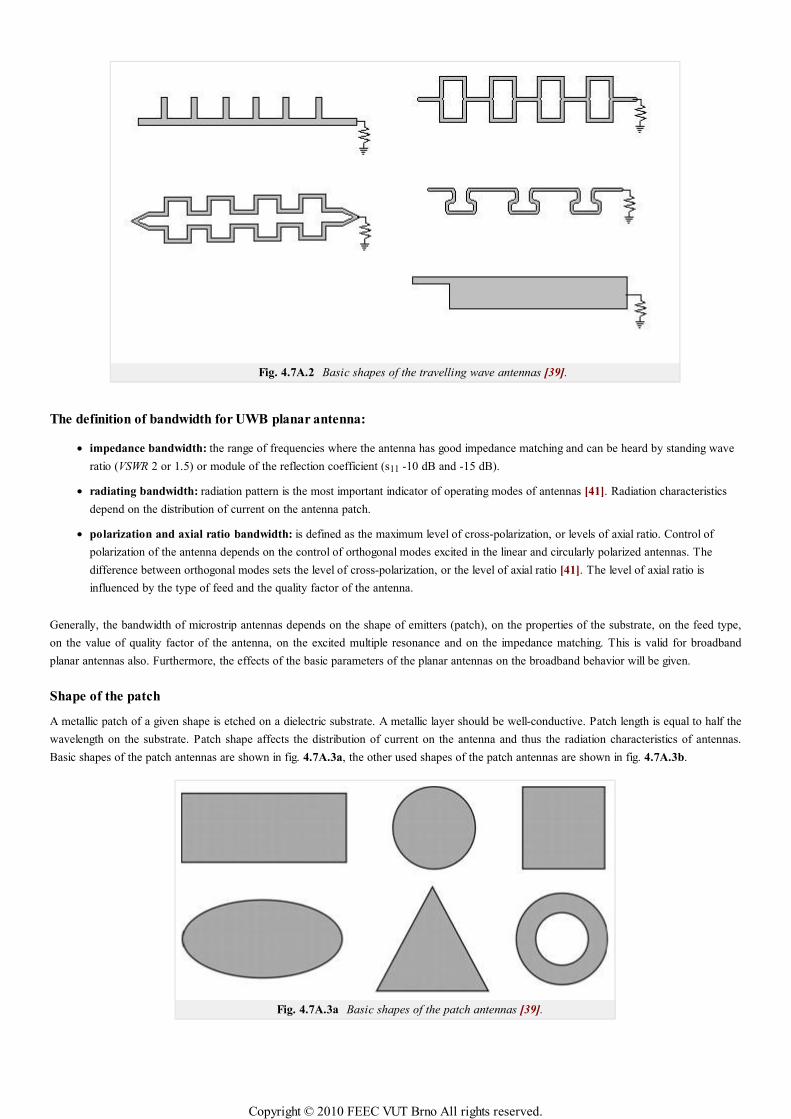
Fig. 4.7A.2 Basic shapes of the travelling wave antennas [39].
The definition of bandwidth for UWB planar antenna:
impedance bandwidth: the range of frequencies where the antenna has good impedance matching and can be heard by standing wave
ratio (VSWR 2 or 1.5) or module of the reflection coefficient (s11 -10 dB and -15 dB).
radiating bandwidth: radiation pattern is the most important indicator of operating modes of antennas [41]. Radiation characteristics
depend on the distribution of current on the antenna patch.
polarization and axial ratio bandwidth: is defined as the maximum level of cross-polarization, or levels of axial ratio. Control of
polarization of the antenna depends on the control of orthogonal modes excited in the linear and circularly polarized antennas. The
difference between orthogonal modes sets the level of cross-polarization, or the level of axial ratio [41]. The level of axial ratio is
influenced by the type of feed and the quality factor of the antenna.
Generally, the bandwidth of microstrip antennas depends on the shape of emitters (patch), on the properties of the substrate, on the feed type,
on the value of quality factor of the antenna, on the excited multiple resonance and on the impedance matching. This is valid for broadband
planar antennas also. Furthermore, the effects of the basic parameters of the planar antennas on the broadband behavior will be given.
Shape of the patch
A metallic patch of a given shape is etched on a dielectric substrate. A metallic layer should be well-conductive. Patch length is equal to half the
wavelength on the substrate. Patch shape affects the distribution of current on the antenna and thus the radiation characteristics of antennas.
Basic shapes of the patch antennas are shown in fig. 4.7A.3a, the other used shapes of the patch antennas are shown in fig. 4.7A.3b.
Fig. 4.7A.3a Basic shapes of the patch antennas [39].
Copyright © 2010 FEEC VUT Brno All rights reserved.

Fig. 4.7A.3b Less common shapes of the patch antennas [39].
Dielectric substrate
Dielectric substrate used for microwave antennas is often of a relative permittivity of 2.2 ≤ εr ≤ 16 and loss factor 0.0001 ≤ tg δ ≤ 0.06. High
permittivity εr has usually the effect of reducing the radiation efficiency of the antenna. Thickness of the substrate is much smaller than the
wavelength.
Feeding
Feeding structure affects the impedance matching, operating modes, parasitic radiation, the radiation of surface waves, and radiated power. The
most commonly used feeding is coaxial probe (outer conductor is connected to ground plane, an internal wire is connected with antenna
element) and microstrip feeding (fig. 4.7A.4).
Fig. 4.7A.4 Microstrip feeding [39]. a) non-embedded lines, b) capacitor coupling, c) embedded
lines.
In some applications, galvanic-separated coupling is used: an antenna is excited by field of the microstrip line (fig. 4.7A.5a) or through the slot
(fig. 4.7A.5b) by the so-called aperture coupling.
Copyright © 2010 FEEC VUT Brno All rights reserved.
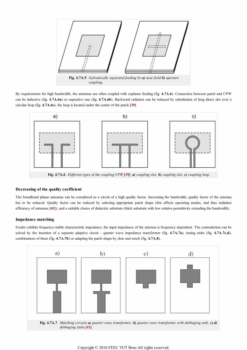
Fig. 4.7A.5 Galvanically separated feeding by a) near field b) aperture
coupling.
By requirements for high bandwidth, the antennas are often coupled with coplanar feeding (fig. 4.7A.6). Connection between patch and CPW
can be inductive (fig. 4.7A.6a) or capacitive one (fig. 4.7A.6b). Backward radiation can be reduced by substitution of long direct slot over a
circular loop (fig. 4.7A.6c), the loop is located under the center of the patch [39].
Fig. 4.7A.6 Different types of the coupling CPW [39], a) coupling slot, b) coupling slot, c) coupling loop.
Decreasing of the quality coefficient
The broadband planar antennas can be considered as a circuit of a high quality factor. Increasing the bandwidth, quality factor of the antenna
has to be reduced. Quality factor can be reduced by selecting appropriate patch shape (this affects operating modes, and thus radiation
efficiency of antennas [41]), and a suitable choice of dielectric substrate (thick substrate with low relative permittivity extending the bandwidth).
Impedance matching
Feeder exhibits frequency-stable characteristic impedance; the input impedance of the antenna is frequency dependent. The contradiction can be
solved by the insertion of a separate adaptive circuit - quarter wave impedance transformer (fig. 4.7A.7a), tuning stubs (fig. 4.7A.7c,d),
combinations of them (fig. 4.7A.7b) or adapting the patch shape by slots and notch (fig. 4.7A.8).
Fig. 4.7A.7 Matching circuits a) quarter wave transformer, b) quarter wave transformer with debbuging stub, c),d)
debbuging stubs [41].
Copyright © 2010 FEEC VUT Brno All rights reserved.

Fig. 4.7A.8 Matching of the patch shape with notchs and slots [41].
A well-matched antenna should cover the desired operating frequency range when keeping the defined level of the parameters which should
vary marginally only (VSWR < 2, module of the reflection coefficient s11 < -10 dB, stable value of gain, the main lobe beam width and radiation
pattern over the desired bandwidth).
In the layer B, a concrete example of the calculation of broadband planar antennas is mentioned. We show the influence of the patch shape and
his size, the choice of coupling and choice of substrate on the characteristics of the antenna.
Copyright © 2010 FEEC VUT Brno All rights reserved.
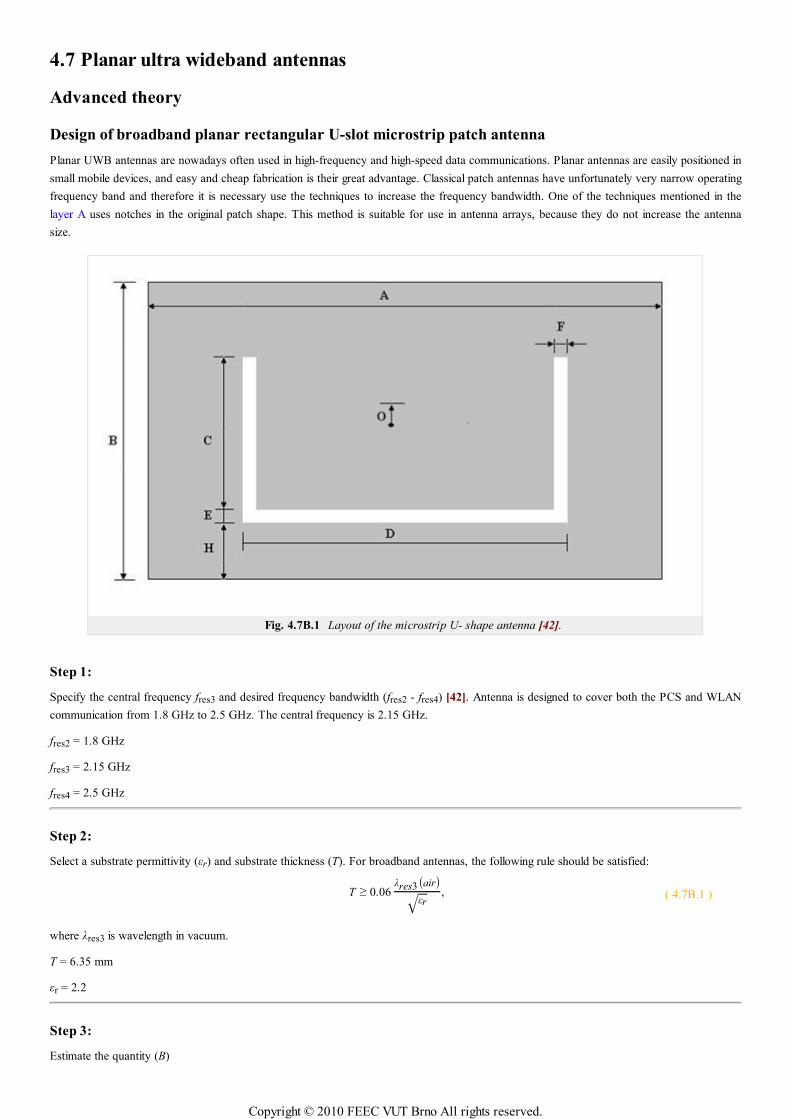
4.7 Planar ultra wideband antennas
Advanced theory
Design of broadband planar rectangular U-slot microstrip patch antenna
Planar UWB antennas are nowadays often used in high-frequency and high-speed data communications. Planar antennas are easily positioned in
small mobile devices, and easy and cheap fabrication is their great advantage. Classical patch antennas have unfortunately very narrow operating
frequency band and therefore it is necessary use the techniques to increase the frequency bandwidth. One of the techniques mentioned in the
layer A uses notches in the original patch shape. This method is suitable for use in antenna arrays, because they do not increase the antenna
size.
Fig. 4.7B.1 Layout of the microstrip U- shape antenna [42].
Step 1:
Specify the central frequency fres3 and desired frequency bandwidth (fres2 - fres4) [42]. Antenna is designed to cover both the PCS and WLAN
communication from 1.8 GHz to 2.5 GHz. The central frequency is 2.15 GHz.
fres2 = 1.8 GHz
fres3 = 2.15 GHz
fres4 = 2.5 GHz
Step 2:
Select a substrate permittivity (εr) and substrate thickness (T). For broadband antennas, the following rule should be satisfied:
T ≥ 0.06λres3(air)
εr√, ( 4.7B.1 )
where λres3 is wavelength in vacuum.
T = 6.35 mm
εr = 2.2
Step 3:
Estimate the quantity (B)
Copyright © 2010 FEEC VUT Brno All rights reserved.

B + 2∆B ≈c0
2 εr√ fres3( 4.7B.2 )
B + 2∆B ≈ 47.04
Step 4:
Calculate of the width of the patch (A)
A = 1.5(B + 2∆B) ( 4.7B.3 )
A = 70.56 mm
Step 5:
Calculate of the effective permitivity (εeff) and parameter 2∆B
εe f f =εr +1
2+
εr −1
2⎛⎝1 +
12TA
⎞⎠√ ( 4.7B.4 )
2∆B = 0.824T(εe f f +0.3)(A
T+0.262)
(εe f f −0.258)(AT
+0.813)( 4.7B.5 )
εeff = 2.465
2∆B = 6.249
Step 6:
Back calculate of the length of the patch (B)
B =c0
2 εe f f√ fres3− 2∆B ( 4.7B.6 )
B = 38.19 mm
Step 7:
Select a starting value of slot thickness (E, F)
E = F =λres3(air)
60( 4.7B.7 )
E = F = 2.33 mm
Step 8:
Calculate width of the U-slot (D)
D =c0
εe f f√ fres2− 2(B + 2∆B − E) ( 4.7B.8 )
D = 21.93 mm
Step 9:
Select C such that
CA
≥ 0.3, CD
≥ 0.75 ( 4.7B.9 )
CA
≥ 0.33, CD
≥ 0.9
Step 10:
Calculate the effective permittivity and effective length extension of the pseudo-patch of the fourth resonance with effective patch width as
Copyright © 2010 FEEC VUT Brno All rights reserved.

D-2F
εe f f (PP) =
εr +1
2+
εr −1
2⎛⎝1 +
12TD−2F
⎞⎠√ ( 4.7B.10 )
2∆B−E − H = 0.824T(ε
e f f (PP) +0.3)(D−2FT
+0.262)(ε
e f f (PP) −0.258)(D−2FT
+0.813)( 4.7B.11 )
εeff(PP) = 2.996
2∆B-E-H = 5.32
Step 11:
Estimate of the position U-slot
H ≈ B − E + 2∆B− E− H −1
εe f f (PP)√
⎛⎝⎜
c0fres4
− (2C + D)⎞⎠⎟ ( 4.7B.12 )
For C = 23.28 H ≈ 11.41
Step 12:
Check that sum C + E + H is less than B. If not adjust C by changing the rations in step 9 and value of H until the design is physically realizable.
C + E + H ≤ B ( 4.7B.13 )
23.28 + 2.33 + 11.41 ≤ 38.19
Tab. 4.7B.1 Approximate values of the parameters calculated using the antenna design relations [42].
A [mm] B [mm] C [mm] D [mm] E [mm] F [mm] O [mm] T [mm] εr
70,56 38,19 23,28 21,93 2,33 2,33 0 6,53 2,2
Copyright © 2010 FEEC VUT Brno All rights reserved.

4.7 Planar ultra wideband antennas
Matlab program
For an approximate design, parameters of a broadband antenna with a rectangular slots and U-shaped notch from the layer B are available here.
The program runs in a command window by calling function
U_antena(fres2, fres3, fres4, εr, T)
For the parameters of the function U_antena we substitute:
fres2 the lower limit of the desired frequency range [Hz]
fres3 central frequency in [Hz], fres3 = fres2 +12 ( fres4 − fres2)
fres4 the higher limit of desired frequency range [Hz]
εr desired permittivity substrate
T desired substrate thickness [mm]
Outputs are the approximate dimensions of the antenna with a rectangular slots and U-shaped notch as shown in figure 4.7B.1.
Copyright © 2010 FEEC VUT Brno All rights reserved.
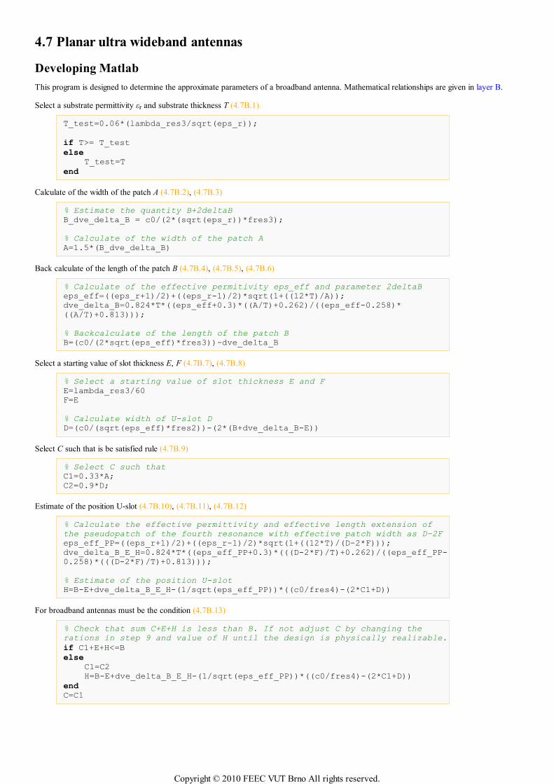
4.7 Planar ultra wideband antennas
Developing Matlab
This program is designed to determine the approximate parameters of a broadband antenna. Mathematical relationships are given in layer B.
Select a substrate permittivity εr and substrate thickness T (4.7B.1)
T_test=0.06*(lambda_res3/sqrt(eps_r));
if T>= T_testelse
T_test=Tend
Calculate of the width of the patch A (4.7B.2), (4.7B.3)
% Estimate the quantity B+2deltaBB_dve_delta_B = c0/(2*(sqrt(eps_r))*fres3);
% Calculate of the width of the patch AA=1.5*(B_dve_delta_B)
Back calculate of the length of the patch B (4.7B.4), (4.7B.5), (4.7B.6)
% Calculate of the effective permitivity eps_eff and parameter 2deltaBeps_eff=((eps_r+1)/2)+((eps_r-1)/2)*sqrt(1+((12*T)/A));dve_delta_B=0.824*T*((eps_eff+0.3)*((A/T)+0.262)/((eps_eff-0.258)*((A/T)+0.813)));
% Backcalculate of the length of the patch BB=(c0/(2*sqrt(eps_eff)*fres3))-dve_delta_B
Select a starting value of slot thickness E, F (4.7B.7), (4.7B.8)
% Select a starting value of slot thickness E and FE=lambda_res3/60F=E
% Calculate width of U-slot DD=(c0/(sqrt(eps_eff)*fres2))-(2*(B+dve_delta_B-E))
Select C such that is be satisfied rule (4.7B.9)
% Select C such thatC1=0.33*A;C2=0.9*D;
Estimate of the position U-slot (4.7B.10), (4.7B.11), (4.7B.12)
% Calculate the effective permittivity and effective length extension ofthe pseudopatch of the fourth resonance with effective patch width as D-2Feps_eff_PP=((eps_r+1)/2)+((eps_r-1)/2)*sqrt(1+((12*T)/(D-2*F)));dve_delta_B_E_H=0.824*T*((eps_eff_PP+0.3)*(((D-2*F)/T)+0.262)/((eps_eff_PP-0.258)*(((D-2*F)/T)+0.813)));
% Estimate of the position U-slotH=B-E+dve_delta_B_E_H-(1/sqrt(eps_eff_PP))*((c0/fres4)-(2*C1+D))
For broadband antennas must be the condition (4.7B.13)
% Check that sum C+E+H is less than B. If not adjust C by changing therations in step 9 and value of H until the design is physically realizable.
if C1+E+H<=Belse
C1=C2H=B-E+dve_delta_B_E_H-(1/sqrt(eps_eff_PP))*((c0/fres4)-(2*C1+D))
end
C=C1
Copyright © 2010 FEEC VUT Brno All rights reserved.

4.7 Planar ultra wideband antennas
Quiz
Answer these questions to get feedback on how well you understand the course. Only one of the answers is correct. You don't have to answer
every question. If you don't know the answer you can just leave it blank (default option: “I won't answer this question”) and this won't affect
your score. Answering correctly will add 2 points to your score but on the other hand you'll lose 1 point if your answer is wrong. The
questions are divided in groups of five questions.
Press See result after you have finished answering.
Displaying questions 1..5 of 5:
Question 1
For what distance is calculated mainly with using of the broadband technology?
Possible answers for question 1:
tens of meters
hundreds of meters
tens of kilometers
I won't answer this question
Question 2
What are the main advantages of broadband access?
Possible answers for question 2:
high speed data transfer, low consumption, high transmission security, resistance to interference
secure data transmission to long distances
using yet unused frequency bands
I won't answer this question
Question 3
What are the basic advantages of planar antennas?
Possible answers for question 3:
usability for large transmission power
small size, low profile, easy integrability into planar microwave circuits
high polarization purity
I won't answer this question
Question 4
What frequency bands are most often used for UWB technology?
Possible answers for question 4:
2,5 – 6,7 GHz
40 GHz and higher
3,1 – 10,6 GHz
I won't answer this question
Question 5
What are requirements to the dielectric substrate used in antenna technology?
Copyright © 2010 FEEC VUT Brno All rights reserved.

Possible answers for question 5:
high permittivity
low permittivity
There aren't put any requirements. It does not matter.
I won't answer this question
Copyright © 2010 FEEC VUT Brno All rights reserved.

Chapter 5: Time-domain modeling of antennas
Introduction
Numerical modeling of antennas in the frequency domain is effective if the antenna parameters are desirable in the narrow band of frequencies.
If the wideband analysis is desirable, it is better to use time-domain analysis. However, this one is suitable only for the structures with low
Q-factor, otherwise, the computed response is too long, and the analysis is time consuming.
For modeling in the time domain, an analyzed structure is excited by a desired pulse [37], and a transient response is computed. From the
excitation pulse and the computed response, we can obtain properties of the analyzed structure at those frequencies which the excitation pulse
contains. It is wideband modeling which can be used for the wideband analysis of antennas, scatterers, or in the area of the electromagnetic
compatibility (EMC), or electromagnetic interference (EMI).
The time-domain modeling has several advantages in the comparison to the frequency-domain one:
The wideband response is obtained by one run of an analysis.
The frequency-domain analysis can not be used for the time variant or nonlinear systems.
By the time domain-analysis, only the beginning of the transient responses can be computed, and the rest of the responses can be
ignored.
Due to the above advantages of the time domain modeling, the basic principles of the time-domain modeling will be described in this chapter.
Again, as in the frequency domain, the formulations which come out from Maxwell’s equations in the differential or integral form are solved.
Copyright © 2010 FEEC VUT Brno All rights reserved.
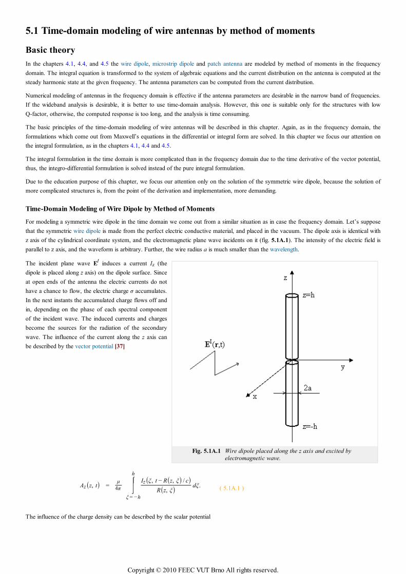
Fig. 5.1A.1 Wire dipole placed along the z axis and excited by
electromagnetic wave.
5.1 Time-domain modeling of wire antennas by method of moments
Basic theory
In the chapters 4.1, 4.4, and 4.5 the wire dipole, microstrip dipole and patch antenna are modeled by method of moments in the frequency
domain. The integral equation is transformed to the system of algebraic equations and the current distribution on the antenna is computed at the
steady harmonic state at the given frequency. The antenna parameters can be computed from the current distribution.
Numerical modeling of antennas in the frequency domain is effective if the antenna parameters are desirable in the narrow band of frequencies.
If the wideband analysis is desirable, it is better to use time-domain analysis. However, this one is suitable only for the structures with low
Q-factor, otherwise, the computed response is too long, and the analysis is time consuming.
The basic principles of the time-domain modeling of wire antennas will be described in this chapter. Again, as in the frequency domain, the
formulations which come out from Maxwell’s equations in the differential or integral form are solved. In this chapter we focus our attention on
the integral formulation, as in the chapters 4.1, 4.4 and 4.5.
The integral formulation in the time domain is more complicated than in the frequency domain due to the time derivative of the vector potential,
thus, the integro-differential formulation is solved instead of the pure integral formulation.
Due to the education purpose of this chapter, we focus our attention only on the solution of the symmetric wire dipole, because the solution of
more complicated structures is, from the point of the derivation and implementation, more demanding.
Time-Domain Modeling of Wire Dipole by Method of Moments
For modeling a symmetric wire dipole in the time domain we come out from a similar situation as in case the frequency domain. Let’s suppose
that the symmetric wire dipole is made from the perfect electric conductive material, and placed in the vacuum. The dipole axis is identical with
z axis of the cylindrical coordinate system, and the electromagnetic plane wave incidents on it (fig. 5.1A.1). The intensity of the electric field is
parallel to z axis, and the waveform is arbitrary. Further, the wire radius a is much smaller than the wavelength.
The incident plane wave EI induces a current Iz (the
dipole is placed along z axis) on the dipole surface. Since
at open ends of the antenna the electric currents do not
have a chance to flow, the electric charge σ accumulates.
In the next instants the accumulated charge flows off and
in, depending on the phase of each spectral component
of the incident wave. The induced currents and charges
become the sources for the radiation of the secondary
wave. The influence of the current along the z axis can
be described by the vector potential [37]
Az(z, t) = µ
4π ⌠⌡⎮⎮
ξ = −h
h
Iz(ξ, t − R(z, ξ) / c)R(z, ξ) dξ. ( 5.1A.1 )
The influence of the charge density can be described by the scalar potential
Copyright © 2010 FEEC VUT Brno All rights reserved.
φ(z, t) = 14πε
⌠⌡⎮⎮
ξ = −h
h
σ(ξ, t − R(z, ξ) / c)R(z, ξ) dξ. ( 5.1A.2 )
The value of the vector potential Az at a arbitrary “target” point z, and instant t can be computed by the addition of contributions of the current
components from all “source” points ξ on the antenna axis. The source current has to be retarded about time R/c which the wave needs for
traveling the distance between the source ξ point and the target point z
R(z, ξ) = a2 + (z − ξ)2√ . ( 5.1A.3 )
Further, c in (5.1A.1) is speed of light in the given environment. The contribution to the vector potential is not proportional to the distance
between the source and target point. The integration has to be carried out along the whole antenna structure. Finally, the value of the integral is
multiplied by the permeability of surrounding medium µ (the vacuum).
In case of the scalar potential, the current distribution is replaced by the charge density σ. The result of the integration is, instead of the
multiplication by the permeability, divided by the permittivity of the surrounding medium ε. The rest in the equation (5.1A.2) stays the same as
in (5.1A.1).
Since the current and the charge are mutually tied, the relations (5.1A.1) and (5.1A.2) has to be tied by the continuity equation
∂σ(z, t)∂ t
= −∂ Iz(z, t)
∂ z. ( 5.1A.4 )
If the vector and scalar potentials are known, the intensity of the electric field radiated by antenna EzS (the scattered field) can be computed
EzS(z, t) = −
∂ Az(z, t) ∂ t −
∂φ(z, t)∂ z
. ( 5.1A.5 )
The derivative of the vector potential with respect to time describes “the dynamic contribution” of the electric charge on the antenna to the
radiated wave (the electric currents, charges in motion, are the source for the vector potential). The partial derivative of the scalar potential with
respect to the variable z express the “static contribution” of the electric charge on the antenna to radiated field (the static charges, accumulated at
ends of the antenna, are the source for the scalar potential)
On the surface of the perfect electric conductor the intensity of the electric field has to satisfied the boundary condition
EzS(z, t) + Ez
I(z, t) = 0 . ( 5.1A.6 )
The system of equations (5.1A.1) to (5.1A.6) is solved numerically in two steps. The first one consists in the space discretization of the problem
and the second one consists in the application of time algorithms on the result of the first step.
The first step is analogical to the solution in the frequency domain, where the method of moments is used for the “transformation” of the
integral equation to the system to algebraic equations. Here, we use again the method of moments for the “transformation” of the integro-
differential equation (5.1A.5) to a system of the retarded differential equations (the space discretization of the problem).
For the second step (the application of the time algorithms), it is possible to use either the explicit, or the implicit algorithm. At the explicit one,
the length of the time step ∆t has to satisfy the following condition: ∆t ≤ Rmin/c, where Rmin is the smallest distance of centers of the
discretization elements and c is the speed of the light in the surrounding medium. At the implicit algorithm, the length of the time step can be
chosen arbitrary. The larger length of the time step increase the speed of computation, but the accuracy falls down. These approaches belong to
the marching on in time (MOT) methods.
The marching on in order method (MOO) is the next method. It is based on the approximation of the transient response by a set of weighted
Laguerre polynomials. The advantage of MOO is its unconditional stability, but the disadvantages are the higher demands on the
implementation, and less effectiveness in the comparison to MOT.
Due to above facts, we focus our attention on MOT. Although we mentioned that the system of equations (5.1A.1) to (5.1A.6) is solved in two
steps (the space discretization and the application of time algorithms), we will merge both these steps. It is appropriate to notify that by MOT
the system of retarded differential equations is transformed to the system of difference equations (the derivative of the vector potential with
respect to tome (5.1A.5) is replaced by appropriate difference).
The advantage of the explicit algorithm is its easier implementation and there is no need to compute an inverse matrix as in case of the solution
in the frequency domain, or as at the implicit approach. However, the explicit approach suffers often from the late time oscillation (the
computed response is not steady, but grows exponentially.). Therefore, the attention in this chapter is focused only on the implicit approach.
Excitation pulse
Copyright © 2010 FEEC VUT Brno All rights reserved.
Before, than we focus our attention on the implicit approach, let’s choose an appropriate excitation pulse.
If we chose the Dirac pulse, the spectrum of the excitation signal would be equally spread over the infinite frequency domain. Since in the
technical practice the solution is desirable over the limited bandwidth and we do not have unlimited computer memory and the power of a
computer, thus, the Dirac pulse is not an ideal choice.
Instead of the Dirac pulse it is better to use the Gaussian pulse modulated by a harmonic signal. By change of its parameters, it is possible to
analyze only the band of our interest.
The vector of the intensity of the electric field of the Gaussian excitation pulse modulated by harmonic signal is given
EI(r, t) = E0 4cT π√
exp[−( 4T (t − t0 −
r⋅akc ))
2
]cos(2π f0t), ( 5.1A.7 )
where E0 is the vector of the intensity of the electric field of the excitation wave at the origin of the coordinate system, r is the positional vector
of the point where the intensity of the excitation wave is computed, ak is the unit vector in the direction of the propagation, c is the speed of the
light in the surrounding medium, T is the width of the Gaussian pulse, t0 is the retardation of its peak, and f0 is the center frequency of the
analyzed band. The example of the Gaussian pulse modulated by the harmonic signal with its spectrum, defined by the following parameters:
|E0|=120π V/m, T=8 ns, t0=10 ns and f0= 500 MHz, is depicted in fig. 5.1A.2.
Fig. 5.1A.2 Gaussian pulse modulated by harmonic
signal in time (leftside) and frequency
(rightside) domains.
Implicit algorithm
The derivation of the implicit algorithm is demanding (the system of the equations (5.1A.1) to (5.1A.6) is discretized in space and time), and for
the interested reader it is carried out in the layer B. In this layer the properties of the implicit scheme are only discussed.
At the implicit algorithm, opposite to the explicit one, the inverse matrix has to be solved and its implementation on the computer is more
demanding than in case of the explicit algorithm. However, its advantage is that the length of the time step can be chosen arbitrarily (we should
keep in mind, the length of the time step influences the accuracy), and this algorithm is more stable than the explicit one.
Using the implicit algorithm will be demonstrated on the analysis of the wire dipole of the length 2 m, which is excited at its center by the
Gaussian pulse modulated by a harmonic signal (5.1A.7) defined by the following parameters: E0=120π V/m, T=6 ns, t0=8 ns, f0 = 0 Hz. Since
the center frequency of the analyzed band is 0 Hz, let’s further call this pulse as the Gaussian pulse. Let’s chose the length of time analysis 400
ns. The body of the dipole is divided to 40 segments (the space discretization of the task, layer B). The analysis is carried out two times for
different lengths of the time step. In case of the first analysis the length of the time step is ∆t = Rmin/c = 0.166 ns, c∆t = 0,05 m, and in the case
of the second analysis the length of the time step is half of the first case, ∆t = Rmin/(2c) = 0.083 ns, c∆t = 0,025 m (the time discretization of
the task).
The excitation Gaussian pulse is depicted in fig. 5.1A.3. The computed current responses to this pulse at the center of the dipole are depicted in
fig. 5.1A.4. Comparing both figures it can be said that the computed responses are significantly larger than the excitation pulse and the
difference between computed current is very small.
The wire dipole is a narrow band antenna which is able to “transform” the energy to the free space only within the limited range of the
frequencies. Since the excitation pulse carries the energy even at the frequencies, where the antenna has this ability significantly smaller, the
energy goes from the one arm of the dipole to the other and back, and the energy is gradually radiated.
Copyright © 2010 FEEC VUT Brno All rights reserved.
Fig. 5.1A.3 Excitation Gaussian pulse. Fig. 5.1A.4 Current responses on the Gaussian pulse
(obr. 5.1A.3) in the center of the wire
antenna for different lengths of the time step
Since the computed responses are stable, the input impedance of the wire antenna can be computed (fig. 5.1A.5, denoted by TD). In the same
picture the input impedance computed by the method of moments in the frequency domain is depicted (denoted by FD). The solution in the
frequency domain is taken as the reference solution because its accuracy is known. Comparing this solution with the results for the implicit
algorithm for the length of the time step ∆t = Rmin/c = 0.166 ns, c∆t = 0,05 m (red line) we can say that larger differences are apparent at higher
frequencies. These differences are mainly caused by the discretization of the system of the equations (5.1A.1) to (5.1A.6) in time. If we
decrease the length of the time step to the half of the original value (green line), the differences are smaller (more accurate approximation in the
time). The length of the time step influences the accuracy of the algorithm.
Fig. 5.1A.5 Real (left) a imaginary (right) part of the input impedance of the analyzed wire dipole.
The length of the time step influences the stability of the algorithm too. This fact is demonstrated in fig. 5.1A.6, where the current response of
the same dipole antenna for the double length of the time step (∆t = 2Rmin/c = 0.333 ns, c∆t = 0,1 m.) is depicted. The computed response is
not stable, but it grows to infinity.
Copyright © 2010 FEEC VUT Brno All rights reserved.
Fig. 5.1A.6 Unstable current response to the Gaussian
pulse (fig. 5.1A.3) in the center of the wire
dipole (larger length of the time step).
For stabilizing the time algorithm different techniques can be used, however, these ones are behind the scope of this chapter.
Copyright © 2010 FEEC VUT Brno All rights reserved.
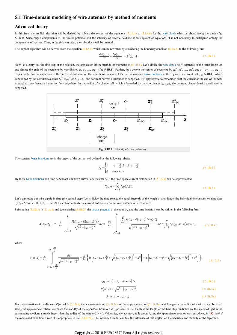
5.1 Time-domain modeling of wire antennas by method of moments
Advanced theory
In this layer the implicit algorithm will be derived by solving the system of the equations (5.1A.1) to (5.1A.6) for the wire dipole which is placed along the z axis (fig.
5.1B.1). Since only z components of the vector potential and the intensity of electric field are in this system of equations, it is not necessary to distinguish among the
components of vectors. Thus, in the following text, the subscript z will be omitted.
The implicit algorithm will be derived from the equation (5.1A.5) which can be rewritten by considering the boundary condition (5.1A.6) to the following form
∂ A(z, t)
∂ t+
∂φ(z, t)∂z
= E I(z, t) . ( 5.1B.1 )
Now, let’s carry out the first step of the solution, the application of the method of moments to (5.1B.1). Let’s divide the wire dipole to N segments of the same length ∆z
and denote the ends of the segments by coordinates z0, z1, …, zN+1 (fig. 5.1B.1). Further, let’s denote the center of segments by z0+, z1
+, …, zN+, and z1
-, z2-, …, zN+1
-,
respectively. For the expansion of the current distribution on the wire dipole in space, let’s use the constant basis functions: in the region of a current cell (fig. 5.1B.1), which
is bounded by the coordinates either zn+, zn+1
+ or zn-1-, zn
-, the constant current distribution is supposed. It is appropriate to remember, that the current at the end of the wire
is equal to zero, because it can not flow anywhere. In the region of a charge cell, which is bounded by the coordinates zn, zn+1, the constant charge density distribution is
supposed.
Fig. 5.1B.1 Wire dipole discretization.
The constant basis functions are in the region of the current cell defined by the following relation
fn =
⎧⎨⎩⎪⎪
1 zn −∆z2
≤ z ≤ zn +∆z2
0 otherwise
. ( 5.1B.2 )
By these basis functions and time dependant unknown current coefficients In (t) the time-space current distribution in (5.1A.1) can be approximated
I(z, t) ≈ ∑n = 1
NIn(t) fn(z).
( 5.1B.3 )
Let’s discretize our wire dipole in time (the second step). Let’s divide the time step to the equal intervals of the length ∆t and denote the individual time instant on time axes
by tk=k∆t for k = 0, 1, 2, …, ∞. At these time instants the current distribution on the wire antenna is be computed.
Substituting (5.1B.3) to (5.1A.1) and (considering (5.1B.2)) the vector potential at the point zm and the time instant tk can be written in the following form
A(zm , tk ) = µ
4π
⌠
⌡
⎮⎮⎮⎮ξ = −h
h
I(ξ, tn − R(zm , ξ) / c)a2 + ||zm − ξ||
2√dξ ≈
µ04π
⌠
⌡
⎮⎮⎮⎮⎮⎮ξ = −h
h
∑n = 1
NIn(tn − R(zm , ξ) / c) fn(ξ)
a2 + ||zm − ξ||2√
dξ = ∑n = 1
NIn(tRk (m, n))κ(m, n), ( 5.1B.4 )
where
κ(m, n) =µ
4π
⌠
⌡⎮⎮⎮⎮
ξ = zn −∆z2
zn −∆z2
dξ
a2 + ||zm − ξ ||2√
=µ
4π ln[zm − zn +∆z2
+⎛⎝zm − zn +
∆z2
⎞⎠2
+ a2√ ] − ln[zm − zn −∆z2
+⎛⎝zm − zn −
∆z2
⎞⎠2
+ a2√ ],( 5.1B.5 )
tRk (m, n) = tk − R(m, n) / c, ( 5.1B.6 )
R(m, n) = a2 + ||zm − zn ||2√ , ( 5.1B.7a )
R(m, n) = ||zm − zn ||. ( 5.1B.7b )
For the evaluation of the distance R(m, n) in (5.1B.6) the accurate relation (5.1B.7a), or the approximate one (5.1B.7b), which neglects the radius of a wire a, can be used.
Using the approximate relation increases the stability of the algorithm, however, it is possible to use it only if the length of the time step multiplied by the speed of light in the
surrounding medium is much larger, than the radius of the wire (c∆t>>a). Otherwise, the accuracy falls down. Using the approximate relation was introduced in [37] and if
the mentioned condition is met, it is appropriate to use (5.1B.7b). The interested reader can test the influence of that neglect on the accuracy and stability of the algorithm.
Copyright © 2010 FEEC VUT Brno All rights reserved.
Let’s discretize the scalar potential (5.1A.2) where the space-time charge density distribution is the unknown quantity. The charge density can be computed with the
continuity equation (5.1A.4) which can be rewritten in the following form
σ(z, t) = −⌠⌡⎮⎮
∂ I(z, t)∂ z
dt. ( 5.1B.8 )
Substituting the space-time charge density distribution (5.1B.3) to (5.1B.8) and approxiomating the partial differentiation of the current with respect to variable z by the
center difference, the continuity equation (5.1B.8), after the swap of the derivation and integration, can be written
σ(z, t) ≈ −
∂ ∑n= 1
N ⌠⌡In(t)dt fn(z)
∂ z≈ − ∑
n = 0
N⌠⌡In+1(t)dt − ⌠⌡In(t)dt
∆zfn
+ (z). ( 5.1B.9 )
Since the constant basis functions are used for the space approximation of the current (5.1B.3), the partial derivative with respect to variable z in (5.1B.9) could not be
computed straightforwardly (the derivative of the constant function is equal to zero), but the center difference has to be used. To be the differentiating correct, the integral of
currents with respect to time at the ends of the wire were included in (5.1B.9), although they are equal to zero. In the last step in (5.1B.9) the basis functions were swaped:
from the spacious approximation of the current by the basis functions fn(z) we got toward the approximation of the charge density by the basis functions fn+(z).
Substituting the continuity equation (5.1B.9) to (5.1A.2) the scalar potential at the point zm+ and the instant tk can be evaluated
φ(zm+ , tk ) = −
14πε
⌠⌡⎮⎮
ξ = −h
h
σ(ξ, tk − R(zm+ , ξ) / c)
R(zm+ , ξ)
dξ ≈ −1
4πε
⌠
⌡
⎮⎮⎮⎮⎮⎮⎮⎮⎮⎮⎮⎮⎮ξ = −h
h
∑n = 0
N
⌠⌡0
tk −R(zm+ , ξ)/c
In+1(t)dt − ⌠⌡0
tk − R(zm+ , ξ)/c
In(t)dt
∆zfn
+ (ξ) 1
R(zm+ , ξ)
dξ =
= ∑n= 1
N
⌠⌡0
tRk (m + , n + )
In(t)dtκ(m + , n + )
∆z− ∑
n= 1
N
⌠⌡0
tRk (m + , n − )
In(t)dtκ(m + , n − )
∆z= φ(zm
+ + , tk ) − φ(zm+ − , tk )
,
( 5.1B.10 )
where
tRk (m ± , n ± ) = tk − R(m ± , n ± ) / c, ( 5.1B.11 )
R(m ± , n ± ) = a2 + ||zm± − zn
± ||2√ , ( 5.1B.12a )
R(m ± , n ± ) = ||zm± − zn
± ||, ( 5.1B.12b )
κ(m ± , n ± ) =1
4πε
⌠
⌡⎮⎮⎮⎮
ξ = zn± −
∆z2
zn± −
∆z2
dξ
a2 + ||zm± − ξ ||
2√=
14πε ln[zm
± − zn± +
∆z2
+⎛⎝zm
± − zn± +
∆z2
⎞⎠2
+ a2√ ] − ln[zm± − zn
± −∆z2
+⎛⎝zm
± − zn± −
∆z2
⎞⎠2
+ a2√ ]. (
5.1B.13
)
Here, as in case of the evaluating of the vector potential, it is possible to use for the evaluation of the distance R(m ± , n ± ) in (5.1B.11) either the accurate relation
(5.1B.12a), or the approximate relation (5.1B.12b). The reasons and the condition are the same as in case of the evaluation of the vector potential.
Similarly the scalar potential at the point zm and the time instant tk can be evaluated zm-
φ(zm− , tk ) = φ(zm
− + , tk ) − φ(zm− − , tk ). ( 5.1B.14 )
To evaluate the relations (5.1B.10) and (5.1B.14), it is necessary to compute the integral of the current with respect to time. The integral can be evaluated according to
different numerical integration rules. We choose the trapezoid rule because its implementation is easy and offers sufficient accuracy. By this rule, the integral of the current
in the interval from 0 to tk,, in case of the equidistant division of the interval, can be computed
⌠⌡0
tk
I(t)dt ≈ ∆t[I(t0 = 0)
2+ ∑
l = 1
k −1I(tl) +
I(tk )2 ]. ( 5.1B.15 )
Now, let’s go back to (5.1B.1) and discretize it. Let’s approximate the first derivative of the vector potential with respect to time by the center difference of the first order.
By this step the partial derivative of the vector potential is evaluated at the point zm and the time instant tk-1/2. To be the calculation sufficiently accurate, the partial
derivative of the scalar potential with respect to variable z has to be evaluated at the same point and the time instant. This can be reached by using the center differentiation
for the scalar potential at the points zm+ and zm
- at two instants tk and tk-1. The average of these central differences is actually numerically evaluated the derivative of the
scalar potential at the point zmand the time instant tk-1/2. Of course, the excitation pulse has to be evaluated at the same point and the instant as the vector and scalar
potentials. After this steps the equation (5.1B.1) can be rewritten into the following form
A(zm , tk )− A(zm , tk −1)
∆t+
12∆z (φ(zm
+ , tk ) − φ(zm− , tk ) + φ(zm
+ , tk −1) − φ(zm− , tk −1)) = E I(z, tk −1/2) . ( 5.1B.16 )
Rearranging terms in (5.1B.16) we obtain
Copyright © 2010 FEEC VUT Brno All rights reserved.
A(zm , tk ) +∆t
2∆z (φ(zm+ , tk ) − φ(zm
− , tk )) = ∆tE I(z, tk −1/2) + A(zm , tk −1)
−∆t
2∆z (φ(zm+ , tk −1) − φ(zm
− , tk −1)). ( 5.1B.17 )
The vector potential on the left-side of the equation (5.1B.17), computed according to (5.1B.4), can be transcribed
A(zm , tk ) = A1(zm , tk ) + A2(zm , tk ) , ( 5.1B.18 )
where
A1(zm , tk ) = ∑n= 1
NIn(tRk (m, n))κ(m, n) f or tRk (m, n) > tk −1 ,
( 5.1B.19a )
A2(zm , tk ) = ∑n= 1
NIn(tRk (m, n))κ(m, n) f or tRk (m, n) ≤ tk −1 .
( 5.1B.19b )
For evaluating A1(zm, tk), only the contributions of currents at delayed time instants tRk(m, n)>tk-1 are considered (the unknowns currents). In case of the evaluating of
A2(zm, tk), only the contributions of currents at delayed instants tRk(m, n)≤tk-1 are considered (the known currents). The unknown current at the time instant tRk(m, n) in the
interval from tk-1 to tk can be evaluated
I(tRk (m, n)) = R(zm , zn)
c I(tk −1) + (1 −R(zm , zn)
c )I(tk ) . ( 5.1B.20 )
Substituting (5.1B.20) to (5.1B.19a), A1(zm, tk) can be expressed by the unknown and known currents at the instants tk and tk-1
A1(zm , tk ) = A11(zm , tk ) + A12(zm , tk ), ( 5.1B.21 )
where
A11(zm , tk ) = ∑n= 1
N
(1 −R(zm , zn)
c∆t )κ(m, n)In(tk ) = ∑n = 1
NA11C(m, n)In(tk ), ( 5.1B.22a )
A12(zm , tk ) = ∑n= 1
N R(zm , zn)c∆t
κ(m, n)In(tk ) = ∑n = 1
NA12C (m, n)In(tk ), ( 5.1B.22b )
The term A11(zm, tk) contains only the unknown currents at the instant tk.
Now, let’s focus our attention on the rest of the right-side of the equation (5.1B.17). The scalar potential (5.1B.10) at the point zm+ can be evaluated
φ(zm+ , tk ) = φ(zm
+ + , tk ) − φ(zm+ − , tk ), ( 5.1B.23 )
where the terms on the right-side (5.1B.23) can be expressed as the vector potential (5.1B.18). Let’s focus our attention on the first term
φ(zm+ + , tk ) = φ1(zm
+ + , tk ) + φ2(zm+ + , tk ), ( 5.1B.24 )
where
φ1(zm+ + , tk ) = ∑
n = 1
N ⌠⌡0
tRk (m + , n + )
In(t)dtκ(m + , n + )
∆z f or tRk (m + , n + ) > tk −1
, ( 5.1B.25a )
φ2(zm+ + , tk ) = ∑
n = 1
N ⌠⌡0
tRk (m + , n + )
In(t)dtκ(m + , n + )
∆z f or tRk (m + , n + ) ≤ tk −1
. ( 5.1B.25b )
The situation is analogical as for the vector potential, however more complicated, because of the integral of the current with respect to time in (5.1B.25). Since the term
φ1(zm++, tk) contains the unknown current at the time instant tk, let’s express the integral of the current over the interval from 0 to tRk(m+, n+) in (5.1B.25a) as the sum of
two integrals
φ1(zm+ + , tk ) = φ1 '(zm
+ + , tk ) + φ13(zm+ + , tk )
. ( 5.1B.26 )
where
φ1 '(zm+ + , tk ) = ∑
n = 1
N ⌠⌡
tk −1
tRk (m + , n + )
In(t)dtκ(m + , n + )
∆z
. ( 5.1B.27a )
φ13(zm+ + , tk ) = ∑
n = 1
N κ(m + , n + )
∆z⌠⌡0
tk −1
In(t)dt = ∑n = 1
Nφ13C(m + , n + ) ⌠
⌡0
tk −1
In(t)dt
. ( 5.1B.27b )
Copyright © 2010 FEEC VUT Brno All rights reserved.
The term φ13(zm++, tk) in (5.1B.27b) can be easily evaluated, since it contains only the known values of the currents. However, the term φ1’(zm
++, tk) contains the unknown
current at the time instant tk. Therefore we express φ1’(zm++, tk) by the trapezoid rule for the numerical evaluation of the integral in the interval from tk-1 to tRk(m+, n+),
and the relations (5.1B.18) and (5.1B.20)
φ1 '(zm+ + , tk ) = ∑
n= 1
N ∆t
2 ( tRk (m + , n + ) − tk −1
∆t )(In(tRk (m + , n + )) + In(tk −1)) κ(m + , n + )∆z
=
= ∑n = 1
N ∆t
2 (1 −R(zm
+ , zm+ )
c∆t )[In(tk −1) R(zm+ , zm
+ )c∆t
+
+ (1 −R(zm
+ , zm+ )
c∆t )In(tk ) + In(tk −1)]κ(m + , n + )
∆z=
= φ11(zm+ + , tk ) + φ12(zm
+ + , tk )
, ( 5.1B.28 )
where
φ11(zm+ + , tk ) = ∑
n = 1
N ∆t
2∆z (1 −R(zm
+ , zm+ )
c∆t )2
κ(m + , n + )In(tk ) = ∑n = 1
Nφ11C(m + , n + )In(tk )
, ( 5.1B.29a )
φ12(zm+ + , tk ) = ∑
n= 1
N ∆t
2∆z (1 −R2(zm
+ , zm+ )
c2 ∆t2 )κ(m + , n + )In(tk −1) = ∑n = 1
Nφ12C (m + , n + )In(tk −1)
. ( 5.1B.29b )
Now only the term φ11(zm++, tk) contains the unknown current at the time instant tk. This one can be easily expressed by (5.1B.29a). The relation (5.1B.24) can be
expressed, considering (5.1B.25) to (5.1B.29), as follow
φ(zm+ + , tk ) = φ11(zm
+ + , tk ) + φ12(zm+ + , tk ) + φ13(zm
+ + , tk ) + φ2(zm+ + , tk ). ( 5.1B.30 )
Analogically we can proceed with the evaluation of the term φ (zm+-, tk)
φ(zm+ − , tk ) = φ11(zm
+ − , tk ) + φ12(zm+ − , tk ) + φ13(zm
+ − , tk ) + φ2(zm+ − , tk ), ( 5.1B.31 )
or the scalar potential at the point zm- and the time instant tk φ(zm
-, tk).
φ(zm− , tk ) = φ(zm
− + , tk ) − φ(zm− − , tk ), ( 5.1B.14 )
where
φ(zm− + , tk ) = φ11(zm
− + , tk ) + φ12(zm− + , tk ) + φ13(zm
− + , tk ) + φ2(zm− + , tk ), ( 5.1B.32a )
φ(zm− − , tk ) = φ11(zm
− − , tk ) + φ12(zm− − , tk ) + φ13(zm
− − , tk ) + φ2(zm− − , tk ). ( 5.1B.32b )
The terms on the right-sides of the relations (5.1B.31) and (5.1B.32) can be expressed similarly as the terms on the right-sides of relations (5.1B.24) to (5.1B.29) by
changing the corresponding superscripts + and -, or vice versa.
Substituting (5.1B.10), (5.1B.14), (5.1B.18) to (5.1B.21) and (5.1B.24) to (5.1B.32) into the left-side of the relation (5.1B.17) and by rearranging the terms in this equation
we obtain
A11(zm , tk ) +∆t
2∆zφ11(zm , tk ) = ∆tE I(zm , tk −1/2) − A12(zm , tk ) − A2(zm , tk ) + A(zm , tk −1) −
−∆t
2∆z (φ12(zm , tk ) + φ13(zm , tk ) + φ2(zm , tk ) + φ(zm+ , tk −1) − φ(zm
− , tk −1)), ( 5.1B.33 )
where
φ11(zm , tk ) = φ11(zm+ + , tk ) − φ11(zm
+ − , tk ) − φ11(zm− + , tk ) + φ11(zm
− − , tk ), ( 5.1B.34a )
φ12(zm , tk ) = φ12(zm+ + , tk ) − φ12(zm
+ − , tk ) − φ12(zm− + , tk ) + φ12(zm
− − , tk ), ( 5.1B.34b )
φ13(zm , tk ) = φ13(zm+ + , tk ) − φ13(zm
+ − , tk ) − φ13(zm− + , tk ) + φ13(zm
− − , tk ), ( 5.1B.34c )
φ2(zm , tk ) = φ2(zm+ + , tk ) − φ2(zm
+ − , tk ) − φ2(zm− + , tk ) + φ2(zm
− − , tk ). ( 5.1B.34d )
The system of N equations (5.1B.33) is possible, with considering (5.1B.18) to (5.1B.21) and (5.1B.23) to (5.1B.32), to rewrite into the following matrix equation
⎛⎝[A11C (m, n)] +∆t
2∆z [φ11C(m, n)]⎞⎠I(m, tk ) = ∆tEI(m, tk −1/2) − [A12C(m, n)]I(n, tk −1) −
− A2(m, tk ) + A(m, tk −1) −∆t
2∆z ([φ12C(m, n)]I(m, tk −1) +
+ [φ13C (m, n)]⎧⎨⎩⎪⎪
⌠⌡0
tk −1
I(m, t)dt
⎫⎬⎭⎪⎪ + φ2(m, tk ) + φ(m + , tk −1) − φ(m − , tk −1)
⎞
⎠⎟⎟⎟
,
( 5.1B.35 )
where
φ11C (m, n) = φ11C(m + , n + ) − φ11C(m + , n − ) − φ11C(m − , n + ) + φ11C(m − , n − ), ( 5.1B.36a )
φ12C(m, n) = φ12C (m + , n + ) − φ12C (m + , n − ) − φ12C(m − , n + ) + φ12C (m − , n − ), ( 5.1B.36b )
Copyright © 2010 FEEC VUT Brno All rights reserved.

φ13C(m, n) = φ13C (m + , n + ) − φ13C (m + , n − ) − φ13C(m − , n + ) + φ13C (m − , n − ), ( 5.1B.36c )
φ2(m, n) = φ2(m + , n + ) − φ2(m + , n − ) − φ2(m − , n + ) + φ2(m − , n − ). ( 5.1B.36d )
In (5.1B.35) we denote the matrix of the size NxN and Nx1 by square and brace brackets, respectively. It is apparent that the left side of the equation (5.1B.35) contains
only the unknown currents at the time instants t=tk, however, the right-side contains the known currents at time instants t±tk-1. The algorithm can start with the assumption
I(m, t0)=0 and computing I(m, t1). When the current are computed I(m,t1), then it is possible to compute I(m,t2) and so on. Further, it should be noted, that it is
necessary to solve the inverse matrix. However, this one does not depend on time and it is spare. Thus, the inverse matrix is computed only once.
Using the implicit algorithm is demonstrated in the layer A on the analysis of the wire dipole.
Numerical model of antenna excitation
Let’s go back to the excitation of our wire antenna, and discus the appropriate numerical model of the excitation. Let’s suppose that the feeding ports of our antenna are
located in the position of the current cells z1, z2, …, zN of our discretized wire antenna (fig. 5.1B.1); denote this place by zf. The length of the feeding port is equal to the
length of the discretization segment. An antenna can generally work in a receiving or transmitting mode.
If the antenna works in the receiving mode, the plane wave electromagnetic wave incidents on antenna’s surface, and its transient dependence can be arbitrary (in our case it
is defined by a Gaussian pulse modulated by a harmonic signal (5.1A.7)). Depending on the direction of the incident wave with the respect to antenna axis, the transient
dependence of the incident wave at the current cells z1, z2, …, zN is delayed. The incident wave induces in the wire antenna a current. The current response at the location
of the feeding port zf can be recorded.
If the antenna works in the transmitting mode, the situation is analogical to the one described in chapter 4.1. In the transmitting mode the voltage source is connected to the
feeding port of the antenna at zf. This source evokes the intensity of the electric field at the feeding port (in our case the time dependence is described by the Gaussian pulse
modulated by a harmonic signal). Since the excitation source is connected only at the location of the feeding port zf, at the other current cells the intensity of the excitation
field is equal to zero.
Copyright © 2010 FEEC VUT Brno All rights reserved.

5.1 Time-domain modeling of wire antennas by method of moments
Matlab program
Program in Matlab for the analysis of the wire dipole in the time domain is available here. The implicit algorithm is implemented in the m-file.
The source is described in detail, and the important parts of the script are discussed in the layer D. At the beginning of the script it is possible to
choose the parameters of the analyzed dipole and the excitation pulse. The results of the analysis are depicted in four independent windows (the
excitation pulse, the current response in the center of the dipole, the real and the imaginary part of the input impedance computed from the
excitation pulse and the computed current response).
Copyright © 2010 FEEC VUT Brno All rights reserved.

5.1 Time-domain modeling of wire antennas by method of moments
Developing Matlab
The program for the analysis of the wire dipole by the implicit approach is from the point of the implementation demanding. Firstly it is
necessary to compute the excitation Gaussian pulse modulated by a harmonic signal (5.1A.7):
EG=E0*4/(c*T*sqrt(pi)).*exp(-(4/T)^2*(t-t0-delt/2).*(t-t0-
delt/2)).*cos(2*pi*f0*(t-delt/2));
Secondly the values of the coefficients κ( m, n) and κ( m±, n±) are evaluated according to the relations (5.1B.5) and (5.1B.13). Further, the
distances between the discretization segments, according to (5.1B.7) and (5.1B.12), are computed. We have an optional choice for this
calculation. We can use either the accurate relations (5.1B.7a) and (5.1B.12a), or the approximate relations with neglecting of the radius of the
antenna wire (5.1B.7b) and (5.1B.12b), if the following condition is met: c∆t>>a.
Rmn=zeros(Nz+1,1);
kappa=zeros(Nz+1,1); % kappa according to (5.1B.5)
for m=0:Nz % (5.1B.13)
hlp1=log((m+0.5)*delz + sqrt(((m+0.5)*delz)^2+a^2));
hlp2=log((m-0.5)*delz + sqrt(((m-0.5)*delz)^2+a^2));
kappa(m+1)=(hlp1-hlp2);
% distance of discretization elements (5.1B.7) and (5.1B.12), optional
choice
% if c*delt>>a is met, it is better to use (5.1B.7b) and (5.1B.12b)
neglecting of radius of dipole (layer B)
% R(m+1)=sqrt(a^2+(m*delz)^2); % (5.1B.7a) a (5.1B.12a)
R(m+1)= m*delz; % (5.1B.7b) a (5.1B.12b)
end
kappaFI=1/4/pi/ep*kappa; % kappa for scalar potential (5.1B.13)
kappa=mi/4/pi*kappa; % kappa for vector potential (5.1B.5)
Further, we evaluate the values of the matrix elements in (5.1B.35), i.e. [A11C(m, n)], [A12C(m,n)] according to the relations (5.1B.35) and
(5.1B.22) for the vector potential and [φ11C(m, n)], [φ12C(m,n)] and [φ13C(m, n)] according to the relations (5.1B.36), (5.1B.27b) and
(5.1B.29) for the scalar potential. Here it is necessary to notice that the elements of these matrixes concern currents for time tRk>tk-1. In case of
the matrixes of the vector potential [A11C(m,n)], [A12C(m, n)], the source code can be written:
A11C=zeros(N,N); % coefficients of vector potential (5.1B.35) and (5.1B.22)
A12C=zeros(N,N);
for m=1:N,
for n=1:N,
mn=abs(m-n); % consider terms at time tk>=tRk>tk-1
if(R(mn+1)<cdelt) % distance has to be smaller than c*delt
A11C(m,n)=A11C(m,n)+(1-R(mn+1)/cdelt)*kappa(mn+1);
A12C(m,n)=A12C(m,n)+R(mn+1)/cdelt*kappa(mn+1);
end
end
end
In case of the matrixes of the scalar potential [φ11C(m, n)], [φ12C(m,n)] and [φ13C(m, n)] only a part of the source code for the calculation of the
contribution of the first term with indexes (m+, n+) in (5.1B.36) will be shown. The calculation of the other terms with the indexes indexi (m+,
n-), (m-, n+) and (m-, n-) is analogical:
FI11C=zeros(N,N); % coefficients of scalar potential (5.1B.36)
FI12C=zeros(N,N); % for ++ according to (5.1B.27b) and (5.1B.29);
FI13C=zeros(N,N); % for other combinations analogically
for m=1:N,
for n=1:N,
mn=abs(m-n); % computing of distance indexes between elements
mnPP=mn; % P is +; M is -
mnPM=mn+1;
mnMP=abs(mn-1);
mnMM=mn;
if(m<n)
hlp=mnPM;
mnPM=mnMP;
mnMP=hlp;
end
% terms contribute if the following condition is met: tRk>tk-1
if(R(mnPP+1)<cdelt)
FI11C(m,n)=FI11C(m,n) -delt/delz/2*(1-R(mnPP+1)
Copyright © 2010 FEEC VUT Brno All rights reserved.

/cdelt)^2*kappaFI(mnPP+1); %(5.1B.29a)
FI12C(m,n)=FI12C(m,n) -delt/delz/2*(1-(R(mnPP+1)
/cdelt)^2)*kappaFI(mnPP+1); %(5.1B.29b)
FI13C(m,n)=FI13C(m,n)-1/delz*kappaFI(mnPP+1); %(5.1B.27b)
end
.
.
.
end
end
Since the inverse matrix in (5.1B.35) does not depend on time, we evaluate it before the time loop:
invA11CFI11C=inv(A11C+delt/delz/2*FI11C); % inverse matrix (5.1B.35)
Finally we implement the time loop where we compute from the known time “samples” of the vector and scalar potential the future samples of
these quantities. Note that the values of currents, or the values of the integrals of currents, which do not fit to discrete time instants, are between
the time instants linearly approximated. The integral of currents, which is computed according to the trapezoid rule, is stored in the variable IS.
The meaning of the other symbols should be apparent. Again in case of the calculation of the scalar potential, the source code is shown only for
the first term with indexes (m+, n+) (see (5.1B.34) and (5.1B.36)), the calculation of the contribution of the other terms with indexes (m+, n-),
(m-, n+) and (m-, n-) is analogical.
% TIME LOOP
for k=3:Nt,
A2=zeros(N,1); % (5.1B.19b)
FI2=zeros(N,1); % (5.1B.36d), (5.1B.25b) and further analogically for
+-,-+,--
for m=1:N,
for n=1:N,
% computing of distance indexes between elements
mn=abs(m-n); % vector potential
mnPP=mn; % scalar potential
mnPM=mn+1; % P is +; M is -
mnMP=abs(mn-1);
mnMM=mn;
if(m<n)
hlp=mnPM;
mnPM=mnMP;
mnMP=hlp;
end
% further the terms are computed if: tRk<=tk-1
if(R(mn+1)>=cdelt) % vector potetntial (5.1B.19b)
tk=k-R(mn+1)/cdelt;
if(tk>1)
ftk=floor(tk); % linear approximation of current
In=(I(n,ftk+1)-I(n,ftk))*(tk-ftk)+I(n,ftk);
A2(m,1)=A2(m,1)+In*kappa(mn+1);
end
end
if(R(mnPP+1)>=cdelt) % scalar potential ++; (5.1B.36d),
(5.1B.25b)
tk=k-R(mnPP+1)/cdelt;
if(tk>1)
ftk=floor(tk); % linear approximation of integral of
current
ISn=(IS(n,ftk+1)-IS(n,ftk))*(tk-ftk)+IS(n,ftk);
FI2(m,1)=FI2(m,1)+ISn/delz*kappaFI(mnPP+1);
end
end
.
.
.
end
end
E(nap,1)=EG(k); % excitation vector is non-zero at the location of
feeding (5.1B.7)
% (5.1B.35)
I(:,k)=invA11CFI11C*(delt*E-A12C*I(:,k-1)-A2+A -delt/2/delz*
(FI12C*I(:,k-1)+FI13C*IS(:,k-1)+FI2+FI)); % integration of current with
respect to time (trapezoid rule) (5.1B.15)
IS(:,k)=(I(:,k)+I(:,k-1))*delt/2+IS(:,k-1); % preparation for the next
step
A=A11C*I(:,k)+A12C*I(:,k-1)+A2; % (5.1B.18) a (5.1B.21)
Copyright © 2010 FEEC VUT Brno All rights reserved.

FI=FI11C*I(:,k)+FI12C*I(:,k-1)+FI13C*IS(:,k-1)+FI2; %
(5.1B.30)-(5.1B.33)
% considering (5.1B.26)-(5.1B.29)
end
Copyright © 2010 FEEC VUT Brno All rights reserved.

5.1 Time-domain modeling of wire antennas by method of moments
Quiz
Answer these questions to get feedback on how well you understand the course. Only one of the answers is correct. You don't have to answer
every question. If you don't know the answer you can just leave it blank (default option: “I won't answer this question”) and this won't affect
your score. Answering correctly will add 2 points to your score but on the other hand you'll lose 1 point if your answer is wrong. The
questions are divided in groups of five questions.
Press See result after you have finished answering.
Displaying questions 1..5 of 5:
Question 1
Time-domain modeling is praticularly suitable for...
Possible answers for question 1:
… a narrowband analysis.
… a wideband analysis.
… an analysis which does not depend on the bandwidth.
I won't answer this question
Question 2
By the method of moments and MOT (marching on-in-time) method the starting equation is "transformed" to a system of...
Possible answers for question 2:
… an algebraic equations.
… a delayed differential equations.
… a difference equations.
I won't answer this question
Question 3
The principle of MOT (marching on-in-time) method is...
Possible answers for question 3:
… the unknonw (new) values of the currents at the current time are computed from the known (old) values of the currents in the
previous time instants and this repeats until the whole response is computed.
… the current response is computed by solving the large matrix equation in an instant.
… the current response is approximated by a set of polynomials and unknown coefficients.
I won't answer this question
Question 4
The length of the time step at the explicit approach...
Possible answers for question 4:
… has to be smaller or eaqual to time, which the electromagnetic wave needs for the traveling the smallest distance between the
centers of the discretization elements.
… has to be larger than the time, which the electromagnetic wave needs for the traveling the smallest distance between the centers of
the discretization elements.
… can be chosen arbitrarily.
I won't answer this question
Question 5
The implicit aproach is...
Copyright © 2010 FEEC VUT Brno All rights reserved.

Possible answers for question 5:
… stable than the explicit one.
… less time consuming than the explicit one, and the inverse matrix do not have to be computed.
… more accurate than the explicit one.
I won't answer this question
Copyright © 2010 FEEC VUT Brno All rights reserved.
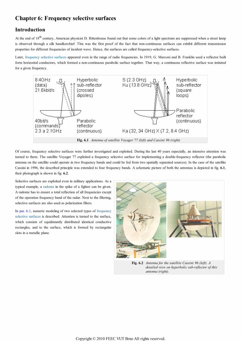
Fig. 6.2 Antenna for the satellite Cassini 96 (left). A
detailed view on hyperbolic sub-reflector of this
antenna (right).
Chapter 6: Frequency selective surfaces
Introduction
At the end of 18th century, American physicist D. Rittenhouse found out that some colors of a light spectrum are suppressed when a street lamp
is observed through a silk handkerchief. This was the first proof of the fact that non-continuous surfaces can exhibit different transmission
properties for different frequencies of incident wave. Hence, the surfaces are called frequency-selective surfaces.
Later, frequency selective surfaces appeared even in the range of radio frequencies. In 1919, G. Marconi and B. Franklin used a reflector built
form horizontal conductors, which formed a non-continuous parabolic surface together. That way, a continuous reflective surface was imitated
for a given frequency.
Fig. 6.1 Antenna of satellite Voyager 77 (left) and Cassini 96 (right)
Of course, frequency selective surfaces were further investigated and exploited. During the last 40 years especially, an intensive attention was
turned to them. The satellite Voyager 77 exploited a frequency selective surface for implementing a double-frequency reflector (the parabolic
antenna on the satellite could operate in two frequency bands and could be fed from two spatially separated sources). In the case of the satellite
Cassini in 1996, the described principle was extended to four frequency bands. A schematic picture of both the antennas is depicted in fig. 6.1,
their photograph is shown in fig. 6.2.
Selective surfaces are exploited even in military applications. As a
typical example, a radome in the spike of a fighter can be given.
A radome has to ensure a total reflection of all frequencies except
of the operation frequency band of the radar. Next to the filtering,
selective surfaces are also used as polarization filters.
In par. 6.1, numeric modeling of two selected types of frequency
selective surfaces is described. Attention is turned to the surface,
which consists of equidistantly distributed identical conductive
rectangles, and to the surface, which is formed by rectangular
slots in a metallic plane.
Copyright © 2010 FEEC VUT Brno All rights reserved.
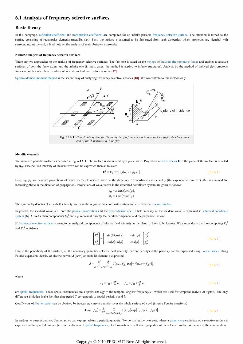
6.1 Analysis of frequency selective surfaces
Basic theory
In this paragraph, reflection coefficient and transmission coefficient are computed for an infinite periodic frequency selective surface. The attention is turned to the
surface consisting of rectangular elements (metallic, slot). First, the surface is assumed to be fabricated from such dielectrics, which properties are identical with
surrounding. At the end, a brief note on the analysis of real substrates is provided.
Numeric analysis of frequency selective surfaces
There are two approaches to the analysis of frequency selective surfaces. The first one is based on the method of induced electromotoric forces and enables to analyze
surfaces of both the finite extent and the infinite one (in most cases, the method is applied to infinite structures). Analysis by the method of induced electromotoric
forces is not described here; readers interested can find more information in [17].
Spectral domain moment method is the second way of analyzing frequency selective surfaces [18]. We concentrate to this method only.
Fig. 6.1A.1 Coordinate system for the analysis of a frequency selective surface (left). An elementary
cell of the dimensions a, b (right).
Metallic elements
We assume a periodic surface as depicted in fig. 6.1A.1. The surface is illuminated by a plane wave. Projection of wave vector k to the plane of the surface is denoted
by kxy. Electric filed intensity of incident wave can be expressed then as follows:
EI = E0 exp[+ j(α0x + β0 y)]. ( 6.1A.1 )
Here, α0, β0 are negative projections of wave vector of incident wave to the directions of coordinate axes x and y (the exponential term exp(+jkr) is assumed for
increasing phase in the direction of propagation). Projections of wave vector in the described coordinate system are given as follows:
α0 = k sin(ϑ)cos(φ),
β0 = k sin(ϑ)sin(φ).
The symbol E0 denotes electric-field intensity vector in the origin of the coordinate system and k is free-space wave number.
In general, the incident wave is of both the parallel polarization and the perpendicular one. If field intensity of the incident wave is expressed in spherical coordinate
system (fig. 6.1A.1), then components EϑI and Eφ
I represent directly the parallel component and the perpendicular one.
If frequency selective surface is going to be analyzed, components of electric field intensity in the plane xy have to be known. We can evaluate them re-computing EϑI
and EφI as follows:
⎡
⎣⎢⎢⎢Ex
I
EyI
⎤
⎦⎥⎥⎥
=
⎡
⎣⎢⎢
sin(ϑ)cos(φ) −sin(φ)sin(ϑ)sin(φ) cos(φ)
⎤
⎦⎥⎥
⎡
⎣⎢⎢⎢E
ϑI
EφI
⎤
⎦⎥⎥⎥. ( 6.1A.2 )
Due to the periodicity of the surface, all the necessary quantities (electric field intensity, current density) in the plane xy can be expressed using Fourier series. Using
Fourier expansion, density of electric current J [A/m] on metallic element is expressed:
J = ∑m = − M
M∑
n = − N
NJ(αm , βn)exp[+ j(αm x + βn y)], ( 6.1A.3 )
where
αn = α0 +2πa m, βn = β0 +
2πb
n ( 6.1A.4 )
are spatial frequencies. Those spatial frequencies are a spatial analogy to the temporal angular frequency ω, which are used for temporal analysis of signals. The only
difference is hidden in the fact that time period T corresponds to spatial periods a and b.
Coefficients of Fourier series can be obtained by integrating current densities over the whole surface of a cell (inverse Fourier transform)
J(αm , βn) =1ab
∬plocha bu ň k y
J(x, y)exp[− j(αm x + βn y)]. ( 6.1A.5 )
In analogy to current density, Fourier series can express arbitrary periodic quantity. We do that in the next part, where a plane wave excitation of a selective surface is
expressed in the spectral domain (i.e., in the domain of spatial frequencies). Determination of reflective properties of the selective surface is the aim of the computation.
Copyright © 2010 FEEC VUT Brno All rights reserved.
Fig. 6.1A.2 Frequency
selective surface
(reflected and
transmitted wave)
Problem formulation
Assume a plane wave falling to a frequency selective surface under angles (ϑ, φ). This wave excites currents in metallic
elements, which form a scattered field ES.
Whereas the magnitude (not the phase) of the intensity of incident wave EI is constant over the whole elementary cell, the
magnitude of the intensity of the scattered wave ES is different in the different points of the cell. Relation between ES and
EI changes according to the surface impedance in a given point. For the surface of conductive elements, we get
EI + ES =Jγ . ( 6.1A.6 )
Here, γ [S.m-1] is electric conductivity of elements. Assuming the electric conductivity of metallic elements to be perfect,
the right-hand side of (6.1A.6) approaches zero, and we get
EI + ES = 0. ( 6.1A.7 )
Intensity of scattered electric field ES in a point determined by the position vector r can be evaluated from vector potential
A
ES(r) = − jωµA +1
k 2∇ [∇ ⋅ A(r)]. ( 6.1A.8 )
As a source of vector potential A, currents J induced by incident wave to metallic elements of selective surface can be considered. Contribution of current in r' to the
potential in r is described by Green function G. For vector potential, we get
A(r) = ∬zdro je
G(r||r′)J(r′)dS ′. ( 6.1A.9 )
In free space, Green function G is of the form
G =exp(− jk||r −r ′ |
|)4π||r −r ′ ||
. ( 6.1A.10 )
Combining relations (6.1A.9), (6.1A.8) and (6.1A.7), integral equation for space-domain electric field is obtained:
− jωµ ∬zdro je
G(r||r′) ⋅ J(r′ )dS ′ +
1
k 2∇[∇ ⋅ ∬zdro je
G(r||r′ )⋅ J(r′ )dS ′] = − EI. ( 6.1A.11 )
Eqn. (6.1A.11) is solved in the domain of spatial frequencies. Eqn. (6.1A.11) is mapped to the spectral domain within two steps. First, eqn. (6.1A.8) is mapped by its
rewriting to the component form and by expressing vector potential by Fourier series. That way, we get [19]
⎡
⎣⎢⎢⎢
ExS(αm , βn)
EzS(αm , βn)
⎤
⎦⎥⎥⎥
= − jωµ
⎡
⎣
⎢⎢⎢⎢⎢
1 −αm
2
k 2
−αm βn
k 2
−αm βn
k 21 −
βn2
k 2
⎤
⎦
⎥⎥⎥⎥⎥
⎡
⎣⎢⎢
Ax (αm , βn)Ay(αm , βn)
⎤
⎦⎥⎥. ( 6.1A.12 )
In the second step, the relation is mapped to the domain of spatial frequencies (6.1A.9) [19]
A(αm , βn) = G(αm , βn)⋅ J(αm , βn). ( 6.1A.13 )
Evaluating Fourier transform of the function (6.1A.10), we get [19] Green function in spectral domain
G(αm , βn) =− j
2 k 2 −αm 2 − βn2√
, ( 6.1A.14 )
where the square-root of negative imaginary part is assumed only.
Combining (6.1A.13), (6.1A.14) and (6.1A.12), the final relation for electric field in spectral domain is obtained
−1
2ωε∑
m, n
⎡
⎣
⎢⎢⎢⎢⎢⎢⎢
k 2 − αm2
k 2 − αm2 − βn
2√−αm βn
k 2 − αm2 − βn
2√−αm βn
k 2 − αm2 − βn
2√k 2 − βn
2
k 2 − αm2 − βn
2√
⎤
⎦
⎥⎥⎥⎥⎥⎥⎥
⎡
⎣⎢⎢⎢
Jx (αm , βn)Jy(αm , βn)
⎤
⎦⎥⎥⎥exp[ j(αm x + βn y)] = −
⎡
⎣⎢⎢⎢
ExI (x, y)
EyI(x, y)
⎤
⎦⎥⎥⎥. ( 6.1A.15 )
Problem solution
Solving the problem, an unknown current distribution in (6.1A.15) is approximated by the linear combination of properly chosen basis functions and unknown
approximation coefficients. Such formal approximation is substituted into the solved eqn. (6.1A.15). Since the approximation of the solution does not meet the initial
relation exactly, we respect this fact by introducing a residual function (residuum). Lower the residuum is, more accurate the approximation is. The residuum is
minimized by Galerkin method (residuum is sequentially multiplied by as many basis functions as many unknown approximation coefficients is computed; that way, N
linear algebraic equations for N unknown approximation coefficients is obtained).
There are two approaches for choosing basis functions. The first one exploits basis functions, which are non-zero over the whole analyzed area. Functions are elected to
physically represent standing waves of a current on an element.
The second approach divides the analyzed region to sub-regions, where current is approximated in terms of basis functions, which functional value is non-zero over a
Copyright © 2010 FEEC VUT Brno All rights reserved.
Fig. 6.1A.4 Equivalent circuit of selective
surface in frequency domain;
surface consist of metallic elements
(left); ϑ = φ = 0. Directivity factor
in Smith chart (right).
given sub-region only. This approach is advantageous in simple analysis of selective surfaces consisting of arbitrarily shaped elements.
Here, we concentrate on the first group of basis functions only. As basis functions, harmonic functions are used (first approach, the layer B), and a combination of
harmonic functions and Chebyshev polynomials is exploited (second approach, the layer B).
A more detailed description of the above-given basis functions for solving (6.1A.15) is introduced in the layer B. Here, obtained results are presented only.
Harmonic basis functions
Assume a frequency selective surface consisting of rectangular perfectly conductive elements of the dimensions a' and b'. If current distribution over an element is
approximated in terms of harmonic basis functions, we obtain for the mode (1, 1) for the parallel polarization such current distribution, which is depicted in fig. 6.1A.3a,
and for the perpendicular polarization, the distribution from fig. 6.1A.3b is obtained
a) b)
Fig. 6.1A.3 Directional field of current density of the mode (1,1)
a) for parallel polarization
b) for perpendicular one.
The cell is of dimensions a = b = 12mm, the metallic element is of dimensions a' = b' = 12mm; f=10GHz, ϑ = 1°, φ = 45°,
d = 1.5mm, εr = 3.7. Magnitude of marginal currents was increased with respect to reality. Plane of incidence is depicted
in red.
Combination of harmonic functions and Chebyshev polynomials
In contrast to purely harmonic basis functions, the function cosine is replaced by Chebyshev polynomial,
which is of infinite magnitude at the edges of the element. That way, strong currents flowing along edges
are correctly modeled.
An equivalent circuit can describe behavior of frequency selective surfaces, which consist of metallic
elements, where inductances of elements together with capacitances among ends of elements create a
serial resonant circuit (fig. 6.1A.4).
Reflection coefficient r (see fig. 6.1A.4) is evaluated according to
PT = P I⎡⎣1 − ||ρ||2⎤⎦. ( 6.1A.16 )
Here, PI is power of incident wave and PT denotes power of wave, which was transmitted by the surface
to the right-hand half-space. Resistance 377 Ω models free space in front of the surface (left) and behind
the surface (right).
Copyright © 2010 FEEC VUT Brno All rights reserved.
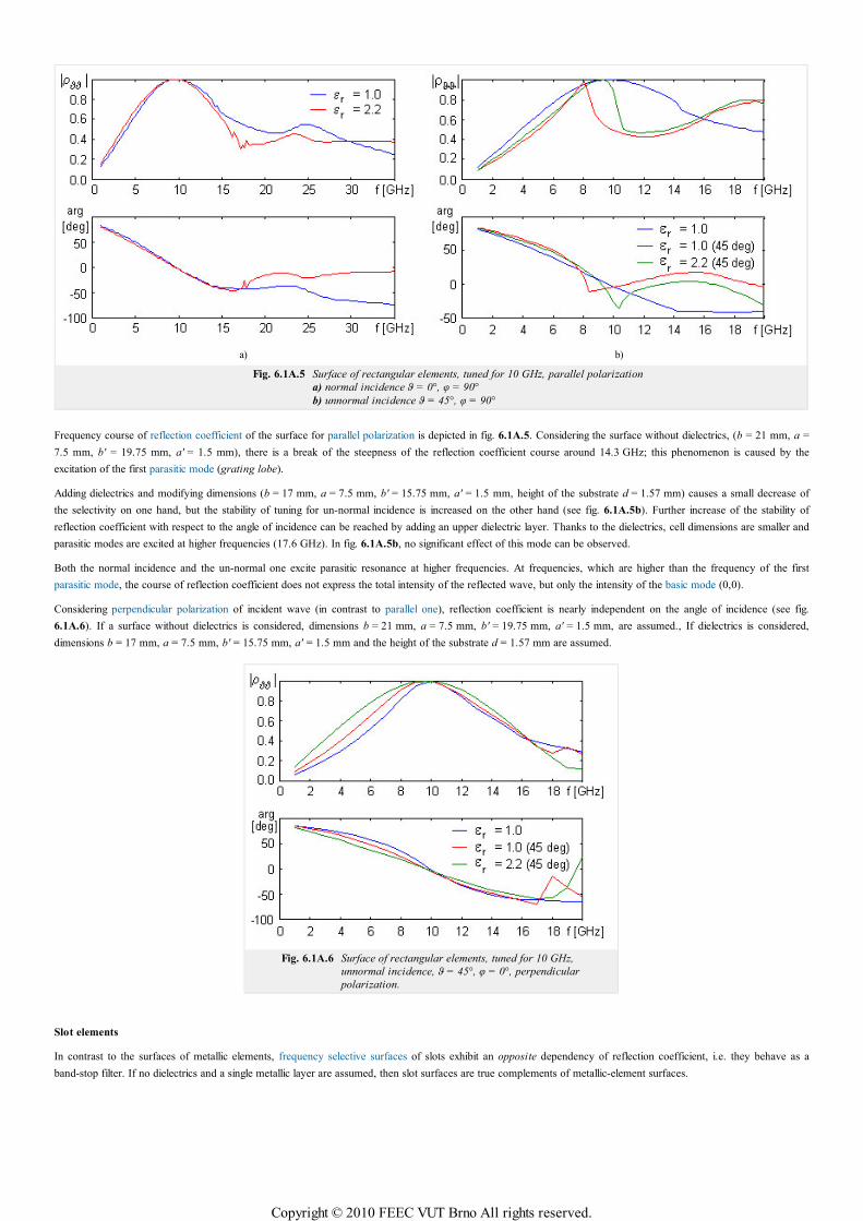
a) b)
Fig. 6.1A.5 Surface of rectangular elements, tuned for 10 GHz, parallel polarization
a) normal incidence ϑ = 0°, φ = 90°
b) unnormal incidence ϑ = 45°, φ = 90°
Frequency course of reflection coefficient of the surface for parallel polarization is depicted in fig. 6.1A.5. Considering the surface without dielectrics, (b = 21 mm, a =
7.5 mm, b' = 19.75 mm, a' = 1.5 mm), there is a break of the steepness of the reflection coefficient course around 14.3 GHz; this phenomenon is caused by the
excitation of the first parasitic mode (grating lobe).
Adding dielectrics and modifying dimensions (b = 17 mm, a = 7.5 mm, b' = 15.75 mm, a' = 1.5 mm, height of the substrate d = 1.57 mm) causes a small decrease of
the selectivity on one hand, but the stability of tuning for un-normal incidence is increased on the other hand (see fig. 6.1A.5b). Further increase of the stability of
reflection coefficient with respect to the angle of incidence can be reached by adding an upper dielectric layer. Thanks to the dielectrics, cell dimensions are smaller and
parasitic modes are excited at higher frequencies (17.6 GHz). In fig. 6.1A.5b, no significant effect of this mode can be observed.
Both the normal incidence and the un-normal one excite parasitic resonance at higher frequencies. At frequencies, which are higher than the frequency of the first
parasitic mode, the course of reflection coefficient does not express the total intensity of the reflected wave, but only the intensity of the basic mode (0,0).
Considering perpendicular polarization of incident wave (in contrast to parallel one), reflection coefficient is nearly independent on the angle of incidence (see fig.
6.1A.6). If a surface without dielectrics is considered, dimensions b = 21 mm, a = 7.5 mm, b' = 19.75 mm, a' = 1.5 mm, are assumed., If dielectrics is considered,
dimensions b = 17 mm, a = 7.5 mm, b' = 15.75 mm, a' = 1.5 mm and the height of the substrate d = 1.57 mm are assumed.
Fig. 6.1A.6 Surface of rectangular elements, tuned for 10 GHz,
unnormal incidence, ϑ = 45°, φ = 0°, perpendicular
polarization.
Slot elements
In contrast to the surfaces of metallic elements, frequency selective surfaces of slots exhibit an opposite dependency of reflection coefficient, i.e. they behave as a
band-stop filter. If no dielectrics and a single metallic layer are assumed, then slot surfaces are true complements of metallic-element surfaces.
Copyright © 2010 FEEC VUT Brno All rights reserved.
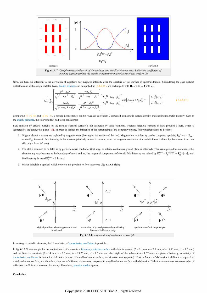
surface 1 surface 2
Fig. 6.1A.7 Complementary behavior of slot surfaces and metallic-element ones. Reflection coefficient of
metallic-element surface (1) equals to transmission coefficient of slot surface (2).
Now, we turn our attention to the derivation of equations for magnetic intensity over the aperture of slot surface in spectral domain. Considering the case without
dielectrics and with a single metallic layer, duality principle can be applied: in (6.1A.15), we exchange E with H, ε with µ, J with JM
−1
2ωµ∑
m, n
⎡
⎣
⎢⎢⎢⎢⎢⎢⎢
k 2 − αm2
k 2 − αm2 − βn
2√−αm βn
k 2 − αm2 − βn
2√−αm βn
k 2 − αm2 − βn
2√k 2 − βn
2
k 2 − αm2 − βn
2√
⎤
⎦
⎥⎥⎥⎥⎥⎥⎥
⎡
⎣⎢⎢⎢
2JxM + (αm , βn)
2JyM + (αm , βn)
⎤
⎦⎥⎥⎥exp[ j(αm x + βn y)] = −
⎡
⎣⎢⎢⎢
2HxI(x, y)
2HyI(x, y)
⎤
⎦⎥⎥⎥. ( 6.1A.17 )
Comparing (6.1A.17) and (6.1A.15), a certain inconsistency can be revealed: coefficient 2 appeared at magnetic current density and exciting magnetic intensity. Next to
the duality principle, the following fact had to be considered:
Field radiated by electric currents of the metallic-element surface is not scattered by those elements, whereas magnetic currents in slots produce a field, which is
scattered by the conductive plane [19]. In order to include the influence of the surrounding of the conductive plane, following steps have to be done:
Original electric currents are replaced by magnetic ones (flowing on the surface of the slot). Magnetic current density can be computed applying JM+ = z × Eap,
where Eap is electric field intensity in the aperture (similarly to electric current, even the magnetic conductor of a real thickness is flown by the current from one
side only - from left one).
1.
The slot is assumed to be filled in by perfect electric conductor (that way, an infinite continuous ground plane is obtained). This assumption does not change the
situation any way because at the boundary of metal and air, the tangential components of electric field intensity are related by Etkov − E
tvzduch = J
M+ ×(−z), and
field intensity in metal Etkov = 0 is zero.
2.
Mirror principle is applied, which converts the problem to free-space one (fig. 6.1A.8 right).3.
original problem when magnetic current
introduced
extension of ground plane and considering
left-hand half-space only
application of mirror principle
Fig. 6.1A.8 Explanation of equivalence principle
In analogy to metallic elements, dual formulation of transmission coefficient is possible τ.
In fig. 6.1A.9, an example for normal incidence of a wave to a frequency selective surface with slots in vacuum (b = 21 mm, a = 7.5 mm, b' = 19.75 mm, a' = 1.5 mm)
and on dielectric substrate (b = 14 mm, a = 7.5 mm, b' = 13.25 mm, a' = 1.5 mm and the height of the substrate d = 1.57 mm) are given. Obviously, selectivity of
transmission coefficient is better for dielectrics (in case of metallic-element surface, the situation was opposite). Next, influence of dielectrics is different compared to
metallic-element surface, and therefore, slots are of different dimensions compared to metallic-element surface with dielectrics. Dielectrics even cause non-zero value of
reflection coefficient on resonant frequency. Even here, parasitic modes appear.
Conclusion
Copyright © 2010 FEEC VUT Brno All rights reserved.
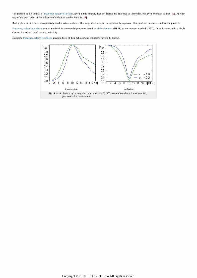
The method of the analysis of frequency selective surfaces, given in this chapter, does not include the influence of dielectrics, but given examples do that [17]. Another
way of the description of the influence of dielectrics can be found in [19].
Real applications use several sequentially lined selective surfaces. That way, selectivity can be significantly improved. Design of such surfaces is rather complicated.
Frequency selective surfaces can be modeled in commercial programs based on finite elements (HFSS) or on moment method (IE3D). In both cases, only a single
element is analyzed thanks to the periodicity.
Designing frequency selective surfaces, physical basis of their behavior and limitations have to be known.
transmission reflection
Fig. 6.1A.9 Surface of rectangular slots, tuned for 10 GHz, normal incidence ϑ = 0° φ = 90°,
perpendicular polarization.
Copyright © 2010 FEEC VUT Brno All rights reserved.
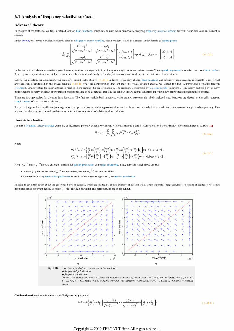
6.1 Analysis of frequency selective surfaces
Advanced theory
In this part of the textbook, we take a detailed look on basis functions, which can be used when numerically analyzing frequency selective surfaces (current distribution over an element is
sought).
In the layer A, we derived a relation for electric field of a frequency selective surface, which consists of metallic elements, in the domain of spatial spectra
−1
2ωε∑
m, n
⎡
⎣
⎢⎢⎢⎢⎢⎢⎢
k 2 − αm2
k 2 − αm2 − βn
2√−αm βn
k 2 − αm2 − βn
2√−αm βn
k 2 − αm2 − βn
2√k 2 − βn
2
k 2 − αm2 − βn
2√
⎤
⎦
⎥⎥⎥⎥⎥⎥⎥
⎡
⎣⎢⎢⎢
Jx (αm , βn)Jy(αm , βn)
⎤
⎦⎥⎥⎥exp[ j(αm x + βn y)] = −
⎡
⎣⎢⎢⎢
ExI(x, y)
EyI(x, y)
⎤
⎦⎥⎥⎥. ( 6.1B.1 )
In the above-given relation, ω denotes angular frequency of a wave, ε is permittivity of the surrounding of selective surface, αm and βn are spatial frequencies, k denotes free-space wave number,
Jx and Jy are components of current density vector over the element, and finally, ExI and Ey
I denote components of electric field intensity of incident wave.
Solving the problem, we approximate the unknown current distribution in (6.1B.1) in terms of properly chosen basis functions and unknown approximation coefficients. Such formal
approximation is substituted to the solved equation (6.1B.1). Since the approximation does not meet the solved equation exactly, we respect this fact by introducing a residual function
(residuum). Smaller values the residual function reaches, more accurate the approximation is. The residuum is minimized by Galerkin method (residuum is sequentially multiplied by as many
basis functions as many unknown approximation coefficients have to be computed; that way the set of N linear algebraic equations for N unknown approximation coefficients is obtained).
There are two approaches for choosing basis functions. The first one exploits basis functions, which are non-zero over the whole analyzed area. Functions are elected to physically represent
standing waves of a current on an element.
The second approach divides the analyzed region to sub-regions, where current is approximated in terms of basis functions, which functional value is non-zero over a given sub-region only. This
approach is advantageous in simple analysis of selective surfaces consisting of arbitrarily shaped elements.
Harmonic basis functions
Assume a frequency selective surface consisting of rectangular perfectly conductive elements of the dimensions a' and b'. Components of current density J are approximated as follows [17]
J(x, y) = ∑p = 0
P∑
q =0
QApqΨ pq
TM + FpqΨ pqTE ,
( 6.1B.2 )
where
Ψ pqTE(x, y) =
⎡⎣⎢
pπ
a ′sin
⎛⎝⎜
pπx
a ′
⎞⎠⎟cos
⎛⎝⎜
qπy
b ′
⎞⎠⎟ux +
qπ
b ′cos
⎛⎝⎜
pπx
a ′
⎞⎠⎟sin
⎛⎝⎜
qπy
b ′
⎞⎠⎟uy
⎤⎦⎥exp[ j(α0 x + β0 y)],
Ψ pqTM (x, y) =
⎡⎣⎢
pπ
b ′sin
⎛⎝⎜
pπx
a ′
⎞⎠⎟cos
⎛⎝⎜
qπy
b ′
⎞⎠⎟ux −
qπ
a ′cos
⎛⎝⎜
pπx
a ′
⎞⎠⎟sin
⎛⎝⎜
qπy
b ′
⎞⎠⎟uy
⎤⎦⎥exp[ j(α0x + β0 y)].
( 6.1B.3 )
Here, ΨpqTE and Ψpq
TM are two different functions for parallel polarization and perpendicular one. These functions differ in two aspects:
Indeces p, q for the function ΨpqTE can reach zero, and for Ψpq
TM are one and higher.
Component Jy for perpendicular polarization has to be of the opposite sign than Jy for parallel polarization.
In order to get better notion about the difference between currents, which are excited by electric intensity of incident wave, which is parallel (perpendicular) to the plane of incidence, we depict
directional fields of current density of mode (1,1) for parallel polarization and perpendicular one in fig. 6.1B.1.
a) b)
Fig. 6.1B.1 Directional field of current density of the mode (1,1)
a) for parallel polarization
b) for perpendicular one.
The cell is of dimensions a = b = 12mm, the metallic element is of dimensions a' = b' = 12mm; f=10GHz, ϑ = 1°, φ = 45°,
d = 1.5mm, εr = 3.7. Magnitude of marginal currents was increased with respect to reality. Plane of incidence is depicted
in red.
Combination of harmonic functions and Chebyshev polynomials
JTE = sin⎡⎣⎢
pπ
a ′
⎛⎝⎜x +
a ′
2
⎞⎠⎟⎤⎦⎥
Tq(2y /b ′)1−(2y/b ′)2√
x +Tp(2x /a ′)1−(2x /a ′)2√
sin⎡⎣⎢
qπ
b ′
⎛⎝⎜y +
b ′
2
⎞⎠⎟⎤⎦⎥y ( 6.1B.4a )
Copyright © 2010 FEEC VUT Brno All rights reserved.
JTM = sin⎡⎣⎢
pπ
a ′
⎛⎝⎜x +
a ′
2
⎞⎠⎟⎤⎦⎥
Tq(2y/b ′)1−(2y /b ′)2√
x −Tp(2x /a ′)1−(2x /a ′)2√
sin⎡⎣⎢
qπ
b ′
⎛⎝⎜y +
b ′
2
⎞⎠⎟⎤⎦⎥y ( 6.1B.4b )
In contrast to harmonic basis functions, the function cosine is replaced by Chebyshev polynomial in order to reach infinite values at the edges of elements. That way, currents flowing along
edges are correctly modeled.
Now, eqn. (6.1B.1) is solved by Galerkin method: eqn. (6.1B.1) is sequentially multiplied by basis functions and the product is integrated over the surface of the element. For purely harmonic
basis functions, we get:
⌠⌡a
b
wm(z)R(z)dz = 0 m = 0,1,…N ,
∑p, q
Ap, q ∑m, n
ΨrsTE∗ (am , βn)K(am , βn)Ψ pq
TE∗ (am , βn) + Fpq ∑m, n
ΨrsTE∗ (am , βn)K(am , βn)Ψ pq
TE∗ (am , βn) =−1ab
∬p ř es element
EtanI (x, y)Ψpq
TE∗ (x, y)dx dy,(
6.1B.5a
)
∑p, q
Ap, q ∑m, n
ΨrsTM ∗ (am , βn)K(am , βn)Ψ pq
TM ∗ (am , βn) + Fpq ∑m, n
ΨrsTM ∗ (am , βn)K(am , βn)Ψ pq
TM ∗ (am , βn) =−1ab
∬p ř es element
EtanI (x, y)Ψpq
TM ∗ (x, y)dx dy.(
6.1B.5b
)
If the above-given set is solved out, electric intensity ES in spectral domain is computed. Intensity ES appears at the left-hand side of eqn. (6.1B.1)
ES = −1
2ωε∑
m, n
⎡
⎣
⎢⎢⎢⎢⎢⎢⎢
k 2 − αm2
k 2 − αm2 − βn
2√−αm βn
k 2 − αm2 − βn
2√−αm βn
k 2 − αm2 − βn
2√k 2 − βn
2
k 2 − αm2 − βn
2√
⎤
⎦
⎥⎥⎥⎥⎥⎥⎥
⎡
⎣⎢⎢
Jx (αm , βn)Jy(αm , βn)
⎤
⎦⎥⎥exp[ j(αm x + βn y)] = −
⎡
⎣⎢⎢⎢
ExI (x, y)
EyI(x, y)
⎤
⎦⎥⎥⎥. ( 6.1B.6 )
Computing electric intensity of scattered wave ES = ER, only the basic harmonic component on the frequency α0, β0 is assumed. If the period a is small (smaller than one half of the wavelength)
and frequency approaches the first resonance of the surface, then a uniform field of the scattered wave exists in the far field region only. If the condition is not met, then parasitic modes can be
excited (higher spatial frequencies are not filtered by the near-field zone, and corresponding waves propagate further).
Let us explain the physical notion of parasitic modes. Explanation is illustrated by fig. 6.1B.2. Here, a two-element antenna array is depicted, which is illuminated by a plane wave arriving from
the direction ϑ. After the incidence, the wave is reflected according to rules of geometric optics. A part of energy can propagate even in the direction of the parasitic (grating) lobe.
Fig. 6.1B.2 Explanation of forming
parasitic lobes
(two-element antenna)
Formation of a parasitic lobe is conditioned by reaching a phase shift, which equals to the integral multiple of 2π by the beam no. 1 on a bold trajectory. From the mathematical point of view:
βDx sin(ϑg) + βDx sin(ϑ) = n2π. ( 6.1B.7 )
The direction, where the parasitic lobe appears, depends on the frequency of the incident wave and on the distance of antenna elements only. The lowest frequency of exciting the parasitic mode
for a given angle of incidence, is for ϑg = 90° :
fg0 =nc
Dx (sin ϑ+1). ( 6.1B.8 )
if the distance of antenna elements equals to a = 21 mm and if perpendicular incidence of wave are assumed, then the first parasitic lobe is excited on the frequency
fg =1⋅3⋅108
0,021⋅(sin0+1) = 14,3 GHz. ( 6.1B.9 )
Copyright © 2010 FEEC VUT Brno All rights reserved.
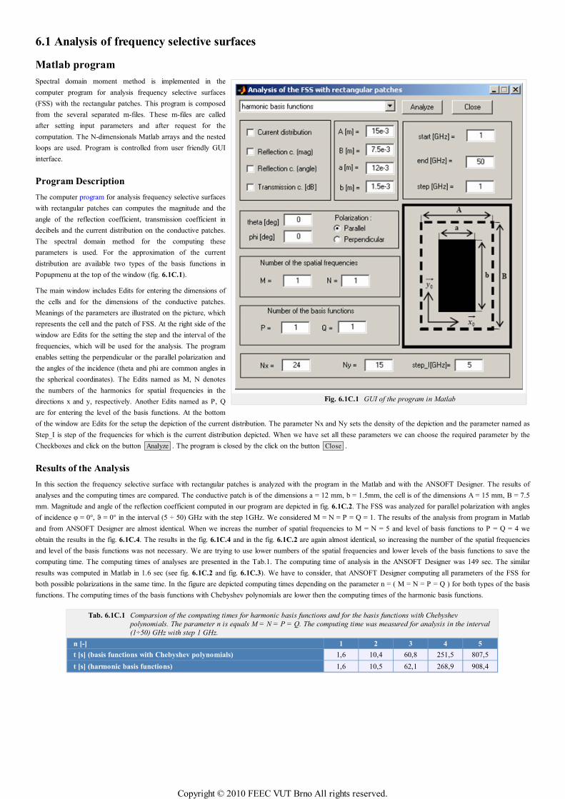
Fig. 6.1C.1 GUI of the program in Matlab
6.1 Analysis of frequency selective surfaces
Matlab program
Spectral domain moment method is implemented in the
computer program for analysis frequency selective surfaces
(FSS) with the rectangular patches. This program is composed
from the several separated m-files. These m-files are called
after setting input parameters and after request for the
computation. The N-dimensionals Matlab arrays and the nested
loops are used. Program is controlled from user friendly GUI
interface.
Program Description
The computer program for analysis frequency selective surfaces
with rectangular patches can computes the magnitude and the
angle of the reflection coefficient, transmission coefficient in
decibels and the current distribution on the conductive patches.
The spectral domain method for the computing these
parameters is used. For the approximation of the current
distribution are available two types of the basis functions in
Popupmenu at the top of the window (fig. 6.1C.1).
The main window includes Edits for entering the dimensions of
the cells and for the dimensions of the conductive patches.
Meanings of the parameters are illustrated on the picture, which
represents the cell and the patch of FSS. At the right side of the
window are Edits for the setting the step and the interval of the
frequencies, which will be used for the analysis. The program
enables setting the perpendicular or the parallel polarization and
the angles of the incidence (theta and phi are common angles in
the spherical coordinates). The Edits named as M, N denotes
the numbers of the harmonics for spatial frequencies in the
directions x and y, respectively. Another Edits named as P, Q
are for entering the level of the basis functions. At the bottom
of the window are Edits for the setup the depiction of the current distribution. The parameter Nx and Ny sets the density of the depiction and the parameter named as
Step_I is step of the frequencies for which is the current distribution depicted. When we have set all these parameters we can choose the required parameter by the
Checkboxes and click on the button Analyze . The program is closed by the click on the button Close .
Results of the Analysis
In this section the frequency selective surface with rectangular patches is analyzed with the program in the Matlab and with the ANSOFT Designer. The results of
analyses and the computing times are compared. The conductive patch is of the dimensions a = 12 mm, b = 1.5mm, the cell is of the dimensions A = 15 mm, B = 7.5
mm. Magnitude and angle of the reflection coefficient computed in our program are depicted in fig. 6.1C.2. The FSS was analyzed for parallel polarization with angles
of incidence φ = 0°, ϑ = 0° in the interval (5 ÷ 50) GHz with the step 1GHz. We considered M = N = P = Q = 1. The results of the analysis from program in Matlab
and from ANSOFT Designer are almost identical. When we increas the number of spatial frequencies to M = N = 5 and level of basis functions to P = Q = 4 we
obtain the results in the fig. 6.1C.4. The results in the fig. 6.1C.4 and in the fig. 6.1C.2 are again almost identical, so increasing the number of the spatial frequencies
and level of the basis functions was not necessary. We are trying to use lower numbers of the spatial frequencies and lower levels of the basis functions to save the
computing time. The computing times of analyses are presented in the Tab.1. The computing time of analysis in the ANSOFT Designer was 149 sec. The similar
results was computed in Matlab in 1.6 sec (see fig. 6.1C.2 and fig. 6.1C.3). We have to consider, that ANSOFT Designer computing all parameters of the FSS for
both possible polarizations in the same time. In the figure are depicted computing times depending on the parameter n = ( M = N = P = Q ) for both types of the basis
functions. The computing times of the basis functions with Chebyshev polynomials are lower then the computing times of the harmonic basis functions.
Tab. 6.1C.1 Comparsion of the computing times for harmonic basis functions and for the basis functions with Chebyshev
polynomials. The parameter n is equals M = N = P = Q. The computing time was measured for analysis in the interval
(1÷50) GHz with step 1 GHz.
n [-] 1 2 3 4 5
t [s] (basis functions with Chebyshev polynomials) 1,6 10,4 60,8 251,5 807,5
t [s] (harmonic basis functions) 1,6 10,5 62,1 268,9 908,4
Copyright © 2010 FEEC VUT Brno All rights reserved.
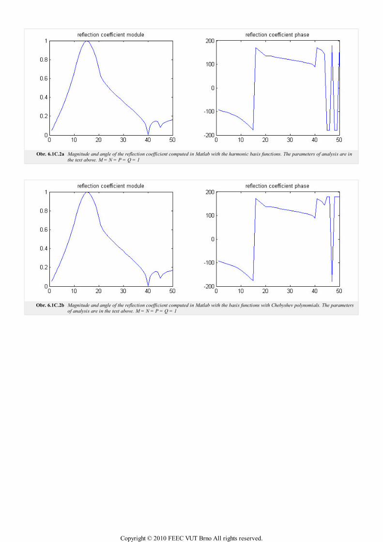
Obr. 6.1C.2a Magnitude and angle of the reflection coefficient computed in Matlab with the harmonic basis functions. The parameters of analysis are in
the text above. M = N = P = Q = 1
Obr. 6.1C.2b Magnitude and angle of the reflection coefficient computed in Matlab with the basis functions with Chebyshev polynomials. The parameters
of analysis are in the text above. M = N = P = Q = 1
Copyright © 2010 FEEC VUT Brno All rights reserved.
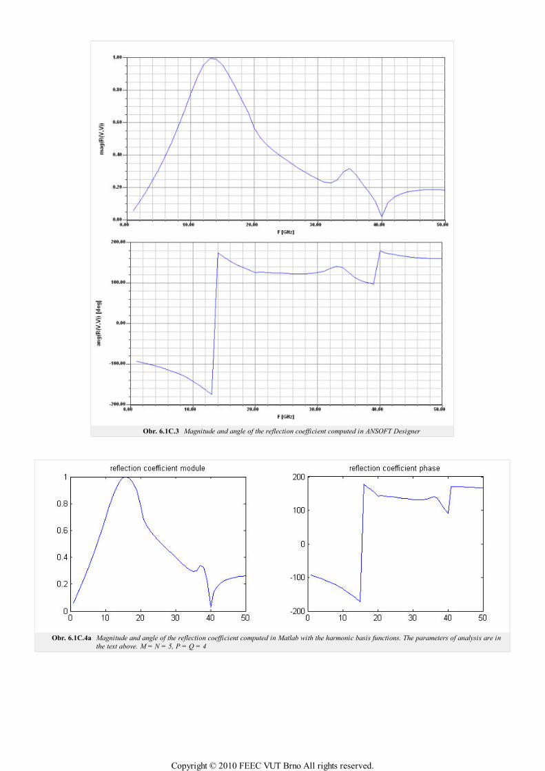
Obr. 6.1C.3 Magnitude and angle of the reflection coefficient computed in ANSOFT Designer
Obr. 6.1C.4a Magnitude and angle of the reflection coefficient computed in Matlab with the harmonic basis functions. The parameters of analysis are in
the text above. M = N = 5, P = Q = 4
Copyright © 2010 FEEC VUT Brno All rights reserved.
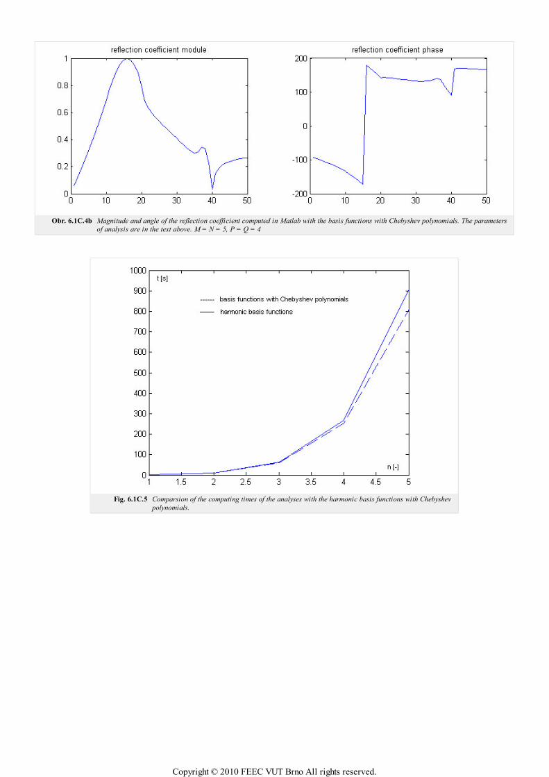
Obr. 6.1C.4b Magnitude and angle of the reflection coefficient computed in Matlab with the basis functions with Chebyshev polynomials. The parameters
of analysis are in the text above. M = N = 5, P = Q = 4
Fig. 6.1C.5 Comparsion of the computing times of the analyses with the harmonic basis functions with Chebyshev
polynomials.
Copyright © 2010 FEEC VUT Brno All rights reserved.
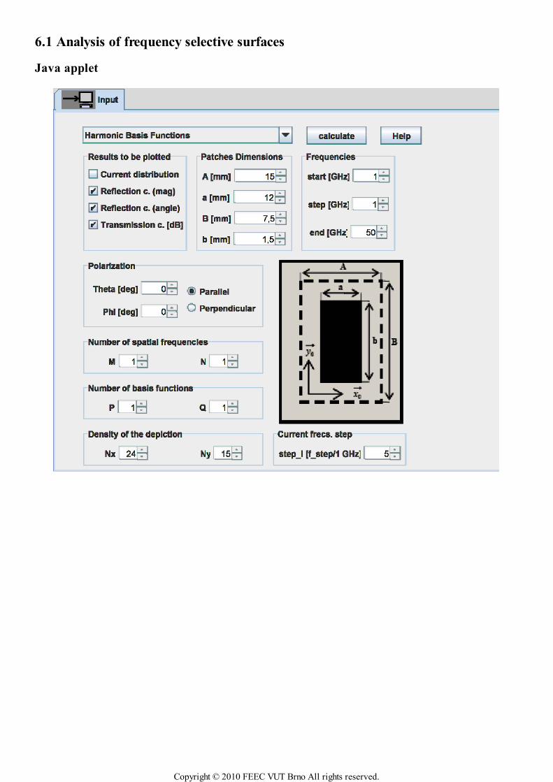
6.1 Analysis of frequency selective surfaces
Java applet
Copyright © 2010 FEEC VUT Brno All rights reserved.

6.1 Analysis of frequency selective surfaces
Quiz
Answer these questions to get feedback on how well you understand the course. Only one of the answers is correct. You don't have to answer
every question. If you don't know the answer you can just leave it blank (default option: “I won't answer this question”) and this won't affect
your score. Answering correctly will add 2 points to your score but on the other hand you'll lose 1 point if your answer is wrong. The
questions are divided in groups of five questions.
Press See result after you have finished answering.
Displaying questions 1..5 of 5:
Question 1
Frequency selective surfaces …
Possible answers for question 1:
… are used to amplify electromagnetic waves.
… can behave as a perfect mirror at one frequency, and as a free space at another frequency.
… are sensitive to frequencies and insensitive to polarizations of waves.
I won't answer this question
Question 2
For the analysis of FSS, we usually use …
Possible answers for question 2:
… the frequency domain method of moments.
… the time-domain moment method.
… the spectral domain method of moments.
I won't answer this question
Question 3
The suppression of wave transitions at given frequencies is caused …
Possible answers for question 3:
… by destructive interferences of waves radiated by currents induced on FSS elements.
… increasing losses in metallic and dielectric parts of the FSS.
… by the critical frequency of waveguides formed by FSS elements.
I won't answer this question
Question 4
Current distribution on the FSS elements can be approximated in terms of …
Possible answers for question 4:
… harmonic and Chebychev basis functions.
… piecewise constant basis functions.
… Dirac pulses.
I won't answer this question
Question 5
Analysis of rectangular slots in a metallic plane and rectangular patches on a dielectric plane …
Copyright © 2010 FEEC VUT Brno All rights reserved.

Possible answers for question 5:
… are the same thanks to the duality principle.
… have to be performed differently due to the different boundary conditions.
… are similar, but the magnetic currents require small changes of the algorithm.
I won't answer this question
Copyright © 2010 FEEC VUT Brno All rights reserved.
Fig. 7.1 Elementary optical signal is formed by
the interface of three uniform plane
waves
Chapter 7: Radio optics
Introduction
The term electric signal usually denotes a time-variant voltage U(t), current I(t) or electric field intensity E(t). Time dependency of those
quantities contains an information.
Every electric signal can be composed of a finite or infinite number of harmonic voltages (currents, intensities) of various frequencies,
amplitudes and initial phases. Amplitudes and phases of those spectral components are given by the spectral function S(ω). The signal can be
therefore described by the relation
U(t) =1
2π⌠⌡
−∞
+∞
S(ω)e jωtdω. ( 7.1 )
In that relation, ω is angular frequency and t is time.
The signal is said to be given by the addition of its spectral components or by inverse Fourier transform of its spectral function (according to
eqn. (7.1)). Since a simple harmonic oscillation is the basic building stone of a signal, we consider this oscillation as elementary signal even it
does not bear any information. The elementary signal is determined by its amplitude, phase and (temporal) frequency f, or time period T = 1/f.
Electromagnetic wave can contain information in time dependency of electric field intensity E(t). Since the wave exists in the space, information
can be hidden even in the spatial distribution of intensity. Then, we speak about optical signal. The spatial signal is richer than the electric one
because it is a function of two variables (x, y). It is associated with an electromagnetic wave (with amplitude distribution of field intensity in the
plane, which is perpendicular to the direction of propagation).
In analogy to the elementary electric signal, elementary spatial signal can be introduced. If coordinate system x, y is given in a plane, which is
perpendicular to the direction of propagation, then a pure harmonic variation of amplitude of field intensity in an axis direction is elementary
optical signal. In the direction of the second axis, amplitude of field intensity is constant (independent to y). If such wave illuminates a projection
screen, a set of dark and light strips of unclear transitions can be seen (the darkest strips correspond to the minimum of the harmonic function,
the lightest strips to the maximum). Distance between two neighboring strips is called spatial period Tx. Reverse value of the spatial period is
called spatyial frequency fx. From the mathematical point of view, elementary optical signal for x-direction can be expressed as follows:
E(x) = Emx [1 + sin(2π fx x)] = Emx [1 + sin(ωx x)]. ( 7.2 )
For y-direction:
E(y) = Emy[1 + sin⎛⎝2π fyx
⎞⎠] = Emy[1 + sin(ωyx)]. ( 7.3 )
Composing these two elementary signals together, two-dimensional spatial signal is obtained:
E(x, y) = Em [1 + sin(ωx x + ωy y)]. ( 7.4 )
Optical signals can be written in symbolic way. Then, we get:
E(x, y) = Em[1 + exp( jωx x) + exp( jωy y)]. ( 7.5 )
In analogy to the time domain, every spatial signal E(x, y) can be composed
of elementary spatial signals of different spatial frequencies, of different
amplitudes and different initial phases. Fourier transform corresponding to
(7.1) is, of course, two-dimensional.
Elementary spatial signal is non-uniform plane wave. Handling those waves
is rather complicated, and therefore, non-uniform waves are decomposed to
three uniform plane waves. In fig. 7.1, blue arrows denote directions of
propagation of three paraxial waves, which amplitudes are E/2, E and E/2,
and which propagate in three symmetric directions with respect to the axis z.
Symbols k denote wave vectors of respective waves. Now, the resultant
field distribution in the plane xy in the parallel direction to the axis y is
computed. For that purpose, projections of wave vectors to the direction y
have to be determined:
( 7.6 )
Copyright © 2010 FEEC VUT Brno All rights reserved.

The computed intensity is given by the addition of three plane waves, which propagate in the direction y , and which are described by wave
numbers k1y, k0y, k2y:
E(y) =Em2
exp⎛⎝ jk1y y
⎞⎠ + Em +
Em2
exp⎛⎝ jk2y y
⎞⎠ =
= Em[exp(+ jk sin ϑy)
2+ 1 +
exp(− jk sin ϑy)2 ] =
= Em[1 + cos(k sin ϑy)]
( 7.7 )
That way, we computed the cosine distribution of the amplitude Ey, and consequently, the elementary optical signal of the spatial frequency
ωy = k.sin ϑ. Now, a general spatial signal can be decomposed by Fourier transform to elementary optical signals, and each elementary signal
can be further decomposed to the triplet of uniform waves.
The above-described principles form the basics of radio optics - on radio frequencies, the spatial distribution of signals is handled the same way
as in optics. Considering the electromagnetic nature of the spatial signal, there is no reason to deny this approach.
In the par. 7.1, we describe Gaussian beam - a narrow beam of coherent radiation. As an example of Gaussian beam, a laser beam of the basic
mode TEM00 can be considered, which leaves the source with planar equiphase surface perpendicular to the direction of propagation. The beam
is not intentionally modulated, but the transversal field distribution is not constant. The maximum intensity appears as the axis of the beam and
the intensity decreases towards the margin of the beam following the Gaussian function. Gaussian beam is let to pass a system of spatial layers
and lenses, and variation of its parameters is observed. The task is typical for optical applications, but we can meet it even on low (radio)
frequencies.
Par. 7.2 deals with the passage of Gaussian beam through various spatial elements (lenses, layers of media, etc.), and with the description of
those phenomena by matrix notation. Gaussian beam is described by the vector of parameters, optical elements are described by matrices.
Multiplying a vector of Gaussian beam parameters at the input of an optical element by the matrix of an optical element, a vector of Gaussian
beam parameters at the output of an optical element is obtained.
Copyright © 2010 FEEC VUT Brno All rights reserved.
7.1 Gaussian beam
Basic theory
Investigating parameter variation of coherent optic beam, which passes an optical system, the simplest laser beam TEM00 is assumed. When
leaving the source, the beam is parallel to the optical axis (its planar equiphase surface is perpendicular to the direction of propagation). Even if
the beam is not modulated, transversal distribution of field intensity is not constant.
Waves, which equiphase surface normal declines for a very small angle form the optical axis (axis z), are called paraxial waves. Those waves
have to meet the equation
∇T2 A − j2k
∂A∂ z
= 0, ( 7.1A.1 )
where
∇T2 =
∂2
∂x 2+
∂2
∂ y2
is the transversal part of Laplace operator, z is a coordinate of the longitudinal axis, k denotes wave number, A is field intensity.
Gaussian beam is one of possible solutions of eqn. (7.1A.1). Power of Gaussian beam is concentrated into a narrow cone. Field distribution in
an arbitrary transversal plane is given by a circularly symmetric Gaussian function; the axis of symmetry is identical with the optical axis. The
width of Gaussian beam is minimal is a so-called neck (here, the equiphase surface is planar). The width gradually increases on both the sides of
the neck (equiphase surfaces are gradually curved).
As already noted, transversal distribution of field intensity of the basic mode TEM00 is described by Gaussian function (the maximum intensity
on the axis gradually decreases towards margin):
E(x, y) = Emax exp(−ρ2
a02 ) = Emax exp(−
x 2 + y2
a02 ), ( 7.1A.2 )
where r denotes the radial distance of the point (x, y) from the beam axis, and a0 is so-called beam radius (a radial distance from the beam axis,
where field intensity decreases to the value Emax/e; e = 2.718... .
Complex amplitude
Assume a paraxial plane wave exp(-jkz), where k = 2π/λ is wave number, λ denotes wavelength and z is optic axis coordinate. The wave is
modulated by the envelope A(r, z), which varies relatively slowly in the direction of the optical axis z. Then, the complex amplitude meets
U(r) = A(r, z)exp(− jkz). ( 7.1A.3 )
The envelope is assumed to stay approximately constant when the distance changes for ∆z = λ. We speak about a local plane wave, which
equiphase surface normals form paraxial beams. Rearranging equations, the definition of the complex envelope of Gaussian beam is obtained:
A(r, z) =A1
q(z)exp[− jk
ρ(r)2
2q(z) ], q(z) = z + jz0 , ρ2 = x2 + y2 . ( 7.1A.4 )
Here, z0 is Rayleigh distance.
In order to separate the amplitude and the phase of a complex envelope, function 1/q(z) is rewritten to the real part R(z) and to the imaginary
one, which is represented by the function W(z). Hence,
1
q(z)=
1
R(z)− j
1
πW 2(z). ( 7.1A.5 )
The function R(z) describes the half-width of Gaussian beam, and W(z) is curvature radius of the beam equiphase surface.
For beam parameters, we can further define:
W(z) = W0 1 + ( zz0 )2
√ , ( 7.1A.6 )
R(z) = z[1 + ( zz0 )2
], ( 7.1A.7 )
W0 =λz0π√ . ( 7.1A.8 )
Copyright © 2010 FEEC VUT Brno All rights reserved.

Properties of Gaussian beam
Gaussian beam is uniquely determined by the following parameters:
Intensity of radiation
Power of the beam
Radius of the beam
The above-given parameters are going to be explained more in detail now.
Intensity of radiation
Intensity of radiation is a function of the axial distance z and the radial one ρ = (x2 + y2)1/2,
I(ρ, z) = I0[W0
W(z)]2
exp[−2ρ2
W 2(z)]. ( 7.1A.9 )
At the beam axis (ρ = 0), intensity is of the maximal value I0 for z = 0. Increasing z, intensity gradually decreases, and for z = ±z0, the intensity
is of the half of the maximum value I0.
Power of the beam
The total power, which is transmitted by the beam, is given by the integral of the product of the beam intensity and its transversal surface
P = ⌠⌡0
∞
I(ρ, z)2πρdρ. ( 7.1A.10 )
At the axis, we get
P =12I(0,z)π[W(z)]
2. ( 7.1A.11 )
Inside a circle of the radius ρ0 = W(z), approximately 86 % of the total power is transmitted. Through a circle of the radius 1.5 W(z),
approximately 99 % of power passes
Since Gaussian beams are often characterized by the transmitted power P, the intensity I is useful to be expressed as a function of P
I(ρ, z) =2P
πW 2(z)exp[−
2ρ2
W 2(z)]. ( 7.1A.12 )
Radius of the beam
In every transversal plane, the intensity is maximal at the optical axis (z). Since most power propagates in the area of the radius W(z), we
understand W(z) as the radius of the beam. Dependency of the radius on the coordinate z is given by the relation
W(z) = W0 1 + ( zz0 )2
√ . ( 7.1A.13 )
In the plane z = 0, the radius is of the minimal walue W0, which is called the position of the maximum necking of the beam.
Further information can be found in [16].
Copyright © 2010 FEEC VUT Brno All rights reserved.

7.1 Gaussian beam
Matlab program
The program serves to computing and depicting parameters of Gaussian beam when passing an optical element.
First, the path of Matlab has to be directed to the folder Gauss. The program is run via the m-file gauss.m. Passing the introductory window,
the following input parameters are required to be typed: wavelength, radius of the beam, and radius of the equiphase surface. Then, the type of
the optical element has to be chosen from a combo. Following types are at our disposal:
Free space
Planar mirror
Spherical mirror
Planar boundary
Spherical boundary
For each of those elements, supplementary parameters have to be determined. Among those parameters, the distance behind the optical
element, where the radius of the equiphase surface and the radius of the beam are going to be observed, has to be given. Then, the graphical
representation of the beam is displayed, and in the table, the beam radius R2 and the equiphase surface radius W2 depending on the distance z
from the optical element are listed. Moreover, the button for finishing the program ( End ) and for entering new parameters are shown.
Copyright © 2010 FEEC VUT Brno All rights reserved.

7.1 Gaussian beam
Developing Matlab
In the program, ABCD law for passing Gaussian beam trough an optical system, is exploited. Entering wavelength, radius of the beam W1, and
radius of the equiphase surface R1, complex curvature at the beginning of the system q1 is evaluated, which consists of a real component a1
and of an imaginary one b1:
a1 = k^2 * R1 * W1^4 / (k^2 * W1^4 + 4*R1^2);
b1 = -2*k * R1^2 * W1^2 / (k^2 * W1^2 + 4*R1^2);
This complex parameter is used for evaluating beam curvature behind the optical element
q2 = (A*q1 + B) / (C*q1 + D);
Here, A, B, C, D are elements of the matrix of the optical element.
In order to determine the beam radius W2 and the equiphase surface radius R2 behind the optical element, following relations are used:
W2 = sqrt( (2*(A*a1+B)^2 + (A*b1)^2) / (k*b1*((A*a1+B)*C - A*(C*a1+D))));
R2 = ((A*a1+B)^2+(A*b1)^2)/((A*a1+B)*(C*a1+D)-A*(C*a1+D));
Next, variation of parameters W and R in a given distance behind the optical elements is computed using the following relations:
W2z(zz) = sqrt((W2)^2*(1+zn/R2)^2+(2*zn/(k*W2))^2); R2z(zz) = ((R2+zn)^2*
(k*W2^2)^2+4*zn^2*R2^2)/((R2+zn)*(k*W2^2)^2+4*zn*R2^2);
Evaluated parameters W and R are shown for single equiphase surfaces depending on the distance from the optical element.
Copyright © 2010 FEEC VUT Brno All rights reserved.

7.1 Gaussian beam
Java applet
Copyright © 2010 FEEC VUT Brno All rights reserved.

7.1 Gaussian beam
Quiz
Answer these questions to get feedback on how well you understand the course. Only one of the answers is correct. You don't have to answer
every question. If you don't know the answer you can just leave it blank (default option: “I won't answer this question”) and this won't affect
your score. Answering correctly will add 2 points to your score but on the other hand you'll lose 1 point if your answer is wrong. The
questions are divided in groups of five questions.
Press See result after you have finished answering.
Displaying questions 1..5 of 5:
Question 1
Paraxial waves are characteristic by …
Possible answers for question 1:
… the propagation exactly in parallel to the optical axis.
… a small angle between the optical axis and the normal to the wave form.
… are sensitive to frequencies and insensitive to polarizations of waves.
I won't answer this question
Question 2
The Gaussian beam is called Gaussian …
Possible answers for question 2:
… according to its inventor Gauss.
… because the intensity follow the Gaussian function in the direction of propagation.
… because the transversal intensity distribution of the basic mode is described by the Gaussian function.
I won't answer this question
Question 3
In order to separate the real and the imaginary part of the complex amplitude …
Possible answers for question 3:
… the real part of 1/q(z) is expressed as a function of the wave form radius, and the imaginary one as a function of the beam width.
… the real part of 1/q(z) is expressed as a function of the beam width, and the imaginary one as a function of the wave form radius.
… the method of the separation of variables has to be applied.
I won't answer this question
Question 4
The Gaussian beam is uniquely defined by …
Possible answers for question 4:
… the intensity, the power and the radius of the beam.
… the intensity, the polarization and the radius of the beam.
… the power and the polarization of the beam.
I won't answer this question
Question 5
In the neck, the Gaussian beam …
Copyright © 2010 FEEC VUT Brno All rights reserved.

Possible answers for question 5:
… exhibits the minimum width and the equiphase surface is not uniquely defined.
… is of the minimum power.
… exhibits the minimum width and the planar equiphase surface.
I won't answer this question
Copyright © 2010 FEEC VUT Brno All rights reserved.
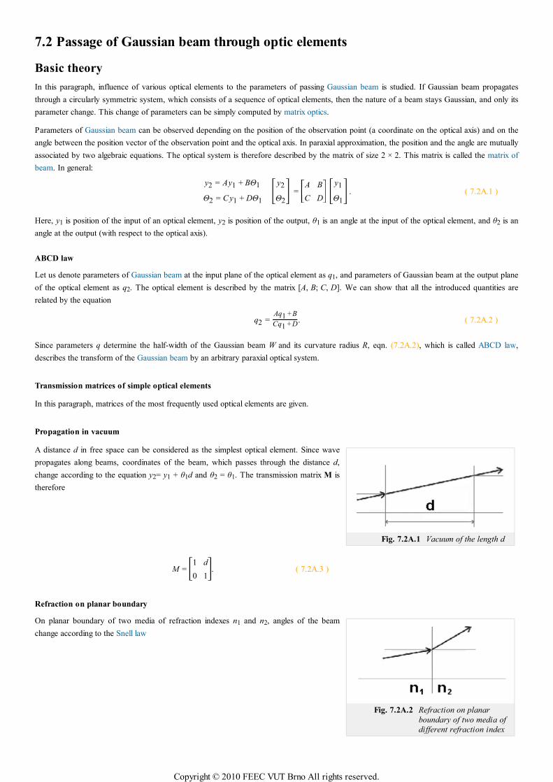
Fig. 7.2A.1 Vacuum of the length d
Fig. 7.2A.2 Refraction on planar
boundary of two media of
different refraction index
7.2 Passage of Gaussian beam through optic elements
Basic theory
In this paragraph, influence of various optical elements to the parameters of passing Gaussian beam is studied. If Gaussian beam propagates
through a circularly symmetric system, which consists of a sequence of optical elements, then the nature of a beam stays Gaussian, and only its
parameter change. This change of parameters can be simply computed by matrix optics.
Parameters of Gaussian beam can be observed depending on the position of the observation point (a coordinate on the optical axis) and on the
angle between the position vector of the observation point and the optical axis. In paraxial approximation, the position and the angle are mutually
associated by two algebraic equations. The optical system is therefore described by the matrix of size 2 × 2. This matrix is called the matrix of
beam. In general:
y2 = Ay1 + BΘ1
Θ2 = Cy1 + DΘ1
[y2
Θ2] =⎡
⎣⎢A B
C D
⎤
⎦⎥ [
y1
Θ1]. ( 7.2A.1 )
Here, y1 is position of the input of an optical element, y2 is position of the output, θ1 is an angle at the input of the optical element, and θ2 is an
angle at the output (with respect to the optical axis).
ABCD law
Let us denote parameters of Gaussian beam at the input plane of the optical element as q1, and parameters of Gaussian beam at the output plane
of the optical element as q2. The optical element is described by the matrix [A, B; C, D]. We can show that all the introduced quantities are
related by the equation
q2 =Aq1 +B
Cq1 + D. ( 7.2A.2 )
Since parameters q determine the half-width of the Gaussian beam W and its curvature radius R, eqn. (7.2A.2), which is called ABCD law,
describes the transform of the Gaussian beam by an arbitrary paraxial optical system.
Transmission matrices of simple optical elements
In this paragraph, matrices of the most frequently used optical elements are given.
Propagation in vacuum
A distance d in free space can be considered as the simplest optical element. Since wave
propagates along beams, coordinates of the beam, which passes through the distance d,
change according to the equation y2= y1 + θ1d and θ2 = θ1. The transmission matrix M is
therefore
M =⎡
⎣⎢1 d
0 1
⎤
⎦⎥. ( 7.2A.3 )
Refraction on planar boundary
On planar boundary of two media of refraction indexes n1 and n2, angles of the beam
change according to the Snell law
Copyright © 2010 FEEC VUT Brno All rights reserved.
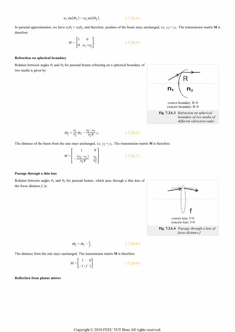
convex boundary: R>0
concave boundary: R<0
Fig. 7.2A.3 Refraction on spherical
boundary of two media of
different refraction index
convex lens: f>0
concave lens: f<0
Fig. 7.2A.4 Passage through a lens of
focus distance f
n1 sin(Θ1) = n2 sin(Θ2). ( 7.2A.4 )
In paraxial approximation, we have n1θ1 ≈ n2θ2, and therefore, position of the beam stays unchanged, i.e. y2 = y1. The transmission matrix M is
therefore
M = [1 0
0 n1 / n2]. ( 7.2A.5 )
Refraction on spherical boundary
Relation between angles θ1 and θ2 for paraxial beams refracting on a spherical boundary of
two media is given by
Θ2 ≈n1n2
Θ1 −n2 −n1
n2Ry. ( 7.2A.6 )
The distance of the beam from the axis stays unchanged, i.e. y2 ≈ y1. The transmission matrix M is therefore:
M =
⎡
⎣
⎢⎢⎢
1 0
−(n2 −n1)
n2R
n1n2
⎤
⎦
⎥⎥⎥. ( 7.2A.7 )
Passage through a thin lens
Relation between angles θ1 and θ2 for paraxial beams, which pass through a thin lens of
the focus distance f, is:
Θ2 = Θ1 −y
f. ( 7.2A.8 )
The distance form the axis stays unchanged. The transmission matrix M is therefore:
M =⎡
⎣⎢ 1 0
−1 / f 1
⎤
⎦⎥. ( 7.2A.9 )
Reflection from planar mirror
Copyright © 2010 FEEC VUT Brno All rights reserved.
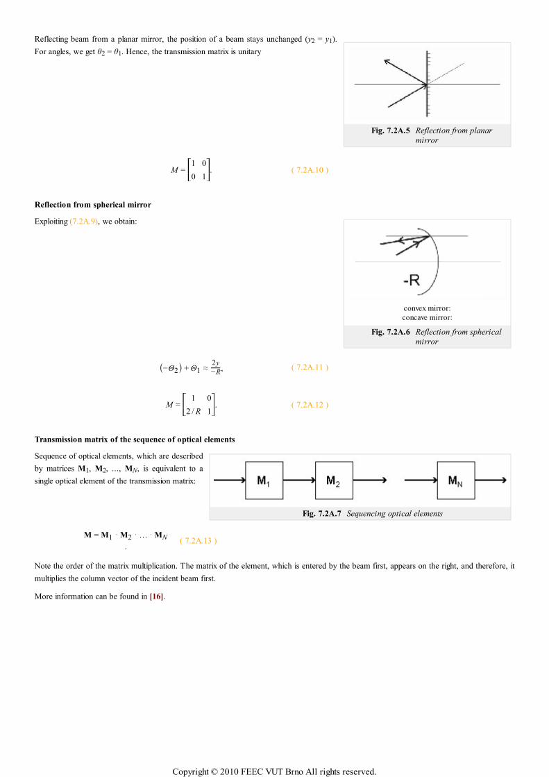
Fig. 7.2A.5 Reflection from planar
mirror
convex mirror:
concave mirror:
Fig. 7.2A.6 Reflection from spherical
mirror
Fig. 7.2A.7 Sequencing optical elements
Reflecting beam from a planar mirror, the position of a beam stays unchanged (y2 = y1).
For angles, we get θ2 = θ1. Hence, the transmission matrix is unitary
M =⎡
⎣⎢1 0
0 1
⎤
⎦⎥. ( 7.2A.10 )
Reflection from spherical mirror
Exploiting (7.2A.9), we obtain:
(−Θ2) + Θ1 ≈2y
−R, ( 7.2A.11 )
M =⎡
⎣⎢ 1 0
2 / R 1
⎤
⎦⎥. ( 7.2A.12 )
Transmission matrix of the sequence of optical elements
Sequence of optical elements, which are described
by matrices M1, M2, ..., MN, is equivalent to a
single optical element of the transmission matrix:
M = M1 ⋅M2 ⋅… ⋅MN
.( 7.2A.13 )
Note the order of the matrix multiplication. The matrix of the element, which is entered by the beam first, appears on the right, and therefore, it
multiplies the column vector of the incident beam first.
More information can be found in [16].
Copyright © 2010 FEEC VUT Brno All rights reserved.

7.2 Passage of Gaussian beam through optic elements
Quiz
Answer these questions to get feedback on how well you understand the course. Only one of the answers is correct. You don't have to answer
every question. If you don't know the answer you can just leave it blank (default option: “I won't answer this question”) and this won't affect
your score. Answering correctly will add 2 points to your score but on the other hand you'll lose 1 point if your answer is wrong. The
questions are divided in groups of five questions.
Press See result after you have finished answering.
Displaying questions 1..5 of 5:
Question 1
The beam matrix of an optical element …
Possible answers for question 1:
… associates the equiphase surface radius and the beam width at the input to the waveform radius and the beam width at the output.
… associates the input position and the input propagation angle to the output position and the output propagation angle.
… enables to compute the output power from the input one.
I won't answer this question
Question 2
The beam matrix of the planar mirror …
Possible answers for question 2:
… is non-diagonal.
… is complex.
… is unitary.
I won't answer this question
Question 3
The beam matrix of the free space …
Possible answers for question 3:
… contains units in the diagonal and the distance above the diagonal.
… is unitary.
… is not diagonal.
I won't answer this question
Question 4
In case the optical system consists of several elements, the resultant beam matrix …
Possible answers for question 4:
… is a product of beam matrices of elements.
… is a sum of beam matrices of elements.
… cannot be simply expressed.
I won't answer this question
Question 5
The focal distance of the convex lens …
Copyright © 2010 FEEC VUT Brno All rights reserved.

Possible answers for question 5:
… can be both positive and negative.
… is negative.
… is positive.
I won't answer this question
Copyright © 2010 FEEC VUT Brno All rights reserved.

Chapter 8: Analysis and simulation of semiconductor structures
Introduction
This chapter deals with semiconductor structures whose the mathematical description of the electromagnetic field is so different that you can not
use any of the methods or computing environment presented in this textbook. We use multi-physical computing environment COMSOL
Multiphysic, which is based on finite element method.
In the first chapter we present the macroscopic description of semiconductor structures called drift and diffusion model.
Copyright © 2010 FEEC VUT Brno All rights reserved.
Tab. 8.1A.1 Typical values of relative
permittivity [44].
Materiál εr []
Si 11,7
SiO2 3,9
Si3N4 7,2
GaAs 12,5
Ge 16,1
8.1 Drift diffusion model
Basic theory
1 Basic Semiconductor Equations
The device modeling represents the problem of charge transport in macroscopic scale in comparison with the semiconductor lattice dimensions.
In this approach we assume that the movement of electron between two collisions is described by Newton law and only the interactions with
lattice are described by quantum mechanics. So, the carriers can be described statistically thought the distribution function that is given by
solving of Boltzman transport equation. However, this is a difficult task to accomplish, thus through several idealistic simplification of Boltzman
equation we obtain the practical system of equations (8.1A.1) called the drift-diffusion model. These equations are also called the basic
semiconductor equations. They can be easily deduced from Maxwells equations.
∇ ⋅ (∇Ψ) =q
ε (n − p − C), ( 8.1A.1a )
∇ ⋅ (Jn) − q∂n∂ t
= qR, ( 8.1A.1b )
∇ ⋅ (Jp) + q∂ p
∂ t= − qR, ( 8.1A.1c )
Jn = qnµn E + qDn∇n, ( 8.1A.1d )
Jp = qpµp E − qDp∇ p. ( 8.1A.1e )
Equation (8.1A.1a) is a Poisson equation for electric potential Ψ, where the charge density is defined by elementary charge q and the
concentration of negatively charged electrons n, the concentration of positively charged holes p and fixed charge concentration C. ε in this
equation denotes permittivity of used semiconductor. Values of relative permittivity for the most common materials are listed in tab. 8.1A.1.
Continuity equation (8.1A.1b) and (8.1A.1c) express that the sources and sinks of current
density are fully compensated by the time change of free charge and joint by function R,
which expresses the rate of generation and recombination of electrons and holes. Jn denotes
current density caused by electrons, Jp current density caused holes and t is the time.
Expression of the rate R requires a good knowledge of the physical mechanisms of
generation and recombination in semiconductor materials and is one of the key parameters
for obtaining the relevant results of simulations of semiconductor structures.
In both current densities equations (8.1A.1d) and (8.1A.1e) the first term on the right side is
a component of current density caused by the Lorenz force, taking into account only the
influence of the electric field E (the effect of magnetic induction is neglected), and establishes the effective mobility of electrons µn and holes µp
Their value is generally defined by empirical relationships. Mobility of charge carriers is a quantity which has a large influence on the properties
of semiconductor components and therefore its correct modeling is very important. The second term on the right side of equations (8.1A.1d)
and (8.1A.1e) represents the effect of carrier diffusion in the direction of the gradient of concentration and introduces Einstein diffusion
constants
Dn = µnkTq , ( 8.1A.2a )
Dp = µpkTq , ( 8.1A.2b )
where k is the Boltzmann constant and T is the temperature.
2 Physical Parameters
The equations (8.1A.1) constitute the basic equation system for analyzing and simulation of most semiconductor devices. However, there may
be cases when become important physical phenomena that are not sufficiently covered by these equations. That is the case of tunneling currents
through very thin layers, which have a significant effect on the properties of the devices. Usually are used the empirical corrections than more
complex system of equations to describe such phenomena. Physical parameters of these equations define the geometry of the device, kind of
semiconductor material and used manufacturing technology. Their modeling will be discussed in the following paragraphs.
Doping Profile
Distribution of impurities in the semiconductor volume, resulting in N type or P type semiconductor, determines the geometry and function of a
semiconductor device. It is therefore essential input information to achieve a accurate results of simulations, so the manufacturing processes
such as ion implantation, diffusion, thermal oxidation, epitaxial accretion and others should be properly modeled. The scope of following
Copyright © 2010 FEEC VUT Brno All rights reserved.
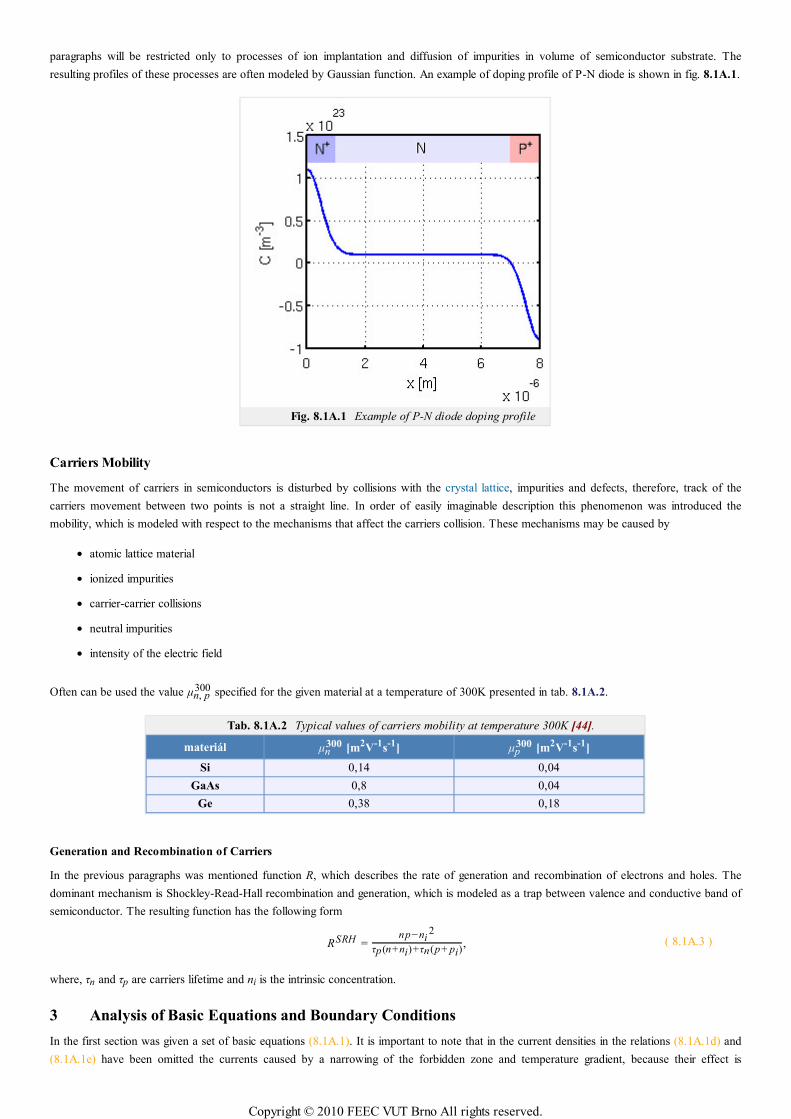
paragraphs will be restricted only to processes of ion implantation and diffusion of impurities in volume of semiconductor substrate. The
resulting profiles of these processes are often modeled by Gaussian function. An example of doping profile of P-N diode is shown in fig. 8.1A.1.
Fig. 8.1A.1 Example of P-N diode doping profile
Carriers Mobility
The movement of carriers in semiconductors is disturbed by collisions with the crystal lattice, impurities and defects, therefore, track of the
carriers movement between two points is not a straight line. In order of easily imaginable description this phenomenon was introduced the
mobility, which is modeled with respect to the mechanisms that affect the carriers collision. These mechanisms may be caused by
atomic lattice material
ionized impurities
carrier-carrier collisions
neutral impurities
intensity of the electric field
Often can be used the value µn, p300 specified for the given material at a temperature of 300K presented in tab. 8.1A.2.
Tab. 8.1A.2 Typical values of carriers mobility at temperature 300K [44].
materiál µn300 [m2V-1s-1] µp
300 [m2V-1s-1]
Si 0,14 0,04
GaAs 0,8 0,04
Ge 0,38 0,18
Generation and Recombination of Carriers
In the previous paragraphs was mentioned function R, which describes the rate of generation and recombination of electrons and holes. The
dominant mechanism is Shockley-Read-Hall recombination and generation, which is modeled as a trap between valence and conductive band of
semiconductor. The resulting function has the following form
RSRH =np−ni
2
τp(n+ni)+τn(p+ pi), ( 8.1A.3 )
where, τn and τp are carriers lifetime and ni is the intrinsic concentration.
3 Analysis of Basic Equations and Boundary Conditions
In the first section was given a set of basic equations (8.1A.1). It is important to note that in the current densities in the relations (8.1A.1d) and
(8.1A.1e) have been omitted the currents caused by a narrowing of the forbidden zone and temperature gradient, because their effect is
Copyright © 2010 FEEC VUT Brno All rights reserved.
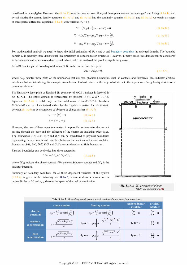
Fig. 8.1A.2 2D geometry of planar
MOSFET transistor [44]
considered to be negligible. However, the (8.1A.13) may become incorrect if any of these phenomenon become significant. Using (8.1A.1a) and
by substituting the current density equations (8.1A.1d) and (8.1A.1e) into the continuity equation (8.1A.1b) and (8.1A.1c) we obtain a system
of three partial differential equations (8.1A.4) with variables Ψ, n a p.
∇ ⋅ (∇ψ) −q
ε (n − p − C) = 0, ( 8.1A.4a )
∇ ⋅ (Dn∇n − nµn∇ψ) − R =∂n∂ t
, ( 8.1A.4b )
∇ ⋅ (Dp∇ p + pµp∇ψ) − R =∂ p
∂ t. ( 8.1A.4c )
For mathematical analysis we need to know the initial estimation of Ψ, n and p and boundary conditions in analyzed domain. The bounded
domain D is generally three-dimensional, like practically all semiconductor structures. However, in many cases, this domain can be considered
as two-dimensional, or even one-dimensional, which make the analyzed the problem significantly easier.
Lets ∂D denotes partial boundary of domain D. It can be divided into two parts
∂ D = ∂ Dp∪∂ Da ( 8.1A.5 )
where ∂Dp denotes those parts of the boundaries that are real, physical boundaries, such as contacts and interfaces. ∂Da indicates artificial
interfaces that are introducing, for example, to exclusion of sub-structure on the large substrate or to the separation of neighboring devices on a
common substrate.
The illustrative description of idealized 2D geometry of MOS transistor is depicted in
fig. 8.1A.2. The entire domain is represented by polygon A-B-C-D-E-F-G-H-A.
Equation (8.1A.4) is valid only in the subdomain A-B-E-F-G-H-A. Insulator
B-C-D-E-B can be characterized either by the Laplace equation for electrostatic
potential (8.1A.6) or by assumption of absence of charge carriers (8.1A.7).
∇ ⋅∇(Ψ) = 0 ( 8.1A.6 )
n = p = C = 0 ( 8.1A.7 )
However, the use of these equations makes it impossible to determine the current
passing through the base and the influence of the charge on insulating oxide layer.
The boundaries A-B, E-F, C-D and B-E can be considered as physical boundaries
representing three contacts and interface between the semiconductor and insulator.
Boundaries A-H, B-C, D-E, F-G and G-H are considered as artificial boundaries.
Physical boundaries can be divided into three categories.
∂ DP = ∂ DO∪∂ DS∪∂ DI, ( 8.1A.8 )
where ∂DO indicate the ohmic contact, ∂DS denotes Schottky contact and ∂DI is the
insulator interface.
Summary of boundary conditions for all three dependent variables of the system
(8.1A.4) is given in the following tab. 8.1A.3, where n denotes normal vector
perpendicular to ∂D and un,p denotes the speed of thermal recombination.
Tab. 8.1A.3 Boundary conditions typical semiconductor interface structures.
ohmic contact Shottky contactsemiconductor
- insulator
artifical
interface
electric
potentialψb =
kTq ar sinh
⎛⎝⎜ C
2ni
⎞⎠⎟ ψb =
kTq ar sinh
⎛⎝⎜ C
2ni
⎞⎠⎟
∂ψ
∂n= 0
∂ψ
∂n= 0
electron
concentration n =C2 +4ni
2√ +C
2Jn n = − qun
⎛
⎝⎜⎜n −
C 2 +4ni2√ +C
2
⎞
⎠⎟⎟ Jn n = 0 ∂n
∂n= 0
hole
concentration p =C2 +4ni
2√ −C
2Jp n = − qup
⎛
⎝⎜⎜p −
C2 +4ni2√ −C
2
⎞
⎠⎟⎟ Jp n = 0
∂ p
∂n= 0
Copyright © 2010 FEEC VUT Brno All rights reserved.
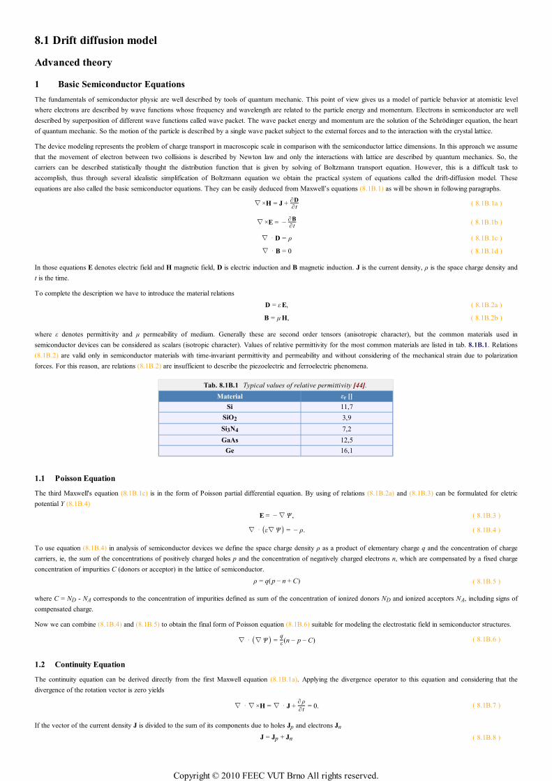
8.1 Drift diffusion model
Advanced theory
1 Basic Semiconductor Equations
The fundamentals of semiconductor physic are well described by tools of quantum mechanic. This point of view gives us a model of particle behavior at atomistic level
where electrons are described by wave functions whose frequency and wavelength are related to the particle energy and momentum. Electrons in semiconductor are well
described by superposition of different wave functions called wave packet. The wave packet energy and momentum are the solution of the Schrödinger equation, the heart
of quantum mechanic. So the motion of the particle is described by a single wave packet subject to the external forces and to the interaction with the crystal lattice.
The device modeling represents the problem of charge transport in macroscopic scale in comparison with the semiconductor lattice dimensions. In this approach we assume
that the movement of electron between two collisions is described by Newton law and only the interactions with lattice are described by quantum mechanics. So, the
carriers can be described statistically thought the distribution function that is given by solving of Boltzmann transport equation. However, this is a difficult task to
accomplish, thus through several idealistic simplification of Boltzmann equation we obtain the practical system of equations called the drift-diffusion model. These
equations are also called the basic semiconductor equations. They can be easily deduced from Maxwell’s equations (8.1B.1) as will be shown in following paragraphs.
∇×H = J +∂D∂ t
( 8.1B.1a )
∇×E = −∂B∂ t
( 8.1B.1b )
∇ ⋅D = ρ ( 8.1B.1c )
∇ ⋅B = 0 ( 8.1B.1d )
In those equations E denotes electric field and H magnetic field, D is electric induction and B magnetic induction. J is the current density, ρ is the space charge density and
t is the time.
To complete the description we have to introduce the material relations
D = εE, ( 8.1B.2a )
B = µH, ( 8.1B.2b )
where ε denotes permittivity and µ permeability of medium. Generally these are second order tensors (anisotropic character), but the common materials used in
semiconductor devices can be considered as scalars (isotropic character). Values of relative permittivity for the most common materials are listed in tab. 8.1B.1. Relations
(8.1B.2) are valid only in semiconductor materials with time-invariant permittivity and permeability and without considering of the mechanical strain due to polarization
forces. For this reason, are relations (8.1B.2) are insufficient to describe the piezoelectric and ferroelectric phenomena.
Tab. 8.1B.1 Typical values of relative permittivity [44].
Material εr []
Si 11,7
SiO2 3,9
Si3N4 7,2
GaAs 12,5
Ge 16,1
1.1 Poisson Equation
The third Maxwell's equation (8.1B.1c) is in the form of Poisson partial differential equation. By using of relations (8.1B.2a) and (8.1B.3) can be formulated for eletric
potential Y (8.1B.4)
E = −∇Ψ , ( 8.1B.3 )
∇ ⋅ (ε∇Ψ) = − ρ. ( 8.1B.4 )
To use equation (8.1B.4) in analysis of semiconductor devices we define the space charge density ρ as a product of elementary charge q and the concentration of charge
carriers, ie, the sum of the concentrations of positively charged holes p and the concentration of negatively charged electrons n, which are compensated by a fixed charge
concentration of impurities C (donors or acceptor) in the lattice of semiconductor.
ρ = q(p − n + C) ( 8.1B.5 )
where C = ND - NA corresponds to the concentration of impurities defined as sum of the concentration of ionized donors ND and ionized acceptors NA, including signs of
compensated charge.
Now we can combine (8.1B.4) and (8.1B.5) to obtain the final form of Poisson equation (8.1B.6) suitable for modeling the electrostatic field in semiconductor structures.
∇ ⋅ (∇Ψ) =q
ε (n − p − C) ( 8.1B.6 )
1.2 Continuity Equation
The continuity equation can be derived directly from the first Maxwell equation (8.1B.1a). Applying the divergence operator to this equation and considering that the
divergence of the rotation vector is zero yields
∇ ⋅∇×H =∇ ⋅ J +∂ ρ
∂ t= 0. ( 8.1B.7 )
If the vector of the current density J is divided to the sum of its components due to holes Jp and electrons Jn
J = Jp + Jn ( 8.1B.8 )
Copyright © 2010 FEEC VUT Brno All rights reserved.
and considering that the fixed charge in the semiconductor crystal lattice is time-invariant
∂C∂ t
= 0, ( 8.1B.9 )
yields
∇ ⋅ (Jp + Jn) + q∂∂ t
(p − n) = 0. ( 8.1B.10 )
This equation expresses that the current density sources or sinks are fully compensated by the time change of space charge. In order to obtain the continuity equation
separately for electrons and holes, we need to establish a common function R, which expresses the rate of generation and recombination of electrons and holes. Then we
get
∇ ⋅ (Jn) − q∂n∂ t
= qR, ( 8.1B.11a )
∇ ⋅ (Jp) + q∂ p
∂ t= − qR. ( 8.1B.11b )
The formulation of the rate R requires a good knowledge of the physical mechanisms of generation and recombination in semiconductor materials and is one of the key
parameters for obtaining the relevant results of simulations of semiconductor structures.
1.3 Kinetic Equations of Charge Carriers
In the previous chapter we introduced the vector current density divided into two components (8.1B.8). Current density of charged particles can be generally expressed as
the product of a charge of single particle, particles concentration and average velocity (drift velocity) of particles. Then the current density of electrons and holes can be
writen as
Jn = qn vn , ( 8.1B.12a )
Jp = qp vp , ( 8.1B.12b )
where vn is the vector of electrons drift velocity and vp id the holes drift velocity. The main problem is relating the drift velocity to forces acting on the carriers. By number
of simplifications and idealistic assumptions [44] the drift velocity can be considered as result of Lorenz force and diffusion force. Then we can write
Jn = qnµn E + qDn∇n, ( 8.1B.13a )
Jp = qpµp E − qDp∇ p. ( 8.1B.13b )
In both equations, the first term on the right side is a component of current density caused by the Lorenz force, taking into account only the influence of electric field
(magnetic induction effect is neglected), and establishes the effective mobility of electrons µn and holes µp. Mobility of charge carriers is a quantity which has a large
influence on the properties of semiconductor components and therefore its correct formulation is very important. The second term on the right side of equations (8.1B.13)
represents the effect of carrier diffusion in the direction of the gradient of carrier concentration and introduces Einstein diffusion constants
Dn = µnkTq , ( 8.1B.14a )
Dp = µpkTq , ( 8.1B.14b )
where k is Boltzmann’s constant and T is the temperature.
2 Physical Parameters
The equations (8.1B.6), (8.1B.11) and (8.1B.13) constitute the basic equation system for analyzing and simulation of most semiconductor devices. However, there may be
cases when become important physical phenomena that are not sufficiently covered by these equations. That is the case of tunneling currents through very thin layers,
which have a significant effect on the properties of the devices. Usually are used the empirical corrections than more complex system of equations to describe such
phenomena.
Physical parameters of these equations define the geometry of the device, kind of semiconductor material and used manufacturing technology. Their modeling will be
discussed in the following paragraphs.
2.1 Doping Profile
Distribution of impurities in the semiconductor volume, resulting in N type or P type semiconductor, determines the geometry and function of a semiconductor device. It is
therefore essential input information to achieve a accurate results of simulations, so the manufacturing processes such as ion implantation, diffusion, thermal oxidation,
epitaxial accretion and others should be properly modeled. The scope of following paragraphs will be restricted only to processes of ion implantation and diffusion of
impurities in volume of semiconductor substrate. The resulting profiles of these processes are often modeled by Gaussian function
G(x) = ae−
(x −b)2
2c2 ,( 8.1B.15 )
where x is the spatial coordinate, a, b and c are real constants and e is the Euler number. Gaussian function is even (symmetrical according to the y-axis) and has the shape
of the "bell", which represents the distribution of impurities in semiconductors as a result of the locally applied technological process. Then constant a determines the peak
concentration of impurities (height of the "bell"), b the position of application of technological process (coordinate of the "bell" peak) and c is proportional to the diffusion
of impurities in the substrate (width of the "bell"). In (8.1B.5), we have introduced a fixed charge concentration C, which corresponds to the distribution of impurities in
semiconductors. Lets assume that ND and NA indicate the peak concentration of acceptors and donors (corresponding to a coefficient), then the one dimensional (1D) P-N
junction problem in general can be formulated as
C = NDi + NDG(xD, bD, cD) − NAG(xA , bA , cA), ( 8.1B.16 )
where NDi is the initial substrate concentration of impurities, which is usually slightly doped by donors, so is type of N. Lets consider the P-N diode reduced to 1D problem
with a total length L = 8 µm made of the silicon substrate with a low initial concentration of donors NDi = 1021 m-3 and the highly doped regions on opposite ends of the
substrate with concentrations of donors consisting ND = 1023 m-3 and NA = 1023 m-3. The width of the P-N transition is LJ = 1 µm. Resulting doping profile is shown in
Copyright © 2010 FEEC VUT Brno All rights reserved.
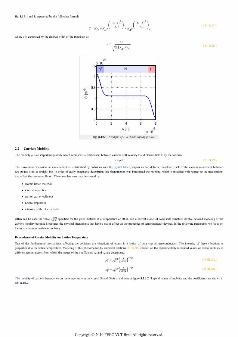
fig. 8.1B.1 and is expressed by the following formula
C = NDi + NDe(−
(x −0)2
2c2 )− N
Ae
(−(x − L)2
2c2 ),
( 8.1B.17 )
where c is expressed by the desired width of the transition as
c =LJ
2ln⎛⎝N
A/NDi
⎞⎠√.
( 8.1B.18 )
Fig. 8.1B.1 Example of P-N diode doping profile
2.2 Carriers Mobility
The mobility µ is an important quantity which represents a relationship between carriers drift velocity v and electric field E by the formula
v = µE. ( 8.1B.19 )
The movement of carriers in semiconductors is disturbed by collisions with the crystal lattice, impurities and defects, therefore, track of the carriers movement between
two points is not a straight line. In order of easily imaginable description this phenomenon was introduced the mobility, which is modeled with respect to the mechanisms
that affect the carriers collision. These mechanisms may be caused by
atomic lattice material
ionized impurities
carrier-carrier collisions
neutral impurities
intensity of the electric field
Often can be used the value µn, p300 specified for the given material at a temperature of 300K, but a correct model of solid-state structure involve detailed modeling of the
carriers mobility because it captures the physical phenomena that have a major effect on the properties of semiconductor devices. In the following paragraphs we focus on
the most common models of mobility.
Dependence of Carrier Mobility on Lattice Temperature
One of the fundamental mechanisms affecting the collisions are vibrations of atoms in a lattice of pure crystal semiconductors. The intensity of these vibrations is
proportional to the lattice temperature. Modeling of this phenomenon by empirical relations (8.1B.20) is based on the experimentally measured values of carrier mobility at
different temperatures, from which the values of the coefficients αn and αp are determined.
µnL = µn
300⎛⎝ T300K
⎞⎠−αn
( 8.1B.20a )
µpL = µp
300⎛⎝ T300K
⎞⎠−αp
( 8.1B.20b )
The mobility of carriers dependence on the temperature in the crystal Si and GaAs are shown in figure 8.1B.2. Typical values of mobility and the coefficients are shown in
tab. 8.1B.2.
Copyright © 2010 FEEC VUT Brno All rights reserved.
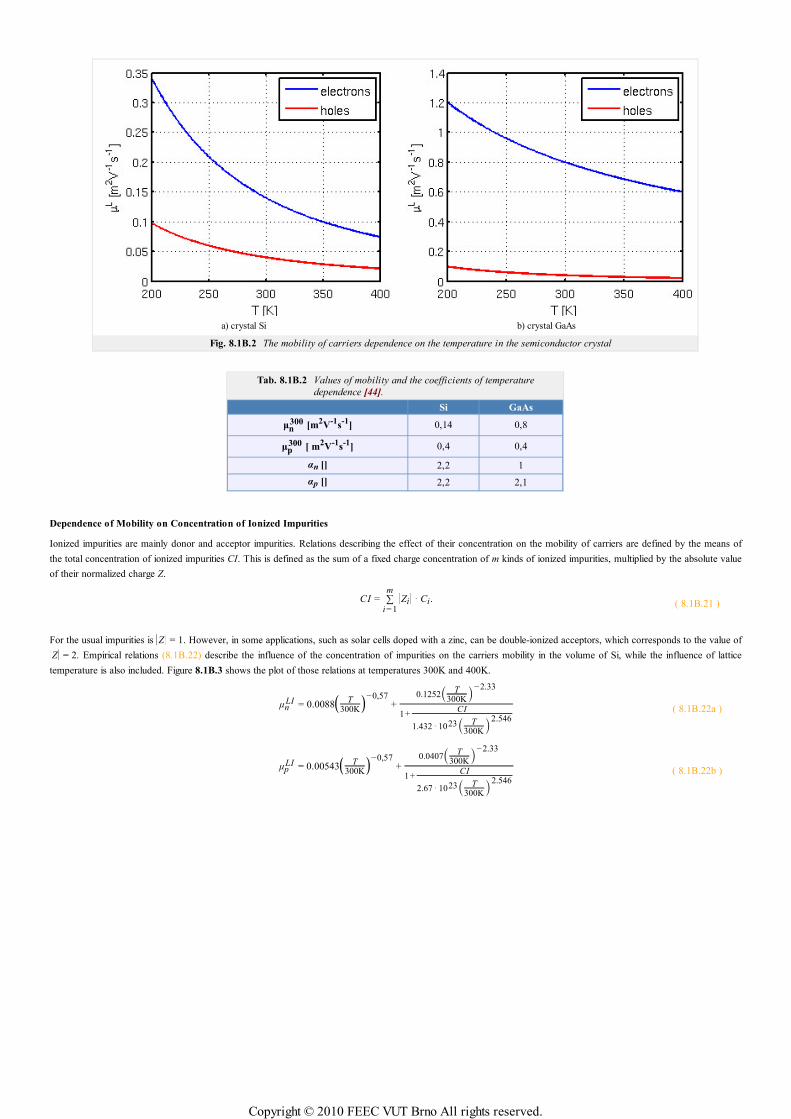
a) crystal Si b) crystal GaAs
Fig. 8.1B.2 The mobility of carriers dependence on the temperature in the semiconductor crystal
Tab. 8.1B.2 Values of mobility and the coefficients of temperature
dependence [44].
Si GaAs
µn300 [m2V-1s-1] 0,14 0,8
µp300 [ m2V-1s-1] 0,4 0,4
αn [] 2,2 1
αp [] 2,2 2,1
Dependence of Mobility on Concentration of Ionized Impurities
Ionized impurities are mainly donor and acceptor impurities. Relations describing the effect of their concentration on the mobility of carriers are defined by the means of
the total concentration of ionized impurities CI. This is defined as the sum of a fixed charge concentration of m kinds of ionized impurities, multiplied by the absolute value
of their normalized charge Z.
CI = ∑i = 1
m||Zi || ⋅Ci. ( 8.1B.21 )
For the usual impurities is ||Z || = 1. However, in some applications, such as solar cells doped with a zinc, can be double-ionized acceptors, which corresponds to the value of
||Z|| = 2. Empirical relations (8.1B.22) describe the influence of the concentration of impurities on the carriers mobility in the volume of Si, while the influence of lattice
temperature is also included. Figure 8.1B.3 shows the plot of those relations at temperatures 300K and 400K.
µnLI = 0.0088
⎛⎝ T300K
⎞⎠−0,57
+0.1252( T
300K)−2.33
1 +CI
1.432⋅1023( T300K)2.546
( 8.1B.22a )
µpLI = 0.00543
⎛⎝ T300K
⎞⎠−0,57
+0.0407( T
300K )−2.33
1+CI
2.67⋅1023( T300K )2.546
( 8.1B.22b )
Copyright © 2010 FEEC VUT Brno All rights reserved.
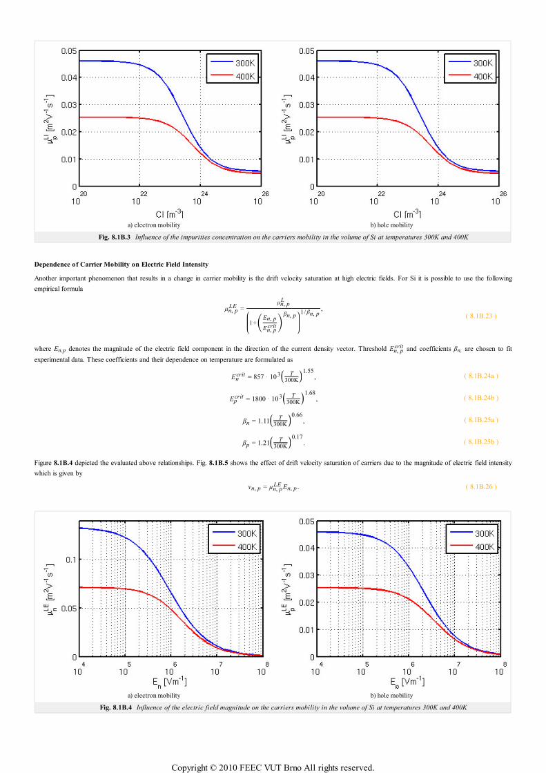
a) electron mobility b) hole mobility
Fig. 8.1B.3 Influence of the impurities concentration on the carriers mobility in the volume of Si at temperatures 300K and 400K
Dependence of Carrier Mobility on Electric Field Intensity
Another important phenomenon that results in a change in carrier mobility is the drift velocity saturation at high electric fields. For Si it is possible to use the following
empirical formula
µn, pLE =
µn, pL
⎛
⎝⎜⎜1+(
En, p
En, pcrit )
βn, p ⎞
⎠⎟⎟
1/ βn, p,
( 8.1B.23 )
where En,p denotes the magnitude of the electric field component in the direction of the current density vector. Threshold En, pcrit and coefficients βn, are chosen to fit
experimental data. These coefficients and their dependence on temperature are formulated as
Encrit = 857 ⋅ 103⎛⎝ T
300K⎞⎠
1.55, ( 8.1B.24a )
Epcrit = 1800 ⋅ 103⎛⎝ T
300K⎞⎠
1.68, ( 8.1B.24b )
βn = 1.11⎛⎝ T
300K⎞⎠
0.66, ( 8.1B.25a )
βp = 1.21⎛⎝ T
300K⎞⎠
0.17. ( 8.1B.25b )
Figure 8.1B.4 depicted the evaluated above relationships. Fig. 8.1B.5 shows the effect of drift velocity saturation of carriers due to the magnitude of electric field intensity
which is given by
vn, p = µn, pLE En, p . ( 8.1B.26 )
a) electron mobility b) hole mobility
Fig. 8.1B.4 Influence of the electric field magnitude on the carriers mobility in the volume of Si at temperatures 300K and 400K
Copyright © 2010 FEEC VUT Brno All rights reserved.
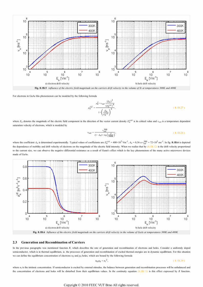
a) electron drift velocity b) hole drift velocity
Fig. 8.1B.5 influence of the electric field magnitude on the carriers drift velocity in the volume of Si at temperatures 300K and 400K
For electrons in GaAs this phenomenon can be modeled by the following formula
µnLE =
µnL +vsat
(En)3
(Encrit )4
1 +( En
Encrit )
4, ( 8.1B.27 )
where En denotes the magnitude of the electric field component in the direction of the vector current density Encrit is its critical value and vsat is a temperature dependent
saturation velocity of electrons, which is modeled by
vsat =vsat
300
(1− An)+ An( T300K)
, ( 8.1B.28 )
where the coefficient An is determined experimentally. Typical values of coefficients are Encrit = 400×103 Vm-1, An = 0,56 a vsat
300 = 72×103 ms-1. In fig. 8.1B.6 is depicted
the dependence of mobility and drift velocity of electrons on the magnitude of the electric field intensity. When we realize that by (8.1B.12) is the drift velocity proportional
to the current size, we can observe the negative differential resistance as a result of Gunn's effect which is the key phenomenon of the many active microwave devices
made of GaAs.
a) electron drift velocity b) hole drift velocity
Fig. 8.1B.6 Influence of the electric field magnitude on the carriers drift velocity in the volume of GaAs at temperatures 300K and 400K
2.3 Generation and Recombination of Carriers
In the previous paragraphs was mentioned function R, which describes the rate of generation and recombination of electrons and holes. Consider a uniformly doped
semiconductor, which is in thermal equilibrium, ie. the processes of generation and recombination of excited thermal energies are in dynamic equilibrium. For this situation
we can define the equilibrium concentration of electrons n0 and p0 holes, which are bound by the following formula
n0 p0 = ni2 , ( 8.1B.29 )
where ni is the intrinsic concentration. If semiconductor is excited by external stimulus, the balance between generation and recombination processes will be unbalanced and
the concentration of electrons and holes will be disturbed from their equilibrium values. In the continuity equation (8.1B.11) is this effect expressed by R function.
Copyright © 2010 FEEC VUT Brno All rights reserved.
Fig. 8.1B.7 2D geometry of planar
MOSFET transistor [44]
Depending on the physical phenomenon which is the cause of generation and recombination event of carriers, we distinguish
RSRH (Shockley-Read-Hall) transitions of phonons
ROPT photon transitions
RSURF surface phenomena
RAU triple Auger transitions
RII impact ionization.
Individual formulations can be combined by simple addition R = RSRH + ROPT + RAU + RSURF + RII.
The dominant mechanism is Shockley-Read-Hall recombination and generation, which is modeled as a trap between valence and conductive band of semiconductor. The
resulting function has the following form
RSRH =np−ni
2
τp (n +n1)+τn (p+ p1), ( 8.1B.30 )
where τn and τp are carriers lifetime, n1 and p1 are the concentrations defined by trap energy level. If the level of trap is in the middle of the forbidden zone, concentrations
are equal intrinsic, p1 = n1 = ni.
3 Analysis of Basic Equations and Boundary Conditions
In the first section was given a set of basic equations (8.1B.6), (8.1B.11) and (8.1B.13). It is important to note that in the current densities in the relations (8.1B.13) have
been omitted the currents caused by a narrowing of the forbidden zone and temperature gradient, because their effect is considered to be negligible. However, the
(8.1B.13) may become incorrect if any of these phenomenon become significant.
Using (8.1B.6) and by substituting the current density equations (8.1B.13) into the continuity equation (8.1B.11) we obtain a system of three partial differential equations
(8.1B.31) with variablesΨ, n and p.
∇ ⋅ (∇ψ) −q
ε (n − p − C) = 0 ( 8.1B.31a )
∇ ⋅ (Dn∇n − nµn∇ψ) − R =∂n∂ t
( 8.1B.31b )
∇ ⋅ (Dp∇ p + pµp∇ψ) − R =∂ p
∂ t( 8.1B.31c )
For mathematical analysis we need to know the initial estimation of Ψ, n and p and boundary conditions in analyzed domain. The bounded domain D is generally three-
dimensional, like practically all semiconductor structures. However, in many cases, this domain can be considered as two-dimensional, or even one-dimensional, which
make the analyzed the problem significantly easier.
Lets ∂D denotes partial boundary of domain D. It can be divided into two parts
∂ D = ∂ Dp∪∂ Da ( 8.1B.32 )
where ∂Dp denotes those parts of the boundaries that are real, physical boundaries, such as contacts and interfaces. ∂Da indicates artificial interfaces that are introducing,
for example, to exclusion of sub-structure on the large substrate or to the separation of neighboring devices on a common substrate.
The illustrative description of idealized 2D geometry of MOS transistor is depicted in fig. 8.1B.7. The entire
domain is represented by polygon A-B-C-D-E-F-G-H-B. Equation (8.1B.31) is valid only in the subdomain
A-B-E-F-G-H-B. Insulator B-C-D-E-B can be characterized either by the Laplace equation for electrostatic
potential (8.1B.33) or by assumption of absence of charge carriers (8.1B.34).
∇ ⋅∇(Ψ) = 0 ( 8.1B.33 )
n = p = C = 0 ( 8.1B.34 )
However, the use of these equations makes it impossible to determine the current passing through the base and
the influence of the charge on insulating oxide layer.
The boundaries A-B, E-F, C-D and B-E can be considered as physical boundaries representing three contacts
and interface between the semiconductor and insulator. Boundaries A-H, B-C, D-E, F-G and G-H are considered
as artificial boundaries.
Physical boundaries can be divided into three categories.
∂ DP = ∂ DO∪∂ DS∪∂ DI ( 8.1B.34 )
where ∂DO indicate the ohmic contact, ∂DS denotes Schottky contact and ∂DI is the insulator interface.
3.1 Ohmic Contact
The simplest boundary condition for the ohmic contact is the Dirichlet boundary condition for the electrostatic potential
Copyright © 2010 FEEC VUT Brno All rights reserved.
ψ(t) − ψb − ψD(t) = 0, ( 8.1B.36 )
where ΨD(t) denotes the external applied voltage and Ψb denotes a built-in potential directly related to impurities in the volume of semiconductor and can be expressed by
the following formula
ψb =kTq ar sinh
⎛⎝⎜ C
2ni
⎞⎠⎟. ( 8.1B.37 )
If the semiconductor is doped only by donors or acceptors, we can use the simplified relations
ND > > NA → ψb ≅kTq ln
⎛⎝⎜
ND2ni
⎞⎠⎟, ( 8.1B.38a )
NA > > ND → ψb ≅kTq ln
⎛⎝⎜
NA2ni
⎞⎠⎟. ( 8.1B.38b )
Furthermore, we consider boundary conditions for carriers concentration. If we consider the thermal balance (8.1B.28) and the absence of space charge on the ohmic
contact, the following relations are valid.
np − ni2 = 0 ( 8.1B.39 )
n − p − C = 0 ( 8.1B.40 )
These two equations can be expressed as Dirichlet boundary conditions for electrons (8.1B.41a) and holes (8.1B.41b)
n =C 2 +4ni
2√ +C
2,
( 8.1B.41a )
p =C 2 +4ni
2√ −C
2.
( 8.1B.41b )
3.2 Schottky Contact
The physical description of Shottkyho contact is not trivial, so for the purpose of device simulation is used a very simplified model. For the electrostatic potential can write
the Dirichlet boundary condition
ψ(t) − ψb − ψs − ψD(t) = 0, ( 8.1B.42 )
where ΨD(t) denotes the external applied voltage and Ψs is the size of Schottky barrier, which is characterized by kind of metal and semiconductor in junction. Ψb again
denotes a built-in potential. Boundary condition for the concentration of carriers is based on the current density flowing through the contact. By using the theory of thermal
emission and diffusion can be derived the following boundary conditions for the reverse polarized contact
Jn n = − qun
⎛
⎝⎜⎜n −
C 2 +4ni2√ +C
2
⎞
⎠⎟⎟, ( 8.1B.43a )
Jp n = − qup
⎛
⎝⎜⎜p −
C2 +4ni2√ −C
2
⎞
⎠⎟⎟, ( 8.1B.43b )
where n denotes the normal vector perpendicular to ∂D and un,p is the speed of thermal recombination.
3.3 Semiconductor Insulator Interface
Another category consists of the interface between semiconductor and insulating material. At this interface must be valid Gauß's law
εsem∂ψ
∂n
|||sem
− εins∂ψ
∂n
|||ins
= Qint , ( 8.1B.44 )
where εsem and εins indicates the permittivity of semiconductor and insulator. Qint is the charge on the interface. For thin layers of insulators such as oxide, can be
neglected the component of electric field in an insulator perpendicular to the interface, thus simplifying to
εsem∂ψ
∂n
|||sem
= Qint . ( 8.1B.45 )
By neglecting of the charge on the interface Qin can be the previous condition reduced to the Neumann condition for the electrostatic potential
∂ψ
∂n= 0. ( 8.1B.46 )
For carriers, the current component perpendicular to the interface must equal the rate of surface recombination RSURF
Jn n = − qRSURF , ( 8.1B.47a )
Jp n = qRSURF . ( 8.1B.47b )
Very often is the surface recombination neglected, so we get simpler conditions
Jn n = 0, ( 8.1B.48a )
Jp n = 0. ( 8.1B.48b )
3.4 Artificial Interface
The last case is the artificial interfaces. Here we assume either the boundary condition (8.1B.49a) (8.1B.49b) and (8.1B.49c) to ensure that the domain is enclosed or
specific values for the electrostatic potential and carrier concentration of the external sources.
Copyright © 2010 FEEC VUT Brno All rights reserved.

∂ψ
∂n= 0 ( 8.1B.49a )
∂n∂n
= 0 ( 8.1B.49b )
∂ p
∂n= 0 ( 8.1B.49c )
Copyright © 2010 FEEC VUT Brno All rights reserved.

8.1 Drift diffusion model
Model in Comsol
The attached file is a model P-N diodes made of silicon for simulation environment COMSOL Multiphysics in version 3.5. 1D model represents
the structure of the doping profile identical to fig. 8.1B.1. The equations (8.1B.31) and boundary conditions for ohmic contact (8.1B.37) and
(8.1B.41) are implemented in the model. The SRH recombination model and table the value of mobility carriers at 300K is used.
After opening the model in COMSOL program plots the uniform mesh of the model. In the Solve menu, click on Solve Problem which run the
default simulation, which is based on calculating the potential and the concentration of carriers, depending on the applied voltage on the diode,
which is varied in range from 0 to 2 V.
In the Postprocessing menu, click on Plot Parameters. In the Line tab in menu Predefined Quantities select variable whose distribution along
the diode we want to plot
psi electric potential
cn concentrations of electrons
cp concentration of holes
In the General tab in the menu Predefined Value select the specific value of applied voltage, for which we want to plot the distribution. The
appropriate quantity is plotted by clicking on button Ok .
V-A characteristics is available in the menu Postprocessing/ Domain Plot Variables, where the in the Point tab select the Boundary Selection
No. 1, check if there is the Ic term in Expression field, and click Ok .
Copyright © 2010 FEEC VUT Brno All rights reserved.
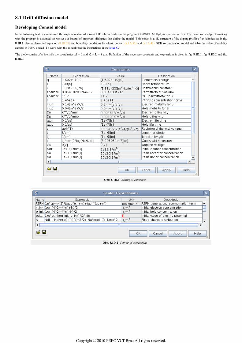
8.1 Drift diffusion model
Developing Comsol model
In the following text is summarized the implementation of a model 1D silicon diodes in the program COMSOL Multiphysics in version 3.5. The basic knowledge of working
with the program is assumed, so we set out images of important dialogues that define the model. This model is a 1D structure of the doping profile of an identical as in fig.
8.1B.1. Are implemented equation (8.1B.31) and boundary conditions for ohmic contact (8.1A.37) and (8.1A.41). SRH recombination model and table the value of mobility
carriers at 300K is used. To work with this model read the instructions in the layer C.
The diode consist of a line with the coordinates x1 = 0 and x2 = L = 8 µm. Definition of the necessary constants and expressions is given in fig. 8.1D.1, fig. 8.1D.2 and fig.
8.1D.3.
Obr. 8.1D.1 Setting of constants
Obr. 8.1D.2 Setting of expressions
Copyright © 2010 FEEC VUT Brno All rights reserved.

Obr. 8.1D.3 Setting of integration variables
Module Poisson equation
In this section is described the electrostatic module. In fig. 8.1D.4 is depicted the settings of preset formula over the diode domain, where the tab Init is set to psi_init.
Obr. 8.1D.4 Setting of Poisson equation coefficients
The fig. 8.1D.5 shows the set of boundary conditions at points x1 and x2.
Copyright © 2010 FEEC VUT Brno All rights reserved.

a)
b)
Obr. 8.1D.5 Setting of boundary conditions of the electrostatic module
Module convention and diffusion of electrons
In fig. 8.1D.6 is depicted the preset formula over the diode domain, where the tab Init is set to n_init.
Copyright © 2010 FEEC VUT Brno All rights reserved.
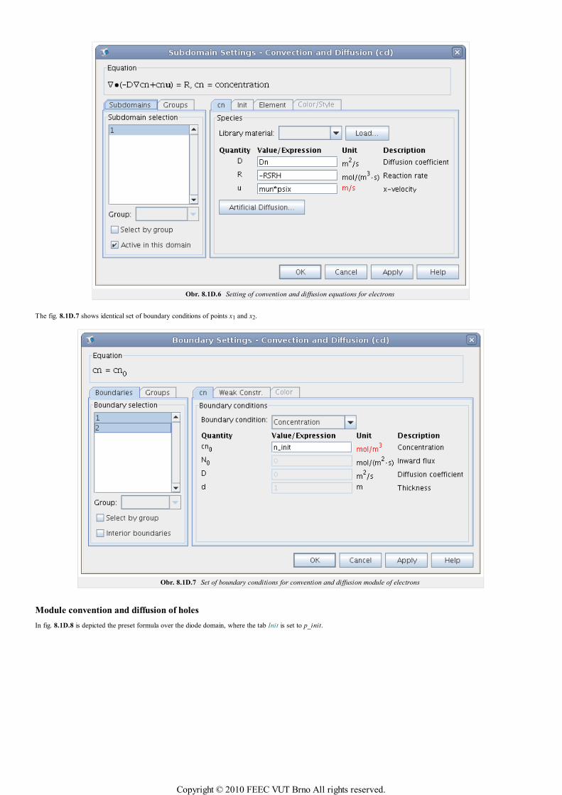
Obr. 8.1D.6 Setting of convention and diffusion equations for electrons
The fig. 8.1D.7 shows identical set of boundary conditions of points x1 and x2.
Obr. 8.1D.7 Set of boundary conditions for convention and diffusion module of electrons
Module convention and diffusion of holes
In fig. 8.1D.8 is depicted the preset formula over the diode domain, where the tab Init is set to p_init.
Copyright © 2010 FEEC VUT Brno All rights reserved.
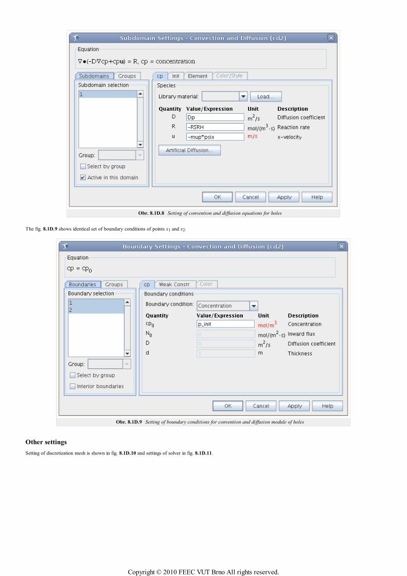
Obr. 8.1D.8 Setting of convention and diffusion equations for holes
The fig. 8.1D.9 shows identical set of boundary conditions of points x1 and x2.
Obr. 8.1D.9 Setting of boundary conditions for convention and diffusion module of holes
Other settings
Setting of discretization mesh is shown in fig. 8.1D.10 and settings of solver in fig. 8.1D.11.
Copyright © 2010 FEEC VUT Brno All rights reserved.

Obr. 8.1D.10 Setting of the density discretization mesh
Obr. 8.1D.11 Setting of solver parameters
Copyright © 2010 FEEC VUT Brno All rights reserved.

8.1 Drift diffusion model
Quiz
Answer these questions to get feedback on how well you understand the course. Only one of the answers is correct. You don't have to answer
every question. If you don't know the answer you can just leave it blank (default option: “I won't answer this question”) and this won't affect
your score. Answering correctly will add 2 points to your score but on the other hand you'll lose 1 point if your answer is wrong. The
questions are divided in groups of five questions.
Press See result after you have finished answering.
Displaying questions 1..10 of 10:
Question 1
Transfer of charge in the volume of semiconductors is mediated by...
Possible answers for question 1:
… photons.
… the electrons.
… the electrons and holes.
I won't answer this question
Question 2
What forces acting on charge carriers is considered in the drift and diffusion model?
Possible answers for question 2:
The forces of electric and magnetic fields.
Diffusive and Lorenz force excluding magnetic effects.
Gravitational force.
I won't answer this question
Question 3
What function is used to model doping profiles resulting from the processes of diffusion and ion implantation?
Possible answers for question 3:
Linear.
Gaussian.
Quadratic.
I won't answer this question
Question 4
What is defined in the model drift and diffusion with doping profile and concentration of charge carriers?
Possible answers for question 4:
Concentrations of free charge.
Built-in potential.
Barrier potential.
I won't answer this question
Question 5
Current density in semiconductors doped by donors only is given by...
Copyright © 2010 FEEC VUT Brno All rights reserved.

Possible answers for question 5:
… sum of the flow of electrons and holes.
… flow of holes.
… flow of electrons.
I won't answer this question
Question 6
What is the dominant cause of generation and recombination of free charge carriers in semiconductors in thermal
equilibrium?
Possible answers for question 6:
Transitions of electrons.
Transitions of photons.
Transitions of phonons.
I won't answer this question
Question 7
Description of the Gunn phenomenon at a macroscopic level, it is possible by...
Possible answers for question 7:
… appropriate modeling electron mobility.
… tools of quantum mechanics.
… empirical corrections.
I won't answer this question
Question 8
Boundary conditionsfor ohmic contact assumed...
Possible answers for question 8:
… zero normal component of current density.
… thermal equilibrium of semiconductor and the absence of free charge at the interface.
… validity of Gauss law.
I won't answer this question
Question 9
Boundary condition for Shottky contact assumed...
Possible answers for question 9:
… apriori knowledge of the Shottky barrier value for the given material.
… infinite speed of thermal recombination.
… negligible influence of thermal recombination.
I won't answer this question
Question 10
What are the dependent variables of the drift and diffusion model?
Possible answers for question 10:
Time and temperature
Drift velocity of charge carriers and electric potential.
Electric potential and concentration of electrons and holes.
I won't answer this question
Copyright © 2010 FEEC VUT Brno All rights reserved.

Copyright © 2010 FEEC VUT Brno All rights reserved.

Chapter 9: Microwave circuits
Introduction
Sorry, this chapter has not been implemented yet.
Copyright © 2010 FEEC VUT Brno All rights reserved.

9.1 Impedance matching
Basic theory
Sorry, this chapter has not been implemented yet.
Copyright © 2010 FEEC VUT Brno All rights reserved.

9.1 Impedance matching
Tips for WinMIDE
Sorry, this chapter has not been implemented yet.
Copyright © 2010 FEEC VUT Brno All rights reserved.

9.2 Passive circuits
Basic theory
Sorry, this chapter has not been implemented yet.
Copyright © 2010 FEEC VUT Brno All rights reserved.

9.2 Passive circuits
Tips for WinMIDE
Sorry, this chapter has not been implemented yet.
Copyright © 2010 FEEC VUT Brno All rights reserved.

9.3 Narrow-band amplifier
Basic theory
Sorry, this chapter has not been implemented yet.
Copyright © 2010 FEEC VUT Brno All rights reserved.

9.3 Narrow-band amplifier
Tips for WinMIDE
Sorry, this chapter has not been implemented yet.
Copyright © 2010 FEEC VUT Brno All rights reserved.

Chapter 10: Short wave wire antennas
Introduction
At present, Radio Amateur transmitting is one of the most popular sports in many countries. Around the word, about 5 million people are
interested in radio amateur transmitting. DXing belongs to the most popular part of this hobby (connecting people from other countries).
People use ionosphere propagation in bands 160 m (1.8 MHz), 80 m (3.5 MHz), 40 m (7 MHz), 30 m (10 MHz), 20 m (14 MHz), 17 m
(18 MHz), 15 m (21 MHz), 12 m (24 MHz) and 10 m (28 MHz).
The antenna is one of most important part of the technical equipment. The antenna must be of a mono-band or multi-band design, the radiation
must be omni-directional or directional in the horizontal plane.
The text presents most popular short wave antennas. The antennas were designed in the freeware 4NEC program.
Copyright © 2010 FEEC VUT Brno All rights reserved.

Fig. 10.1A.1 Historical experiment of
Marconi
10.1 History of antennas and wireless communication
Basic theory
The history of the wireless communication started with the discovery of a coherer
which is an original detection device for the detection of electromagnetic waves in
long-wave frequency band. To the coherer, a long-wave wire antenna was
connected. In first experiments, the wire antenna was unmatched. When Marconi
implemented first tests in 1896, he used the transmatched long-wire hang up on kite
(see fig. 10.1A.1).
Consequently, he used wire antenna with the defined length depended on the
wavelength. For the first radio connection across the Atlantic Ocean, the quarter-
wavelength monopole was used (see fig. 10.1A.2).
Fig. 10.1A.2 Quarter-wavelength dipole antenna of Marconi
After World War II, the antennas with a single fed element and parasitic elements were designed. Yagi-Uda antenna is the most famous antenna
of this type. Yagi-Uda antenna was originated in 1926, and was practically used after World War II. The microwave circuits shifted the
operation frequencies to higher bands. The wavelength of electronics was decreased, and new possibilities of the design were created.
In the following chapters, wire antennas, which are frequently used in various communication applications, are described.
Copyright © 2010 FEEC VUT Brno All rights reserved.

10.1 History of antennas and wireless communication
Quiz
Answer these questions to get feedback on how well you understand the course. Only one of the answers is correct. You don't have to answer
every question. If you don't know the answer you can just leave it blank (default option: “I won't answer this question”) and this won't affect
your score. Answering correctly will add 2 points to your score but on the other hand you'll lose 1 point if your answer is wrong. The
questions are divided in groups of five questions.
Press See result after you have finished answering.
Displaying questions 1..3 of 3:
Question 1
First message on long-wave across Atlantic was transsmited by...
Possible answers for question 1:
… Marconi.
… Popov.
… prof. Raida.
I won't answer this question
Question 2
Koherer is device...
Possible answers for question 2:
… in transmit part of trasciever.
… to receive EM wave.
… which amplified the EM wave behind detector.
I won't answer this question
Question 3
The expansion of directional antennas and applications are...
Possible answers for question 3:
… before World War 1.
… during World War 2.
… during "Cold" War.
I won't answer this question
Copyright © 2010 FEEC VUT Brno All rights reserved.
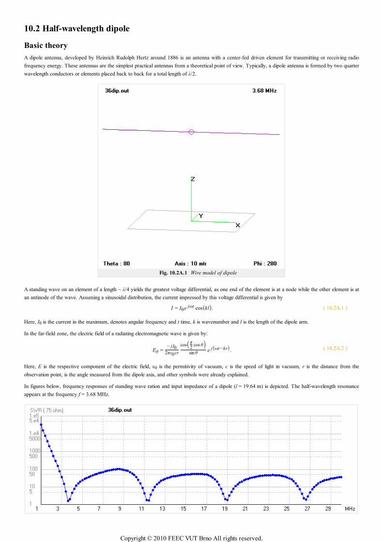
10.2 Half-wavelength dipole
Basic theory
A dipole antenna, developed by Heinrich Rudolph Hertz around 1886 is an antenna with a center-fed driven element for transmitting or receiving radio
frequency energy. These antennas are the simplest practical antennas from a theoretical point of view. Typically, a dipole antenna is formed by two quarter
wavelength conductors or elements placed back to back for a total length of λ/2.
Fig. 10.2A.1 Wire model of dipole
A standing wave on an element of a length ~ λ/4 yields the greatest voltage differential, as one end of the element is at a node while the other element is at
an antinode of the wave. Assuming a sinusoidal distribution, the current impressed by this voltage differential is given by
I = I0e jωt cos(kl). ( 10.2A.1 )
Here, I0 is the current in the maximum, denotes angular frequency and t time, k is wavenumber and l is the length of the dipole arm.
In the far-field zone, the electric field of a radiating electromagnetic wave is given by:
Eθ =− jI0
2πε0cr
cos(π2
cos θ)sin θ
e j(ωt −kr). ( 10.2A.2 )
Here, E is the respective component of the electric field, ε0 is the permitivity of vacuum, c is the speed of light in vacuum, r is the distance from the
observation point, is the angle measured from the dipole axis, and other symbols were already explained.
In figures below, frequency responses of standing wave ration and input impedance of a dipole (l = 19.64 m) is depicted. The half-wavelength resonance
appears at the frequency f = 3.68 MHz.
Copyright © 2010 FEEC VUT Brno All rights reserved.
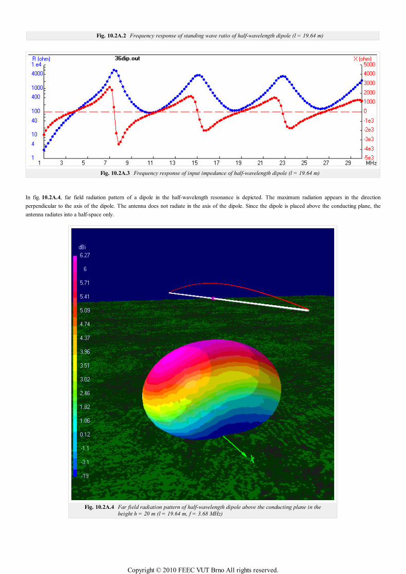
Fig. 10.2A.2 Frequency response of standing wave ratio of half-wavelength dipole (l = 19.64 m)
Fig. 10.2A.3 Frequency response of input impedance of half-wavelength dipole (l = 19.64 m)
In fig. 10.2A.4, far field radiation pattern of a dipole in the half-wavelength resonance is depicted. The maximum radiation appears in the direction
perpendicular to the axis of the dipole. The antenna does not radiate in the axis of the dipole. Since the dipole is placed above the conducting plane, the
antenna radiates into a half-space only.
Fig. 10.2A.4 Far field radiation pattern of half-wavelength dipole above the conducting plane in the
height h = 20 m (l = 19.64 m, f = 3.68 MHz)
Copyright © 2010 FEEC VUT Brno All rights reserved.

10.2 Half-wavelength dipole
Quiz
Answer these questions to get feedback on how well you understand the course. Only one of the answers is correct. You don't have to answer
every question. If you don't know the answer you can just leave it blank (default option: “I won't answer this question”) and this won't affect
your score. Answering correctly will add 2 points to your score but on the other hand you'll lose 1 point if your answer is wrong. The
questions are divided in groups of five questions.
Press See result after you have finished answering.
Displaying questions 1..3 of 3:
Question 1
Input impedance of dipole antenna in resonance is...
Possible answers for question 1:
… 50 Ω.
… 75 Ω.
… 73 + j42 Ω.
I won't answer this question
Question 2
Maximum gain of half-wave dipole is...
Possible answers for question 2:
… 2,13 dBi.
… 1,64 dBd.
… 2,13 dBd.
I won't answer this question
Question 3
Half-wave dipole is...
Possible answers for question 3:
… symmetrical antenna .
… wideband antenna.
… asymmetrical antenna.
I won't answer this question
Copyright © 2010 FEEC VUT Brno All rights reserved.
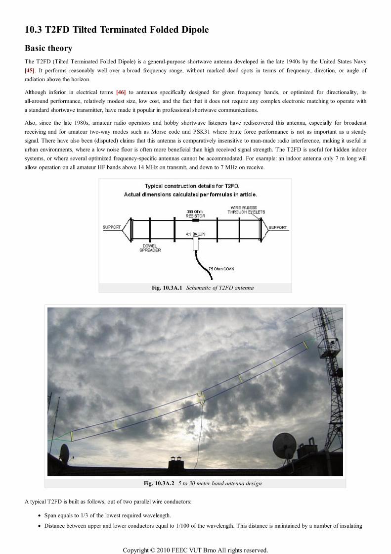
10.3 T2FD Tilted Terminated Folded Dipole
Basic theory
The T2FD (Tilted Terminated Folded Dipole) is a general-purpose shortwave antenna developed in the late 1940s by the United States Navy
[45]. It performs reasonably well over a broad frequency range, without marked dead spots in terms of frequency, direction, or angle of
radiation above the horizon.
Although inferior in electrical terms [46] to antennas specifically designed for given frequency bands, or optimized for directionality, its
all-around performance, relatively modest size, low cost, and the fact that it does not require any complex electronic matching to operate with
a standard shortwave transmitter, have made it popular in professional shortwave communications.
Also, since the late 1980s, amateur radio operators and hobby shortwave listeners have rediscovered this antenna, especially for broadcast
receiving and for amateur two-way modes such as Morse code and PSK31 where brute force performance is not as important as a steady
signal. There have also been (disputed) claims that this antenna is comparatively insensitive to man-made radio interference, making it useful in
urban environments, where a low noise floor is often more beneficial than high received signal strength. The T2FD is useful for hidden indoor
systems, or where several optimized frequency-specific antennas cannot be accommodated. For example: an indoor antenna only 7 m long will
allow operation on all amateur HF bands above 14 MHz on transmit, and down to 7 MHz on receive.
Fig. 10.3A.1 Schematic of T2FD antenna
Fig. 10.3A.2 5 to 30 meter band antenna design
A typical T2FD is built as follows, out of two parallel wire conductors:
Span equals to 1/3 of the lowest required wavelength.
Distance between upper and lower conductors equal to 1/100 of the wavelength. This distance is maintained by a number of insulating
Copyright © 2010 FEEC VUT Brno All rights reserved.
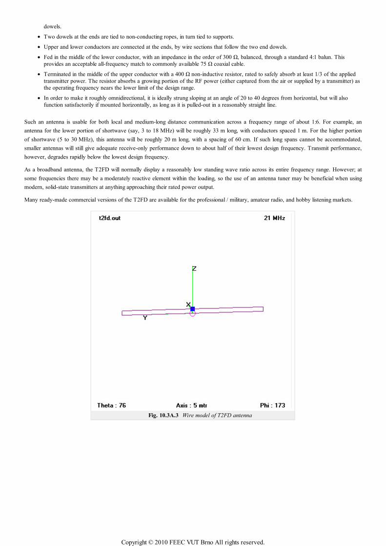
dowels.
Two dowels at the ends are tied to non-conducting ropes, in turn tied to supports.
Upper and lower conductors are connected at the ends, by wire sections that follow the two end dowels.
Fed in the middle of the lower conductor, with an impedance in the order of 300 Ω, balanced, through a standard 4:1 balun. This
provides an acceptable all-frequency match to commonly available 75 Ω coaxial cable.
Terminated in the middle of the upper conductor with a 400 Ω non-inductive resistor, rated to safely absorb at least 1/3 of the applied
transmitter power. The resistor absorbs a growing portion of the RF power (either captured from the air or supplied by a transmitter) as
the operating frequency nears the lower limit of the design range.
In order to make it roughly omnidirectional, it is ideally strung sloping at an angle of 20 to 40 degrees from horizontal, but will also
function satisfactorily if mounted horizontally, as long as it is pulled-out in a reasonably straight line.
Such an antenna is usable for both local and medium-long distance communication across a frequency range of about 1:6. For example, an
antenna for the lower portion of shortwave (say, 3 to 18 MHz) will be roughly 33 m long, with conductors spaced 1 m. For the higher portion
of shortwave (5 to 30 MHz), this antenna will be roughly 20 m long, with a spacing of 60 cm. If such long spans cannot be accommodated,
smaller antennas will still give adequate receive-only performance down to about half of their lowest design frequency. Transmit performance,
however, degrades rapidly below the lowest design frequency.
As a broadband antenna, the T2FD will normally display a reasonably low standing wave ratio across its entire frequency range. However; at
some frequencies there may be a moderately reactive element within the loading, so the use of an antenna tuner may be beneficial when using
modern, solid-state transmitters at anything approaching their rated power output.
Many ready-made commercial versions of the T2FD are available for the professional / military, amateur radio, and hobby listening markets.
Fig. 10.3A.3 Wire model of T2FD antenna
Copyright © 2010 FEEC VUT Brno All rights reserved.
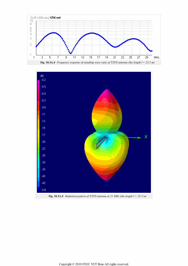
Fig. 10.3A.4 Frequency response of standing wave ratio of T2FD antenna (the length l = 23.5 m)
Fig. 10.3A.5 Radiation pattern of T2FD antenna at 21 MHz (the length l = 23.5 m)
Copyright © 2010 FEEC VUT Brno All rights reserved.

10.3 T2FD Tilted Terminated Folded Dipole
Quiz
Answer these questions to get feedback on how well you understand the course. Only one of the answers is correct. You don't have to answer
every question. If you don't know the answer you can just leave it blank (default option: “I won't answer this question”) and this won't affect
your score. Answering correctly will add 2 points to your score but on the other hand you'll lose 1 point if your answer is wrong. The
questions are divided in groups of five questions.
Press See result after you have finished answering.
Displaying questions 1..3 of 3:
Question 1
The T2FD antenna is terminated by resistor with impedance about...
Possible answers for question 1:
… 50 Ω.
… 300 Ω.
… 400 Ω.
I won't answer this question
Question 2
The T2FD antenna is antenna with...
Possible answers for question 2:
… high gain.
… low profile against half-wave dipole.
… high efficiency of radiation.
I won't answer this question
Question 3
Input impedance of T2FD antenna is about...
Possible answers for question 3:
… 300 Ω.
… 50 Ω.
… 400 Ω.
I won't answer this question
Copyright © 2010 FEEC VUT Brno All rights reserved.
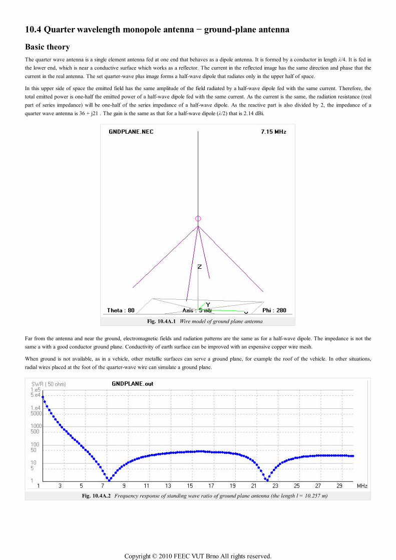
10.4 Quarter wavelength monopole antenna − ground-plane antenna
Basic theory
The quarter wave antenna is a single element antenna fed at one end that behaves as a dipole antenna. It is formed by a conductor in length λ/4. It is fed in
the lower end, which is near a conductive surface which works as a reflector. The current in the reflected image has the same direction and phase that the
current in the real antenna. The set quarter-wave plus image forms a half-wave dipole that radiates only in the upper half of space.
In this upper side of space the emitted field has the same amplitude of the field radiated by a half-wave dipole fed with the same current. Therefore, the
total emitted power is one-half the emitted power of a half-wave dipole fed with the same current. As the current is the same, the radiation resistance (real
part of series impedance) will be one-half of the series impedance of a half-wave dipole. As the reactive part is also divided by 2, the impedance of a
quarter wave antenna is 36 + j21 . The gain is the same as that for a half-wave dipole (λ/2) that is 2.14 dBi.
Fig. 10.4A.1 Wire model of ground plane antenna
Far from the antenna and near the ground, electromagnetic fields and radiation patterns are the same as for a half-wave dipole. The impedance is not the
same a with a good conductor ground plane. Conductivity of earth surface can be improved with an expensive copper wire mesh.
When ground is not available, as in a vehicle, other metallic surfaces can serve a ground plane, for example the roof of the vehicle. In other situations,
radial wires placed at the foot of the quarter-wave wire can simulate a ground plane.
Fig. 10.4A.2 Frequency response of standing wave ratio of ground plane antenna (the length l = 10.257 m)
Copyright © 2010 FEEC VUT Brno All rights reserved.
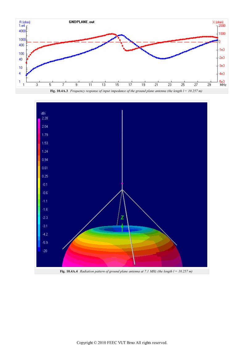
Fig. 10.4A.3 Frequency response of input impedance of the ground plane antenna (the length l = 10.257 m)
Fig. 10.4A.4 Radiation pattern of ground plane antenna at 7.1 MHz (the length l = 10.257 m)
Copyright © 2010 FEEC VUT Brno All rights reserved.

10.4 Quarter wavelength monopole antenna − ground-plane antenna
Quiz
Answer these questions to get feedback on how well you understand the course. Only one of the answers is correct. You don't have to answer
every question. If you don't know the answer you can just leave it blank (default option: “I won't answer this question”) and this won't affect
your score. Answering correctly will add 2 points to your score but on the other hand you'll lose 1 point if your answer is wrong. The
questions are divided in groups of five questions.
Press See result after you have finished answering.
Displaying questions 1..3 of 3:
Question 1
Quarter-wave monopole has input impedance...
Possible answers for question 1:
… similar as half-wave dipole.
… 2 times higher then half-wave dipole.
… 3 times smaller then half-wave dipole.
I won't answer this question
Question 2
The quarter-wave monepole is...
Possible answers for question 2:
… asymmetrical antenna.
… symmetrical antenna.
… antenna with circular polarization.
I won't answer this question
Question 3
The angle of wires of ground part of quarter-wave monopole depends...
Possible answers for question 3:
… the input impedance of the antenna.
… the gain of the antenna.
… the input impedance and gain of the antenna.
I won't answer this question
Copyright © 2010 FEEC VUT Brno All rights reserved.
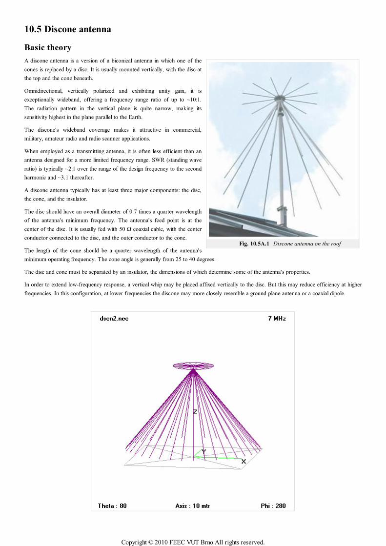
Fig. 10.5A.1 Discone antenna on the roof
10.5 Discone antenna
Basic theory
A discone antenna is a version of a biconical antenna in which one of the
cones is replaced by a disc. It is usually mounted vertically, with the disc at
the top and the cone beneath.
Omnidirectional, vertically polarized and exhibiting unity gain, it is
exceptionally wideband, offering a frequency range ratio of up to ~10:1.
The radiation pattern in the vertical plane is quite narrow, making its
sensitivity highest in the plane parallel to the Earth.
The discone's wideband coverage makes it attractive in commercial,
military, amateur radio and radio scanner applications.
When employed as a transmitting antenna, it is often less efficient than an
antenna designed for a more limited frequency range. SWR (standing wave
ratio) is typically ~2:1 over the range of the design frequency to the second
harmonic and ~3.1 thereafter.
A discone antenna typically has at least three major components: the disc,
the cone, and the insulator.
The disc should have an overall diameter of 0.7 times a quarter wavelength
of the antenna's minimum frequency. The antenna's feed point is at the
center of the disc. It is usually fed with 50 Ω coaxial cable, with the center
conductor connected to the disc, and the outer conductor to the cone.
The length of the cone should be a quarter wavelength of the antenna's
minimum operating frequency. The cone angle is generally from 25 to 40 degrees.
The disc and cone must be separated by an insulator, the dimensions of which determine some of the antenna's properties.
In order to extend low-frequency response, a vertical whip may be placed affixed vertically to the disc. But this may reduce efficiency at higher
frequencies. In this configuration, at lower frequencies the discone may more closely resemble a ground plane antenna or a coaxial dipole.
Copyright © 2010 FEEC VUT Brno All rights reserved.
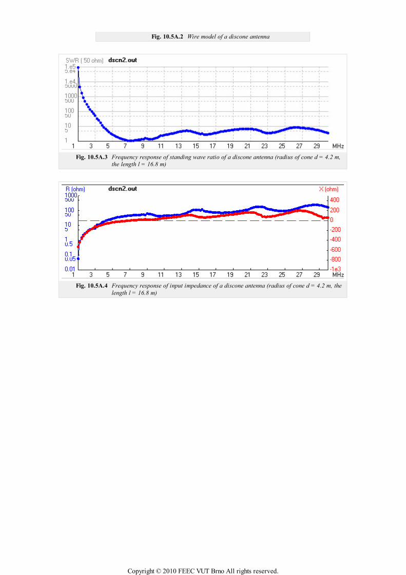
Fig. 10.5A.2 Wire model of a discone antenna
Fig. 10.5A.3 Frequency response of standing wave ratio of a discone antenna (radius of cone d = 4.2 m,
the length l = 16.8 m)
Fig. 10.5A.4 Frequency response of input impedance of a discone antenna (radius of cone d = 4.2 m, the
length l = 16.8 m)
Copyright © 2010 FEEC VUT Brno All rights reserved.
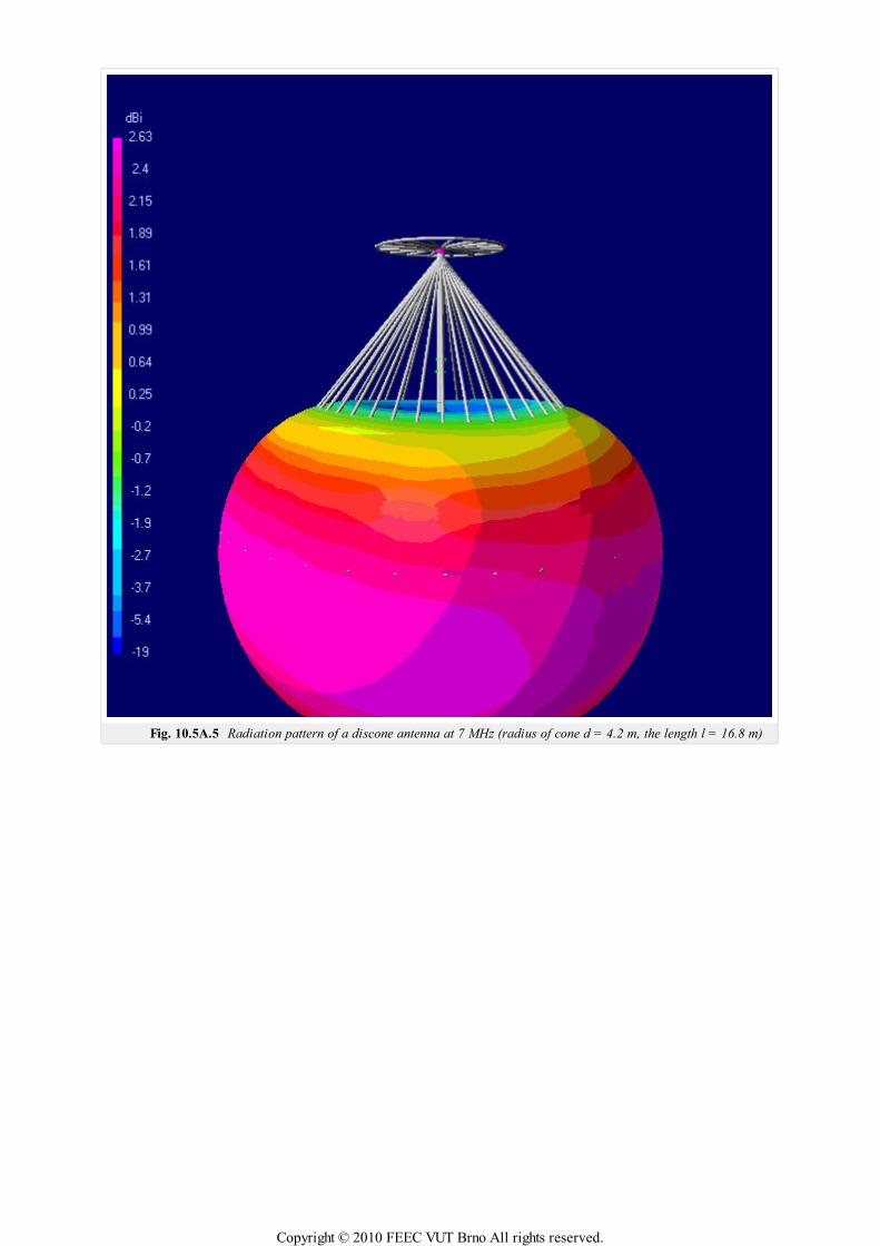
Fig. 10.5A.5 Radiation pattern of a discone antenna at 7 MHz (radius of cone d = 4.2 m, the length l = 16.8 m)
Copyright © 2010 FEEC VUT Brno All rights reserved.
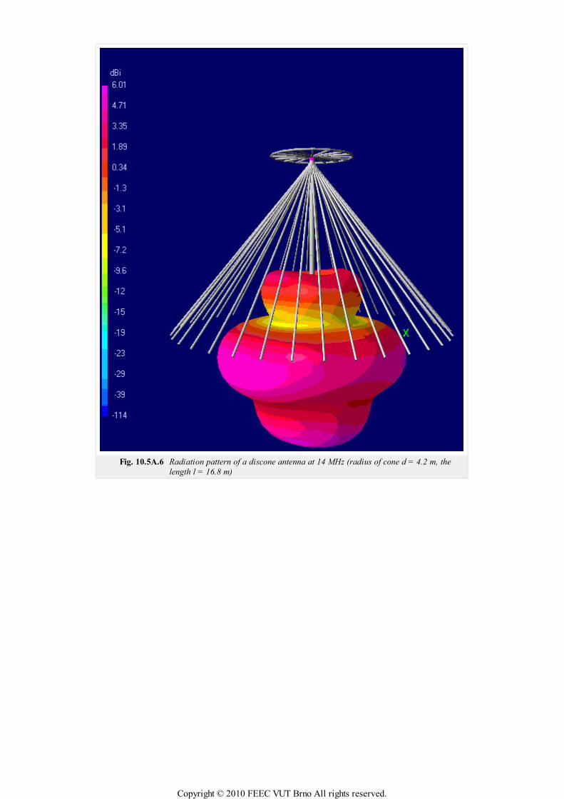
Fig. 10.5A.6 Radiation pattern of a discone antenna at 14 MHz (radius of cone d = 4.2 m, the
length l = 16.8 m)
Copyright © 2010 FEEC VUT Brno All rights reserved.
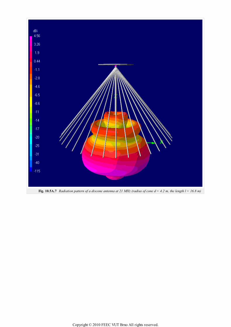
Fig. 10.5A.7 Radiation pattern of a discone antenna at 21 MHz (radius of cone d = 4.2 m, the length l = 16.8 m)
Copyright © 2010 FEEC VUT Brno All rights reserved.
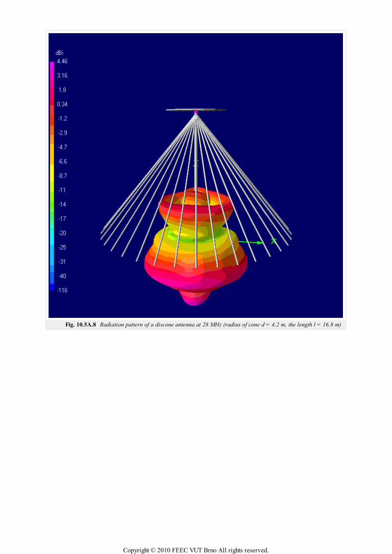
Fig. 10.5A.8 Radiation pattern of a discone antenna at 28 MHz (radius of cone d = 4.2 m, the length l = 16.8 m)
Copyright © 2010 FEEC VUT Brno All rights reserved.

10.5 Discone antenna
Quiz
Answer these questions to get feedback on how well you understand the course. Only one of the answers is correct. You don't have to answer
every question. If you don't know the answer you can just leave it blank (default option: “I won't answer this question”) and this won't affect
your score. Answering correctly will add 2 points to your score but on the other hand you'll lose 1 point if your answer is wrong. The
questions are divided in groups of five questions.
Press See result after you have finished answering.
Displaying questions 1..3 of 3:
Question 1
Discone antena is...
Possible answers for question 1:
… horizontally polarized antenna with high gain.
… vertically polarized wide-band antenna.
… vertically polarized antenna with high gain.
I won't answer this question
Question 2
Bandwidth of discone antenna is usually...
Possible answers for question 2:
… 1:1.
… 1:10.
… 1:3.
I won't answer this question
Question 3
Input impedance of discone antenna is about...
Possible answers for question 3:
… 50 Ω and can be loaded by coaxial cable.
… 75 Ω and can be loaded by symmetrical feed-line.
… 300 Ω and must be loaded by symmetrical balun.
I won't answer this question
Copyright © 2010 FEEC VUT Brno All rights reserved.
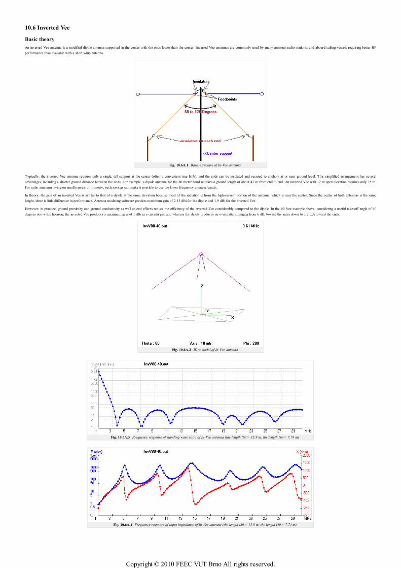
10.6 Inverted Vee
Basic theory
An inverted Vee antenna is a modified dipole antenna supported in the center with the ends lower than the center. Inverted Vee antennas are commonly used by many amateur radio stations, and aboard sailing vessels requiring better HF
performance than available with a short whip antenna.
Fig. 10.6A.1 Basic structure of In-Vee antenna
Typically, the inverted Vee antenna requires only a single, tall support at the center (often a convenient tree limb), and the ends can be insulated and secured to anchors at or near ground level. This simplified arrangement has several
advantages, including a shorter ground distance between the ends. For example, a dipole antenna for the 80 meter band requires a ground length of about 43 m from end to end. An inverted Vee with 12 m apex elevation requires only 35 m.
For radio amateurs living on small parcels of property, such savings can make it possible to use the lower frequency amateur bands.
In theory, the gain of an inverted Vee is similar to that of a dipole at the same elevation because most of the radiation is from the high-current portion of the antenna, which is near the center. Since the center of both antennas is the same
height, there is little difference in performance. Antenna modeling software predicts maximum gain of 2.15 dBi for the dipole and 1.9 dBi for the inverted Vee.
However, in practice, ground proximity and ground conductivity as well as end effects reduce the efficiency of the inverted Vee considerably compared to the dipole. In the 40-foot example above, considering a useful take-off angle of 40
degrees above the horizon, the inverted Vee produces a maximum gain of 1 dBi in a circular pattern, whereas the dipole produces an oval pattern ranging from 6 dBi toward the sides down to 1.2 dBi toward the ends.
Fig. 10.6A.2 Wire model of In-Vee antenna
Fig. 10.6A.3 Frequency response of standing wave ratio of In-Vee antenna (the length l80 = 15.9 m, the length l40 = 7.74 m)
Fig. 10.6A.4 Frequency response of input impedance of In-Vee antenna (the length l80 = 15.9 m, the length l40 = 7.74 m)
Copyright © 2010 FEEC VUT Brno All rights reserved.
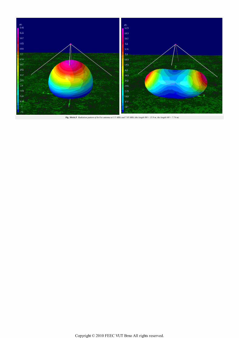
Fig. 10.6A.5 Radiation pattern of In-Vee antenna at 3.5 MHz and 7.05 MHz (the length l80 = 15.9 m, the length l40 = 7.74 m)
Copyright © 2010 FEEC VUT Brno All rights reserved.

10.6 Inverted Vee
Quiz
Answer these questions to get feedback on how well you understand the course. Only one of the answers is correct. You don't have to answer
every question. If you don't know the answer you can just leave it blank (default option: “I won't answer this question”) and this won't affect
your score. Answering correctly will add 2 points to your score but on the other hand you'll lose 1 point if your answer is wrong. The
questions are divided in groups of five questions.
Press See result after you have finished answering.
Displaying questions 1..3 of 3:
Question 1
One of most adventages of Inverted-Vee antenna is...
Possible answers for question 1:
… low length of antenna against half-wave dipole.
… wideband of antenna.
… low weight of antenna.
I won't answer this question
Question 2
Inverted-Vee antenna can be majority used for...
Possible answers for question 2:
… satellite communication.
… ionosphere propagation.
… direct wave propagation.
I won't answer this question
Question 3
Input impedance of Inverted-Vee antenna is about...
Possible answers for question 3:
… 50 Ω and can be loaded by coaxial cable.
… 50 Ω and can be loaded by symmetrical feed-line.
… 300 Ω and must be loaded across symmetrical balun.
I won't answer this question
Copyright © 2010 FEEC VUT Brno All rights reserved.
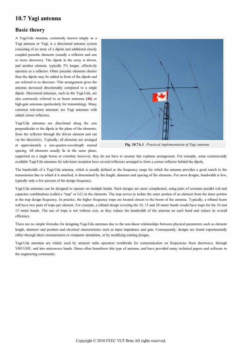
Fig. 10.7A.1 Practical implementation of Yagi antenna
10.7 Yagi antenna
Basic theory
A Yagi-Uda Antenna, commonly known simply as a
Yagi antenna or Yagi, is a directional antenna system
consisting of an array of a dipole and additional closely
coupled parasitic elements (usually a reflector and one
or more directors). The dipole in the array is driven,
and another element, typically 5% longer, effectively
operates as a reflector. Other parasitic elements shorter
than the dipole may be added in front of the dipole and
are referred to as directors. This arrangement gives the
antenna increased directionality compared to a single
dipole. Directional antennas, such as the Yagi-Uda, are
also commonly referred to as beam antennas [46] or
high-gain antennas (particularly for transmitting). Many
common television antennas are Yagi antennas with
added corner reflectors.
Yagi-Uda antennas are directional along the axis
perpendicular to the dipole in the plane of the elements,
from the reflector through the driven element and out
via the director(s). Typically, all elements are arranged
at approximately a one-quarter-wavelength mutual
spacing. All elements usually lie in the same plane,
supported on a single boom or crossbar; however, they do not have to assume this coplanar arrangement. For example, some commercially
available Yagi-Uda antennas for television reception have several reflectors arranged to form a corner reflector behind the dipole.
The bandwidth of a Yagi-Uda antenna, which is usually defined as the frequency range for which the antenna provides a good match to the
transmission line to which it is attached, is determined by the length, diameter and spacing of the elements. For most designs, bandwidth is low,
typically only a few percent of the design frequency.
Yagi-Uda antennas can be designed to operate on multiple bands. Such designs are more complicated, using pairs of resonant parallel coil and
capacitor combinations (called a "trap" or LC) in the elements. The trap serves to isolate the outer portion of an element from the inner portion
at the trap design frequency. In practice, the higher frequency traps are located closest to the boom of the antenna. Typically, a triband beam
will have two pairs of traps per element. For example, a triband design covering the 10, 15 and 20 meter bands would have traps for the 10 and
15 meter bands. The use of traps is not without cost, as they reduce the bandwidth of the antenna on each band and reduce its overall
efficiency.
There are no simple formulas for designing Yagi-Uda antennas due to the non-linear relationships between physical parameters such as element
length, diameter and position and electrical characteristics such as input impedance and gain. Consequently, designs are found experimentally
either through direct measurement or computer simulation, or by modifying existing designs.
Yagi-Uda antennas are widely used by amateur radio operators worldwide for communication on frequencies from shortwave, through
VHF/UHF, and into microwave bands. Hams often homebrew this type of antenna, and have provided many technical papers and software to
the engineering community.
Copyright © 2010 FEEC VUT Brno All rights reserved.
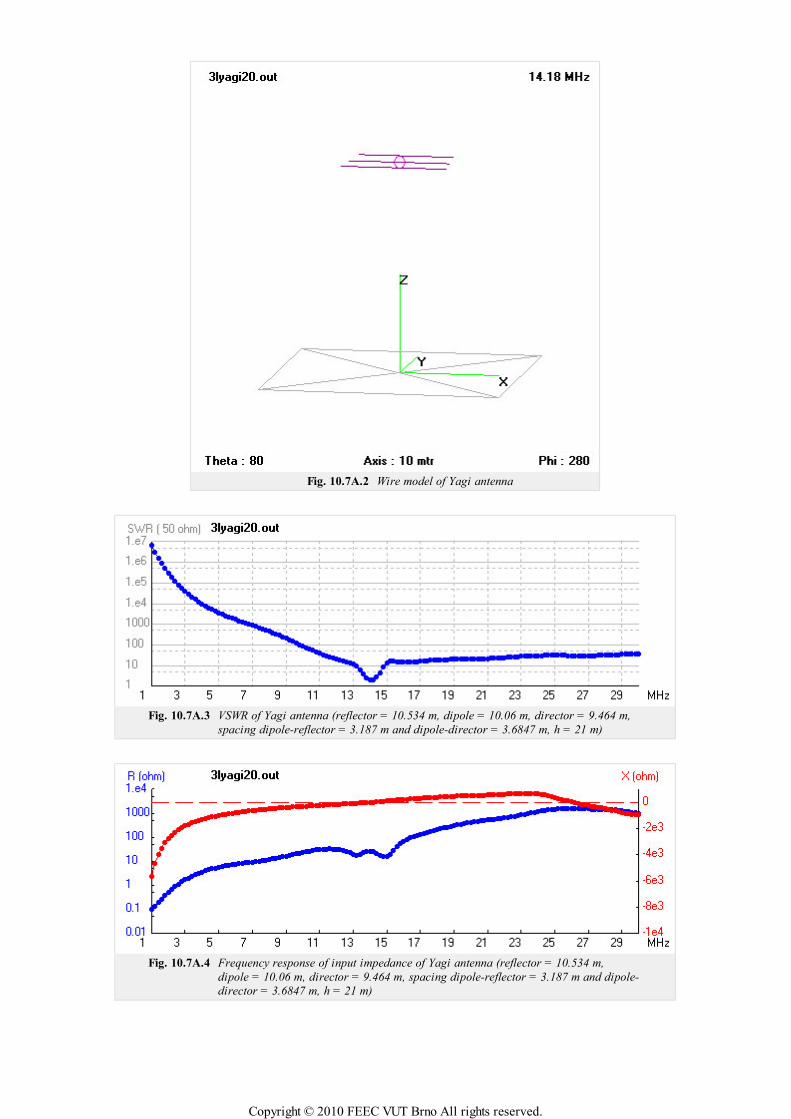
Fig. 10.7A.2 Wire model of Yagi antenna
Fig. 10.7A.3 VSWR of Yagi antenna (reflector = 10.534 m, dipole = 10.06 m, director = 9.464 m,
spacing dipole-reflector = 3.187 m and dipole-director = 3.6847 m, h = 21 m)
Fig. 10.7A.4 Frequency response of input impedance of Yagi antenna (reflector = 10.534 m,
dipole = 10.06 m, director = 9.464 m, spacing dipole-reflector = 3.187 m and dipole-
director = 3.6847 m, h = 21 m)
Copyright © 2010 FEEC VUT Brno All rights reserved.
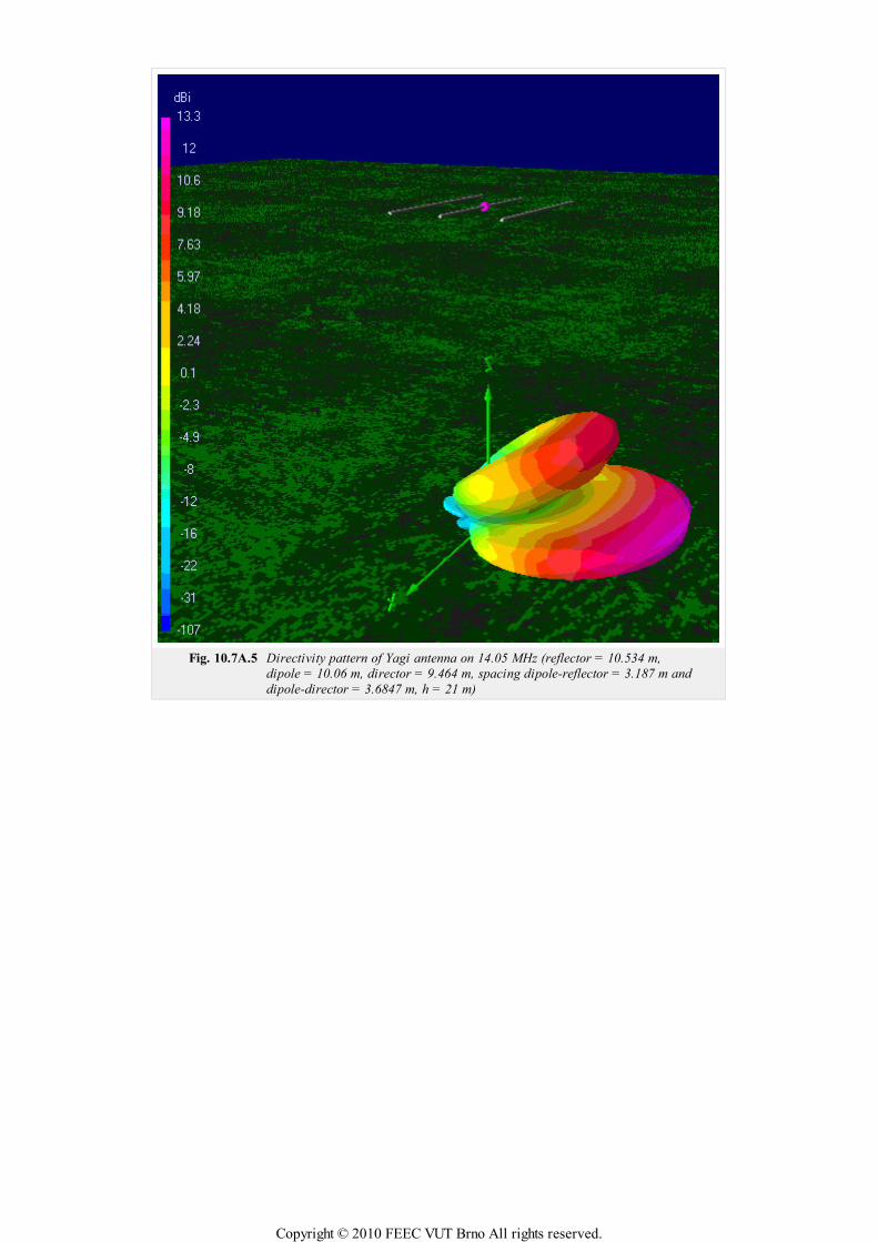
Fig. 10.7A.5 Directivity pattern of Yagi antenna on 14.05 MHz (reflector = 10.534 m,
dipole = 10.06 m, director = 9.464 m, spacing dipole-reflector = 3.187 m and
dipole-director = 3.6847 m, h = 21 m)
Copyright © 2010 FEEC VUT Brno All rights reserved.

10.7 Yagi antenna
Quiz
Answer these questions to get feedback on how well you understand the course. Only one of the answers is correct. You don't have to answer
every question. If you don't know the answer you can just leave it blank (default option: “I won't answer this question”) and this won't affect
your score. Answering correctly will add 2 points to your score but on the other hand you'll lose 1 point if your answer is wrong. The
questions are divided in groups of five questions.
Press See result after you have finished answering.
Displaying questions 1..3 of 3:
Question 1
Yagi antenna is antenna with...
Possible answers for question 1:
… circular polarization.
… with medium gain of radiation.
… omni-directional radiation.
I won't answer this question
Question 2
Yagi antenna can be built from...
Possible answers for question 2:
… several active elements, one reflector and one director.
… several directors, several active elements and several reflectors.
… one active element, one reflector and one director.
I won't answer this question
Question 3
Wideband of Yagi antenna is usually...
Possible answers for question 3:
… 1:10.
… 1:5.
… few percents.
I won't answer this question
Copyright © 2010 FEEC VUT Brno All rights reserved.
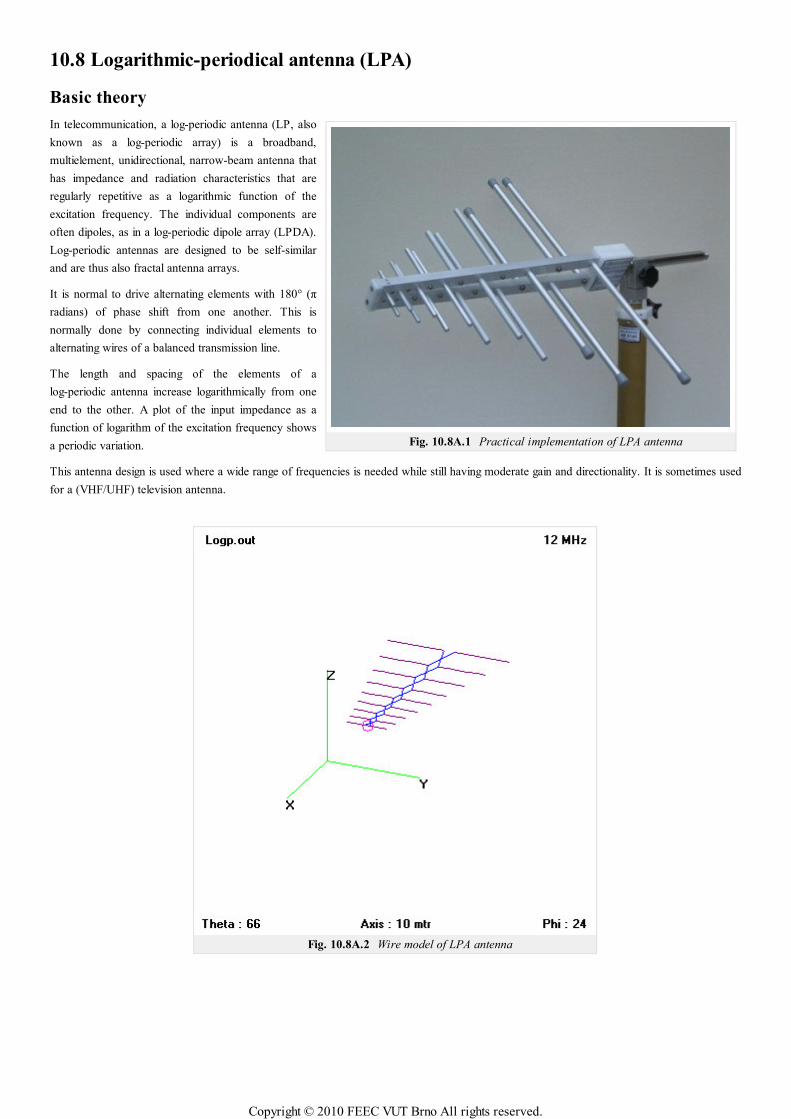
Fig. 10.8A.1 Practical implementation of LPA antenna
10.8 Logarithmic-periodical antenna (LPA)
Basic theory
In telecommunication, a log-periodic antenna (LP, also
known as a log-periodic array) is a broadband,
multielement, unidirectional, narrow-beam antenna that
has impedance and radiation characteristics that are
regularly repetitive as a logarithmic function of the
excitation frequency. The individual components are
often dipoles, as in a log-periodic dipole array (LPDA).
Log-periodic antennas are designed to be self-similar
and are thus also fractal antenna arrays.
It is normal to drive alternating elements with 180° (π
radians) of phase shift from one another. This is
normally done by connecting individual elements to
alternating wires of a balanced transmission line.
The length and spacing of the elements of a
log-periodic antenna increase logarithmically from one
end to the other. A plot of the input impedance as a
function of logarithm of the excitation frequency shows
a periodic variation.
This antenna design is used where a wide range of frequencies is needed while still having moderate gain and directionality. It is sometimes used
for a (VHF/UHF) television antenna.
Fig. 10.8A.2 Wire model of LPA antenna
Copyright © 2010 FEEC VUT Brno All rights reserved.
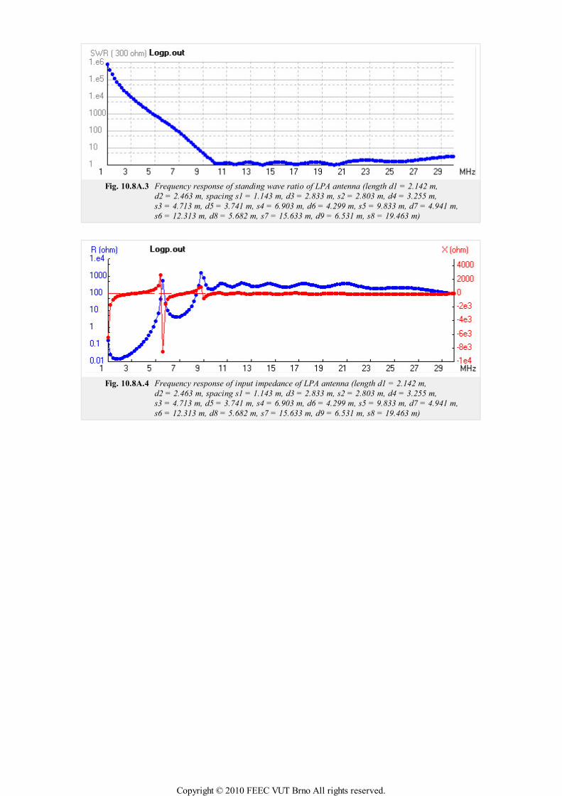
Fig. 10.8A.3 Frequency response of standing wave ratio of LPA antenna (length d1 = 2.142 m,
d2 = 2.463 m, spacing s1 = 1.143 m, d3 = 2.833 m, s2 = 2.803 m, d4 = 3.255 m,
s3 = 4.713 m, d5 = 3.741 m, s4 = 6.903 m, d6 = 4.299 m, s5 = 9.833 m, d7 = 4.941 m,
s6 = 12.313 m, d8 = 5.682 m, s7 = 15.633 m, d9 = 6.531 m, s8 = 19.463 m)
Fig. 10.8A.4 Frequency response of input impedance of LPA antenna (length d1 = 2.142 m,
d2 = 2.463 m, spacing s1 = 1.143 m, d3 = 2.833 m, s2 = 2.803 m, d4 = 3.255 m,
s3 = 4.713 m, d5 = 3.741 m, s4 = 6.903 m, d6 = 4.299 m, s5 = 9.833 m, d7 = 4.941 m,
s6 = 12.313 m, d8 = 5.682 m, s7 = 15.633 m, d9 = 6.531 m, s8 = 19.463 m)
Copyright © 2010 FEEC VUT Brno All rights reserved.
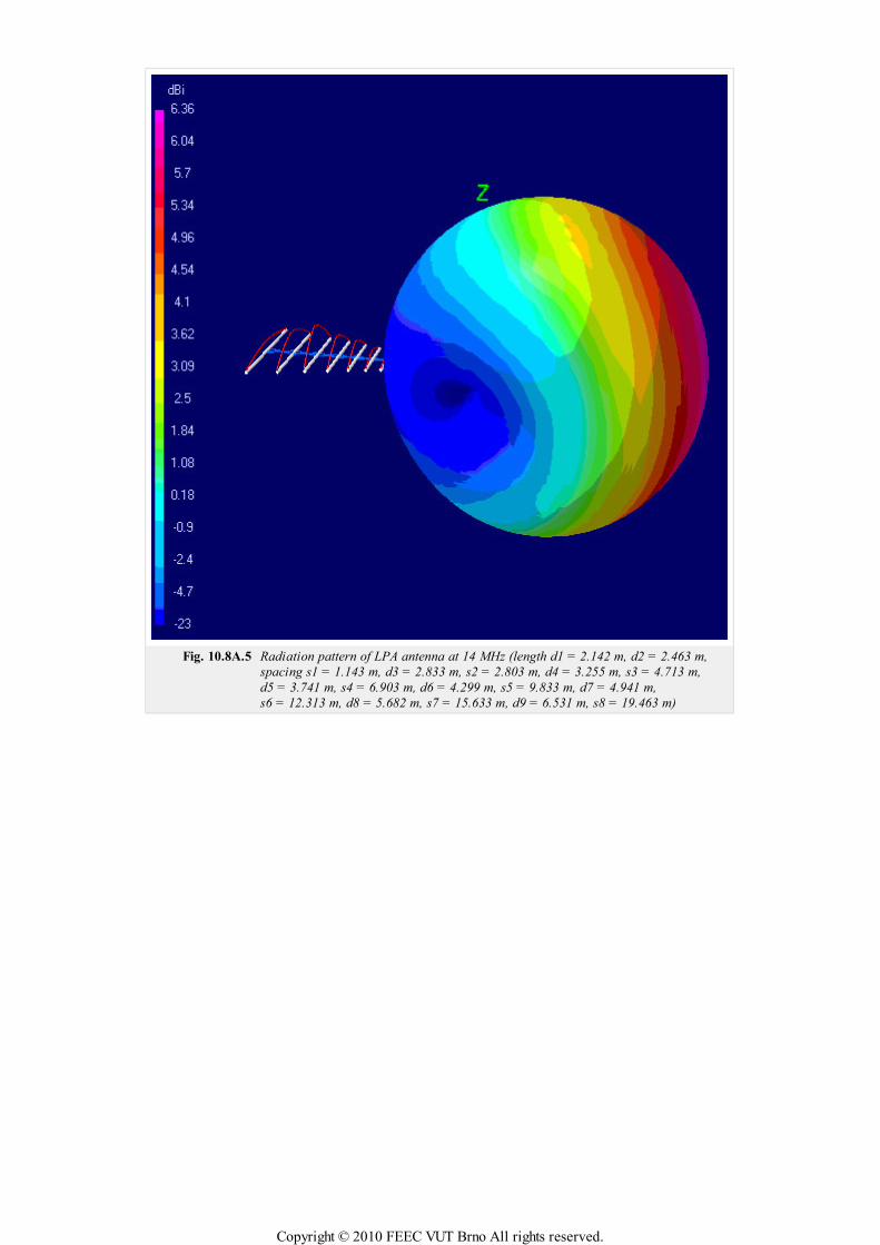
Fig. 10.8A.5 Radiation pattern of LPA antenna at 14 MHz (length d1 = 2.142 m, d2 = 2.463 m,
spacing s1 = 1.143 m, d3 = 2.833 m, s2 = 2.803 m, d4 = 3.255 m, s3 = 4.713 m,
d5 = 3.741 m, s4 = 6.903 m, d6 = 4.299 m, s5 = 9.833 m, d7 = 4.941 m,
s6 = 12.313 m, d8 = 5.682 m, s7 = 15.633 m, d9 = 6.531 m, s8 = 19.463 m)
Copyright © 2010 FEEC VUT Brno All rights reserved.
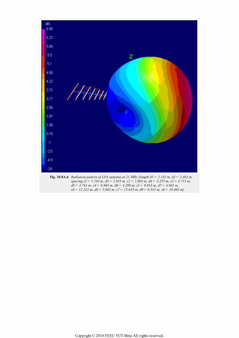
Fig. 10.8A.6 Radiation pattern of LPA antenna at 21 MHz (length d1 = 2.142 m, d2 = 2.463 m,
spacing s1 = 1.143 m, d3 = 2.833 m, s2 = 2.803 m, d4 = 3.255 m, s3 = 4.713 m,
d5 = 3.741 m, s4 = 6.903 m, d6 = 4.299 m, s5 = 9.833 m, d7 = 4.941 m,
s6 = 12.313 m, d8 = 5.682 m, s7 = 15.633 m, d9 = 6.531 m, s8 = 19.463 m)
Copyright © 2010 FEEC VUT Brno All rights reserved.
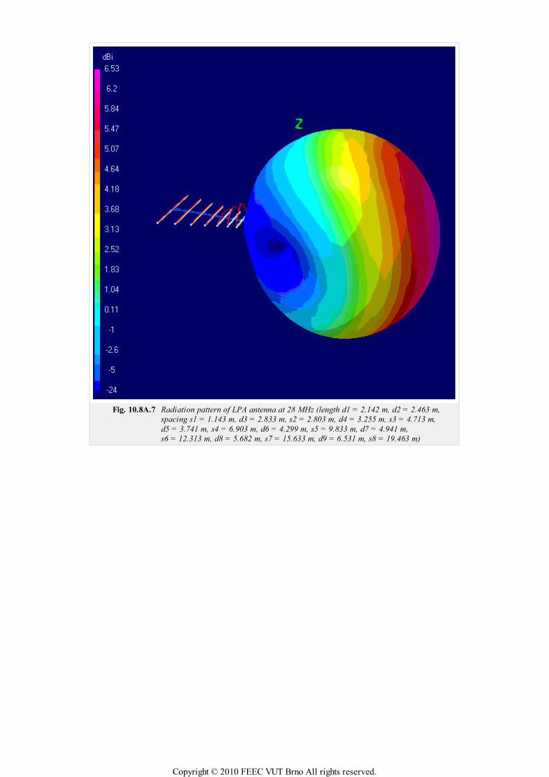
Fig. 10.8A.7 Radiation pattern of LPA antenna at 28 MHz (length d1 = 2.142 m, d2 = 2.463 m,
spacing s1 = 1.143 m, d3 = 2.833 m, s2 = 2.803 m, d4 = 3.255 m, s3 = 4.713 m,
d5 = 3.741 m, s4 = 6.903 m, d6 = 4.299 m, s5 = 9.833 m, d7 = 4.941 m,
s6 = 12.313 m, d8 = 5.682 m, s7 = 15.633 m, d9 = 6.531 m, s8 = 19.463 m)
Copyright © 2010 FEEC VUT Brno All rights reserved.

10.8 Logarithmic-periodical antenna (LPA)
Quiz
Answer these questions to get feedback on how well you understand the course. Only one of the answers is correct. You don't have to answer
every question. If you don't know the answer you can just leave it blank (default option: “I won't answer this question”) and this won't affect
your score. Answering correctly will add 2 points to your score but on the other hand you'll lose 1 point if your answer is wrong. The
questions are divided in groups of five questions.
Press See result after you have finished answering.
Displaying questions 1..3 of 3:
Question 1
LPA antenna is antenna...
Possible answers for question 1:
… with circular polarization.
… with medium value of gain.
… with omni-directional propagation.
I won't answer this question
Question 2
Two neighbour elements are feeded by phase shift...
Possible answers for question 2:
… 180°.
… 225°.
… 0°.
I won't answer this question
Question 3
Wideband of LPA antenna is usually...
Possible answers for question 3:
… 1:10.
… 1:5.
… few percents.
I won't answer this question
Copyright © 2010 FEEC VUT Brno All rights reserved.
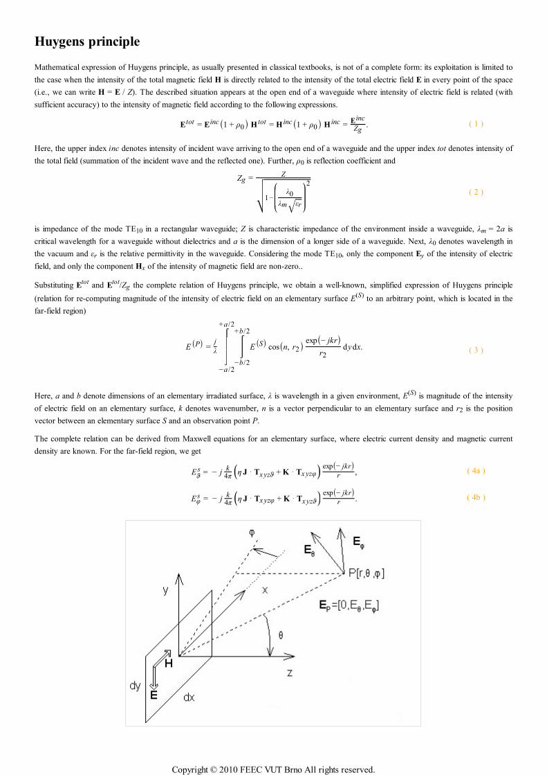
Huygens principle
Mathematical expression of Huygens principle, as usually presented in classical textbooks, is not of a complete form: its exploitation is limited to
the case when the intensity of the total magnetic field H is directly related to the intensity of the total electric field E in every point of the space
(i.e., we can write H = E / Z). The described situation appears at the open end of a waveguide where intensity of electric field is related (with
sufficient accuracy) to the intensity of magnetic field according to the following expressions.
Etot = Einc(1 + ρ0) H tot = H inc(1 + ρ0) H inc =Einc
Zg. ( 1 )
Here, the upper index inc denotes intensity of incident wave arriving to the open end of a waveguide and the upper index tot denotes intensity of
the total field (summation of the incident wave and the reflected one). Further, ρ0 is reflection coefficient and
Zg =Z
1−
⎛
⎝⎜⎜⎜
λ0
λm εr√
⎞
⎠⎟⎟⎟
2
√
( 2 )
is impedance of the mode TE10 in a rectangular waveguide; Z is characteristic impedance of the environment inside a waveguide, λm = 2a is
critical wavelength for a waveguide without dielectrics and a is the dimension of a longer side of a waveguide. Next, λ0 denotes wavelength in
the vacuum and εr is the relative permittivity in the waveguide. Considering the mode TE10, only the component Ey of the intensity of electric
field, and only the component Hx of the intensity of magnetic field are non-zero..
Substituting Etot and Etot/Zg the complete relation of Huygens principle, we obtain a well-known, simplified expression of Huygens principle
(relation for re-computing magnitude of the intensity of electric field on an elementary surface E(S) to an arbitrary point, which is located in the
far-field region)
E(P) =j
λ
⌠
⌡
⎮⎮⎮⎮⎮−a /2
+a /2
⌠⌡⎮⎮
−b/2
+b/2
E(S) cos(n, r2) exp(− jkr)r2
dy dx. ( 3 )
Here, a and b denote dimensions of an elementary irradiated surface, λ is wavelength in a given environment, E(S) is magnitude of the intensity
of electric field on an elementary surface, k denotes wavenumber, n is a vector perpendicular to an elementary surface and r2 is the position
vector between an elementary surface S and an observation point P.
The complete relation can be derived from Maxwell equations for an elementary surface, where electric current density and magnetic current
density are known. For the far-field region, we get
Eϑs = − j
k4π
⎛⎝η J ⋅Txyzϑ +K ⋅Tx yzφ⎞⎠
exp(− jkr)r , ( 4a )
Eφs = − j
k4π
⎛⎝η J ⋅Txyzφ +K ⋅Txyzϑ⎞⎠
exp(− jkr)r . ( 4b )
Copyright © 2010 FEEC VUT Brno All rights reserved.
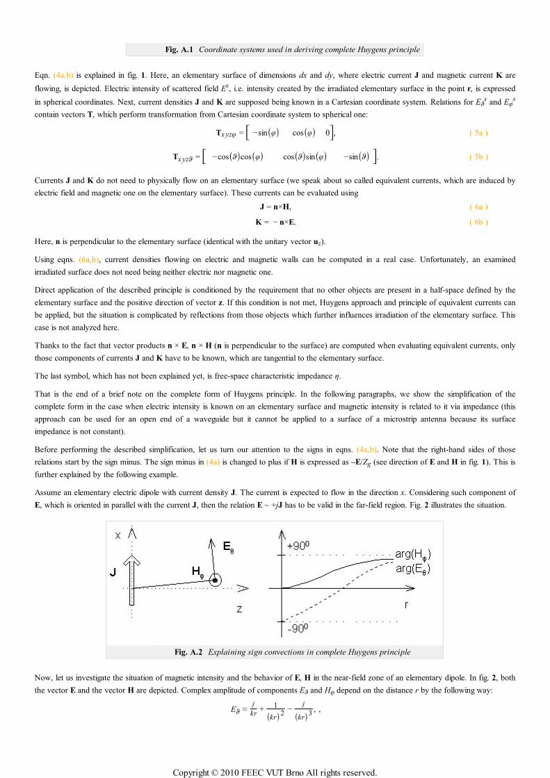
Fig. A.1 Coordinate systems used in deriving complete Huygens principle
Eqn. (4a,b) is explained in fig. 1. Here, an elementary surface of dimensions dx and dy, where electric current J and magnetic current K are
flowing, is depicted. Electric intensity of scattered field Es, i.e. intensity created by the irradiated elementary surface in the point r, is expressed
in spherical coordinates. Next, current densities J and K are supposed being known in a Cartesian coordinate system. Relations for Eϑs and Eφ
s
contain vectors T, which perform transformation from Cartesian coordinate system to spherical one:
Tx yzφ =⎡⎣ −sin(φ) cos(φ) 0
⎤⎦, ( 5a )
Tx yzϑ =⎡⎣ −cos(ϑ)cos(φ) cos(ϑ)sin(φ) −sin(ϑ) ⎤⎦. ( 5b )
Currents J and K do not need to physically flow on an elementary surface (we speak about so called equivalent currents, which are induced by
electric field and magnetic one on the elementary surface). These currents can be evaluated using
J = n×H, ( 6a )
K = − n×E. ( 6b )
Here, n is perpendicular to the elementary surface (identical with the unitary vector uz).
Using eqns. (6a,b), current densities flowing on electric and magnetic walls can be computed in a real case. Unfortunately, an examined
irradiated surface does not need being neither electric nor magnetic one.
Direct application of the described principle is conditioned by the requirement that no other objects are present in a half-space defined by the
elementary surface and the positive direction of vector z. If this condition is not met, Huygens approach and principle of equivalent currents can
be applied, but the situation is complicated by reflections from those objects which further influences irradiation of the elementary surface. This
case is not analyzed here.
Thanks to the fact that vector products n × E, n × H (n is perpendicular to the surface) are computed when evaluating equivalent currents, only
those components of currents J and K have to be known, which are tangential to the elementary surface.
The last symbol, which has not been explained yet, is free-space characteristic impedance η.
That is the end of a brief note on the complete form of Huygens principle. In the following paragraphs, we show the simplification of the
complete form in the case when electric intensity is known on an elementary surface and magnetic intensity is related to it via impedance (this
approach can be used for an open end of a waveguide but it cannot be applied to a surface of a microstrip antenna because its surface
impedance is not constant).
Before performing the described simplification, let us turn our attention to the signs in eqns. (4a,b). Note that the right-hand sides of those
relations start by the sign minus. The sign minus in (4a) is changed to plus if H is expressed as –E/Zg (see direction of E and H in fig. 1). This is
further explained by the following example.
Assume an elementary electric dipole with current density J. The current is expected to flow in the direction x. Considering such component of
E, which is oriented in parallel with the current J, then the relation E ~ +jJ has to be valid in the far-field region. Fig. 2 illustrates the situation.
Fig. A.2 Explaining sign convections in complete Huygens principle
Now, let us investigate the situation of magnetic intensity and the behavior of E, H in the near-field zone of an elementary dipole. In fig. 2, both
the vector E and the vector H are depicted. Complex amplitude of components Eϑ and Hφ depend on the distance r by the following way:
Eϑ ≈j
kr+
1
(kr)2−
j
(kr)3, ,
Copyright © 2010 FEEC VUT Brno All rights reserved.
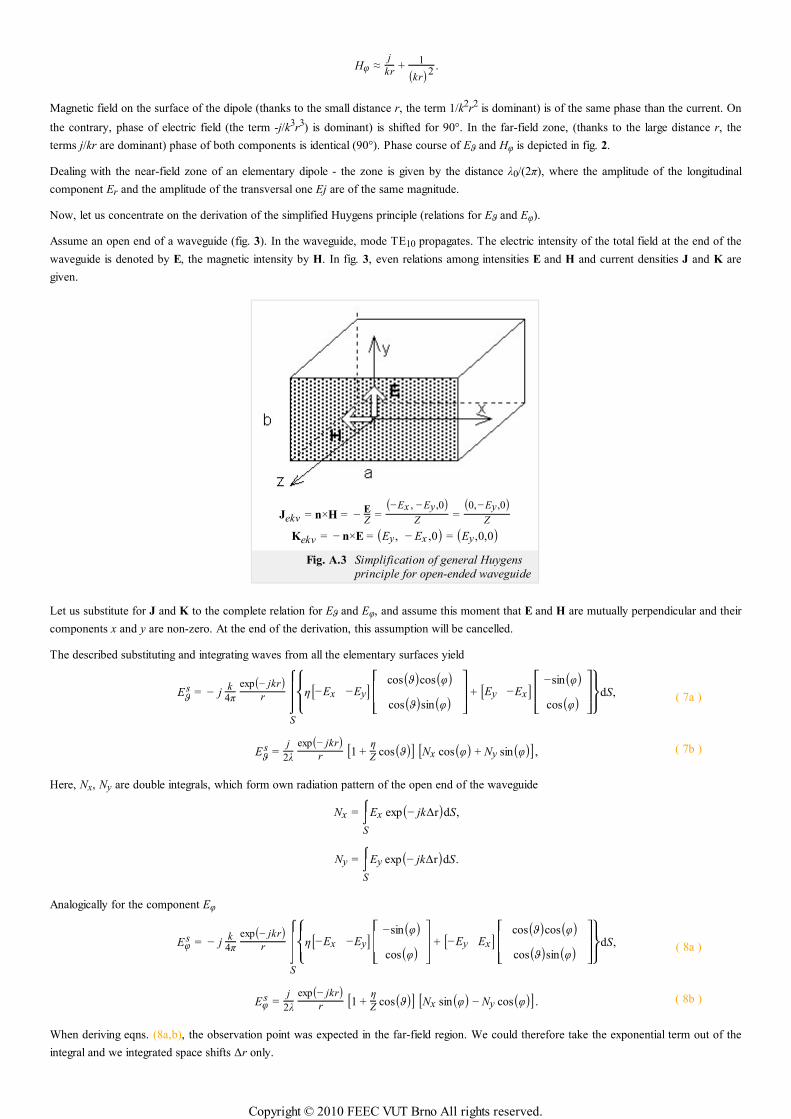
Hφ ≈j
kr+
1
(kr)2.
Magnetic field on the surface of the dipole (thanks to the small distance r, the term 1/k2r2 is dominant) is of the same phase than the current. On
the contrary, phase of electric field (the term -j/k3r3) is dominant) is shifted for 90°. In the far-field zone, (thanks to the large distance r, the
terms j/kr are dominant) phase of both components is identical (90°). Phase course of Eϑ and Hφ is depicted in fig. 2.
Dealing with the near-field zone of an elementary dipole - the zone is given by the distance λ0/(2π), where the amplitude of the longitudinal
component Er and the amplitude of the transversal one Ej are of the same magnitude.
Now, let us concentrate on the derivation of the simplified Huygens principle (relations for Eϑ and Eφ).
Assume an open end of a waveguide (fig. 3). In the waveguide, mode TE10 propagates. The electric intensity of the total field at the end of the
waveguide is denoted by E, the magnetic intensity by H. In fig. 3, even relations among intensities E and H and current densities J and K are
given.
Jekv = n×H = −EZ
=(−Ex , − Ey ,0)
Z=
(0,−Ey ,0)Z
Kekv = − n×E = (Ey, − Ex ,0) = (Ey ,0,0)Fig. A.3 Simplification of general Huygens
principle for open-ended waveguide
Let us substitute for J and K to the complete relation for Eϑ and Eφ, and assume this moment that E and H are mutually perpendicular and their
components x and y are non-zero. At the end of the derivation, this assumption will be cancelled.
The described substituting and integrating waves from all the elementary surfaces yield
Eϑs = − j
k4π
exp(− jkr)r
⌠
⌡⎮⎮⎮S
⎧⎨⎩⎪⎪η[−Ex −Ey]
⎡
⎣⎢⎢
cos(ϑ)cos(φ)cos(ϑ)sin(φ)
⎤
⎦⎥⎥ + [Ey −Ex]
⎡
⎣⎢⎢
−sin(φ)cos(φ)
⎤
⎦⎥⎥⎫⎬⎭⎪⎪dS, ( 7a )
Eϑs =
j
2λ
exp(− jkr)r [1 +
η
Zcos(ϑ)] [Nx cos(φ) + Ny sin(φ)], ( 7b )
Here, Nx, Ny are double integrals, which form own radiation pattern of the open end of the waveguide
Nx = ⌠⌡S
Ex exp(− jk∆r)dS,
Ny = ⌠⌡S
Ey exp(− jk∆r)dS.
Analogically for the component Eφ
Eφs = − j
k4π
exp(− jkr)r
⌠
⌡⎮⎮⎮S
⎧⎨⎩⎪⎪η[−Ex −Ey]
⎡
⎣⎢⎢
−sin(φ)cos(φ)
⎤
⎦⎥⎥ + [−Ey Ex]
⎡
⎣⎢⎢
cos(ϑ)cos(φ)cos(ϑ)sin(φ)
⎤
⎦⎥⎥⎫⎬⎭⎪⎪dS, ( 8a )
Eφs =
j
2λ
exp(− jkr)r [1 +
η
Zcos(ϑ)] [Nx sin(φ) − Ny cos(φ)]. ( 8b )
When deriving eqns. (8a,b), the observation point was expected in the far-field region. We could therefore take the exponential term out of the
integral and we integrated space shifts ∆r only.
Copyright © 2010 FEEC VUT Brno All rights reserved.

In the case of the open end of the waveguide, the situation becomes even simpler because the component Ex is zero, and therefore even Nx is
zero.
And finally, two concluding notes:
Simplified Huygens principle expects that intensity of incident field only Einc (or Hinc) is substituted into it, and that the intensity of the
total field is approximately twice higher (the total field is exactly twice higher for perfectly conducting wall and approximately twice
higher for the open end of the waveguide, e.g.).
1.
Simplified Huygens principle contains the term cos(ϑ) instead of the correct (1 + η cos(ϑ)/Z. Therefore, the simplified principle
introduces an approximation of the real directivity pattern. This approximation can be used when beam-width is going to be determined,
but it is infeasible when side-lobe level is investigated.
2.
Copyright © 2010 FEEC VUT Brno All rights reserved.

Matlab examples
Chapter 2.: EM wave propagation
Fresnel diffraction: fresnel.zip
General diffraction: gen_diffra.zip
Layered media: layers.zip
Chapter 3.: Transmission lines
Waveguides: waveguide.zip
Microstrips: microstrip.zip
Chapter 4.: Antennas
Wire dipole: dipol.zip
Mutual impedance: impedace.zip
Yagi antenna: yagi.zip
Microstrip dipole: m_dipol.zip
Microstrip antenna: rpatch1.m
Multiband patch antenna: patchant.m
Planar ultra wideband antenna: U_antena.m
Chapter 5.: Time-domain modeling of antennas
Drátový dipól: Implicit_EN.m
Chapter 6.: Selective surfaces
Analysis of FSS: FSS_en.zip
Chapter 7.: Radio optics
Gaussian beam: gauss.zip
Copyright © 2010 FEEC VUT Brno All rights reserved.

Java applets
Here are *.ZIP- & *.RAR- files to the source code of the applets for the people who understand the JAVA programming language.
Chapter 4.: Antennas
Wire dipole: ZIP - RAR
Yagi antenna: ZIP - RAR
Microstrip dipole: ZIP - RAR
Copyright © 2010 FEEC VUT Brno All rights reserved.

References
[1] ČERNOHORSKÝ, D., NOVÁČEK, Z., RAIDA, Z. Elektromagnetické vlny a vedení. 2. rozšířené a přepracované vydání. Brno:
Nakladatelství VUTIUM, 1999. ISBN 80-214-1261-5.
[2] JORDAN, E.C., BALMAIN, K. G. Electromagnetic waves and radiating systems. 2nd edition. Englewood Cliffs: Prentice Hall,
1968.
[3] ČERNOHORSKÝ, D., NOVÁČEK, Z., RAIDA, Z. Elektromagnetické vlny a vedení: příklady pro cvičení a domácí projekty.
Dotisk 2. vydání. Brno: FEI VUT v Brně, 2001. ISBN 80-214-1254-2.
[4] REKTORYS, K. a kol. Přehled užité matematiky I, II. Dotisk 6. vydání. Praha: Prometheus, 1995. ISBN 80-858-4972-0.
[5] HARRINGTON, R. F. Field computation by moment methods. Piscataway: IEEE Press, 1993.
[6] AJZENBERG, G. Z. Antěny ultrakorotkych voln. Moskva: Svjazizdat, 1957 (v ruštině).
[7] HUDÁK, I. Analýza drátových antén momentovou metodou. Diploma thesis. Brno: FEI VUT v Brně, 1996.
[8] SAINATI, R. A. CAD of microstrip antennas for wireless applications. Norwood: Artech House, 1996.
[9] HARRINGTON, R. F. Field computation by moment methods. 2nd ed. Piscataway: IEEE Press, 1993.
[10] MOSIG, J. R., GARDIOL, F. E. Analytical and numerical techniques in the Green's function treatment of microstrip antennas and
scatterers. IEE Proceedings H. 1982, vol. 130, no. 2, p. 172 - 182.
[11] ALATAN, L., AKSUN, M. I., LEBLEBICIOGLU, K., BIRAND, M. T. Use of computationally efficient method of moments in the
optimization of printed antennas. IEEE Transactions on Antennas and Propagation. 1999, vol. 47, no. 4, p. 725 - 731.
[12] MOSIG, J. R., GARDIOL, F. E. General integral equation formulation for microstrip antennas and scatterers. IEE Proceedings H.
1985, vol. 132, no. 7, p. 424 - 432.
[13] MOSIG, J. R., GARDIOL, F. E. A dynamical radiation model for microstrip structures. In HAWKES, P. Advances in Electronics
and Electron Physics. New York: Academic Press, 1982, p. 139 - 237.
[14] POZAR, D.M., SCHAUBERT, D.H. Microstrip Antennas. Piscataway: IEEE Press. 1995
[15] ČERNOHORSKÝ, D., RAIDA, Z., ŠKVOR, Z., NOVÁČEK, Z. Analýza a optimalizace mikrovlnných struktur. Brno: VUTIUM
Publishing. 1999.
[16] SALEH, B.E.A., TEICH, M.C. Základy fotoniky I. Praha: Matfyzpress, 1994
[17] MUNK, B.A. Frequency Selective Surfaces: Theory and Design. Chichester: John Wiley and Sons, 2000.
[18] WU, T.K. Frequency Selective Surfaces and Grid Arrays. Chichester: John Willey and Sons, 1995.
[19] SCOTT, C. The Spectral Domain Method in Electromagnetics. Norwood: Artech House, 1989.
[20] GUPTA, K. C., GARG, R., BAHL, I., BHARTIA, P. Microstrip lines and slotlines. 2nd ed. Norwood: Artech House, 1996.
[21] SILVESTER, P. P., FERRARI, R. F. Finite elements for electrical engineers. 3rd ed. Cambridge: Cambridge University Press, 1996.
Copyright © 2010 FEEC VUT Brno All rights reserved.

[22] Wilkinson, E. An N-Way Hybrid Power Divider. IEEE Trans. on Microwave Theory and Techniques, Vol. MTT-8, January 1960,
pp. 116-118.
[23] PARAD, L. I., Moynihan, R. L. Split TEE Power Divider. IEEE Trans. on Microwave Theory and Techniques, Vol. MTT-13,
January 1965, pp. 91-95.
[24] HOFFMANN, K. Planární mikrovlnné obvody. Skriptum ČVUT, Praha 2000.
[25] MAAS, S. Microwave Cookbook. In Czech Rep. is available at the Czech section library of IEEE.
[26] REED, J., Wheeler, G. J. A Method of Analysis of Symetrical Four-Port Networks IEEE Trans. on Microwave Theory and
Techniques, Vol. MTT-4, No. 4., October 1956, pp. 246-52
[27] HOFFMANN, K. Nepublikované sdělení.
[28] REHNMARK, S. High Directivity CTL-Couplers and a New Technique for the Measurements of CTL-Coupler Parameters. IEEE
Trans. on Microwave Theory and Techniques, Vol. MTT-25, No. 12., December 1977, pp. 1116-1121.
[29] CRISTAL, E. G., YOUNG, L. Theory and Tables of Optimum Symmetrical TEM Mode Coupled Transmission Line Directional
Couplers. IEEE Trans. on Microwave Theory and Techniques, Vol. MTT-13, No. 5., September 1965, pp. 544-8.
[30] ŠKVOR, Z. CAD pro vf. techniku. Skriptum ČVUT, Praha 1998.
[31] LEVY, R. General Synthesis of Asymetric Multi-Element Coupled Transmission Line Directional Couplers. IEEE Trans. on
Microwave Theory and Techniques, Vol. MTT-11, No. 4., July 1963, pp. 226-37.
[32] LEVY, R. Tables for Asymetric Multi-Element Coupled Transmission Line Directional Couplers. IEEE Trans. on Microwave
Theory and Techniques, Vol. MTT-12, No. 3., July 1964, pp. 275-79.
[33] WONG, K.-L. Compact and broadband microstrip antennas. John Wiley and Sons, Inc., 2002.
[34] VOLAKIS, J. L. Antenna engineering handbook. McGraw-Hill, 2007.
[35] MARKLEIN, R. The finite integration technique as a general tool to compute acoustic, electromagnetic, elastodynamic, and
coupled wave fields. Available at: http://www.unikassel.de/fb16/tet/marklein/publikationen.html
[36] CLEMENS, M., WEINLAND, T. Discrete electromagnetism with the finite integration technique. Progress In Electromagnetics
Research, PIER 32, 65–87, 2001.
[37] RAO, M. S., Time Domain Electromagnetics. London: Academic Press, 1999.
[38] ČERNOHORSKÝ, D., NOVÁČEK, Z. Antény a šíření rádiových vln. Skripta FEKT VUT, Brno 2003, ISBN 80-86056-47-3.
[39] GARG, R., BHARTIA, P., BAHL, I., ITTIPIBOON, A. Microstrip antenna design handbook. ARTECH HOUSE, INC., Boston,
London 2001, ISBN 0-89006-513-6.
[40] Ultra-Wideband (UWB) Technology. Available at WWW: http://www.intel.com/technology/comms/uwb/
[41] CHEN, Z. N., CHIA, M. Y. W. Broadband Planar Antennas: Design and Applications. John Wiley and Son, Ltd. West Sussex,
England 2006, ISBN 0-470-87174-1.
[42] WEIGAND, S., HUFF, G. H., PAN, K. H., BERNHARD, J. T. Analysis and design of broad-band single-layer rectangular U-slot
Copyright © 2010 FEEC VUT Brno All rights reserved.

microstrip patch antennas. IEEE Transaction on Antennas and Propagation. 2003, vol. 51, no. 3, p. 457-468.
[43] MARŠÁLEK, R., Teorie rádiové komunikace. Elektronická skripta FEKT VUT, Brno 2005.
[44] SELBERHERR, S. Analysis and Simulation of Semiconductor Devices. Hiedelberg: Springer-Verlag, 1984.
[45] COUNTRYMAN, G. L. An Experimental All-Band Nondirectional Transmitting Antenna. W1RBK, (W3HH), QST, June 1949,
page 54.
[46] CEBIK, L. B. Modeling the T2FD. W4RNL. Available at WWW: http://www.cebik.com/content/a10/wire/t2fd.html
Copyright © 2010 FEEC VUT Brno All rights reserved.
Register
Ampér law
Ampér law expresses the fact that the summation of induced conductive current Iind, of enforced conductive current Ivn and of displacement
current dψ/dt, which pass the surface bounded by the closed curve l in the positive direction, equals to the circulation of the magnetic field
intensity vector along this curve.
⌠⌡l
H ⋅ dl = Iind + Ivn +∂ψ
∂ t.
Circulation of vector A along the closed curve l can be imagined as a summation of scalar products of the vector A and a vector of elementary
curve dl in the certain number of points on l. More points are considered, more accurate result is obtained.
Antenna efficiency, efficiency of antenna radiation
Antenna efficiency is defined as a ratio of a radiated power and a supplied one. Efficiency can be evaluated exploiting the following relation:
η =RΣvst
RΣvst +Rztr
(RΣvst is radiation resistance related to input current, and Rztr is lossy resistance related to input current). Good antenna efficiency is conditioned
by a small lossy resistance and (or) by a high radiation resistance. On the contrary, low efficiency is exhibited by antennas of small radiation
resistance, which is typical for antennas much shorter that the wavelength.
Computing radiation efficiency, a lossles antenna is assumed (lossy resistance is zero). Then radiation efficiency is given as a ratio of a real
power radiated by the antenna (we integrate Poynting vector in the far-field region over the whole half-space) and a real power at the input
terminal of the antenna.
Antenna gain
As the gain of the antenna, the maximum value of the directivity factor (in decibels) is understood
Gabs = 10log(Dmax ).
This gain is called the absolute one. The relative gain tells us, how much is the maximum directivity factor higher that the directivity factor of
the reference antenna:
Grel = 10log( DmaxDre f ).
As the reference antenna, the half-wavelength long dipole is usually considered.
Directivity factor D(φ, ϑ) describes the directivity of the antenna radiation: directivity factor is higher than one in those directions, where the
radiation is concentrated, and is smaller than one in those directions, where the radiation is suppressed. Directivity factor of the isotropic source
equals to one.
Aperture-fed microstrip antenna
Microstrip antenna elements are excited via slots in the ground plane. The feeding transmission line is etched on a substrate, which is positioned
below the substrate with the antenna. Both the substrates share the common ground plane with a slot. The transmission line can be found on the
true side of the lower substrate.
Basic mode, parasitic modes
Studying wave propagation, the mode of the lowest critical frequency is called the dominant (basic) mode. Studying wave propagation through
periodic structures, the mode of the lowest spatial frequency is called the basic mode. The term mode denotes here a certain direction of the
radiated wave, for which waves radiated from all the parts of the antenna reach the observation point with the same phase. In analogy to the
antenna array, the basic mode can be understood as a wave propagating in the main lobe direction. Wave propagating in the direction, which is
nearly perpendicular to the structure, is of the lowest spatial frequency (for perpendicular direction, spatial frequency equals to zero). In analogy
to the antenna array, even the periodic structure can have a side-lobe (an intensive radiation to another direction, significantly declining the
normal). This radiation is usually undesired (parasitic mode).
Basis function
Copyright © 2010 FEEC VUT Brno All rights reserved.

Basis function forms a basis of approximating an unknown, sought function. Piecewise constant functions (functions are of unitary value over a
single discretization element and are zero over the rest of elements) and piecewise linear functions are the most frequently used basis functions.
Beam
Beam is a curve, which tangent is of the same direction as the gradient of eiconale in every point. Beam is of the direction of the steepest phase
variation and of the direction of Poynting vector, i.e. the direction of the energy flow.
Bessel function, Neumann function
Solving wave equation in cylindrical and spherical coordinates by the method of variables separation, Bessel differential equation is obtained for
a single variable (radial coordinate)
y″ + 1x y ′ +
⎛⎝⎜1 − ν 2
x 2⎞⎠⎟y = 0.
If n is not an integer number, linear combination of Bessel functions of order n and -n is the solution of the equation
y = C1Jν (x) + C1' J−ν (x).
If n = n is an integer number, solutions Jν(x) and J-ν(x) are linearly dependent and Neumann function Nn(x) has to be used as the second
particular integral.
y = C2Jn(x) + C2' Nn(x).
Biot-Savart law
The force between electric charges in motion is called the magnetic force. The force field, which is created by a moving charge, is called the
magnetic field.
Magnetic field of the charge Q1, which moves by the velocity v 1, is quantified by magnetic displacement B. Magnetic displacement is given by
Biot-Savart law
B(r) =µ0Q1 v1×r
4πr3
Magnetic displacement tells us the force, which is caused by the charge Q1 moving by velocity v1 and which affects the unitary charge in r
moving by unitary velocity. The symbol m0 denotes permeability of vacuum (m0= 1.26 * 10-6 H * m-1).
Boundary conditions
Boundary conditions are met by the electromagnetic field on the boundary of two different media. For the component of E , which is tangential
to the boundary, we write: Etang 1 = Etang 2. Both the intensities are measured in points, which are located near the boundary on different
sides. For normal components of electric displacement vector, we in analogy get: Dnorm 1 = Dnorm 2. Dealing with magnetic field, tangential
components of H and normal components of B have to meet similar conditions.
If one medium is perfectly conductive for electric currents or magnetic ones, boundary conditions can be divided to Dirichlet condition and to
Neumann one.
Dirichlet condition expresses the fact that the component of electric (magnetic) field intensity, which is tangential to the perfect electric
(magnetic) conductor, has to be zero
Et = 0 on PEC, Ht = 0 on PMC.
Neumann condition expresses the fact that derivative of the electric (magnetic) field intensity vector in the normal direction to the perfect
magnetic (electric) conductor has to be zero
n ⋅ grad Ej = 0 j = x, y, z on PMC, n ⋅ grad Hj = 0 j = x, y, z on PEC.
PEC denotes Perfect Electric Conductor, PMC denotes Perfect Magnetic Conductor and n is a normal to the conductive surface.
Cartesian coordinate system
It consists of three rectilinear mutually perpendicular basis vectors x0, y0, z0 (see figure). In this system, an arbitrary point is described by the
vector
A = Ax x0 + Ay y0 + Az z0.
Copyright © 2010 FEEC VUT Brno All rights reserved.
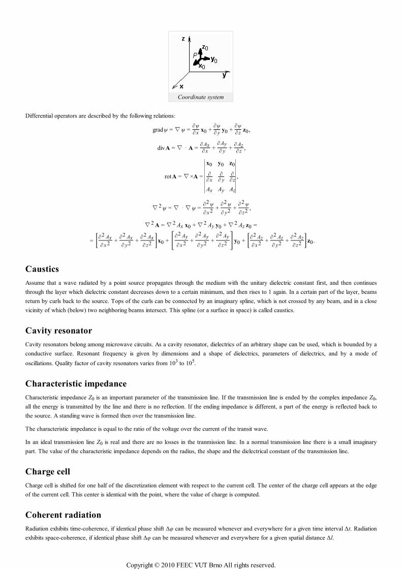
Coordinate system
Differential operators are described by the following relations:
grad ψ =∇ψ =∂ψ
∂ xx0 +
∂ψ
∂ yy0 +
∂ψ
∂ zz0,
div A =∇ ⋅A =∂ Ax∂ x
+∂ Ay
∂ y+
∂ Az∂ z
,
rot A =∇×A =
|
|
|||||
x0 y0 z0
∂∂ x
∂∂ y
∂∂ z
Ax Ay Az
|
|
|||||
,
∇2 ψ =∇ ⋅∇ψ =∂2 ψ
∂ x 2 +∂2 ψ
∂ y2 +∂2 ψ
∂ z2 ,
∇2 A =∇2 Ax x0 +∇2 Ay y0 +∇2 Az z0 =
= [∂2 Ax
∂ x 2 +∂2 Ax
∂ y2 +∂2 Ax
∂ z2 ]x0 + [∂2 Ay
∂ x 2 +∂2 Ay
∂ y2 +∂2 Ay
∂ z2 ]y0 + [∂2 Az
∂ x 2 +∂2 Az
∂ y2 +∂2 Az
∂ z2 ]z0 .
Caustics
Assume that a wave radiated by a point source propagates through the medium with the unitary dielectric constant first, and then continues
through the layer which dielectric constant decreases down to a certain minimum, and then rises to 1 again. In a certain part of the layer, beams
return by curls back to the source. Tops of the curls can be connected by an imaginary spline, which is not crossed by any beam, and in a close
vicinity of which (below) two neighboring beams intersect. This spline (or a surface in space) is called caustics.
Cavity resonator
Cavity resonators belong among microwave circuits. As a cavity resonator, dielectrics of an arbitrary shape can be used, which is bounded by a
conductive surface. Resonant frequency is given by dimensions and a shape of dielectrics, parameters of dielectrics, and by a mode of
oscillations. Quality factor of cavity resonators varies from 103 to 105.
Characteristic impedance
Characteristic impedance Z0 is an important parameter of the transmission line. If the transmission line is ended by the complex impedance Z0,
all the energy is transmitted by the line and there is no reflection. If the ending impedance is different, a part of the energy is reflected back to
the source. A standing wave is formed then over the transmission line.
The characteristic impedance is equal to the ratio of the voltage over the current of the transit wave.
In an ideal transmission line Z0 is real and there are no losses in the tranmission line. In a normal transmission line there is a small imaginary
part. The value of the characteristic impedance depends on the radius, the shape and the dielectrical constant of the transmission line.
Charge cell
Charge cell is shifted for one half of the discretization element with respect to the current cell. The center of the charge cell appears at the edge
of the current cell. This center is identical with the point, where the value of charge is computed.
Coherent radiation
Radiation exhibits time-coherence, if identical phase shift ∆φ can be measured whenever and everywhere for a given time interval ∆t. Radiation
exhibits space-coherence, if identical phase shift ∆φ can be measured whenever and everywhere for a given spatial distance ∆l.
Copyright © 2010 FEEC VUT Brno All rights reserved.

Collocation method
Method of weighted residua is called the collocation method when Dirac pulses play the role of weighting functions.
Continuity equation
Continuity equation describes the mutual relation between the time variation of a charge in a closed volume and currents, which flow out of this
volume
∇ ⋅ J = −∂ ρ
∂ t.
Outflow of current (divergence of current density) is equal to the decrease (therefore minus) of charge density per second.
Coulomb law
Assume two charges Q1 and Q2 in vacuum in the mutual distance d. Charges are of the opposite polarity and do not move. The charges
mutually attracts by a force, which magnitude is
F = 14πε0
Q1Q2d 2 .
The above-given relation expresses Coulomb law. The symbol π denotes Ludolf number and ε0 is permittivity of vacuum (ε0 = 8.85 * 10-12 F *
m-1).
Critical frequency
Critical frequency of a mode in a waveguide specifies a frequency, when the mode starts to propagate in the waveguide. If frequency is lower
than the critical one, then the mode does not propagate.
Cross polarization
Cross polarization equals to the ratio of an electric-field intensity component in a given plane (E or H) and of a component, which is
perpendicular to the previous one.
Crystal lattice
Ideal crystal lattice is a model arrangement of atoms in the volume of material. This arrangement has a periodic character and can be described
by the elementary cell, representing by a parallelepiped with the edge of length a in which individual particles are located. Edge length a is called
the lattice constant and it is an important parameter to describe the crystal structure.
Current cell
Current cell is identical with the discretization element in the analysis of planar antennas by moment method. Over the surface of the current
cell, a constant value of current is usually assumed.
Current distribution
Current, which flows into the dipole, reflects from the ends of the arms and returns back to the generator. The forward current and the
backward one interfere. In the position, where the forward current and the backward one are of the same phase, the maximum amplitude of the
current appears. In the position, where the forward current and the backward one are of the opposite phase, the minimum amplitude of the
current appears. Spatial course of the current amplitude is called the current distribution.
Current induction
If electromagnetic wave impacts a conductor, free charge carriers are set into a motion (induced currents appear). Induced currents become a
source of the secondary wave, which interferes with the primary one (impacting the conductor). The component of the total electric field
intensity vector, which is tangential to the conductive surface, is very small (is zero if the conductor is perfectly conductive).
Cylindrical coordinate system
It consists of a single curvilinear basis vector φ0 and two rectilinear basis vectors r0, z0. Basis vectors are mutually perpendicular (see figure). In
Copyright © 2010 FEEC VUT Brno All rights reserved.
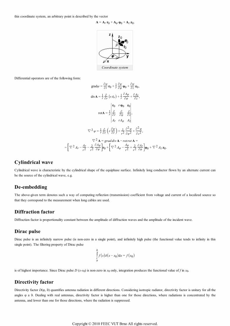
this coordinate system, an arbitrary point is described by the vector
A = Ar r0 + Aφ φ0 + Az z0.
Coordinate system
Differential operators are of the following form:
gradψ =∂ψ
∂rr0 + 1
r
∂ψ
∂φφ0 +
∂ψ
∂ zz0 ,
divA = 1r
∂∂r (rAr) + 1
r
∂ Aφ
∂φ+
∂ Az∂ z
,
rotA = 1r
|
|
|||||
r0 r φ0 z0
∂∂r
∂∂φ
∂∂ z
Ar rAφ Az
|
|
|||||
,
∇2 ψ = 1r
∂∂r (r
∂ψ
∂r ) + 1r2
∂2 ψ
∂φ2 +∂2 ψ
∂ z2 ,
∇2 A = grad div A − rot rot A =
=⎡⎣⎢∇2 Ar −
Ar
r2 − 2r2
∂ Aφ
∂φ
⎤⎦⎥r0 +
⎡⎣⎢∇2 Aφ −
Aφ
r2 + 2r2
∂ Ar∂φ
⎤⎦⎥φ0 +∇2 Az z0 .
Cylindrical wave
Cylindrical wave is characteristic by the cylindrical shape of the equiphase surface. Infinitely long conductor flown by an alternate current can
be the source of the cylindrical wave, e.g.
De-embedding
The above-given term denotes such a way of computing reflection (transmission) coefficient from voltage and current of a localized source so
that they correspond to the measurement when long cables are used.
Diffraction factor
Diffraction factor is proportionality constant between the amplitude of diffraction waves and the amplitude of the incident wave.
Dirac pulse
Dirac pulse is an infinitely narrow pulse (is non-zero in a single point), and infinitely high pulse (the functional value tends to infinity in this
single point). The filtering property of Dirac pulse
⌠⌡a
b
f (x)δ(x − x0)dx = f (x0)
is of highest importance. Since Dirac pulse D (x-x0) is non-zero in x0 only, integration produces the functional value of f in x0.
Directivity factor
Directivity factor D(φ, ϑ) quantifies antenna radiation in different directions. Considering isotropic radiator, directivity factor is unitary for all the
angles φ a ϑ. Dealing with real antennas, directivity factor is higher than one for those directions, where radiations is concentrated by the
antenna, and lower than one for those directions, where the radiation is suppressed.
Copyright © 2010 FEEC VUT Brno All rights reserved.
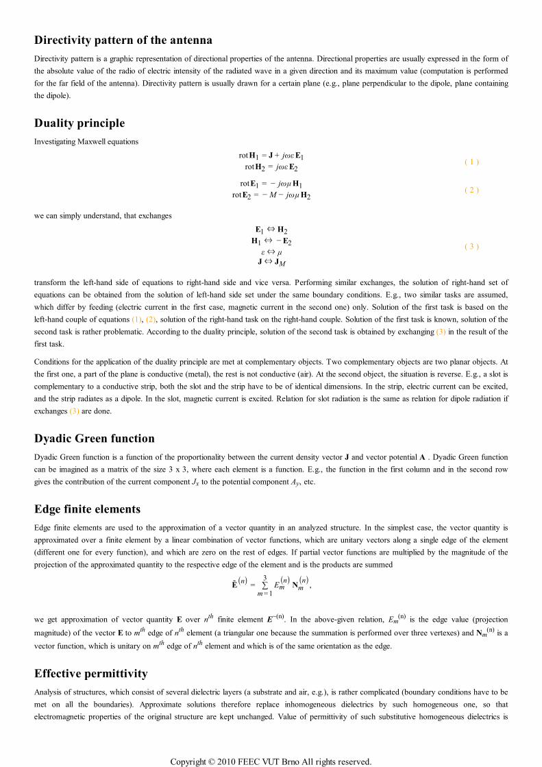
Directivity pattern of the antenna
Directivity pattern is a graphic representation of directional properties of the antenna. Directional properties are usually expressed in the form of
the absolute value of the radio of electric intensity of the radiated wave in a given direction and its maximum value (computation is performed
for the far field of the antenna). Directivity pattern is usually drawn for a certain plane (e.g., plane perpendicular to the dipole, plane containing
the dipole).
Duality principle
Investigating Maxwell equations
rot H1 = J + jωε E1rot H2 = jωε E2
( 1 )
rot E1 = − jωµ H1rot E2 = − M − jωµ H2
( 2 )
we can simply understand, that exchanges
E1 ⇔ H2H1 ⇔ − E2
ε⇔ µ
J⇔ JM
( 3 )
transform the left-hand side of equations to right-hand side and vice versa. Performing similar exchanges, the solution of right-hand set of
equations can be obtained from the solution of left-hand side set under the same boundary conditions. E.g., two similar tasks are assumed,
which differ by feeding (electric current in the first case, magnetic current in the second one) only. Solution of the first task is based on the
left-hand couple of equations (1), (2), solution of the right-hand task on the right-hand couple. Solution of the first task is known, solution of the
second task is rather problematic. According to the duality principle, solution of the second task is obtained by exchanging (3) in the result of the
first task.
Conditions for the application of the duality principle are met at complementary objects. Two complementary objects are two planar objects. At
the first one, a part of the plane is conductive (metal), the rest is not conductive (air). At the second object, the situation is reverse. E.g., a slot is
complementary to a conductive strip, both the slot and the strip have to be of identical dimensions. In the strip, electric current can be excited,
and the strip radiates as a dipole. In the slot, magnetic current is excited. Relation for slot radiation is the same as relation for dipole radiation if
exchanges (3) are done.
Dyadic Green function
Dyadic Green function is a function of the proportionality between the current density vector J and vector potential A . Dyadic Green function
can be imagined as a matrix of the size 3 x 3, where each element is a function. E.g., the function in the first column and in the second row
gives the contribution of the current component Jx to the potential component Ay, etc.
Edge finite elements
Edge finite elements are used to the approximation of a vector quantity in an analyzed structure. In the simplest case, the vector quantity is
approximated over a finite element by a linear combination of vector functions, which are unitary vectors along a single edge of the element
(different one for every function), and which are zero on the rest of edges. If partial vector functions are multiplied by the magnitude of the
projection of the approximated quantity to the respective edge of the element and is the products are summed
E(n) = ∑m = 1
3Em
(n)Nm
(n),
we get approximation of vector quantity E over nth finite element E~(n). In the above-given relation, Em(n) is the edge value (projection
magnitude) of the vector E to mth edge of nth element (a triangular one because the summation is performed over three vertexes) and Nm(n) is a
vector function, which is unitary on mth edge of nth element and which is of the same orientation as the edge.
Effective permittivity
Analysis of structures, which consist of several dielectric layers (a substrate and air, e.g.), is rather complicated (boundary conditions have to be
met on all the boundaries). Approximate solutions therefore replace inhomogeneous dielectrics by such homogeneous one, so that
electromagnetic properties of the original structure are kept unchanged. Value of permittivity of such substitutive homogeneous dielectrics is
Copyright © 2010 FEEC VUT Brno All rights reserved.
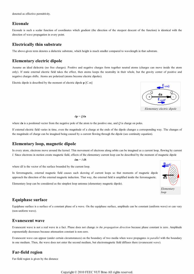
Elementary electric dipole
Elementary
loop
denoted as effective permittivity.
Eiconale
Eiconale is such a scalar function of coordinates which gradient (the direction of the steepest descent of the function) is identical with the
direction of wave propagation in every point.
Electrically thin substrate
The above-given term denotes a dielectric substrate, which height is much smaller compared to wavelength in that substrate.
Elementary electric dipole
Assume an ideal dielectric (no free charges). Positive and negative charges form together neutral atoms (charges can move inside the atom
only). If static external electric field takes the effect, then atoms keeps the neutrality in their whole, but the gravity center of positive and
negative charges shifts. Atoms are polarized (atoms become electric dipoles).
Electric dipole is described by the moment of electric dipole p [C.m]
dp = Qda
where da is a positional vector from the negative pole of the atom to the positive one, and Q is charge on poles.
If external electric field varies in time, even the magnitude of a charge at the ends of the dipole changes a corresponding way. The changes of
the magnitude of charge can be imagined being caused by a current flowing through the dipole (see continuity equation).
Elementary loop, magnetic dipole
In every atom, electrons move around the kernel. This movement of electrons along orbits can be imagined as a current loop, flowing by current
I. Since electrons in motion create magnetic field, effects of the elementary current loop can be described by the moment of magnetic dipole
dm = I dS
where dS is the vector of the surface bounded by the current loop.
In ferromagnetic, external magnetic field causes such skewing of current loops so that moments of magnetic dipole
approach the direction of the external magnetic induction. That way, the external field is amplified inside the ferromagnetic.
Elementary loop can be considered as the simplest loop antenna (elementary magnetic dipole).
Equiphase surface
Equiphase surface is a surface of a constant phase of a wave. On the equiphase surface, amplitude can be constant (uniform wave) or can vary
(non-uniform wave).
Evanescent wave
Evanescent wave is not a real wave in a fact. Phase does not change in the propagation direction because phase constant is zero. Amplitude
exponentially decreases because attenuation constant is non-zero.
Evanescent wave can appear (under certain circumstances) on the boundary of two media when wave propagates in parallel with the boundary
in one medium. Then, the wave does not enter the second medium, but electromagnetic field diffuses there (evanescent wave).
Far-field region
Far-field region is given by the distance
Copyright © 2010 FEEC VUT Brno All rights reserved.
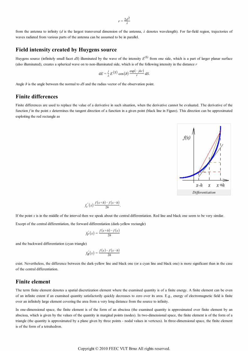
Differentiation
r = 2d 2
λ
from the antenna to infinity (d is the largest transversal dimension of the antenna, λ denotes wavelength). For far-field region, trajectories of
waves radiated from various parts of the antenna can be assumed to be in parallel.
Field intensity created by Huygens source
Huygens source (infinitely small facet dS) illuminated by the wave of the intensity E(S) from one side, which is a part of larger planar surface
(also illuminated), creates a spherical wave on to non-illuminated side, which is of the following intensity in the distance r
dE =j
λE(S) cos(ϑ) exp(− jkr)
r dS.
Angle ϑ is the angle between the normal to dS and the radius vector of the observation point.
Finite differences
Finite differences are used to replace the value of a derivative in such situation, when the derivative cannot be evaluated. The derivative of the
function f in the point x determines the tangent direction of a function in a given point (black line in Figure). This direction can be approximated
exploiting the red rectangle as
fc'(x) f (x +h)− f (x −h)
2h.
If the point x is in the middle of the interval then we speak about the central differentiation. Red line and black one seem to be very similar.
Except of the central differentiation, the forward differentiation (dark-yellow rectangle)
fF'(x) =
f (x +h)− f (x)2h
and the backward differentiation (cyan triangle)
fB'(x) =
f (x)− f (x −h)2h
exist. Nevertheless, the difference between the dark-yellow line and black one (or a cyan line and black one) is more significant than in the case
of the central differentiation.
Finite element
The term finite element denotes a spatial discretization element where the examined quantity is of a finite energy. A finite element can be even
of an infinite extent if an examined quantity satisfactorily quickly decreases to zero over its area. E.g., energy of electromagnetic field is finite
over an infinitely large element covering the area from a very long distance from the source to infinity.
In one-dimensional space, the finite element is of the form of an abscissa (the examined quantity is approximated over finite element by an
abscissa, which is given by the values of the quantity in marginal points (nodes). In two-dimensional space, the finite element is of the form of a
triangle (the quantity is approximated by a plane given by three points - nodal values in vertexes). In three-dimensional space, the finite element
is of the form of a tetrahedron.
Copyright © 2010 FEEC VUT Brno All rights reserved.
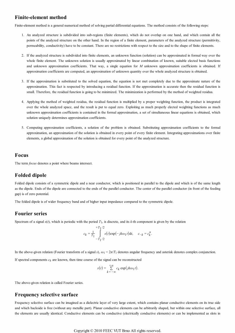
Finite-element method
Finite-element method is a general numerical method of solving partial differential equations. The method consists of the following steps:
An analyzed structure is subdivided into sub-regions (finite elements), which do not overlap on one hand, and which contain all the
points of the analyzed structure on the other hand. In the region of a finite element, parameters of the analyzed structure (permittivity,
permeability, conductivity) have to be constant. There are no restrictions with respect to the size and to the shape of finite elements.
1.
If the analyzed structure is subdivided into finite elements, an unknown function (solution) can be approximated in formal way over the
whole finite element. The unknown solution is usually approximated by linear combination of known, suitable elected basis functions
and unknown approximation coefficients. That way, a single equation for M unknown approximation coefficients is obtained. If
approximation coefficients are computed, an approximation of unknown quantity over the whole analyzed structure is obtained.
2.
If the approximation is substituted to the solved equation, the equation is not met completely due to the approximate nature of the
approximation. This fact is respected by introducing a residual function. If the approximation is accurate then the residual function is
small. Therefore, the residual function is going to be minimized. The minimization is performed by the method of weighted residua.
3.
Applying the method of weighted residua, the residual function is multiplied by a proper weighting function, the product is integrated
over the whole analyzed space, and the result is put to equal zero. Exploiting as much properly elected weighting functions as much
unknown approximation coefficients is contained in the formal approximation, a set of simultaneous linear equations is obtained, which
solution uniquely determines approximation coefficients.
4.
Computing approximation coefficients, a solution of the problem is obtained. Substituting approximation coefficients to the formal
approximation, an approximation of the solution is obtained in every point of every finite element. Integrating approximations over finite
elements, a global approximation of the solution is obtained for every point of the analyzed structure.
5.
Focus
The term focus denotes a point where beams intersect.
Folded dipole
Folded dipole consists of a symmetric dipole and a near conductor, which is positioned in parallel to the dipole and which is of the same length
as the dipole. Ends of the dipole are connected to the ends of the parallel conductor. The center of the parallel conductor (in front of the feeding
gap) is of zero potential.
The folded dipole is of wider frequency band and of higher input impedance compared to the symmetric dipole.
Fourier series
Spectrum of a signal s(t), which is periodic with the period T1, is discrete, and its k-th component is given by the relation
ck = 1T1
⌠⌡−T1 /2
+T1 /2
s(t)exp(− jkω1 t)dt, c−k = ck∗ .
In the above-given relation (Fourier transform of a signal s), ω1 = 2π/T1 denotes angular frequency and asterisk denotes complex conjunction.
If spectral components ck are known, then time course of the signal can be reconstructed
s(t) = ∑k = −∞
+∞ck exp( jkω1 t).
The above-given relation is called Fourier series.
Frequency selective surface
Frequency selective surface can be imagined as a dielectric layer of very large extent, which contains planar conductive elements on its true side
and which backside is free (without any metallic part). Planar conductive elements can be arbitrarily shaped, but within one selective surface, all
the elements are usually identical. Conductive elements can be conductive (electrically conductive elements) or can be implemented as slots in
Copyright © 2010 FEEC VUT Brno All rights reserved.
First Fresnel ellipsoid
continuous metallic true side (magnetically conductive elements).
If the true side of the selective surface is illuminated by harmonic waves of various frequencies, some waves are transmitted with a minimum
attenuation, some waves are totally reflected back to the half-space of the source, and some waves are partially transmitted and partially
reflected. Hence, the surface performs a frequency selection of incident waves.
Fresnel diffraction
The term Fresnel diffraction describes the wave diffraction, which appears when wave transmits a cut in a thin planar obstacle. The obstacle
neither transmits nor reflects the wave.
Fresnel integrals, klothoidy
Fresnel integrals are given by the relation
⌠⌡0
x
exp⎛⎝⎜− j
π
2ν2⎞
⎠⎟dν = ⌠⌡0
x
cos⎛⎝⎜
π
2ν2⎞
⎠⎟dν − j⌠⌡0
x
sin⎛⎝⎜
π
2ν2⎞
⎠⎟dν = C(x) − jS(x).
Their values can be computed by numerical integration in matlab, can be found in tables, can be read from klothoidy.
Klothoidy is a graphical representation of Fresnel integrals. On the horizontal axis, there is a real part of the integration result C(x ), on the
vertical axis, there is an imaginary part of the result S(x). In the above-described coordinate system, Fresnel integrals are of the form of a spiral
curve, which is scaled by the parameter x. If the value of Fresnel integrals is computed for a given value of argument x0, the value of argument
is found on the scale of the spiral curve, and then, the value of integrals C(x0) and S(x0) is directly read on the horizontal axis and the vertical
one.
Fresnel zones
In free space, assume a transmitter V and a receiver P as depicted in the figure. In an arbitrary planar cut, which is perpendicular to the line VP,
such points A1 are searched so that the pointed line VA1 P can be half wavelength longer than the direct distance VP. There is infinite number of
such points and form together a circle of the center in O . Surface bounded by this circle is so called first Fresnel zone, and OA1= r01 is its
radius. The same way, the other points A2, ... An can be found, which meet
V AnP = V P + nλ2.
The annulus surface between A2 and A1 is the second Fresnel zone, etc. Radius of nth zone can be computed using the approximate relation
r0n = OAn = n√ λd1d2
d1 +d2√ .
Repeating the above-described consideration for points A1 in different positions (cuts) along the line VP, different values of the radius of the first
Fresnel zone are obtained. All the points A1 are part of a rotational ellipsoid, which is called the first Fresnel ellipsoid.
Full-wave methods
Full-wave methods are based on the electromagnetic field description by complete Maxwell equations. Validity of full-wave methods is not
frequency-limited. On the other hand, full-wave methods require adoption of numerical approaches (analytical solution of Maxwell equations is
not known for planar structures), and hence, high computational power is needed.
Copyright © 2010 FEEC VUT Brno All rights reserved.
Galerkin method
If weighting functions are identical with basis ones in the method of weighting residua, we speak about Galerkin method.
Gaussian beam, Gaussian function
Assume a laser beam of the basic mode TEM00 , which leaves the source as parallel (equiphase surface is planar and perpendicular to the
direction of propagation, to the optical axis). Although the beam is not intentionally modulated, transversal field distribution is not constant.
Considering the above-mentioned mode, the maximum intensity is in the axis of the beam, and the intensity decreases towards margin of the
beam following Gaussian function:
E(x, y) = Emax exp(−ρ2
a02 ) = Emax exp(−
x 2 + y2
a02 ).
Here, r is radial distance from the axis of the beam, and the function is depicted in the figure. Beam, which is characteristic by the above-
described transversal Gaussian distribution of field intensity, is called Gaussian beam.
Gaussian beam, Gaussian function
General theory of diffraction
General theory of diffraction deals with the wave diffraction on obstacles of an arbitrary shape. Since the general approach is rather
complicated, results for relatively simple geometries are usually used only, and real obstacles are tried to be approximated by these objects (e.g.,
a conductor of finite length can be assumed as an extremely long ellipsoid).
Geometric theory of diffraction
Geometric theory of diffraction (GTD) is an extension of geometrical optics to the medium containing discontinuous inhomogeneities. We solve
the interaction of beams and obstacles, and laws of geometrical optics are completed that way, so that obvious incorrectness (discontinuities on
the boundary of reflection region and shade one) are eliminated on one hand, and the advantages of the geometrical optics (the idea of beams)
are preserved on the other hand.
Geometrical optics
Geometrical optics is a method for the solution of wave phenomena in complex media. The method adopted the conception of wave
propagation along beams from the classical geometrical optics. On the contrary, geometrical optics enables us to compute amplitude and phase
variations of field intensity and wave polarization when wave propagates in the media of continuously changing parameters.
Global basis functions
Global basis functions are of non-zero value over the whole analyzed area. As global basis functions, harmonic functions or Bessel ones are
usually used.
Green function
Copyright © 2010 FEEC VUT Brno All rights reserved.
Green function is a function of the proportionality between the current density vector J and vector potential A.
Hankel functions
Bessel differential equation
y″ + 1x y ′ +
⎛⎝⎜1 − ν 2
x 2⎞⎠⎟y = 0
is met even by the linear combination of Hankel functions of the first kind Hn(1)(x) and of the second kind Hn
(1)(x)
y = C3Hn(1)(x) + C3
' Hn(2)(x).
Hankel functions meet
Hn(1)(x) = Jn(x) + jNn(x),
Hn(2)(x) = Jn(x) − jNn(x).
Hertz vector
Assume ideal dielectrics, which is polarized by the external electric field. The vector of enforced electric polarization Pvn describes polarization.
Then, electric displacement vector can be expressed as
D = ε0 E + Pvn. ( 1 )
Substituting electric displacement vector D (1) to the first Maxwell equation, and assuming zero enforced current Jvn = 0 (induced current is
zero too, because the ideal dielectrics is of zero conductivity)
rot H − jωε0 E = jω Pvn . ( 2 )
Then, the third Maxwell equation can be rewritten to
div E = −div Pvn
ε0. ( 3 )
On the basis of (2) and (3), wave equation for vector potential can be obtained
∇2 A + k 2 A = − jωµ0 Pvn . ( 4 )
For the scalar potential, we get
∇2 φ + k 2φ =div Pvn
ε0. ( 5 )
We express potentials A and φ using an auxiliary vector Πe
A = jωµ0ε0Π e . ( 6 )
φ = − div Π e. ( 7 )
Substituting (6) to wave equation (4) and (7) to (5), we get
jωµ0ε0[∇2 Π e + k 2Π e +Pvnε0 ] = 0. ( 8 )
−div [∇2 Π e + k 2Π e +Pvnε0 ] = 0. ( 9 )
If vector πe is determined to meet the equation
∇2 Π e + k 2Π e = −Pvnε0
, ( 10 )
even (8) and (9) are met at the same time. That way, solution of Maxwell equations is transformed to the solution of a single inhomogeneous
equation when Jvn = 0. Hertz discovered this possibility, and the vector Πe is therefore called electric Hertz vector.
In dual way, magnetic Hertz vector can be introduced.
Huygens principle
Huygens principle says that every point of a closed surface S (more accurately, every elementary facet dS), which is illuminated by a wave
Copyright © 2010 FEEC VUT Brno All rights reserved.

arriving from outside, behaves as a source of an elementary spherical wave for the region inside the surface.
Huygens source, elementary source
The term Huygens source denotes infinitely small facet dS, which is illuminated by an incident wave from one side. Applying Huygens principle,
this facet becomes a source of an electromagnetic wave. Real surface sources of waves (horn antennas, slot antennas, illuminated parabolic
reflector) can be considered then as a set of Huygens sources.
Hybrid finite elements
If a shielded microstrip transmission line is analyzed using hybrid finite elements, all the components of electric field intensity or all the
components of magnetic field intensity are included into the computation. The matter of hybrid finite elements consists in modeling a
longitudinal intensity component by nodal approximation, and in modeling transversal intensity components by edge-vector approximation.
Impedance bandwidth
Impedance bandwidth can be defined as a frequency interval, where 90% of supplied energy enters the antenna (10% energy is reflected back
to the generator). The described situation corresponds approximately to the standing wave ratio equal 2.
Impedance transformer
On high frequencies, impedance transformer plays the same role as the classical transformer on lower frequencies: voltage, current and
impedance are transformed. Transformers differ in their construction.
As the simplest impedance transformer, one-quarter-wavelength-long transmission line can be used. The following relation describes such
transmission line:
Z0tr2 = Z0in Z0out .
Here, Z0tr 2 is squared value of characteristic impedance of transmission line. If the impedance Z0out ends the transmission line, then the
impedance Z0in appears at its input.
Inhomogeneous wave equation
The term homogeneous wave equation denotes the equation of the form
∇2 E + k 2 E = 0. ( 1 )
This equation is valid for Cartesian coordinate system. If vector E meets the equation then this vector describes wave propagation. If right-hand
side of the equation is zero, we are far away from the sources and wave is a source of a wave.
The right-hand side of the inhomogeneous wave equation is non-zero in contrast to (1)
∇2 E + k 2 E = jωµ Je. ( 2 )
In the right-hand side of (2), time derivative (jw) of the source current Je is present. This equation has to be applied if regions near sources
(antennas) are investigated.
Input impedance of the antenna, radiation impedance
Input impedance of the antenna can be measured at the input port of the antenna. Input impedance consists of the radiation resistance RΣ (when
multiplied by the squared input current Ivst2, real radiated power is obtained), of the loss-making resistance Rztr (Rztr Ivst
2 equals to the power,
which is converted to the heat in the antenna and its surrounding) and of the radiation reactance XΣ (describes the mutual energy exchange
between the antenna and the electromagnetic field in its surrounding). Radiation resistance and radiation reactance form the radiation impedance
together.
Ionospheric layer
The ultra-violet radiation of Sun ionizes atmospheric gases - the fission of molecules or atoms produce a positive ion and a negative electron. An
ionized layer of atmosphere is called the ionosphere. The ionosphere begins in the height of 40 km from the earth surface. Concentration of
electrons in the ionosphere varies with height, and significant local maxims can be observed. Intervals around local maxims are called
ionospheric layers.
Copyright © 2010 FEEC VUT Brno All rights reserved.
If electromagnetic wave impacts the ionospheric layer, then the wave trajectory is curved, and under proper conditions, the wave can return
back to the earth.
Isotropic medium, anisotropic medium
Isotropic medium is of the same electric and magnetic properties in all the directions (of the same permittivity and permeability). Therefore,
magnitude of the x-component of electric displacement density Dx depends on the magnitude of the x-component of the electric field intensity
Ex only:
Dx = εEx , Dy = εEy , etc.
From the mathematical point of view, permittivity and permeability are scalar quantities.
Anisotropic medium is of different properties in different directions. Therefore, the x-component of the electric displacement density Dx
depends (in general) on all the three components of electric field intensity:
Dx = εxx Ex + εxyEy + εxzEz.
From the mathematical point of view, permittivity and permeability are tensors, i.e. matrices of the size 3 x 3. Plasma, where steady magnetic
field exists, or steady-magnetized ferrite, are examples of anisotropic media.
Lagrange interpolation polynomials
Lagrange polynomial of degree n can be in general expressed using the simplex coordinate x as
Rm(n, ξ) = 1m ! ∏
k =0
m −1(nξ − k) m ≥ 1 R0(n, ξ) = 1.
Here, n is degree of the approximation polynomial. Equation describes the whole family of polynomials; members of the family differ an index
m, which can vary from zero to n.
Nulls of polynomials Rm(n) are equidistantly distributed on coordinates x=0, 1/n to (m-1)/n, polynomial is of unitary value in x = m/n. Therefore,
Rm(n) contains m equidistantly distributed nulls on the left from x = m/n and no null on the right.
Linear antenna
Linear antenna can be composed of a finite number of elementary dipoles. On the contrary, planar antennas can be composed of a finite
number of Huygens sources.
Linear combination
The term linear combination of vectors (functions) denotes such vector (such function), which is obtained by adding primary vectors (primary
functions) that are multiplied by arbitrary scalar non-zero coefficients.
Linear medium
Permittivity and permeability of a linear medium are constants, which are independent on intensities E and H. If electric field intensity is
increased then electric displacement density proportionally rises. If magnetic field intensity is increased then magnetic flux density proportionally
rises.
Local basis functions
Local basis functions are of non-zero value over a single (or a few) discretization element, and over the rest of elements, they are zero.
Piecewise constant or piecewise linear function are typical representatives of local basis functions.
Longitudinally homogeneous waveguide
The term longitudinally homogeneous waveguide expresses the fact that waveguide parameters are constant in the longitudinal direction. If the
waveguide is lossless, only phase of the wave changes in the longitudinal direction (amplitude stays constant).
Lorenz force
The force acting on a charged particle depends only on its position, speed and amount of charge. The force acting on the elementary charge can
Copyright © 2010 FEEC VUT Brno All rights reserved.

be written as
F = q(E + v×B),
where E and B is the electric field and magnetic induction at the position of the hub.
Matrix optics, matrix of beam, ABCD law
Matrix of beam is a matrix of size 2 x 2, which describes changes of Gaussian beam parameters when passing through an optical element. If
matrix is multiplied (from the right-hand side) by a column vector, which contains beam parameters at the input of an optical element, we obtain
a column vector of beam parameters at its output. The relation is called ABCD law. Due to the matrix nature of above-described operations, we
speak about matrix optics.
Method of induced electromotoric forces, mutual impedance, self-impedance
The method helps us to compute voltages, currents and impedances in antenna systems. The method understands the voltage, which is
observed at the input port of every single antenna element, being induced by the radiation of all the antenna elements (including the own
element). The voltage can be composed from contributions of single elements. Each contribution is proportional to the current of the respective
element. E.g., voltage U1 at the input of the first antenna element equals to the summation
U1 = Z11 I1 + Z12 I2 + Z13 I3 + …
where I1, I2, I3 are currents at the input ports of single elements, Z11, Z12, Z13 are impedances. Z11 is self-impedance, Z1n are mutual
impedances between the first element and the other elements in the antenna system. These impedances depend on the mutual position and
mutual distance of antenna elements.
Microstrip antenna, microstrip dipole, patch antenna
The term microstrip antenna denotes all the antennas, which are fabricated by the microstrip technology. In this textbook, a microstrip dipole
(narrow microstrip conductor on the true side of the substrate, which is interrupted by a feeding gap) and a patch antenna (rectangular antenna
element of the true side of the substrate, which can be fed by a microstrip, by a coaxial probe, or by an aperture in the ground plane) belong to
this class of antennas.
Microstrip transmission line, ground plane
Microstrip transmission line consists of a very thin and relatively narrow strip line, which is placed to a true side of a dielectric substrate. The
backside of the substrate is covered by continuous metallic layer and serves as a ground plate of zero potential. The whole transmission line is
usually put into a rectangular waveguide, which plays to role of shielding. All the metallic parts of the structure (microstrip, ground plate,
metallic waveguide) have to be fabricated from a well-conducting electric conductor in order to reach as low attenuation as possible. Considering
the same reason, dielectric substrate has to be of as low losses as possible.
Microwave frequency band
Microwave frequency band denotes the interval of frequencies from 300 MHz to 300 GHz. Those frequencies correspond to the wavelengths
from 1 m to 1 mm in a free space (in vacuum).
Mirror principle
The mirror principle enables simple modeling of the effect of well-conductive planes, which are near a radiating antenna. The radiation induces
currents on the surface of the plane, which contribute to the antenna radiation as well. According to the mirror principle, contribution of induced
currents equals to the contribution of a mirror images of real antenna elements. A vertical element mirrors with a current of the identical
amplitude and phase. A horizontal element mirrors with a current of the identical amplitude and opposite phase.
Modal analysis of patch antennas
For modal analysis the planar antenna is modeled as a resonant cavity with perfect electric walls at the top and bottom. The main restriction is
that the thickness of the dielectric substrate must be much smaller than the wavelength. Then the variance of the electric field in the plane
perpendicular to the patch (axis z) is negligible. Because of the applied boundary conditions the electric field is non-zero only along the axis z,
whereas the magnetic field has non-zero components only in the x-y plane. Along the boundaries of the metallic patch the Neumann condition
for electric field is valid. It expresses the fact that the derivative of the electric field intensity vector normal to the perfect magnetic conductor
has to be zero (∂E/∂n = 0). It implies the boundaries of the patch can be considered as perfect magnetic conductor.
Copyright © 2010 FEEC VUT Brno All rights reserved.
Modes, mode numbers, dominant mode, band of unimodality
Waves propagating in a waveguide are characterized by a given transversal field distribution. The wave of a given transversal field distribution is
denoted as a given mode of a wave. Every mode can be characterized by a given critical frequency, a given phase velocity, a given wavelength
and a given group velocity. The mode of the lowest critical frequency is called the dominant mode. The frequency band, in which a single mode
of a wave propagates in the waveguide, is called the band of unimodality.
Every mode is characterized by integer constants. Those constants are called mode numbers. Considering rectangular waveguide, mode
numbers specify the number of half-waves of standing waves in the directions of transversal coordinates. E.g. TM11 (transversal magnetic
wave) is of a single half-wave of the longitudinal component of electric field intensity in x and a single half-wave in y (if z is identical with
waveguide axis). Considering TE10 (transversal electric wave, the dominant mode of a rectangular waveguide), a single half-wave of the
longitudinal component of magnetic field intensity appears in x, and in y , this component is constant.
Moment method in spectral domain, spatial domain
Temporal-spatial distribution of electromagnetic field is described by the term exp[j(ω t-kr)], where ω is angular frequency (a change of a phase
over one second), t denotes time, k is wave-number (variation of phase over 1 meter in a given direction, i.e. spatial frequency), and r denotes
length (in a given direction).
Space-domain analysis is based on computations for a single value of the spatial frequency k (the distance r is a variable). In spectral-domain
analysis, the distance r is considered as a constant, and computations are performed for all the possible spatial frequencies k.
Moment method, moment solution
Moment method is a numeric method of solving integral equations (a sought function, e.g. current distribution on the antenna, is included in the
integrated function). The method consists in the discretization of the analyzed structure, in formal approximation of the sought function (known
basis functions and unknown approximation coefficients), in substituting the formal approximation to the solved equation (unknown
approximation coefficients are removed from the integrated function and known basis functions are integrated), in minimizing the approximation
error (the solved equation containing the formal approximation is sequentially multiplied by Dirac pulses in the center of discretization elements
and the product is integrated over the whole analyzed structure - we obtain N equations for N unknown approximation coefficients) and in
solving the final matrix equation (unknown approximation coefficients, and therefore, the approximation of the solution is obtained).
Moment table
The term moment table denotes a matrix, which contains mutual contributions among single charge cells and current ones.
Nodal finite elements
Nodal finite elements serve to piecewise continuous approximation of a scalar quantity in an analyzed structure. In the simplest case, the scalar
quantity is approximated by linear function over a finite element. The linear approximation is composed of partial linear functions, which are
unitary in a given vertex of the element (different one for every function) and which are zero in the rest of vertexes. If partial linear functions
are multiplied by the value of the approximated quantity in such vertex of the element (in such node), where the function is of unitary value, and
the products are summed
E(n) = ∑m = 1
3Em
(n)Nm
(n)
we get a linear approximation of E over nth finite element E~(n). In the above-given relation, Em(n) is a nodal value of the quantity E in mth node
(vertex) of nth finite element (a triangular one because the summation is performed over three vertexes) and Nm(n) is a linear function, which is
unitary in mth node of nth element.
Considering the above-described nodal approximation, the nodal values of the quantity Em are spatial samples of the approximated quantity E.
Nodal value
The term nodal value denotes the value of a sought function in a given, exactly defined point (node). If piecewise constant approximation is
used, then nodes are usually positioned to the center of discretization elements.
Parallel polarization of wave
In the case of the parallel polarization, the vector E of the wave is parallel with the plane of incidence.
Copyright © 2010 FEEC VUT Brno All rights reserved.

Paraxial waves
Paraxial waves are waves, which directions of propagation are nearly the same (they mutually decline for a very small angle). We speak about
paraxial waves if their sum is of a special meaning. E.g., a single non-uniform wave propagating in z-direction can be expressed as a sum of
paraxial uniform waves, which propagate in directions those slightly decline z.
Perpendicular polarization of wave
In the case of perpendicular polarization, the vector E of the wave is perpendicular to the plane of incidence.
Perpendicular polarization, parallel polarization
Polarization describes orientation of the vector of electric field intensity of a wave.
If wave propagates near the boundary of two media, we distinguish the perpendicular polarization and the parallel polarization. First, the plane
of incidence is defined as a plane, which is perpendicular to the plane of boundary and which is parallel to the direction of propagation. The
vector E of the perpendicularly polarized wave is perpendicular to the plane of incidence. The vector E of the wave polarized in parallel is
parallel to the plane of incidence.
If the plane of boundary is identical with the earth surface, then perpendicular polarization is called horizontal polarization, and the parallel
polarization is called the vertical polarization.
Phase velocity, group velocity
Phase velocity determines the change of phase of wave per second. Phase velocity is not associated with the velocity of energy transmission,
and therefore, it can be higher than velocity of light in vacuum c = 3 * 10+8 m/s. Phase velocity tends to infinity in all directions lying on the
equiphase surface (i.e. on the surface associating points of the same phase): the phase changes for 2π radians within infinitely short time period
here.
On the other hand, group velocity determines the speed of energy transmission. Since in the directions, which lie on the wave-surface, energy is
not transmitted (wave-surface is perpendicular to the propagation direction), group velocity is zero here.
In common media, phase velocity and group one are mutually related according to
vf vg = v2 .
Here vf denotes phase velocity, vg is group velocity, and v is free-space velocity of light.
Phonon
This is a quasi-paticle, which was introduced to represent the quantum vibrational energy of the crystal lattice. Using these particles we can
describe the propagation of sound (mechanical) waves in crystals.
Planar microwave transmission line
The term planar microwave transmission line denotes a structure consisting of a metallic planar ground plate and of one or more plan-parallel
planar conductors (metallic strips as electric conductors or slots in metallic plate as magnetic conductors). Various dielectric layers differing in
their electric or magnetic parameters can complete the structure. Planar transmission line can be open (just described) or shielded (placed into a
metallic waveguide.
Plane E, plane H
Magnetic lines of waves radiated by the antenna determine the plane H. Considering the dipole, plane H is perpendicular to the axis of the
dipole.
Electric lines of waves radiated by the antenna determine the plane E. Considering the dipole, all planes containing the dipole are plane E.
Plane of boundary
Plane of boundary is a plane, which separates two media of different electric properties and magnetic ones.
Plane of incidence
Copyright © 2010 FEEC VUT Brno All rights reserved.

Plane of incidence is perpendicular to the plane of boundary and is parallel with the propagation direction of the incident wave
Plane wave
Plane wave is characteristic by the planar equiphase surface (connecting points of the same phase, a plane is obtained). As a plane wave, we can
consider a wave in a very long distance form the source when observed in a very small part of the space (in the frame of a large region, the
wave is already of the spherical nature).
Point source
The term point source denotes such source of electromagnetic waves, which the only ability is the radiation ability. The source is of zero weight
and zero size.
Polarization of dielectrics
Dielectrics do not contain free charge carriers. Dielectrics consist of atoms, where the positive charge of the kernel equals to the negative charge
of the electrons. If the dielectrics are inserted into the external electric field, the kernel of positive charge is deflected in the contra-direction of
the external electric-field intensity, and electrons of the negative charge are deflected in the direction of the external electric field. In dielectrics,
an inner electrical field appears, which intensity is of the opposite orientation than the intensity of the external one. Therefore, the external
electric field is weakened in the dielectrics.
Poynting vector
From the mathematical point of view, Poynting vector can be computed as vector product of electric field intensity vector and complex
conjugated magnetic one. Direction of Poynting vector is identical with the direction of energy propagation. In most situations, magnitude of
Poynting vector equals to the surface power density of a wave.
Propagation constant, attenuation constant, phase constant
Propagation constant γ describes variation of amplitude and variation of phase of a wave in the longitudinal direction in a waveguide.
Propagation constant is given by the relation
γ = β + jα.
Here, β is attenuation constant and α is phase constant). Attenuation constant describes the amplitude decrease on the trajectory 1 meter long;
the amplitude decreases to exp(-β) - multiple of its initial value. Phase constant describes the phase variation on the trajectory 1 meter long in
the direction of wave.
Quality factor of a resonator
Quality factor of an arbitrary resonant circuit of angular frequency ω0 is given by
Q =ω0W
PZ
where W is energy of electromagnetic field in a circuit, and PZ is lost power in a circuit.
Quasi-static analysis, full-wave analysis
Quasi-static analysis of a microstrip transmission line consists in modeling a dominant mode (mode quasi-TEM) propagating along the line, by a
transversal electromagnetic wave. Field distribution of such wave can be determined by a static analysis of the structure (microstrip is assumed
to be of the potential 1 Volt, the shielding waveguide is grounded). Quasi-static analysis gives good results typically below 5 GHz.
If a microstrip transmission line is going to be analyzed on higher microwave frequencies, then full-wave methods have to be applied, which are
based on a direct solution of Maxwell equations.
Quasi-static methods
Quasi-static methods of the analysis of planar microwave transmission lines are based on the assumption that the dominant wave propagating
along the microstrip transmission line can be satisfactorily approximated by the transversal electromagnetic wave, TEM. Then, transversal
components of the dynamic electromagnetic field are close to the components of the static field. Therefore, the approximate field distribution in
the transmission line can be obtained by solving Laplace equation for scalar potential.
Copyright © 2010 FEEC VUT Brno All rights reserved.

Radome
The term radome denotes an antenna cover, which should protect an antenna to the influence of the surrounding (rain, insects, birds, etc.). The
antenna cover should even form a proper interface, which enables to reach desired properties of the antenna (minimal transmission losses,
minimal influence to antenna parameters, etc.).
Rayleigh distance
From a certain distance (Rayleigh distance), wave does not propagate in directions, which correspond to the parallel beams, but it propagates in
directions, which correspond to divergent beams.
Reflection coefficient, transmission coefficient
Reflection coefficient is defined as a ratio of the magnitude of a certain component of electric field intensity of a wave, which is reflected from
an obstacle, and the same component of electric field intensity of incident wave. As an obstacle, we assume an object, which is large enough in
the direction transversal to the direction of wave propagation (there is no diffraction there). The obstacle is of different electrical parameters
than the surrounding.
Transmission coefficient is defined as a ratio of the magnitude of a certain component of electric field intensity of a wave, which transmitted
through an obstacle, and the same component of electric field intensity of incident wave.
Reflector antennas
Reflector antennas consist of a primary radiator (a dipole, e.g.) and a reflector (parabolic one, e.g.). If plane wave is incident to such a reflector,
the reflector concentrates all the energy in the focus. If a primary antenna is positioned to the focus, a strong power appears at its output.
Refractive index
Refractive index is given by the ratio of wave number in a given medium and wave number in the vacuum. In lossless medium, we get
n =εµ
ε0 µ0√ = εr µr√ .
Other words - refractive index says, how longer is wavelength in the vacuum comparing to the wavelength in a given medium.
Resonant resistance
The term denotes input resistance of a patch antenna in resonance (the patch length equals to the half of wavelength). Magnitude of resonant
resistance can be influenced by the patch width and by the position of the antenna input (in patch is fed by a microstrip, then feeder is immersed
into the patch).
Scalar Green function
Scalar Green function is a function of the proportionality between the charge density ρ and scalar potential V.
Scalar potential
Scalar potential simplifies the investigation of the influence of static charges (time derivative equals to zero). Field is then described by the first
and the third Maxwell equation in the form
rot E = 0,div E = 0.
( 1 )
Since curl of gradient identically equals to zero, (1) is met if
E = − grad φ, ( 2 )
(j is scalar potential). Hence, the single scalar equation (Laplace one) has to be solved
∇2 φ = 0. ( 3 )
Eqn. (3) is valid in every region, where potential is finite and continuous. Thanks to (3), the field is described by a single partial differential
equation for a scalar function j.
Physical notion j can be built on the basis of (2)
Copyright © 2010 FEEC VUT Brno All rights reserved.
E⋅ dr = − grad φ ⋅ dr = − dφ.
Since the product E .d r equals to the work, which is performed by the field when moving unitary charge along the elementary path dr,
elementary potential dj equals to the decrease (therefore minus) of the potential energy of this unitary charge in electrostatic field.
Shape function
The term shape function denotes a partial approximation function over a single finite element, which is unitary in a single node and which is zero
in the rest of nodes. Among the most frequently used shape functions, a liner function belongs: a plane, which is unitary in a single node and
which slopes down to zero in the rest of nodes.
All the shape functions, which are unitary in a common node, form a basis function together. In a two-dimensional case, linear basis function is
a pyramid, which is unitary in a common node, and which slopes down to zero on edges of all the finite elements, which share the common
node.
Sign convention
Temporal-spatial distribution of a harmonic wave is usually described by the term exp(+jwt - jkr), where angular frequency ω describes the
phase change within one second and wave-number k the phase change within one meter. Moving in time, the phase increases. Moving in space
in the direction of propagation, the phase decreases.
If signs in the exponential term are swapped to exp(-jwt+ jkr), then the matter of studied phenomena does not change (all the laws stay valid).
Nevertheless, we have to say which sign convention is used and we have to keep the same convention during the whole computation. If some
mathematical relation is going to be transformed from one convention to the second one, only signs at all the imaginary units have to be changed
(+j « -j).
Simplex coordinates
Considering triangular finite element, simplex coordinate axes are of the same orientation as the triangle heights. Simplex coordinates are unitary
in the vertex and zero on the opposite edge. Simplex coordinates depend neither on the shape nor on the size of the triangle. Therefore,
computations can be performed for only one finite element, and results can be recomputed then to an arbitrary triangle.
Dealing with physical matter of simplex coordinates, a general point P inside the triangle subdivides its surface to three partial triangles. Ratio of
the surface of a partial triangle, lying opposite to the first node, to the surface of the whole finite element, equals to the coordinate of P on the
first simplex coordinate axis (similarly, the second coordinate and the third one can be obtained). Obviously, sum of all the three simplex
coordinates equals to one.
Small numbers computing
Assume a very small scalar value x << 1. Then, following approximate relations are valid:
(1 ± x)n≅ 1 ± nx,
e.g.
(1 ± x)n≅ 1 ± 2x, 1 ± x2√ ≅ 1 ± x
2 , 11± x
≅ 1 ∓ x.
Bessel functions:
J0(x) ≅ 1, J1(x) ≅ x2 .
Neumann functions:
N0(x) ≅2π
⎡⎣ln x2 + γ
⎤⎦, N1(x) ≅ − 2x π + N0(x)J1(x).
Snell law
Snell law describes the relation between the angle q (under this angle, wave impacts the planar boundary of two media), and the angle q2 (angle
between the direction of propagation and the normal to the boundary in the second medium). If refraction index of the first medium is n1 (wave
leaves this medium), and refraction index of the second medium is n2 (wave enters this medium), then angles are related by the following
equation:
n1 sin(Θ1) = n2 sin(Θ2).
Copyright © 2010 FEEC VUT Brno All rights reserved.
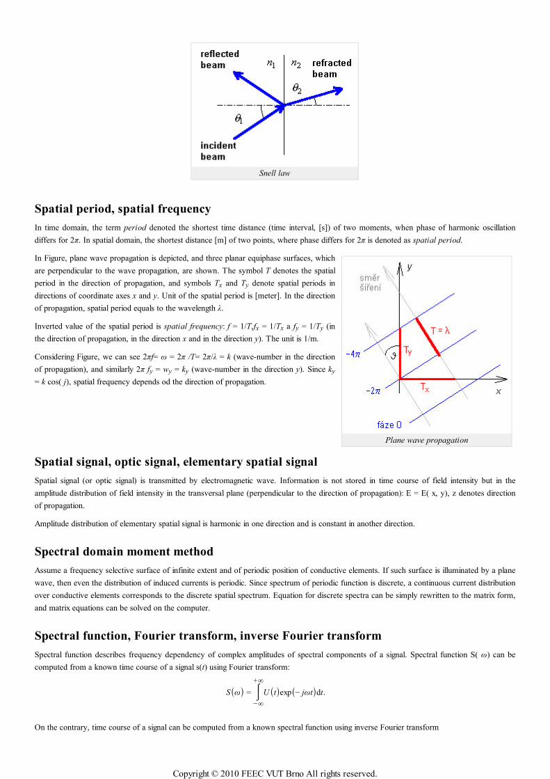
Plane wave propagation
Snell law
Spatial period, spatial frequency
In time domain, the term period denoted the shortest time distance (time interval, [s]) of two moments, when phase of harmonic oscillation
differs for 2π. In spatial domain, the shortest distance [m] of two points, where phase differs for 2π is denoted as spatial period.
In Figure, plane wave propagation is depicted, and three planar equiphase surfaces, which
are perpendicular to the wave propagation, are shown. The symbol T denotes the spatial
period in the direction of propagation, and symbols Tx and Ty denote spatial periods in
directions of coordinate axes x and y. Unit of the spatial period is [meter]. In the direction
of propagation, spatial period equals to the wavelength λ.
Inverted value of the spatial period is spatial frequency: f = 1/T,fx = 1/Tx a fy = 1/Ty (in
the direction of propagation, in the direction x and in the direction y). The unit is 1/m.
Considering Figure, we can see 2πf= ω = 2π /T= 2π/λ = k (wave-number in the direction
of propagation), and similarly 2π fy = wy = ky (wave-number in the direction y). Since ky
= k cos( j), spatial frequency depends od the direction of propagation.
Spatial signal, optic signal, elementary spatial signal
Spatial signal (or optic signal) is transmitted by electromagnetic wave. Information is not stored in time course of field intensity but in the
amplitude distribution of field intensity in the transversal plane (perpendicular to the direction of propagation): E = E( x, y), z denotes direction
of propagation.
Amplitude distribution of elementary spatial signal is harmonic in one direction and is constant in another direction.
Spectral domain moment method
Assume a frequency selective surface of infinite extent and of periodic position of conductive elements. If such surface is illuminated by a plane
wave, then even the distribution of induced currents is periodic. Since spectrum of periodic function is discrete, a continuous current distribution
over conductive elements corresponds to the discrete spatial spectrum. Equation for discrete spectra can be simply rewritten to the matrix form,
and matrix equations can be solved on the computer.
Spectral function, Fourier transform, inverse Fourier transform
Spectral function describes frequency dependency of complex amplitudes of spectral components of a signal. Spectral function S( ω) can be
computed from a known time course of a signal s(t) using Fourier transform:
S(ω) = ⌠⌡
−∞
+∞
U(t)exp(− jωt)dt.
On the contrary, time course of a signal can be computed from a known spectral function using inverse Fourier transform
Copyright © 2010 FEEC VUT Brno All rights reserved.
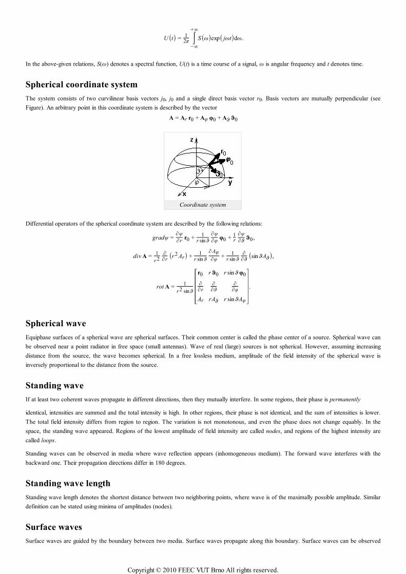
U(t) = 12π
⌠⌡−∞
+∞
S(ω)exp( jωt)dω.
In the above-given relations, S(ω) denotes a spectral function, U(t) is a time course of a signal, ω is angular frequency and t denotes time.
Spherical coordinate system
The system consists of two curvilinear basis vectors j0, j0 and a single direct basis vector r0. Basis vectors are mutually perpendicular (see
Figure). An arbitrary point in this coordinate system is described by the vector
A = Ar r0 + Aφ φ0 + Aϑ ϑ0
Coordinate system
Differential operators of the spherical coordinate system are described by the following relations:
gradψ =∂ψ
∂rr0 + 1
r sin ϑ
∂ψ
∂φφ0 + 1
r
∂ψ
∂ϑϑ0 ,
div A = 1r2
∂∂r (r2 Ar) + 1
r sin ϑ
∂ Aφ
∂φ+ 1
r sin ϑ∂
∂ϑ (sin ϑAϑ),
rot A = 1r2 sin ϑ
⎡
⎣
⎢⎢⎢⎢⎢
r0 r ϑ0 r sin ϑ φ0
∂∂r
∂∂ϑ
∂∂φ
Ar rAϑ r sin ϑAφ
⎤
⎦
⎥⎥⎥⎥⎥.
Spherical wave
Equiphase surfaces of a spherical wave are spherical surfaces. Their common center is called the phase center of a source. Spherical wave can
be observed near a point radiator in free space (small antennas). Wave of real (large) sources is not spherical. However, assuming increasing
distance from the source, the wave becomes spherical. In a free lossless medium, amplitude of the field intensity of the spherical wave is
inversely proportional to the distance from the source.
Standing wave
If at least two coherent waves propagate in different directions, then they mutually interfere. In some regions, their phase is permanently
identical, intensities are summed and the total intensity is high. In other regions, their phase is not identical, and the sum of intensities is lower.
The total field intensity differs from region to region. The variation is not monotonous, and even the phase does not change equably. In the
space, the standing wave appeared. Regions of the lowest amplitude of field intensity are called nodes, and regions of the highest intensity are
called loops.
Standing waves can be observed in media where wave reflection appears (inhomogeneous medium). The forward wave interferes with the
backward one. Their propagation directions differ in 180 degrees.
Standing wave length
Standing wave length denotes the shortest distance between two neighboring points, where wave is of the maximally possible amplitude. Similar
definition can be stated using minima of amplitudes (nodes).
Surface waves
Surface waves are guided by the boundary between two media. Surface waves propagate along this boundary. Surface waves can be observed
Copyright © 2010 FEEC VUT Brno All rights reserved.
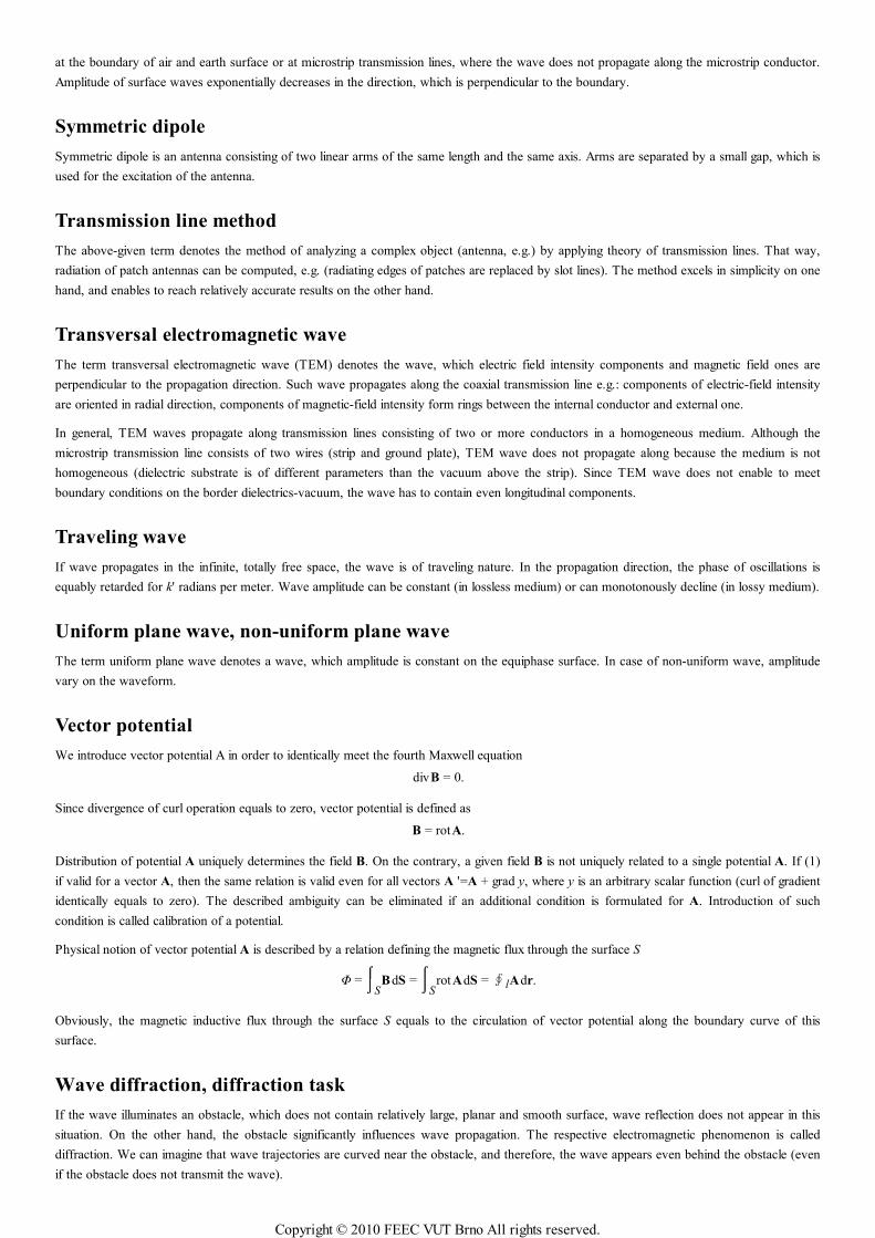
at the boundary of air and earth surface or at microstrip transmission lines, where the wave does not propagate along the microstrip conductor.
Amplitude of surface waves exponentially decreases in the direction, which is perpendicular to the boundary.
Symmetric dipole
Symmetric dipole is an antenna consisting of two linear arms of the same length and the same axis. Arms are separated by a small gap, which is
used for the excitation of the antenna.
Transmission line method
The above-given term denotes the method of analyzing a complex object (antenna, e.g.) by applying theory of transmission lines. That way,
radiation of patch antennas can be computed, e.g. (radiating edges of patches are replaced by slot lines). The method excels in simplicity on one
hand, and enables to reach relatively accurate results on the other hand.
Transversal electromagnetic wave
The term transversal electromagnetic wave (TEM) denotes the wave, which electric field intensity components and magnetic field ones are
perpendicular to the propagation direction. Such wave propagates along the coaxial transmission line e.g.: components of electric-field intensity
are oriented in radial direction, components of magnetic-field intensity form rings between the internal conductor and external one.
In general, TEM waves propagate along transmission lines consisting of two or more conductors in a homogeneous medium. Although the
microstrip transmission line consists of two wires (strip and ground plate), TEM wave does not propagate along because the medium is not
homogeneous (dielectric substrate is of different parameters than the vacuum above the strip). Since TEM wave does not enable to meet
boundary conditions on the border dielectrics-vacuum, the wave has to contain even longitudinal components.
Traveling wave
If wave propagates in the infinite, totally free space, the wave is of traveling nature. In the propagation direction, the phase of oscillations is
equably retarded for k' radians per meter. Wave amplitude can be constant (in lossless medium) or can monotonously decline (in lossy medium).
Uniform plane wave, non-uniform plane wave
The term uniform plane wave denotes a wave, which amplitude is constant on the equiphase surface. In case of non-uniform wave, amplitude
vary on the waveform.
Vector potential
We introduce vector potential A in order to identically meet the fourth Maxwell equation
div B = 0.
Since divergence of curl operation equals to zero, vector potential is defined as
B = rot A.
Distribution of potential A uniquely determines the field B. On the contrary, a given field B is not uniquely related to a single potential A. If (1)
if valid for a vector A, then the same relation is valid even for all vectors A '=A + grad y, where y is an arbitrary scalar function (curl of gradient
identically equals to zero). The described ambiguity can be eliminated if an additional condition is formulated for A. Introduction of such
condition is called calibration of a potential.
Physical notion of vector potential A is described by a relation defining the magnetic flux through the surface S
Φ = ⌠⌡S
B dS = ⌠⌡S
rot A dS =∮lA dr.
Obviously, the magnetic inductive flux through the surface S equals to the circulation of vector potential along the boundary curve of this
surface.
Wave diffraction, diffraction task
If the wave illuminates an obstacle, which does not contain relatively large, planar and smooth surface, wave reflection does not appear in this
situation. On the other hand, the obstacle significantly influences wave propagation. The respective electromagnetic phenomenon is called
diffraction. We can imagine that wave trajectories are curved near the obstacle, and therefore, the wave appears even behind the obstacle (even
if the obstacle does not transmit the wave).
Copyright © 2010 FEEC VUT Brno All rights reserved.

As diffraction, even the other phenomena are explained although the trajectory curvature is not obvious at the first sight (e.g., some cases of
guiding waves). In all the situations, the electromagnetic wave mutually interacts with some substantial object of different electrical parameters
(permittivity, conductivity, permeability).
Wave dispersion
The term dispersion describes the phenomenon when signals on different frequencies propagate by different velocities. Different frequency
components are of different delays at the output, and therefore, they represent a signal, which differs from the input one (signal is distorted).
Wave equation
Wave equation is second-order differential equation for the intensity vector of electric field or the magnetic one. If field intensities meet wave
equation, the field is of the form of wave.
Considering intensity of harmonic electric field, wave equation is of the form
∇2 E + k2 E = jωµ Jvn .
Here, ∇ is differential operator (in Cartesian coordinates, ∇f = [∂f/∂x; ∂f/∂y;∂f/∂z]), E is the vector of electric field intensity, k denotes wave
number, ω is angular frequency of harmonic wave, µ denotes permeability of the medium and Jvn is source current exciting wave.
Dealing with the intensity of harmonic magnetic field, wave equation is of the similar form.
Homogeneous wave equation is of the zero right-hand side (i.e., no source current appears here). Homogeneous wave equation describes the
wave in a long distance from the source, where the influence of the source is negligible, and where wave becomes the source of another wave.
Wave polarization
Polarization describes the orientation of the electric field intensity vector of an electromagnetic wave.
If wave propagates in free space, linear or elliptic polarization can exist. The wave is linearly polarized if the vector E is oriented to the same
direction during the whole time period. If an arrow represents instantaneous intensity vector, then its length changes from zero to maximum and
back during the half-period. During the second half-period, the described phenomenon repeats with an opposite polarity. The ending point of the
arrow moves along a line.
If the wave is of elliptic polarization, then the electric field intensity vector changes its direction during the time period. The arrow representing
the instantaneous intensity vector rotates during the period, and at the same time, changes its length that way, that the ending point moves along
the ellipse. The ellipse is run around within one period exactly. In a special case, the ending point can move along the circle (circular
polarization). Elliptic (circular) polarization can be of clockwise or anti-clockwise nature. The sense of rotation is determined from the direction
of wave propagation. Elliptically polarized wave can be understood as a superposition of two coherent linearly polarized waves, which vectors E
oscillate in different directions and a non-zero mutual shift.
If the wave propagates near the plane of boundary of two media, we distinguish between the perpendicular polarization and the parallel one.
Let us define the plane of incidence: it is a plane, which is perpendicular to the plane of boundary, and at the same time, is parallel to the wave
propagation. The vector E of the perpendicularly polarized wave is perpendicular to the plane of incidence. The vector E of the parallel-
polarized wave is parallel to the plane of incidence.
If the plane of boundary is identical with the earth surface, then the perpendicularly polarized wave is denoted as horizontally polarized, and
the parallel-polarized wave is called vertically polarized one.
Wave reflection
Reflection of a wave is caused by the incidence of a wave on satisfactorily large and perfectly smooth planar boundary between two media of
different electrical parameters.
Wave scattering
If the boundary between two media is not perfectly smooth (is rough), then the incident wave ”reflects” in different areas to different directions.
This phenomenon is called scattering and the wave appearing on the rough surface is called the scattered wave. The term scattering denotes
even the appearance of a new wave on a very high number of randomly situated particles or facets, which are illuminated by an incident wave
in the same moment. As an example, scattering on a large set of raindrops can be given.
Copyright © 2010 FEEC VUT Brno All rights reserved.

Wave vector, wave-number
In a lossless medium, wave number specifies the phase change [radians] of a propagating wave on the one-meter long trajectory in a given
direction. Therefore, wave number is given in radians per meter. Wave number is associated with the wavelength k = 2π/λ and with the phase
velocity of propagation k = ω/vf. If wave-number k is associated with the direction of wave propagation, then both the wavelength and the phase
velocity are associated with the direction of wave propagation. If another direction is considered, the above-given relations stay valid, but all the
three quantities are associated with the given direction. In the direction of propagation, wave number is of the highest value, wavelength and
phase velocity are of the lowest one.
In a lossy medium, wave number is complex. Its real part k' gives the phase change of wave on the one-meter long trajectory as already
explained. Imaginary part (when sign is changed) k'' gives the specific wave attenuation. The wave amplitude decreases on the trajectory of the
length r for
|
||E2E1
|
||= exp(−k ″r)
where k'' is imaginary part of wave-number in the direction r.
Magnitude of the wave vector is identical with the magnitude of wave number. Direction of the wave vector is identical with the direction of
wave propagation. If projections of wave vector to various directions are computed, then wavelength and phase velocity for those directions can
be determined.
Waveguide
The term waveguide denotes a hollow metallic tube, which transversal dimensions are comparable to the wavelength. Wave propagation in a
waveguide can be interpreted as sequential reflections from the walls of the waveguide. In the transversal directions, a standing wave appears (in
different points of the cross-section, different amplitudes of field intensities can be measured).
Wavelength
Wavelength is the shortest distance between two points, where wave is of the same phase.
Weighting function, residuum, method of weighting residua
If approximation of the solution is substituted to the solved equation, the solved equation is not met exactly. This fact is respected by adding a
residual function to the right-hand side of the equation. In order to minimize the residual function (i.e., in order to get as accurate approximation
as possible), the residual function is multiplied by a weighting function, the product is integrated over the whole analyzed structure and the result
is put to equal zero. This algorithm is called the method of weighted residua.
Wire dipole
The dipole is a direct segment of a conductor, which is interrupted by a feeding gap in the center. If a symmetric source of the harmonic voltage
is connected to the gap, then in the first half-period, a current flows to one arm, and charges of the current concentrate at the end of the arm. In
the second half-period, accumulated charges flow back to the source. In the second arm, the situation is similar (in the first half-period,
accumulated charges flow back to the source, in the second half-period, the charges accumulate).
Dealing with the wire dipole, a circular profile and a small radius (with respect to the wavelength) of the antenna wire are assumed.
Yagi antenna, reflector, director
Yagi antenna consists of a single active element and several passive ones. The role of the active element is usually played by a symmetric (or
folded) dipole operating in one-quarter-wavelength resonance. Passive elements are dipoles without the excitation gap. One passive element,
which is longer than the active one, is positioned behind the active element and plays the role of the reflector. The other passive elements are
shorter than the active one, are positioned in front of the active element, and are called directors.
Copyright © 2010 FEEC VUT Brno All rights reserved.


