Embed Size (px)
Citation preview

@1974
\NANGCD INCDRPDRATED
MOD ~~ NRZI
MAGNETIC TAPE TRANSPORT
OPERATION AND MAINTENANCE
MANUAL
2D1DBSE
OCTOBER 1974
U1 WANGCD INCORPORATED
5404 Jandy Place I Los Angeles. California 90066

PREFACE
This manual has been prepared to permit separation of the first three sections, which then form an operator's manual. Material for these sections has been scaled to the requirements and training of computer and offline system operators.
Sections IV and following are addressed to the engineer responsible for setting up and maintaining this equipment on site. Material covered includes:
• Installation of the tape system in system cabinets
• Checkout procedures and requirements
• Interconnection of the tape and data systems
• Principles of design and operation
• Module replacement and adjustment
iii

REV. LETTER
A
B
c
D
E
MOD 11
REVISION LEVEL
DESCRIPTION DATE
Preliminary Copy 3/72
Update all Sections 6/72
Pages: 1-3,II-3,IV-15,IV-16, 1/73 IV-17, V-SA, V-10, V-II, V-13, V-37, VI-6, VI-7, VI-9, VI-12, VI-16, VI-17, VI-27, VI-28, VI-32, VI-32A (new page), VI-36, VI-4S, VI-49, VI-51, VI-52, VI-53, VI-54, VI-55: A-4, A-5, BIO, Bll, B13, B14, B2S, B29, B30, B31, B33, B35, B37, B39, B41, B43, B45.
Revised pages: Title page: 6/73 v through xi: 1-2, 1-3: 1I-4, 1I-6,II-9: IV-l through IV-21; V-I, V-3, V-5, V-9, V-10, V-13, V-17, V-27: VI-32, VI-36, VI-3S, VI-51 through VI-60. Appendix A: A-5, A-6, A-7. Appendix B: Update to latest revision level
Revised pages: 1-3, 4 IV-3, IV-IS, V-9 through 41, VI-I, 2, 6, 33 through 61, Appendix A & Appendix B updated.
iv
10/74
APPROVAL

SECTION I
SECTION II
SECTION III
SECTION IV
TABLE OF CONTENTS
General Description .
1. Purpose . . . · · · . · · · 2. Description . · · · . · · · 3. Specifications . · · · · · System Operation . . . · · . · · · Operator Maintenance Functions
Installation and Initial Checkout .
1. 2. 3. 4. 4.1 4.2 4.2.1
4.2.2
4.3 4.4 4.4.1 4.4.2 4.4.3 4.4.4 4.4.5 4.4.6 4.4.7 4.4.8 4.5 4.5.1 4.5.2 4.5.3 4.5.4 4.6 4.7 4.7.1 4.7.2 4.7.3
Unpacking and Inspection Rack Mounting the Transport Initial Checkout Procedures Interface Requirements . . • . Cabling . • . • . • • . . . . • • . Daisy Chaining . . • • Daisy Chaining with Unit Select Swi tch . . • • • . . • • . . • Daisy Chaining Cable Configuration without a Unit Select Switch . • . Input Requirements Input Control Functions . Off-Line . . • . . • . . Select Forward . . . . Reverse • • . • • Rewind • • • • • Density Select ...••. Overwrite (Qualified Qption) .• Write Enable • • . • . Input Data Functions Write Data . • •• Write Strobe • . • • • • • • • Write Reset ••••• Low Read Threshold Output Requirements Output Control Functions Ready Status • • . On-Line Status • • • • Rewinding Status
v
Page
I-I
I-I 1-1
1-3
11-1
111-1
IV-l
IV-l IV-3
IV-8 IV-9 IV-9 IV-9
IV-IO
IV-IO IV-13
IV-14 IV-14 IV-14 IV-16 IV-16 IV-16 IV-16 IV-16 IV-17 IV-17 IV-17 IV-18 IV-18 IV-18 IV-19 IV-20 IV-20 IV-20 IV-20
P

SECTION V
SECTION VI
P
4.7.4 4.7.5 4.7.6 4.7.7 4.8 4.9 4.9.1 4.9.2 4.9.3 4.9.4
EOI' • • • • • BOI' • • • • • • . . . . . . . . File Protect • • . • . • • • . Density Status Speed Status • • • Output Data Functions Read Data . • • • Read Strobe Pulse • • • . • . • NRZI/PE Status 7/9 Track Status
Principles of Operation
1. 2. 3. 3.1 3.2 . 3.2,,1 3.3 4. 4.1
4.3 4.4 4.5 4.6 4.7 5. 5.1 5.1.1 5.1.2 5.1.3 6.
Power Supply . . • . Capstan Drive and Servo System Reel Drive and Servo System . Limit Switch . . .•• Load Sequence . • . • . • . • . Voltage Fault Sensing . . . • . Automatic Unload . • . . • . . Control Electronics . Reset and On-Line Logic .
Rewind and Unload Logic . • • • Write Enable Logic .••.•. Overwrite and Write Reset Logic File Protect Logic • • • . Ready Logic . • • • . • • • . . • . Data Electronics • • . . • . • Data Electronics, Dual Gap Systems Read-After-Write Head Assembly write Data Flow • • • • • Read Data Flow . • • • • • • • • • Key to Logic Symbols • • • • •
Maintenance on Site
1. 1.1 1.2 1.3 2. 3. 4. 4.1 4.2 5.
Power Supply Maintenance • • • Checking Unregulated Power Supply • Fuses •••••..•••••.• Transformer Taps . • • . • • . • • Transducer Servo Bar Maintenance Opening of Transport Deck . • • • . Deck Overlay Removal • • • • • Removal of Fixed Reel • • . . . Removal of Overlay • • • . Transport Control Logic Module Replacement . • • . • • • • • . • .
vi
Page
IV-20 IV-20 IV-21 IV-21 IV-21 IV-2I IV-2I IV-2I IV-2I IV-2I
V-I
V=l V-3 V-6 V-6 V-8
V-12 V-13 V-13 V-14
V-17 V-19 V-19 V-22 V-22 V-2S V-29 V-29 V-29 V-32 V-39
VI-l
VI-4 VI-4 VI-4 VI-4 VI-6 VI-6 VI-7 VI-7 VI-7
VI-7

6.
7. 8" 9. 9.1 9.2 10 • ., .... ., J..U • .l.
10.2 10.3 11. 12. 13. 13.1 13.2 13.3
14. 14.1 14.2 15. 16. 17. 17.1 17.2 17.2.1 17.2.2 17.2.3 17.2.4 17.3 17.3.1 17.3.2 17.3.3 17.4 17~5
18.
IB.l IB.2 18.3 IB.4 18.5
Servo Electronics Module Replace-ment • • .. . . . • • • • . • • • • Data Electronics Module Replacement OCP Switch Replacement . . .• Head Assembly Replacement RAnl::::tr";nrT i-no Pnni-nC!onC!o TTn;i--... -.t""'----- .... '::::J ............... ""'" ...... ,...., ..... .....,...,'-" ... .a. ...... "'-" ...., ........... '-".
Cleaning the Tape Cleaner • • • • Capstan and Capstan Motor Replacement
Capstan Drive Assembly • • • . • • • • Calculating Capstan Speed Error • • • Vacuum Blower Belt Replacement • • • • Guide Roller Bearing Replacement . Tape Tracking • • • • . • • • Checking Tape Tracking . • • Tape Tracking Alignment Read Stack Azimuth Measuring and Correction • . • • . . . • • • • • Vacuum Chamber Pressure Adjustment • . Tape Tension • Vacuum Pocket Transducer Alignment . • • • • • • • • Regulated Power Supply Adjustments . . Servo Electronics Module Adjustment EaT/BOT Photosense Adjustment . • • • Capstan Servo Adjustment •.• Off-Set • • • • • • • • • Forward Motor Speed Reverse Motor Speed • • • Start/Stop Ramp Time. Reel Servo Adjustment • . . . • • Chamber Measurement . • • • Gain Adjustment • • • • • • • • • • • Reel Position Adjustment • Rewind Test Chamber • • . Unload Test " " " " " " Data Electronics, Dual Gap Systems Adjustments • . • • • • . • • Adjustment Sequence . • • • . • • . . Phase Splitter Quiescent Level Read Amplifier Gain . . . . . Crossfeed Shield •. .• • . . • . Read Strobe Delay . • • .
vii
Page
VI-9 VI-9
VI-12 VI-12 VI~15
VI-IS VI-16 '0'1'" =; c. V..L-.LU
VI-16 VI-17 VI-17 VI-17 VI-19 VI-22 VI-24
VI-27 VI-29 VI-29 VI-31 VI-32 VI-34 VI-34 VI-34 VI-36 VI-36 VI-36 VI-36 VI-37 VI-39 VI-39 VI-39 VI-39 VI-39 VI-40
VI-40 VI-40 VI-41 VI-4l VI-42 VI-43

18.6 18.6.1 18.6.1.1 18.6.1.2 18.6.2 18.7 19.
Write Stack Deskew . . . . . • • . Read Head Stack Profile . . . . . How to Locate the Leading Track • . . Profile Plot . . . . . . . . . . . Write Single Shot Deskew. . . . . Verification - Staircase Measurement . Troubleshooting • . . . . • . • . . .
Appendix A Spare Parts List
Appendix B Engineering Drawings
viii
Page
VI-4S VI-4S VI-4S VI-47 VI-48 VI-48 VI-50

1. 2.
3. 4. 5. c. v.,
7. 8. 8A. 8B. 9. 9A. 9B. 10.
lOA. 11. 12. 13. 14. 15. 16. 17.
18. 19. 20. 21. 22. 23. 24. 25. 26. 27. 28. 29.
30. 31. 32.
33.
LIST OF FIGURES
Mod 11 Tape System, Front View • • • . • . • • • • . File Reel Mounting Hold--Down Knob in Locked (Top) and Unlocked (Bottom) Positions • •• ••. Tape Threading Path ~ ~ e = = = = _ Operator's Control Panel ••..•• Cleaning the Read/Write Head Assembly Cleaning the Tape Guides • • Cleaning the Vacuum Chamber Sensing Holes Tape System Rack Mounting • • • • • • • Tape System Installation • • • • • • • • • • . • • • Tape System Interface Cable Installation Daisy Chaining with Unit Select Switch • • • • • Daisy Chaining without Unit Select Switch • • •
. Daisy Chaining with Drive and Cable Removed Input Termination Configuration Output Configuration Termination •••••• Power Supply • • • • • • • . • • • • . • • • • . Capstan Drive and Servo System • • • • • • • • • Timing Diagrams of Command to Capstan Servo . • . . Reel Servo System . . • • • . • • • Load Sequence Block Diagram . . • • • • • . . . . • Transport Control Electronics • • • • • • . Simplified Logic of Motion Control (Forward and Reverse) • • • • • • • • • • . • • • • • • • . • • . Simplified Logic of Rewind and Unload Control • • . Simplified Logic of Write Enable Control • • • • Overwrite and Write Reset Logic • • • . • • File Protect Logic • • • • • • . . • • • Simplified Logic of Ready Control . • . . . • • Track Locations and Spacing, 7-Track System Track Locations and Spacing, 9-Track System 7-Track File Gap Format • • • • . 9-Track File Gap Format • • • • Write Data Flow, Dual Gap Systems • • . • Write Data Flow Timing Diagram, Dual Gap Systems Write Power Gate and Write Register DC Reset, Dual Gap Systems . • • • • • • • • •• .•. Read Data Flow, Dual Gap Systems . • • • • • • • Read Strobe Generation Circuitry, Dual Gap Systems . Timing Diagram of Read Data Flow and Strobe Generation, Dual Gap Systems . • . • Logic Symbol Example . . . • • .
ix
Page
1-5
11-2 11-3 11-6
111-3 III-4 111-6
IV-5 IV- 6 IV....., 7 IV~ll IV-II
IV-12 IV-13
IV-19 V-2 V-4 V-4 V-7
V- 9 V-14
V-16 V-18 V-20 V-21 V-23 V-24 V-27 V-27 V-28 V-28 V-30 V-3I
V-33 V-34 V-36
V-37 V-39

34. 35. 36.
37. 38. 39. 40. 41. 42. 43. 44,. 45. 46. 47. 48. 49. 50. 51. 52. 53. 54. 55. 56. 57.
Mod 11 Power Transformer Lead Identification • . Deck Overlay Removal • • • . . . • . . • . • . . Transport Control Logic and Servo Electronics Module Replacement • • • • • • . • • • . • • • . • . Data Electronics Module Replacement • • • • OCP Switch Replacement . • • • • • • • • Head Assembly Replacement • • . Vacuum Blower Belt Replacement . • •• • • . Tape Guide Diagram • ~ • • • . . • • • • . • . • . . Roller Guide Adjustment • • • • • . • • • . Checking Tape Tracking, Desired Waveform .•••. Tracking Adjustment .. .. .. .. ........ Read Head Signal Peaks, Dual Gap Systems .•• Vacuum Adjustment • . • . . . • . • • • • . Pucker Pocket Adjustment • • • • • • . • • • Mounting the Tape Loop • • • • • • • . • • • • • Chamber Adjustment • • • .•• • • • • . Ramp Stop Time . . • • . • . • . Read Amplifier Gain Adjustment, Dual Gap Systems Head Gate Adjustment, Dual Gap Systems • • . • • Read Strobe Delay Adjustment, Dual Gap System _ & _
Triggering Method • . . . . . . . . . . • . • • Staircase Waveform, Dual Gap Systems . . . . . Tape Transport (Front View) •.•....•• Tape Transport (Rear View and Cabinet) • . .
x
Page
VI-5 VI-8
VI-IO VI-II VI-13 VI-14 VI-18 VI-20 VI-21 VI-23 VI-26 VI-28 VI-30 VI-31 VI-35 VI-35 VI-38 VI-42 VI-43
VI- 44 VI-46 VI-49 VI-51 VI-52

LIST OF TABLES
Page
1. Mod 11 Specifications . • • . 1-3
2. Input/Output Pin Assignments IV-IS
3" Logic Symbols , ,
4. Maintenance Tools and Supplies VI-2
5. Suggested Schedule for Preventive Maintenance VI-3
6. Data Electronics Adjustment Points, Dual Gap System • . . . • • . • . • . • • . • • . • • VI-44
xi

SECTION I
GENERAL DESCRIPTION
This manual describes the operation and maintenance of the WANGCO Mod 11 digital magnetic tape transport system.
1. PURPOSE
The system provides the equipment necessary to:
A. Move half-inch magnetic tape across a read-write head in response to commands from remote equipment or to signals generated from the operator's control panel located on the transport.
B. Read or write data on magnetic tape and transfer this data between the transport and the controller.
2. DESCRIPTION
In a computer or other .data processing system, the magnetic tape units are used to store very large amounts of data. Recovery of the data without errors depends on proper installation and maintenance of the tape units and the tape itself. The Mod 11 has been designed to permit easy operation and simple maintenance: it also has ample safeguards to protect the tape from damage during its use with the tape unit.
In its standard versions, the Mod 11 uses half-inch computer-grade tape, on reels up to 10-1/2 inches in diameter. The file or supply reel mounts on a hold-down knob that is the same size as the knobs on IBM units. Data on the tape is written so that it may be read by IBM
I-I

systems. Tapes recorded on IBM equipment will be read by the Mod 11. The unit is capable of processing seven track data at densities of 800, 556, and 200 characters per inch. When processing in the seven track format, NRZI dual density operation is provided at either 800/556, 800/200, or 556/200 cpi. The density selection is made via a controller interface command line. The Mod 11 is capable of processing nine-track data at densities of 800 or 1600 cpi. Data at 1600 cpi is phase encoded. The dual density 800/1600 cpi configuration is also available.
Tape speeds on the Mod 11 are 25 through 75 inches per second. With the combination of tape speed and data density considered, data may be transferred into or out of the tape system at rates from 5,000 to 120,000 characters per second.
During normal operation of the tape unit with the data system, tape motion and the reading or writing of data are controlled by the system. When the tape system is not under computer control (i.e.,when it is off line), tape motion can be controlled by the operator through pushbuttons on the front of the machine. Indicator lights are also provided to show the conditions under which the equipment is operating. Complete details about these functions and indications are provided in Section II.
When the system is operating, the speed and direction of the tape are determined by the capstan. As it turns, the capstan pulls the tape past the head assembly so that it may be either written or read. For the tape system to operate efficiently, the tape must be started and brought up to speed as quickly as possible. The inertia of the tape on the reels prevents the reels from starting as rapidly as the capstan, so a length of tape is stored by the vacuum chambers between the supply and takeup reels. Changes in the position of tape in the chambers are compensated for by the reels either feeding tape to the capstan or taking up the slack created by the capstan motion.
Reflective markers at either end of the tape prevent it from being pulled completely from either the supply or takeup reels, except when the operator wants to change the reel. A sensing post near the read/write head assembly illuminates the tape and issues a stop signal when the marker reflects the light into a photocell. Interface status lines for the
1-2

beginning and end of the tape are provided to the computer or data system to indicate which end of the tape has been reached.
will be read correctly, the tape is cleaned just before
blades which clean the dirt or oxide deposits from the tape.
3. SPECIFICATIONS
Transport specifications are listed in Table 1.
Table 1. Mod 11 Specifications
Data Density: 9-track--800 cpi,1600 cpi,800/1600 cpi 7-track--800/556 cpi,556/200 cpi
Tape Velocity: 25 through 75 ips
Rewind Speed: 200 ips nominal
Total Speed Variation: ±4% maximum
Start/Stop Distance:
Start/Stop rT1..: ___ _ .L.LlLlt=:
Head:
Number of Tracks:
Recording Mode:
Static Skew, WRITE:
Static Skew, READ FORWARD:
start distance = .17 ± .02 inch stop distance = .19 ± .02 inch
,1:: 1"\ _..:"..:_-- max. _.I- "I:: ips .Lo.v lll.L .L .L .L i:::H=: L.: al.. ~J
10.7 millisec max. at 37.5 ips 8.9 millisec max. at 45 ips 5.3 millisec max. at 75 ips
dual gap
7 IBM-compatible 9 ANSI - Compatible
NRZI - IBM and ANSI compatible
electronic skew compensation supplied for NRZI
100 micro-inches (0.00254 rom), maximum
1-3

Table 1. Mod 11 Specifications, Continued
Dynamic Skew:
Tape Specifications:
Reel Size:
Tape Tension:
Electronics:
Tape Unit Interface:
Weight:
Height:
Wi dth ~
Depth:
Power:
Operating Environment Temperature: Relative Humidity:
Non-Operating Environment Temperature: Relative Humidity:
Altitude:
75 micro-inches (0.00190 mm), maximum
computer grade, 0.5 inch (12.7 mm), 1.5 mil (0.038 rnrn) thick Mylar base
Up to 10.5 inch (26.7 ern) diameter, IBM hub compatible
8 . 0 ± 0 . 5 0 z . ( 226 . 8 ± 14 . 2 g rams)
Silicon solid state and 930 series DTL logic
DTL logic (low true)
160 Ibs. (72.57 kilograms)
24 inches (60.96 ern)
19 inches (48.26 cm)
19 inches (48.26 ern) (from mounting surface)
115 VAC ±10% 58-62Hz @ 8.5 amps 208 VAC ±10% 58-62Hz @ 4.7 amps 220-240 VAC +10% 48-52Hz @ 4.2 amps \l C; V ftc., :t ,or.l~ L/ ~ -~1.., I~ 2
60 0 to 90°F (150 to 32 0 C) 20 - 80%, Non-condensing
-300 to 140 0 F (-34 0 to +60 0 C) 15 - 95%, Non-condensing
o - 5,000 feet (1.524 km) (standard) 5,000 feet (1.524 km) and up (optional)
1-4

H I
U1
Figure 1. MOD 11 Tape System, Front View

SECTION II
SYSTEM OPERATION
Operation of the Mod 11 tape system requires only a few simple procedures. These include tape loading and unloading, manual rewind, power failure recovery, and possible other special operations required by the data processing system using the tape equipment.
TAPE LOADING is made particularly easy by the toggle-action hold-down knob (Figure 2). Positive indication is provided by the knob for installation of the reel and for the locked condition. To prepare the knob for installation of the reel, depress the toggle at the end marked PRESS.· It will remain in that position. Place the tape reel on the knob, with the write enable ring, or the slot provided for it, toward the tape unit. This will automatically position the end of the tape on the reel for proper threading. After pressing the reel firmly against the knob, using the fingertips against the REEL HUB ONLY,. press the extended end of the toggle tab until it is flush with the face of the hold-down knob. The snap action of the knob will be distinctly felt, and the reel is then firmly locked. Care should also be taken to avoid pressing the reel flanges against the tape pack when loading the tape or locking the knob. Pressure of the flange against the tape edges causes two types of damage: oxide is dislodged from the film, causing potential read errors: deformity of the edge of the tape results in misalignment of the tape as it passes the head. This also increases the possibility of errors.
11-1

Figure 2. File Reel Mounting Hold-Down Knob in Locked (Top) and Unlocked (Bottom) Positions
11-2

FiLE REEL
TOP ROLLER GUIDE
... ._tr-Ht---tl-H----. FI XED VA CUUM '
CHAMBER
'-111--+--- FILE VACUUM CHAMBER
~-""H----I~-H:---H--+--- HEAD GU IDE
,",,---+-~-.,H---+fII....---fIIf---f-- TAP E C LE AN E R
~-~~~~~~-TAPE SENSOR
1t4 __ --IIf+-H---f3--1--- H EA D SH I E LD
L.4--I-_--IH---+l-----Ir4~-- REA 0/ WRIT E HEAD ASSEMBLY
CAPSTAN
1...---- ROLLER GUI DE
~------HEAD GUIDE
FIXED TAKE-UP REEL
Figure 3. Tape Threading Path
11-3

To thread tape follow the procedure given below~ also refer to Figure 3. Machine power need not be on at this time.
1. Lead the end of the tape over the top roller guides and down through the slot between the head and head shield. The passage of the tape through the slot causes the shield over the head assembly to move away from the head. The tape then tracks properly over the read/write heads and other elements in the head assembly.
2. At the capstan end of the head assembly, lead the tape past the left side of the capstan and between the two roller guides~
3. Pass the tape under the fixed takeup reel.
4. Press the end of the tape against the hub through one of the openings in the reel flange.
5. Holding the tape against the hub, turn the reel until the ,end of the tape is overlapped and secured by the next tape layerc
6. Wind three full turns of tape by hand onto the takeup reel.
7. If machine power has not been turned on, press the power switch, the indicator will illuminate. Complete the loading operation by firmly pressing the LOAD pushbutton on the operator's control panel. The tape will be forced into the vacuum chambers and the capstan will pull the tape forward until the beginning-of-tape (BOT) marker reaches the photosense assembly_ Control of the tape system will automatically be turned over to the data system tape controller and the ON-LINE and LOAD indicators will light. No operator is needed to put the tape system on line.
WARNING
DO NOT ATTEMPT A LOAD OPERATION WHILE TAPE IS IN THE CHAMBER SINCE THIS MAY CAUSE A MISLOAD. REMOVE TAPE FROM THE CHAMBERS BY MAINTAINING THE REWIND SWITCH DEPRESSED. THIS ACTION WILL CAUSE THE FILE REEL TO TAKE UP THE SLACK.
II-4

8. If the On-Line mode is not desired, the tape unit may be taken off-line, for manual operation from the control panel, by pressing the RESET pushbutton.
Tape unloading is initiated while the tape is at load point~ The tape is brought to load point at the end of a rewind. To unload the tape, press the REWIND pushbutton on the OCP while the tape is at load point and the transport is in the off-line condition. rr1'1~ =f= ;::;nA -......... -~.t' ......
will be taken up by the supply reel until all tape is removed from the take-up reel. At this time the blower will turn off.
After the blower has stopped, the tape may be completely removed from the tape path and put on the supply reel by depressing and holding in the REWIND pushbutton. When the reel is full, this operation may be stopped by releasing the REWIND pushbutton. The tape reel may then be removed from the machine by pressing the knob toggle to the unlocked position. Again, care should be taken not to press the reel flanges against the sides of the tape.
In the event of power failure while the system is on line, the tension on the tape will be relaxed, preventing any possible tape damage. When power has been restored, tape slack must be taken up as described in step 7. Load the tape. Depress the RESET switch if it is desired to stop forward tape motion. Next, press the REWIND or ON-LINE pushbutton, depending on the requirements of the system with which the MOD 11 is operating.
In the following list, the other operator control functions and indicators (Figure 4) are described, with a review of those already mentioned:
11-5

POWER
LOAD
FORWARD
RESET/ UNIT SELECT
~ ~ r-RESET1 ~ ~ ~ l!NIT SELEfT ~
Figure 4. Operator's Control Panel
This is a combination pushbutton switch and indicator. The indicator is on when regulated power has been supplied to the Mod 11. For the convenience of the maintenance or customer engineer, a power switch is provided on the power supply chassis (Fig. 57) at the inside rear of the machine. It is accessible only when the tape unit is swung open for service.
After threading of the tape, this button is pressed to complete the tape loading operation. Tape is automatically advanced to the load point and then the tape system goes ON-LINE. LOAD and ON-LINE will be lit when the action is completed. After this sequence of operations is completed, the switch becomes functionally disabled and can only be reenabled by loss of vacuum in the chambers. The LOAD light will go out when the tape is advanced from load point or rewound. The LOAD light will be lit any time that the tape is positioned at load point.
This button will function only when the machine is off line. If the ON LINE indicator is on, pressing the FORWARD button will have no affect. If the ON LINE indicator is off and the FORWARD button is pressed, the indicator will light up and the tape unit will move tape in the forward direction at the normal tape speed. To stop the machine, when it is running in this mode, the RESET button should be pressed.
All tape motion, except UNLOAD, regardless of the command that established it, will stop when RESET is pressed. Pressing RESET clears all read, write, and control functions and will also remove the tape unit from on-line operation with the computer or data system. The ON-LINE indicator will be turned off. This switch also houses the Unit Select indicator. This indicator is illuminated if the unit has been selected.
11-6

ON LINE
FILE PROTECT
REWIND
UNIT SELECT SWITCH
PE SELECT
This is a combination switch and indicator. As previously mentioned, it is lit when the system is under control of the computer or data system. If the system is off-line and if control is to be turned .-..T7.o.,,- +-.-.. .... ,....0. ,....-..".,,....,, .... .0.,.... ()l\T_ T.Tl\TH' ; C ,.... .... ac co~ fJ1ho Q-':Tc+-om '-'V,,-".L.. '-""-' .... .&. ... \"".0 '-"...., ..... '.t:"''"''''''-"''''-''--, ......, ..... ~~ ...... ""-' ..... ....., l:".a.."""'"""""" ........ '-""" ...... "' ...... """"";z.....,'-'- .......
will be returned to the OFF-LINE mode if the system interlocks are lost, an OFF=LINE controller co~mand 18
sensed, or the RESET pushbutton is depressed.
rnis indicator is lit when a write enable ring is not installed on the file reel. When a file or supply reel is put on the machine with the write enable ring in place in the slot at the back of the reel, the FILE PROTECT light will be off. This indicates that data may be written on the tape. Without the ring, protective circuits in the tape system prevent data from being recorded or erased.
Pressing this button will result in rewind of the tape, with high speed reverse operation. The operator can stop this reverse motion by pressing the RESET switch. If reset is not pressed, the tape will go beyond the beginning-of-tape marker, stop, and then automatically return to the load point. If the REWIND button is then again pressed, the tape will be drawn out of the tape path and the unload sequence will be completed. If the REWIND button is pressed when the blower is off, the file reel will move slowly in the rewind direction to take up tape, as long as the button is held in. This switch· also is disabled if the system is ON-LINE.
This switch is standard on all NRZI or Phase Encoding units, but is not used on PE/NRZI switchable units. This is a four-position switch used to make the transport assignment in a daisy-chain configuration. A particular drive in the daisy chain is automatically selected if the switch identification number corresponds to the Controller Select line, which has been set TRUE.
This switch is used only on PE/NRZI units. It is a combination alternate action switch and indicator. This switch conditions the system to operate in PE mode when the indicator is lit. To operate in NRZI mode, the switch must be in the alternate state corresponding to the indicator being extinguished. The switch is not installed if the PE SELECT input line is used.
11-7

CARE AND HANDLING OF DIGITAL MAGNETIC TAPE Satisfactory performance of any digital magnetic tape system depends very heavily on the use of good magnetic tape and upon proper handling of the tape by computer operators. Most data reliability problems begin with improper or careless handling of magnetic tape during the loading of the tape on the tape system or in removing the tape. Reliable performance of magnetic tape systems can be to a great extent assured by observing a few simple rules and adopting proper procedures in the handling of tape.
Whenever magnetic tape is handled it should be borne in mind that the mylar or polyester base on which the magnetic coating is applied is only 1 or 1.5 thousandths of an inch thick. The magnetic coating is only a fraction of that thickness. Several things happen when tape is improperly handled. One of the most serious types of damage is that in which the tape is bent, stretched, or otherwise physically deformed so that part of the magnetic coating is dislodged. This results in two possibilities for data errors. In the first case, the area from which the magnetic coating has been removed will no longer accept data when it is written in the area, and of course data cannot be recoverea trom that area. The second potential data error results from the redepositing of the loose oxide at some other location where it can cause the tape to be lifted from the head as the tape passes over the head. This again results in improper writing or reading of the data.
Because of the fragility of the tape, it is important that it be handled as little as possible when putting the tape on the tape drive or removing it. At no time should the tape be handled in any area other than that ahead of the beginning of tape marker (BOT). Should it be necessary because of power failure or some other malfunctions to handle the tape at any other point in its length, extreme care should be exercised to be sure that the edges are not deformed in any way and that no dirt, lint, or other potential contaminants be deposited on the oxide surface or back of the tape. Particles of dust or other material create potential data errors in the same way that oxide dislodged from the surface does, by lifting the tape away from the read and write heads.
When handling the tape in any area, including the length used in threading or loading it on the tape drive, the tape should not be permitted to touch the floor or other surfaces where dust or dirt may be transferred to it. Only that length of tape actually required to thread the tape drive should be
II - 8

removed from the reel in the process of threading. Any extra length of tape that dangles or drops from the machine in the process will be likely to pick up dust or other contaminants. Care should be taken to prevent grease from the fingers from being transferred to the tape, and foods should not be brought into the area where computer tapes are used.
When handling the reel upon which the tape is wound, the flanges of the reel should never be pressed against the tape wound on the reel. This is one of the commonest sources of damage to tape. When the reel flanges are pressed against the tape, the tape edges protruding from the tape pack will be bent, curled and deformed so that oxide is dislodged and proper guiding of the tape is prevented. To handle the reel properly, it should be grasped with both hands at the outer edges so that any pressure required to hold the reel is directed toward the center opening. When mounting the reel on the hold down knob of the tape drive, proper seating of the reel can be accomplished by pressing with the fingertips against the area within half an inch of the reel opening. There is a solid ring at this point; no tape is wound in the area and no tape damage to the tape can result. It is extremely important that the reel not be pressed on the tape drive in any way other than that described. If the flexible part of the reel flange is pressed to seat the reel, damage to the tape will result.
In removing tape from the tape handler, these same precautions should be observed. After unlocking the hold down knob, the tape reel should again be grasped at the outer edges and extreme caution must be used to prevent the reel flange being brought forward to the edge of the tape pack. The tape handler does not discriminate between damage to the front edge or rear edge of the tape. Damage to either edge of the tape results in the same eventual data unreliability. Canisters used for storing the tape should always be handled carefully, with no abrupt motions or hard impacts. After the tape reel is removed from the canister to load it on the tape drive, the tape canister should immediately be closed and locked so that dust will not be introduced into the canister while the tape is on the drive. Broken, chipped, or cracked canisters should be discarded immediately. The cost of a canister is small compared to the value of the data on a reel of magnetic tape.
When tape has been in use for a long time and data errors begin to occur frequently, it is possible to have the tape cleaned and recertified for additional use. If recertification
II - 9
does not restore the tape to a satisfactory level of reliability it should be discarded. Most modern digital magnetic tape, if properly handled will give long and reliable service. It will not last indefinitely, however, and a regular program of tape recertification will help to establish which tapes must be discarded to prevent costly errors and data processing system downtime.
When tape is not in use, it should be stored in canisters under temperature and humidity conditions prescribed by the tape manufacturer. Tape should never be stored or placed near electric motorsj transformers or any other device that may be expected to generate heavy magnetic fields.
II - 10

SECTION III
OPERATOR MAINTENANCE FUNCTIONS
Proper and regular maintenance of the Mod 11 tape transport will assure operation at the high levels of data and mechanical reliability that have been designed into the system. Particularly important are the operator maintenance functions that are intended to keep the system free of dirt and contaminants. At the high densities of data on tapes written or read with the Mod 11, extremely small particles of dust or loose oxide from the tape are capable of causing data errors. Careful attention to the cleaning procedures described in this section will assure the greatest possibility of trouble-free operation.
Unless otherwise specified, all cleaning functions shall be performed at eight-hour intervals of system use. Perform the following preliminary steps:
1. Remove tape from the tape unit as described in Section II.
2. Turn off system power if desired.
3. Remove the head cover by pulling directly away from the front of the machine. The cover will corne off with a gentle steady pull.
4. Open the vacuum chamber door, by depressing with a screwdriver the three spring-loaded latches located on the chamber door. The latches will be in the unfastened position when they extend beyond the door level. The door is now able to swing open to the right side.
111-1

HEAD ASSEMBLY cleaning will be performed in the following manner. Refer to Figure 5.
1. Moisten a soft, lint-free cloth or Q-tip applicator with IBM Tape Transport Cleaner PiN 453511. After the head surfaces, including that of the erase head, have been carefully swabbed, dry them with a separate clean and lint-free cloth.
2. Clean the tape cleaner blades using the same procedure as described in step 1. Also remove the accumulated oxide residue from the cavities between the blades.
3. Clean the guides including the walls of the ceramic washers. Refer to Figure 6 for all guides.
TAPE GUIDE CLEANING. The remaining guides in the tape path must also be cleaned with the specified cleaning agent.
1. The four roller guides shall be cleaned while rotating them to ensure that all the surfaces have been treated.
2. The remaining guide, which is stationary, is located in the lower section of the fixed reel chamber adjacent to the capstan.
CAPSTAN CLEANING should be performed as follows:
1. Moisten a cloth with water.
2. Rotate the capstan slowly with one hand, without touching the rubber surface.
3. At the same time, clean the surface of the capstan with the moistened cloth. Make a visual inspection of the capstan surface, for abrasion or polish; if defects are observed, contact the maintenance engineer.
4. Dry the capstan with a separate clean and lint-free cloth.
111-2

. l!)
111-3

111-4

CHAMBER CLEANING should be performed as follows:
Moisten a lint-free cloth with water. Clean the entire vacuum chamber area, the chamber door, and the vacuum pocket. Dry with a clean lint-free cloth.
TRANSDUCER SERVO BAR SENSE HOLE CLEANING
IMPORTANT
IT IS IMPERATIVE THAT ALL THE SENSING HOLES ON BOTH TRANSDUCER STRIPS BE CLEANED AT MAXIMUM INTERVALS OF ONE WEEK. THE CLEANING MUST BE EXECUTED EXACTLY AS PRESCRIBED BELOW. REFER TO FIGURE 7.
Cleaning of the sensing holes must be done using the special brush, WANGCO Part No. 100367.
1. Dip the end of the brush in 91% isopropyl alcohol.
2. position the brush at 450
to the chamber base so that all the bristle tips are against the surface of the servo bar.
3. Using a fairly light pressure, use the brush in a reciprocating fashion over the line of holes, gradually moving from the bottom to the top, over the entire length of the servo bar.
NOTE: Proper cleaning action is obtained only if you feel the brush bristles "snag" over the holes, indicating penetration.
4. Repeat in the opposite direction, from top to bottom of each servo bar.
5. After both servo bars are cleaned as described in the previous steps wipe them with a clean, lint-free cloth.
At the conclusion of operation re-assemble the unit by performing the following steps:
111-5

H H H I
0'1
Figure 7. Cleaning the Vacuum Chamber Sensing Holes

1. Replace the head cover by aligning the holes in the cover with the mounting pins on the transport and pressing firmly into place.
CAUTION: Care must be taken to ensure that the head assembly wires are not pinched upon installation of the cover.
2. Close the chamber cover door and lock the door in place by fully depressing the three spring latches,using a screwdriver or any other rod-like object. The latches are locked in place when they remain at the same level as the door.
Additional cleaning requirements are carried out at longer intervals. Every four months the entire surface of the tape unit should be cleaned, making sure that accum~lations of dust around the hold-down knobs and in the head area are removed. The head cover should be removed and cleaned on ' the inside and outside, making" sure that all deposits of dust and other possible tape contaminants are removed.
Any periodic maintenance functions beyond those described here are suggested for performance by customer engineers. Details of these additional procedures are described in Section VI.
111-7

SECTION IV
INSTALLATION AND INITIAL CHECKOUT
This section provides installation instructions for the Mod 11 magnetic ~ape system. Information on unpacking the system and on the procedure for electrically connecting and checking out the system is included.
1. UNPACKING AND INSPECTION
Inspect the shipping container for evidence of in-transit damage. Contact the carrier and manufacturer if damage is evident. Specify nature and extent of damage.
Open shipping container and remove contents. (See illustrated instructions on page IV-2.) Check items removed against the Shipping list to verify container contents. Contact a company representative in the event of a packing shortage.
Remove protective padding and covering from the tape system. Verify that the serial number of the unit corresponds to that shown on the shipping invoice.
Visually inspect the exterior of the enclosure for evidence of physical damage that may have occurred in transit.
Check major component assemblies to determine if any assemblies or screws have been loosened. Tighten any loose screws or mounting hardware.
IV-I

PROTECTiVE· FILM
SHIPPING FRAME T -00121
BOX, SHIPPING T -00117
WAN·0471
UNPACKI NG PROCEDURE
SAVE ALL PARTS FOR FUTURE USE
1. OPEN SHIPPING BOX AND REMOVE FOUR CORNER BLOCKS
2 REMOVE TOP BASE FROM BOX * 3. REMOVE TAPE TRANSPORT FROM BOX
4. REMOVE LINERS FROM BETWEEN TAPE TRANSPORT & SHIPPING FRAME & RE· MOVE TAPE FROM TRANSPORT DOOR
5. REMOVE SHIPPING FRAME. SEE MANUAL FOR REMOVAL INSTRUCTIONS
DO NOT REMOVE BOTTOM BASE OR CORNER BLOCKS FROM BOX
REPACKING PROCEDURE
1. ASSEMBLE SHIPPING FRAME TO TAPE TRANSPORT USING SCREWS PREVIOUSLY REMOVED. PLACE SPACERS BETWEEN SHIPPING FRAME AND TAPE TRANSPORT AND UNDER HINGE BLOCKS. SECURE TRANSPORT WITH SHIPPING BOLT
2. PLACE LINERS BETWEEN SHIPPING FRAME AND TAPE TRANSPORT AND SECURE TRANSPORT DOOR WITH TAPE
* 3. PLACE TRANSPORT IN SHIPPING BOX 4. PLACE TOP BASE IN BOX 5. PLACE FOUR CORNER BLOCKS AND RESEAL
SHIPPING BOX
PREFERRED METHOD OF
SHIPPING FRAME HINGE
VIEW"A"
DECK
MOD 11 Tape Transport Unpacking/Repacking Procedure.
IV-2

I I ;
CAUTION
Do not move the three hex drive flat head screws located on the black metal strip of the vacuum chamber door. These screws are factory pre-adjusted to minimize cha:mber leakage.
2. RACK MOUNTING THE TRANSPORT
I I ;
To rack mount the tape unit system,it is required to separate the transport deck from the electronics enclosure. First the enclosure will be mounted to the cabinet, and then the deck will be hung on the hinge blocks. The procedure for doing this is described below.
1. Remove the Allen head shipping bolt securing the right side of the transport to the shipping frame. The bolt is removed from the rear of the shipping frame.
2. Open the vacuum chamber door by depressing with a screwdriver 9r other-rod type object, the three springactuated latches located on the metal strip of the cover.
3. Turn the Phillips head bolt located near the top of the file reel chamber until the casting latch releases from the electronic enclosure. Swing the transport open.
4. The following plugs and wires must be disconnected from subassemblies in the electronic enclosure. Be sure to remove all the tie straps securing the wiring bundles, to allow each cable assembly to be removed separately. a. Head assembly cables P2 and P5 on the Data Electronics
Module. This module is located on the left side of the enclosure.
b. P9, PIO, P14, and Pl7 on the Servo Electronics Module. This module is located in the rear right area of the enclosure.
c. Pl9 and P23 on the Transport Control Logic Module located on the right front side of the enclosure. Detach the two cable clamps holding Pl9 cable from the top panel of the enclosure.
IV-3

d. Disconnect some of the wiring fastened to the terminal strip TB-2 mounted on the bottom front of the enclosure. The wires are located on pins 1,2,4,5,6,7,B,9. Also the ground wire attached to the terminal strip mounting screw located to the right of pin 12 must be removed.
~. Disconnect the vacuum hose from the input of the vacuum impeller. The impeller is located at the right rear of the enclosure. (When reconnecting the vacuum hose to the vacuum impeller the hose must be twisted in a clockwise direction at the impeller intake nipple to provide a spring-like actlon to the hose. This will insure that the transport deck will not be prevented from closing by the vacuum hose).
5. Remove the hinge retaining blocks at the left edge of the transport unit.
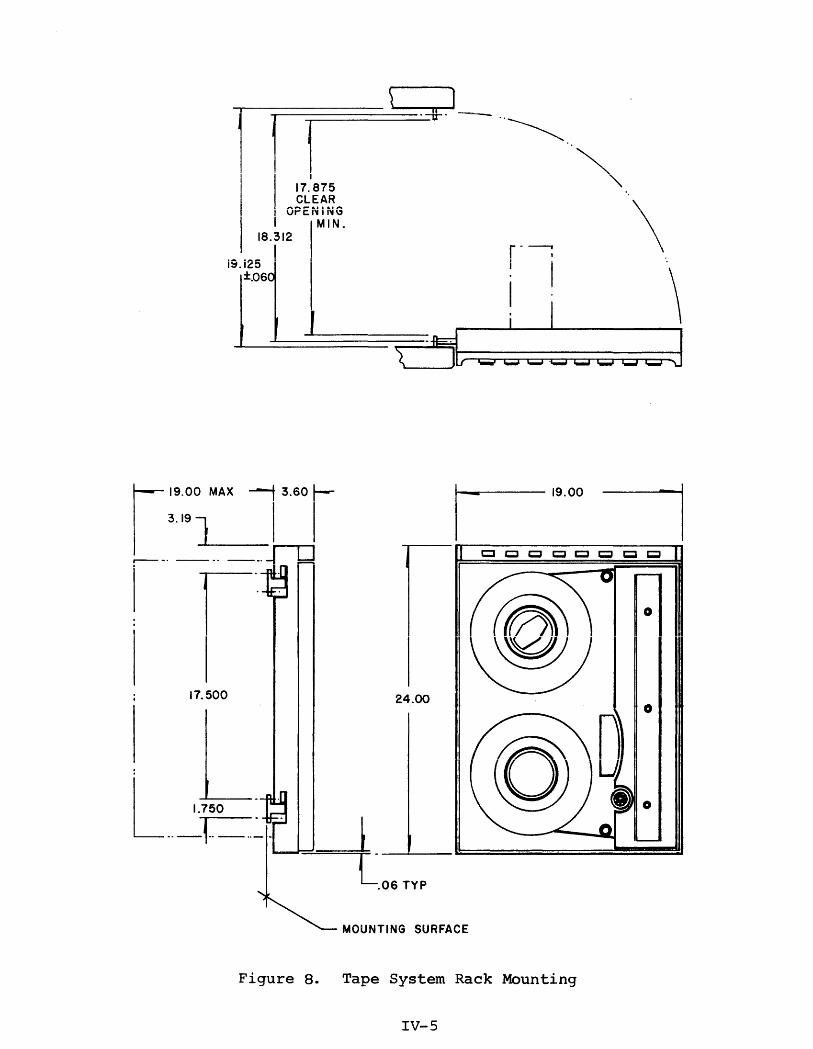
6. Separate the transport deck from the transport electronics enclosure by lifting the transport off the hinge hangers.
7. The electronics enclosure may now be mounted in a standard 19-inch RETMA or Universal rack with a minimum panel space of 24 inches (see Figure 8 and BA). In the event that the enclosure is not accessible from the rear or sides after it is bolted in place, it is recommended to connect the system cables at this time. The WRITE and READ cables must be fed through one of the holes located on the left side of the rear panel and connected to Jl and J6, respectively on the Data Electronics Module. The CONTROL cable may enter from a hole on the right side panel or from a hole on the right side of the rear panel. This cable must be connected to J16 on the Transport Control Logic Module.
B. Mount the transport hinge hangers on the rack and hang the transport on the hinge hangers.
9. Reconnect all items of step 4 to the appropriate subassemblies in the enclosure.
10. The position of the transport with respect to the cabinet opening may be adjusted by means of the hinge block screws accessible through the holes in the overlay. The hinge blocks should be slackened separately so as not to loosen the vertical adjustment.
IV-4
'.
t-- 19.00 MAX l3.60 r 3. 191....L ___ _ -.---.
rl90001 o
17.500 24.00
MOUNTING SURFACE
Figure 8. Tape System Rack Mounting
IV-5

RACK
.----.. ~ \
LENCLOSURE ~.
--"--" --"---
---"-~ .. -----~
LNOo 10 SCREW (FLAT HEAD)
(J
o (J
o o o (} (} (} (}
(}
o (} (}
o (} (J (}
o (J
(} (}
()
)
----NO. 10 LOCK WASHER
.. --L. (HEX. SOC.HD.)
o\o::::~
NOTE: OVERLAY AND DECK COVER NOT SHOWN FOR CLARITY.
Figure 8A. Tape System Installation
. IV-6

WRITE DATA J I - A
WRITE TERMINATOR J I - B ,
OR CABLE TERMINATION FOR NEXT UNIT
...-"====.: ==== ; I,.
READ DATA --~L-...I-': J6-A
READ DATA J6- B
/ w===:-:-==== .. =-=== __ ===
I I
i i
I' "
CONTROL TERMINATOR J 16- A,
OR CABLE TERMi NATiON FOR NEXT UNIT
CONTROL ! N PUT J 16- B
Figure aB. Tape System Interface Cable Installation
IV-7

3. INITIAL CHECKOUT PROCEDURES
To check the proper operation of the transport before placing it in the system, follow the specified procedure.
1. For applications not employing 115 VAC line power, wire the required power plug to the cord and verify that the appropriate primary power transformer wiring is correct. This can be accomplished by checking the wiring against the voltage decal. The decal is located on TB-l which is mounted on the power transformer in the rear of the enclosure. Connect the power cord.
2. Turn the transport power on by setting the power switch located on the power supply chassis to the ON position and pressing the POWER pushbutton switch located on the operator's control panel. At this point the POWER indicator should light up.
3. Load a scratch pad reel of tape without a write enable ring onto the transport and thread the tape, following the procedure in Section II.
4. Press the LOAD pushbutton to initiate the load sequence. The tape will enter the vacuum chambers and then move forward until it reaches the BOT tab. The ON-LINE indicator should light when the BOT reaches the photosensor. At this point, there will be no action when the LOAD pushbutton is pressed. To remove the system from the o~-line mode, press the RESET pushbutton. The system is now in the off-line mode. Since the write ring is not in place, the FILE PROTECT indicator will be illuminated.
5. With the transport off line (ON LINE indicator not illuminated), press the FORWARD pushbutton. Run several feet of tape onto the takeup reel and press the RESET pushbutton to stop the tape. Be sure that when the transport is on line the actions of the FORWARD and REWIND pushbuttons are inoperative.
6. Press the REWIND pushbutton to initiate the rewind mode. The tape will rewind past the BOT tab, return to the BOT tab, and stop with the LOAD indicator lit. To unload the tape, again depress the REWIND pushbutton. Tape will now rewind until the system interlocks are broken, causing the reels to stop and the vacuum system to shut down. The remaining tape in the chambers can now be taken up by the file reel by keeping the REWIND switch depressed. The reel can now be removed. from the unit as outlined in Section II.
IV-8

7. If the system cables have not been connected at this .... " n .... l.me, ",",0 so now as described in step 7 of the previous section.
4. INTERFACE REQUIREMENTS --- .. __ .. -.. -
4.1 CABLING
The interface cables shall be twisted pairs with returns
minimum insulation thickness. Cable twist shall be approximately 30 twists per foot. Maximum cable length shall be 20 feet. The ground side of each pair shall terminate within a few inches of the line receiver or transmitter ground. Connectors shall be Transitron #600-061-lB-SL, or equivalent.
4.2 DAISY CHAINING
Up to four units can be daisy chained on the same bus without any modification to any of the tape units tied in the daisy chain configuration. By changing the position on the Unit Select switch, it is easy to re-assign new tape unit addresses when adding or deleting tape units from the buss.
The following features incorporated into the Mod 11 Transport allow daisy chaining to become a simple operation.
1. Parallel Connectors
Parallel Connectors are provided for all interface cables (Control, Wire, and Read). The advantages of such a system are as follows:
a. It allows all interface signals, including the four select lines,to enter and leave all the tape units in the daisy chain.
b. It eliminates the requirement of using "T" cables. This facilitates daisy chaining,since a drive may be added or removed by simply adding or removing a cable, thus eliminating the requirement of modifying a cable to add another "TII. In addition, system reliability is optimized since only the necessary cabling is used.
IV-9

4.2.1
4.2.2
2. Floating Line Terminators
The line terminating resistors, rather than being mounted on the individual tape units, are packaged on a special terminator board assembly. This assembly is pluggable on any unit, thereby facilitating a change to a different drive when a unit is added or removed from the chain. Regardless of what unit the terminator board is mounted on, as long as any unit on the line is energized, power will be supplied to it.
Daisy Chaining with Unit Select Switch
This configuration is not applicable to PE/NRZI switchable units since they do not incorporate a unit select switch. When daisy chaining in the unit select configuration, all the cables (Control, Read, Write) are l-to-l cables. (See Figure 9.) The operator has the freedom to give each of the four units in the daisy chain the logical address desired, regardless of its physical position on the buss. However, the address for each drive must be unique. That is, each select line should select a different drive.
Daisy Chaining Cable Configuration without a Unit Select Switch
This method is used only with PE/NRZI switchable units. (See Figure 9A.) With this method, the select lines are rotated in the "tape unit to tape unit" control cable. Pin J of the tape unit will always be the active select line of the tape unit. If a tape unit and cable are removed from the daisy chain, the address of the tape units following the removed tape unit will all be reduced by one. (See Figure 9B.) The address of the tape unit is fixed by its physical position if no adapter is used. The Read cable and the Write cable do not require any signal rotation and, therefore, are l-to-l cables.
IV-IO

TAPE SEL CONTROLLER
SEL
SEL
SEL
0
I
2
:5
I I
I
I
I
I
I
I I L
..... J
e 7
9 --
SEL
) c> C) 0 3
HI j2 I 1 -
UNIT I
I I I
!"'"- I J
I 8,
I 7
I 9 I -
r I I I
I I
I
I
I I
-J
8
7
9
---I
L_
SEL
() t 0 0 :5
0 I 2
UNIT 2
THE LOGICAL ADDRESS OF ANY UNIT IS SELECTED BY SWITCH. EACH SELECT LI NE MUST BE USED FOR I AND ONLY I DRIVE.
I I I ,-I
J I 8 -
I 7 - I 9 - I .-
, __ ..J
Figure 9. Daisy Chaining With Unit Select Switch
fTuo ~E~ I
- ., t I
SEL 0 I TA P E I------~ J 1-4 ......... J
CONTROLLER SE L I t---------I 8 8 1-------'
I--_S_E_L~2 __ -1I 7 7 ...... -----'
SEL 3 9 9 t---'!""---
L ____ J
TTul ~~ - 1 I I
1--4 ......... J I
'-----1 8 ~--
'-----1 7 10-----91-----J.
I JI6A JI6B I L ____ J l :JI6A JI6BI
CONTROLLER TO TAPE UNIT CABLE
-TAPE UNIT TO TAPE UNIT CONTROL CABLE
ITU2 I
- --, SEL I
I I I I
I I JI6A JI6B I L ____ .J
Figure 9A. Daisy Chain\ng Without Unit Select Switch
---...
UP TO ~, 4 UNITS
lTu~; ~E~ I
-. - --1 I
--l I I 0::
J ~ I +--..... s ~ I
I
1-----1 7 ~ I 0::
9 9 ~ I I --.J
JIEiA JI6B L _______ .J

r-----' T"fU2 SEi _._-, I I I I I I I !"'""- - I
I"-- -TAPE SEL 0 I t J J
/C CONTROLLER I I I SEl. I 8 8 /t I--
SEL. 2 I I I 7 7
~ ~
SEL. 3 I I I 9 9 ' .... ~
I -- ...... I ...... 1
IJI6A JI6S1
I I ~"""'J
I -~
t-----t 7 a::: lLJ I
9 _~.J I I JI6A JI6S I
8 I 1-------1 7 to------
I I I 9 9 I--
t ----'
I JI6A JI6S I L ____ J L ____ 1 L ______ .J
Figure 9B. Daisy Chaining With "T UI Cable Adapter

4.3 INPUT REQUIREMENTS
Input voltage requirements, a diagram of the input termination configuration, and a list of input control and data functions are shown below:
Input
Logic State
FALSE (Logic 0) +2.5 TRUE (Logic 1) 0.0
SiGNAL
GROUND
Level Requirements
Voltage Current
to +5.5 volts 0 (open collector) to +0.4 volts 26 rna sink
+5V
~ IN 4003 rLlN~ TERMINATOR r / ASSEMBLY
/ r-----l I 180..n.. I I I I
I L
-..
DTL 936 OR EQUIVALENT
Figure 10. Input Termination Configuration
IV-13 P
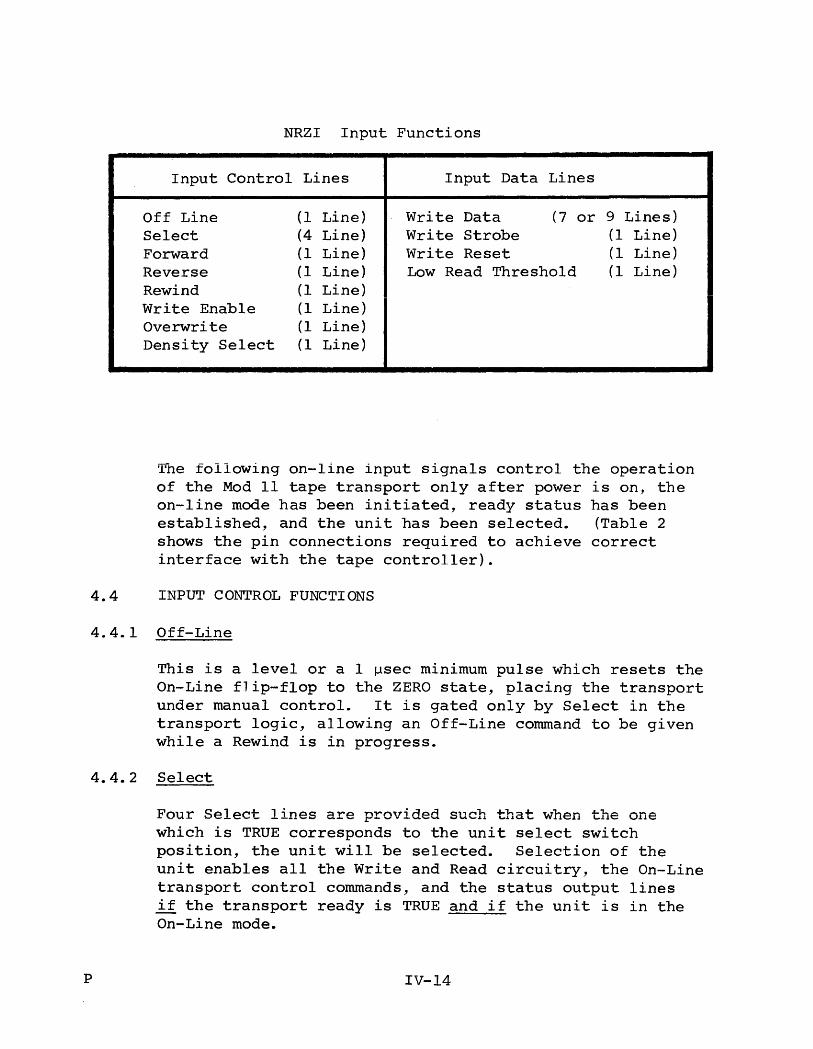
NRZI Input Functions
Input Control Lines Input Data Lines
Off Line (1 Line) Write Data (7 or 9 Lines) Select (4 Line) Write Strobe (1 Line) Forward (1 Line) Write Reset (1 Line) Reverse (1 Line) Low Read Threshold (1 Line) Rewind (1 Line) Write Enable (1 Line) Overwrite (1 Line) Density Select (1 Line)
The tOiiowing on-line input signals control the operation of the Mod 11 tape transport only after power is on, the on-line mode has been initiated, ready status has been established, and the unit has been selected. (Table 2 shows the pin connections required to achieve correct interface with the tape controller).
4.4 INPUT CONTROL FUNCTIONS
4.4.1 Off-Line
This is a level or a 1 ~sec minimum pulse which resets the On-Line flip-flop to the ZERO state, placing the transport under manual control. It is gated only by Select in the transport logic, allowing an Off-Line command to be given while a Rewind is in progress.
4.4.2 Select
p
Four Select lines are provided such that when the one which is TRUE corresponds to the unit select switch position, the unit will be selected. Selection of the unit enables all the Write and Read circuitry, the On-Line transport control commands, and the status output lines if the transport ready is TRUE and if the unit is in the On-Line mode.
IV-14

Table 2.
Connector No. Transitron600-06l-lS-SL
I (or equivalent)
I J-16
. CONTROL INPUTS FROM CUSTOMER
I STATUS OUTPUTS
I TO CUSTOMER
J-l WRITE DATA INPUT CONNECTOR
I J-6 READ
I
DATA OUTPUT CONNECTOR
I
Input/Output Pin Assignments
Signal Nomenclature
I . I
DENS ITY SELECT DENSITY STATUS SELECT 3 COMMAND
• I ~~Tvr~ ~ rOMMAhln trJ~.LJ.LJ'-..L , "'"" ",9.u.
9.LC'1L."J,J
OVERWRITE ~ SELECT 1 COMMAND
SELECT 0 COMMAND FORWARD/STOP REVERSE/STOP REWIND
... OFF-LINE "WRITE ENABLE
I, SPEED READY STATUS ON-LINE STATUS
I REWIND STATUS EOT STATUS BOT STATUS FILE PROTECT STATUS ~+5V TERMINATOR POWER
LOW READ THRESHOLD WRITE DATA STROBE WRITE RESET WRITE DATA PARITY WRITE DATA 0 WRITE DATA 1 WRITE DATA 2 WRITE DATA 3 WRITE DATA 4 WRITE DATA 5 WRITE DATA 6 WRITE DATA 7
READ STROBE READ DATA PARITY READ DATA 0 READ DATA 1 READ DATA 2 READ DATA 3 READ DATA 4 READ DATA 5 READ DATA 6 READ DATA 7 7 TRACK STATUS
,.- -_.
IV-IS
I
I I I , I !
I ! i t I
i
i
I I
! I
! !
I
Signal Pin
D F
9 I
B 8 J C E H L K A T M N U R P S
D A C L M N P R S T u V
2 1 3 4 8 9
14 15 17 18 11
I I
1
I I I
I I
i ! I I
I
I
j I
I I , I i I I I i i
I ! I ! I !
Ground Pin
4 6
=
2 --3 5 -
10 -1
16 11 12 17 14 13 -
4 1 ~
3 10 11 12 13 14 15 16 17 18
B A C D J K R S U V M
I I .
I
P

4.4.3
4.4.4
4.4.5
4.4.6
4.4.7
P
Forward
This is a level which, when TRUE, causes tape to move forward at nominal speed. When the level goes FALSE, the tape motion ceases.
Reverse
This is a level which, when TRUE, causes tape to move in the reverse direction at nominal speed. When the level goes FALSE, tape motion ceases.
Rewind
A I ~sec minimum pulse on this line shall cause the tape transport to drive tape at the specified rewind speed and stop at the Load Point. The transport will initiate a Load Sequence, illuminating the LOAD indicator, and will remain in the On-Line mode. If already at Load Point when the rewind command is given, the command will be ignored. All other motion commands are inhibited until the rewinding sequence is complete.
Density Select
This line is used only with 7-channel tape transports. A TRUE level on this line conditions the MTT to operate at the higher packing density and causes the high density status line to go TRUE. A FALSE level selects the lower data packing density. This line is internally tied TRUE for 9-track systems.
Overwrite (Qualified Option)
This is a level which, when TRUE, causes special action in the write electronics. It is used in conjunction with the Write Enable signal when isolated records are being updated and replaced with equal length records anywhere on tape. Writing the record in the Overwrite mode causes the erase head and write head currents to be turned off immediately at the end of the record, hence preventing the following record from being erased. Any record may be updated up to a maximum of 5 times only. Attempts to update beyond this number will not be guaranteed because the updated record may creep beyond the maximum IRG limits. The leading edge of this pulse must be prior to or coincident with the leading' edge of the Forward or Reverse motion command and the level
IV-16

4.5
4.5.1
must remain TRUE at least 20 ~sec after the initiation of the motion command in order to set the MTT in the Overwrite mode.
If this signal is FALSE during a minimum period of 20 ~sec after the leading edge of the motion command, the MTT will be taken out of the Overwrite mode.
Write Enable
The leading edge of this pulse must be prior to or coincident with the leading edge of the Forward or Reverse motion command and the level must remain TRUE at least 20 ~sec after the initiation of the motion command in order to set the MTT in the Write mode. It is not required to pulse this line if consecutive records are to be written, but merely to hold this line TRUE until the write operation is terminated.
If the Read mode. of operation is required, keep this line FALSE for at least 20 ~sec starting from the leading edge of the motion command. This will reset the Write/Read flip-flop, hence placing the transport in the Read mode. The Write mode can also be disabled by the following conditions:
(a) A Rewind command (b) An Off-Line command (c) Loss of interlocks (d) Manually switching to the Off-Line mode
INPUT DATA FUNCTIONS
Write Da.ta
One line is required for each bit in a character. The Write Data lines shall establish the controlling condition for the NRZI write register. When TRUE, the state of the corresponding flip-flop shall be changed at the time of the write data strobe. This will change the direction of the current through the Write head and establish a flux reversal (One) on the tape. When FALSE, the state of the flip-flop shall not be changed. This shall result in no change in the direction of Write head current, hence no flux reversal (Zero) will be on tape. These data lines must be held steady throughout the time interval consisting of 0.2 ~sec before to 0.2 ~sec after the Write Data Strobe. A minimum of one data line must be TRUE for every strobe.
IV-17 P

4.5.2
4.5.3
4.5.4
Write Strobe
A 1 ~sec pulse on this line shall cause a change in the state of the NRZI Write register cell at the time the deskew single shot times out, if the corresponding write Data Line is TRUE. One pulse is required for each character to be recorded. The recording density is determined by the tape speed and the frequency of the pulses. The frequency shall be stable within 0.25 percent.
Write Reset
A 1 ~sec pulse on this line resets the NRZI Write register. This pulse shall be used to write the Longitudinal Parity Check (LPC) character at the end of each block of data which, therefore, creates an even number of flux reversals (ONE's) in each track of the block. If the unit is in the overwrite mode, this pulse also causes the shut-off of write current.
In a seven-track system this pulse occurs four character times after the last write data strobe of every block of data.
In a nine-track system this pulse occurs eight character times after the last write data strobe of every block of data.
Low Read Threshold
A TRUE level on this line selects a low threshold level (12 percent ) for the read signals, allowing for the detection of marginal areas of tape. A FALSE level on this line selects the normal read signal threshold level (24 percent). This line is active only in the Read mode since the threshold level in the Write mode is fixed at 45 percent.
P IV-IS
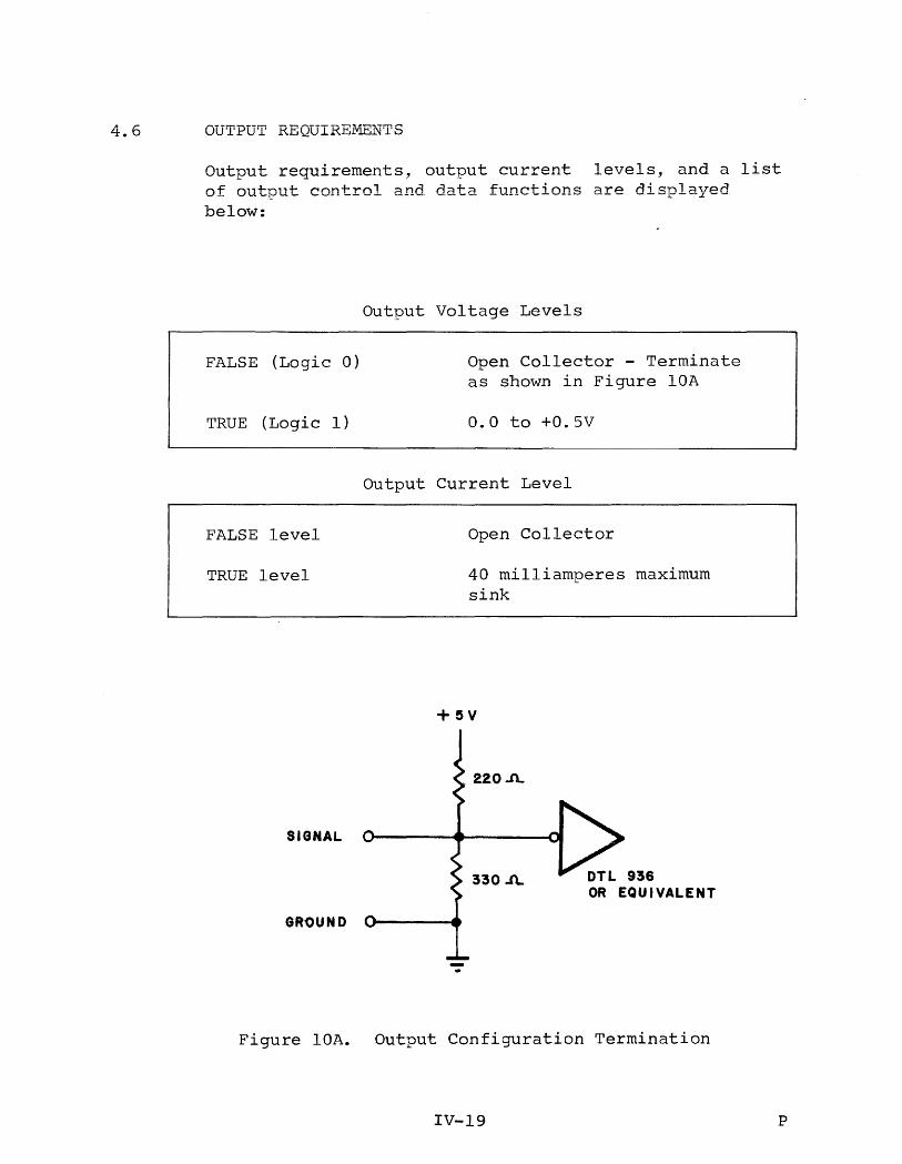
4.6 OUTPUT REQUIREYlliNTS
Output requirements, output current levels, and a list of output control and data functions below:
are
FALSE (Logic 0)
TRUE (Logic 1)
FALSE level
TRUE level
SIGNAL
GROUND
Output Voltage Levels
Open Collector - Terminate as shown in Figure lOA
0.0 to +0.5V
output Current Level
-.
Open Collector
40 milliamperes maximum sink
220..n...
330..n.. DTL 936 OR EQUIVALENT
Figure lOA. Output Configuration Termination
IV-19 p

output Functions
output Control status Lines Output Data Lines
Ready S~.atus (1 line) Read Data (7 or 9 lines) f
File Protect Status (1 line) Read Strobe (1 line)
Rewind Status (1 line) NRZI/PE Status (1 line)
On-Line Status (1 line) 7/9 Trk Status (1 line)
B(")fTl Status I, , .; ..... ~, 'J.J.. \...L ...L...Lllt::}
EaT Status (1 line)
High Density Status (1 line)
Speed
4.7
4.7.1
4.7.2
4.7.3
4.7.4
4.7.5
P
(1 line)
The following On-Line output signals provide the data functions when the unit is ON-LINE and Selected. The control status functions are activated when On-Line and Selected.
OUTPUT CONTROL FUNCTIONS
Ready Status. This line is TRUE when the transport interlocks are made and unit is On-Line and not rewinding, and the initial Load Sequence is complete.
On-line Status. When TRUE, this line indi-cates that the On-Line flip-flop is set and the transport is under remote control.
Rewinding Status. When TRUE, this line indicates that the MTT is rewinding. The rewinding function is completed when the tape is placed at Load Point.
EaT. When TRUE, this line shall indicate that the MTT is reading the EOT reflective marker.
BOT. When TRUE, this line indicates that the MTT is reading the reflective marker at the load point.
IV-20

4.7.6
A .... .... I±. I. I
4.8
4.9
4.9.1
4.9.2
4 .. 9 .. 3
4.9.4
File Protect. A TRUE level on this line indicates that no Write Enable ring has been installed on the supply reel.
Density Status. When this line is TRUE, the Density select input has been set for high density operation, and the read circuitry has been conditioned accordingly. This line is active only for 7-track systems and is tied permanently TRUE for 9-track systems.
SPEED STATUS
When this line is TRUE, it indicates to the system that the selected tape unit operates at the lower one of two tape speeds. This line is utilized when two or more drives of different tape speeds are used in a daisy chain system.
OUTPUT DATA FUNCTIONS
Read Data. One for each bit in a character. Each output is in a level which changes to its appropriate state prior to the trailing edge of the Read Strobe pulse and remains in that state until 0.5 ~sec after the trailing edge of the Read Strobe pulse.
Read Strobe Pulse. The Read Strobe line shall provide a pulse of 2 ~sec for each data character read from tape. The trailing edge of this pulse is used to sample the read data lines.
NRZI/PE status. ~fuen this line is TRUE, it indicates to the system that the selected tape unit is operating in the NRZI mode.
7/9 Track Status. When this line is TRUE, it indicates to the system that the selected tape unit has a 7-track head.
IV-2l P

SECTION V
PRINCIPLES OF OPERATION
For best understanding of the principles of operation of the Mod 11 tape system, the major subassemblies are described separately. The functional separation of system operations relates conveniently to the actual physical packaging of the subassemblies. Following are the major subassemblies, in the sequence in which their operation is explained:
1. Power supply
2. Capstan drive and servo system
3. Reel drive and servo system
4. Control electronics
5. Data electronics
1. POWER SUPPLY
The power supply consists of three assemblies: transformer, rectifier filter and regulators, which supply power to the entire system, including the capstan and reel drive systems, the data electronics and the option electronics. As shown in Figure 11, AC power to the system is controlled by a double-pole single-throw switch on the power supply chassis and by a single-pole, single-throw pushbutton switch on the operator's control panel. The switch on the power supply chassis must be switched on to use the operator's control panel switch to control power. A three-wire cord is used, with the ground line connected directly to the power supply chassis. A fuse is provided in the hot side of the primary power line.
V-I

PII
[!] Tea
Te2 (Q
T87
TO J7 To J8 ECTRONICS ASSY.
"ERVO E~OOq74
Figure 11. Power Supply

Unregulated DC from the power supply is sent to the regulators and the servo amplifiers. The unregulated voltages supplied to the regulators are +24 volts and -24 volts. The unregulated voltages supplied to the servo amplifiers are +24 volts, -24 volts, +44 volts, and -44 volts.
Each voltage regulator consists of a linear integrated circuit amplifier and power transistors. The output voltage tolerance for the regulators are ±5 percent including line and load variations, aging and initial setting accuracy. Each regulator is potentiometer adjustable except for the -5 volt regulator, which is slaved to the +5 volt regulator.
The output level of the +5 volt regulator is prevented from rising above +8 volts to protect the integrated circuits used in the system from over-voltage stress that could occur under abnormal conditions. If the voltage on the +5 volts line goes above +8 volts, an SCR will conduct, shorting the +24 volt unregulated input line to ground until the fuse opens, thus protecting the circuits.
2. CAPSTAN DRIVE AND SERVO SYSTEM
All tape motion in the Mod 11 is initiated by the capstan, which is driven by a DC motor. vfuen the motor is running, a tachometer generates a DC voltage that is used to control the tape velocity through the capstan servo system (see Figure 12).
The strobe disc on the front side of the capstan carries two patterns, one for 50 Hz and one for 60 Hz. The inner pattern is the 60 Hz pattern. When it is viewed under illumination from an AC light (such as fluorescent), the pattern on this disc appears to stand still when the capstan motor of the tape transport is operating at the correct speed. The strobe pattern will be supplied on machines operating at 25, 37.5, and 75 inches per second. Thus, proper operation of the capstan can be under continuous visual inspection by the operator. Any departure from a stationary pattern (i.e., precession of the strobe lines in either a clockwise or counterclockwise direction) indicates a speed variance of the of the capstan drive. (See Section VI for calcualting the percentage of such variance and for adjusting the strobe disc.)
V-3

INPUTS FROM LOGIC
REWIND
FWD COMMAND
REV COM MAND
FWD / REV RAMP GENERATOR
TACHOMETER
CAPSTAN SERVO AMPLIFIER
RAMP~ ____ ~~~~ ____ ~ GEN
R6
R2 ___ -. RAM P I----V
GEN
R3
CAPSTAN MOTOR
FROM ~----'-----TACHOMETER
Figure 12. Capstan Drive and Servo System
i I I I I J V f'-I
~ V I
I I
/ " I
" :/
Figure 13. Timing Diagrams of Command to Capstan Serv9
v - 4

Two ramp generators are used in the capstan servo (See Figure 1). One controls the forward and reverse speeds at nominal velocity, and the other controls the rewind speed. The forward/ reverse ramp generator uses two Zener diodes as precise voltage references. The rewind ramp generator uses the reverse ramp output through R6 as a voltage reference. Resistors Rl and R2 in Figure 12 in combination with R3 and R4, function as a summing network to control the capstan speed. Current through R3 is generated in the tachometer, and R4 provides feedback from the capstan motor, proportional to the motor current. The current feedback is generated by sensing the voltage across a 0.1 ohm resistor (R5) in series with the motor. When the motor is running, the sum of currents in R3 and R4 is equal to the sum of the currents in Rl and R2.
Either a forward or reverse command to the ramp generator preceding Rl establishes tape motion in the appropriate direction. The distances traveled during acceleration or deceleration are such that ~n IBM-compatible inter-record gap is generated. Forward and reverse commands generate currents through Rl having opposite polarities. Symmetry of the start and stop times and distances is readily achieved through the potentiometers in the forward and reverse inputs to the ramp generator. A potentiometer is also used to adjust the capstan drive servo amplifier offset so that no tape motion occurs unless the tape transport has received a motion command.
Figure 13 shows the relative timing of commands to the capstan servo, the ramp function generated, and the resulting tacho~ meter output seen by the servo amplifier.
In the rewind ramp generator, the rise time has a nominal time constant of 1 second. This provides a tim.e interval that permits the tape to accelerate to 200 ips without exceeding the storage capacity of the vacuum chamber. Fall time is nominally a 0.5 second ramp and it assures that the storage chamber capacity is not exceeded as the tape slows and halts.
When the system is in the ready state, the tape is held motionless by the balanced tension (eight ounces) in the chambers and the friction in the capstan drive motor. The wrap on the capstan is nominally 180 degrees. The area of tape in contact with the capstan and the tension on the tape prevent any relative motion between capstan and tape.
V-5

3. REEL DRIVE AND SERVO SYSTEM
Two identical servo systems control the supply and takeup reels in the Mod 11. Storage of appropriate lengths of tape to permit acceleration and deceleration is provided by the vacuum chambers, so that the reels do not have to accelerate as rapidly as the tape does. Storage of tape by the chambers is sufficient to permit the system to operate at the nominal tape speed without program restrictions.
Operation of the reel servo system is diagrammed in Figure 14. A vacuum operated light-sensing circuit provides tape loop information to the servo amplifier, which drives the reel motor. As tape is delivered to the chamber or taken from it, the loop moves up or down, varying the pressure to the piston in the transducer assembly, which varies the position of the mask between the light source and the light-sensing element. This action provides the electrical signal to control the motor speed. Enclosure of the light source prevents ambient light from affecting system performance.
Reel motors are driven by linear amplifiers-, stabilized for all operating situations and sequences. During the Rewind mode the amplifier gain is increase and the output stage operating voltage is raised to offset the increase in back emf generated by the reel motors at higher rpm. An offset signal is fed to the fixed servo amplifier during the unload cycle to bias the tape loop close to the vacuum source end of the chamber. This assures gentle handling of tape as it unloads from the fixed reel. It also prevents loud popping of tape against the chamber grill.
3.1 LIMIT SWITCH
The tape transport is protected from tape spillage by two differential pressure operated switches. (See Figure 15.) One port of the switch is connected to a port in the
• chamber near the atmosphere end and the other port is connected to a port in the same chamber near the vacuum source end. One switch is used to protect each chamber. If
V-6

REEL MOTOR
~ 1f TO PRESSURE LIMIT SWITCH ~I·II ~ .. ~ V\
~~ 1'1111/ ff I (( "W
\\ ___ --- VACUUM LINE
. I PHOTOCELL
ITRANSD_U.CER ASSY ~ _ _ __ •
GAIN ADJUST
--LOOP POSITION ADJUST
~\'rI "--./' i
"1 I
I ..1. --
--................................. ~~-----------~
REEL SERVO AMPLIFIER
-5v
Figure 14. Reel Servo System
V-7

the tape is positioned anywhere between the two ports, there is a pressure difference across the switch holding it closed. If the tape is not between the two ports there is no pressure difference across the switch and the switch opens.
The opening of either switch causes a logic I to be sent to an inverter, which sets a flip-flop to break the ground path to the limit switches and shuts off the blower. This flip-flop provides a memory, so that if tape is pulled back into the chamber after opening a limit switch the transport remains shut down. This flipflop is reset during the load sequence described in paragraph 3.2.
The opening of the limit switch also causes the ready relay to drop out,disconnecting all motors from the amplifiers and connecting them to ground through the load relay.
Potentiometer adjustments are provided on the transport board to permit proper setting of each tape loop position. A potentiometer adjustment is also provided to set the gain of each reel servo amplifier, compensating for the normal manufacturing tolerances in components.
3.2 LOAD SEQUENCE
After tape is threaded, the transport will automatically load on depressing the load pushbutton on the OCP (see Fig. 15). Loading is accomplished by turning on the blower, putting tape into the fixed chamber and file chambers, and putting the reel under servo control. The logic to accomplish this is located on the servo electronics board.
The reel amplifiers are divided into two functional blocks: the preamplifier and the power amplifier,with a signal gate between them. The signal path is inhibited by this gate when the transport is not in the ready condition; therefore, the power amplifier may be conveniently used to drive the reel motors for loading and for automatic unload. The load relay, when energized, disconnects the
v-a

+ 5'1
1 REWIND SWITCH -::- ( N. C.)
i
I I
------------------------------J 18-2
AUTOMATIC UNLOAD BIAS
rUTOMATI~ ----------------------~- UNLOAD~-----------------~ I I 1 FILE REEL AMPLIFIER
TI.'r='n • I I m~n •
PREAMPV- I _ G~:E _ \.::J ~ T
- -- - -, CAPSTAN
AMPLIFIER
[> J7-2?
I J14-5Q
LII A ;ci2 l::~:: . ~~~~ "'-.. --HI SIGNAL 1I----I.A-~ •. .-----I~_-
~ '\ +_" _:_-----r LOAD : I
-
--
, I - ~ I
J I BIAS I I
...... - ... I-___ -I~ ~ - 't-----=----:=:::::: I J8-4J.. 2 SEC . .---__ - .... 1/4 SEC. I ~ I ~ '- LOAD T I
TIMER T TIMER V- I 1_ B:;: ~::~~I~iERL ~J--""'.A.,A'\JA"'-..... A~--=------<J-I FIXED' SIGNAL .---__ ... -_ .. f ~~ _, ~ I YY .. IJ8-1 I
I I
REEL V>--.-. -1 GATE ~ .----------V~----4I--------CT:>-8-2----n-V I PREAMP ......... _.. ; J - I
I ~- FILE CHAMBER READY 5 : I
~-c"
LOAD SWITCH ( N. C.,
I
I
1 TJ15 - 9 I
I J15-8
T I
5 SEC .... TIMER I"""
+ 5v
i . ~ ~~ .. ~
r -LOAD
I GATE I
4Il ~6 I .............. r---J 1 __
IT
II I I
FAULT SENSING n .. ---t_
I I I I
~7-3t
-- Q73
RELAY DRIVE
J 13-11
T ..--c--O------cA J 15-7
.L R~~~~ .SWITCH r -=- (N.O.' I r-
I RELAY DRIVE
Q56 J 13-31
T I I
I
_ lJ15-6 ... ~ READY (-)~-.-~TJ---------------------------------------------------~Hr-~~---~!Q~
1------, U9B I
I I
I , I L!ART O~ SERVO -=-LECTRO~CS_
CR37 ~ ---' ~ I
I I ___ I I '-. I Q75~ I
'--:-__ "'LU_9_A~f - I Q76..r
I I POWER DRIVER I L!L.!.: -~LOP _ -.J I
J14-2 J14-3 J14-1 J --- ~>-- - - - - - "', - - - - - - - - - ~~ '--__ ~- ~ ~ r 1
FIXED CHiNB~ LIMIT FILE CHAMB~R LI M IT
I
I I
KI )
+24v
I I I
K4 III, .. .. ..
CAPSTAN MOTOR
S3.~
FILE REEL MOTOR
FI XED REEL MOTOR
READY RELAY
BLOWER MOTOR
BLOWER RELAY
--
--
0 AC
SWITCH SWITcM Figure 15 .. Load Sequence Block Diagram.
V-9jlD
--

motors from ground, and connects them to the amplifiers for the load and automatic unload cycles. The timing circuits provide the proper sequence for loading.
When the transport is on, but not loaded, the following signals appear at 'the input of the load gate. The rEset switch is normally open, corresponding to a logic 1. The load sequence may be aborted at any time by pressing the RESET switch, thereby putting a logic 0 into the load gate. The load switch common is at a logic zero through pins 8 and 9 of the load relay. The transport ready signal is at a logic 1, since no ground is provided through the open limit switches. The limit switches sense that tape is in the chambers and vacuum is up by sensing the pressure difference across the tape. The inverted 'output of the five-second nominal timer is normally at a logic one. If the LOAD pushbutton is pressed, all inputs to the load gate, are at logic 1, and the load relay will be energized. (The "OR" function is used to energize the relay for automatic unload and will be discussed in'paragraph 3.3.) Once the relay has been energized it stays energized by shifting the load switch to logic 1 by removing the ground from pin 8. The ground on pin 9 of the load relay is swung from pin 8 to pin 10. The load signal also energizes the blower relay at this time. A ground appearing at pin 10 sets the flipflop and turns on the power driver providing a ground to the limi t switches.
The load signal going to a logic 1 starts the timers. The timer circuit consists of a trigger and a capacitor, which is charged through a resistor to +12 and then discharged through a diode. This type of timer delays a logic 1, but not a logic o. Since the timing circuit is an integrator, it has excellent noise immunity.
The load signal starts the two-second and five-second timers simultaneously. The two-second delay provides the time for the blower to build up vacuum. The output of the two-second timer going to logic 1 starts the quarter-second timer. The output of the two-second timer is AND-gated with the inverted output of the quarter-second timer and the five-second timer. As the output of the two-second timer reaches a logic 1, the other signals should be at a logic 1, and the bias circuit to
V-II

3.2.1
the fixed reel amplifier is turned on by this gate. This bias causes the fixed reel to turn counterclockwise, loading tape into the chamber.
When the quarter-second timer goes to the logic 1 state, its output is AND-gated with the five-second timer. This output applies a pulse to the file reel, making it turn clockwise, putting tape into the file chamber. Simultaneously, the inverted output going to zero turns off the bias to the fixed reel.
The tape going into the file chamber closes the limit switch 81, making the file chamber ready signal go to a logic o. This signal turns on the signal gate to the fixed reel amplifier, putting the fixed reel under servo control. The ready relay is turned on through the load relay.
Since tape is already in the fixed chamber at this time, the servo action drives it to the center, closing the fixed chamber lim~t switch, and making the ready signal go to logic O.
The ready signal going to logic 0 turns on the signal gate, putting the file reel amplifier under servo control. The load relay is de-energized, which returns all timers to the o state thereby removing all load biases. A path to hold in the ready relay independent of the load relay is provided through the diode CR37. If the ready signal does not occur within the time determined by the five-second timer, this timer puts a 0 into the load gate, aborting the load.
Voltage Fault Sensing
The Load sequence should not be attempted if a malfunction should occur in the ± 24V supply, or any of the power supply regulators, resulting in the absence of any of the respective supply output voltages. Automatic fault sensing is provided that prevents loading, should such a malfunction occur. The location of this circuitry is illustrated in the block diagram in Figure 15: the circuit details are shown on the schematic in Figure B33.
Referring to Figure B33, the Load relay, K2, is energized by the collector current of Q73, whose base drive is derived from +5V. Should this voltage be absent, then K2 will not pull in. Since the Q73 collector current is derived from the +12V source, K2 cannot pull in if that voltage is absent. Both the +5 and +12 voltages are derived from the
V-12

+24V source, and thus K2 cannot pull in if the +24 voltage is absent.
Should the -5V source fail, that condition will be sensed by transistor Q81, which remains cut off so long as -5V is applied to its base, through R230. If the -5V source should fail, Q81 will be driven on by ~ne +12 voltage, via R229, and forces the base of Q73 to ground. Consequently, K2 cannot pull in if the -5V source fails. Since the -5 voltage is derived from -12V, which, in turn, is developed from the -24V source, K2 cannot pull in if the -12V source (and, obviously, the -24V source) should fail.
The ±44 voltages are not involved in the Load operation, and their presence is therefore not monitored by the circuitry described above.
3.3 AUTOMATIC UNLOAD
When the transport is not holding tension, the ready signal is at a logic 1. (See Fig. 15.) This signal is NAND-gated with the positive TRUE signal from the rewind switch. The output of this gate is inverted and used to pull in the load relay through an OR-gate. It is also used to apply a bias to the file reel. The inverted output of the gate is fed into a circuit which delays logic 1, but not logic O. This circuit is used to inhibit the load sequence. The delay is necessary to prevent a load sequence from starting when the rewind switch is released. Since the rewind switch is a momentary closure type, the transport will remain in the automatic unload mode only as long as the REWIND switch is held in. This mode may be used to take up slack from the chambers in preparing to load or to completely remove tape from the tape path. The bias is designed so that tape is not damaged, even if this mode is used as a slow reel-to-reel rewind.
4. CONTROL ELECTRONICS
The control logic circuitry (see Figure 16) receives its primary inputs from the operator's control panel or the remote controller. In addition, it responds to control signals from the photosense assembly and from the servo amplifiers (during the rewind sequence).
V-13

The internal control circuitry outputs signals to the remote tape controller and to the operator's control panel (in the form of indicator lights). Within the transport, it provides signals to the servo amplifiers and to the data electronics.
4.1 RESET AND ON-LINE LOGIC
FROM REMOTE
When on-line status is TRUE, all pushbutton switches at the operator's control panel are disabled except RESET.
Pressing RESET at the control panel DC resets the terms Rewind, Motion (Forward and Reverse), and On-Line to FALSE~ Remote control of the transport can be restored after a
MOTION
SET WRITE
COHTRO!...L!:~ - aJ!I""l.~'!"'\a.!
WRITE "nii .. j DUMY I fftvt,un ENABLE
SELECT ENABLE - INPUT LOGIC BUFFER - RESET ON LINE
1- , -"----
REMOTE MOTION
COMMANDS
PHOTO AMP
MOTION P.B. -- -MOTION READY CONTROL MOTIoN LOGIC -
OCP FORWARD I ..... FROM f= P.B.
DCP ENABLE REVERSE REWIND STATUS ...
LINES.
l SET ~ON LINE ~
ON LINE - I LOGIC
READY TRANSPORl RESET RELAY READY
DELAY
Figure 16. Transport Control Electronics
V-14
OUTPUT DRIVERS r-
TO REMOTE
CONTROLLER
~} S E
ERVO LECTRONICS
MODULE

RESET action by pressing the ON-LINE pushbutton. The on-line command from the operator's control panel is gated through two cross-coupled OR-gates, and the transport is then ready to accept any remote command.
The transport can always be put in the off-line state by
4.2 MOTION LOGIC (FORWARD AND REVERSE)
A diagram of the logic governing forward and reverse motion is given in Figure 17. Forward and reverse motion commands to the servos are initiated locally from the operator's control panel when the transport is in the off-line mode, or from the remote controller when the transport is on-line.
The OCP-enable line must be TRUE (low) to initiate local motion from the operator's control panel. When the FORWARD pushbutton is pressed, the motion latch comprised of gates A, B, C in Figure 17 is set, and the output of gate A will be TRUE (low). This output is transmitted through NOR-gate D, which ORis the local and remote forNard commands and presents a forward (+) signal to the capstan servo.
Local reverse motion is initiated by pressing the REVERSE pushbutton on the operator's control panel. The reverse switch is interlocked in such a way that a reverse command cannot be initiated simultaneously with a forward command. With the motion latch set by the REVERSE pushbutton, the output ox gate B will be TRUE (low). This output is transmitted through NORgate E, which OR's the local and· remote reverse commands and presents a reverse (+) signal to the capstan servo.
Local reverse or forward motion is terminated if a RESET ACTION is taken, if the transport is mechanically not ready, or if the terms EOT, BOT, or Rewind are TRUE.
When the transport is in the on-line mode, the OCP-enable line will be FALSE (high), thus disabling the FORWARD and REVERSE pushbutton inputs to the motion latch. The NAND-gates labeled F and G in Figure 17 are enabled by the terms Ready and On-Line, and any subsequent forward or reverse motion commands from the remote controller will be transmitted to the capstan servo control through gate D or E.
V-IS

OCP RWDD PANEL SET FWD -------
~OCP ENABLE
READY 8 ON LINE REMOTE FWD
T~ ________ FW_D __ P._B_. ____ ~ ____ ~~: ~~--'-------------~~J FWD (+) TO SERVO
BOT + EOT +REWIND
~ ____ ~ ____ , ______ ~ ____________ ~~ _______ TO READY
LOGIC
RESET P. B. +MECH READY
OO _____ R_E_V_P._B_. ___ {>~--[;:»_.--------4----------~:=-~ ____ _
Figure 17.
BOT READY 8 ON LINE
REMOTE REV '-_'"
Simplified Logic of Motion Control (Forward and Reverse)
REV (+) TO SERVO

The NAND-gate labeled G has an additional term (NOT BOT) on its input. This term prevents reversing off the BOT marker during the on-line mode of operation.
4.3 REWIND AND UNLOAD LOGIC
The rewind sequence is not internally different, whether
~..I- _..1.... ___ ~ ________ ..L..! ___ ..I- L~ _______ ..1.... ___ 1_
Ll:. ::5-Cc!ll;::; l.L~U!!l dll d.{";C.LUll dl:. l:.!lt::! upe.r.-d.1:ur ~
control panel or from a remote command. A logic diagram of this function is given in Figure 18.
The rewind sequence is mechanized with a series of three flip-flops, FF-A, FF-B, and FF-C. The flip-flop FF-A labeled in the diagram is set initially either by the REWIND pushbutton through NAND-gate A, or by the remote rewind command through NAND-gate B. The NAND-gate labeled C decodes the outputs of flip-flops FF-A and FF-C and presents a rewind (-) command to the capstan rewind ramp generator. A reverse-for-rewind is also sent to the capstan servo control through gate D. When the capstan servo receives the rewind (-) and reverse-for-rewind signals, the tape drive ramps to rewind speed and runs until either BOT is reached or a RESET pushbutton action is taken,at the operator's control panel. If no RESET action is taken, the leading edge of the BOT tab loads FF-B and the trailing edge loads FF-C. With FF-B set, the inputs to gate C are no longer TRUE, and the rewind signals to the capstan servo are terminated. The capstan ramps to a stop, a set-forward pulse is generated, and the tape drive begins searching forward for BOT. When BOT is reached, the series of three flip-flops (A, B and C) is reset and tape motion ceases.
At this point, two actions may be used to unload the tape. A RESET action takes the transport off-line, and a subsequent REWIND action causes tape to rewind until tape tension and mechanical interlocks are lost. During the process of unloading, a regular rewind command is distinguished from a rewind-to-unload command by gating together, at E, the terms Off-Line and Ready, BOT, and
V-17

REWIND P. B. ,
OFF LINE
BOT
REMOTE 8 REWIND READY a ON LINE
(RESET)
+ (MECH NOT READY)
REWIND (-)
BOT MOTION
NOT READY ONLI NE ------""'0
BOT READY OFF LINE
REWIND P.B.
--
Qt--... --t
FF-A A
K R
>--.... -- (-) UNLOA,D
t-----tJ Q
--
FF-C B
KRQ
0-__ ---- (-) REWIND
REV FOR REWIND
Figure 18. Simplified Logic of RE~wind and Unload Control

Rewind. Under these conditions, the easy unload latch, comprised of gates F and G, is set, and an unload (-) -signal is sent to the fixed reel servo. The unload latch is reset only by the term Not Mechanically ReadY7 thus, once an unload is initiated, it must complete its cycle. (Note: If a second BOT tab is sensed during an unload cycle, the tape drive will attempt a search for load point cycle and will, in most cases, loop-out, causing the ready relay to drop out. )
4.4 WRITE ENABLE LOGIC
Figure 19 diagrams the write enable logic which is comprised of flip-flop FF-A and a positive pulse generator (B and C). The flip-flop is set when the write enable line from the controller is TRUE (high), enabling the J input of FF-A, and when either a forward or reverse motion command is initiated. The T input positive pulse is generated by a pulse generator (B and C). The pulse is generated when MOTION goes TRUE (high). The output of B goes to ground after a time delay. This negative transition initiates a positive pulse at the output of gate C. The trailing edge of this pulse causes FF-A to change states. When the write enable flip-flop is set, the transport is conditioned to write.
The write enable flip-flop is reset when the write enable line from the controller is FALSE (i.e., when the K input of FF-A goes high after inversion by gate D); and when either a forward or reverse motion command is initiated.
4.5 OVERWRITE AND WRITE RESET LOGIC
The Overwrite logic and write Reset logic are used in conjunction with the Write Enable logic to perform editing or updating of isolated records. The new record must be the same length as the old record. The mechanization is illustrated in Figure 20.
The overwrite signal is received by a line receiver (II)' which inverts the signal and drives the "J" input of FF-A. The output of II is inverted by I2, which drives the "K" input of FF-A. When the overwrite line is TRUE, the "J" input of FF-A is high, and with the next motion command, a trigger pulse is generated, which sets FF-A. The motion pulse also sets FF-B. If write enable is TRUE at this time, and if the file protect switch is on, gate D will be enabled and the write power gate will be turned on.
V-19

WRITE ENABLE (+> ----.... ----------1 J
MOTION
MOTION I I
GATE B
T INPUT
I --t
T
FF-A ~}---T-""K R
READY
I
n I
ttl t--
Q I--~ WRITE ENABLE
TO DATA
Figure 19. Simplified Logic of Write Enable Control
V-20

WRITE ENABLE
OVERWRITE ~-a--------------~J Q
ON LINE AND READY---------
+5V
MOTION (PULSE)----------------o-~
WRITE RESET VIA DATA ----I
ELECTRONICS
-.
FF A
T
+~V
J Q~----------.------~
FF B
T
K Q MOT ION R
F'igure 20. Overwrite and Write Reset Logic
C
o
1>-F
WRITE POWER GATE
FILE r PHOTECT SWITCH .
+12V

After rewriting the new record, a write reset pulse must be generated immediately following the last check character to reset FF-B. This will inhibit gate D, therefore turning off the write power while tape is still in motion. The write power gate is designed to ramp the write power down, so that spurious write current spikes in the IRG will be held to a minimum.
4.6 FILE PROTECT LOGIC
The file protect logic is mechanized such that there will be a minimum of scraping of the write enable ring during the initial loading cycle of the transport.
The mechanization is shown in Figure 21. When a reel of tape is initially loaded, the file protect switch is closed, and the logic latches the write enable solenoid, thus retracting the solenoid pin to prevent scraping of the write enable ring.
When the LOAD pushbutton is pressed, the logic releases the solenoid. This is done to sample if there truly is a write enable ring in place, and that the solenoid was not accidentally energized. When the loading cycle is completed, the transport ready signal is the holding signal.
4.7 READY LOGIC
The ready logic, diagrammed in Figure 22, provides three basic ready signals:
a) Select & Ready (+) from inverter A conditions the data electronics to accept and transmit information to the controller.
b) Ready & On Line from inverter B is transmitted to the controller via an output driver. This line informs the controller that the transport is ready and not rewinding, and therefore able to accept any command from the controller.
c) Ready & Off Line from gate C. This is an internal ready signal that enables the operator control panel so that any motion command generated by the operator control panel will be accepted by the transport.
V-22

OCP LOAD PB
+5v
TRANSPORT READY
E PROTEC" FIL S'TATUS
Figure 21. 'c tect LOgl File Pro
WRITE~
-{L .... POWER u r GATE

ON LINE -v--"-~--------- READY S ON LINE
MOTION
REWIND
RESET + MECH READY ____ _
+ RESET REWIND
Figure 22.
SELECT a ON LINE
A >-SELECT S READY (4)
OFF WNE::::D~---
Simplified Logic of Ready Control
READY S OFF LI NE
( OC P ENABLE)

The ready signal is generated according to the following logic equation:
READY = lDELAYED MOTION) • (REWIND)·(RESET + MECH. READY + RESET REWIND)
and is mechanized by gate D. If all the inputs to gate D are TRUE (high) the output will be low. This low signal goes through inverter E and is gated with the terms Select & On-Line by gate F to provide the Select & Ready term. The low output of gate D goes through inverter G and is gated with the term Off-Line by gate C to provide the Ready & Off-Line term. Gate E and B are collector-aRid to provide the Ready & On-Line term.
5. DATA ELECTRONICS
Data electronics described in this manual pertain to ~ mode recording only. Phase encoding requires additional special data electronics and is described in a separate manual.
In the NRZI mode of recording, a "1" is represented by a change of direction of magnetization between positive and negative, saturation levels, and a "0" is represented by no change of magnetization. The data electronics subsystem provides a format that is compatible with the IBM 727-729, 7-track format, at data densities of 200, 556, and 800 cpi. The subsystem also provides compatibility with the IBM 2400 series USASCII-compatible 9-track format at data densities of 800 cpi. Figures 23 and 24 present the 7-track and 9-track location and space specifications.
At the end of each data record, check characters must be recorded and an inter-record gap inserted. Figures 25 and 26 present the 7-and 9-track IBM inter-record gap and tape mark formats. As indicated by these figures, in the 7-track format the longitudinal redundancy check character (LRCC) only is written, whereas in the 9-track format, both a cyclic redundancy check character (CRCC) and an LRCC are written.
The CRC character is supplied, together with a single write data strobe signal, by the customer to the transport interface. It is separated by four character spaces from the last data character of the previous record. In the 9-track
V-25

system, the LRC character is written four character spaces after the CRCC character, whereas in the 7-track system, the LRC character is written four character spaces after the last data character of the previous record. The LRC character is written by transmitting the WRITE AMPLIFIER RESET signal (leading edge) at the proper time. This signal resets the write flip-flops causing the total number of magnetization transitions in any track to be an even number.
The Inter-record Gap (IRG) displacement is nominally 0.6 inch for 9-channel systems and 0.75 inch for 7-channel systems. The IRG is established by the sum of the following component distances:
Stop Distance - Stop distance is the distance traveled by a point on the tape from the time a stop command is issued until the tape velocity is zero.
Stop Delav Distance - Stop delay distance is the distance traveled by a point on the tape from the time the LRCC character is placed on tape until a stop command is issued" In dual gap systems j if the read data is used to sense the end of the record, the stop delay distance is the distance traveled from the time the LRCC is sensed at the read bus until the stop command is issued. The stop delay time is generated in the customer's controller.
Start Distance - This is the distance traveled by a point on the tape from the time a forward command is issued until the first data character is placed on tape. The Write Delay time appropriate to the start distance is generated in the customer's controller.
A tape mark is used to separate files of information recorded on tape. The tape mark configuration for 7- and 9-track systems is shown in Figures 25 and 26 respectively. Tape mark timing is established and provided by the customer's controller. The command sequence for inserting a tape mark is as follows: a forward command is issued, followed at the proper time by the tape mark character together with its write data strobe. This, in turn, is followed by the LRC character written four character spaces later in a 7-track system and 8 character spaces later in a 9-track system.
V-26

7 TRACK
0.498 % .00211
I
0.460" f
0.048 WRITE HEAD WIDTH 0 .. 030 READ HEAD WIDTH
111111111111111111111111111 C
i 111111111111111111111111111 8 I 1111111"111111111111111111 A f
f I 0.390" __ ,----------t--
I
0.320" f I 0.2~0"
TRACK LOCATIONS 2 - C: +0.0040" -0.0035"
TRACK LOCATION I: ± 0.002~"
f 111111111111111111111111111 8
111111111111111111111111111 4 i ii I iii liilililiiliiiiiiiiii 2
11111111111111111111111111 1 I
DATA CHANNELS WCP 118M DESIGNATIONS
Figure 23. Track Locations and Spacing, 7-Track System
9 TRACK
0.044 WRITE HEAD WIDTH 0.040 READ HEAD WIDTH
t 1 ... ' ........ 1 ........ 1.11. A I -===;-~~~------------------~-+-IIIIIIIIIIIIIIIIIIIIIIIIIII "t
0.498 ± .002" 11111111""1111111111111116 T---------~;=:+=I1III1I1I1II1"11I1I1I1I11I 0
--.-----------t-IIIIIIIIIIIIIIIIIIIIIIIIIIII --.------------+-- HllllllUutUWUIIIHU2
--r--------+--IIIIIIIIIIIIIIIIIIIIIIIIIII p --.-------+--111111111111111111111111111 3
~--+--1IIJ111111111J1111111111111 7 .....>L..-+--IIIIIIIIJlIIIIIIIIIIIIIIIII 5
------~--~~~~~~~~--~-~-~
REFERENCE
ALL TRACK LOCATIONS ± 0.003"
DA T A CHANNELS WCP/ IBM DESIGNATIONS
Figure 24. Track Locations and Spacing, 9-Track System
V-27
l (

NOMINAL IRG ~ ~ 4 CHARACTER SPACES ~
1--°,75" -I- -I- APPROX. 3.9" -I" I
~I C
8
A
8
4
2
l
FIRST DATA J CHARACTER OF
LRCC L TAPE MARK LRCC L LAST DATA CHARACTER
OF PREVIOUS FILE
NEXT FILE L--__ REFERENCE
EDGE
Figure 25. 7-Track File Gap Format
NOMINAL 8 CHARACTER
IRG ~ /. SPACES
4 CHARACTER
1
\
~SPACES
I--O.s" -··1 ... ·..------· ... 1·---- APPROX. 3.75" ---__ ....... ---f--..... -I- I ~I I I I I I I I I I
t LRCC f LRCC CRCC t LFIRST DATA
CHARACTER OF NEXT FILE
L TAPE MARK
L REFERENCE EDGE LAST DATA J
CHARACTER OF PREVIOUS FILE
NOTE: TAPE VIEWED FROM MYLAR SIDE.
Figure 26. 9-Track File Gap Format
V-28
I 4
I 6
I 0
I I 2
I P
I 3
I 7
I 5
~
~

5.1
5.1.1
5.1 .. 2
DATA ELECTRONICS, DUAL GAP SYSTEMS
Read-After-write Head Assembly
A dual-gap read-after-write head is optionally available in either a nine-channel or a seven-channel format. A full-width erase head is located on the oxide side of the tape, positioned 0.34 inch from the write stack head gaps. The write stack is center-tapped and it operates at 50 milliamps of current per leg. The voltage output of the read stack is proportional to the speed of the tape; at 75 ips, it provides 45 to 55 millivolts peak to peak. The erase head operates at 50 milliamps.
Two auxiliary components are mounted adjacent to the read/write head on a common base--the photocell and lamp assembly that detects beginning and end of tape, and the tape cleaner. The photosense assembly is a plug-in unit that is directly cable-connected to the transport electronics printed circuit board. The tape cleaner, whose operation is entirely mechanical, is optimally positioned adjacent to the head so that the cleaned tape passes directly to the read/write head, minimizing the chance of contamination that might result in deterioration of data reliability.
Write Data Flow
Figures 27 and 28 present a block diagram and timing diagram of the flow write data through the system. (Only one data line is shown. The components for the channel represented schematically in these diagrams are, of course, duplicated for each of the other write data channels). Data enters through line receivers whose function is to invert the low-TRUE levels. Each receiver has a terminating impedance of 130 ohms.
A pulse on the write strobe line clocks information from the data lines into the system. The repetition rate is determined by the product of velocity (V) of the transport and the desired data packing density (D). The frame time therefore becomes the reciprocal of this product V~. If a given data line is TRUE, the write strobe pulse passes data on that line through the data strobe reset logic gates, which consist of two NAND-gates, ORld together (see the block labeled A in Figure 27). If a given data line is FALSE, the pulse is gated out.
V-29

WRITE RESET
-.
Figure 27. Write Data Flow, Dual Gap Systems

WRITE STROBE
WRITE DATA LINE
WRITE RESET
r- OIV 10 I I 2 J,JSEC
CRce
U U r---------,---------,------"I u... 0.2 USEC MIN
I I I
I ~ r-- 0.2 USEC MIN I I I
I , 1 : J l: I "I 1--2USEC
-~------__t-I--r___--DE-SK-EW--~---LJI
I I DELAY. TIME I DESKEW SS I OUTPUT ---I I ...... __ -----'r ...... ---L ______ I
WRITE REGISTER
+5V--1 I I
~ l'-TP-I i
I
~ :r-u
~ r-0 I
HEAD CURRENT
+50MA
OV . :/
-50MA3
Figure 28. Write Dlata Flow Timing Diagram, Dual Gap Systems

5.1.3
At the block labeled B (Figure 27) electronic correction is made for the static skew characteristics of the write head. The leading edge of the gated data pulse triggers the write deskew single-shot, whose pulse width has been preset and is adjustable by means of a potentiometer. The trailing edge of the pulse loads the write register, whose contents are then converted into currents by the head drivers. The head drivers operate the write heads, which put the data on tape.
At the end of each block of data, a write reset pulse enters the system. In the nine-channel configuration, this pulse enters eight character times after the last strobe of the data block; in the seven-channel configuration, it enters four character times after the last strobe. The function of this pulse is to reset any head drivers remaining in the set state at the end of a data block, thereby generating the longitudinal redundancy check character on tape.
The write register is DC reset at certain times and under certain conditions to ensure that informatlon is not recorded on tape unless recording is deliberately intended. The logic created for this is such that if anyone of the terms Motion, Write Enable, Select, and Ready is FALSE, the write register will be DC reset.
The flow of power to the write heads is controlled through the write power gate (see Figure 29). This is a NAND-gate function that comprises the terms Write Enable (or Write Permit), Select & Ready, and File Protect. (Write power enters the data electronics printed circuit board from the transport electronics printed circuit board if the file protect switch on the deck has been energized.)
Read Data Flow
Figure 30 presents a block diagram of the flow of read data through the system. (As in Figure 27, only one channel is indicated.) The read head generates a low-level analog signal of approximately 45 to 55 millivolts peak to peak at 75 ips. The read amplifier, which has a differential input and single-ended output, picks up this signal and amplifies it to a suitable level, then sends it to a phase splitter, which generates the complementary signals required for full-wave rectification. The phase splitter output signal level is adjusted to 12 volts peak to peak
V-32

WRITE PERMIT OR WRITE ENABLE ~
SELECT AND READY
I ,
FILE PROTECT SWITCH
+12V~~------~
MOTION
WRITE POWER
WRITE REGISTER DC RESET
WRITE POWER
WRITE REGISTER
RESET
Figure 29. Write Power Gate and Write Register DC Reset, Dual Gap Systems
V-33

<! I
READ HEAD
w WRITE ~ ENABLE(+}
LOW CLIP SELECT (-)
GAIN CONTROL
READ AMP
WRITE/READ THRESHOLD
LOW READ THRESHOLD
INVERTING AMPLIFIER
CLIP LEVEL
GENERATOR
Y
FULL WAVE RECTIFIER
N
PEAK DETECTOR
o
READ REGISTER
DELAYED -[:>-RESET PULSE
SELECT a READY - ....... ...----1
Figure 30. Read Data Flow, Dual Gap Systems
Q
P
". ,
READ
READ STROBE
READ STROBE O. D.

by the attenuator control potentiometer at the output of the read amplifier. A clipping level DC bias is fed into the input of the full-wave rectifier, with the result that positive peaks above the clip-level threshold are observed at the output of the circuite This signal is then sent to the peak detector, which in turn generates ~ n i a; t-~ 1 nnl ~p whn~p t-_ r~ i 1 i na pnap i ~ ~vnC'h rnnnll ~ w; rh - --J---- r---- .. ----- --------=.. --=..- -- -..1;------------ .. ----the peak of the analog signal and is used to load the read register at that time. The contents of the read
• • •• • .. ..... ... .... • • 1
regls~er are sen~ ~o ~ne ou~pu~ arlver ana ~nen to tne customer's data line. Auxiliary to this general flow of read data, several other functional circuits complete and control the read data generation and transfer process. These auxiliary functions are described in the subsections following.
Strobe Generation Circuitry. As in most other NRZI read systems, the OR!d data method of read strobe pulse generation is used in the Mod 11 (see Figure 31). The first arriving bit sensed at the read register is used to trigger the read strobe delay single-shot. This is implemented by taking the complement outputs of the read register and feeding them into a nine-way OR-gate whose output goes to the single-shot. The pulse width of the single-shot is controlled by adjusting a potentiometer and is set to approximately one-half frame time. The frame time is defined as ';D' where V is the tape unit velocity and D is the operating data density.
At the end of the variable time delay period, a read strobe pulse is generated (see the block labeled T in Fig. 31) and sent to the tape controller. The trailing edge of this pulse also triggers the read register delayed reset pulse network, allowing 500 nanos~conds for scanning of the data lines by the controller before the read registers are reset. A summing function (data staircase) is provided at the output of the read registers so that interchannel time displacement can be measured.
A timing diagram for both read data flow and strobe generation is given in Figure 32.
v- 35

TRACKS 1- 9 FROM READ REGISTER
OR
STAIRCASE GENERATOR
GATE
R
READ STROBE DELAY ADJ
READ STROBE DELAY
ONE - SHOT
S
HI/LO DENSITY SELECT INPUT
STROBE PULSE
GENERATOR
READ REGISTER DELAYED RESET PULSE NETWORK
w
READ STROBE OUTPUT LINE DRIVER
READ OUTPUT LINE DRIVER
U
ENABLE ( REF. FIG.32 )
REGISTER RESET
READ REGISTEI~
READ STROBE OUTPUT
Figure 31. Read Strobe Generation Circuitry, Dual Gap Systems

RECTIFIER OUTPUT ~ ~- I~-I I I , I I I I I
PK DET OUT .--n. J I nL-_ I I I I I
I I 1 , READ REG OUTPUT r I I • .-
I I J I <: I I I I I I w -:fl FRAME I I I .• --.]
STROBE DELAY S5 2 TIME
I I I I I I
STROBE PULSE AT nl STROBE PULSE -GEN OUTPUT I I READ REGISTER II I DELAYED RESET
IU :;u:: -PULSE 200 NANOSEC --., r-- 500 NANOSEC I
Figure 32. Timing Diagram of Read Data Flow and Strobe Generation, Dual Gap Systems

High-Low Density Select. Data can be recorded on tape at either a high or low density (more or fewer characters per inch). An input-from the high-low density select function changes the pulse width of the read strobe delay single-shot to correspond to the density of character generation.
Read Permit. This system function allows the remote tape controller unit to enable or inhibit read data at any time. Read permit is conditioned by the terms Select and Ready_ If either of the two terms is FALSE, the read registers and output drivers are disabled. This function is normally tied TRUE on certain interfaces.
Clipping Level Circuitry. This circuitry, shown in Figure 30, generates the clipping levels through which the read signals must pass before reaching the peak detectors. In the write enable mode, approximately 45 percent of the read signal amplitude is clipped. In the read-only mode, the level is decreased so that only 24 per cent of the read signal amplitude is clipped. A provision has been implemented via the low threshold select remote input line so that an even lower threshold level (12 percent) can be selected when reading marginal output tapes. The state of this line has no effect on the clipping level while in the write mode of operation.
Rewind Inhibit. This system function prevents the reading of data if the tape is rewinding. The relevant circuitry prevents current flow in the phase splitter, disabling its operation during rewinding.
V-38
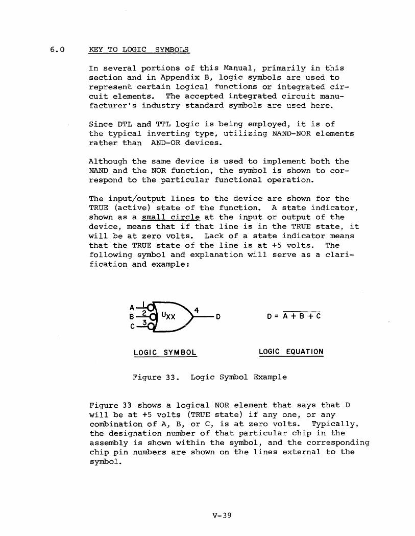
6.0 KEY TO LOGIC SYMBOLS
In several portions of this Manual, primarily in this section and in Appendix B, logic symbols are used to represent certain logical functions or integrated circuit elements. The accepted integrated circuit manufacturer's industry standard sywbols are used here.
Since DTL and TTL logic is being employed, it is of the t}~ical inverting type, utilizing NAND-NOR elements rather than AND-OR devices.
Although the same device is used to implement both the NAND and the NOR function, the symbol is shown to correspond to the particular functional operation.
The input/output lines to the device are shown for the TRUE (active) state of the function. A state indicator, shown as a small circle at the input or output of the device, means that if that line is in the TRUE state, it will be at zero volts. Lack of a state indicator means that the TRUE state of the line is at +5 volts. The following symbol and explanation will serve as a clarification and example:
4 1----0 O=A+B+C
LOGIC SYMBOL LOGIC EQUATION
Figure 33. Logic Symbol Example
Figure 33 shows a logical NOR element that says that D will be at +5 volts (TRUE state) if anyone, or any combination of A, B, or C, is at zero volts. Typically, the designation number of that particular chip in the assembly is shown within the symbol, and the corresponding chip pin numbers are shown on the lines external to the symbol.
V-39

Table 3 shows all of the logic symbols used in this Manual, with their corresponding names and logical equations. The equations shown are defined by the TRUE level of the input signal.
The single-shot produces a positive going pulse at the 11111 output and a negative going pulse at the 110 11 output, and these are initiated at the time that the input pulse transitions to its TRUE state.
The flip-flops are of the J-K type, and their input/output functions are as follows:
Designation Function
Synchronous set input Synchronous reset input Clock input Direct set input Direct clear (or Reset) input Set output Reset output
The following truth tables are applicable to these devices:
SYNCHRONOUS OPERATION ASYNCHRONOUS OPERATION
BEFORE CLOCKS AFTER CLOCK INPUTS OUTPUTS OUTPUTS INPUTS OUTPUTS SD CD 1 a
1 a J K 1 a L L H H L H L X L H L H H L L H H X H L H L L H H L X L H L H H SynchrQnous
Operatlon H L X H L H
v- 40

TABLE 3
SYM BOL NAM E LOGICAL EQUATION
NEGATIVE INVERTER B = A
A:-o-----
--- -
POSITIVE INVERTER
I POSITIVE NAND GATE
I NEGATIVE NOR GATE I
NEGATIVE WIRED OR GATE
F L I P-FLO P ( J - K )
SINGLE SHOT
I
L- --.r-~ I DLyl >=a TIME DELAY NETWORK
V-41
B = A
D = ABC
D=A+B+C
o = A+B+C
SEE TRUTH TABLE
SEE EXPLANATION
B = A· [DLY]
I I .
I
I NOTE I The information contained in this section of the manual is not to be used as criteria for equipment acceptance verification. This section is to be used for Field Service Adjustments information.
SECTION VI
MAINTENANCE ON SITE
Before any Mod 11 tape transport leaves the factory, each of its components has been thoroughly tested and all adjustments have been made to ensure reliable operation. However, injudicious handling in transit or the effect of long use may necessitate the replacement of some parts or the readjustment of some components.
Table 4 lists a basic set of maintenance tools and supplies required, for servicing the Mod 11. As the table suggests, some supplies should also be available to the operator for daily or shift-end cleaning.
Table 5 offers a suggested schedule for preventive maintenance. Again, some of these functions are the resonsibility of the tape transport operator. Procedures for performing them have been specified in Section III. The remainder-preventive maintenance tasks that must be performed by a service engineer--are described in connection with the repair procedures for the subassembly to which they pertain.
In the pages that follow, instructions are provided for replacements, readjustments, and trouble shooting aids that can effectively be made while the tape transport remains installed in the customer's computer system. Some tasks of repair require test equipment not normally available in the field, or special alignment and adjustment tools that are not available to field engineers. Instructions for repairs of this more complex kind are NOT included in this section.
As in the preceding sections, the maintenance instructions are organized in terms of subassembly units.
VI-l

Table 4. Maintenance Tools and Supplies
FOR THE OPERATOR
Lint-free cloth Q-Tip applicators
IBM Tape Transport Cleaner, #453511 Brush - Transducer Hole, #100367
Screwdriver (medium) or Rod
FOR THE SERVICE ENGINEER
Equipment
Allen wrench set
Allen wrench set
Open-end wrench Long-nose pliers Screwdriver set Screwdriver set Soldering aid Soldering iron Voltmeter Reel hub alignment fixtures Oscilloscope Dual trace plug-in XIO scope probes (3) Guide shims (as required) Master alignment tape Standard-level output tape Tote (or Tape Controller) Vacuum Gauge (0-30"H20) OCP Switch Removal Tool Scale - 12" Trimpot Adjustment Tool Gauge - Setting Roller Guide Belt Tensiometer Shims - Capstan Motor Brush - Transducer Hole
Model or Type
For 4-40,6-32,8-32,and 10-32 cap screws
For 4-40,6-32, and 10-32 set screws
For 7/16-in. bolts
Phillips Standard blade
Triplett Model 800 or equivalent WANGCO PiN T-00002 Tektronix 547 or equivalent Tektronix lAl or equivalent Tektronix WANGCO PiN 200203 IBM #432640 or 432641 IBM #461108 or 432152 WANGCO PiN 200448 Marshaltown WANGCO PiN T00015
WANGCO PiN T00032 Gates 5M Polyflex WANGCO PiN 201032-001 & 002 WANGCO PiN 100367
VI-2
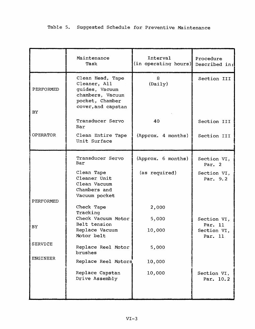
Table 5. Suggested Schedule for Preventive Maintenance
I I I
I I I
PERFORMED
BY
I OPERATOR
PERFORMED
BY
SERVICE
ENGINEER
Maintenance Task
Clean Head, Tape Cleaner, All guides, Vacuum chambers, Vacuum pocket, Chamber cover, and capstan
Transducer Servo Bar
Clean Entire Tape Unit Surface
Transducer Servo Bar
Clean Tape Cleaner Unit Clean Vacuum Chambers and Vacuum pocket
Check Tape Tracking Check Vacuum Motor Belt tension Replace Vacuum Motor belt
I
Replace Reel Motor I brushes
Replace Reel I
Motors
Replace Capstan Drive Assembly
I Interval
operating hours)1
I 8 (Daily)
40
I (Approx. 4 months)
I
(Approx. 6 months)
(as required)
2,000
5,000
10,000
5,000
10,000
10,000
VI-3
I Procedure I Described in:
Section III I
Section III
I Section III
I
Section VI, Par. 2
Section VI, Par. 9.2
Section VI, Par. 11
Section VI, Par. 11
Section VI, Par. 10.2

1. POWER SUPPLY MAINTENANCE
1.1 CHECKING UNREGULATED POWER SUPPLY
A check may be made of the unregulated power supply by testing with a voltmeter at test points provided on the Servo Electronics module. The table below shows the voltages and corresponding test points. The voltages should be within ±20 percent of the specified nominal value. (See Figure B39 for test point locations.)
Voltage Test Point
+44V TP 17 -44V TP 20 +24V TP 18 -24V TP 19
1.2 FUSES
Seven In the on the power supply subassembly. Fl is an 8 amp fuse in the hot side of the primary power line. F2 (5 amp), F3 (5 amp), F4 (10 amp) and F6 (10 amp) supply the arc suppressing diode network (located in the power supply), the servo amplifiers and the power supply regulators. F5 is a 4 amp fuse used to supply current to the +5 volt regulator line only. F7 is a 7.5 amp fuse in the capstan motor line.
1.3 TRANSFORMER TAPS
The Mod 11 tape transport can accept power from various voltage sources, depending on the power transformer primary connection chosen. Figure 34 shows the color coding of the transformer primary wires attached to the terminal strip TBl, which is located inside the transport cabinet and is mounted on top of the transformer.
VI-4

TBI
012 32.7 V RMS
010 BLACK --125V ~I 08 WHITE -- 120V I
06 GRAY -- 100V I 04 VIOLET - 10V I
02 I
BLUE -- OV I 18 V RMS
09 GREEN-_125V~ 07 YEllOW - 120V I
05 ORANGE- 100V I 03 RED 10V I
18V RMS 01 BROWN --OV I
011
LINE T81-1 T81-2 TBI-3 TBI-4 TBI-5 TBI-6 T81-7 TBI-8 TBI-9 TBI-IO VOLTAGE 8RN . BlU RED VIO ORN GRY YEl WHT GRN BlK
90 LINE 8 JUMPER T03 LINE A JUMPER TO 5 100 LINE B JUMPER TO 1 LINE A JUMPER TO 5 110 LINE 8 JUMPER TO 3 LINE A JUMPER TO 7 115 LINE 8 JUMPER TO 3 LINE A JUMPER TO 9 120 LINE 8 JUMPER TO I LINE A JUMPER T07 125 LINE B JUMPER TO I LINE A JUMPER TO 9 180 LINE B JUMPER TO 5 LINE A 200 .L.lNE B JUMPER TO 5 LINE A 210 JUMPER 1'0 7 LINE B LINE A --220 LINE B JUMPER TO 7 LINE A 230 LINE B JUMPER TO 9 LINE A 240 LINE B JUMPER TO 7 LINE A 250 LINE B JUMPER TO 9 LINE A
Figure 34. Mod 11 Power Transformer Lead Identification
VI-5

2. TRANSDUCER SERVO BAR MAINTENANCE
Every six months the followinq servo bar and cavity cleaning procedure should be followed:
1. Open vacuum chamber door by depressing, with a screw driver or other rod like object, the three spring latches located on the metal strip on the cover.
2. Remove chamber walls that partially cover the servo bars. These walls are fastened to the main casting with eleven #4 screws that are at the rear of the casting.
3. Remove the eight screws that hold each servo bar against the tape deck.
4. Clean the bars thoroughly, using IBM tape transport cleaner, PIN 453511, to be sure all particles of dirt art removed.
5. Clean the servo bar cavity in tne tape deck, again using IBM tape transport cleaner, PIN 453511.
6. Reverse the order of instructions 1 and 2 to reassemble the bars and chamber walls.
3. OPENING OF TRANSPORT DECK
1. Turn unit power off at the control panel and disconnect the power cord, or use switch Sl located near the fuse bank.
2. Press in on the three fasteners located on the face of the chamber cover, this will allow the cover to be swung open.
3. Use a Phillip screw driver and turn the screw (located near the top of the file reel vacuum chamber) until it releases the panelock from the deck support bracket.
VI-6

4. DECK OVERLAY REMOVAL
Removal and replacement of many components requires the removal of the deck overlay. The following procedure must be followed.
4.1 REMOVAL OF FIXED REEL
Remove the three screws (item 1, Figure 35) from the reel cover. Remove the reel (item 2, Fi~~re 35)~
4.2 REMOVAL OF OVERLAY
1. Swing open the vacuum chamber door.
2. Remove the read/write head assembly cover by pulling it in the direction perpendicular to the head plate.
3. Loosen, but do not remove the four overlay screws (item 3, Figure 35).
4. Support the overlay prior to total removal of the screws to eliminate possible damage.
5. Lift the overlay off.
5. TRANSPORT CONTROL LOGIC MODULE REPLACEMENT
The Transport Control Logic module can be removed by the following steps: (Refer to Figure 36.)
1. Turn unit power off at the control panel and disconnect the power cord, or use switch Sl located near the fuse bank.
2. Swing open the transport deck as described in subsection 3.
3. Remove all the connectors from the module, using care to avoid damaging the mating pins.
4. Remove the 5 captive screws (item 1, Figure 36). Be sure to support the assembly to prevent damage when the screws are removed. The module is now free to be removed.
VI-7

Figure 35. Deck Overlay Removal
VI-8

6. SERVO ELECTRONICS MODULE REPLACEMENT
The Servo Electronics module can be removed by the following
1.
(RA-rAr 1-n Fi (TI,rA ?h ) \_ ........... --- -- --~--- --.,
Tu.rn unit off at the and disconnect the power cord, or use switch Sl located near the fuse bank.
2. Swing open the transport deck as described in subsection 3.
3. Remove all the connectors from the module using care to avoid damaging the mating pins.
4. Remove the 4 Phillip screws (item 2, Figure 26) connecting the module heatsink to the rear of cabinet. Be sure to support the assembly to prevent damage when removing the screws.
5. After installation of the new module, perform the Servo Electronics Adjustments described in subsection 17.
7. DATA ELECTRONICS MODULE REPLACEMENT
The Data Electronics module, which houses all of the record and read electronics, can be removed by the following steps:
1. Turn unit power off at the control panel and disconnect the power cord, or use switch Sl located near the fuse bank.
2. Remove connectors P3 and P4. (Refer to Figure 37.)
3. Remove the Winchester head cable connectors from the module. IMPORTANT - Use an appropriate size screwdriver on the jackscrew fasteners. Loosen the connectors evenly, alternating turns on each screw. Attempting to loosen one side at a time will cause the connectors to bind and possibly bend the pins. Use of fingers instead of screwdriver risks the possibility of breaking wires on the connectors.
4. While supporting the module to prevent damage, remove the 5 Captive screws (item 1, Figure 37) holding the module to the stand-offs.
VI-9

<: H
I-' o
POWER SUPPLY REGULATOR MODULE
MODULE
Figure 36. Transport Control Logic and Servo Electronics Module Replacement

WRITE HEAD CABLE-~-~~ CONNECTOR
P2
CONNECTORS --===:::::::;;: P-3, P ... 4
READ HEAD CABLE---"""::"':": CONNECTOR
P5
Figure 37. Data Electronics Module Replacement
VI-Il

5. Remove module by sliding it toward the rear of cabinet until it clears the module support.
6. After replacement of the new module, perform the adjustments described in the Data Electronics alignment section 18.
8. OCP SWITCH REPLACEMENT
The operator's control panel pushbutton switches and indicators are sealed assemblies. If either the switch or the indicator fails, the whole sealed assembly must be replaced. (Refer to Figure 38.)
1. Turn unit power off at the control panel and disconnect the power cord, or use switch Sl located near the fuse bank.
2. Swing open the transport deck as described in subsection 3.
3. Note the position of the push-on lugs before removing them from their terminals.
4. Removal of the switch is simplified through the use of WANGCO tool PiN T00015. Grasp the switch at the front of the panel and then insert the tool over the switch ears at the rear of the panel. The pressure applied by the tool will allow the switch to be easily removed.
5. Push the replacement switch firmly into position.
6. Connect the push-on lugs to the replacement switch in the noted positions.
9. HEAD ASSEMBLY REPLACEMENT
The Read/Write head assembly may be removed and replaced in the field by using the following procedure:
CAUTION: SYSTEM POWER MUST BE TURNED OFF PRIOR TO DISCONNECTING OR CONNECTING THE HEAD ASSEMBLY.
VI-12

<: H I
...... LV
•
Figure 38. OCP Switch Replacement

PLUG-I N PHOTOSENSE (REMOVED)
"',"',',"", ",,~_TAPE CLEANER
_~ ___ ..-....._ READ / WRITE HEAD
CAPSTAN
Figure 39. Head Assembly Replacement
VI-14

1. Swing open the transport deck as described in subsection 3.
2. Remove the head connectors P2 and P5 (refer to Figure_37) from the Data Electronics module mounted on the left side of the transport box, using an appropriate size slot screw driver. Do not use fingers for this purpose so that the possibility of damaging connector wires is eliminated.
3. Remove the four cable clamps holding the cables to the transport casting.
4. Remove the overlay per section 4.
5. Remove the three large Allen screws (item 1, Figure 39) fastening the head plate assembly to the deck. Be sure to support the head assembly to prevent damage when removing the screws. Observe the location of shims under the head plate and replace in the same position when installing the new head plate.
6. Remove head assembly.
7. Following the same procedure in reverse, install new head assembly_
8. Perform the tape tracking check described in subsection 13.1
9. T"'\ __ .t= __ ........ rt:::L LUL1U the Data Electronics subsection 18.
9.1 REPLACING THE PHOTOSENSE UNIT
The EOT/BOT photosense unit is a plug-in type. To replace unit, slide it off the connectors and install new one. Refer to subsection 17.1 for the adjustment procedure.
9.2 CLEANING THE TAPE CLEANER
1. Brush away the loose particles.
2. Clean the blades thoroughly with IBM cleaner PiN 453511 using Q-Tip applicator.
VI-IS
10.
10.1
10.2
CAPSTAN AND CAPSTAN MOTOR REPLACEMENT
CAPSTAN ONLY
The capstan can be removed and replaced by releasing the Allen screw on the top of the capstan motor shaft holding the shaft by the flats provided. Note the orientation of the capstan before removing it, and ensure that it is replaced in the same position. Capstan speed adjustments are specified in subsection 17.2.
CAPSTAN DRIVE ASSEMBLY
Replacement of the entire capstan drive assembly (capstan and capstan motor) should be done in accordance with the following procedure:
1. Turn unit power off at the control panel and disconnect the power cord, or use switch Sl located near the fuse bank.
2. Remove the capstan (see subsection 10.1).
3. Remove the tachometer plug P9 from the Servo Electronics module. Remove the tie wraps so the plug wires are free to move.
4. Note the position of the (+) and (-) power leads and then remove the leads.
5. Remove the four Phillips screws holding the motor to the transport deck. Remove the shims between the deck and the motor. Remove the motor.
6. Replace the motor and install capstan.
7. Plug the tachometer lead P9 into the Servo Electronics module.
8. Connect up the (+) and (-) leads to the motor terminals.
9. Perform the adjustments for speed and start/stop ramps as described in subsection 17.2.
10. Machine must be retracked according to 13.2.
VI-16

10.3 CALCULATING CAPSTAN SPEED ERROR
The 50/60 strobe disc "is inserted into each capstan. The inner strobe is for 60 Hz and is marked such. It is to be viewed with the corresponding AC light (such as fluorescent). The 50 Hz disc operates with a 100 Hz source, whereas the 60 Hz disc requires 120 Hz source. The disc image will appear stationary at 25, 37.5 and 75 ips only. The error from nominal for the mentioned speeds is:
E =
where V is nominal speed in ips, and T is the time in seconds for the image to drift one revolution. If the error exceeds 1%, readjust speed per paragraph 17.2.
11. VACUUM BLOWER BELT REPLACEMENT
1. Turn unit power off at the control panel and disconnect the power cord, or use switch Sl located near the fuse bank.
2. Swing open the transport deck.
3. Remove the 5 Phillips screws (item 1, Fiqare 40) securing the blower cover. Remove cover.
4. Loosen the 4 Allen screws (item 2, Figure 40) securing ~ne moun~~ng p~a~e. Slide the motor toward the blower assembly enough to allow the belt to be removed. (Access to these screws is gained through the 3 holes in the motor pulley.)
5. Install new belt with the gear teeth facing outward.
6. Using a belt tension tool as shown in Figure 40, adjust the belt tension for 5 pounds of tension when measured with the Gates 5M tensionmeter.
12. GUIDE ROLLER BEARING REPLACEMENT
Roller guide bearings, which control tape motion to and from the head, can be replaced without destroying preset tracking adjustment if appropriate care is exercised. (See Figure 41.)
VI-17

<: H I ~ co
Figure 40. Vacuum Blower Belt Adjustment

1. Note the position of each part when disassembling the roller guide. During reassembly each part must be positioned in the same manner as removed.
2. For the roller guide in Figure 41A remove the retaining ring, item 1, at the shaft end and remove the guide. For the roller guide in Figure 4lB the socket head screw, item 11, holding the cap in place must be loosened first to access the retaining ring.
3. Insert new bearing(s).
4. Replace the roller guide.
5. When replacing item 10, maintain .015 inch clearance with item 5, to ensure the drum turns freely.
6. The mechanical alignment of these guides is accomplished through the use of a height gauge (WANGCO PiN T00032), the use of which is illustrated in Figure 42.
The guides are to be set to .504/503 inches from the chamber base to the upper guiding edge of the roller guide.
7. To adjust guides (in Figure 41B) loosen the socket head screw, item 8, and adjust for proper indicator reading. To adjust guides, (in Figure 41A), remove the retaining ring and add or remove shim as required for correct indicator reading.
13. TAPE TRACKING
Tape tracking is the mechanical adjustment of elements in the tape path which contribute to the static and dynamic skew of the tape over the read/write head, as well as the proper alignment of the tape edges between the file and fixed reels consistent with proper tape handling (i.e., without damaging the tape). If retracking is found to be required, it is necessary to afterwards check the Read Stack Azimuth alignment per the procedure described in paragraph 13.3.
VI-19

o rffi Utl
I
(A) Deck Mounting Guide 201100
(B) Deck Mounting Guide-Loading 201101
Figure 41. Tape Guide Diagram
Item No. Description WANGeO PIN No.
1 Ring Retaining External 100132-001 2 Washer, Shim 200077-001 3 Shim, Deck Mounting Guide 201033-001 4 Bearing Roller 100006-001 5 Drum, Guide 201041 6 Spring 200156 7 Shaft, Roller Guide 201045 8 Screw, Set Socket Head 6-32 x 1/8 100049-302 9 Stand-off 201047
10 Cap, Loading Deck Mtg. Guide 201046 11 Screw, Set Socket Head 4-40 x 1/8 100049-202 12 Shaft, Loading Deck Mtg. Guide 701044
VI-20
Required
1 2 5 2 1 1 1 1 1 1 1 1

Figure 42. Roller Guide Adjustment
VI-21
13.1
The following tracking procedure assumes that there is no gross misalignment of guiding elements which would cause tape edge damage. All roller guides should be set to .504/503 inches from the chamber base to the upper guiding edge of the roller guide.
CHECKING TAPE TRACKING
This procedure provides an electrical check to verify that tape is tracking in the reverse direction within acceptable limits with respect to the forward direction. The procedure compares the time displacements of the analog signal peaks of the two outside channels while running tape forward with the time displacement of these peaks while running tape in reverse. If the transport is perfectly tracked, the time displacements in both directions will be the same but the phase relationship between the two peaks will be opposite. Since the accuracy of tape tracking is directly dependent on mechanical alignments and mechanical tolerance buildups, perfect tracking is usually not achieved, however, limits are established that will guarantee reliable operation in both directions. Equipment required includes an oscilloscope, ~ :o:J"!!~~' ""-.,,..~~~ ~'''!!~~ __ ..;'!-: _'"_..!! ..L"t _______ .,~ .. _.-'!_. ""'! """I: e U. u.u,u..J.. '-.J..U'-O;;:; ,t-'.J..u,'::I-.J..,L,1, dllU L.llL"ee X..LU prODeS: a.LSO requJ.rea J.s a master skew tape.
1. Scope Controls:
a) Mode - Chop AC b) Sensitivity - as required to get good resolution
of the peak time displacement c) Trigger - external (+), AC, trigger mode d) Sweeptime - 1 ~sec/cm
2. Place Channel 1 scope probe and trigger probe on the test point corresponding to the head track located closest to the transport. This test point is 602 for nine-channel systems and 102 for seven-channel systems.
3. Place Channel 2 probe on the test point corresponding to the channel farthest from the transport. This test point is 702 for nine-channel systems and 902 for seven-channel systems.
VI-22

4. Load the scratch tape and run tape in the forward direction under remote control (use off-line testertote, if available). Record TI (~sec). Run tape
5.
in the reverse direction and record T2 - (See Figure 43.) Since the read head azimuth angle can be in either direction, the actual phase relation between the reference channel and the other outside channel may be opposite to that depicted in Figure 43.
""', ___ .. _ _ _ _.c:"", _"1- ___ ".=I "1- _ _ __ .. _ ..L _.=I ..L _ I'T'I ,_ _ _ ..L'_ _ r" _ .. .. __ _
TIle Vd.l..Ue Ul.l.-2
::illUU.l..U JJe re.l..dLeU LO Tl Dy ::ne ro.l...l..O'w-
ing equation:
T = 2
-T I
± 50 V
~sec
where V represents the transport speed. If this condition is not met, the transport must be realigned. Refer to subsection 13.2 (Tape Tracking Alignment).
! I - T .. T, 2 REVERSE -~ORWARD
0 ~ ~ DIRECTION I "'" \DIRECTIQN ~~ f) (I I ' ~\' I \ illl \\~
Ul \\'\ , iill \\ ~\ ~/J \l\\ I ~ II/I \\\,
~II/ ~\~ II \J (II \\\\ T
j -5 -4 -3 ~ -2 -1 0 1 J V 2 3 \~ .\ 5 .'-
rrI/1 t '\ ~\\ I I/I)~ 'i~\\ h~L r\\~ .I I (~ \ . 1\)\\
JhV \\~ I 1J. 'l , .. F~· ~~Ntl~t
Figure 43. Checking Tape Tracking, Desired Waveform
VI-23
13.2 TAPE TRACKING ALIGNMENT
Before tracking, all roller guides and fixed guides must be set .504/503 inches, measured from the chamber base to the upper guiding edge of the roller guide. Refer to Figure 44 when performing the following steps.
1. There should be no shims under head guides A and B or under capstan motor bosses "X" and "Y" (see Fig.44).
2. Using a master skew tape observe the displacement between the outside head tracks in the forward direction only. Determine which guide i.e., A or B should be shimmed to correct azimuth. This may be done by pressing against the tape edge near guide A or B. If pressing against the tape edge at Guide A improves the azimuth, then guide B requires shims and visa versa. Refer to Read Stack Azimuth Correction in section 13.3.
3. Different procedures are followed depending on whether:
Case (a)
(Case a) Guide A is shimmed (Case b) Guide B is shimmed (Case c) No shims are required
1. Using a master skew tape observe the displacement between the outside head tracks while running tape in the forward direction.
2. Add shims P/N 200203 under guide A until there is zero forward skew.
3. Remove the ceramic guiding washers from guide B, replacing the guide body and cap only.
4. Using master skew tape observe the displacement between outer tracks while running tape in the reverse direction.
5. By pressing against the tape edge near guide B determine whether pushing the tape towards the deck or away from the deck reduces the reverse skew.
VI-24

6. If the skew improves by pushing the tape towards the deck then the capstan motor needs to be shimmed under bosses IIX". If skew improves by pushing away from the deck, motor needs to be shimmed under bosses lIyll.
7. The number of shims depend on the magnitude of skew. However there must be an equal number of shims under each of either the IIX" or "Y" bosses. Shims to be
(2 Mil), PiN 201032=002 (I Mil)~
8. After shimming for zero reverse skew replace ceramic guiding washers at guide B. Both forward and reverse skew should now be close to zero.
Case (b)
1. Remove the ceramic guiding washers from guide B, replacing the guide body and cap only.
2. Follow same procedure for capstan shimming as in case (a).
3. Replace ceramic guiding washers at guide B.
4. Using master skew tape observe the forward skew.
5. Shim guide B for zero forward skew.
6e Both forward and reverse skew should now be close to zero.
Case (c)
Same as Case (a) except neither head guide has to be shimmed.
VI-25

GUIDE A
GU I DE B
__ -+-_ CAPSTAN MOTOR ADAPTOR PLATE
II X II __ ---+-__
_ _____ lIy"
NOTE: ITE MS "X" AND "y" ARE CAPSTAN MOTOR BOSSES
Figure 44. Tracking Adjustment
VI-26

13.3 READ STACK AZIMUTH MEASUREMENT AND CORRECTION
This adjustment is required when the read/write head assembly, capstan or capstan motor have been replaced. It is also used in conjunction with tape tracking alignment in section 13.2. Its purpose is to ensure that the read stack is perpendicular to the tape path. This is a mechanical adjustment and is accomplished by shimming either (but only one) of the two guides mounted on the head assewhly base plate. are mounted by removing the guide, inserting a shim on the guide shaft, and re-assembling the guide on the base plate. The shims are 0.0002 inch thick and one shim will correct for 15 micro-inches of skew.
1. Scope controls:
a) Mode--Chop.
b) Sensitivity--O maximum, both channels.
c) Trigger--External (+) AC trigger mode.
d) Sweeptime--Sufficient resolution so that the read signal peaks are well defined.
2. Place Channel 1 scope probe and trigger probe on the test point corresponding to the head edge track located closest to the transport. This test point is 602 for nine-channel systems and 102 for sevenchannel systems.
3. Place Channel 2 probe on the test point corresponding to the channel farthest from the transport. This test point is 702 for nine-channel systems and 902 for seven-channel systems.
4. Load a master skew alignment tape, making sure that the write enable ring is removed. Place the tape controller unit in a read mode and observe the time displacement between the read signal peaks (see Figure 45). If the time displacement corresponds to a distance less than 25 micro-inches (1 ~sec at 25 ips), no shimming is required:
Distance (~inch) = Velocity (ips) X Time (~sec).
VI-27

TP 702
If the signal on Channel 2 lags the reference channel, and if the time displacement corresponds to a distance greater than 25 micro-inches, the guide on the file reel side of the head assembly must be shimmed. The number of shims can be calculated as follows, where N represents the number of shims:
Figure 45.
N = (Tape Speed) (Time) 15
REFERENCE CHANNEL (TP 602)
Read Head Signal Peaks, Dual Gap Systems
VI-28

I I .
rp' Displacement for Speed Indicated (j.lsec) Number of _lme
Shims 25 ips 37.5 ips 45 ips 75 ips
1 0.4 - 0.91 0.3 - 0.61 0.2 - 0.51 0.1 - 0.3 I 2 1.0 - 1.5 0.7 - 1.0 0.6 - 0.9 0.31-0.50 3 1.6 - 2.1 1.1 - 1.4 1.0 - 1.2 0.51-0.70 I 4 2.2 - 2.7 1.5 - 1.8 1.3 - 1.5 0.71-0.90 t:: ') Q "l "l 1 a ') ') 1 c.. 1 0 ("\ a1 1 1n oJ L.,.u -' • ...; i ....L. J L... L. I ~~u ... '" U I V",':;"'-L .. LV
6 3.4 - 3.9 2.3 - 2.6 1.9 - 2.2 1.11-1.30 7 4.0 - 4.5 2.7 - 3.0 2.3 - 2.5 1.31-1.50 8 4.6 - 5.1 3.1 - 3.4 2.6 - 2.8 1.51-1.70
Shim Table for Standard Tape Speeds
5. If the signal on Channel 2 leads the reference channel, the tape guide on the capstan side of the head assembly must be shimmed according to the instructions in step 4.
6. After the guide is shimmed, verify that the time displacement between the outside channels corresponds to a distance less than 25 micro-inches.
7. Measure and record the static data staircase using the master skew tape and utilizing the method described in subsection 18.7. This data will later be used to compare with the results of that section.
14. VACUUM CHAMBER PRESSURE ADJUSTMENT
14.1 TAPE TENSION
The tape tension is proportional to the chamber vacuum. A vacuum of 30 inches of water produces 8 ounces of tape tension.
1. Load a reel of tape on the deck. If the transducers are to be aligned next, use the continuous tape loop described in Section 15, step 1.
VI-29

CHAMBER TEST NIPPLE
HOSE PUCKER POCKET TEST NIPPLE
VACUUM HOSES
Figure 46. Vacuum Adjustment
VI-30

14.2
2. Connect a vacuum gauge to the test nipple. See Figure 46.
3. Set the vacuum by means of the adjustable air bleed as shown in Figure 46. The vacuum pressure shall be set to 30 ± ~ inches of water. after removing the
VACUUM POCKET
Cap the nipple
Insure that the chamber pressure (paragraph 14.1) is set correctly before making the following adjustment. The drive must be loaded as in 14.1.
1. Connect a vacuum gauge to the test nipple. See Figure 46.
2. Read the gauge. If vacuum is not between 10 and 12 inches of H20, lift the tape from the vacuum pocket, loosen the screw and adjust the metal slide (refer to Figure 47) by moving it up to increase vacuum, or down to decrease vacuum. Put the tape back into the vacuum pocket and check the gauge again. Repeat until proper vacuum is reached. Tighten the screw. Remove the meter and cap the nipple.
Figure 47. Pucker Pocket Adjustment
VI-31
15.
NOTE:
TRANSDUCER ALIGNMENT
1. Ensure that the source vacuum has been set up as described in section 14.1 before making this adjustment. Thread a continuous loop of standard tape (106.25 inches in circumference) around the tape path as shown in Figure 48. This loop can be made up by cutting a piece of tape 106.25 inches long and splicing the two ends together.
2. Load the drive and then hold the RESET switch depressed for 10 seconds to keep the capstan from turning.
3. Using a scale and measuring on the face of the chamber cover, set the loop in the fixed chamber to 7.30 inches below the top of the chamber grill as shown in Figure 49. Both chambers are now at zero position.
4. internal to the transducer assembly enclosure (see illustration on page VI- 3'3) which is mounted on the rear of the transport casting, as shown in Figure 57. With the oscilloscope, monitor TP14 (FILE) located on the Servo Electronics module. Loosen the two screws fastening the bottom photocell board and reposition it until a 0 ±O.lV level is obtained. Tighten down the two screws.
5. Monitor TPII (FIXED) located on the Servo Electronics module, and move the upper photocell board until a o ±O.lV level is obtained. Tighten the photocell board down.
Tightening of the screws on the photocell boards may shift the setting~ therefore, recheck the test points after the screws have been tightened.
6. Remove the continuous t"ape loop.
VI-32

BOTTOM PHOTOCELL BOARD MOUNTi NG SCREW
TOP PHOTOCELL BOARD MOUNTI NG SCREW
Transducer Assembly Enclosure
(For location of Transducer Assembly, see Figure 57)
VI-33

16. REGULATED POWER SUPPLY ADJUSTMENTS
There are four regulated voltages, +12 volts, +S volts, -12 volts and -S volts. The +12 volt, +S volt, and -12 volt regulators are independently adjustable. The -S volt supply is slaved to the +S volt, which it tracks to within ±4 percent.. The adjustable supplies will hold an accuracy of ±S percent' for all variations of load, line, life and setting when adjusted with a meter having a ±2 percent accuracy or better. The adjustments are located on the regulator board. (See Figure B-3). Potentiometer adjustments and test points are given in the following table:
Adjust With Connect Meter Between Voltage to: Potentiometer Test Points
+12V R18 TP4(+) & TP3(-)
+ SV R8 TP2(+) & TP3(-}
- sv - TPl(-) & TP3(+)
-12V R24 TPS(-) & TP3(+}
17. SERVO ELECTRONICS MODULE ADJUSTMENT
17.1
NOTE: Prior to making the Servo Electronics Adjustments, insure that the S volt regulated supplies are correctly adjusted. (See section 16). Also verify that the vacuum is correctly set. (See section 14).
EOT/BOT PHOTOSENSE ADJUSTMENT
1. Connect a voltmeter between test point 7 and ground. (Refer to Figure B-2S).
2. Adjust potentiometer R19l so that the voltmeter reads O.OV ± O.lSV while tape is loaded on the transport but neither photosense tab is being sensed.
VI-34

,t_ .. __ .. I C'.::' C:1 c::i
.. ~.-.-, .. ;:'\ _ .. " I "\ ·gd I
\ II L
JII' II I~ r/ II' ' .. , ~ ~-~I I I ." ~ "~! ~~ ;"1-
. .1
L ..... '. . :'.1
~ ., . _.;,u JbJ" . '"!'
. -:::- ,..
Figure 48. Mounting the Tape Loop
r.1iiii1lii ___ 1iiil.lii
-,
.. ~ 1 7.30
6.00 7.30 I
Figure 49. Chamber Adjustment
VI-35
~ 6.00
~

17.2 CAPSTAN SERVO ADJUSTMENT
17.2.1 Offset
1. Connect a voltmeter between test point 6 and ground (refer to Figure B-25).
2. Adjust the offset control potentiometer R38 so that the voltmeter reads 0 ±O.lOOV.
17.2.2 Forward Motor Speed
The strobe disc is mounted inside the face of the capstan and has two patterns. The inner pattern is used for 60 Hz units, and the outer pattern is used for 50 Hz units.
1. For tape transports operating at 25, 37.5 and 75 ips, while running the unit in the forward direction under manual control, illuminate the capstan with the corresponding AC light (such as fluorescent) and adjust Rll for a stationary pattern on the strobe disc.
2. For all other speeds, using an IBM skew tape adjust the potentiometer for a pulse repetition period shown below. This will be observed at TP3 on the Data Electronics module. (Refer to Figure B-27).
P = 1250 S
j..lsec
where S is machine speed.
17.2.3 Reverse Motor Speed
Connect an exerciser capable of making the transport run both continuous and start/stop forward and reverse programs to the customer logic input on the control electronic board.
1. Refer to the procedure in step 1 (Forward Motor Speed), while using the exerciser to run the tape in reverse, and adjust potentiometer R12.
2. Duplicate the procedure in step 2 (Forward Motor Speed) while using the exerciser to run tape in reverse and adjusting potentiometer R12.
VI-36
17.2.4 Start/Stop Ramp Time
The start/stop ramp times can be properly adjusted only after the forward-reverse speeds have been set up. Only the forward and reverse stop ramps will be adjusted since adjusting the stop ramp for one direction also adjusts the start ramp for the opposite direction. The ramps will be observed at the capstan tachometer output.
Forward Stop Ramp Time:
1. Initiate a start/stop forward motion program.
2. Trigger oscilloscope sweep on IIExternal Negative ll
at the Motion TPS on the transport control logic board (Figure B-21) and monitor the tach signal at TPS on the servo amplifier board (Figure B-2S).
3. Adjust R20 on the servo amplifier board to make the ramp come to ground in the time given by the following equation,after the start of the sweep.
T = 380
S -0.5
where T is the stop ramp in milliseconds and S is the operating speed of the transport in ips.
Since the tachometer signal is grounded, consider the ramp to be at ground when the projection of the straight portion of the signal has crossed the ground level. (Refer to Figure 50).
Reverse Stop Ramp Time:
1. Initiate a start/stop reverse motion program.
2. Using the same procedure as outlined in step 2 of Forward stop Ramp Time paragraph above, adjust potentiometer R19 for the same stop ramp time established in step 3 of the procedure.
VI-37
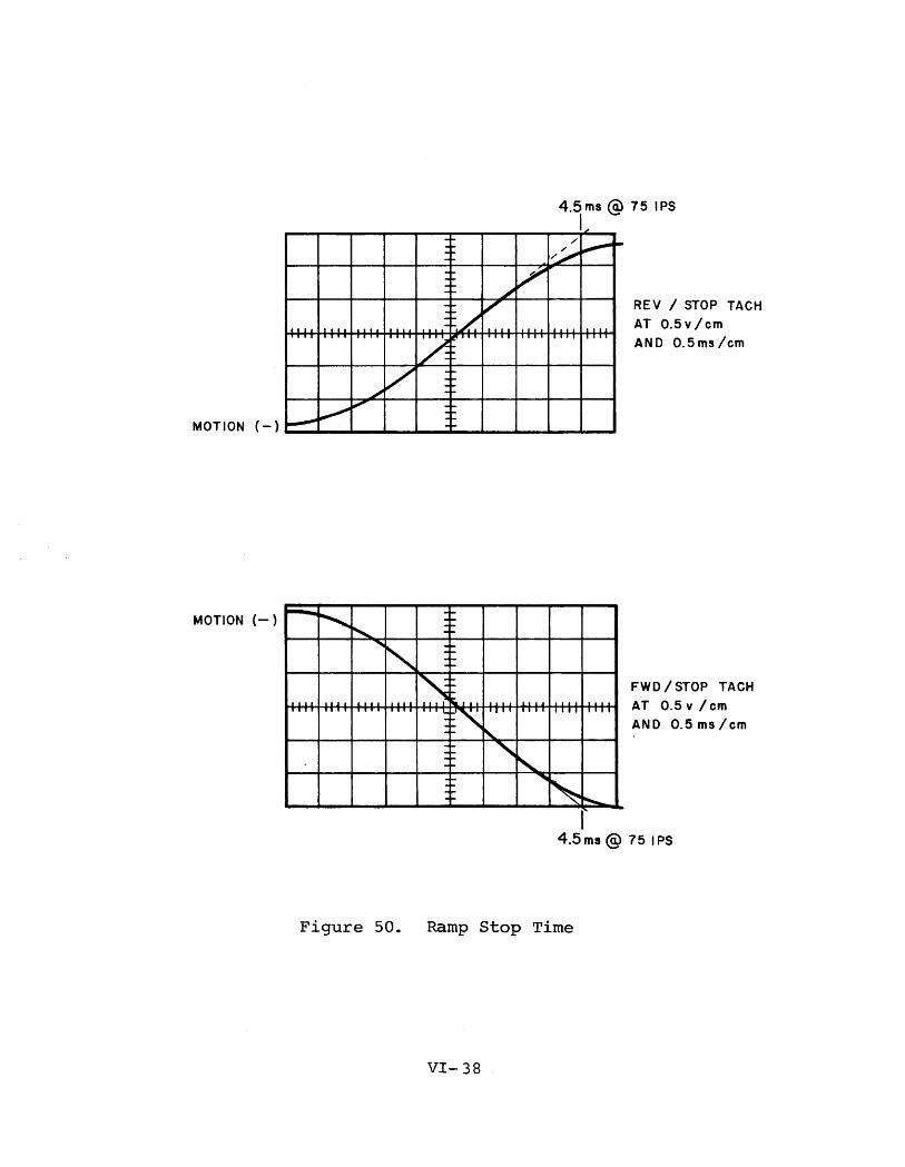
MOTION (-)
MOTION (-)
--~ -:~ -~
-~
..... , , I' 'I
:~!/ -~, , . . .
'l7~ -~
V -~
~ :~ -l-
V ~ ~
~ .1= -~
....... -~
~ --, ----~, :::
:t
. . . I~~ I. ~ . , " \.,
~" --~ -~
:~ -~
I-~ ~
-I-
~ V
~ , ,
""
.. II' III'
"-
" ~ ""'l1lI
4.5ms @ 75 IPS
I " ./ ~~
~
,., , ,
" "
, . , llTT T ·fT
~ "'-I
REV / STOP TACH AT 0.5v/em
AND 0.5 ms /em
FWD/STOP TACH
ATO.5v/em
AND 0.5ms/em
4.5ms @ 75 IPS
Figure 50. Ramp Stop Time
VI- 38

17.3 REEL SERVO ADJUSTMENT
17.3.1 Chamber Measurement
Determine the location of the center of each of the buffer storage chambers by measuring 7.3 inches from the grill at the extreme of the chambers. Mark this point on the outside of the inner door, which covers the chambers. Mark with removable grease pencil or with masking tape. Measure 6 inches both sides of the marks on both charr~ers and mark these spots.
17.3.2 Gain Adjustment
1. If not already there, return tape to BOT.
2. To set the gain of the file reel amplifier, grasp the file reel and move it to shift the tape back and forth between the 6 inch marks established above.
3. Monitor the voltage output at TP16 and adjust R160 so that there is a voltage difference of 24 volts between the 6 inch marks on the vacuum chamber.
4. Using the same procedure as in step 3, set the gain of the fixed reel by adjusting Rl06 and monitoring the voltage output at TP13.
17.3.3 Reel Position Adjustment
17.4
1. Adjust R153 to center the loop in the file reel chamber.
2. Press the Forward pushbutton and all tape to advance to EDT.
3. Adjust RlOa to center the loop in the fixed reel chamber.
REWIND TEST
If tape is not already at EOT, press the reset button, and then the Forward button on the OCP. Allow the tape to run until EaT is reached. Press the Rewind button on the OCP. The tape unit should rewind, set forward and advance to EDT.
VI-39

17.5
18.
18.1
UNLOAD TEST
Press the Rewind button while at BOT. The transport should go into reverse and unwind all the tape from the fixed reel. The fixed reel tape loop should ride near the top (source end) of the fixed reel chamber during this operation.
DATA ELECTRONICS DUAL GAP SYSTEMS ADJUSTMENTS
ADJUSTMENT SEQUENCE
All alignments are made at the factory prior to shipment of equipment. Verify alignments if either the subassembly has been replaced, or if data electronics or heads seem to malfunction. Before performing the adjustments, verify that the scope probes, plug-in unit, and time base are calibrated.
All potentiometer and test point locations are identified by a silk-screened designator adjacent to the component on the module. (See E'igure B....,27 for tQe physical board location of test points and adjustments.)
WARNING: SYSTEM POWER MUST BE TURNED OFF BEFORE DISCONNECTING OR CONNECTING EITHER THE DATA ELECTRONICS MODULE OR THE HEAD ASSEMBLY.
Tape transport and power supply adjustments must be verified before performing the data electronics adjustments. Because of the interrelationship among the circuits, the adjustments must be made in the following sequence:
1. Phase splitter quiescent level adjustment.
2. Read amplifier gain adjustment.
3. Cross feed shield.
4. Read strobe delay adjustment.
5. Write stack deskew.
a) Read stack profile measurement.
b) Write deskew single-shot adjustment.
6. Verification--staircase measurement.
VI- 40

18.2
18.3
PHASE SPLITTER QUIESCENT LEVEL
The following prescribes the adjustment procedure for nine-channel tape transports. The levels at test points 202 and 302 need not be correct for seven-channel systems:
a) Mode--Channel l7DC.
b) Sensitivity--0.05V/cm.
c) Trigger--Internal, automatic stability.
2. Connect Channel 1 probe to test point 102.
3. Without running tape, adjust potentiometer R27 until +1.0 VDC is observed at test point 102.
4. Scan test points 202 and 902 to ensure that the quiescent point of all the phase splitters falls within +1.0 ± 0.3 VDC.
5. If this condition cannot be attained, readjust R27 until the condition is satisfied.
READ AMPLIFIER GAIN
The following prescribes the adjustment procedure for nine-channel tape transports. For seven-channel systems, set R2l8 and R3l8 fully counterclockwise.
1. Scope controls:
a) Mode--Channel liAC.
b) Sensitivity--O.2 V/cm.
c) Trigger--Internal, automatic stability.
2. Load Standard Level Output Tape on the transport and set the tape controller for a continuous write mode at a frequency corresponding to 800 cpi and ones written on all channels.
VI-4l

3. Connect Channel 1 scope probe to test point 102 and run tape forward. Adjust RIlB so that the analog signal has a l2-volt peak to peak amplitude. (See Figure 51.)
4. Repeat for all channels. See Table 3 for correct potentiometers and test points.
-I---~ -I---
I 11111111111111111111111111111111111111111- 11111111 11111111111 1111111111 1111111111 1111111111
-AT T
12 V
1+H-PI02
- . . .. . .. ~. ..... .. . .... ....
~
---------
Figure 51. Read Amplifier Gain Adjustment, Dual Gap Systems
IB.4 CROSSFEED SHIELD
This is a mechanical alignment, on the head gate assembly, necessary to minimize the write-to-read crossfeed signal.
1. Place Channel 1 scope probe on test point 602 and Channel 2 scope probe on test point 702. If this is a seven-channel system, place Channel 1 scope probe on 102 and Channel 2 scope probe on 902. With scope plug-in mode on alternate, set both scope channel vertical gains to 0.2 V/cm.
VI-42

18.5
2. Set the tape controller unit for a continuous write mode, all ones on all channels. Run transport and observe crossfeed on the two edge channels. The crossfeed manifests itself as amplitude modulation of the read data. This can be seen by lifting the head shield cover and observing the amplitude modulatlon lhcrease.
3. Loosen the two head gate screws and reposition the gate by moving it in the plane shown in Figure 52 until a minimum amount of modulation voltage is observed on both channels. The edge of the ferrite should be approximately opposite the Write gap. Be sure that the shield housing is resting on the head block at front and back.
FORWARD TAPE MOTION
/ HEAD GATE ASSEMBLY
COPPER SLUG
r------ SHIELD HOUSING
,------ FERRITE CHIP
WRITE READ HEAD HEAD
ADJUSTMENT DIRECTION
Figure 52. Head Gate Adjustment, Dual Gap Systems
READ STROBE DELAY
1. Scope controls:
a) Mode--Channe1 1, DC.
b) Sensitivity--O.1 V/cm.
c) Trigger--Interna1 (+) trigger mode.
VI-43

-
Table 6. Data Electronics Adjustment Points - Dual Gap Systems
Channel
P
0
1
2
3
4
5
6
7
Alignment Section
Read Amp Gain Write
Test Point Pot. No. Test Point
TP-102 R-ll8 TP-103
TP-202 R-2l8 TP-203
TP-302 R-3l8 TP-303
TP-402 R-418 TP-403
TP-502 R-5l8 TP-503
TP-602 R-6l8 TP-603
TP-702 R-7l8 TP-703 -
TP-802 R-8l8 TP-803
TP-902 R-9l8 TP-903
- ~ - ---- ---'" - -- -- --------~ - ~ - f-
III l II 1 ( 1111 IIII II IT. ~lll llit I! II III I 11'1 " II I I I 1"-~" I
I I I I II I I
- ~ -~ -I-
- ~ = ~ ~ -~ \.. --- ---- -- -- "----i-
I 9.5 USEe AT TP 3 I ~ AT 751PS ~
Deskew Comments
Pot. No.
R-104
R-204 Not used in 7-channel systems
R-304 Not used in 7-channel systems
R-404
R-504
R-604
R-704
R-804
R-904
II II I I Ll I I I, I I' J
Figure 53. Read Strobe Delay Adjustment, Dual Gap Systems
VI-44

18.6
2. Connect Channel 1 scope probe to test point 3.
3. Verify that the transport is selected for high density operation and write all "ones" as described ~~ ~~_~~_~~h lQ A Qro~? .L~.l .t"~.L"-L'::::I.L"-L1:""'.l .......... -., ............ ,t' ....
See Figure 53. Adjust R49 for a pulse width of one-half frame time plus 1.1 ~sec. At 75 ips this
_ _ _ _ _ _ 1
should be 9.5 ~sec. Frame time is defined as __ .L_, . . VD
where V is the transport veloc1ty and D 1S the operating data density.
WRITE STACK DESKEW
The method used to ensure proper Write head deskewing is first to plot the read stack gap scatter in the forward direction, referencing each track to the leading track, and using an IBM Master Skew Tape. Then the gap scatter plot is duplicated while writing all ones on a scratchpad tape by adjusting the potentiometers of the Write Deskew single shots.
18.6.1 Read Head Stack Profile
The method used to measure and record the gap scatter is first to locate the leading track and then to measure the time displacement of each of the other tracks with respect to this track.
18.6.1.1 How to Locate the Leading Track:
The leading track will be located by comparing all the tracks t"O each" other in the method described below. The digital data compared, will be only that which corresponds to the negative peaks of the analog signals observed at TPl02 - TP902. By taking this precaution, error due to the effect of the pulse pairing phenomenon is eliminated.
1. Scope controls:
a) Mode--Chop.
b) Sensitivity--O.2 V/cm, DC, both channels.
c) Trigger--External (+) AC mode connected to CHI Trigger out jack .
. VI-45

CH. I
CH.2
2. Using the IBM Skew Tape, run the transport in the forward direction in the ON-LINE mode.
3. Connect the Channel 1 scope probe to TPl03 and the Channel 2 probe to TPl02. Set the scope sweeptime at 0.5 ~sec/cm. One of the patterns shown in Figure 54 will be observed on the screen:
---+---
I I
A B c
Figure 54. Triggering Method
4. If the display of Figure 54A. is observed, proceed to step 5, since this indicates that correct triggering of alternate bits generated by the negative analog signal peaks has been achieved.
a) If the display of Figure 54B is observed, triggering is on alternate bits but created by the wrong polarity analog signal peak. To correct the triggering, lift and re-apply Channel 1 probe to TPl03. Normally, after one or two tries, triggering will switch to the correct polarity.
b) If the display of Figure 54C is observed, triggering again is incorrect because it is occurring on every bit. To correct this condition, change to a faster or slower scope sweep speed.
VI- 46

c) Once the display of Figure 54A is obtained, do not change the sweep speed for the remainder of the procedure. If greater sweep speed resolution is required, use the Horizontal Magnifier. Correct triggering will be maintained as long as the trigger probe is not moved to another point or if the tape does not change direction.
5~ Move Channel 2 probe to TP203.
a) If it is observed that the positive-going pulse of TP203 follows the trigger pulse, move Channel 2 probe TP303, since TPl03 is the leading of the two tracks and it is required to maintain the Channel 1 probe on the leading track. Repeat the process until the signal on Channel 2 is not observed.
b) If the signal on TP203 is not observed on the screen, ~t is the leading track. Move Channel I probe to TP203. Since the trigger probe has now changed location, verify that triggering is still correct, following the method described in step 4 by observing TPI02 with Channel 2. Move Channel 2 to TP303.
6. Repeat the process described in step 5 until all the tracks have been scanned, making sure correct triggering is maintained every time the Channel I probe is moved to the newly-found
7. To verify that the leading track has truly been located, keep the Channel 1 probe fixed on that track and scan the remainder of the tracks with Channel 2 probe. The leading edge of the positive pulse will be observed at all of the test points.
18.6.1.2 Profile Plot:
Keeping Channel 1 probe on the read register test point corresponding to the leading track, use Channel 2 probe on TPI03 through TP903. Record the time displacement between the leading edges of both pulses for each track, making sure that the proper triggering method is used.
VI- 47

18.6.2 Write Single-Shot Deskew
18.7
This adjustment is performed while the transport is loaded with a scratch tape for writing all ones on all tracks at 800 cpi.
1. While running the transport continuously, display the reference track on Channel 1 and the test track on Channel 2 of the scope. Set the reference track potentiometer to approximately one-third turn from the counterclockwise position. Adjust the corresponding write deskew potentiometer so that the read profile of paragraph 18~6~1=2 is duplicated, making sure that the proper triggering method is used.
2. Repeat for all tracks. See Table 6 for correct test point and potentiometer.
VERIFICATION--STAIRCASE MEASUREMENT
A quick verification of all the foregoing adjustments can be made by checking the width of the data staircase when the transport is running in the forward direction.
1. Scope controls:
a) Mode--Channel 1, DC.
b) Sensitivity--O.l V/cm.
c) Trigger--External (+) AC, Trigger mode.
2. Connect scope trigger probe to test point 3, and Channel 1 probe to test point 2.
3. While writing continuous "ones ll, the waveform should
resemble that shown in Figure 55. Time T should approximate the results of subsection 13.3 step 7 and should not exceed:
100 ~sec (T<1.33 ~sec at 75 ips).
Tape Speed
Time T shall not include the effects of dynamic skew.
VI-48

4. If this condition is not met, repeat the procedures specified in paragraph 18.6.
---"l\
~. \ ~ ... ,
~\ ,
" -.:" ~" 1 I' \ ~ \ " ' .....
\ '\~ \ , .;: ~. " ! \l \ \
~,.. , \
l-'\ \ , ~
I
1\ I I i I
~T~ DYNAMIC SKEW EFFECTS
( EXAGGE RATED FOR ILLUSTRATION)
Figure 55. staircase Waveform, Dual Gap Systems
VI- 49

19. TROUBLESHOOTING
The Troubleshooting Guide on pages VI-52 through VI-60 is a diagnostic aid for the isolation of faults within the transport system. It lists possible symptoms, probable causes for the malfunction, and corrective actions. A reference column cites the text or drawing, relevant to any particular event, which should be consulted for further information and verification. The preceding photographs (Figures 56 and 57) identify assemblies and subassemblies and aid in their location in the transport.
VI-50

<: H I
lJl I---'
O.C.P. SWITCHES
WRITE ENABLE SWITCH
FILE REEL HUB
FIXED REEL HUB
ARM DOOR STOP
Figure 56. Tape Transport (Front View)
Df:CK MOUNTING GUIDE
DECK ftETAINING CATCH
DE:CK MOUNTING GUIDE LOADING
DE:CK MOUNTING GUIDE
PUICKER POCKET
VP.CUUM SENSOR HOLES
VACUUM SENSOR HOLES
~--- HE~AD GUIDE
~--- nlPE CLEANER
.---- BelT I EOT SENSE
RE:AD I WRITE HEAD
CI;:QSSTALK SHIELD
HE:AD GUIDE
CA,PSTAN
DE:CK MOUNTING GUIDE LOADING
DE:CK MOUNTING GUIDE

-< H I
Ul N
DECK RETAINING CATCH
WR ITE ENABLE SW'TCH
FILE REEL MOTOR
LIMIT SWITCHES
S-I MASTER POWER ON/O" SWITCH
DATA ELECTRONICS, PWB
TRANSDUCER ASSEMBLY
VACUUM HOSES
FXEO RIEL ~1CJTOR
CAPSTAN MelTOR
Figure 57. Tape Transport (Rear View and Cabinet)
TB-I
POWER SUPPLY REGULATOR ASSY.
CONTROL LOGIC ELECTRON ICS, P1
TB- :3
POWER SUPPLY ASSEMBLY
SERVO ELECTRON ICS, PW B
VACUUM MOTOR
TB-7
VACUUM BLOWER ASSEMBLY
TB-2

<: H I
U1 LV
Symptom
Power indicator light does not work when POWER pushbutton is pressed on front paneL
TROUBLESHOOTING GUIDE
Probable Cause
Sl power switch in OFF position.
+5 volts mdssing.
Fuse Fl open.
Power indicator lamp burned out~.
No AC vol t~age to transport
Remedy
Switch Sl to ON position (Located next to fuse bank.)
Check +5 volts at TP2 on regulator circuit board which is mounted on the rear panel.
Replace fuse Fl.
Check the two outside terminals for lamp conti.nuity. Replace the lamp i.f it is burned out.
Check outlet with voltme!ter for the proper AC vol tagr'e.
Reference
Section VI, lPigure 57
Section VI I~igure 57
Section VI, Figure 57
Section VI, Paragraph 8
--------------------~----------.------------~--------.--------------.,--~

<! H I
U1 ~
Symptom
When the LOAD button is pressed.the vacuum blower does not turn on.
After the LOAD button is pressed and the vacuum blower comes on, the fixed reel does not put tape into the fixed chamber.
TROUBLESHOOTING GUIDE
Probable Cause
K4 vacuum blower relay missing return path.
+24V not present on K4 vacuum blower relay
K4 vacuum blower relay coil open
Tape threaded incorrectly.
Excessive tape edge damage
Vacuum set incorrectly
Fixed reel amplifier defective
Remedy
Seat the P13 connector
Check relay driver Q:i6 for an open
Seat the P13 connector
Check +24V Fuse F4.
Check for continuity be!tween terminals 3 and 4 of TB7.
Cb.eck threading diagram
Cbeck for excessive tape edge damage
Check and set vacuum level.
Remove tape, check TP13 on Servo Electronics circuit board for proper output during load sequence
Reference
B25 & B26
B25 & B26
B25 & B26
Section VI Figure 57
Section VI Figure 57
Section II Figure 3
Section VI Par. 14
Section V Par. 2 B25 & B26
~------------------~------------------------~_,----------------.--------------------~

<: H I
(J1 (J1
~rROUBLESHOOTING GUIDE
--------------·------------~---------------------------r----------'----------------·,-----Symptom Probable Cause Remedy
~------------------------4_--------------------------~----------,-----------------.---+-Reference
After a LOAD sequence is initiated and both the fixed and file chambers have tape in them, the transport does not tension the tape.
K2, load relay defective
File reel motor defective
Tape was left in chambers prior to pressing t:he LOAD button.
Excessive tape damage.
Vacuum not. set correctly.
Vacuum switches S2 and S3 failed to close.
Check if P8 Pin 3 follows TP 16 on Servo Electronics circuit board during load sequence.
Check if signal of TP 16 on Servo Electronics circuit board is present at TB 2 terminal 6 during load sequence. If not, check for loose connection.
Take up slack by pressing the REWIND button.
Replace tape. If necessary retrack m.achine.
Check and set vacuum.
Check for switch closure as tape goes into each chamber.
B25 & B26
B25, B26 and Sect:ion VI Figure 57
Seci:ion VI, Para. 13
Section VI Par. 14
Assemby vacuum :switches :201097 B-1] L-________________________ ~ __________________________ ~ __________ . _________________ , __ ~ _____ , __________ ~

<: H I
U1 0"1
Symptom
After the LOAD button is pressed and the vacuum blower comes on, the file reel does not put tape into the File Chamber
TROUBLESHOOTING GUIDE
Probable Cause
K2 load relay defective
Fixed reel motor defective
Tape threaded incorrectly
Excessive tape edge damage
Vacuum set incorrectly
File reel amplifier defective
Remedy
Check if J8 Pin 1 follows TP 13 on Servo Electronics circuit board during load sequence.
Check if signal of TP 13 on Servo Electronics circuit board is present at TB 2 terminal 9 during load sequence. If not, check for a loose connection.
Check threading diagram.
Replace tape. If necessary r4~track machine.
Check and set vacuum level.
Remove tape, Check TP 16 on Servo Electronics circuit board for proper output during load sequence.
Reference
B25 & B26
B25 & B 26 Section VI Figure 57
Section II Figure 3
Section VI, Para. 13
Section VI Par. 14
B25 & B26
~------------------------~------------------------~~--,----------------------------,,--------------~

<: H I
U1 .....,J
Symptom
'TROUBLESHOOTING GUIDE
'------.r-----'--------.-------------~'-------------,------.... --------,----~-----------,--~ Probable Cause Remedy
----il----,----,--------''''-- -------p .. ,--- ,-------+------1 Ready relay Kl failed to pull in.
Load relay K2 defective.
Chamber servo transducers defective.
Either reel amplifier defective.
Capstan amplifier defective.
Check that connectors P7 and P14 on Servo Electronics circuit board are seated.
Check that Q76 on Servo Electronics circuit boar.d supplies a ground at the initiation of a load sequence.
Check for relay continuity between P7 pin 3 and +24V .
Check that pins 9 and 10 of K2 make contact during the load sequence.
Check for burned out lamps in transducer box.
Check for proper amplifier operation.
Check TP 6 for approximately 0 volts when no Motion commands are present.
B25 & B26
B25 & B26
B25, B26 B-1 & B--2
B25 & B26
B!5
SE~ction VI par.. 17.3
B 25 & B26
~--------~------~----------------------,----__ ---------,----------------,----~----,----------~

<: H I
Ul OJ
Symptom
When the LOAD pushbutton is pressed, tape tensions, but tape does not move forward.
When the LOAD pushbutton is pressed, tape tensions and the tape moves forward but does not stop at the BOT marker.
TROUBLESHOOTING GUIDE
Probable Cause
No forward motion (forward lamp not lit).
Ramp generator circuit now working.
Capstan amplifier not working.
BOT tab dirty or tarnished.
Photo sense lamp burned out.
Photosense assembly not adjusted correctly.
Open interconnecting Cable
Remedy
Check TPl for high level
Check TP3 for voltage output.
Check TP6 for voltage output
Clean with IBM tape transport cleaner.
Remove head cover and check.
With tape loaded and not at BOT TP7 should be zero vol ts.
With tape loaded and not a"t BOT check cathode of diode CR3 for zero volts on transport control logic board.
Reference
B25 & B 26
B25 & B26
B25 & B26
Sec. VI Para. 17.1 B25 & B26
B23 & B24

<: H I
U1 ~
TROUBLESHOOTING GUIDE
r-------------------------~----------------------------r_--------------------------.,-----Symptom Probable Cause Remedy
~--------------,----------~----------------------------~----------.----------------~---~ Tape does not respond to a forward or reverse command in an ON LINE condition.
Write command given but no data being recorded.
No Ready status from transport.
Check Ready Status J16 Pin T for low level (low TRUE interface).
Interface cable fau.lt. Check at controller cable! and for Ready Status low level input.
No Forward input command Check For\vard level
No Select command.
File protect logic not working.
Jl6 Pin C for low level input.
Check Jumper UU for low level input. Check Sand T jumper for high level.
Remove tape. Turn power OFF. Turn power ON and push in solenoid plunger; it should stay in. Press the LOAD button. The plunger should now come out.
No Wr i te Power Check TP6 for + 12V. (NRZI) J3 Pin 1 for +5V. (PE).
No Write Enable command. Check TP207 for +5 volts.
Missing write clock. Check JI Pin A for negative clock.
Heads not plugged in correctly.
Check J2 connector.
RE:!ferenc~
B23 & B24:
B23 & B24
B23 & B24
B23 & B24
B14 Fig. 55
B27 & B28
B23 & B24
B27 & B28
B2B
~------------------------~-------------.--.... ----............ ~ ........ -----------------------I----_----I----------~

<: H I
0)
o
TROUBLESHOOTING GUIDE
Symptom
Written data is not correct.
Probable Cause
Failure of one write circuit·
Intermittent Wr{te Power, Motion, or Write Reset commands
Correctly wri t:ten data One of the read channels cannot be read. is dead.
Remedy
\ivri te all "ones" and check ~I~PIOI through TP901 for Write signals.
l-1:oni tor Write TP6 and \\Trite Reset JI Pin c. I,ook for level changes.
NRZI-Read all "ones" and check TPI02 throug'h TP902 for proper analog waveforms. Check TPI03 through TP903 for proper digital waveforms.
Reference
B27 & B28
B27 & B28
B27 & B28
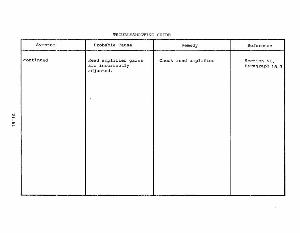
Symptom
continued
TROUBLESHOOTING GUIDE
Probable Cause
Read amplifier gains are incorrectly adjusted.
Remedy
Check read amplifier
Reference
Section VI, Paragraph 18. 3
~--_______________ , ______ -A ____ n. _______ • ____________ ~~. __________ • _________________ I_" ______ I ____________ ~

APPENDIX A
SPARE PARTS
This appendix contains a listing of all spare parts for the WANGCO Mod 11 Tape Unit (For resistors, capacitors, small hardware and other items not included in the following list, any equivalent in type~ value; size; tolerance; and quality may be substituted.)
The listing is contained in table A-1 and includes parts for all three configurations of the Mod 11 Tape Units; that is, NAZi, PE, and PE/N RZi. The Remarks coiumn of the table (A-l)
provides the applicability of the spare parts, that is, whether the part is for N RZI units only, PE/N RZI units only, or all configurations.
The listing of table A-1 is based on, and contains all, spare parts listed il'1 WANGCO drawing number 201193A.
A-1


I
1
Item No.
1 2 3 4 5 6 7 8 9
10 11 12 13 14 15 16 17 18 19 20 21 22 23 24 25 26 27
1 2 3 4 5 6 7 8 9
10 11 12 13 14 15 16 17 18 19 20
t
I
Table A-1. MOD 11 Spare Parts List
No. Description i Part No. 1 Requiredl Remarks or Usage
HEAD ASSEMBLIES, GUIDE ASSEMBLIES & ASSOC!ATED PARTS
Assy, Head Plate, 7Ch, Dual Gap Assy, Head Plate, 7Ch, Dual Gap Assy, Head Plate, 9Ch, Dual Gap Assy, Head Plate, 9Ch Assy, Tape Cleaner Assy, Cross-Talk Shield Assy, Cross-Talk Shield Assy, Plug-In Photosense Cover, Head Cap, Tape Guide Shim, Tape Guide Washer, Tape Guide Spring, Tape Guide
T ~. Drum, I ape uUlde Assy, Deck Mtg. Guide Assy, Deck Mtg. Guide, LOAD Washer, Shim Spring Shim D rum Shaft, Tape Guide Shaft, Tape Guide Cap, Tape Guide Cap, Tape Guide Shim, Head Plate Mounting Shim, Head Plate Mounting Shim, Fixed Guides
200882-003 201001-003 201096-003
i
200926-003 200923 200461 201120 200684 200986 201109 200203 200046 200047 ')
I £00096 201100 201101 200077-001 200156 201033-001 201041
I 201044 I 201045 I 201046 I 201311 i 201032-001 I 201032-002
201033-002
I
i I
I I
i !
1 NRZI, 0.300 inches Gap to Gap 1 NRZI, 0.150 inches Gap to Gap 1 NRZI 1 I PE & PE/NRZI 1 All Configurations 1 7Ch, DIGap, 0.300 inches Gap to Gap 1 All except item 6 1 All Configurations 1 All Configurations 2 Used on Head Assy only
AIR Used on Head Assy only 6 4 on Head Assy, 2 on Deck Assy 3 2 on Head Ass¥, 1 on Deck Assy
I ,.. __ • _ ~ 3 I L. un Head Assy, 1 on DecK Assy 3 I All Configurations 2 I All Configurations
10 Used on items 15 & 16 5 Used on items 15 & 16
25 Used on items 15 & 16 5 U d 15 & 16 se on Items 2 I Used on item 1 5 3 I Used on item 16 2 ! Used on item 16 1 I Used on Deck Assembly
AIR Used on Deck Assembly AI R I Used on Deck Assembl y A/R Used on Deck Assembly
MOTORS, BRUSHES, & ASSOCIATED PARTS
Assy, Reel Motor, FILE REEL 201087 1 All Configurations Assy, Reel Motor, FIXED REEL 201088 1 All Configurations Assy, Capstan Motor & Tach. 201089 1 All Configurations Brush, Reel Motor 100320 2 Use with Motor PIN 200389-001 Brush, Reel Motor 100321 2 Use with Motor PIN 200389-002 Brush, Capstan Motor 100384 2 Use with Motor PIN 200609 Vacuum Motor, 60Hz, 115v 100259 1 Use with item 15 Vacuum Motor, 50Hz, 230v 100375 1 Use with item 14 Vee Belt 100269·001 1 Use with item 7 Vee Belt 100269-002 1 Use with item 8 Fan 100380 1 Used on 230v machines only Pulley, Motor 201036-001 1 Use with item 7 Pulley, Motor 201036-002 1 Use with item 8 Assy, Vacuum Blower, 230v 200912
1
1 50Hz Assy, Vacuum Blower, 115v
1
201104 1
1
60HZ Relay, Motor Start, 11 5v 100258 1 Used in item 15, K3 Relay, Motor Start, 230v 100374 1 Used in item 14, K3 Capacitor, Motor Start, 115v 100275-001 1 Used in item 15 Capacitor, Motor Start, 230v 100275-002 1 Used in item 14 Relay, Power 100280 1 Used in items 14 and 15, K4
A-3
i
I I
I I I I I
I
I !
I
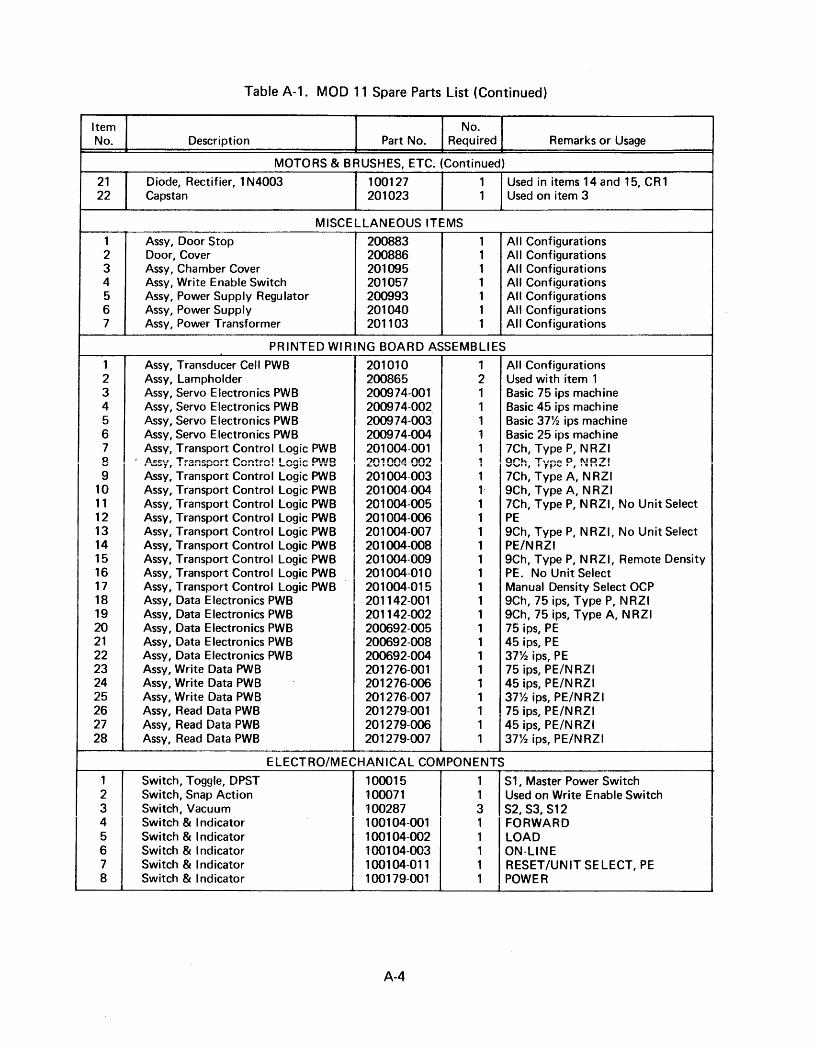
Table A-1. MOD 11 Spare Parts List (Continued)
Item No. No. Description Part No. Required Remarks or Usage
MOTORS & BRUSHeS, ETC. (Continued)
21 Diode, Rectifier, 1 N4003 100127 1 Used in items 14 and 15, CRl 22 Capstan 201023 1 Used on item 3
MISCELLANEOUS ITEMS
1 Assy, Door Stop 200883 1 All Configurations 2 Door, Cover 200886 1 All Configurations 3 Assy, Chamber Cover 201095 1 All Configurations 4 Assy, Write Enable Switch 201057 1 All Configurations 5 Assy, Power Supply Regu!ator 200993 1 A!! Configurations 6 Assy, Power Supply 201040 1 All Configurations 7 Assy, Power Transformer 201103 1 All Configurations
PRINTED WIRING BOARD ASSEMBLIES
1 Assy, Transducer Cell PWB 201010 1 All Configurations 2 Assy, Lampholder 200865 2 Used with item 1 3 Assy, Servo Electronics PWB 200974-001 1 Basic 75 ips machine 4 Assy, Servo Electronics PWB 200974-002 1 Basic 45 ips machine 5 Assy, Servo Electronics PWB 200974-003 1 Basic 37% ips machine 6 Assy, Servo Electronics PWB 200974-004 1 Basic 25 ips machine 7 Assy, Transport Control Logic PWB 201004-001 1 7Ch, Type P, NRZI 8 t A~~":.1 T!"''!:lnr-~n~'" t"nnt-rnl , n~;"",, D\A/D 201004-002 1 . O("h ,,,,...,"" [) !\!D?!
, , ... ..,." • llI.A •• "',..,."', t. '-"''''.,,,.'''. ~v~."" ••• ..., "''''. I, • Y tJ"" • , •• I' ..... 9 Assy, Transport Control Logic PWB 201004-003 1 7Ch, Type A, N RZI
10 Assy, Transport Control Logic PWB 201004-004 1- 9Ch, Type A, N RZI 11 Assy, Transport Control Logic PWB 201004-005 1 7Ch, Type P, N RZI, No Unit Select 12 Assy, Transport Control Logic PWB 201004-006 1 PE 13 Assy, Transport Control Logic PWB 201004-007 1 9Ch, Type P, NRZI, No Unit Select 14 Assy, Transport Control Logic PWB 201004-008 1 PE/NRZI 15 Assy, Transport Control Logic PWB 201004-009 1 9Ch, Type P, N RZI, Remote Density 16 Assy, Transport Control Logic PWB 201004-010 1 PE. No Unit Select 17 Assy, Transport Control Logic PWB 201004-015 1 Manual Density Select OCP 18 Assy, Data Electronics PWB 201142-001 1 9Ch, 75 ips, Type P, NRZI 19 Assy, Data Electronics PWB 201142-002 1 9Ch, 75 ips, Type A, N RZI 20 Assy, Data Electronics PWB 200692-005 1 75 ips, PE 21 Assy, Data Electronics PWB 200692-008 1 45 ips, PE 22 Assy, Data Electronics PWB 200692-004 1 37% ips, PE 23 Assy, Write Data PWB 201276-001 1 75 ips, PE/NRZI 24 Assy, Write Data PWB 201276-006 1 45 ips, PE/NRZI 25 Assy, Write Data PWB 201276-007 1 37% ips, PE/NRZI 26 Assy, Read Data PWB 201279-001 1 75 ips, PE/N RZI 27 Assy, Read Data PWB 201279-006 1 45 ips, PE/NRZI 28 Assy, Read Data PWB 201279-007 1 37% ips, PE/NRZI
ELECTRO/MECHANICAL COMPONENTS
1 Switch, Toggle, DPST 100015 1 S 1, Master Power Switch 2 Switch, Snap Action 100071 1 Used on Write Enable Switch 3 Switch, Vacuum 100287 3 S2,S3,S12 4 Switch & Indicator 100104-001 1 FORWARD 5 Switch & Indicator 100104-002 1 LOAD 6 Switch & Indicator 100104-003 1 ON-LINE 7 Switch & Indicator 100104-011 1 RESET/UNIT SELECT, PE 8 Switch & Indicator 100179-001 1 POWER
A-4

Table A-1. MOD 11 Spare Parts List (Continued)
Item No. No. I Description I Part No. I Required I Remarks or Usage
ELECTRO/MECHANICAL COMPONENTS (Continued)
I
9 Switch & Indicator 100179-007 1 PE/NRZI 10 Switch 100130-001 1 REWIND 11 Switch 100130-002 1 RESET
; I
i2 i
Switch, Thumbwheei I
100245 ;
1 UNIT SELECT . 13 Indicator 100105-002 1 FILE PROTECT
14 Fuse, 8 amp 100028-022 1 Fl 15
I Fuse, 4 amp 100028-023 1 F5
16 Fuse, 5 amp 100028-024 2 F2,F3 17 Fuse, 7.5 amp
I 100028-026 1 F7
18 I Fuse, 10 amp 100028-027 2 F4, F6 19 Relay
I 100279 1 Kl
20 Capacitor, 65,ooouf 100278 2 C3,C4 21 Capacitor, 6,ooouf I 100283 2 Cl, C2 I ')') Cell, Solar
I 100008 2 I Used with item 8 of Head Assvs, Guide " I
I Assys, & Assoc. Parts 23 I Lamp t 100009 1 I Used with item 8 of Head Assys, Guide I
I I Assys, & Assoc. Parts 24
I
Photocell I 100176 2 Used with item 1 of Printed Wiring
I Board Assys.
25 Lamp 100228 2 Used with item 1 of Printed Wiring
: I Board Assys.
I ELECTRONIC COMPONENTS
r 1 I.C. Hex ,nverr, 836/936 100084 • 4 Used on PWB Assy 200692 I t I 7 Used on PWB Assy 201004 !
! 5 Used on PWB Assy 201142 4 Used on PWB Assy 201276
I.C. Hex Inverter, 836/936 100084 2 Used on PWB Assy 201279 2 I.C. Quad 2 Input Nand, 846 100085 1 Used on PWB Assy 200974
t t 6 Used on PWB Assy 201004
1 1· 6 Used on PWB Assy 201142 6 Used on PWB Assy 201276
I.C. Quad 2 Input Nand, 846 100085 1 Used on PWB Assy 201279 3 I.C. Quad 2 'rut Pwr, 858/958 100086 2 Used on PWB Assy 200692
t 3 Used on PWB Assy 201004
l 4 Used on PWB Assy 201142 3 Used on PWB Assy 201276
I.C. Quad 2 Input Pwr, 858/958 100086 3 Used on PWB Assy 201279 4 I.C. 10 Input Nand, 1804 100087 1 Used on PWB Assy 201142
I.C. 10 Input Nand, 1804 100087 1 Used on PWB Assy 201279 5 I.C. Dual Flip-Flop, 9093 100088 3 Used on PWB Assy 201004
. I I 10 Used on PWB Assy 201142 9 Used on PWB Assy 201276
I I.C. Dual Flip-Flop, 9093 100088 5 Used on PWB Assy 201279
6 I.C. Dual Op. Amp, 7739 100089 5 Used on PWB Assy 201142 7 I.C. Mono. Multi, 9601 100090 1 Used on PWB Assy 201142
I.C. Mono. Multi, 9601 100090 9 Used on PWB Assy 201276 I.C. Mono. Multi, 9601 100090 10 Used on PWB Assy 201279
8 I.C. Dual Flip-Flop, 9099 100095 5 Used on PWB Assy 200692 9 I.C.3 Input Nand, 862/962 100107 4 Used on PWB Assy 201004
A-5

Table A-1. MOD 11 Spare Parts List (Continued)
Item No. No. Description Part No. Required Remarks or Usage
ELECTRONIC COMPONENTS (Continued)
10 I.C. Voltage Reg, 7723 100108 3 Used on Pwr.Supply Reg.Assy 200993 11 I.C. Op. Amp, 7741 100109 8 Used on PWB Assy 200974 12 I.C. Dual Op, 1437 100167 14 Used on PWB Assy 201279
I.C. Dual Op, 1437 100167 11 Used on PWB Assy 200692 13 I.C. Quad, 2 Input OR Gate, 1812 100175 3 Used on PWB Assy 201276 14 I.C. Dual Monostable, 2602 100234 5 Used on PWB Assy 200692
LCo Dua! Monostab!e. 2602 100234 1 Used on PWB Assy 201276 15 I.C. Dual Comparator, 1414 100237 9 Used on PWB Assy 200692
I.C. Dual Comparator, 1414 100237 9 Used on PWB Assy 201279 16 I.C. Dual 4 Input Pwr, 844/944 100261 5 Used on PWB Assy 200692
I.C.DuaI4 Input Pwr, 844/944 100261 1 Used on PWB Assy 201004 I.C. Dual 4 Input Pwr, 844/944 100261 5 Used on PWB Assy 201279
17 I.C. Hex Power Drive, 7407 100327 6 Used on PWB Assy 201276 18 Transistor, NPN, 2N4123 100080 20 Used on PWB Assy 200692
32 Used on PWB Assy 200974 12 Used on PWB Assy 201004 72 Used on PWB Assy 201142
6 Used on PWB Assy 201276 Tr::m4!idnr !\!P!\! ?I\.!.d 1?~ 1nn{u:~n 74 . ! ! ..... ,.,! ........ D\AlD A .... ., """ ".,.0 ... _ .. _._ .. _., ..... , --,. ......... IV"",,",'" '-'~u UII I ."u r\"''', ,"VI"""
19 Transistor, PNP, 2N4125 100081 19 Used on PWB Assy 200692 ~
12 Used on PWB Assy 200974 2 Used on Pwr Supply Reg Assy 200993 5 Used on PWB Assy 201004
14 Used on PWB Assy 201142 1 Used on PWB Assy 201276
Transistor, PNP, 2N4125 100081 10 Used on PWB Assy 201279 20 Transistor, Dual NPN, TD101 100082 9 Used on PWB Assy 201142 21 Transistor, PNP, MPSU51 100083 1 Used on PWB Assy 201004
Transistor, PNP, MPSU51 100083 1 Used on PWB Assy 201142 22 Transistor, PNP, TIP30 100113 3 Used on Pwr. Supply Reg Assy 200993 23 Transistor, NPN, 2N2219 100125 3 Used on PWB Assy 200974
Transistor, NPN, 2N2219 100125 3 Used on PWB Assy 201004 24 Transistor, NPN, 2N3053 100158 6 Used on PWB Assy 200974 25 Transistor, NPN, 2N3055 100159 2 Used on PWB Assy 200974
Transistor, NPN, 2N3055 100159 4 Used on Pwr Supply Reg Assy 200993 26 Transistor, PNP, 2N4037 100160 1 Used on PWB Assy 200692
. I I 5 Used on PWB Assy 200974 1 Used on Pwr Supply Reg Assy 200993
Transistor, PNP, 2N4037 100160 1 Used on PWB Assy 201279 27 Transistor, NPN, 2N3772 100219 2 Used on PWB Assy 200974 28 Transistor, NPN, 2N5320 100220 6 Used on PWB Assy 200974 29 Transistor, PNP, 2N5322 100221 5 Used on PWB Assy 200974 30 Transistor, NPN, 2N3773 100281 4 Used on PWB Assy 200974 31 Transistor, NPN, TIP31 B 100282 4 Used on PWB Assy 200974 32 Diode, Signal, 1 N914 100091 27 Used on PWB Assy 200692
50 Used on PWB Assy 200974 11 Used on PWB Assy 201004 46 Used on PWB Assy 201142
3 Used on PWB Assy 201276 Diode, Signal, 1 N914 100091 91 Used on PWB Assy 201279
A-6

Item No.
33
35 36 37 38
1 2 3 4
5 6 7
Table A-1. MOD 11 Spare Parts List (Continued)
Description Part No. Remarks or Usage
ELECTRONiC COMPONENTS (Continuedj
Diode, Zener, 1 N752 Diode, Zener, 1 N752 Diode, Rectifiei, 1 N4003
Diode, Rectifier, 1 N4003 Diode, Zener, 1 N4736A SCR,40654 Diode, Power, 1 N3208 Diode, Zener, 1 N754A
Resistor, Variable, 50 Resistor, Variable, 5K Resistor, Variable, 10K Resistor, Variable, 20K Resistor, Variable, 20K Resistor, Variable, 20K Resistor, Variable, 50K Resistor, Variable, 500 Resistor, Variable, 1 K
100118 100118
I 100127
100127 100161 100162 100174 100373
VARIABLE RESISTORS
100069-500 100069-502 100069-103 100069-203 100069-203 100069-203 100069-503 100163-501 100163-102
A-7
I
4 2 2 1 1 1 1 2 9
Used on PWB Assy 200974 Used on Pwr Supply Reg Assy 200993
i Used on PWB Assy 200692 Used on PWB Assy 200974 Used on Pwr Supply Reg Assy 200993 Used on PWB Assy 201004 . Used on PWB Assy 201142 I Used on PWB Assy 201276 Used on Pwr Supply Reg Assy 200993 I Used on Pwr Supply Reg Assy 200993 I Used on PWB Assy 200974 I Used on PWB Assy 201279 J
1 Used on PWB Assy 201142 9 Used on PWB Assy 201142 9 Used on PWB Assy 201279 1 Used on PWB Assy 200692
10 Used on PWB Assy 201142 lOUsed on PWB Assy 201279 9 Used on PWB Assy 201276 2 Used on Pwr Supply Reg Assy 200993 1 Used on Pwr Supply Reg Assy 200993

APPENDIX B
This appendix contains the circuit schematics, assembly drawings, and material lists for all assemblies and subassemblies in the MOD 11 Tape Transport. These documents are identified in the list on the following page.
The circuit schematics are complete representations of the electronic circuitry. The user 6f this manual will want to consult the schematics in conjunction with his study of the text and the simplified circuit diagrams in the text sections.
The assembly drawings identify every part on any given assembly or subassembly. Parts are identified either by item number (e.g., 1, 2, 3, etc.) or circuit reference nuwber (e.g., Rl, Cl, Ul, etc.). The associated material lists incorporate these identification numbers, together with the part description, WANGCO part number, and part quantity (i.e., the quantity of a particular part required for the given assembly).

B-1.
B-2.
B-3.
B-4.
B-5.
B-6.
B-7.
B-8.
B-9.
B-10.
B-11.
B-12.
B-13.
B-14.
B-15.
B-16.
B-17.
B-18.
B-19.
8-20.
B-21.
8-22.
8-23.
8-24.
8-25.
8-26.
8-27.
8-28.
8-29.
APPENDiX B
ENGINEERING DRAWINGS
ftllr\f"""\ *1" 1\; n-;. IVIUU I 1 1\1 nLI
Power Supply Assy
Power Supply Schematic
Power Supply Regu lator Assy
Power Supply Regulator Schematic
Transducer Enclosure Assy
Transducer Cell Assy
Plug-In Photosense Assy
Photosense Assy
Photosense Connector Assy
Vacuum Blower Assy
Vacuum Blower Schematic
Vacuum Blower Assy
Vacuum Switches Assy
Write Enable Switch Assy
Write Terminator Assy, J1
Control Terminator Assy, J16
OCP Cable Assy
Data Control Cable Assy
Regu lator Output Cable Assy
Servo Regulated Power Cable Assy
Servo Control Cable Assy, No.1
Servo Control Cable Assy, No.2
Transport Control Logic Assy
Transport Control Logic Schematic
Servo Electronics Assy
Servo Electronics Schematic
Data Electronics Assy, Dual Gap
Data Electronics Schematic, Dual Gap
Wiring Diagram
201040H
201040H
200993H
200993H
201085H
201010D
200684A
200707A
201051B
201104G
201104G
200912E
201097C
201057B
200714E
200717D
201058E
201052C
201053A
201054A
201055A
2010568
201004K
201959A
200974P
200974P
201142H
201142H
200947B

." co c -, (1)
r::p -J.
-0 o ~ (1) -,
en c
'"C '"C
-< » en en (1)
3 2: -< '"C tp
o ....... w
TB?
~r7 ~-:==J !---/8.00
321 "",{J
~8
IC~ 43
~,t:yrY;:,ur,4r6 ~"&y/jI2
--~-- ~3) . ."'/#.5 2.(3 -",//V'I
I ."'//Y-;'
P/rYS
TI
9 @
+
I (4
I @
! +
C 3
V lEW J.\. J.\

" c.o c ...., CD
rp -:a.
""0 0 :;E CD ...., Cf) C "0 "0
-< » CI) CI)
CD
3 0-
-< -0')1 " -002 16
"0 tp I\.)
0 -;., 2-
w
20 DATI! N'PftOVEO
r. ,~
-1 .e6?9D Ce3-C£tb RC;"r
.:2 e€6lD
- 2 e66l0
- 2. ,ec~D
{ElREMOVE MARKING "R8 TOP" ON -001
~::::~R STliMP AT ASSYj 41t ON-OOI, V , <'AON-002A5SY,
ill MARK PART NUMBCR,ASSY,ANO LATEST UVISION LETTER ./<' NIGH BLACK CHARAC' TERS PER. WANGCO SP.EC 100037.
NOTES:UNLESS OTHERWISE SPI!C{I'{ED
PART NO, 2010+0-XXX ASSY SEE TABULATION MIt.
~NOTESUN"SSS'~"C""D ~~'3~'7 -\l\l1~ltJ
1 T:O~~:ANCE!l AN;UlAR ~:~~illER§IAi::'L ~""-,;<L"-il~.r~"1-__ w~.ng~c~om~p~UI~8r~p~r~od~U~CI~'_~Fl {.. 2 BREAK ALL SHARP
3 ~:~S ::~~I5"O J k-fllilSl!=C-. -----1 4 ALL DIMS IN INCHES
1175 II I
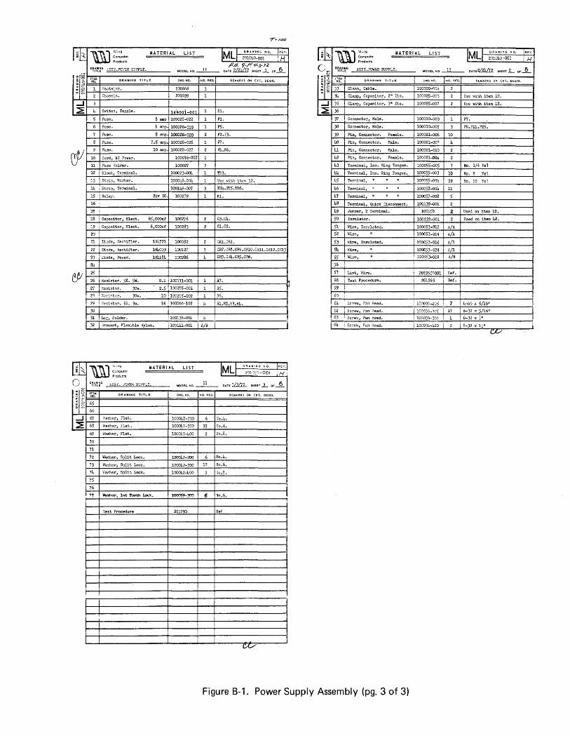
l,,~~·h::;-· \\l Wang " " Compuler PrOduCls
MATERIAL LIST IMILL DR-AWING NO. IREV.
~ ·1 201040-001 I H ,D/i. 7:~/'( ~S-72
DATE 2/'21/72 SHEET 1 OF 6 II
1~I'JF=!~O=~9==================*===7~=*====p===='E=MA='=KS=O=N=C=KT='=D=ES=IG.==~ "ri 1 "eat.ink. 200668 I 1
o~~ Chasois. 201039 I 1
-J~~ ______________ -r ____ ~ __ -+ ______________ ~ ~ Switch, Toggle. 14900i-001 1 S1.
, Fuse. 6 amp , 100028-022 Fl.
6 :Fuse. 4 amp. 100028-019 F5.
7 Fuse. S ""'p. 100028-020 F2.F).
6 Fuse. 7.5 amp. 100026-026
~' I 9 I Fuse. 10 amp. 100028-027 I 2
~10~~C~oro~,~A~C~p~ow~e~r.~ _________ -+ ___ 100~07_~_OO_2+-~1~r-_______________________ ~
~11~~Fu~.s~e~~0~1~de~r~. _______________ +-~lOOO~2~7 ___ +-~~ _______________________ ~
I FU.F6.
12 Block, Terminal. 100023-004 TE3. I:._~.... M .. .....J.. ... _
.... ,.J j ............. _"', ......... " ..... .
l), Strb, Terminal. 100l),9-007 TB4.TE5.TE6.
15 Relay. 24v IX:. 100279 Kl.
16
1'1
18 'Capacitor, Elect. 65,OOOuf 100278 i 2 ' C).C4.
19 Cap<citor, Elect. 6,000uf 10026) Cl.C2.
20
21 Diode, Rectifier .. IN4721 100052 ! 2 CRl.C~2.
22 Diode, Rectifier. 1N4003 100127 CR7 • CR8.CR9 .CRlO .CRll. CR12. CRl)
23 . Liode, Power. 1N1l84 100266 CEl3. C.'l4. CRS. CR6.
24
~~)~25~ ____________ +-____ +-~ ____________ ~ CY 26! Resi.tor. 5%. SII. 0.1 100111-001 i 1 R7.
27 ~osi"tor. 3aw. 2.5 100285-001 R5.
20 ! ",sirtor. 3aw. 10 100205-002 ! 1 . R6.
I I ..... . : 100130-001,
32 J .iro;r.;r.et, Flexible :~ylon. 1100141-001 I Ali!
I ~I~ 1\1\") ~':;:ulcr MATERIAL LIST IMILL DRAWIN." NO. IRE'I·I ~ ·1 201']"~ -001 • H ; l-~ \l...)1J Products
o D;tT*,~~G ASSt. ?O:".'Sft S!!PPLY. MODEL NO. _1_1 ____ DATE J.i.:1!1.1.... SHEET....l- OF~
~111~ 1~5~ ~ ~~65~ ________________ +-_____ +-__ ~ _______________ ~
66
-J 67 "~lasher, Flat. 100047-200 6 - Jo.4.
::E 68 1-lasher, Flat. 100c"7-300 II ~;0.6.
69 ~;asher, Flat. 100c47-400 :"10.8.
70
71
72 Washer, Split Lock. 100042-200 110.4.
73 Washer, Split Lock. 100042-300 12 No.6.
100042-/,00 :10.8.
75
76
11 Ws!h..,., lnt Tooth Loc"'.
Test Procedure 201293 Ref
LIST I'MLL D' .. ING NO. IREV, Ii ·1 211040-001 I H
11 DATE~ SliEET 2 OF 5
NO. H:ECi.; RfAlAfU;:S ON CKI. DESIG.
lOO0OO-OoL 2 I 10002$-003 2 I Use With item 19.
I ~ 35 Clamp, Capacitor. 3" Dia.
.::=:; 36
2 I Uoe With ite", 16.
i 100025-007
37 I Connector, Male. 100010~003 ! 1'7.
38 Connector, Male. 100010-005 3 I P8. Pll. P25.
39 Pin, Connector. Female. 100021-006 10 I uO Pin, Connector. Male. 100021-007 I
I 41 I Pin, Connector. MaJ.e. I 100021-010 I 2 I 42 Pi!lJl Connector. Female. 100021-004
43 Terminal, Ins. Ring Tongue. 100055-00$ 7 No. 1/4 Yel
44 Te",,1nal, Ins. Ring Tongue. 100055-003 11l No. 8 Yel
. h5 . Te~i:1al .. . 1000,5-oou 1Q ,~c. 10 Vel
46 Terminal," 100051-004 11
47 Terminal,' 100057-008
48 Temina1, Quick tisconnect. 100139-004
49 Jumper, 2 Terminal. 1001$0 ~ Used on ite:n 12.
'50 'Insulator. , 100232-001 Used or. item 48.
51 1-lire, Insulated. 1000$3-912 AIR
52 Wire, 100053-914 A/R
53 liire, Insulated. ! 100053-916 A/"-i 54 v:ire, I 100053-924 Ala . 55 . Wire, : 10CY)53-91R AIR
56
1,7 ! Li~t, 'fare. i 201050:001 I Ref.
58 Test Procedure. i 201293 Ref.
~ 01 I .::c r'3.'W , P.:\:1 Head.
62 Sere .. J r3:"1 Head. 6-32 Yo 5/16"
Fi :::::: ;:: ::::: I 100030-420 i 2
6-32 x ~.
I 8-32 xl,"
Figure 8-1. Power Supply Assembly (pg. 3 of 3)

OJ TEl2
I I I I ASSY. POWER I TRANSFORMER L__ 20110. I
~ 6 ( -'Wo~';;) ________________ J
TB7
riJci± TEl7 2 3 J -002 ASSY o 0 I (MOD 12)
4~ I"USE I"OR. -001 ASSY 6.~ I"USE FOR -002 ASS~.
'!cd NOT USED ON -001 ASSY.
INPUT POWER LINE ~ TD IA'fANP'lg".
T!'J7 IS r'AKT 01" SLOW=' ASSY.
T&Z 1.5 MOUNTED AT THE B
NOTES: :JNLESS. OT OTTOM NERW/~'£ . .sPEC/PIED
TB5.
ITO SERVO ELECTRONICS AS';Y. JII.
l_t i t -~=-·tP PII
f ~ ~ ~;t
~I I i ~~ ~~__ II
.. -
I a
TB4
TEl2 (i]
~--FllE REEL MTR. BlK.
-FIXED REEL MTR. RED.
4. ALL DIMS IN INCHES.
1175
200675
\l1 Weng Computer Products
SCHEMATIC POWER 5UPPL Y
T 108
EET+OIt "

'T1 co c: ..., CD
CO
~ ""0 o ~ ..., en c:
"C "Q. -< ::0 CD
CO c: Q) ..... o ~ » CI) CI)
CD
3 S!: -< -"C <p
,--------_._--- --------------
E SEE UN' NC.;',P Ul
F E~R~_'_~ ~ J~ICf\ '; I 'j) (, SEE CRIO ,,321
r· __ ~_ ~ SEE CR/O-:i(,{,~ __
t TPZ
~ Jz("
@ 3 2 I
[liJ G 5 of.
~ ® B 7
lED
='~ (0)
[57/1 o 0 ___ f---~.-® [Q]+ o 2
3 3
C&I:J 4- 0 5 5
-
, J25 TP~ f-
[iL~ TIt~ ,.....
I ClliJ@ I 122" 1 a@i£D @ [IT] ® 0TI ~ I VR~ I ~ ~ [::mJ
"-." TP3 8 ~ ~ ~ [:Ii2J i) ~8 .
+ + lliD [?2!L>] [:ll:J 5 gz::, @Il I C/2:Z I -, [ 2?/J [~ '--
Q~ ~ I~ §QJ [£ill +
J 34 J27 ---- ._._-----®
.-.---- ------.----- - ------------------- - ---.-----.--- ------ -----_._---+----1
t==== -=-~-=-=-.=-=-=-=-=-.:=--..:::-==.:--- - = :..:;:.--..:::-.-=======-=..:.=..::.::--:..:= ---.-. ::.:=:===-===:~::----:=---=. ::====1====1
--.-~
l===r
RcF ®---.--~-
3 P(..AC£S @----:;:::;-~~~~~~
VIEw A-;\
ffiREF r.?:J INSTALL ITEM 3 FLUSH WITH
SURFACE - A -.
(iJMARK PART NUMI3ER,APf'!!OP!!IAr~ DAS NUMBEF: ASSY & LATEST REVIS/ON Lf.TrE:R .12 HIGH BLACK C/-JAR,ACTER5 PER YfANGCO SPEC 100037.
SECT/ON (: - G NO SCALE
NOTES: UNLESS OTHERWISE SPECIFIED
NOTES UNLESS sPECIfiED ----------1-TOLERANCES
x .. xxx:t
_ PART NO. e00993-XXX ASS,( SEE TABULATION :::: :~~ -~----- -\il-------:,~,,}'~B W~g Comp~_~~~UC"
2. BREAK ALL SHARf' EDGES APPROX . .o10 J ------- 4S;Se;;1 13 L'f, pow~~r.2 100
•. AlLO'.S'N'NCHES. f!lilllI $,UPP('.Y e~(;ULATOIZ.S Rob. I
~ 02 = ~:/--I~T-·--.200.--.~193 H lIfl!L.AliIC( ~ _ Ch'ARTED
______ . ____ --l. _______ ....L ___ ._____ W:1:w..r.:~ ~HT -.---~ ~r ~
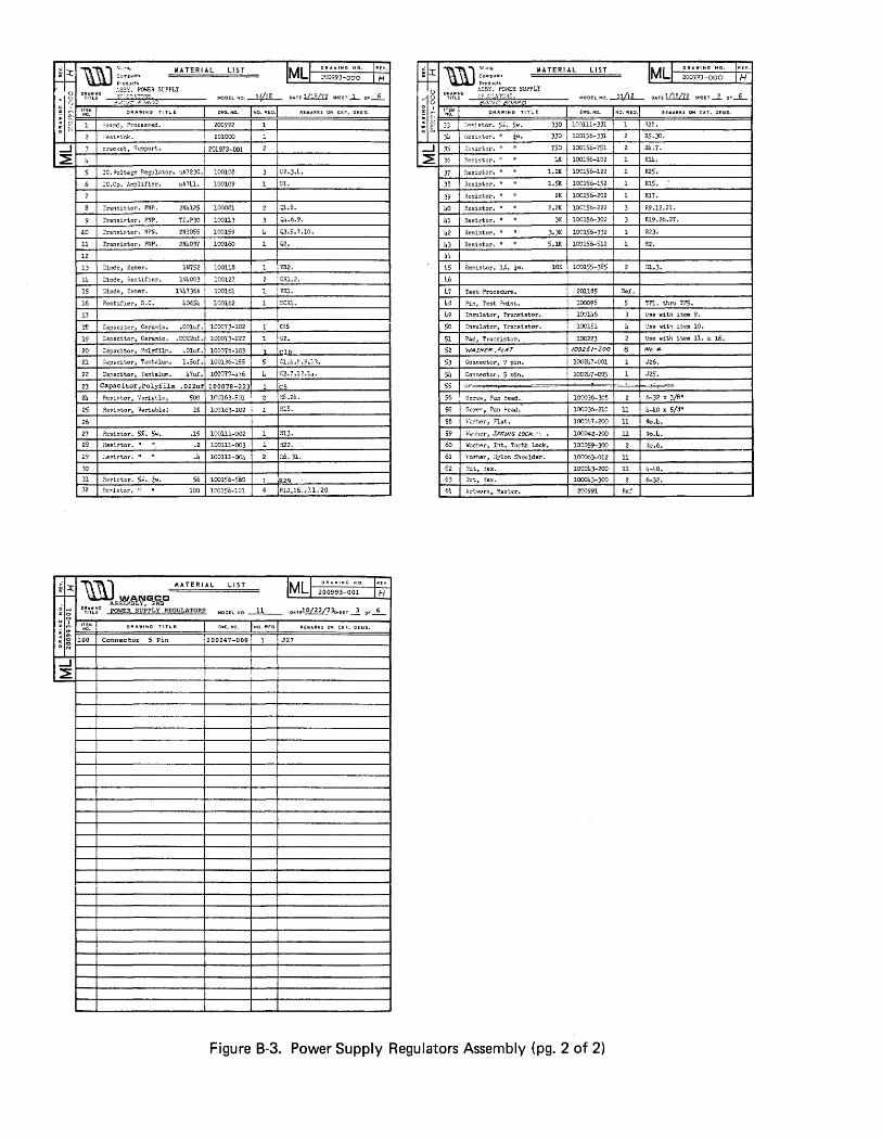
LI ST
MOOELNO.~
200992
;;estsink. 201000
IMILL DRAWING NO. 10". II ·1 200993-000 'H
-J~~_"~"_ac_<._t~,_ou_o~po_r_t. ______ ~~2~Ol~97~3~"O~Ol~ ____ +-________________ -; :::E
Ie. Voltage Regulator. uA723C. 100108 U2.3.4.
IC.Op. Am;>l1fier. uA741. 100109 n.
Transistor. PNP. 2NL125 100081 ~.8.
Tra:1.si \'itor.. P~P. Tio P30 100113
ao Tra~~istor. NPN. 2N3055 100159 ~3.5. 7 .lD.
11 Transistor. PNP. 2N4037 100160 Q2.
12
13 Ciode, Zener. H752 100118 VR2.
14 Dioee, ?ectifier. IN1,003 100127 C!U.2.
IS Dioce, Zener. D4736A 100161 VRl.
16 R.ctifier, S.C. 40654 100162 SCiU.
17
113 Capaci tor, Cera",ic. .001u!. 100073-102 I CIS
19 Capacitor, Ceramic. .0022u!. 100073-222 C2.
20 Capacitor, PolyfiL"II. .01u!. 100078-103 1CIO
21 Capacitor, Tantalum. 1.5uf. 100136-155 C1.L.8.9.13.
22 Ca:oacitor, Tantalum. 47u!. l00?n-),76 C).7 .12.14.
23 Capacitor ,Polyfilm .022uf 10007S-223 CS
21, RB.2L.
25 R18.
26
27 Rcsi,tor. 5%. Sw. .15 WOI11-0u2 !l13.
28 ii.esi~tor. n .2 100111-003 R22.
29 ::'e~i ~tor. n • 4 lOOlll-ocL ~"'. 31.
30
56 100156-560 R29
32 :{e!=istor. II 100 1XllS6-1Cl R10,16. ,:.1,20
IIMLI O''''NG NO. I"~,· II ·1 200993-001 , H ~:l: \\1\1 f- r- \ll\.ls~ft~Gp~O ~ g D~tTW~iG POWER SUPPLY REGULATORS
MATERIAL LI S T
11
a I ITEM
; ~ t=NO:=, =t====O"=A="'!="=G =T=IT=C=E==*====*==*=='='M=AR='=' =oN=CK=r.=o='="G=. ==t : ~ 100 Connector 5 Pin 100247-008 J27 o~~~~~~~~~~----~l~~~~~~+i,~----------------~
-J~~ ______________ +-____ ~ __ ~ ______________ ~ :::E
MATERIAL LI ST IM'LL DRAWING HO. IR'V. II ·1 200993-000 , H I ~ l:ro "W ~':::~::,
~ OOAWING ASSY. PQ;,"ER SUPPLY
_ g I ~T~IT~LE-=:::j;~:a:~~~;7:t(j8·~~;~;'P~'D~==::,:~M:O:OE:'::L':NO:.~1::t/~12::;::"":0::AT:E 1::11:8~/7~2~'H:EE':'T ~2 ~O:F ~6~ u II-ITEM Z C'"'\ NO. REMARKS ON CKT. DESIG.
; ~'F~====.====::==*:=:===:==*====l===:=:;========~ ~ ~~3J~~:'~."C~i~<t~or~.~S~;~.~SW~. _____ J~3_0~1_00_1_11_-3~3_1~ __ -+_R2_0_. ______________ ~
~. 330 100156-331 R5.30. 34 itesistor. d
-J~3'_'4-C_'"_'i_st_o_r'_'_' ________ 7_5_0~1_00_1~56_-7_5_14-__ -+_~_._7. ______________ ~
:::E 36 ".sistor." lK 100156-102 Rl4.
37 f.esistor.· 1.2K 100156-122 R25.
38 aesistor.· 1.5K 100156-152 R15.
39 :iesistor .. n 2K 100156-202 Rl7.
40 :;esistor .. " 2.2K 100156-222 R9.12.21.
41 :tesistor.. II 3K 100156-302 Rl9.26.27.
42 Resistor.. II 3.3K 100156-332 H23.
43 ReSistor. II 5.lK 100156-512 H2.
1,4
L5 Re~istor. 1':';. ~w. 10K 100155-385 Rl.3.
46
47 Test Procedure. 201185 Ref.
48 Pin, Test Point. 100098 TPl. thru TP5.
49 Insulator, Tra.'lsistor. 100146 Use with item 9.
50 !nsulator, T:-a:-:sistor. 100151 ['se with ite:n 10 ..
51 Pad, Transistor. 10022) Use with item 11. & 16.
52 WASH"? .1'''* T 100251-200 No·4
53 Connector, 9 pin. 100247-001 J26.
54 Conoector. 5 oin. 100247-005 J25.
55
56 Ecrew, P<lI1 :fead. 100036-)08 6-32 x 3/8" Scre~·:, Pan ~ead.~ 100036-21J 11 4-40 x 5/3'
58 "'·a~he. J Flat. lOCO)' 7 -200 11 No.4.
,9 hasher, SFA'W!; lOCK.o' •• loo04Z-2oo 11
60 Wa~her, Int. Tooth Lock. 100059-300 :'10.6.
61 It.'a~her, :l:rlon Shoulder . 100063-012 11
62 ~btJ :~ex. 100043-200 11 4-40.
63 :kt, 'lex. 100043-300 6-32.
64 Artwor'.c, !ofa!ter. 200991 P.er
Figure 8-3. Power Supply Regulators Assembly (pg. 2 of 2)

"'T1 cO" e .., CD
CO .h. -0 o ~ .., U) e "0 "0
-< ::0 CD to e Q) r-+ o .., U) (") :rCD
3 Q) r-+ 0"
I) -=.---+----1
I
I I
I I
I I)
r R22' 0.2 5.Vi
tJ+ R21 C 12 22 K 47 )JF
20V
I ~- I
t-
~ R30
;;1-~~~'!I:~ I
330 R2B _ 330
/ ~ VRa CR2 _ I )
10~~. -1 '''-- ~ "2 IN4003 Q9 IN7_ T I.P30 5.6'"
-12V REG I
+5V REG TO 5[IWO I
J27 }
3 GROUND ELECTAONIC~ + 12 V REG !
-5V REG I
+ 12V REG
+ 5V REG
-12V REG
I
TO DMA ,
ELECT RONIC~
I
I
m "",j ELEC'"HONIC51

~ ..., OJ :::l CI)
0-C ("') CD ..., m :::l ("')
0-CI)
c @
» CI) CI)
CD
3 0-
-<
B
I
TYP 2 PLACES
"'0 .. _M._T~=---
L __ \='3
~~,~-~ -"'---.-------"-'"--
l~~)OO h-Lo. ------

." c.c c .., (t)
OJ en --I .., Q)
::J (I)
a. c n (t) ..,
» (I) (I) (t)
3 ~ -<
o C T ""'b/' <0 -svo/"
CENTER TAP ®I>-I-----------~-"--"--
L-..
)'~I A I . .±.;o v----r- . ".00=--'------1
j~~~~~~ l~~-5V (\)
~P<>CT
~~+5V 6"iI
~GND %,IJ
o ~ /02 PLACES
'f"
~Q.~4 ~ t::" ""''' C~ ~~±">, PROTRUSION 10
5 6
,. TOLERANCES
~~~t;~5 2. BREAK ALL SHARP
EOGHi APf'ROX, .010
IML ;:;o:~·· .. I'':; 7 * t· ,y
lIIQllnN(I.~oullll!LIgSHuT..l..g,Z
--
m MARK REF DE51G .12 HIGH CHARACTERS. BLK; o ~6RB~AS";A~~EDc ~~g~~~'DERED IN PLACE.
t. IDENTIFY ASSEMBLY PER WCP SPEC.I00037, TAG.
NOTES:
APPR. lI?,s.~, .. " _,"r "'<'nMhJ£B.!AJ..
I~075
Ul Wang Computer Product.
ASSEMBLY TRANSDUCER CELL PWB
I"!f' ~.
I
ruJJi 1=0'1 2:1 'I 201010 0 \ .... ar :lOF 2

:::J
"'0 :::r o .-+ o ~ :::J ~ » en en (t)
3 g: -<
~------------------------------------------------------------------------------~-----
-- - - - ~r----.
\l1 MATERIAL LIST
D'rT~;O . 6HI.fi!l~PH9l'll!!8. MOOELHO.~ Dol U 2l11:IJ.. Mlln.L Of'-L.
I~ DIII4WINO TlTLI O.G-HO. IND. Itt:Q·1 _U .... Ol I1N CKT. OUIO.
1 uq.Phot.o._. M. 200T07 1
• :) V1DdoIr. 2000$9
" HOIU1n&. 200682 1
eo .. r. 20(68)
6' P1n. r~ •• 100021-009 "
; J •
/TC7VI Si C(?~e I"W:JT ~N',y /-oA? CLA.e/7Y
( lamp pins 2814') ~ aAel TY.: A'~.e 8 e:.4I't'lP ~~I.;V J'"N/.S .Mtlly rt
- Ao'N'S ~IQVG" Bd:-61! SCAt::.LA!:=';4l!& /N ~IIAP ,~( n:--.eN ,~IVIP
,~??J~~~ ,,QICe IlVro ~e.
.3. CeM6/1/T M~'VG.t.?.;it/ r;~~~ ~ l'?S1VI s-) n::; ~t/..sI/IIf:i; (/ ;
2. . ..s~ .Af,.1/.5 // T6f¥) e:;,.) ON i!!!J:)AeL) (~~ T~M ,~ t4!
..:sJ ANt) c:'OVc.e "eM~) •
n:::J e?C # "Q9C1S ; ..54IOh".,c..'.
.~c:~!?/~, /. /a:A.)r/~ A.s..c;.y A-~ ~
,y~ : VI'V~~ eJ7iv<se#/.s~- .$ ~"c:=-/6"D
._------_._----,---~TES ~NLESS SPEC'!'ED DRAWN V'::/'AAr'".4 ..... a" I
1. TOLERANCES CHECK I I .XX:!: ANGULAR APPR, I-? ...... _":If I"u'" .XXX:!: ±
.MAI.~
II 2. BREAK ALL SHARP -- -- !OQWi
EDGES APPROX. .010 --- -3, MACH. SURFACES J flli!Jili 4. ALL DIMS IN INCHES. --- - ---
c:,U5,- //V 101
=/VSE ~ /
IMODEL No, ~
~ ~~72S- - DO NOT
THIS Oltj -:;t/~~ It --ISHEET.2 ~ 2

." cO' c ..., en OJ p, "0 ::J o .-+ o (I)
en :::s (I)
en » (I) (I)
en 3 Ci
-<
Sl/I~'-D
Pl7
RD ~(l .. f'G1 I I
I II7'IIJ I
I~ \_1 Bo7'
, 2 3 4
~ - - - - ---,
:~ D/ 1*,02:
I ,
/
NOTES UNLESS. SPECIFIED
I. TOLEIlANCES .xx:!: ANGULAR .xxx:!: :!:
2. BREAK ALL SUARP EDGES APPROX • .010
3. MACH. SURFAICES
4. ALL DIMS IN INCHES.
\l1 MATERIAL LUT IljLI DUWIIUi NO. ,.,,_
1M ·1 200101 J A·
o-"WlNO MII~l8RJI.I!IiM MODEL NO • ....825...- o"n2lrtD... SHUT.l... O'~ flTLI
I~ OIl"WINO TITL. DWO-NQ. NO. liED. REMAn! ·ON cn. OUIO.
1 Boani. ProoNMdI. 200706 1
2 , Cell, eolar. lOOOO8 2
Ii Lap. lOOOO9 1
.@~GV"...An: I~e ~ ""'S~A.) I4r~s-7; .... n::lkl'AeO /NS/~ eDGe o~ <STeAl.
/. /~T/~ A\SS'y AtSte.~ :.s"~t:" ~;;;;, ~.
N'Q7CS .• ' "VM.~ 0" a7"NE2.wzse ~/,.c:"/~O
04ECK I APPR. il. J~~ a. u
IMATERIIL
IMODEL NO.
UJ ASS~
PHOTOSENSE PWB
~
lor ~
I
A ~ .§lU.c I ~---------b~~--------~ NONE
INEXT ASSY 200707
·200684 FEET 2 OF 2

'"T1 (0 c: ..., ctl
t:tI m '"'0 ::J o ri-O (I)
ctl :::J (I)
ctl
() o :::J :::J ctl (") riO ..., » (I) (I)
ctl
3 C"
-<
r-----------------------------------------------------------------------------------------------------------"--------.----~
432 I
--f~48.0·!O.5-" -l ~ Pl7
I
4 Plt-J 2 (MALE.)
5 i-'I~ I 13 , 4 15 FE.t'V\ALE..)
6 P\i
2 ~-~~--------~-----...... -~I------------t '-_;;..; +..;._O;;..",.;."€;.;,.'.;;.;tO..;.,·,;.... _____ -+2""d0...,Q5_~ 1 ~'-.--------__t
1.. "'21-:X)1 4 i:., tAAl..E.
~-~~-.:...--------~- '-~I--"--------Pi' , MAL:,:[ ___ •• ___ +,,:\ "-:,21-0(:) ?ir. 2. ,--+----------__t
A/";:t -_+--------.-----__t ~-~~ .. ';.;,.r-'o,:........, _,.·.-;;l_.~_P_d.~ ___ + ],';:':,)-12.. ,_;';.,../ '_+-------.-----t ~---~--------__t_-.----+,--+------------t
~_l_} -+-------,----+-----+-,-----ll-----------_t ----------1
I..---I---------------~,---..jl-----------_t
~ TO &. 5WAG.!O TIJE'''-J, SOL.C£liC.e 0 \1oJ PLACE...
1, IDc:~TIFY .A5'S,V pe.R. liN<:P 5PEC 1000:37 -rAG.. I-JOT~.:S '. Ut-lL..E.SS Cn'-'ERw\S G:. 'SPE.C.I F\ ~O
----,r---,----r---~----.'--------.--------__t NOTES UNLESS SPECIFIED DRAWN 1 Ai4U/22.£ II- 22-7, Ul
1. TOLERANCES CHECK I I XXt ANGULAR mR I 4J'/J.,C;L' . ..ti..2:z.. W C P d XXXi t M~li..Ill~-' J •• - ___ ~_..:Omput4~!_~.!Cts __ ~=_t
2 BREAK ALL SHARP EDGES APPROX .. 010
J MACH. SURFACES J 4. ALL DIMS IN INCHES.
FINIS~ A~SE.M6LY,
P\·~OTO ";~C:NSE CCt-..l"'-J /0/
R~1i-D. I
I Mmrr'Nc-~~ 0 .,-\ -C·_j-S·-'·-+'::S;;";CA:-:-L-;:-E ---·-T""c='z=E"TI'---2-c-~~_;-5-~----t-Q--i
~~ ~-'--4---~-'------'-0 0 Co 15 ~,:?J.~lj~ WEIGHT SUEET 2. 0 F 2.

,---_ .. _---" .. ________________ c c •• ., ••••• ___ •
" §' @ ::;
:0
CSh~ -:p ~
:::>
=:::J < Ed] ~ ~
3
2 .e~()
72REQD
XJ :s-
O ~ ., l> " " 11 3 ';J"
" r /
------------,-------._--_.,-- - -,

-n cO' c: ..., CD
tp -< Q) (") c: c: 3 OJ 0" :! CD ..., en (") ;:r CD 3 Q) .-+ o·
MATERIAL 1I!.~ It.~L" ...... , •• 1M'.r 20110. G
: g 'iJ" ~ ~ 1 OUt1l ... __ '_Un
: ~ 2 Brkt. 810wer " .. y
...J 3 i'ull.y.~ci!'
~ 4 :;hroud.81~r ~ •• y
5 Col hr Blower Pu 1.,;:
II) "'l~.v .. 10 CapaCltor.JIt:)tor ~t..rt
11 ~nd Cap.CapaCltor
17 St:rlD."fiarke-
18 ".rlIII.ln •. kli" <:onaue
22 Pln ... · ... l.
24 'Ire Insula-ed
2'. WII<E INSLLJ.TED
27 ··("r.w .... n Hti
29 !icrew. -'an !tc-
,.....;.: .Reher SDllt-l.oek
Jb -.IiI.her, ~pll t Lock
J. w..v, Looc. lnl.TOt"It.h
45 Tu\lnc.i.n..., •
2010k 001
I,n, ,
K3
I002"-<J_OJ!+-...!.-.+-..:..!.. _____ --f 11)02 76-(101
K4
,._on,
IO°I)'i;-I)04 11.
-J:?,x'" e
1000'2_'0' 8 ""
100042-000
100042-600
1000$9-'0< 110 &
lOOl2o~U A/tt
TO CI =!:j-DE TAIL 13
CI
~I~~~I YE LLOW
B LA C K
(2
JI3
6--. ~.----------~
NOTIS UNLESS sr£CIFlI:D
1. TOLERANCES JIOCt ANGU.\.A" )(xxt
2. IREAK AlL "'AM' 100ES APPROx .. 010
1 MACH. SUft'ACES J 4. ALL DIMS IN INCHES.
TO ,e4-~
CRI
O •• WN ~~.z.-r.;: 13·/3,7'" CHECK ~. f...t..£~/ .hl7~ ..... I 7 I MAIIl!!W.
fllIWj
III!lIW..lIo. II ~200675
1/1/"1~
K4
~-
Ul , .Wang Computer Products
ASSY 1I:11III 101
VACUUM BLOWER ~ I I~ 1101 20 II 0 4 G II
~I:~r..:~~ TWEIGHT /sH1ET", OF 4

< Q) (") c: c: 3 OJ 0" ~ ..,
-------------,.70 _____ _
---------------- ----- ------
1~ 4-Rt:sc> 38 .;< ee!J~
2 ,/ ,eE6JD
Toel ~1<.3;TI 1"0 W\O"'o~ _ _~~
(e,cUIQ _
TOFMJ I TO ~'1-'1
DETAIL._ B ------
"REQD
[~:;'~ ;;;~~ ~)~;'n9Te~ ~1S
1]1 ~gff~e~~Y ~-: /~~;,~ ~UY
I~ :;~.zC_%~~~;_;N/:r~ M~';1/;':fz, A'P,R:"t!f'~, /l:JeCtS,
[~ /~Nn'&y A:!7e ,~spec ~t!'7,

23OT. 5'OH ••
D~i'r'~~G -"A""SS,,-,Y,,-• ..:.VA::.:CUUM=...:B:=LO:.::WE=R:.:..' __ MODEL NO. _11 __ _
I'ML' DRAWING NO. ·rREV.
II ·1 200912 I E
DATE 8/16172 SHEET l 0,..1.-1 ~IJ.J \1J ~~~~T¥rP MATERIAL LIST IMLI DRAWING HO. 'REV.
1-1- 200912 IE DRAWING ASSY. VACUUM BLOWER. 11 OATEW!11 SHEET 2 o,~ TITLE
ITEM ; ~ NO.
~ ~~~_~~t1~i~ne~~~am~n~g~,~Im~p~e1~le=r_4-~2=OO~90~1_4-~-+ ___________ ~ Bracket, Fan Mounting. 200911
ITEM DRAWING TITLE REMARKS ON CI(T. DESIG.
=
.... NO.
~ 33 Screw, Pan Head. 100036-328 6-32 x 1.15"
34 Screw, Pan Head. 100036-608 i-20 x in -J~~~B=r=ac=ke=t~,~m=o=~=r~A~s~~. __ +-~2oo~91~3 __ +-~-r _________________ ~ :::E Spacer, Hex. 200914
-J 35' Screw, Flat Head. 820 100040-406 B-32 x 3/B"
:::E 36 Screw" Cap Socket Head. 100041-408 B-32 x t" Pulley, Motor. 201036-002 31
Shroud, Blower Assy. 202090 38 r!asher, Split Lock. 100042-300 18 lIo.6.
Collar, Blower Motor. 201169 39 Washer, Split Lock. 100042-400 10 No.B.
Stand-Off. TB Cover. 20125'6 40 Washer" Split Lock. 100042-600 No.i.
Diode, Rectifier. IN4003 100121 CRI. 41
10 Relay, Power. 24 vtC. 100280 K4. 42 Washer" Int. Tooth Lock. 1000$9-300 No.6.
11 Relay, Motor Starting. 100314 K3. 43
12 Motor, Vacuum. 100315' 44 Washer, Flato 100041-400 No.8.
13 Belt, Vee. 100269-002 45' Nut, Hex. 100043-300 No.6.
14 Capacitor, Motor Starting. 100215'-002 C1. 46 Nut" Hex. 100043-400 No.8.
15 End Cap, Capacitor. 100216-002 41
16 Clamp, Capacitor. 100211-002 48 Screw, Pan Head. 100036-304 6-32 x i" 17 F!CI1'1. 100,380 49 S"=.!"e'W; 1000]6-]12 6-32 ~ 3/J..:"
18 Guard, Finger. 100)81 5'0 ~_.·:~'J,-.~L ' lr!
19 Strip, Marlcer. 100024-006 Use mth item 20.
20 Strip, Terminal. 100044-006
.21 Terminal, Ins. Ring Tongue. 100055-002 Yellow.
22 Terminal, Ins. Ring Tongue. 10005'1-004 Red.
23 Capacitor, AC Line. 100428-001 C2. C3.
24 Connector. 100010-003 J13.
25' Pin, Female. 100021-006
26 Pin, Male. 100021-001 1
21 Wire, Insulated. 10005 3-914 A/R
28 ,,'ire, Insulated. 100053-918 A/R
29 Tubing, Teflon. 100226-022 A/R
30 Screw, Pan Head. 100036-303 5 6-32 x 3/16"
31 Screw, Pan Head. 100036-305' 6-32 x 5/16"
32 Screw, Pan Head. 6-32 x 5/8"
Figure B-12. Vacuum Blower Assembly (pg. 2 of 2)

" to' e: @
rp ....a.
~
< OJ (') e: e: 3 en ~ ;:::t.' (') =r ~ » ~ 3 C'"
-<
7.0d /N. c::'aN~
:3. SO ~ a::w"~
dG~~ /#. ~~
2~+--...,
3 2
3 ?
S3 FIXED
SI2
-=+ t==
----------------------------------------.----------------------------~
II s~.s
~-------,----,------------------~--T_--------p_~ IML~- ~~;;;G NO. t:; U1 MATERIAL LIST =::==:::::;::==
D~tT~=G AS..'Y YAClMf MTC!!!S .' MOOIlI. NO •• ......ll--. DATI 51.2.JI12 "'.eT.J... 0'_
'~r. O."".'NO TITI.I[ ReMARU ON en. 01110.
1 !lrackllt. Sw1 tch Mounting, 2010711 . 1 -~ ------------1 ~2-+---____ ------__ ----_,~--~---r___-.--------------~ ~'~S_w1-t-Ch.;..,_v-ac-uu-III,------.~f--l-OO-28-7--~ :~2,S),S12,
II ~_+----------.,-------,~--------- -----------------1
5 ~6- C;;;;;;;;;-, ----_.----- 100010-005 ~Plb.
f Pin, male. 100021-(0) 2P; -J...;.N-S-'-,--Z----------I
e Pin, P'8III.le, looon-005 --1..P" _1_N_S:_3.:..~A_:.,_' _____ _I
9 Tendnal, Quick Ol'COMllct, 100H9-OO2 ---2.... ------------1 10 Wire, ,Insulated. 1000$)-924 AIR
r-1=_~bin!!...!ygOn. _. 100297-OO~ ~ .. :;;:.3/.;;.;16;.,. • ...;;;I,;.;.,D,;. _______ --1
--NOTES UNi.ESSSPECI~FI~ED~:-=-=. ~'o·~RA~.WN~T~~~~~I~.3~.I't'~I;] •• ':l! if--·II-------\1-.... 11----------.... CHECK I I
2. BREAK ALL SHARP EDGES APPROX •• 010
3. MACH. SURFACES
4. ALL DIMS IN INCHES.
------------------,-----------~nRnrl
A~SSy tOI V;~CUUM SWITCHES 'If
==-TI--'----+':=-~,-~Ildl 20 I 097 . '-______ , ___ ...r..-, __ 2_0_0_6_7_5 ____ ~_ .. ~~~~ )HIT 2 OF 2

" c.c c .., CD
r:p -~ :;E .., ;:;. CD
m ::J Q)
2: CD (f)
=E ~.
::J'"
» en en CD 3 0-
-<
(~ r: I
( I
~ )
b CW@)
I
3
~f@
12 r-.--(J)12eF ( II
2.
~~I ~ r--( 19 !Till DIIIA.IHG TITL.I: DWG.HD. NO.IIIEQ. I!M ... lkS MO.
(2J 1. Pin, Actuator. 200114 1
21 23 2 9racket, Solenoid. 200115 1
-$- -f1j- ~ " Spring. 2OO1l.e 1
23 4 Bracket, Switch Mounting. 200724 1
-.- --Fy 'I !i
.Q. Q. /L -- - '-- r-- to Solenoid. 100062-001 1
~ .... .L..-
l i ~ SII l' Switch, Snap Action. 100011 1
II ) II Connector. 100010-oos' 1 Pa-l.
.1i{= ...
!' Pin, Fe ... 1e. 100021..005 3
@~ -~K>Jf1l ~ '-1C1 Pin, Male. 100021-00) 2
-- .. - - II Strap, Cable. 100031-408 1
~ 1 I'T-I .... Il- l.! Pin, Groove. 100032-316 1
~0 -0 ~ ,~ I 1:1 "I 0 lJ~ Wire, Insulated. 100053-922 A/R
(~ ~~ P" .... 11'
r "
4 16 100036-104 2-56 x t" Scre", Pan Head. 2
I~ 60. o"!. O.!l .r( Screw, Pan Head. 1000)6..106 2 2-56 x 3/S"
EREQD 10 Sc",,,, Pan Head, 1000)6..304 1 6-32 x t" 22 7 \ 19 Screw, Pan flead. 100036-)07 1 6-32 x 7/16"
A ~ 17 20 ., . L ~ . ..'.
.2, ~~t:lb 2:1. Washer, Flat. 100047-300 2 Ho.6.
2D 22 Washer, Int. Tooth Lock. 100059-100 2 No.2.
22- 2:1 Washer, Int. Tooth Lock. 100059-300 2 ~o.6.
.~ TiC Icr?- .~ k=.~ @ !
@ ~) ....... PIAl I
Et'J - - .-3 11'&tIf S. SIN/leN mtlSr ~~ w/7N L-..I 0 2.e&:z.D~ L!lW ~
t:UlAI<st!fIZ. ~/eeJ) IWD M:nIA~ WI'11I ~ 3R.EOO 9 -- PWA.lG-eli Dt: -£"N~~GI;U!!!fJ •
J z Irvl11l ~()I/) (/1'I!!M s-J ~A/eeG/~t::/:) « ® ,()IM ~. ,. . '7 :t • t:J 1 11/ • )
I Zl>I!l()ilFY WITH IVGP sA!c 1I!Ji:'t:$], pr,:;.,
~ '1 .JO/~5 : UAlt'£SS Orn,!:7av/~t? S;.Jcr/~/EiJ
"2 ~~or; (
u ~
NOTES UNLE!iS SPECIFIED DRAWN I AGVI ~RE 11-19-72.
\l1 P23 1. TOLE RANCES CHECK .1
.XX± ANGULAR APPR. j/}(.L,.. I~"·t.,"' r-----. 1J0 .xxx~ ! MATERI~ " Wang Computer Products I ~r--FK£ P£L:!T'~cr sr4U~ 2. BREAK ALL :;HARP ~
4 ~ I---W,e/7?! Vt7L TAcSt-E- C EDGES APPROX .. 010 - ,-
J. MACH. SURFACES J \01 2 )'--WLlrE P1V2 r;.qrt:~ FINISH C;SSY., {/i./.Ir!ITc ~,(J£)et.e SW. Ci'fY.""
4. ALL DIMS I" INCHES. REO·D. -- -5> -+13/ :J
MUDI: No. SCALE
~I 3> -FIt4 P~cCi 1i!enJ&J ~ODIO'S
'2. : \ 20/057 S ~
---' '2.,(:)0 " ; S 00 NOT SCALE WEIGHT SHEET Z 0' 'Z. THIS DRAWING

" co c .., co rp ..... !.J1
~ :::!. r-+ co -l co .., 3 :::J OJ r-+ o ..,
WRITE STROBE {
WRITE PERMIT(NRZI){
WRITE RESET {
LOW READ THFIESHOLD(NRZI){
RTH I (%){
RTH 2 {
WRITE DATA p{
WRITE DATA 7 {
GND
+5V TERMINATOR PWFYNRZ{
+5V TERMINATOR PWRJ P.E.
---------------~~~.------.~-----------r__------
J I REF0 0 REF ,---RI R2 I t--
A J
3t--R3 R4
J B
4t-- R5 R6 J C
V~ 5 r-- R7 RS
D J
6t-- R9 RIOL
E J,_/
7---< RII RI2
F J
S---. RI3 RI4
L T
10 RI5 RIG
---<
J M
II ---< RI7 RI8
N J
12 t-- RI9 R20
p J
13 t-- R21 R22
R T
14t- R23 R24
S T
15 r---- R25 R26 T '.V
T
16 r---- R27 R28
U T
17t- R29 R30 J V
18 K
9 2
"---
A
e£~ P R JUM E ~REF
8
R26-c:::J- R24-CJ- R22-c:JR2 8-c::::r R 21 -CJ- R 16-c:J-
REV.
A
B ·M C
D
E
I NSTALL BETWEEN CONTACTS 510. 6 (E 10. F)
R27_-c::J-_. £l~._3CJ-_· _R_I_5_-c:J-~ ____ ---'4'-_---1 ''-JUMPER
JUMPER RIO
A TO C USE
A TO B JUMPER
A TO B USE
~
~ SEE TABLE 1. i
4. IDENTIFY A~.sY PER WANG SPEC 100037.
[2] ALL EVEN NUMBERED RESISTOR VALUES TO BE 430 OHMS ~W. ± ~596.
[gJ ALL ODD NUf'i\l3ERED RESISTOR VALUES· TO BE 180 OHMS .l4W. t '5%.
m MATCH PIN'tl OF CONNECTOR WITH PAD 'IX IDENTIIFIED ON BOARD.
NOTES UNLESS S.PECIFIED;
____ r:.~gT_~~~.9ql!.4 ~ X X X ~~~ E TAB ~ L AT E q~ L :_ N~E_S_U_NL_E~_SP~_IF_IE_D __ ~D~RA_W_N_4-~~_-+~8~l/~ ,.1Il1
1. TOLERANCES CHECK '-JU \ .. :~~~± AN~ULAR I--fIU':....P.:.::R._-'~'-"""!!!!.5i!:_-=-=:.!..-<.<---t ~_ \. \'1I~.ng Comp~ler.Pro~!ucts __
2. BREAK ALL SHARP EDGES APPRDX .. 010
3. MACH. SURFACES
4. ALL DIMS IN INCHES.
ASSEMBLY WRITE TERMINATOR
JI ~~------ ~-- ]~20 07-~
t--------t-.t:lW~-~...,..,A=y.:.A~L:::L=-.....--~, ?(: I ~~_...!: HA RT E~L_ E .,.-...l.... ____ ~ __ ~_L._. _______ ........ ...;\1R;.;..,~;..;'b.;.;T.f;.;..w~..;,;~~~~EIGHT===:E'_EE_T_4-_CF __ 4-_
w

Resistor. 5%. t .... 15 R2.h.6.e.lo.12.l!J.16.18.20. ! 430 100156-431
R22.24.26.20.30. ! ~~_I~"~,e~1·t~,~P~ol~a~ri~za~t~io~n~. ____ +-~10~0~22~2 __ +-~~ __________________ 1
B ~o~nector, 18 Pin. 100246 -~ ~.~9+-c ________ -+ ____ ~~ __________ ;!
10 "<'ire in<u1ated 100051-024 AI?. J\lm~er A to c. i Etr- .. . 1
\ I 13 . I i r 1), I Art,;ork, 11aster. 200712 !lef. J ~1~5~T~es~t~~~0~c~ed=ur~e~' ________ 1_~20=09=6~6 __ +-~~f'-r ________ -----------1 ~+_-----------+----4_--~-----------j ~+-----------~----+--+------------i ~+-----------~----+--+------------I ~+-----------~--~--r-----------1
I
~~--------~--+-~---------1
Ir' I I I
J DUAL GAP NRZI TYPE 'P'
i~ \ili) :::.~:D MATERIAL LIST "ML1 DRAWING NO. ~IR".i II ·1 200714-003 I /,
.; ORAWING ASSY. WRITE TERI1INATOR. 'Z M TITLE ALL. DATE .1!JJ.JJ24 SHEEl 3 OF 4
~ J i I~:: Drawing Title Owg.No. Oty. Remarb on Ckt. D1Uig.
~ ~!! BJar.:i, Proc(:ssed.
~~4----=~--~+=~~~~~~~~~:1 --' Resistor, 5%. 'W. 180 100156-181 15 R1.3.5.7.9.11.13.15.17.19. i
200713
:E R21.23. 25.27 .29. i
Resistor) 5%. ~W. 430 100156-431 14 R2.4.6.8.10.12.14.16.18.20.!
R22.24.28.30.
Insert, Polarization. 100222
Connector, 18 Pin. 100246
10 ,iire, Insulated. 100051-024 , AIR Jumper A to B.
11
12
13
14 Artwork, Me.ster. 200712 Ref
15 Test Procedure. 200966 Ref.
I
I
DUAL GAP NRZI TYPE-P
~~t 0 "f'l@)I· .. ·ceq==MA:=T:=E=R=IA=:L====L:=IS:::::T===IIMLI jm.; - \ .... \ \ compute< II .J 200714 - O~2 I 0 i
PlodVCIS 9/1 ~/71 I 0' O;tt~~G PSSY.i",'1ITE ~~?.:~rU,T:J::'. MODEL NO ALL DATE §J..5.iIl:. SHEET 2 OF.L I ~I~ '~6~ I DRAWING lITLE "MAR.' ON CKT. DESIG. I ~1~~1~=bo=a=ro=,=p=ro=ce=S=S.=d=.~==~~==2D=J=71=3==*===~==~==~======~==1
-J~3~~;(e~S~i3~to~r~,~5%=.~1~.,;~. ____ ~lS~O~1~OO~1~56_-1~B~1+-=15 __ ~R~Q~.3=.5=.7=.~9.=11~.=13~.1~S_.1=7_.1~9.~2_1.~ :::iE R23.25.27.29. i
3.esistor. 5%. iw. 430 100156-431 14 5(2.4.6.8.: .• 12.14.16.15.20.22. ! ?.24.26.2e.30. ]
~+------------r----+--+------------~ Insert, Polarization. 100222 •
8 ':;onnector, 18 Pino 100246
lQ ":ire, Insulated. 100051-024 AlB. Ju:n.per A to B. and where R.l:)
11 I position is 0
12
13
14 Artwork, Master 0 200712 Ref.
15 Test Procedure. 200966 ~r.
I ~~--------~---r~-----------J
~+----------4----~-+-----------"1
IT
Figure 8-15. Write Terminator Assembly, J1 (pg. 2 of 2)
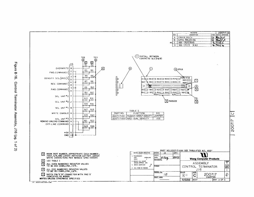
-"C cp
o ....... I'\J -
TP2. TPI
,)16 ~~m rn ~?>
OVERWRITE
FWD.COMMAND{
DENSITY SEL(NRZI){
REV. COMMAND {
R WO. COMMANO{
SEL UNIT*2
SEL UNIT *0
SEL UNIT ill! I
WRITE ENABLE
SEL UNIT*3 REWIND UNLOAD COMMAND
OFF-LINE COMMAND
+5V GND
r-
8 21-C 31----<
D 4r---<
E
5r--<
H
7
J
8
K
9 VI-:J L
I 5
-~
RI R2 I
R3 R4
V T
R5 R?/ T
R7 R8
I
R9 RIO T
RII RI2 T
RI3 RI4
T RI5 RI6
T RI7 RIB
I RI9 R20
T R21 R22
T R23 R24
T
m MARK PART NUMBER, APPROPRIATE DASH NUMBER, ASSY, S/N.AND LATEST REVISION LETTER .12HIGH WHITE CHARACTERS PER WANGCOSPEC 100037.
(3] SEE TABLE I
~ ALL EVEN NUMBERED RESISTOR VALUES ~ TO BE 430 OHMS,1/4W .±5"7o.
fTI All ODD NUMBERED RESISTOR VALUES ~ TO BE 180 OHMS,1/4W, ± 5"7'0.
ill MATCH PIN 'A' OF CONNECTOR WITH PAD 'A' IDENTIFIED ON SOARD
.. OTES:UNLESS OTHERWISE SPECIFIED
----,----_.- --,----,-------.--~~.---
INSTALL BETWEEN CONTACTS 1&2(A&B)
REV. U
~ ~~GIN RE~' B MFG. RELE
·M C SEE CRIO 3 ~ t-SEE CRIO
"ill FARSIDE
5 :3
3 2
PART NO.200717-XXX SEE TABULATED MIL ASSY NOTESUNLESS-S-PE-CI-FIE~D.::-_·_-+OR;:..A..:.WN-+_~-~_--_-tZ-~.n:.:....:..:...7/--i- ----·---1~' 1 -------
1. TOLERANCES ~
:~~~:5:r~ ::. ~ONT:~~~~~~~~N:~;l 4. All DIMS IN INCHES. J 1 6 1
~-.-------- ~ -.....-=~'=",-----------
10 ~:I C 200'717 {J r-·--------tm~::=XT~A$~Y~~------~ 4 _ CHAR!ED
________ -L.. ______ . __ --I....;,;ffi;;;lr.;.~~;;;.;~.;.;.W~N...;.L~ WEIGHT ___ 3 OF :3
u
I'
I'o o (\J

T \1..0
. h g/ ,hb, , 1\~1 \'Ion< MATERIAL LIST IMLL DR .. ,NO NO, JOEY .•
,J..:J;: \UlJ ~~:.~::' =================y=:: ~ I' ·1 200717 - 001 1 D
( 0 '; D~t!(~O ASSY.COlITROL TI:R.'!I!lATOR. MODEL NO. ~ DATE ~ SHEET 1 DF-L '. ~.~ ITEM i B~N~D,~=====OR='~W='N=G=T='T=L=E====4=~~==4=~=F====RE=M=AR=KS==ON=C=<=T,=O="='G=,==9
~ ~~~1~B~oa~ro~,~p~~~e.~.e=d~' ______ -4~2~00~71=6 __ ~~-t __________________ ;
180 100156-1Bl ~L R1.3.5.7 .9.11.13.15.17 .19.2123
Resi.tor. 5%. iv. 430 100156-431 :11 R2.4. S.W.12.1A:.15.18.2R22.24
7 Insert, Polarization. 100222
B Connector. IS Pin. 100246
10 Pin, Connector. Male. 1ooo9B TPl. TP2.
11
12 Wire, Insolated. 100051-024 AIR Jumper in R6 position.
13
1.4 Artwork, Master. 200715 Ref.
15 Test Procedure. 200966 Rer.
I I
NK.ll llJAL 1);;N:;rrr. T 12ll
~ (1r~t===F=~~==j ~I~r-~~~~~~~------~--~--~~~----------------~
ITEM ORAWING TITLE REMARKS ON CKT. DESIG. NO. 1 Board, Processed. 200716
Resistor. 5%. iv. IBO 100156-161 12 RI.3.5.7 .9.11.13.15.17 .19.21.23
Resistor, S%. iv. 430 100156-431 12 R2.4.6.B.I0.12.14.10.1B.20.22.
124 .
Insert, Polarization. 100222
B Connector, 18 Pin. 100246
10 Pin, Conn.§!ctor. Male. 1OOO9B TPl. TP2.
11
12
13
14 Artwork, Master. 200715 Ref.
15 Test Procedure. 200966 Ref.
R
Figure 8-16. Control Terminator Assembly, J 16 (pg. 2 of 2)

o (') -C (') Q)
Q: CD
» tJ') tJ')
CD
3 C'"
-<
o C:=J c:=J C=l r==J c=::J 3.00 BG;;:~t. qr~n(R:) D II
UNIT SELECT ~25 REQD POWER
I ~~~t:~1MN2LL :Jet{ -J !-- 19.ci±0.5"- --- ... ,~m-""":::"'JJ~
~.:: ;o~:~~~F1'f==-:-==E==AR==~.~~. ~- - W~ , -- p ~;-:--'U'J~~..::~~~~~:~~~~~~~~=
v _______ .. --.A
A~S
Ac=JS
I -V (N.C.)
03
(N.O)
@ GREEN
INDICATOR-5WITCH DETAIL
TYP COLOR CODE HOOK-UP
POWER
LOAD
ON LINt
REWIND
FILE PROTECT
FORWARD
RESET/UNIT lSELECT
6 11,ee5lD
...--.-- FROM T82- I } (REF) FROM PWR SUPPLY
J...--.-- FROM T82-2 CHASSIS
~;R~~RI I CONTROL I PANEL: PI9
~-l-1----.!. __ ~ ____ ~BROWN._ .(E
n~~--------------~~~ • • I BROWN
~'Z e :1 _________ ~,~:~~~~~~W4 ORANGE
I . ..L' _________ ----!BROWN
~• I . ..!.I ___________ ~G~RE~E~N~
• I I I YELLOW I I ORANGE
PI9
fg 1:1 I RED YELLOW ORANGE
. ___________ ~R~
I BROWN
lQ+ GREEN I I
! /1
I[ ~ ~~: ~i Iii
9 1 . YEL.LOW <c . ' I ORANG: I i
: BRO~:
L ___ ==-=-====:=--_-_-_. ___ J
FRONT ~!~ SCALE -NCI~IE
1')(»5.J-)2I. a/H 1'~24A/!I.
".
[~:~\~~~~lg6~~i. 12111GH COLOR/BLACK, PEA
I. IDENTIFY PI;R WCP SPE~ 100037, TAG.
NOTES: UNLESS OTHERWISE SPECIFIEO.
1.::::::SSSPECIFIEO·-r.=,."...""", '="""""".-------·W-----
, ~;:. 'ii;:::x~:.,:U .. R _ wang~~mput.r Producta
J --b~~.--~~--------

" cO' t: -& (1)
rp -!Xl o Q) r+ Q)
() o :::J r+ -&
Q. () Q)
S!: (1)
» ~ (1)
3 S!: -<
r-:--- 40.0' .to ... •
~\-P22---;~i .. :=
W\ RoE. "::IIOE.
(j) '2 pt,.,6.C.ES
P22 P3 r---. r-')1-- MOTION (+) 1
2)~-REW'ND (-) 2. 3)~-5ELEC.T ~ I<E..6Dy(+)-K3 4)-~-W«\"TE. EN,60SLE.( +) -kA 5) 1--SeiEeTt DIY l/IYE (+) - k 5 b>+--HI6~\ DE.\'-J5ITY (-)-1-<', ')+--W~'TE. PwIC!. c..AiE.-k7 S)+--we'TE ?Nfl. c;.t-JD-k8 9H-- WRITE RESET ~9
L-...- '--
LIST U1 MATERIAL
'='t- W~"NGICa i D~tr"~~G ~ATA CONTROL CABLE MODEc NO. 107!!
I~ OftAWING TITLE OwG. NO. NO. REO
ML I OItAWIHC NO.
.1 2010152
0 .. ' 1.24-72 ..... ,
I CONNECTOR /00010 - 009 2 P3. P22
2 PIN. FEMALE /00021-006 16
...J 3 PIN, NAtE /00021 - 007 2
:::E 4 WIRE, INSULATED 1000153-9IB A I R
1_ ... lc
~-+-----------------4-------~--+-------------.-----
REVISIONS 2.01052 Ie REV. DESCRIPTION CHK. OATE APPROVED
o MAIi?IC~ REF DE"5IG • . /2 ~IG\-I CAARACTEIZS ?EIa wCP spe.c. \OOO\~.
1. 1 DEM.I FY P!~ wep SPEC 10003"1 TA4,
NOTES' U"lLEScs. OTl-leW~e 'SPECIFIED,
NOTES UNLESS !:::;PE~C;;:IFI;;::;ED::---r.O::-RA;::W;:;-N'IrA. ACu.;;'-;-:I\J";/, ~'5"i'§""~;;::E-/r.'.-;;n:::-_-;;O:-ar-------------------1 CHECK I I U1 I. TOLE RANCES APPR. I 'jh· ~-..; P/~,/,· b1AT~RIA Wang Computer Products
.XX± ANGULAR
.XXX± ±
2. BREAK ALL SHARP EOGES APPRO) .• 010
3. MACH. SURFAces
4. ALL DIMS IN I~_CH_E~S' __ --I
~MbDI'
.ASSEM9LY, t)AT A CoNTgOL CAB,- E..
~.f
~1 2:1 20/052
It!mIi
101
'1iiY." REO'O.
J
c SHEET '2 () j: 'Z.. DO NOT SCALE WEI.GHT THIS DRAWING

o s::: .-+
"C s::: .-+
(') Q)
2: CD
» ~ 3 2: -<
----.---------------~----.-----•. --
P4 r41~---CieoUWI;:) __ ,_---:.Il-Kl
nl~ ...... -- .... ~". lite-G. -----=-'-+(l1!U
~-- -1~V.~E('a ----P::....f.<I .. l
l''3.lIoP---- -+ , 2 V,1le'G. -----.:..+<I!~J
P2.\
. ~:--.:~~.:.-- :~ ~---- 4- '~v. QB:4 M 2 ,~r ___ 12.\1. ~EG '
Ul MATERIAL. LIST
'~ DIU.INO TITI.I D_G. HO. NO.IIIQ.
1 ColIDeotor. 100010-00$
I ConnecWr. 100010-009 , Pin, relUle. 100021-006 14
4 P1n, Ma.1e. 100021-007 .3
S Win. lllUIUlat.ed. 10005.3-916 A/R
REMAUII ON en. oUiG.
P4. P21.
P26.
fPi~ L..:.-_ .:...J.
1. TOLERANCES • XX:!: ANGULAR .xxxt :t
2. BREAK ALL IffARP EDGES APPROX .• 010
CHEC:K
APPR •
3. MACH. SURFACES J.EJ.fiUaI:l 4. ALL DIMS IN INCHES.
CD
MAl-II B~~.
PIM;6~1I 14- PL.4~.S
@) ~.i~:£~~~W! ~ , '0001 .... t. 10Gl'TIN 1P'sa. *fM:.p SNC.. IOOO"l"'~,
Nms.: Vf~~n.s DrM&&\1 ' .. ~fI' .... U1
!8LV .... 1Of. OJTPUT 5. jLE.... ,
'1053 A ,,"EIT 2, •• 2 WEIGHT -

'T1 cO' c .., CD
OJ ~ P en CD
:2 o :0 CD co c Q) r-+ CD a. ." o ~ ..,
2
~ ~ \P27 @'
11~~ bjl 0
~ ~2P1JocE.9 3 2 REGiO
P27 P\2 ;----.. r;-I~ of. ~v RE'G. 2> +12v~~. -~ 2-3> e:.Rou .... g ,3 4 L , -1'2V REG. ~4
5> - 5" ~E6. r<5 L.,...I '--
U1 MATERIAL LIST
7.0"t0.5"
~--<I / - -- ---- PI\
2
~
0' .@ 0' 0
4
c!l ~
I REF
"(!) M602~ ReF Oesl(i •. \1 ~I6,", ~Tet5 • PE2 WCP sp&c, 1000li
1. IOE .... ,..,FY pet WCP SPEC 100001 TA4.
NOTE'S~ UNLESS OTI-IEfW'Se. ~PE"F';O.
NOTES UNLE!!lSSSP;;EEcC;FIFiF;'EDDIrD;;:RA;';WN;;;-r:A.60i"Zi'illlll"2~e.-r.III_-;22:::~_7.I:;:r-----------------...1 CHECK I \\1 I'M'L 1,... DRAWING NO. Tu¥.
~ I~ 201054 TA APPR. <' ?nh fiW72 1. TOLERANCES
.xx:t ANGULAR
.xxx:t :t MATER., .fJ / 2. BREAK ALL lIHARI' gg 5 P 7. (.""""
MODEL NO. ~ '1DAT! ~ SHEET J.... OF.-t...
OUWlOCC ASSY. SERVO REGULATED TlTL! PQ'!!ER CABLE. EDGES APP~ox .. 010
ASCS»EM6\..Y. sellvo 101 ITEM DI .... WING TITLe: NO. DWG. HO.
1 Connector. 100010-005
2 Pin, Female. 100021-006
) Pin, Male. 100021-001
4 Wire, Inl'lll11ted. 100(5)-918
NO. REO. REMARKS ON CKT. OEstG.
2 P1? P27.
7 )
A/R
3. MACH. SURfACES
4. ALL DIMS ""_'NCH_E..:..;.S._~
I MODE' No.
NEXT ASSy
MOO 10.,5
2OOb75
REGULA TEO POI<I&R c,.o. S L e. rmr.;: , cl 201054

en CD
:2 o (j o ::l .-+ .., o (j Q)
C'" .. CD z ~ --A
r-------------------.--------------'------------------'--------------------'---------------'---------------------,-----------------------------
P20
t-------1.0e:tOOS,.---i r-~--------'~ ~----,--------
r---r;.=-~----,- - ---- -- ----+-"""
LOAD P6. COM -.~--+
L.OAD PS. N/C ----"'U'" Re,.ET PS ..,/c. -,---toU
TRANSPORT REAOY (- )
FOt.WA5l0 (+) -·----W14
SE.T l=OiWAR.O .. __ --II-CI",.
R.EW/NC) ,-) ------+41~ 2.EVI2'&l. (+)-'-----41-<l
VIEW lW DI2ECTION OS: 'A' ~ MAfl~ Ja,£.' DII'$1I4 •• Ia . ..,Ia. ... C .... C.ACTEI2S
PEr. W(~" SPK IOOOI,a,
i. IDENTJI=~~( PE2 Wj'" SPllC 10001"1 T",-NO'U.S: OWL!SS O'T~EI.~VI~E SP&C,IFH!O.
Ul MATERIAL LIST lML; _.AWING NO. , .. V.
2010SS. I',q ~lf)·~r.·
\.\) I. TOLERANCES .XX:!: ANGULAR
DRAWING AS.'l:!. NO.1.
TITL! :iEUQ !tQIIII!QL !66~~
'~~ OIIAWIHG TlTLI I 1 Connector.
2 P1o, Male,
3 Pin, 'ernale.
" Wire, Insulated.
.- "
MOOEI.. NO. ~ DATe ltl.liLIl $IIUT_l o,-L
O.G. HO. ]NO. REO.I R!lURK' ON en. DUIO.
10001'1-009 2 PlS. P20.
100021-00) 2
1rJOO21-OO$ 1'1
10005J-924 A/R
- ---
.XXX:!: :I:
2. BREAK ALL SHARP EOOES APl'ROX •• 010
3. MACH. SURFACES J 4. ALL DIMS IN INCHES.
---------------,----~
ASSE:M8L:V, NUMBER 1 SEI'toVO C()NTRCIL. C.A!tL..L
~--.------~~~
t-------~NEX'f""ASSY MOD \015' ._ ......... C_ 001055' 200615 DO N01·'!CALI WEIGH"r .-r--.--......-'--~
~.'m , ___ . ~_~ __ __' __ • __________ ""'_TH.:.:.:.::.:;,'. DI""W1NQ

"T'I c.c c: .., CD
OJ ~ ~
en CD
< o () o :::J r-+ .., Q.. () Q)
Q: ... CD
z !=> I'.)
» (I)
~ 3 c--<
2
, L
MATERIAL LFST Iljlll DRAwING NO. Jui. , ' tJb I!!'t ., 201QS6 18
JI .q.'tn . MQ,OI!L NO. ~ D"'Tf~ SHUT....l.: 0'-1.:...
DIIAWIN4, flT.A.!! OlIGo NO. NO.IIEO. _EM"'_U ON CKT. 'DUIO:
CUIl.ctor. 100010..003 nB. P24. Pln, Mel •• 100021-003
1----------- 7.0· tOo' .--------.......
~ [\P24 ~~7----- ---------LA Pie ~ lo...-_or--J~.--4---------~ \ ~
I 2. PLACES
-® TVP 2 PLS
.~
~I MAI<k: REF DES'<=' •. 1'1. HIGH CHARACTE.55 Pe.~ WCP 'SPEC. \ 00o,'3
1. IOENTlFV PeIZ WCP SPEC.. 100037 TAG.
NOTES', UNL.ess OT\-lEI2WISE 'SPEC'FIEC
NOTES UNLE!:S;-;SP;;;;E;;CI~FI;;;ED~-r;:;D=RA;:WN;:;-"!rA.G.~-;-'UT.':;:;llii.~;p-r.I'~_1.;'-;.I;--7 .. 71.;r-------------------I CHECK T ", I. TOLERANCES
.XX:!: ANGULAR
.XXX:!: :!:
2. BREAK ALL I;HARP EDGES APPROX .. 010
3. MACH. SURFJ\CES
4. ALL DIMS I~I INCHES.
APPR. tt:;.~ ~.2'lI-?~ ~ MATER I ~ ,
MOOFI Nn
MOO II NEXT ASSY
200~'5'
~
ASSEMBLY. NUMBER 2 loa SERVO CONTROL C.ABLE I£'(b.
00 NOT SCALE THIS DIIAWING
~I WEIGHT
. , 2010S'b B'
IsHEET 20F~

(.1 0 3 4. 5 I J ZI
(I 2 01 J24
I A'60 I e {} []gJ
88 [flQ]
2.77 27 I,
LUIS 17220,
~ (113 I~ ~ lj/9 I (£2] ~ IcB'
DESCIUPTION
C .fEE REV E.O. (bel'? 99-#)
;: SEE REV t:.O (OCR /041)
H SEE NEVE.O. (beH//JJ)
J SEE REV EO (OCR 1241)
K SEE REV EO (OCR 1339j
JtNJ1~ 10
~ US I ~ uU) I ~
1'::::/41
88 J:11~~~ '1'/ O[~:R2~
wS> ~S~P~2~---4-------rv.~v.mm~~~~~4rl1~ 321 6S4
Jte. @)e 7
NOTES UHL.ESS SPECIFIED
t. TOlEMNCfS .XXi ANGUl.AIt ,
2. MEM ALL SHARI'
(g) ~ JI//JI~ R£Q(./I£eMMTS ~ Mti [2) t:J" ct:JMpove.<.JTS SNOW.u /~ ~
,qlit; w:ul/~Bt..e. ~ MIL--
I.JOT~S: VIJU355 t:!:)r,.;e2wl.s6 SPl!~O!=16lJ
Ul Wang Computer ProductI
EDGESAPPftOX .• D10 --.- ASSEMBLY 1,,1
1 IW:H. SUflf'oIoCES J t..flliOO=----~ ~ •. AllO'''''"'NOIE1. __ • _ TRANSPORT CONTROL LOGIC ft i>
~ iIU.
1 _____ -t.==m~o~d~1 ,~~ 2' I 0 ~2~1S "" ............ ---
PW8 I
Figure B-23. Transport Controi Logic Assembly (pg. 1 of 3)

i '<: "1\1\' Vl!ANGJ;D ==M=A=T=E =R I=A=L===L",I=ST=== t--t-- 'l.llJ INCORPORATED
IIMLI O''''NO "0. I'ev. II .1 201004 -000 I K
~? D~r~~G ASS? • TRANSPORT CONTROL LDGIC PWB MODEL NO. 1075 OATE' 2/4/72 SHEET 1 OF..1-..
~ § '~6~ ~ ~r-~~~_,_~~,_p_r_oc_ •• _._.d ________ ~20_10_0_3 ___ 1t-_l __ ~ ____________ -----i
-J~+-__________ -+ ____ ~i __ ~ __________ ~ ~ IC. Hex. Inverter l00084! 7 Ul,2 ,3,4,5,21 ,24
Ie. Quad. 2 Input Nand.
Ie. Quad. 2 Input Power 100086 U16,17,18
Ie. Dual Flip-Flop 100088 UlO,ll,22
IC. Triple 3 Input Nand. 100107 U7,9,14,lS
Ie. Dual 4 Input Power Gate U.3
10
Tra.ns1Rtor. NPN. 2N4123 Ql,2 ,::1,4.7,8.10,11,12,15,16,1
12 Transistor, PH? 2N412S 100081
Transistor. NPIf 21(2219 Q9 20 21
Transistor. PNP tlPS-U5! 100083 Q14
16 Diode I Rectifier IN4b03 100127 CRl,9
17 Diode, Signal IN914 100091 11 CR2,3 ,4,5 ,6.7,8,10 ,11,12,13
19 Capac1 tor, Cerate 330pt 100073-331 C12
capaeitor, .OO22uf ClO
21 Capaci tor, .OOluf 100073-102 C8,9
Capac1 tor, Polyt'U. .01ut' 100018-103 Cl.3,4,19
23 Capacitor, .022ut 100078-223 C15
Capacitor, .lu! 100078-104 C2 6 17
2. capacitor. TantalUli 100070-106 C7 ,11.14 .HI.21,22,23
27 Capaci tor: l0001D-476 C20
2. Cap&c:1 tor. 100136_106 C13
29
31 Re~ietor, ~",3" 100068-470 R45
Resistor. ,. .W 100 100156-101 R38,68,69, 71, 73, 76, 79
LI ST hMLI O'U'NG MO. I"v. II -I '01004-002 I ~
~Ilc \\"'W~_NGCD MATERIAL -- \lJ.iJ INCO~I>ORAT-D ASSY • TRANSPORT CONTROL
z N !-;·~~trw~~~_o -=~LOG~l~C~PWB~~9C~H;. ~TY~P~E:' P:'~~'::::::":~=:;:'''':DA:TE~':/:11:17~2~'::"':fT:'::I~OF~.t~ ~ r 1~~104 DRAWING TITLE ~EI.UAI(S ON CI(T.
~ ~~9~;9=7c.~pa~c~jt~o=r'~T~.=nt~'~1~==~1.~5U~f=9~10=01=3~6_~15=5=~1' ~1~==~~~~~~~~~ c N r--i~~~~~~=-~~~~~~-r~-4~~--------------~
-J ReSistor, 5~,~'" 390 100064-391 R58
~ 94 Resistor,";'If 100156-751 024
Resistor," " 750 100156-751 043
96 Resistor," 3W 100068-470 .80 Resistor," fW' 390 100064-391 R81
98 Resistor," lit' 1.5K 100156-152
100
102 Wire, SoUd Insulated 100248-924 AIR Jumper Il. FrOll. VV to I""
Jumper J2. Froa GG to HH.
Jumper J3. Not Used.
Jumper J4. Not Used.
.Jumper J5. Not Used.
Jumper J6. From CC to DO.
Jumper J7. FrOll Y to Z.
Jumper JB. FrOil S to T.
JUJllper 19. FrOlll P to R.
JWlper Jll.Fro. " to X.
Jumper Jl2.Not Used.
JlUlper J13. "
Jumper J14.Frolll G to H.
JUllper JlS.FrOil LL to PP.
Jumper J16.From V to v.
Jumper JIT. Not used.
Jumper JIB.
Jumper J19. "
Jumper J20.
i ~ ,"', \J\I~_NG_~D MATERI AL -I-- u..JlJ INCORPORATEO
!-IST
~ ~ D~NI'~~~SY. TRANSPORT CONTROL LOGIC PWB
o ~ ITEM H NO. _ 33
100156-221
Re~15tor, 1"'," 267 100155-234
IIMLI ORAWIMO HO. J"'. II ·1 201004-000 I K
DATE ~ $HEET 2 OF--1_
Rl9 20 25 42
R49
-J~~~~=.='=.<=or~.~5=~~:· ____ ~~-r='0=01=5=6-~4=31~~ __ ~R~74=.=77~ ____________ ~ ~ 36 Resistor, lOX:' 511 1001:;'5-261 R48
Resistor. 5'.1,," 560 100156-561
38 Resistor," .. 390 100156-391
Resistor," " lK 100156-102
40 Resistor, n .. 1.5E 100156-152
Resistor." .. 2.2K 100156-222
4' Resistor," " 100]56-332
Resist.or, II .. 3.61< 100156-362
Resistor, II II 5.1£ 100156-5]2
Resistor," " 6.8£ 100156-682
!.2K lCOl~s-e22
Resistor," .. 10K 100156-103
48 Resistor," " 5.GK 100156-562
49 Resistor," .. 201( 100156-203
Resistor, It " 22J1; l00156-22~
ReSistor, II ., 47K 100156-473
52 Resistor," n lOOK 100156-104
Resistor." to 100156-114
Resistor," " 2201( 100156-224
.5 Resistor, If n 3901< 100156-394
• 1
58
59 Pin, Male. Test Point 100098
Sere ... Captive 100.62
. 61 Pod, Tran!li!Jtol" 100223
62 I Connector. 9 Pin 100241-001
Connector, 5 Pin 100241 .. 005
~'.k: 1\1\'WANGCD MATERIAL -- \l.llJ INCOR?ORA.HD
ASSY . TRANSPORT CONTROL
LlH
RSO,61
R70,12
R18,62
R6, 7,12,28,31,55,59,60
R51
R3,4,13,29,32
Rl 2 11 21.22 23,26,27,30,84,
R85,33 ,41,46 ,47 ,56,57,75,78;82
R5 ,9,10 t 40,63
Rl6,36.65,67 j 83
R52
R14
R53
R34
RI5,17,37,64
R66
""5 ",,9
J22 20
J21
IIMLl O","HG MO. I .. ',' II -I 201004-003 I r:
z :3 hO;;iTWI~L~_· ..::::LOG~le~P\fB~7~CH~.~TY~PE~. A:·=:;.-=:::'::.:;:~~=-0::A:':TE~2/~1~1/~7~2 "':"':':fT~l:. :"':OF~I!·~· . ~ 71=~'~6=~~=====0"=A=.='H="=T='T=L=E====~======~==~====R='M='="='=O=N=C='T=.=O'='='G.==~ : § ~ ~~9=1~ ________________ ~ ________ r-__ ;-________________ --;
92
....J 9:3 Reshtor, 5~,2" 390 100064-391 R5.
::E Resistor, to ; ..
Resistor," " 750 R43
96 Resistor," 31' 41 100068-470 R80
Resistor," ~W' 390 100064-391 RSI
Resistor," tV 99
100
101
102 I Wire, sol1d Insulated 100248-924 AIR Jum.per Jl. FroRl VV to ww.
Jumper J2. From GG to FF.
Jwaper J3. Not used.
Jumper J4. ..
.JulI;per .IS. "
Jumper J6. From cc to EE.
Jumper J7. Sot used.
Jumper J8. FrOID 5 to T.
JUlDper J9. FrOlll P to R.
Jumper no. From RR to SS.
Jumper Jll.Not used.
JUJII;per J12. frOJI K to M.
JUliper Jl3.Fror. J to L.
Jumper J14.fram G to H.
Jumper JlS.FrOlD LL to PP.
J1.Dnper Jl6.FrOIl U to V.
JUlllper J17.Not used.
Jumper J18. n "
Jumper J19 ...
JWlper J20.From .u.A to BBB.
~ ~ Ul VI! ~G.QD ===M",A T=E=R=I",A:=L==L",I =ST=== t--I-- INCORPORATED
IIMLl DRAWING NO. IReV. II .1 201004-000 I ):
~ g D~~T~~GASSY.TRA.NSPORT COll'TROL LOGIC PWB MOOELNO. 1075 OATE 2/4/72 SHEET 3 OF-1!......
~ ~~IT;'M~~~~OR~.~.~'H~G~T~'T~L~.~~~~::~~~~=-::~~R~-=~~~::~ ~ ~ NO. Connector, 5 Pin 100247-008 J23. REO. " ON e<T. D'''O.
65 CanDee tor I 3 Pin 100247-010 J24.
-J~~ ______________ +-____ ~ __ 4-____________ ~ :E 67
68 Schematic
69 Artwork I' Mu ter
I I
--1 93 Resistor, 5", iw
~ Resistor," it' 750
Resistor," " 750
ReSistor, "
97 Resistor," 21' 390
98 Resistor," iw l.SK
101
102 Wire, Solid Insulated
201959 201002
201146
LlH
Ref Ref
Ref.
IIMLl OHO'MO "0. I·,v. II -I 201004-004 I !\
1075 DATE 2/11/72 SHEET 11 OF --1
100064-391 .58
100156-151 R24
100156-751 .43
100068-470 R80
100064-391 R81
100156-152 as,
100248-924 AIR Jumper J1. From VV to n.
Jumper J2. From GG to FF.
Jumper J3. Not used.
Jumper J4. "
Jumper .J5. ..
Jumper J6. From cc to EE.
Jumper J7. Not used.
Jumper J8. From S to T.
Jampe r J9. From Pto R.
Jumper JIO.Frotl RR to SS.
JUJDper J11. Not used.
JUJDper J12.Fron K to M.
Ju.per J13. From J to L.
Jumper J14. From G to R.
Jumper J15.From. LL to PP.
Jumper JIG.frolD U to v.
Jumper J17.Not used.
Jumper J18. to
Jumper .119. "
Jumper J20. "
~ '< \\1\ 'WANGCD MATERiAl
-t-'- ~ ~~~~~P~;A~;~~ORT CONTROL
LI ST IM'LL DRAWING NO. IRf V•
II ·1 201004-001 J r.. O:tT~~' LOGIC PWB. 7CH. TYPE'P' 1075 OAT, 2/11/72,""T 1 OF 1
8 ~'T~E"::;"-=:::::OR:A~':' H:G:T:' T:L:,==:;......:o.:o.:H:.:o.:..:;::IH~o.:R:Eo:::;, I=-:::.~E~".:"~':O...:H :c:. T~. :o,=-,':, •. :'=:..j CaPdcitor. Tantalum. J.5uf 100136-155' 1 1 C5. ~ ":;
92
-J 93 Resistor. 5%.'~. 390 100064-391 R5a.
:E 94 Resistor. " I:oiW. 750 100156-751 R24.
95 Resistor. n 750 -751 R43.
96 Resistor." 3w. 47 100068-470 R80.
97 Resistor. II ~. 390 , 100C64-391· 1 R8J.
98 Resistor." ~~ J.5K 100156-152 I 1 R54.
99
100
101
102 Wire, Solid Insulated. 100248-924 AIR Jumper JJ. Fran VV to WW.
Jumper J2. "GG to HH.
Jumper J3. Not used.
Jumper J4. n
Jumper J5. ..
Jumper J6. From CC to 00.
Jumper J7. Y to Z.
Jumper Ja. s to T.
Jumper J9. P to R.
Jumper J10. Not used.
Jumper Jl1. fran W to X.
Jumper J12. Not used.
Jumper J13. ,I
Jumper J14. From G to H.
Jumper J15. " LL to PP •
Jumper J16. ,. U to V.
Jumper J17. Not used.
Jumper J18.
Jumper J19 •
I I I Jumper J20. FROM AM to BBB.
1ft) UH'[T SELECT
~ .1: 1\\\ 'WANGCD MATERiAl LIST IMLI ..... NO HO. 1"'·1 ...:. - \U.1J INCOFl-POFIATfO II ., 201004_005 1 ,",,_ ,
ASSY • TRANSPORT CONTROL , OR "'II'IHG LOGIC PWB 7eR TYPE 'P' 1075"" ", 1 1
z ~1~T~'T~LE~::::::::::::::::~"":~:'::~==::::;=-~D.:"~~:/l=1:7~2"':':H'~n~':...:o,~~~_~; o 0'" ;: ~ I~~~ DRAWING "."LE
: ~r-9_11-c_a~p'_C_it_0~r._T_._nt_'1_u_m ___ 1._5_U'-r~~~-r~~_C=5~. ________________ ~
~ 93 Resistor, 5~.~W
::E. 94 Resistor," ~W 95 Resistor,"
96 Resistor,"
97 Resistor." ~W
98 Resistor," ~W
99
100
101
102 Wire. Solld Insulated
390 100064-391
150 100156-751
100068-470
390
I.SK 1001S6-152
AIR
R58.
R24.
R43.
R80.
R8l.
R54.
_Jumper .11. From vv to WY.
.Jumper .12. From GG to I'fll.
Jumper J3. Not used.
JUlllper .J4. "
Jumper J.5. "
JWllper .J6. Fl"O!l CC to DD.
Jumper .J7. Fron Y to Z.
.Jumper JB. From S to T.
Juaper J9. Fro1ll P tc R,
Jumper .JlO.Not used.
Jumper Jll.From W to X.
Jumper .Jl2.Not used.
JUDIper J13. "
Jumper J14. From G to H.
.Jumper J15.Frolll LL to PP.
Jumper .Il6.From U to V.
JUJrIper J17.Not used.
Jumper JIB.FI'OII TT to lTU.
JUDlper J19.not used.
Ju.per J20.Fro. AAA to BDB.
Figure 8-23. Transport Control Logic Assembly (pg. 2 of 3)

o ~ 92
l:il ~I 97 Resist.or 5% ~ .... 82 100064-820
98 RESISTOR syb Y,tw /oK /00156·/03
99
100
lO~ i
IM'LI 0"'''" NO. 1""·1 II ·1-:>01004-006 J J,. _\
IlPE , OJ. TE 7-12- 71HHT 1 01= 1 :
R!::Ju.lHCS ,?N CKT. DBIC;. J C5.
J
I I RBI.
l021~Vire Solid Insulated. 100248-924 AIR Ju~r J1. From XX to h'1'J.
I Jumper J2. From GG to HH.
j Jumper J3. From KK to JJ f ! Jumper J4. yy to ZZ.
J I Jwnper J5. AA to BB.
1 Jumper J6, CC to DD.
! Jumper J7. Y to z.
J Jumper J8. S to T.
J , Jumper J9. P to R.
1 i . Jumper J10. Not Used.
Jumper 31L From W to X.
1 Jumper J12. Not Used,
Jump~r J13.
Jumper J14. From G to H.
Jumper J15. "LL to PP.
I j Jumper J16. ., tJ to V.
1 Jumper J17. ~ot Used.
Jumper J 1 So Y":ot :'::s:ed.
i I Jumoer Jl9 ~""'t 1silil.
I Jumper J2::L Not Used.
,; 1_ 1\\\ 1 =M~A~T~E=RI=A=L=o::L=I=ST= I'MLL OR""O NO. ~.,vJ ~ ~ \UlJ ~~~~r~O ~ -I 201004-010 i .i', I
AS$"f. TRANSPORT COSTROL I D~tTW~~G LOGIC P'I'ffl 9CH. TYPE 'P' llPE D.-. TE3/5/73 SHEEr'1 OF II : : ~ ~....:::::::::~~~""'::::'~~~::""::~~
; ~F='~=a~~=====D="A=W=,"=O=T='=TL=E=====F=======F==~===='='='A='="=D="='="=·======9 ~ ~~~91~~C=,~p,~c'~t~or~'~T~.n~t~'I~U~~~I~.5~Uf~~IO~O~13~6-~1~55~~~~C~5~.---------------1
-.J 93
~ 94
97 Resistor. 5~, ~w 82 100064-820 RSI.
98 Resistor, 11 tW 10K 100156-103 RS4
99
100
101 ' I 102 I Wlre, Solid Insulated I 100248-924 I AIR I 1umper Jl. F!'Om xx: to WW.
Jumper J2. From GG to HH.
l Jumper J3. From KK to .JJ.
Jumper J4. r'rom YY to ZZ.
Jumper J5. From AA to BE.
Jumper J6. From CC to DO.
JUMper .)7. FrOm Y to Z.
Jumper J8. From 5 to T.
Jumper .)9. From P to R.
Jumper JI0.Not used,
J·..unper Jll.From W to N.
Jumper J13. "
.Jumper .Jl4.From G to Il.
i i .Jumper 115. From LL to PP.
Jumper JI6.FrOM U to V,
Jumper .Jl7.;-';ot used.
Jumper 118. From TT to LT.
I Jumper Jl9.Sot used.
I Jumper J2D." It J
NO UNI T SELECT
~i.l::- \\\\lWJl..NGCO MATERiAl LIST ~ ~ HCORPOP.ATED
I I ASSY. TRA.~SPORT CONTROL g I t; D~tl~~r; LOGIC PWB SCR. TYPE r P' 1075
IM'I I DRA.,NO NO. l",v·1 II -I 201w4-007 I K I
0.-.1/- /11 / 72 SHEET' 1 OF_,:,"l I
Oil 'I ~;g !~g~ ORAWING TITLE
• 0F=~F==================P======~====P=================~ ~ ~ 91 Capacitor, Tantalum l.Suf 100136-155
REMARKS 01'1 CK1. DESIG •
...J Resistor, 5~r!W
~ 94 Resistor, II iw Resistor," "
Resistor," ~W
98 Resistor,";W
99
I 101 I
102 ?lire, Solid Insulated
390 100064-391
750 100156-751
100156-751
100068-470
100064-391
1.5K 100156_152
100248-924 AIR
i
1
i
LIST
o c 91 o
Capacitor, Tantalum. lSuf 100136-155
92
CS.
RSS.
R43.
RBI.
RS4.
.Jumper 11. From VV to WW.
. Jumper J2. From GG to HH.
Jumper J3. Not used.
. Jumper 14. "
Jumper .J5. "
.Jumper J6. From CC to DD.
Jumper J7. From Y to Z,
Jumper J8. From S to T.
Jumper J9. From P to R.
! Jumper .JlO.:iot used.
I JUlllper Jll.FrOli. " to X.
Jumper .i12.Not used.
Jumper J13. "
Jumper J14.From G to H.
Jumper .1l5.Fl'OIII LL to PP.
1 Jumper J16.From U to V.
r .ll111lper J17.Not used.
Jumper JI8.From TT to UU.
Jumper JI9.Not used.
JUIlper J20, "
hMLL 00",,0 NO. I',v. II ·l 201001, - 015 i L
cs.
~~9~3~~~~,,~·s~to~r~.~~~.~J~w~. ____ ~3~90~~lXO==~~.-~3~91~~~~n~56~. ________________ ~
~ 94 Resistor." tWo 750 100156-751 R2L.
95 Resistor." 750 100156-751 R1.3.
96 .Resister. II )w. L7 100068-u7J RBo.
97 R.esistor. 'I lw, 390 1Y.lo6L-391 lUll.
98 Resistor. II ~"W. l.SK lJJ156-152 H5L.
99
101
102 riire, Solie. ':nsulated. I 1302L.8-92L 1 AIR JUIll.per Jl. From. VV to ·~W.
Ju:n.ner J2. II GO" RH.
I Juaper J). :lot Used.
JUr.lper JL.. "
JUl'lper JS. n
Jwn.per J6 From CC to tD.
Jumper J7. II Y II Z
JUIlIper J8. II S" T
JU"lper J9. n P n R
JUMper J10. :lot USied.
';urr.per ~':':'. hom '1'1 to X
Jumper J13. tl
Jum;"ler JJ.L. From G to H.
Julll.oer J15. KM. q PP.
Jumper Jl6 U' v. Jumper J17. "- . D to E
! JU'"Iiper J18. from TT to UU.
I JUMper J19. 't.o -A to 8.
.jumper J20. II
I
BASIC PEINRZt
LI ST ~;l. ·~\\'ll\l'JJ?.!"J(S_qC MATERIAL . fNCOflPORAHO
liMI I ORA-WINC NO. IREV. ji IL.l 201004-008 I K"
ASSY • TRANS PORT CONTROL
';1 c;tT~~e 1..C(iIC PWB 9CR TYPE 'P' 11 OA,Tf8/4/72 ~!1EE1·1 Of ~_ • ~~':;'5~~'I~~~D~RA~,:,,~o~T:'~TL~E~:::I~~D:'.:.N~o.~;IN:O:.R:EO~.~~~RE~"'~":KS:O-N:C=K~T.::~~~ ~I: F9=1 =====~==*-1====='*1===:=======1 ~~~9~1~~ca~p=ac~1~to~r~,~Ta~n~t'~I~=-~I~.5~U~frll~0~01~36~-~15=5-t~1~~~--------------~
92 !! ~~9~3~~~~S~1s~to~r~,~5~%,~'W~ ____ ~~I~O~0~~4~-~39~1-t~~~R5~.~. ______________ ~ ~ 94 Resistor," iw 750 100156-751 R24.
95 Resistor,"" 750 100156-751 R43.
96 Resistor." 3W 471 100068-470 I 1 R80.
Resistor I" iw 100064-391
98 Resistor," zlf" 1. Sf( 100156-152
99 .
J 100 i
102 Wire, Solid Insulated 100248-924 ' AIR
i
J i I
!
LOW DENSITY STATUS.
~ if. \\\\1 MATERIAL LIST
t-- - \lllJ WANGCO ASSY • TRANSPORT CONTROL
l: ~ n~tr"'I~~G LOGIC PWB 9CH.TYPE 'P' lAOOELNO. 1075
R8l.
R54.
i .JWll.per Jl. From VV to 1t'W. I .Jumper 32. From GO to HR. I Jumper .J3. Not used. I Jumper J4 •
Jumper J5. ..
.Jumper J6. It
.Jumper J7. Froa Y to Z.
1 JUIIlper .J8. FrOID. S to T~
Jumper 19. From P to R •
Jumper JI0.Not used.
JUlllper Jll. FroIIl ... to x. i Jumper .Jl2.Not used.
Jumper J13. "
Jumper .rlt. FrOIl G to H.
JWllper J15.FTom MM to PP.
Jumper JI6, From. U to V.
Jumper J11. From D to E.
.Jumper .118. From IT to UT'.
Jumper J19. From A to n.
Jumper .J20.Not used.
lULL o' ... we NO. 1"":1 II VI -I 201004-016 II( I
OAT' 1/29/7 i..", I 0' I I I 1~6~ :>RAWING TITLE
'~~~~~~~~~~79~========~ ; g 91 Capacitor,Tant. l.~uf 100136-155 CS.
t:. ~ 92
..-' 93 Resistor: 5%:~W
:E 94 Resistor," -'£W
95 Resistor, II
96 Resistor, II 3W
97 Resistor I" ~w
98 Resistor I" ~W
99
1100 '
101 I
390 100064-391 RS8 •
750 100156-751 R24.
750 100156-751 R43.
47 10006B-470 RBO.
390 100064-391 R8I.
I.5K 100156-152' R54.
I
102 IWire, Solid Insulated 110024B-924 I AIR Jumper J1. From VV to WW.
j Jumper J2. From GG to HH.
, Jumper J3. Not used.
Jump_er J 4. Not used.
Jumper J5. Not used.
i Jumper J6. From CC to EE.
i Jumper J7. From Y to Z.
Ju:'""nper J8. From S to T.
Jumper J9. From P to R.
j Jumper 310.Ilot used.
I Jumper J11.Fram W to X.
I Jurn:er J12.Not used.
gum er J13.Not used.
14 F G 'I JurnDer J • rom to ••
1 I ! Jumper J15.From LL to PP. I I I \ Jumper J16. From U to V. J I I ! Jumper J17. Not used. I i 1 Jumper JIB. Not used.
I i i Jumoer JI9.Not used. J 1 1 Jumper J20. Not used. J i : i J
REMOI'3 DS:ISITI SELECT
L! Si
l1DD.
hM' l ORA<' ••• 0. -.L"".J II L\ 20100u - 009 ! }; .1
DATE 2/16/71 SHEET 1 OF 1 ;
C5.
1~~9~3~R=es=is=t=or=.~s=%~.~~~. ____ ~3~~-r_1OCD __ 6_L~-3~91-+ ____ rR_SB_. ________________ ,
..e::::. 9" Resistor." two 750 100156-751 a2h.
95 Resi.!tor ~ " 750 100156-751 :lL 3.
96 nesistor. II Jw. 47 100068-470 I RBO.
97 j ~esistor." two 390 1OO06L - 391 I RBI.
98 Resistor. IT tv. 1.5K 100156-152 "54.
99 llOC i -.l
101 1 II 1021 \O:ir-e J Solid Insulated. 1OO2LB-924 I AIR I JU~D.r Jl. From VV to ....
j Ju.'n:oer J2. II GO II HH •
I Jumper- J3. Not Used. I 1 I ! Jumoer JL.
1 i i
f Ju:nper J6. II
! Jumner J7. From Y to Z.
1 I I Jum;:>er Je. II S" T.
1 1 JUI!l~er J9. II P II . R.
I Ju.·II"Oer JI0. Not Used.
i i I Jumper Jl1. From W to X.
1 i JUiilper J12. NO't. U:5eo.
i _ i Jumper J13. "
! JUM?er JIlt. Fran G to H,
j i JUlQ":)er JlS. n HN n PP.
! ! } Jum~er J16. It U II V.
i Jwn?er J17. n D n F.
i I':ump~r J1B. TT" UU,
i J Jumper J19. II A tI C.
J Jumper J2O. n AM " BED.
NRZI NO UNIT SELECT. MANUAL DENSITY SELECT. D See Shipping Configuro8tion
s" 1\1\ 'WANGCO MATERIAL
I- r- \UlJ IASSyfl.PTR~~\OpORT CON7ROl D~i\~~ti LOGIC PWB. 7Ch. Type 'A'
~ ~ I~ Drawing Title
LIST
Dwg. No.
1075
Oty.
hMLl .'A"N. NO. ~.EV. ~ ·1 201004-017 I A
DATE 6/10/74 ~HEET 1 OF 1·
RemarkJ on Ckt. DeSIg..
: g 91 o ~~92~----------------~-------i----r-----------------~
-J~9~3~~Re~s~is~to~r~,~5%~,~~W~.----~39~0~~1~00~0~64~-3~9~I-r~-i~~~~--~------------i ~ 94 Resistor," "". 750 100156-751 R24.
95 Resistor,"" 750 -751 R43.
96 Resistor. It 3W. 47 100068-470 RBO.
97 Res; stor. II i::iw. 390 100064-391 RBI.
98 Resistor,"~. 1. 5K 100156-152 R54.
100 •
101
102 i Wire. Sol id Insulated. 100248-924 . AIR Jumper JI. Fr"" VV to WW.
J:Jmper J2. GG to FF.
; Jumper J3. Not used.
Jumper J4.
Jumper J5. II
Jumper J6. Frrrn CC to EE.
Jumper J7. Not used.
Jumper J8. From S to 1.
Jumper J9. P to R.
Jurnjler JIO. " RR to SS.
Jumper J! 1. Not used.
Jumper J12. From K to M.
! Jumper JI3. J to L.
i Jumper J14. G to H.
Jumper J15. ft1 to PP.
I Jumper J16. U to v. i Jumper JI7. D to E.
I Jumper JIB. IT to UU.
! Jumper J19. " A to B.
I Jumper JZO. Not used.
Figure 8-23. Transport Control Logic Assembly (pg. 3 of 3)

DEN.SEL.{ 0
I
I OFF {IL+--!-t-LI NE ~ _ rl L.t+-I -4---+-q
I -OFF, I I
• !i.;f>iEl~~
I I I ICR ~ +5V
+5V Isd 11N4f'3* I i BV ! s4---+---' I! 110
l i i I FWDj 1, d J i i STOP l i1wo/f:~.I----+~
J ~TOP ~ WRT.EN. K i
I
!
UNIT SEL. COM
SEL 0 COM SEL I COM SEL 2 COM SEL. 3 COM
ON LINE (-)
R~VERSE PB COM F
REWIND PB. N/O II(-f------'I------,
REWIND PB N/C II*+----~_q REWIND PB. COM
RESET PB. 0/0
RESET P8 COM
LOAD P8 COM
LOAD PB NjC
LOAD P B N/C cOAD P B COM
RESET FB Njo
TRANSPORT READY (-J
J21
+5V
T P 7
R 36 10K
+5V
+ 12 V 5 4---.----T--+ 12Y
+ 5 V 2M---I--~-+--+ 5 V e21 +
IO)J.FT
GROUND I~--~~"--"-'
-12 V 3~( 11------<>------.. 12 V
+5V
R42 220
yy z Z
R43
(!J
R 12 +5V
Z2Kt 12 .... 1"2..( r--........ d ........ ")
.OI~.U6'" 'U3-
RI. 3.6K I +SV "I I t • RI6 ~
I '" ,
-12V
HIGH DENSITY STATUS
I ~Hr:I:1 ..-+-+----*NI,REWIND rt121} STATUS
~ ! ! ..-+-+----*pl~ FILE
" \-PROTECT
IT"""' r+-+----"*. R i}BD:r
~141 STATus
U
SELECT &READY(+) HIGH DENSlTY(-)
,------~-+------HI MOTlON(+) WRITE ENABLEl+)
r----H(9)1 WRITE RESET
8 WRITE POWER GND
; I ~:~~~Tp~OO:E~!:EA~~ r--~-+----"--~2 REWIND (-)
~--'---------------''---~++~~rr----~
VV wwl 51+ 12V RESULATED
+12V~~ WRITE VOLTAGE
+5V4----tx"m J20
FWD c-)
L-___ --~l7iON LINE IND
,..----..-----4.)!OI FORWARD IN~ DRIVE
+SV _-i'H I' FORWARD IND +SV R76 . 100 !
T5V~!RESET/UNI7 SELECT?5v. !
~-'-----'4L! RESET,l\JNIT SEL DR.
~ +5V ~HI+5V POWER 1"10 R 79 100 ~EI POWER IND GND
I .1 "I
+ 5Y
A MFG REI.
I L~~~~SED I DELE TED
Q21 C23 CI6 CR. , R85 TP9
6. JI6 PINS JNCSED ARE; 15,18\ V J 19 PI~S U~USc.D ARE ;8.0,.-1. ~ «
o ~TgTE~i';~Es ~~T~~~: l~uEN~~~;;C;F SEL.ECT ADD JUMPER Y TO Z.
(J\ I.()
(£1 +5V OPTIONS TO CUSTOMER CONTROLLER. (J\
o TYPE 'P'VERSIDN JUMPER CONFIGURATION SHOWN.
o ~5~EADY DELAY NOT REQUIRED DELETE
GJ FOR VAR COMPONENTS SEE MIL.
o C\J
t R6e~
IOO .. ~
NOTES. UNLESS OTHERWISE SPECIFICED.
i 2~412:) J20
RG7~u7! 1+'_ ...... ;.;;'O"'K'-4 100 I
(20 -+ 47)J.rT + ~
-!2V
\ll Wancc:o Incorporated
SCHEMAT I C 168 -;-;:;.:. '~S:JD~.: CONTROL LOGIC
MOD II
&lII..AIIil: 201004
Figure 8-24. Transport Control Logic Schematic

I (;t I I I
I 5 ~ -----
I
I:' I~ I) c:
-.----------l.----P-I !
~---
~ --- ]---_.- - - ------
4- PLXES®I------~,~ I
-4 PLACf.S @i = I
ReF @ ____ ~I ,-1. PLAc.E'S @I--,-----
~F 0.....----===== 4 PI..AC.ES @il----~..,=
RE.F (Df---'-':=='=== -4 PLACES @l~---~.L
4 Pi..ACE.$ @ -ll' YleW ~\-~\
I
TYPICAL ~SISTOIZ. INST,4LL.ATION
5UL~I:1
I
(:
---~-----:-
I Cl:%)
I
-+---- - ----
RE.F
TYP. POWe:1<. DIODE. I Nl!tT,4L.I..IITION
5GALE 1:1
Ii
I I
--\---\
--@) RE~Y SClCKE.T
e RELAY
I
\LNOT uSE.D
J, ~ :2. REQ'O-8 PLAC.E<;,
2REQD~ ~:2 I<EQ'D-8PLA£.E5
SPeS I c==J I ---6 I<EF
=r======I~-~~ 8~~c~. i '
cd'le/nid',,? 0 12EF .
_ 1. .. ~ :2i2EQD-8tJt.ACES I ~Rf:F
J, I @) ;;z 12EQ'o-8 PlACES
il ~ 21Z~b.8 f'LAC£.~ I I
VIEW 13-1~ TYPICAL ~t.1S\STOR It-JSTALLATION
SCALE. I: I,
I) (:
I~
I D I SEE. REv E.O,( DCR 944)
. E ~ SEE REY EO. (XI< !l5') 114 ~ P./,fI"J~ I F I SEE REV. E.O. c.i ~ b"'{~_ I G SEE REV. E.O. (DCR 955) I 'eo' IT,.., "'~ , H ' S~E REV. E.O. (OCR 951) i'4. Vzr . ,/;
J SEE REV. E.O. (OC R I I 80) <;0 ." ./1If!.
K SEE REV E.O.(DCR SOl) iC21 ,...." !.M~. B
L SEE REV E.O.COCR 13S~) "1;-';' '''''''''If>tJ. M SEE REV E.O.(OCR 1117 ) ;~ .,." .~ ! .. l SEo CR/o 30~o
I p r SEE [ii/O 3634
I I!I.J'Y .. iJ, 17'1-
+-
----------- I.
OJ COMPO .... ~h1TS OUTLINED IN DASHED LINES ARE VAI2IABLE. se.E. MIL FOI2 P~sc.12I~E.;..l VALLI~S.
\lJ
,: : -= =:::~,a J" I"'MA=TE"'R_IAI ____ --I
~ •. "', .. ., ,. ,."''',. I
Wang Compulw Products
ASSEMBLY SERVO ELECTRONICS
I MOO 1075 ~= I i 200675
A\
Figure 8-25 .. Servo Electronics Assembly (pg. 1 of 2)
0...
<:j I"O'l o o N

l ~ 12 \lJ ~~::::::, MATERIAL LIST
() I PRAWI .. C 11
T/cO
IIMLl D""" "D. l'EV•
II ·1 2C"07L - 000 I p
DHE ~ SHE-ET 1 OF \0
: ~F=N0~'97==~~O"=A=W='N=G~T="T=L=E====~~~~=f~~~==="="'='="=D=N=C='T=.=D'="=G.==~ ;il~ rrT:~LE ~ 2r-~_:·_,,~ro~,_P~ro~c~e,_,e~d~. ______ ~~2~OO~9~73~-r __ ~ ______________ -----4
::eats1nk. 2010L2
-J~-r--------------+-~~-r--;---------____ ~ ~ :;:C.~'Uac. 2 Input !'Iand. 100065
Ie.Opera.tional A.""lpli:'ier. 100109 C1.2. )."-,.6.7.8.
7 '!'ran!istor. N'P:-f. 2tiL123 10COCO 32 ;l.u.t.lu.16.1B .19. 20. 21. 22.?J.
~2'.26. 33.3;'.35.36.)7. )8.)9.40.
~'.'S.'8,'9.64. 74. 75.78.19. oJ.
Tran!istor. PNP. 12 ~2.3.5.? .15.17. 2".i'2.LL .'lo61.
~63.
2N2219 lCC125 ~73. 76.??
2N3053 10C158 ~B. 31.L1. 56.60.65.
12 ':"ran:'li:5tor. P:-iP. ~9.2e.u3.u7 .62 ....
13 :-ran~i~tor. ~{P:-:. ..l2.13.
lh Transistor. X?:.l. 2N5320 100220 ~11. 27 .46.u9.68.82
16' Tra:l!istor. P:;rP. 2115322 1002?l ..l0. 3;).4,.66.67.
16 Tronsistor. :.;rPN'. 2N)??3 :;52.53.71.72.
17 Transi,tor. ~?N. TLP3lE 100252 ~0.51.69. 70.
IB
19 Bocle, aCroal. $0 C:U.2.3.',.5 .6. 7. e .°.10.11.12.
CEU3.14.15. 20. 21.22.2).21, .25.
C~25. 27. 2~. 29. 30. 31.)? )). 3". CR3S. 36.)e. 39. "0.Ll.4 2 .LL .• 5.
CR46.47.48.49.50.51.52.5).54.
CR$5.56.
2'J :icr'e) Zener. 1'175"2 lCoJl18 V:U.2.
1:14003 lOQ127 CiU6.1?3?"3.
1-'°00, ·ower. 1:<320e I 10)174 2 I Cfll.S.19.
MATERIAL LIST IIMLL DR .. w'tlG 1010. IItEY. II ·1 20fJ974 - 000 l P l,,~iG.'" UJ w.ng Compuler
PrQ(lucls
~ ~ t~~~::~jL~~' ~A;~SV~' '~D:~S'~:~I:~:~~~~n~T'~~O~~l1~GS~' ~I§~""~'~EL~N~O~' ~;11;;~;~O'~TE~':~~::~::::0:N"'::::::._:2D:":'::::10:1 ~I R 25 Cao,citor, CERAMIC 47p~ . looo73-h70 CS.
-.J 26
~ 21 C&paci tor, • 001'uf 100073-152 C6.1b,23.
23 Capacitor, .005u! 100073-502 1 C7.
29 C"'PAC11"OR . 0033", loOon·3~2 4 CI1.24.37.3I!L
)0 :a:oacitor, ?o1j·e~te:r. .039uf 100078-393 C).4.
31 Capacitor, .1uf lOO239-10L. Cl5.22.
32 Ca!)acitor, • 15uf 100128-154 C1.
33 Capsci tor, .47u! 10012S-h7h 05.
Jt. Capacitor, !'a"ltalull1. 1.5uf 100136-155 .s C'.lC.- .27.28.)6.
35 C2?2Ci tor, 3.3uf 100284-)35 G12.20.
36 Capacitor, lOu! 100070-106 3 ,14.33.)L.
37 Ca;'>Bcitor, L7uf 1000'70-476 9 - Cll.21. 29.30.31. )2.35.1"3, 3 ~
3B
39 :=!.esistor, Variable. lK 100163-102 R191.
i!O Re!"!ist')r, ,K 100163-502 "11.12. 3B.
41 R.e:"istor, 10K 100163-103 R19.20.100.106.15).16C.
42
, 100068-001 R228.
44 Re::li!"!tor." two 22 100156-220 6 RlJh.l)S.18L185.Zi3,.Z~4
45 Resistor. n 100 100156-101 16 135.46.47. 74, 77 .ti1.90.132.13).
R140.1Bl.1S 1.109 .161.218.20,.
u6 =reSistor. 5". ~. 120 100064-121 Rl26.176.
210 100156-241 R44.
48 ~!'l1stor."
49 :tE'Qistor. n
270 10015:.;.6-...;2.;.7;.l,-+ __ t-~_6';.;.7.;..' ________ -;
330 100156-331 :1l93.19". 209. 210.
50 ~e~istor. n )w. 330 100066-331 RH.42.
51 ~e~lstor." ~W'. 390 100156- 391 R211.
510 100156-511 .~37 • 39.
ilATERIAL LIST
II DATE 21!il:11... SHEET.l.- OF to
-.J 56 '(esistor." 910 100l56-9ill 3 ~'2.s).'B. :E~57~~~~S~i.~t~or~'-"----------ll~~10=01~5~6-=1=02~-,~.~35~ll~.~2.~h~.5~.1~6-.2-e-.3-3.-~-.-LO-.-L3-.6-3-.~
R65 .67 .69.57 .96.11).114.11€.
PJ.19 .129 .1)1.1h6.16).164.169.
Rl70.180.152.156.207.21'.216.
5B Resistor. 5%. 3v. lK 100008-102 EU27 • 12B.130.177 .178.179.
59 :te~istol". 5%. ,iv. 1.2K 10J156-122
60 !\e~istor. II 2K 100156-202 ?J.~ .60.61.
2K 10OC64-202 'll:'. 62 Resistor. II ~W'. 2.2K 1D'l156-222
63 R.e~istor. It 2.7K 100156-27 2 :\13.lh.
~I. P'.ee:U~to=-. 11 JK 1001$6-302 ?~5.62.2JO.
65 ~e~1stor." 3.6K 100156-362
66 :ie:o:istor. It 3.9K 100156-391 ",4.66.70.212.
67 Resistor. II 5.lK 100156-512 121.24.36.188.
68 ::?esistor. 11 5.6K 100156-562 il208.
5.= 100155-357 R29.)0.
70 ~~!"istor. 5%. n 6.21( 100156-622
71 iec:;i!'ltor. It ~w. 6. 2K 100064 -62 2 R73.76.
72 RFS/S70R S'" ;';'W .3.31< /00IS5·33.2 /?i'i'2
73 ~e~i~tor. 5%. iw. 10K 100156-103 "38 R51.~'.56.78.82.B3.86.BB.91.92.
R95.97.98.99.116.120.121.122.
..lh2.145.147.166.168.171.
EU7).197 .198 .199.2OO.2D1.202.
P.203.2oL .213. 214.219.220.229
74 >~i~tor. S'L ~w. = 100156-113 ?.68.
16K 10Jl56-16] a31. ]2.
R84. 94 .105 .111.143.156. 221.
LIST IIMLl DRAWING NO. IR£V.
II ·1 20)97U - MO I p
MODe:LNO.~ DATE 5iJJ.il2... SHEET.JL Df.J.Q..
221 1001,6-22)
-J~e~~~ ________________ ~r-______ ~ __ ~ __________________ ~ :E 81 :tesi:stor. 5%. :We 33K 100156-33] a50.
39K 10~156-393 4 R101.139.152.231
83
BlJ Resi!"!tor. 5%. -,"W. 5lK 100156-513 p.B9.217 •
66 Re!51~tor. n 8211 100156-823 RIl? .167.
87
88 ~es1star. U. ~w. 9O.9K 100155-477 R107 .110.157 .1,B.
IIDK 1001510-114 Po80
90 Re!'i~tor .. S:t.. ~"W. lOOK 1001,6-104 6 "17.64. .85.93.144.223.
120K 1001,6-124 'illS.165.
92 Re!"!lstor. It 150K 10?1S6-154 R125.175.
93 Resistor." 390K 100156-394 RI08.
9u ~esi s-tor. 5%. ~"'W. nOK 1001,6-274
95 ~csl:3tor. II 3)OK 100156-334 fll.2].172.169.195.
96 qesi~tor. 1%. q ~99K 100155-,45 _'10].159.
97 :i.e::istor. 5;£. 11 510K 1oo1So-514 ill12.162.
l~e; 100156-105
99
100 Resistor. 5%. ~tI. . 2Meg 100156-205 lUS4.; .227 •
101 _'.At ..... 3. ; ,! J .1. ~.
102
103
10L
105 ~eats1nk. 100096 ,10.11.
106 \';lrc, ~tranded I!"'Isulated. 100C53-?l6 A/R Ue" With ite .. 22.
107 Pin, Te~t Point. 100)98 25 TPl thru TP25.
lOB Insulator, TramJi~tor. 100151 TO-]
109 Pad, Trem!·lstor. 100223 22 TO->.
MATERIAL LIST hMLI DRAWING NO. IIIEV.
II ·1 200,7" - 000 I p
I c:;<:::y ~"',YQ ~P'CTRo~rrcs il PATE5.l!i:JL SHEET..i. OF 10
-.J 112
:E il)
:nsulator, T!'"ans1stor. 100116 Use with items 17.
Gonnector. 9 pin. 100247-001 J1S.
111 Connector. 5" pin. 1002h7-005 J~.10.12.17 •
115 Connector. 5 pin. 100247-008 J11.
116 Connecto!"'.:3 pin. 100247-010 J~.13.1e.
ll7 Conn"?ctor. 3 pin. 100247-011
lle r;onnecto r. 5 pin. 100247-006 Jlh.
119
120 Sc::-ew J Pan ~ead. 100036-208 20 4-40 x 2" 121 t.:asher, nat. 1()()(lL7-200 20 0<0.4.
122 \·.a~her. SPRI~IG' LDCK::.. • 100042-200 20 ~0.4.
123 Wa.:'!her, :fylon Shoulder. 100063-012 20 TO-3.
100063-008
125 Nut, Hex. 100043-200 20 4-40. 126 WASflEIi', FLAT 100Z51'ZOO 20 '-104
127
128
20097"2 ~ef.
130 Test Procedure. 200876 Ref.
I I
',~(J
LIST IIML.I O'AWINO NO. -I .. ' ~ 2OO'l7h - 001 Ip
MODEL. NO. II DUE li1911..l. SHfe:T (} 6 Of \0
I NO. REO.
-.J 147 ?esistor. 1X. i,w. 6.34K 100155-366 R25.c. :E~1=4~9~~~'~i~"t~or~'~'='~=---~6~.~~Krl~00~1~55~_~~~6-+~~r'~26~.~--------------~
149 :l •• istor." 7.6BK 100155-374 R27 •
zrK 100156-20) R22.
lSI ~esistor." 2("1( 1001,6-20) R23.
152 ~es19tor .. n 1.510K 1001$6-5110 RlOl •
...J 117 ::.e~::'.stor. 1%. ~w.
:E :1.:.8 :i.Gsistor. 11
149 ~e!>iS"tor. II
15~ ?e~dstor. 5%. til. 151 Re~istor. If
1;'2 iles:"stor. 11
I I
....J 11.7 :ie!!istor. 1% • ..;w. ~ 11.;8 Re"i~tor. " "
1L9 .=-tesi.!tor. n "
150 nesistor. 5%. t11l. 151 Re~istor.
152 Resi:!ltor. n -
LIST
10.5K 100155-3,7
10.5K 10?155-3( 7
6.19' 100155-36,
47K 100156-L73
47K l00156-L 73
680K 100156-684
LIST
11
T/.?c
IIMLL D""NG 00_ JRE'. II ·1 2[0974 - C02 I P
DAn 1dJ.1:J1.. SHEET 7 OF 10
R25.
:t20.
R27.
HZ<.
n02.
T/,'!O
11M LJt----+-'1 '·p'c-l'· II .• 200974 - 003
MODELNO.~ DATE §.iJJ...1J1 ~f.ET 8 OF 10
12.7K 100155-395
12.7K 1001,5-395
$OK 10015,-363
5lK 100156-51)
,lK 1001,6-,13
82CK 100156-824
'(25.
i\26 •
R27.
R22.
R23.
Rl02.
r--+----------------r------+~-+--------------.----
Figure 8-25. Servo Electronics Assembly (pg. 2 of 2)

H G
Ji8
REWINOP.~. N/CR---'------------,
I hj + 12V
I 61
+12V
R 9 i 750~
I
I
2
~EVER5E (+)
UNLOAD (-)
J 18
~-~~~-4~~,~I-------~-----U CRII
J7
"'E~ EaT' B i 7 v--~-lR4-' 3_8-7-'-_-----<~4I----+*Hff ~OA~ PB 8~-~~*-._~
~ C
H G
F E o
-==-+==--Rll
ill CI
l -12V R204 R203
r
OK 10K
TP25 TP24 LIf1IT SWITCHES
!
F E o
c B
+5V of 5V I
'PEEol .1 "25 R261 "27 R22 R23 I RI02 I 751P5 I 6.34' 7.68K 20 K ISIOK I
451P5 i 10.5< i6J9 K 47 < 1660< i 37.5 IPS i 12.7K jS.90K 51'" le20K I
i
1 J I
c B
LAST USED U9
ae2
PBS L TP2S
I CR56 C39
K I
A
TPS TP4
- 24V
DELE TEO
057
,R57.15D.1SI.232!
i I
A
TACtiOMETER
ill FOR ,ARI;,BLE COMPONENT \iALJE5 SEE TABLE.
ALL ~PN TRANSISTORS 2N4123
ALL PNP T RAN51STOR5 2N412,.
2 ALL DIODES IN914
I ALL RE515TORS)-4 w:': 5 jl6.
UNLESS CTHE:.R:W SE 5i>ECIF iE.D.,
Figure 8-26. Servo Electronics Schematic
5
2
qI'(Jl
o o N

9
I 8~ I I
7
3
J
---
t I
J
H .G F
I I
I
I I
I I I
i I I
I I , I
I ~ 1 I I I JUMPER 9 I !
l~-! ' -r---' -1- ----
~, Jl.)MP~~flll Ir------JIII QI"'~UM~PE~i[j8}1 ___ ..JI r
-'--'------i---'--- --~- ---
H G F
E
/
I t
Jumf'e/Z 51 I :t(JJ!# 4+--- '-i .. _-
i .. ~ - - - I I
,--_ ..
I
E
D c B
I !
I I I
I
I I I
.-1- I -j---- I _.
I .. _-- . ~.
1
-4--- - --.. --~--... - -- _ .. _. -- I
I. ~fMNCEs
.XXX:t t
:LMEN:.IlU.SIUN' ..... _ ...
A I ... ·
I-t. 8
C 0
E
,F' G H
!
!
----PRODUCTION RElD
SEE REV E.O (OCR474)
seE ~"". Eo. SEE REV E O~OCR 1799)
SEE REV EO (OCR 1172)
SC:E REV E,C. (J2R ,423)
"~E. c.f/./o 3232 SEE CR /0 32.2.7
---
I ;l Iii I, ~
~: L~
4 H 9 .... DATI -10 .. ,. 'fP"J'i.l Jh tr, ~ /'0 191 IIU, ?P /..lj
I),," "f7ln -e.,y ,,/; I"""f;~~b~
%> r"c<&,~"" ~ o", . .,:.i ~"/,_2/
-
5
3
2
1 IIAO<.......... J kf.l!!§l:!-=---------1 I ... ALL DU$IHIIQtiES.
D c B A Figure B-27. Data Electronics, Dual
Gap (pg. 1 of 7)

......J 3 ':'~st ?roceare. :.ef.
~ I;:;.:-je;:( Inverter. '..'1.2.i. .?31.
5 .iC."",uad.:2 Input .\a.'lc. lYJ~b5 l!3.L.5.6.7.15.
lY)()86 1."26.27 .25.32.
1::.10 Ir;'!1.:t ·janc!. DOC8? 1]29.
I:::.Scal ~'lb-Flop. 1000,S 10 'JIC'.1l.1:?13.:.'~.:1.22.n.2L.
9 I IC.:)perationa1 A"IPli!"i€r. H6.17.1b.19.2':l.
lQ ! Ie. voo::-statle. 10009'::
111 2~ .123 100080 63 d.2.S.B.9.11.1J.11.15.
i ;101-901. :.102-902. :;J.03-903.
:<106-906. :<107-907.
1) I ':'ran~istoI'. P:i? 2KL125 1000f1 11; IlL6.7 .10.12. '<10E-909.
11.. Tra."l.!1istor . .i.'Ual :"lP~. TD-lOl 100082
15 Trangistol'. PrJ? Mrs-US!. 100083 QJ.
16
17 Transistor NPN 2N71lS 151000-001 9 0105-905.
18 Diode, SignaL 1:-1"911 100091 L6 CRl. CRlOl-901. CRl02-902.
CRl03-903. GRl~-904.
CRl05-905.
19 D1ode~ :tect::f1er. 1NU003 100127 CRl.
CRpacitor~ CerBlllic. JJpf 100073-330 CI09-909.
22 Ca-pacitor, Hica. 68pf' 100213-680 CJ6.
2) Capacitor, Cerandc. lOOpf 11)')073-101 CI02-902.
24 CapACitor, 220pr 1(()()73-221 0105-905.
25 Cap.ic1t.6:r, Polyf'tlm. .OO15uf' 100077-152 035.
IIMLI 0",".0 .0. I·,,· [I _I 201142-001 1 H
5:r \l)WANGCO MATERIAL LIST r-r- I'liCORPORAT£O
ASSY. :JAT,!!, ElECTRONrcs
; ~ ~,~::~:O PWBD:~:~:~T1:,:':~ DIG. 9TRK '0'" '0 •~. ~ NO.
:-::: 81 Capacitor. PolystJrene .. 002u 100077-202
OAT£ 3130172 ~HEeT 1 OF 1 11
C34.
82 Capacitor, Polyester .. 0015u 100225-152 C41.
-J~83~~ca~pa~c~it~or~.~PO~ly~s~ty~,.~ne~.~5~10~Pf~I~OC~07~7.~5~l:~~-+~Cl~0~1-~90~1~. __________ ~ ~ 84 Capacitor, 'Tantalum. .1Suf 100136-154 C106-905.
85 Capacitor, Tantalum. .15uf 10C136-154 CI07-907.
86 Capad tor, Polyfilm. .082uf 100078-823 ClllS-908.
87
B8
89 Resis.tor. 5~. \4"W' 150K 100156·154 RlI5·915.
90 Pesistor. 150K 100156-154 RI1E-9lo.
91
91
93 Screw, Captive. 100262
94 Wire. Solid Insulated. 100248~924 AIR Jumper Jl. frOfTl A to C.
Jumper J2. M" N,
JumDer J3. " AA " B6.
Jum er J9. Not Used.
Jumper J10. .'
• Jumoer ~111. t="l"om CC to DO.
Jumper J12. " GG" HH.
I ~b: \11 .... =M;;;A;";T,;;E,;;,R;,;;IA=L=~LI,;;S,;,,T= ~ DRAW'NG A5=Y • LATA ~L:.CBa"lICS
....I! TITLE ?Tt."E 3ASIC ~JAFL.
30 ! :;<!:1ac:..tor~ CL. .• E.lt..17.1"· .F<.2).21.::2.23.
C2'~.2E<.29 ,]0.:1.;2. 31.)a.)o.Lt'1.
31
)2 J 33 i J4 i :iesistor, 'Jaria:' le. 50' l00069-50C .:1.27.
J5 :1.e~istor. 5K, 102,69-502 ?J.I0-915.
2'JK I IJJOb~-2~3
)7 1
)8 R.esbtor. 5%. ,'W. 10 1 10':1$6-100 Rl31-931.
39 Resis':.or. 1%. n 61.9 100155-113 18 ?J.21-921. ?J.?2-922.
40 ?tesi~tor." n 75 100155-lS1 R125-925.
41 :tesi:stor. 5%. n 120 ·100156-121 R117-917.
42 Resi~tor." 1w. 120 l00J67-12! ;.20.
h3 Resi~T.or. 1%. 4"'01'. 162 10']155-2'13 P29.
44
220 101156-221 R51.
46 :tesigtor. 2%. l'w. 220 100142-221 10 R26. Rl12-912.
h7 Resi~tor. 1%. ,,'W. 267 1001,,-234 RD.
48 :leSist:JT. s;r;. lw. 270 100067-271 Rl8.
330 100156-))1 :<:l3.31. '3.35.
390 100064-391 ?.28.
51
52 ~!listor. 5% • .tv. 470 l00156-h71 Rl5.19.40.47.52.
5) Resistor. rI. n 511 100155-261 R38.41.72.
SL He.!!listor. S;C. " 560 100156-561 19 R71;. RlOB-9De. Rl09-909.
~:Ie \l)WANGCO MATERIAL LIST r=. ...... " INCORPOFIAHO
ASSY. DATA ElECT~OICCS PWS
bMLL D""NO .0. I',,· II -I 20ll42-002 1 \.4
D~~T~~C 75IPS. TYPE 'A' JIG. 9 TRK
~Sl I~~ ". 81 Capacitor, Polystyrene .002uf 100077-202 I c34
82
...J~83~~ca~pa~cl~t~o,~,~PO~1Y!~s~tY~rre~n'~5~10~Plf~:~00~07~7-~5~1l~~~~C~IO~.~9C~I~. __________ ~ ~ 84 Capacitor Tantalum . 5 f '00136-154 9 cl06·906.
85 Capacitor, Tantalum .1Suf :00136~154 cI07·907.
86 Capacitor, Polvfilm .082uf 100078-823 cl08·908.
87
88
89 ReSistor, 5,!,~w 150K 100156-154
90 Re~ Istor. " 150K 100156-154 RIl6-9!6.
91
92
93 Screw. Captive 100262 5
94 Wire. Solid Insulated 100248-924 AIR JumDer J from 8 to C.
Jumper J2. from M to p,
Jumoer J3. Not sed.
Jumper J9.
Jumper JI0. " ..
Jumoer Jll. Fr(Jl1l 00 to ~E .
Jumper J12. from GG to HH.
..J 57 Resiator. ,:t. ~. ::E
,8 ~esisto:-. 1%. ,4W.
59 ?..esist:>r. S.:L "
61 Resist:>l". 5%. "
6,3 ?.e~i!3toI'. IT
64 ?€!listor. If
65 Resistor. II
66 :u.sist:>I'."
67
69 :tes1st:r." "
70
71 Re-istor. 5% ... w.
72
73 R-esistor. 5) ..... w.
74
75 ConnectGr. 9 pin.
76 Connector. 5 pin.
77 ?in. Male.
78 Connector, ~ead.
79 sn ~ ,H
80
1. 2K 10C156-122 37
hMLI D""" '0. I'''· I' ·1 2elll.2 - 000 J H
R39.
ln7 .22.25.30.)2.44.53.57.70.71 •
RIO)-903. Rl06-906. n07-9()?
1.96K lOC155-)l1 20 ""2.55. 1U20-920. R123-923.
2.4K l00156-2w.2 33 ~.1l.12.1L..16.21.1.L5.
RlQ5-9J5. Rl19-919. :tl2L-92!.....
R43.
3.3K 100156-332. 41 R24.5L.56.60.15. Rl13-Yl3.
R111-51Lo Rl29-929. Rl33-933.
lJ.7K 10C156-!..72 :01..56.
5.Jj{ lOCl56-512 fiLa.50.
6.8K lOC156-632 itL6.59. IiUD-91C. :ilU-91L
~.2K 100156-522 :l.2J.
10K 1«)156-103 18 f<126-926. RI27 -927.
18. 100156-133 "36. 39K 100156-393 Rl30-930.
68K 100156-683 R31 .. ;132-932.
lOOK 100156-10h il.61.62.63.bh .b$ .66.67 .68.69.
100241.005 ,4. 100098 JJ Test ?o1r.ts.
1001)7 J2.J5.
~ 4-
IIMLI ",.,NO NO. I",· II ·1 101L' - "" ! fI
Ca:C2C:' tori PolysT.:,·rene .• OJ:'7uf
:!a;;)aci -:'OT, ?olye~":,er. .0JlSuf
100077-472
lCJ2?~-1;2
CJL. C,"l.
...J 03 CaoOlcitor , ?ol~·5t:rrene •• :]::lu[ 1~)'J77-102
::E 84 Capiit;i~or, Tantah.r:l. • 22uf lCJl)6-22L.
85 Capac:.toT. Tantalun. .22uf 100130-22L
• buf IGJ12b_l,4
87
ss 89 S.e~i:ltor. 5;i. ~w. 33M 1001,6-331.
9') :i.e!'isto:-. rr 3JOK 10C'156-J3L
n 91
93 5crew, Captive. 100202
~lCl-·/Ol.
':;100-906 •
Cl~7-9~7 .
CIOEl-906 •
d1l6-91':'.
9h Wire, Solid Insulat.ed. l002Lc-924 AIEl.. JUMopr Jl. :'I'Jm A 1.0 ....
Jumper J2. n M n!-l.
JUm:>er J3. II AA "bE.
Jcrnper J9 • . ~ot >..:.sec.
Jumper J10. " ..
.. ·ulllper J1~. ?ron CC to DD.
JUMPER Jlc. " GG" HH
<:I I !~5~
~ ~ t1 R2
...J 83
::E 84
85
87
S8
89
90
91
92
93
9L!
95
LI ST
MOOEI.. NO. _"_1 __
I'MLI OR"'" '0. I"'· I' ·1 2DelL> - 00!l 1 H
DATE"6J1Qi11. ~f4EET..lL OF..£.
96 WireJ
Solid Insulated. l:>024!;1-92li AIR Jumper JL;. i'rom V to !AI'.
Jumper JS. "T" O.
Jumper J6. H" J.
These are permanent jU.'1I.per:s Jumper J7. "F "G.
tjllt ::Il:.!!It be innalled on all Jumper J8. X" Y.
LIST
Capacitol", Tantalu.
8S Capacitor, Tanta1u. .22uf 100136-224
Capacitor. PolyU11II
Resistor, ~~, tit" 100156-334
Resistor," "
Screw, Captive
Wire, SOlld Insulated
IIMLI ",,'''0 NO. I'" II .1 201142-00< I H
OATE"3/30/72 S~EfT 1 OF 1
CI08-90S.
R1l5-915.
AIR JWlper n. Fraa B to C.
JWlper J2. From M to P.
Jumper J3. Not used.
Jumper J9. "
Ju.p4J.'l" JIO ...
Jumper Jll.FrQIII 00 to tE.
JUlDper Jl2.TrOil GG to Hl!
Figure 8-27. Data Electronics, Dual Gap (pg. 2 of 7)

MATERIAL LIST
~l I ;2
::31Scre~, ::anti'/e. I toO", I 5 I ol.! ! ·""ir,,;, S':lli~ InsulateC.
I ":u:noe::- ';11. ,"r:;:,r:: ..:;::: to ;:'1.
I ,,!UMPE.~ JI2. GG
I 1 I i I L
I I
1 I
I i I !
I ! I !
,; \\l =~=A=T=E=R=I A=L==L1=S=T = ;.-= WANGCO
IIMLL ""," NO. I"'· II .1 281112 - 009 I ~ ASS!". U7A 2~,3CTRO~IICS P~.
~ 8" O~tT·~~C J'?rlIPS r::?E Ip I ll;Ai. JA..J;J. 1,10::";:,- NO D"Te~~HEfll oF1
~ I DRAWING TITl. E
~ ~ :. Ca'jacitor,?oly::t~n'ene .OJl7uf lOXl77- IJ72 o g
92 ::::a:Jaci :'or, ?olj·e"t~::'. • OJl;uf 1::J225-152
.....J -..-, :aiJac::.torJ?o:YS:'i=-ene .CCui' lOJC'77-1G2 C1:)1-1V1.
:E s:.. Ca;:>aci "!.C:", Ta"l.tal"..::n. . • 22uf DOl36-22 ..
• 22uf IJ:136-nL C1:7-907.
87
90 j :{eSl.stor. 130K 10015&-334' 9 I '116-916.
:il
02
9)
9L Wil"e, Solid Insulated. l002ul1-92L. A/R Ju:nper- Jl. From A to C.
jt:rI":;:ler- JJ. 11 AA II •••
JUill:Je. ';9 • .lot u~ed.
':U:'l'Jer ':10. I
'::w.:Jer Jl:l. From:C touC.
I JUMPER Ji,z, " GG" HH
96 1 I
97
98 I
99
100 Bracket, ~4ounting. 200016 ~ I
:::.01 Screw, Pan liud. 100030-206
lC2 ·";si5her, Fla."t. 100) .. 7-200; 0 No.2.
103 'Jliasher lnt. Tooth Locl<. 100059-100 So.I.
101 I Nut, t1.ex. lc:xxJL.3--200 I 6 I 2-Sb.
I !
I I
DATE 8/21/72 SHE£; 1· O~ 1
-.J I I C:.?::.d':.,:;,,~vl:;:.ii-:.:;- .. t:"''" lO"C7i-102 •
~ Capacitor, TantalWII Cl06-90i
Capaci tor, ,.
I 86 Cl!lpacitor, Polyfillll
Resistor, S\.iw 330K j 100156-334
I Re:;istor, " 330K I 100156-334
!
SCI:"'€,W, Captive
I Wire, Solid Insulated AIR Jumper J1. From 8 to C.
Jumper 12. From M 1.0 P.
JWI1per .13. ~ot used.
.1umper .J9. ., "
Jumper no." "
Jumper .111. From DO to EE.
JUllper J12.From GG to HH.
II i ! I J]
'MILl CO,.,," N'. I .. ,· )1 .. I 201142-010 I ~ ~:r \.\JWANGCO MATERIAL LIST r=-r-- INCORPORATEO
ASSY. DATA ELECTRONICS PWB
g S D~tT~~G 4Q-45IPS.T'YPE'A' DUAL GAP 9 TRKMOrlEL ",0 OAn:B/21/72 SI'EET 1 OF 1
~~j~1 ITEM
.... 81 Capacitor-,Polystyrene .0047uf
~ 83 Capacl.tor,Polystyrene
~ 84 Capacitor,Talltalu.
cap&Cl.tor, ..
Capacitor, Polyfilm CI08-90B.
ReSistor, 5<;. ,~w 330K j 100156-334 R1l5-915.
Resistol'", ' 330K 100156-334 R1l6-91G.
Wire, Solid Insulated AIR Jumper ·n. FrOID B to C.
Jtm.per J2. FrOID Ii to P.
Jumper J3. Not used.
J\lIlper Jf:!. "
I Jumper JI0. "
j Juaper Jll.fro. on to EE.
! ! J_per J12.Pl'OlII GG to HR.
I I I
99 \
Bracket. IIountinr;
Screw. Pan liead 2-56 X 3/8"
W'&liher, nat No.2.
Washer, I~t. Tooth Loct . ' Nut, Hex.
I 1
LI IT
capacitor, Tantalum
Capacitor, ~47uf
Capacitor. Polyfilll
Resistor) 5~.1.
Resistor." "
93 Screw, Captive
!'ire, Solid Insulated
I
i
!
~ -;- \.\JW.<I.NGCO MATERIAL LIST r:~ INCORPORATED
ASSY.DATA ELECTRONICS PrfB
D~~T~~C 30-39.9IPS.T':t'PE'P' DUAL GAP MODEL ~O 9 IRK
:'E", NO.
Capaci tor, Polys tyrene .OO47uf
Capacitor, Po1yfU. .OOlSl.If 100225-152
Capacitol',
Capacitor, Polyfillll
Resistor, 5l.,;W
Re:;oistor, It 100156-334
94 Wire, Solid Insulated
97 i
Bracket, Mounting
Sere., Pan Head
asher, Flat j 10004.7-200
..asbe r. 1 D t. Tootb Lock 1100009-200
Nut. Hex. l 100<><3-200
I I
!:MI r-I --::::~:::~-r,I"..,....;' I II L.I I H
OATE li.11ill SHEET...L. OF 1
CI06-906.
RUG-9IG.
AIR Jum~r 31. Froll A to C.
Jumper J2. From M to S.
JUilper JJ. From AA to BB.
Jumper J9. Not used.
Juaper JIO.Not used.
I JUlllper Jll. FrOG! CC to DD.
1 Jumper J12.frOlll GG to Itlf.
I !
J
I
'IMLI '"'''' NO. I",· II ·1 201I42_011 \1-\
OATEBJ21/72 SI-!EET 1 OF 1
C41.
JUilper .Jl. From A to C.
Juaper J2. Froll M to N.
J\lJlper J3. Fnw. AA to BB.
Jumper ·19. "ot used.
JUllper JI0." "
Jumper Jll.FrOlll CC to DD.
Jumper J12. From GG to HH.
I
2-56 X 3/8"
Capacitor, TantalW1
Cape.citor,
Resistor, S~,i1f
Resistor, "
93 Screw, Captive
94 Wire, Solid Insulated
j
US T
C34.
RllS-915.
100156-334 I 9
i 1 100262 1 5
1 100248-924 I AIR Jwaper Jl. Frolll B to C.
i i
I
i
Juaper J2. From til to P.
.juaper J3~ Not used.
Juaper ./9. ..
Jumper .110." "
Ju.per .Jll..From DD to EE.
r Jumper J12.Fcom GG to HH.
I
L
'MILl O""NO NO. I",· 11 .1 20114:l-012 I H
O"'TE~!i-IEE1~OFi
-J~~c~a~~'i~to~r~.~~1~y,~ty~re=D~e~~~1~~~77~_1~02~~~~Cl~Ol~-~'O~1.~ ________ ~ .:E. Capacitor, iantalua C106-906.
85 capaCitor, CI07_907.
lOOl28-1.Ef'!l CI08-SOS.
ReSistor. 5'r.. 1'1i' ReSistor, " lOOlS6-334 I Rlle-SIS.
9li I I I 92 ;
94 Wire, Solid In.:;;ulated AIR JUlllper Jl. From B to C.
Jumper J2. Fro. M to P.
Jumper J3. Not used.
:UUper J9. ..
JUlI~r Jll.frOil DD to EE.
j j Jum~r J12. Fro. GG to HH.
Bracket, ltIounting
Sere., Pan Head 100036-206: 6 1 2-5G X 3/8"
Washer, Flat
Washer, Int. Togtb Lock
J 100043-200 i 6
Figure 8-27. Data Electronics, Dual Gap (pg. 3 of 7)

i~ Ul~~~~T~D MATERIAL LIST
ASSY.DATA ELECTRO~ICS PIfB
:z ~ o~ .. t~~C; 23-29. 9IPS.TYPE 'P'Dt'AL GAP 9 TRK MOJE_ ... ?
IIMLL ",,'"' " . .1'" ~ -l 201142-013 I H
PATE 8/21/72 SI"IEP 1 OFi
~ ~ 'Th! O'l. ... w NG TITLE I ~"G."':J. RE\\ARKS ON :KT. DESI!;;
~~F8='+C='P='C="O="=~'=Y'=ty,=en=e.=oo=82u~'1~1O=00=77_=82=2*==*============9 82 Capa.citor,Polye~ter .0015uf 1100225-152
~ 83 Capacitor,Polystyrene .OODu] 100077-152
~ Capacltor,Tantalum 100136-474
Capacitor, 100136-474
86 CapacHor,Polyfilm
Resistor, 5";,tW
Resistor," "
i Wire, SolLd Insulated l 100248-921 A/R Ju~per J1. From A to C.
Jumper J2, From M to S.
Jum~er J3. From M to BB.
Jll!Dper J9. Not used.
Jumper JI0." "
Jumper Jl1.From CC to DD,
JUlllper J12.From GG to Kt!.
Bracket, Mounting
Sere .. , Pan Head 2-56 X 3/8"
Washer, Flat No.2,
Washer, Int, Tooth Lock
Nut, He:x.
I
IMLI ""'" '0. I"'. ~ -l 201142-0'8 I ~
-.J 1-13 Capac~tor.?ol-"st)'rene 510pf
~ 54 Capacitor, Tantall!m CI06-906.
capacitl)r, Tantalum CI07_907.
Capacitor, Pol}film CIOS-90S.
87 I
! HE-sis tor, 5~., tw
Screw, Captlve
lUre, SOILd Insulated Jumper Jl. From B to C.
JUmper .12. From N to P.
Jumper J3. Sot u5ed.
Jumper J9. "
.Jumper .no. '
Jumper Jl1.From DD to EE.
Jumper Jl2.Fro. FF to ce.
IIML ""'" 'o. II _I 201142-014 I I" ~:l: " ..... WANGCO MATERIAL LIST
r-r-- ~ I·.COR~OR~TEO ASSY . DATA ELECTRONI CS P'WB
g:;; O~i"'t~~C23-29.9I?S.TYPE·A' DeAL GAP 9 TRKMCCEL NO
~ ~ 1~6M O~AWI"'G TITL.e: C'WC;.NO. II'<:) «::;:Q
~ ~ 81' Capacitor,Polystyrene .0082uf 100077-822 1 1
85 Capacitor, CI07-907.
86 capacitor,Polyfilm CI08-908.
Resistor, 5",~W R1l5-915.
Resistor, ,.
., ,
94 IWlre, ~olid In~ulated I 100248-924 I AIR Jumper .Jl. From e to C.
JUlIlper J2. Fro~ M to P.
Jumper JJ. Sot used.
Jumper JI0." "
JUIllper Jll.Froli DD to EE.
Jumper .Jl2 .. From GG to HH ..
Bracket J Mounting
Screw, Pan Read 2-56 X 3/8"
Washer. lnt. Tooth Lock
Nut, Hell:.
~i'I ""'\WANGCO MATERIAL LIST
~r- ~AS~~o~~~:t.~~CTRONTrs Ptm
IIMLI ""'N' ". I",. ~ .. ) 201142-019 I H
o en t::e~r"'~~G"O->15IPS. TIPF. 'P' mAL GAP 7 TRK "'Q~E. ~o
~ ~ ITEIII; 0111 ",WlliG TI "fI..E O .. C..NO. 1"0. REQ REIU.'H~ 01'1 (jt;T.
~ ~F=:=·~C'=P='C="=O'='=~='Y='t=y,=e=n.=.=M=4=7U~f=======?===4============~==~ ellpact tor,Polyester .0015uf
.....J 83 capac.tor,~lystyrene 100017-102 i 9
~ capacltor, Tantalum
CapaCl tor, Tantalum .22uf CI07-907.
Capacltor, Polyfilln CI08-908.
Resistor, 51..;'" R1l5-91S.
Reslstor, ' RI16-9l6.
Scre,.., Captive
It'Lre, Solid Insulated !urrper .n. From A to C.
JUlllper .J2. FroD III to N.
Jumper J3. from AA to BB.
JWlper J9, Not used.
Jumper no. " ,JuMper .Jll.Fro. CC to nn.
S .. per J.i:2.trCtlll for to ..... lr.
~:I ""'IW.Il._NG.J:lO MATERIAL _ ~ INCC"l~~RA~SC
ASSY.DATA ELECTRONICS PI'B g ~ D~t"f·~~C; 'SIPS.TYPE 'A' DIG 9 TRK
LIST hMLI 00."" '0. I·,,· II -I 201142-01' I H
~ % !~'" DRAWING TITLE RE/oI ... ;!tCS DN CKT. OHIC:'.
~~~~·f=============;0==02U~fr.IO~O~Ol~7_~20~2=T~~==~=============9 Capacitor' ,M1 ca .820..£1' I Q0243-821
-..J Capacitor,Polystyrene :510pf!
~ CapaCitor. Tantalum
Capa.citor, TantalUII. .15uf CI07-907.
CapaCitor, Polyfi1 ..
. Re~istor, 5",;" Resistor," "
93 Screw. Captive
94 Wire, Solid Insulated AIR Jumper Jl. Fl"OIII B to C.
JUUlper J2. From M to N.
Jumper .]10. "
Jumper ·ll1.From DO to EE.
Jurnpe r J12. FrCIUl GG to Hft.
IIML '''''NO '0. I .. '· ~ -I 201142-020 I H
~ I ""'\WANGCO MATERIAL LIST i-r-- '-1.! "0_"''''0
, A.SSY. DATA ELECTRO~ICS
:t la O~~Tw~~C,i 40-45lPS. TYPE' l\' D/G 7 TRK "0:1;:... ... 0
~ % ,r£w QA,t,WlliG TITLE 1 ONCt.NO.
~ ~ NO. capacitoJ',Polystyrene .0047uf' 100077-47:2 o N
-..J 83 Capacitor,Polystyrene CI0l-901.
~ Capa~l tor, iant.lua .22uf
Capac:i tor, Tantal:.lll • 22uf
Capac i tor I Poly fi lin
ReSistor, 5'f.,tW R1l5-9l5.
ReSl:;tor," .. R116-916.
Screw, Cllptive
Wire, Solid Ins111at"d ,\/R JUIlIper 11. From e to C.
Jumper J2. From M to P.
. Jumper .13. Not used.
Jumper J9. "
Jumper JIO. ,.
Jumper Jl1.FrOIll DO to EE.
. }·-pc:- .J12.::,0::. 'F"!' to ce.
5:I. " ..... WANGCO MATERIAL I""'-~ ~1N'CQAF'OAAreO
LIST hMLL "'''NO ". 1''' II -I 201142-017 ~H ASSY.~ATA ELECTRONICS PWB
o h;.D~;~;:'-=7:5:IP:S.:TY:P:E:'P:':D/:G:7:T:~K~~::::~::~~,:.,:,=31:'2:!7:,~,:,,:,,~J~.:,_~1~ ; ~ ITfM DRAWING tiTLE ; r;;;. ItO.
: ~ 81 Capacitor,Polystyrene .002uf 1100077-202
82 Capacitor,Mica 820 f ' lG0243~321 ....J 83 Caoacitor PolYStYrene 510,f 100077-511 :e 84 Capacitor,7antalum .lluf 100136-114
85 CapaCitor, .15uf 100136-154
R6 Capacitor,Polyfllm .082uf 100 078-823
87
8e
89 Resistor.5;"J..W IIOK 100156-154
90 Resistor" 150K 100156-154
91
92
93 Screw, CaptiIJe 100261
C3~.
C41.
C 1 0 I - 90 ~ .
CI06-906.
CI07-907.
CI08-908.
RIII-911.
R1l6-916
94 Wi reo SO'I ~ d Insulated 10024-3-924 AIR Jumper Jl. From A to C.
~ -= Ul~::~~,~O MATERIAL LIST
ASS\' . DATA El.ECTJtO~ICS PWB D~~r·~~G30·:j9.9IPS.T'i'PE'P' Dt:AL GAP 7 TRK.,.c!:£:- ~o
Jumper J2. From M" "';0 N.
Jumper J3. From AA to BB.
Jurrtoer J9. Not used.
JUJIlper JlO. Not used.
JUrrJper Jll.FrDm CC to DO.
Jumper J12.From FF to GG.
IIMLI '"'''' '0. 1"'· ~ -1 201142-021 I H
~? lTE'-I ORA ... d"-G TITLE RFau.RIC~ ON (K1.
2;~+=C'=P.c=!t=0"=~='Y'=,y="n=e=.OO=47~Uf=====P==?===========~ o,r-;-~~~~~~~~~~~~~~---------;
CapaCitor, Polyester .OOl~uf
.....J Capacitor, Polystyrene
::;E 84 CapaCitor, Tantalulli CI06-906.
CapaCitor, .33uf CI07-907 •
Capacitor, Polyftl!ll CI08-908.
ReSistor, 5",~" R1l5-91~.
Resistor, " " R1l6-916.
Screw, Captive
Wir"", ~oUd Insulated 100248-924 AIR JWJlper Jl. From A to C.
JUlllper .J2. From III to N.
Jumper JJ. From AA to DB .
Jumper .110. "
Jumper 11l.FE'0III CC to DD.
Juaper Jl2.FrOlll F'F to eG •
Figure B-27. Data Electronics, Dual Gap (pg. 4 of 7)
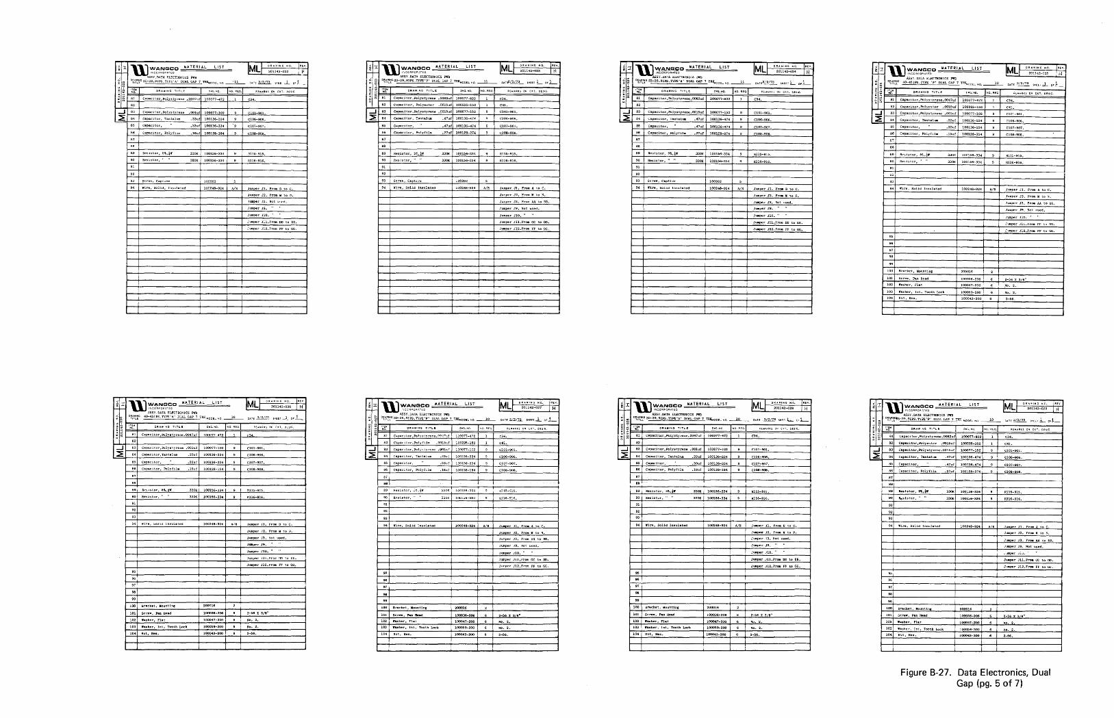
IML' ",.,", ,,- 1"'-~~~~~2_0_"_42_-0_22 __ ~H_
...J Ca pacitor,Polystyrelle
~ capacitor, Tantalum C106-906.
capaCItor'. 100136-334 -. Cl07-907.
86 capacitor, Polyfillil C108-908.
Resistor, 5"', ~If 330K 1,00156-334 \ a115-915,
Resistor," " 390K: I 100156-334 Rl16-916.
j
94 j Wire, Solid, Insulated AIR J1.lIIIper J1. From B to C.
1 Jumper J"2. From M to P.
i I )Ulllper J3. N'ot used.
i
J !
J
j
I ] I I I
~, ""'IWANGCC MATERIAL LIST "',= ~ I"IC::l~OJRA~~O
ASSY. DATA t.LECTRO~ICS PWB
1)~:Tw~~O 40-45IPS.TYPE'A' DL"AL GAP 7 TRKMODE_"IO
Capac 1 tor. Polystyrene. 0047ui
Jumper J9. " "
Jumper .n\). '
Jumper J12. From FF to eG.
hMLL ""'" 'o. ~"I' ., 201142-026 I H
-J~-+_C~'P~'C_i_tD~,,~~_'y~s~ty_~_ne __ .O_O'_Uf~_'O_00_77_-~lQ_2r-__ +-~~~ __________ ~ ~ capaCl tor, Tantalum el06-906.
CapaCltor, 100136-224 Cl07-907.
CapaCltor, Po1yfl1m .15uf
Resistor. ;l'Jo.tW
ReSistor, ' R1l6-916,
lure, ::;Olld Insulated 100248-924' AIR Jumper 11. FrODl B to C.
Jumper ,~2. From N to P.
JUJDper .J3. :'lot used.
J~pe[' J9.
J1JJ'IIper J10. "
I JUliper J12.froa; FF to 00.
Bracket, MClunting 2 i Sc rew, Pan Head 2-56 X 3/8"
., .. sller, Flat 100047-200 i NO. 2:.
"&!liter, Jnt. Tooth Lock 100059-200 I 6 Mo. 2.
Mut, Hex. 100043-200
I
~ I ""'IWA_NG_!=C MATERIAL LIST r-:I-- ~INCOAFOR""T€O ASSY.DATA ELECTRONICS PWB
O~:'T~~c;.23-29.9IPS.'I'YPE'P· Dt:AL GAP 7 TRXMOOEI.. .. O
~ 81 capacitor,Polystyrene .0082uf
capacitor, Polyester .OOl5uf 100225-152:
Capacitor,
capacitor, Polyfilll1
Resistor, "
9li
, l00.26~
Wire, Sohd Insulated
IMILL 0'"''' NC_ 1'''-II ., 201142-023 I H
r;"T~/3/73 SHEEI 1 OF 1
C34.
CI07-907.
Cl0S-90S,
R115-915.
R116-91E!,
A./a JUllper J1. From A to C.
Jumper J2. From M to N.
Jumper J3. From AA to BS.
J1.IJllper J9. Not used.
.]Ullper J10. "
Jumper J11.FrOlll CC to DD.
. Jumper JI2.FrOlb FF to eG.
II I i I
~~ Ul~~~~i~O MATERIAL LIST
ASSY. DATA ELECTRONICS PWB
D~tr"'t~~G30-39.9IPS.TYPE'P· DUAL GAP 1 T~ODEL..NO
'''M 'D.
CapacitoZ"",Polyfilm ,0015uf
IIMLL 0''''"'"'_ I'" II _j 201142-027 ~H
C,l,TE..JL.aLZ2... SHH1..l... OF1
C41.
-J~=+~C~'P~'~Ci~to~,,~~~l~,s~ty~re~ne~.O~Ol~U~f~~~+-~4-~C~lO~1-~90~1~. __________ ~ ~ capilcitor, Tar.talum
Capacitor, CI07-907.
Capacitor, Polyfillll CI08-908.
871 i
I R~ 15-915,
ReSlsto., ' 11.116-916.
9"
Wire, Solid Insulated JU!IIj?er 11. From A to C.
Jumper J2. FrOlll M to N.
Jumper n. Fr-om f.A to BB.
]llB'Iper )9. N'ot used.
JUIlper JI0." "
Jumper Jll, From CC tCi ro.
Jwnper J12.FrOal FF to GC_
95
I
!
Bracket, Mountin,
Screw, Pui Head 2-:56 X 3 8"
No.2.
washer. Int. Tootlt Lock 100059-200 No.2.
104 I !,{ut, lIex.
! I
"MLL 0",,,,, NO_ 1,,,_ II ., 20"42-024 j H ~:r ""'IW. _~NG~C MATERIAL LIST ~I-- ~J\lCORPORjl,TED
ASSY.iJATA EUCTRUrllCS PWIi o ~ O~tT~~G 23-29.9IPS.T'iPE'A' DUAL GAP 7 T~OO!;l.. NO
. i ~ ':.I~ O",WONG TOT.,
Capac:i tor .Polystyrene.OO82uf 100077-822 C34,
..J Capacitor,Polystyrene.OO15uf 100077-152
~ I CliipMCl."10r. Tantal.ua CI06-906.
1 85 Capacitor, " 100136-474 C107-907,
I 86 Capacitor, Polyfila .27uf 100128-274
, .. Resistor. 5'1.,,, 100156-334. R1l5-915.
Resistor." ..
Screw, Captive
Wire, Soll.d Insulated I 100248-924 A/R JUlIl~r JL Fraa B to C.
I Juaper J2. From I( to P.
I Jumper J3~ Not used.
Ju.per J9. " ..
Jumper JI0. "
Jualper Jll.From DD to EE.
Jumper J2:2.Fr-oJ:l FF to GG.
Ii I I i
~ T ""'IW~NGCC MATERiAl lilT r:~ ~INCQR"'QRA'EO
ASSY. DATA ElZCTRONICS PIfB ll~i'rw~~G3O-39,9IPS.TYPE'A' DUAL GAP 7 TRK,...ODEL '10
capaci t.OT. Polys ty rcene .0047uf
IMIL' "'">N'",_ I .. ,· ~ .1 201142--028 I H
-J~-+~C~.P~'C_'~tD~'.~~~ly~.~ty~r.~ne~'O~O'~Uf~~~~+-~~~C~lO~l-~~~'~. __________ ~ ~ Capac1tor. Tantalum CI06-906.
capacitor, 100136-334 C107-907.
CapaCitor, Polyfilll1 100128-184 Cl08-908.
Hesistor, 5\,iW 1115-915.
Reliistor," " 100136-334
94 Wire, Solid Insulated AIR Juaper .11. From B to C.
JWlpee 12. FrOlll N to P.
Jumper .J3. Sot used.
JUllper J9. " "
Jumper JI0." "
JUllllper JILFr'oa DD to EE.
JUllper J12. Fro. FF to GG.
BrlLcket, Mounting , 2
101 Screw, Pan Head 100036-206 2-561(3/8"
Washer, Flat 100047-200
•• aher, I nt. Tooth Lock No.2.
Nl1t, lIex. 100043-200
li&l "\lJ~~~~,~C MATERIAL LIST
.! ASSY.DA'I'A ELECTRONICS PII'B Or DRAWING 40-4SIPS TYPE 'P' DUAL CAP 7 TR~ 'I:q TITLE' --weDE:.. NO •
~lt~ '~57 iJ~AWtNG TITL£
~ ~ Capacitor,Polystyrene.OO47uf 100077-472
capacitor.Polyester .OO15uf
Ca1lacitor,Polystyrell.e .OOluf l00077~102
Capacitor, ra.ntalum 100136-224
85 Capacitor, 100136-224
Capacitor, Poly-hIm
ReSIstor, 5'\ .111' 100156-334
Resistor.·' ,- 330K 100156-334
CATE 3/2173 .>I-Iff ,.1 OF 1
C41 •
R1l5-91S,
RUG-916.
94 WIre. Solid Insulated 100248-924 A/R Ju:m.per J1. From A to C,
Jumper J2. From \1 to S.
1
JumpE'1:' J9. Not used.
Jumper JI0. "
.]UD.~r Jl1.From CC to DD •
JU.per JI2.FJ:"0GI FF to GG.
Bracket, Moullting 2 I
Sc rew, Pall Head 100036-206 2-56 X 3(8"
washer, Flat 100047-200
Washer, Int. Tooth Lock 100059-200 No.2.
S:ut, Hex, 100043-200
~ I ""'IWANGCC MATERIAL LIlT r--+-' ~NCORPORATEO
ASSY.DATA ELECTRONICS PifB
: ~ C~j';.~~'3-2!:J.9IPS_TYPE'P' DrAL GAP 7 TRX MODEL "'0
~ ~ I~~ QR;II,WINC:; TlTI..E
~ ~ 81 Capllcitor,Po1ystyrene.OO82uf 100077-822
CIlp&Cltor,Po1yester .OO1::'uf lOO22~-1:)2
"MLL D'''''' NO. I'" ~ :L 201142-029 1 H
C41.
.-1I--=t_C::'::::P'::;Ci:.:.to::r.:.::.~;:;1",Y9::tY:.:.r::en;:;e.c:;00::.:1::5U~f r----.:.==:::.=:t----':....t--'=="--------------t ~ Capac 1 tOI:'. Tantalum CI06-906.
CapaCitor,
Capa.cltor, Polyfl1111 .27uf 1 CI08-908.
aeaistor, ~,i. 100156-334
Resistor," .. R1l6-91S.
94 Wire, Solid Insulated JU:!£..er J1. FI:'OIII A to C.
Jumper J2. From M to ~,
Jumper J3. fro. AA tD BB.
JlDlpe r J9. Not used.
JUJllpoerjlO. ,.
1 Juaper Jll.FrOla CC to 00.
i I .. '
.71 1
i Bracket, Mounting 200016
SlCrew, Pan Head I 100036~206 t 2-5& X .3 8"
"asher, flat
103, WAsher, Int, 100059-200
Nut, Hex. 2-56,
Figure 8-27. Data Electronics, Dual Gap (pg. 5 of 7)

ci;: Ul~!~!::,';7,O MATERIAL LIST
ASSY.DATA ELECTRONICS PWB o D~iT~~G23-29.9IPS.TVPE:'A' DUAL GAP 7TRK ~ODEL "10
; 2 IT~M Ofb''''I'I~G TITL..!O:
~ ~ ~O. ca pacitor,Polystyrene.0082uf 100077-822 o N
...J Capac 1 tor ,Polys ty rene .0015ui
~ Capacitor, TantalulII
CapaCItor.
Caparitor,PolyiillJ.
Reslstor. 5~.:tlf' 100156-334
ReSlstOr, "
\fire, Solid In~ulated
Bracket Mount1nl:
Sere"'. Plln Head
"asher, Flat
Washer, Int. Tooth Lock
~ut. Rex.
UNSTROB£O DATA
$ID "1WANGCO MATERIAL lilT
I-of-- ~ A~;~~;:;4';Lc'(TRONI(1 PWB ~ U"! O~tT'::~'C 40-45:P5.TYPE'A' DUAL GAP 9 TRK~ooe:~.,o
~ ~ "'0 0 ..... , mLE
~ ~ 81 Capacitor, PolyS! rene.0047uf :00077-472
82 laDaC 1 ~or, Polystyrene.C0l5uf l00225-152
--l 83 Capacitor, Polystyrene COluf 100077-102
~ 8.1 Capacitor, Tantalum .22uf 100136-224
85 Capacitor, .22u f -224
86 Capaci tor. Polyfi 1m .1Suf :00128-154
87
88
330K 100156-334
230K ~ 334
91
93
10
hMLL "..,,, '0. I,,,· II -I 201142-030 I H
PA ~ E 3)2/73 ~Hff, J OF 1
C34.
JUJIlper Jl. From. B to C.
Jumper .12. Fr()m M to P.
JUIllper J3. Not used.
.Jumper J9. '! "
Jumper .JlO.
Jumper J11. From DO to EE.
Ju:npE'r J12.Fr()lll FF to GG.
2-56 X 3/8"
No.2.
IIMLI ",""0 '0. I'" (I _( 2011'1-035 IB
C3o!.
C41.
ClOl-qOl
Cl06· 0 0E.
C1C7-?O;,
CI08-?OB.
P.116-?16,
94 Wire, Solid Insulated 100248-924 AIR Jumper Jl from B to C
Jumper J2 M to N
Jumper J3 lliof.: used.
JUl'1per J9
Jumper JIO
Jumper Jl: froll' DO to EE
JUMper J12' GG to HH
95
96
97
98
99
~-+~"~"~'~Pt~.~Mo=u~nt~io:.:..' ______ ~1~O~~OI=6 __ -+~-+ ______________ ~ __ __ 101 Screw Pan Head 100036-206 2-56X38"
102 Wasner Flat 100047-200 No.2.
103 Washer, Int. Tooth lock 100059-200 NO.2.
104 Nut, Hex 10004)·200 2·56.
$ I "1WANGCO MATERIAL r-+- ~ INCClFlPOllll.TED
LIST
o OJt ... W1NG Z {'\J TITLE
~ ; '~5'
ASSY.DAT!\, ELECTHONICS P:~B 75IPS TYDE I,A' DIG 7 TRK
~.~ 81 Capacitor,Pol stvrere .002uf
82 Cao<l.citcr,~i:::a E'20pf
10e077-1)2
10(1243-821
...J 83 Capac;tor,Po1ystyrere 510pf lOOe77-51l
::E 84 Capacltor,Tar;ta1uIT. .15uf 11)[0136-154
85 Capacltor,Tantalum .15uf 100136-151
86 Capacitor>PDlyfl~rn .082u'" lOC078-S23
87
88
150K lOC156-15~
90 Res'stor," 150K 100156-154
91
92
93 Screw, Captive 10C262
hML 0","" NO. .n II -I 201142- 032 I H-'
O,HEl!.1il.l. SHEET 1 OF 1
"'Q . .,Eof
C34,
1 ICd1.
9 IC101-90l.
(106-906.
(107-907.
CllS-90S.
R1l5-915,
94 Wire, Solid Insulated 10C248-924 AIR Jumper Jl. From B to C.
~" "1WANGCO MATERIAL LIlT _ ~'NCO",poFu'TeD
JuTT'per J2. Fro!'" !vi to 1\.
Jumper J3. Not used
JumDer J9. Not used.
JJmper .1l0.Not used.
JL.lmper Jll.From 00 to EE.
Jumper J12.FroiT' FF to GG.
I'MLL ''''''0 '0. I",· (I -1 20Jl42-036 Iii
ASSY.OATA ELE(HON:el PWS a \')~N'~~I:; lO-lZ.9rpS.~YPEIP'OUAL GAP 9 T::;:~oo~\. ... o ~_ o ... rr 4/25/74 SIoIEET o ch--===:::::::::::::~~~~===-=~=-! ~ ~ '~~
~ ~~8.:..1 ~(.~pa::::c.:.:it:::or,--__ ----, . ..::;01:.:;5u:.;.f+l",00::.:.1::.:61'-"1:.:;13=-+--=---+...:Cc:..34:.:.. ____ ----i 82 Capacitor 0015uf 10]0225·}52
....J 8] Capacitor . 0033uf lJOO7?~33(l
:E 34 Capacitor,TantalulTI luf l0013E~105
85 I Capacitor, luf -105
86 ; Capacitor,PoljfillTl . '7uf 100118-474
87
38 I
(41.
CI01-901.
CI06-906.
Cle7-g0?
Cloa-908 .
89 i Resistor, 5~.~w 750K 100156~754 I 9 Rl1S-915.
90 I Resistor, ' 750K ·754 9 1 R116-916.
91
93
94 Wire, Sol id Insulated 100248-92~ AlP. Jumper Jl. From /l to :.
Jumper J2. From M to N.
Jumper J3. From AA to BB.
Jumper J9. Not used.
.JLJm~er JlJ. '
Jumper Jll. From CC to DO.
Jumper J12. from GG to YH.
95
96
97
9B
99
100 Bracket. Mounti':;L_~"_. ___ rl:.::,00=0:.::16 __ -+"";;'--+~ ________ -I 101 Screw, Pan Head 100036-206 2-56 X 3/8"
102 Washer, Flat 100047-200 No.2.
103 Washer, Int. Tooth Lock 100059-200 No,2.
104 Nut. Hex 100043-200 2·56.
U'l'ST:tOEEL LATA.
IIMLI 0","" '0. I .. •· (I _( 2011,2 - 0)) I f.l &:I. "1W ..... NGgO MATERIAL LIH
:-- ~I!lJC(H~PCFlnED . AS, Y. DATA E'.~SCTRO:lICS PWE. ~ O~it~~G 40-45i?8. 9Cfi. L(J. 7YPC ! A 1 MODEL NO. ~ D.llE:d£.i.1J..... SHEET 1 OF 1
~ 1~6~ O!'lA'1\'I~G TITL..E RE"'AIi1(S ON C~T. Dnl(;
g 61 Ca':l3Cl.tor J ?o::'ystyrene .1JCJ..7uf 100077-L72 C)4.
82 Ca?OIc.:tor, ?olyeste:-. .OO15uf 100225-152 Ci.l.
....J 1-=8,.::.J +O;,:O:,:O';;,;oi;.;.to;.;.r:.., ',::Ol",Y"",ty",re,::.n:.:..e ---,.O.:..:O~lu"-irr.:..:1OOO.:..:.;..77,-,-1.:..:0,,-2 +--,-+C..:.l~:.:1...:.-9.:.:0:;;... ------1 ~ 81. Ca?aci:.or J Tantalum. .22uf 108:)6-22L CI06-906.
~5 Caoacitor, .22cf 100136-22L ClD7-907.
86 Capacitor, ?olyfilm. .15uf lOO128-15L CIOB-90B.
B7
88
89 ~si:stor. 5J;. 4:"'. 330K lOOl56-J3h .
90 :tesic:tor. 3301( lJ015o-33L "'-16-916.
91
92
93 Screw, Captive. 100262
9L i>!ire, Solid Insulated. 1002U-;'2L AIR JutT\~er Jl. From E to C.
Ju:n:le::- J2. " ~ "J.
JU.'llpe:- J). Not Used.
Jumpe!' J9. "
Jumper JIO. "
JUllloer J12. II J.G n 1-11.
IIMLI '"''''' '0. I,,·. (I _( 201]42·037 IA
10 ~"H 4/25174 ,HEP 1 Of 1
C3~.
82
....J~8_,+-c~ap_ac_it_or~._PO~lY~st~y_re_ne __ .0_c3_3U~f~10_00_77_-3_3_2+-__ ~(_1O_1_.9_01 ____________ ~
~ 84 Capacitor,Tantalum 1uf! 100136-105 C106-906.
85 Capacitor, luf" -105 Cl07-907
86 Capacitor,Poljfilm .47uf 100128-474 ClOB·908.
87
86
89 Resis:or, 5~.I.W. 710K 100156·754, 9 R115-911.
90 Resistor," " 750K -754 Pl16-916.
91
92
93
94 Wire, Sol id Insulated lOOZ48-92A A/R Jumper Jl From B to C
Jumper J2, From M to P.
Jumper J3. !'tot used.
Jumper J9.
Jump~r JI0. "
Jumper Jll. From DO t.o EE.
Jumper ..i:2.
95
96
97
9B
99
100 Bracket, Mounting 200016
101 Screw, Pan Head 100036·106 2-56' 318"
102 Washer, flClt 10004)-200 NO.2.
103 Washer, rnt. Tooth Lock 100059-200 No.2.
104 Nut. Hex 100043-200 2-56.
IMILL " .. ,"0.,. ;"'. II -I 201142-034 I B
~ ID "lWANGCO MATERIAL LIST r-r-- ~ ''''CO'H'OIlA~fO
. AIIY.DATA ELEcnOI.:CI PWB : '8 o~it~~r;; 40-4srpS.T'I'PE'lI.' DUAL GAP 7TRK "'C:E,-~O 10
;' ~ !~~~ O~"'WI"G TITLE ;)~':'.NQ. 1,,0. RE~., ~ ~ 81 Capacitor, Pclystyrene,0047uf ; l00077-472 ! C34.
82 Capacitor, Polystyrene,0015uf 100225-152 1 I C41.
--' 83 Capacitor, Pclystyrene .001ui" 100077-102 9 I C101-901.
~ 84 Ca;l3citor,Tantalum . 22uf lOO~ ]6-224 I 9 , C106-906
85 Capacitor, .22uf' -224 I 9 Cl07-907.
86 Capacitor, Polyfilm .15uf 100128-154 I Cl08-908,
87 i
88
89 ~ Resi stor, 5~.\w. 330K 1001S6-334 R11S-91S.
90 i Resistor, 330K -334 R116-916.
91 ! 921 93 I
gt i Wire. So;';d Insulated 100248-924 AIR Jumpe" Jl from B to C,
91
96
97
98
99
100 Bracket. MOur,ting 200016
:o~ Screw. Pan Head 100036-106
102 'Washer. Flat 100047·200
103 ~asher, Int. Tooth Lock, 100059-200
104 Nut. "lex 100043-200
E ~ "lWANGCO MATERIAL LIST
f-~ ~ Ass~~P8;;;€hECTRONICS PWB
~ co D;~f~~Ci 10-12.9IPS.TYPE'P' DUAL GAP 7TR~o=E~"-:
~ 9 1~6~ ( ~ ~ olJ Capacitor .015,f 100165-153
82 Capacitor .0015u" 100225-152
....J 83 Capacitor .0033uf 100077-332
:E B4 Capacitor,Tantalum luf I00136-1D5
85 Capacitor. Illf I -105
85 Capacitor.Poly"'ilm • 47u f '10C128-474
87
88
89 Resistor, 5";;, \.w , 710, 100156-7S4
90 Res; star, ' 710K -754
91
92
93
lC
Jumper J2 M to N
Jumper J3 Not used.
Jumper J9 Not used.
Jumper Jl0
Jumpe" Jll DO to EE
Jumper J12 FF to GG
2-56 X 3/8"
NO.2.
NO.2.
2-56.
IMILI '''''NO'' I .. ,. ~ -I 281142-038 111
.: ... -f 4/25/74
C34.
C41.
Cl0l·901.
Cl06-906.
CI07·907.
Cl08·908 .
RII5·911.
~116-916.
94 Wire, SoHd lnsul/lted 100248-924 AIR Junper ~l. From A to C.
Jumper J2. From M to N.
Jumper J3. From A.A to B8.
Jumper J9. Not us.ed,
Jumper J10. "
Jumper Jll. From CC to DO.
95
96
97
98
99
100 8racket, Mounting 200016
101 Screw, Pan Head 100036-206 2-56 X 31S"
102 Washer, Flat 100047-200 No.2.
103 Washer. Int. Tooth Lock 100019-200 No.2.
104 Nut, Hex. 100043-200 2-56.
Figure B-27. Data Electronics, Dual Gap (pg. 6 of 7)

"ML1 0",,", 'D. I", ~ -I 201142-039 ! A
CaD1I.citor .015t..f 100151-113 (34,
I
~ ...J 1---'8:::.3 +-"-Ca:::;p"-''';.:..it:.:.or:..:.,,-,Po,,,,1vc::.st:Lvr:...:e,,,oec...,,,OC,,,3,,,,3i.i-'1' .--'1"'00"-'0::..:77--'-3:.::;32'-+--"--+-"C:.::10:.:.1....:-"::.:.C~-'-' -------...f :E. 84 Capaci:.or, 7antalum luf 100136-105 Cl06-906.
85 Capil.ci~or, luf -105 C107-907.
86 Capaci':or,Polyfi111 .'7uf lOOP8-474 CI08-9OB.
88
€S Pesistor, 5't.~. 710K 100156-754 <111-911.
90 Resistor, 710K -714 RI16-916.
91
92'
93 I 94 Wire, $01 ~d Insulated 100248-924 AIR Jumper JL From B to C.
! Jumper J2. C"rol"1 ~ to P.
! Jumpe:- J3. Not used,
Jumper J9.
l Jumper JiO.
I Jumper Jll. From ~D :0 EE,
Jumper J12. F=-toGG.
95 i
96
97 !
98
99
100 Bracket, MOtH'1ting 200015 :
101 . Screw, Pan Head, 100036-206 2-56 X 3/S"
102 ' Washer,Flat 100047-200 No.2.
103 ! Washer, tnt. Tooth Lack 100059-200 No.1.
104 Nut. Hex. 100043-100 2-56.
23
84 CaJacitor. ~ant61\.l~ .6Quf :8C136-631. 1 :lD6-906.
85 Capac i ':.0" , .6c.u~ -684 I
86 :~ DB- 908.
87
88
89 Resis:or, 5'·,· .. w.
90 Reslstor, 5601(1 -554 I 9
51 I I ~--~~~~--------+--+---------~
~ ! 94 ! i'Jl re, Sol id r.,sul a ted 1 JJ2L1-3-gZt!. 1 Po/P. ' '::'",Mper ~:. From i-. t.o :.
: : .tmpe r ~'~. ~. to ".
t..A to BB.
Jurrper ':9. Not ~5ed.
I ! I , JUMper ;)G.
J~mper ~:!1, From CC to DO.
~urr.per ,.' ~2. 3G to Hr.
95 I i
96 I
97 ! I
98
99
lOU . 3racket, f"',ountlng. , 200016
101 Screw, Pan Head 100836-206 2-56 X 318'
102 ''''asher, Flat. 10004'-200 ;"'10,2.
iJ3 "jasher, :nt. Toot'! Lock. 10:J059-2:10 ,No.2.
104 ~ut. HI:.)L ! 103043-100 I, 6 ! 1-56
Figure B-27. Data Electronics, Dual Gap (pg. 7 of 7)

II
9
8
7
6
5
4
3
-12Y +~v
A B
._-" ::1
t:~-t
. II I TRK'2 I..L+
I II II I I.l+
I
E F H
~
J <. 114 - --- II
SHT.6 OF 6
'i" 1 OPEN
I
I-I 10
f" "I r"o:o
------9
~i.AC O ... T .. OUTPUT(.-)
8
LAST USED DELETED U3Z
QI3
CRZ R75 C41 C9,C25.C26 7 TP9
TRK :) QX09 CRX05
RX33 CX09
TPX03
------_. 14 6
R r4
_._----5
TIi!~S
"1'=1- -----18 4
TRK7
--+---- ----·------~-3
4 AI.L CAPACITORS TO BE IN MICROFARAD .,to", 1011,
3 AI.L DIODE TO BE 100091
_, _2 AI.L RESISTORS IN OHMS t 5'" ~4 W
I UNUSED PINS' JIA-B PINS 6.8 FIJ· J6A-B PINS 5.6.7,12,13,16,EH.
NOTES, UNLESS OTHERWISE SPECIFIED.
H
2
L--~~--~~------~~------~~--------~--~----~----~----~--------~G~--------~------~~~~----~--~K Figure 8-28. Data Electronics, Dual Gap Schematic

58
S!>
S6
S9
I
_ ______________ PI60
1'
r[){NSlTY SE\.EeT ~
~:~Rl'~ SEL :irL Sfl
"l
-LINt.
~TVf'
, EN 1CP
(-I
RWRlTE(-) )(001
Z(()M. I ('w. o C<:1'·
~~
TO;u>[ ON
ONTAO..UR ::::,
FU o
ED SWV; ~NSlTY SWV'i
t Sllorus LIOIE~TIF..
>W'A sv;tUS
~51ATUS
TSWUS
~I C.P. 'C~I
I-~ WN lC I
I I j-CO l12
I jJ I't1W£II Lfl ts:: UloO LfF OOILI'IE L' 2"J' ' f V
A£Me
~EJ ff eJ !
l..: ,. ... ,. OCP caar ... 2OtO"
i., 5 C K £ H
e 9 7 e J A
~ I .. T .. p
~ 4 10 ;; 5 2
~I
~ ~
I
P 19i
~ ~I OIl N
• II 14 D .. I
S4 ~Cl 7 II ~- III
~I r~ fil 11 I
i R'
~I I "1
TO fa 7
ASSY _IllI$ENSE 1>1"200684
AS$"I' TllNISCUCER "' .. 2010"
~----------------~ .", ~----------------; -~ ~ ------------------f
~~~c\;.=========+
~----------------~ nw.s RII"-----------_1 ~(~~------------_1
::---P~ P21 ~ ~~----------~~~~~----------------------~======~--------------~ ~ ::::: _________________________ ~ __ '~~ __ W_'~~~~_aa£ ____ ~--------------------__i
I
P22 P3 ~----------- ~TI------------------------_;l'
r:::::::::::::::~r~~ & l=.nt~ @
1-____________ HroH IlOISITY(-) _ ,... ~to5l ~ ~---------S€LECT t ONLlN.'E'E(~ .. !)==A\S ... ~-~~= ...... ~===~~ I-------------::~~:~~~::::::::::::::::==::::~i' 1---------- .. 1£ ~rl":
I I
P5 r • I I
ASSY, 9 CHNIWEL
II'N ZOlO96
Cpt~Jl;~;;' )
i t 9
~
L ~ __ .:......:::===:::..J
/>S&y,
ImIl.A1tIR II'!I Z00993
II AC
P6
} TRI( P
}- TAl< 0
} TRK I
TRKZ
} TRK3
14 TRK 04
R IS
} TRK5 5 17 }- TRK6 u 18 }- TRK , V
Z } RE"~ S"'q,CBE 8 OU"'PUT(-)
PI L
}- TR. P 10
" }- TRK 0
N } ~RI( I
12 P
'RK 2 13 R
}- TRK ~ 14 S
}- 'RK" 15 T
TRK 5 16 U
TRK 6 17
I~ITRKT ~ }-mB~~ ; }- WRITE F'ESHH
~ WRITE FERMIT<-)
~ READ PERt.I"(-)
D LeW READ 4 THRESHOLDt-)
OLTPUTl-)
r"~'
CUSTOMER OR C RC::: IflFUT WRITE DR!VE~S
IIOTU~ftO'f'1U) ..- -'>dz:.
1.TQt.11UIICU ....,. \ll ....... --""" ~
a.-:=~,. WIRING DIAGRAM 1-1. IIIIIDl JUllfJIICB J ItllIDI1 Io1AGT-'PE TRANSPORT
~ ....... L~ .. ~ 9 Q-l»lNEL DIG
I ~-" ~!rl 200947 8 ~ I .. _ .....
200675 1_ I .. ..., J:::: ' 0' I
Figure 8-29. Magtape Transport Wiring Diagram


![[]):~:ji:{n - bitsavers.org](https://img.pdfslide.net/doc/110x75/633203e75696ca44730304b0/jin-bitsaversorg.jpg)


