Embed Size (px)
Citation preview
Nanoparticulate Dye-Semiconductor Hybrid MaterialsFormed by Electrochemical Self-Assembly as Electrodesin Photoelectrochemical CellsKazuteru Nonomuraa, Thomas Loewensteina, Esther Michaelisb, Peter Kunzed,Manuela Schiekd, Jens Reemtsc, Mirian Yoshie Iwayae, Michael Warkf,Jiri Rathouskyg, Katharina Al-Shameryd, Achim Kittelc, Jurgen Parisic,Dieter Wohrleb, Tsukasa Yoshidae, and Derck Schlettweina
a Institut fur Angewandte Physik, Justus-Liebig-Universitat Gießen, Heinrich-Buff-Ring 16,35392 Gießen, Germany
a Institut fur Organische und Makromolekulare Chemie, Universitat Bremen, Germanyc Abteilung Energie- und Halbleiterforschung, Institut fur Physik, Universitat Oldenburg, Germanyd Physikalische Chemie 1, Institut fur Reine und Angewandte Chemie, Universitat Oldenburg,
Germanye Environmental and Renewable Energy Systems, Faculty of Engineering, Gifu University, Japanf Institut fur Physikalische Chemie und Elektrochemie, Universitat Hannover, Germanyg J. Heyrovsky Institute of Physical Chemistry, Academy of Sciences of the Czech Republic,
Prague, Czech Republic
Reprint requests to J. P.; E-mail: [email protected]
Z. Naturforsch. 64a, 518 – 530 (2009); received January 26, 2009
Dye-sensitized zinc oxide thin films were prepared, characterized and optimized for applications asphotoelectrochemically active electrodes. Conditions were established under which crystalline thinfilms of ZnO with a porous texture were formed by electrochemically induced crystallization con-trolled by structure-directing agents (SDA). Dye molecules were adsorbed either directly as SDAduring this preparation step or, preferably, following desorption of a SDA. The external quantum effi-ciency (IPCE) could thereby be increased significantly. Particular emphasis was laid on dye moleculesthat absorb in the red part of the visible spectrum. Model experiments under ultrahigh vacuum (UHV)conditions with dye molecules adsorbed on defined crystal planes of single crystals aimed at a deeperunderstanding of the coupling of the chromophore electronic π-system within molecular aggregatesand to the semiconductor surface. Detailed photoelectrochemical kinetic measurements were used tocharacterize and optimize the electrochemically prepared dye-sensitized ZnO films. Parallel electri-cal characterization in vacuum served to distinguish between contributions of charge transport withinthe ZnO semiconductor matrix and the ions of the electrolyte in the pore system of the electrode.
Key words: Electrodeposition; Photosensitization; Film Growth; Adsorption; ElectricalConduction.
1. Introduction
Dye-sensitized electrodes of wide-bandgap semi-conductors like TiO2 or ZnO represent a photochem-ical approach to a regenerative solar cell that providesboth considerable fundamental insight and technicalpromise [1 – 4]. Even if TiO2 is the most success-ful electrode material up to now [4] ZnO offers im-portant advantages for technical applications [5 – 12]mainly since crystalline films can be obtained by elec-trochemical deposition during electrolysis of aqueouszinc salt solutions without any annealing steps thatwould limit the choice of substrates. Earlier, we re-
0932–0784 / 09 / 0700–0518 $ 06.00 c© 2009 Verlag der Zeitschrift fur Naturforschung, Tubingen · http://znaturforsch.com
ported the successful preparation of dye-loaded ZnOsemiconductor thin films by electrodeposition in thepresence of water-soluble dyes based on simultane-ous self-assembly of ZnO and the adsorbed dye, yield-ing a homogeneously coloured ZnO film with porousmorphology [13]. Recently we have shown that im-proved overall conversion efficiencies ≤ 2.3% of pho-toelectrochemical cells consisting of ZnO/dye hybridthin films can be achieved by extension of the one-step procedure towards a two-step procedure that con-sists of dye-desorption after electrodeposition and sub-sequent adsorption of a wide choice of sensitizermolecules [14].
K. Nonomura et al. · Nanoparticulate Dye-Semiconductor Hybrid Materials 519
Table 1. Sample porosity calculated from film thickness and Zn-content of the films and specific surface area from Kryptonadsorption of a 1.5 µm thick film grown in the presence of Eosin Y, following Eosin Y extraction, and following adsorptionof either Eosin Y, TSPcZn or N3 for 1 h in the respective dye solution.
Specific surface area (surface area in cm2 divided by the geometric film area in cm2)Porosity as-deposited film following extraction of the SDA following adsorption of
Eosin Y TSPcZn N363% ∼ 1 110 (220)* 127 66 ∼ 1 (84)*
* Value determined for a film of 3 µm average film thickness.
In the present contribution we will show how thisapproach can be utilized to tune in detail the ZnO elec-trode structure and morphology by extending the rangeof both structure-directing agents (SDA) and sensi-tizer molecules. The photoelectrochemical character-istics of the obtained materials will be analyzed andmodel experiments will be used to reveal the role ofsurface interactions and charge conduction in the ma-trix materials.
2. Results and Discussion
2.1. Role of Dye Agglomeration and PoreAccessibility for the Performance of Electrodes
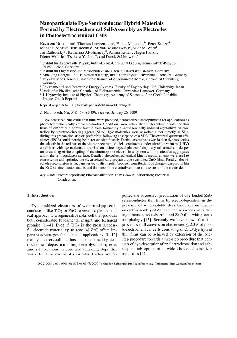
The two-step preparation method was used toincrease the efficiency of cis-bis(isothiocyanato)-bis(2,2′-bipyridyl-4,4′-dicarboxylato)-ruthenium(II) (N3)as a sensitizer for ZnO. N3 had proven almost idealfor the sensitization of TiO2 with a high external quan-tum efficiency (incident photon conversion efficiencyIPCE) above 80% over a wide range of the visiblespectrum [4]. For films of ZnO deposited in the pres-ence of N3, however, quite poor performance at IPCE< 5% was observed [15]. The efficiency increased toIPCE < 50% in the two-step preparation when the dis-odium salt of 2-(2,4,5,7-tetrabromo-6-hydroxy-3-oxo-3H-xanthene-9-yl) benzoic acid (Eosin Y) was used asSDA, removed in aqueous KNO3 and finally N3 wasallowed to adsorb from a solution in ethanol (Fig. 1).An improved efficiency for N3 could be reached if N3was adsorbed in the ZnO pores and the pores were stillaccessible to the electrolyte and agglomerate forma-tion of N3 at the electrode surface as also proven bytime-resolved photocurrent measurements [16].
Since the accessibility of pores in ZnO is a fun-damental prerequisite to obtain sensitized electrodesof high efficiency, gas sorption experiments were per-formed on the thin films to directly measure the acces-sible sample surface area (related to 1 cm2 of the sup-port) and compared to the overall pore volume (givenas porosity) estimated from the deposited amount of
Fig. 1. (a) Amount of N3 taken up by films of ZnO (two-step procedure with Eosin Y as SDA) with an average filmthickness of 0.6 µm (×, 68% porosity), 2.4 µm (�, 64%porosity), and 2.5 µm (�, 55% porosity) during adsorptionof N3 from a solution in ethanol and (b) external quantumefficiency (IPCE) of the films at the wavelength of 500 nmand a photon flux of 5 ·1015 photons s−1cm−2.
ZnO, the average film thickness, and the density ofZnO. Krypton had to be used as adsorptive gas becausethe very small absolute surface area of the samples inthe range of only tens or hundreds square centimetersrequire a significantly improved accuracy of the mea-surements [17]. The results are summarized in Table 1for Eosin Y as SDA and three different sensitizers: N3,Eosin Y, and 2,9,16,23-tetrasulfophthalocyaninatozinc(TSPcZn). In spite of 63% porosity calculated fromthe composition and thickness of the film, a negligi-ble Krypton uptake was found for the as-deposited film(specific surface area of only a few cm2/cm2 desig-nated as 1 in Table 1). The surface area was consid-erably increased after Eosin Y desorption and then de-creased again upon adsorption of N3. In the case ofEosin Y or TSPcZn the specific surface area stayedconsiderably higher or even increased. Therefore, the
520 K. Nonomura et al. · Nanoparticulate Dye-Semiconductor Hybrid Materials
(a) (b)
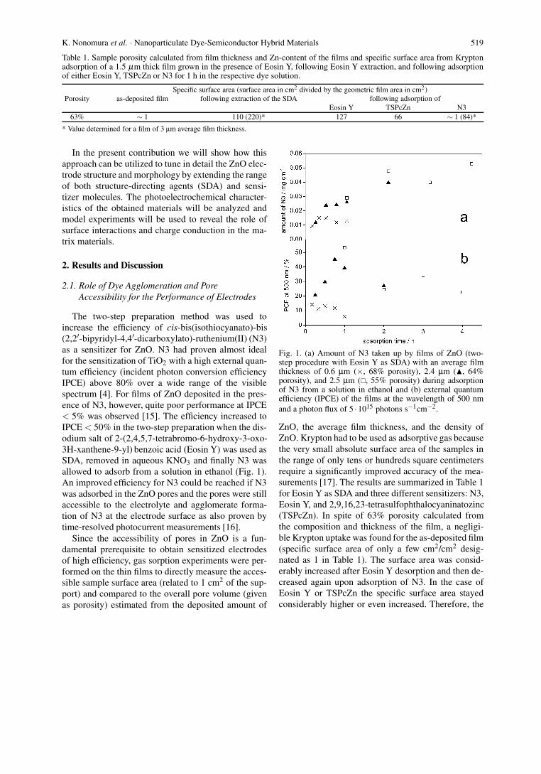
Fig. 2. Transient photocurrent measured at (a) one-step films of TSTPPZn / ZnO (i), TSPcZn / ZnO (ii) and (b) two-step filmsof TSTPPZn / ZnO (i), TSPcZn / ZnO (ii) under illumination with visible light (385 – 900 nm, light intensity: 200 mW cm−2)in contact with acetonitrile-ethylene carbonate (v/v = 4 : 1) containing 0.5 M TBAI and 0.05 M I2 at an electrode potential of−0.2 V vs. Ag/NO3.
adsorption conditions especially for N3 if used as asensitizer have to be adjusted very carefully to leavethe pores accessible (Fig. 1, Table 1) and to avoid poreblocking.
It is one of the main goals to find alternative sensi-tizers, that are readily available, that absorb in the longwavelength part of the visible spectrum, and that donot interact in such a destructive way with the ZnOfilms as the N3 Ru complex. A large part of the photo-electrochemical study was therefore dedicated to thedetailed study of TSPcZn as sensitizer. Because oftheir close structural relation and to provide an ex-ample of independently absorbing sensitizers in onefilm (pan-chromatic sensitization) 5,10,15,20-tetrakis(4-sulfonatophenyl)porphyrinatozinc (TSTPPZn) wasalso studied. Hybrid thin films of crystalline ZnO mod-ified by TSPcZn and/or TSTPPZn were prepared byelectrochemical deposition from aqueous zinc salt so-lutions in either the “one-step” process with the sen-sitizers adsorbed during ZnO deposition or by the“two-step” method by chemical adsorption of the sen-sitizers to ZnO that had been grown independentlyin the presence of Eosin Y as SDA. In films con-taining both sensitizers, they worked in parallel pro-viding pan-chromatic sensitization. Recombination ofelectrons injected into the conduction band of ZnOwith remaining defect electrons (holes) in the highestoccupied molecular orbital (HOMO) of the sensitiz-ers was indicated for the one-step films by the over-shoot of the photocurrent (Fig. 2a), but was consid-erably suppressed for the films prepared by the two-
step method (Fig. 2b) showing an almost rectangularresponse, standing for widely suppressed recombina-tion. At a closer view, a rather slow increase of the pho-tocurrent was observed upon opening of the shutter andthe photocurrent decayed quite slowly after closure ofthe shutter. This observation indicates reversible trap-ping and detrapping of charge, most likely in electrontraps of the ZnO semiconductor. Since TSPcZn/ZnOwith its higher photocurrent obviously was able to fillthese traps faster, an almost ideal rectangular responsewas observed.
The increased surface area and suppressed recom-bination led to a significantly increased photocurrentfor the films prepared by the two-step method (Fig. 2).This could also be seen in a maximum IPCE = 10%(TSTPP) and IPCE = 12% (TSPcZn) for the two-step films as opposed to IPCE = 0.14% (TSTPP) andIPCE = 0.6% (TSPcZn) for the one-step films [18].It is interesting to note that in these cases the ZnOfilm thickness and even the dye load or dye concen-tration could be quite similar (Table 2) and still gavesignificantly better performance for the films preparedby the two-step method, also seen in a clearly in-creased photocurrent when normalized to the amountof sensitizers in the films (Table 2). The highest valuewas reached for TSPcZn/ZnO prepared by the two-step method, speaking for the highest quantum effi-ciency in this case. Also for the films with both sen-sitizers present the two-step preparation gives consid-erably more efficient electrodes than the preparation inone step.
K. Nonomura et al. · Nanoparticulate Dye-Semiconductor Hybrid Materials 521
Table 2. Dye content and average film thickness of the investigated films and comparison of the observed photocurrents iph atan incident photon flux of 1016 s−1 cm−2 normalized for the given dye content to provide a rough measure of the sensitizationefficiency.Electrode material dye content/ film thickness/ dye content/ normalized normalized normalized
10−9 mol cm−2 µm 10−5 mol cm−3 iph (430 nm)/s−1 iph (560 nm)/s−1 iph (680 nm)/s−1
one-stepTSPcZn/ZnO 11.7 2.6 4.5 0.08
one-stepTSTPPZn/ZnO 16.2 2.7 6.0 0.14 0.06
one-stepa
(TSPcZn+TSTPPZn)/ZnO 0.642TSPcZn 2.2 0.29 0.10 0.05 0.52
13TSTPPZn 6.0
one-stepb 1.37(TSPcZn+TSTPPZn)/ZnO TSPcZn 5.2 0.26 0.03 0.03 0.72
29.1TSTPPZn 5.6
two-stepTSPcZn/ZnO 2.38 3.0 0.79 87.44
two-stepTSTPPZn/ZnO 17.4 2.5 6.9 14.54 3.73
two-step 4.30(TSPcZn+TSTPPZn)/ZnO TSPcZn 3.0 1.4 32.91 6.86 37.59
5.43TSTPPZn 1.8
a Prepared in the presence of 25 µM of TSPcZn and 25 µM of TSTPPZn in the preparation solution.b Prepared in the presence of 50 µM of TSPcZn and 50 µM of TSTPPZn in the preparation solution.
2.2. Optimized Structure-Directing Agents and TheirRole in the Electrodeposition of Porous ZnO
To increase the porosity and surface area beyondthe level reached with Eosin Y, different types ofSDA were studied in the deposition of highly porousZnO films from oxygen saturated ZnCl2 solutions.Films were deposited in the presence of different smallmolecules like benzoic acid, p-toluene sulfonic acid,and benzene tetracarboxylic acid as model compoundsand of sodium dodecyl sulfate (SDS) as a representa-tive of an anionic surfactant [19]. A mixed aqueoussolution of ZnCl2 and KCl served as a bath for theelectrodeposition of the ZnO films. The different SDAwere added in increments to the deposition mixturefrom concentrated stock solutions in 50 µM (calcu-lated concentration in the deposition bath) steps, whichallowed to follow the rate of the film growth and es-pecially the effect of additives on it in detail by mea-suring the time evolution of the observed current den-sity of ZnO deposition. Whereas the current densityusually reached only 0.15 mA/cm2 in the depositionof pure ZnO [20], the current increased to more than
Fig. 3. Time evolution of the cathodic current density of ZnOelectrodeposition during the step-wise addition of benzenetetracarboxylic acid (a), p-toluenesulfonic acid (b), benzoicacid (c) and without any addition (d).
1 mA/cm2 in the presence of 50 µmol of some nega-tively charged dyes, e. g. Eosin Y, because of the cat-alytic effect of the dyes on the electrodeposition [21]. Ifbenzoic acid was added, the resulting current increased
522 K. Nonomura et al. · Nanoparticulate Dye-Semiconductor Hybrid Materials
(a)(b)
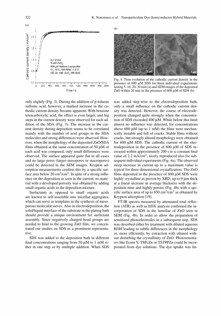
Fig. 4. Time evolution of the cathodic current density in thepresence of 600 µM SDS for three individual experimentslasting 5, 10, 20, 30 min (a) and SEM images of the depositedZnO within 20 min in the presence of 600 µM of SDS (b).
only slightly (Fig. 3). During the addition of p-toluenesulfonic acid, however, a marked increase in the ca-thodic current density became apparent. With benzenetetracarboxylic acid, the effect is even larger, and bigsteps in the current density were observed for each ad-dition of the SDA (Fig. 3). The increase in the cur-rent density during deposition seems to be correlatedmainly with the number of acid groups in the SDAmolecules and strong differences were observed. How-ever, when the morphology of the deposited ZnO/SDAfilms obtained at the same concentration of 50 µM ofeach acid was compared, only small differences wereobserved. The surface appeared quite flat in all casesand no large pores (larger mesopores or macropores)could be detected in the SEM images. Krypton ad-sorption measurements confirm this by a specific sur-face area below 20 cm2/cm2. In spite of a strong influ-ence on the deposition as seen in the current, no mate-rial with a developed porosity was obtained by addingsmall organic acids to the deposition mixture.
Surfactants as opposed to small organic acidsare known to self-assemble into micellar aggregates,which can serve as templates in the synthesis of meso-porous molecular sieves. Also in electrodeposition, thesolid/liquid interface of the substrate in the plating bathshould provide a unique environment for surfactantassembly. Since negatively charged head groups areneeded to bind to the growing ZnO film, we concen-trated our studies on SDS as a prominent representa-tive.
SDS was added to the deposition bath in differentfinal concentrations ranging from 50 µM to 1 mM ei-ther in one step or by multiple addition. When SDS
was added step-wise to the electrodeposition bath,only a small influence on the cathodic current den-sity was detected. However, the course of electrode-position changed quite strongly when the concentra-tion of SDS exceeded 400 µM. While below this limitalmost no influence was detected, for concentrationsabove 600 µM (up to 1 mM) the films were mechan-ically instable and full of cracks. Stable films withoutcracks, but strongly altered morphology were obtainedfor 600 µM SDS. The cathodic current of the elec-trodeposition in the presence of 600 µM of SDS in-creased within approximately 200 s to a constant finalvalue of 2.2 mA/cm2, nicely reproduced also for sub-sequent individual experiments (Fig. 4a). The observedsteep increase in current up to a maximum value istypical for three-dimensional crystallization. The ZnOfilms deposited in the presence of 600 µM SDS werehighly crystalline as proven by XRD, up to 9 µm thickat a linear increase in average thickness with the de-position time and highly porous (Fig. 4b) with a spe-cific surface area of up to 650 cm2/cm2 as obtained byKrypton adsorption [19].
FT-IR spectra measured by attenuated total reflec-tion (ATR) as well as EDX analysis confirmed the in-corporation of SDS in the lamellae of ZnO seen inSEM (Fig. 4b). In order to allow the preparation ofsensitized photoelectrodes in a subsequent step, SDSwas desorbed either by treatment with diluted aqueousKOH leading to subtle differences in the morphologyor, more efficiently, by extraction with ethanol with-out disturbing the crystallinity of ZnO. Photosensitiz-ers like Eosin Y, TSPcZn or TSTPPZn could be incor-porated from dye solutions. The dye uptake was lin-
K. Nonomura et al. · Nanoparticulate Dye-Semiconductor Hybrid Materials 523
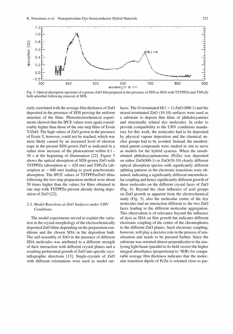
Fig. 5. Optical absorption spectrum of a porous ZnO film prepared in the presence of SDS as SDA with TSTPPZn and TSPcZnboth adsorbed following removal of SDS.
early correlated with the average film thickness of ZnOdeposited in the presence of SDS proving the uniformstructure of the films. Photoelectrochemical experi-ments showed that the IPCE values were again consid-erably higher than those of the one-step films of EosinY/ZnO. The high values of ZnO grown in the presenceof Eosin Y, however, could not be reached, which wasmost likely caused by an increased level of electrontraps in the present SDS-grown ZnO as indicated in arather slow increase of the photocurrent within 0.1 –30 s at the beginning of illumination [22]. Figure 5shows the optical absorption of SDS-grown ZnO withTSTPPZn (absorption at ∼ 420 nm) and TSPcZn (ab-sorption at ∼ 680 nm) leading to good panchromaticabsorption. The IPCE values of TSTPPZn/ZnO filmsfollowing the two-step preparation method were about50 times higher than the values for films obtained inone step with TSTPPZn present already during depo-sition of ZnO [22].
2.3. Model Reactions at ZnO Surfaces under UHVConditions
The model experiments served to explain the varia-tion in the crystal morphology of the electrochemicallydeposited ZnO films depending on the preparation con-ditions and the chosen SDA in the deposition bath.The self-assembly of ZnO in the presence of differentSDA molecules was attributed to a different strengthof their interaction with different crystal planes and aresulting preferential growth of ZnO into specific crys-tallographic directions [13]. Single-crystals of ZnOwith different orientations were used as model sur-
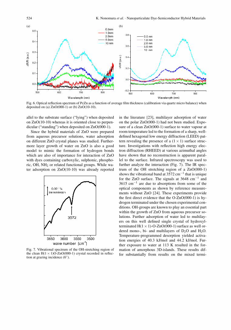
faces. The O-terminated H(1×1)-ZnO (000-1) and themixed-terminated ZnO (10-10) surfaces were used asa substrate to deposit thin films of phthalocyaninesand structurally related dye molecules. In order toprovide compatibility to the UHV conditions manda-tory for this work, the molecules had to be depositedby physical vapour deposition and the chemical an-chor groups had to be avoided. Instead, the unsubsti-tuted parent compounds were studied in situ to serveas models for the hybrid systems. When the unsub-stituted phthalocyaninatozinc (PcZn) was depositedon either ZnO(000-1) or ZnO(10-10) clearly differentoptical absorption spectra with significantly differentsplitting patterns in the electronic transitions were ob-tained, indicating a significantly different intermolecu-lar coupling and hence significantly different growth ofthese molecules on the different crystal faces of ZnO(Fig. 6). Beyond the clear influence of acid groupson ZnO growth as apparent from the electrochemicalstudy (Fig. 3), also the molecular centre of the dyemolecules had an interaction different to the two ZnOfaces leading to the different molecular aggregation.This observation is of relevance beyond the influenceof dyes as SDA on film growth but indicates differentelectronic coupling of the centre of the chromophoresto the different ZnO planes. Such electronic coupling,however, will play a decisive role in the process of sen-sitization and needs to be pursued further. Since thesubstrate was oriented almost perpendicular to the ana-lyzing light beam (parallel to its field vector) the higherintegral absorbance (proportional to *R/R) for compa-rable average film thickness indicates that the molec-ular transition dipole of PcZn is oriented close to par-
524 K. Nonomura et al. · Nanoparticulate Dye-Semiconductor Hybrid Materials
(a) (b)
Fig. 6. Optical reflection spectrum of PcZn as a function of average film thickness (calibration via quartz micro balance) whendeposited on (a) ZnO(000-1) or (b) ZnO(10-10).
allel to the substrate surface (“lying”) when depositedon ZnO(10-10) whereas it is oriented close to perpen-dicular (“standing”) when deposited on ZnO(000-1).
Since the hybrid materials of ZnO were preparedfrom aqueous precursor solutions, water adsorptionon different ZnO crystal planes was studied. Further-more layer growth of water on ZnO is also a goodmodel to mimic the formation of hydrogen bondswhich are also of importance for interaction of ZnOwith dyes containing carboxylic, sulphonic, phospho-ric, OH, NH2 or related functional groups. While wa-ter adsorption on ZnO(10-10) was already reported
Fig. 7. Vibrational spectrum of the OH-stretching region ofthe clean H(1× 1)O-ZnO(000-1) crystal recorded in reflec-tion at grazing incidence (6◦).
in the literature [23], multilayer adsorption of wateron the polar ZnO(000-1) had not been studied. Expo-sure of a clean ZnO(000-1) surface to water vapour atroom temperature led to the formation of a sharp, well-defined hexagonal low energy diffraction (LEED) pat-tern revealing the presence of a (1× 1) surface struc-ture. Investigations with reflection high energy elec-tron diffraction (RHEED) at various azimuthal angleshave shown that no reconstruction is apparent paral-lel to the surface. Infrared spectroscopy was used tofurther analyze the interaction (Fig. 7). The IR spec-trum of the OH stretching region of a ZnO(000-1)shows the vibrational band at 3572 cm−1 that is uniquefor the ZnO surface. The signals at 3648 cm−1 and3615 cm−1 are due to absorptions from some of theoptical components as shown by reference measure-ments without ZnO [24]. These experiments providethe first direct evidence that the O-ZnO(000-1) is hy-drogen terminated under the chosen experimental con-ditions. OH-groups are known to play an essential partwithin the growth of ZnO from aqueous precursor so-lutions. Further adsorption of water led to multilay-ers on this well defined single crystal of hydroxyl-terminated H(1×1)-O-ZnO(000-1) surface as well or-dered mono-, bi- and multilayers of D2O and H2O.Temperature-programmed desorption yielded activa-tion energies of 40.3 kJ/mol and 44.2 kJ/mol. Fur-ther exposure to water at 113 K resulted in the for-mation of amorphous 3D-islands. These results dif-fer substantially from results on the mixed termi-
K. Nonomura et al. · Nanoparticulate Dye-Semiconductor Hybrid Materials 525
(a) (b)
Fig. 8. Arrhenius plots of the temperature dependent conductance of either pure ZnO or ZnO with either Eosin Y or ZnPTSadsorbed in (a) darkness and (b) under illumination with white light of 0.1 mW/cm2.
nated ZnO(10-10), where a more complex scenario forZnO(10-10) has been found in which every second wa-ter molecule of a full monolayer dissociated while theremaining water molecules were strongly bound by a“key-lock” type structural arrangement [23]. The re-sulting water adlayer formed a well-defined (2×1) su-perlattice of intact water molecules which is stable upto 360 K. The comparison of these results indicatesthat the ZnO(10-10) surface should exhibit a morepronounced ability to participate in hydrogen bridg-ing with adsorbed SDA or sensitizers and that the twostudied surfaces show significantly different interac-tion with OH and hence different optimum adsorptiongeometries and preferred binding sites for the studiedSDA and sensitizers leading to the different film mor-phologies observed in electrodeposition.
2.4. Electrical Conduction and Photoconduction inZnO/Dye Hybrid Materials
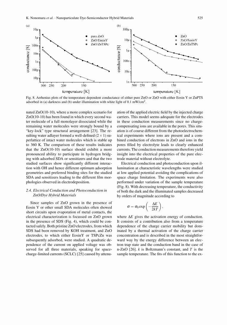
Since samples of ZnO grown in the presence ofEosin Y or other small SDA molecules often showedshort circuits upon evaporation of metal contacts, theelectrical characterization is focussed on ZnO grownin the presence of SDS (Fig. 4), which could be con-tacted safely. Both pristine ZnO electrodes, from whichSDS had been removed by KOH treatment, and ZnOelectrodes, to which either EosinY or TSPcZn wassubsequently adsorbed, were studied. A quadratic de-pendence of the current on applied voltage was ob-served for all three materials, speaking for space-charge-limited currents (SCLC) [25] caused by attenu-
ation of the applied electric field by the injected chargecarriers. This model seems adequate for the electrodesin these conduction measurements since no charge-compensating ions are available in the pores. This situ-ation is of course different from the photoelectrochem-ical experiments where ions are present and a com-bined conduction of electrons in ZnO and ions in thepores filled by electrolyte leads to clearly enhancedcurrents. The conduction measurements therefore yieldinsight into the electrical properties of the pure elec-trode material without electrolyte.
Electrical conduction and photoconduction upon il-lumination at characteristic wavelengths were studiedat low applied potential avoiding the complications ofspace charge limitation. The experiments were alsoperformed under variation of the sample temperature(Fig. 8). With decreasing temperature, the conductivityof both the dark and the illuminated samples decreasedby orders of magnitude according to
σ = σ0 exp(− ∆E
2kT
),
where ∆E gives the activation energy of conduction.It consists of a contribution also from a temperaturedependence of the charge carrier mobility but dom-inated by a thermal activation of the charge carrierconcentration and is described in the most straightfor-ward way by the energy difference between an elec-tron trap state and the conduction band in the case ofn-ZnO [26]. k is Boltzmann’s constant, and T is thesample temperature. The fits of this function to the ex-
526 K. Nonomura et al. · Nanoparticulate Dye-Semiconductor Hybrid Materials
perimental data show good agreement with two char-acteristic activation energies ∆E1 and ∆E2 and a transi-tion temperature in the range of 170 K for all samples.The calculated values are ∆E1 = 238 meV and ∆E2 =396 meV for the pure ZnO, ∆E1 = 220 meV and ∆E2 =452 meV for ZnO/EosinY, and ∆E2 = 548 meV forthe ZnO/TSPcZn. We relate the two different activa-tion energies to trap bands at these energies below theconduction band of ZnO. At the transition temperatureT0 ≈ 170 K, the same concentration of electrons is ex-cited from each trap band and
n1 exp(− E1
kT0
)= exp
(− E2
kT0
)
then leads to a relation of trapped charge in the two trapbands of n2/n1 ≈ 5 ·104 for the pure ZnO. The adsorp-tion of the sensitizers had a clear influence on the dis-tribution of the traps in the material as already seen inthe decrease of conductivity and confirmed by the ob-served changes in the activation energy. Introductionof the sensitizers led to a trap distribution extendingfurther into the band gap leading to the increased acti-vation energies and lower conductivity.
Under illumination the conductivity rose by someorders of magnitude and the activation energies de-creased for all three types of materials. For the pureZnO deposited in the presence of SDS this can be ex-plained by a high trap concentration leading to a sit-uation similar to amorphous semiconductors [27, 28],thereby confirming the high trap concentration al-ready concluded from the photoelectrochemical mea-surements. For the dye loaded ZnO illumination leadsto an excitation of electrons from the ground state ofthe dyes. From this first excited state electrons canbe transferred to the conduction band of ZnO as alsoseen in the photoelectrochemical experiments. There-fore, the concentration of electrons in the conductionband of the ZnO/dye hybrid material increased, and,hence, the conductivity rose. The highest increase ofthe conductivity under illumination could be observedin case of the Eosin Y sensitized material, explainedby a higher amount of Eosin Y in the hybrid mate-rial when compared with TSPcZn. We calculate thethermal activation energy under illumination to ∆E1 =112 meV and ∆E2 = 202 meV for the pure ZnO, ∆E1 =84 meV and ∆E2 = 200 meV for the Eosin Y loadedmaterial, and ∆E1 = 70 meV and ∆E2 = 354 meV forthe ZnTSPc loaded ZnO. The decrease in activation en-ergy relative to the dark conductivity by about a factor
0.5 can again be regarded typical for amorphous mate-rials, if aside from electron traps near the conductionband also hole traps near the valence band are consid-ered [27, 28].
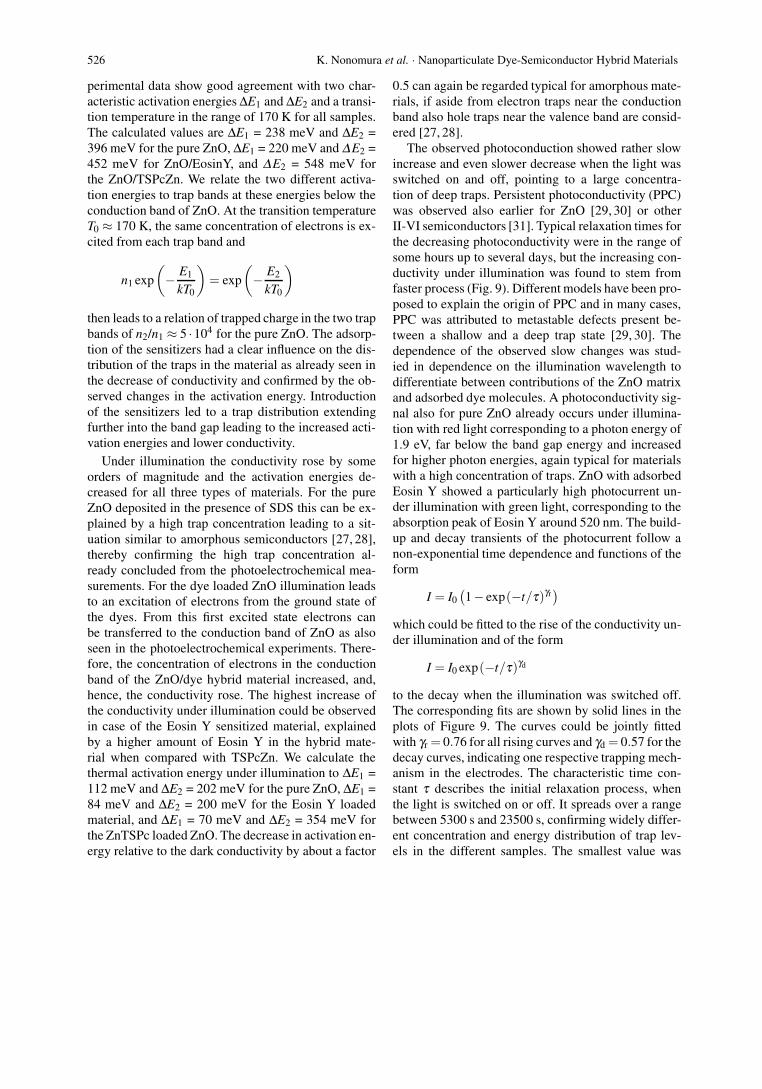
The observed photoconduction showed rather slowincrease and even slower decrease when the light wasswitched on and off, pointing to a large concentra-tion of deep traps. Persistent photoconductivity (PPC)was observed also earlier for ZnO [29, 30] or otherII-VI semiconductors [31]. Typical relaxation times forthe decreasing photoconductivity were in the range ofsome hours up to several days, but the increasing con-ductivity under illumination was found to stem fromfaster process (Fig. 9). Different models have been pro-posed to explain the origin of PPC and in many cases,PPC was attributed to metastable defects present be-tween a shallow and a deep trap state [29, 30]. Thedependence of the observed slow changes was stud-ied in dependence on the illumination wavelength todifferentiate between contributions of the ZnO matrixand adsorbed dye molecules. A photoconductivity sig-nal also for pure ZnO already occurs under illumina-tion with red light corresponding to a photon energy of1.9 eV, far below the band gap energy and increasedfor higher photon energies, again typical for materialswith a high concentration of traps. ZnO with adsorbedEosin Y showed a particularly high photocurrent un-der illumination with green light, corresponding to theabsorption peak of Eosin Y around 520 nm. The build-up and decay transients of the photocurrent follow anon-exponential time dependence and functions of theform
I = I0(1− exp(−t/τ)γr
)which could be fitted to the rise of the conductivity un-der illumination and of the form
I = I0 exp(−t/τ)γd
to the decay when the illumination was switched off.The corresponding fits are shown by solid lines in theplots of Figure 9. The curves could be jointly fittedwith γr = 0.76 for all rising curves and γd = 0.57 for thedecay curves, indicating one respective trapping mech-anism in the electrodes. The characteristic time con-stant τ describes the initial relaxation process, whenthe light is switched on or off. It spreads over a rangebetween 5300 s and 23500 s, confirming widely differ-ent concentration and energy distribution of trap lev-els in the different samples. The smallest value was
K. Nonomura et al. · Nanoparticulate Dye-Semiconductor Hybrid Materials 527
(a) (b)
(c) (d)
Fig. 9. Photocurrent versus time curves for (a) ZnO and (c) ZnO/Eosin Y after illumination with five different excitationwavelengths (LEDs � 656 nm, • 594 nm, � 534 nm, � 474 nm, 440 nm) was switched on, for (b) ZnO and (d) ZnO/EosinY samples after illumination was switched off. The thin solid lines indicate stretched exponential fits.
reached for ZnO with adsorbed Eosin Y, when the illu-mination with green light was switched off, explainedby fastest saturation of the effect for strongly absorbedlight.
The observed changes on the time scale of hourscould only be observed because the samples were an-alyzed in a pure state in an inert vacuum environment.In the photoelectrochemical experiments in the pres-ence of a redox electrolyte, relaxations occurred within0.1 – 30 s because of competing charge transfer [22].Nevertheless both types of experiments clearly showedthe strong influence of trap levels on the photocon-duction and photovoltaic characteristics of the presentZnO electrodes prepared in the presence of SDS.
3. Conclusions
The interplay of experimental methods from a rangeof different fields has been used to determine the keyparameters to optimize the performance of sensitizedZnO electrodes prepared by electrodeposition. Water
adsorption was found to play a crucial role on baresurfaces of ZnO and adsorption of different structuredirecting agents (SDA) was also found to directly in-fluence the observed current during electrochemicaldeposition and the resulting morphology of the ZnOthin films. The current of the O2-reduction and henceZnO precipitation was found to increase not only uponaddition of Eosin Y as an electrocatalyst but also inthe case of organic acids like toluenesulfonic acid orbenzenetetracarboxylic acid lifting the blocking of thesurface by Zn2+-addition [20]. Crystalline ZnO witha large accessible inner surface as determined by gassorption measurements was in particular obtained byaddition of the anionic surfactant SDS. Deposition ofunsubstituted phthalocyanines as model chromophoresshowed different adsorption and aggregate formationon the different pure ZnO surfaces in UHV indicat-ing different electronic interaction of the chromophoresystem with different faces of ZnO. It can thereforebe assumed that aside from acidic chemical anchorgroups also the interaction with the chromophore sys-
528 K. Nonomura et al. · Nanoparticulate Dye-Semiconductor Hybrid Materials
tem plays a role in ZnO crystallization. Consequencesof the electronic coupling of the chromophores onthe photoelectrochemical performance of electrodeshave to be assumed and should be investigated further.Temperature-dependent measurements of the electricalconduction and photoconduction under illumination atdifferent wavelengths showed the presence of deep traplevels in the porous ZnO matrix and also in the hy-brid materials with adsorbed sensitizers leading to longresponse times and persistent photoconduction in thesamples if measured in vacuum. Photoelectrochemicalmeasurements in the presence of a redox electrolyteshowed much faster response times because of fast in-teractions with these trap levels. A detailed character-ization of the electrode kinetics clearly revealed therelevance of an optimized inner surface area with ad-sorbed sensitizers that are accessible by the redox elec-trolyte and of a maintained high electrical conductivityat preferably low trap density also in the porous ZnOmatrix. These parameters reflect the need for a goodaccessibility of the sensitizers for both electronic trans-port in the semiconductor matrix and ionic transport inthe electrolyte. Both transport pathways are attenuatedby an increased surface area of the electrodes. An in-creased surface area, however, allows an increased sen-sitizer concentration and hence increased light harvest-ing. Experiments are on the way to further optimize thematerials by a strategic pore design of different poresizes and their optimum distribution in the film.
4. Experimental
The synthesis and preparation of 5,10,15,20-tetrakis(4-sulfonatophenyl)porphyrinatozinc (TSTPPZn) and2,9,16,23-tetrasulfophthalocyaninatozinc(II)(TSPcZn)was performed as reported earlier [32], all other chem-icals were purchased commercially. The electrodepo-sition of ZnO/dye hybrid materials was carried out ina three electrode single compartment cell containing70 mL of solution with a saturated calomel electrode(SCE) as reference electrode, a Zn wire as counterelectrode and 2.5× 1.5 cm2 pieces of F-doped SnO2on glass (ASAHI GLASS) as working electrode underpotentiostatic control (Wenking Potentiostat ST 88) at−0.9 V vs. SCE for 30 minutes at 70 ◦C. The one-stepelectrodepositions were carried out from aqueous solu-tions with 0.1 M Zn(NO3)2 and 25 – 50 µM of the dyes.The “two-step” films were prepared from ZnO/Eosin Y(or ZnO/SDS, respectively) grown as described above,but from an oxygen-saturated solution of 5 mM ZnCl2
(FLUKA, > 98%), 0.1 M KCl (ROTH, > 99%) and50 µM Eosin Y (ALDRICH) or 600 µM SDS and on arotating electrode (500 RPM) [19]. The SDA was thendesorbed overnight by a treatment in aqueous KOH(pH 10.5). Different sensitizers were subsequently ad-sorbed from solutions in ethanol or water. UV-vis spec-tra were measured in transmission using a HITACHIU-3000 spectrometer or a PERKIN ELMER Lambda9 using air as reference. The film thickness was mea-sured by an ALPHASTEP or VEECO Dektak 3 surfaceprofiler. The dye content of the films was analyzed byUV-vis absorption spectroscopy following dissolutionof the films in 7 N aqueous NH3 solutions. The sur-face area of the films was determined from adsorptionisotherms of Krypton at 77 K measured by an ASAP2010 apparatus (Micromeritics). Prior to each adsorp-tion measurement, samples were outgassed at 150 ◦Cover night, this temperature being the upper limit of thestability of the organic components contained withinthe films. For the determination of the small surfaceareas of thin films containing only about 1 mg of ZnOper cm2, the adsorption of Krypton at 77 K was cho-sen because its saturation vapour pressure is low at thistemperature. Consequently the “dead space” correctionfor gas molecules that are not adsorbed is small enoughto measure the low amount of adsorbed gas with rea-sonable precision [17].
The photoelectrochemical study was performed ina conventional three-electrode arrangement in a 5 mLglass cell with the deposited thin film as a windowof the cell illuminated from the glass/FTO side andused as the working electrode, a Pt counter electrodeand a Ag/AgNO3 reference electrode with acetonitrile(ROTH, 99.9%) as internal solvent. A 1 : 4 by vol-ume mixture of acetonitrile with ethylene carbonate(FLUKA, > 99%) dissolving 0.5 M tetrabutyl-ammon-ium iodide (TBAI, SIGMA, 99%) and 0.05 M Io-dine (SCHARLAU, 99.8%) was used as electrolyte.The measurements were performed at a potential withnegligible dark currents (−0.2 V vs Ag/AgNO3). Forthe time-resolved measurements, an ORIEL 1000 Wxenon arc lamp equipped with a water filter and a UVcutoff filter to restrict illumination to the visible range(385 nm – 900 nm) at 200 mW cm−2 was used. The il-lumination time of the electrode was controlled using amechanical shutter. The shutter needed about 10 ms toreach a completely open (or closed) position as mea-sured with a SIEMENS SFH 291 silicon-PIN-photo-diode. The potentials and currents were measured witha JAISSLE Bi-Potentiostat-Galvanostat with a rise
K. Nonomura et al. · Nanoparticulate Dye-Semiconductor Hybrid Materials 529
time of 100 µs connected to a HAMEG HM 305 os-cilloscope. Photocurrent spectra were measured witha BUNKO KEIKI CEP-2000 spectral sensitivity ana-lyzing system adjusted to 1016 photons cm−2 s−1. Theresults are generally reported in terms of the IPCE (In-cident Photon Conversion Efficiency), the amount ofelectrons in the external circuit divided by the amountof photons incident on the electrode. To provide an es-timate of the sensitisation efficiency of the dyes in thedifferent electrodes, however, the observed photocur-rent was also normalised on the dye content to obtain anumber comparable to a turnover frequency in cataly-sis [33] by dividing the photocurrent density (in termsof electrons generated per second in a unit electrodearea) by the dye content per unit electrode area.
The model adsorption and desorption experiments atsingle crystalline ZnO faces were performed in a ultra-high vacuum system equipped with RHEED (reflectionhigh energy electron diffraction), UV-vis spectroscopy,IR-spectroscopy and thermal desorption spectroscopy.For the IR experiments the H(1× 1)-ZnO(000-1) sur-face was prepared by cooling the single crystal ZnOsubstrate to 130 K before applying repeated cycles ofargon-ion bombardment at 473 K for 20 min and an-nealing to 873 K for 5 min (each cycle) before ultra-pure water vapour was leaked into the chamber. A sim-ilar protocol was used also for ZnO pretreatment be-fore deposition of the organic model compounds fromKnudsen evaporation cells.
For the conduction measurements, 100 nm thickgold contacts with a diameter of 0.5 mm were evapo-rated on top of the electrodes and then a spring loadedgold pin was placed on top. Unwanted scrunching ofthe porous electrodes resulting in an unstable electricalcontact and destruction of the films could be avoidedby placing a thin slice of indium between the gold tipand the gold contact. The sample was mounted inside achamber with dry nitrogen atmosphere and illuminatedfrom the backside of the substrate. These conditionswere necessary to avoid any interference by humid-ity or adsorbed gas molecules in the porous films. Thecharacterization of the transverse photocurrent, i. e. thephotocurrent flowing normal to the film plane, in theZnO/dye samples was carried out by applying 200 mVbias voltage via a Keithley 2400 source meter. In or-der to study the spectral response of the transversalfilm conductivity, we illuminated the samples by lightemitting diodes (LEDs) of different emission spectrawith a calibrated spectrally integrated light intensity of0.25 mW/cm2 at the position of the sample at an ambi-ent temperature of 300 K.
Acknowledgement
The authors are grateful to the Volkswagen Foun-dation for financial support (I/77722 (80314), I/77723,I/77724, I/77725) as well as to N. I. Jaeger (Univ. Bre-men), T. Oekermann (Univ. Hannover), and D. Lincot(ENSCP Paris) for numerous fruitful discussions.
[1] H. Tributsch and M. Calvin, Photochem. Photobiol. 14,95 (1971).
[2] H. Gerischer and F. Willig, Top. Curr. Chem. 61, 31(1976).
[3] A. J. Nozik and R. Memming, J. Phys. Chem. 100,13061 (1996).
[4] M. Gratzel, Prog. Photovolt: Res. Appl. 14, 429 (2006).[5] M. Izaki and T. Omi, Appl. Phys. Lett. 68, 243 (1996).[6] S. Peulon and D. Lincot, Adv. Mater. 8, 166 (1996).[7] B. Mari, M. Mollar, A. Mechkour, B. Partiti, M. Per-
ales, and J. Cembrero, Microelectronics Journal 35, 79(2004).
[8] T. Oekermann, T. Yoshida, C. Boeckler, J. Caro, andH. Minoura, J. Phys. Chem B 109, 12560 (2005).
[9] D. Lincot, Thin Solid Films 487, 40 (2005).[10] B. Illy, B. A. Shollock, J. L. MacManus-Driscoll, and
M. P. Ryan, Nanotechnology 16, 320 (2005).[11] A. Goux, T. Pauporte, and D. Lincot, J. Electroanal.
Chem. 587, 193 (2006).[12] Z. G. Chen, Y. W. Tang, L. S. Zhang, and L. J. Luo,
Electrochim. Acta 51, 5870 (2006).
[13] T. Yoshida, M. Tochimoto, D. Schlettwein, G. Schnei-der, D. Wohrle, T. Sugiura, and H. Minoura, Chem.Mater. 11, 2657 (1999).
[14] T. Yoshida, M. Iwaya, H. Ando, T. Oekermann,K. Nonomura, D. Schlettwein, D. Wohrle, and H. Mi-noura, Chem. Commun. 400 (2004).
[15] K. Nonomura, T. Yoshida, D. Schlettwein, and H. Mi-noura, Electrochim. Acta 48, 3071 (2003).
[16] T. Loewenstein, K. Nonomura, T. Yoshida, E. Michae-lis, D. Wohrle, J. Rathousky, M. Wark, and D. Schlett-wein, J. Electrochem. Soc. 153, A699 (2006).
[17] J. Rathousky, T. Loewenstein, K. Nonomura, T. Yoshi-da, M. Wark, and D. Schlettwein, Studies in SurfaceScience and Catalysis 156, 315 (2005).
[18] K. Nonomura, T. Loewenstein, E. Michaelis, D. Wohr-le, T. Yoshida, H. Minoura, and D. Schlettwein, Phys.Chem. Chem. Phys. 8, 3867 (2006).
[19] E. Michaelis, D. Wohrle, J. Rathousky, and M. Wark,Thin Solid Films 497, 163 (2006).
[20] A. Goux, T. Pauporte, and D. Lincot, Electrochim. Acta51, 3168 (2006).

530 K. Nonomura et al. · Nanoparticulate Dye-Semiconductor Hybrid Materials
[21] T. Yoshida, T. Pauporte, D. Lincot, T. Oekermann,and H. Minoura, J. Electrochem. Soc. 150, C608(2003).
[22] K. Nonomura, Dissertation, Universitat Gießen,Gießen (Germany) 2006.
[23] B. Meyer, D. Marx, O. Dulub, U. Diebold, M. Kunat,D. Langenberg, and C. Woll, Angew. Chem. Int. Ed.43, 6642 (2004).
[24] M. Schiek, K. Al-Shamery, M. Kunat, F. Traeger, andCh. Woll, PCCP 8, 1505 (2006).
[25] A. Rose, Phys. Rev. 97, 1538 (1955).[26] B. Sapoval and C. Hermann, Physics of Semiconduc-
tors, Springer, Berlin 1995.[27] N. F. Mott and E. A. Davis, Physics of Amorphous Ma-
terials, Longman Scientific and Technical, New York1979.
[28] J. Z. Liu and S. Wagner, Phys. Rev. B 39, 11157 (1989).[29] S. A. Studenikin, N. Golego, and M. Cocivera, J. Appl.
Phys. 87, 2413 (2000).[30] P. Sharma and K. Sreenivas, J. Appl. Phys. 93, 3963
(2003).[31] H. X. Jiang and J. Y. Lin, Phys. Rev. Lett. 64, 2547
(1990).[32] E. Michaelis, K. Nonomura, D. Schlettwein, T. Yoshi-
da, H. Minoura, and D. Wohrle, J. Porphyrins and Ph-thalocyanin 8, 1366 (2004).
[33] V. Parmon, A. V. Emeline, and N. Serpone, Intern. J.Photoenergy 4, 91 (2002).


![~] VIPUL DYE CH~M LTD?](https://img.pdfslide.net/doc/110x75/6317d1391e5d335f8d0a8a2c/-vipul-dye-chm-ltd.jpg)


