Embed Size (px)
Citation preview


Nanoscale Microwave Engineering


FOCUS SERIES
Series Editor Pascal Maigné
Nanoscale MicrowaveEngineering
Optical Control of Nanodevices
Charlotte Tripon-CanselietJean Chazelas
First published 2014 in Great Britain and the United States by ISTE Ltd and John Wiley & Sons, Inc.
Apart from any fair dealing for the purposes of research or private study, or criticism or review, aspermitted under the Copyright, Designs and Patents Act 1988, this publication may only be reproduced,stored or transmitted, in any form or by any means, with the prior permission in writing of the publishers,or in the case of reprographic reproduction in accordance with the terms and licenses issued by theCLA. Enquiries concerning reproduction outside these terms should be sent to the publishers at theundermentioned address:
ISTE Ltd John Wiley & Sons, Inc.27-37 St George’s Road 111 River StreetLondon SW19 4EU Hoboken, NJ 07030UK USA
www.iste.co.uk www.wiley.com
© ISTE Ltd 2014The rights of Charlotte Tripon-Canseliet and Jean Chazelas to be identified as the author of this workhave been asserted by them in accordance with the Copyright, Designs and Patents Act 1988.
Library of Congress Control Number: 2014930265
British Library Cataloguing-in-Publication DataA CIP record for this book is available from the British LibraryISSN 2051-2481 (Print)ISSN 2051-249X (Online)ISBN 978-1-84821-587-0
Printed and bound in Great Britain by CPI Group (UK) Ltd., Croydon, Surrey CR0 4YY

Contents
INTRODUCTION . . . . . . . . . . . . . . . . . . . . . . . . . . . . . . . . . . . ix
CHAPTER 1. NANOTECHNOLOGY-BASEDMATERIALS AND THEIRINTERACTION WITH LIGHT . . . . . . . . . . . . . . . . . . . . . . . . . . . 1
1.1. Review of main trends in 3D to 0D materials. . . . . . . . . . . . 11.1.1. Main trends in 3D materials for radio frequency (RF)electronics and photonics . . . . . . . . . . . . . . . . . . . . . . . . . . 11.1.2. Main trends in 2D materials for RF electronicsand photonics . . . . . . . . . . . . . . . . . . . . . . . . . . . . . . . . . 21.1.3. Review of other two-dimensional structures for RFelectronic applications . . . . . . . . . . . . . . . . . . . . . . . . . . . . 51.1.4. Main trends in 1D materials for RF electronicsand photonics . . . . . . . . . . . . . . . . . . . . . . . . . . . . . . . . . 61.1.5. Other 1D materials for RF applications . . . . . . . . . . . . . 91.1.6. Some attempts on 0D materials . . . . . . . . . . . . . . . . . . 13
1.2. Light/matter interactions. . . . . . . . . . . . . . . . . . . . . . . . . 131.2.1. Fundamental electromagnetic properties of 3Dbulk materials . . . . . . . . . . . . . . . . . . . . . . . . . . . . . . . . . 141.2.2. Linear optical transitions . . . . . . . . . . . . . . . . . . . . . . 221.2.3. Bandgap engineering in nanomaterials: effect ofconfinement/sizing on bandgap structure . . . . . . . . . . . . . . . . 23
1.3. Focus on two light/matter interactions at the material level . . . 261.3.1. Photoconductivity in semiconductor material . . . . . . . . . 261.3.2. Example of light absorption in metals: plasmonics. . . . . . 45

vi Nanoscale Microwave Engineering
CHAPTER 2. ELECTROMAGNETICMATERIAL CHARACTERIZATIONAT NANOSCALE . . . . . . . . . . . . . . . . . . . . . . . . . . . . . . . . . . . 51
2.1. State of the art of macroscopic material characterizationtechniques in the microwave domain with dedicated equipment. . . 512.1.1. Static resistivity . . . . . . . . . . . . . . . . . . . . . . . . . . . . 512.1.2. Carrier and doping density . . . . . . . . . . . . . . . . . . . . . 532.1.3. Contact resistance and Schottky barriers . . . . . . . . . . . . 552.1.4. Transient methods for the determination ofcarrier dynamics . . . . . . . . . . . . . . . . . . . . . . . . . . . . . . . 562.1.5. Frequency methods for complex permittivitydetermination in frequency . . . . . . . . . . . . . . . . . . . . . . . . . 57
2.2. Evolution of techniques for nanomaterial characterization . . . 602.2.1. The CNT transistor . . . . . . . . . . . . . . . . . . . . . . . . . . 602.2.2. Optimizing DC measurements. . . . . . . . . . . . . . . . . . . 602.2.3. Pulsed I-V measurements. . . . . . . . . . . . . . . . . . . . . . 612.2.4. Capacitance–voltage measurements . . . . . . . . . . . . . . . 61
2.3. Micro- to nanoexperimental techniques for the characterizationof 2D, 1D and 0D materials. . . . . . . . . . . . . . . . . . . . . . . . . . 62
CHAPTER 3. NANOTECHNOLOGY-BASEDCOMPONENTSAND DEVICES . . . . . . . . . . . . . . . . . . . . . . . . . . . . . . . . . . . . 65
3.1. Photoconductive switches for microwave applications . . . . . . 673.1.1. Major stakes . . . . . . . . . . . . . . . . . . . . . . . . . . . . . . 673.1.2. Basic principles . . . . . . . . . . . . . . . . . . . . . . . . . . . . 673.1.3. State of the art of photoconductive switching . . . . . . . . . 713.1.4. Photoconductive switching at nanoscale – examples. . . . . 72
3.2. 2D materials for microwave applications . . . . . . . . . . . . . . 743.2.1. Graphene for RF applications . . . . . . . . . . . . . . . . . . . 743.2.2. Optoelectronic functions . . . . . . . . . . . . . . . . . . . . . . 763.2.3. Other potential applications of graphene . . . . . . . . . . . . 77
3.3. 1D materials for RF electronics and photonics . . . . . . . . . . . 783.3.1. Carbon nanotubes in microwave and RF circuits . . . . . . . 783.3.2. CNT microwave transistors . . . . . . . . . . . . . . . . . . . . 793.3.3. RF absorbing and shielding materials based onCNT composites . . . . . . . . . . . . . . . . . . . . . . . . . . . . . . . 823.3.4. Interconnects. . . . . . . . . . . . . . . . . . . . . . . . . . . . . . 83
CHAPTER 4. NANOTECHNOLOGY-BASED SUBSYSTEMS . . . . . . . . . 85
4.1. Sampling and analog-to-digital converter . . . . . . . . . . . . . . 854.1.1. Basic principles of sampling and subsampling . . . . . . . . 874.1.2. Optical sampling of microwave signals . . . . . . . . . . . . . 89

Contents vii
4.2. Photomixing principle . . . . . . . . . . . . . . . . . . . . . . . . . . 894.3. Nanoantennas for microwave to THz applications . . . . . . . . 914.3.1. Optical control of antennas in the microwave domain . . . 914.3.2. THz photoconducting antennas . . . . . . . . . . . . . . . . . . 914.3.3. 2D material-based THz antennas . . . . . . . . . . . . . . . . . 924.3.4. 1D material-based antennas . . . . . . . . . . . . . . . . . . . . 924.3.5. Challenges for future applications . . . . . . . . . . . . . . . . 96
CONCLUSIONS AND PERSPECTIVES . . . . . . . . . . . . . . . . . . . . . . 99
C.1. Conclusions . . . . . . . . . . . . . . . . . . . . . . . . . . . . . . . . 99C.2. Perspectives: beyond graphene structures for advancedmicrowave functions. . . . . . . . . . . . . . . . . . . . . . . . . . . . . . 100C.2.1. van der Waals heterostructures . . . . . . . . . . . . . . . . . . 101C.2.2. Beyond graphene: heterogeneous integration ofgraphene with other 2D semiconductor materials . . . . . . . . . . . 103C.2.3. Graphene allotropes . . . . . . . . . . . . . . . . . . . . . . . . . 103
BIBLIOGRAPHY . . . . . . . . . . . . . . . . . . . . . . . . . . . . . . . . . . . 105
INDEX . . . . . . . . . . . . . . . . . . . . . . . . . . . . . . . . . . . . . . . . . 119


Introduction
I.1. General introduction
When addressing the main requirements of future interconnected systemenvironments, autonomy and resilience are the most challenging factorssince they include very demanding technology aspects and integratedintelligence aspects.
In an environment where communications often take a larger place, it isobvious that all the future systems will be required to have the capability ofworking in a networked ambient environment.
New systems will be defined by key words representing their mainfunctions: smart, autonomous, wireless, networked and sensing systems. Theadjective smart and autonomous refer to the autonomy in terms of energy,such as zero power consumption or energy harvesting, and to the autonomydefined from the decision point of view (i.e., they have the capability to dowhat is needed to be done, when it seems optimal to do it).
It also requires the inclusion of all the elements required for a dedicatedmission: protection of the environment, communication, security or defense,biomedical and e-health, and power electronics.
I.2. Definition of a new area “nanoarchitectronics”
Richard Feynman’s visionary speech in 1959 had inspired the field ofnanotechnology, with the theme “to synthesize nanoscale building blockswith precisely controlled size and composition, and assemble them into

x Nanoscale Microwave Engineering
larger structures with unique properties and functions”. Never before inhistory has any technology provided so many possibilities to create andmanipulate such tiny structures as the basic elements for functional devicesand hierarchical systems that render superior performances.
Microwave systems, technology and material-based architectures atnanoscale lead to a novel approach and a novel scientific area. We proposeto call this new area nanoarchitectronics because it describes the ability tobuild up or design new architectures at the material level, device level andsystem level, including electromagnetics and electronics at nanoscale,nanomaterials and nanotechnologies based on basic physics and embeddedsoftware systems.
As an example and following the research on two-dimensional (2D)atomic crystals, it appears extremely powerful to assemble isolated atomicplanes into designer heterostructures made layer by layer in a preciselychosen sequence. The first, already remarkably complex, suchheterostructures (often referred to as “Van der Waals”) have recently beenfabricated and investigated, revealing unusual properties and newphenomena.
In this book, we will address an additional new field, which could beentitled beyond nanoarchitectronics, in which we are looking to a newdimension of the above-mentioned architectures, when dealing with theinteractions of electromagnetic waves and nanodevices. As an example ofthese new capabilities, this book will present new approaches linked to theuse of photonics technologies to control nanoscale microwave devices.
We have chosen to reduce the scope of our analysis to the impact ofnanotechnologies on electromagnetic (EM) applications ranging from radiofrequency (RF) to terahertz (THz) and to extract technologies that exhibitadvanced or new performances with size reduction either by continuity likeMore Moore or by breakthrough quantum effects [PIE 10a].
Interesting nanostructured materials, devices and systems alreadyconstitute research areas in RF nanoelectronics [PIE 10b].

Introduction xi
I.3. Three main thrusts
I.3.1. Thrust 1 – around new nanodevices and systems
The following research fields are concerned: carbon nanotubes (CNT),graphene and nanowire (NW), graphene nanoribbon (GNR) circuits andtransmission lines, semiconductor- and other novel material-basednanotechnology for RF electronics, nanostructured microwave materials andmetamaterials, nanowireless sensors and power meters, nanoantennas andarrays, THz nanoelectronics/photonics, including signal generation andprocessing, photoemission and detection, nano-interconnects for advancedRF packaging, nanoscale electromechanical switches (NEMS) andresonators, spin waves for RF nanoelectronics (spintronics) and molecularelectronics, nanoplasmonic structures for RF applications andsuperconducting nanostructures and RF nanodevices for quantuminformation processing.
I.3.2. Thrust 2 – around theoretical issues and modeling
The following research fields are concerned: multiphysics modeling ofnanostructures and nanodevices, ballistic transport, wave solutions andmultiport circuits in nanomaterials, combined electromagnetic/coherenttransport problem in nanodevices, electrodynamics, radiation, detection andphotogeneration in nanostructures, and wave mixing, dispersive andnonlinear effects in nanomaterials.
I.3.3. Thrust 3 – around technology, instrumentation, imaging andreliability
The following research fields are concerned: broadband characterizationof nanoscale devices/systems for RF applications, microwave nanoscalenear-field imaging and surface patterning, noise measurement of nanoscaledevices and three-dimensional (3D) integration of carbon- andsilicon/semiconductor-based nanodevices.
The scientific theories associated with these research areas cover thefollowing fields [ENG 07]:
– advanced metamaterials, electromagnetic/photonic band gap structures;

xii Nanoscale Microwave Engineering
– nanostructured materials modeling;
– nanoelectromagnetism;
– nanoscale devices and components;
– miniaturized antennas and optical nanoantennas;
– 2D and graphene metamaterials, graphene photonics;
– metatronics: nanocircuits and nanosystems.
This book will focus on the engineering of nanomaterials for microwave,millimeter wave and terahertz applications and especially on the opticalcontrol of these nanodevices.
The purpose of this book is to provide the readers with requiredknowledge to enter the world of nanoarchitects for microwave nanosystems.
Here, we recall the main trends for 3D, 2D and one-dimensional (1D)materials, which could be used in the definition of new system architectures(see [ALA 09, Figure 1]). In the field of the interaction between light andsemiconductor materials, some elements of the history of photoconductivityand the capability to go from the picosecond (ps) domain to the THzfrequency range will be given.
Figure I.1. Classification of nanomaterials: a) 0D spheres and clusters, b) 1D nanofibers,wires and rods, c) 2D films, plates and networks, and d) 3D nanomaterials
I.4. Organization of the book
The book is organized as follows: Chapter 1 deals with nanotechnology-based materials for ultrafast microwave applications and their interactionwith light. Chapter 1 is focused on two aspects: first to give some trends innew semiconductor materials from 3D to 0D and second to give an in-depth

Introduction xiii
analysis of the interaction at nanoscale between light and these newmaterials in photoconductivity and plasmonics. The materials concerned arecarbon-based materials (especially graphene and carbon nanotubes), NW-based technologies: Si, III–V semiconductors, ZnO, etc., nanostructuredmaterials and metamaterials.
Chapter 2 addresses EM material characterization at nanoscale, includinga state of the art of macroscopic material characterization techniques in themicrowave domain with dedicated equipment, EM environment constraints(T°, mechanical stability and multiscale access) and noise contributions inmeasurements and the evolution of techniques for mesoscopic nanomaterialcharacterization.
Chapter 3 is devoted to nanotechnology-based components and devices,reviewing the existing components and a state of the art with thesetechnologies (active) and with a focus on new passive components anddevices with optional optical control (photoconductivity and plasmonics).
Chapter 4 presents the engineering of new optically controlled microwavefunctions based on 2D and 1D semiconductor materials.
Finally, in the Conclusion, we draw some perspectives of this new fieldof optically controlled low-dimensional materials with a focus on the so-called Van der Waals heterostructures as an example of nanoarchitectronics.


1
Nanotechnology-based Materials andTheir Interaction with Light
Chapter 1 will be dedicated to nanotechnology-based materials for ultrafast microwaveapplications and the interactions of these materials mainly semiconducting with light. It will focuson two aspects, the first aspect is to give some trends in new semiconductor materials fromthree dimensional (3D) to zero dimensional (0D) and the second aspect is to give a deepanalysis of the interactions at nanoscale between light and these new materials aroundphotoconductivity and plasmonics. Materials concerned are carbon-based materials (especiallygraphene and carbon nanotubes), nanowire-based technologies: Si, III-V semiconductors, ZnO,nanostructured materials and metamaterials.
1.1. Review of main trends in 3D to 0D materials
1.1.1. Main trends in 3D materials for radio frequency (RF) electronicsand photonics
Controlling the permittivity and permeability of three-dimensional (3D)materials appears as a major challenge for future electromagnetism systems.Nanomaterials are high-potential candidates for applications in microwave,millimeter wave, terahertz (THz) and optical systems. During the lastdecade, numerous research activities have been devoted to the study ofartificial materials, such as metamaterials [ENG 06]. Mixing components atthe nanoscale results in materials providing superior properties comparedwith conventional microscale composites and, at the same time, that can besynthesized using simple and inexpensive techniques.
Nanoscale Microwave Engineering: Optical Control of Nanodevices, First Edition. Charlotte Tripon-Canseliet and Jean Chazelas.© ISTE Ltd 2014. Published by ISTE Ltd and John Wiley & Sons, Inc.
2 Nanoscale Microwave Engineering
In particular, major research advances have been obtained by the group ofNader Engheta, who worked on specific materials such as epsilon-near-zero(ENZ), mu-near-zero (MNZ), zero-index metamaterials and double-negativematerials [ALU 07].
The introduction on the structure of the split-ring resonator (SRR) by J.Pendry in 1999 opened the way for the demonstration of metamaterialsbased on the periodic implantation of such SRRs [PEN 99, PEN 07,SMI 00]. The implementation of the first effective medium with left-handedproperties by D.R. Smith in 2000 was possible due to the use of smallmetallic resonators, SRRs. The SRR appeared as the first non-magneticresonator capable of showing negative values of the magnetic permeabilityaround its resonance frequency.
The control and the tunability of those materials remain as the greatfuture challenges in this field.
1.1.2.Main trends in 2D materials for RF electronics and photonics
The combination of the unique properties of two-dimensional (2D)semiconductor materials, such as graphene, with new device concepts andnanotechnology can overcome some of the main limitations of traditionalelectronics in terms of maximum operating frequency, linearity and powerdissipation.
1.1.2.1. The example of graphene
Graphene is a flat monolayer of carbon atoms forming a 2D honeycomblattice. Graphene is a basic building block of graphite and carbon nanotubes(CNTs). Graphene properties were first introduced by Wallace in 1947.
At the beginning of the 21st Century, Andre Geim, Konstantin Novoselovand their collaborators from the University of Manchester (UK), and theInstitute for Microelectronics Technology in Chernogolovka (Russia),published their results on graphene structures in October 2004 [NOV 04].
After reviewing some important papers in the literature devoted to thisnew material, we can derive some basic characteristics of graphene materialsand their main applications.

Nanotechnology-based Materials 3
Figure 1.1. Graphene: a flat monolayer of carbon atoms forming a 2D honeycomb lattice
Figure 1.2. Top left: graphene is a honeycomb lattice of carbon atoms. Top right: graphitecan be viewed as a stack of graphene layers. Bottom left: carbon nanotubes are rolled-upcylinders of graphene. Bottom right: fullerenes C60 are molecules consisting of wrapped
graphene by the introduction of pentagons on the hexagonal lattice [CAS 06]

4 Nanoscale Microwave Engineering
Parameters Typical characteristics
Thickness 0.142 nm
Band structure Semi-metal or zero-bandgap semiconductor
Electron transport Ballistic at room temperatureRelativistic quantum Dirac equation
Carrier mobilities 1,00,000 cm²/V.s in suspended graphene10,000 cm²/V.s in graphene on substrate
Young’s modulus 1.5 TPa
Breakdown current 108 A/cm²
Current density 1 A/µm
Transistor cutoff frequency 350 GHz
Carrier density 1014 cm−2
Optical absorption πα∼2.3%
Thermal conductivity 5,000 W/m.K
Table 1.1. Typical characteristics of graphene [CAS 09, AVO 10,WAN 10, LOV 12, WU 12, SCH 10]
One of the main characteristics of this material is that intrinsic grapheneis a semi-metal or a zero-bandgap semiconductor. In this material, theelectron transport is ballistic at room temperature and is described by arelativistic-like quantum Dirac equation instead of a Schrödinger equation.
Graphene demonstrates not only an electric field effect but also a ballisticelectronic transport, which results in very high charge carrier mobilitiesmore than 100,000 cm²/V.s.
Such mobilities of graphene exceed that of silicon by at least a factor of40, which makes it particularly important for designers of the next-generation fast transistors.
Also, graphene has a Young’s modulus of 1.5 TPa.
Due to these unique properties, graphene is very promising for high-frequency nanoelectronic devices, such as oscillators and switches. Inpractical applications, graphene is deposited on a SiO2 layer with a typicalthickness of 300 nm, which is grown over a doped silicon substrate.

Nanotechnology-based Materials 5
It is interesting to note that the conductivity of the graphene sheet is ananisotropic tensor and it can be controlled by applying an electrostatic andmagnetostatic biasing field. This property introduces the possibility ofdeveloping new applications, which cannot be obtained by conventionalconducting materials of fixed conductivities.
1.1.2.2. Graphene for RF applications
Recent results on the use of graphene for microwave applications enabledus to review some functions covering the field of nanocircuits up to therealization of new microwave functions based on this material; among those,we will review the following functions in Chapter 2: RF mixers, frequencymultipliers, antennas, isolator, circuits, transistors and field-effect transistors(FETs), photodetectors, barristor, optoelectronic functions such as graphenephotodetector and other potential applications of graphene, superconductingFETs and room-temperature spintronics, and transparent electrodes[OBE 11].
Some helpful analysis on the use of graphene for microwave applicationswill be given in Chapter 3.
1.1.3. Review of other two-dimensional structures for RF electronicapplications
1.1.3.1. Plasmonic structures
Plasmonics is based on the interaction process between anelectromagnetic radiation and the conduction electrons at metallic interfacesor in small metallic nanostructures. For noble metals such as Ag and Au, theplasma frequency is in the visible or ultraviolet region; therefore, theirpermittivity has negative real parts in the optical frequencies. These metalsbehave as plasmonic materials, and their interaction with optical signalsinvolves surface plasmon resonances (SPRs). These plasmonic structuresprovide interesting possibilities not only for synthesizing subwavelengthcavities or new metamaterials at infrared and optical frequencies, but also foraddressing new microwave functions involving confined optical interactionsand microwave modulation of the electric field at a semiconductor/dielectricinterface [AHM 12].
A detailed approach of plasmonic structures has been given in theIntroduction.

6 Nanoscale Microwave Engineering
1.1.3.2. Two-dimensional semiconductor materials
The 2D semiconductors such as transition metal dichalcogenides (such asMoS2, MoSe2, WS2 or WSe2) show excellent device characteristics, as wellas novel optical, electrical and optoelectronic characteristics due to quantumsize effects. Recent research of 2D materials based on chalcogenides and/orIII–V semiconductors on Si/SiO2 substrates has been achieved. It isimportant for both fundamental science and applications, such as electronics,photonics and chemical sensing. Unlike the zero-bandgap graphene, it ispossible to tune the bandgap of 2D semiconductor materials by the choice ofelements and the number of layers. The large bandgaps of 2Dsemiconductors (e.g. 1.8 eV for MoS2monolayer nanosheet) and their carriermobility make these materials very attractive for the next-generationnanoelectronic and nanophotonic devices [JAV 13].
1.1.4.Main trends in 1D materials for RF electronics and photonics
This section deals with recent research on carbon-based and non-carbon-based one-dimensional (1D) materials such as nanorods/carbon nanotubes(CNTs), boron nitride nanotubes (BNNTs) and semiconductor nanowires(NWs).
1.1.4.1. CNT materials and microwave applications
It is well known that CNTs are cylinders of nanometer (nm) diameter of agraphene sheet wrapped up to form a tube. Since their experimentaldiscovery in 1991 [IIJ 91], numerous research efforts have been devoted toexploring their physical properties including electromagnetic waveinteraction of the conducting CNTs, which seems to contain importantfeatures compared with traditional conductors [GHA 11 ].
Single-wall carbon nanotubes (SWCNTs) can be seen as rolled-up sheetsof graphene, i.e. a monolayer hexagonal lattice of carbon atoms. They can beuniquely described by a double index or chiral vector (n,m) that correspondsto the way the graphene sheet is rolled up, i.e. the angle it makes with thevectors of the lattice and how tightly the CNT is rolled up. According to thisindex, an SWCNT may be metallic (i.e. no bandgap) or semiconducting (i.e.diameter-dependent bandgap). The only truly metallic CNTs are the

Nanotechnology-based Materials 7
armchair n = m, rolled along vector a2 as shown in Figure 1.3. For zigzag(rolled along vector a1) and chiral SWCNTs, there are two cases: if n − m =3j + 1 or 3j + 2, then the CNTs are semiconducting. However, if n − m = 3j,the bandgap is sufficiently small in that they behave as metals at ambienttemperature. They are semi-metallic tubes, usually referred to as beingsimply metallic CNTs. In this case, from Figure 1.3, or the three-congruence,it is simple to conclude that, if all chiral vectors have the same probability,there should be 1/3 metallic SWCNTs and 2/3 semiconducting. CommonCNT production methods usually have a narrow diameter distribution butchiral vectors of semiconductor and metal SWCNTs are equivalentlydistributed.
Multiwall carbon nanotubes (MWCNTs) are concentric shells likeRussian dolls made up of SWCNTs. They are available in a variety ofdiameters, number of shells, etc.
CNTs can display huge length-to-diameter aspect ratios because thediameter varies from 1 nm to a few tens of nm, but lengths up to half a meterhave been reported [CHA 08]. Usual lengths vary from less than 1µm to 100µm depending on the fabrication technique and application.
Figure 1.3. Chiral vector of CNT
The earliest research has been focused on the synthesis of CNTsnecessary for experiments. The progress of common growth techniquesincluding arc discharge and laser ablation of graphite pieces and laterchemical vapor deposition (CVD) and plasma-enhanced CVD has

8 Nanoscale Microwave Engineering
significantly improved the quality of the CNTs [MEY 05]. Recently, manycompanies have concentrated their efforts to develop and control the growthtechniques to perform very high purity and uniform CNTs in length anddiameter. The physical properties of CNTs [SAI 98] have demonstratedunique electronic structure depending on their dimensions and chiralities,which have been considered as a major discovery in the field ofsemiconductor devices. In addition, due to strong covalent carbon–carbonbonding, CNTs present very high tensile strength, thermal and electricalconductivity. Hence, those mechanical and electrical properties make themalso very attractive for reinforcing composite materials for aerospaceapplications. Usually, CNTs are classified into two categories: SWCNTs thatare composed of a single graphitic cylinder, where the diameter varies from0.7 to 2 nm, and MWCNTs that are composed of several concentric graphiticlayers, where the diameter varies from 10 to 200 nm. Commercial CNTs areavailable in a powder form where they are entangled and randomlydistributed [ZHA 13].
1.1.4.1.1 Carbon nanotubes for RF applications
CNTs are competitive elements in many RF applications like high-frequency transistors, AM demodulators, matched loads, transmission linesand antennas.
The knowledge of dielectric properties at low frequency (direct current(DC) to 1 MHz) as well as high frequency (above 1 MHz) is the key fordeveloping novel electronic devices such as radio frequency-miniaturizedresonators [SAB 09a, SAB 09b] as electronic model for futureimplementation [SAB 09c]. Therefore, the electrical characterization at radiofrequency/microwave (RF/M) bands becomes a challenge where commonmeasurement techniques are inappropriate. For high-frequencymeasurements, complex permittivity is usually used to describe the dielectricproperties of a material where the real part of the permittivity is related tothe dielectric constant and the imaginary part can be associated with theconductivity [TRI 14].
1.1.4.2. BNNT materials and microwave applications
Theoretically predicted in 1994, BNNTs appeared as a 1D allotrope of a2D sheet of boron nitride in a hexagonal lattice with alternating boron andnitride atoms [RUB 94, COH 10].

Nanotechnology-based Materials 9
Similar to the CNTs, BNNTs have many unique properties. In particular,BNNTs are semiconductors with a wide bandgap (~5.5 eV) weaklydependent on the tube diameter, helicity and the number of walls. Comparedwith the CNTs, BNNTs have not only high thermal conductivity but alsohigh oxidation resistivity, as well as high thermal and chemical stability,which render BNNTs a promising tubular material for developing nanotube-based electronic devices in certain hazardous and high-temperatureenvironments [WAN 09, WAN 10].
1.1.5. Other 1D materials for RF applications
Semiconductor NWs have drawn enormous research efforts for theirspecial material properties and wide-ranging device applications withoutstanding performances [SAB 09c, TRI 11, RUB 04]. As one of theelementary building blocks of nanoelectronic devices, NWs configured asFETs have been shown to operate at ultralow power below microwatts withan enhanced operational speed. Semiconductor NWs, such as groups IV[QIN 08, HOC 08], III–V [CHA 08, CUI 03] and II–VI [XIA 06, BRY 06],and others [NIL 08, LIU 05, COM 05] have demonstrated the prospectiveconstruction of state-of-the-art devices.
This section deals with recent research on non-carbon-based 1D materialssuch as semiconductor NWs.
1.1.5.1. Semiconductor nanowires Si and II–V compounds
Semiconductor NWs have been extensively investigated as nanoscalebuilding blocks for novel nanoelectronics and nanophotonics. Both top-downfabrications based on conventional microfabrication technologies and top-down fabrication based on chemical synthesis (from the gaseous or from theliquid phase) are possible. In addition to being driven by the need toovercome some limitations of the top-down fabrication, the study of bottom-up NW growth is motivated by their interesting electrical transport andoptical properties that are remarkably different from those of thecorresponding bulk materials. Homogeneous NWs can be developed byusing a number of chemical methods, among which the metalorganicchemical vapor deposition (MOCVD) is arguably the most common forIII–V compounds. Apart from homogeneous NWs, it is possible tosynthesize heterostructures along the axial and radial directions, whichallows for the manipulation of the NW properties and bandgap engineering.

10 Nanoscale Microwave Engineering
By applying heteroepitaxy on NWs, junction geometries can also beengineered. In addition, it is easier to overcome the lattice mismatch problemwhen doing heteroepitaxy on bulk and/or using tensile or compressive strain,allowing more flexibility in matching the absorption to the desiredwavelength. As already mentioned, NWs are 1D or quasi-1D nanostructureswith unusual electronic and optoelectronic properties, arising from uniquecharacteristics such as:
– extremely high aspect ratio: with lengths ranging from ~1 to 10 μm anddiameters ranging from ~2 to 100 nm, NWs are ideal for dense deviceintegration and exploitation of size effects, i.e. large surface-to-volume ratioand 2D quantum confinement, which lead to interesting new phenomena;
– synthetic flexibility: both top-down and bottom-up fabrication methodsand growth techniques are applicable to the entire range of semiconductors,allowing us to tailor NW optical and the electronic properties through thechoice of materials, doping and bandgap engineering;
– NW technologies are in principle compatible with mainstream (CMOS)fabrication processes: top-down methods include in situ fabrication byconventional lithographic techniques and processing, or direct transfer offabricated NWs on a host substrate, similar to the bottom-up methods whereadditional functionalities may also be integrated during the synthesis throughdoping or the formation of axial and radial heterostructures.
Moreover, the small lateral dimensions of NWs allow extremeheteroepitaxial growth which may be important, for instance, for theintegration of III–V semiconductors on silicon platforms.
1.1.5.2. Si and GaAs nanowire field-effect transistors
Single-electron Si NW FETs were fabricated, and a Coulomb blockadewas observed even at room temperature ([SUN 11, Figure 4]). The effects oflength-induced strain on the transport properties of such devices wereinvestigated.
Gallium arsenide (GaAs) NW FETs with universal (back) gates areroutinely fabricated by photolithography and electron-beam lithography onSi/SiO2 substrates to determine NW transport parameters (Figure 1.5).Transport properties of three-branch monolithic GaAs NW junctions arebeing investigated for the realization of Y-junction transistors and quantumjunction devices [DAI 11].
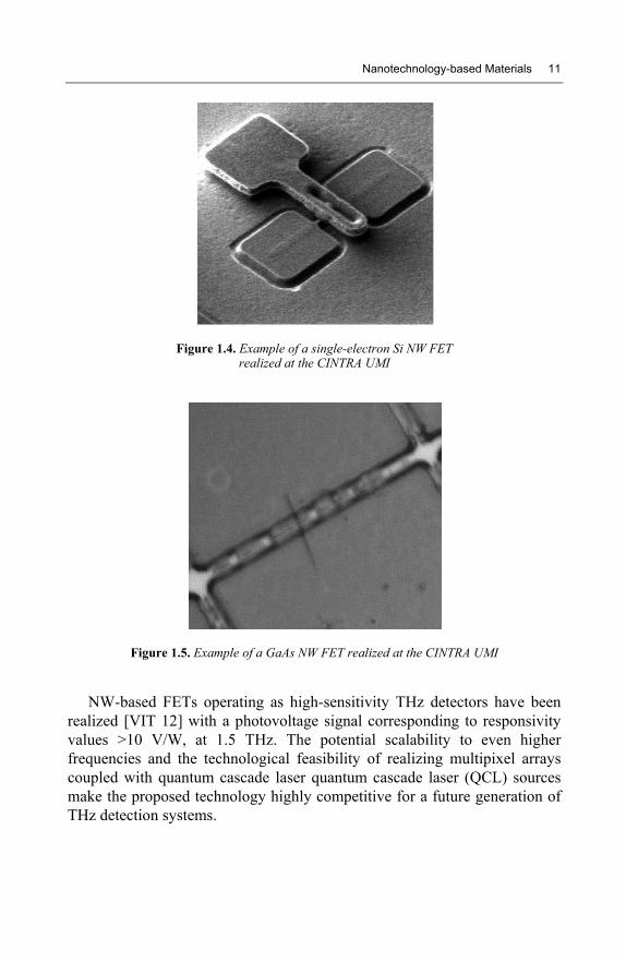
Nanotechnology-based Materials 11
Figure 1.4. Example of a single-electron Si NW FETrealized at the CINTRA UMI
Figure 1.5. Example of a GaAs NW FET realized at the CINTRA UMI
NW-based FETs operating as high-sensitivity THz detectors have beenrealized [VIT 12] with a photovoltage signal corresponding to responsivityvalues >10 V/W, at 1.5 THz. The potential scalability to even higherfrequencies and the technological feasibility of realizing multipixel arrayscoupled with quantum cascade laser quantum cascade laser (QCL) sourcesmake the proposed technology highly competitive for a future generation ofTHz detection systems.

12 Nanoscale Microwave Engineering
Semiconductor NWs are an ideal building block for implementingrectifying diodes or plasma-wave detectors that could be well operated intothe THz, due to their typical attofarad-order capacitance. As active channelof our FET detectors, we select indium arsenide (InAs) NWs since theyshow reasonably high electron mobility even at room temperature (~1000cm²/Vs) and a potentially long electron mean free path, enabling hightransconductance at very low drive voltages. InAs NWs with l.5 m lengthand having a diameter of 30 nm were grown bottom-up on InAs (111) Bsubstrates by chemical beam epitaxy (CBE).
1.1.5.3. ZnO nanorods
In recent years, 1D semiconducting nanostructures have attractedtremendous interest for their unique physical properties attributed to theirsmall dimensions. Driven by their enticing potential as nanoscale buildingblocks for integrated electronic and photonic circuits, many efforts havebeen devoted to the fabrication and characterization of functional devicesbased on 1D nanostructures, such as FETs, sensors, lasers and solar cells. Inparallel, integration of device elements has been explored by both top-downand bottom-up techniques. To fully utilize the scaling advantage of the 1Dstructures, vertical alignment provides an efficient and flexible way toconstruct 3D architectures. In fact, 3D architecture using semiconductingNWs as scaffolds has been used for vertical FETs [NG 04] and field-emission devices [GAN XX]. In most of the earlier reports, vertical 1Dsemiconductor materials were grown on epitaxial substrates. The control oftheir horizontal ordering and density requires a complex process [GAN 04,MAR 03]. In addition, the resulting 1D arrays are free-standing, thus posingdifficulty to fabricate “bottom” and “top” electrodes to address individual1D channels. In this work, a high-density zinc oxide (ZnO) NW array wasassembled into an anodic alumina membrane (AAM) via the CVD methodassisted by electrodeposition of tin (Sn) catalysts. The electrical transportand photoconduction of individual vertical ZnO NWs were characterizedusing conductive atomic force microscopy (AFM). AAM has been widelyused as a template for fabrication and direct assembly of a variety of 1Dnanostructures [GAN 04]. Its advantage lies in the convenience ofcontrolling the aspect ratio and the integration density.
Among the II–VI semiconductors, ZnO NWs have been extensivelystudied for their abundant physical properties and numerous deviceapplications. At the material level, ZnO has a stable wurtzite crystal

Nanotechnology-based Materials 13
structure. The zinc atoms are tetrahedrally coordinated with four oxygenatoms, which can be considered as two interpenetrating hexagonal lattices ofzinc and oxygen. ZnO is a semiconductor that shows strong piezoelectricand pyroelectric properties. It has a direct wide bandgap of 3.37 eV at roomtemperature. As a result, ZnO nanostructures have become cutting edgenanotechnology research in transparent electronics, actuators, sensors,optoelectronics and spintronics, especially ZnO NW-based electronicdevices including FETs [CHA 08].
1.1.6. Some attempts on 0D materials
Earlier, it was shown that quantum dots (QDs) deposited within or overGaAs can enable and/or enhance the efficiency of THz signal generation[LEY 09]. Here we describe the efficient generation of THz output signalsusing PC THz antennas based on semiconductor structures comprising InAsQDs embedded in high-quality crystalline GaAs, whereby the embeddedQDs act as the ultrafast capture mechanism [EST 09,RAF 04].
1.2. Light/matter interactions
This section addresses the interaction between a light wave and a materialaiming at the realization of new optically controlled microwave functions.This new research area, which aims towards a new family of microwavedevices, deals mainly with the photoconductivity in semiconductors with 3D,2D and 1D structures for applications ranging from the generation ofmicrowave signals to the sampling of those signals.
Section 1.2.1 is focused on the identification of the main electromagneticproperties of specific families of matter. Section 1.2.2 discusses themechanisms of potential optical transitions and light absorption insemiconductors and dielectric or semi-insulating material/metal interfaces.Section 1.2.3 addresses the photoconductivity of semiconductor materials.
When interacting with a material, the electric field E and the magneticfield B that define an electromagnetic wave progressing in time with apulsation ω and a wave vector k will interact with the electromagneticproperties of the material, such as its permittivity, permeability andconductivity.

14 Nanoscale Microwave Engineering
During this interaction, the coupling of these fields with the material willgenerate some effects on the material polarization (see Table 1.2), leading tooptical signal wave vector direction modification by wave phase velocitychange through optical index tuning
Table 1.2. Review of main light/matter interaction
In this book, the study is limited to two light/matter interactions occurringby absorption such as photoconductive effect and plasmonics, involvingsemiconducting materials and dielecric/metal interfaces properties,respectively.
1.2.1. Fundamental electromagnetic properties of 3D bulk materials
The distinction of semiconducting, dielectric and metallic materialsoriginates from their electronic band structure, i.e. the spatial distribution ofelectrons and holes inside leading to a conductive or non-conductivebehavior. The knowledge of the density of states (DoS) respecting the Fermigolden rule leads to the definition of the density of free electrons in theconduction band and free holes in the valence band. In materialsdemonstrating a non-zero energy gap between conduction and valence bands(semiconducting materials), highest carrier density values appear at energylevels near valence and conduction band edges such as Ev and Ec. Opticaltransitions by absorption and emission of energy, which can be radiative ornon-radiative processes, can temporally modify these densities by generationof excitons (pairs of free carriers) according to their lifetime.
Nanotechnology-based Materials 15
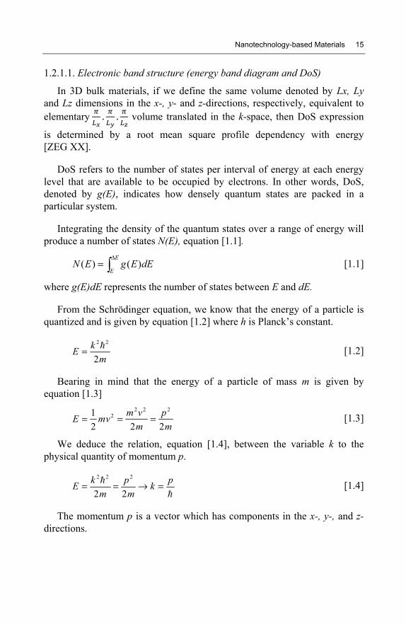
1.2.1.1. Electronic band structure (energy band diagram and DoS)
In 3D bulk materials, if we define the same volume denoted by Lx, Lyand Lz dimensions in the x-, y- and z-directions, respectively, equivalent toelementary . . volume translated in the k-space, then DoS expression
is determined by a root mean square profile dependency with energy[ZEG XX].
DoS refers to the number of states per interval of energy at each energylevel that are available to be occupied by electrons. In other words, DoS,denoted by g(E), indicates how densely quantum states are packed in aparticular system.
Integrating the density of the quantum states over a range of energy willproduce a number of states N(E), equation [1.1].
( ) ( )E
EN E g E dE
Δ= ∫ [1.1]
where g(E)dE represents the number of states between E and dE.
From the Schrödinger equation, we know that the energy of a particle isquantized and is given by equation [1.2] where h is Planck’s constant.
2 2
2kEm
= [1.2]
Bearing in mind that the energy of a particle of mass m is given byequation [1.3]
2 2 221
2 2 2m v pE mvm m
= = = [1.3]
We deduce the relation, equation [1.4], between the variable k to thephysical quantity of momentum p.
2 2 2
2 2k p pE km m
= = → = [1.4]
The momentum p is a vector which has components in the x-, y-, and z-directions.

16 Nanoscale Microwave Engineering
In a 3D system, the total energy is given by equation [1.5]
( )2
2 2 2
2 x y zE k k km
= + + [1.5]
Knowing that the quantum states are separated by an interval of π/a, thevolume of the unit cell (associated with a sphere) is given by equation [1.6]
3
0V aπ⎛ ⎞= ⎜ ⎟
⎝ ⎠[1.6]
The DoS problem is a problem of finding the number of states in theinterval of and +E E dE . In k-space, the intervals are simply and + .k k dkBecause we are operating three dimensions, k represents the radius of asphere in k-space and dk is the thickness of the sphere.
The final result for the DoS is calculated from the expression of g(E)dE,the number of states between E and dE (see equation [1.7]):
( ) ( ) ( )
( )
12
12
1 12 2 23
2 4 1
32 23
2 3
33 2
2 2
2 2( )
2 2
2
2( )2
m m E Eag E dE dE
ma EdE
a mg E dE EdE
π
π
π
−
−
− −
−=
=
⎛ ⎞= ⎜ ⎟⎝ ⎠
[1.7]
1.2.1.2. Optical constants and the dielectric function + Kramers–Krönigrelationships
Kramers–Krönig relations describe the connection between the real andimaginary parts of linear complex optical functions descriptive of light–matter interaction phenomena such as susceptibility, dielectric function,refraction index and reflectivity. The real and imaginary parts are connectedby a special form of the Hilbert transform. The sum rules are universalconstraints that determine the results of integration over the infinite spectralrange of the functions descriptive of relevant optical properties of the
Nanotechnology-based Materials 17
medium under investigation. By applying the Kramers–Krönig relation, it ispossible to acquire knowledge on dispersive phenomena by the measurementof absorptive phenomena on the whole spectrum.
Hilbert transforms connect the real and imaginary parts of a(ω) as follows(equation [1.8]):Re a ω P dω′ [1.8]
Im a ω 1πP Re a ω′ω′ ω dω′Thus, the causality of a(t), together with its property of being a function
belonging to the space of the square-integrable functions L2, implies that itsFourier transform a(ω) is analytic in the upper complex ω-plane and that thereal and imaginary parts of a(ω) are not independent but are connected bynon-local, integral relations called dispersion relations.
The linear susceptibility function describes, at a fundamental level, theconnection between the microscopic dynamics of the system underconsideration and its linear optical properties. Nevertheless, it isexperimentally much easier to measure other quantities that are moredirectly related to the behavior of light influenced by its interaction withmatter. The most commonly used optical constants are the complex index ofrefraction N (ω) = η(ω) + iκ(ω), and the complex reflectivity at normalincidence r(ω). It has been shown that relevant integral relations can also beestablished for these quantities.
1.2.1.3. Free carriers density
For each type of semiconductor, extrinsic or intrinsic (i.e. doped or non-intentionally doped), at the thermodynamic equilibrium state, theconcentrations of electrons n0 (9) and holes p0 (10) are defined according tothe DoS in the valence band Nv and in the conduction band Nc. They dependalso on the minimum energy in the conduction band Ec, the maximumenergy in the valence band Ev and the Fermi level EF. They can be expressedwith respect to the intrinsic concentration ni of the semiconductor using theaction mass low (11), where T represents the temperature in Kelvin and kBrepresents the Boltzmann constant.

18 Nanoscale Microwave Engineering
c F0 c
B
E En N exp
k T⎡ ⎤−
= −⎢ ⎥⎣ ⎦
[1.9]
[1.10]
[1.11]
Nc and Nv are calculated from the product of the DoS defined in [1.7] bythe Fermi–Dirac distribution function as described in the previous paragraphfor 3D materials.
When the material is subjected to an external perturbation such asillumination, these carrier concentrations are modified following equations[1.12] and [1.13] and the law of mass action is no longer valid [1.14].
[1.12]
[1.13]
[1.14]
The system will try to recover an equilibrium state through multiplerecombinations between the free carriers in the photoexcited material. Thepresence of impurities modifies the structure of the material bandgap. Theseimpurities introduce an intermediate energy level between Ev and Ec, whichfavors generation-recombination processes at a level called traps level.
Below, three major types of generation-recombination of electron–holepair processes are identified.
1.2.1.3.1. Thermal (emission or absorption of phonons)
The thermal generation-recombination is linked to the emission orabsorption of phonons. These thermal processes are involved in the presenceof free carriers in the valence or conduction band in the frame of intrinsic orextrinsic semiconductors under equilibrium state, i.e. without opticalpumping or current injection. When the temperature decreases, the thermal
v F0 v
B
E Ep N exp
k T⎡ ⎤−
= −⎢ ⎥⎣ ⎦
20 0 in p n=
0n n n= + Δ
0p p p= + Δ
2inp n≠

Nanotechnology-based Materials 19
generation of carriers decreases; thus, the free carrier concentrationdiminishes.
1.2.1.3.2. Radiative (emission or absorption of photons)
During the radiative generation-recombination, an electron–hole pair isgenerated or recombines through the emission or absorption of photons,respectively.
1.2.1.3.3. Auger
The Auger mechanism intervenes when a recombination between anelectron and a hole followed by an energy transfer from the recombined pairto a free carrier.
In the case of the refraction of this incoming wave with a wavelength,electro- or acousto-optic interactions will modify the index of the materialsand consequently to transmit the incident wave under different anglesfollowing the well-known Snell–Descartes law.
The interaction between a light wave and a material will differ accordingto the nature of the material [WIK]. For a conventional material (n > 1), theangle of refraction will be positive, and for an artificial material (n < 0), thisangle will be negative (see Figure 1.6).
For an interaction with a completely reflecting material, the incidentwave will be reflected under an angle equal to the incident wave for aconducting material. If the material is an insulator, the incident wave will bereflected or diffracted under an angle according to the Snell–Descartes law.
This chapter will be dedicated to this kind of material, especially thosewith a bandgap (semiconductor). A semiconductor material is an insulatorthat becomes a conductor under an external excitation, which could bethermal or electrical or optical. Under an external excitation, the number offree carriers for each energy band is modified. As an example, an electron inthe valence band is transferred into the conduction band leaving a hole in thevalence band. The energy brought by the external excitation must be greaterthan or equal to the gap energy in order to generate the electron–hole pairs.
The photoconductivity or photoconductive effect is based on thephenomenon of photon absorption into a semiconductor material[SAL 07].

20 Nanoscale Microwave Engineering
Figure 1.6. Interaction of a light wave with a conventional material(n ≥ 1) or an artificial material (n < 1). For a color version of this figure, see
www.iste.co.uk/tripon/nanotechnology.zip
Under a light illumination with an energy larger than the bandgap Eg[1.15], free carriers (either electrons or holes) are photogenerated in thematerial in the illuminated area.
The absorption α of the semiconductor is defined with respect to thewavelength λ of the optical signal associated with the light illumination[1.16]. In these equations, Eg is measured in eV, α is measured in cm–1, h isthe Planck’s constant and υ is the optical frequency.
[1.15]
( )44.10 gh Eα υ≈ − [1.16]
We must therefore consider the optical wavelength/semiconductorcouple in favor of the photoconductive effect (see Figure 1.7), whichshows absorption coefficient for various semiconductors with respectto the photon energy and the wavelength from 200 nm to 1.4 µm.As an example, in Table 1.3, typical values for α for GaAs and Si aregiven.
gh Eυ ≥

Nanotechnology-based Materials 21
α (cm–1)
λ = 671 nm
α (cm–1)
λ = 800 nm
GaAs 2.6 × 10⁴ 104
Si 4 × 10³ 103
Table 1.3. Absorption coefficients for GaAs and Si attwo different wavelengths
Figure 1.7. Absorption coefficient for various semiconductors with respect to the photonenergy and the wavelength from 200 nm to 1.4 µm
During the optical illumination, the material absorbs a flux φ of incomingphotons if the optical wavelength is included in the absorption band of thesemiconductor. The expression of this flux can be determined by using theabsorption coefficient α per unit of surface and time.
In the direction of the light illumination, the flux follows an exponentiallow decreasing proportionally to the absorption depth z and the reflectioncoefficient R of the surface of the semiconductor [1.16]. Its amplitude ismaximum at the surface level, i.e. at z = 0 (equation [1.17]).

22 Nanoscale Microwave Engineering
In equation [1.18], Popt represents the incoming optical power and A is theilluminated area of the material, c is the speed of light and q is the charge ofthe electron.
z0 e
−αφ = φ [1.17]
( )opt0
P 1 1 RA hc q
λφ = −[1.18]
In the simplified case of the air/semiconductor interface, the reflectivityor reflectance r [1.19] depends on the material index ñsc, which in the case ofan absorbing material includes an imaginary part representing the absorption[1.20].
The reflection coefficient R is equal to the square norm of the reflectancecalculated at the interface [1.21] and depends on the relative permittivity ofthe semiconductor εr and on the absorption at a given wavelength λ.
[1.19]
[1.20]
[1.21]
1.2.2. Linear optical transitions
The optical properties of semiconductors at low light levels are oftenreferred to as linear properties in contrast to the nonlinear optical properties.There are many physical processes that control the amount of absorption orother optical properties of a semiconductor. These processes depend on thewavelength of radiation, the specific properties of the semiconductor beingstudied, and other external parameters such as pressure and temperature.Optical properties of semiconductors are affected either by the introductionof impurity dopants (both p and n- type) or by unwanted impurities or
sc rn n i i4αλ= − κ = ε −
π
sc
sc
n 1rn 1
−=
+
( )
( )
22
r*
22
r
14R rr
14
αλ⎛ ⎞ε − + ⎜ ⎟π⎝ ⎠= =αλ⎛ ⎞ε + + ⎜ ⎟π⎝ ⎠

Nanotechnology-based Materials 23
defects, similar to electrical properties. Intrinsic optical properties ofsemiconductors are properties that depend on their perfect crystalline nature,and extrinsic properties are brought by impurities or defects. Many types ofdefects exist in real solids: point defects, macroscopic structural defects, etc.Figure 1.8 schematically depicts various contributions to the absorptionspectrum of a typical semiconductor as functions of wavelength (top axis)and photon energy (bottom axis). Some of the structures shown may bereduced or they are not actually present in a particular semiconductor (e.g.impurity absorption and bound excitons).
Figure 1.8. Absorption spectrum of typical semiconductor showinga wide range of optical processes [AMI 95]
1.2.3. Bandgap engineering in nanomaterials: effect of confinement/sizingon bandgap structure
1.2.3.1. Material particularities of 2D materials: electronic band structure(energy band diagram/DoS) in 2D materials – Van Hove singularities
In 2D, an electron is confined along one dimension but is able to travelfreely in the other two directions. In the image below an electron would beconfined in the z-direction but would travel freely in the XY plane.

24 Nanoscale Microwave Engineering
In the 3D DoS analysis, a spherical volume of width dk had to be used.However, in 2D, the problem of calculation becomes easier because we onlyneed to operate in two dimensions. In the 2D case, the unit cell is simply asquare with a side length of π/a.
The area of the unit cell is given by equation [1.22]:
2
0A aπ⎛ ⎞= ⎜ ⎟
⎝ ⎠[1.22]
Because we know the relation between k and E, we can find DoS as afunction of energy.
Substituting the results into the DoS equation will give the DoS in termsof energy [1.23].
1 12 2 2
2 2 2
2
2
2 2( )
( )
a mE m mEg E dE dE
a mg E dE dE
π
π
−⎡ ⎤⎛ ⎞ ⎛ ⎞⎢ ⎥= ⎜ ⎟ ⎜ ⎟⎝ ⎠ ⎝ ⎠⎢ ⎥⎣ ⎦
=
[1.23]
It should be noted that the 2D DoS does not depend on energy.
1.2.3.2. Material particularities of 1D materials: energy band diagram/DoSin 1D materials
The DoS for a 1D quantum mechanical system shows a unique solutionthat has application in materials such as NWs and CNTs. In both x-and y-directions, the electron is confined, but it moves freely in the z-direction.
Going from the 2D case to the 1D case, the unit cell becomes a linesegment of length π/a.
Just as a ring was used in the 2D system to find the number of quantumstates in a differential interval of energy, so a line segment is used in the 1D

Nanotechnology-based Materials 25
situation. The line segment stretches from k to k + dk or E to E + dE, and thelength of the line is simply dE. Dividing the infinitesimal line length dE bythe line length of the unit cell and then multiplying by 2 (i.e. accounting forthe two electron spins), the DoS equation is [1.24]
0
2( ) 2 (2)L dk ag k dk dkL
aπ π
⎛ ⎞= = =⎜ ⎟ ⎛ ⎞⎝ ⎠ ⎜ ⎟
⎝ ⎠
[1.24]
Replacing dE with dk, the DoS for 1D materials can be written [1.25] as
12
2 2
1 12 2 1
22 1
2
2( )
2 2( )
(2)2 ( )
2 1( )
ag k dk dk
a m mEg E dE dE
a m m E dE
a mg E dE dEE
π
π
π
π
−
− −−
−
=
⎡ ⎤⎛ ⎞⎢ ⎥= ⎜ ⎟⎝ ⎠⎢ ⎥⎣ ⎦
⎛ ⎞= ⎜ ⎟⎝ ⎠
⎛ ⎞= ⎜ ⎟⎜ ⎟⎝ ⎠
[1.25]
A typical representation of the DoS for 1D materials is shown inFigure 1.9.
1.2.3.3. Material particularities of 0D materials: energy band diagram/DoSin 1D materials
The DoS for a 0D structure (e.g. QD) is associated with the absence ofmotion and the absence of k-space to be filled with electrons. As a result, theavailable states only exist at discrete energies. In that case, the DoS for 0Dmaterials can be expressed as a delta function:
g(E) = 2 (E-Ec) [1.26]

26 Nanoscale Microwave Engineering
Figure 1.9. Typical representation of the density ofstates of 1D materials
1.3. Focus on two light/matter interactions at the material level
1.3.1. Photoconductivity in semiconductor material
1.3.1.1. General description and some elements on the history of the field
As an introduction, some major pioneering contributions in the field ofphotoconductivity have been selected.
First, we recall the work presented in 1873 by Willoughby Smith[SMI 73] who discovered photoconductivity in selenium while testing themetal for its high resistance properties in conjunction with his workinvolving submarine telegraph cables.
Since this early discovery, a strong effort has been made to control thespeed and the efficiency of this new effect found in semiconductors
This pioneering work was followed later by a major paper by Albert Rosein 1955 [ROS 55], which concentrated on the performance ofphotoconductors, where he stated that “all semi-conductors and insulatorsare photoconductors that the characteristic parameter of a photoconductor isthe lifetime of a free carrier”. The photoelectron current is equal to the

Nanotechnology-based Materials 27
product of absorbed photon current and the ratio of lifetime to transit time ofa free carrier. This relation holds as well for the commonly known types ofbarriers as for uniform photoconductors. The photoelectron current mayrange from a small fraction of the photon current to many powers of 10greater than the photon current depending on the ratio of lifetime to transittime. There is good evidence for lifetimes in different photoconductorsextending from 10−12 s to values approaching a second. The lifetimes of freeelectrons and free holes are, in general, independent of each other andsignificantly different. Only at sufficiently high excitation rates for which thefree carrier densities exceed the densities of bound states do the electron andhole lifetimes necessarily become equal. Some decades later, the timeresponse of a photoconductor was deeply analyzed by B. Winter and E.Rosencher [ROS 98].
1.3.1.2. Material photoconductivity
The absorption of energy in these materials will generate localized chargecarriers electron density Δn in the valence band and generation of holesdensity through a transfer toward the conduction band owing to theirdisplacement in the material and the generation of a current if the material issubmitted to an electric field. In this configuration, this increase of freecarriers depends directly on the duration of the optical illumination and onthe lifetime τn,p of the electrons/holes in the conduction/valence band beforetheir recombination in order to reach an equilibrium state.
The intrinsic conductivity of a semiconductor material can be expresseddirectly as a function of the carrier density at the thermal equilibriumthrough equation [1.27]:
[1.27]
The photoconductivity resulting from the increase of the carrier densityof the semiconductor through photon absorption is written as equations[1.28] and [1.29]:
[1.28]
[1.29]
0 (x)σ = σ + Δσ
n p(x) q n(x) p(x)⎡ ⎤Δσ = μ Δ + μ Δ⎣ ⎦
28 Nanoscale Microwave Engineering
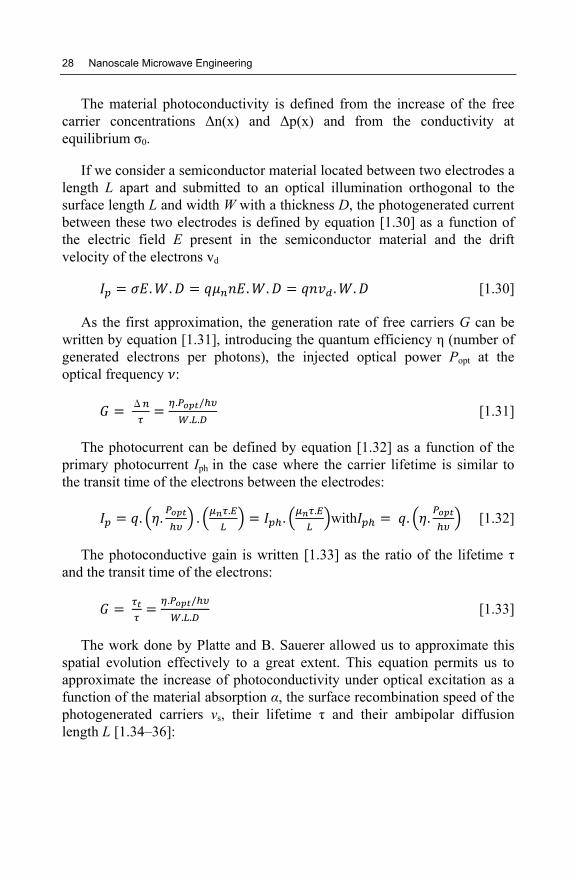
The material photoconductivity is defined from the increase of the freecarrier concentrations Δn(x) and Δp(x) and from the conductivity atequilibrium σ0.
If we consider a semiconductor material located between two electrodes alength L apart and submitted to an optical illumination orthogonal to thesurface length L and width W with a thickness D, the photogenerated currentbetween these two electrodes is defined by equation [1.30] as a function ofthe electric field E present in the semiconductor material and the driftvelocity of the electrons vd. . . . . . [1.30]
As the first approximation, the generation rate of free carriers G can bewritten by equation [1.31], introducing the quantum efficiency η (number ofgenerated electrons per photons), the injected optical power Popt at theoptical frequency :
Δ . /. . [1.31]
The photocurrent can be defined by equation [1.32] as a function of theprimary photocurrent Iph in the case where the carrier lifetime is similar tothe transit time of the electrons between the electrodes:. . . . . . with . . [1.32]
The photoconductive gain is written [1.33] as the ratio of the lifetime τand the transit time of the electrons:. /. . [1.33]
The work done by Platte and B. Sauerer allowed us to approximate thisspatial evolution effectively to a great extent. This equation permits us toapproximate the increase of photoconductivity under optical excitation as afunction of the material absorption α, the surface recombination speed of thephotogenerated carriers vs, their lifetime τ and their ambipolar diffusionlength L [1.34–36]:
Nanotechnology-based Materials 29
[1.34]
with [1.35]
[1.36]
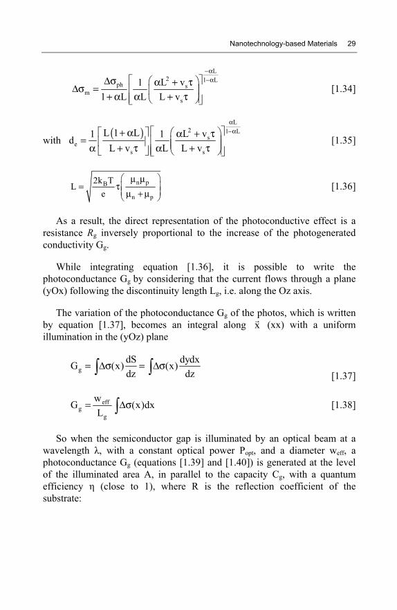
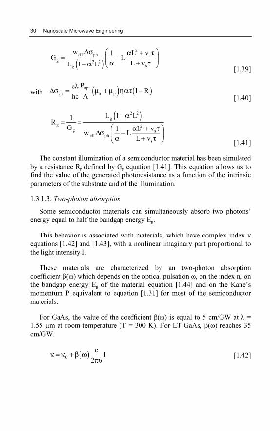
As a result, the direct representation of the photoconductive effect is aresistance Rg inversely proportional to the increase of the photogeneratedconductivity Gg.
While integrating equation [1.36], it is possible to write thephotoconductance Gg by considering that the current flows through a plane(yOx) following the discontinuity length Lg, i.e. along the Oz axis.
The variation of the photoconductance Gg of the photos, which is writtenby equation [1.37], becomes an integral along (xx) with a uniformillumination in the (yOz) plane
[1.37]
[1.38]
So when the semiconductor gap is illuminated by an optical beam at awavelength λ, with a constant optical power Popt, and a diameter weff, aphotoconductance Gg (equations [1.39] and [1.40]) is generated at the levelof the illuminated area A, in parallel to the capacity Cg, with a quantumefficiency η (close to 1), where R is the reflection coefficient of thesubstrate:
L2 1 L
ph sm
s
L v11 L L L v
−α−α⎡ ⎤Δσ ⎛ ⎞α + τΔσ = ⎢ ⎥⎜ ⎟+ α α + τ⎢ ⎥⎝ ⎠⎣ ⎦
( )L
2 1 Ls
es s
L 1 L L v1 1dL v L L v
α−α⎡ ⎤⎡ ⎤ ⎛ ⎞+ α α + τ= ⎢ ⎥⎜ ⎟⎢ ⎥ ⎜ ⎟α + τ α + τ⎢ ⎥⎝ ⎠⎣ ⎦ ⎣ ⎦
n pB
n p
2k TL
e
⎛ ⎞μ μ= τ⎜ ⎟⎜ ⎟μ + μ⎝ ⎠
x
gdS dydxG (x) (x)dz dz
= Δσ = Δσ∫ ∫
effg
g
wG (x)dxL
= Δσ∫
30 Nanoscale Microwave Engineering
[1.39]
with[1.40]
[1.41]
The constant illumination of a semiconductor material has been simulatedby a resistance Rg defined by Gg equation [1.41]. This equation allows us tofind the value of the generated photoresistance as a function of the intrinsicparameters of the substrate and of the illumination.
1.3.1.3. Two-photon absorption
Some semiconductor materials can simultaneously absorb two photons’energy equal to half the bandgap energy Eg.
This behavior is associated with materials, which have complex index κequations [1.42] and [1.43], with a nonlinear imaginary part proportional tothe light intensity I.
These materials are characterized by an two-photon absorptioncoefficient β(ω) which depends on the optical pulsation ω, on the index n, onthe bandgap energy Eg of the material equation [1.44] and on the Kane’smomentum P equivalent to equation [1.31] for most of the semiconductormaterials.
For GaAs, the value of the coefficient β(ω) is equal to 5 cm/GW at λ =1.55 µm at room temperature (T = 300 K). For LT-GaAs, β(ω) reaches 35cm/GW.
[1.42]
( )2
eff ph sg 2 2
sg
w L v1G LL vL 1 L
Δσ ⎛ ⎞α + τ= −⎜ ⎟α + τ− α ⎝ ⎠
( ) ( )optph n p
Pe 1 Rhc AλΔσ = μ + μ ηατ −
( )2 2g
g 2g s
eff phs
L 1 L1RG L v1w L
L v
− α= =
⎛ ⎞α + τΔσ −⎜ ⎟α + τ⎝ ⎠
( )0c I2
κ = κ + β ωπυ

Nanotechnology-based Materials 31
with
0
10,5Pm
= [1.43]
[1.44]
These materials can be optically excited at an optical wavelength λ2pequal to twice the absorption wavelength λg corresponding to Eg. The firstphoton will allow an electron in the valence band to reach a superiorintermediate energy level centered in the bandgap. The second photontransfers its energy to this electron, which will have access to the conductionband.
This nonlinear absorption effect in these materials opens the way to therealization of optically controlled circuit materials with a high-power opticalsource at a wavelength equal to 2λg.
As an example, for GaAs, it could be interesting to use an optical source at1.55 µm corresponding to the conventional telecommunication wavelength.
1.3.1.4. Recent 1.55 µm semiconductor materials
Conventional ultrahigh speed photoconductors are based onsemiconductor materials such as LT GaAs sensitive to the wavelength of0.85 μm. Widely known impulse laser diodes have been developed at 1.55µm with high repetition rates in the few GHz range for fiber optictelecommunications. However, at 1.55 µm, the LT GaAs is no longersensitive, and it was necessary to study semiconductor material withcharacteristics equivalent to LT GaAs in terms of dark resistivity andlifetime or recombination time but operating at 1.55 µm.
At the beginning of the 21st Century, numerous research activities havebeen developed to realize materials at 1.55 µm, such as indium galliumarsenide (InGaAs) and LT InGaAs, [MAN 07] together with the insertion ofErAs nanoparticles in InGaAs [ZHA 10].
( ) ( )( )
32 2
g2 3 5
g g
2 / E 1e P7245 hc n E 2 / E
ω −π ⎛ ⎞β ω = ⎜ ⎟⎝ ⎠ ω
0 4αλκ =
π

32 Nanoscale Microwave Engineering
Now the research activities are focused on:
1) ternary compounds such as GaBiAs [PAC 09];
2) quaternary compounds such as GaAsSbN [TAN 13] and GaInAsN[GRA 12];
3) two-photon absorption in GaAs photonic crystals [COM 08];
4) Fe-doped InGaAs [HAT 11];
5) Fe-doped InGaAsP [FEK 11];
6) InGaAs/InAlAs [SAR 08].
Table 1.4 presents some elements for the comparison of performances ofnew ultrahigh speed photoconductor operating in the 1.55 µm region.
Type of semiconductors Response time (ps) Dark resistivity(Ohm.cm)
Mobility(cm²/V.s)
GaAsBi 1 60 2,000
GaInAsN 4.4
GaAsSbN 1.3 1 × 10⁷
TPA GaAs 1
LT-InGaAs 0.2 3 490
Fe doped InGaAs 0.6 2,200
ErAs/InGaAssuperlattice
0.2 – 0,6 340
InGaAs/InAlAs 0.75 106
Be-dopedInGaAs/InAlAsmultilayer
1 100–200 500– 1,500
Cold Fe-implantedInGaAsP
0.3–3 1,200Up to 2,500
400
Table 1.4. Comparison of performances of newphotoconductor operating at 1.55 µm

Nanotechnology-based Materials 33
1.3.1.5. Interest for increasing the confinement and low-dimensionalmaterials
Recent research involving UPMC (Paris 6 University), IEMN (CNRS andUniversity of Lille) and Thales have shown the importance of reducing thegap dimensions in order to increase the photoconductance. As shown inFigure 1.10, when reducing the gap length Lg and the optical beam diameter,the photoconductance increases exponentially. Numerical models ofphotoconductivity through equation [1.26] help us to determine potentialhigh photoconductance as a function of optical beam diameter, gap lengthand width dimension tunings. Also in Figure 1.10, the photoconductance Ggvalue is calculated as a function of optical beam diameter for different gaplengths. As a result, a reduction of gap length from 50 to 0.5 m improvesphotoconductance by a factor of 100 with an optical beam diameter of 62.5µm (multimode fiber – MMF). Also, an optical beam diameter of 5 µm(single-mode fiber – SMF) enhances Gg by a factor of 10 for a gap length of0.5 m compared with the same power illumination with an optical beamdiameter of 62.5 µm. Then, an optical focusing system allows us to reducethe gap length and increase the On/Off ratio [TRI 12].
Figure 1.10. Photoconductance as a function of optical beam diameter for various gaplengths (GaAs substrate, λ = 0.8 µm, Popt = 100 mW, η = 1, Ρ = 30%, μn+μp = 8900cm²/Vs,
α = 4.104cm-1 vs= 104cm/s, L = 2µm, τ = 200 ps)

34 Nanoscale Microwave Engineering
1.3.1.6. General optical properties of SW CNTs (1D)
CNT-based optoelectronics devices started their emergence 10 years agobecause of their exceptional material optical properties in terms of banddiagram, delivering direct energy band transitions and drastically reducingphonon-assisted transitions responsible for noise in global performances andlow defect density, compared with classical bulk semiconducting materials.In this way, photoconductive and photovoltaic effects in SW and MW CNTsare mainly exploited to develop NIR photodetectors. Today, this materialacts as a new contributor for THz signal generation by photomixing.
1.3.1.6.1. Electronic nature of SWCNTs
The electronic properties of CNT are defined from a graphene monolayerwhere carbon atoms are spatially distributed as a periodic honeycombgeometry (Figure 1.11). From the growth process, CNTs are formed as anaxial graphene sheet rolling following a chiral vector Ct relying on twoarbitrary vectors a1 and a2 separated by an angle as
Figure 1.11. Representation of CNT electronic naturewith chirality indices (n,m). For a color version of this figure, see
www.iste.co.uk/tripon/nanotechnology.zip
1 2hC na ma= + [1.45]
2 2
2cos2
n mn nm m
θ +=+ +
[1.46]

Nanotechnology-based Materials 35
The two n and m integers define the chirality of a CNT by imposing thedirection of Ch, which can be identified as zigzag, armchair or stronglychiral.
This (n,m) integer pair also determines the CNT electronic nature as asemiconducting or metallic nanomaterial if m = 3N and n =0, m = n, 2m + n= 3N, in a zigzag, armchair or chiral configuration, respectively, as inequations [1.45] and [1.46].
CNT diameter is also related to this (n,m) integer pair as expressed in[1.47].
2 20h
t
C ad n nm mπ π
= = + +
with a0 = √3. 0,246 [1.47]
1.3.1.6.2. SW/MW CNT energy band diagrams
Optical absorption and emission properties of SW/MW CNTs rely ontheir energy band diagram characterized by unconventional conduction andvalence bands profiles with discretized energy spikes values known as VanHove singularity pairs (Figure 1.12). The energy separation between thehighest valence band and the lowest conduction band singularities is givenby [1.48] and [1.49], where ac-c is the lattice distance of two carbon atoms(~0.142 nm) and dt is the SW CNT diameter.E d 2a γ /d [1.48]E d 6a γ /d [1.49]
As shown in Figure 1.12, the first Van Hove peaks determine theauthorized transfer energy for both semiconductor and metallic SW CNT[MIN 01], from a global energy band diagram study. Thus, opticaltransitions occur at E d , 2E d , E d , 4E d …. energy levels,which are determined experimentally from fluorescence and emissionspectra from photoluminescence or electroluminescence and/or absorptionspectra from Raman spectroscopy. These energy levels strongly depend onthe tube diameter and chirality vector.

36 Nanoscale Microwave Engineering
Figure 1.12. Energy levels as a function of DoS for a) semiconducting andb) metallic SW CNT[PIE 101]
1.3.1.6.3. Semiconducting and metallic SW CNT optical absorbance spectra
From a classical description of electron/hole pair propagating oncylindrical surface, absorption spectra can be modeled by [1.50] [PED 04]:
∝ ∑ , ². ² ² [1.50]
where ψ x, y is the nth exciton state with energy En, ω is the photonenergy of light excitation, Γ is the phenomenological line width of 0.05 eV,and E = E E is the bandgap of the CNT, where E is the excitonbinding energy and E is the exciton energy. From this formula, absorptionspectra appear as a sum of Lorentzian curves depending on the diameter ofthe nanotube through the Eg parameter, covering a wideband opticalwavelength spectrum from UV to NIR.
For semiconducting SW CNT, two typical absorption peakscharacterizing the lowest and the second interband electronic transition,referred to as S1 and S2 in Figure 1.13, are well identified with an energy of0.7 eV and 1.2 eV, respectively.

Nanotechnology-based Materials 37
Absorbance spectra can be shifted by doping, high-pressure treatment orchemical exposure [WAN 12, ZHA 06]. Also, in the case of a multilayeredCNT film characterized by a specific thickness and an average nanotubediameter, absorbance optical spectra can be modified by an S1 peak shift offew meV.
Figure 1.13. Optical absorption spectrum of SWNT film in air at atmospheric pressure in awide range of energy from UV to far-IR [PIE 10]
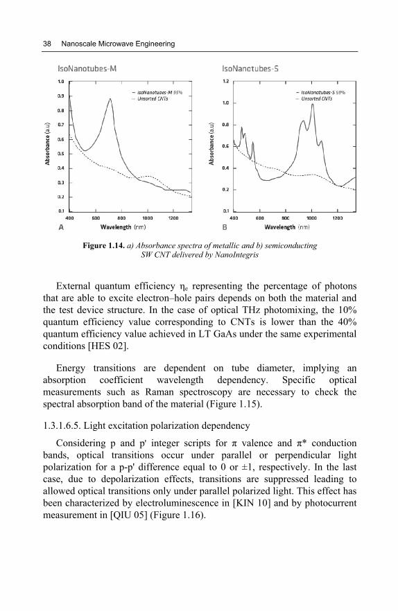
In the framework of this project, absorbance spectra of commercial CNTare identified by the provider NanoIntegris for both semiconducting andmetallic SW CNT, as shown in Figure 1.14. An absorbance of 50% at awavelength of 0.8 µm is expected for a CNT mixture of 99%semiconducting and 1% metallic.
1.3.1.6.4. Semiconducting absorption coefficient and quantum efficiency
Absorption peaks (Van Hove singularities S11 and S22) of typical CNTtypes with 1-nm diameter are fairly well matched with commonly usedinfrared spectrum. An equivalent absorption coefficient of 24 × 104cm−1 isreported for CNT bundles, which is high compared to the absorptioncoefficient of LT GaAs (6,000 cm−1). This point shows another potentialadvantage of CNTs as compared to semiconducting material [HAQ 06].
38 Nanoscale Microwave Engineering
Figure 1.14. a) Absorbance spectra of metallic and b) semiconductingSW CNT delivered by NanoIntegris
External quantum efficiency ηe representing the percentage of photonsthat are able to excite electron–hole pairs depends on both the material andthe test device structure. In the case of optical THz photomixing, the 10%quantum efficiency value corresponding to CNTs is lower than the 40%quantum efficiency value achieved in LT GaAs under the same experimentalconditions [HES 02].
Energy transitions are dependent on tube diameter, implying anabsorption coefficient wavelength dependency. Specific opticalmeasurements such as Raman spectroscopy are necessary to check thespectral absorption band of the material (Figure 1.15).
1.3.1.6.5. Light excitation polarization dependency
Considering p and p' integer scripts for π valence and π* conductionbands, optical transitions occur under parallel or perpendicular lightpolarization for a p-p' difference equal to 0 or ±1, respectively. In the lastcase, due to depolarization effects, transitions are suppressed leading toallowed optical transitions only under parallel polarized light. This effect hasbeen characterized by electroluminescence in [KIN 10] and by photocurrentmeasurement in [QIU 05] (Figure 1.16).

Nanotechnology-based Materials 39
Figure 1.15. Energy transition versus SWCNT diameter [DRE 05]
Figure 1.16. Polarization and wavelength dependence of the photocurrent. a) Polarizationdependence of the photocurrent. The photocurrent is maximized for linearly polarized light
along the length of the CNT. b) Wavelength dependence of the photocurrent. Thephotocurrent peaks at the expected S22 exciton transition [QIU 05]
1.3.1.7. Metal/CNT contact-type influence
For optoelectronic applications, metal characteristics of CNT-baseddevices must be studied for electrical characterization and understanding ofelectron and holes-generated photocurrent behavior, as in many cases aSchottky barrier is created at the CNT/metal interface. The work function of

40 Nanoscale Microwave Engineering
CNT estimated to 5 eV determining this barrier height with considered metaljustifies the choice of asymmetrical electrodes’ access in order to avoidcarrier photocurrent suppression [HON 10a, Figure 1.17]).
Figure 1.17. a) Transfer characteristics of the Au-CNT-Au CNTFET with IR source OFF(IR = 0) and ON (IR = 50 mW) at zero bias. b) Relationship between gate voltage andphotocurrent and corresponding band diagrams at negative and positive gate voltages – bias-dependent measurement of the Au-CNT-Au CNTFET with IR = 0 and IR = 50 mW atc) Vg = −0.5 V and d) Vg = 2 V
1.3.1.8. DC optoelectronic properties
The photoconductive behavior of CNTs mainly depends on three criteria:
1) CNT orientation to electrical accesses, which enables photocurrentmeasurement under bias or in a bias-free configuration. For this criterion,CNT deposition method will;
2) CNT density, which also determines the contact resistance value withelectrodes’ metallization;

Nanotechnology-based Materials 41
3) CNT contact type with electrical accesses metal which can rapidlyestablish a different Schottky barrier for electrons and holes leading to apotential photocurrent annealing as in CNT-based infrared photodetection[HON 10b].
From DC electrical characterization, the key parameter extraction such asphotoconductance can be achieved by photocurrent measurement, assumingthe active area volume is determined in two identified configurations asfollows:
– Planar unique or bundles of CNT: in this case, the active area volume Vis estimated by the product of the surface of a CNT (LCNT x 2πdCNT/2) with athickness equal to an atomic layer and with the number of CNTs;
– Vertical CNT bundles (N × M CNTs): in this case, the active areavolume V is estimated by the product of the active surface of a CNT (de ×2πdCNT/2) with a thickness equal to an atomic layer and with N × M.
1.3.1.8.1. State of the art for horizontal unique SW CNT case
In the case of CNTs deposited in the same plane as electrical access, thebenefit of CNT-based electronic devices such as p-n junctions and FETselectrical characterization under specific illumination is crucial.
In the case of p-n junctions, illumination absorption can be transferred ona unique CNT through two processes: first, the excitation of one electronfrom valence band to conduction band by the absorption of a photon withenergy larger than the bandgap and, second, a photon-assisted tunnelingprocess when the photon energy is less than the bandgap. Calculation of thegenerated photocurrent as a function of the incoming photon energy leads toa spectral photoresponse characterized by multiple peak values due to themultiple direct bandgaps.
For both types of CNT-based electronic devices, I–V characteristics havedemonstrated a change in current under bias on one (p-n junction) or twocontacts (FET) associated with IR illumination, as shown in Figure 1.18from [FRE 03] considering a CNT-FET and in Figure 1.19 from [GUO 06]considering metallic and semiconducting CNT-SBFET.

42 Nanoscale Microwave Engineering
Figure 1.18. a) Photocurrent as a function of the polarization angle of the incident infraredlight. (Excitation energy 1.28 eV, drain voltage +1 V and gate voltage −1.5 V.) b) SEM imageof the NTFET. The maximum current in c) is observed with light polarized along the nanotubeaxis (indicated by the arrows). d) Drain-voltage dependence of the current (O) without lightand with infrared light [GUO 06]. (Gate voltage, −2 V; IR intensity, 5.6 KW/cm2) [FRE 03]
Figure 1.19. The source-drain current versus the photon energy for a (22,0) CNT withEg 0.49 eV (the solid line), a (17,0) CNT with Eg 0.63 eV (dashed line) and a (13,0) CNTwith Eg 0.82 eV (dashed-dotted line) under the illumination intensity of 107 W/cm2 atVG = VD/2 = 0.2 V in the presence of electron–phonon coupling. For comparison, the dottedline with crosses shows the current of the (17,0) CNT without electron–phonon coupling. Thevertical bars show the subbandgap

Nanotechnology-based Materials 43
1.3.1.8.2. State of the art for SW CNT film case
For a film constituted of planar CNTs array, photocurrent measurementshave been performed by using a two-electrode device underneath the filmallowing bias of the structure [LIU 09]. In this example, thephotoconductivity showed an increase, decrease or even negative valueswhen the laser spot was on different positions between contact electrodes,showing a position-dependent photoconductivity of partially aligned films ofCNTs. Photon-induced charge carrier generation in SWCNTs andsubsequent charge separation across the metal–CNT contacts are believed tocause the photoconductivity changes.
A net photovoltage of 4 mV and a photocurrent of 10 μA were producedunder the laser intensity of 27 mW with a quantum efficiency of 7.8% invacuum (Figure 1.20). The photocurrent was observed to be in the directionof nanotube alignment. Finally, it was found that a strong dependence of thepolarization of the incident light on the photocurrent and the orientation ofthe films influenced the dynamics of the rise and fall of the photocurrent.
Figure 1.20. a) Schematic of the carbon nanotube sheets under testing. The bottom partshows the top view of the device. A–E are five testing positions on the sample where a laserspot was pointed. The shaded area indicates that the laser spot was on position C. b) Banddiagram of carbon nanotube (right) in contact with platinum electrodes (left). c) SEM imageof a partially rolled thin film of carbon nanotubes; inset compares the non-oriented (bottom)and partially oriented (top) samples. d) The amplitude of photocurrent as a function of laserintensity. Measurements were done in an open environment

44 Nanoscale Microwave Engineering
1.3.1.8.3. State of the art for MW CNT bundle case
Through experimental comparison, it was found that macroscale CNTmaterials also have potential distinct optical properties. Photoresponse inbundles of MWNTs was observed by Wei et al. [WEI 06], Passacantandoet al. [PAS 08] and Coscia et al. [COS 09]. A recent study has also shownthat a MWNT film is capable of generating a position-dependentphotocurrent [SUN 08, STO 08]. Photoresponse of MWNT/polymercomposite films [STO 08] and photoconductivity of doped nanotubes[JIJ 06] have been studied. There were very few studies about verticallyaligned MWNTs before [ZHA 10]. In this last study, length dependency ondetected photocurrent level was demonstrated, leading to an estimation ofthe penetration depth of light larger than 300 µm in this orientation(Figure 1.21).
e) photocurrent dependent on bias voltage
Figure 1.21. a) Schematic of the MWNTs device under testing. The bottom part shows the topview of the device. The electrodes are Mo; the applied voltage on the electrodes is the biasvoltage, Vbias; b) short-aligned MWNTs device (20 µm length); c) long-aligned MWNTs (300µm length); d) MWNTs removed device; e) photocurrent dependent on bias voltage at roomtemperature, setting laser power of 27 mW and wavelength at 532 nm. L-CNT means long-aligned MWNTs device, S-CNT means short-aligned MWNTs, R-CNT means MWNTsremoved device

Nanotechnology-based Materials 45
1.3.1.8.4. Carrier dynamics extraction
The key parameters of carriers such as lifetime and mobility aredeterminant of the estimation of transient photoconductivity σph calculatedfrom the sum of electrons and holes conductivity σn from [1.51] and [1.52],considering the photogenerated electron n and the hole density p:σ qenμ [1.51]σ qenμ [1.52]
Photoconductance value is calculated by integration of σph over a timecorresponding to the carrier lifetime in an active volume.
A real-time investigation of ultra-fast carrier dynamics in SWCNT bundlesusing femtosecond time-resolved photoelectron spectroscopy has beendeveloped and applied to identify carrier lifetimes value in CNTs bundles[HER 02]. A pump–probe scheme allows an investigation of charge carriersfrom 2.38 eV above EF to the immediate vicinity of the Fermi level and below,down to about −0.2 eV, and the study of fundamental scattering processessuch as e–e or e–ph scattering directly in the time domain (Figure 1.21).
A carrier lifetime of 1–3 ps with a mobility of 104 cm²/V.s has beenobtained experimentally [HES 02] (Figure 1.22).
1.3.2. Example of light absorption in metals: plasmonics
1.3.2.1. Elements on the index and phase conditions for a conventionalmetal/dielectric interface
We consider the generation of surface plasmons (oscillation of electronsat a frequency defined as the plasma frequency) at the metal/dielectricinterface. These surface plasmons are excited by an electric field incomingin the incident plane of the excitation (typically an optical excitation intranverse electro magnetic (TEM) mode) and following a specific angle.
Under these conditions, the light wave incoming on the metal/dielectricinterface (Figure 1.23) will be partially or totally absorbed. In thisconfiguration, no reflection of this light wave is obtained. The reflectionspectrum at the metal/dielectric interface as a function of the incidence anglewill reach a minimum value at an angle of incidence called SPR angle, θc.

46 Nanoscale Microwave Engineering
Figure 1.22. Sample fit of a low-energy cross-correlation (XC) trace to a bi-exponentialdecay. The slow and fast components can be associated with e–e and e–ph interactions,
i.e. internal thermalization and cooling of the electron gas, respectively
Figure 1.23. Definition of a metal/dielectric

Nanotechnology-based Materials 47
The angle θc [1.53] corresponds to the total reflection angle defined bythe index ratios nm and nd of the metal and dielectric material, respectively,forming the interface allowing the evanescent mode at the level of theinterface and parallel to the x-axis
[1.53]
Taking into account the permittivity of the dielectric εd, the oscillationfrequency of the SPP ωsp intervenes at a frequency lower than the plasmafrequency ωp [1.54]:
1p
spd
ωω
ε=
+[1.54]
It has been demonstrated that the component of the wave vector along thex-axis is defined by the following equation, representing the plasmonicdispersion equation [1.55]:
[1.55]
This dispersion equation, shown in Figures 1.24 and 1.25, allows us tounderstand that an optical coupling is needed in order to match the wavevector of the incident photon (kphoton,air curve) with a plasmon present at theinterface level of two dielectric materials with different optical index values(red and green curves).
A coupling via a prism or a grating (see Figure 1.26) adding a phaseelement in sin θr (θr representing the incidence angle in the prism or at thecoupling grating level) is realized by natural reflection in the case of theprism and by disordered diffraction in the case of a periodic grating with astep Λ.
By considering the complex permittivity [1.56] of the metal:
' ''m m mjε ε ε= + [1.56]
0 d mx
d m
kc
ω ε εε ε
=+
1sin mc
d
nn
θ − ⎛ ⎞= ⎜ ⎟
⎝ ⎠
2
0p
nem
ωε
=
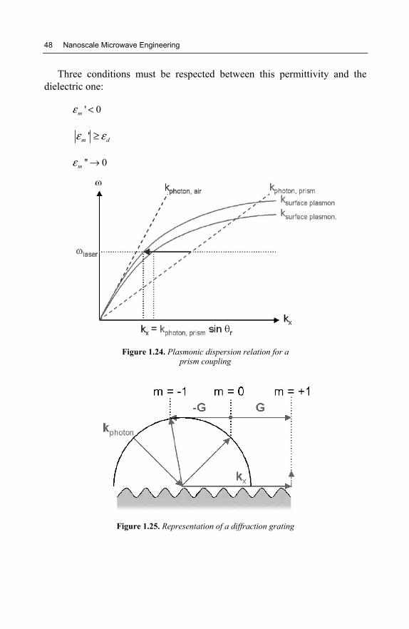
48 Nanoscale Microwave Engineering
Three conditions must be respected between this permittivity and thedielectric one:
' 0mε <
'm dε ε≥
'' 0mε →
Figure 1.24. Plasmonic dispersion relation for aprism coupling
Figure 1.25. Representation of a diffraction grating

Nanotechnology-based Materials 49
Figure 1.26. Plasmonic dispersion relation in case ofa coupling by grating
1.3.2.2. Matching conditions: metal/semiconductor interface
In the conventional case, the generation of plasmon is donesimultaneously between the two faces of the metal, i.e. at the couplingmaterial/metal interface and the metal/dielectric interface inducing twopotential configurations for the optical coupling either by the front face or bythe rear face [KRE 71, OTT 68].
If the dielectric material is replaced by a semiconductor material forintegration or efficiency reasons, a plasmon generation at the metal–semiconductor interface must be favored.
To satisfy this latest condition, constraints on materials must be takeninto account. For example, it will be necessary to have an index of thecoupling material greater than or equal to the semiconductor material indextoward the desired incidence angle:
εprism>= εdielectric

2
Electromagnetic MaterialCharacterization at Nanoscale
This chapter deals with the definition and parameters of some dedicated measurementtechniques in order to define and measure the main parameters associated with a material. Itaddresses static and dynamic characterization techniques including ultrafast approaches bothfrom the photonic and electronic points of view [SCH 06].
2.1. State of the art of macroscopic material characterization techniquesin the microwave domain with dedicated equipment
2.1.1. Static resistivity
Determination of static resistivity of a semiconducting material is oneof the major key material parameters that allow its exploitation in thetechnology of any integrated device/circuit/system. Its knowledge will helpto quantify the carrier density n and p and their associated mobility n,p atthermodynamic equilibrium, as is equal to 1/[q(n n + p p)]. In this area,several characterization techniques today constitute state-of-the-art methodsin a contacting or contactless electrical access environment, dedicated to 3Dmaterials as described in the following.
2.1.1.1. Two-point versus four-point probe
The four-probe technique, originally proposed by Winner in 1916 ingeophysics and then by Valdes in the case of semiconductor materials, iscommonly used to determine the resistivity of materials using two identicalprobe terminals working in differential mode. In this configuration, parasitic
Nanoscale Microwave Engineering: Optical Control of Nanodevices, First Edition. Charlotte Tripon-Canseliet and Jean Chazelas.© ISTE Ltd 2014. Published by ISTE Ltd and John Wiley & Sons, Inc.
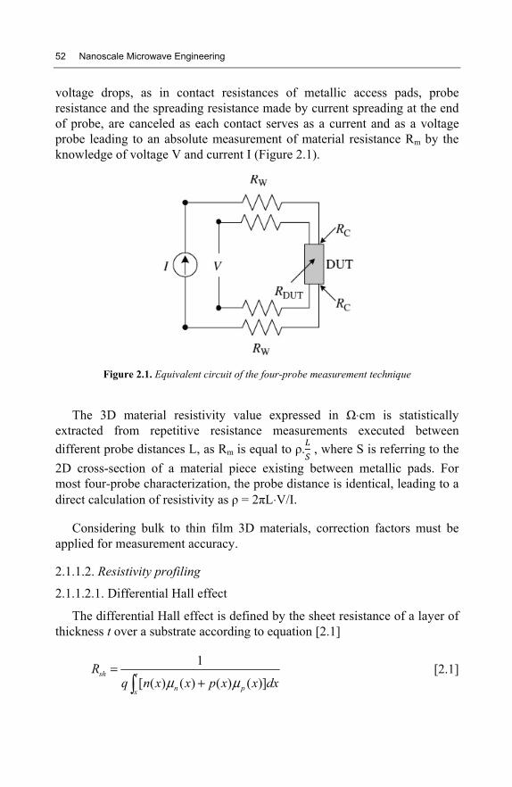
52 Nanoscale Microwave Engineering
voltage drops, as in contact resistances of metallic access pads, proberesistance and the spreading resistance made by current spreading at the endof probe, are canceled as each contact serves as a current and as a voltageprobe leading to an absolute measurement of material resistance Rm by theknowledge of voltage V and current I (Figure 2.1).
Figure 2.1. Equivalent circuit of the four-probe measurement technique
The 3D material resistivity value expressed in ⋅cm is statisticallyextracted from repetitive resistance measurements executed betweendifferent probe distances L, as Rm is equal to . , where S is referring to the2D cross-section of a material piece existing between metallic pads. Formost four-probe characterization, the probe distance is identical, leading to adirect calculation of resistivity as = 2 L⋅V/I.
Considering bulk to thin film 3D materials, correction factors must beapplied for measurement accuracy.
2.1.1.2. Resistivity profiling
2.1.1.2.1. Differential Hall effect
The differential Hall effect is defined by the sheet resistance of a layer ofthickness t over a substrate according to equation [2.1]
1
[ ( ) ( ) ( ) ( )]sh t
n px
Rq n x x p x x dxμ μ
=+
[2.1]

Electromagnetic Material Characterization at Nanoscale 53
If the sample is a thin layer, it must be separated from the substrate by aninsulating layer to confine the four-point probe current to the layer.
2.1.1.2.2. Spreading resistance profiling
The spreading resistance probe technique is used today to generateresistivity and dopant density depth profiles. It has very high dynamic range(1012–1021 cm 3) and is capable of profiling very shallow junctions into thenanometer regime. Substantial progress has been made in data collection andtreatment. The latter relates to improved sample preparation and probeconditioning procedures. The instrument consists of two carefully alignedprobes that are stepped along the semiconductor surface. The resistancebetween the probes is given by R = 2Rp + 2Rc + 2Rsp, where Rp is the proberesistance, Rc is the contact resistance and Rsp is the spreading resistance.The resistance is measured at each location.
2.1.1.3. Some contactless method examples
Well adapted to nanotechnology, contactless resistivity measurementmethods are divided into two broad categories: electrical and non-electricalmeasurements. Commercial equipment is available for both. Electricalcontactless measurement techniques fall into several categories: the sampleis placed into a microwave circuit and perturbs the transmission or reflectioncharacteristics of a waveguide or cavity, the sample is capacitively coupledto the measuring apparatus, and the sample is inductively coupled to theapparatus.
Eddy current method is used to determine the resistivity using theintegration of the material inside a resonant cavity. Induced Eddy currents bymagnetic field excitation can be measured through Joule heating by energyabsorption (equation [2.2])
2
0( / ) ( )
t
a TP K V n x dxσ= [2.2]
2.1.2. Carrier and doping density
2.1.2.1. Capacitance–voltage (C-V) and current–voltage (I-V) measurements
Capacitance–voltage measurements are associated with semiconductorjunctions where a space charge area is created and modulated by an appliedvoltage.

54 Nanoscale Microwave Engineering
The C-V profiling method has been used with Schottky barrier diodesusing metal, p-n junctions, metal-oxide-semiconductor (MOS) capacitors,metal-oxide-semiconductor field effect transistors (MOSFETs) and metal-air-semiconductor structures.
As far as nanotechnology is concerned, DC permittivity measurementshave been performed through C-V characterization techniques applied tocapacitive circuits. Specific attention must be given to the Debye length,which sets a limit to the spatial resolution of the measured profile. Indeed,this Debye length problem arises because the capacitance is determined bythe movement of majority carriers, and the majority carrier distributioncannot follow abrupt spatial changes in doping density profiles.
2.1.2.2. Hall effect
The key feature of Hall measurements is the ability to determine thecarrier density, carrier type and mobility.
Hall theory predicts the Hall coefficient RH [2.3]
RH = r(p b2n)/[q(p + bn)²] [2.3]
where b = n/ p and r is the scattering factor whose value lies between 1 and2, depending on the scattering mechanism in the semiconductor.
The Hall coefficient is determined experimentally as in [2.4]
RH = tVH/BI [2.4]
where t is the sample thickness, VH is the Hall voltage, B is the magneticfield and I is the current.
2.1.2.3. Optical techniques
Optical techniques become useful for material optical properties such asabsorption coefficient determination and complex optical index over a widehigh-frequency bandwidth. In this way, experimental techniques allow us toknow the reflection, transmission and absorption coefficients R, T and A,respectively, by use of dedicated test cells in incidence with an opticalsignal.

Electromagnetic Material Characterization at Nanoscale 55
The optical transmittance T [2.5] through a semiconductor wafer ofthickness t is approximately
T =(1 . R)² .exp(– t) [2.5]
For reasonable measurement sensitivity, t should be of the order ofunity. For varying from 1 to 10 cm 1, representative of shallow impurityabsorption at low densities, the sample must be 1–10 mm thick. Samples ofthis thickness are convenient for bulk wafers but not for epitaxial layers,making the IR spectroscopy of thin layers impractical.
Other approaches such as photoluminescence are extremely helpful forthe determination of the electronic band structure.
2.1.3. Contact resistance and Schottky barriers
According to the fact that all semiconductor devices have contacts and allcontacts have contact resistance, it is important to characterize such contacts,especially in the case of 2D or 1D materials. Contacts are generallymetal–semiconductor contacts, but they may be semiconductor–semiconductor contacts, where both semiconductors can be single crystal,polycrystalline or amorphous, linked to the identification of the Fermi levellocalization. For a discussion of the measurement techniques, the typeof contact is unimportant, but the resistance of the contact material isimportant.
Several types of contact are conventionally studied: metal–semiconductor(Schottky) or ohmic.
The work function of a solid is defined as the energy difference betweenthe vacuum level and the Fermi level. Work functions for the metal and thesemiconductor are shown in Figure 2.2, with the metal work function Mbeing less than the semiconductor work function S. The work function isgiven as the energy M related to the potential M by M = M/q.

56 Nanoscale Microwave Engineering
Figure 2.2. Schematic of the metal–semiconductor contactsaccording to the Schottky model
2.1.4. Transient methods for the determination of carrier dynamics
2.1.4.1. Recombination lifetime – optical measurements
Lifetimes are divided into two primary categories: recombinationlifetimes and generation lifetimes. The concept of the recombination lifetimer holds when excess carriers decay as a result of recombination. When theserecombination and generation events occur in the bulk, they arecharacterized by r and g. When they occur at the surface, they arecharacterized by the surface recombination velocity vr and the surfacegeneration velocity vg. Both bulk and surface recombination or generationoccur simultaneously and their separation is sometimes quite difficult. Themeasured lifetimes are always effective lifetimes consisting of bulk andsurface components.
Pump–probe measurement techniques, using a combination of electro-optic probes detecting ultrashort electrical signals, have been widelydeveloped for identification of ultrafast carrier lifetimes in 3D, 2D and 1Dmaterials such as in [ORT 01, COU 08].

Electromagnetic Material Characterization at Nanoscale 57
2.1.4.2. Conductivity mobility
The study and applications of the Hall effect can be found in the literaturefocused on solid state physics and semiconducting materials. The Hall effectmeasurement technique has found wide application in the characterization ofsemiconductor materials because it gives the resistivity, carrier density andmobility. Hall found that a magnetic field applied to a conductorperpendicular to the direction of current flow produces an electric fieldperpendicular to the magnetic field and the current. For more detail on this,see section 1.3.1.
2.1.5. Frequency methods for complex permittivity determination infrequency
2.1.5.1. Scientific background
The principles and techniques of permittivity measurements usingtransmission lines have been widely studied for the determination of bulkmaterial permittivity, permeability and conductivity in the frequencydomain. A non-destructive method by electromagnetic coupling of anunknown material thin layer with a tranverse electromagnetic (quasi-TEM)propagation mode in planar configuration (microstrip or coplanar line) hasbecome the most appropriate methodology today to achieve a complete andbroadband characterization [CHE 10, KAS 10]. For nanomaterialcharacterization, only coaxial line techniques have been used because ofCNT delivery in disperse solutions [DEC 12] inducing frequency bandwidthlimitation and the random orientation of CNTs compared to the E-fieldpolarization direction. In this chapter, we present a new measurementtechnique of frequency-dependent complex anisotropic permittivity of in-situgrown nanomaterials by integration in a planar multilayered structure.
2.1.5.2. Direct extraction of the propagation constant of a coplanarmultilayered structure
After an analytic S-to-ABCD-matrix conversion, equations [2.6] and[2.7], and a de-embedding procedure for microwave probe parasiticperturbation suppression, exact determination of the effective propagationconstant ( reff) [2.8] and permittivity ( reff) [2.9] of a transverse N-layerstructure of length L is obtained.

58 Nanoscale Microwave Engineering
[2.6]
with [2.7]
[2.8]
[2.9]
2.1.5.3. Permittivity extraction of unknown layer by inverse problemresolution
As an inverse problem, relative permittivity of the SWCNT layerextraction is achieved using a conformal mapping technique from theVeyres–Fouad Hanna approximation [VEY 80], assuming a multilayeredstructure as a superposition of capacitances Ci of each individual materiallayer i with coplanar transmission line (Figure 2.3). The total capacitance Cis equal to the sum of each individual capacitance [2.10].
[2.10]
Individual capacitance Ci of layer i is directly related to the completeintegral equations K(ki) and K (ki) expressed in equations [2.11] and [2.12]assuming the identity .
[2.11]
with
and [2.12]

Electromagnetic Material Characterization at Nanoscale 59
Specific expressions must be applied for layer 0 representing the coplanarline capacitance in air as expressed in [2.13].
with and [2.13]
From the determination of effective permittivity reff of the completemultilayered structure, layer characteristics such as thickness, coplanar linedimensions and relative permittivity of one layer can be extracted by analyticresolution of equation [2.10] in its completed expression.
Figure 2.3. Transverse representation of a five-layer structure for individual capacitance Cidefinition from [PIE 10a]: (a) C0, (b) C1, (c) C2, (d) C3, (e) C4 and (f) C5

60 Nanoscale Microwave Engineering
2.2. Evolution of techniques for nanomaterial characterization
For 1D materials, the problems associated with attempting to scale downtraditional semiconductor devices have led researchers to look into CNT-baseddevices, such as CNT FETs, as alternatives. Because they are not subject tothe same scaling problems as traditional semiconductor devices, CNT FETsare being studied for a wide variety of applications, including logic devices,memory devices and sensors.
The research on these devices typically involves determining variouselectrical parameters, which may include current–voltage (I-V), pulsed I-Vand capacitance (C) measurements. Characterizing the electrical properties ofdelicate nanoelectronic devices requires instruments and measurementtechniques optimized for low power levels and high measurement sensitivity.
2.2.1. The CNT transistor
A single semiconducting CNT can be used as the conducting channelbetween the source and the drain of an FET. Two metal contacts are locatedacross both ends of the CNT to form the source and drain terminals of theFET. The CNT is placed at the top of an oxide layer that has been processedabove a doped silicon substrate, which forms the gate terminal. Connectionsare made to the three device under test (DUT) terminals to perform theelectrical measurements.
The I-V characteristics of a CNT transistor can be used to extract many ofthe device’s parameters, study the effects of fabrication technique andprocess variations, determine the quality of the contacts, etc.
2.2.2. Optimizing DC measurements
The following techniques will improve the quality of DC measurementsmade on CNT FETs:
1) Limit current: to prevent damage to the device while performing I-Vcharacterization, the user should limit the amount of current that can flowthrough the device.
2) Provide sufficient settling time: because CNT FET measurementsoften involve measuring low current (<1 A), it is important to allow

Electromagnetic Material Characterization at Nanoscale 61
sufficient settling time to ensure the measurements are stabilized after acurrent or voltage has been applied. Some of the factors that affect thesettling time of the measurement circuit include the cables, test fixtures,switches, probers, the DUT resistance and the current range of themeasurement instrument. To ensure settled readings, additional delay timecan be added to the voltage or current step time before the measurement.
3) Use proper speed modes: this affects the settling time of the reading, aswell as the integration time of the measurement.
4) Minimize noisy measurements: noise may be generated from a varietyof sources, including particle collisions, defects, AC pick-up andelectrostatic interference. Noisy measurements result when a noise signal issuperimposed on the DC signal being measured. This can result in inaccurateor fluctuating measurements. Electrostatic interference is another cause ofnoisy measurements when measuring low currents. This coupling occurswhen an electrically charged object approaches the circuit under test. Inhigh-impedance circuits, this charge does not decay rapidly and can result inunstable measurements.
2.2.3. Pulsed I-V measurements
In addition to making traditional DC I-V measurements, it may bedesirable to perform ultrafast pulsed I-V measurements for various reasons.First, it may be important to observe the high-speed response of the CNTdevice. In some cases, nanostructures can be destroyed by the heat generatedwhen making traditional DC measurements. Pulsed I-V measurements canreduce the total energy dissipated in a device and therefore reduce thepotential for damage. Finally, pulsed electrical testing can prevent currentdrifting in measurements that can occur during DC measurements.
2.2.4. Capacitance–voltage measurements
In addition to performing DC and pulsed I-V measurements on CNTFETs, measuring the capacitance of the FET can also provide informationabout the device, including the mobility, timing effects and gate dielectrics.

62 Nanoscale Microwave Engineering
2.2.4.1. Optimizing capacitance measurements
To improve the quality of capacitance measurements, it will be necessaryto perform open compensation (for measurements < 10 pF).
2.3. Micro- to nanoexperimental techniques for the characterization of2D, 1D and 0D materials
In the field of electrostatic force microscopy (EFM) of nanostructures,experiments aiming to probe the local electronic properties of nanostructureson insulators have been realized. Such experiments are based on the use ofan AFM operated in one of its electrical modes: EFM, Kelvin forcemicroscopy (KFM), etc. Results based on charge injection and EFMexperiments applied to 0D and 1D nanostructures have been obtained onsilicon nanoparticles and CNTs. Experimentally, the tip of the EFMcantilever is used to address a single nanostructure and inject charges whenpressed with a few nanonewtons of force and biased with respect to thesubstrate at an injection voltage (Figure 2.4). In this process, charges aretransferred (in most cases from the EFM tip into the nanostructure). EFMdata consist of the shift of the resonance frequency f0 of the cantilever, whenbiased at a detection voltage VEFM. EFM frequency shifts are proportional tothe gradient of the electrostatic force acting on the EFM tip [MÉL 04].
Figure 2.4. a) Injection of an amount Q of charges in a single silicon nanoparticle (gray) ofheight h by tunneling through the nanoparticle native oxide (white) from the EFM tip biasedat Vinj. b) Equivalent surface dipole Q x h/ . When the tip is scanned at a distance z over thesubstrate plane, the dipole interacts with its tip image. In a plane geometry, this image dipoleof momentum Q x h/ would be located at 2z over the substrate plane
Specific techniques have recently been developed in order to keepmicrometer scale access for nanometer scale material parameter extraction,

Electromagnetic Material Characterization at Nanoscale 63
from DC to microwave frequencies. As high impedance is mainlydemonstrated by such materials in contact with electrical electrodes, anelectrical access environment has to be reconsidered in order to overcomehigh contact resistance. In such a way, electrical circuits relying on aWheatstone bridge implementation could be a technical solution [CUR 08].


3
Nanotechnology-basedComponents and Devices
This chapter summarizes some research approaches for the realization of new opticallycontrolled microwave functions. This concept, part of the microwave photonics research area,driving a new family of microwave devices, mainly deals with the photoconductivity insemiconductors with 1D, 2D and 3D structures for applications ranging from the generation andsampling of signals from the microwaves to the THz frequencies.
This chapter presents the newly envisaged optically controlled microwave functions atnanoscale and describes the main parameters involved in these nanodevices and associatedfunctions.
A photoconductive switch is an electrical switch, which is based on thephotoconductivity of a material, i.e. an increase in its electrical conductanceas a result of illumination by light. In almost all research in this field, asemiconductor material is used, where the absorbed light (with a photonenergy above the bandgap energy) generates electrons and holes carriers,which then contribute to the conductivity.
In the last decades few decades, the most commonly used semiconductorswere chromium-doped gallium arsenide (Cr-GaAs), low-temperature-growngallium arsenide (LT-GaAs), indium phosphide (InP), cadmium selenide(CdSe), and Si and its derivatives (amorphous silicon and silicon on sapphire(SoS)).
Nanoscale Microwave Engineering: Optical Control of Nanodevices, First Edition. Charlotte Tripon-Canseliet and Jean Chazelas.© ISTE Ltd 2014. Published by ISTE Ltd and John Wiley & Sons, Inc.

66 Nanoscale Microwave Engineering
To reduce the recovery time of the switch (determined by the lifetime ofphotoexcited carriers), we typically use low-temperature growth (oftenfollowed by rapid thermal annealing), some doping (e.g. chromium in GaAs)or ion bombardment for producing crystal defects. Apart from the recoverytime, important criteria are the bandgap energy, dark resistivity and electricalbreakdown resistance.
There are different designs of photoconductive switches:
– bulk devices, which are several millimeters or even centimeters longwith electrical contacts on the end faces, used for switching very highvoltages (sometimes above 100 kV);
– devices with a small gap in a microstrip; the gap can be straight orinterdigitated and has a width between a few microns and tens of microns forlow-power applications with very high speed;
– sliding contact devices for the highest speed, where a point between thetwo parallel strips of a coplanar stripline is illuminated.
All such devices are of the metal–semiconductor–metal (MSM) type.
The main applications of photoconductive switches are as follows:
– sampling of analog signals in very fast analog-to-digital converters;
– generation of submillimeter wave and terahertz pulses;
– generation of microwaves and millimeter waves.
The new generation of ultra-high-speed photoconductive switchingstarted on the basis of the Auston photo-switch [AVS 83] using LT-GaAsdue to its ultrafast trapping characteristics and low leakage current [MCL 97,TAN 96]. However, at the end of 20th century only high-qualityphotoconductive materials requiring an 800 nm illumination exist to switchsuch devices resulting in the use of bulky and expensive Ti-Sapphire pulselasers. On the contrary, 1550 nm wavelength optical control through theavailability of compact fiber and solid-state mode locked lasers sources wasaccessible but without high-quality photoconductive materials.

Nanotechnology-based Components and Devices 67
3.1. Photoconductive switches for microwave applications
3.1.1. Major stakes
Integration of optical technologies into telecommunication systemsenabled the improvement of performances together with a reduction of thedimensions and architecture complexity of these systems. One aspect ofintegration is addressed in the direct optical control of microwave circuits inintegrated technology. The optical signal is used to command either theactive circuits or passive devices.
Concerning the control of nonlinear circuits, the optical signal is applieddirectly to their active components. As an example, and following theapproaches, the optical control of the gain of a microwave amplifier and theoptical control of a microwave oscillator frequency and output power werevalidated [DE 81, YEN 77, FAC 05]. The main drawback of these circuits islinked to the low dynamic range of the optical control. For the control oflinear microwave circuits, with transmission line discontinuity, functionssuch as switching and phase shifting based on photoconductivity have beendemonstrated [TRI 12, CAN 03]. Photo switching gives rise to researchaiming at THz signals generation and sampling. Optically controlled phaseshifting opens new horizons in the achievement of new wideband phasearray antenna architecture in the transmit and receive modes. Moreover,optically tunable filter and resonator functions have been realized.
3.1.2. Basic principles
The simplest optically controlled microwave device is called thephotoconductive switch or photoswitch. It is based on a metallic microwavetransmission line interrupted by a gap of length Lg and width w, deposited ona semiconductor substrate of thickness h and relative permittivity εr.
The gap between the two electrodes will act as a light/semiconductorinterface, i.e. it will allow the illumination, by an optical source, of thesemiconductor substrate that gives rise to the photoconductor effect(Figure 3.1).

68 Nanoscale Microwave Engineering
Figure 3.1. Schematic of a cross-section of a microwave photoswitchin a microstrip configuration
This approach is a basic building block necessary to realize opticallycontrolled microwave monolithic integrated circuits (O-MMICs) forwideband applications. It is designed for any semiconductor material,depending on the applications in terms of operating frequencies andachievable optical wavelength.
In the field of microwaves, two main MMIC technologies have beendeveloped: coplanar waveguide (CPW) and microstrip configurations (seeFigure 3.2).
Figure 3.2. Schematic of the interrupted coplanar waveguide configuration

Nanotechnology-based Components and Devices 69
The operating principle is as follows:
– Without an optical illumination (OFF state), the propagation of themicrowave signal is almost completely interrupted by the slit of the line. Theassociated device is electrically equivalent to a capacity in series Cgassociated with the electrodes created by the transmission line interruption(slit), and also with two capacities in parallel, associated with the coupling ofthe electrodes to the ground plane Cp.
– Under light illumination (ON state), the photon energy is absorbed bythe semiconductor material inducing a reduction of the resistivity due to thecreation of a localized free-carrier plasma area, characterized by thephotoconductance parameter extracted from equation [3.1]. The propagationof the microwave signal through the line slit is thus allowed. As a result, aphotoresistance is added in parallel to the capacitance Cg in order tocomplete the equivalent electrical scheme (see Figure 3.3).
Figure 3.3. Electrical equivalent scheme of a microwave photoswitcha) in the OFF state and b) in the ON state
The associated device works as a switch, modifying the phase andamplitude of the microwave signal flowing through this electricaldiscontinuity.
The ability of this microwave photoswitch to enable or to prevent thetransmission of a microwave signal is defined by the complex variableℜON/OFF representing the ON/OFF ratio, determined from the transmission Sparameters, S21 (or S12), in these two states, as defined in equations [3.2] and[3.3]. The insertion losses of the device are determined by the module of theS21 (or S12) parameters, obtained through light illumination and expressed indecibels.

70 Nanoscale Microwave Engineering
In these equations, the parameters are the following:
– μn and μp represent, respectively, the carrier mobilities of the electronsand holes photogenerated;
– η is the quantum efficiency;
– α is the absorption coefficient;
– R is the reflection coefficient at the air/semiconductor interface;
– Popt is the incident optical power;
A and weff are the illuminated area and the diameter of the optical beam;
– Lg is the effective length of the illuminated area (which could differfrom weff);
– L is the ambipolar diffusion length of the carriers;
– vs is the recombination speed at the surface level and τ is the carrierlifetime.
( )
g n p
2opt eff s
2 2g s
eG (µ µ ) (1 R)h
P w L v1 1 LA L L v1 L
= + η α τ −ν
⎡ ⎤α + τ× −⎢ ⎥α + τ−α ⎣ ⎦[3.1]
( ) ( ) On /OffiOn /Off 21 21 On /OffS On S Off R e Δϕℜ = =
[3.2]
( )21 0 0S (Off ) j2 Z Cg 1 j2 Z Cg= ω + ω
( ) ( )( ) ( )( )
021
0 0 0
2Z Gg 1 j Cg GgS On
1 2Z Gg 1 j 2Z Cg 1 2Z Gg+ ω
=+ + ω +
[3.3]

Nanotechnology-based Components and Devices 71
3.1.3. State of the art of photoconductive switching
For decades, numerous research activities have been driven by improvingthe performances of photoconductive switching devices due to the resultsobtained with the new growth technologies of semiconductors. These newapproaches offer the ability to realize components and devices withabsorption capabilities in spectral regions compatible with the opticalsources, i.e. in the visible domain (from 532 to 670 nm) and in the near IR(0.78–1.55 µm). Nowadays, the most studied materials are Gallium Arsenide(GaAs) and Indium Phosphide (InP) in the III-V for ultra-high speedapplications and Silicon (Si)-based for the applications in the millisecond(ms) range semiconductor compounds families.
3.1.3.1. Switching of continuous wave (CW) electrical signals by a CWoptical source
As mentioned earlier, the first photoswitch was demonstrated by D.H.Auston in 1975 by realizing the switching of a continuous signal of 20 V by anoptical beam in free-space propagation. The illuminating optical signal wasobtained at 0.53 µm after a frequency doubling of 1.06 µm laser source basedon a potassium di-hydrogen phosphate (KDP) crystal. This laser source at0.53 µm illuminates a Si-based microstrip realizing the ON state. For the OFFstate, the 1.06 µm source was used to realize a direct contact to the groundplane.
3.1.3.2. Switching of CW electrical signals by an intensity-modulated opticalsource
An interrupted CPW gap illuminated by an impulse optical source wasdemonstrated [CAS 76]. The photoconduction is obtained by applying anoptical pulsed signal between the transmission line central electrode and theground plane.
Figure 3.4. Schematic of the short-circuited coplanar waveguide configuration

72 Nanoscale Microwave Engineering
By integrating a thin plate of GaAs:Cr into a coaxial line charged to50 Ω, it was possible to switch a CW signal of 250 V with a pulse of 30 psand 10 µJ.
This approach opens the way to switch high-voltage signals by ultrashortoptical pulses in order to realize high-power microwave signals.
This approach requires a semiconductor material with an ultrashortcarrier recombination time. This leads to the studies of doped materials orlow-temperature grown materials such as GaAs with carrier lifetime in theorder of a few picoseconds [LID 92] or below one picosecond [LIN 12],measured by temporal autocorrelation. Another attempt of the sameperformances was achieved by using GaAs: As+ [LIN 97].
3.1.3.3. Switching microwave signals by a CW optical source
Numerous semiconductor materials were studied for switchingmicrowave signals such as amorphous Si, Ge, C diamond, CdS,CdS0.5Se0.5, GaP and SoS.
An interdigitated gap photoconductive microwave switch using InP:Feunder an optical illumination at 0.805 µm was realized, showing an ON/OFFratio of 43 dB at 100 MHz and 23 dB at 1 GHz under 50 mW optical power[AND 89].
3.1.4. Photoconductive switching at nanoscale – examples
Up to now, the best performances in terms of the ON/OFF ratio ofmicrowave frequencies have been obtained due to the use of high-resistivitymaterials (ρ > 107 Ω⋅cm) and the extreme confinement of the area ofinteraction between the optical illumination and the semiconductor. Thisapproach requires an optimization of the dimension in the submicron region.
The reduction of the capacity Cg together with the confinement of theilluminated area allows us to greatly lower the amplitude of the radiofrequency (RF) signal in the OFF state while drastically increasing thecarrier density locally in the ON state, inducing a large modification to thematerial conductivity. These last achieved performances have a strongimpact, for example, on the optical power to be launched for the opticalcontrol of the photoswitch.

Nanotechnology-based Components and Devices 73
Today, thanks to the development of technological tools dedicated tonanotechnology, the definition of nano scale interaction volume by thereduction of microwave transmission lines with optical waveguides to thenano scale (Figure 3.5 – Table 3.1) is reachable.
a) b)
Figure 3.5. Examples of CPW-based microwave photoswitch on LT-GaAs;a) with an external illumination [TRI 06] or b) with an integrated
optical waveguide (courtesy of IEMN)
Key parameters Dimensions
Micron scale Submicron scale
Interaction volume 20 x 20 x 2 µm3 1 x 1 x 0.5 µm3
Insertion losses
(@ 20 GHz)
30 dB <10 dB
ON/OFF ratio (amplitude)
(@ 20 GHz)
~ 3 dB >30 dB
Table 3.1. Performances of GaAs nanophotoswitch underoptical illumination at 0.8 µm

74 Nanoscale Microwave Engineering
3.2. 2D materials for microwave applications
3.2.1. Graphene for RF applications
As mentioned in the Introduction, recent results on the use of graphenefor microwave applications allowed us to revisit some functions covering thefield of nanocircuits for the realization of new microwave functions. Amongthem, we will review the following functions here.
3.2.1.1. RF mixers and multipliers
Recently, IBM showed the operation of transistors fabricated on epitaxialgraphene with a current gain cutoff frequency fT of 100 GHz.
The unique ambipolar transport properties of graphene are explained bythe fact that the electrical conduction in a graphene field-effect transistor(GFET) can be dominated by either positive holes or negative electrons,depending on the bias applied to the gate electrode. It has been shown thatthe resulting effect is a V-shaped drain current–gate voltage (ID–VGS)characteristics [WAN 10], combined with its extremely high mobility. Thiswill allow the development of a new form of nonlinear electronics for RFand mixed-signal applications [MER 08].
As an example of these new nonlinear devices, frequency doubling hasbeen realized with a single graphene transistor by biasing the gate to theminimum conduction point and superimposing a sinusoidal input signal tothe gate. In 2009, demonstration of a new frequency multiplier device basedon graphene with the potential has been made in order to overcome the mainproblems of conventional frequency multipliers. For the first time, frequencydoubling is realized with just a single transistor device that can give veryhigh spectral purity at the output without any additional filtering [WAN 09].
3.2.1.2. Terahertz absorber
In the infrared-to-visible spectral range, the expected absorbance hasbeen calculated to be independent of frequency and to have a magnitudegiven by πα∼ 2:293% and validated experimentally [MAK 08]. Thisextremely large value of absorbance for monoatomic layer materials opensthe way to new far-IR and THz devices such as perfect absorber in the THzregion [AND 13].

Nanotechnology-based Components and Devices 75
3.2.1.3. Isolator
The anisotropic tensor conductivity of a magnetically biased graphenesheet can be used to introduce Faraday rotation. Thus, a magnetically biasedgraphene sheet can be used to rotate the polarization of a normally incidentplane wave. As an application of the graphene Faraday rotation, theypropose a circular waveguide Faraday rotator. It consists of a circularcylindrical waveguide loaded with a graphene sheet perpendicular to its axis.The main advantage of this configuration compared to conventionalconfigurations based on ferrites is its bandwidth, which is limited only by thewaveguide, since graphene is almost frequency independent at microwavefrequencies [ATT 12].
Furthermore, the extremely thin nature of graphene (one atomic layer,1.42 A°) provides exceptional compactness and better heat sinking comparedto ferrite solutions. The power handling might also be excellent, due to theunique thermal properties of graphene up to 400 K. These non-reciprocalgyrotropic properties of graphene can also be used for the realization of anon-reciprocal spatial isolator [SOU 12].
3.2.1.4. RF switches
Graphene, due to its large Young modulus, appears as a potential materialfor nanoelectromechanical (NEMS) devices. Dragoman et al. [DRA 07]showed that graphene can also act as a very efficient RF-NEMS switch formicrowave applications. In this case, metallic graphene nanomembranes (asingle graphene monolayer with a thickness of l nm) are periodically loadinga CPW. It is found that the resistance is tunable as a function of the appliedDC voltage in the 30–100 V range while the capacitance was approximately1 pF. This simple structure can be used as a tunable voltage variableattenuator in microwave range. The RF MEMS switch is a good candidatefor applications working in a wide bandwidth frequency range up to 60 GHz.
3.2.1.5. Transistors and field effect transistors (FETs)
The first graphene transistor was reported by AMICA and AachenUniversity in 2007. In the following 3 years, the cutoff frequency of GFETtransistors has increased from a few gigahertz to 100 GHz. The cutofffrequency of this device is as high as 170 GHz at a drain voltage of 2.2 V.These results unveil the great potential of graphene for future RFapplications.

76 Nanoscale Microwave Engineering
Numerical simulations predict that the cutoff frequencies could be in theorder of several THz. Fabrication and experimental characterization ofdifferent GFETs have been introduced by different authors based ondifferent fabrication technologies and facilities.
The graphene transistors also possess high current density of > 1 mA/μm.
One of the most important properties of graphene is a strong electric fieldeffect, which leads to a carrier density in the range of n < 1014 cm–2, withhigh carrier mobilities for both electrons and holes (as high as 104 cm²/Vs atroom temperature), this attracts a lot of attention to graphene as a possiblematerial for a future high-speed field effect transistor (FET).
The most often studied GFET structure is a back-gated configurationwhere the graphene flake is contacted to form source and drain electrodesand the substrate acts as a back-gate. By depositing a dielectric layer on topof such devices, we can achieve a top-gate configuration allowing both gatebiases to control the charge concentration in the device channel.Nevertheless, graphene was found to be attractive for high-speed analogelectronics, where transistor current gain is more important than ION/IOFF.Transistors with cutoff frequencies as high as 350 GHz and high-frequencycircuits have recently been demonstrated.
3.2.1.6. Graphene barristor
Researchers from Samsung demonstrated the first graphene-based triodedevice called barrister. After a three-terminal active device, a graphenevariable barrier “barristor” (GB), in which the key is an atomically sharpinterface between graphene and hydrogenated silicon. Large modulation onthe device current (ON/OFF ratio of 105) is achieved by adjusting the gatevoltage to control the graphene-silicon Schottky barrier [YAN 02].
3.2.2. Optoelectronic functions
3.2.2.1. Graphene photodetectors
Technical challenges concern the achievement of new graphene-on-Silicon photodetector and its integration on chips to obtain graphene-basedoptoelectronic chips for more efficient broadband optical signal processing[KLE 13]. Through experiments, some researchers found that their detectorwould generate, without bias, 16 mA of current for each watt of incoming

Nanotechnology-based Components and Devices 77
light. Its detection frequency was 20 GHz, already competitive withgermanium.
Demonstration of an ultrawideband CMOS-compatible photodetectorbased on graphene. A multigigahertz operation over all fiber-optictelecommunication bands has been demonstrated. Further optimization of thedevice geometry led to high-speed electrical measurements on graphene-based photodetectors operating at frequencies up to 40 GHz [POS 13].
Demonstration of a graphene/silicon-heterostructure photodiode formedby integrating graphene onto a silicon optical waveguide on a silicon oninsulator (SOI) with a near- to mid-IR operational range has been achieved[WAN 13]. The waveguide enables the absorption of evanescent light thatpropagates parallel to the graphene sheet, which results in a responsivity ashigh as 0.1 A/W at a 1.5 V bias at room temperature.
Photoconductivity in graphene devices has been studied widely across thespectral range from visible light to telecommunication bands.
As explained in Chapter 1, graphene demonstrates ultrafast carrierdynamics for both electrons and holes, and it has been shown that a weakinternal electric field allows high-speed and efficient photocarrier separationand the weak optical absorption of graphene limits its photoresponsivity[GAN 13]. A waveguide-integrated graphene photodetector thatsimultaneously exhibits high responsivity, high speed and broad spectralbandwidth has been demonstrated. Using a metal-doped graphene junctioncoupled evanescently to the waveguide, the detector achieves aphotoresponsivity exceeding 0.1 A/W together with a nearly uniformresponse between 1,450 and 1,590 nm.
3.2.3. Other potential applications of graphene
Another route to graphene-based electronics [OBE 11] is to considergraphene as a conductive sheet rather than a channel material that can beused to make:
– a single electron-transistor (SET);
– superconducting FETs and room temperature spintronics;
– transparent electrodes.

78 Nanoscale Microwave Engineering
3.3. 1D materials for RF electronics and photonics
3.3.1. Carbon nanotubes in microwave and RF circuits
Ziaei [ZIA 08] introduced an RF nanoswitch based on vertically alignedcarbon nanotubes (CNTs). It consists of CNTs perpendicular to the substrate.Two different architectures are proposed for this CNT switch: a series-basedswitch using ohmic contact between CNTs and a capacitive-based switchimplemented in shunt configuration. The RF ohmic switch is designed byimplementing CNTs in two sides of a CPW discontinuity. By applying DCvoltage on the two sides of the CPW discontinuity, an electrostatic force isintroduced between the two arms of the CNT switch. By electrostaticattraction, the switch is electrically closed and the RF signal is transmittedacross the CPW. On the other hand, the shunt switch is based on twonanotube capacitive contacts between the inner line and the two sides of theground planes of the CPW.
For radiation applications, since 2005 Rutherglen et al. [RUT 09] havepresented a detailed study on CNT dipole antenna based on simpletransmission line approximation.
Most recent nanotechnology developments in RF and THz electronicshave been reviewed by Cha et al. [CHA 11]. On the basis of the equivalentcircuit model of a single-walled CNT (SWCNT) transistor [BUR 04], it ispredicted that a cutoff frequency of THz should be achievable.
Other interesting configurations for active components based on CNT arecold cathode THz vacuum tubes, which were proposed by the NationalAeronautics and Space Administration (NASA) Jet Propulsion Laboratory(JPL).
CNT has a potential to be used as nanoscale transmission lines and ashigh-performance passive components in nanoelectronics [ZHA 06].
To distinguish the resistance from the imperfect contact or carrierscattering in the diffusive region, we present a resistance extractionmethodology for a single CNT. The resistance of a single CNT consists ofthe following three parts:

Nanotechnology-based Components and Devices 79
– the intrinsic quantum resistance R0 = h/(2e²) resulting from the carrierscattering between a 1D and 3D conductor;
– the resistance in the diffusion region caused by phonon scatteringhL/(4e²λeff), where L is the length and λeff is the effective mean free path(MFP) of the CNT.
– the contact resistance between the CNT and the metal Rcontact.
The quantum resistance and the resistance caused by phonon scatteringare related to the conduction channels N(d), which depend on the diameter ofthe CNT.
The total resistance of a single CNT is described by R1 = 2Rcontact + R0(1+ L/λeff)/N(d).
The contact resistance for the CNT with 12 nm average diameter hasbeen measured at 8,859 Ω. The contact length between the CNT and themetal is typically approximately 1 μm in this configuration. We estimate thatthe specific contact resistivity between the CNT and the Ti/Au metalelectrode is of the order of 10 μΩ cm2. This value is close to the contactresistivity between the CNT and the Ti/Au electrode reported by others[AVO 05].
3.3.2. CNT microwave transistors
Scaling factor requirements in existing devices increased performancesand density are faced to technological, economic and fundamental physicslimits. For active components, an evolutionary approach based on well-established three-terminal transistor concepts using different materials, suchas CNTs, has been suggested for the last 10 years to address many of theproblems present in strong scaled semiconductor devices, for examplelimitations in transition frequency limit with gate length reduction(Figure 3.6).
This strategy intervenes with technology solutions of the near future,compared to solutions of the more distant future, suggesting new conceptssuch as two-terminal molecular devices, spintronics and quantumcomputing.

80 Nanoscale Microwave Engineering
Compared to alternative materials tested by the silicon electronicsindustry, such as SOI, SiGe and high-k dielectrics, SWCNTs have someunique advantages including their nanoscale dimensions as well as electronicand optical properties stated from their band structure.
Figure 3.6. Transition frequency predictions as a function of gatelength for classical semiconductor and CNT-based transistor devices
3.3.2.1. State of the art of CNT-FETs components
Because of their excellent transport properties, in terms of electronmobility and saturated velocity, and also of thermal dissipation (Table 3.2),CNTs have been first implemented in Si-p-type-based FETs structures toensure free holes carrier transport between source and drain electrodes.| |.
In addition, the CNT energy gap Egis controlled by CNT diameter d CNTaccording to [3.4] where a C-C is the distance between two Carbon atomsequal to 0.142 nm
Several CNT-FET configurations with back-gate electrode made by a p++Si substrate and separated from source and drain by a SiO2 layer, with aCNT draping over Au/Ti metal electrodes or a CNT deposited under (Ti/Co)metal electrodes, have been investigated [AVO 05, SAI 98] in order to

Nanotechnology-based Components and Devices 81
reduce contact resistance from 1,000 to 30 kΩ, inducing enhancement of on-state currents up to 1 µA and transconductance from 0.001 to 0.3 µS.
Figure 3.7. CNT energy gap and intrinsic doping ni as afunction of tube radius
Table 3.2. Comparison of CNT properties with othersemiconductor materials [133]
Top-gate CNT-FET components have been suggested [CAM 01] toreduce the threshold gate voltage from –12 to 0.5 V assumed by the gatedielectric layer thickness, improving also the gate-CNT channel couplingand the cutoff frequency (device capacitance reduction through the gate-to-source and gate-to-drain geometrical overlaps), and to improve

82 Nanoscale Microwave Engineering
transconductance to 3.25 µS. Optimizations of devices have been focused onthe selection of suitable high dielectric gate insulator and electrode/CNTcontact resistance metal [TAN 98, MAR 98, WIN 02].
Today, state-of-the-art devices from IEMN incorporate SWCNT samplescontaining 99% pure semiconducting SWCNTs (Figure 3.8), and achieveoperating frequencies above 80 GHz [NOU 09].
Figure 3.8. Cross-sectional representation of state-of-the-art CNT FETon solid substrate (Si-based) [NOU 09]
Recently, researchers at IBM proposed a new topology of transistors,owing to the deposit aligned films of CNT in solution, in a back-gateconfiguration. This approach is based on the dielectrophoresis method,which tries to avoid the migration of metal along the CNTs. Theydemonstrated extrinsic current gain and power gain cutoff frequencies,respectively, of 7 GHz and 15 GHz. While the extrinsic current gain iscomparable to the state of the art, the extrinsic power gain is improved. Thede-embedded, intrinsic current gain and power gain cutoff frequencies of153 GHz and 30 GHz are the highest values experimentally achieved to date[STE 12].
3.3.3. RF absorbing and shielding materials based on CNT composites
Composites based on CNTs are very promising for the development ofnew shielding and absorbing materials at microwave frequencies with a highperformance and a large operating frequency band, due to their high aspectratio and special conductive properties, for an excellent absorption level withlow CNT concentration [SAI 06].

Nanotechnology-based Components and Devices 83
CNTs have the potential to be used as nanoscale transmission lines and ashigh-performance passive components in nanoelectronics. In this chapter, wehave discussed SWCNTs that were developed using a chemical vapordeposition technique. Both the DC and AC two-terminal resistances weremeasured and analyzed. The transmission properties of the SWCNTs wereshown by comparing the S parameters of a device with CNTs with those of adevice without a CNT. The RF characterization of the CNTs was carried outusing the network analyzer at 20 GHz frequency [ZHA 06].
3.3.4. Interconnects
Metallic CNT bundles have been studied as potential candidates for next-generation interconnect conductors due to their excellent electrical propertiesand high electromigration resistance. Aligned CNT bundles offer advantagesover randomly developed nanotubes in terms of lower resistance and easierprocess integration. Vertically aligned CNT bundles have been demonstratedas interconnect contact/via. The low resistance of 0.6 Ω for 2 μm CNT viahas been achieved. Horizontally aligned CNT bundles are promisingcandidates for interconnect lines. In addition, we measured the globalresistance of the CNT bundles. The intershell interaction within a singleCNT is the second-order effect in our measurement compared to the globalresistance. Therefore, it is reasonable to assume that the inner walls of theCNT will not contribute to the overall conductance. Assuming one CNT hasone conducting graphite shell, the overall resistance of a single CNT is stillmuch larger than the resistance of a 1D quantum wire R0 (13 kΩ). Thisadditional resistance is believed to result from the imperfect contact betweenthe CNT and the metal or the phonon scattering in the diffusive region[CHA 10].


4
Nanotechnology-based Subsystems
Chapter 4 is devoted to nanotechnology-based subsystems. It will address the following topics:functions of sampling and analog-to-digital conversion, optical mixing of microwave signals, thefield of nanoantennas including the optical control of antennas, THz photoconducting antennas,2D and 1D material-based antennas. Challenges for future applications and reconfigurableantennas will also be analyzed.
4.1. Sampling and analog-to-digital converter
Analog-to-digital converters (ADCs) are required in numerousapplications. As described in Figure 4.1, the requirements in terms ofresolution (numbers of bits) are broadly distributed over a large range offrequencies depending on the applications, from consumer electronics tomilitary and satellite systems.
Figure 4.1. Commercial and military applications of high-speed ADCs [WAL 99]. For acolor version of this figure, see www.iste.co.uk/tripon/nanotechnology.zip
Nanoscale Microwave Engineering: Optical Control of Nanodevices, First Edition. Charlotte Tripon-Canseliet and Jean Chazelas.© ISTE Ltd 2014. Published by ISTE Ltd and John Wiley & Sons, Inc.

86 Nanoscale Microwave Engineering
The main limitations of high-speed ADCs are described in Figure 4.2. Itshows the state of the art of purely electronic ADCs exhibiting theconstraints in time aperture and theoretical limits.
Some specific parameters of the sampling or subsampling schemes aredefined as follows:
1) SINAD: signal-to-noise and distortion ratio
– This represents the ratio of the power in the desired signal to the powerin all the other spectral components.
2) SNR: signal-to-noise ratio
– This represents the ratio of the power in the desired signal to the powerin all the other components, excluding the first five harmonics and DC.
3) SFDR: spurious-free dynamic range
– This defines the ratio of the power in the desired signal to the power inthe next highest discrete spectral component.
4) Sampling jitter
– This is the variation in sampling time referred to the average clock rate.
Figure 4.2. High-speed ADC limitations and futureprospects [WAL 08]. For a color version of this figure, see
www.iste.co.uk/tripon/nanotechnology.zip

Nanotechnology-based Subsystems 87
4.1.1. Basic principles of sampling and subsampling
An example of an ideal sampling in the time and frequency domains isshown in Figure 4.3.
Figure 4.3. Ideal sampling scheme
A signal f(t), after having been digitized at the frequency fs, has a spectralrepresentation equal to the spectral representation of f(t) shifted every fs. Iffs > 2fmax, there is no spectrum overlapping, where fs is equal to 2·fmaxdefining the Nyquist frequency.
An example of an ideal subsampling in the time and frequency domainsis shown in Figure 4.4. In this configuration, the input signal must have adefined bandwidth. It can be reconstructed only if fs > 2BW.
One of the main requirements for digitizing high-frequency signals isassociated with the jitter requirements defined in Figure 4.5, as has beensummarized in the Chazelas “rule of ten” (the sampling of a 10 GHz signalwith 10 bits of effective number of bits (ENOB) requires a jitter t in therange of 10 fs).

88 Nanoscale Microwave Engineering
Figure 4.4. Ideal subsampling scheme
Figure 4.5. Time jitter definition

Nanotechnology-based Subsystems 89
4.1.2. Optical sampling of microwave signals
The approach described concerns the optical sampling of microwavesignals [ROU 11, TRI 11, TRI 13]. The approach has focused on thefollowing aspects:
1) The constraint of the jitter of the optical source controlling the sampledevices, which defines the performances of the sampling system.
2) The simplicity of the switch structure included in the samplingfunction.
3) The linearity of the sampling system.
For applications requiring us to simultaneously handle wide bandwidthsignals and high linearity, according to the Chazelas rule deduced from [4.1]for a sinusoidal incoming signal:
12. . .2nin
tfπ
= [4.1]
where t represents the clock jitter, n is the desired effective number of bitsand fin is the maximum frequency of the incoming signal.
The constraints on the performances of the clock in terms of jitter, timeaperture and repetition rate are extremely high. It shows that the jitter mustbe in 10 s of the fs region.
The proposed approach is based on a microwave switch that is opticallycontrolled by a pulsed laser source (picosecond pulse width) (Figure 4.7) andhigh repetition rate. The simplest version of the photoswitch is a microstripor coplanar interrupted transmission line (Figure 4.6).
4.2. Photomixing principle
Photomixers are heterodyne optoelectronic devices designed for thegeneration of ultra-high-frequency electromagnetic waves. These frequenciescould reach the THz field based on the mixing of two light waves of slightlydifferent wavelengths. Usually, these wavelengths are in the visible or IRregion. The conversion principle is based on the detection of the temporalinterference generated by the two optical beams [DID 62], and the frequency

90 Nanoscale Microwave Engineering
difference of the two lightwaves corresponds to the targeted microwave upto THz frequency.
Figure 4.6. Example of an ultra-high-speed wideband microwavephotoconductive switch
Figure 4.7. Principle of the sampling architecture
The active part of the photomixer is made of a semiconductor elementwith a resistivity modulated at ultra-high frequency. This modulation comesfrom the quadratic detection of the temporal interference between the twooptical sources. The device is based on ultrashort lifetime photoconductive

Nanotechnology-based Subsystems 91
materials (~1 ps) compatible with the THz signal generation. Metal–semiconductor–metal structures are usually used [CHO 92].
The core of the submillimeter wave or THz photomixer is aphotoconductive antenna, i.e. a dipole based on an ultra-high-speed materialable to synchronize the carriers with the beating frequency (in the picosecondrange based on LT-GaAs material, for example) [AUS 84].
4.3. Nanoantennas for microwave to THz applications
4.3.1. Optical control of antennas in the microwave domain
The photoconductive effect exploited in an RF device induces a phaseshifting of the RF signal flowing in the device as shown in the imaginarypart of the ON/OFF ratio in equation [1.19]. In this configuration, theenvisaged phase variation depending directly on the incident optical powerallows the use of the photoswitch as an optically controlled phase shifter.
This new functionality could in the future be inserted into phased arrayantennas requiring a phase and amplitude control of the transmittedmicrowave signals in order to control the radiation pattern of the antenna inthe two dimensions.
4.3.2. THz photoconducting antennas
In the following, an array of photoconducting antennas that generateelectrically controllable millimeter wave and submillimeter wave radiationsin free space is described. Under quasi-sinusoidal optical illumination, theemitted radiation is directional and electrically steerable, and it can bescanned through an angle of more than 40°. The center of the scanning rangecan be adjusted by changing the angle of incidence of the pump beam. Thefar-field radiation pattern of the array is measured and discussed. Also, someproperties of the array are demonstrated under illumination by a short opticalpulse. These include electrical control of the frequency content of the signaland mapping of the spatial profile of the applied electric field onto theradiated waveform. The latter property can be used to multiplex informationpresented in parallel into a train of radiated pulses with a bit spacing of 6 ps.

92 Nanoscale Microwave Engineering
4.3.3. 2D material-based THz antennas
The electromagnetic properties of graphene have led to numerousresearch activities from an electromagnetic point of view; graphene can bedescribed as an infinitesimally thin medium characterized by a surfaceconductivity [LOV 12, LLA 12, GOM 12].
A particularly promising emerging field is graphene-enabled wirelesscommunications. Wireless communications among nanosystems cannot beachieved by simply reducing the size of a classical metallic antenna down toa few micrometers, since this would impose the use of very high resonantfrequencies in the optical range. Due to the expected very limited power ofnanosystems, the low mobility of electrons in metals when nanoscalestructures are considered, and the challenges in implementing opticalnanotransceivers [RUS 10, CHE 13], the feasibility of wirelesscommunications among nanosystems would be compromised if thisapproach were followed. However, due to its groundbreaking properties,graphene technology has been widely studied to implement wirelesscommunications among nanosystems.
Indeed, graphene-based plasmonic nanoantennas, a few micrometers insize, have been predicted to radiate electromagnetic waves at the THz band[LLA 12]. The important role of graphene conductivity in the characteristicsof graphene antennas has been analyzed, and their radiation performanceboth in transmission and reception is studied numerically.
4.3.4. 1D material-based antennas
Despite several international laboratories having theoretically studied thepossibility of using nanotubes as antennas [HAN 05, BUR 06, FIT 07, HUA08] in different frequency domains, such as THz [WAN 08, WU 08, CHO 10,JOR 10], GHz [KOK 10] and optics [CIU 10], no experimental demonstrationhas been performed to the best of our knowledge. Before going through thephysics of nanoantennas, we briefly introduce the basics of antennas and thenof nanotubes/nanowires separately. Thus, we will go from the macro-wireantenna model to the nanowire antenna model and review the similar anddifferent parameters between both scales. Wire antennas are the oldest andmost versatile antennas suited for various applications. It is a simple deviceand easy to understand most of the radiation mechanisms and the dipolestructure simplification of radiating elements. The typical configuration is

Nanotechnology-based Subsystems 93
made up of two conductor wires, with a length of λ/2, as shown in Figure4.8(a). The current distribution in the conductor wires (Figure 4.8(b)) can beconsidered in one dimension, due to the geometry (usually the z-axisdirection). This is the time variation of the current distribution that willgenerate a radiated electromagnetic field in the surrounding space. Maxwell’sequations lead to the relationship between the current variation I(z) and theradiated field Eθ in the far-field space [4.2] [BAL 05]:
/ 2cos
/ 2
sin ( )4
likrikz
l
keE in I z e dzr
θθ θ
π
+−
−
= [4.2]
where η is the characteristic impedance of free space, k is the constantpropagation, l is the dipole length and r and θ are the radius and elevationangle coordinates, respectively. The 3D emission pattern is said to beomnidirectional because it only depends on . Figure 4.8(b) shows thetypical radiation pattern of a wire antenna in a plane containing the z-axis.
Figure 4.8. a) Current distribution and free-space radiated field of a half-wavelengthnanodipole and b) associated E-plane typical wire antenna pattern
Along with the radiation pattern is a set of other key parameters that areused to quantify an antenna and its performances [BAL 05]:
1) The input impedance is the impedance that the power input circuit willhave to match in order to transmit the maximum power to the radiatingdevice.
2) The gain is the ratio of intensity, in a given direction, to the radiationintensity that would be obtained if the power accepted by the antenna was

94 Nanoscale Microwave Engineering
radiated isotropically. The radiation intensity corresponding to theisotropically radiated power is equal to the input power accepted by theantenna divided by 4 .
3) The directivity is the ratio of the radiation intensity in a given directionfrom the antenna to the radiation intensity average over all directions.
4) The radiation efficiency is the ratio of the radiated power over theaccepted power and is a dimensionless combined factor of both theconduction efficiency (losses through metal conduction) and dielectricefficiency (losses through propagation in dielectric space).
Size reduction toward nanometric scale changes the electromagneticproperties of the conducting elements. When a wire is fabricated whosecross-sectional dimension is comparable with the quantum mechanical(Fermi) wavelength of the electron, the wire essentially forms a single-modewaveguide for the electron waves. Then, in a 1D conductor such as ananotube, the electrons are only free to move along the length of the wire,and not in the transverse direction. Therefore, the current distribution iseffectively 1D. In addition to the electron transport occurring in only onedimension, we also have two more important effects: large resistance andlarge inductance.
While copper is typically used in applications where high conductivity isrequired, it does not maintain its bulk conductivity when scaled to nanometerdimensions. In contrast, nanotubes have better conductivity than copperwhen scaled to their diameter. It has recently been shown that the DCresistance per unit length of a single-walled CNT at room temperature isapproximately 6 kΩ/ m. A copper wire with the same diameter (1.5 nm)would have an even higher resistance per unit length. This resistance per unitlength is quite large compared with the characteristic impedance of freespace, as well as typical radiation resistances in traditional antennas.Therefore, it cannot be neglected. Recently, it has been proven that the ACand DC resistances are the same for a nanotube up to approximately 10 GHz.However, these high impedances could be significantly reduced to 50 Ω if,instead of resistive contact between the CNT and the dielectric substrate, acapacitive contact is used [BUR 04]. This means that between the metalliccontact and CNT, a thin dielectric is introduced. This particularconfiguration of the contact, i.e. metal/dielectric/nanotube, means that inparallel with the 6.5 kΩ resistance will be a capacitor with the overall effectof reducing the impedance of the CNT. Thus, the nano-T/R module could
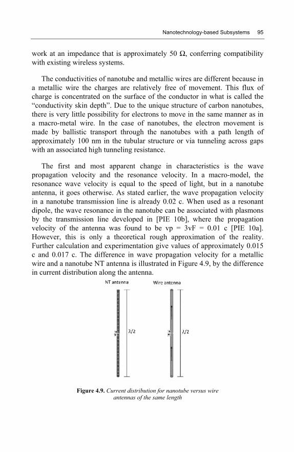
Nanotechnology-based Subsystems 95
work at an impedance that is approximately 50 Ω, conferring compatibilitywith existing wireless systems.
The conductivities of nanotube and metallic wires are different because ina metallic wire the charges are relatively free of movement. This flux ofcharge is concentrated on the surface of the conductor in what is called the“conductivity skin depth”. Due to the unique structure of carbon nanotubes,there is very little possibility for electrons to move in the same manner as ina macro-metal wire. In the case of nanotubes, the electron movement ismade by ballistic transport through the nanotubes with a path length ofapproximately 100 nm in the tubular structure or via tunneling across gapswith an associated high tunneling resistance.
The first and most apparent change in characteristics is the wavepropagation velocity and the resonance velocity. In a macro-model, theresonance wave velocity is equal to the speed of light, but in a nanotubeantenna, it goes otherwise. As stated earlier, the wave propagation velocityin a nanotube transmission line is already 0.02 c. When used as a resonantdipole, the wave resonance in the nanotube can be associated with plasmonsby the transmission line developed in [PIE 10b], where the propagationvelocity of the antenna was found to be vp = 3vF = 0.01 c [PIE 10a].However, this is only a theoretical rough approximation of the reality.Further calculation and experimentation give values of approximately 0.015c and 0.017 c. The difference in wave propagation velocity for a metallicwire and a nanotube NT antenna is illustrated in Figure 4.9, by the differencein current distribution along the antenna.
Figure 4.9. Current distribution for nanotube versus wireantennas of the same length

96 Nanoscale Microwave Engineering
Some recent papers deal with the theoretical study of the interaction of1D electronic systems with microwave radiation, leading to a quantitativetheory of CNT antenna performance. Since CNTs can be developed havinglengths in the order of centimeters, and can be metallic, a natural topic is toconsider CNTs for centimeter and millimeter wave antenna applications. Infact, one of the technical issues that scientists have to face to bringnanotechnologies to reality is the communication and data exchange betweenthe nano-sized devices or organisms and the macro-world.Using nanoantennas based on CNTs for wireless communications couldsolve this issue.
4.3.5. Challenges for future applications
4.3.5.1. THz wireless communications
Due to the increasing demand for wireless communication, requirementsfor more bandwidth and consequently an implied increase in carrierfrequency for communications and data transfers have been deployed.
The main interests in the field of THz wireless communications havebeen extensively described, recalling some basic parameters such as theultralarge bandwidth capacity compared with microwave systems, the betterdirectionality and the “security” associated with the ultralarge bandwidth[FED 10]
Compared to IR systems, THz radiations have lower attenuation underconstraint atmospheric conditions such as fog. THz radiation appears as aviable solution for the last mile and first mile problems [SAB 09a,COH 10] (the last and first mile problems refer to establishing broadband,multiuser local wireless connections with high-speed networks, i.e.fiber-optical).
Basic considerations of THz and sub-THz communication are discussedincluding:
1) free space versus guided waves;
2) directionality;
3) scintillations;

Nanotechnology-based Subsystems 97
4) atmospheric and free-space damping including fog, rain anddust/smoke;
5) indoor versus outdoor communication.
4.3.5.1.1. Secure wireless THz communications
Many papers in the THz scientific literature claim that THz can be usedfor “secure” communications. Scenarios for secure links might includestealthy short-distance communications between vehicles – manned orunmanned – and personnel. Unmanned vehicles may require short-distancesecure communication links so that they can receive instructions/transmitdata before dispersing to conduct their remote-controlled or autonomousmission. For the link to be secure, unauthorized personnel should not be ableto identify either the data via eavesdropping on communication channels orthe presence of a communication link.
The main characteristics of THz communication for securecommunications are:
1) highly directional beams compared to microwave communications;
2) less scattering of radiation compared to IR wireless;
3) limited propagation distance due to atmospheric attenuation;
4) encryption of the beam;
5) large channel bandwidth for spread spectrum techniques that enableanti-jamming and low probability of detection systems.
4.3.5.2. Reconfigurable antennas
This field appears as a very hot topic in the research of reconfigurableantennas and especially in the field of reconfigurable metamaterials forantenna applications.
Vardaxoglou from Loughborough University, UK studied in 2006 theimpact of the use of photoconductive switches on the reconfiguration ofmicrowave antennas opening the possibility of switching to all the requiredfrequencies, thus eliminating the need for complicated wideband andmultiband antenna solutions.

98 Nanoscale Microwave Engineering
He studied an optically reconfigurable CPW-fed coplanar stripline (CPS)dipole antenna with an optically induced frequency shift of 39.4%, which isachieved from switches in the ON state to switches in the OFF state. Theantenna shows ideal forward-plane radiation patterns and good boresightgain during switching operations. The performances of the phase shifterswere evaluated using illumination from laser light-emitting diodes (LEDs)running at various optical power levels, varied by changing the drivingcurrent to the LEDs. In his experiments, the insertion loss with the LEDs ONcan almost be maintained near the resonance frequency, and can be as low as0.7 dB at 4.2 GHz.
Recently, Tripon-Canseliet and Maci studied a new concept ofreconfigurable metasurface based on photoconductive switching.

Conclusions and Perspectives
In conclusion, we will draw some perspectives of this new field of optically controlled lowdimensionality materials. It will focus on Van der Waals hetero-structures and “beyondgraphene” materials as an example of nanoarchitectronics.
C.1. Conclusions
As discussed in this book, converged elements from recent researchresults show that microwave systems, technology and material-basedarchitectures at the nanoscale lead to a novel approach and a novel scientificarea.
As defined in the Introduction to this book, we propose to call this newarea nanoarchitectronics due to its ability to mix material research andelectromagnetic research, leading to the requirements to develop multiscaleapproaches.
Our analysis was focused on potential breakthrough technologies forfuture EM applications ranging from RF to THz due to the enhancement ofquantum effects in 2D and 1D structures [GEI 13].
As an example and following the research on 2D atomic crystals, itappears extremely powerful to assemble isolated atomic planes into designerheterostructures made layer by layer in a precisely chosen sequence. In orderto add new functionalities to graphene, research has been carried out on themodification of the graphene band structure, or its combination with othersemiconductors in hybrid devices. A promising route toward making such
Nanoscale Microwave Engineering: Optical Control of Nanodevices, First Edition. Charlotte Tripon-Canseliet and Jean Chazelas.© ISTE Ltd 2014. Published by ISTE Ltd and John Wiley & Sons, Inc.

100 Nanoscale Microwave Engineering
devices is the use of graphene in conjunction with atomic layers of transitionmetal dichalcogenides (MX2) and gallium chalcogenides (GaX), or bycreating graphene heterostructures with thin films of III-V semiconductors.
As an example, in the framework of the European Flagship Graphene, itis proposed to address the investigation of atomically thin 2D systems,including the growth and study of atomically thin 2D crystals beyondgraphene; the production of graphene heterostructures with semiconductormaterials; the investigation of their electronic and optical properties; thedevelopment of applications of hybrid systems in functional devices, and thegrowth and preparation of new layered systems for spintronics.
The application of this approach will cover the following topics:
– real-world applications in functional electronics or high-endinstrumentation development (e.g. detectors and sensors);
– new device concepts that will change the currently availabletechnologies and production methods in industrial sectors such aselectronics, energy and sensors;
– stretching the fundamental limits of miniaturization in widely useddevices.
C.2. Perspectives: beyond graphene structures for advanced microwavefunctions
Carbon-based nanostructures, such as carbon nanotubes and graphenesheets, have interesting electrical properties, which make it possible forcarbon to play the same role as silicon and III-IV alloys have in theelectronics revolution over the last five decades.
On the contrary, non-carbon-based nanostructures, such as gold, silverand zinc oxide nanoparticles, have important properties in the area of theoptical and infrared range. These properties are known as plasmonicsproperties due to the interaction of electron gas in the crystals of thesematerials with electromagnetic fields in this spectrum range.
These nanostructures can be used individually as in the case of fieldeffect transistors, nanoantennas or nanotransmission lines. They can also beused as composite structures as in the case of absorbing materials, shielding

Conclusions and Perspectives 101
screens or composite substrates. In composite structures, nanomaterials playa significant role in modifying the properties of the host material.
C.2.1. van der Waals heterostructures
These heterostructures, called van der Waals heterostructures(Figure C.1), have recently been investigated, and their unusual propertiesand new phenomena have been revealed. Research into graphene and other2D atomic crystals is intense and is likely to remain one of the leading topicsin condensed matter physics and materials science for many years. Lookingbeyond this field, isolated atomic planes can also be reassembled intodesigner heterostructures made layer by layer in a precisely chosen sequence[GEI 13].
Figure C.1. Example of van der Waals heterostructures from [GEI 13]. For a color versionof this figure, see www.iste.co.uk/tripon/nanotechnolgoy.zip
Based on Van Hove singularities as explained in Chapter 1, a new rangeof 2D heterostructures have been studied to add photoactive properties byusing semiconducting transition metal dichalcogenides (TMDC)/graphenestacks and enhanced light–matter interactions [BRI 13], leading to enhancedphoton absorption and electron-hole creation (which are collected in
102 Nanoscale Microwave Engineering
transparent graphene electrodes). This makes it possible to developextremely efficient flexible photovoltaic devices with photoresponsivityabove 0.1 A/W.
Graphene and hexagonal boron nitride (h-BN) have the same crystalstructure and have very similar lattice constants, but unlike graphene, h-BNis an insulator with a large energy bandgap of 6 eV. Most previous studieshave focused on the use of thick layers of BN as a substrate for grapheneelectronics or as a dielectric in experiments on coupled 2D electron gases.
Hexagonal boron nitride [BRI 12] is an appealing substrate because it hasan atomically smooth surface that is relatively free of dangling bonds andcharge traps. It also has a lattice constant similar to that of graphite, and haslarge optical phonon modes and a large electrical bandgap. High-qualityexfoliated mono- and bilayer graphene devices on single-crystal h-BNsubstrates, using a mechanical transfer process, have been reported[DEA 10].
The nanosheet and nanowire heterostructure provide an architecture tointegrate the extraordinary properties of 1D nanowires and 2D nanosheetsinto a 3D space. They hold great potential in applications that requestcomplex nanomaterials with multiple functionality, high surface area andefficient charge transport.
For instance, this heterostructure can be useful for solar energy asphotovoltaics and energy storage, such as supercapacitors and lithium ionbatteries.
The epitaxial NS NW heterostructure can also be very useful for otherimportant fields, such as 3D optoelectronics and sensing [CHU 13].
The most widely studied 2D material is graphene. Engineering of agraphene bandgap increases the fabrication complexity and either reducesthe mobilities to the level of strained silicon films or requires high voltages.Although single layers of molybdenum di-sulfate (MoS2) have a largeintrinsic bandgap of 1.8 eV, the recently reported mobilities were too low forpractical devices. Approaches such as the use of a hafnium oxide gatedielectric were demonstrated at room temperature with of at least200 cm2/V s, similar to that of graphene nanoribbons. Monolayer MoS2could also be substituted for graphene in applications that require thin

Conclusions and Perspectives 103
transparent semiconductors, such as optoelectronics and energy harvestingsingle-layer MoS2 transistors.
C.2.2. Beyond graphene: heterogeneous integration of graphene withother 2D semiconductor materials
Silicon atoms crystallize in bonding configurations that are similar tothose in graphene, opening up the potential for exceptional electronicproperties with possible applications in nanoscale electronics.
Silicene [RAI 13], the graphene equivalent for silicon, could open newtrends, providing new perspectives for application, especially due to itscompatibility with Si-based electronics.
Since the discovery of graphene and the tremendous growth in this fieldof research, much effort has been made to search theoretically andexperimentally for similar 2D materials composed of group IV elements,especially silicon [PAT 12]. However, silicene does not seem to exist innature nor is there any solid phase of silicon similar to graphite. As a result,pure 2D silicene layers cannot be generated by exfoliation methods asperformed initially in the case of graphene. More sophisticated methods haveto be considered for the growth or synthesis of silicene. One promisingconcept for synthesizing silicene is to deposit silicon on metal surfaces thatdo not interact strongly with the Si atoms or that do not form compounds.
In order to develop real 2D silicene sheets, Ag(111) surfaces withsix-fold top-layer symmetry [LEB 09] can be utilized, which might supportthe formation of a honeycomb Si layer.
Similar to silicene, research activities have also been devoted togermanene [BIA 13].
C.2.3. Graphene allotropes
Many 2D periodic carbon allotropes, e.g. graphyne and graphdiyne, canbe envisioned [MAL 12, HIR 10]. Graphynes and graphdiynes are built fromtriple- and double-bonded units of two carbon atoms. Examples are given inFigure I.1. Many graphynes and graphdiynes including those depicted inFigure C.2 can be assumed to be chemically stable.

104 Nanoscale Microwave Engineering
Figure C.2. Structures of graphene and graphynes: a) graphene, b) α−graphyne,c) β−graphyne and d) 6,6,12-graphyne. In all cases, there is only one resonance structure, i.e.one of several equivalent Lewis structures
All these areas of “beyond graphene” enhance the need fornanoarchitectronics simulation and design tools, methods, growth andtechnologies, which will be the main area in physics from our point of viewover the next 10 years.

Bibliography
[ALA 09] ALAGARASI A., “Introduction to nanomaterials,” in VISWANATHAN B.(ed.), Nanomaterials, Narosa Publishing House, 2009.
[ALU 07] ALU A., SILVEIRINHA M.G., SALANDRINO A., et al., “Epsilon-near-zerometamaterials and electromagnetic sources: tailoring the radiation phasepattern”, Physical Review B, vol. 75, 1555410, 2007.
[AMI 95] AMIRTHARAJ P.M., SEILER D.G., “Optical properties of semiconductors”,Handbook of Optics, McGraw Hill, 1995.
[AND 89] ANDERSSON I., ENG S.T., “Phase and amplitude characteristics of InP:Femodified interdigitated gap photoconductive microwave switches”, IEEETransactions on Microwave Theory and Techniques, vol. 37, no. 4, pp. 729–733,April 1989.
[AND 13] ANDRYIEUSKI A., LAVRINENKO A.V., “Graphene metamaterials basedtunable terahertz absorber: effective surface conductivity approach”, OpticsExpress, vol. 21, no. 7, pp. 9144–9155, 2013.
[ATT 12] ATTIYA A.M., “From nanotechnology in RF and microwave applications:review article”, 29th National Radio Science Conference (NRSC 2012), CairoUniversity, Egypt, 2012.
[AUS 83] AUSTON D.H., “Impulse response of photoconductors in transmissionlines”, IEEE Journal of Quantum Electronics, vol. QE-19, no. 4, pp. 639–648,April 1983.
[AUS 84] AUSTON D.H., CHEUNG K.P., SMITH P.R., “Picosecond photoconductiveHertzian dipoles”, Applied Physics Letters, vol. 45, pp. 284–286, 1984.
Nanoscale Microwave Engineering: Optical Control of Nanodevices, First Edition. Charlotte Tripon-Canseliet and Jean Chazelas.© ISTE Ltd 2014. Published by ISTE Ltd and John Wiley & Sons, Inc.
106 Nanoscale Microwave Engineering
[AVO 05] AVOURIS P., RADOSAVLJEVIC M., WIND S.J., “CNT electronics andoptoelectronics”, in ROTKIN S.V., SUBRAMONEY S. (eds), Applied Physics ofCarbon Nanotubes: Fundamentals of Theory, Optics and Transport Devices,NanoScience and Technology, Springer, Berlin/Heidelberg, pp. 227–251, 2005.
[AVO 10] AVOURIS P., “Graphene: electronic and photonic properties and devices”,Nano Letters, vol. 10, pp. 4285–4294, 2010.
[BAL 05] BALANIS C.A., Antenna Theory: Analysis and Design, 3rd ed., Wiley-Interscience, 2005.
[BIA 13] BIANCO E., BUTLER S., JIANG S., et al., “Stability and exfoliation ofgermanane: a germanium graphane analogue”, ACS Nano, vol. 7, pp. 4414–4421, 2013.
[BRI 12] BRITNELL L., GORBACHEV R.V., JALIL R., et al., “Atomically thin boronnitride: a tunnelling barrier for graphene devices”, Nano Lett., vol. 12, no. 3,pp. 1707–1710, 2012.
[BRI 13] BRITNELL L., RIBEIRO R.M., ECKMANN A., et al., “Strong light matterinteractions in heterostructures of atomically thin films”, Science 14, vol. 340,no. 6, June 2013.
[BRY 06] BRYLLERT T., WERNERSSON L.E., FROBERG L.E., et al., “Vertical high-mobility wrap-gated InAs nanowire transistor”, IEEE Electron Device Letters,vol. 27, no. 5, pp. 323–325, May 2006.
[BUR 04a] BURKE P.J., “Lüttinger liquid theory as a model of the gigahertzelectrical properties of Carbon nanotubes (erratum)”, IEEE Transactions onNanotechnologies, vol. 3, no. 2, pp. 331–331, March 2004.
[BUR 04b] BURKE P.J., “AC performances of nanoelectronics: towards a THznanotube transistor”, Solid State Electronics, vol. 40, no. 10–11, pp. 1981–1986,2004.
[BUR 06] BURKE P.J., LI S., YU Z., “Quantitative theory of nanowire and nanotubeantenna performance”, IEEE Transactions on Nanotechnology, vol. 5, no. 4,pp. 314–334, July 2006.
[CAN 03] CANSELIET C., ALGANI C., DESHOURS F., et al., “Contrôle optiqued'antennes à balayage par photoconduction – Application à un réseau d'antennesintégrées sur GaAs”, Optique Hertzienne et Diélectrique, Calais, France,September 2003.
[CAS 76] CASTAGNÉ R., LAVAL S., LAVAL R., “Picosecond 1-wavelengthoptoelectronic gate”, Electronics Letters, vol. 12, no. 17, pp. 438–439, August1976.

Bibliography 107
[CAS 06] CASTRO NETO A.H., GUINEA F., PERES N.M.R., “Drawing conclusionsfrom graphene”, Physics World, vol. 19, pp. 1–5, November 2006.
[CAS 09] CASTRO NETO A.H., GUINEA F., PERES N.M.R., et al., “The electronicproperties of graphene”, Reviews of Modern Physics, vol. 81, pp. 109–162, 2009.
[CHA 08a] CHAN C.K., PENG H.L., LIU G., et al., “High-performance lithiumbattery anodes using silicon nanowires”, Nature Nanotechnology, vol. 3, no. 1,pp. 31–35, January 2008.
[CHA 08b] CHANG P.-C., LU J.G., “ZnO nanowire field-effect transistors”, IEEETransactions on Electron Devices, vol. 55, no. 11, pp. 2977–2987, November2008.
[CHA 10] CHAI Y., XIAO Z., CHAN P.C.H., “Horizontally aligned carbon nanotubebundles for interconnect application: diameter-dependent contact resistance andmean free path”, Nanotechnology, vol. 21, pp. 235705–235709, 2010.
[CHA 11] CHA S.N., CHOI J.H., BAIK C.W., et al., “Perspectives on nanotechnologyfor RF and terahertz electronics”, IEEE Transactions on Microwave Theory andTechniques, vol. 59, no. 10, pp. 2709 – 2718, 2011.
[CHE 10] CHEN H., XI N., LAI K.W.C., et al., “Development of infrared detectorsusing single carbon-nanotube-based field-effect transistors”, IEEE Transactionson Nanotechnology, vol. 9, no. 5, pp. 582–589, September 2010.
[CHE 13] CHEN P.-Y., ALU A., “All-graphene terahertz analog nanodevices andnanocircuits”, 7th European Conference on Antennas and Propagation(EUCAP’13), Gothenburg, Sweden 2013.
[CHE 97] CHEN E., CHOU S.Y., “Characteristics of coplanar transmission lines onmultilayer substrates: modeling and experiments”, IEEE Transactions OnMicrowave Theory and Techniques, vol. 45, no. 6, June 1997.
[CHO 10] CHOI S., et al., “Design of efficient terahertz antennas: CNT versus gold”,Apsursi, pp. 1–1, Toronto, 2010
[CHO 92] CHOU S.Y., LIU M.Y., “Nanoscale terahertz metal-semiconductor-metalphotodetectors”, IEEE Journal of Quantum Electronics, vol. 28, no. 10,pp. 2358–2368, 1992.
[CIU 10] CIU X., et al., “Sphere on pillar optical nano-antennas”, IEEENanotechnology Materials and Devices Conference (NMDC), vol. 171, pp. 171–176, 2010.
[COH 10] COHEN M.L., ZETTL A., “The physics of boron nitride nanotubes”,Physics Today, pp. 34–38, November 2010.

108 Nanoscale Microwave Engineering
[COM 05] COMINI E., FAGLIA G., SBERVEGLIERI G., et al., “Tin oxide nanobeltselectrical and sensing properties,” Sensors and Actuators B: Chemical, vol. 111,pp. 2–6, November 2005.
[COM 08] COMBRIÉ S., DE ROSSI A., TRAN Q., et al., “GaAs photonic crystal cavitywith ultrahigh Q: microwatt nonlinearity at 1.55 µm”, Optical Letters, vol. 33,pp. 1908–1910, 2008.
[COS 09] COSCIA U., AMBROSONE G., AMBROSIO A., et al., “Photoconductivity ofmultiwalled CNT deposited by CVD”, Solid State Sciences, vol. 11, no. 10,pp. 1806–1809, 2009.
[COU 08] COUTAZ J.L., (ed.), Optoélectronique THz, EDP Sciences, 2008.
[CUI 03] CUI Y., ZHONG Z.H., WANG D.L., et al., “High performance siliconnanowire field effect transistors”, Nano Letters, vol. 3, no. 2, pp. 149–152,February 2003.
[CUR 08] CURUTCHET A., THÉRON D., WERQUIN M., et al., “Nonlinearcharacterization and modeling of carbon nanotube field-effect transistors”,IEEE Transactions on Microwave Theory and Techniques, vol. 56, no. 7,pp. 1505–1510, July 2008.
[DAI 11] DAI X., WANG J., LARRUE A., et al., “GaAs nanowire field-effect-transistors for RF applications”, International Conference on Materials forAdvanced Technologies (ICMAT 2011), Singapore, 2011.
[DE 06] DE CAMARGO E CASTRO L., Modeling of carbon nanotube field-effecttransistors, PhD Thesis, University of British Columbia, 2006.
[DE 81] DE SALLES A.A.A., “Optical control of GaAs MESFET’s”, IEEETransaction on Microwave Theory & Technology, vol. MTT-31, pp. 812–820,1981.
[DEA 10] DEAN C.R., YOUNG A.F., MERIC I., et al., “Boron nitride substrates forhigh-quality graphene electronics”, Nature Nanotechnology, vol. 5, pp. 722–726,2010.
[DEC 11] DECROSSAS E., El-GHAZALY S.M., “Microwave dielectriccharacterization of carbon nanotube networks”, in BIANCO S. (ed.), MaterialsScience, Composite Materials “Carbon Nanotubes: From Research toApplications”, Intech, 2011.
[DEC 12] DECROSSAS E., El SABBAGH M. A., HANNA V. F., et al., “Rigorouscharacterization of carbon nanotube complex permittivity over a broadband ofRF Frequencies”, IEEE Transactions on Electromagnetic Compatibility,vol. 54, pp. 81–87, February 2012.

Bibliography 109
[DID 62] DIDOMENICO M., SVELTO Jr. O., PANTELL R.H. et al., “Optical frequencymixing in bulk semiconductors”, Applied Physics Letters, vol. 1, no. 4,pp. 77–79, 1962.
[DRA 07] DRAGOMAN M., DRAGOMAN D., MULLER A.A., “High frequency devicesbased on graphene”, International Semiconductor Conference (CAS ’07), pp. 53–56, Sinaia, Romania 2007.
[DRE 05] DRESSELHAUS M.S., DRESSELHAUS G., SAITO R., et al., “Ramanspectroscopy of carbon nanotubes”, Physics Reports, vol. 409, pp. 47–99, 2005.
[ENG 06] ENGHETA N., ZIOLKOWSKI R.W. (eds), Metamaterials: Physics andEngineering Explorations, John Wiley & Sons, New York, 2006.
[ENG 07] ENGHETA N., “Circuits with light at nanoscales: optical nanocircuitsinspired by metamaterials”, Science, vol. 317, pp. 1698–1702, September 2007.
[EL 09a] EL SABBAGH M.A., EL-GHAZALY M.A.,“Miniaturized carbon nanotube-based RF resonator”, IEEE MTT-S International Microwave Symposium Digest,Boston, MA, 7–12 June 2009.
[EL 09b] EL SABBAGH M.A., EL-GHAZALY S.M., NASEEM H.A., “Carbonnanotube-based planar transmission lines”, IEEE MTT-S InternationalMicrowave Symposium Digest, Boston, MA, 7–12 June 2009.
[EL 09c] EL SABBAGH M.A., EL-GHAZALY S.M., “Frequency-dependent circuitmodels of carbon nanotube networks”, Electrical Performance of ElectronicPackaging and Systems, Portland, OR, 19–21 October 2009.
[EST 09] ESTACIO E., et al., 34th International Conference on Infrared, Millimeter,and Terahertz Waves, Busan, pp. 773–774, 21–25 September 2009.
[FAC 05] FACI S., et al., “Modélisation électrique non linéaire dephotocommutateurs microrubans pour la conception de circuits microondesactifs et passifs commandés par voie optique”, 14ème Journées NationalesMicroondes, Nantes, France, May 2005.
[FED 10] FEDERICI J., MOELLER L., “Review of terahertz and subterahertz wirelesscommunications”, Journal of Applied Physics, vol. 107, pp. 111101, 2010.
[FEK 11] FEKECS A., BERNIER M., MORRIS D., et al., “Fabrication of highresistivity cold-implanted InGaAsP photoconductors for efficient pulsedterahertz devices,” Optical Materials Express, vol. 1, pp. 1165–1177, 2011.
[FIT 07] FITCHTNER N., et al., “Investigation of copper and carbon nanotubesantennas using thin wire integral equations”, IEEE Asia Pacific MicrowaveConference (APMC), Asia-Pacific, 2007.

110 Nanoscale Microwave Engineering
[FRE 03] FREITAG M., MARTIN Y., MISEWICH J.A., et al., “Photoconductivity ofsingle carbon nanotubes”, Nano Letters, vol. 3, no. 8, pp. 1067–1071, 2003.
[FRI 13] FRIEDLEIN R., FLEURENCE A., OZAKI T., et al., “Silicene: atom-thicksilicon with tunable properties”, SPIE Newsroom, 7 June 2013.
[FRO 92] FROBERG N.M., HU B.B., ZHANG X.-C., AUSTON D.H., et al., “Terahertzradiation from a photoconducting antenna array”, Quantum Electronics, IEEEJournal of, vol. 28, no. 10, pp. 2291–2301, October 1992.
[GAN 04] GANGLOFF L., MINOUX E., TEO K.B.K., et al. “Self-aligned, gated arraysof individual nanotube and nanowire emitters”, Nano Letters, vol. 4, no. 9, pp.1575–1579, July 29 2004.
[GAN 13] GAN X., SHIUE R.-J., GAO Y., et al., “Chip-integrated ultrafast graphenephotodetector with high responsivity”, Nature Photonics, 15 September 2013.
[GEI 13] GEIM A.K., GRIGORIEVA I.V., “Van der Waals heterostructures”, Nature,vol. 499, pp. 419–425, 2013.
[GOM 12] GOMEZ-DIAZ J.S., PERRUISSEAU-CARRIER J., “Microwave to THzproperties of graphene and potential antenna applications”, Proceedings of ISAP,2012.
[GRA 12] GRAHAM C., GWILLIAM R., SEEDS A., “Nitrogen ion implanted InP basedphoto-switch”, Optics Express, vol. 20, no. 2, November 2012.
[GUO 06] GUO Y., et al., “Theoretical investigation on photoconductivity of singleintrinsic carbon nanotubes”, Applied Physics Letters, vol. 88, pp. 133111, 2006.
[HAN 05] HANSON G.W., “Fundamental transmitting properties of carbon nanotubeantennas”, IEEE Transaction on Antennas and Propagation, vol. 53, no. 11,pp. 3426–3435, November 2005.
[HAQ 06] HAQUE S., MARINELLI C., UDREA F., et al., “Absorption characteristicsof single wall carbon nanotubes”, NSTI Nanotechnology Conference, vol. 1,pp. 134–137, 2006.
[HAT 11] HATEM O., CUNNINGHAM J., LINFIELD E.H., et al., “Terahertz-frequencyphotoconductive detectors fabricated from metal-organic chemical vapordeposition-grown Fe-doped InGaAs”, Applied Physics Letters, vol. 98, no. 12,pp. 121107, 2011.
[HER 02] HERTEL T., et al., “Charge-carrier dynamics in single-wall carbonnanotube bundles: a time-domain study”, Applied Physics A, vol. 75, pp. 449–465, 2002.
[HES 10] HESHMAT B., et al., “Evaluation of carbon nanotubes for THzphotomixing”, Radar Conference, Washington DC, pp. 1176–1179, May 2010.

Bibliography 111
[HOC 08] HOCHBAUM A.I., CHEN R.K., DELGADO R.D., et al., “Enhancedthermoelectric performance of rough silicon nanowires”, Nature, vol. 451,no. 7175, pp. 163–167, January 2008.
[HUA 08] HUANG Y., et al., “Performance predication of carbon nanotubes bundledipole antenna”, IEEE Transactions on Nanotechnology, vol. 7, pp. 331–337,2008.
[IIJ 91] IIJIMA S., “Helical microtubules of graphitic carbon”, Nature, vol. 354,pp. 56–58, 1991.
[JAV 13] JAVEY A., “2D semiconductors: materials, interfaces, and devices”, 224thECS Meeting, The Electrochemical Society, San Francisco, CA, 2013.
[JOH 05] JOHANSSON A., WIDENKVIST E., LU J., “Fabrication of high-aspect-ratioprussian blue nanotubes using a porous alumina template”, Nano Letters, vol. 5,pp. 1603–1606, 2005.
[JOR 10] JORNET J.M., et al., “Graphene-based nano-antennas for electromagneticnanocommunications in the terahertz band”, Proceedings of the 4th EuropeanConference on Antennas and Propagation (EuCAP), Barcelona, Spain,12–16 April 2010.
[KAS10] KASSEM H., VIGNERAS V. LUNET G., “Characterization techniques formaterials’ properties measurement”, in MININ I. (ed.), Microwave and MillimeterWave Technologies from Photonic Bandgap Devices to Antenna andApplications, 2010.
[KIN 10] KINOSHITA M., STEINER M., ENGEL M., et al., “The polarized carbonnanotube thin film LED”, Optics Express, vol. 18, pp. 25738–25745, 2010.
[KLE 13] KLEKACHEV A.V., NOURBAKHSH A., ASSELBERGHS I., et al., “Graphenetransistors and photodetectors”, The Electrochemical Society Interface, Spring2013.
[KOK 10] KOKSAL C.E., et al., “Design and analysis of systems based on RFreceivers with multiple CNT antennas”, Nano Communication Networks, vol. 1,pp. 160–172, 2010.
[LEB 09] LEBÈGUE S., ERIKSSON O., Physical Review B, vol. 79, pp. 115409–1,115409–4, 2009.
[LEY 09] LEYMAN R., CARNEGIE D., BAZIEVA N., et al., “Characterisation ofInAs:GaAs quantum dot-based photoconductive THz Antennas”, 34thInternational Conference on Infrared, Millimeter, and Terahertz Waves,pp. 773–774, September 2009.
112 Nanoscale Microwave Engineering
[LEY 13] LEYMAN R., CARNEGIE D., BAZIEVA N., et al., “Characterisation ofInAs:GaAs quantum dot-based photoconductive THz antennas”, IEEE PhotonicsConference (IPC), pp. 418–419, 2013.
[LI 13] LI C., YU Y., CHI M., et al., “Epitaxial nanosheet-nanowireheterostructures”, Nano Letters, vol. 13, pp. 948−953, 2013.
[LID 92] LIDEIKIS T., NAUDZIUS K., TREIDERIS G., et al., “Picosecond GaAs andInGaAs photocnductive switches obtained by low-temperature meta-organicchemical vapour deposition”, Semiconductor Science and Technology, vol. 7,pp. 845–849, 1992.
[LIN 02] LIN W.Z., LIU Z.G., LLAO R., et al., “Characterization of femtosecondlow-temperature grown GaAs photoconductive switch”, Chinese Physics Letters,vol. 19, no. 4, pp. 557–559, 2002.
[LIN 97] LIN G.-R., PAN C.-L., “Picosecond responses of low dosage arsenic-ion-implanted GaAs photoconductors”, Applied Physics Letters, vol. 71, no. 20,pp. 2901–2903, November 1997.
[LIU 05] LIU F., BAO M., WANG K.L., et al., “One dimensional transport of In2O3nanowires,” Applied Physics Letters, vol. 86, no. 21, pp. 213–101, May 2005.
[LIU 09] LIU Y., et al., “Alignment enhanced photoconductivity in single wallcarbon nanotube films”, Nanotechnlogy, vol. 20, no. 8, pp. 035203, 2009.
[LLA 12] LLATSER I., KREMERS C., CHIGRIN D.N., et al., “Radiation characteristicsof tunable graphennas in the terahertz band”, Radioengineering, vol. 21, no. 4,pp. 946–953, 2012.
[LOV 12] LOVAT G., “Equivalent circuit for electromagnetic interaction andtransmission through graphene sheets”, IEEE Transactions on ElectromagneticCompatibility, vol. 54, no. 1, 2012.
[MAK 08] MAK K.F., SFEIR M.Y., WU Y., et al., “Measurement of the opticalconductivity of graphene”, Physical Review Letters, vol. 101, pp. 196405–1,196405–4, 2008.
[MAN 07] MANGENEY J., CHIMOT N., MEIGNIEN L., et al., “Emissioncharacteristics of ion-irradiated In0.53Ga0.47As based photoconductive antennasexcited at 1.55 μm”, Optics Express, vol. 15, pp. 8943–8950, 2007.
[MAR 98] MARTEL R., SCHMIDT T., SHEA H.R., et al., Applied Physics Letters,vol. 73, pp. 2447–2449, 1998.
[MAR 03] MARTENSSON T., BORGSTROM M., SEIFERT W., et al., Nanotechnology,vol. 14, pp. 1255–1258, 2003.

Bibliography 113
[MCI 97] MCINTOSH K.A., NICHOLS K.B., VERGHESE S., et al., “Investigation ofultrashort photocarrier relaxation times in low-temperature-grown GaAs”,Applied Physics Letters, vol. 70, no. 3, pp. 354–356, 1997.
[MÉL 04] MÉLIN T., DIESINGER H., DERESMES D., et al., “Probing nanoscaledipole-dipole interactions by electric force microscopy”, Physics Review Letters,vol. 92, pp. 166101, 2004.
[MER 08] MERIC I., BAKLITSKAYA N., KIM P., et al., “RF performance of top-gated,zero-bandgap graphene field-effect transistors,” IEDM Technical Digest, pp. 1–4, 2008.
[MEY 05] MEYYAPAN M., Carbon Nanotubes: Science and Applications, 1st ed.,CRC Press LLC, FL, 2005.
[MIN 01] MINAMI N., KAZAOUI S., JACQUEMIN R., et al., “Optical properties ofsemiconducting and metallic single wall carbon nanotubes: effects of doping andhigh pressure”, Synthetic Metals, vol. 116, pp. 405–409, 2001.
[MIN 04] MINOUX E., TEO K.B.K., VINCENT P., et al., “Self-aligned, gated arrays ofindividual nanotube and nanowire emitters”, Nano Letters, vol 4, n°9,pp 1575–1579, July 29, 2004
[NG 04] NG H.T., HAN J., YAMADA T., et al., “Single crystal nanowire verticalsurround-gate field-effect transistor”, Nano Letters, vol. 4, pp. 1247, 2004.
[NIL 08] NILSSON H.A., DUTY T., ABAY S., et al., “A radio frequency single-electron transistor based on an InAs”, Nano Letters, vol. 8, no. 3, pp. 872–875,March 2008.
[NOU 09] NOUGARET L., HAPPY H., DAMBRINE G., et al., “80 GHz field-effecttransistors produced using high purity semiconducting single-walled carbonnanotubes”, Applied Physics Letters, vol. 94, pp. 243505–1, 243505–3, 2009.
[NOV 04] NOVOSELOV K.S., GEIM A.K., MOROZOV S.V., et al., “Electric fieldeffect in atomically thin carbon films”, Science, vol. 306, pp. 666–669, 2004.
[OBE 11] OBENG Y., SRINIVASAN P., “Graphene: is it the future forsemiconductors?”, The Electrochemical Interface, pp. 47–52, Spring 2011.
[ORT 01] ORTIZ V., STELLMACHER M., MARCADET X., et al., “Control of low-temperature-grown GaAs for ultrafast switching applications”, vol. 4280,Proceedings of the SPIE, 23 pp. 202–210, April 2001.
[PAC 09] PACEBUTAS V., BERTULIS K., ALEKSEJENKO G., et al., “Molecular-beam-epitaxy grown GaBiAs for terahertz optoelectronic applications”, Journal ofMaterials Science: Materials in Electronics, vol. 20, pp. S363–S366, 2009.

114 Nanoscale Microwave Engineering
[PAS 08] PASSACANTANDO M., BUSSOLOTTI F., GROSSI V., et al.,“Photoconductivity in defective carbon nanotube sheets under ultraviolet–visiblenear infrared radiation”, Applied Physics Letters, vol. 93, no. 5, pp. 051911–051913, 2008.
[PED 04] PEDERSEN T.G., “Exciton effects in carbon nanotubes”, Carbon, vol. 42,nos. 5–6, pp. 1007–1010, 2004.
[PEN 99] PENDRY J.B., HOLDEN A.J., ROBBINS D.J., et al., “Magnetism fromconductors and enhanced nonlinear phenomena”, IEEE Transactions onMicrowave Theory and Techniques, vol. 47, no. 11, pp. 2075–2084, November1999.
[PEN 07] PENDRY J.B., “Metamaterials and the control of electromagnetic fields”,Conference on Coherence and Quantum Optics OSA Technical Digest (CD)(Optical Society of America), paper CMB2, 2007.
[PIE 10a] PIERANTONI L., “RF nanotechnology–concept, birth, mission, andperspectives”, IEEE Microwave Magazine, vol. 11, no. 4, pp. 130–137, June2010.
[PIE 10b] PIERANTONI L., COCCETTI F., “Radio-frequency nanoelectronics: a newparadigm in electronic systems design”, Proceedings of Asia-Pacific MicrowaveConference, Yokohama, Japan, 2010.
[POS 13] POSPISCHIL A., HUMER M., FURCHI M.M., et al., “CMOS-compatiblegraphene photodetector covering all optical communication bands”, NaturePhotonics, pp. 892–896, 2013.
[QIN 08] QIN Y., WANG X.D., WANG Z.L., “Microfibre-nanowire hybrid structurefor energy scavenging”, Nature, vol. 451, no. 7180, pp. 809–813, February 14,2008.
[QIU 05] QIU X., FREITAG M., PEREBEINOS V., et al., “Photoconductivity spectra ofsingle-carbon nanotubes: implications on the nature of their excited states”, NanoLetters, vol. 5, pp. 749–752, 2005.
[RAD 11] RADISAVLJEVIC B., RADENOVIC A., BRIVIO J., et al., “Single-layer MoStransistors”, Nature Nanotechnology, vol. 6, pp. 147–150, 2011.
[RAF 04] RAFAILOV E.U., et al., “Photonics technology letters”, IEEE, vol. 16,pp. 2439–2441, 2004.
[RUB 94] RUBIO A., CORKHILL J.L., COHEN M.L., “Theory of graphitic boronnitride nanotubes”, Physical Review B, vol. 49, no. 7, pp. 5081–5084, February1994.
[ROS 55] ROSE A., “Performance of photoconductors”, Proceedings of the IRE,vol. 43, no. 12, pp. 1850–1869, December 1955.

Bibliography 115
[ROS 98] ROSENCHER E., VINTER B., Optoélectronique, Masson, Paris, France,1998.
[ROU 11] ROUX J.F., DELORD J.M., COUTAZ J.L., “RF frequency response ofphotoconductive samplers”, IEEE Journal of Quantum Electronics, vol. 47, no.2, pp. 223–229, 2011.
[RUS 10] RUSSER P., FICHTNER N., LUGLI P., et al., “Nanoelectronics-basedintegrated antennas”, IEEE Microwave Magazine, pp. 58–71, December 2010.
[RUT 09] RUTHERGLEN C., JAIN D., BURKE P., “Nanotube electronics forradiofrequency applications”, Nature Nanotechnology, vol. 4, pp. 811–819,2009.
[SAI 98] SAITO R., DRESSELHAUS G., DRESSELHAUS M.S., Physical Properties ofCarbon Nanotubes, 1st ed., Imperial College Press, London, 1998.
[SAI 06] SAIB A., BEDNARZ L., DAUSSIN R., et al., “Carbon nanotube compositesfor broadband microwave absorbing materials”, IEEE Transactions onMicrowave Theory and Techniques, vol. 54, no. 6, pp. 2745–2754, 2006.
[SAL 07] SALEH B.E.A., TEICH M.C., Fundamentals of Photonics, WileyInterscience, 2007.
[SAR 08] SARTORIUS B., ROEHLE H., KÜNZEL H., et al., “All-fiber terahertz time-domain spectrometer operating at 1.55 μm telecom wavelengths”, OpticsExpress, vol. 16, no. 13, 9565–9570, June 2008.
[SCH 06] SCHROEDER D.K., Semiconductor Material and Device Characterization,Wiley, 2006.
[SCH 10] SCHWIERZ F., “Graphene transistors”, Nature Nanotechnology, vol. 5,pp. 487–496, July 2010.
[SMI 73] SMITH W., “Effect of light on selenium during the passage of an electriccurrent”, Nature, p. 303, February 1873.
[SMI 00] SMITH D.R., PADILLA W.J., VIER D.C., et al., “Composite medium withsimultaneously negative permeability and permittivity”, Physical Review Letters,vol. 84, no. 18, pp. 4184–4187, 2000.
[SOU 12] SOUNAS D.L., CALOZ C., “Gyrotropy and nonreciprocity of graphene formicrowave applications”, IEEE Transactions on Microwave Theory andTechniques, vol. 60, no. 4, pp. 901–914, 2012.
[STE 12] STEINER M., ENGEL M., LIN Y.-M., et al., “High-frequency performanceof scaled carbon nanotube array field-effect transistors”, Applied Physics Letters,vol. 101, pp. 053123–4, 2012.

116 Nanoscale Microwave Engineering
[STO 09] STOKES P., LIU L.W., ZOU J.H., et al., “Photoresponse in large areamultiwalled carbon nanotube, polymer nanocomposite films”, Applied PhysicsLetters, vol. 94, pp. 042110–042113, 2009.
[SUN 08] SUN J.L., XU J., ZHU J.L., et al., “Disordered multiwalled carbonnanotube mat for light spot position detecting”, Applied Physics A: MaterialScience & Processing, vol. 91, no. 2, pp. 229–233, 2008.
[SUN 11] SUN Y., RUSLI, SINGH N., “Room-temperature operation of silicon single-electron transistor fabricated using optical lithography”, IEEE Transactions onNanotechnology, vol. 10, no. 1, pp. 96–98, 2011.
[TAN 96] TAN H.K., JAGADISH C., KORONA K.P., et al., “Ion-implanted GaAs forsubpicosecond optoelectronic applications”, IEEE Journal of Selected Topics inQuantam Electronics, vol. 2, pp. 636–642, 1996.
[TAN 98] TANS S.J., VERSCHUEREN A.R.M., DEKKER C., “Room-temperaturetransistor based on a single carbon nanotube”, Nature, vol. 393, no. 49,pp. 49–52, 1998.
[TAN 13] TAN K.H., YOON S.F., WICAKSONO S., et al., “Low temperature grownGaNAsSb: a promising material for photoconductive switch application”,Applied Physics Letters, vol. 103, no. 11, pp. 111113, 1–4, 2013.
[TRI 06] TRIPON-CANSELIET C., FACI S., BLARY K., et al., “Optically-controlledmicrowave phase shifting and sampling by efficient photoconductive switchingon LT-GaAs substrate integrated technology”, International Conference onApplication of Photonic Technology, Quebec, Canada, June 2006.
[TRI 11] TRIPON-CANSELIET C., FACI S., HAPPY H., et al., “Optically controllednanotechnologies for microwave integrated devices”, IEEE InternationalNanoElectronics Conference (INEC), Taipei, Taiwan, 2011.
[TRI 12] TRIPON-CANSELIET C., FACI S., PAGIES A., et al., “Microwave on/off ratioenhancement of GaAs photoconductive switches at nanometer scale, IEEEJournal of Lightwave Technology, vol. 1, no. 12, pp. 3576–3579, 2012.
[TRI 13] TRIPON-CANSELIET C., FACI S., DECOSTER D., et al., “Nanophotoconductive switches for microwave applications”, Proceedings of SPIEPhotonics West, San Francisco, CA, 2013.
[TRI 14] TRIPON-CANSELIET C., XAVIER S., MODREANU M., et al., NEMO 2014,2014.
[VAN 07] VAN ZEGHBROECK B., Principles of Semiconductor Devices, ColaradoUniversity, 2007.

Bibliography 117
[VEY 80] VEYRES C., HANNA V.F., “Extension of the application of conformalmapping techniques to coplanar lines with finite dimensions”, InternationalJournal of Electronics, vol. 48, pp. 47–56, 1980.
[VIT 12] VITIELLO M.S., VITI L., ROMEO L., et al., “Semiconductor nanowires forhighly sensitive, room-temperature detection of terahertz quantum cascade laseremission”, Applied Physics Letters, vol. 100, p. 241101, 2012.
[VOG 12] VOGT P., DE PADOVA P., QUARESIMA C., et al., “Silicene: compellingexperimental evidence for graphene like two-dimensional silicon”, PhysicalReview Letters, vol. 108, pp. 155501–1, 155501–5, 2012.
[WAL 08] WALDEN R.H., “Analog-to-digital converters and associated ICtechnologies”, IEEE CSIC, pp. 1–2, 2008.
[WAL 99] WALDEN R.H., “Analog-to-digital converter survey and analysis”, IEEEJournal on Selected Areas in Communications, vol. 17, no. 4, pp. 539–550, April1999.
[WAN 08] WANG Y., et al., “Properties of terahertz wave generated by the metalliccarbon nanotube antenna”, Chinese Optics Letters, vol. 6, no. 10, pp. 770–772,2008.
[WAN 09a] WANG H., NEZICH D., KONG J., et al., “Graphene frequencymultipliers”, IEEE Electron Device Letters, vol. 30, no. 5, pp. 547–549, May2009.
[WAN 09b] WANG J., LEE C.H., BANDO Y., et al., “Multiwalled boron nitridenanotubes: growth, properties, and applications”, in YAP Y.K. (ed.), B-C-NNanotubes and Related Nanostructures, Springer Science + Business Media,LLC, pp. 906–908, 2009.
[WAN 10a] WANG J., LEE C.H., YAP Y.K., “Recent advancements in boron nitridenanotubes”, Nanoscale, vol. 2, pp. 2028–2034, 2010.
[WAN 10b] WANG H., HSU A., WU J., et al., “Graphene-based ambipolar RFmixers”, IEEE Electron Device Letters, vol. 31, no. 9, pp. 906–908, September2010.
[WAN 12] WANG S., ZHANG Z.Y., PENG L.M., “Doping-free carbon nanotubeoptoelectronic devices”, Chinese Science Bulletin, vol. 57, nos. 2–3, pp. 149–156, 2012.
[WAN 13] WANG X., CHENG Z., XU K., et al., “High-responsivity graphene/silicon-heterostructure waveguide photodetectors”, Nature Photonics, vol. 7, pp. 888–891, 2013.
[WEI 06] WEI J., SUN J., ZHU J., et al., “Carbon nanotube macrobundles for lightsensing”, Small, vol. 2, nos. 8–9, pp. 988–993, 2006.

118 Nanoscale Microwave Engineering
[WIK] WIKIPEDIA
[WIN 02] WIND S.J., APPENZELLER J., MARTEL R., et al., Applied Physics Letters,vol. 80, pp. 3817–3819, 2002.
[WU 08] WU Q., et al., “Terahertz generation in the carbon nanotubes antenna”,IEEE, vol. 978, 2008.
[WU 12] WU Y., JENKINS K.A., VALDES-GARCIA A., et al., “State-of-the-artgraphene high-frequency electronics”, Nano Letters, vol. 12, pp. 3062–3067,2012.
[YAN 12] YANG H., HEO J., PARK S., et al., “Graphene barristor, a triode devicewith a gate-controlled Schottky barrier”, Science, vol. 336, pp. 1140–1143, 2012.
[YEN 77] YEN H.W., et al., “Switching of GaAs IMPATT diode oscillator byoptical illumination”, Applied Physics Letters, vol. 31, no. 2, pp. 120–122, 1977.
[XIA 06] XIANG J., LU W., HU Y.J., et al., “Ge/Si nanowire heterostructures ashigh-performance field-effect transistors”, Nature, vol. 441, no. 7092, pp. 489–493, May 2006.
[ZHA 06a] ZHAO J., CHEN X., XIE J.R.H., “Optical properties and photonic devicesof doped carbon nanotubes”, Analytica Chimica Acta, vol. 568, nos. 1–2,pp. 161–170, May 2006.
[ZHA 06b] ZHANG M., HUO X., CHAN P.C.H., et al., “Radio-frequencycharacterization for the single-walled carbon nanotubes”, Applied PhysicsLetters, vol. 88, no. 16, pp. 163109–1631096-3, 2006.
[ZHA 10a] ZHAO Z.-Y., SCHWAGMANN A., OSPALD F., et al., “1.55 μmphotoconductive THz emitters based on ErAs:In0.53Ga0.47As superlattices”,Photonics Society Winter Topical Meeting Series (WTM), IEEE, 2010.
[ZHA 10b] ZHANG J., et al., “Length-dependent photoinduced current in vertically-aligned MWNTs forests”, Microsystem Technologies, vol. 16, pp. 2115–2118,2010.
[ZHA 13] ZHANG R., ZHANG Y., ZHANG Q., et al., “Growth of half-meter longcarbon nanotubes based on Schulz–Flory distribution,” ACS Nano, vol. 7, no. 7,pp. 6156–6161, June 2013.
[ZIA 08] ZIAEI A., BAILLIF M.L., DEMOUSTIER S., et al., “Microwave applicationsof carbon nanotubes: nano-antennas and nanoswitches”, in VARADAN V.K.,(ed.), Nanosensors and Microsensors for Bio-Systems, Proceedings of SPIE,vol. 6931, 2008.
Index
A, B
absorption spectrum, 23, 37AM demodulator, 8Auger mechanism, 19bi-exponential decay, 46Boltzmann constant, 17boron nitride nanotubes (BNNTs),6, 8, 9
bundle case, 44
C, D
carbon atoms, 2, 3, 6, 34, 35,80, 103
carrier density, 4, 14, 27, 51, 54, 57,72, 76
carrier dynamics, 45, 77carbon nanotube (CNT) transistor,60, 78
chemical vapor deposition (CVD), 7,9, 12, 83
chiral vector, 6, 7, 34Coulomb blockade, 10dichalcogenides, 6, 100, 101dielectric function, 16differential Hall effect, 52Dirac equation, 4doping density, 53, 54
E, F
electroluminescence, 35, 38electron-beam lithography, 10electronic band structure, 14, 15,23, 55
Fermi–Dirac distribution function, 18film case, 43free carriers density, 17
G, H, I
geometry, 34, 62, 77graphene monolayer, 34, 75honeycomb, 2, 3, 34, 103interfaceair/semiconductor, 22, 70CNT/metal, 39Light/semiconductor, 67metal/semiconductor, 49metal/dielectric, 45, 46, 49, 94material/metal, 13, 49semiconductor/dielectric, 5
K, L
Kramers–Krönig relation, 16, 17light polarization, 38linear optical transitions, 22Lorentzian curves, 36
Nanoscale Microwave Engineering: Optical Control of Nanodevices, First Edition. Charlotte Tripon-Canseliet and Jean Chazelas.© ISTE Ltd 2014. Published by ISTE Ltd and John Wiley & Sons, Inc.

120 Nanoscale Microwave Engineering
M, N, O
material photoconductivity, 27, 28multiwall carbon nanotubes(MWCNTs), 7, 8
nanoarchitectronics, 99, 104nanoelectronicdevices, 4, 9, 60NanoIntegris, 37, 38nanophotonic devices, 6nanowire field-effect transistors, 10nanowires (NWs), 1, 6, 9, 10, 12, 24,92, 102,
optical constants, 16, 17optoelectronic, 5, 6, 10, 13, 34, 39,40, 76, 89, 102, 103
P
permittivity, 1, 5, 8, 13, 22, 47, 48,54, 57–59, 67
photoconductance, 29, 33, 41, 45, 69photoconducting antenna, 91photoconductive switching, 66, 71,72, 98
photocurrent, 28, 38–44photolithography, 10photoluminescence, 35, 55
photomixing, 34, 38, 89photon absorption, 19, 27, 30, 32,101
Planck’s constant, 15, 20plasma-enhanced CVD, 7plasmonic materials, 5plasmonics, 1, 5, 14, 45, 100
S
sampling, 13, 65–67, 86–90Schottky barriers, 56Schrödinger equation, 4, 15semiconductor nanowires, 6, 9, 12Snell–Descartes law, 19spintronics, 5,13, 77, 79, 100static resistivity, 51subsampling, 86–88subwavelength, 5SWCNTs, 6, 7, 8, 34, 43, 80, 82, 83switching, 66, 67, 71, 72, 97, 98
T, Y, Z
two-photon absorption, 30, 32Young’s modulus, 4ZnO nanorods, 12


