Embed Size (px)
Citation preview

Sincrotrone Trieste SCpAS.S. 14 Km. 163,5 in AREA Science Park34012 Trieste ITALYwww.elettra.trieste.it - [email protected]
2 0 0 7 - 0 8e l e t t r aE L E T T R A H i g H L i g H T s > 0 7 - 0 8
ELETTRA HigHLigHTs
2007-2008


e l e t t r a2 0 0 7 - 0 8E L E T T R A H i g H L i g H T s > 0 7 - 0 8

ELETTRA HIGHLIGHTS 2007-2008EDITORIAL COMMITTEE
> Alessandro Baraldi
> Daniele Cocco
> Paolo Craievich
> Doriano Lamba
> Andrea Lausi
> Andrea Locatelli
> Laura Bibi Palatini
> Adriana Pertosi
> Kevin C. Prince
Cover Picture: Ultra High Vacuum chamber of the APE beamline
(photo by Luca Casonato)
Graphic Design: Studio Link (www.studio-link.it)
Graphart s.r.l.
Print: Graphart s.r.l.

5elettra Highlights
Publication of Elettra’s Highlights occurs this year while our efforts to relaunch the Elettra Laboratory
activities by upgrading the Elettra light source and constructing the new FERMI@Elettra fourth
generation light source are nearing their peak. Several of the Elettra machine upgrade projects have
been successfully completed in 2007, including construction of the Booster full-energy injector, upgrade of
the RF plant, and installation of a Global Orbit Feedback. Full-energy injection has already been achieved at
the time of this writing and top-up operation is scheduled for mid-2009.
We have mapped a strategy - in collaboration with our key partners and users - to take maximum advantage
of the upgraded Elettra storage ring with top-up operating mode. Important steps included the successful
workshop “New Frontiers in Insertion Devices” (November 20-21, 2006) and “The Future of Elettra” series
(May 21 and December 2-3, 2007). The scope of the workshops was to review insertion devices at the most
advanced synchrotron radiation facilities worldwide, the prospects for top-up operation at Elettra, as well as
the different undulator/wiggler beamlines at Elettra and the related upgrade plans.
Several high performance beamlines were inaugurated at Elettra and/or opened to users, including the
infrared microscopy and spectroscopy beamline SISSI in partnership with the University of Rome “La Sapienza”
and INFM-CNR, the high-resolution photoemission beamline Bad-ELPH in partnership with the University of
Augsburg, the powder diffraction beamline MCX in partnership with the University of Trento and the INSTM
Consortium, and the scanning and imaging microscopy beamline TWINMIC. In addition, award of contracts by
external public institutions made available significant resources for new development projects, such as the
construction of a second structural biology beamline (and related support laboratories) and the upgrade of the
SuperESCA and ESCAmicroscopy beamlines.
As far as the new free-electron laser (FEL) source, FERMI@Elettra, is concerned, the conceptual design
phase was concluded successfully with the publication in February 2007 of the Conceptual Design Report
(CDR), developed through scientific collaborations with the Lawrence Berkeley National Laboratory, the
Massachusetts Institute of Technology, INFN and INFM, among others. The FERMI@Elettra project was
included in the European Infrastructure Roadmap developed by ESFRI (the European Strategy Forum on
Research Infrastructures), within the network of all FEL projects in Europe, and we received funding from the
EU for the establishment of an European consortium of complementary FEL facilities (IRUVX).
The FERMI@Elettra construction phase started off with the restructuring of the management team and the
hiring in February 2007 of managers experienced in the construction of FEL light sources. An international
engineering group was retained to design all of the infrastructure of FERMI and manage the entire construction
process. Since the Summer of 2007, several feasibility studies and preliminary civil engineering construction
projects have been carried out. The photoinjector electron source has been completed with the installation of
the beam transport and diagnostics. Furthermore, the main components of the photoinjector have been
acquired from UCLA to perform the first tests on the beam in collaboration with MAX-Lab in Lund (Sweden),
a partner of Elettra in the framework of the IRUVX Consortium.
Particularly relevant in 2007 was the award of a grant by the European Research Council (ERC) to
Sincrotrone Trieste scientists for the construction of an inelastic scattering beamline for the FERMI@Elettra

6 elettra Highlights
source. The selection process by the ERC has been particularly strict: less than 3% of the submitted proposals
have been funded to date.
The Booster project and the current upgrade of the beamlines will bring Elettra on par with the most
advanced competitors and will at the same time emphasize the experience we have gained in the international
arena. The FERMI@Elettra project, the first and, at present, only seeded FEL facility under construction
worldwide, will enhance our international presence and attract new and highly qualified partners. These
developments have been made possible by a major loan from the European Investment Bank (EIB), which
recognizes the importance of the project at a pan-European level. All this strengthens the trend towards an
internationalization of Sincrotrone Trieste, and its Elettra Laboratory.
We take this opportunity to thank our employees, our Partners and external Users for their enthusiasm and
dedication over the years. We trust that with their help we will be able to meet the major challenge of fully
exploiting an upgraded Elettra light source while developing the new FEL source FERMI@Elettra.
Alfonso FranciosiChief Executive Officer
Sincrotrone Trieste S.C.p.A.

7elettra Highlights
TABLE OF CONTENTS
RESEARCH HIGHLIGHTS
Life Sciences 12
> The first structure of a bacterial S-layer protein 14
> Meriolins, a new class of cell death–inducing kinase inhibitors with enhanced selectivity
for cyclin-dependent kinases 16
> E-coli frataxin: structural characterisation of ion binding sites 18
> X-ray structure analysis of tRNAGly acceptor stem microhelices: comparison of structure and hydration 20
> High resolution structure of a plant cell wall degrading enzyme variant and short strong
hydrogen bonds in proteins 22
> Structure and membrane interaction modes of the defence peptide LL-37 and its analogues 24
> Tracking implanted mammalian cells in-vivo using synchrotron x-ray imaging 26
Surfaces and Interfaces 28
> The structure of alkanethiols monolayers self-assembled on gold 30
> Molecular charge distribution and dispersion of electronic states in the contact layer 32
between pentacene and Cu(119) and beyond
> Periodic arrays of Cu-phthalocyanine chains on Au(110) 34
> Pentacene nanorails on Au(110) 36
> Charge transfer at the ZnPcCl8/Ag(111) interface probed by a combined photoemission
and x-ray absorption study 38
> A two-dimensional Mott-Hubbard insulator: Sn/Si(111)-(√3x√3)R30° 40
> Probing electronic charge localisation in semiconductors by resonant photoelectron diffraction 42
> One-dimensional 3d electronic bands of monatomic Cu chains 44
> Surface stress determination using low-energy electron diffraction 46
> Order-disorder transition at the mesoscopic scale: Pd stripes on W(110) 48
> Generation of 360° domain walls in magnetic tunnel junctions 50
> Synergetic effects of the Cu/Pt(110) surface alloy: enhanced reactivity of water and carbon monoxide 52
> Investigation of NOx storage processes on barium oxide based single-crystal model catalysts 54
> Electrochemical oxidation of C60 and growth of p- and n-dopable fullerene films 56

8 elettra Highlights
Materials Science 58
> Burning match oxidation process on chiral silicon nanowires 60
> Surface science approach to individual quasi-1D nanostructures:
SPEM, X-PEEM, LEEM and LEED on SnO2 nanostructures 62
> Fabrication of X-ray patternable mesostructured silica films 64
> Time-resolved in situ small-angle X-ray diffraction experiments for a better understanding
of the formation of surfactant-templated silica 66
> Two-band parallel conductivity at terahertz frequencies in the superconducting state of MgB2 68
> Angle resolved photoemission and the physics of CoO2 triangular planes 70
> The role of metal contact in the sensitivity of single walled carbon nanotubes to NO2 72
> Synthesis of unexpected large quantities of single-walled aluminogermanate nanotubes 74
> On the attenuation length of low energy electrons in solids 76
Atomic and molecular physics 78
> Tracking the full break-up of H2 molecules 80
> Photoionization of ions in a trap: a new tool to evaluate plasma physics.
First results in the case of Xe+ 82
> The umbrella motion of core-excited CH3 and CD3 methyl radicals 84
> Synchrotron-laser two-color experiments at the GasPhase beamline:
experimental setup and first results 86
Theory@Elettra 88
> First-principles hyper-Raman spectrum of vitreous silica 90
> Ab initio simulation of photoemission spectroscopy in solids: normal-emission spectra of Cu(001) 92
> Looking underneath fullerenes on Au(110): formation of dimples in the substrate 94
> Carbon dioxide activation and hydrogenation on Ni surfaces for organic synthesis 96

9elettra Highlights
FACILITY HIGHLIGHTS
Elettra and instrumentation research 100
> Elettra status, accelerator physics activities and projects 102
> The new Elettra booster is in operation 104
> Beam emittance measurement for the new full energy injector at Elettra 106
> Low energy X-ray fluorescence microspectroscopy down to the C edge with sub-micron
optical resolution 108
> A two-dimensional detector for pump-and-probe and time resolved experiments 110
FERMI@Elettra 112
> Single bunch beam break up instability in normal conducting linacs 114
> Low-energy transverse RF deflector cavity 116
> The 100-MeV beam diagnostic station 118
> Beam based alignment in the FERMI@Elettra undulator chains and FEL performance 120
> The gun spectrometer for the FERMI@Elettra project 122
> FERMI@Elettra photoinjector has started its commissioning! 124
FACTS & FIGURES
> The company 128
> The staff 130
> Beamlines and users 132
> Financial figures 135
> Projects / Sponsored research 136
> Technology transfer at Elettra 138
EVENTS
> Events at Elettra 142
> Other events 150
> Workshops, conferences, meetings and schools 153
> Visits 155


RESEARCH HIGHLIGHTS

LIFE SCIENCES
13Research Highlights LiFE sCiENCEs
It is nowadays difficult to underestimate the role played in the life science
field by protein crystallography and especially by synchrotron radiation: most
protein crystals diffract poorly radiation from laboratory sources and many
laboratories in the world rely on synchrotron beamlines, either for Multi- and
Single-wavelength Anomalous Dispersion experiments or for routine data
collection. Perhaps less well-known among life scientists, but equally relevant, is
the contribution of small-angle x-ray scattering (SAXS) and infrared techniques.
Three Elettra beamlines are devoted to this task, XRD1, SAXS and SISSI, and a
new one, XRD2, is under construction.
Two of the beamlines (XRD1 and SAXS) have undergone significant changes
in 2007. In particular, the optics of the single crystal X-ray diffraction beamline
has been largely rebuilt, with the addition of a collimating mirror and the
replacement of the focusing mirror. XRD1 was the first beamline to become
operational and the upgrade, after more than 10 years of operation, was absolutely
necessary. After a short stop the beamline became again fully operational, but in
the second half of 2007 the entire synchrotron was stopped for the installation
of the booster. All these modifications have been quite relevant for the users,
since the new mirrors and the new monochromator crystal with an effective cooling
system have improved the brilliance of XRD1 by at least a factor of ten and the
stability of the beam. Other necessary improvements at the experimental station,
in particular a robot for the automated mounting of frozen crystals, a new
goniometer with kappa-geometry, a new detector and an automatic centering
system are under way. Changes at XRD1 have also affected the SAXS beamline,
since the enlargement of the experimental hutch of the former has allowed for the
movement of the detector further away from the sample, significantly improving
the maximum achievable resolution of the latter. Furthermore, the new XRD1
hutch is also fully compliant with a white beam experimental setup.
The installation of the booster is presently allowing full-energy mode injection,
reducing the bottlenecks of the previous mode of procedure.
The upgrade of the beamlines performance has also brought (or brought back)
new users: the over-subscription ratios (i.e., the number of shifts requested with
respect to the total available) for the first semester of 2008 for XRD1 and SAXS
were 2.3 and 2.6, respectively, whilst they were 1.6 and 2.3 in the same period
of 2006 (we cannot consider the second semester of 2007, since the operations
for the installation of the booster reduced the user’s period to only 2 months).
Among the international users, let us underline the presence of several groups
from India, who are becoming important partners of Elettra.
The construction of a second X-ray diffraction beamline is under way and we
hope to have it operational quite soon.
Finally, the Source for Imaging and Spectroscopic Studies in the Infrared
(SISSI) beamline for spectroscopy, microspectroscopy and imaging applications,
operational since 2006, has seen intensification and diversification of its
application in the life science research field, including biochemistry, cell biology,
biomedical diagnostics, time resolved IR and protein folding.
Giuseppe Zanotti
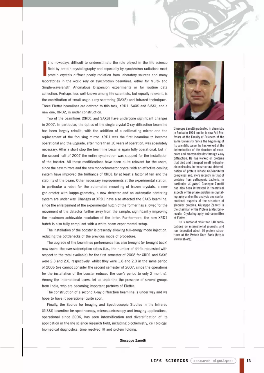
Giuseppe Zanotti graduated in chemistry in Padua in 1974 and he is now Full Pro-fessor at the Faculty of Sciences of the same University. Since the beginning of its scientific career he has worked at the determination of the structure of mole-cules and macromolecules through x-ray diffraction. He has worked on proteins that bind and transport small hydropho-bic molecules, in the structural determi-nation of protein kinase CK2/inhibitor complexes and, more recently, in that of proteins from pathogenic bacteria, in particular H. pylori. Giuseppe Zanotti has also been interested in theoretical aspects of the phase problem in crystal-lography and on the analysis and confor-mational aspects of the structure of globular proteins. Giuseppe Zanotti is the chairman of the Protein & Macromo-lecular Crystallography sub-committee at Elettra.
He is author of more than 140 publi-cations on international journals and has deposited about 90 protein struc-tures at the Protein Data Bank (http://www.rcsb.org).

14 Research Highlights LiFE sCiENCEs
T. Pavkov1, E. M. Egelseer2, M. Tesarz2, D. I. Svergun3, U. B. Sleytr2, W. Keller1
1 Institute of Molecular Biosciences, Structural Biology, University of Graz, Graz, Austria2 Center for Nanobiotechnology, University of Natural Resources and Applied Life Sciences, Vienna, Austria3 The European Molecular Biology Laboratory, Hamburg Outstation, Hamburg, Germany
E-mail: [email protected]
THE FIRST STRUCTURE OF A BACTERIAL S-LAYER pROTEIN
Crystalline bacterial cell surface layers termed S-layers represent a first order self-assembly system which has been optimized in the course of evolution. It is estimated that the majority of bacteria and archaea produce S-layers. An intact “closed” S-layer on an average-sized, rod-shaped cell consists of approximately 5 × 10⁵ monomers. Thus, at a generation time of about 20 min (e.g. for Geobacilli), at least 500 copies of a single polypeptide species with a molecular mass of approximately 100,000 Da have to be synthesized each second, translo-cated to the cell surface and incorporated into the S-layer lattice. S-layers provide organisms with a selective advantage by fulfilling vari-ous functions including protective coats, molecular sieves in the ultrafiltration range, ion and molecule traps, and structures involved in cell surface interactions and antifouling coats. In a great variety of archaea, they are involved in determining cell shape and they contribute to virulence when present in the component of cell walls of pathogens.
In spite of their biological importance for the functionality of prokaryotic cells, high resolu-tion structural information of S-layer proteins is very scarce. The main reason for the absence of 3-D structural information resides in the tendency of S-layer proteins to self-assemble into 2-D crystalline lattices, thereby prevent-ing the formation of 3-D crystals. Up to date, only 2 structures of archaeal recombinant S-layer fragments from Staphylothermus mari-nus [1] and Methanosarcina mazei [2] were reported.Recently we determined the structure of the bacterial S-layer protein SbsC from Geobacil-lus stearothermophilus [3]. Various soluble N- and C-terminal deletion mutants were pro-duced [4] of which rSbsC(31-844) and rSbsC(31-443) yielded crystals suitable for structure determi-nation [3]. Combining the X-ray structures and a solution structure of rSbsC(447-1099) obtained by small angle X-ray scattering we observed a very elongated and flexible mole-cule. The crystal structure of rSbsC(31–844)
Figure 1. Domain structure of rSbsC(31-844). Domains I, II and III are shown in ribbon and domains IV, V and VI in surface representation, indicating partial disorder. Flexible linkers are shown in yellow.

15Research Highlights LiFE sCiENCEs
revealed a novel fold, consisting of six sepa-rate domains, which are connected by short flexible linkers (Figure 1). The N-terminal domain exhibits positively charged residues regularly spaced along the putative secondary cell wall polymer (SCWP) binding site (Fig-ure 2). Upon SCWP binding, a considerable stabilization of the N-terminal domain occurs. These findings provide insight into the pro-cesses of S-layer attachment to the underlying cell wall and self-assembly, and also accom-modate the observed mechanical strength, the polarity of the S-layer, and the pronounced requirement for internal flexibility inherent to cell growth and division. The SCWP-mediated anchoring of S-layer subunits to the rigid cell wall layer is crucial, since this step guarantees a defined orientation for incorporated S-layer proteins, while allowing enough flexibility for recrystallization of S-layer subunits to con-tinuously assume a low free energy arrange-ment. In addition, the specific S-layer-SCWP interaction may play an important role in the
regulated transport of the S-layer protein through the peptidoglycan layer. The structure of the N-terminal part of SbsC provides the basis for detailed functional stud-ies by site-directed mutagenesis for determin-ing the exact interaction sites responsible for self-assembly, as well as specific binding of SCWP and other interacting proteins.
References[1] J. Stetefeld, M. Jenny, T. Schulthess, R.
Landwehr, J. Engel, R.A. Kammerer, Nature Structural Biology 7, 772 (2000).
[2] H. Jing, J. Takagi, J.H. Liu, S. Lindgren, R.G. Zhang, A. Joachimiak, J.H. Wang, T.A. Springer, Structure 10, 1453 (2002).
[3] T. Pavkov, E.M. Egelseer, M. Tesarz, D.I. Svergun, U.B. Sleytr, W. Keller, Structure 16, 1226 (2008).
[4] M. Jarosch, E.M. Egelseer, C. Huber, D. Moll, D. Mattanovich, U.B. Sleytr, M. Sára, Microbiology 147, 1353 (2001).
Figure 2. Putative SCWP binding site. (A) The ribbon diagram represents the structure of the SCWP binding domain including the residues of the putative ligand binding site (shown as stick model, Lys – yellow, Arg – green, Tyr – cyan, His – orange). (B) The electrostatic potential mapped onto the surface of domain I shows a positively charged trace extending along the putative SCWP binding site (marked in green), which is preferentially targeting the negatively charged SCWP (adapted from Pavkov et al. [3] ).

16 Research Highlights LiFE sCiENCEs
K. Bettayeb1, O. M. Tirado2, S. Marionneau-Lambot3, Y. Ferandin1, O. Lozach1, J. C. Morris4, S. Mateo-Lozano2, P. Drueckes5,6, C. Schachtele5, M. H. G. Kubbutat5, F. Liger7, B. Marquet7, B. Joseph7, A. Echalier8, J. A. Endicott8, V. Notario2, L. Meijer1
1 Centre National de la Recherche Scientifique, Cell Cycle Group & UPS2682, Station Biologique, Roscoff, Bretagne, France.2 Laboratory of Experimental Carcinogenesis, Lombardi Comprehensive Cancer Center, Georgetown University Medical Center, Washington, District of Columbia, USA3 Cancéropôle Grand Ouest, Nantes, France4 Department of Chemistry, School of Chemistry and Physics, University of Adelaide, Adelaide, Australia.5 ProQinase GmbH, Freiburg, Germany.6 Novartis Institutes for BioMedical Research, Expertise Platform Kinases, Basel, Switzerland. 7 ICBMS, UMR 5246, Université Lyon 1, Laboratoire de Chimie Organique 1, Villeurbanne, France8 University of Oxford, Laboratory of Molecular Biophysics, Department of Biochemistry, Oxford, United Kingdom
E-mail: [email protected]
MERIOLINS, A NEw CLASS OF CELL DEATH–INDUCING kINASE INHIBITORS wITH ENHANCED SELECTIVITY FOR CYCLIN-DEpENDENT kINASES
A characteristic of many human diseases is an alteration in the pattern of protein phosphory-lation. As a result, the last decade has wit-nessed an exponential growth in efforts to identify, optimize and evaluate small molecu-lar weight, pharmacological inhibitors of numerous protein kinases [1]. Currently about 60 kinase inhibitors are undergoing clinical evaluation against cancers, inflammation, dia-betes and neurodegenerative diseases. The success of Gleevec to treat chronic myeloge-nous leukemia (CML) patients attests to the potential importance of protein kinase inhibi-tors as drugs of the future.
Among the 518 human protein kinases, cyclin-dependent kinases (CDKs) have attract-ed considerable interest given their involve-ment in many essential physiological path-ways and aberrant activities in multiple human diseases, especially cancer and neurodegen-erative conditions. Sequential activation of CDK4/6 and CDK2 controls progression from G1 to S-phase of the cell cycle, and activation of CDK1 is essential for progression from G2 into M-phase [2]. All CDK inhibitors identi-fied to date are ATP-competitive and tend to exhibit selectivity for particular members of the family as well as activity towards other protein kinases. For example, many CDK inhibitors also inhibit glycogen synthase kinase-3 and sometimes casein kinase 1.
ATP-competitive protein kinase inhibitors have been identified from a variety of sources. Though many are the result of library screen-
ing and medicinal chemistry programs several interesting compounds have also been extract-ed from natural products. Meridianins are a family of 3-(2-aminopyrimidine)indoles ini-tially extracted from Aplidium meridianum, an Ascidian from the South Atlantic (South Geor-gia Islands) [2]. They were shown to have promise as a kinase inhibitory scaffold, and subsequently a number of derivatives were synthesized by various groups. However, although some meridianins inhibit various kinases such as CDKs, GSK-3, cyclic nucle-otide-dependent kinases and CK1, they dis-played only modest anti-proliferative effects.
Interestingly, meridianins share some structural similarity with variolins, another family of marine natural compounds contain-ing a central pyrido[3’,2’:4,5]pyrrolo[1,2-c]pyrimidine core substituted with a 2-aminopy-rimidine ring. Variolins were initially extracted from Kirkpatrickia variolosa, a rare and dif-ficult to access Antarctic sponge, but subse-quent total synthesis by Morris [4] and others provided further opportunity to examine the molecule’s properties.
The chemical similarity between meridia-nins and variolins provided an opportunity to synthesize a hybrid structure, which was termed the meriolins. Surprisingly, selected meriolins were found to display potent inhibitory activity and relative selectivity towards CDKs, and also exhibited better anti-proliferative and pro-apop-totic properties in cell cultures than their “inspi-rational parent” molecules.

17Research Highlights LiFE sCiENCEs
To elaborate the molecular interactions that mediate meriolin binding to the CDK active site, we determined the crystal struc-tures of Meriolin 3 and Variolin B in complex with CDK2/cyclin A (Figure 1). These struc-tures revealed that the two molecules bind in very different orientations in the CDK2 ATP-binding pocket. Meriolin 3 makes two hydro-gen bonds to the CDK2 backbone within the hinge sequence that links the two lobes of the kinase and two further hydrogen bonds with the side chains of Lys33 and Glu51. Variolin B like Meriolin 3 makes two equivalent hydrogen bonds with the CDK2 hinge, and also interacts with the side chain of Lys33 through its hydroxyl group. In addition two ordered water molecules are discernible in the Variolin B-bound active site and it interacts with the Ile10 main chain amine. However, the presence of a third ring fused to the Vario-lin B indole system creates a planar structure that is too large to be accommodated at the back of the ATP binding site if Variolin B were to adopt the Meriolin 3 binding mode. As a result the indole moiety common to both
inhibitors is flipped 180o between the two bound structures.
Further study of the meriolins in the neuro-blastoma cell line SH-SY5Y showed that they prevent phosphorylation at CDK2-, CDK1- and CDK9-specific sites and induce rapid degrada-tion of the survival factor Mcl-1. In addition, Meriolin 3 potently inhibits tumor growth in two mouse xenograft models: Ewing’s sarcoma and LS174T colorectal carcinoma. Taken together, our results suggest that meriolins con-stitute a new kinase inhibitory scaffold with promising anti-tumor activity.
References[1] M.E.M. Noble, J.A. Endicott, L.N. John-
son, Science 303,1800 (2004).[2] M. Malumbres and M. Barbacid, Nature
Rev. Cancer 1, 222 (2001).[3] M. Gompel, M. Leost, E. B. de Kier Joffe
et al., Bioorg Med. Chem. Lett. 14, 1703 (2004).
[4] R.J. Anderson, J.B. Hill, J.C. Morris, J. Org. Chem. 70, 6204 (2005).
Figure 1. Details of the interactions of Meriolin 3 and Variolin B with the ATP binding pocket of CDK2/cyclin A. (A) Meriolin 3, (B) Variolin B. Selected CDK2 residues and the two inhibitors are drawn in ball and stick mode with CDK2 carbon, nitrogen and oxygen atoms colored yellow, blue and red respectively. Meriolin 3 and Variolin B bind in the CDK2 ATP binding site and carbon atoms are colored magenta and cyan respectively. Hydrogen bonds are drawn with dotted lines and two bound water molecules visible in the Variolin B-bound complex structure as red crosses.

18 Research Highlights LiFE sCiENCEs
M. Franzese1, C. Pastore3, P.A. Temussi1,3, A. Pastore3, F. Sica1,2
1 Dipartimento di Chimica “Paolo Corradini”, University of Naples, Italy2 Istituto di Biostrutture e Bioimmagini, CNR, Naples, Italy3 National Institute for Medical Research, London, United Kingdom
E-mail: [email protected]
E-coli FRATAxIN: STRUCTURAL CHARACTERISATION OF ION BINDING SITES
The inherited human Friedreich’s ataxia, a severe neuro- and cardio-degenerative disease, has been attributed to deficiency of the conser-ved mitochondrial protein frataxin (Fxn). Dif-ferent and somewhat conflicting functions have been proposed for Fxn. Recent data sug-gest that the protein plays a key role in eukar-yote cellular iron metabolism, particularly in the biosynthesis of mitochondrial heme and iron-sulphur cluster (FeS). Frataxin binds iron with features distinctly different from those of any other protein with this property: Fxn struc-tural model does not contain cavities which could host iron or a suitable prosthetic group and, moreover, the frataxin sequences do not present conserved histidines and/or cysteines, which are the residues usually implicated in chelating iron. In agreement with these struc-tural features, the Fxn affinity for iron has been shown to be very weak, being at the very best in the micromolar range [1]. NMR on the bac-terial [1] and yeast ortholog of human frataxin has indicated that the iron ions bind at a semi-
conserved negatively charged ridge which con-tains several Asp and Glu side chains. To gain a better insight on the iron binding, we have performed a crystallographic study on the pro-tein from E-coli (CyaY) [2], whose structure has been previously determined by X-Ray dif-fraction and NMR. The molecule is folded in a α-β-sandwich motif with a negatively charged α1- β1 region, where conserved acidic residues are clustered (Figure 1).
The study has been approached perform-ing co-crystallization trials in different condi-tions of iron/ protein ratio, pH and precipitant agent, as well as soaking experiments. All trials with Fe(II) were performed under anae-robic conditions in a glove box. In all cases, the crystals were isomorphous with the native ones and they were tested by collecting a full set of diffraction data. The presence of metal ions was checked by calculating anomalous difference maps and observed difference Fou-rier maps. None of these maps indicated the presence of iron in the crystals.
Figure 1. Ribbon model of CyaY structure. The anionic surface patch cluster of twelve acidic (-) residues localized in the α1-β1 region is shown.

19Research Highlights LiFE sCiENCEs
The binding of other positive ions were also studied using the same approach. In par-ticular, Eu(III) was chosen as variant to Fe(III), whereas Ca(II) and Co(II) were used to mimic Fe(II) This choice was suggested by NMR results that indicate that these ions behave very similar to Fe(III) and Fe(II), respectively [1]. Crystal derivatives with Co(II) (CyaY-Co) and Eu(III) (CyaY-Eu) were obtained and their structures refined at 1.75 and 1.42 Å resolu-tion, respectively. In both cases, the protein moiety is very similar to the wild type structu-re as evidenced by the very small root mean square deviations for the main chain atoms.
Both the anomalous difference maps and the observed difference Fourier maps calcula-ted for the Eu(III) complex contain five strong peaks (Figure 2). The europium ion in the S1 site is coordinated with an approximate octahedral geometry to the protein residues D3 and E55 and to four water molecules. In the S2 site, the ion is bound to E33 and to four solvent molecules in a distorted octahedral geometry, with the sixth ligand not well defi-ned. A strong peak on the density map (S3) was also assigned to an Eu(III) ion and is located at only 6.1 Å from S1; in this case two water molecules form a bridge between the two ions. The protein residues involved in the binding to this third metal ion are D29 and D31, which adopt a different conformation with respect to the apo-form. Four water molecules complete the coordination sphere. Finally, the remaining two sites involve resi-dues whose side chains are partially disorde-
Figure 2. Observed difference Fourier maps for Eu3+ contoured at 4.0σ above mean level (A,B). The view of (B) is changed to show sites S4 and S5. Protein side chains (ball-and-stick model) that are involved in metal coordination are marked.
red in the apo structure. In particular, Eu(III) in S4 is coordinated to the two carboxylate oxygens of D23 and to E19 and to two water molecules. The binding in S5 has an octahe-dral geometry and is stabilized by the side chains of D76 and D27 of a symmetry related molecule and by four water molecules.
For CyaY-Co, only the sites S1 and S2, which display a coordination similar to that observed for the CyaY-Eu structure, are occu-pied.
These results show that all the binding sites of CyaY with the metals are on the exter-nal protein surface (Figure 2) and involve few protein residues and several water molecules. The interaction of CyaY with the metals does not induce main chain conformational varia-tions and only three side chains change orien-tations to accommodate the ligands. Surpris-ingly, the iron derivatives of the protein could not be obtained. This might have been caused by the crystallization conditions that could interfere with the iron binding; alternatively, it may suggest that the capacity to bind the iron is associated to an aggregated form of the pro-tein, present at low concentration in solution.
References[1] M. Nair, S. Adinolfi, C. Pastore, G. Kelly,
P.A. Temussi, A. Pastore, Structure, 12, 2037 (2004).
[2] C. Pastore, M. Franzese, F. Sica, P.A. Temussi, A. Pastore, FEBS Journal, 274, 4199 (2007).

20 Research Highlights LiFE sCiENCEs
C. Förster1, A. Zerressen-Harte1, J.P. Fürste1, M. Perbandt2, Ch. Betzel2, V.A. Erdmann1
1 Institute of Chemistry and Biochemistry, Free University Berlin, Berlin, Germany2 Institute of Biochemistry and Molecularbiology, University of Hamburg, c/o DESY, Hamburg, Germany
E-mail: [email protected]
x-RAY STRUCTURE ANALYSIS OF tRNAGly ACCEpTOR STEM MICROHELICES: COMpARISON OF STRUCTURE AND HYDRATION
tRNA identity elements assure the correct ami-noacylation of tRNAs by the aminoacyl-tRNA synthetases with the cognate amino acid. The tRNAGly / glycyl-tRNA synthetase is a member of the so-called ‘class II system’ in which the tRNA determinants consist of rather simple ele-ments [1]. The glycine system is a special case within ‘class II’: there exists a large divergence between eukaryotes/archaebacteria and eubac-teria. Not only the glycyl-tRNA synthetases differ to great extent in protein structure and sequence motifs, also the tRNA identity ele-ments differ [2]. These are located in the ami-noacyl stem of tRNAGly, with additionally the discriminator base, that strictly has to be adeno-sine in the eukaryotic/archaebacterial but uracil
in the eubacterial case [2,3]. Due to these diffe-rences a unique evolutionary divergence is discussed in the literature for this system.
Recently, we solved the crystal structures of the Escherichia coli and the human tRNAGly aminoacyl stem microhelices (PDB-IDs: 2VAL, 2V7R). Here we present a comparative crystal structure analysis of the tRNAGly accep-tor stem microhelices and of their surrounding hydration patterns.
The E.coli and human tRNAGly acceptor stem microhelices show sequence homology within the first three base pairs (Fig.1), which contain the C2-G71 identity element [2,3]. Both tRNAGly helices crystallize at different conditions and the crystals show different morphology, space groups, crystal packing and resolution of X-ray diffraction data. The E.coli tRNAGly acceptor stem crystallizes in the space group P3221 with the unit cell para-meters a=b=35.35 Å, c=130.82 Å, γ=120.00° and diffracts to 2.0 Å resolution. The asymme-tric unit contains two RNA duplexes, 55 defi-ned water molecules and one magnesium atom. The two E.coli tRNAGly microhelices show minimal differences in their local and overall geometric parameters. The hydrated magnesium ion is bound to helix A in vicinity of the second and third base pair (data not shown). Helix B contains no magnesium. Slight deviations in the helical parameters might represent a magnesium-bound and a magnesium-free state of the tRNAGly microhe-lix. The human tRNAGly aminoacyl stem cry-stallizes in the monoclinic space group C2 with the cell constants: a=37.12 Å, b=37.49 Å, c=30.38 Å, β=113.02°. The crystals diffract to 1.2 Å resolution and contain one molecule in the asymmetric unit. A total of 85 water mole-cules could be assigned per RNA and no fur-ther ligand or metal ion could be detected.
Figure 1. Tertiary tRNA structure, derived from [4], with the acceptor stem region pointed out showing the E.coli and the human tRNAGly
sequences.

21Research Highlights LiFE sCiENCEs
All tRNAGly acceptor stems form the stan-dard A-type RNA, respectively. The values for the local helical parameters of the three RNAs like twist, slide, tilt, rise and χ-displacement lie in the expected values known for the cano-nical A-type RNA. The sugar puckering of the three RNAs is distributed in the 2’-exo confor-mation for all nucleotides. The backbone pho-sphate-phosphate distances also demonstrate the canonical A-form RNA structure. The pho-sphate backbone α/γ torsion angles all adopt the (-)gauche/(+)gauche conformation where-as the β torsion angles show the anti confor-mation around +/-180 degrees.
A comparative analysis of the hydration patterns surrounding the RNAs is demonstrated in figure 2, which schematically shows the assi-gnment of the water molecules to the nucleoba-ses and phosphates of the RNAs. We observed different pictures for all three hydration pat-terns. This observation is highlighted by an overlay of the three RNA helices in figure 2b, showing the tRNAGly microhelices with similar helical geometry which are accompanied by a large variability in their hydration patterns.
Further experiments will have to clarify a possible specificity of hydration in RNAs. Repetitive crystallization and structure analy-sis with identification and comparison of water molecules will help to further investigate this
question. Regarding RNA–protein interac-tions, the hydration layer might be the first contact site and play an important role for recognition, like for example in combination with tRNA identity elements.
This work was funded within the RiNA net-work for RNA technologies by the Federal Ministry of Education and Research, the City of Berlin, and the European Regional Develop-ment Fund. We thank the Fonds der Chemi-schen Industrie (Verband der Chemischen Indu-strie e.V.), and National Foundation for Cancer Research, USA, for additional support. We gre-atly acknowledge the DESY synchrotron (Ham-burg, Germany) and the Elettra synchrotron (Trieste, Italy) for providing beam time.
References[1] G. Eriani, M. Delarue, O. Poch, J. Gangloff
and D. Moras, Nature 34, 203 (1990). [2] K. Shiba, Glycyl-tRNA Synthetases. “The
Aminoacyl-tRNA Synthetases”, Landess Bioscience, Georgetown, Texas, U.S.A. Chapter 13, 125 (2005).
[3] W.H. McClain, K. Foss, R.A. Jenkins and J. Schneider, Proc. Natl. Acad. Sci. U.S.A. 88, 6147 (1991).
[4] H. Shi and P.B. Moore, RNA 6, 1091 (2000).
Figure 2. (a) Schematically drawn hydration patterns of the E.coli tRNAGly microhelix A, the magnesium-bound RNA (water shown as blue dots) and B, the magnesium-free RNA (cyan dots) and of the human tRNAGly microhelix, which is magnesium-free (red dots). (b) Superposition (stereo presentation) of the different hydration layers surrounding the two E.coli and the human tRNAGly microhelices: The water molecules are shown as dots with the colours corresponding to the ones described above.

22 Research Highlights LiFE sCiENCEs
A. Langkilde1§, L. Lo Leggio1, A. Mølgaard1, S. Larsen1,2
1Department of Chemistry, University of Copenhagen, Copenhagen, Denmark 2European Synchrotron Radiation Facility (ESRF), Grenoble, France§Present address: Department of Medicinal Chemistry, University of Copenhagen, Copenhagen, Denmark
E-mail: [email protected]
HIGH RESOLUTION STRUCTURE OF A pLANT CELL wALL DEGRADING ENzYME VARIANT AND SHORT STRONG HYDROGEN BONDS IN pROTEINS
Hydrogen bonds play a pivotal role for the structure and function of proteins in shaping secondary structure, protein-ligand interac-tions and catalytic activity. The very short O-H…O hydrogen bonds formed between car-boxylic acid and carboxylate groups are among the strongest. Many textbooks present aspar-tate and glutamate as the charged species, in accordance with the pKa values of the free acids (3.9 and 4.2, respectively). The local chemical environment in a protein can how-ever change the microscopic pKa value of a carboxylic acid group significantly, keeping the carboxylic acid residues protonated at higher pH. It is noteworthy that Asp and Glu are not generally considered as possible hydro-gen bond donors in programs employed in the analysis of protein structures, therefore hydro-gen bonds between carboxylic acid and car-boxylate groups may be overlooked.
The formation of short, strong hydrogen bonds with partially covalent character causes deshielding of the involved proton giving rise to 1H NMR chemical shifts above 18 ppm. Such low field proton signals and their rela-tion to Low Barrier Hydrogen Bonds (LBHB) considered to be important for catalysis have been extensively studied and debated. Serine proteases with a catalytic Asp-His-Ser triad containing a short Asp-His hydrogen bond were among the best investigated systems in relation to LBHBs [1]. A virtually identical catalytic Asp-His-Ser triad was also found in rhamnogalacturonan acetylesterase (RGAE), and the esterase catalysis is assumed to follow a similar mechanism [2].
An extreme low field signal (at approxi-mately 18 ppm) in the 1H NMR spectrum of rhamnogalacturonan acetylesterase (RGAE) showed the presence of a short strong hydro-
gen bond in the protein. This signal was also present in the mutant RGAE D192N. This was unexpected as this variant could not form the short His-Asp hydrogen bond which in serine proteases gives rise to the signal around 18 ppm.
To elucidate this aspect the structure of RGAE D192N variant has been determined by X-ray crystallography using data collected to 1.33 Å resolution at Elettra. The high resolu-tion data (99.5 % complete, average redun-dancy of 9, and Rmerge=3.2 %) enabled struc-ture refinement in SHELXL including model-ing of disordered side chains and inclusion of anisotropic displacement parameters on non H atom (R=11.57 %, Rfree=15.34 %).
The high resolution structure permitted a thorough analysis of the short hydrogen bonds, as the estimated standard deviation on the donor-acceptor distances of these hydrogen bonds were in the 0.01-0.03 Å range. A careful analysis and comparison of the structure of RGAE D192N and the wild-type structure known to a resolution of 1.12 Å [3], was con-ducted with the purpose of identifying possible candidates for the short hydrogen bond with the 18 ppm deshielded proton. An examination of the short hydrogen bonds in the RGAE, the calculated pKa values, and solvent accessibili-ties identified a buried carboxylic acid car-boxylate hydrogen bond between Asp75-Asp87 as the likely origin of the 18 ppm sig-nal, supported by theoretical calculations of the chemical shift values [4].
Despite the precedents in the literature our results show that the low-field signals observed in some 1H NMR experiments on proteins can not be assigned to active site hydrogen bonds without additional evidence. In the present case, the 18 ppm 1H NMR signal in RGAE

23Research Highlights LiFE sCiENCEs
cannot be assigned to the hydrogen bond between the residues in the catalytic triad.
Our analysis of RGAE structures revealed furthermore that all the short hydrogen bonds in this enzyme are located close to the active site indicating a role in the enzymatic func-tion. Interactions between carboxylic acid side-chains are not rare. A search in a PDB subset revealed short contacts between car-boxylic acid side-chains in 16 % of the protein chains. Many of the shortest contacts involve residues that are putative catalytic residues or residues close to the active site, which empha-size the importance of including Asp and Glu as possible hydrogen bond donors in protein structure analysis.
References[1] W. W. Cleland, P. A. Frey, J. A. Gerlt, J.
Biol. Chem. 273, 25529 (1998).[2] A. Mølgaard, S. Kauppinen, S. Larsen,
Structure 8, 373 (2000).[3] A. Mølgaard, S. Larsen, Acta Cryst. D 58,
111 (2002).[4] A. Langkilde, S. M. Kristensen, L. Lo Leg-
gio, A. Mølgaard, J. H. Jensen, A. R. Houk, J.-C. N. Poulsen, S. Kauppinen, S. Larsen, Acta Cryst. D 64, 851(2008).
Figure 1. The overall structure of RGAE D192N is shown excluding Thr79 and Ser80 which could not be located in the density maps. Terminal residues, Thr1 and Leu233, are labeled. The three residues that correspond to the catalytic triad (Ser9-His195-Asn192) are colored green. The N-acetyl-D-glucosamine and acetate ion are illustrated by spheres and the shortest hydrogen bonds are shown as dashed lines.

24 Research Highlights LiFE sCiENCEs
F. Morgera1,2, L. Vaccari1, S. Pacor2, N. Antcheva2, D. Scaini1, L. Casalis1, A. Tossi2
1 Sincrotrone Trieste S.C.p.A., Trieste, Italy 2 Department of Life Sciences, University of Trieste, Italy
E-mail: [email protected]
STRUCTURE AND MEMBRANE INTERACTION MODES OF THE DEFENCE pEpTIDE LL-37 AND ITS ANALOGUES
Co-evolution of humans and pathogens has led to multiple defence mechanisms. They are commonly defined as innate and adaptive immunity, respectively the non specific first line of defence and the inducible specific one. The human peptide LL37 is a small natural protein belonging to the “Host Defence Pep-tides” group (HDPs) and has multiple roles in immunity, acting either as direct antimicrobial molecule or as an immunomodulating agent [1]. Increasing antibiotic resistance and the urgent need for alternative approaches to infection management has lead to the syste-matic study of the mode of action of HDPs so as to identify the main structure-activity requirements for developing new potential therapeutic agents. Within this framework, we have analysed the effects of structural varia-tions on membrane interactions for LL-37 and its chimpanzee orthologue (mmuRL37), using
several complementary biophysical and bio-chemical methods. Transmission and ATR-FTIR spectroscopy in solution and on model membranes respectively provided information on both peptide and membrane structure variations upon interaction. In particular, we focused on the backbone amide vibrations (amide I & II; 1500-1700 cm-1), widely used to study the conformations of proteins. Moreo-ver, AFM was performed at Nanostructure Laboratory @ Elettra on the same supported membranes as used for IR measurements, giving insights on the morphology and phase status. The study of the biological activity on bacterial cells (not shown) allowed a comple-te overview of peptide mode of action, highlighting the structural requirements necessary for a selective activity against pathogens. FTIR transmission spectroscopy in D2O provided information on the confor-
Figure 1. Transmission (A) and ATR- FTIR (B) amide I & II spectra of LL37 (a) and mmuRL37 (b). The bottom panels show the respective spectra 2nd derivatives.

25Research Highlights LiFE sCiENCEs
mational states of the HDPs in solution at higher concentrations, which may reflect tho-se reached at the bacterial membrane surface (Figure 1A). Spectra of LL-37 carried out after complete H/D exchange, indicate a sta-ble helical structure, whereas mmuRL37 shows a broader, more composite amide I band, indicative of a more random structure even under these high concentration condi-tions. ATR-FTIR experiments in the presence of a Germanium supported egg phosphatidyl glycerol (PG) bilayer gave insights on how the peptides bind to this anionic membrane, a simple model for bacterial membranes (Figu-re 1B). In particular, it shows LL-37 in con-tact with the bilayer after dehydration, revea-ling a sharp band centred at 1652 cm-1, typi-cally assigned to a α-helical structure. In this case, the ATR amide I and II bands for RL-37 confirm that in the presence of anionic lipids, it gives rise to a strong α-helical signal. The frequency of this band is red-shifted (to 1656 cm-1) with respect to LL-37, possibly indica-ting a deeper insertion of the helical segment into the hydrophobic environment of the membrane. This is consistent with the greater effect exerted by RL-37 on the lipid acyl ban-ds (not shown), with a more marked shift in the CH2 stretching frequencies (from 2920 to 2924 cm-1 and from 2850 to 2854 cm-1 for the antisymmetric and symmetric modes) [2]. AFM images of dehydrated PG bilayers upon LL-37 or mmuRL-37 interaction are shown in Figure 2., indicating the latter peptide causes a generalized perturbation in the bilayer,
resulting in lesions of varying sizes and with a more amorphous appearance. LL-37 instead generates a defined pattern of perturbations consistent with the formation of many holes of roughly the same size that are visible only at higher resolution. The topography of these holes suggests they may be toroidal in nature, being characterized by a positive curvature of the membrane resulting from accumulation of AMPs at the bilayer surface. Our conclusions are further corroborated by AFM-phase ima-ging, which provides information on physical variations beyond morphology. These show that the lipid bilayer preserves its phase homo-geneity upon LL-37 interaction, while it beco-mes inhomogeneous upon mmuRL37 interac-tion. This could be explained assuming an important perturbation of the lipid order indu-ced by mmuRL-37, which is not appreciable for the human peptide. In conclusion, the comparison of these structural data with the biological ones has suggested a different mode of action for the two orthologs. In fact, it would appear that the evolution of the pri-mate peptide has led to sequence variations, resulting in different modes of membrane interaction and membrane lesions.
References[1] R.E. Hancock et al., Nat. Biotechnol. 24,
1551 (2006).[2] L. Tamm et al., Quarterly Reviews of Bio-
physics 30, 365. UK, Cambridge Univer-sity Press (1997).
Figure 2. AFM topographic (A) and phase (B) images of lipid bilayer upon interaction with LL-37 (top), and mmuRL37 (bottom). Insets are respectively the topography and phase images at a higher resolution of the lipid bilayer upon LL-37 interaction.

26 Research Highlights LiFE sCiENCEs
C. J. Hall1, E. Schültke2, R. Menk3, F. Arfelli4, B. Juurlink2
1 Monash University, Monash Centre for Sychrotron Science, Melbourne, Australia2 The University of Saskatchewan, Dept. of Anatomy and Cell Biology, Saskatoon, Canada3 Sincrotrone Trieste S.C.p.A., Trieste, Italy4 Physics Department, University of Trieste, Italy
E-mail: [email protected]
TRACkING IMpLANTED MAMMALIAN CELLS in-vivo USING SYNCHROTRON x-RAY IMAGING
X-ray imaging (radiography) is currently the most common method of producing medical images. The mature technology behind both the production and detection of x-ray photons has enabled relatively inexpensive, but high quality x-ray imaging systems to be made available to health services worldwide. One advantage that x-rays have over other photons used for imaging is their high penetration. This quality allows x-ray fluxes to be used to image organs inside the body making visible both tissue morphology and with appropriate contrast agents, function. Recently there has been considerable interest in the use of biome-dical x-ray imaging at spatial resolutions of less than 50 microns. This effort has been lar-gely led by groups using synchrotron sources or with recently developed x-ray tubes having a very fine electron focal spots.
Our work on the SYRMEP beam line attempts to combine phase contrast radiogra-phy with novel contrast markers for cells. The hope is that low dose, high contrast images can be produced which would simultaneously show anatomy and marked function. With the high fidelity x-ray beams available at Elettra, fruitful research into novel x-ray markers has become possible. One method used to enhance the contrast of implanted cells against the background of endogenous tissue is to engine-er extrinsic cells in a way that allows a highly specific uptake of a contrast agent on a tempo-rary basis. This method is already used exten-sively in optical microscopy and medical radiography. An alternative approach which is more suited to gene therapy for instance, is that extrinsic cells are loaded with a contrast marker before implantation. In this case the contrast agent is designed to reside in the cells for long periods of time. The technique requi-
res a marker that is chemically inert, non-toxic, and does not interfere with the normal functio-ning of the cells. Colloidal gold fits the requi-rements of this second type of methodology very well.
Gold is one of the least reactive of the ele-ments making it potentially useful as an inert marker. Furthermore the surfaces of gold nano-particles created in colloids can be coa-ted with a variety of proteins to provide fun-ctional behaviour in a biological environment. These features provide it with good prospects as an agent for a variety of biological systems research [1]. For instance gold colloid has been used recently as a vascular x-ray contrast agent in animal radiology [2]. The use of gold labelled proteins as a cell tagging technique in electron microscopy is not new but so far little investigation has been made into using gold colloids for functional x-ray imaging. Our team has embarked on a study to investigate ways of exploiting gold nano-particles as a means to trace movement of marked cells in-vivo. We are using both projection x-ray radio-graphy and computed micro-tomography (µCT) on SYRMEP[3]. The initial disease model we have chosen is an aggressive mali-gnant brain tumour: glioblastoma multiforme, modelled in rats. Propagated C6 glioma cells were encouraged to phagocytose gold nano-particles by including gold labelled serum pro-teins in their growth medium[4]. A number of gold loaded cells were subsequently implanted in the brains of laboratory animals and allo-wed to develop into tumours. X-ray imaging performed at Elettra was used to visualise the morphology and distribution of the resulting cancers. Results have been very encouraging with the clusters of gold loaded cells quite cle-arly visible in the x-ray images. To investigate

27Research Highlights LiFE sCiENCEs
the potential for the idea to work with non syn-chrotron sources we also made images with the Tomolab facility at Elettra using the same specimens. Initial results suggest that although the contrast of the lesion is not as good as with the synchrotron source, the images are of suf-ficient quality to be useful in neurological research.
The first paper on this work will be publi-shed this year in the European Journal of Radiology.
Figure 1. A screenshot of one of the rat head tomographs. The was data taken on the SYRMEP beam line with a monochromatic beam of 25 keV. The projection images were sampled with 28 micron pixels and reconstructed using filtered back-projection. The burr hole drilled in the skull when the cells were introduced is visible on the top of the skull. Underneath this within the brain cavity, the lesion formed by the marked Glioma cells is visible as a radio opaque cloud.
References[1] B.H. Juurlink, R.M. Devon, Experientia
47, 75 (1991).[2] J.F. Hainfeld et al., Br. J. Radiol. 79, 248
(2006).[3] M.J. Paulus et al., Neoplasia 2, 62 (2000).[4] B. H. J. Juurlink, W. Walz, Neural cell cul-
ture techniques in Neuromethods Vol. 33: Cell Neurobiology Techniques, A. A. Boul-ton, G. B. Baker, A. N. Bateson, Editors, Humana Press, Totowa, NJ, p. 53 (1998).

SURFACES AND INTERFACES

29Research Highlights iNTRODUCTiON
In the Surfaces and Interfaces section, systems at the nano-scale are attracting
increasing attention, from the traditional sense of the outermost layers of a
surface to the specific properties of nanometer localisation. The issues tackled
by the scientific community selected here, constitute the basis for further research
fully exploiting synchrotron radiation (SR) and eventually exploiting the
characteristics of new light sources, accompanied by complementary experimental
techniques and theoretical efforts.
A major effort is devoted to the study of organic molecule self-assembling on
model inorganic surfaces. The sulfur-gold interaction of alkanethiols on gold,
competing with the weak van der Waals forces between the radical chains, has
been shown to drive molecular self-assembling, whose specific structure has been
brilliantly solved by grazing-incidence x-ray diffraction (GIXRD). Surface diffraction
also solved the structure of planar pi-conjugated aromatic molecules interacting
with metal surfaces. Other contributions show that polarization-dependent near-
edge x-ray absorption spectroscopy (NEXAFS) is not only used as a straightforward
probe for molecular orientation, but it is also exploited to enlighten the modification
of empty states upon adsorption, whose interface state dispersion is outlined by
high-resolution angular-resolved photoemission (ARPES). All these are brilliant
examples of geometric, structural and electronic structure determination.
ARPES is widely used for fundamental surface and interface phenomena,
enlightening the formation of one-dimensional 3d-bands in Cu nanowires
constructed on a Pt vicinal surface, and disentangling the very nature of the √3
Sn/Si structure, also corroborated by scanning-tunneling spectroscopy data,
showing an insulating Mott-Hubbard ground state.
One major issue for the facility is structural and magnetic nano-imaging.
Quantitative information on the surface stress exerted by adsorbed oxygen islands
on tungsten, and stress-induced stripes disordering at high temperature with the
same behaviour of finite-size Ising lattices, are brought to light by photoemission
and low energy electron microscopy (LEEM). Rotation of magnetic domain walls
is clearly detected and imaged in NiFe magnetically soft layers, enlightening the
role of spectroscopic imaging of magnetic systems at the nanoscale, one of the
major trends in SR.
Furthermore, nano-sized oxides for storage and reduction and bimetallic
catalysts were studied under reaction with gases by high-resolution core-level
photoemission, while resonant photoelectron diffraction allows identification of
defect states on titania surfaces. Catalytic activity in more realistic environments
(temperature, pressure) may be definitely envisaged as a further potential research
objective with SR and new-generation light sources.
Carlo Mariani
Carlo Mariani is professor of Condensed Matter Physics at the Roma “La Sapien-za” University since 2001. Previously, at University of Modena, Université Pierre et Marie Curie (Paris), Italian National Research Council (CNR) in Frascati, Fritz-Haber-Institut der Max Planck Ges-ellschaft in Berlin.Research activity focused on the experi-mental study of low-dimensional sys-tems, surfaces and nano-structures, with a variety of experimental approach-es, also exploiting synchrotron radiation. Study of model two-dimensional (2D) surface and interface systems, ordered 1D nano-wires, size-confinement, self-organized nano-structured organic mol-ecules on surfaces and hybrid systems.Author of more than 130 refereed papers on international journals, several pro-ceedings, and communications to con-ferences. Referee of major international journals and of EU research projects. Member of Scientific and Organizing Committees of international conferences. President of the Italian Society for Syn-chrotron Radiation and member of the Elettra scientific review panel.

30 Research Highlights sURFACEs AND iNTERFACEs
A. Cossaro1, R. Mazzarello2, R. Rousseau2, L. Casalis3, A. Verdini1, A. Kohlmeyer4, L. Floreano1, S. Scandolo5, A. Morgante1,6, M. L. Klein4, G. Scoles2,3,7
1 Laboratorio Nazionale TASC, INFM-CNR, Trieste, Italy 2 SISSA - Scuola Internazionale Superiore di Studi Avanzati, Trieste, Italy3 Sincrotrone Trieste S.C.p.A., Trieste, Italy4 Department of Chemistry, University of Pennsylvania, Philadelphia, PA, USA5 International Center for Theoretical Physics and INFM/Democritos, Trieste, Italy6 Department of Physics, University of Trieste, Trieste, Italy7 Department of Chemistry, Princeton University, NJ, USA
E-mail: [email protected]
THE STRUCTURE OF ALkANETHIOLS MONOLAYERS SELF-ASSEMBLED ON GOLD
We have determined the structural configura-tion of Alkanethiols [(CH2)nCH3SH] on gold, a puzzling issue that was raised almost 15 years ago in Princeton and that we have final-ly solved in Trieste by a concerted experimen-tal and theorethical effort. Alkanethiols on gold represent the archetypal among self-assembled monolayers (SAMs), since they form a strong link to the metal substrate through the thiol head-group, while the tail-group can be easily functionalized to tailor the SAM properties, such as wetting, corrosion, adhesion, lubrication and conductivity. At the same time, gold, being unreactive and bio-compatible, can be easily patterned, and obtained as a colloid, as nanoclusters and as a thin film. In the latter case, the surface of the individual grains prevalently displays the high symmetry (111) crystal face.
Common to all alkanethiols on Au(111) is the formation of an ordered SAM displaying a hexagonal (√3×√3) symmetry, corresponding to the adsorption of one standing-up molecule each three Au atoms. Long-chain alkanethiols display an additional modulation of the (√3×√3) structure, yielding a c(4×2) superlat-tice with the same molecular concentration. These densely packed ordered phases can be equivalently obtained by adsorption from the vapor-phase or in dilute solution, which explains the widespread employment of this system in many research fields. [1]
Even if alkanethiols on Au(111) are by far the most studied SAMs, the exact determina-tion of the adsorption site of sulphur gave rise to a longstanding controversy. First, ab initio calculations were supporting the adsorption of
thiols with S in between two Au atoms (bridge site), whereas experiments of photoelectron and photon interference between S and Au atoms rather indicated the presence of sulphur on-top of single Au atoms. Second, the forma-tion of the c(4×2) superlattice implies that the SAM must be formed by molecules adopting two different orientations or adsorption sites.
Recently we have studied the SAM struc-ture of methylthiol (CH3SH), MT, the simplest and yet the most disputed one. By a recursive comparison between diffraction measurements (x-rays and photoelectrons) and molecular dynamics calculations, we have found a mod-el consistent with ours and former experi-ments, where the simple (√3×√3) structure results from the dynamical equilibrium between thiols adsorbed in two different, but interchangeable configurations. One configu-ration is formed by a thiol in a bridge site, the other is formed by two thiols that pull an Au atom out of the surface yielding a staple struc-ture, where the S atoms are laterally linked to the common Au adatom, but they sit almost on-top of a surface Au atom. This novel struc-ture is made energetically competitive with the bridge site by the presence of vacancies. [2]
Due to the fast Au surface diffusion, the Au vacancies produced by the staples are rapidly delocalized over the surface. The vacancy dif-fusion favors the interchange between bridge and staple configurations (on a picosecond timescale at room temperature). The dynami-cal disorder due to diffusing vacancies and thiol interchange prevents the establishment of a long range correlation between the bridge and staple thiols, yielding an average (√3×√3)

31Research Highlights sURFACEs AND iNTERFACEs
symmetry, that simply leads to an MT cover-age of one molecule every three surface Au atoms. [2]
Once verified for the case of methylthiol, we tested the predictive strength of our model on long-chain alkanethiol SAMs, which dis-play the more complex c(4×2) superlattice. We have considered the case of hexanethiol [(CH2)5CH3SH], HT, which intermediate length yields a SAM with coexisting (√3×√3) and c(4×2) phases. Both molecular dynamics calculations and x-ray diffraction measure-ments indicate that the HT SAM contains the same ingredients of the MT one, i.e. Au vacan-cies, Au adatoms, and thiols, in both bridge and staple configuration. In this case, howev-er, the dynamical disorder at the surface is strongly hampered by the van der Waals’ inter-action among the tails of the HT molecules. Calculations predict an effective slowing of the interchange mechanism. With respect to MT, the longer living staple and bridge HT configurations allow the establishment of a correlation among them and the vacancies, that gives rise to the c(4×2) symmetry phase. Experimentally, the atomic disorder of the sur-face layer is partially quenched yielding a vacancy delocalization much lower than in the
MT case. The adatoms in the staple configura-tion are found to line-up yielding the charac-teristic zig-zag arrangement of the molecules (Figure 1). [3]
In conclusion, thiols on the Au(111) sur-face are found to adsorb in two different geo-metric configurations and to produce a dynam-ical disorder by creating adatoms and vacan-cies that rapidly diffuse over the surface. The van der Waals’ interaction among the tails of long chain alkanethiols drives the ordering of the thiols, hence reducing the dynamical dis-order on the Au surface.
References[1] C. Love, L.A. Estroff, J.K. Kriebel, R.G.
Nuzzo, G.M. Whitesides, Chem. Rev. 105, 1103 (2005).
[2] R. Mazzarello, A. Cossaro, A. Verdini, R. Rousseau, L. Casalis, M.F. Danisman, L. Floreano, S. Scandolo, A. Morgante, G. Scoles, Phys. Rev. Lett. 97, 016102 (2007).
[3] A. Cossaro, R. Mazzarello, R. Rousseau, L. Casalis, A. Verdini, A. Kohlmeyer, L. Flo-reano, S. Scandolo, A. Morgante, M.L. Klein, G. Scoles, Science 321, 946 (2008).
Figure 1. 3D pictorial of the c(4x2) structural model resulting from x-ray diffraction fit. Hexanethiols (S in light-blue, C in black) in bridge and staple configurations are shown; surface Au atoms in yellow, Au adatoms in orange. Partially occupied Au positions are indicated by transparent atoms (surface atoms in green, adatoms in orange).

32 Research Highlights sURFACEs AND iNTERFACEs
E. Annese1, J. Fujii1, C. Baldacchini2, B. Zhou1, C.E. Viol1, I. Vobornik1, M.G. Betti2, G. Rossi1,3
1 Laboratorio Nazionale TASC, INFM-CNR, Trieste, Italy2 Physics Department, University La Sapienza, Roma, Italy3 Physics Department, University of Modena and Reggio Emilia, Modena, Italy
E-mail: [email protected]
MOLECULAR CHARGE DISTRIBUTION AND DISpERSION OF ELECTRONIC STATES IN THE CONTACT LAYER BETwEEN pENTACENE AND Cu(119) AND BEYOND
The demand for novel devices exploiting the physical and chemical properties of organic films is rapidly increasing. One of the most promising molecules in organic electronics is pentacene, because of its planar structure and conductive properties. The properties of π-conjugated organic films are controlled by the energy position of the molecular states with respect to the Fermi level, in particular the highest occupied and the lowest unoccu-pied molecular orbitals (HOMO and LUMO). Recent spectroscopy experiments provided evidence of the formation of hybrid electron states at the interface between organic mole-cules and noble metal surfaces [1-2]. The delocalization of the electronic states at the interface remains an open issue.
We observed significant difference in the electronic states of the pentacene molecules in direct contact with the Cu(119) substrate and
the overlayer pentacene molecules by the analysis of STM (scanning tunnelling micro-scopy) and ARPES (angle resolved photoelec-tron spectroscopy with polarized synchrotron radiation) results in ultrathin [∼monolayer (ML)] pentacene films. Both ARPES and STM data were measured at the APE-INFM beam-line at Elettra.
Photoelectrons were excited by photons linearly polarised either perpendicular (see Figures 1a and 1b) or parallel (Figure 1c) to the long molecular axis. The ARPES results are presented in Figure 1a for 1 ML and for 2 ML coverages and compared to the spectrum of the clean Cu(119) surface. The molecular adsorption of a single pentacene layer on Cu (119) induces a spectral density increase at the Fermi edge (I1). Two pentacene-induced featu-res can be singled out at 1 eV (I2) and at 1.45 eV (I3) (Figure 1a). I1 peak shows a k-depen-
Figure 1. ARPES spectra at hν=18 eV; a) Angle integrated spectra around Γ for pentacene on Cu(119): clean substrate (grey shaded), monolayer (ML) and ~2 ML : b) Molecular interface state, I2, and the residual substrate sp band dispersing along Γ’-X’. c) I1 (close to EF) and HOMO derived spectral features, I3, along the Γ’-X’ direction.

33Research Highlights sURFACEs AND iNTERFACEs
dent intensity modulation in this energy region 0–1.5 eV along Γ - X. The peak I2 disperses from X to Γ. The energy dispersion along Γ -X can be ascribed to the charge delocalization along the pentacene chains, which is mediated by the metallic substrate at the interface. As the molecular layers pile up, at higher penta-cene coverages, I1 and I2 are not detected, whi-le the HOMO-derived peak I3 increases in intensity.
Interacting molecules, in contact with copper, generate dispersive electronic states associated to a perturbed electron charge density distribution of the molecular orbitals (Figure 2). The STM images were acquired with atomic resolution at the relevant values of the bias voltages |VbL|, |VbH|, which correspond to the binding energies of the molecular interface states I1 and I3 (Figure 1a).
In Figure 2 are imaged both isolated pen-tacene molecules (0.05 mol/nm2) (Figure 2 a-b) and molecules on a coverage exceeding the monolayer (1.1 ML ~ 0.80 mol/nm2 ) (Figure 2c-d). The individual adsorbed penta-cene molecule shows seven protrusions charge pattern at both VbL and VbH. In particular the molecule in Figure 2a1) differs from the charge electron distribution of the HOMO of the free molecules, giving the signature of the interac-tion between pentacene and substrate. A char-ge pattern similar to that in Figure 2 a1) could also be observed at the higher pentacene den-sity when imaging at VbL Figure 2c) and at VbH for interface layer molecules. At VbH a diffe-rent type of molecular charge pattern can be distinguished. These correspond to the top-
most molecules, not surrounded by other molecules besides the ones underneath (Figure 2d1) mimicking the HOMO features of the free molecule.
We have identified a peculiar charge den-sity distribution of the pentacene molecules in contact with the Cu(119) surface. The pertur-bed molecular orbitals are strictly limited to the contact layer. The second layer molecules are weakly bound to the contact layer but pre-serve the in-plane orientation, the alignment along the substrate template and a charge den-sity distribution mimicking free pentacene molecular orbitals. In the reciprocal space, the molecular charge distortion gives rise to the electronic states localized at the interface, with a tiny dispersion along the pentacene long molecular axis.
ReferencesA. Ferretti [1] et al, Phys. Rev. Lett. 99, 046802 (2007).C. Baldacchini [2] et al, Phys. Rev. B 76, 245430 (2007).
Figure 2. (a-d) Bias-dependent STM images of pentacene on Cu(119) at submonolayer coverage (a, b) and 1.1 ML coverage (c, d); size: 9.1 × 10 nm2; in a) and c) the bias corresponds to LUMO derived features (VbL), in b) and d) the bias corresponds to HOMO derived features (VbH); (a1, b1, c1, d1-2) are zoom-in to the selected molecules in the images (a-d); The insets are the HOMO and LUMO calculated electronic density distributions.

34 Research Highlights sURFACEs AND iNTERFACEs
L. Floreano1, A. Cossaro1, R. Gotter1, A. Verdini1, A. Morgante1,2, F. Evangelista3, A. Ruocco3, G. Bavdek1,4, D. Cvetko1,4
1 Laboratorio Nazionale TASC, INFM-CNR, Trieste, Italy 2 Physics Department, University of Trieste, Italy3 Physics Department and CNISM, University of Roma III, Italy4 Physics Department, University of Ljubljana, Slovenia
E-mail: [email protected]
pERIODIC ARRAYS OF Cu-phthalocyanine CHAINS ON Au(110)
Metal-Phthalocyanines (M-Pc) are aromatic dyes formed by four pyrrolic and four benzene macrocycles arranged around a central metal atom in a planar geometry. This family of mol-ecules is widely employed in organic-based electronic devices (OEDs), due to the easy trimming of its optical response by simple replacement of the central metal species (Cu-Pc is the basic consitituent of hemoglobine, Mg-Pc that of chlorophyll, etc).
The electronic properties of real OEDs devi-ate from those of pristine active material because of the interface formed between the organic film and the electrodes. In fact, a proper overlap between the electron orbitals at the interface is required for optimal charge injection. Moreover molecular reorientation at the interface can induce topological defects, thus inhibiting the charge transport. [1] Most of poly-aromatic molecules, like Cu-Pc, adsorb flat on metal sur-faces, but the presence of defects and the atom-ic structure underneath affect the azimuthal ori-entation of the molecules as well as their spac-ing, which drive the orientation of next layers, i.e. the device performances.
The Au(110) surface is well suited for a thorough study of the atomistic processes that govern the growth of Cu-Pc on gold. The sur-face exhibits a large atomic reconstruction in its ground state, the so-called missing row (1×2)-Au(110) phase. This phase is formed by narrow (111) microfacets, i.e. the same sym-metry planes exposed by poly-crystalline gold electrodes. The channels between such facets determine a marked uniaxial anisotropy, which influences surface diffusion and molecular orientation. Reconstructions of higher order missing row type are energetically accessible by adsorption of atoms/molecules.
We exploited the complementary probing depth and chemical sensitivity of the different investigation techniques available at the Aloisa beamline (Figure 1) to fully characterize the ordered growth of Cu-Pc on the (1×2)-Au(110) surface, from the early stage of deposition up to the saturation of the first monolayer. The deposition has been monitored in real time by helium atom scattering (HAS) and low energy electron diffraction (LEED). The correspond-ing molecular orientation has been studied by variable polarization absorption spectroscopy (NEXAFS), whereas the Au substrate structure has been determined by out-of-plane surface X-ray diffraction (SXRD).
Several ordered molecular phases may be produced in the submonolayer range that involve large rearrangements of the Au(110) substrate. Common to all submonolayer phas-es appears a quasi unidimensional character of the overlayer ordering, where Cu-Pc mole-cules line up edge-to-edge into extended chains. Such chains are aligned along the Au missing row direction and display an intrac-hain commensurate 5-fold periodicity of 14.4 Å. An effective interchain repulsion mecha-
Figure 1. Different probing depths of GIXRD, LEED, and HAS schematically represented in the three panels, from left to right, respectively. The sketch represents a single organic overlayer on top of a metal crystal. Reproduced with permission from ref. [2]. Copyright 2008 American Chemical Society.

35Research Highlights sURFACEs AND iNTERFACEs
nism drives the formation of regular arrays of parallel Cu-Pc chains, whose spacing along [001] varies with the molecular coverage [2].
Cu-Pc molecules are found to relieve the missing row geometry of the Au substrate inducing a shallow reconstruction beneath the chains. Molecules are found to lie flat on the surface for the (5×5) phase, whereas they are slightly tilted off the surface in the laterally compressed “(5×3)” monolayer phase, where they coexist with a large number of point defects. In fact, the “(5×3)” monolayer phase yields a clear diffraction pattern as seen by LEED and SXRD, whereas only diffuse scat-tering can be detected by HAS because of the large cross-section of these defects. [3] The large substrate reconstructions are character-ized by added rows aside the Cu-Pc chains, thus mimicking the monoatomic steps on the Au(111) surface, that are also known to drive the azimuthal reorientation of Cu-Pc [4].
From comparison of the (5×5) and “(5×3)” structural determinations, we can draw a sketch of the surface evolution through the intermediate symmetry phases, as shown in Figure 2. Regular arrays of Cu-Pc chains with the desired spacing can be thus obtained by simply tuning the coverage and substrate tem-perature.
References[1] C.D. Dimitrakopoulos, P.R.L. Malenfant,
Adv. Mater. 14, 99 (2002).[2] L. Floreano, A. Cossaro, R. Gotter, A.
Verdini, G. Bavdek, F. Evangelista, A. Ruocco, A. Morgante, D. Cvetko, J. Phys. Chem. C 112, 10794 (2008).
[3] A. Cossaro, D. Cvetko, G. Bavdek, L. Floreano, R. Gotter, A. Morgante, F. Evangelista, A. Ruocco, J. Phys. Chem. B 108, 14671 (2004).
[4] I. Chizov, G. Scoles, A. Kahn, Langmuir 16, 4358 (2000).
Figure 2. Sideview of the model for four consecutive phases of Cu-Pc on Au(110). The (5×5) and “(5×3)” are drawn from NEXAFS and SXRD analysis. The low coverage (5×7) phase (3/7 ML) has been drawn on the basis of the observed domain wall proliferation leading to the formation of the (5×5) phase. The high coverage (5×7) phase (6/7 ML) has been drawn from the assumption that Cu-Pc molecules have the tendency to lie flat on the substrate. Reproduced with permission from ref. [2]. Copyright 2008 American Chemical Society.

36 Research Highlights sURFACEs AND iNTERFACEs
G. Bavdek1,2, A. Cossaro1, D. Cvetko1,2, A. Morgante1,3, C. Africh1, C. Blasetti1,3, F. Esch1, L. Floreano1
1 Laboratorio Nazionale TASC, INFM-CNR, Trieste, Italy 2 Physics Department, University of Ljubljana, Slovenia3 Physics Department, University of Trieste, Italy
E-mail: [email protected]
pENTACENE NANORAILS ON Au(110)
Among the organic molecules employed for the fabrication of organic electronic devices (OEDs), Pentacene is one of the few having reached the consumer market, thanks to its electronic properties (large charge mobility), as well as due to its large thermal and mechan-ical stability. Nowadays, the realization of single layer molecular devices has definitely entered in the prototypical stage and the molecular nanomanipulation let us envisage the last step towards device miniaturization. As a consequence, the possibility to fabricate by self-assembly regular molecular arrays in non-trivial configurations becomes of interest also for OEDs fabrication.
Strongly anisotropic substrates are used as templates to pursue the self-assembly of nano-
patterned organic overlayers. The highly cor-rugated (1×2)-Au(110) surface is generally well suited for driving the accomodation of poly-conjugated molecules, thanks to its large instability towards higher order reconstruc-tions. [1] We have found that Pentacene depo-sition on Au (110) follows a Stranski-Krastanov regime of growth, i.e. 3D islands, with stand-ing up molecular orientation, grow on top of a first layer of standing flat molecules. The cor-responding phase diagram (Figure 1) has been drawn from real time acquisition of photo-emission spectra (XPS) together with He dif-fraction patterns (HAS). [2]
We have characterized in detail the adsorp-tion geometry of the pentacene monolayer phases by means of near-edge X-ray absorp-
Figure 1. Phase diagram of pentacene films on Au(110). The ‘(6×3)’ phase is quoted since it has not a well-defined equilibrium coverage. The completion of the first monolayer is conventionally assigned in between the (3×6) and (6×8) phases. Reproduced with permission from ref. [2]. Copyright 2006 American Chemical Society.

37Research Highlights sURFACEs AND iNTERFACEs
tion spectroscopy (NEXAFS) at the carbon K-shell and scanning tunneling microscopy (STM). As the coverage increases the mole-cules undergo some azimuthal reorientations. In particular, we succeeded in preparing a peculiar phase at the saturation of the first monolayer, displaying a strongly anisotropic template formed by two types of electronically and orientationally unequivalent pentacene molecules, mimicking regular arrays of nano-rails (Figure 2).
Flat-lying molecules, aligned side-by-side with the long molecular axis along the [001] direction, form long crosstie chains extending in the [110] direction. In between the adjacent flat chains, additional on-edge molecules, i.e. tilted by 90˚ around their molecular axis, line up head-to-tail into rails extending along [110]. These molecules are only weakly hybridized with the substrate, as indicated by their lowest unoccupied molecular orbitals, which closely resemble those of the free mol-ecule. The nanorail structure is found to be stable up to 420 K in vacuum and also to remain in place after exposure to air, thus being a template well suited for further self-assembly of organic heterostructures. [3]
The same molecule thus displays two geo-metrically and electronically unequivalent configurations within the same monolayer phase. It is particularly important to have
Figure 2. The (3×6) phase (left) is formed exclusively by flat-laying molecules (one molecule per unit cell), which align into chains extending in the [110] direction. The (6×8) phase (right panel) also contains flat chains, as the (3×6) phase, but they are separated by chains of on-edge molecules, forming regular arrays of nanorails (three molecules per unit cell). The cells are indicated by rectangles (thick lines). Reproduced with permission from ref. [3]. Copyright 2008 American Chemical Society.
available regular and stable arrays of quasi-free pentacene molecules (the rail chains) for further lateral coupling to other molecules or molecular assemblies, for example to enhance the charge transfer in donor-acceptor hetero-junctions for photovoltaic applications. At the same time, 2/3 of the molecules (the crosstie chains) are in an optimal configuration for mediating the charge transport towards the metallic substrate. According to the most recent studies on the annealing of intermixed active layers in organic photovoltaic cells, [4] the high degree of order of the nanorails is also expected to further enhance the efficiency of a possible heterojunction.
References[1] S. Prato, L. Floreano, D. Cvetko, V. De
Renzi, A. Morgante, S. Modesti, F. Bisca-rini, R. Zamboni, C. Taliani, J. Phys. Chem. B 103, 7788 (1999).
[2] L. Floreano, A. Cossaro, D. Cvetko, G. Bavdek, A. Morgante, J. Phys. Chem. B 110, 4908 (2006).
[3] G. Bavdek,, A. Cossaro, D. Cvetko, C. Africh, C. Blasetti, F. Esch, A. Morgante, L. Floreano, Langmuir 24, 767 (2008).
[4] A.C. Mayer, M.T. Lloyd, D.J. Herman, T.D. Kasen, G.G. Malliaras, Appl. Phys. Lett. 85, 6272 (2004).

38 Research Highlights sURFACEs AND iNTERFACEs
L. Giovanelli1,2, P. Amsalem1,2, J. M. Themlin1,2, Y. Ksari1,2, M. Abel1,2, L. Nony1,2, F. Bondino3, E. Magnano3, M. Mossoyan-Deneux1,2, L. Porte1,2
1 Aix-Marseille Université, IM2NP, Centre Scientifique de Saint-Jérôme, Marseill, France2 Centre National de la Recherche Scientifique, Marseille-Toulon, France3 Laboratorio Nazionale TASC, INFM-CNR, Trieste, Italy
E-mail: [email protected]
CHARGE TRANSFER AT THE znpcCl8/Ag(111) INTERFACE pROBED BY A COMBINED pHOTOEMISSION AND x-RAY ABSORpTION STUDY
The study of the interface formation between molecular thin films and well ordered inor-ganic surfaces has elicited increasing scien-tific interest. In fact, the performance improve-ments of future electronic devices based on organic molecules will strongly depend on the advances made in the fundamental under-standing of the physical phenomena taking place at these interfaces and during the organ-ic thin film growth [1]. More recently, the
possibility of designing original low-dimen-sional systems based on self-assembled func-tionalized organic molecules has further spurred the surface science community in get-ting a deeper understanding of the intermo-lecular and molecule-substrate interaction [2]. Within the rich field of molecular self-assem-bly, the study of model systems with an increasing degree of complexity is highly desirable.
Figure 1. Valence band spectra of ZnPcCl8/Ag(111) as a function of molecular film thickness. Thick markers evidence the HOMO of the thick film molecules and of the interface molecules (former LUMO). A high resolution STM image of 1 ML ZnPcCl8/Ag(111) is shown in the inset.

39Research Highlights sURFACEs AND iNTERFACEs
Following that purpose, a detailed study of zinc-phthalocyanine (Zn-Pc) derivatives deposited on Ag(111) has recently been under-taken [3,4]. By substituting eight outermost hydrogens with halogen atoms (Cl and F), the two-dimensional self-assembling properties reveal a rich behavior through the appearance of various two-dimensional phases. The pres-ence of regularly-spaced fault-lines in the 1 ML structure suggests that the molecule-sub-strate interaction plays a key role in the self-organization phenomenon. In the present study, the evolution of the electronic structure of a thin film of ZnPcCl8 grown on Ag(111) has been investigated. We compare the occu-pied and unoccupied electronic states mea-sured when the surface coverage is less than one monolayer (sub-ML) to those of a thin film of increasing thickness.
The valence band (VB) was studied by Ultaviolet Photoemission Spectroscopy from the earliest stages of adsorption up to a thick molecular layer. Figure 1 shows the spectra measured in the region close to the Fermi level (EF). The VB in this region is modified after the first deposition. There is an overall enhan-cement of the energy distribution curve, and a new density of states grows up as a strong spectral feature centered at 0.4 eV. On the basis of the evolution at higher coverage, it is clear that this feature is distinct from the elec-tronic states originating from the HOMO orbi-tal of the isolated molecule. When the thick-ness is raised beyond 0.6 nm, the intensity of the new feature close to EF diminishes and eventually disappears. This behaviour is the clear sign of an interface character. To explain this feature, we put forward a charge transfer from the metal substrate to the first molecular layer with the consequent creation of occupied interface states at the expense of unoccupied molecular states.
Figure 2 displays the nitrogen near-edge X-ray absorption fine structure (NEXAFS) spectra of a multilayer (top) and a sub-ML of ZnPcCl8/Ag(111) measured at the beamline BACH. The NEXAFS spectra are closely related to the density of unoccupied states of the system, under the additional influence of a core hole. The spectrum of the multilayer is representative of the (weakly-interacting) ZnPcCl8 molecules and up to 401 eV the spec-tral features are due to optical transitions to empty states of π character, the lowest in ener-gy being due to the LUMO. The spectrum of the sub-ML is noticeably different. One easily recognizes all the main features but there is a general redistribution of their intensities and
relative energy positions. Most remarkably, the intensity ratio between the first two fea-tures has considerably changed, the first one being reduced with respect to the second. This evidence corroborates the charge-transfer sce-nario and further indicates that the LUMO of the first-layer molecules becomes partially filled. Nevertheless, the lack of a sizeable den-sity of states at EF suggests that more compli-cated mechanisms of intra- or extra-molecular charge redistribution may be important to understand the full picture.
In conclusion, our measurements give fur-ther insight into the mechanism of interface formation between a metal and a planar conju-gated organic molecule. The molecular adsorp-tion is accompanied by the formation of some intense interface states: a charge transfer from the substrate fills in a previously unoccupied molecular orbital with a possible hybridization with the substrate states. Accordingly, a reduc-tion (filling) of the lowest unoccupied molecu-lar orbital (LUMO) and a redistribution of higher unoccupied states take place.
References[1] D. Cahen et al., Materials Today 8, 32
(2005).[2] T. Yokoyama et al., Nature 413, 619
(2001).[3] M. Abel et al., ChemPhysChem 82, 7
(2006).[4] L. Giovanelli et al., J. Phys. Chem. C 112,
8654 (2008).
Figure 2. N K edge X-ray absorption spectra of a thick layer of ZnPcCl8 (top) and a sub-ML of ZnPcCl8/Ag(111) (bottom).

40 Research Highlights sURFACEs AND iNTERFACEs
S. Modesti1,2, L. Petaccia1,3, G. Ceballos1, I. Vobornik1, G. Panaccione1, G. Rossi1,4, L. Ottaviano5, R. Larciprete3,6, S. Lizzit3, A. Goldoni3
1 Laboratorio Nazionale TASC, INFM-CNR, Trieste, Italy2 Dipartimento di Fisica, Università di Trieste, Trieste, Italy3 Sincrotrone Trieste S.C.p.A., Trieste, Italy4 INFM, Dipartimento di Fisica, Università di Modena e Reggio Emilia, Modena, Italy5 Università degli Studi dell’Aquila, Coppito-L’Aquila, Italy6 CNR-Istituto dei Sistemi Complessi, Monterotondo-Roma, Italy
E-mail: [email protected]
A TwO-DIMENSIONAL MOTT-HUBBARD INSULATOR: Sn/Si(111)-(√3x√3)R30°
A Mott-Hubbard insulator is a system with an odd number of electrons per unit cell where the tendency of the electrons to be spatially localized to minimize Coulomb repulsion pre-vails on the tendency to be delocalized to minimize the cost in kinetic energy from spa-tial confinement. In three-dimensional mate-rial the tendency to delocalize usually wins and solids with an odd number of electrons per unit cell conduct, as predicted by the band the-ory. In systems with a lower number of dimen-sions there is less freedom for the motion of the electron and the correlations caused by the
Coulomb repulsion have a stronger effect. An example are the high-temperature supercon-ductors, quasi-two-dimensional solids that conduct when the doping is above a minimum value, and are Mott-Hubbard insulators below this value. The electron correlation effects play a fundamental role also in the metallic and superconducting phases in these materials, but the full understanding of their effects is difficult to reach because of the complexity of these systems.
Simpler strictly two-dimensional (2D) systems are easier to study and can provide a
Figure 1. (a) Filled state STM image of the Sn/Si(111)-(√3×√3)R30° surface consisting in 1/3 of a monolayer of Sn atoms on the Si(111) surface in a triangular lattice. All the Sn atoms are equivalent and the Sn layer is not rippled. The dark-bright region on the left is a defect. The image has been taken at 4 K.(b) Average tunneling spectra of the same surface measured far from the defects at different temperatures, (c) Single conductance spectra at 5 K. The normalized conductance mimics the local density of states. A narrow gap across the Fermi level – 0 sample voltage – opens below 70 K.

41Research Highlights sURFACEs AND iNTERFACEs
useful aid to the understanding of the physics of the high temperature superconductors. Mott insulators have been created over the past decade on the surfaces of common semicon-ductors (SiC, GaAs, Si, Ge) by absorption of suitable atoms in order to get systems with an odd number of electron per unit cell and nar-row bands. We have demonstrated that one third of a monolayer of Sn in a triangular lat-tice on Si(111), despite having a half-filled surface band, is a narrow gap insulator below 70 K and a bad metal above this temperature [1]. Our experimental results are in agreement with LSDA+U calculations that predict an antiferromagnetic Mott-Hubbard insulating ground state [2]. This system is an interesting playground for the rich physics of 2D triangu-lar Mott insulators.
The structure of 1/3 of a monolayer of Sn on Si(111) in a triangular lattice has been determined by scanning tunnelling microscopy (STM) at 4 K and photoelectron diffraction (PED) from the Sn 4d core levels at 30 K mea-sured at the SuperESCA beamline. The data indicate that all the Sn adsorbed atoms have the same bonding geometry – they are bonded to three surface Si atoms - and the same height with respect to the Si surface plane. Since the photoelectron diffraction is a fast process on the time scale of the atomic motions, the PED data provide a snapshot of the structure and confirm that absence of ripple in the Sn layer observed by STM is not a time averaging effect – like in the isoelectronic Sn/Ge(111) system,- but is real.
Figure 2. Photoemission spectra at 298 K and 30 K along the ΓM direction of the surface √3 × √3 Brillouin zone for different values of the parallel wave vector. The the M point is at 0:56 Å-1. Also shown for comparison is the Fermi edge measured on polycrystalline Ta at 30 K. The yellow marks the region where the spectral intensity decreases at low temperature and the Mott-Hubbard gap opens. The energy width of this region is comparable to that measured by STS.
The electronic properties of the system have been determined by scanning tunnelling spectroscopy (STS) from 300 K to 4 K and by angle resolved photoemission spectroscopy down to 30 K (APE beamline). Both techni-ques show a decrease of the spectral intensity in a ~200 meV window across the Fermi level from 300 K and 70 K, and the opening of a ~50 meV gap below 70 K.
These results are not compatible with a band-theory picture since because by elec-tron counting the ground state of the system should be metallic. All LDA calculations pre-dict a metallic state. On the contrary, LSDA+U calculations [2], that take into account part of the correlation effects neglec-ted by LDA, find an antiferromagnetic insu-lating ground state that without buckling, in the limit of the LSDA+U approximation, in a strong indication of a Mott-Hubbard ground state. The magnitude of the predicted gap and the spectral functions are in good agreement with the experimental results. According to the calculations the antiferromagnetic cou-pling is strong enough to induce spin orde-ring at least on a local scale. The challenge is now to find experimental evidences of the antiferromagnetic (local) order.
References [1] S. Modesti et al., Phys. Rev. Lett. 98,
126401 (2007). [2] G. Profeta and E. Tosatti, Phys. Rev.
Lett. 98, 086401 (2007).

42 Research Highlights sURFACEs AND iNTERFACEs
P. Krüger1, S. Bourgeois1, B. Domenichini1, H. Magnan2, D. Chandesris3, P. Le Fèvre3, A. M. Flank3, J. Jupille4, L. Floreano5, A. Cossaro5, A. Verdini5, A. Morgante5
1 ICB, UMR 5209 CNRS-Université de Bourgogne, Dijon, France2 SPCSI, CEA Saclay, Gif-sur-Yvette, France3 Synchrotron SOLEIL, Gif-sur-Yvette, France4 Institut des NanoSciences de Paris, CNRS, Paris5 Laboratorio Nazionale TASC, INFM-CNR and Sincrotrone Trieste S.C.p.A., Trieste, Italy
E-mail: [email protected]
pROBING ELECTRONIC CHARGE LOCALISATION IN SEMICONDUCTORS BY RESONANT pHOTOELECTRON DIFFRACTION
Many properties of semiconductors and oxides depend crucially on defects and impurities. The whole field of microelectronics hinges on the possibility to switch between electron and hole transport by appropriate doping. Another exam-ple is solid state catalysis where in many cases surface defects are the active sites of the catalytic reaction. Defects so strongly modify the tran-sport and chemical properties of the semicon-ductor because they introduce new electronic states in the band gap. Detailed knowledge of these “defect states” is crucial for the understan-ding of the material properties. Titanium dioxide is a wide-gap semiconductor used for many technological applications. TiO2 can easily be electron doped by reduction which produces
oxygen vacancies and a defect state in the band gap. This state is occupied by the “excess” elec-trons that are left behind upon vacancy forma-tion at O2- anion sites (O2- ½ O2 + 2e-). A major question is: where are these excess elec-trons localized, or in other words: what is the spatial distribution of the defect charge? At the most stable surface of TiO2, rutile(110), O vacancies preferentially form at O1 sites (Figure 1). It is known that the excess electrons occupy Ti-3d orbitals, but the important question on which Ti sites they are located could never been answered by experiment. On the theoretical side many studies have been reported but the results obtained with different approaches are strongly conflicting [1].
Figure 1. Model of the TiO2 (110) surface. Small blue (big red) balls are titanium (oxygen) atoms. An oxygen vacancy is indicated as V.

43Research Highlights sURFACEs AND iNTERFACEs
Recently, we have studied the charge distri-bution of the defect state using a novel synchrotron based technique: resonant photoelectron diffraction [2]. In a photoelectron diffraction (PED) experiment one measures the angular distribution of the photoelectrons emitted from a single crystal surface for fixed photon and electron energy. The angular modulation of intensity, called PED pattern, is produced by the diffraction of the photoelectron wave that is emitted from a certain atom and scattered at the neighbouring atoms. The PED pattern thus reflects the local environment around the emitter atoms. This is routinely exploited in core-level PED, a well-established structural technique. Here we have analysed photoelectrons from the defect state in the valence band rather than from a core-level. In this case the only emitter atoms are those that carry some excess charge. By analysing the PED pattern we succeeded in identifying these atoms. Due to the low defect concentration of a few percent of a monolayer, the count rate of such a defect state PED experiment is, in general, very low. This is why we have done the experiment in a resonant mode, by tuning the x-ray energy to the Ti-L2 adsorption edge. The photoemission intensity of the defect state could thereby be enhanced by two orders of magnitude. The resonant PED pattern, as measured at the Aloisa beamline, is shown in Figure 2. Bright spots correspond to directions of high photoemission intensity. Due to the focussing effect of electron-atom scattering, high intensity can be expected along interatomic
directions from an emitter to a neighbour atom. It can be seen that all bright spots agree well with interatomic directions from sites Ti1, Ti2 and Ti3, which indicates that all these three sites carry some defect charge. For a quantitative analysis we have simulated the PED patterns of all possible emitter sites using first-principle multiple scattering calculations. The relative weights of the different sites were then obtained by a least square fit to the experimental pattern. The result is that about two thirds of the defect charge is located on the sub-surface site Ti3. The remaining one third of the charge is shared between the surface layer sites Ti1 and Ti2. These findings are in good agreement with DFT calculations but in contradiction with some competing theoretical approaches [1]. In conclusion we have shown that resonant PED can be used to measure the charge localisation of defect or impurity states in semiconductors and that it provides element- and site-specific information on the valence electronic structure of surfaces.
References [1] M. V. Ganduglia-Pirovano et al., Surf. Sci.
Rep. 62, 219 (2007).[2] P. Krüger et al., Phys. Rev. Lett. 100,
055501 (2008).
Figure 2. Experimental photoelectron diffraction pattern from the defect state in TiO2 (110) excited at the Ti-2p-3d resonance. The azimuthal anisotropy, I(θ,φ)/I0(θ)-1, is shown as a stereographic projection for θ<80º. On the right, relevant interatomic directions are indicated in the irreducible quarter of the pattern.

44 Research Highlights sURFACEs AND iNTERFACEs
P. H. Zhou1, P. Moras2, L. Ferrari3, G. Bihlmayer4, S. Blügel4, C. Carbone2
1 International Center for Theoretical Physics, Trieste, Italy.2 Istituto di Struttura della Materia, Consiglio Nazionale delle Ricerche, Trieste, Italy.3 Istituto dei Sistemi Complessi, Consiglio Nazionale delle Ricerche, Roma, Italy.4 Institut für Festkörperforschung, Forschungszentrum Jülich, Germany.
E-mail: [email protected]
ONE-DIMENSIONAL 3d ELECTRONIC BANDS OF MONATOMIC Cu CHAINS
By mean of nanoscale structuring and self-organization processes at surfaces, metallic systems can be tailored with given geometry, suitable periodicity, and large lateral coher-ence. In the synthesis of nanomaterials, vicinal surfaces are suitable templates for forming one-dimensional structures with a high degree of order and characteristic electronic properties of confined geometries. A number of peculiar phenomena, such as Peierls transitions, peri-odic lattice distortions, and charge density waves, have been observed on the sp-states of these one-dimensional systems. Compared with sp-electrons, d-states have wave functions more localized near the atomic core, experi-ence a larger correlation effect, and present much smaller energy dispersions and group velocities. This imposes constraints on the degree of coherence to shorter length scales, as well as on the required sensitivity of the mea-surements in probing smaller bandwidths.
In an angle-resolved photoemission exper-iment, carried out on the VUV-beamline at
Elettra [1], we examined the 3d-bands of arrays of Cu wires, artificially constructed by self-assembling on the vicinal Pt(997) surface, which presents a regular sequence of mona-tomic steps and eight atom wide terraces [2]. The resulting structure can be regarded as a dense one-dimensional superlattice of one to eight atom wide Cu wires separated by narrow Pt terraces.
Figure 1 shows photoemission intensity plots as a function of the in-plane wave vector for eight chains of Cu on Pt(997), forming a full monolayer on the Pt substrate. The location of the extremal points in the band dispersion indi-cates that the Cu atoms are hexagonally packed with the bulk Pt-Pt interatomic distance of 2.77 Å. The 3d-states of the monolayer display a two-dimensional character with a significant energy dispersion along and perpendicular to the direction of the substrate steps.
When the width of the Cu wires reduces the electronic structure of the system tends to acquire a one-dimensional character. Figure 2
Figure 1. Photoemission intensity plot of the dispersion of eight chains on Pt(997) along the [110] and [112] directions of the Pt(997) substrate which correspond the directions (a) parallel to and (b) perpendicular chains directions, respectively.

45Research Highlights sURFACEs AND iNTERFACEs
shows the electronic states of monatomic Cu chains in the directions (a) along and (b) per-pendicular to the chains. Along the chain directions the data exhibit two band states which display detectable dispersion. In con-trast, for both bands no significant binding energy changes are observed as a function of the in-plane wave vector perpendicular to the chain axis. This qualitatively different behav-ior along the two directions clearly highlights the strongly anisotropic character of the 3d electronic states in the chain array geometry.
The photoemission results are interpreted on the basis of ab-initio calculations of Cu monatomic chains on a Pt stepped surface, based on the full potential linearized augment-ed plane wave method. In figure 2 c) it can be seen that the calculated band structure com-pares well to the experimental bands of the Cu/Pt(997) system. Detailed analyses of band symmetry and charge density distribution indicate that the Cu 3d-states do not signifi-cantly bind to the substrate at the center and at the boundaries of the Brillouin zone, while they weakly hybridize with Pt 5d-states in the middle of the zone. The one-dimensional con-finement of the Cu 3d electronic states thus mainly arises from a vanishing interaction between the chains and a weak degree of elec-tronic coupling to the metallic substrate. While the Cu 3d-states form dispersing bands along the chain axis, because of the electron hopping due to the overlapping d-wave functions at neighboring sites, they do not to delocalize across the Pt terraces.
Interestingly, the band structure displays a periodicity which corresponds to the lateral arrangement of the Cu chains array. Indeed, the lateral periodicity given by the ordered sequence of decorated steps and terraces man-ifests itself also introducing new zone bound-aries along the chain axis. In conclusion, the one-dimensional geometry of the monatomic chains results in the localization of the Cu 3d-states, with band dispersion of one-dimen-sional character and periodicity defined by the specific arrangement of the superlattice.
References [1] P. H. Zhou, P. Moras, L. Ferrari, G. Bihl-
mayer, S. Blügel, and C. Carbone, Phys. Rev. Lett. 101, 11268 (2008).
[2] P. Gambardella, M. Blanc, H. Brune, K. Kuhnke, and K. Kern, Phys. Rev. B 61, 2254 (2000).
Figure 2. Electronic band dispersion of Cu monatomic chains, (a) along and (b) perpendicular to chain direction. (c) Comparison of the experimental data with ab initio calculations of the band structure of monatomic Cu chains on Pt(664). Open red circles represent states with substantial charge density on Cu atoms at the step edge. Blue spheres represent data from the experimental results of Cu/Pt(997).

46 Research Highlights sURFACEs AND iNTERFACEs
T.O. Menteş1, N. Stojiæ2,3, N. Binggeli4, M.Á. Niño1, A. Locatelli1, L. Aballe5, M. Kiskinova1, E. Bauer6
1 Sincrotrone Trieste S.C.p.A., Trieste, Italy2 Scuola Internazionale Superiore di Studi Avanzati (SISSA), Trieste, Italy3 Theory@Elettra Group, INFM-CNR DEMOCRITOS, Trieste, Italy4 Abdus Salam International Centre for Theoretical Physics and INFM-CNR DEMOCRITOS National Simulation Center, Trieste, Italy5 CELLS-ALBA Synchrotron Light Facility, C3 Campus Universitat Autónoma de Barcelona, Barcelona, Spain6 Department of Physics, Arizona State University, Tempe, Arizona, USA
E-mail: [email protected]
SURFACE STRESS DETERMINATION USING LOw-ENERGY ELECTRON DIFFRACTION
The modified interactions on solid surfaces as compared to those in the bulk often result in surface stress. The surface atoms prefer to be closer together or further apart than the bulk lattice spacing, putting them under tensile or compressive stress, respectively [1].
Although the presence of surface stress is a well known phenomenon, its quantitative determination is still a challenge, both experi-mentally and theoretically. The most common experimental approach is based on measuring the bending of a thin sample upon adsorption of a foreign species on one side. This macro-scopic effect is directly related to the change in the surface stress, but the method suffers from the averaging over the whole area. On the the-oretical side, density-functional theory (DFT) calculations give reliable results for the bulk elastic parameters, while the studies of surface elasticity are complicated by the large super-cells and demanding convergence criteria.
Our work shows that careful low-energy electron diffraction (LEED) measurements can give quantitative information on the surfa-ce stress [2]. The analysis is based on the lat-tice relaxations upon stress release at a bounda-ry. Previously, a change in unit volume obser-ved in small crystallites had been attributed to strain relaxation. In a similar fashion, we fol-lowed the changes in the average lattice con-stant in small two-dimensional oxygen islands on W(110), and combined the diffraction analysis with DFT calculations [2].
Oxygen adsorbed on a W(110) surface orders into a p(1×2) structure for coverages below 0.5 ML. At low coverages, the oxygen adatoms pack into islands, which grow in size with increasing coverage. At 0.5 ML, the who-
le surface is covered with the p(1×2)-ordered oxygen, whereas higher coverages result in structures with higher packing density.
Figure 1a displays the microspot-LEED pattern showing the two rotational p(1×2) domains (measured in a 2 micron diameter area with a single atomic step). The width of the diffraction spots gives the average island size (or domain size at higher coverage). We found that the half-order spot separations change systematically as the oxygen coverage is increased and the spots get sharper. This corresponds to a variation in the average distance between the oxygen atoms. The frac-tional changes in the spot separation have an inverse relation with the island size, as shown in Figure 1b. This inverse scaling is explained by a finite-length Frenkel-Kontorova chain, with the magnitude of the lattice relaxations proportional to the surface stress change across the island boundary [2]. Using calculated for-ce constants, we obtained ∆τ = -6.5 N/m along [110] as the stress difference between the oxy-gen covered and the clean tungsten surfaces.
For comparison, we performed DFT pseu-dopotential calculations using the PWSCF code. We utilized a thick symmetric slab to simulate the clean and oxygen covered tung-sten surface. The structural parameters and the surface energy from our calculation showed good agreement with the data from the litera-ture [2].
The calculated surface stress change between oxygen covered and clean W was found to be ∆τ = -4.72 N/m, in fair agreement with the experiment despite the approxima-tions in the experimental model. The level of this agreement is highlighted by a comparison

47Research Highlights sURFACEs AND iNTERFACEs
with the existing crystal-bending data [3], which lead to significantly lower values. We attribute the difference to the macroscopic nature of the crystal-bending measurement, which is avoided in our microspot diffraction data. Clearly the calculation does not take into account any surface defects, and a quantitative comparison is only possible with an experi-ment using a defect-free surface.
In addition to the surface stress values, the calculation gave further insight into our expe-rimental observations. As seen in Figure 1c, the mismatch in the oxygen lattice along [001] sca-les with a higher power of the inverse island size. The calculations predict a very small stress change along the [001] direction, which is not sufficient to cause any significant lattice relaxation. However, stretching the calculation slab along [110], a small stress is induced along [001]. This stress-strain coupling between orthogonal directions gives an explanation to the experimentally observed higher-order sca-ling along the [001] direction.
In conclusion, we show that, using low-energy electron diffraction, it is possible to extract quantitative information on surface stress. We expect our analysis to be of general use, beyond the specific O/W(110) adsorbate system studied here
References[1] H. Ibach, Surf. Sci. Rep. 29, 195 (1997).[2] T. O. Menteş, N. Stojić, N. Binggeli, M.
A. Niño, A. Locatelli, L. Aballe, M. Kiskinova, E. Bauer, Phys. Rev. B 77, 155414 (2008).
[3] D. Sander, A. Enders, J. Kirschner, Euro-phys. Lett. 45, 208 (1999).
Figure 1. (a) LEED pattern of the p(1×2) oxygen covered surface. (b) and (c) the evolution of the average oxygen lattice as a function of average island size along [110] and [001], respectively.

48 Research Highlights sURFACEs AND iNTERFACEs
T.O. Menteş1, A. Locatelli1, L. Aballe2, E. Bauer3
1Sincrotrone Trieste S.C.p.A., Trieste, Italy 2CELLS-ALBA Synchrotron Light Facility, C3 Campus Universitat Autónoma de Barcelona, Barcelona, Spain3Department of Physics, Arizona State University, Tempe, Arizona, USA
E-mail: [email protected]
ORDER-DISORDER TRANSITION AT THE MESOSCOpIC SCALE: pd STRIpES ON w(110)
Spontaneous formation of patterns is a com-mon occurrence in nature. From the Turing patterns during chemical reactions to the wavy stripes of sand dunes, one can find a plethora of examples with almost periodic shapes and forms. In addition to their aesthetically plea-sant regularity, such patterns usually appear at length scales surprisingly larger than their building blocks (like the dunes made of small sand particles). This is generally due to the interplay between opposing processes, which may extend to long distances.
Most commonly, the pattern is formed out of equilibrium, and is kept in a steady-state by a driving force (the wind for sand dunes, a thermal gradient for convection patterns, etc) [1]. On the other hand, in some cases quasi-periodic structures can be observed in thermo-dynamic equilibrium, that is at the minimum of the free-energy. The mesoscopic order is stabilized by competing interactions with dif-ferent range of influence. Short distance inte-raction can be bonding (in the case of atoms and molecules) or exchange between consti-tuents, whereas at the long-range we generally find electrostatic, dipolar or elastic type inte-ractions.
In this study we illustrate the formation of adlayer patterns induced by the elastic interac-tion between adlayer steps. Surface stress had already been shown to cause a periodic orde-ring of atomic steps on crystal surfaces [2]. The competition, which determines the pattern
period, is between the energy cost of step cre-ation due to bond breaking, and the elastic energy gain due to stress relaxation at the step. The period depends exponentially on the inte-raction parameters and easily reaches meso-scopic length scales above 100 nanometers.
Using low-energy electron microscopy (LEEM), a method which allows imaging structure of surfaces with a lateral resolution of about 10 nanometers, we have observed that a small amount of palladium (less than a single atomic layer) on W(110) spontaneously orders into monolayer stripes at high tempera-tures [3]. A series of images of Pd stripes on W(110) at different temperatures is shown in Figure 1. The alternating bright and dark areas correspond to regions covered with a Pd monolayer and those covered with a dilute Pd lattice gas, respectively. The pattern period and the contrast sharply decrease with increa-sing temperature.
The variation of the period as a function of temperature is plotted in Figure 2a. We have shown in ref [3] that this variation is due to the broadening of the stripe boundari-es. As the boundary gets smeared out with increasing temperature, the energy cost of step creation decreases. However, the same broadening also reduces the elastic relaxation energy, counterbalancing the influence of the boundary energy at the highest temperatures before the stripes disorder. The pattern disor-ders at Tc = 1170 K.
Figure 1. LEEM image series of Pd stripes on W(110) surface as a function of temperature. Regions covered with the Pd monolayer are bright. Image size is 2×2 μm2. Temperature increases from left to right (1100 K, 1120 K, 1130 K, 1145 K and 1160 K). The curved lines correspond to monatomic steps on the tungsten substrate.

49Research Highlights sURFACEs AND iNTERFACEs
We have shown that the temperature dependence of the pattern period can be descri-bed using the results from the two-dimensional Ising model [3]. As shown in Figure 2a, the variation is reproduced very well. On the other hand, the critical temperature found by fitting the stripe period, T0
c = 1202 K, is considerably higher than the stripe disordering temperature Tc. This apparent discrepancy finds an expla-nation when we consider the order at the ato-mic scale. Condensed regions of Pd show a distinct diffraction spot, as marked by an arrow in the inset of Figure 2b. With increasing tem-perature, the intensity of the Pd spot decrea-ses, as a consequence of Pd atoms subliming from condensed regions into the lattice gas. However, the spot is present, although increa-singly weak and diffuse, all the way up to about T0
c, as can be expected from the Ising model without long range interaction.
Our experiment is a direct confirmation that the short-range order at the atomic scale survives at temperatures higher than the disor-
dering temperature of the mesoscopic pattern. Moreover, the difference between Tc and T0
c depends on the ratio of the short and long ran-ge interaction parameters. These observations are relevant for order-disorder transitions in all pattern forming systems.
References[1] M. C. Cross and P. C. Hohenberg, Rev.
Mod. Phys. 65, 851 (1993).[2] O. L. Alerhand, D. Vanderbilt, R. D. Mea-
de, and J. D. Joannopoulos, Phys. Rev. Lett. 61, 1973 (1988).
[3] T. O. Menteş, A. Locatelli, L. Aballe, and E. Bauer, Phys. Rev. Lett. 101, 085701 (2008).
Figure 2. The logarithm of the stripe period as a function of temperature is displayed in panel (a). Panel (b) shows the temperature dependence of the Pd low-energy electron diffraction spot intensity. The LEED pattern is seen in the inset.

50 Research Highlights sURFACEs AND iNTERFACEs
F. Montaigne1, M. Hehn1, N. Rougemaille2, S. El Moussaoui3, F. Maccherozzi3, R. Belkhou3, D. Lacour1
1 Laboratoire de Physique des Matériaux, Nancy-Université, CNRS, Vandœuvre lès Nancy, France2 Institut Néel, CNRS and Université Joseph Fourier, Grenoble, France3 Synchrotron SOLEIL, Gif-sur-Yvette, France
E-mail: [email protected]
GENERATION OF 360° DOMAIN wALLS IN MAGNETIC TUNNEL jUNCTIONS
Magnetic tunnel junctions (MTJ) are probably one of the most studied devices in the so called spintronics research field. Their active part is composed of two ferromagnetic electrodes separated by a thin insulating layer. This layer is that thin (0,5 – 3 nm) that a tunnel current exist between the two electrodes. The tunnel conduction depends on the density of states in each electrode, and therefore for a ferroma-gnetic material on the spin. This leads to the most attractive property of MTJs: their electri-cal resistance varies strongly with the magne-tic configuration of the electrodes. The resi-stance can vary from more than 100% between a parallel and an antiparallel alignement of the two magnetizations. The Magnetic Random Access Memories (MRAM) and the read heads of hard drive disks take benefits from this pro-perty. In the MRAM case, the parallel or anti-parallel alignment of the electrodes magneti-zations is used to store a bit. Measuring the MTJs resistance gives access to its magnetic configuration and consequently to the stored data bit. In the case of read heads, magnetic fields originating form the hard drive disk change the relative angle between the two
electrodes magnetizations. This leads to a resi-stance variation directly linked to the magne-tic bits stored in the hard drive. Mainly to increase storage capacity, smaller and smaller MTJs have to be realized. Size effect starts then to play an important role and can affect drastically the electrodes magnetic properties. By combining high resolution magnetic ima-ging at Elettra and micromagnetic simulations, we have demonstrated the strong influence of a dipolar magnetic coupling on the magnetiza-tion reversal of MTJs [1].
Understanding the domain wall formation process is crucial since it affects both the magnetic and electrical properties of MTJs. For example, when the MTJs are structured in micrometer sized elements, an antiferroma-gnetic coupling tends to align the magnetiza-tion of each electrode in an antiparallel confi-guration. This coupling originates from the magnetic stray field at the nanostructures edges (see red arrows in Figure 1). We have studied the case of MTJs patterned in ellipses. First, magnetic multilayers have been deposi-ted by sputtering on silicon substrates. Then, by combining electron beam lithography and
Figure 1. Schematic representation of our MTJs. The two magnetic electrodes, composed of a nickel/iron alloy and of cobalt, are respectively represented in green and purple. They are separated by 2 nm thick layer of oxidized aluminium (not represented for clarity reason). The magnetic stray field sketched in red tends to align the magnetization each electrode in an antiparallel configuration.

51Research Highlights sURFACEs AND iNTERFACEs
dry etching, ellipses with an aspect ratio of 1:3 and lateral dimensions of 1 µm have been defined. They are composed of the following stack: Ta(5nm)/Co(4nm)/Al2O3(2nm)/Fe20Ni80(4nm)/Ru(2nm). We have used the high spatial resolution of the X-ray Photoe-mission Electron Microscopy (X-PEEM) combined to X-ray Magnetic Circular Dichroi-sm (XMCD) available at the Nanospectro-scopy beamline to image the magnetic confi-guration of our MTJs. This powerful technique allows imaging independently the magnetic configuration in each electrode, provided that the electrodes are composed of different ele-ments. Figure 2(a) shows that, when no magnetic field is applied, both layer magneti-zations are mainly in an antiparallel configu-ration. Moreover, if the Co layer magnetiza-tion is uniform, surprisingly this is not always the case in the NiFe layer. The (b) and (c) parts of Figure 2 present images obtained in geome-tries where the technique is sensitive to the magnetization component either along the ellipses long axis (b) or along the ellipses short axis (c). The combination of this imaging technique with in-silico modelling (right part of the Figure 2b and 2c) allows understanding the nature and the formation process of the
Figure 2. (a) XMCD-PEEM images of 4 ellipses recorded at the Co and at the Ni edges. The photons incidence direction is aligned along the ellipses long axis from the top left corner. The white and black contrasts correspond to magnetization components aligned along the long ellipses axis. XMCD-PEEM images of 2 ellipses (1 µm x 3 µm) measured at the Ni edge. The grey level distribution corresponds to the scalar projection of the local magnetization with respect to the light incidence: (b) parallel and (c) perpendicular to the ellipses long axis.
non-uniform magnetization distribution in the NiFe layer. In this region, the magnetization rotates continuously by 360°, forming an object separating two regions of uniform magnetization. This magnetic object is called a 360° domain wall. By simulations, only one chirality is obtained for the wall, although three different cases can be observed experi-mentally: no wall and two chiralities (Figure 2). This difference has been attributed to local magnetic anisotropy fluctuations at the ellip-ses extremities, which drive the magnetization curling direction during the reversal process.
References [1] M. Hehn et al., Appl. Phys. Lett. 92, 072501
(2008).

52 Research Highlights sURFACEs AND iNTERFACEs
M. J. Gladys1, O. R. Inderwildi1, S. Karakatsani1, V. Fiorin1, G. Held1,2
1 Department of Chemistry, University of Cambridge, Cambridge, UK 2 Department of Chemistry, University of Reading, Reading, UK
E-mail: [email protected]
SYNERGETIC EFFECTS OF THE Cu/pt(110) SURFACE ALLOY: ENHANCED REACTIVITY OF wATER AND CARBON MONOxIDE
The demand for an alternative energy econo-my is becoming increasingly pressing. One way of replacing fossil fuels is through fuel cell technology which requires efficient meth-anol or hydrogen production on an industrial scale. In these processes the water-gas shift (WGS) reaction, CO + H2O H2 + CO2, is an essential reaction step, for which typically binary alloy catalysts are used. Adding a sec-ond metal to a catalyst surface either provides the opportunity for several reactions to occur in parallel, each catalysed by a different sur-face constituent individually, or generates synergetic characteristics beyond either of the individual constituents. In this context, cop-per is a promising material, whose catalytic potential was appreciated very early and has since been studied extensively. Pure Cu is used in hydrocarbon synthesis reactions, such as methanol production, however due to its low melting temperature it is susceptible to sintering and therefore rarely used in other industrial processes [1]. It is used, however, as additive to other catalytically active metals, e.g. providing protection from coking (carbon deposits) during reactions [1,2].
We have studied the adsorption character-istics and reactivity of the WGS reactants, water and CO, on the bimetallic Cu/Pt110 surface using high resolution X-ray photo-electron spectroscopy in combination with ab initio model calculations [3]. The clean Pt110 surface has a (1×2) ”missing row reconstruction” (every second row of surface atoms is missing) and is known for its high catalytic activity [4]; when covered with 0.5 ML Cu, the copper atoms fill the troughs of the missing rows and form nanowires (Figure 1a), which are stable up to 830K. This has dramatic consequences for the reactivity of this surface. While water adsorbs intact on clean Pt110, the bimetallic 0.5ML Cu/Pt110-(1×2) surface induces partial disso-ciation at temperatures above 170K, as can be seen by the appearance of a second peak in the O1s photoelectron spectrum (Figure 2a). Ab initio calculations show that water disso-ciation occurs via the Cu surface atoms. When the molecules adsorb on top of Cu atoms the dissociation barrier is only 0.53eV, low enough for dissociation at 170K into a mixed OH+H layer as shown in Figure 1a. The
Figure 1. a) Adsorption geometry for (OH+H) on 0.5ML Cu/ Pt110-(1×2). b) Potential energy diagrams for water adsorbed onto clean Pt110-(1x2) (blue) and water on a Cu adatom on 0.5ML Cu/Pt110-(1×2) (red).
a) b)

53Research Highlights sURFACEs AND iNTERFACEs
potential energy diagrams (Figure 1b) for this reaction clearly show that the barrier is lower and the adsorption energy of the dissociated layer is higher for the bimetallic surface. The OH molecules stay near the Cu atoms and block the adsorption of further water, thus dissociation will stop as soon as all Cu atoms are covered. This explains why the experi-mental results indicate that dissociation termi-nates already when half the Cu atoms are cov-ered by OH. Hydrogen bonds with intact water molecules will additionally stabilise the OH molecules.
CO does not dissociate on this surface but the adsorption energy is enhanced with respect to, both Pt and Cu110 surfaces. Figure 2b represents a series of temperature programmed (TP) C1s spectra (100K–550K) after CO was adsorbed on the 0.5ML Cu/Pt110 surface at 100K. Up to about 300K, we observe satellite structure in the low binding energy range (287-289eV), which is typical for CO bond-ing to Cu surface atoms. The C1s signal at higher temperatures (peak at 286.7eV) is typ-ical for adsorption on Pt atoms and very sim-ilar to CO on clean Pt110, however, the maximum desorption temperature is 30K higher. Our ab initio calculations in combina-tion with the experimental valence band spec-tra reveal that the Cu 3d-band is narrowed and shifted upwards with respect to the Cu110. This causes electron donation from the Cu to the Pt surface atoms and explains the observed increase in the CO-Pt bond strength.
Our study shows that this bimetallic Cu/Pt surface has superior catalytic activity for water activation as compared to pure Cu and Pt, however, CO poisoning is still a potential problem. The high effective diffusion barrier for Cu atoms would allow high working tem-peratures for this system, which is an advan-tage over pure Cu catalysts currently in use.
References[1] J. Sinfelt, Bimetallic Catalysis; Wiley, New
York, 1983.[2] J. A. Rodriguez, Surf. Sci. Rep. 24, 223
(1996).[3] M. J. Gladys, et al., J. Phys. Chem. C 112,
6422 (2008).[4] G. Ertl, Surf. Sci. 299/300, 742 (1994) and
references therein.
Figure 2. a) O1s XPS signal after water was dosed on the 0.4ML Cu/Pt110 surface at 150K (top, essentially intact water layer with a small X-ray induced OH signal) and 220K (bottom, two well resolved peaks assigned to H2O, red, and OH, blue); b) TP-XPS C1s spectra (peak intensity vs binding energy and sample temperature; 100K–550K; 0.1K/s; 5K/spectrum) of CO adsorbed on the 0.5ML Cu/Pt110-(1×2) at 5x10⁻⁹ mbar for 300s at 100K.

54 Research Highlights sURFACEs AND iNTERFACEs
T. Staudt1, A. Desikusumastuti1, M. Happel1, J. Libuda1, E. Vesselli2, A. Baraldi2, S. Gardonio3, S. Lizzit3, F. Rohr4
1 Lehrstuhl für Physikalische Chemie II, Friedrich-Alexander-Universität Erlangen-Nürnberg, Erlangen, Germany2 Physics Department and Center of Excellence for Nanostructured Materials, Trieste University, Trieste, Italy, and Laboratorio Nazionale TASC, INFM-CNR, Trieste, Italy3 Sincrotrone Trieste S.C.p.A., Trieste, Italy4 Umicore AG & Co. KG, Hanau-Wolfgang, Germany
E-mail: [email protected]
INVESTIGATION OF NOx STORAGE pROCESSES ON BARIUM OxIDE BASED SINGLE-CRYSTAL MODEL CATALYSTS
An improved level of understanding and mani-pulation of the structural and chemical proper-ties of catalytically active surfaces at the microscopic level may open up novel routes towards a rational improvement of heteroge-neous catalysts [1]. In particular, the integra-tion of storage functionalities into catalytic materials represents an intriguing and versatile tool to improve the selectivity and activity of heterogeneous catalysts under non-stationary reaction conditions. A prominent example in the field of exhaust gas aftertreatment in lean-burn engines, is the NOx storage and reduction (NSR) catalyst, where barium based materials represent the key storage component [2].
Lean-burn engines, i.e. combustion engi-nes operating under air-rich conditions, provi-de the advantage of substantially higher fuel and CO2 efficiency. However they give rise to the emission of toxic gases, in particular NOx. The NSR concept circumvents the problem by converting the NOx to nitrates and storing them as Ba(NO3)2 during lean operation. During fuel-rich operations, the nitrate decom-poses and is reduced to nitrogen. Due to the complexity of the catalytic systems, the underlying surface chemistry, however, remains poorly understood at the microscopic level; a typical problem which is commonly denoted as the “material gap between hetero-geneous catalysis and surface science”. The development of model systems with increa-sing degree of complexity represents one pos-sible strategy to bridge this gap. The use of single crystal based model catalysts provides the possibility to apply the full spectrum of surface science experimental methods, and, thus, to obtain a detailed understanding of the underlying processes that control reactivity and microkinetics.
In order to model NOx storage materials, single-crystal-based model catalysts are pre-pared by deposition of barium and subsequent oxidation on ordered Al2O3 films (prepared on a NiAl(110) surface). The size of the particle can be controlled over a large range via the amount of Ba deposited. Accordingly, two dif-ferent experimental situations were selected in the present study, corresponding to smaller and larger Nanoparticles (see [3] for details).
Using the high-resolution photoelectron spectroscopy (HR-PES) capabilities at the Elettra SuperESCA beamline, the first syn-chrotron radiation based investigation of a NSR model system was performed. The com-position of the model catalysts, the interaction between the catalytically active barium oxide particles and the support and their reactivity and storage capability during interaction with NO2 was analysed.
On the pure alumina support, exposure to NO2 at room temperature, leads to slow forma-tion of surface nitrite species, accompanied by further oxidation of the support and an increa-sing thickness of the Al2O3 film. At large expo-sures, two very slow processes occur, the for-mation of a small amount of surface nitrates and the decomposition to aluminum oxynitri-des (for details see [4]).
During preparation of the nanoparticles, intermixing of Ba2+ and Al3+ ions occurs, yiel-ding to the formation of mixed oxide aluminate-like particles (BaAl2xO1+3x), even at 300 K. This process is accompanied by a continuous increa-se of the aluminum oxide film thickness. Whe-reas intermixing is nearly complete for small particles at room temperature, there are kinetic limitations towards aluminate formation for lar-ger particles. These, however, can be overcome by annealing the model catalyst in O2. The for-
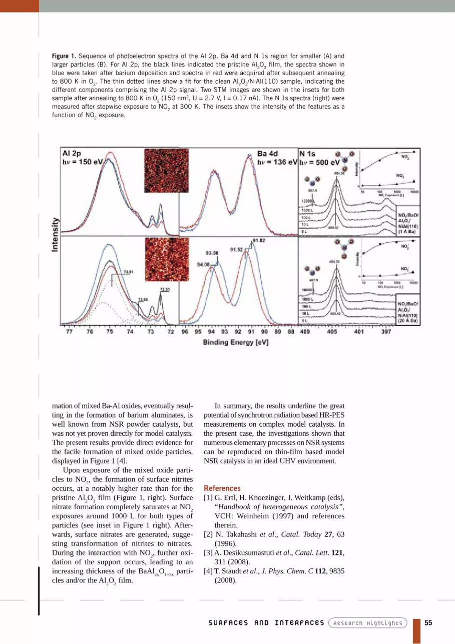
55Research Highlights sURFACEs AND iNTERFACEs
mation of mixed Ba-Al oxides, eventually resul-ting in the formation of barium aluminates, is well known from NSR powder catalysts, but was not yet proven directly for model catalysts. The present results provide direct evidence for the facile formation of mixed oxide particles, displayed in Figure 1 [4].
Upon exposure of the mixed oxide parti-cles to NO2, the formation of surface nitrites occurs, at a notably higher rate than for the pristine Al2O3 film (Figure 1, right). Surface nitrate formation completely saturates at NO2 exposures around 1000 L for both types of particles (see inset in Figure 1 right). After-wards, surface nitrates are generated, sugge-sting transformation of nitrites to nitrates. During the interaction with NO2, further oxi-dation of the support occurs, leading to an increasing thickness of the BaAl2xO1+3x parti-cles and/or the Al2O3 film.
In summary, the results underline the great potential of synchrotron radiation based HR-PES measurements on complex model catalysts. In the present case, the investigations shown that numerous elementary processes on NSR systems can be reproduced on thin-film based model NSR catalysts in an ideal UHV environment.
References[1] G. Ertl, H. Knoezinger, J. Weitkamp (eds),
“Handbook of heterogeneous catalysis”, VCH: Weinheim (1997) and references therein.
[2] N. Takahashi et al., Catal. Today 27, 63 (1996).
[3] A. Desikusumastuti et al., Catal. Lett. 121, 311 (2008).
[4] T. Staudt et al., J. Phys. Chem. C 112, 9835 (2008).
Figure 1. Sequence of photoelectron spectra of the Al 2p, Ba 4d and N 1s region for smaller (A) and larger particles (B). For Al 2p, the black lines indicated the pristine Al2O3 film, the spectra shown in blue were taken after barium deposition and spectra in red were acquired after subsequent annealing to 800 K in O2. The thin dotted lines show a fit for the clean Al2O3/NiAl(110) sample, indicating the different components comprising the Al 2p signal. Two STM images are shown in the insets for both sample after annealing to 800 K in O2 (150 nm2, U = 2.7 V, I = 0.17 nA). The N 1s spectra (right) were measured after stepwise exposure to NO2 at 300 K. The insets show the intensity of the features as a function of NO2 exposure.

56 Research Highlights sURFACEs AND iNTERFACEs
C. Bruno1, M. Marcaccio1, D. Paolucci1, C. Castellarin-Cudia2, A. Goldoni2, A. V. Streletskii3, T. Drewello3, S. Barison4, A. Venturini5, F. Zerbetto1, F. Paolucci1
1INSTM Sezione di Bologna, Dipartimento di Chimica “G. Ciamician”, Università di Bologna, Italy2Sincrotrone Trieste S.C.p.A., Trieste, Italy3Department of Chemistry, University of Warwick, Coventry, England4IENI – CNR, Padova, Italy5ISOF – CNR, Bologna, Italy
E-mail: [email protected]
ELECTROCHEMICAL OxIDATION OF C60 AND GROwTH OF p- AND n-DOpABLE FULLERENE FILMS
The facile reduction of fullerenes, exemplified by the electrochemical stepwise reversible addition of up to six electrons to C60 and C70 [1], contrasts with their difficult oxidation [2].
We recently succeeded in obtaining the cyclic voltammetric reversible generation of C60
2+ and C60
3+ [3]. This was allowed by the adop-tion of ultra-dry solvents and electrolytes with very high oxidation resistance and low nucle-ophilicity which ultimately led to the seren-dipitous discovery that C60 may be oxidatively
electropolymerized [4] thus forming stable conducting polymeric films able to transport both holes and electrons, a feature that is not possessed by many organic systems.
Figure 1A shows multi-scan cyclic voltam-metric (CV) curves of a dichloromethane solu-tion of C60 run between 0 and 2.20 V, i.e. cor-responding to the generation of C60
2+ [3]. The curves show the appearance of new peaks and an overall progressive current increase due to the formation of a redox-active deposit on the electrode. The electrochemical response is strongly reminiscent of that observed in text-book examples of conducting polymers.
Despite of the formation of a thick film (≥ 500 nm) on the electrode, the CV curves shown in Figure 1A are still largely dominated by the diffusion-controlled voltammetric peaks typical of pristine C60 in solution. The voltam-metric response of the film changes signifi-cantly in a blank electrolyte solution (Figure 1B): while the peaks due to C60 in solution are no longer observed, the curve displays a reversible behavior that comprises very broad reversible peaks located in the same potential regions where pristine C60 undergoes either oxidation or reduction. The film retains the electroactive properties of the pristine fuller-ene, with significant differences that may be attributed to the formation of a bonded struc-ture where charge may be injected and trans-ported. This is inferred from the observation that the CV peaks of pristine C60 in Figure 1A are only slightly affected by the presence of the film except for a large increase in intensity, in turn associated to an increase of the elec-troactive surface area. The separation between forward and reverse peaks has not greatly increased even in the presence of thick films
Figure 1. (A) Cyclic voltammetric curves of a 0.15 mM solution of C60 in dichloromethane; the solution is 0.05 M in (TBA)AsF6. Scan rate: 1.0 V. The multi-scan cyclic voltammetric curves show progressive film growth. (B) Cyclic voltammetric curves (1st and 50th cycles) of a film-modified Pt electrode in a 0.05 M blank (TBA)AsF6 dichloromethane solution. The film displays both cathodic and anodic behaviour (highly reproducible over repetitive cycling). Scan rates: 0.4 V/s. T = 298 K.

57Research Highlights sURFACEs AND iNTERFACEs
thus suggesting that the film resistivity is neg-ligible. Quantum chemical calculations at B3LYP/6-31G* level suggest that sp3 carbon centers form at the site of polymerization, thus preventing the formation of a fully conjugated structure. Charge transport should occur in the polymer via a hopping mechanism.
Physical-chemical characterizations of the film were carried out with atomic force micro-scopy, Raman, infrared and X-ray-photoelec-tron (XPS) spectroscopies, secondary ion mass spectrometry (SIMS), scanning electron microscopy, energy-dispersive X-ray analysis (EDX) and matrix-assisted laser desorption/ionization [4]. For example, figure 2a shows the C 1s measured with XPS. Compared to pristine C60 films, the shift and lineshape of the measured C 1s peak is consistent with the for-mation of a conducting polymer. Importantly, XPS measurements evidenced that there is no reaction between the counter-ions and C60. The addition of F atoms from AsF6
- onto the fuller-ene cage was in fact a possible drawback of the present anodic electropolymerization route. Fingerprints of the C-F bonds are expected at higher energy than the observed binding energies. The F 1s binding energy (Figure 2b) and the atomic ratio F:As ~ 6 are consistent with the presence of supporting electrolyte (TBA)AsF6 entrapped into the pol-ymer. This was also confirmed by EDX and SIMS.
The neutral films exposed to air and sol-vents showed a remarkable stability and did not undergo any significant degradation under electrochemical oxidation or reduction condi-tions, provided that highly aprotic and non-nucleophilic conditions were used. Finally,
Riccò et al. prepared solid-state C60(AsF6)2 and using powder X-rays diffraction, they showed that C60 molecules develop intercon-nections via coupled intermolecular bonds (2+2 cycloaddition) forming 1D chains with zigzag arrangements.
References[1] Q. Xie et al., J. Am. Chem. Soc. 114, 3977
(1992); Y. Oshawa et al, J. Chem. Soc., Chem. Commun. 781 (1992).
[2] Q. Xie et al., J. Am. Chem. Soc. 115, 9818 (1993).
[3] C. Bruno et al., J. Am. Chem. Soc. 125, 15738 (2003).
[4] C. Bruno et al., J. Am. Chem. Soc. 130, 3788 (2008).
Figure 2. XPS of the C 1s (a) and F 1s (b) core levels. A possible structure of polymeric double linked (C60)2
2+ is shown. The arrow indicates the binding energy of undoped non-polymeric C60 films. The energy where the peak corresponding to C-F bond should be expected is shown with a triangle.

MATERIALS SCIENCE

59Research Highlights MATERiALs sCiENCE
Condensed matter science over the last several decades has been driven
mainly by the discovery of new materials exhibiting exotic properties.
Starting from the end-seventies, one can recall the discoveries of “valence
fluctuation” phenomenon, heavy fermions, quasi-crystals, high temperature
cuprate superconductors, fullerenes, carbon nanotubes, other exotic
superconductors, inorganic nanomaterials, colossal magnetoresistive materials,
and graphene, to name just a few.
Materials Physics and Chemistry are now accepted, distinct and one of the
most vibrant sub-branches of science where the study of such materials and their
properties have led us to many largely unexplored and little understood frontiers
of science. This necessitated, as well as was helped along by, tremendous
progress both in terms of experimental and theoretical tools over these decades.
Therefore, it is not surprising to find that activities within Elettra reflect this
global trend, with about one third of over 200 publications listed in the Elettra
data base for 2007 can be classified as materials science research. Reflecting
the wide spectrum of investigations under the broad banner of materials science,
Elettra-based research covered areas ranging from magnetism to electronic
properties, from atomic structure to bulk structures via the mesoscopic scale,
from fundamentally important issues to issues with great technological
implications. In keeping with the technological innovations that have given rise
to increasingly sophisticated experimental possibilities, Elettra has responded to
this ever-increasing challenge by designing and commissioning new and
sophisticated beamlines to probe novel properties of matter, while continuously
upgrading several of the older beamlines to keep their competitive edge. In this
context, it is worthwhile to note that materials science, more than any other
single discipline, requires the most diverse range of techniques to elucidate the
complex range of properties of matter it deals with; for example, a reasonable
understanding of a single system may require addressing its electronic and
magnetic properties, its long-range geometric structure as well as its local
structure (that may be distinctly different from the global structure), shape and
ordering (when probing finite size systems), etc. Therefore, it does not come as
a surprise that materials science research at Elettra accesses the widest range
of beamlines, totaling more than a third of the beamlines here, including photon
scattering, absorption and photoemission techniques with photon energies
varying from a few meV to several keV.
While it is difficult to select a “representative” set of examples for such a
wide range of activities and applications of Elettra facilities to investigate materials
science, in the following, a limited set of investigations is highlighted to give a
glimpse of the diversity of issues addressed and techniques employed.
Dipankar Das Sarma
Educated at IIT Kanpur for MSc Physics in 1977 and at IISc Bangalore for PhD degree in 1982, Dipankar Das Sarma is author of more than 300 research publi-cations with an H-index of 41 and over 6000 citations. Fellow of all three major Academies in India and also a Fellow of the American Physical Society and of TWAS. Recipient of most major awards and recognitions within India and sev-eral international prizes. Adjunct or Vis-iting Professor at several important institutions. Member of the Editorial Board or Advisory Board of about 8 sci-entific journals in Physics and Chemis-try. Presently, MLS Chair Professor of Physics and Chairman, Centre for Advanced Materials at Indian Associa-tion for the Cultivation of Science. Mem-ber of several national and international committees, including Chairman, Pro-posal Review Committee at Elettra.

60 Research Highlights MATERiALs sCiENCE
P. De Padova1, C. Quaresima1, P. Perfetti1, B. Olivieri2, C. Leandri3, B. Aufray3, S. Vizzini3, H. Oughaddou4, G. Le Lay3
1 CNR-ISM, Roma, Italy2 CNR-ISAC, Roma, Italy3 CRMCN-CNRS, Marseille, France4 Commissariat à l’energie Atomique, Laboratoire SIMA, DSM-IRAMIS-SPCSI, Gif sur Yvette, France, and Département de Physique, Université de Cergy Pontoise, France
E-mail: [email protected]
BURNING MATCH OxIDATION pROCESS ON CHIRAL SILICON NANOwIRES
Silicon nanowires (SiNWs) are one of the most stimulating structures in nanoscience due to the central function played by Si in the world of semiconductor industry and in the fundamental physics. The high resolution (HR) photoemission spectroscopy (PES) experiments on self-aligned straight SiNWs on the silver (110) surface were carried out at the VUV beam line of ELETTRA in Trieste, whereas the STM and STS observations of the SiNWs were performed at the CINaM in Mar-seille [1,2].
Figure 1a displays HR Si 2p PES spectrum measured at ϑe-=0° of 0.5 ML Si deposited on Ag(110) surface at room temperature (RT). This peak is composed of four (spin-orbit splitted) components S1, S2, S3 and S4 attributed to different Si atoms located at the SiNWs. The spectrum is completely dominated by the
S2 component. Its full width at half maximum (FWHM) is 130 meV, which is the narrowest Si 2p line shape ever reported in a solid phase photoemission experiment. Another important result arises from the fit of the Si 2p spectra, which imposes two significantly different val-ues of the Lorentzian FWHMs Γ1/2 = 40 meV and Γ3/2 = 25 meV respectively for the Si 2p1/2 and Si 2p3/2 lines, which have a common Gaussian FWHM of just 95 meV. The evi-dence of the extra broadening of the 2p1/2 Lorentzian FWHM, points to a non-radiative Coster-Kronig Auger LLV transition, forbid-den in semiconducting Si (Si gap: 1.12 eV), but allowed in a metallic state.
Figure 1b shows a 10.2 x 10.2 nm2 filled-states STM image of 0.5 ML Si/Ag(110) depos-ited at RT. The x2 periodicity of the SiNWs parallel to the Ag direction and a misalignment
Figure 1. (a) Normal emission convoluted Si 2p core level for SiNWs after the deposition of 0.5 ML of Si on Ag(110). (b) 10.2x10.2 nm2 filled-states STM image. (c) 3D view of 10.2x10.2 nm2 filled-states STM image: dip asymmetry at right-side.

61Research Highlights MATERiALs sCiENCE
not affected by the O2 atoms. At higher oxy-gen exposure, the oxidation of the Si NWs proceeds progressively from their extremities along the [–110] direction maintaining an atomic structure preferably developed along the one-dimension of the wires. This is clear-ly observed in the Figure 2b at 30 L and at higher oxygen exposure. The oxidation behaves according to a match–burning pro-cess, where the extremities of the Si NWs are considered as the head of a match, which reacts with oxygen.
These characteristic features discovered through the HR STM observations of the oxi-dized Si NWs find their corresponding signa-tures in spectroscopy measurements. Figures 2c and 2d report the Si 2p core-level spectra measured on the Si NWs, after 20 and 40 L of O2 exposure. The virgin part of the Si NWs on Ag(110) reveals the four doublets, S1, S2, S3 and S4, and the oxidized part at higher binding energy further four new peaks S1+, S2+, S3+ and S4+ assigned to the +1, +2, +3 and +4 oxidation states of Si.
References [1] P. De Padova, C. Quaresima, P. Perfetti, B.
Olivieri, C. Leandri, B. Aufray, S. Vizzini, G. Le Lay, Nano Lett. 8, 271 (2008).
[2] P. De Padova, C. Leandri, S. Vizzini, C. Quaresima, P. Perfetti, B. Olivieri, H. Oughaddou, B. Aufray and G. Le Lay, Nano Lett. 8, 2299 (2008).
between the right and left side protrusions cor-responding to a glide of one aAg[-110] lattice parameter are evidenced. The line profile along the [100] direction assigns a lateral size of ~ 1.6 nm for every single SiNW, i.e. an x4 width of 4aAg[100], while the height is about 0.2 nm. The nanostructures are never terminated along the [100] Ag direction, but along the [3-34] direc-tion of the Ag(110) surface. This fact confers to NWs an asymmetric morphology with respect to the plane perpendicular to the (110) surface. The asymmetric transverse shape of the SiNWs is evidenced by the 3D view reported in Figure 1c of the previous STM image, where a dip is clearly noticeable on the right side of each NW. On other extended areas there is the reverse situation where the dip is always situated on their left side and the nanostructures are termi-nated along the [-334] direction. Hence the two types of symmetry breaking NWs phase sepa-rate in large “magnetic-like” domains of oppo-site “spin” to recover the overall mirror sym-metry of the bare surface.
Figures 2a and 2b display a 22 x 22 nm2 and 27.3 x 27.3 nm2 filled-states STM images of 0.5 ML Si deposited at RT on the Ag(110) surface exposed to a 15 L and 30 L doses of O2. The termination-sides of the clean Si NWs are drastically modified, showing apparently some black voids or hollows (circled images in Figure 2a that announce the onset of the oxidation process. These termination-sides are involved at first in the oxidation process, whereas the almost totality of the Si NWs is
Figure 2. Filled-states STM images of Si NWs on Ag(110) at different oxygen doses: (a) 22 x 22 nm2 at 15 L. (b) 27.3x27.3 nm2 at 30 L. Convoluted Si 2p core levels of SiNWs grown on Ag(110) and exposed to O2 at: (c) 20 L and (d) 40 L.

62 Research Highlights MATERiALs sCiENCE
A. Kolmakov1, S. Potluri1, T. O. Mentes2, M. A. Nino2, A. Locatelli2, A. Barinov2, L. Gregoratti2, M. Kiskinova2
1 Southern Illinois University at Carbondale, Illinois 62901-4401, USA2 Sincrotrone Trieste S.C.p.A., Trieste, Italy
E-mail: [email protected]
SURFACE SCIENCE AppROACH TO UNDIVIDUAL qUASI-1D NANOSTRUCTURES: SpEM, x-pEEM, LEEM AND LEED ON SnO2 NANOSTRUCTURES
Metal oxide quasi one-dimensional nano-structures such as wires, belts rods and tubes are in the focus of intense research due to their unique potential for applications in the nano-(opto)electronics, chemical sensing and catalysis [1,2]. Due to the high surface-to-bulk aspect ratio of these materials, the sur-face structural and electronic properties play a dominant role, which has motivated the cur-rent rapidly growing communities exploring the modification of these properties by vary-ing the size, defects density, doping level etc. In this respect surface sensitive electron spec-troscopies are among the most appropriate methods, but they needed to step into micro-scopic world in order to probe individual nanostructures. Thanks to the ultra-bright and tunable photon beams provided by the syn-chrotron facilities the Scanning PhotoElectron Microscopy (SPEM) and X-ray Photoelectron Emission Microscopy (XPEEM) have become
amenable with the size domain of the nano-structures (10-100 nm) [3,4].
Using the SPEM and XPEEM instruments at Elettra in combination with structural sen-sitive Low Energy Electron Microscopy (LEEM) we explored the surface structure and chemical states of individual SnO2 nano-wires and nanobelts [4]. Figure 1a shows the LEEM image of a SnO2 nanobelt and the micro-LEED pattern, which manifests the (010) structure of side facets comparable to the ones observed for SnO2 rutile crystals. Figure 1b shows the XANES spectrum (vio-let) of the SnO2 nanobelt, which contains overlapping features of SnO2 and SnO phases, indicative for certain degree of oxygen defi-ciency. This was confirmed by Sn 3d and O 1s spectra measured on individual nanobelts with SPEM [4]. We also demonstrated the possibility to use SPEM for probing electron transport properties by imaging in-situ the
Figure 1. (a) LEEM image (FOV 20 µm) and the micro-LEED pattern, corresponding to the (010) facet of the nanostructure (b) XANES spectrum (violet) taken from individual SnO2 nanowire, which contains features characteristic for the SnO (yellow) and SnO2 (blue) compounds. The energy scale is offset with respect to the first maximum of Sn 3d5/2.
(a) (b)

63Research Highlights MATERiALs sCiENCE
nanostructures wired as active element of the chemiresistor device. Figure 2a shows a sketch of the fabricated chemiresistor gas sensing device: the SnO2 nanowire network contacted by two electrodes. The support is a Si3N4 membrane with periodic holes, allow-ing the nanowires placed over the holes to be locally probed. The potential of SPEM for analyzing the charge distribution and trans-port properties is based on the correlation between the applied potential and kinetic energy of the emitted photoelectrons. The Sn 4d images in Figure 2b demonstrate that we can monitor the percolating character of the conductivity: the strong attenuation of the sig-nal from certain wires when biasing one of the electrodes indicates their higher resistivity.
These pioneering results are opening new avenues to explore the effect of size and envi-ronment (e.g. gases and temperature) on the surface activity, electronic properties and functionality of nano-materials.
References [1] A. Kolmakov, Int. J. Nanotechn. 5, 250
(2008).[2] A. Kolmakov, X. Chen, M. Moskovits, J.
Nanosci. Nanotechn. 8, 111 (2008).[3] S. Günther, B. Kaulich, L. Gregoratti, M.
Kiskinova, Prog. Surf. Sci. 70, 187 (2002).
[4] A. Kolmakov, S. Potluri, A. Barinov, T. Mentes, L. Gregoratti, M. Nino, A. Locatelli, M. Kiskinova, ACS Nano 2008 in press.
Figure 2. (a) Sketch of the device and the SPEM set-up for imaging the Sn 4d emission from the SnO2 nanowire mats under variable bias conditions. (b) Sn 4d maps of the chemiresistor of percolating nanowires taken with grounded electrodes (top) and with right electrode biased at -8 V (bottom). The differences in the Sn 4d images are due to the presence of highly resistive nodes (marked with white circles), which impede even potential distribution along the nanowires. The caused rigid electron energy shift is beyond the energy window of the analyzer, tuned to the Sn 4d emission with grounded electrodes, which results in strong attenuation of the signal from certain nanowires.
(a)
(b)

64 Research Highlights MATERiALs sCiENCE
P. Falcaro1, S. Costacurta1,2, L. Malfatti2, T. Kidchob2, M.F. Casula3, M. Piccinini4, A. Marcelli4, B. Marmiroli5, H. Amenitsch5, M. Takahashi6, P. Innocenzi2
1 Associazione CIVEN Venezia Marghera, Italy2 Laboratorio di Scienza dei Materiali e Nanotecnologie (LMNT), Università di Sassari, Alghero, Italy3 Dipartimento di Scienze Chimiche, Università di Cagliari, Monserrato, Italy4 Laboratori Nazionali di Frascati – INFN, Italy5 Institute of Biophysics and Nanosystems Structure Research, Austrian Academy of Sciences, Graz, Austria6 Institute for Chemical Research, Kyoto University Gokasho, Japan
E-mail: [email protected]
FABRICATION OF x-RAY pATTERNABLE MESOSTRUCTURED SILICA FILMS
Mesoporous films have aroused great interest because of the high ordered porosity, chemical compositional control, high thermal stability, possibility to use inorganic or hybrid porous matrix to grow or embed functional molecules or active nanoparticles [1,2]. Prospected appli-cations in advanced devices have be raised, among which, for instance, ultralow-k dielec-tric or photonic materials, sensing and solar cell devices, photonic and catalysis applica-tions, etc.
Until now, research on mesostructured films has been focused intensively on the control of geometric factors, such as the symmetry and the degree of order of the mesostructure, chem-ical composition, sensing properties. To pro-duce a device based on mesoporous films another step is required: the capability to con-trol the shape and geometry (scale of micron or millimetre). Acquiring the technology for designing devices is the key to engineering the materials and fabricate nano-devices [3].
We have successfully developed a highly-integrated patterning technology based on the response to X-ray radiation of mesostructured materials; we have combined different syn-chrotron technologies for in situ characteriza-tion, processing control and final material pro-duction.
Deep X-ray Lithography (DXRL) has been used to pattern mesostructured silica thin films. This lithographic approach is based on selective template removal and silica polycondensation induced by synchrotron radiation. The areas of the film that are not exposed to radiation can be selectively etched owing to a lower crosslinking degree of the inorganic network. An important advantage of this method is the possibility to
simultaneously remove the surfactant and to induce condensation of the silica network in a single-step process. Small-angle X-ray Scatter-ing (SAXS), DXRL and IR microimaging beam-lines at Elettra have been employed during the same experiment. For the first time X-ray pat-ternable mesostructured silica films have been fabricated; this experiment opens the route to new technologies for functional applications.
Block copolymer surfactant Pluronic F127, bis(4-tert-butylphenyl)iodonium p-toluenesul-fonate (PG), and ethanol (EtOH) were purchased from Aldrich and used as-received. P-type/boron doped, (100) oriented, 400mm thick silicon wafers (Si-Mat) were employed as the substrates. A stock sol was prepared, containing 3.1 mL of ethanol, 4.3 mL of tetraethylorthosilicate, and HCl (0.355 mL, 0.77M). This sol was left to react under stirring in a closed vessel for 1 h at room temperature. A templating solution was prepared dissolving Pluronic F127 (1.3 g) in ethanol (15 mL), HCl (1.5 mL, 0.06M) and 0,6 bis(4-tert-butylphenyl)iodonium p-toluenesul-fonate. Silicon substrates were dip-coated in the precursor sol at the withdrawal speed of 2.3 mm s-1 and at 40% relative humidity (RH). The as-deposited films were patterned by DXRL 3 h after deposition. The samples were exposed through X-ray masks containing test patterns of different size, shape, and geometry (5 to 500 mm). The masks had a gold absorber. After this procedure, the films were chemically etched to remove the unirradiated parts of the mesostruc-ture. The samples were sonicated in a developing solution (mixture of ethylene glycol and etha-nol), and then dried under an air flow. The films, after the lithographic process, were thermally treated at 150 °C for 1 h.

65Research Highlights MATERiALs sCiENCE
In order to perform GISAXS tests, as-deposited mesostructured films were exposed to synchrotron radiation through a mask that covered half of the film, so that a large area of the sample could be investigated by the prob-ing beam. GISAXS experiments showed that in both the irradiated and the masked regions, the mesostructure has 2D hexagonal symme-try (space group p6m) [4]. TEM measurements have confirmed a p6m mesostructure with cylindrical micelles. A comparison between the GISAXS patterns with and without mask has shown that no substantial change in spot position and sharpness occurred, leading to conclude that no change in mesostructure symmetry took place upon deep X-ray pattern-ing (Figures 1a and 1b ). The exposure of the films to X-rays did not cause, therefore, any structural changes in mesophase or mesostruc-ture damage.
The regions that were not exposed to X-ray radiation could be easily etched. This develop-ing process is fast and effective, and optical profilometry measurements have revealed that the masked areas of the samples were com-pletely removed by etching. Figure 1c shows portions of a mesoporous film patterned with pillars subsequently etched. We have also evaluated if the etching process affects the mesostructure, because in the etching proce-dure the whole film is immersed into the solu-tion: this could cause a partial degradation of the Si–O–Si network resulting in loss of order or collapse of the inorganic walls with mes-ostructure disruption.
This work shows the possibility to pattern mesotructured films in order to control geom-etry and to fabricate functional devices. No change in the diffraction patterns of the etched film has been detected, indicating that the mesostructure is retained upon etching. Mes-ostructure preservation is very important from the viewpoint of applications, in that the prop-erties associated with the order (e.g., high spe-cific surface area, pore accessibility) must be retained to ensure the functionality of the material.
References[1] P. Falcaro, S.; Costacurta, G. Mattei, H. Amen-
itsch, A. Marcelli, M. C. Guidi, M. Piccinini, A. Nucara, L. Malfatti, T. Kidchob, P. Inno-cenzi. J. Am. Chem. Soc. 127, 3838, (2005);
[2] a) D. Buso, P. Falcaro, S. Costacurta, M. Guglielmi, A. Martucci, P. Innocenzi, L. Malfatti, V. Bello, G. Mattei, C. Sada, H. Amenitsch, I. Gerdova, A. Haché. Chem. Mater. 17, 4965, (2005); b) S. Costacur-ta, L. Malfatti, P. Innocenzi, H. Amen-itsch, A. Masili, A. Corrias, M. F. Casula Microporous and Mesoporous Mater., in press (2008) DOI:10.1016/j.micromeso. 2008.02.003
[3] P. Innocenzi, T. Kidchob, P. Falcaro, M. Takahashi, Chem. Mater. 20, 607, (2008).
[4] D. Grosso, Galo J. de A. A. Soler-Illia, F. Babonneau, C. Sanchez, P.A. Albouy, A. Brunet-Bruneau, A. Ruud Balkenende, Adv. Mater., 13, 1085, (2001).
Figure 1. Grazing incidence small-angle X-ray scattering of the non-irradiated (a) and irradiated (b) mesostructured film regions, respectively. Both patterns show a p6m symmetry in the space group and have a d-spacing of 12 nm. Mesostructured silica pillars with dimensions of 350 nm (height) x 100 µm (FWHM - diameter) have been obtained by X-ray patterning procedure (c).

66 Research Highlights MATERiALs sCiENCE
N. Baccile1, C. V. Teixeira2, H. Amenitsch3, F. Villain4, M. Lindén2, F. Babonneau1
1 Laboratoire de Chimie de la Matière Condensée de Paris (LCMCP), Université Pierre et Marie Curie-Paris 6 and CNRS, Paris, France 2 Department of Physical Chemistry, Åbo Akademi University, Turku, Finland 3 Institute of Biophysics and Nanosystems Research, Austrian Academy of Sciences, Graz, Austria 4 Chimie Inorganique et Matériaux Moléculaires (CIM2), Université Pierre et Marie Curie-Paris 6 and CNRS, Paris, France
E-mail: [email protected]
TIME-RESOLVED in situ SMALL-ANGLE x-RAY DIFFRACTION ExpERIMENTS FOR A BETTER UNDERSTANDING OF THE FORMATION OF SURFACTANT-TEMpLATED SILICA
Nanoscience is a relatively new discipline in which common interest arose worldwide in the past 20 years. The two main approaches, which are used to build and control matter, are generally referred to as top-down and bottom-up. Top-down approach mainly con-sists in casting matter into nano-objects by using patterning techniques, like in the fab-rication of transistors and microchips. On the contrary, the bottom-up approach consists in building nano-objects atom-by-atom, starting from single atom to groups of molecules and finally to materials with given nanostructures. This communication deals with the formation of nanomaterials with ordered porosity via a bottom-up approach. These materials are ob-
tained through assemblies of two types of ob-jects: surfactant molecules (e.g. cetyltrimeth-ylammonium bromide, C16H33N
+(CH3)3Br-, CTAB) which have a tendency to form oil droplets in water, around which silica precur-sor (e.g., tetraethoxysilane, Si(OEt)4, TEOS) will react to form a silica layer (Figure 1). The growth of the silica layers will then lead to the formation of silica-based powders in which the oil droplets are trapped in ordered arrays. Then upon calcination, the organic phase can be eliminated to give a silica pow-der with a controlled and ordered porosity, which can find many applications in the field of catalysis, sensors, drug delivery, depollu-tion devices.
Figure 1. Scheme representing our time-resolved in situ approach to study the formation of surfactant-templated silica powder.

67Research Highlights MATERiALs sCiENCE
The objective of this communication is to better understand the formation of such silica-surfactant assemblies governed by complex self-assembly mechanism between organic and inorganic moieties. We follow in real time the development of the ordered silica-surfactant phase using Small Angle X-ray Diffraction. Similar studies exist for systems prepared under basic conditions. Here, strongly acidic conditions are used that modify the charge on the growing silica species, and thus the type of interactions with the surfactants.
The whole reaction takes place in a con-ventional glass beaker at 25°C and atmospheric pressure. At time zero, the surfactant molecules (CTAB) are homogeneously dispersed in water together with the silica precursor (TEOS). Once in contact with water, TEOS reacts through hy-drolysis and condensation to form silica. During the reaction, the solution mixture is continuously pumped out of the beaker in a closed circuit through a capillary tube placed in front of the X-ray beam. The X-ray diffraction patterns are thus collected regularly on an image plate.
Three different systems are studied with a constant TEOS/CTAB ratio (1:0.12) and various water concentrations. Figure 2 shows the time-resolved evolution of the X-ray patterns ob-tained for one system (TEOS:CTAB:HCl:H2O = 1:0.12:9.2:130).
For each system, one diffraction peak ap-pears first at increasing reaction times with di-lution (from 100 s to 300 s). At longer times, two additional diffraction peaks are observed at higher q-values, which indicate an increase in the ordering of the scattering objects which can be described as surfactant micelles cov-ered with a silica layer. The q-value is actu-ally related to the distance between micelles,
which is around 4 nm. The associated distanc-es for each peak allow us to identify that they originate from a two-dimensional hexagonal close packing array of cylinders. The main re-sult extracted from these experiments is the di-rect formation of this hexagonal phase in each case, with no other transient phase. The time evolution of the main peak in the XRD pat-tern – namely its associated d-spacing and its full-width-at-half-maximum - shows two dis-tinct stages which are also strongly dependent on the sol composition. There seems to be a co-existence of an ordered phase and a disor-dered one for longer times under experimental conditions (acidic pH) compared to the usual ones (basic pH), indicating that the ordering process is clearly slower in our case.
These results were also coupled to com-plementary Raman scattering experiments (not reported here) to follow also in real time, before precipitation, the hydrolysis of TEOS. This technique is sensitive to the vibration mode of the molecule, and here to the sym-metric breathing mode of the Si(OEt)4 tetra-hedron. Once one Si-OEt group is hydrolyzed and replaced by one Si-OH group, the perfect symmetry is disrupted and the intensity of the Raman signal decreases. These experiments confirm the increasing rate of the hydrolysis reaction with TEOS concentration, and more interestingly, demonstrate the acceleration of the hydrolysis rate in presence of CTAB mi-celles due to micellar solubilization and sur-factant stabilization of emulsion droplets.
Reference[1] N. Baccile, et al., Chem. Mater. 20, 1161
(2008).
Figure 2. Time-resolved XRD patterns showing the formation of the silica-surfactant ordered phase (TEOS:CTAB:HCl:H2O = 1:0.12:9.2:130). A data sampling time of 10 s per frame was used.

68 Research Highlights MATERiALs sCiENCE
P. Dore1, A. Perucchi2, M. Ortolani3, D. Di Castro1, S. Lupi1,2, V. Ferrando4, M. Putti4, I. Pallecchi4, C. Ferdeghini4, X. X. Xi5
1 CNR-INFM Coherentia and Dipartimento di Fisica, Università di Roma La Sapienza, Rome, Italy 2 Sincrotrone Trieste S.C.p.A., Trieste, Italy3 CNR-Istituto di Fotonica e Nanotecnologie, Rome, Italy4 CNR-LAMIA and Università di Genova, Genoa, Italy5 Department of Physics Pennsylvania State University University Park, USA
E-mail: [email protected]
TwO-BAND pARALLEL CONDUCTIVITY AT TERAHERTz FREqUENCIES IN THE SUpERCONDUCTING STATE OF MgB2
The recent discovery of superconductivity in MgB2 has raised a large interest [1] because of an unprecedentedly high TC (≈40 K) in a con-ventional BCS superconductor, in which the phononic origin of the superconducting pai-ring has been established. Furthermore, MgB2 clearly shows the existence of two electronic bands (π and σ) which origin two distinct energy gaps (∆
σ and ∆
π) in the superconduc-
ting state. Since the two-band superconducti-vity is an intriguing phenomenon that, althou-gh addressed theoretically, had been never observed before, MgB2 gives a unique oppor-tunity for testing theoretical models of BCS superconductivity in the two-band case.
Infrared spectroscopy can have an impor-tant role in studying the low-energy electro-dynamics of complex systems. In particular, reflectance measurements at terahertz (THz) frequencies on a superconducting system at temperatures below the critical temperature TC can allow the determination of the super-conducting energy gap ∆ in a non-invasive way. For example, in a isotropic s-wave BCS superconductor, the reflectance R(ω) for T<< TC abruptly approaches the unity at ω=2∆ (optical gap), thus giving a maximum in the ratio RS/RN, where RS and RN are the reflec-tances in the superconducting and normal sta-tes, respectively.
In the THz spectra of the two-band MgB2 superconductor, only a feature at ω≈2∆
π was
generally seen with no evidence of the σ-gap [2]. On the contrary, the effect of the σ-gap is dominating in a realistic two-gap modelling based on the generally employed two-band parallel conductivity assumption (i.e., inde-pendent BCS responses of the two bands). This inconsistency raises an important pro-
blem, suggesting that this assumption can be questioned when applied at THz frequencies.
We performed reflectance measurements on high-quality MgB2 epitaxial films [3] at the infrared beamline SISSI. Since MgB2 quickly degrades in air, each film was sealed under vacuum in a quartz ampoule after growth and the optical experiments were continuously performed in vacuum. In the THz range (fre-quency ν <4 THz or ω<130 cm−1, photon ener-gies below 16 meV) we measured the intensi-ty reflected by the sample by cycling the tem-perature in the 5-50 K range. We thus obtained R(T)/R(42) (i.e., for T<TC, RS/RN) spectra with high accuracy (± 0.1%). Measurement perfor-med on an ultra-clean MgB2 film with TC=41 K show that R(50 K))/R(42 K) is flat within experimental uncertainties, as expected, whi-le, on decreasing temperature below TC, the R(T)/R(42) increases and a clear edge structu-re becomes evident at T=5 K (Figure 1a). We remark that only the high accuracy of the pre-sent synchrotron measurements allows the detection of an effect as small as 0.5%. The grey line in Figure 1a is the 5 K model spec-trum computed on the basis of the two-band parallel conductivity assumption by employing independently obtained parameters (plasma frequencies Ω
σ and Ω
π, relaxation rates γ
σ and
γπ, energy gaps ∆
σ and ∆
π) to model the BCS
response of each band. The resemblance of the model spectrum with the data is highly signi-ficant, and the edge structure observed in both model and measured spectra around 14 meV can be attributed to the σ-gap. This finding, obtained in a ultra-clean MgB2 film, is a cru-cial result, since it allows us to reconcile THz observations with the predictions of BCS cal-culations.

69Research Highlights MATERiALs sCiENCE
To investigate the effect of the impurity level, we performed R(T)/R(42 K) measure-ments on a second film (TC=40.3 K), previou-sly irradiated with a low fluence of thermal neutrons which only induces a slight increase of the impurity scattering rates, in particular of γ
σ [4]. In this case an edge in the R(5 K)/R(42
K) is observed around 7 meV (Figure 1b). The model spectrum obtained by employing the ultra-clean film parameters, with the exception of γ
σ increased by about a factor 3, is in gene-
ral agreement with the data (Figure 1b). In conclusion, our results (M. Ortolani, P.
Dore et al., Phys. Rev. B 77, 100507, 2008) show that the RS/RN spectrum measured at THz frequencies on a ultra-clean film gives evidence of the σ-gap and can be well descri-bed on the basis of the two-band parallel con-ductivity assumption. In a film with an impu-rity level slightly higher than that of the ultra-clean film, only the effect of the π-gap is well evident, thus explaining the inconsistency between theory and previous THz experiments in terms of different impurity levels. The proof that the two-band parallel conductivity assum-ption can well describe the electrodynamic response of MgB2 at THz frequencies is of general interest since MgB2 epitaxial films are
being extensively investigated for possible applications in superconducting devices and terahertz electronics.
References[1] Comprehensive reviews on the MgB2 pro-
perties are reported in Physica C, 456 (2007)
[2] For a review of infrared studies on MgB2, see: A.B. Kuzmenko, Physica C 456, 63 (2007)
[3] A.V. Pogrebnyakov et al., Phys. Rev. Lett. 93, 147006 (2004).
[4] V. Ferrando et al., J. Appl. Phys. 101, 043903 (2007).
Figure 1. Reflectivity ratios R(T)/R(42 K) in the THz range. The 5 K data are compared to BCS calculations (thick gray line, film thickness 200 nm; dotted line, semi-infinite medium) as obtained, on the basis of the two-band parallel conductivity assumption, by using plasma frequencies Ω
σ = 3.8 eV,
Ωπ = 5 eV (from our
measurements of the absolute reflectance in the entire infrared range), relaxation rates γ
σ=11 meV
(γσ = 37 meV in (b)],
γπ = 7.2 meV, and gap
values ∆σ =7.2 meV,
∆π =2.3 meV
(from tunnelling spectroscopy measurements [4]).

70 Research Highlights MATERiALs sCiENCE
M. Zacchigna1, A. Nicolaou2,3, V. Brouet2, A. Tejeda3, P. Lejay4, S. Hébert5, H. Muguerra5, D. Grebille5, F. Parmigiani6
1 Laboratorio Nazionale TASC, INFM-CNR, Trieste, Italy2 Lab. Physique des Solides, UMR 8502, Université Paris-Sud, Orsay, France3 Synchrotron SOLEIL, Gif-sur-Yvette, France4 Institut Néel, Grenoble, France5 Lab. CRSIMAT, UMR6508, CNRS et Ensicaen, Caen, France6 Sincrotone Trieste S.C.p.A., Trieste and Dipartimento di Fisica, Università di Trieste, Italy
E-mail: [email protected]
ANGLE RESOLVED pHOTOEMISSION AND THE pHYSICS OF CoO2 TRIANGULAR pLANES
Studies on transition metals oxides have been the source for some of the most interesting discoveries in solid state physics in the last decades, due to the richness of the phenomena that these compounds can provide. In the case of cobaltates, one is looking at layered metals, where a triangular plane of Co ions (embedded in CoO2 slabs) can accommodate a varying number of electrons. Recently, the NaxCoO2 family gained a double interest. On one hand, it is promising for industrial applications, because of its high thermoelectric power. On the other hand, its behaviour attracted interest of the solid state community for its rich phase diagram [1]: magnetic transitions, unusual metal-insulator transitions, and, as if it was not
enough, superconductivity were discovered within this family. The superconducting phase, appearing in what can be seen as a doped Mott insulator, reminds of the case of cuprates and triggered even more interest. This called for a detailed determination and understanding of the electronic structure.
Figure 1 displays the Fermi Surface (FS) measured by ARPES of Na0.82CoO2, one of the magnetic phases. Its hexagonal shape is characteristic of the triangular symmetry of the CoO2 slab and agrees well with other ARPES studies of Na cobaltates [2,3]. Because ARPES is very surface sensitive and the Na environment of the surface after cleaving is somewhat ill-defined, one can however wonder how the
Figure 1. (a) Comparison of the structures of Na and misfit cobaltates. The same CoO2 slabs are present in the two families, but separated either by Na or Rock-Salt layers. (b) Fermi Surface of Na0.82CoO2 measured on the BACH beamline at 100eV and 20K. Red points indicate the trace of the BiBaCoO FS.
(a) (b)

71Research Highlights MATERiALs sCiENCE
surface of these materials is representative of the bulk properties. In this framework, we decided to extend our interest to the bigger family of misfit cobaltates, where an inert Bi-O plane “protects” the CoO2 plane, much like in Bi cuprates (see Figure 1). The rationale here is also to evaluate the role of the structure surrounding the CoO2 planes. We demonstrated [4] that the electronic structure of the misfit cobaltate [Bi2Ba2O4].[CoO2]~2 (BiBaCoO) is very similar to that of NaxCoO2. In particular, the FS periodicity is the one dictated by the triangular lattice. The FS crossings for this compound are reported as red points on the FS map of Na0.82CoO2 (Figure 1), evidencing the identical hexagonal shape. The careful analysis of the Fermi velocity (vf), lineshape and size of the FS (kf value) allows a more detailed comparison. Assuming a rigid band filling of the a1g band, the size of the FS in BiBaCoO corresponds to x~0.7. One would then expect a smaller FS in Na0.82CoO2, contrary to the observation of Figure 1. This signals a deviation from the rigid band filling picture, which remains to be clearly understood. It could be attributed to a lower doping at the surface than bulk, but it is also interesting to discuss in connection with the inhomogeneous charge distribution observed by other experiments for this doping range.
In a series of experiments at the BACH and APE beamlines at Elettra and the SIS
Figure 2. Lineshapes at kf for BiBaCoO, BiSrCoO and BiCaCoO. The QP peak forms a narrow (~100meV) band followed by a broad “hump”, superimposed to the contribution from other bands and/or incoherent background. This structure is universal to cobaltates, as show by the comparison of the dispersions for BiBaCo and Na0.82CoO2. Red line and dotted white lines sketched the dispersion of QP and hump, respectively.
beamine at the SLS, we have performed an extensive study of different misfit phases. Unexpectedly, we observed a progressive decrease in the intensity of the quasiparticle (coherent) peak near kf (Figure 2), when the structure of the intercalated Rock-Salt planes is shrinked by use of Ba, Sr or Ca, i.e. the doping is increased from x~0.7 to x~0.8. We showed that this change should not be interpreted as a shift of the band below the Fermi level but rather to a transfer of spectral weight to a hump (incoherent feature) at higher binding energy [4]. The implication of this is of key importance for the interpretation of the lineshape. It emphasizes its peak-dip-hump nature, which is also present in NaxCoO2. We attribute this to a strong (polaronic) coupling to collective excitations (see sketch of Figure 2), which is found to increase with x.
References[1] M.L. Foo et al., Phys. Rev. Lett. 92,
247001 (2004) and ref. therein.[2] H-B. Yang et al., Phys. Rev. Lett. 95,
146401 (2005).[3] D. Qian et al., Phys. Rev. Lett. 96, 216405
(2006).[4] V. Brouet et al., Phys. Rev. B 76, 100403
(2007).

72 Research Highlights MATERiALs sCiENCE
R. Larciprete1,2, L. Petaccia2, S. Lizzit2, A. Goldoni2
1 CNR- Institute of Complex Systems, Italy2 Sincrotrone Trieste S.C.p.A., Trieste, Italy
E-mail: [email protected]
THE ROLE OF METAL CONTACT IN THE SENSITIVITY OF SINGLE wALLED CARBON NANOTUBES TO NO2
In the last years an intrinsic sensitivity of car-bon nanotubes (CNTs) has been reported [1] for diverse gases at room temperature (RT), with particular emphasis on NO2, because of its importance in environmental pollution. For the latter, a detection level on the order of ppm has been measured at RT for CNT based sen-sors. In general the mechanism believed to regulate the response of single walled nano-tubes (SWCNTs) to adsorbed NO2 is identified in the electron transfer from semiconducting CNTs to the oxidising adsorbates, (∼0.1 elec-trons per molecule) [2], which increases the hole carrier density in p-type tubes. However, what is still under debate is if there is at all the possibility to adsorb NO2 on CNTs at RT, as the calculated NO2-CNT binding energies of 0.11÷0.79 eV2 correspond to desorption tem-perature ranging between 45 K and 320 K.
In this study we show that whereas NO2 adsorbs on SWCNTs at low temperature (150 K), at T≥200 K there is no interaction between the tube lattice and NO2 molecules or frag-ments. Thus any change in the CNT transport properties observed at RT can only be the
result of external effects, such as NO2 adsorb-tion on metals in contact with CNTs (residual contaminants, catalyser particles, metal con-tacts). We used high energy resolution X-ray photoemission spectroscopy at the SuperES-CA beamline of ELETTRA to follow the adsorption of NO2 on SWCNTs at different temperatures [3,4]. Figure 1a shows the results obtained at 150 K: the C1s peak intensity diminishes with increasing NO2 dose due to the building up of an adsorbed layer; more-over the binding energy (BE) shift to lower values, undoubtedly indicates the occurrence of charge withdrawal from the C lattice by the NO2 adsorbate. After a dose of 150 L the N1s spectrum exhibits three peaks at 401.5, 404.5 and 407 eV, assigned to NO3 (and/or NO2 mul-tilayer), NO2 and NO species, respectively. On the contrary the N1s spectra measured while dosing NO2 (∼ 400 L) at 200 K remain flat and simultaneously no sign of C1s attenuation and line shape changing is revealed (Figure 1b). Thus NO2 molecules do not interact with SWCNTs at T≥200 K. The effect of NO2 adsorption on SWCNTs covered by a uniform
Figure 1. (a) Sequence of C1s spectra measured while dosing SWCNTs with 150 L of NO2 at 150 K; inset: N1s spectrum measured at the end of the up-take. (b) C1s spectra measured on SWCNTs before (black) and after (yellow) the exposure to 400 L of NO2 at 200 K; inset: sequence of N1s spectra measured while dosing the gas.

73Research Highlights MATERiALs sCiENCE
distribution of Rh clusters (inset in Figure 2c) is illustrated in Figure 2. The C1s spectra mea-sured before and after the addition of Rh (Fig-ure 2a) indicate that the adsorbed metal atoms only determine a down BE shift of ~ 60 meV, which has to be attributed to the charge trans-fer across the Rh-SWCNTs junction. The cor-responding Rh3d5/2 spectrum (B in Figure 2b) exhibits two components at 307.19±0.01 eV (B) and 306.75±0.01 eV (S) attributed to Rh adatoms located below and at the surface sites. The effect on the C1s spectrum of 1 L of NO2 is a further down shift of 145 meV (C in Fig-ure 2a), undoubtedly mediated by the presence of the Rh nanoclusters which get oxidized. Bonding of NO2 to Rh atoms is witnessed by the Rh3d5/2 spectrum (C in Figure 2b), in which the surface component has vanished and the remaining peak is broadened due to the Rh atoms bonding to adsorbates. These are NO and NO2, - the former originated from the NO2 dissociation- as attested by the N1s com-ponents at 400.2 and 402.3 eV (C in Figure 2c). The N1s spectrum measured at increasing temperature shows the progressive desorption of the NOx (x=0-2) adspecies. At the same time the Rh3d core level narrows, whereas the C1s peak moves back towards the original BE position.
Lacking any direct interaction between NO2 and CNTs, the C1s peak shifts have to be related to adsorbate induced variations of the Rh work function, which in turn modify the line up of the CNT bands at the metal-nano-
tube junction. Likely, NOx adsorption on the Rh nanoclusters is responsible of changing the height of the Schottky barrier at the Rh-semi-conductive CNT contact. Thus the effect of NO2 on the nanotubes is not a direct doping but a modification of the alignment of the CNT bands, which indirectly affects the sensi-tivity of CNTs to adsorbates. If not considered adequately, it can be taken as a reversible direct interaction between SWCNTs and gas molecules, which at T≥200 K does not exist.
References [1] J. Kong et al., Science 287, 622 (2000)[2] S. Peng et al., Chem. Phys. Lett. 387, 271
(2004)[3] A. Goldoni et al., J. Am. Chem. Soc. 125,
11329 (2003) [4] R. Larciprete et al., J. Phys. Chem. C 111,
12169 (2007)
Figure 2. (a-c) C1s, Rh3d5/2 and N1s core level spectra measured on SWCNTs (curve A), on the Rh/SWCNTs before (curves B) and after (curves C) the exposure to 1 L of NO2 at 200 K, and after sample annealing (curves D-E). The inset in (c) displays the SEM image of the SWCNTs decorated with the Rh clusters.

74 Research Highlights MATERiALs sCiENCE
C. Levard1,2, J. Rose1,2, A. Masion1,2, E. Doelsch3, D. Borschneck1,2, L. Olivi4, C. Dominici5, O. Grauby6, J.C. Woicik7, J.-Y. Bottero1,2
1 CEREGE, Aix-Marseille University Aix en Provence, France 2 CNRS, CEREGE (UMR-6635, FR ECCOREV), Aix en Provence, France3 CIRAD, Environmental Risks of Recycling Research Unit, Aix-en-Provence, France4 Sincrotrone Trieste S.C.p.A., Trieste, Italy 5 CP2M, Aix-Marseille University, Marseille, France6 CRMC2, Campus de Luminy, Marseille Cedex 09, France7 NIST, Gaithersburg, USA
E-mail: [email protected]
SYNTHESIS OF UNExpECTED LARGE qUANTITIES OF SINGLE-wALLED ALUMINOGERMANATE NANOTUBES
Over the past two decades, there has been increasing interest in non-carbon based nano-tubes and their unique properties, such as reac-tivity and a highly specific surface area. Since 1992 and the synthesis of tungstene disulfide nanotubes [1], synthesis of such tubular struc-tures from different inorganic materials such as SiO2, MoO3, V2O5 and Al2O3, TiO2, GaN, etc., has increased. These years of research gave rise to multiple applications such as elec-tronics, catalysis, gas storage. In parallel, many synthesis methods have been explored, e.g. template processes, reverse micellar sys-tems, vapor depositions and electrochemical
reactions. The low rate of nanotube production is a recurrent shortcoming of these complex processes. The production of a high quantity of material can be long and expensive and is a real challenge for industrial-scale applica-tions.
Imogolite (Al2SiO3(OH)4), a natural alumi-nosilicate nanotube (formation that occur in nature at ambient pressure and low tempera-ture), appears to be easy to synthesize. These aluminosilicates nanotubes were obtained by coprecipitation of aluminum and silicon mono-mers in aqueous solution with an initial milli-molar concentration yielding to very small
Figure 1. Structure of imogolite (Ø=2 nm, L= few tens to several hundred of nanometers). Imogolite is composed of a curved gibbsite (Al(OH)3) layer on the outer surface and Si monomers linked to 6 Al inside the tube

75Research Highlights MATERiALs sCiENCE
amount of material [2]. Attempts to synthesize imogolite from more concentrated (decimolar) solutions failed [3].
In the present paper, we report the case of single-walled aluminogermanate nanotubes, analogous to natural imogolite (Al2GeO3(OH)4). These inorganic nanotubes were mass synthe-sized by replacing silicon by germanium in decimolar concentration [4]. The proposed new protocol increased the production by two orders of magnitude. The Aluminogermanate nanotubes were characterized using a multi-scale approach.
The Ge local environment has been inves-tigated using X-ray Absorption Spectroscopy (XAS) (Figure 2-A). Ge was in tetrahedral coordination and linked to the Al layer by about 6 Al atoms, characteristic to the imogo-lite local structure.
TEM images (Figure 2-B) confirmed the fiber structure of the aluminogermanate nano-tubes synthesized from a decimolar concentra-tion. The aluminogermanate nanotubes aggre-gated in a fibrous network. A picture analysis revealed an average diameter of 3.03 nm ± 0.11 nm. The small standard deviation indi-cated a very homogeneous diameter size dis-tribution.
We have synthesized aluminogermanate nanotubes, with a structure analogous to natu-ral imogolite, in high quantities. The Ge-imo-golite structure was confirmed by a multi-method characterization. The Ge-imogolite synthesis efficiency was considerably increased (x 85 in wt.) compared to “standard” methods. Considering the mild synthesis con-ditions (aqueous solution, low temperature), this is encouraging with respect to potential industrial applications of these nanotubes.
References[1] R. Tenne, L. Margulis, M. Genut, G. Hodes,
Nature 360, 444 (1992).[2] V.C. Farmer, A.R. Fraser, J.M. Tait, J.
Chem. Soc. Chem. Comm. 462, (1977)[3] R. Nakanishi, S. I. Wada, M. Suzuki, M.
Maeda, J. Fac. Agr. Kyushu Univ. 52, 147 (2007).
[4] C. Levard, J. Rose, A. Masion, E. Doelsch, D. Borschneck, L. Olivi, C. Dominici, O. Grauby, J.C. Woicik, J.-Y. Bottero, J. Am. Chem. Soc. 130, 5862 (2008).
Figure 2. Caracterization of the Ge-imogolite structure. Pseudo-radial distribution function of Ge-imogolite synthesized from a decimolar concentration and comparison with the Ge-imolite reference synthesized from a millimolar concentration (A). TEM picture of Ge-imogolite synthesized from a decimolar concentration (B).
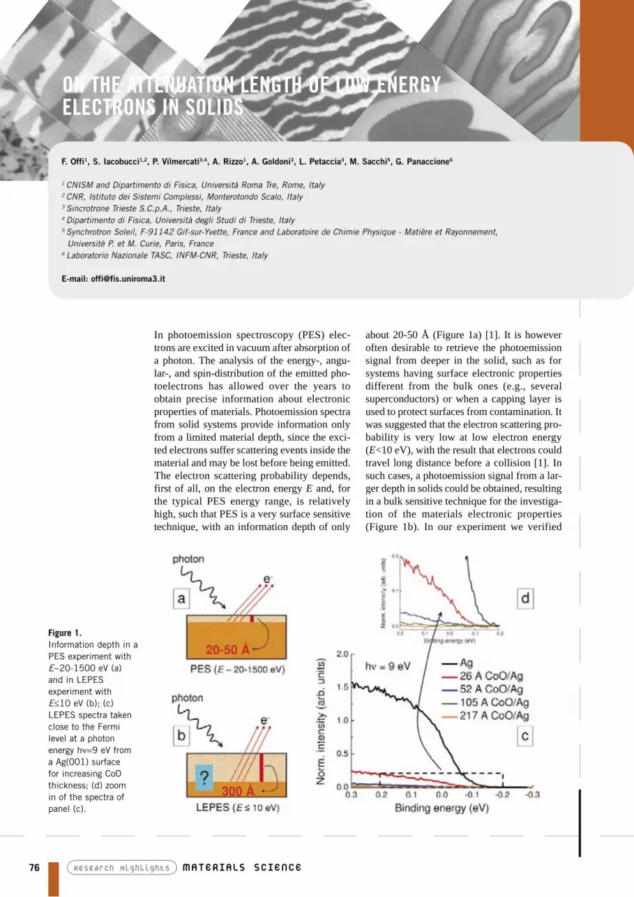
76 Research Highlights MATERiALs sCiENCE
F. Offi1, S. Iacobucci1,2, P. Vilmercati3,4, A. Rizzo1, A. Goldoni3, L. Petaccia3, M. Sacchi5, G. Panaccione6
1 CNISM and Dipartimento di Fisica, Università Roma Tre, Rome, Italy 2 CNR, Istituto dei Sistemi Complessi, Monterotondo Scalo, Italy3 Sincrotrone Trieste S.C.p.A., Trieste, Italy4 Dipartimento di Fisica, Università degli Studi di Trieste, Italy5 Synchrotron Soleil, F-91142 Gif-sur-Yvette, France and Laboratoire de Chimie Physique - Matière et Rayonnement, Universitè P. et M. Curie, Paris, France6 Laboratorio Nazionale TASC, INFM-CNR, Trieste, Italy
E-mail: [email protected]
ON THE ATTENUATION LENGTH OF LOw ENERGY ELECTRONS IN SOLIDS
In photoemission spectroscopy (PES) elec-trons are excited in vacuum after absorption of a photon. The analysis of the energy-, angu-lar-, and spin-distribution of the emitted pho-toelectrons has allowed over the years to obtain precise information about electronic properties of materials. Photoemission spectra from solid systems provide information only from a limited material depth, since the exci-ted electrons suffer scattering events inside the material and may be lost before being emitted. The electron scattering probability depends, first of all, on the electron energy E and, for the typical PES energy range, is relatively high, such that PES is a very surface sensitive technique, with an information depth of only
about 20-50 Å (Figure 1a) [1]. It is however often desirable to retrieve the photoemission signal from deeper in the solid, such as for systems having surface electronic properties different from the bulk ones (e.g., several superconductors) or when a capping layer is used to protect surfaces from contamination. It was suggested that the electron scattering pro-bability is very low at low electron energy (E<10 eV), with the result that electrons could travel long distance before a collision [1]. In such cases, a photoemission signal from a lar-ger depth in solids could be obtained, resulting in a bulk sensitive technique for the investiga-tion of the materials electronic properties (Figure 1b). In our experiment we verified
Figure 1. Information depth in a PES experiment with E~20-1500 eV (a) and in LEPES experiment with E≤10 eV (b); (c) LEPES spectra taken close to the Fermi level at a photon energy hν=9 eV from a Ag(001) surface for increasing CoO thickness; (d) zoom in of the spectra of panel (c).

77Research Highlights MATERiALs sCiENCE
such hypothesis, obtaining that indeed the information depth of low energy photoemis-sion spectroscopy (LEPES) is increasing when lowering electron energy, but considerably less than expected. Given the recent renewed interest in LEPES experiments [2], our results set a firm limit on the values and limitations of the technique.
In order to investigate the information depth of LEPES we used the photon supplied at the BaD ElPh beamline, where high intensi-ty flux is available for energy between about 5 and 20 eV. We detected the electrons excited by such photons in an Ag substrate for increa-sing thickness of a CoO overlayer [3]. For dif-ferent photon energies, we acquired the photo-emission intensity close to the Ag Fermi edge (zero binding energy) looking at its progressive attenuation for increasing overlayer thickness (the insulator CoO makes no contribution in the intensity at the Fermi level). Figure1c is an example for a photon energy hν = 9 eV: the Ag intensity steadily decreases upon increasing CoO thickness, until, for overlayer thicker than 52 Å, the intensity is extremely weak, as seen in the zoom in of Figure 1d. From such data we can evaluate the information depth of the tech-nique by computing the electron attenuation length Λ. We integrated the photoemission signal intensity in the energy interval ±0.2 eV with respect to the Fermi level and we fitted the results with an exponential decay function of the kind Id=I0 e
-d/Λ, where Id is the integrated intensity corresponding to the CoO thickness d and I0 is the integrated intensity for overlayer thickness d=0 (bare Ag substrate). The obtai-ned values of Λ are plotted in Figure 2 (solid circles with error bars) versus the electron energy measured in respect to the Fermi level.
Superimposed to the experimental points is a theoretical calculation (dashed line) adapted from the curve proposed in Ref. [1] for the atte-nuation length of electrons in inorganic com-pounds. Such curve is generally used for sub-stantiating the very large attenuation length of low energy electrons, and it is still cited as an indication of the bulk sensitivity of LEPES. We fitted the curve to our experimental data having only a scale factor as a free parameter. The best fit, shown in Figure 2, was obtained by divi-ding the curve from Ref. [1] by a 6.0 factor. Therefore, while our data reproduce the Λ ver-sus electron energy dependence as suggested by the Seah-Dench curve [1], the absolute value obtained is much smaller than earlier suggested.
Our results thus indicate a moderate incre-ase of the bulk-sensitivity in photoemission spectroscopy with very low energy electrons. While care must be taken in analysing spectral change versus photon energy [3], LEPES may therefore unravel the electronic properties in many solid systems with complicated surface behaviour when combined with the high ener-gy resolution available at modern synchrotron radiation beamline.
References [1] M. P. Seach and W. A. Dench, Surf. Interf.
Analysis 1, 2 (1979).[2] T. Kiss, F. Kanetaka, T. Yokoya, T. Shimoji-
ma, K. Kanai, S. Shin, Y. Onuki, T. Togashi, C. Zhang, C. T. Chen, and S. Watanabe, Phys. Rev. Lett. 94, 057001 (2005).
[3] F. Offi, S. Iacobucci, P. Vilmercati, A. Riz-zo, A. Goldoni, M. Sacchi, and G. Panac-cione, Phys. Rev. B 77, 201101(R) (2008).
Figure 2. Electron attenuation length Λ is plotted as symbols with error bars versus electron energy. The superimposed dashed line is a theoretical calculation of electron attenuation length resulting from a fit of the experimental data with a curve suggested in Ref. [1] reduced by a scaling factor of 6.0.

ATOMIC AND MOLECULAR pHYSICS

79Research Highlights ATOMiC AND MOLECULAR pHysiCs
A s a member of the program committee A (Gas Phase) at Elettra for the last
10 years, I have been able to follow the development of science in this
field over time. The quality of the research has grown during the years, as
researchers have become more experienced and one can also see the gradual
increase of international commitment.
In the present highlights these trends are very visible. There are studies of very
fundamental processes such as the kinetic energy release in the double photo
ionization of H2. Taking away two electrons from this molecule leaves two protons
interacting and the report deals with the physical interpretation of the “kinetic
energy release effect”. Two protons in interaction is the absolutely simplest
molecular ion one can think of. Nevertheless there is a lot of physics to deal with!
There are two very nice results from instrument development efforts. A new
ECR ion trap has been installed at the gas phase beamline and the results show
that this method to study cross sections gives very good conditions. I have during
the years followed cross section measurements both at Daresbury and at LURE.
The ECR ion trap is a very nice contribution to the field. A laser synchronized to
the SR-beam has been installed and the first results are very nice.
Finally, Elettra has during the last years developed a very solid research
programme concerning studies of molecular radicals. These studies are important
and the report in this year’s Highlights represents the state-of-the-art in the field.
As chairman of the gas phase PAC I would also like to point out that these
results would never have been achieved without the hard work of the in-house
responsible scientist and of the Elettra staff. Several of them are co-authors of the
reports and the combination of international presence with high quality in-house
research is obviously promising for the future.
Svante Svensson
Svante Svensson graduated 1976 in the well known ESCA group in Uppsala headed by the Nobel Laureate Kai Siegbahn. He has been active in synchrotron radiation based research since 1981 and has spe-cialized on high resolution electron spec-troscoopy on atoms, molecules, clusters and liquids. Recently he has also taken up high kinetic energy photoelectron spec-troscopy. Beamline development and end station instrumentation have been impor-tant issues in his research.Prof. Svensson has several international commitments apart from his activity in the PAC at ELETTRA. He is coordinator of a Nordic Research Network and also coor-dinator of the contributions to MAX in IRUVX. He is co-author of 270 articles. At the moment he spends a year as visiting professor at the Triangle de la Physique in Paris, where he will take part in the com-missioning and startup of the PLEIADES beam line.

80 Research Highlights ATOMiC AND MOLECULAR pHysiCs
T. J. Reddish1, J. Colgan2, P. Bolognesi3, L. Avaldi3, M. Gisselbrecht4, M. Lavollée4, M. S. Pindzola5, A. Huetz4
1 Department of Physics, University of Windsor, Windsor, Ontario, Canada 2 Theoretical Division, Los Alamos National laboratory, Los Alamos, New Mexico, USA3 CNR-IMIP, Area della Ricerca di Roma 1, Monterotondo Scalo, Italy4 CNRS- Universitè Paris Sud, LIXAM, Orsay, France5 Department of Physics, Auburn University, Auburn, USA
E-mail: [email protected]
TRACkING THE FULL BREAk-Up OF H2 MOLECULES
The fate of a molecule after absorption of a photon with sufficient energy to break it apart is of fundamental importance for the compre-hension of several natural phenomena and for an efficient handling of many industrial pro-cesses. Indeed when bonds are broken neutral and charged radicals are formed and react with neighbouring molecules. The greater the ener-gy absorbed, the greater the number of possi-ble reactions and the “damage” produced on the molecule itself and its environment. In H2 when the energy absorbed is large enough to remove the two electrons, the molecule then explodes due to the repulsive interaction between the two protons.
hν + H2 H+ + H+ + e1 + e2
The probability to remove two electrons is about two orders of magnitude lower than the
one to eject only one electron, because it is dominated by the interaction between the elec-trons themselves (i.e. they have to be conside-red a “correlated pair”). Thus intense VUV sources of radiation and efficient spectrome-ters that enable the time correlated detection of few charged particles are needed to investiga-te this process. These requirements have been met by an experiment at ALS [1] and a series of experiments [2,3] at the Gasphase beamline at Elettra. In these experiments a uniform elec-tric field guides the positive and negative char-ges produced in the break-up in opposite directions from the interaction region to the detectors, while a magnetic field ensures that the fast electrons are detected as well. For each particle the position of impact on the detector and its time-of-flight are measured. From these quantities the initial momenta of the four particles are reconstructed and, due to the high velocity of the protons in the Cou-lomb explosion (i.e. the protons fly away in a time shorter than the molecular rotation), the alignment of the molecular axis with respect to the polarization of incident light is determi-ned. Thus a 3D “photograph” of the Coulomb explosion can be taken.
In an earlier work [2], we studied how the spatial distribution of one escaping electron, having fixed the direction of the other one, depends on the alignment of the molecular axis with respect to polarization of the inci-dent radiation. Here we report the results of a study that unravels the dependence of the elec-tron spatial distribution on the internuclear separation R. The purely repulsive character of the H2
2+ potential curve results in a proton kinetic energy release, KER, whose value (Figure 1) depends on R at the moment of the
Figure 1. Schematic potential energy diagram of the initial and final states for PDI of H2. During double ionization the ground vibrational state is projected onto the upper repulsive curve, whose dissociation limit is at 31.67 eV, resulting in a broad range of kinetic energies for the final proton pair.

81Research Highlights ATOMiC AND MOLECULAR pHysiCs
double ionization. Selection of the KER allows one to probe the interplay between the electro-nic and nuclear motion in the process. The experiment was performed at 76.09 eV, ~25 eV above the double ionisation threshold at the equilibrium internuclear distance, with the Elettra ring operated in the four bunch mode. A selection of the measured fully differential cross sections, FDCS, is reported in figure 2. The two columns correspond to FDCS in which the two photoelectrons are measured in coincidence with ions whose KERs are 16.5 and 23.5 eV, respectively. These KERs corre-spond approximately to R = 1.6 and 1.2 a0. The FDCSs display a noticeable variation with the direction of the fixed electron (indicated by the arrows in Figure 2), with the alignment of molecular axis and with R. The experimen-tal observations are in very good agreement with the calculations of the Time Dependent Close-Coupling (TDCC) method [4] perfor-med at different R. TDCC calculations of the FDCS for each final M state accessed in the transition, where M = 0 (Σ), ±1 (Π) is the total magnetic quantum number in a reference fra-me aligned with the molecular axis. The FDCS results from the contributions of the Σ, Π components and their cross term. This analysis allows one to establish that the Π component, slowly varying with R, gives the main contri-bution to the FDCS while the Σ component is responsible of the variation with R. The cross term, with its constructive/destructive interfe-rence between the two components, amplifies the changes in R of the pure Σ component. The analogy of these findings with the those for the photoionization of H2
+[3], where electron-electron correlations are completely absent, leads to the conclusion that the observed R-dependent trends in the photodouble ioniza-tion of H2 are due to the electron-ion, rather than electron-electron, interactions. Therefore the Σ electronic states which lie near the inter-nuclear axis, in contrast to the Π states con-centrated in the plane between the nuclei, are more sensitive to variations in R.
References[1] T. Weber et al., Nature 431, 437 (2004).[2] M. Gisselbrecht et al., Phys. Rev. Lett. 96,
153002 (2006).[3] T.J. Reddish et al., Phys. Rev. Lett. 100,
193001 (2008).[4] J. Colgan, M.S. Pindzola and F. Robiche-
aux, Phys. Rev. Lett. 98, 153001 (2007).
Figure 2. FDCSs in the ‘coplanar’ geometry for E1 = E2 = 12.5 ± 10 eV: (a) direction of the fixed electron θ1 = 60° and of the molecular axis θN = 20º, (b) θ1 = 60°, θN = 160º and (c) θ1 = 90°, θN = 20º. Two KER values, 16.5 (left) and 23.5 eV (right) corresponding to approximately R = 1.6, 1.2 a0, respectively, are shown. The experimental data are arbitrarily normalized to the TDCC results convoluted over the experimental bandwidths (solid); unaveraged TDCC results for the stated values (dashed) have the scaling factors indicated. See [3] for more details.

82 Research Highlights ATOMiC AND MOLECULAR pHysiCs
R. Thissen1, J.M. Bizau2, C. Blancard3, M. Coreno4, C. Dehon5, P. Franceschi6, A. Giuliani7, J. Lemaire5 , C. Nicolas8
1 Laboratoire de Planétologie de Grenoble, UJF, Bât. D de Physique, Grenoble, France2 Laboratoire d’Interaction des Rayons X avec la Matière (LIXAM), Université Paris-Sud, Orsay cedex, France3 CEA DAM Ile-de-France, DPTA, Bruyères-le-Châtel Cedex, France4 CNR-IMIP, Rome branch and Gas Phase Beamline@Elettra, Trieste, Italy5 Laboratoire de Chimie Physique, Bât. 350, Université Paris Sud, Orsay, France6 Sincrotrone Trieste S.C.p.A., Trieste, Italy 7 Cepia, Institut National de la Recherche Agronomique (INRA), Nantes Cedex 3, France8 Synchrotron SOLEIL, L’Orme des Merisiers, Saint Aubin, Gif-sur-Yvette cedex, France
E-mail: [email protected]
pHOTOIONIzATION OF IONS IN A TRAp: A NEw TOOL TO EVALUATE pLASMA pHYSICS. FIRST RESULTS IN THE CASE OF xe+
The “Fourth State of Matter”, often called plasma, differs from the solid, liquid and gas state by its significant number of electrically charged particles which affect its electrical properties and behaviour. Besides being inher-ent in our daily lives through many aspects, plasmas make up more than 99 percent of the visible universe.
An ordinary gas is electrically “neutral”. Indeed, in each atom the positive charges of the nucleus are balanced by an equal number of negatively charged electrons. A gas turns into plasma when insertion of heat or of other energy can induce the release of some or all electrons from a significant number of atoms, so that the electrical characteristics of the gas are macroscopically affected. Atoms being left with a positive charge, the detached nega-tive electrons are free to move about and both atoms and the resulting electrically charged gas are said to be “ionized.”
Atomic spectroscopy is a powerful tool for characterizing plasma properties such as their thermodynamic state and transport. The determination of the populations and degree of ionization of species inside the plasma requires knowledge of the production rates (cross sections) for many atomic processes. Beyond their fundamental interest, photoioni-zation of ions is particularly important for such different fields as astrophysics, planetary sciences and, more generally, all applications of energetic plasmas (food processing, waste disposal, fusion research, X-ray laser, electro-nic etching or implantation). Photoabsorption cross sections are fundamental information
needed for the description of radiation tran-sfer, the main way for energy to diffuse inside the plasma.
The main obstacle to experimental studies in this field is the difficulty to produce clean targets of multiply-charged ions with density high enough to compensate for both the rela-tively low flux of the available XUV photon sources and the low value of photoionization cross sections. One technique allowing for the measurement of absolute photoionization cross sections on a large variety of ion sam-ples was implemented during the 80’s in Daresbury [1]. It consists in merging two beams: one of mass-selected ions and one of energy-selected synchrotron radiation. The major limitation of this method is that the ionic target is often composed of a mixture of ions in different excited states, as the time of flight of the ions between the source and the interaction region is very short (typically a few µsec). The determination of the popula-tion of ions in the different states present in the target usually requires theoretical data.
We propose [2] a new method to measure the photoionization cross sections of the pure ground level of ionic species: store ions in a trap and wait for a time long enough for exci-ted states to radiatively decay to the ground state before their irradiation. To this purpose, we installed the MICRA [3] (Mobile Ion Cyclotron Resonance Analyzer) Penning ion trap on the low energy branch of the Gas Phase Beam-Line, in order to analyze the change of the photoion population as a fun-ction of photon energy.

83Research Highlights ATOMiC AND MOLECULAR pHysiCs
The target ions are first produced by elec-tron ionization of Xe atoms, producing the Xe+ ions in both fundamental 2P3/2 and meta-stable 2P1/2 state. After a 1 s delay for relax-ation, the Xe+ ions are irradiated for 1.3 s and the mass spectrum of ions in the trap is recorded. The resulting photoionization (Xe2+ signal) spectrum is shown as the thick curve on the upper panel of Figure 1. The spectrum clearly shows a rise of the signal at 20.9 eV, the energy of the first threshold for the direct photoionization process:
Xe+ 5p5 2P3/2 + hν Xe2+ 5p4 + e-
The positions of the thresholds for the
various terms of the Xe2+ 5p4 configuration are shown as vertical bars. Above the continua produced by process (1), prominent lines are observed. In our spectrum, the absence of sig-nal below 20.9 eV demonstrates that the ions in the trap are in the ground level at the moment of the irradiation.
The measurement was reproduced using the merged beam experiment at ASTRID [4]. The spectrum obtained is shown in the lower
panel of Figure 1. In addition to the previ-ously observed lines, new ones, marked with an asterisk, appear. The most intense is below 20.9 eV and reveals an overwhelming contri-bution of Xe+ ions in metastable levels.
This work shows that an ion trap coupled to synchrotron radiation allows for the measu-rement of a pure ionic population. Further developments are foreseen, since the possibi-lity of doing in-cell chemistry with mass selec-ted ions opens new opportunities for studies in fields including spectroscopic and dynamic studies on molecular or cluster ions, multiply charged molecular ions, bio molecules, etc.
References [1] J.B. West, J. Phys. B 34, R45 (2001).[2] R. Thissen, J.M. Bizau, C. Blancard, M.
Coreno, C. Dehon, P. Franceschi, A. Giu-liani, J. Lemaire and C. Nicolas, Phys. Rev. Lett. 100, 223001 (2008).
[3] J. Lemaire et al., Phys. Rev. Lett. 89, 273002 (2002).
[4] H. Kjeldsen et al., Nucl. Instrum. Meth. B 234, 349 (2005)
Figure 1. Variation of the photoionization cross sections of Xe+ ion (blue lines). Upper panel: with ion trap result; lower panel: the merged beam experiment. The vertical bars give the position of the various ionization thresholds for ions in the ground and metastable levels. The asterisks correspond to transitions from the metastable level.

84 Research Highlights ATOMiC AND MOLECULAR pHysiCs
U. Ekström1, V. Carravetta2, M. Alagia3,4, M. Lavollée5, R. Richter6, S. Stranges3,4,7
1 Department of Physics, Chemistry and Biology (IFM), Linköping University, Sweden 2 Institute of Chemical Physical Processes, CNR, Pisa, Italy3 Istituto per lo Studio dei Materiali Nanostrutturati, CNR, Roma, Italy4 Laboratorio Nazionale TASC, INFM-CNR, Trieste, Italy5 CNRS, Université Paris-Sud, LIXAM UMR 8624, Orsay-Cedex, France 6 Sincrotrone Trieste S.C.p.A., Trieste, Italy7 Dipartimento di Chimica, Università La Sapienza, Roma, Italy
E-mail: [email protected]; [email protected]
THE UMBRELLA MOTION OF CORE-ExCITED CH3 AND CD3 METHYL RADICALS
Since 1934, when it was first observed in ammonia, the umbrella nuclear motion (insert of Figure 1) has been widely investigated both from a theoretical and an experimental point of view in a number of molecules. Such nuclear motion, which is typically character-ized by a particularly large amplitude, occurs if the molecule can exist in two stable geo-metrical configurations, which are related by an inversion of the molecular structure and correspond to two symmetric local minima separated by a potential barrier. In a double well potential, such as the one presented in Figure 1 for the electronically excited methyl radical CH3, the potential barrier prevents classical oscillations between the two energy minima, but barrier penetration, a strictly quantum effect known as “tunneling”, can produce large umbrella-like oscillations. Such motion leads to a “tunneling splitting” of the
vibrational levels that is directly related to the characteristic time needed by the molecule to go from one minimum energy configuration to the other [1].
The umbrella-like motion caused by a core-electron excitation at the central atom of an AX3 molecule could be studied only recent-ly for the methyl free radicals CH3 and CD3 [2,3]. Its observation by x-ray absorption spectroscopy (XAS) [4] is rather difficult, for the intrinsic problems that make vibrationally resolved XAS spectra quite rare in the litera-ture for polyatomic molecules. Due to their fast Auger and radiative decay, core excited states have a very short lifetime that is com-parable to the typical time of a molecular vibration. As a consequence the vibrational structure of an XAS spectrum can be easily masked by the large lifetime broadening of the electronic band.
A detailed study of the umbrella-like vibration in inner-shell molecular spectroscopy has been carried out by a joint theoretical and experimental investigation on the lowest-lying planar to non-planar core excitation in the CH3 and CD3 methyl radicals. The high resolution XAS has been recorded for both isotopomers by combining a pyrolytic supersonic jet source (to generate efficiently the radicals) with an intense and high-resolution SR source. The complex vibrational structure observed in the spectra has been theoretically predicted in terms of the excitation of the symmetrical stretching and the symmetrical out of plane bending (the umbrella mode) accompanying the core electron excitation. The strong anharmonicity of the potential energy surface of the excited
Figure 1. The potential energy surface for core excited CH3. Contour lines have been drawn with 0.1 eV interval and starting from the minima which are marked with dots; an extra contour at 0.05 eV has also been drawn with a dotted line. The umbrella motion is shown in the insert.

85Research Highlights ATOMiC AND MOLECULAR pHysiCs
state (Figure 1) along the bending coordinate has a profound effect on the energy and relative intensity patterns of the bending vibrational progression, with a remarkable isotopic effect. By a detailed theoretical characterization of the double well potential energy surface of the excited state a rather small potential barrier of 45 meV, with a consequently short umbrella inversion time of 149 fs for CH3 and 375 fs for CD3 was here estimated, for the first time, for a core excited state.
The excellent agreement between the experimental and theoretical XAS spectra observed in Figure 2 proves that, in the case of the methyl radical, it is possible to calcula-te high quality potential energy surfaces for core-hole states using spin-restricted Kohn-Sham DFT, and that the adopted model for the vibrational motion including the explicit cou-pling of only the two symmetrical modes, that allow the molecule to move from the planar to the pyramidal equilibrium geometry, is valid. Extending the study of CH3 to the iso-topomer CD3 has improved our understanding
of the XAS vibrational structure and provided additional information on the accuracy of the theoretical-experimental approach used in this work. This kind of investigation is plan-ned to be also extended to the low symmetry methyl radicals CH2D and CD2H.
References[1] E. Merzbacher, “Quantum Mechanics”, New
York: John Wiley & Sons, Inc. (1970).[2] M. Alagia, M. Lavolee, R. Richter, U.
Ekstrom, V. Carravetta, D. Stranges, B. Brunetti and S. Stranges, Phys. Rev. A 76, 22509 (2007).
[3] U. Ekstrom, V. Carravetta, M. Alagia, M. Lavolee, R. Richter, C. Bolcato and S. Stranges, J. Chem. Phys. 128, 44302 (2008).
[4] J. Stöhr, “NEXAFS Spectroscopy”, Berlin: Springer-Verlag (1992).
Figure 2. Left: experimental XAS spectrum of CD3 and CH3 recorded with 30 meV photon bandwidth. The spectra of the radical generated in a seeded beam are reported in curves a) and b) where the small hot band contribution is shown in grey. Curve c) reports the spectrum of internally cold CH3 radicals [1]. Right: calculated XAS spectra; the theoretical relative intensities (Franck-Condon factors) of the symmetrical stretching and bending vibrational progressions are presented as bar diagrams and convoluted (line), using the experimental natural and photon bandwidths, for a better comparison to the experiment.

86 Research Highlights ATOMiC AND MOLECULAR pHysiCs
A. Moise1, M. Alagia2,3, L. Banchi1, M. Ferianis1, K. C. Prince1,3, R. Richter1
1 Sincrotrone Trieste S.C.p.A., Trieste, Italy2 ISMN-CNR, Sez. Roma 1, Roma, Italy3 Laboratorio Nazionale TASC, INFM-CNR, Trieste, Italy
E-mail: [email protected]
SYNCHROTRON-LASER TwO-COLOR ExpERIMENTS AT THE Gasphase BEAMLINE: ExpERIMENTAL SETUp AND FIRST RESULTS
Two color experiments are used in many labo-ratories to study the dynamics of atomic and molecular processes. Usually the experiments are performed using two (or more) synchro-nized lasers, to prepare the target in a particular well defined state and probe the products of the process. The large range of wavelengths and pulse lengths available, together with the high sensitivity guaranteed by the high number of photons per pulse allows the detailed study of even very low cross section processes. Due to progress in high harmonic generation those studies now extend even to the attosecond time scale and into the soft x-ray region [1]. A natu-ral extension of the laboratory multi-color stud-ies is the application of synchrotron-laser experiments, especially in the range of ionizing
radiation processes. Synchrotrons are widely tunable, and provide high average flux over the whole range of energies. They also provide relatively short pulses, allowing the study of dynamics. The typical pulses of third genera-tion storage rings are in the low picosecond range, although techniques like laser slicing are now employed to generate short x-ray pulses. The coupling of lasers and synchrotrons was started already in the eighties at second genera-tion light sources. Those pioneering studies were very important to show the potential of such experiments. With the development of third generation light sources the available pho-ton flux and resolution have improved, but the main experimental difficulties have remained unchanged [2]. Although synchrotrons are
Figure 1. (a) Direct and resonant two-color photoionization of noble gases. (b) Lifetime measurement of the 1s3p 1Po state of helium (dots). The graph includes a simulation of the signal (red line) using the Elettra bunch structure (blue line) and the known lifetime of the state (black dotted line).

87Research Highlights ATOMiC AND MOLECULAR pHysiCs
pulsed light sources, the time structure is very different from typical laser sources, as it depends on the electron bunch structure of the storage ring. The other main difference is that, although the average numbers of photons of the two sources are becoming more similar, the photons available per laser pulse or synchrotron bunch are widely different. The most common mode of operation for many light sources is multibunch – the ring is filled with many elec-tron packets, and in the case of Elettra the sepa-ration between the pulses is ~ 2 nanoseconds. This high repetition rate cannot be matched by the lasers, causing additional difficulties in syn-chronization and data acquisition.
We describe experiments carried out using a tunable mode-locked Ti:Sapphire oscillator and synchrotron light pulses in the EUV range [3]. Synchrotron radiation was used to prepare the target (here noble gas atoms) in a well defined quantum state, which was then ionized directly into the continuum, or via an autoion-izing state, by the laser. A schematic picture of the processes is shown in Figure 1a.
In the first case – the ionization into the con-tinuum – the use of a pulsed laser permits the determination of the lifetime of the excited state by varying the delay between the laser and syn-chrotron light pulse. A measurement performed in this way does not rely on the time resolution of the detectors, but depends entirely on the syn-chronization of the laser and synchrotron light pulses. Results obtained for the 1s3p state of helium are shown in Figure 1b. The setup is suit-able to study the dynamics from a few nanosec-onds down to 10s of picoseconds during multi-bunch operation of the storage ring [3].
Ionization via autoionizing states embed-ded in the ionization continuum allows the exploration of highly excited states of the tar-get. In noble gases the single photon ground state absorption spectra are dominated by the ns and nd series. The widths, positions and shapes of the autoionizing resonances strongly depend on electron correlation and have been the subject of many theoretical investigations. Rydberg series of even parity are not accessible in transitions from the atomic ground state due to selection rules, but can be studied via dou-ble-resonance schemes. We show an overview of the neon nf’ Rydberg series using a combi-nation of laser and synchrotron radiation. The synchrotron wavelength has been fixed to one of the 3d resonances detected by VUV fluores-cence (Figure 2a). Then the laser was scanned in the wavelength range 810…890 nm to cover the energy between the two spin-orbit states of Ne+. Two series of Rydberg states are allowed,
but within our signal-to-noise ratio only the nf’ has been observed. In the dipole approxima-tion, under field free conditions only transi-tions to J=2 states are allowed from the J=0 ground state. Thus the series is mainly the nf’ [5/2]2 series of Rydberg states. The two color neon spectrum is shown in Figure 2b.
In the described experiment the laser has been used together with a PEPICO mass spec-trometer, but signal levels have demonstrated that experiments using other configurations available at the beamline are possible.
We thank all our colleagues at Elettra for support and generous loans of equipment. We are also grateful to Laser Optronic (Milano) and Laser Source (Roma) for support and the loan of an autocorrelator.
References[1] M. Drescher, M. Hentschel, R. Kienberger,
M. Uiberacker, V. Yakovlev, A. Scrinzi, Th. Westerwalbesloh, U. Kleineberg, U. Heinzmann, and F. Krausz, Nature (Lon-don) 419, 803 (2002)
[2] F. J. Wuilleumier and M. Meyer, J. Phys. B: At. Mol. Opt. Phys. 39, R425(2006)
[3] A. Moise, M. Alagia, L. Banchi, M. Feri-anis, K. C. Prince and R. Richter, Nucl. Instrum. Methods A 588, 502 (2008)
Figure 2. (a) Part of the neon single photon VUV fluorescence spectrum showing the 3d group of states. The transition used to record the two-photon spectrum is marked (*). (b) The two color neon ionization spectrum recorded via the (2P°½ )3d’ 2[3/2]°1 state. The two-photon ionization thresholds are marked.

THEORY@ELETTRA

89Research Highlights THEORy@ELETTRA
The numerical simulation of matter at the nanometric scale is proving to be
the missing link between experiment and theory. The role of computers in
science is twofold. On the one hand, they allow one to solve equations that
could not be tackled by any analytical methods. On the other hand, computers
give access to virtual experiments in which the representation of the physical
reality, though necessarily schematic and simplified, can be tuned and varied at
will down to atomic details. When real experiments can be done, simulations give
predictions, interpretations, as well as a very accurate assessment of theories and
models. In other cases (actually the most interesting), by means of virtual
experiments, computers permit investigation of properties and processes that
cannot be directly observed in real experiments, thus providing a unique insight
into the system being studied, complementary to that obtained in the laboratory.
Large-scale facilities are the ideal environment for the development of a
multi-disciplinary approach to complex problems in the physics and chemistry of
matter at the nanometric scale, and for the nucleation of collaborations between
theorists, experts in computer simulation, and experimentalists. These
collaborations result in a scientific output that is way superior to the sum of the
inputs from the individual disciplines.
The Theory@Elettra group is a joint initiative of the Elettra Synchrotron
Radiation Laboratory and the DEMOCRITOS National Simulation Center of INFM-
CNR. The group is located in the premises of the Elettra laboratory and aims at
i) providing direct support to the scientists at the laboratory as well as to the
international community active in the field of synchrotron radiation research; ii)
developing new theoretical and simulation methods particularly targeted to the
problems investigated in synchrotron radiation laboratories; iii) fostering the
collaboration between local experimentalists and external theorists, and iv)
promoting access to the laboratory by external users.
The first two papers reported in this section, by Umari and Pasquarello and
by Stojic et al., are examples of the ongoing effort to extend the scope of first-
principles calculations based on density-functional theory to an ever increasing
range of processes and properties. In the first paper it is shown how the hyper-
Raman spectrum of materials can be simulated on a computer, a task that will
allow a thorough characterization of complex systems, such as glasses, by
comparing the detailed features of the simulated spectra with those observed in
the laboratory. In the second paper N. Stojic extends a technique previously
adopted to calculate transmission coefficients in quantum point contacts to a
totally different process, namely photoemission from valence electrons at metal
surfaces. The other two papers, by Huang et al. and by Ding et al., are examples
of fruitful collaborations between scientists of the Theory@Elettra group and
experimentalists operating at synchrotron beamlines.
Stefano Baroni
Stefano Baroni is a condensed matter theorist, mostly known for his contribu-tions to the field of quantum simulations of materials. He is full professor of phys-ics at the Scuola Internazionale Superi-ore di Studi Avanzati (SISSA), head of the condensed matter theory sector of SISSA, and founding director of the CNR-INFM DEMOCRITOS National Simulation Center in Trieste, and former director of CECAM, the Centre Européen de Calcul Atomique et Moléculaire at the École Normale Supérieure in Lyon, France. SB is a fellow of the American Physical Society and a corresponding member of the Accademia Peloritana dei Pericolanti in Messina. He is the deviser and founder of the Theo-ry@Elettra group.

90 Research Highlights THEORy@ELETTRA
P. Umari1, A. Pasquarello2,3
1 Theory@Elettra group INFM-CNR DEMOCRITOS, Trieste, Italy2 Ecole Polytechnique Fédérale de Lausanne, Institute of Theoretical Physics, Lausanne, Switzerland3 Institut Romand de Recherche Numérique en Physique de Materiaux, Lausanne, Switzerland
E-mail: [email protected]
FIRST-pRINCIpLES HYpER-RAMAN SpECTRUM OF VITREOUS SILICA
Hyper-Raman scattering (HRS) is a non-linear three-photons process in which two in-coming photons are scattered into a photon and a pho-non. Although the HRS signal is typically ~106 times smaller than that for linear two photons Raman scattering (RS), new experimental set-ups permit the achievement of comparable resolutions. The interest in addressing HRS is that there are different selection rules from RS and infrared (IR) spectroscopies. Moreover, there are modes that are inactive both in RS and IR but become visible in HRS. As vitreous materials lack space periodicity, the analysis of their vibrational spectra can provide access to valuable structural information. In particu-lar, in vitreous silica, which is a disordered material formed by a network of corner-shar-ing SiO4 tetrahedra, the analysis of the Raman spectrum could provide estimates for the con-centration of small ring structures [1]. This was possible through the analysis and com-parison of experimental RS spectra with theo-retical density-functional results for a model structure previously obtained by a first-princi-ples molecular dynamics simulation. Indeed, it is now possible to calculate within the density-functional framework a large variety of vibra-tional spectra such as inelastic neutron scatter-ing (INS), IR and the RS in the non-resonant regime. When applied to crystalline materials, for which the structure is known, agreement with the experimental results within a few per-cent is usually obtained. In our work [2] we introduce a method for calculating within the density-functional framework the HRS in the non-resonant limit and we present results for a model of vitreous silica.
In analogy with linear non-resonant RS processes, non-resonant HRS cross sections are determined by the HRS tensors. These are composed of two terms: the first accounts for
the modulation of the first hyper-susceptibility tensor directly by atomic displacements; the second term accounts for the modulation due to electric fields which accompany longitudi-nal modes. In contrast to RS, this requires also for isotropic vitreous materials consideration of the particular scattering geometry realized in the experimental setups. The scheme requires the Born effective charges, the deriv-atives of the hyper-susceptibility tensor with respect to atomic displacements and the sec-ond hyper-susceptibility tensor which can be easily calculated through an approach based on finite electric fields [3].
We apply our method to a model structure of vitreous silica previously generated by first-principles molecular dynamics which consists of 72 atoms at the experimental den-sity. For this model a large variety of spectra such as the INS response, the neutron weight-ed vibrational density of states, the IR and RS response, has been previously calculated. We show in Figure 1 the HRS spectra for a scat-tering angle of 90 degrees in the VV and VH configurations. In the insets the spectra are compared to measured results [4] in the fre-quency range 350-650 cm-1 and excellent agreement is found both for the position and intensity of the main peak. We analyze the VH spectra in terms of separate contributions from the first and second term in the HRS tensors. In Figure 1 we show that in the VH configuration most of the spectrum and in particular the main features at ~500 and ~1200 cm-1 originate from the modulation due to longitudinal modes. Moreover, this component strongly resembles the energy loss infrared spectrum. In the VV configura-tion only the first-term in the HRS tensor contributes, and the spectrum resembles the vibrational density of states.

91Research Highlights THEORy@ELETTRA
In conclusion, we provided a scheme for the calculation of HRS spectra in the non-res-onant regime and could obtain for the first time the HRS spectrum of a disordered mate-rial from first-principles. This methodology will open new opportunities for the study of vibrational properties in disordered and com-plex materials.
Figure 1. Reduced HRS spectra of vitreous silica for a scattering angle of 90 degrees. Upper panel: in-coming and out-going photons, vertically polarized. Theory: total (solid line). Lower panel: in-coming and out-going photons, vertically and horizontally polarized, respectively. Theory: total (solid line), contribution from first- (dotted line) and second- (dashed line) term in the HRS. A Gaussian broadening of 16 cm-1 has been used. Insets: calculated (solid line) and measured (dashed line) spectrum. The experimental lines are from Ref. [4].
References[1] P. Umari, X. Gonze, and A. Pasquarello,
Phys. Rev. Lett. 90, 027401 (2003).[2] P. Umari and A. Pasquarello, Phys. Rev.
Lett. 98, 176402 (2007).[3] P. Umari and A. Pasquarello, Phys. Rev.
Lett. 89, 157602 (2002).[4] B. Hehlen, E. Courtens, R. Vacher, A.
Yamanaka, M. Kataoka, and K. Inoue, Phys. Rev. Lett. 84, 5355 (2000).

92 Research Highlights THEORy@ELETTRA
N. Stojiæ1,2, A. Dal Corso1,2, B. Zhou3, S. Baroni1,2
1 Scuola Internazionale Superiore di Studi Avanzati, Trieste, Italy2 Theory@Elettra group INFM-CNR DEMOCRITOS, Trieste, Italy3 Laboratorio Nazionale TASC, INFM-CNR, Trieste, Italy
E-mail: [email protected]
Ab initio SIMULATION OF pHOTOEMISSION SpECTROSCOpY IN SOLIDS: NORMAL-EMISSION SpECTRA OF CU(001)
Photoemission spectroscopy (PES) is one of the most basic techniques for investigating the electronic properties of solids. In practice, however, it is difficult to extract information directly from the observed spectra and theore-tical considerations are necessary for a precise determination of the underlying transitions. In the energy range of ultra-violet photoemission spectroscopy (UPS, between 5 and 100 eV), the spectra are dominated by wavevector-con-serving transitions (direct transitions) with transition matrix elements differing signifi-cantly for any pair of initial and final states. Hence, in UPS, final-state effects play a major role. In empirical approaches these final states are often modelled by free-electron bands, but, in reality, they are influenced by the crystal potential especially at low photon energies and, therefore, their proper description requi-res detailed calculation.
Despite the wide use of ab initio approa-ches based on density-functional theory (DFT), there have been only few attempts to apply them to the calculations of UPS. In contrast to X-ray PES, for which measured spectra are routinely compared to the ab initio density of electronic states, the simulation and interpre-tation of UPS spectra is highly nontrivial. Using DFT, it is not easy to account for the non-periodic nature of electronic states invol-ved in PES and to accurately describe self-energy effects on the quasiparticle states. We address the first problem by calculating the transmission of electrons from the crystalline medium into the vacuum, using an approach specially developed for our plane-wave-based pseudopotential implementation of DFT [1]. Self-energy effects are accounted for semi-empirically: the real part of the self-energy shifts of DFT bands is described by applying
Figure 1. An example of all the allowed direct transitions for the Cu(001) spectrum, ħν=23 eV, p-polarization and θ=65˚ (panel a). Panel b) shows the effect of the dipole matrix elements. Panel c) shows the effects of the transmission factors.

93Research Highlights THEORy@ELETTRA
the LDA+U method, while the imaginary part (lifetime effects), is added as an empirical parameter. In our approach, we calculate dipo-le matrix elements completely ab initio and describe the effects of the change of the die-lectric function upon crossing the surface (surface-optics effects), by Snell’s and Fre-snel’s equations.
Our approach [2] is based on the bulk three-step model, which breaks the photoemission process into three independent steps: excitation of the photoelectron, its transport through the crystal up to the surface, and its escape into the vacuum. In this model, the photoemission cur-rent is proportional to the product of the prob-ability that an electron is excited from an initial bulk state to an intermediate bulk state, times the probability that the electron in the interme-diate state is transmitted into the vacuum. The energy and the component of the momentum parallel to the surface are conserved.
In Figure 1 we illustrate the influence of the dipole matrix elements and of the transmission factors on the shape of the spectrum. In panel a we show all the direct transitions regardless of the symmetry, their dipole matrix elements, and the transmission coefficients. In panel b we cal-culate the photoemission spectrum setting the transmission factor to be maximum (one) for all the bands. After introducing the dipole matrix elements, only few peaks remain. The addition of the transmission factor (panel c) selects the intermediate states with the correct symmetry, imposing the selection rules, and also modula-tes the peak intensities.
Figure 2 compares our ab initio and cor-rected (LDA+U and surface optics) spectra, with a recently measured spectrum on the Cu(001) single crystal surface at the APE beamline (TASC). The ab initio spectrum has the correct number of peaks, but their posi-tions are somewhat shifted and the peak ratio is overestimated. This is improved in the cor-rected spectrum which shows better agreement with experiment. However, we cannot repro-duce the high-energy broad structure present in the experimental spectrum. We explain it by non-direct transitions, allowed due to a small broadening of k// in the experiment.
We have introduced a new method for the ab initio low-energy photoemission calcula-tions based on pseudopotentials and plane-waves, which has an advantage in its simplici-ty and unbiased basis-set, with the possibility to significantly reduce the number of empiri-cal parameters. Our results are in reasonable agreement with experiment for low photon energies. Empirical corrections, including the LDA+U and surface-optics, give significant improvements.
References [1] A. Smogunov, A. Dal Corso, and E. Tosat-
ti, Phys. Rev. B 70, 045417 (2004).[2] N. Stojić, A. Dal Corso, B. Zhou, and S.
Baroni, Phys. Rev. B 77, 195166 (2008).
Figure 2. Comparison of our Cu(001) ab initio and corrected spectra, with the experimental spectrum for ħν=17 eV, p-polarization and θ=45˚.

94 Research Highlights THEORy@ELETTRA
M. Huang1, S. Fabris1, M. Hinterstein2,3, X. Torrelles2, R. Felici4, J. Rius2, H. Fuess3, M. Pedio5
1 Theory@Elettra group INFM-CNR DEMOCRITOS, Trieste, Italy 2 Institut de Ciència de Materials de Barcelona, ICMAB-CSIC, Barcelona, Spain3 Technische Universität Darmstadt, Darmstadt, Germany4 European Synchrotron Radiation Facility (ESRF), Grenoble, France5 Laboratorio Nazionale TASC, INFM-CNR, Trieste, Italy
E-mail: [email protected]
LOOkING UNDERNEATH FULLERENES ON Au(110): FORMATION OF DIMpLES IN THE SUBSTRATE
The adsorption of large organic molecules on metal surfaces can lead to complex nano-structuring of the supporting substrate. The mechanisms driving the substrate reconstruc-tion are controlled by an interplay between intermolecular and of molecule-substrate interactions involving a large number of sites. This can result in either displacive substrate reconstructions, yielding extensive mass transport, and/or in complex structural defor-mation of the adsorbed molecules. In this context the interaction of fullerenes with sur-faces can be seen as a model system. The presence of strong directional π molecular states, together with the capability of being an acceptor or donor of electrons allows fullerene to establish different kinds of inter-action ranging from van der Waals to ionic and covalent bonding, through the C atoms that are in direct contact with the substrate.
The interaction between fullerene C60 molecules and the Au(110) surface induces a massive p(6x5) substrate reconstruction and leads to the formation of surface nanoscale pits [1]. The dimples are one and two layers deep, host the fullerene molecules and allow for a large increase in the metal/molecule contact area. In this study [2] we show that this new configuration alters the electronic properties of the molecule+substrate system as detected by Photoemission (UPS) and Inverse Photoemission (IPE). Our numerical simulations based on density functional the-ory (DFT) shows that the driving force for the surface reorganization is provided by the formation of strong directional C-Au bonds resulting from the hybridization between the molecular π orbitals and the surface s metal states.
DFT calculations based on plane-waves pseudopotentials, and periodic supercells pro-vide insight into the molecular bonding mech-anism inducing the nanopit formation at the C60/Au(110) interface. The electronic ground state was calculated for the local geometry of the fullerene adsorbed in the Au nanopits; this geometry was obtained experimentally from synchrotron radiation surface x-ray diffraction data [2]. The calculated bonding charge, the density of electronic states (DOS), and the partial DOS (C p-DOS, resulting from project-ing the wave functions on the atomic C-2p states) provide evidence of strong directional C-Au bonding (Figure 1).
The bonding charge density is mostly local-ized between the lateral C atoms in contact with the nanopit edges, while the interstitial region directly underneath the C60 is not primarily involved in bond formation. The degree of directional electronic contribution to the bond-ing is showed in Figure 1A by charge accumu-lation (red pockets) localized along the shortest C-Au bond lengths (marked by dashed lines and ranging between 3.1-3.3 Å). Moreover, molecular adsorption induces the polarization of the C60 molecule, involving mostly the C atoms on the lower half of the molecule.
Any ionic contribution to the C60/Au(110) bonding would result in new molecular fea-tures at the Fermi level due to the population of the C60 LUMO, like those measured in the C60/Ag and C60/Cu systems. In the present case, both the photoemission spectrum and the calculated DOS (Figure 1B) do not present any new feature between the Fermi level and the C60 HOMO. The same conclusion can be drawn from the analysis of the unoccupied states (conduction band inverse photoemission

95Research Highlights THEORy@ELETTRA
data [3], IPE, and DOS in Figures 1B and C). With respect to an isolated C60 molecule (Fig-ure 1C), the LUMO and LUMO+1 states (labeled b) are shifted to lower energies upon adsorption (Figure 1B) but no significant frac-tion of the C60 LUMO is transferred below the Fermi level.
Moreover, the HOMO and the higher ener-gy molecular states (labeled c and d in Figure 1b and c) are not affected by the molecular adsorption. This allows us to align the calcu-lated energies of the c and d states to the cor-responding features in the IPE (Figure 1d). By doing so, we conclude that the broad feature above the Fermi level (a and a`) results from two different origins: a flat contribution from the gold s states (a) and the molecular LUMO (a’). At higher energies, the spectrum is domi-nated by the three distinct molecular peaks (b, c, and d in Figure 1d).
The additional charge available after C60 adsorption is redistributed in the contact inter-facial region and substrate mass transport takes place in order to form and maximize the number of strong directional bonds. In fcc metals, the hexagonal structure of the (111) surfaces allows the formation of 12 C-metal
bonds by surface vacancy formation, as in the case of C60/Pt(111) [4]. Mass transport is facilitated on more open substrates, like the Au(110) surface, where the number of bonds can be maximized according to size and shape of the nanopit. In the present case, the mea-sured fullerene corrugation is determined by the presence of two different adsorption sites related to different depths.
This study demonstrates that the 6x5 reconstruction of the Au(110) surface upon fullerene adsorption yields the formation of nanopits at the interface which are one and two layers deep. The larger fullerene/metal contact area allows for the formation of a large number of C-Au covalent bonds.
References [1] M. Pedio et al., Phys. Rev. Lett. 85, 1040
(2000).[2] M. Hinterstain et al., Phys. Rev. B 77,
153412 (2008).[3] M. Pedio et al., J. Electron Spectrosc.
Relat. Phenom. 76, 405 (1995).[4] R. Felici, M. Pedio, and F. Borgatti, Nat.
Mater. 4, 688 (2005).
Figure 1. (A) Bonding charge density obtained from DFT. Positive and negative electron density isosurfaces (|0.006| e/Å3) are displayed in red and light gray areas, respectively. (B) Experimental PE spectrum (red), calculated DOS (black) for C60/Au(110) and (C) C p-DOS for an isolated C60 molecule. (D) Conduction band IPE data and C p-DOS for C60/Au(110).

96 Research Highlights THEORy@ELETTRA
X. Ding1, M. Peressi1,2, A. Baldereschi2,3, E. Vesselli4,5, L. De Rogatis5,6, A. Baraldi4,5, G. Comelli4,5 , R. Rosei4,5, P. Fornasiero6, L. Savio7, L. Vattuone7, M. Rocca7
1 Theory@Elettra Group, CNR-INFM DEMOCRITOS, Trieste, Italy2 Department of Theoretical Physics, University of Trieste, Italy3 CNR-INFM DEMOCRITOS, Trieste, Italy and EPFL, Lausanne, Switzerland4 Department of Physics, University of Trieste and CENMAT, Trieste, Italy5 Laboratorio Nazionale TASC, INFM-CNR, Trieste, Italy6 Department of Chemistry, University of Trieste, Italy7 Department of Physics, University of Genova, Italy
E-mail: [email protected]
CARBON DIOxIDE ACTIVATION AND HYDROGENATION ON Ni SURFACES FOR ORGANIC SYNTHESIS
There is a great interest in carbon dioxide (CO2) chemistry, not only for its capture to reduce greenhouse effects, but also for its stor-age and recycling in useful technological applications as a synthesis feedstock. As an example, it is a key compound for the synthe-sis of methanol, according to the reaction CO 2+3H 2 CH 3OH+H 2O, a promising candidate as energy carrier to feed internal combustion engines or fuel cells.
CO2, however, is a closed shell, stable, and poorly reactive molecule, making diffi-cult the development of low-cost and efficient catalysts for its conversion. Cu-based cata-lysts are normally used, but recent experimen-tal findings indicate that model Ni/Cu cata-lysts are 60 times more active for CO2 hydro-genation than traditional pure Cu ones. For-mate (HCOO) has been identified as the first intermediate in the methanol synthesis. How-ever, not only the details of the reaction path are unknown and the promoting role of Ni is obscure, but, surprisingly, there is a lack of knowledge concerning even more basic ques-tions, such as the CO2 interaction with Ni and other transition metal surfaces.
Although available techniques, both experimental and theoretical, do not allow us to follow in detail the evolution of the catalyst and the whole reaction under standard tem-perature and pressure conditions, investiga-tions performed on model systems for simpli-fied reaction schemes can contribute to a deeper comprehension of heterogeneous cata-lytic organic synthesis processes involving carbon dioxide as a reactant and therefore can
suggest the design of new and more efficient catalysts.
The comprehensive study of the mecha-nism of chemisorption, activation and hydro-genation of CO2 on Ni by characterizing the stable intermediates of the reaction and by identifying the relevant reaction paths has been made possible by a close collaboration between theoreticians and experimentalists, covering several complementary competences [1-4]. Geometries, adsorption energies, and vibrational frequencies of adsorbed CO2, HCOO and related transition states as well as reaction/diffusion energy barriers are obtained by atomic-scale quantum mechanical numeri-cal simulations, providing a guide for experi-ments and for the interpretation of experimen-tal data and allowing us to propose a full description of the mechanism.
Ni(110) is the only transition metal, low Miller index surface to which CO2 chemically binds. The molecule receives electronic charge from the metal, bends, and binds to the surface with the carbon atom in a “V” con-figuration. When adsorbed H approaches CO2, the H-CO2 complex flips and binds to the sur-face with the two oxygen atoms and H binds to the carbon atom, thus yielding the formate intermediate which is known to exist in such a “reversed Y” configuration and to be pres-ent also under real catalyst working condi-tions. The resulting energy barrier for CO2 hydrogenation is relatively small (0.43 eV) and, most importantly, smaller than that for CO2 desorption and that for dissociation into CO + O. The presence of hydrogen steers the

97Research Highlights THEORy@ELETTRA
reaction in the desired direction and prevents the formation of CO which is unreactive. This is the key point of CO2 + H chemistry on Ni(110), since the charge transfer from the metal to the molecule yields an activated state which is reactive with hydrogen via an induced flip of the complex. This does not occur on Cu, where CO2 is not activated by the metal, interacting only very weakly, remaining neutral, linear and unreactive: its first hydrogenation requires therefore a much higher reaction barrier (~1 eV). This provides possible explanations for the promoting role of Ni in Ni/Cu catalysts.
References [1] E. Vesselli et al., J. Am. Chem. Soc. 130,
11417 (2008).[2] X. Ding et al., Phys. Rev. B 76, 195425
(2007). [3] X. Ding et al., Mat. Sci. Eng. C 27, 1355
(2007).[4] X. Ding et al., AIP Conference Procee-
dings 1018, 197 (2008).
Figure 1. Results of numerical simulation for the CO2 + H HCOO reaction. Energies (with respect to gas-phase H and CO2) and geometries are given for the most relevant states, starting from coadsorbed H and CO2, with CO2 charged, bent and bonded to metal in a “V” shaped configuration. LB and SB indicate the long- and short-bridge adsorption sites of the “reversed Y” HCOO, respectively, which are both possible and almost energetically equivalent. TS indicates the transition state of the reaction, responsible of the hydrogenation energy barrier, while D is that of formate diffusion between the two possible states. Only the outer three Ni layers are shown, but a thicker slab has been used in the calculations.


facility HigHligHts

elettra and instrumentation researcH

101Facility Highlights elettra and instrumentation researcH
Scientific breakthroughs very often or perhaps normally are not the result of
a linear process of development. They result from some form of jump in our
understanding of a subject. They can be catalyzed by a theoretical leap
forward in which an entirely new concept is developed, or by new measurements
methodologies, capable of giving an entirely new level of information. Developments
of new measurement methodologies have often led to scientific breakthroughs, for
example and perhaps most famously, the development of the Scanning Tunneling
Microscopy (STM). This example gives us many interesting clues to how revolution-
ary ideas are developed. Firstly, the problem that Binnig and Rohrer originally were
trying to solve was really quite disconnected from the eventual uses of STM in
surface science; they needed to find a way to image defects in the oxide layers in
a Josephson junction. Secondly, although the brilliant realization that tunnel cur-
rents from atomically sharp tips could lead to scanned atomic resolution images
was made in 1978, it took 4 years for the first breakthrough result to be achieved
in the imaging of single atomic steps in Au(111) in 1982, followed by the iconic
images of the Si(7x7) reconstruction in 1983. Their first paper on the topic was
also rejected. Clearly in instrumentation, brilliant concepts usually have to be fol-
lowed by years of persistence! Thirdly, inventions can lead in unexpected direc-
tions. Although the STM was a breakthrough in surface science, the closely con-
nected invention of the AFM by Binnig, Quate and Gerber in 1986 arguably has
spawned many more discoveries, due to its amazing variety of imaging modalities.
In synchrotron radiation research, if we look for potentially revolutionary break-
throughs, we can perhaps point to x-ray imaging as an example. Although x-ray
holography was first described decades ago, it has only been with the development
of very high brightness x-ray sources, good detectors, fast computer algorithms and
sophisticated sample environments has the field started to take off. For example,
experiments at the FLASH FEL by Chapman et al. have demonstrated fsec pump
probe imaging and very recent experiments at ALS by Marchesini et al. have shown
how it is possible to use a uniformly redundant array as a reference object, speed-
ing up acquisition by factors of thousands. These instrumentation developments
potentially will have enormous scientific impacts, from nanoscience to biology.
Although considered to be ‘science fiction’ only a few years ago, with vision, per-
sistence, patience and the ability of those involved to pick the right targets for their
work, diffractive x-ray imaging is now rapidly developing. One of the things that
made this field possible was the availability of good detectors. These happened to
be available based on advances in other fields, but unfortunately, this is usually
not the case. The area of detectors still stands as one that has huge potential to
push forward x-ray science. Not only can new detector technologies speed acquisi-
tion, they can give us access to measurements that were previously impossible.
The advent of time stamping pixel detectors will be one development that will
clearly spawn many new discoveries.
Finally we should not neglect the machines that give us photons. Important
incremental advances in brightness and beam stability are still possible with 3rd
generation machines, such as through topoff operation, in-vacuum undulators, and
shorter bunches. Of course the largest performance jump is now arriving with the
advent of VUV-soft x-ray FELs, and soon hard x-ray FELs, but there will always be
a place for the high average power, high repetition rate, and easy tunability of
conventional synchrotron sources. The advance of science and the advance of
instrumentation are intrinsically linked. With the increasingly sophisticated range
of instrumentation tools available today, it is indeed an exciting time to contem-
plate the advances in science that will be made possible in the next few years.
Howard Padmore
Howard Padmore started out in synchro-tron radiation at Daresbury Laboratory, working from the start of SRS operations in 1982 in the surface science group. He became head of the soft x-ray group in 1987, and then moved to Berkeley in 1993 to head the Experimental Systems Group (ESG) at the ALS where he became a Division Deputy in 2003. He leads the ESG in running 10 of the facility beam-lines, and in developing new techniques in synchrotron radiation research. His personal work currently is in low energy photoemission and PEEM, applied to photocathodes and solar energy conver-sion devices as well as ultra-fast studies of material dynamics using x-ray streak camera techniques.

102 Facility Highlights elettra and instrumentation researcH
E. Karantzoulis Sincrotrone Trieste S.C.p.A., Trieste, Italy
E-mail: [email protected]
elettra status, accelerator pHysics activities and projects
During 2007 Elettra operated for 5 runs of 4 to 8 weeks each for a total of 5424 hours, of which 3888 (71.7%) scheduled to user exper-iments with a user uptime (Figure 1) of 90.4% (94.1% excluding beam losses due to storms and external electricity supply interruptions). In addition to storms and external electricity supply interruptions (36.2% of the downtime) the other major causes of downtime were due to delays during the refill phase (18.9%), to the Linac systems (11.3%) and to water-cool-ing systems (9.4 %) faults. The storage ring operated at 2 GeV for 74.4% of its user time whereas the 25.6% was at 2.4 GeV. The pre-vailing user operation’s mode was multi bunch (97.5% of the time) consisting in fill-ing 415 of the 432 available RF-buckets with 330 mA at 2 GeV and 140 mA at 2.4 GeV with 48 (24 at 2.4 GeV ) hours between refills. The remaining 2.5% of user time was dedicated to 4 bunch mode, with 4 equidis-tant bunches of 32 mA total current at 2 GeV and 8 hours between refills.
A long shutdown of three months during autumn was required for the installation of the new transfer line and septum necessary
for the transportation of the electrons from the new Elettra injector to the storage ring. During the other 5 shutdowns of 1 to 2 weeks duration maintenance work was mainly made on the vacuum system, cooling and electrical system, power supplies and radiofrequency. The old RF-plant in section 9 was moved to the booster to be used as the booster RF-plant. Some minor installation concerning the new LIBERA beam position detectors went on to completion during 2007 and so the Global Orbit Feedback that stabilizes the electron orbit to an accuracy of a few microns rms, started operating. Finally, beam loss monitors that show the radiation created when the electron beam hits the vacuum chamber were also installed prior to booster commissioning.
Each of the 5 runs started with a few days dedicated to accelerator physics whereas the total accelerator physics and machine time for developments/projects was 1242 hours or the 23.8% of the total. In Figure 2 the per-centage of time distribution can be seen. Thus the SR-FEL (storage ring free electron laser) had the 43% of the Accelerator physics time,
Figure 1. Blue: user uptime in 2007 with partial uptime during the five runs of the year (105÷109). Red: user uptime excluding beam losses due to storms.
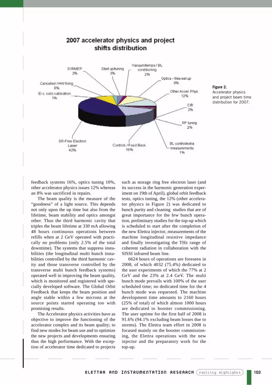
103Facility Highlights elettra and instrumentation researcH
feedback systems 16%, optics tuning 10%, other accelerator physics issues 12% whereas an 8% was sacrificed in repairs.
The beam quality is the measure of the “goodness” of a light source. This depends not only upon the up time but also from the lifetime, beam stability and optics amongst other. Thus the third harmonic cavity that triples the beam lifetime at 330 mA allowing 48 hours continuous operations between refills when at 2 GeV operated with practi-cally no problems (only 2.5% of the total downtime). The systems that suppress insta-bilities (the longitudinal multi bunch insta-bilities controlled by the third harmonic cav-ity and those transverse controlled by the transverse multi bunch feedback systems) operated well in improving the beam quality, which is monitored and registered with spe-cially developed software. The Global Orbit Feedback that keeps the beam position and angle stable within a few microns at the source points started operating too with promising results.
The Accelerator physics activities have as objective to improve the functioning of the accelerator complex and its beam quality; to find new modes for beam use and to optimize the new projects and developments ensuring thus the high performance. With the excep-tion of accelerator time dedicated to projects
such as storage ring free electron laser (and its success in the harmonic generation exper-iment on 19th of April), global orbit feedback tests, optics tuning, the 12% (other accelera-tor physics in Figure 2) was dedicated to bunch purity and cleaning studies that are of great importance for the few bunch opera-tion, preliminary studies for the top-up which is scheduled to start after the completion of the new Elettra injector, measurements of the machine longitudinal resistive impedance and finally investigating the THz range of coherent radiation in collaboration with the SISSI infrared beam line.
6624 hours of operations are foreseen in 2008, of which 4032 (75.4%) dedicated to the user experiments of which the 77% at 2 GeV and the 23% at 2.4 GeV. The multi bunch mode prevails with 100% of the user scheduled time; no dedicated time for the 4 bunch mode was requested. The machine development time amounts to 2160 hours (25% of total) of which almost 1000 hours are dedicated to booster commissioning. The user uptime for the first half of 2008 is 91.6% (94.1% excluding beam losses due to storms). The Elettra team effort in 2008 is focused mainly on the booster commission-ing, the Elettra operations with the new injector and the preparatory work for the top-up.
Figure 2. Accelerator physics and project beam time distribution for 2007.

104 Facility Highlights elettra and instrumentation researcH
M. Svandrlik on behalf of the Elettra Booster Project TeamSincrotrone Trieste S.C.p.A., Trieste, Italy
E-mail: [email protected]
tHe new elettra Booster is in operation
The new Elettra booster injector is in opera-tion since March 3rd, 2008, as planned in the original time schedule. Elettra was shutdown for 5 months between October 2007 and February 2008 to allow the installation of the new 2.5 GeV transfer line connecting the Boo-ster to the storage ring and to carry out the final part of the booster commissioning.
The Booster Project started in March 2005 and lasted therefore exactly 3 years. The allo-cated budget over this period was 13.9 M€. Of that amount about 60% went into the acce-lerator hardware, 40% in building and servi-ces. As for manpower, 79 people of the Elettra staff contributed to the project, mostly part time. The manpower employed was 100 man-years for the 3 years duration of the project.
The main project challenge was to replace the existing Linac injector with the new full energy Booster, located in a new building insi-de the storage ring main building, affecting as less as possible the users’ operation of the faci-lity. This required careful planning of both installation and commissioning, foreseeing the consequences of possible delays and program-ming appropriate back-up plans. Strong over-lap between hardware and beam commissio-ning phases was needed to mitigate the effect of unexpected issues.
Commissioning activities were focussed to get a working injector, in order to avoid delays that would compromise the timely restart of the facility for users. Beam commissioning was performed in three different phases. During the first phase, between September 7th and October 13th, 2007, the beam was first extracted from the gun, accelerated through the linac pre-injector to the nominal energy, 100 MeV, and then injected into the booster. First 100 turns in the booster were obtained on September 26th, while in the following days the beam could be ramped in energy up to 800 MeV and extracted from the Booster. The maximum achievable energy was at that time limited by the booster main magnets power converters, not yet performing to specifica-tion.
On December 11th the BTS transfer line installation was completed. During the same shutdown the new injection septa magnets, capable of operating up to 2.5 GeV, were also installed in Elettra. Meanwhile, also improve-ments on various booster sub-systems were carried out. In particular one of the limiting factors on the power converters, a distortion of the output current waveform at low currents, could be removed. Just prior to the Christmas shutdown, during the second beam commis-
Figure 1. Frequent injection mode tests performed in February 2008, at 2.0 GeV, insertion devices at maximum gap and beamline shutters closed. Beam current in the storage ring is kept constant between 300 ± 1 mA.

105Facility Highlights elettra and instrumentation researcH
sioning phase, the beam could then be extrac-ted from the booster for the first time at 2.0 GeV, in single shot mode.
The Christmas shutdown allowed a further improvement in the performance of the power converters. During the third and final com-missioning phase, booster operation at 2.0 GeV, 1 Hz repetition rate, could be establi-shed. On February 11th it was finally possible to inject for the first time into Elettra at full energy, i.e. 2.0 GeV. In order to quickly reco-ver good vacuum conditions in the storage ring, after the new septum installation, the beam current intensity in the Storage Ring was kept as high as possible, by successfully testing the frequent injection mode, as shown in Figure 1.
Users’ operation at 2.0 GeV started on March 3rd, 2008, with routine full energy refil-ls on top of the stored current. On the 13th of April the beam was then injected in Elettra at 2.4 GeV, the other user operation energy. In May, single bunch operation of the injector was established for Storage Ring FEL users at 0.9 GeV.
Figure 2. Booster cycles in August 2008: energy is 2.0 GeV, repetition frequency 2.4 Hz, beam current at extraction 2.0 mA.
In the timeframe between April and August 2008 injection for users has been performed at 0.9 GeV, due to a harmful fault on one of the cabinets of the bending magnets power conver-ters, occurred on April 17th. The repair of this cabinet has been included in a general refurbi-shing program which is being carried out by the supplier of the converters to finally meet their original specified performance. After the intervention scheduled during the summer shu-tdown in August, booster operation at 2.0 GeV, 2.4 Hz, 2mA of extracted beam current has been established (Figure 2) with good reliabili-ty and improving reproducibility. Injection rates of 1.5 mA/s have then been achieved, with best injection efficiencies measured to be close to 100%.
Reliable operation at full energy allows now to start the top-up mode experiment campaign.
The Booster inauguration ceremony was held on March 28th, 2008. The project was con-cluded on time and on budget. Key performan-ce achievements are:
Users’ operation at 2.0 GeV established•Overall efficiency larger than 80%•

106 Facility Highlights elettra and instrumentation researcH
G. Penco1, L. Badano1, S. Bassanese1, G. Ciani1, P. Craievich1, S. Di Mitri1, M. Ferianis1, M. Veronese1, M. Predonzani1, A. Lutman2
1 Sincrotrone Trieste S.C.p.A., Trieste, Italy 2 DEEI, University of Trieste, Italy
E-mail: [email protected]
Beam emittance measurement for tHe new full energy injector at elettra
The Elettra new full energy Booster was com-missioned and it is now in routinely operation at ELETTRA. During the commissioning of the 100 MeV pre-injector linac, the Twiss functions and the normalized beam emittance was mea-sured in order to match the optics with the tran-sfer line. The diagnostic station, which was installed at the end of straight-on line after the first transfer line bending magnet, is equipped with three types of screens: a YAG:Ce scintilla-tion screen, an OTR and a CHROMOX (Al2 O3:CrO2) screen, imaged by a CCD digital camera. To measure the emittance of the beam a quadrupole scan of the QF (for the x-plane) and QD (for the y-plane) was performed. Moreover a four electrode pick-up prototype, designed at DESY, is installed to detect the beam longitudinal structure. A global sketch of this equipment is shown in Figure 1 and readers are referred to [1] for more details. The phase space coordinates (x, x') of a single particle and the Twiss vector (β, α, γ) are tran-sformed through a beam transport channel R as following:
;
1)
Defining Q the quadrupole transfer matrix and S the lattice transfer matrix up to the screen, the global transfer matrix R can be written as:
,
where K is the quadrupole field strength. When the scan is performed on the quadrupo-le QD to measure the horizontal emittance, S is the transfer matrix of a drift, while when the scan is on the quadrupole QF, S becomes
where KQD isQDquadrupole strength,δq isthe distance between QD and QF, D is the drift between QD and the screen. The mean square ofthebunchtransversesizeisσ2=εβ,whereεis the geometric emittance: after some calcu-lationσ2 can be written as a quadratic function of K, with the coefficients as function of the Twiss parameters:
Thus the optical functions and finally the geometric emittance is obtained by quadratic fitting the measured mean square of the beam size σ2 as function of the quadrupole field strength.
A great effort was spent in the images analysis, in order to obtain a reliable estima-tionoftheσ2 of the bunch. Readers are refer-red to [2] to have more details. Single bunch simulation performed during the Booster project design phase predicted a normalized emittanceat90%(ε90) of about 70 µrad. Boo-ster requirements specified a single bunch charge of 50-150pC and a ε90 of about 200 µrad at 100 MeV, therefore simulation results had a safety margin. Measurements were per-formed in single bunch mode, at 107 MeV, varying the bunch charge from 50 pC up to 150 pC and optimizing the bunching system. The transport efficiency between the thermo-

107Facility Highlights elettra and instrumentation researcH
ionic filament and the diagnostic station is about 50%. A scan on the quadrupole QD was performed, acquiring five images for each K values. The experimental data obtained and the quadratic fit is shown in Figure 2. The value of 11 µrad refers to the normalized RMS vertical emittance, which corresponds to 39% of the bunch particles in phase space if one assumesaGaussiandistribution[3].Theε90 is 4.6 times larger than the RMS emittance, so wecanestimateaε90 of about 51 µrad. This value is in good agreement with the simula-tion. Similarly, a scan on the quadrupole QF was performed, providing a normalized RMS horizontal emittance of about 23 µrad (ε90 =110 µrad). The asymmetry between the two planes can be due to an asymmetry in the emission or to a horizontal misalignment of the pre-injector, which can introduce dipole
components in the accelerating structures RF fields, leading to a horizontal emittance grow up. Increasing the charge per bunch up to 150 pC, as expected we obtained an increment of the normalized RMS emittance in both planes: εRMS,y=17µrad(ε90,y=78µrad)andεRMS,x =31 µrad (ε90,x=142 µrad).
References [1] S. Bassenese et al., “The Diagnostic Line of
Elettra Booster 100MeV Pre-injector”, Pro-ceeding of the EPAC 2008 Conference.
[2] G. Penco et al., “Beam emittance measu-rement for the new full energy injector at ELETTRA”, Proceeding of the EPAC 2008 conference.
[3] M. Martini and H.Schonauer, CERN PS 97-18.
Figure 1. Schematic layout of the emittance measurement station installed at the end of straight-on line after the first transfer line bending magnet.
Figure 2. QD quadrupole scan results for the RMS normalized vertical emittance measurements.

108 Facility Highlights elettra and instrumentation researcH
A. Longoni1, R. Alberti1, T. Klatka1, A. Marcello2, A. De Marco2, D. Bacescu3, A. Gianoncelli3, B. Kaulich3, M. Kiskinova3
1 Politecnico di Milano, Dipartimento di Elettronica e Informazione and INFN sezione di Milano, Milano, Italy2 ICGEB - AREA Science Park, Trieste, Italy3 Sincrotrone Trieste S.C.p.A., Trieste, Italy
E-mail: [email protected]
low energy X-ray fluorescence microspectroscopy down to tHe c edge witH suB-micron optical resolution
X-ray micro-fluorescence (µ-XRF) has been recognized as one of the best methods for ele-ment specific analysis with chemical sensitiv-ity to low concentrations, much superior than that of XANES. However, the µ-XRF stations operating in the synchrotron facilities work in multi-keV (>2 keV) range, lacking the access to the K-absorption edges of low-Z elements as C, N, O, F, Na, Mg, Al and Si that are of particular interest for many domains of life science, environmental and geochemistry, cul-tural heritage and new materials.
The TwinMic station [1], hosting x-ray transmission microscopes operating at 200 – 2000 eV photon energies with sub-100 nm optical resolution with classical XANES anal-
ysis mode, is the first to have implemented a soft X-ray fluorescence (LEXRF) spectrome-ter with sub-micron resolution. The developed modular LEXRF instrument can host up to eight Silicon drift detectors (SDD). The data acquisition and read-out electronics [2] have specifically been designed and adapted to the photon flux and geometrical constraints of the TwinMic station (Figure 1a).
Pilot experiments with only 2 of eight SDDs demonstrate the potential of element specific analysis down to C edge with a detec-tor and electronics limited energy resolution of down to 80 eV at C K-edge (Figure 1b).
Figure 2 depicts the first feasibility experi-ments in collaboration with ICGEB, illustrat-
Figure 1. (a) Low energy X-ray fluorescence (LEXRF) setup with up to at SDD detectors in angular configuration facing toward the microprobe of the TwinMic microscope operated in scanning transmission mode. Customized designed multi-channel read-out electronics including a custom pulsed-reset preamplifier system are mounted close to the detectors for optimum performance of the LEXRF spectrometer.(b) Unfocused beam LEXRF spectra of human epatocyte cells from liver; LEXRF peaks can clearly be resolved down to the C absorption edge.

109Facility Highlights elettra and instrumentation researcH
Figure 2. Scanning transmission and LEXRF maps of epatocyte cells from human liver simultaneously acquired with the TwinMic station in scanning transmission mode: BF is the brightfield or absorption map, DPC the corresponding differential phase contrast map. The image size is 40 x 40 µm2 with 40 x 40 pixels of the raster scan and an exposure time of 10s per pixel.
ing the potential of the set-up for applications in human biology and virology. They aim at fostering the development of novel genetically encoded contrast labels for the detection of sub-cellular processes and bio-functions through specific targeting of externally admin-istered probes.
A spatial resolution with the current setup of two detectors (<700 nm) has been achieved. The full potential of the LEXRF, resolution of 100 nm with chemical sensitivity in the range of a few 100 ppm range instrument is expected when all 8 detectors are purchased and imple-mented.
The developed XRF system is coupled with the STXM (Scanning X-ray Transmis-sion Microscope) operation mode of TwinMic, allowing to simultaneously collect brightfield (absorption) images, phase contrast images and XRF maps, providing morphological and chemical information at the same time.
References[1] B. Kaulich et al., in Proc. 8th Int. Conf.
X-ray Microscopy (IPAP, Tokyo, 2006) 7, 22 (2006).
[2] R. Alberti et al., IEEE Trans on Nucl. Sci. 54, 751 (2007).

110 Facility Highlights elettra and instrumentation researcH
G. Cautero1, R. Sergo1, L. Stebel1, P. Lacovig1, P. Pittana1, M. Predonzani1, S. Carrato2
1 Sincrotrone Trieste S.C.p.A., Trieste, Italy2 D.E.E.I., University of Trieste, Trieste, Italy
E-mail: [email protected]
a two-dimensional detector for pump-and-proBe and time resolved eXperiments
Objective of time resolved experiments is to measure the dynamics of chemical/physical reactions. When an external excitation (pump) is used to excite a non equilibrium state and the dynamic evolution is monitored through one or more light pulses (probes), the tech-nique is called “pump&probe analysis” and the time resolution is limited only by the used pulse width.
In pump&probe experiments that combine laser and synchrotron radiation pulses, the time resolution is limited by the SR pulse width and, with the upcoming FEL, is fore-seen to be in the tens of femto seconds.
When also spatial and energy resolutions are required, it is possible to combine pump&probe with electron spectromicroscopy techniques, where electron analyzers and suit-able focalizing tools allow meV and below micrometer resolutions.
A typical approach in order to perform pump and probe or, more generally, “time resolved” experiments consists in associating to each single count received by the detector the “exact time” it was acquired or, alterna-tively, other external events.
Usually the detectors available on electron analyzers are not suited to front this job. For
this reason in the Instrumentations and Detec-tors Laboratory of Elettra a new bidimension-al detector setup has been developed specifi-cally for time resolved acquisition.
It consists in a (cross) delay lines detector, where the delay anodes are two orthogonal microstrip lines; the position is obtained by calculating the time between the start and stop signals coming from the anodes ends; it is evi-dent that this detection approach is intrinsi-cally suitable for highly resolved timing infor-mation.
The time decoding is based on a digital TDC chip that provides up to 10 ps time resolu-tion, with a time window ranging up to 40 ms, and is able to handle up to 40 Mcounts/s.
Main features are:Two-dimensional acquisition with spatial •resolution better than 100 µm and 150 µm in the two directionsThe count rate (more than 4 Mcounts/s) •exceeds the performances of the best count-mode two-dimensional detectors presently available on electron analyzers.It is able to correlate each count with exter-•nal events and/or with the time it has occurred.
Figure 1. (a) Experimental setup for the first time resolved acquisition; (b) histograms of counted events for three different delays (with reference to the ramp generator), e.g. for three different electron energies.

111Facility Highlights elettra and instrumentation researcH
Two simple time resolved tests in UHV are reported in this document in order to
illustrate one use of the detector combined a) with the energy dispersion properties of electron analyzersunderline the fact that the possibility to b) associate at each event the time it was received allows to follow the reaction dynamics, regardless of the availability of analyzers or SR pulses
In the first test (Figure 1a) the detector is mounted on an electron analyzer; an electron gun, controlled by a waveform generator, sim-ulates the variable kinetic energy (KE) of the electrons emitted from a sample. The output of the waveform generator is 1 kHz ramp with 1ms rise time connected to both the electron gun (to set the KE of the electrons) and to the detector (to trigger the acquisition).
Each detected event is “time – stamped” and data are stored in frames identified by the time. The time resolution is set to meet the experiment requirements – in this case in the µs scale. When it is necessary to follow events in the time scale of ms down to ns it is possible to use a clock counter inside the detector electronics, other-wise the TDC intrinsic time resolution (27 ps) is available. The histograms of the number of observed events versus KE have been plotted in
Figure 1b, where equally spaced—on the hori-zontal axis—peaks are correctly obtained for electrons with linearly increasing delay and, consequently, increasing kinetic energy.
In the second test (Figure 2a) an electron gun is placed in front of the detector, with a grid in between the two.
Every 0.6 ms, a 200 ns pulse is supplied to the detector trigger and, delayed by 500ms and amplified to 150 V, to the grid in order to stop the electrons (KE is set to 75 eV) coming from the electron gun; finally, 100 MHz clock is used to “time stamp” the events. In Figure 2b the counts relative to an acquisition are report-ed; with 10 ns time resolution it is possible to follow the effect of the voltage barrier on the electrons and to appreciate the correspondence with what is reasonable to foresee. It is appar-ent that, in the same way, it is possible to fol-low any kind of experiment where dynamics in the order of ns are expected.
Figure 2. (a) Second UHV test for time resolved experiments: experimental setup; (b) effect on the count rate of a negative 200 ns pulse applied to the grid (the lower figure is a zoom of the upper one).
b)
a)

fermi@elettra

113Facility Highlights Fermi@elettra
This last year has been very busy for the FERMI@Elettra project, but looking
forward, next year will be even busier as we continue ramping up to deliver
the project in the relatively short time remaining. During last year we
continued to refine the overall design and performance parameters in order to
bring more to the users for the same cost, as well as ramping up to start
production on many of the major systems.
Certainly the biggest and most noticeable progress was in the area of civil
engineering. One needs only to visit the linac area to see that there is work
occurring by the contractors as they build up the linac extension. Even more
significant is the work that occurred in the offices of the infrastructure team and
design/architecture firm. Together the completed completed the entire detailed
design work of the FERMI civil engineering.
An improvement in FEL I has lead us to reconsider FEL II and its primary
design and potential wavelength reach. In short, together the linac and undulators
are capable of reaching shorter wavelengths than what is listed in the CDR, and
we will exploit that capability in the build up of FEL II.
Key to the overall operation of the FEL is a high-brightness electron beam,
and the best way to generate such a high-quality beam is to study in detail what
others have done and then set about to do the same and better. The FERMI
project has done just that by using a proven photocathode rf-gun system for the
generation of the high-quality electron beam.
To gain experience with this rf-gun system we formed a collaboration with
MAX Lab in Lund Sweden to allow us to perform the initial commissioning of the
rf-gun while we wait for the linac tunnel extension to be completed. This
commissioning is now well advanced with initial measurements of the electron
beam emittance already performed.
The linac is next to accept the beam from the rf gun, and it is the next major
system that must be ready for operations, but it is also the one that must undergo
the most significant rebuild. In October/November 2007 we removed the entire
linac in preparation for the linac tunnel rebuild. Now we need to reinstall the linac
in its new configuration.
Sincrotrone Trieste has teamed with a newly the formed company Kyma S.r.l.
to produce the undulators for the FERMI@Elettra project. Through interaction
with the Kyma S.r.l. partners ST has transferred essential technology to Kyma
S.r.l. and this has allowed the new company to produce its first high-quality
undulator. These undulators will be installed, beam will be passed along their
length, and we will have produced FEL light.
Once one has generated an FEL pulse it must be transported and focused
onto the samples of the various experimental end stations. The FERMI@Elettra
program has chosen three primary areas of research: Low-Density Matter (LDM),
Diffraction and Projection Imaging (DiProI), and Elastic and Inelastic Scattering
(EIS). This will constitute our initial core experimental programs.
In concluding, the FERMI@Elettra project is beginning to move forward
rapidly and starting to accelerate. This next couple of years will be very intense,
but as things start to materialize and tests get underway it should also prove to
be an intensely satisfying couple of years.
Stephen Val Milton
Stephen Val Milton is the Director of the FERMI@Elettra project at Sincrotrone Trieste. From 1998 until 2002 he led the APS free-electron laser project, LEUTL. This project was the first to achieve full saturation of a self-amplified spontane-ous emission free- electron laser in the visible to ultraviolet wavelength range. Following the completion of the LEUTL project he took over as Director of the ANL component of the Linac Coherent Light Source (LCLS) where he was responsible for the delivery of the 130-m long undulator system of the LCLS at the Stanford Linear Accelerator Center.

114 Facility Highlights Fermi@elettra
single BuncH Beam BreaK up instaBility in normal conducting linacs
M. Borland1, P. Craievich2, S. Di Mitri2, A. A. Zholents3
1 Argonne National Laboratory, Argonne, IL, U.S.A.2 Sincrotrone Trieste S.C.p.A., Trieste, Italy3 Lawrence Berkeley National Laboratory, Berkeley, CA, U.S.A.
E-mail: [email protected]
The electron beam for the FERMI FEL must be extremely collimated and with a very small beam size; these properties are formal-ly described by the transverse emittance parameter that is proportional to the width of the particle position and angular divergence distribution in the transverse plane of inter-est. The Single Bunch Beam Break Up (SBBU) instability is one of the main source of emittance degradation. In practice, the high current electron beam travelling off axis through the FERMI linac generates an image charge on the inner surface of the accelerat-ing sections; in turn, this excites an electro-magnetic field called geometric transverse wake field that interacts with the real beam by perturbing its transverse dynamics [1]. In
fact, the wake field effect is an angular kick distributed along the bunch that forces the bunch tail to deviate from the bunch head axis. As the beam travels, the bunch tail oscil-lates in the transverse planes; if the oscilla-tion amplitude is very large, the transverse emittance blows up. In this case the bunch assumes a typical distortion in the (t,x) and (t,y) plane called “banana shape” [2]. Figure 1 shows the jitter (shot-to-shot variation) of the banana shape in both transverse planes in presence of trajectory jitter.
Figure 1 demonstrates how the wake field effect is related to the transverse off axis posi-tion of the bunch inside the accelerating sec-tions: if the bunch position changes, the wake field effect changes as well. Notice that a
Figure 1. Banana shape (slice centroid lateral deviation vs. Time coordinate in the bunch in 100 fs unit) at the linac end affected by trajectory jitter. The bunch head is on the left. The maximum head-tail deviation is 180 µm in the horizontal plane and 240 µm in the vertical plane, close to the rms unperturbed beam size.
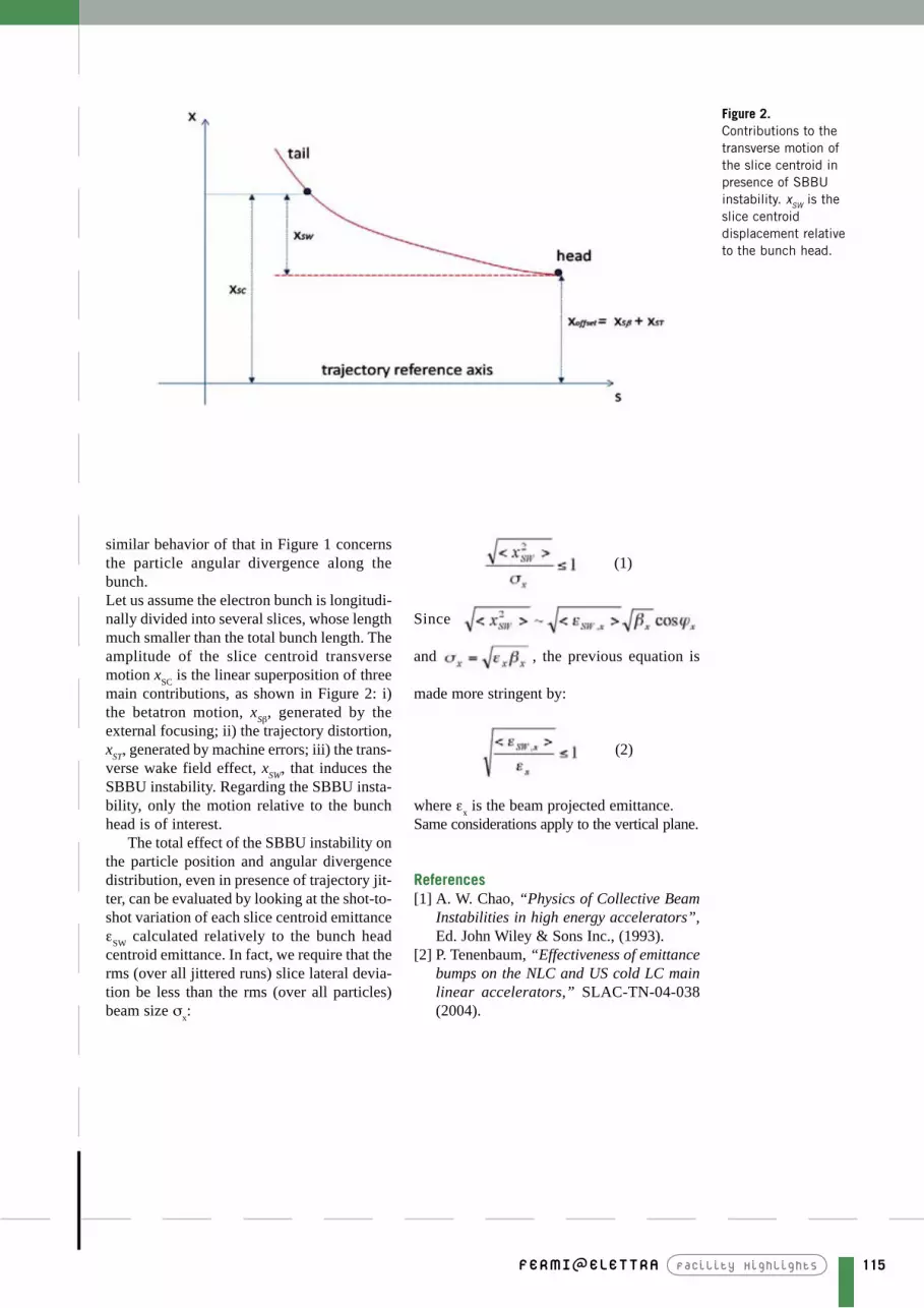
115Facility Highlights Fermi@elettra
similar behavior of that in Figure 1 concerns the particle angular divergence along the bunch.Let us assume the electron bunch is longitudi-nally divided into several slices, whose length much smaller than the total bunch length. The amplitude of the slice centroid transverse motion xSC is the linear superposition of three main contributions, as shown in Figure 2: i) the betatron motion, xSβ
, generated by the external focusing; ii) the trajectory distortion, xST, generated by machine errors; iii) the trans-verse wake field effect, xSW, that induces the SBBU instability. Regarding the SBBU insta-bility, only the motion relative to the bunch head is of interest.
The total effect of the SBBU instability on the particle position and angular divergence distribution, even in presence of trajectory jit-ter, can be evaluated by looking at the shot-to-shot variation of each slice centroid emittance εSW calculated relatively to the bunch head centroid emittance. In fact, we require that the rms (over all jittered runs) slice lateral devia-tion be less than the rms (over all particles) beam size σx:
(1)
Since
and , the previous equation is
made more stringent by:
(2)
where εx is the beam projected emittance. Same considerations apply to the vertical plane.
References[1] A. W. Chao, “Physics of Collective Beam
Instabilities in high energy accelerators”, Ed. John Wiley & Sons Inc., (1993).
[2] P. Tenenbaum, “Effectiveness of emittance bumps on the NLC and US cold LC main linear accelerators,” SLAC-TN-04-038 (2004).
Figure 2. Contributions to the transverse motion of the slice centroid in presence of SBBU instability. xSW is the slice centroid displacement relative to the bunch head.

116 Facility Highlights Fermi@elettra
P. Craievich1, S. Biedron1, C. Bontoiu1, S. Di Mitri1, M.Ferianis1, A.Rubino1, M. Veronese1, M. Petronio2, D. Alesini3, L. Palumbo3, L. Ficcadenti4
1 Sincrotrone Trieste S.C.p.A., Trieste, Italy 2 DEEI, University of Trieste, Italy3 INFN/LNF, Rome, Italy 4 University La Sapienza, Rome, Italy
E-mail: [email protected]
low-energy transverse rf deflector cavity
FERMI@Elettra is a soft X-ray fourth gene-ration light source under development at the Elettra laboratory. The single bunch beam is produced by a photo-injector, then accelera-ted up to 1.2 GeV by a linear accelerator, and finally transported to the undulators, where the free electron lasing occurs. In order to completely characterize the beam phase space by means of measurements of the bunch leng-th and of the transverse slice emittance two deflecting cavities will be positioned at two points in the linac. One will be placed at 1.2 GeV (high energy), just before the FEL pro-cess starts; the second at 250 MeV (low ener-gy), after the first bunch compressor (BC1). The description of the low-energy bunch deflection, which allows the efficiency of the first bunch compressor to be measured, toge-ther with the RF design are here presented.
Complete characterization of the beam phase space by means of measurements of the bunch length and of the transverse slice emit-
tance are important tasks for the FERMI FEL project. The deflector following BC1 will operate in a vertical deflecting mode to allow measurements of the horizontal slice emittan-ce and bunch length. Figure 1 sketches the bunch vertical deflection when the centroid remains on the trajectory axis while the beam is stretched in the transverse direction and collides with an optical transition radiation (OTR) screen. The deflector will be followed by a multi-screen emittance measurement sta-tion with quadrupole magnets in-between the screens.
If the finite transverse emittance of the bunch is taken into account, then the beam size at the screen after the deflection can be estimated by the quadratic summation of the RMS non-deflected particle transverse size distribution and of the RMS beam size in the pencil beam approximation. Finite emittance contribute to the increase of the beam size measured at the screen, but if the deflecting
Figure 1. Deflector operating mode: the centroid remains on axis while the beam is stretched in the transversal direction and collides to an OTR screen.

117Facility Highlights Fermi@elettra
voltage is sufficiently large the relative error due to finite emittance can be reduce, i.e. a relative error less than 3% requires a deflect-ing voltage V
⊥≥1.6 MV. The measurement of
the transverse slice emittance requires short portions of the bunch length to be resolved at the screen after the bunch is deflected. Con-sidering a division into 30 slices of the whole bunch (about 700 µm for the medium bunch length option) and assuming 10 µm RMS resolution of the screen, then a contrast of 70% allows the detection of the 40 µm slice length. In the approximation of a uniform bunch current distribution, a minimum peak voltage of 2.3 MV is required to achieve the desired vertical deflection of the bunch in the worse case optical condition.
The RF design and the choice between dif-ferent options was done taking into account the following constraints: a minimum peak voltage of 2.3 MV, a working RF frequency of 2998 MHz, an RF pulse length less than 3 µs, and a maximum available RF power of 5 MW. Deflecting cavities, such as iris loaded travel-ling wave (TW) guide or multi cell standing wave (SW) structures, are a powerful tool to reach this aim. The minimum peak voltage can be achieved by both traveling wave or stand-ing wave structures. In particular the deflector at low energy will work at maximum beam energy of 250 MeV. We have chosen to scale the deflecting SW structure developed for the SPARC project [1] to the FERMI operating frequency. Such a choice allows us to reach
the desired resolution with full flexibility. This could become important if one contemplates use of an even shorter bunch as in the single bunch compressor scheme which was propo-sed as a possible option for FERMI@Elettra. The deflector is a standing wave structure composed of 5-cells operating on the π-mode. The design is shown in figure 2. The main RF parameters of the deflector are the quality fac-tor Q=15600, the transverse shunt impedance R
⊥=2.4 MΩ, the filling factor τ=0.8 µm at
coupling coefficient β=1, and the working fre-quency fr=2.998 GHz. The total length of the RF structure is 0.5m and the maximum inte-grated deflecting voltage is 4.9 MV with 5 MW of input power [2].
As a conclusion, a peak voltage of 2.3 MV for the RF deflector is completely satisfactory for the bunch length measurement. The same specification allows for a resolution of 30 sli-ces over the medium bunch length of the FER-MI@Elettra project with an intensity contrast of about 70%. The 5-cell SW structure being built will achieve this peak voltage require-ment and also allow us flexibility to explore adequately even shorter bunch length.
References[1] D. Alesini et al., Nucl. Instr. Meth. A 568
488 (2000).[2] P. Craievich et al., “Fermi Low-Enegy
Transverse RF Deflector Cavity”, Procee-dings of EPAC08, Genoa, Italy, (2008).
Figure 2. Technical drawing of the standing wave 5-cell deflector.

118 Facility Highlights Fermi@elettra
S. Spampinati1,2, S. Di Mitri1, G. Penco1
1 Sincrotrone Trieste S.C.p.A., Trieste, Italy2 University of Nova Gorica, Nova Gorica, Slovenia
E-mail: [email protected]
tHe 100-mev Beam diagnostic station
The FERMI Free Electron Laser (FEL) will be a 4th generation light source in which powerful and coherent VUV, X-radiation is generated by the passage of the high energy electron beam through an undulator chain. A very high quality, high density electron beam is needed to produce the high brightness FEL. The elec-trons are extracted by a Cu target illuminated by a UV laser and accelerated by the high volt-age electric field of the RF Gun. Then, the beam will be further accelerated to 1.2 GeV in the main linac and its length will be com-pressed in magnetic chicanes (bunch compres-sors) to achieve a high peak current. The elec-tron beam characteristics will be controlled and tuned by a lot of ‘knobs’ distributed along the machine. The passage from the injector to the linac is a critical point since the beam com-ing from the Gun shall be matched with the optics of lattice downstream. In order to do this, a beam diagnostic station will be placed there, where the beam energy is approximate-ly 100 MeV. This diagnostic station is placed across the so called Laser Heater area. This is constituted an undulator placed in a small magnetic chicane where the electron beam interacts with an external laser. This interac-tion provides an increase of the electron beam energy spread in order to prevent the develop-ment of succeeding instabilities. The 100 MeV diagnostic station is equipped with quadru-poles and Optical Transition Radiation (OTR) screens to measure and correct the beam optics and to evaluate the transverse emittance. A Beam Position Monitor (BPM) and a spec-trometer (dipole magnet) are downstream the laser heater chicane. Figure 1 shows sketch of the FERMI@Elettra layout.
Small transverse emittance is one of the peculiarities of an electron beam driving a single pass VUV, X-ray FEL and it is provided by the photo-injector. Many parameters have to be optimized there to reach the required
normalized emittance value (<2 μm rad forFERMI). A precise emittance measurement is then an important topic for this kind of machine. A multi-screens technique [1] will be implemented to measure the beam emittance and the beam Twiss parameters at the end of the photo-injector. The screens are placed at a relative betatron phase advance of 60 degree, in both x and y plane. The second screen is in the laser heater chicane, just after the laser heater undulator, in correspondence of the beam waist. To avoid emittance degradation, the incoming electron beam optics has to be matched to the linac optics; the matching will be performed by the four quadrupoles at the beginning of the diagnostic section.
The last part of the 100 MeV energy diag-nostic station is represented by a spectrometer line. The knowledge of the beam energy at this point is required for two reasons: to satisfy a resonance condition (provide the exact amount of beam heating) in the undulator between the electron beam energy and the wavelength of the external laser; to optimize the injection into the main linac. For this purpose, the beam average energy has to be known with an accu-racy of 100 keV rms. The maximum disper-sion in the centre of the laser heater chicane is 3.1 cm. Theferore a BPM with < 5 micron rms resolution placed there will permit to resolve a shot-to-shot relative energy variation of 0.1%. This BPM will be part of the FERMI longitudinal feedback system. The correlated beam energy spread in the laser heater chicane is mainly due to the off-crest acceleration pro-vided by the upstream injector. Then, a scan of the average beam energy and energy spread as function of the injector RF phase and voltage will be performed to characterize the longitu-dinal beam dynamics.
Alignment and transverse matching between the laser and the electron beam is very important in order to have the correct

119Facility Highlights Fermi@elettra
interaction between the two beams and there-fore the desired heating. The relative align-ment between the photon and electron beam hastobebetterthan50μm.Toachievethis,two screens, capable of recording the image of the two beams, are placed in the laser heater chicane before and after the undulator. The layout of the laser heater chicane foresees some space for the future integration of an optical replica synthesizer [2] that could be able to measure the beam current profile with 10 fs rms resolution of the bunch duration. A dispersive section and an additional undulator are needed for this diagnostics. The additional dispersive section and an Optical Transition Radiation (OTR) screen are then sufficient to detect the beam energy modulation provided by the laser/electron interaction.
References[1] H. Widemann, “Particle Accelerator Phys-
ics”, Spriger, II ed., (1999) [2] T E. Saldin E.A. Schneidmiller, and M.V.
Yurkov, Nucl. Instr. Meth. A 539, 499 (2005).
Figure 1. Sketch of the FERMI@Elettra layout

120 Facility Highlights Fermi@elettra
S. Di Mitri1, B. Diviacco1, S. Spampinati1,2
1 Sincrotrone Trieste S.C.p.A., Trieste, Italy2 University of Nova Gorica, Nova Gorica, Slovenia
E-mail: [email protected]
Beam Based alignment in tHe fermi@elettra undulator cHains and fel performance
The FERMI FEL is going to generate coherent light by the passage of the high energy elec-tron beam through an undulator chain. The continuous interaction of the electrons with the induced radiation in the undulators ampli-fies the FEL light power. This interaction is guaranteed by the transverse overlap of the electron beam and the photon beam in the undulator chain. Therefore it is very important to steer the electron beam on a straight path, in spite of all trajectory perturbations that can be introduced by the undulator misalignment, quadrupole misalignment and beam launching error. The Beam Based Alignment (BBA) is a technique that uses 1 µm resolution Beam Position Monitors to calculate the trajectory offsets; then, steerers (dipole correctors) and
quadrupoles are used to steer the electron beam on an ideal straight path.
The FERMI FEL will be a variable polar-ization user facility that implies a changing undulator light polarization. When the phases of the devices are changed, their focusing changes as well and the quadrupole gradients between the undulators shall be changed accordingly to maintain the beam optics fixed. Unfortunately, if a quadrupole is traversed off axis, a dipole field component is excited and it will kick the electron beam by modifying its trajectory. Thus, we need to centre the quadru-poles on the straight path identified by the BBA algorithm because when the undulators change their polarization, the new focusing setting must not perturb the reference trajec-
Figure 1. Electron beam straight path constructed through the BBA algorithm (solid line). The realistic beam trajectory (dotted line) is affected by distortion inside the undulators. According to the statistic provided by the BBA algorithm applied to Fermi FEL1 at 60 nm resonance FEL wavelength, the relative displacement of the electron beam from the undulator axis (dashed line) is in the range 200 – 600 µm.

121Facility Highlights Fermi@elettra
tory. The quadrupoles will be moved on the reference trajectory with remotely controlled micro-movers in the horizontal and vertical plane. A similar option could be adopted for the undulators, but it is not strictly required for the FERMI FEL at the cost of a small reduc-tion of the final FEL peak power.
Once the undulators are closed to the nom-inal gap, they will contribute to the trajectory distortion in two ways:
an error of the first field integral will be 1) compensated by correction coils mounted at the undulator edges;the focusing of the undulator traversed off 2) axis induces an angular kick error. The relative displacement of the electron beam and of the undulators has in turn two sources: first, the static alignment of the undulators with respect to the machine ref-erence axis has a finite accuracy. Second and more important, the straight path deter-mined by the BBA algorithm is not neces-sary on the same line of the machine refer-ence axis. Simulations actually show that it is far from the linac axis by several 100’s micron and that it is dependent on the beam launching error and on the accuracy of the initial machine alignment.
The evolution of the FEL radiation peak power is plotted in Figure 2. It shows that the off axis motion of the electrons with respect to the undulator magnetic axis makes the FEL to saturate at a lower power level (compare the solid line with the others); however, this remains within the FEL tolerances and users requirements.
References[1] P. Emma, R. Carr, H. D. Nuhn, Nucl. Instr.
Meth. A 429, 407 (1999).[2] U. Hahn, J. Pflüger, G. Schmidt, Nucl.
Instr. Meth. A 429, 276 (1999). [3] T. Tanaka, H. Kitamura, T. Shintake, Nucl.
Instr. Meth. A 528, 172 (2004).
Figure 2. Power evolution along the undulator chain of FEL1 at 60 nm for a beam reference trajectory parallel to the undulators.

122 Facility Highlights Fermi@elettra
G. Penco1, D. Castronovo1, D. Zangrando1, M. Trovò1, G. Loda1
1 Sincrotrone Trieste S.C.p.A., Trieste, Italy
E-mail: [email protected]
The Gun SpecTRomeTeR FoR The FeRmI@eleTTRa pRojecT
The FERMI photo-injector gun has been built and it is now in the MAX-lab, at Lund, in order to perform RF high power tests and a preliminary commissioning with the driven laser [1]. Diagnostics have been designed and inserted in the gun-to-first accelerating section in order to tune the injector parameters and achieve the specified performance. In this fra-mework the spectrometer at the gun exit plays an important role to accurately know the peak field of the gun accelerating gradient and the injection phase. The energy of the bunch has to be known with an error less than 0.1 %. The gun spectrometer diagnostic beam line is mainly composed by the bending magnet and a Yag screen, that combining with a Cerenkov radiator allow the investigation and characte-rization of eventual deterioration of the longi-tudinal profile due to the space charge forces and microbunching instabilities [2].The beam energy measurements will be performed gene-rally at low charge, but it could be interesting to operate the spectrometer even at high char-ge, to investigate the effects induced by the space charge forces. Thus to compensate the
blow up of the bunch due to the space charge defocusing an additional quadrupole is inser-ted just at the exit of the bending magnet.
The bending magnetic design has been the result of the optimization and balance of phy-sics requirements and layout constraints. In order to accommodate all diagnostics in betwe-en the gun and the first accelerator structure, the trajectories cross is placed at about 1 m from the cathode. One of the main physics request is that particles with the same energy but having a transversal displacement have to be bended in the same way. This means that the quadrupole integrated field along the beam tra-jectory is specified to be very small, in details of the order of 0.2% with respect to the integra-ted field on the nominal trajectory. Since the bunch energy is about 5 MeV, an accurate stu-dy of the quadrupole components even in the fringe fields was carried on. The choice of a bending angle of 60° is a good compromise between high resolution and low peak magne-tic field and consequently low fringe fields. Acting on the chanfer of the iron yoke we minimized the variation between the integrated field sampled by particles on the nominal tra-jectory and particles on parallel trajectories with a horizontal displacement up to 20 mm.
The optimized magnet design is reported in figure 1.
The magnetic design was carried on in parallel and in strong interaction with 3D tra-cking code of electron bunches in order to simulate the bunch energy measurement and optimize the performance of the spectrometer beamline. Figure 2 shows the horizontal profi-le at the spectrometer screen and the energy distribution along the bunch when a low char-ge flat-top bunch is launched with different RF gun phase and consequently different energy and energy spread. In this case there is a good linearity between the screen images and the energy spread.
Figure 1. 3D bending magnet design.

123Facility Highlights Fermi@elettra
If the bunch charge is increased up to the nominal value of 800 pC, the space charge forces introduce a large defocusing effect and change the energy distribution in the bunch. In order to contain the large defocusing it is necessary to switch on the quadrupole of the spectrometer beamline. The same happens even at low charge when in some configura-tion the relative energy spread of the bunch can assume values around 10%. In this con-dition when the bunch passes thought the quadrupole, chromatic effects have to be taken into account during the screen images analysis, to accurately evaluate the energy spread.
The nominal electron bunch produced by the FERMI photoinjector is a 800 pC - 10 ps bunch with a ramped longitudinal profile [3] and the spectrometer can be very useful to check and control the efficiency in producing the desired ramping current distribution. In
fact setting the RF gun phase far off crest to superimpose a very linear energy correlation along the bunch, particles on the head of the bunch are bended less than particles on the tail, so the ramped longitudinal profile can be reproduced at the spectrometer screen. Since the high resolution of the screen, this measu-rement resolves the longitudinal profile better than 0.2 ps, which is better than a commercial streak camera.
References [1] M. Trovò et al., Proc. of the EPAC 2008
conference.[2] G. Penco et al., Proc. of the EPAC 2008
conference.[2] G. Penco et al., “Ramping longitudinal
distribution studies for the FERMI@ELETTRA injector”, Proc. of the FEL 2006 conference.
Figure 2. Horizontal profile at the spectrometer screen (top) and bunch energy distribution (bottom) for a low charge flat-top bunch tracked through the spectrometer beam line for different RF gun phase.

124 Facility Highlights Fermi@elettra
M. Trovò1, L. Badano1, F. Cianciosi1, P. Craievich1, F. Curbis2, N. Cutic2, M. Danailov1, A. Demidovich1, R. Gobessi1, D. Kumbaro2, F. Lindau2, G. Penco1, L. Pivetta1, L. Rumiz1, G. Scalamera1, D. Wang1, F. Zudini1
1 Sincrotrone Trieste S.C.p.A., Trieste, Italy2 MAX-lab, University of Lund, Lund, Sweden
E-mail: [email protected]
fermi@elettra pHotoinjector Has started its commissioning!
The new FERMI@Elettra photoinjector is presently undergoing high-power testing and characterization at MAX-Lab in Lund Swe-den. This effort is a collaboration between Sincrotrone Trieste, MAX-lab and UCLA. The 1.6-cell RF gun cavity and the focusing solenoid [1] were successfully designed and built by the Particle Beam Physics Laboratory at UCLA, delivered to Sincrotrone Trieste (ST) at the beginning of 2008, and installed in the linac tunnel at MAX-Lab. Use of the MAX-Lab facility will allow the FERMI proj-ect to progress significantly with the photoin-jector while waiting for the completion of the new linac building extension at Sincrotrone Trieste.
The experiments in MAX-lab aim to per-form the acceptance test of the FERMI Gun and to start its commissioning using the exist-ing S-band 25 MW klystron and the operating photoinjector UV laser (262 nm, 10 ps dura-tion and 500 J pulse energy available) regu-larly used during the FEL operation of the MAX-lab injector [2].
The crucial elements of the FERMI photo-injector (RF cavity, magnets, laser beam diag-nostics and transport and electron beam diag-nostics) have been installed by the ST staff in the injector tunnel of MAX-lab, as shown in Figure 1, during the Easter shutdown [3]. The system was completely set up in situ by assem-bling the different components (supports, vac-
Figure 1. FERMI gun back-view with RF waveguide and cavity and pumping system in the MAX-lab tunnel. Left: FERMI gun picture. Right: 3D cad rendering as designed.

125Facility Highlights Fermi@elettra
uum components, wave guides, pumping sys-tem and diagnostics). The photoinjector has also been equipped with its own control sys-tem that interfaces in an effective manner to all the devices, allowing the development of the specific high-level software to tune the photoinjector.
During the allocated beam time of week 21, the RF gun was conditioned to full speci-fications, achieving, in four nights, the nomi-nal values of 10 MW input peak power (cor-responding to a maximum gradient of the electrical field at the photocathode of about 120 MV/m), 3 µs pulse duration and 10 Hz repetition rate. Electrons accelerated by this filed gain, upon reaching the exit of the gun, an energy of about 5 MeV.
On the night of May 28, the RF gun’s cop-per cathode was illuminated by a UV laser operating at 262 nm and delivering 50 µJ per pulse and the first FERMI photoelectrons were clearly detected on both the integrating current transformer (ICT) and YAG:Ce scin-tillation screen. Figure 2 shows the time beha-viour of the RF power at the gun input mea-sured by means of a directional coupler, the laser time arrival as measured with a photo-diode signal, and the electron beam current signal as measured with the ICT. The photo-electron peak, superimposed on the dark cur-rent background, is clearly visible on the ICT trace in correspondence of the laser shot. The photoelectron beam charge was measured to be equal to 180 pC, corresponding to a quan-tum efficiency QE = 1.7·10-5.
During the third allocated beam time of weeks 27 and 28, the Gun commissioning advanced and achieved new crucial results. The photoelectron extraction and the gun tun-ing were performed in a more systematic way. Moreover the dedicated gun diagnostics were integrated in the photoinjector control system thus enabling a full set up of the gun facility.
In conclusion, the FERMI photo-cathode gun commissioning has been successfully started in the MAX-lab tunnel with encourag-ing results: the cavity conditioning went on smoothly, the first photoelectrons were extracted and measured, the first quantum efficiency measurement indicates a good cathode surface cleanness and, more impor-tantly and in general, the system behaves according to specification.
Further activities are planned at MAX-lab to continue the characterization of the FERMI gun e-beam and to proceed the system com-missioning. This will allow us to reduce the
commissioning time at Trieste. The system will be moved back to Trieste as soon as the FERMI site will be completed.
References[1] G. D’Auria et al., “The new Photoinjector
for the FERMI Project”, PAC’07, Albu-querque, TUPMN028, 974 (2007).
[2] S. Thorin et al., “Start-to-end simulations for a seeded harmonic generation free elec-tron laser”, Phys. Rev. ST Accel. Beams 10, 110701 (2007)
[3] M. Trovò et al., “Status of the FERMI@Elettra Photoinjector”, EPAC 08, Genova, MOPC080, 247 (2008).
Figure 2. Time behaviour of the RF power at the input of the gun (a), of the photodiode signal of the laser (b) and of the ICT signal (c).


facts & figures

128 facts & figures
the company
Sincrotrone Trieste S.C.p.A. began operations in 1987: it is a non-profit Share Company (Società Consortile per
Azioni) recognised as being of national interest by a State Law, which manages the Elettra Laboratory. Elettra
continues to update itself and grow. In addition to significant modernisation projects relating to beamline
sources and other components, a new fourth generation light source, FERMI@Elettra, is under construction alongside
the original one.
Elettra is an Associate Laboratory of the International Atomic Energy Agency (IAEA) of Vienna, and forms a key node
in the science and technology network of the Central European Initiative (CEI).
It participates in more than twenty projects within the EU Framework Programme for Research and Development, and
co-ordinates project I3 (IA-SFS), which encourages transnational access to and technological development in European
synchrotron light laboratories.
On its site Elettra hosts the National Laboratory TASC (INFM-CNR), a facility for micromanufacturing and
nanoscience. It has also established enduring working relationships with important Italian and foreign institutions,
including various CNR (National Research Council) bodies, the Academies of Science of Austria and the Czech Republic,
UNESCO’s International Centre of Theoretical Physics (ICTP), the International School of Advanced Studies (SISSA),
and the Universities of Milan, Trento, Trieste and Udine. These partners are actively contributing to the construction and
operation of beamlines and support laboratories.
Elettra’s scientific and technical quality and developments are constantly monitored by Board-appointed international
Committees which advise on all relevant aspects of the general and development policy, scientific programs, accelerator
development, technology transfer and industrial applications.
ShareholderS> AREA Science Park Consortium (51%)
> Autonomous Region of Friuli Venezia Giulia (40%)
> INFM-CNR (National Institute of Material Physics of the Italian National Research Council) (5%)
> The national Agency for inward investment promotion and enterprise development (4%)
allianceS and PartnerShiPS> IAEA (International Atomic Energy Agency)
> CEI (Central European Initiative)
> IRUVX (European Consortium for FELs up to the UV/softXray)
> Austrian Academy of Sciences
> Academy of Sciences of the Czech Republic
> CNR (Consiglio Nazionale delle Ricerche – National Research Council)
> CNRS (Centre National de la Recherche Scientifique)
> ICTP - UNESCO (International Centre for Theoretical Physics)
> INSTM (Consorzio Interuniversitario Nazionale per la Scienza e Tecnologia dei Materiali – National Inter-University Consortium for Materials Science and Technology)
> INFN (Istituto Nazionale di Fisica Nucleare National Institute of Nuclear Physics)
> ISAS (International School of Advanced Studies)
> Charles University, Prague
> University of Nova Gorica
> University of Milan – Bicocca
> University of Trento
> University of Trieste
> University of Udine

129facts & figures
MAC IAP
President Chief ExecutiveOfficer
SAC
Board of Directors
Vice President
Groups & Clusters
Strategic Commitee Executive Commitee
Board of Auditors Council of Partners
Sincrotrone Trieste S.C.p.A. is managed by a Board of Directors, assisted by a shareholder-appointed Board of Auditors,
and advised by Board-appointed international committees such as the Council of Partners for general and development
policy, the Scientific Advisory Council for scientific programs, the Machine Advisory Committee for accelerator
development, and the Industrial Advisory Panel as far as technology transfer and industrial applications are concerned.
Board of auditors
chairman: fabio matarazzoNicola Archidiacono
Claudio SambriPaolo Marchesi
Ugo Braico
Board of directors
president: carlo rizzutoVice president: giovanni comelli
chief executive officer: alfonso franciosiRoberto Della MarinaMarcello Fontanesi
Gemma RavizzaGiorgio Rossi
Giorgio SulligoiAlessandro Trovarelli
council of Partners
president: carlo rizzutoFabio Barbone
Stefano FantoniAlain Fontaine
Marcello FontanesiDante GatteschiPeter Laggner
Vladimir MatolinFabio RuzzierClaudio Tuniz
Machine advisory committee
(Mac)chairman: richard p. Walker
Paul J. EmmaMikael ErikssonJerome Hastings
Carlo PaganiClaudio Pellegrini
Mike PooleRobert W. Schoenlein
Hans Weise
Scientific advisory council
(Sac)chairman: ingolf Lindau
David AttwoodGordon Brown
Charles S. FadleyRobert HuberSine Larsen
Dietrich MenzelCharles V. Shank
Friso van der Veen
industrial advisory Panel
(iaP)chairman: alberto sangiovanni-Vincentelli
Carlo CastellanoEnrico AlbizzatiMaurizio Arienzo
Mauro Ferrari

130 facts & figures
the staff
clUSterS
GroU
PS
elettra Fermi research technologyPlatform
Scientists and reseachers
technical Personnel
administrative and clerical Personnel
total 315
accelerators 40
electromagnetism 40
information technology 36
Beamlines 62
Mechanical, Vacuum and optical engineering 29
infrastructure 25
administration 27
coordination 56
Sincrotrone Trieste has adopted a matrix-type of organization. The four Strategic Initiatives correspond to and are
implemented through four Clusters of different Projects, grouped together based on the complementarity of the
different project goals. The human and instrumental resources required by the different projects are managed
within eight Groups of staff members with similar or related expertise.

131facts & figures
StaFF diStriBUtion BY GroUP
Elettra provides support for training and education of university students, hosting courses, lectures, stages ranging from Physics to Engineering and support for scientific activities. A collaboration with the International Centre of Theoretical Physics has been established with the aim of giving the opportunity to junior representatives of scientific institutes in developing countries to participate in Elettra’s projects.
traininG and career deVeloPeMent (July 2007 - June 2008)
UNDERGRADUATE STUDENTS
PoSTGRADUATE STUDENTS
PhD STUDENTS (University of Trieste, University of Trento, SISSA)
TRIL, STEP and SESAME students and visitors from ICTP
16
15
24
20

132 facts & figures
BeamLines and users
B e a m L i n e s source* energy range (eV) partner institutions
1.1L tWinmic A multipurpose twin X-ray microscopy beamline for improving life conditions and human health
short id 250 - 2000 ESRF, PSI, SLS, CNR-INFM, King’s Coll. London, RheinAhrCampus Remagen, Göttingen Univ., ITPo Ljubljana
1.2L nanospectroscopy SPELEEM (Elmitec GmbH) and LEEM-PEEM end-station id 50 - 1000 CNRS
1.2r feL European Free-Electron Laser project id 1,8 - 9,5
2.2L esca microscopy Scanning photoelectron microscopy (SPEM) id 200 - 1400
2.2r superesca Fast X-ray photoemission experiments on surfaces id 85 - 1500
3.2L spectro microscopy Angle-resolved photoemission microscope id 27 - 95
3.2r VuV photoemission Angle-resolved photoemission in the VUV range id 16 - 1000 CNR
4.2 circularly polarised Light Circularly Polarised Photoemission and X-ray absorption spectroscopy
id 5 - 1000 CNR
5.2L saXs Small Angle X-Ray Scattering id 8000 - 16000 Austrian Academy of Science
5.2r Xrd1 X-ray Diffraction id 4000 - 22000 CNR
6.1L materials science Photoemission and X-ray absorption bm 40 - 800 Czech Academy of Science, Charles University, Prague
6.1r syrmep SYnchrotron Radiation for MEdical Physics bm 8000 - 35000 University of Trieste
6.2r gas phase Research on gaseous systems id 14 - 1000 CNR, CNR-INFM, INSTM
7.1 mcX Powder Diffraction Beamline bm 2100 - 23000 University of Trento, INSTM
7.2 aLoisa Advanced Line for overlayer, Interface and Surface Analysis id 120 - 8000 CNR-INFM
8.1L Bear Bending magnet for Emission Absorption and Reflectivity bm 4 - 1400 CNR-INFM
8.1r LiLit Laboratory for Interdisciplinary LIThography bm 1000 - 5000 CNR, CNR-INFM
8.2 Bach Beamline for Advanced DiCHroism id 35 - 1600 CNR-INFM
9.1 sissi Source for Imaging and Spectroscopic Studies in the Infrared bm 0,001 - 3 CNR-INFM, Univ. of Rome “La Sapienza”
9.2 ape Advanced Photoelectric-effect Experiments id 10-2000 CNR-INFM
10.1L X-ray microfluorescence X-ray microfluorescence bm 4000 - 20000
10.1r dXrL Deep-etch Lithography bm 2000 - 20000
10.2L iuVs Inelastic Ultra Violet Scattering id 11-2008
10.2r Bad elph Photoemission with low energy photons id 4 - 25 Wuerzburg Univ.
11.1r Xafs X-ray Absorption Fine Structure bm 2300 - 25000 ICTP
11.2 Xrd2 X-ray Diffraction id
source* id = insertion device (wiggler or undulator) bm = bending magnet

133facts & figures
The allocation of beamtime to proposing users occurs via international committees and referees and the users have
their own representative body to assess the quality of the service (Scientific Review Committee).
Scientific review committee
Dipankar Das Sarma(Chairman)
atoms, Molecules & Plasmas
Svante Svensson (Chairman) Vincenzo Aquilanti
Uwe BeckerJohn M. Dyke
catalytic Material/Surface Science
Carlo Mariani (Chairman) Philip HofmannFalko P. NetzerPetra Rudolf
Michèle Rose Sauvage-SimkinRobertino Zanoni
condensed matterelectronic & Magnetic Structure
Dipankar Das Sarma (Chairman) Hermann DürrMark Golden
Giorgio MargaritondoMaurizio Sacchi
instrumentation & technological materialslife and Medical Sciences (excluding crystallography)Polymers and Soft MatterGraeme Morrison (Chairman)
Paul DumasChristopher Hall
Lisa MillerGünther Schmal
Steve Wilkins
Protein & Macromolecular crystallography
Giuseppe Zanotti (Chairman) Tilman Schirmer
Dusan TurkLuigi Vitagliano
hard condensed matter - Structures
Maurizio Benfatto (Chairman)Robert Joseph Cernik
Paola D’AngeloMarco Milanesio
Scattering
Paolo Mariani (Chairman) Stephanie FinetDaniele FiorettoHermann FranzGiulio Monaco

134 facts & figures
allocated ProPoSalS BY reSearch area: tot = 288 (July 2007 - June 2008)
USerS at elettra: tot = 750 (July 2007 - June 2008)
2004 - 2008 ProPoSalS SUBMitted BY SeMeSter
From October 1st, 2007 to March 2nd, 2008 the Elettra light source was closed due to the booster installation.

135facts & figures
financiaL figures
running costsGeneral costs € 6.046.920Personnel € 13.981.938Utilities € 5.024.115Accelerator group € 279.953Administration group € 261.536Beamlines group € 866.151Coordination group € 1.799.596Electromagnetism group € 478.285IT group € 369.051Infrastructure group € 1.070.664Mechanical, Vacuum and optical engineering € 355.982Industrial Liason office operation € 607.602Scientific partnerships € 350.000
development projects € 6.817.338
total ordinarY oPeration € 38.309.131
Special projectsBooster € 55.305Fermi € 58.392.360
total SPecial ProJectS € 58.447.665
General total € 96.756.796
BUdGet allocation For 2008

136 facts & figures
proJects / sponsored research
the recent shift in the Company activities to a project-based approach has had a very positive effect on the ability
to propose projects to external funding institutions and thus attract resources: the last two calendar years, 2007
and 2008 (not yet concluded), were extremely successful in this respect. As for the FERMI project, in December
2007 we were officially notified of the signing of the program agreement “FERMI@Elettra – Phase II” with the Ministry
of University and Research, that assigns to the Company a contribution of 11.7 million Euro.
Apart from this main project, the Company has been able to win research contracts with public entities on the
European, Italian and Regional levels, acquiring contributions equivalent to 8.8 million Euro in 2007 and 3.1 million
Euro in the first half of 2008. At the time of this writing, submitted applications for external funding presently under
evaluation by the Region of Friuli Venezia Giulia and by the European Commission (EC) total in excess of 4 million Euro,
while the further requests for funding in the applications that are presently being drafted, in view of the deadlines in
autumn 2008, total about 10 million Euro more.
Particularly relevant is the acquisition of a Starting Grant assigned by the European Research Council (ERC) to the
project for the construction of an inelastic scattering beamline for the FERMI source, coordinated by Dr. Claudio Mas-
ciovecchio, scientist of the Beamlines Group of the Company. The selection process by the ERC has been particularly
strict: less than 3% of the submitted projects have obtained funding. This success testifies the absolute excellence at
the European level of the personnel and of the programmes of the Company.
The consolidated presence of national and international partners has in the past brought in significant investments.
Various new initiatives have been undertaken to increase this presence and to consolidate the transformation of the
Company into an international institution. The most important ones are the definition and constitution, with EC funding
in the preparatory phase, of a European Consortium of FELs (with Germany, United Kingdom and Sweden as the original
founders and Switzerland, France, The Netherlands and Poland adhering subsequently). This Consortium is the pos-
sible base for a transformation of the Company into an international foundation (or some other form of institution).
Other important achievements have been obtained within the I3 project IA-SFS (Integrating Activity on Synchrotron
and Free Electron Laser Science). Elettra has been the coordinator of this project since March 2004: this is the most
significant FP6 (Sixth European Union Framework Programme) project in the field of synchrotron radiation and free
electron lasers (see http://www.elettra.trieste.it/i3/). The EC finances a total of 27 million Euro within the project for
user access to the European network of synchrotron light sources, not to mention the joint development of various spe-
cific technologies. Elettra has proved itself with a precise, timely and transparent management of the assigned funding
and excellently coordinated the manifold activities of this project. The other international institutions that participate
in the project have voted unanimously for Elettra to coordinate the new integrated initiative that will continue IA-SFS
in FP7, namely the ELISA project (European Light Sources Activities – Synchrotrons and Free Electron Lasers) that
is presently under negotiation. Furthermore, the IA-SFS has been selected as one of the 40 “success stories” of FP6
to be included in a publication, edited by the European Commission, that will be distributed to the general public,
National and Regional authorities, European Parliament, Delegations and Representations of the European Union all
over the world.
During the last 12 months, Elettra participated in 31 research contracts (see table) funded by the following exter-
nal agencies: European Commission, Italian Ministry of Research, Region Friuli Venezia Giulia, International Centre for
Theoretical Physics, Indian Department of Science and Technology.

137facts & figures
name short name coordinator
Development of a 3D detector with micrometer space resolution and picosecond time resolution
3D detector Elettra
Desorption measurements from photoresists for the Extreme UltraViolet Lithography EUVL photoresists Elettra
X-ray diffraction from polycrystalline materials in controlled environment XRD polycrystalline materials Elettra
Monitoring station for PM10 particles PM10 Elettra
The Elettra storage-ring FEL: a multi-purpose light source EUFoS Elettra
Realization of a technological platform for the crystallographic analysis of biological macromolecules of biomedical interest for the industrial research
DAGEAS Elettra
Study of hybrid organic/inorganic interfaces for strategic applications in the field of flexible displays and biochips
Nano-BioSoLEd Elettra
Study and realization of prototype platforms for plane and helical undulators Elettra
Convalidation of LiFArte activity INVISIBLE AREA Science Park
Development and realization of solid state ultrafast laser amplifiers optimizd for FEL applications
FEL Laser Amplifiers Elettra
Distributed environment monitoring based on Grid MADBAG Elettra
Anti Counterfeiting Tags ACT Elettra
Development of chemical sensors for environmental and biological diagnosis based on nanowires and nanotubes
Nanowire/nanotube sensors Elettra
regionaL research contracts
name short name coordinator
Biocrystallography on a Highly Integrated Technology Platform for European Structural Genomics
BIoXHIT EMBL Germany
Integrating Activity on Synchrotron and Free Electron Laser Science IA-SFS Elettra
European FEL Design Study EURoFEL DESY Germany
European Design Study Towards a Global TeV Linear Collider EURoTeV DESY Germany
Enabling Grids for E-sciencE - II EGEE-II CERN Switzerland
Light Source Theory Network LighTnet STFC United Kingdom
ICTP-Elettra Users Programme Elettra
Transnational access of the Indian scientists to the Elettra beamlines Elettra
Conservation materials for stained glass windows-assessment of treatments, studies on reversibility, and performance of innovative restoration strategies and products
CoNSTGLASS Fraunhofer-Institut für Silicatforschung Germany
Deployment of Remote Instrumentation Infrastructure DoRII PSNC Poland
Preparatory Phase of the IRUVX-FEL Consortium IRUVX-PP DESY Germany
TIME-Resolved Spectroscopy of Nanoscale Dynamics in Condensed Matter Physics TIMER Elettra
european/internationaL research contracts
name short name coordinator
Nano- and micro-spectroscopy by synchrotron radiation integrated with advanced STM/AFM systems to study manmade atomic scale functional materials
Integrated nanospectroscopies Elettra
BooSTER-Elettra Elettra
Post-Genomic Structural Biology: Developing Infrastructures for Protein Crystallography Structural biology Elettra
FERMI@Elettra - Phase I Elettra
High efficiency innovative light sources for solid state illumination devices with civil and automotive applications
LUCI CNR
FERMI@Elettra - Phase II Elettra
nationaL research contracts

138 facts & figures
technoLogy transfer at eLettra
the Industrial Liaison Office (ILO) was set up in 2004 to promote the exceptional body of skills and technical ex-
pertise resulting from the experience accumulated in the construction and running of the Elettra facilities over a
long period of time. This know-how is of particular interest to other Synchrotron facilities, suppliers of advanced
instrumentation and private industrial companies operating in different fields: mechanical, optical, pharmaceutical,
microelectronics, energy, chemistry etc.
Products and services are sold throughout the world. 2007 turnover is reported on the next page together with the
trend over the years, and show an increase in consultancies and instrumentation business.
In 2007, in order to supply the world market and, initially, the FERMI@Elettra project with undulators, a partner-
ship of an entrepreneurial nature was established and a spin-off company (Kyma srl) was created to set up an industrial
scale production structure. After launching the production of undulators for FERMI@Elettra, Kyma will operate in the
international market as an expert and qualified supplier of accelerator components.
In 2008 ILO, for the first time, presents itself to industry through a catalogue that describes Sincrotrone Trieste
technologies and services. The catalogue has been specifically conceived for this target and describes various examples
of the great variety of studies, skills and technological resources to be found in the Laboratory. For enterprises that must
innovate continuously, access to this valuable source of knowledge can provide useful support to R&D activity and a
genuine competitive advantage in the international marketplace.
Furthermore, in terms of market share, ILO has proved its capability to sell Elettra-developed scientific instrumen-
tation to other synchrotron facilities and research laboratories worldwide, so that in 2008 another catalogue concerning
Elettra products has been released.
The catalogue includes: photon or charged particle detectors, based on centroid finding techniques – such as
(cross) delay anode detectors – or based on multi-channel acquisition, employed in several of Elettra’s beamlines (See
the technical paper on page 110); high voltage bipolar power supply systems especially suited for benders of X-ray
biomorph mirrors; picoammeters with a sampling frequency of 10 kHz on 4 independent channels; ionisation chambers
and beam position monitors used to characterise and monitor photon and electron beams and other devices developed
in our Instrumentation and Detectors Laboratory such as multi-point strain gauges; charge pulse amplifiers; high vol-
tage pulse generators; RF filters etc.
As far as accelerator parts that are still provided directly by Elettra are concerned, resonant cavities are illustrated,
whose purpose is to accelerate electrons passing through them by the application of accelerating voltages ranging from
tens to hundreds of kilovolts, with a resonant frequency of 500 MHz.

139facts & figures
country numBer of orders amount (thousands of euro)
Switzerland 1 1,00
Italy 10 238,56
Germany 7 355,90
France 3 33,38
United States 5 36,30
United Kingdom 1 36,80
Spain 2 795,40
Canada 1 31,05
ToTAL 30 1.528,38
2007 orders amount By customer country
2007 trend in turn oVer of commerciaL actiVity (thousands of euro)
2007 orders amount By commerciaL actiVity


EVENTS

142 Events
EVENTS aT ELETTRa
Official visit of Giorgio Napolitano, President of the Republic of Italy
(March 28, 2008)Carlo Rizzuto and local Authorities receive the President of the Republic Giorgio Napolitano: the President of FVG Region Riccardo Illy, the President of the Province of Trieste Maria Bassa Poropat and the Mayor of Trieste Roberto Dipiazza (1, 2). After the speech of Carlo Rizzuto (3, 4), President Napolitano visits the Syrmep beamline for mammography (5) and watched the 3D simulation of the new free electron laser FERMI@Elettra (6). In the Control Room, he activates the injection of the new Booster (7) and signs the visitors book (8). Finally he receives the Elettra medal (9). 1
2
4
3
5

143Events
6
7
8 9

144 Events
Visit of the Friuli Venezia Giulia Region’ President
(December 19, 2007)Riccardo Illy, President of the Friuli Venezia Giulia Region, attends the ceremony for the opening of the first FERMI building (1, 2). On the occasion of the visit, the “Gianfranco Rados” Scholarship was awarded to Francesca Iannelli (3).
1
2
3

145Events
Official visit of Bartholomew I of Constantinople
(March 4, 2008)The highest religious authority of the Orthodox Church, His All Holiness Bartholomew I, Archbishop of Constantinople, New Rome and Ecumenical Patriarch, visits Trieste in occa-sion of the 225th anniversary of the Greek-oriental community.

146 Events
Open Day at Elettra
(May 10, 2008)808 persons visit the Elettra and TASC labora-tories in 23 tours, guided by 58 volunteers.

147Events

148 Events
Elettra Spring Party
(May 22, 2008)A social event for the Elettra staff, with music and games. The party takes place in the hall of the Linac Underground, where the laboratories of FERMI@Elettra project will be built.

149Events
Israeli Ambassador in Italy
(March 10, 2008)H. E. Gideon Meier visits Elettra
Press Tour
(July 12, 2008)The Press Tour organ-ized by Area Science Park to show the scien-tific park. The journal-ists, from local and na-tional newspapers and agencies, during the vist at the Elettra laboratory.
TV interview
(April 17, 2008)TG Leonardo - RAI 3 and RAI International - video-tape at the ESCA Microscopy beamline. TV broadcast of a special report on the new technology for anti-counterfeiting of art works, the project “Leaf Art”.

150 Events
OTHER EVENTS
InnovAction
(Udine, February 14-17, 2008)Elettra and FERMI@Elettra at the Udine Fair of knowledge, ideas and innovation.

151Events
FEST
(Trieste, April 17-22, 2008)The virtual tour of FERMI@Elettra (1) is presented at the 2008 edition of FEST, Inter-national Science Media Fair (2).
Festival della Scienza - Festival of Science
(Genoa, October 25 - November 6, 2007)The particulate monitoring unit set up at Elettra to collect PM10 samples is displayed at the Festival of Science.
1
2

152 Events
Meetings dedicated to orientations, schools and training
(Bologna, November 8-9, 2008) (Padova, May 22, 2008)Sincrotrone Trieste’s stands at Bologna - Incontro Aziende-Studenti Companies-Students Meeting (1) - and Padova “Università aperta” incontro aziende-studenti “University Open Day” companies-students meeting (2).
The new catalogue “Services and Technologies for Industry”
(Trieste, June 19, 2008)Press conference for the presentation of the new Sincrotrone Trieste catalogue: Carlo Rizzuto, President of ST, and Renzo Tondo, President of Friuli Venezia Giulia Region (1) and the catalogue cover (2).
1
1
2
2

153Events
WORKSHOPS, CONFERENCES, MEETINGS aND SCHOOLS
Timing and Synchronization Workshop
(Trieste, March 26-28, 2008) The participants at the workshop
Introduzione all’ottica - In Viaggio con la luce / Introduction to Optics - Travelling with light
(Trieste, November 5-7, 2007)The Optic School organized by Sincrotrone Trieste: the poster of the school (1) and some students attending lessons at the Elettra Laboratory (2).
1 2

154 Events
EPAC 2008 - 11th European Particle Accelerator Conference
(Genoa, June 23-27, 2008)Sincrotrone Trieste's stand at the conference. ST is one of the organizers of the event.
6th International Workshop on LEEM-PEEM
(Trieste, November 7-11, 2008)Poster of the workshop (1) and picture of the participants during the visit to Miramare Castle (2). The workshop was organized by Sincrotrone Trieste.
1
2

155Events
VISITORS DISTRIbuTION PER INSTITuTE (September 2007 - august 2008)
EVENT PLaCE DaTE ORGaNISERS / COLLabORaTORS
Introduzione all'ottica - In Viaggio con la luce Introduction to Optics - Travelling with light
ST 5-7/11, 2007 Sincrotrone Trieste
XV Users' Meeting Trieste 3-4/12, 2007 Sincrotrone Trieste
Solid State Modulator Workshop Trieste 6-7/12, 2007 Sincrotrone Trieste
Timing and Synchronization Workshop ST 26-28/03, 2008 Sincrotrone Trieste / INFN / Enea
EUROTeV/GANMVL All hands Meeting ST 31/03-01/04, 2008 Sincrotrone Trieste
Tavola Rotonda "Ricercatori stranieri in Italia" Trieste 01/04, 2008 SISSA / Sincrotrone Trieste
PiezoWalk Drives" NanoPosition with Millimiter Travel, Workshop
ST 02/04, 2008 PI Physik Instrumente / Sincrotrone Trieste
Tango collaboration meeting ST 17-18/04, 2008 Sincrotrone Trieste
Advanced School on Synchrotron and Free Electron Laser Sources and their Multidisciplinary Applications
Trieste 7-25/04, 2008 Sincrotrone Trieste / ICTP / IAEA
POCPA Workshop - 1st Workshop on POwer Converters for Particle Accelerator
ST 19-21/05, 2008 Sincrotrone Trieste / CERN
EPAC 2008 - 11th European Particle Accelerator Conference Genova 23-27/06, 2008 Sincrotrone Trieste / INFN / EPS
1st Internal Elettra Workshop on Time-Resolved Experiments ST 21/07, 2008 Sincrotrone Trieste
6th International Workshop on LEEM-PEEM TS 7-11/09, 2008 Sincrotrone Trieste
WORKSHOPS, CONFERENCE, MEETING aND SCHOOLS (October 2007 - September 2008)
* estimated visitors at December 2008(effective visitors at September 2008: 4908)
VISITORS DISTRIbuTION PER COuNTRy (September 2007 - august 2008) VISITORS - PERIOD 2006-2008
VISITS

Sincrotrone TriesteElettra Laboratory
Sincrotrone Trieste S.C.p.A.
Industrial Liaison O cewww.elettra.trieste.it/[email protected]: +39 040 375 8303Fax: +39 040 375 8623
PRODUCTS FOR RESEARCH LABS AND SYNCHTROTRONS
sett_08.indd 1 26-09-2008 17:38:30
Power SuppliesNew families of intelligent (DSP or PC embedded) power supplies, which cover many types of applications (high voltage/current, four-quadrant, etc.) and configurations are forthcoming. Epics of Tango interface are often already included and custom-built solutions are possible.
DetectorsPhoton and charged particle detectors, based on cross delay anodes, multi anodes and centroid finding techniques are continuously developed. 3D information (x, y, time) with spatial and time resolutions in the order of tens of micro- and pico-seconds are available through many custom-built solutions.
Lab InstrumentationFast picoammeters, multi-point strain gauges, charge pulse amplifiers, ion chambers, pulse generators, RF filters, etc. Every tool is intelligent and in sole cases Epics/Tango interfaces are already included.
Accelerator ComponentsElettra, over the years, has acquired wide experience in developing and realizing accelerators components, such as undulators, resonant cavities, etc. For the production of Insertion Devices a specific spin-off company has been set-up.

Equipment for Light Sources
Design and Manufacturing of Pure Permanent Magnet (PPM) Undulators
Instrumentation for Magnetic Measurements
Large Climate Chamber Test Services
KYMA S.R.L.S.S. 14 Km 163,5 Kmin Area Science ParkIT-34012 - Trieste - Italy
www.kyma-undulators.eu
A spin-o company of Sincrotrone Trieste s.c.p.a.in partnership with Euromisure s.r.l. and Cosylab d.d.
sett_08.indd 1 1-10-2008 8:38:42


Sincrotrone Trieste SCpAS.S. 14 Km. 163,5 in AREA Science Park34012 Trieste ITALYwww.elettra.trieste.it - [email protected]
2 0 0 7 - 0 8e l e t t r aE L E T T R A H i g H L i g H T s > 0 7 - 0 8
ELETTRA HigHLigHTs
2007-2008


