Embed Size (px)
Citation preview
applied sciences
Article
Performance Enhancement of Inexpensive Glow DischargeDetector Operating in Up-Conversion Mode in MillimeterWave Detection for Focal Plane Arrays
Arun Ramachandra Kurup 1,* , Daniel Rozban 1, Lidor Kahana 1 , Amir Abramovich 1 , Yitzhak Yitzhaky 2
and Natan Kopeika 2
�����������������
Citation: Ramachandra Kurup, A.;
Rozban, D.; Kahana, L.; Abramovich,
A.; Yitzhaky, Y.; Kopeika, N.
Performance Enhancement of
Inexpensive Glow Discharge Detector
Operating in Up-Conversion Mode in
Millimeter Wave Detection for Focal
Plane Arrays. Appl. Sci. 2021, 11, 9564.
https://doi.org/10.3390/app11209564
Academic Editor: Yiming Zhu
Received: 15 August 2021
Accepted: 12 October 2021
Published: 14 October 2021
Publisher’s Note: MDPI stays neutral
with regard to jurisdictional claims in
published maps and institutional affil-
iations.
Copyright: © 2021 by the authors.
Licensee MDPI, Basel, Switzerland.
This article is an open access article
distributed under the terms and
conditions of the Creative Commons
Attribution (CC BY) license (https://
creativecommons.org/licenses/by/
4.0/).
1 Department of Electrical and Electronic Engineering, Ariel University, Ariel 40700, Israel;[email protected] (D.R.); [email protected] (L.K.); [email protected] (A.A.)
2 Department of Electro-Optics and Photonics Engineering, School of Electrical and Computer Engineering,Ben-Gurion University of the Negev, Beer Sheva 84105, Israel; [email protected] (Y.Y.);[email protected] (N.K.)
* Correspondence: [email protected]
Featured Application: An elementary method for MMW detection by GDD-LTF combination assingle pixel for focal plane arrays.
Abstract: Performance enhancement of a very inexpensive millimeter-wave (MMW)/terahertz (THz)sensor for MMW/THz imaging systems is experimentally demonstrated in this study. The MMWsensor is composed of a glow discharge detector (GDD) and a light-to-frequency (LTF) convertercombination. The experimental results given in this study show an improvement in the performanceparameters of the detector element, such as the minimum detectable signal, as well as the signal tonoise ratio (SNR) and the noise equivalent power (NEP), when a NIR long-pass filter was insertedbetween the GDD and the LTF combination. A detailed derivation of the NEP of this unique sensoris presented in this work. Based on this derivation and the experimental measurements, the NEPvalue was calculated.
Keywords: millimeter wave imaging; terahertz sensor; glow discharge detector; light-to-frequencyconverter; focal plane array; quasi optical design; millimeter wave to visible up-conversion imaging
1. Introduction
The lack of rigid, inexpensive, and easy-to-use room temperature MMW/THz sensorsand pixels for focal plane arrays (FPAs) makes it difficult to develop some applications,especially those that require MMW/THz imaging systems. Currently, one of the maininterests of MMW technology is the development of low-cost, fast, highly sensitive, com-pact, room-temperature sensors. This will allow applications in medicine, communications,homeland security, material science, and space technology [1,2]. The common MMW/THzdetectors are semiconductor MMW detectors, Schottky diodes, Golay cells, pyroelectricdetectors, bolometers, and microbolometers [3,4]. Semiconductor MMW detectors havehigh sensitivity and can operate at room temperature [1]. However, they are extremelysensitive to electrostatic discharge (ESD), very expensive and they will be affected and getdamaged during instances of incidence by high MMW power. For example, the zero-biaseddetector (ZBD) WR10ZBD of Virginia Diodes Inc. has a damage input power of 1 mW [5].Schottky diodes have a fast response time and lower noise-equivalent power (NEP). How-ever, they are not used for high-power THz pulses, as they are less sensitive at higherfrequencies of the MMW/THz band, and require much more local oscillator power [6].Previous studies had proved that weakly ionized plasma (WIP) in a glow discharge neonlamp can be more sensitive to MMW/THz radiations and has a shorter response timewhen compared to that of a Schottky diode [7]. In addition, GDDs can be used to detect
Appl. Sci. 2021, 11, 9564. https://doi.org/10.3390/app11209564 https://www.mdpi.com/journal/applsci
Appl. Sci. 2021, 11, 9564 2 of 14
higher power MMW radiation with both higher and faster response [8]. Hence, we usedglow discharge detectors (GDD) as MMW/THz detectors. This will also help to reducethe complexity and cost of the detection system. The cost of individual MMW detectorscan play a key role in MMW focal plane array imaging with large numbers of detectors.Fortunately, these GDD devices can run for only about 50 cents each. The GDD is orders ofmagnitude less expensive—50 cents compared to the price of other MMW detectors, whichis at least hundreds of dollars.
The glow discharge detector (GDD) was found to be one of the typical MMW/THzradiation detectors [3,4,6–12] and pixels in focal plane arrays [13–18] but is orders ofmagnitude less expensive compared to other known MMW/THz sensors [1]. This isparticularly important for detector arrays as in imaging. Two detection methods of theGDD were investigated: the first is the electrical current method [3,4,6–11], in whichthe changes in the bias current of the GDD due to incident MMW/THz radiation weremeasured. The second is the optical up-conversion method [12,18], in which the changesin the emitted light of the GDD due to the incident MMW/THz radiation were measuredusing a standard optical sensor.
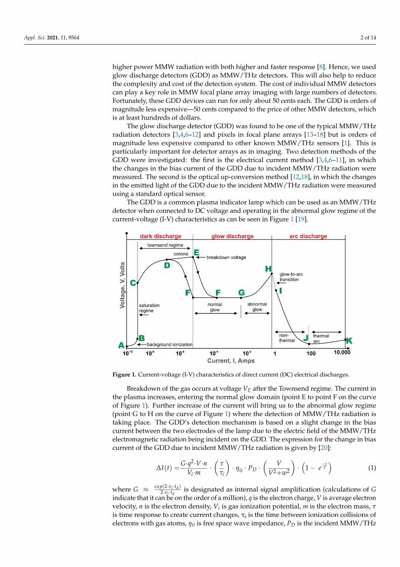
The GDD is a common plasma indicator lamp which can be used as an MMW/THzdetector when connected to DC voltage and operating in the abnormal glow regime of thecurrent-voltage (I-V) characteristics as can be seen in Figure 1 [19].
Figure 1. Current-voltage (I-V) characteristics of direct current (DC) electrical discharges.
Breakdown of the gas occurs at voltage VE after the Townsend regime. The current inthe plasma increases, entering the normal glow domain (point E to point F on the curveof Figure 1). Further increase of the current will bring us to the abnormal glow regime(point G to H on the curve of Figure 1) where the detection of MMW/THz radiation istaking place. The GDD’s detection mechanism is based on a slight change in the biascurrent between the two electrodes of the lamp due to the electric field of the MMW/THzelectromagnetic radiation being incident on the GDD. The expression for the change in biascurrent of the GDD due to incident MMW/THz radiation is given by [20]:
∆I(t) =G·q2·V·n
Vi·m·(
τ
τi
)· η0 · PD ·
(V
V2+w2
)·(
1− e−tτ
)(1)
where G ≈ exp(2·vi ·td)2·υi ·td
is designated as internal signal amplification (calculations of Gindicate that it can be on the order of a million), q is the electron charge, V is average electronvelocity, n is the electron density, Vi is gas ionization potential, m is the electron mass, τis time response to create current changes, τi is the time between ionization collisions ofelectrons with gas atoms, η0 is free space wave impedance, PD is the incident MMW/THz
Appl. Sci. 2021, 11, 9564 3 of 14
radiation power density on the detector, υ is the electron-neutral atom elastic collisionfrequency, ω is the electromagnetic radiation frequency, td is the average electron drifttime to the anode, and υi is ionization collision frequency. The dominant MMW/THzdetection mechanism inside the plasma was found to be enhanced cascade ionization ratherthan diffusion current [4,20–22]. The enhanced cascade ionization mechanism increasesthe current while the diffusion current mechanism decreases it. The response time of theplasma inside the GDD is on the order of picoseconds. However, the electronic responsetime is limited by GDD’s electrode parasitic impedance and the electronic circuit to about1 µs [16].
According to the glow discharge theory, the light emission intensity is directly linkedto the detection of the MMW/THz radiation. GDD illumination is originated from therecombination between free electrons and positive ions which occur mostly around thenegative glow area [20], which is adjacent to the cathode. This area is where the DC electricfield and the total electron energy are at a maximum. Furthermore, when the frequency ofthe MMW radiation is equal to the inelastic collision rate, maximum response of the GDDis obtained (see Equation (1)) [20]. The radiation affects mostly the area around the cathodedark space, which is adjacent to the cathode.
A new detection mechanism for MMW/THz radiation detection using GDD, namedup-conversion method, was suggested [17]. The up-conversion method (optical detection)refers to the detection of changes in the emitted light from the GDD due to incidentMMW/THz radiation, rather than the changes in its electrical current (electronic detection).In the up-conversion method, a basic photodiode or any basic light sensor is requiredin order to measure the changes in the GDD emitted light. The advantages of the up-conversion method are: (1) a very fast response time which is limited by the light sensorresponse, (2) a lower internal noise compared to the electric detection [17], and (3) it is veryinexpensive.
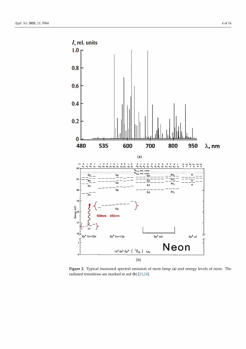
The spectral emission of typical neon lamp and its energy levels are shown inFigure 2 [23].
Figure 2a shows a spectral measurement of a typical neon lamp carried out by ISF125M, Bruker Inc. The measurement accuracy of the radiated lines is better than 1 GHz [23].The radiated energy levels of Figure 2b are in excellent agreement with the experimentalresults of Figure 2a.
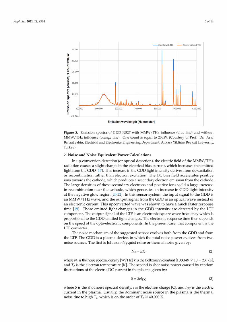
In preliminary research aiming to investigate the influence of MMW radiation onthe GDD emitted light spectrum, it was discovered that the strongest influence of theMMW/THz on the GDD emitted light spectrum is located in the NIR around 800 nm–1000 nm (see solid blue line in Figure 3). Furthermore, almost no influence of the MMW/THzaround 500 nm–600 nm was noticeable. Figure 3 shows preliminary experimental spectrummeasurements and analysis of the emitted light from GDD N527 (of International LightInc.), without MMW radiation (orange solid line) and with MMW radiation (blue solid line).Despite the many advantages mentioned above regarding the GDD and LTF combinationpixel as a useful and robust MMW detector, further improvement to the detector pixelsensitivity and to the SNR are required. This paper proposes the use of an optical long-passfilter as a part of the GDD and LTF pixel component, thus enhancing the pixel detectorsensitivity as well as its signal-to-noise ratio and thus improving performance of thesuggested THz/MMW radiation sensor or pixel. The addition of the long-pass filter isshown here to improve the total SNR of the detected MMW signal. This improvementis due to two reasons. The first reason is the improvement in the noise level due to thefiltering of the bias illumination noise of the GDD and the second reason is the increase inthe signal level due to back reflection from the filter body towards the GDD cross-section.
Appl. Sci. 2021, 11, 9564 4 of 14
1
(a)
Figure 2. Typical measured spectral emission of neon lamp (a) and energy levels of neon. Theradiated transitions are marked in red (b) [23,24].
Appl. Sci. 2021, 11, 9564 5 of 14
Figure 3. Emission spectra of GDD N527 with MMW/THz influence (blue line) and withoutMMW/THz influence (orange line). One count is equal to 20µW. (Courtesy of Prof. Dr. AsafBehzat Sahin, Electrical and Electronics Engineering Department, Ankara Yildirim Beyazit University,Turkey).
2. Noise and Noise Equivalent Power Calculations
In up-conversion detection (or optical detection), the electric field of the MMW/THzradiation causes a slight change in the electrical bias current, which increases the emittedlight from the GDD [17]. This increase in the GDD light intensity derives from de-excitationor recombination rather than electron excitation. The DC bias field accelerates positiveions towards the cathode, which produces a secondary electron emission from the cathode.The large densities of these secondary electrons and positive ions yield a large increasein recombination near the cathode, which generates an increase in GDD light intensityat the negative glow region [20,22]. In this sensor system, the input signal to the GDD isan MMW/THz wave, and the output signal from the GDD is an optical wave instead ofan electronic current. This upconverted wave was shown to have a much faster responsetime [19]. Those emitted light changes in the GDD intensity are detected by the LTFcomponent. The output signal of the LTF is an electronic square wave frequency which isproportional to the GDD emitted light changes. The electronic response time then dependson the speed of the opto-electronic components. In the present case, that component is theLTF converter.
The noise mechanism of the suggested sensor evolves both from the GDD and fromthe LTF. The GDD is a plasma device, in which the total noise power evolves from twonoise sources. The first is Johnson–Nyquist noise or thermal noise given by:
N0 = kTe (2)
where N0 is the noise spectral density [W/Hz], k is the Boltzmann constant [1.380649× 10− 23 J/K],and Te is the electron temperature [K]. The second is shot noise power caused by randomfluctuations of the electric DC current in the plasma given by:
S = 2eIDC (3)
where S is the shot noise spectral density, e is the electron charge [C], and IDC is the electriccurrent in the plasma. Usually, the dominant noise source in the plasma is the thermalnoise due to high Te, which is on the order of Te ∼= 40,000 K.
Appl. Sci. 2021, 11, 9564 6 of 14
While the electronic detection (or electrical detection) is controlled by ionizing col-lisions and by electron energy or temperature, the up-conversion detection is controlledby positive ion-secondary electron recombination processes and is affected primarily bypositive ion energy or temperature. Due to the larger mass of the ion as compared to theelectron mass, the positive ion temperature is orders of magnitude less than the electrontemperature. Thus, up-conversion detection Johnson noise is significantly less than the elec-tronic detection Johnson noise [14]. Furthermore, according to the literature, the electrontemperature in plasma, Te, is on the order of 30,000–40,000 K, while the ion temperature Tiis around 500 K [25]. Therefore, the noise generated in up-conversion detection is composedof both thermal noise (using Ti) and shot noise (due to recombination between secondaryelectrons and positive ions near the GDD cathode). The influence of those noise sourceson the GDD emitted light fluctuations can be measured with a basic optical power meter.For example, measuring the irradiance of the GDD in two successive measurements andsubtracting them, yields the total noise in the GDD irradiance. The GDD irradiance is theinput signal to the LTF component which is attached to it. Thus, the output frequency noise,∆fn, is the subtraction of two successive output frequency measurements. Furthermore, theinfluence of the MMW/THz radiation, ∆fMMW, on the output frequency can be measuredthe same way if we subtract two successive measurements where the first one is withMMW radiation and the second one is without MMW radiation.
The LTF converts input optical irradiance, Ee, to the electric TTL levels frequency, fo.Re is the irradiance responsivity. The dark frequency of the LTF is fD is 2 Hz. The NEP ofthe suggested sensor can be calculated according to:
NEP =(∆ f n+ f D)
Re√
B(4)
where B = 1 MHz is bandwidth of the LTF [26]. Note that the GDD modulation bandwidthis very high, on the order of several GHz [12,18], attesting to the GDD speed of response.In these speed measurements, speed was limited by the optoelectronic detector and not bythe GDD plasma.
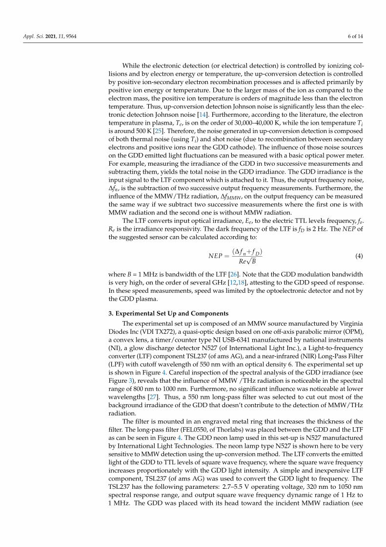
3. Experimental Set Up and Components
The experimental set up is composed of an MMW source manufactured by VirginiaDiodes Inc (VDI TX272), a quasi-optic design based on one off-axis parabolic mirror (OPM),a convex lens, a timer/counter type NI USB-6341 manufactured by national instruments(NI), a glow discharge detector N527 (of International Light Inc.), a Light-to-frequencyconverter (LTF) component TSL237 (of ams AG), and a near-infrared (NIR) Long-Pass Filter(LPF) with cutoff wavelength of 550 nm with an optical density 6. The experimental set upis shown in Figure 4. Careful inspection of the spectral analysis of the GDD irradiance (seeFigure 3), reveals that the influence of MMW /THz radiation is noticeable in the spectralrange of 800 nm to 1000 nm. Furthermore, no significant influence was noticeable at lowerwavelengths [27]. Thus, a 550 nm long-pass filter was selected to cut out most of thebackground irradiance of the GDD that doesn’t contribute to the detection of MMW/THzradiation.
The filter is mounted in an engraved metal ring that increases the thickness of thefilter. The long-pass filter (FEL0550, of Thorlabs) was placed between the GDD and the LTFas can be seen in Figure 4. The GDD neon lamp used in this set-up is N527 manufacturedby International Light Technologies. The neon lamp type N527 is shown here to be verysensitive to MMW detection using the up-conversion method. The LTF converts the emittedlight of the GDD to TTL levels of square wave frequency, where the square wave frequencyincreases proportionately with the GDD light intensity. A simple and inexpensive LTFcomponent, TSL237 (of ams AG) was used to convert the GDD light to frequency. TheTSL237 has the following parameters: 2.7–5.5 V operating voltage, 320 nm to 1050 nmspectral response range, and output square wave frequency dynamic range of 1 Hz to1 MHz. The GDD was placed with its head toward the incident MMW radiation (see
Appl. Sci. 2021, 11, 9564 7 of 14
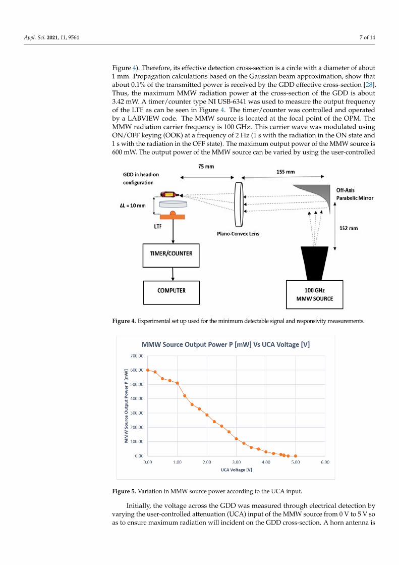
Figure 4). Therefore, its effective detection cross-section is a circle with a diameter of about1 mm. Propagation calculations based on the Gaussian beam approximation, show thatabout 0.1% of the transmitted power is received by the GDD effective cross-section [28].Thus, the maximum MMW radiation power at the cross-section of the GDD is about3.42 mW. A timer/counter type NI USB-6341 was used to measure the output frequencyof the LTF as can be seen in Figure 4. The timer/counter was controlled and operatedby a LABVIEW code. The MMW source is located at the focal point of the OPM. TheMMW radiation carrier frequency is 100 GHz. This carrier wave was modulated usingON/OFF keying (OOK) at a frequency of 2 Hz (1 s with the radiation in the ON state and1 s with the radiation in the OFF state). The maximum output power of the MMW source is600 mW. The output power of the MMW source can be varied by using the user-controlledattenuation (UCA) voltage in the source as shown in Figure 5.
Figure 4. Experimental set up used for the minimum detectable signal and responsivity measurements.
Figure 5. Variation in MMW source power according to the UCA input.
Initially, the voltage across the GDD was measured through electrical detection byvarying the user-controlled attenuation (UCA) input of the MMW source from 0 V to 5 V soas to ensure maximum radiation will incident on the GDD cross-section. A horn antenna is
Appl. Sci. 2021, 11, 9564 8 of 14
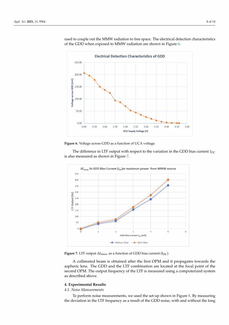
used to couple out the MMW radiation to free space. The electrical detection characteristicsof the GDD when exposed to MMW radiation are shown in Figure 6.
Figure 6. Voltage across GDD as a function of UCA voltage.
The difference in LTF output with respect to the variation in the GDD bias current IDCis also measured as shown in Figure 7.
Figure 7. LTF output ∆fmmw as a function of GDD bias current (IDC).
A collimated beam is obtained after the first OPM and it propagates towards theaspheric lens. The GDD and the LTF combination are located at the focal point of thesecond OPM. The output frequency of the LTF is measured using a computerized systemas described above.
4. Experimental Results4.1. Noise Measurements
To perform noise measurements, we used the set-up shown in Figure 8. By measuringthe deviation in the LTF frequency as a result of the GDD noise, with and without the long
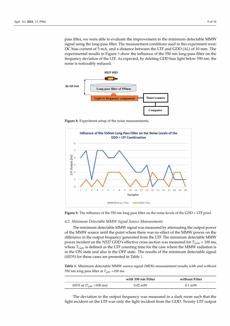
Appl. Sci. 2021, 11, 9564 9 of 14
pass filter, we were able to evaluate the improvement in the minimum detectable MMWsignal using the long-pass filter. The measurement conditions used in this experiment were:DC bias current of 5 mA, and a distance between the LTF and GDD (∆L) of 10 mm. Theexperimental results in Figure 9 show the influence of the 550 nm long-pass filter on thefrequency deviation of the LTF. As expected, by deleting GDD bias light below 550 nm, thenoise is noticeably reduced.
Figure 8. Experiment setup of the noise measurements.
Figure 9. The influence of the 550 nm long pass filter on the noise levels of the GDD + LTF pixel.
4.2. Minimum Detectable MMW Signal Source Measurements
The minimum detectable MMW signal was measured by attenuating the output powerof the MMW source until the point where there was no effect of the MMW power on thedifference in the output frequency generated from the LTF. The minimum detectable MMWpower incident on the N527 GDD’s effective cross-section was measured for TGate = 100 ms,where TGate is defined as the LTF counting time for the case where the MMW radiation isin the ON state and also in the OFF state. The results of the minimum detectable signal(MDS) for these cases are presented in Table 1.
Table 1. Minimum detectable MMW source signal (MDS) measurement results with and without550 nm long pass filter at Tgate =100 ms.
with 550 nm Filter without Filter
MDS at (Tgate =100 ms) 0.02 mW 0.1 mW
The deviation in the output frequency was measured in a dark room such that thelight incident on the LTF was only the light incident from the GDD. Twenty LTF output
Appl. Sci. 2021, 11, 9564 10 of 14
frequency measurements were taken using a single pixel in a consecutive manner of onewith MMW radiation and one without it. Every sample was taken in Tgate = 100 ms. Thesubtraction between two consecutive samples gives the MMW influence on the outputfrequency. The measurement results are summarized in Table 1 for GDD N527.
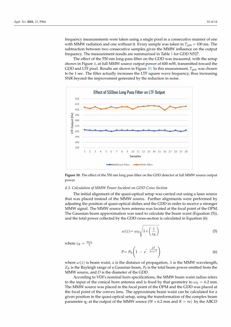
The effect of the 550 nm long-pass filter on the GDD was measured, with the setupshown in Figure 4, at full MMW source output power of 600 mW, transmitted toward theGDD and LTF pixel. Results are shown in Figure 10. In this measurement, Tgate was chosento be 1 sec. The filter actually increases the LTF square wave frequency, thus increasingSNR beyond the improvement generated by the reduction in noise.
Appl. Sci. 2021, 11, x FOR PEER REVIEW 11 of 15
Figure 10. The effect of the 550 nm long pass filter on the GDD detector at full MMW source output
power.
4.3. Calculation of MMW Power Incident on GDD cross Section
The initial alignment of the quasi‐optical setup was carried out using a laser source
that was placed instead of the MMW source. Further alignments were performed by
adjusting the position of quasi‐optical dishes and the GDD in order to receive a stronger
MMW signal. The MMW source horn antenna was located at the focal point of the OPM.
The Gaussian beam approximation was used to calculate the beam waist (Equation (5)),
and the total power collected by the GDD cross‐section is calculated in Equation (6).
ω z = ω0 1+z
zR (5)
where zR=πω0
λ
𝑃=P0 1 - e-
D2
2ω z 2 (6)
where ω z is beam waist, 𝒛 is the distance of propagation, λ is the MMW wavelength,
ZR is the Rayleigh range of a Gaussian beam, P0 is the total beam power emitted from
the MMW source, and D is the diameter of the GDD.
According to VDI’s nominal horn specifications, the MMW beam waist radius refers
to the input of the conical horn antenna and is fixed by that geometry to 𝜔 6.2 mm.
The MMW source was placed in the focal point of the OPM and the GDD was placed at
the focal point of the convex lens. The approximate beam waist can be calculated for a
given position in the quasi‐optical setup, using the transformation of the complex beam
parameter q1 at the output of the MMW source (W = 6.2 mm and 𝑅 ∞ by the ABCD transfer matrix for paraxial rays. The complex beam parameter q2 can then be calculated
at that given position using Equation (4). Knowing the complex beam parameter q2 can
allow the calculation of the beam waist (W) and the beam radius of curvature (R) at that
given position using Equation (5).
A BC D
1 d0 1
1 01 F⁄ 1
1 d0 1
1 01 F⁄ 1
1 d0 1
(7)
𝑞𝐴𝑞 𝐵𝐶𝑞 𝐷
(8)
Figure 10. The effect of the 550 nm long pass filter on the GDD detector at full MMW source outputpower.
4.3. Calculation of MMW Power Incident on GDD Cross Section
The initial alignment of the quasi-optical setup was carried out using a laser sourcethat was placed instead of the MMW source. Further alignments were performed byadjusting the position of quasi-optical dishes and the GDD in order to receive a strongerMMW signal. The MMW source horn antenna was located at the focal point of the OPM.The Gaussian beam approximation was used to calculate the beam waist (Equation (5)),and the total power collected by the GDD cross-section is calculated in Equation (6).
ω(z)= ω0
√1+(
zzR
)(5)
where zR = πω0λ
P= P0
(1 − e
− D2
2ω(z)2
)(6)
where ω(z) is beam waist, z is the distance of propagation, λ is the MMW wavelength,ZR is the Rayleigh range of a Gaussian beam, P0 is the total beam power emitted from theMMW source, and D is the diameter of the GDD.
According to VDI’s nominal horn specifications, the MMW beam waist radius refersto the input of the conical horn antenna and is fixed by that geometry to ω0 = 6.2 mm.The MMW source was placed in the focal point of the OPM and the GDD was placed atthe focal point of the convex lens. The approximate beam waist can be calculated for agiven position in the quasi-optical setup, using the transformation of the complex beamparameter q1 at the output of the MMW source (W = 6.2 mm and R = ∞) by the ABCD
Appl. Sci. 2021, 11, 9564 11 of 14
transfer matrix for paraxial rays. The complex beam parameter q2 can then be calculated atthat given position using Equation (4). Knowing the complex beam parameter q2 can allowthe calculation of the beam waist (W) and the beam radius of curvature (R) at that givenposition using Equation (5).[
A BC D
]=
[1 d30 1
][1 0
−1/FLens 1
][1 d20 1
][1 0
−1/FOPM 1
][1 d10 1
](7)
q2 =Aq1 + BCq1 + D
(8)
1q2
=1R− iλ
πW2 (9)
The parameters in Equation (7) are as follows:d1 is the distance between the transmitter and the OPM (152 mm), FLens is the focal
length of the lens (75 mm), FOPM is the focal length of both of the OPM components(152 mm), d2 is the distance between the OPM and lens (155 mm), and d3 is the distancebetween the lens and the GDD (75 mm).
4.4. Calculation of the Irradiance Responsivity
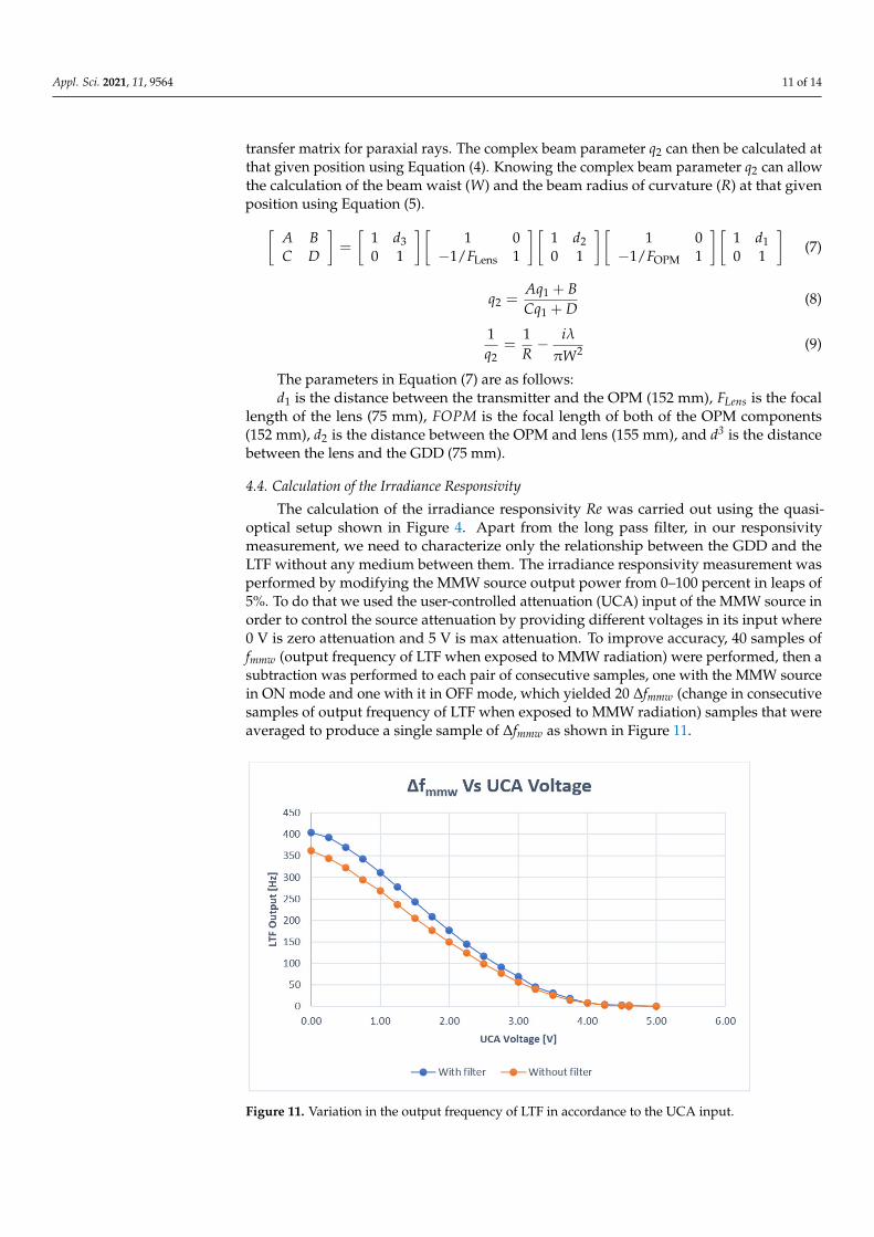
The calculation of the irradiance responsivity Re was carried out using the quasi-optical setup shown in Figure 4. Apart from the long pass filter, in our responsivitymeasurement, we need to characterize only the relationship between the GDD and theLTF without any medium between them. The irradiance responsivity measurement wasperformed by modifying the MMW source output power from 0–100 percent in leaps of5%. To do that we used the user-controlled attenuation (UCA) input of the MMW source inorder to control the source attenuation by providing different voltages in its input where0 V is zero attenuation and 5 V is max attenuation. To improve accuracy, 40 samples offmmw (output frequency of LTF when exposed to MMW radiation) were performed, then asubtraction was performed to each pair of consecutive samples, one with the MMW sourcein ON mode and one with it in OFF mode, which yielded 20 ∆fmmw (change in consecutivesamples of output frequency of LTF when exposed to MMW radiation) samples that wereaveraged to produce a single sample of ∆fmmw as shown in Figure 11.
Figure 11. Variation in the output frequency of LTF in accordance to the UCA input.
Appl. Sci. 2021, 11, 9564 12 of 14
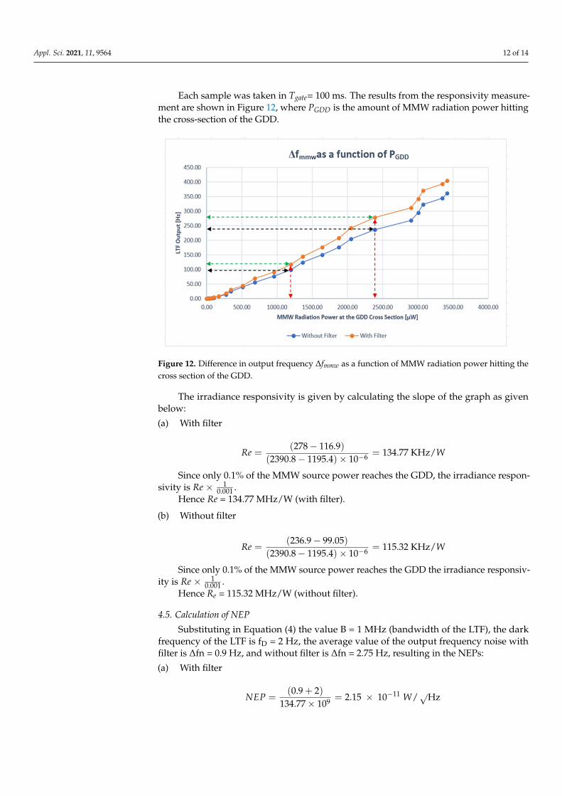
Each sample was taken in Tgate= 100 ms. The results from the responsivity measure-ment are shown in Figure 12, where PGDD is the amount of MMW radiation power hittingthe cross-section of the GDD.
Figure 12. Difference in output frequency ∆fmmw as a function of MMW radiation power hitting thecross section of the GDD.
The irradiance responsivity is given by calculating the slope of the graph as givenbelow:
(a) With filter
Re =(278− 116.9)
(2390.8− 1195.4)× 10−6 = 134.77 KHz/W
Since only 0.1% of the MMW source power reaches the GDD, the irradiance respon-sivity is Re × 1
0.001 .Hence Re = 134.77 MHz/W (with filter).
(b) Without filter
Re =(236.9− 99.05)
(2390.8− 1195.4)× 10−6 = 115.32 KHz/W
Since only 0.1% of the MMW source power reaches the GDD the irradiance responsiv-ity is Re × 1
0.001 .Hence Re = 115.32 MHz/W (without filter).
4.5. Calculation of NEP
Substituting in Equation (4) the value B = 1 MHz (bandwidth of the LTF), the darkfrequency of the LTF is fD = 2 Hz, the average value of the output frequency noise withfilter is ∆fn = 0.9 Hz, and without filter is ∆fn = 2.75 Hz, resulting in the NEPs:
(a) With filter
NEP =(0.9 + 2)
134.77× 109 = 2.15 × 10⁻¹¹ W/√Hz
Appl. Sci. 2021, 11, 9564 13 of 14
(b) Without filter
NEP =(2.75 + 2)
115.32× 109 = 4.12 × 10⁻¹¹ W/√Hz
5. Discussion
The results show great promise for the future of GDDs as MMW detectors. In thisproof of concept, we decreased the amount of white bias light noise received by theMMW detector and improved the sensitivity to MMW radiation. These phenomena canbe explained by three main factors. First, by removing the DC bias light below 550 nm,the long pass filter lowered the noise floor of the setup that enables us to increase ourLTF measurement precision. Second, by adding a filter to the detector set-up, internalreflections from the filter back to the GDD and from the GDD forward to the filter occurwhich contributes to the increase of signal together with changing the LTF operational pointdue to the decrease in the background light of the GDD. Third, the decrease in perceivedGDD illumination power caused by the filter brings about the decrease of LTF workingvoltage which increases the accuracy of the pulse rate frequency generated by the LTFsemiconductor device. In other words, at low SNR such as when measuring minimumdetectable signal, LTF output pulse rate is further reduced because of the low SNR than itshould be. At high SNR, the output LTF pulse rate is increased more than expected fromthe increased GDD light intensity alone. A setup of a GDD and LTF is shown here to bevery sensitive to MMW radiation. Following all advantages achieved, we can now create abetter and more sensitive GDD and LTF MMW detector in multiple or singular systems.
6. Conclusions
The setup of a GDD and LTF is shown here to be very sensitive to MMW radiation. Byadding the long-pass filter, the noise level in the output from the GDD is reduced. Thus,a higher value of SNR is obtained. By using the data from Figure 12 and Equation (4),the NEP can be calculated for both incidence with and without long-pass filter, wherethe average value of the output frequency noise with filter is ∆fn = 0.9 Hz, and withoutfilter is ∆fn = 2.75 Hz. NEP is 2.15 × 10⁻¹¹ W/
√Hz (with filter) and 4.12 × 10⁻¹¹ W/
√Hz
(without filter). The GDD and LTF setup can be used as a pixel in a focal plane array (FPA),such that the pixel readout can be performed using a digital system.
7. Future Works
The GDD-LTF combination with a filter was found to be a good choice for MMW/THzdetection as it can reduce NEP, thereby improving the SNR. Because of the frame of the 550nm NIR filter, the minimum separation between GDD and LTF used here is 10 mm. Thedistance between the GDD and LTF reduced the amount of incident light from the GDD tothe LTF, thereby limiting the detection level. We have performed the same experiment witha minimum separation of 2 mm between the GDD and the LTF without the filter. The resultswere found to be impressive as they can achieve better values for irradiance responsivity,Re = 215.23 MHz/W, and noise equivalent power, NEP = 3.34 × 10⁻¹¹ W/
√Hz. Our future
work is to accommodate a filter without a frame so that it will be able to obtain an enhanceddetection level by the GDD-LTF combination.
Author Contributions: Conceptualization, A.R.K. and D.R.; methodology, L.K.; software, D.R.;validation, A.A., N.K. and Y.Y.; formal analysis, D.R.; investigation, A.R.K.; resources, A.R.K. andD.R.; data curation, A.R.K. and L.K.; writing—original draft preparation, A.R.K.; writing—review andediting, A.A., N.K. and Y.Y.; visualization, A.R.K.; supervision, A.A. and D.R.; project administration,A.A. All authors have read and agreed to the published version of the manuscript.
Funding: This research received no external funding.
Appl. Sci. 2021, 11, 9564 14 of 14
Acknowledgments: The authors are grateful to the administrative and technical support from theAriel University, Ariel, Israel and Ben-Gurion University of the Negev, Beer Sheva, Israel.
Conflicts of Interest: The authors declare no conflict of interest.
References1. Rogalski, A.; Sizov, F. Terahertz Detectors and Focal Plane Arrays. Opto Electron. Rev. 2011, 19, 346–404. [CrossRef]2. Siegel, P.H. Terahertz Technology. IEEE Trans. Microw. Theory 2002, 50, 910–928. [CrossRef]3. Abramovich, A.; Kopeika, N.S.; Rozban, D.; Farber, E. Inexpensive Detector for Terahertz Imaging. Appl. Opt. 2007, 46, 7207–7211.
[CrossRef] [PubMed]4. Rozban, D.; Abramovich, A.; Kopeika, N.S.; Farber, E. Terahertz Detection Mechanism of Inexpensive Sensitive Glow Discharge
Detector. Appl. Phys. 2008, 103, 093306–1–093306-4. [CrossRef]5. Virginia Diodes Inc. Product Datasheet. Available online: https://vadiodes.com/en/products-6/detectors (accessed on 14
June 2021).6. Alain, M.; John, W.; John, G.A. THz Local Oscillator Source. IEEE Microw. Wirel. Compon. Lett. 2004, 14, 253–255.7. Hou, L.; Shi, W. Fast Terahertz Continuous-Wave Detector Based on Weakly Ionized Plasma. IEEE Electron Device Lett. 2012, 33,
1583–1585. [CrossRef]8. Haj Yahya, A.; Klein, A.; Balal, N.; Borodin, D.; Friedman, A. Comparison between Up-Conversion Detection in Glow-Discharge
Detectors and Schottky Diode for MMW/THz High-Power Single Pulse. Appl. Sci. 2021, 11, 4172.9. Abramovich, A.; Kopeika, N.S.; Rozban, D. THz Polarization Effects on Detection Responsivity of Glow Discharge Detectors
(GDD). IEEE Sens. 2009, 9, 1181–1184.10. Rozban, D.; Aharon, A.; Kopeika, N.S.; Abramovich, A. W-Band Chirp Radar Mock-Up Using a Glow Discharge Detector. IEEE
Sens. 2013, 13, 139–145. [CrossRef]11. Aharon, A.; Rozban, D.; Kopeika, N.S.; Abramovich, A. Heterodyne Detection at 300 GHz Using Neon Indicator Lamp Glow
Discharge Detector. Appl. Opt. 2013, 52, 4077–4082. [CrossRef]12. Aharon, A.; Rozban, D.; Ben-laish, M.; Abramovich, A.; Yitzhaky, Y.; Kopeika, N.S. Ultra-Wideband and Inexpensive Glow
Discharge Detector for Millimeter Wave Wireless Communication Based on Up-Conversion to Visual Light. Appl. Opt. 2019, 58,F26–F31. [CrossRef] [PubMed]
13. Abramovich, A.; Kopeika, N.S.; Rozban, D. Design of Inexpensive Diffraction Limited Focal Plane Arrays for MM Wavelengthand THz Using Glow Discharge Detector Pixels. Appl. Phys. 2008, 104, 033302. [CrossRef]
14. Rozban, D.; Levanon, A.; Joseph, H.; Aharon, A.; Abramovich, A.; Kopeika, N.S.; Yitzhaky, Y.; Belenky, A.; Yadid-Pecht, O.Inexpensive THz Focal Plane Array Imaging Using Neon Indicator Lamps as Detectors. IEEE Sens. 2011, 11, 1962–1968. [CrossRef]
15. Shilemay, M.; Rozban, D.; Levanon, A.; Yitzhaky, Y.; Kopeika, N.S.; Yadid-Pecht, O.; Abramovich, A. Performance Quantificationof a Millimeter-Wavelength Imaging System Based on Inexpensive Glow-Discharge-Detector Focal-Plane Array. Appl. Opt. 2013,52, C43–C49. [CrossRef]
16. Rozban, D.; Aharon, A.; Levanon, A.; Abramovich, A.; Kopeika, N.S. Switching and Fast Operation of Glow Discharge Detectorfor Millimeter Wave Focal Plane Array Imaging Systems. IEEE Sens. 2015, 15, 6659–6663. [CrossRef]
17. Aharon, A.; Rozban, D.; Klein, A.; Abramovich, A.; Yitzhaky, Y.; Kopeika, N.S. Detection and Up-Conversion of Three-DimensionalMMW/THz Images to the Visible. Photon. Res. 2016, 4, 306–312. [CrossRef]
18. Rozban, D.; Aharon, A.; Kahana, L.; Abramovich, A.; Yitzhaky, Y.; Altan, H.; Kopeika, N.S. Robust, Sensitive, and Inexpensive 2DFocal Plane Array Upconverting MMW Imaging into the Visible. IEEE Photonics Technol. Lett. 2019, 31, 747–750. [CrossRef]
19. Fan, L.; Junkai, J.; Haiyun, L.; Juan, D.; Feng, L. Preliminary Study of Glow Discharge Plasma on the Static Pressure Measurement.In Proceedings of the 1st Global Power and Propulsion Forum GPPF, Zurich, Switzerland, 16–18 January 2014.
20. Kopeika, N.S. Glow Discharge Detection of Long Wavelength Electromagnetic Radiation: Cascade Ionization Process InternalSignal Gain and Temporal and Spectral Response Properties. IEEE Trans. Plasma Sci. 1978, 6, 139–157. [CrossRef]
21. Kopeika, N.S. On the Mechanism of Glow Discharge Detection of Microwave and Millimeter Wave Radiation. Proc. IEEE 1975,63, 981–982. [CrossRef]
22. Mavrodineanu, R. Hollow Cathode Discharges. Res. Natl. Bur. Stand. 1984, 89, 143. [CrossRef] [PubMed]23. Vasil’chenko, S.S.; Serdukov, V.I. Emission Spectrum of Neon as a Frequency Reference for Spectrophotometers. Atmos. Ocean.
Opt. 2013, 26, 154–158. [CrossRef]24. Nighan, W.L. Basic Kinetic Processes in Neon Gas Discharge Displays. IEEE Trans. Electron Devices 1981, 28, 625–630. [CrossRef]25. Wiesemann, K. A Short Introduction to Plasma Physics. arXiv 2014, arXiv:1404.0509. Available online: http://cds.cern.ch/record/
1693043/files/arXiv:1404.0509.pdf (accessed on 14 June 2021).26. ams AG Product Datasheet. LTF Specifications. Available online: https://ams.com/tsl237 (accessed on 14 June 2021).27. Abramovich, A.; Yitzhaky, Y.; Kopeika, N.S.; Kahana, L.; Rozban, D. Up-conversion of Millimeter Waves to Visible Waves:
Inexpensive Focal Plane Array MMW Imaging and Ultra-fast MMW Wireless Communication. In Proceedings of the TerahertzEmitters, Receivers, and Applications XI, Online Only, Bellingham, DC, USA, 24 August–4 September 2020; Volume 11499,p. 114990U.
28. Kahana, L.; Rozban, D.; Gihasi, M.; Abramovich, A.; Yitzhaky, Y.; Kopeika, N. Inexpensive Millimeter-Wave CommunicationChannel Using Glow Discharge Detector and Satellite Dish Antenna. Electronics 2020, 9, 677. [CrossRef]


![[O] [H] functionalization on carbon nanotube using (O2–H2) gas mixture DC glow discharge](https://img.pdfslide.net/doc/110x75/63482ac62cd4c1a3540cdb1c/o-h-functionalization-on-carbon-nanotube-using-o2h2-gas-mixture-dc-glow.jpg)


