Embed Size (px)
Citation preview

Performance Enhancement of Organic Photovoltaic Cells
through Nanostructuring and Molecular Doping
Dissertation zur Erlangung des akademischen Grades
d o c t o r r e r u m n a t u r a l i u m
(Dr. rer. nat.)
im Fach Physik
eingereicht an der
Mathematisch-Naturwissenschaftlichen Fakultät
der Humboldt-Universität zu Berlin
von
Herrn M.S.-Physik Shuwen Yu
Präsident der Humboldt-Universität zu Berlin Prof. Dr. Jan-Hendrik Olbertz
Dekan der Mathematisch-Naturwissenschaftlichen Fakultät Prof. Dr. Elmar Kulke
Gutachter/innen: 1. Prof. Norbert Koch 2. Prof. Beate Röder3. Prof. Dieter Neher
Tag der mündlichen Prüfung: 27.02.2015

Abstract The present work mainly focuses on improving the performance of OPVCs by tailoring
the donor-acceptor interface geometry and by tuning the electrical properties of interfaces with p-type molecular doping.
Crystalline and uniform nanocolumns of pentacene (PEN) and diindenoperylene (DIP) were fabricated by glancing angle deposition (GLAD), forming an interdigitated donor/acceptor heterojunction with [6,6]-phenyl-C61-butyric acid methyl ester (PCBM) and/or fullerene as the electron acceptor. The short circuit current of nanocolumn-based OPVCs increased significantly compared to planar heterojunction OPVCs made from the same materials. The performance improvement of OPVCs had been verified to be contributed decisively by the donor-acceptor interface area enlargement because of reduced impact of short exciton diffusion length in organic materials.
P-type molecular doping as applied in polyfuran (PF) based OPVCs was investigated by using tetrafluorotetracyanoquinodimethane (F4-TCNQ) as the dopant for various doping ratios. Ultraviolet photoelectron spectroscopy (UPS) was applied to analyze the energy level shift with increasing doping ratio leading to the enlargement of the open circuit voltage in OPVCs, from 0.2 V to close to 0.4 V. Combining this observation with the results of doped polymer films, their morphology and absorption behavior, a net dipole pointing towards the donor material at the donor-acceptor interface of OPVCs is proposed. Overall, this work demonstrates the potential of both the GLAD technique and molecular electrical doping for improving the performance of OPVCs.
Keywords: organic photovoltaic cells, glancing angle deposition, nanocolumn structure, donor/acceptor interface, molecular doping
1
Kurzfassung Die vorliegende Arbeit beschäftigt sich mit der Leistungssteigerung organischer Solarzellen
durch Änderung der Geometrie an der Donor-Akzeptor Grenzfläche und dem Einstellen der elektronischen Eigenschaften von Grenzflächen durch molekulares p-Dotieren.
Kristalline und gleichmäßige Nanosäulen aus dem organischen Halbleiter Pentazen wurden durch glancing angle deposition (GLAD) hergestellt, die einen ineinandergreifenden Heteroübergang zu Methanofulleren [6,6]-Phenyl-C61-Butansäure Methylester (PCBM) als Akzeptor ermöglichten. Die Kurzschlussspannung der nanosäulenbasierten Solarzellen war signifikant erhöht im Vergleich zu planaren Heteroübergängen zwischen denselben Materialien. Die Leistungssteigerung der Solarzellen konnte maßgebend der vergrößerten Grenzfläche zugewiesen werden, wegen des verringerten Einflusses der kurzen Exciton Diffusionslänge.
Molekulares p-Dotieren mit Tetrafluorotetracyanoquinodimethan (F4TCNQ) als Dotand in polyfuranbasierten Solarzellen wurde für verschiede Dotierkonzentrationen untersucht. Ultraviolettphotoelektronenspektroskopie wurde verwendet, um die Veränderungen der Energieniveaus mit zunehmender Dotierkonzentration zu analysieren, welche zu einer Vergrößerung der 0,2 V Kurzschlussspannung auf bis zu 0,4 V führte. Nach Kombination dieser Beobachtung mit Ergebnissen an dotierten Polymerfilmen, insbesondere bezüglich deren Morphologie und Absorptionsverhalten, wurde vorgeschlagen, dass ein resultierender Dipol an der Donor-Akzeptorgrenzfläche präsent ist. Zusammenfassend zeigt die vorliegende Arbeit das Potential sowohl der GLAD Technik als auch des molekularen, elektrischen Dotierens für die Leistungsverbesserung organischer Solarzellen
Stichwörter: organische Solarzellen, glancing angle deposition, Nanosäulen Donor-Akzeptorgrenzfläche, molekulares Dotieren
2

3
Contents
1. Introduction .............................................................................................................. 6
2. Fundamentals ........................................................................................................ 11
2.1 Conjugated organic semiconductors ................................................................... 11 2.1.1 Charge carrier transport ............................................................................... 14 2.1.2 Doping organic semiconductors .................................................................. 18
2.2 Organic thin film ................................................................................................. 22 2.2.1 Vacuum deposition ...................................................................................... 22 2.2.2 Solution processing ..................................................................................... 26
2.3 Organic photovoltaic cells (OPVCs) ................................................................... 28 2.3.1 Operation mechanism of OPVCs ................................................................ 28 2.3.2 Electrical characterization of OPVCs ......................................................... 36
3. Methodology and materials .......................................................................... 41
3.1 Methodology ....................................................................................................... 41 3.1.1 Spin coating................................................................................................. 41 3.1.2 Glancing angle deposition ........................................................................... 43 3.1.3 Scanning electron microscopy .................................................................... 46 3.1.4 Scanning force microscopy ......................................................................... 48 3.1.5 Ultraviolet/visible absorption spectroscopy ................................................ 51
3.2 Materials .............................................................................................................. 54 3.2.1 Organic materials ........................................................................................ 54 3.2.2 Holes transport material .............................................................................. 56 3.2.3 Electrodes and substrates for OPVCs .......................................................... 56
4. Results and Discussion ..................................................................................... 58
4.1 Pentacene nanocolumn structure and application in OPVCs .............................. 58 4.1.1 Introduction ................................................................................................. 58 4.1.2 PEN nanocolumn ........................................................................................ 59 4.1.3 Analysis of OPVCs ..................................................................................... 62 4.1.4 Summary ..................................................................................................... 67 4.1.5 Experimental details .................................................................................... 67
4.2 DIP nanocolumn structure and application in OPVCs ........................................ 70 4.2.1 Introduction ................................................................................................. 70 4.2.2 DIP nanocolumn .......................................................................................... 71 4.2.3 Analysis of OPVCS .................................................................................... 78 4.2.4 Summary ..................................................................................................... 87 4.2.5 Experimental details .................................................................................... 88
4

4.3 F4-TCNQ doping in polyfuran ............................................................................ 90 4.3.1 Introduction ................................................................................................. 90 4.3.2 Absorption, morphology and conductivity .................................................. 91 4.3.3 Analysis of OPVCs ..................................................................................... 96 4.3.4 Summary ................................................................................................... 102 4.3.5 Experimental details .................................................................................. 103
5. Summary and outlook .................................................................................... 105
Acknowledgements
Bibliography
Selbstsändigkeitserklärung
5

Chapter 1 Introduction
6
Chapter 1
Introduction The industrial revolution brought human beings advanced technologies and new life
styles, but at the same time, it also led to high-energy consumption. Every day people are
becoming more aware of the crucial requirement for sustainable energy production in order to
maintain daily activities. Since the world became fully aware of the shortage of natural fossil
fuels, the development of global warming and the associated pollution of the environment,
renewable and low pollution substitutes have been actively sought. Solar energy is one of the
most abundant renewable energy resources. With an estimated 885 million TWh reaching the
Earth’s surface every year, this form of energy would go a long way towards satisfying the
world’s enormous energy needs. Furthermore, the conversion of solar energy to electricity is
carbon-free and harmless to the environment. Hence, solar energy is considered as a favorite
candidate for replacing traditional fossil fuel energy production. In order to utilize solar
energy efficiently, improvement of power conversion efficiency (PCE) in photovoltaic (PV)
cells is necessary. Nowadays, great efforts have been made to do so for organic and inorganic
PV cells, from lab research to industrial manufacturing. The laboratory records of solar cell
PCE are 44.7% and 12% for inorganic and organic PV cells respectively.[Green, 2014]
However, the price of PV generated electricity is still not low enough to replace other energy
resources. Therefore, lower price for high conversion efficiency, long lifetime and stable PV
cells will be the research focus right now and in future.
Organic photovoltaic cells have a strong potential to complement the usage of solar
energy inorganic PV cells, owing to their advantages such as the possible fabrication on
flexible substrates and large-scale surfaces. Furthermore, they usually possess high absorption
and the huge variety of tailoring materials with optimized optical and electrical properties
could cover the entire visible light range and even the infrared region. Printing techniques
have facilitated low-cost manufactories. Besides, the research of OPVCs is also inspired by
the development of organic light emitting diodes that are used in mobile phone displays.
The first generation of OPVCs comprised of a single organic semiconductor layer with
two metal electrodes referred to as a sandwich structure. The PCE of these devices was less
than 1% as a result of the low dielectric constant of organic semiconductors.[Ghosh, 1973,
Tang, 1975] In 1979, C.W. Tang presented the concept of the planar heterojunction OPVCs
(Fig.1.1a) employing copper phthalocyanine as an absorber and perylene carboxylic
derivative to assist the excitons separation.[Tang, 1986, Tang, 1979] Soon the PCE of
heterojunction OPVCs reached 2% with different organic semiconductors. Later in 1992, bulk
heterojunction OPVCs (Fig.1.1b) made from solution processing were reported by Sariciftci

Chapter 1 Introduction
7
et al.[Sariciftci, 1992] The principle involved the mixing of the donor and acceptor materials
in solution, making a donor-acceptor blend structure that could solve the problem of short
exciton lifetime. Nowadays, PCE of bulk heterojunction OPVCs can exceed 10%.[You, 2013a,
You, 2013b, Green, 2013] The current record in PCE is 12% as Heliatek reported in 2012.
However, unlike for inorganic PV cells, there are still many unsolved problems of OPVCs,
such as issues with doping mechanisms in organic semiconductors. Therefore, further
research may lead to further improvements in the PCE of OPVCs.
Energy conversion in OPVCs comprises of four processes: (I) the generation of excitons
(electron-hole pairs) by light absorption (exciton generation rate: ), (II) excitons diffusion
to donor-acceptor interface, (III) dissociation at the donor-acceptor interface (exciton
dissociation efficiency: ) and (IV) dissociated charges transported to respective electrodes
and collected as output photocurrent (charge transfer efficiency: and charge collection efficiency: ). The internal quantum efficiency can be described by the expression:
∙ ∙ ∙ (1.1)
Fig.1.1 Schematic representation of OPVCs with bilayer heterojunction (a), bulk heterojunction (b) and
vertically aligned nanostructured heterojunction devices (c) and their donor-acceptor interfaces
configuration respectively including exciton creation and dissociation processing. Plus (+) denotes
positive charge; minus (-) denotes negative charge; dot-line circled plus and minus denotes
electron-hole pairs. A denotes electron acceptor; D denotes electron donor; yellow dash-line arrows
denote the charges transport pass way.
The external quantum efficiency is given as
1 R (1.2)
where R is the reflectivity of the substrate-air interface.

Chapter 1 Introduction
8
In principle, each of these efficiencies suggests an individual route for device
optimization. However, the improvement of either efficiency may lead to a decrease in the
other. Indeed, the most critical two steps for the energy conversion of OPVCs are light
absorption and exciton dissociation. Considering the numerous species of synthesized organic
materials it is not difficult to improve the light absorption efficiency of OPVCs by exploring
new organic materials with large absorption co-efficiency and small band gap. The exciton
dissociation in fact includes two steps: exciton diffusion ( ) and dissociation, and can
be limited in both steps. In addition, there is an inherent tradeoff between the light absorption
(thickness dependent) and exciton diffusion efficiency. In order to solve the conflict, besides
utilizing new organic materials with large exciton diffusion length (for instance highly
ordered crystalline structure), an alternative option is employing more sophisticated device
architectures such as metal-organic-metal sandwich structures, bilayer heterojunction
structures and bulk heterojunction structures.[Tang, 1975, Tang, 1986, Yu, 1995] With these
state of the art structures, outstanding improvement of PCE has been achieved. The
introduction of the heterojunction concept in OPVCs was inspired by inorganic solar cells,
creating an electron-donor/electron-acceptor interface in the vicinity of which exciton
dissociation has been verified. In the manner of a PN junction, recombination of dissociated
charges was hindered and consequently, the exciton dissociation efficiency was increased.
However, for many organic semiconductors, their exciton diffusion length was shorter than
the active absorber thickness. A large fraction of photogenerated excitons recombined before
they were transported to the donor/acceptor interface. As a result, the exciton diffusion
efficiency was limited. In this stage, the trade-off between absorption and exciton dissociation
efficiency became the obstacle towards improving the PCE of OPVCs. Later, the
breakthrough of PCE was implemented by employing bulk heterojunction as shown in
Fig1.1b, in which the interpenetrating network of donor/acceptor structure was achieved
through the phase separation of the mixture of donor and acceptor polymers. Two main
advantages of this structure are i) enlarged the donor/acceptor interface area and ii) reducing
the limitation of short exciton diffusion length when increasing absorber thickness to absorb
more light. Furthermore, the bulk heterojunction could also be fabricated with vacuum
deposition (co-deposition) with conjugated molecules, which has been demonstrated as a
successful approach for improving the PCE of OPVCs.[Wagner, 2010, Gruber, 2013, Xiao,
2013] Nevertheless, there are still unavoidable problems impeding further performance
improvement like low charge-carrier mobility, exciton quenching and morphological issues
such as dead-ends in the conduction pathway. Recently, an idealized bulk heterojunction
comprising crystalline, vertically aligned ordered nanostructure was applied to overcome
those limitations. As shown in Fig.1.1c, well controlled nanocolumns could also create the
interdigitated and laterally structured configuration of separate donor/acceptor phases, and the
contorted and resistive conducting pathway occurring in bulk heterojunction architecture
could be eliminated successfully.[Lunt, 2011, Yu, 2011] In addition, the morphological
characteristics of donor and acceptor are independent, meaning there is negligible concern
with the phase separation processing and it is possible to quantitatively evaluate the influence
of interface area.

Chapter 1 Introduction
9
The leitmotif of this work is the optimization of the bilayer heterojunction device
architecture, more specifically the donor-acceptor interface of OPVCs in order to improve the
PCE using two different approaches. The first approach involves increasing the short circuit
current (Jsc) via maximizing the active donor-acceptor interface area by growing a columnar
structure using glancing angle deposition (GLAD) in a vacuum. By using appropriate
deposition parameters pentacene (PEN) and diindenoperylene (DIP) grow in nanocolumn
structures on ITO or PEDOT:PSS coated ITO substrates. The interdigitated donor-acceptor
structure of OPVCs is realized by spin coating PCBM on top of PEN columns or depositing
C60 on top of DIP columns structure respectively. The second approach requires the
enlargement of the open circuit voltage (Voc) by tuning the energy level alignment through
molecular doping. The doping process is achieved by mixing the strong dopant small
molecule F4-TCNQ with polyfuran in THF solvent with different monomer ratios. The
OPVCs based on doped polyfuran films are realized by depositing C60 on top. Taking into
consideration the results of morphology, electrical and optical properties of the doped
polyfuran layer, the increase of Voc in these OPVCs is proposed that originates from a net
interface dipole raising the photovoltaic gap which directly impacts the value of Voc.
The organization of this work is as follows. Chapter 2 starts with an overview of the
fundamental properties of conjugated organic semiconductors and aspects of the basic
principles of charge carrier transport, doping and film formation. After that, an overview of
OPVCs operation principles is presented and the methods used to analyze the performance of
OPVCs are also outlined. In chapter 3, the principles of the experimental methods like spin
coating and GLAD are described. Additional experimental analysis methods and facilities
such as scanning electron microscopy (SEM), scanning force microscopy (SFM) and
ultraviolet/visible absorption (UV-VIS) spectroscopy will be covered. Furthermore, section
3.2 will outline the materials used in this work including organic materials, electrode and
substrates.
In Chapter 4 the experimental results and discussion will be presented. In section 4.1,
firstly the morphology of pentacene columnar structure prepared by GLAD is investigated by
SEM. By manipulating the experimental parameters, a vertically aligned, homogeneous
crystalline pentacene columnar structure on ITO substrate is made to form interdigitated
heterojunction combined with PCBM as acceptor spin-coated. Compared with planar bi-layer
structure, the interface area of interdigitated structure is successfully enlarged owing to the
infiltration of PCBM into the gaps of pentacene nanocolumn as revealed by SEM results. The
OPVCs is fabricated based on the columnar pentacene/PCBM heterojunction and the J-V
performance is measured in the vacuum. With regard to the performance of OPVCs
employing pentacene columnar structure, the Jsc is significantly increased matching
expectations. The remarkable improvement of J-V characteristics verifies that utilizing
vertical aligned columnar structure can effectively improve the performance of OPVCs by
maximizing the donor-acceptor interface area and eliminating charge transport and exciton
diffusion bottlenecks. Although the preparation of the perfectly interdigitated heterojunction

Chapter 1 Introduction
10
via vacuum depositing C60 as the acceptor was fail, it motivated further study of optimized
nanocolumn morphology.
Section 4.2 presents different morphological properties of vertically aligned nanocolumn
structure with another molecule diindenoperylene grown by GLAD, as well as its application
in OPVCs. AFM and SEM were used to quantitatively analyze the donor/acceptor interface
area and evaluate the quality of the interdigitated heterojunction. X-ray diffraction and
ultraviolet/visible absorption spectroscopy were carried out to help identify the DIP molecular
orientations. In comparison to bilayer heterojunction devices, the power conversion efficiency
of OPVCs employing DIP columnar structure is increased, despite the fact that the DIP
volume in columnar structured OPVCs is much less as shown from the quantitative analysis
of absorption spectra. The performance improvement of OPVCs can be linked to both the
enlarged donor-acceptor interface area and the enhanced light absorption.
Section 4.3 presents another promising method: doping, to improve the characteristics of
OPVCs. The morphological, optical and electrical properties of pristine and F4-TCNQ doped
polyfuran are studied with AFM, ultraviolet/visible absorption spectroscopy and ultraviolet
photoelectron spectroscopy respectively. The conductivities of doping polyfuran are also
investigated. Polyfuran with different F4-TCNQ doping percentage as electron donor is used
to fabricate OPVCs with fullerene acting as the acceptor. Upon increasing the doping ratio,
the photovoltaic gap of OPVCs is increased significantly, resulting in larger Voc, as verified by
UPS results. This phenomenon might be induced by net dipoles between doping polyfuran
and fullerene with a positive end at polyfuran. At the end, doping polyfuran as an electron
transport layer is used in OPVCs to assist in optimizing the performance of OPVCs based on
ZnPc/C60. Through successfully eliminating the S-shape of devices based on ZnPc/C60
heterojunction and additional absorption in blue region, the power conversion efficiency has
been improved remarkably.
Chapter 5 gives a summary of this work and an outlook on further work.

Chapter 2 Fundamentals
11
Chapter 2
Fundamentals In this chapter, the necessary physical fundamentals are summarized for the
understanding and discussion of the experimental results, such as charge transport and doping
of organic semiconductors. The film formation models for vacuum and solution based
depositions are also described. Furthermore, the operation of organic photovoltaic cells and
other basic principles are illustrated.
2.1 Conjugated organic semiconductors
Conjugated organic semiconductors (COS) have been investigated for several decades.
In the 1960s interest reached a new level following the discovery of electroluminescence.
Later, the application of organic semiconductors in the field of organic electronics drew large
attention, in particular, both in academia and industry where many are trying to implement
and optimize organic light emitting diodes and organic photovoltaic cells.
COS, of which there are two types - low molecular weight materials and polymers, refer
to organic materials exhibiting semiconductor properties owing to their electron configuration
of atomic carbon in the ground state (1s22s22p2). The first and second s-orbitals are fully
occupied by two different spin electrons and the remaining two electrons take up either two of
three degenerated p-orbitals. One s- and two p-orbitals can form three hybrid orbitals in the
same plane, named sp2-hybridisations. In molecules the overlapped sp2-hybrid orbitals from
adjacent carbon atoms form σ-bonds, while the third p-orbital kept perpendicular to the sp2
plane can lead to the formation ofπ-bonds. Take as an example the most simple aromatic
molecule benzene where all carbon atoms are sp2 hybridized (see Fig.2.1). This means that
two out the three p-orbitals are hybridized with the s orbital forming three equivalent ones
with the third p-orbital perpendicular to the plane of the hybridized three. The three in plane
hybridized orbitals form σ-bonds with adjacent neighbors and the p_z orbitals form π-bonds
respectively, retaking a delocalized electron cloud. In addition, all six π-bonds are equivalent.
In comparison toσ-bonds, π-bonds are much weaker due to significantly less overlap of the
neighboring p-orbitals as a result of their parallel orientation. This leads to a delocalized
electron clouds mainly localized above and below the molecular plane. In this case,
negatively charged π-clouds on either side of the symmetry plane are compensated by the
positive charges of the atomic nuclei in the molecular plane. As a result, there are two
opposite dipole pointing toward the centered molecular plane canceling the dipole moment,

Chapter 2 Fundamentals
12
resulting in quadrupolar and higher order moments, and π-type molecular orbitals (bonding
- antibonding ∗) are formed with spatially extended atoms. In the ground state, all orbitals
are fully filled with electrons up to the highest occupied molecular orbital (HOMO), and all
orbitals are empty from the lowest unoccupied molecular orbital (LUMO).
One theoretical mode to describe the molecular orbitals was developed through solving
the Schrödinger equation , called linear combination of atomic orbitals
(LCAO).[Atkins, 2006] Consider the simplest case of one electron that can be found
belonging to two atomic orbitals and respectively, with the total electron
wavefunction given by the equation
N (2.1)
where N is normalized factor. When a large molecule or even polymer are then considered,
the general form of the sum wavefunction extending to all orbitals in the molecule would be
∑ (2.2)
where | | denotes the proportion of atomic orbital in the bonds, representing bond
polarity information in the molecule. However, computation of electron wavefunctions for
large weight molecules in reality with this mode is impossible due to the complex
electron-electron interactions in a many body system. In addition, this mode is restricted to
the linear molecules. Therefore the approach is unable to solve nonlinear cases like
conjugated molecules since further approximation is required. Erich Hückel suggested, for
conjugated molecules, that carbon atoms be treated equally, neglecting the influence of the
alternative single and double bonds along the carbon atoms chain. In this way, all σ–bonds
are considered fixed, the Coulomb integral α related to π-bonds can then be taken as equal.
Consider once again benzene as an example. By employing Hückel approximation, the
energies of benzene six π-bonds could be obtained from diagonalizing the Hamiltonian
matrix[Atkins, 2006, Huckel, 1931]
(2.3)
where the eigenvalues are E α 2β, α β, α β respectively, α denotes Coulomb
integral and β denotes resonance integral. As indicated in Fig.2.2, all bonding energies are
filled such that the energy level α β is the highest occupied molecular orbital, and
symmetrically while α β denotes the lowest unoccupied molecular orbital.

Chapter 2 Fundamentals
13
Fig.2.1 Schematic of sp2 hybridization in benzene molecule and formation of π -bonds
andσ-bonds.[Atkins, 2006]
Fig.2.2 Electronic structure of the benzene molecules π-electrons [Atkins, 2006].
Molecular solids are mainly bound by Van der Waals forces as a result of dipole-dipole
interactions by charge fluctuation causing non-permanent dipole moments. The dipole-dipole
interaction energy can be given by the equation [Atkins, 2006]
(2.4)
where , are dipoles of two molecules respectively, r is the distance between two
dipoles average, is the vacuum permittivity and is the dipole orientations
dependent function. Comparing with covalent bonding, the weak bonding forces of Van der
Waals type forces give rise to low melting points and lower hardness, and in particular a big
difference for both charge transport and optical properties.
The optical absorption characteristics of COS are dominated by their optical gap which
is related to the extension of the - ∗ transitions. Upon optical excitation electron-hole
pairs are created which usually localize on one molecule or a few monomer units of a
polymer chain (Frankel exciton) due to the strong coulomb attraction. Frankel exciton is often
found in organic semiconductor where molecules are not packed densely. If the exciton's
electron hole spacing is larger, extending over many molecular units, such a large distance
electron-hole pair is called a Wannier exciton[Wannier, 1937] (see Fig. 2.3).

Chapter 2 Fundamentals
14
Fig.2.3 Excitons with different radii, diagrams of Frenkel exciton (left) and Wannier exciton
(right).[Schwoerer, 2005]
Fig.2.4 Schematic representation of a polaron. The black minus is conduction electron; dash circles
are original lattice sites; grey minus are repulsed electrons; red plus is an attracted hole.
Another important effect that needs to be addressed is the polaronic effect that is
typically observed in ionic and highly polar semiconductors like π-conjugated polymers.
This effect was first introduced by Landau in 1933[Landau, 1933] to describe electron
movement on a polarized lattice. The formation of polaron can be explained in the following
manner. The Coulomb interaction between a conduction electron (hole) and surrounding
lattice can deform the lattice environment, attracting holes (electrons) to the surrounding
lattice sites close to the conduction electron (hole) and pushing the residual sites electrons
(holes) away as shown in Fig.2.4. In -conjugated polymers, the intersubbands are created
due to the rearrangement of charges distribution, which can be found from ultraviolet/visible
absorption spectroscopy (detailed discussion in section 4.3).
2.1.1 Charge carrier transport
Through years of development, conjugated organic materials have been based
preferentially upon either holes (positive polarons) transport or electron (negative polarons)
transport (In fact, organic materials could transport both holes and electrons[Sirringhaus,

Chapter 2 Fundamentals
15
2003]), and in most cases, the distinction relies on the relative ease of charge injection from
electrodes used in devices rather than the actual charge transport capability of the materials.
For instance, for organic photovoltaic cells, diindenoperylene (DIP) is usually referred to as a
donor (for hole transport), e.g. when combined with fullerene acting as the acceptor (electrons
transport); However, in combination with α -sexithiophene (6T), DIP can also act an
acceptor.[Hörmann, 2011a]
Normally electronic transport properties can be described with the carrier mobility ( )
given by the Einstein-Smoluchowski equation in the absence of external potential,
μ (2.5)
where D is charge diffusion coefficient of the materials, is Boltzmann constant and T is
temperature. Additionally, can be defined by the electric field-induced velocity and the
applied electric field E,
μ ⁄ . (2.6)
Similar to observations for inorganic semiconductors,[Glaeser, 1966b] upon temperature
increase, the charge carrier mobility OSCs is reduced due to increased phonon
scattering.[Warta, 1985] Subsequently, the local polarization interactions increase resulting in
the width of the bands narrowing [Holstein, 1959a, Holstein, 1959b, Hannewald, 2004, Koch,
2006]. It turns out to be polarization networks in which polarons jump from one unit to their
adjacent units. This process of charge transport is named polaron-hopping transport which
recently has been shown to happen in a number of materials, such as amorphous materials and
polymer thin films. Considering also the coherent electron transport (tunneling effect), the
final mobility can be given as a sum of these two contributions,
μ μ μ (2.7)
The first term denotes the contribution of coherent electron transport dominating at low
temperature, and the second term represents the domination of hopping transport in high
temperature region. [Glaeser, 1966a, Emin, 1975] For instance, in the case of strong electron-
-photon couplings (see Fig.2.5), there are three regions: (i) at low temperature (T ≪ T ), the
mobility is dominated by tunneling, decreased upon temperature increasing, (ii) in the
intermediate region (T T T ), hopping transport starts to dominate, and the integral
mobility starts to increase gradually with temperature raise and (iii) in the third region of very
high temperature (T T ), the mobility starts to decrease due to the interruption of high
thermal energy. The thermal energy is high enough to dissociate polarons leading to the
occurrence of the scattering between residual electrons and thermal photons. Consequently,
the conductivity is decreased.[Coropceanu, 2007b]

Fig.
the c
T
cons
the p
pack
ener
2004
impo
mec
theo
Hols
this
band
unde
2006
hopp
and
2.5 Predictio
case of strong
T T , hop
sidered due to
paper.[Coropc
High charg
king and orie
rgetic disord
4, Jurchescu
ossible to h
chanisms du
oretical mode
One system
stein in 1959
model was
ds and also
erstanding th
6, Fischer, 2
ping can be d
the tunnelin
n of the temp
g electron-pho
pping transpor
o its high ener
ceanu, 2007b]
ge carrier m
entation of t
der.[de Boer,
u, 2004, Zen
have one m
ue to the c
els of charge
matic model u
9, called Blo
only able of
limited to
he initial sim
2006, Fratin
described as,
g mobility (c
perature depen
oton coupling
rt dominates i
gy which mig
mobility pose
the molecule
2004, Chan
n, 2004, Die
model cover
complicated
transport in
used to desc
ch-wave ban
f describing
o a specific
mple cases.[M
ni, 2009] In
,
coherent char
csch
ndent of mob
gs. i) T ≪ T
is in domain;
ght dissociate
es stringent
es or polyme
ng, 2004, A
eckmann, 19
ring the wh
interplay o
organics are
cribe the char
nd mode.[Ho
the mobility
c temperatur
Moses, 2006,
the simple
arge transport
exp
ility based on
, tunneling t
iii) T T ,
polarons. Thi
requirements
er chains, as
Adam, 1994,
993, Dunlap
hole range
of these par
e required.
rge transport
olstein, 1959
y in the syst
re range, it
, Li, 2007, K
one dimen
2
t) is given by
p 2 csch
Cha
n the Holstein
ransport acts
the thermal e
is figure is rep
s on the che
well as imp
Sheraw, 200
p, 1996, Bäs
of charge
rameters. Th
t theory was
a, Holstein,
tem of the n
was still b
Kakuta, 2007
sional case,
y
apter 2 Fundam
n polaron mod
as dominatio
energy needs
produced base
emical struc
purities and s
03, Mas-Tor
ssler, 1993]
carrier mob
hus, approp
first reporte
1959b] Alth
narrow electr
broadly used
7, Ostroverkh
the mobilit
mentals
16
de for
on; ii)
to be
ed on
cture,
static
rrent,
It is
bility
priate
ed by
ough
ronic
d for
hova,
ty of
(2.8)
(2.9)

Chapter 2 Fundamentals
17
where a is the spacing between molecules, t is the absolute value of the transfer integral for electrons or holes, is the energy of an optical phonon and α E ω⁄ is the ratio of the
polaron binding energy to an photon energy representing the electron-photon coupling
strength.[Warta, 1985, Coropceanu, 2007b, Brutting, 2012] Equation 2.9, which is based on
the assumption of narrowing band, is normally used to analyze the coherent charge transfer at
low temperature.
When intermolecular distances and orientations in organic thin films vary as in
molecular doped polymers, static disorder dominates the charge transport properties. Upon
increasing the amount of disorder, more and more band states present in highly ordered
materials become localized, turning charge transport in the hopping regime with charges
migrating between interacting molecules. One applicable model describing hopping in a
manifold of sites is the Gaussian disorder model. The hopping rate was simplified by Miller
and Abrahams[Miller, 1960, Bassler, 2012] and given by the expression
∙ exp 2exp
1 (2.10)
where is the attempt hopping frequency, is the separation between sites and ,
is the overlap factor and, and are the site energies. The first exponential term represents
the overlap of the wave function between state i and j associated with the tunneling effect.
The second exponential term is the Boltzmann factor for a jump to higher energy level and
equal to 1 for a jump to lower energy site. This mode enables the description of the case of
weak electron-photon coupling and low temperatures, indicating that upwards hops are
temperature activated and downwards hops are temperature independent.
Another simplified mode to describe the semi-classical electron-transfer rates in highly
disorder organic semiconductor system was given by Marcus,[Marcus, 1993]
exp (2.11)
where is intramolecular reorganization energy. This mode is suitable for large electron-
-photon couplings and high temperature due to the introduction of .
In reality, hopping is well accepted to describe the motion of charge carriers, owing to
the static, energetic and positional disorder in low-mobility organic semiconductors.[Brutting,
2012] However, new developed organic materials with high mobility of 1 cm2/VS cannot be
simply explained with one model[Anthony, 2010]. Thus, understanding charge carrier
transport requires a combination of the Bloch-wave band model and the hopping model,
which has previously been discussed in detail [Brutting, 2012]. Experimentally, the charge
carrier mobilities of organic materials, which can be prepared as thin films, may be

Chapter 2 Fundamentals
18
investigated using several methods such as time-of-flight measurement, space charge limited
current method in diode measurement and field-effect transistor measurement.
2.1.2 Doping organic semiconductors
Doping was used as one of the most efficient strategies for realizing device functionality
in organic semiconductors (OSCs) for several decades as inspired by the doping of inorganic
semiconductors. [Akamatu, 1954, Lüssem, 2013] Ideally, doping OSCs was expected to
achieve the same functions of inorganic counterparts, such as increasing conductivity and
tuning the position of Fermi-level for a single layer. In fact, doping led to an increase in
conductivity for OSCs as verified by many methods such as filling of shallow traps or by
introducing additional traps, [Gao, 2003, Arkhipov, 2005a, Arkhipov, 2005b, Krellner, 2007,
Yim, 2008, Sun, 2009, Zhang, 2010, Rivnay, 2011, Mityashin, 2012, Nicolai, 2012, Olthof,
2012, Pingel, 2012]. This conductivity increase is demonstrated in Fig.2.6 where there
increase is almost linear with the doping ration increase in the low doping region. The
function of tuning energy level is still under investigation.
In general, the doping process in OSCs is similar to that for inorganic counterparts, in
that dopants are mixed with the host material becoming ionized. Afterwards holes (electrons)
are donated to the host material leading to the creation of electrons (holes). However, the
indeed doping behavior is different caused by the complex charge transport characteristics, as
discussed in section 2.1.1.
Fig.2.6 Conductivity of polyfuran film with increased doping ratio. The dopant is
tetrafluorotetracyanoquinodimethane (F4-TCNQ). The doping ratio 1% refers to the additional of 1
F4-TCNQ molecule per 100 periodic polyfuran monomer units.

Chapter 2 Fundamentals
19
In early research, the doping of OSCs was inspired by the doping of inorganic
semiconductors, utilizing iodine or bromine as dopants. However, when applied to organic
electronic devices, the devices exhibited short life-time induced by instabilities of the doping
atom in OSCs caused for example by diffusion. [Akamatu, 1954, Yamamoto, 1979] Later,
small metal atoms, for instance lithium, were used as dopants with such doping OSCs systems
also suffering instability issues like diffusion.[Kido, 1998, Walzer, 2007, Parthasarathy, 2001]
In order to solve the problem mentioned above, large atoms or even molecules provide a
suitable alternative. Therefore, molecular doping OSCs were developed in an attempt to
realize controllable and stable doping.[Kearns, 1960, Nollau, 2000b, Zhang, 2009, Salzmann,
2012a, Aziz, 2007] Karl Leo and his co-workers did systematical research both on p-type and
n-type doping to understand the molecular doping behavior and presented stable doping of
OSCs with small molecules and successfully applied this to fabricate organic electronic
devices. [Reineke, 2009, Lüssem, 2013, Pfeiffer, 1998, Maennig, 2001, Nollau, 2000a]
One model (see Fig.2.7) used to describe the organic doping is integer charge transfer.
For p-type doping, an electron transfers from the HOMO of the host to the LUMO of the
dopant, creating a localized charge on the dopant and a coulombically bound hole or mobile
hole in the OSCs matrix. In this case, the electron affinity (EA) of the p-type dopant must be
higher than the ionization energy (IE) of the host. Similarly, for n-type doping, the dopant
donates an electron from its’ HOMO to the LUMO of the host, thereby creating a hole. (In
reality, n-type doping was not commonly used as p-type doping because few molecules could
satisfy the energy level requirement that the LUMO of the dopant molecule needs to be higher
than the HOMO of the host molecule).
Figure 2.8 illustrates another recently reported model for molecular doping in
OSCs.[Aziz, 2007, Salzmann, 2012a, Pingel, 2010, Mendez, 2013, Heimel, 2012] This model
suggested that frontier molecular orbital hybridization could happen between the HOMO of
OSCs and the LUMO of dopants for a p-type doping, which led a middle state with a reduced
energy gap composed of hybrid orbitals. The middle state was named as charge-transfer
complex. In such a state, free charge can be produced by intermolecular excitation. For
instance, doping 2,7-didecy(1)benzothieno(3,2-b)(1)benzothiophene (BTBT) with
tetracyanochinodimethan (TCNQ) and its fluorinated derivatives, orbital hybridization
between the BTBT HOMO and the LUMO of the TCNQ derivatives results in the formation
of a charge-transfer complex with a reduced energy gap. That extra absorption peak in the
infrared region corresponds to low energy transitions that can be deduced based on the model
with Hückel-like treatment.[Salzmann, 2012a, Huckel, 1931] The band gap energy can be
obtained from the secular equation
4 (2.12)
where EH-O is energy level of OSCs HOMO, EL-D is energy level of dopant LUMO and is
the intermolecular resonance integral. According to equation 2.12, the complex band gap
energy strongly depends on the EL-D.

Chapter 2 Fundamentals
20
Fig.2.7 Schematic representation of molecular doping mode: integer charge transfer mode. (a) p-type
doping; (b) n-type doping. LUMO denotes the lowest unoccupied molecular orbitals, HOMO denotes
the highest occupied molecular orbitals. OSCs are organic semiconductors, red balls with plus inside
denote positive charges, blue balls with minus denote negative charges. Dash-line balls with minus
denote the original position of negative charges before doping.
Fig.2.8 Schematic representation of alternative molecular doping mode: charge transfer complex mode.
LUMO denotes the lowest unoccupied molecular orbitals, HOMO denotes the highest occupied
molecular orbitals. OSCs are organic semiconductors, CPX denotes the energy levels of charge transfer
complex, red ball with plus inside denote positive charges, blue ball with minus denote negative
charges. Dash-line balls with minus and plus denote the final positions of negative and positive charges
after doping. The figure is reproduced from the paper [Mendez, 2013].
Doping efficiency is mainly determined by the ionization rate of the dopant in OSCs.
Commonly, it is given by the ratio of free charge carriers to the number of dopants. As a result

Chapter 2 Fundamentals
21
of the low dielectric constant in OSCs, strong Coulomb interaction between ionized dopants
and the charge transferred to the host can hinder them from turning to free charges, which
means not every ionized dopant can generate a free charge. Thus, doping efficiency in OSCs
is much lower than that in inorganic semiconductors. In addition, as demonstrated in the
second model, the ionization rate of the dopant is strongly affected by the magnitude of
hybridization which can be determined by the individual energy levels of OSCs and dopants,
as well as the molecular structures at the nodal.[Coropceanu, 2007a, Salzmann, 2012a,
Mendez, 2013, Lüssem, 2013, Walzer, 2007] For instance, the IE of zinc phthalocyanine was
5.28 and EA of tetrafluorotetracyanoquinodimethane (F4-TCNQ) was 5.24. Assuming the
charge transfer rate of ZnPc/p-type dopant F4-TCNQ was 1; when using TCNQ whose EA
was 4.5 eV instead of F4-TCNQ as dopant, the charge transfer rate decreased to 0.2.[Gao,
2002, Brutting, 2012]

Chapter 2 Fundamentals
22
2.2 Organic thin film fabrication
The fundamental properties of organic thin film are strongly dependent upon the film
structure. [Koma, 1995, Kowarik, 2008b, Kowarik, 2008a, Dürr, 2002, Hinderhofer, 2012b,
Kim, 2012, Gruber, 2013, Oh, 2011, Noriega, 2013] Recently, a rapid increase in research
activity on organic thin films was triggered by their successful application in electronics and
optoelectronics, as well as their further application potential.[You, 2013b, Søndergaard, 2013,
Reineke, 2009] In order to optimize the film structure to satisfy the stringent requirements
when trying to enhance the performance of an organic electronic device, a thorough
understanding of the physics of growth processes is essential to accurately control over the
dynamics of films formation. In terms of the growth method, thin film preparation can
typically be completed in two ways: vacuum deposition and solution processing. In this
section, first the dynamic processing of film formation on the substrate and the models of film
growth are presented. Furthermore, the importance of molecular orientation with respect to
the substrate normal is emphasized. Second, the fundamental principle and procedure of film
formation from solution processing are both introduced.
2.2.1 Vacuum deposition
Organic molecular beam deposition (OMBD) has been used as a well-established
vacuum deposition method to prepare organic thin film since 1985.[Koma, 1985, Masahiko,
1989] Compared to other techniques, the OMBD has the advantages of accurate thickness
control, and clean environment and substrate, which both are important for investigating the
film formation mechanism and fundamental properties.
The micro view of film formation process by OMBD is now outlined. Assuming a
sublimed molecule impinges on a given substrate surface with a certain velocity, either an
elastic or inelastic collision can occur. In the case of an elastic collision no energy is
transferred, but during inelastic collision the molecule may gain or lose energy. Of course
when the molecule is losing energy its probability of being absorbed at the surface is higher.
The absorbed molecules lack the energy to escape the sorbent surface where they only can
diffuse, exhibiting a random walk-like path until they dissipate all their energy or are bonded
through nucleation and stabilized on the surface. Upon deposition multiple dynamic processes
can occur such as inter-layer diffusion, intra-layer diffusion and dissociation of previously
formed molecular nucleation as shown in Fig.2.9. Hence, the final film morphology is
impacted by several dynamic processes, depending on the interaction between the substrate
and absorbed molecules. [Venables, 1984, Forrest, 1997]

Fig.2
subs
mole
disso
respe
ener
phys
that
distu
conv
i
abso
repr
Paul
usua
surfa
bond
sma
boun
subs
grow
(Vol
2.9 Simplified
strate in vacuu
ecules; half tr
ociation, des
ectively. Repr
The forces k
rgy, physisor
sisorption, th
originates
urbance on
venience, Le
is potential e
orbed molec
resents attrac
li repulsive
ally refers t
face, induced
ds.
There are th
all clusters d
nds between
strate, then a
wing to form
lmer-Weber
d schematic r
um. The blue b
ransparent red
orption, grow
roduced from
keeping mol
rption (physi
he realm of
from the in
the molec
ennard-Jones
energy at th
cules and
ctive potenti
potential th
to high bon
d by electron
hree primary
develop into
individual m
additional m
m three-dime
growth mod
representation
balls are mole
d balls are th
wing on nuc
[Schreiber, 20
lecules stable
cal absorptio
low bonding
nduced mole
cular and e
Potential is
e minimum,
is effective
al induced b
at dominate
ding energy
n density rea
y growth mod
films.[Barab
molecules are
olecules pre
ensional islan
e). The othe
n of dynamic
ecules initially
he original m
cleation/defec
004]
e on the subs
on) or chemi
g energy, is m
ecular dipol
electronic s
used to desc
4
, r is the dis
e molecular
by van der W
s at small d
y between a
arrangement
des (see Fig
bási, 1995, P
e stronger th
efer to attach
nds. This mo
er extreme ca
process of m
y on the substr
molecule positi
cts and inter
strate surface
isorption (ch
mainly medi
le. This mea
tructure for
cribe the phy
stance betwe
r diameter.[I
Waals force,
distances. In
absorbed mo
, which can
2.10) on sub
Pimpinelli, 1
an the bound
h to the exist
ode is referr
ase is that th
Cha
molecular depo
rate; red balls
ions before m
r-layer diffus
e are relevan
emical absor
iated by van
ans that the
r absorbed
sical absorbe
een substrate
bach, 2006]
, and the sec
contrast, th
olecules and
consist of c
bstrates that d
1998, Schreib
ds between m
ting clusters
ed to as isla
e molecular
apter 2 Fundam
osition on a g
are new in-co
motion. Diffu
sion are dep
nt for the bon
rption). The
n der Waals f
ere is nearly
molecules.
ed interaction
(2
e surface and
] The first
cond term i
he chemisorp
d given subs
covalent or
differentiate
ber, 2004] I
molecules an
s at the subst
and growth m
binding ene
mentals
23
given
oming
usion,
picted
nding
term
force
y no
For
n:
2.13)
d the
term
s the
ption
strate
ionic
how
f the
d the
trate,
mode
ergies

Chapter 2 Fundamentals
24
are equal to, or less than, the molecule-substrate interaction strength. As a result, the
molecules tend to fill all voids and complete a monolayer on the substrate before starting to
grow another monolayer. Intuitively one calls this layer-by-layer growth mode (Frank-van de
Merwe growth mode). The intermediate case is a combination of the last two. After initially
forming a (few) monolayer(s), further layer growth becomes unfavorable due to the weaker
molecule-substrate interaction the farther away the new layer is. Consequently, islands start to
form after a certain amount of full monolayers were grown.
Molecular anisotropic features (e.g. rod-like molecules like pentacene and
diindenoperylene) need to be considered in the processing of single molecule growth to form
films on the substrate. This is relevant since experimental observations reveal that the
molecular orientation relative to the substrate can strongly affect the many physical properties
of organic films. [Gruber, 2013, Kowarik, 2009, Tripathi, 2006, Heinrich, 2007, Salzmann,
2012b] For instance, there is a large difference between the absorption coefficient of
diindenoperylene lying phase and the standing phase because its’ transition dipole moment is
polarized along the molecular long axis (detail discussion in Section 4.2). [Heinemeyer,
2008b] Fig.2.11 shows the angle dependent absorption measurement of 100 nm
diindenoperylene thin film on indium tin oxide substrate. As can be seen, the absorbance
peaks in the range of 400-600 nm are significantly increased upon increasing the angle
between the incident light beam and the surface normal, meaning that on the substrate, most
of diindenoperylene molecules adopt “standing” orientation.
Fig.2.10 Different molecular growth models by physical deposition in vacuum. Sketch of island growth,
layer-by-layer grow and layer-plus-island growth models. Green and purple balls represent molecules.
For simplification, the molecular orientation with respect to the substrate surface normal
was described in two cases. First if the van der Waals interaction, often existing among
molecular semiconductors, exceeds the interaction between molecules and the substrate, then
the following scenario may take place. One single molecule reaching at the substrate surface
exhibits lying orientation. When several molecules meet this molecule in the process of
diffusion on the substrate surface, they can form a stable agglomeration and tilt out of the
substrate plane,[Meyer zu Heringdorf, 2001b] as shown in Fig.2.12a and b. In another case,
when the interaction between molecules and the substrate is substantial enough in the first
monolayer, such as for conjugated molecules on clean metal surfaces, the molecular

Chapter 2 Fundamentals
25
orientation is confined by this interaction. However, once film thickness increases to a realm,
the interaction between molecules deposited later and the substrate gets weaker, and as such
the van der Waals interaction dominates once again resulting in “standing” molecules on top
of lying molecules (see Fig.2.12c). [Glowatzki, 2007, Ziroff, 2010, Koch, 2007b, Bröker,
2010]
Fig.2.11 Ultraviolet/Visible spectra of 100 nm thick diindenoperylene thin film vacuum
deposited on indium tin oxide substrate. The sample was placed perpendicular to the incident
light beam when using 0 degree.
Fig.2.12 Schematic presentations of molecular orientation on the substrates. (a) A single molecule lies
on the substrate. (b) A group of molecules exhibit a “standing” orientation due to the van der Waals
interaction among molecules being stronger than the interaction between molecules and the substrate.
(c) The interaction between molecules and the substrate is stronger than the van der Waals interaction
in the first monolayers and molecules adopt a lying orientation. The top molecules have weaker
interactions with the substrate and thus exhibit a “standing” orientation. Reproduce from [Wilke,
2013]

Chapter 2 Fundamentals
26
2.2.2 Solution processing
Growth characteristics of polymer films are also very important as for the case of
molecular films, determining optical and electrical properties as discussed previously.
However, unlike for small molecules, thermal evaporation is not applicable to highly
conjugated polymers because of instability (decomposition and degradation) at high
temperature. Therefore, organic thin films consisting of conjugated polymers are typically
formed from solution processing such as spray or spin coating and droplet casting. Generally,
the complicated processes of polymer film formation from homogeneous dissolved polymeric
solutions can be described as follows. The solution is deposited onto the substrate and then
spread out across the substrate (depending on the preparation method used). When the solvent
dries out, it first turns to a gel state with entangled polymer chains leading to an increase in
the viscosity. A solid film results with further drying. [Felton, 2013]
The spreading process of the solution on the substrate surface is related to the wetting
properties of the solution such as the surface tension and the characteristics of the substrate
surface i.e. roughness and hydrophobicity. Two typical wetting models are shown in Fig.2.13
(a) and (b). The entangled polymer structure in the gel state is induced by polymer chains
interpenetrating each other as a result of the hydrodynamic interaction between the polymer
and the solvent during a local increase in viscosity. [Bauer, 1998] Furthermore, the
evaporation rate of the solvent is also crucial in the film formation process. For instance, if
the evaporation rate is too high, the droplets may dry before spreading over the whole
substrate surface leading to a small crystalline size. On the other hand, the solid polymer film
might be re-dissolved and resulting in a large crystalline size due to the relative high local
concentration. This will occur if the evaporation rate is too low.
Fig.2.13 Diagram of two types wetting models in film coating process. a) Bad wetting. b) Good
wetting. (c) Spreading. The dark green square denotes the substrate; red wine quasi-sphere/film denotes
the solution.
The formation of a polymer film is dependent upon the interplay of the macromolecules
with the substrate, preparation methods, as well as processing conditions such as air pressure
and humidity. For instance, PEDOT:PSS polymer film is coated on top of ITO substrate as a

Chapter 2 Fundamentals
27
hole transport layer to smooth the substrate surface. The work function of PEDOT:PSS can be
increased with an annealing process that aims to remove the residual water in the polymer
film.[Koch, 2007d]

Chapter 2 Fundamentals
28
2.3 Organic photovoltaic cells
This section will introduce the theoretical fundamentals and operation mechanisms of
OPVCs. First from microscopic point of view, the basic principles of energy level alignment
in the device are introduced and the modes for understanding exciton generation, transfer and
dissociation processing are illustrated. Next the idealized equivalent circuit mode and other
important parameters for analyzing the OPVCs performance are described.
2.3.1 Operation mechanism of OPVCs
Separated charge carriers are transported towards the respective electrodes. The general
structure of OPVCs consists of one or more thin organic layers between two metal or
conductive electrodes with different work functions. In the work presented in this thesis, two
organic thin layers (bilayer) acting as active absorbers are employed as donor and acceptor
materials respectively. The operation of OPVCs can be described as follows as shown in
Fig.2.14,
i). Excitons are generated in absorbers by illumination.
ii). Excitons diffuse to the donor/acceptor interface
iii). Excitons at the donor/acceptor interface are separate to free electrons and holes.
iv). Separated charge carriers are transported towards the respective electrodes.
Fig.2.14 Diagram of three-step operation principle of a bilayer heterojunction OPVs. Orange/blue
boxes denote HOMO and LUMO of organic materials respectively and hv denotes energy of photon. EF
is the substrate Fermi level.

Chapter 2 Fundamentals
29
Using the discussion presented above, the basic principles for the design of high
efficiency OPVCs can be easily summarized. First strong absorbing materials combined with
high quantum efficiency are preferred, ideally covering the entire range of the solar spectrum.
Second, before separating excitons to charge carriers at the interface of the donor/acceptor
layers, it is necessary that excitons have a sufficient diffusion length in order to be transported
to the interface. The exciton diffusion in organic film is very complicated, and normally the
excitons diffusion length is used to quantitatively describe the excitons diffusion processing.
However, there are many factors which could impact the excitons diffusion length, such as the
material’s chemical structure and crystallization and molecular orientation.[Menke, 2014] The
exciton dissociation process is in principle governed by the energy-level offset at or in
vicinity of the donor/acceptor interface.[Sariciftci, 1992, Sariciftci, 1993, Stübinger, 2001,
Koch, 2007a] After exciton dissociation, charge carrier transport with inhibited recombination
requires high charge carrier mobility as is discussed in section 2.1.1.
a. Energy level alignment
As mentioned previously, the electronic structure of the interfaces within the OPVCs
plays an important role in device performance. For instance, the energy offset between the
HOMO of the donor and the LUMO of the acceptor governs exciton dissociation to free
charges and hence has a direct impact on the possible Voc of OPVCs [Wilke, 2012]. Also the
energy level alignment between electrodes and the organic films could lead to barriers that
hinder the collection of dissociated charges from the OPVCs.
(i) Electrode/organic interface
In general, the simplest model describing the interface energetics is vacuum level (Evac)
alignment (Schottky-Mott limit). In this case, no internal dipolar layers arise after molecular
deposition on the substrate. Then electron and hole injection barriers (EIB and HIB) at
electrode/organic interfaces can be estimated from separately determining the electrode work
function ( ), and the electron affinity (EA) as well as ionization energy (IE) of the organic
materials (c. f. Fig.2.15a) respectively using the expressions EIB= -EA and HIB=IE- .
However, the model is only applicable to certain interfaces. Routinely one observes
physicochemical process at the interface, leading to vacuum level shifts. Calculation of the
barrier heights via the above equations breaks down for this situation,[Witte, 2005, Kahn,
2003a, De Renzi, 2005, Koch, 2003]. As shown in Fig.2.15b, the values of EIB and HIB can
be changed by the vacuum energy shiftΔ so that EIB EA and HIB IE
where Δ . The charge injection barrier depends on the specific contact materials.
For instance, if using a higher electrode ( IE), in order to establish thermodynamic
equilibrium, charge transfer from molecules to electrode will occur at the interface. However,
this normally results in the alignment of the HOMO below the Fermi Level again, leading to
small HIB (Fig.2.15c). However the exact energy level alignment is dependent on many
aspects as contaminations of the surfaces that are not presented in detail here.

Chapter 2 Fundamentals
30
Fig.2.15 Schematic energy level diagrams for interfaces between electrodes and organic materials. (a)
Vacuum level alignment. (b) Low work function contact (Δ ). (c) High work function contact. is
electrode work function, EF is electrode Fermi level, L is LUMO of organic semiconductor, H is
HOMO of organic semiconductor, EA is electron affinity of organic semiconductor, IE is ionization
energy of organic semiconductor, EIB and EIB’ are electron injection barriers, and HIB and HIB’ are
hole injection barriers.
In this work, the bottom electrode used for device fabrication is PEDOT:PSS. Different
to metal electrodes, the interaction between polymer electrodes and molecules is quite weak.
Several studies on energy level alignment between PEDOT:PSS and some organic
semiconductors presented a comparably simple rule showing that the employment of a higher
work function PEDOT:PSS electrode ( IE) could effectively reduce the HIB to a few
hundreds meV (polaron relaxation energy). [Koch, 2007b, Rentenberger, 2006, Koch, 2005,
Wagner, 2010, Wilke, 2011, Wagner, 2012] One model explaining such behavior is the
integer charge transfer model, where pinning occurs between substrate Fermi level and
positively charged states formed by positive polarons in the organic materials.[Fahlman, 2007,
Braun, 2009, Brutting, 2012]
(ii) Organic/organic interface
For simplification, the Schottky Mott limit can be adopted to study the energy level
alignment at organic/organic interfaces also if no strong chemical interaction occurs (see
Fig.2.16). After depositing the second molecule semiconductor on top of initial molecule,
vacuum level pinning occurs with no associated energy level shift. The energy offset between
the HOMO level of first organic semiconductor and LUMO level of second organic
semiconductor is defined as the photovoltaic gap (Epvg), which plays a crucial role on
photogenerated exciton dissociation in OPVCs, which is given by the expression:

Chapter 2 Fundamentals
31
Fig.2.16 Schematic energy level diagrams for interfaces between organic and organic semiconductors
on substrates. (a) Vacuum level alignment. (b) Non vacuum level alignment. IE1 is ionization energy of
first organic semiconductor, EA2 is electron affinity of second organic semiconductor, Epvg is
photovoltaic gap. The small interface dipole at organic/organic interface is due to polarization effect.
(2.14)
Furthermore, the energy level alignment at organic/organic interface can also be affected by
the morphologies and molecular orientation of the organic layers, as well as substrate energy
level pinning conditions.
b. Photogeneration
The absorption probability of an incident photon of energy can be described by the
absorption coefficient α which can be determined by ultraviolet/visible absorption
spectroscopy. This is discussed in greater detail in next chapter. When the photon energy is
larger than the absorber’s optical gap, excitons can be generated. The light intensity, and
hence also the photogenerated charge carriers, decreases exponentially with sample depth z,
but for an infinitesimal thick organic layer the probability of absorbing photons can be taken
to be equivalent. The absorption coefficient in organic film is therefore given by:
α ∗ (2.15)
where A* is a constant and Eg is the optical gap energy. The photogeneration (G) of
electron-hole pairs (excitons) on an area A thereby can be obtained by integrating over the
film thickness,
G z ∗ 1 (2.16)

Chapter 2 Fundamentals
32
where is incident light wavelength, is the reflectance and is the incident
photon flux.[Brabec, 2003]
c. Recombination
Generated electrons and holes can recombine during transportation and do not contribute
to the output electrical current. Energy generated by electron-hole annihilation can be
redirected in two manners called radiative recombination and non-radiative recombination. In
a non-radiative recombination, the energy is taken up by generated phonons owing to atomic
vibrations or other charge carriers who can lose their energy via scattering.[Brabec, 2003]
This process is only predominant when there are abundant mediate states in the energy gap. In
contrast, radiative recombination generates photons once again.
One well accepted model for describing the charge carrier recombination was introduced
by Langevin in 1903.[Langevin, 1903, Foertig, 2009, van der Holst, 2009] The recombination
rate is given by the equation,
(2.17)
where and are electron and hole mobility respectively, is the relative dielectric constant of the semiconductor, is the vacuum permeability, and are the charge
carrier concentration of photogenerated electrons and holes and is the intrinsic charge
carrier concentration. This model assumes that the recombination of charge carriers only
occurs when the mean-free path of charge carriers is smaller than Coulomb radius rc,
. (2.18)
Theoretically, in the work presented here, it is found that employing high charge carrier
mobility organic materials as absorbers can be very helpful towards hindering the
photogenerated charge carrier recombination in OPVCs. Additionally, in real organic
electronics, the recombination also takes place at the interface of grain boundaries, the
contacts between organic materials and electrodes, as well as at the defects in the organic
materials.
d. Exciton diffusion
The photogenerated excitons (electron-hole pairs) can be separated to free electrons and
holes at or around the interface of the donor/acceptor layers where the Coulomb interaction
can be overcome by the electrical field produced by the donor/acceptor heterojunction, and
thus effectively contribute to the net electrical current,. Therefore, the randomly produced
excitons in the organic layer are transferred to the interface where separation can occur. There

Chapter 2 Fundamentals
33
are two types of theories used to describe the energy transfer of exciton migration in organic
semiconductors, Förster and Dexter transfer.
The Förster transfer rate is given by Förster transfer refers to the non-radiative transfer
taking place via dipole-dipole interaction between the electronic states of the “host”
molecules and the “neighboring” molecules.[Förster, 1959, Ahn, 2007, Feron, 2012] Here, the
“host” molecule is the energy donor that contains the exciton, and the “neighboring” molecule
is the molecule that will accept energy. The transfer process can be described as follows. Due
to light absorption in a “host” molecule, the molecule is excited to the higher vibrational level
of its first electronic excitation state and subsequently converted to lower vibrational levels of
the same electronic state to reach thermal equilibrium. When the energy difference for one of
thermal relaxation is equivalent to one possible absorption transition of a “neighboring”
molecule with a sufficiently strong dipole-dipole interaction, the same processes give rise to a
transfer of excitation energy from the “host” molecule to the “neighboring” molecule.
Naturally, excitation transfer between highly ordered comparable molecules can occur
simultaneously and therefore, in solid films, the excitation can migrate from the absorbing
molecule to another molecule over tens of nanometers away before recombination.[Förster,
1959] The Förster transfer rate is given by
(2.19)
where is the fluorescence lifetime of the exciton, r is the distance between “host”
molecule and “neighboring” molecule, and is the Förster transfer radius,[Förster, 1959]
which is defined as:
Fig.2.17 Diagram of simplified model of Förster transfer. D denotes donor molecule and A denotes
acceptor molecule. [Förster, 1959]

Chapter 2 Fundamentals
34
(2.20)
where is the fluorescence quantum yield, k is the orientation factor between the “host” and
“neighboring” molecule, n is the refractive index, is Avogadro’s number, v is the
frequency of light, is the peak-normalised fluorescence spectrum of the donor and
is the absorption spectrum of the “neighboring”.
Considering highly ordered molecular packing, the intermolecular spacing is very small,
and their Coulombic interaction may no longer be determined by dipole-dipole interaction.
Additionally, Förster transfer is forbidden for triplet exciton transfer; thus Förster transfer
model is not applicable. Another model, the Dexter transfer model, allows for a description of
the energy transfer process in terms of electron exchange directly, which requires the
molecular orbitals to overlap.[Dexter, 1953] The transfer rate decays exponentially with
increasing distance between two molecules, and remains constant within the typical distance
(d) of one nanometer. A thickness dependent expression for the transfer rate is
∙ ∙ exp (2.21)
where K relates to orbital interaction, J is nominalized spectral overlap integral and L is the
van der Waals radius.[Dexter, 1953, Menke, 2014] One simplified representation is shown in
Fig.2.18 describing the process of electron transfer through the physical exchange of electrons
in the Dexter transfer model. Thus, exciton transfer can be described as an ensemble of
self-energy transfer hopping events in one unit lattice.[Powell, 1975]
Fig.2.18 Simplified schematic representation of triplet Dexter transfer.
e. Exciton dissociation

Chapter 2 Fundamentals
35
In general, when excitons diffuse to the donor/acceptor interface without recombining,
they can be separated to free charges. Alternatively, they can recombine to the ground state. In
order to obtain high efficiency of OPVCs, the exciton dissociation rate must be high and
stable, and recombination should be inhibited. However, the mechanism of exciton
dissociation across the donor/aceeptor interface into free charge carriers is still under debate.
[Sano, 1979, Braun, 1984, Barth, 1997, Peumans, 2004, Wojcik, 2009, Deibel, 2010]
In order to separate the excitons to free charges, the binding energy of exactions must be
overcome. Normally, the binding energy of a delocalized exciton is given as
E 4⁄ , where r is the exciton radius. After the excitons are successfully
separated, one of two situations can develop - either the excitons are separated into free
charges or they form charge transfer excitons.[Frankevich, 1992, Deibel, 2009, Mihailetchi,
2004, Zhu, 2009, Nenashev, 2011, Arkhipov, 2004] In 1938, the first model used to describe
the probability of charge-pair separation were reported by Onsager.[Onsager, 1938] Later,
Braun optimized this model by considering the external application of an electrical field in the
well-known Onsager-Braun model in which the balance of charge pair recombination and
dissociation rates are combined giving the expression [Braun, 1984]
⟨ ⟩
⟨ ⟩∙ ∙ exp ∙ 1 ⋯ (2.22)
where ⟨ ⟩ is the average mobility of charge carriers, a is the thermalisation radius, is the
Coulomb binding energy with 8⁄ ⟨ ⟩ in the Taylor expansion of a first
order Bessel function. The model is not capable of capturing the geminate pair dissociation of
materials with high charge carrier mobility due to the assumption that the mean free path of
charges is much smaller than the length scale of dissociation process.
In order to solve this limitation of the Onsager-Braun model, some corrections were
applied by taking into consideration hopping transport with disorder density of states and the
energetics at heterojunction interfaces.[Peumans, 2004, Barth, 1997, Wojcik, 2009, Deibel,
2010, Nenashev, 2011, Rubel, 2008] The dissociation probability is given as a function of
three factors: the recombination rate, particular energies of localized states and certain
transition rates between hopping sites. The dissociation probability is expressed as
1∑
∑ (2.23)
where 1⁄ is the recombination rate of the initial electron transition in going from site 1 to
the origin, j and n are hopping sites, and Ej is the site energy.[Rubel, 2008] According to
recent experimental findings, a large energy-level offset at organic-organic heterojunction and
the maximization of the interface area can both benefit exciton dissociation.[Snaith, 2002,
Deibel, 2010]

Chapter 2 Fundamentals
36
2.3.2 Electrical characterization of OPVCs
a. Photocurrent, dark current and open circuit voltage
The photocurrent in organic semiconductors is generated by the collection of separated
charges as a result of the photovoltaic effect, which is dependent on the incident light. An
important parameter for OPV cells is the short circuit current, which is related to the light
density and photocurrent density as follows:
(2.24)
where q is electrical charge, is the incident photon flux density and is the
quantum efficiency (QE) of the cells. The QE is the ratio of the number of charge carrier
collected by electrodes to the number of total incident photons, relevant for the characteristics
of materials such as absorption coefficient and efficiency of exciton dissociation.
The dark current density ( ) flowing through the OPV cells in the opposite direction
to the photocurrent that is dependent on an external applied bias in the dark. The current
density under dark conditions for a photovoltaic cell behaves like an ideal diode such that:
⁄ 1 (2.25)
where is a reverse saturation current density which is temperature dependent, is
Boltzmann’s constant, T is temperature and n is the ideality factor of the diode. For a diode in
the exponential region at moderate voltage, the current density in low voltage region is mainly
influenced by the shunt resistance, while in high voltage region it is impacted by the series
resistance. The ideality factor of the diode can be determined from derivation of the logarithm
J-V current (see Fig.2.19):[Schroder, 2006]
n ∙ (2.26)
In the upper region (A) in Fig. 2.19, the relationship between the current density and the
applied voltage is approximately linear,, which can be used to estimate the series resistance of
the diode. For ideal OPV cells (n=1), the overall current is approximately equal to the sum of
dark current and photocurrent. This summation is known as the superposition approximation
and given by the equation [Fredrik A. Lindholm, 1979]
⁄ 1 . (2.27)

Fig.
dens
the l
circu
illum
flow
Com
is lim
Fig.2
dark
of m
2.19 Log-lin
sity in high vo
inear region f
When the p
uit voltage (
mination whe
w in the devic
mbining equa
mited by the
2.20 I-V char
k conditions, J
maximum outp
near plot of th
oltage region,
from which th
performance
) is consi
en the electro
ce. For the id
ations (2.24)
QE which d
racteristics un
Jsc is short circ
put power poin
he J-V curve
which can be
e series resista
e of OPVCs
dered, define
odes are isol
deal diode,
and (2.28),
directly deter
nder illuminati
cuit current de
nt, and Vmpp is
for a diode.
used to deriv
ance can be d
is analyzed
ed as the ma
lated from ea
is calcula
ln
increase
rmines the Jsc
ion and dark.
ensity, Voc is o
the voltage o
The green da
ve the ideal fac
etermined.
d, another im
aximum outp
ach other, wh
ated from
1 .
es logarithmi
c.
Jdark is the cu
open circuit vo
of maximum o
Cha
ash line is th
ctor for a diod
mportant par
put potential
hich means th
ically with li
urrent density
oltage, Jmpp is
utput power p
apter 2 Fundam
he slope of cu
de. The region
rameter the
difference u
here is no cu
(2
ight intensity
y of OPVCs u
the current de
point.
mentals
37
urrent
n A is
open
under
urrent
2.28)
y and
under
ensity

Chapter 2 Fundamentals
38
The effective operating regime of an OPV cell is in the range of positive bias, from 0 to
and the power is given by . As shown in Fig.2.20, there is a maximum value η
for under illumination that is used to define the PCE which is given by
η (2.29)
where is the effective incident light power, Vmpp is the voltage of maximum output power
point and Jmpp is the current density of maximum output power point. The PCE is also closely
related to the fill factor (FF) defined by the ratio,
FF . (2.30)
The PCE can be expressed with FF as,
η
. (2.31)
FF represents the diode properties of the PV cells. In general, a large series resistance and a
relevant small shunt resistance can reduce the FF.
b. Idealized Equivalent circuit mode
The series resistance ( ), composed of the resistance of the active organic absorbers and
contacts between organic and electrodes, is a very important parameter which affects the
maximum power and causes degradation of PV cells. The main impact of is in reducing
the FF. Therefore it needs to be kept as small as possible (see Fig.2.21a for details).The shunt
resistance ( ) is also a cause for significant power losses. In particular it has a relatively
stronger impact under low light intensity (see Fig.2.21b). As low shunt resistances provide an
alternate current path for the photocurrent, the leads to a reduction in the output current.
In order to understand and easily analyze these characteristics of PV cells, an idealized
equivalent circuit model for a bilayer device is used as depicted in Fig.2.22. [Sze, 2007] This model consists of a photon-induced current generator ( ), a diode, a shunt resistor ( ),
and a series resistance ( ). Frequently, and are assumed to be constant, but in
reality, they depend on the device current density. This is highlighted in Fig.2.19 where the
slopes of J-V curve in the low and high voltage region are different, corresponding to
different resistances upon the voltage increases. Considering the realistic influence of
resistances on the OPVCs performance, and can be approximately evaluated by
J-V curve fitting. domains in the low voltage region, thereby can be obtained by fitting
around zero bias and is significant in high voltage region that enables the fitting around
zero current density. The expressions of resistance calculation are [Schroder, 2006],

Chapter 2 Fundamentals
39
Fig.2.21 Qualitative representation of the impact of Rsh and Rs on the J-V performance of OPVCs. (a)
The slope of the current density in the high voltage region is reduced when Rs is increased. (b) The
slope of the current density in the low voltage region is increased when Rsh is decreased. [Nelson,
2003]
(2.32)
(2.33)
where A is the device active area. A sample fit is shown in Fig.2.23.
Fig.2.22 Diagram of ideal equivalent circuit model for OPVCs. Jph is the photogenerated current
density, Jdark is the dark current density of the diode, Jsh is the leak current density, Rsh is the shunt
resistance and Rs is the series resistance.
With all parameters evaluated, the current density of PV cells can be generalized from
the Shockley equation [Bube, 1981],

Chapter 2 Fundamentals
40
1ℎ
(2.34)
where A denotes the area of the cell and is the reverse saturation current density. [Barry P.
Rand and Diana P. Burk, 2007, Potscavage, 2008]
Overall, this model provides a direct and easy way to quantitatively understand the
physical defects when a device shows performance worse than expectation, which can be very
helpful to find ways to improve the PCE. Another method used to evaluate the Rs is fitting the
dark J-V performance as shown in Fig.2.12 according to the modified Shockley equation,
exp 1 (2.35)
where n can be obtained from equation (2.17) and the can be found from the extrapolation
of linear region to zero bias. Thus, Rs can be given by the equation
ln 1 (2.36)
Fig. 2.23 Representation of approximate evaluation slopes of J-V curve under illumination. The series
resistance is given by the slope of J-V curve around zero current density and shunt resistance is given
by the slope of J-V curve around zero bias. A1, A2, A3 and A4 are the data points on J-V curve around
Voc and Jsc respectively.

Chapter 3 Methodology and materials
41
Chapter 3
Methodology and materials This chapter will introduce the methodologies used to fabricate organic films and to
analyze the performance of these devices, as well as all materials used for films and devices
fabrication. Spin coating is used to prepare organic films from solution and GLAD is used to
fabricate vertical aligned nanocolumn structure to be used in the fabrication of OPVCs.
Scanning electron microscopy and atomic force microscopy are the two main methods for
investigating films topography. Ultra-violet/visible absorption microscopy is to explore the
absorption behavior of different materials and different film architectures.
3.1. Methodology
3.1.1 Spin coating
Spin coating has been employed in the preparation of thin film coating with soluble
materials for many years. The procedure offers better controllability during coating, good
reproducibility, is applicable for large area substrate and is low cost. The process of film
formation by spin coating is illustrated in Fig. 3.1. The excess solution on the flat surface of
the substrate is ejected upon acceleration by plane rotation due to the action of centrifugal
force, resulting in the formation of a homogeneous thin film of coating material at high
speeds. The final thinning of the film follows the same steps as in polymer thin film
formation.
Fig.3.1 Schematic drawing of spin-coating process. Step 1: depositing the solution on the plane. Step 2:
acceleration to the setting rotation speed and film thinning by radial flow of the solution. Step 3: thin
film formed with further drying.

Chapter 3 Methodology and materials
42
Fig.3.2 Schematic drawing of the deviation from ideal spin coating; a) Steaks in the film most likely
induced by unclean matter on the substrate. b) Non-uniform film due to the imperfect wetting
characteristics.
The first report with regards to a theoretical model for the spin coating process was
presented by Emslie et al in 1958, [Emslie, 1958] in which they showed a reasonable
correlation between spin coating process and the resulting film thickness, although some
impacts on the thickness during spin-coating were ignored. An improved model was later
formulated that considered rest impact factors, showing correspondence between simulation
and experimental results.[Meyerhofer, 1978, Jenekhe, 1984, Flack, 1984, Sukanek, 1985,
Bornside, 1987, Lawrence, 1988] To simplify the simulation process, spin coating was
divided into two stages. In the first stage, the solvent evaporation is neglected, therefore, the
solution concentration is constant. Thus the rate of the change of film thickness h can be
described by [Emslie, 1958]
(3.1)
where t is rotation time, is solution concentration, is initial solution viscosity and
is rotation speed. In the second stage of the simulation process, solvent evaporation is
considered, and consequently, the film thickness is calculated from [Bornside, 1987]
1 (3.2)
where is the initial solvent mass fraction (SMF) in the solution, is SMF in
equilibrium state with that of in gas phase and k is mass transfer coefficient.
Through comparison of results from simulations and experiments, the polymer film
thickness fabricated by spin coating is shown to be primarily controlled by the solution
viscosity, the rotation rate of the plane, as well as polymer concentration in solution which is
related to viscosity. Using a faster rotation speed or lowering the viscosity of the solution can
lead to thinner films. Furthermore, other parameters that could influence the film formation
include solvent evaporation rate, the initial amount of solution and the history of acceleration
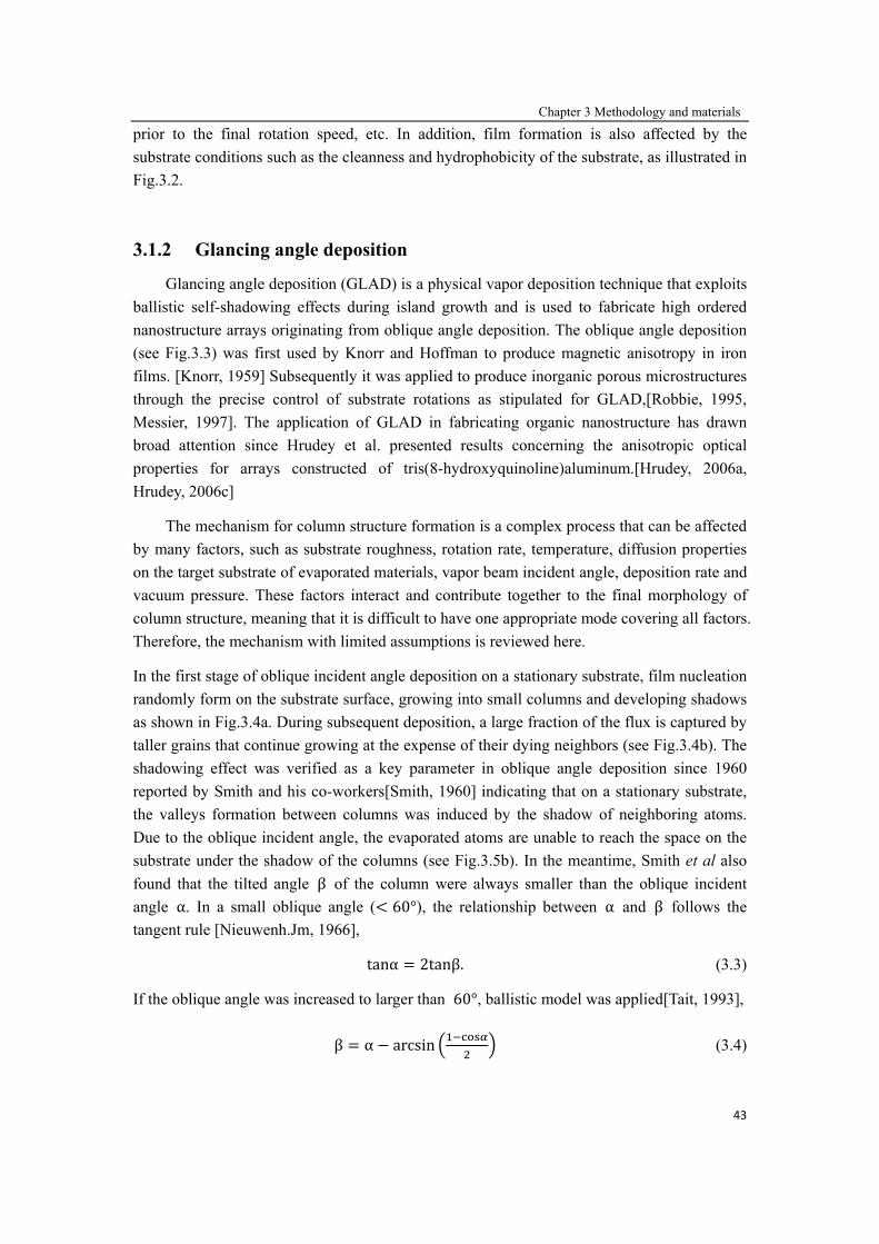
Chapter 3 Methodology and materials
43
prior to the final rotation speed, etc. In addition, film formation is also affected by the
substrate conditions such as the cleanness and hydrophobicity of the substrate, as illustrated in
Fig.3.2.
3.1.2 Glancing angle deposition
Glancing angle deposition (GLAD) is a physical vapor deposition technique that exploits
ballistic self-shadowing effects during island growth and is used to fabricate high ordered
nanostructure arrays originating from oblique angle deposition. The oblique angle deposition
(see Fig.3.3) was first used by Knorr and Hoffman to produce magnetic anisotropy in iron
films. [Knorr, 1959] Subsequently it was applied to produce inorganic porous microstructures
through the precise control of substrate rotations as stipulated for GLAD,[Robbie, 1995,
Messier, 1997]. The application of GLAD in fabricating organic nanostructure has drawn
broad attention since Hrudey et al. presented results concerning the anisotropic optical
properties for arrays constructed of tris(8-hydroxyquinoline)aluminum.[Hrudey, 2006a,
Hrudey, 2006c]
The mechanism for column structure formation is a complex process that can be affected
by many factors, such as substrate roughness, rotation rate, temperature, diffusion properties
on the target substrate of evaporated materials, vapor beam incident angle, deposition rate and
vacuum pressure. These factors interact and contribute together to the final morphology of
column structure, meaning that it is difficult to have one appropriate mode covering all factors.
Therefore, the mechanism with limited assumptions is reviewed here.
In the first stage of oblique incident angle deposition on a stationary substrate, film nucleation
randomly form on the substrate surface, growing into small columns and developing shadows
as shown in Fig.3.4a. During subsequent deposition, a large fraction of the flux is captured by
taller grains that continue growing at the expense of their dying neighbors (see Fig.3.4b). The
shadowing effect was verified as a key parameter in oblique angle deposition since 1960
reported by Smith and his co-workers[Smith, 1960] indicating that on a stationary substrate,
the valleys formation between columns was induced by the shadow of neighboring atoms.
Due to the oblique incident angle, the evaporated atoms are unable to reach the space on the
substrate under the shadow of the columns (see Fig.3.5b). In the meantime, Smith et al also
found that the tilted angle β of the column were always smaller than the oblique incident
angle α. In a small oblique angle ( 60°), the relationship between α and β follows the
tangent rule [Nieuwenh.Jm, 1966],
tanα 2tanβ. (3.3)
If the oblique angle was increased to larger than 60°, ballistic model was applied[Tait, 1993],
β α arcsin (3.4)

Chapter 3 Methodology and materials
44
Fig. 3.3. Definition of oblique incident angle deposition. The red line with arrow end is the evaporated
molecular beam and the angle between the beam and surface normal α is defined as incident angle, the
substrate could be rotated above its surface normal, the substrate rotation rate is ϕ.
Fig.3.4 Schematic representation of columns formation procedure. (a) Film nucleation formed on the
substrate at the beginning of evaporation. (b) Development of column structures.
Fig.3.5 Schematic representation of growth modes of (a) vertical deposition and (b) oblique incident
deposition and ballistic mode[Dirks, 1977]. Blue discs denote atoms, blue dash circles denote the
possible attaching positions for coming atoms, grey squares denote substrate, green dash-dot line
denote surface normal, α is the incident angle, β denote the column tilt angle, D is the center
diameter of the possible positions and the thick red line on the substrate denotes the shadow space. This
figure is reproduced from [Abelmann, 1997b]

Chapter 3 Methodology and materials
45
Another explanation for the phenomenon (when β ) was proposed by Kambersky et
al.[Kambersky, 1961] suggesting that all atoms with an oblique incident angle moved towards
the surface normal when they reach the column tops due to the retaining parallel momentum
to the substrate surface. However, this explanation is unable to distinguish between the
contribution to movement from either parallel momentum or random diffusion. In any case, as
mentioned previously, these modes are only capable of giving a first approximation of column
formation with oblique incident angle deposition. The approximation is limited as β is
dependent on many other features during preparation such as surface roughness, temperature
and evaporation rate, etc.[Nakhodkin, 1972, Hashimoto, 1982, Hagemeyer, 1993, Lintymer,
2003]
A column deposited by oblique incident angle on a stationary substrate always shows
textural anisotropy due to the shadow effect. If continuous substrate rotation rate were to be
applied in conjunction with oblique incident angle then the shadowing anisotropy can be
corrected, thus leading to vertically aligned column structures[Zhang, 2007a, Robbie, 1996,
Abelmann, 1997a]. The diameter of a GLAD column is to some extent larger than that
prepared without substrate rotation. By taking into consideration the surface diffusion, the
column diameter can be described by a power law [Karabacak, 2003, Cetinkaya, 2008,
Kaminska, 2005],
, ∝ (3.5)
Fig. 3.6 Schematic drawing of GLAD system in vacuum chamber. The bottom crucible is source heated
with a tungsten filament, the back rod is the step motor controlling substrate rotation about the surface
normal and the side rod is the controller attached on the substrate platform that tunes the angle of
oblique incident molecular beam α.

Chapter 3 Methodology and materials
46
where w denotes column width, t denotes film thickness and p is a growth coefficient
depending on the incident angle and the material. However, the relation between growth
coefficient and incident angle is still not clear and must be defined on a case by case basis. As
such, the final column diameter is difficult to measure. In addition, the crystal structure of
materials is also affected by the depositing incident angle, leading to changes in the crystal
main axis as a result of GLAD to comparison to negligible effects from vertical deposition. In
vertical deposition there is only a reference plane-substrate surface, while in GLAD the
oblique incident beam acts as an additional reference plane. During deposition, the crystal
orientation with respect to both reference planes is important. [Volmer, 1921] The origin of
this phenomenon is the subject of much debate. One suggestion is that it can be induced by
the surface dynamic equilibrium as qualitatively measured by the condensation coefficient
[Francombe, 1964]. Another study has emphasized the preferential growth orientation, called
evolutionary selection, as the main cause of this phenomenon [van der Drift, 1967].
Due to limited physical knowledge, the mechanism for column structure formation is
still not fully understood. A universal rule that summarizes the large collection of
experimental observations is difficult to define as there are always exceptional observations
disobeying the former modes. To enhance the controllability of the morphology of column
structures formed, further experimental and theoretical studies are necessary.
In this work, a home-made glancing angle deposition system was used as shown in
Fig.3.6. The substrate is fixed on a platform attached to a controller that was used to
manipulate the incident angle of the molecular beam α. On the back of the platform, a step
motor was mounted to control the substrate rotation rate ω about the surface normal. In most
cases, the deposition was started under high vacuum condition ( 10 mbar). Under
exceptional conditions, the pressure was decreased to 10 mbar by filling the chamber
with Argon gas to reduce the mean free pass of evaporated molecules.
3.1.3 Scanning electron microscopy
The first reported application of scanning electron microscope (SEM) was in 1942 by
Zworykin, who presented topographic contrast provided by emitted secondary electrons.
[Goldstein, 2003] In 1965, the first commercial SEM was developed by Pease and Nixon with
significant improvement of the spatial resolution.[Breton, 1999] Nowadays, the SEM is an
extremely useful approach for imaging and analyzing the structure and surface morphology of
materials. A simplified SEM instrument structure is shown in Fig.3.7a.
In the SEM, a focused electron beam interacts with a specimen leading to a number of
particle and radiation emissions such as backscattered electrons (BSEs), secondary electrons
(SEs) and x-rays, etc. (see Fig. 3.7b). Electrons produced at a cathode are accelerated through
a voltage difference of 0.1-50 KV between the cathode and the anode of the device. The
electron probe that reaches the surface has a diameter of 1-10 nm, with the diameter

Chapter 3 Methodology and materials
47
controlled by a series of electromagnetic lenses in conjugation with apertures.[Reimer, 1998]
“Scanning” is achieved by controlling the magnetic field generated by the coil system that
allows for the sweeping of the focused electron beam across the specimen surface. The
incident electrons interact with the sample and in doing so lose some of their kinetic energy
due to elastic or inelastic collisions. This then leads to the emission of electrons and x-rays
from the sample.[Reimer, 1998] Among the varieties of electron emissions, SEs are produced
as a result of the inelastic collisions between incoming electrons and weakly bound electrons
in the conduction band. The SEs are collected with the Everhart-Thornley detector and
subsequently used to create images of the topographic features of the specimen. Image quality
is a function of the SEs yield, enhanced edge effect emission (Fig. 3.8) and small particles,
and partial collection due to the shadow on the surface.
Fig.3.7 (a) Schematic representation of the SEM instrument. Bottom grey square is the specimen
placed in vacuum. The SEs detector is the secondary electron detector, yellow beams are (manipulated)
electron beam, the upper black triangle tip is electron gun tip in between a cathode and anode, the
condenser-lens and apertures are used to assist to focus the electron beam and control the electron beam
radius, coils system in the middle is to tune the direction of electron beam which is used to change to
investigation position on specimen. (b) Primary interaction between incident electrons and the
specimen. The SEs are the secondary electrons and BEs are the backscattered electrons.

Chapter 3 Methodology and materials
48
Fig.3.8 (a) Enhanced SEs emission due to edge effect. The IEB is the incident electron beam, the
escaped E represents escaped electrons, the red unfilled balls under the surface are volumes of injected
electrons and the blue arrows are electron escape directions. (b) A SEM micrograph example showing
the edge effect.
The SEs yield mainly depends on the chemical composition of the sample and the tilt
angle of the surface element with respect to incoming electrons, as well as incident electron
energy. Owing to their low exit energy, less than 50 eV, electrons can escape from only a few
nanometer depths below the specimen surface. At the specimen edges, more secondary
electrons can leave the specimen surface compared with that of flat area as shown in Fig. 3.8.
Therefore, the areas around edges appear brighter in images.
In this work, the HITACHI S-4100 SEM with cold field emission gun was used to
investigate samples’ topography and lateral structure. The accelerating voltage can be varied
between 0.5 and 30 KV. The maximum resolution that can be reached is 1.5 nm. In order to
obtain high resolution images, before investigation a 10 nm thick gold layer was usually
sputtered onto specimens.
3.1.4 Scanning force microscopy
The scanning force microscope (SFM) invented by Binning et al in 1986 was developed
from the scanning tunneling microscope,[Binnig, 1986] and allows for the study of the
surface topography with sub-molecular resolution. The basic principle of the SFM is to
measure the attractive or repulsive force between the sharp tip mounted on a flexible
cantilever and the surface of solid film on an atomic scale of nanometers. A schematic
representation of SFM operation process is shown in Fig. 3.9.

Fig.3
subs
plate
shine
trans
boun
cant
leve
scan
long
the e
whe
mole
pote
The
~
3.9 Schematic
strate, red line
e squares betw
es on the tipto
slated to an ele
During scan
nced off the
tilever deflec
er principle)
nning the int
g-range and
expression
ere is pot
ecular diame
ential by
two terms in
and repul
c representatio
s are laser bea
ween laser and
op of cantileve
ectrical signal
nning, an acc
e back of th
ctions due to
and convert
teraction betw
short-range
tential energ
eter. The int
F
n the equatio
sive force ~
on of SFM op
ams, feedback
d photodetecto
er and is reflec
l by the contro
curately cont
he cantilever
o its bending
ted into elec
ween the tip
forces. Reca
4
gy at the mi
teraction forc
on 3.7 refer to
~ in sho
peration. Blue
k is data collec
or are minors.
cted to the ph
oller.
ntrolled tip m
r is captured
g are detecte
ctrical signa
and sample
all that the L
4
inimum, r is
ce F is given
4 12
o long range
ort displacem
Cha
e ball/purple r
ction system c
. The laser be
otodector, wh
moves line by
d by a four-
ed on an An
als for mapp
e surface is p
Lennard-Jone
s tip-sample
n as the der
6
e force domin
ment[Cappell
apter 3 Methodo
rods represent
controlled by c
am emitted fr
ile the collect
y line, and th
-segment ph
ngstrom spat
ping.[E. Mey
principally du
es potential
distance an
ivative of th
nated by van
a, 1999].
dology and mate
t molecules o
computers and
rom the laser d
ted optical sig
he laser beam
hotodetector.
tial scale (op
yer, 2003] W
ue to two fo
is give
nd is effe
he Lennard-J
(3
n der Waals’ f
erials
49
on the
d two
diode
nal is
m line
The
ptical
While
orces:
en by
(3.6)
ctive
Jones
3.7)
force

Fig.3
deriv
betw
mod
inve
cant
indic
nano
inter
appr
is de
z-dir
is ba
can
of h
surfa
the d
whe
com
para
3.10 Interactio
vative of Lenn
ween these two
There are
de, non-cont
estigating su
tilever drive
cated in Fig
ometers. Du
raction force
roach is used
etected and
rection in or
ased on the
be deduced
height variati
face morphol
data in the z-
ere is the
mprising N p
ameter is the
on between ti
nar-Jones pote
o regimes lies
several tech
act mode an
urface morph
n by piezo
g. 3.10 with
uring scannin
e. To follow
d. The deflec
then used in
der to keep t
scanner’s m
from 3D AF
ions on the
logy is the r
-direction:
e height val
pixels and
3D surface
ip and the sam
ential. Contac
the intermitte
hniques base
nd tapping m
hology of m
crystals is
reasonable
ng on an un
w the surfac
ction of refle
n a feedback
the amplitude
otion in z-di
FM topograph
surface topo
root mean sq
lue of pixel
is the mea
area of the e
mple surface f
ct and non-con
ent contact reg
d on the SF
mode. The ta
molecular an
forced to v
setting amp
ndulating su
ce topograph
ected laser be
k loop to co
e constant. S
irection. At
hy statistics,
ography. The
quare roughn
∑
l j of the s
an height va
entire image
Cha
for a SFM de
ntact regimes
gion.
FM operatio
apping mod
nd polymer f
ibrate in the
plitude typic
urface, the c
hy with the
eam induced
ontrol the tip
Subsequently
the same tim
, can be used
e principle p
ness (rms), e
surface z
alue :
that can als
apter 3 Methodo
ependent on d
are highlight
n principle,
e was used
films. In tap
e intermitten
ally in the r
antilever is
cantilever ti
d by the bend
p movement
y, the mappin
me, surface r
d as a quantit
parameter for
expressed by
z , in t
∑ . An
o be calculat
dology and mate
distance define
ted respective
such as co
in this work
pping mode
nt-contact re
range of ten
bent due to
tip the follow
ding of canti
up and dow
ng of morpho
roughness, w
tative descrip
r quantifying
y the deviatio
the AFM im
nother impo
ted from the
erials
50
ed by
ely. In
ntact
k for
, the
egion
ns of
o the
wing
lever
wn in
ology
which
ption
g the
on of
(3.8)
mage
ortant
e root

Chapter 3 Methodology and materials
51
mean square roughness. The entire surface area is the sum of the area ( ) of all of the
triangles formed by three adjacent data points,
(3.9)
∑ (3.10)
where a,b,c are displacements of each three adjacent points ( , , ), ( , , ),
( , , ) respectively.
In addition, the oscillation of tip only allows it to impinge the sample surface at the
lowest point periodically; thus, scanning operates in the attractive force region for most of the
time but only a short fraction of time in the repulsive region. Therefore, the lateral forces in
tapping mode are much lower than in the contact mode. This feature makes the tapping mode
appropriate for soft matter scan without damaging the sample surface such as organic
molecules. In this work, Bruker Multimode-8 AFM is used to investigate the morphology of
the most samples.
3.1.5 Ultraviolet/visible absorption spectroscopy
In general, ultra-violet/visible (UV-Vis) spectroscopy is a technique allowing one to
access information concerning the absorption and scattering characteristics of a given sample.
A simplified description involves a sample being placed between a monochromatic light
source and a photodetector, with the intensity of light beam measured before and after passing
through the sample. After extraction of the “background” (substrate or cuvette with solvent),
the extinction spectrum is plotted as a function of wavelength.
As discussed in chapter 2, for a single molecule, the absorption corresponds to the
excitation of outer electrons mainly the ∗ transition and ∗ transition. For an
organic solid, the absorption is the sum of the absorptions of each molecule. Thus, the extent
and intensity of absorption are both dependent on the molecular electronic structure and the
number of molecules that absorb light of a given wavelength. This can be described by the
Beer-Lambert law which states that the transmittance (T) of light through a substance is
dependent on the extinction coefficiency (ε) of the substance and the distance (L) the light
travels through the substance as given by
T 10 (3.11)
where is intensity of the incident light, is intensity of light transmitted through the
substance, c is concentration of the substance. For a given molecule, α is constant at a

Chapter 3 Methodology and materials
52
specific wavelength and the product εc defined as the absorbance (A), which can be read
from the spectrum directly, is given as
A (3.12)
Fig.3.11 Schematic representation of the Beer-Lambert law. The orange ball is light source and the
orange arrow bars represent the light rays.
Fig.3.12 Schematic representation of PerkinElmer lambda 900 spectrometer. Grey lines with arrows in
front are light beams. The upper purple and dark red balls are deuterium and tungsten-halogen lamp
respectively. The light is converted to a monochrome source by a filter and monochromator.
Subsequently the focused monochromatic light is split into two light beams by a common beam
depolarizer. The two light beams are then recalculated by attenuators to ensure equal light intensity
output.

Chapter 3 Methodology and materials
53
In principle, the absorption peaks of given molecules in UV-Vis spectrum should be
sharp as the energies of the electronic transitions are constant. However, common spectra
show broad peaks rather than sharp peaks. This is due to discrete vibrational energy levels and
rotational energy levels at each electronic energy level where transitions may also occur.
Prevalently throughout this work, measurements of absorption were carried out with a
PerkinElmer lambda 900 spectrometer with the instrument structure is shown in Fig. 3.12.
The setup is also capable of measuring the absorption of infrared region at a wavelength of
3000 nm, which allows for the investigation of the polaronic absorption induced by molecular
doping in polymer. In order to minimize the error due to substrates difference, calibration is
necessary prior to measure UV-Vis spectroscopy for reference substrate and the sample
substrate before using.

Chapter 3 Methodology and materials
54
3.2 Materials
In this section, the materials used to fabricate OPVs and the experimental conditions are
introduced. Additionally, sample preparation and measurements will be illustrated in detail.
3.2.1 Organic materials
Pentacene (PEN) (99%), fullerene (C60) (99.9%) and bathocuproine (BCP) (96%)
purchased from Sigma-Aldrich were used directly without sublimation.
[6.6]-phenyl-C61-butyric acid methyl ester (PCBM) was purchased from American Dye
Source, Inc. Tetrafluorotetracyanoquinodimethane (F4-TCNQ) ( 98%) was purchased from
Tokyo Chemical Industry co. LTD. Znic phthalocyanine (ZnPc) and diindenoperylene (DIP)
were twice sublimated. Ploy (3,4-ethylenedioxythiphene):poly(styrenesulfonate)
(PEDOT:PSS) were purchased from H.C. Stark GmbH&Co. KG. Purified polyfuran was
provided by Bendikov group (Weizmann institute of science).
a. Organic materials for column structure
As mentioned in section 3.1.2, the morphology of column structures grown with GLAD
is also dependent on the properties of organic materials such as the diffusion length and
crystalline characteristics. In this work, PEN and DIP were chosen and their chemical
structures are depicted in Fig.3.13 (a) and (b) respectively.
PEN is one of the most intensively investigated conjugated organic molecules over the
past several decades due to its importance in organic electronic devices applications.
Considering high charge carrier mobility for holes and low mobility for electrons, PEN has
been used as a good donor material for OPVCs.[Salzmann, 2008] Furthermore, singlet fission
discovered recently in PEN film, which could increase the quantum efficiency significantly,
makes PEN a much stronger candidate. With appropriate deposition rate, molecular beam
incident angle and substrate rotation rate, the columnar structure on indium tin oxide (ITO)
substrate is achievable. [Witten, 1981, Meyer zu Heringdorf, 2001a, Ruiz, 2003a, Ruiz, 2003b,
Abelmann, 1997b, Zhang, 2007a]
DIP has drawn great attention since its application on OPVs owing to its advantage of
having a long exciton diffusion length.[Wagner, 2010, Stübinger, 2001, Dürr, 2002,
Heinemeyer, 2008a, Kurrle, 2008, Meiss, 2010] Appropriate crystalline structure and stability
in ambient conditions make DIP a good candidate for fabricating column structures.
Furthermore, lying phase DIP, which enhances the absorption, has been found in column
structure layers by x-ray diffraction spectroscopy (XRD).

Chapter 3 Methodology and materials
55
Fig.3.13 Chemical structure of organic materials as donors and acceptors for OPVs; (a) PEN; (b) DIP;
(c) C60; (d) PCBM.
b. Other functional organic materials
C60 consisting of 12 pentagons and 20 hexagonsone is one of the most promising n-type
semiconductors and has been applied widely in the field of organic electronics (Fig.3.13c).
[Kroto, 1985, Itaka, 2006, Wang, 2006] The PCBM (Fig.3.13d) is one of the most commonly
used polymers as an acceptor for solution processed OPVs. The solubility of PCBM is
improved by adding the side group, and to a large extent the electronic properties of
buckminsterfullerene are preserved. F4-TCNQ (Fig.3.14a) is a strong acceptor small molecule
that is broadly used for the p-type doping of materials in organic electronics to manipulate the
energy alignment and improving conductivity.[Gao, 2003, Aziz, 2007, Sun, 2009, Lu, 2013,
Pingel, 2013]
Fig.3.14 Chemical structures of organic materials; (a) F4-TCNQ; (b) ZnPc; (c) polyfuran (one
monomer); (d) PSS; (f) PEDOT.

Chapter 3 Methodology and materials
56
Polyfuran is a p-type highly conductive conjugated polymer with electrical and optical
properties similar to P3HT, with the chemical structure shown in Fig.3.14c. However, due to
the difficulties in their synthesis, it has been the subject of less attention than
P3HT.[González-Tejera, 2008, Ferron, 2012] ZnPc has been extensively studied as a
promising semiconductor material for OPVs, exhibiting good absorption in visible region and
a high value of exciton diffusion length.[Amsalem, 2009, Hong, 2007, Pfuetzner, 2011,
Senthilarasu, 2007, Zeng, 2010] BCP, in this work, is treated as exciton-blocking layer
between acceptor and cathode, as well as a protection layer preventing damage due to metal
evaporation.[Chan, 2006, Lo, 2010, Vogel, 2006a, Gommans]
3.2.2 Holes transport material
In the field of OPVCs, PEDOT:PSS is one of the most commonly used holes transport
materials that is transparent and highly conductive, and it consists of PEDOT and PSS in
various ratios. The chemical structures are shown in Fig.3.14 (d) and (f). [Drury, Halik, 2002,
Groenendaal, 2000, Kirchmeyer, 2005] This highly conductive polymer is neutral since the
positive charges on PEDOT are stabilized by negative charges on PSS and the conductivity
can be tuned by employing various ratios of PEDOT in the mixture, ranging from 10-5 S/cm
to over 100 S/cm. Although PEDOT is hydrophobic, the PEDOT:PSS can form agglomerates
in aqueous dispersion, assisted by dressing hydrophilic PSS.[Jukes, 2004, Greczynski, 1999]
PEDOT:PSS thin film can be easily prepared by spin coating under ambient conditions,
with the thickness controllable. The value of work function ( ) of PEDOT:PSS film is
significantly impacted by water contamination, thus in order to obtain high for reducing
injection barrier, an annealing process is necessary to remove the residual water before
fabricating devices.[Koch, 2007c]
In this work, three types of PEDOT:PSS were used: CH8000 (weight ratio is 1:20),
AI4803 (weight ratio is 1:6) and HIL1.3 (fluorinated derivative of the stand PEDOT:PSS)
respectively. [Wilke, 2013]
3.2.3 Electrodes and substrates for OPVCs
In this work, glass substrates with patterned ITO (purchased from Thin film Devices Inc.
and Präzisions Glas & Optik GmbH) were used for OPVs fabrication and ITO was treated as
the bottom anode with a sheet resistance of 20 Ω/sq. The average thickness of ITO layer is
about 120 nm and the roughness is approximately 2 nm. For absorption measurement, quartz
glass (Präzisions Glas & Optik GmbH) substrates were sometimes used instead of ITO to
reduce the influence of light scattering. The pre-cleaning procedure of all the substrates is as
follows. First the substrates were scrubbed with diluted Hellmanex solution, then rinsed with

Chapter 3 Methodology and materials
57
deionized water and blown dry with N2 gas. Next they were sonicated for 10 min in acetone
and isopropanol respectively and then blown dry again. In the application of OPVs, prior to
use, Ultraviolet-ozone (UV-ozone) treatment for more than 30 minutes was applied to
improve the wetting of the substrate by an aqueous suspension of the intrinsically conducting
polymer PEDOT:PSS.[Destruel, 2006, Lo, 2013] Moreover, the ozone treatment can also
affect ITO surface work function by increasing the oxygen concentration on top of the
surface.[Sugiyama, 2000, Destruel, 2006] The prototypical morphology of an ITO surface is
presented in Fig. 3.15 with the average rms for all ITO substrate being approximately 2 nm.
Additionally the ITO substrates were pre-patterned with pure HCl etching to define the device
active area.
The top electrode (cathode) used for some devices is samarium (Sm) exhibiting a
relatively low work function of approximately 2.8 eV and was investigated in ultra-high
vacuum condition ( 10 mbar) with UPS.[Koch, 2002] The low work function is to some
extent sufficient for charge collection in OPVCs and results from high energy offset between
the cathode and anode leading to a high extraction electrical field. However, a crucial issue
with using Sm as the top electrode is that Sm is sensitive to oxygen and can very easily be
oxidized. Therefore, the J-V characteristics of the devices with Sm were measured in an inner
environment (high vacuum or glovebox).
Alternatively, a widely used top electrode material is aluminum (Al) with a work
function about 4.1 eV.[Koch, 2000] However if using Al as the cathode of OPVCs electron
blocking layer or protection layer is needed due to the issues of exciton quenching occurring
at the organic/Al interface with Al atoms diffusion taking place during deposition. [Vogel,
2006a, Gommans, 2008, Wagner, 2012]
Fig.3.15 The typical morphology of ITO and PEDOT:PSS substrates investigated by AFM. The value
of rms are 4 nm and 1 nm respectively.

Chapter 4 Results and discussion
58
Chapter 4
Results and discussion This chapter is divided into three sections based on the materials and methods employed
to fabricate OPVCs. The first section will focus on presenting vertically aligned pentacene
nanocolumn architecture grown by GLAD and its application in OPVCs. The second section
will illustrate the experimental and measurement results of DIP column structure on different
substrates and their application in OPVCs. Compared to bilayer heterojunction devices, the
performance of OPVCs utilizing nanocolumn structure improved owing to interface area
enlargement and enhanced absorption by effectively using a thick organic film. The last
section will demonstrate the process of molecular doping in polymer film with F4-TCNQ
employed as the dopant. The results of molecular doping in OPVCs are then introduced.
4.1 Pentacene nanocolumn and application in
OPVCs
4.1.1 Introduction
OPVCs have been extensively studied since the first study of bi-layer donor/acceptor
heterojunction devices.[Tang, 1986] Significant improvement in power conversion efficiency
was achieved through the production of bulk heterojunctions (BHJ) from solution processed
conjugated polymer/fullerene mixtures. The BHJ morphology enables large interface areas
between donor and acceptor material that facilitates efficient exciton dissociation.[Yu, 1995,
Halls, 1995, Peumans, 2003a] At the same time, if the donor/acceptor phase separation length
scale is on the order of the exciton diffusion length, losses due to excition recombination can
be minimized.[Peumans, 2003a, Halls, 1995, Yu, 1995] However, in such random blends
charge carrier mobility may be low, charge trapping at morphological bottlenecks can quench
excitons, and dead-ends in the conduction pathway may build up unwanted space charge.
Hence, a vertically interdigitated array of densely packed alternating donor and acceptor
columns with a diameter in the range of the exciton diffusion length sandwiched between the
electrodes could eliminate above problems and thus maximize OPVC efficiency.[Yang, 2005,
Zheng, 2009a] A suitable lithography-free method to fabricate such organic vertically
aligned nano-columnar structures is GLAD, which is a physical vapor deposition technique
that exploits self-shadowing effects during island growth.[Hrudey, 2006b, Zhang, 2007b] In
GLAD, a molecular beam is directed under a glancing angle () onto the substrate, which
simultaneously rotates about its surface normal. This results in the growth of vertical
columnar structures, whose morphology can be controlled by variation of and substrate

Chapter 4 Results and discussion
59
rotation rate (), as well as the substrate surface energy, morphology, and
temperature.[Abelmann, 1997a, Zhao, 2002, Robbie, 1997]
In this section the growth of vertically aligned crystalline nanocolumn arrays (NCAs) of
PEN by GLAD is examined and their beneficial effects for OPVCs compared to devices with
PEN donor layers grown by conventional (normal incidence) molecular beam deposition. The
interdigitated donor/acceptor active layer was produced by filling the void volume around the
PEN nanocolumns with the acceptor PCBM from solution, since evaporation of the acceptor
would likely lead to holes due to shadowing of the molecular beam. Further device
performance improvement was achieved by inserting a thin PEN electron-blocking layer prior
to NCA growth to prevent electron current leakage to the anode. Lastly, the possibility of
depositing C60 as acceptor on PEN nanocolumns for interdigitated bulk heterojunction is
investigated.
4.1.2 PEN nanocolumn
The formation of nanocolumns is caused by the shadowing effect of molecular islands
with respect to the incoming material flux, aggravated by the large oblique incident deposition
angle. During deposition a large fraction of the flux is captured by taller grains that continue
growing at the expense of their dying neighbors. As discussed in chapter 3, the morphology of
column structure is determined by several parameters, such as incident angle (), substrate
rotation rate ω and the features of substrate, as well as features of the materials. In this work,
the influence of each individual parameter on column structure with PEN is investigated.
Figures 4.1.1b-d show representative topography and cross-section micrographs of PEN
columnar structures grown by GLAD on ITO. Compared with the typical flat and
homogeneous morphology of vertically deposited PEN thin films on ITO, displayed in Fig.
4.1.1a, almost square shaped crystalline PEN nanocolumns with large gaps between them
persist after GLAD deposition. The polycrystalline structure of PEN nanocolumns, which is
important towards obtaining high charge carrier mobility for a low solar cell series resistance,
has been demonstrated earlier by Zhang et al.[Zhang, 2007b] As expected, due to the incident
angle, there were two polymorph observed on ITO. The diameter of the columns in the
samples used for fabricating OPVCs later is predominantly in the range of 120 nm to 180 nm
and the column area-density is approximately 3×107 mm-2. The cross-section view (Figs.
4.1.1c-d) reveals that the height of the individual columns is rather uniform, about 210 nm,
except for a few higher protrusions. There are always small gaps between the columns, even
for locally high area-densities.
The results of PEN column presented above using of 85°, ω of 6 revolutions per
minute (rpm) and a deposition rate of ca. 1 Å/s on bare ITO likewise are depicted in Fig4.1.2b.
When the incident angle was changed to 80° while keeping the other parameters constant, the
density of the column increased as a result of rather weak shadow effect as illustrated in
Fig.4.1.2a. The “column” density fabricated with 80° incident angle is much larger than that

Chapter 4 Results and discussion
60
using an 85° incident angle, corresponding to valleys of lower volume, and thus agreeing with
the assumption of a relationship between column intensity and incident angle as discussed in
section 3.1.2.
In figures 4.1.3(c) and (d), the influence of the substrates with different morphology on
column formation is presented. The two substrates were amounted into the chamber at the
same time for the PEN deposition to make sure using the same deposition parameters. In
contrast to column structure on ITO substrate (Fig.4.1.3c), PEN film on PEDOT:PSS coated
ITO substrate exhibits rather different morphology. No prototypical column features can be
observed but the features are similar to PEN thin film prepared with vertically deposition on
PEDOT:PSS (see Fig.4.1.3b). The absence of column structure on PEDOT:PSS is related to
the large diffusion length of PEN molecules on smooth surfaces during vacuum deposition.
As can been seen from figures 4.1.3 (a) and (b), in comparison to PEN film vertically
deposited on ITO (a) and PEDOT:PSS (b), the average island size on PEDOT:PSS is much
larger than that on ITO due to the extended diffusion length on smoother surfaces. There are
many studies of PEN molecules growth on silicon oxide surface where the roughness is
similar to PEDOT:PSS, approximately rms of 0.2 nm, which demonstrates a PEN molecular
diffusion length in the range of micrometers.[Heringdorf, 2001, Abelmann, 1997b, Ruiz,
2003a, Ruiz, 2003b] In GLAD, the extended diffusion length on PEDOT:PSS enlarges the
initial island growth size as for vertical deposition leading to a weakening of the shadow
effect at the onset of growth core formation. Therefore, there is no PEN columnar structure
growing on PEDOT:PSS coated ITO substrate.
Fig. 4.1.1 SEM micrographs of PEN films on ITO. a) Top view of vertically deposited pentacene. b)
Top view of a GLAD pentacene nanocolumn array (NCA). c) and d) Cross-section views of a GLAD
pentacene NCA.

Chapter 4 Results and discussion
61
Fig.4.1.2 SEM micrographs of PEN film on ITO. a) Top view of the sample fabricated with incident
angle of 80°. b) Top view of the sample fabricated with incident angle of 85°.
Fig.4.1.3 AFM micrographs of PEN film/columns on ITO and PEDOT:PSS coated ITO. a) Vertically
deposited on ITO. b) Vertically deposited on PEDOT:PSS coated ITO. c) GLAD on ITO. d) GLAD on
PEDOT:PSS coated ITO. Vertically deposition rate is 0.02 nm/s. GLAD parameters:
rpm and deposition rate: 0.1 nm/s. The height scale for all figures is 100 nm.

Chapter 4 Results and discussion
62
4.1.3 Analysis of OPVCs
a. Solution processing for electron acceptor
The interpenetrating donor-acceptor structure was obtained by PCBM solution spin coating
onto the PEN nanocolumn arrays. As shown in Fig. 4.1.4a, spin coating with low
concentration PCBM solution (18 mg/ml in chlorobenzene) left the underlying PEN
nanocolumns still clearly visible. Although such a highly corrugated surface easily leads to
electrical shorts,[Seungkeun, 2009, Reddy, 2009, Vogel, 2006b] the observation implies that
PEN nanocolumns still stand vertically on the ITO substrate and are not impeded by PCBM
spin coating. In addition, PCBM infiltration into gaps between nanocolumns occurred as
shown in Fig. 4.1.4b. With a higher concentration PCBM solution (28 mg/ml), a rather
smooth surface was obtained and the gaps were filled adequately by PCBM (see Figs. 4.1.4
c-d). Firstly, the OPVCs based on PEN/PCBM interdigitated heterojunction were prepared on
bare ITO substrate, transferred to UHV chamber via ambient condition and completed with
Sm deposition as the top electrode. However, all devices were “dead”, displaying short
circuits. This might be induced by the current short-pass formed by infiltrated PCBM
contacting both electrodes. Unsurprisingly, the reference devices prepared under the same
conditions employing bilayer structure with PEN/PCBM were also “dead” unless
PEDOT:PSS was applied before PEN deposition.
Fig.4.1.4 SEM micrographs of PCBM solution deposited onto pentacene NCAs. a) and b) Top and
cross-section views of low concentration(18 mg/ml) PCBM solution. (c) and (d) Top and cross-section
views of high concentration(28 mg/ml) PCBM solution.

Chapter 4 Results and discussion
63
Fig.4.1.5 Morphology of PEN on ITO (a) and PEDOT:PSS (b) investigated by AFM.
Fig. 4.1.6 Structures of the investigated OPVCs. a) Planar bi-layer structure. b) PNC (pentacene
nanocolumn) structure. c) PEBL (pentacene electron-blocking layer) combined with PNC.
Figure 4.1.5 presents the morphology of PEN on ITO and PEDOT:PSS substrate
respectively. Obviously, the PEN island size on PEDOT:PSS substrate is much larger than
that on ITO, meaning that there are less PEN crystalline boundaries on sample b. This is
beneficial for effectively reducing the possibility of having a current short. However, as
presented previously, it is impossible to fabricate PEN nanocolumns on PEDOT:PSS substrate.
Therefore another electrode interface was considered where BCP was deposited as a blocking
layer before evaporating Sm in order to prevent the two electrodes contacting with PCBM
directly. As predicted, the development of current short-pass was efficiently prevented by the
inserted-BCP between PCBM and Sm. In addition BCP with wide optical energy gap (3.5 eV
[Peumans, 2000]) was used as an exciton-blocking layer. Although BCP introduces the
problem of crystallization, it remains a good candidate to act as protection-layer for the active
the donor/acceptor layer during metal deposition. (In this work, all metal evaporation were
finished in 30 minutes after BCP deposition, avoiding the crystalline issue reported
[Masumoto, 2008])

Chapter 4 Results and discussion
64
Fig. 4.1.7 Current density-voltage characteristics of NC heterojunction and improved devices compared
with bi-layer heterojunction devices at the same illumination density. Squares with the black line show
the characteristics of all three devices in dark.
Fig. 4.1.8 Current density-voltage characteristics in dark for the three device structures.
Tab. 4.1 Characteristic performance parameters of OPVCs. Open circuit voltage (Voc), short circuit
current (Jsc), fill factor (FF).

Chapter 4 Results and discussion
65
Fig. 4.1.9 Top and cross-section view of pentacene nanocolumn array grown on a 10 nm thick PEBL.
The structure of all investigated OPVC variants are shown in Fig. 4.1.6. For comparison
with OPVCs that have PEN nanocolumns, an optimized bi-layer planar heterojunction OPVC
employing ITO/PEDOT:PSS/50nm PEN/30nm PCBM/8nm BCP/100nm Sm (structure A)
was fabricated at room temperature, as suggested in [Reddy, 2009]. Interdigitated OPVC
fabrication was done by BCP and cathode (Sm) deposition in high vacuum (structure B). The
current density-voltage characteristics of interdigitated OPVCs and reference bi-layer cells
are shown in Fig. 4.1.7 with the characteristic parameters summarized in Tab. 4.1. The
open-circuit voltage (Voc) of all cells is virtually the same, i.e., 0.5 V. However, the short
circuit current density (Jsc) of interdigitated cells with structure B has more than doubled
compared to that of the reference bi-layer cell under the same illumination condition. The fill
factor (FF) of the cell with structure has slightly increased from 0.48 to 0.51. The improved
performance of interdigitated cells is attributed to the increased active interface area due to
the PEN nanocolumns. From the SEM images a ca. threefold increased interface area with
nanocolumns is estimated, which in principle could lead to threefold increase Jsc threefold if
there are no other factors impacting device performance. Since Jsc in structure B OPVCs was
only doubled compared to structure A, we expect additional effects to play a role. Considering
the characteristics of devices in the dark, shown on a logarithmic scale in Fig. 4.1.8, a much
lower specific shunt resistivity of structure B devices was obtained (approx. 0.02 MΩ cm2)
compared to that of structure A devices (approx. 2.86 MΩ cm2).[Sze, 2007] The low shunt
resistance could be due to current leakage paths produced by the infiltration of the PCBM
acceptor phase to the bottom electrode, which does not occur in the planar bi-layer reference
device.
To eliminate the problem of leakage paths, a 10nm thick PEN film was deposited on ITO
before growing PEN nanocolumns as an electron-blocking layer, shown as structure C in Fig.
4.1.6 (c). As seen from Fig. 4.1.9, there is no marked difference of pentacene nanocolumns
compared to those in Fig. 4.1.1 except for the thin PEN electron-blocking layer. A remarkable
increase in Jsc resulted (see Fig. 4.1.7 and Tab. 1), owing to the increased shunt resistivity
(approx. 1 MΩ cm2), as shown in Fig. 4.1.8. Hence, the influence of current leakage paths is
reduced but not entirely eliminated. Employing a heavily p-doped thin film was suggested as

Chapter 4 Results and discussion
66
electron-blocking layer that might be helpful to further improve device performance.
Nevertheless, the characteristics of interdigitated OPVCs employing PEN nanocolumns were
improved significantly by utilizing the thin electron-blocking layer. The Jsc improvement now
reached more than 90% of the expected threefold increase due to increased active interface
area. However power conversion efficiency values under standard illumination conditions
(due to the experimental setup in vacuum) cannot be provided. Devices with structure C
(interdigitated) are estimated to have an efficiency of ca. 4%, as opposed to only ca. 1.5% for
those with structure A (planar), at 2.5 mW/cm2 illumination from a halogen lamp with an
emission spectrum close to daylight in the visible region.
b. Vacuum deposition for electron acceptor On the other hand, attempts were made to build the donor-acceptor heterojunction by
depositing C60 (deposition rate: 0.2 nm/s) on top of PEN nanocolumns in vacuum (3.510 mbar). However, due to the narrow “tunnels” (gaps), it was easier for evaporated C60
molecules to be deposited on the wall of the tunnels than passing the tunnel and be deposited
on the bottom of the tunnels. Thus, this led to unfilled holes underneath as indicated in
Fig.4.1.10a. The unfilled holes are huge defects that significantly reduce the PCE of OPVCs.
Afterwards, the vacuum level was reduced to 3.5 10 mbar by venting the chamber with
argon gas in an attempt to shorten the evaporated molecules free pathway to allow the
evaporated molecules to move randomly. To some extent, this method was helpful for C60
molecules passing through the “tunnels”, but unfilled holes still existed. In any case, devices
were fabricated based on the heterojunction of PEN nanocolumns/C60, and the performance
was poor as predicted. In particular the Jsc was very low as shown in Fig.4.1.10b.[Salzmann,
2008] Thus, vacuum depositing electron acceptor molecules to fabricate interdigitated
heterojunction is not suitable for such high intensity columnar structure. Large volume valley
is necessary for evaporated molecules passing the “tunnel”.
Fig.4.1.10 (a) Evaporation of C60 on top of PEN columns in vacuum. (b) Performance of OPCVs
under illumination 2.5 mW/cm2 in vacuum, device structure ITO/PEN column/C60/BCP/Sm.

Chapter 4 Results and discussion
67
4.1.4 Summary
In conclusion, the morphology of pentacene nanocolumns grown by GLAD has been
investigated with SEM and AFM, through variation of the experimental conditions. Final
vertically aligned crystalline pentacene nanocolumns with a diameter of ~ 160 nm were
achieved. Qualitative analysis of the influence of substrate morphology and incident angle on
PEN nanocolumn architecture has been presented. Interdigitated OPVCs structures were
achieved by spin-coating PCBM onto the optimized pentacene nanocolumns, which led to a
threefold increase of active donor/acceptor interface area as compared to planar bi-layer
structures. By employing an additional planar thin pentacene electron-blocking layer, Jsc was
increased from 0.17 mA cm-2 to 0.47 mA cm-2, thus attributing over 90% of the expected
increase to the larger interface area. The remarkable conversion efficiency of OPVCs based
on NC structures proves that it is an effective architecture towards eliminating charge
transport and exciton diffusion bottlenecks while maximizing the interface area. Other
materials as donors and/or acceptors employed in similar structures will most likely lead to
significant further improvements in OPVCs performance in the future. In addition, attempts to
fabricate the OPVCs with vacuum deposition of electron acceptor C60 were made.
Unfortunately, the performance of OPVCs was not satisfactory due to the large amount of
defects induced by appearance of unfilled hole after vacuum deposition.
4.1.5 Experimental details
ITO coated glass substrates (Präzisions Glas & Optik, sheet resistance < 20 Ω/sq, surface
roughness (rms): 2 nm) were sonicated for 10 min in acetone and, subsequently, isopropanol.
After cleanness, ITO coated substrates were patterned by etching processing (36.5% HCl
solution), leaving two parallel strips ITO (1 mm width) on glass, and the pattern ITO
substrates were cleaned once more as description before.
Fig.4.1.11 The bottom cyan box is denoted as glass substrate;the light blue squares are denoted as ITO.
UV-ozone-treatment was applied to improve the wetting of the substrate by an aqueous
suspension of the intrinsically conducting polymer poly(ethylene-dioxythiophene): poly-
-(styrenesulfonate) (PEDOT:PSS) (H.C. Starck GmbH, CH8000), employed as substrate for
OPVCs. PEDOT:PSS was spin-coated and subsequently annealed at 200 for 5 min under

Chapter 4 Results and discussion
68
ambient conditions to desorb residual water. PEN was deposited by GLAD on glass substrates
coated with 20Ω/square ITO (patterned) in a high vacuum chamber (base pressure ~3×10⁻⁷
mbar). A computer-controlled stepper motor was used to facilitate sample rotation about the
substrate surface normal. The molecular flux incidence angle α and the substrate rotation rate
ω were set between 60° to 85° and 3 or 6 rounds per minute, respectively during nanocolumn
growth for device fabrication. The distance between the center of the substrate and the
evaporation source was 15 cm, and the deposition rate at the substrate was ca. 1 Å/s, as
monitored by a quartz-crystal microbalance which vertically faced the evaporation source.
The nominal thickness recorded by microbalance was corrected according the profiles of
AFM and SEM investigation.
OPVCs were fabricated by spin-coating PCBM dissolved in chlorobenzene (28 mg/ml)
onto the NCAs at 25 rounds per second in a nitrogen glove box. The pentacene/PCBM
interdigitated structures were subsequently annealed at 85 for 20 min to remove residual
solvent and to facilitate improved PCBM infiltration into the voids between the PEN
nanocolumns. An 8 nm thick exciton-blocking layer of BCP was deposited onto the structure
before a 100 nm thick Sm cathode was evaporated in high vacuum (base pressure ~8×10⁻⁸
mbar). The Sm evaporation was carried with a mask as shown in Fig.4.1.12 and the exact size
of devices was determined by the crossing area of the bottom ITO substrate and the top Sm, in
most cases it was 1 mm2. The current density-voltage characteristics in dark and under
illumination (2.5 mW/cm2, Solux C6 halogen lamp) were measured in vacuum (2×10⁻⁸ mbar)
with a Keithley 2400 SourceMeter® as shown in Figure 4.1.13, and the sample morphology
was investigated with a HITACHI S-4100 field-emission SEM, after sputter-coating the
samples with a thin conductive Au layer.
Fig.4.1.12 Left is the shape of mask used for top Sm evaporation; the white zones on the mask are
empty where Sm atoms can penetrate through and reach to the top of samples. Right image is
topography of one device investigated by SEM; the yellow-dash-line square denotes the crossing area
of bottom ITO and perpendicular top Sm, the size of an active OPVC.

Chapter 4 Results and discussion
69
Fig.4.1.13 J-V measurement system. Inner of blue frame denotes in vacuum. The sample facing front is
put on a frame holder which also contacts with sample’s bottom electrode. The front electrode rod
approaches to the sample as the top contact. Keithley is used to control applied bias to devices.
Samples are illuminated by the lamp through chamber’s window.

Chapter 4 Results and discussion
70
4.2 DIP nanocolumn and application in OPVCs
4.2.1 Introduction
Since the initial application of “sandwich” structure in organic photovoltaic cells
(OPVCs) in the 1970s’, [Tang, 1975, Ghosh, 1973] the power conversion efficiency of
OPVCs significantly increased only after introducing the donor/acceptor heterojunction
concept,[Tang, 1986] where layers of preferentially hole/electron conducting materials with
an interface promoting exciton dissociation are employed. Today, high open circuit voltage
( ) and optimized light harvesting can be realized with a wide variety of organic
semiconductors suitable for application in OPVCs.[Svensson, 2003, Kietzke, 2006, Zhang,
2006, Bailey-Salzman, 2007, Riede, 2008, Bijleveld, 2010, Wagner, 2012, Dou, 2013,
Hörmann, 2011b, Wagner, 2010] However, the short diffusion length of photo-generated
excitons in such materials (typically in the range of tens of nanometers[Stübinger, 2001,
Kurrle, 2008]) significantly limits the fraction of excitons dissociated at the donor/acceptor
interface, thus restricting the generation of mobile charges. To reconcile the exciton diffusion
length with the average dimensions of organic heterojunctions, the concept of bulk
heterojunction was introduced, which allows increasing the effective area of the
donor/acceptor interface and, simultaneously, reducing the separation between individual
donor and acceptor volumes.[Yu, 1995, Halls, 1995, Peumans, 2003a] While this approach
turned out to be highly successful for polymer-based OPVCs processed from solution [Ma,
2005] and molecular blend structure OPVCs typically from vacuum co-deposition[Wagner,
2012, Gruber, 2013, Xiao, 2013], low charge-carrier mobility, exciton quenching, and
morphological issues like dead-ends in the conduction pathway (i.e., individual, isolated
phase grains without connection to the respective electrode) still limit the desired efficiency
improvement of this approach [Salzmann, 2008, Opitz, 2010a, Gruber, 2012]. Idealized
structures to overcome these limitations are bulk heterojunction OPVCs comprising a
crystalline, vertically interdigitated, and laterally structured configuration of separate
donor/acceptor phases, with the aim to enable generated excitons to most likely reach an
interface and the separated charges to be efficiently collected by the electrodes through
individual donor/acceptor zones.[Yang, 2004, Koch, 2007a] As demonstrated in previous
studies, a preparation technique highly promising for realizing such structures is glancing
angle deposition (GLAD), [Robbie, 1996, Robbie, 1997, Van Dijken, Zhou] as schematically
illustrated in Fig. 4.2.1, where high aspect-ratio nanocolumns (NCs) are established through
shadowing effects.[Zheng, 2009b, Yang, 2004, Yu, 2011, Koch, 2007a]
Here, OPVCs based on a conventional bilayer heterojunction of a donor/acceptor pair are
compared to devices with interdigitated heterojunctions comprising NC arrays.
Diindenoperylene (DIP) was chosen as the donor material to establish NC arrays via GLAD
as it is an emerging material for OPVCs [Wagner, 2010]. To accomplish the interdigitated
donor/acceptor heterojunction, fullerene (C60) was employed as the acceptor material by

Chapter 4 Results and discussion
71
subsequent (vertical) physical vapor deposition in order to fill the voids between the NCs, as
schematically illustrated in Fig. 4.2.10 (columnar). The performance of NC-based devices is
shown to be significantly improved in comparison to the bilayer reference OPVCs, which can
be related to the increase in active interface area and enhanced absorption of the NC arrays, as
well as reducing the influence of the “trade-off” between getting high light absorption with
thick C60 film and obtaining good exciton dissociation efficiency, which requires a film
thickness close to excitons diffusion length.
4.2.2 DIP nanocolumn
a. Morphology
The formation of individual NCs upon GLAD is due to limited adsorbate diffusion,
shadowing effects of the collimated molecular flux under oblique angle (α 70°), and
continuous rotation of the substrate (c.f. Fig. 4.2.1), which leads to a large fraction of the
incoming flux being captured by larger grains that, therefore, preferentially grow.[Robbie,
1997, Yu, 2011, Zhang, 2007a, Abelmann, 1997a, Zhao, 2002] Fig. 4.2.2 illustrates the
representative topography and cross section of conventional vertically deposited DIP films
and GLAD deposited DIP nanocolumn on bare ITO. The vertically deposited film on bare
ITO (Fig. 2.2a-b) shows a morphology of (terraced) islands as expected for DIP.[Turak, 2011,
Dürr, 2002] In contrast, with GLAD a highly corrugated morphology of polygon-shaped
nanocolumns reaching down to the ITO substrate is apparent (Fig. 4.2.2c-d). As a result, the
surface roughness (root-mean-square-rms: 9.2 nm) increases by more than a factor of two
(rms: 22.4 nm) through GLAD, and the bottom radius of the NCs is in the range 60 and 80 nm
(c.f. Fig. 4.2.2a-b). This is well within the range of the reported exciton diffusion length of
crystalline DIP between 20 and 100 nm [Kurrle, 2008, Lunt]. To enhance the shadow effect, a
10 nm thick DIP film was vertically deposited on the substrates prior to GLAD to increase the
substrate roughness as shown in Fig.4.2.3. Besides increasing the surface roughness, the
underneath DIP thin film also acts as an electron blocking layer, in analogy to a procedure
introduced in a previous study on pentacene NCs[Yu, 2011]. After obtaining such DIP
nanocolumn structures, attempts were made to fabricate OPVCs, employing C60 and PCBM
as electron acceptor. However, all devices showed short circuit without diode properties. Even
for bilayer heterojunction with 50 nm DIP film and 50 nm C60 film, diode properties could
only be observed when using PEDOT:PSS as the hole transport layer. Therefore, the
possibility of growing DIP columns on PEDOT:PSS was explored.
Figures 4.2.4 (a-b) shows the morphology of DIP nanocolumns grown by GLAD on
PEDOT:PSS coated ITO substrate. Unlike DIP-NCs on bare ITO, DIP-NCs on the
PEDOT:PSS exhibited some connectivity and had a broader distribution of diameters, which
is a direct result of the increased molecular diffusibility on the smoother surface. (PEN
columnar structure could not be obtained on polymer coated ITO substrates. For further
details see section 4.1) As previously, a 10 nm thick DIP film was vertically deposited on the

Chapter 4 Results and discussion
72
substrates prior to GLAD to increase the substrate roughness. With this approach, the
homogeneity of the NCs on the bare ITO substrate was significantly improved (Fig. 4.2.4c)
and essentially monodisperse columns were formed with mean lateral and vertical extensions
of 65 nm (radius) and 120 nm respectively. For the PEDOT:PSS covered ITO substrates, the
same trend was essentially observed with the void area between the NCs approximately
doubling in size (Fig. 4.2.4d). In Fig.4.2.5, PEDOT:PSS layer can be observed since the
sample was not covered by gold, which is commonly sputtered onto the organic film prior to
SEM measurement to avoid charging and increase resolution.
Fig.4.2.1 Experimental geometry of GLAD; α is the angle of the molecular flux with respect to the
sample normal and ω the substrate rotation frequency measured in rpm.
Fig. 4.2.2 SEM micrographs (top and cross-section view) of DIP thin film and nanocolumns on bare
ITO substrates.

Chapter 4 Results and discussion
73
Fig.4.2.3. SEM micrographs (top and cross-section view) of 100 nm DIP nanocolumns on 10 nm thick
DIP film coated ITO.
Fig. 4.2.4. SEM micrographs (top and cross-section view) of DIP thin film and nanocolumns. (a-b)
100nm DIP nanocolumns on PEDOT:PSS; (c-d)100nm DIP nanocolumns on 10 nm thick DIP film
coated PEDOT:PSS.
Fig.4.2.5 SEM micrographs (cross-section) of DIP nanocolumns on PEDOT:PSS (HIL1.3) without Au
coating.
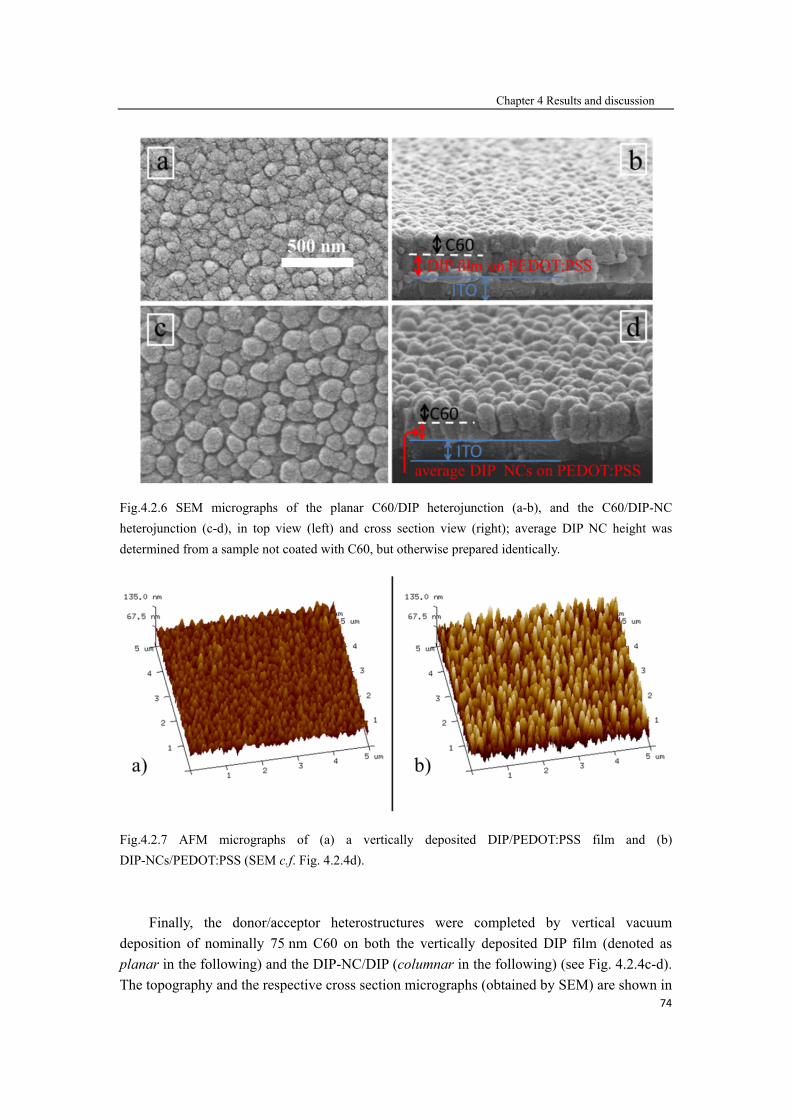
Chapter 4 Results and discussion
74
Fig.4.2.6 SEM micrographs of the planar C60/DIP heterojunction (a-b), and the C60/DIP-NC
heterojunction (c-d), in top view (left) and cross section view (right); average DIP NC height was
determined from a sample not coated with C60, but otherwise prepared identically.
Fig.4.2.7 AFM micrographs of (a) a vertically deposited DIP/PEDOT:PSS film and (b)
DIP-NCs/PEDOT:PSS (SEM c.f. Fig. 4.2.4d).
Finally, the donor/acceptor heterostructures were completed by vertical vacuum
deposition of nominally 75 nm C60 on both the vertically deposited DIP film (denoted as
planar in the following) and the DIP-NC/DIP (columnar in the following) (see Fig. 4.2.4c-d).
The topography and the respective cross section micrographs (obtained by SEM) are shown in

Chapter 4 Results and discussion
75
Fig. 4.2.6a-d. The comparison with the DIP-only samples reveals that fullerene molecules
completely cover the vertically deposited DIP layer (Fig. 4.2.6a-b) and also fully penetrate
into the voids between the NCs (Fig. 4.2.6c-d). For the NCs, this is clearly seen in Fig. 4.2.6d
from the absence of a clear-cut DIP/C60 interface, which is, in contrast, clearly observed in
the cross section view of the bilayer structure (Fig. 4.2.6b). Finally, the AFM micrographs
shown in Fig. 4.2.7 were used to determine the surface-area enlargement factor (ξ) of the
films, which increases from ξ = 1.068 for planar film to ξ = 1.288 for NC structures made by
GLAD. It should be noted that this value represents a lower limit for ξ due to the finite
curvature of the AFM tip.
b. Structure
To assess the microstructure of the samples, grazing-incidence X-ray diffraction
(GIXRD) and specular X-ray diffraction (XRD) are performed Fig.4.2.8a shows GIXRD
in-plane data of C60 on vertically deposited DIP (black curve) compared to C60 on DIP-NCs
(red curve) and two reference scans on DIP-NCs (blue curve) and pristine C60 (black curve),
all deposited on ITO (c.f. Fig. 4.2.2 for respective SEM data). In all cases, DIP is found to
grow crystalline in two different polymorphs with the dominant one denoted as B (“bulk
phase”) and the minor one as B’ in the following. In the corresponding specular XRD scans
(Fig.4.2.9) only one peak series is observed with a (001)-lattice spacing of 1.665 nm, which is
indicative of an almost upright-standing molecular orientation. Via the corresponding
reciprocal space maps (Fig.4.2.9), both observed polymorphs B and B’ are shown to be
significantly different from known crystal structures, that is single-crystal and thin-film
phases [Heinrich, 2007, Lunt, 2009, Dürr, 2002, Kowarik, 2009, Dürr, 2003]. An
unambiguous determination of the unit-cell parameters is impossible in the present case as the
diffraction intensities are smeared out along rings in the reciprocal space maps. However,
combining the GIXRD and specular XRD results, in analogy with known DIP crystal
structures [Heinrich, 2007, Turak, 2011], a monoclinic space-group with a monoclinic angle
of β = 92.4° is assumed. While the in-plane reflections in the q||-range between 1-2 Å-1 due to
DIP molecules in upright orientation are present in all DIP samples, both samples comprising
DIP-NCs show increased (001)- reflection also in GIXRD. This observation is indicative of
additional crystalline grains in a “lying” molecular orientation. Therefore, the vertically
deposited film can be regarded as fiber-textured (“2D-powder”) in that DIP-NCs show a more
“3D-powder like” crystalline property. This can be best observed in the full reciprocal space
maps (Fig.4.2.9) where the DIP related peaks of the NC samples are smeared out significantly
more than those of the vertically deposited film. In contrast to DIP on the smooth substrates
like SiOx,[Kowarik, 2006] such rings are also observed for vertically deposited DIP on ITO,
which is attributed to the higher surface roughness of this substrate that increases the
mosaicity of the adsorbate.
1. GIXRD, XRD measurements and data analysis were led by Dr. Ingo Salzmann.

Fig 4
curv
DIP
recip
depo
phas
and
subs
obse
mole
4.2.8 (a) In-pl
ve) and on 100
NCs (blue c
procal space
osited on bare
ses of DIP (see
on 100 nm D
strates with a
erved. The in
ecules (“λ-pha
lane GIXRD d
0 nm C60 on 1
curve) and 20
maps (Fig. 4
e ITO substrat
e text). (b) Sp
DIP-NCs on a
PEDOT:PSS/
nset is a zoom
ase”) [Kowari
data of nomin
160 nm DIP-N
0 nm C60 (gr
.2.9) by integ
es. Index labe
pecular XRD o
a 10 nm DIP
ITO reference
m of the (00
k, 2006], whi
nally 60 nm C
NCs (red curve
reen curve). T
grating along
els B and B’ in
of nominally 5
underlayer (r
e sample (gre
04) reflection
ch is enhance
C
C60 on 90 nm
e), as well as f
The data was
g qz (range: 0
ndicate the tw
50 nm vertica
red curve), bo
ey curve) with
highlighting
d in the DIP-N
Chapter 4 Resul
vertically dep
for reference s
s extracted fr
0.0 – 0.1 Å-1
wo different ob
ally deposited
oth on PEDOT
h the ITO (222
the contribu
NC sample.
lts and discussio
posited DIP (
samples of 16
rom the respe
1). All films
bserved crysta
DIP (black cu
T:PSS coated
2) and (211) p
ution of lying
on
76
black
60 nm
ective
were
alline
urve),
d ITO
peaks
g DIP

Chapter 4 Results and discussion
77
Fig.4.2.9 Specular X-ray diffraction (XRD) and grazing-incidence X-ray diffraction (GIXRD) data of
the investigated DIP films on bare ITO substrates: (a) XRD data of 60 nm C60 on 90 nm vertically
deposited DIP [GIXRD: (e)], 100 nm C60 on nominally 160 nm thick DIP nanocolumns (DIP-NCs)
established by glancing-angle deposition (GLAD) [GIXRD: (f)], as well as pure reference films of
160 nm DIP-NCs [GIXRD: (d)] and 20 nm C60; peaks labelled with B and B’ relate to the polymorphs
discussed in the text. (b) Indexation of the reflections observed in GIXRD (c-f) from the q|| positions,
the unit-cell parameters of the DIP polymorphs can be estimated.
Finally, the C60 top-layer is found to grow crystalline on both types of DIP underlayers, in
line with previous findings for C60/DIP/SiOx or C60/PEN.[Hinderhofer, 2012a, Salzmann,
2008]
Both for vertically deposited DIP and the DIP-NCs, a similar growth behavior is found
on PEDOT:PSS coated ITO substrates, as demonstrated by the XRD data depicted in
Figure 4.2.8b. Once again, the DIP (00l)-series with an identical lattice spacing of 1.66 nm is
recovered, but in contrast to bare ITO substrates, now up to higher order owing to the lower
surface roughness of the polymer coating. At 1.47 Å-1 an additional reflection is observed
related to lying DIP, which was denoted as λ-phase in previous studies [Kowarik, 2006].
Compared to the vertically deposited DIP film with a peak ratio of 9:1 (area) between the
(004) and the λ-phase peak, this ratio changes to almost 1:1 for DIP NCs (see inset in Fig.

Chapter 4 Results and discussion
78
4.2.8b), thus, clearly indicating as seen in the above data on the pristine ITO substrates - an
increase of the lying DIP fraction in the samples grown by GLAD.
4.2.3 Analysis of OPVCs
a. DIP column/C60
These structures are now used in OPVCs in order to assess the impact of NCs on device
performance. Unlike PEN nanocolumn structure, the valley volume of DIP column on ITO
substrate is larger and thus very difficult to build working OPVCs (all devices showed short
circuit) based on bare DIP column on ITO, even with BCP blocking layer. Therefore, in the
following all nanocolumn structures used to fabricate OPVCs were built on PEDOT:PSS
coated ITO substrate. OPVCs of planar and NC form, both capped with a 6.5 nm BCP layer
followed by a 100 nm Sm top-electrode are compared in Fig.4.2.10. The beneficial role of
BCP in such device structures has been extensively investigated and attributed to the
protection of the active layer during metal deposition.[Gommans, 2008, Vogel, 2006a] The
J-V characteristics of both devices were recorded under 25 mW/cm2 illumination from a
halogen lamp in a vacuum. The results are shown in Fig. 4.2.11a with the corresponding key
parameters summarized in Table 4.2. While the open circuit voltages ( ) of both OPVCs are
almost identical (ca. 0.8 V), the short circuit current ( ) under illumination is almost 20%
higher in the NC-based OPVCs. Furthermore, the decrease in the current density is less
pronounced in the fourth quadrant for the NC devices. This is related to the series resistance
( ) which is lower by more than one order of magnitude and further explains the higher fill
factor (FF).[Sze, 1981] The much smaller Rs is associated for the NC-based OPVCs to closed
pathways within the active donor/acceptor layer. Moreover, the higher FF is further related to
the lower ideality factor (n) of the NC-OPVCs (n = 1.1) as compared to that of the bilayer
OPVCs (n = 6.4). These values were deduced from the slope of the logarithmically
represented J-V characteristics in the exponential regime (in Fig. 4.2.11b) based on the
non-ideality diode equation:[Sze, 1981]
Fig.4.2.10 Scheme of the OPVC structures used; left: conventional bilayer OPVC, right: OPVC with
DIP-NCs.

Chapter 4 Results and discussion
79
(4.1)
where is the saturation current density, n the diode ideality factor, k Boltzmann’s constant
and T the temperature.
Fig.4.2.11 (a) J-V characteristics of bilayer and DIP-NC based OPVCs. Black closed/open square
symbols: bilayer device in dark/illuminated (25 mW/cm2) in vacuum and blue closed/open triangle
symbols: DIP-NC based device in dark/illuminated (25 mW/cm2) in vacuum. (b) J-V curves in dark in
logarithmic representation. The red line and green line are the slopes of current in exponential region.

enca
simu
perf
whic
Fig.4
to am
Tabl
plan
the s
exter
pla
col
2.
To assess th
apsulation, re
ulated AM
formance of
ch well docu
4.2.12 Compa
mbient air dem
e 4.2: Key pa
ar denotes th
short-circuit c
rnal power-co
Voc
anar 0
lumn 0
The DIP nan
Berlin, and
evaporation.
conditions o
he influence
eference OPV
1.5 illumi
the air-expo
uments the st
arison of OPV
monstrating ne
arameters of
e bilayer OPV
current, FF th
onversion effic
c (V) Js
0.79
0.77
nocolumns st
d transferred
. The J-V p
of simulated A
e of air expo
VCs were fa
ination at
osed OPVCs
tability of the
VC characteris
egligible degra
OPVC perfor
VC, column th
he fill factor, R
ciency under 2
sc (mA/cm2)
1.05
1.25
tructures we
d to Univer
performance
AM 1.5 illum
sure, e.g., du
abricated and
100 mW/cm
s, almost id
e DIP-NCs a
stics of bilayer
adation under
rmance, as de
he DIP-NC ba
RS the serial r
25 mW/cm2 il
FF
0.43
0.48
ere fabricated
rsität Augsb
of OPVCs
mination at 1
C
ue to sample
d characterize
m2 (Fig. 4.2
entical J-V
against (short
r devices mea
r 100 mW/cm2
educed from t
ased device; V
resistance, Rsh
llumination (h
Rs(Ω) R
6100
260
d with GLAD
burg for C6
was measu
00 mW/cm2
Chapter 4 Resul
e transfer thr
ed in-situ un
2.12).2 Com
characteristi
t) ambient ex
asured in-situ 2 illumination.
the J-V curve
VOC the open-c
h the shunt res
halogen lamp)
Rsh(MΩ)
0.34 1
0.17 1
D at Humbol
60, BCP an
ured in glov
.
lts and discussio
rough air or
nder conditio
mpared with
ics are obser
xposure.
and after exp
.
es (c.f. Fig 4.2
circuit voltag
sistance, and
in vacuum.
1.4% 0.05%
1.8% 0.05%
ldt Universit
nd top elect
vebox (N2 fi
on
80
poor
ns of
the
rved,
osure
2.11);
e, JSC
η the
%
%
tät zu
trode
illed)

Fig.4
depo
unde
(blac
from
the
On
unde
abso
were
of D
equa
show
sam
4.2.13 (a) UV-
osited DIP/PE
erlayer on PE
ck curve), 20
m the substrate
Since the D
absorption c
average, a 5
erlayer plus
orption spect
e fully dissol
DIP containe
als that of a
wing a comp
mple exhibits
V-VIS absorpti
EDOT:PSS, a
EDOT:PSS (bl
nm sample (r
e in equal amo
DIP structure
characteristic
50 nm plana
100 nm colu
tra cannot be
lved in a def
ed therein. It
a 20 nm thic
parison of th
s a significa
on spectra of
and that of 1
lue dash curv
red dash curv
ount of solvent
and molecul
cs of DIP of
ar film absor
umns), but cl
e directly co
fined volume
t was found
ck DIP film
he respectiv
antly higher
50 nm (black
00 nm DIP-N
ve). (b) UV-V
ve) and the N
t and measure
lar orientatio
f correspondi
rbs 1.5 more
learly, due to
ompared. The
e of 1,2-dichl
d that the vo
m fabricated
ve solution s
r absorbance
C
curve) and 20
NCs on a ve
VIS absorption
C-based samp
ed in solution.
on varied bet
ing samples
e photons th
o the inheren
erefore, indiv
lorobenezene
olume of DIP
by vertical
spectra. Thu
e than the
Chapter 4 Resul
0 nm (red poin
ertically depo
n spectra of t
ple (blue poin
ween planar
are compare
han the NC s
nt structural
vidual samp
e to measure
P present in
deposition w
s it is appar
vertically d
lts and discussio
nt curve) verti
osited 10 nm
the 50 nm sa
nt curve) disso
r and NC dev
ed in Fig. 4.
structure (10
differences,
ples of both t
e the total am
n the NC-OP
with Fig. 4.2
rent that the
deposited sam
on
81
ically
m DIP
ample
olved
vices,
2.13.
0 nm
their
types
mount
PVCs
2.13b
e NC
mple

Chapter 4 Results and discussion
82
(normalized to the number of molecules present in each sample). This finding can be
understood by the different molecular orientation of DIP in the planar film and in NCs. Planar
films comprise a fiber-textured with a preferential vertical molecular orientation
(“2D-powder”), while the NCs exhibit significantly less-textured growth (more “3D-powder
like”) and a substantial fraction of "lying" molecules. As the absorption is dominated by the
fundamental HOMO-LUMO transition (c.f. in Fig. 4.2.13b), which is polarized along the long
molecular axis of DIP, this transition is less efficiently excited in the vertically deposited film
than in the DIP-NCs.[Heinemeyer, 2008a]
Overall, with less DIP molecules (by a factor of 0.4, as deduced from UV-VIS) and,
therefore, lower total absorption by DIP NCs (c.f. Fig. 4.2.13a), the power conversion
efficiency (η) of NC-OPVC reaches 1.8 %, significantly larger than that of the stronger
absorbing planar structure (bilayer OPVC, η = 1.4 %) as listed in Table 4.2 (Note: The same
measurement conditions are utilized for both structures without using the solar simulator.
Without spectral corrections the efficiency is in the range as reported in the literature for
similar devices [Steindamm, 2012, Gruber, 2013, Schuenemann, 2013]). In comparison to the
bilayer OPVCs, more photo-generated excitons in NC-OPVCs can reach the donor/acceptor
interface for dissociation. This is due to the increase of the active interface area in the NC
heterojunction by ca. 20% compared to the planar heterojunction. This is less than the overall
efficiency increase of almost 30%, therefore, another mechanism may contribute beneficially.
The intrinsic vertical distribution of the donor/acceptor interface introduced through the NCs
covers a wider range of high optical intensity, which may be generated by interference effects
through reflection at the back electrode [Gruber, 2013, Kurrle, 2008, Opitz, 2010b, Stübinger,
2001, Peumans, 2003b]. As a result the impact of comparably short exciton diffusion length
reduces in C60 when employing a thicker film. Moreover, the lying phases may positively
influence Jsc and FF, but due to the unknown spatial distribution of the two DIP orientations
the contribution cannot be quantified.
b. DIP column/PCBM
In addition, PCBM was also tested as the electron acceptor material, spin coated on to
DIP nanocolumn as electron donor using exact same method for PEN/PCBM OPVCs. The
concentration of 25 mg/ml PCBM was spin coated at 20 rps onto DIP column structure in the
glovebox (sometimes DIP column was annealed with 80 for 10 minutes before PCBM
spin coating). However, this solution process did not proceed as expected since the solvent
chlorobenzene that was used to dissolve PCBM also could dissolve DIP molecules. Thus in
the process of PCBM solution spin coating, DIP columnar structure was ruined due to
re-dissolving (c.f. Fig. 4.2.14).

Fig.
chlor
roun
Fig.
PCB
disso
lowe
the
NCs
by t
4.2.14 SEM
robenzen solv
nds per second
4.2.15 SEM
BM layer on D
To bypass
olve PCBM
er than that
SEM images
s succeeded i
the thin PCB
M micrographs
vent were spi
d (rps) and for
micrographs o
DIP NCs; (c-d)
the re-disso
instead of ch
in chloroben
s (Fig. 4.2.1
in the infiltra
BM film thic
s of re-dissol
in-coated onto
r (b) 30 s at 10
of PCBM on
) top and cross
olving probl
hlorobenzen
nzene, 15 m
5a-b), low c
ation of NCs
ckness since
lving DIP fil
o DIP column
0 rps and after
top of DIP N
s-section view
lem, the oth
ne. The solub
mg/ml. From
concentration
s structure. In
e it was unab
C
lm by chloro
n prepared w
rwards anneale
NCs. (a-b) Top
w of thick PCB
her solvent
bility of PCB
m the top-vie
n (6 mg/ml)
n addition co
ble to fulfill
Chapter 4 Resul
benzen solve
with GLAD (a
ed at 120 .
p and cross-se
BM layer on D
chlorometha
BM in chlorom
ew and cross
PCBM spin-
orrugated top
the valleys.
lts and discussio
ent. Two drop
a) for 1 min
ection view o
DIP NCs.
ane was use
methane is m
s-section vie
-coated onto
pography wa
. When usin
on
83
ps of
at 25
f thin
ed to
much
ew of
o DIP
as led
ng 12

Chapter 4 Results and discussion
84
by the thin PCBM film thickness since it was unable to fulfill the valleys. When using 12
mg/ml PCBM solution for spin coating, the surface is rather flat as shown in Fig. 4.2.15 c-d.
The OPVCs were fabricated by depositing BCP and Sm on top subsequently. The J-V
characteristics were recorded under 25 mW/cm2 illumination from a halogen lamp in vacuum
with the results shown in Fig. 4.2.16. From the trends it can be seen that the Jsc is 0.61
mA/cm2 and Voc is 0.56 V and they are both smaller than those of DIP/C60 devices, as well as
the fill factor, consequently the PCE of the devices is lower. Moreover, the device
reproducibility is poor due in part to the uncontrollability of PCBM solution spin coating. Due
to the limitation of PCBM solubility in new solvent chloromethane (12mg/ml), this results in
an inhomogeneous PCBM layer thickness on top of NCs.
In total, using chloromethane as solvent to bypass the re-dissolve issue is incapable of
optimizing the performance of OPVCs with this solution process until an appropriate solvent
with solubility for PCBM larger than 20 mg/ml is identified. However the solubility for DIP
extremely must be low so that the DIP columnar structure can survive the solution spin coat
process similar to the devices consisting of PEN/PCBM.
Fig.4.2.16 J-V characteristics of OPVCs based on DIP NCs/PCBM heterojunction.
c. DIP on graphene3
Lying phase DIP is a promising material towards improving the light absorption when
was applied to OPVCs for electron donor. In this section the morphology and absorption
behavior of lying DIP on graphene substrate will briefly be discussed.
3. Graphene coated substrates were provided by the group of Prof. Müllen (Max Planck
Institute for Polymer Research). Graphene that was grown using the chemical vapor
deposition method was transferred to patterned ITO substrates to act as the anode.
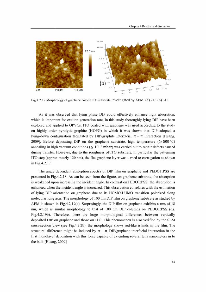
Fig.4
whic
expl
on h
lying
2009
anne
duri
ITO
in F
pres
is w
enha
of ly
mole
AFM
nm,
Fig.
depo
cros
struc
first
the b
4.2.17 Morpho
As it was
ch is importa
lored and ap
highly order
g-down con
9]. Before
ealing in hig
ing transfer.
O step (approx
ig.4.2.17.
The angle
sented in Fig
weakened upo
anced when t
ying DIP or
ecular long a
M is shown i
which is s
4.2.19b). T
osited DIP o
ss-section vie
ctural differe
t monolayer
bulk.[Huang
ology of graph
observed th
ant for excit
pplied to OPV
r pyrolytic g
nfiguration fa
depositing D
gh vacuum co
However, du
ximately 120
dependent a
g.4.2.18. As c
on increasing
the incident
rientation on
axis. The mo
in Fig.4.2.19
imilar morp
Therefore, th
on graphene a
ew (see Fig.
ence might b
deposition w
g, 2009]
hene coated IT
hat lying pha
ton generatio
VCs. ITO co
graphite (HO
acilitated by
DIP on the
onditions (
ue to the rou
0 nm), the fla
bsorption sp
can be seen f
g the inciden
angle is incr
n graphene d
orphology of
9(a). Surprisi
phology to t
here are hu
and those on
4.2.2b), the
be induced b
with this forc
TO substrate i
ase DIP cou
on rate, in th
oated with g
OPG) in wh
y DIP/graphi
graphene s
10 mbar
ughness of IT
at graphene
pectra of DIP
from the figu
nt angle. In c
reased. This o
due to its H
f 100 nm DIP
ingly, the DI
that of 100
uge morpho
n ITO. This p
morphology
by π π D
ce capable of
C
investigated
uld effective
his study thor
raphene was
hich it was
ite interfacia
substrate, hi
r) was carried
TO substrate
layer was tu
P film on gr
ure, on graph
ontrast on PE
observation c
HOMO-LUM
P film on gra
IP film on g
nm DIP co
ological diff
phenomenon
y shows rod-
IP/graphene
f extending s
Chapter 4 Resul
by AFM. (a)
ly enhance
roughly lyin
s used accord
shown that
al π π inte
igh tempera
d out to repa
e, in particul
rned to corru
raphene and
hene substrat
EDOT:PSS,
correlates wi
O transition
phene substr
raphene exh
olumns on P
ferences bet
n is also veri
-like islands
interfacial i
several tens
lts and discussio
) 2D; (b) 3D
light absorp
ng DIP have
ding to the s
t DIP adopt
eraction [Hu
ature ( 500
air defects ca
lar the patter
ugation as sh
PEDOT:PSS
te, the absorp
the absorpti
ith the estim
n polarized a
rate as studie
hibits a rms o
PEDOT:PSS
tween verti
ified by the S
in the film.
interaction in
nanometers
on
85
.
ption,
been
study
ted a
uang,
0 )
aused
rning
hown
S are
ption
on is
ation
along
ed by
of 18
(c.f.
cally
SEM
The
n the
in to

Chapter 4 Results and discussion
86
Fig.4.2.18 (a) Angle dependent absorption spectra of vertically deposited DIP film on a graphene
substrate. (b) Angle dependent absorption spectra of vertically deposited DIP on PEDOT:PSS. The film
thickness monitored with quartz microbalance for both samples is 50 nm. The incident angle is defined
by the angle between incident light and the substrate surface normal.
Fig.4.2.19 Morphology of DIP on graphene substrate with vertical deposition (a) and on
PEDOT:PSS substrate with GLAD (b). Both were investigated by AFM measurements.

Chapter 4 Results and discussion
87
Fig.4.2.20 Morphology of DIP film on graphene substrate with vertical deposition,
investigated by SEM. (a) Top-view. (b) Cross-section view.
OPVCs were fabricated based on the rod-like DIP film, employing C60 as electron
acceptor, BCP as blocking layer and Sm as top electrode. However, no working OPVCs could
be obtained, even without diode characteristics, due to current short-pass between the two
electrodes as when using pentacene on ITO to fabricate OPVCs (see section 4.1). Although
the application of graphene in OPVCs combined with lying DIP was unsuccessful, tuning
molecular orientation may still be a very efficient method to optimize the performance of
OPVCs via improving the active organic layers’ absorption. Furthermore, graphene was
assumed to be a very promising candidate for replacing the ITO as the electrode for organic
optoelectronic devices in the future, if the conductivity of grapheme could be further
increased.
4.2.4 Summary
The morphology and structure of crystalline DIP nanocolumns grown by GLAD on
pristine and PEDOT:PSS coated ITO substrates has been demonstrated and such structures
applied in OPVCs. Despite the fact that the DIP volume in NC-based OPVCs was less than
one half of that in planar heterojunctions (with also an overall lower absorption by the NCs),
the power-conversion efficiency of the solar cells increased from 1.4% (planar) to 1.8%
through using DIP-NCs in the active layer. This noteworthy finding is explained as follows. (i)
An increase of active interface area between DIP-NCs and the surrounding C60 acceptors
which improves charge-carrier generation through exciton dissociation at that interface. (ii) A
more random orientation of crystalline DIP grains in the NCs enhances light absorption in
comparison to the fiber-textured, upright standing DIP in vertically deposited films. (iii) The
vertically oriented donor/acceptor interface enabled by the NCs is further beneficial for light
absorption, since it covers a wider vertical range, and light intensity variations due to
interference effects can be accommodated. Further investigation of the contribution of
molecular orientation on light absorption for OPVCs was carried out by growing lying DIP on
a graphene substrate. Unfortunately, due to the short current induced by the morphology
issues of lying DIP on graphene, no working OPVCs were produced. The development of a
process for the preparation of a smoother lying DIP on graphene is certainly a worthwhile
direction for future investigations. Nevertheless, the present work underlines the key role of

Chapter 4 Results and discussion
88
structure and morphology in OPVCs and demonstrates that their targeted optimization by
glancing angle deposition offers good perspectives for pushing further the limits of organic
photovoltaics in future applications.
4.2.5 Experimental details
ITO coated glass substrates (Präzisions Glas & Optik, sheet resistance < 20 Ω/sq, surface
roughness (rms): 2 nm) were sonicated for 10 min in acetone and, subsequently then, in
isopropanol. After cleanness, ITO coated substrates were also patterned for devices
fabrication as described in section 4.1.11. UV-ozone-treatment was applied to improve the
wetting of the substrate by an aqueous suspension of the intrinsically conducting polymer
poly(ethylene-dioxythiophene): poly(styrenesulfonate) (PEDOT:PSS) (H.C. Starck GmbH,
HIL 1.3) employed as substrate for OPVCs. PEDOT:PSS was spin-coated and subsequently
annealed at 200 for 5 min under ambient conditions to desorb residual water. DIP was
purified twice by gradient sublimation. NCs were grown by GLAD, the material sublimed
from a resistively heated ceramic crucible with a deposition rate of ca. 0.1 nm/s (quartz
crystal microbalance, base pressure < 5×10⁻⁷ mbar) at room temperature. The incident angle
of the molecular flux () with respect to the substrate surface normal was set to 84o (c.f.
Fig. 4.2.1) and the substrate rotation frequency () was 6 revolutions per minute
(computer-controlled step-motor). OPVCs were completed with a 75 nm thick C60 (99.9%,
Sigma-Aldrich) layer deposited at a rate of 0.02 nm/s on the DIP films/NCs in another
vacuum chamber (base pressure < 2×10⁻⁸ mbar). Sample transfer between the chambers was
done through ambient conditions. A 6.5 nm thick bathocuproine (BCP, 96%, Sigma-Aldrich)
layer was deposited onto the donor/acceptor structure followed by a 100 nm thick samarium
(Sm) layer that was used as the cathode. The current density versus voltage (J-V)
characteristics were measured in-situ in dark and under illumination (25 mW/cm2, Solux C6
halogen lamp, close to daylight spectrum in the visible region) with a Keithley 2400
SourceMeter®. (Device performance measurement system is same as description in section
4.1) The sample morphology was investigated with a Bruker Multimode-8 atomic force
microscope (AFM) and a HITACHI S-4100 field-emission scanning electron microscope
(SEM), using the latter after sputter-coating the samples with a thin gold layer to avoid
sample charging. Optical absorption spectra (UV-VIS) were recorded with a PerkinElmer
Lambda 900 spectrometer. X-ray diffraction experiments were carried out in inert (He)
atmosphere at beamline W1 at the synchrotron radiation source HASYLAB (DESY, Germany)
using a primary beam energy of 10.5 keV and a one-dimensional position sensitive detector
(Mythen 1K, Dectris) mounted in the z-direction covering a range of out-of-plane scattering
angles of ca. 3.8°. For grazing-incidence diffraction, five scans at fixed out-of-plane position
were performed for every reciprocal space map [Salzmann, 2012b]. Specular X-ray
diffraction (XRD) on the PEDOT:PSS-substrate samples was performed with a Philips X’Pert
system in Bragg-Berntano geometry (sealed Cr-tube, secondary HOPG monochromator).
Graphene annealing processing was carried out under high vacuum conditions (base pressure

Chapter 4 Results and discussion
89
< 10-7 mbar) and heated up to 500 on the ceramic covered hot plane at least for one hour
and cooled down automatically until it reached the ambient temperature.

Chapter 4 Results and discussion
90
4.3 F4-TCNQ doping in polyfuran
In this section of the thesis, the characteristics of molecular doped polymeric
semiconductor will be investigated. F4-TCNQ as a p-type dopant is mixed with polyfuran and
applied in the fabrication of organic photovoltaic cells combining with C60 as electron
acceptor. In this section attention will be drawn to the definition of the doping ratios used in
this work. For example, 1% doping refers to the addition of one F4-TCNQ molecule per 100
monomer units (see section 3.2) of polyfuran.
4.3.1 Introduction
For several decades, organic photovoltaic cells (OPVCs) have been extensively
investigated owing to the advantage of low-cost and simplicity of large-scale processing.
[Tang, 1986, Tang, 1975, Ramsdale, 2002, Koster, 2005, Snaith, 2006, Geiser, 2008,
Jørgensen, 2008, Søndergaard, 2013, You, 2013a, You, 2013b] Basic strategies used to
improve the power conversion efficiency are available. For example, the short-circuit current
density (Jsc) may be enhanced by increasing light absorption by using low band gap
polymers[Bundgaard, 2007] or by optimization of blend film morphology [Thompson, 2008].
Another approach towards improving power conversion efficiency is to the increase the
open-circuit voltage (Voc) via maximizing the photovoltaic gap (Epvg), which is the energetic
difference between the valence band onset (VB-onset) of the donor polymer and the onset of
the LUMO of the acceptor molecule at the heterojunction.[Wilke, 2012] One material
parameter that influences both Jsc and Voc in OPVCs is the hole and electron mobility of the
donor and acceptor material respectively. A mobility that is too large can be detrimental for
the device performance as seen in a decrease in Voc.[Tress, 2011b] On the other hand Jsc is
limited by the mobility of the slowest carriers when the photo current is space charge limited.
As most polymer/fullerene based OPVCs suffer from low hole mobility in polymers in
comparison to the high electron mobility in the fullerene[Tunc, 2012, Melzer, 2004, Koster,
2005], balanced mobilities are required for high efficiency. To increase the hole mobility in
the polymer, electrical doping can be applied by introducing dopants such as F4TCNQ into
polymer films.
Doping organic semiconductors, which is one of the most effective methods of
improving the characteristics of organic electronic devices, is selected in order to obtain
analogous benefits as for doping in inorganic semiconductors, which has been well proved
and explained theoretically and experimentally. Doping inorganic semiconductors enables the
precise adjustment of band positions and improvement of conductivity, thus tuning the optical
and electrical properties. In principle, the doping mechanism of organic semiconductors
(OSCs) is similar to those in inorganic semiconductors where holes are generated by
removing electrons in the highest occupied orbital states or donating electrons in the lowest
unoccupied orbital states through ionization of the dopant. Recently, stable doping of OSCs

Chapter 4 Results and discussion
91
has been demonstrated by adding strong molecular dopants to conjugated polymers or small
molecules. Consequently the conductivity of doped film increases by several orders of
magnitude and can be used as charge transport layers in organic light emitting diodes and
organic photovoltaic cells (OPVCs). [Lüssem, 2013, Brutting, 2012, Blochwitz, 1998, Zhou,
2002, Meerheim, 2006, Reineke, 2009] [Sun, 2009, Salzmann, 2012a, Lüssem, 2013, Pingel,
2013, Mendez, 2013, Duong, 2013, Mityashin, 2012] In the case of poly(3-hexyl -thiophene)
(P3HT) for high doping ratios [>1% (F4TCNQ:thiophene units)], the mobility, and therefore
the conductivity, increases linear [Pingel, 2012, Pingel, 2013]. In addition, for concentrations
<2% (F4TCNQ: thiophene units), p-type dopant molecules reduce the interfacial
recombination via charge transfer excitons and results in the favorable formation of separated
carriers[Deschler, 2011].
In this section, the effect of p-type electrical doping of polyfuran on the performance of a
bilayer heterojunction OPVCs with C60 as acceptor material is presented. To analyze the
doping effect, the absorption characteristics, conductivity and morphology of polyfuran thin
film with different F4-TCNQ doping ratio were investigated. As expected for high dopant
concentrations (still lower than 2%) Jsc significantly increased. For even higher concentrations
such as an over doped system (up to 40%), unexpectedly Voc significantly increased and Jsc
was just slightly higher in comparison to the undoped system. Ultra violet photoelectron
spectroscopy (UPS) data showed an increase in the photovoltaic gap, a finding that supports
the predicted increase of Voc at very high dopant concentrations. In addition, the effect of high
doping concentration (1%) polyfuran treated as the hole transport layer was investigated in
combination with ZnPc as the electron donor and C60 as the electron acceptor.
4.3.2 Absorption, morphology and conductivity
a. Absorption
The normalized UV-Vis absorption spectra of F4-TCNQ doped polyfuran thin films with
varied doping ratios starting with pristine polyfuran until 100% F4-TCNQ doped polyfuran,
i.e. on quartz substrates is depicted in Fig.4.3.1. As indicated by the absorption onset of
pristine PF, the optical gap is determined to be 2.30 eV which is remarkably close to the
theoretically predicted value of 2.38 eV.[Zade, 2006] Upon doping, pronounced sub-band gap
absorption features develop in addition to the absorption of pristine polyfuran. A qualitative
comparison of the NIR region to the known spectra of ionized F4-TCNQ anions [Torrance,
1980, Dixon, 1989] allows a clear identification of the prominent 1.43 and 1.62 eV peaks for
the absorption of singly negatively charged F4-TCNQ (Fig.4.3.2a). Due to the scattering
effect induced by inhomogeneous morphology (Fig.4.3.3), the second ionic peak at 1.62 eV
could not be observed on the sample of pristine F4-TCNQ film, but was observed in solvent
as shown in Fig.4.3.2b. The broad absorption bands between 1.3 and 1.8 eV and the
absorption below 1.1 eV can be attributed to polyfuran polarons similar to P3HT. [Pingel,
2013] For very high doping concentrations the absorption above 3 eV is also enhanced due to
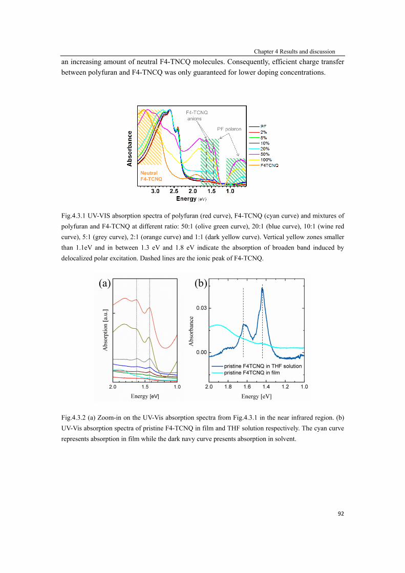
Chapter 4 Results and discussion
92
an increasing amount of neutral F4-TNCQ molecules. Consequently, efficient charge transfer
between polyfuran and F4-TNCQ was only guaranteed for lower doping concentrations.
Fig.4.3.1 UV-VIS absorption spectra of polyfuran (red curve), F4-TCNQ (cyan curve) and mixtures of
polyfuran and F4-TCNQ at different ratio: 50:1 (olive green curve), 20:1 (blue curve), 10:1 (wine red
curve), 5:1 (grey curve), 2:1 (orange curve) and 1:1 (dark yellow curve). Vertical yellow zones smaller
than 1.1eV and in between 1.3 eV and 1.8 eV indicate the absorption of broaden band induced by
delocalized polar excitation. Dashed lines are the ionic peak of F4-TCNQ.
Fig.4.3.2 (a) Zoom-in on the UV-Vis absorption spectra from Fig.4.3.1 in the near infrared region. (b)
UV-Vis absorption spectra of pristine F4-TCNQ in film and THF solution respectively. The cyan curve
represents absorption in film while the dark navy curve presents absorption in solvent.
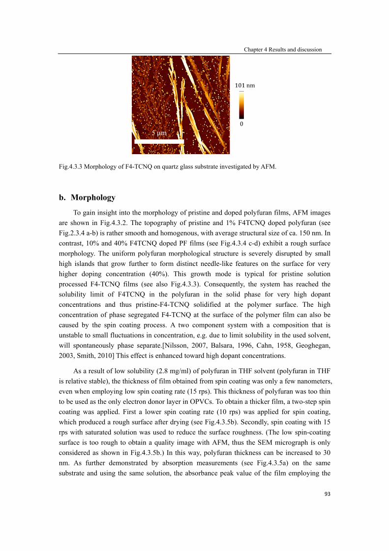
Chapter 4 Results and discussion
93
Fig.4.3.3 Morphology of F4-TCNQ on quartz glass substrate investigated by AFM.
b. Morphology
To gain insight into the morphology of pristine and doped polyfuran films, AFM images
are shown in Fig.4.3.2. The topography of pristine and 1% F4TCNQ doped polyfuran (see
Fig.2.3.4 a-b) is rather smooth and homogenous, with average structural size of ca. 150 nm. In
contrast, 10% and 40% F4TCNQ doped PF films (see Fig.4.3.4 c-d) exhibit a rough surface
morphology. The uniform polyfuran morphological structure is severely disrupted by small
high islands that grow further to form distinct needle-like features on the surface for very
higher doping concentration (40%). This growth mode is typical for pristine solution
processed F4-TCNQ films (see also Fig.4.3.3). Consequently, the system has reached the
solubility limit of F4TCNQ in the polyfuran in the solid phase for very high dopant
concentrations and thus pristine-F4-TCNQ solidified at the polymer surface. The high
concentration of phase segregated F4-TCNQ at the surface of the polymer film can also be
caused by the spin coating process. A two component system with a composition that is
unstable to small fluctuations in concentration, e.g. due to limit solubility in the used solvent,
will spontaneously phase separate.[Nilsson, 2007, Balsara, 1996, Cahn, 1958, Geoghegan,
2003, Smith, 2010] This effect is enhanced toward high dopant concentrations.
As a result of low solubility (2.8 mg/ml) of polyfuran in THF solvent (polyfuran in THF
is relative stable), the thickness of film obtained from spin coating was only a few nanometers,
even when employing low spin coating rate (15 rps). This thickness of polyfuran was too thin
to be used as the only electron donor layer in OPVCs. To obtain a thicker film, a two-step spin
coating was applied. First a lower spin coating rate (10 rps) was applied for spin coating,
which produced a rough surface after drying (see Fig.4.3.5b). Secondly, spin coating with 15
rps with saturated solution was used to reduce the surface roughness. (The low spin-coating
surface is too rough to obtain a quality image with AFM, thus the SEM micrograph is only
considered as shown in Fig.4.3.5b.) In this way, polyfuran thickness can be increased to 30
nm. As further demonstrated by absorption measurements (see Fig.4.3.5a) on the same
substrate and using the same solution, the absorbance peak value of the film employing the

Chapter 4 Results and discussion
94
two spin-coating procedure is much larger than that of the film obtained with a single
spin-coating.
Fig.4.3.4 AFM micrographs of (a) spin coated pristine polyfuran/PEDOT:PSS film, (b)
F4-TCNQ:polyfuran (1:100) mixture/PEDOT:PSS, (c) F4-TCNQ:polyfuran (1:10)
mixture/PEDOT:PSS and (d) F4-TCNQ:polyfuran (2:5) mixture/PEDOT:PSS.
Conductivity
Fig.4.3.6 shows the conductivity of doped polyfuran films with a film thickness of 30 nm.
Similar to the prototypical case of F4-TCNQ doped P3HT the conductivity increased rapidly
for low doping ratios (lower than 2%). In this region it has been shown for P3HT that both the
mobility and the density of states (DOS) drastically increases with doping
concentration.[Pingel, 2013, Arkhipov, 2005b] The improvement in transport has also been
attributed to the filling of traps by the dopant-induced carriers [Mendez, 2013, Olthof, 2012,
Salzmann, 2012a, Gao, 2003, Gao, 2001, Pingel, 2013]. Beyond a doping ratio of 2%, the
conductivity decreased and is likely due to the morphological changes determined by the
AFM results. Due to the formation of intercalated areas of pristine F4-TCNQ, charge transfer
might be significantly impeded. Note that polyfuran films are amorphous.[Gok, 2005, Sen,

Chapter 4 Results and discussion
95
2008] Consequently, a decrease in crystallinity did not decrease the conductivity. However, at
the moment it is impossible to exclude improved ordering in the films with low dopant
concentration as observed for poly(p-phenylenevinylene) blended with fullerene
derivatives.[He, 2007, Melzer, 2004]
Fig.4.3.5 (a) Absorption spectra of polyfuran film on ITO substrate; black line is a single spin coating
film (15 rps) and the red line is twice spin coating film (first: 10 rps; second: 15 rps). (b) SEM
micrograph of rough polyfuran surface obtained with low spin-coating rate of 10 rps.
Fig.4.3.6 Conductivity of polyfuran films with an increasing amount of dopant F4-TCNQ. Inset:
schematic representation of conductivity measurement using interdigitated electrodes of ITO on glass
substrates with an organic film shown in semitransparent yellow.

Chapter 4 Results and discussion
96
4.3.3 Analysis of OPVCs
a. polyfuran/C60
Bilayer heterojunction organic photovoltaic devices were fabricated using 50 nm C60 as
the acceptor deposited on doped and undoped spin coated polyfuran films (base pressure 10-8
mbar). 6 nm BCP acting as a blocking layer and aluminum as the top electrode was deposited
after C60. The device structure is presented in Fig.4.3.7. Fig.4.3.9(a) shows the logarithmic
dark performance of pristine (device A), 1% doping (device B), 10% doping (device C) and
40% doping (device D) respectively. Again, based on the non-ideality diode equation
(equation 4.1), the series resistance can be deduced from the slope of the logarithmically
represented J-V characteristics in the exponential regime. For device A, B and C the series
resistance are 270 Ω, 40 Ω and 340 Ω respectively. Unfortunately, it is impossible to measure
the Rs for device D due to the presence of current leak. Benefiting from an increase in the
conductivity, device B exhibits the lowest Rs, following Pouillet’s Law
R (4.2)
where is conductivity of the film, l is the active organic layer thickness and S is the active
device area.
The short circuit current density (Jsc) (obtained under the illumination of 56 mW/cm2)
using pure polyfuran was quite low compared to state of the art polymer/PCBM
devices.[Green, 2014] Nevertheless, 1% doping increased Jsc by a factor of two compared to
the undoped polyfuran film as a result of the improved conductivity in the polymer while
keeping the open circuit voltage (Voc) at 0.2 V. However, higher dopant concentrations
increased Jsc only by 30 % in comparison to the device with undoped polyfuran film, which
correlates with the trend of the conductivity upon very high doping ratios. For dopant
concentrations above 1% the Voc increased by up to 0.39 V (at 40% dopant concentration). In
order to understand this Voc increase, the energy level alignment at the heterojunction was
investigated using UPS measurements. As mentioned before, Epvg is clearly related to Voc (Epvg
is an upper bound to Voc)[Vandewal, 2009, Wilke, 2012]. As shown in Fig. 4.3.10a within the
experimental error (50 meV) vacuum level (VL) alignment is established for the undoped
system. The polyfuran VB-onset is located 0.40 eV below the substrate Fermi level (EF) as
shown in Fig.4.3.8. The ionization energy of HIL1.3 substrate is 5.60 eV. After depositing
polyfuran on the substrate, in order to reach electronic equilibrium, the electrons were
injected to the substrate from polyfuran film. This was done until the Fermi-level pinning was
reached and the valence band onset was observed at 0.40 eV lower than the substrate
Fermi-level, thus yielding an ionization energy of 4.8 eV.

Chapter 4 Results and discussion
97
Fig. 4.3.7 Schematic representation of OPVCs structure.
Fig.4.3.9 (a) J-V characteristics of OPVCs based on different dopant F4-TCNQ in dark in logarithmic
representation. Black closed square symbols: pristine polyfuran, red dot symbols: 1% doping, blue
up-triangle symbols: 10% doping and green down-triangle symbols: 40% doping. (b) J-V curve under
illumination (56 mW/cm2) in air. The device structure is shown in the inset and in the device from
bottom to top the layers are glass/ITO/PEDOT:PSS/polyfuran (doped)/C60/BCP/Al.

Chapter 4 Results and discussion
98
However, the actual pinning level in the tail of the VB-onset could not ascertained from the
UPS spectra due to extremely low density of states (DOS) in this energy range [Frisch, 2011,
Hwang, 2009]. However, the VB-onset of F4-TCNQ doped polyfuran shifted to higher
binding energy (BE) by 0.20 eV, mainly caused by an increased DOS and energetic disorder
due to the doping effect. Consequently, the tail of the polymer VB-onset is broader and the
pinning level is shifted further in the band gap[Arkhipov, 2005a, Pingel, 2013].
As can be seen in Fig.4.3.10b, the VL is also shifted in parallel resulting in a smaller
work function ( for the 1% doped PF film compared to the electron affinity of C60 (4.45
eV[Akaike, 2008]). This induces pinning of the C60 LUMO at EF for the system and a VL
shift to higher values [Niederhausen, 2012]. Most importantly, Epvg is less affected by the
different energy level alignment due to the 1% doping that is also shown by a constant Voc in
the device (see table 4.3). Nevertheless, Epvg is explicitly enhanced for the very high doping
ratios of 10% and 40%. This is due to an increase in for the F4-TCNQ doped films that
results in the LUMO being pushed further away from EF. It is imperative to note that the
increase is not generated by the doping process itself but by the incipient interlayer formation
of pristine F4-TCNQ between the doped polymer film and C60 at very high dopant
concentrations. Due to the very large electron affinity of F4-TCNQ molecules [Kahn, 2003b]
compared to the of the doped polyfuran, film electrons will be transferred to the
unoccupied state of F4-TCNQ to establish electrical equilibrium. These negative charges
induce a local VL shift at the heterojunction with the C60 layer [Niederhausen, 2012].
Consequently, higher doping ratios also facilitate the formation of pristine F4-TCNQ domains
on top of the doped polymer film, increasing the amount of negative charges and the doped
polymer . The calculated values of Epvg and Voc are shown in Table 4.3. Note that Epvg and
Voc do not increase equally. This indicates an increase of charge recombination in highly
doped OPCVs.
Fig.4.3.8 Secondary electron cut-off (SECO) and valance region photoemission spectra of the HIL1.3
substrate, pristine polyfuran film and 1% doped polyfuran film with F4TNCQ. PF denotes polyfuran
and HIL1.3 is the PEDOT:PSS substrate.

Chapter 4 Results and discussion
99
Fig. 4.3.10 Energy level alignment of the undoped PF/C60 (a) and F4TCNQ doped PF/C60
heterojunction with 1%(b), 10%(c), and 40%(d) dopant concentration. The pink areas between the PF
and C60 layers indicate the increasing amount of pristine F4TCNQ domains at the doped polymer
surface for very high doping ration. A few F4TCNQ molecules became negatively charged that
increases the surface potential energy of the doped PF film. PF denotes polyfuran, EF denotes the
Fermi-level, Ev denotes the valence band, Ec denotes the conduction band and Evac denotes the vacuum
level.
Overall, through using F4-TCNQ interlayer facilitated by a large ratio of F4-TCNQ
doping in polyfuran, the photovoltaic gap was effectively enlarged by pushing the valence
band edge of doped polyfuran away from EF and lifting the C60 HOMO onset towards EF.
Consequently, the Voc of OPVCs employing doped polyfuran increased. However, owing to
the morphology interruption in high doping ratio, the conductivity of doped polyfuran was
reduced, which is the result of lower Jsc compared to OPVCs based on 1% doping polyfuran.

Chapter 4 Results and discussion
100
Table 4.3 The parameters of photovoltaic gap and experimentally measured VOC of devices employing
the dopant F4TCNQ at different ratios in polyfuran films.
Doping ratio pristine 1% doping 10% doping 40% doping
photovoltaic gap (eV) 0.50 0.60 0.80 0.90
Voc (V) 0.20 0.20 0.27 0.39
Therefore, the final power conversion efficiencies of devices with large Voc were not
improved as expected, an issue that might be resolved in the future. However, strong evidence
is provided that molecular doping is an effective method for manipulating energy level
alignment, which is important for the performance of organic electronic devices.
b. Polyfuran/ZnPc/C60
In order to compensate for the decrease of donor layer thickness, 10 nm thick ZnPc was
deposited (0.2 nm/S) on top of polyfuran (doped), followed with C60 as the acceptor, BCP as
a blocking layer and Al as the top electrode. The J-V characterization for this device layering
is depicted in Fig.4.3.12. Another reference device consisting of only 50 nm ZnPc acting as
the electron acceptor was also fabricated. Compared to the performance of device E (see
Fig.4.3.12), the Voc of device F was much larger, reaching 0.45 V (the HOMO of ZnPc is
about 5.1 eV).[Tress, 2011b] However, the typical S-shape J-V curve for device F, which may
be induced by imbalanced charge mobility in ZnPc (hole mobility:~10 / ∙ ) and
C60 (electron mobility:~10 / ∙ ) [Tress, 2011a, Terao, 2007, Itaka, 2006, Melzer,
2004]. Due to the low hole mobility in ZnPc, accumulated holes accumulated to a greater
degree in ZnPc than in C60, leading to an increase in the electrical field close to the device
anode until steady-state was reached where the external hole current equals the electron
current. The schematic energy levels diagram in ZnPc/C60 heterojunction is shown in
Fig.4.3.11. In region 1 close to anode, to remain neutral, space-charges are created. Originally,
the current density at the external voltage of “principle Voc” equals zero. However, within the
build-up space charges, current density tended to zero before the application of the “principle
Voc”, resulting in a lost on device Voc.
The Jsc for both devices are almost equivalent although the absorbance of 50 nm ZnPc
was higher than that of 20 nm doped polyfuran (see Fig.4.3.13), the absorption region differed,
and the S-shape also caused a loss of Jsc. However in device G, the Voc was maintained to that
measured for device F while the S-shape was eliminated. The loss of hole mobility in thin
ZnPc can therefore be compensated by underlying p-type doped polyfuran. Furthermore,
larger Jsc in device G suggests that the excitons produced by polyfuran can be transported
through ZnPc to the ZnPc/C60 interface and dissociated due to the large exciton diffusion

Chapter 4 Results and discussion
101
length in ZnPc (approximately 30 nm).[Kerp, 1998] Thus, the overall performance of device
G was much better than that of reference device E and F (shown in Tab.4.4).
Fig.4.3.11 Schematic diagram of energy levels in ZnPc/C60 based OPVCs. V1 is build-up potential in
different regions respectively. [Melzer, 2004]
Fig.4.3.12. J-V characterization illuminated at 56 mW/cm2 in air based on different device architectures.
(device E) Open black square: ITO/PEDOT:PSS/ 20 nm 1% doping polyfuran/65 nm C60/6.5 nm
BCP/Al, (device F) Open blue dot: Open black square: ITO/PEDOT:PSS/50 nm ZnPc/65 nm
C60/BCP/Al and (device G) Open red wine triangle: ITO/PEDOT:PSS/20 nm 1% doping polyfuran/10
nm ZnPc/65 nm C60/BCP/Al.

Fig.4
Tabl
the o
pow
cond
impr
whil
in Z
4.3
4.3.13 UV-Vis
e 4.4 Key par
open-circuit v
er-conversion
ditions.
Device E
Device F
Device G
In total, in
roved signifi
le eliminatin
ZnPc, and als
3.4 Sum
F4-TCNQ w
s absorption sp
rameters of OP
voltage, JSC i
n efficiency u
V
E
F
G
these doped
icantly. Dope
ng the S-shap
o as an absor
mary
was mixed w
pectra of 1% d
PVC performa
s the short-ci
under 100 mW
Voc (V)
0.22
0.45
0.48
d polyfuran/Z
ed polyfuran
pe that comp
rber, absorbi
with polyfura
doped polyfur
ance, as deduc
ircuit current,
W/cm2 illumi
Jsc (
/ZnPc/C60 a
n played a ve
pensated for
ing light at b
an with vario
C
ran and ZnPc.
ced from the J
, FF is the fi
ination (solar
(mA/cm2)
3.35
3.06
4.28
rchitectures,
ery important
the current l
lue waveleng
ous ratios and
Chapter 4 Resul
J-V curves (c.f
ill factor, and
simulator) s
FF
0.45
0.36
0.48
the perform
t role as a ho
loss induced
gths.
d spin-coated
lts and discussio
.f. Fig 4.34). V
d η is the ext
subject to am
0.4%
0.5%
1.0%
mance of OP
ole transport
d by low mob
d on substrat
on
102
VOC is
ternal
mbient
PVCs
layer,
bility
tes to

Chapter 4 Results and discussion
103
form films. The electronic characteristics of p-type doping polyfuran films have been
investigated. For low doping ratios between 1% and 2%, the conductivity of doping polyfuran
film could be significantly improved by one order of magnitude, which was very helpful for
photogenerated charges transport, and thus improved the short circuit current density of the
OPVCs. In addition, the doped polyfuran with high conductivity was also a good candidate
for the hole transport layer, as shown in polyfuran/ZnPc/C60 architecture. For high doping
ratio (above 10%), the photovoltaic gap was enlarged effectively due to accidently
introducing a neutral F4-TCNQ layer, leading to larger Voc for OPVCs compared to that of
devices with low doping ratios. Unfortunately the morphology of high ratio doping polyfuran
was severely affected and the conductivity lowered, which in turn affected the Jsc of OPVCs.
Nevertheless, the results of UPS measurements confirmed the initial assumption that
molecular doping enabled the tuning of the energy level alignment in OPVCs. Thus it
demonstrates that the doping of organic semiconductors is a promising approach towards
achieving the desired functionality for organic electronic devices.
4.3.5 Experimental details
Glass substrates coated with patterned indium tin oxide (Thin film Devices Inc., sheet
resistance 20 Ω/sq) and quartz glass substrates were cleaned in an ultrasonic bath with
acetone and isopropanol separately and afterwards with de-ionized water.
UV-ozone-treatment was applied to improve the wetting of the substrate by an aqueous
suspension of the intrinsically conducting polymer PEDOT:PSS employed as the substrate
coating for OPVC application. PEDOT:PSS was spin-coated and subsequently annealed at
200 for 5 min under ambient conditions to remove residual water. Polyfuran purified with
soxhlet extractions with methanol, hexane and chloroform separately was dissolved in
tetrahydrofuran (THF) (2.5 mg/ml).4 F4-TNCQ ( 98%, Tokyo chemical industry co. LTD)
was dissolved in THF (0.7 mg/ml) in a N2 filed glovebox. The doping was accomplished by
mixing two solutions with designed monomer ratios under N2 atmosphere (Glovebox, Braun
GmbH), where 1% referred to the addition of 1 F4TCNQ molecule per 100 polyfuran
monomer units (one monomer unit is shown in Fig. 3.14c). Pristine and F4TCNQ doped
polyfuran films were spin coated on i) solvent cleaned fused silica substrates for UV-Vis
absorption analysis measured with a PerkinElmer Lambda 900 spectrometer; ii) solvent
cleaned interdigitated ITO contacts (electrode distance of 200μm) on fused silica to measure
the conductivity with a Keithley 2600 SourceMeter® and iii) PEDOT:PSS covered ITO
substrates for OPVCs application. The conductivity of both pristine and F4-TCNQ doping
polyfuran were measured with the Keithley 2610 SourceMeter@ on pre-etched interdigitated
ITO substrate, with the thickness of ITO electrode measured as 120 nm (much thicker than
film thickness).
4. Polyfuran is supplied by the group of Prof. Bendikov (Weizmann institute of science).
The mass average molecular mass is 14.2 KDa.

Chapter 4 Results and discussion
104
Each photovoltaic device was completed by depositing C60 (0.2 nm/s) as the acceptor
material under vacuum conditions (base pressure≫10-7mbar), BCP (0.5 nm/min) as the
blocking layer and aluminum as the top electrode. The deposition of ZnPc (twice sublimed)
was also carried out in the vacuum before C60 evaporation. Device characterization was
carried out under AM1.5G at 56 mW/cm2 illumination in ambient condition with a Keithley
2600 SourceMeter@ without encapsulation. Morphological investigations were performed
using a Bruker multimode-8 atomic force microscope (AFM). Photoemission experiments
were carried out in house using the HeI excitation (21.22 eV) of a He discharge lamp and a
PECS Phoibos 100 hemispherical energy analyzer (base pressure 5x10 −10 mbar). Sample
transfer between the preparation and analysis chamber was done without breaking the vacuum
investigating the undoped and doped polymer /C60 heterojunction.

Chapter 5 Summary and outlook
105
Chapter 5
Summary and outlook The key role of interface properties including morphology and energetics in OPVCs has
been recognized for some time. However, the mechanism of OPVCs is still not fully
understood and their abundant organic material species make them even more complicated
and difficult to comprehend.
This thesis has focused on investigating the influence of the donor/acceptor interface on
the performance of OPVCs. The interface area, which plays a crucial role for exciton
dissociation, is increased effectively by incorporating nanocolumn structure in OPVCs, with
the enlarged interface area subsequently producing an increase in Jsc. Owing to the
introduction of the vertical donor/acceptor interface with the nanocolumn structure, the
influence of the low exciton dissociation efficiency caused by short diffusion lengths in
organic materials is reduced while using a thick absorber film. When a thick film is used, the
light absorption can be reasonably enhanced. In addition, the light absorption enhancement in
OPVCs can also result from the improved absorption features, which is caused by a change in
the molecular orientation such as nanocolumn structured DIP grown by GLAD. Tuning the
interface energy level alignment is achieved through molecular doping. This doping leads to a
change of Gaussian density of states and further energetic disorder causing a variation in the
conductivity and leading to energy level shifts. Moreover, stable and controllable doping can
lead to the formation of net dipoles at the donor/acceptor interface, which also contribute to
the photovoltaic gap enlargement and subsequently increasing the Voc of OPVCs.
Within this thesis, the interface properties as a function of structure, morphology and
electronics in OPVCs have been studied. Firstly pentacene and DIP, acting as an electron
donor in OPVCs, were used to produce nanostructure with GLAD (sections 4.1 and 4.2).
Pentacene grows preferentially layer-by-layer leading to a weak shadow effect. Therefore the
nanocolumn structure can be only formed on a rough surface such as ITO. In comparison to
pentacene, DIP grows preferentially in island-mode, accelerating the shadow effect in GLAD,
which allows for the fabrication of DIP nanostructure on a smooth surface as shown in section
4.2. The interdigitated donor/acceptor heterojunction was formed by depositing molecular
acceptor in vacuum or spin-coating polymer acceptor from solution on top of columnar
structure. For pentacene nanocolumn arrays based OPVCs, the short circuit issue can be
easily solved by introducing BCP as a buffer layer which leads to high density of nanocolumn
arrays on the ITO substrate. However, for the OPVCs with DIP columnar structure on ITO,
unavoidable current short passes induced by the low-density nanocolumn distribution
rendered all devices beyond functional use. Fortunately, this problem can be excluded by
employing PEDOT:PSS prior to depositing DIP. In the meantime, the low-density columnar

Chapter 5 Summary and outlook
106
structure allows for the successful deposition of the acceptor in vacuum to form a perfectly
infiltrated heterojunction. Furthermore, using GLAD, DIP grows in a “3D” powder-like
crystalline structure, which enhanced its light absorption in OPVCs.
The short circuit current of OPVCs was increased due to the enlarged donor/acceptor
interface area and the enhanced light absorption which can explained as follows. The
vertically aligned donor/acceptor interfaces compensate for the issue of low exciton
dissociation efficiency induced by short exciton diffusion lengths while employing a thick
active absorption organic layer. The improvement is also based on a reduction of detrimental
impacts of the optical interference effect and can be a subject of optics simulation in
interdigitated nanostructure OPVCs. This may provide quantitative support for understanding
the nanostructure functionality. In any case, the application of an interdigitated heterojunction
is helpful towards solving the conflict between using thick organic absorber films and
obtaining effective dissociation efficiency which requires absorber thickness closed to the
excitons diffusion length in absorbers. The successful application of nanostructure in OPVCs
demonstrates targeted optimization by GLAD, and thus offers promising perspectives for
pushing further the limits of OPVCs in future applications.
In the third section of the main results chapter (section 4.3), doping effects on the
performance of OPVCs have been addressed. P-type doping polyfuran film with F4-TCNQ
was used as an electron donor, as well as a hole transport layer, in OPVCs. The observation of
an improved Jsc for OPVCs based on polyfuran with low doping ratio can be explained by the
conductivity increase due to the ionic F4-TCNQ as shown in the absorption spectra. The open
circuit voltage of OPVCs employing a high doping ratio was increased significantly by the
enlarged photovoltaic gap. This observation satisfied expectations with regards to the tuning
of the energy level in organic electronic devices. However, based on the results of UPS
measurements, the Epvg enlargement was due to the introduced net dipoles, but not directly
associated with the doping. The increase in Epvg was inferred that the donor/acceptor interface
dipoles arising from a random distributed pristine F4-TCNQ network was due to over doping.
The functionality of doping was realized by increasing the conductivity to reach the charge
carrier mobility balance for donor/acceptor heterojunction, such as eliminating the S-shape of
J-V curve. Nevertheless, this study outlined the necessity for a detailed knowledge of the
energetics of OPVCs since the Epvg can be directly determined by the energy level offset
between donor HOMO and acceptor LUMO. Although the OPVCs performance did not
match expectations, the study still demonstrated that doping organic semiconductor could be a
promising method towards augmenting the functionality of organic electronic devices
provided in the future a detailed understanding of the molecular doping mechanism is
formulated.
There are a number of unsolved issues that have arisen during this work that motivate
future exploration. For instance, it would be interesting to investigate the impact of
nanostructure on OPVCs quantum efficiency and design an accurate optical system to
quantitatively analyze the advantages of organic nanostructure for light absorption and charge
separation. Graphene is a promising candidate to replace ITO as the electrode, forming the

Chapter 5 Summary and outlook
107
basis of an interesting research endeavor. As a material, graphene is not only light-weight but
also transparent, renewable and its use leads to a decrease in pollutant output. In addition,
graphene also has the potential to change molecular orientation as observed for lying DIP,
which allows for the enhancement of the materials light absorption for OPVCs. If the
conductivity of graphene is reduced to less than 100 Ω/square, it may be perfect substitutive
electrode for organic optoelectronics. Moreover, the doping behavior and its application in
organic electronic devices are also very promising directions for future work. In general, the
organic doping process is very complicated. In this work, the short current density of OPVCs
was severely affected by high doping concentrations due to the morphology interruption. This
leads to PCE that was not significantly improved with a doubled open circuit voltage.
Therefore, a better control of the doping process is necessary to eliminate the morphological
issues and improve the doping efficiency.

Acknowledgements
108
Acknowledgements
I spent more than five years of my life in Berlin and this is the longest time I live in one city
except my hometown. I experience many things, and those will be my cherishing
remembrance.
Here, I would like to thank all people who make this work possible and appreciate their help
both in my work and life. Foremost, I want to express sincere gratitude to my supervisor Prof.
Dr. Norbert Koch for providing me the great opportunity to pursue my study in the
Department of Physics at Humboldt Universtät zu Berlin. He is always pleased and patient to
guide me through my research, sharing his overwhelming knowledge with me. Considering
my research interests in photovoltaic cells, he provided me the opportunity to study OPVCs,
focusing on the influence of interface characteristics on OPVCs performance.
I want to specially thank Johannes Frisch who offers me a lot of help in work with many
valuable suggestions in experimental, in particular, he helped me start my life in Berlin,
getting everything in life easy for me. The same appreciation goes to Junming Li and Dr.
Haibo Wang, who share countless time in labs and office with me. I wouldn’t survive without
their care after my surgery. I also want to thank Dr. Ingo Saltzmann, Dr. Andreas Opitz,
Raphael Schlesinger for fruitful discussion of experiment results, all manuscripts reading and
valuable suggestions. Furthermore, all XRD results in this work were measured and analyzed
by Dr. Ingo Saltzmann who also introduced me experiment setups in the beginning of my
study. I want to thank Dr. Georg Heimel for theoretical discussion in fundamentals and the
translation of abstract to German, thank Dr. Jian Zhang for introducing the GLAD and thank
Hua Liang for introduction of AFM. I also would like to thank Prof. Dr. Jürgen P. Rabe for
allowing me to access to the experimental facilities in his laboratories.
UPS experiments were carried out by Johannes Frisch and Dr. Patrick Amsalem. I want to
thank Johannes Frisch for valuable discussion about the energy level alignment of molecular
doping in OPVCs, thank Dr. Patrick Amsalem and Dr. Martin Oehzelt for valuable discussion
about the energy level alignment of OPVCs and SEM measurements shown in this work are
mainly done with Dr. Peter Schäfer at Institut für Physik and Carola Klimm at
Helmhotz-Zentrum Berlin für Materialien und Energies GmbH. I also want to thank Dr.
Melanie Timpel for valuable suggestions of SEM measurement.
I thank Henriette Strahl for all things she helped me especially about my visa extension and
taking me to hospital when I got really sick. Thank Paul Zybarth and Timo Florian for
experimental setups maintenance. Thank Poblenz Evi for safety introduction of chemical lab.
Thank Dr. Mauro Castellani who shared the office for helping fix GLAD system.

Acknowledgements
109
I also would like to thank all people I spent time together in labs, offices and coffee room,
Benjamin Bröker, Jens Niederhausen, Giovanni Ligorio, Stefanie Winkler, Andreas Wilke,
Henry Mendez, Christo Christodoulou, Navid Abedi Khaledi, Hendrik Glowatyki, Philipp
Herrmann, Sven Käbisch and Marco Nardi. In addition, I want to thank all my friends who
share happy life in Berlin, Pei Zhao, Anyi Wang, Zhilin Yu, Gang Feng, Jianwen Liu, Yide He,
Yan Qiao and Yuan Zhang.
Last but not least, I want to thank my beloved wife Li Liu for her love, care and support. I
also thank my parents for trust, respect and endless support. A big thank you goes to my
parents in law for their care and understanding. At the end, I want to dedicate this thesis to my
grandfather who passed away one year ago.
110
Bibliography
[Abelmann, 1997a] ABELMANN, L. & LODDER, C. 1997a, Oblique evaporation and surface diffusion.
Thin Solid Films, 305, 1‐21.
[Abelmann, 1997b] ABELMANN, L. & LODDER, C. 1997b, Oblique evaporation and surface diffusion.
Thin Solid Films, 305, 1‐21.
[Adam, 1994] ADAM, D., SCHUHMACHER, P., SIMMERER, J., HAUSSLING, L., SIEMENSMEYER, K.,
ETZBACHI, K. H., RINGSDORF, H. & HAARER, D. 1994, Fast photoconduction in the highly
ordered columnar phase of a discotic liquid crystal. Nature Mater., 371.
[Ahn, 2007] AHN, T.‐S., WRIGHT, N. & BARDEEN, C. J. 2007, The effects of orientational and energetic
disorder on Forster energy migration along a one‐dimensional lattice. Chemical Physics
Letters, 446, 43‐48.
[Akaike, 2008] AKAIKE, K., KANAI, K., YOSHIDA, H., TSUTSUMI, J., NISHI, T., SATO, N., OUCHI, Y. & SEKI,
K. 2008, Ultraviolet photoelectron spectroscopy and inverse photoemission spectroscopy of
6,6 ‐phenyl‐C‐61‐butyric acid methyl ester in gas and solid phases. Journal of Applied Physics,
104, 5.
[Akamatu, 1954] AKAMATU, H., INOKUCHI, H. & MATSUNAGA, Y. 1954, Electrical conductivity of the
perylene‐bromine complex. Nature, 173, 168‐169.
[Amsalem, 2009] AMSALEM, P., GIOVANELLI, L., THEMLIN, J. M. & ANGOT, T. 2009, Electronic and
vibrational properties at the ZnPc/Ag(110) interface. Physical Review B, 79, 10.
[Anthony, 2010] ANTHONY, J. E., FACCHETTI, A., HEENEY, M., MARDER, S. R. & ZHAN, X. 2010, n‐Type
Organic Semiconductors in Organic Electronics. Advanced Materials, 22, 3876‐3892.
[Arkhipov, 2004] ARKHIPOV, V. I. & BÄSSLER, H. 2004, Exciton dissociation and charge photogeneration
in pristine and doped conjugated polymers. physica status solidi (a), 201, 1152‐1187.
[Arkhipov, 2005a] ARKHIPOV, V. I., EMELIANOVA, E. V., HEREMANS, P. & BÄSSLER, H. 2005a, Analytic
model of carrier mobility in doped disordered organic semiconductors. Physical Review B, 72,
235202.
[Arkhipov, 2005b] ARKHIPOV, V. I., HEREMANS, P., EMELIANOVA, E. V. & BÄSSLER, H. 2005b, Effect of
doping on the density‐of‐states distribution and carrier hopping in disordered organic
semiconductors. Physical Review B, 71, 045214.
[Atkins, 2006] ATKINS, P. & PAULA, J. D. 2006. Physical Chemistry, New York, Oxford University Press.
[Aziz, 2007] AZIZ, E. E., VOLLMER, A., EISEBITT, S., EBERHARDT, W., PINGEL, P., NEHER, D. & KOCH, N.
2007, Localized charge transfer in a molecularly doped conducting polymer. Advanced
Materials, 19, 3257‐+.
[Bailey‐Salzman, 2007] BAILEY‐SALZMAN, R. F., RAND, B. P. & FORREST, S. R. 2007, Near‐infrared
sensitive small molecule organic photovoltaic cells based on chloroaluminum phthalocyanine.
Appl. Phys. Lett., 91, 013508.
[Balsara, 1996] BALSARA, N. P., LIN, C. & HAMMOUDA, B. 1996, Early stages of nucleation and growth
in a polymer blend. Phys. Rev. Lett., 77, 3847‐3850.
[Barabási, 1995] BARABÁSI, A. L. & STANLEY, H. E. 1995. Fractal concepts in surface growth, Cambridge

111
University Press.
[Barry P. Rand and Diana P. Burk, 2007] BARRY P. RAND AND DIANA P. BURK, S. R. F. 2007, Offset
energies at organic semicondutor heterojunction and their influence on the open‐circuit
voltage of thin‐film solar cells. Physical Review B, 75.
[Barth, 1997] BARTH, S., HERTEL, D., TAK, Y. H., BÄSSLER, H. & HÖRHOLD, H. H. 1997, Geminate pair
dissociation in random organic systems. Chem. Phys. Lett., 274, 165‐170.
[Bässler, 1993] BÄSSLER, H. 1993, Charge transport in disordered organic photoconductors a monte
carlo simulation study. physica status solidi (b), 175, 15‐56.
[Bassler, 2012] BASSLER, H. & KOHLER, A. 2012, Charge transport in organic semiconductors. Top Curr.
Chem., 312, 1‐65.
[Bauer, 1998] BAUER, K. H. 1998. Coated pharmaceutical dosage forms: fundamentals, manufacturing
techniques, biopharmaceutical aspects, test methods, and raw materials, CRC Press.
[Bijleveld, 2010] BIJLEVELD, J. C., VERSTRIJDEN, R. A. M., WIENK, M. M. & JANSSEN, R. A. J. 2010,
Maximizing the open‐circuit voltage of polymer: Fullerene solar cells. Applied Physics Letters,
97, 073304.
[Binnig, 1986] BINNIG, G., QUATE, C. F. & GERBER, C. 1986, Atomic force microscope. Phys. Rev. Lett.,
56, 930‐933.
[Blochwitz, 1998] BLOCHWITZ, J., PFEIFFER, M., FRITZ, T. & LEO, K. 1998, Low voltage organic light
emitting diodes featuring doped phthalocyanine as hole transport material. Appl. Phys. Lett.,
73, 729‐731.
[Bornside, 1987] BORNSIDE, D. E., MACOSKO, C. W. & SCRIVEN, L. E. 1987, On the modeling of spin
coating. Journal of Imaging Technology, 13, 122‐130.
[Brabec, 2003] BRABEC, C. J., DYAKONOV, V., J., P. & SARICIFTCI, N. S. 2003. Organic photovoltaics,
Springer.
[Braun, 1984] BRAUN, C. L. 1984, Electric field assisted dissociation of charge transfer states as a
mechanism of photocarrier production. The Journal of Chemical Physics, 80, 4157‐4161.
[Braun, 2009] BRAUN, S., SALANECK, W. R. & FAHLMAN, M. 2009, Energy‐level alignment at
organic/metal and organic/organic interfaces. Advanced Materials, 21, 1450‐1472.
[Breton, 1999] BRETON, P. J. 1999, From microns to nanometers: Early landmarks in the science of
scanning electron microscope imaging. Scanning Microscopy International, 13, 6.
[Bröker, 2010] BRÖKER, B., HOFMANN, O. T., RANGGER, G. M., FRANK, P., BLUM, R. P., RIEGER, R.,
VENEMA, L., VOLLMER, A., MÜLLEN, K., RABE, J. P., WINKLER, A., RUDOLF, P., ZOJER, E. &
KOCH, N. 2010, Density‐dependent reorientation and rehybridization of chemisorbed
conjugated molecules for controlling interface electronic structure. Physical Review Letters,
104, 246805.
[Brutting, 2012] BRUTTING, W., ADACHI, C. & HOLMES, R. J. 2012. Physics of organic semiconductors,
Weinheim, Germany, Wiley‐VCH Verlag&Co. KGaA.
[Bube, 1981] BUBE, R. H. & FAHRENBRUCH, A. L. 1981, Photovoltaic effect. Advances in Electronics and
Physics, 56, 163‐217.
[Bundgaard, 2007] BUNDGAARD, E. & KREBS, F. C. 2007, Low band gap polymers for organic
photovoltaics. Solar Energy Materials and Solar Cells, 91, 954‐985.
[Cahn, 1958] CAHN, J. W. & HILLIARD, J. E. 1958, Free energy of a nonuniform system. 1. Interfacial

112
free energy. J. Chem. phys., 28, 258‐267.
[Cappella, 1999] CAPPELLA, B. & DIETLER, G. 1999, Force‐distance curves by atomic force microscopy.
Surface Science Reports, 34, 1‐104.
[Cetinkaya, 2008] CETINKAYA, M., MALVADKAR, N. & DEMIREL, M. C. 2008, Power‐law scaling of
structured poly(p‐xylylene) deposited by oblique angle. Journal of Polymer Science Part
B‐Polymer Physics, 46, 640‐648.
[Chan, 2006] CHAN, M. Y., LEE, C. S., LAI, S. L., FUNG, M. K., WONG, F. L., SUN, H. Y., LAU, K. M. & LEE, S.
T. 2006, Efficient organic photovoltaic devices using a combination of exciton blocking layer
and anodic buffer layer. Journal of Applied Physics, 100, 4.
[Chang, 2004] CHANG, P. C., LEE, J., HUANG, D., SUBRAMANIAN, V., MURPHY, A. R. & FRÉCHET, J. M. J.
2004, Film morphology and thin film transistor performance of solution‐processed
oligothiophenes. Chemistry of Materials, 16, 4783‐4789.
[Coropceanu, 2007a] COROPCEANU, V., CORNIL, J., DA SILVA, D. A., OLIVIER, Y., SILBEY, R. & BREDAS, J.
L. 2007a, Charge transport in organic semiconductors (vol 107, pg 926, 2007). Chemical
Reviews, 107, 2165‐2165.
[Coropceanu, 2007b] COROPCEANU, V., CORNIL, J., DA SILVA FILHO, D. A., OLIVIER, Y., SILBEY, R. &
BRÉDAS, J.‐L. 2007b, Charge transport in organic semiconductors. Chemical Reviews, 107,
926‐952.
[de Boer, 2004] DE BOER, R. W. I., GERSHENSON, M. E., MORPURGO, A. F. & PODZOROV, V. 2004,
Organic single‐crystal field‐effect transistors. physica status solidi (a), 201, 1302‐1331.
[De Renzi, 2005] DE RENZI, V., ROUSSEAU, R., MARCHETTO, D., BIAGI, R., SCANDOLO, S. & DEL
PENNINO, U. 2005, Metal work‐function changes induced by organic adsorbates: A combined
experimental and theoretical study. Physical Review Letters, 95, 046804.
[Deibel, 2009] DEIBEL, C., STROBEL, T. & DYAKONOV, V. 2009, Origin of the efficient polaron‐pair
dissociation in polymer‐fullerene blends. Physical Review Letters, 103, 036402.
[Deibel, 2010] DEIBEL, C., STROBEL, T. & DYAKONOV, V. 2010, Role of the charge transfer state in
organic donor–acceptor solar cells. Advanced Materials, 22, 4097‐4111.
[Deschler, 2011] DESCHLER, F., DA COMO, E., LIMMER, T., TAUTZ, R., GODDE, T., BAYER, M., VON
HAUFF, E., YILMAZ, S., ALLARD, S., SCHERF, U. & FELDMANN, J. 2011, Reduced Charge Transfer
Exciton Recombination in Organic Semiconductor Heterojunctions by Molecular Doping.
Physical Review Letters, 107, 4.
[Destruel, 2006] DESTRUEL, P., BOCK, H., SÉGUY, I., JOLINAT, P., OUKACHMIH, M. & BEDEL‐PEREIRA, E.
2006, Influence of indium tin oxide treatment using UV–ozone and argon plasma on the
photovoltaic parameters of devices based on organic discotic materials. Polymer
International, 55, 601‐607.
[Dexter, 1953] DEXTER, D. L. 1953, A theory of sensitized luminescence in solids. J. Chem. phys., 21,
836‐850.
[Dieckmann, 1993] DIECKMANN, A., BÄSSLER, H. & BORSENBERGER, P. M. 1993, An assessment of the
role of dipoles on the density‐of‐states function of disordered molecular solids. J. Chem. phys.,
99, 8136.
[Dirks, 1977] DIRKS, A. G. & LEAMY, H. J. 1977, Columnar microstructure in vapor‐deposited thin films.
Thin Solid Films, 47, 219‐233.

113
[Dixon, 1989] DIXON, D. A., CALABRESE, J. C. & MILLER, J. S. 1989, Crystall and molecular‐structure of
the 2‐1 charge‐transfer salt of decamethylferrocene and
perfluoro‐7,7,8,8‐tetracyano‐p‐quinodimethane: [Fe(C5Me5)2+ ]2 [TCNQF4]
2‐ electric
structure of [TCNQF4]N (N = 0, 1‐, 2‐). J. Chem. phys., 93, 2284‐2291.
[Dou, 2013] DOU, L., YOU, J., HONG, Z., XU, Z., LI, G., STREET, R. A. & YANG, Y. 2013, 25th anniversary
article: a decade of organic/polymeric photovoltaic research. Adv. Mater., 25, 6642‐71.
[Drury, 1998] DRURY, C. J., MUTSAERS, C. M. J., HART, C. M., MATTERS, M. & DE LEEUW, D. M. 1998,
Low‐cost all‐polymer integrated circuits. Appl. Phys. Lett., 73, 108‐110.
[Dunlap, 1996] DUNLAP, D. H., PARRIS, P. E. & KENKRE, V. M. 1996, Charge‐dipole model for the
universal field dependence of mobilities in molecularly doped polymers. Phys. Rev. Lett., 77,
542‐545.
[Duong, 2013] DUONG, D. T., WANG, C., ANTONO, E., TONEY, M. F. & SALLEO, A. 2013, The chemical
and structural origin of efficient p‐type doping in P3HT. Organic Electronics, 14, 1330‐1336.
[Dürr, 2003] DÜRR, A. C., KOCH, N., KELSCH, M., RÜHM, A., GHIJSEN, J., JOHNSON, R. L., PIREAUX, J. J.,
SCHWARTZ, J., SCHREIBER, F., DOSCH, H. & KAHN, A. 2003, Interplay between morphology,
structure, and electronic properties at diindenoperylene‐gold interfaces. Phys. Rev. B, 68,
115428.
[Dürr, 2002] DÜRR, A. C., SCHREIBER, F., MÜNCH, M., KARL, N., KRAUSE, B., KRUPPA, V. & DOSCH, H.
2002, High structural order in thin films of the organic semiconductor diindenoperylene.
Applied Physics Letters, 81, 2276.
[E. Meyer, 2003] E. MEYER, H. J. HUG & BENNEWITZ, R. 2003. Scanning probe microscopy. The lab on a
tip., Heidelberg, Springer, Berlin.
[Emin, 1975] EMIN, D. 1975, Phonon‐assited transition rates. 1. Optical‐phonon‐assisted hopping in
solids. Adv. Phys., 24, 305‐348.
[Emslie, 1958] EMSLIE, A. G., BONNER, F. T. & PECK, L. G. 1958, Flow of a viscous liquid on a rotating
disk. J. Appl. Phys., 29, 858‐862.
[Fahlman, 2007] FAHLMAN, M., CRISPIN, A., CRISPIN, X., HENZE, S. K. M., JONG, M. P. D., OSIKOWICZ,
W., TENGSTEDT, C. & SALANECK, W. R. 2007, Electronic structure of hybrid interfaces for
polymer‐based electronics. Journal of Physics: Condensed Matter, 19, 183202.
[Felton, 2013] FELTON, L. A. 2013, Mechanisms of polymeric film formation. International Journal of
Pharmaceutics, 457, 423‐427.
[Feron, 2012] FERON, K., BELCHER, W., FELL, C. & DASTOOR, P. 2012, Organic solar cells:
Understanding the role of Förster resonance energy transfer. International Journal of
Molecular Sciences, 13, 17019‐17047.
[Ferron, 2012] FERRON, C. C., DELGADO, M. C. R., GIDRON, O., SHARMA, S., SHEBERLA, D., SHEYNIN, Y.,
BENDIKOV, M., NAVARRETE, J. T. L. & HERNANDEZ, V. 2012, α‐Oligofurans show a sizeable
extent of π‐conjugation as probed by Raman spectroscopy. Chem. Commun., 48, 6732‐6734.
[Fischer, 2006] FISCHER, M., DRESSEL, M., GOMPF, B., TRIPATHI, A. K. & PFLAUM, J. 2006, Infrared
spectroscopy on the charge accumulation layer in rubrene single crystals. Applied Physics
Letters, 89, ‐.
[Flack, 1984] FLACK, W. W., SOONG, D. S., BELL, A. T. & HESS, D. W. 1984, A mathematical model for
spin coating of polymer resists. J. Appl. Phys., 56, 1199‐1206.

114
[Foertig, 2009] FOERTIG, A., BAUMANN, A., RAUH, D., DYAKONOV, V. & DEIBEL, C. 2009, Charge carrier
concentration and temperature dependent recombination in polymer‐fullerene solar cells.
Applied Physics Letters, 95, ‐.
[Forrest, 1997] FORREST, S. R. 1997, Ultrathin organic films grown by organic molecular beam
deposition and related techniques. Chem. Rev., 97, 1793‐1896.
[Förster, 1959] FÖRSTER, T. 1959, Transfer mechanisms of electronic excitation. Discuss. Faraday Soc.,
27, 7‐17.
[Francombe, 1964] FRANCOMBE, M. H. & SATO, H. 1964. Single crystal films, Pergamon, Oxford.
[Frankevich, 1992] FRANKEVICH, E. L., LYMAREV, A. A., SOKOLIK, I., KARASZ, F. E., BLUMSTENGEL, S.,
BAUGHMAN, R. H. & HÖRHOLD, H. H. 1992, Polaron‐pair generation in poly(phenylene
vinylenes). Phys. Rev. B, 46, 9320‐9324.
[Fratini, 2009] FRATINI, S. & CIUCHI, S. 2009, Bandlike motion and mobility saturation in organic
molecular semiconductors. Physical Review Letters, 103, 266601.
[Fredrik A. Lindholm, 1979] FREDRIK A. LINDHOLM, J. G. F., EDWARD L. BURGESS 1979, Application of
the Supperposition Principle to Solar‐Cell Analysis. IEEE Transaction on Electron Devices,
ED‐26.
[Frisch, 2011] FRISCH, J., VOLLMER, A., RABE, J. P. & KOCH, N. 2011, Ultrathin polythiophene films on
an intrinsically conducting polymer electrode: Charge transfer induced valence states and
interface dipoles. Organic Electronics, 12, 916‐922.
[Gao, 2001] GAO, W. & KAHN, A. 2001, Controlled p‐doping of zinc phthalocyanine by coevaporation
with tetrafluorotetracyanoquinodimethane: A direct and inverse photoemission study.
Applied Physics Letters, 79, 4040.
[Gao, 2002] GAO, W. & KAHN, A. 2002, Electronic structure and current injection in zinc
phthalocyanine doped with tetrafluorotetracyanoquinodimethane: Interface versus bulk
effects. Organic Electronics, 3, 53‐63.
[Gao, 2003] GAO, W. & KAHN, A. 2003, Controlled p doping of the hole‐transport molecular material
N,N′‐diphenyl‐N,N′‐bis(1‐naphthyl)‐1,1′‐biphenyl‐4,4′‐diamine with
tetrafluorotetracyanoquinodimethane. Journal of Applied Physics, 94, 359.
[Geiser, 2008] GEISER, A., FAN, B., BENMANSOUR, H., CASTRO, F., HEIER, J., KELLER, B., MAYERHOFER,
K. E., NUESCH, F. & HANY, R. 2008, Poly(3‐hexylthiophene)/C‐60 heterojunction solar cells:
Implication of morphology on performance and ambipolar charge collection. Solar Energy
Materials and Solar Cells, 92, 464‐473.
[Geoghegan, 2003] GEOGHEGAN, M. & KRAUSCH, G. 2003, Wetting at polymer surfaces and interfaces.
Progress in Polymer Science, 28, 261‐302.
[Ghosh, 1973] GHOSH, A. K. & FENG, T. 1973, Rectification, space‐charge‐limited current, photovoltaic
and photoconductive properties of Al∕tetracene∕Au sandwich cell. J. Appl. Phys., 44, 2781.
[Glaeser, 1966a] GLAESER, R. M. & BERRY, R. S. 1966a, MOBILITIES OF ELECTRONS AND HOLES IN
ORGANIC MOLECULAR SOLIDS . COMPARISON OF BAND AND HOPPING MODELS. J. Chem.
phys., 44, 3797‐&.
[Glaeser, 1966b] GLAESER, R. M. & BERRY, R. S. 1966b, Mobilities of electrons and holes in organic
molecular solids. comparison of band and hopping models. J. Chem. phys., 44, 3797‐3810.
[Glowatzki, 2007] GLOWATZKI, H., DUHM, S., BRAUN, K. F., RABE, J. P. & KOCH, N. 2007, Molecular

115
chains and carpets of sexithiophenes on Au(111). Physical Review B, 76, 125425.
[Gok, 2005] GOK, A., CAN, H. K., SARI, B. & TALU, M. 2005, X‐ray diffraction studies and DC electrical
conductivity of poly(2‐halogenanilines) and their composites with polyfuran. Materials
Letters, 59, 80‐84.
[Goldstein, 2003] GOLDSTEIN, J., NEWBURY, D. E., JOY, D. C., LYMAN, C. E., ECHLIN, P., LIFSHIN, E.,
SAWYER, L. & MICHAEL, J. R. 2003. Scanning electron microscopy and X‐ray microanalysis,
New York, Plenum Press.
[Gommans, 2008] GOMMANS, H., VERREET, B., RAND, B. P., MULLER, R., POORTMANS, J., HEREMANS,
P. & GENOE, J. 2008, On the role of bathocuproine in organic photovoltaic cells. Adv. Funct.
Mater., 18, 3686‐3691.
[González‐Tejera, 2008] GONZÁLEZ‐TEJERA, M. J., DE LA BLANCA, E. S. & CARRILLO, I. 2008, Polyfuran
conducting polymers: Synthesis, properties, and applications. Synthetic Metals, 158, 165‐189.
[Greczynski, 1999] GRECZYNSKI, G., KUGLER, T. & SALANECK, W. R. 1999, Characterization of the
PEDOT‐PSS system by means of X‐ray and ultraviolet photoelectron spectroscopy. Thin Solid
Films, 354, 129‐135.
[Green, 2013] GREEN, M. A., EMERY, K., HISHIKAWA, Y., WARTA, W. & DUNLOP, E. D. 2013, Solar cell
efficiency tables (version 41). Progress in Photovoltaics: Research and Applications, 21, 1‐11.
[Green, 2014] GREEN, M. A., EMERY, K., HISHIKAWA, Y., WARTA, W. & DUNLOP, E. D. 2014, Solar cell
efficiency tables (version 44). Progress in Photovoltaics, 22, 701‐710.
[Groenendaal, 2000] GROENENDAAL, L., JONAS, F., FREITAG, D., PIELARTZIK, H. & REYNOLDS, J. R. 2000,
Poly(3,4‐ethylenedioxythiophene) and its derivatives: past, present, and future. Adv. Mater.,
12, 481‐494.
[Gruber, 2013] GRUBER, M., RAWOLLE, M., WAGNER, J., MAGERL, D., HÖRMANN, U., PERLICH, J.,
ROTH, S. V., OPITZ, A., SCHREIBER, F., MÜLLER‐BUSCHBAUM, P. & BRÜTTING, W. 2013,
Correlating structure and morphology to device performance of molecular organic
donor‐acceptor photovoltaic cells based on diindenoperylene (DIP) and C60. Adv. Energy
Mater., 3, 1075‐1083.
[Gruber, 2012] GRUBER, M., WAGNER, J., KLEIN, K., HÖRMANN, U., OPITZ, A., STUTZMANN, M. &
BRÜTTING, W. 2012, Thermodynamic efficiency limit of molecular donor‐acceptor solar cells
and its application to diindenoperylene/C60‐based planar heterojunction devices. Adv.
Energy Mater., 2, 1100‐1108.
[Hagemeyer, 1993] HAGEMEYER, A., RICHTER, H. J., HIBST, H., MAIER, V. & MAROSI, L. 1993,
Crystallographic texture and morphology of obliquely deposited co‐cr magnetic thin‐films on
flexible polymeric sunbstrates. Thin Solid Films, 230, 199‐202.
[Halik, 2002] HALIK, M., KLAUK, H., ZSCHIESCHANG, U., KRIEM, T., SCHMID, G., RADLIK, W. & WUSSOW,
K. 2002, Fully patterned all‐organic thin film transistors. Applied Physics Letters, 81, 289‐291.
[Halls, 1995] HALLS, J. J. M., WALSH, C. A., GREENHAM, N. C., MARSEGLIA, E. A., FRIEND, R. H.,
MORATTI, S. C. & HOLMES, A. B. 1995, Efficient photodiodes from interpenetrating polymer
networks. Nature, 376.
[Hannewald, 2004] HANNEWALD, K., STOJANOVIĆ, V. M., SCHELLEKENS, J. M. T., BOBBERT, P. A.,
KRESSE, G. & HAFNER, J. 2004, Theory of polaron bandwidth narrowing in organic molecular
crystals. Physical Review B, 69, 075211.

116
[Hashimoto, 1982] HASHIMOTO, T., OKAMOTO, K., HARA, K., KAMIYA, M. & FUJIWARA, H. 1982,
Columnar structure and texture of iorn films evaporated at oblique‐incidence. Thin Solid
Films, 91, 145‐154.
[He, 2007] HE, F., TIAN, L. L., TIAN, X. Y., XU, H., WANG, Y. H., XIE, W. J., HANIF, M., XIA, J. L., SHEN, F. Z.,
YANG, B., LI, F., MA, Y. G., YANG, Y. Q. & SHEN, J. C. 2007, Diphenylamine‐Substituted
Cruciform Oligo(phenylene vinylene): Enhanced One‐ and Two‐Photon Excited Fluorescence
in the Solid State. Advanced Functional Materials, 17, 1551‐1557.
[Heimel, 2012] HEIMEL, G., SALZMANN, I. & KOCH, N. 2012, On the fundamental processes in
molecular electrical doping of organic semiconductors. Theory and Applications in
Computational Chemistry: The First Decade of the Second Millennium, 1456, 148‐156.
[Heinemeyer, 2008a] HEINEMEYER, U., SCHOLZ, R., GISSLÉN, L., ALONSO, M., OSSÓ, J., GARRIGA, M.,
HINDERHOFER, A., KYTKA, M., KOWARIK, S., GERLACH, A. & SCHREIBER, F. 2008a,
Exciton‐phonon coupling in diindenoperylene thin films. Phys. Rev. B, 78.
[Heinemeyer, 2008b] HEINEMEYER, U., SCHOLZ, R., GISSLÉN, L., ALONSO, M. I., OSSÓ, J. O., GARRIGA,
M., HINDERHOFER, A., KYTKA, M., KOWARIK, S., GERLACH, A. & SCHREIBER, F. 2008b,
Exciton‐phonon coupling in diindenoperylene thin films. Phys. Rev. B, 78, 085210.
[Heinrich, 2007] HEINRICH, M. A., PFLAUM, J., TRIPATHI, A. K., FREY, W., STEIGERWALD, M. L. &
SIEGRIST, T. 2007, Enantiotropic polymorphism in diindenoperylene. J. Phys. Chem. C, 111,
18878‐18881.
[Heringdorf, 2001] HERINGDORF, F., REUTER, M. C. & TROMP, R. M. 2001, Growth dynamics of
pentacene thin films. Nature, 412, 517‐520.
[Hinderhofer, 2012a] HINDERHOFER, A., GERLACH, A., BROCH, K., HOSOKAI, T., YONEZAWA, K., KATO,
K., KERA, S., UENO, N. & SCHREIBER, F. 2012a, Geometric and electronic structure of
templated C60 on diindenoperylene thin films. J. Phys. Chem. C, 117, 1053‐1058.
[Hinderhofer, 2012b] HINDERHOFER, A., HOSOKAI, T., YONEZAWA, K., GERLACH, A., KATO, K., BROCH,
K., FRANK, C., NOVAK, J., KERA, S., UENO, N. & SCHREIBER, F. 2012b, Post‐growth surface
smoothing of thin films of diindenoperylene. Applied Physics Letters, 101.
[Holstein, 1959a] HOLSTEIN, T. 1959a, Studies of polaron motion: Part I. The molecular‐crystal model.
Annals of Physics, 8, 325‐342.
[Holstein, 1959b] HOLSTEIN, T. 1959b, Studies of polaron motion: Part II. The “small” polaron. Annals
of Physics, 8, 343‐389.
[Hong, 2007] HONG, Z. R., MAENNIG, B., LESSMANN, R., PFEIFFER, M., LEO, K. & SIMON, P. 2007,
Improved efficiency of zinc phthalocyanine/C‐60 based photovoltaic cells via nanoscale
interface modification. Applied Physics Letters, 90, 3.
[Hörmann, 2011a] HÖRMANN, U., WAGNER, J., GRUBER, M., OPITZ, A. & BRÜTTING, W. 2011a,
Approaching the ultimate open circuit voltage in thiophene based single junction solar cells
by applying diindenoperylene as acceptor. Phys. Status Solidi RRL, 5, 241‐243.
[Hörmann, 2011b] HÖRMANN, U., WAGNER, J., GRUBER, M., OPITZ, A. & BRÜTTING, W. 2011b,
Approaching the ultimate open circuit voltage in thiophene based single junction solar cells
by applying diindenoperylene as acceptor. Phys. Stat. Sol. ‐R, 5, 241‐243.
[Hrudey, 2006a] HRUDEY, P. C. P., SZETO, B. & BRETT, M. J. 2006a, Strong circular Bragg phenomena in
self‐ordered porous helical nanorod arrays of Alq3. Applied Physics Letters, 88, 251106.

117
[Hrudey, 2006b] HRUDEY, P. C. P., WESTRA, K. L. & BRETT, M. J. 2006b, Highly ordered organic Alq3
chiral luminescent thin films fabricated by glancing‐angle deposition. Advanced Materials, 18,
224‐228.
[Hrudey, 2006c] HRUDEY, P. C. P., WESTRA, K. L. & BRETT, M. J. 2006c, Highly ordered organic Alq3
chiral luminescent thin films fabricated by glancing‐angle deposition. Adv. Mater., 18,
224‐228.
[Huang, 2009] HUANG, Y. L., CHEN, W., HUANG, H., QI, D. C., CHEN, S., GAO, X. Y., PFLAUM, J. & WEE, A.
T. S. 2009, Ultrathin films of diindenoperylene on graphite and SiO2. The Journal of Physical
Chemistry C, 113, 9251‐9255.
[Huckel, 1931] HUCKEL, E. 1931, Quantum contributions to the benzene problem. Zeitschrift Fur
Physik, 72, 310‐337.
[Hwang, 2009] HWANG, J., WAN, A. & KAHN, A. 2009, Energetics of metal‐organic interfaces: New
experiments and assessment of the field. Materials Science & Engineering R‐Reports, 64,
1‐31.
[Ibach, 2006] IBACH, H. 2006. Physics of Surfaces and Interfaces, Heidelberg, Germany, Springer‐Verlag
Berlin.
[Itaka, 2006] ITAKA, K., YAMASHIRO, M., YAMAGUCHI, J., HAEMORI, M., YAGINUMA, S., MATSUMOTO,
Y., KONDO, M. & KOINUMA, H. 2006, High‐mobility C60 field‐effect transistors fabricated on
molecular‐ wetting controlled substrates. Advanced Materials, 18, 1713‐1716.
[Jenekhe, 1984] JENEKHE, S. A. 1984, Effects of solvent mass transfer on flow of polymer solutions on
a flat rotating disk. Industrial & Engineering Chemistry Fundamentals, 23, 425‐432.
[Jørgensen, 2008] JØRGENSEN, M., NORRMAN, K. & KREBS, F. C. 2008, Stability/degradation of
polymer solar cells. Sol. Energ. Mat. Sol. Cells, 92, 686‐714.
[Jukes, 2004] JUKES, P. C., MARTIN, S. J., HIGGINS, A. M., GEOGHEGAN, M., JONES, R. A. L., LANGRIDGE,
S., WEHRUM, A. & KIRCHMEYER, S. 2004, Controlling the surface composition of
poly(3,4‐ethylene dioxythiophene)–poly(styrene sulfonate) blends by heat treatment.
Advanced Materials, 16, 807‐811.
[Jurchescu, 2004] JURCHESCU, O. D., BAAS, J. & PALSTRA, T. T. M. 2004, Effect of impurities on the
mobility of single crystal pentacene. Applied Physics Letters, 84, 3061.
[Kahn, 2003a] KAHN, A., KOCH, N. & GAO, W. 2003a, Electronic structure and electrical properties of
interfaces between metals and π‐conjugated molecular films. Journal of Polymer Science Part
B: Polymer Physics, 41, 2529‐2548.
[Kahn, 2003b] KAHN, A., KOCH, N. & GAO, W. Y. 2003b, Electronic structure and electrical properties of
interfaces between metals and pi‐conjugated molecular films. Journal of Polymer Science Part
B‐Polymer Physics, 41, 2529‐2548.
[Kakuta, 2007] KAKUTA, H., HIRAHARA, T., MATSUDA, I., NAGAO, T., HASEGAWA, S., UENO, N. &
SAKAMOTO, K. 2007, Electronic Structures of the Highest Occupied Molecular Orbital Bands
of a Pentacene Ultrathin Film. Phys. Rev. Lett., 98.
[Kambersky, 1961] KAMBERSKY, V., MALEK, Z., ONDRIS, M. & FRAIT, Z. 1961, Dependence of uniaxial
magnetic anisotropy in evaporated films on angle of incidence. Czechoslovak Journal of
Physics, 11, 171.
[Kaminska, 2005] KAMINSKA, K., AMASSIAN, A., MARTINU, L. & ROBBIE, K. 2005, Growth of vacuum

118
evaporated ultraporous silicon studied with spectroscopic ellipsometry and scanning electron
microscopy. Journal of Applied Physics, 97, 8.
[Karabacak, 2003] KARABACAK, T., SINGH, J. P., ZHAO, Y. P., WANG, G. C. & LU, T. M. 2003, Scaling
during shadowing growth of isolated nanocolumns. Physical Review B, 68, 5.
[Kearns, 1960] KEARNS, D. R., TOLLIN, G. & CALVIN, M. 1960, Electrical properties of organic solids. II.
effects of added electron acceptor on metal‐free phthalocyanine. J. Chem. phys., 32,
1020‐1025.
[Kerp, 1998] KERP, H. R., DONKER, H., KOEHORST, R. B. M., SCHAAFSMA, T. J. & VAN FAASSEN, E. E.
1998, Exciton transport in organic dye layers for photovoltaic applications. Chem. Phys. Lett.,
298.
[Kido, 1998] KIDO, J. & MATSUMOTO, T. 1998, Bright organic electroluminescent devices having a
metal‐doped electron‐injecting layer. Appl. Phys. Lett., 73, 2866‐2868.
[Kietzke, 2006] KIETZKE, T., EGBE, D. A. M., HORHÖLD, H.‐H. & NEHER, D. 2006, Comparative study of
M3EH‐PPV‐based bilayer photovoltaic devices. Macromolecules, 39, 4018‐4022.
[Kim, 2012] KIM, D. H., JEON, Y. P., LEE, S. H., LEE, D. U., KIM, T. W. & HAN, S. H. 2012, Enhancement of
the power conversion efficiency for organic photovoltaic devices due to an embedded rugged
nanostructural layer. Organic Electronics, 13, 1068‐1072.
[Kirchmeyer, 2005] KIRCHMEYER, S. & REUTER, K. 2005, Scientific importance, properties and growing
applications of poly(3,4‐ethylenedioxythiophene). Journal of Materials Chemistry, 15,
2077‐2088.
[Knorr, 1959] KNORR, T. & HOFFMAN, R. 1959, Dependence of geometric magnetic anisotropy in thin
iron films. Phys. Rev., 113, 1039‐1046.
[Koch, 2007a] KOCH, N. 2007a, Organic electronic devices and their functional interfaces.
Chemphyschem : a Eur. J. Chem. Phys. & Phys. Chem., 8, 1438‐55.
[Koch, 2005] KOCH, N., DUHM, S., RABE, J. P., VOLLMER, A. & JOHNSON, R. L. 2005, Optimized hole
injection with strong electron acceptors at organic‐metal interfaces. Physical Review Letters,
95, 237601.
[Koch, 2002] KOCH, N., GHIJSEN, J., JOHNSON, R. L., SCHWARTZ, J., PIREAUX, J. J. & KAHN, A. 2002,
Physisorption‐like Interaction at the Interfaces Formed by Pentacene and Samarium. The
Journal of Physical Chemistry B, 106, 4192‐4196.
[Koch, 2003] KOCH, N., KAHN, A., GHIJSEN, J., PIREAUX, J.‐J., SCHWARTZ, J., JOHNSON, R. L. &
ELSCHNER, A. 2003, Conjugated organic molecules on metal versus polymer electrodes:
Demonstration of a key energy level alignment mechanism. Applied Physics Letters, 82,
70‐72.
[Koch, 2000] KOCH, N., PAIRLEITNER, R., LE, Q. T., FORSYTHE, E. W., GAO, Y. & LEISING, G. 2000,
Photoemission spectroscopic investigation on the interface formation of a ladder‐type
poly(para‐phenylene) with aluminum. Appl. Phys. Lett., 76, 3738‐3740.
[Koch, 2007b] KOCH, N., VOLLMER, A., DUHM, S., SAKAMOTO, Y. & SUZUKI, T. 2007b, The effect of
fluorination on pentacene/gold interface energetics and charge reorganization energy.
Advanced Materials, 19, 112‐116.
[Koch, 2007c] KOCH, N., VOLLMER, A. & ELSCHNER, A. 2007c, Influence of water on the work function
of conducting poly(3,4‐ethylenedioxythiophene)/poly(styrenesulfonate). Applied Physics

119
Letters, 90, ‐.
[Koch, 2007d] KOCH, N., VOLLMER, A. & ELSCHNER, A. 2007d, Influence of water on the work function
of conducting poly(3,4‐ethylenedioxythiophene)/poly(styrenesulfonate). Applied Physics
Letters, 90, 043512.
[Koch, 2006] KOCH, N., VOLLMER, A., SALZMANN, I., NICKEL, B., WEISS, H. & RABE, J. P. 2006, Evidence
for temperature‐dependent electron band dispersion in pentacene. Physical Review Letters,
96, 156803.
[Koma, 1995] KOMA, A. 1995, Molecular beam epitaxial growth of organic thin films. Progress in
Crystal Growth and Characterization of Materials, 30, 129‐152.
[Koma, 1985] KOMA, A., SUNOUCHI, K. & MIYAJIMA, T. 1985, Fabrication of ultrathin heterostructures
with van der waals epitaxy. J. Vac. Sci.& Technol. B, 3, 724‐724.
[Koster, 2005] KOSTER, L. J. A., MIHAILETCHI, V. D., RAMAKER, R. & BLOM, P. W. M. 2005, Light
intensity dependence of open‐circuit voltage of polymer : fullerene solar cells. Applied
Physics Letters, 86, 3.
[Kowarik, 2008a] KOWARIK, S., GERLACH, A., HINDERHOFER, A., MILITA, S., BORGATTI, F., ZONTONE, F.,
SUZUKI, T., BISCARINI, F. & SCHREIBER, F. 2008a, Structure, morphology, and growth
dynamics of perfluoro‐pentacene thin films. Physica Status Solidi‐Rapid Research Letters, 2,
120‐122.
[Kowarik, 2008b] KOWARIK, S., GERLACH, A. & SCHREIBER, F. 2008b, Organic molecular beam
deposition: fundamentals, growth dynamics, and in situ studies. Journal of
Physics‐Condensed Matter, 20, 12.
[Kowarik, 2009] KOWARIK, S., GERLACH, A., SELLNER, S., CAVALCANTI, L., KONOVALOV, O. &
SCHREIBER, F. 2009, Real‐time X‐ray diffraction measurements of structural dynamics and
polymorphism in diindenoperylene growth. Applied Physics A, 95, 233‐239.
[Kowarik, 2006] KOWARIK, S., GERLACH, A., SELLNER, S., SCHREIBER, F., CAVALCANTI, L. & KONOVALOV,
O. 2006, Real‐time observation of structural and orientational transitions during growth of
organic thin films. Phys. Rev. Lett., 96, 125504.
[Krellner, 2007] KRELLNER, C., HAAS, S., GOLDMANN, C., PERNSTICH, K. P., GUNDLACH, D. J. &
BATLOGG, B. 2007, Density of bulk trap states in organic semiconductor crystals: Discrete
levels induced by oxygen in rubrene. Physical Review B, 75, 245115.
[Kroto, 1985] KROTO, H. W., KROTO, H. W., O'BRIEN, S. C., CURL, R. F. & SMALLEY, R. E. 1985, C60:
Buckminsterfullerene. Nature 318.
[Kurrle, 2008] KURRLE, D. & PFLAUM, J. 2008, Exciton diffusion length in the organic semiconductor
diindenoperylene. Applied Physics Letters, 92, 133306.
[Landau, 1933] LANDAU, L. D. 1933, Electron motion in crystal lattices. Phys. Z. Sowjet., 3, 664.
[Langevin, 1903] LANGEVIN, P. 1903, The recombination and mobilities of ions in gases. Annales De
Chimie Et De Physique, 28, 433‐530.
[Lawrence, 1988] LAWRENCE, C. J. 1988, The mechanics of spin coating of polymer films. Physics of
Fluids (1958‐1988), 31, 2786‐2795.
[Li, 2007] LI, Z. Q., PODZOROV, V., SAI, N., MARTIN, M. C., GERSHENSON, M. E., DI VENTRA, M. &
BASOV, D. N. 2007, Light quasiparticles dominate electronic transport in molecular crystal
field‐effect transistors. Phys. Rev. Lett., 99.

120
[Lintymer, 2003] LINTYMER, J., GAVOILLE, J., MARTIN, N. & TAKADOUM, J. 2003, Glancing angle
deposition to modify microstructure and properties of sputter deposited chromium thin films.
Surface & Coatings Technology, 174, 316‐323.
[Lo, 2010] LO, M. F., NG, T. W., LAI, S. L., WONG, F. L., FUNG, M. K., LEE, S. T. & LEE, C. S. 2010,
Operation stability enhancement in organic photovoltaic device by a metal doped organic
exciton blocking layer. Applied Physics Letters, 97, 3.
[Lo, 2013] LO, M. F., NG, T. W., MO, H. W. & LEE, C. S. 2013, Direct Threat of a UV‐Ozone Treated
Indium‐Tin‐Oxide Substrate to the Stabilities of Common Organic Semiconductors. Advanced
Functional Materials, 23, 1718‐1723.
[Lu, 2013] LU, G., BLAKESLEY, J., HIMMELBERGER, S., PINGEL, P., FRISCH, J., LIEBERWIRTH, I.,
SALZMANN, I., OEHZELT, M., DI PIETRO, R., SALLEO, A., KOCH, N. & NEHER, D. 2013, Moderate
doping leads to high performance of semiconductor/insulator polymer blend transistors. Nat
Commun, 4, 1588.
[Lunt, 2009] LUNT, R. R., GIEBINK, N. C., BELAK, A. A., BENZIGER, J. B. & FORREST, S. R. 2009, Exciton
diffusion lengths of organic semiconductor thin films measured by spectrally resolved
photoluminescence quenching. J. Appl. Phys., 105, ‐.
[Lunt, 2011] LUNT, R. R., OSEDACH, T. P., BROWN, P. R., ROWEHL, J. A. & BULOVIC, V. 2011, Practical
roadmap and limits to nanostructured photovoltaics. Adv Mater, 23, 5712‐27.
[Lüssem, 2013] LÜSSEM, B., RIEDE, M. & LEO, K. 2013, Doping of organic semiconductors. physica
status solidi (a), 210, 9‐43.
[Ma, 2005] MA, W., YANG, C., GONG, X., LEE, K. & HEEGER, A. J. 2005, Thermally Stable, Efficient
Polymer Solar Cells with Nanoscale Control of the Interpenetrating Network Morphology. Adv.
Funct. Mater., 15, 1617‐1622.
[Maennig, 2001] MAENNIG, B., PFEIFFER, M., NOLLAU, A., ZHOU, X., LEO, K. & SIMON, P. 2001,
Controlled p‐type doping of polycrystalline and amorphous organic layers: Self‐consistent
description of conductivity and field‐effect mobility by a microscopic percolation model.
Physical Review B, 64, art. no.‐195208.
[Marcus, 1993] MARCUS, R. A. 1993, Electron transfer reactions in chemistry. Theory and experiment.
Reviews of Modern Physics, 65, 599‐610.
[Mas‐Torrent, 2004] MAS‐TORRENT, M., HADLEY, P., BROMLEY, S. T., RIBAS, X., TARRÉS, J., MAS, M.,
MOLINS, E., VECIANA, J. & ROVIRA, C. 2004, Correlation between crystal structure and
mobility in organic field‐effect transistors based on single crystals of tetrathiafulvalene
derivatives. Journal of the American Chemical Society, 126, 8546‐8553.
[Masahiko, 1989] MASAHIKO, H., HIROYUKI, S., AKIRA, Y. & ANTHONY, F. G. 1989, Epitaxial growth of
organic thin films by organic molecular beam epitaxy. Japanese Journal of Applied Physics, 28,
L306.
[Masumoto, 2008] MASUMOTO, Y. & MORI, T. 2008, Application of organic bathocuproine‐based alloy
film to organic light‐emitting diodes. Thin Solid Films, 516, 3350‐3356.
[Meerheim, 2006] MEERHEIM, R., WALZER, K., PFEIFFER, M. & LEO, K. 2006, Ultrastable and efficient
red organic light emitting diodes with doped transport layers. Applied Physics Letters, 89, ‐.
[Meiss, 2010] MEISS, J., HUMMERT, M., ZIEHLKE, H., LEO, K. & RIEDE, M. 2010, Organic solar cells with
very high fill factor and voltage using tetrapropyl‐tetraphenyl‐diindenoperylene as green

121
donor. physica status solidi (RRL) ‐ Rapid Research Letters, 4, 329‐331.
[Melzer, 2004] MELZER, C., KOOP, E. J., MIHAILETCHI, V. D. & BLOM, P. W. M. 2004, Hole Transport in
Poly(phenylene vinylene)/Methanofullerene Bulk‐Heterojunction Solar Cells. Advanced
Functional Materials, 14, 865‐870.
[Mendez, 2013] MENDEZ, H., HEIMEL, G., OPITZ, A., SAUER, K., BARKOWSKI, P., OEHZELT, M., SOEDA, J.,
OKAMOTO, T., TAKEYA, J., ARLIN, J. B., BALANDIER, J. Y., GEERTS, Y., KOCH, N. & SALZMANN, I.
2013, Doping of organic semiconductors: impact of dopant strength and electronic coupling.
Angew Chem Int Ed Engl, 52, 7751‐5.
[Menke, 2014] MENKE, S. M. & HOLMES, R. J. 2014, Exciton diffusion in organic photovoltaic cells.
Energy Environ. Sci., 7, 469‐469.
[Messier, 1997] MESSIER, R. 1997, Engineered sculptured nematic thin films. J. Vac. Sci. & Technolog.
A: Vac., Surf., and Films, 15, 2148.
[Meyer zu Heringdorf, 2001a] MEYER ZU HERINGDORF, F.‐J., REUTER, M. C. & TROMP, R. M. 2001a,
Growth dynamics of pentacene thin films. 412.
[Meyer zu Heringdorf, 2001b] MEYER ZU HERINGDORF, F.‐J., REUTER, M. C. & TROMP, R. M. 2001b,
Growth dynamics of pentacene thin films. Nature, 412, 517‐520.
[Meyerhofer, 1978] MEYERHOFER, D. 1978, Characteristics of resist films produced by spinning. J. Appl.
Phys., 49, 3993‐3997.
[Mihailetchi, 2004] MIHAILETCHI, V. D., KOSTER, L. J. A., HUMMELEN, J. C. & BLOM, P. W. M. 2004,
Photocurrent generation in polymer‐fullerene bulk heterojunctions. Physical Review Letters,
93, 216601.
[Miller, 1960] MILLER, A. & ABRAHAMS, E. 1960, Impurity conduction at low concentrations. Phys. Rev.,
120, 745‐755.
[Mityashin, 2012] MITYASHIN, A., OLIVIER, Y., VAN REGEMORTER, T., ROLIN, C., VERLAAK, S.,
MARTINELLI, N. G., BELJONNE, D., CORNIL, J., GENOE, J. & HEREMANS, P. 2012, Unraveling
the mechanism of molecular doping in organic semiconductors. Adv Mater, 24, 1535‐9.
[Moses, 2006] MOSES, D., SOCI, C., CHI, X. & RAMIREZ, A. P. 2006, Mechanism of carrier
photogeneration and carrier transport in molecular crystal tetracene. Phys. Rev. Lett., 97.
[Nakhodkin, 1972] NAKHODKIN, N. G. & SHALDERVAN, A. I. 1972, Effect of vapor incidence angles on
profile and properties of condensed films. Thin Solid Films, 10, 109‐&.
[Nelson, 2003] NELSON, J. 2003. The Physics of Solar Cells, Imperial College Press.
[Nenashev, 2011] NENASHEV, A. V., BARANOVSKII, S. D., WIEMER, M., JANSSON, F., ÖSTERBACKA, R.,
DVURECHENSKII, A. V. & GEBHARD, F. 2011, Theory of exciton dissociation at the interface
between a conjugated polymer and an electron acceptor. Physical Review B, 84, 035210.
[Nicolai, 2012] NICOLAI, H. T., KUIK, M., WETZELAER, G. A. H., DE BOER, B., CAMPBELL, C., RISKO, C.,
BRÉDAS, J. L. & BLOM, P. W. M. 2012, Unification of trap‐limited electron transport in
semiconducting polymers. Nat Mater, 11, 882‐887.
[Niederhausen, 2012] NIEDERHAUSEN, J., AMSALEM, P., WILKE, A., SCHLESINGER, R., WINKLER, S.,
VOLLMER, A., RABE, J. P. & KOCH, N. 2012, Doping of C‐60 (sub)monolayers by Fermi‐level
pinning induced electron transfer. Physical Review B, 86, 5.
[Nieuwenh.Jm, 1966] NIEUWENH.JM & HAANSTRA, H. B. 1966, Microfractography of thin films. Philips
Tech. Rev., 27, 87.
122
[Nilsson, 2007] NILSSON, S., BERNASIK, A., BUDKOWSKI, A. & MOONS, E. 2007, Morphology and Phase
Segregation of Spin‐Casted Films of Polyfluorene/PCBM Blends. Macromolecules, 40,
8291‐8301.
[Nollau, 2000a] NOLLAU, A., PFEIFFER, M., FRITZ, T. & LEO, K. 2000a, Controlled n‐type doping of a
molecular organic semiconductor: Naphthalenetetracarboxylic dianhydride (NTCDA) doped
with bis(ethylenedithio)‐tetrathiafulvalene (BEDT‐TTF). Journal of Applied Physics, 87,
4340‐4343.
[Nollau, 2000b] NOLLAU, A., PFEIFFER, M., FRITZ, T. & LEO, K. 2000b, Controlled n‐type doping of a
molecular organic semiconductor: Naphthalenetetracarboxylic dianhydride (NTCDA) doped
with bis(ethylenedithio)‐tetrathiafulvalene (BEDT‐TTF). J. Appl. Phys., 87, 4340‐4343.
[Noriega, 2013] NORIEGA, R., RIVNAY, J., VANDEWAL, K., KOCH, F. P., STINGELIN, N., SMITH, P., TONEY,
M. F. & SALLEO, A. 2013, A general relationship between disorder, aggregation and charge
transport in conjugated polymers. Nat Mater, 12, 1038‐44.
[Oh, 2011] OH, J. Y., JANG, W. S., LEE, T. I., MYOUNG, J.‐M. & BAIK, H. K. 2011, Driving vertical phase
separation in a bulk‐heterojunction by inserting a poly(3‐hexylthiophene) layer for highly
efficient organic solar cells. Applied Physics Letters, 98, 023303.
[Olthof, 2012] OLTHOF, S., MEHRAEEN, S., MOHAPATRA, S. K., BARLOW, S., COROPCEANU, V., BRÉDAS,
J.‐L., MARDER, S. R. & KAHN, A. 2012, Ultralow Doping in Organic Semiconductors: Evidence
of Trap Filling. Physical Review Letters, 109.
[Onsager, 1938] ONSAGER, L. 1938, Initial Recombination of Ions. Phys. Rev., 54, 554‐557.
[Opitz, 2010a] OPITZ, A., WAGNER, J., BRU, X, TTING, W., SALZMANN, I., KOCH, N., MANARA, J.,
PFLAUM, J., HINDERHOFER, A. & SCHREIBER, F. 2010a, Charge Separation at Molecular
Donor–Acceptor Interfaces: Correlation Between Morphology and Solar Cell
Performance. Selected Topics in Quantum Electronics, IEEE Journal of, 16, 1707‐1717.
[Opitz, 2010b] OPITZ, A., WAGNER, J., BRÜTTING, W., SALZMANN, I., KOCH, N., MANARA, J., PFLAUM,
J., HINDERHOFER, A. & SCHREIBER, F. 2010b, Charge separation at molecular donor–acceptor
interfaces: correlation between morphology and solar cell performance. J. Select. Topics
Quantum Electron., 16, 1707.
[Ostroverkhova, 2006] OSTROVERKHOVA, O., COOKE, D. G., HEGMANN, F. A., ANTHONY, J. E.,
PODZOROV, V., GERSHENSON, M. E., JURCHESCU, O. D. & PALSTRA, T. T. M. 2006, Ultrafast
carrier dynamics in pentacene, functionalized pentacene, tetracene, and rubrene single
crystals. Applied Physics Letters, 88, ‐.
[Parthasarathy, 2001] PARTHASARATHY, G., SHEN, C., KAHN, A. & FORREST, S. R. 2001, Lithium doping
of semiconducting organic charge transport materials. Journal of Applied Physics, 89, 4986.
[Peumans, 2000] PEUMANS, P., BULOVIC, V. & FORREST, S. R. 2000, Efficient photon harvesting at high
optical intensities in ultrathin organic double‐heterostructure photovoltaic diodes. Applied
Physics Letters, 76, 2650‐2652.
[Peumans, 2004] PEUMANS, P. & FORREST, S. R. 2004, Separation of geminate charge‐pairs at donor–
acceptor interfaces in disordered solids. Chemical Physics Letters, 398, 27‐31.
[Peumans, 2003a] PEUMANS, P., UCHIDA, S. & FORREST, S. R. 2003a, Efficient bulk heterojunction
photovoltaic cells using small‐molecular‐weight organic thin films. Nature, 425, 158‐162.
[Peumans, 2003b] PEUMANS, P., UCHIDA, S. & FORREST, S. R. 2003b, Efficient bulk heterojunction

123
photovoltaic cells using small‐molecular‐weight organic thin films. Nature, 425, 158‐162.
[Pfeiffer, 1998] PFEIFFER, M., BEYER, A., FRITZ, T. & LEO, K. 1998, Controlled doping of phthalocyanine
layers by cosublimation with acceptor molecules: A systematic Seebeck and conductivity
study. Applied Physics Letters, 73, 3202‐3204.
[Pfuetzner, 2011] PFUETZNER, S., MICKEL, C., JANKOWSKI, J., HEIN, M., MEISS, J., SCHUENEMANN, C.,
ELSCHNER, C., LEVIN, A. A., RELLINGHAUS, B., LEO, K. & RIEDE, M. 2011, The influence of
substrate heating on morphology and layer growth in C‐60:ZnPc bulk heterojunction solar
cells. Organic Electronics, 12, 435‐441.
[Pimpinelli, 1998] PIMPINELLI, A. & VILLAIN, J. 1998. Physics of Crystal Growth, Cambridge University
Press.
[Pingel, 2013] PINGEL, P. & NEHER, D. 2013, Comprehensive picture of p‐type doping of P3HT with the
molecular acceptor F_4TCNQ. Physical Review B, 87.
[Pingel, 2012] PINGEL, P., SCHWARZL, R. & NEHER, D. 2012, Effect of molecular p‐doping on hole
density and mobility in poly(3‐hexylthiophene). Applied Physics Letters, 100.
[Pingel, 2010] PINGEL, P., ZHU, L. Y., PARK, K. S., VOGEL, J. O., JANIETZ, S., KIM, E. G., RABE, J. P.,
BREDAS, J. L. & KOCH, N. 2010, Charge‐Transfer Localization in Molecularly Doped
Thiophene‐Based Donor Polymers. Journal of Physical Chemistry Letters, 1, 2037‐2041.
[Potscavage, 2008] POTSCAVAGE, W. J., YOO, S. & KIPPELEN, B. 2008, Origin of the open‐circuit voltage
in multilayer heterojunction organic solar cells. Applied Physics Letters, 93, 193308.
[Powell, 1975] POWELL, R. C. & SOOS, Z. G. 1975, Singlet exciton energy transfer in organic solids.
Journal of Luminescence, 11, 1‐45.
[Ramsdale, 2002] RAMSDALE, C. M., BARKER, J. A., ARIAS, A. C., MACKENZIE, J. D., FRIEND, R. H. &
GREENHAM, N. C. 2002, The origin of the open‐circuit voltage in polyfluorene‐based
photovoltaic devices. Journal of Applied Physics, 92, 4266‐4270.
[Reddy, 2009] REDDY, V. S., KARAK, S., RAY, S. K. & DHAR, A. 2009, Photovoltaic properties of
pentacene/[6,6]‐phenyl C61 butyric acid methyl ester based bilayer hetero‐junction solar
cells. Journal of Physics D: Applied Physics, 42.
[Reimer, 1998] REIMER, L. 1998. Scanning electron microscopy: Physics of image formation and
microanalysis, Berlin Heidelberg New York, Springer‐Verlag.
[Reineke, 2009] REINEKE, S., LINDNER, F., SCHWARTZ, G., SEIDLER, N., WALZER, K., LUSSEM, B. & LEO,
K. 2009, White organic light‐emitting diodes with fluorescent tube efficiency. Nature, 459,
234‐U116.
[Rentenberger, 2006] RENTENBERGER, S., VOLLMER, A., ZOJER, E., SCHENNACH, R. & KOCH, N. 2006,
UV∕ozone treated Au for air‐stable, low hole injection barrier electrodes in organic
electronics. Journal of Applied Physics, 100, ‐.
[Riede, 2008] RIEDE, M., MUELLER, T., TRESS, W., SCHUEPPEL, R. & LEO, K. 2008, Small‐molecule solar
cells‐status and perspectives. Nanotechnology, 19, 424001.
[Rivnay, 2011] RIVNAY, J., NORIEGA, R., NORTHRUP, J. E., KLINE, R. J., TONEY, M. F. & SALLEO, A. 2011,
Structural origin of gap states in semicrystalline polymers and the implications for charge
transport. Physical Review B, 83, 121306.
[Robbie, 1995] ROBBIE, K. 1995, Fabrication of thin films with highly porous microstructures. J. Vac.
Sci. & Technolog. A: Vac., Surf., and Films, 13, 1032.

124
[Robbie, 1997] ROBBIE, K. & BRETT, M. J. 1997, Sculptured thin films and glancing angle deposition:
Growth mechanics and applications. J. Vac. Sci. Technol. A, 15, 1460‐1465.
[Robbie, 1996] ROBBIE, K., BRETT, M. J. & LAKHTAKIA, A. 1996, Chiral sculptured thin films. Nature
Mater., 384.
[Rubel, 2008] RUBEL, O., BARANOVSKII, S. D., STOLZ, W. & GEBHARD, F. 2008, Exact solution for
hopping dissociation of geminate electron‐hole pairs in a disordered chain. Physical Review
Letters, 100, 196602.
[Ruiz, 2003a] RUIZ, R., NICKEL, B., KOCH, N., FELDMAN, L. C., HAGLUND, R. F., KAHN, A., FAMILY, F. &
SCOLES, G. 2003a, Dynamic scaling, island size distribution, and morphology in the
aggregation regime of submonolayer pentacene films. Physical Review Letters, 91, 136102.
[Ruiz, 2003b] RUIZ, R., NICKEL, B., KOCH, N., FELDMAN, L. C., HAGLUND, R. F., KAHN, A. & SCOLES, G.
2003b, Pentacene ultrathin film formation on reduced and oxidized Si surfaces. Physical
Review B, 67, 125406.
[Salzmann, 2008] SALZMANN, I., DUHM, S., OPITZ, R., JOHNSON, R. L., RABE, J. P. & KOCH, N. 2008,
Structural and electronic properties of pentacene‐fullerene heterojunctions. J. Appl. Phys.,
104, ‐.
[Salzmann, 2012a] SALZMANN, I., HEIMEL, G., DUHM, S., OEHZELT, M., PINGEL, P., GEORGE, B. M.,
SCHNEGG, A., LIPS, K., BLUM, R. P., VOLLMER, A. & KOCH, N. 2012a, Intermolecular
Hybridization Governs Molecular Electrical Doping. Physical Review Letters, 108.
[Salzmann, 2012b] SALZMANN, I., MOSER, A., OEHZELT, M., BREUER, T., FENG, X., JUANG, Z.‐Y., NABOK,
D., DELLA VALLE, R. G., DUHM, S., HEIMEL, G., BRILLANTE, A., VENUTI, E., BILOTTI, I.,
CHRISTODOULOU, C., FRISCH, J., PUSCHNIG, P., DRAXL, C., WITTE, G., MÜLLEN, K. & KOCH, N.
2012b, Epitaxial growth of π‐stacked perfluoropentacene on graphene‐coated quartz. ACS
Nano, 6, 10874‐10883.
[Sano, 1979] SANO, H. & TACHIYA, M. 1979, Partially diffusion‐controlled recombination. J. Chem.
phys., 71, 1276‐1282.
[Sariciftci, 1993] SARICIFTCI, N. S., BRAUN, D., ZHANG, C., SRDANOV, V. I., HEEGER, A. J., STUCKY, G. &
WUDL, F. 1993, Semiconducting polymer‐buckminsterfullerene heterojunctions: Diodes,
photodiodes, and photovoltaic cells. Appl. Phys. Lett., 62, 585‐587.
[Sariciftci, 1992] SARICIFTCI, N. S., SMILOWITZ, L., HEEGER, A. J. & WUDL, F. 1992, Photoinduced
electron transfer from a conducting polymer to buckminsterfullerene. Science, 258,
1474‐1476.
[Schreiber, 2004] SCHREIBER, F. 2004, Organic molecular beam deposition: Growth studies beyond the
first monolayer. physica status solidi (a), 201, 1037‐1054.
[Schroder, 2006] SCHRODER, D. K. 2006. Semiconductor Material and Device Characterization,3rd, A
John Wiley & Sons, Inc.
[Schuenemann, 2013] SCHUENEMANN, C., PETRICH, A., SCHULZE, R., WYNANDS, D., MEISS, J., HEIN,
M. P., JANKOWSKI, J., ELSCHNER, C., ALEX, J., HUMMERT, M., EICHHORN, K.‐J., LEO, K. & RIEDE,
M. 2013, Diindenoperylene derivatives: A model to investigate the path from molecular
structure via morphology to solar cell performance. Org. Electron., 14, 1704‐1714.
[Schwoerer, 2005] SCHWOERER, M. & WOLF, H. C. 2005. Organic Molecular Solids, Weinheim,
Wiley‐VCH Verlag GmbH&Co.

125
[Sen, 2008] SEN, S., BARDAKCI, B., YAVUZ, A. G. & GOK, A. U. 2008, Polyfuran/zeolite LTA composites
and adsorption properties. European Polymer Journal, 44, 2708‐2717.
[Senthilarasu, 2007] SENTHILARASU, S., HAHN, Y. B. & LEE, S. H. 2007, Structural analysis of zinc
phthalocyanine (ZnPc) thin films: X‐ray diffraction study. Journal of Applied Physics, 102, 6.
[Seungkeun, 2009] SEUNGKEUN, C., POTSCAVAGE JR, W. J. & BERNARD, K. 2009, Area‐scaling of
organic solar cells. J. Appl. Phys., 106.
[Sheraw, 2003] SHERAW, C. D., JACKSON, T. N., EATON, D. L. & ANTHONY, J. E. 2003, Functionalized
pentacene active layer organic thin‐film transistors. Advanced Materials, 15, 2009‐2011.
[Sirringhaus, 2003] SIRRINGHAUS, H. 2003, Organic semiconductors: An equal‐opportunity conductor.
Nat. Mater., 2.
[Smith, 1960] SMITH, D. O., COHEN, M. S. & WEISS, G. P. 1960, Oblique‐incident anisotropy in
evaporated permalloy films. J. Appl. Phys., 31, 1755‐1762.
[Smith, 2010] SMITH, J., HAMILTON, R., MCCULLOCH, I., STINGELIN‐STUTZMANN, N., HEENEY, M.,
BRADLEY, D. D. C. & ANTHOPOULOS, T. D. 2010, Solution‐processed organic transistors based
on semiconducting blends. Journal of Materials Chemistry, 20, 2562‐2574.
[Snaith, 2002] SNAITH, H. J., ARIAS, A. C., MORTEANI, A. C., SILVA, C. & FRIEND, R. H. 2002, Charge
generation kinetics and transport mechanisms in blended polyfluorene photovoltaic devices.
Nano Letters, 2, 1353‐1357.
[Snaith, 2006] SNAITH, H. J., SCHMIDT‐MENDE, L., GRATZEL, M. & CHIESA, M. 2006, Light intensity,
temperature, and thickness dependence of the open‐circuit voltage in solid‐state
dye‐sensitized solar cells. Physical Review B, 74, 6.
[Søndergaard, 2013] SØNDERGAARD, R. R., HÖSEL, M. & KREBS, F. C. 2013, Roll‐to‐roll fabrication of
large area functional organic materials. J. Polym. Sci., Part B: Polym. Phys., 51, 16‐34.
[Steindamm, 2012] STEINDAMM, A., BRENDEL, M., TOPCZAK, A. K. & PFLAUM, J. 2012, Thickness
dependent effects of an intermediate molecular blocking layer on the optoelectronic
characteristics of organic bilayer photovoltaic cells. Applied Physics Letters, 101, ‐.
[Stübinger, 2001] STÜBINGER, T. & BRÜTTING, W. 2001, Exciton diffusion and optical interference in
organic donor–acceptor photovoltaic cells. J. Appl. Phys., 90, 3632.
[Sugiyama, 2000] SUGIYAMA, K., ISHII, H., OUCHI, Y. & SEKI, K. 2000, Dependence of indium‐tin‐oxide
work function on surface cleaning method as studied by ultraviolet and x‐ray photoemission
spectroscopies. Journal of Applied Physics, 87, 295‐298.
[Sukanek, 1985] SUKANEK, P. C. 1985, Spin coating. Journal of Imaging Technology, 11, 184‐190.
[Sun, 2009] SUN, J., JUNG, B. J., LEE, T., BERGER, L., HUANG, J., LIU, Y., REICH, D. H. & KATZ, H. E. 2009,
Tunability of mobility and conductivity over large ranges in
poly(3,3'''‐didodecylquaterthiophene)/insulating polymer composites. ACS Appl Mater
Interfaces, 1, 412‐9.
[Svensson, 2003] SVENSSON, M., ZHANG, F., VEENSTRA, S., VERHEES, W., HUMMELEN, J., KROON, J.,
INGANÄ, O. & ANDERSSON, M. 2003, High‐performance polymer solar cells of an alternating
polyfluorene copolymer and a fullerene derivative. Adv. Mater., 15, 988.
[Sze, 1981] SZE, S. M. 1981. Physics of semiconductor devices, 2nd ed., New York, Wiley.
[Sze, 2007] SZE, S. M. 2007. Physics of Semiconductor Devices, 3rd, New Jersey, John Wiley& Sons, Inc.
[Tait, 1993] TAIT, R. N., SMY, T. & BRETT, M. J. 1993, Modeling and characterizatioin of columnar

126
growth in evaporated‐films. Thin Solid Films, 226, 196‐201.
[Tang, 1979] TANG, C. W. 1979. Multilayer organic photovoltaic elements. US Patents.
[Tang, 1986] TANG, C. W. 1986, Two‐layer organic photovoltaic cell. Appl. Phys. Lett., 48, 183.
[Tang, 1975] TANG, C. W. & ALBRECHT, A. C. 1975, Photovoltaic effects of metal–chlorophyll‐a–
metal sandwich cells. J. Chem. Phys., 62, 2139‐2149.
[Terao, 2007] TERAO, Y., SASABE, H. & ADACHI, C. 2007, Correlation of hole mobility, exciton diffusion
length, and solar cell characteristics in phthalocyanine/fullerene organic solar cells. Applied
Physics Letters, 90, ‐.
[Thompson, 2008] THOMPSON, B. C. & FRECHET, J. M. J. 2008, Organic photovoltaics ‐
Polymer‐fullerene composite solar cells. Angewandte Chemie‐International Edition, 47,
58‐77.
[Torrance, 1980] TORRANCE, J. B., MAYERLE, J. J., BECHGAARD, K., SILVERMAN, B. D. & TOMKIEWICZ, Y.
1980, Comparison of 2 isostructural organic‐compounds, one metallic and the other
insulating. Phys. Rev. B, 22, 4960‐4965.
[Tress, 2011a] TRESS, W., PETRICH, A., HUMMERT, M., HEIN, M., LEO, K. & RIEDE, M. 2011a,
Imbalanced mobilities causing S‐shaped IV curves in planar heterojunction organic solar cells.
Applied Physics Letters, 98, ‐.
[Tress, 2011b] TRESS, W., PFUETZNER, S., LEO, K. & RIEDE, M. 2011b, Open circuit voltage and IV curve
shape of ZnPc:C60 solar cells with varied mixing ratio and hole transport layer. Journal of
Photonics for Energy, 1, 011114‐011114‐11.
[Tripathi, 2006] TRIPATHI, A. K. & PFLAUM, J. 2006, Correlation between ambipolar transport and
structural phase transition in diindenoperylene single crystals. Applied Physics Letters, 89, ‐.
[Tunc, 2012] TUNC, A. V., DE SIO, A., RIEDEL, D., DESCHLER, F., DA COMO, E., PARISI, J. & VON HAUFF, E.
2012, Molecular doping of low‐bandgap‐polymer:fullerene solar cells: Effects on transport
and solar cells. Organic Electronics, 13, 290‐296.
[Turak, 2011] TURAK, A., NGUYEN, M., MAYE, F., HEIDKAMP, J., LIENERTH, P., WRACHTRUP, J. & DOSCH,
H. 2011, Nanoscale engineering of exciton dissociating interfaces in organic photovoltaics. J.
Nano Res., 14.
[United Nations Environment Programme (UNEP)] UNITED NATIONS ENVIRONMENT PROGRAMME
(UNEP), E. I. I. O. G. E. Y. B. <uyb_2013_new.pdf>.
[van der Drift, 1967] VAN DER DRIFT, A. 1967. Evolutionary selection a principle governing growth
orientation in vapour‐deposition layers, Philips Res. Rep.
[van der Holst, 2009] VAN DER HOLST, J. J. M., VAN OOST, F. W. A., COEHOORN, R. & BOBBERT, P. A.
2009, Electron‐hole recombination in disordered organic semiconductors: Validity of the
Langevin formula. Phys. Rev. B, 80, 235202.
[Van Dijken, 2011] VAN DIJKEN, J. G., FLEISCHAUER, M. D. & BRETT, M. J. 2011, Controlled
nanostructuring of CuPc thin films via glancing angle deposition for idealized organic
photovoltaic architectures. J. Mater. Chem., 21, 1013‐1019.
[Vandewal, 2009] VANDEWAL, K., TVINGSTEDT, K., GADISA, A., INGANAS, O. & MANCA, J. V. 2009, On
the origin of the open‐circuit voltage of polymer‐fullerene solar cells. Nature Materials, 8,
904‐909.
[Venables, 1984] VENABLES, J. A., SPILLER, G. D. T. & HANBUCKEN, M. 1984, Nucleation and growth of

127
thin films. Reports on Progress in Physics, 47, 399.
[Vogel, 2006a] VOGEL, M., DOKA, S., BREYER, C., LUX‐STEINER, M. C. & FOSTIROPOULOS, K. 2006a, On
the function of a bathocuproine buffer layer in organic photovoltaic cells. Applied Physics
Letters, 89, 163501.
[Vogel, 2006b] VOGEL, M., DOKA, S., BREYER, C., LUX‐STEINER, M. C. & FOSTIROPOULOS, K. 2006b, On
the function of a bathocuproine buffer layer in organic photovoltaic cells. Applied Physics
Letters, 89, ‐.
[Volmer, 1921] VOLMER, M. 1921, Crystal formation by directed steam molecules. Zeitschrift Fur
Physik, 5, 31‐34.
[Wagner, 2010] WAGNER, J., GRUBER, M., HINDERHOFER, A., WILKE, A., BRÖKER, B., FRISCH, J.,
AMSALEM, P., VOLLMER, A., OPITZ, A., KOCH, N., SCHREIBER, F. & BRÜTTING, W. 2010, High
fill factor and open circuit voltage in organic photovoltaic cells with diindenoperylene as
donor material. Adv. Funct. Mater., 20, 4295‐4303.
[Wagner, 2012] WAGNER, J., GRUBER, M., WILKE, A., TANAKA, Y., TOPCZAK, K., STEINDAMM, A.,
HÖRMANN, U., OPITZ, A., NAKAYAMA, Y., ISHII, H., PFLAUM, J., KOCH, N. & BRÜTTING, W.
2012, Identification of different origins for s‐shaped current voltage characteristics in planar
heterojunction organic solar cells. J. Appl. Phys., 111, 054509.
[Walzer, 2007] WALZER, K., MAENNIG, B., PFEIFFER, M. & LEO, K. 2007, Highly Efficient Organic
Devices Based on Electrically Doped Transport Layers. Chemical Reviews, 107, 1233‐1271.
[Wang, 2006] WANG, S. D., KANAI, K., OUCHI, Y. & SEKI, K. 2006, Bottom contact ambipolar organic
thin film transistor and organic inverter based on C60/pentacene heterostructure. Organic
Electronics, 7, 457‐464.
[Wannier, 1937] WANNIER, G. H. 1937, The Structure of Electronic Excitation Levels in Insulating
Crystals. Phys. Rev., 52, 191‐197.
[Warta, 1985] WARTA, W. & KARL, N. 1985, Hot holes in naphthalene: High, electric‐field‐dependent
mobilities. Phys. Rev. B, 32, 1172‐1182.
[Wilke, 2013] WILKE, A. 2013, Electronic properties of interfaces in molecular organic photovoltaic cells.
Ph.D., Humboldt‐Universität zu Berlin.
[Wilke, 2011] WILKE, A., AMSALEM, P., FRISCH, J., BRÖKER, B., VOLLMER, A. & KOCH, N. 2011, Electric
fields induced by energy level pinning at organic heterojunctions. Applied Physics Letters, 98,
123304.
[Wilke, 2012] WILKE, A., ENDRES, J., HORMANN, U., NIEDERHAUSEN, J., SCHLESINGER, R., FRISCH, J.,
AMSALEM, P., WAGNER, J., GRUBER, M., OPITZ, A., VOLLMER, A., BRUTTING, W., KAHN, A. &
KOCH, N. 2012, Correlation between interface energetics and open circuit voltage in organic
photovoltaic cells. Applied Physics Letters, 101.
[Witte, 2005] WITTE, G., LUKAS, S., BAGUS, P. S. & WÖLL, C. 2005, Vacuum level alignment at
organic/metal junctions: “Cushion” effect and the interface dipole. Applied Physics Letters, 87,
‐.
[Witten, 1981] WITTEN, T. A. & SANDER, L. M. 1981, Diffusion‐limited aggregation, a kinetic critical
phenomenon. Phys. Rev. Lett., 47, 1400‐1403.
[Wojcik, 2009] WOJCIK, M. & TACHIYA, M. 2009, Accuracies of the empirical theories of the escape
probability based on Eigen model and Braun model compared with the exact extension of

128
Onsager theory. The Journal of Chemical Physics, 130, ‐.
[Xiao, 2013] XIAO, X., ZIMMERMAN, J. D., LASSITER, B. E., BERGEMANN, K. J. & FORREST, S. R. 2013, A
hybrid planar‐mixed tetraphenyldibenzoperiflanthene/C70 photovoltaic cell. Applied Physics
Letters, 102, ‐.
[Yamamoto, 1979] YAMAMOTO, Y., YOSHINO, K. & INUISHI, Y. 1979, Electrical‐properties of
phthalocyanine halogen complexes. J. Phys. Soc. Japan, 47, 1887‐1891.
[Yang, 2004] YANG, F., SHTEIN, M. & FORREST, S. R. 2004, Controlled growth of a molecular bulk
heterojunction photovoltaic cell. Nature Mater., 4, 37‐41.
[Yang, 2005] YANG, F., SHTEIN, M. & FORREST, S. R. 2005, Controlled growth of a molecular bulk
heterojunction photovoltaic cell. Nature Materials, 4, 37‐41.
[Yim, 2008] YIM, K.‐H., WHITING, G. L., MURPHY, C. E., HALLS, J. J. M., BURROUGHES, J. H., FRIEND, R.
H. & KIM, J.‐S. 2008, Controlling Electrical Properties of Conjugated Polymers via a
Solution‐Based p‐Type Doping. Advanced Materials, 20, 3319‐3324.
[You, 2013a] YOU, J., CHEN, C. C., HONG, Z., YOSHIMURA, K., OHYA, K., XU, R., YE, S., GAO, J., LI, G. &
YANG, Y. 2013a, 10.2% power conversion efficiency polymer tandem solar cells consisting of
two identical sub‐cells. Adv. Mater., 25, 3973‐8.
[You, 2013b] YOU, J., DOU, L., YOSHIMURA, K., KATO, T., OHYA, K., MORIARTY, T., EMERY, K., CHEN, C. C.,
GAO, J., LI, G. & YANG, Y. 2013b, A polymer tandem solar cell with 10.6% power conversion
efficiency. Nat Commun, 4, 1446.
[Yu, 1995] YU, G., GAO, J., HUMMELEN, J. C., WUDL, F. & HEEGER, A. J. 1995, Polymer photovoltaic
cells: Enhanced efficiencies via a network of internal donor‐acceptor heterojunctions. Science,
270, 1789‐1791.
[Yu, 2011] YU, S. W., KLIMM, C., SCHÄFER, P., RABE, J. P., RECH, B. & KOCH, N. 2011, Organic
photovoltaic cells with interdigitated structures based on pentacene nanocolumn arrays. Org.
Electron., 12, 2180‐2184.
[Zade, 2006] ZADE, S. S. & BENDIKOV, M. 2006, From oligomers to polymer: Convergence in the
HOMO‐LUMO gaps of conjugated oligomers. Organic Letters, 8, 5243‐5246.
[Zen, 2004] ZEN, A., PFLAUM, J., HIRSCHMANN, S., ZHUANG, W., JAISER, F., ASAWAPIROM, U., RABE, J.
P., SCHERF, U. & NEHER, D. 2004, Effect of molecular weight and annealing of
poly(3‐hexylthiophene)s on the performance of organic field‐effect transistors. Advanced
Functional Materials, 14, 757‐764.
[Zeng, 2010] ZENG, W. J., YONG, K. S., KAM, Z. M., ZHU, F. R. & LI, Y. N. 2010, Effect of blend layer
morphology on performance of ZnPc: C‐60‐based photovoltaic cells. Applied Physics Letters,
97, 3.
[Zhang, 2006] ZHANG, F., MAMMO, W., ANDERSSON, L. M., ADMASSIE, S., ANDERSSON, M. R. &
INGANÄS, O. 2006, Low‐bandgap alternating fluorene copolymer/methanofullerene
heterojunctions in efficient near‐infrared polymer solar cells. Adv. Mater., 18, 2169‐2173.
[Zhang, 2007a] ZHANG, J., SALZMANN, I., ROGASCHEWSKI, S., RABE, J. P., KOCH, N., ZHANG, F. & XU, Z.
2007a, Arrays of crystalline C60 and pentacene nanocolumns. Appl. Phys. Lett., 90, 193117.
[Zhang, 2007b] ZHANG, J., SALZMANN, I., ROGASCHEWSKI, S., RABE, J. P., KOCH, N., ZHANG, F. & XU, Z.
2007b, Arrays of crystalline C60 and pentacene nanocolumns. Applied Physics Letters, 90, ‐.
[Zhang, 2010] ZHANG, Y. & BLOM, P. W. M. 2010, Enhancement of the hole injection into regioregular

129
poly(3‐hexylthiophene) by molecular doping. Applied Physics Letters, 97, 083303.
[Zhang, 2009] ZHANG, Y., DE BOER, B. & BLOM, P. W. M. 2009, Controllable Molecular Doping and
Charge Transport in Solution‐Processed Polymer Semiconducting Layers. Advanced Functional
Materials, 19, 1901‐1905.
[Zhao, 2002] ZHAO, Y. P., YE, D. X., WANG, G. C. & LU, T. M. 2002, Novel nano‐column and nano‐flower
arrays by glancing angle deposition. Nano lett., 2, 351‐354.
[Zheng, 2009a] ZHENG, Y., BEKELE, R., OUYANG, J. & XUE, J. 2009a, Organic photovoltaic cells with
vertically aligned crystalline molecular nanorods. Organic Electronics, 10, 1621‐1625.
[Zheng, 2009b] ZHENG, Y., BEKELE, R., OUYANG, J. M. & XUE, J. G. 2009b, Organic photovoltaic cells
with vertically aligned crystalline molecular nanorods. Org. Electron., 10, 1621‐1625.
[Zhou, 2002] ZHOU, X., PFEIFFER, M., HUANG, J. S., BLOCHWITZ‐NIMOTH, J., QIN, D. S., WERNER, A.,
DRECHSEL, J., MAENNIG, B. & LEO, K. 2002, Low‐voltage inverted transparent vacuum
deposited organic light‐emitting diodes using electrical doping. Applied Physics Letters, 81,
922‐924.
[Zhou, 2012] ZHOU, Y., TAIMA, T., MIYADERA, T., YAMANARI, T., KITAMURA, M., NAKATSU, K. &
YOSHIDA, Y. 2012, Glancing angle deposition of copper iodide nanocrystals for efficient
organic photovoltaics. Nano Lett., 12, 4146‐4152.
[Zhu, 2009] ZHU, X. Y., YANG, Q. & MUNTWILER, M. 2009, Charge‐transfer excitons at organic
semiconductor surfaces and interfaces. Accounts of Chemical Research, 42, 1779‐1787.
[Ziroff, 2010] ZIROFF, J., FORSTER, F., SCHÖLL, A., PUSCHNIG, P. & REINERT, F. 2010, Hybridization of
organic molecular orbitals with substrate states at interfaces: PTCDA on silver. Physical
Review Letters, 104, 233004.

130
Selbstständigkeitserklärung
Hiermit erkläre ich eidesstatlich, dass ich die Dissertation selbständig und nur unter Verwendung der angegebenen Hilfen und Zitate angefertigt zu haben. Desweiteren besitze ich keinen weiteren Doktortitel und habe mich nicht anderweitig um einen weiteren Doktortitel beworben. Ferner erkläre ich, dass ich die Promotionsordnung der Mathematisch-Naturwissen- schaſtlichen Fakultät I der Humboldt-Universität gelesen und zur Kenntnis genommen habe. Shuwen Yu Berlin, 3.09.2014