Embed Size (px)
Citation preview

ETH Library
Portable devices for mobile healthmonitoring
Doctoral Thesis
Author(s):Degen, Thomas Werner
Publication date:2011
Permanent link:https://doi.org/10.3929/ethz-a-6560370
Rights / license:In Copyright - Non-Commercial Use Permitted
This page was generated automatically upon download from the ETH Zurich Research Collection.For more information, please consult the Terms of use.

Diss. ETHZ No. 19640
Portable Devicesfor
Mobile Health Monitoring
A dissertation submitted to
ETH ZURICH
for the degree of
DOCTOR OF SCIENCES
presented by
Thomas Werner Degen
Diplôme en électronique-physique,Université de Neuchâtel
born February 21, 1970
citizen of Oberwil (BL)
accepted on the recommendation of
Prof. Dr. Hans-Andrea Loeliger, examinerDr. Hanspeter Schmid, co-examiner
Dr. Rolf Vetter, co-examiner
2011

To Isabelle and Raphael, to Christinaand to my whole familyfor all the hours spentaway from you
Ça me prend,parfois,
au coucher du soleil:l‘impression de vieillir
dans une salle d’attente
Franco de Guglielmo

iii
Copyright © 2011 Thomas Degen. All rights reserved.The author can be reached at <[email protected]>

CONTENTS
Abstract . . . . . . . . . . . . . . . . . . . . . . . . . . . . . . . . . . 1
Zusammenfassung (German) . . . . . . . . . . . . . . . . . . . . . 2
1. Introduction . . . . . . . . . . . . . . . . . . . . . . . . . . . . . . 3
1.1 Motivation and Objectives . . . . . . . . . . . . . . . . . . . 3
1.2 Structure of the Thesis . . . . . . . . . . . . . . . . . . . . . 4
2. Overview of the Research Field . . . . . . . . . . . . . . . . . . 5
2.1 Signal Description . . . . . . . . . . . . . . . . . . . . . . . . 6
2.2 Signal Acquisition . . . . . . . . . . . . . . . . . . . . . . . . 7
2.2.1 Electrodes . . . . . . . . . . . . . . . . . . . . . . . . 7
2.2.2 Artifacts . . . . . . . . . . . . . . . . . . . . . . . . . 11
2.2.3 Patient Isolation and Common Mode Rejection Ratio 12
2.2.4 Common Mode to Differential Mode Conversion . . 17
2.2.5 Total Common Mode Rejection Ratio . . . . . . . . . 23
2.2.6 Reducing the power-line Interference by Filtering . 26
2.3 Amplifiers for Bioelectric Events . . . . . . . . . . . . . . . 27
2.3.1 Amplifiers using Tripolar Electrodes . . . . . . . . . 28
2.3.2 Amplifiers for Two Electrodes . . . . . . . . . . . . . 28
2.3.3 Amplifiers using Reference Electrodes . . . . . . . . 30
2.3.4 AC-coupled Amplifiers . . . . . . . . . . . . . . . . . 35
2.3.5 DC-coupled Amplifiers . . . . . . . . . . . . . . . . . 40
2.3.6 Review of Amplifiers for Bioelectric Events . . . . . 43
2.4 Figures of Merit . . . . . . . . . . . . . . . . . . . . . . . . . 45

Contents v
3. Monitoring Electrode-Skin Impedance Mismatch . . . . . . . 46
3.1 Problem Statement . . . . . . . . . . . . . . . . . . . . . . . 46
3.2 Prior Art . . . . . . . . . . . . . . . . . . . . . . . . . . . . . 46
3.3 Method . . . . . . . . . . . . . . . . . . . . . . . . . . . . . . 47
3.3.1 Experimental Results . . . . . . . . . . . . . . . . . . 50
3.4 Novelty . . . . . . . . . . . . . . . . . . . . . . . . . . . . . . 56
4. Low-Noise Two-wired Buffer Electrodes . . . . . . . . . . . . . . 57
4.1 Problem Statement . . . . . . . . . . . . . . . . . . . . . . . 57
4.2 Prior Art . . . . . . . . . . . . . . . . . . . . . . . . . . . . . 57
4.2.1 Pilot Study . . . . . . . . . . . . . . . . . . . . . . . . 58
4.3 Method . . . . . . . . . . . . . . . . . . . . . . . . . . . . . . 60
4.3.1 Results . . . . . . . . . . . . . . . . . . . . . . . . . . 65
4.4 Novelty . . . . . . . . . . . . . . . . . . . . . . . . . . . . . . 68
5. Gain Adaptation for Amplifying Electrodes . . . . . . . . . . . 69
5.1 Problem Statement . . . . . . . . . . . . . . . . . . . . . . . 69
5.2 Prior Art . . . . . . . . . . . . . . . . . . . . . . . . . . . . . 69
5.3 Method . . . . . . . . . . . . . . . . . . . . . . . . . . . . . . 70
5.3.1 Implementation . . . . . . . . . . . . . . . . . . . . . 74
5.3.2 Results . . . . . . . . . . . . . . . . . . . . . . . . . . 78
5.4 Novelty . . . . . . . . . . . . . . . . . . . . . . . . . . . . . . 83
6. Two-wired Amplifying Electrodes . . . . . . . . . . . . . . . . . 84
6.1 Problem Statement . . . . . . . . . . . . . . . . . . . . . . . 84
6.2 Prior Art . . . . . . . . . . . . . . . . . . . . . . . . . . . . . 85
6.3 Method . . . . . . . . . . . . . . . . . . . . . . . . . . . . . . 85
6.3.1 Two-Wired Amplifying Electrodes . . . . . . . . . . 86
6.3.2 Amplifier Stage . . . . . . . . . . . . . . . . . . . . . 89
6.3.3 Results . . . . . . . . . . . . . . . . . . . . . . . . . . 100
6.4 Evaluation of Additional Op-Amps . . . . . . . . . . . . . . 112
6.5 Novelty . . . . . . . . . . . . . . . . . . . . . . . . . . . . . . 114

Contents vi
7. Conclusion . . . . . . . . . . . . . . . . . . . . . . . . . . . . . . . 116
Appendix 121
A. Figures of Merit . . . . . . . . . . . . . . . . . . . . . . . . . . . . 122
B. Schematics for Simulation . . . . . . . . . . . . . . . . . . . . . . 123
B.1 Two-Wired Amplifying Electrode . . . . . . . . . . . . . . . 123
B.2 Low-Voltage Two-Wired Amplifying Electrode . . . . . . . 127
B.3 Two-Wired Buffer Electrodes . . . . . . . . . . . . . . . . . 130
Bibliography . . . . . . . . . . . . . . . . . . . . . . . . . . . . . . . . 133
Curriculum vitae . . . . . . . . . . . . . . . . . . . . . . . . . . . . . 157
Acknowledgments . . . . . . . . . . . . . . . . . . . . . . . . . . . . 159
Index . . . . . . . . . . . . . . . . . . . . . . . . . . . . . . . . . . . . 161

ABSTRACT
In this thesis we investigate methods to improve amplifiers for bioelec-tric events such as ECG (electrocardiogram) and EEG (electroencepha-logram). The focus being on noise-optimization, power minimization,wearability and the reduction of motion artifacts. The research wasmotivated by the challenges arising while building wearable medicaldevices. The main topic is active electrodes and their application.
The most important results were described in four publications (IEEETransactions on Biomedical Engineering).
These include:
• The measurement of the electrode-skin impedance mismatch be-tween two electrodes while concurrently measuring a bioelectricalsignal without degradation of the performance of the amplifier.
• The efficient, noise-optimized measurement of bioelectrical signalsby means of two-wired active buffer electrodes.
• The reduction of power-line interference when using amplifyingelectrodes by means of autonomous adaption of the gain of thesubsequent differential amplification.
• The design of an amplifier with two-wired amplifying electrodeshaving a gain of 40 dB. The amplifier’s features include offset com-pensation, CMRR improvement in software and a bandwidth ex-tending down to DC.
These results contribute to the development of the next generation ofwearable and highly integrated medical monitoring devices suited fordaily use.

ZUSAMMENFASSUNG
Im Rahmen dieser Dissertation befassen wir uns mit Methoden bio-elektrische Verstärker zu verbessern. Der Schwerpunkt liegt auf Ver-stärkern für EKG (Elektrokardiogramm) und EEG (Elektroenzephalo-gramm). Besonderes Gewicht liegt auf Rauschoptimierung, geringemVerbrauch, Tragbarkeit und Reduktion der Bewegungs-Artefakte. DieForschung wurde motiviert durch die bei der Entwicklung tragbarerbiomedizinischer Verstärker auftretenden Fragestellungen. Aktive Elek-troden und deren Anwendung bilden einen Schwerpunktbereich.
Die wichtigsten Resultate dieser Arbeit wurden in vier Publikationenveröffentlicht (IEEE Transactions on Biomedical Engineering).
Die Resultate beinhalten:
• Die Messung des Ungleichgewichts der Elektroden-Haut Über-gangsimpedanz bei gleichzeitiger störungsfreier Aufzeichnung ei-nes bioelektrischen Signals.
• Die rauscharme und leistungseffiziente Messung von bioelektri-schen Signalen mittels zweiadriger aktiver Puffer-Elektroden.
• Die Reduktion der 50 Hz Interferenz bei der Verwendung verstär-kender Elektroden durch die autonome Anpassung der nachfol-genden differentiellen Verstärkung.
• Die Entwicklung eines Verstärkers mit zweiadrigen verstärken-den Elektroden mit einer Verstärkung von 40 dB. Die Eigenschaf-ten des Verstärkers umfassen Offset-Kompensation, Software-ba-sierte Wiederherstellung der CMRR und eine Bandbreite bis undmit DC.
Diese Resultate tragen bei zur Entwicklung der nächsten Generationvon tragbaren und hoch-integrierten medizinischen Geräten für dentäglichen Einsatz.

1. INTRODUCTION
1.1 Motivation and Objectives
IN spite of more powerful examination techniques such as computertomography, EEG and ECG are still very widely used. EEG is the
only medical indication to diagnose an ongoing epileptic seizure withcertitude. While ECG is, to the author’s knowledge, still the most power-efficient method to monitor the heart beat. Both EEG and ECG have anexcellent temporal resolution but a poor spatial resolution.
There is a regained interest in ECG and EEG driven by a new paradigm.Instead of collecting a single data point (e.g., the blood pressure of aperson at the time of a visit to the doctor) it is better to monitor thevariation of several parameters during the day or the progression of ameasurement over a long period. This allows for a better evaluationof an individual’s health condition and even helps to foresee a criticalcondition before it occurs. This is a concept which has long been wellaccepted in the field of industrial maintenance but has yet to becomestandard for human health.
The new paradigm led to the development of new portable monitoringdevices intended for daily use. Working in this field we realized thatthere is little knowledge about how to miniaturize an ECG or EEG mea-surement system while maintaining the clinical use for the physician.
Body-worn devices are also very susceptible to a variation of the contactbetween the skin and the electrodes. As a result of the electrodes beingpressed to the skin large variations of the baseline1 appear for exampleduring physical activity. These variations are a result of the variationof the contact pressure.
The methods developed during this thesis serve the purpose of enhanc-ing wearable bioelectric monitoring devices.
1 the baseline corresponds to the period of zero muscle activity of the heart and nor-mally is flat

1. Introduction 4
1.2 Structure of the Thesis
The thesis is divided into three parts. In the first part we give a shortrecapitulation of the theory behind biopotential measurement systems.We start with the most important components of a bioelectric measure-ment chain and then discuss the different amplifier topologies.
The second part consists of a synopsis of the four publications writtenduring this thesis. Each chapter is divided into four parts, namely prob-lem statement, prior art, method and novelty.
The last part contains the conclusion followed by the appendix. In theappendix there is a recapitulation of the figures of merit as well as thesimulation schematics of the circuits described in the second part.

2. OVERVIEW OF THE RESEARCH FIELD
THE theory of bioelectrical measurements is well established andmany excellent books have been written. In the bibliography (chap-
ter B.3) at the end of this report we compiled a list of publications cover-ing the design of electrodes and amplifiers. For a detailed overview werecommend the following books: ‘Handbuch Medizintechnik’ [Menk 89],‘Medical Instrumentation, Applications and Design’ [Webs 98] and ‘Kli-nische Elektroenzephalographie’ [Zsch 02].
The objective of this chapter is to give a broad overview of the generaltheory required as background for the more specific problems treated inthe second part of this thesis. The emphasis is placed on the electricalcharacteristics of the bioelectric signals as well as the important designparameters. The design parameters will be summarized at the end ofthis chapter in section 2.4.
In this thesis we will analyze the measurement situation from the pointof view of an electrical engineer. Clinical interpretation and biochemicalprocesses are not within the scope of this overview.
We start with a short overview of the bioelectric signal chain:
At the origin of a bioelectric measurement is always the source. For anECG the source is the muscle contraction of the heart. To measure asignal from such a source we then need a transducer which, in the caseof bio-electric measurements, is a set of electrodes. The bioelectric sig-nal is then amplified and presented to the user in one form or another.The amplified signal can also be stored for future reference.
The bioelectric signal is a current or voltage where both reference pointsare at a body-derived potential. The body itself is connected capacitivelyto the earth, e.g., the electric potential of the surface of the earth. Theamplifier may have its own power supply, e.g., batteries and thereforehave its one reference voltage which we call system ground. The relationbetween the system ground and the earth will be treated in more detailin section 2.2.3

2. Overview of the Research Field 6
CB
Earth
Signal-
-source -amplification
-representation
-transducer
Fig. 2.1: Bioelectrical signal chain consisting of the signal-source, -transducer,-amplifier and -representation.
2.1 Signal Description
ECG and EEG are the two most commonly measured biopotentials. Ta-ble 2.1 resumes the most important signal descriptions for ECG andEEG.
Tab. 2.1: Typical values for ECG and EEG
Amplitudea Bandwidthb f0c Noised
ECG 1 mV 0.1 - 200 Hz 0.016 Hz 1.4 µVrms
EEG 10-100 µV 10 - 1000 Hz 1 Hz 1.5 µVrms
a typical peak amplitude, depends on clinical application and location of the elec-trodes [Zsch 02], [Menk 89]
b typical bandwidth, depends on clinical application [Zsch 02], [Menk 89]c recommended corner frequency of the highpass filter used to remove the electrode-
electrolyte offset voltage [AAMI 99]d typical voltage noise of electrodes when using Ag/AgCl-electrodes integrated over
the respective signal bandwidth
The value of the integrated voltage noise of the electrode was introducedin table 2.1 to give a rough estimate of the lowest detectable bioelectricsignal. The origin of the presented value is detailed in section 2.2.1.The implication of the electrode’s voltage noise on amplifier design isdiscussed in more detail in section 2.3.4 and 2.3.5.
2. Overview of the Research Field 7
2.2 Signal Acquisition
The main difference between an amplifier for an arbitrary electric sig-nal and an amplifier for bioelectric events is the specific requirement forpatient safety. Safety regulations demand the patient be isolated fromany electric path to the earth. In addition to the electric isolation, thebioelectric signal has a relatively large source resistance (i.e., severalkΩ) and the electrode-skin interface may vary considerably from per-son to person. Even between different electrodes on the same patientthe electrode-skin impedance as well as the electrode-electrolyte offsetvoltage can vary considerably as shown in the following section.
We now resume the specific elements in the signal acquisition chain ofbioelectric measurement systems starting with the electrodes.
2.2.1 Electrodes
Electrodes are the transducers between the body and the electro-phy-siological signal measured by a bioelectrical amplifier.
It is important to understand that there is a change in the nature ofthe electric current taking place at the electrode site. Inside the skinthe electric current is transported by ions, whereas from the electrodeonwards, the current is carried on by free electrons inside the metal. Asa consequence, there is an electro-chemical reaction taking place at thesite of the electrode, often supported by the electrolyte [Menk 89]. Thisleads to some important conclusions:
• The material of the electrode directly impacts the quality of theelectro-chemical reaction. The best material in terms of noise isAg/AgCl (silver/silver chloride) [Huig 02, Fern 00, Godi 91]
• After applying an electrode to the skin, the electrode-skin inter-face requires a time of about 15 minutes to build an electro-che-mical equilibrium. During this time excessive noise is measured[Huig 02].
Electrode-Noise
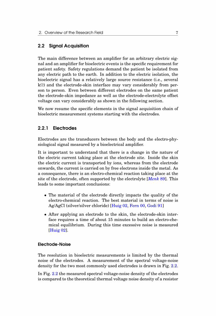
The resolution in bioelectric measurements is limited by the thermalnoise of the electrodes. A measurement of the spectral voltage-noisedensity for the two most commonly used electrodes is drawn in Fig. 2.2.
In Fig. 2.2 the measured spectral voltage-noise density of the electrodesis compared to the theoretical thermal voltage noise density of a resistor

2. Overview of the Research Field 8
1 10010 1k 10k0.1
100
103
104
10
1
volta
ge n
oise
den
sity
[nV
/√H
z]
frequency [Hz]
100 MΩ
1 MΩ
10 kΩ
100 Ω
Ag/AgCl
Au
1 / f
Fig. 2.2: Typical measured spectral voltage-noise density of Ag/AgCl and Au elec-trodes compared to the theoretical thermal noise of a resistor. (The measure-ments of the electrode noise were carried out by biosemi [bios], explanations at”http://www.biosemi.com/faq/without_paste.html“)
calculated in function of its resistance and temperature:
vnR ≈√
4kBTR (2.1)
Where kB stands for the Boltzmann constant, T for the temperature inKelvin and R for the resistance of the electrode.
From Fig. 2.2 we can estimate the integrated spectral voltage-noise den-sity of an Ag/AgCl electrode over the bandwidth of 10 Hz to 1 kHz toabout 1.4 µVrms. This was used for the electrode noise reported in ta-ble 2.1 for an ECG recording.
The integrated spectral voltage-noise density is only a rough measure-ment because it holds no information on the contribution at a specificfrequency. A closer look at the spectral voltage-noise density of anAg/AgCl electrode reveals a resistive behavior for frequencies aboveabout 3 Hz while the density varies inversely proportional to f for lowerfrequencies. Above 3 Hz the inherent noise of an Ag/AgCl electrodecorresponds to the thermal noise of a 25 kΩ resistor (estimated fromFig. 2.2). This supports the often encountered recommendation to re-place electrodes when the corresponding electrode-skin impedance (of-ten measured at 10 Hz) raises over 20 kΩ.
For the design of an amplifier for bioelectric events the spectral volta-ge-noise density of the electrodes yields the target value for the input-referred spectral voltage-noise density of the amplifier (see also section2.3.4 and 2.3.5).

2. Overview of the Research Field 9
Electrode-Skin Interface
A simple model for the electrode-skin interface which is widely usedin literature is shown in Fig. 2.3. The values for this model are ex-tracted from various sources as for example [Yama 77] and [Mett 90].The model shows typical values for an Ag/AgCl electrode with goodohmic contact such as the commonly used disposable pre-gelled elec-trodes. If a more complex model of the electrode-skin interface is re-quired we refer to the extensive work of Neumann in [Webs 98].
Zskin-electrode
ZinΩ20 k
Voffset Vn
Cc120 cmΩ/
body amplifier
20 pF
skin electrode
Rs Rc
1.36 V± 0.3 V
30 nV/√Hz(@10Hz)
Fig. 2.3: A simplified model of the electrode-skin interface for a pre-gelled Ag/AgClelectrode.
To the offset voltage Voffset is added in series the voltage noise sourceVn which corresponds to the inherent noise of the electrode described inthe previous section. As an example, the spectral voltage-noise densityfor an Ag/AgCl electrode is depicted in Fig. 2.2.
For different dry electrodes, the typical value for the resistor Rc is muchhigher, i.e., in the range of 1.4 MΩ [Burk 00]. The same is true forintegrated electrodes, which have much higher source resistances (notshown in figure 2.3) due to the absence of Ag/AgCl or similar suitablematerials [Tahe 94].
In general, the skin impedance decreases with frequency and dependson size, material and pressure of the applied electrode. A set of mea-surements is for example reported in [Rose 88].
Between the electrodes and the skin there is always a supplementarylayer. Either gel is applied manually or transpiration will accumulateand form an electrolyte between the skin and electrode. This additionalinterface will improve the ohmic contact by increasing the contact sur-face. But this interface is a half-cell structure (interface between metaland electrolyte) resulting in a redox reaction. This reaction pumps elec-tric charges between electrode and the electrolyte, resulting in a poten-tial difference Voffset between the electrode and the electrolyte of typ-ically 1.36 V (this is the standard electrode potential involved in theredox reaction Cl2 + 2e− ↔ 2Cl−). The electrode potential varies with

2. Overview of the Research Field 10
temperature, pressure and, most important, concentration of the elec-trolyte. As a result, the voltage across the electrode-electrolyte inter-face varies between different electrodes. In bioelectric applications, avariation of up to ±300 mV is to be expected [AAMI 99]. A detailed de-scription is found in the fifth chapter of [Webs 98].
As a consequence of the unknown offset voltage Voffset between elec-trode and skin, there is no method to measure the electrode-skin re-sistance (i.e., the electrode-skin impedance at DC). In most applicationsthe electrode-skin impedance is measured at around 10 Hz.
The electrode-electrolyte interface will also contribute to the voltagechange resulting from electrode movement, an effect which is part ofthe noise summarized by motion artifacts (see section 2.2.2).
Aside from the commonly used conductive electrodes there is a secondgroup of electrodes, called polarizable electrodes.
Polarizable Electrodes
Polarizable electrodes are electrodes which do not actually conduct anelectron current. Instead, there is a displacement current (a change ofthe local E-field). All capacitive electrodes are polarizable electrodes.The name polarizable electrodes comes from the fact the electrode be-comes polarized when a voltage is applied across it.
By making electrodes out of rubber mixed with graphite, the interfacecomes close to the model of a perfectly polarizable electrode. Polarizableelectrodes do not have a half-cell voltage because no redox reaction istaking place [Zsch 02].
Polarizable electrodes cannot be used with DC-coupled amplifiers, theymust be used with AC-coupled amplifiers, which are discussed in sec-tion 2.3.4. Polarizable electrodes do not allow measuring the DC valueof a bioelectric signal.
In theory capacitors are noiseless. Therefore we should think that polar-izable electrodes are the perfect choice for bioelectric signals. Althoughideal capacitors are noiseless, they shape the noise of the resistors inthe circuit and therefore the noise of polarizable electrodes cannot bediscussed without taking into account the input stage of the amplifierfor bioelectric events used, e.g., its input impedance. The noise of AC-coupled input stages is discussed in more detail in section 2.3.4.
Polarizable electrodes themselves are not noiseless because of dielectricnoise (skin) and motion artifacts. Motion artifacts will be discussed insection 2.2.2.
2. Overview of the Research Field 11
Active Electrodes
Electrodes comprising electronics to amplify the bioelectric signal arecalled active electrodes. The amplification does not necessarily have tobe a voltage amplification. In fact, most commercially active electrodesprovide a voltage gain of one and are therefore called buffer electrodes.Buffer electrodes provide, however, an impedance transformation by re-ducing the source impedance seen by the remote bioelectrical amplifier.Most buffer electrodes described in literature employ an op-amp (oper-ational amplifier) in the voltage-follower configuration [Ko 98].
As a general rule it can be said that active electrodes reduce the neg-ative effects of long wires (mainly capacitive interference) but requireadditional leads for their power supply.
The number of wires can be the limiting factor for some applicationssuch as a 128-lead or 256-lead EEG. In addition, large number of wiresper electrode increases the total wire thickness of the electrode andtherefore its stiffness. This may lead to augmented motion artifactsand increases the size of the connectors which is a limiting factor forwearable devices.
Active electrodes are an important part of this work. We will describetwo-wired active buffer electrodes in chapter 4 and two-wired amplify-ing electrodes in chapter 6.
2.2.2 Artifacts
Any part of the recorded signal which has not its origin in the bioelectriceffect under observation is called an artifact. This can be other bioelec-tric signals like muscle activity which is recorded as part of an EEG.It can also be the result of an electromagnetic interference from vari-ous origins (e.g., power-line interference) or being a result of movementof the electrodes (i.e., motion artifacts). A good overview of commonlyencountered artifacts can be found in [Webs 84] and [Mett 90].
To reduce artifacts some basic rules should always be followed:
• In order to reduce magnetic coupling of the power-line voltage tothe system, long wires should be twisted whenever possible to min-imize loops.
• To reduce capacitive coupling of the power-line interference wiresshould be driven with the lowest possible impedance and, if possi-ble, shielded with a low impedance potential which is close to thebody voltage (guarding).

2. Overview of the Research Field 12
• In the case of shielded wires their movement should be reducedas much as possible as to reduce tribo-electric noise generated byfriction and deformation of the insulation.
• Wires connecting to the electrodes should be as flexible as possiblein order to reduce motion artifacts.
Motion Artifacts
One of the most severe limitations for body-worn bioelectrical amplifiersis motion artifacts, i.e., signal disturbances due to motion of the wires,the electrodes or the subject. It has been demonstrated that motion ar-tifacts in general scale inversely to the input resistance of the amplifierfor bioelectric events up to an input resistance of 1 GΩ [Zipp 79b]. Mo-tion artifacts do also scale linearly with the input bias current, whichshould be kept below 50 pA [Zipp 79b].
To reduce motion artifacts by electrical means several methods havebeen proposed: Some motion artifacts are not in the same frequencyband as the bioelectric signal and can be filtered out.
The most effective methods are those which reduce the motion arti-fact at the source: skin-abrasion or the use of micromachined elec-trodes [Gris 02]. Unfortunately, these methods are not well suited forlong-term monitoring applications as the skin grows back and microma-chined electrodes may lead to skin irritation.
Some authors use capacitive coupled electrodes to enhance immunity tomotion artifacts [Burk 00] and [Harl 03]. Yet, the claim that capacitivecoupled electrodes reduce motion artifact has never been proven.
Capacitive electrodes (i.e., polarizable electrodes) suffer from an addi-tional kind of motion artifacts which results from motion-related chan-ges of their coupling capacity. Motion artifacts of polarizable electrodesare discussed in section 2.3.4.
2.2.3 Patient Isolation and Common Mode Rejection Ratio
The standard for patient isolation requires that the total current flow-ing through the patient and the measurement equipment to earth doesnot exceed a peak value of 50 µArms, even in the unlikely event thatthe patient touches a power outlet. These and other requirements areregulated by the AAMI standard (Association for the Advancement ofMedical Instrumentation) [AAMI 99] and the IEC (International Elec-trotechnical Commission) standard [IEC 08]. As a result, the signalsource, e.g., the human body, cannot be grounded (connected by a low

2. Overview of the Research Field 13
impedance path to earth) as is the case for most electric measurements,but must be kept electrically isolated. Equally, the measurement equip-ment must provide some means of isolation, this can be achieved byusing capacitive electrodes, by using an isolated battery supply (e.g.,wearable devices) or by using isolation amplifiers.
A typical measurement situation is shown in Fig. 2.4 with a three-leadECG as an example for an amplifier for bioelectric events.
CsB
CB
VPO
VCM
Ze1e1
e2
rlZe2
Zrl
VIM
V DM
Vout
CP
Power Line
Earth
SystemGround
CsP
Fig. 2.4: A typical measurement situation for a three-lead ECG including power-line interference.
As in bioelectric measurements the human body is floating, this im-plies that there is only a capacitive coupling of the patient to both theearth (CB) and the power mains (CP ). The capacitive coupling from thebody to the earth is usually stronger than the capacitive coupling tothe power mains. Typical values from literature are CB ≈ 300 pF andCP ≈ 20 pF [Mars 84], [Pall 88]. These values serve as an example andcan change considerably, for example, when touching a metal structurelike a window frame.
As a result of the capacitive coupling, the body potential as a whole willoscillate with 50 or 60 Hz with respect to earth.
The voltage between the body and the system ground (the referencepotential of the amplifier for bioelectric events) is called VCM (common-mode voltage). The voltage between the system ground and earth iscalled VIM (isolation mode voltage). The sum of both voltages is called

2. Overview of the Research Field 14
VPO (body voltage) and can easily attain values of several volts. If for ex-ample we consider the power-line voltage in Switzerland (230 V, 50 Hz)we can express the body voltage VPO by:
VPO ≈ZB
ZP + ZBV230 (2.2)
with
ZB =1
jωCB(2.3)
ZP =1
jωCP(2.4)
follows
VPO ≈CP
CP + CBV230 ≈ 14 Vrms (2.5)
ZB and ZP denote the impedance associated with the capacitance versusearth and the power line respectively, j stands for the imaginary unit.
The amplifier for bioelectric events in Fig. 2.4 has two signal electrodes(e1 and e2) and one reference electrode (rl). Ze1 , Ze2 and Zrl stand forthe corresponding electrode-skin impedances. The input impedance ofthe amplifier is not yet shown. We will discuss the influence of the inputimpedance later (see 2.2.4).
The reference electrode (rl) connects the system ground to the body.Yet, this electrode is not mandatory; there are amplifiers for bioelectricevents with only two electrodes (see 2.3.2)
The bioelectric signal of interest is the differential voltage between thetwo signal electrodes (e1 and e2), the corresponding voltage is denotedas VDM (differential mode voltage).
The common-mode voltage VCM is defined by the measurement situa-tion:
VCM = VPO − VIM (2.6)
The main source for the common-mode voltage VCM is the power lines. Ifwe consider again the power-line voltage in Switzerland (230 V, 50 Hz)we can express the common-mode voltage as:
VCM = ZrlZBZsP−ZsBZP
Zrl (ZP+ZB)(ZsP+ZsB )+ZPZB(ZsP+ZsB )+ZsPZsB (ZP+ZB)V230 (2.7)
Where ZB = 1/jωCB stands for example for the impedance associatedwith capacitor CB.
For surface electrodes made out of Ag/AgCl we can assume that at 50 HzZrl Zx with Zx ∈ ZP , ZB, ZsB , ZsP which leads to the simplified

2. Overview of the Research Field 15
equation:
VCM ≈ ZrlZBZsP − ZsBZP
ZPZB(ZsP +ZsB ) + ZsPZsB (ZP +ZB)V230 (2.8)
It is very difficult to give an approximate value for the resulting com-mon-mode voltage VCM because the values of ZsP and ZsB vary verymuch between different amplifiers and measurement situations. Thevalue of VCM can be anywhere in the range from 0 V to 230 Vrms.
It is important to note that according to equation (2.8) the amplitude ofthe common-mode voltage VCM scales linearly with the electrode-skinimpedance Zrl of the reference electrode.
It is also informative to note that according to equation (2.7) there aretwo particular situations for which the common-mode voltage VCM iszero.
Zrl = 0: Unfortunately, this is not possible in a real measurement situ-ation. For low frequencies there is always an electrode-skin impe-dance of several kΩ. A good way to reduce the influence of Zrl is touse a DRL (driven right leg) circuit as discussed in section 2.3.3.
ZBZsP = ZsBZP : If this equation is fulfilled then the numerator of equa-tion (2.7) would be zero. Unfortunately, these capacities cannot becontrolled. As a measure of precaution, the patient should avoidtouching any metal surface during a recording because this willmost probably lead to low values for either ZB or ZP and, most ofthe time, increase the inequality of the two terms in the equationabove leading to even more interferences.
In all other circumstances there is a common-mode voltage VCM 6= 0.
There is one more important case to consider:
ZsB ZB; ZsP ZP : This is a typical situation for body-worn portabledevices which store the recordings locally or transmit the data viaa wireless link. This setting will result in a relative low common-mode voltage.
For this setting the resulting formula reads:
VCM = ZrlZBZsP − ZsBZPZsPZsB (ZB + ZP )
V230
= jωZrlCsBCP − CBCsB
CP + CBV230 ≈ 120 µVrms (2.9)

2. Overview of the Research Field 16
Typical values used were Zrl=10 kΩ (@ 50 Hz), CB=300 pF, CP=20 pF,CsB=300 fF and CsP=200 fF. The power-line frequency was assumed tobe f=50 Hz (Europe). Note, in this model the phase shift between VCM
and V230 is either +90 or −90.
Again, the amplitude of the common-mode voltage VCM scales linearlywith the electrode-skin impedance Zrl of the reference electrode.
As the bioelectrical signal VDM is in the order of some millivolts or lower,it is important that the amplifier for bioelectric events effectively re-jects the common-mode voltage. This feature is quantified by the CMRR(common mode rejection ratio), which is defined as the ratio between thedifferential-mode gain GDM and the common-mode gain GCM (see alsosection 6.3.3):
CMRR =
∣∣∣∣GDM
GCM
∣∣∣∣ (2.10)
with
GDM =∂Vout
∂VDM(2.11)
GCM =∂Vout
∂VCM(2.12)
An amplifier for bioelectric events should have a CMRR of more than80 dB (@ 50 Hz) [Mett 91]. This is necessary to suppress the common-mode voltage VCM at the output of the amplifier to values lower thanthe smallest amplified signal that still is above the noise floor of theelectrodes.
The second reason why the common-mode voltage has to be reduced isthat, according to equation (2.2), the body voltage VPO can reach valuesof about 14 Vrms. Yet, the supply voltage of the input stage of an ampli-fier for bioelectric events will be most probably below 14 Vrms ≈ 40 Vpp.Yet, the peak-to-peak value of the common-mode voltage VCM must staywithin the limits of the supply voltage, otherwise the input signal maybe clipped. As a result, the common-mode voltage must be smaller thanthe 40 Vpp assumed for the body voltage VPO . This is achieved by eithera good isolation (e.g., a large ZsB and ZsP ), a DRL circuit or both (for theDRL circuit please refer to section 2.3.3).
Body-worn devices which store the bioelectric recording locally, with orwithout transmission, are very well isolated, which results in a verylow common-mode voltage VCM as shown by equation (2.9). To reducethe common-mode voltage below the amplified input signal of some µVa CMRR of 50 dB is sufficient. A DRL circuit may reduce the com-mon-mode voltage by 10 to 50 dB [Mett 90]. In practice, a reduction of30 dB is easily achieved. Using a DRL circuit then reduces the CMRRrequirement to 20 dB.

2. Overview of the Research Field 17
Table 2.2 recapitulates the minimal CMRR (@ 50 Hz) we recommend foran amplifier for bioelectric events:
Tab. 2.2: Recommended CMRR for amplifier for bioelectric events. For the DRLcircuit please refer to section 2.3.3
CMRR (@ 50 Hz) DRL circuit will be used without DRL circuitmains powered 80 dB —a
body-worn 20 dB 50 dB
a Not recommended because the amplifier may saturate due to excessive commonmode interference
2.2.4 Common Mode to Differential Mode Conversion
The total CMRR of an amplifier for bioelectric events is, most of thetime, limited by parasitic effects which are not under the full control ofthe designer. The four most important parasitic effects are described inthe following sections, starting with the capacitive coupling to the leads.
Capacitive Coupling to the Leads
Fig. 2.5 depicts a typical measurement situation with two parasitic el-ements made visible: The parasitic capacitances Cp1 and Cp2 betweenthe power line and the two leads as well as the input impedances Zi1
and Zi2 of the amplifier for bioelectric events.
For the discussion of the common-mode voltage we consider a measure-ment system which is grounded, i.e., ZsB=0 . This corresponds to a stan-dard measurement system (e.g., an oscilloscope) and is a valid modelto understand the different processes leading to a superposition of thecommon-mode voltage VCM on the amplified bioelectrical signal Vout .The model cannot be used to explain the origin of the common-modevoltage (this was done in the previous section) and even more, such asystem would not fulfill the patient safety requirements.
As a first result of ZsB = 0 we can state that the system ground andearth have the same electric potential, i.e., VIM = 0. If we further as-sume that Zi1 Ze1 and Zi2 Ze2 we can express the differentialvoltage VDM para as a result of the common-mode voltage VCM and thetwo parasitic capacitances Zp1 and Zp2 by:
VDM para =
(Ze2
Ze2 + Zp2− Ze1
Ze1 + Zp1
)(V230 − VCM ) (2.13)

2. Overview of the Research Field 18
VCM
Ze1
Zi2 Zi1
Ze2V D
M
Vout
Cp1Cp2
VIM
VPO
CP
Power Line
CB
Earth
CsB
Fig. 2.5: Typical measurement situation where parts of the common-mode signalare first converted to a differential signal by the means of parasitic elementsand then amplified by the system thus degrading the CMRR of the amplifier.
Where Zp1 = 1/jωCp1 stands for example for the impedance of the par-asitic capacitance Cp1 .
The parasitic capacitances together with the corresponding electrode-skin impedances form two individual potential dividers. An asymmetrybetween these two dividers will result in part of the common-mode volt-age VCM being converted into a differential voltage VDM para and ampli-fied by the system. This effect degrades the common mode rejection ofthe whole amplifier system without affecting the CMRR of the differen-tial amplifier itself.
To describe this effect we calculate the CMRR resulting from the capac-itive coupling which is expressed by:
CMRRpara =
∣∣∣∣ ∂VCM
∂VDM para
∣∣∣∣ =
∣∣∣∣∂VDM para
∂VCM
∣∣∣∣−1
(2.14)
=
∣∣∣∣ (Ze1 + Zp1 )(Ze2 + Zp2 )
Ze1 (Ze2 + Zp2 )− Ze2 (Ze1 + Zp1 )
∣∣∣∣ (2.15)
The resulting CMRRpara can achieve values from 20 dB to 200 dB (@50 Hz) depending on the topology of the amplifier. Values above 150 dBare not found in practice.

2. Overview of the Research Field 19
According to equation (2.15) it is possible to reduce the influence of theparasitic capacitances Cp1 and Cp2 by reducing the electrode-skin im-pedance of the electrodes Zel (e.g., by using active electrodes). Anotherpossibility is to shield the wires with a low-impedance shield [Hors 98].
Note, shielding the wires with system ground will reduce the input im-pedance of the amplifier by increasing the input capacitance [Mett 91].
The potential-divider Effect
A very similar process is known as the potential-divider effect [Mett 90].Again, there is a differential mode voltage VDM pot which is a result ofthe common-mode voltage VCM and a parasitic effect, i.e., the imbal-ance of two electrode-skin impedances Ze1 and Ze2 . Referring again toFig. 2.5 and neglecting the parasitic capacitances Cp1 and Cp2 we canwrite:
VDM pot =
(Zi2
Zi2 + Ze2− Zi1
Zi1 + Ze1
)VCM (2.16)
We will replace the individual impedances by a term using the meanvalue and the difference:
Zx1 = Zx +1
2∆Zx Zx2 = Zx −
1
2∆Zx (2.17)
∆Zx = Zx1 − Zx2 stands for the difference between the two correspond-ing impedances and Zx represents the mean value of the correspondingimpedances with x ∈ i, e.
If we assume that Zi1 Ze1 and Zi2 Ze2 we can rewrite equation(2.16) as follows:
VDM pot =Ze
Zi
(∆Ze
Ze− ∆Zi
Zi
)VCM (2.18)
The relative difference of the two input impedances ∆Zi/Zi is in generalmuch smaller compared to the relative difference of the electrode-skinimpedances ∆Ze/Ze. We can therefore neglect the second term withinthe parenthesis of equation (2.18) which leads to the equation encoun-tered throughout the literature:
VDM pot ≈∆Ze
ZiVCM (2.19)
The resulting CMRR is expressed by:
CMRRpot =Zi|∆Ze|
(2.20)

2. Overview of the Research Field 20
The relative variation between different electrode-skin impedances mayeasily reach 50 % and cannot be controlled. To minimize the potential-divider effect the input impedance of the amplifier for bioelectric eventsshould be as high as possible.
Modern MOS-FET input stages, which at 50 Hz are mainly capacitive,achieve input impedances which are larger than 1 GΩ (i.e., > 109Ω).
For ∆Ze = 10 kΩ (@ 50 Hz) and Zi > 109 Ω (@ 50 Hz) the resulting up-per limit for the CMRR will be over 100 dB (@ 50 Hz). At the statedfrequency the input impedance Zi > 109 Ω corresponds to an input ca-pacity Ci < 3.2 pF. Knowing that for a purely capacitive input the inputimpedance is given by
Zi =1
jωCi(2.21)
An alternative method often implemented in EEG recording systemsis to actively measure the electrode-skin impedances at the beginningof the measurement and warn the operator if the impedance mismatchexceeds a certain limit.
Gain Mismatch in Amplifying Electrodes
This effect is usually only seen in amplifiers for bioelectric events usingamplifying electrodes, e.g., active electrodes with a gain not equal toone, or digitizing electrodes. If the gain of two individual electrodes isdifferent it results again a differential voltage VDM gain which is directlyproportional to the common-mode voltage VCM :
VDM gain = ∆GVCM (2.22)
Where ∆G = G1 − G2 stands for the difference of the two gains. Thecorresponding CMRR reads:
CMRRgain =
∣∣∣∣GDM
GCM
∣∣∣∣ =
∣∣∣∣ G∆G
∣∣∣∣ (2.23)
If two individual amplifying electrodes have a gain set by resistors witha certain tolerance Q this will limit the CMRR of a signal amplified bythese two electrodes. For example, if we consider amplifying electrodeswhere the gain is set with two resistors R1 and R2 using a non-invertingconfiguration (see Fig. 6.1 for an example) we can assume that the mostcritical configuration concerning the CMRR is given by:
G1 = 1 +R1(1 +Q)
R2(1−Q)and G2 = 1 +
R1(1−Q)
R2(1 +Q)(2.24)
2. Overview of the Research Field 21
thus
∆G =R1(1 +Q)2 − (R1(1−Q)2)
R2(1−Q2)(2.25)
with Q2 1
∆G ≈ 4QR1
R2(2.26)
We can then calculate the worst-case value for the CMRR according toequation (2.23):
CMRRgain =1
4Q
∣∣∣∣ G
G−1
∣∣∣∣ (2.27)
with
Q =|∆R|R
(2.28)
First of all we see that for buffer electrodes (G = 1) there is no addi-tional CMRR limitation due to the gain mismatch. If we now consideran active electrode with a gain of 20 dB (non-inverting configuration) weconclude that according to equation (2.27) using resistors with a toler-ance of 1% would lead to a worst-case CMRR of merely 28.4 dB, far toolow for an amplifier for bioelectric events. On the other hand, to guaran-tee a worst-case CMRR of 80 dB the tolerance of the employed resistorsneeds to be 0.025 ‰, far too high for individual components. To reach agood CMRR the gain mismatch must be compensated for (see 6.3.2).
Note, equation (2.27) does not apply to amplifying electrodes when thegain-setting network is connected to a common node (not the signalground) corresponding to the mean value of all input voltages [Valc 04].See also section 2.2.5 later in this chapter.
Corner-Frequency Mismatch for Individual Highpass Filters
Most amplifiers for bioelectric events employ a highpass filter. The fil-ter removes the DC offset between different electrode-electrolyte inter-faces which can attain several hundred millivolts (see 2.3.6). In manyapplications the DC offset is removed only after the bioelectric signalis converted into a single-ended signal. Thus both the signal and thehighpass filter are referenced to the system ground.
If capacitive coupled electrodes are used (see section 2.2.1), or if thehighpass is realized somewhere else in the circuit where the bioelectricsignal is still bipolar, the tolerances of the elements forming the high-pass filter will also lead to a limitation of the CMRR.

2. Overview of the Research Field 22
We can describe the transfer function of a highpass filter by the generalform:
h(f) =jf 1
f0
1 + jf 1f0
(2.29)
Where j is the imaginary unit and f0 the corner frequency of the high-pass filter. For bioelectric signals the CMRR is usually most limited at50 Hz (or 60 Hz). For Switzerland we can therefore examine the gain ofthe highpass filter at 50 Hz and obtain:
Ghp(50 Hz) = |h(50 Hz)| = 50√2500 + f 2
0
(2.30)
If individual highpass filters are used their gain at 50 Hz will be dif-ferent depending on their actual corner frequency f0 due to componenttolerances. The corresponding CMRR limitation is calculated by equa-tion (2.23).
Thus, the variation of the gain ∆G has to be estimated from equation(2.30):
CMRRhp(@50Hz) =G
|∆G|≈ G(f0=f0)
|∆G|(2.31)
according to Taylor’s theorem (error propagation)
∆G ≈ dG
df0∆f0 = − 50f0√
(2500 + f20 )3∆f0 (2.32)
≈ −G f202500 + f20
∆f0f0
(2.33)
it follows
CMRRhp(@50Hz) ≈ 2500 + f02
f02
f0|∆f0|
(2.34)
If, for example, the highpass filters are built using capacitors with atolerance of 10% and resistors with a tolerance of 1% we can say thatfor the worst-case the corner frequency has a tolerance of 11%. For acorner frequency f0 = 1 Hz (e.g., for EEG) we then calculate the worst-case value for the CMRR (@ 50 Hz) according to equation (2.34) andobtain 87.1 dB. For an ECG with a highpass filter at 0.016 Hz the sameconsideration will lead to a worst-case CMRR (@ 50 Hz) of 159 dB.
According to equation (2.34), the corner frequency has to be chosen aslow as possible in order to minimize the effect of corner frequency vari-ations. At the same time it can be estimated that the CMRR (@ 50 Hz)

2. Overview of the Research Field 23
limitation due to component tolerances of individual highpass filters isnot very critical.
It is important to note that this limitation also applies to electrodeswith an individual lowpass filter like for example when using individualanti-aliasing filters for signal and reference electrodes or when usingamplifiers with a limited bandwidth (see also chapter 4 and chapter 6).By analogy we can estimate that the corner frequency of individual low-pass filters should be at least 2.5 kHz (i.e., fifty times the power-linefrequency) to again obtain a worst-case CMRR (@ 50 Hz) of 87.1 dB:
CMRRlp(@50Hz) ≈2500 + f0 lp
2
2500
f0 lp
|∆f0 lp |(2.35)
Where f0 lp stands for the corner frequency of an individual lowpassfilter.
2.2.5 Total Common Mode Rejection Ratio
As long as the bioelectric signal is differential, i.e., not converted intoa single-ended signal, each stage in an amplifier for bioelectric eventscontributes with a finite CMRR. In the worst case the total CMRR of asequence of stages in respect to a specific common-mode signal (e.g., thepower-line interference) is given by [Pall 91b]:
1
CMRRtotal=∑i
1
CMRRi(2.36)
Where CMRRi stands for the individual CMRR contribution due to oneof the above mentioned effects. The total CMRR is always smaller thanthe smallest individual CMRR (in a worst-case scenario).
It is important to note that the total CMRR can also be better than theindividual CMRRs (for a given frequency). This is the case if individualcontributions of the same common-mode signal cancel each other (i.e.,have a different sign). We will discuss a method to improve the CMRRof an amplifier for bioelectric events based on canceling contributions indetail in chapter 5
Most of the time one of the four described parasitic effects dominates. Asa general rule of thumb we can estimate that for amplifiers which arenot using a FET-input stage, the potential-divider effect will be limit-ing. For amplifying electrodes the gain mismatch will limit the CMRR.For capacitively coupled electrodes the corner-frequency mismatch isthe dominant factor while for non-buffered EEG amplifiers the capaci-tive coupling to the leads will be most limiting.

2. Overview of the Research Field 24
CMRR of Instrumentation Amplifiers
This section is based on the publication of Pallas-Areny [Pall 91].
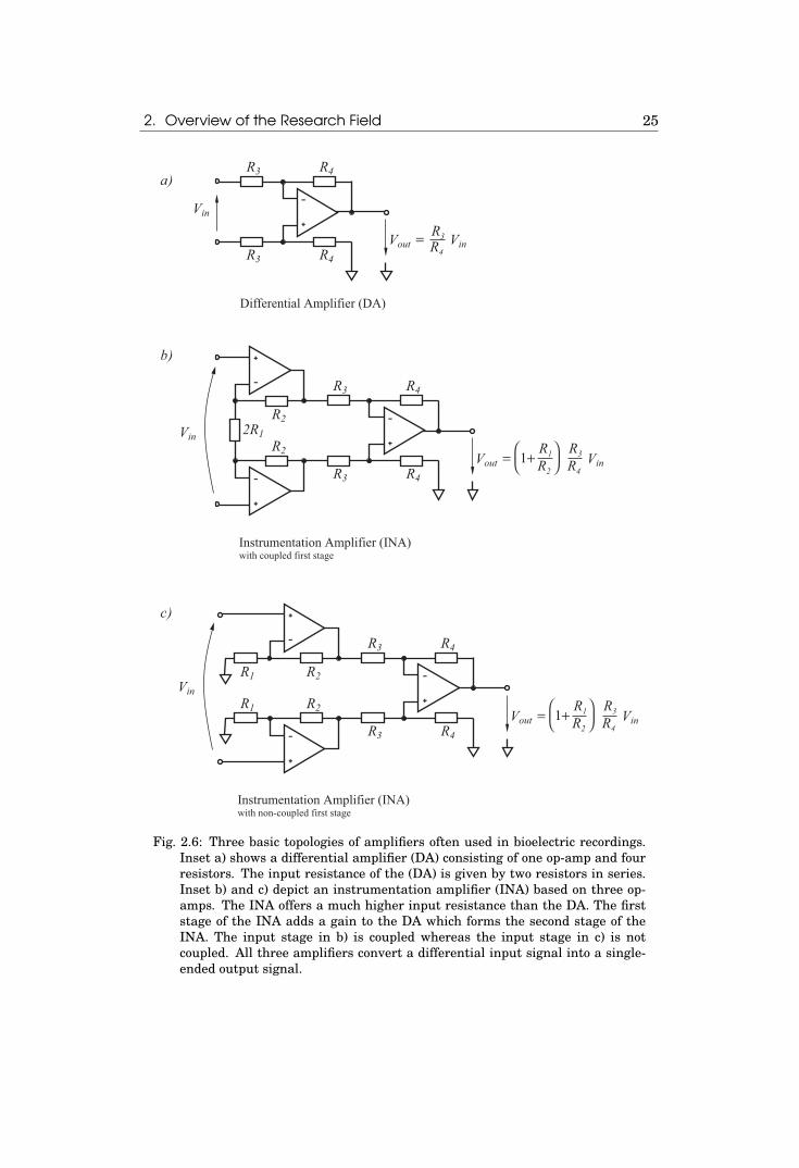
In section 2.2.4 we have seen that for amplifying electrodes the gainmismatch between individual electrodes can lead to a severe limitationof the CMRR. Also individual lowpass or highpass filter can lead to alimited CMRR (@ 50 Hz) when the corner frequency of the filter is closeto the frequency of the power-line interference. The basic considerationof gain mismatch can also be applied to amplifiers. Fig. 2.6 shows threebasic amplifiers, one DA (differential amplifier) and two versions of anINA (instrumentation amplifier).
The DA in Fig. 2.6 can also be seen as having two branches with a in-dividual gain. Therefore, according to equation (2.23), a gain mismatchbetween these two branches will result in a limitation of the CMRR.
If the four resistors have a tolerance Q and the DA has a closed-loopgain of G the worst-case CMRR is then reduced to [Pall 91] :
CMRRgain =G+ 1
4Q(2.37)
with
Q =|∆R|R
If for example resistors with a tolerance of 1 % are used for a differentialamplifier with a nominal gain of 20 dB, the resulting CMRRgain yields48.8 dB. This is still much lower than the recommended value of 80 dB(@ 50 Hz) [Mett 93] but higher than the 28.4 dB corresponding to theworst-case CMRR for two individual amplifying electrodes with a gainof 20 dB (see section 2.2.4). This is because the gain of the differen-tial amplifier improves the CMRR whereas the gain of the amplifyingelectrodes has very little effect on the CMRR.
Considering the INA depicted in Fig. 2.6 c) we can estimate the totalworst-case CMRR based on resistor tolerances by combining equation(2.36), equation (2.37) and equation (2.27).
1
CMRRtotal worstcase=
1
CMRRAE+
1
CMRRDA
= 4Q|GAE−1|GAE
+4Q
GDA + 1(2.38)
with
Q =|∆R|R
2. Overview of the Research Field 25
b)
c)
a)
Differential Amplifier (DA)
Vin
Vout VinR4R3
-
-
-
R3= R4
R4R3
Instrumentation Amplifier (INA)with coupled first stage
Vin
Vin
Vout VinR4R3
-
--
= ⎛⎝1+ ⎞⎠ R3R4
R1R2
R4R3
-
-
-
R2
R22R1
-
--
Instrumentation Amplifier (INA)with non-coupled first stage
VoutR4R3
-
-
-
R4R3
-
-
-
R2
R2
-
--
R1
R1
Vin= ⎛⎝1+ ⎞⎠ R3R4
R1R2
Fig. 2.6: Three basic topologies of amplifiers often used in bioelectric recordings.Inset a) shows a differential amplifier (DA) consisting of one op-amp and fourresistors. The input resistance of the (DA) is given by two resistors in series.Inset b) and c) depict an instrumentation amplifier (INA) based on three op-amps. The INA offers a much higher input resistance than the DA. The firststage of the INA adds a gain to the DA which forms the second stage of theINA. The input stage in b) is coupled whereas the input stage in c) is notcoupled. All three amplifiers convert a differential input signal into a single-ended output signal.
2. Overview of the Research Field 26
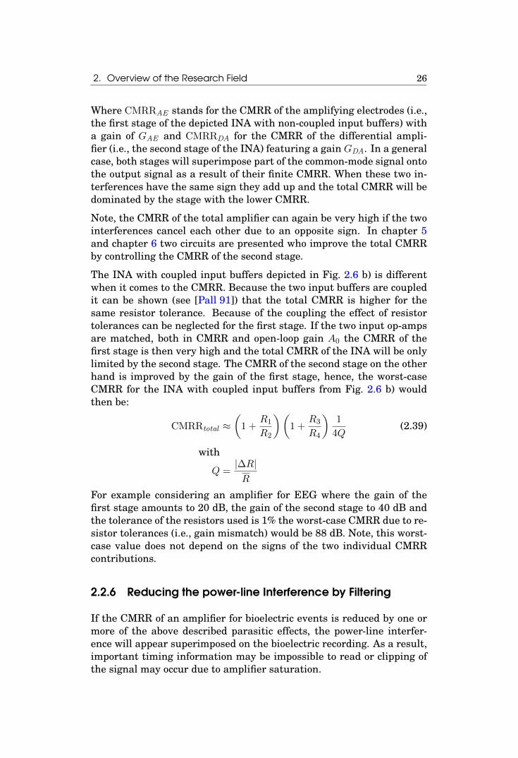
Where CMRRAE stands for the CMRR of the amplifying electrodes (i.e.,the first stage of the depicted INA with non-coupled input buffers) witha gain of GAE and CMRRDA for the CMRR of the differential ampli-fier (i.e., the second stage of the INA) featuring a gain GDA. In a generalcase, both stages will superimpose part of the common-mode signal ontothe output signal as a result of their finite CMRR. When these two in-terferences have the same sign they add up and the total CMRR will bedominated by the stage with the lower CMRR.
Note, the CMRR of the total amplifier can again be very high if the twointerferences cancel each other due to an opposite sign. In chapter 5and chapter 6 two circuits are presented who improve the total CMRRby controlling the CMRR of the second stage.
The INA with coupled input buffers depicted in Fig. 2.6 b) is differentwhen it comes to the CMRR. Because the two input buffers are coupledit can be shown (see [Pall 91]) that the total CMRR is higher for thesame resistor tolerance. Because of the coupling the effect of resistortolerances can be neglected for the first stage. If the two input op-ampsare matched, both in CMRR and open-loop gain A0 the CMRR of thefirst stage is then very high and the total CMRR of the INA will be onlylimited by the second stage. The CMRR of the second stage on the otherhand is improved by the gain of the first stage, hence, the worst-caseCMRR for the INA with coupled input buffers from Fig. 2.6 b) wouldthen be:
CMRRtotal ≈(
1 +R1
R2
)(1 +
R3
R4
)1
4Q(2.39)
with
Q =|∆R|R
For example considering an amplifier for EEG where the gain of thefirst stage amounts to 20 dB, the gain of the second stage to 40 dB andthe tolerance of the resistors used is 1% the worst-case CMRR due to re-sistor tolerances (i.e., gain mismatch) would be 88 dB. Note, this worst-case value does not depend on the signs of the two individual CMRRcontributions.
2.2.6 Reducing the power-line Interference by Filtering
If the CMRR of an amplifier for bioelectric events is reduced by one ormore of the above described parasitic effects, the power-line interfer-ence will appear superimposed on the bioelectric recording. As a result,important timing information may be impossible to read or clipping ofthe signal may occur due to amplifier saturation.

2. Overview of the Research Field 27
To reduce the power-line interference of the recording, a notch filter maybe used to restore the original signal (as long there was no clipping ofthe signal). In our opinion, the use of a notch filter should be avoidedwhenever possible for two reasons:
• The notch filter does not differentiate between the power-line in-terference and the bioelectrical signal and thus removes part ofthe bioelectrical signal.
• An analog notch filter has a highly non-linear phase shift and thusalters the form of the bioelectric signal. This changes importanttiming information especially in ECG.
Instead of using a filter, a more elegant method is to generate an arti-ficial sinusoidal voltage with the same phase, amplitude and frequencyas the power-line interference and then subtract it from the bioelectricsignal [Dots 96] and [Hwan 08]
A very good analysis which compares notch filters to adaptive filters ispresented in [Hami 96].
It is always better to maximize the CMRR rather than filtering the sig-nal afterwards. Maximizing the CMRR reduces the risk of clipping andremoves all common mode interferences, the power-line interference it-self but also its harmonics.
Note, we do not discourage filtering in general. An analog anti-aliasingfilter should be used to remove the out-of-band component of the sig-nal prior to sampling the bioelectrical signal. The sampled signal canthen be filtered digitally to remove quantization noise from the sam-pling process. A smoothing filter which is well adapted to biologicalsignals is the Savitzky-Golay filter which is available in MATLAB also.The Savitzky-Golay filter performs a local polynomial regression whichhas the advantage that local minima or maxima are better preservedthan by a moving-average filter.
2.3 Amplifiers for Bioelectric Events
An amplifier for bioelectric events requires some means to define a ref-erence for the bioelectric signal to measure. This reference is normallynot the earth but a signal related to a body potential on the same bodythan the signal of interest. We now resume the most commonly usedways to generate a reference voltage for biopotential measurements.
2. Overview of the Research Field 28
2.3.1 Amplifiers using Tripolar Electrodes
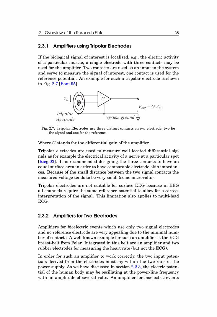
If the biological signal of interest is localized, e.g., the electric activityof a particular muscle, a single electrode with three contacts may beused for the amplifier. Two contacts are used as an input to the systemand serve to measure the signal of interest, one contact is used for thereference potential. An example for such a tripolar electrode is shownin Fig. 2.7 [Boni 95].
Vin
tripolarelectrode
Vout = G Vin
G
system ground
Fig. 2.7: Tripolar Electrodes use three distinct contacts on one electrode, two forthe signal and one for the reference.
Where G stands for the differential gain of the amplifier.
Tripolar electrodes are used to measure well located differential sig-nals as for example the electrical activity of a nerve at a particular spot[Rieg 03]. It is recommended designing the three contacts to have anequal surface area in order to have comparable electrode-skin impedan-ces. Because of the small distance between the two signal contacts themeasured voltage tends to be very small (some microvolts).
Tripolar electrodes are not suitable for surface EEG because in EEGall channels require the same reference potential to allow for a correctinterpretation of the signal. This limitation also applies to multi-leadECG.
2.3.2 Amplifiers for Two Electrodes
Amplifiers for bioelectric events which use only two signal electrodesand no reference electrode are very appealing due to the minimal num-ber of contacts. A well-known example for such an amplifier is the ECGbreast-belt from Polar. Integrated in this belt are an amplifier and tworubber electrodes for measuring the heart rate (but not the ECG).
In order for such an amplifier to work correctly, the two input poten-tials derived from the electrodes must lay within the two rails of thepower supply. As we have discussed in section 2.2.3, the electric poten-tial of the human body may be oscillating at the power-line frequencywith an amplitude of several volts. An amplifier for bioelectric events
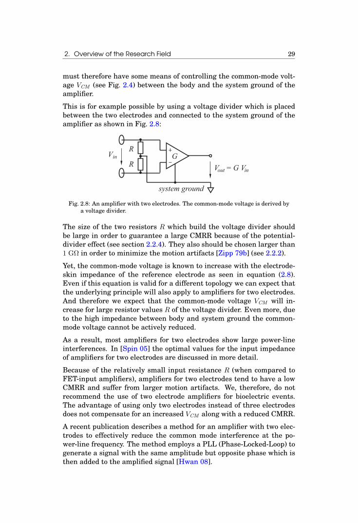
2. Overview of the Research Field 29
must therefore have some means of controlling the common-mode volt-age VCM (see Fig. 2.4) between the body and the system ground of theamplifier.
This is for example possible by using a voltage divider which is placedbetween the two electrodes and connected to the system ground of theamplifier as shown in Fig. 2.8:
Vin
Vout = G Vin
system ground
R
RG
Fig. 2.8: An amplifier with two electrodes. The common-mode voltage is derived bya voltage divider.
The size of the two resistors R which build the voltage divider shouldbe large in order to guarantee a large CMRR because of the potential-divider effect (see section 2.2.4). They also should be chosen larger than1 GΩ in order to minimize the motion artifacts [Zipp 79b] (see 2.2.2).
Yet, the common-mode voltage is known to increase with the electrode-skin impedance of the reference electrode as seen in equation (2.8).Even if this equation is valid for a different topology we can expect thatthe underlying principle will also apply to amplifiers for two electrodes.And therefore we expect that the common-mode voltage VCM will in-crease for large resistor values R of the voltage divider. Even more, dueto the high impedance between body and system ground the common-mode voltage cannot be actively reduced.
As a result, most amplifiers for two electrodes show large power-lineinterferences. In [Spin 05] the optimal values for the input impedanceof amplifiers for two electrodes are discussed in more detail.
Because of the relatively small input resistance R (when compared toFET-input amplifiers), amplifiers for two electrodes tend to have a lowCMRR and suffer from larger motion artifacts. We, therefore, do notrecommend the use of two electrode amplifiers for bioelectric events.The advantage of using only two electrodes instead of three electrodesdoes not compensate for an increased VCM along with a reduced CMRR.
A recent publication describes a method for an amplifier with two elec-trodes to effectively reduce the common mode interference at the po-wer-line frequency. The method employs a PLL (Phase-Locked-Loop) togenerate a signal with the same amplitude but opposite phase which isthen added to the amplified signal [Hwan 08].

2. Overview of the Research Field 30
The only industrial applications of two-electrode amplifiers known tous are defibrillators. Defibrillators require large electrodes with a verylow electrode-skin impedance to avoid skin burns. In this particularapplication two-electrode amplifiers are used to detect the presence ofthe heart beat after a defibrillation pulse was administered. The lowCMRR resulting from the two-electrode topology is of less concern asthe electrodes are large, the electrode-skin impedance is small and noclinical ECG is to be measured.
2.3.3 Amplifiers using Reference Electrodes
We will now discuss systems which use one set of electrodes for themeasurement of the bioelectric signal (called signal electrodes) and an-other set of electrodes for the common-mode voltage (reference electrodeor/and DRL-electrode).
Amplifiers using an unbuffered Reference Electrode
The concept of the tripolar electrode (see section 2.3.1) can be gener-alized to an amplifier having two (or more) signal electrodes and onereference electrode. The latter can be used for example to directly con-nect the body surface potential to the signal reference of an amplifierfor bioelectric events as shown in Fig. 2.9:
sign
al e
lect
rode
sre
fere
nce
elec
trod
e
Vin 1
Vin 2
Vout 1 = G Vin 1
system ground
Vout 2
Zrl
VDM = Vin 2 - Vin 1
VCM ≈ 2Vin 2 + Vin 1 G
G
VCM
VDM
VPO CsB
Earth
Fig. 2.9: An unbuffered electrode is placed unto the skin serving as reference elec-trode.
In Fig. 2.9 only two signal electrodes are shown, but the topology caneasily be expanded to larger number of signal electrodes. In the case

2. Overview of the Research Field 31
of two signal electrodes the common-mode voltage VCM as well as thebioelectric signal of interest VDM can also be described by:
VDM = Vin 2−Vin 1 (2.40)
VCM ≈Vin 2 +Vin 1
2(2.41)
The value for the common-mode voltage VCM given by equation (2.41)is an approximation which is only true if the bioelectric signals are ne-glected and thus the whole body would have the same potential. But itis a good approximation considering the small amplitude of bioelectricsignals in general.
From Fig. 2.9 we can again see that the common-mode voltage VCM
would be zero if the electrode-skin impedance Zrl of the reference elec-trode is zero. Unfortunately, this is never the case for an amplifier forbioelectric events because of the low conductivity of the skin.
If we take as an example an amplifier for bioelectric events using anisolation amplifier with the supply being connected to earth we can as-sume a relatively large capacitive coupling from the system ground toearth. If we take for example the ISO124 (orig. Burr-Brown, now TI)the isolation capacitance CsB is about 2 pF. This seams a small valuebut in the case of multi-electrode amplifier this value quickly increases.If for example we take an EEG amplifier with 64 electrodes the isolationcapacitance could easily attain 128 pF.
According to equation (2.8) we can estimate the common-mode voltagefor the example above to:
VCM ≈ jωZrlCPCsB − CBCsP
CsB + CSP + CP + CBV230 = 4 mVrms (2.42)
Typical values used were Zrl=10 kΩ (@ 50 Hz), CB=300 pF, CP=20 pF,CsP=200 fF and a power-line frequency of 50 Hz.
Compared to the EEG signal itself which can have an amplitude ofabout 10 µV only, this is a large common-mode signal. Especially for mo-bile applications where the electrode-skin impedance can be larger thanin the example above. To reduce the common-mode voltage actively onepossibility is to omit the reference electrode and use a resistive networkto generate a reference potential out of all input electrodes. This refer-ence is then fed back to the body using a low impedance electrode. Thisis commonly done using a DRL circuit.
Amplifiers using a DRL Electrode
To reduce the impact of the electrode-skin impedance Zrl of the refer-ence electrode in Fig. 2.9 an active circuit may be used in order to drive

2. Overview of the Research Field 32
the body surface potential. An example of such a system is the DRL(driven right leg) circuit1. The purpose of the DRL circuit is to reducethe common-mode voltage via negative feedback [Wint 83b]. An exam-ple of a DRL circuit is shown in Fig. 2.10.
sign
al e
lect
rode
s
DRLelectrode
DRLop-amp
Vin 1
Vin 2
system ground
R
R
C
G
G
Vout 1 = G Vin 1
V div
= G
VC
M
V DRL
Vout 2 = G Vin 2
Zrl
VCM
Vrl
Fig. 2.10: A feedback loop is built around a driven right leg (DRL) electrode in orderto force the system ground to a known potential, e.g., the potential of the body.
In Fig. 2.10 the amplified input voltages of the two signal electrodes areaveraged using a resistive voltage divider built by the two resistors R.We will calculated the voltage using the system ground as the referenceand obtain:
Vdiv = (Vout 1 +Vout 2 )/2
= G (Vin 1 +Vin 2 )/2 = GVCM (2.43)
The voltage Vdiv generated by the voltage divider corresponds to theamplified common-mode voltage GVCM and is compared by the DRLop-amp to the system ground. The difference is amplified, inverted,integrated and fed back to the body via the DRL electrode. Thus, thevoltage at the output of the DRL op-amp can then be expressed by:
VDRL = −G 2
jωCRVCM (2.44)
It is important to note that equation (2.44) is only true as long as theoutput voltage of the DRL op-amp does not saturate and as long all sig-nal electrodes are connected (to sense the common-mode voltage). Thisseems difficult at first because of the high gain of the DRL loop. But at
1 Originally the DRL circuit was attached to an electrode placed on the right leg,thus the name of the circuit.

2. Overview of the Research Field 33
the same time the voltage at the input of the DRL op-amp (correspond-ing to the amplified common-mode voltage) will be driven to very lowvalues by the negative feedback due to the principle of virtual ground.
The amplifier with the DRL circuit senses, amplifies, inverts and inte-grates the common-mode voltage VCM and then presents the resultingvoltage at the opposite pole of the electrode-skin impedance of the DRLelectrode (acting as reference electrode). The voltage Vrl over the skin-electrode impedance Zrl can be calculated as:
Vrl = VCM − VDRL
=
(1 +G
2
jωCR
)VCM (2.45)
As a result of the DRL loop, the voltage over the impedance Zrl is am-plified which means the current through the impedance Zrl is larger forthe same common-mode voltage in the presence of a DRL circuit whencompared to the previous circuit without DRL circuit (see previous sec-tion 2.3.3).
The larger current through the electrode-skin impedance with the samecommon-mode voltage can also be interpreted as if the electrode-skinimpedance Zrl would be smaller in the case of a DRL circuit. Accordingto equation (2.7) the common-mode voltage VCM scales linearly withZrl . Thus, by analogy we can conclude that the DRL circuit reducesthe common-mode voltage by the factor by which the current throughthe electrodes-skin impedance increases for any given common-modevoltage VCM (as long the DRL amplifier does not saturate).
The reduction of the common-mode voltage VCM is often expressed asan improvement of the CMRR. The improvement of the CMRR due to aDRL circuit is then expressed by:
CMRRDRL = CMRRorig + 20 log
(1 +G
2
jωCR
)(2.46)
Where CMRRorig is the CMRR without DRL circuit, G is the forwardgain of the signal electrodes and 2/jωCR corresponds to the gain of theDRL circuit.
The reduction of the common-mode voltage VCM is proportional to thegain of the feedback loop. A high gain of the feedback loop is thereforemost desirable but may lead to instability. The role of the capacitor C inthe feedback loop is to ensure stability by increasing the phase margin.To visualize the gain of the DRL circuit and to evaluate the phase mar-gin we recommend the use of a P-Spice-based tool for every new circuit.An example of a CMRR measurement of an amplifier including a DRLcircuit will be discussed later in section 6.3.3.

2. Overview of the Research Field 34
When using a DRL circuit, the common-mode voltage VCM resultingfrom the power-line interference can be reduced by a factor of up to300, resulting in an increase of the CMRR by about 50 dB (@ 50 Hz)[Mett 90].
For the circuit above there is no limitation to the number of signal elec-trodes. However, if one electrode does not connect to the body, this elec-trode acts like an antenna picking up power-line interference. This in-terference is then amplified and added to the amplified common-modevoltage via the resistive divider. For this reason systems with a largenumber of signal electrodes may preferably use one or more dedicatedreference electrodes for the measurement of the common-mode voltage.
Using dedicated Electrodes for the DRL Loop
Instead of generating a reference by averaging all input signals it is pos-sible to use one or more dedicated reference electrodes. Fig. 2.11 depictsa system with one dedicated reference electrode and two signal elec-trodes. The reference electrode senses the common-mode voltage VCM
As before, the common-mode voltage is amplified, inverted, integratedand fed back to the body in order to drive the common-mode voltageVCM to lower values.
In Fig. 2.11 the reference electrode is buffered in order to generate alow-impedance node which drives the resistor R. It also has the effectthat all electrodes present the same input impedance thus reducing the‘potential-divider effect’ described in section 2.2.4.
If the reference electrode is affected by a bioelectrical signal, this sig-nal appears superimposed on all channels. Thus, a reference electrodeneeds to be attached to a location which is ideally not affected by anybioelectric signal. It is also possible to use several electrodes connectedby a resistive network. This reduces the sensitivity to interferences ofthe reference electrodes but again increases the risk of one referenceelectrode loosing contact.
Other uses of the DRL Circuit
The primary use of the DRL circuit is to reduce the common-mode volt-age VCM . The DRL circuit can also be used to force the common-modevoltage VCM to a known signal by superimposing a voltage source to thereference of the DRL op-amp (instead of signal ground). The source canbe a DC voltage [Levk 82] or an AC voltage [Ober 82].
Two examples for amplifiers using the DRL circuit for these purposeswill be discussed later in this thesis. In chapter 3 we will use a DRL

2. Overview of the Research Field 35
referenceelectrode
sign
al e
lect
rode
s
DRLelectrode
DRLopamp
Vin 1
Vin 2
system ground
R
C
G
G
Vout 1 = G Vin 1
Vout 2 = G Vin 2
Zrl
Vrl
V DRLVCM
Fig. 2.11: A dedicated reference electrode is used to obtain a reference voltage.
circuit to superimpose a sinusoidal voltage of 10 kHz to measure theelectrode-skin impedance mismatch. In chapter 6 we will demonstratehow a DRL circuit can be used to drive the DC value of the input voltageto the mid-range of an active input circuit, e.g., an active electrode.
2.3.4 AC-coupled Amplifiers
Most amplifiers for bioelectric events are designed with a highpass fil-ter at some place in the signal path in order to remove the unwantedelectrode-electrolyte potential, which may differ between electrodes byup to ±300 mV.
One possibility is to place the highpass filter after the differentiation,where the bioelectric signal is already converted from a bipolar signalto an unipolar signal. The disadvantage of this approach is that onlya limited gain may be implemented in the stages prior to the highpassfilter or else clipping of the signal may occur.
To avoid this limitation, some amplifiers place the highpass filter beforethe differentiation where the signal is still bipolar. These systems aregenerally called AC-coupled amplifiers. AC-coupled input stages aredescribed since the early beginning of ECG recordings [Pall 89]. The

2. Overview of the Research Field 36
topology is appealing because the maximum gain can be realized in thefirst stage. This minimizes the noise contribution of all following stages.
Examples for AC-coupled amplifiers are systems with a blocking capac-itor right on the electrodes or systems which use insulating electrodes(see 2.2.1).
Fig. 2.12 shows a model of an insulated electrode where a coupling ca-pacitor is placed in series with the signal path.
Vin IbiasVout = H(ω) G Vin
system ground
ChpG
RhpChpRhpjω
H(ω) =ChpRhp1+ jω
Fig. 2.12: Schematic view of an AC-coupled input stage
The corner frequency of this particular input stage is given by:
f0 =1
2πChpRhp(2.47)
The resistor Rhp is required to generate a path to the system ground forthe input bias current Ibias of the amplifier. The potential-divider effect(see section 2.2.4) has the potential to limit the CMRR of AC-coupledamplifiers because the capacitor Chp increases the source impedance ofthe signal while the resistor Rhp reduces the input impedance of theamplifier (here an op-amp with the gain G). The use of a bootstrapcircuit can raise this input impedance at 50 Hz [Pall 90] .
Many authors claim that using capacitively coupled electrodes reducesmotion artifacts [Aliz 96], [Tahe 94]. We, however, have not been able toreproduce any measurements confirming a reduction of motion artifactswhen using capacitively coupled electrodes.
Remote Off-Body ECG Sensing
Off-body measurement systems are a subgroup of AC-coupled ampli-fiers. As the name suggests, in off-body sensing systems the electrodesare not in contact with the body.
The first amplifier using off-body electrodes was described in 1993 byClippingdale [Clip 93]. The development was driven by the need torecord ECGs from people with skin burns who could not tolerate elec-trodes in contact with the skin. Consequently, the electrodes for the

2. Overview of the Research Field 37
ECG were placed under a hospital bed. The coupling between body andelectrodes was purely capacitive, with the electrode forming one conduc-tor of the capacitor and the human body forming the second conductor1.
Because the capacitive coupling between electrode and skin is achievedthrough air at a distance of several centimeters, the resulting capaci-tance tends to be rather small, approximately given by the formula fora parallel-plate capacitor (
√A d for a circular plate):
C ≈ εε0A
d(2.48)
Where ε0 is the electrical permittivity of free space, ε the electrical per-mittivity of the dielectric (if any), A the surface and d the distance inbetween of the two conductors.
Because of the small input capacitance the input resistance of the am-plifier for bioelectric events has to be as large as possible in order toachieve a low corner frequency in the order of some Hertz. First, a boot-strap circuit was used to guarantee a large input impedance. Later,modern instrumentation amplifiers were used with virtually no biascurrent [Harl 02]. The input node of the amplifier is floating yet stillconstant over a long period of time [Harl 02b]. To avoid saturation ofthe floating input of the instrumentation amplifier the electrodes re-quire elaborate shielding.
We would expect that the measurement is free of any motion artifactbecause the electrodes are no longer in direct contact with the skin.Unfortunately this is not the case, a motion of the body will also varythe size of the coupling capacity. Varying the size of a charged capacitorwill generate a voltage change over the capacitor. To understand this,we assume the charge Q to be constant, which is true for a very shortperiod of time. The voltage V over the capacitor is given by the chargedivided by the capacitance.
V =Q
C=
Q
εε0Ad (2.49)
When the distance d between the skin and the electrode varies due tomotion a voltage change results:
∆V =Q
εε0A∆d (2.50)
This voltage change is directly superimposed onto the bioelectric signaland hence not distinguishable from it. In [Kim 04] it was for example
1 A capacitor can be described as being a passive electronic component consisting ofa pair of conductors separated by an insulator

2. Overview of the Research Field 38
shown that the measured off-body recording showed waves which weredue to the movement of the blood vessels and not due to the bioelectricactivity of the heart. Note, although the signal is not of bioelectric origin,it can still be used to measure the heart rate using an amplifier forbioelectric events.
To reduce the effect of body motion, a larger distance d is advantageous.This is because the relative voltage change is equal to a relative changein distance. From equation (2.50) we can deduce:
∆V
V=
∆d
d(2.51)
Yet, a larger distance d yields a lower capacity and consecutively re-quires a larger input resistance.
In addition, off-body measurements suffer from a low CMRR becausethe difference between the different coupling capacitances can be verylarge, depending on the actual skin-electrode distance. The CMRR (@50 Hz) is then expressed by equation (2.34). In addition, the coupling ca-pacitance correspond the skin-electrode impedance seen from the pointof view of the potential-divider effect and thus equation (2.20) does alsoapply. As a consequence we highly recommend the use of a DRL circuitalso for off-body amplifiers as demonstrated in [Lim 06], [Burk 00].
Because remote off-body systems also measure the movement of the sur-face of the skin they are not suitable for clinical ECG or EEG measure-ments. However, they offer very promising solutions for the observationof the heart beat (and therefore heart beat variation) with the greatestcomfort possible, even in the bathtub [Lim 04] and without touching theskin.
Noise of AC-coupled Input Stages
Amplifiers for bioelectric events used in high-quality recordings shouldhave an input-referred spectral voltage-noise density which is lowerthan the measured spectral voltage-noise density of an Ag/AgCl elec-trode (see Fig. 2.2). Contrariwise, amplifiers for mobile applicationsmay have a higher input noise to allow for a reduced power consump-tion.
To investigate the noise behavior of an AC-coupled input stage we usea very simple model consisting of an ideal source Vin (source resistanceis zero), a highpass filter and an ideal amplifier (no input noise andinfinite input resistance). For bioelectric amplifiers the source resis-tance (i.e., the electrode-skin impedance) can be neglected because theinput impedance of the amplifier is several magnitudes larger over the
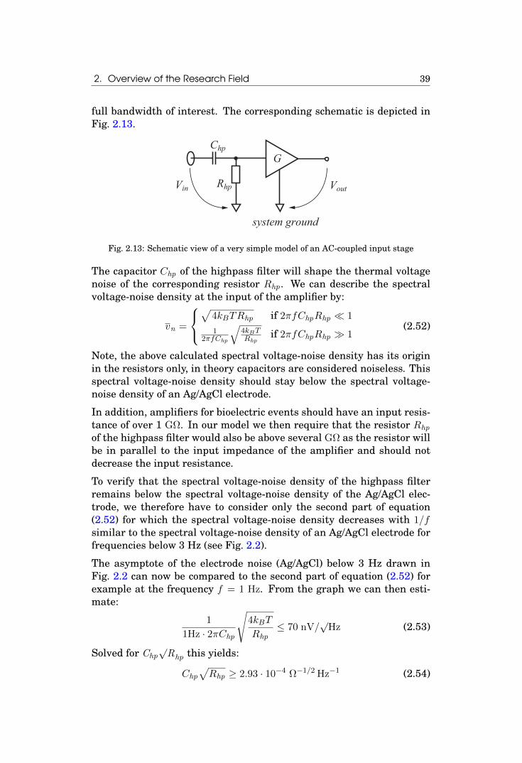
2. Overview of the Research Field 39
full bandwidth of interest. The corresponding schematic is depicted inFig. 2.13.
Vin Vout
system ground
ChpG
Rhp
Fig. 2.13: Schematic view of a very simple model of an AC-coupled input stage
The capacitor Chp of the highpass filter will shape the thermal voltagenoise of the corresponding resistor Rhp . We can describe the spectralvoltage-noise density at the input of the amplifier by:
vn =
√
4kBTRhp if 2πfChpRhp 1
12πfChp
√4kBTRhp
if 2πfChpRhp 1(2.52)
Note, the above calculated spectral voltage-noise density has its originin the resistors only, in theory capacitors are considered noiseless. Thisspectral voltage-noise density should stay below the spectral voltage-noise density of an Ag/AgCl electrode.
In addition, amplifiers for bioelectric events should have an input resis-tance of over 1 GΩ. In our model we then require that the resistor Rhp
of the highpass filter would also be above several GΩ as the resistor willbe in parallel to the input impedance of the amplifier and should notdecrease the input resistance.
To verify that the spectral voltage-noise density of the highpass filterremains below the spectral voltage-noise density of the Ag/AgCl elec-trode, we therefore have to consider only the second part of equation(2.52) for which the spectral voltage-noise density decreases with 1/fsimilar to the spectral voltage-noise density of an Ag/AgCl electrode forfrequencies below 3 Hz (see Fig. 2.2).
The asymptote of the electrode noise (Ag/AgCl) below 3 Hz drawn inFig. 2.2 can now be compared to the second part of equation (2.52) forexample at the frequency f = 1 Hz. From the graph we can then esti-mate:
1
1Hz · 2πChp
√4kBT
Rhp≤ 70 nV/
√Hz (2.53)
Solved for Chp√Rhp this yields:
Chp
√Rhp ≥ 2.93 · 10−4 Ω−1/2 Hz−1 (2.54)

2. Overview of the Research Field 40
Multiplying both sides with√Rhp results in:
ChpRhp ≥ 2.93 · 10−4 Ω−1/2 Hz−1√Rhp (2.55)
We can express the product on the left side by the corner frequencyf0 of the highpass filter which is defined by the application (e.g., ECGor EEG) by ChpRhp = 1/2πf0. After substituting the product we cancalculate the maximal resistance Rhp which still fulfills equation (2.55):
Rhp ≤(
1
2πf0 2.93 · 10−4
)2
Ω (2.56)
For f0 = 0.016 Hz (i.e., for ECG) we obtain Rhp ≤ 1.16 GΩ and a corre-sponding Chp ≥ 8.6 nF.
This is a reasonable value for the input impedance of an amplifier forbioelectric events when used for ECG. For example the INA121 (TI) hasan input stage which can be modeled by an input resistance Rin = 1GΩparallel to an input capacitance of Cin = 1 pF. For frequencies below thecorner frequency f0 = 0.016 Hz the input impedance still behaves like aresistance and the highpass filter made out of Rhp and Chp will still befunctional. For higher frequencies (e.g., 50 Hz) the two capacitors Chp
and Cin will form a capacitive voltage divider with the gain of Chp/(Chp+Cin) ≈ 1 which leads to a slightly reduced input signal.
But for f0 = 1 Hz (EEG) we obtain Rhp ≤ 296 kΩ which is far too lowfor an amplifier for bioelectric events. Yet, increasing Rhp will eitherincrease the spectral voltage-noise density (for the same f0) or result ina lower f0 (for the same spectral voltage-noise density).
We conclude that AC-coupled amplifiers may be used for ECG measure-ments but are not suited for EEG measurements because there will al-ways be a trade-off between spectral voltage-noise density and the inputresistance or settling time.
As an example, in [Pran 00] and [Harl 02] an AC-coupled amplifier isbuilt using the input resistance Rin of an INA 116 (orig. Burr-Brown,now TI) as part of the highpass filter. Noise measurements are providedas well.
2.3.5 DC-coupled Amplifiers
After all, there is a crucial downside to using AC-coupled input stages:The low-frequency part including the DC voltage of the bioelectric sig-nal is inevitably lost. Yet, it was shown that removing the DC offsetmay also remove some clinically relevant data. Examples of clinically

2. Overview of the Research Field 41
relevant low-frequency signals are the depolarization prior to an epilep-tic seizure [Iked 99], the change of alertness that can be measured byEEG [Zsch 02] or the sleep pattern of preterm infants [Vanh 02].
Fig. 2.14 illustrates the effect of a highpass filtering by showing thesame recording, once with a highpass filter and once without.
EEG+
DC
EEG 100 µV
100 µV
1 [s]
Fig. 2.14: Twice the same EEG recording, the first trace without a highpass filterand the second trace with a highpass filter. (Picture reproduced from [Zsch 02])
Without discussing the medical meaning we can easily see that the tracewithout AC-coupling (named ‘EEG + DC’) holds more details than thetrace with AC-coupling (named ‘EEG’). The interpretation of the addi-tional information in DC-coupled EEG systems is still under investi-gation. Yet, the fact that there is additional information available isundisputed.
This leads to a new emerging standard, the Full-Band EEG [Vanh 05].To record a Full-Band EEG the amplifier must be built without a high-pass filter. However, it is possible to allow for manual compensation ofa DC offset at any given time by the operator.
Instead of removing the DC offset manually, it is possible to samplethe full signal with an ADC having a large dynamic range. The re-quired number of bits is given by the maximum tolerable offset dividedby the desired resolution. If, for example, the maximum tolerable off-set is ±300 mV as proposed by the AAMI [AAMI 99] and the desiredresolution is 1 µVrms, we can calculate the required number of bits:
n ≥ log2
(600 mV
1 µV
)= 19.2 (2.57)
An ADC with 20-bit resolution would be sufficient. This is for examplethe effective number of bits of the AD7734, a 24-bit ADC from AnalogDevices, when used with a sampling rate of about 1 kHz.
We will demonstrate in chapter 6 a second way to measure the low-fre-quency part of a bioelectric signal, i.e., by looking at the feedback signalused to compensate for the skin-electrode offset.

2. Overview of the Research Field 42
Noise of DC-coupled Input Stages
Amplifier for bioelectric events require a very high input impedance (@50 Hz) to avoid limitation of the CMRR due to the potential-divider ef-fect (see 2.2.4). They also require a very high input resistance to limitmotion artifacts [Zipp 79].
For this reason most of the amplifiers for bioelectric events have FETinput stages which are affected by 1/f noise. This means that the spec-tral voltage-noise density of the input-referred voltage noise is flat downto a certain corner frequency. Below this corner frequency the spectralvoltage-noise density increases by a factor of ten per two decades. (Thename 1/f is derived from the fact that the corresponding power spectraldensity rolls off with 1/f ).
Because an Ag/AgCl electrode has a similar characteristic (see Fig. 2.2),the amplifier can be designed to stay below the spectral voltage-noisedensity of an Ag/AgCl electrode.

2. Overview of the Research Field 43
2.3.6 Review of Amplifiers for Bioelectric Events
Reviewing the discussed amplifiers for bioelectric events we distinguishbetween four main topologies as depicted in Fig. 2.15.
b)
d)
c)
Vout
CHP
high gain low resolution
RHP
ADa)
Vin
low gain high resolution
high gain
DC feedback
low resolution
VinVout
CHP
low gain high gain low resolution
RHP
AD
VinVout
CLP RLP
AD
Vin Vout
AD
-
--
Fig. 2.15: Four main topologies for amplifier for bioelectric events. They are a) AC-coupled input stage, b) DC-coupled input buffer with DC feedback, c) standardtwo-stage bioelectric amplifier and d) DC-coupled input stage followed by ahigh-resolution ADC.
All four topologies are described in literature and used in commerciallyavailable amplifiers for bioelectric events. None of the four topologies isideally suited for all purposes. The four topologies are:

2. Overview of the Research Field 44
a) AC-coupled input stage: This topology may suffer from an addi-tional CMRR limitation due to the corner-frequency mismatch (see2.2.4). Input impedance, input-referred noise or settling time maybe a limiting factor especially for EEG (see 2.3.4). This is the onlytopology which allows off-body sensing of an ECG (see 2.3.4)
b) DC-coupled input buffer with DC feedback: In contrast to the AC-coupled input buffer the DC feedback topology allows to use a com-mon reference electrode. The highpass filter is realized in the firststage which allows for a high gain in the first stage to reduce thenoise contribution of the following stages. The DC gain is alwaysone, thus the low-frequency part of the signal is not fully removed.As a result, this part of the signal can also be sampled in orderto measure the bioelectric signal down to DC. This is the besttopology for amplifying electrodes (see chapter 6) and [Mett 94].This topology can also be used to build fully differential ampli-fiers which do not suffer from the CMRR limitation due to corner-frequency mismatch [Spin 03].
c) Standard two-stage amplifier: This presents the most frequentlyused topology in amplifiers for bioelectric events. A low-gain DC-coupled buffer is followed by a highpass filter and a second gainstage. The second gain stage boosts the bioelectric signal andallows the use of standard low-resolution ADCs or plotters. Thegain of the first stage is limited to a factor of 5 to 15 (dependingon the supply voltage) in order to handle DC offsets of ±300 mV[AAMI 99] without saturating the first stage. The DC offset isnormally rejected without being measured.
d) DC-coupled input stage followed by a high-resolution ADC: Afteran initial gain of 5 to 15 the bioelectric signal is sampled by a high-resolution ADC. This topology replaces more and more of the two-stage amplifiers because of the lower part count and the presenceof the low-frequency part of the bioelectric signal in the measure-ment. This is only possible due to the development of ADCs with24-bit resolution. Because most of the signal processing is per-formed digitally it offers the highest flexibility but also the highestpower consumption of all systems presented. Filters are usuallyimplemented as FIR (finite impulse response) filters with a per-fect linear phase response resulting in a minimal distortion of thebioelectric signal. To our knowledge, there are no publications de-scribing such a system in detail, yet several systems are availablecommercially on the market, e.g., ’active-one’ from biosemi [bios].

2. Overview of the Research Field 45
2.4 Figures of Merit
At this point we would like to summarize the most important figures ofmerit for amplifiers for bioelectric events like EEG and EEG:
Noise: A high-quality amplifier for bioelectric events should generateless equivalent input noise than the employed electrode. Accord-ing to Fig. 2.2 the spectral voltage-noise density of an Ag/AgCl-Electrode can be estimated to 30 nV/
√Hz at 100 Hz. The total
noise power in a bandwidth of 10 Hz - 1 kHz (ECG) can be esti-mated as 1.4 µVrms and the spectral voltage-noise density is in-versely proportional to f for frequencies below 3 Hz.
Input-stage design: For a correct bioelectric signal representation theAAMI [AAMI 99] defines a lower corner frequency of at most 0.016Hz for clinical ECG and 0.05 Hz for ambulant ECG. The cornerfrequency for EEG should be at most 1 Hz. The AAMI also de-fines a minimum level of ±300 mV DC offset which the amplifierfor bioelectric events must be able to accept. The offset originatesmostly from the electrode-skin interface. To reduce motion arti-facts, the input resistance of the amplifier should be larger than1 GΩ [Zipp 79]. All filters should have a linear phase response toguarantee optimal signal reproduction.
CMRR: The CMRR (@ 50 Hz) has to be large enough to ideally reducethe power-line interference to a level below the resolution of theamplifier while in standard mode of operation (e.g., the person isnot touching a metal surface). The required value for the CMRRdepends on the measurement situation. A body-worn device withbatteries and wireless link requires a CMRR (@ 50 Hz) of onlyabout 20 dB (resp. 50 dB if no DRL is used) because there is onlya very small common-mode voltage. A standard EEG device whichis not entirely worn on the body should have a CMRR (@ 50 Hz) ofat least 80 dB [Mett 93] and use a DRL circuit.
Soft factors: Mobile devices intended for the consumer market requirethe lowest possible cost for the components. This works hand inhand with the aim to achieve the lowest possible power consump-tion, because the autonomy increases and/or the weight of the de-vice can be reduced by using smaller batteries.Additional cost factors include the complexity of the electronic cir-cuit (number of ICs) and required mechanical parts (number ofwires and connectors).

3. CONTINUOUS MONITORING OFELECTRODE-SKIN IMPEDANCE MISMATCHDURING BIOELECTRIC RECORDINGS
This chapter is a synopsis of the corresponding publication in the IEEETransactions on Biomedical Engineering [Dege 08].
3.1 Problem Statement
The electrode-skin impedance is an important parameter for amplifiersfor bioelectric events. A large electrode-skin impedance results in moreinterferences (noise) like for example increased coupling of the power-line voltage to the leads. A large electrode-skin impedance mismatchleads to a reduced CMRR.
It would be beneficial to monitor the electrode-skin impedance duringthe measurement in order to give feedback to the operator. The mon-itoring of the electrode-skin impedance should not degrade the qualityof the recording. The following work describes a suitable method to con-tinuously monitor the electrode-skin impedance.
3.2 Prior Art
Several publications describe how to measure electrode-skin impedan-ces by injecting a sinusoidal current via an additional reference elec-trode through the body and then measuring the voltage drop over allthe different signal electrodes. The frequency of the sinusoidal cur-rent ranges from 120 Hz [Hami 00] to 20 kHz [Devl 84]. These meth-ods do not measure one electrode-skin impedance but two in series (theelectrode-skin impedance of the reference electrode is always measuredalong with the electrode-skin impedance of the signal electrode underinvestigation).
Another method measures the electrode-skin imbalance based on thepower-line interference [Spin 06] while the reference electrode has to be

3. Monitoring Electrode-Skin Impedance Mismatch 47
disconnected.
Grimbergen et al. describe a method to measure a single electrode-skin impedance based on the power-line interference while concurrentlymeasuring the input current and the input voltage by a second high-impedance electrode [Grim 92].
Only one of these methods is designed to simultaneously measure thebioelectric signal [Devl 84]. Yet, all these methods lower the input re-sistance of the amplifier for bioelectric events, which degrades the mea-surement due to the potential-divider effect (see section 2.2.4) and in-creases motion artifacts [Zipp 79b].
Only one publication describes a method which does not reduce the in-put resistance of the amplifier for bioelectric events; it forces a knowncommon-mode voltage VCM via the DRL circuit [Ober 82]. Unfortu-nately, the method only yields a binary decision for ‘bad’ or ‘good’ con-tact. Our method is derived from this work, but is able to measure theelectrode-skin imbalance between two electrodes.
3.3 Method
Our method is based on superimposing a known voltage Vadd to the ref-erence voltage of the DRL circuit (see also section 2.3.3) to force thecommon-mode voltage VCM to a known voltage. The superposition ofan additional signal does not affect the ability of the DRL to reduce thepower-line interference.
The amplifier is considered to be a CMOS amplifier with a FET-inputstage. This is the standard for amplifiers for bioelectric events. Theyhave a very high input impedance Zin modeled by a resistor Rin in par-allel to a capacitor Cin :
Zin =Rin
1 + jωRinCin(3.1)
Typical values are Rin > 1012 Ω and Cin = 1 pF.
The amplitude and frequency of Vadd is not defined by the method but bythe application and the bandwidth of the amplifier for bioelectric events.In other words, the frequency of Vadd has to be chosen within the signalbandwidth of the amplifier used, but not too close to the frequency ofthe power-line interference.
The calculations in this section are made for a sinusoidal voltage Vadd
with an amplitude of 10 mV and a frequency of 1.2 kHz. In this examplethe frequency was chosen relatively high in order to be able to observe

3. Monitoring Electrode-Skin Impedance Mismatch 48
the variation of the electrode-skin impedance imbalance resulting frommanually pressing electrodes to the skin. The imbalance variation re-sulting from manual movements have an upper frequency limit of about30 Hz.
In order to quantify the electrode-skin impedance mismatch of a pairof electrodes we measure the amplitude and phase of the known com-mon-mode signal after the first amplifier stage. This is done by syn-chronous demodulation, e.g., by multiplying the signal of interest withVadd followed by a lowpass filter (this is the same principle that lock-inamplifiers use).
The block diagram of the amplifier for bioelectric events is depicted inFig. 3.1.
The above figure represents a generalized view of the schematic whichcan be adapted from one to ‘n’ channels. Each channel is preceded by aprotection circuit which limits the maximal current through the body to50 µArms.
For our test application we built the instrumentation amplifier (INA)in Fig. 3.1 using three low-power CMOS op-amps of the type LMC6462(National Semiconductor) chosen for its high input resistance (Rin >1012Ω, Cin = 1.5 pF) . The gain of the INA was set to 20 dB. The CMRRof the INA was maximized by manually trimming one resistor [Pall 91].For the DRL circuit we used the TS914 (STMicroelectronics) chosen forits larger bandwidth.
The measurement circuit operates as follows: any voltage appearing atthe positive input of the DRL op-ampOPDRL forces the DRL loop to reactin such a way that the differential input voltage of the DRL op-amp isagain zero (principle of virtual ground). For a sinusoidal signal this istrue as long as the frequency remains within the bandwidth of the DRLloop. As a result, the sinusoidal voltage Vadd appears as a common-modevoltage to the input of the instrumentation amplifier (INA). This knowncommon-mode voltage is rejected by the CMRR of the INA, except forthe part which is converted to a differential signal by the electrode-skinimpedance mismatch (this is known as the potential-divider effect, seesection 2.2.4). The signal is then amplified by the differential-mode gainof each INA and appears superimposed on the corresponding outputvoltage Vout i . If we ignore all other sources, e.g., power-line interferenceand bioelectric signal, we can calculate the residue of the known com-mon-mode signal Vadd i at the electrode ‘i’.
This residual voltage is:
Vadd i =1
CMRRpot·GDM · Vadd (3.2)

3. Monitoring Electrode-Skin Impedance Mismatch 49
DRLC RDRL
Zel 'i+1'
Zel 'i'
Zref
OPDRLaddV
out 'i'V
out 'i+1'V
electrodeDRL
protection circuit
electrodereference
electrodessignal
channel
INA
'i'
channel
to remaining channels 'i+3' ... 'n'
INA
'i+1'
multiply
norm 'i'
phase 'i'multiply
norm 'i+1'
phase 'i+1'
add 'i'V add 'i+1'V
20 kΩ20 kΩ
Fig. 3.1: Block diagram of the amplifier for bioelectric events. The amplifier has onereference electrode, one DRL (driven-right-leg) electrode and ‘n’ signal elec-trodes of which only two are shown. Each channel has one instrumentationamplifier (INA) with a gain of 20 dB. A known common-mode voltage Vadd isapplied to the positive input of the op-amp OPDRL which is part of the DRLloop.
This equation is valid as long as the CMRR of the INA is much largerthan CMRRpot . CMRRpot stands for the common mode rejection ratioresulting from the potential-divider effect. The corresponding formulais derived in section 2.2.4):
CMRRpot =Zin
|∆Zel |(3.3)
∆Zel stands for the difference of two electrode-skin impedances and Zin

3. Monitoring Electrode-Skin Impedance Mismatch 50
represents the mean value of the two common mode input impedancesof the amplifier. GDM represents the differential-mode gain (for the fre-quency of Vadd ).
Combining equation (3.3) and (3.2) yields:
Vadd i ≈Zel i−Zref
Zin
GDM · Vadd (3.4)
In this particular application and for the chosen frequency of the knowncommon-mode signal Vadd the input impedance of the INA is primarilycapacitive. With this in mind, we can solve for the input electrode-skinimpedance mismatch:
Zel i−Zref ≈1
jωCin GDM
Vadd i
Vadd(3.5)
In the measurement circuit we quantify the residual voltage Vadd i by amultiplication with the original common-mode signal Vadd . This is usu-ally called synchronous demodulation and results in two signals ‘norm i’and ‘phase i’ representing amplitude and phase of the residual signal.These two signals can then be used to calculate the electrode-skin im-pedance mismatch between the reference electrode and the signal elec-trode ‘i’ according to equation (3.5).
In a real measurement situation Vout i is composed of the amplified bio-electric signal and the residue of the known common-mode voltage Vadd .To improve rejection of the bioelectric signal either a bandpass filter(here at 1.2 kHz) can be used or a longer integration period of the twosignals ‘norm i’ and ‘phase i’.
To measure the electrode-skin impedance mismatch between two signalelectrodes i and j, the corresponding residue Vout i and Vout j are mea-sured separately and then subtracted mathematically. For an absolute(precise) measurement of the electrode-skin impedance mismatch themean input capacitance Cin of the INAs must be known very preciselyalong with the common-mode gain GDM . If these values are not knownit is still possible to calibrate the circuit using a resistor with a knownvalue.
3.3.1 Experimental Results
To validate the method we quantify the amplitude of the residual com-mon-mode voltage Vadd i using known impedances and a sinusoidal volt-age Vadd with an amplitude of 10 mV and a frequency of 1.2 kHz.
Fig. 3.2 shows the measurements which have been carried out using anECG phantom and a set of known resistors which were added in series

3. Monitoring Electrode-Skin Impedance Mismatch 51
0
15
10
-10
-5
-15
-20
5
-20 -15 -10 -5 0 5 10 15 20Impedance Imbalance (Rel i - Rref ) [kΩ]
error 10% of fullscale(uncalibrated)
linearization
norm‘i’ * sign(phase‘i’) [μV]
norm‘i’ * sign(phase‘i’)
Fig. 3.2: The norm of the residue of the common-mode signal Vadd i multiplied bythe corresponding phase as a function of the artificial impedance mismatchRel i −Rref added to an ECG phantom.
to the input of the amplifier for bioelectric events. Looking closely atequation (3.5) and knowing that the difference between to resistors is areal number, we deduce that Vadd i/Vadd results in an imaginary num-ber. As a consequence the phase shift between Vadd i and Vadd assumesmostly two distinct values, i.e.,±90. The sign of Vadd i/Vadd correspondsto the sign of Zel i − Zref and indicates which of the two involved resis-tances is larger.
The residual voltage is measured both in amplitude and phase. InFig. 3.2 the amplitude (norm) is drawn while the phase is used to de-termine the sign. As predicted by equation (3.5) the phase shift waseither +90 (positive sign) or −90 (negative sign).
Fig. 3.2 confirms the linear relation between the residual voltage ex-pressed by norm i · sign(phase i) and the resistive mismatch Rel i −Rref .From the figure the gradient of the linearization can be estimated toabout 0.75 µV/kΩ. The gradient can also be predicted from equation(3.5), using the values from our circuit (Vadd = 10 mV, Cin ≈ 1.5 pF,f = 1.2 kHz, GDM = 20 dB) the resulting gradient would be 1.1 µV/kΩwhich is close to the measured value. 1
1 The larger the CMRR the smaller the residual voltage. For the measurements de-scribed in the publication we added two switched-capacitor bandpass filters with again of 40 dB each to Vadd i and Vadd . This was done prior to the synchronous demod-ulation and resulted in a stable measurement in spite of the small residual voltage.The figure in the publication showed the real measurement while the gradient wasgiven based on the circuit described which had only one switched-capacitor band-pass filter and consequently did not match the gradient in the corresponding figure.

3. Monitoring Electrode-Skin Impedance Mismatch 52
The absolute values of Rel i and Rref have no influence on the residualvoltage.
Having gauged the measurement signal with known resistances we cannow estimate the electrode-skin impedance mismatch when measuringa bioelectric signal. Without calibration the error is about 10 % of theshown scale and 1 % of the overall full-scale value (200 kΩ). The lin-earity can be improved by increasing the amplitude of the additionalcommon-mode signal Vadd while reducing both the CMR (common moderange) and the maximal gain of the amplifier.
Calibration is only required if the absolute value of the electrode-skinimpedance mismatch is to be measured, because the impedance Zin ofthe INA may vary from device to device. Calibration is not requiredwhen only the power-line vulnerability condition (i.e., an estimation ofCMRRpot ) is to be determined according to equation (3.2).
Electrode-Skin Impedance Mismatch versus Applied Force
We now apply a sinusoidal force to the signal electrode ‘i’ and both thenorm of the residual voltage |Vadd i | and the bioelectric recording aremeasured. For this measurement, a subject is lying on the ground withthree dry electrodes (custom made Ag/AgCl electrode with a diameterof 12 mm attached to a dry gel pad with a diameter of 30 mm) pressedto the body by individual weights of 300 g. One electrode is then pulledaway from the body with a sinusoidal force corresponding to a weight of100 g and a frequency of 0.33 Hz. Fig. 3.3 shows the corresponding ECGmeasurement.
As a result of the sinusoidal force, the bioelectric signal displays a si-nusoidal disturbance of the same frequency, i.e., 0.33 Hz. The norm ofthe residual voltage is digitally filtered by a lowpass filter with a cor-ner frequency of 2.5 Hz and zero phase shift. The estimated electrode-skin impedance mismatch is also indicated with a second axis using thepreviously determined conversion factor 0.75 µV/kΩ. All signals are fil-tered by an additional digital 50-Hz notch filter for better visualization.
Fig. 3.3 demonstrates that there is a strong relationship between themeasured electrode-skin impedance mismatch and the baseline varia-tion. This is in accordance with previously published results [Hami 00],[Devl 84] showing a similar relation between impedance mismatch andbaseline shift. This kind of artifact is called skin-stretch artifact or skin-motion artifact [Sear 00].
However, the amplifier in this work has a very high input resistance(Rin > 10 TΩ) when compared to previous amplifiers. As a result thereare nearly no additional currents through the electrode-skin interface

3. Monitoring Electrode-Skin Impedance Mismatch 53
1 2 3 4 5 6 7 8
-1
0
1
2
3
4
time [s]
|Vadd i |
Vout i -Vout 'i+1'
ECG
[m
V]
estimated im
pedance mism
atch [kΩ]
wei
ght
[g]
0
20
norm of the residual voltage [μV
]
300
200
40
60
80
0
30
60
force applied to electrode i
Fig. 3.3: A simultaneous measurement of an ECG and the norm of the residualvoltage |Vadd i | resulting from a sinusoidal force applied to electrode ‘i’. Themeasurement reveals a strong relation between the norm of the residual volt-age and the baseline variation of the ECG. The residual voltage can be used toestimate the input electrode-skin impedance mismatch.
at the frequency of interest (0.33 Hz). This is important because theamplitude of the motion artifact voltage is proportional to the currentthrough the electrodes [Zipp 79b].
For this particular measurement an impedance variation of about 20 kΩresults in a baseline shift of about 3 mV. The measured impedance, how-ever, is not sinusoidal. We believe this is a result of the previously re-ported nonlinear relationship between stretching and relaxation of theskin [Oedm 81] which is probably due to the viscoelastic properties ofthe skin.
Electrode-Skin Impedance Mismatch versus Series Resistance
An additional measurement on a test subject has been performed in or-der to verify the influence of the impedance mismatch on the bioelectricrecording. This time a 20 kΩ potentiometer is added in series to the in-put of the signal electrode ‘i’ and the resistance of the potentiometer isaltered manually. The corresponding measurement is shown in Fig. 3.4.Again, a digital 50-Hz notch filter is used for better visualization.
This measurement indicates that the prior observed baseline variationis not a result of the current flowing into the electrodes, i.e., the baseline

3. Monitoring Electrode-Skin Impedance Mismatch 54
1 2 3 4 5 6 7 8
-2
-1
0
1
2
time [s]
ECG
[m
V]
additional impedance m
ismatch [kΩ
]
-4
-3
-20
0
20
40
60
80
100
|Vadd i |
Vout 'i' -Vout 'i+1'
norm of the residual voltage [μV
]
0
30
60
Fig. 3.4: Another simultaneous measurement of an ECG and the norm of the resid-ual voltage |Vadd i | generated by manually varying a 20 kΩ potentiometer inseries to the input of the electrode ‘i’. Although the variation of the resistanceis clearly visible, there is no baseline variation at all.
variation is not a result of the potential-divider effect. The finding isnot unexpected. In order to have an impedance variation of about 20 kΩresult in a voltage change of about 3 mV, a current of close to 150 nAmust flow. The bias current of the INA is only in the order of somepA. Even when considering that the impedance variation is measuredat 1.2 kHz and the baseline variation takes place at 0.33 Hz, the biascurrent of the INA can be neglected.
But then, how does the measured electrode-skin impedance mismatchrelate to the observed baseline variation? We propose that there are twodistinct effects: a change of the resistance and a change of the capaci-tance within the skin. By compressing the skin, the resistance of theskin varies. If we consider the resistivity of the skin ρ constant (as afirst approximation) we can describe the resistance of the skin by:
Rskin = ρd
A(3.6)
Where A and d denote surface and thickness of the skin region underinvestigation, e.g., the skin under the electrode.
Pressing an electrode to the skin will reduce the thickness of the skinand therefore result in a change of the electrode-skin impedance imbal-ance measured by our method.

3. Monitoring Electrode-Skin Impedance Mismatch 55
The baseline variation is produced by the second effect, the variationof the capacitance built by inner and outer layer of the skin. Betweenthese two layers there is a voltage difference of about 100 mV whichis maintained by the body to form a protective barrier. This voltage ismaintained by a ionic current, i.e., the body is actively transporting ionsthrough the skin, e.g., via the sweat glands. In [Talh 96] this currentis called ‘injury current’. The ‘injury current is balanced by the driftcurrent id resulting from the electric field across the capacitor (i.e., theskin).
id = VskinA
ρd(3.7)
In the presence of an electrode this balance is disturbed by the biascurrent of the amplifier. The bias current ib adds to the ‘injury current’.The proposed model is depicted in Fig. 3.5:
electrode-skininterface
injurycurrent
Vskin
driftcurrent
biascurrent
stratumgranulosum
transitionalcells
stratumcorneum
R C
electrode
Fig. 3.5: The body generates a negative voltage between the inner and outer skin byan ionic current called by some authors ‘injury current’. The current is mainlybalanced by a drift current. The different skin-layers act like a capacitor.
The three currents are in equilibrium:
id = iinjury + ibias (3.8)
Applying a force to the electrode will disturb the balance of the threecurrents. Compressing the skin immediately varies the capacitance ofthe capacitor built by the different skin-layers, resulting in a voltagechange over the capacitor. Likewise, the inter-skin resistance of the skindecreases and thus the injury current generates a lower voltage drop.These two fast effects are followed by a slower process during which anew equilibrium is reached. The new equilibrium is defined by the newcapacitance, the new inter-skin impedance and the three currents.

3. Monitoring Electrode-Skin Impedance Mismatch 56
This model is in agreement with the characteristics of motion artifactsreported in the literature. The model also proposes a fast and slow effectas described in [Oedm 81]. The new equilibrium is characterized by alarger capacitance. Accordingly, starting from a compressed skin will re-sult in a larger time constant (until a new equilibrium is reached) thanstarting from a non-compressed skin as it was described in [Talh 96].Our model also anticipates that removing the upper part of the skin re-duces motion artifacts [Burb 78] because part of the inter-skin capacitoris destroyed and the stored charge reduced.
3.4 Novelty
The method discussed above is the first method which allows to mea-sure the electrode-skin imbalance concurrently with the bioelectric sig-nal without altering the input impedance of the amplifier for bioelectricevents.
This method can also be used to give real-time feedback to an operatoron the quality of the electrode-skin imbalance. It is possible to detectthe lift-off of one electrode. The method is also capable of generating anerror signal for adaptive filtering of motion artifacts.
Based on the measurement signals, we proposed the first skin model formotion artifacts comprising a variable capacitance. The skin model hasthe potential to explain many of the reported characteristics of motionartifacts.

4. LOW-NOISE TWO-WIRED BUFFERELECTRODES FOR BIOELECTRICAMPLIFIERS
This chapter is a synopsis of the corresponding publication in the IEEETransactions on Biomedical Engineering [Dege 07].
4.1 Problem Statement
Bioelectric recordings suffer from extensive power-line interference andother artifacts due to the high source impedance of the biological signaland the long wires, notably in the case of EEG measurements.
It has been proven many times that buffering the signal using activeelectrodes reduces the interferences. Despite the improvement of thesignal quality, active electrodes are rarely used in practice. We attributethis to the noise added to the bioelectric signal and to increased com-plexity due to the higher number of connecting wires. The followingwork describes buffer electrodes with low noise and a low number ofwires.
4.2 Prior Art
Active electrodes have been reported as early as 1968 when a singleFET-transistor was used to buffer the signals from an ECG [Rich 68].Several publications describe the design and use of buffer electrodesand their ability to reduce motion artifacts and render skin prepara-tion unnecessary while improving the quality of the signal in general[Nish 92], [Ko 98]. Most buffer electrodes reported in the literature arebuilt using operational amplifiers (op-amps) in a voltage-follower con-figuration.
There is only one publication known to us which describes a two-wiredbuffer electrode. The electrode employs a custom-made integrated cir-cuit [Padm 90], which, according the the circuit diagram, is based on

4. Low-Noise Two-wired Buffer Electrodes 58
a (customized) op-amp. It should be noted that the reported two-wiredelectrode has one particularity: the bioelectric signal has to be the low-est voltage in the circuit because the substrate of the circuit is used asthe input node. This limits the number of electrodes to one electrodeper integrated circuit. A circuit capable of driving these electrodes inrespect of their particular requirement is not described in the publica-tion.
There is one company known to us which markets two-wired bufferedelectrodes [bios]. Unfortunately, the design of their electrodes “activetwo” is not disclosed to the public.
4.2.1 Pilot Study
To verify the claim that buffer electrodes reduce power-line interference[Fern 97], we built buffer electrodes using a CMOS amplifier in a stan-dard buffer configuration employing three wires per electrode. The usedop-amp was designed by us as part of an exercise to build integratedelectrodes (not part of this thesis). To achieve minimal size, we bondedthe op-amp directly onto a PCB (printed circuit board) with gold con-tacts (necessary for bonding). This results in the smallest-active-surfaceelectrodes reported so far.
Fig. 4.1 details the different steps from fabrication to the application ofthe active buffer electrode. ©1 shows the naked PCB with the squarepad, on which the chip (as a naked die) is glued. Also visible are somesmall squares beside the large square to which the connecting pads willbe bonded. Once the chip is bonded to the PCB, the chip is covered by aglob top, and a single op-amp is cut off from the remaining PCB©2 . Onone side an Ag/AgCl cup electrode is soldered onto the PCB ©3 and theoverhanging corners are cut off. To the other end of the PCB a very thinand flexible three-lead wire©4 is soldered (no shielding is required). Thewhole PCB is drenched in epoxy and covered by a shrink tube©5 to sealoff the circuit from the environment.
To be able to add the buffer electrodes to an existing amplifier, e.g., in ahospital, we fabricated a very simple connector box (depicted in Fig. 4.1)comprising a battery and a resistive divider ©6 . Fig. 4.2 illustrates theschematic of the box with one buffer electrode drawn.
Three active buffer electrodes ©7 made with tin-cup electrodes ©5 weretested at the USZ (university hospital in Zurich) by recording an EEG.The connector box allows connecting the buffered bioelectric signal tothe standard measurement box by a touch-proof connector ©8 . Fig. 4.3shows the FFT (fast Fourier transform) of two signals recorded simul-taneously at two close sites. The FFT on the left belongs to a standard

4. Low-Noise Two-wired Buffer Electrodes 59
1
2
3
4
5 6
7
8
Fig. 4.1: Smallest active electrode to date made by directly gluing the operationalamplifier to the board, bonding the contacts and protecting the circuit with aglob top. Numbers are explained in the text.
system groundbox re
fere
nce
volta
ge
3x
3V
10kΩ
10kΩ
VoutVin
Fig. 4.2: The schematics of the buffer electrodes and the corresponding driver cir-cuit. The latter consisting of nothing more than a battery and a resistive di-vider. The resistive divider is used to connect the external reference voltage(from the existing amplifier) to the mid-supply of the buffer electrodes.
passive Ag/AgCl electrode, the one on the right to our active buffer elec-trode.

4. Low-Noise Two-wired Buffer Electrodes 60
Standard Ag-AgCl Electrode
applied with Gel
Active Sn Electrode
applied with Gel
50 H
z50
Hz
50 H
z50
Hz
10 µ
V1
µV
10 µ
V1
µV
Fig. 4.3: The FFT of two EEG signals recorded with a passive and an active elec-trode at two close sites. The FFTs correspond to a signal stretch of about 2 ssampled with 416 Hz, only the part from 0 to 52 Hz is shown.
The two FFTs look similar except for the 50-Hz component, which isabout 10 times larger for the passive electrode than for the active elec-trode. This proves that the use of active electrodes reduces the po-wer-line interference. The improvement corresponds to about 18 dB (@50 Hz). Both electrodes were connected to the same amplifier by meansof unshielded leads. The recordings were taken in a shielded (!) room atthe USZ.
The pilot study proved to us the beneficial effect of buffer electrodes, butalso showed us the disadvantage of using electrodes with three wires,i.e., the increased complexity when connecting to the circuit and theincreased stiffness of the cable. The aim was to develop buffer electrodeswith two wires and a low noise contribution.
4.3 Method
To reduce the number of wires, we designed active electrodes using acurrent supply and voltage output. To design the electrode with as lownoise as possible, we reduced the number of active elements to the min-imum: one transistor (MOS-FET) as input buffer and one transistor(J-FET) for the current-source. For comparison we also designed a two-wired buffer electrode using an off-the-shelf op-amp.
Amplifiers for bioelectric events require a high input impedance. Forthis reason we use a FET transistor for the single-transistor electrodeand a CMOS op-amp for the single-op-amp electrode. The two buffer

4. Low-Noise Two-wired Buffer Electrodes 61
electrodes are drawn in Fig. 4.4:
active electrode
VCC
D
SG
electrodeactive
a) using a PMOS b) using an opamp
VCC
Isup
Vin
Vout VoutVin
Isup
Fig. 4.4: Principle of an active buffer electrode biased by a current-source witheither a) an FET transistor or b) an CMOS op-amp employed as a voltagefollower.
Both buffer electrodes are implemented as voltage followers. Fig. 4.4 a)shows a P-MOS-based level shifter using a single FET (NDS336 fromFairchild Semiconductor). This P-MOS transistor was chosen becauseof its low threshold voltage and a very small channel-length modulationparameter λ. Fig. 4.4 b) depicts an op-amp-based buffer electrode usingthe LMC7111 (National Semiconductor). This CMOS-input op-amp waschosen because of the low supply voltage of 2.7 V.
The two buffer electrodes were supplied by a current-source of the typeJ505 (Vishay) which consists of a single J-FET (Junction FET). TheJ505 was chosen for its simple topology. To source 1 mA the J505 re-quires a voltage drop of about 1.2 V. Fig. 4.5 shows an extract of thecorresponding datasheet.
Schematic Diagram Output Current vs. Forward Voltage
I F (
mA
)
VF (V)0 1 2 3 4 5
0
1
2
3
4
5
Fig. 4.5: An extract of the datasheet of the J505 current-source from Vishay show-ing the schematic of the current-source as well as the graph of the forwardcurrent IF in function of the forward voltage Vf .

4. Low-Noise Two-wired Buffer Electrodes 62
The output voltage Vout of both electrodes is identical to the supply volt-age of the device and can be written as:
Vout MOS = −VDS = Vin − VGS (4.1)
Vout opamp =A0
1 +A0Vin (4.2)
Where VGS < 0 denotes the gate-source voltage of the P-MOS device andA0 stands for the open-loop gain of the op-amp. It should be noted thatin the case of the MOS-based electrode the gate-source voltage VGS addsan offset to the output voltage Vout MOS . The value of VGS depends onthe technology used but also on the supply current Isup and is normallyin the order of several hundred millivolts:
VGS =
√2 IDS
β(1 + λVDS )+ Vth (4.3)
Equation (4.3) is valid for a MOS transistor in saturation. Isup = −IDS
stands for the supply current of the buffer electrodes, β for the gainfactor (technology dependent) and λ denotes the channel-length modu-lation parameter. Vth < 0 is the threshold voltage of the chosen P-MOStransistor and can vary between identical devices by ±100 mV. For bio-electric signals this offset will be added to the offset from the electrode-skin interface. Because amplifiers for bioelectric events need to be ableto handle offset values as large as ±300 mV, it is reasonable to assumethat this additional offset can be handled too and may only require alittle adjustment in the design of the amplifier.
Note, the op-amp of the buffer electrode in Fig. 4.4 b) is not able toactively drive the output voltage Vout opamp , the correct output voltagecan only be reached because of the current-source. If, for example, theinput voltage Vin raises above the output voltage Vout opamp (which cor-responds to the supply voltage of the op-amp) the output stage of theop-amp reacts by reducing the impedance between the positive supplyand the output. This has no effect as the two terminals are alreadyshort-circuited. However, the resistance between the output and thenegative supply of the op-amp increases also and the constant currentfrom the source will therefore cause the output voltage to rise until theoutput voltage matches the input voltage again. The current-source (J-FET) can be considered to be the upper part of the output stage of thebuffer electrode.
The requirements for the op-amp are that one supply is included in theinput range and that the maximal current the output stage of the op-amp can handle being connected to this supply exceeds the value ofthe supply current Isup . The active electrode with an op-amp has al-ready been described, although using an custom-made integrated cir-cuit [Padm 90].

4. Low-Noise Two-wired Buffer Electrodes 63
The gain of the two active electrodes can be shown to be close to unity:
Gain MOS =
(∂Vin
∂Vout
)−1
=
(1− ∂VGS
∂VDS
)−1
=
(1− ∂VGS
∂IDS· ∂IDS
∂VDS
)−1
≈ 1− 1
gmr0(4.4)
with
gm =2IDS
VGS − Vthand r0 =
1 + λVDS
λIDS(4.5)
Gain opamp ≈ 1− 1
A0(4.6)
Where gm denotes the forward transconductance and r0 the output re-sistance of the MOS device. Equation (4.4) is valid for a MOS transistorin saturation.
The next important characteristic of a buffer electrode is the outputresistance. The output resistance should be low in order to reduce theinterference when long wires are used, e.g., for EEG applications. Theoutput resistance of the op-amp-based electrode is very low because ofthe negative feedback and is below some Ω. The output resistance of theP-MOS-based electrode is given by:
Rout MOS =∂Vout
∂Isup=
(∂IDS
∂VDS
)−1
with VGS =VDS +Vin (4.7)
=
(β(VGS−Vth)(1−λVDS ) +
β
2(VGS−Vth)2 λ
)−1
(4.8)
=
(gm+
1
r0
)−1
=1
gm+ 1r0
=1
2IDSVGS−Vth + λIDS
1+λVDS
(4.9)
for λ → 0
Rout MOS ≈
√1
2βIsup(4.10)
Again we see that the output resistance depends on the supply currentIsup . The higher the supply current the lower the output resistanceRout MOS of the MOS-based electrode.
The most important characteristic for a buffer electrode is the spectralvoltage-noise density of the electrode, because the noise of the electrodeis added one-to-one to the bioelectric signal. The spectral voltage-noisedensity of the op-amp can be found in the datasheet. The spectral vol-tage-noise density of the transistor is a function of the supply current.For example, the square value of the spectral voltage-noise density for

4. Low-Noise Two-wired Buffer Electrodes 64
frequencies above the flicker noise corner frequency can be expressedby:
v2n MOS ≈4kBTα
gm=
4kBTα√2βIsup(1 + λVDS )
(4.11)
Where kB stands for the Boltzmann constant, T for the temperature inKelvin and α for the transistor noise coefficient (a typical value for α is2/3).
We can now estimate the required supply current Isup for the two dif-ferent active buffer electrodes. For the op-amp-based electrode we rec-ommend to use at least twice the supply current of the op-amp as asupply for the electrode to provide for any tolerances. For the MOS-based electrode we have a lower limit given either by the desired noiselevel, which then has to be matched to equation (4.11), or by the max-imal desired output resistance, which is given by equation (4.10). Alow supply current will also reduce the bandwidth of the P-MOS-basedelectrode, which could eventually lead to a reduction of the CMRR dueto the frequency mismatch between different electrodes, similar to theeffect discussed in section 2.2.4.
The active buffer electrodes described above can be added to an existingamplifier for bioelectric events as long as an additional current-sourceis provided to supply the buffer electrodes. The electrodes themselveshave a limited input CMR (common mode range) due to the voltagedrop over the current-source and, for the op-amp-based electrode, therequirement for the minimal voltage supply of the op-amp.
For the MOS-based electrode (in saturation) the minimal output volt-age Vout MOS corresponds to Vth − VGS (this is the inverse of the over-drive voltage which depends on Isup and can be several hundred milli-volts), the minimal input voltage equals Vth which is about -780mV forthe NDS336. The op-amp-based electrode requires a minimal outputvoltage Vout opamp of 2.7 V (for the LMC 7111) which coincides with theminimal input voltage.
We therefore strongly recommend the use of a DRL circuit to drive theinput common-mode voltage of the amplifier to the midrange voltage ofthe input CMR of the employed active buffer electrodes (see also sec-tion 2.3.3). The use of a DRL circuit to drive the DC value of an activeelectrode is demonstrated for the amplifier with two-wired amplifyingelectrodes in chapter 6.
We will resume the results for the chosen reference currents later intable 4.1.

4. Low-Noise Two-wired Buffer Electrodes 65
4.3.1 Results
We fabricated several prototypes of two-wired active buffer electrodesusing buttons for trousers on which we soldered a small PCB. This de-sign allowed us to attach different disposable electrodes. Fig.4.6 showsan Ag/AgCl brush-type EEG electrode clipped to one of the active elec-trodes.
1 cm
Fig. 4.6: A shielded two-wire active electrode mounted on a button in order toattach different types of disposable electrodes.
The prototype electrodes are left unprotected to allow the soldered com-ponents to be easily changed.
We first measured the input-referred spectral voltage-noise density ofthe two different electrodes for a supply current Isup of 1 mA. In Fig. 4.7the spectral voltage-noise density of both two-wired active buffer elec-trodes is presented together with the spectral voltage-noise density ofan Ag/AgCl electrode1 for comparison.
The noise of the P-MOS is very similar to the noise of the Ag/AgCl elec-trode except for the low-frequency part. At low frequencies the noiseof the P-MOS is higher, the corner frequency from which the spectralvoltage-noise density shows a frequency dependency is higher for theP-MOS than for an Ag/AgCl electrode. We can estimate the total noiseby approximating the area under the curves.
We then estimate the total voltage noise from 0.1 Hz to 200 Hz (ECG) to2.05 µVrms for the MOS-based electrode with a supply current of 1 mA.This is higher than the total voltage noise of an Ag/AgCL electrode thatamounts to 1.4 µVrms. The op-amp-based electrode does visibly havemore noise at lower frequencies and does not present itself as a goodsolution for ECG.
1 The measurements of the electrode noise were carried out by biosemi [bios], expla-nations at ”http://www.biosemi.com/faq/without_paste.html“

4. Low-Noise Two-wired Buffer Electrodes 66
1 10010 1k0.1
600
spec
tral v
olta
ge n
oise
den
sity
[nV
rms/
√Hz]
frequency [Hz]
800
400
200
0
NDS 336 LMC 7111
Ag/AgCl
Fig. 4.7: The spectral voltage-noise density of the two different active buffer elec-trodes measured with a supply current of 1 mA using a vector signal analyzer(Stanford SR785). Different sampling rates were used above and below 100 Hz.
If we estimate the total voltage noise from 10 Hz to 1 kHz (EEG) we get11.1 µVrms for the op-amp-based electrode, which is nearly ten timeshigher than the total voltage noise of an Ag/AgCL electrode in this fre-quency band (1.5 µVrms). A much better choice for EEG is the MOS-based electrode, which has a total voltage noise of less than 1 µVrms forthe same frequency band. This is even lower than the inherent noiseof the Ag/AgCl electrode. We do not recommend reducing the supplycurrent of the MOS-based electrode because this would result in morelow-frequency noise for which the MOS-based electrode is worse thanthe Ag/AgCl electrode. With a supply current of 1 mA the spectral vol-tage-noise density of the electrode is higher than that of the MOS-basedelectrode for frequencies above about 100 Hz. The spectral voltage-noisedensity of the MOS-based electrode at 1 kHz is around 10 nV/
√Hz (this
is the limit of the Stanford SR785).
As a first conclusion we can state that the total voltage noise of theop-amp-based electrode is more than ten times higher than the totalvoltage noise of the MOS-based electrode. As long as the additional DCoffset of ±100 mV added by the MOS based active electrodes does notsaturate the subsequent amplifier, the MOS-based electrodes will allowto measure signals which are ten times smaller. If the buffer electrodeis to be added to an existing amplifier which cannot be adapted to adjustfor the additional DC offset, the op-amp-based electrode may be used inspite of the larger noise contribution.
Table 4.1 shows the most important characteristics measured for the

4. Low-Noise Two-wired Buffer Electrodes 67
two buffer electrodes . The MOS-based electrode from Fig.4.4 a) wasmeasured with two different reference currents, i.e., 1 mA and 10 µA forcomparison.
Tab. 4.1: The measured characteristics for both active electrodes.
Components P-MOS op-ampNDS336 LMC7111
Isup [mA] 1 0.01 1Offset [mV] 840± 25 620± 17 3± 1
VCC [V] ≥1.84 V ≥1.62 V ≥3.7 VNoisea [µVrms] 0.96 1.95 11.1Gain 0.99986 0.9999993 0.99986Rin
b [GΩ] 3000 3000 5000Rout [Ω] 50 4.1k 0.1Ibias [pA] −0.060 −0.060 −31
a total noise from 10 Hz to 1 kHzb Measured with a parameter analyzer HP4155B/4156B
To test the electrodes we recorded the ECG of the author with all threeactive buffer electrodes from Tab. 4.1. The amplifier used was an exper-imental set-up with a gain of 60 dB based on the INA122 (orig. Burr-Brown, now TI) without additional filtering. We measured an ECG be-cause we estimate that the quality of an amplifier can be best evaluatedwith the distinct features of an ECG recording, e.g., the absence of noiseand the flatness of the baseline.
time [s]
EC
G[
V]
P-MOS 1m A
P-MOS 10µA
OpAmp 1m A
1 V
0
0
0
0 0.5 1 1.5 2 2.5 3
Fig. 4.8: Three ECG curves from the author recorded at different times. The type ofthe electrode as well as the supply current are included as part of the curve’sname.
4. Low-Noise Two-wired Buffer Electrodes 68
The recordings were taken on different days using disposable dry pre-gelled adhesive electrodes. No prior cleaning of the skin was necessary.Two recordings were taken with a P-MOS based two-wired active elec-trode but with different supply currents. One recording was taken withan op-amp-based electrode.
It should be noted that the trace with the lower reference current (P-MOS 10uA) appears to display slightly more noise.
4.4 Novelty
We have successfully demonstrated the use of a single transistor for anECG recording using two-wires per electrode. Although the use of asingle transistor was not new, it was somehow no longer considered be-cause of the large prevalence of op-amps. We have shown that the useof a single transistor adds ten times less voltage noise to the bioelectricsignal than the use of an op-amp (for the same supply current). In ad-dition, the input bias current is minimal when using a single transistorwhich is important to reduce motion artifacts [Zipp 79b].
Furthermore, using a low-noise single-transistor-based active electrodeensures the maximal input impedance which is important for bioelectricrecordings. Using a buffer electrode with a high input impedance allowsus to use any type of amplifier for the subsequent stage, e.g., low-noiseamplifiers with a bipolar input stage. This results in a much largerchoice for the subsequent amplifier stage.

5. ENHANCING INTERFERENCE REJECTIONOF AMPLIFYING ELECTRODES BYAUTOMATED GAIN ADAPTION
This chapter is a synopsis of the corresponding publication in the IEEETransactions on Biomedical Engineering [Dege 04].
5.1 Problem Statement
In order to minimize the input-referred noise of an amplifier for bio-electric events, it is desirable to amplify the signal close to the source,i.e., already on the electrode. Yet, without any control of the gain, anygain mismatch between different electrodes will compromise the over-all CMRR of the amplifier. The following work demonstrates an au-tonomous method to compensate for a gain mismatch of individual elec-trodes by adapting the gain of the subsequent differential amplifier.
5.2 Prior Art
A mismatch of the gain between different electrodes is known to be crit-ical for achieving a good CMRR [Pall 91] (see also section 2.2.4). Forexample, when building a multi-electrode system with two-stage instru-mentation amplifiers it is important that the amplifiers share a commonreference node [Mett 94] ,[Mett 91].
This is because when using a common reference node the CMRR of thesecond stage is improved by the gain of the first stage as demonstratedin [Pall 91b].
Accordingly, amplifying electrodes have been demonstrated where thefirst stage of a two-stage amplifier with common reference node is placedon the electrodes. Yet, because the electrodes need a common referencevoltage, the electrodes require up to five connecting wires [Valc 04].
In [Pall 91] it is also shown that for a single differential amplifier builtusing one op-amp and four resistors it is possible to improve the CMRR

5. Gain Adaptation for Amplifying Electrodes 70
of the differential amplifier by manually trimming one of the four resis-tors.
In [Ober 82] a method was presented to estimate the electrode-skin im-pedance at the input of an amplifier for bioelectric events by forcing aknown common-mode voltage via the DRL circuit.
5.3 Method
We combined the afore mentioned results and methods to compensatefor the gain mismatch of amplifying electrodes by adjusting the gainof the following differential amplifier. The adjustment was done usinga voltage-controlled resistor combined with synchronous demodulationall together being part of a PI-control loop.
The method was demonstrated with a known common-mode signal su-perimposed to the input via the DRL circuit as well as with the power-line interference at 50 Hz. Both times the common-mode signal holdsthe information on how to adjust the gain of the differential amplifier inorder to improve the overall CMRR of the amplifier.
Using a known common-mode Signal
The first method we propose consists of applying a known common-mode signal Vadd to the non-inverting input of a DRL circuit. We mea-sure the amplification and phase shift of this known common-mode sig-nal after the differential amplifier. These measurements will yield thecontrol signals needed to implement a digital control loop which regu-lates the gain of the differential amplifier by means of a variable resis-tor.
By varying the voltage-controlled resistor we adapt the gain of the dif-ferential amplifier until the known common-mode signal Vadd is mini-mized. This simultaneously maximizes the overall CMRR of the ampli-fier and minimizes the interference of any other common-mode signal,including the 50-Hz power-line interference. Fig. 5.1 shows the pro-posed circuit.
The DRL circuit was already introduced in section 2.3.3. As a shortrecapitulation we look at the known common-mode signal Vadd . Thissignal will be amplified by the DRL circuit, applied to the body andthen sensed by the two amplifying electrodes. The output voltages VAand VB of the two electrodes are averaged by a resistive divider builtusing two identical resistors R0. The amplified common-mode voltage

5. Gain Adaptation for Amplifying Electrodes 71
κ ∫ Δ
digital part
bandpass
multiply
phase
amplitude
400 Hz
bandpass
PID loop
converter
converter
AD
AD
OPDRL
OPB
OPA
OPD
V CM
V in
B VB
VA
Vout
Vadd
VCM
VC
M re
sV in
A
RDRL
R4
R3
R2
R1
R0
R0
R5 R6
R7 R8
C0 IC
Driven Right Leg circuit
Differential Amplifier (DA)
Amplifying Electrodes
GB= 1+ R4
R3
GA = 1+ R2
R1
2GA + GB
Fig. 5.1: A two-lead ECG amplifier composed of amplifying electrodes and a differ-ential amplifier (DA) with adjustable gain and a digital control circuit to adaptthe gain of the DA
will be equal to the known common-mode signal Vadd as long as theDRL op-amp does not saturate (principle of virtual ground).
If there is a gain mismatch between the two amplifying electrodes, partof the common-mode signal will be converted into a differential-modesignal Vcm res and amplified by the differential amplifier. The result ofthe gain mismatch is a reduced CMRR (see also section 2.2.4) leading tounwanted interferences. The residue of the common-mode signal VCM res
can be expressed by:
VCM res = (GB −GA)VCM (5.1)
Where GA and GB stand for the individual gains of the two amplifyingelectrodes. The phase shift between the common-mode signal VCM andthe amplified residue GDM · VCM res at the output of the differential am-plifier is then either 0 or 180. The aim of our method is to degeneratethe CMRR of the differential amplifier in a controlled way such that thecommon mode after the differential amplifier and the amplified residue

5. Gain Adaptation for Amplifying Electrodes 72
cancel each other out:
GDM · VCM res = −GCMGA +GB
2VCM (5.2)
Where GDM is the differential-mode gain and GCM is the common-modegain of the differential amplifier. Combining equation (5.1) and equation(5.2) yields the desired common-mode gain of the differential amplifier:
GCM = −2 (GB −GA)
GA +GBGDM (5.3)
The controlled degeneration of the CMRR is achieved by varying the vol-tage-controlled resistorR8 of the differential amplifier. We subsequentlyincrease R8 for a phase shift > 90 and decrease R8 for a phase shift< 90 until we obtain a phase shift of exactly 90.
It has to be noted that there might be an additional phase shift betweenthe known common-mode voltage Vadd and the common-mode voltageVCM which is introduced by the DRL circuit (depending on the cornerfrequency f0 = 1/πC0R0 of the DRL circuit). When measuring the phaseshift between the known common-mode voltage Vadd and its residue thisadditional phase shift has to be taken into account (see section 5.3.1).
Using the 50-Hz Interference as common-mode Signal
Instead of adding a known common-mode signal, it would be sufficientto analyze any existing common-mode signal such as the 50-Hz power-line interference. The advantage of this method is obvious: no addi-tional common-mode signal has to be added. The disadvantage is thesmall and arbitrary signal amplitude. The chosen common-mode signalneeds to be amplified before processing.
Unlike the first method, no prior knowledge of the phase of the 50-Hzinterference is available. Therefore, we measure the phase of the 50-Hz interference in reference to an internally generated reference signal(also 50 Hz) at two different locations in the circuit and determine theresulting phase shift by a simple subtraction of the two individual phaseshifts. Fig. 5.2 depicts the circuit we designed:
The two locations used to measure the 50-Hz interference are the outputvoltage of the DRL circuit and the output voltage Vout of the differentialamplifier.
Because the DRL circuit is an integrator, there is an additional phaseshift of 90 between the common-mode signal at the output of the drivenright leg and the amplified common-mode signal. Consequently, whenusing the power-line interference as common-mode signal, the desired

5. Gain Adaptation for Amplifying Electrodes 73
κ ∫ Δ
digital partconverter
multiply
multiplyphase
phase
ampl.
sinsin
50 Hz
bandpass
bandpass
PID loop
converter
converter
AD
AD
AD
OPDRL
OPB
OPA
OPD
V CM
VB
VA
Vout
RDRL
R4
R3
R2
R1
R0
R0
R5 R6
R7
R8
C0 IC
Driven Right Leg
Differential Amplifier (DA)
cos
cos
V in
BV i
n A
Amplifying Electrodes
GB= 1+ R4
R3
GA = 1+ R2
R1
VC
M re
s
2GA + GB VCM
Fig. 5.2: A two-lead ECG amplifier where the gain of the differential amplifier (DA)is adapted until the phase shift of the 50-Hz power-line interference measuredat different locations matches the desired value
phase shift is 0. We then increase R8 for a phase shift > 0 and de-crease R8 for a phase shift < 0 until we obtain a phase shift of exactly0. Again, depending on the corner frequency f0 = 1/πC0R0 of the DRLloop there may be an additional phase shift to be considered.
Both methods work well for signals which are below about 1 kHz. Forhigher frequencies the mismatch in the open-loop gain of the op-ampswill determine the total CMRR and this cannot be compensated for byvarying the resistor of the differential amplifier. For a very thoroughanalysis of the CMRR we refer to [Pall 91]. It is also important to notethat the known common-mode signal Vadd has to be amplified with thesame gain (and phase) as the common-mode signal which should be min-imized (e.g., the power-line interference) which normally means that theknown common-mode signal Vadd has to lie within the bandwidth of theamplifier.

5. Gain Adaptation for Amplifying Electrodes 74
5.3.1 Implementation
To vary the CMRR of the differential amplifier we built a voltage-con-trolled resistor using two FETs (field effect transistors) as shown inFig. 5.3
=Ω
gategate
G4 k
Ωk21
B SD
Fig. 5.3: The variable resistor as it was implemented, using two FETs in anti-parallel configuration and two resistors for defining the minimal and maximalvalue of the resistor.
The resistance of this device is a function of the voltage over the gate.The minimal and maximal resistance is defined by two conventionalresistors. For the implementation in Fig. 5.3 the two resistors are 4 kΩand 21 kΩ, resulting in a minimal resistance of 4 kΩ (FETs fully on) anda maximal resistance of 25 kΩ (FETs fully off). The two FETs were usedin an anti-parallel configuration to achieve symmetry. The remainingresistors of the DA have a value of 10 kΩ each. The resistance of thevoltage-controlled resistor is not a linear function of the gate voltage.
It is important to ensure that the resistance of the voltage-controlledresistor R8 does not change when the voltage drop over the resistorchanges (e.g., in the presence of a ECG spike). Therefore, it is necessarythat the two FETs are operated in the ohmic region, which is defined bythe following basic inequality:
VDS < VGS − Vth (5.4)
Vth is the threshold voltage of the employed FETs and can be found inthe datasheets. VGS has best to be measured for the targeted resistanceof the FET which in our case amounts to VGS = 1.4 V for a target resis-tance of 16.8 kΩ. (The target resistance was chosen in a way to have atotal resistance of 10 kΩ.)
In our circuit the maximum possible VDS = 6/40 ·VDD is achieved whenthe intermediate node VB reaches VDD or VSS (assuming that the sig-nal ground is at VDD/2). Assuming a threshold voltage Vth of 0.6 V themaximal supply voltage for this implementation is then 5 V. A highersupply voltage would eventually lead to the FETs not being operatedin the ohmic region, as a result a change in VDS would give rise to anundesired change in the resistance of the FETs.

5. Gain Adaptation for Amplifying Electrodes 75
The control loop which is driving the gate voltage was implemented us-ing a data-acquisition card (DAQ-1200 from National Instruments) incombination with a PC (running LabView). The AD converter on theDAQ card is an eight-channel 12-bit converter with 100kS/s. The DAconverter is a two-channel 12-bit converter with 20kS/s. Bandpass fil-tering and anti-aliasing was added using switched-capacitor filters to-gether with active analog filters. We implemented both methods sepa-rately.
Using a known common-mode Signal
We chose the known common-mode signal Vadd to be a sinusoidal signalwith a frequency of 400 Hz and an amplitude of 20 mV peak-to-peak.In this first example, we set the optimal phase shift to about −45 bychoosing an appropriate C0. It is always possible to choose an appropri-ate C0 for a common-mode signal of 400 Hz without violating the sta-bility conditions for a DRL circuit [Wint 83]. It does, however, reducethe bandwidth of the DRL circuit. The reason we chose this particularvalue for C0 was to simplify data processing. In section 5.3.1 we willpresent a method which will work with all values of C0 (for the valuesused see table 5.3).
The voltage after the DA was first filtered by a switched-capacitor band-pass with a center frequency of 400 Hz and then sampled with 1.6 kHz.The center frequency of the bandpass is set by the same frequency whichgenerates the 400-Hz common-mode signal. With this technique, a goodagreement between the signal frequency and the bandpass is achieved.
To measure the phase shift, we use a very simple vector multiplica-tion, which allows us to calculate the amplitude and the sign of thephase shift of the common-mode signal. I.e., through multiplication ofthe sampled values by the vector ~v = [1,−1,−1, 1], the resulting scalar,which we call error signal e, represents the component of the common-mode voltage having a phase shift of +45 or −135. This scalar e isused directly as an input to the controller. Fig. 5.4 clarifies the algo-rithm for three exemplary waveforms. Other waveforms may result inother values but over time the mean value will always be zero except forthe desired waveform with the right frequency (principle of synchronousdemodulation). Note, this particular algorithm is only valid for an opti-mal phase shift of −45.
Again, the algorithm is based on the principle of synchronous demod-ulation. Even though other frequencies also contribute to the value ofthe multiplication, their contribution is canceled out by averaging. Wetake an average over 20 periods which we then feed to the digitally

5. Gain Adaptation for Amplifying Electrodes 76
t
A
* = 0
* = 0
* = 2 A 2
1
1
1
11
11
11
1
1
1
Sampling (1.6 kHz)
Vadd (400 Hz)
Vout = at+b (linear) :
Vout = A sin(ω -45˚) :
Vout = A sin(ω+45˚) :
Fig. 5.4: Vout is sampled with 1.6 kHz and then multiplied with the vector ~v =[1,−1,−1, 1]. Only components of the same frequency with a phase shift ofeither 45 or −135 result in a constant scalar 6= 0
implemented PID-controller, with ‘P’ standing for proportion, ‘I’ for in-tegration, and ‘D’ for differentiation.
The controller is implemented using a recursive algorithm of the gen-eral form:
u(k)− u(k−1) = q0e(k) + q1e(k−1) + q2e(k−2) (5.5)
q0 = K (1 +TDTs
) (5.6)
q1 = −K (1 + 2TDTs− TsTI
) (5.7)
q2 = KTDTs
(5.8)
u(k) is the kth value of the output of the PID-controller, which will betranslated into a voltage by a DA converter and applied to the gates ofthe FETs emulating R8. e is the error signal which, in this case, is theaveraged value of the vector multiplication representing the amplitudeof the known common-mode signal Vadd after the DA. K stands for thegain, TI for the time constant of the integration, and TD for the time con-stant of the differentiation. Ts is the time between samples. Table 5.1resumes the values used.
The values in table 5.1 represent a more specific case of the controllerused. Because TD = 0 the algorithm acts as a PI-controller.

5. Gain Adaptation for Amplifying Electrodes 77
Tab. 5.1: Values used for the digital controller
K = 0.0005TD = 0sTI = 0.05sTs = 0.0025s
Using the 50-Hz Interference as common-mode Signal
In order to use the power-line interference to control the voltage-control-led resistor R8 we need to sample two different signals, Vout and VCM .Both signals are first conditioned by two identical switched-capacitorbandpass filters with a center frequency f0 = 50 Hz and an anti-aliasinglowpass filter with a corner frequency fc = 2 kHz. Together, the signal-conditioning circuits have an overall gain of 32 dB at 50 Hz. Both sig-nals are sampled with 8 kHz and digitally multiplied with a sine anda cosine of 50 Hz (also sampled at 8 kHz). The scalar result of the twomultiplications (sine and cosine) is converted into a complex number.The complex modulus represents the amplitude; the complex argumentthe phase shift of the 50-Hz component of the sampled signals with ref-erence to the internally generated sine of 50 Hz. The values are aver-aged over 20 periods. The phase shift of the 50-Hz common-mode signalbetween VCM and Vout is then simply the difference of the two complexarguments.
The phase shift is entered into the digital control circuit in order tocontrol the voltage-controlled resistor R8. Table 5.2 resumes the valuesused.
Tab. 5.2: Values used for the digital controller
K = 0.0005TD = 0sTI = 1sTs = 0.02s
Again, the results presented later in this work were all obtained usingthe above values resulting in a PI controller. This leads to a slower butmore stable settling of the controller.
Calibration Procedure
The electronic circuitry of the signal processing may cause additionalphase shift (or the DRL circuit may have a different phase shift than in-tended). This additional phase shift must be subtracted from the resultof the vector multiplication.

5. Gain Adaptation for Amplifying Electrodes 78
The automatic calibration procedure consists of averaging the phaseshift for the maximal value of R8 and the minimal value of R8, in ourcase for R8 = 4 kΩ and R8 = 25 kΩ. We chose a minimum and maximumvalue of R8 which is 2.5 times smaller or larger, respectively, than thetarget value of 10 kΩ. Using a wider range for R8 may interfere with therequirement of the FETs being in the ohmic region. Using a narrowerrange may have an adverse effect on the calibration procedure. The av-eraged phase shift is then used as the optimal phase shift which has tobe reached.
The calibration procedure is applied prior to the measurements and canbe reapplied when necessary, e.g., after a displacement of the electrodesor in regular intervals. During the calibration procedure no measure-ment is possible.
5.3.2 Results
Amplifying Electrodes
In order to evaluate the two proposed methods we designed amplify-ing electrodes using surface mounted devices (SMD). The op-amp usedwas a TS931 (SGS-Thomson). This is a standard low-power rail-to-railCMOS op-amp in a tiny SOT23-5 package. The op-amp was chosen forits small form factor and its high input resistance. The intended gainwas 29.8 dB. The PCB with the op-amp and two gain-setting resistorswas either soldered to an Ag/AgCl cup electrode or a gold clip to allowdisposable electrodes to be used. Fig. 5.5 depicts two different ampli-fying electrodes and the active circuit on PCB employed for both elec-trodes.
Using an Additional common-mode Signal
We tested the method by building the proposed circuit of Fig. 5.1 ona test board using standard components. The ECG signals were mea-sured by a set of amplifying electrodes as depicted in Fig. 5.5. Dry-gelelectrodes were attached to the gold-plated buttons and applied man-ually to the body. The third electrode was located on the left leg. Allmeasurement equipment was powered by batteries. Table 5.3 lists theresistor values used:
The ECG was measured with two active electrodes having differentgains of 30.9 dB (35.08) and 28 dB (25.12) respectively. This reducesthe CMRR of the first stage to 9.6 dB as calculated in equation (2.23).

5. Gain Adaptation for Amplifying Electrodes 79
Fig. 5.5: A pair of active electrodes and the designed PCB with SMD parts. ThePCB is either soldered to an Ag/AgCl cup electrode or a gold clip used for dis-posable electrodes.
Tab. 5.3: Values used for our circuit
R1, R3 = 680kΩ R2, R4 = 22kΩ (27kΩ)R5, R7 = 10kΩ R6, R8 = 10kΩ
R0 = 100kΩ C0 = 10nF
As a result of this very low CMRR the recording will be affected by largepower-line interferences.
Fig. 5.6 shows an ECG recorded simultaneously with two different dif-ferential amplifiers (DA), each one followed by a lowpass filter with again of 29.5 dB. Both DA use the same amplifying electrodes. The stan-dard DA is built with four resistors of 10 kΩ with a tolerance of 1 %.The second DA is built with the same set of resistors, but with the re-sistor R8 being emulated by two FETs and two resistors as depicted inFig. 5.3. The measurement is made using the first method based ona known common-mode signal Vadd with an amplitude of 20 mV peak-to-peak and a frequency of 400 Hz. The waveforms in Fig. 5.6 wererecorded while the FET transistors were regulated by the PI controlloop. The initial settling time was several 100 ms.
An offset of +0.2 or −0.2 mV was added to the signals for better visual-ization. As expected, the ECG signal using a standard DA shows a largeamount of 50-Hz interference. This is due to the low CMRRel, which isa result of the difference in gain of the two amplifying electrodes. At thesame time, the regulated DA is able to adjust the low CMRRel by regu-lating the resistor R8 and, consequently reduces the 50-Hz interference.This also becomes visible when we inspect the FFT (fast Fourier trans-form) of both signals as shown in Fig. 5.7:
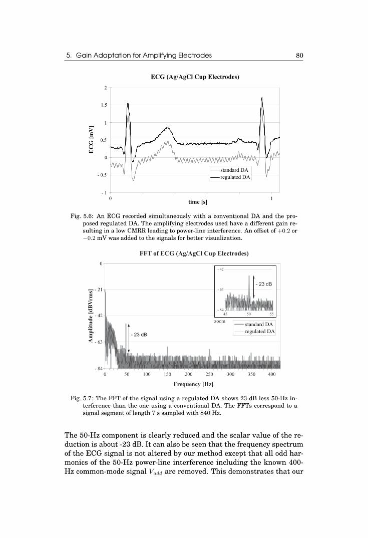
5. Gain Adaptation for Amplifying Electrodes 80
0 1
standard DAregulated DA
1.5
- 1
- 0.5
0
0.5
1
2
time [s]
EC
G [m
V]
ECG (Ag/AgCl Cup Electrodes)
Fig. 5.6: An ECG recorded simultaneously with a conventional DA and the pro-posed regulated DA. The amplifying electrodes used have a different gain re-sulting in a low CMRR leading to power-line interference. An offset of +0.2 or−0.2 mV was added to the signals for better visualization.
0 50 100 150 200 250 300 350 400
standard DAregulated DA
- 63
- 84
- 21
- 42
0
Frequency [Hz]
Am
plitu
de [d
BVr
ms]
FFT of ECG (Ag/AgCl Cup Electrodes)
- 23 dB
- 42
- 63
- 8450 5545
zoom
- 23 dB
Fig. 5.7: The FFT of the signal using a regulated DA shows 23 dB less 50-Hz in-terference than the one using a conventional DA. The FFTs correspond to asignal segment of length 7 s sampled with 840 Hz.
The 50-Hz component is clearly reduced and the scalar value of the re-duction is about -23 dB. It can also be seen that the frequency spectrumof the ECG signal is not altered by our method except that all odd har-monics of the 50-Hz power-line interference including the known 400-Hz common-mode signal Vadd are removed. This demonstrates that our

5. Gain Adaptation for Amplifying Electrodes 81
method is different from a simple analog 50-Hz notch filter.
Using the 50-Hz Interference as common-mode Signal
Again, the DA was designed on a test board using the same componentsas before. This time no common-mode voltage Vadd was added. Instead,the 50-Hz interference was measured at two different locations as de-scribed in section 5.3. The recordings in Fig. 5.8 are measured afteran initial settling time of several seconds. For better visualization, weagain added an offset of +0.2 or−0.2 mV. The result is comparable to theresult of the first method as exemplified in the respective FFT displayedin Fig. 5.9.
0 1
standard DAregulated DA
0
time [s]
EC
G [m
V]
ECG (Ag/AgCl Cup Electrodes)
1.5
- 1
- 0.5
- 1.5
0.5
1
2
Fig. 5.8: An ECG recorded simultaneously with a conventional DA and the pro-posed regulated DA. The amplifying electrodes have a different gain resultingin a low CMRR leading to power-line interference. An offset of +0.2 or−0.2 mVwas added to the signals for better visualization.
In this example our method reduces the 50-Hz power-line interferenceby about 30 dB. We can also see that the second harmonic (at 100Hz) isreduced, whereas all the other frequencies remain the same. The smalldifferences at higher frequencies result from the noise level of the ADconverters of the employed oscilloscope.
Comparing the Two Methods
The two methods (using a known common-mode signal versus using thepower-line interference) yield a very similar result. The difference in

5. Gain Adaptation for Amplifying Electrodes 82
0 25 50 75 100
standard DAregulated DA
- 62
- 83
- 20
0
- 41
- 104
Frequency [Hz]
Am
plitu
de [d
BVr
ms]
FFT of ECG (Ag/AgCl Cup Electrodes)
- 30 dB
- 62
- 83
- 10450 5545
- 30 dB
zoom
Fig. 5.9: The FFT of the signal after the regulated DA shows 30 dB less 50-Hzinterference than that of the one recorded with a conventional DA. The FFTscorrespond to a signal segment of length 24 s sampled with 250 Hz.
the FFT of the different recordings is mainly an offset due to the varia-tion in amplitude and baseline of the two measurements. The reason forthe difference in amplitude and baseline is that the measurements weretaken on two different days and the exact location of the electrodes couldnot be reproduced. The question is why we need two different meth-ods. The first method is much faster than the second. The frequency ofthe additional common-mode signal is eight times higher than the fre-quency of the power-line interference and its amplitude can be chosento suit the specific situation. Consequently, the control loop settles inless than 100 ms, which corresponds to about 40 iterations. This is im-portant in applications with many amplifying electrodes like that for anEEG [Mett 90].
Yet, the first method is based on the introduction of a known common-mode signal Vadd applied to the input of the DRL circuit. This is notthe case with the second method, which is simpler when looking at theanalog part of the circuit. This method does not require the use of aDRL circuit, a simple reference electrode would be sufficient (althoughin our example we use a DRL circuit). On the other hand, the secondmethod requires much more time for the control loop to settle. Dueto the very low signal level and the ECG being in the same frequencyband, one step of the PD controller occurs only after at least 20 cycles(400 ms). The control loop still needs about 40 iterations, which takesabout 16 seconds. There is no prior knowledge required of the phase ofthe common-mode signal.

5. Gain Adaptation for Amplifying Electrodes 83
5.4 Novelty
We have successfully shown that the known principle of increasing theCMRR of a differential amplifier can also be applied to a two-stage am-plifier. As the method does only change the gain of the second stage it ispossible to place the first stage of the amplifier on the electrodes, thushaving amplifying electrodes. The use of amplifying electrodes withouta common reference point and without a possibility to compensate fortheir individual gains would result in an overall CMRR which is low-ered.
It is important to note that our method also functions with electrodeswhich do not share a common reference node (as for example digitizingelectrodes). As there is no need for a common reference node, the num-ber of wires needed for the amplifying electrodes can be reduced by oneas compared to the same design not using automated gain adaptation.
It is also the first method known to the author using the power-lineinterference itself as the input to generate a control signal. This allowsus to use the method without the need of a DRL circuit (although theauthors recommend a DRL circuit).

6. A PSEUDO-DIFFERENTIAL AMPLIFIER FORBIOELECTRIC EVENTS WITH DC-OFFSETCOMPENSATION USING TWO-WIREDAMPLIFYING ELECTRODES
This chapter is a synopsis of the corresponding publication in the IEEETransactions on Biomedical Engineering [Dege 06].
6.1 Problem Statement
Amplifying electrodes supposedly reduce the input-referred noise of anamplifier for bioelectric events because the signal is amplified at thesource already as opposed to standard amplifiers where the electrodesact as (passive) transducers for the bioelectric signals.
Yet, amplifying electrodes have several limitations. First, the gain ofthe electrodes is limited by the electrode-electrolyte voltage which canvary between electrodes by up to ±300 mV [AAMI 99]. If this offset isnot compensated for, active electrodes with a supply voltage of 3 V willhave their gain limited to 14 dB. Second, the gain mismatch betweenelectrodes will limit the CMRR as expressed in equation (2.23). For ex-ample, according to equation (2.27) using 1-% resistors to set the gainof non-coupled electrodes to 14 dB will result in an expected worst-caseCMRR of 29.9 dB (dependent of the gain). Additionally, the use of am-plifying electrodes will result in more wires and larger connectors. Thismay lead to stiffer cables and increased mechanical size of the connec-tors, especially in the case of EEG amplifiers with a large number ofelectrodes, e.g., 256 for a dense-array EEG. Stiffer cables in turn willlead to increased motion artifacts.
The following work demonstrates two-wired amplifying electrodes witha gain of 40 dB together with an amplifier for bioelectric events makinguse of these electrodes. The overall CMRR (@ 50 Hz) of the amplifierwith DRL and gain adaptation is 109.7 dB.

6. Two-wired Amplifying Electrodes 85
6.2 Prior Art
Amplifying electrodes with a gain greater than 0 dB are rarely describedin literature. An example of such an electrode is derived from the stan-dard two op-amp instrumentation amplifier with the first stage beingplaced onto the electrodes [Valc 04]. The resulting amplifying electroderequires four wires for the reference electrode and five wires for thesignal electrodes. The gain of the active electrode was 15 dB and theCMRR of the amplifier was 96 dB. The CMRR is kept high by keeping acommon reference node for all electrodes [Pall 91b], which on the otherhand leads to the requirement of five wires per signal electrode.
Another amplifier was described using amplifying electrodes with 20 dBgain and four wires (plus shield) but without a common reference node.The amplifier has a CMRR of 85-90 dB [Duns 95]. The relatively highCMRR was achieved by hand-picking the gain-setting resistors of theelectrodes while manually trimming the gain-setting resistors of the in-strumentation stage (this corresponds to a manual implementation ofthe automatic method we earlier described in chapter 5).
One publication describes amplifying electrodes with a highpass filterplaced on the electrode itself. The electrodes have been built using smallSMD components. These electrodes have a mid-band gain of 43.5 dB[Mett 97]. The CMRR of an amplifier using these electrodes is not givenin the publication. The electrodes require four wires but do not allowtemporary adjustment of the corner frequency of the highpass filter.(This is an often desired feature to reduce the recovery time after place-ment or after a motion artifact.)
Electrodes with two wires but only 0 dB gain are described in litera-ture [Padm 90], [Dege 07]. An implementation of such two-wired bufferelectrodes are even commercially available [bios].
6.3 Method
Having a large gain on the electrodes would be beneficial for three rea-sons. First, using the same op-amp (operational amplifier) with a highergain reduces the input-referred noise of the op-amp itself as confirmedby noise measurements (see 6.3.3 Fig. 6.8). Second, the noise contri-bution of the subsequent stages to the input-referred noise is reducedthe more the higher the implemented gain in the first stage is. Thenoise requirements of the following amplifier stage can be lowered ac-cordingly, this might also allow for a reduction in power consumption.Third, compared to using buffer electrodes the total number of op-amps

6. Two-wired Amplifying Electrodes 86
can be reduced because a large part of the gain is implemented on theelectrodes.
To reduce the number of wires, we will use a current supply instead ofa voltage supply [Padm 90], [Dege 07].
To compensate for any gain mismatch between the amplifying elec-trodes, we will measure the latter and compensate for the difference ingain later, using a software algorithm. This is only possible because theamplifier developed for the electrodes has a pseudo-differential topology.The input signals are sampled using differential AD converters. Thisallows placing the differentiation between two signals into the softwarepart of the recording system. The method used for compensating a mis-match in gain is comparable to the hardware-based method describedin chapter 5.
The compensation of the electrode-electrolyte offset voltage is achievedby a DC compensation based on an error-feedback loop which conservesthe high input impedance of the amplifying electrodes (no highpass fil-ter at the input of the amplifier). At the same time, the error signalrepresents the low-frequency part of the bioelectric signal (frequencybelow 0.016 Hz for ECG respectively below 1 Hz for EEG) which maybe clinically relevant and is normally lost when using a highpass filterat the input of an amplifier. The low-frequency part of the bioelectricsignal can therefore be measured down to DC, although at a lower res-olution. (For examples of relevant data refer to section 2.3.5.)
6.3.1 Two-Wired Amplifying Electrodes
The amplifying electrodes are built using a CMOS-input op-amp, i.e.,the LMC7111 (National Semiconductor). The LMC7111 was chosen be-cause of the low supply voltage of 2.7 V and the high input resistance.The op-amp is used in a non-inverting configuration with the gain setby two resistors (1%) to 40 dB. A diode may be used to ensure properstart-up behavior. The full circuit is depicted in Fig. 6.1.
Instead of a voltage supply the electrode receives a constant currentIsup . The current is then split between the different parts of the circuit.IL denotes the supply current of the op-amp (LMC7111), ID the cur-rent through the diode D1 and IR the current through the gain-settingresistive network built by R1 and R2.
The role of the diode is mainly to insure a stable start-up behavior andmay or may not be necessary depending on the topology of the employedop-amp. We tested each employed op-amp with or without the diode D1
before deciding on the topology. We will give an overview of the testedop-amps in table 6.2.

6. Two-wired Amplifying Electrodes 87
Isup= const
Vin
VDD1
Vref
Vout
IL ID
IR
IL+ ID- IR Isup
R1
R2
Vout = (Vin-Vref )(1+ )+ VD+ Vref
R2
R1
_
Vin
Vout = (Vin-Vref )(1+ )+ Vref
R2
R1
_
VDD1Vout
ILIR ID
IL+ ID Isup
Isup= const
R1
R2
Vref
a) 1 b)
Fig. 6.1: The principle of the two-wired amplifying electrode biased by a constantcurrent-source Isup . The active part of the electrode consists of a CMOS op-amp, two resistors to define the gain and a diode used for improved start-upbehavior. Part a) depicts the published version which has an additional voltageoffset of VD. Part b) shows the improved design with lower supply voltage. Themass symbol refers to a common reference point, e.g., the negative pole of thebattery.
The negative supply is connected to a reference voltage Vref which istypically held around 500 mV above the system ground and will play animportant role in the DC-offset compensation scheme.
All measurements presented herein are made with the electrode de-picted in Fig. 6.1 a). For a new design we strongly recommend using theimproved version depicted in Fig. 6.1 b). All calculations in this chapterare made for the improved version of the electrode.
The output voltage of the electrode is given by:
Vout = (Vin − Vref )
(1 +
R2
R1
)+ Vref (6.1)
This equation is true as long as the current-source delivers enough cur-rent to supply the active electrode but not more than the op-amp cansink and as long as the open-loop gain of the op-amp is substantiallyhigher (> 40 dB) than the gain of the electrode. :
Isup >Vsup max
R1 +R2+ IL max (6.2)
Isup <Vsup min
R1 +R2+ Isink max (6.3)
The amount of current an op-amp can sink may depend on the supplyvoltage Vsup of the op-amp. The supply voltage of the op-amp on the

6. Two-wired Amplifying Electrodes 88
other hand depends on the input signal:
Vsup = Vout − Vref = (Vin − Vref )
(1 +
R2
R1
)(6.4)
Vsup is the supply voltage of the op-amp which has both an upper andlower limit, which can be found in the corresponding data sheet. Thesupply voltage of the op-amp has always to be above the minimal supplyvoltage specified in the data sheet. The upper limit is either given bythe data-sheet or is limited by the supply voltage of the whole circuit.
Vout min − Vref max ≥ Vsup min (6.5)
Where Vsup min denotes the minimal supply voltage of the op-amp. Thevalue depends on the amount of supply current Isup the op-amp has tosink (see Fig. 6.7). As an example for the LMC7111 the minimal supplyvoltage was measured to be 2.6 V when sinking a current Isup of 1 mA.
To ensure the correct behavior of the amplifying electrode, we suggestto test the electrode with half the supply current at the maximal out-put voltage and with the double supply current at the minimal outputvoltage (similar to a corner analysis).
The output resistance Rout of the active electrode can be expressed bythe output resistance of the op-amp Rout Op plus the output resistanceof the diode Rout D (if required) divided by the open loop gain A0 of theop-amp:
Rout =Rout Op +Rout D
1 +A0(6.6)
As an example, the open-loop gain of the LMC7111 for Vsup OP = 2.7 Vwhile sinking a current is typically > 100 dB. Rout Op is normally about100 Ω.
The differential resistance of the diode on the other hand depends onthe current through the diode ID and can be approximated by:
Rout D =∂VD∂ID
=∂(Vth ln
(IDIS
))∂ID
=Vth
ID(6.7)
Vth = kBT/q0 is the thermal voltage and yields about 25 mV for an am-bient temperature of 22 C (295.15 K). IS is the reverse current of thediode. We used a small-signal diode BAS16 (Fairchild Semiconductor)which has a reverse current of about 1 µA
For our electrode with a supply current Isup of 1 mA, we measured anoutput resistance of the diode of about 25.6 Ω which is very close to the25.4 Ω resulting from equation (6.7).

6. Two-wired Amplifying Electrodes 89
Going back to equation (6.6), we can estimate the total output resistanceof the amplifying electrode to be far below 0.1 Ω.
The amplifying electrodes were supplied by a current-source of the typeJ505 (Vishay) which was already used for the buffer electrodes in chap-ter 4. Again, the current-source (J-FET) can be considered to be theupper part of the output stage of the op-amp. The requirements for theop-amp are that one supply is included in the input range and that themaximal current the op-amp output stage can sink exceeds the value ofthe supply current Isup as defined in equation (6.3).
6.3.2 Amplifier Stage
The amplifier stage uses one DRL electrode, one reference electrode(subscript ‘r’) and ‘n’ signal electrodes to measure the bioelectric sig-nal of interest (see also section 2.3.3). For the calculations we considerone signal electrode out of the ‘n’ electrodes (subscript ‘i’). The bioelec-tric signal of interest is then Vin i − Vin r . Fig. 6.2 depicts the amplifierstage.
The primary requirement of the amplifier is to ensure that the outputvoltages of the electrodes do not saturate. This is a stumbling block forthe use of amplifying electrodes with a gain larger than 15 dB (depend-ing on the supply voltage). To avoid saturation of the output voltage wewill adapt the reference voltage Vref i of each individual signal electrode‘i’ which is simultaneously the lower (negative) supply voltage of the op-amp placed on the amplifying electrode. We can condense the functionof the amplifier stage into three main tasks:
• Provide the necessary supply current Isup for the electrodes.
• Generate the adequate reference voltages Vref i in order to com-pensate for any DC offset between electrodes.
• Reduce any common-mode voltage by feeding it back to the bodyvia a DRL circuit which is simultaneously determining the DCcomponent of the input voltage of the reference electrode.
These three functions are achieved in the above order by a current-source and two different feedback loops.
The current-source for each electrode is a J505 (Vishay), based on a sin-gle J-FET (Junction FET). The J505 was chosen for its simple topology.To source 1 mA the J505 requires a voltage drop of about 1.2 V. (For theschematic of the current-source please refer to Fig. 4.5).

6. Two-wired Amplifying Electrodes 90
feedbackerror-
loop
DRLloop
VCC
reference
VCC
channel 'i'
electrode 'i' signalactive
electrode
electrode
active
DRLVout i - Vout rVin i - Vin r
V out
r =
VD
RLV o
ut i
DC
= V
DRL
Vin rVref r
Vref r
Vout r
Isup
Isup
VDRL
CDRL
Cfb
RDRL
Rc RaRfb
Rb
Vin i
Vref i
Vfb
VDRL
Vout i
β
α
: forward gain: feedback gainβ
α
‘inverter’
Fig. 6.2: The amplifier stage for providing the necessary bias voltages and biascurrents. Bias sources are implemented by a current-source and two differentfeedback loops. The first feedback loop (‘DRL loop’) is built around the refer-ence electrode and the DRL electrode. The second loop (‘error-feedback loop’)is built around each signal electrode of which only the electrode ‘i’ is drawn.The amplified output signal for each channel is Vout i − Vout r . All op-amps areof the LT1490 type. The ground symbol stands for a local reference, e.g., thesystem ground of the amplifier.
The first feedback loop (‘DRL loop‘) is realized around a reference elec-trode and the DRL electrode. The purpose of the first loop is to definethe correct bias voltage for the reference electrode. In detail this meansthat if the output voltage Vout r of the reference electrode is higher thanVDRL, a current will flow into the resistor RDRL and the op-amp whichdrives the DRL electrode has to lower its output voltage to allow thiscurrent to flow through CDRL as well. This lowers the input voltage of

6. Two-wired Amplifying Electrodes 91
all electrodes connected to the DRL electrode via the human body. Yetlowering the input voltage of the reference electrode Vin r while the ref-erence voltage Vref r stays fixed at 500 mV will also lower the outputvoltage Vout and close the loop. The value of VDRL was chosen in sucha way that it was in the middle of the valid range of Vout r (this will beanalyzed further in section 6.3.3 where the results are described). Forthe amplifying electrode in Fig. 6.1 a) VDRL should be about 3.55 V, forthe amplifying electrode in Fig. 6.1 b) VDRL should be about 3 V.
In other words, the task of the first feedback loop is to maintain thevoltage between the system ground of the amplifier and the surface po-tential of the body at a constant level, and simultaneously reduce anycommon-mode signal at the input. The input voltage of the referenceelectrode Vin r will also be fixed by this first feedback loop. For thepresent circuit Vin r is held around 25 mV above Vref , the exact valuewill be derived later in equation (6.1).
The corner frequency of the first feedback loop is f0 = 1/2πRDRLCDRL.To guarantee the stability of the first loop we chose the values RDRL =220 kΩ and CDRL = 15 nF, which resulted in a corner frequency off0 = 53 Hz, an open-loop phase margin of about 30 [Wint 83] and aCMRR improvement of about 40 dB (@ 50 Hz) as indicated by equation(2.46) and visible in Fig. 6.9 later in the results section. Smaller valuesof CDRL will increase the overall CMRR but may lead to oscillation orinstability within the feedback loop.
The second loop (‘error-feedback loop‘) is built individually around eachsignal electrode. The purpose of the second loop is to compensate fora difference in the electrode-electrolyte interface voltage between thereference electrode and each signal electrode. The voltage differencemay reach values of up to ±300 mV [AAMI 99].
In other words, the second loop implements a highpass behavior for eachsignal electrode. We will examine the loop in detail for the ith electrode.The reference voltage Vref i is adjusted by the loop as long as the DCvalue of the output voltage Vout i is different from VDRL. The guidingprinciple is the same as for the first feedback loop except that this timeit is the reference voltage which is adapted while the input voltage Vin i
is fixed (by the first feedback loop superimposed by the bioelectric sig-nal). For the loop to be stable we need to invert the output of the corre-sponding integrator. For this purpose we added a voltage inverter withthe following transfer function:
Vref i =Rc +RbRb
Vref r −RcRa
(Vfb − Vref r ) (6.8)
The inverter will also convert the range of Vfb which is 0 to VCC tothe desired reference voltage swing Vref i = 500 ± 300 mV by its gain

6. Two-wired Amplifying Electrodes 92
of −Rc/Ra. As we will see later in equation (6.11), this gain will alsoreduce the size of the feedback capacitor for a chosen time constant.
By choosing an adequate value for Rb, the midpoint of the output rangecan be shifted to Vref r . As a consequence the initial reference voltageVref i after power-up will be close to Vref r , thus reducing the start-uptime of the circuit.
The output-range limitation of the inverter will also ensure that Vref i
cannot be substantially higher than VDRL. This is important becauseif Vref i − VDRL ≥ 550 mV, the built-in protection diode of the op-ampplaced on the reference electrode would start to conduct a current andthus prevent the operation of the first feedback loop.
The values used were Ra = 47 kΩ, Rb = 9.1 kΩ and Rc = 4.7 kΩ. The sec-ond loop forces the DC value of Vout i to be equal to VDRL plus a residualoffset. The offset is mainly given by the input offset and bias current ofthe op-amp used and can be expressed by:
Vout i DC = VDRL + Voff opamp +Rfb Ibias opamp (6.9)
Voff opamp is the input offset voltage of the op-amp building the integra-tor, Ibias opamp corresponds to the bias current at the negative input. Inour prototype circuit the value of the residual offset was about 40 mV.
The time constant of the second feedback loop is much lower (at leastfive decades) than the time constant of the first feedback loop. Thisensures the stability of the second feedback loop despite it being inter-linked with the first one (see also section 6.3.2, Fig. 6.9).
The amplifier stage is of a pseudo-differential nature, the amplified andDC-offset-free bioelectric signal is represented by Vout i − Vout r . Yet thebioelectric signal is only visible on Vout i whereas the common-mode sig-nal is present on both Vout i and Vout r . Considering only Vout i wouldshow large common mode interferences (see also Fig. 6.10).
Fig. 6.3 illustrates the overall transfer function of the pseudo-differen-tial amplifier and the electrodes.
The transfer function can be expressed by the forward gain α and thefeedback gain β:
Vout i − Vout r
Vin i − Vin r=
α
1−αβ(6.10)
Where α corresponds to the gain of the electrodes as stated in equation(6.1). The bandwidth f0 lp of α is given by the GBP (gain-bandwidth-product) of the employed op-amp (LMC7111) which is 50 kHz dividedby the gain of the amplifying electrodes. β corresponds to the transfer

6. Two-wired Amplifying Electrodes 93
500
Gain [dB]
40
20
0
fβ=1 =
80
60
Frequency [Hz]
Vout i - Vout rVin i - Vin r
Vref iref i - - Vref rref rVin in i - - Vin rn r
A0 (LMC7111) (LMC7111)
: feedback gainβ: forward gainα
β
α
12πCfbRfb Ra
Rcf0
Fig. 6.3: The transfer function of the pseudo-differential amplifier stage with theelectrodes. The upper corner frequency f0 lp is fixed by the function of theopen-loop gain A0 and the corresponding gain-bandwidth-product (GBP) of theemployed op-amp (LMC7111). The overall gain is expressed by equation (6.10)and the lower corner frequency f0 depends on the feedback loop as expressedin equation (6.11).
function of the integrator multiplied by a constant factor Ra/Rc as ex-pressed by equation (6.8). The resulting transfer function is a highpasswhere the corner frequency is defined by the condition αβ = 1. Conse-quently, we can express the cut-off frequency f0 by:
f0 =1
2πRfbCfb
(1 +
R2
R1
)RcRa
(6.11)
Below the corner frequency the transfer function can be approximatedby 1/β and above f0 by α. We used Rfb = 10 MΩ and Cfb = 10 µF whichresults in a corner frequency of fb = 0.016 Hz as required for recordingan ECG. To restore the DC value after replacing the electrodes or toallow for fast recovery after an artifact, we placed a switch in parallel toRfb enabling us to temporarily shift the corner frequency. When openingthe switch a small charge may be injected into Cfb resulting in a voltagestep at the output. This has no adverse effects on the system.
A particularity of this amplifier is the fact that the cut-off frequency ofthe highpass depends on the gain of the active electrode. We can usethe same amplifier for EEG by using a low-noise electrode with a gainof 60 dB which results in a cut-off frequency of 0.16 Hz, which is lowerthan most EEG amplifiers offer.
DC-Offset Measurement
As reported earlier, the purpose of the second feedback loop is to adjustfor the electrode-electrolyte voltage offset between the reference elec-
6. Two-wired Amplifying Electrodes 94
trode and each individual signal electrode. Let us assume that there isa DC offset between Vin i of the ith signal electrode and Vin r of the refer-ence electrode. The second feedback loop will then adjust the referencevoltage Vref i until the DC component of the signal is again VDRL. Thisleads to the following relation:
Vref i−Vref r =
(1 +
R1
R2
)(Vin i − Vin r ) (6.12)
=
(gain
gain− 1
)(Vin i − Vin r ) (6.13)
For a large gain Vref i − Vref r equals Vin i − Vin r , which corresponds tothe offset voltage between electrodes. This means that by measuringthe reference voltage of an electrode, it is possible to deduce the offsetvoltage of this electrode compared to the reference electrode. This fea-ture allows measuring the full bandwidth of the bioelectric signal (plusthe electrode-electrolyte offset voltage, which is considered to be rela-tively stable). Fig. 6.3 also displays the frequency response of equation(6.13) which can is expressed by:
Vref i − Vref r
Vin i − Vin r=
αβ
1− αβ(6.14)
Vfb holds the same information but with an amplitude ten times larger.To our knowledge this is the first circuit reported which allows us tomeasure a bioelectric signal with frequencies down to DC while sup-pressing the DC offset between electrodes.
A second consequence of equation (6.13) is that the limits within whichthe circuit can compensate a DC offset are given directly by the voltageswing of Vref i which on the other hand is limited by the total supplyvoltage divided by the constant factor Rc/Ra as shown in equation (6.8).
Amplifier Design and CMRR
The main problem of amplifying electrodes is the possible reduction ofthe CMRR due to a variance in gain (@ 50 Hz) between electrodes. Letus assume that the reference electrode has a gain of Gr and the sig-nal electrode ‘i’ has a gain of Gi. If we now calculate the difference weobtain:
Vout = GiVin i −GrVin r (6.15)
this can be expressed as:
Vout =Gi+Gr
2(Vin i−Vin r ) + (Gi−Gr)
Vin i +Vin r
2(6.16)

6. Two-wired Amplifying Electrodes 95
This is nothing else than separating the differential-mode gain GDM
and common-mode gain GDM knowing that the differential-mode andthe common-mode input voltages are given by:
VDM = Vin i − Vin r (6.17)
VCM =Vin i + Vin r
2(6.18)
Thus equation (6.16) leads directly to the CMRR:
CMRR =GainDM
GainCM= 20 log
(Gi +Gr
2 |Gi −Gr|
)(6.19)
Which corresponds to the formula derived in section 2.2.4. It allows usto calculate the expected CMRR for a given gain mismatch [Pall 91]. Ifthe gain mismatch is a result of the tolerance of the gain-setting re-sistors we can express the worst-case CMRR of the total INA by equa-tion (2.38). For our circuit we use resistors with a tolerance of 1% andelectrodes with a gain of 40 dB which leads to an expected worst-caseCMRR of about 28 dB of the total INA due to the use of the amplify-ing electrodes (which are the limiting factor). Note, our electrodes arenon-coupled electrodes, using coupled electrodes would yield a betterCMRR.
28 dB may be sufficient for a body-worn device when using a DRL circuitbut not for a clinical ECG or EEG (see table 2.2 for an overview). ADRL circuit may improve this CMRR by up to 50 dB [Mett 90]. TheDRL circuit implemented for this amplifier results in an improvementof about 40 dB (@ 50 Hz) pushing the CMRR of the amplifier (includingDRL) to about 68 dB (@ 50 Hz).
To improve the CMRR further we will compensate for the gain mis-match of each signal electrode in respect to the reference electrode whendifferentiating, similar to the method presented in chapter 5.
Because our amplifier is pseudo differential (the signal is only presentof Vout i but the common mode interference also present on Vout r ) wecan first convert the signals into a digital representation and then stillcompensate for the gain mismatch in software. Therefore we requireall signals to be sampled, either by a fully single-ended ADC (analog todigital converter) and a multiplexer or in a pseudo-differential configu-ration as shown in Fig. 6.4. (Using two fully differential converters isalso possible but would no longer allow compensating for a gain mis-match in software.)
The pseudo-differential approach requires one more AD channel for thereference VDRL. The reference voltages Vref i and Vref r are sampled onlyif the low-frequency part of the bioelectric signal (below f0) is of interest.

6. Two-wired Amplifying Electrodes 96
n
n
b) pseudo differentiala) fully single ended
n
n
AD
D
MuxS&H
AD
DA
A
Vout i
Vref i
Vout iVout r
Vout r
Vref rVref i
Vref r
VDRL
VDRLVAD
Fig. 6.4: Two ways of interfacing the amplifier by a) converting all four single-endedsignals separately or b) using three differential AD converters to convert themin a pseudo-differential way. This enables simple software based algorithms tocompensate for differences in gain and thus improving the CMRR.
To compensate for the gain mismatch (@ 50 Hz) we will first measure theamplitude of the power-line interference A50 r and A50 i for the differentsignals. The amplified and compensated bioelectric signal VBE is thencalculated by:
VBE = 2A50 rVout i −A50 iVout r
A50 r +A50 i(6.20)
= 2GiA50 rVin i −GrA50 iVin r
A50 r +A50 i
= 2GiGrA50(Vin i − Vin r )
A50(Gr +Gi)
= 2GiGr(Vin i − Vin r )
Gr +Gi(6.21)
Gr and Gi represent the gain (with mismatch) of the two amplifyingelectrodes considered, one being the reference electrode the other the ith
signal electrode. A50 r and A50 i stand for the measured amplitude (byFFT) of the 50-Hz power-line interference overlaid on the output volt-age of the reference electrode, respectively the ith signal electrode. A50
would then be the amplitude of the 50-Hz common mode interference onthe body prior to the amplification. Note, A50 is not present in the finalequation (6.21).
To obtain A50 r and A50 i we used the discrete Fourier transform of thesampled values. Unlike the method described in chapter 5 this methoddoes not necessitate a phase-shift measurement because the Fourier

6. Two-wired Amplifying Electrodes 97
transform allows us to obtain the amplitude of the 50-Hz componentindependently from any phase shift (we assume that the 50 Hz are wellwithin the passband of the amplifier).
By implementing equation (6.21) based on the measurement of the 50Hz interference, the latter can be reduced as shown in section 6.3.3. Theremaining 50-Hz component of the output signal is mostly part of thedifferential bioelectric signal itself. An example is shown in Fig. 6.12and Fig. 6.13.
The CMRR is improved to the value of:
CMRR =GiA50 r +GrA50 i
2|GiA50 r −GrA50 i|(6.22)
An absolute value for the improved CMRR cannot be given, because theimprovement also depends on the value of the measured common-modesignal itself. The larger the common-mode signal, the better the CMRR.We can say that the CMRR increases as much as necessary to ensurethat the measured common-mode signal is minimized on the reading.
We can give an upper limit to which this schema can function. Themaximum value for the CMRR improvement is obtained if the common-mode signals measured on the two output voltages A50 i and A50 r are aslarge as the input range of the ADC. The 50-Hz interference after thegain adaptation will correspond to the resolution of the ADC, and, as aresult, the upper limit can be given by:
CMRR ≤ 20 log (2n) (6.23)
Where ‘n’ corresponds to the resolution of the ADC. It has to be notedthat this is not necessarily the best measurement situation, it is moreadvantageous to have less power-line interference from the beginningeven though this yields a lower CMRR.
Contrary to a 50-Hz notch filter, the method will reduce all common-mode signals without altering the differential-mode signal, i.e., the bio-electric signal.
The difference between the fully single-ended circuit shown in Fig. 6.4 a)and the pseudo-differential implementation of Fig. 6.4 b) presented inFig. 6.4 is the necessary input range of the ADC. In Fig. 6.4 a) the inputrange must be at least VDRL +Vout whereas in Fig. 6.4 b) the input rangecan be as low as ±Vout/2. As a consequence, the resolution for the samenumber of bits is higher in b). For example, the AD7731 can have aninput range as low as ±20 mV and provides three differential ADCsin one IC. At 400 Hz the AD7731 has a resolution of 14.5 bit whichis equivalent to 1.73 µV. The upper limit of the CMRR improvementaccording to equation (6.23) would then amount to 87 dB (in addition to

6. Two-wired Amplifying Electrodes 98
the expected 68 dB CMRR of the amplifier with DRL mentioned above@ 50 Hz).
Digital Control Loop
Regardless of which AD-conversion scheme is chosen, it is possible toimplement the second feedback loop responsible for the DC-offset com-pensation by an analog circuit as shown in Fig. 6.2 or by a digital filteras shown in Fig. 6.5.
m
nFIR
A
DA
D
VCC
electrode 'i' signalactive
Vref r
Isup
Rc Ra
Rb
Vin i
Vref i Vfb
VDRL
Vout i
‘inverter’
Fig. 6.5: The second feedback loop built as a digital control loop by replacing theintegrator of Fig. 6.2 with a digital filter (FIR) and an AD/DA converter. Thefeedback loop is again shown for the electrode ‘i’. There is no need for a capac-itor.
The partially digital loop functions in a similar way to the fully analogloop. The feedback voltage Vfb is generated by the DAC (digital to analogconverter) while the digital filter (FIR) generates the necessary codesfor the DAC based on the differential input of the ADC. The second op-amp stage (inverter) is still needed for sinking the supply current of theamplifying electrode and serves also for adapting the output range ofthe DAC to the desired reference voltage range. Equation (6.8) is stillvalid and defines the function of the inverter.
The corner frequency of the digital filter f0 FIR is calculated analogouslyto the corner frequency of the integrator used in the analog loop. Start-ing from equation (6.11) we then obtain:
f0 FIR = f0R1
R1 +R2
RaRc
(6.24)
f0 stands for the desired corner frequency of the transfer function ofthe amplifier (e.g., 0.016 Hz for ECG). R1 and R2 are the gain-settingresistors of the amplifying electrode.

6. Two-wired Amplifying Electrodes 99
The main differences between the analog and the digital implementa-tion are:
• the digital loop requires no capacitor, which enables fully inte-grated solutions, e.g., within an ASIC.
• the time constant between different channels matches perfectlyand removes the CMRR degradation due the mismatch of cornerfrequencies (see also section 2.2.4)
• the digital loop introduces discrete steps in the output waveform(quantization noise). In between these steps the signal does notshow the typical superimposed exponential variation which is usu-ally a characteristic of highpass filtered signals. Because the expo-nential variation is absent it is possible to measure signal featureslike the S-T elevation without distortion. Saturation of the outputvoltage can be avoided easily.
In addition, adaptive filter techniques may be used resulting in shortersettling times. Likewise the part count decreases as the DAC replacesan op-amp together with some passive components as well as the ADCnecessary to sample Vfb (required only if the DC part of the signal is ofinterest).
Because of the discrete nature of the output voltage Vfb , the DC offsetof the bioelectric signal cannot be completely nullified. There remains aresidual offset Voff res which can be calculated in relation to the resolu-tion of the DAC:
Voff res =VCC
2m
(1 +
R2
R1
)· RaRc
(6.25)
m denotes the number of bits of the DAC. For a supply voltage of 5 V anda DAC with 12 bits this results in a residual offset voltage of ±12 mV.In other words, each time the digital code of the DAC is changed bythe FIR filter, the signal Vout i will display a discrete step (quantizationnoise) with an amplitude corresponding to a multiple of the residualoffset calculated in equation (6.25).
If not handled appropriately, this leads to an oscillating behavior of theoutput voltage Vout i with a mean value of zero volt. This behavior isshown in section 6.3.3 Fig. 6.14. Because the exact timing of thesesteps is known a priori by the software, the latter can be removed be-fore displaying or storing the signal. A better solution is to implementa hysteresis where the two thresholds differ at least by the value of theresidual offset calculated in equation (6.25).

6. Two-wired Amplifying Electrodes 100
6.3.3 Results
Two-Wired Amplifying Electrodes
The fabrication of the prototype electrode was straight-forward. Wemounted all the components on a printed circuit board (PCB). The PCBwas then soldered onto the back of a snap button cut from a pair oftrousers which allowed us to use different kinds of disposable electrodes.An example of a disposable pre-gelled EEG electrode clipped to an activeelectrode is shown in Fig. 6.6. One wire is connected to a low-ohmic node(i.e., the reference voltage) and was used to shield the output voltage ofthe amplifying electrode. This yields a relatively large input capaci-tance for the subsequent stage, in this case an ADC, lowering the inputimpedance of the second stage. This has no negative effect because ofthe low output resistance of the amplifying electrode.
Fig. 6.6: A shielded amplifying two-wired active electrode mounted onto a buttonin order to attach different types of disposable electrodes.
First we measured the input range for which the electrode operates inthe linear region. Fig. 6.7 shows the output voltage Vout while varyingthe input voltage Vin , the reference voltage Vref was set to zero.
The lower corner of the input voltage range is defined by the minimalsupply voltage of the employed op-amp which is required to sink thecurrent present at the output, i.e., Isup − IL − IR. It is important tonote that for both op-amps the required supply voltage increases severalhundred millivolts if the supply current increases from 1 mA to 2 mA.
The upper corner of the input voltage is defined by the available voltagesupply. In our case we had a voltage supply of 5 V where 1.2 V weredropped over the current-source (i.e., a J-FET J505 from Vishay). Fora maximal output voltage of 3.8 V and a reference current of 1 mA, thelinear output range was about 1.25 V starting from 2.5 V. This trans-lates to an input range of 12.5 mV starting at 20 mV for the design a) orat 25 mV for the design b). The input range of the design a) starts froma lower voltage because of the additional voltage drop over the diode.

6. Two-wired Amplifying Electrodes 101
1 mA
0 10 20
2
3
4
5
30 40 Vin [mV]
Vou
t [V
]
1 mA
2 mA3 mA
Vout max
Vsup min
linear range
1 mA
0 10 20
2
3
4
5
30 40 Vin [mV]
Vou
t [V
]
1 mA
2 mA3 mA
Vout max
Vsup min
linear range
a) b)
Fig. 6.7: The characteristic voltage gain of the two-wired amplifying electrode mea-sured for three different supply currents and Vref = 0. Part a) depicts thepublished electrode from Fig. 6.1 a) built with an op-amp LMC7111 (NationalSemiconductor) and a diode which is a BAS16. Part b) shows the improved de-sign from Fig. 6.1 b) built with an op-amp LMV301 (National Semiconductor)but without a diode. For both implementations R1 and R2 have a value of 39 Ωrespectively 3.9 kΩ.
This input range may appear to be too small to accommodate the po-wer-line interference. This is not the case: the DRL-loop will reduce thecommon-mode voltage between the body and the reference of the am-plifier. In section 6.3.2 Fig. 6.9 we will see that the common-mode gainof the amplifier is approximately one (@ 50 Hz). This means that com-mon-mode voltage seen at the input is hardly amplified by the differentelectrodes. The common mode input range (@ 50 Hz) is therefore limitedby the output swing of the DRL electrode, which is ±1.5 V.
The gain of the amplifying electrode was set with two resistors of 39 Ωand 3.9 kΩ. The very small value of the resistors was chosen to mini-mize the voltage-noise contribution of the resistors in order to be ableto measure the voltage noise of the op-amp. According to equation (2.1),the input-referred voltage-noise contribution of the two resistors in thefrequency band from 0.1 Hz to 1 kHz amounts to about 25.4 nV each (thevoltage noise of the larger resistors is divided by the gain of the ampli-fying electrode). For the chosen values the resistors will also define theminimal supply current Isup min which is defined by:
Isup min ≥ IL + IR = IL(Vsup max ) +Vsup max
R1 +R2(6.26)
For our example we have IL ≈ 60 µA (for the LMC7111) respectivelyIL ≈ 150 µA (for the LMV301) and IR ≈ 840 µA, which results in aminimal supply current Isup min of roughly 1 mA. This is certainly notoptimal for a low-power application. For future designs the values ofthe resistors R1 and R2 should be higher, e.g., 1 kΩ and 100 kΩ.

6. Two-wired Amplifying Electrodes 102
The gain of the amplifying electrode appears in Fig. 6.7 as the gradientof the regression line. The gradient for a supply current of 1 mA is cal-culated by the parameter analyzer (HP4155B/4156B Hewlett Packard)and corresponds for this particular electrodes to a gain of 40.06 dB(LMC7111) and 40.12 dB (LMV301). The regression line in Fig.6.7 a)also reveals the voltage drop over the diode VD which corresponds tothe intersection with the y-axis and yields 555 mV.
For the supply current of 1 mA there is a sharp drop at Vout ≈ 4.5 V. Thisis because when the current through the gain-setting resistors reachesabout 1 mA the voltage of the negative input of the op-amp cannot riseany higher. In result the op-amp will short-circuit the diode in the at-tempt to increase the output voltage. The curve then becomes flat andstays at the value Vout = (Isup − IL)(R1 +R2). This is of no consequencefor our circuit as the voltage supply is limited by the current-source to3.8 V (including the reference voltage Vref .
A similar measurement (input current versus input voltage) was per-formed to determine the input resistance and the bias current of theelectrode. The differential input resistance is over 1 TΩ and the biascurrent corresponds to about 60 pA.
It should be noted that for the improved amplifying electrode depictedin Fig. 6.1 b) the regression line ideally would not show any offset.
Noise
Next, we measured the input-referred spectral voltage-noise density ofthe amplifying electrode. The measurement is shown in Fig. 6.8.
The noise of the amplifying electrode is mainly due to the op-amp used,which in this implementation was an LMC7111 (the resistors R1 and R2
have been chosen accordingly). The total input-referred voltage noise ofthe electrode corresponds to the integrated spectral voltage-noise den-sity over the desired bandwidth. For comparison, we used the extrapo-lated spectral voltage-noise density as indicated by the dotted lines. Fora bandwidth of 10 Hz to 1 kHz (EEG) the computed integral results in9.3 µVrms. If we consider the total amplifier then the noise is mainlydue to two sources: the active electrode and the noise generated by theerror-feedback loop. This is because the noise of the error-feedback loopadds to the reference voltage Vref i and is therefore amplified by the ac-tive electrode. The total noise of the system in the bandwidth of 10 Hzto 1 kHz computes to 14.2 µVrms. This is low enough for our test appli-cation which is a body-worn ECG recorder.
For comparison we added the spectral voltage-noise density of the sameop-amp when used as active buffer electrode (gain of 1). The input-

6. Two-wired Amplifying Electrodes 103
1 10010 1k0.1
400400
600600
200200
0
active electrode (LMC 7111)
total circuit
Ag/AgCl
buffer electrode(LMC 7111)
f0
spec
tral v
olta
ge n
oise
den
sity
[nV
rms/
spec
tral v
olta
ge n
oise
den
sity
[nV
rms/
√Hz]
Hz]
frequency [Hz]
Fig. 6.8: The spectral voltage-noise density of the amplifying two-wired electrodeand the total system (no additional gain) was measured with a vector signalanalyzer (Stanford SR785). For comparison we added the spectral voltage-noise density of the two-wired buffer electrode (gain=1) using the same oper-ational amplifier (LMC7111) as well as the spectral voltage noise of the totalamplifier (including the second feedback loop). Different sampling rates wereused above and below 100 Hz. f0 denotes the upper bandwidth of the amplify-ing electrode defined by the gain-bandwidth product of the employed op-amp(LMC7111).
referred noise is higher even though the same op-amp is used. Thisconfirms that using an amplifying electrode with a gain of about 40 dBlowers the noise when compared to the same active electrode configuredas a buffer electrode. In addition, the noise of the subsequent stages willcontribute less in the case of amplifying electrodes. The total noise ofthe buffer electrode in the bandwidth of 10 Hz to 1 kHz can be estimatedto 11.1 µVrms This improvement may be considered small, but it comeswithout cost. The noise reduction becomes more important the higherthe gain of the active electrode is. To our knowledge 40 dB correspondsto the second highest gain1 of any reported input stage of an amplifierfor bioelectric events (excluding AC-coupled stages). This large gain hasbeen possible because of the error-feedback loop which suppresses theelectrode-electrolyte offset voltage.
Table 6.1 resumes the characteristics of the two amplifying electrodescompared to the buffer electrode presented in chapter 4.
For a high-quality system the noise has to be reduced by choosing theappropriate op-amps. We will show additional choices for op-amps in an
1 The highest reported gain of 43.5 dB was obtained using active electrodes with astopped integrator in the feedback loop [Mett 97] but without any means to com-pensate for any gain mismatch.

6. Two-wired Amplifying Electrodes 104
Tab. 6.1: The measured characteristics for both amplifying electrodes and thebuffer electrode from chapter 4.
Electrodes amplifying electrode buffer electrodeLMC7111 Fig. 6.1 a) Fig. 6.1 b)
Isup [mA] 1 1 1Offset [mV] 555± 25 3± 1 3± 1
VCCa [V] ≥4.45 V ≥3.9 V ≥3.7 VRin
b [GΩ] 5000 5000 5000Ibias [pA] −60 −60 −60
Rout [Ω] 65 < 0.1 < 0.1Noisec [µVrms] 9.3 9.3 11.1Gain [dB] 40.06 40.06 -0.01
a VCC of the total amplifier assuming Vref = 500 mV and the voltage drop over thecurrent-source 1.2 V
b Measured with a parameter analyzer HP4155B/4156Bc total noise from 10 Hz to 1 kHz
addendum to these results later in section 6.4.
CMRR
To analyze the CMRR of a pair of electrodes of the amplifier in more de-tail we measured the two gains of these electrodes (quantifying the gainmismatch) and simulated the different gain functions in a P-Spice-basedsimulator (OrCAD). We also measured the CMRR of the total amplifierusing these two electrodes in the frequency domain between 5 Hz and50 kHz.
The different results of the total amplifier are shown in Fig. 6.9. Themeasured gains of the two electrodes allowed us to quantify the CMRRdue to the gain mismatch as defined in equation (6.19) which led to aCMRR of about 30 dB. The simulation and measurements correspondto the case of a non-compensated gain mismatch and do not describe theperformance of the final amplifier system.
Fig. 6.9 is an asymptotic representation of the different transfer func-tions defining the CMRR of one signal electrode ‘i’ in relation to thereference electrode ‘r’ of the amplifier. The simulation is based on twodifferent spice simulations, one for the differential gain and one for thecommon-mode gain. The definitions of the different lines representingthe decomposition of the overall CMRR are compiled below:

6. Two-wired Amplifying Electrodes 105
CMRR
= 0.016-3
40
50
80
-80
-40
500
[dB]
Electrodes (LMC7111)
CMRRel =30 dBFrequency [Hz]=
(Simulation 1)
(Simulation 1)
(Simulation 2)
(Calculated = GDM / GCM ) (Measured values for CMRR )
GCM r
f0
GCM i
GDM i
GCM
GDM
GDM r
Fig. 6.9: The CMRR of the amplifier from Fig. 6.2 is defined by the ratio of thedifferential gain GDM of the differential input signal divided by the common-mode gain GCM of the differential input signal (here the two solid lines). Thecommon-mode gain of the differential signal is affected by the difference ingain of the corresponding single-ended output signals. GDM r and GCM r arethe differential and common-mode gain of the output voltage of the referenceelectrode Vout r , whereas GDM i and GCM i are the differential and common-mode gain of the output of the signal electrode ‘i’ (dotted lines). The dashed line‘Electrodes (LMC7111)’ represents the gain of the active electrodes without thesecond feedback loop. The higher frequencies are suppressed as a result of thelimited open-loop gain of the op-amp. The squares represent measured valuesof the CMRR for our prototype circuit. The value of CMRRel was limited bythe mismatch in gain (@ 50 Hz) between the two electrodes as described inequation (6.19). The actual value of the CMRR between the two electrodeswas only about 30 dB due to resistor tolerances.
GDM i =Vout i
Vin i − Vin r
GDM r =Vout r
Vin i − Vin r
GDM =Vout i−Vout r
Vin i−Vin r
GCM i = 2Vout i
Vin i + Vin r(6.27)
GCM r = 2Vout r
Vin i + Vin r(6.28)
GCM = 2Vout i−Vout r
Vin i +Vin r(6.29)
As the gain differs for each signal electrode so does the CMRR of theamplifier for each pair of electrodes. This is a typical situation for amulti-electrode amplifier with non-coupled electrodes.
The differential-mode gain of the reference output voltage GDM r is verylow because Vout is forced to a constant value by the first feedback loop.
6. Two-wired Amplifying Electrodes 106
GDM i corresponds to the transfer function of the active electrodes (lineLMC7111) but is damped at low frequencies (< f0) by the second feed-back loop. Because GDM i GDM r , the differential-to-differential gainGDM already drawn in Fig. 6.3 also covers the GDM i curve. The twocommon-mode gains GCM r and GCM i almost overlap. Their mismatchis a result of the resistor tolerances resulting in a reduced CMRR de-fined by equation (6.19). The CMRR was measured for this particularpair of electrodes at about 30 dB. This is a little bit better than the28-dB worst-case CMRR expected from the tolerance of the resistorsas estimated by equation (2.27). For frequencies below the corner fre-quency of the second feedback loop f0 ≈ 0.016 Hz we see that GCM r andGCM i diverge while they are very close for frequencies above the cor-ner frequency. It follows that the differential common-mode gain GCM
is mostly 30 dB below the single common-mode gains but follows GCM r
below f0.
The corner frequency of the first feedback loop (DRL loop) is expressedby 1/2πRDRLCDRL yielding 53 Hz. This corresponds to the frequencywhere the gain of GCM r equals -3 dB.
To summarize we can express the CMRR at 50 Hz by:
CMRR ≈ 20 log
(Gi+Gr
2(Gi−Gr)·(
1 +GDM
2πRDRLCDRL·50
))≈ 30+40 dB (6.30)
For our prototype we measured a CMRR of 61.7 dB at 50 Hz (with theDRL) for a non-compensated gain mismatch. This is still good enoughfor a body-worn amplifier (see table 2.2) like the one we built, but not fora clinical application which typically uses mains-powered amplifiers.
Yet, the measured CMRR is below the estimated CMRR from equation(6.30) which is probably due to the gain of the amplifying electrodesbeing affected by the limited gain-bandwidth product of the employedop-amp. This affects both terms in equation (6.30) by reducing the over-all gain of the electrodes as well as by increasing their individual gainmismatch. We think that a larger gain-bandwidth product would im-prove the CMRR of the amplifier.
The low CMRR is probably the main reason why amplifying electrodesare not encountered often in clinical EEG and ECG. We will now eval-uate the gain adaptation described before in section 6.3.2. To do so wemust first measure a real ECG (or EEG) with the existing amplifier.
ECG
We now record a three-lead ECG. The system was composed of one DRLelectrode together with the active reference electrode and one signal

6. Two-wired Amplifying Electrodes 107
electrode, which corresponds to the amplifier shown in Fig. 6.2. We esti-mate that an ECG is best suited to evaluate the quality of a bioelectricsignal due to its distinctive shape. The ECG signal was recorded with-out any skin preparation by using disposable self-adhering pre-gelledelectrodes as depicted in Fig. 6.6. The output voltages of the amplifyingelectrodes Vout r and Vout i were sampled with a differential preampli-fier and an oscilloscope (ADA400A and TDS744 from Tektronix) withoutany gain adaptation. The corresponding ECG is shown in Fig. 6.10:
0.0 5 1 1.5 2 2.50
0.02
0.04
0.06
0.08
0.10
0.12
time [s]
ECG [V]
Vout i - Vout r (signal)
Vref i - Vref r (DC-offset)
Fig. 6.10: A sample ECG recording made with the circuit shown in Fig. 6.2.The recording was made with disposable pre-gelled electrodes from Conmed.The gain of the active electrode was about 40 dB, the values of the resistorswere Ra = 47 kΩ, Rb = 9.1 kΩ, Rc = 4.7 kΩ, Rfb = 10 MΩ, Cfb = 10 µF,RDRL = 220 kΩ and CDRL = 15 nF. The signal was sampled with an Oscillo-scope making use of a differential preamplifier (TDS744 and ADA400A fromTektronix).
The ECG in Fig. 6.10 shows a flat baseline and very little 50-Hz inter-ference. The DC voltage of the ECG should be maintained at zero by thesecond error-feedback loop. According to the figure, there is an offset ofabout 40 mV. This corresponds to the value calculated in equation (6.9).
The low-frequency parts of the signal were measured simultaneously(Vref i −Vref ). The total DC offset between the electrodes is about 12 mV;supposedly the difference of the polarization voltage at the electrode-electrolyte interface (in contrast to the EEG there is no DC signal in anECG).
To further improve the CMRR of the system we now implement thegain adaptation. For this reason we sample the individual signals usinga differential ADC with an input range of 200 mV and 14-bit resolution(NI DAQCard-1200 from National Instruments) using the pseudo-dif-ferential configuration shown in Fig. 6.4 b). The resulting signals Vout i−VDRL and Vout − VDRL are displayed in Fig. 6.11:

6. Two-wired Amplifying Electrodes 108
0.5 1 1.5 2 2.5time [s]
ECG [V]
(-0.02V offset added)
20ms
- 0.04
0.04
0
0.06
0.08
0.02
- 0.02
Vout i - VDRL
Vout r - VDRL
Fig. 6.11: A pseudo-differential ECG recording made with the pseudo-differen-tial configuration shown in Fig. 6.4 b). The recording was made with a NIDAQCard-1200 from National Instruments. These two waveforms are nor-mally not available with common amplifiers. The distinct noise visible on bothwaveforms corresponds to the common-mode signals which will be removed bycalculating the difference similar to the signal shown in Fig. 6.10. For bettervisualization we added an artificial offset to Vout i − VDRL of -20 mV.
The two signals from Fig. 6.11 correspond to a pseudo-differential sig-nal that is not normally accessible in standard amplifiers for bioelectricevents. We can confirm the pseudo-differential nature of the configura-tion by the fact that the biopotential signal is present only on the signalelectrode. However, the common mode interference is present on bothsignals (the visible ‘noise’). Both signals still show all the common modenoise, e.g., the 50-Hz power-line interference is clearly visible in the en-largement. The also visible higher-frequency contributions are mostlyinduced by the oscilloscope (used for visualization) standing close to thesubject. The frequency decomposition obtained by a Fourier transformof the two signals can be seen in the corresponding clipping; namelyFig. 6.12 a) and Fig. 6.12 b).
According to Fig. 6.12, the 50-Hz components of the two pseudo-differ-ential signals are not the same. This is mainly due to the difference inthe gain of the two electrodes, but also due to the fact that the bioelectricsignal itself has a 50-Hz component which is only present on one lead;Vout i − VDRL. Two factors are helpful in this situation. First, the 50-Hzcommon-mode interference is usually much larger than the 50-Hz com-ponent of the bioelectric signal. Second, the power-line interferences onthe two signals are in phase. Thus, by taking the difference betweenthe two unipolar signals the power-line interference will be vigorouslyreduced. Taking the difference results in a signal similar to the signalmeasured in Fig. 6.10 with the corresponding frequency decomposition

6. Two-wired Amplifying Electrodes 109
0 100 200 300 400 500 0
0. 2
0. 4
0. 6
0. 8
1
0 100 200 300 400 500 0
0. 2
0. 4
0. 6
0. 8
1 [mV]
[mV]
[mV]
[mV]
0 100 200 300 400 5000
0. 2
0. 4
0. 6
0. 8
1
0 100 200 300 400 5000
0. 2
0. 4
0. 6
0. 8
1
927 µV 943 µV
16,5 µV 2,85 µV
frequency [Hz] frequency [Hz]
frequency [Hz] frequency [Hz] V - V out DRL V - Vout i DRL
V - V out i out V - V out i out
b) a)
c) d)
Fig. 6.12: The frequency decomposition of the two pseudo-differential signals aswell as their difference with and without gain adaptation. Inset a) and b)are the two pseudo-differential signals shown in Fig. 6.11. Inset c) and d) arethe digitally obtained differential signals. Inset c) corresponds to the simpledifference of the two signals shown in Fig. 6.11, d) corresponds to the digitallyimproved signal (with gain adaptation) shown in Fig. 6.13. The value writtenin italic corresponds to the absolute value of the 50-Hz component. The FFTscorrespond to a signal stretch of 4.5 s sampled with 1000 Hz.
shown in Fig. 6.12 c). From the figure we can estimate the CMRR fromthe gain mismatch to 35 dB. This value is close to the value of the firstterm given in equation (6.30). The existence of a 50-Hz component ofthe ECG signal which is not in phase with the power-line interferenceis confirmed by the fact that the difference of the two 50-Hz components(absolute value) of the two unipolar signals and the 50-Hz component ofthe difference signal do not match perfectly (943− 927 ≤ 16.5).
We can go further and obtain a better reduction of the 50-Hz componentby applying equation (6.20):
ECG = 2943Vout i − 927Vout
943 + 927(6.31)
Fig. 6.13 presents the resulting ECG and Fig. 6.12 d) shows the corre-

6. Two-wired Amplifying Electrodes 110
sponding frequency decomposition.
0.5 1 1.5 2 2.5
0.04
0
0.06
0.08
0.02
- 0.02
20ms
time [s]
ECG [V]
Vout i - Vout
Fig. 6.13: The digitally calculated difference of the two pseudo-differential sig-nals of Fig. 6.11. The enlargement shows no 50-Hz interference, the discreteFourier transform in Fig. 6.12 d) reveals an amplitude of 2.85 µV of the 50-Hz component. This component is probably due to the bioelectric signal itself.The high-frequency spikes are probably due to the absence of any anti-aliasingfilter in the experimental set-up.
The remaining 50-Hz component is about 2.85 µV. This is most probablynot common mode interference but the bioelectric signal itself. This issupported by the fact that the phase between the 50-Hz component ofthe difference signal and the 50-Hz component of the reference signalis 88.7 which is nearly orthogonal. It is impossible to give an exactvalue for the CMRR, because we can only roughly estimate the commonmode part and the difference mode part of the 50-Hz component. If theremaining 2.85 µV were only due to the differential signal, the CMRR at50 Hz would be infinite. If we estimate that the part of the 2.85 µV beingin phase with the 943 µV was the remaining common mode interference,then the improvement of the CMRR could be estimated to:
∆CMRR = 20 log
(16.5
2.85 cos (88.7)
)≈ 48 dB (6.32)
The total CMRR (including the 61.7 dB of the amplifier with DRL)would then amount to about 109.7 dB (@ 50 Hz).
It has to be noted that for an optimal CMRR the bandwidth of theamplifier and the amplifying electrode should extend to at least twodecades above the 50 Hz. A large enough bandwidth will ensure thatthe mismatch in the upper low-pass corner frequency does not intro-duce a CMRR limitation similar to the mismatch in the highpass filterwhich was analyzed in section 2.2.4.
The trace of the digitally calculated ECG has no visible 50-Hz commonmode interference, which can be confirmed by looking at the correspond-ing frequency spectrum in Fig. 6.12 d). There is visibly more noise than

6. Two-wired Amplifying Electrodes 111
in the fully differential recording shown in Fig. 6.10. One reason isthat by using two differential ADCs the noise of four input signals wasadding up (due to a limitation of the experimental setup) whereas inthe recording shown in Fig. 6.10 only two input signals contribute tothe noise. The other reason may be that for this prototype circuit therewas no anti-aliasing filter and therefore no reduction of high frequencynoise. The different recordings were taken on different days and theelectrodes were not placed at exactly the same location.
Digital Control Loop
We also implemented the digital control loop as depicted in Fig. 6.5. Theresulting ECG is shown in Fig. 6.10.
thresholdthreshold
0 1 2 3 4 5
0
0.1
time [s]
ECG [V]
Fig. 6.14: A sample ECG recording obtained with a digital control loop as shown inFig. 6.5. The baseline steps are a result of the discrete steps of the DAC. Theiramplitude corresponds to the residual offset calculated in equation (6.25). Thecorner frequency of the digital highpass was calculated according to equation(6.24). The mean value of the recording is approximately 0 V. The oscillationcan be suppressed by implementing a hysteresis.
As an example, the digital filter we used was implemented in LabViewand consisted of a lowpass filter with a length of 511 tabs1 followed by anintegrator. The group delay (at 1000-Hz sampling frequency) was about0.26 s. Because of the large group delay the additional delay throughsampling and computing in LabView was not relevant.
The recording also demonstrates the presence of an oscillation (quanti-zation noise) which is due to the discrete steps of the DAC. The observedstep size of about 24 mV corresponds to the value calculated in equation(6.25). The gray line shows the recording when the software would in-
1 this is the maximal number of tabs for a simple FIR filter in LabView

6. Two-wired Amplifying Electrodes 112
hibit any ADC change while the mean value of the bioelectric signal lieswithin a higher and a lower threshold.
The two thresholds are indicated by the semitransparent region behindthe recordings. As we can see, there is also no superimposed hyper-bolical relaxation curve like in highpass filtered signals. This enablesa precise measurement of the S-T elevation even shortly after a spikewhich would have driven a conventional amplifier into saturation. Note,there was no capacitor required for the suppression of the DC offset.
6.4 Evaluation of Additional Op-Amps
We built the first amplifying electrodes using the LMC7111 (NationalSemiconductor). We later tested other op-amps for their suitability. Theselection criteria were a high input impedance, low supply voltage (<3 V) and low noise. All op-amps for low supply voltage which we foundhave a rail-to-rail input stage, although this is not required for the func-tion of the amplifying electrode.
The start-up behavior cannot be simulated correctly. Therefore, we re-commend always testing the op-amp by building an amplifying electrodeand ramping up the input voltage from 0 V to the supply voltage ofthe amplifier two times. One time for a supply current which is belowthe intended supply current and one time for a supply current which isabove the intended supply current. The op-amp has always to be testedwith the final current-source.
Note, some op-amps do not require the diode D1 for proper functioning.
We found two additional op-amps which work seamlessly for the two-wired amplifying electrode, the LMV301 (National Semiconductors) andthe TS1851 (Texas Instruments).
We then measured the spectral voltage-noise density of the active elec-trode with a gain of 40 dB (R1 = 330 Ω and R2 = 33 kΩ) using threedifferent op-amps. The corresponding curves are shown in Fig. 6.15 to-gether with the spectral voltage-noise density of an Ag/AgCl electrode[bios].
The total voltage noise of the electrode when using the LMV301 in thefrequency band from 10 Hz to 1 kHz equals 5.4 µVrms. The same figurefor the electrode using the TS1851 equals 2.9 µVrms. This is still largerthan the total noise of an Ag/AgCl electrode which amounts to 1.5 µVrms.
The low-frequency part is more critical and more difficult to estimate,but from fig 6.15 we can estimate that the spectral voltage-noise densityof the active electrode built with the TS1851 is about the double of the

6. Two-wired Amplifying Electrodes 113
1 10010 1k0.1
active electrode (TS1851)
active electrode (LMV301)
frequency [Hz]
400400
600600
200200
0
active electrode (LMC 7111)
Ag/AgClsp
ectra
l vol
tage
noi
se d
ensi
ty [n
Vrm
s/sp
ectra
l vol
tage
noi
se d
ensi
ty [n
Vrm
s/√H
z]H
z]
Fig. 6.15: The spectral voltage-noise density of the low-voltage two-wired amplify-ing electrodes was measured with a vector signal analyzer (Stanford SR785).
spectral voltage-noise density of the Ag/AgCl electrode. If we assumethat the total voltage noise of the Ag/AgCl electrode integrated over thebandwidth from 0.1 Hz to 200 Hz equals 1.4 µV we than can estimatethe total voltage noise of the active electrode over the same frequencyband to about 2.8 µV.
This noise level is sufficiently low for the intended use in a portableECG recorder because in that application the ECG is sampled with an8-bit ADC only. Assuming a maximal peak of 1 mV for the ECG (seetable 2.1) using an 8-bit ADC results in a resolution of about 4 µV. Asa conclusion we state that the two-wired amplifying electrode based onthe TS1851 is a good choice for portable ECG recorders.
Comparing again the two op-amps we see that they also differ in theirinput impedance. The LMV301 has a CMOS input stage and a ratherhigh 1/f corner frequency. The TS1851 has lower noise level, but alsoa lower input impedance. The input stage of the TS1851 is not speci-fied in the corresponding data sheet. The lower input impedance of theTS1851 will lead to a reduced CMRR due to the potential-divider effect(see section 2.2.4). Yet again, for portable applications the commonmode requirement is lower (see table 2.2).
We also see that both additional op-amps have a larger gain-bandwidth-product (GBP) resulting in a larger bandwidth of the electrodes. Thisis very much welcome as the limited GBP of the LMC7111 may havelimited the CMRR of the amplifier for bioelectric events (prior to gainadaptation)1.
1 As a general rule it is not recommended to relie on the limited bandwidth of an

6. Two-wired Amplifying Electrodes 114
Amplifying electrodes based on this three op-amps are compared in theTable 6.2.
Tab. 6.2: The characteristics according to the datasheet for all three op-amps whenused for an amplifying electrode accordingly to Fig. 6.1 b).
Components amplifying electrodeLMC7111 LMV301 TS1851
diodes required 1 1 -Isup [mA] 1 1 1VCCa [V] ≥3.9 V ≥3.5 V ≥3.5 VRin [GΩ] 5000 5000 N.A.Ibias [pA] −60 −60 −10000
Rout [Ω] 0.1 0.1 0.1vn
b [nV/√
Hz] 110 40 45Noisec [µVrms] 9.3 5.4 2.91/f corner [Hz] 7 90 8GBP [kHz] 50 1000 480
a assuming Vref = 500 mV and the voltage drop over the current-source 1.2 Vb spectral voltage-noise density at 1 kHzc measured total input-referred noise from 10 Hz to 1 kHz
6.5 Novelty
To the best of our knowledge, this is the first reported amplifier forbioelectric events which employs two-wired amplifying electrodes. Thegain of the electrodes is about 40 dB. To prevent saturation of the out-put voltage of the electrodes a highpass filter is implemented. The filteris based on error feedback, thus preserving the high input impedance ofthe employed CMOS op-amps. To overcome the limitation of amplifyingelectrodes, namely the limitation of CMRR due to tolerance mismatch,the amplifier implements a gain adaptation which is done purely in soft-ware. To our knowledge this is the first time this gain adaptation is ap-plied in software and not in hardware. This is only possible because ofthe pseudo-differential topology of the amplifier. Unlike a 50-Hz notchfilter, the CMRR improvement achieved by our method reduces commonmode interferences at all frequencies of interest.
Because the amplifier is able to compensate for a gain mismatch of theamplifying electrodes, and because the error-feedback loop can be im-plemented without the need of a large capacitor, this topology is also
op-amp to define the upper bandwidth of an amplifier.

6. Two-wired Amplifying Electrodes 115
suited for an integrated solution, e.g., this topology could be easily im-plemented in an ASIC. An example of an integrated amplifier for bio-electric signals taking advantage of an error feedback to dispose of thecapacitors was published after this work by Rieger et al. [Rieg 09].
To our knowledge, this amplifier for bioelectric events was among thefirst amplifiers reported that are able to measure a physiological sig-nal for frequencies down to DC. The measurement of the low-frequencycomponents is achieved by sampling the error signal itself. This allowsus to measure clinically relevant data normally not available with otherreported amplifiers.

7. CONCLUSION
THIS thesis was motivated by the needs of the industry to developsmall low-power amplifiers for bioelectric events intended for body-
worn long-term-monitoring applications. The developed amplifiers areoptimized for low-power consumption and a small form factor. Theydo not meet all the CE/FDA regulations for medical devices (e.g., con-cerning ESD protection and patient currents) as they are intended formonitoring applications only.
The results of this thesis influenced two devices which are used and soldtoday on the market, an electronic stethoscope and a belt-worn recorderfor ECG, EEG and respiration. Beside the practical impact, four scien-tific journal publications emerged during this work.
In this chapter we will summarize the main results:
Electrodes
Throughout this work we tested various new materials for the designof electrodes. For hand-held devices we did not find a material whichis more appropriate than the pre-gelled Ag/AgCl electrodes commonlyused.
For long-term monitoring there are currently no electrodes availablewhich satisfy all requirements. Pre-gelled electrodes lead to skin-irri-tation when applied for several hours. All other kinds of surface elec-trodes we tested or developed tend to suffer from bad ohmic contact,especially when used without a gel. We obtained very good results us-ing conductive rubber electrodes which retain the moisture produced bythe human body. The key for success might be keeping the electrodeswet during the recording, the EMPA (Swiss Federal Laboratories forMaterials Science and Technology) in St. Gallen is currently developingsuch electrodes.
Active Electrodes
Active buffer electrodes are proven to reduce both motion artifacts andpower-line interference. Their main disadvantages are the increased

7. Conclusion 117
number of wires and the addition of noise to the total amplifier. Thetotal noise could be kept low by using a simple FET-transistor as bufferelectrode while employing low-noise non-FET op-amps in the subse-quent stage.
Amplifying active electrodes have the potential to reduce the overallnoise of an amplifier, but when being non-coupled, suffer from severeCMRR limitations. When coupled they require a large number of wires(typically five for signal electrodes).
For long-term monitoring we strongly recommend the use of dry activeelectrodes as it has been shown that they produce the best recordings.This is because pre-gelled electrodes tend to dry out when used overlong periods of time (and they lead to skin irritation).
Active electrodes are an important part of this work. We contributed intwo ways: First, we developed the first two-wired amplifying electrodefor EEG measurements. Second, we developed two-wired buffer elec-trodes with very low noise which can be added to any existing amplifierand make it profit from the above mentioned benefits.
Amplifier Design
Amplifiers for biomedical applications require a low-noise input stageto maximize the signal-to-noise ratio (SNR) already limited by the in-herent noise of the electrodes. In addition, they require a large commonmode rejection ratio (CMRR) in order to successfully reduce the power-line interference. Part of the CMRR can be achieved by actively reduc-ing the common-mode signal via a DRL circuit. However, the most im-portant parameter of the amplifier remains the input impedance, whichshould be larger than 1012Ω. A lower input impedance decreases theCMRR due to the potential-divider effect and increases motion artifacts.
Our contribution is manyfold: First, we developed a new circuit ableto monitor the electrode-skin impedance mismatch present at the inputof the amplifier without reducing the input impedance of the amplifier.This allows us to monitor the quality of the bioelectric recording (i.e.,the contact of the electrodes) without degrading the amplifier in realtime. Second, we demonstrated an autonomous method to compensatefor any gain mismatch in non-coupled amplifying electrodes. Third, wedeveloped a new pseudo-differential amplifier structure which allowsus to compensate for a gain mismatch in software. The last two con-tribution both enable the application of non-coupled amplifying elec-trodes or digitizing electrodes without the severe reduction in CMRRthis would mean in standard amplifiers. The error feedback employedto reject the electrode-electrolyte voltage used in the pseudo-differential

7. Conclusion 118
amplifier can be implemented without the use of large capacitors whichmakes the described topology suitable for an integrated circuit (IC). Inaddition, it allows to measure the bioelectric signal down to DC, whichopens the door to new applications.
Using a DRL Circuit
The use of a DRL circuit for amplifiers for bioelectric events is commonpractice. Although the design of DRL circuits is far from being a simpletask there are not many publications to be found in scientific journals.There is only one article covering the analysis of a DRL circuit used withAC-coupled amplifiers [Burk 00]. One article shows the application of aDRL even for off-body measurements [Lim 06].
The use of a DRL circuit for amplifiers for bioelectric events is not chal-lenged by the scientific community. Our own measurements show thatthe use of a DRL circuit may not be appropriate in the context of drypassive electrodes where a bad contact of either the ground electrode orthe reference electrode leads to extensive clipping of the bioelectric sig-nals. In this particular situation, the use of a DRL circuit leads to a lossof the biological information. We also showed that body-worn amplifiersmay not require a DRL circuit due to the low powerline interference.
In all other circumstances we encourage the use of a DRL circuit.
Besides the reduction of the common-mode voltage, the DRL circuit canbe used to force the common-mode voltage to a known voltage signal.The systems presented in this thesis are, to our knowledge, the firstsystems published which make use of the phase shift of this additionalcommon-mode signal to control the common-mode voltage itself.
Using a 24-bit ADC
The use of 24-bit ADCs will increase in the future. For the time being,their power consumption is too large for many mobile applications orsimply to large for an integrated solution. Their main advantage is thatit becomes possible to use low-gain amplifier stages without any high-pass filter. This removes all clipping problems and thus preserves allinformation within the bioelectric recording.
Motion Artifacts
Motion artifacts can come from multiple origins. One is the capacitivecoupling between wires. Another is the result of the potential-divider

7. Conclusion 119
effect. Both of them can be reduced by proper design of the amplifierand also by the use of active electrodes.
In this work we claim that there is another source of motion artifactswhich is dominant for hand-held devices. It is the intra-skin chargewhich is caused by very small currents inside the skin. It is this kindof motion artifact which is increased by a low input impedance of am-plifiers for bioelectric events. We do not know of any non-invasive wayto reduce this artifact. It is therefore important to minimize the weightand to mechanically decouple the electrodes from the remaining unitfor wearable devices in order to minimize their variation of the contactpressure.
Outlook
The reduction of size and power consumption will continue and lead tomore and more ubiquitous devices. Long-term monitoring of bioelectricsignals will grow in importance as a proven instrument to ensure anoptimal outcome of therapies, to increase the quality of life and decreasecosts.
Only after the number of devices has grown as the number of electronicconsumer devices has in the past, integrated solutions will become af-fordable. This will lead to even smaller devices which may be placedinvisibly into our daily garments.
Future Research
During this thesis we developed a system consisting of two synchro-nized amplifiers for bioelectric events. Unfortunately this system waslost during the move of our laboratory. It would have been a perfecttool to undertake a comparative analysis using two different amplifiersindependently recording the same bioelectric signal.
We would like to encourage researchers reading this thesis to rebuildsuch a system and to investigate the requirements of body-worn am-plifiers in more detail. Such a system would, for example, allow oneto quantify body-worn amplifiers in respect to the required CMRR. Itwould also allow quantifying the effect of a DRL circuit, or the use ofpolarizable electrodes on parameters like noise and motion artifacts.For this we would recommend to build electrodes with two interwovenbut electrically isolated contact surfaces which then serve as input totwo independent but synchronized amplifiers for bioelectric events.

7. Conclusion 120
Synopsis
Ein Herz schlägt mit etwa einem Hertz

APPENDIX

A. FIGURES OF MERIT
Tab. A.1: Some important design parameters of the circuits described in the previ-ous chapters.
Chapter Rin [Ω] f0 [Hz] Gain [dB] vna [nV/
√Hz] CMR [V ] CMRRb [dB]
Circuit first stage @1 Hz @50 Hz
Chapter 2 c> 1012 0.016 > 20 < 70 ±0.3 > 80Design Goals d> 1012 0.016 > 14 e<700 ±0.15 > 20Chapter 3 f> 1013 0.016 20 − ±0.25 −ImpedanceMismatch
Chapter 4 g> 1012 N/A −0.01 300 2.8 @5V N/ABufferElectrode
h> 1012 N/A −0.01 600 1.3 @5V N/A
Chapter 5 i> 1012 0.016 29.8 − ±0.15 +23Gain Adaptionj k> 1012 0.016 30.1 − v ± 0.15 +30Chapter 6 l> 1012 0.016 40.06 300 ±0.45 @5V m ≈ 30
AmplifyingElectrode
n> 108 0.016 − 170 − −
a Input-referred spectral voltage-noise densityb when used with a DRL circuitc high quality ECG amplifierd wearable ECG amplifiere This value was chosen by the author based on actual circuit performance. Value
may change for different realizations.f No change to underlying designg NDS 336 @1mAh LMC7111i common-mode signal of 400 Hzj No change to underlying designk common-mode signal of 50 Hzl LMC 7111
m CMRR increased to 60.7 dB with DRL and to 109.7 with gain adaptationn TS 1851

B. SCHEMATICS FOR SIMULATION
The following sections show the schematics used for simulation andPCB design in OrCAD and served as a starting point for a development.
B.1 Two-Wired Amplifying Electrode
05.3 V1
5 Vm4.71
58.2 V4
5 Vm3.42
4 Vm8.99
fer_le
fer_niV
fer
NIB1117CML43U
-2
+3
V-4
TUO 6
V+7
1R
k9.3
142R
5D61SAB
35.3 V8
98.2 V1
5 Vm8.10
5 Vm3.42
5 Vm4.71
gis_le
gis_fer
gis_niV
NIB1117CML53U
-2
+3
V-4
TUO6
V+7
3R
k9.3
6D61SAB
4R 73
Fig. B.1: The schematic of the two-wired electrode used for simulation and PCBdesign.

B. Schematics for Simulation 124
2 2. 3V5
05. 6V 0
Vm8.994
gis_V
3 5.3V8
fer_V5
Vm0.00
5V
m8.10lrd_V
05.3V0
lrd _V05. 3
V0
05.3V0
05.6V0
4V
m8 .99
fer_V
tuo_V
05.6V0
05.3V1
05.6V0
V00 5.6
05. 6V 0
05.3V1
V00 5.35
Vm 4.71
5V
m4.71 5V
m4. 71
0
RAB_
CCV
0
0
0
R AB_
CCV
RAB_
CCV
0
RAB_
CC V
0
RAB_
CCV
0
RAB_
CCV
0
RAB_
CCV
0
R AB _
CC V
gis_le
fer_n iV
gi s_fer
fer
fe r_le
gis_n iV
la
ed
IV
5
5.
3
3V
05 = Q
ERF
m01 = LP
MA V0 = FF
OV
CCV
cdV5.6
93U
TL/0941TL
+3
-2
V+8
V-4
TU
O1
1VcdV5.3
0 2R
geM01
lavC
2C
lavC
:S
RET
EM
AR
AP
k33 = lavR51
D405J
cdV5.0
1C
u0 1
63U
T L/ 0941TL+
3
-2
V+8
V-4
TU
O1
31D
405J
12 R
k1
:S
RET
EM
AR
AP
k000 01 = 2lavR
TL/0941TL83
U
+3
-2
V+8
V-4
TU
O1
4VcaV1cd V0
91R
k5.5
:S
RET
EM
AR
AP
/ 10
n / 1
00n
n1 = lavC
TL/0941TL33
U+
3
-2
V+8
V-4
TU
O1
41D
405J
21D
405J
TL/0941 TL73
U+
3
-2
V+8
V-4
TU
O1
5R
k022
61R
074
Fig. B.2: Second sheet of schematic used for simulation. The capacitor C2 in theDRL feedback loop is simulated for three different values, i.e., 1, 10 and 100 nF.There is one reference electrode and one signal electrode for simulation only.

B. Schematics for Simulation 125
0.7
2
:e
ru
tar
epm
eT
yc
ne
uqe
rF
zH
m0
.1
zHm
01
zHm0
01
zH0
.1
zH
01
zH0
01
zH
K0
.1
zH
K01
zHK
001
)GI
S_L
E(
V)
FER_LE
(V
10n
1n
100n
10n
1n
100n
0
-100
-200
-300
100
Fig. B.3: The simulated differential-mode gain for the two active electrodes, oneused as reference electrode (in the DRL-loop) and one used as signal electrodefor three distinct values of C2.

B. Schematics for Simulation 126
0.
72
:e
rut
are
pm
eT
ycne
uq
erF
zHm0.
1z
Hm
01
zHm0
01
zH0
.1
zH0
1z
H00
1zH
K0
.1
zHK
01
zHK
00
1)
GIS
_L
E(
V)
FER_
LE
(V
0
10n
1n
100n
60
-60
-120
100
Fig. B.4: The simulated common-mode gain of the two active electrodes, one usedas reference electrode (in the DRL-loop) and one used as signal electrode forthree distinct values of C2. The two simulations are required to calculate theCMRR of the amplifier as depicted in Fig. 6.9.

B. Schematics for Simulation 127
B.2 Low-Voltage Two-Wired Amplifying Electrode
Vm1 .0 52
V 00 5.2
Vm 9.3 72
Vm 1.0 52
V 00 5.2
Vm9 .3 72
V m4. 272
V m4. 272
fer_le
fer_ n iV
fer
g is_ niV
gis_fer
gi s_le3
R
k 86
1R
k8 6
05U
SN/ 12 9 v
mlAu6. 541 Au1. 581-
Au93. 93
3 2
7 4
6+ -
V+ V-
TU
O
5C
n2. 2
1 5U
SN/ 12 9 v
mlAu6. 541 Au0. 581-
Au93. 93
3 2
7 4
6+ -
V+ V-
TU
O
4 R
086 32.7
5uA
2 R
086 32.7
5uA
6C
n 2.2
V007.3
Vm0.052
V005.2
Vm0.016
V022.1V003.3
fer_V
lrd_V
2_ da _V
da_V
0
tt aB_
CC
V
00 0
0
33 _C
CV
0
CC
V
Au1.534
1V
Ap8.933
6V
A0
61V
A071
V
Am381 .1
11V
A0
V005.2
Vm9. 372
Vm9. 372
V005 .2
Vm9.372
V00 5.2
V003 .3
V003.3
V0 05.2
g is_n iV
fer_n iV
fe r_l e
l rd_V
0
0
33_C
CV
33 _C
CV
3V
0 5 = Q
ERF
m01 = LP
MA
V0 = FF
OV
An89. 22
2C
n51
V+ V-
06U
419STAu2. 132
Au2 .132-
13R
k01
V+V-
95U
419STA0
An89.22-
Au7 .532
Au7 .532-4V
c aV1
cdV0
A n94.11
A n94.11
5R
k0 22
Fig. B.5: First sheet of schematic used for simulation. The two-wired electrodeshave an additional capacitor which forms another lowpass filter for an in-creased overall filter order.

B. Schematics for Simulation 128
laedI5.2V
V005. 2
Vm0.052
Vm 1.052
V005.2
V005 .2
V 003.3
V305 .2
V235.2
V305 .2
V 235.2
V305.2
V003.3
V305.2V005.2
V245.1
Vm1. 052
V005 .2
V005.2
V007 .3
V007.3
V005.2
V003.3
Vm 0.052
Vm1.052
gis_V
1C
DA
0C
DA
1_P
SM_
CD
A
g is_ le
gis_ fer
ferfer_le
lrd_V
fer_V
fe r_V
lrd _V
lrd_V
0
33_C
CV
33_C
CV
0
0
33_C
CV 0
3 3_C
CV
ttaB _
CC
V
ttaB_
CC
V
0
0
33_C
CV
33_C
CV
V+V-
46U
419ST
Au8 .712
Au9. 432
Au7 .254-
8 C
n001
03R
k8.11Ap5.071
0 2R
geM1
Ap0.071
V+ V-
56U
419STAu1 .332
Au6 .502-
4 C
n3. 3
52R
k11
Ap9.961
:SRETEMARAP
k33 = la vR
0 1R
k8.11
Ap5.0 71
6 R
k01
Ap0.071
1C
u7 .4
42 C
n3. 3
ccv
ssvA35
UJ 6604
CH45
Ap 1.0 43Ap0.0 71
An 637.1
A n070.2-
12R
k1.9
Au 84.72
31D
005J
Au6. 712
V+V-
66U
419ST
Au8. 712
Au9.432
Au7 .254-
:SR ET EMA RAP
k0000 1 = 2 lavR
7C
n 001
42R
k1 1
Ap9. 961
92 R
k031
An0.322
72R
k31An9.222
91R
k74
Au84.72
3 C
n74
:SRETEMARAP
n51 = lavC
7R
k31An 7.022
9 R
k031
An9.022
A85U
SN /
B464 6C
M LAp9.96 1
Ap5 .071
A u107.6
An0 .322-+-
V+V- TU
O
32 C
n74
32R
k7.4
61R
k7.4
Ap23.95
A75U
SN/
B4646C
ML
Ap9.961
Ap 5.071
Au107.6
A n9.022-1
+-
V V-
TU
O
51D
005J
Au6. 712
Fig. B.6: Second sheet of schematic used for simulation. There is one referenceelectrode and one signal electrode for simulation only. The two-wired electrodeis followed by a second order multiple-feedback lowpass filter.

B. Schematics for Simulation 129
0.
72
:e
rut
are
pme
T
ycn
eu
qe
rF
zH
m0
1z
H0
.1
zH
00
1z
HK
01
zH
M0
.1
zH
M0
01
zHm
0.
1)1
_PS
M_
CD
A(
BD
V)
1CD
A(
BD
V)
0C
DA
(BD
V)
GI
S_
LE
(B
DV
)F
ER
_L
E(
BD
V
002
-
05
1-
001
-
05-
0-
05
001
with
add
ition
alca
paci
tor o
n el
ectro
de
with
out a
dditi
onal
capa
cito
r on
elec
trode
Fig. B.7: The simulated closed-loop gain of the two active electrodes after the elec-trodes and after the lowpass filter. The transfer function of the electrode isonce shown with the additional capacitor and once without the additional ca-pacitor for comparison. The low-frequency parts of the bioelectric signal issampled as well (‘ADC_MSP_1’) but with a different ADC (at a lower samplingfrequency).

B. Schematics for Simulation 130
B.3 Two-Wired Buffer Electrodes
V230.3
V004.2
V662.3
V707.2
V007.2
V704.2
sunim_le
sunim_le
sulp_le
sunim_niV
sulp_niV sulp_niV
0
0
2D61SAB
1D61SAB
92UNIB1117CML
2
34
6
7
-
+ V-
TUO
V+
03UNIB1117CML
2
3
4
6
7
-
+ V-
TUO
V+
sunim_niV
0
12UP633SDN
sunim_le
0
22UP633SDN
op-amp electrode p-MOS FET electrode
Fig. B.8: The two-wired buffer electrodes exist in two versions. One employs anop-amp for buffering, one a simple p-MOS FET transistor. For simulation onlyone of the two pairs is connected (not shown in this schematic).

B. Schematics for Simulation 131
V 8 .3 x aM
V 5.3 x aMV30 5.2
V3 19.4
V819.3
V307.4
V 228.2
V 953.3
V305. 2
V005.2
V619.4
V 853.3
V021. 3
V008.2V853.3V953.3
V819.3
V819.3
INA
_p
ferV
INA
_n
ferV
n_A
NItuo_
Vp_
ANI
sulp_ le
sunim_le
sunim_ni
V
su lp_niV
0
RA
B_C
CV
RA
B_C
CV
00
0
0
RA
B_C
CV
RA
B_C
CV
RA
B_C
CV
0
RA
B_C
CV
0
0
RA
B_C
CV
0
CC
Vc d
V5
81M
PLP/48
SS
B1
2 3
D13U
SN/
B46 46C
M L
21 31
4 11
41+ -
V+ V-
TU
O
02R
geM01
22 R
31 R
l av R
51R
001
41R
001
: SR ET EMAR AP
0 03 = lavR
6V
cdV7.4
1C
u01
3V
V4.2
81 R
V5.2
12 R
k1
:SRETEMARAP
330
= 2lavR
91M
PLP/48
SS
B
1
2 3
4V
caV1
cdV0
91 R
k1
01 01
32 R
:SRETEMARAP
p 02 = lavC
SN/
B4646C
ML
A1
3U
32
411
1
+-
V+V- TU
O
23U
221A
N I
0 1 2 3 45 6
7P
NIN
NI
FE
RD
DV
EE
V
1G
R2
GR
TU
O71 R
033
61 R
k001
21 R
003S
N/B4646
CML
B13U
56
411
7
+-
V+V-
TU
O 2l av R
Fig. B.9: Second sheet of schematic used for simulation. There is one referenceelectrode and one signal electrode for simulation only. The current-source inthis simulation is made with a op-amp and a transistor, this was used forinvestigating the influence of variances in the supply current. The AC sourcefeeds a resistive divider in order to generate both a differential as a common-mode signal. This allows simulating the CMRR in one simulation.

B. Schematics for Simulation 132
0.
72
:
er
ut
ar
ep
meT
yc
ne
uq
er
Fz
Hm
0.
1zH
m0
1z
Hm
00
1z
H0
.1
zH
01
zH
001
zH
K0
.1
zH
K01
zH
K0
01
))
SU
NIM_
NI
V(
V-)
SU
LP_N
IV(
V(
/
)T
UO
_V
(V
))
SU
NI
M_
NI
V(
V
+
)SU
LP
_N
IV
(V
( /
)
TUO
_V
(V
*2
))
)S
UN
IM
_NI
V(
V-
)SU
LP
_N
IV(
V(
*2(
/
))S
UN
IM
_N
IV
(V+
)SU
LP_
NI
V(
V(
0
-20
20
40
60
80
Fig. B.10: The simulated closed-loop common-mode gain and differential-mode gainof the amplifier with the two-wired buffer electrodes. The CMRR can be ex-pressed by dividing the two expressions, this is only correct because the simu-lation tool uses the partial derivative.

BIBLIOGRAPHY
[e.g., 2004] The bibliographic references are sorted in alphabeticalorder in three categories. In the first category are listedall publications related to biopotential measurements.The second category includes all references relating tomethods and circuits for CMOS integrations. The lastcategory encompasses all referred books, the latter ref-erences start with a four letter word put in emphasis.
Bibliography 134
Biopotentials
[Adli 98] X. Adli and Y. Yamamoto, “Impedance balancing analysisfor power-line interference elimination in ECG signal,” inIMTC/98 Conference Proceedings, 1998, vol. 1, pp. 235–238.
[Akin 99] T. Akin, B. Ziaie, S. A. Nikles, and K. Najafi, “A modularmicromachined high-density connector system for biomedicalapplications,” in IEEE Transactions on Biomedical Engineer-ing, vol. 46, no. 4, pp. 471–480, 1999.
[Aliz 96] B. Alizadeh-Taheri, R. L. Smith, and R. T. Knight, “An active,microfabricated, scalp electrode array for EEG recording,” inSensors and Actuators A (Physical), , no. 1, pp. 606–611, June1996.
[Assa 09] C. Assambo, and M. J. Burke “Amplifier input impedancein dry electrode ECG recording,” in Proc. of the 31st AnnualIntern. Conf. of the IEEE EMBS Minneapolis, USA, pp. 1774–1777, Sep. 2009.
[Badi 00] L. Badillo, V. Ponomaryov, F. Gallegos, L. Igartua, and J.Gutierrez, “Long term multichannel EEG recorder digitalsystem,” in Proceedings of the IASTED International Con-ference, M. H. Hamza, Ed., 2000, pp. 275–278.
[Bell 00] A. Belardinelii, G. Palagi, R. Bedini, A. Ripoli, V. Macel-lari, and D. Franchi. “Advanced technology for personalbiomedical signal logging and monitoring,” in Digest of Pa-pers. Fourth International Symposium on Wearable Comput-ers. IEEE Comput. Soc., 2000.
[Berd 02] L. Berdondini, T. Overstolz, F. de Rooij, N., M. Koudelka-Hep,S. Martinoia, P. Seitz, M. Wany, and N. Blanc, “High resolu-tion electrophysiological activity imaging of in-vitro neuronalnetworks,” in 2nd Annual International IEEE EMBS SpecialTopic Conference on Microtechnologies in Medicine and Biol-ogy, A. Dittmar and D. Beebe, Eds., 2002.
[Berd 01] L. Berdondini, T. Overstolz, F. de Rooij, N., M. Koudelka-Hep, M. Wany, and P. Seitz, “High-density microelectrodearrays for electrophysiological activity imaging of neuronalnetworks,” in ICECS 2001, A. Dittmar and D. Beebe, Eds.,vol. 3, 2001.
[Berg 29] H. Berger, “Über das Elektrenkephalogramm des Menschen,”in European Arch. of Psychiatry and Clinical Neuroscience,no. 87, pp. 527–570, 1929.
[Bin 95] H. Bin, Y. B. Chernyak, and R. J. Cohen, “An equivalent bodysurface charge model representing three-dimensional bioelec-trical activity,” in IEEE Transactions on Biomedical Engi-neering, vol. 42, no. 7, pp. 637–646, July 1995.

Bibliography 135
[Blum 03] R. A. Blum, J. D. Ross, C. M. Simon, E. A. Brown, R. R. Harri-son, and S. P. DeWeerth, “A custom multielectrode array withintegrated low-noise preamplifiers,” in Proceedings of the25th Annual International Conference of the IEEE Engineer-ing in Medicine and Biology Society IEEE Cat, A. Dittmarand D. Beebe, Eds., 2003.
[Boni 95] S. Bonilla, L. Rasquinha, and P. Tarjan, “tripolar concentricring electrodes for detecting forehead myoelectric potentials,”in 1995 IEEE Engineering in Medicine and Biology 17th An-nual Conference and 21 Canadian Medical and Biological En-gineering Conference (Cat,95, vol. 2, pp. 1549–1550, 1995.
[Brin 95] M. E. Brinson, and D. J. Faulkner, “New approaches ot mea-surement of operational amplifier common-mode rejection ra-tion in the frequency domain,” in IEE Proc. Circuits DevicesSystems, vol. 142, no. 4, pp. 247–253, Aug. 1995.
[Burb 78] P. D. Burbank, and G. J. Webster, “Reducing skin potentialmotion artefact by skin abrasion,” in Medical & BiologicalEngineering & Computing, vol. 16, pp. 31–38, Jan. 1978.
[Burk 00] M. J. Burke and D. T. Geeson, “A micropower dry-electrodeECG preamplifier,” in IEEE Transactions on Biomedical En-gineering, vol. 47, no. 2, pp. 155–162, Feb. 2000.
[Casa 94] O. Casas and R. Pallas-Areny, “Signal to noise ratio in bio-electrical impedance measurements using synchronous sam-pling,” in Proceedings of the 16th Annual International Con-ference of the IEEE Engineering in Medicine and Biology So-ciety, J. Sheppard-NF, M. Eden, and G. Kantor, Eds., vol. 2,pp. 890–891, 1994.
[Chim 00] M. F. Chimene and R. Pallas-Areny, “A comprehensive modelfor power line interference in biopotential measurements,”in IEEE Transactions on Instrumentation and Measurement,vol. 49, no. 3, pp. 535–540, June 2000.
[Clel 81] A. D. McClellan, “Extracellular amplifier with bootstrappedinput stage results in high common-mode rejection,” in Medi-cal & Biological Engineering & Computing, vol. 19, no. 5, pp.657–658, Sept. 1981.
[Cros 84] W. G. Crosier and R. C. Lee, “Multipurpose EOG/ECG/EMGelectrophysiological amplifier,” in Frontiers of Engineeringand Computing in Health Care 1984, J. L. Semmlow and W.Welkowitz, Eds., pp. 327–330, 1984.
[Crow 95] J. A. Crowe, A. Harrison, and B. R. Hayes-Gill, “The feasi-bility of long-term fetal heart rate monitoring in the homeenvironment using maternal abdominal electrodes,” in Phys-iological Measurement, vol. 16, no. 3, pp. 195–202, Aug. 1995.
Bibliography 136
[Dask 98] I. K. Daskalov, I. A. Dotsinsky, and I. I. Christov, “Develop-ments in ECG Acquisition, Preprocessing, Parameter Mea-surement, and Recording,” in IEEE Engineering in Medicineand Biology, vol. 17, no. 2, pp. 50–58, March–April, 1998.
[Dege 03] T. Degen, H. Jäckel, M. Rufer, and S. Wyss, “SPEEDY: afall detector in a wrist watch,” in Proc. Seventh IEEE Intern.Symposium on Wearable Computers, White Plains, USA, pp.184–187, Oct. 2003.
[Dege 04] T. Degen, and H. Jäckel, “Enhancing interference rejection ofamplifying electrodes by automated gain adaption,” in IEEETransactions on Biomedical Engineering, vol. 51, no. 11, pp.2031–2039, Nov. 2004.
[Dege 04b] T. Degen, and H. Jäckel, “Preamplified two-wired active elec-trodes with DC-offset compensation,” in Proc. of the 26th An-nual Intern. Conf. of the IEEE EMBS, San. Francisco, USA,pp. 2251–2254, Sep. 2004.
[Dege 06] T. Degen, and H. Jäckel, “A pseudodifferential amplifierfor bioelectric events with DC-offset compensation usingtwo-wired amplifying electrodes,” in IEEE Transactions onBiomedical Engineering, vol. 53, no. 2, pp. 300–310, Feb.2006.
[Dege 07] T. Degen, S. Torrent, and H. Jäckel, “Low-noise two-wiredbuffer electrodes for bioelectric amplifiers,” in IEEE Trans-actions on Biomedical Engineering, vol. 54, no. 7, pp. 1328–1334, July 2007.
[Dege 08] T. Degen, and H. Jäckel, “Continuous monitoring of electrode-skin impedance mismatch during bioelectric recordings,” inIEEE Transactions on Biomedical Engineering, vol. 55, no. 6,pp. 1711–1714, June 2008.
[Devl 84] P. H. Devlin, R. G. Mark, and J. W. Ketchum “Detection ofelectrode motion noise in ECG signals by monitoring elec-trode impedance,” in Proc. Computers in Cardiology, Los An-geles, pp. 51–56, 1984.
[Dobr 05] D. Dobrev, “Simple two-electrode biosignal amplifier,” in Med-ical & Biological Engineering & Computing, vol. 43, pp. 725–729, 2005.
[Dobr 04] D. Dobrev and I. Daskalov, “Two-electrode low supply voltageelectrocardiogram signal amplifier,” in Medical & BiologicalEngineering & Computing, vol. 42, pp. 272-276, 2004.
[Dobr 02] D. Dobrev and I. Daskalov, “Two-electrode biopotential am-plifier with current-driven inputs,” in Medical & BiologicalEngineering & Computing, vol. 40, pp. 122-127, Jan. 2002.

Bibliography 137
[Dobr 02b] D. Dobrev, “Two-electrode non-differential biopotential am-plifier,” in Medical & Biological Engineering & Computing,vol. 40, pp. 546–549, Sep. 2002.
[Doku 99] Z. Dokur, T. Olmez, and E. Yazgan, “Comparison of discretewavelet and fourier transforms for ECG beat classification,”in Electronics Letters, vol. 35, no. 18, pp. 1502–1504, Sept.1999.
[Dots 96] I. A. Dotsinsky, and I. K. Daskalov, “Accuracy of 50 hz inter-ference subtraction from an electrocardiogram,” in Medical &Biological Engineering & Computing, vol. 34, no. 6, pp. 489–494, Nov. 1996.
[Dots 91] I. A. Dotsinsky, I. I. Christov, and I. K. Daskalov, “Multi-channel DC amplifier for a microprocessor electroencephalo-graph,” in Medical & Biological Engineering & Computing,vol. 29, pp. 324–329, May 1991.
[Dots 85] I. A. Dotsinsky, I. I. Christov, C. L. Levkov, and I. K. Daskalov,“A microprocessor-electrocardiograph,” in Medical & Biolog-ical Engineering & Computing, vol. 23, pp. 209–212, May1985.
[Dozi 07] R. Dozio, A. Baba, C. Assambo, and M. J. Burke “Time basedmeasurement of the impedance of the skin-electrode interfacefor dry electrode ECG recording,” in Proc. of the 29th AnnualIntern. Conf. of the IEEE EMBS Lyon, France, pp. 5001–5004,Sep. 2007.
[Duns 95] W. J. Ross Dunseath and E. F. Kelly, “Multichannel pc-baseddata-acquisition system for high-resolution EEG,” in IEEETransactions on Biomedical Engineering, vol. 42, no. 12, pp.1212–1217, Dec. 1995.
[Eint 03] W. Einthoven, “Die galvanometrische Registrierung desmenschlichen Elektrokardiogramms, zugleich eine Beurtei-lung der Anwendung des Capillarelektrometers in der Phy-siologie,” in Archiv für die gesammte Physiologie des Men-schen und der Thiere, no. 99, pp. 472–480, 1903.
[Enok 97] C. Enokawa, Y. Yonezawa, H. Maki, and M. Aritomo, “Amicrocontroller-based implantable telemetry system for sym-pathetic nerve activity and ECG measurement,” in Proceed-ings of the 19th Annual International Conference of the IEEEEngineering in Medicine and Biology Society, H. K. Changand Y. T. Zhang, Eds., vol. 5, pp. 2232–2234, 1997.
[Fern 00] M. Fernandez and R. Pallas-Areny, “Ag-AgCl electrode noisein high resolution ECG measurements,” in Biomedical In-strumentation & Technology, vol. 34, no. 2, pp. 125–130,March 2000.

Bibliography 138
[Fern 99] M. Fernandez and R. Pallas-Areny, “A comprehensive modelfor power-line interference in biopotential measurements,” inIMTC/99, V. Piuri and M. Savino, Eds., vol. 1, pp. 573–578,1999.
[Fern 97] M. Fernandez and R. Pallas-Areny, “A simple active electrodefor power line interference reduction in high resolution biopo-tential measurements,” in Proceedings of the 18th Annual In-ternational Conference of the IEEE Engineering in Medicineand Biology Society, H. Boom, C. Robinson, W. Rutten, M.Neuman, and H. Wijkstra, Eds., vol. 1, pp. 97–98, 1997.
[Flic 00] B. B. Flick and R. Orglmeister, “A portable microsystem-based telemetric pressure and temperature measurementunit,” in IEEE Transactions on Biomedical Engineering, vol.47, no. 1, pp. 12–16, Jan. 2000.
[Font 10] M. B. A. Fontes, M. Op de Beeck, C. Van Hoof, and H. P. Neves“Tuning electrode impedance for the electrical recording ofbiopotentials,” in Proc. of the 32nd Annual Intern. Conf. of theIEEE EMBS Buenos Aires, Argentina, pp. 1812–1815, Sep.2010.
[Gagn 00] S. Gagne, U. S. Ganguly, and S. Comtois, “Compensation ofthe differential floating capacitance between dual microelec-trodes,” in IEEE Transactions on Biomedical Engineering,vol. 47, no. 4, pp. 551–555, 2000.
[Gasu 00] M. Gasulla, O. Casas, and R. Pallas-Areny, “On the commonmode response of fully differential circuits,” in Proceedingsof the 17th IEEE Instrumentation and Measurement Technol-ogy Conference [Cat, V. Piuri and M. Savino, Eds., vol. 2, pp.1045–1049, 2000.
[Godi 91] D. T. Godin, P. A. Parker, and R. N. Scott, “Noise character-istics of stainless-steel surface electrodes,” in Medical & Bio-logical Engineering & Computing, vol. 29, no. 6, pp. 585–590,Nov. 1991.
[Gond 96] C. Gondran, E Siebert, S. Yocoub, and E. Novokov, “Noise ofsurface bio-potential electrodes based on nasicon ceramic andAg-AgCl,” in Medical & Biological Engineering & Computing,vol. 34, no. 6, pp. 460–466, Nov. 1996.
[Gond 95] C. Gondran, E. Siebert, P. Fabry, E. Novakov, and P. Y.Gumery, “Non-polarisable dry electrode based on nasicon ce-ramic,” in Medical & Biological Engineering & Computing,vol. 33, no. 3, pp. 452–457, May 1995.
[Gorg 86] A. Gorgenyi, B. Telkes, B. Pataki, and Z. Papp, “A multi-channel biomedical amplifier system,” in Proceedings ofthe Eighth Annual Conference of the IEEE/Engineering inMedicine and Biology Society (Cat, G. V. Kondraske and C.J. Robinson, Eds., vol. 2, pp. 750–753, 1986.

Bibliography 139
[Grim 97] C. A. Grimbergen, A. C. Metting van Rijn, A. P. Kuiper, R.H. Honsbeek, K. Speijer, and A. Peper, “Dc rejection anddeblocking in multichannel bioelectric recordings,” in 1995IEEE Engineering in Medicine and Biology 17th Annual Con-ference and 21 Canadian Medical and Biological EngineeringConference (Cat, vol. 2, pp. 1665–1666, 1997.
[Grim 94] C. A. Grimbergen, A. C. Metting van Rijn, and A. Peper, “Sys-tem configurations with a/d conversion for multichannel bio-electric recordings,” in Proceedings of the 16th Annual Inter-national Conference of the IEEE Engineering in Medicine andBiology Society, vol. 2, pp. 996–997, 1994.
[Grim 92] C. A. Grimbergen, A. C. Metting van Rijn, and A. Peper, “Amethod for the measurement of the properties of individualelectrode-skin interfaces and the implications of the electrodeproperties for the amplifier,” in Proceedings of the 14 th An-nual International Conference of the IEEE Engineering inMedicine and Biology Society, vol. 6, pp. 2382–2383, 1992.
[Gris 02] P. Griss, H. K. Tolvanen-Laakso, P. Merilainen, and G.Stemme, “Characterization of micromachined spiked biopo-tential electrodes,” in IEEE Transactions on Biomedical En-gineering, vol. 49, no. 6, pp. 597–604, June 2002.
[Guy 93] C. N. Guy, S. Walker, G. Alarcon, C. D. Binnie, P. Chesterman,P. Fenwick, and S. Smith, “MEG and EEG in epilepsy: isthere a difference?,” in Physiological Measurement, vol. 14,Nov. 1993.
[Hack 04] J. R. Hackworth, “Measurement of Common ModeRejection Ratio,” in Electrical Power and MachineryLaboratory, Navy College, Example Formal Lab Report,http://www.lions.odu.edu/ jhackwor/365nc/, last accessed Nov.2004.
[Hage 85] B. Hagemann, G. Luhede, and H. Luczak, “Improved activeelectrodes for recording bioelectric signals in work physiol-ogy,” in European Journal of Applied Physiology, vol. 54, pp.95–98, 1985.
[Haje 99] M. F. Hajer, A. C. Metting Van Rijn, and C. A. Grimber-gen, “Design of an optical power supply for biopotentialmeasurement systems,” in Proceedings of the First JointBMES/EMBS Conference, H. Boom, C. Robinson, W. Rutten,M. Neuman, and H. Wijkstra, Eds., vol. 2, p. 845, 1999.
[Hami 96] P. S. Hamilton, “A Comparison of Adaptive and NonadaptiveFilters for Reduction of Power Line Interference in the ECG,”in IEEE Transactions on Biomedical Engineering, vol. 43, no.1, pp. 105–109, January 1996.

Bibliography 140
[Hami 00] P. S. Hamilton, M. G. Curley, R. M. Aimi, abd C. Sae-Hau,“Comparison of Methods for Adaptive Removal of Motion Ar-tifact,” in Computers in Cardiology, vol. 27, pp. 383–386,2000.
[Hams 84] G. H. Hamstra, A. Peper, and C. A. Grimbergen, “Low-power, low-noise instrumentation amplifier for physiologicalsignals,” in Medical & Biological Engineering & Computing,vol. 22, no. 3, pp. 272–274, May 1984.
[Harl 02] C. J. Harland, T. D. Clark, and R. J. Prance, “Electric po-tential probes - new directions in the remote sensing of thehuman body,” in Measurement Science and Technology, vol.13, pp. 163–169, 2002.
[Harl 02b] C. J. Harland, T. D. Clark, and R. J. Prance, “Remote detec-tion of human electroencephalograms using ultrahigh inputimpedance electric potential sensors,” in Applied Physics Let-ters, vol. 81, no. 17, pp. 3284–3286, Oct. 2002.
[Harl 03] C. J. Harland, T. D. Clark, and R. J. Prance, “High resolu-tion ambulatory electrocardiographic monitoring using wrist-mounted electric potential sensors," in Measurement Scienceand Technology, vol. 14, pp. 923–928, 2003
[Harr 03] R. R. Harrison, and C. Charles, “A low-power low-noiseCMOS amplifier for neural recording applications,” in IEEEJournal of Solid-State Circuits, vol. 38, no. 6, June 2003.
[He 92] B. He and R. J. Cohen, “Body surface laplacian ECG map-ping,” in IEEE Transactions on Biomedical Engineering, vol.39, no. 11, pp. 1179–1191, Nov. 1992.
[Heun 84] R. van Heuningen, H. G. Goovaerts, and F. R. de Vries, “A lownoise isolated amplifier system for electrophysiological mea-surements: basic considerations and design,” in Medical &Biological Engineering & Computing, vol. 22, no. 1, pp. 77–85, Jan. 1984.
[Holm 74] G. Holmer-N, “Isolation amplifier energized by ultrasound,”in IEEE Transactions on Biomedical Engineering, vol. 21, no.4, pp. 329–333, July 1974.
[Hors 98] M. J. van-der Horst, A. C. Metting van Rijn, A. Peper, and C.A. Grimbergen, “High frequency interference effects in am-plifiers for biopotential recordings,” in Proceedings of the 20thAnnual International Conference of the IEEE Engineering inMedicine and Biology Society, H. K. Chang and Y. T. Zhang,Eds., vol. 6, pp. 3309–3312, 1998.
[Huan 98] Q. Huang, and M. Oberle, “A 0.5-mw passive telemetry icfor biomedical applications,” in IEEE Journal of Solid StateCircuits, vol. 33, no. 7, pp. 937–946, July 1998.

Bibliography 141
[Huig 02] E. Huigen, A. Peper, and C. A. Grimbergen, “Investigationinto the origin of the noise of surface electrodes,” in Medical &Biological Engineering & Computing, vol. 40, no. 3, pp. 332–338, May 2002.
[Hwan 08] I.-D. Hwang, and J. G. Webster, “Direct interference cancel-ing for two-electrode biopotential amplifier” in IEEE Trans-actions on Biomedical Engineering, vol. 55, no. 11, pp. 2620–2627, 2008.
[Iked 99] A. Ikeda et al., “Focal ictal direct current shifts in humanepilepsy as studied by subdural and scalp recording,” inBrain, vol. 5, no. 122, pp. 827–838, 1999.
[Ishi 93] M. Ishijima, “Monitoring of electrocardiograms in bed with-out utilizing body surface electrodes,” in IEEE Transactionson Biomedical Engineering, vol. 40, no. 6, pp. 593–594, 1993.
[Jova 98] E. Jovanoc, T. Martin, and D. Raskovic. “Issues in wearablecomputing for medical monitoring applications: A case studyof a wearable ECG monitoring device,” in Proc. of the 20thAnnual International Conference of the IEEE Engineering inMedicine and Biology Society, 3:1295–1298, 1998.
[Jage 97] P. J. A. deJager, R. Peper, A. C. Metting van Rijn, and C. A.Grimbergen, “Suppression of low frequency effects of highfrequency interference in bioelectrical recordings,” in Pro-ceedings of the 18th Annual International Conference of theIEEE Engineering in Medicine and Biology Society, H. Boom,C. Robinson, W. Rutten, M. Neuman, and H. Wijkstra, Eds.,vol. 1, pp. 26–27, 1997.
[Jin 87] J. Jin and G. Schoffa, “Problems with isolation amplifiersin computer-based multichannel ECG systems,” in Biomedi-zinische Technik, vol. 32, no. 5, pp. 107–112, May 1987.
[Jord 95] C. Jordan, C. Weller, C. Thornton, and D. E. F. Newton, “Mon-itoring evoked potentials during surgery to assess the level ofanaesthesia,” in Journal of Medical Engineering & Technol-ogy, vol. 19, no. 2, pp. 77–79, March 1995.
[Kang 08] T.-H. Kang, C. R. Merritt, E. Grant, B. Pourdeyhimi, and H.T. Nagle, “Nonwoven fabric active electrodes for biopotentialmeasurement during normal daily activity,” in IEEE Trans-actions on Biomedical Engineering, vol. 55, no. 1, pp. 188–195, 2008.
[Kim 04] K. K. Kim, Y. K. Lim, and K. S. Park, “The electricallynon-contacting ECG measurement on the toilet seat usingthe capacitively-coupled insulated electrodes,” in Proc. of the26th Annual Intern. Conf. of the IEEE EMBS, San. Francisco,USA, pp. 2375–2378, Sep. 2004.

Bibliography 142
[Ko 98] W. H. Ko, “Active electrodes for EEG and evoked potential,”in Proceedings of the 20th Annual International Conference ofthe IEEE Engineering in Medicine and Biology Society, H. K.Chang and Y. T. Zhang, Eds., vol. 4, pp. 2221–2224, 1998.
[Ko 71] W. H. Ko, E. T. Yon, E. Greenstein, J. Hynecek, and D. Conrad,“A micropower telemetry system with active electrodes,” inDigest of technical papers of the 1971 international solid statecircuits conference, L. Winner, Ed.,71, pp. 102–103, 1971.
[Ko 70] W. H. Ko, M. R. Neuman, R. N. Wolfson, and E. T. Yon, “Insu-lated active electrodes,” in IEEE Transactions on IndustrialElectronics and Control Instrumentation, vol. 17, no. 2, pp.195–198, 1970.
[Lant 97] G. Lantz, C. M. Michel, R. D. Pascual-Marqui, L. Spinelli, M.Seeck, S. Seri, T. Landis, and I. Rosen, “Extracranial local-ization of intracranial interictal epileptiform activity usingloreta (low resolution electromagnetic tomography),” in Elec-troencephalography and Clinical Neurophysiology, vol. 102,no. 5, pp. 414–422, May 1997.
[Laud 98] M. K. Laudon, J. G. Webster, R. Frayne, and T. M. Grist, “Min-imizing interference from magnetic resonance imagers dur-ing electrocardiography,” in IEEE Transactions on Biomedi-cal Engineering, vol. 45, no. 2, pp. 160–164, Feb. 1998.
[Laug 94] J. A. McLaughlin, E. T. McAdams, and J. Anderson, “Noveldry electrode ECG sensor system,” in Proceedings of the 16thAnnual International Conference of the IEEE Engineering inMedicine and Biology Society, J. Sheppard-NF, M. Eden, andG. Kantor, Eds., vol. 2, p. 804, 1994.
[Levk 82] L. Levkov, C., “Amplification of biosignals by body potentialdriving,” in Medical & Biological Engineering & Computing,vol. 20, pp. 248–250, March 1982.
[Li 96] J. H. Li, C. Joppek, and U. Faust, “Fast eit data acquisitionsystem with active electrodes and its application to cardiacimaging,” in Physiological Measurement, vol. 17, Nov. 1996.
[Libe 83] B. Libet, et al., “Time of Conscious Intention to Act in Rela-tion to Onset of Cerebral Activity (Readiness-Potential). TheUnconscious Initiation of Freely Voluntary Act,” in Brain, vol.106 (Pt 3), pp. 623–642, 1983.
[Lim 04] Y. K. Lim, K. K. Kim, and K. S. Park, “The ECG measurementin the bathtub using the insulated electrodes,” in Proc. of the26th Annual Intern. Conf. of the IEEE EMBS, San. Francisco,USA, pp. 2383–2385, Sep. 2004.
[Lim 06] Y. G. Lim, K. K. Kim, and K. S. Park, “ECG measurementon a chair without conductive contact,” in IEEE Transactions

Bibliography 143
on Biomedical Engineering, vol. 53, no. 5, pp. 956–959, May.2006.
[Linn 95] A. C. Linnenbank, A. C. MettingVanRijn, C. C. Grimbergen,and J. M. T. DeBakker “Choosing the resolution in AD con-version of biomedical signals,” in Proc. of the XXIInd Interna-tional Congress on Electrocardiology, Nijmegen, The Nether-lands, vol. 16, 198-199, 1995.
[Lu 97] C. C. Lu, R. Plourde, W. Y. Fang, S. Uhlhorn, and P. P. Tarjan,“Laplacian electrocardiograms with active electrodes,” in Pro-ceedings of the 1997 16th Southern Biomedical EngineeringConference (Cat, J. D. Bumgardner and A. D. Puckett, Eds.,pp. 121–124, 1997.
[Lu 97b] C. C. Lu, W. Y. Feng, and P. P. Tarjan, “Laplacian electro-cardiograms with active electrodes for arrhythmia detection,”in Proceedings of the 19th Annual International Conferenceof the IEEE Engineering in Medicine and Biology Society, J.D. Bumgardner and A. D. Puckett, Eds., vol. 1, pp. 363–366,1997.
[Maas 82] A. J. J. Maas and M. Rodenberg, “Digital automatic circuit forover-range correction,” in Medical & Biological Engineering& Computing, vol. 20, no. 2, pp. 245–247, March 1982.
[Maki 98] H. Maki, Y. Yonezawa, E. Harada, and I. Ninomiya, “An im-plantable telemetry system powered by a capacitor havinghigh capacitance,” in Proceedings of the 20th Annual Interna-tional Conference of the IEEE Engineering in Medicine andBiology Society, H. K. Chang and Y. T. Zhang, Eds., vol. 4, pp.1943–1946, 1998.
[Mars 84] I. Marshall and J. M. Neilson, “Mains interference in ECGrecording,” in Journal of Medical Engineering & Technology,vol. 8, no. 4, pp. 177–180, July 1984.
[Mett 97] A. C. Metting van Rijn, A. P. Kuiper, T. E. Dankers, and C.A. Grimbergen, “Low-cost active electrode improves the res-olution in biopotential recordings,” in Proceedings of the 18thAnnual International Conference of the IEEE Engineering inMedicine and Biology Society, H. Boom, C. Robinson, W. Rut-ten, M. Neuman, and H. Wijkstra, Eds., vol. 1, pp. 101–102,1997.
[Mett 94] A. C. Metting van Rijn, A. Peper, and C. A. Grimberger, “Am-plifiers for bioelectric events: a design with a minimal num-ber of parts,” in Medical & Biological Engineering & Comput-ing, vol. 32, no. 3, pp. 305–310, May 1994.
[Mett 94b] A. C. Metting van Rijn, A. Peper, and C. A. Grimbergen, “Awireless infrared link for a 16-channel EEG telemetry sys-tem,” in Proceedings of the 16th Annual International Confer-

Bibliography 144
ence of the IEEE Engineering in Medicine and Biology Soci-ety, J. Sheppard-NF, M. Eden, and G. Kantor, Eds., vol. 2, pp.906–907, 1994.
[Mett 93] A. C. Metting van Rijn, A. P. Kuiper, A. C. Linnenbank, and C.A. Grimbergen, “Patient isolation in multichannel bioelectricrecordings by digital transmission through a single opticalfiber,” in IEEE Transactions on Biomedical Engineering, vol.40, no. 3, pp. 302–308, March 1993.
[Mett 91] A. C. Metting van Rijn, A. Peper, and C. A. Grimbergen,“High-quality recording of bioelectric events. part 2. low-noise, low-power multichannel amplifier design,” in Medi-cal & Biological Engineering & Computing, vol. 29, no. 4, pp.433–440, July 1991.
[Mett 91b] A. C. Metting van Rijn, A. Peper, and C. A. Grimbergen, “Theisolation mode rejection ratio in bioelectric amplifiers,” inIEEE Transactions on Biomedical Engineering, vol. 38, no.11, pp. 1154–1157, Nov. 1991.
[Mett 90] A. C. Metting van Rijn, A. Peper, and C. A. Grimbergen,“High-quality recording of bioelectric events. part 1. interfer-ence reduction, theory and practice,” in Medical & BiologicalEngineering & Computing, vol. 28, no. 5, pp. 389–397, Sept.1990.
[Mitr 82] T. K. Mitra, B. R. Das, S. C. Bera, and P. C. Dhara, “Anovel design criterion of a bio-instrumentation solid-statepre-amplifier,” in Journal of the Institution of Electronicsand Telecommunication Engineers, vol. 28, no. 6, pp. 282–286,June 1982.
[Mohs 04] P. Mohseni and K. Najafi, “A fully integrated neural recordingamplifier with dc input stabilization,” in IEEE Transactionson Biomedical Engineering, May 2004.
[Mohs 02] P. Mohseni and K. Najafi, “A low power fully integrated band-pass operational amplifier for biomedical neural recording ap-plications,” in Conference Proceedings, A. Dittmar and D.Beebe, Eds., vol. 3, 2002.
[Mohs 03] P. Mohseni and K. Najafi, “A wireless fm multi-channel mi-crosystem for biomedical neural recording applications,” in2003 Southwest Symposium on Mixed Signal Design Cat, A.Dittmar and D. Beebe, Eds., 2003.
[Mora 98] F. Mora, G. Villegas, A. Hernandez, W. Conronado, R. Jus-tiniano, and G. Passariello, “Design of an instrumentationsystem for a neurocardiology laboratory,” in Proceedings ofthe 1998 Second IEEE International Caracas Conference onDevices, Circuits and Systems, pp. 272–277, 1998.

Bibliography 145
[Mund 00] C. W. Mundt and H. T. Nagle, “Applications of spice for model-ing miniaturized biomedical sensor systems,” in IEEE Trans-actions on Biomedical Engineering, vol. 47, no. 2, pp. 149–154, Feb. 2000.
[Nish 93] S. Nishimura and Y. Tomita, “Development of an activeelectrode with an amplifier for surface electromyogram,” inTransactions of the Society of Instrument and Control Engi-neers, vol. 29, no. 12, pp. 1474–1476, 1993.
[Nish 92] S. Nishimura, Y. Tomita, and T. Horiuchi, “Clinical applica-tion of an active electrode using an operational amplifier,” inIEEE Transactions on Biomedical Engineering, vol. 39, no.10, pp. 1096–1099, Oct. 1992.
[Ober 82] T. Oberg, “A circuit for contact monitoring in electrocardio-graphy,” in IEEE Transactions on Biomedical Engineering,vol. 29, no. 5, pp. 361–364, May 1982.
[Oedm 89] S. Ödman, “Changes in skin potentials induced by skin com-pression,” in Medical & Biological Engineering & Computing,Vol. 27, pp. 390–393, July 1989.
[Oedm 82] S. Ödman, “On the spread of deformation potentials in theskin,” in Medical & Biological Engineering & Computing,Vol. 20, pp. 451–456, July 1982.
[Oedm 81] S. Ödman, “Potential and impedance variations followingskin deformation,” in Medical & Biological Engineering &Computing, Vol. 19, pp. 271–278, May 1981.
[Ohya 99] M. Ohyama, Y. Tomita, S. Honda, H. Uchida, and N. Mat-suo, “Active wireless electrodes for multichannel surface elec-tromyography,” in Transactions of the Institute of ElectricalEngineers of Japan, Part E, vol. 119, no. 5, pp. 279–284, May1999.
[Ohya 97] M. Ohyama, Y. Tomita, S. Honda, H. Uchida, and N. Matsuo,“Active wireless electrodes for surface electromyography,” inProceedings of the 18th Annual International Conference ofthe IEEE Engineering in Medicine and Biology Society, H.Boom, C. Robinson, W. Rutten, M. Neuman, and H. Wijkstra,Eds., vol. 1, pp. 295–296, 1997.
[Olss 03] R.-H. Olsson III, A.-N. Gulari, and K.-D. Wise, “A fully-integrated bandpass amplifier for extracellular neural record-ing,” in Conference Proceedings, 2003.
[Olss 02] R.-H. Olsson III, M. N. Gulari, and K. D. Wise, “Silicon neu-ral recording arrays with on-chip electronics for in-vivo dataacquisition,” in 2nd Annual International IEEE EMBS Spe-cial Topic Conference on Microtechnologies in Medicine andBiology, A. Dittmar and D. Beebe, Eds., 2002.

Bibliography 146
[Olth 93] W. Olthuis, A. Volanschi, J. G. Bomer, and P. Bergveld, “A newprobe for measuring electrolytic conductance,” in Sensors andActuators B (Chemical), , no. 1, pp. 230–233, May 1993.
[Padm 90] F. Z. Padmadinata, J. J. Veerhoek, G. J. A. van Dijk, and J.H. Huijsing, “Microelectronic skin electrode,” in Sensors andActuators B (Chemical), , no. 1, pp. 491–494, Jan. 1990.
[Pall 93] R. Pallas-Areny and J. G. Webster, “Bioelectric impedancemeasurements using synchronous sampling,” in IEEE Trans-actions on Biomedical Engineering, vol. 40, no. 8, pp. 824–829, Aug. 1993.
[Pall 93b] R. Pallas-Areny and J. G. Webster, “Ac instrumentation am-plifier for bioimpedance measurements,” in IEEE Transac-tions on Biomedical Engineering, vol. 40, no. 8, pp. 830–833,Aug. 1993.
[Pall 91] R. Pallas-Areny and J. G. Webster, “Common mode rejectionratio in differential amplifiers,” in IEEE Transactions on In-strumentation and Measurement, vol. 40, no. 4, pp. 669–676,Aug. 1991.
[Pall 91b] R. Pallas-Areny and J. G. Webster, “Common mode rejec-tion ratio for cascaded differential amplifier stages,” in IEEETransactions on Instrumentation and Measurement, vol. 40,no. 4, pp. 677–681, Aug. 1991.
[Pall 90] R. Pallas-Areny and J. G. Webster, “Composite instrumen-tation amplifier for biopotentials,” in Annals of BiomedicalEngineering, vol. 18, no. 3, pp. 251–262, 1990.
[Pall 89] R. Pallas-Areny, J. Colominas, and J. Rosell, “An improvedbuffer for bioelectric signals,” in IEEE Transactions onBiomedical Engineering, vol. 36, no. 4, pp. 490–493, 1989.
[Pall 89b] R. Pallas-Areny and J. Colominas, “Differential mode inter-ferences in biopotential amplifiers,” in Images of the TwentyFirst Century, Y. Kim and F. A. Spelman, Eds., vol. 5, pp.1721–1722, 1989.
[Pall 88] R. Pallas-Areny, “Interference-rejection characteristics of bio-potential amplifiers: A comparative analysis,” in IEEE Trans-actions on Biomedical Engineering, vol. 35, no. 11, pp. 953–959, Nov. 1988.
[Pall 87] R. Pallas-Areny, “On the simulation of real 50-60-hz electri-cal fields (biological application),” in IEEE Engineering inMedicine and Biology Magazine, vol. 6, no. 1, pp. 58, March1987.
[Pall 86] R. Pallas-Areny, “On the reduction of interference due to com-mon mode voltage in two-electrode biopotential amplifiers,”in IEEE Transactions on Biomedical Engineering, vol. 33, no.11, pp. 1043–1046, Nov. 1986.

Bibliography 147
[Para 03] R. Paradiso, A. Gemignani, E-P. Scilingo, and D. De-Rossi,“Knitted bioclothes for cardiopulmonary monitoring,” in Pro-ceedings of the 25th Annual International Conference of theIEEE Engineering in Medicine and Biology Society IEEE Cat,vol. 4, pp. 3720–3723, 2003.
[Para 03b] R. Paradiso, “Wearable health care system for vital signsmonitoring,” in Conference Proceedings of the 4th Interna-tional IEEE EMBS Special Topic Conference on InformationTechnology Applications in Biomedicine, pp. 283–286, 2003.
[Pepe 90] A. Peper, R. Jonges, C. A. Grimbergen, T. G. Losekoot, andJ. Strackee, “Method for the computation of an accurate zeroreference for ECG signals,” in Medical & Biological Engineer-ing & Computing, vol. 28, no. 2, pp. 105–112, March 1990.
[Pepe 83] A. Peper and C. A. Grimbergen, “EEG measurement duringelectrical stimulation,” in IEEE Transactions on BiomedicalEngineering, vol. 30, no. 4, pp. 231–234, 1983.
[Pran 00] R. J. Prance, A. Debray, T. D. Clark, H. Prance, M. Nock, C. J.Harland, and A. J. Clippingdale, “Ultra-low-noise electrical-potential probe for human-body scanning,” in MeasurementScience and Technology, 2000.
[Ramo 99] J. Ramos, R. Pallas-Areny, and M. Tresanchez, “Multichannelfront-end for low level instrumentation signals,” in Measure-ment, vol. 25, no. 1, pp. 41–46, Jan. 1999.
[Rein 87] W. N. Reining, W. J. Tompkins, and J. G. Webster, “An am-bulatory cardiac output monitor,” in Proceedings of the NinthAnnual Conference of the IEEE Engineering in Medicine andBiology Society (Cat, V. Piuri and M. Savino, Eds., vol. 2, pp.916–918, 1987.
[Rich 68] P. C. Richardson and F. K. Coombs, “New construction tech-niques for insulated electrocardiographic electrodes,” in Pro-ceedings of the annual conference on engineering in medicineand biology, Vol, M. H. Hamza, Ed., 1968.
[Rieg 09] R. Rieger, Y-Y. Pan, “A high-gain asquisition system with verylarge input range,” in IEEE Transactions on Circuits andSystems I: Regular Papers, vol. 56, no. 9, pp. 1921–129, Sep.2009.
[Rieg 03] R. Rieger, J. Taylor, A. Demosthenous, N. Donaldson, and P.J. Langlois, “Design of a low-noise preamplifier for nerve cuffelectrode recording,” in IEEE Journal of Solid-State Circuits,vol. 38, no. 8, Aug. 2003.
[Rose 88] J. Rosell, J. Colominas, P. Riu, R. Pallas-Areny, and J. G. Web-ster, “Skin impedance from 1 Hz to 1 MHz,” in IEEE Transac-tions on Biomedical Engineering, vol. 35, no. 8, pp. 649–651,Aug. 1988.

Bibliography 148
[Sabe 01] E. E. Sabelman, D. Schwandt, and D. L. Jaffe. “The wamas(wearable accelerometric motion analysis system: combiningtechnology development and research in human mobility,” inConf. Intellectual Property in the VA: Changes, Challenges &Collaborations, Arlington, VA, 2001.
[Schu 02] Y. Schutz, S. Weinsier, P. Terrier, and D. Durrer. “A new ac-celerometric method to assess the daily walking practice,” inInternational Journal of Obesity, 26:111–118, 2002.
[Sear 00] A. Searle, and L. Kirkup, “A direct comparision of wet, dryand insulating bioelectric recording electrodes” in Physiol.Meas., vol. 21, pp. 271–283, Jan., 2000.
[Segu 04] J. J. Segura-Juárez, D. Cuesta-Frau, L. Samblas-Penam andM. Aboy, “A Microcontroller-Based Portable Electrocardio-graph Recorder” in Transactions on Biomedical Engineering,vol. 51, no. 9, pp. 1686–1690, Sep., 2004.
[Shan 84] T. M. R. Shankar and J. G. Webster, “Design of an automat-ically balancing electrical impedance plethysmograph,” inJournal of Clinical Engineering, vol. 9, no. 2, pp. 129–134,June 1984.
[Smit 87] H. W. Smit, K. Verton, and C. A. Grimbergen, “A low-costmultichannel preamplifier for physiological signals,” in IEEETransactions on Biomedical Engineering, vol. 34, no. 4, pp.307–310, 1987.
[Spin 06] E. M. Spinelli, M. A. Mayoski, and R. Pallas-Areny, “A prac-tical approach to electrode-skin impedance unbalance mea-surement,” in IEEE Transactions on Biomedical Engineering,vol. 53, pp. 1451–1453, Jul. 2006.
[Spin 05] E. M. Spinelli, and M. A. Mayoski, “Two-electrode biopo-tential measurements: Power line interference analysis,” inIEEE Transactions on Biomedical Engineering, vol. 52, pp.1436–1442, Aug. 2005.
[Spin 04] E. M. Spinelli, N. Martinez, M. A. Mayoski, and R. Pallas-Areny, “A novel fully differential biopotential amplifier withDC suppression,” in IEEE Transactions on Biomedical Engi-neering, vol. 51, pp. 1444–1448, Aug. 2004.
[Spin 03] E. M. Spinelli and R. Pallas-Areny, “Ac-coupled front-endfor biopotential measurements,” in IEEE Transactions onBiomedical Engineering, vol. 50, pp. 391–395, March 2003.
[Spin 01] E. M. Spinelli, N. H. Martinez, and M. A. Mayosky, “A sin-gle supply biopotential amplifier,” in Medical Engineering &Physics, , no. 23, pp. 235–238, Apr. 2001.

Bibliography 149
[Spin 00] E. M. Spinelli and M. A. Mayosky, “Ac coupled three op-ampbiopotential amplifier with active dc suppression,” in IEEETransactions on Biomedical Engineering, vol. 47, no. 12, pp.1616–1619, Dec. 2000.
[Spin 99] E. M. Spinelli, N. H. Martinez, and M. A. Mayosky, “A trans-conductance driven-right-leg circuit,” in IEEE Transactionson Biomedical Engineering, vol. 46, no. 12, pp. 1466–1470,Dec. 1999.
[Stan 01] K. Stangel, S. Kolnsberg, D. Hammerschmidt, B. J. Hosticka,H. K. Trieu, and W. Mokwa, “A programmable intraocularcmos pressure sensor system implant,” in IEEE Journal ofSolid State Circuits, vol. 36, no. 7, pp. 1094–1100, July 2001.
[Tahe 94] B. A. Taheri, R. T. Knight, and R. L. Smith, “A dry electrodefor EEG recording,” in Electroencephalography and ClinicalNeurophysiology, vol. 90, no. 5, pp. 376–383, May 1994.
[Talh 96] H. de Talhouet and G. Webster, J., “The origin of skin-stretch-caused motion artifacts under electrodes,” in PhysiologicalMeasurement, May 1996.
[Tayl 83] D. Tayler and R. Vincent, “Signal distortion in the electrocar-diogram due to inadequate phase response,” in IEEE Trans-actions on Biomedical Engineering, vol. 30, no. 6, pp. 352–356, June 1983.
[Thak 80] N. V. Thakor and J. G. Webster, “Ground-free ECG recordingwith two electrodes,” in IEEE Transactions on BiomedicalEngineering, vol. 27, no. 12, pp. 699–804, Dec. 1980.
[Toaz 98] A. L. Toazza, F. Mendes-de Azevedo, and J. M. Neto, “Micro-controlled system for measuring skin/electrode impedance inbioelectrical recordings,” in Proceedings of the 1998 SecondIEEE International Caracas Conference on Devices, Circuitsand Systems, pp. 278–281, 1998.
[Tsun 04] D. Tsunami, J. McNames, A. Colbert, S. Person, and R. Ham-merschlag “Variable frequency bioimpedance instrumenta-tion,” in Proceedings of the 26th Annual International Con-ference of the IEEE Engineering in Medicine and Biology So-ciety, pp. 2386–2389, September 2004.
[Valc 04] E. S. Valchinov, and N. E. Pallikarakis, “An active electrodefor biopotential recording from small localized bio-sources” inBiomedical Engineering Online, 3:25, July 2004.
[Vanh 05] S. Vanhatalo, J. Voipo, and K. Kaila, “Full-band EEG(FbEEG): an emerging standard in electroenchephalography,”in Clinical Neurophysiology, vol. 116, no. 1 , pp. 1-8, Jan. 2005

Bibliography 150
[Vanh 02] S. Vanhatalo et al., “DC-EEG discloses prominent, very slowactivity patterns during sleep in preterm infants,” in ClinicalNeurophysiology, vol. 113, no. 11 , pp. 1822-1825, Nov. 2002
[Varl 96] A. R. Varlan, and W. Sansen, “Characterisation of planar elec-trodes realised in planar microelectronic technology,” in Med-ical & Biological Engineering & Computing, vol. 34, no. 4, pp.308–312, July 1996.
[Verb 94] M. Verbeke, S. Gur, A. Ron, and R. Iraqi, “Manual or auto-matic nulling DC offset for physiological DC amplifier,” inMedical Engineering & Physics, vol. 16, pp. 171–171, March1994.
[Webs 84] J. G. Webster, “Reducing motion artifacts and interference inbiopotential recording,” in IEEE Transactions on BiomedicalEngineering, vol. 31, no. 12, pp. 823–826, Dec. 1984.
[Webs 77] J. G. Webster, “Interference and motion artifact in biopoten-tials,” in IEEE 1977 Region 6 Conference Record ’Electronicsserving Mankind’, V. Piuri and M. Savino, Eds., pp. 53–64,1977.
[Whit 87] D. R. White, “Phase compensation of the three op amp instru-mentation amplifier,” in IEEE Transactions on Instrumenta-tion and Measurement, vol. 36, no. 3, pp. 842–844, Sept. 1987.
[Wint 83] B. B. Winter and J. G. Webster, “Reduction of interferencedue to common mode voltage in biopotential amplifiers,” inIEEE Transactions on Biomedical Engineering, vol. 30, no. 1,pp. 58–61, Jan. 1983.
[Wint 83b] B. B. Winter and J. G. Webster, “Driven-right-leg circuit de-sign,” in IEEE Transactions on Biomedical Engineering, vol.30, no. 1, pp. 62–66, Jan. 1983.
[Woo 92] E. J. Woo, P. Hua, J. G. Webster, W. J. Tompkins, and R.Pallas-Areny, “Skin impedance measurements using simpleand compound electrodes,” in Medical & Biological Engineer-ing & Computing, vol. 30, no. 1, pp. 97–102, Jan. 1992.
[Yaco 97] S. Yacoub, E. Novakov, Y. Gumery-P, C. Gondran, and E.Siebert, “Noise analysis of nasicon ceramic dry electrodes,”in 1995 IEEE Engineering in Medicine and Biology 17th An-nual Conference and 21 Canadian Medical and Biological En-gineering Conference (Cat, vol. 2, pp. 1553–1554, 1997.
[Yama 77] T. Yamamoto and Y. Yamamoto, “Analysis for the changeof skin impedance,” in Medical & Biological Engineering &Computing, vol. 15, no. 3, pp. 219–227, May 1977.
[Zipp 79] P. Zipp and E. Schad, “Quantification of motion artifacts insurface applied bioelectrodes,” in Biomedizinische Technik,vol. 24, pp. 76–81, April 1979.

Bibliography 151
[Zipp 79b] P. Zipp and H. Ahrens, “A model of bioelectrode motion arte-fact and reduction of artefact by amplifier input stage design,”in Journal of Biomedical Engineering, vol. 1, no. 4, pp. 273–276, Oct. 1979.
[Zipp 78] P. Zipp, H. Gessner, and H. Ahrens, “Methods of reducingmovement interference when recording bioelectric signals bymeans of surface electrodes,” in Biomedizinische Technik, vol.23, pp. 1–2, May-June 1978.
CMOS integration
[Alza 01] H. Alzaher and M. Ismail, “A cmos fully balanced differentialdifference amplifier and its applications,” in IEEE Transac-tions on Circuits and Systems II: Analog and Digital SignalProcessing, vol. 48, no. 6, pp. 614–620, June 2001.
[Bult 90] K. Bult, and G. Geelen, “A fast settling CMOS op amp for SCcircuits with 90 dB DC gain,” in IEEE J. Solid-State Circuits,vol. 25, no. 6, pp. 1379–1384, Dec. 1990.
[Bund 00] A. Bunde, S. Havlin, J. W. Kantelhardt, T. Penzel, H. Peter-J,and K. Voigt, “Correlated and uncorrelated regions in heart-rate fluctuations during sleep,” in Physical Review Letters,vol. 85, no. 17, pp. 3736–3739, Oct. 2000.
[Chi 98] Chi-Hung-Lin, and M. Ismail, “A low voltage CMOS rail-to-rail class-AB input/output opamp with slew-rate and settlingenhancement,” in Proceedings of 1998 IEEE InternationalSymposium on Circuits and Systems, vol. 1, pp. 448–450,1998.
[Chun 97] H. Chung-Chih, M. Ismail, K. Halonen, and V. Porra, “Low-voltage rail-to-rail cmos differential difference amplifier,” inProceedings of 1997 IEEE International Symposium on Cir-cuits and Systems, vol. 1, pp. 145–148, 1997.
[Degr 82] M. G. Degrauwe, J. Rijmenants, E. A. Vittoz, and H. J. deMan, “Adaptive biasing CMOS Amplifiers,” in IEEE Journalof Solid-State Circuits, vol. 17, no. 3, pp. 522–528, June 1982.
[Dezh 01] Y. Dezhong, “A method to standardize a reference of scalpEEG recordings to a point at infinity,” in Physiological Mea-surement, vol. 22, no. 4, pp. 693–711, Nov. 2001.
[Elwa 00] H. Elwan, W. Gao, R. Sadkowski, and M. Ismail, “CMOS low-voltage class-AB operational transconductance amplifier,” inElectronics Letters, vol. 36, no. 17, pp. 1439–1440, Aug. 2000.
[Hamm 98] C. M. Hammerschmied and H. Qiuting, “Design and imple-mentation of an untrimmed mosfet-only 10-bit a/d converterwith -79-db thd,” in IEEE Journal of Solid State Circuits, vol.33, no. 8, pp. 1148–1157, Aug. 1998.

Bibliography 152
[Hanw 99] L. Hanwoo and K. M. Buckley, “ECG data compression usingcut and align beats approach and 2-d transforms,” in IEEETransactions on Biomedical Engineering, vol. 46, no. 5, pp.556–564, May 1999.
[Huij 95] J. H. Huijsing, R. Hogervorst, and K.-J. de Langen, “low-po-wer low-voltage VLSI operational amplifier cells,” in IEEETransanctions on Circuits and Systems I, vol. 42, no. 11, pp.841–852, Nov. 1995.
[Isma 99] A. M. Ismail and A. M. Soliman, “Novel cmos linearised bal-anced output transconductance amplifier based on differen-tial pairs,” in Frequenz, vol. 53, no. 7, pp. 170–174, July 1999.
[Jane 92] R. Jane, P. Laguna, N. V. Thakor, and P. Caminal, “Adaptivebaseline wander removal in the ECG: Comparative analysiswith cubic spline technique,” in Proceedings of Computer inCardiology 1992 (Cat, pp. 143–146, 1992.
[Kada 99] S. Kadambe, R. Murray, and G. F. Boudreaux-Bartels,“Wavelet transform-based qrs complex detector,” in IEEETransactions on Biomedical Engineering, vol. 46, no. 7, pp.838–848, July 1999.
[Kala 95] T. Kalayci and O. Ozdamar, “Wavelet preprocessing for au-tomated neural network detection of EEG spikes,” in IEEEEngineering in Medicine and Biology Magazine, vol. 14, no.2, pp. 160–166, March 1995.
[Kham 00] A. Khamene and S. Negahdaripour, “A new method for theextraction of fetal ECG from the composite abdominal signal,”in IEEE Transactions on Biomedical Engineering, vol. 47, no.4, pp. 507–516, 2000.
[Klum 00] E. A. M. Klumperink, S. L. J. Gierkink, A. P. van-der Wel, andB. Nauta, “Reducing mosfet 1/f noise and power consumptionby switched biasing,” in IEEE Journal of Solid State Circuits,vol. 35, no. 7, pp. 994–1001, July 2000.
[Kyun 00] K. Kyung-Hwan and K. Sung-June, “Noise performance de-sign of cmos preamplifier for the active semiconductor neuralprobe,” in IEEE Transactions on Biomedical Engineering, vol.47, no. 8, pp. 1097–1105, Aug. 2000.
[Lang 98] K-J. de Langen, and J. H. Huijsing, “Compact low-voltagepower-efficient operational amplifier cells for VLSI,” in IEEEJ. Solid-State Circuits, vol. 33, no. 10, pp. 1482–1496, Oct.1998.
[Loel 99] T. Loeliger, and W. Guggenbühl, “Cascode configurations forswitched current copiers,” in Analog Integrated Circuits andSignal Processing, vol. 19, pp. 115–127, May 1999.

Bibliography 153
[Lu 98] G. N. Lu and G. Sou, “1.3 v single-stage cmos opamp,” inElectronics Letters, vol. 34, no. 22, pp. 2073–2074, Oct. 1998.
[Mart 98] R. Martins, S. Selberherr, and F. A. Vaz, “A CMOS IC forPortable EEG Acquisition Systems” in IEEE Transactions onInstrumentation and Measurement, vol. 47, no. 5, pp. 1191–1196, Oct. 1998.
[Meno 99] C. Menolfi and H. Qiuting, “A fully integrated, untrimmedcmos instrumentation amplifier with submicrovolt offset,” inIEEE Journal of Solid State Circuits, vol. 34, no. 3, pp. 415–420, March 1999.
[Moro 01] D. V. Morozov and A. S. Korotkov, “A realization of low-distortion cmos transconductance amplifier,” in IEEE Trans-actions on Circuits and Systems I: Fundamental Theory andApplications, vol. 48, no. 9, pp. 1138–1141, Sept. 2001.
[Mort 00] S. Mortezapour and E. K. F. Lee, “A 1-v, 8-bit successive ap-proximation adc in standard cmos process,” in IEEE Journalof Solid State Circuits, vol. 35, no. 4, pp. 642–646, 2000.
[Qing 00] B. Qing, K. D. Wise, and D. J. Anderson, “A high-yield mi-croassembly structure for three-dimensional microelectrodearrays,” in IEEE Transactions on Biomedical Engineering,vol. 47, no. 3, pp. 281–289, March 2000.
[Qing 97] B. Qing, K. D. Wise, J. F. Hetke, and D. J. Anderson, “Amicroassembly structure for intracortical three-dimensionalelectrode arrays,” in Proceedings of the 18th Annual Interna-tional Conference of the IEEE Engineering in Medicine andBiology Society, H. Boom, C. Robinson, W. Rutten, M. Neu-man, and H. Wijkstra, Eds., vol. 1, pp. 264–265, 1997.
[Reay 95] R. J. Reay, and T. A. Kovacs, “An unconditionally stable two-stage CMOS amplifier,” in IEEE Journal of Solid State Cir-cuits, vol. 30, no. 5, pp. 591–594, May 1995.
[Saec 90] E. Säckinger, and W. Guggenbühl, “A highswing, high-impedance MOS cascode circuit” in IEEE Journal of Solid-State Circuits, vol. 25, pp. 289-U298, Feb.1990.
[Saha 00] J. S. Sahambi, S. N. Tandon, and R. K. P. Bhatt, “An au-tomated approach to beat-by-beat qt-interval analysis,” inIEEE Engineering in Medicine and Biology Magazine, vol. 19,no. 3, pp. 97–101, May 2000.
[Senh 95] L. Senhadji, G. Carrault, J. J. Bellanger, and G. Passariello,“Comparing wavelet transforms for recognizing cardiac pat-terns,” in IEEE Engineering in Medicine and Biology Maga-zine, vol. 14, no. 2, pp. 167–173, March 1995.
Bibliography 154
[Shu 94] H. Shu-Chuan and M. Ismail, “Design of a cmos differentialdifference amplifier and its applications in a/d and d/a con-verters,” in APCCAS ‘94, 1994, pp. 478–483, 1994.
[Tae 00] Y. Tae-Hwan, H. Fun-Jung, S. Dong-Yong, P. Se-Ik, O. Seung-Jae, J. Sung-Cherl, S. Hyung-Cheul, and K. Sung-June, “Amicromachined silicon depth probe for multichannel neuralrecording,” in IEEE Transactions on Biomedical Engineering,vol. 47, no. 8, pp. 1082–1087, Aug. 2000.
[Wang 90] Z. Wang, “Making cmos ota a linear transconductor,” in Elec-tronics Letters, vol. 26, no. 18, pp. 1448–1449, Aug. 1990.
[Wang 90b] Z. Wang and W. Guggenbuhl, “A voltage-controllable linearmos transconductor using bias offset technique,” in IEEEJournal of Solid State Circuits, vol. 25, no. 1, pp. 315–317,Feb. 1990.
Books
[AAMI 99] American National Standard ANSI/AAMI EC38:1998, Am-bulatory electrocardiographs, Arlingon (VA): Association forthe Advancement of Medical Instrumentation, 1999.
[Di 97] J. Di, Hochpräzise "Switched Current" Schaltungen, Ph.D.thesis, ETH Zurich, 1997.
[Clip 93] A. J. Clippingdale, The sensing of spatial electrical potential,Ph.D. thesis, University of Sussex, 1993.
[IEC 08] International Electrotechnical Commission standard IEC/EN60601-1, Medical electrical equipment, International Stan-dards and conformity assessment for government, businessand society for all electrical, electronic and related technolo-gies, 2008.
[Huij 96] J. H. Huijsing, Design of low-voltage low-power operationalamplifier cells, Springer, 1996
[Hwan 79] K. Hwang, Computer Arithmetic, John Wiley and Sons, 1979.
[Guyt 00] A. C. Guyton and J. E. Hall, Textbook of Medical Physiology,W.B. Saunders Company, 2000.
[Jesp 01] P.G.A. Jespers, Integrated Converters, Oxford UniversityPress, 2001.
[Menk 89] W. Menke, Handbuch Medizintechnik, Ecomed, Lands-berg/Lech, 4. Auflage, 4 Ordner, 1989-. . .
[Mett 93] A. C. Metting van Rijn, The Modelling of biopotential Record-ings and its Implications for Instrumentation Design, Ph.D.thesis, Technische Universität Delft, 1993.

Bibliography 155
[Nobe 65] Nobel Lectures, Physiology or Medicine 1922-1941, ElsevierPublishing Company, Amsterdam, 1965.
[Plas 94] R. van de Plassche, Integrated Analog-to-Digital and Digital-to-Analog Converters, Kluwer Academic Publishers, 1994.
[Tiet 02] U. Tietze and Ch. Schenk, Halbleiter-Schaltungstechnik,Springer-Verlag, 12th edition, 2002.
[Webs 98] J. G. Webster, Editor, Medical Instrumentation, Applicationand Design John Wiley and Sons, 3rd edition, 1998.
[Wick 04] R. Wicki, Herzschlag-Detektion mit Radar - Eine Mach-barkeitsstudie diploma thesis, Institute of Scientific Comput-ing, ETH Zurich, 2004.
[Wies 01] H.G. Wieser, “Foramen ovale electrodes” in Epilepsy Surgery,pp. 573–584. Lüders HO, Comair YG (eds), Philadelphia, scnded., 2001.
[Zsch 02] S. Zschocke, Klinische Elektroenzephalographie Springer-Verlag, Heidelberg, 2.Aufl., 2002.
Products
[bios] “active one,” http://www.biosemi.com, last accessed Nov.2004.
[vita] “vitaphone,” http://www.vitaphone.de, last accessed Nov.2004.
[cadi] “Cadiscope,” http://www.strela-development.net, last ac-cessed Nov. 2004.
[hso] “HSO-Link,” http://www.strela-development.net, last ac-cessed Nov. 2004
[stre] “Strela Development AG,” Sennweidstrasse 45 CH-6312Steinhausen
[uniSG] “Cumulative Thesis at the University of St. Gallen,”http://www.studium.unisg.ch/Studium/Doktorat/Allge-meineInformationen/Dissertationsformen.aspx, last accessedMarch 2011
Projects
[cti1] H. Jäckel, and F. Voegeli, “Aktive Biosignal-Sonden (für EEG,EKG etc) mit drahtloser Daten- und Energieübertragung,”KTI-Projekt 4431.1

Bibliography 156
[cti2] M. Weder, and U. Froitzheim, “Personal Textile ElectrodesPTE,” KTI-Projekt 7819.2
[empa] “Ein intelligentes T-Shirt überwacht das Herz” Jahresbericht2006, pp. 32–33, http://e-collection.ethbib.ethz.ch/ecol-pool/journal/empa_jahresbericht/2006.pdf, last accessedDez. 2007.
[EU1] EMERGE “Emergency Monitoring and Prevention,” EU-project 045056
Reports
[degen] T. Degen, “Akustische Messungen an elektronis-chen Stethoskopen,” interner Bericht, IfE, ETHZhttp://www.library.ethz.ch
[wyru] S. Wyss, and M. Rufer, “Wearable lifesaver II” Diploma The-sis, IfE, ETHZ, ws2002/2003
[maku] C. Mattman, and A. Kuhn, “Truly Wireless ECG,” SemesterThesis, IfE, ETHZ, ss2003
Patent Applications
[USpat] T. Degen, “Pseudo differential amplifier with DC-offset com-pensation using two-wired preamplified active electrodes”Patent Application, US60/604,513, 27. December 2004

CURRICULUM VITAE
Personal Data
Name: Thomas Werner DegenDate of birth: February 21, 1970Citizenship: Oberwil (BL), SwitzerlandEmail: [email protected]
Professional Experience
2009 – CTO, NovaShunt AG, Zurich, CHActive medical implant
2007 – 2009 Director of Engineering, NovaShunt AG, Zurich, CHActive medical implant
2006 – 2007 Research Assistant, University of Applied Science, Rap-perswil, CHAnalog design in CMOS for measurement applications
2004 – 2006 Senior Engineer, Strela-Development AG, Steinhausen,CHMobile Health Monitoring Systems
2004 Consultant, Awaiba LdA, Funchal, Madaira, PortugalAnalog design in CMOS for imaging applications
1998 – 1999 Research Assistant, Swiss Federal Institute of Technol-ogy, Zurich, CHCTI project, wireless electrodes
1997 – 1998 Exchange program, Indian Institute of Science, Ben-galuru, IndiaIndustrial project, data acquisition
1995 – 1996 Research Assistant, University of Applied Science, Biel-Bienne, CHCTI project, ASIC for brushless DC motor applications

Curriculum vitae 158
Awards
Prix Omega: “Blood flow measurement based on thermal diffusion inthe ski”, award for the best diploma thesis, University ofNeuchâtel, 2004
Education
2000 – 2004 Ph.D. studies Electronics Laboratory, Swiss FederalInstitute of Technology, Zurich, CH
1989 – 1994 M.S. degree Institute of Microtechnology, Diplomain Physical Electronics, University ofNeuchâtel, Neuchâtel, CH
1980 – 1988 GrammarSchool
Gymnasium for Mathematics and Nat-ural Sciences, Basel, CH

ACKNOWLEDGMENTS
I would like to thank all of you who have in some way or another con-tributed to this thesis. Most of all I would like to thank Prof. Dr. Hans-Andrea Loeliger who stepped in when my former professor decided toabandon my thesis. Thanks are also going to Dr. Vetter and Dr. Schmidfor accepting to be co-examiners. Especially Dr. Schmid invested an in-credible amount of time in proofreading the thesis and it was also himencouraging me to reduce the number of pages to a mere hundred.
Consequently, I would like to express my gratitude to all members ofthe electronics laboratory for their support. This is especially true forTheodor, Markus and Matthias, who were true friends during our com-mon time in the office. I would like to thank all three for showing menew angles to look at the world and the meaning of ‘Parabelflug’ (zero-gflight) including means to qualify it.
My special thanks go to Ruth, Eveline and Esther for organizing thedaily life. To Fritz for his moral support and for the whole analog groupbeing there whenever needed. To the digital group for all the coffee andthe student projects in common and of course to the students alwayseager to work on my projects. Without Ruth I would have abandonedthis work before the end.
Finally, this thesis would never have been possible without the continu-ous backing of Christina, my beloved wife, thank you so much!
Special Thanksgiving
I wish to thank Christina, Mr. Fridolin Voegeli, Mr. Michael Breuss, Ms.Veronica Ossevoort, Dr. Julian Randall and Ms. Michelle Jenkins forproof-reading the different manuscripts. Special thanks to Mr. JhonnyLloyd and Ms. Susi Trenka for proof-reading my publications.

Acknowledgment 160
Additional Acknowledgments
I will also acknowledge that this thesis took far too long and that I ampartially responsible for it. On the other hand, it is a pity that there areno official rules for the acceptance of a cumulative thesis even thoughthe use of previously published material is, under few conditions, ex-plicitly permitted by the implementation rules of the rector of the ETHZurich. I was shocked to realize that these rules are not respected andI would even argue that this is not to the advantage of the ETH Zurichnor does it benefit our economy. It certainly does not help to reduce thetimespan required for a Ph.D.
Cumulative dissertations are not something subversive, Einstein didone at the university of Zurich. The university of St. Gallen has veryclear rules regarding the subject: “A cumulative thesis must consistof at least three essays reflecting the quality standard required by re-puted international journals; they may already have been published.At least one essay must have been contributed by the Ph.D. studenthim or herself and must comprise a substantial part of the thesis as awhole”[uniSG]. I would wish the rules at the ETH Zurich would be asclear as the rules at the university of St. Gallen.
At some universities it is common practice to conclude the thesis with aset of theses. I follow this tradition by naming five theses for a success-ful Ph.D. program which removes part of the arbitrariness.
Five Theses for Future Successful Ph.D. Thesis
1. A Ph.D. is a contract between a young researcher and the depart-ment of an institute for higher education like the ETH Zurich.
2. The department appoints the thesis committee consisting of a pro-fessor being appointed as advisor to the thesis, at least one co-examiner and the chair of the committee (a member of the depart-ment) before the beginning of the thesis.
3. The professor defines the content and the goals of the Ph.D.
4. After one year the Ph.D. candidate presents his research plan tothe committee for approval. After this approval the content of theresearch plan cannot be changed without written consent of thethesis committee.
5. Every year the state of the thesis work is presented to the thesiscommittee until the thesis is finished, successfully or not.
INDEX
List of abbreviations
VCM (common-mode voltage), 13VDM (differential mode voltage), 14VIM (isolation mode voltage), 13VPO (body voltage), 14AAMI (association for the advancement
of medical instrumentation), 12ADC (analog to digital converter), 95CMR (common mode range), 52, 64CMRR (common mode rejection ratio), 16DA (differential amplifier), 24DAC (digital to analog converter), 98DRL (driven right leg), 32EMPA (Swiss Federal Laboratories for Materials Science and Tech-
nology), 116FET (field effect transistor), 74FFT (fast Fourier transform), 58, 79FIR (finite impulse response), 44GBP (gain-bandwidth-product), 92IEC (International Electrotechnical Commission), 12INA (instrumentation amplifier), 24op-amp (operational amplifier), 11, 85PCB (printed circuit board), 58USZ (university hospital, Zurich), 58
161


