Embed Size (px)
Citation preview

IEEE TRANSACTIONS ON ELECTROMAGNETIC COMPATIBILITY, VOL. 56, NO. 6, DECEMBER 2014 1287
Predicting Field Coupling to an IC Using MeasuredCoupling Factors
Ji Zhang, Xiang Li, Richard Moseley, Member, IEEE, David Pommerenke, Senior Member, IEEE,and Daryl G. Beetner, Senior Member, IEEE
Abstract—High-strength electric and magnetic fields can capac-itively or inductively couple energy to integrated circuits (ICs) andcause them to fail. While measurements can show when an IC willfail, they do not provide insight into the mechanisms for failure.Modeling the response of the IC to these fields is challenging, inpart because of the small features of the IC and the large amountof circuitry information that must be included from the IC andprinted circuit board. The goal of the following work is to developa methodology for predicting the voltage or current on the pinsof the IC from incident electric or magnetic fields. The methodis based on measuring “coupling factors,” which show the rela-tionship between a specific field component and the IC response.These coupling factors can be determined by placing the IC in aknown electric or magnetic field within a transverse electromag-netic cell and measuring the response. The developed techniquewas validated by predicting the response of a commercially avail-able 8-bit microcontroller to the electromagnetic fields generatedby the nearby discharge of an electrostatic discharge gun. The pro-posed approach allows the prediction of the waveforms and a betterunderstanding of failure mechanisms without the need to know ormodel IC geometry and circuitry.
Index Terms—Electromagnetic coupling, electrostatic discharge(ESD), IC immunity, modeling, prediction.
I. INTRODUCTION
INTEGRATED circuits (ICs) are susceptible to errors causedby electrostatic discharge (ESD) events, electrical fast tran-
sients, or pulsed or continuous RF signals [1]. While most elec-tromagnetic energy is conductively coupled to the IC throughtraces on the printed circuit board (PCB), it may also be capac-itively or inductively coupled directly to the IC package or die.Measurements are often used to determine the level of electricor magnetic fields required to cause the IC to fail, but these mea-surements are often very time consuming, and more importantly,may not provide a deeper understanding of the mechanisms thatcaused the error. The goal of the following work is to provide a
Manuscript received August 23, 2013; revised March 18, 2014; acceptedAugust 25, 2014. Date of publication September 19, 2014; date of currentversion December 11, 2014. This work was supported in part by the NationalScience Foundation under Award 0855878.
J. Zhang is with the Electrical and Computer Engineering, Missouri Univer-sity of Science and Technology, Rolla, MO 65401 USA, and also with CiscoSystems Inc., San Jose, CA 95134 USA (e-mail: [email protected]).
X. Li and R. Moseley are with the Freescale Semiconductor, Inc., Austin, TX78735 USA (e-mail: [email protected]; [email protected]).
D. Pommerenke is with the Electromagnetic Compatibility Laboratory, Mis-souri University of Science and Technology, Rolla, MO 65401 USA (e-mail:[email protected]).
D. Beetner is with the Electrical and Computer Engineering, Missouri Uni-versity of Science and Technology, Rolla, MO 65401 USA (e-mail: [email protected]).
Color versions of one or more of the figures in this paper are available onlineat http://ieeexplore.ieee.org.
Digital Object Identifier 10.1109/TEMC.2014.2355719
Fig. 1. Electromagnetic fields coupled to an IC during an ESD event.
Fig. 2. Field coupling test using an ESD generator.
method of predicting the voltage or current waveforms on pinsof an IC in the presence of incident electric or magnetic fields.Predicting the waveforms from the fields allows one to betterpredict when the IC might fail and to obtain a better understand-ing of the failure mechanisms.
A typical scenario, where energy is coupled to an IC throughelectromagnetic fields is illustrated in Fig. 1. An ESD eventoccurs a short distance from an IC mounted on a PCB. Electricand magnetic fields generated by the ESD event couple to theIC, possibly causing a disruption of the IC. In laboratory tests,the ESD events are usually created by an ESD generator (gun)discharging to the return plane as illustrated in Fig. 2 [2].Unlike tests for conducted immunity, where signals are applieddirectly to traces connected to the IC, the signals coupled toindividual pins are difficult to predict and depend on parameterslike the package geometry, the IC circuitry, the relative locationand orientation of the source and the IC, the source waveform,and many others. Typical measurement protocols look only for afailure of the IC, and not the waveform on individual pins. Whilethese waveforms could be measured, doing so on many pins isdifficult and time consuming. The difficultly is compounded bythe fact that thorough testing requires the test be repeated formany positions and orientations of the IC and source.
One approach for predicting the currents and voltages in theIC is to use a full-wave model of the ESD gun and IC package
0018-9375 © 2014 IEEE. Personal use is permitted, but republication/redistribution requires IEEE permission.See http://www.ieee.org/publications standards/publications/rights/index.html for more information.

1288 IEEE TRANSACTIONS ON ELECTROMAGNETIC COMPATIBILITY, VOL. 56, NO. 6, DECEMBER 2014
[3], [4]. Full-wave modeling of the IC package requires theuse of a fine mesh, while the relatively large size of the ESDgun requires a large computation volume. Consequently, the si-multaneous presence of the large ESD gun and small-scale ICpackage results in a large number of mesh elements and verylong simulation times. In addition, accurate full-wave simula-tions require accurate models of the circuit elements inside thedie [5], [6]. These circuit elements may not be known, and ifknown, may not be easily incorporated into the full-wave model.
Another method of predicting the current and voltage wave-forms is to use a SPICE circuit model of the IC, where fieldcoupling is represented within the SPICE model [7]. The cou-pled electrical and magnetic energy is represented with equiva-lent current and voltage sources. A detailed SPICE model of theIC package and die is required [8]. This method is much morecomputationally efficient than pure full-wave simulations andallows rapid simulation of many package and source configura-tions. Detailed information about the die and package, however,may not always be easy to obtain.
The following paper presents a method for predicting the volt-age or currents on the pins of an IC from incident electromag-netic field using measured coupling factors. The coupling factorsrepresent the frequency-dependent transfer function from the in-cident field to the voltage or current at the pin. Coupling factorsare found using a transverse electromagnetic (TEM) cell anda vector network analyzer. Coupling factors are found for thetangential magnetic fields, Hx and Hy , and for the vertical elec-trical field, Ez . The voltage or current at a pin can be found fromthe superposition of these three components. The advantages ofthis method are that no information is required about the internalcharacteristics of the IC or connected support circuitry and thatsimulations may be performed very quickly for a wide varietyof incident fields. Information about the incident fields can beobtained through full-wave simulations or measurements.
The proposed method is described in detail in the followingsections. The theoretical basis behind the coupling factors andmethods for determining their values are described first, fol-lowed by an experimental validation of the approach using acommercial microcontroller. The predicted voltage waveformon the power pin of the microcontroller during an ESD test isshown to closely match the measured response.
II. COUPLING FACTORS
A. Definition
To simplify prediction, the mechanisms resulting in EM fieldcoupling are treated as a “black box” whose transfer charac-teristics can be determined through experiments. The transferfunction can be determined by applying known EM fields tothe IC as input variables and measuring the IC’s response. Thetransfer functions between the fields and measured response arethe “coupling factors.”
The voltage and current coupled to an IC is a superpositionof contributions from multiple field components. In most sce-narios, the IC is mounted very close to a ground-plane as shownin Fig. 2. In this case, the tangential electric field and verti-cal magnetic field incident on the IC are small and typically
Fig. 3. Coupling factors are defined for the vertical electric field EZ and thetangential magnetic field components Hx and Hy .
can be ignored. The primary coupling comes from the verticalelectric field component Ez , and the tangential magnetic fieldcomponents Hx and Hy . The coupling factors are consequentlydefined according to these three field components, as illustratedin Fig. 3.
The coupling factor for each field component is defined as theratio of the voltage (or current) at the measurement point (Vmea)resulting from the incident field to the strength of the incidentfield component at the IC location
CFEz
Δ=VmeaE z
(f)Ez (f)
(1)
CFHx
Δ=VmeaH x
(f)Hx(f)
(2)
CFHy
Δ=VmeaH y
(f)Hy (f)
(3)
where Vmea Ezis the measured voltage resulting from the in-
cident vertical electric field, and Vmea Hxand Vmea Hy
are themeasured voltages resulting from incident tangential magneticfields in the x- and y-directions, respectively. The total coupledvoltage is a superposition of the contributions from each fieldcomponent
Vinduced = CFEz· Ez + CFHx
· Hx + CFHy· Hy . (4)
B. Measurement
To find the coupling factors, the IC must be excited with well-known electric and magnetic fields and the response to thesefields must be measured. Here, a TEM cell, a hybrid coupler,and a vector network analyzer (VNA) are used to perform themeasurement, as illustrated in Figs. 4 and 5. The IC under testis mounted on a test board and placed in the TEM cell above theseptum. Within the TEM cell, the IC is exposed to an incidentTEM wave generated by the VNA. The propagating wave ideallycontains three field-components: Ez , Hx , and Hy . The valuesof these components can be easily calculated from the VNAstimulation voltage [9], [10]. The resulting voltage at the IC pin,Vinduced , is measured outside the TEM cell using the VNA.
To separate the response of the IC to the electric field fromthe response to the magnetic fields, the TEM cell is fed twosignals that are either in-phase or out-of-phase with one an-other. The signal from the VNA is split into two channelsby a 180° hybrid coupler, as shown in Figs. 4 and 5. The

ZHANG et al.: PREDICTING FIELD COUPLING TO AN IC USING MEASURED COUPLING FACTORS 1289
Fig. 4. Experimental setup for extracting the coupling factors (top view).
Fig. 5: Experimental setup for extracting the coupling factors (cutaway view).
hybrid generates two signals that are either in-phase or 180°out-of-phase with one another. Changing the phase allows ei-ther the electric field or the magnetic field to dominate at theIC location, as will be explained later. The two cables from thehybrid to the TEM cell should be the same length, so the sig-nals in each cable arrive at the TEM cell at the same time.The receiving port of the network analyzer is connected tothe IC pin under test to measure the response voltage. Two225Ω 0402 SMT resistors are inserted in series between theIC pin and the coaxial probe so that a 10:1 probing systemis constructed to avoid changing the voltage/current at thepins.
The characteristics of the hybrid coupler must be measuredto determine the coupling factors. The hybrid coupler has fourports: two input ports and two output ports. Depending on whichinput is selected, the phase difference between the outputs willeither be 0° or 180°.
The S-parameter transfer functions between the inputs of thehybrid coupler and the outputs are illustrated in Fig. 6 for thecase where the phase difference between the outputs is 180°.The transfer functions for this case will be denoted as H180 a
and H180 b . For the other case where the two outputs are in-phase (separated by 0°), the transfer functions from input tooutput port “a” and “b” will be denoted as H0 a and H0 b .These measured transfer functions for the hybrid coupler areused in future equations so that no additional deembedding isrequired.
Fig. 6. Transfer function from input to outputs of the hybrid coupler for thecase where outputs are 180° out-of-phase.
Fig. 7. EM field distribution within the TEM cell.
Driving the TEM cell inputs with signals that are in-phase or180° out-of-phase can enhance or cancel electric or magneticfields at the center of the cell, as illustrated in Fig. 7 [9]. Whenthe input on the left-hand side of the TEM cell is of the samephase as the input on the right-hand side of the TEM cell, theelectric fields generated by the two signals are in-phase, butthe magnetic field is of opposite phase (since the currents aretraveling in the opposite direction). Ideally, the electric field atthe center of the TEM cell is twice the electric field producedby a single input and the magnetic field at the center of the TEMcell is zero. More precisely, the vertical electric field, Ez (f),and tangential magnetic field, Ht(f), at the center of the TEMcell (at the IC location) are given by
Ez (f) =V0,a(f)dTEM
+V0,b(f)dTEM
=Vin(f) · H0a
(f)dTEM
+Vin · H0b
(f)dTEM
(5)

1290 IEEE TRANSACTIONS ON ELECTROMAGNETIC COMPATIBILITY, VOL. 56, NO. 6, DECEMBER 2014
Ht(f) =V0,a(f)dTEM · η − V0,b(f)
dTEM · η =Vin(f) · H0a
(f)dTEM · η
−Vin · H0b(f)
dTEM · η (6)
where V0,a and V0,b are the in-phase input voltages at inputs aand b of the TEM cell (corresponding to the hybrid output ports aand b), Vin is the signal at the input of the hybrid coupler, whichis equivalent to the signal at the output of the VNA, dTEM isthe distance from the septum to the TEM cell wall, and η is thewave impedance (120 π in air).
When the TEM cell inputs are 180° out-of-phase, the mag-netic fields generated by the two signals are in-phase, but theelectric fields are of opposite phase. The fields at the center ofthe TEM cell (at the IC location) are given by
Ez (f) =V180,a(f)
dTEM+
V180,b(f)dTEM
=Vin(f) · H180a
(f)dTEM
+Vin(f) · H180b
(f)dTEM
(7)
Ht (f) =V180,a(f)dTEM · η − V180,b (f)
dTEM · η =Vin (f) · H180a
(f)dTEM · η
−Vin (f) · H180b(f)
dTEM · η (8)
where V180,a and V180,b are the 180° out-of-phase inputs to theTEM cell.
Applying inputs to the TEM cell that are in-phase exposes theIC to a strong vertical electric field and allows one to determinethe coupling factor for the Ez field. Applying inputs that areout-of-phase generates a strong tangential magnetic field and,by rotating the IC, allows one to determine the coupling factorsfor the Hx and Hy fields. So long as the dimension of the IC(e.g., 1.5 cm × 1.5 cm) are small compared to the wavelengthof energy from a typical ESD event (e.g., no more than a fewgigahertz), it is reasonable to assume that the electromagneticfields are uniformly distributed over the IC, both during TEMand ESD gun tests. Furthermore, since the IC is located at thecenter of the TEM cell (on one wall), the relative phase of thewavefronts propagating from the two TEM ports to the IC areonly determined by the hybrid coupler’s response (as shown inFig. 6).
C. Calculation of Coupling Factors
Values of S21 from the hybrid coupler input to the ICpin voltage (or current) can be expressed in terms of cou-pling factors. The relationship is found from the expres-sion for the electric and magnetic fields in the TEM cell[(5)–(8)], from the expression for inducted voltage in (4),and using the fact that S21 = Vinduced/Vin . The relationshipvaries depending on the configuration of the hybrid couplerand the orientation of the IC. These relationships are givenas follows.
1) In-phase inputs (primarily Ez ):
S21Ez(f) = CFEz
(f)(
H0a(f)
dTEM+
H0b(f)
dTEM
)+ CFHy
(f)
×(
H0a(f)
dTEM · η − H0b(f)
dTEM · η
)+ CFHx
(f) · 0.
(9)
2) 180° out-of-phase outputs and 0° rotation of the IC (pri-marily Hy ):
S21H y (f) = CFEz(f)
(H180a (f)
dTEM+
H180b (f)dTEM
)
+ CFHy(f)
(H180a (f)dTEM · η − H180b (f)
dTEM · η
)
+ CFHx(f) · 0. (10)
3) 180° out-of-phase outputs and 90° rotation of the IC (pri-marily HX ):
S21Hx(f) = CFEz
(f)(
H180a(f)
dTEM+
H180b(f)
dTEM
)
+ CFHy(f) · 0 + CFHx
(f)
×(
H180a(f)
dTEM · η − H180b(f)
dTEM · η
). (11)
In matrix form, these relationships are given as⎡⎢⎢⎣
S21Ez
S21Hy
S21Hx
⎤⎥⎥⎦ =
⎡⎢⎢⎢⎢⎢⎢⎢⎣
H0a+ H0b
dTEM
H0a− H0b
dTEM · η 0
H180a+ H180b
dTEM
H180a− H180b
dTEM · η 0
H180a+ H180b
dTEM0
H180a− H180b
dTEM · η
⎤⎥⎥⎥⎥⎥⎥⎥⎦
×
⎡⎢⎢⎣
CFEz
CFHy
CFHx
⎤⎥⎥⎦ (12)
where values of S21, of the coupling factors, and of hybrid cou-pler transfer functions are dependent on frequency. The couplingfactors can be found from measurements of S21 by solving thisset of linear equations. Once the coupling factors have beenidentified, the IC’s response to any incident field can be foundusing (4) when the incident fields are known.
III. VALIDATION
Application of the coupling factors was demonstrated by us-ing them to predict the voltages at pins of a microcontrollerduring an ESD test, where an ESD gun was discharged a shortdistance away from the IC.

ZHANG et al.: PREDICTING FIELD COUPLING TO AN IC USING MEASURED COUPLING FACTORS 1291
Fig. 8. ESD test setup.
Fig. 9. IC on test board: (a) top and bottom view of PCB (b) applica-tion/measurement circuit.
A. Test Setup
The ESD gun was discharged to the return plane at a point4 cm from the IC, as shown in Fig. 8. Tests were performed withthe ESD gun set to a 1-kV charge. Only the IC was exposedto the EM field; all measurement equipment and cables wereshielded from the ESD event.
The voltage on the VDD pin (see Fig. 9) was measured duringthe ESD event. An oscilloscope was connected to the VDD pinthrough a 2.2-nF coupling capacitor. The voltage was scaled
Fig. 10. Experimentally determined coupling factors when all pins wereconnected.
through a 10:1 voltage divider (consisting of a 450-Ω SMTresistor and the 50-Ω input impedance of the instrument). Allcircuitry besides the IC under test (including the power supplyand GPIO control) were located on the bottom of the PCBas shown in Fig. 9 so that the measurement circuitry couldbe isolated from the ESD event. Three different configurationswere tested: all power/return pins connected to the power/returnrails on the PCB; only the VDD pin connected to the power railwhile the other power/return pins were unconnected (floating),and only the VDD and VSS1 pin connected to power/return netwhile the other pins were unconnected. The I/O pins were leftfloating in each case. Values for electric and magnetic fieldswere found using a full-wave simulation model of the ESDgun [3].
B. Predicted Results
Fig. 10 shows the coupling factors for each field componentwhen all five power and return pins were connected. The Ez ,Hy , and Hx coupling factor are marked in red, blue, and green,respectively. Not surprisingly, the coupling factors all rise atthe rate of 20 dB/decade, corresponding to the increasing ca-pacitive or inductive coupling. This rising trend stops around afew gigahertz, where the energy begins to decrease. The risingtrend is broken in part by the 1-GHz bandwidth limitation of theTEM cell. The trend is also impacted by the self-inductance andcapacitance of the IC package, which will attenuate the portionof the coupled energy that reaches the measurement port at highfrequencies.
The induced voltage on the VDD pin can be predicted using(4) from the calculated coupling factors and the simulated EMfields from the ESD gun. The predicted and measured resultsare shown in Fig. 11 in the frequency domain and in Fig. 12 inthe time domain.
The major features of the measured voltage are generally pre-dicted well in both the time and frequency domains, though theagreement between simulation and measurement is poor below100 MHz. There are two possible reasons for this poor agree-ment. First, the inductive and capacitive coupling is small at lowfrequency so that the S21 data used to find the coupling factorsare less accurate at these frequencies due to noise. Second, the

1292 IEEE TRANSACTIONS ON ELECTROMAGNETIC COMPATIBILITY, VOL. 56, NO. 6, DECEMBER 2014
Fig. 11. Spectral density of measured and predicted voltage on the Vdd pin(all pins connected).
Fig. 12. Time-domain waveform of measured and predicted voltage on theVdd pin (all pins connected).
predicted voltage is only as good as the fields predicted by theESD gun model. The accuracy of the ESD gun model is also notgood below 100 MHz [3]. Both measured and simulated volt-ages drop rapidly beyond 1 GHz due to the rapidly decreasingEM field from the ESD gun.
Coupling factors and measured and predicted voltage on theVdd pin were similarly found for the case where only the VDDand VSS1 pins were connected. Fig. 13 shows the couplingfactors and Figs. 14 and 15 show the corresponding voltage onthe VDD pin. A strong resonance is shown around 600 MHz inthis case associated with the die and package. This resonance ispredicted well in both the time and frequency domains.
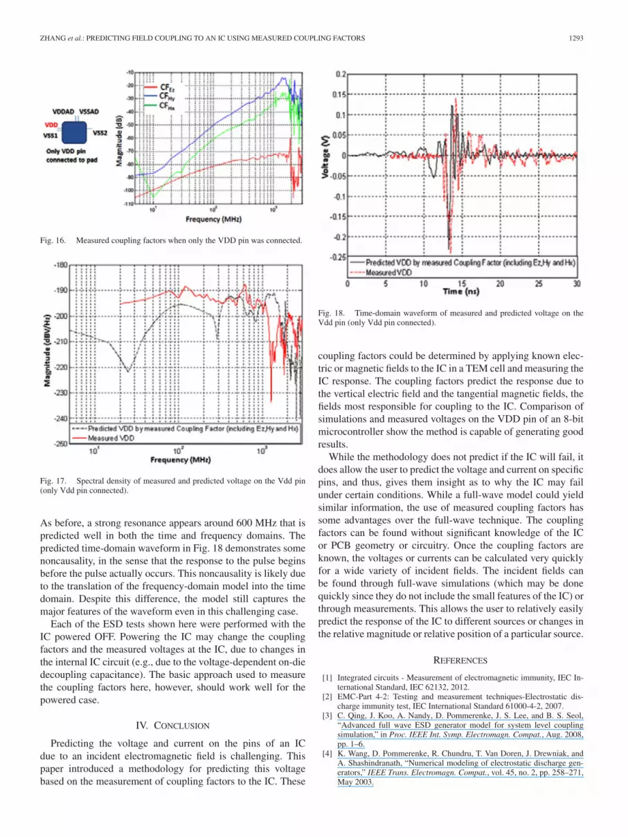
Coupling factors and measured and predicted voltages on Vddwhen only the VDD pin was connected are shown in Figs. 16–18.
Fig. 13. Measured coupling factors when only VDD/VSS1 were connected.
Fig. 14. Spectral density of measured and predicted voltage on the Vdd pin(only Vdd/Vss1 pins connected).
Fig. 15. Time-domain waveform of measured and predicted voltage on theVdd pin (only Vdd/Vss1 pins connected).
ZHANG et al.: PREDICTING FIELD COUPLING TO AN IC USING MEASURED COUPLING FACTORS 1293
Fig. 16. Measured coupling factors when only the VDD pin was connected.
Fig. 17. Spectral density of measured and predicted voltage on the Vdd pin(only Vdd pin connected).
As before, a strong resonance appears around 600 MHz that ispredicted well in both the time and frequency domains. Thepredicted time-domain waveform in Fig. 18 demonstrates somenoncausality, in the sense that the response to the pulse beginsbefore the pulse actually occurs. This noncausality is likely dueto the translation of the frequency-domain model into the timedomain. Despite this difference, the model still captures themajor features of the waveform even in this challenging case.
Each of the ESD tests shown here were performed with theIC powered OFF. Powering the IC may change the couplingfactors and the measured voltages at the IC, due to changes inthe internal IC circuit (e.g., due to the voltage-dependent on-diedecoupling capacitance). The basic approach used to measurethe coupling factors here, however, should work well for thepowered case.
IV. CONCLUSION
Predicting the voltage and current on the pins of an ICdue to an incident electromagnetic field is challenging. Thispaper introduced a methodology for predicting this voltagebased on the measurement of coupling factors to the IC. These
Fig. 18. Time-domain waveform of measured and predicted voltage on theVdd pin (only Vdd pin connected).
coupling factors could be determined by applying known elec-tric or magnetic fields to the IC in a TEM cell and measuring theIC response. The coupling factors predict the response due tothe vertical electric field and the tangential magnetic fields, thefields most responsible for coupling to the IC. Comparison ofsimulations and measured voltages on the VDD pin of an 8-bitmicrocontroller show the method is capable of generating goodresults.
While the methodology does not predict if the IC will fail, itdoes allow the user to predict the voltage and current on specificpins, and thus, gives them insight as to why the IC may failunder certain conditions. While a full-wave model could yieldsimilar information, the use of measured coupling factors hassome advantages over the full-wave technique. The couplingfactors can be found without significant knowledge of the ICor PCB geometry or circuitry. Once the coupling factors areknown, the voltages or currents can be calculated very quicklyfor a wide variety of incident fields. The incident fields canbe found through full-wave simulations (which may be donequickly since they do not include the small features of the IC) orthrough measurements. This allows the user to relatively easilypredict the response of the IC to different sources or changes inthe relative magnitude or relative position of a particular source.
REFERENCES
[1] Integrated circuits - Measurement of electromagnetic immunity, IEC In-ternational Standard, IEC 62132, 2012.
[2] EMC-Part 4-2: Testing and measurement techniques-Electrostatic dis-charge immunity test, IEC International Standard 61000-4-2, 2007.
[3] C. Qing, J. Koo, A. Nandy, D. Pommerenke, J. S. Lee, and B. S. Seol,“Advanced full wave ESD generator model for system level couplingsimulation,” in Proc. IEEE Int. Symp. Electromagn. Compat., Aug. 2008,pp. 1–6.
[4] K. Wang, D. Pommerenke, R. Chundru, T. Van Doren, J. Drewniak, andA. Shashindranath, “Numerical modeling of electrostatic discharge gen-erators,” IEEE Trans. Electromagn. Compat., vol. 45, no. 2, pp. 258–271,May 2003.

1294 IEEE TRANSACTIONS ON ELECTROMAGNETIC COMPATIBILITY, VOL. 56, NO. 6, DECEMBER 2014
[5] J. Koo, L. Han; S. Herrin, R. Moseley, R. Carlton, D. G. Beetner, andD. Pommerenke, “A nonlinear microcontroller power distribution net-work model for the characterization of immunity to electrical fast tran-sients,” IEEE Trans. Electromagn. Compat., vol. 51, no. 3, pp. 611–619,Aug. 2009.
[6] M. Stockinger, J. W. Miller, M. G. Khazhinsky, C. A. Torres, J. C. Weldon,B. D. Preble, M. J. Bayer, M. Akers, and V. G. Kamat, “Boosted anddistributed rail clamp networks for ESD protection in advanced CMOStechnologies,” in Proc. Electr. Overstress/Electrostatic Discharge Symp.,Sep. 2003, pp. 21–25.
[7] J. Zhang, D. G. Beetner, R. Moseley, S. Herrin, and D. Pommerenke,“Modeling electromagnetic field coupling from an ESD gun to an IC,”in Proc. IEEE Int. Symp. Electromagn. Compat., Aug. 14–19 2011,pp. 553–558.
[8] J. Zhang, J. Koo, D. G. Beetner, R. Moseley, S. Herrin, and D. Pom-merenke, “Modeling of the immunity of ICs to EFTs,” in Proc. IEEE Int.Symp. Electromagn. Compat., Jul. 2010, pp. 484–489.
[9] V. Kasturi, S. Deng, T. Hubing, and D. Beetner, “Quantifying electric andmagnetic field coupling from integrated circuits with TEM cell measure-ments,” in Proc. 2006 IEEE Int. Symp. Electromagn. Compat., Aug 14–16,2006, vol. 2, pp. 422–425.
[10] L. Ren and Z. Chen, “Improvement of expression for excitation by anelectric dipole in GTEM cell,” J. Electron., vol. 19, no. 1, pp. 94–98,2002.
Ji Zhang received the B.S. and M.S. degree inelectronic engineering from Tsinghua University,Beijing, China, in 2005 and 2008, respectively, andthe Ph.D. degree from the Electromagnetic Compati-bility Laboratory, Missouri University of Science andTechnology, Rolla, MO, USA, in 2013.
He is currently working for Cisco Systems Inc.,San Jose, CA, USA. His research interests include theimmunity of integrated circuits (IC) to electrical fasttransient events and electrostatic discharge events,IC power delivery network (PDN) modeling, recon-
struction of emission sources, modeling/optimization for high-speed series-linkchannel, and power integrity of board and ASIC package.
Xiang Li received the B.S. degree in electronicinformation engineering from Jilin University,Changechun, China, in 2007 and the M.S. de-gree from Electromagnetic Compatibility Labora-tory, Missouri University of Science and Technology,Rolla, MO, USA, in 2010.
She is currently an EMC Engineer working forFreescale Semiconductor, Inc., Austin, TX, USA. Herresearch interests include the radiated emission andimmunity of integrated circuits (IC), conducted emis-sion and immunity of the IC, electrostatic discharge
event modeling, and crosstalk within harness bundles.
Richard Moseley (M’09) received the B.S.E.E. de-gree from Texas A&M University, College Station,TX, USA, in 1981.
In 1981, he joined Motorola, and in March 2005,he joined the EMC engineering team as an Applica-tions and Systems Engineer. He is currently a SeniorEMC Engineer with the Microcontroller SolutionsGroup, Freescale Semiconductor, Inc., Austin, TX,USA, where he is involved in EMC test and valida-tion engineer.
David Pommerenke (SM’03) received the Ph.D. de-gree from the Technical University Berlin, Berlin,Germany, in 1996.
He was with Hewlett Packard for five years. In2001, he joined the Electromagnetic CompatibilityLaboratory, Missouri University of S&T, Rolla, MO,USA, where he is currently a Professor. He has au-thored or coauthored more than 200 papers and isinventor on 13 patents. His current research interestsinclude system-level electrostatic discharge (ESD),electronics, numerical simulations, EMC measure-
ment methods, and instrumentations and measurement/instrumentation ESDand EMC.
Dr. Pommerenke is an Associate Editor for the IEEE TRANSACTIONS ON
EMC.
Daryl G. Beetner (S’89–M’98–SM’03) received theB.S. degree in electrical engineering from SouthernIllinois University at Edwardsville, Edwardsville, IL,USA, in 1990, and the M.S. and D.Sc. degrees inelectrical engineering from Washington Universityin St Louis, St Louis, MO, USA, in 1994 and 1997,respectively.
He is currently a Professor and the Chair of Elec-trical and Computer Engineering at the Missouri Uni-versity of Science and Technology (formerly calledthe University of Missouri - Rolla), Rolla, MO, USA.
He conducts research with the Electromagnetic Compatibility Laboratory atMissouri S&T on a wide variety of topics including EMC at the chip and systemlevel and detection and neutralization of explosive devices.
Prof. Beetner is an Associate Editor for the IEEE TRANSACTIONS ON IN-STRUMENTATION AND MEASUREMENT.


