Embed Size (px)
Citation preview

Contents lists available at ScienceDirect
Materials Science in Semiconductor Processing
Materials Science in Semiconductor Processing 39 (2015) 536–543
http://d1369-80
n CorrE-m
journal homepage: www.elsevier.com/locate/mssp
Preparation, structural and optical investigationsof ITO nanopowder and ITO/epoxy nanocomposites
Abdelfatteh Bouzidi a, Karim Omri b,c, Lassaad El Mir b,c, Hajer Guermazi a,n
a Research Unit, Physics of Insulating and Semi-insulating Materials, Faculty of Sciences, University of Sfax, B.P. 1171, 3000 Sfax, Tunisiab Physics Laboratory of Nanomaterials for Environment, 6072 Gabes, Tunisiac Al Imam Mohammad Ibn Saud University (IMSIU), College of Sciences, Department of Physics, Riyadh 11623, Saudi Arabia
a r t i c l e i n f o
Keywords:ITO nanoparticleNanocompositeUV–vis absorptionAFM analysisX–ray diffractionBand-gap energy
x.doi.org/10.1016/j.mssp.2015.04.05101/& 2015 Elsevier Ltd. All rights reserved.
esponding author. Tel.: þ216 92019819; faxail address: [email protected] (H. G
a b s t r a c t
Indium Tin Oxide (ITO) nanopowder was synthesized by a sol–gel method. It wascharacterized by X-ray diffraction (XRD) and transmission electron microscopy. ITO/epoxynanocomposites (ITO–EP-NCs) were prepared by mechanically dispersing the as-preparedITO nanopowder into epoxy matrix. The XRD patterns show structural changes dependingon ITO content. The interdependence of structural, morphological, optical properties andthe dispersed concentration of ITO nanoparticles were investigated. The UV–visibleabsorption spectra revealed that the ITO–EP-NCs exhibit enhanced UV light absorptionproperties and wide absorption bandwidth ranging up to 400 nm from 2 wt% ITO loading.Thus, it indicated that UV and IR-shielding properties have been improved with theincorporation of ITO nanoparticles into the epoxy matrix.
The gap energy of epoxy matrix was reduced by adding the ITO-NPs, leading to theimprovement of its electrical conductivity. Indeed, the AC electrical conductivity of ITO–EP-NCsshowed a critical percolation threshold pc¼0.21 wt% ITO. For low loading (o2 wt% ITO), theITO–EP-NCs have combined good transparency in the visible range and enhanced electricalconductivity, which are required for optoelectronics devices.
& 2015 Elsevier Ltd. All rights reserved.
1. Introduction
Polymer matrix nanocomposites have attracted consider-able attention recently as new generation of high performancematerials because of their interesting physical and chemicalproperties resulting from the combination of organic and ino-rganic materials in single compound. They possess enhancedelectrical, optical, mechanical, magnetic and optoelectronicproperties. Therefore, many studies have reported the use ofhybrid nanocomposites in optoelectronic or optical applica-tions requiring high visible transparency and UV-shielding[1–7]. However, structural, mechanical, electrical (mainly the
: þ216 74246347.uermazi).
percolation effect) and optical properties of nanocompositeshave been found to be influenced by the dispersion state [8–10], particle size [11], geometric shape [12,13] surface state,processing parameters and annealing temperature [9,14] ofnanocomposites. Thus, the properties of the nanocompositematerials can be engineered through judicious selection ofnanoparticles, polymer matrix and processing parameters.Epoxy resins are a class of important thermosetting polymerswith extensive industrial applications, it has been widely usedas matrix for composite materials, coatings, adhesives andused for electronic and optical devices packaging [15,16].Epoxy does not block UV-light, but it can be modified to blockUV or IR-light via the addition of appropriate inorganicnanoparticles [17,18]. In the aerospace industry epoxy resinswere used as a matrix on aluminum alloy 2024-T3 for prot-ecting the surface of aircraft [19]. The incorporation of various
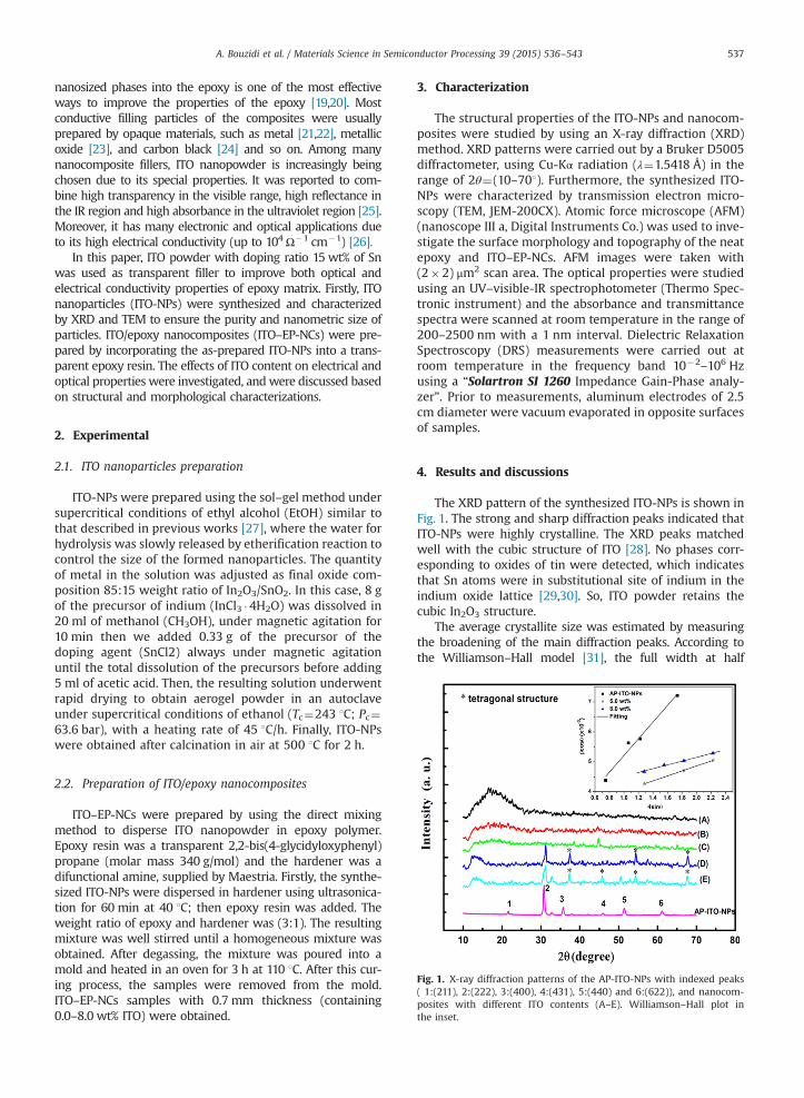
Fig. 1. X-ray diffraction patterns of the AP-ITO-NPs with indexed peaks( 1:(211), 2:(222), 3:(400), 4:(431), 5:(440) and 6:(622)), and nanocom-posites with different ITO contents (A–E). Williamson–Hall plot inthe inset.
A. Bouzidi et al. / Materials Science in Semiconductor Processing 39 (2015) 536–543 537
nanosized phases into the epoxy is one of the most effectiveways to improve the properties of the epoxy [19,20]. Mostconductive filling particles of the composites were usuallyprepared by opaque materials, such as metal [21,22], metallicoxide [23], and carbon black [24] and so on. Among manynanocomposite fillers, ITO nanopowder is increasingly beingchosen due to its special properties. It was reported to com-bine high transparency in the visible range, high reflectance inthe IR region and high absorbance in the ultraviolet region [25].Moreover, it has many electronic and optical applications dueto its high electrical conductivity (up to 104Ω�1 cm�1) [26].
In this paper, ITO powder with doping ratio 15 wt% of Snwas used as transparent filler to improve both optical andelectrical conductivity properties of epoxy matrix. Firstly, ITOnanoparticles (ITO-NPs) were synthesized and characterizedby XRD and TEM to ensure the purity and nanometric size ofparticles. ITO/epoxy nanocomposites (ITO–EP-NCs) were pre-pared by incorporating the as-prepared ITO-NPs into a trans-parent epoxy resin. The effects of ITO content on electrical andoptical properties were investigated, andwere discussed basedon structural and morphological characterizations.
2. Experimental
2.1. ITO nanoparticles preparation
ITO-NPs were prepared using the sol–gel method undersupercritical conditions of ethyl alcohol (EtOH) similar tothat described in previous works [27], where the water forhydrolysis was slowly released by etherification reaction tocontrol the size of the formed nanoparticles. The quantityof metal in the solution was adjusted as final oxide com-position 85:15 weight ratio of In2O3/SnO2. In this case, 8 gof the precursor of indium (InCl3 �4H2O) was dissolved in20 ml of methanol (CH3OH), under magnetic agitation for10 min then we added 0.33 g of the precursor of thedoping agent (SnCl2) always under magnetic agitationuntil the total dissolution of the precursors before adding5 ml of acetic acid. Then, the resulting solution underwentrapid drying to obtain aerogel powder in an autoclaveunder supercritical conditions of ethanol (Tc¼243 1C; Pc¼63.6 bar), with a heating rate of 45 1C/h. Finally, ITO-NPswere obtained after calcination in air at 500 1C for 2 h.
2.2. Preparation of ITO/epoxy nanocomposites
ITO–EP-NCs were prepared by using the direct mixingmethod to disperse ITO nanopowder in epoxy polymer.Epoxy resin was a transparent 2,2-bis(4-glycidyloxyphenyl)propane (molar mass 340 g/mol) and the hardener was adifunctional amine, supplied by Maestria. Firstly, the synthe-sized ITO-NPs were dispersed in hardener using ultrasonica-tion for 60 min at 40 1C; then epoxy resin was added. Theweight ratio of epoxy and hardener was (3:1). The resultingmixture was well stirred until a homogeneous mixture wasobtained. After degassing, the mixture was poured into amold and heated in an oven for 3 h at 110 1C. After this cur-ing process, the samples were removed from the mold.ITO–EP-NCs samples with 0.7 mm thickness (containing0.0–8.0 wt% ITO) were obtained.
3. Characterization
The structural properties of the ITO-NPs and nanocom-posites were studied by using an X-ray diffraction (XRD)method. XRD patterns were carried out by a Bruker D5005diffractometer, using Cu-Kα radiation (λ¼1.5418 Å) in therange of 2θ¼(10–701). Furthermore, the synthesized ITO-NPs were characterized by transmission electron micro-scopy (TEM, JEM-200CX). Atomic force microscope (AFM)(nanoscope III a, Digital Instruments Co.) was used to inve-stigate the surface morphology and topography of the neatepoxy and ITO–EP-NCs. AFM images were taken with(2�2) μm2 scan area. The optical properties were studiedusing an UV–visible-IR spectrophotometer (Thermo Spec-tronic instrument) and the absorbance and transmittancespectra were scanned at room temperature in the range of200–2500 nm with a 1 nm interval. Dielectric RelaxationSpectroscopy (DRS) measurements were carried out atroom temperature in the frequency band 10�2–106 Hzusing a “Solartron SI 1260 Impedance Gain-Phase analy-zer”. Prior to measurements, aluminum electrodes of 2.5cm diameter were vacuum evaporated in opposite surfacesof samples.
4. Results and discussions
The XRD pattern of the synthesized ITO-NPs is shown inFig. 1. The strong and sharp diffraction peaks indicated thatITO-NPs were highly crystalline. The XRD peaks matchedwell with the cubic structure of ITO [28]. No phases corr-esponding to oxides of tin were detected, which indicatesthat Sn atoms were in substitutional site of indium in theindium oxide lattice [29,30]. So, ITO powder retains thecubic In2O3 structure.
The average crystallite size was estimated by measuringthe broadening of the main diffraction peaks. According tothe Williamson–Hall model [31], the full width at half

A. Bouzidi et al. / Materials Science in Semiconductor Processing 39 (2015) 536–543538
maximum (β) of the XRD peak is attributed to the crystallitesize (D) and strain (ε) induced in ITO network by crystalimperfection and distortion. These parameters were relatedby the following equation:
β cos θ¼ kλDþ4ε sin θ ð1Þ
where the shape factor k¼0.9, λ is the wavelength of Cu Kαradiation (1.5405 Å), and θ is the Bragg angle.
Williamson–Hall plot is presented in the inset of Fig. 1.The strain ε and the particle size D of ITO-NPs were estimatedfrom the linear fit to the data. We found 27.9�10�4 and58 nm, respectively. The obtained particle size value is closeto that obtained from TEM observations. Indeed, the TEMmicrograph of ITO powder (Fig. 2) shows a homogenous dis-tribution of nanoparticles with similar prismatic shape and amean value of about 60 nm.
XRD patterns of the neat epoxy 0.0 wt% (A) and nan-ocomposites (B, C, D and E for 0.5, 2.0, 5.0 and 8.0 wt% ITO,respectively) are displayed in Fig. 1. The X-ray patterns (A–C) recorded a broad peak focused at about 2θ¼171. Nosignificant difference was found between the referenceneat epoxy (0.0 wt%), 0.5 wt% and 2.0 wt% ITO nanocom-posites, because of the largely amorphous structure ofEpoxy. Furthermore, the broad amorphous peak exhibits adecrease in its intensity and a shift towards lower angles inthe case of samples with 5.0 and 8.0 wt% ITO ((D) and (E)patterns respectively), due to supplementary disorder ind-uced by ITO0NPs insertion. Besides, one can easily noticein (D) and (E) patterns, additional peaks matching wellwith a tetragonal-SnO2 structure (JCPDS Card 88-0287).The presence of this phase in high filled nanocompositesproves lattice alteration of ITO. Similar effect was reportedby Nadaud et al. [32] and was related to change of the Sn–O distance. Likewise, Parent et al. [33] found a shorteningof the Sn–O distance in ITO films and proved that the tinenvironment in films is similar to that in SnO2. So, in thesame way, ITO is confined in the epoxy matrix duringthe curing process of nanocomposites. In this condition,strains can be induced due to the expansion/compressionof the resin, and as a result, the tin environment becomessimilar to that in SnO2, which leads to the change of the
Fig. 2. The TEM micrographs of the ITO nanopowder.
ITO crystalline network from the cubic-In2O3 structure totetragonal-SnO2 one. In fact, the strain values for ITOparticles in epoxy matrix were estimated from W–H plot(inset of Fig. 1). The strain values are 8.3�10�4 and6.3�10�4 for samples with 5.0 and 8.0 wt% ITO, respec-tively, while the as-prepared ITO with cubic-In2O3 struc-ture was highly strained (27.9�10�4) which proves thatIn2O3 network is strongly distorted by tin insertion. In fact,the ionic radius of tin ðrSn4þ ¼ 0:71 A ̊Þ is smaller than thatof indium ðrIn3þ ¼ 0:81 A ̊Þ [32]. The decrease of strain val-ues for ITO-NPs dispersed in nanocomposites, demon-strates that ITO network in nanocomposites was relaxedand switched to tetragonal-SnO2 structure.
The UV–vis absorption and transmittance spectra ofnanocomposites at different concentrations of ITO are shownin Fig. 3(a) and (b). All absorption curves exhibit a broadintense band around 300 nm, the position of which does notchange with ITO concentration (Fig. 3(a)). It was related tobenzene chromophores in the epoxy resin [34]. The absorp-tion edge exhibits a red-shift as the ITO content increases.Furthermore, the absorbance increases with increasing ITOamount in the UV–visible light range (Fig. 3(c)). Fig. 3(b)shows that by adding the ITO nanoparticles to the epoxymatrix, the transmittance of the nanocomposites was dec-reased in the whole wavelength region. The transmittance isof about 90% in the range of 400–1000 nm for neat epoxy(Fig. 3(b)). Then, it drops sharply in the UV region due to theonset of fundamental absorption. The low ITO filled nano-composite (0.5 wt%) exhibits slight decrease of transmittancein the vis–NIR region (400–1000 nm) compared to neatepoxy. It retains more than 80% transparency in this region.Whereas, transparency of the nanocomposites fall to about30% with increase of ITO content (up to 8.0 wt%). This figureshows that the introduction of ITO nanoparticles into epoxymatrix (at the 8.0 wt% content) obviously improves the IR-shielding efficiency with an enhancement of about 70–80%in the IR region. However, the absorption of UV-light wasextended up to about 400 nm for higher filled nanocompo-sites. As can be seen in Fig. 3(b), in the UV range, epoxy resinonly blocks UV-light in the range between 200 and 350 nm,however it becomes high UV light blocker (up to 400 nm) viathe addition of ITO-NPs from 5.0 wt% filling concentration,and high loading samples show stronger absorption of UV-light (Fig. 3(c)).
Based on the literature [9,35], several reasons can con-tribute to the reduction of the transmittance of nanocompo-sites by increasing the filler concentration. Some authorsattributed this reduction to the relatively large particles size,and the mismatch of refractive index between the polymermatrix and the nanoparticles (the refractive index of epoxy-resin is 1.54–1.55 [9], and that of ITO is 1.89–2 [36–38])which leads to intense light scattering [39]. In addition, thelight scattering caused by the surface roughness is also onereason for the decrease of the transmittance of the epoxynanocomposites with increasing the ITO content. This effectwill be confirmed by the AFM spectroscopy. Indeed, the 3DAFM images of the surface topography obtained for the neatepoxy and nanocomposite samples are shown in Fig. 4.
Fig. 4(a1) shows that the surface of neat epoxy sampleis quite smooth and thus the light scattering caused by thesurface roughness would be insignificant in transmittance.

Fig. 3. (a) Absorbance in the range of (200–1000 nm), (b) transmittancespectra in the range of (200–2500 nm) of nanocomposites, and (c)transmittance and absorbance versus wt% of ITO at λ¼600 nm andλ¼300 nm respectively. The inset shows Tauc's plot to calculate Eg.
A. Bouzidi et al. / Materials Science in Semiconductor Processing 39 (2015) 536–543 539
The increasing of the surface roughness with increase ofITO content (Fig. 4(a2)–(a5) and (b)) leads to the increaseof light scattering caused by the nanoparticles because ofthe mismatch of refractive index between the nanoparti-cles and the polymer matrix; which result in a reduction oftransmittance.
The optical band gap of nanocomposites was evaluatedusing Tauc's relation assuming that the band transition isdirect [35,40]:
ðahnÞ2 ¼ Aðhn–EgÞ ð2Þwhere A is a constant which depends on transition prob-ability, Eg is the band gap energy, and hν is the incident pho-ton energy. α is the optical absorption coefficient evaluatedfrom absorbance data. The inset of Fig. 3(a) shows the bandgap energy evaluation for the nanocomposites. The interceptbetween the solid lines and x-axis provides band gap energy.The fit parameters obtained from the linear part of the Taucplots are gathered in Table 1. The band gap energy of the asprepared ITO-NPs was determined as well and added inTable 1. We found 3.64 eV, in good agreement with that pro-vided by Sarhaddi et al. [30].
Furthermore, the optical band gap (Eg) of the ITO–EP-NCs can be obtained from the optical transmission spectraby using the relation [41]:
Eg eVð Þ ¼ 1241:5=λc ð3Þwhere λc is the critical wavelength defined as the inflexionpoint of the UV absorption edge; practically, its position isdetermined from the second derivative of the transmissioncurve. The obtained values of Eg are added in Table 1. Theyare closed to that obtained using the Tauc model (Eq. (2)).
Moreover, Fig. 5 reveals a decrease of the band edgeenergy as ITO content increases, from 3.401 eV in the neatepoxy polymer to 2.783 eV in 8.0 wt% filled nanocompo-sites. Therefore, the decreased values of Eg can be relatedto intermolecular interactions with ITO-NPs, as it has beenalready deduced from XRD. Therefore, the reduction in thegap energy by adding the ITO-NPs, would lead to enhance-ment of electrical conductivity of epoxy polymer.
Moreover, in the case of nanocomposites with high ITOcontent, it can be seen a changing in the slope of α in thevicinity of 2.4 eV (�500 nm), (Fig. 3(a)) due to ITO band gapeffect. Table 1 provides the calculated values of the band gapenergy of ITO-NPs embedded in epoxy matrix, according toEq. (3). It can be noticed that the apparent gap energy of ITOin nanocomposites was red-shifted compared to that of asprepared ITO-NPs. This red-shift can be due to a mismatch inpermittivity values between ITO and epoxy polymer [16,42],and structural changes in ITO network as it has been alreadyrevealed from XRD data. On the other hand, the apparentband gap of ITO in nanocomposites exhibits a slight blue-shift as ITO content increases (Fig. 5). This may be due to thevariation of the medium surrounding the ITO-NPs in highfilled nanocomposites when the distance between the par-ticles is reduced. It is important to mention that the absorp-tion edge of nanocomposites, instead of being abrupt, itoccurs quite smoothly (Fig. 3(a)). Thus, the observed absorp-tion tail in optical spectra (Fig. 3(a)) was explained using theUrbach–Martienssen rule [43,44]:
α¼ α0expE�EgEU
� �ð4Þ
where α0 is a constant, EU is the Urbach energy which isinterpreted as the width of the tail of localized states in thedirect band gap and determines the steepness of the Urbachtail. The exponential absorption edge seems to be due to

Fig. 4. 3D topographic AFM images (a1–a5) of pure epoxy and the ITO/epoxy nanocomposites, (b) surface roughness (RMS) versus wt% ITO.
Table 1Optical parameters of nanocomposites and ITO nanoparticles.
wt% ITO 0.0 0.5 2.0 5.0 8.0 ITOb
NCs ITOa NCs ITOa NCs ITOa
From Tauc plot Eg (eV) 3.516 3.492 3.414 – 3.086 – 2.815 – 3.642A(cm eV)�1 2.07�105 1.96�105 1.75�105 – 1.74�105 – 1.31�105 – 1.60�109
From Eq. (3) λc (nm) 365 365.5 375 500 412 478 446 474 336Eg(eV) 3.401 3.396 3.310 2.483 3.013 2.590 2.783 2.619 3.694
EU(eV) 0.290 0.298 0.444 1.039 0.700 0.768 0.708 0.726 –
a ITO dispersed in epoxy matrix.b As-prepared ITO nanoparticles.
A. Bouzidi et al. / Materials Science in Semiconductor Processing 39 (2015) 536–543540
fluctuations in the electronic energy bands caused by latticevibrations as it has been explained in semiconductor materi-als [44]. EU values in nanocomposites were calculated byfitting experimental data in Eq. (4) and added in Table 1. Theevolution of EU in nanocomposites and in ITO embedded inepoxy matrix versus wt% ITO is given in Fig. 5. This figureshowed that the values of EU were higher in nanocompositescompared to the neat epoxy one, and highest value was
obtained in highest filled nanocomposites. The increment ofthe tail widths can be explained by creation of disorder andimperfections in nanocomposites network by adding ITO-NPs, a case which may increase localized states withinthe forbidden band gap. This is consistent with the decreaseof the gap energy of ITO–EP-NCs. For ITO embedded in epoxymatrix, the decrease of EU with ITO content is consistent withXRD results. Indeed, the ITO lattice in epoxy matrix was

Fig. 5. Optical band gap energy Eg and Urbach energy EU plots versus wt%ITO for nanocomposites and ITO dispersed in epoxy matrix (ITO (a)).
Fig. 6. Real part of dielectric permittivity versus λ2.
Fig. 7. Imaginary part of dielectric permittivity versus λ3.
Table 2Calculated values of optical constants.
Samples (wt%ITO)
ε1 ωp
(1015 rad/s)τ(10�14 s)
N/m*(047 g�1 cm�3)
0.0 6.215 1.08 3.18 1.990.5 6.197 1.03 2.54 1.8082.0 6.118 0.795 1.85 1.0635.0 6.05 0.488 1.61 0.3978.0 6.018 0.306 0.508 0.155
A. Bouzidi et al. / Materials Science in Semiconductor Processing 39 (2015) 536–543 541
relaxed and seems to be less distorted compared to as pre-pared ITO one, which results in a decrease of disorder in ITOlattice, and thus leads to lower values of Urbach energy.
The complex dielectric permittivity ε is directly relatedto the optical properties of the solid material. It can be int-roduced from the following equation:
ε¼ ε1� iε2 ð5Þ
The real (ε1) and imaginary (ε2) parts of dielectric per-mittivity for neat epoxy and ITO–EP-NCs with differentITO contents are also determined by the following rela-tions [45]:
ε1 ¼ n2�k2 ð6Þ
ε2 ¼ 2nk ð7Þ
where n¼ 1þRð Þ=ð1�RÞþffiffiffiffiffiffiffiffiffiffiffiffiffiffiffiffiffiffiffiffiffiffiffiffiffiffiffiffiffiffiffiffiffiffiffiffiffiffiffiffiffiffiffiffiffiffiffiffiffiffiffiffiffiffiffiffiffi1þRð Þ2= 1�Rð Þ2� k2�1
� �ris
the refractive index, R is the reflectance of material, andk¼λα/4π is the extinction coefficient.
For all samples, it is found that, in infrared range, ε1 islinear function of the square of the wavelength (Fig. 6),while ε2 is linear with λ3 (Fig. 7).
These results can be used in order to determine theoptical constants: ε1, ωp and τ which respectively repre-sent the dielectric permittivity at high frequencies, theplasma frequency and relaxation time, using the followingequations [46,47]:
ε1 � ε1� ε1ω2p
4π2c2λ2 ð8Þ
ε2 ¼ 2nk� ε1ω2p
8π3c3τλ3 ð9Þ
The free carrier's concentration-to-effective mass ratioN=mn is then calculated from:
ω2p ¼
4πNe2
ε1mne
ð10Þ
The calculated values of these constants are gatheredin Table 2.
The electric conductivity σe was deduced from absorp-tion data using the relation [48]:
σe ¼ λnc=2π ð11ÞFig. 8 shows the variations of electrical conductivity
as a function of wt% ITO. It shows an enhancement of σe

Fig. 9. AC conductivity σAC of the investigated samples, as function offrequency.
Fig. 10. Comparison of theoretical percolation threshold predicted byEq. (12) (solid lines) and experimental data (scatters).
Fig. 8. Evolution of electrical conductivity of nanocomposites versus wt%ITO for λ¼510 nm.
A. Bouzidi et al. / Materials Science in Semiconductor Processing 39 (2015) 536–543542
values as wt% ITO increases, due to ITO conductivity. Ind-eed, ITO is a heavily doped n-type semi-conductor, whichcontains free carriers within the conduction band [39]. Theimprovement in electrical conductivity agrees well withthe reduction of the gap energy of nanocomposites (Fig. 8).Thus, with increasing wt% ITO, we can improve electricalconductivity of epoxy polymer. So, epoxy nanocompositesseem to accumulate less charge compared with neat epoxypolymer. This is consistent with the results of Fabiani et al.[49] and Wang et al. [50].
The AC conductivity σAC obtained by DRS measure-ments, is shown in Fig. 9, as function of frequency for theinvestigated samples.
To investigate the effect of ITO filling on electrical con-ductivity of epoxy matrix, we plotted, in Fig. 10, σAC as fun-ction of wt% ITO. As can be seen, the addition of ITO nano-particles enhances the electrical properties of an epoxy resin.By continuously adding fillers, the composite's conductivityincreases a few orders of magnitude (Fig. 10). The experi-mental curve exhibits a sharp change for low ITO concentra-tions, typical of a percolation phenomenon. Percolation mec-hanism can be expressed pretty well as a power law [51]:
σ ¼ σeðp�pcÞs ; p4pc ð12Þwhere σ is the conductivity of bulk resultant material, σe isthe effective conductivity of inclusion, p is the percentageweight of ITO-NPs, pc is critical percolation threshold and sis the critical exponent. In fact, Eq. (12) has beenwidely usedto fit the experimental nanocomposite electrical conductivitydata as a function of ITO content. Fig. 10 shows the best fit tothe experimentally measured conductivity data as a functionof weight fraction according to Eq. (12). This analysis revealsa percolation threshold pc of about 0.21 wt% with R2¼0.98994 and a critical exponent s of 1.32 for ITO–EP-NCs.The critical percolation threshold pc indicates the criticalloading that causes the significant increase in the conduc-tivity. After this point, the addition of more filler only cau-ses a moderate increase in conductivity. Actually, transportin a polymer filled with conducting particles is due to the
electron hopping/tunneling across the inter-particle gapson the system. Thus, when ITO content increases the dis-tance between the particles is reduced, and consequently theconductivity rises.
5. Conclusions
In this work, tin-doped-In2O3 nanopowder was synthe-sized by the sol–gel method under supercritical conditions.The XRD patterns of ITO nanopowder show strained cubic-In2O3 phase without any indication of crystalline SnO2 as anadditional phase. While in nanocomposites ITO structurewas relaxed and switched to tetragonal-SnO2. The UV–visibleabsorption spectra revealed that the nanocomposites exhibitenhanced UV-light absorption properties. Furthermore, withthe incorporation of ITO nanoparticles into the epoxy matrixwe obviously improved the IR-shielding efficiency with anenhancement of about 70–80%. These results showed thatITO–EP-NCs can be potential candidates for UV and IR-shie-lding applications. Moreover, the gap energy of epoxy matrixdecreases from 3.401 to 2.783 eV, as ITO content increasesfrom 0.0 to 8.0 wt% respectively. The apparent gap energy ofITO in nanocomposites exhibits a red-shift compared to that of

A. Bouzidi et al. / Materials Science in Semiconductor Processing 39 (2015) 536–543 543
as prepared ITO-NPs due to residual strains. Moreover, the ele-ctrical conductivity of nanocomposites increases with increas-ing filler content, matching well with the red-shift of the bandgap. AC conductivity of ITO–EP-NCs, showed a critical percola-tion threshold pc¼0.21 wt% ITO. For low loading, the ITO–EP-NCs have combined good transparency in the visible rangeand enhanced electrical conductivity, which are required foroptoelectronics devices.
Acknowledgments
This study has been supported by the Tunisian Ministryof High Education and Scientific Research. The authorsgratefully acknowledge Prof. R. Chtourou, Research centerand Technologies of the Energy, Photovoltaic LaboratoryTunisia, for the use of UV–visible measurements facilities.
References
[1] A. Thabet, Y.A. Mobarak, M. Bakry, J. Eng. Sci. 39 (2011) 377–403.[2] L. Shanghua, M.L. Meng, S.T. Muhammet, K.K. Do, M. Mamoun, Nano
Rev. 1 (2010) 5214, http://dx.doi.org/10.3402/nano.v1i0.5214.[3] K. Sarita, K. Susheel, C. Annamaria, N. James, H. Youssef, K. Rajesh,
Prog. Polym. Sci. 778 (2013) 1–30.[4] X.Y. Huang, H.R. Heulings, V. Le, J. Le, Chem. Mater. 13 (2001)
3754–3759.[5] W. Caseri, Chem. Eng. Commun. 196 (2009) 549–572.[6] H. Althues, J. Henle, S. Kaskel, Chem. Soc. Rev. 36 (2007) 1454–1465.[7] P.M. Ajayan, L.S. Schadler, P.B. Braun, Nanocomposite Science and
Technology, Wiley VCH, Weinheim, Germany, 2003.[8] C. Lü, Y. Cheng, Y. Liu, F. Liu, B. Yang, Adv. Mater. 18 (2006) 1188.[9] Y.S. Luo, J.P. Yang, X.J. Dai, Y. Yang, S.Y. Fu, J. Phys. Chem. C 113 (2009)
9406.[10] C.J. CapozziR.A. Gerhardt, Adv. Funct. Mater. 17 (2007) 2515–2521.[11] G. Xia, G.C. Wei, C. Yu, S.Z. Ping, Chin. Phys. B 23 (2014) 076403.[12] A.S. Khairul, M. Mariatti, A. Azizan, N. Chee Mang, W.T. Tham
J. Mater. Sci. Mater. El 22 (2011) 757–764.[13] L. Shen, F.Q. Wang, H. Yang, Q.R. Meng, Polym. Test. 30 (2011)
442–448.[14] K. Dai, Y.C. Zhang, J.H. Tang, X. Ji, Z.M. Li, J. Appl. Polym. Sci. 125
(2012) E561–E570.[15] Epoxy Resin: Chemistry and Technologyin: C.A. May (Ed.), Dekker,
New York, .[16] H. Smaoui, L. El Mir, H. Guermazi, S. Agnel, A. Toureille, J. Alloy.
Compd. 477 (2009) 316–321.[17] D. Sun, H.-J. Sue, N. Miyatake, J. Phys. Chem. C 112 (2008)
16002–16010.[18] Y. Yang, Y.-Q. Li, S.-Y. Fu, H.-M. Xiao, J. Phys. Chem. C 112 (2008)
10553–10558.[19] S. Hongwei, L. Fuchun, Y. Lihong, H. Enhou, Prog. Org. Coat. 62
(2008) 359–368.[20] N.D. Ngoc, D.L. Minh, K.N. Quang, S.K. Byung, Adv. Nat. Sci. Nanosci.
Nanotechnol. 2 (2011) 045013.
[21] S. Nam, H.W. Cho, T. Kim, D. Kim, B.J. Sung, S. Lim, H. Kim, Appl. Phys.Lett. 99 (2011) 043104.
[22] L. Zhang, W. Wang, X.G. Wang, P. Bass, Z.Y. Cheng, Appl. Phys. Lett.103 (2013) 232903.
[23] C.L. Yuan, X.Y. Liu, Y. Yang, J.W. Xu, Y. Gu, Acta Phys. Sin. 59 (2010)7396.
[24] X.Q. Yin, J.F. Capsal, D. Guyomar, Appl. Phys. Lett. 104 (2014) 052913.[25] C.G. Granqvist, A. Hultaker, Thin Solid Films 411 (2001) 1–5.[26] J.G. Nam, H. Choi, S.H. Kim, K.H. Song, S.C. Park, Scr. Mater. 44 (2001)
2047.[27] L. El Mir, J. El Ghoul, S. Alaya, M. Ben Salem, C. Barthouand, H.J. Von
Bardeleben, Physica B 403 (2008) 1770.[28] S.R. Ramanan, Thin Solid Films 389 (2001) 207–212.[29] H. Ibrahem, M. Moghdad, IPASJ Int. J. Electr. Eng. 1 (2013) 18–22.[30] R. Sarhaddi, N. Shahtahmasebi, M. RezaeeRokn-Abadi, M.M. Bagheri-
Mohagheghi, Physica E 43 (2010) 452–457.[31] V.D. Mote, Y. Purushotham, B.N. Dole, J. Theor. Appl. Phys. 6 (2012)
1–8.[32] N. Nadaud, N. Lequeux, M. Nanot, J. Jove, T. Roisnel, J. Solid State
Chem. 135 (1998) 140–148.[33] Ph. Parent, H. Dexpert, G. Tourillon, J.M. Grimal, J. Electrochem. Soc.
139 (1992) 276–281.[34] M. Mondragon, M.A. Cortes, E. Arias, C. Falcony, O.Z. Angel, Polym.
Eng. Sci. 51 (9) (2011) 1808–1814.[35] P. Tao, A. Viswanath, L.S. Schadler, B.C. Benicewicz, R.W. Siegel, ACS
Appl. Mater. Interfaces 3 (2011) 3638–3645.[36] B.D. Cullity, Elements of X-Ray Diffraction, Addison-Wesley, Reading
MA, 1978.[37] J.C. Manifacier, L. Szepessy, J.F. Bresse, N.I. Perctin, R. Stuck, Mater.
Res. Bull. 14 (1979) 163–175.[38] M. Gross, A Winnacker, P.J. Wellmann, Thin Solid Films 515 (2007)
8567–8572.[39] J. Ederth, P. Johnsson, G. Niklasson, A. Hoel, A. Hultaker, P. Heszler,
C. Granqvist, A.R. Doorn, M. Jongerius, D. Burgard, Phys. Rev. B 68(2003) 155410.
[40] P. Singh, A. Kaushal, D. Kaur, J. Alloy. Compd. 471 (2009) 11–15.[41] M. Ohring, The Materials Science of Thin Films, Academic Press, New
York, 1991.[42] D. Sun, H.J. Sue, N. Miyatake, J. Phys. Chem. C 112 (2008)
16002–16010.[43] F. Urbach, Phys. Rev. 92 (1953) 1324.[44] B. Abay, S.H. Güder, H. Efeoglu, K.Y. Yogurtçu, Turk. J. Phys. 25 (2001)
543–549.[45] M.A. Omar, Elementary Solid State Physics, Addison-Wesley Publish-
ing Company, New York, 1993.[46] A.K. Wolaton, T.S. Moss, Proc. R. Soc. Lond. A 81 (1963) 5091.[47] M. Sesha Reddy, K.T. Ramakrishna Reddy, B.S. Naidu, P.J. Reddy, Opt.
Mater. 4 (1995) 787–790.[48] E. Marquez, A.M. Bernal-Oliva, J.M. Gonzalez-Leal, R. Prieto-Alcon,
A. Ledesma, R. Jimenez-Garay, I. Martil, Mater. Chem. Phys. 60(1999) 231–239.
[49] D. Fabiani, G.C. Montanari, A. Dardano, G. Guastavino, L. Testa,M. Sangermano, IEEE CEIDP Annual Report Conference, 2008,pp. 710–713.
[50] Q. Wang, G. Chen, IEEE International Conference on Solid DielectricsPotsdam Germany, 2010, pp. 4–9.
[51] R.N. Othman, A.N. Wilkinson, Int. J. Automot. Mech. Eng. 10 (2014)1832–1840.


![[2012] Investigation into photocatalytic decolorization of Reactive Black 5 (RB5) using Ti O2 nanopowder](https://img.pdfslide.net/doc/110x75/6311038f277fc434e604858e/2012-investigation-into-photocatalytic-decolorization-of-reactive-black-5-rb5.jpg)


