Embed Size (px)
Citation preview

1. INTRODUCTION
This paper describes two hardware architectures devel-oped for control applications as part of the “Valcard”project, a collaboration between the Computing Labo-ratory and the Engineering Science Department at Ox-ford University. The particular application area consid-ered is sensor validation, and three examples are givenof the architectures in use; however, many of the re-quirements of the particular domain are similar to thoseof a broader class of control applications.
The principal enabling technology is the Field Pro-grammable Gate Array (FPGA), which is a configur-able matrix of simple logic cells. A technique calledhardware compilation (Page and Luk, 1991) is used tospecify FPGA functionality in a high-level imperativeprogramming language called Handel, which is a de-rivative of occam (Inmos, 1988a). The background tothe Valcard Project, including introductions to FPGAs,hardware compilation, and the requirements for hard-ware platforms for sensor validation, are described in(Henry, 1995a).
This paper provides a brief review of these topics, andthen describes the two PC-hosted architectures. Thefirst card, aimed at simpler applications, consists of anISA-bus card which can host up to two FPGAs, andwhich can also support a daughter board holding appli-cation-specific circuitry. The second design is modular,
based on the transputer (Inmos, 1988b), in whichFPGA modules provide interfacing between thetransputer and application-specific circuitry, and mayin addition carry out low-level signal processing toreduce the computational burden on the processor.
After each architecture is described, applications arepresented. The first, the so-called FPGA card, has beenused in thermocouple and dissolved oxygen sensorapplications, while the second, the transputer card, hasbeen applied to a Coriolis mass flow meter.
These architectures provide the advantages of a soft-ware-based prototyping environment: high-level ab-stract design definition, automated design transforma-tion, symbolic debugging, and a high degree of re-usebetween applications. At the same time, few con-straints are placed on the hardware functionality imple-mented using the cards. Indeed, as much of the hard-ware is described in software, experimentation withalternative designs, and continuous revision and updat-ing, are rendered far easier than with traditional hard-ware design approaches, and so a wider range of hard-ware solutions might be considered using this route.
Finally, the limitations of these architectures are con-sidered along with issues for further research. Keythemes are the extension of the design methodologyfrom prototyping to the manufacture of ASICS, and theprovision of Fieldbus communication capability.
PROGRAMMABLE HARDWARE ARCHITECTURES FORSENSOR VALIDATION
M. P. Henry†*, N. Archer†, M. R. A. Atia†, J. Bowles†, D. W. Clarke†, P. M. A. Fraher†,I. Page‡, G. Randall‡, J.C-Y. Yang†.
† Department of Engineering Science, Parks Road, Oxford OX1 3PJ.‡ Computing Laboratory, Parks Road, Oxford. OX1 3QD.
* To whom correspondence should be addressed: [email protected]
Abstract. A previous paper (Henry, 1995a) introduced the technique of hardware compilation as the basis for developinghighly flexible programmable hardware platforms for control applications such as sensor validation. This paper describes twoPC-hosted architectures for sensor validation research. The first holds up to two FPGAs and supports a daughter board withapplication-specific circuitry. The second is based on the transputer TRAM standard, and consists of programmable hardwaremodules providing interfacing and low-level signal processing between the transputer and arbitrary I/O components. Threeapplications are described, based upon a thermocouple, a dissolved oxygen probe and a Coriolis mass flow meter.
Key Words. Field-Programmable Gate Arrays (FPGAs); hardware compilation; Handel; occam; transputers; sensorvalidation; uncertainty; fault detection and diagnosis; fieldbus; thermocouple; dissolved oxygen sensing; Labview.

2. CONTEXT AND MOTIVATION
This section explains the context of and motivationbehind the Valcard project. A summary of the sensorvalidation research aims and prototyping requirementsis followed by brief notes on FPGAs and hardwarecompilation. Alternative solutions are considered, andthen the Valcard project is summarised. Each of thesetopics is covered in more detail by (Henry, 1995a).
2.1. Sensor validationFor a number of years the Control Engineering groupat Oxford has been developing the concept of the self-validating or SEVA sensor (Henry and Clarke, 1993).The term “sensor” includes both the transducer(s) andwhat is often called in industry the transmitter, whichconverts the transducer signals into a form (pneumaticpressure, current, or more recently digital message)which can be sent to the control system. In the SEVAcontext, it is assumed that the sensor has local compu-tational power, and a digital communication capabilitywhich enables it to send and receive messages of arbi-trary complexity.
Like many intelligent sensors available commercially,the SEVA sensor performs self-checking. Instead ofoutputting simple device-specific error codes or valid-ity bits, it generates generic validity metrics for eachmeasurement (Fig. 1):
• The validated measurement value (VMV) is thebest estimate of the true measurand value, takingall diagnostic information into account. If a faultoccurs, then the VMV is corrected to the bestability of the sensor. In the most severe cases(where the raw data are useless or have stoppedcompletely), the current VMV is extrapolated frompast measurement behaviour.
• The validated uncertainty (VU) is the uncertaintyassociated with the VMV. The metrological defi-nition is used here (Kline and McClintock, 1953;ANSI, 1985): the VU gives a confidence intervalfor the true value of the measurand. For example,if VMV is 2.51 units, and the VU is 0.08, then thereis a 95% chance that the true measurement lieswithin the interval 2.51 ± 0.08 units. The VU takes
into account all likely sources of error, includingnoise, measurement technology and any fault-cor-rection strategy currently being used.
• The measurement value status is a discrete-valuedflag indicating how the VMV has been calculated.A few basic categories are admitted, such asCLEAR - the VMV has been calculated normally,BLURRED - the VMV is still based on live data,but is being corrected for a fault, and BLIND - theVMV is being projected from past behaviour. TheMV status allows users of the measurement todetermine whether it is acceptable - for example,BLIND data should never be used for feedbackcontrol.
It is becoming increasingly common for sensors togenerate more than one measurement (e.g., processtemperature and pressure), a practice encouraged bydigital communications, whereby more than one datachannel can be transmitted over a single pair of wires.In the SEVA scheme the VMV, VU and MV status aregenerated for each measurement (as, for example, asingle fault may affect each measurement in a differentway). In addition, a single, generic device status isprovided to summarise the health of the physical in-strument, and detailed diagnostics are made availableas required.
The SEVA group has several active research areas:
• The development of prototype SEVA sensors suchas Coriolis mass flow (Henry, 1994a), thermocou-ple (Yang, 1993), and dissolved oxygen (Clarkeand Fraher, 1995).
• Self-validating actuators, such as valves (Alsop,1995).
• Control, fault detection and validation of loops andprocesses which use SEVA sensors and actuators(Clarke, 1995; Yang and Clarke, 1995).
For experimental work and practical demonstrations,prototype SEVA instruments are a prerequisite. Suchprototypes have usually been based upon commercialinstruments. In the first generation of SEVA sensors aPC was interfaced to an industrial sensor to pick upsignals relating to measurement and diagnostics (Fig.2). It is frequently a further requirement for controlsignals to pass from the PC to the sensor, for exampleto activate testing circuitry. Often, the transmitter isbypassed entirely, and the PC is interfaced directly tothe transducer. The PC acts as a self-validating trans-mitter by performing fault detection, validation, andmeasurement and uncertainty calculations. The neteffect is that the PC and sensor together provide anon-line demonstration of how a standalone SEVAtransmitter would behave.
Although there are several advantages obtained bybasing prototypes upon existing industrial instruments
validated measurement value (VMV)
TheSelf-Validating
Sensor
validated uncertainty (VU)
measurement value status
device status
detailed diagnosis
Fieldbus
Fig. 1. Parameters generated by the Self-ValidatingSensor

(results are more readily exploited, and are taken moreseriously by users), a disadvantage is that access to thedesired signals is not readily available, as the deviceswere not developed with such provision in mind.
The development of a sensor-specific interface to thePC is an intensive task, requiring perhaps severalworker-months of effort, with regular liaison with thesensor design team. This work is frequently on thecritical path of the entire instrument validation process,because the development (or confirmation) of diagnos-tic methods depends upon having access to the relevantsignals so that their behaviour may be observed in avariety of faulty and non-faulty conditions.
As research proceeds the need for extensions or modi-fications to the hardware interface may become appar-ent (e.g., the introduction of additional active testing oron-line calibration procedures, or the monitoring ofextra signals). It is therefore desirable for the hardwareand signal conditioning portions, and thus their inter-face to the validating microprocessor, to exhibit a highdegree of flexibility. Ideally the hardware should be asreadily changeable as the software running on the proc-essor, which can be recompiled and loaded with ease.
2.2. A lternative technologiesA number of technologies have been considered forcarrying out prototyping work:
• PC + commercial cards. This was the approachused for developing the first generation of SEVAprototypes. In practice, it has been found that ageneral-purpose data-acquisition card rarely pro-vides exactly what is needed for each SEVA appli-cation. Additional, customised circuitry is inevita-bly required, and such hardware is relatively in-flexible when design modifications are required.Another limitation is that advances in, for example,ADC and DAC chip design (e.g. precision and/orbandwidth improvements) become available ingeneral-purpose cards at a much later date than ifit is possible to use the chips themselves directly.
• Fixed architecture for sensor applications. Analternative approach is to develop or buy a fixedarchitecture aimed at sensor applications. An ex-ample is the universal sensor interface IC (USIC)(Wilson et al., 1996) developed as part of theEUREKA project JAMIE (Joint Analogue Micro-systems of Europe). The USIC features a RISCprocessor, on-chip op-amps, 2 ADCs and DACsand RS-485 interfacing capability. Such develop-ments offer an excellent low-cost route for thedevelopment of conventional sensors in a numberof classes, but are insufficiently flexible to satisfythe broader requirements for validation. For exam-ple, the hardware and interfacing requirements forCoriolis validation listed in section 5 are farbroader than those envisaged in the design ofdevices such as USIC.
• Programmable hardware. Here the hardware it-self is programmable, so that modifications can bemade as readily as to the validation software.Clearly, there are limits to the programmability ofcertain hardware components (e.g., analogue sig-nal conditioning); the adoption of a modular struc-ture would reduce the requirements for hardwarechange to a minimum. This approach allows theconstruction of a prototype using exactly the com-ponents (ADCs, DACs etc.) that might be used ina commercial system, and as such represents a stepbeyond the use of general-purpose data-acquisi-tion cards. Furthermore, the choice of componentsis not restricted to those employed in such cards.
The Programmable Hardware approach was adoptedas offering the maximum flexibility. The key hardwareand software technologies required are now described.
2.3. Field Programmable Gate ArraysA Field-Programmable Gate Array is an electronicchip containing an array of computing blocks (calledconfigurable logic blocks or CLBs), each of which canperform a limited number of logical operations. AnFPGA also contains a number of I/O blocks (IOBs),providing an interface between each external packagepin and the internal logic. The function of each block,and the interconnections between them, are determinedby on-chip static memory, which is configurable. Typi-cally the FPGA is configured once on power-up froman EPROM or a processor, but it is also possible torepeatedly reconfigure the FPGA to perform a seriesof different functions.
Until recently there have been two categories of FPGAdesign tools. The first is the schematic drawing pack-age, e.g., Workview (Viewlogic, 1991). The second isthe behavioural description approach, in which re-quirements are specified using a variety of textualforms, such as declarations (e.g., pin assignments),Boolean equations, truth tables, and state-machine de-scriptions. VHDL (IEEE, 1994) is perhaps the most
Transducer
Transmitter
PC
Interfacing
Fig. 2. Typical hardware for SEVA application

important example of this approach, although it is notrestricted to FPGA design. More recently, a third toolclass has emerged, in which FPGA functionality isdescribed in the form of an executable program (thehardware compiler).
The output of most design tools is a net-list consistingof the desired logic functions and the connections be-tween them. The computationally-expensive task ofplace and route maps the net-list onto the resourcesavailable in the target FPGA, and generates a bit file toconfigure the device to perform the required task.
2.4. Hardware compilationIn hardware compilation (Hoare and Page, 1994), aprogramming language, or more exactly a specificationlanguage that can be executed, is used to describeFPGA functionality. The Handel language (Page andLuk, 1991, Spivey and Page, 1993) is based on occam.Its provision of high- granularity parallel and sequentialinstructions is particularly suitable for the specificationof FPGA functionality. A description of the languageis is provided by Spivey and Page (1993), while Henry(1995a) discusses in some detail the suitability of thelanguage for defining FPGA functionality. A shortexample of Handel code, providing an interface and testoutput to a dual-channel 12 bit DAC, is shown inAppendix 1. The Handel compiler transforms a Handeldeclaration into a net-list, which is passed to the placeand route process.
There are a number of advantages to using hardwarecompilation, as opposed to the traditional methods ofFPGA design. Handel can satisfactorily express awhole range of requirements, from simple signal con-nection through to floating point operations, in a com-pact, textual form. Handel has well-defined semanticsand so is amenable to analysis (e.g., for correctness) andautomated generation. Through the provision of func-tions and parameterisation (Page, 1994), a high degreeof reuse can be achieved between applications.
2.5. The Valcard projectThis project was established to improve the technologyused for implementing SEVA prototypes. The principalaim was the creation of an FPGA-based validation card,to be configured using hardware compilation tech-niques, with sufficient flexibility to be applicable to awide range of instruments.
Commercial systems are available allowing rapid pro-totyping of digital systems using FPGAs (Guccione andGonzalez, 1995 1). A range of platforms are supported,including PC, Sun and the transputer. The intendedapplication domains include super-computing, multi-
media, video processing and microprocessor prototyp-ing, and the cost and (over-) specification of suchsystems are not well suited to the process instrumenta-tion domain.
The main benefits of developing a programmable hard-ware platform for validation were expected to be theminimisation of application-specific hardware (as op-posed to Handel and other software), and the maximalre-use of code between applications:
• FPGAs can implement a range of requirementsfrom simple connections, to low-level signal con-ditioning and processing, which might otherwisebe carried out by application-specific circuitry.
• The latest generation of ADCs and DACs, calledΣ∆ devices (Boser and Wooley, 1983), have avariety of features to minimise analogue signalconditioning requirements, e.g. over-sampling, toeliminate the need for anti-aliasing, and program-mable gains. Their correspondingly complex pro-grammable interfaces are readily dealt with byHandel routines. Libraries of drivers can be reusedin different applications.
• The provision of a card standardises aspects of allapplications (e.g., using ISA bus and softwareports to communicate data to PC-based software,power supply from PC bus).
• The first generation of SEVA sensors used a cus-tom-built C++ library (called Siamese) combininghost functionality (e.g., graphics) with instrumentfunctionality (e.g., diagnostic reasoning). If thecard has on-board processing power, it would bepossible to split instrument and host functionality,thus aiding code development and re-use.
The first requirement of the project was to draw up thedetailed specification for the card. Consideration of theapplication domain - industrial measurement - pointedto two separate philosophies:
• The most common forms of commercial sensor arepowered via the same pair of wires used for datacommunication. In the 4-20mA domain this placesa severe restriction on power consumption, andwhereas with the advent of fieldbus more powermay be available, this is more than compensatedfor by the extra power requirements to provide theprocessing necessary to operate the communica-tion software. So, “powered-off-the-bus” or “two-wire” devices tend to be power- and cost-limited.
• The second class of commercial instruments enjoyindependent power supplies (either mains or bat-tery). Typically, these are devices which requireextra power to carry out the measuring process(e.g., Coriolis, magnetic flow meters). In thissmaller market segment, functionality is more im-portant than power consumption.
1 Steve Guccione maintains a list of FPGA-based computing machineson the World-Wide Web: hhtp:/www.io.com/~guccione/HW_list.html

These two different approaches are reflected in the twoarchitectures which were developed within the project.
The remainder of this paper describes these two archi-tectures in more detail. The corresponding changes inapplication and host software are also outlined. Threesensor validation applications are presented which havebeen developed using the new cards. Finally, conclu-sions are drawn about the suitability of the architecturesand proposals are made for improvements.
3. THE FPGA CARD
The FPGA card has been designed for maximum flexi-bility. It carries no microprocessor, but holds one or twoXilinx 3000 series FPGAs. It is intended either for verylow-computation applications, in which case full vali-dation can be programmed into the FPGAs, or simplyto provide flexible interfacing for validation calcula-tions taking place on the host PC. It has already beenused for other applications, such as high-speed decod-ing in a communications project.
The FPGA card supports a range of Xilinx chips fromthe 3064 to the 3195, so the capacity and expense ofthe card can be matched to the application. An 84-pinPLCC package is used. A schematic of the card isshown in Fig. 3, while Fig. 4 shows a photograph ofthe card together with daughter boards for the thermo-couple and dissolved oxygen applications.
3.1. Internal structureThe FPGA card has a 16-bit bus which is shared by thetwo FPGAs and the daughter board (Archer andBowles, 1995). The bus connects to fixed pins on eachFPGA, thus constraining the design. In a typical appli-cation, additional connections may be required be-tween the FPGAs and/or the daughter board: a numberof pins are free on each of the FPGAs and these can behardwired as required. The need for greater flexibilityin interconnection will be one of the issues for the nextgeneration of FPGA card.
An important requirement for any FPGA application isthe selection of an appropriate clock rate. If the clockrate is too fast for the complexity of the design, then
Fig. 3. Simplified structure of the FPGA card.
0 105
cm
Fig. 4. FPGA card (centre) and daughter boards: (left) thermocouple; (right) dissolved oxygen.

logic propagation from one cycle will not have beencompleted before the next cycle begins, and errors mayresult. Provision is made on the card both for low-frequency clocks (using an RC oscillator) such as mightbe used in, say, stepper motor applications (Henry1995a), and for high-frequency crystal oscillators in therange 1 - 20 MHz. Both FPGAs share the same clocksource to ensure synchronous operation.
3.2. Interfacing to the PC hostGeneric array logic chips (GALs) are used to providethe lowest level interfacing to the PC bus, and providethe following facilities:
• The lowest 5 address lines are read from the PCbus, allowing up to 32 locations in PC i/o memoryto be used by the card. These locations start at anaddress defined in a GAL. The use of each locationis defined in Handel for the particular application.
• Full 16 bit data transfers are permitted between theinternal bus and the PC bus. However, PC accessto the internal bus is controlled by the master FPGAto prevent improper reads or writes.
• PC Bus interrupts can be generated by the card.
3.3. Using the cardUsing the card is a two-stage process:
• First, the appropriate FPGA configuration must bedownloaded from the PC to the card.
• Once the FPGA configuration has been loaded andthe application started, there must be facilities forthe exchange of data between the PC and the card.
Three locations in PC memory (typically 0x200 -0x202) are used to reset and configure the FPGAs.Multiple FPGAs are configured in a daisy-chain, in-cluding up to three devices on the daughter board. A Cprogram has been written to download configurationfiles (in the standard .EXO format) from the host PC.
Once an application is running, data are exchangedbetween the PC and the card via the I/O ports. Thenumber and usage of the ports is defined within theHandel code itself. For example, one port may bewritten to by the PC software to request active testingor setting changes on the card. Other ports may be readto provide the latest measurement data. In addition, thecard has the ability to generate PC interrupts to ensurethat new data are dealt with promptly. Note that sepa-rate PC programs are typically used to configure theFPGAs and to support the application (e.g., via agraphical user interface).
The card’s simplicity ensures that it is easily supportedby host software - for example, the thermocouple ap-plication has been hosted by PC software written inVisual Basic, C++, and National Instrument’s Lab-view.
3.3. Application 1: thermocoupleThe first implementation of a SEVA thermocouple isdescribed by Yang (1993). It used two commercialanalogue I/O cards and specialised circuitry to provideraw data to a PC software package. The softwarecarried out measurement and uncertainty calculations,and detection of and compensation for a number offaults.
The current implementation (Atia, et al., 1995) hasbeen used to explore how much SEVA functionalitycan be included entirely within FPGAs. In practice, asimple but complete thermocouple validation systemwas implemented using two Xilinx 3195 FPGAs. Thissystem has been used to demonstrate to academics andindustrial audiences that simple SEVA devices can beimplemented entirely within silicon, for exampleASICs.
Figure 5 shows the function performed by each of themajor components. The daughter board holds the con-
C
UB
Uncertainty
S
P
raw raw
Calculations
Temperature
Temp. & Unc.Slave 1 FPGA
A/D
FPGA Card
Daughter Board
Thermocouple
Fault detectioncircuit
dataConfiguration
Ref. Temperature
digital data(serial)
Thermocouple data (parallel)
Reference data (parallel)
Slave 2 FPGA
Configuration
Master FPGAFault
Detection &Validation
VU
VMV
MV Status
Fig. 5. Hardware for the thermocouple application

nection to the thermocouple, the fault-detection cir-cuitry, the reference temperature circuitry, and a high-precision Σ∆ ADC. All of these components are con-trolled by an additional FPGA (Slave 2) mounted on thedaughter board. The raw data from the thermocoupleand reference junction are passed to the FPGA cardproper. Here raw temperature and uncertainty are cal-culated in the first FPGA (Slave 1), using fixed-pointarithmetic, while the Master FPGA carries out faultdetection, measurement correction, and the generationof the SEVA metrics VMV, VU, and MV status. Theseparameters are communicated to the host softwarepackage via the PC bus.
In this application the minimum requirement of the hostsoftware is simply to download the required FPGAconfiguration and then to collect and display the vali-dated data at regular intervals. Successful implementa-
tions have been written in C++, Visual Basic, andLabview. In practice, these different host programshave explored different extensions to SEVA, such asfieldbus (P-net) communication and sensor fusion(Henry, 1995b). For example, Fig. 6 shows the Lab-view interface to the thermocouple card. Here someadditions have been made to the FPGA card function-ality described by (Atia, et al. 1995): device status isgenerated, and the user can request active self-testingat any time, in addition to the regular hourly checks.
3.4. Application 2: dissolved oxygenThe second sensor validation project using the FPGAcard is a commercial dissolved oxygen sensor (Clarkeand Fraher, 1995). In this application, no validationtakes place on the FPGA card itself. Instead, the cardprovides a simple interface to the required set of I/Ocomponents for PC-based validation software. The
Fig. 6. Labview application interfacing to the FPGA card thermocouple.
16 Bit Data
AD7714 Configuration Data
Master FPGASlave1 FPGA
AD7714-5Sigma/Delta converter
RESETSCLKDOUTDRDY DIN
13 59
19.6608MHZ
PC BUS
MAX53812 bit D/A
RELAY CIRCUIT
16 Bit Data
8 bits + 2 handshake
A BC D E
F
TRACKS ON PCB
9 TRACKS 1 WIRE
16 WIRES
H J K G
DIN SCLK CS
2.4576MHz
MCLK
XC3090 XC3064Master clocked at 19.6608MHz
for PC port operation
Slave clocked at 2.4576MHz
for AD7714-5 operation
CH1
CH2
CH3
+
-
+
-
+
-
Measurement Electrode
Test Electrode
Temp bridge
Electrode
Reference
Fig. 7. Hardware for the dissolved oxygen application

commercial transmitter is bypassed entirely, and thedaughter board connects directly to the transducer. Theinterfacing requirements include the following:
• Very high accuracy measurement of voltage froma measurement electrode (to provide uncorrectedoxygen data - typically at 20Hz).
• Very high accuracy measurement of voltage froma bridge circuit connected to a thermistor (to pro-vide temperature data).
• Occasional, higher-frequency data from a test elec-trode (typically at 200Hz).
• A DC voltage applied to the reference electrode.• The ability to switch between data streams from the
test and measurement electrodes.• Interrupt generation when a new sample is ready.
Figure 7 shows the resulting hardware configuration.The FPGAs provide a set of software ports allowing thePC application control over each of the I/O compo-nents:
• One byte-wide port is used for control when writtento and provides status data when read.
• Three byte-wide ports are used for reading sampleddata and writing configuration data.
The primary daughter board component is the Ana-logue Devices AD-7714 Σ∆ ADC. It samples from thethermistor bridge, or measurement or reference elec-trode, as determined by the relay state. At 20Hz, itprovides 21 bits of precision. The ADC has complexinterfacing requirements, as several on-chip registerscontrol its behaviour. This complexity is hidden fromthe PC application: the three configuration ports offerreduced options which are adequate for the DOx appli-cation. The desired configuration is written to the ports,and then a bit is set in the control port. The FPGA cardtransmits a complete set of configuration data to theAD-7714. Similarly, when new data is generated by the
ADC, either a bit is set in the status byte or an interruptis generated, and in either case the complete 21-bitsample is ready to be read in the data ports.
A Maxim 538 12-bit DAC is provided to generateoutput to the reference electrode, and it is controlled ina similar manner. The desired output is written to thelower two data ports, and a control bit is set. Finally, asingle bit in the control word sets the relay state.
Figure 8 shows a dissolved oxygen validation program(based on the old Siamese libraries) in operation. Othersoftware packages (e.g., for use with Labview) arecurrently under development.
4. TRANSPUTER CARD
The transputer card provides a more powerful, flexible,but also more costly, hardware platform for validation.It is based upon the TRAM standard (Inmos, 1988b),which specifies physical, electrical and data require-ments for transputer-related modules. The transputer isa micro-processor intended for embedded and parallel-
0 105
cm
Fig. 8. Transputer card modules (left to right): transputer module, Comtram module, FPGA module, Coriolis-specific daughter board.
Fig. 9. Dissolved oxygen validation software writtenin C++ running under DOS.

processing applications. Each transputer has up to 420MHz serial “links” for data communication. Com-mercial transputer host boards (an example is shown inFig. 10) can support several TRAM modules and pro-vide facilities for connecting links between modules asdesired by the user. For example, several transputerscan be supported by a host board, each processing datain parallel with the others, and communicating vialinks. Alternatively, a single transputer can control andcommunicate with modules performing other tasks,e.g., a frame grabber module for image processing, anethernet link module, or a hard disk module. Thetransputer has been used as a host for a number of FPGAsystems e.g., HARP (Hoare and Page, 1994).
4.1. NomenclatureHad a single, fixed architecture been developed, itwould certainly have been called a “Valcard”. Insteada variety of cards and modules were used, some com-mercial, some developed by the project but generic, andsome application-specific. As a consequence, to avoidconfusion, consistent nomenclature is an important is-sue. For clarity, the following terms are defined as theyare used in the rest of the paper:
• Valcard - a reference to the principle of developingflexible hardware exploiting hardware compilationtechniques, or to the Oxford-based project. It is notthe name of any specific piece of hardware.
• FPGA card - this refers to the architecture de-scribed in Section 3.
• Transputer card - this refers to the architecturedescribed in this section, and is shorthand for“transputer-based Valcard architecture”. Atransputer card consists of a host board, atransputer module, a Comtram module, and one ormore FPGA modules, each of which may have adaughter card.
• Host board - this refers to a commercial PC carddesigned to support several TRAM-compliantmodules. Any commercial product might be suit-
able; in this project Transtech’s TMB-16 was used(Transtech, 1994).
• Transputer module - this is a commercial TRAMmodule holding a transputer and some RAM.
• Valcard module - this denotes either of theTRAM modules developed as part of the Valcardproject: the Comtram module or the FPGA module(as described in the next section).
• Daughter board - this term refers exclusively toapplication-specific hardware which plugs intoFPGA modules.
4.1. Valcard modulesThe transputer card exploits the TRAM standard andlink architecture. It is assumed that a single transputermodule will be used to control and communicate withall Valcard modules. A link from the transputer moduleis used to communicate via a “Comtram” module withan arbitrary number of FPGA modules, each of whichsupports a daughter board holding application-specificcircuitry. Figure 9 shows the Comtram and FPGAmodules, and a daughter board for the Coriolis appli-cation, all of which were designed and constructed atOxford. Figure 10 shows the various modules mountedon a host board.
4.1. Comtram moduleThe Comtram module is a size 1 TRAM module, whichprovides an interface between a link from thetransputer module and two distinct buses which arespecific to the Valcard architecture:
• The configuration bus is used to configure each ofthe FPGAs in the current set of modules. The busis uni-directional and one byte wide (together withcontrol and handshaking lines). Jumpers on theFPGA modules and daughter boards are used toenable the configuration of an arbitrary number ofFPGAs via the configuration bus and daughterboard connectors: in a series of trials, up to fourFPGA modules and one FPGA on a daughter
0 105
cm
Fig. 10. Transputer card with transputer module and Valcard modules mounted on the host board, excluding buscabling.

board were successfully configured (i.e., a total ofnine FPGAs).
• The communication bus is used to exchange databetween the FPGA modules and the transputeronce the application software and FPGA configu-rations have been loaded. The bus is bi-directional,one byte in each direction (plus handshaking).Each FPGA module holds a number of addressesto which the transputer can read or write data viathe bus. A key feature is that the exact functionalityof the communication bus is defined by the FPGAconfigurations, and can therefore be application-specific. This aspect of the communication bus isdiscussed further in the Coriolis example.
In each case bandwidth remains constrained by the20Mbps serial link, but the use of separate buses allowsmuch greater flexibility than would be possible usingconventional transputer link communication betweenall modules.
On power-up the Comtram module directs all data fromthe transputer link to the configuration bus. Once theconfigured line is set (indicating that all FPGAs havebeen configured), the communication bus is used ex-clusively for data transfers to the transputer. Varioustechnical difficulties have prevented the use of a singlebus for both communication and configuration in thefirst implementation, although the two buses may bemerged in a later design.
4.2. FPGA moduleEach FPGA module holds two Xilinx 3000 series de-vices (Fig. 11). One FPGA (the Master) is connected tothe communication and configuration buses. The other(the Slave) interfaces with the daughter board connec-tor, providing the following facilities:
22 general purpose i/o lines
• 5MHz clock signal• 0 and +5V supplies• Configuration lines for FPGAs mounted on the
daughter board
Distributing the global clock simplifies synchronisa-tion between the FPGA and daughter board compo-nents, although a separate clock can be placed on thedaughter board if required.
Typically, the Master FPGA deals primarily with buscommunications, and the Slave controls and commu-nicates with the daughter board components. If signifi-cant data processing takes place within the FPGAs(e.g., in the Coriolis application described later), thenhigher-capacity devices are used. 25-general purposeinterconnect lines are provided between the FPGAs.
4.3. Software supportThe software requirements for a transputer-based ar-chitecture are rather more complex than those for theFPGA card. The commercial transputer card requiresdevice drivers and software on the host PC if it is tofunction properly (Transtech, 1994). In particular, inorder to execute code on one or more transputers on thecard, a DOS program called Iserver must be runningon the host PC. Iserver downloads the transputer codeand then provides basic services for the transputer(s)such as disk, keyboard and video I/O. Fortunately,source code for Iserver is available, and so its function-ality has been extended to provide additional services.
A program called GPUSH (general purpose Seva host)is the result: it supplies all basic transputer services butalso provides a Siamese-style user-interface includingreal-time graphics. Figure 12 shows GPUSH runningthe Coriolis application. The messages shown on theconsole indicate the steps taken to set up the applica-tion. First the instrument-specific code is downloadedonto the transputer. The first task of the transputer is toreset and configure the FPGAs to provide the requiredinterface to the instrument. Note that the configurationfile is on the host file-system, to which GPUSH pro-vides access. Finally, the transputer begins instrumentvalidation, and GPUSH provides a user interface.
At present, host support can only be provided in theDOS environment, using Oxford’s Siamese libraries.
20 WAY IDC
INTER FPGA BUS I/O BUS
32 WAY DIN
CONFIGURATION BUS / AUXILARY BUS
COMMUNICATION BUS
25 connections
16 WAY IDC
MASTER FPGA
XC3064/3090/3195
SLAVE FPGA
XC3064/3090/3195
22 I/O
& PWR & FPGA CFG
DAUGHTER BOARD SOCKET
8 + 2 HANDSHAKE IN
8 + 2 HANDSHAKE OUT
Fig. 11. Schematic of FPGA module
Fig. 12. GPUSH software supporting transputer card
However, Windows device drivers and libraries areunder development, so that commercial packages suchas Labview can be used to support transputer-basedValcard applications.
5. TRANSPUTER CARD APPLICATION:CORIOLIS MASS FLOW METER
The Coriolis mass flow meter (Henry 1994a) is the mostsophisticated instrument for which a self-validatingprototype has been implemented. It simultaneouslymeasures the process fluid mass flow, density andtemperature by maintaining and observing vibrations ina flowtube (Fig. 13). The flowtube shown operates incounter-phase mode, with the drivers on each sidevibrating 180° out of phase with each other. The veloc-ity sensors are used to measure the frequency of oscil-lation (which indicates the process density), and thephase difference between the two sensors (which iscaused by the action of Coriolis forces) is directlyproportional to the mass flow of the process fluid.
The Coriolis transmitter contains a microprocessor anda sophisticated analogue control system. For the crea-tion of a self-validating prototype based on a PC, theinterfacing requirements are complex: indeed it was the
time and expense of creating a suitable interface to theCoriolis meter that partly inspired the Valcard initia-tive (Henry, 1995a). Table 1 lists the characteristics ofthe signals which are monitored as part of the valida-tion package.
Briefly, signals 1 to 6 are used for diagnostic purposes,and the amplitude of each signal is of primary concern.Signals 7 - 10 are raw measurement data generated bythe transmitter electronics - the frequency of signals 8- 10 must be determined to very high precision in orderto retain the measurement accuracy of the meter (e.g.,0.2% of reading for mass flow). Finally, signals 11 and12 are outputs used to modify the behaviour of thetransmitter to improve its performance in the presenceof particular fault modes. Note that the sampling raterequired by the validation system is 10Hz, so thatwhere possible average values should be provided forsignals 1-10 for the last 100ms.
Henry (1995a) describes the architecture of the firstversion of the Coriolis validation system. Here a newimplementation is described based upon the valcard-based transputer card architecture.
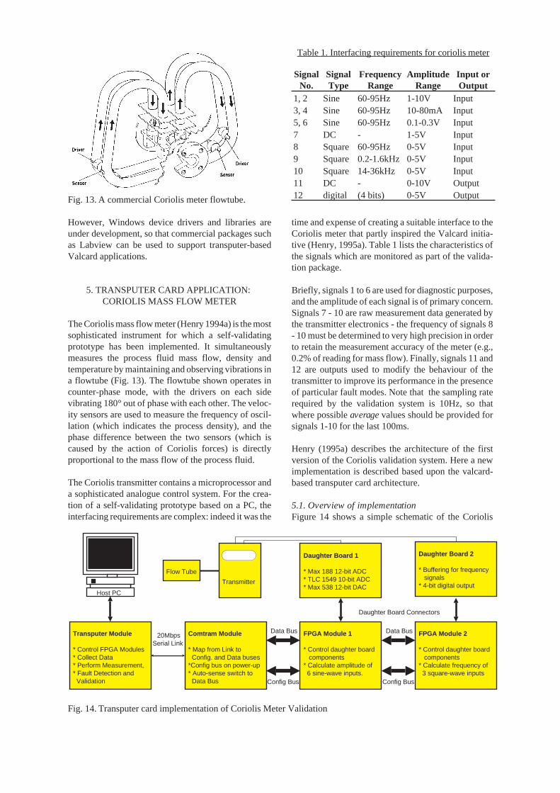
5.1. Overview of implementationFigure 14 shows a simple schematic of the Coriolis
Table 1. Interfacing requirements for coriolis meter
SignalNo.
SignalType
FrequencyRange
AmplitudeRange
Input orOutput
1, 2 Sine 60-95Hz 1-10V Input3, 4 Sine 60-95Hz 10-80mA Input5, 6 Sine 60-95Hz 0.1-0.3V Input7 DC - 1-5V Input8 Square 60-95Hz 0-5V Input9 Square 0.2-1.6kHz 0-5V Input10 Square 14-36kHz 0-5V Input11 DC - 0-10V Output12 digital (4 bits) 0-5V OutputFig. 13. A commercial Coriolis meter flowtube.
Comtram Module
* Map from Link toConfig. and Data buses
*Config bus on power-up* Auto-sense switch toData Bus
20MbpsSerial Link
Transputer Module
* Control FPGA Modules* Collect Data* Perform Measurement,* Fault Detection andValidation
FPGA Module 1
* Control daughter boardcomponents
* Calculate amplitude of6 sine-wave inputs.
FPGA Module 2
* Control daughter boardcomponents
* Calculate frequency of3 square-wave inputs
Daughter Board 1
* Max 188 12-bit ADC* TLC 1549 10-bit ADC* Max 538 12-bit DAC
Daughter Board 2
* Buffering for frequencysignals
* 4-bit digital output
Daughter Board Connectors
Data Bus
Transmitter
Host PC
Config Bus
Data Bus
Config Bus
Flow Tube
Fig. 14. Transputer card implementation of Coriolis Meter Validation

validation scheme implemented using the Valcard ar-chitecture. Each signal pick-off point within the Cori-olis transmitter is connected directly to the appropriatedaughter board on one of the FPGA modules. Datapasses via the FPGA modules to the transputer, whichperforms measurement, fault detection, and validationcalculations, and then passes the validated measure-ment data to the host PC.
All twelve signals can be dealt with using only twoFPGA modules plus daughter boards. In addition, theFPGAs carry out significant signal processing taskswhich otherwise would require a substantial increase inthe workload of the transputer and/or additional ana-logue circuitry.
5.2. FPGA Module 1This module, together with its daughter board, dealswith signals 1 - 7. The daughter board is shown in Fig.9. Signal 7 is a straightforward DC voltage with only asmall influence on measurement accuracy and faultdetection. It is thus sampled using the Texas TLC 154910-bit ADC.
Signals 1 - 6 are all sinusoidal. At any instant they havethe same frequency, which lies between 60 and 95Hz,but they have different phases. The property of interestfor each signal is its RMS amplitude, which may varyby up to an order of magnitude with changes in operat-ing and fault conditions.
In the original Coriolis validation system, analoguesignal conditioning was used to extract an RMS ampli-tude signal, which was then fed into an ADC. In thetransputer card version, very little hardware is used asthe conversion is carried out within the FPGA module.
The Maxim 188 is a high-speed 12-bit ADC withbuilt-in multiplexer. Signals 1 - 6 are supplied to theADC and each is sampled at 10KHz. The FPGA module
rectifies each signal by detecting zero crossings andperforming integration using the composite Simpsonmethod. To make the most effective use of FPGAsilicon, this calculation is carried out using integerarithmetic; to obtain the RMS amplitude the integralmust be scaled by the frequency of the sine-wave,which is carried out by the transputer.
As the frequency of oscillation is typically about 80Hz,while the transputer processes data at 10Hz, the FPGAmodule measures several waveforms so that an averagevalue over the last 100ms is presented to the transputer.
A further refinement is the use of a Maxim 538 12-bitDAC to generate the reference voltage for the ADC.This ensures that the full ADC range is used as thesignals vary in magnitude. Briefly, once the transputerhas received data for each channel and calculated theRMS amplitude, a new reference voltage can be as-signed to each signal, based on the current amplitude.This reference is used each time the signal is sampledover the next 100ms interval. The transputer must ofcourse scale the resulting data for reference voltage aswell as frequency when calculating amplitude.
5.3. FPGA Module 2This module, and its daughter board, deal with theremaining signals 8 - 12. Signals 11 (a DAC voltageoutput) and 12 (a 4-bit digital output) are straightfor-ward: the transputer is provided with a port to write thedesired outputs, which are then transferred to the cor-responding daughter board components.
R/W Not Used Address DataMod.7 6 5 4 3 2 1 0
Fig. 15. Structure of Communication Bus CommandByte
143 16150 12831 159
Not Used
AD
C L
o
AD
C H
i
TX
S L
o
TX
S H
i
Not Used Not Used
1 3 4 5 6 7 8 9 15
Sig. 8 Sig. 9 Sig. 10
Lo Mi HiLo Mi HiLo Mi HiNot Used
DA
C L
o
DA
C H
i
DA
C C
ontr
ol
128 129 130 131 143
Not Used
DA
C L
o
DA
C H
i
DA
C C
ontr
ol
TX
S C
ontr
ol
16 17 18 19 20 31 144 145 146 147 148 149 150 159
Read
Mod. #2
Read
Mod. #1
Write
Mod. #2
Mod. #1
Card #2
Not Used
32 127 160 255
0
144
2
AD
C D
ata
AD
C C
ontr
ol
Out
put P
ort
Fig. 16. Communication bus address space for Coriolis application

Signals 8, 9 and 10 provide raw measurement data inthe form of square-waves, the frequency of which mustbe measured to a high accuracy. This is achieved bycounting 5MHz clock ticks. As the input frequenciesvary from 60Hz to 36kHz (Table 1), appropriate num-bers of waveforms are gated while the clock ticks arecounted. As a result, the transputer receives averagefrequency data for the last 100ms.
5.4. Communication bus operationThe communication bus plays an essential role in trans-ferring data between the FPGA modules and thetransputer. Bus usage is determined almost entirely byhow the Master FPGA on each module responds to thedata input lines: in other words bus functionality isdefined by the Handel code running within the FPGAs,and can be changed (and indeed subsequently refinedand extended) to suit each application.
In the Coriolis example, a very simple protocol has beendefined. The transputer commences all bus operationsby writing a one-byte command to the communicationbus. The structure of the command is shown in Fig. 15.
Bit 7 indicates whether the request is for a read or awrite. Bit 4 indicates whether FPGA module 1 or 2 isbeing addressed, while bits 0-3 provide the address ofthe byte-wide port of interest within the FPGA module.If the port is to be written to, the transputer sends a byteof data as soon as the command byte is acknowledged.If the port is to be read, the FPGA module sends therequired byte of data to the transputer to be read.
The command byte can also be viewed as a singleaddress in a space of read and write ports. Figure 15illustrates this idea, and shows how ports were actuallyused in an early version of the Coriolis application. Anoverview of the address space is shown in the centralstrip, while the function of each port is shown in theupper strip (FPGA module 2) and lower strip (FPGAmodule 1). For example, ports 0-2 are read by thetransputer to obtain the latest 24-bit estimate of thefrequency of signal 8 over the last 100ms. There areplenty of unused locations in the address space, but newports have been added incrementally to the map as theapplication has been developed.
This bus protocol provides a simple, if not particularlyefficient, interface between the transputer and theFPGA modules. From the perspective of the validationsoftware running on the transputer, requests are sentand data received via a conventional transputer link. Awrite operation is effected by two byte writes to the link(command + data), while a read operation requires abyte write (command) followed by a byte read (data).
Of course, this functionality is limited, as, for example,there is no method for an FPGA module to activelyrequest a data transfer, nor is data transfer between
modules possible, except via the transputer. In addi-tion, single-byte data transfers are not particularly ef-ficient use of bus bandwidth. However, as all function-ality is defined in the software running on thetransputer and FPGAs, such additional features arereadily added. For example, the size of data transfer(say 1,2,4 or 8 bytes) might be included within thecommand byte using the unused bits 5 and 6 (Fig. 15).Alternatively, reading from or writing to particularports might by convention entail multiple-byte trans-fers. This leads to no difficulty as long as bothtransputer and FPGA module expect the same behav-iour. In practice, however, for the Coriolis application,bus bandwidth is not in short supply, and this verysimple interface is entirely adequate.
5.5. Transputer and host softwareThe Coriolis validation software which runs on thetransputer is largely the same as the original PC-basedsoftware, with some important changes:
• The original program had to provide both instru-ment and host functionality (e.g., graphical userinterface). Most host functionality is now providedby the GPUSH package, which simplifies thetransputer code considerably. On the other hand,transputer-host communication has been pro-vided.
• The transputer program includes code to down-load configuration data to the FPGA modules be-fore validation can commence.
• The data acquisition routines have been modifiedto operate the communication bus as described inthe last section.
The requirements for the PC-based host software,GPUSH, have already been discussed in Section 4.3.This software has served satisfactorily for the Coriolisapplication. Figure 12 shows the Coriolis validationsoftware running under GPUSH. Additionally, vali-dated Coriolis data are sent (using the Modbus digitalcommunication protocol) to an IA series control work-station for display and monitoring. This is a furtherdemonstration of the viability of the SEVA conceptsfor use in industrial control systems, and anticipatesone of the themes of future work.
6. CONCLUSIONS AND FUTURE WORK
This paper has described two architectures which havebeen developed to apply hardware compilation tech-niques to build systems for use in sensor validationapplications. In assessing the results that have beenachieved, a number of questions may be posed:
• Are the architectures and associated developmenttools (in particular hardware compilation) suitablefor the application domain?

• Is development work more effective using the newarchitectures?
• Have the new architectures assisted the extensionof the research programme into new areas?
Each of these questions will be examined in the follow-ing subsections.
6.1. Applicability to sensor validationAs the thermocouple, dissolved oxygen probe and Co-riolis meter examples have demonstrated, the architec-tures developed in the Valcard project have proved tobe applicable to a range of sensor validation systems,each with quite different requirements. Correspond-ingly, the Handel code routines running in FPGAs havecarried out a range of tasks:
• The provision of a simple interface for PC softwareto a set of I/O devices (in the dissolved oxygenapplication)
• A complete validation task for a simple sensor(thermocouple), including measurement and un-certainty calculation (using fixed-point arithmetic)and diagnostic reasoning.
• Signal conditioning tasks such as sine-wave recti-fication and high accuracy frequency measurement(Coriolis application)
Given the flexibility shown by these architectures, theymay well be adapted to other types of application, andwithin the Engineering Science Department at Oxfordthe FPGA card is being offered as a general purposeplatform for a wide range of projects.
6.2. Improvements in system developmentThe experience gained in using the new architecturesand tools has justified many of the claims for improvingsystem development work such as creating a newSEVA prototype. The following benefits have beenobserved in a number of projects:
• The architectures are sufficiently flexible that oneor other can form the basis for any SEVA proto-type. This implies a high degree of re-use of hard-ware and host software. Use of PCB manufacturingensures that cards are available quickly andcheaply for new projects.
• Application-specific hardware can be kept to anabsolute minimum, as many tasks traditionally car-ried out in fixed-function components can be im-plemented within FPGAs. This can cause a signifi-cant reduction in hardware - as demonstrated by thefact that only two FPGA modules and daughtercards are needed for the Coriolis application. In-deed, an entirely separate Coriolis meter could bevalidated on the same transputer card by the addi-tion of two identical modules.
• The hardware requirements for a project can besettled early and implemented quickly. A variety
of FPGA code routines can be written, to test thehardware components in the first instance, fol-lowed by incremental development of the applica-tion. Many design decisions (such as the divisionof processing between FPGAs and processor) canbe taken late in the project, on the basis of experi-ence using the system. In the case of the transputercard, even the bus protocol can be modified in thelight of experience.
• There is a much higher degree of software re-usethan in the past. A library of Handel code fordriving various hardware components and forcommon signal-processing techniques is beingmaintained. The separation of host and instrumentsoftware has increased code re-use on each side,and the provision of Valcard links to commercialpackages such as Labview reduces or indeed ob-viates the need for developing and maintaininggraphical user interface software.
In the light of these advances, it is intended to use thesearchitectures or their successors in all future develop-ment work in the SEVA research project.
6.3. Additional benefits to the SEVA projectA number of new goals have been achieved directly orindirectly as a result of the Valcard project:
• Validation of several instruments within a singlehost PC. This has been achieved using three ther-mocouple validation systems, and is being used forresearch into sensor fusion using SEVA metrics.
• Transmission of SEVA metrics over industrialcommunication systems, namely the P-Net Field-bus standard (Henry, 1995b) and Modbus.
• The development of an entire sensor validationapplication (thermocouple) within hardware, dem-onstrating that SEVA can be implemented in low-cost technology such as ASICs.
6.4. Limitations of the architecturesA number of criticisms can be made of the architec-tures. One of the most difficult design decisions was todetermine how many pins should be provided forFPGA and daughter board connections. In practice,different applications have different requirements, andfixed interconnections proved insufficiently flexible.In the case of the FPGA card, additional hardwiredconnections were usually required. This problem canbe solved using programmable interconnect devices,which will be used in the next generation of card.
Feedback received from industrial engineers has beenpositive regarding the rapid prototyping capability, butsaw the technology as of limited value for actual indus-trial use. One concern was the high cost and powerconsumption of FPGAs. A PC-based card is a usefulprototyping tool, but is usually not appropriate as afinal product for intelligent instrumentation.

6.5. Future developmentsIt is intended to develop these architectures. A numberof issues have been identified:
• A new generation of FPGA card will include pro-grammable interconnect chips, RAM, and ROM.
• Configurability may be extended to the front-endof the system hardware. through the use of therecently introduced “analog” FPGAs.
• Fieldbus (of one flavour or another) is the futureworking environment for all intelligent industrialsensors. The provision of a fieldbus capabilitywould allow the development of standalone SEVAprototypes.
• The extension of the rapid-prototyping methodol-ogy through to a commercial implementation - forexample in the form of an ASIC - could be valuableto the control and instrumentation industry. In thisscenario, an instrument design is prototyped in aPC environment such as Valcard, defined in stand-ard languages for both hardware (e.g. Xilinxnetlist) and software (e.g. C code), and thenmapped directly into a low-cost, low-power ASIC.
7. ACKNOWLEDGEMENTS
This work was partly funded by EPSRC grantsGR/J44636 (Valcard) and GR/K48884, and by the Fox-boro Company. Thanks are due to Analog Devices forthe donation of a range of components.
8. REFERENCES
ANSI (1985). Measurement Uncertainty. ANSI/ASME PTC
19.1-1985.Archer, N. and J. Bowles (1995). PC Configurable LCA
Card. Internal Report, Department of EngineeringScience, Oxford University.
Atia, M. R. A., J. Bowles, D. W. Clarke, M. P. Henry,I. Page, G. Randall, and J. C-Y. Yang (1995). “ASelf-Validating Temperature Sensor Implemented inFPGAs”. Proc. 5th Workshop on Field Programma-ble Logic and Applications, eds. W. Moore and W.Luk, Oxford, UK..
Boser, B. E. and B. A. Wooley (1988). The design ofsigma-delta modulation analog-to-digital convert-ers. IEEE J. Solid-State Circuits, vol SC-23, pp1298-1308.
Clarke, D. W. (1995), “Sensor, Actuator and LoopValidation”, IEEE J. Control Systems, August 1995,pp 39-45.
Clarke, D. W. and P. M. Fraher (1995). “Model-BasedValidation of a DOx Sensor”. Plenary Paper at theIFAC Workshop On-Line Fault Detection and Moni-toring in the Chemical Process Industries, New-castle, U.K.
Wilson, P.D., R. S. Spraggs and S. P. Hopkins (1996).“ Universal sensor interface chip (USIC): specifica-tion and applications outline”. Sensor Review, Vol16, No. 1, pp18-21.
Guccione, S. A. and M. J. Gonzalez (1995). “Super-computing with reconfigurable architectures”. Proc.5th Workshop on Field Programmable Logic andApplications, eds. W. Moore and W. Luk, Oxford,UK.
Henry, M. P. and D. W. Clarke (1993). The Self-Vali-dating Sensor: Rationale, Definitions and Exam-ples. Control Engineering Practice, 1, 585.
Henry, M. P. (1994). A SEVA Sensor - The CoriolisMass Flow Meter. IFAC/IMACS Safeprocess Sym-posium, Espoo.
Henry, M. P. (1995a). “Keynote Paper: hardware com-pilation - a New Technique for Rapid Prototypingof Digital Systems - Applied to sensor validation”,Control Engineering Practice, Vol 3, No. 7, pp 907-924.
Henry M. P. (1995b). “Fieldbus and sensor validation”,IEE Computing and Control Journal, Vol 6, No. 6,pp 263-272.
Hoare, C. A. R. and I. Page (1994). Hardware andSoftware: The Closing Gap. Transputer Communi-cations, Willie, 2(2), June 1994, 69-90.
IEEE (1994). VHDL revised standard (VHDL 1076-1993).
Inmos (1988a). occam2 Reference Manual. PrenticeHall International, Hemel Hempstead, UK.
Inmos (1988b). Transputer Reference Manual. Pren-tice Hall International, Hemel Hempstead, UK.
Kline, S. J. and F. A. McClintock (1953). Describinguncertainties in single sample experiments. Mech.Eng., pp 3-8.
Page, I. (1994). Parameterised Processor Generation.In More FPGAs, W. Moore and W. Luk (eds.),Abingdon EE&CS Books, Oxford.
Page, I. and W. Luk (1991). Compiling occam intoField-Programmable Gate Arrays. In FPGAs, W.Moore and W. Luk (eds.), Abingdon EE&CSBooks, Oxford.
Spivey, M. and I. Page (1993). How to design hardwarewith Handel. Internal Report, Oxford UniversityComputer Laboratory.
Transtech (1994). Transputer Motherboard User Man-ual. Transtech Parallel Systems, High Wycombe,UK.
Viewlogic (1991). Workview Manual. Viewlogic Sys-tems, Inc., Malboro Massachusetts, USA.
Yang, J. C-Y. (1993). Self-Validating Sensors. D.PhilThesis, Department of Engineering Science, Uni-versity of Oxford.
Yang, J. C-Y. and D. W. Clarke (1996). Control UsingSelf-Validating Sensors. Trans. Inst. MC, Vol 18,No 1, pp15-23.

Appendix 1: Handel code to drive the MAX532 DAC from an FPGA
(* Handel code for driving MAX532 Dual Channel 12-bit DACGenerates a positive ramp on the right channel
and a negative ramp on the left channel *)
use “valslavepins95.hdl”; (* include file giving defaults *)
(* CONSTANTS *)val datawidth = 12; (* size of each data register *)val txregwidth = 24; (* size of transmission register *)val txshift = 1; (* shift by a single bit *)val txbit = 23; (* which bit to output - top bit *)
(* VARIABLES *) (* length in bits *) (* tag for simulation *)
val data_left = Int datawidth “data_left”; (* left channel data *)val data_right = Int datawidth “data_right”; (* right channel data *)val txregister = Int txregwidth “txregister”; (* transmission register *)val txloop = Int 5 “txloop”; (* loop counter *)
(* CHANNELS *)val txdataChan = Chan 1 “txdataChan”; (* one bit data stream to MAX532 *)val sclkChan = Chan 1 “sclkChan”; (* clock signal to MAX532 *)val csChan = Chan 1 “csChan”; (* data ready signal to MAX532 *)
(* Channel Protocol Converters - interface definition for each channel *)val txdataChanCPC = (CPC_NhPortOut [ IO_21 ] , Output txdataChan);val sclkChanCPC = (CPC_NhPortOut [ IO_20 ] , Output sclkChan);val csChanCPC = (CPC_NhPortOut [ IO_19 ] , Output csChan);
prog := Handel(
[ txdataChanCPC, sclkChanCPC, csChanCPC ], (* CPCs used *)[ data_left, data_right, txregister, txloop ], (* Variables used *)
Seq [ (* Start of program code *)
Par [ (* Initialisation *)data_left := C 0,data_right := C 0,txregister := C 0,txloop := C 0],
While (TRUE, (* Main loop - endless *)Seq[
While ( txloop != C txregwidth, (* for each bit *)Seq[
Par [ (* set up data and rising edge *)sclkChan !! C 0, (* output low on clock line *)txdataChan !! txregister BIT txbit (* output data bit *)],
Par[ (* generate rising edge *)sclkChan !! C 1, (* output high on clock line *)txdataChan !! txregister BIT txbit, (* output data bit *)txloop := txloop + C 1, (* increment loop *)txregister := txregister < txshift (* shift transmission register *)]
]),
Par [ (* data transfer complete *)csChan !! C 1, (* flag data complete to DAC *)txloop := C 0, (* reset loop counter *)data_left := data_left - C 1, (* negative ramp *)data_right := data_right + C 1 (* positive ramp *)],
txregister := data_left ^ data_right (* assign new data *)] (* end write/read Seq *)
) (* end While *)] (* end program Seq *)
); (* end program *)


