Embed Size (px)
Citation preview
Protection Power device performance investigation using TCAD simulations F.Roqueta and K.Tahri
STMicroelectronics
16, rue Pierre et Marie Curie, 37071 TOURS Cedex 2, FRANCE
E-mail : [email protected]
Abstract
The paper presents a methodology for simulating the
dynamic performances of a protection device used against
EOS. Due to the coupling of electric and thermal
phenomena occurring in the device during the EOS event,
electro-thermal simulations are required. In order to
obtain accurate description of the device behavior,
component is simulated at different scales : 2D electro-
thermal simulation at device-scale and 3D thermal
simulation at the package-scale. This approach allows to
understand the behavior of the component and then to
optimize it.
1. Introduction
Electrical overstress (EOS) are transient events that
are temporary enforcing a circuit or a device to work
above normal operating area. Those events can be
induced by lightning strikes, inductive load switching and
Electro-Static Discharge (ESD). Signal is typically
defined as an over voltage or over current event with a
duration exceeding 1 to 1000 nanoseconds and nominal
durations of 1 millisecond that occurs while the device is
in operation. This signal covers a large range of
waveform defined by following parameters : wave shape,
duration, peak current and peak voltage. EOS damage can
be exhibited either in an immediate failure or a failure
over a period of time after the EOS event. EOS is the
main contributor to IC component failures [1,2].
Widely adopted solution to protection devices against
voltage and/or current surge are metal-oxide based
Varistor, fuse and Transient Voltage Suppressor (TVS)
diode. TVS diode operates by shunting excess current
when the induced voltage exceeds the avalanche
breakdown potential. It is a clamping device, suppressing
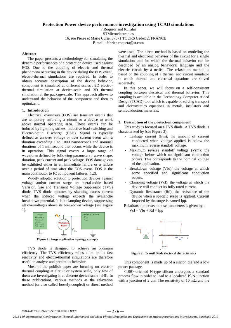
all overvoltages above its breakdown voltage (see Figure
1).
Figure 1 : Surge application topology example
TVS diode is designed to achieve an optimum
efficiency. The TVS efficiency relies a lot on its fast
reactivity and electro-thermal simulations are therefore
useful to analyse and predict its behavior.
Most of the publish paper are focusing on electro-
thermal coupling at circuit or system scale, only few of
them are investigating it at discrete device scale [3-8]. In
these publications, various methods as the relaxation
method (or also called loosely coupled) or direct method
were used. The direct method is based on modeling the
thermal and electronic behavior of the circuit for a single
simulation tool for which the thermal behavior can be
described by an analog behavioral language and the
electric circuit by a netlist. The relaxation method is
based on the coupling of a thermal and circuit simulator
in which thermal and electrical equations are solved
separately.
In this paper, we will focus on a self-consistent
coupling between electrical and thermal behavior. This
coupling is available in the Technology Computer Aided
Design (TCAD) tool which is capable of solving transport
and electrostatics equations in metals, insulators and
semiconductors materials.
2. Description of the protection component
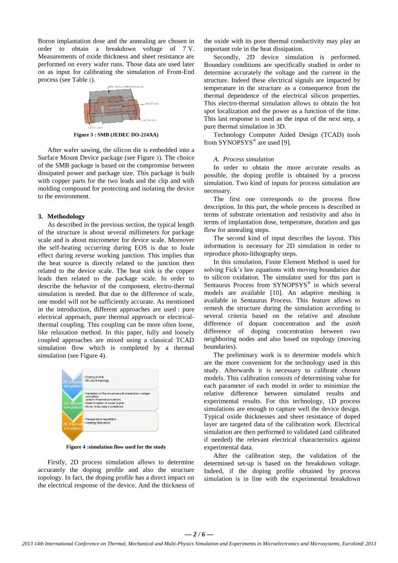
This study is focused on a TVS diode. A TVS diode is
characterized by (see Figure 2) :
- Leakage current (Irm): the amount of current
conducted when voltage applied is below the
maximum reverse standoff voltage.
- Maximum reverse standoff voltage (Vrm): the
voltage below which no significant conduction
occurs. This corresponds to the nominal voltage
of the application.
- Breakdown voltage (Vbr): the voltage at which
some specified and significant conduction
occurs.
- Clamping voltage (Vcl): the voltage at which the
device will conduct its fully rated current.
- Dynamic Resistance (Rd): the resistance of the
device when a specific surge is applied. Current
imposed by the surge is named Ipp.
Relationship between those parameters is given by :
Vcl = Vbr + Rd × Ipp
Figure 2 : Transil Diode electrical characteristics
This component is made up of a silicon die and a low
power package.
<100>-oriented N-type silicon undergoes a standard
process flow in order to lead to a localized P+/N junction
with a junction of 2 µm. The resistivity of 10 mΩ.cm, the
978-1-4673-6139-2/13/$31.00 ©2013 IEEE
2013 14th International Conference on Thermal, Mechanical and Multi-Physics Simulation and Experiments in Microelectronics and Microsystems, EuroSimE 2013
— 1 / 6 —
Boron implantation dose and the annealing are chosen in
order to obtain a breakdown voltage of 7 V.
Measurements of oxide thickness and sheet resistance are
performed on every wafer runs. Those data are used later
on as input for calibrating the simulation of Front-End
process (see Table 1).
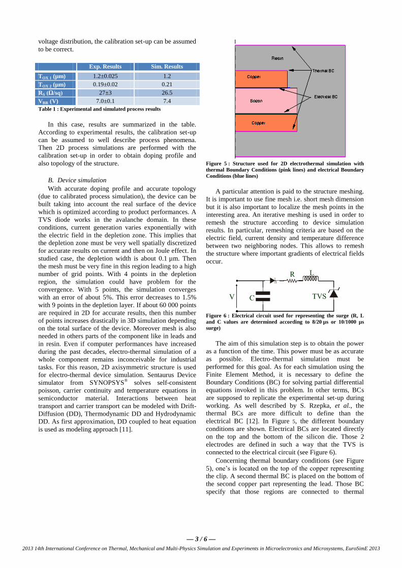
Figure 3 : SMB (JEDEC DO-214AA)
After wafer sawing, the silicon die is embedded into a
Surface Mount Device package (see Figure 3). The choice
of the SMB package is based on the compromise between
dissipated power and package size. This package is built
with copper parts for the two leads and the clip and with
molding compound for protecting and isolating the device
to the environment.
3. Methodology
As described in the previous section, the typical length
of the structure is about several millimeters for package
scale and is about micrometer for device scale. Moreover
the self-heating occurring during EOS is due to Joule
effect during reverse working junction. This implies that
the heat source is directly related to the junction then
related to the device scale. The heat sink is the copper
leads then related to the package scale. In order to
describe the behavior of the component, electro-thermal
simulation is needed. But due to the difference of scale,
one model will not be sufficiently accurate. As mentioned
in the introduction, different approaches are used : pure
electrical approach, pure thermal approach or electrical-
thermal coupling. This coupling can be more often loose,
like relaxation method. In this paper, fully and loosely
coupled approaches are mixed using a classical TCAD
simulation flow which is completed by a thermal
simulation (see Figure 4).
Figure 4 :simulation flow used for the study
Firstly, 2D process simulation allows to determine
accurately the doping profile and also the structure
topology. In fact, the doping profile has a direct impact on
the electrical response of the device. And the thickness of
the oxide with its poor thermal conductivity may play an
important role in the heat dissipation.
Secondly, 2D device simulation is performed.
Boundary conditions are specifically studied in order to
determine accurately the voltage and the current in the
structure. Indeed these electrical signals are impacted by
temperature in the structure as a consequence from the
thermal dependence of the electrical silicon properties.
This electro-thermal simulation allows to obtain the hot
spot localization and the power as a function of the time.
This last response is used as the input of the next step, a
pure thermal simulation in 3D.
Technology Computer Aided Design (TCAD) tools
from SYNOPSYS® are used [9].
A. Process simulation
In order to obtain the more accurate results as
possible, the doping profile is obtained by a process
simulation. Two kind of inputs for process simulation are
necessary.
The first one corresponds to the process flow
description. In this part, the whole process is described in
terms of substrate orientation and resistivity and also in
terms of implantation dose, temperature, duration and gas
flow for annealing steps.
The second kind of input describes the layout. This
information is necessary for 2D simulation in order to
reproduce photo-lithography steps.
In this simulation, Finite Element Method is used for
solving Fick’s law equations with moving boundaries due
to silicon oxidation. The simulator used for this part is
Sentaurus Process from SYNOPSYS® in which several
models are available [10]. An adaptive meshing is
available in Sentaurus Process. This feature allows to
remesh the structure during the simulation according to
several criteria based on the relative and absolute
difference of dopant concentration and the asinh
difference of doping concentration between two
neighboring nodes and also based on topology (moving
boundaries).
The preliminary work is to determine models which
are the more convenient for the technology used in this
study. Afterwards it is necessary to calibrate chosen
models. This calibration consists of determining value for
each parameter of each model in order to minimize the
relative difference between simulated results and
experimental results. For this technology, 1D process
simulations are enough to capture well the device design.
Typical oxide thicknesses and sheet resistance of doped
layer are targeted data of the calibration work. Electrical
simulation are then performed to validated (and calibrated
if needed) the relevant electrical characteristics against
experimental data.
After the calibration step, the validation of the
determined set-up is based on the breakdown voltage.
Indeed, if the doping profile obtained by process
simulation is in line with the experimental breakdown
2013 14th International Conference on Thermal, Mechanical and Multi-Physics Simulation and Experiments in Microelectronics and Microsystems, EuroSimE 2013
— 2 / 6 —
voltage distribution, the calibration set-up can be assumed
to be correct.
Exp. Results Sim. Results
TOX 1 (µm) 1.2±0.025 1.2
TOX 2 (µm) 0.19±0.02 0.21
RS (Ω/sq) 27±3 26.5
VBR (V) 7.0±0.1 7.4
Table 1 : Experimental and simulated process results
In this case, results are summarized in the table.
According to experimental results, the calibration set-up
can be assumed to well describe process phenomena.
Then 2D process simulations are performed with the
calibration set-up in order to obtain doping profile and
also topology of the structure.
B. Device simulation
With accurate doping profile and accurate topology
(due to calibrated process simulation), the device can be
built taking into account the real surface of the device
which is optimized according to product performances. A
TVS diode works in the avalanche domain. In these
conditions, current generation varies exponentially with
the electric field in the depletion zone. This implies that
the depletion zone must be very well spatially discretized
for accurate results on current and then on Joule effect. In
studied case, the depletion width is about 0.1 µm. Then
the mesh must be very fine in this region leading to a high
number of grid points. With 4 points in the depletion
region, the simulation could have problem for the
convergence. With 5 points, the simulation converges
with an error of about 5%. This error decreases to 1.5%
with 9 points in the depletion layer. If about 60 000 points
are required in 2D for accurate results, then this number
of points increases drastically in 3D simulation depending
on the total surface of the device. Moreover mesh is also
needed in others parts of the component like in leads and
in resin. Even if computer performances have increased
during the past decades, electro-thermal simulation of a
whole component remains inconceivable for industrial
tasks. For this reason, 2D axisymmetric structure is used
for electro-thermal device simulation. Sentaurus Device
simulator from SYNOPSYS® solves self-consistent
poisson, carrier continuity and temperature equations in
semiconductor material. Interactions between heat
transport and carrier transport can be modeled with Drift-
Diffusion (DD), Thermodynamic DD and Hydrodynamic
DD. As first approximation, DD coupled to heat equation
is used as modeling approach [11].
Figure 5 : Structure used for 2D electrothermal simulation with
thermal Boundary Conditions (pink lines) and electrical Boundary
Conditions (blue lines)
A particular attention is paid to the structure meshing.
It is important to use fine mesh i.e. short mesh dimension
but it is also important to localize the mesh points in the
interesting area. An iterative meshing is used in order to
remesh the structure according to device simulation
results. In particular, remeshing criteria are based on the
electric field, current density and temperature difference
between two neighboring nodes. This allows to remesh
the structure where important gradients of electrical fields
occur.
Figure 6 : Electrical circuit used for representing the surge (R, L
and C values are determined according to 8/20 µs or 10/1000 µs
surge)
The aim of this simulation step is to obtain the power
as a function of the time. This power must be as accurate
as possible. Electro-thermal simulation must be
performed for this goal. As for each simulation using the
Finite Element Method, it is necessary to define the
Boundary Conditions (BC) for solving partial differential
equations invoked in this problem. In other terms, BCs
are supposed to replicate the experimental set-up during
working. As well described by S. Rzepka, et al., the
thermal BCs are more difficult to define than the
electrical BC [12]. In Figure 5, the different boundary
conditions are shown. Electrical BCs are located directly
on the top and the bottom of the silicon die. Those 2
electrodes are defined in such a way that the TVS is
connected to the electrical circuit (see Figure 6).
Concerning thermal boundary conditions (see Figure
5), one’s is located on the top of the copper representing
the clip. A second thermal BC is placed on the bottom of
the second copper part representing the lead. Those BC
specify that those regions are connected to thermal
2013 14th International Conference on Thermal, Mechanical and Multi-Physics Simulation and Experiments in Microelectronics and Microsystems, EuroSimE 2013
— 3 / 6 —
resistances (Rth1 and Rth2) representing the thermal path
through copper parts from the silicon die to the board
which is assumed to be fixed at room temperature. The
third thermal BC around the resin represents a free natural
convective heat transfer. Due to the relative short power
pulses this BC have a weak impact on thermal results.
Nevertheless the value of the convective transfer
coefficient is estimated from Nusselt, Prandtl and Grashof
numbers with Vaschy-Buckingham theorem [13]. The
value retained for this structure is 7 W/(m²·k). The
calculation of the thermal resistances Rth1 and Rth2 is
difficult. That is the reason why 3D thermal simulations
are required. For 2D electro-thermal resistances Rth1 and
Rth2 are overestimated in order to underestimate the
dissipation and then overestimate the self-heating. In this
way, the temperature impact on the electrical results is
increased.
a)
b) Figure 7 : Evolution of electrical result during a 10/1000µs surge (a:
current et voltage and b : power and temperature)
In Figure 7–a, the current and the voltage versus time
are plotted. Those curves depend on the surge level and
on the surge type. Here 10/1000µs surge with a peak
pulse current value of 42 A is used as an example. From
current and voltage evolution, power versus time is easily
obtained (see Figure 7–b). This curve is the input for the
3D thermal simulation. Another output obtained from 2D
electro-thermal simulation is the temperature evolution
(see Figure 7–b) and also the temperature distribution in
the structure as seen in Figure 8. Another interesting
output is the distribution of the total heat generation and
its different contributors (Joule heat, Recombination heat,
Peltier heat and Thomson heat). For device functioning in
reverse, the Joule effect is the main contributor and is
located at the junction where electron and hole currents
are generated due to avalanche phenomena. It is important
to know where is generated and how in order to refine the
3D thermal model especially for placing the heat source.
Distributions show that the heat source must be located at
the junction and the other heat sources (like Joule effect
in Copper) can be neglected.
Figure 8 : Temperature distribution during 10/1000µs surge at 20 µs
In spite of the simulation duration, it is important to
validate some assumptions necessary for 3D thermal
simulation. Sensibility study concerning the thermal
resistances Rth1 and Rth2 is performed in order to estimate
the impact of those parameters on the power evolution
during the surge. This impact is more important for longer
pulse than for shorter. That is the reason why this
sensibility study focuses on 10/1000µs surge. A large
variation (factor ten) of the Rth value induces no variation
of the peak power value but a variation of 5% of the
maximum temperature in the structure. This result shown
in Figure 9 indicates that the 2D model describes correctly
electrical phenomena and 3D thermal simulation is
needed for more accurate results concerning thermal
phenomena.
Figure 9 : evolutions of power and maximum temperature in the
structure for 10/1000µs surge for different Rth values
2013 14th International Conference on Thermal, Mechanical and Multi-Physics Simulation and Experiments in Microelectronics and Microsystems, EuroSimE 2013
— 4 / 6 —
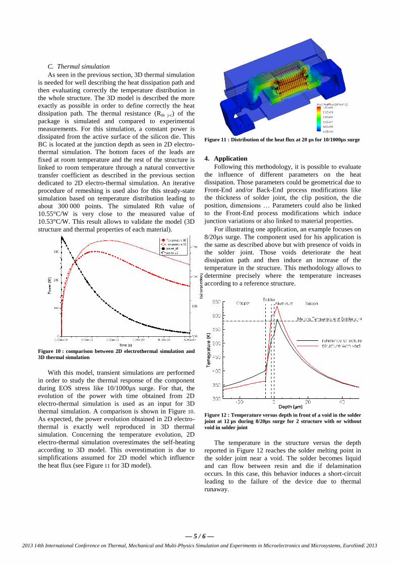
C. Thermal simulation
As seen in the previous section, 3D thermal simulation
is needed for well describing the heat dissipation path and
then evaluating correctly the temperature distribution in
the whole structure. The 3D model is described the more
exactly as possible in order to define correctly the heat
dissipation path. The thermal resistance (Rth j-c) of the
package is simulated and compared to experimental
measurements. For this simulation, a constant power is
dissipated from the active surface of the silicon die. This
BC is located at the junction depth as seen in 2D electro-
thermal simulation. The bottom faces of the leads are
fixed at room temperature and the rest of the structure is
linked to room temperature through a natural convective
transfer coefficient as described in the previous section
dedicated to 2D electro-thermal simulation. An iterative
procedure of remeshing is used also for this steady-state
simulation based on temperature distribution leading to
about 300 000 points. The simulated Rth value of
10.55°C/W is very close to the measured value of
10.53°C/W. This result allows to validate the model (3D
structure and thermal properties of each material).
Figure 10 : comparison between 2D electrothermal simulation and
3D thermal simulation
With this model, transient simulations are performed
in order to study the thermal response of the component
during EOS stress like 10/1000µs surge. For that, the
evolution of the power with time obtained from 2D
electro-thermal simulation is used as an input for 3D
thermal simulation. A comparison is shown in Figure 10.
As expected, the power evolution obtained in 2D electro-
thermal is exactly well reproduced in 3D thermal
simulation. Concerning the temperature evolution, 2D
electro-thermal simulation overestimates the self-heating
according to 3D model. This overestimation is due to
simplifications assumed for 2D model which influence
the heat flux (see Figure 11 for 3D model).
Figure 11 : Distribution of the heat flux at 20 µs for 10/1000µs surge
4. Application
Following this methodology, it is possible to evaluate
the influence of different parameters on the heat
dissipation. Those parameters could be geometrical due to
Front-End and/or Back-End process modifications like
the thickness of solder joint, the clip position, the die
position, dimensions … Parameters could also be linked
to the Front-End process modifications which induce
junction variations or also linked to material properties.
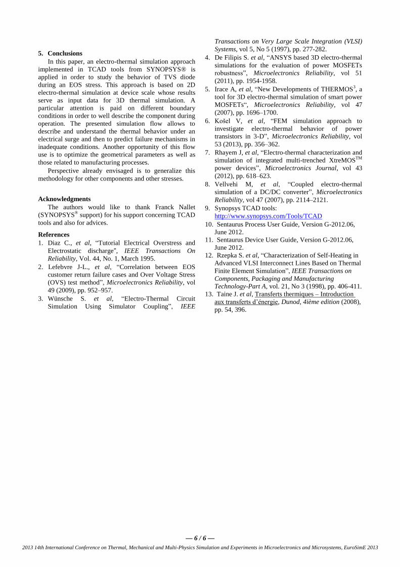
For illustrating one application, an example focuses on
8/20µs surge. The component used for his application is
the same as described above but with presence of voids in
the solder joint. Those voids deteriorate the heat
dissipation path and then induce an increase of the
temperature in the structure. This methodology allows to
determine precisely where the temperature increases
according to a reference structure.
Figure 12 : Temperature versus depth in front of a void in the solder
joint at 12 µs during 8/20µs surge for 2 structure with or without
void in solder joint
The temperature in the structure versus the depth
reported in Figure 12 reaches the solder melting point in
the solder joint near a void. The solder becomes liquid
and can flow between resin and die if delamination
occurs. In this case, this behavior induces a short-circuit
leading to the failure of the device due to thermal
runaway.
2013 14th International Conference on Thermal, Mechanical and Multi-Physics Simulation and Experiments in Microelectronics and Microsystems, EuroSimE 2013
— 5 / 6 —
5. Conclusions
In this paper, an electro-thermal simulation approach
implemented in TCAD tools from SYNOPSYS® is
applied in order to study the behavior of TVS diode
during an EOS stress. This approach is based on 2D
electro-thermal simulation at device scale whose results
serve as input data for 3D thermal simulation. A
particular attention is paid on different boundary
conditions in order to well describe the component during
operation. The presented simulation flow allows to
describe and understand the thermal behavior under an
electrical surge and then to predict failure mechanisms in
inadequate conditions. Another opportunity of this flow
use is to optimize the geometrical parameters as well as
those related to manufacturing processes.
Perspective already envisaged is to generalize this
methodology for other components and other stresses.
Acknowledgments
The authors would like to thank Franck Nallet
(SYNOPSYS® support) for his support concerning TCAD
tools and also for advices.
References
1. Diaz C., et al, “Tutorial Electrical Overstress and
Electrostatic discharge”, IEEE Transactions On
Reliability, Vol. 44, No. 1, March 1995.
2. Lefebvre J-L., et al, “Correlation between EOS
customer return failure cases and Over Voltage Stress
(OVS) test method”, Microelectronics Reliability, vol
49 (2009), pp. 952–957.
3. Wünsche S. et al, “Electro-Thermal Circuit
Simulation Using Simulator Coupling”, IEEE
Transactions on Very Large Scale Integration (VLSI)
Systems, vol 5, No 5 (1997), pp. 277-282.
4. De Filipis S. et al, “ANSYS based 3D electro-thermal
simulations for the evaluation of power MOSFETs
robustness”, Microelectronics Reliability, vol 51
(2011), pp. 1954-1958.
5. Irace A, et al, “New Developments of THERMOS3, a
tool for 3D electro-thermal simulation of smart power
MOSFETs“, Microelectronics Reliability, vol 47
(2007), pp. 1696–1700.
6. Košel V, et al, “FEM simulation approach to
investigate electro-thermal behavior of power
transistors in 3-D”, Microelectronics Reliability, vol
53 (2013), pp. 356–362.
7. Rhayem J, et al, “Electro-thermal characterization and
simulation of integrated multi-trenched XtreMOSTM
power devices”, Microelectronics Journal, vol 43
(2012), pp. 618–623.
8. Vellvehi M, et al, “Coupled electro-thermal
simulation of a DC/DC converter”, Microelectronics
Reliability, vol 47 (2007), pp. 2114–2121.
9. Synopsys TCAD tools:
http://www.synopsys.com/Tools/TCAD
10. Sentaurus Process User Guide, Version G-2012.06,
June 2012.
11. Sentaurus Device User Guide, Version G-2012.06,
June 2012.
12. Rzepka S. et al, “Characterization of Self-Heating in
Advanced VLSI Interconnect Lines Based on Thermal
Finite Element Simulation”, IEEE Transactions on
Components, Packaging and Manufacturing
Technology-Part A, vol. 21, No 3 (1998), pp. 406-411.
13. Taine J. et al, Transferts thermiques – Introduction
aux transferts d’énergie, Dunod, 4ième edition (2008),
pp. 54, 396.
2013 14th International Conference on Thermal, Mechanical and Multi-Physics Simulation and Experiments in Microelectronics and Microsystems, EuroSimE 2013
— 6 / 6 —


