Embed Size (px)
Citation preview

INT. J. ELECTR ONICS, 1999, VOL. 86, NO. 5, 549± 590
Quantum-dot cellular automata: computing with coupled quantum dots
WOLFGANG POROD² ³ , CRAIG S. LENT² ,GARY H. BERNSTEIN² , ALEXEI O. ORLOV² ,ISLAMSHAH AMLANI² , GREGORY L. SNIDER ² ,and JAMES L. MERZ²
We discuss novel nanoelectronic architecture paradigms based on cells composedof coupled quantum-dots. Boolean logic functions may be implemented in speci® carrays of cells representing binary information, the so-called quantum-dot cellularautomata (QCA ). Cells may also be viewed as carrying analogue information andwe outline a network-theoretic description of such quantum-dot nonlinear net-works (Q-CNN). In addition, we discuss possible realizations of these structuresin a variety of semiconductor systems ( including GaAs/AlGaAs, Si/SiGe, andSi/SiO2), rings of metallic tunnel junctions, and candidates for molecular imple-mentations. We report the experimental demonstration of all the necessaryelements of a QCA cell, including direct measurement of the charge polarizationof a double-dot system, and direct control of the polarization of those dots viasingle electron transitions in driver dots. Our experiments are the ® rst demon-stration of a single electron controlled by single electrons.
1. Introduction
Silicon technology has experienced an exponential improvement in virtually any® gure of merit, following Gordon Moore’ s famous dictum remarkably closely for morethan three decades. However, there are indications now that this progress will slow, oreven come to a standstill, as technological and fundamental limits are reached. Thisslow-down of silicon ULSI technology may provide an opportunity for alternativedevice technologies. In this paper, we will describe some ideas of the Notre DameNanoDevices Group on a possible future nanoelectronic computing technologybased on cells of coupled quantum dots. More speci® cally, we envision nanostructureswhere information is encoded by the arrangement of single electrons. Now, 100 yearsafter the discovery of the electron, it has become feasible to manipulate electrons oneelectron at a time, and to engineer device structures based on individual electrons.
Among the chief technological limitations responsible for this expected slow-down of silicon technology are the interconnect problem and power dissipation(Ferry et al. 1987, 1988, Keyes 1987, Bohr 1996). As more and more devices arepacked into the same area, the heat generated during a switching cycle can no longerbe removed and may result in damage to the chip. Interconnections do not scale inconcert with device scaling because of the e� ect of wire resistance and capacitance,giving rise to a wiring bottleneck. It is generally recognized that alternate approachesare needed to create innovative technologies that provide greater device and
International Journal of Electronics ISSN 0020± 7217 print/ISSN 1362± 3060 online Ñ 1999 Taylor & Francis Ltdhttp://www.tandf .co.uk/JNLS/etn.htm
http://www.taylorandfrancis.com/JNLS/etn.htm
Received 1 June 1997. Accepted 30 October 1998.² Department of Electrical Engineering, University of Notre Dame, Notre Dame,
IN 46556, USA.³ Corresponding author.

interconnect functionality, or to utilize innovative circuit and system architecturalfeatures that provide more function per transistor (Semiconductor IndustryAssociation 1994). However, these obstacles for silicon circuitry may present anopportunity for alternative device technologies which are designed for the nanometerregime and which are interconnected in an appropriate architecture.
In this paper, we describe our ideas of using nanostructures (more speci® cally,quantum dots) which are arranged in locally-interconnected cellular-autom ata-likearrays. We will demonstrate that suitably designed structures, the so-called `quan-tum-dot cellular automata’ (QCA ) (Lent et al. 1993 b), may be used for computationand signal processing. The fundamental idea for QCA operation is to encode infor-mation using the charge con® guration of a set of dots. This is an important breakwith the transistor paradigm. From the electro-mechanical relays of Konrad Zuse tothe modern CMOS circuit, binary information has been encoded by current switches.It works well so long as the switched current from one element can be transformedinto the control voltage for another element. As device sizes shrink to the molecularlimit, the current-switching paradigm falters for three primary reasons:
(1) the nano-switch becomes leaky, making a hard OFF-state di� cult to main-tain;
(2) the switched current is so small in magnitude that it is hard for it to activatethe next device; and
(3) the interconnects which carry current from one device to another begin todominate the performance.
The QCA approach eliminates these problems by adopting an approach tocoding information which is more naturally suited to nanostructures.
Our work is based on the highly advanced state-of -the-art in the ® eld of nano-structures and the emerging technology of quantum-dot fabrication (Capasso 1990,Weisbuch and Vinter 1991, Kelly 1995, Turton 1995, Montemerlo et al. 1996). Asschematically shown in ® gure 1, several groups have demonstrated that electrons
550 W . Porod et al.
Figure 1. Schematic diagram of arti® cial `quantum-dot atoms’ and `quantum-dot molecules’which are occupied by few electrons.

may be completely con® ned in semiconductor nanostructures, which may then bethought of as arti® cial `semiconductor atoms’ (Reed et al. 1988, Meirav et al. 1990).Controllable occupation of these quantum dots has been achieved in the few-electronregime (Meurer et al. 1992). One may speak of `quantum-dot hydrogen’ , `quantum-dot helium’ , `quantum-dot lithium ’ , etc. (Kastner 1993, Ashoori 1996). Veryrecently, coupling between quantum-dot atoms in close proximity has been observed,thus realizing arti® cial `quantum-dot molecules’ (Ho� mann et al. 1995, Waugh et al.1995, Blick et al. 1996).
Note that our scheme is not a quantum computer in the sense of the `quantumcomputing’ community, as reviewed by Spiller (1996). QCAs do not require quan-tum mechanical phase coherence over the entire array; phase coherence is onlyrequired inside each cell, and the cell± cell interactions are classical. This limitedrequirement of quantum mechanical phase coherence makes QCAs a more attractivecandidate for actual implementations.
The use of quantum dots for device applications entails a need for new circuitarchitecture ideas for these new devices. The nanostructures we envision will containonly few electrons available for conduction. It is hard to imagine how devices basedon nanostructures could function in conventional circuits, primarily due to theproblems associated with charging the interconnect wiring with the few electronsavailable. Therefore, we propose to envision a nanoelectronic architecture where theinformation is contained in the arrangement of charges and not in the ¯ ow ofcharges (i.e. current). In other words, the devices interact by direct Coulomb coup-ling and not by currents through wires. We envision to utilize the existing physicalinteractions between neighbouring devices in order to directly produce the dynamics,such that the logical operation of each cell would require no additional connectionsbeyond the physical coupling within a certain range of interactions. We are led toconsider cellular-autom ata-like device architectures (To� oli and Margolus 1987,Biafore 1994) of cells communicating with each other by their Coulombic inter-action.
Figure 2 schematically shows a locally-interconnected array consisting of cells ofnanoelectronic devices. The physical interactions together with the array topologydetermine the overall functionality. What form must a cellular array take when itsdynamics should result directly from known physical interactions? If we simply
Quantum -dot cellular autom ata 551
Figure 2. Schematic picture of a cellular array where the interconnections are given byphysical law. The underlying physics determines the overall functionality of the array.

arrange nanometer-scale devices in a dense cellular array, the device cells may inter-act, but we have given up all control over which cells interact with which neighboursand when they interact. In general, the state of a cell will depend on the state of itsneighbours within a certain range. The main questions now are: `What functionalitydoes one obtain for a given physical structure?’ and `Given a certain array beha-viour, there a physical system to implement it?’
In the following sections we will develop these ideas in detail and we will presenta concrete example of a quantum-dot cell with an appropriate architecture, the so-called quantum-dot cellular automata. We will discuss how one may construct QCAcells that encode binary information and how one can thus realize Boolean logicfunctions. We will also discuss that one may view these arrays as quantum-dotcellular neural (or, nonlinear ) networks (Q-CNNs). A key question, of course, areimplementations. We will discuss ideas (and on-going work) for attempting to imple-ment these structures in a variety of semiconductor systems (including GaAs/AlGaA s, Si/SiGe, and Si/SiO2) and also metallic dots. Alternative implementationsinclude molecular structures. We will call attention to a speci® c molecule whichappears to be particularly promising since it possesses a structure similar to aQCA cell. One of the most promising material systems appears to be Si/SiO2, mostlydue to the excellent insulating properties of the oxide. Note that our search for atechnology beyond silicon may bring us back to silicon!
Exciting as the vision of a possible nanoelectronics technology may be, manyfundamental and technological challenges remain to be overcome. We should keep inmind that this exploration has just begun and that other promising designs remainyet to be discovered. This exciting journey will require the combined e� ortsof technologists , device physicists, circuits-and-systems theorists and computerarchitects.
2. Quantum-dot cellular automata
Based upon the emerging technology of quantum-dot fabrication, the NotreDame NanoDevices Group has developed the QCA scheme for computing withcells of coupled quantum dots (Lent et al. 1993 a), which will be described below.To our knowledge, this is the ® rst concrete proposal to utilize quantum dots forcomputing. There had been earlier suggestions that device± device coupling might beutilized in a cellular-autom ata scheme, alas, without an accompanying proposal for aspeci® c implementation (Ferry and Porod 1986, Grondin et al. 1987).
What we have in mind is the general architecture shown in ® gure 3. The couplingbetween the cells is given by their physical interaction, and not by wires. The physicalmechanisms available for interactions between nanoelectronic structures are theCoulomb interaction and quantum-mechanical tunnelling.
2.1. A quantum -dot cell
The quantum-dot cellular automata (QCA ) scheme is based on a cell whichcontains four quantum dots (Lent et al. 1993 a), as schematically shown in® gure 4(a). The quantum dots are shown as the open circles which represent thecon® ning electronic potential. In the ideal case, each cell is occupied by two elec-trons, which are schematically shown as solid dots. The electrons are allowed toj̀ump’ between the individual quantum dots in a cell by the mechanism of quantum
552 W . Porod et al.

mechanical tunnelling. Tunnelling is possible on the nanometer scale when the elec-tronic wavefunction su� ciently l̀eaks’ out of the con® ning potential of each dot, andthe rate of these jumps may be controlled during fabrication by the physical separa-tion between neighbouring dots.
This quantum-dot cell represents an interesting dynamical system. The two elec-trons experience their mutual Coulombic repulsion, yet they are constrained tooccupy the quantum dots. If left alone, they will seek, by hopping between thedots, the con® guration corresponding to the physical ground state of the cell. It isclear that the two electrons will tend to occupy di� erent dots because of theCoulomb energy cost associated with bringing them together in close proximity onthe same dot. It is easy to see that the ground state of the system will be an equalsuperposition of the two basic con® gurations with electrons at opposite corners, asshown in ® gure 4(b).
Quantum -dot cellular autom ata 553
Figure 3. Each cell in the array interacts with the `environment’ which includes the Coulombinteraction with neighbouring cells.
Figure 4. Schematic of the basic four-site cell. (a) The geometry of the cell. The tunnellingenergy between two neighbouring sites is designated by t, while a is the near-neighbourdistance. (b) Coulombic repulsion causes the electrons to occupy antipodal sites withinthe cell. These two bistable states result in cell polarizations of P = + 1 and P = 1.

We may associate a `polarization’ with a speci® c arrangement of the two elec-trons in each cell. Note that this polarization is not a dipole moment, but a measurefor the alignment of the charge along the two cell diagonals. If cells 1 and 3 areoccupied, we call it a polarization of P = + 1, while electrons on sites 2 and 4 giveP = 1 (compare ® gure 4). Any polarization between these two extreme values ispossible, corresponding to con® gurations where the electrons are more evenly`smeared out’ over all dots. The ground state of an isolated cell is a superpositionwith equal weight of the two basic con® gurations, and therefore has a net polariza-tion of zero.
As described in the literature, this cell has been studied by solving theSchroÈ dinger equation using a quantum mechanical model Hamiltonian (Tougawet al. 1993). We do not need to concern ourselves here with the details, but su� ceit to say that the basic ingredients to the equation of motion are:
(1) the quantized energy levels in each dot;
(2) the coupling between the dots by tunnelling;
(3) the Coulombic charge cost for a doubly-occup ied dot;
(4) the Coulomb interaction between electrons in the same cell and also withthose in neighbouring cells.
The solution of the SchroÈ dinger equation, using cell parameters for an experi-mentally reasonable model, con® rms the intuitive understanding that the groundstate is a superposition of the P = + 1 and P = 1 states. In addition to the groundstate, the Hamiltonian model yields excited states and cell dynamics.
2.2. Cell± cell coupling
The properties of an isolated cell were discussed above. The two polarizationstates of the cell will not be energetically equivalent if other cells are nearby. Here, westudy the interactions between two cells, each occupied by two electrons. The elec-trons are allowed to tunnel between the dots in the same cell, but not betweendi� erent cells. Since the tunnelling probabilities decay exponentially with distance,this can be achieved by having a larger dot± dot distance between cells than withinthe same cell. Coupling between the two cells is provided by the Coulomb interactionbetween the electrons in di� erent cells.
Figure 5 shows how one cell is in¯ uenced by the state of its neighbour. The insetshows two cells where the polarization of cell 1 (P1) is determined by the polarizationof its neighbour (P2). The polarization of cell 2 is presumed to be ® xed at a givenvalue, corresponding to a certain arrangement of charges in cell 2, and this chargedistribution exerts its in¯ uence on cell 1, thus determining its polarization P1 . Theimportant ® nding here is the strongly nonlinear nature of the cell± cell coupling. Asshown in the ® gure, cell 1 is almost completely polarized even though cell 2 mightonly be partially polarized. For example, a polarization of P2 = 0.1 induces almostperfect polarization in cell 1, i.e. P1 = 0.99. In other words, even a small asymmetryof charge in cell 2 is su� cient to break the degeneracy of the two basic states in cell 1by energetically favouring one con® guration over the other.
The abruptness of the cell± cell response function depends upon the ratio of thestrength of the tunnelling energy to the Coulomb energy for electrons on neighbour-ing sites. This re¯ ects a competition between the kinetic and potential energy of the
554 W . Porod et al.

electron. For a large tunnelling energy, an electron has a tendency to spread outmore evenly over the available dots, and the nonlinearity becomes less pronounced.Stronger Coulomb coupling tends to keep electrons apart, and the nonlinearitybecomes more pronounced . Properly designed cells will possess strongly nonlinearcoupling characteristics.
This bistable saturation is the basis for the application of such quantum-dot cellsfor computing structures. The nonlinear saturation plays the role of gain in conven-tional circuitsÐ restoring signal levels after each stage. Note that no power dissipa-tion is required in this case.
These general conclusions regarding cell behaviour and cell± cell coupling are notspeci® c to the four-dot cell discussed so far. Similar behaviour is also found foralternate cell designs, such as cells with ® ve dots (four in the corners and one inthe centre), as opposed to the four discussed here (Tougaw et al. 1993).
2.3. QCA logic
Based upon the bistable behaviour of the cell± cell coupling, the cell polarizationcan be used to encode binary information. We have demonstrated that the physicalinteractions between cells may be used to realize elementary Boolean logic functions(Lent et al. 1994, Lent and Tougaw 1994).
Figure 6 shows examples of simple arrays of cells. In each case, the polarizationof the cell at the edge of the array is kept ® xed; this is the so-called driver cell and it isplotted with a thick border. We call it the driver since it determines the state of thewhole array. Without a polarized driver, the cells in a given array would be un-polarized in the absence of a symmetry-breaking in¯ uence that would favour one ofthe basis states over the other. Each ® gure shows the cell polarizations correspondingto the physical ground state con® guration of the whole array.
Figure 6(a) shows that a line of cells allows the propagation of information, thusrealizing a binary wire (Lent and Tougaw 1993). Note that only in information butno electric current ¯ ows down the line, which results in low power dissipation.Information can also ¯ ow around corners, as shown in ® gure 6(b), and fan-out is
Quantum -dot cellular autom ata 555
Figure 5. The cell ± cell response. The polarization of cell 2 is ® xed and its Coulombic e� ecton the polarization of cell 1 is measured. The nonlinearity and bistable saturation ofthis response serves the same role as gain in a conventional digital circuit.

possible, shown in ® gure 6(c). Cells which are positioned diagonally from each othertend to anti-align. This feature is employed to construct an inverter as shown in® gure 6(d). In each case, electronic motion is con® ned to within a given cell, but notbetween di� erent cells. Only information, and not charge, is allowed to propagateover the whole array.
These quantum-dot cells are an example of quantum-functional devices. Utilizingquantum-mechanical e� ects for device operation may give rise to new functionality.Figure 7 shows the fundamental QCA logical device, a three-input majority gate,from which more complex circuits can be built. The central cell, labelled the devicecell, has three ® xed inputs, labelled A, B and C. The device cell has its lowest energystate if it assumes the polarization of the majority of the three input cells. The outputcan be connected to other wires from the output cell. The di� erence between inputand output cells in this device, and in QCA arrays in general, is simply that inputsare ® xed and outputs are free to change. The inputs to a particular device can comefrom previous calculations or be directly fed in from array edges. The ® gure also
556 W . Porod et al.
Figure 6. Examples of simple QCA arrays showing (a) a binary wire, (b) signal propagationaround corners, (c) the possibility of fan-out, and (d) an inverter.
Figure 7. Majority logic gate. The basic structure simply consists of an intersection of lines.Also shown are the computed majority logic truth table and its logic symbol.
shows the majority logic truth table which was computed as the physical groundstate polarizations for a given combination of inputs. Using conventional circuitry,the design of a majority logic gate would be signi® cantly more complicated, beingcomposed of some 26 MOS transistors. The new physics of quantum mechanics givesrise to new functionality, which allows a rather compact realization of majority logic.
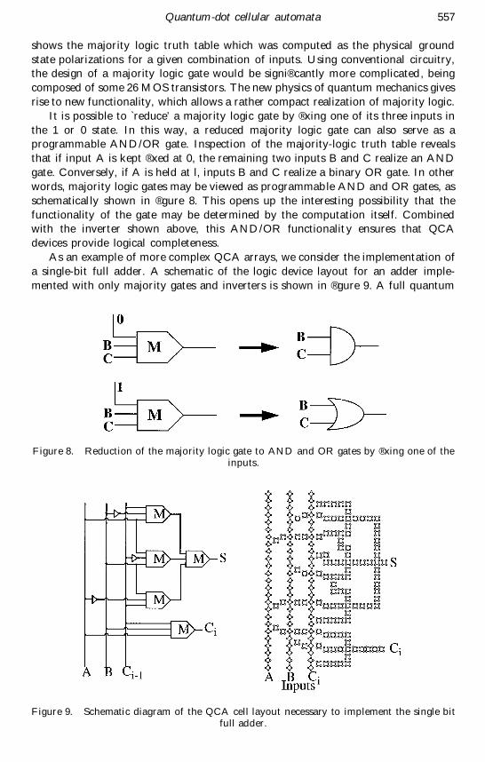
It is possible to `reduce’ a majority logic gate by ® xing one of its three inputs inthe 1 or 0 state. In this way, a reduced majority logic gate can also serve as aprogrammable AND/OR gate. Inspection of the majority-logic truth table revealsthat if input A is kept ® xed at 0, the remaining two inputs B and C realize an ANDgate. Conversely, if A is held at l, inputs B and C realize a binary OR gate. In otherwords, majority logic gates may be viewed as programmable AND and OR gates, asschematically shown in ® gure 8. This opens up the interesting possibility that thefunctionality of the gate may be determined by the computation itself. Combinedwith the inverter shown above, this AND/OR functionalit y ensures that QCAdevices provide logical completeness.
As an example of more complex QCA arrays, we consider the implementation ofa single-bit full adder. A schematic of the logic device layout for an adder imple-mented with only majority gates and inverters is shown in ® gure 9. A full quantum
Quantum -dot cellular autom ata 557
Figure 8. Reduction of the majority logic gate to AND and OR gates by ® xing one of theinputs.
Figure 9. Schematic diagram of the QCA cell layout necessary to implement the single bitfull adder.

mechanical simulation of such an adder has been performed, and veri® es that ityields the correct ground state output for all eight possible combinations of thethree inputs (Tougaw and Lent 1994). The general principles for computing withsuch QCA arrays will be discussed below.
2.4. Computing with QCAs
A QCA array like the adder discussed above works because the layout of thequantum-dot cells has provided a mapping between the physical problem of ® ndingthe ground state of the cells and the computational problem. The physical problemcan be stated as follows: given the boundary conditions imposed by the input, whatis the lowest energy con® guration of the electrons in the cellular array? It is theability to make this mapping between the physical ground state and the uniquelogical solution state that is at the heart of the QCA approach. This is illustratedschematically in ® gure 10.
Without getting too far into implementation-speci® c features, let us brie¯ yaddress the question of input and output in a QCA array. Setting an input wirerequires coercively setting the state of the ® rst cell in the wire. This can be accom-plished very simply by charging nearby conductors to repel electrons from one dotand attract them to another. In quantum dots made in semiconductors or metals,this has become a standard experimental technique, usually called a `plunger elec-trode’ , to alter electron occupancy of a dot. Reading an output state is more di� cult.We require the ability to sense the charge state of a dot without having the measure-ment process alter the charge state. Since the local charge produces a local electro-static potential, this is really a question of constructing a small electrometer.Fortunately , electrometers made from ballistic point-contac ts and from isolated
558 W . Porod et al.
Figure 10. Schematic representation of computing with a QCA array. The key concepts are`computing with the ground state’ and `edge-driven computation’ described in the text.

dots themselves have already been demonstrated, both in metallic and semiconduc-tor systems (Baza n et al. 1996, Bernstein et al. 1996). These electrometers can non-invasively measure the charge state of a single dot. Note that input and output areonly performed at the edges of the array; no information or energy need ¯ ow tointerior cells.
Computation in a QCA array proceeds along the following three basic steps:
(1) First, the initial data is set by ® xing the polarization of those cells at the edge,which represent the input information (edge-driven computation).
(2) Next, the whole array is allowed to relax (or is adiabatically transformed) tothe new ground state, compatible with the input cells kept ® xed (computingwith the ground state).
(3) Finally, the results of the computation are read by sensing the polarization ofthose cells at the periphery which represent the output data.
Computing is thus accomplished by the mapping between the physical groundstate of the array and the logical solution state of the computational problem. Thetwo key features which characterize this new computing paradigm are `computingwith the ground state’ and `edge-driven computation ’ which we discuss in furtherdetail below.
2.4.1. Computing with the ground state. Consider a QCA array before the start ofa computation . The array, left to itself , will have assumed its physical groundstate. Presenting the input data, i.e. setting the polarization of the input cells, willdeliver energy to the system, thus promoting the array to an excited state. Thecomputation consists in the array reaching the new ground state con® guration,compatible with the boundary conditions given by the ® xed input cells. Note thatthe information is contained in the ground state itself , and not in how the groundstate is reached. This relegates the question of the dynamics of the computation toone of secondary importance; although it is of signi® cance, of course, for actualimplementations. In the following, we will discuss two extreme cases for thisdynamics, namely one where the system is completely left to itself , and anotherwhere exquisite external control is exercised.
2.4.1.1. L et physics do the computing. The natural tendency of a system to assumethe ground state may be used to drive the computation process, as schematicallyshown in ® gure 11(a). Dissipative processes due to the unavoidable coupling tothe environment will relax the system from the initial excited state to the newground state. The actual dynamics will be tremendously eomplicated since all thedetails of the system-environment coupling are unknown and uncontrollable .However, we do not have to concern ourselves with the detailed path in which theground state is reached, as long as the ground state is reached. The attractive fea-ture of this relaxation computation is that no external control is needed. However,there also are drawbacks in that the system may get `stuck’ in metastable statesand that there is no ® xed time in which the computation is completed.
2.4.1.2. Adiabatic computing. Due to the above di� culties associated with meta-stable states, Lent and co-workers have developed a clocked adiabatic scheme forcomputing with QCAs. The system is always kept in its instantalleou s groundstate which is adiabatically transformed during the computation from the initialstate to the desired ® nal state, as schematically depicted in ® gure 11(b). This is
Quantum -dot cellular autom ata 559

accomplished by lowering or raising potential barriers within the cells in concertwith clock signals. The modulation of the potential barriers allows or inhibitschanges of the cell polarization. The presence of clocks makes synchronized opera-tion possible, and pipelined architectures have been proposed (Lent et al. 1994,Lent and Tougaw 1996, 1997).
2.4.2. Edge-driven computation. Edge-driven computation means that only the per-iphery of a QCA array can be contacted, which is used to write the input and toread the output of the computation . No internal cells may be contacted directly.This implies that no signals or power can be delivered from the outside to the in-terior of an array. All interior cells interact only within their local neighbourhoo d.The absence of signal and power lines to each and every interior cell has obviousbene® ts for the interconnect problem and heat dissipation.
The lack of direct contact to the interior cells also has profound consequences forthe such arrays can be used for computation. Since no power can ¯ ow from theoutside, interior cells cannot be maintained in a far-from-equilibr ium state. Since noexternal signals are brought to the inside, internal cells cannot be in¯ uenced directly.These are the reasons why the ground state of the whole array is used to representthe information, as opposed to the states of each individual cell. In fact, edge-drivencomputation necessitates computing with the ground state!
Conventional circuits, on the other hand, maintain devices in a far-from-equili-brium state. This has the advantage of noise immunity, but the price to be paidcomes in the form of the need for wires to deliver power (contributing to the wiringbottleneck) and the power dissipated during switching (contributing to the heatdissipation problem ).
560 W . Porod et al.
Figure 11. Schematic representation of (a) relaxation computing and (b) adiabatic computing.

2.5. Switching of QCA arraysAs discussed in the previous section, quantum-dot cellular automata take advan-
tage of the concept of computing with the ground state, which means that thephysical ground state of the system is mapped directly to the logical solution ofthe problem that the device is designed to solve. This emphasis on the groundstate is one of the strengths of the QCA architecture Ð the details of the evolutionof the system, which may be hard to control, are not essential in getting the compu-tation right. The dynamics of the system are doing the computing only in the sensethat they move the system to its new ground state. This view of the computationalprocess has also made it appropriate to ® rst study the steady-state behaviour of thesedevices before looking at the dynamic behaviour.
The dynamics of the system, however, cannot be completely neglected. Thedynamics of the system are relevant for two reasons. The ® rst is that an analysisof the system’s dynamics is necessary to quantif y the switching speed of QCA arrays.Second, as has been pointed out by Landauer, the presence of metastable statescould cause a signi® cant delay in the system reaching its new ground state, so theidenti® cation of such states is important.
We have considered two approaches to switching the array from the solution ofone problem to another. The ® rst approach involves switching the input cells sud-denly and allowing dissipative coupling to the environment to relax the array to thenew solution state. The inputs are kept ® xed during this relaxation. The secondmethod involves switching the array gradually by smoothly changing the input stateswhile simultaneous ly modulating the inter-dot barriers over the whole array. In thisway the array can be switched adiabatically, keeping the system at all times in theinstantaneous ground state. This adiabatic approach thus removes any problemsassociated with possible metastable states and enables clocked control of switchingevents. An analogous regime for metal cells, for which barriers cannot be loweredbut occupancy can be changed, has been developed.
In the adiabatic switching approach described in the previous section, it wasalways assumed that the interdot potential barrier was modulated simultaneouslyfor all cells in the array. From the point of view of fabrication complexity, this is animportant feature. It permits one conductor, typically one gate electrode, to controlthe barriers of all cells. If each cell had to be separately timed and controlled, thewiring problem introduced could easily overwhelm the simpli® cation won by theinherent local interconnectivity of the QCA architecture itself .
We can gain signi® cant advantage, however, by relaxing this requirementslightly. If we subdivide an array of cells into subarrays, we can partition the com-putational problem and gain the advantages of multi-phase clocking and pipelining.For each sub-array a single potential (or gate) modulates the inter-dot barriers in allthe cells. This enables us to use one sub-array to perform a certain calculation, thenfreeze its state by raising the inter-dot barriers and use the output of that array as theinput to a successor array. During the calculation phase, the successor array is keptin the unpolarized state so that it does not in¯ uence the calculation. An analogousregime for metal cells, for which barriers cannot be lowered but occupancy can bechanged is also possible.
The adiabatic pipelining scheme has several bene® ts. The most obvious bene® t isthat the clocking cycles of the cells are interlaced so that as soon as information is nolonger necessary for further calculations, it is released to free up room for newinformation. This allows the device to be in the process of carrying out several
Quantum -dot cellular autom ata 561

calculations at once, especially if the pipeline is long. Such simultaneous calculationstages maximize the throughput of each total system. A second bene® t of this systemis that the number of cells in each sub-array can be kept well below the thermo-dynamic limits to it size. Finally, this clocked approach clearly demonstrates that, atleast from an architectural standpoint, general purpose computing with QCA arraysis feasible.
2.6. Thermodynam ic considerations
Thermal ¯ uctuations are of concern for ground state computing. Thermal noisemay excite the system from its ground state to a higher-energy state, and therebyinterfere with the computation. The probability for the occurrence of such errors isbasically given by the relative magnitude of a typical excitation energy to the thermalenergy, k T . Excitation energies become larger as the size of the system becomessmaller, thereby providing increasing noise immunity. A typical QCA cell fabricatedwith current state-of -the-art lithography (for minimum feature sizes of 20 nm) isexpected to operate at cryogenic temperatures, whereas a molecular implementation(for feature sizes of 2 nm) would work at room temperature, as illustrated in® gure 12.
Thermodynamic considerations also are of concern for large arrays, and entropyneeds to be taken into account. The tendency of a system to increase its entropymakes error states more favourable. As the size of the system increases, so do thenumber of possible error con® gurations. This sets an upper limit on the size of theallowed number of cells in an array before entropy takes over. We have shown thatthis limit depends in an exponential fashion on the ratio of a typical excitationenergy to the thermal energy (Lent et al. 1994). For example, arrays with about20 000 cells are feasible if this typical error energy is 10 times larger than the thermalenergy.
3. Quantum-dot cellular neural networks
In addition to employing QCA cells to encode binary information as describedin the previous section, these cells may also be used in an analogue mode. As
562 W . Porod et al.
Figure 12. Cell± cell response functions for various temperatures. (a) Semiconductor cell withminimum lithographic feature sizes of 20 nm and (b) molecular implementation withdimensions of 2 nm.

schematically shown in ® gure 13, each cell interacts with its neighbours within acertain range, thus forming what we call a quantum-dot cellular nonlinear network(Q-CNN) (Toth et al. 1996). This way of viewing coupled cells as an analogue non-linear dynamical system is similar to cellular nonlinear (or, neural) networks (CNN),which are locally-interc onnected structures implemented using conventional circuitry(Chua and Yang 1988). Each cell is described by appropriate state variables, and thedynamics of the whole array is given by the dynamical law for each cell, whichincludes the in¯ uence exerted by the neighbours on any given cell.
In the paragraphs below, we develop a simple two-state model for the quantumstates in each cell and show how the quantum dynamics of the array can be trans-formed into a CNN-style description by choosing appropriate state variables. Thegeneral features of this model are:
(1) each cell is a quantum system, characterized by both classical and quantumdegrees of freedom;
(2) the interactions between cells only depends upon the classical degrees offreedom; the precise form of the `synaptic input’ is determined by the physicsof the intercellular interactions ; and
(3) the state equations are derived from the time-dependent SchroÈ dinger equa-tion; one state equation exists for each classical and quantum degree offreedom.
For the case of a two-dimensional array, each Q-CNN cell possesses an equiva-lent CNN-cell model described by the di� erential equations given below. We maythus think of such a quantum-dot cell array as a special case of cellular nonlinearnetworks (Nossek and Roska 1993). The equivalent circuit describing a cell is com-posed of two linear capacitors, four nonlinear controlled sources and eight linearcontrolled sources representing the interactions between the cell and its eight neigh-bours (Csurgay 1996).
Our quantum model is a special case of a general formalism for `quantum net-works’ developed by Mahler (1995). As schematically shown in ® gure 14, a quantumnetwork consists of subsystems which are special quantum objects denoted as`network nodes’ and the interaction channels between them are denoted as `net-work edges’ . For the study of such systems, Mahler has developed a density
Quantum -dot cellular autom ata 563
Figure 13. Schematic view of a locally-connected cellular QCA array. The circle indicates therange of interaction for the central cell.

matrix formalism for the theoretical study of small (coherent) quantum networks:the network node is taken as a ® nite local state space of dimension n. The networkmight be a regular lattice or an irregular array of nodes. The network is coupled toexternal driving ® elds and dissipative channels, which are required for measurement.This approach provides a system-theoretic tool adaptable to situations where a ® nitequantum mechanical state space is controlled by a classical environment. This form-alism is su� ciently general to also include dissipation, but we have not yet incorpo-rated that in our Q-CNN models; this work is in progress.
3.1. Quantum model of cell array
Following the work of Toth et al. (1996), we describe the quantum state in eachcell using the two basis states j u 1 i and j u 2 i which are completely polarized.
j C i = a j u 1 i + b j u 2 i
Within this two-state model, each property of a cell is completely speci® ed by thequantum mechanical amplitudes a and b . In particular, P, the cell polarization isgiven by
P = j a j2 j b j
2
The Coulomb interaction between adjacent cells increases the energy of thecon® guration if the two cell polarizations di� er. This can be accounted for by anenergy shif t corresponding to the weighted sum of the neighbouring polarizations,which we denote by PE. The cell dynamics is then given by the SchroÈ dingerequation
ihd / d tj C i = Hj C i
where H represents the cell Hamiltonian. Once the Hamiltonian is speci® ed, the celldynamics is completely determined. j C i represents the state of q given cell, and notthe state of the whole array; quantum entanglement is not accounted for in thisformulation.
564 W . Porod et al.
Figure 14. Quantum network: the subsystems of the network are special quantum objectsdenoted as `network nodes’ and the interaction channels are denoted as `network edges’(af ter Mahler 1995).

3.2. Formulating CNN-like quantum dynam ics
In order to transform the quantum mechanical description of an array into aCNN-style description, we perform a transformation from the quantum-mechanicalstate variables to a set of state variables which contains the classical cell polarization,P, and a quantum mechanical phase angle, u
j C i = ( a , b ) ! j C i = ( P, u )
This transformation is accomplished by the relations
a = [( 1 + P) / 2]1/ 2b = [( 1 P) / 2]1/ 2eiu
With this, the dynamical equations derived from the SchroÈ dinger equation can berewritten as CNN-like dynamical equations for the new state variables P and u
h d / d tP = 2 g sin u ( 1 P2 ) 1/ 2
h d / d t u = PE + 2 g cos u P/ ( 1 P2) 1/ 2
The term PE accounts for the cell± cell interaction and g is the tunnelling matrixelement between dots. For a more detailed derivation, we refer to the original paperby Toth and co-workers (1996).
It can be shown that the resulting dynamics for each cell is governed by aLiapounov function V (P, u ) which is given by Porod et al. (1997)
V ( P, u ) = 2 g cos u ( 1 P2 ) 1/ 2 + PPE
3.3. Cellular network model of quantum -dot array
This above network model simulates the dynamics of the polarization and thephase of the coupled cellular array. If the polarization of the driver cells of an arrayin equilibrium is changed in time, a dynamics of the polarizations and phases for allcells in the whole array is launched. In the framework of the CNN model, ground-state computing by the quantum cellular array corresponds to transients betweenequilibrium states.
It is well known for CNN arrays that the dynamics may give rise to interestingspatio-temporal wave-phenomena (Chua 1995). A signi® cant literature exists on thissubject, and di� erent classes of wave behaviour and pattern formation have beenidenti® ed (Zuse 1969, Porod et al. 1996).
In complete analogy, spatio-temporal wave-behaviour also exists for thedynamics of Q-CNN arrays. We have begun to study these phenomena and wepresent a few examples below.
Figure 15 shows wave front motion in a linear Q-CNN array. The driver cell onthe left-hand-side is switched at t = 0, thereby launching such a soliton-like wavefront. The ® gure shows snapshots of the classical polarization P and the quantummechanical phase angle u at various times. Note that the information about thedirection of propagation is contained in the sign of the phase angle. Just fromthe polarization alone, one could not tell whether the wave front would move tothe right or left.
Figure 16 shows examples of wave-like excitation patterns in two-dimensionalQ-CNN arrays. The top panel shows an example of wave behaviour induced by aperiodic modulation of the boundaries. Note that a ® xed cell block is also included
Quantum -dot cellular autom ata 565

566 W . Porod et al.
Fig
ure
15.
Wav
efro
nt
mo
tio
nin
alin
ear
Q-C
NN
arra
y.

Quantum -dot cellular autom ata 567
Fig
ure
16.
Exa
mpl
esof
wav
e-lik
eex
cita
tion
patt
erns
intw
o-di
men
sion
alQ
-CN
Nar
rays
.T
he
top
pan
elsh
ow
sco
ncen
tric
wav
esdu
eto
ap
erio
dic
mod
ula
tio
nof
the
bou
ndar
ies.
Th
eb
otto
mp
anel
show
sa
spir
alw
ave
due
tocy
clic
alm
od
ulat
ion
of
the
bou
ndar
ies.

near the upper left-hand corner. Several snapshots are shown (time increases fromleft to right) which display concentric wave fronts. The bottom panel shows anexample of cyclical excitations at the boundaries which give rise to a spiral wave.The excitation at each of the four boundaries are 90ë out of phase with respect totheir neighbouring edge.
4. Possible quantum-dot cell implementations
In this section, we discuss possible implementations of the coupled-quan tum-dotcells discussed so far. Based upon the reported studies in the literature on single-electron charging and dot± dot coupling, experimental e� orts are underway at NotreDame to realize a QCA cell in semicondutors using split-gate technology and in ringsof metallic tunnel junctions (Bernstein et al. 1996). We give a brief review of thatwork, including the results and implications of our numerical modelling. We alsodiscuss a candidate molecule which might serve as a prototype molecular electronicsimplementation of a QCA cell.
4.1. Gate-controlled quantum dots
The fabrication of a QCA cell by split-gate technology is a challenging problem,yet appears to be within reach of current lithographic capability (Bernstein et al.1996). Figure 17 shows a possible physical realization which is based on electrostaticcon® nement provided by a top metallic electrode (Taylor 1994). The key imple-mentation challenges are (i) to gain su� cient gate control in order to de® ne quantumdots in the few-electron regime, and (ii) to place these dots su� ciently close toeach other in order to make coupling possible. Using these techniques, it is con-ceivable that coupled-dot cells may be realized in a variety of materials systems,such as III± V compound semiconductors, Si/SiGe heterolayers , and Si/SiO2 struc-tures.
In order to achieve a crisp con® ning potential, it is important to minimize thee� ects of fringing ® elds, which may be accomplished by bringing the electrons asclose as possible to the top surface. This design strategy of t̀rading mobility versusgate control’ by utilizing near-surface 2DEGs has been pioneered by Snider et al.(1991). However, the resultant proximity of the quantum dot to the surface raises thequestion of the e� ect of the exposed surface on the quantum con® nement. To studythese questions, we have undertaken extensive numerical modelling of such gate-controlled dots, and we have explictly included the in¯ uence of surface states whichare occupied, in a self -consistent fashion, according to the local electrostatic poten-tial (Chen and Porod 1995).
568 W . Porod et al.
Figure 17. Possible physical realization of gate-controlled quantum dots by top metallic gates.

We have performed numerical simulations for the design of quantum dot struc-tures in the few-electron regime, both in the AlGaAs/GaAs and Si/SiO2 materialsystems. The con® ning potential is obtained from the Poisson equation within aThomas-Fermi charge model. The electronic states in the quantum dot are thenobtained from solutions of the axisymmetric SchroÈ dinger equation. Our model takesinto account the e� ect of surface states by viewing the exposed surface as the interfacebetween the semiconductor and air (or vacuum ). Figure 18 schematically shows thesimulation strategy, where we employ a ® nite-element technique for the semiconductordomain and a boundary element method for the dielectric above (Chen et al. 1994).Both domains are coupled at the exposed surface, taking into account the e� ect ofcharged surface states. This is particularly important for modelling the III± Vmaterial system, where surface states are known to be signi® cant.
Our modelling shows that the single most critical parameter for the design ofgate-control led dots is the proximity of the 2DEG to the top metallic gates. Thisdistance is limited in the III± V material system by the l̀eakiness’ of the layer separ-ating the electronic system from the electrodes. Distances as close as 25 nm have beenachieved, but more typically 40 nm are being used. The silicon material systemappears to be particularly promising candidate because of the extremely good insu-lating properties of its native oxide. SiO2 layers can be made as thin as 10 nm, andeven less (4 nm appears to be about the limit). This allows for extremely crisp con-® ning potentials.
We have explored various gate con® gurations and biasing modes. Our simula-tions show that the number of electrons can be e� ectively controlled in the fewelectron regime by the combined action of depletion and enhancement gates,which we will illustrate below.
4.1.1. AlGaAs/GaAs material system. Figure 19 shows an example of the occupa-tion of quantum dots for combined enhancement/depletion mode biasing on anAlGaAs/GaAs 2DEG. The main idea is to negatively bias the outer electrode
Quantum -dot cellular autom ata 569
Figure 18. Solution strategy used in the numerical simulations. Finite elements are used inthe semiconductor domain, and a boundary element technique for the dielectric above.

(gate 2) such that the 2D electron density is depleted, or near depletion; a positivebias on the inner electrode (gate 1) is then utilized to induce the quantum dot andto control its occupation. In this example, we have chosen a radius of rG1 = 6 nmfor the centre enhancement gate, and a radius of rG2 = 50 nm for the surroundingdepletion gate. The resulting number of electrons induced by three di� erent voltageson the depletion gate, V G2, is plotted as a function of the enhancement gate biasvoltage, V G1 . We see that variations of the depletion-gate bias of 10 mV will resultin threshold-vol tage variations of as much as 80 mV. This biasing mode appearsto be an e� ective way of controlling the quantum-dot threshold voltage in thefew-electron regime.
The use of a single, negatively-bia sed depletion gate would not su� ce for ourpurposes. Even though it would be possible to obtain few-electron dots, the resultingpotential variations are too gradual to allow fabrication of a QCA cell with closely-spaced dots (Chen and Porod 1995).
4.1.2. Si/SiO 2 material system. We have also performed numerical simulations forthe design of gated few-electron quantum dot structures in the Si/SiO2 materialsystem. The motivation for this work has been to investigate the feasibility oftransferring the emerging technology of quantum dot fabrication from the III± Vsemiconductors, where it was pioneered over the past few years, to the technologi-cally more important Si/SiO2 material system. Silicon appears to be a promisingcandidate due to the excellent insulating behaviour of thin SiO2 ® lms which yieldsthe required crisp gate-control of the potential in the plane of the two-dimensionalelectron gas at the Si/SiO2 interface. Another advantage of silicon for quantumdot applications appears to be the higher e� ective mass, as compared to the III± Vmaterials, which reduces the sensitivity of the energy levels to size ¯ uctuations.
570 W . Porod et al.
Figure 19. Example of dot occupation using combined enhancement (G1) and depletion (G2)gates in the AlGaAs/GaAs material system.

Quantum dots may be realized by applying a positive bias to a metallic gate onthe surface, as schematically shown in the inset to ® gure 20. The positive voltageinduces an inversion layer underneath the biased gate, which may lead to the for-mation of an `electron droplet’ at the silicon/oxide interface, i.e. a quantum dot.Figure 20 shows, for an applied gate bias of 1.7 V, the corresponding potentialvariations along the Si/SiO2 interface. An electronic system is induced when thesilicon conduction band edge at the oxide interface, indicated by the solid line,dips below the Fermi level ( indicated by the thin horizontal line). We see that theformation of a quantum dot critically depends upon the thickness of the oxide layer.Our modelling shows that for a 10 nm gate radius, an oxide thickness around (orbelow) 10 nm is required. Further modelling shows that these dots are occupied inthe few-electron regime (Chen and Porod 1998).
Our modelling suggests a design strategy as schematically shown in ® gure 21.Two metallic electrodes are being used, one (the bottom one) as a depletion gate, andthe top one as an enhancement gate. We envision to fabricate openings in the bottomelectrode by electron beam lithography with dimensions of about 20 nm. The topelectrode is then evaporated onto the patterned and oxidized metallic layer, whichresults in a top electrode which may reach the semiconductor surface inside theopenings, providing the enhancement gates.
4.2. Rings of metallic tunnel junctions
In addition to the semiconductor systems discussed above, single-electron tunnel-ling phenomena may also be observed in metallic tunnel junctions (Fulton andDolan 1987, Grabert and Devoret 1992). Consider a ring of metallic tunnel junc-tions, schematically shown in ® gure 22(a). The tunnel junctions are represented by
Quantum -dot cellular autom ata 571
Figure 20. Potential variation at the silicon/silicon dioxide interface as a function of oxidethickness.

the crossed capacitor symbols, indicating that these junctions are characterized bycapacitance and tunnel resistance. The metallic droplets themselves are the `wires’between the tunnel junctions. Consider now that two extra electrons are added tosuch a cell, as schematically shown in part (b) of the ® gure. It can be shown that thiscell exhibits precisely the same two distinct ground state con® gurations as the semi-conductor cell discussed above. In addition, the cell± cell coupling also shows thesame strongly nonlinear saturating characteristic (Lent and Tougaw 1994). Note that
572 W . Porod et al.
Figure 21. Design strategy for a quantum-dot cell in the silicon material system using thecombined action of two metallic electrodes.
Figure 22. Possible QCA implementation using rings of metallic tunnel junctions. (a) Basiccell, (b) cell occupied by two additional electrons, (c) line of capacitively coupled cells.

cell± cell coupling is purely capacitive, as schematically shown for the line of cells in® gure 22(c). The metallic tunnel-junction cell may be used as a building block formore complicated structures, in a fashion completely analogous to the semiconduc-tor implementations.
Using the technique of shadow evaporation, coupled-dot structures have recentlybeen fabricated and tested in the aluminium-alum inium oxide material system. Theseexperiments will be described in more detail in a separate section below.
4.3. Possible molecular implementation
As discussed above, QCA room temperature operation would require molecular-scale implementations of the basic cell. Molecular chemistry promises to o� er theversatility for the desired miniaturization. The requirements for a molecular QCAtechnology include:
(1) cells made of a rigid array of identical clusters with inter-cell interactions thatare insulating (e.g. a square arrangement of four clusters);
(2) two-electron occupation of each cell with distinct arrangements of the twocharges;
(3) charge interchange between these distinct arrangements, which are energeti-cally equal in the absence of a polarizing ® eld;
(4) patterning of cells into prede® ned array geometries on a substrate; and
(5) connections to the periphery of an array for inputs and outputs.
In previous work by Fehlner and co-workers, a candidate for such a prototypicalmolecular cell has been synthesized and crystallographically characterized (Cen et al.1992, 1993). As schematically illustrated in ® gure 23, these molecular substances withthe formula M2{(CO)9Co3CCO2}4, where M = Mo, Mn, Fe, Co, Cu, consist ofsquare arrays of transition metal clusters; each containing three cobalt atoms. It isremarkable that the four clusters are arranged in a (¯ at) square, as opposed to a(three-dimensional) tetrahedron, which one might have expected. The reason for thisbehaviour lies in the two metallic atoms at the centre which form a `spindle’ and theclusters attach themselves in the plane perpendicular to this axis.
It has been demonstrated that these compounds may be obtained as pure crystal-line molecular solids in gram quantities. In spite of high molecular weights, thesesubstances are soluble and most dissolve without dissociation, which makes itpossible to disperse them on a substrate. Each cell has an edge-to-edge distanceof about 20 nm, which is precisely the desired dimension for QCA room tempera-ture operation. The spectroscopic properties demonstrate intra-cell cluster-coreelectronic communication and inter-cell interactions are insulating.
5. Experimental demonstration of QCA elements
As described above, a basic QCA cell can be built of two series-connected dotsseparated by tunnelling barriers and capacitively coupled to identical double-dots. Ifthe cell is biased such that there are two excess electrons within the four dots, theseelectrons will be forced to opposite corners by Coulomb repulsion. Experimentally, itis necessary to both set and detect the desired cell polarization. Operation of arealistic QCA cell should be demonstrated in an environment comparable to that
Quantum -dot cellular autom ata 573

574 W . Porod et al.
Fig
ure
23.
Can
did
ate
for
am
ole
cula
rQ
CA
cell
cons
isti
ngof
4ou
ter
(CO
) 9C
o3C
clu
ster
sw
hic
har
ear
ran
ged
ina
plan
ear
oun
da
`spi
nd
le’c
on
stit
ute
db
yth
eM
2co
re.

in which it will function. The control of a QCA cell must be by single electrons, sincein a QCA system, polarization of cells is in¯ uenced totally by the single electronpolarization of nearest neighbour-ce lls. In short, we must have single electronscontrolled by single electrons.
Critical to any device or system whose operation depends upon the motion ofsingle electrons is a means of detecting their positions. It has been shown that a singleelectron transistor (SET) can be used to detect charge variation in a nearby dot(Lafarge et al. 1991, Bazan et al. 1996). In previous experiments, the Coulombinteraction of electrons within a double-dot has been inferred exclusively fromtheir series conductance (Pothier et al. 1992, Sakamoto et al. 1994, Waugh et al.1995). A detection scheme that can probe the polarization state of the double-dotexternally, and with high sensitivity, has not heretofore been developed.
5.1. Measurement of double-dot polarization
In this section, we present direct measurement of the internal charge state of ametal/oxide double-dot system. Speci® cally, our charge detection technique is sensi-tive not only to the charge variation of individual dots, but also to the exchange ofone electron between the two dots. This important property of our detection schememakes it suitable for sensing the polarization state of a QCA cell.
Metal dot structures are constructed of small aluminium wires separated byextremely thin aluminium oxide barriers which allow electrons to tunnel betweenthe sections. Figure 24 shows a scanning electron micrograph (SEM) of an SET. Thearea of the oxide barriers (i.e. the overlap of lines) is small (about 60 60 nm2),resulting in correspondingly small capacitances between the sections. A centre island
Quantum -dot cellular autom ata 575
Figure 24. Field emission scanning electron micrograph of a single electron tunnelling tran-sistor fabricated at Notre Dame. The gate electrode is to the left, and the two tunneljunctions are at both ends of the `dot’ . The sizes of the tunnel junctions are approxi-mately 60 60 nm2 .

of metal, referred to as the `dot’ , is therefore isolated from the rest of the system byl̀eaky’ barriers. These dots assume the property of accepting charge by units of
single electrons only.Fabrication of metal dots connected by leaky tunnel junctions is accomplished
through a series of carefully controlled processing steps, due to Fulton and Dolan(1987). First, a double layer of resist is exposed by electron beam lithography (EBL)and developed to form the desired pattern. (The resist layers are chosen to result in alarge degree of undercut, allowing the tilting procedure described below. ) Second,the wafer is coated in a high-vacuum chamber by a thin aluminium ® lm whichreaches the surface of the wafer only where the resist has been developed, i.e.removed. (The remaining aluminium rests on the surface of the resist to be removedin the ® nal step. ) Next, the aluminium is exposed in situ to a controlled amount ofoxygen in order to oxidize its surface. Since this is a self -limiting process, the ® nalthickness of the oxide is well-controlled. The wafer is then tilted so that a secondevaporated aluminium pattern is translated laterally from the ® rst, but overlappingin very tiny areas which form the leaky junctions. The presence of the metal over theoxide then protects the junction from further oxidation in ambient. In our case, thebottom electrode metal was 25 nm thick with 50 nm of Al forming the top electrode.In the ® nal lift-o� step, the resist is dissolved in a suitable solvent and all extraneousmetal residing on the surface of the resist is removed.
Figure 25 is a schematic diagram of our metal dot system, consisting of twoislands in series connected by a tunnel junction with each island capacitively coupled
576 W . Porod et al.
Figure 25. Schematic diagram of the device structure. Capacitance parameters of di� erentparts of the device are listed in table 1. The capacitances of the coupling capacitors C11and C22 are approximately 10% of the total capacitances of the electrometers. Thecircuit used to compensate for parasitic capacitance between the driver gates VA / VBand the electrometer islands E1/E2 is not shown.

to an SET electrometer. An interdigitated design is used to increase the couplingcapacitance, enhancing electrometer sensitivity. The two dots labelled D1 and D2between the three tunnel junctions were 1.4 m m long. In the vicinity of each dot are`driver gate’ electrodes A and B used to change the electron populations of theirrespective dots. Each dot of the double-dot system is also capacitively coupled to anSET (labelled E1 and E2) with an island length of 1.1 m m. Figure 26 is an SEM of thecell depicted in ® gure 25. The typical tunnel resistance of a junction, based on I± Vmeasurements of the electrometers at 4.2 K, was approximate ly 200 k V . The totalcapacitance of the electrometers, CS , extracted from the charging energy(EC 80 meV), was approximate ly 1 fF.
Measurements were carried out at the base temperature of our dilution refrig-erator ( 10 mK) using standard ac lock-in techniques. A 4 mV excitation voltage ata frequency of 20 Hz was used to measure the conductance of the double-dot andthe electrometers. A 1 T magnetic ® eld was applied to suppress the superconductivityof Al.
Initial experiments were performed to extract the lithographic and parasiticcapacitance parameters of the di� erent parts of the circuit. Capacitances betweeneach gate and island were determined from the period of the Coulomb blockade
Quantum -dot cellular autom ata 577
Figure 26. Scanning electron micrograph of fabricated QCA cell test system. On the left isthe double-dot structure, and on the right are the two SET electrometers. The electro-meters are coupled to the double-dot structure via interdigitated capacitors.

oscillations (CBO) (Averin and Likharev 1991). Table 1 shows the extracted systemcapacitances .
In subsequent experiments, the charge on the double-dot structure was varied bysweeping gates A and B. Conductances through the double-dot and both SET elec-trometers were simultaneous ly measured. The sensitivities of the electrometers, asexpected from Lafarge et al. (1991), were proportional to CD1-E1 and CD2-E2. Also,the operating points of the electrometers were set to be equal. Coupling capacitorsCD1-E1 and CD2-E2 were designed to be relatively large in order to increase thesensitivity of the electrometers (table 1), yet constitute a su� ciently small fractionof the total capacitance of the electrometers for them to act as non-invasive probes(Bazan et al. 1996).
Our external circuitry was more involved than that shown in ® gure 25 in order tocompensate for parasitic capacitances between the gates and the islands, which arenon-negligible , as can be seen from table 1. To suppress the in¯ uence of the parasiticcapacitances CA-E1 , CA-E2, CB-E1 , and CB-E2 , we applied inverted compensationvoltages proportional to VA and VB to gates C and D. Using this charge compensa-tion technique, we were able to reduce the e� ect of the parasitic capacitance by atleast a factor of 100.
Figure 27 is a contour plot of the conductance through the double-dot as afunction of driver gate voltages, VA and VB . The resulting charging diagram ofsuch a measurement forms a `honeycomb’ structure ® rst observed by Pothier et al.(1992). The honeycomb boundaries (solid lines) represent the regions where a changein electron population (n1 , n2) occurs on one or both of the dots, with n1 and n2
representing excess populations of D1 and D2, respectively. Each hexagonal cellmarks a region in which a given charge con® guration is stable due to Coulombblockade. In the interior of the cell there is no charge transport through the
578 W . Porod et al.
ApproximateCapacitance Type capacitance (aF)
Cjunction Lithographic 400CA-D1 Lithographic 47.7CB-D2 Lithographic 49.5CC-E1 Lithographic 29CD-E2 Lithographic 26.6CD1-E1 Lithographic 106CD2-E2 Lithographic 106CA-E1 Parasitic 21CA-E2 Parasitic 8CB-E1 Parasitic 9.7CB-E2 Parasitic 21.3CC-E2 Parasitic 7.5CD-E1 Parasitic 7.5CE1-E2 Parasitic 36.8CA-D2 Parasitic 6.4CB-D1 Parasitic 6.4CD1-E2 Parasitic 16CD2-E1 Parasitic 16
Table 1. Lithographic and parasitic capacitancesbetween various gates and islands shown in® gure 24, measured from the period of theCoulomb blockade oscillations.

double-dot; conductance through the double-dot peaks only at the `triple points’ ,depicted by a convergence of contour lines, where the Coulomb blockade is lif ted forboth dots.
The charge con® guration of the double-dot can be varied by sweeping gatevoltages A and B along any of the three directions shown in ® gure 27, and willnot result in a current ¯ ow through the double-dot. For instance, along directionsI and II, charge is added to only one of the dots in units of single electrons, while thepopulation of the other dot stays constant. Charge redistribution in the double-dot(line III) takes place when the driver gates are swept in opposite directions. Alongdirection III, electrons are shif ted from one dot to the other while the total charge onthe double-dot remains unchanged.
Figure 28 shows grey-scale contour plots of the conductance through SET elec-trometers E1 [® gure 28(a)] and E2 [® gure 28(b)] as a function of the driver gatevoltages, where light areas represent higher conductance . Superimposed on eachplot are the solid lines that de® ne the honeycomb structure of ® gure 27. The changein the conductance of each electrometer re¯ ects the variation of the electrostaticpotential in the dot capacitively coupled to it. A sharp change in the conductanceof E1 from light to dark in the horizontal direction [® gure 28(a)] represents addition
Quantum -dot cellular autom ata 579
Figure 27. Charging diagram of the double-dot as a function of driver gate voltages. Chargecon® gurations (n1 , n2), which represent the number of extra electrons on D1 and D2,respectively, are arbitrarily chosen. Lines labelled I, II and III show a few directions inwhich charge can shift between di� erent con® gurations of the double-dot.

580 W . Porod et al.
Figure 28. Charging diagram of the electrometers as a function of the same driver gatevoltages shown in ® gure 2 with the honeycomb boundaries of ® gure 4 superimposed.(a) Charging diagram of E1. Sharp transitions in the horizontal direction indicate achange in the population of D1. (b) Charging diagram of E2. Sharp transitions in thevertical direction re¯ ect a change in the population of D2.
(b)
(a)

of an electron on D1. Similarly, sharp variation in conductance of E2 in the verticaldirection [® gure 28(b)] indicates discrete variation of charge on D2. Hence, thesharpest variations in the conductances of each electrometer can be used to sensethe charging of their capacitively coupled dots.
Sensing the state of a QCA cell requires detection of charge redistribution in thedouble-dot shown by direction III in ® gure 27, but as seen in ® gure 28, the transitionalong this direction is weaker than the others. During charge redistribution in thedouble-dot (line III in ® gure 27), the population of each dot simultaneously changesby one electron with one dot losing an electron and the other gaining one, so thesignals from the two dots are out of phase by 180ë . The cross capacitance betweenD1 (D2) and E2 (E1) causes charging of each dot of the series double-dot to be seenin both electrometers, and since the signals are out of phase, the net response isreduced. For instance, the signal detected in E1 (E2) along direction III is about 30%weaker than that along the direction I (II).
Figure 29 shows honeycomb borders (solid lines taken from ® gure 27) overlaidon a grey-scale contour plot of a di� erential signal, (G1-G2), where G1 and G2 are theconductances of E1 and E2, respectively. Along the directions I and II in ® gure 27,the signals of E1 and E2 have the same phase, giving a suppressed di� erential signal.The most conspicuous transition, represented by a higher density of contour lines,
Quantum -dot cellular autom ata 581
Figure 29. Di� erential signal obtained from the charging diagrams of the individual electro-meters. The most salient transition is in the direction of charge redistribution indicatedby a higher density of contour lines.

occurs at the boundary between the (0, 1) and (1, 0) states, indicating movement ofan electron from one dot to the other. As mentioned above, this is due to the phasedi� erence (180ë ) in the signals of the individual electrometers, yielding a di� erentialsignal which is approximate ly twice as strong as the one detected by a single electro-meter.
Our device architecture allows us to directly observe the internal state of adouble-dot system by detecting all possible charge transitions of a single electron.A di� erential detector that utilizes the signals from both electrometers is mostsensitive to the charge redistribution in the double-dot. With this investigation, wedemonstrate that our di� erential detector can be used as the output of a QCA cell.
5.2. Single electron switch, controlled by a single electron
As described above, the operation of a QCA cell requires a change in the cellpolarization controlled by a single electron transition. Changing the polarization ofthe cell is accomplished using gate electrodes to force one electron to switch from onedot to the other within a double-dot (the input double-dot ) which in turn induces aswitch of the other electron in its double-dot (the output double-dot ). This is onlypossible when the change of the electrostatic potential on input double-dot due to thecharge redistribution is strong enough to `drag’ the charge state of the outputdouble-dot through the corresponding honeycomb border (thick line) of ® gure 30,thus switching its electron con® guration.
Therefore, to produce a functioning QCA cell, the gate biases for each double-dot must set the working point of the charging state as closely as possible to thecentre of the transition border. Then the cell is in its most symmetrical state, and inthe absence of an input signal the two polarizations are equally probable.Calculations show that the charge state of the output double-dot can switch underthe in® uence of electrostatic potential from a single electron in the input double-dot.This switching will be re¯ ected in a movement of the honeycomb border back andforth along the diagonal direction E. Switching takes place each time the bordercrosses the working point.
Here we report the ® rst experimental observation of a honeycomb border shif t ina double-dot caused by single electron charging of adjacent dots. We compare theseexperimental results with the results of the di� erential detector of the previous sec-tion, and with theoretical calculations to con® rm that this shif t causes electronexchange within the double-dot.
To perform this experiment we use the same circuit as in the previous section,shown schematically in ® gure 25. Now we use the SET transistors as the input dotsof a QCA cell and investigate how these single electron drivers a� ect the outputdouble-dot charge state. Since we no longer have direct-coupled electrometers, wemust determine the charge state of the output double-dot indirectly by measuring itsconductance, which requires a sweep of gates A and B. To prevent these voltagesfrom a� ecting the input dots, we apply compensating voltages to gates C and D asdescribed in the previous section. It is important to note that without such cancella-tion, the simple honeycomb pattern of the output double-dot changes dramatically,since charge states of the input dots will depend on the voltages of gates A and B.
If we carefully control the charge on the SET islands E1 and E2, they can mimicthe input double-dot of a full four-dot QCA cell. Gates A and B, as before, controlthe charge state of the double-dot, while the purpose of gates C and D is now very
582 W . Porod et al.

di� erent. Gates C and D are now the input drivers of the QCA cell, which are used to`switch’ an electron between the input dots, inducing an electron switch within theoutput double-dot. We cannot actually switch an electron between the input dotssince they are not con® gured as a double-dot. However, if biases with oppositepolarities are applied to gates C and D, each time an electron is removed fromone input dot, another is added to the other, mimicking an electron exchange inan input double-dot. In our experiment, special care is taken to compensate forbackground charges to ensure that the electron transitions occur simultaneously.
A switch in electrons between the input dots will cause a shift in position of theconductance peaks of the output double-dot (and the entire honeycomb ) seen in® gure 30. In order to observe this honeycomb border shif t, `snapshots’ of the honey-comb are taken for di� erent `push-pull’ (+ VC = VD ) settings on the driver gates. It iswell known (Lafarge et al. 1991) that the potential on a metal dot in the Coulombblockade regime changes linearly as a function of gate voltage with an abrupt shif twhen the electron population of the dot changes, resulting in sawtooth oscillations.We indeed observe a slow shif t of the honeycomb border corresponding to thegradual increase of the potential on the input dots, followed by an abrupt `reset’ .
Quantum -dot cellular autom ata 583
Figure 30. Charging diagram of the output double-dot. QCA operation will be shown by themotion of this honeycomb along the diagonal E. In particular we will concentrate onthe border between the (0, 1) and (1, 0) states which is marked with a heavy line.

584 W . Porod et al.
Fig
ure
31.
Ch
argi
ng
diag
ram
of
the
outp
ut
dou
ble
-do
tw
ith
(a)
VC
=
V D=
0.
67m
V,
and
(b)
VC
=
VD
=+
0.67
mV
.T
hes
ep
rese
nt
the
max
imu
msh
ift
ofth
eb
orde
rbe
twee
nth
e(0
,1 )
and
(1,
0 )st
ates
.

Figure 31 shows two snapshots taken at the extremes of the shif t, with a measuredshif t of approxim ately 440 m V.
To demonstrate that the observed shif t is due to single electron charging of theinput dots, and not to parasitic coupling from the driver gates, we directly measurethe shif t of the honeycomb border while sweeping gates C and D over su� cientvoltage that several electron transfers occur in the input dots. The shif t from electroncharging will be periodic, since the potential on the input dots resets at each electrontransfer, while parasitic coupling will add a monotonic term to the border shift. Todetect the honeycomb border, we sweep the double-dot gates A and B along thediagonal E in ® gure 30. At ® nite temperature, the conductance of a double-dotshows a peak as we sweep VA and VB , and the position of this peak marks theborder. Here we de® ne the `diagonal voltage’ as the change in voltage alongthe direction E, with D VA = D VB . For each setting of the driver gates we sweepthe diagonal voltages to ® nd the position of the honeycomb border. These data areassembled as a 3D contour plot.
Figure 32 shows a contour plot of one border as a function of diagonal voltage,the displacement from the working point ( D VA and D VB ) and driver (+ VC and
Quantum -dot cellular autom ata 585
Figure 32. Contour plot of the conductance through the double-dot as a function of thedi� erential driver voltages VC = VD and the diagonal voltage. The honeycomb bor-der is marked by the peak in conductance, and the black circles mark the calculatedposition of the border.

VD ) voltages, representing the position of the honeycomb border with respect to a® xed working point de® ned as Vdiagonal = 0. The solid circles in ® gure 32 plot thetheoretical position of the border calculated using the measured capacitance valuesgiven in table 1. The experiment matches theory extremely well, considering thatthe only ® tting parameter used is background charge. The background charge canrandomly displace the border, but cannot change the magnitude or period of anobserved shif t. The somewhat smaller amplitude of the theoretical honeycomb shif tis most likely due to uncertainty in the measured junction capacitance ( 15% ). Thesawtooth oscillations of ® gure 32 occur each time an electron is added to one andremoved from the other input dot, con® rming that the shif t is due to a single electrontransfer. If the working point on the honeycomb pattern of ® gure 30, ( VA , VB), ischosen close to a border, the shif t will cause a border crossing when electronexchange occurs within the input dots.
To con® rm that the border shif t is indicative of an electron transfer in the outputdouble-dot, we compare the border shif t observed in ® gure 32 with the data from thedi� erential detector in ® gure 29, where a diagonal voltage change of approxim ately600 m V is required for an electron to complete the switch from one dot to the other.As mentioned earlier, the transition is not abrupt due to ® nite temperature, and for afunctional QCA cell the border shif t must be su� cient to overcome this broadenedtransition. The observed shift of 440 m V is nearly su� cient to completely switch theelectron, but a larger shif t would be desirable. An increase of the coupling capaci-tance between the input and output dots will increase the shif t.
We also compare the observed border shif t to the results of our simulations,which include the complete circuitry of the system, assume a temperature of 0 K,and include all experimentally determined parasitic capacitances. Figure 33(a) showsthe calculated potential on input dot E1, which, as expected, is a sawtooth patternwith abrupt transitions when an electron enters or leaves the dot. Figure 33(b) showsthe calculated potential on the output dot, D1, and ® gure 33(c) shows the calculatedshif t of the honeycomb border as a function of the driver gate voltages. Figure 33(b)and (c) demonstrate that with a proper setting of the working point of the doubledot, and a temperature of 0 K, the input dots are able to produce su� cient shif t toswitch an electron from one output dot to the other, as evidenced by the abruptpotential changes in ® gure 33(d). Since the match between the calculated and experi-mental honeycomb shif t is very good, we believe that the data of ® gure 33(b), inconjunction with the di� erential detector data, con® rms that we are able to controlthe position of the electron on the output double-dot with a single electron on theinput dots. However, if the voltage range of the drivers is too large, the parasiticcoupling from the drivers will pull the working point away from the border so thatthe shif t from the electron transfer is unable to cause a border crossing, and theelectron population on the double-dot remains unchanged. This e� ect correspondsto the monotonic tilt of the sawtooth curve in ® gure 33(c).
We have experimentally demonstrated the ® rst switching of a single electronbetween dots controlled by a single electron. This control is shown by a honeycombborder shif t induced by changes in the charge con® guration of the coupled inputdots. The observed shift is in excellent agreement with calculations, and a compari-son of the shif t with the electrometer measurement shows that the border shiftinduces an electron switch which is nearly complete. Future devices will be optimizedby an increased coupling of the input and output dots to fully overcome the ® nitetemperature smearing.
586 W . Porod et al.

6. Conclusion
We have developed a novel nanoelectronic scheme for computing with coupledquantum dots, where information is encoded by the arrangement of single electrons.We have shown that such structures, the so-called quantum-dot cellular automata,may be used for binary information processing. In addition, an analogue version isalso possible, the so-called quantum-dot cellular nonlinear networks, which exhibit
Quantum -dot cellular autom ata 587
Figure 33. Simulated operation of the QCA cell as a function of the di� erential drivervoltages VC = VD . (a) The potential of the input dot E1, showing a sawtooth beha-viour with sharp transitions corresponding to single electron charging events. (b) Thepotential of dot D1 of the double-dot, where the sharp transitions occur when anelectron exchanges position within the double-dot. (c) The displacement from the work-ing point ( VA = VB = 1.5 mV) of the honeycomb border along the diagonal E. Electronexchange occurs when the border crosses zero.

wave phenomena. We have discussed possible realizations of these structures in avariety of semiconductor systems (including GaAs/AlGaAs, Si/SiGe, and Si/SiO2),rings of metallic tunnel junctions and candidates for molecular implementations.Finally we have experimentally realized the key elements of QCA operation. Ourstudies are the ® rst experiments to demonstrate the control of a single electron bysingle electrons.
Acknowledgements
The work described in this paper was made possible by the hard and dilligentwork of the postdocs and students in Notre Dame NanoDevices Group, includingGreg Baza n, Yuriy V. Brazhnik, Minhan Chen, Henry K. Harbury, Geza Toth, P.Doug Tougaw, Weiwen Weng and Xiaoshan Zuo. This research was supported inpart by DARPA, ONR, and NSF.
References
Ashoori, R. C., 1996, Electrons in arti® cial atoms. Nature , 379, 413.Averin, D. V., and Likharev, K. K., 1991, Single electronics: a correlated transfer of single
electrons and Cooper pairs in systems of small tunnel junctions. In B. L. Altshuler,P. A. Lee, and R. A. Webb (Eds) Mesoscopic Phenomena in Solids (Amsterdam: NorthHolland), pp. 173± 271.
Bazaí n, G., Orlov, A. O., Snider, G. L., and Bernstein, G. H., 1996, Charge detectorrealization for AlGaAs/GaAs quantum-dot cellular automata. Journal of V acuumScience and Technology B, 14, 4046± 4050.
Bernstein, G. H., Bazaí n, G., Chen, M., Lent, C. S., Merz , J. L., Orlov, A. O., Porod,W.,Snider, G. L., and Tougaw, P. D., 1996, Practical issues in the realization of quan-tum-dot cellular automata. Superlattice Microstructures, 20, 447± 459.
Biafore, M. , 1994, Cellular automata for nanometer-scale computation. Physica D , 70, 415.Blick, R. H., Huag, R. J.,Weis, J., Pfannkuche, D., Klitzing, K. v., and Eberl, K., 1996,
Single-electron tunneling through a double quantum dot: The arti® cial molecule.Physics Reviews B, 53, 7899± 7902.
Bohr, M. T., 1996, Interconnect scalingÐ the real limiter to high performance ULSI. SolidState Technology, 105 (September issue).
Capasso, F. (Ed.), 1990, Physics of Quantum Electron Devices, Springer Series in Electronicsand Photonics 28 (Berlin± Heidelberg: Springer-Verlag).
Cen,W., Lindenfeld, P., and Fehlner,T. P., 1992, On the interface of metal± metal multiplebond compounds and organometallic clusters. Journal of the American ChemicalSociety, 114, 5451± 5452.
Cen,W., Haller, K. J., and Fehlner,T. P., 1993, On the role of PES data in the identi® cationof metal ± metal charge transfer bands in clusters of clusters. Journal of ElectronSpectroscopy, 66, 29± 36.
Chen, M., and Porod,W., 1995, Design of gate-con® ned quantum dot structures in the few-electron regime. Journal of Applied Physics, 78, 1050± 1057.
Chen, M., and Porod, W. , 1998, Simulation of quantum-dot structures in Si/SiO2 . V L SIDesign, 6, 335± 339.
Chem, M., Porod,W., and Kirkner, D. J., 1994, A coupled ® nite element/boundary elementmethod for semiconductor quantum devices with exposed surfaces. Journal of AppliedPhysics, 75, 2545± 2554.
Chua, L. O. (Ed.), 1995, Special issue on nonlinear waves, patterns and spatio-temporal choasin dynamic arrays. IEEE Transactions on Circuits and Systems, I. Fundamental Theoryand Applications , 42, (October issue).
Chua, L. O., and Yang, L., 1988, Cellular neural networks: theory. IEEE Transactions onCircuits Systems, CAS-35, 1257± 1272; and CNN: Applications. IEEE Transactions onCircuits Systems, CAS-35, 1273± 1290.
Csurgay, A., 1996, Private communication.
588 W . Porod et al.

Ferry, D. K., and Porod,W., 1986, Interconnections and architecture for ensembles of micro-structures. Superlattices and Microstructures, 2, 41.
Ferry, D. K., Grondin, R. O., and Porod,W., 1987, Interconnection, dissipation, and com-putation. V L SI Electronics: Microstructure Science, Vol. 15. In N. G. Einspruch, S. S.Cohen, and G. Gildenblat (Eds). (Academic Press), p. 451.
Ferry, D. K., Akers, L. A., and Greeneich, E. W., 1988, Ultra L arge Scale IntegratedMicroelectronics (Prentice Hall).
Fulton, T. A., and Dolan, G. H., 1987, Observation of single-electron charging e� ects insmall tunnel junctions. Physics Review L etters, 59, 109± 112.
Grabert, H., and Devoret, M. H. (Eds), 1992, Single Charge Tunneling (New York:Plenum).
Grondin, R. O., Porod,W., Loeffler, C. M., and Ferry, D. K., 1987, Cooperative e� ects ininterconnected device arrays. In L. Carter (Ed.) Molecular Electronic Devices II(Amsterdam: Dekker), pp. 605± 622.
Hoffman, F., Heinzel, T., Wharam, D. A., Kotthaus, J. P., Boïhm, G., Klein, W.,Traï nkle, G., and Weimann, G. , 1995, Single electron switching in a parallel quantumdot. Physics Reviews B, 51, 13872± 13875.
Kastner, M. A., 1993, Arti® cial atoms. Physics Today , 46, 24.Kelly, M. J. , 1995, L ow-Dimensional Semiconductors: Materials, Physics, Technology, Devices
(Oxford: Clarendon).Keyes, R. W. , 1987, The Physics of V L SI Systems (Addison-Wesley).Lafarge, P., Pothier, H., Williams, E. R., Esteve, D., Urbina, C., and Devoret,
M. H., 1991, Direct observation of macroscopic charge quantization. Zeitschrift fuÈ rPhysik B, 85, 327± 332.
Lent, C. S., and Tougaw, P. D., 1993, Lines of interacting quantum-dot cells: a binary wire.Journal of Applied Physics, 74, 6227± 6233.
Lent, C. S., and Taugaw, P. D., 1994, Bistable saturation due to single electron charging inrings of tunnel junction. Journal of Applied Physics, 75, 4077± 4080.
Lent, C. S., and Tougaw, P. D. , 1996, Dynamics of quantum cellular automata. Journal ofApplied Physics, 80, 4722± 4736.
Lent, C. S., and Tougaw, P. D. , 1997, A device architecture for computing with quantum dots.Proceedings of the IEEE, 85, 541± 557.
Lent, C. S., Tougaw, P. D., and Porod, W., 1993a, Bistable saturation in coupled quantumdots for quantum cellular automata. Applied Physics L etters, 62, 714± 716.
Lent, C. S., Tougaw, P. D., Porod, W., and Bernstein, G. H., 1993b, Quantum cellularautomata. Nanotechnology , 4, 49± 57.
Lent, C. S.,Tougaw, P. D., and Porod,W., 1994, Quantum cellular automata: the physics ofcomputing with arrays of quantum-dot molecules. In IEEE Computer Society Press,Proceedings of the W orkshop on Physics and Computation, PhysComp94 (LosAlamitos, CA: IEEE), pp. 1± 9.
Mahler, G., and Weberruß, V. A., 1995, Quantum Networks: Dynam ics of OpenNanostructures (Berlin± Heidelberg: Springer-Verlag).
Meirav, U., Kastner, M. A., and Wind, S. J., 1990, Single-electron charging and periodicconductance resonances in GaAs nanostructures. Physics Reviews L etters, 65, 771±774.
Meurer, B., Heitmann, D., and Ploog, K., 1992, Single-electron charging of quantum-dotatoms. Physics Reviews L etters, 68, 1371± 1374.
Montemerlo, M. S., Love, C. J., Opiteck, G. J., Goldhaber-Gordon, D., andEllenbogen, J. C., 1996, Technologies and designs for electronic nanocomputers.The MITRE Corp. preprint is available at http://www.mitre.org/research/nanotech/
Nossek, J. A., and Roska, T., 1993, Special issue on cellular neural networks. IEEETransactions on Circuits Syst., I. Fundam ental Theory and Applications, 40, (Marchissue).
Porod,W., Harbury, H. K., and Lent, C. S., 1996, Study of wave phenomena in physically-coupled device arrqays using the Helmholtz equation as a model. Presented at theFourth W orkshop on Physics and ComputationÐ PhysComp96, Boston, MA.
Porod,W., Lent, C. S.,Toth, G., Luo, H., Csurgay, A., Huang,Y.-F., and Liu, R.-W., 1997,Quantun-dot cellular nonlinear networks: computing with locally-interconnected
Quantum -dot cellular autom ata 589
quantum dot arrays. Proceedings of the IEEE Intenational Symposium on Circuits andSystemsÐ ISCAS’97.
Pothier, H., Lefarge, P., Urbina, C., Esteve, D., and Devoret, M. H., 1992, Single-electronpump based on charging e� ects. Europhysics L etters, 17, 249± 254.
Reed, M. A., Randall, J. N., Aggarwal, R. J., Matyi, R. J., Moore,T. M., and Wetsel, A.E., 1988, Observation of discrete electronic states in zero-dimensional semiconductornanostructures. Physics Reviews L etters, 60, 535± 538.
Sakamoto, T., Hwang, S., Nihey, F., Nakamura, Y., and Nakamura, K., 1994, Coulombblockade of two quantum dots in series. Japanese Journal of Applied Physics, 33, 4876±4877.
Semiconductor Industry Association, 1994, The National Technology Roadm ap forSemiconductors (Austin, TX: Sematech).
Snider, G. L., Miller, M. S., Rooks, M. J. and Hu, E. L., 1991, Quantized conductance inballistic constrictions at 30 K. Applied Physics L etters, 59, 2727± 2729.
Spiller,T. P., 1996, Quantum information processing: cryptography, computation, and tele-portation. Proceedings of the IEEE, 84, 1719± 1746.
Taylor, R. P., 1994, The role of surface-gate technology for AlGaAs/GaAs nanostructures.Nanotechnology , 5, 183± 198.
Toffoli,T., and Margolus, N., 1987, Cellular Autom ata Machines: A New Environment forModeling (MIT Press).
Toth, G., Lent, C. S., Tougaw, P. D., Brazhnik, Y., Weng, W., Porod, W., Liu, R.-W., andHuang,Y.-F., 1996, Quantum cellular neural networks. Superlattice Microstructures,20, 473± 477.
Tougaw, P. D., and Lent, C. S., 1994, Logical devices implemented using quantum cellularautomata. Journal of Applied Physics, 75, 1818± 1825.
Tougaw, P. D., Lent, C. S., and Porod,W., 1993, Bistable saturation in coupled quantum-dotcells. Journal of Applied Physics, 74, 3558± 3566.
Turton, R., 1995, The Quantum Dot: a Journay into the Future of Microelectronics (Oxford:Oxford University Press).
Waugh, F. R., Berry, M. J., Mar, D. J., Westervelt, R. M., Campman, K. L. , andGoddard, A. C., 1995, Single-electron charging in double and triple quantum dotswith tunable coupling. Physics Reviews L etters, 75, 705± 708.
Weisbuch, C., and Vinter, B., 1991, Quantum Semiconductor Structures: Fundam entals andApplications (New York: Academic Press).
Zuse, K., 1969, Rechnender Raum (Vieweg, Braunschweig); translated as: Calculating Space(MIT Technical Translations AZT-70-164-GEMIT, 1970).
590 Quantum -dot cellular autom ata


