Embed Size (px)
Citation preview

University of Southern Queensland
Faculty of Health, Engineering & Sciences
Controller Area Network to Modbus Network Bridge to
interface gas detection units with Building Management
Systems
A dissertation submitted by
Matthew Quinton
in fulfilment of the requirements of
ENG4112 Research Project
towards the degree of
Bachelor of Electrical & Electronic Engineering
Submitted: October, 2015

Abstract
Building Management Systems (BMS') are computer systems designed to control systems
inside buildings or other facilities. While BMS' are common, there is no one size fits all
approach. Controller Area Network (CAN) is a communication protocol sometimes used
within BMS'. Modbus is a very common industrial communications protocol. The two
protocols are not directly compatible and need to be ’bridged’ to communicate with each
other.
Gas Detection Australia (GDA) design and manufacture gas detection equipment. They
have a current and ongoing need to interface Modbus enabled equipment with CAN
enabled equipment in client BMS'. This project is sponsored with the aim of producing
a network bridge to translate between the two protocols. The specific Modbus variation
implemented is Modbus ASCII master.
The design was based around the PIC 18F87K22 microprocessor. This was chosen to
remain consistent with other GDA products. The communication interfaces were designed
using integrated circuits that closely mimic the software development tools. This was a
deliberate choice made to make software development simpler and to make it easier to
translate source code to the finished product. A testing method was also created to allow
the assessment of bridge performance.
Testing demonstrated proof of concept using the development board. Separate testing
of RS-485 hardware suggests that the full hardware specification is valid. Stress tests
were carried out and determined that the bridge could be expected to be capable of
responding to four CAN messages per second. The testing was limited by issues relating
to the inconsistent operation of the CAN interface.

University of Southern Queensland
Faculty of Health, Engineering & Sciences
ENG4111/2 Research Project
Limitations of Use
The Council of the University of Southern Queensland, its Faculty of Health, Engineering
& Sciences, and the staff of the University of Southern Queensland, do not accept any
responsibility for the truth, accuracy or completeness of material contained within or
associated with this dissertation.
Persons using all or any part of this material do so at their own risk, and not at the risk of
the Council of the University of Southern Queensland, its Faculty of Health, Engineering
& Sciences or the staff of the University of Southern Queensland.
This dissertation reports an educational exercise and has no purpose or validity beyond
this exercise. The sole purpose of the course pair entitled “Research Project” is to con-
tribute to the overall education within the student’s chosen degree program. This doc-
ument, the associated hardware, software, drawings, and other material set out in the
associated appendices should not be used for any other purpose: if they are so used, it is
entirely at the risk of the user.
Dean
Faculty of Health, Engineering & Sciences

Certification of Dissertation
I certify that the ideas, designs and experimental work, results, analyses and conclusions
set out in this dissertation are entirely my own effort, except where otherwise indicated
and acknowledged.
I further certify that the work is original and has not been previously submitted for
assessment in any other course or institution, except where specifically stated.
Matthew Quinton
0061024766

Acknowledgments
I would like to thank my academic supervisor, Mr Mark Phythian for his guidance and
support. He often went above and beyond to help me achieve my project aims.
I would also like to thank my two professional supervisors from Gas Detection Australia,
Mr James Boucher and Mr Chris Kelly. Without any of these people this project could
not have taken place. I would especially like to recognise Mr Kelly, who was a continuous
source of knowledge throughout the project. I would also like to thank Mr Trent Rutten
from GDA for his assistance with hands on technical matters.
Finally I would like to thank my wife, Sam who was always there to listen and to help
me through this project. Her patience and understanding were vital.
Matthew Quinton

Contents
Abstract i
Acknowledgments iv
List of Figures xii
List of Tables xiv
Chapter 1 Introduction 1
1.1 Motivation . . . . . . . . . . . . . . . . . . . . . . . . . . . . . . . . . . . 2
1.2 Aim . . . . . . . . . . . . . . . . . . . . . . . . . . . . . . . . . . . . . . . 2
1.3 Project Objectives . . . . . . . . . . . . . . . . . . . . . . . . . . . . . . . 3
1.4 Overview of the Dissertation . . . . . . . . . . . . . . . . . . . . . . . . . 4
Chapter 2 Relevant Literature and Design Constraints 5
2.1 Chapter Overview . . . . . . . . . . . . . . . . . . . . . . . . . . . . . . . 6
2.2 Building Management Systems . . . . . . . . . . . . . . . . . . . . . . . . 7
2.3 Controller Area Network . . . . . . . . . . . . . . . . . . . . . . . . . . . . 8
2.3.1 General CAN Features . . . . . . . . . . . . . . . . . . . . . . . . . 8
CONTENTS vi
2.3.2 Standards . . . . . . . . . . . . . . . . . . . . . . . . . . . . . . . . 9
2.3.3 Frame Format . . . . . . . . . . . . . . . . . . . . . . . . . . . . . 9
2.4 Modbus . . . . . . . . . . . . . . . . . . . . . . . . . . . . . . . . . . . . . 11
2.4.1 General Modbus Features . . . . . . . . . . . . . . . . . . . . . . . 11
2.4.2 Frame Format . . . . . . . . . . . . . . . . . . . . . . . . . . . . . 13
2.4.3 RTU, ASCII and TCP . . . . . . . . . . . . . . . . . . . . . . . . . 14
2.5 Bridging the Protocols . . . . . . . . . . . . . . . . . . . . . . . . . . . . . 15
2.5.1 Previous Works . . . . . . . . . . . . . . . . . . . . . . . . . . . . . 15
2.5.2 Lessons from Previous Works . . . . . . . . . . . . . . . . . . . . . 16
2.5.3 Existing Bridges and Available Products . . . . . . . . . . . . . . . 17
2.6 Constraints . . . . . . . . . . . . . . . . . . . . . . . . . . . . . . . . . . . 20
2.7 Chapter Summary . . . . . . . . . . . . . . . . . . . . . . . . . . . . . . . 20
Chapter 3 Design Methodology 21
3.1 Chapter Overview . . . . . . . . . . . . . . . . . . . . . . . . . . . . . . . 22
3.2 Equipment . . . . . . . . . . . . . . . . . . . . . . . . . . . . . . . . . . . 23
3.3 Hardware Design . . . . . . . . . . . . . . . . . . . . . . . . . . . . . . . . 24
3.3.1 Microprocessor . . . . . . . . . . . . . . . . . . . . . . . . . . . . . 24
3.3.2 CAN Interface . . . . . . . . . . . . . . . . . . . . . . . . . . . . . 25
3.3.3 Serial Interface . . . . . . . . . . . . . . . . . . . . . . . . . . . . . 26
3.3.4 Power Supply . . . . . . . . . . . . . . . . . . . . . . . . . . . . . . 26
3.3.5 Isolation . . . . . . . . . . . . . . . . . . . . . . . . . . . . . . . . . 27

CONTENTS vii
3.3.6 Ancillary Circuitry . . . . . . . . . . . . . . . . . . . . . . . . . . . 27
3.3.7 Printed Circtuit Board . . . . . . . . . . . . . . . . . . . . . . . . . 29
3.4 Software Design . . . . . . . . . . . . . . . . . . . . . . . . . . . . . . . . . 30
3.4.1 CAN Interface . . . . . . . . . . . . . . . . . . . . . . . . . . . . . 30
3.4.2 Modbus Interface . . . . . . . . . . . . . . . . . . . . . . . . . . . . 30
3.4.3 Ancillary Functions . . . . . . . . . . . . . . . . . . . . . . . . . . 31
3.4.4 Main . . . . . . . . . . . . . . . . . . . . . . . . . . . . . . . . . . . 32
3.5 Proposed Testing Methodology . . . . . . . . . . . . . . . . . . . . . . . . 33
3.5.1 RS485 Confirmation . . . . . . . . . . . . . . . . . . . . . . . . . . 34
3.5.2 Physical Cable Testing . . . . . . . . . . . . . . . . . . . . . . . . . 34
3.6 Chapter Summary . . . . . . . . . . . . . . . . . . . . . . . . . . . . . . . 35
Chapter 4 Design of the Network Bridge 36
4.1 Chapter Overview . . . . . . . . . . . . . . . . . . . . . . . . . . . . . . . 37
4.2 Hardware Design . . . . . . . . . . . . . . . . . . . . . . . . . . . . . . . . 38
4.2.1 Microprocessor . . . . . . . . . . . . . . . . . . . . . . . . . . . . . 38
4.2.2 CAN Interface . . . . . . . . . . . . . . . . . . . . . . . . . . . . . 38
4.2.3 Serial Interface . . . . . . . . . . . . . . . . . . . . . . . . . . . . . 39
4.2.4 Power Supply . . . . . . . . . . . . . . . . . . . . . . . . . . . . . . 40
4.2.5 Isolation . . . . . . . . . . . . . . . . . . . . . . . . . . . . . . . . . 41
4.2.6 Ancillary Circuitry . . . . . . . . . . . . . . . . . . . . . . . . . . . 41
4.2.7 Printed Circuit Board . . . . . . . . . . . . . . . . . . . . . . . . . 42

CONTENTS viii
4.3 Software Design . . . . . . . . . . . . . . . . . . . . . . . . . . . . . . . . . 44
4.4 Chapter Summary . . . . . . . . . . . . . . . . . . . . . . . . . . . . . . . 47
Chapter 5 Results and Discussion 48
5.1 Results . . . . . . . . . . . . . . . . . . . . . . . . . . . . . . . . . . . . . . 49
5.1.1 Proof of bridge concept . . . . . . . . . . . . . . . . . . . . . . . . 49
5.1.2 Bridge stress testing . . . . . . . . . . . . . . . . . . . . . . . . . . 51
5.1.3 Proof of RS-485 concept . . . . . . . . . . . . . . . . . . . . . . . . 53
5.1.4 Physical Cable Testing . . . . . . . . . . . . . . . . . . . . . . . . . 54
5.2 Discussion . . . . . . . . . . . . . . . . . . . . . . . . . . . . . . . . . . . . 57
5.2.1 Proof of Concept . . . . . . . . . . . . . . . . . . . . . . . . . . . . 57
5.2.2 Stress Tests . . . . . . . . . . . . . . . . . . . . . . . . . . . . . . . 57
5.2.3 Proof RS-485 Concept . . . . . . . . . . . . . . . . . . . . . . . . . 58
5.2.4 Physical Cable Testing . . . . . . . . . . . . . . . . . . . . . . . . . 58
5.2.5 Discussion of issues and limitations - CAN Interface . . . . . . . . 59
5.2.6 Discussion of issues and limitations - Modbusslave simulator . . . 62
5.3 Chapter Summary . . . . . . . . . . . . . . . . . . . . . . . . . . . . . . . 63
Chapter 6 Conclusion and Future Work 64
6.1 Conclusions . . . . . . . . . . . . . . . . . . . . . . . . . . . . . . . . . . . 65
6.2 Recommendations and Future Work . . . . . . . . . . . . . . . . . . . . . 66
References 67

CONTENTS ix
Appendix A Project Specification 71
Appendix B Controller Area Network 74
B.1 List of frame field descriptions . . . . . . . . . . . . . . . . . . . . . . . . 75
B.2 Physical Connection . . . . . . . . . . . . . . . . . . . . . . . . . . . . . . 76
B.2.1 Topology . . . . . . . . . . . . . . . . . . . . . . . . . . . . . . . . 76
B.2.2 Transmission and Signals . . . . . . . . . . . . . . . . . . . . . . . 76
B.2.3 Encoding . . . . . . . . . . . . . . . . . . . . . . . . . . . . . . . . 78
B.2.4 Synchronisation and Bit Stuffing . . . . . . . . . . . . . . . . . . . 79
B.2.5 Errors . . . . . . . . . . . . . . . . . . . . . . . . . . . . . . . . . . 80
B.3 Masks and Filters . . . . . . . . . . . . . . . . . . . . . . . . . . . . . . . . 81
Appendix C Modbus 82
C.1 Protocol Data Unit . . . . . . . . . . . . . . . . . . . . . . . . . . . . . . . 83
C.2 Error Checking . . . . . . . . . . . . . . . . . . . . . . . . . . . . . . . . . 83
C.3 Physical Media . . . . . . . . . . . . . . . . . . . . . . . . . . . . . . . . . 83
C.4 RS 485 Data Rates . . . . . . . . . . . . . . . . . . . . . . . . . . . . . . . 84
C.5 Encoding and Synchronisation . . . . . . . . . . . . . . . . . . . . . . . . 84
Appendix D Network Bridge Source Code - C 85
D.1 C Header . . . . . . . . . . . . . . . . . . . . . . . . . . . . . . . . . . . . 86
D.2 Modbus Functions . . . . . . . . . . . . . . . . . . . . . . . . . . . . . . . 87
D.3 Ancillary Functions . . . . . . . . . . . . . . . . . . . . . . . . . . . . . . . 92

CONTENTS x
D.4 Main Function . . . . . . . . . . . . . . . . . . . . . . . . . . . . . . . . . 94
Appendix E Hardware Design Images 97
E.1 Schematic . . . . . . . . . . . . . . . . . . . . . . . . . . . . . . . . . . . . 98
E.2 PCB Top Layer . . . . . . . . . . . . . . . . . . . . . . . . . . . . . . . . . 99
E.3 PCB Bottom Layer . . . . . . . . . . . . . . . . . . . . . . . . . . . . . . . 100
E.4 PCB 3D Top Layer . . . . . . . . . . . . . . . . . . . . . . . . . . . . . . . 101
E.5 PCB 3D Bottom Layer . . . . . . . . . . . . . . . . . . . . . . . . . . . . . 102
Appendix F Results and Discussion Supporting Information 103
F.1 Click Board Schematics . . . . . . . . . . . . . . . . . . . . . . . . . . . . 104
F.2 Photos . . . . . . . . . . . . . . . . . . . . . . . . . . . . . . . . . . . . . . 106
F.3 Code Listings . . . . . . . . . . . . . . . . . . . . . . . . . . . . . . . . . . 107
Appendix G Datasheets 108
G.1 PIC18F87K22 . . . . . . . . . . . . . . . . . . . . . . . . . . . . . . . . . . 109
G.2 DF04S . . . . . . . . . . . . . . . . . . . . . . . . . . . . . . . . . . . . . . 113
G.3 HCPL-2601.S . . . . . . . . . . . . . . . . . . . . . . . . . . . . . . . . . . 115
G.4 LM2671 . . . . . . . . . . . . . . . . . . . . . . . . . . . . . . . . . . . . . 118
G.5 MCP2515 . . . . . . . . . . . . . . . . . . . . . . . . . . . . . . . . . . . . 120
G.6 MCP2551 . . . . . . . . . . . . . . . . . . . . . . . . . . . . . . . . . . . . 126
G.7 ROE0505S . . . . . . . . . . . . . . . . . . . . . . . . . . . . . . . . . . . . 127
Appendix H Documentation and Manuals 128

CONTENTS xi
H.1 Overview . . . . . . . . . . . . . . . . . . . . . . . . . . . . . . . . . . . . 129
H.2 Technical Manual . . . . . . . . . . . . . . . . . . . . . . . . . . . . . . . . 129
H.3 Operators Manual . . . . . . . . . . . . . . . . . . . . . . . . . . . . . . . 130
H.4 Software Manual . . . . . . . . . . . . . . . . . . . . . . . . . . . . . . . . 130
Appendix I Preliminary Report Documentation 131
I.1 Overview . . . . . . . . . . . . . . . . . . . . . . . . . . . . . . . . . . . . 132

List of Figures
2.1 CAN Frame - 11bit Identifier (adapted from (Corrigan 2008a)). . . . . . . 10
2.2 CAN Frame - 11bit Identifier (adapted from (Corrigan 2008a)). . . . . . . 10
2.3 Modbus RTU Frame (adapted from (Thomas 2008)). . . . . . . . . . . . . 13
2.4 Modbus ASCII Frame (adapted from (Thomas 2008)). . . . . . . . . . . . 13
4.1 Network Bridge Logical Overview . . . . . . . . . . . . . . . . . . . . . . . 37
4.2 CAN Communications Hardware Interface . . . . . . . . . . . . . . . . . . 39
4.3 Serial Communications Hardware Interface . . . . . . . . . . . . . . . . . 39
4.4 Power Supply Hardware . . . . . . . . . . . . . . . . . . . . . . . . . . . . 40
4.5 Indication LEDs . . . . . . . . . . . . . . . . . . . . . . . . . . . . . . . . 41
4.6 Bridge Data Flow Diagram . . . . . . . . . . . . . . . . . . . . . . . . . . 44
5.1 Proof of bridge concept - complete transmission . . . . . . . . . . . . . . . 50
5.2 Percentage of frames received . . . . . . . . . . . . . . . . . . . . . . . . . 52
5.3 RS-485 master packet using 3.3V click board . . . . . . . . . . . . . . . . 53
5.4 Short transmission line CAN traffic . . . . . . . . . . . . . . . . . . . . . . 54
5.5 1 meter twisted pair CAN traffic . . . . . . . . . . . . . . . . . . . . . . . 55

LIST OF FIGURES xiii
5.6 10 meter twisted pair CAN traffic . . . . . . . . . . . . . . . . . . . . . . . 55
5.7 10 meter twisted pair CAN traffic on working bus . . . . . . . . . . . . . . 56
5.8 10 meter twisted pair CAN response . . . . . . . . . . . . . . . . . . . . . 56
5.9 Code exert of serial data sent . . . . . . . . . . . . . . . . . . . . . . . . . 62
5.10 Serial synchronisation errors with 16MHz crystal . . . . . . . . . . . . . . 62
B.1 CAN bit levels (adapted from (ISO 2003a)). . . . . . . . . . . . . . . . . . 77
B.2 NRZ and Manchester Encoding (adapted from (CAN in Automation 2015a)). 78
B.3 CAN bit stuffing (adapted from (CAN in Automation 2015a)). . . . . . . 79
F.1 RS-485 Click board schematic . . . . . . . . . . . . . . . . . . . . . . . . . 104
F.2 CANSpi Click board schematic . . . . . . . . . . . . . . . . . . . . . . . . 105
F.3 RS-485 testing set-up . . . . . . . . . . . . . . . . . . . . . . . . . . . . . . 106

List of Tables
2.1 Modbus memory organisation . . . . . . . . . . . . . . . . . . . . . . . . . 12
5.1 Results for frame bridge frame loss - CAN baud 125kbps and Modbus baud
9.6kbps . . . . . . . . . . . . . . . . . . . . . . . . . . . . . . . . . . . . . 51

Glossary of Terms
A - Ampere
AC - Alternating Current
ASCII - American Standard Code for Information Exchange
CAN - Controller Area Network
CR - Carriage Return (ASCII character)
DC - Direct Current
DFD - Data Flow Diagram
GDA - Gas Detection Australia Pty Ltd
GLCD - Graphical Liquid Crystal Display
IC - Integrated Circuit
IP - Ingress Protection Rating
LED - Light Emitting Diode
LF - Line Feed (ASCII Character)
OSI - Open Systems Interconnection
PCB - Printed Circuit Board
RMS - Root Mean Squared
SPI - Serial Peripheral Interface
UART - Universal Asynchronous Receiver/Transmitter
USB - Universal Serial Bus
V - Voltage/Volts
Messaging Rate - The time delay between CAN frames sent by the USB-CAN converter.

Chapter 1
Introduction

1.1 Motivation 2
1.1 Motivation
GDA designs and manufactures electronic gas sensors and control units. Most of the
sensors are industry standard 4-20 mA output and are hard wired back to control units.
These control units are restricted by only having Modbus, relay switched Volt Free Con-
tacts (VFC) and analogue current outputs to communicate with the customers' existing
equipment. There are a growing number of customers requesting or already using Con-
trolled Area Network (CAN) bus as part of their Building Management System (BMS),
which GDA doesn't currently or plan to support as a direct hardware feature in their
pre-existing products.
GDA wants to explore the development of a CAN bus to Modbus network bridge to
allow customers to directly interface their BMS with GDA control units to simplify the
installation and increase customer satisfaction. The current methods are to add a 4-20
mA current receiver and a CAN bus node with analogue inputs or a CAN bus node with
digital inputs to receive the digital signals generated by the output relays on the control
units. Depending upon the complexity of the customers' system and requirements this
results in significant wiring, which could be replaced by a few wires used by the CAN bus
and Modbus (Gas Detection Australia 2015).
1.2 Aim
GDA requires the development of a network bridge to interface their existing products
with CAN enabled BMS'. The aim is to create a solution to this problem by developing a
network bridge that is capable of interfacing with both CAN enabled BMS' and Modbus
enabled gas detection controllers. The key goal is facilitating the delivery of information
in a bidirectional manner between the two separate systems.
All variations of Modbus will be explored, however the chosen protocol for this bridge is
Modbus ASCII.

1.3 Project Objectives 3
1.3 Project Objectives
The objectives of this project are to design and develop a CAN bus to Modbus network
bridge. The design should be of sufficient quality that it can be used as the base of a
commercial product. It is intended that any prior research or products conducted or
developed for this task will be considered but the final design will be original where
appropriate. The network bridge must be able to reconcile messages sent from Building
Management Systems that operate a CAN bus architecture with that of the Modbus
architecture based gas detection control units.
The Modbus interface must be implemented upon the RS-485 serial standard to be con-
sistent with existing products. Ideally, the network bridge will be configurable between
Modbus RTU and Modbus ASCII. Due to the lack of a RS-485 enabled Modbus ASCII
slave device to test on, testing will be performed using the Universal Asynchronous Re-
ceiver Transmitter (UART) as the physical layer.
The network bridge is intended to be a standalone product; however, it may be expanded
to become a module that may be added to other GDA products. The network bridge
should be developed in line with GDA procedures and methods. Final hardware compo-
nents are to be based upon Printed Circuit Board technology but can be developed and
tested using other methods. Software development is to take place using existing tools
and methods available at GDA.
As well as developing the network bridge, testing procedures and documentation are also
required to ensure correct functionality of the network bridge. Secondary objectives are
to create testing procedures for the network bridge and also to develop documentation on
the operation and maintenance of the network bridge.

1.4 Overview of the Dissertation 4
1.4 Overview of the Dissertation
This dissertation is organized as follows:
Chapter 2 explores the literature and considers existing products as well as requirements
of the sponsoring organisation, Gas Detection Australia.
Chapter 3 details the design methodology as well as the design of the testing parameters
for the bridge.
Chapter 4 includes the final design of the hardware and software for the network bridge.
Chapter 5 examines and discusses the results obtained and the challenges faced in the
design.
Chapter 6 concludes the dissertation and suggests further work in the area of CAN bus
to Modbus network bridges.

Chapter 2
Relevant Literature and Design
Constraints

2.1 Chapter Overview 6
2.1 Chapter Overview
The bridge is to be designed for use with Building Management Systems. This will require
background information on these systems. This is to give an understanding on how the
expected use affects the requirements of the bridge.
To be able to develop a device that translates two separate protocols requires an un-
derstanding of those protocols. This chapter covers some of the basic principles of each
protocol and this gives enough understanding of what is required to reconcile them. The
key differences will be highlighted so that the potential solutions can be developed in later
chapters.
This is further supported by undertaking a review of the literature on this topic as well
as a review of existing commercial products in this space.

2.2 Building Management Systems 7
2.2 Building Management Systems
Building Management Systems (BMS'), sometimes referred to as Building Automation
Systems (BAS) are computer systems that control and monitor various systems within
buildings or facilities. Typical systems that are controlled include heating, ventilation and
air-conditioning (HVAC) electrical distribution, lighting, safety equipment, security sys-
tems, and many more (So 2001). The functionality and capabilities of BMS' are beyond
the scope of this project. An understanding of where the network bridge might fit into
a BMS is the primary concern. As part of the monitoring aspects of BMS', digital and
analogue equipment feeds signals to the BMS. This might include thermostats, sensors,
pressure transducers or numerous other devices (So 2001). The proposed network bridge
is a 'device' that relays gas levels from the field to the BMS. The term device is loose
because in this case it is not a simple sensor but will involve the sensor, controller and
the network bridge. Logically, the network bridge is a gas sensor CAN node within the
BMS.
There are many different communication interfaces used within BMS'. CAN is just one
of the options available when choosing BMS architectures. There is no guarantee that
equipment from one vendor will be compatible with equipment from another, even if they
implement comparable technology (Butzin, Golatowski, Niedermeier, Vicari & Wuchner
2014). As a result, there are no standard requirements or acquisition techniques for BMS'.
The network layout of the BMS, the protocol or protocols used, the individual pieces of
equipment used, and the configuration of the network all contribute to the way a BMS
requests and acquires information. Since all BMS differ it is not possible to satisfy all
requirements with one rigid solution. The aim is to follow the CAN standard as closely
as possible and to give as much flexibility for implementation in different CAN enabled
BMS'. Flexibility would come from configurable parameters for the CAN interface such
as data rates and message types. It may also have flow on affects to the implementation
of the Modbus interface. If possible, examination of a real world BMS would be ideal for
testing of the network bridge to confirm that it operates correctly.

2.3 Controller Area Network 8
2.3 Controller Area Network
Controller Area Network (CAN) was introduced in the mid-1980s by Robert Bosch. The
protocol was designed for distributed automotive control systems. In 1991 Bosch pub-
lished the 2.0 standard containing two parts; part A as the standard for the 11-bit iden-
tifier version and part B as the standard for the 29-bit identifier version. In 1993 CAN
was standardised internationally by the International Organisation for Standards (ISO)
as ISO 11898 (Ferreira & Fonseca 2011). There are two ISO components to a CAN
implementation. ISO 11898-1 defines the data link layer and physical signalling and one
of the parts labelled 11898-X, where X is 2-6 and defines the physical layer for different
applications (ISO 2003a). ISO 11898-2 is the most popular of these physical layer ex-
tensions in use today. Even with the ISO standardisation in place for over twenty years,
CAN is often referred to as CAN 2.0A or 2.0B in reference to the 1991 Bosch standards.
2.3.1 General CAN Features
As mentioned, CAN is a two layer OSI model. ISO 11898-1 is required for CAN implemen-
tations but the system developer has the choice from the 11898-X parts. ISO 11898-2 is
the most common selection and is the assumed standard for this project. It is outside the
scope of the project to implement more than one of the 11898-X parts. Most of the infor-
mation found about CAN is derived direct from these standards (ISO 2003a, ISO 2003b).
CAN is a multi-master system with carrier sense multiple access (CSMA). Each CAN node
on the bus can transmit and receive messages. Collisions are handled using arbitration
of the identifier in the message. CAN is a message orientated system. Message contents
are defined rather than nodes or their addresses. A node will examine the contents of
a frame to determine if it is the desired destination for the frame - if it is not it will
discard the message. Every message has an identifier that is unique on the network and
this defines the content and priority of the message. CAN has numerous in-built fault
handling features including a cyclic redundancy check (CRC).
The physical wiring is a differential pair and CAN defines transmission rates up to 1Mbit
per second over a transmission length of 30 meters (ISO 2003a). Bus lengths of up to
5000 meters are possible at a baud of 10kbits per second. The trade-off for greater speed
is bus run length. CAN has grown to be more than a control system bus for vehicles and

2.3 Controller Area Network 9
is now used in multiple industries including industrial communications, medicine, robotics
and general embedded applications. CAN has benefited from large production volumes
and sound performance to emerge in other industries (Ferreira & Fonseca 2011).
2.3.2 Standards
Exhaustive exploration of the standards is not required. CAN controller chips and com-
piler library functions handle the intricacies of the protocol and their application will be
the focus of this project. An understanding of some aspects is important in order to
properly link CAN to Modbus. ISO 11898-1 defines the data link layer and the physical
signalling aspects of CAN. It forms the base upon which other standards are built. The ba-
sic concepts of CAN, the architecture, Logical Link Control (LLC) sub-layer and Medium
Access Control (MAC) sub-layer are specified. ISO 11898-2 is one of the three extensions
to ISO 11898-1 (ISO 2003a). It defines the high-speed (1Mbit/s) medium access unit and
outlines the medium dependant interface (MDI) features. Electrical characteristics of the
CAN nodes and bus are defined.
ISO 11898-1 is fundamental to any CAN implementation as it specifies the underlying
principles of CAN. From their implementations can vary with requirements. The Inter-
national Organisation for Standards (ISO) defines four other standards to complement
11898-1. They are labelled Part 3 through Part 6. It would be possible to use another
standard for this project; however ISO11898-2 is recognised as the most popular stan-
dard by Ferreira & Fonseca (2011) and will be used for this project. This should allow
maximum compatibility. Higher level protocols have been developed over the years to fill
in the gap where more sophisticated messaging is required. There are several industry
common protocols as well as academic based protocols in existence today. CANopen,
DeviceNet, J1939, FTT-CAN and TT-CAN are some of the more common CAN based
higher level protocols (Ferreira & Fonseca 2011, Corrigan 2008b).
2.3.3 Frame Format
There are two standard frame formats for CAN; one for each of the two addressing modes.
Figure 2.1 is the 11-bit identifier frame and Figure 2.2 is the extended 29-bit identifier
frame. The fields in each frame are considered below.

2.3 Controller Area Network 10
Figure 2.1: CAN Frame - 11bit Identifier (adapted from (Corrigan 2008a)).
The key difference between the two addressing modes is the increased identifier size.
Figure 2.2: CAN Frame - 11bit Identifier (adapted from (Corrigan 2008a)).
Data Frames are the most common frame format and is of the form shown in Figure 2.1
and Figure 2.2.Remote frames are used when a node wants to request information from
another node. The composition is similar to the data frame with two exceptions. The
RTR bit in the arbitration field is marked as recessive to indicate a remote frame and
there will be no data. An error frame is transmitted when a node detects an error in
a message. The other nodes on the bus will respond by sending error frames of their
own. There are safeguards in place to ensure that repeated transmissions of errors do
not completely congest the bus. The overload frame is primarily used to provide a delay
between messages in the event that a node is too busy. It has a similar format to the
error frame.
An in depth discussion of the CAN protocol is beyond the scope of this project. Much
of the implementation of CAN is handled by dedicated integrated circuits and software
libraries. Appendix B contains further specifics about the CAN protocol.

2.4 Modbus 11
2.4 Modbus
Modbus was created in 1979 by Modicon and was a propriety protocol designed for
communication between Modicon Programmable Logic Controllers (PLCs) (de Sousa
& Portugal 2011). Modbus was effectively the first ever industrial field bus protocol
(Hui, Hao & Daogang 2013). Modicon openly published the protocol and it remains free
to use, resulting in Modbus becoming the first de facto standard for industrial commu-
nications. Today it is maintained by Modbus-IDA, is still used widely in industry and
continues to evolve (de Sousa & Portugal 2011).
2.4.1 General Modbus Features
Modbus is free and as such is one of the most widely used protocols across many industries.
It is used with sensors and actuators that are network enabled. It is also used with more
complex automation equipment such as RTUs, PLCs, human machine interfaces (HMIs)
and supervisory control and data acquisition (SCADA) systems (de Sousa & Portugal
2011). Most of these implementations would be either on RS-485 or TCP networks. RS-
232 Modbus implementations are limited to point-to-point connections, such as HMI to
PLC (Thomas 2008).
Modbus is simple to implement and due to its wide use there is a lot of information
freely available. There are also several different implementations, meaning you can pick
the exact flavour that meets your needs. For example, Modbus RTU has smaller frames
than Modbus ASCII so at the same baud is slightly faster (de Sousa & Portugal 2011).
Modbus ASCII has deliberate delimiter, (colon character :) making frame reception an
easier process than RTU.

2.4 Modbus 12
Table 2.1: Modbus memory organisation
Name Memory range Number of bits Functionality
Input registers 1(0)-65,536 (65,535) 16 Read
Holding registers 1(0)-65,536 (65,535) 16 Read and Write
Discrete inputs 1(0)-65,536 (65,535) 1 Read
Coils 1(0)-65,536 (65,535) 1 Read and Write
Modbus allows devices to read and write data to memory locations on another device.
The device performing the reading and writing will have some processing ability (such as
a PLC) but the device being written to and read does not need processing ability (such as
a sensor), although it may have some. Modbus uses the client-server model. The device
processing is the client and it makes requests to the server. The server never initiates an
exchange. Clients can make multiple requests to multiple distinct servers one at a time.
The specification does not allow for servers to have more than one client, but it is possible.
Some devices acting as servers may have the ability to process simultaneous requests but
it is generally done sequentially (de Sousa & Portugal 2011, Modbus Org 2006c).
The reading and writing functions are carried out in the memory of the server. The
protocol defines the organisation of this memory but customisation is allowable (Modbus
Org 2006c). Table 2.1 gives an overview of the specified organisation scheme. Note that
the figures in the table are theoretical only. Many devices will have a memory range
lower than specified here. Typically analogue inputs and outputs are handled through
the registers and the digital inputs and outputs through the discrete inputs and coils.
To access the memory locations of table 2.1 requires specific querying from the Master
to the Slave. This section gives an outline in brief according to the reference guide by
Modicon, Inc. (1996). The are 24 separate function codes within the Modbus specification.
Each function has a unique code that forms part of the Modbus data. For example,
function ’01’ is ’Read Coil Status’. The function code used determines the format of the
frame data. Reading is the key focus of the network bridge so that will be the focus
here. The read functions (01 - 04) have very similar formats. The data component of
the message begins with a slave address. The selected function code appears next. This
is followed by the high and then low bytes of the address to be read. If the address fits
in the low byte, the high will be zero. Likewise with the number of points to be read,
which also has a high and low byte. They are the final two components respectively. An

2.4 Modbus 13
example follows:
To read coils 5-10 (hexadecimal and begins at zero) from slave 11 the query is as follows:
Slave address: 0A
Function: 01
Address high: 00
Address low: 04
Number of points high: 00
Number of points low: 06
The response from the slave follows a similar format but is not the focus given the bridge
is a master only. The query forms the data portion of the Modbus frames discussed next.
2.4.2 Frame Format
The implementations have similarities in their frame composition. They both include the
function code and data fields.
Figure 2.3: Modbus RTU Frame (adapted from (Thomas 2008)).
Each implementation has an address and error checking field. The ASCII frame also has
the explicit start bit (:) and end bits (carriage return and line feed). Figure 3 shows the
format for an RTU frame and Figure 4 shows the format for an ASCII frame.
Figure 2.4: Modbus ASCII Frame (adapted from (Thomas 2008)).
As with CAN, there is a lot of detail involved with a Modbus protocol implementation.
Integrated circuits, microprocessors and software libraries handle a lot of the details. As
a result, exploration of the finer details is left to Appendix C.

2.4 Modbus 14
2.4.3 RTU, ASCII and TCP
RTU and ASCII are asynchronous protocols that are implemented on serial channels,
generally either EIA/TIA-232 (RS-232) or EIA/TIA-485 (RS-485). They are designed
to be used on a physical bus with the slaves and master connected to the trunk. Both
transfer a start bit as part of the frame. They differ in the way the frames are constructed
and the way data is represented. RTU mode uses binary encoding and does not use
delimiters (headers and trailers). ASCII encodes the data as ASCII characters and does
use delimiters (Modbus Org 2006b). To compensate for the lack of delimiters while in
RTU mode, timing limits between characters and frames are used. A no signal period
of at least 3.5 character times between frames acts like the delimiter in RTU mode. In
ASCII mode frames have a header and trailer. The : character is the delimiter in ASCII
mode (de Sousa & Portugal 2011). Frame composition is considered later.
There are limitations on both serial variants of the protocol. Since the protocol was
conceived in 1979 data types officially supported are limited to those available at the
time (Modbus Org 2006c). It is possible to work around solutions to cater for modern
formats such as using two 16 bit registers to store 32 bit values. There are also no security
features inherent to the protocol.
Modbus TCP is also a direct byte representation protocol (de Sousa & Portugal 2011).
It is not a serial protocol. The Modbus frames are sent through an existing TCP network
and the connections are managed by the TCP protocol. There is a reserved port 502
for requests to establish Modbus TCP connections. Devices can be clients and servers
simultaneously, send multiple requests simultaneously and do not have to wait for replies
(Modbus Org 2006a). Modbus TCP frames only share the function code and data fields
with the other two protocols, with the rest of the frame made up using the Modbus
Application Protocol Header (MBAP) (de Sousa & Portugal 2011, Modbus Org 2006a).
Theoretically the physical layer for Modbus TCP could be anything but is commonly
Ethernet (Rinaldi 2010). From this point onwards, there is no reference to Modbus TCP.
This section was added for completeness only.

2.5 Bridging the Protocols 15
2.5 Bridging the Protocols
Creating bridges or similar devices to link dissimilar protocols is not a new principle.
Several papers have been written that explore the merging of CAN bus and Modbus
(REF). There are also four companies that the writer is aware of that produce existing
devices for this purpose.
2.5.1 Previous Works
A very brief paper by Guohuan, Hao & Wei (2009) identified the spread of fieldbus tech-
nology in many industries and applications as well as the incompatibility of the many
existing standards and protocols. They briefly discuss the two protocols and then de-
velop a design for the protocol conversion interface. The hardware design identifies five
components inside a block diagram; MAX232 as the serial interface, a PIC18F458 as the
microprocessor, two 6N137 optocouplers chips to isolate each bus driver from the proces-
sor, and an MCP2551 for the differential bus driving capabilities for CAN. The software
design is only developed for the case of CAN as a master and Modbus as a slave. The
brief description and a flowchart demonstrate the process at a high level of abstraction.
Wang, Zhang, Li & Ren (2013) studied the design of an adapter for Low-voltage distri-
bution systems in Intelligent Electric Grids. Modbus is identified as the low level control
network protocol of choice in this application. The major issue identified with the adapter
is the dissimilar data sizes between the two protocols. Wang also refers to other studies
that state issues with existing products. They claim that these devices do not properly
take into account the data size problem. They may be able to transmit more than the 8
byte limit imposed by CAN but have issues with frame loss during communication. The
articles referenced were not locatable to confirm the information, however, the frame size
incompatibility is well known to the author. The rest of the paper outlines the selected
hardware as well as the process required for developing the software.
The issue of conversion is addressed by using transparent transmission. When a Modbus
frame is received and needs to be sent over CAN the adapter firsts completes the CRC
check on the Modbus frame and then sends the whole remaining frame as the CAN data.
The receiving CAN node must then parse the non-data fields of the Modbus frame. Wang
claims this method reduces mapping errors when compared to stripping Modbus frames

2.5 Bridging the Protocols 16
down to just the data before being transmitted on the CAN bus.
The second major challenge addressed by software design is the issue of CAN data sizes.
Wang applies techniques from the sub-packaging rule defined in Ethernet to deconstruct
frames at the CAN transmitter and reconstruct at the CAN receiver. The final consid-
eration is the delay in frame sending from the CAN interface. Wang noted that frames
would sometimes be lost when transmitting at high speed. To address the issue a delay
time between sending frames was calculated. This was based on the bit timing of the
CAN bus based upon the selected baud rate along with the bus state, the priority of the
sending node and the delay time of transmission. The authors claimed that the device
was built, tested and met the requirements of the low-voltage distribution system.
The most recent study known to the author focused upon an adaptation layer for Mod-
bus to CAN (Cena, Bertolotti, Hu & Valenzano 2014). The paper discussed how the
traditional Modbus implementations’ speed limitations are potential issues, the introduc-
tion of Modbus-TCP as a potential solution and the idea of layering Modbus on top of
other protocols as another solution. The theme of this paper is different to the others
in that it is not a converter but a variation of Modbus similar to that of Modbus-TCP.
CAN was chosen as it is simple, fast and many microcontrollers have CAN controllers
built in. The adaptation layer has significant differences to the proposed bridge in this
project, however, the issue of large (greater than 8 bytes) Modbus data PDUs requiring
fragmentation and reassembly for transmission on CAN is evident. The solution engaged
to solve the fragmentation-reassembly issue was to change the composition of the CAN
data frames. In the first transmission of a Modbus frame over CAN, 2 bits at the start
of the data field are reserved for identifying the protocol and the length of the Modbus
frame. Subsequent frames in the sequence gain back the two header bits for data since
these fields are constant for any one Modbus message. The CAN CRC field is used in
place of the Modbus CRC field which is parsed from the Modbus frame. While similarities
are identifiable in this paper, the differences between a bridge or protocol converter and
an adaptation layer are significant and much of the rest of Cena is largely inapplicable.
2.5.2 Lessons from Previous Works
There are common identifiable issues and themes within the above works. De-fragmenting
and reconstitution of the Modbus PDUs for transmission over CAN is the major challenge.

2.5 Bridging the Protocols 17
There needs to be a method of reducing Modbus PDUs of up to 252 bytes into 8 bytes
or less size for transmission. The solution posed in (Guohuan et al. 2009) offers no detail
beyond that of a flowchart. Wang et al. (2013) propose sending the whole Modbus without
the CRC field (as CAN has its own comparable field) and then parsing the unrequired
fields at the CAN receiving end. This method is not suitable to this project as there is no
guarantee of control over the other CAN nodes on the network. Similarly, the adaptation
layer proposed by (Cena et al. 2014) require configuration of the receiving CAN nodes
and given the different nature of the protocol bridge and protocol adaptation layers is not
optimal for this project.
Wang’s lesson regarding the mapping errors when simply stripping the data out of the
Modbus frames is noted. The issue may be less pronounced on the buses the bridge will
operate on. Testing may reveal if this is an issue.
There are two basic ways of achieving CAN transmissions using microcontrollers; using a
microcontroller with embedded CAN controller and external CAN transceiver, or using a
microcontroller with external CAN controller and external CAN transceiver. All papers
reviewed suggest the former as the ideal path to take due to ease with implementations and
hardware design. Using optocouplers to isolate the microcontroller from the transmission
devices is also identified as desirable.
2.5.3 Existing Bridges and Available Products
Considering existing products is important. It allows appreciation for what has been
achieved and may also help identify areas for improvement. It is highly unlikely that any
of the products identified in this section would be suitable for the exact use intended for
the network bridge. Ultimately, GDA would like a product developed internally. This
allows for consistency in products and gives the opportunity to expand aspects of the
network bridge into other products or applications if desirable.
Anybus Communicator from HMS
The Anybus Communicator is capable of interfacing CAN and Modbus RTU through
a protocol conversion interface. This device has a configurable setup option for CAN

2.5 Bridging the Protocols 18
messaging that is configured through a graphical user interface (GUI). It supports both
CAN standards 2.0A and 2.0B as well as serial communication standards RS-485 and
RS-232. This product was designed to be used in fieldbus setups involving PLCs. It may
require significant adaptation for it to function correctly in the BMS environment. It can
only function as a Modbus slave. The obvious major drawback is the intended market for
this device. It was designed for fieldbus use it may not interface as desired with BMSs
expected for the network bridge (HMS 2015). In terms of general functionality the only
significant improvement would be to add Modbus master capabilities.
CAN/Modbus Converters from ADF Web
ADF web offers several products in this category. There are Modbus TCP solutions
that will not be considered and four different Modbus serial offerings. Electronically
there are two variants; one is a Modbus master and the other is Modbus slave. The
other two products are the same devices with extra galvanic isolation and a different
enclosure. Each device has RS-232 and RS-485 connection and one CAN port. They
support data rates on the CAN side up to the limit (1Mbps) and on the Modbus side up
to the limit (115kbps) from the official standard. The devices are fully two directional
messaging capable. Each device is only capable of being either a Modbus master or slave
and not both (ADF web 2015). This may not be suitable for this task. Further, to use
these devices requires the use of Windows based propriety software from ADF web called
Compositor SW67011. The biggest improvement would be to have the configuration built
into the device to remove the need for external software. Providing an interface to the
device that allows on the fly configuration is consistent with practices at GDA. More
flexibility with regards to Modbus configuration would also be desirable.
Modbus RTU to CAN converter from ICP DAS
This device is another protocol converter that supports CAN to Modbus RTU data trans-
fer in both directions. It supports RS-485, RS-232 and RS-422 serial communication stan-
dards. One of its applications listed is building automation so it is likely useful in this
task. It is configurable using proprietary software for the device. The device only sup-
ports Modbus RTU as a master and not as a slave. It does not support Modbus ASCII.
The configuration requires software and cannot be done by interfacing with the device

2.5 Bridging the Protocols 19
directly (ICP DAS USA 2015). To be useful in this task, this device would ideally need
support for Modbus ASCII and the ability to configure as a Modbus slave. Configuration
would be better achieved with an interface on the device itself.
There are several products all of which have their own strengths and weaknesses. None
of these products are suitable for this exact project, but they do provide some proof of
concept for the objectives outlined. Further, each device has limitations and this provides
opportunities for the network bridge.

2.6 Constraints 20
2.6 Constraints
As a sponsored project the network bridge design must be carried out within the con-
straints of the host organisation and within their requirements. Below is a description of
those constraints and requirements.
As a potential commercial product, the bridge must be financially viable. When selecting
components for use in the bridge they must be approved by GDA from a cost perspec-
tive. All components in this project have successfully passed through this process. If a
component to be specified is similar to one used on another existing GDA product, it
may be used on the network bridge to help reduce stocking costs and make use of existing
expertise within the organisation.
The development environment used in this project was chosen as it is the current envi-
ronment employed by GDA. This includes the development board, microprocessor, pro-
gramming language and compiler. Finally, GDA’s general design guidelines were followed
regarding component choice and software design methodology where possible.
There is also a design considerations to be stated. Modbus frames can theoretically
contain data up to 508 bytes in length. In the specific application of the bridge within
GDA, this is unlikely to be the case. Discussions with GDA engineers suggest it is
reasonable to assume that data requirements will not exceed 16 bytes.
2.7 Chapter Summary
This chapter was about the fundamental concepts and considerations for the design of the
network bridge. It contains some fundamental information about the CAN and Modbus
protocols. It also explored previous work that had been carried out in this area including
the investigation of several existing commercial products. Finally, constraint set out as a
consequence of undertaking a sponsored project were considered.

Chapter 3
Design Methodology

3.1 Chapter Overview 22
3.1 Chapter Overview
The basic principle is to keep it as simple as possible whilst meeting the requirements
previously outlined. Hardware design is more restrictive as it is not as simple to create
basic design to build on. The final hardware design must be of commercial quality.
Therefore the design of the hardware will be conducted with the aim of producing one
finished product which can then be produced as a printed circuit board (PCB).
The hardware design methodology involves smaller increments leading to a complete
design. Each logical section, such as the Modbus interface, is broken down and designed
separately. Existing library functions will be used from the chosen compiler to prove
concepts where possible. Only once all concepts are proven will more advanced techniques
be use to refine the design.
Software design will be performed logically first, and then in code.

3.2 Equipment 23
3.2 Equipment
The following is a run-down of the equipment used during this project. This list is not
exhaustive but highlights the key tools used.
As previously mentioned the development environment used was consistent with GDA
practices. The development board used was an EasyPIC Pro v7 from MikroElektron-
ika. A PIC 18F87K22 microprocessor was used in development and in final design as
discussed later. The EasyPIC Pro board supports UART over universal serial bus (USB)
natively and this was used for serial communications. A 3.3V CANSpi click board was
used in conjunction with the development board to provide the CAN interface. During
testing, two 5V CANSpi modules were also used. To view activity on the buses, a UNIT
UTD2102CEL 100MHz digital storage oscilloscope was used.
Windows 7 based personal computers (PC) were used to run the development environment
and simulation software for Modbus and CAN. USB cables were used to connect the USB
UART module of the development board to the PC. During initial testing, the two 5V
CANSpi modules were used. Later on a USB-CAN Converter from ICP-DAS, Inc was
used to simulate a CAN node. This was done so that testing was not performed on
two devices created during the project. Using external devices that are rated as per
the communication standards validates testing results. The converter translates CAN
messages to USB so they may be interacted with via PC. 15cm male-male breadboarding
wires were used as the CAN transmission lines. Short wires were used to avoid reflections
and other physical effects on the line.
The software package used to complete software as MikroC Pro for PIC. Tha programming
language used was ’C’. The terminal function of MikroC Pro was used for initial serial
communications testing as well as troubleshooting. To simulate a Modbus slave, the
freely available software program ’Modbus Slave’ was used. This program is free for a
trial period of 30 days. This program uses COM ports to access the UART over USB.
The USB-CAN converter shipped with basic software that allows sending and receiving
of CAN messages and was used in this project.

3.3 Hardware Design 24
3.3 Hardware Design
Some of the traditional design choices are forgone here for the benefits of using tried and
tested equipment already available at GDA. Technical functionality is the key requirement
and should be observed first. Where possible, components used in existing GDA products
may be used if they meet the specification and it provides benefit to GDA through reduced
stocking costs or product familiarity. This is true regardless of whether the component
selected is not the ideal selection based on other criteria. As a general rule, where two
or more components meet all the requirements laid out, the cheapest component shall be
selected.
The other major design consideration is alignment with the software development environ-
ment. The circuitry found on the EasyPic Pro and add-on boards has proven functionality.
It makes sense to utilise these circuits as a template for two reasons; they are proven to
work and take away much of the risk of trying new methods, and they make the transfer
of software from the development environment to the final product much simpler. Minor
changes to microprocessor pin configurations will be required1.
Data-sheets for all devices mentioned by name in this section can be found in appendix G.
3.3.1 Microprocessor
The microprocessor is the central cog in the design. It affects the choice of all other
components. Selection of the device was largely driven by GDA. The desire was to use a
processor already deployed in other products and suitable for future commercial products.
GDA favours the PIC range of processors from MikroElektronika. The device still needed
to conform to the following requirements:
1. Ability to process CAN messages at data rates up to 1 Mbits per second and serial
messages up to 19.2 kbits per second.
2. Sufficient memory to buffer communications data and serve other functionalities
defined in ancillary circuitry later in the chapter.
3. Sufficient pins to service all functions of the bridge.
1This is due to the predefined pin configuration of the development board.

3.3 Hardware Design 25
4. Be available to use on the intended development equipment and with the selected
compiler and design environment.
Items one and two are critical in that they will affect the performance of the bridge’s
main functions. Item four is required so that the software design will integrate with
the hardware design correctly. Selectable PIC processors for this task far exceed the
requirements of item one. Below is a conservative calculation of the required memory
space:
Let’s assume that we need to buffer at any one time ten Modbus messages and ten CAN
messages. The non-data portions of the CAN frames will be filtered by the hardware for
us. We may need to buffer the entire Modbus frames. CAN frame requirements would
be:
Memcan = 8bytes× 10 = 80bytes (3.1)
This is fairly insignificant. Now we consider the modbus requirements. From figure 2.4,
we see a the maximum size of a complete Modbus ASCII frame is 513 bytes. So:
Memasc = 513bytes× 10 = 5, 130bytes (3.2)
We need at least 5.2 kbytes of memory for buffering alone using this conservative approach.
The microprocessor selected was a PIC 18F87K22 which operates up to 64MHz, supports
up to 128k bytes program memory, has 80 pins and is a supported chip on the selected
development board. The processor is to be operated at 5 volts.
3.3.2 CAN Interface
Using a PIC processor as the central processor for the network bridge gives two clear
options for implementing the CAN interface; select a PIC processor with an in-built CAN
module or select a PIC processor with an SPI module and utilise an external CAN-SPI
integrated circuit to allow the processor and CAN transceiver to communicate. The
process of selecting the CAN interface logically relies upon the selection of the processor.

3.3 Hardware Design 26
In order to make the individual modules of the network bridge more portable, it was
decided to use an external CAN device. The transceiver chip selected needed to support
the full ISO standards (usually referred to as CAN 2.0A and 2.0B in datasheets). It also
has to operate on the same supply voltage as the processor. In total, two CAN devices
are required; a CAN-SPI conversion integrate circuit (IC) and a CAN transceiver IC.
The devices selected were the MCP2515 and MCP2551 from Microchip. The SPI module
of the processor was used to communicate with the MCP2551 transceiver via the MCP2515
chip. Supporting circuitry was selected using the 3.3V CANSpi click board as a guide.
3.3.3 Serial Interface
To enable Modbus communication the bridge requires a serial interface. The physical
layer chosen for this project was RS-4852. This implementation required a transceiver to
convert signals from the processor to the correct levels for transmission on the serial bus.
The devices selected were DS485M from Texas Instruments. This is a product that had
been used on a previous GDA product. Supporting circuitry was selected using the RS485
Click board from MikroElektronika as a guide.
3.3.4 Power Supply
There is no guarantee of the supply voltage from the Building Management System.
GDA’s experience suggests that a 24V AC, 24V DC or lower voltage supply is likely.
Dealing with AC and assuming that the 24V AC supply occasionally spikes at 30V RMS.
The equation for the max voltage the power circuitry needs to with stand is:
Vmax = 30V ∗√
2 = 42.43V (3.3)
The bridge’s functional circuitry is mostly digital so the supply requires rectification if
the source is AC. A bridge rectifier diode IC was selected to perform this task. The device
2UART is used for the software development stage and the final solution can be modified to make use
of RS-485.

3.3 Hardware Design 27
chosen was the DF04S, which accepts input bridge voltages up to 280V and an average
rectified forward current of 1.5A.
The next stage of the power supply design in the switching regulator. A linear power
supply was not considered. A 5V linear regulator would use too much power and generate
excessive heat considering the supply voltage could be as high as 24V. The regulator IC
chosen was the LM2671 from Texas Instruments. This device can tolerate input voltages
up to 45V, can supply 5V in a fixed output configuration and operates at 96% efficiency.
The final power consideration was analogue supply. The touch panel feedback is an
analogue signal connected to the processor. The analogue supply pin of the processor was
connected. Low pass filtering components were added to reduce high frequency noise on
the signals.
3.3.5 Isolation
Communication transmission lines from external sources could be the source of voltage
or current spikes. It is therefore important to isolate the communication interfaces from
the rest of the board circuitry for protection. In order to achieve this it was necessary to
isolate power supplies for those interfaces as well.
Isolation of the CAN interface was achieved by placing optical isolation ICs between the
MCP2515 CAN-SPI chip and the MCP2551 transceiver chip. Similarly, isolation of the
Modbus interfaces was achieved by placing optical isolation ICs between the processor
and the DS485M transceiver chip. The isolation ICs used were HCPL-2601S.
Optically isolated DC-DC regulators were used to isolate the power supplies for the com-
munications on the board. They take the supply 5V and isolate it for CAN and Modbus
to create separate power supplies. The isolated DC-DC converters ICs used were ROE-
0505S.
3.3.6 Ancillary Circuitry
In the event of a power failure that is localised to the area containing the bridge, a battery
backup system was added to allow the bridge to communicate the failure. The battery

3.3 Hardware Design 28
was designed to take over the supply of power when the standard supply dropped below a
certain level. A test point was added and connected to a processor pin for determination
of this level. This allows the bridge to self diagnose a power fault back to the BMS so
that it may be attended to. A battery test point was also added to provide battery level
feedback.
Five LEDs were included in the design for use as indicators. A power LED is lit when
the bridge power supply is active. There are two LEDs for Modbus communications; one
for transmission and one for reception. They are intended to illuminate when the RS-485
transceiver is operating. Similarly, the CAN communication has one LED indicating bus
activity3. The final LED is for error reporting. With the exception of the power LED, all
LEDs are connected to the processor and their operation is to be configured in software.
The bridge design includes a Graphical Liquid Crystal Display (GLCD) and touch screen
combination for use as a human-machine interface. The design used is adapted directly
from the EasyPic Pro v7 development board but is arranged on different pins. To specify
the limiting resistor for the supply voltage, the development board current was measured
using a multi-meter. The value of the resistor used on the bridge was adjusted to reflect
the 6V supply.
The operation of these devices are to be configured in software.
Numerous capacitors were used in the design of the bridge. Many were selected by
following recommendations from chip manufactures for use with ICs or the processor
such as decoupling capacitors. Some were also included due to the potential for long
track lengths on the PCB and the high frequencies encountered. Much of this part of
the design was carried out under guidance from GDA engineers rather than driven by
research carried out by the writer.
3One LED is sufficient since CAN is a differential system where both lines are used for transmission
and receival.

3.3 Hardware Design 29
3.3.7 Printed Circtuit Board
PCB arrangement was focussed on having the functionalities of the board in separate
areas. This was compounded by the use of isolation. Two layers were used; top and
bottom. The processor was located centrally and its decoupling capacitors and crystal
nearby. The power supply was placed at the bottom of the board. The CAN interface
and its isolated power supply were located to one side of the board. Likewise with the
Modbus circuitry to the other side. The communication headers were placed opposite
each other for aesthetics. Keep-out sections were placed around each of the communica-
tions interfaces containing the isolated components. Thick tracks were run through the
middle of the board for high current transfer. Three main ground planes were placed; a
standard ground plane and separate isolated ground planes for each of the communication
interfaces. Two smaller ground planes were also placed around each of the oscillators.
The GLCD was placed on the top layer as it is intended to be embedded in the lid of the
encapsulation. The LEDs are also located on the top layer. All headers and the contrast
potentiometer for the GLCD were located on the bottom layer since it is the accessible
side of the board post installation4.
Ideally all tracks would have been placed manually but time restraints did not allow this.
Some of the important track laying was carried out by hand but some use of Altium’s
auto-route feature were utilised.
4Assuming that the bridge is mounted as currently planned. GDA will be responsible for this.

3.4 Software Design 30
3.4 Software Design
The key software design principle is modularity. Ideally, GDA will be able to use separate
modules of this bridge in other projects. Where feasible, code was written in separate ’C’
files and combined using a header file inside a project. The design of the software was
approached on two levels; an overview of the whole bridge functionality illustrated using
data flows and then by considering the protocol implementations.
Logically, the bridge is both a CAN node and a Modbus ASCII master. CAN message
handling and Modbus message handling are established separately first. Interrupt sources
were to be used to receive messages and forward the data out of the other interface.
To visualise the process and also to aid development, a data flow diagrams (DFD) was
created to show the bridge operation. The figure can be found in chapter 4.
3.4.1 CAN Interface
MikroC Pro comes with a CANSpi library containing a suite of functions for the ini-
tialisation and operation of a CANSpi module attached to a PIC processor. The initial
design idea was to use an SPI interrupt to start the processing of a CAN message using
the library functions. CAN reception and transmission would be handled inside interrupt
routines. During testing this was found not to be possible and will be discussed in the
relevant chapter. A minor change was required. The interrupt routines were configured
to set flags that were processed in the main loop. Again during testing this was proven
ineffective for the CAN communications. Eventually the entire CAN functionality was
moved to the main function of the project. All initialisation and message handling was
processed there. For proof of concept, arbitrary configurations were used on the bridge.
Testing of the CAN interface was undertaken using the USB-CAN converter.
3.4.2 Modbus Interface
Modbus functionality had to be added to the bridge from scratch. Some existing Modbus
RTU code was available from GDA as a guide. During development, all serial commu-
nications were performed using the UART. The MikroC software includes a library for

3.4 Software Design 31
RS-485 which is overlaid onto the UART. The bridge was designed using UART and the
RS-485 implementation would only occur on the finished bridge (PCB).
The bridge is not a typical Modbus master. The logic for operation is not configured on
the bridge itself. This would be performed on the BMS CAN node. The bridge needs
only to communicate with a Modbus slave and report errors such as time-out and is not
required to poll directly. Facilitation of the communications was divided into five key
functions:
1. Serial Transmit
2. Modbus Transmit
3. Serial Receive
4. Modbus Receive
5. Longitudinal Redundancy Check (LRC)
The serial functions were developed first. To test their functionality the terminal window
in MikroC was used to send and receive UART communications. Once the serial functions
worked as desired, the Modbus functionality was created. Transmission was achieved first
by creating a function that took the data and encased it in a Modbus frame. Then the
Modbus receive functionality was created by coding a reversing of that process. Initially,
both were tested using the terminal. The LRC was the last function created as it required
working send and receive functions. Hand calculations were performed on messages sent
to ensure that the LRC was accurate.
3.4.3 Ancillary Functions
This section is devoted to the functionality not strictly related to one protocol or the
other. These are functions which support the translation between the two. CAN data
is treated as numeric but Modbus ASCII encodes as ASCII. An ASCII to Hex and Hex
to ASCII set of functions were created to allow the transition between the two encoding
schemes. A simple example follows:
Consider the hexadecimal number 0x2D. To send this as Modbus ASCII the bridge needs

3.4 Software Design 32
to convert each character into two characters, ’2’ and ’D’. ’2’ will be encoded as 0x32 and
’D’ will be encoded as 0x44. These values are taken from the ASCII table.
Functions were created to automate this process as well as its inverse. In order to separate
two digit hexadecimal numbers into a pair of single digit hexadecimal numbers, two
functions were written.
The literature shows the incompatibility in data sizes between the two protocols. A
method was required to successfully decompose and reconstitute Modbus frames with
data lengths of greater than 8 bytes into two or more CAN frames. Due to reasons
discussed in later sections, this was not implemented. The designed principle for this is
discussed in the next chapter.
3.4.4 Main
The original design of the main function was to initialise the communications modules
and provide GLCD functionality and LED indications. During the design it was noted
that the interrupt implementation of CAN proposed would not work. Interrupt flag
setting was implemented and this requires the response to them in main code. Code was
implemented to check the status of flags and respond with appropriate communication
operations. While the extended functionalities of the bridge such as the GLCD and LEDs
were designed for in hardware, their implementation in software falls out of the scope of
this project. Inclusion in hardware was given to allow this design to be built on in future.

3.5 Proposed Testing Methodology 33
3.5 Proposed Testing Methodology
The bridge’s functionality needs to be verified. A testing procedure was developed with
the aim of determining the capabilities of the bridge, its limitations and where it can be
improved.
This section is an outline of the intended testing procedure.
To be satisfied that the CAN and Modbus functionalities work as desired they must be
able to communicate with devices that conform with their standards. A series of tests
were designed to assess the performance of the bridge. All CAN related testing will be
conducted using the USB-CAN converter to simulate the BMS CAN node. Modbusslave
will be used to simulate the Modbus ASCII slave. The first test is to verify the concept.
The bridge should:
1. Receive a CAN frame
2. Extract the data
3. Put the data in a Modbus frame and send it
4. Receive a Modbus frame back and extract the new data
5. Put the new data into a CAN frame and send it back to the originating CAN node.
The device needs to successfully complete this test as the first stage. The parameters of
each protocol such as speed, filters, flags etcetera can be selected arbitrarily. The test
should be performed separately using the 11bit and the 29bit CAN identifiers to ensure
compliance with both standards (2.0A and 2.0B).
After successful completion of the first test the bridge should use the same testing proce-
dure to confirm that the bridge operates fully over the range of possible communication
speeds. This means up to 1Mbit on the CAN side and 19.2kbit on the Modbus side. Each
extreme from both protocols should be tested with each other, i.e. max CAN speed with
minimum Modbus speed etc. These tests will confirm whether the bridge can function
over the baud ranges given in the protocol standards.
The next suite of tests determine the performance of the bridge over that range. These
are to be facilitated using stress tests on the bridge. An amount of frames will be sent

3.5 Proposed Testing Methodology 34
from the USB-CAN converter dependant on the BMS messaging rate. The faster the rate,
the more messages that will be sent. A count of the number of frames that the BMS CAN
nodes send and receive will be kept. The success ratio is the number of frames received
divided by the number of frames sent. These results should be tabulated as percentages
and graphed for analysis.
Testing should be performed at differing baud rates to determine how the bridge performs
over the range of specified operation speeds. Four sets of parameters are to be used:
1. Maximum CAN baud and maximum Modbus baud
2. Minimum CAN baud and minimum Modbus baud;
3. Maximum CAN baud and minimum Modbus baud;
4. Minimum CAN baud and maximum Modbus baud
Performing the testing at the extremes will allow the performance of the bridge to be
specifiable within the boundary of those results.
3.5.1 RS485 Confirmation
There was no RS-485 enabled Modbus ASCII slave device to test with during the project.
The hardware design was adapted from the 3.3V RS-485 Click board from MikroElek-
tronika (MikroeElektronika 2012b). In order to prove the hardware concept of the serial
interface, testing was carried out using a RS-485 click board and an oscilloscope. The
RS-485 was connected to a bread board and terminated using a 120 ohm resistor. A
successful test would be achieved by the observation of an RS-485 master packet on the
bus. A photograph of the testing set-up with the bread board, terminating resistor and
oscilloscope can be found in appendix F.
3.5.2 Physical Cable Testing
In an attempt to rule out physical level issues, testing was carried out with the CAN
interface and different transmission lines. The majority of testing was completed using
fifteen centimetre male-male breadboarding wires. Tests were done using one meter and

3.6 Chapter Summary 35
ten meter lengths of twisted pair (as per the CAN physical specification). Measurements
were taken with an oscilloscope. If transmission lines were the cause of CAN transmission
errors, these tests would show evidence of abnormal signal levels. This may include
overshoot, jitter, ringing etcetera.
3.6 Chapter Summary
This chapter covered all aspects of the methodology. This included the key equipment
used, the hardware and software design approaches as well as the proposed testing meth-
ods.

Chapter 4
Design of the Network Bridge

4.1 Chapter Overview 37
4.1 Chapter Overview
This chapter details the hardware and software design elements of the network bridge. It
is worth re-iterating that several hardware components included in the design do not have
accompanying software elements. The bridge is to be expanded and developed further as
a commercial product and this requires a complete hardware base. Figure 4.1 shows the
overall logical design of the bridge. It is to operate as a CAN node and Modbus ASCII
master simultaneously.
Figure 4.1: Network Bridge Logical Overview

4.2 Hardware Design 38
4.2 Hardware Design
The hardware design process had two distinct phases; the schematic design and the PCB
layout. Each functional subsection of the bridge is detailed using focussed versions of
the schematic found in appendix E. This design will consider the major components of
the design and will not focus on simpler features such as current limiting resistors or
decoupling capacitors.
The final section will include the PCB layout of the bridge and justify the positioning
of components on the board. All ICs included in this design have selected extracts from
their data-sheets located in appendix G.
4.2.1 Microprocessor
The oscillator chosen is a 14.7456MHz crystal. The rationale for this selection was to use
a crystal with a frequency wholly divisible by 9600. This allows the UART to generate
the required bauds without error. Using crystals with non-divisible frequencies can cause
issues that will be discussed in a later chapter. The timing of the CAN-SPI interface is
set by the crystal connected to the MCP2515 IC and is not affected by this selection.
The programming header P2 is connected to SPI pins on the PIC to allow programming.
The MCLR pin is arranged with resistors R2, R1 and capacitor C35 to give a time constant
matched to the start-up time of the processor.
The processor data-sheet recommends 100nF capacitors for decoupling between the pos-
itive voltage pins and their associated grounded pins. Additional 10uF capacitors were
also included due to the high power requirements of the optical isolation employed on the
bridge. The value used was recommended by the GDA engineers.
4.2.2 CAN Interface
The MCP2515 IC is interfaced to the SPI1 pins of the processor. The reset and chip select
(CS) pins are connected to pins on port B of the processor and must be configured in
software. The oscillator used is a 10MHz crystal as recommended on the MCP2515 data-
sheet. The two data pins, RX and TX are connected to the MCP2551 CAN transceiver

4.2 Hardware Design 39
via the HCPI-2601S optical isolators. The isolated supply voltage and ground can also be
observed. This will be discussed in a later section. The header P4 is for connection of the
transmission lines. They are labelled CAN high and low and should only be connected as
such. The CAN interface is shown in figure 4.2.
Figure 4.2: CAN Communications Hardware Interface
4.2.3 Serial Interface
Figure 4.3: Serial Communications Hardware Interface
The RS-485 interface is shown in figure 4.3. There are 3 pins from the DS485M that

4.2 Hardware Design 40
communicate with the processor through the HCPI-2601S optical isolation chips. These
are the transmit enable pin and the two data pins (receive [RO] and transmit [DE]). The
receive enable pin is held low (on) via R19, a 390 ohm resistor. The intent is to use this
as a troubleshooting feature for transmission as the internal circuity of the DS485M will
mean transmitted messages will echo on the reception input. The jumpers J2 and J3
can be used to stop the transmission lines floating, which can create noise on the bus1.
Jumper J4 is used to enable a termination resistor when the bridge will be acting as the
first or last node on the bus. The header P3 is the transmission line connection for the
RS-485 bus.
4.2.4 Power Supply
Power to the bridge is supplied into P1. The bridge expects up to 24V that could be DC
or AC. Rectification is provided by the DF04S bridge rectifier. The rectified voltage is
passed to the LM2671 switching regulator. This device is configured to produce 6V. This
will allow the expected 1V drop across the diodes D4-D6 to produce 5V. All components
selected were specified using the data-sheet as a guide.
Figure 4.4: Power Supply Hardware
The processor is supplied from net VMI (the cathode end of D5 and D6). The commu-
nications interfaces are supplied from the output side of the voltage regulator U3. This
device has a rated drop-out of 40mV at 250mA essentially making the output voltage the
same as the input. The enable pin is connected to pin 27 on the processor. The rationale
is that this gives control of the power supply to the non-processor components of the
bridge to the processor. During a power outage, non-critical components can be disabled
and the processor put in sleep mode to prolong the life of the battery. The advantage of
1The calculation for this resistor value in the datasheet recommends a lower value than used. The
RS485 Click for MikroElectronica and a previous GDA device with a RS-485 interface use the value here.

4.2 Hardware Design 41
this strategy is that the processor will not require a reset and allows a diagnostic message
to be sent from the bridge to the BMS informing of a power outage. The diodes D3, D4,
D5 and D6 are required to prevent current draw into the regulator U2 or charging of the
battery.
The analogue supply is required for operation of the touch panel. The inductor L2 is for
low pass filtering of the analogue supply.
The isolated DC-DC converters U4 and U5 are for the CAN and Modbus isolated power
supplies.
4.2.5 Isolation
There are two isolation approaches present; the power isolation and the data isolation.
The data isolation refers to the HCP1-2601S optical isolators between the CAN and RS-
485 transceivers and the MCP2515 IC or processor respectively. These devices protect
the data lines of the communications interfaces. The isolated supplies provide power to
the communication circuitry on the outside edge side of the optical isolators.
4.2.6 Ancillary Circuitry
LED D11 is used to indicate power to the bridge. D7 is an indicator of serial reception.
D8 is an indicator of serial transmission. D9 indicates when there is activity on the CAN
bus. D10 is designed for use in fault indication. All LEDs bar D11 are software configured.
The communication indicator diodes are to be powered when the relevant activity occurs
on the buses. D10 is flexible and may be configured to meet user needs.
Figure 4.5: Indication LEDs

4.2 Hardware Design 42
The GLCD and touch panel combination were used during design and testing. The imple-
mentation used for the bridge is a near replica of the circuitry found on the development
board. Component R25 has been adjusted to account for the change in input voltage.
The calculations are below:
A 1.4V drop was measured across the resistor. Its value was 20ohms so
Ires = 1.4V/20Ω = 7mA (4.1)
The voltage drop will change as a result of the great supply voltage (6V) on the bridge
giving a drop of
Vnew = 1.4 + 1 = 2.4V (4.2)
Now we can see the new value of resistance required to maintain a current similar to the
original
Rnew = 2.4V/0.07A = 34.29Ω (4.3)
The next highest E12 series is selected at 39 Ohms. This is resistor R25.
4.2.7 Printed Circuit Board
The final PCB top and bottom layer layouts are found in appendix D. Appendix D
also contains 3D visualisations of the PCB. Both the top and bottom layer have been
utilised for ease of placement and aesthetics. Simple placement rules have been observed.
The layout is broken up into functional elements; power supply, CAN interface, Modbus
interface and the processor. The two communication interfaces are placed on either side of
the board. Both of these sections are optically isolated, have their own ground planes and
are bounded by keep-out sections. The power supply circuitry is located on the bottom
of the board. Isolated power is kept to the edges of the board and away from non-isolated
power. The processor is located centrally. Both crystal oscillators have ground planes
surrounding them for shielding. The inductor L1 was placed safely away from the feedback
of the regulator. Decoupling capacitors were placed near their respective ICs.
The processor was aligned so that the relevant pins for communications are easily ac-
cessible for the relevant communications interface. Communication headers are aligned
for aesthetics. LEDs for the communications are located on the same side of the board
as the interface. All circuitry that needs to be accessible by a technician is located on

4.2 Hardware Design 43
the bottom layer. The intention is to place the PCB in an ingress protection (IP) rated
enclosure with the GLCD and LEDs embedded in the lid and sealed. As such, only the
bottom layer of the PCB will be normally accessible. The design of this enclosure is not
within the scope of the project but was a design consideration.

4.3 Software Design 44
4.3 Software Design
This section details the code written for the network bridge. All code referred to here can
be located in appendix D. The modular approach to this software requires a header to tie
the code together. The header file ProjectDevBoard contains the function prototypes for
the project.
The first element of the design is the data flow diagram. The DFD shown in figure 4.6 is
the ideal DFD in that it assumes that serial peripheral interface (SPI) interrupts function
correctly. The tested bridge does not have this functionality and it is replaced with a
flag check within a continuous loop. The other processes, data stores and flows are not
affected by this change.
Figure 4.6: Bridge Data Flow Diagram

4.3 Software Design 45
Modbus functionality is confined to the C file ’Modbus’. There are several variables within
the global scope of the Modbus C file. The most important being the send and receive
buffers and frame length storage. There are six modbus functions:
1. modbus init - Initialisation of the Modbus interface.
2. TX serial - Transmission of serial data.
3. TX modbus - Creation of Modbus transmission frames.
4. RX serial - Reception of serial data.
5. RX modbus - Checking of LRC from serial receptions and data extraction.
6. LRC - Calculates the longitudinal redundancy check of a frame.
The initialisation function sets up the UART with the correct parameters for Modbus
communications. This includes the baud rate, synchronisation (asynchronous for Modbus)
and number of data bits2.
The serial transmission function should only be called after the Modbus transmission
function to ensure data integrity. As a result, the only function call is located inside the
Modbus transmit function. It receives the size of the data to send as an argument. The
send frame is put into the serial transmit register TXREG1, byte by byte until the full
frame is sent.
The Modbus transmission function receives a buffer of data and the buffer length as
arguments. An ASCII colon (hexadecimal 0x3A) is placed in position zero of the global
send frame. The contents of the argument data frame are then copied to the global send
frame. The LRC function is called and the result stored. Since the LRC will be a two byte
result it has to be split into two ASCII characters. This is performed by the functions
split first and split second. These two characters and the new line characters (ASCII
CR and LF) are appended to the end of the global send frame. The function then calls
TX serial to send the Modbus frame.
2Note that parity checking was not implemented due to reasons discussed later. However, instead of
the 7 data bits with a parity check required by the standard, 8 data bits with no parity was used since
the 8th bit is always 0 due to the hexadecimal value of the ASCII characters used.

4.3 Software Design 46
The first step in the serial reception function is to read the current byte off the UART. If
a colon has previously been received the variable named Go will be in set mode (equal to
one) and the function will extract the contents of the UART until the line feed character
is received. If Go is not set (equal to zero) and a colon is received, Go will be set and the
reception process can continue. Any other characters received in this circumstance will
be ignored. A count of the number of bytes in the received Modbus frame is maintained
for use in the RX modbus function.
The Modbus receive function copies the serial frame into a holding array ignoring the
colon character. The LRC of the received message is then checked and if correct, the data
only portion of the frame is placed back in the reception array3.
CAN functionality was entirely produced from the CANSpi library within the MikroC
environment. All CANSpi functions were called directly from the main program, Pro-
jectDevBoard. CAN flags for initialisation, sending and receiving are all cleared before
being set using predefined bitwise arguments. The CANspi interface is then initialised
and configured using the flag, mask and filter combinations. A brief description of the
operation of masks and filters can be found in appendix B. The module is then set in
operation mode where the two functions CANSPIWrite and CANSPIRead can be used to
send and receive CAN frames respectively. The interrupt service routine for the UART
reception is also found in the main program. It simply checks for the correct flag, calls
the serial reception function, sets a flag for the main loop and clears the interrupt flag.
The other functions written for this project include the ancillary functions for hexadecimal
to and from ASCII conversions. hex ascii and ascii hex makes use of the sequential order-
ing of ASCII characters for conversion between formats. The split first and split second
functions makes use of simple bitwise operations to extract the first four or second four
bits of a byte. This is used to take a two character byte and convert it into two, one
character bytes as required when converting to a Modbus ASCII frame. The comb digits
functions performs the inverse of this. This is used when converting Modbus ASCII frames
back to standard data to be sent on the CAN bus.
The last significant design component is the decomposition and reconstitution of multiple
CAN frames. For the scope of this project it was previously deemed unnecessary since
3The size of array is passed as an argument and as such the calling function will know the size of the
data frame.
4.4 Chapter Summary 47
Modbus data was unlikely to exceed 16 bytes. The design is included for completeness.
CAN data frames only have room for 8 bytes of data and Modbus ASCII could potentially
contain 504 bytes of data4. The Modbus data is ASCII encoded. Eight bytes of data can
only carry 4 bytes of information since a byte requires two characters. We only need
more than one CAN frame if the data size is greater than 16 bytes. To account for this
eventuality, the first data byte will carry information that determines the amount of data
related to the current frame. If the data to be received is less than or equal to 14 bytes,
the first byte is zero. If there is more data to follow the first byte is marked 0xFF. On
every subsequent frame the process is repeated until all data is sent and the first byte of
a CAN frame is zero.
4.4 Chapter Summary
This chapter detailed the hardware and software design of the bridge. A logical overview
was presented. Hardware components were specified and justified. The software design
was presented as data flows first, then as descriptions of code.
4While this is possible it is not anticipated in the intended application of the bridge. There may be a
need to send more than one CAN frame worth of data.

Chapter 5
Results and Discussion

5.1 Results 49
5.1 Results
The intention was to assess the bridge performance as outlined in the testing methodol-
ogy. Due to time constraints and GDA ordering cycles, a finished PCB was not attainable
during the project span, therefore, the tests were undertaken using a development board.
As the design of the PCB is consistent with the hardware components used on the de-
velopment board test platform1, it is reasonable to assume that the PCB would perform
similarly.
Given no RS-485 enabled Modbus ASCII devices were accessible for testing, UART over
USB was used to give access to PC based simulation software as an alternative2.
As a result of the testing set-up described, separate verification of the RS-485 functionality
of the PCB was required.
5.1.1 Proof of bridge concept
As stated in the methodology, the first test is to verify the concept of the bridge by
1. Receiving a CAN frame
2. Extracting the data
3. Placing the data in a Modbus frame and sending it to the slave
4. Receiving the Modbus slaves response frame and extracting the new data
5. Placing the new data into a CAN frame and sending it back to the originating CAN
node.
Figure 5.1 demonstrates the bridge concept by successfully completing all of the above
steps. In the figure, the movement of data is easily traceable between the CAN and
Modbus interfaces. Frames are being sent from the BMS simulating CAN node (right
window, top view) to the bridge, which in turn sends the data (01 02 03) on to the
Modbus slave. This is viewed as an ’RX’ line on the Modbus serial traffic viewer (left
1The test platform refers to the development board and CANSpi click board.2This is Modbusslave program.

5.1 Results 50
window). The ’TX’ in the same window is the slave response with data ’00 00 08 00 00
01’ in ASCII format. The bridge then extracts this data from the Modbus frame and
sends it on the CAN bus to the BMS simulating CAN node (right window, bottom view).
It is important to note that the data returned by the Modbus slave simulator is not a
valid response to the transmitted frame. The simulator sends the same response to any
transmitted message.
Figure 5.1: Proof of bridge concept - complete transmission

5.1 Results 51
Table 5.1: Results for frame bridge frame loss - CAN baud 125kbps and Modbus baud 9.6kbps
CAN message rate (ms) Frames Sent Frames Received Success % Loss %
1000 100 100 100% 0%
750 100 100 100% 0%
500 100 100 100% 0%
250 200 200 100% 0%
200 400 379 95% 5%
150 400 285 71% 29%
125 400 238 60% 40%
100 400 191 48% 52%
50 800 191 24% 76%
25 800 96 12% 88%
10 1600 77 5% 95%
5.1.2 Bridge stress testing
Table 5.1 contains the results for stress testing of the bridge. It shows the percentage of
successful transmission and frame loss at different CAN messaging rates. CAN messaging
rates is the amount of time between CAN frame transmission from the BMS. In the
testing, the BMS is simulated using the USB-CAN converter.
Figure 5.2 is a graphical representation of the tabulated data above. What is evident
is that the bridge will successfully maintain 100% frame transmission when the CAN
messaging rate is slower than approximately 220ms at CAN baud 125kbps and Modbus
baud 9.6kbps. This leads to the conclusion that it takes the bridge about 220ms to
process a complete message transaction. The loss is linear, and proportional to the CAN
messaging rate. For example, when the messaging rate is 10ms, for every 77 frames we
receive, over 1500 frames are lost. This is a roughly 1:20 ratio consistent with the linear
loss conclusion.

5.1 Results 52
Figure 5.2: Percentage of frames received

5.1 Results 53
5.1.3 Proof of RS-485 concept
Figure 5.3: RS-485 master packet using 3.3V click board
As mentioned previously we needed to prove the concept of the RS-485 communication
hardware of the bridge hardware design. Testing was carried out as per the methodology
using a development board, RS-485 click board and an oscilloscope.
Figure 5.3 demonstrates this test. The start and stop bits are circled. This transmission
has two eight bit bytes as marked. The least significant bit is sent first so bytes are
read right to left. The value of byte one is 0x6D and the value of byte two is 0xA9.
This is consistent with the transmitted message and successfully demonstrates RS-485
communications are possible with the designed hardware.

5.1 Results 54
5.1.4 Physical Cable Testing
Figure 5.4 is the CAN bus as seen when the USB-CAN converter is reporting a trans-
mission error. The transmission line is the breadboarding wire. This frame repeated
periodically on the bus.
Figure 5.4: Short transmission line CAN traffic
Figure 5.5 is the CAN bus as seen when using the 1m twisted pair. It is the same frame
as viewed in figure 5.4, however now we see significant overshoot on rising edges. Removal
of the terminating resistor on the click board does not noticeably alter the image.
Figure 5.6 is the CAN bus as seen when using the 10m twisted pair. The overshoot is
still prevalent and is joined by significant ringing on the frame. Again the terminating
resistor had no meaningful effect.
To this point, transmission line tests had been performed using the development board
that generates the errors on the USB-CAN converter. Figure 5.7 is taken from the working
CAN bus on 10m twisted pair. The ringing and overshoot is present on this test as well.
This is a frame from the USB-CAN converter.
Figure 5.8 shows the response from the bridge on the working bus using 10m transmission
line. It is a much cleaner signal than the USB-CAN converter produces in any test.
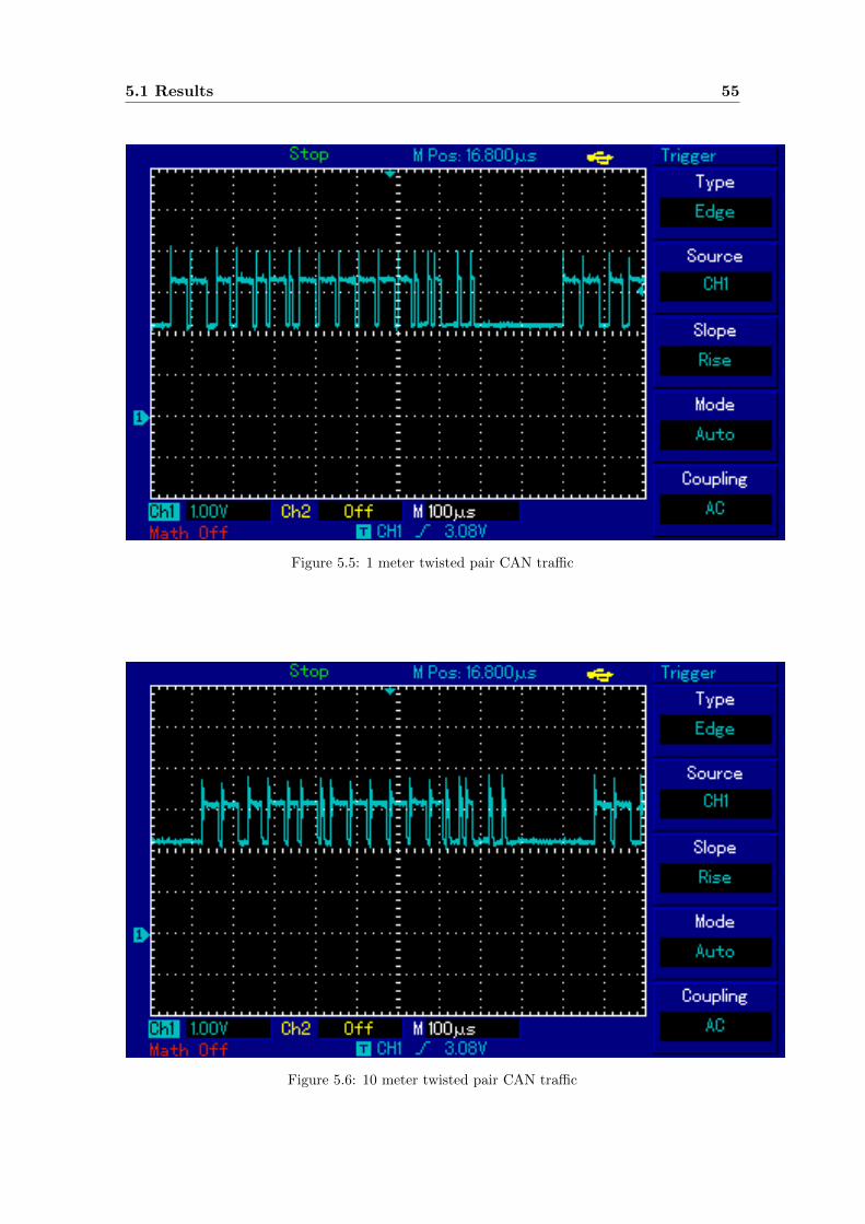
5.1 Results 55
Figure 5.5: 1 meter twisted pair CAN traffic
Figure 5.6: 10 meter twisted pair CAN traffic

5.1 Results 56
Figure 5.7: 10 meter twisted pair CAN traffic on working bus
Figure 5.8: 10 meter twisted pair CAN response

5.2 Discussion 57
5.2 Discussion
Initial testing of the bridge was unsuccessful. The cause of the issue was pinpointed to
be either the bridge’s CAN interface, the USB-CAN converter or a combination of both.
These issues did not allow full completion of the testing as per the methodology. For the
testing that was performed, results are discussed below. Following that is a discussion of
the issues and limitations of the bridge, the methodology and the testing equipment.
5.2.1 Proof of Concept
The concept of the bridge has been demonstrated successfully. A full message was sent
and received through both bridge interfaces. This proves that according to the method-
ology outlined, the hardware and software designs of the bridge can perform the basic
functionality required.
5.2.2 Stress Tests
Initial testing showed malfunctions of the CAN interface, thus results for all stress testing
parameters were not obtained. The discussion of the cause of these errors is found in the
subsection labelled Issues and Limitations - CAN Interface.
The results that were attained showed that at CAN baud rate 125kbps and Modbus baud
9.6kbps, the bridge is able to complete, without loss, full CAN to Modbus and return
message translation in around 220ms. This effectively means that the bridge can be
polled by the BMS CAN node four times a second. This is far more than needed for a
practical BMS requirement. If it were possible to increase the baud rates for the interfaces,
it is likely we would see an increase in performance. This is unnecessary given the proven
performance is adequate. There is no known reason why gas detection equipment would
need to update its status at a faster rate.
There is a linear decrease in performance at faster messaging rates. The effect would be
significant if messaging times were required in that region. For the application of the
bridge that is not the case.
For all tests at all messaging rates, the number of CAN frames received back by the

5.2 Discussion 58
BMS CAN node simulator was exactly equal to the number of Modbus frames sent by
the bridge. This means that the frame loss must occur between the bridge’s CAN frame
reception and Modbus transmission. As it was not possible to alter the source code of
the bridge during testing, a counter could not be placed at these points in software. If
that were possible, it would identify where the loss had occurred and verify the assertion
above.
5.2.3 Proof RS-485 Concept
The testing results for the RS-485 tests showed the expected signal on the bus that
conforms to the RS-485 standard. This indicates that due to the consistency of design
between the test platform and the PCB, the PCB can be expected to perform similarly
and therefore conforms to the RS-485 standard.
5.2.4 Physical Cable Testing
The results of the physical cable testing showed that significant overshoot and ringing was
present on the bus during tests with different parameters. These results were consistent
across the working CAN bus and non-working CAN bus tests. This suggests that the
transmission errors experienced were not caused by the transmission lines.

5.2 Discussion 59
5.2.5 Discussion of issues and limitations - CAN Interface
The original design methodology for the CAN interface was to utilise the existing CANSpi
library. It was intended that SPI interrupt would be used to signal that SPI data had been
received. This would flag to the bridge that a CAN message was received. This approach
was not suitable. The CANSpi library initialisation function sets the parameters of the
SPI module. Under these conditions, SPI interrupts enabled within the main program do
not function. As a result, the interrupt method for CAN reception was abandoned. Each
pass through the main functions’ infinite loop tests whether a CAN message has been
received. This is the alternative solution.
Another issue encountered with using CANSpi library functions within interrupt routines
is their re-entrancy. When there is a possibility of a function being called from the
main program loop and an interrupt routine, the MikroC compiler throws a re-entrancy
error. This is to stop the interrupt call of the function overwriting the stack or data from
the original function call. This also occurred during testing of Modbus functions within
interrupts. The issue is resolvable by setting flags in interrupt services routines that are
checked in the main loop. This is the approach taken for the Modbus (UART) interrupts.
Two 5V CANSpi modules were used in early attempts to successfully initiate CAN com-
munications. Use of these devices was not successful. The CANSpi click board was
configured on the development board. One of the 5V CANSpi modules was configured
on another identical development board. Previous research in chapter 2 had shown that
5V and 3.3V CAN transceivers can exist on the same bus. When CAN messages were
not detected on either end, diagnostic checks were performed using an oscilloscope. The
inspection found that SPI data was not transferring from the CAN-SPI as expected. The
CAN-SPI chip was replaced on these boards and the testing was performed again. One of
the two CANSpi 5V board still did not function. The other now produced a signal that
resembled a CAN frame. The two different CANSpi modules still did not communicate
with each other. At this point, the USB-CAN converter had become available and testing
went forward on that platform only.
Tests performed with the USB-CAN converter and the development board fitted with the
CANSpi click board were challenging. The most significant issue was the inability of the
bridge to receive CAN messages. CAN frames were successfully sent from the bridge to
the USB-CAN converter. To use the CANSpi library certain flags, masks and filters need

5.2 Discussion 60
to be set. The data-sheet of the MCP2515 3 and the help file for the CANSpi library in
MikroC were difficult to reconcile. There is no consistency in naming. It takes educated
guessing or trial and error to identify correct parameters for use. The masks and filters
were ruled out as the cause. The issue was eventually identified to be with CAN flags. The
library example provided with MikroC was used as a guide. In this example the CANSpi
initialises with the 11 bit message type. The reception flags were configured for 29 bit
reception only. This was difficult to identify due to the lack of consistency between the
library help and component data-sheet. The change required to complete the test were
alterations of the flag ” CANSPI XTD MSG” to ” CANSPI STD MSG” in two locations
of the source code. This was a simple issue to resolve but time intensive to identify.
The above issues were found during early testing to demonstrate that the CANSpi library
was viable. The major issue with the CAN interface was discovered when the proof
of concept test was attempted. Inconsistencies were observed with the CAN interface.
The USB-CAN intermittently reported a transmission error indicated via the ’err’ LED
flashing. The error did not occur with any pattern which made troubleshooting difficult.
Occasionally, the USB-CAN converter would successfully send one or more CAN frames
and then stop working, giving the error indication. Other times it would not send any
successful CAN messages. An attempt was made to use the SPI to report the contents of
the registers in the CAN-SPI IC in the hopes of diagnosing the error. The code listing can
be found in appendix F. The initial conclusion was that the issue is related to differing
configurations of the USB-CAN converter and the initialisation functions of the CANSPI
library. There is insufficient information in either user manual to reconcile these issues
easily or in a timely manner. It is not possible to rule out equipment failure given that
the USB-CAN devices is a two port device and one of the two ports stopped working
during testing.
To this point, the CAN interface had been very inconsistent and only functioned spo-
radically. The functionality was sufficient for proof of concept testing. Diagnostics were
abandoned due to time limitations at this stage of the project.
During final testing and data gathering the bridge began to work flawlessly on the main de-
velopment board. This was without making any change to source code that had previously
not worked with any consistency. Uploading the same source code onto the secondary
development board did not work. This meant any further configuration of the source code
3The CAN-SPI IC on the bridge is the same as the one found on the click board by design.

5.2 Discussion 61
past this point was not possible. The only difference between the two development boards
are the crystals connected to the processor. They should not effect the CAN interface
given it has its own, separate oscillation source. The conclusion here is that the source
code may have become corrupted. This would explain why the latest source code version
does not function. Once rectified, it would be possible to carry out stress tests at the
different baud rates. Full exploration of board capabilities would also be possible.
What was possible was tested using the working development board with the configuration
parameters set in the source code. This is the CAN baud at 125kbps and Modbus baud
at 9.6kbps as described in the stress testing above. The CAN message type is the 11 bit
identifier version(CAN 2.0A).
Development of user written functions to access the CAN interface via SPI may address
some or all of the above issues. It would give full control over the interface. This would
also likely improve the performance of the bridge. The obvious downside is that a lot of
work would be required to recreate the functionality offered by the CANSpi library and
this is out of the scope of this project.

5.2 Discussion 62
5.2.6 Discussion of issues and limitations - Modbusslave simulator
Equipment issues were experienced with the Modbusslave simulator. This program has a
serial traffic viewer to allow the user to monitor outgoing and incoming serial messages in
ASCII format. When doing initial testing with the development board some irregularities
were observed. A screen capture of an example can be seen in figure 5.10. The data that
was sent is as per figure 5.9.
Figure 5.9: Code exert of serial data sent
Figure 5.10: Serial synchronisation errors with 16MHz crystal
The data being sent from the bridge was not consistent with what was received by the
Modbusslave traffic viewer. Reproducing the transmission and viewing the results on the
MikroC terminal produced the expected outcome. The issue was identified as a timing
error. The crystal on the development board was 16MHz. This led to small errors in

5.3 Chapter Summary 63
baud generation for the UART. This synchronisation error caused the Modbusslave to
receive characters not sent and to not receive characters actually sent. Replacement of
the 16MHz crystal with a 14.7456MHz crystal4 removed the error. Serial traffic then
appeared as expected. Interestingly, during compilation of results for this dissertation,
the second development board with a 16MHz crystal could not reproduce this error.
Whilst the change of crystal appeared to rectify the problem during the first encounter,
it is not possible to rule out other factors as the cause. Using a perfect divisor crystal is
still advisable when possible.
The resolution of the timing error led to further testing of the Modbusslave simulator. The
simulator was configured as per an example on the developers website. The development
board was then configured to send a test message that would extract some information
off the simulator in a known fashion. The results of this test were not as expected. The
simulator did receive and respond to the sent frame, but the response was not what was
expected. It was also not a known error response. Further testing showed that regardless
of the frame sent to the simulator, the same response is received (data component is 00 00
08 00 00 01). This can be seen in the results of the proof of concept. The version of the
simulator used was a free trial. As such the software does not offer full functionality. For
the purposes of testing the bridge it was adequate. It did prevent the testing of Modbus
frames with data sizes over 6 bytes. Responses are always the same as described above,
and as a result never contain enough (16bytes or more) data to test the decomposition
and reconstitution of large data frames.
5.3 Chapter Summary
This chapter has covered the results from testing the bridge, including proof of concept,
stress testing, RS-485 testing and the testing of physical cables. It also included a discus-
sion of the significance of these results and detailed discussion of the issues and challenges
encountered during the bridge design and testing.
4The same device found on the final bridge hardware. This discovery drove that selection.

Chapter 6
Conclusion and Future Work

6.1 Conclusions 65
6.1 Conclusions
The network bridge to translate between CAN and Modbus frames is of commercial
interest to GDA. Research showed the concept was feasible. A PIC microprocessor based
embedded system was designed to facilitate the protocol translation. The hardware (PCB)
and software (C code) were outlined in detail.
Relevant testing demonstrated both the proof of concept and initial performance. The
testing was limited but demonstrated the bridge will be able to respond fast enough for
the given application. The bridge is able to respond to four CAN messages per second at
CAN baud 125kbps and Modbus baud 9.6kbps. This is sufficient for the BMS application
and meets the main project objective.
Many issues were encountered with the implementation of the CAN interface and they
prevented further exploration of the bridge performance and capabilities. The cause of
these issues were identified to be the source code for the CAN interface. This was a result
of a lack of configuration control available to the user when utilising the inbuilt library
functions of the MikroC development environment.
A limitation of the Modbus simulator was experienced. It did not respond with accurate
or expected frames to legitimate requests. This issue did not affect the critical testing,
but did prevent the testing of decomposition and reconstitution of Modbus frames with
data sizes greater than sixteen bytes. The design of this process was still presented but
not implemented.
As the bridge did not reach a complete finished state, documentation was not completed
in full. Appendix I contains an outline of the intended content of these documents.
The main objectives of the project were met. The design was completed and proof
of concept demonstrated. Full testing and exploration of the bridge performance and
capabilities were not possible. The next section details relevant further work to rectify
the issues and develop this topic further.

6.2 Recommendations and Future Work 66
6.2 Recommendations and Future Work
The inconsistencies with the CAN interface are of most interest. It would be useful to
do further testing with the SPI to communicate directly with the CAN-SPI chip to trou-
bleshoot the CAN interface. If time was available, a full re-write of the CANSpi libraries
from scratch would give more control to the developer and allow better diagnostics. Once
complete, a full suite of stress testing could determine the full capabilities of the bridge.
To improve and expand the Modbus interface functionality a few simple changes could be
made. Full support of all parity types could be implemented. This is a simple fix requiring
the configuration of one bit per byte of the serial transmission. The decomposition and
reconstitution of data sizes greater than 16 bytes could be implemented. This would
require access to a more sophisticated Modbus slave simulator.
Modbus RTU functionality could be added to make the bridge more flexible. As seen
with existing commercial products, they are generally static in their implementation.
The implementation is relatively simple. The ASCII and Hex conversions are no longer
required, and the frames do not use delimiters. This makes the frame composition simpler
than Modbus ASCII. The added complexity comes in the sending of the frames. Interrupt
driven timers are required to adhere to the timing laws of the Modbus RTU transmission
scheme.
Finally, investigations into Modbus TCP could be carried out. This would require the
addition of an Ethernet hardware interface to the bridge, adding greater flexibility to the
device.
There are non-communications based work that would improve the bridge. The GLCD
and touch panel could be configured to allow status displays and customisation of the
bridge parameters such as baud rates. The software configuration for power failure and
LED operation (including errors) could be implemented.
If performance improvements were required, one way to achieve this might be to further
logically separate the CAN and Modbus interfaces. This would involve make the bridge a
complete standalone Modbus master that interacts with the Modbus slaves as per normal
Modbus operation. The bridge could maintain the key Modbus data in memory and
simply release it when a CAN request came through.
References
ADF web (2015), ‘Gateway/bridge: Can rom/to Modbus’, http://www.adfweb.com/
home/products/Can_modbus.asp?frompg=nav1_7. [Online; accessed April-2015].
ANSI (2014), Tia/eia Standard: Commercial Building Telecommunications Cabling Stan-
dard, Standard TIA/EIA-485, American National Standards Institute.
Blackman, J. & Monroe, S. (2013), Overview of 3.3v Can (controller area network)
Transceivers, Applications report, Texas Instruments.
Butzin, B., Golatowski, F., Niedermeier, C., Vicari, N. & Wuchner, E. (2014), A model
based development approach for building automation systems’, in ‘Emerging Tech-
nology and Factory Automation’, Institute of Electical and Electronic Engineers,
Barcelona.
CAN in Automation (2015a), ‘Can: Physical layer’, http://www.can-cia.org/index.
php?id=systemdesign-can. [Online; accessed April-2015].
CAN in Automation (2015b), ‘Controller area network’, http://www.can-cia.org/
index.php?id=systemdesign-can. [Online; accessed April-2015].
Cena, G., Bertolotti, I., Hu, T. & Valenzano, A. (2014), Design, verification, and per-
formance of a modbus-can adaptation layer, in ‘10th IEEE Workshop on Factory
Communication Systems’, Toulouse.
Corrigan, S. (2008a), Controller area network physical layer requirements, Applications
report, Texas Instruments, Texas.
Corrigan, S. (2008b), Introduction to the controller area network (can), Applications
report, Texas Instruments, Texas.

REFERENCES 68
de Sousa, M. & Portugal, P. (2011), Modbus, in B. Wilamowski & D. Irwin, eds, ‘The
Industrial Electronics Handbook: Industrial Communications Systems’, CRC Press,
chapter Modbus.
Fairchild Semiconductor Corporation (2006), ‘Single-channel: 6n137, hcpl-2601, hcpl-2611
dual-channel: Hcpl-2630, hcpl-2631 high speed-10 mbit/s logic gate optocouplers’,
Datasheet.
Fairchild Semiconductor Corporation (2015), ‘Df005s - df10s: Bridge rectifiers’,
Datasheet.
Ferreira, J. & Fonseca, J. (2011), Controller area network, in B. Wilamowski & D. Irwin,
eds, ‘The Industrial Electronics Handbook: Industrial Communications Systems’,
CRC Press, chapter Controller Area Network.
Gas Detection Australia (2015), ‘Usq fourth year project bachelor of beng electrical/elec-
tronic engineering’, Project Specification. Toowoomba.
Guohuan, L., Hao, Z. & Wei, Z. (2009), Research on designing method of can bus and mod-
bus protocol conversion interface, in ‘International Conference on Future BioMedical
Information Engineering’, Institute of Electrical and Electronic Engineers, Sanya.
HMS (2015), ‘Anybus communicator: Can’, http://www.anybus.com/products/
abccan.shtml. [Online; accessed April-2015].
Hui, L., Hao, Z. & Daogang, P. (2013), Research and application of communication
gateway of epa and modbus/tcp, in ‘5th International Conference on Computational
Intelligence and Communication Networks’, Mathura.
ICP DAS USA (2015), ‘I-7530a-mr: Modbus rtu to can converter’, http://www.
icpdas-usa.com/i_7530a_mr.html. [Online; accessed Apirl-2015].
IEEE (2015), Ethernet, Standard IEEE802.3, Institute of Electrical and Electronic Engi-
neers.
Institute of Engineers (1997), Towards sustainable engineering practice: engineering
frameworks for sustainability, Technical report, Institute of Engineers, Canberra.
ISO (2003a), Road vehicles - controller area network (can) - part 1: Data link layer
and physical signalling, Standard ISO 11989-1, International Organization for Stan-
darization.

REFERENCES 69
ISO (2003b), Road vehicles - controller area network (can) - part 2: High-speed medium
access unit, Standard ISO 11989-2, International Organization for Standarization.
Maxim Integrated (2006), ‘How far and how fast can you go with rs-485?’, https://www.
maximintegrated.com/en/app-notes/index.mvp/id/3884. Application Note.
Microchip (2010), ‘Mcp2551: High-speed can transceiver’, Datasheet.
Microchip (2011), ‘Pic18f87k22 family: 64/80-pin, high-performance, 1-mbit enhanced
flash mcus with 12-bit a/d and nanowatt xlp technology’, Datasheet.
Microchip (2012), ‘Mcp2515: Stand-alone can controller with spi interface’, Datasheet.
MikroeElektronika (2012a), CANSpi Click Manual v100, MikroeElektronika.
MikroeElektronika (2012b), RS485 Click Manual v100, MikroeElektronika.
Modbus Org (2006a), Modbus messaging on tcp/ip implemenation guide, Technical re-
port, Modbus Organisation, Inc.
Modbus Org (2006b), Modbus over serial line: Specification & implementation guide,
Technical report, Modbus Organisation, Inc.
Modbus Org (2006c), Modbus protocol specification, Technical report, Modbus Organi-
sation, Inc.
Modicon, Inc. (1996), Modbus protocol reference guide, Technical report, MODICON,
Inc., North Andover, Massachusetts. Rev. J.
RECOM (2012), ‘Roe0505s: Econoline dc/dc-converter’, Datasheet.
Rinaldi, J. (2010), ‘Modbus tcp vs. modbus rtu’, http://www.rtaautomation.com/
modbus-tcp-vs-modbus-rtu. [Online; accessed April-2015].
So, A. (2001), Building control and automation systems, in T. Samad, ed., ‘Perspectives
in Control Engineering Technologies, Applications and New Directions’, Wiley-IEEE
Press, chapter Building Control and Automation Systems.
Texas Instruments (1998), ‘Lm2671 simple switcher power converter high efficiency 500ma
step-down voltage regulator with features’, Datasheet.
Thomas, G. (2008), ‘Introduction to modbus serial and modbus tcp’, the EXTENSION:
A Technical Supplement to Control Network 9(5), 1–4.

REFERENCES 70
University of Southern Queensland (2012), ‘Electronic circuits: Study book’. Toowoomba.
Wang, L., Zhang, T., Li, K. & Ren, B. (2013), Study of can-modbus communications
adapter for low-voltage distribution system, in ‘International Conference on Mecha-
tronic Sciences, Electric Engineering and Computer’, IEEE, Shenyang.

Appendix A
Project Specification

72
ENG 4111/2 (or ENG8002) Research Project
Project Specification
For: Matthew Quinton
Topic: CAN bus to MODBUS network bridge to interface gas
detection units with Building Management Systems
Supervisors: Mark Pythian
James Boucher
Sponsorship: Faculty of Health, Engineering & Sciences
Gas Detection Australia Pty Ltd
Project Aim: The aim is to investigate, design and build a network bridge
to interface CAN bus enabled Building Management Sys-
tems (BMS) with MODBUS enabled gas sensors and control
units.
Program:
1. Review the literature to investigate the relevant CAN bus and MODBUS standards
and their implementations, how BMS function and any existing solutions for the
network bridge.
2. Based upon the literature and sponsor requirements create network bridge specifi-
cations including consideration for hardware connections, standards, device intelli-
gence and data integrity.
3. Develop a network bridge including hardware and software components for the spec-
ified hardware connection type.
4. Develop a testing procedure for the network bridge and verify correct functionality.
5. Produce all documentation including technical manual, operators manual, manu-
facturing procedure, programming guide and software manuals as necessary.
As time and resources permit:
1. Design and build/acquire/emulate a BMS system and test the network bridge in a
quasi-situation or on-site with a customers BMS and evaluate performance.

73
2. Investigate and implement other MODBUS hardware configurations as a separate
specification or additional board option
3. Investigate and implement other hardware connections options as a separate speci-
fication or additional board option
Agreed:
Student Name: Matthew Quinton
Date: 13th April 2015
Supervisor Name: Mark Phythian
Date: 13th April 2015

Appendix B
Controller Area Network

B.1 List of frame field descriptions 75
This appendix contains further technical information about the CAN protocol.
B.1 List of frame field descriptions
The following describe the fields of CAN frames as per ISO (2003a).
SOF Start of frame used to synchronise nodes after idle state (dominant bit).
Identifier Establishes message priority as per arbitration (11 or 29 bits).
RTR Remote transmission request dominant bit when information is required from
another node. The identifier determines the specific node requested.
IDE Identifier extension this means that a standard CAN identifier is being transmitted
with no extension (dominant single bit).
R0 Reserved bit unused at this stage.
DLC Data length code number of bytes being transmitted (4 bit).
Data Up to 64bits may be transmitted.
CRC Cyclic redundancy check 15 bits plus 1 bit delimiter contains checksum for error
detection.
ACK Receiving nodes overwrite this bit with dominant to indicate error free message
received. If the receiving node leaves as recessive the message is discarded and the sender
repeats transmission.
EOF End of frame 7 bit field indicates end of frame. Also disables bit stuffing. Dominant
means a stuffing error.
IFS Interframe space 7bit field contains time required to move a correctly received frame
to its position in a message buffer by the controller /citecorr2.
The extended frame includes the extra 18 bit identifier as well as three other fields.
SRR Substitute remote request bit replaces RTR and is a placeholder.

B.2 Physical Connection 76
IDE Identifier extension bit indicates that more identifier bits follow.
R1 Additional reserve bit .
B.2 Physical Connection
The physical medium is two wires and a separate ground connection. Unshielded 120
ohm twisted pair cabling is common. Using higher quality cable is recommended in
harsher environments. To minimise the effect of reflections on the cables terminating
resistors are required on both ends of the bus. Connectors used should also have the
same characteristic impedance as the line and terminating resistors /citecorr1. There
are several other considerations that need to be taken into account when designing CAN
bus networks but are largely beyond the scope of this project. The aim is to add a
node into an existing network and not to create or alter an existing or new network.
The characteristics of the connections are of importance and should be considered when
selecting components.
B.2.1 Topology
CAN is bus based. Replicated buses are not explicit in the standard but are possible
and research has been conducted around star. Star networks require a coupler or some
other central device to facilitate broadcasts to nodes. Faults have to be treated differently
when in star mode and this is the basis for significant research beyond the scope of this
project (Ferreira & Fonseca 2011).
B.2.2 Transmission and Signals
CAN is a differential signalling protocol. A high and a low signal is sent out on comple-
mentary connections. The message is dominant when the high is held high and the low
is held low (ISO 2003a). Typically, the bus is passively biased to 2.5V. The high voltage
is approximately 1V higher (3.5V) and the low voltage is approximately 1V lower (1.5V).
This gives a typical voltage differential of 2V (Corrigan 2008a). 3.3V or 5V transceivers are
common and can be interoperable with each other (Blackman & Monroe 2013). Figure B.1

B.2 Physical Connection 77
demonstrates the dominant and recessive voltages levels for the CAN bus. Dominant bits
are used in the arbitration process for multiple access.
Figure B.1: CAN bit levels (adapted from (ISO 2003a)).

B.2 Physical Connection 78
B.2.3 Encoding
CAN uses Non Return to Zero (NRZ) and as such only one timeslot is required per
bit (CAN in Automation 2015a). Figure B.2. shows the NRZ encoding scheme as well
as the Manchester encoding for point of difference. Manchester encoding uses the state
change to signify a bit where NRZ uses a level. The key difference is that NRZ simply
drives the bit value on the bus whilst Manchester schemes force a transition.
Figure B.2: NRZ and Manchester Encoding (adapted from (CAN in Automation 2015a)).

B.2 Physical Connection 79
B.2.4 Synchronisation and Bit Stuffing
The NRZ encoding scheme has no inherent synchronisation so this is achieved using a
start bit within the packets. Figure B.3 demonstrates the synchronisation issues with
NRZ. If a large number of consecutive bits of the same value are transmitted it can be
difficult to resynchronise due to the lack of a rising or falling edge. To overcome this
issue CAN uses bit stuffing to break sequences of 6 or more consecutive bits of the same
polarity. A bit of opposite polarity to the sequence is inserted after 5 consecutive bits.
Bit stuffing introduces extra overhead to transmission. The effect can be estimated if the
timing is an issuet (CAN in Automation 2015a).
Figure B.3: CAN bit stuffing (adapted from (CAN in Automation 2015a)).

B.2 Physical Connection 80
B.2.5 Errors
CAN has five error checking methods; three at message level and two at the bit level.
When any of these errors is detected, an error frame is generated by the receiving node.
The transmitting node will attempt to resend the frame until received correctly. The
three message level checks are the CRC, the ACK and the form check. The CRC is a
standard 15-bit checksum with a 1-bit delimiter. The ACK is comprised of two bits; the
ACK bit and a delimiter. The form check is carried out by checking the SOF, EOF, ACK
and CRC delimiters. During arbitration, conflicting bit values may be written to the bus
and this is also true of the acknowledge slot. If this is detected for any other bit an error
is generated. The second bit level error check is bit stuffing. If six consecutive bits of the
same polarity are received then an error is generated.

B.3 Masks and Filters 81
B.3 Masks and Filters
The following contains some information about how the filters and masks work in CAN
addressing (ISO 2003a).
Filters are a bitwise enabler of CAN IDs. In order for a message to make it through a
filter, 1s must be in place of the corresponding ID bits. For example:
ID = 3 - convert to binary - 00000000011 (for an 11 bit address)
Filter - convert to binary - 00000000000 - would not allow this ID through since the 0s in
the bit spacers of the ID filter
Filter - convert to binary - 00000000011 - would allow this ID through since the 1s enable
the spaces in the filter
The masks take precedence over the filters. In other words, the mask enables the filter.
For our previous example:
ID = 3 - convert to binary - 00000000011
Filter - convert to binary - 00000000000 - we saw before this would not allow ID 3 through,
unless we configure a mask to override it
Mask - convert to binary - 00000000000 - here we are saying we don’t care what the filter
says, let everything in. The mask 0s disable the corresponding bits in the filter.
Likewise, a mask of 11111111111 will not let any message through.
This setup gives you quite a lot of flexibility in how you handle messages, and through
which filters and buffers they pass.
Most of the abilities of these filters are not used within the scope of the bridge. They
are important on more complicated CAN networks and would need to be considered for
future commerical use of the bridge.

Appendix C
Modbus

C.1 Protocol Data Unit 83
C.1 Protocol Data Unit
The Protocol Data Units (PDU) is comprised of the function code and the data field of
a Modbus frame. There is a large list of functions available for Modbus. The most com-
monly used are those associated with accessing memory addresses (de Sousa & Portugal
2011). At this stage, a complete discussion of the available function codes is not required.
C.2 Error Checking
Modbus has two built in error checking facilities; parity checking and frame checking.
Parity checking is implemented by configuring network devices as either Even, Odd or No
parity. If Even or Odd is chosen then one bit is adjusted so that the data frame has the
same parity as the network configuration. This will detect bit errors where the number of
errors is odd only. Frame checking is achieved using a Cyclic Redundancy Check (CRC)
for Modbus RTU or Longitudinal Redundancy Check (LRC) for Modbus ASCII.
C.3 Physical Media
Some of the features of the protocol are not solely governed by the specification alone.
This is due to the fact that Modbus does not define a physical layer. The physical media
that carry it define some parameters. For this project the serial interface used is UART
and RS-485.
RS-485 is a two wire balanced system with a third common wire. Four wire Modbus is
possible to give full duplex capabilities to a network. This project is a two wire based
network. A requirement of Modbus serial is to have shielded cables where one end of each
cable is connected to protective ground (Modbus Org 2006b).
RS-485 allows multi-drop connections using a bus (trunk) with direct connections (daisy
chain) or derivations (drop) cables. Derivation cables must be no more than 20 meters
long (Modbus Organisation, Inc. 2006). 1200 meters is the maximum length for the trunk
cable (Maxim Integrated 2006).

C.4 RS 485 Data Rates 84
C.4 RS 485 Data Rates
The specification defines the two standard baud rates of 9600kbps and 19200kpbs of
which the latter is the default (Modbus Organisation, Inc. 2006). The maximum baud
listed in the specification is 115kpbs. It may be possible to operate Modbus on serial
lines at speeds of 10Mbps (Maxim Integrated 2006), although is a trade-off between run
length and speed and as such this speed will not be achievable at near maximum lengths.
Using techniques such as pre-emphasis and receiver equalisation it may be possible to
achieve data rates of 800kbps over 1200 meters and 50Mbps over lengths of hundreds of
meters (Maxim Integrated 2006).
C.5 Encoding and Synchronisation
RS-485 is an asynchronous differential system that utilises a start bit/s and stop bit/s
either side of the data. Timing between sender and receiver must be agreed upon ahead
of time and synchronisation is carried out relative to the leading edge of the start bit (?).

Appendix D
Network Bridge Source Code - C

D.1 C Header 86
D.1 C Header
This listing contains the header file where function prototypes are defined.
Listing D.1: Project Header.
/∗−−−−−−−−−−−−−−−−−−−−−−−−−−−−−−−−−−−−−−−−−−−−−−−−−−−−−−−−−−−−−−−−−−−−−−−−−−−−−−−−−−−−−−−−−−−−−−−−−−−−−−−−−−−−−−−−−−−−−−−−−−−−−−−−−−−−−−−−−−−−−−−−−−−−−−−−−−−−−−−−−−−−−−−−−−−−−−−−−−−−−−−−−−−−−−−−−−−−−−−−−−−−−Gas Detec t ion Aus t ra l i aCANbus to Modbus Network BridgeBENH Fina l Year Pro jec t
Matthew Quinton0061024766
Pro jec t headerPIC : 18F87K22V1.0D/−−−−−−−−−−−−−−−−−−−−−−−−−−−−−−−−−−−−−−−−−−−−−−−−−−−−−−−−−−−−−−−−−−∗///−−−−−−−−−−−−−−−−−−−−−−−−−−−−−−−−−−−−−−−−−−−−−−−−−−−−−−−−−−−−−−−−−−−//−−−−−−−−−−−−−−−−−−−−END OF HEADING−−−−−−−−−−−−−−−−−−−−−−−−−−−−−−−−−
/∗−−−−−−−−−−−−−−−−−−−−−−−−−−−−−−−−−−−−−−−−−−−−−−−−−−−−−−−−−−−−−−−−−−−MODBUS FUNCTIONS/−−−−−−−−−−−−−−−−−−−−−−−−−−−−−−−−−−−−−−−−−−−−−−−−−−−−−−−−−−−−−−−−−−∗/
void modbus in it ( ) ;
void TX ser ia l (unsigned short numchar ) ;
void TX modbus(unsigned char∗ buf f , unsigned char l ength ) ;
void RX Seria l (unsigned char ∗ r e t ) ;
void RX modbus(unsigned char ∗ ret , unsigned short l ength ) ;
unsigned short LRC(unsigned char∗ bu f f e r , unsigned short numchar ) ;
/∗−−−−−−−−−−−−−−−−−−−−−−−−−−−−−−−−−−−−−−−−−−−−−−−−−−−−−−−−−−−−−−−−−−−GENERAL FUNCTIONS/−−−−−−−−−−−−−−−−−−−−−−−−−−−−−−−−−−−−−−−−−−−−−−−−−−−−−−−−−−−−−−−−−−∗/
unsigned short h e x a s c i i (unsigned short d i g i t ) ;
unsigned short a s c i i h e x (unsigned d i g i t ) ;
unsigned short s p l i t f i r s t (unsigned short hex d ig ) ;
unsigned short s p l i t s e c o n d (unsigned short hex d ig ) ;
unsigned short comb dig i t s (unsigned short dig1 , unsigned short dig2 ) ;

D.2 Modbus Functions 87
D.2 Modbus Functions
This listing contains the Modbus functions using the UART for serial communications.
Listing D.2: Modbus Functions.
/∗−−−−−−−−−−−−−−−−−−−−−−−−−−−−−−−−−−−−−−−−−−−−−−−−−−−−−−−−−−−−−−−−−−−−−−−−−−−−−−−−−−−−−−−−−−−−−−−−−−−−−−−−−−−−−−−−−−−−−−−−−−−−−−−−−−−−−−−−−−−−−−−−−−−−−−−−−−−−−−−−−−−−−−−−−−−−−−−−−−−−−−−−−−−−−−−−−−−−−−−−−−−−−Gas Detec t ion Aus t ra l i aCANbus to Modbus Network BridgeBENH Fina l Year Pro jec t
Matthew Quinton0061024766
Modbus ASCII Master FunctionsPIC : 18F87K22V1.0D/−−−−−−−−−−−−−−−−−−−−−−−−−−−−−−−−−−−−−−−−−−−−−−−−−−−−−−−−−−−−−−−−−−∗///−−−−−−−−−−−−−−−−−−−−−−−−−−−−−−−−−−−−−−−−−−−−−−−−−−−−−−−−−−−−−−−−−−−//−−−−−−−−−−−−−−−−−−−−END OF HEADING−−−−−−−−−−−−−−−−−−−−−−−−−−−−−−−−−
/∗−−−−−−−−−−−−−−−−−−−−−−−−−−−−−−−−−−−−−−−−−−−−−−−−−−−−−−−−−−−−−−−−−−−De f i n i t i o n s and v a r i a b l e s/−−−−−−−−−−−−−−−−−−−−−−−−−−−−−−−−−−−−−−−−−−−−−−−−−−−−−−−−−−−−−−−−−−∗/#include ” ProjectDevBoard . h”
unsigned short baud = 9600 ; // Baud ra t eunsigned short par i t y = 0 ; // Par i ty (0 − even , 1 − odd , 2 − none )unsigned short s t o p b i t s = 1 ; // Number o f s top b i t s (1 − even/odd par i t y , 2 − no pa r i t y )unsigned short s l a v e ; // S lave address f o r TX and RX
unsigned short MBReceived = 0 ; //Modbus frame Recived f l a gunsigned short Ser ia lCount = 0 ; //Number o f b i t r e c i v ed through s e r i a lunsigned short S e r i a l B u f f e r [ 3 0 ] ; // Buf fer used to s t o r e p a r t i a l modbus frameunsigned short ModbusRecFrame [ 3 0 ] ; // Send frame fo r Modbusunsigned short ModbusSendFrame [ 3 0 ] ; // Receive frame fo r Modbusunsigned short ModbusFrameLength ; // Length o f r e c e i v ed frame
const unsigned short co lon = 0x3A ; // Asc i i COLON charac t e rconst unsigned short c a r r e t = 0x0D ; // Asc i i c a r r i a g e re turn charac t e rconst unsigned short l i n f d = 0x0A ; // Asc i i l i n e f e ed charac t e runsigned short val msg ;//−−−−−−−−−−−−−−−−−−−−END OF SECTION−−−−−−−−−−−−−−−−−−−−−−−−−−−−−−−−−
/∗−−−−−−−−−−−−−−−−−−−−−−−−−−−−−−−−−−−−−−−−−−−−−−−−−−−−−−−−−−−−−−−−−−−

D.2 Modbus Functions 88
FUNCTION: UART I n i t i a l i s a t i o n
Set up o f s e r i a l comms ./−−−−−−−−−−−−−−−−−−−−−−−−−−−−−−−−−−−−−−−−−−−−−−−−−−−−−−−−−−−−−−−−−−∗/void modbus in it ( )
UART1 Init ( 9 6 0 0 ) ; // I n i t i a l i s e UART1TXSTA.TX9 = 0 ; // 8 b i t TXTXSTA.SYNC = 0 ; // AsynchronousTXSTA.SENDB = 1 ; // Send break charac t e rRCSTA.RX9 = 0 ; // 8 b i t RXUART Set Active(&UART1 Read , 0 , &UART1 Data Ready , &UART1 Tx Idle ) ;
//−−−−−−−−−−−−−−−−−−−−END OF FUNCTION−−−−−−−−−−−−−−−−−−−−−−−−−−−−−−−−
/∗−−−−−−−−−−−−−−−−−−−−−−−−−−−−−−−−−−−−−−−−−−−−−−−−−−−−−−−−−−−−−−−−−−−FUNCTION: Transmit s e r i a l
Argument : numchar − number o f charac t e r s to be t ransmi t t ed/−−−−−−−−−−−−−−−−−−−−−−−−−−−−−−−−−−−−−−−−−−−−−−−−−−−−−−−−−−−−−−−−−−∗/void TX ser ia l (unsigned short numchar )
unsigned short i ;for ( i = 0 ; i < numchar ; i++)
while (PIR1 . TX1IF == 0 ) ; // Check f o r TX bu f f e r spaceTXREG1 = ModbusSendFrame [ i ] ; // Place next charac t e r in TX bu f f e r
Delay us ( 5 ) ;
//−−−−−−−−−−−−−−−−−−−−END OF FUNCTION−−−−−−−−−−−−−−−−−−−−−−−−−−−−−−−−
/∗−−−−−−−−−−−−−−−−−−−−−−−−−−−−−−−−−−−−−−−−−−−−−−−−−−−−−−−−−−−−−−−−−−−FUNCTION: Modbus Transmit
Argument : unsigned char∗ b u f f − message to TXunsigned char l e n g t h − l e n g t h o f message to TX
/−−−−−−−−−−−−−−−−−−−−−−−−−−−−−−−−−−−−−−−−−−−−−−−−−−−−−−−−−−−−−−−−−−∗/void TX modbus(unsigned char∗ buf f , unsigned char l ength )
unsigned char i ;unsigned char new length = length + 5 ; // To a l l ow fo r Star t , LRC, end charsunsigned char hex LRC ; // To s t o r e Hex va lue o f LRC
ModbusSendFrame [ 0 ] = co lon ; // In s e r t s t a r t charac t e r :
for ( i = 1 ; i < l ength +1; i++)

D.2 Modbus Functions 89
ModbusSendFrame [ i ] = bu f f [ i −1] ;// Perform LRC and p lace in framehex LRC = LRC( buf f , l ength ) ;ModbusSendFrame [ new length −4] = s p l i t f i r s t (hex LRC ) ;ModbusSendFrame [ new length −3] = s p l i t s e c o n d (hex LRC ) ;// Add car r i a g e re turn and l i n e f e ed to frameModbusSendFrame [ new length −2] = c a r r e t ;ModbusSendFrame [ new length −1] = l i n f d ;// Transmit on s e r i a l l i n eTX ser ia l ( new length ) ;
//−−−−−−−−−−−−−−−−−−−−END OF FUNCTION−−−−−−−−−−−−−−−−−−−−−−−−−−−−−−−−
/∗−−−−−−−−−−−−−−−−−−−−−−−−−−−−−−−−−−−−−−−−−−−−−−−−−−−−−−−−−−−−−−−−−−−FUNCTION: S e r i a l Receive
Argument : unsigned char∗ r e t − b u f f e r to RX/−−−−−−−−−−−−−−−−−−−−−−−−−−−−−−−−−−−−−−−−−−−−−−−−−−−−−−−−−−−−−−−−−−∗/void RX Seria l (unsigned char ∗ r e t )unsigned short c , k ;stat ic unsigned short go = 0 ;
int p ;c = UART1 Read ( ) ;i f (RCSTA1 & 0x06 ) // Check f o r frame error or overrun errorRCSTA.CREN = 0 ;c = RCREG;RCSTA.CREN = 1 ; // i f overrun or frame r e s e t r e c e i v e r
elsei f ( go )S e r i a l B u f f e r [ Ser ia lCount ] = c ; // read b i tSer ia lCount++; // inc counteri f ( c == l i n f d ) // t e s t i f frame f u l lfor ( k = 0 ; k < Ser ia lCount ; k++) //Swap b u f f e r in t o modbus frame
r e t [ k+1] = S e r i a l B u f f e r [ k ] ; // copy by t er e t [ 0 ] = Ser ia lCount ;go = 0 ;MBReceived = 1 ; //Flag t ha t modbus frame re c i v edSer ia lCount = 0 ; // r e s e t the s e r i a l b i t counter
else

D.2 Modbus Functions 90
i f ( c == colon )S e r i a l B u f f e r [ Ser ia lCount ] = c ; // read b i tSer ia lCount++; // inc countergo = 1 ;
//−−−−−−−−−−−−−−−−−−−−END OF FUNCTION−−−−−−−−−−−−−−−−−−−−−−−−−−−−−−−−
/∗−−−−−−−−−−−−−−−−−−−−−−−−−−−−−−−−−−−−−−−−−−−−−−−−−−−−−−−−−−−−−−−−−−−FUNCTION: Modbus Receive
Argument : unsigned char∗ r e t − message to RXunsigned shor t l e n g t h − l e n g t h o f message to RX
/−−−−−−−−−−−−−−−−−−−−−−−−−−−−−−−−−−−−−−−−−−−−−−−−−−−−−−−−−−−−−−−−−−∗/void RX modbus(unsigned char ∗ ret , unsigned short l ength )
unsigned short p ;unsigned short g ;unsigned short r x l r c ;unsigned char h o l d a r r [ 3 0 ] ;unsigned short new len = length − 5 ;
for (p = 0 ; p < new len + 1 ; p++) // Transfer to ho l d ing array
h o l d a r r [ p ] = a s c i i h e x ( r e t [ p +1 ] ) ;// Extrac t LRC from framer x l r c = comb dig i t s ( a s c i i h e x ( r e t [ l ength − 3 ] ) , a s c i i h e x ( r e t [ l ength − 2 ] ) ) ;for ( g = 0 ; g < new len ; g++)
r e t [ g ] = h o l d a r r [ g +1] ; // Transfer data on ly back to frame arrayi f (LRC( ret , new len ) != r x l r c ) // Check f o r LRC
r e t [ g ] == 0xFF ; // LRC error//−−−−−−−−−−−−−−−−−−−−END OF FUNCTION−−−−−−−−−−−−−−−−−−−−−−−−−−−−−−−−
/∗−−−−−−−−−−−−−−−−−−−−−−−−−−−−−−−−−−−−−−−−−−−−−−−−−−−−−−−−−−−−−−−−−−−FUNCTION: Long i tud ina l Redunancy Check
Argument : unsigned shor t numchar − number o f charac t e r s in frameunsigned char∗ b u f f e r − frame to be LRC
/−−−−−−−−−−−−−−−−−−−−−−−−−−−−−−−−−−−−−−−−−−−−−−−−−−−−−−−−−−−−−−−−−−∗/unsigned short LRC(unsigned char∗ bu f f e r , unsigned short numchar )

D.2 Modbus Functions 91
unsigned short sum = 0 ;unsigned short i = 0 ;
for ( i = 0 ; i < numchar ; i++)
sum = sum + b u f f e r [ i ] ; // Sum framereturn (˜ ( sum | 0 b1111111100000000 ) ) + 1 ; // Perform 2s compliment
//−−−−−−−−−−−−−−−−−−−−END OF FUNCTION−−−−−−−−−−−−−−−−−−−−−−−−−−−−−−−−

D.3 Ancillary Functions 92
D.3 Ancillary Functions
This listing contains the ancillary functions used in the network bridge.
Listing D.3: Ancillary Functions.
/∗−−−−−−−−−−−−−−−−−−−−−−−−−−−−−−−−−−−−−−−−−−−−−−−−−−−−−−−−−−−−−−−−−−−−−−−−−−−−−−−−−−−−−−−−−−−−−−−−−−−−−−−−−−−−−−−−−−−−−−−−−−−−−−−−−−−−−−−−−−−−−−−−−−−−−−−−−−−−−−−−−−−−−−−−−−−−−−−−−−−−−−−−−−−−−−−−−−−−−−−−−−−−−Gas Detec t ion Aus t ra l i aCANbus to Modbus Network BridgeBENH Fina l Year Pro jec t
Matthew Quinton0061024766
Non communication f unc t i on sPIC : 18F87K22V1.0D/−−−−−−−−−−−−−−−−−−−−−−−−−−−−−−−−−−−−−−−−−−−−−−−−−−−−−−−−−−−−−−−−−−∗///−−−−−−−−−−−−−−−−−−−−−−−−−−−−−−−−−−−−−−−−−−−−−−−−−−−−−−−−−−−−−−−−−−−//−−−−−−−−−−−−−−−−−−−−END OF HEADING−−−−−−−−−−−−−−−−−−−−−−−−−−−−−−−−−
#include ” ProjectDevBoard . h”
/∗−−−−−−−−−−−−−−−−−−−−−−−−−−−−−−−−−−−−−−−−−−−−−−−−−−−−−−−−−−−−−−−−−−−FUNCTION: Hex to Asc i i
Argument : hex char to conver tReturn : a s c i i va lue o f charac t e r (0 i f e r ror )
/−−−−−−−−−−−−−−−−−−−−−−−−−−−−−−−−−−−−−−−−−−−−−−−−−−−−−−−−−−−−−−−−−−∗/unsigned short h e x a s c i i (unsigned short d i g i t )
i f ( d i g i t >= 0 && d i g i t <=9)return d i g i t + 0x30 ;
else i f ( d i g i t > 9 && d i g i t < 16)return d i g i t + 0x37 ;
elsereturn 0 ;
//−−−−−−−−−−−−−−−−−−−−END OF FUNCTION−−−−−−−−−−−−−−−−−−−−−−−−−−−−−−−−
/∗−−−−−−−−−−−−−−−−−−−−−−−−−−−−−−−−−−−−−−−−−−−−−−−−−−−−−−−−−−−−−−−−−−−FUNCTION: Asc i i to hex
Argument : a s c i i char to conver tReturn : hex va lue o f charac t e r (0 i f e r ror )
/−−−−−−−−−−−−−−−−−−−−−−−−−−−−−−−−−−−−−−−−−−−−−−−−−−−−−−−−−−−−−−−−−−∗/
unsigned short a s c i i h e x (unsigned d i g i t )

D.3 Ancillary Functions 93
i f ( d i g i t >= 0x30 && d i g i t <=0x39 )
return d i g i t − 0x30 ;else i f ( d i g i t > 0x40 && d i g i t < 0x47 )
return d i g i t − 0x37 ;else
return 0 ;//−−−−−−−−−−−−−−−−−−−−END OF FUNCTION−−−−−−−−−−−−−−−−−−−−−−−−−−−−−−−−
/∗−−−−−−−−−−−−−−−−−−−−−−−−−−−−−−−−−−−−−−−−−−−−−−−−−−−−−−−−−−−−−−−−−−−FUNCTION: S p l i t d i g i t s f i r s t
Argument : hex number where f i r s t d i g i t i s to be e x t r a c t e dReturn : ex t raced f i r s t d i g i t
/−−−−−−−−−−−−−−−−−−−−−−−−−−−−−−−−−−−−−−−−−−−−−−−−−−−−−−−−−−−−−−−−−−∗/
unsigned short s p l i t f i r s t (unsigned short hex d ig )
return hex d ig >> 4 ;//−−−−−−−−−−−−−−−−−−−−END OF FUNCTION−−−−−−−−−−−−−−−−−−−−−−−−−−−−−−−−
/∗−−−−−−−−−−−−−−−−−−−−−−−−−−−−−−−−−−−−−−−−−−−−−−−−−−−−−−−−−−−−−−−−−−−FUNCTION: S p l i t d i g i t s second
Argument : hex number where second d i g i t i s to be e x t r a c t e dReturn : ex t raced second d i g i t
/−−−−−−−−−−−−−−−−−−−−−−−−−−−−−−−−−−−−−−−−−−−−−−−−−−−−−−−−−−−−−−−−−−∗/unsigned short s p l i t s e c o n d (unsigned short hex d ig )
return hex d ig & 0b00001111 ;//−−−−−−−−−−−−−−−−−−−−END OF FUNCTION−−−−−−−−−−−−−−−−−−−−−−−−−−−−−−−−
/∗−−−−−−−−−−−−−−−−−−−−−−−−−−−−−−−−−−−−−−−−−−−−−−−−−−−−−−−−−−−−−−−−−−−FUNCTION: Combine d i g i t s
Argument : two d i g i t s to be combinedReturn : va lue o f d i g i t s combined
/−−−−−−−−−−−−−−−−−−−−−−−−−−−−−−−−−−−−−−−−−−−−−−−−−−−−−−−−−−−−−−−−−−∗/
unsigned short comb dig i t s (unsigned short dig1 , unsigned short dig2 )unsigned int a = 0 ;a = dig1 << 4 ;a = a | dig2 ;return a ;
//−−−−−−−−−−−−−−−−−−−−END OF FUNCTION−−−−−−−−−−−−−−−−−−−−−−−−−−−−−−−−
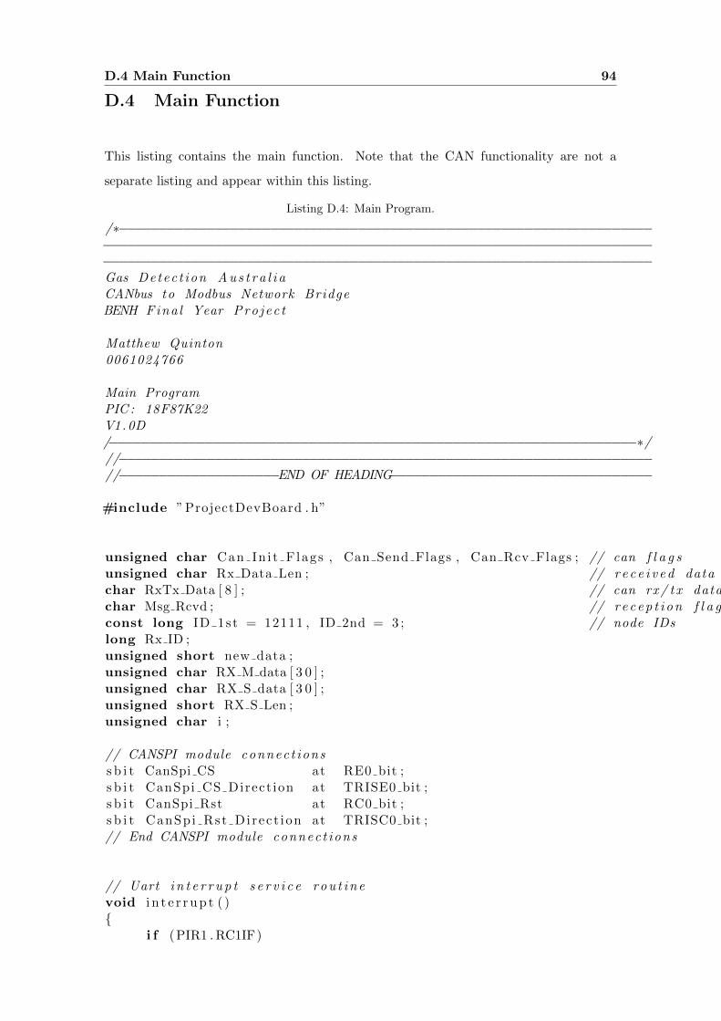
D.4 Main Function 94
D.4 Main Function
This listing contains the main function. Note that the CAN functionality are not a
separate listing and appear within this listing.
Listing D.4: Main Program.
/∗−−−−−−−−−−−−−−−−−−−−−−−−−−−−−−−−−−−−−−−−−−−−−−−−−−−−−−−−−−−−−−−−−−−−−−−−−−−−−−−−−−−−−−−−−−−−−−−−−−−−−−−−−−−−−−−−−−−−−−−−−−−−−−−−−−−−−−−−−−−−−−−−−−−−−−−−−−−−−−−−−−−−−−−−−−−−−−−−−−−−−−−−−−−−−−−−−−−−−−−−−−−−−Gas Detec t ion Aus t ra l i aCANbus to Modbus Network BridgeBENH Fina l Year Pro jec t
Matthew Quinton0061024766
Main ProgramPIC : 18F87K22V1.0D/−−−−−−−−−−−−−−−−−−−−−−−−−−−−−−−−−−−−−−−−−−−−−−−−−−−−−−−−−−−−−−−−−−∗///−−−−−−−−−−−−−−−−−−−−−−−−−−−−−−−−−−−−−−−−−−−−−−−−−−−−−−−−−−−−−−−−−−−//−−−−−−−−−−−−−−−−−−−−END OF HEADING−−−−−−−−−−−−−−−−−−−−−−−−−−−−−−−−−
#include ” ProjectDevBoard . h”
unsigned char Can In i t F lags , Can Send Flags , Can Rcv Flags ; // can f l a g sunsigned char Rx Data Len ; // r e c e i v ed data l en g t h in by t e schar RxTx Data [ 8 ] ; // can rx / t x data b u f f e rchar Msg Rcvd ; // recep t i on f l a gconst long ID 1st = 12111 , ID 2nd = 3 ; // node IDslong Rx ID ;unsigned short new data ;unsigned char RX M data [ 3 0 ] ;unsigned char RX S data [ 3 0 ] ;unsigned short RX S Len ;unsigned char i ;
// CANSPI module connec t ionss b i t CanSpi CS at RE0 bit ;s b i t CanSpi CS Direct ion at TRISE0 bit ;s b i t CanSpi Rst at RC0 bit ;s b i t CanSpi Rst Direct ion at TRISC0 bit ;// End CANSPI module connec t ions
// Uart i n t e r r u p t s e r v i c e rou t inevoid i n t e r r u p t ( )
i f (PIR1 . RC1IF)
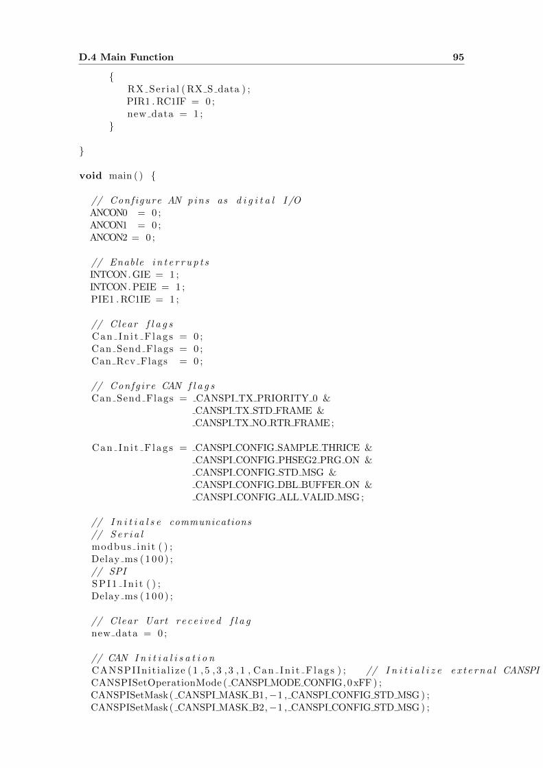
D.4 Main Function 95
RX Seria l ( RX S data ) ;PIR1 . RC1IF = 0 ;new data = 1 ;
void main ( )
// Conf igure AN pins as d i g i t a l I /OANCON0 = 0 ;ANCON1 = 0 ;ANCON2 = 0 ;
// Enable i n t e r r u p t sINTCON. GIE = 1 ;INTCON. PEIE = 1 ;PIE1 . RC1IE = 1 ;
// Clear f l a g sCan In i t F lag s = 0 ;Can Send Flags = 0 ;Can Rcv Flags = 0 ;
// Confg ire CAN f l a g sCan Send Flags = CANSPI TX PRIORITY 0 &
CANSPI TX STD FRAME &CANSPI TX NO RTR FRAME;
Can In i t F lag s = CANSPI CONFIG SAMPLE THRICE &CANSPI CONFIG PHSEG2 PRG ON &CANSPI CONFIG STD MSG &CANSPI CONFIG DBL BUFFER ON &CANSPI CONFIG ALL VALID MSG ;
// I n i t i a l s e communications// S e r i a lmodbus in it ( ) ;Delay ms ( 1 0 0 ) ;// SPISPI1 In i t ( ) ;Delay ms ( 1 0 0 ) ;
// Clear Uart r e c e i v ed f l a gnew data = 0 ;
// CAN I n i t i a l i s a t i o nCANSPIIni t ia l i ze ( 1 , 5 , 3 , 3 , 1 , Can In i t F lag s ) ; // I n i t i a l i z e e x t e r na l CANSPI module @ 125kHzCANSPISetOperationMode ( CANSPI MODE CONFIG, 0xFF ) ;CANSPISetMask( CANSPI MASK B1,−1 , CANSPI CONFIG STD MSG ) ;CANSPISetMask( CANSPI MASK B2,−1 , CANSPI CONFIG STD MSG ) ;

D.4 Main Function 96
CANSPISetFilter ( CANSPI FILTER B2 F4 , ID 2nd , CANSPI CONFIG STD MSG ) ;// s e t NORMAL mode a f t e r i n i t i a l i s a t i o nCANSPISetOperationMode ( CANSPI MODE NORMAL, 0xFF ) ;
// I n f i n i t e loop to proces s messages to RX and TXwhile (1 )// Check f o r CAN rece i v edMsg Rcvd = CANSPIRead( Rx ID , RxTx Data , Rx Data Len , Can Rcv Flags ) ;i f ( Msg Rcvd == 0xFF)
// I f CAN rece i v ed send on modbusTX modbus( RxTx Data , 6 ) ;Msg Rcvd = 0 ;
i f ( new data )
// Process here i f UART in t e r r u p tRX S Len = RX S data [ 0 ] ;RX modbus( RX S data , RX S Len ) ;// Write Modbus data to CANCANSPIWrite ( ID 1st , RX S data , RX S Len−5, Can Send Flags ) ;new data = 0 ;

Appendix E
Hardware Design Images

E.1 Schematic 98
E.1 Schematic
11
22
33
44
55
66
77
88
DD
CC
BB
AA
Scal
eSh
eet
Size
FCSM
No.
DWG
No.
Rev
A3
GD
CA
NM
OD
V1.
6
1 of 1
1.6
GDCM
-002
Draw
n By
:
Mat
thew
Qui
nton
Title
:
23/10
/15Da
te
C2 100n
F
TX-C
AN1
RX-C
AN2
CLKO
UT3
TX0R
TS4
TX1R
TS5
TX2R
TS6
MCP2515
OSC2
7
OSC1
8
GND
9RX
1BF
10
RX0B
F11
INT
12
SCK
13
SI14
SO15
CS16
RESE
T17
VDD
18
U10
MCP
2515
1 2
X2 10M
HzC2
6
22pF
C25
22pF
R24
10k
R15
56 O
hm
R16
56 O
hm
R14
4K7
R18
4K7
R17
120 Ohm
12
J4 Jum
per
R19
390
GND_
MOD
_ISO
GND_
CAN_
ISO
GND_
CAN_
ISO
+5V_
CAN_
ISO
+5V_
RS48
5_IS
O
GND_
MOD
_ISO GN
D_M
OD_I
SOGN
D_M
OD_I
SO
12
X1 14.7
456M
HzC5
4
22pF
C53
22pF
GND
GND
GND
GND
VCAP
VCAP
C52
10uF
GND
GND
VIN
C310
nFCB
1
SS2
SYNC
3
FB4
ON/O
FF5
GND
6
VIN
7
VSW
8
LM2671
U2 LM26
71-5
.0 S
witc
hing
Reg
ulat
or
L1 100u
H @
>0.
5 A
D23.
3A, 5
0V S
chot
tky
Rect GN
DGN
D
12
J3 Jum
per
12
J2 Jum
per
1 2 3
P3 RS48
5A B GND
GND
CANH
CANL
+5V
C21
100n
F
GND_
MOD
_ISO
GND_
CAN_
ISO
+5V_
CAN_
ISO
DC-D
C
-Vin
1
+Vin
2
-Vou
t3
+Vou
t4
U5 ROE-
0505
S
GND
GND
DC-D
C
-Vin
1
+Vin
2
-Vou
t3
+Vou
t4
U4 ROE-
0505
S
C17
100n
F
R23
820R
R20
1k
R8
1k
R9 820R
R10
820R
R12
820R
R21
820R
GND
MCL
RGN
D
R1 100k
12
J1 Jum
per GN
D
RO1
RE2
DE3
DI4
GND
5
A6
B7
VCC
8U9 DS
485M
R11
1k R13
1k
Cer
Cer
Cer
Cer
Cap's
acr
oss p
airs
of V
dd a
nd V
ss
+5V
C19
100u
FC1
810
uF
+5V
C15
100u
FC1
410
uF
A2
GND
5
VO6
VCC
8VE
7
K3
U8 HCP1
-260
1.S
A2
GND
5
VO6
VCC
8VE
7
K3
U7 HCP1
-260
1.S
A2
GND
5VO
6
VCC
8
VE7
K3
U6 HCP1
-260
1.S
A2
GND
5VO
6
VCC
8
VE7
K3
U11
HCP1
-260
1.S
A2
GND
5
VO6
VCC
8VE
7
K3
U12
HCP1
-260
1.S
+5V
GND
GND
+5V
GND
R22
1kTX
D
GND+5V
RXD
VREF
CANL
CANH RS
U13
MCP
2551
+5V
+5V
+5V
PGD
PGC
MCL
R
PGD
PGC
SCK2
SDI2
SDO2
SCK2
SDI2
SDO2
12
34
56
78
910
P2 Head
er 2
x5
1 2 3 4 5 6 7 8 9 10 11 12 13 14 15 16 17 18 19 20P6 GLCD
GND
+5V
GND
+6V
10K
RV1
GND
Q1 BC85
7B
Q3 BC85
0C
Q2 BC85
7B
Q4 BC85
0C
Q5 BC85
0C
GND
C56
100n
F
C57
100n
F
Read
_XRe
ad_Y
DRIV
EADR
IVEB
DRIV
EA
+5V_
A
DRIV
EB
Read
_X
Read
_Y
1 2 3 4
P5
04FM
N-BM
TTN-
A-TF
GND
Botto
mLe
ftTo
pRi
ght
+5V_
RS48
5_IS
O
+5V_
RS48
5_IS
O
+5V_
RS48
5_IS
O
~ ~-+
Rect
ifier
D1 DF04
S
1 2 3
P4 CAN
C_GN
D
C55
10uF
RH2/
A18
1
RH3/
A19
2RE
1/AD
9/W
R/P2
C3
RE0/
AD8/
RD/P
2D4
RG0/
ECCP
3/P3
A5
RG1/
TX2/
CK2/
AN19
/C3O
UT6
RG2/
RX2/
DT2/
AN18
/C3I
NA7
RG3/
CCP4
/P3D
/AN1
7/C3
INB
8
RG5/
MCL
R9
RG4/
CCP5
/P1D
/RTC
C/T7
CKI/T
5G/A
N16/
C3IN
C10
VSS
11
VDDC
ORE/
VCAP
12
RF7/
SS1/
AN5
13RF
6/AN
11/C
1INA
14RF
5/AN
10/C
1INB
15RF
4/AN
9/C2
INA
16RF
3/AN
8/C2
INB/
CTM
UI17
RF2/
AN7/
C1OU
T18
RH7/
AN15
/P1B
/CCP
619
RH6/
AN14
/P1C
/CCP
7/C1
INC
20RH
5/AN
13/P
3B/C
CP8/
C2IN
D21
RH4/
AN12
/P3C
/CCP
9/C2
INC
22
RF1/
AN6/
C2OU
T/CT
DIN
23EN
VREG
24
AVDD
25
AVSS
26
RA3/
AN3/
VREF
+27
RA2/
AN2/
VREF
-28
RA1/
AN1
29RA
0/AN
0/UL
PWU
30
VSS
31
VDD
32
RA5/
AN4/
HLVD
IN/T
1CKI
/T3G
33RA
4/T0
CKI
34
RC1/
SOSC
/ECC
P2/P
2A35
RC0/
SOSC
O/SC
KLI
36
RC6/
TX1/
CK1
37
RC7/
RX1/
DT1
38
RJ4/
BA0
39RJ
5/CE
40RJ
6/LB
41RJ
7/UB
42
RC2/
ECCP
1/P1
A43
RC3/
SCK1
/SCL
144
RC4/
SDI1
/SDA
145
RC5/
SDO1
46
RB7/
KBI3
/PGD
47
VDD
48
OSC1
/CLK
I/RA7
49OS
C2/C
LKO/
RA6
50
VSS
51
RB6/
KBI2
/PGC
52
RB5/
KBI1
/T3C
KI/T
1G53
RB4/
KBI0
54RB
3/IN
T3/E
CCP2
/P2A
/CTE
D255
RB2/
INT2
/CTE
D156
RB1/
INT1
57RB
0/IN
T0/F
LTO
58
RJ3/
WRH
59
RJ2/
WRL
60
RJ1/
OE61
RJ0/
ALE
62
RD7/
AD7/
PSP7
/SS2
63
RD6/
AD6/
PSP6
/SCK
2/SC
L264
RD5/
AD5/
PSP5
/SDI
2/SD
A265
RD4/
AD4/
PSP4
/SDO
266
RD3/
AD3/
PSP3
67
RD2/
AD2/
PSP2
68
RD1/
AD1/
PSP1
/T5C
KI/T
7G69
VSS
70
VDD
71
RD0/
AD0/
PSP0
/CTP
L72
RE7/
AD15
/ECC
P2/P
2A73
RE6/
AD14
/P1B
/CCP
674
RE5/
AD13
/P1C
/CCP
775
RE4/
AD12
/P3B
/CCP
876
RE3/
AD11
/P3C
/CCP
9/RE
F077
RE2/
AD10
/CS/
P2B/
CCP1
078
RH0/
A16/
AN23
79
RH1/
A17/
AN22
80
U1 PIC1
8F87
K22-
I/PT
D11
POW
ER
D7 RSTX
D8 RSRX
D9 CAN
GND
D10
FAULT
+6V
R40
820R
GND
560
R36
560
R37
560
R38
560
R39
C4 1uF
GND
C31
100n
F
C20
22uF 6V3
C16
22uF 6V3
Cer
Cer
C22
10uF
C27
10uF
C23
10uF
C24
100n
F
C35
10uF
6V3
L2 33uH
C40
10uF
GND
+5V_
A
+5V_
A+5
V_A +5V_
A+5
V_A
GND
GND_
CAN_
ISO
+5V_
RS48
5_IS
O
C32
100n
FC3
310
0nF
C34
100n
F
C41
100n
F
GND
C5
22uF 6V3
C6
22uF 6V3
C1
>22uF 50V
Cer
+5V_
A
GND_
MOD
_ISO
C44
10uF
C43
10uF
C42
10uF
GND_
CAN_
ISO
+5V_
CAN_
ISO
C28
100n
FC2
910
0nF
C30
100n
F
+5V_
CAN_
ISO
+5V_
CAN_
ISO
Cap's
for U
6, U
7, U
8 an
d U9
Cap's
for U
11, U
12 a
nd U
13
C47
100n
FC4
810
0nF
C49
100n
F
R2 100R
R25
39 O
hm
R26 1k
R27 1k
R28
10k
R29
10k
R30
10k
R31
10k
R32
100k
R33
1k R34
10k
R35
100k
C10 100nF GN
D
C8 100n
FD3S1G
D4 S1G
BT1
2x3V
Li GN
D
R5 33k
R6
68k
R4 330k
R3 680k
GND
Vsp
Vpp
GND
GND
Vsp
Vpp
Vpp
Vsp
C36
10nF
C37
100n
F
GND
GND
+6V
D5 S1G
D6 S1G
VMI
VMI
MCU
_VCC
MCU
_VCC
MCU
_VCC
+5V_
In
EN_P
C7 100n
F
A
+5V_
RS48
5_IS
O
A
B
B
RS48
5_Rx
RS48
5_Rx
RS48
5_TE
RS48
5_TE
RS48
5_Tx
RS48
5_Tx
RE
RE
GND_
MOD
_ISO
GND_
MOD
_ISO
GND_
CAN_
ISO
CAN_
RESE
T
CAN_
RESE
T
CAN_
CS
CAN_
CS
CAN_
SO
CAN_
SI
CAN_
SCK
CAN_
INT
CAN_
SOCA
N_SI
CAN_
SCK
CAN_
INT
GND_
MOD
_ISO
+5V_
RS48
5_IS
O
C12
22uF 6V3
C13
100n
F
EN_P
R7
10k
GND
C9
22uF 6V3
GND
+5V
In GND
EN
Out
NR/F
B
U3 TPS7
3250
DBVT
C11
1uF
GND
+5V_
In
+5V
GND
+5V
GND
12
P1 24V
PIBT101 PIBT102COBT1
PIC101PIC102COC1
PIC201 PIC202CO
C2PI
C301
PIC3
02
COC3
PIC4
01PI
C402CO
C4
PIC501 PIC502COC5
PIC601 PIC602COC6
PIC701PIC702 COC
7
PIC801PIC802CO
C8
PIC901 PIC902COC9
PIC1001PIC1002COC10
PIC1101PIC1102COC11
PIC1201 PIC1202COC12
PIC1301 PIC1302COC13
PIC1401 PIC1402COC14
PIC1501 PIC1502COC15
PIC1601 PIC1602COC16PIC1701 PIC1702
COC17
PIC1801 PIC1802COC18
PIC1901 PIC1902COC19
PIC2001 PIC2002CO
C20PIC2101 PIC2102COC21
PIC2201PIC2202COC22
PIC2301 PIC2302COC23 PIC2401PIC2402
COC24
PIC2
501
PIC2
502
COC25
PIC2
601
PIC2
602
COC26
PIC2701 PIC2702CO
C27
PIC2801PIC2802COC28
PIC2901PIC2902COC29
PIC3001PIC3002COC30
PIC3101PIC3102COC31
PIC3201PIC3202CO
C32 PIC3301PIC3302
COC33 PIC3401PIC3402
COC34
PIC3501PIC3502CO
C35
PIC3601PIC3602COC36
PIC3701PIC3702COC37
PIC4001 PIC4002CO
C40
PIC4101PIC4102COC41
PIC4201PIC4202 COC42 PIC4301PIC4302 C
OC43 PIC4401PIC4402 COC44 PIC4701PIC4702 CO
C47 PIC4801PIC4802 C
OC48
PIC4901PIC4902 COC49
PIC5201 PIC5202COC52
PIC5
301
PIC5
302
COC53
PIC5
401
PIC5
402
COC54
PIC5501PIC5502COC55
PIC5601PIC5602COC56
PIC5701PIC5702CO
C57
PID1
01
PID1
02PI
D103
PID1
04COD1
PID20APID20KCO
D2
PID3
0API
D30K
COD3
PID40A
PID4
0KCO
D4PID50A
PID5
0KCO
D5
PID60A
PID6
0KCO
D6
PID70A PID70KCOD7
PID80A PID80KCOD8
PID90A PID90KCOD9
PID100A PID100KCOD10
PID110A
PID110K
COD11
PIJ101
PIJ1
02
COJ1
PIJ201
PIJ202
COJ2
PIJ3
01
PIJ302
COJ3
PIJ401
PIJ402
COJ4
PIL1
01PI
L102
COL1
PIL2
01PIL202
COL2
PIP101
PIP102
COP1
PIP2
01PI
P202
PIP2
03PI
P204
PIP2
05PI
P206
PIP2
07PI
P208
PIP2
09PI
P201
0
COP2
PIP301
PIP302
PIP303CO
P3
PIP401
PIP402
PIP403CO
P4
PIP5
01
PIP5
02
PIP503
PIP504CO
P5
PIP601
PIP602
PIP603
PIP604
PIP605
PIP606
PIP607
PIP608
PIP609
PIP6010
PIP6011
PIP6012
PIP6013
PIP6014
PIP6015
PIP6016
PIP6017
PIP6018
PIP6019
PIP6020
COP6
PIQ101PIQ102
PIQ103
COQ1
PIQ201PIQ202
PIQ203
COQ2
PIQ301 PIQ302
PIQ303 CO
Q3
PIQ401
PIQ402 PIQ403COQ4
PIQ501
PIQ502PIQ503 COQ5
PIR101PIR102 COR1
PIR2
01PI
R202CO
R2
PIR3
01PI
R302
COR3
PIR4
01PI
R402
COR4
PIR501 PIR502
COR5
PIR6
01PIR602
COR6
PIR701PIR702COR7
PIR801 PIR802COR8PI
R901
PIR902CO
R9
PIR1001PIR1002 COR10
PIR1
101
PIR1
102
COR11
PIR1201PIR1202 COR12
PIR1
301
PIR1
302
COR13
PIR1401 PIR1402COR14 PIR1
501
PIR1
502
COR15
PIR1
601
PIR1
602
COR16
PIR1701 PIR1702COR17
PIR1801 PIR1802COR18PIR1901 PIR1902
COR19
PIR2001PIR2002 COR20
PIR2101PIR2102 COR21PI
R220
1PI
R220
2COR22
PIR2301 PIR2302COR23
PIR2401 PIR2402
COR24
PIR2
501
PIR2
502COR25
PIR2
601
PIR2
602COR26
PIR2
701
PIR2
702COR27
PIR2801 PIR2802COR28
PIR2
901
PIR2
902
COR29
PIR3001PIR3002CO
R30
PIR3
101
PIR3
102COR31
PIR3201 PIR3202COR3
2
PIR3301 PIR3302COR33
PIR3401
PIR3
402
COR34
PIR3501PIR3502 COR35PIR3601 PIR3602C
OR36
PIR3701 PIR3702COR37
PIR3801 PIR3802COR38
PIR3901 PIR3902COR3
9PI
R400
1PI
R400
2COR40
PIRV101 PIRV102PI
RV10
3CORV1
PIU101
PIU102
PIU103
PIU104
PIU105
PIU106
PIU107
PIU108
PIU109
PIU1010
PIU1011
PIU1012
PIU1013
PIU1014
PIU1015
PIU1016
PIU1017
PIU1018
PIU1019
PIU1020
PIU1021
PIU1022
PIU1023
PIU1024
PIU1025
PIU1026
PIU1027
PIU1028
PIU1029
PIU1030
PIU1031
PIU1032
PIU1033
PIU1034
PIU1035
PIU1036
PIU1037
PIU1038
PIU1039
PIU1040
PIU1041
PIU1042
PIU1043
PIU1044
PIU1045
PIU1046
PIU1047
PIU1048
PIU1049
PIU1050
PIU1051
PIU1052
PIU1053
PIU1054
PIU1055
PIU1056
PIU1057
PIU1058
PIU1059
PIU1060
PIU1061
PIU1062
PIU1063
PIU1064
PIU1065
PIU1066
PIU1067
PIU1068
PIU1069
PIU1070
PIU1071
PIU1072
PIU1073
PIU1074
PIU1075
PIU1076
PIU1077
PIU1078
PIU1079
PIU1080
COU1PI
U201
PIU2
02
PIU2
03
PIU2
04PI
U205
PIU2
06
PIU2
07
PIU2
08
COU2
PIU3
01
PIU3
02
PIU3
03
PIU3
04
PIU3
05
COU3
PIU401
PIU402
PIU403
PIU404
COU4
PIU501
PIU502
PIU503
PIU504
COU5
PIU6
02
PIU6
03
PIU6
05PI
U606
PIU6
07
PIU6
08
COU6
PIU7
02
PIU7
03PI
U705
PIU7
06
PIU7
07PI
U708CO
U7
PIU8
02
PIU8
03PI
U805
PIU8
06
PIU8
07PI
U808COU8
PIU901
PIU902
PIU903
PIU904
PIU905
PIU906
PIU907
PIU908
COU9
PIU1001
PIU1002
PIU1003
PIU1004
PIU1005
PIU1006
PIU1007
PIU1008
PIU1009
PIU10010
PIU10011
PIU10012
PIU10013
PIU10014
PIU10015
PIU10016
PIU10017
PIU10018COU10
PIU1
102
PIU1
103
PIU1
105
PIU1106
PIU1107
PIU1108COU11
PIU1202
PIU1203
PIU1
205
PIU1
206
PIU1
207
PIU1208COU12
PIU1
301
PIU1302PIU1303
PIU1
304
PIU1
305
PIU1
306
PIU1
307
PIU1
308
COU13
PIX101PIX102 COX1
PIX201 PIX202COX2
PIC1201PIC1301
PIC1401PIC1501
PIC1801PIC1901
PIC2301PIC2402
PIC2802PIC3102
PIP6017
PIR801
PIR1002 PIR1202
PIR2002 PIR2102
PIU3
04
PIU402
PIU502
PIU6
07
PIU6
08
PIU10018
PIU1107
PIU1108
PIC4001PIC4102
PIC5502
PIL202
PIQ102
PIQ202
PIR2
602
PIR2
702
PIR3301
PIU1025
PIC1601PIC1701
PIC2701
PIC2902PIC3002
PIR2
202
PIR2301
PIU404
PIU1
207
PIU1208
PIU1303
PIC901PIC1002
PID3
0K
PID4
0K
PIU2
04
PIU3
01
PIC2001PIC2101
PIC2202PIC3202
PIC3302PIC3402
PIR9
01
PIR1
101
PIR1
302
PIR1401
PIU504
PIU7
07PI
U708
PIU8
07PI
U808
PIU908
PIC501PIC601
PIC702PI
D30A PI
D50A
PID110A
PIL1
02
PIR502
PIR2
501
PIJ201PI
R150
1
PIU906
PIJ302PI
R160
1
PIU907
PIU1054
PIU10016
PIU1057
PIU10012
PIU1053
PIU10017
PIU1044
PIU10013
PIU1045
PIU10015
PIU1046
PIU10014
PIR2
601
PIR2
902
PIR3002
PIR3
102
PIU1034
PIR3302 PIR3401
PIU1033
PIR702
PIU1027
PIU3
03
PIBT102
PIC101PIC202
PIC4
01
PIC502PIC602
PIC701
PIC801
PIC902PIC1001
PIC1101
PIC1202PIC1302
PIC1402PIC1502
PIC1802PIC1902
PIC2302PIC2401
PIC2
502
PIC2
602
PIC2801PIC3101
PIC3501
PIC3601PIC3701
PIC4002PIC4101
PIC4201PIC4301
PIC4401PIC4701
PIC4801PIC4901
PIC5202
PIC5
301
PIC5
401
PIC5501
PIC5701
PID1
02
PID20A
PID70KPID80K
PID90KPID100K
PIJ101
PIP2
09PI
P201
0
PIP601
PIP6018
PIQ302
PIQ502
PIR3
01
PIR602
PIR701
PIR3501
PIR4
001
PIRV102
PIU1011
PIU1026
PIU1031
PIU1051
PIU1070
PIU2
06
PIU3
02
PIU401
PIU501
PIU6
05
PIU1009
PIU1
105
PIC1602PIC1702
PIC2702
PIC2901PIC3001
PIP403
PIR2402
PIU403
PIU1
205
PIU1302
PIC2002PIC2102
PIC2201PIC3201
PIC3301PIC3401
PIP303
PIR1802
PIR1902
PIU503
PIU7
05
PIU8
05
PIU905
PIP2
07PI
R201
PIU109
NLMCLR
PIC4202PIC4302
PIC4402PIC4702
PIC4802PIC4902
PIL2
01
PIP2
01
PIR102
PIU1032
PIU1048
PIU1071
PIBT101PIC802
PID40A
PID60A
PIR4
02
PIC3
01PI
U201
PIC3
02
PID20K
PIL1
01PI
U208
PIC4
02
PIU2
02
PIC1102PI
U305
PIC2
501
PIU1008
PIX201
PIC2
601
PIU1007
PIX202
PIC3502PI
J102PIR101
PIR2
02
PIC5
302
PIU1050
PIX102
PIC5
402
PIU1049
PIX101
PIC5602PIQ402
PIR3201
PID1
03
PIP101
PID1
04PIP102
PID70APIR3602PID80APIR3702
PID90APIR3802PID100APIR3902
PID110KPIR4
002
PIJ202
PIR1402
PIJ3
01
PIR1801
PIJ401
PIR1701
PIJ402
PIP301
PIR1
502
PIP302
PIR1
602PIR1702
PIP401
PIU1
307
PIP402
PIU1
306
PIP503
PIQ103
PIP504
PIQ203
PIP602
PIR2
502
PIP603
PIRV101
PIP604
PIU1018
PIP605
PIU104
PIP606
PIU103
PIP607
PIU1078
PIP608
PIU1077
PIP609
PIU1076
PIP6010
PIU1075
PIP6011
PIU1074
PIP6012
PIU1073
PIP6013
PIU1017
PIP6014
PIU1016
PIP6015
PIU1015
PIP6016
PIRV
103
PIP6019
PIU1014
PIP6020
PIU1013
PIQ101PIR3001
PIQ201PIR2802
PIQ301PIR2
901
PIQ303
PIR2
701 PIR2801
PIQ401
PIR3
101
PIQ501
PIR3
402
PIR902
PIU6
02
PIR1001PI
U702
PIR1
102 PIU7
06PIU903
PIR1201
PIU8
02
PIR1
301 PIU8
06
PIU904
PIR2001PIU1002
PIU1106
PIR2101PIU1202
PIR2
201
PIU1
206
PIU1
301
PIR2302PI
U110
2
PIR2401PI
U130
8
PIR3601
PIU1062
PIR3701PIU1061
PIR3801PIU1060
PIR3901PIU1059
PIU101
PIU102
PIU105
PIU1010
PIU1019
PIU1020
PIU1021
PIU1022
PIU1023
PIU1024
PIU1035
PIU1036
PIU1037
PIU1038
PIU1039
PIU1040
PIU1041
PIU1042
PIU1043
PIU1055
PIU1056
PIU1063
PIU1067
PIU1068
PIU1069
PIU1072
PIU1079
PIU1080
PIU2
03
PIU2
05
PIU6
03
PIU901
PIU1001
PIU1203
PIU1003
PIU1004
PIU1005
PIU1006
PIU10010
PIU10011
PIU1
103
PIU1
304
PIU1
305
PIP2
03
PIU1052
PIP2
05
PIU1047
PIR1901
PIU902
PIC5601PI
P502
PIQ403PIR3202
PIU1030
PIC5702
PIP5
01
PIQ503PIR3502
PIU1029
PIR802
PIU107
PIU6
06
PIU108
PIU7
03
PIU106
PIU8
03
PIP2
08
PIU1064
PIP2
04
PIU1065
PIP2
06
PIU1066
PIC5201PIU1012
PIC102PIC201
PID1
01PI
U207
PID5
0K
PID6
0K
PIP2
02PIC3602PIR501PI
R601
PIU1058
PIC3702
PIR3
02PIR4
01
PIU1028

E.2 PCB Top Layer 99
E.2 PCB Top Layer
PABT102 PABT101
COBT
1
PAC101
PAC102
COC1
PAC202
PAC201
COC2
PAC302PAC301
COC3
PAC402
PAC401COC4
PAC501PAC502
COC5
PAC601
PAC602
COC6
PAC702PAC701
COC7
PAC802PAC801
COC8
PAC902
PAC901
COC9 PAC100
1
PAC100
2
COC1
0
PAC110
2
PAC110
1
COC1
1PAC
1202
PAC120
1
COC1
2
PAC1301
PAC130
2
COC1
3
PAC1402
PAC1401
COC1
4
PAC1502PAC15
01CO
C15
PAC1602
PAC1601C
OC16
PAC1702
PAC1701C
OC17
PAC1802
PAC1801
COC18
PAC1902
PAC1901
COC1
9
PAC2002PAC2001
COC20
PAC2102PAC2101
COC2
1
PAC2202
PAC2201 COC22
PAC2302
PAC2301
COC23
PAC2402
PAC2401
COC24
PAC250
2
PAC2501
COC25
PAC260
2
PAC260
1 COC26
PAC2702
PAC2701COC27
PAC2801
PAC2802
COC2
8
PAC290
2
PAC290
1
COC29 PAC300
2
PAC300
1
COC30
PAC3102PAC31
01CO
C31
PAC320
1
PAC320
2 COC32PAC330
2
PAC330
1
COC33
PAC340
2
PAC340
1 COC34
PAC350
1
PAC350
2
COC35
PAC360
2
PAC3601
COC3
6
PAC3702
PAC3701CO
C37
PAC380
2
PAC380
1
COC38
PAC390
2
PAC3901
COC39
PAC400
2
PAC400
1COC40
PAC4101
PAC410
2
COC41
PAC4202
PAC4201
COC42
PAC4302PAC43
01COC43 PAC4
401
PAC440
2COC44
PAC4702
PAC4701CO
C47
PAC4802
PAC4801COC48
PAC490
1
PAC490
2COC49
PAC520
2
PAC5201
COC52
PAC530
2
PAC530
1COC
53
PAC540
2
PAC540
1 COC
54
PAC5502
PAC5501CO
C55
PAC5602PAC5601
COC5
6
PAC570
2
PAC5701COC57
PAD103PAD102
PAD104PAD101
COD1PAD20K PAD20ACOD
2 PAD30A
PAD30K
COD3
PAD40A
PAD40K
COD4
PAD50A
PAD50KCOD5
PAD60A
PAD60K
COD6
PAD70K
PAD70A
COD7
PAD80K
PAD80A
COD8
PAD90A
PAD90K
COD9
PAD100K
PAD100A
COD10
PAD110A
PAD110K
COD1
1PAJ1
02
PAJ101
COJ1
PAJ202
PAJ201
COJ2 PAJ3
02PAJ3
01COJ
3PAJ402
PAJ401
COJ4
PAL102PAL101
COL1
PAL202
PAL201
COL2
PAP101
PAP102
COP1
PAP202
PAP2010
PAP208
PAP204
PAP206
PAP205
PAP203
PAP201
PAP207
PAP209
COP2
PAP301
PAP303
PAP302
COP3
PAP401
PAP403
PAP402 CO
P4
PAP504PAP
503PAP5
02PAP
501
COP5
PAP6020
PAP6017
PAP6018
PAP6019
PAP6016
PAP6011
PAP608
PAP609
PAP6010
PAP606
PAP605
PAP604
PAP601
PAP602
PAP603
PAP607
PAP6014
PAP6013
PAP6012
PAP6015
PAP600
COP6
PAQ102
PAQ101
PAQ103
COQ1
PAQ202
PAQ201
PAQ203
COQ2
PAQ3
02
PAQ3
01
PAQ303
COQ3
PAQ402
PAQ401
PAQ4
03
COQ4
PAQ502PAQ501
PAQ503COQ5
PAR101 PAR102
COR1
PAR201
PAR202
COR2
PAR301
PAR302
COR3
PAR401
PAR402
COR4
PAR501PAR502
COR5
PAR601
PAR602COR6
PAR702
PAR701
COR7
PAR802
PAR801C
OR8
PAR901
PAR902
COR9
PAR100
2
PAR100
1
COR10
PAR110
1
PAR110
2
COR11
PAR1202
PAR1201
COR1
2
PAR130
2
PAR130
1
COR13
PAR1402
PAR1401
COR1
4
PAR1502
PAR1501C
OR15
PAR1602PAR1601
COR1
6
PAR1702
PAR1701 C
OR17
PAR1802PAR1801
COR1
8
PAR1902PAR1901
COR19
PAR2002PAR20
01COR20
PAR2102PAR21
01CO
R21
PAR2202
PAR220
1 COR22PAR230
2
PAR230
1
COR23
PAR2402
PAR2401
COR2
4
PAR2501PAR25
02CO
R25
PAR2602PAR26
01COR26
PAR2702
PAR2701CO
R27
PAR2802
PAR2801 C
OR28
PAR2902PAR2901
COR29
PAR3002
PAR3001
COR3
0
PAR3102PAR3101
COR3
1
PAR3202
PAR3201C
OR32
PAR3302
PAR3301CO
R33
PAR3402PAR34
01COR
34
PAR350
2
PAR3501COR35
PAR3602
PAR3601 COR3
6
PAR3702
PAR3701 COR3
7
PAR3802
PAR3801
COR38
PAR3902
PAR3901CO
R39
PAR4002
PAR4001 COR4
0
PARV102
PARV103
PARV101
CORV1
PAU101
PAU102
PAU103
PAU104
PAU105
PAU106
PAU107
PAU108
PAU109
PAU1010
PAU1011
PAU1012
PAU1013
PAU1014
PAU1015
PAU1016
PAU1017
PAU1018
PAU1019
PAU1020
PAU1021PAU1022PAU1023PAU1024PAU1025PAU
1026PAU1027PAU1028PAU1029PAU1030PAU103
1PAU1032PAU1033PAU1034PAU1035PAU1036P
AU1037PAU1038PAU1039PAU1040P
AU1041
PAU1042
PAU1043
PAU1044
PAU1045
PAU1046
PAU1047
PAU1048
PAU1049
PAU1050
PAU1051
PAU1052
PAU1053
PAU1054
PAU1055
PAU1056
PAU1057
PAU1058
PAU1059
PAU1060
PAU1061PAU1062PAU1063PAU1064PAU1065PAU1066PAU1067PAU1068PAU1069PAU1070PAU1071PAU1072PAU1073PAU1074PAU1075PAU1076PAU1077PAU1078PAU1079PAU1080COU
1
PAU201
PAU202
PAU203
PAU204
PAU208
PAU207
PAU206
PAU205
COU2
PAU304
PAU305
PAU303PAU302
PAU301COU3
PAU401
PAU403PAU40
2PAU40
4COU4
PAU504
PAU502
PAU503
PAU501
COU5
PAU605
PAU606
PAU607
PAU6
08
PAU603
PAU602
PAU604
PAU6
01
COU6
PAU701
PAU704
PAU702
PAU703
PAU708
PAU707
PAU706
PAU705
COU7
PAU805
PAU806
PAU807
PAU808
PAU803
PAU802
PAU804
PAU801COU8
PAU901PAU902P
AU903PAU904
PAU908PAU907P
AU906PAU905
COU9
PAU1007
PAU1006
PAU1005
PAU1001
PAU1002
PAU1003
PAU1004
PAU1
0012
PAU1
0013
PAU1
0014
PAU1
0018
PAU1
0017
PAU1
0016
PAU1
0015
PAU1
0011
PAU1
0010
PAU1008
PAU1009
COU1
0
PAU110
5
PAU1106
PAU1107
PAU110
8
PAU1103
PAU1102
PAU110
4
PAU110
1
COU11
PAU1205
PAU1206
PAU1207
PAU120
8
PAU1203
PAU1202
PAU1204
PAU120
1
COU1
2
PAU130
5PAU1306
PAU130
7PAU1308
PAU130
4PAU1303
PAU130
2PAU1301
COU1
3
PAX101PAX102
COX1
PAX201PAX202
COX2
PAC120
1PAC13
01
PAC1401PAC1501
PAC1801
PAC1901
PAC2301
PAC2402
PAC2802
PAC3102
PAC380
1PAC3
901
PAR801
PAR100
2
PAR1202
PAR2002 PAR2102
PAU304
PAU402
PAU502
PAU607
PAU6
08PA
U100
18
PAU1107
PAU110
8
PAC400
1PAC
4102
PAC5502
PAL202
PAQ102
PAQ202
PAR2602PAR27
02
PAR3301
PAU1025
PAC1601
PAC1701
PAC2701
PAC290
2
PAC300
2PAR2
202
PAR230
1
PAU404PAU1207
PAU120
8
PAU1303
PAC901
PAC100
2
PAD30K
PAD40K
PAU204
PAU301
PAC2001PAC2101
PAC2202
PAC320
2
PAC330
2
PAC340
2
PAR901
PAR110
1
PAR130
2
PAR1401
PAU504
PAU707
PAU708
PAU807
PAU808
PAU908
PAC501 PAC601PAC702
PAD30A
PAD50A
PAD110A
PAL102 PAR502
PAR2501
PAJ201
PAR1501
PAU906
PAJ302
PAR1601
PAU907
PAU1054
PAU1
0016
PAU1057
PAU1
0012
PAU1053
PAU1
0017
PAU1044
PAU1
0013
PAU1045
PAU1
0015
PAU1046
PAU1
0014
PAR2601
PAR2902PAR3002
PAR3102
PAU1034
PAR3302
PAR3401
PAU1033
PAR702
PAU1027
PAU303
PABT102
PAC101
PAC202
PAC401
PAC502 PAC602PAC701
PAC801
PAC902
PAC100
1
PAC110
1PAC
1202
PAC130
2
PAC1402PAC1502
PAC1802
PAC1902
PAC2302 PAC2401
PAC250
2
PAC260
2
PAC2801
PAC3101
PAC350
1
PAC3601
PAC3701
PAC380
2PAC
3902
PAC400
2PAC4
101
PAC4201PAC43
01
PAC4401
PAC4701
PAC4801 PAC
4901
PAC520
2PAC
5301
PAC540
1
PAC5501
PAC5701
PAD102
PAD20A
PAD70K
PAD80K
PAD90K
PAD100K
PAJ101
PAP209
PAP2010
PAQ3
02 PAQ502
PAR301
PAR602
PAR701
PAR3501
PAR4001
PARV102
PAU1011
PAU1026PAU1031
PAU1051
PAU1070
PAU206
PAU302
PAU401
PAU501
PAU605
PAU1009
PAU110
5
PAC1602
PAC1702
PAC2702
PAC290
1
PAC300
1
PAP403
PAR2402
PAU403
PAU1205
PAU130
2
PAC2002PAC2102
PAC2201
PAC320
1
PAC330
1
PAC340
1
PAP303
PAR1802
PAR1902
PAU503
PAU705
PAU805 PAU905
PAP207
PAR201 P
AU109
PAC4202
PAC4302
PAC440
2
PAC4702
PAC4802
PAC490
2
PAL201
PAP201
PAR102
PAU1032
PAU1048
PAU1071
PABT101PAC
802
PAD40A
PAD60A
PAR402
PAC301
PAU201
PAC302
PAD20KPAL101
PAU208
PAC402
PAU202
PAC110
2
PAU305
PAC2501
PAU1008
PAX201
PAC260
1
PAU1007
PAX202
PAC350
2PAJ1
02PAR
101PAR202
PAC530
2
PAU1050
PAX102PAC
5402
PAU1049
PAX101
PAC5602 PAQ402
PAR3201
PAD103
PAP101
PAD104
PAP102
PAD70A PAR3
602
PAD80A PAR37
02
PAD90A
PAR3802
PAD100A
PAR3902
PAD110K PAR40
02
PAJ202
PAR1402
PAJ301
PAR1801
PAJ401
PAR1701
PAJ402
PAP301
PAR1502
PAP302
PAR1602PAR1702
PAP401
PAU130
7PAP4
02PAU1306
PAP503
PAQ103
PAP504
PAQ203
PAR2502
PARV101
PAU1018
PAU104
PAU103
PAU1078PAU1077PAU1076PAU1075PAU1
074PAU1073
PAU1017
PAU1016
PAU1015
PARV103
PAU1014
PAU1013
PAQ101
PAR3001
PAQ201
PAR2802
PAQ3
01
PAR2901
PAQ303
PAR2701
PAR2801
PAQ401 PAR3101
PAQ501
PAR3402
PAR902
PAU602
PAR100
1PAU
702
PAR110
2PAU
706
PAU903
PAR1201
PAU802
PAR130
1PAU
806 PAU904
PAR2001
PAU1002
PAU1106
PAR2101 PAU1
202PAR
2201
PAU1206
PAU1301
PAR230
2PAU1
102
PAR2401
PAU1308
PAR3601
PAU1062
PAR3701
PAU1061
PAR3801
PAU1060
PAR3901
PAU1059
PAU603
PAU901
PAU1001
PAU1203
PAU1103
PAU130
4
PAP203
PAU1052
PAP205
PAU1047
PAR1901
PAU902
PAC5601
PAP502
PAQ4
03
PAR3202
PAU1030
PAC570
2
PAP501
PAQ503PAR
3502
PAU1029
PAR802
PAU107
PAU606
PAU108
PAU703
PAU106
PAU803
PAP208
PAU1064
PAP204
PAU1065PAP206
PAU1066
PAC5201
PAU1012
PAC102
PAC201
PAD101
PAU207
PAD50K
PAD60K
PAP202
PAC360
2
PAR501PAR6
01
PAU1058
PAC3702
PAR302
PAR401
PAU1028
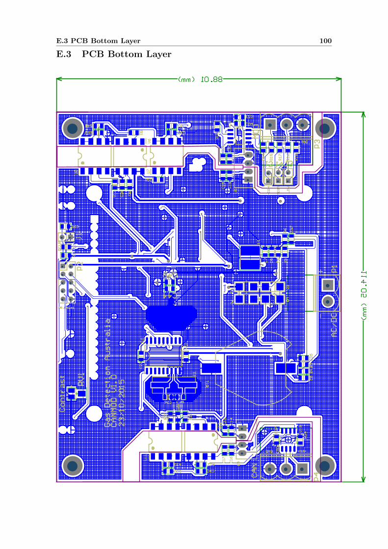
E.3 PCB Bottom Layer 100
E.3 PCB Bottom Layer
PABT102 PABT101
COBT
1
PAC101
PAC102
COC1
PAC202
PAC201
COC2
PAC302PAC301
COC3
PAC402
PAC401COC4
PAC501PAC502
COC5
PAC601
PAC602
COC6
PAC702PAC701
COC7
PAC802PAC801
COC8
PAC902
PAC901
COC9 PAC100
1
PAC100
2
COC1
0
PAC110
2
PAC110
1
COC1
1PAC
1202
PAC120
1
COC1
2
PAC1301
PAC130
2
COC1
3
PAC1402
PAC1401
COC1
4
PAC1502PAC15
01CO
C15
PAC1602
PAC1601C
OC16
PAC1702
PAC1701C
OC17
PAC1802
PAC1801
COC18
PAC1902
PAC1901
COC1
9
PAC2002PAC2001
COC20
PAC2102PAC2101
COC2
1
PAC2202
PAC2201 COC22
PAC2302
PAC2301
COC23
PAC2402
PAC2401
COC24
PAC250
2
PAC2501
COC25
PAC260
2
PAC260
1 COC26
PAC2702
PAC2701COC27
PAC2801
PAC2802
COC2
8
PAC290
2
PAC290
1
COC29 PAC300
2
PAC300
1
COC30
PAC3102PAC31
01CO
C31
PAC320
1
PAC320
2 COC32PAC330
2
PAC330
1
COC33
PAC340
2
PAC340
1 COC34
PAC350
1
PAC350
2
COC35
PAC360
2
PAC3601
COC3
6
PAC3702
PAC3701CO
C37
PAC380
2
PAC380
1
COC38
PAC390
2
PAC3901
COC39
PAC400
2
PAC400
1COC40
PAC4101
PAC410
2
COC41
PAC4202
PAC4201
COC42
PAC4302PAC43
01COC43 PAC4
401
PAC440
2COC44
PAC4702
PAC4701CO
C47
PAC4802
PAC4801COC48
PAC490
1
PAC490
2COC49
PAC520
2
PAC5201
COC52
PAC530
2
PAC530
1COC
53
PAC540
2
PAC540
1 COC
54
PAC5502
PAC5501CO
C55
PAC5602PAC5601
COC5
6
PAC570
2
PAC5701COC57
PAD103PAD102
PAD104PAD101
COD1PAD20K PAD20ACOD
2 PAD30A
PAD30K
COD3
PAD40A
PAD40K
COD4
PAD50A
PAD50KCOD5
PAD60A
PAD60K
COD6
PAD70K
PAD70A
COD7
PAD80K
PAD80A
COD8
PAD90A
PAD90K
COD9
PAD100K
PAD100A
COD10
PAD110A
PAD110K
COD1
1PAJ1
02
PAJ101
COJ1
PAJ202
PAJ201
COJ2 PAJ3
02PAJ3
01COJ
3PAJ402
PAJ401
COJ4
PAL102PAL101
COL1
PAL202
PAL201
COL2
PAP101
PAP102
COP1
PAP202
PAP2010
PAP208
PAP204
PAP206
PAP205
PAP203
PAP201
PAP207
PAP209
COP2
PAP301
PAP303
PAP302
COP3
PAP401
PAP403
PAP402 CO
P4
PAP504PAP
503PAP5
02PAP
501
COP5
PAP6020
PAP6017
PAP6018
PAP6019
PAP6016
PAP6011
PAP608
PAP609
PAP6010
PAP606
PAP605
PAP604
PAP601
PAP602
PAP603
PAP607
PAP6014
PAP6013
PAP6012
PAP6015
PAP600
COP6
PAQ102
PAQ101
PAQ103
COQ1
PAQ202
PAQ201
PAQ203
COQ2
PAQ3
02
PAQ3
01
PAQ303
COQ3
PAQ402
PAQ401
PAQ4
03
COQ4
PAQ502PAQ501
PAQ503COQ5
PAR101 PAR102
COR1
PAR201
PAR202
COR2
PAR301
PAR302
COR3
PAR401
PAR402
COR4
PAR501PAR502
COR5
PAR601
PAR602COR6
PAR702
PAR701
COR7
PAR802
PAR801C
OR8
PAR901
PAR902
COR9
PAR100
2
PAR100
1
COR10
PAR110
1
PAR110
2
COR11
PAR1202
PAR1201
COR1
2
PAR130
2
PAR130
1
COR13
PAR1402
PAR1401
COR1
4
PAR1502
PAR1501C
OR15
PAR1602PAR1601
COR1
6
PAR1702
PAR1701 C
OR17
PAR1802PAR1801
COR1
8
PAR1902PAR1901
COR19
PAR2002PAR20
01COR20
PAR2102PAR21
01CO
R21
PAR2202
PAR220
1 COR22PAR230
2
PAR230
1
COR23
PAR2402
PAR2401
COR2
4
PAR2501PAR25
02CO
R25
PAR2602PAR26
01COR26
PAR2702
PAR2701CO
R27
PAR2802
PAR2801 C
OR28
PAR2902PAR2901
COR29
PAR3002
PAR3001
COR3
0
PAR3102PAR3101
COR3
1
PAR3202
PAR3201C
OR32
PAR3302
PAR3301CO
R33
PAR3402PAR34
01COR
34
PAR350
2
PAR3501COR35
PAR3602
PAR3601 COR3
6
PAR3702
PAR3701 COR3
7
PAR3802
PAR3801
COR38
PAR3902
PAR3901CO
R39
PAR4002
PAR4001 COR4
0
PARV102
PARV103
PARV101
CORV1
PAU101
PAU102
PAU103
PAU104
PAU105
PAU106
PAU107
PAU108
PAU109
PAU1010
PAU1011
PAU1012
PAU1013
PAU1014
PAU1015
PAU1016
PAU1017
PAU1018
PAU1019
PAU1020
PAU1021PAU1022PAU1023PAU1024PAU1025PAU
1026PAU1027PAU1028PAU1029PAU1030PAU103
1PAU1032PAU1033PAU1034PAU1035PAU1036P
AU1037PAU1038PAU1039PAU1040P
AU1041
PAU1042
PAU1043
PAU1044
PAU1045
PAU1046
PAU1047
PAU1048
PAU1049
PAU1050
PAU1051
PAU1052
PAU1053
PAU1054
PAU1055
PAU1056
PAU1057
PAU1058
PAU1059
PAU1060
PAU1061PAU1062PAU1063PAU1064PAU1065PAU1066PAU1067PAU1068PAU1069PAU1070PAU1071PAU1072PAU1073PAU1074PAU1075PAU1076PAU1077PAU1078PAU1079PAU1080COU
1
PAU201
PAU202
PAU203
PAU204
PAU208
PAU207
PAU206
PAU205
COU2
PAU304
PAU305
PAU303PAU302
PAU301COU3
PAU401
PAU403PAU40
2PAU40
4COU4
PAU504
PAU502
PAU503
PAU501
COU5
PAU605
PAU606
PAU607
PAU6
08
PAU603
PAU602
PAU604
PAU6
01
COU6
PAU701
PAU704
PAU702
PAU703
PAU708
PAU707
PAU706
PAU705
COU7
PAU805
PAU806
PAU807
PAU808
PAU803
PAU802
PAU804
PAU801COU8
PAU901PAU902P
AU903PAU904
PAU908PAU907P
AU906PAU905
COU9
PAU1007
PAU1006
PAU1005
PAU1001
PAU1002
PAU1003
PAU1004
PAU1
0012
PAU1
0013
PAU1
0014
PAU1
0018
PAU1
0017
PAU1
0016
PAU1
0015
PAU1
0011
PAU1
0010
PAU1008
PAU1009
COU1
0
PAU110
5
PAU1106
PAU1107
PAU110
8
PAU1103
PAU1102
PAU110
4
PAU110
1
COU11
PAU1205
PAU1206
PAU1207
PAU120
8
PAU1203
PAU1202
PAU1204
PAU120
1
COU1
2
PAU130
5PAU1306
PAU130
7PAU1308
PAU130
4PAU1303
PAU130
2PAU1301
COU1
3
PAX101PAX102
COX1
PAX201PAX202
COX2
PAC120
1PAC13
01
PAC1401PAC1501
PAC1801
PAC1901
PAC2301
PAC2402
PAC2802
PAC3102
PAC380
1PAC3
901
PAR801
PAR100
2
PAR1202
PAR2002 PAR2102
PAU304
PAU402
PAU502
PAU607
PAU6
08PA
U100
18
PAU1107
PAU110
8
PAC400
1PAC
4102
PAC5502
PAL202
PAQ102
PAQ202
PAR2602PAR27
02
PAR3301
PAU1025
PAC1601
PAC1701
PAC2701
PAC290
2
PAC300
2PAR2
202
PAR230
1
PAU404PAU1207
PAU120
8
PAU1303
PAC901
PAC100
2
PAD30K
PAD40K
PAU204
PAU301
PAC2001PAC2101
PAC2202
PAC320
2
PAC330
2
PAC340
2
PAR901
PAR110
1
PAR130
2
PAR1401
PAU504
PAU707
PAU708
PAU807
PAU808
PAU908
PAC501 PAC601PAC702
PAD30A
PAD50A
PAD110A
PAL102 PAR502
PAR2501
PAJ201
PAR1501
PAU906
PAJ302
PAR1601
PAU907
PAU1054
PAU1
0016
PAU1057
PAU1
0012
PAU1053
PAU1
0017
PAU1044
PAU1
0013
PAU1045
PAU1
0015
PAU1046
PAU1
0014
PAR2601
PAR2902PAR3002
PAR3102
PAU1034
PAR3302
PAR3401
PAU1033
PAR702
PAU1027
PAU303
PABT102
PAC101
PAC202
PAC401
PAC502 PAC602PAC701
PAC801
PAC902
PAC100
1
PAC110
1PAC
1202
PAC130
2
PAC1402PAC1502
PAC1802
PAC1902
PAC2302 PAC2401
PAC250
2
PAC260
2
PAC2801
PAC3101
PAC350
1
PAC3601
PAC3701
PAC380
2PAC
3902
PAC400
2PAC4
101
PAC4201PAC43
01
PAC4401
PAC4701
PAC4801 PAC
4901
PAC520
2PAC
5301
PAC540
1
PAC5501
PAC5701
PAD102
PAD20A
PAD70K
PAD80K
PAD90K
PAD100K
PAJ101
PAP209
PAP2010
PAQ3
02 PAQ502
PAR301
PAR602
PAR701
PAR3501
PAR4001
PARV102
PAU1011
PAU1026PAU1031
PAU1051
PAU1070
PAU206
PAU302
PAU401
PAU501
PAU605
PAU1009
PAU110
5
PAC1602
PAC1702
PAC2702
PAC290
1
PAC300
1
PAP403
PAR2402
PAU403
PAU1205
PAU130
2
PAC2002PAC2102
PAC2201
PAC320
1
PAC330
1
PAC340
1
PAP303
PAR1802
PAR1902
PAU503
PAU705
PAU805 PAU905
PAP207
PAR201 P
AU109
PAC4202
PAC4302
PAC440
2
PAC4702
PAC4802
PAC490
2
PAL201
PAP201
PAR102
PAU1032
PAU1048
PAU1071
PABT101PAC
802
PAD40A
PAD60A
PAR402
PAC301
PAU201
PAC302
PAD20KPAL101
PAU208
PAC402
PAU202
PAC110
2
PAU305
PAC2501
PAU1008
PAX201
PAC260
1
PAU1007
PAX202
PAC350
2PAJ1
02PAR
101PAR202
PAC530
2
PAU1050
PAX102PAC
5402
PAU1049
PAX101
PAC5602 PAQ402
PAR3201
PAD103
PAP101
PAD104
PAP102
PAD70A PAR3
602
PAD80A PAR37
02
PAD90A
PAR3802
PAD100A
PAR3902
PAD110K PAR40
02
PAJ202
PAR1402
PAJ301
PAR1801
PAJ401
PAR1701
PAJ402
PAP301
PAR1502
PAP302
PAR1602PAR1702
PAP401
PAU130
7PAP4
02PAU1306
PAP503
PAQ103
PAP504
PAQ203
PAR2502
PARV101
PAU1018
PAU104
PAU103
PAU1078PAU1077PAU1076PAU1075PAU1
074PAU1073
PAU1017
PAU1016
PAU1015
PARV103
PAU1014
PAU1013
PAQ101
PAR3001
PAQ201
PAR2802
PAQ3
01
PAR2901
PAQ303
PAR2701
PAR2801
PAQ401 PAR3101
PAQ501
PAR3402
PAR902
PAU602
PAR100
1PAU
702
PAR110
2PAU
706
PAU903
PAR1201
PAU802
PAR130
1PAU
806 PAU904
PAR2001
PAU1002
PAU1106
PAR2101 PAU1
202PAR
2201
PAU1206
PAU1301
PAR230
2PAU1
102
PAR2401
PAU1308
PAR3601
PAU1062
PAR3701
PAU1061
PAR3801
PAU1060
PAR3901
PAU1059
PAU603
PAU901
PAU1001
PAU1203
PAU1103
PAU130
4
PAP203
PAU1052
PAP205
PAU1047
PAR1901
PAU902
PAC5601
PAP502
PAQ4
03
PAR3202
PAU1030
PAC570
2
PAP501
PAQ503PAR
3502
PAU1029
PAR802
PAU107
PAU606
PAU108
PAU703
PAU106
PAU803
PAP208
PAU1064
PAP204
PAU1065PAP206
PAU1066
PAC5201
PAU1012
PAC102
PAC201
PAD101
PAU207
PAD50K
PAD60K
PAP202
PAC360
2
PAR501PAR6
01
PAU1058
PAC3702
PAR302
PAR401
PAU1028

E.4 PCB 3D Top Layer 101
E.4 PCB 3D Top Layer

E.5 PCB 3D Bottom Layer 102
E.5 PCB 3D Bottom Layer

Appendix F
Results and Discussion
Supporting Information
Put all the stuff here

F.1 Click Board Schematics 104
F.1 Click Board Schematics
This is the schematics of the click boards used in testing. They can be compared to the
hardware design of the bridge.
RS-485 Click Board (MikroeElektronika 2012b).
Figure F.1: RS-485 Click board schematic

F.1 Click Board Schematics 105
CANSpi Click Board (MikroeElektronika 2012a).
Figure F.2: CANSpi Click board schematic

F.2 Photos 106
F.2 Photos
RS-485 physical layer test image.
Figure F.3: RS-485 testing set-up

F.3 Code Listings 107
F.3 Code Listings
The following code was used in an attempt to diagnose the error with CAN transmission
from the USB-CAN module to the development board with the bridge source code. It was
not successful, however it would be ideal to further explore this as a debugging option.
Listing F.1: CANSPI Error Fetch.
// Code appended to ProjectDevBoard . c// Intended to grab the error code from the CANSPI ch ip// And d i s p l a y i t on Port F LEDs o f the development board
Msg Rcvd = 0 ;Delay us ( 1 0 0 ) ;CanSpi CS = 0 ;Delay us ( 1 0 0 ) ;SPI1 Write (0 b10100000 ;SPI1 Read ( Msg Rcvd ) ;LATF = Msg Rcvd ;CanSpi CS = 1 ;Delay us ( 2 0 0 ) ;Msg Rcvd = 0 ;

Appendix G
Datasheets

G.1 PIC18F87K22 109
G.1 PIC18F87K22
2009-2011 Microchip Technology Inc. DS39960D-page 3
PIC18F87K22 FAMILY
Low-Power Features:• Power-Managed modes:
- Run: CPU on, peripherals on- Idle: CPU off, peripherals on- Sleep: CPU off, peripherals off
• Two-Speed Oscillator Start-up• Fail-Safe Clock Monitor
• Power-Saving Peripheral Module Disable (PMD)
• Ultra Low-Power Wake-up
• Fast Wake-up, 1 s Typical
• Low-Power WDT, 300 nA Typical
• Ultra Low 50 nA Input Leakage
• Run mode Currents Down to 5.5 A, Typical
• Idle mode Currents Down to 1.7 A Typical
• Sleep mode Currents Down to Very Low 20 nA, Typical
• RTCC Current Downs to Very Low 700 nA, Typical
Special Microcontroller Features:• Operating Voltage Range: 1.8V to 5.5V• On-Chip 3.3V Regulator
• Operating Speed up to 64 MHz• Up to 128 Kbytes On-Chip Flash Program
Memory
• Data EEPROM of 1,024 Bytes
• 4K x 8 General Purpose Registers (SRAM)
• 10,000 Erase/Write Cycle Flash Program Memory, Minimum
• 1,000,000 Erase/write Cycle Data EEPROM Memory, Typical
• Flash Retention: 40 Years, Minimum
• Three Internal Oscillators: LF-INTRC (31 kHz), MF-INTOSC (500 kHz) and HF-INTOSC (16 MHz)
• Self-Programmable under Software Control
• Priority Levels for Interrupts
• 8 x 8 Single-Cycle Hardware Multiplier
• Extended Watchdog Timer (WDT):
- Programmable period from 4 ms to 4,194s (about 70 minutes)
• In-Circuit Serial Programming™ (ICSP™) via Two Pins
• In-Circuit Debug via Two Pins
• Programmable:
- BOR
- LVD
Device
Program Memory Data Memory
I/O12-BitA/D (ch)
CCP/ECCP(PWM)
MSSP
EU
SA
RT
Co
mp
arat
ors
Tim
ers
8/16
-Bit
Ext
ern
al B
us
CT
MU
RT
CC
Flash(bytes)
# Single-WordInstructions
SRAM(bytes)
EEPROM(bytes)
SPIMasterI2C™
PIC18F65K22 32K 16,383 2K 1K 53 16 5/3 2 Y Y 2 3 4/4 N Y Y
PIC18F66K22 64K 32,768 4K 1K 53 16 7/3 2 Y Y 2 3 6/5 N Y Y
PIC18F67K22 128K 65,536 4K 1K 53 16 7/3 2 Y Y 2 3 6/5 N Y Y
PIC18F85K22 32K 16,383 2K 1K 69 24 5/3 2 Y Y 2 3 4/4 Y Y Y
PIC18F86K22 64K 32,768 4K 1K 69 24 7/3 2 Y Y 2 3 6/5 Y Y Y
PIC18F87K22 128K 65,536 4K 1K 69 24 7/3 2 Y Y 2 3 6/5 Y Y Y
64/80-Pin, High-Performance, 1-Mbit Enhanced Flash MCUs with 12-Bit A/D and nanoWatt XLP Technology

G.1 PIC18F87K22 110
PIC18F87K22 FAMILY
DS39960D-page 6 2009-2011 Microchip Technology Inc.
Pin Diagrams – PIC18F8XK22
3
456
78
910111213
14
15
16
4847
4645
44
434241
4039
64 63 62 61
21 22 23 24 25 26 27 28 29 30 31 32
RE
2/P
2B/C
CP
10(2
) /CS
/AD
10
RE
4/P
3B/C
CP
8(3) /A
D12
RE
5/P
1C/C
CP
7(3) /A
D13
RE
6/P
1B/C
CP
6(3) /A
D14
RE
7/E
CC
P2/
P2A
/AD
15R
D0/
PS
P0/
CT
PLS
/AD
0V
DD
VS
S
RD
1/T
5CK
I/T7G
/PS
P1/
AD
1R
D2/
PS
P2/
AD
2R
D3/
PS
P3/
AD
3
RD
4/S
DO
2/P
SP
4/A
D4
RD
5/S
DI2
/SD
A2/
PS
P5/
AD
5R
D6/
SC
K2/
SC
L2/P
SP
6/A
D6
RD
7/S
S2/
PS
P7/
AD
7
RE1/P2C/WR/AD9RE0/P2D/RD/AD8RG0/ECCP3/P3A
RG1/TX2/CK2/AN19/C3OUTRG2/RX2/DT2/AN18/C3INA
RG3/CCP4/AN17/P3D/C3INBMCLR/RG5
RG4/RTCC/T7CKI(2)/T5G/CCP5/AN16/P1D/C3INCVSS
VDDCORE/VCAP
RF7/AN5/SS1
RB0/INT0/FLT0RB1/INT1RB2/INT2/CTED1RB3/INT3/CTED2/ECCP2(1)/P2ARB4/KBI0RB5/KBI1/T3CKI/T1GRB6/KBI2/PGCVSS
OSC2/CLKO/RA6OSC1/CLKI/RA7VDD
RB7/KBI3/PGD
RC4/SDI1/SDA1RC3/SCK1/SCL1RC2/ECCP1/P1A
EN
VR
EG
RF
1/A
N6/
C2O
UT
/CT
DIN
AV
DD
AV
SS
RA
3/A
N3/
VR
EF+
RA
2/A
N2/
VR
EF-
RA
1/A
N1
RA
0/A
N0/
ULP
WU
VS
S
VD
D
RA
4/T
0CK
I
RA
5/A
N4/
T1C
KI/T
3G/H
LVD
IN
RC
1/S
OS
C/E
CC
P2/
P2A
RC
0/S
OS
CO
/SC
KL
I
RC
7/R
X1/
DT
1R
C6/
TX
1/C
K1
RC5/SDO1
RJ0
/ALE
RJ1
/OE
RH
1/A
N22
/A17
RH
0/A
N23
/A16
12
RH2/AN21/A18RH3/AN20/A19
1718
RH7/CCP6(3)/P1B/AN15RH6/CCP7(3)/P1C/AN14/C1INC
RH
5/C
CP
8(3) /P
3B/A
N13
/C2I
ND
RH
4/C
CP
9(2,3
) /P3C
/AN
12/C
2IN
C
RJ5
/CE
RJ4
/BA
0
37
RJ7/UBRJ6/LB
50
49
RJ2/WRLRJ3/WRH
19
20
33 34 35 36 38
58575655
5453
5251
60
59
68 67 66 6572 71 70 6974 7378 77 76 757980
80-Pin TQFP
RF5/AN10/C1INBRF4/AN9/C2INA
RF3/AN8/C2INB/CTMUIRF2/AN7/C1OUT
RF6/AN11/C1INA
PIC18F85K22PIC18F86K22PIC18F87K22
Note 1: The ECCP2 pin placement depends on the CCP2MX Configuration bit setting and whether the device isin Microcontroller or Extended Microcontroller mode.
2: Not available on the PIC18F65K22 and PIC18F85K22 devices.
3: The CC6, CCP7, CCP8 and CCP9 pin placement depends on the setting of the ECCPMX Configurationbit (CONFIG3H<1>).
RE
3/P
3C/C
CP
9(2,3
)/R
EF
0/A
D11
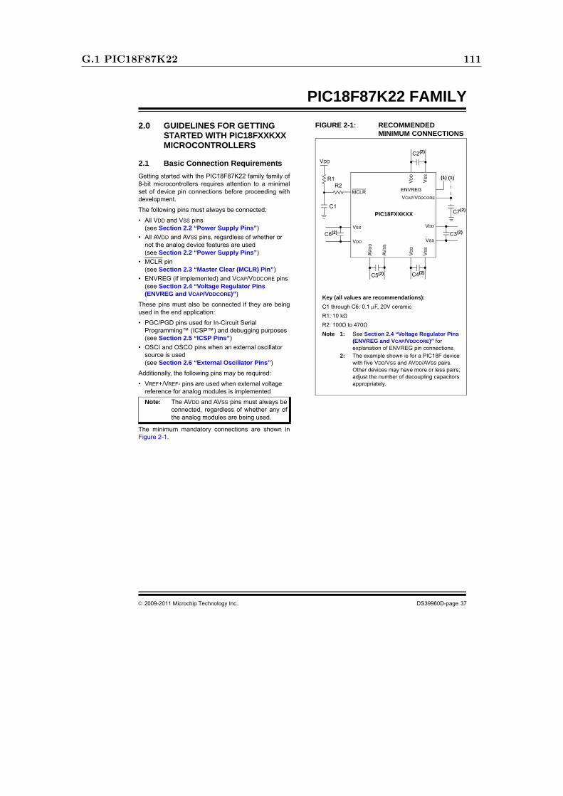
G.1 PIC18F87K22 111
2009-2011 Microchip Technology Inc. DS39960D-page 37
PIC18F87K22 FAMILY
2.0 GUIDELINES FOR GETTING STARTED WITH PIC18FXXKXX MICROCONTROLLERS
2.1 Basic Connection Requirements
Getting started with the PIC18F87K22 family family of8-bit microcontrollers requires attention to a minimalset of device pin connections before proceeding withdevelopment.
The following pins must always be connected:
• All VDD and VSS pins (see Section 2.2 “Power Supply Pins”)
• All AVDD and AVSS pins, regardless of whether or not the analog device features are used (see Section 2.2 “Power Supply Pins”)
• MCLR pin (see Section 2.3 “Master Clear (MCLR) Pin”)
• ENVREG (if implemented) and VCAP/VDDCORE pins (see Section 2.4 “Voltage Regulator Pins (ENVREG and VCAP/VDDCORE)”)
These pins must also be connected if they are beingused in the end application:
• PGC/PGD pins used for In-Circuit Serial Programming™ (ICSP™) and debugging purposes (see Section 2.5 “ICSP Pins”)
• OSCI and OSCO pins when an external oscillator source is used (see Section 2.6 “External Oscillator Pins”)
Additionally, the following pins may be required:
• VREF+/VREF- pins are used when external voltage reference for analog modules is implemented
The minimum mandatory connections are shown inFigure 2-1.
FIGURE 2-1: RECOMMENDED MINIMUM CONNECTIONS
Note: The AVDD and AVSS pins must always beconnected, regardless of whether any ofthe analog modules are being used.
PIC18FXXKXX
VD
D
VS
S
VDD
VSS
VSS
VDD
AV
DD
AV
SS
VD
D
VS
S
C1
R1
VDD
MCLRVCAP/VDDCORE
R2ENVREG
(1)
C7(2)
C2(2)
C3(2)
C4(2)C5(2)
C6(2)
Key (all values are recommendations):
C1 through C6: 0.1 F, 20V ceramic
R1: 10 kΩ
R2: 100Ω to 470Ω
Note 1: See Section 2.4 “Voltage Regulator Pins (ENVREG and VCAP/VDDCORE)” for explanation of ENVREG pin connections.
2: The example shown is for a PIC18F device with five VDD/VSS and AVDD/AVSS pairs. Other devices may have more or less pairs; adjust the number of decoupling capacitors appropriately.
(1)

G.1 PIC18F87K22 112
PIC18F87K22 FAMILY
DS39960D-page 38 2009-2011 Microchip Technology Inc.
2.2 Power Supply Pins
2.2.1 DECOUPLING CAPACITORS
The use of decoupling capacitors on every pair ofpower supply pins, such as VDD, VSS, AVDD andAVSS, is required.
Consider the following criteria when using decouplingcapacitors:
• Value and type of capacitor: A 0.1 F (100 nF), 10-20V capacitor is recommended. The capacitor should be a low-ESR device, with a resonance frequency in the range of 200 MHz and higher. Ceramic capacitors are recommended.
• Placement on the printed circuit board: The decoupling capacitors should be placed as close to the pins as possible. It is recommended to place the capacitors on the same side of the board as the device. If space is constricted, the capacitor can be placed on another layer on the PCB using a via; however, ensure that the trace length from the pin to the capacitor is no greater than 0.25 inch (6 mm).
• Handling high-frequency noise: If the board is experiencing high-frequency noise (upward of tens of MHz), add a second ceramic type capaci-tor in parallel to the above described decoupling capacitor. The value of the second capacitor can be in the range of 0.01 F to 0.001 F. Place this second capacitor next to each primary decoupling capacitor. In high-speed circuit designs, consider implementing a decade pair of capacitances as close to the power and ground pins as possible (e.g., 0.1 F in parallel with 0.001 F).
• Maximizing performance: On the board layout from the power supply circuit, run the power and return traces to the decoupling capacitors first, and then to the device pins. This ensures that the decoupling capacitors are first in the power chain. Equally important is to keep the trace length between the capacitor and the power pins to a minimum, thereby reducing PCB trace inductance.
2.2.2 TANK CAPACITORS
On boards with power traces running longer thansix inches in length, it is suggested to use a tank capac-itor for integrated circuits, including microcontrollers, tosupply a local power source. The value of the tankcapacitor should be determined based on the traceresistance that connects the power supply source tothe device, and the maximum current drawn by thedevice in the application. In other words, select the tankcapacitor so that it meets the acceptable voltage sag atthe device. Typical values range from 4.7 F to 47 F.
2.3 Master Clear (MCLR) Pin
The MCLR pin provides two specific devicefunctions: Device Reset, and Device Programmingand Debugging. If programming and debugging arenot required in the end application, a directconnection to VDD may be all that is required. Theaddition of other components, to help increase theapplication’s resistance to spurious Resets fromvoltage sags, may be beneficial. A typicalconfiguration is shown in Figure 2-1. Other circuitdesigns may be implemented, depending on theapplication’s requirements.
During programming and debugging, the resistanceand capacitance that can be added to the pin mustbe considered. Device programmers and debuggersdrive the MCLR pin. Consequently, specific voltagelevels (VIH and VIL) and fast signal transitions mustnot be adversely affected. Therefore, specific valuesof R1 and C1 will need to be adjusted based on theapplication and PCB requirements. For example, it isrecommended that the capacitor, C1, be isolatedfrom the MCLR pin during programming anddebugging operations by using a jumper (Figure 2-2).The jumper is replaced for normal run-timeoperations.
Any components associated with the MCLR pinshould be placed within 0.25 inch (6 mm) of the pin.
FIGURE 2-2: EXAMPLE OF MCLR PIN CONNECTIONS
Note 1: R1 10 k is recommended. A suggestedstarting value is 10 k. Ensure that theMCLR pin VIH and VIL specifications are met.
2: R2 470 will limit any current flowing intoMCLR from the external capacitor, C, in theevent of MCLR pin breakdown, due toElectrostatic Discharge (ESD) or ElectricalOverstress (EOS). Ensure that the MCLR pinVIH and VIL specifications are met.
C1
R2R1
VDD
MCLR
PIC18FXXKXXJP

G.2 DF04S 113
G.2 DF04SD
F005S
- DF
10S —
Brid
ge R
ectifiers
© 1998 Fairchild Semiconductor Corporation www.fairchildsemi.com
DF005S - DF10S Rev. 1.5
May 2015
DF005S - DF10SBridge Rectifiers
Features• Maximum Surge Rating: IFSM = 50 A
I2t = 10 A2Sec
• Optimized VF: Typical 0.94 V at 1.5 A, 25°C
• Glass Passivated Junctions
• Lead Free Compliant to EU RoHS 2002/95/EU Directives
• Green Molding Compound: IEC61249
• Qualified with IR Reflow and Wave Soldering
• UL Certified, UL #E258596
Ordering Information
Part Number Top Mark Package Packing Method
DF005S DF005S SDIP 4L Tape and Reel
DF01S DF01S SDIP 4L Tape and Reel
DF02S DF02S SDIP 4L Tape and Reel
DF04S DF04S SDIP 4L Tape and Reel
DF06S DF06S SDIP 4L Tape and Reel
DF08S DF08S SDIP 4L Tape and Reel
DF10S DF10S SDIP 4L Tape and Reel
Description
With the ever-pressing need to improve power supplyefficiency, improve surge rating, improve reliability, andreduce size, the DFxS family sets a standard in perfor-mance.
The design offers an surge rating of 50 A. This is impor-tant when improving reliability and increasing efficiency.High efficiency designs strive to reduce circuit resis-tance, which, unfortunately can result in increasedinrush surge. As such high surge current ratings can berequired to maintain or improve reliability.
The design also offers better efficiency by achieving a1.5 A VF of 1.1 V maximum at 25°C. This lower VF alsosupports cooler and more efficient operation.
Finally, the DFxS achieves all this in a SDIP surfacemount form factor, reducing board space and volumetricrequirements vs. competitive devices.
+
-~
~
IN
OUT
SDIP

G.2 DF04S 114
DF
005S - D
F10S
— B
ridg
e Rectifiers
© 1998 Fairchild Semiconductor Corporation www.fairchildsemi.com
DF005S - DF10S Rev. 1.5 2
Absolute Maximum RatingsStresses exceeding the absolute maximum ratings may damage the device. The device may not function or be opera-ble above the recommended operating conditions and stressing the parts to these levels is not recommended. In addi-tion, extended exposure to stresses above the recommended operating conditions may affect device reliability. Theabsolute maximum ratings are stress ratings only. Values are at TA = 25°C unless otherwise noted.
Thermal CharacteristicsValues are at TA = 25°C unless otherwise noted.
Notes:
1. Device mounted on PCB with 0.5 inch × 0.5 inch (13 mm × 13 mm).
2. The thermal resistances (RθJA & ψJL) are characterized with the device mounted on the following FR4 printed circuit
boards, as shown in Figure 1 and Figure 2. PCB size: 76.2 x 114.3 mm.
Heating effect from adjacent dice is considered and only two dices are powered at the same time.
Symbol ParameterValue
UnitDF005S DF01S DF02S DF04S DF06S DF08S DF10S
VRRM Maximum Repetitive Reverse Voltage 50 100 200 400 600 800 1000 V
VRMS Maximum RMS Bridge Input Voltage 35 70 140 280 420 560 700 V
VDC DC Reverse Voltage at Rated IR 50 100 200 400 600 800 1000 V
IF(AV)Average Rectified Forward Current at TA = 40°C 1.5 A
IFSM
Non-Repetitive Peak Forward SurgeCurrent8.3 ms Single Half-Sine Wave
50 A
TSTG Storage Temperature Range -55 to +150 °C
TJ Operating Junction Temperature -55 to +150 °C
Symbol Parameter Value Unit
PD Power Dissipation 3.1 W
RθJAThermal Resistance, Junction-to-Ambient
Single-Die Measurement(1)
(Maximum Land Pattern: 13 x 13 mm)62
°C/WMulti-Die Measurement(2)
(Maximum Land Pattern: 13 x 13 mm)50
Multi-Die Measurement(2)
(Minimum Land Pattern: 1.3 x 1.5 mm)105
ψJLThermal CharacterizationParameter, Junction to Lead
Single-Die Measurement(2)
(Maximum and Minimum Land Pattern)27 °C/W
Figure 1. Maximum Pads of 2 oz Copper Figure 2. Minimum Pads of 2 oz Copper
F
F
SS
F
F
SS

G.3 HCPL-2601.S 115
G.3 HCPL-2601.S
©2005 Fairchild Semiconductor Corporation
1
www.fairchildsemi.com
Single-Channel: 6N137, HCPL-2601, HCPL-2611 Dual-Channel: HCPL-2630, HCPL-2631 Rev. 1.0.5
Single-Channel: 6N137, HCPL-2601, HCPL-2611 Dual-Channel: HCPL-2630, HCPL-2631 High Speed-10 MBit/s Logic Gate Optocouplers
tm
July 2006
Single-Channel: 6N137, HCPL-2601, HCPL-2611Dual-Channel: HCPL-2630, HCPL-2631High Speed-10 MBit/s Logic Gate Optocouplers
Features
Very high speed-10 MBit/s
Superior CMR-10 kV/µs
Double working voltage-480V
Fan-out of 8 over -40°C to +85°C
Logic gate output
Strobable output
Wired OR-open collector
U.L. recognized (File # E90700)
Applications
Ground loop elimination
LSTTL to TTL, LSTTL or 5-volt CMOS
Line receiver, data transmission
Data multiplexing
Switching power supplies
Pulse transformer replacement
Computer-peripheral interface
Description
The 6N137, HCPL-2601/2611 single-channel and HCPL-2630/2631 dual-channel optocouplers consist of a 850 nm AlGaASLED, optically coupled to a very high speed integrated photo-detector logic gate with a strobable output. This output featuresan open collector, thereby permitting wired OR outputs. Thecoupled parameters are guaranteed over the temperature rangeof -40°C to +85°C. A maximum input signal of 5 mA will providea minimum output sink current of 13mA (fan out of 8).
An internal noise shield provides superior common mode rejec-tion of typically 10kV/µs. The HCPL- 2601 and HCPL- 2631 hasa minimum CMR of 5 kV/µs. The HCPL-2611 has a minimumCMR of 10 kV/µs.
Package Schematic
Truth Table (Positive Logic)
A 0.1µF bypass capacitor must be connected between pins 8 and 5. (See note 1)
8
8
1
8
1
1
1
2
3
4 5
6
7
8N/C
_
VCC
VE
VO
GND
+
N/C
VF
1
2
3
4 5
6
7
8+
_
VF1
VCC
V01
V02
GND
VF2
_
+
HCPL-2630HCPL-2631
6N137HCPL-2601HCPL-2611
Input Enable Output
H H L
L H H
H L H
L L H
H NC L
L NC H

G.3 HCPL-2601.S 116
2
www.fairchildsemi.com
Single-Channel: 6N137, HCPL-2601, HCPL-2611 Dual-Channel: HCPL-2630, HCPL-2631 Rev. 1.0.5
Single-Channel: 6N137, HCPL-2601, HCPL-2611 Dual-Channel: HCPL-2630, HCPL-2631 High Speed-10 M
Bit/s Logic Gate Optocouplers
Absolute Maximum Ratings
(T
A
= 25°C unless otherwise specified)
Recommended Operating Conditions
*6.3mA is a guard banded value which allows for at least 20% CTR degradation. Initial input current threshold value is5.0 mA or less.
Parameter Symbol Value Units
Storage Temperature T
STG
-55 to +125 °C
Operating Temperature T
OPR
-40 to +85 °C
Lead Solder Temperature T
SOL
260 for 10 sec °C
EMITTER
DC/Average Forward Single Channel I
F
50 mA
Input Current Dual Channel (Each Channel) 30
Enable Input VoltageNot to exceed V
CC
by more than 500 mVSingle Channel V
E
5.5 V
Reverse Input Voltage Each Channel V
R
5.0 V
Power Dissipation Single Channel P
I
100 mW
Dual Channel (Each Channel)
45
DETECTOR
Supply Voltage V
CC
(1 minute max)7.0 V
Output Current Single Channel I
O
50 mA
Dual Channel (Each Channel) 50
Output Voltage Each Channel V
O
7.0 V
Collector Output Single Channel P
O
85 mW
Power Dissipation Dual Channel (Each Channel) 60
Parameter Symbol Min Max Units
Input Current, Low Level I
FL
0 250 µA
Input Current, High Level I
FH
*6.3 15 mA
Supply Voltage, Output V
CC
4.5 5.5 V
Enable Voltage, Low Level V
EL
0 0.8 V
Enable Voltage, High Level V
EH
2.0 V
CC
V
Low Level Supply Current T
A
-40 +85 °C
Fan Out (TTL load) N 8
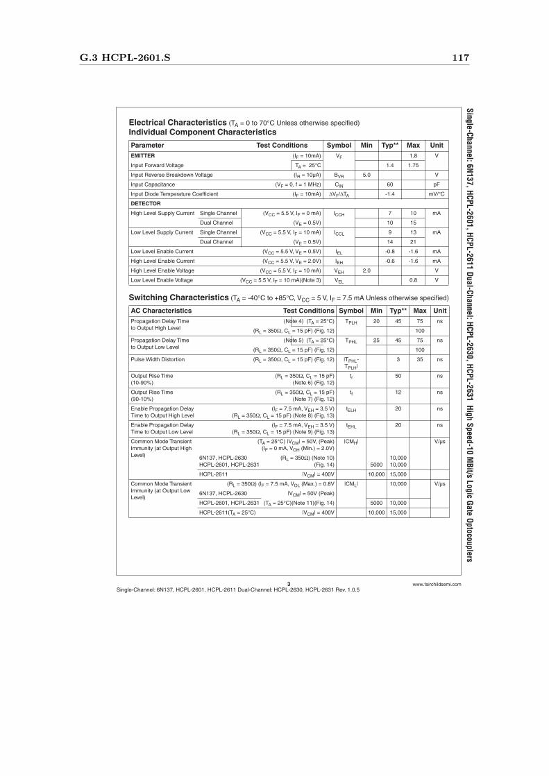
G.3 HCPL-2601.S 117
3
www.fairchildsemi.com
Single-Channel: 6N137, HCPL-2601, HCPL-2611 Dual-Channel: HCPL-2630, HCPL-2631 Rev. 1.0.5
Single-Channel: 6N137, HCPL-2601, HCPL-2611 Dual-Channel: HCPL-2630, HCPL-2631 High Speed-10 M
Bit/s Logic Gate Optocouplers
Electrical Characteristics
(T
A
= 0 to 70°C Unless otherwise specified)
Individual Component Characteristics
Switching Characteristics
(T
A
= -40°C to +85°C, V
CC
= 5 V, I
F
= 7.5 mA Unless otherwise specified)
Parameter Test Conditions Symbol Min Typ** Max Unit
EMITTER
(I
F
= 10mA) V
F
1.8 V
Input Forward Voltage T
A
= 25°C 1.4 1.75
Input Reverse Breakdown Voltage (I
R
= 10µA) B
VR
5.0 V
Input Capacitance (V
F
= 0, f = 1 MHz) C
IN
60 pF
Input Diode Temperature Coefficient (I
F
= 10mA)
∆
V
F
/
∆
T
A
-1.4 mV/°C
DETECTOR
High Level Supply Current Single Channel (V
CC
= 5.5 V, I
F
= 0 mA) I
CCH
7 10 mA
Dual Channel (V
E
= 0.5V) 10 15
Low Level Supply Current Single Channel (V
CC
= 5.5 V, I
F
= 10 mA) I
CCL
9 13 mA
Dual Channel (V
E
= 0.5V) 14 21
Low Level Enable Current (V
CC
= 5.5 V, V
E
= 0.5V) I
EL
-0.8 -1.6 mA
High Level Enable Current (V
CC
= 5.5 V, V
E
= 2.0V) I
EH
-0.6 -1.6 mA
High Level Enable Voltage (V
CC
= 5.5 V, I
F
= 10 mA) V
EH
2.0 V
Low Level Enable Voltage (V
CC
= 5.5 V, I
F
= 10 mA)(Note 3) V
EL
0.8 V
AC Characteristics Test Conditions Symbol Min Typ** Max Unit
Propagation Delay Timeto Output High Level
(Note 4) (T
A
= 25°C) T
PLH
20 45 75 ns
(R
L
= 350
Ω
, C
L
= 15 pF) (Fig. 12) 100
Propagation Delay Timeto Output Low Level
(Note 5) (T
A
= 25°C) T
PHL
25 45 75 ns
(R
L
= 350
Ω
, C
L
= 15 pF) (Fig. 12) 100
Pulse Width Distortion (R
L
= 350
Ω
, C
L
= 15 pF) (Fig. 12) |T
PHL
-T
PLH
|3 35 ns
Output Rise Time (10-90%)
(R
L
= 350
Ω
, C
L
= 15 pF)(Note 6) (Fig. 12)
t
r
50 ns
Output Rise Time (90-10%)
(R
L
= 350
Ω
, C
L
= 15 pF)(Note 7) (Fig. 12)
t
f
12 ns
Enable Propagation Delay Time to Output High Level
(I
F
= 7.5 mA, V
EH
= 3.5 V)(R
L
= 350
Ω
, C
L
= 15 pF) (Note 8) (Fig. 13)t
ELH
20 ns
Enable Propagation Delay Time to Output Low Level
(I
F
= 7.5 mA, V
EH
= 3.5 V)(R
L
= 350
Ω
, C
L
= 15 pF) (Note 9) (Fig. 13)t
EHL
20 ns
Common Mode Transient Immunity (at Output High Level)
(T
A
= 25°C) |V
CM
| = 50V, (Peak)(I
F
= 0 mA, V
OH
(Min.) = 2.0V)|CM
H
| V/µs
6N137, HCPL-2630HCPL-2601, HCPL-2631
(R
L
= 350
Ω
) (Note 10)(Fig. 14) 5000
10,00010,000
HCPL-2611 |V
CM
| = 400V 10,000 15,000
Common Mode Transient Immunity (at Output Low Level)
(R
L
= 350
Ω
) (I
F
= 7.5 mA, V
OL
(Max.) = 0.8V |CM
L
| 10,000 V/µs
6N137, HCPL-2630 |V
CM
| = 50V (Peak)
HCPL-2601, HCPL-2631 (T
A
= 25°C)(Note 11)(Fig. 14) 5000 10,000
HCPL-2611(TA = 25°C) |VCM| = 400V 10,000 15,000

G.4 LM2671 118
G.4 LM2671
LM2671
www.ti.com SNVS008K –SEPTEMBER 1998–REVISED APRIL 2013
LM2671 SIMPLE SWITCHER® Power Converter High Efficiency 500mA Step-Down VoltageRegulator with Features
Check for Samples: LM2671
1FEATURES234• Efficiency up to 96% DESCRIPTION
The LM2671 series of regulators are monolithic• Available in SOIC, 8-pin PDIP and WSONintegrated circuits built with a LMDMOS process.PackagesThese regulators provide all the active functions for a• Computer Design Software LM267X Made step-down (buck) switching regulator, capable of
Simple (version 6.0) driving a 500mA load current with excellent line and• Simple and Easy to Design With load regulation. These devices are available in fixed
output voltages of 3.3V, 5.0V, 12V, and an adjustable• Requires Only 5 external Componentsoutput version.• Uses Readily Available Standard InductorsRequiring a minimum number of external• 3.3V, 5.0V, 12V, and Adjustable Outputcomponents, these regulators are simple to use andVersionsinclude patented internal frequency compensation
• Adjustable Version Output Voltage Range: (Patent Nos. 5,382,918 and 5,514,947), fixed1.21V to 37V frequency oscillator, external shutdown, soft-start,
and frequency synchronization.• ±1.5% Max Output Voltage Tolerance OverLine and Load Conditions The LM2671 series operates at a switching frequency
• Ensured 500mA Output Load Current of 260 kHz, thus allowing smaller sized filtercomponents than what would be needed with lower• 0.25Ω DMOS Output Switchfrequency switching regulators. Because of its very
• Wide Input Voltage Range: 8V to 40V high efficiency (>90%), the copper traces on the• 260 kHz Fixed Frequency Internal Oscillator printed circuit board are the only heat sinking needed.• TTL Shutdown Capability, Low Power Standby A family of standard inductors for use with the
Mode LM2671 are available from several differentmanufacturers. This feature greatly simplifies the• Soft-Start and Frequency Synchronizationdesign of switch-mode power supplies using these• Thermal Shutdown and Current Limitadvanced ICs. Also included in the datasheet areProtectionselector guides for diodes and capacitors designed towork in switch-mode power supplies.APPLICATIONSOther features include a ensured ±1.5% tolerance on• Simple High Efficiency (>90%) Step-Down output voltage within specified input voltages and
(Buck) Regulator output load conditions, and ±10% on the oscillator• Efficient Pre-Regulator for Linear Regulators frequency. External shutdown is included, featuring
typically 50 μA stand-by current. The output switchincludes current limiting, as well as thermal shutdownfor full protection under fault conditions.
To simplify the LM2671 buck regulator designprocedure, there exists computer design software,LM267X Made Simple (version 6.0).
1
Please be aware that an important notice concerning availability, standard warranty, and use in critical applications ofTexas Instruments semiconductor products and disclaimers thereto appears at the end of this data sheet.
2SIMPLE SWITCHER, WEBENCH are registered trademarks of Texas Instruments.3Windows is a registered trademark of Microsoft Corporation.4All other trademarks are the property of their respective owners.
PRODUCTION DATA information is current as of publication date. Copyright © 1998–2013, Texas Instruments IncorporatedProducts conform to specifications per the terms of the TexasInstruments standard warranty. Production processing does notnecessarily include testing of all parameters.

G.4 LM2671 119
LM2671
SNVS008K –SEPTEMBER 1998–REVISED APRIL 2013 www.ti.com
TEST CIRCUIT AND LAYOUT GUIDELINES
CIN - 22 μF, 50V Tantalum, Sprague “199D Series”COUT - 47 μF, 25V Tantalum, Sprague “595D Series”D1 - 3.3A, 50V Schottky Rectifier, IR 30WQ05FL1 - 68 μH Sumida #RCR110D-680LCB - 0.01 μF, 50V Ceramic
Figure 22. Standard Test Circuits and Layout GuidesFixed Output Voltage Versions
CIN - 22 μF, 50V Tantalum, Sprague “199D Series”COUT - 47 μF, 25V Tantalum, Sprague “595D Series”D1 - 3.3A, 50V Schottky Rectifier, IR 30WQ05FL1 - 68 μH Sumida #RCR110D-680LR1 - 1.5 kΩ, 1%CB - 0.01 μF, 50V CeramicFor a 5V output, select R2 to be 4.75 kΩ, 1%
where VREF = 1.21V
Use a 1% resistor for best stability.
Figure 23. Standard Test Circuits and Layout GuidesAdjustable Output Voltage Versions
Application Hints
The LM2671 provides all of the active functions required for a step-down (buck) switching regulator. The internalpower switch is a DMOS power MOSFET to provide power supply designs with high current capability, up to0.5A, and highly efficient operation.
10 Submit Documentation Feedback Copyright © 1998–2013, Texas Instruments Incorporated
Product Folder Links: LM2671

G.5 MCP2515 120
G.5 MCP2515
2003-2012 Microchip Technology Inc. DS21801G-page 1
MCP2515
Features:
• Implements CAN V2.0B at 1 Mb/s:
- 0 – 8 byte length in the data field
- Standard and extended data and remote frames
• Receive Buffers, Masks and Filters:
- Two receive buffers with prioritized message storage
- Six 29-bit filters
- Two 29-bit masks
• Data Byte Filtering on the First Two Data Bytes (applies to standard data frames)
• Three Transmit Buffers with Prioritization and Abort Features
• High-Speed SPI Interface (10 MHz):
- SPI modes 0,0 and 1,1
• One-Shot mode Ensures Message Transmission is Attempted Only One Time
• Clock Out Pin with Programmable Prescaler:
- Can be used as a clock source for other device(s)
• Start-of-Frame (SOF) Signal is Available for Monitoring the SOF Signal:
- Can be used for time-slot-based protocols and/or bus diagnostics to detect early bus degradation
• Interrupt Output Pin with Selectable Enables
• Buffer Full Output Pins Configurable as:
- Interrupt output for each receive buffer
- General purpose output
• Request-to-Send (RTS) Input Pins Individually Configurable as:
- Control pins to request transmission for each transmit buffer
- General purpose inputs
• Low-Power CMOS Technology:
- Operates from 2.7V – 5.5V
- 5 mA active current (typical)
- 1 µA standby current (typical) (Sleep mode)
• Temperature Ranges Supported:
- Industrial (I): -40°C to +85°C
- Extended (E): -40°C to +125°C
DescriptionMicrochip Technology’s MCP2515 is a stand-aloneController Area Network (CAN) controller thatimplements the CAN specification, version 2.0B. It iscapable of transmitting and receiving both standardand extended data and remote frames. The MCP2515has two acceptance masks and six acceptance filtersthat are used to filter out unwanted messages, therebyreducing the host MCU’s overhead. The MCP2515interfaces with microcontrollers (MCUs) via an industrystandard Serial Peripheral Interface (SPI).
Package Types
16
5
TXCAN
RXCAN
VDD
RESET
CS
SO
MC
P25
15
1
2
3
4
18
17
16
15
SI
SCK
INT
RX0BF
14
13
12
11
RX1BF10
OSC2
OSC1
CLKOUT/SOF
TX2RTS
5
6
7
8
Vss 9
TX0RTS
TX1RTS
MC
P25
15
TXCANRXCAN
TX0RTS
OSC1
CLKOUT/SOF
OSC2
CS
VDD
RESET
SO
SCKINT
SI
RX0BFRX1BFVSS
TX1RTS
TX2RTSNC NC
1312
123456789
20191817161514
1110
18-Lead PDIP/SOIC
20-LEAD TSSOP
2
MCP251520-Lead 4x4 QFN*
NC
TX2RTS
TX0RTS
SO
SI
OS
C2
NC
OS
C1
GN
D
RX
1B
F
SCK
RX
CA
N
TX
CA
N
VD
D
RE
SE
T
TX1RTSEP
20
1
19 18 17
3
4
14
13
12
116 7 8 9
21
10
15CLKOUT
CS
INT
RX
0B
F
* Includes Exposed Thermal Pad (EP); see Table 1-1.
Stand-Alone CAN Controller with SPI Interface

G.5 MCP2515 121
2003-2012 Microchip Technology Inc. DS21801G-page 39
MCP2515
5.0 BIT TIMING
All nodes on a given CAN bus must have the samenominal bit rate. The CAN protocol uses Non Return toZero (NRZ) coding, which does not encode a clockwithin the data stream. Therefore, the receive clockmust be recovered by the receiving nodes andsynchronized to the transmitter’s clock.
As oscillators and transmission times may vary fromnode to node, the receiver must have some type ofPhase Lock Loop (PLL) synchronized to datatransmission edges to synchronize and maintain thereceiver clock. Since the data is NRZ-coded, it isnecessary to include bit-stuffing to ensure that an edgeoccurs at least every six bit times to maintain the DigitalPhase Lock Loop (DPLL) synchronization.
The bit timing of the MCP2515 is implemented using aDPLL that is configured to synchronize to the incomingdata, as well as provide the nominal timing for thetransmitted data. The DPLL breaks each bit time intomultiple segments made up of minimal periods of time,called the Time Quanta (TQ).
Bus timing functions executed within the bit time frame(such as synchronization to the local oscillator, networktransmission delay compensation and sample pointpositioning) are defined by the programmable bit timinglogic of the DPLL.
5.1 The CAN Bit TIme
All devices on the CAN bus must use the same bit rate.However, all devices are not required to have the samemaster oscillator clock frequency. For the differentclock frequencies of the individual devices, the bit ratehas to be adjusted by appropriately setting the BaudRate Prescaler and number of time quanta in eachsegment.
The CAN bit time is made up of non-overlappingsegments. Each of these segments are made up ofinteger units called Time Quanta (TQ), explained laterin this data sheet. The Nominal Bit Rate (NBR) isdefined in the CAN specification as the number of bitsper second transmitted by an ideal transmitter with noresynchronization. It can be described with theequation:
EQUATION 5-1:
Nominal Bit Time
The Nominal Bit Time (NBT) (tbit) is made up of non-overlapping segments (Figure 5-1). Therefore, theNBT is the summation of the following segments:
Associated with the NBT are the sample point,Synchronization Jump Width (SJW) and InformationProcessing Time (IPT), which are explained later.
SYNCHRONIZATION SEGMENT
The Synchronization Segment (SyncSeg) is the firstsegment in the NBT and is used to synchronize thenodes on the bus. Bit edges are expected to occurwithin the SyncSeg. This segment is fixed at 1 TQ.
FIGURE 5-1: CAN BIT TIME SEGMENTS
NBR fbit1
tbit-------= =
tbit tSyncSeg tPropSeg tPS1 tPS2+ + +=
Nominal Bit Time (NBT), tbit
SamplePoint
SyncSeg PropSeg PhaseSeg1 (PS1) PhaseSeg2 (PS2)

G.5 MCP2515 122
MCP2515
DS21801G-page 40 2003-2012 Microchip Technology Inc.
PROPAGATION SEGMENT
The Propagation Segment (PropSeg) exists tocompensate for physical delays between nodes. Thepropagation delay is defined as twice the sum of thesignal’s propagation time on the bus line, including thedelays associated with the bus driver. The PropSeg isprogrammable from 1-8 TQ.
PHASE SEGMENT 1 (PS1) AND PHASE SEGMENT 2 (PS2)
The two phase segments, PS1 and PS2, are used tocompensate for edge phase errors on the bus. PS1 canbe lengthened (or PS2 shortened) by resyncronization.PS1 is programmable from 1-8 TQ and PS2 isprogrammable from 2-8 TQ.
SAMPLE POINT
The sample point is the point in the bit time at which thelogic level is read and interpreted. The sample point islocated at the end of PS1. The exception to this rule isif the sample mode is configured to sample three timesper bit. In this case, while the bit is still sampled at theend of PS1, two additional samples are taken at one-half TQ intervals prior to the end of PS1, with the valueof the bit being determined by a majority decision.
INFORMATION PROCESSING TIME
The Information Processing Time (IPT) is the timerequired for the logic to determine the bit level of asampled bit. The IPT begins at the sample point, ismeasured in TQ and is fixed at 2 TQ for the MicrochipCAN module. Since PS2 also begins at the samplepoint and is the last segment in the bit time, it isrequired that the PS2 minimum is not less than the IPT.
Therefore:
SYNCHRONIZATION JUMP WIDTH
The Synchronization Jump Width (SJW) adjusts the bitclock as necessary by 1-4 TQ (as configured) tomaintain synchronization with the transmittedmessage. Synchronization is covered in more detaillater in this data sheet.
Time Quantum
Each of the segments that make up a bit time are madeup of integer units called Time Quanta (TQ). The lengthof each Time Quantum is based on the oscillator period(tOSC). The base TQ equals twice the oscillator period.Figure 5-2 shows how the bit period is derived fromTOSC and TQ. The TQ length equals one TQ clockperiod (tBRPCLK), which is programmable using aprogrammable prescaler, called the Baud RatePrescaler (BRP). This is illustrated in the followingequation:
EQUATION 5-2:
FIGURE 5-2: TQ AND THE BIT PERIOD
PS2min IPT 2TQ= =
TQ 2 BRP TOSC 2 BRPFOSC-------------------= =
Where: BRP equals the configuration as shown inRegister 5-1.
tOSC
TBRPCLK
tBITSync
(fixed)PropSeg
(Programmable)PS2
(Programmable)PS1
(Programmable)
TQ(tTQ)
CAN Bit Time

G.5 MCP2515 123
2003-2012 Microchip Technology Inc. DS21801G-page 43
MCP2515
5.3 Programming Time Segments
Some requirements for programming of the timesegments:
• PropSeg + PS1 >= PS2
• PropSeg + PS1 >= TDELAY
• PS2 > SJW
For example, assuming that a 125 kHz CAN baud ratewith FOSC = 20 MHz is desired:
TOSC = 50 ns, choose BRP<5:0> = 04h, thenTQ = 500 ns. To obtain 125 kHz, the bit time must be 16TQ.
Typically, the sampling of the bit should take place atabout 60-70% of the bit time, depending on the systemparameters. Also, typically, the TDELAY is 1-2 TQ.
SyncSeg = 1 TQ and PropSeg = 2 TQ. So settingPS1 = 7 TQ would place the sample at 10 TQ after thetransition. This would leave 6 TQ for PS2.
Since PS2 is 6, according to the rules, SJW could be amaximum of 4 TQ. However, a large SJW is typicallyonly necessary when the clock generation of the differ-ent nodes is inaccurate or unstable, such as usingceramic resonators. So a SJW of 1 is usually enough.
5.4 Oscillator Tolerance
The bit timing requirements allow ceramic resonatorsto be used in applications with transmission rates of upto 125 kbit/sec as a rule of thumb. For the full busspeed range of the CAN protocol, a quartz oscillator isrequired. A maximum node-to-node oscillator variationof 1.7% is allowed.
5.5 Bit Timing Configuration Registers
The configuration registers (CNF1, CNF2, CNF3)control the bit timing for the CAN bus interface. Theseregisters can only be modified when the MCP2515 is inConfiguration mode (see Section 10.0 “Modes ofOperation”).
5.5.1 CNF1
The BRP<5:0> bits control the Baud Rate Prescaler.These bits set the length of TQ relative to the OSC1input frequency, with the minimum TQ length being2 TOSC (when BRP<5:0> = ‘b000000’). TheSJW<1:0> bits select the SJW in terms of number ofTQs.
5.5.2 CNF2
The PRSEG<2:0> bits set the length (in TQ’s) of thepropagation segment. The PHSEG1<2:0> bits set thelength (in TQ’s) of PS1.
The SAM bit controls how many times the RXCAN pinis sampled. Setting this bit to a ‘1’ causes the bus to besampled three times: twice at TQ/2 before the samplepoint and once at the normal sample point (which is atthe end of PS1). The value of the bus is determined tobe the majority sampled. If the SAM bit is set to a ‘0’,the RXCAN pin is sampled only once at the samplepoint.
The BTLMODE bit controls how the length of PS2 isdetermined. If this bit is set to a ‘1’, the length of PS2 isdetermined by the PHSEG2<2:0> bits of CNF3 (seeSection 5.5.3 “CNF3”). If the BTLMODE bit is set to a‘0’, the length of PS2 is greater than that of PS1 and theinformation processing time (which is fixed at 2 TQ forthe MCP2515).
5.5.3 CNF3
The PHSEG2<2:0> bits set the length (in TQ’s) of PS2,if the CNF2.BTLMODE bit is set to a ‘1’. If theBTLMODE bit is set to a ‘0’, the PHSEG2<2:0> bitshave no effect.

G.5 MCP2515 124
2003-2012 Microchip Technology Inc. DS21801G-page 65
MCP2515
12.0 SPI INTERFACE
12.1 Overview
The MCP2515 is designed to interface directly with theSerial Peripheral Interface (SPI) port available on manymicrocontrollers and supports Mode 0,0 and Mode 1,1.Commands and data are sent to the device via the SIpin, with data being clocked in on the rising edge ofSCK. Data is driven out by the MCP2515 (on the SOline) on the falling edge of SCK. The CS pin must beheld low while any operation is performed. Table 12-1shows the instruction bytes for all operations. Refer toFigure 12-10 and Figure 12-11 for detailed input andoutput timing diagrams for both Mode 0,0 and Mode1,1 operation.
12.2 RESET Instruction
The RESET instruction can be used to re-initialize theinternal registers of the MCP2515 and set Configurationmode. This command provides the same functionality,via the SPI interface, as the RESET pin.
The RESET instruction is a single-byte instruction thatrequires selecting the device by pulling CS low,sending the instruction byte and then raising CS. It ishighly recommended that the Reset command be sent(or the RESET pin be lowered) as part of the power-oninitialization sequence.
12.3 READ Instruction
The READ instruction is started by lowering the CS pin.The READ instruction is then sent to the MCP2515followed by the 8-bit address (A7 through A0). Next, thedata stored in the register at the selected address willbe shifted out on the SO pin.
The internal Address Pointer is automaticallyincremented to the next address once each byte ofdata is shifted out. Therefore, it is possible to read thenext consecutive register address by continuing to pro-vide clock pulses. Any number of consecutive registerlocations can be read sequentially using this method.The read operation is terminated by raising the CS pin(Figure 12-2).
12.4 READ RX BUFFER Instruction
The READ RX BUFFER instruction (Figure 12-3) pro-vides a means to quickly address a receive buffer forreading. This instruction reduces the SPI overhead byone byte, the address byte. The command byte actuallyhas four possible values that determine the AddressPointer location. Once the command byte is sent, thecontroller clocks out the data at the address location
the same as the READ instruction (i.e., sequential readsare possible). This instruction further reduces the SPIoverhead by automatically clearing the associatedreceive flag (CANINTF.RXnIF) when CS is raised at theend of the command.
12.5 WRITE Instruction
The WRITE instruction is started by lowering the CSpin. The WRITE instruction is then sent to the MCP2515followed by the address and at least one byte of data.
It is possible to write to sequential registers bycontinuing to clock in data bytes, as long as CS is heldlow. Data will actually be written to the register on therising edge of the SCK line for the D0 bit. If the CS lineis brought high before eight bits are loaded, the writewill be aborted for that data byte and previous bytes inthe command will have been written. Refer to the timingdiagram in Figure 12-4 for a more detailed illustration ofthe byte write sequence.
12.6 LOAD TX BUFFER Instruction
The LOAD TX BUFFER instruction (Figure 12-5) elimi-nates the eight-bit address required by a normal Writecommand. The eight-bit instruction sets the AddressPointer to one of six addresses to quickly write to atransmit buffer that points to the “ID” or “data” addressof any of the three transmit buffers.
12.7 REQUEST-TO-SEND (RTS) Instruction
The RTS command can be used to initiate messagetransmission for one or more of the transmit buffers.
The MCP2515 is selected by lowering the CS pin. TheRTS command byte is then sent. Shown in Figure 12-6,the last 3 bits of this command indicate which transmitbuffer(s) are enabled to send.
This command will set the TxBnCTRL.TXREQ bit forthe respective buffer(s). Any or all of the last three bitscan be set in a single command. If the RTS commandis sent with nnn = 000, the command will be ignored.
12.8 READ STATUS Instruction
The READ STATUS instruction allows single instructionaccess to some of the often used status bits formessage reception and transmission.
The MCP2515 is selected by lowering the CS pin andthe Read Status command byte, shown in Figure 12-8,is sent to the MCP2515. Once the command byte issent, the MCP2515 will return eight bits of data thatcontain the status.
If additional clocks are sent after the first eight bits aretransmitted, the MCP2515 will continue to output thestatus bits as long as the CS pin is held low and clocksare provided on SCK.
Note: The MCP2515 expects the first byte afterlowering CS to be the instruction/command byte. This implies that CS mustbe raised and then lowered again toinvoke another command.

G.5 MCP2515 125
MCP2515
DS21801G-page 66 2003-2012 Microchip Technology Inc.
Each status bit returned in this command may also beread by using the standard Read command with theappropriate register address.
12.9 RX STATUS Instruction
The RX STATUS instruction (Figure 12-9) is used toquickly determine which filter matched the messageand message type (standard, extended, remote). Afterthe command byte is sent, the controller will return8 bits of data that contain the status data. If more clocksare sent after the eight bits are transmitted, thecontroller will continue to output the same status bits aslong as the CS pin stays low and clocks are provided.
12.10 BIT MODIFY Instruction
The BIT MODIFY instruction provides a means for set-ting or clearing individual bits in specific status and con-trol registers. This command is not available for allregisters. See Section 11.0 “Register Map” todetermine which registers allow the use of thiscommand.
The part is selected by lowering the CS pin and the BitModify command byte is then sent to the MCP2515.The command is followed by the address of theregister, the mask byte and finally the data byte.
The mask byte determines which bits in the register willbe allowed to change. A ‘1’ in the mask byte will allowa bit in the register to change, while a ‘0’ will not.
The data byte determines what value the modified bitsin the register will be changed to. A ‘1’ in the data bytewill set the bit and a ‘0’ will clear the bit, provided thatthe mask for that bit is set to a ‘1’ (see Figure 12-7).
FIGURE 12-1: BIT MODIFY
TABLE 12-1: SPI INSTRUCTION SET
Note: Executing the Bit Modify command onregisters that are not bit-modifiable willforce the mask to FFh. This will allow byte-writes to the registers, not bit modify.
Mask byte
Data byte
PreviousRegisterContents
ResultingRegisterContents
0 0 1 11 10 0
X X 1 10 0X X
0 1 0 11 00 0
0 1 1 10 00 0
Instruction Name Instruction Format Description
RESET 1100 0000 Resets internal registers to default state, set Configuration mode.
READ 0000 0011 Read data from register beginning at selected address.
READ RX BUFFER 1001 0nm0 When reading a receive buffer, reduces the overhead of a normal Read command by placing the Address Pointer at one of four locations, as indicated by ‘n,m’. Note: The associated RX flag bit (CANINTF.RXnIF) will be cleared after bringing CS high.
WRITE 0000 0010 Write data to register beginning at selected address.
LOAD TX BUFFER 0100 0abc When loading a transmit buffer, reduces the overhead of a normal Write command by placing the Address Pointer at one of six locations as indicated by ‘a,b,c’.
RTS (Message
Request-To-Send)
1000 0nnn Instructs controller to begin message transmission sequence for any of the transmit buffers.
READ STATUS 1010 0000 Quick polling command that reads several status bits for transmit and receive functions.
RX STATUS 1011 0000 Quick polling command that indicates filter match and message type (standard, extended and/or remote) of received message.
BIT MODIFY 0000 0101 Allows the user to set or clear individual bits in a particular register. Note: Not all registers can be bit-modified with this command. Executing this command on registers that are not bit-modifiable will force the mask to FFh. See the register map in Section 11.0 “Register Map” for a list of the registers that apply.
1000 0nnnRequest-to-send for TXBO
Request-to-send for TXB1
Request-to-send for TXB2

G.6 MCP2551 126
G.6 MCP2551
© 2010 Microchip Technology Inc. DS21667F-page 1
MCP2551
Features
• Supports 1 Mb/s operation
• Implements ISO-11898 standard physical layer requirements
• Suitable for 12V and 24V systems
• Externally-controlled slope for reduced RFI emissions
• Detection of ground fault (permanent Dominant) on TXD input
• Power-on Reset and voltage brown-out protection
• An unpowered node or brown-out event will not disturb the CAN bus
• Low current standby operation
• Protection against damage due to short-circuit conditions (positive or negative battery voltage)
• Protection against high-voltage transients
• Automatic thermal shutdown protection
• Up to 112 nodes can be connected
• High-noise immunity due to differential bus implementation
• Temperature ranges:
- Industrial (I): -40°C to +85°C
- Extended (E): -40°C to +125°C
Package Types
Block Diagram
RS
CANH
CANL
VREF
TXD
VSS
VDD
RXD
1
2
3
4
8
7
6
5
PDIP/SOIC
MC
P25
51
ThermalShutdown
VDD
VSS
CANH
CANL
TXD
RS
RXD
VREF
VDD
Slope Control
Power-OnReset
ReferenceVoltage
Receiver
GND
0.5 VDD
TXDDominant
Detect
DriverControl
High-Speed CAN Transceiver

G.7 ROE0505S 127
G.7 ROE0505S
Input Voltage Range ±10% max.
Output Voltage Accuracy -2% typ., ±5% max.
Line Voltage Regulation (low line to high line at max. load) 1.2% typ.
20% to 100% load (5V output) 10% max.
Output Ripple and Noise (20MHz BW limited) 52mVp-p typ. / 100mVp-p max.
Operating Frequency (Vin=nominal input) 50kHz min. / 82kHz typ. / 105kHz max.
Efficiency 75% typ. / 70% min.
Isolation Test Voltage 1000 VDC min.
(tested for 1 second)
Isolation Capacitance 75pF max.
Isolation Resistance (Viso=500V) 1GΩ min.
Short-Circuit Protection 1 sec.
Operating Temperature Range -40°C to +85°C
Storage Temperature -55°C to +125°C
Relative Humidity 95% RH
Package Weight 1.4g
MTBF (+25°C) using MIL-HDBK 217F 2400 x 10³ hours
MTBF (+85°C) using MIL-HDBK 217F 650 x 10³ hoursDetailed Information see Application Notes chapter "MTBF"
Typical Characteristics
Derating-Graph(Ambient Temperature)
Tolerance Envelope
1 www.recom-electronic.comREV: 0/2012
RoHS2002/95/EC
6/6
Selection GuidePart Input Output OutputNumber Voltage Voltage Current EfficiencySMD (VDC) (VDC) (mA) (typ.)
ROE-0505S 5 5 200 75%
Specifications (measured at TA = 25°C, nominal input voltage, full load and after warm-up)
1 Watt SIP4Single Output
1:1 Input Range Low Cost 1W Converter Efficiency to 75% -40°C to +85°C Operating Temperature Range
Features
UnregulatedConverters
ROE
ECONOLINEDC/DC-Converter
!
"
"
#$%
"
&
#
'
"#(#)(
&
*+')()

Appendix H
Documentation and Manuals

H.1 Overview 129
H.1 Overview
There are limitations of producing commercial use documentation with an incomplete
product. Given the software and hardware of the bridge are going to undergo significant
change before these documents are complete, full documentation will not be produced.
Below is an outline of what would be included in each of the required documents.
Technical Manual
Operators Manual
Software Manual
H.2 Technical Manual
This document will include the following information.
Mounting instructions - The bridge is to be placed inside a plastic container and sealed
to obtain an IP rating. This enclosure will likely be intended for a wall mount so will
include screw holes. The manual should include instructions.
Power supply - Include connections diagrams and suitable supply voltages. For the bridge
this is currently 12V - 24V AC or DC.
Communications connections - Include the connection instructions for both communica-
tions interfaces. Will demonstrate the correct wiring for each bus as well as the use of
the ground connections.
Any other information regarding installation or hardware diagnostics. This might include
information about test points.

H.3 Operators Manual 130
H.3 Operators Manual
This document will focus on how to use the bridge. It will be a simple document since
the bridge is intended to be configured and left alone.
Bridge Setup - Section will include information about the default configuration of the
bridge. Will refer you to the software manual if you wish to make configuration changes
to the bridge.
CAN Setup - Will give instructions on how to configure the BMS CAN node for successful
interaction with the bridge - how to access the Modbus slave from the CAN node.
Diagnostics - This section will give a troubleshooting guide to the bridge. Will include
information about the fault (ERR) LED and the meaning of different frequency flashes.
Software changes - refer software manual
H.4 Software Manual
This document will outline how to make software configuration changes to the bridge.
The types of changes the user can expect include:
CAN baud rate
CAN addressing mode (STD or XTD)
CAN flags, filters and masks
Modbus baud rate
Modbus parity (none, even, odd)
Modbus mode (ASCII or RTU)
Error reporting to BMS CAN node
Power outage response
GLCD display information
The menu operations via the GLCD and touch panel were not included in the scope of
the project so implementation of these features are not possible.

Appendix I
Preliminary Report
Documentation

I.1 Overview 132
I.1 Overview
This section is a selected extract from the preliminary report containing non-technical
aspects of the project. This includes consideration for sustainability and the environment,
a risk assessment, ethical considerations, the initial design concept and methodology,
resource requirements and a proposed time-line.
These were originally submissions as part of the preliminary report submitted in June
2015.

I.1 Overview 133
ENG4111 – Research Project Part 1 CAN to Modbus Network Bridge Preliminary Report Matthew Quinton 0061024766
Page 16 of 30
4. Consequential Effects
4.1 Sustainability and Environment The Institute of Engineers (1997) published a document with guidelines for engineers when dealing
with issues of sustainability. The key considerations for this project are considered below. Wherever
possible, these factors will be considered in decisions regarding this project.
4.1.1 E-waste and finite resources
E-waste and finite resource use are issues that confront any involved in the manufacturing of
electronic devices. Silicon is the major resource for integrated circuits and fortunately, the Earth is
abundant with this resource. However, the processes involved in the manufacture have negative
environmental effects. These include the use of cleaning agents, solders (especially lead based),
plastics in packaging, and disposal of waste products (ELE1502 Electronic Circuits: Study Book 2012).
These issues present a challenge to this project. Ultimately, there is little that can be done on this
project as these practices are well ingrained in the industry and there is less flexibility in a sponsored
project. When the opportunity to take a sustainable option arises throughout the project, it is
important that it is taken.
4.1.2Eradication of poverty
It is important to consider whether engineering projects actively contribute to the increase or
decrease of poverty. For there to be true sustainability there needs to be equality for all genders,
ages and races regarding living standards and employment participation (Institute of Engineers
1997). This project has little consequence on these issues directly but is part of larger systems that
may have had significant impact historically.
Electronics in general contribute to this issue as a lot of manufacturing is done in countries with
lower labour costs (ELE1502 Electronic Circuits: Study Book 2012). This raises the issue of
exploitation of the works in these countries. The counter argument is that it may not be feasible to
produce electronic products at the same prices if labour costs are higher.
Building management systems and their autonomous nature may have contributed to the loss of
employment for some demographics; however this is a complex issue involving many factors and the
discussion is well beyond the scope of this project. The network bridge itself performs a function
that a human could not.
It is important to recognise the effect such systems have on the population wherever they are used
but is not something considered further here.

I.1 Overview 134
ENG4111 – Research Project Part 1 CAN to Modbus Network Bridge Preliminary Report Matthew Quinton 0061024766
Page 17 of 30
4.2 Risk Assessment The network bridge is a small, low power electronic device. It presents little innate safety risk due to
these traits but is not immune to hazards. Table 2 considers risks appropriate to this type of device
during design and production and Table 3 considers risk during the installing, operation and
maintenance of the network bridge (ENG4111 Research project part 1: Project reference book
2011).
Table 2: Project risk assessment – Safety during development
Hazard Likelihood Exposure Consequence Control Electrical shock – low voltage
Slight Frequently Critical damage to equipment
Ensure powering of circuits only occurs after rigorous checking for short circuits
Soldering iron Slight Frequently Minor burns Clear working space – when soldering taking place it should be the only active task
Table 3: Project risk assessment - Operation
Hazard Likelihood Exposure Consequence Control Network bridge failure
Significant Continuous BMS receives incorrect information – could be severe dependant on environment
The network bridge must have in-built features that see it fail safe – when failure occurs it should be immediately reported to the BMS
Electric shock Extremely slight
Occasionally Electric shock – possible injury or death
Installations to be performed by trained operators – due care taken when connecting power to device as required for any electronic installation

I.1 Overview 135
ENG4111 – Research Project Part 1 CAN to Modbus Network Bridge Preliminary Report Matthew Quinton 0061024766
Page 18 of 30
The other type of risk to be managed is project completion risk. That is, what obstacles might be
present during the project and what effect might they have upon a successful completion. These
risks are considered in Table 4.
Table 4: Project risk assessment - Project Completion
Hazard Likelihood Exposure Consequence Control Components take longer to receive than planned
Significant Occasional Latter project stages are delayed or not able to be completed
Complete these activities at the earliest possible stage to give a buffer to unplanned delays
Network bridge or individual aspects do not work
Significant Continuous Project may not be completed during time allotted
Planning of all aspects so that the flow on effects of current work is known. Identify extra time in which to allocate to the project if needed (ie weekends)
4.3 Ethical The main ethical issue in consideration for this project is that of intellectual property. Since it is a
sponsored project, the work and any outcomes are property of GDA. At various stages of the project
there will be requirements to interact with third parties. As such, consideration must be paid to
what information can be shared during these interactions. Further to this, it is important to abide by
Engineers Australia’s Code of Ethics throughout the project.

I.1 Overview 136
ENG4111 – Research Project Part 1 CAN to Modbus Network Bridge Preliminary Report Matthew Quinton 0061024766
Page 19 of 30
Initial design concept
At this stage design is in its infancy but Figure 5 demonstrates the intended logical functionality of
the network bridge. There is clear logical distinction between the CAN and Modbus nodes even
though they will both be housed in the same physical device. This figure is not meant to be a
complete design, but is a useful diagram for visualising how the project will be approached. This
approach is discussed further in the methodology below.
Figure 5: Initial design concept

I.1 Overview 137
ENG4111 – Research Project Part 1 CAN to Modbus Network Bridge Preliminary Report Matthew Quinton 0061024766
Page 20 of 30
5. Methodology
5.1 The method The network bridge has two major components; hardware and software. While they are interlinked,
it is convenient to develop them separately and then combine them after proving concepts
individually. The other key methodology for the project is the testing procedures for the hardware,
software and the completed network bridge. Conceptually, there are three separate components to
the bridge; the CAN node, the Modbus node and the intelligence that connects them. Figure 5
demonstrates this logical separation.
Hardware development will involve designing circuitry to provide the physical interface used to
implement the protocols. It will be necessary to use a microprocessor to implement the protocols
and to provide the logical interface between them. The microprocessor selection is the first step in
the hardware design. It will influence what other hardware can and will be used. There will likely be
sundry electronics required to operate the microprocessor in the manner desired. After the selection
of a microprocessor is the selection of hardware components for the CAN bus and Modbus
interfaces. It is likely the Modbus interface will be directly implementable from the microprocessor
with few extra components due to many devices supporting serial communications. The CAN bus
interface will require further consideration as it is not supported completely in most
microprocessors. Even though many parts may have an integrated CAN controller, which is not the
only circuitry required. As a result, full circuitry to enable a CAN interface is required and will be
specified.
The software development procedure is based around the conceptual view of the network bridge.
Each of the two protocol interfaces will be developed first. It does not matter in which order this is
done. Where possible, existing code libraries within the compiler for development of CAN, Modbus
and serial communications will be utilised to prove concepts. Once each interface has been
implemented using existing code libraries, they will be rewritten using techniques consistent with
GDA practices. Once the CAN bus interface and Modbus interface are developed, the next state is to
connect the two logically. This will involve the development of a real time operating system with
buffers to handle messages from each interface. It will be necessary to calculate and then verify data
timing and data throughput requirements to determine how best information transfer is handled.
This may have an effect on the hardware specifications and this will be adjusted if necessary.
GDA has preferences to certain manufacturers and suppliers due to existing development platforms
and business relationships. As a result, the selection of hardware and development tools are more
limited than might otherwise be the case. A PIC branded microprocessor will be chosen for the task.
The compiler and development software to be used is MicroC Pro for PIC version 6.60. The EasyPIC
Pro v7 development board will be used for software development prior to the completion of
hardware design and testing.
Testing for the correct operation is required for the network bridge. As discussed, testing of each
protocol interface will be conducted individually at first. This will involve setting up another node, or
simulating a node, using that protocol and connecting it to the network bridge. Known data and
instructions can then be passed to and from the network bridge to verify that it can correctly
transmit using each protocol. To test the full functionality of the network bridge a combination of

I.1 Overview 138
ENG4111 – Research Project Part 1 CAN to Modbus Network Bridge Preliminary Report Matthew Quinton 0061024766
Page 21 of 30
the above testing procedure will be required. Simulated or real nodes for both CAN and Modbus will
be required. Placing the network bridge in between will allow testing of data transmission and
requests between the two nodes.
5.2 Resources This project is sponsored by GDA and as such all resourcing is done through this channel. Below is a
list of requirements for the project:
Microprocessors for both development and final products
Printed circuit board (PCB) and electronic components
PIC development board
C language compiler for PIC
Testing equipment (devices to simulate Modbus or CAN bus nodes, oscilloscopes etc.)
Electronics manufacturing and prototyping equipment (soldering etc.)
All of the above will be acquired through GDA. We they already have possession of such equipment
and resources it will be used. Any extra requirements will need to be justified to and requested
through GDA’s purchasing channels. Vendors will be likely chosen from existing suppliers or by those
approved by GDA. All costing decisions are made by GDA and justification may need to be made if
desirable products are more expensive than alternatives. It is acceptable to locate other sources for
resources if required but they must be approved by GDA before purchasing will occur.
The most critical resources to this project are the software development tools and the PCBs. GDA
has possession of multiple development tools suitable for the task which should mitigate risk
associated with this resource. The greater risk is with PCB production. As the manufacturing of any
designed PCBs will likely take place internationally, there may significant timing issues with their
acquisition. To help reduce the risks of this, hardware design will be a priority early in the project
development to allow as much time as possible. If it is becomes clear that procurement of PCBs will
not happen within acceptable time frames it may be possible to use breadboards or prototyping
boards to complete the hardware construction.

I.1 Overview 139
Pag
e 0
of
30
5.3
Tim
eli
ne
s –
Ga
ntt
ch
art
Th
e fo
llow
ing
Gan
tt c
har
t d
emo
nst
rate
s th
e ex
pec
ted
tim
ing
of
pro
ject
sta
ges
and
th
eir
eff
ect
on
mile
sto
nes
fo
r th
e p
roje
ct.
This
ch
art
dem
on
stra
tes
that
man
y as
pec
ts o
f th
e p
roje
ct c
an b
e w
ork
ed
up
on
ind
epen
den
tly
and
mu
st b
e d
on
e co
ncu
rren
tly
to a
llow
fo
r co
mp
leti
on
of
the
pro
ject
wit
hin
th
e d
efin
ed t
imel
ines
. It
is im
po
rtan
t th
at s
tage
s th
at r
ely
on
ear
lier
task
s b
e co
mp
lete
d a
s id
enti
fied
or
wit
hin
rea
son
able
var
iati
on
s.
Task
Lab
el
Pre
de
cess
ors
Exp
ect
ed
Du
rati
on
(w
ee
ks)
22/0
629
/06
6/07
13/0
720
/07
27/0
73/
0810
/08
17/0
824
/08
31/0
87/
0914
/09
21/0
928
/09
5/10
12/1
019
/10
26/1
0
Har
dw
are
de
sign
A1
Har
dw
are
pro
toty
pin
gB
A2
Har
dw
are
pro
toty
pin
g -
test
ing
CB
1
Har
dw
are
PC
B la
you
tD
C1
Har
dw
are
PC
B d
eli
very
ED
3
Har
dw
are
PC
B t
est
ing
FE
1
Soft
war
e d
esi
gn -
Mo
db
us
G2
Soft
war
e d
esi
gn -
CA
NH
2
Soft
war
e d
esi
gn -
Bri
dge
IG
, H4
Soft
war
e t
est
ing
- M
od
bu
sJ
G1
Soft
war
e t
est
ing
- C
AN
KH
1
Soft
war
e t
est
ing
- B
rid
geL
J, K
4
Ne
two
rk b
rid
ge h
ard
war
e/s
oft
war
e c
om
bin
atio
nM
F, L
3
Ne
two
rk b
rid
ge h
ard
war
e/s
oft
war
e c
om
bin
atio
n -
te
stin
gN
M2
Do
cum
en
tati
on
ON
2
Dis
sert
atio
n -
incr
em
en
tal
P15
Dis
sert
atio
n -
co
mp
leti
on
QN
, O, P
2
Dat
e (
we
eks
ap
art
- st
arti
ng
Jun
e 2
2, 2
015)


