Embed Size (px)
Citation preview

Rapid single flux quantum technology for SQUID applications
O.A. Mukhanov*, S. Sarwana, D. Gupta, A.F. Kirichenko, S.V. Rylov1
HYPRES, Inc., 175 Clearbrook Rd., Elmsford, NY 10523, USA
Abstract
The rapid single flux quantum (RSFQ) mixed-signal technology offers a way to enhance performance and reduce
complexity and cost of SQUID systems. Ultra-sensitive analog SQUID front ends can be combined with low-power and
ultra-fast RSFQ digital circuits on a single chip to form mixed-signal circuits combining the sensitivity and noise level of
an ‘‘analog SQUID’’ and the increased slew-rate, dynamic range, linearity, and simple multi-channel readout elec-
tronics of digital RSFQ circuits. We have developed several RSFQ-based circuits to perform sensing, digitization, and
timing of various weak signals including outputs of detector arrays. The key enabling factor for the implementation of
all these SQUID-RSFQ circuits is the availability of a high-yield, low-noise fabrication process. � 2001 Elsevier
Science B.V. All rights reserved.
Keywords: Rapid single flux quantum; SQUID; Detector readout; Digital
1. Introduction
Since its invention in 1985 [1], rapid (or resistiveuntil 1987 [2]) single flux quantum (RSFQ) logicfamily has been dominant superconductive digitaltechnology. No other digital technology can offersub-terabit-per-second throughput while main-taining sub-lW or potentially sub-nW power dis-sipation per logic gate. Such unique advantagesshould impact a wide variety of applicationsranging from high-performance computing en-gines [3] to high-fidelity digital receivers [4].However, practical insertion of such comparablylarge-integration-scale applications would require
an advanced manufacturable fabrication processwith sub-micron lithography, which is not avail-able to date. For small-integration-scale applica-tions, there were several attempts to developdigital SQUID circuits. However, these digitalSQUIDs were either too complex [5] for today’sfabrication process or did not use the speed ad-vantage of RSFQ technology (e.g. Refs. [6,7]).
We have identified medium-integration-scaleapplications (below 1000 Josephson junctions (JJs)per chip), which are suitable for a high-yield pro-duction using existing fabrication process [8].These applications are digital readout circuits. Forexample, they can be used in place of analogSQUIDs to read out superconducting tunneljunctions (STJ) X-ray detector arrays and directlydigitize their output pulses or time of their arrival.Other applications include readout of SIS mixerswhere no analog SQUIDs could be used due tohigh-bandwidth requirements. In this paper, we
Physica C 368 (2002) 196–202
www.elsevier.com/locate/physc
*Corresponding author.
E-mail address: [email protected] (O.A. Mukhanov).1 Present address: IBM Research Center, Yorktown Heights,
NY, USA.
0921-4534/01/$ - see front matter � 2001 Elsevier Science B.V. All rights reserved.
PII: S0921 -4534 (01 )01166 -2
present these two medium-complexity digitizerexamples and describe their designs and results ofexperimental evaluations.
2. STJ detector readout digitizer
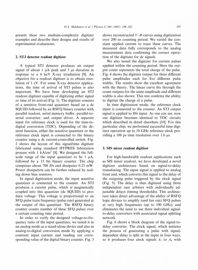
A typical STJ detector produces an outputsignal of about 1 lA peak and 5 ls duration inresponse to a 6 keV X-ray irradiation [9]. Anobjective for a readout digitizer is to obtain reso-lution of 1 eV. For some X-ray detector applica-tions, the time of arrival of STJ pulses is alsoimportant. We have been developing an STJreadout digitizer capable of digitizing either signalor time of its arrival (Fig. 1). The digitizer consistsof a sensitive front-end quantizer based on a dcSQUID followed by an RSFQ binary counter withparallel readout, serial memory buffer, parallel-to-serial converter, and output driver. A separateinput for reference clock is used for the time-to-digital conversion (TDC). Depending of the de-sired function, either the sensitive quantizer or thereference clock input is connected to the binarycounter using a dc current-controlled switch. Fig.2 shows the layout of this signal/time digitizerfabricated using standard HYPRES fabricationprocess with 1 kA/cm2 [8]. We designed the full-scale range of the input quantizer to be 1 lA,followed by a 15 bit binary counter. The chipcomprises about 700 JJs and dissipates 0.25 mW.Power dissipation can be further reduced by scal-ing down bias resistors.
In signal digitization mode, the input sensitivequantizer is connected to the counter. An STJproduces a current pulse, which is magneticallycoupled into this quantizer (dc SQUID) to pro-duce voltage. This voltage is proportional to anSFQ pulse train frequency (pulse rate) generated atthe output of this quantizer. The RSFQ binarycounter counts number of these SFQ pulses overa certain counting time period.
In order to verify the designed voltage-to-fre-quency ratio of the input quantizer, we tested it inan analog mode as a stand-alone device and also inanalog-to-digital conversion mode by applying aconstant input current and reading out corre-sponding value of the digital binary counter. Fig. 3
shows reconstructed V –U curves using digitizationover 200 ns counting period. We varied the con-stant applied current to trace these curves. Themeasured data fully corresponds to the analogmeasurement data confirming the correct opera-tion of the digitizer for dc signals.
We also tested the digitizer for current pulsesapplied within the counting period. Here the out-put count represents the total charge of the pulse.Fig. 4 shows the digitizer output for three differentpulse amplitudes each for five different pulsewidths. The results show the excellent agreementwith the theory. The linear curve fits through thecount outputs for the same amplitude and differentwidths is also shown. This test confirms the abilityto digitize the charge of a pulse.
In time digitization mode, the reference clockinput is connected to the counter. An STJ outputsignal is applied to Hit input. As one can see, nowour digitizer becomes identical to TDC circuitswhich described in detail elsewhere [10]. For thisparticular chip, we performed successful time digi-tizer operation up to 10 GHz reference clock pro-viding a 100 ps time resolution over 1.6 ls.
3. SIS mixer readout digitizer
For high-bandwidth readout applications suchas SIS mixer readout, we have developed a noveldigitizer architecture based on signal-to-delaytransducing. The input signal is applied to analogfront end, which converts this signal to the delay ofthe outgoing pulse triggered by the clock signal(Fig. 5). The delay is then digitized using threeindependent race arbiters with individually ad-justable delays (timing thresholds). This architec-ture takes direct advantage of the ability of RSFQlogic devices to amplify (and fan out) SFQ pulsesat very high frequencies (up to 100 GHz), andeliminates the need to use three individual signal-to-delay converters with associated signal splittingnetwork.
Fig. 6 shows a block diagram of the signal-to-delay converter. The clock signal, which initiatesthe process of generating a pulse with signal-dependent delay is split at the input in four ways,so it produces four clock signals A1 to A4 with
O.A. Mukhanov et al. / Physica C 368 (2002) 196–202 197

individually adjustable delays. The clock pulses A1
and A4 are recombined using an inductive merger.The circuit is designed in such a way that theoutput junction J1 generates only one SFQ pulse.
This pulse is released somewhere in-between thoseindividual clock pulses from A1 to A4 branchesdepending on the value of the input signal appliedmagnetically to the inductor L1. Fig. 7 shows this
Fig. 1. (a) Block diagram of an STJ readout circuit that can perform either signal or time digitizer functions. (b) Block diagram of the
RSFQ digital counter with memory buffer, a shift register, allows the time digitizer to store several time stamps between multiple input
pulses. The parallel-to-serial converter reduces the number of outputs.
198 O.A. Mukhanov et al. / Physica C 368 (2002) 196–202

relationship between the input signal and theoutput pulse delay in a graphical form. The mo-ment of the output pulse release is determined bycrossing the plotted curve with a horizontal linerepresenting a given value of the input signal. Forinstance, signal S1 crosses the curve a half-waybetween the clock pulses A1 and A4. Smaller inputsignal would cause the output pulse to be releasedearlier (closer to A1), while larger signal will shift itcloser to A4. In order to obtain a high-sensitivitycomparator, the transducer is followed by a racearbiter device. In our design, we use for this pur-pose a so-called set-read-clear cell (SRC cell),which is a variation of a RSFQ logic B flip-flop[11]. It operates as follows: the cell periodicallyreceives read signal and clear clock signals. If the
variable-delay signal arrives before the read signal,an output of ‘‘1’’ is generated, while if it arrivesafter the read signal, it would not be read out, butrather will be erased or cleared. In Fig. 7, the po-sition of ‘‘read’’ signal is marked as point C, whilethe position of the clear signal is marked as B andB� (the latter is clear signal of the next clock pe-riod). As one can see, by changing the position ofthe ‘‘read’’ timing threshold one can implement asignal comparator with a threshold position vari-able from point S0 to S2, i.e. in a quite large dy-namic range.
A photograph of a complete digitizer integratedcircuit providing full implementation of the blockdiagram (Fig. 5) is shown in Fig. 8. The digitizeroccupies a small portion of a HYPRES standard
Fig. 2. Chip layout of the STJ readout digitizer (5� 5 mm2).
O.A. Mukhanov et al. / Physica C 368 (2002) 196–202 199

5� 5 mm2 chip. It is implemented in HYPRESstandard Nb technology with 1 kA/cm2 criticalcurrent density [8].
Fig. 9a shows operation of the digitizer at highclock rate (10 GHz) with low-speed clock signal.The observed that amount of threshold noise
Fig. 4. The time integral of several current pulses of varying widths and amplitudes were digitized. The linear fits for each data set
corresponding to three different pulse amplitudes (Apulse) are shown.
Fig. 3. Reconstructed V –U curves for three different SQUID bias values. The dc input to the primary coil of the transformer coupled
to the front-end SQUID (high-sensitivity input) was varied and the number of SFQ pulses was counted in a 200 ns counting period.
The counts are proportional to the SFQ pulse frequency that is proportional to the voltage across the dc SQUID.
200 O.A. Mukhanov et al. / Physica C 368 (2002) 196–202

(which is about 1 lA in Fig. 9) does not changeconsiderably from low-frequency clock up toabout 10–11 GHz. At higher clock rates the noise
Fig. 7. Signal-to delay conversion curves of the digitizer front
end.
Fig. 9. Operation of the digitizer at high clock speed (a) 10
GHz, (b) 17 GHz and with low-speed input signal. Traces from
top to bottom are input signal, three comparator outputs (0.2
mV each), output signal reconstruction from the on-chip digi-
tal-to-analog converter (0.2 mV). The digitizer sensitivity can be
estimated from the circuit periodic response to the input signal:
the period in this ADC is 8.6 lA. The noise at 10 GHz is about1 lA, while at 17 GHz is about 3 lA.
Fig. 8. Photograph of a 2-bit 10 GS/s RSFQ digitizer for SIS
mixer readout. The chip size is 5� 5 mm2. The area shown is
1:7� 1:3 mm2.
Fig. 6. Implementation of the digitizer front end based on a
four-arm signal-to-delay transducer.
Fig. 5. Block diagram of a 2-bit signal digitizer for an SIS
mixer readout based on signal-to-delay conversion and timing
arbitration.
O.A. Mukhanov et al. / Physica C 368 (2002) 196–202 201

performance gets progressively worse, for instanceat 17 GHz clock (the highest clock frequency wehad operated our digitizer) it approaches about 3lA (Fig. 9b).
It worth noting that the digitizer has the abilityto achieve much better sensitivity under optimalconditions. It is seen that in Fig. 9, we have alsosharp thresholds coinciding in all three compara-tors. The reason for their better noise is highersignal-to-delay conversion ratio (which is abouttwo orders of magnitude higher near these thresh-olds). We measured that the threshold width canbe reduced by this technique to 100 nA.
Fig. 10 shows the results of a beat frequency testof the digitizer at 10 GHz (both analog signal andclock). This test proves the ability of our digitizerto digitize high input bandwidth signals.
4. Conclusions
We have shown two possible applications formid-complexity RSFQ readout digitizers. Theycan bring much greater functionality compared totraditional SQUID-based readouts placed in thenearest vicinity of sensors including e.g. STJs andSIS mixers. All these digitizers are built using a
combination of a sensitive front-end quantizerbased on dc SQUID followed by high-speed digitalRSFQ circuitry.
Compared to traditional analog SQUIDs, thesedigitizers require availability of a fabrication pro-cess capable of producing RSFQ chips with severalhundreds of junctions integrated on a single chip.This integration level is well within capabilities ofexisting Nb fabrication foundries.
Acknowledgements
Authors would like to thank Drs. V. Semenov,T. Oku, H. Shimizu, and D. Martin for valuablediscussions.
References
[1] K.K. Likharev, O.A. Mukhanov, V.K. Semenov, in: H.-D.
Hahlbohm, K. L€uubbig (Eds.), SQUID’85, Walter de
Gruyter, Berlin, 1985, pp. 1103–1108.
[2] O.A. Mukhanov, V.K. Semenov, K.K. Likharev, IEEE
Trans. Magn. MAG-23 (1987) 759–762.
[3] M. Dorojevets, P. Bunyk, D. Zinoviev, K. Likharev, FED
J. 10 (2000) 3–14.
[4] D.K. Brock, O.A. Mukhanov, J. Rosa, IEEE Commun.
Mag. 39 (2001) 174–179.
[5] V.K. Semenov, Yu.A. Polyakov, in: H. Koch, S. Knappe
(Eds.), Extended Abstracts of ISEC’97, PTB, Berlin, 1997,
pp. 329–331.
[6] M. Radparvar, S. Rylov, IEEE Trans. Appl. Supercond. 7
(1997) 3682–3685.
[7] D. Gupta, M. Radparvar, IEEE Trans. Appl. Supercond.
11 (2001) 1261–1264.
[8] HYPRES Design Rules, available at www.hypres.com.
[9] T. Oku, T. Ikeda, C. Otani, K. Kawai, H. Sato, H.
Shimizu, H. Miyasaka, Y. Takizawa, H. Watanabe, W.
Ootani, H. Akoh, H. Nakagawa, M. Aoyagi, T. Taino,
in: T. Kobayashi, M. Tonouchi (Eds.), Extended Abstracts
of ISEC’01, Osaka, 2001, pp. 319–320.
[10] O.A. Mukhanov, A.F. Kirichenko, J.M. Vogt, M.S.
Pambianchi, IEEE Trans. Appl. Supercond. 9 (1999)
3619–3622.
[11] S.V. Polonsky, V.K. Semenov, A.F. Kirichenko, IEEE
Trans. Appl. Supercond. 4 (1994) 9–18.
Fig. 10. Beat frequency test of a 2-bit digitizer at 10.000000
GHz clock and 10.000005 GHz signal. Upper traces––outputs
of the three comparators (0.2 mV each), bottom trace––output
of the on-chip DAC (0.2 mV). Period of output beat signal is
5 kHz. The signal amplitude is 2 lA peak-to-peak.
202 O.A. Mukhanov et al. / Physica C 368 (2002) 196–202


