Embed Size (px)
Citation preview

IOP PUBLISHING JOURNAL OF PHYSICS D: APPLIED PHYSICS
J. Phys. D: Appl. Phys. 40 (2007) 4691–4700 doi:10.1088/0022-3727/40/15/051
Rate dependent strengths of some solderjointsD M Williamson1, J E Field, S J P Palmer and C R Siviour
Department of Physics, University of Cambridge, Cavendish Laboratory, J J ThomsonAvenue, Cambridge, CB3 0HE, UK
E-mail: [email protected]
Received 22 April 2007, in final form 23 April 2007Published 20 July 2007Online at stacks.iop.org/JPhysD/40/4691
AbstractThe shear strengths of three lead-free solder joints have been measured overthe range of loading rates 10−3 to ∼105 mm min−1. Binary (SnAg), ternary(SnAgCu) and quaternary (Castin: SnAgCuSb) alloys have been comparedto a conventional binary SnPb solder alloy. Results show that at loadingrates from 10−3 to 102 mm min−1, all four materials exhibit a linearrelationship between the shear strength and the loading rate when the dataare plotted on a log–log plot. At the highest loading rate of 105 mm min−1,the strengths of the binary alloys were in agreement with extrapolationsmade from the lower loading rate data. In contrast, the strengths of thehigher order alloys were found to be significantly lower than those predictedby extrapolation. This is explained by a change in failure mechanism on thepart of the higher order alloys. Similar behaviour was found inmeasurements of the tensile strengths of solder joints using a novel high-rateloading tensile test. Optical and electron microscopy were used to examinethe microstructures of interest in conjunction with energy dispersive x-rayanalysis for elemental identification. The effect of artificial aging and reflowof the solder joints is also reported.
1. Introduction
Electronic devices are increasingly mobile, and therefore proneto experience more severe shocks, for example from beingdropped, than in the past. These devices often undergo thermalcycling, due to heating of the device when in use, whichinduces rapid ageing of the solder, characterised by graingrowth [1] and diffusion of metals from the substrate into thesolder [2]. Grain growth is known to contribute to weakeningof materials [3,4], and intermetallics act to embrittle the joints.Finally, the introduction of lead-free solders, on environmentalgrounds, means that it is necessary to evaluate the strengths ofboth traditional and lead-free solders for future use [5].
Until recently, most research into solder has dealt withthe effects of thermal fatigue and ageing [6], and that whichhas dealt with the strain rate sensitivity of the materialwas mainly concerned with quasistatic or creep behaviour[7–23]. However, the increase in use of mobile telephonesand computers means that solder joints are regularly loaded
1 Author to whom any correspondence should be addressed.
at strain rates higher than those previously considered, indrop impacts, for example [24, 25]. Surface mounting ofcomponents means that during an impact, causing a suddendeceleration of the device, the joint must transfer the wholemomentum of a component to the board. Therefore, in orderto understand more fully the processes that take place in theseevents, measurements of the strength of solders must now beextended to higher strain rates.
As noted above, electronic products are susceptibleto accelerated ageing due to the relatively high operatingtemperatures within such devices. Solder alloys are typicallychosen to have a low melting point. This makes the jointseasier to form but also means that they are continually at a highfraction of their melting point when in use, which encouragescreep, stress relaxation and microstructural changes. Thermalageing causes reduction in the shear strength of the materialthrough grain growth [1, 26, 27] and intermetallic growth.Adhesion between the solder and the PCB is provided byan intermetallic layer. However, with age the layer grows,the joint becomes brittle and the adhesive strength is reduced[28–31]. Thermal cycling also occurs, which introduces cyclic
0022-3727/07/154691+10$30.00 © 2007 IOP Publishing Ltd Printed in the UK 4691

D M Williamson et al
Table 1. The solders studied, their composition and melting points.
Name Composition Tm (◦C)
SnPb 63% Sn,37% Pb 183SnAg 96.5% Sn, 3.5% Ag 221SnAgCu 95.5% Sn, 3.8% Ag, 0.7% Cu 216Castin 96.2% Sn, 2.5% Ag, 0.8% Cu, 0.5% Sb 217
deformation into the joint, due to the different thermalexpansion coefficients of the component and circuit board. Theshear strains induced by this cycling can be up to 10% [28].
A further stimulus for research on lead-free solders is theneed to replace lead on environmental grounds [32]. Therefore,there is currently a need for an examination of the dynamicproperties of both traditional and lead-free solders. This willprovide data for constitutive modelling of the alloys currentlyin use and to assist with understanding the strength of realjoints.
Recent research in this laboratory has concentrated onmeasuring the dynamic properties of bulk solders and solderjoints in compression, shear and tension. Siviour et al [33]describes the use of split Hopkinson pressure bar (SHPB)techniques to record the properties of five solders as a functionof strain rate over the range of 200–4000 s−1, temperatureand thermal ageing. This paper describes the measurementof the shear strength of the solder balls attached to a PCB,using an instrumented lateral force device for loading rates inthe range 10−3–102 mm min−1 and at 105 mm min−1 using amodified SHPB. Finally, a spall test, using liquid impact, hasbeen devised for assessing the dynamic tensile strengths ofsolder ball/PCB connections.
2. Experimental
PCBs (LUCENT 388 PBGA) were provided containing fourkinds of solder material in two rows of nine balls aroundtheir periphery. The pitch between solder balls was 2.54 mmwith nominal diameters of the balls of 760 µm. Table 1lists the solders studied, their compositions and their meltingpoints, Tm.
The shear strength of a solder joint was determined bymeasuring the maximum lateral force required to shear a solderball off its mounting on the PCB. In what follows, the loadingrates quoted refer to the speed of the blade.
2.1. Loading rates 10−3 to 102 mm min−1
The shear strength of solder joints for loading rates from10−3 to 102 mm min−1 were measured using an Instron 4466testing machine. Solder balls were tested individually, usinga flat-faced blade fabricated from brass. Figure 1 shows theexperimental apparatus.
The Instron is a displacement-controlled machine fromwhich the time, load and displacement data can be recorded.The solder board mount sits upon an x–y stage allowingprecision adjustment, all the balls on a given row can be testedby repositioning the mount accordingly. Sheared solder ballsand PCBs were retained for analysis by microscopy.
Figure 1. A PCB is mounted with the brass blade ready to movedown and shear off a solder ball.
Figure 2. The Hopkinson bar attachment constructed from Dural.The two PCBs are separated by a spacer. The blade can shear off upto two balls from each board simultaneously.
2.2. Loading rate range 105 mm min−1
The shear strength of solder joints at loading rates∼105 mm min−1 (equivalent to a strain rate of ∼2200 s−1),were obtained using a modified SHPB. An attachment wasdesigned and built that enabled solder balls to be sheared offeither singly, or in pairs, from either PCB using the SHPB in acompression configuration. Figure 2 shows a photograph of theattachment. Dural was the material of choice for the bars andattachment as it has one of the lowest mechanical impedancesof common and readily machined metallic materials, and bestmatches that of the solder material. By constructing theattachment from the same material as the bars, unwantedreflections are reduced.
The blade was constructed as an end-cap for the output-barwhilst the body of the jig holding the PCB boards is mountedon the input-bar. This configuration minimises noise on thetransmitted wave from which the shear forces are calculated.
4692

Rate dependent strengths of some solder joints
Blade speeds of between 3 and 12 m s−1 were achievable, withload-time data recorded by an oscilloscope and downloadedto a desktop computer. Measurements of the blade speedwere performed directly from the shear force history usingknowledge of the distance from the solder ball to the shoulderof the blade which, in coming in to contact with the jig body,produces an obvious signal in the force record. The numberof solder balls removed could be controlled by changing thelateral position of the PCB within the rig. In situations wereseveral solder balls are removed simultaneously, the shear forcewas obtained by dividing the maximum load recorded by thenumber of balls removed.
2.3. Dynamic tensile strength of solder joints; a spall test
This is a more difficult measurement to make than shear orcompression. At low rates, there has been some success [34] indesigning a device which grips the solder ball and pulls it awayfrom the mounting. This usually involves some deformationof the solder ball and is not suitable for high-rate loading ofthe joint.
We have designed a new test based on spall. Thisinvolves generating a compression pulse which passes acrossthe interface and then changes phase to tension when it reflectsat a free surface, see, for example Kolsky [35]. Some way infrom the free surface the resultant pulse becomes tensile and,when it exceeds the tensile strength of the material, failureresults. Since solder balls are small (diameter ∼0.75 mm), theloading pulse has to be less than about 100 ns. Such pulsescan be generated by lasers or liquid impact. In this paper,we use equipment (multiple impact jet apparatus, MIJA) wehave developed for producing controlled liquid impacts for rainerosion studies of aerospace materials. Coad et al [36] andField [37] describe the equipment and give the theory of liquidimpact. Velocities in the range up to 600 m s−1 can readilybe achieved, and this produces pressures (due to compressiblebehaviour of the liquid in the early stages of impact) of up to1.6 GPa. Pulse durations, which depend on the radius of theimpacting liquid in the contact area, can achieve the ∼100 nsrequired.
A simple holder was machined from dural such that thereverse side of the PCB was exposed to the incident waterjet. A hollow in the holder provided space for any spalledmaterial to be contained and recovered. A vacuum pump,incorporated in the MIJA facility, held the holder in placeon a computer-controlled x–y stage, which can be used toposition a desired solder ball joint directly under the water jet.In practice, several solder balls were removed per shot, suchwere the characteristics of the impact. The number of solderballs removed per shot was recorded as a function of incidentjet velocity.
3. Results
3.1. Shear; loading rates 10−3–102 mm min−1
For each experiment, a force-displacement curve was producedrepresenting the loading path of the solder ball. The area underthis curve, see figure 3 for an example, represents the workperformed in shearing a solder ball from its pad, i.e. the total
Figure 3. Load–displacement curve for shearing off a Castin solderball from its pad using a blade speed of 1.00 mm min−1. Data wereacquired at a rate of one reading per second.
Table 2. Total energy required to shear a virgin solder ball from itspad for each of the four materials, blade speed 1.00 mm min−1, atroom temperature.
Material Total energy (mJ)
SnPb 4.0 ± 0.1SnAg 4.6 ± 0.6SnAgCu 5.7 ± 0.8Castin 6.0 ± 0.3
energy required to remove the solder ball. By integrating theforce–displacement curves to find the areas, comparisons canbe made between the four material types. The results are givenin table 2.
Each value in table 2 represents the mean of at least fourmeasurements, the error quoted is the standard deviation inthat mean. It can be seen that solder balls made from differentmaterials require different amounts of energy to shear off. Inall of these experiments, the joints failed by shear within thebulk of the solder balls.
3.2. Shear; loading rate 105 mm min−1
Experiments at this loading rate were carried out using theapparatus shown in figure 2, which was held in the SHPBapparatus. The force trace obtained from the output bar givesa direct measurement of the force transmitted by the solder ballinto the blade. Typical output traces are shown in figure 4; twotraces are shown for a pair of balls being removed and a singletrace for one ball. The results are encouragingly consistent;the traces for the pairs of balls being very similar, and bothbeing twice the magnitude of the single ball trace.
Table 3 shows that at the high loading rate of∼105 mm min−1, the binary alloys are stronger than the ternaryand quaternary alloys of SnAgCu and Castin by a factor of overtwo.
Microscopic examination of the failure surfaces showsthat there are differences in failure mechanisms. In the caseof the binary alloys SnPb and SnAg, the interface between the
4693

D M Williamson et al
Figure 4. Traces showing one and two solder balls being removed.
Table 3. Summary of Hopkinson bar results.
Mean blade Mean peak force Number ofMaterial speed (m s−1) per ball (N) experiments
SnPb 2.6 ± 0.3 54 ± 6 6SnAg 2.9 ± 0.3 52 ± 7 7SnAgCu 2.7 ± 0.6 16 ± 4 5Castin 3.3 ± 0.8 22 ± 9 7
solder and pad is sufficiently strong that shearing takes placewithin the bulk material, as per low rates. However, in thecase of the higher order alloys SnAgCu and Castin, it is theinterface which fails, leaving clean, characteristically brittle,fracture surfaces.
3.3. Rate dependence of shear strengths
Figures 5 and 6 show the peak shear forces required to removethe virgin (unaged) binary and higher order alloys solder ballsrespectively over the range of speeds investigated. In the caseof the binary alloys, the highest shear speed data lies on thesame trend line as the low-speed data. The SnAg materialwas approximately 20% stronger than the SnPb over the rangeof loading rates investigated. In the case of the higher orderalloys, the highest rate data falls short of the values one wouldexpect based upon an extrapolation of the low-speed data; thiscorresponds to a change in failure mechanism (see below). Nostatistically significant difference in strength is seen betweenthe higher order alloys.
Figure 7 shows optical micrographs of the failed boardspost SHPB testing. Note that in the case of SnAg (a) thecopper pad has also been partially removed to reveal the PCBstructure underneath. This occasionally happened, but onlyfor bimetallic solders. The SnPb (b) has undergone ductilefracture as was most common for the bimetallic solders. TheSnAgCu (c) and Castin (d) materials consistently failed at theinterface.
3.4. Effect of accelerated ageing on shear strength
Accelerated ageing was achieved by thermally cycling thePCBs through temperatures of −40 ◦C to +125 ◦C a prescribednumber of times, either 500 or 1000 cycles. Theseconditions are referred to as 500TC and 1000TC, respectively.
Figure 5. Rate dependent binary alloy shear strengths.
Figure 6. Rate dependence higher order alloy shear strengths.
Comparisons are made with the unaged solder joint shearstrengths.
The effect of thermal aging on SnAg is to reduce the shearstrength of the joint by approximately 20% over the completerange of blade speeds tested. There is no discernable differencebetween the 500TC and the 1000 TC data indicating that themechanism responsible for the reduction in strength appearsto have saturated. Figure 8 shows the data together with linesof best fit.
The effect of artificial aging on SnPb is most pronounced atthe highest rates of shearing performed on the SHPBs. At theserates, the strengths are reduced by factors of approximately25% and 40% from the unconditioned strength for the 500TCand the 1000TC artificially aged joints, respectively. It isclear from the 500TC data that the spread of results is alsoincreased. Within the slow-speed data any differences aremuch less pronounced and masked by the data spread. Figure 9shows the data with lines of best fit.
The effect of 1000TC thermal aging upon the SnAgCusolder joints is to reduce the shear strength by approximately20% over the range of rates tested in the Instron (10−3–102 mm min−1). When tested in the SHPB, there is nodiscernable difference between the data from the 500TC
4694

Rate dependent strengths of some solder joints
Figure 7. Optical micrographs comparing different types of failure.(a) SnAg, (b) SnPb, (c) SnAgCu, (d) Castin. See body text fordescription.
Figure 8. Effect of thermal ageing on SnAg solder joint strength asa function of rate.
samples and the 1000TC samples. Figure 10 shows the datawith linear lines fitted to the Instron data and extrapolated upto SHPB speed data.
The effect of 1000TC thermal aging upon the Castin solderjoints is to reduce the shear strength by approximately 20%over the range of blade speeds tested in the Instron (10−3–102 mm min−1). At SHPB rates the unaged data exhibits alarge spread, which encapsulates the aged data. Figure 11shows the data with linear fits to the Instron data, extrapolatedup to SHPB rates.
3.5. Effect of reflow on shear strength
Reflow refers to the process of effectively remaking the solderjoint. The PCB passes through an oven and is subjected tovarying temperatures dictated by a thermal profile. Once the
Figure 9. Effect of thermal ageing upon SnPb solder joint strengthas a function of rate.
Figure 10. Effects of artificial ageing upon SnAgCu solder jointstrength as a function of rate.
Figure 11. Effects of thermal ageing upon Castin solder jointstrength as a function of rate.
4695

D M Williamson et al
Figure 12. Effects of reflow upon SnAg joint strength as a functionof rate.
Figure 13. Effects of reflow upon SnPb joint strength as a functionof rate.
melting point of the solder is reached surface tension collapsesthe paste and forms the joint. PCBs were evaluated that hadundergone this process three and six times, they are referredto as ‘3 × reflow’ and ‘6 × reflow’ respectively. Comparisonsare made to singly processed solder joints.
The results of measuring the shear strength of reflowedSnAg are shown in figure 12. It would appear that withinthe loading-rates investigated, the reflow process made nodiscernable difference to the shear strength of the SnAg solderjoint. The effect of reflowing the SnPb solder joint is mostpronounced at the lowest speeds investigated where there is anapproximately 45% increase in strength. The rate sensitivityof the refluxed solder joints is apparently reduced, resulting ina crossover of the fitted lines and a high-speed reflow strengthless than that of the virgin solder balls. The results obtainedare shown in figure 13.
The results of measuring the shear strength of refluxedSnAgCu are shown in figure 14. It would appear that withinthe range of speeds investigated with the Instron, the reflowprocess made no discernable difference to the shear strengthof the SnAgCu solder joint. However, at the speeds achieved
Figure 14. Effects of reflow upon SnAgCu joint strength as afunction of rate.
Figure 15. Effects of reflow upon Castin joint strength as a functionof rate.
with the SHPB, the shear strength would appear to be increasedcompared to that of the virgin material and comes somewhatcloser to the value expected if one extrapolates the slow-speeddata.
The effect of reflowing the Castin joints would appear tobe a reduction in the rate sensitivity of the shear strength of thejoints within the range of rates evaluated using the Instron. AtSHPB speeds no discernable difference is seen in the soldershear strength. The results obtained are shown in figure 15.
3.6. Spall strength from liquid impact
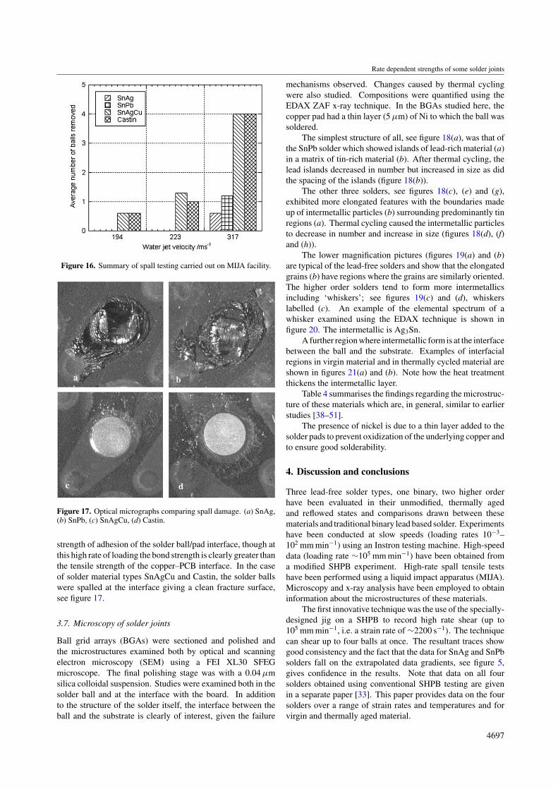
Several firing pressures were used to propel the water jets atdifferent velocities thereby exerting a range of forces on thejoints. In total, over fifty shots were performed. Figure 16summarises the results.
In the case of solder material types SnAg and SnPb, itwould appear that the solder ball/pad interface is sufficientlystrong that the copper pad substrates preferentially spall fromthe PCB, taking small amounts of PCB with them. This leavesvery rough fracture surfaces. It is not possible to determine the
4696
Rate dependent strengths of some solder joints
Figure 16. Summary of spall testing carried out on MIJA facility.
Figure 17. Optical micrographs comparing spall damage. (a) SnAg,(b) SnPb, (c) SnAgCu, (d) Castin.
strength of adhesion of the solder ball/pad interface, though atthis high rate of loading the bond strength is clearly greater thanthe tensile strength of the copper–PCB interface. In the caseof solder material types SnAgCu and Castin, the solder ballswere spalled at the interface giving a clean fracture surface,see figure 17.
3.7. Microscopy of solder joints
Ball grid arrays (BGAs) were sectioned and polished andthe microstructures examined both by optical and scanningelectron microscopy (SEM) using a FEI XL30 SFEGmicroscope. The final polishing stage was with a 0.04 µmsilica colloidal suspension. Studies were examined both in thesolder ball and at the interface with the board. In additionto the structure of the solder itself, the interface between theball and the substrate is clearly of interest, given the failure
mechanisms observed. Changes caused by thermal cyclingwere also studied. Compositions were quantified using theEDAX ZAF x-ray technique. In the BGAs studied here, thecopper pad had a thin layer (5 µm) of Ni to which the ball wassoldered.
The simplest structure of all, see figure 18(a), was that ofthe SnPb solder which showed islands of lead-rich material (a)in a matrix of tin-rich material (b). After thermal cycling, thelead islands decreased in number but increased in size as didthe spacing of the islands (figure 18(b)).
The other three solders, see figures 18(c), (e) and (g),exhibited more elongated features with the boundaries madeup of intermetallic particles (b) surrounding predominantly tinregions (a). Thermal cycling caused the intermetallic particlesto decrease in number and increase in size (figures 18(d), (f)and (h)).
The lower magnification pictures (figures 19(a) and (b)are typical of the lead-free solders and show that the elongatedgrains (b) have regions where the grains are similarly oriented.The higher order solders tend to form more intermetallicsincluding ‘whiskers’; see figures 19(c) and (d), whiskerslabelled (c). An example of the elemental spectrum of awhisker examined using the EDAX technique is shown infigure 20. The intermetallic is Ag3Sn.
A further region where intermetallic form is at the interfacebetween the ball and the substrate. Examples of interfacialregions in virgin material and in thermally cycled material areshown in figures 21(a) and (b). Note how the heat treatmentthickens the intermetallic layer.
Table 4 summarises the findings regarding the microstruc-ture of these materials which are, in general, similar to earlierstudies [38–51].
The presence of nickel is due to a thin layer added to thesolder pads to prevent oxidization of the underlying copper andto ensure good solderability.
4. Discussion and conclusions
Three lead-free solder types, one binary, two higher orderhave been evaluated in their unmodified, thermally agedand reflowed states and comparisons drawn between thesematerials and traditional binary lead based solder. Experimentshave been conducted at slow speeds (loading rates 10−3–102 mm min−1) using an Instron testing machine. High-speeddata (loading rate ∼105 mm min−1) have been obtained froma modified SHPB experiment. High-rate spall tensile testshave been performed using a liquid impact apparatus (MIJA).Microscopy and x-ray analysis have been employed to obtaininformation about the microstructures of these materials.
The first innovative technique was the use of the specially-designed jig on a SHPB to record high rate shear (up to105 mm min−1, i.e. a strain rate of ∼2200 s−1). The techniquecan shear up to four balls at once. The resultant traces showgood consistency and the fact that the data for SnAg and SnPbsolders fall on the extrapolated data gradients, see figure 5,gives confidence in the results. Note that data on all foursolders obtained using conventional SHPB testing are givenin a separate paper [33]. This paper provides data on the foursolders over a range of strain rates and temperatures and forvirgin and thermally aged material.
4697

D M Williamson et al
Figure 18. (a) Virgin SnPb microstructure, (b) 1000TC SnPb microstructure, (c) virgin SnAg bulk microstructure, (d) 1000TC SnAg bulkmicrostructure, (e) virgin SnAgCu microstructure, (f) 1000TC SnAgCu microstructure, (g) virgin Castin bulk microstructure and(h) 1000TC Castin bulk microstructure.
The binary solder of virgin joints have high-rate strengthsthat are consistent with the trend lines extrapolated fromthe low-speed experiments; on a log–log plot the strength-shear speed trend is linear, an observation made byprevious researchers [52, 53]. These data could thereforebe described by models such as the Cowper–Symondsmodel [54], previously used for solder [53], or the Zerilli–Armstrong model [55], both of which predict this form ofrelationship.
The higher order alloys show a similar dependence ofstrength on strain rate, but only at the lower rates investigatedon the Instron. The data from the higher rate SHPBexperiments show strengths that are significantly lower thanthose one would expect based on extrapolations of the low-rate data.
The micrographs in figure 7 show the differentmechanisms operating. The SnAg solder (figure 7(a)) has thehighest strength of all the solders at this top rate of loading. Infact, it appears that the strength of the solder is now comparableto the strength of the bonding of the copper pad. The SnPbsolder (figure 7(b)) continues to shear in the solder material asfor all of the lower rates of loading. The SnAgCu and Castinsolders are now weakest at the interfaces. The position of thefailure, and large spread of data points suggest that this is dueto the intermetallics in the interlayer (see table 4).
The effect of thermal aging is to reduce the strengths ofthe alloys. The largest changes occur with the SnPb solder andsince it has the simplest microstructure (lead-rich particles in atin-rich matrix, see figure 18(a) and (b) it is possible to measurethe grain sizes and their changes for virgin, 500TC and 1000TC
4698

Rate dependent strengths of some solder joints
Figure 19. Optical micrographs of (a) virgin SnAg, (b) virgin Castin, (c) virgin SnAgCu and (d) 1000TC SnAgCu sectioned and polishedballs on PCB.
Figure 20. X-ray spectrum of Ag3Sn intermetallic taken fromSnAgCu 1000 TC whisker.
solder. If the material follows a Hall–Petch relationship [3,4],then [3, 4], then strength should be proportional to (grainsize)−0.5, the observed changes fit this explanation very well.
The microstructure of the other alloys is more complex(see figures 18(c) to (h)) although the grains and boundaryparticles again coarsen with age. The added feature at thehighest rate of shear is the change of failure mechanismto interfacial failure which is attributed to the growthof intermetallics at the interface (see figures 19, 20 andtable 4).
Reflow increases the low-speed shear strength of thelead based solder by 44% at most. This effect reduces withincreasing blade speed. Reflow appears to have little tono effect on the lead-free solder joints with the exceptionof SnAgCu, where the high-rate strength appears to recoverslightly to values closer to the strength predicted if oneextrapolates the low-rate data.
Figure 21. (a) Virgin SnAgCu interfacial microstructure and (b)1000TC SnAgCu interfacial microstructure.
The tensile strengths of solder joints at high rates ofloading were studied using a second novel technique, basedon spall and described in section 2.3. The results show that theinterfaces of the SnAgCu and Castin solders are weakest. Thisagrees with the high shear strength data and the postulated roleof intermetallics.
Based purely on mechanical considerations and theevidence presented in this paper, of the solders researchedhere the authors conclude that SnAg is the most suitable as
4699

D M Williamson et al
Table 4. Intermetallic Compounds.
Present in Present atSolder bulk material interface with pad
SnPb Islands of Pb in Sn Ni3Sn4
SnAg Sn surrounded by particles Ni3Sn4
of Ag3SnSnAgCu Sn surrounded by particles Cu–Sn–Ni, Ag3Sn.
of Ag3Sn, Cu–Sn, Cu6Sn5 Large whiskers Ag3SnCastin Sn, Sn surrounded by particles Cu–Sn–Ni whiskers
Ag, Cu, Sb of Ag3Sn, Cu–Sn, Cu6Sn5 of Cu6Sn5
a replacement to the lead based solder. The reasons for this aretwofold; the first is that over the range of speeds evaluatedSnAg had at all times superior shear strength over SnPb.The second is that at the highest rates of testing the solderball/substrate interface retained its integrity and strength; this isin stark contrast to the higher order alloys SnAgCu and Castin,which were significantly weaker than one would expect basedupon the low speed trend lines. This last point illustrates theimportance of dynamic testing of lead-free solder candidates.
Acknowledgments
This research is part of a collaboration project with the Instituteof Micro-electronics (IME), Singapore and the NationalUniversity of Singapore (NUS). Ee Hau (IME) is thanked forcoordinating the project and Professors C T Lim and V Tan fortheir input. R Flaxman is thanked for his help with the samplepreparation and construction of the loading devices andJ Rickard for his help with the SEM.
References
[1] Jung K and Conrad H 2001 J. Electron. Mater. 30 1294–302Jung K and Conrad H 2001 J. Electron. Mater. 30 1303–07Jung K and Conrad H 2001 J. Electron. Mater. 30 1308–12
[2] Ho C E, Chen W T and Kao C R 2001 J. Electron. Mater.30 379–85
[3] Armstrong R W, Codd I, Douthwaite R M and Petch N J Phil.Mag. 7 45–58
[4] Armstrong R W 2001 Encyclopaedia of Materials: Scienceand Technology (Elsevier: Amsterdam) pp 7103–14
[5] Zeng K and Tu K N 2002 Mater. Sci. Eng. R 38 55–105[6] Tummala R R (ed) 2001 Fundamentals of Microsystems
Packaging (New York: McGraw-Hill)[7] Dawson T H 1972 Metall. Trans. 3 3201[8] Wray P J 1973 Metall. Trans. 4 2475[9] Alden T H 1987 Scr. Metall. 21 735
[10] Vaynman S 1989 IEEE Trans. Compon. Hybrids Manuf.Technol. 12 469
[11] Solomon H D 1990 J. Electron. Mater. 19 929[12] Cole M and Caulfield T 1992 Scr. Metall. Mater.
27 903[13] Kawashima K, Ito T and Sakuragi M 1992 J. Mater. Sci.
27 6387[14] Liang J, Goldhardt N, Lee P S, Schroeder S A and Morris W L
1996 Fatigue Fract. Eng. Mater. Struct. 19 1401[15] Plumbridge W J and Gagg C R 1999 J. Mater. Sci.: Mater.
Electron. 10 461[16] Shi X W, Zhou W Pang J L J and Wang Z P 1999 J. Electron.
Packag. 121 179[17] Dai L H, Lee S W R and Huang X J 2000 Key Eng. Mater.
177 267
[18] Lee W S, Chen L W and Yeh L T 2001 Mater. Trans. 42 686[19] Unal O and Foley J C 2001 J. Mater. Sci. Lett. 20 1585[20] Shohji I, Yoshida T, Takahashi T and Hioki S 2002 Mater.
Trans. 43 1854[21] El-Bahay M M, El Mossalamy M E, Mahdy M and
Bahgat A A 2004 J. Mater. Sci.: Mater. Electron. 15 519[22] Shohji I, Yoshida T, Takahashi T and Hioki S 2004 J. Mater.
Sci. Eng. 366 50[23] Shohji I, Yoshida T, Takahashi T and Hioki S 2004 J. Mater.
Sci.: Mater. Electron. 15 219[24] Lim C T and Low Y J 2002 Proc. 52nd Electronics
Components and Technology Conf. (San Diego CA)(New York: IEEE) p 1270
[25] Seah S K W, Lim C T, Wong E H, Tan V B C and Shim V P W2002 Proc. 4th Electronics Packaging Technology Conf.(Singapore) (New York: IEEE) p 120
[26] Tang H and Basaran C 2001 Int. J. Damage Mech. 10 235[27] Basaran C and Wen Y 2003 J. Electron. Packag. 125 426[28] Plumbridge W J 1996 J. Mater. Sci. 31 2501[29] Lee H-T and Chen M-H 2002 Mater. Sci. Eng. E A 333 24[30] Lee T Y, Choi W J, Tu K N, Jang J W, Juo S M, Lin J K,
Frear D R, Zeng K and Kivilahti J K 2002 J. Mater. Res.17 291
[31] Zeng K and Tu K N 2002 Mater. Sci. Eng. R 38 55[32] Tu K N, Gusak A M and Li M 2003 J. Appl. Phys. 93 1335[33] Siviour C R, Walley S M, Proud W G and Field J E 2005
J. Phys. D: Appl. Phys. 38 4131–9[34] ASTM Standard F1269-06 Test method for destructive shear
testing of ball bonds[35] Kolsky J 1953 Stress Waves in Solids (Oxford: Clarenden
Press)[36] Coad E J, Pickles C S J, Seward C R, Jilbert G H and Field J E
1998 Proc. R. Soc. Lond. 454 213–38[37] Field J E 1999 Wear 233–235 1–12[38] Fields R J, Low III S R and Lucey G K Jr 1992 The Metal
Science of Joining ed M J Cieslak (Warrendale, PA: TMS)pp 165–73
[39] Sigelko J, Choi S, Subramanian K N, Lucas J P and Bieler T R1999 J. Electron. Mater. 28 1184–8
[40] Chada S, Fournelle R A, Laub W and Shangguan D 2000J. Electron. Mater. 29 1214–21
[41] Choi S, Subramanian K N, Lucas J P and Bieler T R 2000J. Electron. Mater. 29 1249–57
[42] Sigelko J, Choi S, Subramanian K N and Lucas J P 2000J. Electron. Mater. 29 1307–11
[43] Choi W K and Lee H M 2000 J. Electron. Mater.29 1207–13
[44] Moon K-W, Boettinger W J, Kattner U R, Biancaniello F Sand Handwerker C A 2000 J. Electron. Mater.29 1122–36
[45] Lee H-T and Chen M-H 2002 Mater. Sci. Eng. 333 24–34[46] Kim K S, Huh S H and Suganuma K 2002 Mater. Sci. Eng.
333 106–14[47] Maveety J G, Liu P, Vijayen J, Hua F and Sanchez E A 2004
J. Electron. Mater. 33 1355–62[48] Vianco P T, Rejent J A and Kilgo A C 2004 J. Electron. Mater.
33 1389–400[49] Allen S L, Notis M R, Chromik R R and Vinci R P 2004
J. Mater. Res. 19 1417–24[50] Allen S L, Notis M R, Chromik R R and Vinci R P 2004
J. Mater. Res. 19 1425–31[51] Ghosh G 2004 J. Mater. Res. 19 1439–54[52] Lang F, Tanaka H, Munegata O, Taguchi T and Narita T 2005
Mater. Charact. 54 223–9[53] Wang B, Zheng J and Shu D 2003 Key Eng. Mater.
233–236 181–6[54] Jones N 1989 Structural Impact (Cambridge: Cambridge
University Press)[55] Zerilli F J and Armstrong R W 1987 J. Appl. Phys.
61 1816–25
4700


