Embed Size (px)
Citation preview
Hindawi Publishing CorporationEURASIP Journal on Embedded SystemsVolume 2008, Article ID 597872, 13 pagesdoi:10.1155/2008/597872
Research ArticleSmart Camera Based on Embedded HW/SW Coprocessor
Romuald Mosqueron,1 Julien Dubois,2 Marco Mattavelli,1 and David Mauvilet1
1 GR-LSM, Faculte STI, Ecole Polytechnique Federale de Lausanne (EPFL), CH 1015 Lausanne, Switzerland2 Laboratoire LE2I, Faculte des Sciences Mirande, Universite de Bourgogne, 21000 Dijon, France
Correspondence should be addressed to Romuald Mosqueron, [email protected]
Received 1 March 2008; Revised 29 July 2008; Accepted 8 September 2008
Recommended by Guy Gogniat
This paper describes an image acquisition and a processing system based on a new coprocessor architecture designed for CMOSsensor imaging. The system exploits the full potential CMOS selective access imaging technology because the coprocessor unitis integrated into the image acquisition loop. The acquisition and coprocessing architecture are compatible with the majorityof CMOS sensors. It enables the dynamic selection of a wide variety of acquisition modes as well as the reconfiguration andimplementation of high-performance image preprocessing algorithms (calibration, filtering, denoising, binarization, patternrecognition). Furthermore, the processing and data transfer, from the CMOS sensor to the processor, can be operatedsimultaneously to increase achievable performances. The coprocessor architecture has been designed so as to obtain a unit that canbe configured on the fly, in terms of type and number of chained processing stages (up to 8 successive predefined preprocessingstages), during the image acquisition process that can be defined by the user according to each specific application requirement.Examples of acquisition and processing performances are reported and compared to classical image acquisition systems based onstandard modular PC platforms. The experimental results show a considerable increase of the achievable performances.
Copyright © 2008 Romuald Mosqueron et al. This is an open access article distributed under the Creative Commons AttributionLicense, which permits unrestricted use, distribution, and reproduction in any medium, provided the original work is properlycited.
1. INTRODUCTION
Nowadays, smart cameras are more and more applied fortheir specific performances and their processing capabilitiesin di!erent application fields. We can distinguish threetypical classes of smart cameras.
(i) Artificial retinas: in which dedicated processing isdirectly integrated aside the pixel. The processingcapabilities are usually fixed or limited to a few simpleand local functions [1–3].
(ii) Standard cameras directly connected to a computer viaa standard interfaces: all the processing is performedinto the computer CPU [4, 5].
(iii) Cameras including embedded processing units: theprocessing is performed into the camera and onlythe processing results or some image features aretransferred outside the camera [6, 7].
For the class of the artificial retinas cameras, the imageprocessing capabilities, or better the pixel imaging capabili-ties, are usually fixed locally to a small pixel neighborhood
and remain very limited in scope. No application specificprocessing can be added at the image acquisition stage.However, such kind of sensors can achieve very highfrequency acquisition rates that are necessary for some classof applications. In the case of a standard camera interfacedwith a computer, the data transfer between the cameraand the computer is limited by the connection interface.When dealing with applications requiring high frame-rateor very high resolution cameras, usually the problem is theamount of data that needs to be transferred to the CPU.This may largely exceed the available standard interfacebandwidth. For such class of applications, di!erent cameraarchitectures that include embedded processing units havebeen developed.
This paper proposes a novel smart camera architecturebased on a specific coprocessor designed for on-line indus-trial process control. This paper describes a coprocessor unitdesign providing an interface for the full control of the sensoracquisition process driven from the main application CPU.This key feature enables the acquisition to be controlledon the fly in function of the algorithm’s scheduling. Themain processor and the coprocessor are, respectively, in
2 EURASIP Journal on Embedded Systems
charge of the high-level tasks, the acquisition and processingdecision imposed by the application, and the lower-leveltasks, characterized by high level of processing regularity andparallelism. The processing can be adapted easily, thanks tothe structure, to the application’s requirements.
The paper is organized as follows. Section 2 presents thecontext and the objectives of the new embedded system.Section 3 presents the coprocessor platform. The coprocessorarchitecture is presented in Section 4 and its features arediscussed in detail. The performance of the coprocessorarchitecture are reported in Section 5 and compared to aclassical image acquisition and processing scheme. Resultsof a complete postal sorting application are presented inSection 6 showing the potential parallelism of this platform.Finally, Section 7 concludes the paper presenting the per-spectives of further work.
2. CONTEXT AND COPROCESSOR INTOPROCESSING/ACQUISTION LOOP
For image-processing applications requiring very high-performances, an adaptive image acquisition stage is veryoften the key feature to satisfy the real-time constraints.Although we can nowadays observe the wide availability oflow-cost high-speed high-resolution sensors, the high pixelrate to be transferred to the central processing unit from theimage sensor is often the main system bottleneck in termsof performance. This fact indeed pushes the theoreticallyachievable system performance to higher and higher levels soas to be able to cover new demanding applications. However,higher pixel rates require new architectural approaches so asto reduce the costs of the interfacing and processing stagesthat are now the real bottleneck of such systems. Wheneversuch high pixel rate can be reduced according to the analysisof its intrinsic semantic content (i.e., image portions canbe discarded not being relevant for the application), theresponse time of common system architectures is too slowto timely adapt the acquisition stage to the relevant imagesequence content. Indeed, the transfer time from the sensorto the CPU unit is often too large to enable the system toreact, and finally results in being too expensive in terms ofequipment and interfaces.
The coprocessing approach has been investigated in thelast few years by several authors. Some works presentedin literature are based on hardware coprocessing designsspecifically dedicated to a single application [8–10]. Theperformance improvements reported in literature are quiterelevant, when comparing architectures with or withoutcoprocessor, those results present speed-up factors up tofew hundreds. Other authors have proposed generic systemswhose property is the possibility to implement di!erentalgorithms on a coprocessing-based architecture [11]. In theclass of “generic” coprocessor units, only a few authors havementioned the possibility to control the image acquisitionstage simultaneously with the processing stage. Gorgonproposed a coprocessor unit to control the acquisition stageof charge coupled devices (CCDs) sensor [12]. Jung et al.presented a preprocessing unit to control CMOS sensor [13],but the achieved functionality operates only on the specific
image corrections used to compensate physical limitationof the CMOS sensor. The key point is to control theacquisition on the fly in function of the di!erent algorithmtasks.
The integration of a coprocessing element into the imageacquisition loop of a CMOS sensor has very interesting fea-tures. Standard CCD-based image systems are synchronousand require that the full image is downloaded before pro-ceeding to a new acquisition. CMOS sensors are much moreflexible because not only they are intrinsically asynchronous,but they are also capable of performing image acquisitionson limited section of the sensor up to the acquisition ofsingle pixels. For several applications such flexibility can besuccessfully exploited so as to reduce the data transfer tothe central CPU thus considerably reducing the necessarydata bandwidth. As a consequence, the overall processingrequirement of the application has just to process a limitedportion of the original image. The key to achieve such resultsis to be able to provide to the main application the necessaryinformation to adapt the acquisition stage without the needto transfer the full image to the central CPU. In other words,CMOS imaging can achieve the following:
(i) a selective image acquisition stage depending on theimage content itself and on the requirements of theapplication,
(ii) a relevant reduction of the data volume to betransmitted to the processing unit once the selectiveacquisition stage has been activated.
The condition for which such features can be achievedis that a “coprocessing” element is inserted in the imageacquisition loop driven by the “high-level” application.Di!erent approaches can be considered; the implementationof an embedded ASIC or a configurable processor is one ofthem. The processing capabilities of these components, as theSTV0676 (ST Microelectronics: STV0676 datasheet; avail-able at http://www.datasheetcatalog.org/datasheet/stmicroe-lectronics/9068.pdf) or the CMOS coprocessor introducedby [14–16], are examples. However, the level of flexibility ofsuch architecture is quite limited since only a few processingparameters can be configured according to the applicationconstraints. All the components are fixed with their ownprocessing. A recently designed chip with a coprocessor isthe named OMAP DM-510 (Texas Instrument: OMAP DM-510 page; available at http://focus.ti.com/general/docs/wtbu/wtbuproductcontent.tsp ? templateId=6123 & navigationId=12802&contentId=41258). Such component is very inter-esting, but only addresses low-power applications, typicallymobile phones. Moreover, all the chip components havededicated interfaces, thus the control of specific CMOS isvery complex or even impossible, for the number of controlsignals to handle. For instance, the high-speed CMOSsensor MT9M413 (Micron-Aptina: MT9M413 datasheet;available at http://www.aptina.com/products/images ensors/mt9m413c36stc/#overview) required almost 150 pins tobe implemented (included data). The “artificial retina”approach has similar features in terms of processing possi-bilities [17]. These architectures are frequently developed
Romuald Mosqueron et al. 3
to process a neighborhood of the pixels [1–3], howeverthe process is usually reduced to small size neighborhoods(usually smaller than 16 ! 16). The acquisition can becontrolled, but is dependent on the architecture and thetargeted applications. So as to obtain the features presentedabove, a heterogenous architecture is proposed: a processorassociated to an FPGA. The acquisition is a task of theFPGA, therefore any CMOS sensor can be controlled.Consequently, any CMOS sensor with specific acquisitionmodes (as, e.g., scan line) can be interfaced. The flexibility ofthe heterogeneous structure o!ers a large panel of solutionsfor the implementation of image processing for on-lineindustrial control.
In such architecture the “coprocessing” unit besidesthe control of the acquisition stage becomes naturally incharge of the standard low-level repetitive tasks such asfiltering, denoising, and binarization. In fact, the full controlof the acquisition stage enables the right control of thepreprocessing tasks usually performed at the level of thecentral CPU or high-level application.
For instance, the “instructions” for a selective imageacquisition stage, that is, an acquisition stage for whichonly a (small) portion of the image that presents certainfeatures needs to be “acquired” and transmitted to thecentral CPU for further high-level processing, are handledby the “coprocessor” accessing directly the CMOS sensoritself in an asynchronous manner. At this point also theprocessing associated to the specific feature “found” in theimage can be e"ciently implemented at the “coprocessor”level. Then, only the “selected” image portion alreadypreprocessed and/or prefiltered is transferred to the centralCPU unit. The coprocessing task schedule can be selectedon the fly depending on the acquisition commands and isadapted to the acquisition form that is region/pixel-based.By this approach, the necessary data bandwidth can bedrastically reduced eliminating in most of the cases the majorsystem limitation. An example of achievable performance forsome classical preprocessing stage is provided in Section 5.The main processor, freed from image acquisition andpreprocessing tasks, can then be used for further process-ing and/or high-level algorithms defined by the specificapplication.
The challenging aspects of the coprocessor design aremainly related to the variable acquisition mode (i.e., inputimage format and layout). Obviously, the bandwidth asso-ciated to a window processing can be optimized; moreover,the nature, the complexity, and the number of possibleprocessing stages can be adapted at each acquisition mode.Many di!erent acquisition modes are then available. In allmodes, a window can be selected in the full-range image,the size and the integration time are defined, and a sub-sampling (on Y and X) can also be specified. In the simplemultiexposition mode, the same window is acquired severaltimes or periodically and the delay between two acquisitionscan be defined. Also in the tracking multiexposition mode,the window can be translated. Such modes allow to createa “subimage” image by row or column accumulation whenthe sensor is used as line sensor even with lines varying theirposition during the acquisition itself.
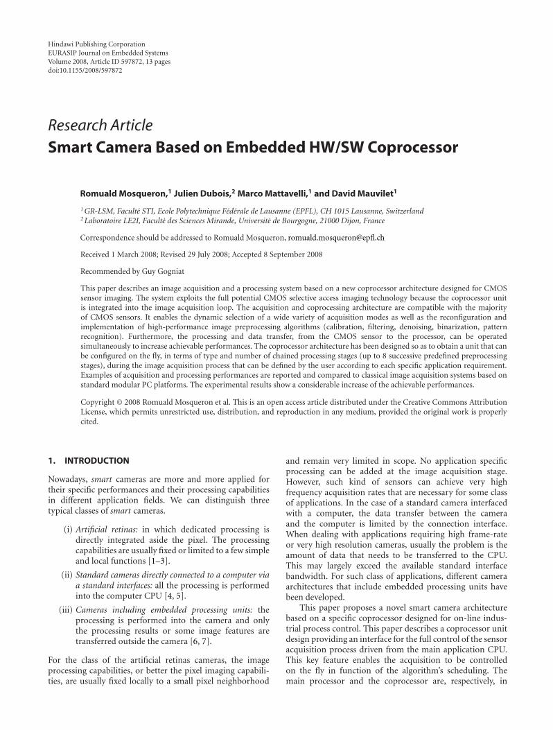
Mainprocessor
/DSP
Processing Acquisition CMOSsensor
COP
DataControls
Figure 1: Block diagram of the coprocessor-based architecture.
The first interesting result achieved by implementing thisarchitecture is that relevant speed-up factors are obtain-able for reconfigurable processing modules, thus providingenough flexibility in terms of choices of processing andin terms of acquisition modes defined on the fly by theapplication itself (selection and preprocessing of any kind ofarea of interest). The second interesting result is that such on-the-fly adaptation of the acquisition mode yields a furtherbandwidth reduction for the transfer of the image data tothe central CPU. This feature represents for some applicationa further speed-up in the overall system performance interms of reduction of processing or increase of the achievableacquisition/processing frame rate.
3. ARCHITECTURE OF THE COPROCESSOR CAMERA
The overall system can be described as an autonomousintelligent camera with powerful embedded processing whencompared with modular systems associated with a computer.
The system has been thought for monitoring applicationssuch as road monitoring [18] or intrusion detection or anyother similar application. Quality control and control ofindustrial processes, where very high frame-rate on specificimage sections are required, is another application field ofthe system. For such kind of processes, only the “relevant”portions of the images are necessary to be transmitted tothe host CPU for further processing. In some cases, onlythe result of the preprocessing, or of the processing (i.e., thedetected feature), is needed to be transmitted outside thesystem to a local host PC or via Internet.
The system is composed of an embedded frame-grabberequipped, at di!erent levels, of processing capabilities for theimage acquired by the sensor and it is illustrated in Figure 1.This figure illustrates the main architectural componentsof the camera with embedded coprocessing stage. In thisarchitecture, the coprocessor part (COP) is divided in twoparts: a part dedicated to the acquisition and a second partdedicated to a preprocessing stage.
The association of the processing and acquisition stagesaims at reducing the pixel rate for applications where“irrelevant” image portions are detected by the coprocessor.The processing is then complemented by the processor forhigher-level tasks at a possibly lower pixel-rate. The partition
4 EURASIP Journal on Embedded Systems
of the tasks is made by exploiting the specificity of eachelement, to use it as e"ciently as possible, thus reducing thepixel-rate when possible and the processing time so as toincrease the overall throughput. This architectural approachto the processing of sequences is particularly adapted toand performing, but not limited to, tracking applications,pattern recognition applications, and compression applica-tions. Video compression is generally used in camera systemsso as to reduce the bandwidth of the data transfer and tobe able to use a standard communication channel withoutaddition of acquisition boards such as the camera-link forinstance. However, with high performance sensors, there isimmediately the problem of the connection that becomesnow the system “bottleneck”, and prevents from transfer-ring the images rate provided by the sensor. The systemdescribed in this paper also supports the implementationof a compression stage (thanks to multimedia processor’sfunctionalities) that makes it possible to approach to thesensor limit capabilities.
The system is composed of a compact stack of 4 boards,enabling to easily interface various types of sensor/camerasand thus answering to various resolution and acquisitionspeed requirements in the most modular and economic way.The four boards described hereafter are the following:
(i) the motherboard containing the main processor,
(ii) the communication board,
(iii) the board including the coprocessor,
(iv) the camera interface board.
3.1. Motherboard
The motherboard contains a Nexperia PNX1500 (Philips:PNX 1500 datasheet; available at http://www.nxp.com/acrobat download/literature/9397/75010486.pdf) processorat 300 MHz and includes functions for the sound and imageprocessing. This processor has been selected for the powerfulVLIW core and for the variety of supported integratedinterfaces such as Ethernet controller, DDRam controller,and PCI. Moreover, it includes a 32-bit TriMedia 3260 CPUcore with 5-issue slot engine and 31 pipelined functionalunits. It operates up to 10000 Mops and 1300 Mips and canexecute up to 5 operations per clock cycle. In addition,Nexperia integrates a graphic 2D engine able to display upto a resolution of 1024 ! 768 to 60 Hz. A large library canbe used to program several standards (MPEG, H263, etc.)and several interfaces. The Nexperia power consumptiondepends on the processing charge, typically it is around1.5 W. Around this processor, we can find communicationinterfaces such as Ethernet and ISDN, as well as acquisitionand rendering of video images and analogical sound. Themotherboard contains a 64 Mbytes DDR Ram (333 MHz) tostore data. In addition, there are 32 Mbytes of flash memoryused to store the programs or di!erent information. Severalinterface components can communicate via a PCI bus, likeEthernet and VGA. Thus, motherboard contains an internalbus which is a PCI and all the platforms communicate viathis bus.
3.2. Communication board
The second board is based on an FPGA Spartan XL(Spartan XL (Xilinx: Spartan XL datasheet; available athttp://direct.xilinx.com/bvdocs/publications/ds060.pdf)) tomanage the PCI arbiter, the communication interfaces suchas USB2.0 and Firewire that can be driven to connectthe camera with digital standard interfaces. This boardprovides four functionalities. It extends the communicationof the motherboard with standards USB 2.0, IEEE1394,and Ethernet 10/100. The ethernet connection is important,because systems and a computer can communicate by thisinterface with a simple IP number. It also provides acentralized power supply for the system. On this board, aconverter N/A is used to display on a standard VGA monitor.All the components cited before have a PCI input to avoiddi!erent link with the processor.
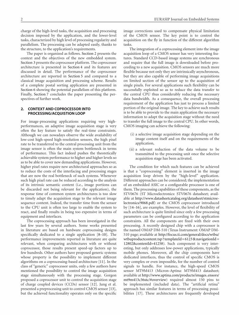
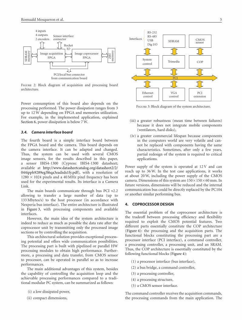
3.3. Acquisition and processing board
This board is the COP part in charge of the acquisition andthe preprocessing stages of the video signal coming fromthe CMOS sensors or cameras. The preprocessing part isindependent from the acquisition part. Its architecture isillustrated in Figure 2. The main functions are partitionedinto two FPGAs. The first FPGA is a Virtex2Pro VP4-fg456-5(Xilinx: Virtex 2 Pro datasheet; available at http://direct.xilinx.com/bvdocs/publications/ds083.pdf), their functionsare to acquire images and communicate the configurationand orders to the camera. This FPGA drives the cameraand can be adapted to several sensors or cameras; it isjust an implementation with the right driver. Therefore, itimplements a wide variety of acquisition modes (randomregion acquisition, variable image size, variable acquisi-tion modes line/region based, multiexposition image). Thesecond FPGA is a Virtex2Pro vp20-fg676-53, and high-performance image preprocessing (calibration, filtering,denoising, binarization, pattern recognition) is its principalfunction. These FPGAs include, respectively, 1 IBM PowerPC, 28 18 kb BRAMs, 3008 slices and 2, 88, 9280 for thelarge one. Both FPGAs communicate through two high-speed serial channels, specific to Xilinx, called RocketIO(Xilinx: RocketIO User Guide; available at http://www.xilinx.com/bvdocs/publications/ug024.pdf). Moreover, eachFPGA communicate with the processor via the PCI bus.Xilinx FPGAs have been chosen, because of their high-speedserial communication, PowerPC are available, and they areflexible and reprogrammable. Interface drivers are alreadydeveloped and optimized by Xilinx.
This board contains, in addition of FPGAs:
(i) 2 SDRAM until 128 Mbytes associated with theacquisition FPGA used to store several images,
(ii) 2 ZBT until 8 Mbytes associated with the coprocess-ing FPGA used for processing tasks,
(iii) 4 optocoupled inputs,
(iv) 4 optocoupled output,
(v) 2 encoders.
Romuald Mosqueron et al. 5
4 inputs4 outputs2 encoders
Sensor interfaceconnector
SDR
AM
mem
ory
Image acquisitionFPGA
Image coprocessorFPGA Z
BT
mem
ory
PCI/local bus connectorfrom communication board
RocketIO
Figure 2: Block diagram of acquisition and processing boardarchitecture.
Power consumption of this board also depends on theprocessing performed. The power dissipation ranges from 3up to 12 W depending on FPGA and memories utilization.For example, in the implemented application, explainedSection 6, power dissipation is below 7 W.
3.4. Camera interface board
The fourth board is a simple interface board betweenthe FPGA board and the camera. This board depends onthe camera interface. It can be adapted and changed.Thus, the system can be used with several CMOSimage sensors, for the results described in this paper,a sensor IBIS4-1300 (Cypress: IBIS4-1300 datasheet;available at http://www.datasheetcatalog.org/datasheet2/2/044ipph9289eg3l6qa3eadzds1fy.pdf), with a resolution of1280 ! 1024 pixels and a 40 MHz pixel frequency has beenused for the experimental results. Its interface is a CameraLink.
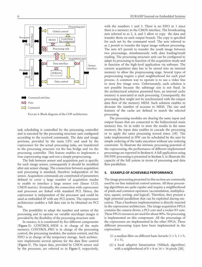
The main boards communicate through bus PCI v2.2allowing to transfer a large number of data (up to133 Mbytes/s) to the host processor (in accordance withNexperia bus interface). The entire architecture is illustratedin Figure 3, with processing components and availableinterfaces.
However, the main idea of the system architecture isindeed to reduce as much as possible the data rate after thecoprocessor unit by transmitting only the processed imagesections or by controlling the acquisition.
This architectural solution provides exceptional process-ing potential and o!ers wide communication possibilities.The processing part is built with pipelined or parallel HWprocessing modules to obtain high performance. Further-more, a processing and data transfer, from CMOS sensorto processor, can be operated in parallel so as to increaseperformances.
The main additional advantages of this system, besidesthe capability of controlling the acquisition loop and theachievable processing performances compared to a tradi-tional modular PC system, can be summarized as follows:
(i) a low dissipated power,
(ii) compact dimensions,
Interfaces
RS-232RS-485USBDig I/O
SDRAM CMOSsensor
Systemcontrol
Trimedia COP
PCI
Ethernetcontrol
VGAcontrol
PCIextension
Figure 3: Block diagram of the system architecture.
(iii) a greater robustness (mean time between failures)because it does not integrate mobile components(ventilators, hard disks),
(iv) a greater commercial lifespan because componentsin the computers world are very volatile and can-not be replaced with components having the samecharacteristics. Sometimes, after only a few years,partial redesign of the system is required to criticalapplications.
Power supply of the system is operated at 12 V and canreach up to 36 W. In the test case applications, it worksat about 20 W, including the power supply of the CMOScamera. Dimensions of this system are 150!150!60 mm. Infuture versions, dimensions will be reduced and the internalcommunication bus could be directly replaced by the PC104or another similar performing bus.
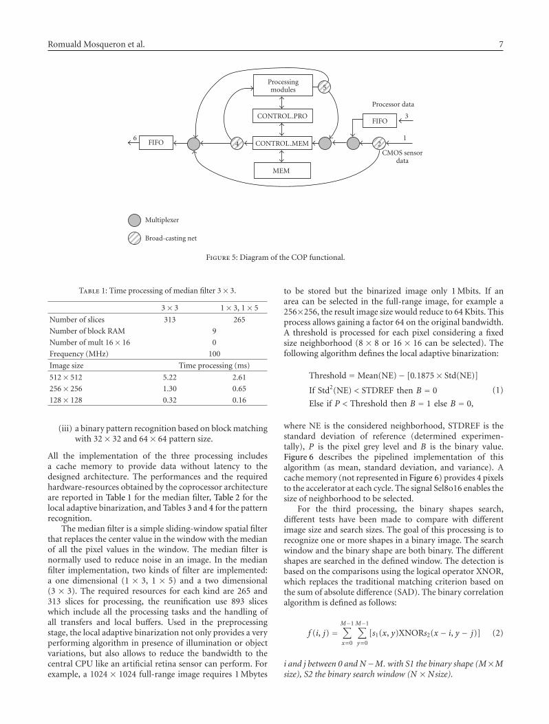
4. COPROCESSOR DESIGN
The essential problem of the coprocessor architecture isthe tradeo! between processing e"ciency and flexibilityrequired to exploit the CMOS potential features. Twodi!erent parts essentially constitute the COP architecture(Figure 4): the processing and the acquisition parts. Thefunctional blocks constituting the processing part are aprocessor interface (PCI interface), a command controller,a processing controller, a processing unit, and an SRAM.Thus, the COP architecture is essentially constituted by thefollowing functional blocks (Figure 4):
(1) a processor interface (bus interface),
(2) a bus bridge, a command controller,
(3) a processing controller,
(4) a processing structure,
(5) a CMOS sensor interface.
The command controller receives the acquisition commands,the processing commands from the main application. The
6 EURASIP Journal on Embedded Systems
Processing part
Global control
PCI
Processor
PCI
inte
rfac
e
SRAM Controleurdu traitement
Processing unit
Acquisition part
Data interface
PCI
Processor
PCI
inte
rfac
e
SDRAM
Sensorinterface
Data control
Command and data
Data
Command
Figure 4: Block diagram of the COP architecture.
task scheduling is controlled by the processing controllerand is executed by the processing structure unit configuredaccording to the received commands. The data and imageportions, provided by the main CPU and used by thecoprocessor for the actual processing tasks, are transferredto the processing structure via the bus bridge and via theprocessing controller. This feature enables to implement atrue coprocessing stage and not a simple preprocessing.
The link between sensor and acquisition part is specificfor each image sensor, consequently it should be modifiedafter any sensor change. The connection between acquisitionand processing is standard, therefore independent of thesensor. Acquisition commands are constituted of parametersdefined to cover a large number of acquisition modesto enable to interface a large sensor sort (linear CCD,CMOS matrix). Eventually, the connection with coprocessorand processor are linked with standard PCI. Hence, thecoprocessor is independent of the processor and could beused as embedded IP with any PCI system. The coprocessorarchitecture enables a full data rate to be obtained on PCIbus.
The possibility to adapt the number and nature of theprocessing and to operate on variable size/shape images isprovided by the flexibility of the processing structure unit.
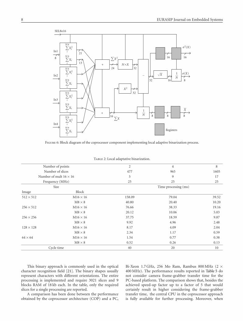
In essence, it is constituted by five di!erent components(Figure 5): CONTROL MEM is in charge of the mainmemory, CONTROL PRO is in charge of the processingcontrol, the processing modules, the system control, and theFIFO is in charge of the temporary storage. Such architec-ture implements several options for the data flow control(Figure 5). The input data, provided by CMOS sensor andby the processor, are referred to in Figure 5, respectively,
with the numbers 1 and 3. There is no FIFO in 1 sincethere is a memory in the CMOS interface. The broadcastingnets referred to as 2, 4, and 5 allow to copy the data andtransfer them on each output branch. The copy is specifiedfor each net by the command word. The nets referred toas 2 permit to transfer the input image without processing.The nets 4/5 permit to transfer the result image betweentwo processings, simultaneously with data loading/resultreading. The processing structure unit can be configured toadapt its processing in function of the acquisition mode andin function of the high-level application via software. Thecurrent acquisition data has to be stored into an internalmemory to allow the preprocessing stage. Several types ofpreprocessing require a pixel neighborhood for each pixelprocess. A common way to operate is to use a video lineto store few image rows. Unfortunately, such solution isnot possible because the subimage size is not fixed. Inthe architectural solution presented here, an internal cachememory is associated at each processing. Consequently, theprocessing flow might not be synchronized with the outputdata flow of the memory MEM. Such solution enables todecrease the number of accesses to MEM. The size andfeatures of the cache are defined to match the selectedprocessing.
The processing modules are sharing the same input andoutput busses that are connected to the bidirectional mainmemory bus. So in order to store the results in the samememory, the input data enables to cascade the processingor to apply the same processing several times [19]. Thetasks implemented in HW can be scheduled by the user bysimple ordering of the tasks execution without any orderingconstraint. To illustrate the intrinsic processing potential ofthe coprocessing, the performance of di!erent implementedprocessings are reported in Section 6. A full application usingSW/HW processing is presented in Section 5, to illustrate thecapacity of the full system in terms of processing and dataflow parallelism.
5. EXAMPLE OF ACHIEVABLE PERFORMANCE
The image processing presented in this section are commonlyused by on-line industrial control systems. All these process-ing algorithms are quite regular and require a neighborhoodof pixels and common operators (accumulation, multiplica-tion, square, sorting, and logical). Therefore, they present ahigh potential parallelism that can be exploited during exe-cution. Thus a hardware implementation is directly insertedin the coprocessor architecture. The image acquisition FPGAcontains the camera driver, a PCI core and a rocket IO core.These FPGA resources are used for about 90%. No processingis implemented on this component. All the processings ofthe coprocessor are implemented in the other FPGA. Threedi!erent processing types have been implemented in thecoprocessor:
(i) a median filter on di!erent basic kernels (1!3, 1!5,3! 3),
(ii) a local adaptive binarization (Niblack algorithm)with a neighborhood of 8! 8 or 16! 16 pixels [20],
Romuald Mosqueron et al. 7
Processingmodules
CONTROL PRO
CONTROL MEM
MEM
Processor data
FIFO
FIFO
CMOS sensordata
Multiplexer
Broad-casting net
3
124
6
5
Figure 5: Diagram of the COP functional.
Table 1: Time processing of median filter 3! 3.
3! 3 1! 3, 1! 5
Number of slices 313 265Number of block RAM 9Number of mult 16! 16 0Frequency (MHz) 100
Image size Time processing (ms)
512! 512 5.22 2.61256! 256 1.30 0.65128! 128 0.32 0.16
(iii) a binary pattern recognition based on block matchingwith 32! 32 and 64! 64 pattern size.
All the implementation of the three processing includesa cache memory to provide data without latency to thedesigned architecture. The performances and the requiredhardware-resources obtained by the coprocessor architectureare reported in Table 1 for the median filter, Table 2 for thelocal adaptive binarization, and Tables 3 and 4 for the patternrecognition.
The median filter is a simple sliding-window spatial filterthat replaces the center value in the window with the medianof all the pixel values in the window. The median filter isnormally used to reduce noise in an image. In the medianfilter implementation, two kinds of filter are implemented:a one dimensional (1 ! 3, 1 ! 5) and a two dimensional(3 ! 3). The required resources for each kind are 265 and313 slices for processing, the reunification use 893 sliceswhich include all the processing tasks and the handling ofall transfers and local bu!ers. Used in the preprocessingstage, the local adaptive binarization not only provides a veryperforming algorithm in presence of illumination or objectvariations, but also allows to reduce the bandwidth to thecentral CPU like an artificial retina sensor can perform. Forexample, a 1024 ! 1024 full-range image requires 1 Mbytes
to be stored but the binarized image only 1 Mbits. If anarea can be selected in the full-range image, for example a256!256, the result image size would reduce to 64 Kbits. Thisprocess allows gaining a factor 64 on the original bandwidth.A threshold is processed for each pixel considering a fixedsize neighborhood (8 ! 8 or 16 ! 16 can be selected). Thefollowing algorithm defines the local adaptive binarization:
Threshold = Mean(NE)" [0.1875! Std(NE)]
If Std2(NE) < STDREF then B = 0
Else if P < Threshold then B = 1 else B = 0,
(1)
where NE is the considered neighborhood, STDREF is thestandard deviation of reference (determined experimen-tally), P is the pixel grey level and B is the binary value.Figure 6 describes the pipelined implementation of thisalgorithm (as mean, standard deviation, and variance). Acache memory (not represented in Figure 6) provides 4 pixelsto the accelerator at each cycle. The signal Sel8o16 enables thesize of neighborhood to be selected.
For the third processing, the binary shapes search,di!erent tests have been made to compare with di!erentimage size and search sizes. The goal of this processing is torecognize one or more shapes in a binary image. The searchwindow and the binary shape are both binary. The di!erentshapes are searched in the defined window. The detection isbased on the comparisons using the logical operator XNOR,which replaces the traditional matching criterion based onthe sum of absolute di!erence (SAD). The binary correlationalgorithm is defined as follows:
f (i, j) =M"1!
x=0
M"1!
y=0
[s1(x, y)XNORs2(x " i, y " j)] (2)
i and j between 0 and N"M. with S1 the binary shape (M!Msize), S2 the binary search window (N !Nsize).
8 EURASIP Journal on Embedded Systems
SEL8o16
In1
8
N/4!
i
X2i
N/4!
i
Xi
21
13
In2
N/4!
i
X2i
N/4!
i
Xi
In3
N/4!
i
X2i
N/4!
i
Xi
In4
N/4!
i
X2i
N/4!
i
Xi
+
!X2
24N!X
32
16 16
!2(X)
"32
#X
16
1N
!(X)
8
X2
32
+16 !
X
1N 8 8 8
X
Registers
Figure 6: Block diagram of the coprocessor component implementing local adaptive binarization process.
Table 2: Local adaptative binarization.
Number of points 2 4 8Number of slices 477 965 1605
Number of mult 16! 16 5 9 17Frequency (MHz) 25 25 25
Size Time processing (ms)Image Block
512! 512 M16! 16 158.09 79.04 39.52M8! 8 40.80 20.40 10.20
256! 512 M16! 16 76.66 38.33 19.16M8! 8 20.12 10.06 5.03
256! 256 M16! 16 37.75 18.59 9.87M8! 8 9.92 4.96 2.48
128! 128 M16! 16 8.17 4.09 2.04M8! 8 2.34 1.17 0.59
64! 64 M16! 16 1.54 0.77 0.38M8! 8 0.52 0.26 0.13
Cycle time 40 20 10
This binary approach is commonly used in the opticalcharacter recognition field [21]. The binary shapes usuallyrepresent characters with di!erent orientations. The entireprocessing is implemented and require 3021 slices and 9blocks RAM of 18 kb each. In the table, only the requiredslices for a single processing are reported.
A comparison has been done between the performanceobtained by the coprocessor architecture (COP) and a PC,
Bi-Xeon 1.7 GHz, 256 Mo Ram, Rambus 800 MHz (2 !400 MHz). The performance results reported in Table 5 donot consider camera frame-grabber transfer time for thePC-based platform. The comparison shows that, besides theachieved speed-up factor up to a factor of 5 that wouldcertainly result in higher considering the frame-grabbertransfer time, the central CPU in the coprocessor approachis fully available for further processing. Moreover, when
Romuald Mosqueron et al. 9
Table 3: Binary shapes research with a 50 MHz frequency.
Shape size 64! 64 32! 32 16! 16Block size 64! 128 32! 64 16! 32Mem. blocks 6 3 2Slices/ 2328 1300 1250 700 750 400detect. block 127 70 40detection block used 16 8 16 8 16 8
Image Size Processing time (ms)
512! 512 16.05 9.2 4.93 32.1 18.4 9.86256! 256 2.96 2.015 1.155 5.92 4.03 2.31256! 512 6.9 4.32 2.39 13.8 8.64 4.78128! 128 0.335 0.375 NC 0.67 0.75 NC
Table 4: Time to search a shape in an image (ms).
Number of shapes 5 4 3 2 1
256! 512 68.52 59.88 51.24 42.6 33.96256! 256 32.67 28.64 24.61 20.58 16.55128! 128 6.73 5.99 5.24 4.49 3.74
Table 5: Processing comparisons.
Processing PC (Mpixel/s) COP (Mpixel/s)
Median 1! 3 41 100Median 1! 5 28 100Median 3! 3 27 50Niblack 8! 8 5 25Niblack 16! 16 4 14
a bandwidth reduction is possible by means of adaptiveacquisition, the coprocessor approach provides much higherspeed-up gains.
6. APPLICATION EXAMPLE: READING A BAR CODEFOR POSTAL SORTING
6.1. Application description
The postal sorting is a real-world example showing theprocessing possibilities and the achieved level of parallelismof the system [22]. The goal of this application is to readbar codes on the letters, to enable the automatic sortingat the di!erent stages of the logistic postal letter handling.If the bar codes cannot be read, the letter is rejected andneed to be processed manually. This application has beendeveloped with the objective of replacing an exiting platformwhich integrates a camera associated with a PC. The newembedded solution has been developed to increase as muchas possible the processing performances and to obtain aportable and more flexible system. Indeed due to the factthat bar codes printed on letters may be of bad quality orsuperposed to other visual information the possibility ofimplementing more complex processing increase the rate ofcorrect detections/decodings achievable. Ideally, to correctlyread the largest percentage of bar codes, each processing stage
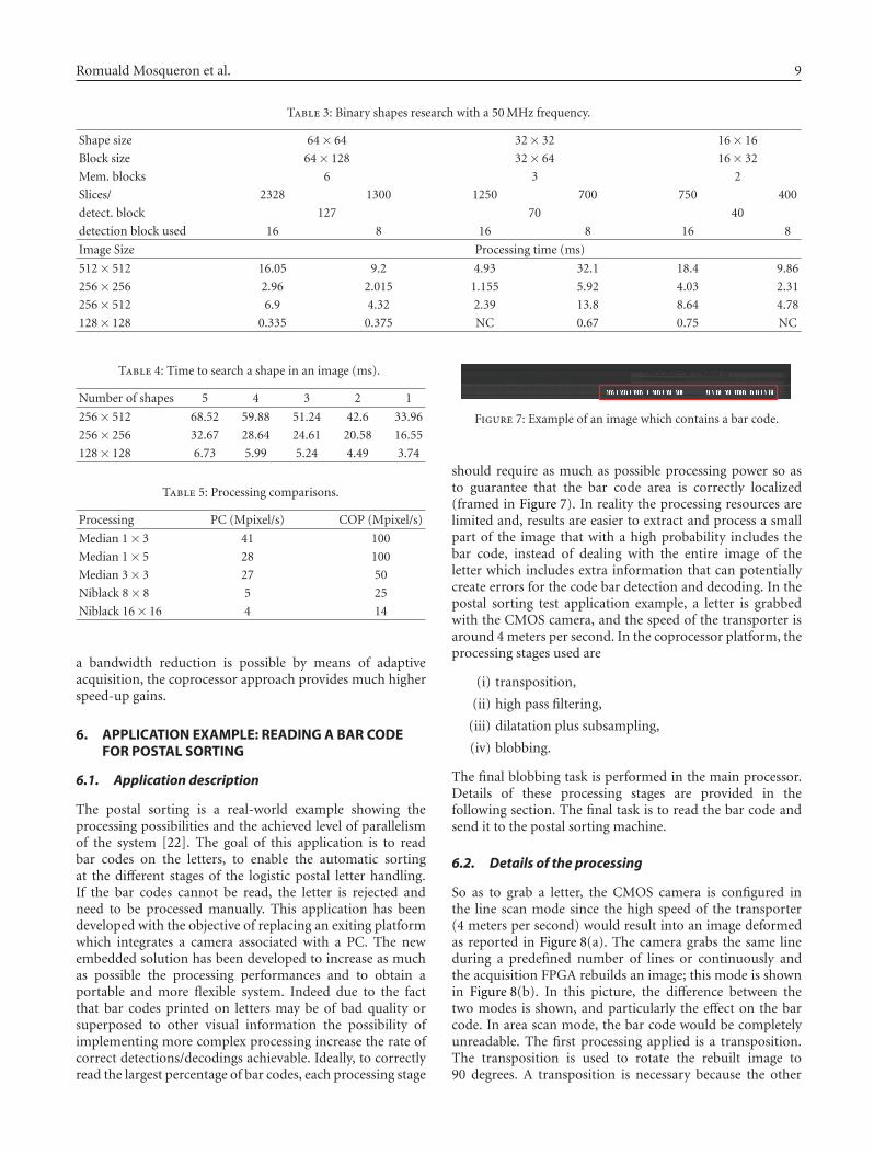
Figure 7: Example of an image which contains a bar code.
should require as much as possible processing power so asto guarantee that the bar code area is correctly localized(framed in Figure 7). In reality the processing resources arelimited and, results are easier to extract and process a smallpart of the image that with a high probability includes thebar code, instead of dealing with the entire image of theletter which includes extra information that can potentiallycreate errors for the code bar detection and decoding. In thepostal sorting test application example, a letter is grabbedwith the CMOS camera, and the speed of the transporter isaround 4 meters per second. In the coprocessor platform, theprocessing stages used are
(i) transposition,
(ii) high pass filtering,
(iii) dilatation plus subsampling,
(iv) blobbing.
The final blobbing task is performed in the main processor.Details of these processing stages are provided in thefollowing section. The final task is to read the bar code andsend it to the postal sorting machine.
6.2. Details of the processing
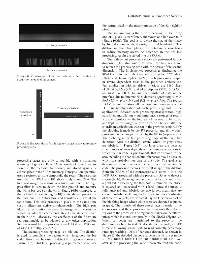
So as to grab a letter, the CMOS camera is configured inthe line scan mode since the high speed of the transporter(4 meters per second) would result into an image deformedas reported in Figure 8(a). The camera grabs the same lineduring a predefined number of lines or continuously andthe acquisition FPGA rebuilds an image; this mode is shownin Figure 8(b). In this picture, the di!erence between thetwo modes is shown, and particularly the e!ect on the barcode. In area scan mode, the bar code would be completelyunreadable. The first processing applied is a transposition.The transposition is used to rotate the rebuilt image to90 degrees. A transposition is necessary because the other
10 EURASIP Journal on Embedded Systems
(a) Area scan mode
(b) Line scan mode
Figure 8: Visualization of the bar code with the two di!erentacquisition modes of the camera.
Processing direction
Acquisitiondirection
Figure 9: Transposition of an image to change in the appropriateprocessing sense.
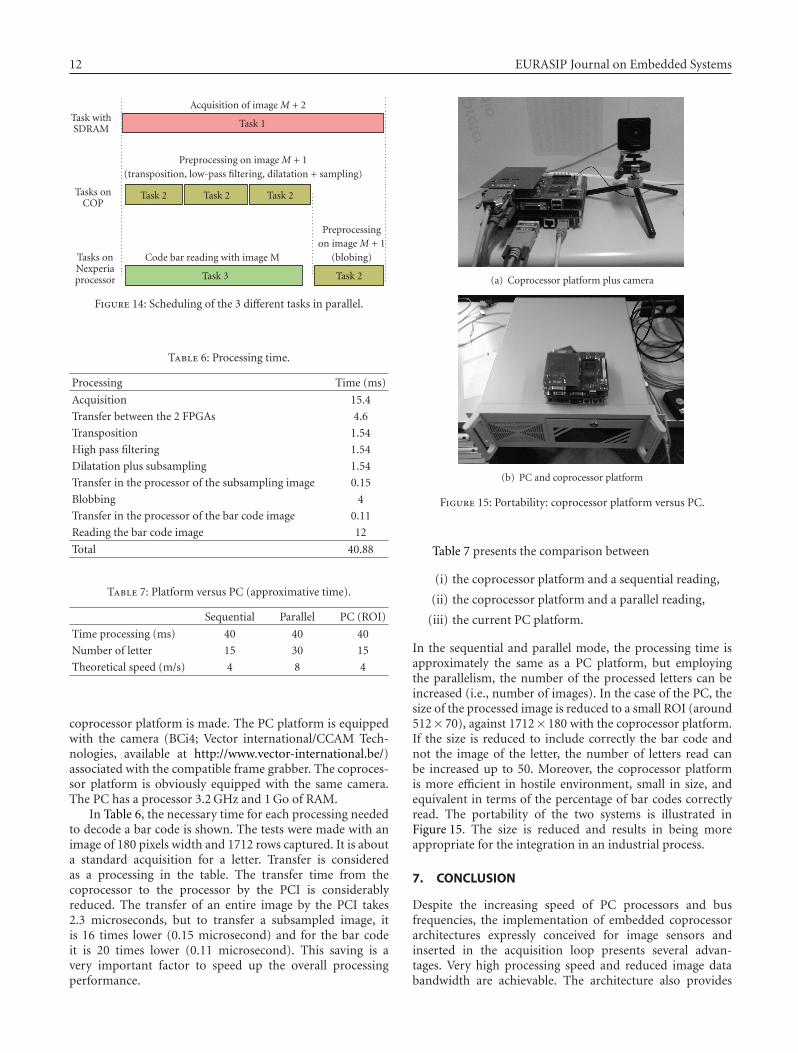
processing stages are only compatible with a horizontalscanning (Figure 9). Four 32 bits words of four lines arestored in the memory, transposed, and stored again at acorrect place in the SRAM memory. Transposition operationuses 4 registers to store temporally the result. The resourcesused by the FPGA are 186 slices (only about 2%). Thefirst real image processing is a high pass filter. The highpass filter is used to delete the background and to raisethe white bar code as shown in Figure 10(b) compared tothe original image in Figure 10(a). As shown previously,the data bus is a 32 bits bus, and transfers 4 pixels at thesame time. This task processes 4 pixels at the same time(i.e., 4 filters are active simultaneously). The high passfilter is a convolution between the image and the windowwhich includes the coe"cients. Results are directly storedin the SRAM. Obviously the coe"cients of the filters arereprogrammable to be adapted to any other application.Resources used for this processing are 1125 slices (12%) and44 (4! 11) multipliers (50%).
The second processing stage is a dilation. The dilationis used to complete the region which integrates the barcodes, thus it will be easier to detect this region as shown inFigure 10(c). This latter processing is performed to replace
the central pixel by the maximum value of the 32 neighborpixels.
The subsampling is the third processing. In fact, onlyone of 4 pixels is transferred, moreover one line over four(Figure 10(d)). The goal is to divide the size of the imageby 16 and consequently the original pixel bandwidth. Thedilation and the subsampling are executed in the same tasksto reduce memory access. As described in the two lastprocessing, results are stored into the SRAM.
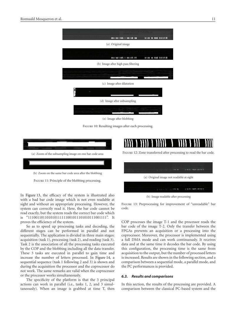
These three last processing stages are performed in onedimension (line dimension) to obtain the best result andto reduce the processing time with the access of the seconddimension. The implemented processings (including theSRAM address controller) request all together 2623 slices(26%) and 44 multipliers (46%). Each processing is spiltin several dependent tasks in the pipelined architecture.Full application with all driver interface use 3880 slices(41%), 4 BRAMs (4%), and 44 multipliers (50%). 3 BRAMsare used like FIFOs to save the transfer of data in theinterface, due to di!erent clock domains. (processing $ PCI,RocketIO $ processing and PCI $ processing). The fourthBRAM is used to store all the configuration sent via thePCI bus (configuration of each processing and of theapplication). Between each processing (transposition, highpass filter, and dilation + subsampling), a storage of resultsis made. Results after the high pass filter need to be storedand kept. In this image, only the areas will be sent after thecoordinates calculation. As seen in the previous section, onlythe blobbing is made by the SW processor and all the otherprocessing stages are performed by the FPGA (coprocessor).The blobbing is the last processing stage of the code bardetection. After the dilation, several white (or grey) areasare labeled. In Figure 10(d), two large areas are detected(the number of areas depends on the number of sections inwhich the bar code is partitioned), that correspond to thearea including the bar codes, but other areas may be detectedwhich are probably not part of the code. The goal is todetermine the coordinates of the two zones that contain thecode. The processor receives the result image of the dilationfrom the SRAM of the coprocessor and stores it into theDDR RAM associated with the processor. So as to detect aregion (blob), the image is described row by row and whena pixel value exceeding the threshold is founded, the objectis squared and associated with a label. Once the image isfully analyzed and labeled, the two largest areas, that arechosen probably including the bar code and the coordinatesof these two objects, are extracted. Figure 11 shows a part ofthe blobbing image where white areas are detected (squaredin grey). The transfer of these coordinates is made to thecoprocessor and the coprocessor transfers only the selectedregions to the processor. The regions are taken on the filteredimage which is stored temporally in the SRAM (Figure 12).When bar codes are transferred to the processor, thedecoding can be activated. To decode the bar code, an FFTis made following several tests to read correctly percentagerates approaching 100% of bar code detected. As shown inFigure 12, the decoded bar code value in the picture exampleis “1111010111101011111001001111010111001111” andafter all the processing the system correctly read the code.
Romuald Mosqueron et al. 11
(a) Original image
(b) Image after high pass filtering
(c) Image after dilatation
(d) Image after subsampling
(e) Image after blobbing
Figure 10: Resulting images after each processing.
(a) Zoom of the subsampling image on one bar code area
(b) Zoom on the same bar code area after the blobbing
Figure 11: Principle of the blobbing processing.
In Figure 13, the e"cacy of the system is illustrated alsowith a bad bar code image which is not even readable atsight and without an appropriate processing. However, thesystem can correctly read it. Here, the bar code cannot beread exactly, but the system reads the correct bar code whichis “111001101101010111111001011101010111001111”. Itproves the e"ciency of the system.
So as to speed up processing tasks and decoding, thedi!erent stages can be performed in parallel and notsequentially. The application is divided in three main stages:acquisition (task 1), processing (task 2), and reading (task 3).Task 2 is the association of all the processing tasks executedby the COP and the blobbing including all the data transfer.These 3 tasks are executed in parallel to gain time andincrease the number of letters processed. In Figure 14, asequential sequence (task 1 following 2 and 3) is shown andduring the acquisition the processor and the coprocessor donot work. The same remarks are valid when the coprocessoror the processor works simultaneously.
The specificity of the platform is that the 3 principalactions can work in parallel (i.e., tasks 1, 2, and 3 simul-taneously). When an image is grabbed at time T, then
Figure 12: Zone transferred after processing to read the bar code.
(a) Original image not readable at sight
(b) Image readable after processing
Figure 13: Preprocessing for improvement of “unreadable” barcode.
COP processes the image T-1 and the processor reads thebar code of the image T-2. Only the transfer between theFPGAs prevents an acquisition or a processing into thecoprocessor. Moreover, the processor is implemented usinga full DMA mode and can work continuously. It receivesdata and at the same time it decodes the bar code. By usingthis configuration, the processing time is the same fromacquisition to the output, but the number of processed lettersis increased. Results are shown in the following section, and acomparison between a sequential mode, a parallel mode, andthe PC performances is provided.
6.3. Results and comparisons
In this section, the results of the processing are provided. Acomparison between the classical PC-based system and the
12 EURASIP Journal on Embedded Systems
Task withSDRAM
Acquisition of image M + 2
Task 1
Preprocessing on image M + 1(transposition, low-pass filtering, dilatation + sampling)
Tasks onCOP
Task 2 Task 2 Task 2
Tasks onNexperiaprocessor
Code bar reading with image M
Task 3
Preprocessingon image M + 1
(blobing)
Task 2
Figure 14: Scheduling of the 3 di!erent tasks in parallel.
Table 6: Processing time.
Processing Time (ms)
Acquisition 15.4Transfer between the 2 FPGAs 4.6Transposition 1.54High pass filtering 1.54Dilatation plus subsampling 1.54Transfer in the processor of the subsampling image 0.15Blobbing 4Transfer in the processor of the bar code image 0.11Reading the bar code image 12
Total 40.88
Table 7: Platform versus PC (approximative time).
Sequential Parallel PC (ROI)
Time processing (ms) 40 40 40Number of letter 15 30 15Theoretical speed (m/s) 4 8 4
coprocessor platform is made. The PC platform is equippedwith the camera (BCi4; Vector international/CCAM Tech-nologies, available at http://www.vector-international.be/)associated with the compatible frame grabber. The coproces-sor platform is obviously equipped with the same camera.The PC has a processor 3.2 GHz and 1 Go of RAM.
In Table 6, the necessary time for each processing neededto decode a bar code is shown. The tests were made with animage of 180 pixels width and 1712 rows captured. It is abouta standard acquisition for a letter. Transfer is consideredas a processing in the table. The transfer time from thecoprocessor to the processor by the PCI is considerablyreduced. The transfer of an entire image by the PCI takes2.3 microseconds, but to transfer a subsampled image, itis 16 times lower (0.15 microsecond) and for the bar codeit is 20 times lower (0.11 microsecond). This saving is avery important factor to speed up the overall processingperformance.
(a) Coprocessor platform plus camera
(b) PC and coprocessor platform
Figure 15: Portability: coprocessor platform versus PC.
Table 7 presents the comparison between
(i) the coprocessor platform and a sequential reading,
(ii) the coprocessor platform and a parallel reading,
(iii) the current PC platform.
In the sequential and parallel mode, the processing time isapproximately the same as a PC platform, but employingthe parallelism, the number of the processed letters can beincreased (i.e., number of images). In the case of the PC, thesize of the processed image is reduced to a small ROI (around512! 70), against 1712! 180 with the coprocessor platform.If the size is reduced to include correctly the bar code andnot the image of the letter, the number of letters read canbe increased up to 50. Moreover, the coprocessor platformis more e"cient in hostile environment, small in size, andequivalent in terms of the percentage of bar codes correctlyread. The portability of the two systems is illustrated inFigure 15. The size is reduced and results in being moreappropriate for the integration in an industrial process.
7. CONCLUSION
Despite the increasing speed of PC processors and busfrequencies, the implementation of embedded coprocessorarchitectures expressly conceived for image sensors andinserted in the acquisition loop presents several advan-tages. Very high processing speed and reduced image databandwidth are achievable. The architecture also provides
Romuald Mosqueron et al. 13
high degree of flexibility in the preprocessing stage forthe di!erent acquisition modes specific of CMOS imaging.Moreover, new processing tasks can be easily added infunction of the application and the platform supports a widepanel of data interfaces. A complete test case applicationhas been successfully implemented on this platform, withsignificant performance improvements when compared to aclassical PC-based platform.
REFERENCES
[1] L. F. L. Y. Voon, G. Cathebras, B. Bellach, B. Lamalle, andP. Gorria, “Silicon retina for real-time pattern recognition,”in Sensors and Camera Systems for Scientific, Industrial, andDigital Photography Applications II, vol. 4306 of Proceedings ofSPIE, pp. 168–177, San Jose, Calif, USA, January 2001.
[2] R. D. Burns, C. Thomas, P. Thomas, and R. Hornsey, “Pixel-parallel CMOS active pixel sensor for fast object location,”in Ultrahigh- and High-Speed Photography, Photonics, andVideography, vol. 5210 of Proceedings of SPIE, pp. 84–94, SanDiego, Calif, USA, August 2003.
[3] J. Dubois, D. Ginhac, M. Paindavoine, and B. Heyrman,“A 10 000 fps CMOS sensor with massively parallel imageprocessing,” IEEE Journal of Solid-State Circuits, vol. 43, no.3, pp. 706–717, 2008.
[4] Y. Shi, R. Taib, and S. Lichman, “GestureCam: a smartcamera for gesture recognition and gesture-controlled webnavigation,” in Proceedings of the 9th International Conferenceon Control, Automation, Robotics and Vision (ICARCV ’06), pp.1–6, Singapore, December 2006.
[5] R. Y. D. Xu, “A computer vision based whiteboard capturesystem,” in Proceedings of IEEE Workshop on Applications ofComputer Vision (WACV ’08), pp. 1–6, Copper Mountain,Colo, USA, January 2008.
[6] R. Mosqueron, J. Dubois, and M. Paindavoine, “High-speedsmart camera with high resolution,” EURASIP Journal onEmbedded Systems, vol. 2007, Article ID 24163, 16 pages, 2007.
[7] M. McErlean, “An FPGA implementation of hierarchicalmotion estimation for embedded object tracking,” in Pro-ceedings of the 6th IEEE International Symposium on SignalProcessing and Information Technology (ISSPIT ’06), pp. 242–247, Vancouver, BC, Canada, August 2006.
[8] B. Bosi, G. Bois, and Y. Savaria, “Reconfigurable pipelined 2-Dconvolvers for fast digital signal processing,” IEEE Transactionson Very Large Scale Integration (VLSI) Systems, vol. 7, no. 3, pp.299–308, 1999.
[9] C. W. Murphy and D. M. Harvey, “Reconfigurable hardwareimplementation of BinDCT,” Electronics Letters, vol. 38, no. 18,pp. 1012–1013, 2002.
[10] N. W. Bergmann and Y. Y. Chung, “Video compressionwith custom computers,” IEEE Transactions on ConsumerElectronics, vol. 43, no. 3, pp. 925–933, 1997.
[11] C. Hinkelbein, A. Kugel, R. Maenner, et al., “Pattern recog-nition algorithms on FPGAs and CPUs for the ATLAS LVL2trigger,” IEEE Transactions on Nuclear Science, vol. 47, no. 2,pp. 362–366, 2000.
[12] M. Gorgon and J. Pryzybylo, “FPGA based controller forheterogenous image processing system,” in Proceedings ofEuromicro Symposium on Digital Systems Design (Euro-DSD’01), pp. 453–457, Warsaw, Poland, September 2001.
[13] Y. H. Jung, J. S. Kim, B. S. Hur, and M. G. Kang, “Design ofreal-time image enhancement preprocessor for CMOS image
sensor,” IEEE Transactions on Consumer Electronics, vol. 46, no.1, pp. 68–75, 2000.
[14] K. Tiri, D. Hwang, A. Hodjat, et al., “A side-channel leakagefree coprocessor IC in 0.18 µm CMOS for embedded AES-based cryptographic and biometric processing,” in Proceedingsof the 42nd Design Automation Conference (DAC ’05), pp. 222–227, Anaheim, Calif, USA, June 2005.
[15] S. G. Smith, J. E. D. Hurwitz, M. J. Torrie, et al., “A single-chipCMOS 306! 244-pixel NTSC video camera and a descendantcoprocessor device,” IEEE Journal of Solid-State Circuits, vol.33, no. 12, pp. 2104–2110, 1998.
[16] X.-R. Yu, Z.-B. Dai, and X.-H. Yang, “A parallel co-processorarchitecture for block cipher processing,” in Proceedings of the7th International Conference on ASIC (ASICON ’07), pp. 842–845, Guilin, China, October 2007.
[17] F. Paillet, D. Mercier, and T. M. Bernard, “Second generationprogrammable artificial retina,” in Proceedings of the 12thAnnual IEEE International ASIC/SOC Conference, pp. 304–309, Washington, DC, USA, September 1999.
[18] M. Bramberger, M. Quaritsch, T. Winkler, B. Rinner, andH. Schwabach, “Integrating multi-camera tracking into adynamic task allocation system for smart cameras,” in Pro-ceedings of IEEE International Conference on Advanced Videoand Signal Based Surveillance (AVSS ’05), pp. 474–479, Como,Italy, September 2005.
[19] J. Dubais and M. Mattavelli, “Embedded co-processor archi-tecture for CMOS based image acquisition,” in Proceedings ofIEEE International Conference on Image Processing (ICIP ’03),vol. 2, pp. 591–594, Barcelona, Spain, September 2003.
[20] O. D. Trier and A. K. Jain, “Goal-directed evaluation ofbinarization methods,” IEEE Transactions on Pattern Analysisand Machine Intelligence, vol. 17, no. 12, pp. 1191–1201, 1995.
[21] S. V. Rice, F. R. Jenkins, and T. A. Nartker, “The fifth annualtest of OCR accuracy,” Tech. Rep. TR-96-01, InformationScience Research Institute, Las Vegas, Nev, USA, 1996.
[22] R. Mosqueron, J. Dubois, and M. Mattavelli, “Smart camerawith embedded co-processor: a postal sorting application,” inOptical and Digital Image Processing, vol. 7000 of Proceedingsof SPIE, pp. 1–12, Strasbourg, France, April 2008.
EURASIP Journal on Advances in Signal Processing
Special Issue onAdvances in Signal Processing for Maritime Applications
Call for Papers
The maritime domain continues to be important for oursociety. Significant investments continue to be made toincrease our knowledge about what “happens” underwater,whether at or near the sea surface, within the water column,or at the seabed. The latest geophysical, archaeological, andoceanographical surveys deliver more accurate global knowl-edge at increased resolutions. Surveillance applications allowdynamic systems, such as marine mammal populations, orunderwater intruder scenarios, to be accurately character-ized. Underwater exploration is fundamentally reliant onthe e!ective processing of sensor signal data. The minia-turization and power e"ciency of modern microprocessortechnology have facilitated applications using sophisticatedand complex algorithms, for example, synthetic aperturesonar, with some algorithms utilizing underwater and satel-lite communications. The distributed sensing and fusionof data have become technically feasible, and the teamingof multiple autonomous sensor platforms will, in thefuture, provide enhanced capabilities, for example, multipassclassification techniques for objects on the sea bottom. Forsuch multiplatform applications, signal processing will alsobe required to provide intelligent control procedures.
All maritime applications face the same di"cult operatingenvironment: fading channels, rapidly changing environ-mental conditions, high noise levels at sensors, sparsecoverage of the measurement area, limited reliability ofcommunication channels, and the need for robustness andlow energy consumption, just to name a few. There areobvious technical similarities in the signal processing thathave been applied to di!erent measurement equipment,and this Special Issue aims to help foster cross-fertilizationbetween these di!erent application areas.
This Special Issue solicits submissions from researchersand engineers working on maritime applications and devel-oping or applying advanced signal processing techniques.Topics of interest include, but are not limited to:
• Sonar applications for surveillance and reconnaissance• Radar applications for measuring physical parameters
of the sea surface and surface objects• Nonacoustic data processing and sensor fusion for
improved target tracking and situational awareness• Underwater imaging for automatic classification
• Signal processing for distributed sensing and network-ing including underwater communication
• Signal processing to enable autonomy and intelligentcontrol
Before submission authors should carefully read over thejournal’s Author Guidelines, which are located at http://www.hindawi.com/journals/asp/guidelines.html. Authors shouldfollow the EURASIP Journal on Advances in Signal Pro-cessing manuscript format described at the journal sitehttp://www.hindawi.com/journals/asp/. Prospective authorsshould submit an electronic copy of their complete manu-script through the journal Manuscript Tracking Systemat http://mts.hindawi.com/, according to the followingtimetable:
Manuscript Due July 1, 2009
First Round of Reviews October 1, 2009
Publication Date January 1, 2010
Lead Guest Editor
Frank Ehlers, NATO Undersea Research Centre (NURC),Viale San Bartolomeo 400, 19126 La Spezia, Italy;[email protected]
Guest Editors
Warren Fox, BlueView Technologies, 2151 N. NorthlakeWay, Suite 101, Seattle, WA 98103, USA;[email protected]
Dirk Maiwald, ATLAS ELEKTRONIK GmbH,Sebaldsbrücker Heerstrasse 235, 28309 Bremen, Germany;[email protected]
Martin Ulmke, Department of Sensor Data andInformation Fusion (SDF), German Defence ResearchEstablishment (FGAN-FKIE), Neuenahrer Strasse 20, 53343Wachtberg, Germany; [email protected]
Gary Wood, Naval Systems Department DSTL, WinfrithTechnology Centre, Dorchester Dorset DT2 8WX, UK;[email protected]
Hindawi Publishing Corporationhttp://www.hindawi.com


