Embed Size (px)
Citation preview
Resonances of nanocylinders with gap defects
J. Merle Elson a,*, Klaus Halterman a, Surendra Singh b
a Physics and Computational Sciences, Research and Engineering Sciences,
Naval Air Warfare Center, China Lake, CA 93555, USAb University of Tulsa, Electrical Engineering Department, Tulsa, OK 74104, USA
Received 30 August 2005; accepted 29 January 2006
Available online 20 February 2006
Abstract
We have investigated the plasmonic resonance characteristics of canonical circular and square cylinders, with gap defects, that
are illuminated by a plane wave. The circular and square cylinders have vee shaped gaps and constant width gaps, respectively. The
electric and magnetic fields are obtained by solving the Lippmann–Schwinger equation from which we compute the far-field
scattering cross-section and near-field local electromagnetic energy density.
Numerical results are given for numerous wavelength and gap dimensions to qualitatively present the effects of gap defects on
the scattering cross-section and local electromagnetic energy density.
Published by Elsevier B.V.
Keywords: Nanocylinders; Defect modes; Plasma resonance; Scattering cross section
www.elsevier.com/locate/photonics
Photonics and Nanostructures – Fundamentals and Applications 4 (2006) 94–102
1. Introduction
The concept of the surface plasmon, reported
theoretically by Ritchie [1], was crucial in explaining
experimental observations in optical scattering [2].
These studies were concerned with surface plasmons
that could propagate along a planar interface but were
localized in the direction perpendicular to the interface.
In the case of metallic particles that are much smaller
than the wavelength of incident light, the surface
plasmon resonance can also occur that can yield intense
field localization with a spatial extent that is much
smaller than the classical diffraction limit. In recent
years, such surface plasma resonance effects have
received considerable attention by the research com-
munity. This is in part due to potential applications in
plasmon-based optical devices, such as optical wave-
* Corresponding author. Tel.: +1 505 281 1812.
E-mail address: [email protected] (J.M. Elson).
1569-4410/$ – see front matter. Published by Elsevier B.V.
doi:10.1016/j.photonics.2006.01.004
guides [3,4] and bio-sensors [5]. In addition to
theoretical results indicating the existence of nanopar-
ticle plasmon resonance, experimental evidence has also
revealed the optical field enhancement in the vicinity of
the nanoparticles [6]. Metals such as gold, silver and
aluminum are capable of supporting surface plasmon
modes due to the abundance of conduction electrons.
The plasmon resonance is responsible for field
enhancement leading to a large scattering cross-section
(SCS) at specific wavelengths for different shapes of
metallic nanoparticles. The number of resonances and
the wavelength at which these resonances occur are
strongly dependent on the shape of the nanoparticle. For
instance, a round cylinder exhibits a single resonance
while a triangular cylinder of the same metal may exhibit
five or more distinct resonances [7–10]. The optical
behavior of an array of nanocylinders of circular cross-
section has also been reported based on a finite
difference time domain (FDTD) approach [11], and
an experimental work reported the response of a three
dimensional array of microscopic wires [12]. A
J.M. Elson et al. / Photonics and Nanostructures – Fundamentals and Applications 4 (2006) 94–102 95
theoretical and experimental study of the response of
gold nanoparticles and nanoparticle dimmers to a near
filed excitation has been utilized in detecting slight
asymmetries in dimmers comprising of identical
nanoparticles [13]. Recently, a transparent photonic
band has been described for an all-evanescent metal-
dielectric multilayer structure [14,15].
Recently, the authors have reported on plasmonic
resonances and electromagnetic forces between two
silver nanowires of square cross section [17]. In the
present work, we use a similar integral equation
formulation to compute the scattering cross-section
and local electromagnetic energy density distribution
for three types of cross sections of nanowires versus
wavelength and various gap defect configurations.
These shapes provide interesting results on the plasma
resonance characteristics. The first shape we consider is
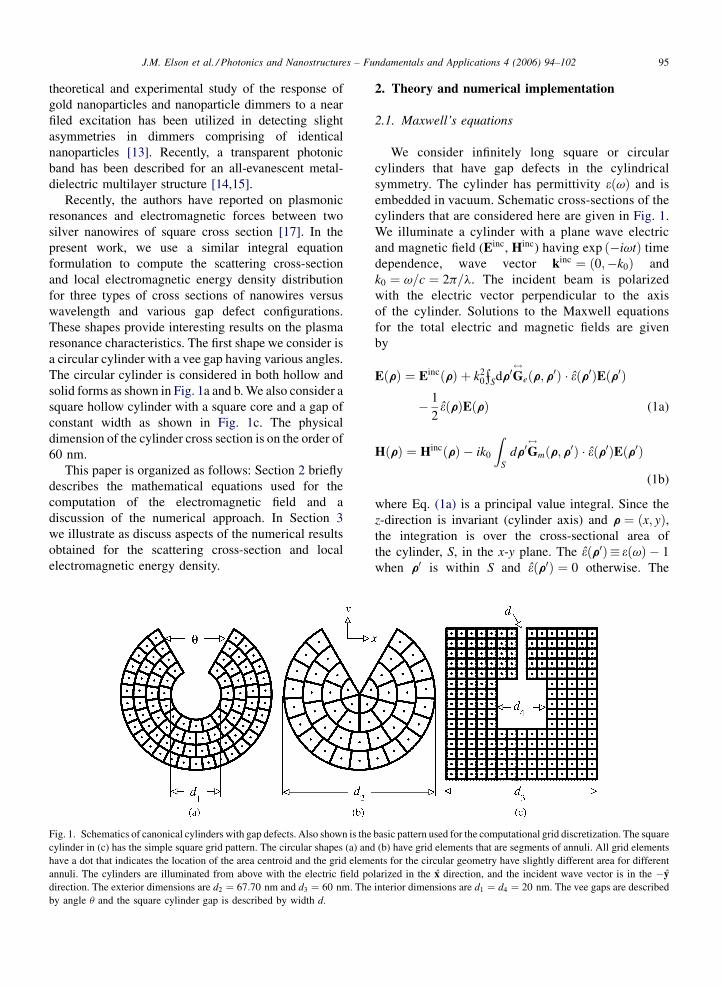
a circular cylinder with a vee gap having various angles.
The circular cylinder is considered in both hollow and
solid forms as shown in Fig. 1a and b. We also consider a
square hollow cylinder with a square core and a gap of
constant width as shown in Fig. 1c. The physical
dimension of the cylinder cross section is on the order of
60 nm.
This paper is organized as follows: Section 2 briefly
describes the mathematical equations used for the
computation of the electromagnetic field and a
discussion of the numerical approach. In Section 3
we illustrate as discuss aspects of the numerical results
obtained for the scattering cross-section and local
electromagnetic energy density.
Fig. 1. Schematics of canonical cylinders with gap defects. Also shown is the
cylinder in (c) has the simple square grid pattern. The circular shapes (a) and
have a dot that indicates the location of the area centroid and the grid eleme
annuli. The cylinders are illuminated from above with the electric field po
direction. The exterior dimensions are d2 ¼ 67:70 nm and d3 ¼ 60 nm. The
by angle u and the square cylinder gap is described by width d.
2. Theory and numerical implementation
2.1. Maxwell’s equations
We consider infinitely long square or circular
cylinders that have gap defects in the cylindrical
symmetry. The cylinder has permittivity eðvÞ and is
embedded in vacuum. Schematic cross-sections of the
cylinders that are considered here are given in Fig. 1.
We illuminate a cylinder with a plane wave electric
and magnetic field (Einc, Hinc) having exp ð�ivtÞ time
dependence, wave vector kinc ¼ ð0;�k0Þ and
k0 ¼ v=c ¼ 2p=l. The incident beam is polarized
with the electric vector perpendicular to the axis
of the cylinder. Solutions to the Maxwell equations
for the total electric and magnetic fields are given
by
EðrÞ ¼ EincðrÞ þ k20BS
dr0Ge
$ðr; r0Þ � eðr0ÞEðr0Þ
� 1
2eðrÞEðrÞ (1a)
HðrÞ ¼ HincðrÞ � ik0
ZS
dr0Gm
$ðr; r0Þ � eðr0ÞEðr0Þ
(1b)
where Eq. (1a) is a principal value integral. Since the
z-direction is invariant (cylinder axis) and r ¼ ðx; yÞ,the integration is over the cross-sectional area of
the cylinder, S, in the x-y plane. The eðr0Þ � eðvÞ � 1
when r0 is within S and eðr0Þ ¼ 0 otherwise. The
basic pattern used for the computational grid discretization. The square
(b) have grid elements that are segments of annuli. All grid elements
nts for the circular geometry have slightly different area for different
larized in the x direction, and the incident wave vector is in the �y
interior dimensions are d1 ¼ d4 ¼ 20 nm. The vee gaps are described
J.M. Elson et al. / Photonics and Nanostructures – Fundamentals and Applications 4 (2006) 94–10296
electric Ge
$and magnetic Gm
$Green tensors are
well known for 2D geometry and they are described
elsewhere [16,17].
Numerical integration of Eqs. (1a) and (1b) is
straightforward by dividing the cross-section S into a
grid of k ¼ 1!K area segments, each having area Ak
with area centroid rk. With this, we write Eq. (1a) in a
form suitable for matrix formalism as
EðrkÞ ¼ EincðrkÞ
þ k20
XK
k0¼1
�ð1� dk;k0 ÞAk0Ge
$ðrk; rk0 Þeðrk0 ÞEðrk0 Þ
þ dk;k0
�M$ðrkÞ �
1
2eðrkÞ I
$�� EðrkÞ
�
M$ðrkÞ ¼ B
Akdr0Ge
$ðrk; rk þ r0Þeðrk þ r0Þ (2b)
where the M$
integral is the self term, I$
is the identity
matrix, and dk;k0 is the Kronecker delta. To give an
approximate value to M$
, we analytically integrate
Eq. (2b) over a circular area of radius Rk where
pR2k ¼ Ak. The electric field solution integral equation
as written in Eq. (2a) is now in the form of a linear
system of equations and can be solved by the BiConju-
gate Gradient Method. Using this method has the dis-
tinct advantage that minimal matrix storage is required
as only a row or column is required at any given time.
The magnetic field solution is obtained from Eq. (1b).
2.2. Grid elements for cylinder cross-section
In the case of cylinders with square cross-section S,
as in Fig. 1c, a simple grid that is used in this work is
typically a series of squares with constant area Ak and
their area centroids are at the center of each grid square.
However, when the cross-section S is circular as in
Fig. 1a and b, square grids are a poor choice. In this
case, we devise a grid pattern that takes advantage of
the circular geometry. The radial direction is divided
into n ¼ 1!N annuli each having spatial resolution
of thickness dr ¼ rn � rn�1. It is easy to show that
the n th annulus will have a radial area centroid
rcn ¼ ð2=3Þðr3
n � r3n�1Þ=ðr2
n � r2n�1Þ. The spatial resolu-
tion in the azimuthal direction for the n th annulus is
written as dnf ¼ rc
nDfn, which is generally different for
each annulus. The Dfn is the azimuthal resolution in
angle for the n th annulus. Then, using the radial
resolution dr as a starting value, the azimuthal angle
resolution in the n th annulus is initially written as
Dfn ¼ dr=rcn and this nominal value may need a slight
adjustment. Since the total azimuthal angle along the
annulus is c ¼ ð2p� ugÞ, we examine the ratio
c=Dfn ¼ m and then adjust Dfn!Dfn such that m
becomes the nearest integer. Each grid segment in the n
th annulus will then have area ðr2n � r2
n�1ÞDfn=2 with
approximately equal spatial resolution in the radial dr
and azimuthal dnf ¼ rc
nDfn directions. It follows that for
the cylinders with circular geometry, the area of the k th
grid element in the n th annulus has the form
Ak ¼ ðr2n � r2
n�1ÞDfn=2. This value is constant for grid
elements within any annulus, but generally is slightly
different when the area of grid elements between
different annuli are compared.
2.3. Scattering and local electromagnetic energy
density
Evaluation of plasmonic resonance for the cylinder
geometry considered here can be analyzed by comput-
ing the far-field scattered radiation or the near-field
electromagnetic energy density in and around the
cylinder. The far-field expressions yield the angular
distribution of scattered radiation and the scattering
cross-section. The local electromagnetic field energy
density yields the spatial distribution of field energy. In
all numerical data to follow, the incident plane wave has
wave vector in the �y direction and the electric field is
polarized in the x direction. For this case the incident
power as given by the Poynting vector is just S0 ¼ c=8p.
2.3.1. Differential scattering and scattering
cross-section
Considering Eqs. (1a) and (1b) in the far-field
where jrj� jr0j and k0jrj� 1, we compute the radial
component of the Poynting vector SðuÞ for propagation
in the u direction. It is straightforward to show that for
the scattered fields the differential scattered power per
unit polar angle is
1
S0
dSðuÞdu¼ ð2pÞ4
l3jPxcos u � Pysin uj2 (3)
where
P j ¼Z
S
dr0eðr0Þ4p
E jðr0Þ and j ¼ x or y: (4)
The polar angle u is measured relative to the y axis and
Px and Py are the net polarization components of the
cylinder. This expression for scattering has the l�3 pre-
factor corresponding to the classic Rayleigh wavelength
dependence for 2D geometry. In the case of plasmon
resonance, however, the scattering strengths as given by
Px and Py depend strongly on wavelength. Integration of
J.M. Elson et al. / Photonics and Nanostructures – Fundamentals and Applications 4 (2006) 94–102 97
Eq. (3) over all u yields the total amount of energy
scattered by the cylinder as the SCS which is written
SCS ¼ 1
S0
Z 2p
0
dSðuÞdu
du ¼ pð2pÞ4
l3½jPxj2 þ jPyj2�: (5)
2.3.2. Local electromagnetic energy density
We compute the time-averaged local electromag-
netic energy density UðrÞ [18] of the electromagnetic
field at point r as
UðrÞ ¼ 1
8p
�Re
�dðveðvÞÞ
dv
�jEðrÞj2 þ jHðrÞj2
�(6)
where the dðveðvÞÞ=dv reduces to unity when r is
outside a cylinder cross-section.
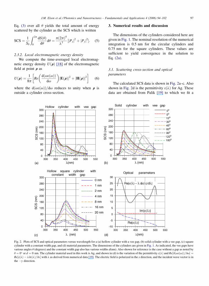
Fig. 2. Plots of SCS and optical parameters versus wavelength for a (a) hollo
cylinder with a constant width gap, and (d) material parameters. The dimensi
various angles u (degrees) and the constant width gap also has various widths
u ¼ 0� or d ¼ 0 nm. The cylinder material used in this work is Ag, and show
Re½eðlÞ � l@eðlÞ=@l� with l as derived from numerical data [19]. The electr
the �y direction.
3. Numerical results and discussion
The dimensions of the cylinders considered here are
given in Fig. 1. The nominal resolution of the numerical
integration is 0.5 nm for the circular cylinders and
0.75 nm for the square cylinders. These values are
sufficient to yield convergence in the solution to
Eq. (2a).
3.1. Scattering cross-section and optical
parameters
The calculated SCS data is shown in Fig. 2a–c. Also
shown in Fig. 2d is the permittivity eðlÞ for Ag. These
data are obtained from Palik [19] to which we fit a
w cylinder with a vee gap, (b) solid cylinder with a vee gap, (c) square
ons of the cylinders are given in Fig. 1. As indicated, the vee gaps have
d(nm). Also shown for reference is the case without a gap as noted by
n in (d) is the variation of the permittivity eðlÞ and Re½@ðveðvÞÞ=@v� ¼ic field is polarized in the x direction, and the incident wave vector is in
J.M. Elson et al. / Photonics and Nanostructures – Fundamentals and Applications 4 (2006) 94–10298
polynomial. From this, we can easily obtain the
derivative term needed with Eq. (6) and these data
are also shown.
For the circular cylinders in Fig. 2a and b and smaller
gap angles, the dominant resonance is in the vicinity of
340 nm. In this range and as seen in Fig. 2d, the
ReðeÞ9 � 1 and this coincides with the onset of the
coherent surface plasma resonance oscillation of the free
electron density for a semi-infinite planar interface. As
the gap angle increases, shape effects become increas-
ingly important such that highly localized corner modes
can dominate. This is especially noticeable in Fig. 2b for
u ¼ 45� ! 120�. This is clearly seen later in the contour
plots of the local electromagnetic energy density UðrÞ. In
Fig. 2c the SCS is shown for the square cylinder for
several gap widths d, the peaks are in the vicinity of
400 nm. Finally, we show in Fig. 2d the coefficient
Re½eðlÞ � l@eðlÞ=@l� that is relevant to the UðrÞ. It is
seen that for the dispersive material considered here, this
derivative coefficient contributes significantly to the local
electromagnetic energy density.
3.2. Hollow core circular cylinder
In Figs. 3–5 , we show contour plots of the local
electromagnetic energy density for a hollow cylinder at
wavelengths of 340, 410, and 480 nm where the gap
angles range from 0� to 180�. All plots are shown on the
same log scale and when comparing all three sets of
plots, it is evident that the l ¼ 340 nm case generally
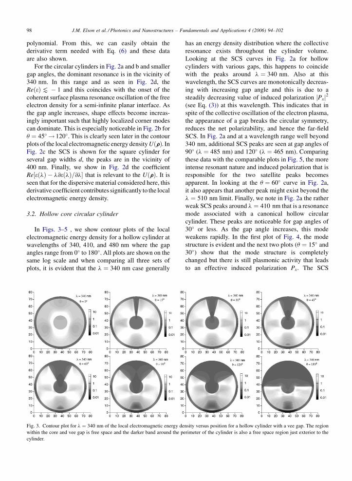
Fig. 3. Contour plot for l ¼ 340 nm of the local electromagnetic energy de
within the core and vee gap is free space and the darker band around the p
cylinder.
has an energy density distribution where the collective
resonance exists throughout the cylinder volume.
Looking at the SCS curves in Fig. 2a for hollow
cylinders with various gaps, this happens to coincide
with the peaks around l ¼ 340 nm. Also at this
wavelength, the SCS curves are monotonically decreas-
ing with increasing gap angle and this is due to a
steadily decreasing value of induced polarization jPxj2(see Eq. (3)) at this wavelength. This indicates that in
spite of the collective oscillation of the electron plasma,
the appearance of a gap breaks the circular symmetry,
reduces the net polarizability, and hence the far-field
SCS. In Fig. 2a and at a wavelength range well beyond
340 nm, additional SCS peaks are seen at gap angles of
90� (l ¼ 485 nm) and 120� (l ¼ 465 nm). Comparing
these data with the comparable plots in Fig. 5, the more
intense resonant nature and induced polarization that is
responsible for the two satellite peaks becomes
apparent. In looking at the u ¼ 60� curve in Fig. 2a,
it also appears that another peak might exist beyond the
l ¼ 510 nm limit. Finally, we note in Fig. 2a the rather
weak SCS peaks around l ¼ 410 nm that is a resonance
mode associated with a canonical hollow circular
cylinder. These peaks are noticeable for gap angles of
30� or less. As the gap angle increases, this mode
weakens rapidly. In the first plot of Fig. 4, the mode
structure is evident and the next two plots (u ¼ 15� and
30�) show that the mode structure is completely
changed but there is still plasmonic activity that leads
to an effective induced polarization Px. The SCS
nsity versus position for a hollow cylinder with a vee gap. The region
erimeter of the cylinder is also a free space region just exterior to the
J.M. Elson et al. / Photonics and Nanostructures – Fundamentals and Applications 4 (2006) 94–102 99
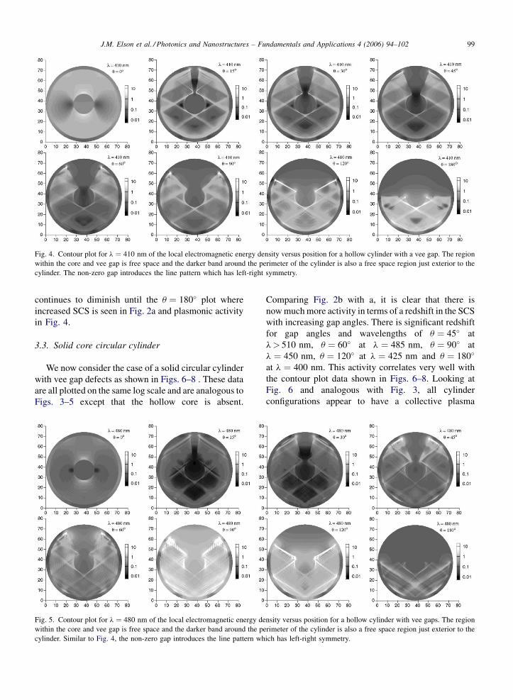
Fig. 4. Contour plot for l ¼ 410 nm of the local electromagnetic energy density versus position for a hollow cylinder with a vee gap. The region
within the core and vee gap is free space and the darker band around the perimeter of the cylinder is also a free space region just exterior to the
cylinder. The non-zero gap introduces the line pattern which has left-right symmetry.
continues to diminish until the u ¼ 180� plot where
increased SCS is seen in Fig. 2a and plasmonic activity
in Fig. 4.
3.3. Solid core circular cylinder
We now consider the case of a solid circular cylinder
with vee gap defects as shown in Figs. 6–8 . These data
are all plotted on the same log scale and are analogous to
Figs. 3–5 except that the hollow core is absent.
Fig. 5. Contour plot for l ¼ 480 nm of the local electromagnetic energy de
within the core and vee gap is free space and the darker band around the pe
cylinder. Similar to Fig. 4, the non-zero gap introduces the line pattern wh
Comparing Fig. 2b with a, it is clear that there is
now much more activity in terms of a redshift in the SCS
with increasing gap angles. There is significant redshift
for gap angles and wavelengths of u ¼ 45� at
l> 510 nm, u ¼ 60� at l ¼ 485 nm, u ¼ 90� at
l ¼ 450 nm, u ¼ 120� at l ¼ 425 nm and u ¼ 180�
at l ¼ 400 nm. This activity correlates very well with
the contour plot data shown in Figs. 6–8. Looking at
Fig. 6 and analogous with Fig. 3, all cylinder
configurations appear to have a collective plasma
nsity versus position for a hollow cylinder with vee gaps. The region
rimeter of the cylinder is also a free space region just exterior to the
ich has left-right symmetry.
J.M. Elson et al. / Photonics and Nanostructures – Fundamentals and Applications 4 (2006) 94–102100
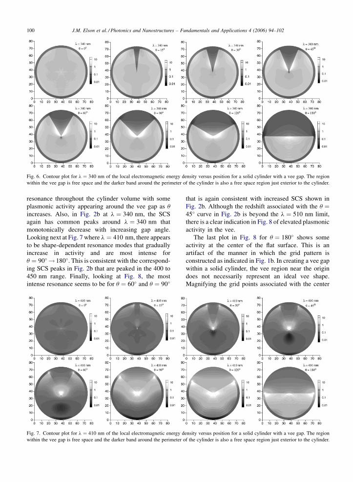
Fig. 6. Contour plot for l ¼ 340 nm of the local electromagnetic energy density versus position for a solid cylinder with a vee gap. The region
within the vee gap is free space and the darker band around the perimeter of the cylinder is also a free space region just exterior to the cylinder.
resonance throughout the cylinder volume with some
plasmonic activity appearing around the vee gap as u
increases. Also, in Fig. 2b at l ¼ 340 nm, the SCS
again has common peaks around l ¼ 340 nm that
monotonically decrease with increasing gap angle.
Looking next at Fig. 7 where l ¼ 410 nm, there appears
to be shape-dependent resonance modes that gradually
increase in activity and are most intense for
u ¼ 90� ! 180�. This is consistent with the correspond-
ing SCS peaks in Fig. 2b that are peaked in the 400 to
450 nm range. Finally, looking at Fig. 8, the most
intense resonance seems to be for u ¼ 60� and u ¼ 90�
Fig. 7. Contour plot for l ¼ 410 nm of the local electromagnetic energy d
within the vee gap is free space and the darker band around the perimeter o
that is again consistent with increased SCS shown in
Fig. 2b. Although the redshift associated with the u ¼45� curve in Fig. 2b is beyond the l ¼ 510 nm limit,
there is a clear indication in Fig. 8 of elevated plasmonic
activity in the vee.
The last plot in Fig. 8 for u ¼ 180� shows some
activity at the center of the flat surface. This is an
artifact of the manner in which the grid pattern is
constructed as indicated in Fig. 1b. In creating a vee gap
within a solid cylinder, the vee region near the origin
does not necessarily represent an ideal vee shape.
Magnifying the grid points associated with the center
ensity versus position for a solid cylinder with a vee gap. The region
f the cylinder is also a free space region just exterior to the cylinder.
J.M. Elson et al. / Photonics and Nanostructures – Fundamentals and Applications 4 (2006) 94–102 101
Fig. 8. Contour plot for l ¼ 480 nm of the local electromagnetic energy density versus position for a solid cylinder with a vee gap. The region
within the vee gap is free space and the darker band around the perimeter of the cylinder is also the free space region just exterior to the cylinder.
Fig. 9. Contour plots of local electromagnetic energy density versus position for a hollow square cylinder with a 0, 2, 8 and 16 nm gaps. The
wavelengths are 340, 410 and 480 nm. The region within the core and gap is free space and the darker band around the perimeter of a square is the
free space region just exterior to the cylinder.
J.M. Elson et al. / Photonics and Nanostructures – Fundamentals and Applications 4 (2006) 94–102102
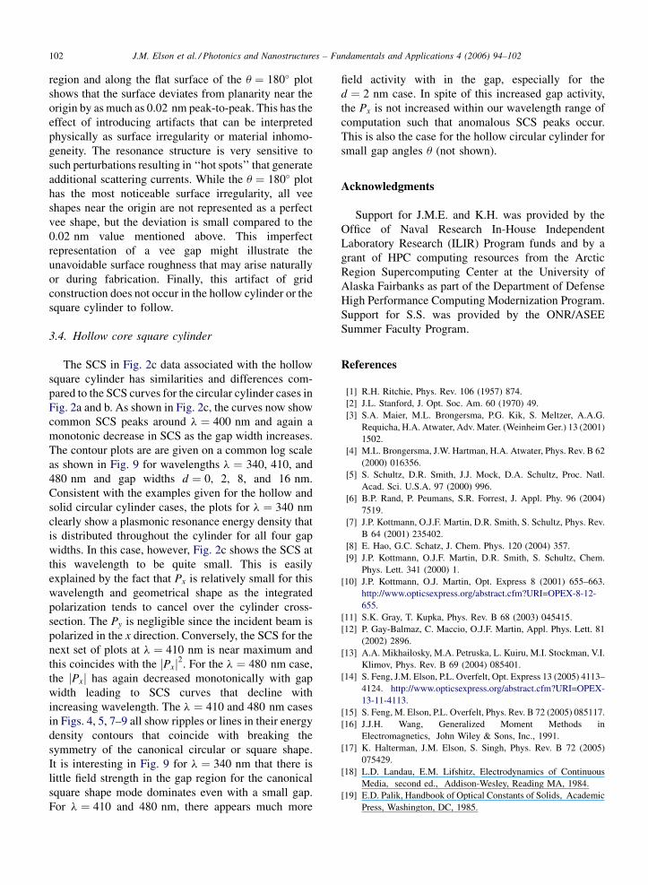
region and along the flat surface of the u ¼ 180� plot
shows that the surface deviates from planarity near the
origin by as much as 0.02 nm peak-to-peak. This has the
effect of introducing artifacts that can be interpreted
physically as surface irregularity or material inhomo-
geneity. The resonance structure is very sensitive to
such perturbations resulting in ‘‘hot spots’’ that generate
additional scattering currents. While the u ¼ 180� plot
has the most noticeable surface irregularity, all vee
shapes near the origin are not represented as a perfect
vee shape, but the deviation is small compared to the
0.02 nm value mentioned above. This imperfect
representation of a vee gap might illustrate the
unavoidable surface roughness that may arise naturally
or during fabrication. Finally, this artifact of grid
construction does not occur in the hollow cylinder or the
square cylinder to follow.
3.4. Hollow core square cylinder
The SCS in Fig. 2c data associated with the hollow
square cylinder has similarities and differences com-
pared to the SCS curves for the circular cylinder cases in
Fig. 2a and b. As shown in Fig. 2c, the curves now show
common SCS peaks around l ¼ 400 nm and again a
monotonic decrease in SCS as the gap width increases.
The contour plots are are given on a common log scale
as shown in Fig. 9 for wavelengths l ¼ 340, 410, and
480 nm and gap widths d ¼ 0, 2, 8, and 16 nm.
Consistent with the examples given for the hollow and
solid circular cylinder cases, the plots for l ¼ 340 nm
clearly show a plasmonic resonance energy density that
is distributed throughout the cylinder for all four gap
widths. In this case, however, Fig. 2c shows the SCS at
this wavelength to be quite small. This is easily
explained by the fact that Px is relatively small for this
wavelength and geometrical shape as the integrated
polarization tends to cancel over the cylinder cross-
section. The Py is negligible since the incident beam is
polarized in the x direction. Conversely, the SCS for the
next set of plots at l ¼ 410 nm is near maximum and
this coincides with the jPxj2. For the l ¼ 480 nm case,
the jPxj has again decreased monotonically with gap
width leading to SCS curves that decline with
increasing wavelength. The l ¼ 410 and 480 nm cases
in Figs. 4, 5, 7–9 all show ripples or lines in their energy
density contours that coincide with breaking the
symmetry of the canonical circular or square shape.
It is interesting in Fig. 9 for l ¼ 340 nm that there is
little field strength in the gap region for the canonical
square shape mode dominates even with a small gap.
For l ¼ 410 and 480 nm, there appears much more
field activity with in the gap, especially for the
d ¼ 2 nm case. In spite of this increased gap activity,
the Px is not increased within our wavelength range of
computation such that anomalous SCS peaks occur.
This is also the case for the hollow circular cylinder for
small gap angles u (not shown).
Acknowledgments
Support for J.M.E. and K.H. was provided by the
Office of Naval Research In-House Independent
Laboratory Research (ILIR) Program funds and by a
grant of HPC computing resources from the Arctic
Region Supercomputing Center at the University of
Alaska Fairbanks as part of the Department of Defense
High Performance Computing Modernization Program.
Support for S.S. was provided by the ONR/ASEE
Summer Faculty Program.
References
[1] R.H. Ritchie, Phys. Rev. 106 (1957) 874.
[2] J.L. Stanford, J. Opt. Soc. Am. 60 (1970) 49.
[3] S.A. Maier, M.L. Brongersma, P.G. Kik, S. Meltzer, A.A.G.
Requicha, H.A. Atwater, Adv. Mater. (Weinheim Ger.) 13 (2001)
1502.
[4] M.L. Brongersma, J.W. Hartman, H.A. Atwater, Phys. Rev. B 62
(2000) 016356.
[5] S. Schultz, D.R. Smith, J.J. Mock, D.A. Schultz, Proc. Natl.
Acad. Sci. U.S.A. 97 (2000) 996.
[6] B.P. Rand, P. Peumans, S.R. Forrest, J. Appl. Phy. 96 (2004)
7519.
[7] J.P. Kottmann, O.J.F. Martin, D.R. Smith, S. Schultz, Phys. Rev.
B 64 (2001) 235402.
[8] E. Hao, G.C. Schatz, J. Chem. Phys. 120 (2004) 357.
[9] J.P. Kottmann, O.J.F. Martin, D.R. Smith, S. Schultz, Chem.
Phys. Lett. 341 (2000) 1.
[10] J.P. Kottmann, O.J. Martin, Opt. Express 8 (2001) 655–663.
http://www.opticsexpress.org/abstract.cfm?URI=OPEX-8-12-
655.
[11] S.K. Gray, T. Kupka, Phys. Rev. B 68 (2003) 045415.
[12] P. Gay-Balmaz, C. Maccio, O.J.F. Martin, Appl. Phys. Lett. 81
(2002) 2896.
[13] A.A. Mikhailosky, M.A. Petruska, L. Kuiru, M.I. Stockman, V.I.
Klimov, Phys. Rev. B 69 (2004) 085401.
[14] S. Feng, J.M. Elson, P.L. Overfelt, Opt. Express 13 (2005) 4113–
4124. http://www.opticsexpress.org/abstract.cfm?URI=OPEX-
13-11-4113.
[15] S. Feng, M. Elson, P.L. Overfelt, Phys. Rev. B 72 (2005) 085117.
[16] J.J.H. Wang, Generalized Moment Methods in
Electromagnetics, John Wiley & Sons, Inc., 1991.
[17] K. Halterman, J.M. Elson, S. Singh, Phys. Rev. B 72 (2005)
075429.
[18] L.D. Landau, E.M. Lifshitz, Electrodynamics of Continuous
Media, second ed., Addison-Wesley, Reading MA, 1984.
[19] E.D. Palik, Handbook of Optical Constants of Solids, Academic
Press, Washington, DC, 1985.


