Embed Size (px)
Citation preview
ARTICLESPUBLISHED ONLINE: 4 DECEMBER 2011 | DOI: 10.1038/NMAT3200
Second-harmonic generation in siliconwaveguides strained by silicon nitrideM. Cazzanelli1, F. Bianco1, E. Borga1, G. Pucker2, M. Ghulinyan2, E. Degoli3, E. Luppi4, V. Véniard5,S. Ossicini3, D. Modotto6, S. Wabnitz6, R. Pierobon7 and L. Pavesi1*Silicon photonics meets the electronics requirement of increased speed and bandwidth with on-chip optical networks.All-optical data management requires nonlinear silicon photonics. In silicon only third-order optical nonlinearities are presentowing to its crystalline inversion symmetry. Introducing a second-order nonlinearity into silicon photonics by proper materialengineering would be highly desirable. It would enable devices for wideband wavelength conversion operating at relatively lowoptical powers. Here we show that a sizeable second-order nonlinearity at optical wavelengths is induced in a silicon waveguideby using a stressing silicon nitride overlayer. We carried out second-harmonic-generation experiments and first-principlecalculations, which both yield large values of strain-induced bulk second-order nonlinear susceptibility, up to 40 pm V−1 at2,300 nm. We envisage that nonlinear strained silicon could provide a competing platform for a new class of integrated lightsources spanning the near- to mid-infrared spectrum from 1.2 to 10µm.
When a crystal possesses a significant second-ordernonlinear optical susceptibility, χ (2), it can produce awide variety of wavelengths from an optical pump1.
In fact, a second-order crystal generates shorter wavelengths bysecond-harmonic generation or longer wavelengths by spontaneousparametric down-conversion of a single pump beam. Such a crystalcan also nonlinearly mix two different beams, thus generating otherwavelengths by sum-frequency or difference-frequency generation.These possibilities are much more intriguing whenever the crystalcan be used in integrated optical circuits because, on the one hand,light confinement reduces the average optical power needed totrigger nonlinear processes and, on the other hand, relatively longeffective interaction lengths can be exploited.
Si photonics has demonstrated the integration of multipleoptical functionalities with microelectronic devices2,3. On the basisof the third- or higher-order nonlinearities of Si (ref. 4), functionssuch as amplification and lasing, wavelength conversion andoptical processing have all been demonstrated in recent years5.However, third-order refractive nonlinearities require relativelyhigh optical powers, and compete with nonlinear-loss mechanismssuch as two-photon absorption and two-photon induced free-carrier absorption. Yet, the second-order term of the nonlinearsusceptibility tensor cannot be exploited in Si simply becauseχ (2) vanishes in the dipole approximation owing to the crystalcentrosymmetry: the residual χ (2), which is due to higher-multipoleprocesses, is too weak to be exploited in optical devices6.
Second-harmonic generation (SHG) was observed in reflectionfrom Si surfaces7–11 or in diffusion from Si photonic crystalnanocavities12. This indicates that the reduction of the Si symmetrymay indeed induce a significant χ (2). In these cases, the Sisymmetry was broken by the presence of a surface. Several groupshave pointed out that the surface contribution to χ (2) can be
1Nanoscience Laboratory, Department of Physics, University of Trento, via Sommarive 14, 38123 Povo, Trento, Italy, 2Advanced Photonics & PhotovoltaicsUnit, Bruno Kessler Foundation, via Sommarive 18, 38123 Povo, Trento, Italy, 3Istituto di Nanoscienze-CNR-S3 and Dipartimento di Scienze e Metodidell’Ingegneria, Università di Modena e Reggio Emilia, via Amendola 2 Pad. Morselli, I-42122 Reggio Emilia, Italy, 4Department of Chemistry, University ofCalifornia Berkeley, California 94720, USA, 5Laboratoire des Solides Irradiés, Ecole Polytechnique, Route de Saclay, F-91128 Palaiseau and EuropeanTheoretical Spectroscopy Facility (ETSF), France, 6Department of Information Engineering, University of Brescia, via Branze 38, 25123 Brescia, Italy,7CIVEN, via delle Industrie 5, I-30175, Venezia Marghera, Italy. *e-mail: [email protected].
strengthened by applying a strain8–10. It was also reported thatstrain and increased internal surfaces in a Si photonic crystalwaveguide may induce a strong χ (2), which enables measurementof electro-optic effects13,14. Theoretically, these results are so farqualitatively but not quantitatively understood15. The prospect ofcontrolling second-order nonlinear phenomena in Si by meansof strain is very intriguing. In this work we provide the firstquantitative demonstration of second-order nonlinearities instrained Si through both ab initio calculations and SHGexperimentsin suitably engineered Si waveguides.
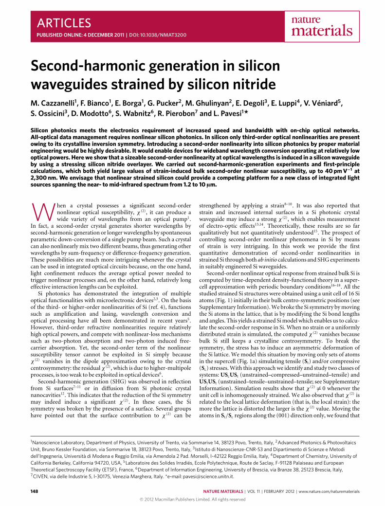
Second-order nonlinear optical response from strained bulk Si iscomputed by time-dependent density-functional theory in a super-cell approximation with periodic boundary conditions16–18. All thestudied strained Si structures were obtained using a unit cell of 16 Siatoms (Fig. 1) initially in their bulk centro-symmetric positions (seeSupplementary Information).We broke the Si symmetry bymovingthe Si atoms in the lattice, that is by modifying the Si bond lengthsand angles. This yields a strained Simodel which enables us to calcu-late the second-order response in Si. When no strain or a uniformlydistributed strain is simulated, the computed χ (2) vanishes becausebulk Si still keeps a crystalline centrosymmetry. To break thesymmetry, the stress has to induce an asymmetric deformation ofthe Si lattice. We model this situation by moving only sets of atomsin the supercell (Fig. 1a) simulating tensile (St) and/or compressive(Sc) stresses.With this approachwe identify and study two classes ofsystems: UScUSt (unstrained–compressed–unstrained–tensile) andUStUSt (unstrained–tensile–unstrained–tensile; see SupplementaryInformation). Simulation results show that χ (2)
6= 0 whenever theunit cell is inhomogeneously strained. We also observed that χ (2) isrelated to the local lattice deformation (that is, the local strain): themore the lattice is distorted the larger is the χ (2) value. Moving theatoms in St/Sc regions along the (001) direction only, we found that
148 NATURE MATERIALS | VOL 11 | FEBRUARY 2012 | www.nature.com/naturematerials
© 2012 Macmillan Publishers Limited. All rights reserved
NATURE MATERIALS DOI: 10.1038/NMAT3200 ARTICLES
× 50
Si¬
Si b
ond
Ato
m in
dex
Bond length (Å) Bond angle (°)
(2) (p
m V
¬1 )
χ
Wavelength (nm)
SS1 = 2.4 × 10¬5 GPa
HY1 = 3.2 × 10¬1 GPa16¬1715¬1614¬1513¬1412¬13
9¬108¬97¬86¬75¬64¬53¬42¬31¬2
11¬1210¬11
2.25 2.30 2.35 2.40 2.45 104 108 112
123456789
10111213141516
0
50
100
150
200
1,500 2,000 2,500 3,000 3,500
(2) (p
m V
¬1 )
χ
Wavelength (nm)
SS2 = 2.2 × 10¬3 GPa
HY2 = 7.5 × 10¬1 GPa
0
50
100
150
200
1,500 2,000 2,500 3,000 3,500
(2) (p
m V
¬1 )
χ
Wavelength (nm)
SS3 = 1.2 × 10¬1 GPa
HY3 = 9.1 × 10¬1 GPa
0
50
100
150
200
1,500 2,000 2,500 3,000 3,500
b c d
e
f
U
U
St
Sc
16
1514
1312
1110
7
89
6
54
32
1
a
HY1, SS1HY2, SS2HY3, SS3
HY1, SS1HY2, SS2HY3, SS3
Figure 1 | First-principle calculations of strained Si second-order nonlinearity. a, Simulation unit cell: the different colours refer to the different bonddeformations used. Orange: the bonds were elongated to represent a tensile stress, indicated by St. Yellow: no bond variation with respect to the relaxed Silattice (unperturbed region). Red: the bonds were shortened to represent a compressive stress, indicated by Sc. b, Maximum bond-length distortions forUScUSt structures. The unstrained bulk-Si bond length is 2.332 Å. The colours (blue–black–red) refer to the calculations shown in d–f. c, Maximumbond-angle distortions for UScUSt structures. The unstrained bulk-Si angles are 109.5◦. The colours (blue–black–red) refer to the calculations shown in d–f.The constant bond lengths and angles represent the unstrained region and coincide with Si-bulk values. The hierarchy of increasing strain in the threestructures (blue–black–red), which is reflected also in the corresponding values of pressure (HY) and in the YZ component of the shear stress (SS; seeSupplementary Information), is evident. d–f, The results of the simulations in terms of the χ (2) values. d, A weakly strained Si. e, A medium-strained Si.f, A heavily strained Si.
χ (2) is lower than 0.5 pmV−1 at 2,500 nm. In contrast, if we increasethe strain inhomogeneity moving the atoms also in the (1̄10)direction, we found that χ (2) increases significantly (Fig. 1). Foreach class,UScUSt andUStUSt, we studied three structures, inwhichwe have progressively increased the applied strain. In Fig. 1b,c weshow the maximum structural distortion in term of bond lengthsand angles for the UScUSt structures (the same can be found forthe UStUSt structures; see Supplementary Information). The typeand magnitude of strain is qualitatively observed as bond-lengthand angle deviations with respect to the unstrained Si bulk values.We observe that χ (2) has a maximum of 6 pmV−1 at a wavelengthof 1,900 nm for purely tensile strain. The magnitude of the appliedstrain was up to 5% bond distortion of the unstrained bulk value,that is up to 0.12 Å. When compressive and tensile strains areapplied (Fig. 1), χ (2) increases further, reaching a maximum valueof about 200 pmV−1 at 1,800 nm, as shown in Fig. 1f. In this case,the strain gradient is larger than that of the pure-tensile-straincase, because of the change in sign of the strain itself between Stand Sc (Fig. 1b,c). As the reported calculations refer to a strainedbulk Si, we also investigate the contribution to χ (2) from a Si/SiO2interface. We found a χ (2) smaller than 1 pmV−1 (SupplementaryInformation), whereas from the literature it is found that thefree Si surface induces a χ (2) of ∼3 pmV−1(refs 11,19). Therefore,breaking the Si inversion symmetry by an interface or a free surfaceyields a χ (2) that is significantly smaller than what can be achievedby inhomogeneously straining bulk Si.
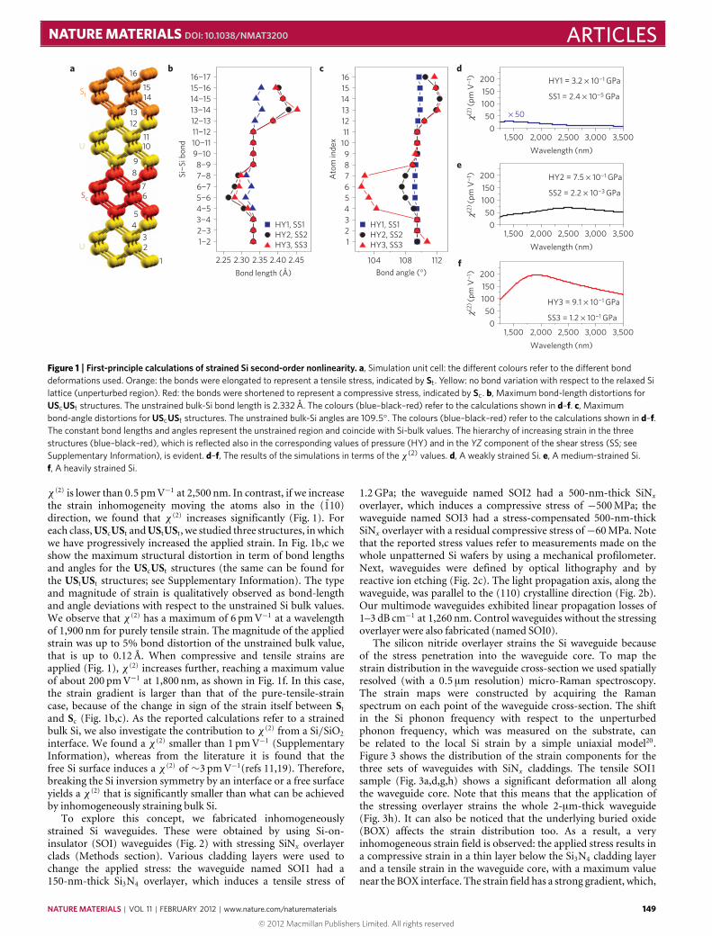
To explore this concept, we fabricated inhomogeneouslystrained Si waveguides. These were obtained by using Si-on-insulator (SOI) waveguides (Fig. 2) with stressing SiNx overlayerclads (Methods section). Various cladding layers were used tochange the applied stress: the waveguide named SOI1 had a150-nm-thick Si3N4 overlayer, which induces a tensile stress of
1.2 GPa; the waveguide named SOI2 had a 500-nm-thick SiNxoverlayer, which induces a compressive stress of −500MPa; thewaveguide named SOI3 had a stress-compensated 500-nm-thickSiNx overlayer with a residual compressive stress of−60MPa. Notethat the reported stress values refer to measurements made on thewhole unpatterned Si wafers by using a mechanical profilometer.Next, waveguides were defined by optical lithography and byreactive ion etching (Fig. 2c). The light propagation axis, along thewaveguide, was parallel to the (110) crystalline direction (Fig. 2b).Our multimode waveguides exhibited linear propagation losses of1–3 dB cm−1 at 1,260 nm. Control waveguides without the stressingoverlayer were also fabricated (named SOI0).
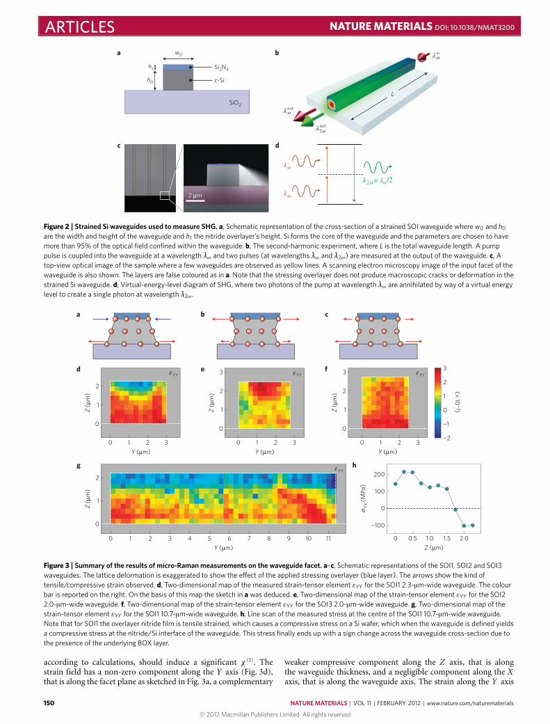
The silicon nitride overlayer strains the Si waveguide becauseof the stress penetration into the waveguide core. To map thestrain distribution in the waveguide cross-section we used spatiallyresolved (with a 0.5 µm resolution) micro-Raman spectroscopy.The strain maps were constructed by acquiring the Ramanspectrum on each point of the waveguide cross-section. The shiftin the Si phonon frequency with respect to the unperturbedphonon frequency, which was measured on the substrate, canbe related to the local Si strain by a simple uniaxial model20.Figure 3 shows the distribution of the strain components for thethree sets of waveguides with SiNx claddings. The tensile SOI1sample (Fig. 3a,d,g,h) shows a significant deformation all alongthe waveguide core. Note that this means that the application ofthe stressing overlayer strains the whole 2-µm-thick waveguide(Fig. 3h). It can also be noticed that the underlying buried oxide(BOX) affects the strain distribution too. As a result, a veryinhomogeneous strain field is observed: the applied stress results ina compressive strain in a thin layer below the Si3N4 cladding layerand a tensile strain in the waveguide core, with a maximum valuenear the BOX interface. The strain field has a strong gradient, which,
NATURE MATERIALS | VOL 11 | FEBRUARY 2012 | www.nature.com/naturematerials 149
© 2012 Macmillan Publishers Limited. All rights reserved
ARTICLES NATURE MATERIALS DOI: 10.1038/NMAT3200
a
dc
2 μm
h1
h0
SiO2
Si3N4
c-Si
w0
ωλ
ωλ
λ λ2 = /2
outω
ω
b
λ
out2λ
L
inωλ
ω ω
Figure 2 | Strained Si waveguides used to measure SHG. a, Schematic representation of the cross-section of a strained SOI waveguide where w0 and h0
are the width and height of the waveguide and h1 the nitride overlayer’s height. Si forms the core of the waveguide and the parameters are chosen to havemore than 95% of the optical field confined within the waveguide. b, The second-harmonic experiment, where L is the total waveguide length. A pumppulse is coupled into the waveguide at a wavelength λω and two pulses (at wavelengths λω and λ2ω) are measured at the output of the waveguide. c, Atop-view optical image of the sample where a few waveguides are observed as yellow lines. A scanning electron microscopy image of the input facet of thewaveguide is also shown. The layers are false coloured as in a. Note that the stressing overlayer does not produce macroscopic cracks or deformation in thestrained Si waveguide. d, Virtual-energy-level diagram of SHG, where two photons of the pump at wavelength λω are annihilated by way of a virtual energylevel to create a single photon at wavelength λ2ω .
h
Z (
μm)
Z (μm)
Y (μm)
Z (
μm)
Y (μm)
YYε
(× 10¬
3)
YY
(MPa
)σ
0
1
2
4 5 6 7 8 9 10 110 1 2 3
¬100
0
100
200
0 0.5 1.0 1.5 2.0
3210
0
1
2
3
Z (
μm)
Y (μm)
YYε
0
1
2
3
Z (
μm)
Y (μm)
YYε
1
0
2
¬1
¬2
3
32103210
0
1
2
YYεg
a b c
d e f
Figure 3 | Summary of the results of micro-Raman measurements on the waveguide facet. a–c, Schematic representations of the SOI1, SOI2 and SOI3waveguides. The lattice deformation is exaggerated to show the effect of the applied stressing overlayer (blue layer). The arrows show the kind oftensile/compressive strain observed. d, Two-dimensional map of the measured strain-tensor element εYY for the SOI1 2.3-µm-wide waveguide. The colourbar is reported on the right. On the basis of this map the sketch in a was deduced. e, Two-dimensional map of the strain-tensor element εYY for the SOI22.0-µm-wide waveguide. f, Two-dimensional map of the strain-tensor element εYY for the SOI3 2.0-µm-wide waveguide. g, Two-dimensional map of thestrain-tensor element εYY for the SOI1 10.7-µm-wide waveguide. h, Line scan of the measured stress at the centre of the SOI1 10.7-µm-wide waveguide.Note that for SOI1 the overlayer nitride film is tensile strained, which causes a compressive stress on a Si wafer, which when the waveguide is defined yieldsa compressive stress at the nitride/Si interface of the waveguide. This stress finally ends up with a sign change across the waveguide cross-section due tothe presence of the underlying BOX layer.
according to calculations, should induce a significant χ (2). Thestrain field has a non-zero component along the Y axis (Fig. 3d),that is along the facet plane as sketched in Fig. 3a, a complementary
weaker compressive component along the Z axis, that is alongthe waveguide thickness, and a negligible component along the Xaxis, that is along the waveguide axis. The strain along the Y axis
150 NATURE MATERIALS | VOL 11 | FEBRUARY 2012 | www.nature.com/naturematerials
© 2012 Macmillan Publishers Limited. All rights reserved
NATURE MATERIALS DOI: 10.1038/NMAT3200 ARTICLES
(× 10
¬3 )
YY
ε
Z (μm) 2.52.01.51.00.50
0
1
¬1
¬2
3
2
SOI0 3.0 μmSOI 1 2.3 μmSOI2 2.0 μmSOI3 2.0 μm
Figure 4 | Strain profiles (εYY) for the different waveguide types. Profilesrefer to the strain along the Z direction at the centre of the waveguides. Thewaveguide widths are reported in the key.
also depends on the waveguide width: the wider the waveguide themore inhomogeneous the strain (compare Fig. 3d with 3g). Thesituation is different for the compressed SOI2waveguide (Fig. 3b,e):although here the Si is mainly tensile strained, an inhomogeneousstrain field is still present. This field has a maximum near theoverlayer and gradually weakens near the underlying BOX. SOI3shows a strain field that is the opposite of SOI2 (Fig. 3c,f) due tothe stronger effect of the BOX with respect to the overlayer. InFig. 4 we report the Z -profile of the strain at the waveguide centre,for the various samples. SOI1 and SOI2 show important straingradients of opposite signs, reflecting the influence of strong tensileand compressive stress applied by the SiNx overlayers. Strain andits gradient are low for the reference SOI0 sample. SOI3 shows asimilar strain gradient, but the average strain is about twice that ofSOI0. In both samples the origin of strain is mainly due to the stressinduced by the BOX.
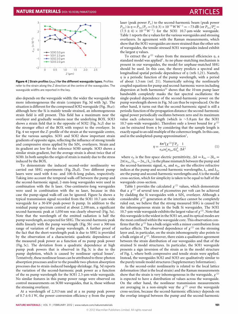
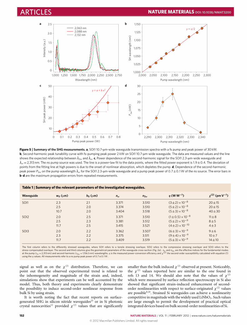
To demonstrate the induced second-order nonlinearity wecarried out SHG experiments (Fig. 2b,d). Two different pumplasers were used with 4-ns- and 100-fs-long pulses, respectively.Taking into account the temporal walk-off between the pump andthe second-harmonic signal, 2-mm-long waveguides were used incombination with the fs laser. One-centimetre-long waveguideswere used in combination with the ns laser, because in thiscase the pump-signal walk-off can be ignored. Figure 5a shows atypical transmission signal recorded from the SOI1 10.7-µm-widewaveguide for a 30-kW-peak-power fs pump. In addition to theresidual pump spectrum centred at about 2,100 nm, a significantsecond-harmonic peak at 1,050 nm was clearly observed (Fig. 5a).Note that the wavelength of the emitted radiation is half thepumpwavelength, as expected for SHG. The second-harmonic peakshifts linearly with the pump wavelength (Fig. 5b) over a 300 nmrange of variation of the pump wavelength. A further proof ofthe fact that the short-wavelength peak is due to SHG is providedby the observation of a characteristic quadratic dependence ofthe measured peak power as a function of ns pump peak power(Fig. 5c). The deviation from a quadratic dependence at highpump peak powers that is observed in Fig. 5c is due to thepump depletion, which is caused by nonlinear optical losses5.Tentatively, these nonlinear losses can be attributed to three-photonabsorption processes and/or to the possible two-photon absorptionprocesses due to strain-induced bandgap shrinkage. Fig. 5d reportsthe variation of the second-harmonic peak power as a functionof the ns pump wavelength for the SOI1 2.3-µm-wide waveguide.No similar features in this pump power range were observed oncontrol measurements on SOI0 waveguides, that is, those withoutthe stressing overlayer.
At a wavelength of 2,313 nm and at a ns pump peak powerof 0.7± 0.1W, the power-conversion efficiency η from the pump
laser (peak power Pω) to the second-harmonic beam (peak powerP2ω) is η=P2ω/Pω= (5±3)×10−8 WW−1=−73 dB (or P2ω/P2
ω=
(7.5 ± 4) × 10−8 W−1) for the SOI1 10.7-µm-wide waveguide.Table 1 reports the η values for the various waveguides and stressingoverlayers. In agreement with the Raman measurements, whichshow that the SOI1waveguides aremore strained than the other setsof waveguides, the tensile-stressed SOI1 waveguides indeed exhibitthe largest η values.
To extract the χ (2) values from the measured efficiencies η, astandard model was applied1. As no phase-matching mechanism ispresent in our waveguides, the model for unphase-matched SHGshould be used. In this case, the theory predicts a spectral andlongitudinal spatial periodic dependence of η (refs 1,21). Namely,η is a periodic function of the pump wavelength, with a periodof about 1.5 nm (ref. 21). Numerically solving the nonlinearlycoupled equations for pump and second-harmonic waves includingdispersion at both harmonics22 shows that the 10 nm pump laserbandwidth completely masks the fast spectral oscillations: thesingle-peaked dependence of the second-harmonic power on thepump wavelength shown in Fig. 5d can thus be reproduced. On theother hand, it turns out that the second-harmonic signal is still aperiodic function of the propagation distance: the second-harmonicsignal power periodically oscillates between zero and its maximumvalue each coherence length (which is ∼5.8 µm for the SOI110.7-µm-wide waveguide). Therefore only a lower bound for χ (2)
can be extracted from η by considering that the sample length isexactly equal to an oddmultiple of the coherence length. In this case,and in the undepleted-pump approximation1,
η=8π2[χ (2)
]2Pω
ε0cn2ωn2ωAλ2ω
11k2
(1)
where ε0 is the free-space electric permittivity, 1k = k2ω− 2kω =2π(n2ω/λ2ω−2nω/λω) is the phasemismatch between the pump andthe second-harmonic signal, nω and n2ω are the effective refractiveindices at the pump and second-harmonic wavelengths, λω and λ2ωare the pump and second-harmonic wavelengths andA is themodalcross-section, which for simplicity is taken to be equal to half of thewaveguide cross-section.
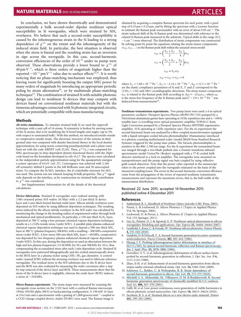
Table 1 provides the calculated χ (2) values, which demonstratethat a χ (2) of several tens of picometres per volt can be achievedby cladding the Si waveguides with a SiNx overlayer. Although aconsiderable χ (2) generation at the interface cannot be completelyruled out, we believe that the strong measured SHG is caused bythe inhomogeneous strain in the bulk Si waveguides. The SOI110.7-µm-wide waveguide exhibits the largest value ofχ (2). Note thatthis waveguide is thewidest in the SOI1 set, and its opticalmodes arethemost confinedwithin the waveguide core. This observation con-firms that the χ (2) has a bulk origin with a minor contribution fromsurface effects. The observed dependence of χ (2) on the stressinglayer and, in particular, on the strain inhomogeneity also points toa bulk origin of χ (2). Moreover, there exists a qualitative agreementbetween the strain distribution of our waveguides and that of thestrained Si model structures. In particular, the SOI1 waveguidepresents a sign inversion of the strain as in the model structureof Fig. 1, where both compressive and tensile strain were applied.Instead, the waveguides SOI2 and SOI3 are qualitatively similar tothe purely tensilemodel structures (Supplementary Information).
As the second-order nonlinearity is related to the local latticedeformation (that is the local strain) and the Ramanmeasurementsshow that the strain is very inhomogeneous in the waveguide, χ (2)
is expected to have a distribution of values across the waveguide.On the other hand, the nonlinear transmission measurementsare averaging in a non-simple way the χ (2) over the waveguidecross-section, because the second-harmonic efficiency depends onthe overlap integral between the pump and the second-harmonic
NATURE MATERIALS | VOL 11 | FEBRUARY 2012 | www.nature.com/naturematerials 151
© 2012 Macmillan Publishers Limited. All rights reserved
ARTICLES NATURE MATERIALS DOI: 10.1038/NMAT3200
y = x/2
Inte
nsity
(a.
u.)
Wavelength (nm)
SH p
eak
pow
er (
nW)
Pump peak power (W) Pump wavelength (nm)
Pump wavelength (nm)
y = a + b x2
1,000 1,250 1,500 1,750 2,000 2,250 2,500 2,750
0
2.5
2.0
1.5
1.0
0.5
10
20
30
40
50
0 0.1 0.3 0.5 0.70.2 0.4 0.6 0.80
5
10
15
20
25
30
2,290 2,300 2,310 2,320 2,330 2,340
2,000 2,050 2,100 2,150 2,200 2,250 2,3001,000
1,025
1,050
1,075
1,100
1,125
1,1502,063 nm2,088 nm2,132 nm
a
c
b
d
P 2
(nW
)SH
wav
elen
gth
(nm
) ω
Figure 5 | Summary of the SHG measurements. a, SOI1 10.7-µm-wide waveguide transmission spectra with a fs pump and peak power of 30 kW.b, Second-harmonic peak tunability curve with fs-pumping peak power 2 kW on SOI1 10.7-µm-wide waveguide. The data are measured values and the lineshows the expected relationship between λ2ω and λω . c, Power dependence of the second-harmonic signal for the SOI1 2.3-µm-wide waveguide andλω = 2,313 nm. The ns pump source was used. The line is a power-law fit to the data points, where the fitted power exponent is 1.9±0.4. The deviation ofpoints from the fitting line at high powers is due to the onset of nonlinear absorption, which depletes the pump. d, Dependence of the second-harmonicpeak power P2ω on the pump wavelength λω for the SOI1 2.3-µm-wide waveguide and a pump peak power of 0.7±0.1 W of the ns source. The error bars inb–d are the maximum propagation errors from repeated measurements.
Table 1 | Summary of the relevant parameters of the investigated waveguides.
Waveguide w0 (µm) h0 (µm) nω n2ω η (W W−1) χ(2) (pm V−1)
SOI1 2.3 2.1 3.371 3.510 (3±2)× 10−8 20± 152.5 2.0 3.374 3.510 (5±2)× 10−8 20± 1510.7 2.0 3.404 3.518 (5±3)× 10−8 40±30
SOI2 2.0 2.5 3.371 3.510 (1±0.5)× 10−8 11±82.5 2.3 3.381 3.512 (5±2)× 10−9 8±511.7 2.5 3.415 3.521 (4±2)× 10−10 4±3
SOI3 2.0 2.2 3.362 3.507 (6±3)× 10−9 9±62.3 2.2 3.375 3.511 (9±4)× 10−9 10±711.7 2.2 3.409 3.519 (5±3)× 10−9 14± 10
The first column refers to the differently stressed waveguides, where SOI1 refers to a tensile stressing overlayer, SOI2 refers to the compressive stressing overlayer and SOI3 refers to thestress-compensated overlayer. The second and third columns give the geometrical parameters of the waveguide cross-section (Fig. 2a). nω and n2ω are the effective indices for the fundamental modesat the pump (λω = 2,313 nm) and second-harmonic (λ2ω = 1,156.5 nm) wavelengths. η is the measured power-conversion efficiency and χ (2) the second-order susceptibility calculated with equation (1)using the η values. All measurements refer to a ns pump peak power of 0.7±0.1 W .
signal as well as on the χ (2) distribution. Therefore, we canpoint out that the observed experimental trend is related tothe inhomogeneity and magnitude of the strain and, indeed,simulations show that experiments can be well accounted by themodel. Thus, both theory and experiments clearly demonstratethe possibility to induce second-order nonlinear response frombulk Si by using strain.
It is worth noting the fact that recent reports on surface-generated SHG in silicon nitride waveguides23 or in Si photoniccrystal nanocavities12 provided χ (2) values that are significantly
smaller than the bulk induced χ (2) observed at present. Noticeably,the χ (2) values reported here are similar to the one found inrefs 13 and 14. We should also note that the values of χ (2)
which were measured by surface reflection spectroscopy in Si alsoshowed that significant strain-induced enhancement of second-order nonlinearities with respect to surface-originated χ (2) valuesare possible9,10. Strained Si waveguides can achieve a nonlinearitycompetitive inmagnitudewith thewidely used LiNbO3. Such valuesare large enough to permit the development of practical opticalintegrated devices based on bulk second-order nonlinearities of Si.
152 NATURE MATERIALS | VOL 11 | FEBRUARY 2012 | www.nature.com/naturematerials
© 2012 Macmillan Publishers Limited. All rights reserved
NATURE MATERIALS DOI: 10.1038/NMAT3200 ARTICLESIn conclusion, we have shown theoretically and demonstrated
experimentally a bulk second-order dipolar nonlinear opticalsusceptibility in Si waveguides, which were strained by SiNxoverlayers. We believe that such a second-order susceptibility iscaused by the inhomogeneous strain in the Si leading to a strongdependence of χ (2) on the extent and the inhomogeneity of theinduced strain field. In particular, the best situation is observedwhen the stress is biaxial and the resulting strain has an inversionin sign across the waveguide. In this case, second-harmonicconversion efficiencies of the order of 10−8 under ns pump wereobserved. These observations provide a lower bound to χ (2) of40 pmV−1, which is three orders of magnitude higher than thereported ∼10−2 pmV−1 value due to surface effects12,23. It is worthnoticing that no phase-matching mechanism was employed, thusleaving room for significantly boosting the output SHG power bymany orders of magnitude by introducing an appropriate periodicpoling by strain alternation24, or by multimode phase-matchingtechniques23. The combination of strained Si with suitable photonicdesign can lead to nonlinear Si devices that may compete withdevices based on conventional nonlinear materials but with theimmense advantages connectedwith Si photonic integrated circuits,which are potentially compatible withmassmanufacturing.
MethodsAb-initio simulations. To simulate strained bulk Si we used the supercelltechnique with a unit cell of 16 atoms. Si symmetry is broken by moving someof the Si atoms, that is by modifying the Si bond lengths and angles (up to 5%with respect to unstrained bulk). With this method, we introduced tensile–tensileor compressive–tensile strain. The electronic structure of the systems in theirground state was computed with density functional theory in the local densityapproximation, by using norm-conserving pseudopotentials and a plane-wavebasis set with the code ABINIT (refs 25,26). Then, χ (2)(λω) was computed forSHG spectroscopy in time-dependent density-functional theory with the 2lightcode based on the formalism developed in refs 16,17. The spectra were calculatedin the independent particle approximation using for the quasiparticle energiesa scissor operator of 0.6 eV (ref. 27). Convergence was achieved with 2,166off-symmetry shifted k points in the full Brillouin zone and 20 unoccupiedstates. To compute the Si/SiO2 interface, the β-cristobalite structure for SiO2
was used. The system was not relaxed, keeping Si bulk properties. The χ (2) signalonly depends on the interface, as by construction no strained bulk contributionto χ (2) was considered.
See Supplementary Information for all the details of the theoreticalcalculations.
Device fabrication. Strained Si waveguides were realized starting with(100)-oriented prime SOI wafers (Si-Mat) with a 2.2-µm-thick Si devicelayer and 2-µm-thick buried thermal oxide layer. Silicon nitride overlayers weredeposited on SOI wafers by using different deposition techniques. The resultingstress induced by the silicon nitride overlayer in the SOI wafer was calculated bymonitoring the change in the bending radius of unpatterned wafers through bothmechanical and optical profilometry. In particular, a 150-nm-thick Si3N4 layer,deposited at 780 ◦C using a low-pressure chemical vapour deposition technique,results in a 1.2GPa tensile stress (wafer SOI1). A parallel-plate plasma-enhancedchemical vapour deposition technique was used to deposit a 500-nm-thick SiNx
layer at 300 ◦C (plasma frequency 308 kHz) with a resulting−500MPa compressivestress (wafer SOI2). A low-stress 500-nm-thick SiNx layer (−60MPa, compressive)was deposited by two-frequency plasma-enhanced chemical vapour deposition(wafer SOI3). In this case, during the deposition we used an alternation between thehigh and low plasma frequencies (13.56MHz for 50 s and 308 kHz for 10 s), thuscompensating the accumulated stress after each 1min deposition cycle. Strained Siwaveguides were patterned lithographically and dry-etched anisotropically downto the BOX layer in a plasma etcher using CHF3–SF6 gas chemistry. A controlwafer (named SOI0) without the stressing overlayer was used to fabricate referencewaveguides. The residual stress in the SOI substrates due to the Si device layerand the BOX was also evaluated by measuring the wafer curvatures after a stepby step removal of the device layer and BOX. These measurements show that thestress of the Si device layer is negligible, whereas the oxide layer (BOX) inducesa stress of −318MPa.
Micro-Raman experiments. The strain maps were measured by scanning thewaveguide cross-section on the [110] facet with a confocal Raman microscope(Witec SNOM alpha 300 S) in backscattering configuration. A 150mW Ar laserat 514.5 nm and a spectrometer with a grating of 1,800 groovesmm−1 coupled toa CCD (charge-coupled device; Andor DU401) were used. The Raman image is
obtained by acquiring a complete Raman spectrum for each point, with a pixelstep of 0.25 µm×0.25 µm, and by fitting the spectrum with a Lorentz functionto estimate the Raman peak wavenumber with an error of about 0.05 cm−1. Thestrain-induced shift of the Si Raman peak was determined with reference to therelaxed Si Raman peak measured in the substrate. Typical shifts in the range (0.5,−1 cm−1) were observed. The distribution of strain components was constructedby solving point by point the equations relating the strain-tensor components(εXX ,εYY ,...) to the Raman peak shift within the uniaxial-stressmodel
εXX =
(S11+S12
2−
S444
)σYY
εYY =
(S11+S12
2+
S444
)σYY
εZZ = S12σYY
εXZ = εYZ = εXY = 0
where S11 = 7.68×10⁻¹² Pa−1, S12 =−2.14×10⁻¹² Pa−1, S44 = 12.7×10⁻¹² Pa−1are the elastic compliance parameters of Si and X , Y and Z correspond to the(110), (−110) and (001) crystallographic directions. The stress-tensor componentσYY is related to the Raman peak shift according to 1ω≈−Cω0σYY , where ω0
is the stress-free frequency of the Si Raman peak and C ∼ 3.9×10⁻¹² Pa−1 wasdeduced from measurements28.
Nonlinear-transmission experiments. Two pump lasers were used: a 4 ns opticalparametric oscillator (Newport Spectra-Physics MOPO-PO 710) pumped by aNd:yttrium aluminium garnet laser operating at 10Hz repetition rate and a∼100 fstunable laser (a travelling-wave optical parametric amplifier TOPAS-C fromLight Conversion pumped by a Newport Spectra-Physics SPITFIRE regenerativeamplifier, 35 fs operating at 1 kHz repetition rate). For the ns experiment thesecond-harmonic beam was analysed by a fibre-coupled monochromator equippedwith a liquid-nitrogen-cooled InGaAs photomultiplier (Hamamatsu) interfacedto a photon-counting multichannel scaler (model SR430 from Stanford ResearchSystems) triggered by the pump laser pulses. The InGaAs photomultiplier issensitive in the 800–1,700 nm range. For the fs experiment the transmitted beamwas imaged through a two-blade pinhole into a Fourier-transform infraredspectrometer model Vertex70v (Bruker) equipped with a 77-K-cooled InSbdetector interfaced to a lock-in amplifier. The waveguides were mounted onnanopositioners and the pump signal was butt-coupled by using reflectivegold-coated objectives. Note that the power value reported in the manuscriptrefers to the power coupled into the waveguide estimated on the basis of themeasured coupling losses. The errors in the second-harmonic conversion efficiencycome from the propagation of the errors of repeated nonlinear transmissionmeasurements and represent the maximum errors, that is, the half-width of themeasurement distribution.
Received 22 June 2011; accepted 14 November 2011;published online 4 December 2011
References1. Sutherland, R. L. Handbook of Nonlinear Optics 2nd edn (CRC Press, 2003).2. Pavesi, L. & Lockwood, D. Silicon Photonics I (Topics in Applied Physics
Vol. 94, Springer, 2004).3. Lockwood, D. & Pavesi, L. Silicon Photonics II (Topics in Applied Physics
Vol. 119, Springer, 2011).4. Lin, Q., Painter, O. J. & Agrawal, G. P. Nonlinear optical phenomena in silicon
waveguides: Modeling and applications. Opt. Express 25, 16604–16644 (2007).5. Leuthold, J., Koos, C. & Freude,W.Nonlinear silicon photonics.Nature Photon.
4, 535–544 (2010).6. Guidotti, D.&Driscoll, T. A. Second-harmonic generation in centro-symmetric
semiconductors. Nuovo Cimento. 8D, 385–416 (1986).7. Huang, J. Y. Probing inhomogeneous lattice deformation at interface of
Si(111)/SiO2 by optical second-harmonic reflection and Raman spectroscopy.Jpn. J. Appl. Phys. 33, 3878–3886 (1994).
8. Govorkov, S. V. et al. Inhomogeneous deformation of silicon surface layersprobed by second-harmonic generation in reflection. J. Opt. Soc. Am. B 6,1117–1124 (1989).
9. Zhao, Ji-H. et al. Enhancement of second-harmonic generation from siliconstripes under external cylindrical strain. Opt. Lett. 34, 3340–3342 (2009).
10. Schriever, C., Bohley, C. & Wehrspohn, R. B. Strain dependence ofsecond-harmonic generation in silicon. Opt. Lett. 35, 273–275 (2010).
11. Mitchell, S. A., Mehendale, M., Villeneuve, D. M. & Boukherroub, R. Secondharmonic generation spectroscopy of chemically modified Si(111) surfaces.Surf. Sci. 488, 367–378 (2001).
12. Galli, M. et al. Low-power continuous-wave generation of visible harmonics insilicon photonic crystal nanocavities. Opt. Express 18, 26613–26624 (2010).
13. Jacobsen, R. S. et al. Strained silicon as a new electro-optic material. Nature441, 199–202 (2006).
NATURE MATERIALS | VOL 11 | FEBRUARY 2012 | www.nature.com/naturematerials 153
© 2012 Macmillan Publishers Limited. All rights reserved

ARTICLES NATURE MATERIALS DOI: 10.1038/NMAT3200
14. Chmielak, B. et al. Pockels effect based fully integrated, strained siliconelectro-optic modulator. Opt. Express 19, 17212–17219 (2011).
15. Hon, N. K., Tsia, K. K., Solli, D. R., Jalali, B. & Khurgin, J. B. Stress-inducedχ (2) in silicon—comparison between theoretical and experimental values.Proc. 6th IEEE Int. Conf. Group IV Photonics 232–234 (2009).
16. Luppi, E., Hübener, H. & Véniard, V. Ab-initio second-order nonlinear opticsin solids. J. Chem. Phys. 132, 241104 (2010).
17. Luppi, E., Hübener, H. & Véniard, V. Ab-initio second-order nonlinear opticsin solids: Second-harmonic generation spectroscopy from time-dependentdensity-functional theory. Phys. Rev. B 82, 235201 (2010).
18. Hübener, H., Luppi, E. & Véniard, V. Ab initio calculation of many-bodyeffects on the second-harmonic generation spectra of hexagonal SiC polytypes.Phys. Rev. B 83, 115205 (2011).
19. Mejia, J. E. et al. Surface second-harmonic generation from Si(111)(1×1)H:Theory versus experiment. Phys. Rev. B 66, 195329 (2002).
20. De Wolf, I., Maes, H. E. & Jones, S. K. Stress measurements in silicon devicesthroughRaman spectroscopy: Bridging the gap between theory and experiment.J. Appl. Phys. 79, 7148–7156 (1996).
21. Fejer, M. M., Magel, G. A., Jundt, D. H. & Byer, R. L. Quasi-phase matchedsecond harmonic generation—tuning and tolerances. IEEE J. QuantumElectron. 28, 2631–2654 (1992).
22. Liu, X., Qian, L. J. &Wise, F. W. Generation of optical spatiotemporal solitons.Phys. Rev. Lett. 82, 4631–4634 (1999).
23. Levy, J. S., Foster, M. A., Gaeta, A. L. & Lipson, M. Harmonic generation insilicon nitride ring resonators. Opt. Express 19, 11415–11421 (2011).
24. Hon, N. K., Tsia, K. K., Solli, D. R & Jalali, B. Periodically poled silicon.Appl. Phys. Lett. 94, 091116 (2009).
25. Gonze, X. et al. ABINIT: First-principles approach to material and nanosystemproperties. Comput. Phys. Commun. 180, 2582–2615 (2009).
26. Gonze, X. et al. A brief introduction to the ABINIT software package.Z. Kristallogr. 220, 558–562 (2005).
27. Godby, R. W., Schluter, M. & Sham, L. J. Self-energy operators andexchange–correlation potentials in semiconductors. Phys. Rev. B 37,10159–10175 (1988).
28. Bianco, F. et al. To be published.
AcknowledgementsWe acknowledge discussions and experimental help by P. Bettotti, A. Pitanti, B. Dierre,F. Enrichi, K. Fedus and A. Yeremian. This work was supported by the FU-PAT(Provincia Autonoma di Trento) project NAOMI, by a grant from Fondazione Cariplono 2009-2730 and by Fondazione Cassa di Risparmio di Modena through the project‘Progettazione di materiali nanostrutturati semiconduttori per la fotonica, l’energiarinnovabile e l’ambiente’. We also acknowledge the supercomputing facility CINECA forgranted central processing unit time.
Author contributionsM.C. and L.P. conceived the experiments. E.B., F.B. and M.C. made the nonlinear opticalmeasurements. M.G. and G.P. fabricated the waveguides. E.D., E.L., V.V. and S.O. carriedout the ab initio simulations. D.M. and S.W. did the nonlinear propagation modelling.R.P. and F.B. made the micro-Raman measurements. L.P. wrote the manuscript incollaboration with all the authors.
Additional informationThe authors declare no competing financial interests. Supplementary informationaccompanies this paper on www.nature.com/naturematerials. Reprints and permissionsinformation is available online at http://www.nature.com/reprints. Correspondence andrequests for materials should be addressed to L.P.
154 NATURE MATERIALS | VOL 11 | FEBRUARY 2012 | www.nature.com/naturematerials
© 2012 Macmillan Publishers Limited. All rights reserved


