Embed Size (px)
Citation preview

Signal Conditioning IC for Proximity Sensors
Application Note 5375
Introduction
Avago Technologies has launched its very first signal conditioning IC, APDS-9700, to enhance the performance and robustness of the optical sensors used for proximity or object detection.
This application note provides a brief description of using APDS-9700 incorporating with Avago optical proximity sensor, HSDL-9100. It shows how APDS-9700 has greatly improved the robustness and efficiency of the optical proximity sensor, especially to work under ambient light and artificial light conditions.
Useful information and guideline of application circuit are described to help designers to have a better insight to design-in the signal conditioning IC.
Optical sensors integrate an emitter and photo detector, either in discrete forms or housed them in a single package. The emitter will convert the electrical signal into optical signal and transmit to the photo detector, which will then convert the received optical signal to electrical signal. The most common types of optical sensors are reflective and transmissive sensors. Both types serve the purpose to detect the presence, length, number of an object. Transmissive sensors detect the object when the transmitted optical signal is blocked by the object, whereas reflective sensors detect the object when the transmitted optical signal is reflected back to the photo detector by the object.
Generally, in the application of the optical sensors, a LED driver is used to provide current to the emitter and an amplifier is adopted to amplify the output photocurrent to achieve an optimal result. Normally, these driver and amplifier circuits are designed in discrete which use up the pcb space and costly.
APDS-9700 is an application-specific integrated circuit designed to enhance the performance and robustness of the optical sensors by providing sufficient current to drive the emitter of the optical sensors and making sensor output suitable and reliable for reading by controller. Besides incorporating intelligence in object-detection system, with APDS-9700 compact QFN package (2mm x 2mm) has made it a best solution in PCB space saving and cost effectiveness for designers.

2
Table of Contents
1. Block Diagram Overview: Theory of Operation 3 1.1 Infrared LED Driver 3
1.2 Photo Detector Amplifier 4
2. Key Features of APDS-9700 5
3. Application Circuit of Signal Conditioning IC with Proximity Sensor 6
4. Testing Circuit Using APDS-9700 and HSDL-9100 8 4.1 Design Criteria 8
4.2 Testing Conditions 8
4.3 Parameters that affect detectable distance 12
4.4 Reflectivity of the Reflective Objects 14
4.5 Useful Calculations 15
5. Recommended Window Design and Light Guide for HSDL-9100 19 5.1 Flat window solution 19
5.2 Light guide solution if D>0.2mm 20
5.3 Comparison results of using
(i) without window lens,
(ii) with Flat window solution and
(iii) with light guide 21
6. Reference Layout & Evaluation Board 22 6.1 PCB Layout Consideration 22
6.2 Evaluation Board 23
7. Land Pattern and Keep-out Area Guideline 24 7.1 Recommended Minimum Land Pattern 24
7.2 Keep-out Area Recommendations 24
8. Recommended Reflow Profile 25
9. Implementation of Distance to Digital Conversion using APDS-9700 & HSDL-9100 26 9.1 When there is object detected 27
9.2 When there is no object detected 27
9.3 Testing Condition 28
9.4 Design Criteria 29
3
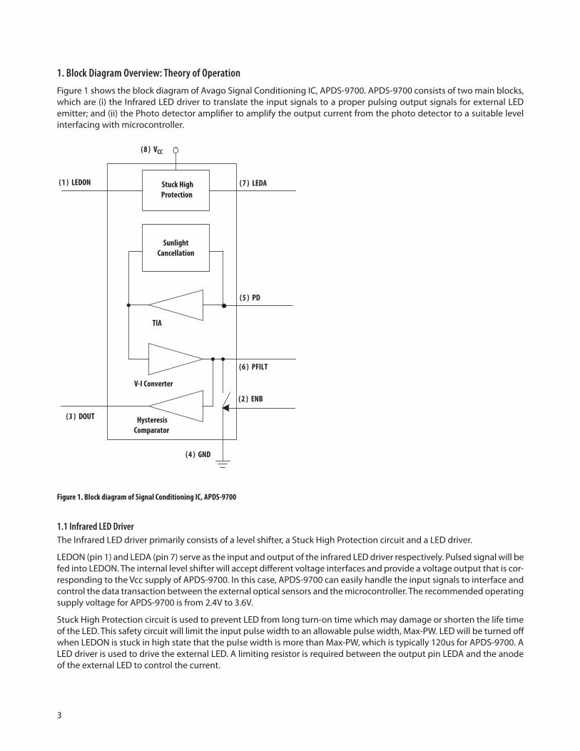
1. Block Diagram Overview: Theory of Operation
Figure 1 shows the block diagram of Avago Signal Conditioning IC, APDS-9700. APDS-9700 consists of two main blocks, which are (i) the Infrared LED driver to translate the input signals to a proper pulsing output signals for external LED emitter; and (ii) the Photo detector amplifier to amplify the output current from the photo detector to a suitable level interfacing with microcontroller.
Figure 1. Block diagram of Signal Conditioning IC, APDS-9700
1.1 Infrared LED DriverThe Infrared LED driver primarily consists of a level shifter, a Stuck High Protection circuit and a LED driver.
LEDON (pin 1) and LEDA (pin 7) serve as the input and output of the infrared LED driver respectively. Pulsed signal will be fed into LEDON. The internal level shifter will accept different voltage interfaces and provide a voltage output that is cor-responding to the Vcc supply of APDS-9700. In this case, APDS-9700 can easily handle the input signals to interface and control the data transaction between the external optical sensors and the microcontroller. The recommended operating supply voltage for APDS-9700 is from 2.4V to 3.6V.
Stuck High Protection circuit is used to prevent LED from long turn-on time which may damage or shorten the life time of the LED. This safety circuit will limit the input pulse width to an allowable pulse width, Max-PW. LED will be turned off when LEDON is stuck in high state that the pulse width is more than Max-PW, which is typically 120us for APDS-9700. A LED driver is used to drive the external LED. A limiting resistor is required between the output pin LEDA and the anode of the external LED to control the current.
SunlightCancellation
Stuck HighProtection
(8 ) VCC
(7 ) LEDA
(6 ) PFILT
(2 ) ENB
(4 ) GND
(5 ) PD
(1 ) LEDON
(3 ) DOUT
V-I Converter
TIA
HysteresisComparator

4
1.2 Photo Detector AmplifierThe Photo Detector Amplifier primarily consists of a Trans-Impedance Amplifier (TIA), a Sunlight Cancellation circuit, a Voltage to Current (V-I) Converter and a Hysteresis Comparator.
PD (pin 5) is the input of the photo detector circuit, where photocurrent generated by the photo detector will be fed into it. The Trans-Impedance amplifier (TIA) converts the detected photocurrent to voltage and then amplifies it to a pre-defined gain. The TIA is self-regulated internally, and has high power supply rejection ratio (PSSR) to reject disturbing noise in the power supply and low power consumption.
Ambient light rejection requirements ensure proper working of the optical sensors under a wide range of environmen-tal conditions. The internal Sunlight Cancellation circuit is used to eliminate the strong sunlight effect in the form of DC current that has transformed from light energy when the device is exposed under the sun. In addition, the Sunlight Can-cellation has also removed the 50/60 Hz flickering effect from an artificial light source such as florescent lamp, filament bulb lamp and halogen lamp. Therefore, with the Sunlight Cancellation circuit, the optical sensors have a brilliant robust-ness of performing normal operation when infrared rays are transmitted from the LED, and then detected by the photo detector without affected by the interferences from the strong sunlight in the external environment as well as from an artificial light in an internal environment.
The configuration of the TIA circuit and the Sunlight Cancellation circuit is served as a band-pass filter with bandwidth that operates between 10k Hz and 1M Hz. The filtered signal from the TIA and Sunlight Cancellation circuits are then connected to the input of the Voltage to Current (V-I) converter, another amplifier that has a second set of pre-defined gain. The output of V-I converter will then be used as an analog output at PFILT (pin 6) or digital output at DOUT (pin 3) after the Hysteresis Comparator. Thus, APDS-9700 has two options for the outputs.
The analog output pin PFILT is connected with a capacitor and a resistor in parallel with respect to ground. It is acting as an integrator, where the capacitor and resistor are used to define the time constant.
To get a digital output from DOUT pin, the output of the V-I converter is fed to the input of the Hysteresis Comparator, which is able to have Hysteresis of 40mV. If the input voltage of the comparator is greater than the reference threshold voltage, a logic “LOW” is generated from the comparator output. On the contrary, if the input voltage of the comparator is smaller than the reference threshold voltage, a logic “HIGH” will be generated. DOUT is an open collector digital output and thus pull-up resistor is required to connect from DOUT to Vcc
To use analog or digital output is much dependent on the application; PFILT is continuously varying output used to connect to ADC pin of the controller for binary number output, whereas DOUT is “high” or “low” output used to connect to GPIO pin of the controller for switching “ON” or “OFF” purpose. Designer can use either one of the outputs or both outputs to meet the design criteria.

5
2. Key Features of APDS-9700
• Low power consumption – Complete shutdown mode is available
• Supply voltage of 2.4V to 3.6V
• External LED current control – Using a limiting resistor
• Maximum LED pulse width control – To protect the LED from damage and prolong LED operating time
• Sunlight cancellation circuit – Operational up to 100k LUX ambient light
• Artificial light immunity
• High PSRR and wide band width Tran-impedance amplifier
• Analog and Digital output pins available
• Integration and gain controls – Using external capacitor and resistor
• Built in Hysteresis comparator for producing digital output
• Small 2mm x 2mm QFN 8-pin package – Space saving compared to discrete solution by more than 80%
Lead free and RoHS compliant
6
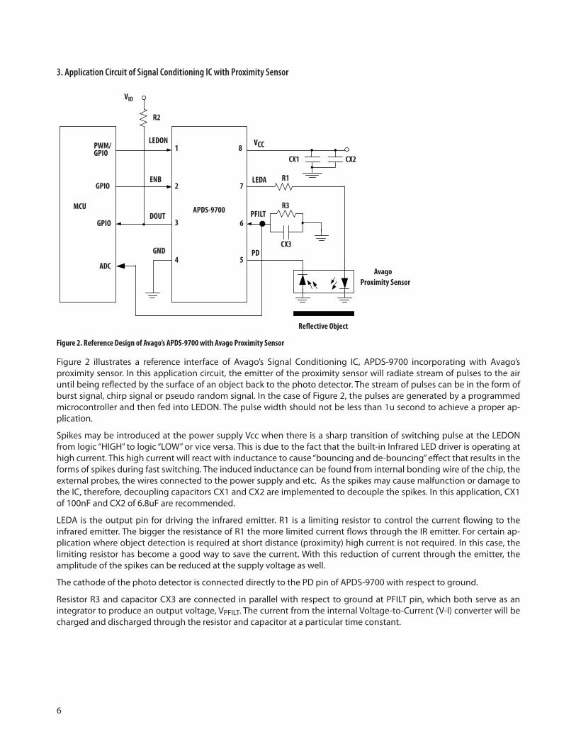
3. Application Circuit of Signal Conditioning IC with Proximity Sensor
Figure 2. Reference Design of Avago’s APDS-9700 with Avago Proximity Sensor
Figure 2 illustrates a reference interface of Avago’s Signal Conditioning IC, APDS-9700 incorporating with Avago’s proximity sensor. In this application circuit, the emitter of the proximity sensor will radiate stream of pulses to the air until being reflected by the surface of an object back to the photo detector. The stream of pulses can be in the form of burst signal, chirp signal or pseudo random signal. In the case of Figure 2, the pulses are generated by a programmed microcontroller and then fed into LEDON. The pulse width should not be less than 1u second to achieve a proper ap-plication.
Spikes may be introduced at the power supply Vcc when there is a sharp transition of switching pulse at the LEDON from logic “HIGH” to logic “LOW” or vice versa. This is due to the fact that the built-in Infrared LED driver is operating at high current. This high current will react with inductance to cause “bouncing and de-bouncing” effect that results in the forms of spikes during fast switching. The induced inductance can be found from internal bonding wire of the chip, the external probes, the wires connected to the power supply and etc. As the spikes may cause malfunction or damage to the IC, therefore, decoupling capacitors CX1 and CX2 are implemented to decouple the spikes. In this application, CX1 of 100nF and CX2 of 6.8uF are recommended.
LEDA is the output pin for driving the infrared emitter. R1 is a limiting resistor to control the current flowing to the infrared emitter. The bigger the resistance of R1 the more limited current flows through the IR emitter. For certain ap-plication where object detection is required at short distance (proximity) high current is not required. In this case, the limiting resistor has become a good way to save the current. With this reduction of current through the emitter, the amplitude of the spikes can be reduced at the supply voltage as well.
The cathode of the photo detector is connected directly to the PD pin of APDS-9700 with respect to ground.
Resistor R3 and capacitor CX3 are connected in parallel with respect to ground at PFILT pin, which both serve as an integrator to produce an output voltage, VPFILT. The current from the internal Voltage-to-Current (V-I) converter will be charged and discharged through the resistor and capacitor at a particular time constant.
VCC
R2
VIO
LEDON
ENB
DOUT
Reflective Object
LEDA
PFILT
PDGND
R1
R3
CX1
CX3
MCU
APDS -9700
1
2
3
4
8
5
6
7
AvagoProximity Sensor
PWM/GPIO
GPIO
GPIO
ADC
CX2
APDS-9700

7
Larger capacitance of CX3 and resistance of R3 take longer time to charge and discharge, which give smaller leakage and noise at output. In addition, distance detection sensitivity is increased with its smaller leakage. However, too large in values in capacitor CX3 and resistor R3 will require a long stream of pulses and wider pulse width so that the integra-tion time is sufficient for VPFILT to cross over the threshold voltage VTH at the comparator. Wider pulse width with long stream of pulses means consume more power.
Smaller capacitance of CX3 and resistance of R3 means the integration time will be shorter. Sufficiently short streams of pulses are required for VPFILT to cross over the threshold voltage of VTH at the comparator. Thus, less power is consumed. However, the faster charging and discharging time will cause larger leakage and more noise at output, which results in poorer distance detection sensitivity. In conclusion, the choice of values for resistor R3 and capacitor CX3 has to be ap-propriate to ensure low power consumption with good distance detection sensitivity.
The analog output pin of PFILT can be connected to an Analog-to-Digital converter (ADC) of a microcontroller, in which the continuously varying voltage will be converted into digital format in the form of binary number. The binary number can be displayed on the monitor of a PC, LED or LCD display panel etc. to indicate the distance of detection.
The integrated voltage VPFILT besides being used as output voltage at PFILT pin, it is fed to the input of the Hysteresis Comparator too. If the input of the Hysteresis Comparator reaches a predefined reference threshold voltage VTH, a tran-sition of logic “HIGH” to “LOW” will be present at the output of the Hysteresis Comparator; else a transition of logic “LOW” to “HIGH” is observed. As a result, a digital output corresponding to the change of the photo detector is produced at DOUT pin. As DOUT is an open collector pin, a pull up resistor R2 is required to tie from DOUT to Vcc.
The digital output pin of DOUT can be connected to a microcontroller MCU, LED, a switch etc. to indicate an “ON” or “OFF” stage of whether an object is being detected.
APDS-9700 has an enable mode, ENB pin, which allows user to shut down the IC when the device is not required for operation to save tremendous current energy. When ENB is at high, the device is in shut down mode; When ENB is at low, it turns on the device and resumes its normal operation. These operations can be implemented with the use of state machine to have a sequence of activities to safe energy which can be controlled using MCU.

8
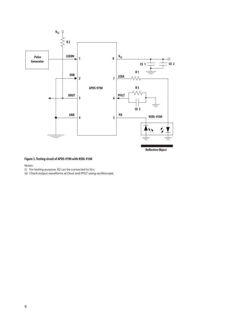
4. Testing Circuit Using APDS-9700 and HSDL-9100
4.1 Design Criteria1. Decoupling capacitors CX1 and CX2 are essential at Vcc to reduce any spikes incurred during fast switching.
2. The injected pulses at LEDON must be greater than 1u second in pulse width and 1.8V in amplitude as to turn on the internal level shifter function. Pulses that do not meet these criteria may fail to turn on the LED.
3. The output current from the LED driver is 120mA typically, despite any duty cycle used in the pulse width. The choice of amount current flow to the LED depends on the LED reliability and characteristic. The bigger the pulse width will consume more power and may shorten the LED operating life time. The amount of current flow can be controlled by the external limiting resistor R1.
4. Maximum allowable pulse width is 120us typically to prevent excessive current flow into LED. Pulse width that bigger than 120us will turn off LED driver to send the pulsed current.
5. Selection of combination values of R3 and CX3 is critical. Too small in values results ripples at output and reduces the distance sensitivity. However, too large in values will take longer integration time to cross over the threshold voltage, VTH, of 655mV typically. From here, C3 and R3 can be then varied to improve the ripples and distance sensitivity.
6. Digital output DOUT is an open collector pin. A pull-up resistor R2 is required to tie to VIO. In this case, R2 of 10k ohm is recommended. In operation,
DOUT=0 when VPFILT>VTH;
DOUT=Vcc when VPFILT<VTH
7. ENB is the power down enable; ENB=0 for normal mode operation and ENB=1 for shutdown mode. It should not be left floating.
8. Power saving is essential in circuit design. For APDS-9700, Idle current is 650uA (max) and shutdown current is 1uA (max). It is recommended to use ENB pin to shutdown APDS-9700 when it is not used. If ENB is connected to GND, then it is recommended to use a control switch at Vcc to turn off APDS-9700.
4.2 Testing ConditionsThis section provides a guideline for APDS-9700 users to carry out evaluation or measurement using application circuit as indicated in Figure 3. Avago’s proximity sensor, HSDL-9100, is used to estimate the performance of APDS-9700.
The following table shows the recommended application circuit components and equipments used for evaluation and testing.
Table 1. Recommended application components
Components Recommended Values
R1 10 ohm
R2 10k ohm
R3 510k ohm
CX1 100n F, Ceramic
CX2 6.8u F, Tantalum
CX3 3.3n F, Ceramic
Avago Proximity Sensor HSDL-9100
Equipment for Evaluation
Power Supply – Supply APDS-9700
Function Generator – Pulse generator to LEDON
Oscilloscope – Probe for input/output waveforms
Reflective Object – White reflective card
9
VCC
R 2
VCC
APDS-9700
1
2
3
4
LEDON
ENB
DOUT
8
5
6
7
Re�ective Object
LEDA
PFILT
PDGND
R 1
R 3
CX 1 CX 2
CX 3
HSDL-9100
PulseGenerator
Figure 3. Testing circuit of APDS-9700 with HSDL-9100
Notes:(i) For testing purpose, R2 can be connected to Vcc;(ii) Check output waveforms at Dout and PFILT using oscilloscope.
10
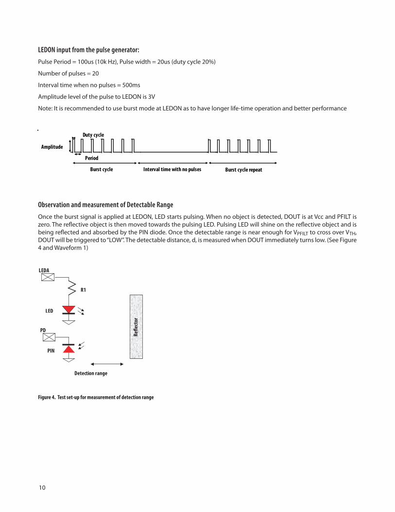
LEDON input from the pulse generator:
Pulse Period = 100us (10k Hz), Pulse width = 20us (duty cycle 20%)
Number of pulses = 20
Interval time when no pulses = 500ms
Amplitude level of the pulse to LEDON is 3V
Note: It is recommended to use burst mode at LEDON as to have longer life-time operation and better performance
Observation and measurement of Detectable Range
Once the burst signal is applied at LEDON, LED starts pulsing. When no object is detected, DOUT is at Vcc and PFILT is zero. The reflective object is then moved towards the pulsing LED. Pulsing LED will shine on the reflective object and is being reflected and absorbed by the PIN diode. Once the detectable range is near enough for VPFILT to cross over VTH, DOUT will be triggered to “LOW”. The detectable distance, d, is measured when DOUT immediately turns low. (See Figure 4 and Waveform 1)
Figure 4. Test set-up for measurement of detection range
Period
Duty cycle
Burst cycle
Amplitude
Interval time with no pulses Burst cycle repeat
PD
R1
LED
PIN
Detection range
LEDA
Refle
ctor
11
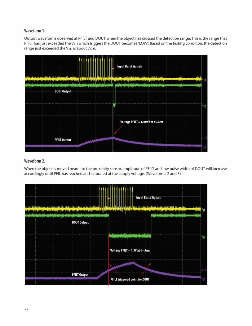
Waveform 1.
Output waveforms observed at PFILT and DOUT when the object has crossed the detection range. This is the range that PFILT has just exceeded the VTH which triggers the DOUT becomes “LOW”. Based on the testing condition, the detection range just exceeded the VTH is about 7cm.
Waveform 2.
When the object is moved nearer to the proximity sensor, amplitude of PFILT and low pulse width of DOUT will increase accordingly until PFIL has reached and saturated at the supply voltage. (Waveforms 2 and 3)
PFILT triggered point for DOUT
Voltage PFILT = 1.3V at d=5cm
Input Burst Signals
PFILT Output
DOUT Output
Input Burst Signals
PFILT Output
DOUT Output
Voltage PFILT = 660mV at d=7cm
12
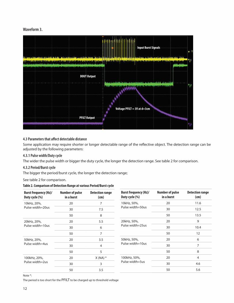
Waveform 3.
4.3 Parameters that affect detectable distanceSome application may require shorter or longer detectable range of the reflective object. The detection range can be adjusted by the following parameters:
4.3.1 Pulse width/Duty cycle The wider the pulse width or bigger the duty cycle, the longer the detection range. See table 2 for comparison.
4.3.2 Period/Burst cycle The bigger the period/burst cycle, the longer the detection range;
See table 2 for comparison.
Voltage PFILT = 3V at d=3cm
Input Burst Signals
PFILT Output
DOUT Output
Table 2. Comparison of Detection Range at various Period/Burst cycle
Burst frequency (Hz)/Duty cycle (%)
Number of pulsein a burst
Detection range (cm)
10kHz, 20%,Pulse width=20us
20 7
30 7.5
50 8
20kHz, 20%,Pulse width=10us
20 5.5
30 6
50 7
50kHz, 20%,Pulse width=4us
20 3.5
30 4
50 5
100kHz, 20%,Pulse width=2us
20 X (NA) *
30 3
50 3.5
Note *:
The period is too short for the PFILT to be charged up to threshold voltage
Burst frequency (Hz)/Duty cycle (%)
Number of pulse in a burst
Detection range (cm)
10kHz, 50%,Pulse width=50us
20 11.6
30 12.5
50 13.5
20kHz, 50%,Pulse width=25us
20 9
30 10.4
50 12
50kHz, 50%,Pulse width=10us
20 6
30 7
50 8
100kHz, 50%,Pulse width=5us
20 4
30 4.6
50 5.6
13
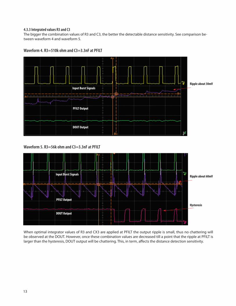
4.3.3 Integrated values R3 and C3The bigger the combination values of R3 and C3, the better the detectable distance sensitivity. See comparison be-tween waveform 4 and waveform 5.
Waveform 4. R3=510k ohm and C3=3.3nF at PFILT
Waveform 5. R3=56k ohm and C3=3.3nF at PFILT
When optimal integrator values of R3 and CX3 are applied at PFILT the output ripple is small, thus no chattering will be observed at the DOUT. However, once these combination values are decreased till a point that the ripple at PFILT is larger than the hysteresis, DOUT output will be chattering. This, in term, affects the distance detection sensitivity.
Hysteresis
Ripple about 60mV
Ripple about 30mV
Input Burst Signals
DOUT Output
PFILT Output
Input Burst Signals
DOUT Output
PFILT Output
14
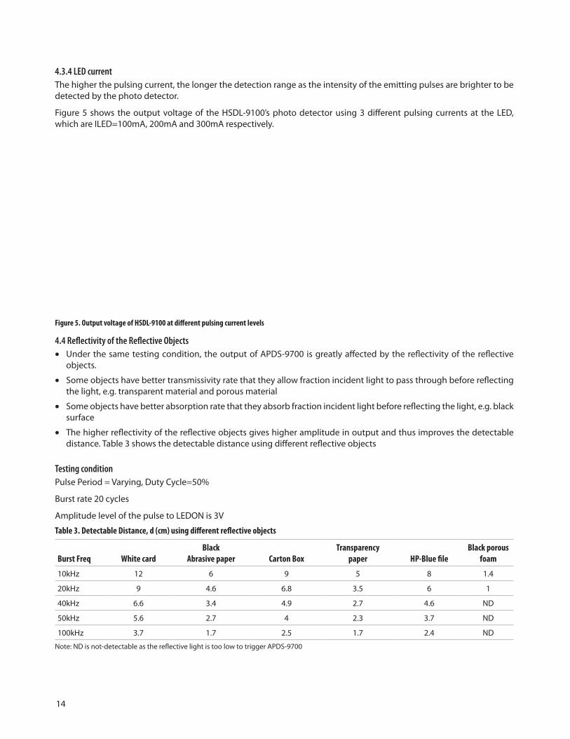
4.3.4 LED currentThe higher the pulsing current, the longer the detection range as the intensity of the emitting pulses are brighter to be detected by the photo detector.
Figure 5 shows the output voltage of the HSDL-9100’s photo detector using 3 different pulsing currents at the LED, which are ILED=100mA, 200mA and 300mA respectively.
Figure 5. Output voltage of HSDL-9100 at different pulsing current levels
4.4 Reflectivity of the Reflective Objects• Under the same testing condition, the output of APDS-9700 is greatly affected by the reflectivity of the reflective
objects.
• Some objects have better transmissivity rate that they allow fraction incident light to pass through before reflecting the light, e.g. transparent material and porous material
• Some objects have better absorption rate that they absorb fraction incident light before reflecting the light, e.g. black surface
• The higher reflectivity of the reflective objects gives higher amplitude in output and thus improves the detectable distance. Table 3 shows the detectable distance using different reflective objects
Testing conditionPulse Period = Varying, Duty Cycle=50%
Burst rate 20 cycles
Amplitude level of the pulse to LEDON is 3V
Table 3. Detectable Distance, d (cm) using different reflective objects
Burst Freq White cardBlack
Abrasive paper Carton BoxTransparency
paper HP-Blue fileBlack porous
foam
10kHz 12 6 9 5 8 1.4
20kHz 9 4.6 6.8 3.5 6 1
40kHz 6.6 3.4 4.9 2.7 4.6 ND
50kHz 5.6 2.7 4 2.3 3.7 ND
100kHz 3.7 1.7 2.5 1.7 2.4 ND
Note: ND is not-detectable as the reflective light is too low to trigger APDS-9700
15
4.5 Useful Calculations
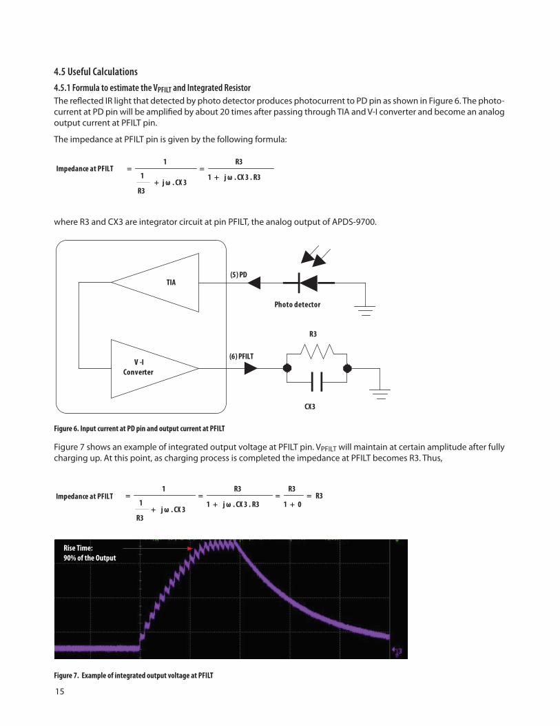
4.5.1 Formula to estimate the VPFILT and Integrated ResistorThe reflected IR light that detected by photo detector produces photocurrent to PD pin as shown in Figure 6. The photo-current at PD pin will be amplified by about 20 times after passing through TIA and V-I converter and become an analog output current at PFILT pin.
The impedance at PFILT pin is given by the following formula:
where R3 and CX3 are integrator circuit at pin PFILT, the analog output of APDS-9700.
Figure 6. Input current at PD pin and output current at PFILT
Figure 7 shows an example of integrated output voltage at PFILT pin. VPFILT will maintain at certain amplitude after fully charging up. At this point, as charging process is completed the impedance at PFILT becomes R3. Thus,
Figure 7. Example of integrated output voltage at PFILT
V -IConverter
(5) PD
(6) PFILT
R3
CX3
Photo detector
TIA
120 m A x 20%2.5 ms + 100 ms
2.5 msx=
0.59 m A=
Pulsing Time + No Pulsing Time
Pulsing Timex Current driven x Duty Cycle=Current consumption by LED
.1.
1
1
CX 3 . R3j
R3
CX 3jR3
Impedance at PFILTω
ω+
=
+
=
01.1.
1
1R3
R3
CX 3 . R3j
R3
CX 3jR3
=+
=+
=
+
=ω
ω
Duty CyclexIPDxDuty CyclexxIPD
R
xDuty CyclexRxxIPDV
xDuty CyclexRxxIPDVPFILT
0389.0
9.020
7.03
0.93207.0
0.9320
==
=
=
(F1)0.9320 xDuty Cycle xRxxIPDVPFILTVoltage PFILT, =
Impedance at PFILT
(F2)
Rise Time:90% of the Output
16
Taking charging process completed at 90% of the output VPFILT (see Figure 7), the formula to estimate VPFILT is given by:
where
IPD: Photocurrent at PD pin of APDS-9700
20: Amplification factor from PD pin to PFILT pin
R3: Integrator resistor at PFILT pin, used to convert current IPFILT to VPFILT
Duty cycle: Duration of pulsing voltage occurred at PFILT
0.9: Complete voltage taken at time rise, 90% of the output
The threshold level at PFILT pin to trigger the internal comparator is 0.65V typically. Using 0.7V as guard band value, the integrator resistor R3 can be calculated as following:
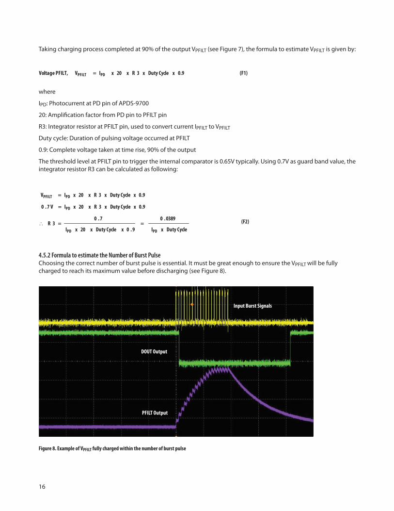
4.5.2 Formula to estimate the Number of Burst PulseChoosing the correct number of burst pulse is essential. It must be great enough to ensure the VPFILT will be fully charged to reach its maximum value before discharging (see Figure 8).
Figure 8. Example of VPFILT fully charged within the number of burst pulse
120 m A x 20%2.5 ms + 100 ms
2.5 msx=
0.59 m A=
Pulsing Time + No Pulsing Time
Pulsing Timex Current driven x Duty Cycle=Current consumption by LED
.1.
1
1
CX 3 . R3j
R3
CX 3jR3
Impedance at PFILTω
ω+
=
+
=
01.1.
1
1R3
R3
CX 3 . R3j
R3
CX 3jR3
=+
=+
=
+
=ω
ω
Duty CyclexIPDxDuty CyclexxIPD
R
xDuty CyclexRxxIPDV
xDuty CyclexRxxIPDVPFILT
0389.0
9.020
7.03
0.93207.0
0.9320
==
=
=
(F1)0.9320 xDuty Cycle xRxxIPDVPFILTVoltage PFILT, =
Impedance at PFILT
(F2)
Input Burst Signals
DOUT Output
PFILT Output
17
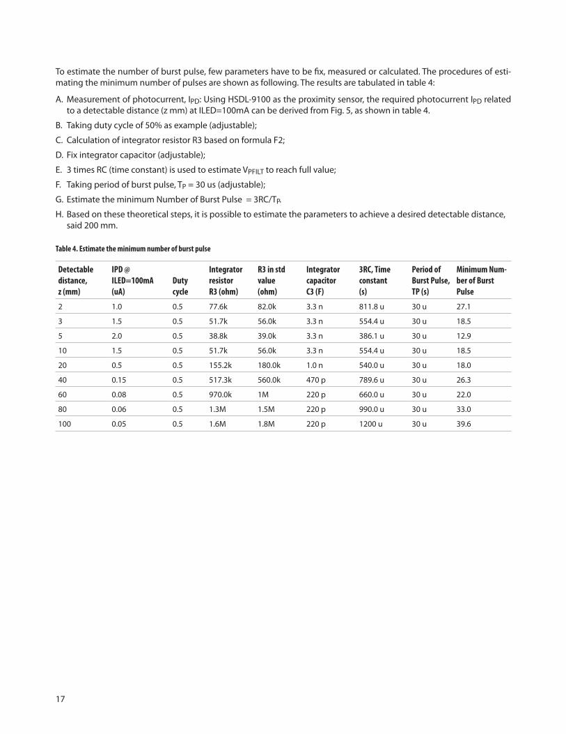
To estimate the number of burst pulse, few parameters have to be fix, measured or calculated. The procedures of esti-mating the minimum number of pulses are shown as following. The results are tabulated in table 4:
A. Measurement of photocurrent, IPD: Using HSDL-9100 as the proximity sensor, the required photocurrent IPD related to a detectable distance (z mm) at ILED=100mA can be derived from Fig. 5, as shown in table 4.
B. Taking duty cycle of 50% as example (adjustable);
C. Calculation of integrator resistor R3 based on formula F2;
D. Fix integrator capacitor (adjustable);
E. 3 times RC (time constant) is used to estimate VPFILT to reach full value;
F. Taking period of burst pulse, TP = 30 us (adjustable);
G. Estimate the minimum Number of Burst Pulse = 3RC/TP.
H. Based on these theoretical steps, it is possible to estimate the parameters to achieve a desired detectable distance, said 200 mm.
Table 4. Estimate the minimum number of burst pulse
Detectable distance,z (mm)
IPD @ ILED=100mA(uA)
Duty cycle
Integrator resistorR3 (ohm)
R3 in std value(ohm)
Integrator capacitor C3 (F)
3RC, Time constant(s)
Period of Burst Pulse, TP (s)
Minimum Num-ber of Burst Pulse
2 1.0 0.5 77.6k 82.0k 3.3 n 811.8 u 30 u 27.1
3 1.5 0.5 51.7k 56.0k 3.3 n 554.4 u 30 u 18.5
5 2.0 0.5 38.8k 39.0k 3.3 n 386.1 u 30 u 12.9
10 1.5 0.5 51.7k 56.0k 3.3 n 554.4 u 30 u 18.5
20 0.5 0.5 155.2k 180.0k 1.0 n 540.0 u 30 u 18.0
40 0.15 0.5 517.3k 560.0k 470 p 789.6 u 30 u 26.3
60 0.08 0.5 970.0k 1M 220 p 660.0 u 30 u 22.0
80 0.06 0.5 1.3M 1.5M 220 p 990.0 u 30 u 33.0
100 0.05 0.5 1.6M 1.8M 220 p 1200 u 30 u 39.6
18
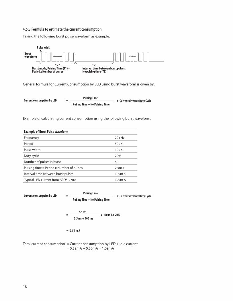
4.5.3 Formula to estimate the current consumption
Taking the following burst pulse waveform as example:
General formula for Current Consumption by LED using burst waveform is given by:
Example of calculating current consumption using the following burst waveform:
Example of Burst Pulse Waveform
Frequency 20k Hz
Period 50u s
Pulse width 10u s
Duty cycle 20%
Number of pulses in burst 50
Pulsing time = Period x Number of pulses 2.5m s
Interval time between burst pulses 100m s
Typical LED current from APDS-9700 120m A
Total current consumption = Current consumption by LED + Idle current = 0.59mA + 0.50mA = 1.09mA
Burst waveform
Pulse width
Burst mode, Pulsing Time (T1) = Period x Number of pulses
Interval time between burst pulses, No pulsing time (T2)
120 m A x 20%2.5 ms + 100 ms
2.5 msx=
0.59 m A=
Pulsing Time + No Pulsing Time
Pulsing Timex Current driven x Duty Cycle=Current consumption by LED
.1.
1
1
CX 3 . R3j
R3
CX 3jR3
Impedance at PFILTω
ω+
=
+
=
01.1.
1
1R3
R3
CX 3 . R3j
R3
CX 3jR3
=+
=+
=
+
=ω
ω
Duty CyclexIPDxDuty CyclexxIPD
R
xDuty CyclexRxxIPDV
xDuty CyclexRxxIPDVPFILT
0389.0
9.020
7.03
0.93207.0
0.9320
==
=
=
(F1)0.9320 xDuty Cycle xRxxIPDVPFILTVoltage PFILT, =
Impedance at PFILT
(F2)
19
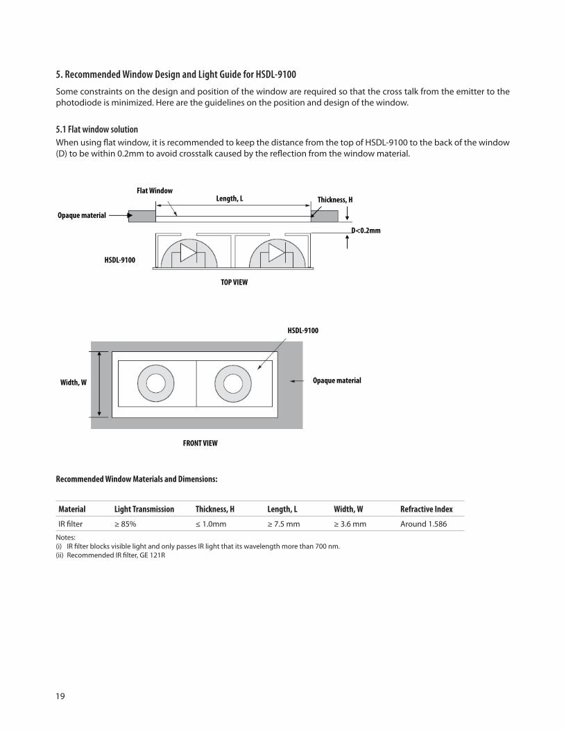
5. Recommended Window Design and Light Guide for HSDL-9100
Some constraints on the design and position of the window are required so that the cross talk from the emitter to the photodiode is minimized. Here are the guidelines on the position and design of the window.
5.1 Flat window solutionWhen using flat window, it is recommended to keep the distance from the top of HSDL-9100 to the back of the window (D) to be within 0.2mm to avoid crosstalk caused by the reflection from the window material.
Recommended Window Materials and Dimensions:
Material Light Transmission Thickness, H Length, L Width, W Refractive Index
IR filter ≥ 85% ≤ 1.0mm ≥ 7.5 mm ≥ 3.6 mm Around 1.586
Notes: (i) IR filter blocks visible light and only passes IR light that its wavelength more than 700 nm. (ii) Recommended IR filter, GE 121R
Thickness, H
D<0.2mm
Length, LFlat Window
Opaque material
HSDL-9100
Width, W
TOP VIEW
FRONT VIEW
HSDL-9100
Opaque material
20
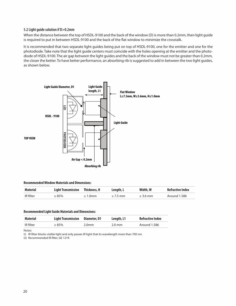
5.2 Light guide solution if D>0.2mm When the distance between the top of HSDL-9100 and the back of the window (D) is more than 0.2mm, then light guide is required to put in between HSDL-9100 and the back of the flat window to minimize the crosstalk.
It is recommended that two separate light guides being put on top of HSDL-9100, one for the emitter and one for the photodiode. Take note that the light guide centers must coincide with the holes opening at the emitter and the photo-diode of HSDL-9100. The air gap between the light guides and the back of the window must not be greater than 0.2mm, the closer the better. To have better performance, an absorbing rib is suggested to add in between the two light guides, as shown below.
Recommended Window Materials and Dimensions:
Material Light Transmission Thickness, H Length, L Width, W Refractive Index
IR filter ≥ 85% ≤ 1.0mm ≥ 7.5 mm ≥ 3.6 mm Around 1.586
Recommended Light Guide Materials and Dimensions:
Material Light Transmission Diameter, D1 Length, L1 Refractive Index
IR filter ≥ 85% 2.0mm 2.0 mm Around 1.586
Notes: (i) IR filter blocks visible light and only passes IR light that its wavelength more than 700 nm. (ii) Recommended IR filter, GE 121R
Light Guide Diameter, D1 Light Guidelength, L1
Light Guide
Absorbing rib
Air Gap < 0.2mm
HSDL - 9100
Flat WindowL≥7.5mm, W≥3.6mm, H≤1.0mm
TOP VIEW
21
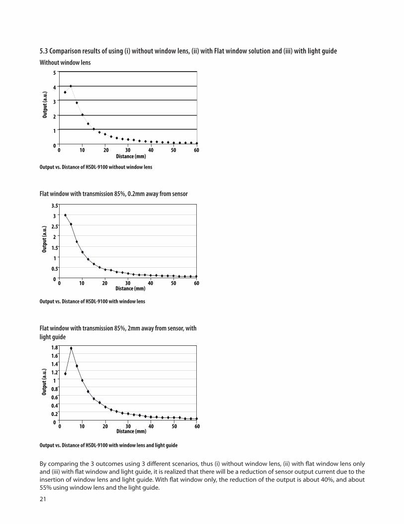
5.3 Comparison results of using (i) without window lens, (ii) with Flat window solution and (iii) with light guide
Without window lens
0
0.5
1
1.5
2
2.5
3
3.5
0 10 20 30 40 50 60Distance (mm)
Outp
ut (a
.u.)
00.20.40.60.8
11.21.41.61.8
0 10 20 30 40 50 60Distance (mm)
Outp
ut (a
.u.)
0
1
2
3
4
5
0 10 20 30 40 50 60Distance (mm)
Outp
ut (a
.u.)
Output vs. Distance of HSDL-9100 with window lens and light guide
By comparing the 3 outcomes using 3 different scenarios, thus (i) without window lens, (ii) with flat window lens only and (iii) with flat window and light guide, it is realized that there will be a reduction of sensor output current due to the insertion of window lens and light guide. With flat window only, the reduction of the output is about 40%, and about 55% using window lens and the light guide.
Output vs. Distance of HSDL-9100 without window lens
Flat window with transmission 85%, 0.2mm away from sensor
Output vs. Distance of HSDL-9100 with window lens
Flat window with transmission 85%, 2mm away from sensor, with light guide
22
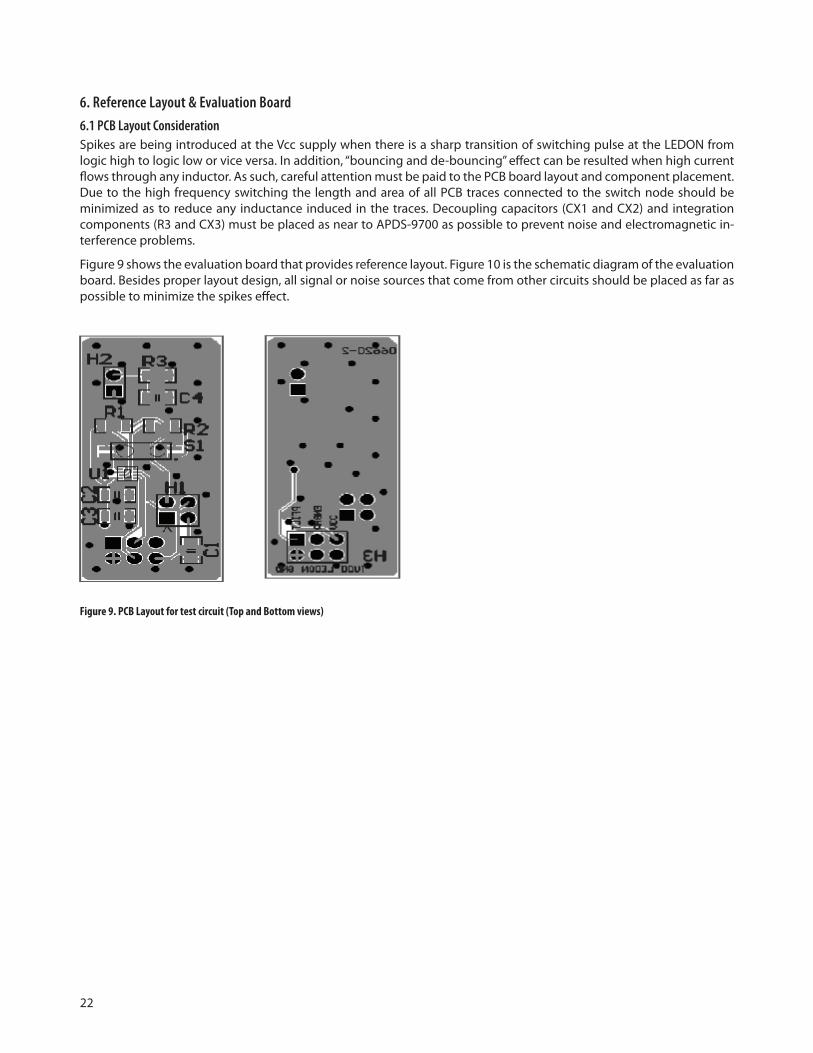
Figure 9. PCB Layout for test circuit (Top and Bottom views)
6. Reference Layout & Evaluation Board
6.1 PCB Layout ConsiderationSpikes are being introduced at the Vcc supply when there is a sharp transition of switching pulse at the LEDON from logic high to logic low or vice versa. In addition, “bouncing and de-bouncing” effect can be resulted when high current flows through any inductor. As such, careful attention must be paid to the PCB board layout and component placement. Due to the high frequency switching the length and area of all PCB traces connected to the switch node should be minimized as to reduce any inductance induced in the traces. Decoupling capacitors (CX1 and CX2) and integration components (R3 and CX3) must be placed as near to APDS-9700 as possible to prevent noise and electromagnetic in-terference problems.
Figure 9 shows the evaluation board that provides reference layout. Figure 10 is the schematic diagram of the evaluation board. Besides proper layout design, all signal or noise sources that come from other circuits should be placed as far as possible to minimize the spikes effect.
23
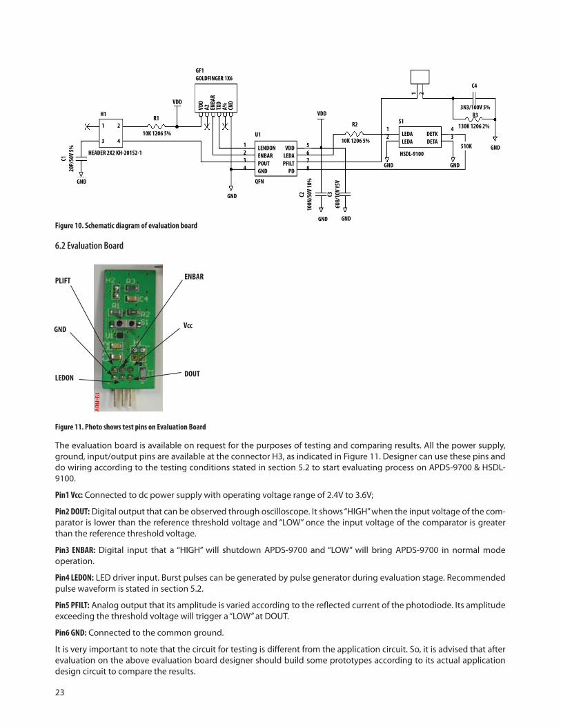
Figure 10. Schematic diagram of evaluation board
6.2 Evaluation Board
Figure 11. Photo shows test pins on Evaluation Board
The evaluation board is available on request for the purposes of testing and comparing results. All the power supply, ground, input/output pins are available at the connector H3, as indicated in Figure 11. Designer can use these pins and do wiring according to the testing conditions stated in section 5.2 to start evaluating process on APDS-9700 & HSDL-9100.
Pin1 Vcc: Connected to dc power supply with operating voltage range of 2.4V to 3.6V;
Pin2 DOUT: Digital output that can be observed through oscilloscope. It shows “HIGH” when the input voltage of the com-parator is lower than the reference threshold voltage and “LOW” once the input voltage of the comparator is greater than the reference threshold voltage.
Pin3 ENBAR: Digital input that a “HIGH” will shutdown APDS-9700 and “LOW” will bring APDS-9700 in normal mode operation.
Pin4 LEDON: LED driver input. Burst pulses can be generated by pulse generator during evaluation stage. Recommended pulse waveform is stated in section 5.2.
Pin5 PFILT: Analog output that its amplitude is varied according to the reflected current of the photodiode. Its amplitude exceeding the threshold voltage will trigger a “LOW” at DOUT.
Pin6 GND: Connected to the common ground.
It is very important to note that the circuit for testing is different from the application circuit. So, it is advised that after evaluation on the above evaluation board designer should build some prototypes according to its actual application design circuit to compare the results.
PLIFT
GND
LEDON
ENBAR
Vcc
DOUT
VDD
A2 ENBA
RTX
DA% CN
D
LENDONENBAR POUTGND
VDD LEDAPFILT
PD
GND GND
GND GND
GND
GND
GND
VDD
VDD
1 2
3 4LEDA DETKLEDA DETA1
234
5678
H1
HEADER 2X2 KH-20152-1
10K 1206 5%
3N3/100V 5%R3
130K 1206 2%
510K
1 42 3
C4
S1
HSDL-9100
U1
QFN
R2
GF1GOLDFINGER 1X6
R1
C120
P/50
V 5%
C210
0N/5
0V 1
0%
C36U
8/10
V Y5
V
1
2
10K 1206 5%
Figure 10. Schematic diagram of evaluation board
24
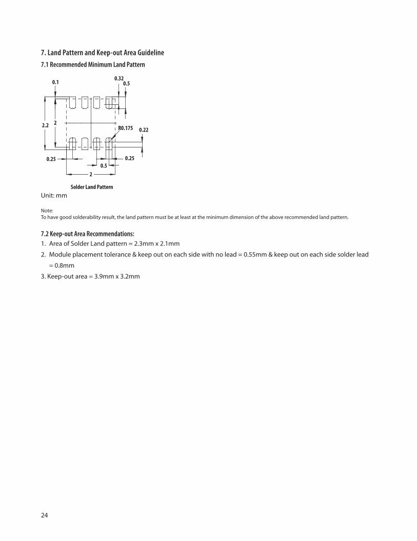
7. Land Pattern and Keep-out Area Guideline
7.1 Recommended Minimum Land Pattern
0.5
Solder Land Pattern
0.250.25
2
0.1 0.5
R0.17522.2
0.22
0.32
Unit: mm
Note: To have good solderability result, the land pattern must be at least at the minimum dimension of the above recommended land pattern.
7.2 Keep-out Area Recommendations:1. Area of Solder Land pattern = 2.3mm x 2.1mm
2. Module placement tolerance & keep out on each side with no lead = 0.55mm & keep out on each side solder lead
= 0.8mm
3. Keep-out area = 3.9mm x 3.2mm
25
50 100 150 200 250 300t-TIME(SECONDS)
25
80
120
150
180200
230
255
0
T - TE
MPE
RATU
RE (°
C)
R1
R2
R3 R4
R5
217
MAX 260C
60 sec to 90 secAbove 217 C
P1HEAT
UP
P2SOLDER PASTE DRY
P3SOLDERREFLOW
P4COOL DOWN
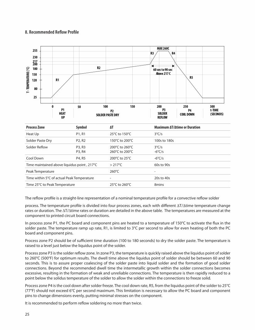
8. Recommended Reflow Profile
Process Zone Symbol ∆T Maximum ∆T/∆time or Duration
Heat Up P1, R1 25°C to 150°C 3°C/s
Solder Paste Dry P2, R2 150°C to 200°C 100s to 180s
Solder Reflow P3, R3P3, R4
200°C to 260°C 260°C to 200°C
3°C/s-6°C/s
Cool Down P4, R5 200°C to 25°C -6°C/s
Time maintained above liquidus point , 217°C > 217°C 60s to 90s
Peak Temperature 260°C -
Time within 5°C of actual Peak Temperature - 20s to 40s
Time 25°C to Peak Temperature 25°C to 260°C 8mins
The reflow profile is a straight-line representation of a nominal temperature profile for a convective reflow solder
process. The temperature profile is divided into four process zones, each with different ∆T/∆time temperature change rates or duration. The ∆T/∆time rates or duration are detailed in the above table. The temperatures are measured at the component to printed circuit board connections.
In process zone P1, the PC board and component pins are heated to a temperature of 150°C to activate the flux in the solder paste. The temperature ramp up rate, R1, is limited to 3°C per second to allow for even heating of both the PC board and component pins.
Process zone P2 should be of sufficient time duration (100 to 180 seconds) to dry the solder paste. The temperature is raised to a level just below the liquidus point of the solder.
Process zone P3 is the solder reflow zone. In zone P3, the temperature is quickly raised above the liquidus point of solder to 260°C (500°F) for optimum results. The dwell time above the liquidus point of solder should be between 60 and 90 seconds. This is to assure proper coalescing of the solder paste into liquid solder and the formation of good solder connections. Beyond the recommended dwell time the intermetallic growth within the solder connections becomes excessive, resulting in the formation of weak and unreliable connections. The temperature is then rapidly reduced to a point below the solidus temperature of the solder to allow the solder within the connections to freeze solid.
Process zone P4 is the cool down after solder freeze. The cool down rate, R5, from the liquidus point of the solder to 25°C (77°F) should not exceed 6°C per second maximum. This limitation is necessary to allow the PC board and component pins to change dimensions evenly, putting minimal stresses on the component.
It is recommended to perform reflow soldering no more than twice.
26
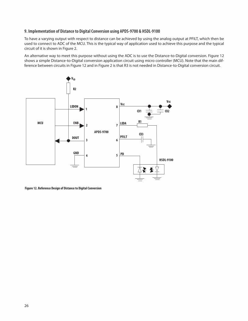
9. Implementation of Distance to Digital Conversion using APDS-9700 & HSDL-9100
To have a varying output with respect to distance can be achieved by using the analog output at PFILT, which then be used to connect to ADC of the MCU. This is the typical way of application used to achieve this purpose and the typical circuit of it is shown in Figure 2.
An alternative way to meet this purpose without using the ADC is to use the Distance-to-Digital conversion. Figure 12 shows a simple Distance-to-Digital conversion application circuit using micro controller (MCU). Note that the main dif-ference between circuits in Figure 12 and in Figure 2 is that R3 is not needed in Distance-to-Digital conversion circuit.
Figure 12. Reference Design of Distance to Digital Conversion
1
2
3
4
8
7
6
5
APDS-9700
MCU
LEDON
ENB
DOUT
VIO
Vcc
R2
R1
CX3
LEDA
PFILT
GND PD
Vcc
CX1 CX2
HSDL-9100

27
An algorithm has been designed for implementing a Distance-to-Digital conversion using Avago APDS-9700 and proximity sensor. The logical process of this algorithm is as following:
9.1 When there is object detected: • When APDS-9700 is not in use ENB is held high so that APDS-9700 is in shutdown mode. During shutdown mode, the
integration capacitor CX3 is discharged by the internal circuitry at PFILT.
• During active mode, when ENB is pulled low, LEDON is pulsed high to enable LED to be turned on for a pre-determined period of time.
• Note that the form of pulses used is in burst mode, meaning after pulsing at the predefined period of time, there will be a predefined interval time that pulsing stops until next cycle of pulses start at the predefined period of time again. (see Figure 13)
LEDON
Prede�ned maximum number of pulses
Prede�ned interval time when LEDON not pulsing
After interval time, prede�ned maximum number of pulses resumes
Figure 13. Predefined maximum number of pulses and time interval at LEDON
• When an object is detected the pulsed light will be reflected to photodiode of the proximity sensor. The light energy will be amplified, filtered and integrated on CX3.
• The pulsing continues until the output voltage level at CX3 exceeds the internal threshold of 655mV and the DOUT pin will pull low.
• The change from high to low at DOUT can be connected to the MCU interrupt pin to signal the MCU that the integrated charge at CX3 has exceeded threshold level. Once the interrupt pin is executed ENB pulls high and pulsing at LEDON is stopped. At this point, CX3 will be discharged to zero for the next conversion.
• Note that in this application the maximum number of pre-determined pulses has to be fixed as the relationship between detectable distance and pulse count is not linear but proportional.
• The number of count in pulses before interruption will be used as a benchmark to reflect the distance that the object is detected.
• After the interruption, the pulsing will resume after the interval time to detect if there is any object nearby the proximity sensor.
9.2 When there is no object detected:
• When there is no object near to proximity sensor, LED will continue to pulse until the predefined maximum number of pulses is hit.
• Once the pulse count reaches its maximum count the LED pulsing will be stopped at the predefined interval time and the MCU will interpret this as out of range or there is no object detected in the detection zone.
• After the predefined interval time that pulsing stops, the pulsing will resume as to repeat the whole cycle to detect any object near to proximity sensor.
• To safe power, ENB is set high within the interval time that pulsing stops.
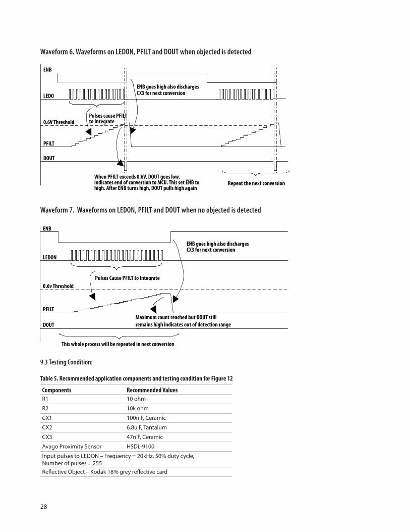
28
ENB
LEDON
PFILT
DOUT
0.6V Threshold
ENB goes high also discharges CX3 for next conversion
Pulses cause PFILT to Integrate
When PFILT exceeds 0.6V, DOUT goes low, indicates end of conversion to MCU. This set ENB to high. After ENB turns high, DOUT pulls high again
Repeat the next conversion
Waveform 6. Waveforms on LEDON, PFILT and DOUT when objected is detected
Waveform 7. Waveforms on LEDON, PFILT and DOUT when no objected is detected
ENB
LEDON
PFILT
DOUT
0.6v ThresholdPulses Cause PFILT to Integrate
ENB goes high also discharges CX3 for next conversion
This whole process will be repeated in next conversion
Maximum count reached but DOUT stillremains high indicates out of detection range
9.3 Testing Condition:
Table 5. Recommended application components and testing condition for Figure 12
Components Recommended ValuesR1 10 ohm
R2 10k ohm
CX1 100n F, Ceramic
CX2 6.8u F, Tantalum
CX3 47n F, Ceramic
Avago Proximity Sensor HSDL-9100
Input pulses to LEDON – Frequency = 20kHz, 50% duty cycle, Number of pulses = 255
Reflective Object – Kodak 18% grey reflective card
29
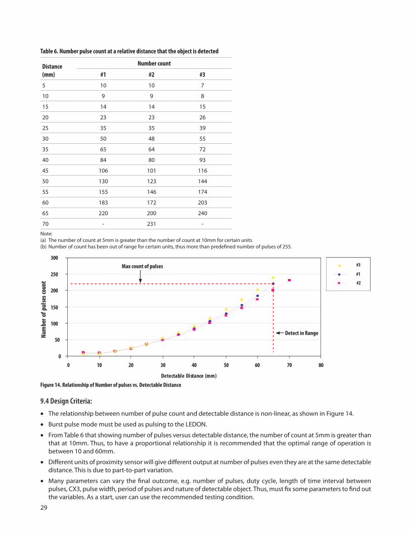
Table 6. Number pulse count at a relative distance that the object is detected
Distance (mm)
Number count
#1 #2 #3
5 10 10 7
10 9 9 8
15 14 14 15
20 23 23 26
25 35 35 39
30 50 48 55
35 65 64 72
40 84 80 93
45 106 101 116
50 130 123 144
55 155 146 174
60 183 172 203
65 220 200 240
70 - 231 -
Note:(a) The number of count at 5mm is greater than the number of count at 10mm for certain units(b) Number of count has been out of range for certain units, thus more than predefined number of pulses of 255.
Figure 14. Relationship of Number of pulses vs. Detectable Distance
9.4 Design Criteria:
• The relationship between number of pulse count and detectable distance is non-linear, as shown in Figure 14.
• Burst pulse mode must be used as pulsing to the LEDON.
• From Table 6 that showing number of pulses versus detectable distance, the number of count at 5mm is greater than that at 10mm. Thus, to have a proportional relationship it is recommended that the optimal range of operation is between 10 and 60mm.
• Different units of proximity sensor will give different output at number of pulses even they are at the same detectable distance. This is due to part-to-part variation.
• Many parameters can vary the final outcome, e.g. number of pulses, duty cycle, length of time interval between pulses, CX3, pulse width, period of pulses and nature of detectable object. Thus, must fix some parameters to find out the variables. As a start, user can use the recommended testing condition.
0
50
100
150
200
250
300
0 10 20 30 40 50 60 70 80
Detectable Distance (mm)
Num
ber o
f pul
ses c
ount
#1
#2
#3
Detect in Range
Max count of pulses
For product information and a complete list of distributors, please go to our web site: www.avagotech.com
Avago, Avago Technologies, and the A logo are trademarks of Avago Technologies, Limited in the United States and other countries.Data subject to change. Copyright © 2007 Avago Technologies Limited. All rights reserved. AV02-1031EN - April 4, 2008
Appendix:
List of Figures
Figure 1. Block diagram of Signal Conditioning IC, APDS-9700 3
Figure 2. Reference Design of Avago’s APDS-9700 with Avago Proximity Sensor 6
Figure 3. Testing circuit of APDS-9700 with HSDL-9100 9
Figure 4.Test set-up for measurement of detection range 10
Figure 5. Output voltage of HSDL-9100 at different pulsing current levels 14
Figure 6. Input current at PD pin and output current at PFILT 15
Figure 7. Example of integrated output voltage at PFILT 15
Figure 8. Example of VPFILT fully charged within the number of burst pulse 16
Figure 9. PCB Layout for test circuit (Top and Bottom views) 22
Figure 10. Schematic diagram of evaluation board 23
Figure 11. Photo shows test pins on Evaluation Board 23
Figure 12. Reference Design of Distance to Digital Conversion 26
Figure 13. Predefined maximum number of pulses and time interval at LEDON 27
Figure 14. Relationship of Number of pulses vs. Detectable Distance 29
List of Tables
Table 1. Recommended application components 8
Table 2. Comparison of Detection Range at various Period/Burst cycle 12
Table 3. Detectable Distance, d (cm) using different reflective objects 14
Table 4. Estimate the minimum number of burst pulse 17
Table 5. Recommended application components and testing condition for Figure 8 28
Table 6. Number pulse count at a relative distance that the object is detected 29
List of Waveforms
Waveform 1. 11
Waveform 2. 11
Waveform 3. 12
Waveform 4. R3=510k ohm and C3=3.3nF at PFILT 13
Waveform 5. R3=56k ohm and C3=3.3nF at PFILT 13
Waveform 6. Waveforms on LEDON, PFILT and DOUT when object is detected 28
Waveform 7. Waveforms on LEDON, PFILT and DOUT when no object is detected 28