Embed Size (px)
Citation preview
Smart Altera Firmware for DSP with FPGAs
Uwe Meyer-Baesea, A. Verab, A. Meyer-Baesea, M. Pattichisb, R. Perrya, aFAMU-FSU, ECE Dept., 2525 Pottsdamer Street, Tallahassee, FL USA-32310;
bUniversity of New Mexico, ECE Dept., Albuquerque, NM 87131
ABSTRACT Design of current DSP applications using state-of-the art multi-million gates devices requires a broad foundation of engineering skills ranging from knowledge of hardware-efficient DSP algorithms to CAD design tools. The requirement of short time-to-market, however, requires to replace the traditional HDL based designs by a MatLab/Simulink-based design flow. This not only allows the over 1 million MatLab users to design with FPGAs but also to by-pass the hardware design engineer and leads therefore to shorter development time. We have evaluated the Altera/Simulink tool flow used for a University design environment and present design experience of a semester course at FAMU-FSU College of Engineering. We discuss the required background knowledge, key target smart firmware for FPGAs and possible advanced designs, e.g. FFT and multirate filter banks and wavelets designed by students with only basic logic experience. . Keywords: FPGA, Simulink, top down design flow, undergraduate curriculum.
1. INTRODUCTION
Field-programmable gate arrays (FPGAs) are on the verge of revolutionizing digital signal processing. Many front-end digital signal processing (DSP) algorithms, such as FFTs, multi channel filter banks, or wavelets, to name just a few, previously built with ASICs or programmable digital signal processors, are now most often replaced by FPGAs. The two FPGA market leaders (Altera and Xilinx) both report revenues greater than $1 billion. FPGAs have enjoyed steady growth of more than 20% in the last decade, outperforming ASICs and programmable digital signal processors (PDSPs) by 10%. The question when using such a relatively new MatLab/Simulink design flow for a designer however is the question, if this flow delivers good quality of results (QoR), or if the synthesized designs are more of a “quick and dirty” quality. This design study has been presented at last year’s SPIE conference. Initially, software packages from Altera, Synopsys and Xilinx were considered that have the following advantages and disadvantages:
Software package Advantages Disadvantages Altera Quartus
Similar interface to MaxPlusII software that students use in digital logic lab.
Quality-of-results not as good as with FC2. No free ModelTech simulator like with Xilinx.
Xilinx ISE
Uses Synopsis synthesis tools and has “RTL” viewer. Uses (basic) ModelTech simulator.
Simulator needs additional testbench written in HDL.
Synopsys FC2 or DC ultra
Best in class synthesis with e.g. pipeline retiming.
Very sophisticated software package.
Since Synopsys no longer supports the FC2 FPGA tool, we decided that we will only look into design flow that use Altera or Xilinx tools. We found that the Simulink design flow for FPGAs has become a viable design path. Both vendors provide a sophisticated toolbox of library elements that are almost complete and the quality of results (QOR) for most of the Simulink design matches or exceeds hand optimized VHDL coding. The compile time was very reasonable.
Independent Component Analyses, Wavelets, Unsupervised Nano-Biomimetic Sensors, and Neural Networks V, edited byHarold H. Szu, Jack Agee, Proc. of SPIE Vol. 6576, 65760T, (2007) · 0277-786X/07/$18 · doi: 10.1117/12.719017
Proc. of SPIE Vol. 6576 65760T-1
Downloaded From: http://proceedings.spiedigitallibrary.org/ on 02/18/2016 Terms of Use: http://spiedigitallibrary.org/ss/TermsOfUse.aspx
The design flow allows a software developer to quickly explore FPGA design options in terms of size and speed and to check if the resulting design fulfills the design constraints. Overall, the comparisons showed the strengths of the tools. We have also heard that the weakness we discovered have been used to improve the tools. The costs for a development lab are reasonable, given the fact that software (MatLab, FPGA tool) as well as hardware boards are available at University prices. Our conclusion of the preliminary study showed that the Simulink design flow for FPGAs is an interesting alternative both for a University lab as well as for the professional developers in industry and we would like to report in the following our progress in the development of an undergraduate lecture and laboratory, based on this MatLab/Simulink design flow.
2. PROJECT OVERVIEW
The 3 year project was split in three major sections in order to allow sufficient time for lecture notes and lab development and to review of the material by internal and outside experts.
Year 1: Kick-off meeting to discuss opportunities and challenges took
place at UNM (Summer 2005) Design flow study based on 6 typical designs1 (Summer
2005) topic selection from statistics of 11 reviewers hired as
consultants for 1 day (Fall 2005) Altera Laboratory development (Fall 2005) Lecture notes for Altera course (Fall 2005) Altera based lectures and labs (Spring 2006)
Year 2: Xilinx boards evaluation and demo development for new
Nexys boards (Summer 2006) 2-day evaluation of Altera lecture and lab by reviewer (Fall
2006) Xilinx laboratory and documentation development. (Fall
2006) Lecture notes for Xilinx course (Fall 2006) Xilinx based lectures and labs (Spring 2007)
Year 3:
2-day evaluation of Xilinx lectures and labs by reviewer (Summer 2007) Xilinx laboratory update. (Fall 2007) Xilinx based lectures and labs (Spring 2008) Final report (Summer 2008)
As a guide, we used the topics and many different design examples that are documented in a DSP with FPGAs3,12 book shown in Fig. 1.
3. LECTURE NOTES DEVELOPMENT
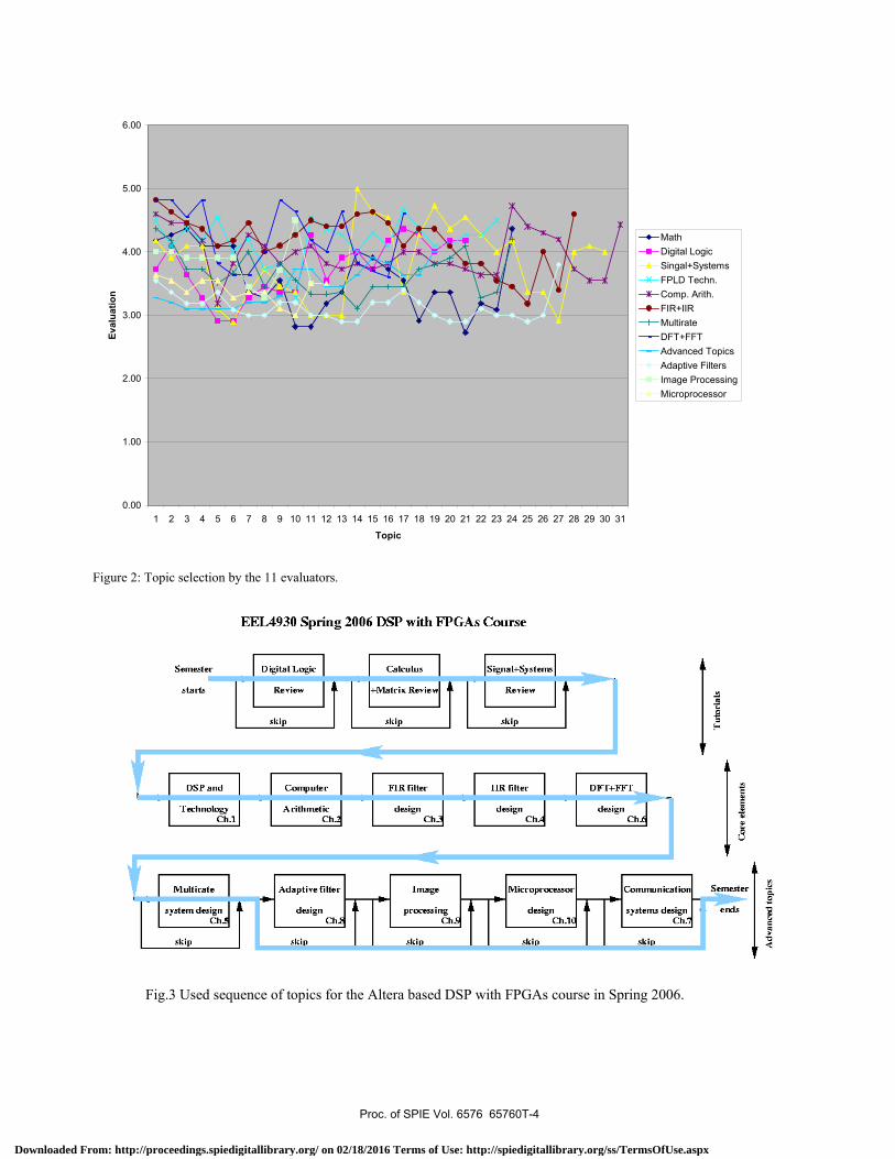
In the first year of this study, we first identified the appropriate topics from the textbook on DSP with FPGAs12 for an undergraduate course and selected appropriate lab exercises. We used 11 consultants to evaluate appropriate topics and the overall evaluation is shown in Fig. 2. Only topics with evaluation scores of 4 and larger were considered for the course. Based on this evaluation we then selected the topic, quizzes and laboratory experiments to be covered in class. Fig. 3 gives an overview of the first run of the course in Spring 2006. The thick grey line is the actual sequence we used in the Spring 2006 course, while the solid black line show possible flows. Notice the three sections consisting of
Figure 1: Cover of the first edition of the book3 by the first author.
Proc. of SPIE Vol. 6576 65760T-2
Downloaded From: http://proceedings.spiedigitallibrary.org/ on 02/18/2016 Terms of Use: http://spiedigitallibrary.org/ss/TermsOfUse.aspx
introductional material (tutorials), the sine-qua-non part (without which it could not be, i.e., core elements) and optional material (advanced topics) that can be selected based on the instructors preference and available time. Some state Universities in the US use a 4 month/per semester schedule (e.g. Florida) while others use a 3 month/semester time line (e.g. California). Before we could use the DSP with FPGAs12 book, we have to review digital logic, math and linear algebra using MatLab, and signal and systems. The reviewer found the following topics most relevant:
Digital Logic Review Math using MatLab4,5 Signal and Systems • Design circle • Data Types and
Representations • Logic Equations • Combinational Logic • Sequential Logic • Memory Elements • First look at an FPGA • FSM • Timing • Testbench
1. Linear algebra ° Basic terms and
operations 2. MatLab getting started
° MatLab as powerful pocket calculator
° MatLab as function library
° MatLab as plot program 3. Computing with complex
numbers 4. Implementing non trivial
functions with FPGAs ° Trigonometric functions ° Logarithm and
exponential functions ° Taylor and Chebychev
approximations ° Polynomial functions ° Roots of polynomials
5. Geometric series 6. Graph plotting
Signal terms: periodicity, power, continuous, discrete
System properties: linearity, time invariance, stability, causality
Fourier series Fourier transforms Fourier transform pairs FT theorems: superposition,
convolution, shift, symmetry Z-transform Z-transform pairs Z-transform theorems:
superposition, convolution, shift, symmetry
Random variable: mean, variance, higher moments
PDF distribution: normal, uniform, discrete
Auto- and crosscorrelation
After the review of basic ideas we started using the graduate book on DSP with FPGAs12. The first chapter of the book starts with a snapshot of today's FPGA technology, and the devices and tools used to design state-of-the-art DSP systems. It also includes a detailed case study of a frequency synthesizer, including compilation steps, simulation, performance evaluation, power estimation, and floor planning. The case study is the basis for more than 30 other design examples in subsequent chapters. For “full development,” Xilinx and Altera software tutorials needed to be included in the full educational material development (EMD). For the prototype, we selected only to present one FPGA design tool package per semester. We selected the following lecture topics from chapter 1:
1. Digital Signal Processing (DSP) • What, Why and How
2. A typical DSP System • Applications
3. Sampling and Quantization • Image and audio signals
4. A/D and D/A Conversion • Architecture • S/N ratio
5. FPL Technology • Classification by Granularity
6. DSP Technology Requirements • DSP features of FPGAs • FPGA and Programmable Signal
Processors 7. Design Implementation
• FPGA structure • Altera Cyclone II • Case Study: Frequency Synthesizer • Design with IP blocks
Proc. of SPIE Vol. 6576 65760T-3
Downloaded From: http://proceedings.spiedigitallibrary.org/ on 02/18/2016 Terms of Use: http://spiedigitallibrary.org/ss/TermsOfUse.aspx
EEL4930 Spring 2006 DSP with FPGAS Course
D ithI Lgi IRi + +VIi[kRi + Ri +I
Skip Skip Skip
DSPd FlRflIfr[ llRflhi Dyr4-wr I
A[iih,,!iiI I I
Ch.1 Ch. Ch. ChA Ch.4
MIii[i
__________Skip
0.00
1.00
2.00
3.00
4.00
5.00
6.00
1 2 3 4 5 6 7 8 9 10 11 12 13 14 15 16 17 18 19 20 21 22 23 24 25 26 27 28 29 30 31
Topic
Eval
uatio
n
MathDigital LogicSingal+SystemsFPLD Techn.Comp. Arith.FIR+IIRMultirateDFT+FFTAdvanced TopicsAdaptive FiltersImage ProcessingMicroprocessor
Figure 2: Topic selection by the 11 evaluators.
Fig.3 Used sequence of topics for the Altera based DSP with FPGAs course in Spring 2006.
Proc. of SPIE Vol. 6576 65760T-4
Downloaded From: http://proceedings.spiedigitallibrary.org/ on 02/18/2016 Terms of Use: http://spiedigitallibrary.org/ss/TermsOfUse.aspx
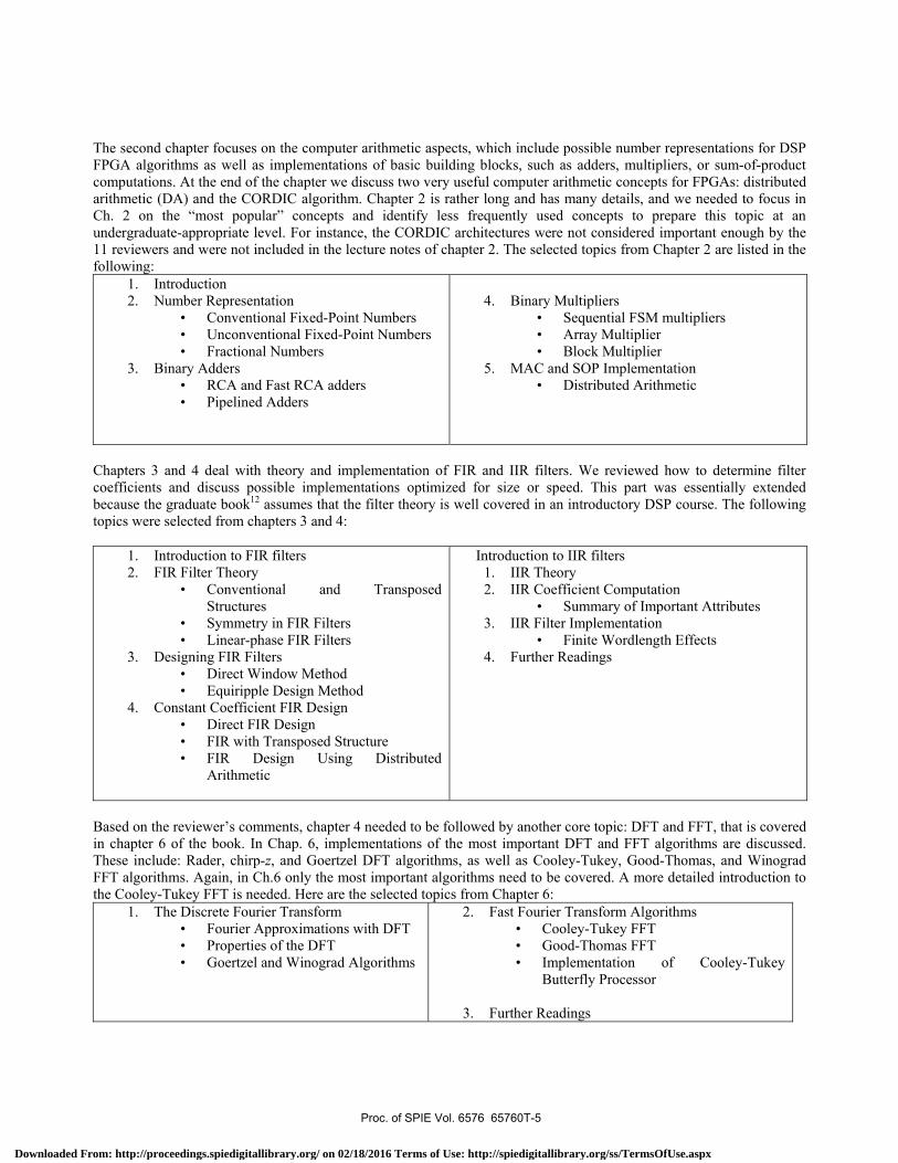
The second chapter focuses on the computer arithmetic aspects, which include possible number representations for DSP FPGA algorithms as well as implementations of basic building blocks, such as adders, multipliers, or sum-of-product computations. At the end of the chapter we discuss two very useful computer arithmetic concepts for FPGAs: distributed arithmetic (DA) and the CORDIC algorithm. Chapter 2 is rather long and has many details, and we needed to focus in Ch. 2 on the “most popular” concepts and identify less frequently used concepts to prepare this topic at an undergraduate-appropriate level. For instance, the CORDIC architectures were not considered important enough by the 11 reviewers and were not included in the lecture notes of chapter 2. The selected topics from Chapter 2 are listed in the following:
1. Introduction 2. Number Representation
• Conventional Fixed-Point Numbers • Unconventional Fixed-Point Numbers • Fractional Numbers
3. Binary Adders • RCA and Fast RCA adders • Pipelined Adders
4. Binary Multipliers
• Sequential FSM multipliers • Array Multiplier • Block Multiplier
5. MAC and SOP Implementation • Distributed Arithmetic
Chapters 3 and 4 deal with theory and implementation of FIR and IIR filters. We reviewed how to determine filter coefficients and discuss possible implementations optimized for size or speed. This part was essentially extended because the graduate book12 assumes that the filter theory is well covered in an introductory DSP course. The following topics were selected from chapters 3 and 4:
1. Introduction to FIR filters 2. FIR Filter Theory
• Conventional and Transposed Structures
• Symmetry in FIR Filters • Linear-phase FIR Filters
3. Designing FIR Filters • Direct Window Method • Equiripple Design Method
4. Constant Coefficient FIR Design • Direct FIR Design • FIR with Transposed Structure • FIR Design Using Distributed
Arithmetic
Introduction to IIR filters 1. IIR Theory 2. IIR Coefficient Computation
• Summary of Important Attributes 3. IIR Filter Implementation
• Finite Wordlength Effects 4. Further Readings
Based on the reviewer’s comments, chapter 4 needed to be followed by another core topic: DFT and FFT, that is covered in chapter 6 of the book. In Chap. 6, implementations of the most important DFT and FFT algorithms are discussed. These include: Rader, chirp-z, and Goertzel DFT algorithms, as well as Cooley-Tukey, Good-Thomas, and Winograd FFT algorithms. Again, in Ch.6 only the most important algorithms need to be covered. A more detailed introduction to the Cooley-Tukey FFT is needed. Here are the selected topics from Chapter 6:
1. The Discrete Fourier Transform • Fourier Approximations with DFT • Properties of the DFT • Goertzel and Winograd Algorithms
2. Fast Fourier Transform Algorithms • Cooley-Tukey FFT • Good-Thomas FFT • Implementation of Cooley-Tukey
Butterfly Processor
3. Further Readings
Proc. of SPIE Vol. 6576 65760T-5
Downloaded From: http://proceedings.spiedigitallibrary.org/ on 02/18/2016 Terms of Use: http://spiedigitallibrary.org/ss/TermsOfUse.aspx
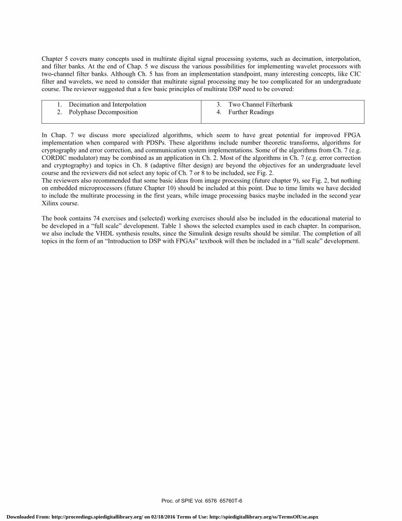
Chapter 5 covers many concepts used in multirate digital signal processing systems, such as decimation, interpolation, and filter banks. At the end of Chap. 5 we discuss the various possibilities for implementing wavelet processors with two-channel filter banks. Although Ch. 5 has from an implementation standpoint, many interesting concepts, like CIC filter and wavelets, we need to consider that multirate signal processing may be too complicated for an undergraduate course. The reviewer suggested that a few basic principles of multirate DSP need to be covered:
1. Decimation and Interpolation 2. Polyphase Decomposition
3. Two Channel Filterbank 4. Further Readings
In Chap. 7 we discuss more specialized algorithms, which seem to have great potential for improved FPGA implementation when compared with PDSPs. These algorithms include number theoretic transforms, algorithms for cryptography and error correction, and communication system implementations. Some of the algorithms from Ch. 7 (e.g. CORDIC modulator) may be combined as an application in Ch. 2. Most of the algorithms in Ch. 7 (e.g. error correction and cryptography) and topics in Ch. 8 (adaptive filter design) are beyond the objectives for an undergraduate level course and the reviewers did not select any topic of Ch. 7 or 8 to be included, see Fig. 2. The reviewers also recommended that some basic ideas from image processing (future chapter 9), see Fig. 2, but nothing on embedded microprocessors (future Chapter 10) should be included at this point. Due to time limits we have decided to include the multirate processing in the first years, while image processing basics maybe included in the second year Xilinx course. The book contains 74 exercises and (selected) working exercises should also be included in the educational material to be developed in a “full scale” development. Table 1 shows the selected examples used in each chapter. In comparison, we also include the VHDL synthesis results, since the Simulink design results should be similar. The completion of all topics in the form of an “Introduction to DSP with FPGAs” textbook will then be included in a “full scale” development.
Proc. of SPIE Vol. 6576 65760T-6
Downloaded From: http://proceedings.spiedigitallibrary.org/ on 02/18/2016 Terms of Use: http://spiedigitallibrary.org/ss/TermsOfUse.aspx
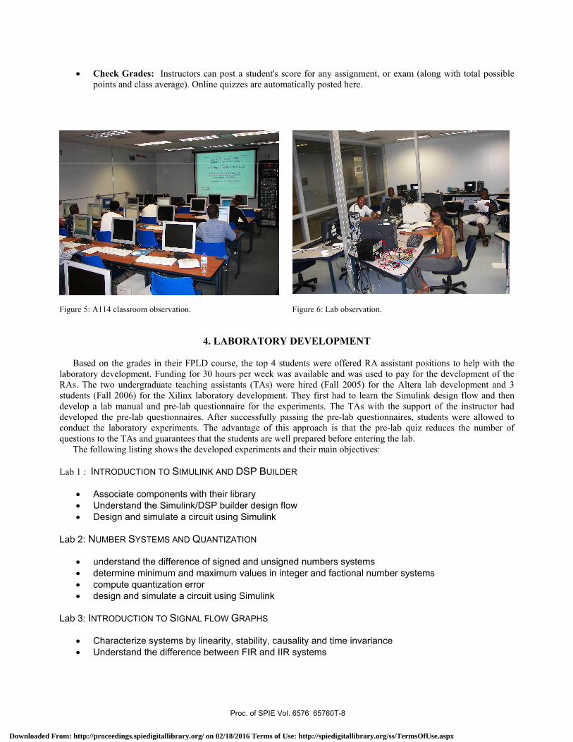
The Altera prototype course was tested in a classroom setting in Spring 2006. A multimedia classroom (B144) with terminals and software tools for 25 students at the FAMU-FSU College of Engineering was used (see Fig. 5). The teaching material was continuously updated and improved based on feedback from the online learning system Blackboard1. Outside evaluators from academia and industry (later) also had access to the class web page as “guests” and evaluated the significance of the covered topics, tools and procedures in written reports. We used the following Blackboard features to post class material [BB6]:
• Class Announcements to post important deadlines, like test topics, times, and dates • Course Documents including course PPT slides, online tutorials, handouts, course readings, etc. • Staff Information to deliver pictures, telephone and email numbers of instructors, TAs and support personnel. • Assignments including example files, detailed lab or HW instructions, and links • Resources with links to other sites, from FPGA vendor data sheets, e-journals to the FSU homepage
In the future, we plan to enable Blackboard's built-in communication and student tools to allow asynchronous activities and access, such as:
• E-mail Sender forms that enable any course participant to send e-mail to any individual or groups within the class
• Class Roster: The e-mail address or homepage of any class member can be accessed on this page. • Virtual Classroom: Class members can be assigned to have real-time talks on this page.
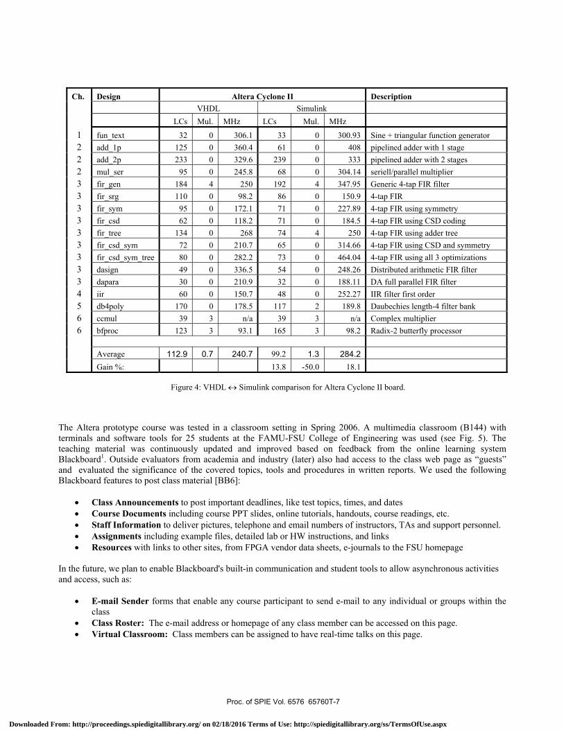
Ch. Design Altera Cyclone II Description VHDL Simulink LCs Mul. MHz LCs Mul. MHz
1 fun_text 32 0 306.1 33 0 300.93 Sine + triangular function generator 2 add_1p 125 0 360.4 61 0 408 pipelined adder with 1 stage 2 add_2p 233 0 329.6 239 0 333 pipelined adder with 2 stages 2 mul_ser 95 0 245.8 68 0 304.14 seriell/parallel multiplier 3 fir_gen 184 4 250 192 4 347.95 Generic 4-tap FIR filter 3 fir_srg 110 0 98.2 86 0 150.9 4-tap FIR 3 fir_sym 95 0 172.1 71 0 227.89 4-tap FIR using symmetry 3 fir_csd 62 0 118.2 71 0 184.5 4-tap FIR using CSD coding 3 fir_tree 134 0 268 74 4 250 4-tap FIR using adder tree 3 fir_csd_sym 72 0 210.7 65 0 314.66 4-tap FIR using CSD and symmetry 3 fir_csd_sym_tree 80 0 282.2 73 0 464.04 4-tap FIR using all 3 optimizations 3 dasign 49 0 336.5 54 0 248.26 Distributed arithmetic FIR filter 3 dapara 30 0 210.9 32 0 188.11 DA full parallel FIR filter 4 iir 60 0 150.7 48 0 252.27 IIR filter first order 5 db4poly 170 0 178.5 117 2 189.8 Daubechies length-4 filter bank 6 ccmul 39 3 n/a 39 3 n/a Complex multiplier 6 bfproc 123 3 93.1 165 3 98.2 Radix-2 butterfly processor
Average 112.9 0.7 240.7 99.2 1.3 284.2 Gain %: 13.8 -50.0 18.1
Figure 4: VHDL ↔ Simulink comparison for Altera Cyclone II board.
Proc. of SPIE Vol. 6576 65760T-7
Downloaded From: http://proceedings.spiedigitallibrary.org/ on 02/18/2016 Terms of Use: http://spiedigitallibrary.org/ss/TermsOfUse.aspx
• Check Grades: Instructors can post a student's score for any assignment, or exam (along with total possible points and class average). Online quizzes are automatically posted here.
4. LABORATORY DEVELOPMENT
Based on the grades in their FPLD course, the top 4 students were offered RA assistant positions to help with the
laboratory development. Funding for 30 hours per week was available and was used to pay for the development of the RAs. The two undergraduate teaching assistants (TAs) were hired (Fall 2005) for the Altera lab development and 3 students (Fall 2006) for the Xilinx laboratory development. They first had to learn the Simulink design flow and then develop a lab manual and pre-lab questionnaire for the experiments. The TAs with the support of the instructor had developed the pre-lab questionnaires. After successfully passing the pre-lab questionnaires, students were allowed to conduct the laboratory experiments. The advantage of this approach is that the pre-lab quiz reduces the number of questions to the TAs and guarantees that the students are well prepared before entering the lab.
The following listing shows the developed experiments and their main objectives: Lab 1 : INTRODUCTION TO SIMULINK AND DSP BUILDER
• Associate components with their library • Understand the Simulink/DSP builder design flow • Design and simulate a circuit using Simulink
Lab 2: NUMBER SYSTEMS AND QUANTIZATION
• understand the difference of signed and unsigned numbers systems • determine minimum and maximum values in integer and factional number systems • compute quantization error • design and simulate a circuit using Simulink
Lab 3: INTRODUCTION TO SIGNAL FLOW GRAPHS
• Characterize systems by linearity, stability, causality and time invariance • Understand the difference between FIR and IIR systems
Figure 5: A114 classroom observation. Figure 6: Lab observation.
Proc. of SPIE Vol. 6576 65760T-8
Downloaded From: http://proceedings.spiedigitallibrary.org/ on 02/18/2016 Terms of Use: http://spiedigitallibrary.org/ss/TermsOfUse.aspx
• Design and simulate nonlinear, FIR and IIR systems using Simulink Lab 4: INTRODUCTION TO MATLAB M-FILE SCRIPTS
• write simple M-file scripts to define tables and to use predefined functions. • use the MatLab help, demo and function library • design and simulate complex multiplier systems using Simulink
Lab 5: INTRODUCTION TO FIR FILTER
• Design and simulate an moving average filter • Understand the difference between direct and transposed form FIR filters • Design and simulate a reduced adder graph FIR filter using Simulink
Lab 6: INTRODUCTION TO IIR FILTER
• Design and simulate an first order IIR filter • Determine magnitude, phase and pole zero diagram of IIR filters • Design a 3rd order elliptic low pass filters • Compare IIR and FIR design parameter
Lab 7: INTRODUCTION TO DISCRETE FOURIER TRANSFORM
• Develop a basic Goertzel IIR loop and compute test data • Configure a sub design with I/O ports • Instantiate previously develop block • Design and simulate selected DFT component
Lab 8: INTRODUCTION TO FAST FOURIER TRANSFORM
• Develop a radix-2 FFT and compute test data • Understand the difference between DFT and FFT • Design and simulate a FFT using the principle of decimation in frequency using Simulink
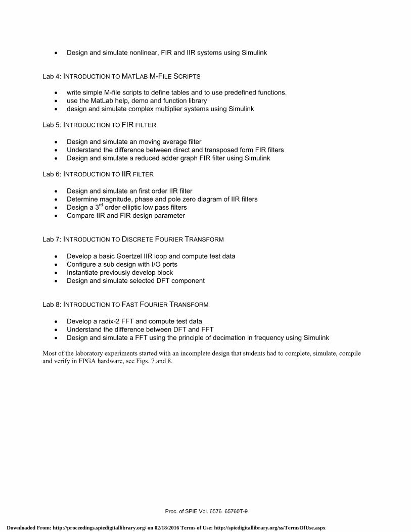
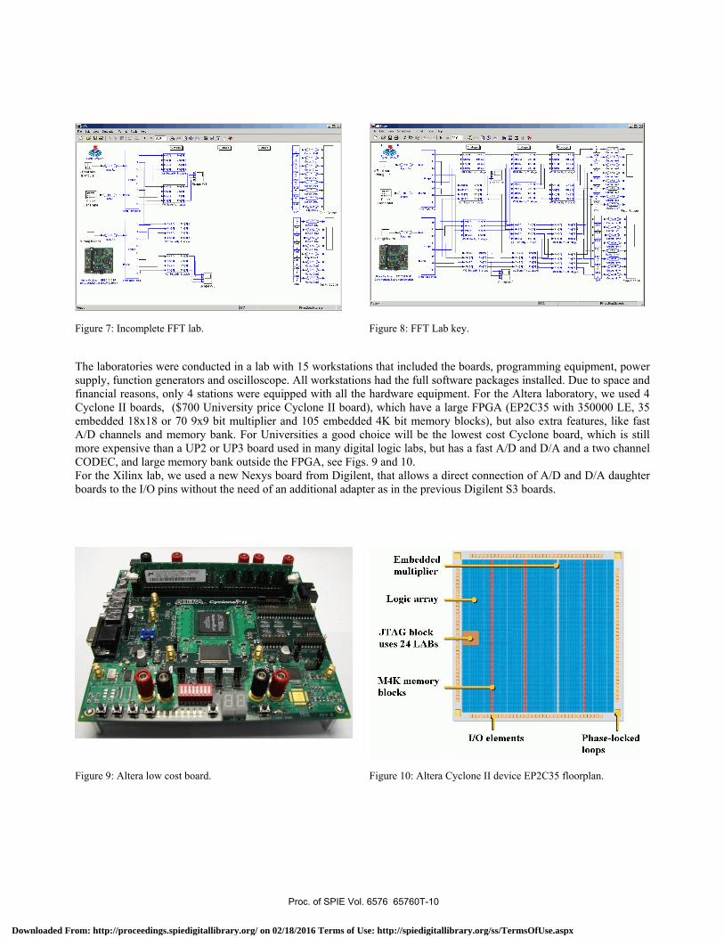
Most of the laboratory experiments started with an incomplete design that students had to complete, simulate, compile and verify in FPGA hardware, see Figs. 7 and 8.
Proc. of SPIE Vol. 6576 65760T-9
Downloaded From: http://proceedings.spiedigitallibrary.org/ on 02/18/2016 Terms of Use: http://spiedigitallibrary.org/ss/TermsOfUse.aspx
[ [ H
'I'H
HH
IHIII
IHH
•rJflJ-
Embeddedmultiplier
Logic array
JTAG blockuses 24 LABs
M4K memoryblocks
I..IIJJJJJJJJJJ
JLJlJJlJjJJJJ-J
1!
Phase-locked
loops
T.:.I I
I/O elements
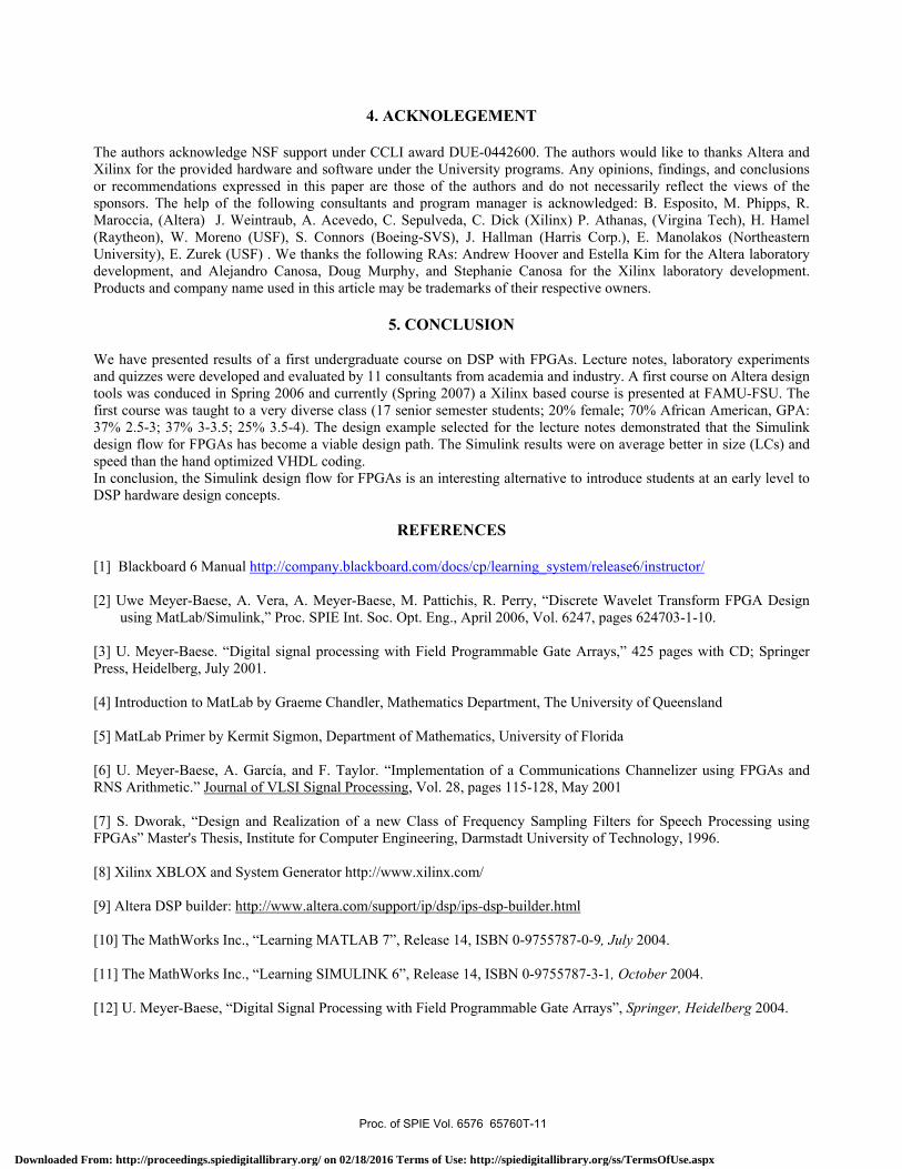
The laboratories were conducted in a lab with 15 workstations that included the boards, programming equipment, power supply, function generators and oscilloscope. All workstations had the full software packages installed. Due to space and financial reasons, only 4 stations were equipped with all the hardware equipment. For the Altera laboratory, we used 4 Cyclone II boards, ($700 University price Cyclone II board), which have a large FPGA (EP2C35 with 350000 LE, 35 embedded 18x18 or 70 9x9 bit multiplier and 105 embedded 4K bit memory blocks), but also extra features, like fast A/D channels and memory bank. For Universities a good choice will be the lowest cost Cyclone board, which is still more expensive than a UP2 or UP3 board used in many digital logic labs, but has a fast A/D and D/A and a two channel CODEC, and large memory bank outside the FPGA, see Figs. 9 and 10. For the Xilinx lab, we used a new Nexys board from Digilent, that allows a direct connection of A/D and D/A daughter boards to the I/O pins without the need of an additional adapter as in the previous Digilent S3 boards.
Figure 7: Incomplete FFT lab. Figure 8: FFT Lab key.
Figure 9: Altera low cost board. Figure 10: Altera Cyclone II device EP2C35 floorplan.
Proc. of SPIE Vol. 6576 65760T-10
Downloaded From: http://proceedings.spiedigitallibrary.org/ on 02/18/2016 Terms of Use: http://spiedigitallibrary.org/ss/TermsOfUse.aspx
4. ACKNOLEGEMENT
The authors acknowledge NSF support under CCLI award DUE-0442600. The authors would like to thanks Altera and Xilinx for the provided hardware and software under the University programs. Any opinions, findings, and conclusions or recommendations expressed in this paper are those of the authors and do not necessarily reflect the views of the sponsors. The help of the following consultants and program manager is acknowledged: B. Esposito, M. Phipps, R. Maroccia, (Altera) J. Weintraub, A. Acevedo, C. Sepulveda, C. Dick (Xilinx) P. Athanas, (Virgina Tech), H. Hamel (Raytheon), W. Moreno (USF), S. Connors (Boeing-SVS), J. Hallman (Harris Corp.), E. Manolakos (Northeastern University), E. Zurek (USF) . We thanks the following RAs: Andrew Hoover and Estella Kim for the Altera laboratory development, and Alejandro Canosa, Doug Murphy, and Stephanie Canosa for the Xilinx laboratory development. Products and company name used in this article may be trademarks of their respective owners.
5. CONCLUSION We have presented results of a first undergraduate course on DSP with FPGAs. Lecture notes, laboratory experiments and quizzes were developed and evaluated by 11 consultants from academia and industry. A first course on Altera design tools was conduced in Spring 2006 and currently (Spring 2007) a Xilinx based course is presented at FAMU-FSU. The first course was taught to a very diverse class (17 senior semester students; 20% female; 70% African American, GPA: 37% 2.5-3; 37% 3-3.5; 25% 3.5-4). The design example selected for the lecture notes demonstrated that the Simulink design flow for FPGAs has become a viable design path. The Simulink results were on average better in size (LCs) and speed than the hand optimized VHDL coding. In conclusion, the Simulink design flow for FPGAs is an interesting alternative to introduce students at an early level to DSP hardware design concepts.
REFERENCES
[1] Blackboard 6 Manual http://company.blackboard.com/docs/cp/learning_system/release6/instructor/ [2] Uwe Meyer-Baese, A. Vera, A. Meyer-Baese, M. Pattichis, R. Perry, “Discrete Wavelet Transform FPGA Design
using MatLab/Simulink,” Proc. SPIE Int. Soc. Opt. Eng., April 2006, Vol. 6247, pages 624703-1-10. [3] U. Meyer-Baese. “Digital signal processing with Field Programmable Gate Arrays,” 425 pages with CD; Springer Press, Heidelberg, July 2001. [4] Introduction to MatLab by Graeme Chandler, Mathematics Department, The University of Queensland [5] MatLab Primer by Kermit Sigmon, Department of Mathematics, University of Florida [6] U. Meyer-Baese, A. García, and F. Taylor. “Implementation of a Communications Channelizer using FPGAs and RNS Arithmetic.” Journal of VLSI Signal Processing, Vol. 28, pages 115-128, May 2001 [7] S. Dworak, “Design and Realization of a new Class of Frequency Sampling Filters for Speech Processing using FPGAs” Master's Thesis, Institute for Computer Engineering, Darmstadt University of Technology, 1996. [8] Xilinx XBLOX and System Generator http://www.xilinx.com/ [9] Altera DSP builder: http://www.altera.com/support/ip/dsp/ips-dsp-builder.html [10] The MathWorks Inc., “Learning MATLAB 7”, Release 14, ISBN 0-9755787-0-9, July 2004. [11] The MathWorks Inc., “Learning SIMULINK 6”, Release 14, ISBN 0-9755787-3-1, October 2004. [12] U. Meyer-Baese, “Digital Signal Processing with Field Programmable Gate Arrays”, Springer, Heidelberg 2004.
Proc. of SPIE Vol. 6576 65760T-11
Downloaded From: http://proceedings.spiedigitallibrary.org/ on 02/18/2016 Terms of Use: http://spiedigitallibrary.org/ss/TermsOfUse.aspx


