Embed Size (px)
Citation preview
Strategic advantage through science and technology: exploring the UK semiconductor innovation system 1
Strategic advantage through science and technology:exploring the UK semiconductor innovation system
Semiconductors are a class of materials used across a wide range of technologies that we rely on daily, most crucially computer chips. Recent chip shortages have affected automotive and consumer electronics supply chains, highlighting the criticality of secure access to semiconductors and their contribution to UK GDP.1,2 In the last few months, foreign interest in acquiring UK-based semiconductor companies has prompted the UK government to review associated national security implications.3,4
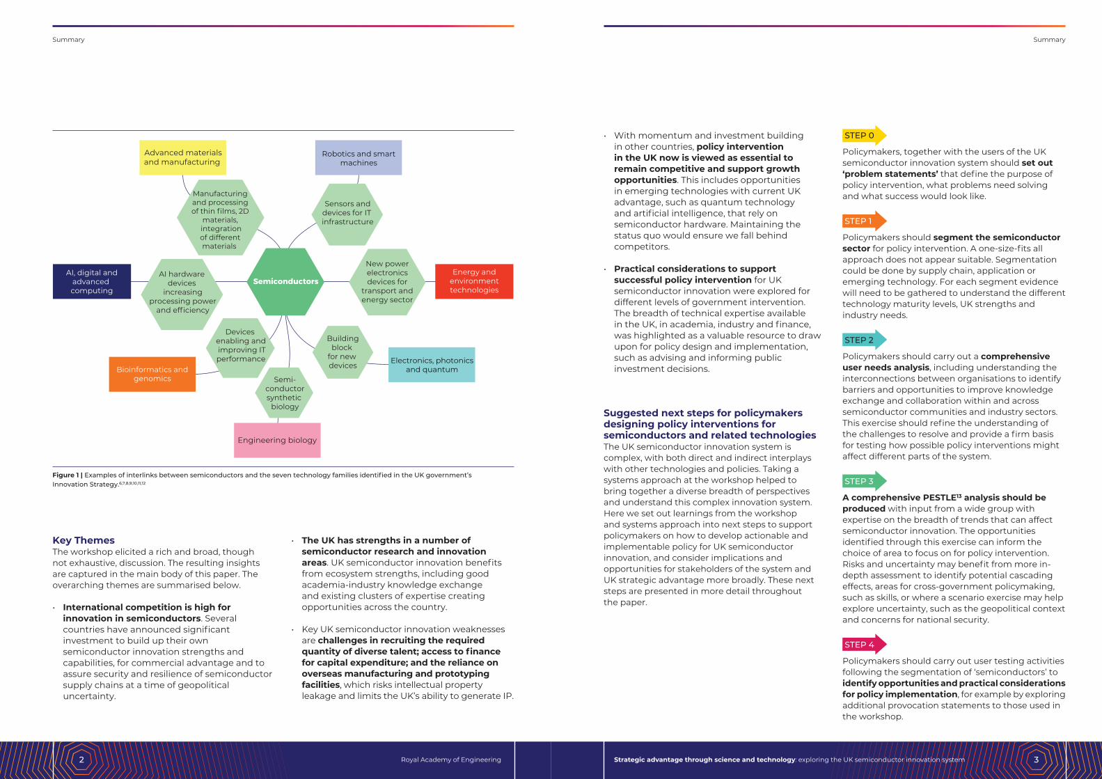
The UK government has ambitions to deliver UK strategic advantage through science and technology. Innovation in semiconductors is necessary to enable the development of many emerging technologies identified as of interest for UK strategic advantage, such as artificial intelligence, advanced and quantum computing, or smart machines, with examples in Figure 1.5 Semiconductor innovation will also continue to play an important role in improving performance of current technologies, such as consumer electronics.
The UK has strengths in semiconductor research and innovation. With both opportunities for commercial advantage and considerations for national security, semiconductors make a good candidate for the Integrated Review ‘own – collaborate – access’ framework.
Summary
To understand the UK semiconductor innovation system, opportunities and implications for strategic advantage, the Royal Academy of Engineering convened a workshop in November 2021 bringing together stakeholders from across the system, including researchers, start-ups and scale-ups, industry, finance and government policymakers.
This paper summarises the workshop discussion, taking a systems approach to better understand the needs of users, the wider socio-politico-technical context, as well as practical consideration for successful policy implementation to build on UK semiconductor innovation strengths. With significant investment announced by competitor countries, UK government intervention is viewed as necessary to capitalise on opportunities here or risk seeing commercialisation of innovative products, technologies and processes happen elsewhere, with the UK missing out on the associated benefits. As such, this paper proposes next steps for policy development, learning from the insights gathered at the workshop to get to practical and implementable policies.
Strategic advantage through science and technology: exploring the UK semiconductor innovation systemRoyal Academy of Engineering2 3
Key Themes The workshop elicited a rich and broad, though not exhaustive, discussion. The resulting insights are captured in the main body of this paper. The overarching themes are summarised below.
• International competition is high for innovation in semiconductors. Several countries have announced significant investment to build up their own semiconductor innovation strengths and capabilities, for commercial advantage and to assure security and resilience of semiconductor supply chains at a time of geopolitical uncertainty.
• The UK has strengths in a number of semiconductor research and innovation areas. UK semiconductor innovation benefits from ecosystem strengths, including good academia-industry knowledge exchange and existing clusters of expertise creating opportunities across the country.
• Key UK semiconductor innovation weaknesses are challenges in recruiting the required quantity of diverse talent; access to finance for capital expenditure; and the reliance on overseas manufacturing and prototyping facilities, which risks intellectual property leakage and limits the UK’s ability to generate IP.
• With momentum and investment building in other countries, policy intervention in the UK now is viewed as essential to remain competitive and support growth opportunities. This includes opportunities in emerging technologies with current UK advantage, such as quantum technology and artificial intelligence, that rely on semiconductor hardware. Maintaining the status quo would ensure we fall behind competitors.
• Practical considerations to support successful policy intervention for UK semiconductor innovation were explored for different levels of government intervention. The breadth of technical expertise available in the UK, in academia, industry and finance, was highlighted as a valuable resource to draw upon for policy design and implementation, such as advising and informing public investment decisions.
Suggested next steps for policymakers designing policy interventions for semiconductors and related technologiesThe UK semiconductor innovation system is complex, with both direct and indirect interplays with other technologies and policies. Taking a systems approach at the workshop helped to bring together a diverse breadth of perspectives and understand this complex innovation system. Here we set out learnings from the workshop and systems approach into next steps to support policymakers on how to develop actionable and implementable policy for UK semiconductor innovation, and consider implications and opportunities for stakeholders of the system and UK strategic advantage more broadly. These next steps are presented in more detail throughout the paper.
Advanced materialsand manufacturing
Engineering biology
Semiconductors
Manufacturing and processing of thin films, 2D
materials, integrationof different materials
Sensors anddevices for IT infrastructure
AI hardware devices
increasingprocessing power
and efficiency
New powerelectronicsdevices for
transport andenergy sector
Robotics and smartmachines
AI, digital andadvanced computing
Energy andenvironmenttechnologies
Devices enabling and improving ITperformance
Buildingblock
for new devices
Semi-conductorsynthetic
biology
Electronics, photonicsand quantumBioinformatics and
genomics
STEP 0
Policymakers, together with the users of the UK semiconductor innovation system should set out ‘problem statements’ that define the purpose of policy intervention, what problems need solving and what success would look like.
STEP 1
Policymakers should segment the semiconductor sector for policy intervention. A one-size-fits all approach does not appear suitable. Segmentation could be done by supply chain, application or emerging technology. For each segment evidence will need to be gathered to understand the different technology maturity levels, UK strengths and industry needs.
STEP 2
Policymakers should carry out a comprehensive user needs analysis, including understanding the interconnections between organisations to identify barriers and opportunities to improve knowledge exchange and collaboration within and across semiconductor communities and industry sectors. This exercise should refine the understanding of the challenges to resolve and provide a firm basis for testing how possible policy interventions might affect different parts of the system.
STEP 3
A comprehensive PESTLE13 analysis should be produced with input from a wide group with expertise on the breadth of trends that can affect semiconductor innovation. The opportunities identified through this exercise can inform the choice of area to focus on for policy intervention. Risks and uncertainty may benefit from more in-depth assessment to identify potential cascading effects, areas for cross-government policymaking, such as skills, or where a scenario exercise may help explore uncertainty, such as the geopolitical context and concerns for national security.
STEP 4
Policymakers should carry out user testing activities following the segmentation of ‘semiconductors’ to identify opportunities and practical considerations for policy implementation, for example by exploring additional provocation statements to those used in the workshop.
Figure 1 | Examples of interlinks between semiconductors and the seven technology families identified in the UK government’s Innovation Strategy.6,7,8,9,10,11,12
Summary Summary
Strategic advantage through science and technology: exploring the UK semiconductor innovation systemRoyal Academy of Engineering4 5
The workshop approach
UK semiconductor innovation strengths and weaknesses in an internationally competitive context
How does the wider environment affect the UK semiconductor innovation system?
Concluding remarks
Semiconductors: defining the boundaries of the ‘sector’
The UK semiconductor innovation system: understanding users and their needs
Considerations for policy interventions
References
4
10
6
21
5
17
8
23
Contents
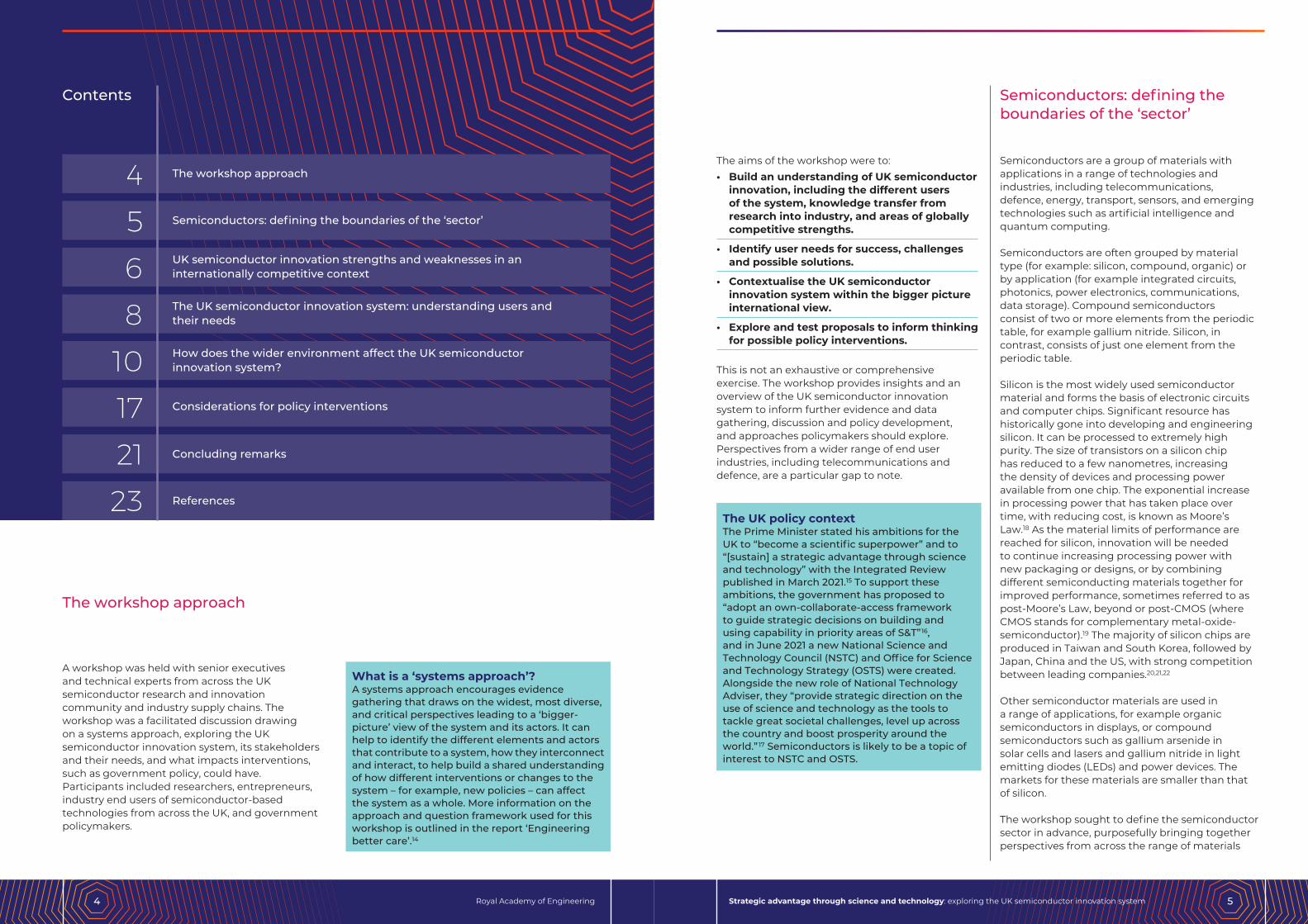
A workshop was held with senior executives and technical experts from across the UK semiconductor research and innovation community and industry supply chains. The workshop was a facilitated discussion drawing on a systems approach, exploring the UK semiconductor innovation system, its stakeholders and their needs, and what impacts interventions, such as government policy, could have. Participants included researchers, entrepreneurs, industry end users of semiconductor-based technologies from across the UK, and government policymakers.
Semiconductors are a group of materials with applications in a range of technologies and industries, including telecommunications, defence, energy, transport, sensors, and emerging technologies such as artificial intelligence and quantum computing.
Semiconductors are often grouped by material type (for example: silicon, compound, organic) or by application (for example integrated circuits, photonics, power electronics, communications, data storage). Compound semiconductors consist of two or more elements from the periodic table, for example gallium nitride. Silicon, in contrast, consists of just one element from the periodic table.
Silicon is the most widely used semiconductor material and forms the basis of electronic circuits and computer chips. Significant resource has historically gone into developing and engineering silicon. It can be processed to extremely high purity. The size of transistors on a silicon chip has reduced to a few nanometres, increasing the density of devices and processing power available from one chip. The exponential increase in processing power that has taken place over time, with reducing cost, is known as Moore’s Law.18 As the material limits of performance are reached for silicon, innovation will be needed to continue increasing processing power with new packaging or designs, or by combining different semiconducting materials together for improved performance, sometimes referred to as post-Moore’s Law, beyond or post-CMOS (where CMOS stands for complementary metal-oxide-semiconductor).19 The majority of silicon chips are produced in Taiwan and South Korea, followed by Japan, China and the US, with strong competition between leading companies.20,21,22
Other semiconductor materials are used in a range of applications, for example organic semiconductors in displays, or compound semiconductors such as gallium arsenide in solar cells and lasers and gallium nitride in light emitting diodes (LEDs) and power devices. The markets for these materials are smaller than that of silicon.
The workshop sought to define the semiconductor sector in advance, purposefully bringing together perspectives from across the range of materials
The workshop approach
Semiconductors: defining the boundaries of the ‘sector’
What is a ‘systems approach’?A systems approach encourages evidence gathering that draws on the widest, most diverse, and critical perspectives leading to a ‘bigger-picture’ view of the system and its actors. It can help to identify the different elements and actors that contribute to a system, how they interconnect and interact, to help build a shared understanding of how different interventions or changes to the system – for example, new policies – can affect the system as a whole. More information on the approach and question framework used for this workshop is outlined in the report ‘Engineering better care’.14
The UK policy contextThe Prime Minister stated his ambitions for the UK to “become a scientific superpower” and to “[sustain] a strategic advantage through science and technology” with the Integrated Review published in March 2021.15 To support these ambitions, the government has proposed to “adopt an own-collaborate-access framework to guide strategic decisions on building and using capability in priority areas of S&T”16, and in June 2021 a new National Science and Technology Council (NSTC) and Office for Science and Technology Strategy (OSTS) were created. Alongside the new role of National Technology Adviser, they “provide strategic direction on the use of science and technology as the tools to tackle great societal challenges, level up across the country and boost prosperity around the world.”17 Semiconductors is likely to be a topic of interest to NSTC and OSTS.
The aims of the workshop were to: • Build an understanding of UK semiconductor
innovation, including the different users of the system, knowledge transfer from research into industry, and areas of globally competitive strengths.
• Identify user needs for success, challenges and possible solutions.
• Contextualise the UK semiconductor innovation system within the bigger picture international view.
• Explore and test proposals to inform thinking for possible policy interventions.
This is not an exhaustive or comprehensive exercise. The workshop provides insights and an overview of the UK semiconductor innovation system to inform further evidence and data gathering, discussion and policy development, and approaches policymakers should explore. Perspectives from a wider range of end user industries, including telecommunications and defence, are a particular gap to note.
Strategic advantage through science and technology: exploring the UK semiconductor innovation systemRoyal Academy of Engineering6 7
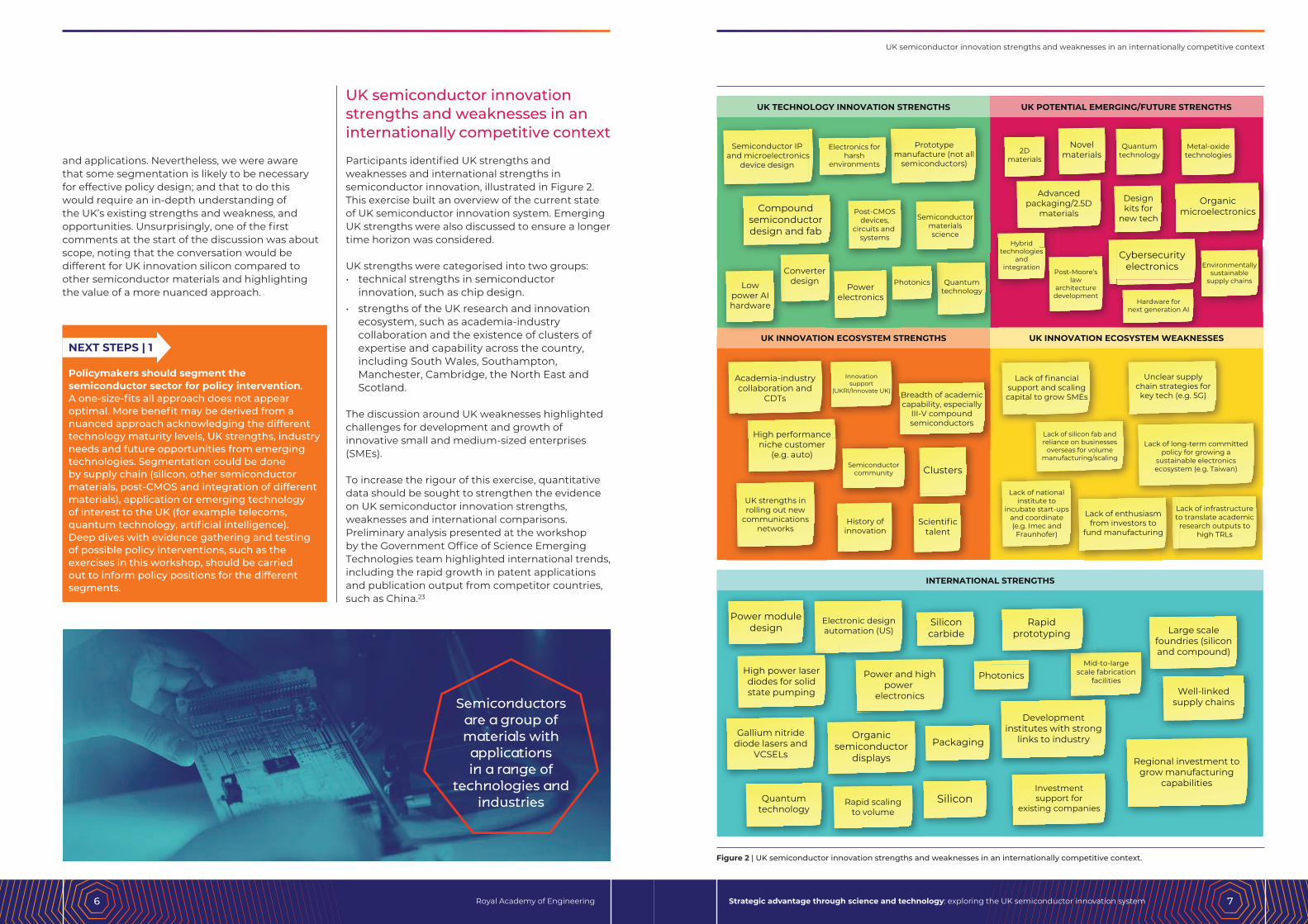
Semiconductor IP and microelectronics
device design
Electronics forharsh
environments
Prototypemanufacture (not all
semiconductors)
UK TECHNOLOGY INNOVATION STRENGTHS
UK INNOVATION ECOSYSTEM STRENGTHS UK INNOVATION ECOSYSTEM WEAKNESSES
UK POTENTIAL EMERGING/FUTURE STRENGTHS
Compound semiconductor design and fab
Post-CMOSdevices,
circuits and systems
Semiconductormaterialsscience
Lowpower AIhardware
Converterdesign
Powerelectronics
Photonics Quantumtechnology
Quantumtechnology
Novelmaterials
Metal-oxidetechnologies2D
materials
Advancedpackaging/2.5D
materials
Designkits for
new tech
Organicmicroelectronics
Hybridtechnologies
andintegration
Post-Moore’slaw
architecturedevelopment
Cybersecurityelectronics
Hardware fornext generation AI
Environmentallysustainable
supply chains
Academia-industrycollaboration and
CDTs
Innovationsupport
(UKRI/Innovate UK) Breadth of academiccapability, especially
III-V compoundsemiconductors
High performanceniche customer
(e.g. auto)Semiconductor
community Clusters
UK strengths inrolling out new
communicationsnetworks
History ofinnovation
Scientifictalent
INTERNATIONAL STRENGTHS
Lack of financialsupport and scaling
capital to grow SMEs
Unclear supplychain strategies for
key tech (e.g. 5G)
Lack of silicon fab andreliance on businesses
overseas for volumemanufacturing/scaling
Lack of long-term committedpolicy for growing a
sustainable electronicsecosystem (e.g. Taiwan)
Lack of nationalinstitute to
incubate start-upsand coordinate(e.g. Imec and
Fraunhofer)
Lack of enthusiasmfrom investors to
fund manufacturing
Lack of infrastructureto translate academic
research outputs tohigh TRLs
Power moduledesign
Electronic designautomation (US)
Siliconcarbide
Rapidprototyping Large scale
foundries (siliconand compound)
High power laserdiodes for solidstate pumping
Power and highpower
electronics
PhotonicsMid-to-large
scale fabricationfacilities
Well-linkedsupply chains
Gallium nitridediode lasers and
VCSELs
Organicsemiconductor
displays
Packaging
Developmentinstitutes with strong
links to industry
Regional investment togrow manufacturing
capabilities
Quantumtechnology
Rapid scalingto volume
SiliconInvestmentsupport for
existing companies
and applications. Nevertheless, we were aware that some segmentation is likely to be necessary for effective policy design; and that to do this would require an in-depth understanding of the UK’s existing strengths and weakness, and opportunities. Unsurprisingly, one of the first comments at the start of the discussion was about scope, noting that the conversation would be different for UK innovation silicon compared to other semiconductor materials and highlighting the value of a more nuanced approach.
UK semiconductor innovation strengths and weaknesses in an internationally competitive context
Participants identified UK strengths and weaknesses and international strengths in semiconductor innovation, illustrated in Figure 2. This exercise built an overview of the current state of UK semiconductor innovation system. Emerging UK strengths were also discussed to ensure a longer time horizon was considered.
UK strengths were categorised into two groups: • technical strengths in semiconductor
innovation, such as chip design.• strengths of the UK research and innovation
ecosystem, such as academia-industry collaboration and the existence of clusters of expertise and capability across the country, including South Wales, Southampton, Manchester, Cambridge, the North East and Scotland.
The discussion around UK weaknesses highlighted challenges for development and growth of innovative small and medium-sized enterprises (SMEs).
To increase the rigour of this exercise, quantitative data should be sought to strengthen the evidence on UK semiconductor innovation strengths, weaknesses and international comparisons. Preliminary analysis presented at the workshop by the Government Office of Science Emerging Technologies team highlighted international trends, including the rapid growth in patent applications and publication output from competitor countries, such as China.23
Figure 2 | UK semiconductor innovation strengths and weaknesses in an internationally competitive context.
NEXT STEPS | 1
Policymakers should segment the semiconductor sector for policy intervention. A one-size-fits all approach does not appear optimal. More benefit may be derived from a nuanced approach acknowledging the different technology maturity levels, UK strengths, industry needs and future opportunities from emerging technologies. Segmentation could be done by supply chain (silicon, other semiconductor materials, post-CMOS and integration of different materials), application or emerging technology of interest to the UK (for example telecoms, quantum technology, artificial intelligence). Deep dives with evidence gathering and testing of possible policy interventions, such as the exercises in this workshop, should be carried out to inform policy positions for the different segments.
UK semiconductor innovation strengths and weaknesses in an internationally competitive context
Semiconductors are a group of materials with
applications in a range of
technologies and industries
Strategic advantage through science and technology: exploring the UK semiconductor innovation systemRoyal Academy of Engineering8 9
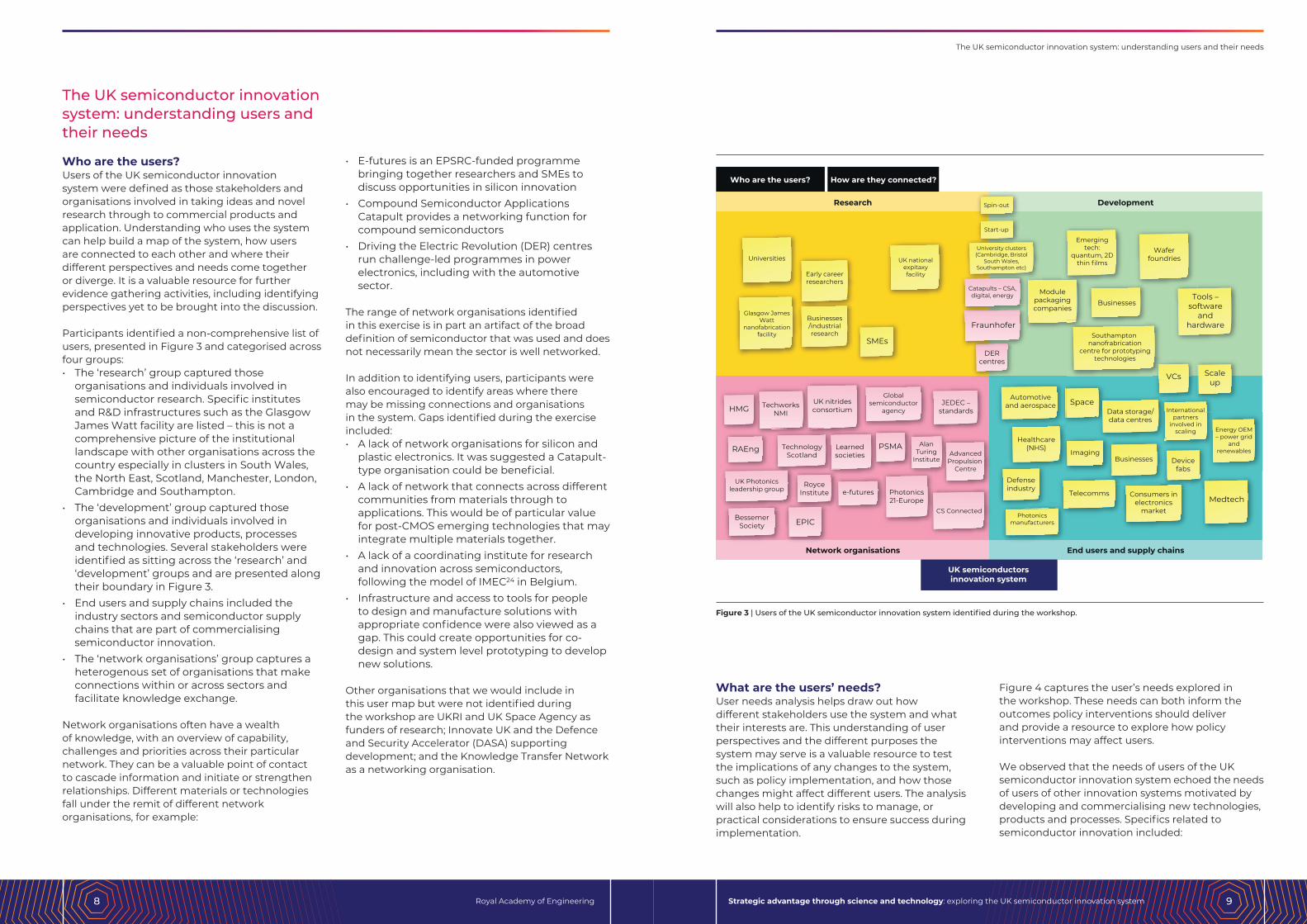
Who are the users?Users of the UK semiconductor innovation system were defined as those stakeholders and organisations involved in taking ideas and novel research through to commercial products and application. Understanding who uses the system can help build a map of the system, how users are connected to each other and where their different perspectives and needs come together or diverge. It is a valuable resource for further evidence gathering activities, including identifying perspectives yet to be brought into the discussion.
Participants identified a non-comprehensive list of users, presented in Figure 3 and categorised across four groups: • The ‘research’ group captured those
organisations and individuals involved in semiconductor research. Specific institutes and R&D infrastructures such as the Glasgow James Watt facility are listed – this is not a comprehensive picture of the institutional landscape with other organisations across the country especially in clusters in South Wales, the North East, Scotland, Manchester, London, Cambridge and Southampton.
• The ‘development’ group captured those organisations and individuals involved in developing innovative products, processes and technologies. Several stakeholders were identified as sitting across the ‘research’ and ‘development’ groups and are presented along their boundary in Figure 3.
• End users and supply chains included the industry sectors and semiconductor supply chains that are part of commercialising semiconductor innovation.
• The ‘network organisations’ group captures a heterogenous set of organisations that make connections within or across sectors and facilitate knowledge exchange.
Network organisations often have a wealth of knowledge, with an overview of capability, challenges and priorities across their particular network. They can be a valuable point of contact to cascade information and initiate or strengthen relationships. Different materials or technologies fall under the remit of different network organisations, for example:
• E-futures is an EPSRC-funded programme bringing together researchers and SMEs to discuss opportunities in silicon innovation
• Compound Semiconductor Applications Catapult provides a networking function for compound semiconductors
• Driving the Electric Revolution (DER) centres run challenge-led programmes in power electronics, including with the automotive sector.
The range of network organisations identified in this exercise is in part an artifact of the broad definition of semiconductor that was used and does not necessarily mean the sector is well networked.
In addition to identifying users, participants were also encouraged to identify areas where there may be missing connections and organisations in the system. Gaps identified during the exercise included:• A lack of network organisations for silicon and
plastic electronics. It was suggested a Catapult-type organisation could be beneficial.
• A lack of network that connects across different communities from materials through to applications. This would be of particular value for post-CMOS emerging technologies that may integrate multiple materials together.
• A lack of a coordinating institute for research and innovation across semiconductors, following the model of IMEC24 in Belgium.
• Infrastructure and access to tools for people to design and manufacture solutions with appropriate confidence were also viewed as a gap. This could create opportunities for co-design and system level prototyping to develop new solutions.
Other organisations that we would include in this user map but were not identified during the workshop are UKRI and UK Space Agency as funders of research; Innovate UK and the Defence and Security Accelerator (DASA) supporting development; and the Knowledge Transfer Network as a networking organisation.
What are the users’ needs?User needs analysis helps draw out how different stakeholders use the system and what their interests are. This understanding of user perspectives and the different purposes the system may serve is a valuable resource to test the implications of any changes to the system, such as policy implementation, and how those changes might affect different users. The analysis will also help to identify risks to manage, or practical considerations to ensure success during implementation.
Businesses
Fraunhofer
Universities
Early careerresearchers
Glasgow JamesWatt
nanofabricationfacility
Businesses/industrialresearch
SMEs
UK nationalexpitaxyfacility
Research Development
Network organisations End users and supply chains
Spin-out
Start-up
University clusters(Cambridge, Bristol
South Wales,Southampton etc)
Catapults – CSA,digital, energy
DERcentres
Emergingtech:
quantum, 2Dthin films
Southampton nanofrabrication
centre for prototypingtechnologies
Tools –software
andhardware
Modulepackagingcompanies
Waferfoundries
VCs Scaleup
Automotiveand aerospace Space
Data storage/data centres
Internationalpartners
involved inscaling Energy OEM
– power gridand
renewables
Healthcare(NHS)
ImagingBusinesses Device
fabs
Defenseindustry
Telecomms Consumers inelectronics
marketMedtech
Photonicsmanufacturers
HMG TechworksNMI
UK nitridesconsortium
Globalsemiconductor
agencyJEDEC –
standards
RAEng TechnologyScotland
PSMALearnedsocieties
AlanTuring
InstituteAdvanced
Propulsion Centre
UK Photonicsleadership group
RoyceInstitute e-futures Photonics
21-EuropeCS Connected
BessemerSociety EPIC
UK semiconductorsinnovation system
Who are the users? How are they connected?
Figure 4 captures the user’s needs explored in the workshop. These needs can both inform the outcomes policy interventions should deliver and provide a resource to explore how policy interventions may affect users.
We observed that the needs of users of the UK semiconductor innovation system echoed the needs of users of other innovation systems motivated by developing and commercialising new technologies, products and processes. Specifics related to semiconductor innovation included:
The UK semiconductor innovation system: understanding users and their needs
Figure 3 | Users of the UK semiconductor innovation system identified during the workshop.
The UK semiconductor innovation system: understanding users and their needs
Strategic advantage through science and technology: exploring the UK semiconductor innovation systemRoyal Academy of Engineering10 11
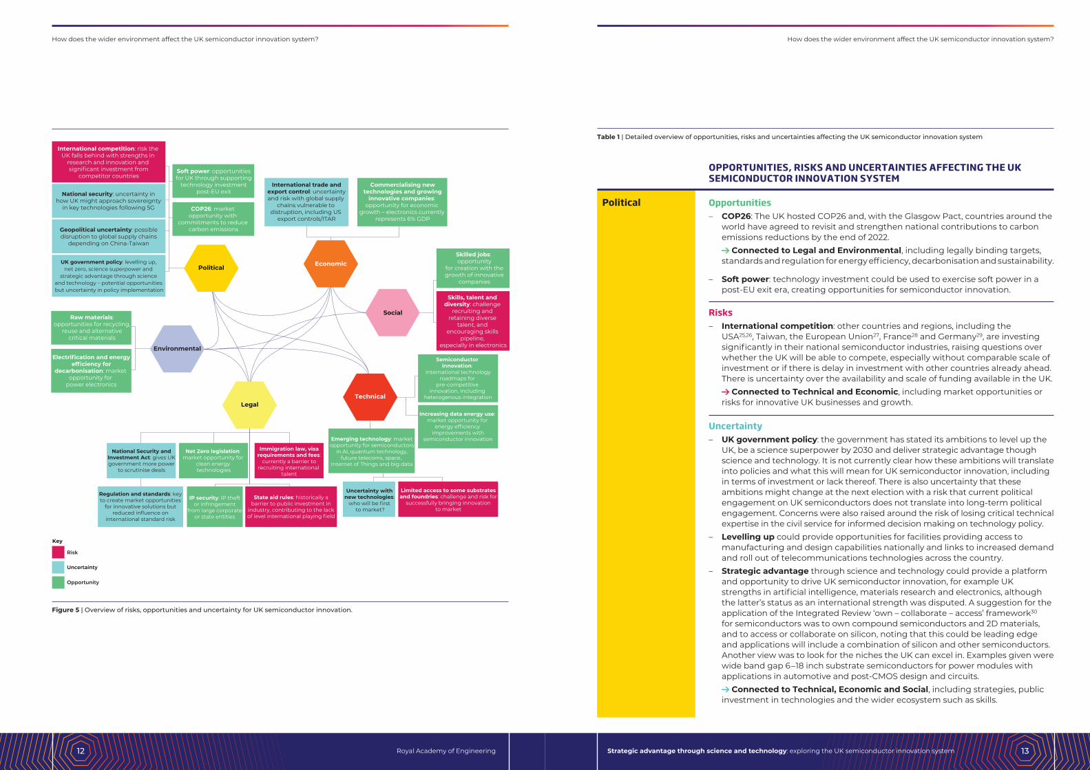
Participants were prompted to discuss how political, economic, social, technological, legal and environmental (PESTLE) events and macro trends may affect the UK semiconductor innovation system. The aim was to consider the wider context the semiconductor innovation system operates in. A summary of the findings is presented in Figure 5, with most trends and events identified interlinked to others. Table 1 records the insights from the PESTLE analysis in more detail.
The opportunities, risks and uncertainties listed can help focus policy interventions, especially where government action can provide clarity, direction or joined-up policy making.
For risks, identifying interconnections is of crucial importance to assess how a risk may propagate. For example, access to diverse and skilled talent is a key risk for semiconductors that would have wider implications. If it isn’t managed and mitigated, companies would face barriers to grow and carry out innovation without access to skilled staff, limiting the opportunity for economic growth and delivery of strategic advantage. Solving the skills challenge, whether related to the depth of UK expertise or the quantity, without enough semiconductor engineers in the UK, is a complex challenge and dependent in part on immigration policy, education and skills policy and the wider research and innovation culture attracting and retaining talent in semiconductor-related careers in the UK.
energy company
university researcher
investor
RTO
UK-based manufacturer
end user
investment
What are the needs of users?
start-upI can develop and commercialise my
technology, including by funding CapEx, and be internationally competitive
I can transfer energy from offshore to onshoreand provide reliable energy to UK business
and consumers
I can move ideas to commercialisation
I can have a better chance of ROI
I can plan for the future and attract inwardinvestment
I can have a level playing field with the restof the world and create UK end to end
supply chains
I can protect core strengths and moveforward with resilience with a supply of chips
that meets my demands
As a… I need… so that…
access tocustomers
training andmentorship
match fundingfor IUK grants
skilledstaff
small-mediumscale prototyping
control of supplychain to protect
IP leakage
ability to innovatewith access to
infrastructures formanufacturering
and design ofnovel tech
simplicity ofgovernment support and regulations
supply chainawareness
customepitaxy
IUK co-fundingcompetitions
access to highpower
electronics
access to policymakers to input
on regulation
reliable cost-effective supply chain
funding to help retainentrepreneurial
researchers
funding to progresstechnology to TRL
where it can attractinvestment
incentives topatent
technology
understanding of valueand opportunities frompatents vs publications
access to industry usecase and better
engagement withend users
flexibleindustrialpartners
access tofacilities, incl.international
secure careerpaths and inclusive
research culture
time to dedicate tocommercialisation
and support spin out
support forearly stage
research
assurance my targetinvestment will have
customers
a timeline to exit possibly
preferring short
to know the company has theright vision, the right team tolead the business, a credible
technology
skilledstaff
support inemerging tech for
my customers
certainty in innovation support
for my customers
ecosphere withmanufacturingsupport to aid
product development
and supply
supportivesupply chain
investmentsupport and
financialsupport
for scaling
a skilledtalent pool
support to tradeand move goods
globally andcost-effectively
understanding of newtechnologies and howthey might disrupt my
business local securesupply chains
access tointernational
markets
access tomanufacturing
slots
costcompetitiveness
Figure 4 | Needs analysis for users of the UK semiconductor innovation system.
NEXT STEPS | 2
Policymakers should carry out a comprehensive user needs analysis, including understanding the interconnections between organisations to identify barriers and opportunities to improve knowledge exchange and collaboration within and across semiconductor communities and industry sectors.
This exercise could assess where existing network organisations would benefit from increased visibility and capacity, as well as where additional connections would provide added value by drawing upon the users’ needs analysis (Figure 4) and ecosystem strengths and weaknesses (Figure 2).
This exercise should refine the understanding of the challenges to resolve and provide a firm basis for testing how possible policy interventions might affect different parts of the system. Understanding the needs of different users can also support effective communication of policy intervention and build buy-in across communities.
• Challenges in recruiting and retaining diverse and skilled talent, including in specific areas such as microelectronics.
• Access to funding, and in particular patient capital and investors to fund capital expenditure for hardware innovation.
• Access and control over the supply chain for custom epitaxy to progress development whilst protecting against IP leakage.
• Access to customers and international markets. • From the end user business perspective:
understanding new technologies and how they might disrupt businesses.
• Long-term certainty, including support and market signalling from government policy, such as a strategy or public procurement programme creating demand for semiconductor applications.
How does the wider environment affect the UK semiconductor innovation system?
NEXT STEPS | 3
A comprehensive PESTLE analysis should be produced with input from a wide group with expertise on the breadth of trends that can affect semiconductor innovation. The opportunities identified through this exercise can inform the choice of area to focus on for policy intervention. Risks and uncertainty may benefit from more in-depth assessment to identify potential cascading effects, areas for cross-government policymaking, such as skills, or where a scenario exercise may help explore uncertainty, such as the geopolitical context and concerns for national security.
How does the wider environment affect the UK semiconductor innovation system?
The opportunities identified through this exercise can
inform the choice of area to focus
on for policy intervention
Strategic advantage through science and technology: exploring the UK semiconductor innovation systemRoyal Academy of Engineering12 13
Table 1 | Detailed overview of opportunities, risks and uncertainties affecting the UK semiconductor innovation system
OPPORTUNITIES, RISKS AND UNCERTAINTIES AFFECTING THE UK SEMICONDUCTOR INNOVATION SYSTEM
Opportunities – COP26: The UK hosted COP26 and, with the Glasgow Pact, countries around the
world have agreed to revisit and strengthen national contributions to carbon emissions reductions by the end of 2022.
Connected to Legal and Environmental, including legally binding targets, standards and regulation for energy efficiency, decarbonisation and sustainability.
– Soft power: technology investment could be used to exercise soft power in a post-EU exit era, creating opportunities for semiconductor innovation.
Risks– International competition: other countries and regions, including the
USA25,26, Taiwan, the European Union27, France28 and Germany29, are investing significantly in their national semiconductor industries, raising questions over whether the UK will be able to compete, especially without comparable scale of investment or if there is delay in investment with other countries already ahead. There is uncertainty over the availability and scale of funding available in the UK.
Connected to Technical and Economic, including market opportunities or risks for innovative UK businesses and growth.
Uncertainty– UK government policy: the government has stated its ambitions to level up the
UK, be a science superpower by 2030 and deliver strategic advantage though science and technology. It is not currently clear how these ambitions will translate into policies and what this will mean for UK semiconductor innovation, including in terms of investment or lack thereof. There is also uncertainty that these ambitions might change at the next election with a risk that current political engagement on UK semiconductors does not translate into long-term political engagement. Concerns were also raised around the risk of losing critical technical expertise in the civil service for informed decision making on technology policy.
– Levelling up could provide opportunities for facilities providing access to manufacturing and design capabilities nationally and links to increased demand and roll out of telecommunications technologies across the country.
– Strategic advantage through science and technology could provide a platform and opportunity to drive UK semiconductor innovation, for example UK strengths in artificial intelligence, materials research and electronics, although the latter’s status as an international strength was disputed. A suggestion for the application of the Integrated Review ‘own – collaborate – access’ framework30 for semiconductors was to own compound semiconductors and 2D materials, and to access or collaborate on silicon, noting that this could be leading edge and applications will include a combination of silicon and other semiconductors. Another view was to look for the niches the UK can excel in. Examples given were wide band gap 6–18 inch substrate semiconductors for power modules with applications in automotive and post-CMOS design and circuits.
Connected to Technical, Economic and Social, including strategies, public investment in technologies and the wider ecosystem such as skills.
Political
Risk
Opportunity
Uncertainty
Key
Political
Environmental
Economic
Social
LegalTechnical
International competition: risk the UK falls behind with strengths in
research and innovation and significant investment from
competitor countries
National security: uncertainty inhow UK might approach sovereignty
in key technologies following 5G
Geopolitical uncertainty: possibledisruption to global supply chains
depending on China-Taiwan
UK government policy: levelling up, net zero, science superpower and
strategic advantage through science and technology – potential opportunities but uncertainty in policy implementation
Soft power: opportunitiesfor UK through supporting
technology investmentpost-EU exit
COP26: market opportunity with
commitments to reduce carbon emissions
International trade andexport control: uncertaintyand risk with global supply
chains vulnerable to distruption, including US
export controls/ITAR
Commercialising newtechnologies and growing
innovative companies: opportunity for economic
growth – electronics currently represents 6% GDP
Raw materials:opportunities for recycling,
reuse and alternativecritical materials
Electrification and energyefficiency for
decarbonisation: market opportunity for
power electronics
Skilled jobs: opportunity
for creation with thegrowth of innovative
companies
Skills, talent and diversity: challenge
recruiting and retaining diverse
talent, and encouraging skills
pipeline, especially in electronics
Semiconductor innovation:
international technologyroadmaps for
pre-competitive innovation, including
heterogenous integration
Increasing data energy use: market opportunity for
energy efficiency improvements with
semiconductor innovation
Limited access to some substratesand foundries: challenge and risk for
successfully bringing innovationto market
Emerging technology: marketopportunity for semiconductors
in AI, quantum technology,future telecoms, space,
Internet of Things and big data
Uncertainty with new technologies:
who will be first to market?
National Security andInvestment Act: gives UKgovernment more power
to scrutinise deals
Net Zero legislation: market opportunity for
clean energy technologies
Immigration law, visarequirements and fees:
currently a barrier torecruiting international
talent
Regulation and standards: keyto create market opportunities
for innovative solutions butreduced influence on
international standard risk
IP security: IP theftor infringement
from large corporateor state entities
State aid rules: historically abarrier to public investment in
industry, contributing to the lackof level international playing field
Figure 5 | Overview of risks, opportunities and uncertainty for UK semiconductor innovation.
How does the wider environment affect the UK semiconductor innovation system? How does the wider environment affect the UK semiconductor innovation system?
Strategic advantage through science and technology: exploring the UK semiconductor innovation systemRoyal Academy of Engineering14 15
– National security: The UK maintains sovereign capability where necessary for defence purposes and politicians have raised concerns regarding foreign ownership of certain technologies, for example 5G. There may be linked opportunities for semiconductor innovation to deliver upon security and defence needs.
Connected to Legal and Technical, including sovereign supply chains and government intervention in foreign deals.
– Geopolitical uncertainty: There is uncertainty around China and how its relationship will evolve with Taiwan, currently where most chips with small circuits are produced31,32 and which the UK supply chain is depends upon. Tensions between China and the US33 may create challenges in global chip supply chains and technology development, as well as potential opportunities for the UK.
Connected to Economic and Legal, including disruption to supply chains affecting a range of industries, export controls and market opportunities.
Opportunity – Economic growth: Building on the UK’s strengths was viewed as an
opportunity, including electronics (forecast 7.5% GVA in 202134) and artificial intelligence (algorithmics).
Connected to Social and Political, including delivering growth and skilled jobs across the country.
Uncertainty– International trade: Globalised supply chains can be vulnerable to disruption,
as exemplified recently with chip shortages around the world affecting several industries. Potential for future disruption is linked to geopolitical uncertainty and trade disputes. Trade deals are in the process of being rolled over or newly negotiated following the UK’s exit from the European Union, with the potential to create uncertainty and barriers. Export controls and state intervention, including from beyond the UK such as the International Traffic in Arms Regulation (ITAR) in the US that applies to some semiconductors, risks leading to market fragmentation and creates uncertainty around access to markets. The UK’s exit from the EU was viewed as a risk driving investment away.
Connected to Legal and Political, including trade deals and export controls.
Risk – Skills, talent and diversity: Access to talent is viewed as a significant challenge
currently. The skills base is shrinking and non-diverse in electronics, with the semiconductor sector not viewed as attractive to young people. The current political context is also acting as a deterrent to attracting international talent to the UK and retaining UK-trained talent. One foundry in Scotland described its struggle to recruit, taking six to nine months. There is also a lack of mobility between academia and industry, with a question raised regarding whether the UK PhD system trains experts that have the right skills for industry and academia. Investment in UK skills, technology, new research institutions like the Alan Turing Institute or IMEC in Belgium, and long-term success of UK businesses could create incentives and appeal for talent to join the UK semiconductor innovation system, and support a more diverse, inclusive workforce.
Connected to Legal, Economic and Political, including immigration rules, education and skills policy, and opportunity for job creation.
Economic
Opportunities– Semiconductor innovation: International technology roadmaps for
heterogeneous integration set out direction and pre-competition innovation and will shape the landscape that companies follow. Post Moore’s law, there may be a transition from system-level optimising to software and hardware co-design, and a new opportunity for innovation. There was discussion over the risks for countries that do not own a supply chain as lack of access to foundries creates challenges and can limit innovation development. The UK is in this situation, and there was debate as to whether modest investment could support and build up existing supply chains. In the US, fabrication facilities have been repurposed and Belgium has a coordinating institute IMEC that supports developing new technologies to commercialisation.
Connected to Economic, Social and Political, including potential for economic growth with new markets, needs for talent to deliver innovation, and government strategies and support for innovation.
– Emerging technologies: Several emerging technologies rely on the use of semiconductors, including artificial intelligence, quantum technology, future telecommunications such as 6G, space technologies, Internet of Things and big data, creating opportunities for new markets, processes and products. The UK has strengths in these emerging technologies, across physics and materials research, that can be built upon. There is uncertainty about which technology within those families will be commercialised first, time to market, how the market will look and evolve, and the role of government support. The challenge remains translating novel designs and materials into commercial products, as for some technology areas (like batteries), the barrier to entry is high. The limited UK supply of some semiconductor substrates, cost for manufacturing tools and access to foundries whilst retaining control of intellectual property are all challenges. In some areas of semiconductor innovation, lack of UK capability risks the growth and economic benefit going overseas: an example mentioned was semiconductor packaging.
Connected to Economic, Social and Political, including potential for economic growth with new markets, needs for talent to deliver innovation, and government strategies and international competition.
– Data and energy use: Increasing data and related energy use is viewed to be a key driver to develop more energy-efficient semiconductor applications.
Connected to Environmental and Legal, including net zero targets, regulation and standards for energy efficiency.
Opportunity– Net Zero legislation: Legislation to reduce UK carbon emissions is driving
opportunities to deliver innovation to deliver decarbonisation, including with semiconductors.
Connected to Technical, Environmental and Political, including energy and resource efficiency.
Risks – Regulation and standards: Reduced influence on international standards is
viewed as a key risk that would not require significant investment to ensure involvement. Regulation such as energy efficiency and for new technologies may impact start-ups but could create opportunities to boost change, with new markets for semiconductor innovation. There is a question of where
Social
Technical
Legal
How does the wider environment affect the UK semiconductor innovation system? How does the wider environment affect the UK semiconductor innovation system?
Strategic advantage through science and technology: exploring the UK semiconductor innovation systemRoyal Academy of Engineering16 17
Considerations for policy interventions
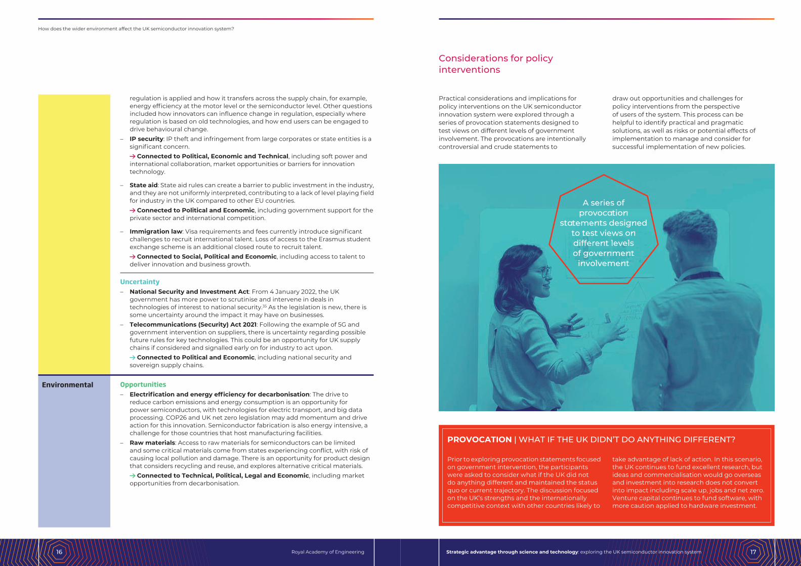
Practical considerations and implications for policy interventions on the UK semiconductor innovation system were explored through a series of provocation statements designed to test views on different levels of government involvement. The provocations are intentionally controversial and crude statements to
Prior to exploring provocation statements focused on government intervention, the participants were asked to consider what if the UK did not do anything different and maintained the status quo or current trajectory. The discussion focused on the UK’s strengths and the internationally competitive context with other countries likely to
PROVOCATION | WHAT IF THE UK DIDN’T DO ANYTHING DIFFERENT?
take advantage of lack of action. In this scenario, the UK continues to fund excellent research, but ideas and commercialisation would go overseas and investment into research does not convert into impact including scale up, jobs and net zero. Venture capital continues to fund software, with more caution applied to hardware investment.
draw out opportunities and challenges for policy interventions from the perspective of users of the system. This process can be helpful to identify practical and pragmatic solutions, as well as risks or potential effects of implementation to manage and consider for successful implementation of new policies.
regulation is applied and how it transfers across the supply chain, for example, energy efficiency at the motor level or the semiconductor level. Other questions included how innovators can influence change in regulation, especially where regulation is based on old technologies, and how end users can be engaged to drive behavioural change.
– IP security: IP theft and infringement from large corporates or state entities is a significant concern.
Connected to Political, Economic and Technical, including soft power and international collaboration, market opportunities or barriers for innovation technology.
– State aid: State aid rules can create a barrier to public investment in the industry, and they are not uniformly interpreted, contributing to a lack of level playing field for industry in the UK compared to other EU countries.
Connected to Political and Economic, including government support for the private sector and international competition.
– Immigration law: Visa requirements and fees currently introduce significant challenges to recruit international talent. Loss of access to the Erasmus student exchange scheme is an additional closed route to recruit talent.
Connected to Social, Political and Economic, including access to talent to deliver innovation and business growth.
Uncertainty– National Security and Investment Act: From 4 January 2022, the UK
government has more power to scrutinise and intervene in deals in technologies of interest to national security.35 As the legislation is new, there is some uncertainty around the impact it may have on businesses.
– Telecommunications (Security) Act 2021: Following the example of 5G and government intervention on suppliers, there is uncertainty regarding possible future rules for key technologies. This could be an opportunity for UK supply chains if considered and signalled early on for industry to act upon.
Connected to Political and Economic, including national security and sovereign supply chains.
Opportunities– Electrification and energy efficiency for decarbonisation: The drive to
reduce carbon emissions and energy consumption is an opportunity for power semiconductors, with technologies for electric transport, and big data processing. COP26 and UK net zero legislation may add momentum and drive action for this innovation. Semiconductor fabrication is also energy intensive, a challenge for those countries that host manufacturing facilities.
– Raw materials: Access to raw materials for semiconductors can be limited and some critical materials come from states experiencing conflict, with risk of causing local pollution and damage. There is an opportunity for product design that considers recycling and reuse, and explores alternative critical materials.
Connected to Technical, Political, Legal and Economic, including market opportunities from decarbonisation.
Environmental
How does the wider environment affect the UK semiconductor innovation system?
A series of provocation
statements designed to test views on different levels of government
involvement
Strategic advantage through science and technology: exploring the UK semiconductor innovation systemRoyal Academy of Engineering18 19
Cost The cost to the taxpayer of a UK sovereign capability in semiconductors is likely to be very high, especially for silicon and noting that the scale of investment would vary for different semiconductors. Commercial opportunity is also potentially significant and would be aided by long-term investment, by attracting private match funding and by leading to opportunities for businesses with return on public investment including creating skilled employment in the UK. Another potential benefit would be driving down the cost for UK semiconductor companies to be internationally competitive.
Stability and critical mass Opportunities from a UK sovereign capability stem from the long-term stability that would be provided, creating critical mass with demand and market pull over a defined or long period of time, and giving confidence to businesses to invest and develop skills and innovation in the UK.
Perspectives from the private sector Visibility and control over the supply chain and protection over IP are key potential benefits of a UK sovereign capability. Depending on how sovereign capability would be created, assuming partnerships between private and public sectors, ownership of IP would need to be clear and could potentially be restrictive and challenging for business.
Considerations for successful implementation: – State-owned industries have a reputation
for lacking in agility, making them slow to react to market and technology changes, and ultimately contributing to the perception that non-commercial operations are lower quality. Successful implementation would have to ensure this risk is mitigated for and managed. Practical questions were raised with regards to the challenges of actually building a sovereign capability including attracting and retaining talent, reliable access to technologies and long supply chains. The long lead time in building up the expertise and capability may lead to missed opportunities in the interim and it would be challenging to serve all aspects
This already happens to some extent, for example the focus on quantum technology with a strategy and national centre. A more nuanced approach to government backing specific technologies or industries could improve the chances of success with policies that are clear, sustainable, and longer-term to provide market certainty.
Risk This type of government intervention was perceived as carrying a range of potential risks, including: – The risk of picking the ‘wrong’ winners and
losing a balance of innovation across different areas or areas being underfunded. These choices are challenging to make, including by skilled investors, and viewed as even more challenging for government with limited technical capabilities. Concerns were raised that political bias may influence decisions wrongly.
– The risk of losing out to competitor countries by not picking winners is important to consider and was compared to backing all the horses on the racetrack, still losing money.
– The risk to diversity and inclusion was highlighted, as without appropriate mechanisms support can be biased towards certain groups or ‘loudest voices’ while missing out on talent.
Potential benefits: – Government support for consciously chosen
markets or technologies could put critical mass behind a particular technology, build on existing investments and know-how, overall lowering the risk of investment for the private sector.
Considerations for successful implementation:– The DARPA model was suggested as a delivery
model that draws on visionary academics and engages industry. Money is central, raising the question of whether the UK would provide an equivalent amount of investment to DARPA.
– A broad consultation across the sector, including people from different backgrounds and career stages, would be valuable to inform decisions.
of semiconductors due to the diversity of materials and applications.
– A public-private partnership could be a model for successful implementation. Long-term planning and investment could create critical mass, support UK companies to invest and facilitate rapid prototyping and scale-up to leverage more impact and innovation from academia.
– The permeability at the interface between academia and industry has a crucial role to play in successful delivery of a sovereign capability – with talent and ideas moving across.
– The nature of the capability could be designed to meet UK needs with flexibility built in to evolve over time as UK needs change. It should also build on UK strengths, for example in the case of silicon, principally in design, or across the supply chain for compound semiconductors or post-CMOS emerging technologies.
Suggested ideas for a UK sovereign capability: – The UK could take on this idea of a UK ‘trusted’
fabrication facility to support development of semiconductor innovation whilst protecting innovative companies’ IP and supplying customers that want a secure supply chain without links to China. This idea is inspired by a US semiconductor fabrication facility that is positioning itself as the US ‘trusted’ fabrication facility, providing security and assurance. A golden share model for government involvement at board-level could ensure the trusted status.
– A potential collaboration with UK-based tool manufacturers.
– The Defence Advanced Research Projects Agency (DARPA) model was highlighted as a delivery model option, noting that a customer would need to be identified to provide pull-through.
– Technical expertise could be drawn upon to identify potential winners and develop a portfolio approach to manage risk. It does not necessarily have to sit within government, which might not hold the technical expertise necessary but could draw on wider groups and communities to advise on decision-making.
– Historical case studies from the UK and abroad can provide lessons learnt on similar decisions, including both successes and failures, Concorde being an example.
– Collaborations and networks should be built and used to enable fast decision-making, putting together the approach, strategy and the right people around the table to make decisions, including when to stop or change the approach to meet clear criteria for success.
Suggested idea for government-backed winners: – An opportunity would be to capture a future
market bottleneck that cannot be achieved without government support.
PROVOCATION | THE UK HAS SOVEREIGN CAPABILITY IN SEMICONDUCTORS PROVOCATION | THE UK GOVERNMENT PICKS WINNERS
Considerations for policy interventions Considerations for policy interventions
Strategic advantage through science and technology: exploring the UK semiconductor innovation systemRoyal Academy of Engineering20 21
Concluding remarks
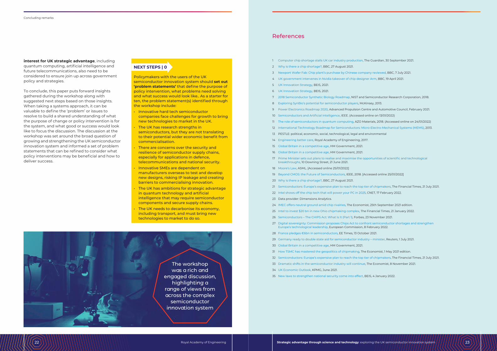
The workshop was a rich and engaged discussion, highlighting a range of views from across the complex semiconductor innovation system. Policy intervention is viewed as crucial to capitalise on commercial opportunities for the UK in an internationally competitive context, and to ensure security of supply and resilience of the wider economy amidst geopolitical uncertainty. With significant strategic investment in competitor countries, the UK will fall behind without government action and any delay increases that risk.
The benefits of a nuanced approach by segmenting semiconductors for policy intervention should be recognised by considering different policies to deliver commercial advantage in those areas of UK innovation strength, and to strengthen security of supply for silicon chips and other technologies for which it may be unrealistic to set up manufacturing in the UK. Semiconductors are a broad group of materials, with diverse needs across the innovation system.
Practical considerations for policy that were highlighted as part of the discussion included the value to businesses of certainty and confidence that government can provide by setting out long-term objectives or strategies, as well as finance and mechanisms enabling companies to conduct innovation activities and leverage additional investment. With the high level of global competition, flexibility and agility will be key to contribute to success. There is a wealth of expertise, both technical and in private investment, to leverage for effective decision making. Additional testing activities may be valuable to explore the opportunities and challenges for collaborations and access to infrastructures, that may be considered to address other user needs identified in this workshop.
Semiconductors make a good candidate for the Integrated Review ‘own – collaborate – access’ framework, defining the applications and supply chains to own for national security reasons or for commercial advantage, as well as areas for collaboration and access.
With regards to commercial advantage, opportunities for growth of the UK semiconductor industry should be examined, including taking down barriers for innovative SMEs to grow. The requirements from emerging technologies of
NEXT STEPS | 4
Policymakers should carry out user testing activities after segmenting the ‘semiconductors sector’ to identify opportunities and practical considerations for policy implementation, including by exploring additional provocation statements to those used in the workshop. For example, these may explore interventions for silicon, other materials such as compound semiconductors and emerging technologies such as 2D materials and post-CMOS. Suggestions for additional provocation statements include: • ‘The UK government supports and opens a
UK-based semiconductor innovation facility’ – to consider any specific need for R&D infrastructure, which users it would serve and technical considerations for a shared facility or suitability of use for multiple materials.
• ‘The UK government identifies and invests to own a key bottleneck in international supply chains’ – to consider the practicalities of identifying such a pinch point and what may be required or viewed as corresponding to ownership.
• ‘The UK government launches a no-cost semiconductor strategy’ – to consider non-financial interventions and direction-setting.
• ‘The UK has international partnerships for access to manufacturing prototyping facilities and supply chains’ – to consider the potential for collaboration or access.
Considerations for a new fund with the current finance landscape: – Access to finance for scale-up is a key barrier
in the semiconductor innovation system, and such a fund could fill the gap or barrier of finding a lead investor and de-risk investment for other investment funds.
– Such a fund needs to be at a sufficiently large scale for impact, but it is important to acknowledge that demand will always outstrip supply.
– A new fund should avoid unhealthy competition crowding out other venture capital funds and the private sector, and rather build collaborative relationships.
– Lessons should be learnt from existing funding bodies. For example, a benefit of Innovate UK funding is acting as a signal of quality to other investors; and one of the challenges is the amount of work and information necessary for grant proposals to get relatively small amounts of money. It was noted that funding bodies such as UKRI and Innovate UK effectively are monopoly suppliers, enabling them to ask for high level of input and information in applications.
– Existing government funding does not give the right to fail. Without allowing for failure, it is possible to miss the big wins too.
– An investment fund was suggested as a better balance of public and private direction and risk assessment compared to other suggested policy interventions.
– There are ongoing discussions to establish a venture capital-type fund for compound semiconductors. Government-matched investment would send a strong signal to investors and industry.
Potential benefits:– A government investment fund could create
momentum for further investment, signalling intent and crowding in private investment. It is an opportunity to help increase confidence for other investors.
– It is an opportunity to develop vertical supply chains.
Considerations for successful implementation:– Government ownership and stakes in
investments should not be overbearing and should include avenues for exit. Investment decisions must be commercial decisions.
– Implications of state aid rules and how they will apply to such a fund are key considerations to ensure it adds value.
– The role of government in the operation of the fund will need to be clearly defined and set up to ensure the fund is able to operate at pace and avoid excessive bureaucracy. The selection board for example will need to be well informed or have a mechanism to bring in technical and industry views into investment decisions. Government may consider placing money with existing UK funds, with an experienced team that can ensure shorter due diligence times.
– Consideration should be given to whether such a fund would be outcomes-based or goals-based and focus on UK needs. For example, the fund could have the purpose of creating a foundry, developing designs or another particular outcome. The level of funding would need to be appropriate to achieving the goal.
– Training and professional development for founders to run successful SMEs should be part of making the most of the opportunity to develop a thriving innovation ecosystem.
PROVOCATION | THE UK HAS A GOVERNMENT-BACKED SEMICONDUCTOR INVESTMENT FUND
Considerations for policy interventions
Strategic advantage through science and technology: exploring the UK semiconductor innovation systemRoyal Academy of Engineering22 23
References
1 Computer chip shortage stalls UK car industry production, The Guardian, 30 September 2021.
2 Why is there a chip shortage?, BBC, 27 August 2021.
3 Newport Wafer Fab: Chip plant’s purchase by Chinese company reviewed, BBC, 7 July 2021.
4 UK government intervenes in Nvidia takeover of chip designer Arm, BBC, 19 April 2021.
5 UK Innovation Strategy, BEIS, 2021.
6 UK Innovation Strategy, BEIS, 2021.
7 2018 Semiconductor Synthetic Biology Roadmap, NIST and Semiconductor Research Corporation, 2018.
8 Exploring SynBio’s potential for semiconductor players, McKinsey, 2013.
9 Power Electronics Roadmap 2020, Advanced Propulsion Centre and Automotive Council, February 2021.
10 Semiconductors and Artificial Intelligence, IEEE. (Accessed online on 13/01/2022)
11 The role of semiconductors in quantum computing, AZO Materials, 2018. (Accessed online on 24/01/2022)
12 International Technology Roadmap for Semiconductors: Micro-Electro-Mechanical Systems (MEMS), 2013.
13 PESTLE: political, economic, social, technological, legal and environmental
14 Engineering better care, Royal Academy of Engineering, 2017.
15 Global Britain in a competitive age, HM Government, 2021.
16 Global Britain in a competitive age, HM Government, 2021.
17 Prime Minister sets out plans to realise and maximise the opportunities of scientific and technological breakthroughs, 10 Downing Street, 21 June 2021.
18 Moore’s Law, ASML. [Accessed online 25/01/2022]
19 Beyond CMOS: the Future of Semiconductors, IEEE, 2018. [Accessed online 25/01/2022]
20 Why is there a chip shortage?, BBC, 27 August 2021.
21 Semiconductors: Europe’s expensive plan to reach the top tier of chipmakers, The Financial Times, 21 July 2021.
22 Intel shows off the chip tech that will power your PC in 2025, CNET, 17 February 2022.
23 Data provider: Dimensions Analytics.
24 IMEC offers neutral ground amid chip rivalries, The Economist, 25th September 2021 edition.
25 Intel to invest $20 bn in new Ohio chipmaking complex, The Financial Times, 21 January 2022.
26 Semiconductors – The CHIPS Act: What Is It (Part 1), Forbes, 23 November 2021.
27 Digital sovereignty: Commission proposes Chips Act to confront semiconductor shortages and strengthen Europe’s technological leadership, European Commission, 8 February 2022.
28 France pledges €6bn in semiconductors, EE Times, 13 October 2021.
29 Germany ready to double state aid for semiconductor industry – minister, Reuters, 1 July 2021.
30 Global Britain in a competitive age, HM Government, 2021.
31 How TSMC has mastered the geopolitics of chipmaking, The Economist, 1 May 2021 edition.
32 Semiconductors: Europe’s expensive plan to reach the top tier of chipmakers, The Financial Times, 21 July 2021.
33 Dramatic shifts in the semiconductor industry will continue, The Economist, 8 November 2021.
34 UK Economic Outlook, KPMG, June 2021.
35 New laws to strengthen national security come into effect, BEIS, 4 January 2022.
interest for UK strategic advantage, including quantum computing, artificial intelligence and future telecommunications, also need to be considered to ensure join up across government policy and strategies.
To conclude, this paper puts forward insights gathered during the workshop along with suggested next steps based on those insights. When taking a systems approach, it can be valuable to define the ‘problem’ or issues to resolve to build a shared understanding of what the purpose of change or policy intervention is for the system, and what good or success would look like to focus the discussion. The discussion at the workshop was set around the broad question of growing and strengthening the UK semiconductor innovation system and informed a set of problem statements that can be refined to consider what policy interventions may be beneficial and how to deliver success.
NEXT STEPS | 0
Policymakers with the users of the UK semiconductor innovation system should set out ‘problem statements’ that define the purpose of policy intervention, what problems need solving and what success would look like.. As a starter for ten, the problem statement(s) identified through the workshop include: • Innovative hard tech semiconductor
companies face challenges for growth to bring new technologies to market in the UK.
• The UK has research strengths in semiconductors, but they are not translating to their potential wider economic benefit from commercialisation.
• There are concerns over the security and resilience of semiconductor supply chains, especially for applications in defence, telecommunications and national security.
• Innovative SMEs are dependent on manufacturers overseas to test and develop new designs, risking IP leakage and creating barriers to commercialising innovation.
• The UK has ambitions for strategic advantage in quantum technology and artificial intelligence that may require semiconductor components and secure supply chains.
• The UK needs to decarbonise its economy, including transport, and must bring new technologies to market to do so.
Concluding remarks
Strategic advantage through science and technology: exploring the UK semiconductor innovation system 23
The workshop was a rich and
engaged discussion, highlighting a
range of views from across the complex
semiconductor innovation system
The Royal Academy of Engineering is harnessing the power of engineering to build a sustainable society and an inclusive economy that works for everyone.
In collaboration with our Fellows and partners, we’re growing talent and developing skills for the future, driving innovation and building global partnerships, and influencing policy and engaging the public.
Together we’re working to tackle the greatest challenges of our age.
What we do
TALENT & DIVERSITY
We’re growing talent by training, supporting, mentoring and funding the most talented and creative researchers, innovators and leaders from across the engineering profession.
We’re developing skills for the future by identifying the challenges of an ever-changing world and developing the skills and approaches we need to build a resilient and diverse engineering profession.
INNOVATION
We’re driving innovation by investing in some of the country’s most creative and exciting engineering ideas and businesses.
We’re building global partnerships that bring the world’s best engineers from industry, entrepreneurship and academia together to collaborate on creative innovations that address the greatest global challenges of our age.
POLICY & ENGAGEMENT
We’re influencing policy through the National Engineering Policy Centre – providing independent expert support to policymakers on issues of importance.
We’re engaging the public by opening their eyes to the wonders of engineering and inspiring young people to become the next generation of engineers.
Royal Academy of EngineeringPrince Philip House | 3 Carlton House Terrace | London SW1Y 5DGTel 020 7766 0600www.raeng.org.uk @RAEngNews
Registered charity number 293074