Embed Size (px)
Citation preview

Diamond and Related Materials 12(2003) 2186–2194
0925-9635/03/$ - see front matter� 2003 Elsevier B.V. All rights reserved.doi:10.1016/j.diamond.2003.08.001
Structural features of diamond layers photo-emitting at sub-band gapenergies
S. Orlanducci , V. Sessa , M.L. Terranova *, F. Tazzioli , C. Vicario , I. Boscolo , S. Cialdi ,a,f a,f a,f, b,f b,e,f c,f c,f
L. Catani , M. Rossid,f e,g
Dipartimento di Scienze e Tecnologie Chimiche, Universita di Roma ‘Tor Vergata’, Via della Ricerca Scientifica, Roma 00133, Italya `LNF, Frascati, Roma, Italyb
Dipartimento di Fisica dell’Universita di Milano, via Celoria 16, Milano 20133, Italyc `Dipartimento di Fisica, Universita di Roma ‘Tor Vergata’, Via della Ricerca Scientifica, Roma 00133, Italyd `
Dipartimento di Energetica, Universita di Roma ‘La Sapienza’, Via A. Scarpa 16, Roma 00161, Italye `INFN (National Institute of Nuclear Physics), Italyf
INFM (National Institute for the Physics of Matter), Italyg
Received 23 November 2002; received in revised form 2 August 2003; accepted 4 August 2003
Abstract
The photoemission behaviour of a series of diamond-based polycrystalline films irradiated by the second(2.3 eV), third (3.5eV) and fourth(4.7 eV) harmonics produced by a Q-switched-mode-locked Nd: Yag laser has been investigated and related tothe structural and compositional characteristics of the layers. The materials were polycrystalline undoped diamond films as wellas Nd- and N-containing diamond films grown by CVD techniques, diamond-like and amorphous carbon layers. The morphologicaland structural characteristics of the films were investigated by electron microscopy, Raman spectroscopy and electron diffraction.The analysis of the photoemission curves does not evidence any improvement of the emission efficiency in the case of Nd-containing films nor for the diamond films grown in the presence of N The results evidence conversely a strong correlation2.
between the characteristics of the photoemission process at sub-band gap energies and the presence of amorphous sp -C patches2
located at the diamond film surfaces. The photoemitting properties of our samples are discussed and rationalized by consideringcharge emission occurring at the sp -diamond-vacuum border and the emission process governed by the ratio of amorphous sp -2 2
C to crystalline sp -C. The rather high values of quantum efficiency measured in the course of the present research at 3.5 and3
4.7 eV suggest that a proper distribution of amorphous carbon onto a good quality diamond surface is the key factor for thepreparation of efficient and stable photocathode materials.� 2003 Elsevier B.V. All rights reserved.
Keywords: Diamond layers; Photoemission; Photocathodes
1. Introduction
Wide-ranging researches have been recently addressedat producing and testing materials for photocathodes andcold cathodes assuring good emission as well as func-tionality and reliability. In this context CVD diamond,with and without the presence of foreign atoms such asB, Nd or N , is considered interesting as a photoemitting2
materialw1–7x characterized at the same time by chem-ical inertness and high radiation damage threshold.
*Corresponding author. Tel.:q39-0672594416; fax: q39-0672594378.
E-mail address: [email protected](M.L. Terranova).
Preliminary experiments performed in our laboratoriesat 3.5 eV evidenced a good sub-band gap photoemissionof diamond filmsw7x, and stimulated further studies onthe emission characteristics of carbon layers with differ-ent structures and compositions. It was therefore feltworthwhile to investigate the photoemission behaviourof polycrystalline undoped diamond films, Nd- and N-containing diamond films, as well as diamond-like(DL)and amorphous C layers irradiated with the second(2.3eV), third (3.5 eV) and fourth (4.7 eV) harmonicsprovided by a Q-switched-mode-locked Nd: Yag laser.This type of laser is largely used for driving photocath-odes, due to the capability to operate confidently up to

2187S. Orlanducci et al. / Diamond and Related Materials 12 (2003) 2186–2194
the fourth harmonics and to provide very powerfulpulses with few picoseconds duration.
For diamond, the energy gap between valence andconduction band is quoted 5.5 eV for an indirecttransition(i.e. a three-body photon–phonon–atom inter-action) and 7 eV for a direct transitionw8,9x. Thesurface hydrogenation was experimentally found to low-er the vacuum level, even allowing negative affinityw8x.However, the 4.7 eV photon energy is not sufficient toexcite an electron over the gap of the bulk. Therefore,surface band structures, different from the bulk one, arerequired to explain the experimental phenomenon ofone-photon emission. The radiation of 4.7 eV is, there-fore, interesting for investigating such transition.
The choice of introducing Nd and N inside diamond2
was made on the basis of the following considerations.The N-doping was thought to be effective in improvingthe emission properties, due to the introduction of alevel at 1.7 eV below the CBM(conduction bandminimum) of diamond w5x. The 2.3 eV radiation issuitable for extracting electrons from this level. Theinsertion of N could also contribute to multi-photon2
excitation from the valence band by creating additionalreal intermediate states in the gap. Incidentally, a dopeddiamond photocathode operating at the green light(2.3eV) would be considered a breakthrough in this matter.
By inserting Nd, the diamond-based material becomesconductive and an acceptor level is introduced at 0.1eV above the valence band maximum(VBM) w10x. Inthis case, an enhancement of the emission efficiencydue to a downward band bending at the surface couldbe expected, as it happens with Boron doping. There is,however, also an adverse effect that we have illustratedin a previous articlew7x.
The three harmonics of the laser are together a suitabletool for investigating the sub band gap behaviour of thematerial and have the advantage of allowing the studyof multi-photon processes.The photoemitting behaviourof the above cited materials have been correlated to themorphological-structural characteristics investigated bymeans of SEM(scanning electron microscopy), Ramanspectroscopy and RHEED(reflection high energy elec-tron diffraction), in order to identify the carbon-basedstructures characterized by the best emissionperformances.
2. Experimental
The diamond films have been generated by means ofa hot filament CVD reactor coupled to a powder-flowingapparatus. A scheme and a detailed description of theapparatus have been published in Ref.w11x. The poly-crystalline diamond layers are generated by activationof CH yH mixtures. The Nd-containing layers were4 2
obtained by using a system of carrier fluxes able todeliver at controlled rates Nd(III )-acetylacetonate(in
powder form, Sigma-Aldrich Inc.) to the growing dia-mond phase. The carrier gas was Ar, but for theproduction of N-doped layers, Ar was substituted byN The general operating conditions were: deposition2.
temperature: 650"5 8C; total pressure: 36 Torr; activegas phase composition: 1% CH in H ; flow rate of the4 2
CH yH mixture: 200 sccm; flow rate of the carrier4 2
streams: 50 sccm. The thickness of the layers wasapproximately 2mm.
The DL layers were obtained by pulsed laser ablationof glassy carbon targets, using a XeCl laser with fluence10 J cm per pulse(pulse duration 30 ns, repetition3 y2
rate 5 Hz) w12x. The amorphous C layers were producedby e-beam irradiation of hydrocarbons(Es1 keV, Is10 mA, Ps1.3=10 Pa), following an alreadyy2
described procedurew13x. All the films were depositedon a-Ti substrates.
The RHEED analyses were performed using an AEIEM6G microscope equipped with a high-resolution dif-fraction stage(acceleration voltage: 60 kV).
The Raman spectra were obtained at room temperaturein the backscattering configuration using an Ar-ion laserbeam(514 nm, laser output power 130 mW). The spotsize on the samples was approximately 1 mm .2
The photoemission experiments at 2.3, 3.5 and 4.7eV photon energies have been performed using a Q-switched-mode-locked Nd:YAG laser which delivers;25 ps pulses with maximum energy;100 mJ atls266 nm,;300 mJ at ls355 nm and;3 mJ atls532 nm. The laser beam illuminated a sample area ofapproximately 2 mm at 08 incidence angle. A Faraday2
cup anode at ground potential collected the emittedcharge. The cathode was held at a negative DC voltageranging up to 6 kV at a distance of 3 mm from theanode. The accelerating field could, therefore, reach 2MV ym. A scheme of the apparatus can be found in Ref.w7x.
3. Results and discussion
The results of the photoemission experiments havebeen interpreted in the framework of the Fowler–DuBridge–Betchel theoryw14–16x. Following this the-ory, the relationship between emitted chargeQ andn
incident radiation energyJ is a power law of the form:Q AJ , where the exponentn indicates the order of then
n
photoemission process, i.e. the numbern of photonsabsorbed for one electron emission. In the conditions ofour experiments the exponentn is obtained from apower-law fitting of the experimental data. The quantumefficiency (QE) is given by the ratio of the number ofemitted electrons to the number of incoming photons.
The experiments performed by using the 2.3 eV laserbeam did not evidence substantial differences in thephotoemission behaviour of the various diamond-basedmaterials. The emission measurements from undoped

2188 S. Orlanducci et al. / Diamond and Related Materials 12 (2003) 2186–2194
Fig. 1. (a) Emission curve at 4.7 eV for a typical undoped polycrys-talline diamond film.(b) Raman spectrum(c) RHEED pattern.
Fig. 2. (a) Emission curve at 4.7 eV for a Nd-containing polycrys-talline diamond film.(b) Raman spectrum(c) RHEED pattern.
diamond, Nd- and N-containing diamond layers indicat-ed in all cases a QE of approximately 10 pCymJy6 3
(i.e. 1 pC per 100mJ which is 2.3=10 electrons pery8
photon) and the experimentalQ vs. J curves obtainedfrom the various samples suggested mostly a three-photon regime.
The results of previous studies on photoemission fromundoped and Nd-containing diamond films illuminatedby 3.5 eV radiation showed a very similar behaviourfor both the materials, with QE in the range 10 pCyy2
mJ (i.e. 1 pC per 10mJ which is 3.5=10 electrons2 y7
per photon) w7x. Here we want to stress that the curvesof emitted charge vs. light intensity were characterizedby an exponent lower than two for most of the samples.This is indicative of an emission following both theone- and two-power photoemission law
In the case of the emission experiments performedwith 4.7 eV photons, for the various diamond-based

2189S. Orlanducci et al. / Diamond and Related Materials 12 (2003) 2186–2194
Fig. 3. SIMS depth profile of a Nd-containing diamond film grown in the presence of N .2
polycrystalline materials the measured values of thepower dependence were between 1 and 2, indicating aone-photon, two-photon or hybrid oneytwo-photon pro-cess regimes.
In Fig. 1a is reported the emission curve at 4.7 eVUV light from a good-emitting undoped diamond film,along with the Raman spectrum(Fig. 1b) and theRHEED pattern(Fig. 1c) of the same sample. The linearslope of the emitted charge vs. photon flux shows aone-photon process, with quantum efficiency of5=10 .y6
The Raman spectrum(Fig. 1b) shows the peak ofdiamond at 1332 cm and a broad signal at approxi-y1
mately 1480 cm attributed to non-diamond carbon.y1
The crystalline quality of the diamond lattice is betterevidenced by the curve fitting to a Lorentzian line. Theanalysis of the diffraction rings shown in Fig. 1c revealsthe presence of only one homogeneous set belonging tothe diamond crystal lattice(space group Fd3 m). TheRHEED pattern indicates a randomly oriented goodquality polycrystalline diamond.
Fig. 2 reports the emission curve(a), the Ramanspectrum(b) and the RHEED pattern(c) of a typicalNd-containing diamond film grown using Ar as carriergas.
In this case, the emission turns out to be a two-photonprocess characterized by a rather high efficiency(QEs10 pCymJ ).y2 2
As one can observe, the general features of the Ramanspectra(Fig. 2b) taken from Nd-containing diamondfilms are similar to those taken from the undopeddiamond, whereas differences are detected in theRHEED pattern. In Fig. 2c two sets of diffraction ringsare observed, one of them produced by a good quality
diamond with polycrystalline texture. The signals pro-duced by the other phase are characterized by a slightbroadening of the Debye rings and suggest the presenceof nanosized structures with estimated dimensionsbetween 20 and 50 nm. These features are ascribed toNd clusters embedded into the diamond matrix.
The presence of Nd inside the diamond phase hasbeen confirmed by the SIMS analysis performed withO ions of 6 keV. The spectrum obtained at a depth ofq
2
approximately 0.9mm, evidences some positive Nd-related ions(Nd , NdO ). The SIMS depth profileq q
reported in Fig. 3 indicates a rather homogeneouspresence of Nd throughout the film.
In Fig. 4 is reported the emission curve(a) and thestructural characteristics(b, c) of the best-emitting Nd-containing diamond film grown, under the same exper-imental conditions, using N as carrier gas. TheQ vs. J2
curve shows that the emission is slightly lowered withrespect to the samples grown without N . It is to be2
noted, however, that in most cases the diamond layersgrown in the presence of N were characterized by a2
relevant reduction of the emission, up to a factor two.As one can see, the general features of the Raman
spectrum shown in Fig. 4b are very different from thoseof Fig. 1c and Fig. 2c. The decomposition of theexperimental spectrum into five Lorentzian curvesallows to evidence a remarkable reduction of the signalat approximately 1332 cm , corresponding to the dia-y1
mond phase. Moreover, two groups of frequencies arerecorded in the 1000–1800 cm region, namely they1
two bands at approximately 1350 and 1550 cmy1
ascribed to amorphous sp -Cw17x, and two other bands2
at approximately 1160 and 1480 cm likely producedy1
by a tetrahedral amorphous carbonw18,19x. Overall, the

2190 S. Orlanducci et al. / Diamond and Related Materials 12 (2003) 2186–2194
Fig. 4. (a) Emission curve at 4.7 eV for a Nd-containing diamondfilm grown in the presence of N(b) Raman spectrum(c) RHEED2
pattern.
Nd-diamond films grown by using N flows are char-2
acterized by a decrease of the diamond phase and anincrease of the amorphous sp -C and sp -C phases. The3 2
Raman indications about a relevant lowering of crystal-linity are in agreement with the structural featuresrevealed by RHEED(Fig. 4c), where the vanishing
Debye rings are indicative of a heavily disturbed dia-mond lattice.
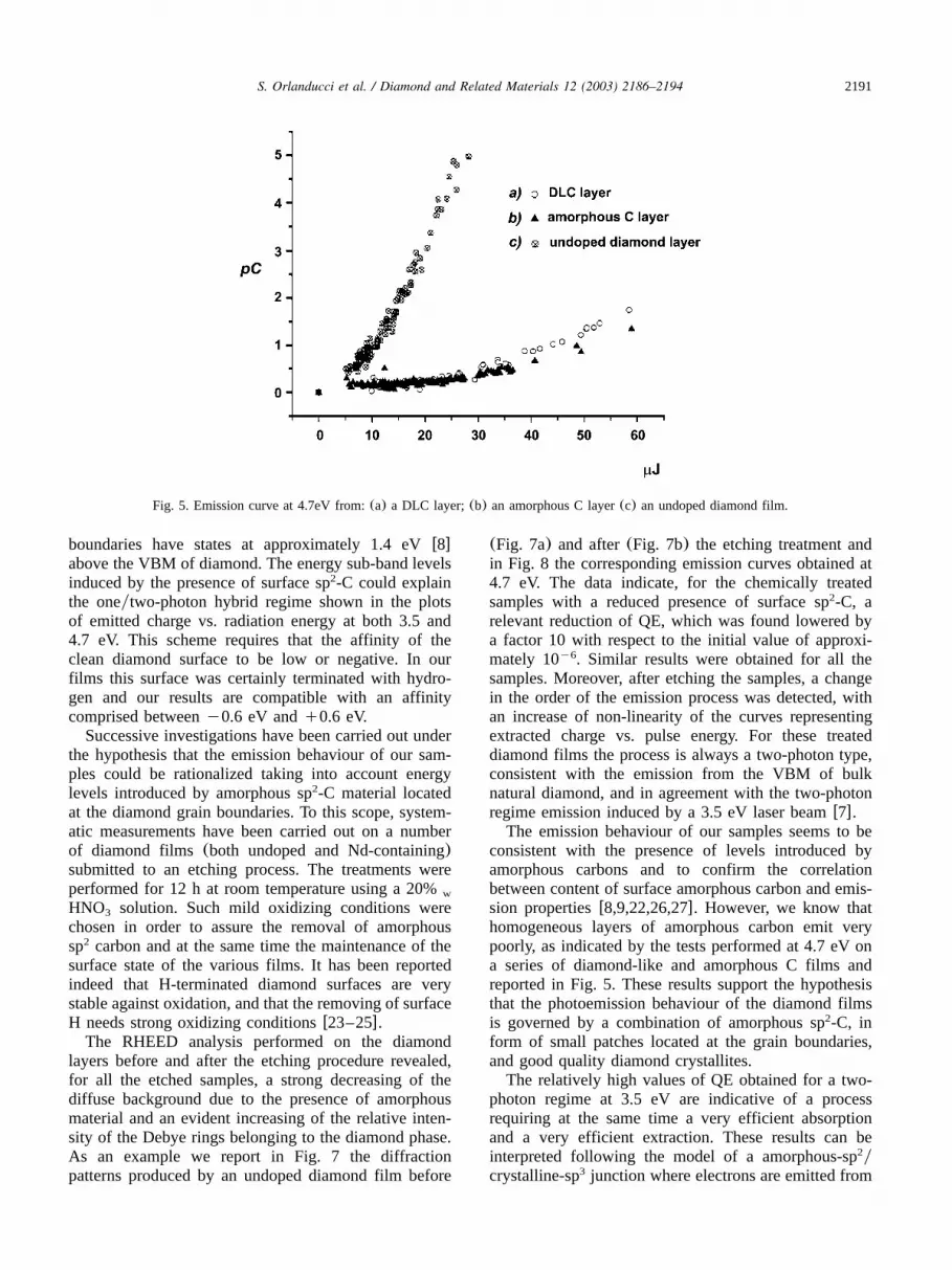
Photoelectron emission has also been investigatedfrom carbon layers with different structures. We reportin Fig. 5 the emission curves at 4.7 eV from a DL andan amorphous carbon layer characterized by the highestquantum yields. For both these materials, the QE are atleast one order of magnitude lower than for the diamondsamples and from the exponent n it can be deduced thatthe photoemission process involves two photons.
It is to be noted that neither the Nd-containingdiamond films nor those grown in the presence of N2
did show the expected increasing of emission efficiency.The energy level introduced by Nd is too close to thebottom of the gap to contribute to two-photon absorp-tion. We have already discussed other possible effectsof Nd on QE in a previous articlew7x
The substantial common behaviour of undoped andNd-containing layers illuminated with 2.3, 3.5 and 4.7eV photons could indicate that the effect of Nd ismasked by the stronger action of amorphous phases.
As regarding the samples grown in the presence ofN , this impurity was supposed to introduce an inter-2,
mediate band of levels in the gap, approximately 1.7 eVbelow the conduction band, eventually allowing thedirect extraction at 2.3 eV. No improvement of theemission has been observed in the experiments per-formed at 2.3 and 3.5 eV, whereas at 4.7 eV, the QEresulted in most cases worsened by a factor up to two.The 4.7 eV case will be discussed later. In the 2.3 eVcase, the absence of linearity in the emission curvesindicates that there is no direct extraction from thequoted intermediate level. This result could indicate thatthe doping with N was unsuccessful. The SIMS spec-2
trum reported in Fig. 3 does not, indeed, show signalsproduced by N It is reasonable to admit, therefore, that2.
under our experimental conditions only scarce amountsof N , below the detection limit of the SIMS technique,2
are introduced inside the diamond layers.Moreover, it must be considered that even a low-level
incorporation of N in the diamond films results in the2
degradation of the crystalline quality of the deposits.This effect, already reported in the literaturew20,21x,has been observed also in the course of the presentexperiments. The SEM pictures reported in Fig. 6 showthe different morphologies of the Nd-containing sampleof Fig. 2 and of the Nd-containing film grown in N2atmosphere of Fig. 4, and evidence the less definedcrystallographic features of this last material.
Conversely, a positive effect on the photoemissionperformances was found related to the presence ofamorphous carbon phases. The strict correlation foundout between the one-photon emission regime and thepresence of sp -C patches at the diamond film surface2
complies with the non-homogeneous emission modelproposed by Cui et al.w22x. The sp carbons at the grain2
2191S. Orlanducci et al. / Diamond and Related Materials 12 (2003) 2186–2194
Fig. 5. Emission curve at 4.7eV from:(a) a DLC layer;(b) an amorphous C layer(c) an undoped diamond film.
boundaries have states at approximately 1.4 eVw8xabove the VBM of diamond. The energy sub-band levelsinduced by the presence of surface sp -C could explain2
the oneytwo-photon hybrid regime shown in the plotsof emitted charge vs. radiation energy at both 3.5 and4.7 eV. This scheme requires that the affinity of theclean diamond surface to be low or negative. In ourfilms this surface was certainly terminated with hydro-gen and our results are compatible with an affinitycomprised betweeny0.6 eV andq0.6 eV.
Successive investigations have been carried out underthe hypothesis that the emission behaviour of our sam-ples could be rationalized taking into account energylevels introduced by amorphous sp -C material located2
at the diamond grain boundaries. To this scope, system-atic measurements have been carried out on a numberof diamond films (both undoped and Nd-containing)submitted to an etching process. The treatments wereperformed for 12 h at room temperature using a 20%w
HNO solution. Such mild oxidizing conditions were3
chosen in order to assure the removal of amorphoussp carbon and at the same time the maintenance of the2
surface state of the various films. It has been reportedindeed that H-terminated diamond surfaces are verystable against oxidation, and that the removing of surfaceH needs strong oxidizing conditionsw23–25x.
The RHEED analysis performed on the diamondlayers before and after the etching procedure revealed,for all the etched samples, a strong decreasing of thediffuse background due to the presence of amorphousmaterial and an evident increasing of the relative inten-sity of the Debye rings belonging to the diamond phase.As an example we report in Fig. 7 the diffractionpatterns produced by an undoped diamond film before
(Fig. 7a) and after(Fig. 7b) the etching treatment andin Fig. 8 the corresponding emission curves obtained at4.7 eV. The data indicate, for the chemically treatedsamples with a reduced presence of surface sp -C, a2
relevant reduction of QE, which was found lowered bya factor 10 with respect to the initial value of approxi-mately 10 . Similar results were obtained for all they6
samples. Moreover, after etching the samples, a changein the order of the emission process was detected, withan increase of non-linearity of the curves representingextracted charge vs. pulse energy. For these treateddiamond films the process is always a two-photon type,consistent with the emission from the VBM of bulknatural diamond, and in agreement with the two-photonregime emission induced by a 3.5 eV laser beamw7x.
The emission behaviour of our samples seems to beconsistent with the presence of levels introduced byamorphous carbons and to confirm the correlationbetween content of surface amorphous carbon and emis-sion propertiesw8,9,22,26,27x. However, we know thathomogeneous layers of amorphous carbon emit verypoorly, as indicated by the tests performed at 4.7 eV ona series of diamond-like and amorphous C films andreported in Fig. 5. These results support the hypothesisthat the photoemission behaviour of the diamond filmsis governed by a combination of amorphous sp -C, in2
form of small patches located at the grain boundaries,and good quality diamond crystallites.
The relatively high values of QE obtained for a two-photon regime at 3.5 eV are indicative of a processrequiring at the same time a very efficient absorptionand a very efficient extraction. These results can beinterpreted following the model of a amorphous-spy2
crystalline-sp junction where electrons are emitted from3

2192 S. Orlanducci et al. / Diamond and Related Materials 12 (2003) 2186–2194
Fig. 6. SEM pictures of:(a) a Nd-containing diamond film(the sameof Fig. 2); (b) a Nd-containing diamond film grown in the presenceof N (the same of Fig. 4).2
Fig. 7. RHEED patterns of a diamond film before(a) and after(b)the etching process.
the sp -diamond-vacuum borders and drifted over the2
diamond surface. Following this model the amorphoussp phases would assure a high absorption, and the2
electric field at the amorphous-spycrystalline-sp junc-2 3
tion would provide an efficient extraction.The features of photoemission from diamond films at
2.3, 3.5 and 4.7 eV is explained on the basis of theband diagram of the amorphous sp carbon, which2
presents a gap of approximately 2 eV between conduc-tion and valence band. An electron inside the amorphoussp patch firstly jumps across the gap and subsequently2
moves out of the junction towards the diamond grainsurface. The hybrid one-two-photon regime could bedue to the variability of the affinity over the grainsurface.
4. Conclusions
The main results of the present research, focused onthe relationship between microstructure of CVD growndiamond-based layers and photoemission behaviour atsub-band gap energies, can be briefly summarized asfollows:
i. The insertion of Nd did not modify substantially theemission behaviour of the Nd-diamond films, whichdo not show the conjectured improvement of theemission efficiency;
ii. For the diamond films grown in the presence of N2
no striking differences were detected at 2.3 and 3.5eV with respect to the samples grown without N . At2
4.7 eV a worsening of the emission performanceswas observed, with a strong reduction of the quantumyield. The presence of N during the deposition2

2193S. Orlanducci et al. / Diamond and Related Materials 12 (2003) 2186–2194
Fig. 8. Emission curves at 4.7 eV from a diamond sample before(a) and after(b) the etching process.
process was found to degrade the structural order ofthe diamond phase.
iii.The emission experiments performed on a series ofas grown and etched diamond-based films evidenceda correlation between emission behaviour and pres-ence of an amorphous sp -C phase.2
iv. The current investigation supports the hypothesis thatthe photoemission process is mainly controlled by thepresence of surface amorphous sp -C patches located2
at the grain boundaries of the polycrystalline diamondfilms. The results of the photoemission experimentsperformed at 2.3, 3.5 and 4.7 eV have been analysedtaking into account the surface levels associated withthe presence of small deposits of amorphous sp -C2
and considering charge emission occurring at the sp -2
diamond-vacuum border, in the framework of an non-homogeneous emission modelw22x. In this context,both the ratio of amorphous sp -C to diamond-C and2
the crystalline quality of the diamond phase arecritical factors, which can affect the emission effi-ciency. A high absorption can be assured by acontrolled distribution of the sp amorphous phase at2
the film surface, but a good structural order of thediamond phase is needed for promoting the extractionefficiency. The effect of crystalline quality of diamondon the overall emission efficiency has been clearlyevidenced in the case of the samples grown in thepresence of N , where less ordered crystalline struc-2
tures were found in general, to emit poorly.v. We produced diamond-based layers operating at one-
photon regime, with a quantum efficiency, at sub-band 4.7 eV photon energy, up to 5=10 ,y6
comparable to that of metals. As an example Cu,
commonly used as RF gun photocathodes, has a QEbetween 2.2=10 and 1.4=10 depending ony6 y4
surface cleaning and laser activationw28x. It is to benoted that our data have been obtained at the ratherlow field of 10 kVycm. The produced films are stableand their emission efficiency does not degrade underprolonged laser irradiation.
Considering the promising applications as robust andefficient UV photoemission source envisaged for thesediamond-based layers, further investigations are plannedin order to define the optimal relationship betweensurface amorphous carbon and diamond structure ableto maximise the QE at the three wavelengths and toobtain a linear photoelectron effect at 4.7 eV.
Acknowledgments
The research work has been partially supported byCAERES -INFN Project. The collaboration of Dr M.Fabrizio for the SIMS analysis is gratefullyacknowledged.
References
w1x F.J. Himpsel, J.K. Knapp, J.A. van Vechten, D.E. Eastman,Phys. Rev. 20(1979) 624.
w2x J. Fisher, T. Srinivasan-Rao, T. Tsang, G. Brandes, Nucl.Instrum. Meth. A 340(1994) 190.
w3x K. Okano, S. Koizumi, S. Ravi, P. Silva, G.A.J. Amaratunga,Nature 381(1996) 140.
w4x P. Muggli, R. Brogle, S. Jou, H.J. Doerr, R.F. Bushah, C. Joshi,IEEE Trans. Plasma Sci. 24(1996) 428.
w5x L. Diederich, O.M. Kuttel, P. Ruffieux, Th. Pillo, P. Aebi, L.¨Schlapbach, Surf. Sci. 417(1998) 41.

2194 S. Orlanducci et al. / Diamond and Related Materials 12 (2003) 2186–2194
w6x A. Breskin, T. Boutboul, A. Buzulutskov, R. Chechik, G. Garty,E. Shefer, et al., Nucl. Instrum Meth. A 442(2000) 58.
w7x I. Boscolo, S. Cialdi, G. Benedek, F. Tazzioli, M.L. Terranova,E. Rembeza, et al., Opt. Comm. 187(2001) 179.
w8x J. Robertson, M.J. Rutter, Diamond Relat. Mater. 7(1998)620.
w9x J. Robertson, Mater. Res. Soc. Symp. Proc. 621(2000) R1.1.1.w10x M.L. Terranova, V. Sessa, S. Piccirillo, M. Rossi, G. Micocci,
A. Serra, et al., Appl. Phys. Lett. 75(1999) 379.w11x M.L. Terranova, S. Piccirillo, V. Sessa, M. Rossi, G. Cappuccio,
Adv. Mater. 5(1999) 101.w12x M. Rossi, G. Gabrielli, T. Papa, S. Piccirillo, V. Sessa, M.L.
Terranova, et al., Surf. Coat. Technol. 139(2001) 87.w13x M.L. Terranova, M. Rossi, V. Sessa, G. Vitali, Phys. Status
Solidi 154(1996) 127.w14x R.H. Fowler, Phys. Rev. 38(1931) 45.w15x L.A. Du Bridge, Phys. Rev. 43(1933) 727.w16x J.H. Bechtel, J. Appl. Phys. 46(1975) 1585.w17x A.C. Ferrari, J. Robertson, Phys. Rev. B 61(2000) 14 095.
w18x B. Marcus, L. Fayette, M. Mermoux, L. Abello, G. Lucazeaua,J. Appl. Phys. 76(1994) 3463.
w19x Q. Zhang, S.F. Yoon, J. Ahn, Rusli, Y.P. Guo, A.T.S. Wee, etal., Diamond Relat. Mater. 8(1999) 215.
w20x A. Afzal, C.A. Rego, W. Ahmed, R.I. Cherry, Diamond Relat.Mater. (1998) 1033.
w21x Q. Zhang, S.F. Yoon, J. Ahn, Rusly, Y.P. Guo, Microelectr. J.29 (1998) 875.
w22x J.B. Cui, J. Ristein, L. Ley, Phys. Rev. B 60(1999) 16 135.w23x K.V. Kvaskov, V.V. Gorbachaev, Sov. Phys. Semicond. 22
(1988) 314.w24x P.K. Baumann, R.J. Nemanich, J. Appl. Phys. 83(1998) 2072.w25x A. Laikhtman, A. Hoffman, R. Kalish, Y. Avigal, A. Breskin,
R. Chechik, et al., Appl. Phys. Lett 73(1998) 1433.w26x A.V. Karabutov, V.D. Frolov, V.I. Konov, Diamond Relat.
Mater. 10(2001) 840.w27x Z. Sun, J.S. Chen, Y.J. Li, B.K. Tay, S.P. Lau, G.Y. Chen,
Appl. Surf. Sci. 173(2001) 282.w28x C. Travier, Nucl. Instrum Meth. A 340(1994) 35.