Embed Size (px)
Citation preview
arX
iv:0
805.
2666
v2 [
cond
-mat
.oth
er]
20
Nov
200
8
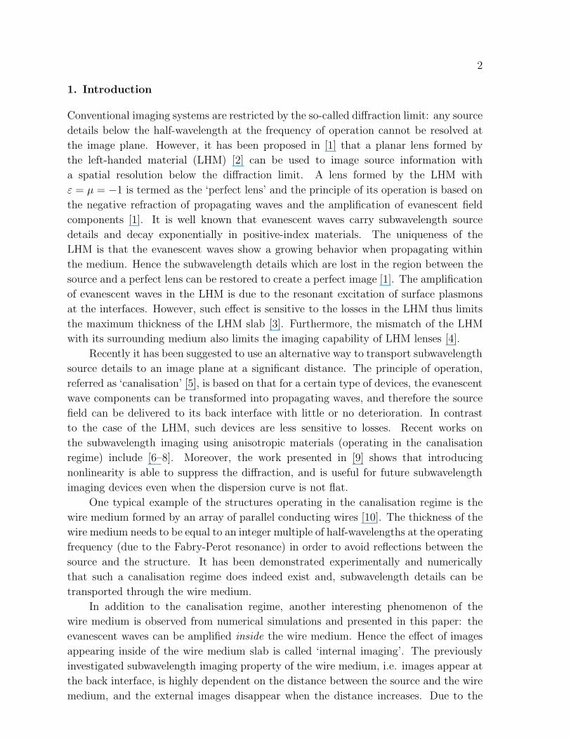
Subwavelength internal imaging by means of the
wire medium
Yan Zhao, Pavel Belov and Yang Hao
School of Electronic Engineering and Computer Science, Queen Mary, University of
London, Mile End Road, London, E1 4NS, United Kingdom
E-mail: [email protected]
Abstract. The phenomenon of evanescent wave amplification inside of a half-
wavelength-thick wire medium slab is studied numerically and used for subwavelength
imaging of objects at significant distances from the lens in this paper. The wire
medium is analyzed using both a spatially dispersive finite-difference time-domain
(FDTD) method employing the effective medium theory and a full-wave commercial
electromagnetic simulator CST Microwave StudioTM modelling the physical structure.
It is demonstrated that subwavelength details of a source placed at a distance of
λ/10 from a wire medium slab can be detected inside the slab with a resolution of
approximately λ/10 in spite of the fact that they cannot be resolved at the front
interface of the device, due to the rapid decay of evanescent spatial harmonics in free
space. The influence of different distances between the source and the wire medium
on the internal imaging property is also addressed.
2
1. Introduction
Conventional imaging systems are restricted by the so-called diffraction limit: any source
details below the half-wavelength at the frequency of operation cannot be resolved at
the image plane. However, it has been proposed in [1] that a planar lens formed by
the left-handed material (LHM) [2] can be used to image source information with
a spatial resolution below the diffraction limit. A lens formed by the LHM with
ε = µ = −1 is termed as the ‘perfect lens’ and the principle of its operation is based on
the negative refraction of propagating waves and the amplification of evanescent field
components [1]. It is well known that evanescent waves carry subwavelength source
details and decay exponentially in positive-index materials. The uniqueness of the
LHM is that the evanescent waves show a growing behavior when propagating within
the medium. Hence the subwavelength details which are lost in the region between the
source and a perfect lens can be restored to create a perfect image [1]. The amplification
of evanescent waves in the LHM is due to the resonant excitation of surface plasmons
at the interfaces. However, such effect is sensitive to the losses in the LHM thus limits
the maximum thickness of the LHM slab [3]. Furthermore, the mismatch of the LHM
with its surrounding medium also limits the imaging capability of LHM lenses [4].
Recently it has been suggested to use an alternative way to transport subwavelength
source details to an image plane at a significant distance. The principle of operation,
referred as ‘canalisation’ [5], is based on that for a certain type of devices, the evanescent
wave components can be transformed into propagating waves, and therefore the source
field can be delivered to its back interface with little or no deterioration. In contrast
to the case of the LHM, such devices are less sensitive to losses. Recent works on
the subwavelength imaging using anisotropic materials (operating in the canalisation
regime) include [6–8]. Moreover, the work presented in [9] shows that introducing
nonlinearity is able to suppress the diffraction, and is useful for future subwavelength
imaging devices even when the dispersion curve is not flat.
One typical example of the structures operating in the canalisation regime is the
wire medium formed by an array of parallel conducting wires [10]. The thickness of the
wire medium needs to be equal to an integer multiple of half-wavelengths at the operating
frequency (due to the Fabry-Perot resonance) in order to avoid reflections between the
source and the structure. It has been demonstrated experimentally and numerically
that such a canalisation regime does indeed exist and, subwavelength details can be
transported through the wire medium.
In addition to the canalisation regime, another interesting phenomenon of the
wire medium is observed from numerical simulations and presented in this paper: the
evanescent waves can be amplified inside the wire medium. Hence the effect of images
appearing inside of the wire medium slab is called ‘internal imaging’. The previously
investigated subwavelength imaging property of the wire medium, i.e. images appear at
the back interface, is highly dependent on the distance between the source and the wire
medium, and the external images disappear when the distance increases. Due to the

3
internal imaging effect, the subwavelength imaging capability of the wire medium can
be further improved. In contrast to the case of LHM lenses where the amplification of
evanescent waves is due to the resonant excitation of surface plasmons, the amplification
of evanescent waves in a wire medium slab is a result of the resonant excitation of
standing waves inside the slab. Although the internal imaging effect also exists in LHM
slabs (there are two focal points at both inside and outside of LHM lenses), as mentioned
above, the practical realization of LHM lenses has many difficulties. On the other hand,
the internal imaging capability of the wire medium can be used for subwavelength
imaging of objects at significant distances from the lens. In the following, we first
present the numerical simulation results using a spatially dispersive finite-difference
time-domain (FDTD) method developed in [11], where the effective medium theory
is used and micro-structures of the wire medium are neglected. Hence the FDTD
method has better efficiency comparing with simulations modelling micro-structures.
Then the FDTD simulation results are validated by a commercial simulation package
CST Microwave StudioTM modelling the actual physical structure of the wire medium.
2. Spatially dispersive FDTD simulations of internal imaging by the wire
medium
The simulation of the wire medium can be performed either by modelling the physical
structure i.e. parallel conducting wires, or using the effective medium theory, so that
the wire medium can be represented by a homogeneous dielectric slab provided that the
inner spacing of wires is much smaller than the wavelength of interest. In this section, we
demonstrate the internal imaging phenomenon numerically using the effective medium
theory by applying the spatially dispersive FDTD method [11]. modelling the physical
structure based on a commercial simulation package CST Microwave StudioTM is
introduced in the next section.
The wire medium can be approximated as a homogeneous dielectric slab with both
frequency and spatial dispersions. In this paper we use the following expression for the
permittivity tensor derived in [12]:
ε(ω,q) = xx + ε(ω, qy)yy + zz, ε(ω, qy) = 1 −
k2p
k2− q2
y
, (1)
where the y-axis is oriented along wires, qy is the y-component of the wave vector q,
k = ω/c is the wave number of the free space, c is the speed of light, and kp is the wave
number corresponding to the plasma frequency of the wire medium. The wave number
kp depends on the lattice periods a and b, and on the radius of wires r [13]:
k2
p =2π/(ab)
ln√
ab2πr
+ F (a/b), F (ξ) = −
1
2ln ξ +
+∞∑
n=1
(
coth(πnξ) − 1
n
)
+π
6ξ.(2)
For the case of the square grid (a = b), F (1) = 0.5275 and the expression (2) reduces to
k2
p =2π/a2
ln a2πr
+ 0.5275. (3)

4
The expression (1) for the permittivity tensor of the wire medium is valid, and the
structure is non-magnetic if the wires are thin as compared to the lattice periods (when
the polarization across the wires is negligibly small as compared to the longitudinal
polarization) and if the lattice periods are much smaller than the wavelength (when the
wire medium can be homogenized).
A spatially dispersive FDTD method has been developed [11] to take into account
the spatial dispersion effect in the wire medium [12]. We have applied the spatially
dispersive FDTD method to analyze the subwavelength imaging property of the wire
medium [11]. In this paper, we extend the method to three dimensions to study the
internal imaging property of the wire medium.
The computation domain in FDTD is shown in Fig. 1 (except that the wire medium
is modelled as a bulk material instead of the parallel thin wires). A crown-shaped near-
1.1
0.6 0.50.3
0 0
0.2
0.4
0.6
0.8
1
0
0.2
0.4
0.6
0.8
1
x/λ
y/λfront interface
back interface
source plane
z/λ
wire medium
λ/2 d
internal image plane0.4
0.70.8
0.2 0.1
0.91
Figure 1. A three-dimensional (3-D) FDTD simulation domain for the modelling of
internal subwavelength imaging by a wire medium slab with thickness λ/2 and infinite
transverse dimensions.
field source is applied in the simulations and it is placed at a distance of d to the
front interface of the wire medium. The distance d varies from λ/15, λ/10 to λ/7.
The source is modelled as segments of perfect electric conductor (PEC) using staircase
approximations, and it is excited at the bottom left corner using a delta-gap excitation
in FDTD [14]. The radius of the PEC wires is the same as the FDTD cell size, which
is fixed at λ/100 for all FDTD simulations. The time step is chosen according to
the Courant stability criterion [14]. Berenger’s perfectly matched layer (PML) [15] is
employed to truncate the outer boundary of the simulation domain along y-direction
and the modified PML [16] is applied to model infinite wire medium slabs along x- and

5
z-directions and reduce the convergence time in simulations [16]. The dimensions of
the simulation domain in x- and z-directions are 2λ/3 × 2λ/3. The thickness of the
wire medium slab is chosen as λ/2 to achieve good impedance matching between the
source and the structure. As shown in Fig. 1, the middle plane of the wire medium is
defined as the internal image plane. It has been demonstrated that the wire medium
can image the electric field component along the wires [10]. Inside the wire medium, the
field distribution has TEM polarization (transverse electric and magnetic modes with
respect to the orientation of wires) and it is formed by the so-called transmission-line
modes [5]. The electric field components of such modes are zero along the wires (but
the electric displacement is non-zero). Therefore, in Fig. 2 we plot the distributions of
electric field only at the source plane and the front interface, but at the internal image
plane the electric displacement (normalized to the free space permittivity) is plotted
instead. It is equivalent to the electric current density flowing along the wire since
Dy = ε0Ey + Jy/(jω). The field distributions at various planes are calculated according
to different distances d between the source and the wire medium and plotted after the
steady state is reached in simulations.
External image plane(back interface)
Internal image plane(middle plane)Source plane Front interface
d=
λ/1
5d
=λ/1
0d
=λ/7
x/λ
z/λ
0.1 0.2 0.3 0.4 0.7
0.3
0.4
0.5
0.6
0.7
00
0.2
0.1
0.5 0.6
x/λ
z/λ
0.1 0.2 0.3 0.4 0.7
0.3
0.4
0.5
0.6
0.7
00
0.2
0.1
0.5 0.6
x/λ
z/λ
0.1 0.2 0.3 0.4 0.7
0.3
0.4
0.5
0.6
0.7
00
0.2
0.1
0.5 0.6
x/λ
z/λ
0.1 0.2 0.3 0.4 0.7
0.3
0.4
0.5
0.6
0.7
00
0.2
0.1
0.5 0.6
x/λ
z/λ
0.1 0.2 0.3 0.4 0.7
0.3
0.4
0.5
0.6
0.7
00
0.2
0.1
0.5 0.6
x/λ
z/λ
0.1 0.2 0.3 0.4 0.7
0.3
0.4
0.5
0.6
0.7
00
0.2
0.1
0.5 0.6
x/λ
z/λ
0.1 0.2 0.3 0.4 0.7
0.3
0.4
0.5
0.6
0.7
00
0.2
0.1
0.5 0.6
x/λ
z/λ
0.1 0.2 0.3 0.4 0.7
0.3
0.4
0.5
0.6
0.7
00
0.2
0.1
0.5 0.6
x/λ
z/λ
0.1 0.2 0.3 0.4 0.7
0.3
0.4
0.5
0.6
0.7
00
0.2
0.1
0.5 0.6
0
0.25
0.5
0.75
1
x/λ
z/λ
0.1 0.2 0.3 0.4 0.7
0.3
0.4
0.5
0.6
0.7
00
0.2
0.1
0.5 0.6
x/λ
z/λ
0.1 0.2 0.3 0.4 0.7
0.3
0.4
0.5
0.6
0.7
00
0.2
0.1
0.5 0.6
x/λ
z/λ
0.1 0.2 0.3 0.4 0.7
0.3
0.4
0.5
0.6
0.7
00
0.2
0.1
0.5 0.6
Figure 2. Normalized distributions of the y-component of the electric field at the
source plane, the front interface, and the electric displacement at the internal image
plane of the wire medium for different distances between the source and the wire
medium calculated from spatially dispersive FDTD simulations.
It is clearly seen that the crown-shaped source creates a subwavelength field

6
distribution at the source plane, however, it becomes blurred at the front interface
of the wire medium due to the spatial decay of the evanescent spatial harmonics in the
free space region, especially for the case of d = λ/7 that the distribution at the front
interface can be hardly identified. The wire medium operates in the canalisation regime
and the electric field distribution at the back interface is repeated at the front one,
however, such field distribution does not create a sharp image of the original source.
The surprising result is that inside the wire medium, lost subwavelength details can be
recovered due to the amplification of evanescent wave components. In contrast to the
case of LHM slabs, all incident evanescent spatial harmonics inside the wire medium are
transformed into propagating waves, independent on their transverse variations. The
thickness of the wire medium slab is tuned to the Fabry-Perot resonance. As a result,
the evanescent waves excite standing waves inside the slab and in this case, they are
amplified due to the natural resonance of the wire medium slab. It can be identified
from Fig. 2 that the resolution of the internal images is about λ/10.
The internal images with good subwavelength resolutions are observed when the
source is placed close to the wire medium slab (i.e. d < λ/15). If the distance is increased
to λ/10 and even λ/7, the internal images do not contain enough subwavelength details
of the source. We conclude that internal imaging with good subwavelength resolution is
available only for a limited range of distances between the source and the wire medium,
because the dependence of the transfer function for the evanescent spatial harmonics on
the transverse wave vector is linear rather than exponential as for the case of LHM [1].
In the above analysis, we have assumed the wire medium to be a homogeneous
dielectric material. However in practice, since the electric displacement inside the wire
medium is proportional to the currents flowing along the wires, in order to detect the
internal images, one needs to measure the current density instead of either electric or
magnetic field, in contrast to the canalisation regime that the image is formed at the back
interface of the wire medium and can be detected using the near-field scanning. In the
following section, we model the physical structure of the wire medium and demonstrate
numerically that the currents along the wires indeed carry the subwavelength details of
a source.
3. Simulations of internal imaging by modelling the physical structure of
the wire medium
In the simulations using CST Microwave StudioTM, the overall dimensions of the wire
medium and the crown-shaped source are kept the same as in the previous section
using the FDTD method. The number of wires is 21 × 21 along x- and z-directions
respectively, and the inner spacing between wires is a = λ/30. The radius of the wires
is r = λ/300. We also consider three different distances between the source and the
wire medium: d = λ/15, d = λ/10 and d = λ/7. The normalized distributions of the
y-component of the electric field at the source plane, at the front interface, as well as
the current density along the wires (the currents are converted to field intensities to
7
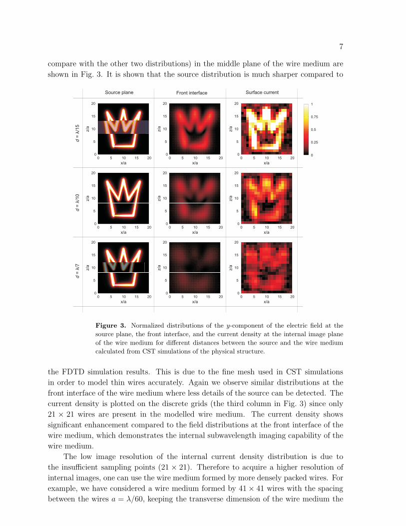
compare with the other two distributions) in the middle plane of the wire medium are
shown in Fig. 3. It is shown that the source distribution is much sharper compared to
Source plane Front interface Surface current
d=
λ/1
5d
=λ/1
0d
=λ/7
x/a
z/a
5 10 20
10
15
20
00
5
15
x/a
z/a
5 10 20
10
15
20
00
5
15
x/a
z/a
5 10 20
10
15
20
00
5
15
5 10 20
10
15
20
00
5
15
5 10 20
10
15
20
00
5
15
5 10 20
10
15
20
00
5
15
5 10 20
10
15
20
00
5
15
5 10 20
10
15
20
00
5
15
5 10 20
10
15
20
00
5
15
0
0.25
0.5
0.75
1
x/az/a
x/a
z/a
x/a
z/a
x/a
z/a
x/az/a
x/a
z/a
Figure 3. Normalized distributions of the y-component of the electric field at the
source plane, the front interface, and the current density at the internal image plane
of the wire medium for different distances between the source and the wire medium
calculated from CST simulations of the physical structure.
the FDTD simulation results. This is due to the fine mesh used in CST simulations
in order to model thin wires accurately. Again we observe similar distributions at the
front interface of the wire medium where less details of the source can be detected. The
current density is plotted on the discrete grids (the third column in Fig. 3) since only
21 × 21 wires are present in the modelled wire medium. The current density shows
significant enhancement compared to the field distributions at the front interface of the
wire medium, which demonstrates the internal subwavelength imaging capability of the
wire medium.
The low image resolution of the internal current density distribution is due to
the insufficient sampling points (21 × 21). Therefore to acquire a higher resolution of
internal images, one can use the wire medium formed by more densely packed wires. For
example, we have considered a wire medium formed by 41 × 41 wires with the spacing
between the wires a = λ/60, keeping the transverse dimension of the wire medium the

8
same as the previous case. According to Eq. (2), the plasma frequency is higher for
this case and therefore one could expect images with a higher resolution. However the
wire density cannot be increased arbitrarily due to the fact that when the filling ratio of
wires increases, the structure may exhibit anisotropic magnetic properties [17–19]. The
influence of the material parameter change on the subwavelength imaging property of
the wire medium is currently under our investigation.
The current density distributions from CST simulations for the case of 41 × 41
wires are plotted in Fig. 4. Note that for illustration purposes, the distributions are not
x/a
0
0.2
0.4
0.6
1.0
1.2
x/a x/a
z/a
z/a
z/a
0
0.04
0.08
0.12
0.16
0.2
0.8
0
0.1
0.2
0.3
0.5
0.6
0.4
d = λ/15 d = λ/10 d = λ/7
10 20 40
20
30
40
00
10
30 10 20 40
20
30
40
00
10
30 10 20 40
20
30
40
00
10
30
Figure 4. The current density from CST simulations of the physical wire medium
(41 × 41 wires) for different distances between the source and the wire medium.
normalized. It can be seen that by increasing the density of wires, the internal image
resolution can be improved, which is especially useful when a more complex source is
considered.
The preliminary estimations show that the image appears near the middle plane of
the λ/2 thick wire medium slab and does not change significantly even when the image
plane is offset from the middle plane by 5-10%. The plane of the best image formation
cannot be determined precisely from numerical simulations since the distribution of
electric displacement or current density inside the wire medium varies slowly along the
direction of wires. We have considered a wire medium slab with a half-wavelength
thickness in this paper. For the wire medium slabs with greater thicknesses (an integer
multiple of a half-wavelength), there are multiple planes for the internal imaging, where
the evanescent spatial harmonics generated by the source can be amplified and the
information lost in the free space region can be restored. The number of internal image
planes can be given by N if the thickness of the wire medium is Nλ/2. The distance of
the internal image planes to the front interface of the wire medium can be approximately
given by (2n − 1)λ/4 where n = 1, 2, ..., N .
4. Conclusion
The internal imaging capability of the wire medium, i.e. images with a much
higher resolution appear inside of the wire medium comparing with the external
ones, is demonstrated numerically by modelling the physical structure and using the
effective medium theory: the wire medium slabs are capable of imaging a source with

9
subwavelength resolutions located at significant distances away from the device. The
operational principle of ‘internal imaging’ is based on the excitation of standing waves
inside the wire medium slab rather than the resonance of surface plasmons in LHMs. The
features of being low loss and easy in manufacturing make the wire medium attractive
for practical applications. In practice, it is possible to capture the internal image
by embedding detectors into metallic wires at the internal image plane and directly
measuring the currents flowing along the wires. The internal imaging effect can be
used for subsurface imaging and the creation of new generation subwavelength imaging
devices.
Acknowledgements
The authors would like to thank EPSRC for the financial support and Mr. G. Palikaras
for his help during the preparation of the manuscript. P. A. Belov acknowledges the
financial support by EPSRC Advanced Research Fellowship EP/E053025/1.
References
[1] J. Pendry, “Negative refraction index makes a perfect lens,” Phys. Rev. Lett. 85, 3966-3969 (2000).
[2] V. G. Veselago, “The electrodynamics of substances with simultaneously negative values of ε and
µ,” Sov. Phys. Usp. 10, 509-514 (1968).
[3] V. A. Podolskiy, and E. E. Narimanov, “Near-sighted superlens,” Opt. Lett. 30, 75-77 (2005).
[4] D. R. Smith, D. Schurig, M. Rosenbluth, S. Schultz, S. A. Ramakrishna, and J. B. Pendry,
“Limitations on subdiffraction imaging with a negative refractive index slab,” Appl. Phys. Lett.
82, 1506 (2003).
[5] P. A. Belov, C. R. Simovski, and P. Ikonen, “canalisation of subwavelength images by
electromagnetic crystals,” Phys. Rev. B 71, 193105 (2005).
[6] P. A. Belov and Y. Hao, “Subwavelength imaging at optical frequencies using a transmission device
formed by a periodic layered metal-dielectric structure operating in the canalisation regime,”
Phys. Rev. B 73, 113110 (2006).
[7] B. Wood, J. B. Pendry, and D. P. Tsai, “Directed subwavelength imaging using a layered metal-
dielectric system,” Phys. Rev. B 74, 115116 (2006).
[8] M. Scalora et al., “Negative refraction and sub-wavelength focusing in the visible range using
transparent metallodielectric stacks,” Opt. Express 15, 508-523 (2007).
[9] Y. Liu, G. Bartal, D. A. Genov, and X. Zhang, “Subwavelength discrete solitons in nonlinear
metamaterials,” Phys. Rev. Lett. 99, 153901 (2007).
[10] P. A. Belov, Y. Hao, and S. Sudhakaran, “Subwavelength microwave imaging using an array of
parallel conducting wires as a lens,” Phys. Rev. B 73, 033108 (2006).
[11] Y. Zhao, P. A. Belov, and Y. Hao, “Spatially dispersive finite-difference time-domain analysis of
sub-wavelength imaging by the wire medium slabs,” Opt. Express 14, 5154-5167 (2006).
[12] P. A. Belov, R. Marques, S. I. Maslovski, I. S. Nefedov, M. Silverinha, C. R. Simovski, and S. A.
Tretyakov, “Strong spatial dispersion in wire media in the very large wavelength limit,” Phys.
Rev. B 67, 113103 (2003).
[13] P. A. Belov, S. A. Tretyakov, and A. J. Viitanen, “Dispersion and reflection properties of artificial
media formed by regular lattices of ideally conducting wires,” J. Electromagn. Waves Applic.
16, 1153-1170 (2002).
[14] A. Taflove, Computational electrodynamics: the finite-difference time-domain method, 2nd ed.,
Artech House, Norwood, MA (2000).

10
[15] J. R. Berenger, “A perfectly matched layer for the absorption of electromagnetic waves,” J.
Computat. Phys. 114, 185-200 (1994).
[16] Y. Zhao, P. A. Belov, and Y. Hao, “modelling of wave propagation in wire media using spatially
dispersive finite-difference time-domain method: numerical aspects,” IEEE Trans. Antennas
Propagat. 55, 3070-3077 (2007).
[17] J. S. Tyo, “A class of artificial materials isorefractive with free space,” IEEE Trans. Antennas and
Propagat. 51, 1093 (2003).
[18] X. Hu, C. T. Chan, J. Zi, M. Li, and K.-M. Ho, “Diamagnetic response of metallic photonic
crystals at infrared and visible frequencies,” Phys. Rev. Lett. 99, 223901 (2006).
[19] J. Shin, J.-T. Shen, P. B. Catrysse, and S. Fan, “Cut-through metal slit array as an anisotropic
metamaterial film,” IEEE J. Selected Topics Quantum Electronics 12, 1116-1122 (2006).