Embed Size (px)
Citation preview
PHYSICAL REVIEW B 15 AUGUST 2000-IVOLUME 62, NUMBER 7
Surface roughness and surface-induced resistivity of gold films on mica:Application of quantitative scanning tunneling microscopy
Raul C. Munoz,* Guillermo Vidal, Marcelo Mulsow, Judit G. Lisoni, Claudio Arenas, Andres Concha,Fernando Mora, and Roberto Espejo
Departamento de Fı´sica and Departamento de Ingenierı´a Electrica, Facultad de Ciencias Fı´sicas y Matema´ticas, Universidad de Chile,Blanco Encalada 2008, Casilla 487-3, Santiago, Chile
German Kremer and Luis MoragaDepartamento de Fı´sica, Facultad de Ciencias, Universidad de Chile, Las Palmeras 3425, Santiago, Chile
Rolando Esparza and Patricio HaberleDepartamento de Fı´sica, Universidad Te´cnica Federico Santa Marı´a, Casilla 110-V, Valparaı´so, Chile
~Received 15 December 1999; revised manuscript received 30 March 2000!
We report measurements of the resistivityr(T) of a gold film 70 nm thick deposited on mica preheated to300 °C in UHV, performed between 4 and 300 K, and measurements of the surface topography of the samefilm performed with a scanning tunneling microscope~STM!. From the roughness measured with the STM wedetermine the parametersd ~rms amplitude! and j ~lateral correlation length! corresponding to a Gaussianrepresentation of the average height-height autocorrelation function~ACF!. We use the parametersd andj tocalculate the quantum reflectivityR and the increase in resistivity induced by electron-surface scattering on thisfilm, according to a modified version of the theory of Sheng, Xing, and Wang~mSXW! @Munozet al., J. Phys.:Condens. Matter11, L299 ~1999!#. The mSXW theory is able to select the appropriate scale of distance overwhich corrugations take place, leading toR'1 for corrugations taking place over scales of distances that arelong when compared to a few Fermi wavelengthlF , andR,1 for corrugations taking place over scales ofdistances that are comparable tolF ~to within an order of magnitude!. The reflectivity R determined bycorrugations ocurring over a scale of distances comparable tolF approaches zero for a certain angle. Theresistivity r(T) of the film increases by roughly a factor of 4 between 4 and 300 K, and so does the bulkresistivity r0(T) predicted by mSXW theory. With the parametersd andj measured on our 70-nm film, wereproduced approximately the thickness and temperature dependence of the resistivity~between 4 and 300 K!of several gold films on mica reported by Sambles, Elsom, and Jarvis@Philos. Trans. R. Soc. London, Ser. A304, 365 ~1982!#, without using any adjustable parameters. The results of this paper suggest that the relevantquantities controlling electron-surface scattering in continuous gold films of arbitrary thickness, are the param-etersd andj describing the average ACF that characterizes the surface of the sample on a nanoscopic scale, inagreement with the accepted view regarding the conductivity of ultrathin films.
icix
inthonath
iemmbpon
abg
thei-he
entullydesK
ingm-is-ent
ess
for
z-
I. INTRODUCTION
One of the fundamental problems in solid-state physthat has attracted the attention of researchers for over syears, relates to the effect of electron-surface scatteringthe transport properties of thin metallic and semiconductfilms. One of the central issues is how the surface ofstructure affects its electrical transport properties, whenor more of the dimensions characterizing the structurecomparable to or smaller than the mean-free-path ofcharge carriers; what is known as ‘‘size effects.’’
One of the complexities associated with size effectsrelated to the scale of distances involved. Arguments stming from the wavelike nature of the electron and frowave optics have been applied to describe the collisiontween the electrons and the surface. These argumentsto the fact that, for the surface roughness to have an influeon the charge transport properties of the film, the scaledistances over which the surface roughness takes placethe typical amplitude of the surface roughness, shouldcomparable to or smaller than the characteristic wavelen
PRB 620163-1829/2000/62~7!/4686~12!/$15.00
sty
ongee
ree
s-
e-intceofndeth
of the carrier, the Fermi wavelengthlF ,1 which for severalmetals is in the range of nanometers. The invention ofscanning tunneling microscope~STM! has opened the possbility of directly measuring surface roughness within tscale set bylF .
There is experimental evidence supporting the argumoutlined above. Schumacher performed a series of carefcontrolled experiments, evaporating silver onto glass sliheld at 225 K under UHV; the films were annealed at 350after evaporation to achieve minimum resistance. A varyamount of silver atoms was further evaporated at low teperatures (T<100 K) onto the annealed films and the restivity of the films was observed to increase by a few percwith the addition of less than a monolayer.2 However, directevidence reporting the resistivity and the surface roughnmeasured on the scale set bylF on the same filmappears tobe missing.
The theoretical work concerning size effects focusedmany decades on the Fuchs-Sondheimer~FS! theory. FS de-scribe the motion of electrons in the metal film by a Boltmann transport equation~BTE!, where the effect of the
4686 ©2000 The American Physical Society
onvif
d-
ry
r
lmle
roa
-c
t-isry
tuhaeof
nthngrsceth
fe
ththon
t ogtioinntsuth
of-
We-toganf
r-
tal
ofn;theis-sssting
ss
that
ndi-lm
m of
ur-oni-ce
rst
at
pa-
ize
Ws of
esis-e
tivityednd
ith
the
oatherusere abeenif-ns
the-g
t ari-thepa-ar-th,f
PRB 62 4687SURFACE ROUGHNESS AND SURFACE-INDUCED . . .
rough surface is incorporated into the boundary conditithat must be satisfied by the electron distribution functiona specularity parameterR, which represents the fraction oelectrons 0<R<1 that are specularly reflected upon colliing with the rough surface.1,3
It is well known that this approach is inadequate for vethin, high-purity samples where the film thicknesst is muchsmaller than the bulk mean-free-pathl. On the one hand, foultrathin high-purity films, the conductivity of the film isknown to exhibit a stepwise increase with increasing fithickness, as a consequence of the quantization of the etronic energy levels induced by confinement of the electgas between two parallel potential barriers; what is knownquantum size effects~QSE!. The modeling of electron motion via a BTE with FS boundary conditions, does not acount for QSE. On the other hand, in the limitl→`, the FSconductivity diverges as ln(l/t), implying that when the con-ductivity of the film is limited only by electron-surface scatering, there is no dissipation, an unphysical result that arfrom the omission of quantum effects in the classical theoTo overcome these shortcomings, a number of quantransport theories applicable to several special casesbeen published.4–8 The quantum transport theories succeedin describing the experimental data in ultrathin filmsCoSi2.
9
The goal of theoretical research on size effects has beebuild a formalism that would permit the prediction of bothe reflectivity R characterizing electron-surface scatteriand the increase in resistivity due to size effects from fiprinciples, from the information contained in the surfaroughness profile. A significant step towards this goal istheory of Sheng, Xing, and Wang~SXW!, that unifies theavailable quantum transport theories applicable to the difent special cases with the classical FS formalism.3,10 SXWabandoned the model in which the motion of electrons inmetal film is described via BTE. They calculated insteadGreen’s function describing electrons confined within twpotential barriers, one of which is flat, the other is a radomly rough surface. SXW computed the dissipative parthe electron self-energy due to electron-surface scatterinthe presence of the rough surface using Dyson’s equaand proceeded to calculate the conductivity of the film usthe Kubo transport formalism. However, in their treatmeSXW modeled the surface roughness by a white-noiseface profile, assuming that the Fourier transform ofheight-height autocorrelation function~ACF! which on aver-age characterizes the surface, is a constant independentin-plane momentum.10 This white-noise approximation severely limits the predictive power of the SXW formalism.
We have recently proposed a modified version of SXtheory ~mSXW! that permits the calculation of both the rflectivity R and the increase in resistivity attributableelectron-surface scattering, in films in which the averaACF is described either by a Gaussian or byexponential.11 The mSXW theory permits the calculation othe reflectivityR and of the ratio of film conductivitys tobulk conductivitys0 attributable to electron-surface scatteing, in terms of the parametersd ~the rms amplitude of theACF! andj ~the lateral correlation length of the ACF! on ananoscopic scale for either of the two models, Gaussianexponential, in a continuous film of thicknesst.11
sa
c-ns
-
es.
mved
to
t
e
r-
ee
-finn,g,r-
e
the
e
or
The experimental work related to size effects in thin mefilms, during several decades, relied on the method of:~i!preparing families of samples of the same material butdifferent thickness under similar conditions of evaporatio~ii ! measuring one or more of the transport properties ofdifferent members of the family, most commonly the restivity; ~iii ! fitting the theoretical models to the thickneand/or the temperature dependence of the data and adjuthe parameters provided by theory~specularity parameterR,bulk conductivitys0 , and in some cases the rms roughneamplituded!.
The data analysis often proceeds from the assumptionthe specularity parameterR characterizing a family ofsamples of the same material prepared under similar cotions of evaporation is the same, independent of the fithickness, and is a constant independent of the momentuthe electron. The lack of direct measurements ofd andj inan independent experiment so far has prevented averifica-tion of whether or not the parameters characterizing the sface roughness inferred from fitting the resistivity datafamilies of thin metal films prepared under similar condtions of evaporation, actually do correspond to the surfaroughness measured on these films. The availability of atheory that permits the calculation of size effects from fiprinciples, from the parametersd and j that describe thesurface profile, together with the invention of the STM thmakes possible the direct measurement ofd and j on a na-nometric scale, permits a reversal of the trend based onrameter fitting of resistivity datawithout independent verifi-cation that has dominated experimental research on seffects for decades.
This paper reports on the application of the mSXtheory, and illustrates how measurements of the roughnesthe surface of the sample can be used to calculate the rtivity of the film induced by electron-surface scattering. Wreport measurements of the temperature dependent resisr(T) of a gold film 70 nm thick deposited on mica preheatto 300 °C in UHV, performed between 4 and 300 K, ameasurements of the surface topography of thesamefilmperformed with a STM. From the roughness measured wthe STM we determine the parametersd andj correspondingto a Gaussian representation of the average ACF. We useparametersd andj to calculate the reflectivityR and the bulkresistivity r0(T) according to mSXW theory. We chose tanalyze the surface roughness data using a Gaussian rthan an exponential representation of the ACF, becamodifications have been proposed to the FS theory wheGaussian representation of the surface roughness hasemployed. In this paper we compare the predictions of dferent versions of the classical theories with the predictioof mSXW theory using a Gaussian representation ofACF, with the parametersd andj measured in an independent experiment. Such comparisons will reveal interestindifferences between mSXW theory and other theories.
This paper is organized as follows: In Sec. II we presenbrief outline of mSXW theory. In Sec. III we present expemental details concerning the sample preparation andmeasurements. In Sec. IV we present the results of thisper: the structure of the films, the average ACF’s that chacterize the surface of the film in different scales of lengand the reflectivityR predicted by mSXW theory for each o
n
n
n
het-inF
ithulfoo
-t
e
nn-mghb
ia
t-
t toe
--heto
ntof-
on,,
een
-
-
e
lue
of-.histhe
totak-
er-
gn-
pera-
ctede
hefacee ofuldm-
4688 PRB 62RAUL C. MUNOZ et al.
the different scales of length for a Gaussian representatiothe ACF. We present as well the film resistivityr(T) mea-sured between 4 and 300 K on this film, and the correspoing bulk resistivity r0(T) predicted by mSXW theory. InSec. V we discuss these results and in Sec. VI we presesummary of this paper.
II. THEORY
The mSXW theory provides a way of calculating both tspecularity functionR and the increase in resistivity attribuable to electron-surface scattering from first principles, usinformation contained in the roughness profile, if the ACcharacterizing the surface of the sample is described eby a Gaussian or by an exponential. Summarizing resalready published, the SXW theory leads to a quantum remulation of the FS model, that includes the effectselectron-surface scattering via a reflectivity parameterR thatcan be calculated from
R~ki!5S 12kzQ~ki!
11kzQ~ki!D 2
, ~1!
which is Eq.~7! in Ref. 10, whereQ(ki) represents the dissipative part of the self-energy of the electron gas dueelectron-surface scattering; withkz
25kF22ki
2, where kF
stands for the Fermi momentum andki5(kx ,ky) representsthe in-plane momentum. The ratio of the film conductivitysto bulk conductivitys0 may be computed in terms of threflectivity R
12s
s05
3
2
l
t
1
X0Nc(n51
Nc
un~12un2!
3@12R~un!#@12Ed~un!#
12R~un!Ed~un!, ~2!
wheret is the film thickness,l the carrier mean-free-path ithe bulk—s0 and l represent the conductivity and meafree-path that would be observed in a film having the saconcentration of impurities as the thin film, but thick enousuch that the effect of electron-surface scattering canneglected—
un5qn
kF5cosun5
np
tkF, Xc5
tkF
p, Nc5 int~Xc!,
where int (M ) stands for the integer part ofM,
X053
2 F121
3 S Nc
XcD 2S 11
1
NcD S 11
1
2NcD G
andEd(un)5exp@2t/(unl)#, which corresponds to Eq.~11! ofRef. 10. The calculation of the electron self-energyQ(ki) forthe case in which the ACF is described by a Gaussf (x,y)5d2 exp@2(x21y2)/j2# has been published.11
The parametersd and j are determined from the heighheight surface ACFf (r i) defined by
f ~r i!5S21ESh~ai!h~ai1r i!d2ai , ~3!
of
d-
t a
g
ertsr-f
o
e
e
n
whereS denotes the surface of the sample,r i5(x,y) standsfor the in-plane coordinates, andh(ai) represents the randomheight characterizing the surface roughness with respecthe average surface atz5t. The quantity measured with thSTM is the functionh(ai).
Notice that in the mSXW theory,R ands0 are no longeradjustable parameters. The availability of a theory that permits the calculation ofs/s0 from the knowledge of the parameters~d, j! that can be independently measured with tSTM, suggests the traditional method of fitting parametersthe conductivity data of a family of samples of differethickness—prepared under similar conditionsevaporation—should be abandoned.A new method to compare theory and experiment is required. Knowing ~d, j! wemay use Eq.~2! to compute the film conductivitys. How-ever, a difficulty arises because to perform this calculatiwe need to know thes0 and l that characterize the bulkwhich, therefore, are not known apriori. Nevertheless, usingthe mSXW theory, the parameterss0 and l can be deter-mined by means of an iterative process that has already bpublished,12 that proceeds as follows:
As a first approximation,l (T) corresponding to each temperature, can be calculated froml 1(T)5s(T)mvF /(nq2),wheres(T) is the conductivity of the film measured at temperatureT, m is the electron mass,vF is the Fermi velocity,n the electron density, andq the electron charge. This valuis used to compute a first estimation of@s(T)/s0(T)#1 , us-ing Eq. ~2!, l 5 l 1 , and employing the parametersd and jdetermined from the STM measurements. A corrected vafor l can then be computed froml 25 l 1@s0(T)/s(T)#1 , anda new value of@s(T)/s0(T)#2 can be calculated usingl5 l 2 and Eq.~2!. This process is repeated until the values@s(T)/s0(T)# j and @s(T)/s0(T)# j 11 between two successive iterationsj and j 11 do not differ by more than 0.01%We found that 5 to 15 iterations are sufficient to satisfy tcriterion, depending on temperature and on the purity offilm.
If grain boundary scattering is negligible comparedelectron-surface scattering, if electron-surface scatteringing place at the lower surface of the film~in contact with thesubstrate! is negligible compared to electron-surface scatting taking place at the upper~exposed! surface of the film,and if the resistivity arising from electron-impurity scatterinat 300 K is small compared to that arising from electrophonon scattering at the same temperature, then the temture dependent bulk resistivityr0(T)51/s0(T) computedthrough this iteration process should agree with that expefrom electron-phonon scattering in crystalline gold. If thparameters (d,j) chosen to describe the roughness of tsurface and if the theory chosen to describe electron-surscattering are correct, then the temperature dependencr0(T) determined according to this iteration process shobe consistent with a Block-Gruneisen description as recomended by Matula, using the constants A, B, C, andu ap-propriate for crystalline gold:13
r0~T!5rR1AS 11BT
u2CTDfS u2CT
T D , with
f~x!54x25E0
x z5 exp~z!
@exp~z!21#2 dz, ~4!
l r
io
t tatickceang
lpdihethede
rytopll
o
rathoeda
filthss
thlehigal
afEn
un
Mteadnimrehl
.
Men
TMthentheale,cent
the
e-olt-datated
locka 9the
icae-
5°C.
thand
d
nd toAuDS-
PRB 62 4689SURFACE ROUGHNESS AND SURFACE-INDUCED . . .
whererR stands for the temperature-independent residuasistivity ~attributed to impurity scattering! determined by thethin film resistivityr~4.2! measured at 4.2 K and by the ratr0(4.2)/r(4.2) predicted by theory.
III. EXPERIMENT
We performed some preparatory experiments to selecconditions of evaporation. The temperature of the substr300 °C, the speed of evaporation, 6 nm/min, and the thness of the film, 70 nm, were chosen such as to producontinuous film where the influence of grain-boundary sctering would be minimized, for grain boundary scattericould influence the resistivity of the film but isnot includedin the SXW theory. A necessary condition that might heminimizing grain-boundary scattering, is that the lateralmension D characterizing the grains that make up tsamples should be at least one order of magnitude largerthe thicknesst of the films for then the electrons are expectto undergo an average of several collisions with the upplower surface of the film before colliding with the boundaof a grain. If the thickness of the films whose resistivity isbe analyzed, is in the range of 100 nm, then the samshould be made up of grains havingD of the order of severahundred nm.
The gold films were prepared by thermal evaporation2-mm diameter, 99.99% pure gold wire~MATKEMI ! from aW basket onto 20 mm310 mm30.15 mm Muscovite Rubymica slides ~GOODFELLOW!. The mica was freshlycleaved before evaporation. The stainless-steel evapowas baked for many hours after loading the mica andgold wire until reaching a pressure in the range10210mbar. The thickness of the gold films was monitorduring evaporation with a quartz-crystal oscillator that wcalibrated with a profilometer~TENCOR!. To avoid scratch-ing the surface, the thickness was measured with the prometerafter the surface roughness and the resistivity ofsamples had been measured. During evaporation the prewas in the range of 1029 mbar.
During the preparatory experiments designed to selectconditions of evaporation, the morphology of the sampwas examined using x-ray diffraction; the crystalograpstructure of the films and of the mica was determined usinSiemens D-5000 x-ray difractometer. The samples wereexamined using a scanning electron microscope~SEM!. Thesamples were kept under moderate vacuum in a dessicbetween the different experimental steps~measurements othe roughness with the STM, x-ray measurements, Smeasurements, resistivity measurements, determinatiothe thickness with the profilometer!.
The surface topography was measured with the STM rning in air in the constant-current mode usingW tips. STMmeasurements were performed with a commercial OCRON instrument, using tungsten tips 0.25 mm in diameand freshly etched in a 0.8 M NaOH solution. All images h2563256 pixels. We verified that the images did not depeon the gap voltage nor on the tunneling current. Beforeaging the gold samples, we verified that the freshly prepaW tips produced neat images of C atoms running on higoriented pyrolytic graphite~HOPG!. Tips that did not pro-duce neat images of C atoms on HOPG were discarded
e-
hee,-a
t-
-
an
r/
es
f
toref
s
o-eure
esca
so
tor
Mof
-
I-r
d-dy
We paid particular attention to searching with the STfor direct experimental evidence of barriers existing betweadjacent grains. For this purpose we imaged with the Sthe valleys that are left after the grains coalesced to formfilm. The bottom of these valleys look fairly smooth withian atomic scale. We did not find any sharp changes inSTM signal recorded on these valleys on an atomic scthat might indicate the presence of a barrier between adjagrains.
Conductivity measurements were performed usingfour-probe method, running a current of 100mA pp at 160Hz, using SRS 830 lock-in amplifiers from Stanford Rsearch. Data acquisition was computed controlled; the vage drop across the sample was averaged over 100points, the relative error in the voltage readings is estimaat 2 parts in 10 000. The sample was mounted on a Cu blocated in the variable temperature insert of the dewar ofT ~JANIS! superconducting magnet. The temperature ofCu block was maintained within60.1 K between 4 and 300K.
The crystalographic structure of the films and the mwas determined using a Siemens D-5000 x-ray difractomter.
IV. RESULTS
A. Structure of the films
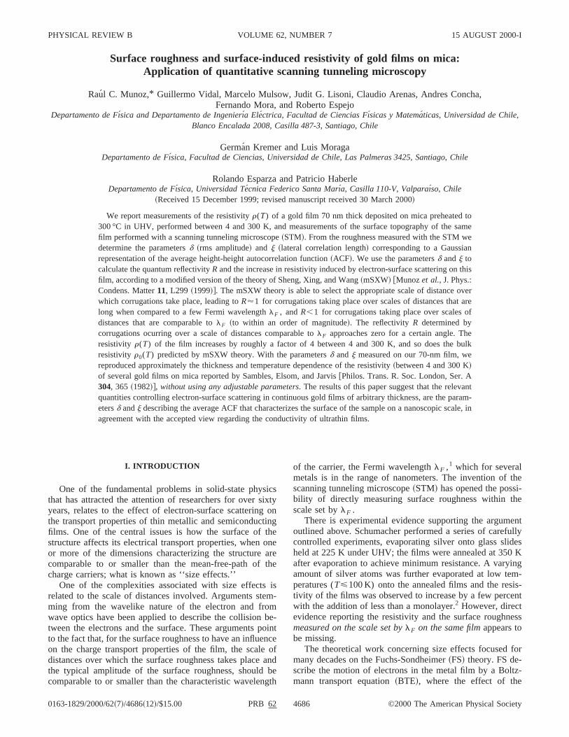
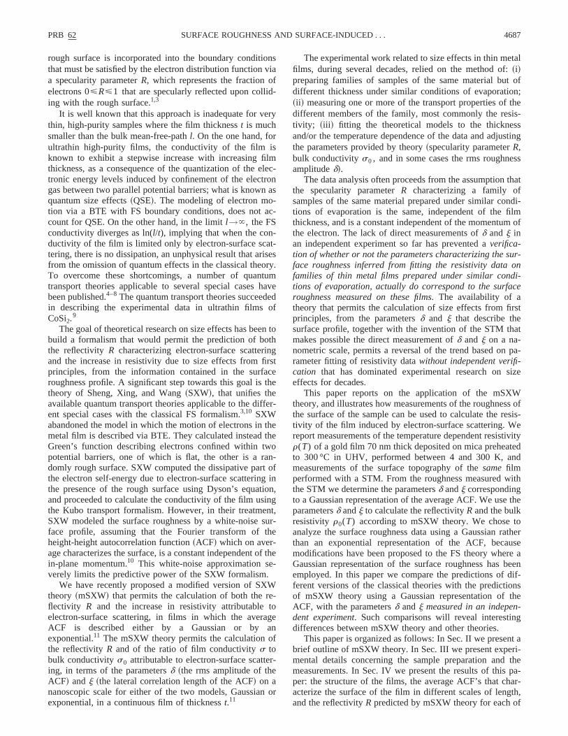
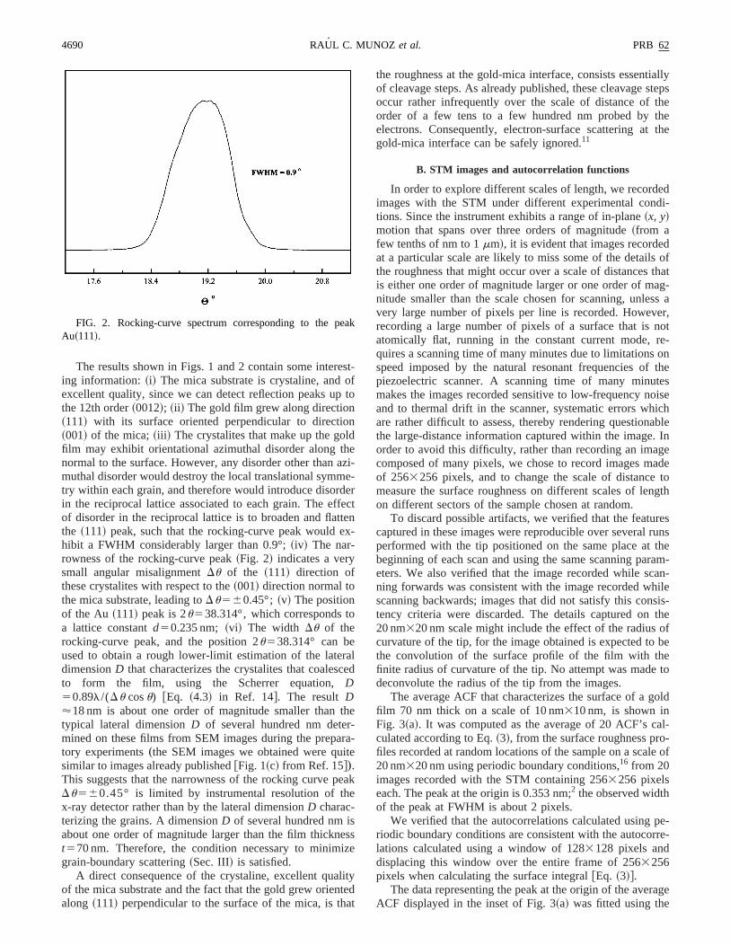
The u-2u spectrum is shown in Fig. 1 for a gold film 6nm thick deposited on a mica substrate preheated to 300The rocking curve spectrum corresponding to the~111! re-flection peak of Au is shown in Fig. 2. In this case bodetector and source moved together during the scanlocked in a position initially fixed at an angle 2u538.314°corresponding to the~111! peak of gold. The radiation usewas theKa line of Cu, with a wavelengthla50.154 nm.The full width at half maximum~FWHM! of the gold~111!peak is about 0.9°.
FIG. 1. u-2u spectra of a gold film 65 nm thick deposited omuscovite ruby mica, under UHV. The substrate was preheate300 °C prior to deposition, evaporation rate was 6 nm/min. Thefilm was characterized using crystallographic data card JCPICDD No. 4-784. The inset shows theu-2u spectra of the micasubstrate before evaporation of the gold film.
esofp
onldheazee
fetex
o
race
thr-ra
ite
ee
esiz
littea
tiallystepsthethe
the
eddi-
dofthatag-ss aer,notre-onthe
tesoiseichableIn
geadeto
ngth
resrunstheram-an-ile
sis-theofbeeto
old
al--
le of
pe-rre-
age
ea
4690 PRB 62RAUL C. MUNOZ et al.
The results shown in Figs. 1 and 2 contain some intering information:~i! The mica substrate is crystaline, andexcellent quality, since we can detect reflection peaks uthe 12th order~0012!; ~ii ! The gold film grew along direction~111! with its surface oriented perpendicular to directi~001! of the mica;~iii ! The crystalites that make up the gofilm may exhibit orientational azimuthal disorder along tnormal to the surface. However, any disorder other thanmuthal disorder would destroy the local translational symmtry within each grain, and therefore would introduce disordin the reciprocal lattice associated to each grain. The efof disorder in the reciprocal lattice is to broaden and flatthe ~111! peak, such that the rocking-curve peak would ehibit a FWHM considerably larger than 0.9°;~iv! The nar-rowness of the rocking-curve peak~Fig. 2! indicates a verysmall angular misalignmentDu of the ~111! direction ofthese crystalites with respect to the~001! direction normal tothe mica substrate, leading toDu560.45°; ~v! The positionof the Au ~111! peak is 2u538.314°, which corresponds ta lattice constantd50.235 nm; ~vi! The width Du of therocking-curve peak, and the position 2u538.314° can beused to obtain a rough lower-limit estimation of the latedimensionD that characterizes the crystalites that coalesto form the film, using the Scherrer equation,D50.89l/(Du cosu) @Eq. ~4.3! in Ref. 14#. The resultD'18 nm is about one order of magnitude smaller thantypical lateral dimensionD of several hundred nm detemined on these films from SEM images during the prepatory experiments„the SEM images we obtained were qusimilar to images already published@Fig. 1~c! from Ref. 15#….This suggests that the narrowness of the rocking curve pDu560.45° is limited by instrumental resolution of thx-ray detector rather than by the lateral dimensionD charac-terizing the grains. A dimensionD of several hundred nm isabout one order of magnitude larger than the film thicknt570 nm. Therefore, the condition necessary to minimgrain-boundary scattering~Sec. III! is satisfied.
A direct consequence of the crystaline, excellent quaof the mica substrate and the fact that the gold grew orienalong ~111! perpendicular to the surface of the mica, is th
FIG. 2. Rocking-curve spectrum corresponding to the pAu~111!.
t-
to
i--rctn-
ld
e
-
ak
se
yd
t
the roughness at the gold-mica interface, consists essenof cleavage steps. As already published, these cleavageoccur rather infrequently over the scale of distance oforder of a few tens to a few hundred nm probed byelectrons. Consequently, electron-surface scattering atgold-mica interface can be safely ignored.11
B. STM images and autocorrelation functions
In order to explore different scales of length, we recordimages with the STM under different experimental contions. Since the instrument exhibits a range of in-plane~x, y!motion that spans over three orders of magnitude~from afew tenths of nm to 1mm!, it is evident that images recordeat a particular scale are likely to miss some of the detailsthe roughness that might occur over a scale of distancesis either one order of magnitude larger or one order of mnitude smaller than the scale chosen for scanning, unlevery large number of pixels per line is recorded. Howevrecording a large number of pixels of a surface that isatomically flat, running in the constant current mode,quires a scanning time of many minutes due to limitationsspeed imposed by the natural resonant frequencies ofpiezoelectric scanner. A scanning time of many minumakes the images recorded sensitive to low-frequency nand to thermal drift in the scanner, systematic errors whare rather difficult to assess, thereby rendering questionthe large-distance information captured within the image.order to avoid this difficulty, rather than recording an imacomposed of many pixels, we chose to record images mof 2563256 pixels, and to change the scale of distancemeasure the surface roughness on different scales of leon different sectors of the sample chosen at random.
To discard possible artifacts, we verified that the featucaptured in these images were reproducible over severalperformed with the tip positioned on the same place atbeginning of each scan and using the same scanning paeters. We also verified that the image recorded while scning forwards was consistent with the image recorded whscanning backwards; images that did not satisfy this contency criteria were discarded. The details captured on20 nm320 nm scale might include the effect of the radiuscurvature of the tip, for the image obtained is expected tothe convolution of the surface profile of the film with thfinite radius of curvature of the tip. No attempt was madedeconvolute the radius of the tip from the images.
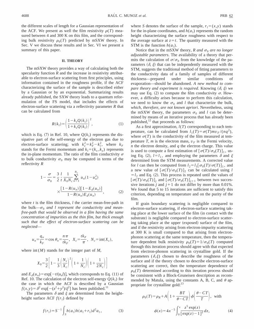
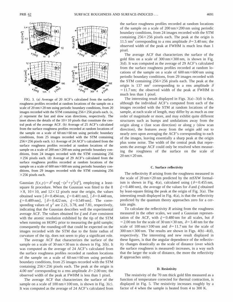
The average ACF that characterizes the surface of a gfilm 70 nm thick on a scale of 10 nm310 nm, is shown inFig. 3~a!. It was computed as the average of 20 ACF’s cculated according to Eq.~3!, from the surface roughness profiles recorded at random locations of the sample on a sca20 nm320 nm using periodic boundary conditions,16 from 20images recorded with the STM containing 2563256 pixelseach. The peak at the origin is 0.353 nm;2 the observed widthof the peak at FWHM is about 2 pixels.
We verified that the autocorrelations calculated usingriodic boundary conditions are consistent with the autocolations calculated using a window of 1283128 pixels anddisplacing this window over the entire frame of 2563256pixels when calculating the surface integral@Eq. ~3!#.
The data representing the peak at the origin of the averACF displayed in the inset of Fig. 3~a! was fitted using the
k
es
lynt
Mletho
oleth
rotio
TMis
l.th
o
ions
Mis
1
the
tedlo-
ithe
is
hetheonentthe
toachiginre-sur-of
in-
cer-
sesen-
inctiv-
hvity
a, is
a
eon0
T-
syinge
t-56e
t-56
PRB 62 4691SURFACE ROUGHNESS AND SURFACE-INDUCED . . .
Gaussianf (x,y)5d2 exp@2(x21y2)/j2#, employing a least-square fit procedure. When the Gaussian was fitted to th38, 10310, and 12312 pixels near the origin, the valueobtained [email protected] nm,j50.401 nm],@d50.448 nm,j50.489 nm], @d50.422 nm, j50.549 nm]. The corre-sponding values ofx2 are 2.21, 3.78, and 7.81, respectiveindicating that the Gaussian describes well the experimeaverage ACF. The values obtained forj andd are consistentwith the atomic resolution exhibited by the tip of the STwhen running on HOPG prior to measuring the gold sampconsequently the rounding-off that could be expected onimages recorded with the STM due to the finite radiuscurvature of the tip, does not seem to play a significant r
The average ACF that characterizes the surface ofsample on a scale of 30 nm330 nm is shown in Fig. 3~b!. Itwas computed as the average of 24 ACF’s calculated fthe surface roughness profiles recorded at random locaof the sample on a scale of 60 nm360 nm using periodicboundary conditions, from 25 images recorded with the Scontaining 2563256 pixels each. The peak at the origin4.00 nm2 corresponding to a rms amplituded52.00 nm; theobserved width of the peak at FWHM is less than 1 pixe
The average ACF that characterizes the surface ofsample on a scale of 100 nm3100 nm, is shown in Fig. 3~c!.It was computed as the average of 24 ACF’s calculated fr
FIG. 3. ~a! Average of 20 ACF’s calculated from the surfacroughness profiles recorded at random locations of the samplescale of 20 nm320 nm using periodic boundary conditions, from 2images recorded with the STM containing 2563256 pixels each.~x,y! represent the fast and slow scan directions, respectively.inset shows the details of the 10310 pixels that constitute the central peak of the average ACF.~b! Average of 25 ACF’s calculatedfrom the surface roughness profiles recorded at random locationthe sample on a scale of 60 nm360 nm using periodic boundarconditions, from 25 images recorded with the STM contain2563256 pixels each.~c! Average of 24 ACF’s calculated from thsurface roughness profiles recorded at random locations ofsample on a scale of 200 nm3200 nm using periodic boundary conditions, from 24 images recorded with the STM containing 23256 pixels each.~d! Average of 29 ACF’s calculated from thsurface roughness profiles recorded at random locations ofsample on a scale of 600 nm3600 nm using periodic boundary conditions, from 29 images recorded with the STM containing 23256 pixels each.
8
,al
;ef.e
mns
e
m
the surface roughness profiles recorded at random locatof the sample on a scale of 200 nm3200 nm using periodicboundary conditions, from 24 images recorded with the STcontaining 2563256 pixels each. The peak at the origin11.5 nm2 corresponding to a rms amplituded53.40 nm; theobserved width of the peak at FWHM is much less thanpixel.
The average ACF that characterizes the surface ofgold film on a scale of 300 nm3300 nm, is shown in Fig.3~d!. It was computed as the average of 29 ACF’s calculafrom the surface roughness profiles recorded at randomcations of the sample on a scale of 600 nm3600 nm usingperiodic boundary conditions, from 29 images recorded wthe STM containing 2563256 pixels each. The peak at thorigin is 137 nm2 corresponding to a rms amplituded511.7 nm; the observed width of the peak at FWHMmuch less than 1 pixel.
The interesting result displayed in Figs. 3~a!–3~d! is that,although the individual ACF’s computed from each of timages recorded with the STM at random locations ofsample, at each scale of length, may differ by as much asorder of magnitude or more, and may exhibit quite differestructures such as bumps and undulations away fromorigin along x ~fast scan direction! or along y ~slow scandirection!, the features away from the origin add outnearly zero upon averaging the ACF’s corresponding to eof the images, leaving essentially a sharp peak at the orplus some noise. The width of the central peak that repsents the average ACF could only be resolved when meaing the roughness of the surface on the scale20 nm320 nm.
C. Surface reflectivity
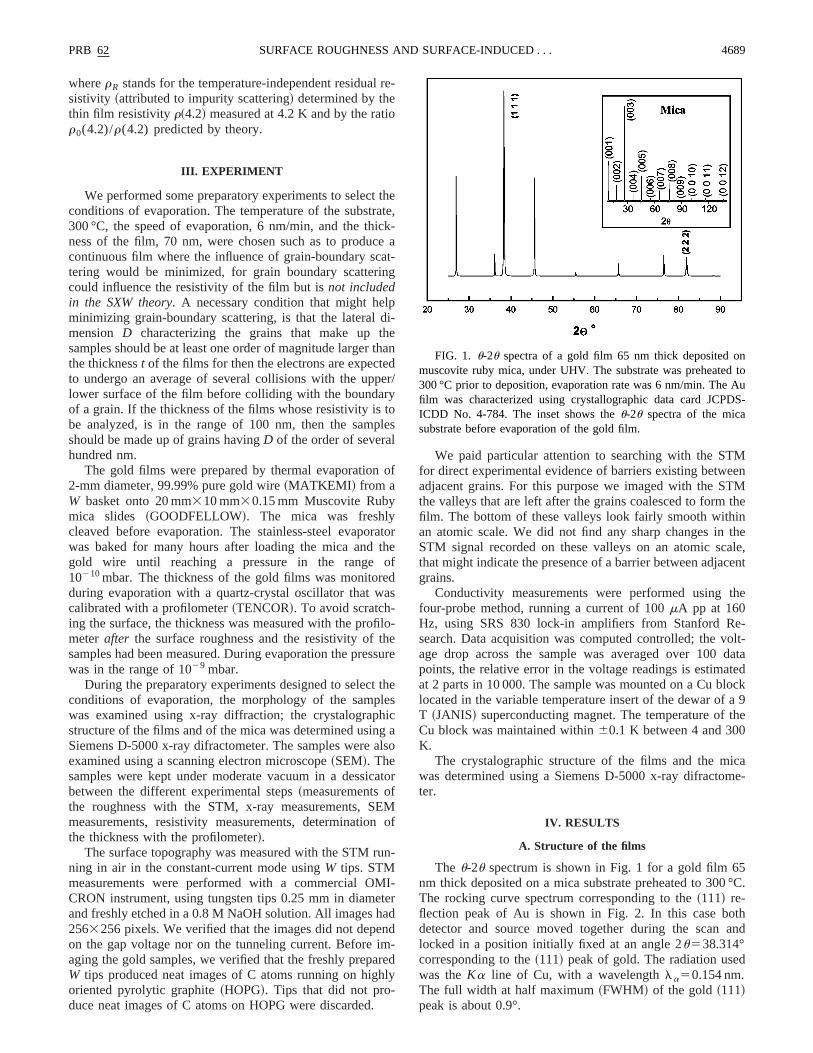
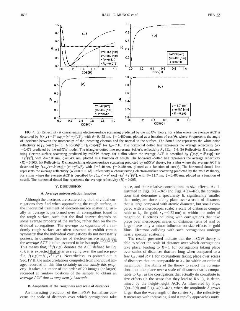
The reflectivityR arising from the roughness measuredthe scale of 20 nm320 nm predicted by the mSXW formalism is shown in Fig. 4~a!, calculated using (d50.455 nm,j50.480 nm), the average of the values ford andj obtainedby least-square fitting the peak at the origin of Fig. 3~a!. Theinteresting result displayed in Fig. 4~a!, is that the reflectivitypredicted by the quantum theory approaches zero for atain angle.
To calculate the reflectivityR arising from the roughnesmeasured in the other scales, we used a Gaussian reprtation of the ACF, withj50.480 nm for all scales, butd52.00 nm for the scale of 30 nm330 nm,d53.40 nm for thescale of 100 nm3100 nm andd511.7 nm for the scale of300 nm3300 nm. The results are shown in Figs. 4~b!–4~d!,respectively. The interesting and new result displayedthese figures, is that the angular dependence of the refleity changes drastically as the scale of distance~over whichthe surface roughness is measured! increases, in a way sucthat the larger the scale of distance, the more the reflectiR approaches unity.
D. Resistivity
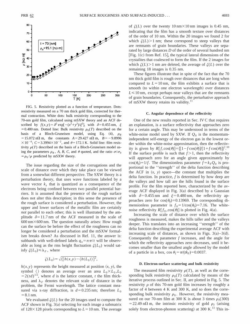
The resistivity of the 70 nm thick gold film measured asfunction of temperature corrected for thermal contractiondisplayed in Fig. 5. The resistivity increases roughly byfactor of 4 when the sample is heated from 4 to 300 K.
a
he
of
he
he
ACF is
hite-noise
vityCF is
ory,f
4692 PRB 62RAUL C. MUNOZ et al.
FIG. 4. ~a! ReflectivityR characterizing electron-surface scattering predicted by the mSXW theory, for a film where the averagedescribed byf (x,y)5d2 exp@2(x2 1y2)/j2#, with d50.455 nm,j50.480 nm, plotted as a function of cos(u), whereu represents the angleof incidence between the momentum of the incoming electron and the normal to the surface. The dotted line represents the wreflectivity R@ f 0 ,cos(u)#5$@12f0 cos(u)#/@11f0 cos(u)#%2 for f 057.16. The horizontal dotted line represents the average reflectivity^R&50.479 predicted by the mSXW model. The triangles-dotted line represents Soffer’s reflectivityRS @Eq. ~5!#. ~b! Reflectivity R character-izing electron-surface scattering predicted by mSXW theory, for a film where the average ACF is described byf (x,y)5d2 exp@2(x2
1y2)/j2#, with d52.00 nm, j50.480 nm, plotted as a function of cos(u). The horizontal-dotted line represents the average reflecti^R&50.903.~c! Reflectivity R characterizing electron-surface scattering predicted by mSXW theory, for a film where the average Adescribed byf (x,y)5d2 exp@2(x2 1y2)/j2#, with d53.40 nm, j50.480 nm, plotted as a function of cos(u). The horizontal-dotted linerepresents the average reflectivity^R&50.957.~d! Reflectivity R characterizing electron-surface scattering predicted by the mSXW thefor a film where the average ACF is described byf (x,y)5d2 exp@2(x2 1y2)/j2#, with d511.7 nm,j50.480 nm, plotted as a function ocos(u). The horizontal-dotted line represents the average reflectivity^R&50.995.
t
im
t
il-
cesm-pa-
ke
ldgo
isons
to aes
a-pa-to
s.
.
V. DISCUSSION
A. Average autocorrelation function
Although the electrons are scattered by the individual crugations they find when approaching the rough surfacethe theoretical treatment of electron-surface scattering, ually an average is performed over all corrugations foundthe rough surface, such that the final answer dependssome average property of the surface, rather than on thedividual corrugations. Theaverage corrugationsof a ran-domly rough surface are often assumed to exhibit cersymmetry that the individual corrugations do not necessapossess. In quantum theories of electron-surface scattetheaverageACF is often assumed to be isotropic.4–6,8,10,17,18
This means that, iff (x,y) denotes the ACF defined by Eq~3!, it is expected that after averaging over the surface pfile, f (x,y)5 f (Ax21y2). Nevertheless, as pointed outSec. IV B, the autocorrelations computed from individual iages recorded on this film certainlydo not satisfy this prop-erty. It takes a number of the order of 20 images~or larger!recorded atrandom locations of the sample, to obtain aaverage ACF that is very nearly isotropic.
B. Amplitude of the roughness and scale of distances
An interesting prediction of the mSXW formalism concerns the scale of distances over which corrugations
or-, insu-inonin-
ainrilyring,
.ro-n
-
n
-ake
place, and their relative contributions to size effects. Aslustrated in Figs. 3~a!–3~d! and Figs. 4~a!–4~d!, the corruga-tions that determine a specularityR, significantly smallerthan unity, are those taking place over a scale of distanthat is large compared with atomic diameter, but small copared with a mesoscopic scale; a scale of distances comrable tolF ~in gold, lF50.52 nm) to within one order ofmagnitude. Electrons colliding with corrugations that taplace over mesoscopic scales of distances~tens of nm! orlarger have only a minor influence on size effects in gofilms. Electrons colliding with such corrugations undernearly specular scattering.
The results presented indicate that the mSXW theoryable to select the scale of distance over which corrugatitake place, leading toR'1 for corrugations taking placeover scales of distances that are long when comparedfew lF , andR,1 for corrugations taking place over scalof distances that are comparable tolF ~to within an order ofmagnitude!. The ability of the theory to select the corrugtions that take place over a scale of distances that is comrable tolF , as the corrugations that actually do contributesize effects~in the sense that they lead toR,1), is deter-mined by the height-height ACF. As illustrated by Fig3~a!–3~d! and Figs. 4~a!–4~d!, when the amplituded growslarger than the wavelength of the carrierlF , the reflectivityR increases with increasingd and it rapidly approaches unity
thwesytha
faet
nlmoghna
r
thea
heix
,cesorhatepa-
efor
70enis
antsach
reserothe
or-iv-
by
ge
eceav-n
i-
acelleysheith
rbe-del
eheae--
tserhee
us
PRB 62 4693SURFACE ROUGHNESS AND SURFACE-INDUCED . . .
The issue regarding the size of the corrugations andscale of distance over which they take place can be viefrom a somewhat different perspective. The SXW theory iperturbation theory, that uses wave functions labeled bwave vectorkz that is quantized as a consequence ofelectrons being confined between two parallel potential briers. It is assumed that the presence of the rough surdoes not alter this description; in this sense the presencthe rough surface is considered a perturbation. However,upper and lower surfaces of the metallic film are certainot parallel to each other; this is well illustrated by the aplitude d511.7 nm of the ACF measured in the scale600 nm3600 nm. The question naturally arises: How roucan the surface be before the effect of the roughness calonger be considered a perturbation and the mSXW formism breaks down? As discussed in Ref. 11, the answesubbands with well-defined labelsqn5np/t will be observ-able as long as the rms height fluctuationz(L0) would sat-isfy z(L0)<lF , where
z~L0!5A^@h~x,y!2^h~L0!,
h(x,y) represents the height measured at position~x, y!, thesymbol ^ & denotes an average over an areaL03L0 ,L052(td)1/2, whered is the lattice constant,t the film thick-ness, andlF denotes the relevant scale of distance inproblem, the Fermi wavelength. The lattice constant msured via x-ray diffraction, isd50.235 nm; thereforeL058.1 nm.
We evaluatedz(L) for the 20 images used to compute tACF shown in Fig. 3~a! selecting for each image a submatrof 1283128 pixels corresponding toL510 nm. The average
FIG. 5. Resistivity plotted as a function of temperature. Doresistivity measured on a 70 nm thick gold film, corrected for thmal contraction. White dots: bulk resistivity corresponding to t70-nm gold film, calculated using mSXW theory and an ACF dscribed by f (x,y)5d2 exp@2(x21y2)/j2#, with d50.455 nm, j50.480 nm. Dotted line: Bulk resistivityr0(T) described on thebasis of a Bloch-Gruneisen model, using Eq.~4!, rR
515.072 nV m, the constantsA529.427 nV m, B529.899631024; C53.399431022, andu5172.1 K. Solid line: film resis-tivity r(T) described on the basis of a Bloch-Gruneisen modeling the parametersrR , A, B, C, andu quoted, and the ratios/s0
5r0 /r predicted by mSXW theory.
ed
aaer-ceof
hey-f
nol-is:
e-
of z(L) over the twenty 10 nm310 nm images is 0.45 nmindicating that the film has a smooth texture over distanof the order of 10 nm. Within the 20 images we found 2 fwhich z(L).1 nm; these correspond to steep valleys tare remnants of grain boundaries. These valleys are srated by large distancesD of the order of several hundred nm@Fig. 1~c! from Ref. 15#, the typical lateral dimensions of thcrystalites that coalesced to form the film. If the 2 imageswhich z(L).1 nm are deleted, the average ofz(L) over theremaining 18 images is 0.35 nm.
These figures illustrate that in spite of the fact that thenm thick gold film is rough over distances that are long whcompared toL510 nm, the film exhibits a surface thatsmooth~to within one electron wavelength! over distancesL<10 nm, except perhaps near valleys that are the remnof grain boundaries. Consequently, the perturbative approof mSXW theory retains its validity.11
C. Angular dependence of the reflectivity
One of the new results reported in Sec. IV C that requian explanation, is a surface reflectivity that approaches zfor a certain angle. This may be understood in terms ofwhite-noise model used by SXW. IfQ0 is the momentum-independent self-energy of the electron gas in the lowestder within the white-noise approximation, then the reflectity is given by R@ f ,cos(u)#5$@12f cos(u)#/@11f cos(u)#%2.10
If the surface profile is such thatf .1, then the reflectivitywill approach zero for an angle given approximatelycos(u0)51/f . The dimensionless parameterf 5kFQ0 is pro-portional to the ‘‘strength’’ of the delta function describinthe ACF in ~x, y! space—the constant that multiplies thdelta function. In practice,f is determined by how deep arthe valleys and how tall are the hills found in the surfaprofile. For the film reported here, characterized by theerage ACF displayed in Fig. 3~a! described by a Gaussiawith d50.455 nm andj50.480 nm, the reflectivity ap-proaches zero for cos(u0)50.13969. The corresponding dmensionless parameter isf 051/cos(u0)57.16. The white-noise reflectivityR@ f 0 ,cos(u)# is plotted in Fig. 4~a!.
Increasing the scale of distance over which the surfroughness is measured, makes the hills taller and the vadeeper. This translates into an increasing ‘‘strength’’ of tdelta function describing the experimental average ACF wincreasing scale of distances, as shown in Figs. 3~a!–3~d!.Consequently the parameterf increases, and the angle fowhich the reflectivity approaches zero decreases, until itcomes smaller than the smallest angle allowed by the moof a particle in a box, cosu15p/(tkF)50.0037.
D. Electron-surface scattering and bulk resistivity
The measured film resistivityr(T), as well as the corre-sponding bulk resistivityr0(T) calculated by means of thiterative process outlined in Sec. II, are plotted in Fig. 5. Tresistivity r of this 70-nm gold film increases by roughlyfactor of 4 between 4 K and 300 K, and so does the corrsponding bulk resistivityr0 . However, the resistivity measured on our 70-nm film at 300 K is about 3 timesr I(300)522.49 nV m, the intrinsic resistivity of goldr I ~arisingsolely from electron-phonon scattering! at 300 K.13 This in-
:-
-
-
yheq
-rye
-o
poo
nm9%
a
th
an
snmitenis
erivanfoarn
exgee
EJAnS
oufo
thr-ra
s
th
m
g
ary
on
mingm
he. 6eo-a-n a
ual
ofin-tiv-rightof
he
erby
%is-
m
en
4694 PRB 62RAUL C. MUNOZ et al.
dicates that the resistivity of our film is probably limited bimpurities, in spite of using gold wire 99.99% pure as tstarting material. This is also reflected in the fact that if E~4! is used to describe the temperature dependence ofr0(T),then a constantA529.427 nV m and a residual resistivityrR515.07 nV m are required. This constantA is more thantwice the constantA512.359 nV m recommended by Matulafor crystaline gold,13 and the residual resistivityrR515.07 nV m is almost as large asr I(300). Therefore, thetemperature dependence ofr0(T) predicted by mSXWtheory in our 70-nm film is inconsistent with the BlochGruneisen description of electron-phonon scattering in ctaline gold, and this is probably a consequence of thehanced resistivity arising from impurities in our film.
Sambles, Elsom, and Jarvis~SEJ! published measurements of the resistivity of films deposited by thermal evapration of gold on mica, prepared under conditions of evaration ~temperature of the substrate, 280 °C, speedevaporation, 5 nm/min! which are similar to ours~tempera-ture of the substrate, 300 °C, speed of evaporation, 6min!, except for the fact that SEJ used gold 99.999pure.15 SEJ prepared films in which the lateral dimensionDcharacterizing the crystalites that make up the samplesalso in the range of several hundred nm@Fig. 1~c! of Ref.15#. Some of the SEJ samples also satisfy the conditionD should be about an order of magnitude larger thant tominimize the effect of grain boundary scattering~Sec. 3!.SEJ measured the resistivity of the gold films between 2300 K.
At this point it seems appropriate to clarify similaritieand differences between the resistivity data of our 70-film and the thinner SEJ films; a comparison of the resistivof our 70-nm film and the SEJ 80-nm film has bepublished.12~b! At room temperature our resistivity dataalmost 3 times larger than the intrinsic resistivityr I(300)522.49 nV m expected purely from electron-phonon scatting in crystaline gold. This is in contrast to the SEJ resistity data, which at 300 K is some 20% to 30% larger thr I(300). As already published, a plausible explanationthis discrepancy may be the fact that the purity of our sting material, 99.99%,is 2 orders of magnitude lower thathe purity of 99.9999% used by SEJ.12
Since SEJ samples exhibit a resistivity close to thatpected from crystaline gold, and were evaporated usinspeed of evaporation and a substrate temperature closwhat we used in preparing our 70-nm film, we may wondwhat the predictions of mSXW theory would be if the Ssamples had a surface characterized also by a Gaussianwith d50.455 nm andj50.480 nm. To answer this questiowe proceeded to analyze the data corresponding to thefilms and calculated by means of the iterative processlined in Sec. II, for each of the 4 thinner SEJ films andeach temperatureT, the corresponding bulk resistivityr0(T)predicted by mSXW theory using a Gaussian ACF withparametersd andj measured on our 70 nm film. The inteesting result is that for the 4 thinner SEJ films, the tempeture dependence ofr0(T) predicted by mSXW theory turnout to be consistent with Eq.~4!, using the constantsA, B, C,andu recommended by Matula for crystaline gold, but wislightly different residual resistivitiesrR for each film. Weexcluded from the analysis SEJ films thicker than 126 n
.
s-n-
--f
/
re
at
d
y
--
rt-
-ato
r
CF
EJt-r
e
-
,
for two reasons:~i! the thickness of these films begins beincomparable to the lateral dimensionD characterizing thegrains, therefore one might expect enhanced grain-boundscattering in these thicker films;~ii ! the thicker films wereshown to be polycrystaline when examined by reflectihigh-energy electron diffraction.15
The fact thatr0(T) predicted by mSXW theory for thefour SEJ films is consistent with what is expected froelectron-phonon scattering plus electron-impurity scatterin crystaline gold, means that the resistivity computed frothe Bloch-Gruneisen model and from the ratios(T)/s0(T)predicted by mSXW theory, should be comparable to tmeasured film resistivy. This is, indeed, the case: In Figwe plot the original SEJ data as a dotted line, and the thretical predictions as a solid line, in the same double logrithmic scale used by SEJ. The predictions are based oBloch-Gruneisen model@Eq. ~4!# describing electron-phononscattering in the bulk, corrected for the ratios/s05r0 /rpredicted by mSXW theory@Eq. ~2!# describing electron-surface scattering. The interesting result is that the residresistivity predicted by mSXW theoryturns out to be differ-ent for films of different thickness—despite the fact that thefilms were evaporated under similar conditionsevaporation—and decrease as the thickness of the filmcreases; this is at variance with the constant residual resisity ~independent of film thickness! that has been assumed foseveral decades in the analysis of size-effect data. This mbe expected if thicker films had a smaller concentrationimpurities than thinner films, something consistent with tfact that at 4 K, the bulk mean free pathl predicted bymSXW theory grows larger as the film grows thicker.
It is interesting to note that on these films, which are ov100 atoms thick, the increase in resistivity inducedelectron-surface scattering predicted by theory atT<10 K,amounts to 17% in our 70-nm film, and roughly 42% to 53in the SEJ films. It is also interesting to note that the res
FIG. 6. Dotted line: resistivity of the 35, 53, 80, and 126 nthick gold films on mica reported in Fig. 3~a! of Ref. 15. Solid line:film resistivity r(T) described on the basis of a Bloch-Gruneismodel, using Eq. ~4!, rR as listed, and the constantsA512.359 nV m, B529.899631024; C53.399431022; u5172.1 K from Ref. 13, and using the ratios/s0 predicted bymSXW theory for an ACF described byf (x,y)5d2 exp@2(x2
1y2)/j2#, with d50.455 nm,j50.480 nm.
inm
elth
Ea
hehrrya-dmo
ls
iche
n
f
-isaleos
e-rdXWeinth
e,3eFS
E
ffeely
cein
tona-de-and
ers,
er.is
yer-
lmsthan
ringousherized-n-
rcon-
on-del.the
lyaseeaning
heduc-
toin-nethe
e-h
ct,ole,k-
theer-
PRB 62 4695SURFACE ROUGHNESS AND SURFACE-INDUCED . . .
tivity ratio RR5r0(300)/r0(4.2 K) predicted by theory, is4.57 in our 70-nm film, and it is 4.50, 7.52, 13.1, and 21.9the SEJ-35, SEJ-53, SEJ-80, and SEJ-126-nm filrespectively.
As shown in Fig. 6, we have reproduced approximat~to within 7% or better! the temperature dependence andthickness dependence of the resistivity of these four Sfilms between 4 and 300 K, using mSXW theory andGaussian ACF characterized byd50.455 nm and j50.480 nm,without using any adjustable parameter. Thereis an interesting corollary to this unexpected result: If tsurface of the SEJ films were described by a Gaussian cacterized by the same parameters~d, j! we measured on oufilm, then grain-boundary scattering would contribute velittle to the resistivity of the four SEJ films we have anlyzed, since the data seems approximately representemSXW theory describing electron-surface scattering cobined with a Bloch-Gruneisen model that describes electrphonon scattering in the bulk,and neither of these modeinclude grain-boundary scattering.
E. Comparison between the mSXW theory and other theories
At this point it seems appropriate to compare the predtions of the mSXW theory with those based on various otmodels that have appeared in the literature.
1. Fuchs-Sondheimer model
The first and by far the most popular model used for madecades, is the FS model. Since in the FS theory,R is anadjustable parameter that is assumed to be independent omomentum of the electron, and in the mSXW theoryR de-pends on the angleu between the momentum of the incoming electron and the normal to the surface, the question arregarding which constantR should be used in the classictheory, to compare the FS model with the mSXW modOne natural way to perform such a comparison is to chothe average of the quantum reflectivityR5^R(u)& predictedby theory. For the film 70 nm thick, the mSXW theory prdicts ^R(u)&50.479 in the case of a Gaussian ACF. Accoing to a comparison between the FS theory and the mStheory already published,11 the FS model overestimates theffect of electron-surface scattering by an amount thatcreases with increasing mean-free-path, due to the factthe angular dependence of the reflectivityR is completelyignored in the FS model.
At temperatures between 4 and 10 K, the bulk mean-frpathl predicted by mSXW in our 70-nm film is about 55 nmand it is 134 nm in the SEJ-35, 229 nm in the SEJ-53, 4nm in the SEJ-80, and 757 nm in the SEJ-126 film, resptively. At temperatures below 10 K, the predictions of themodel coincide~within 1%! with the predictions of themSXW model in our sample, becausel /t,1, but FS overes-timates the effect of electron-surface scattering in the Sfilms by an amount around 12%, because in these filmsl /t.1.
2. Soffer’s model
Another model that has been used to analyze size edata is a model proposed by Soffer.19 Soffer assumes that thmotion of the electrons within the metal film is correct
s,
yeJ
ar-
by-
n-
-r
y
the
es
l.e
-
-at
e-
7c-
J
ct
described by a BTE, and introduces the effect of surfaroughness via boundary conditions similar to those usedthe FS model, except that Soffer’s reflectivityRS is assumedto depend onu:
RS~u!5expF2S 4pd
lFcos~u! D 2G , ~5!
wherelF is the Fermi wavelength andd is the rms amplitudeof the surface roughness. A modification of this modelinclude grain-boundary scattering was used by SEJ to alyze their data. Fitting the temperature and the thicknesspendence of the data measured on six films between 2300 K, using a model containing five adjustable parametSEJ arrive at the conclusion thatr 5d/lF'0.05, and conse-quentlyd'0.026 nm, about one-tenth of an atomic diametThe value ofd measured with the STM on our 70-nm filmabout 17 times larger. Ford50.455 nm, Soffer’s reflectivity@plotted in Fig. 4~a!# leads to an average reflectivit^RS(u)&'0.079, and hence to predominantly diffuse scatting. If Soffer’s theory is to agree with the data ford50.455 nm, then the resistivity measured on the SEJ fishould have been about one order of magnitude largerobserved.
Data recorded on samples measured with the STM duthe preparatory experiments, indicate that in a continufilm prepared by thermal evaporation of gold on mica, troughness measured on a nanometric scale is characteby a rms amplituded that is comparable to the Fermi wavelengthlF . This implies that Soffer’s model leads to essetially diffuse scattering in these films.
3. Elsom and Sambles’s model
Elsom and Sambles~ES! published a model to account fothe effect of the macroscopic surface roughness on theductivity of thin metal films.20 ES calculated numerically theconductance of a two-dimensional rectangular grid of cductances whose values are derived from a thickness moThe thickness model used to approximate the structure ofmetal film, consists of a random distribution of partialoverlapping chopped cones, with the cone height and bradii chosen to have a Gaussian spread about some mvalues. Local surface roughness is accounted for by usSoffer’s theory, to convert the grid of thicknesses into tcorresponding conductances. This demanded the introtion of an effective bulk mean-free-path, which was usedscale the dimensions of the model to the real film. The prcipal variables involved in this model, are the mean cobase radius, the cone angle and the chopping fraction ofcones.
This model describes thethickness dependence of the rsistivity of metal films that are grown nonepitaxially, whicare in their initial stage of growth. At this stage the film is astructure formed by islands that are beginning to conduand where grain-boundary scattering plays a central ronce the islands begin to merge with increasing film thicness. Consequently, in the ES model the resistivity offilm is almost certainly dominated by grain-boundary scatt
o
enbsrtX
yzua
rtfa
e
uepn-
ha
obifyTM,
uedid
un
dneitrethry-3
o
cky
fatin
am-uref 20sngesis-ap-
ellicrac-orts ofing
eof theor-n aap-
in-
re-ngevi-oth-
ataur-tlyent.
thata ono-
m-hate
er-
faceofrsts
n 4y ofss
useto
4696 PRB 62RAUL C. MUNOZ et al.
ing and perhaps by percolation through the islands. By ctrast, in the mSXW model the film is assumed to be acon-tinuous epitaxial film, and the mSXW theory describes thresistivity of the epitaxial film that exhibits a contributiodue to surface scattering, with the contribution dominatedelectron-surface scattering at the upper and lower surfacethe film. Thusthe ES model applies to a charge transporegime, which is the opposite of that described by the mSmodel.
F. Conclusion
This paper departs from the traditional method of analing size-effect data. On the one hand, we have used a qtum formulation in which the reflectivityR of the surface isentirely determined byQ@ t,d,j,cos(u)# via Eq. ~1!, wherethe functionQ@ t,d,j,cos(u)# represents the dissipative paof the self-energy of the electron gas due to electron-surscattering. Rather than assuming a constantR ~e.g.,R inde-pendent ofu, and the same for films of different thickness!,we have used a reflectivity that not only depends onu, butdepends as well on the thicknesst, and on the parametersdandj characterizing the roughness of the film. We replacthe strong assumption thatR is the same in our 70-nm filmand in the SEJ films, by the weak assumption that, becaour film and the SEJ films were prepared—with the exction of the purity of the starting material—under similar coditions of evaporation, then the parametersd andj should beabout the same. Impurities in the range of 1 part in 104 or 1part in 106 should have little incidence in the surface rougness measured with the STM, for impurities distributedrandom in such a small concentration may affect theserved resistivity of the film but are not expected to modits roughness profile, for the images recorded with the Sdo not depend on the particular resistance of the samplelong as it is a conductor.
On the other hand, rather than assuming that the bresistivity r0—the resistivity that would be observed in thabsence of surface scattering—is the same for films offerent thickness prepared on different evaporation runs unsimilar conditions of evaporation, wecalculatedr0 using themSXW model and our surface roughness data, and fothatr0 predicted by theory consists of two contributions:~a!the intrinsic temperature-dependent resistivityr I(T) arisingfrom electron-phonon scattering, which~if not masked byimpurities! is the same for films of different thickness ancoincides with the Bloch-Gruneisen model in crystalligold; and~b! a temperature-independent residual resistivrR that changes from film to film, even though the films weevaporated under similar conditions. A consequence offinding is that the resistivity ratio RR predicted by theochanges by almost one order of magnitude from the SEJfilm to the SEJ-126 film.
The fact that the rms surface roughness measured on70 nm film turns out to be17 times largerthan the valueinferred by SEJ from fitting the temperature and the thiness dependence of the resistivity measured on a familgold films of different thickness,using a model containingfive adjustable parameters, casts doubts on the validity oboth the theoretical model used in fitting the resistivity d~Soffer’s reflectivity and the central role assigned to gra
n-
yof
W
-n-
ce
d
se-
-t-
as
lk
f-er
d
y
is
5
ur
-of
a-
boundary scattering in the SEJ films!, as well as on the un-derlying assumptions that constitute the basis for the pareter fitting of resistivity data that has dominated the literatfor several decades. The discrepancy of nearly a factor obetween the measured and the inferredd reported here castdoubts on the validity of data analysis performed by fittiparameters describing the surface roughness to a set of rtivity data, unless the fitted parameters agree, at leastproximately, with the roughness of the filmsmeasured in anindependent experiment. This discrepancy underlines thneed of revisiting transport measurements on thin metafilms, and the need of cross-checking the parameters chaterizing the surface roughness obtained by fitting transpdata, with direct measurements of the surface roughnesthe films performed on a nanometric scale with a scannprobe microscope capable of atomic resolution.
To our knowledge, this is the first paper in which thtemperature dependence and the thickness dependenceresistivity predicted by a theory, that uses as input the infmation contained in the surface roughness measured onanometric scale in an independent experiment, agreesproximately with the resistivity measured on a set of thmetallic films. The theory contains no adjustable parameters. However, sincethe roughness and the resistivity wemeasured on different filmsprepared under similar conditions of evaporation—except for the purity of the startimaterial—the analysis presented might be considered asdence supporting the mSXW theory, but certainly may nbe considered a proof of its validity until the surface rougness and resistivity are measuredon the same filmon varioussamples of different thickness.
The results presented cast doubts on the validity of danalysis performed by fitting parameters describing the sface roughness to a set of resistivity data without direcmeasuring these parameters in an independent experimThis paper cast doubts on two of the central assumptionshave been used for decades to analyze size-effect datfamilies of films prepared under similar conditions of evapration: The assumption that the reflectivityR is a constantindependent of the momentum of the electron and is comon to all members of the family, and the assumption tthe bulk resistivityr0 is common to all members of thfamily.
VI. SUMMARY
This paper reports on the application of a modified vsion of the theory of Xeng, Xing, and Wang~mSXW!11 andillustrates how measurements of the roughness of the surof a metallic film can be used to calculate the resistivitythe film attributable to electron-surface scattering from fiprinciples,without free parameters. We report measurementof the resistivityr(T) of a gold film 70 nm thick depositedon mica preheated to 300 °C in UHV, performed betweeand 300 K, and measurements of the surface topographthe same film performed with a STM. From the roughnemeasured with the STM we determine the parametersd ~rmsamplitude! andj ~lateral correlation length! corresponding toa Gaussian representation of the average ACF data. Wethe parametersd andj determined via STM measurements
-m
seion
feof
s
k
tiv-
tinefaecmol
mp-ffecte-
p-eent
isingbi-
e onre-
yonerderes
PRB 62 4697SURFACE ROUGHNESS AND SURFACE-INDUCED . . .
calculate the quantum reflectivityR, and the increase in resistivity induced by electron-surface scattering on this filaccording to mSXW theory.
The results indicate that the mSXW theory is able tolect the appropriate scale of distance over which corrugattake place, leading toR'1 for corrugations taking placeover scale of distances that are long when compared to alF , and R,1 for corrugations taking place over scaledistances that are comparable tolF ~to within an order ofmagnitude!. The reflectivity R determined by corrugationoccurring over a scale of distances comparable tolF is suchthat it approaches zero for a certain angle.
With the parametersd andj measured on our 70 nm thicfilm, we reproduced approximately~to within 7% or better!the thickness and temperature dependence of the resis~between 4 and 300 K! of several gold films on mica reported by Sambles, Elsom, and Jarvis.15
The results presented underline the need of revisitransport measurements on thin metallic films, and the nof cross-checking the parameters characterizing the surroughness—obtained by fitting transport data—with dirmeasurements of the surface roughness of the film perforwith a scanning probe microscope capable of atomic res
s
,
-s
w
ity
gedcetedu-
tion. This paper casts doubts on two of the central assutions that have been used for decades to analyze size-edata on families of metal films of different thickness prpared under similar conditions of evaporation: The assumtion that the reflectivityR is a constant independent of thmomentum of the electron and the same for films of differthickness, and the assumption that the bulk resistivityr0 iscommon to all members of the family. The results of thpaper suggest that the relevant quantities controllelectron-surface scattering in continuous gold films of artrary thickness, are the parametersd and j describing theaverage ACF that characterizes the surface of the sampla nanoscopic scale, in agreement with the accepted viewgarding the conductivity of ultrathin films.
ACKNOWLEDGMENTS
R.M., G.K., and L.M. gratefully acknowledge funding bFONDECYT under Contract No. 1960914, by FundaciANDES under Contract No. C-12776, by FONDAP undContract No. 11980002, and by Universidad de Chile unContract No. EDID99/008. P.H. gratefully acknowledgfunding by FONDECYT under Contract No. 1990304.
n
R.
i.
*Corresponding author: Departamento de Fı´sica, Facultad de Cien-cias Fı´sicas y Matema´ticas, Universidad de Chile, Blanco En-calada 2008, Casilla 487-3, Santiago, Chile. Email [email protected] FAX: 56-2-696-7359.
1J. M. Ziman,Electrons and Phonons~Clarendon Oxford, 1960!.2D. Schumacher, Thin Solid Films152, 499 ~1987!.3E. H. Sondheimer, Adv. Phys.1, 1 ~1952!.4Z. Tesanovicet al., Phys. Rev. Lett.57, 2760~1986!.5N. Trivedi and N. W. Aschroft, Phys. Rev. B38, 12 298~1988!.6K. M. Leung, Phys. Rev. B30, 647 ~1984!.7C. S. Chu and R. S. Sorbello, Phys. Rev. B38, 7260~1988!.8G. Fishman and D. Calecki, Phys. Rev. Lett.62, 1302~1989!.9J. C. Henselet al., Phys. Rev. Lett.54, 1840~1985!.
10L. Sheng, D. Y. Xing, and Z. D. Wang, Phys. Rev. B51, 7325~1995!.
s:
11R. C. Munozet al., J. Phys.: Condens. Matter11, L299 ~1999!.12~a! R. C. Munozet al., Phys. Rev. B61, 4514~2000!; ~b! R. C.
Munoz et al., J. Phys.: Condens. Matter12, 2903~2000!.13R. A. Matula, J. Phys. Chem. Ref. Data8, 1147~1979!.14D. Schumacher,Surface Scattering Experiments with Conductio
Electrons~Springer-Verlag, Berlin, 1993!.15J. R. Sambles, K. C. Elsom, and D. J. Jarvis, Philos. Trans.
Soc. London, Ser. A304, 365 ~1982!.16D. Porath, Y. Goldstein, A. Grayevsky, and O. Millo, Surf. Sc
321, 81 ~1994!.17D. Calecki and G. Fishman, Surf. Sci.229, 110 ~1990!.18G. Fishman and D. Calecki, Phys. Rev. B43, 11 581~1991!.19S. B. Soffer, J. Appl. Phys.38, 1710~1967!.20K. C. Elsom and J. R. Sambles, J. Phys. F: Met. Phys.11, 647
~1981!.


