Embed Size (px)
Citation preview
Published by JY 0772 BU CD Customer Service Printed in the Netherlands Subject to modification EN 3122 785 17091
©Copyright 2007 Philips Consumer Electronics B.V. Eindhoven, The Netherlands.All rights reserved. No part of this publication may be reproduced, stored in a retrieval system or transmitted, in any form or by any means, electronic, mechanical, photocopying, or otherwise without the prior permission of Philips.
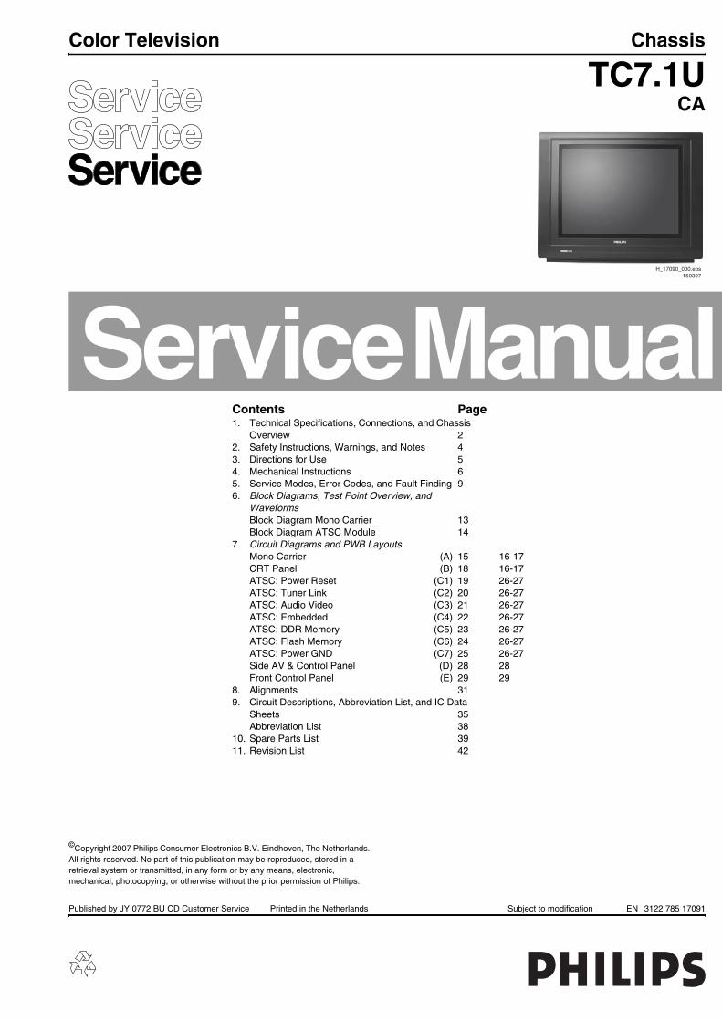
Color Television Chassis
TC7.1UCA
H_17090_000.eps150307
Contents Page1. Technical Specifications, Connections, and Chassis
Overview 22. Safety Instructions, Warnings, and Notes 43. Directions for Use 54. Mechanical Instructions 65. Service Modes, Error Codes, and Fault Finding 96. Block Diagrams, Test Point Overview, and
WaveformsBlock Diagram Mono Carrier 13Block Diagram ATSC Module 14
7. Circuit Diagrams and PWB LayoutsMono Carrier (A) 15 16-17CRT Panel (B) 18 16-17ATSC: Power Reset (C1) 19 26-27ATSC: Tuner Link (C2) 20 26-27ATSC: Audio Video (C3) 21 26-27ATSC: Embedded (C4) 22 26-27ATSC: DDR Memory (C5) 23 26-27ATSC: Flash Memory (C6) 24 26-27ATSC: Power GND (C7) 25 26-27Side AV & Control Panel (D) 28 28Front Control Panel (E) 29 29
8. Alignments 319. Circuit Descriptions, Abbreviation List, and IC Data
Sheets 35Abbreviation List 38
10. Spare Parts List 3911. Revision List 42
Technical Specifications, Connections, and Chassis OverviewEN 2 TC7.1U CA1.
1. Technical Specifications, Connections, and Chassis Overview
Index of this chapter:1.1 Technical Specifications1.2 Side and Rear Connections1.3 Chassis Overview
Notes:• Figures can deviate due to the different set executions.• Specifications are indicative (subject to change).
1.1 Technical Specifications
1.1.1 Vision
Display type : CRT, Real FlatScreen size : 27” (69 cm), 4:3Tuning system : PLLPresets/channels : 181Tuner bands : Full-CableTV color systems : ATSC
: NTSCVideo playback : NTSCAerial input : 75 ohm, F-typeCable : Unscrambled Digital
Cable -QAM
1.1.2 Sound
Sound systems : Stereo BTSCMaximum power (WRMS) : 2 x 2
1.1.3 Miscellaneous
Power supply:- Mains voltage (VAC) : 108-132- Mains frequency (Hz) : 50 / 60
Ambient conditions:- Temperature range (°C) : +5 to +40- Maximum humidity : 90% R.H.
Power consumption (values are indicative)- Normal operation (W) : ≈ 120- Stand-by (W) : < 1
Dimensions (WxHxD inch) : 29.2 x 23 x 19.1
Weight (lb) : 94.8
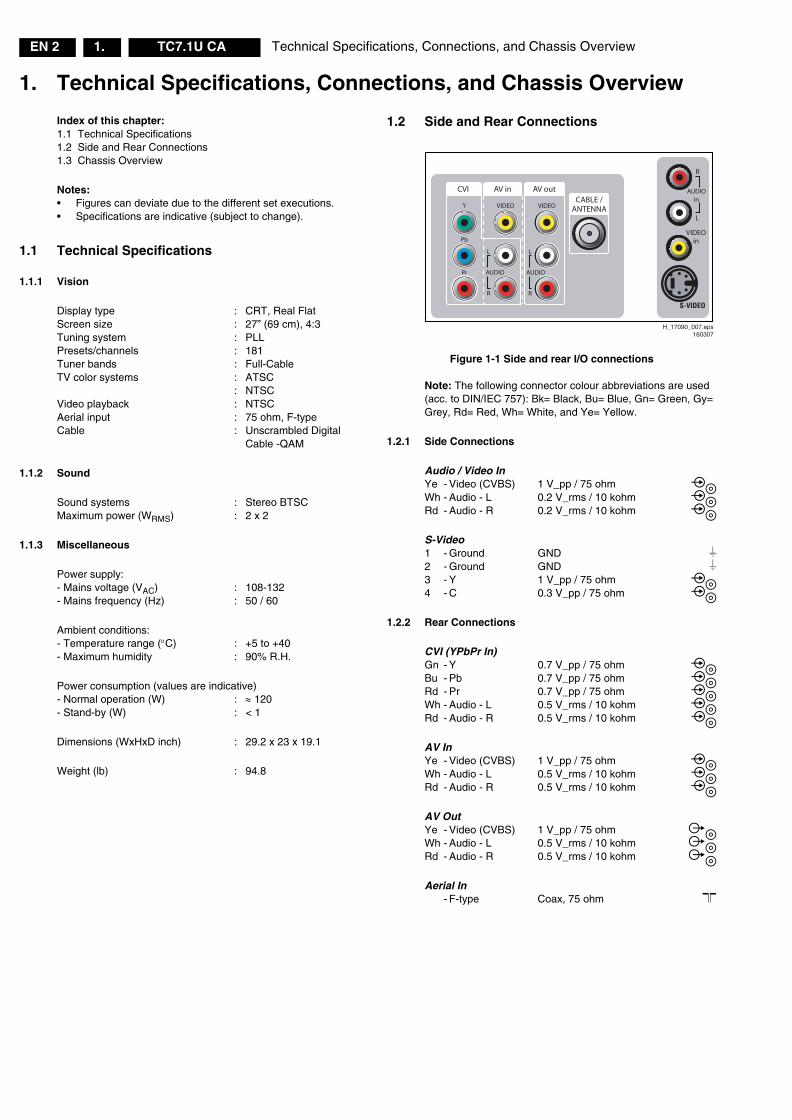
1.2 Side and Rear Connections
Figure 1-1 Side and rear I/O connections
Note: The following connector colour abbreviations are used (acc. to DIN/IEC 757): Bk= Black, Bu= Blue, Gn= Green, Gy= Grey, Rd= Red, Wh= White, and Ye= Yellow.
1.2.1 Side Connections
Audio / Video InYe - Video (CVBS) 1 V_pp / 75 ohm ��
Wh - Audio - L 0.2 V_rms / 10 kohm ��
Rd - Audio - R 0.2 V_rms / 10 kohm ��
S-Video1 - Ground GND �
2 - Ground GND �3 - Y 1 V_pp / 75 ohm ��
4 - C 0.3 V_pp / 75 ohm ��
1.2.2 Rear Connections
CVI (YPbPr In)Gn - Y 0.7 V_pp / 75 ohm ��
Bu - Pb 0.7 V_pp / 75 ohm ��Rd - Pr 0.7 V_pp / 75 ohm ��
Wh - Audio - L 0.5 V_rms / 10 kohm ��
Rd - Audio - R 0.5 V_rms / 10 kohm ��
AV InYe - Video (CVBS) 1 V_pp / 75 ohm ��
Wh - Audio - L 0.5 V_rms / 10 kohm ��Rd - Audio - R 0.5 V_rms / 10 kohm ��
AV OutYe - Video (CVBS) 1 V_pp / 75 ohm ��Wh - Audio - L 0.5 V_rms / 10 kohm ��
Rd - Audio - R 0.5 V_rms / 10 kohm ��
Aerial In- F-type Coax, 75 ohm �
H_17090_007.eps160307
Technical Specifications, Connections, and Chassis Overview EN 3TC7.1U CA 1.
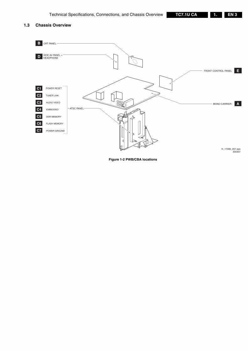
1.3 Chassis Overview
Figure 1-2 PWB/CBA locations
MONO CARRIER
EFRONT CONTROL PANEL
H_17090_057.eps300307
SIDE AV PANEL +HEADPHONE
B
D
CRT PANEL
A
C1
C2
C3
C4
C5
C6
C7
POWER RESET
TUNER LINK
AUDIO VIDEO
EMBEDDED
DDR MEMORY
FLASH MEMORY
POWER GROUND
ATSC PANEL
Safety Instructions, Warnings, and NotesEN 4 TC7.1U CA2.
2. Safety Instructions, Warnings, and Notes
Index of this chapter:2.1 Safety Instructions2.2 Maintenance Instructions2.3 Warnings2.4 Notes
2.1 Safety Instructions
Safety regulations require the following during a repair:• Connect the set to the Mains/AC Power via an isolation
transformer (> 800 VA).• Replace safety components, indicated by the symbol �,
only by components identical to the original ones. Any other component substitution (other than original type) may increase risk of fire or electrical shock hazard.
• Wear safety goggles when you replace the CRT. Safety regulations require that after a repair, the set must be returned in its original condition. Pay in particular attention to the following points: • General repair instruction: as a strict precaution, we advise
you to re-solder the solder connections through which the horizontal deflection current flows. In particular this is valid for the:1. Pins of the line output transformer (LOT).2. Fly-back capacitor(s).3. S-correction capacitor(s).4. Line output transistor.5. Pins of the connector with wires to the deflection coil.6. Other components through which the deflection current
flows.
Note: This re-soldering is advised to prevent bad connections due to metal fatigue in solder connections, and is therefore only necessary for television sets more than two years old.• Route the wire trees and EHT cable correctly and secure
them with the mounted cable clamps.• Check the insulation of the Mains/AC Power lead for
external damage. • Check the strain relief of the Mains/AC Power cord for
proper function, to prevent the cord from touching the CRT, hot components, or heat sinks.
• Check the electrical DC resistance between the Mains/AC Power plug and the secondary side (only for sets that have a Mains/AC Power isolated power supply): 1. Unplug the Mains/AC Power cord and connect a wire
between the two pins of the Mains/AC Power plug. 2. Set the Mains/AC Power switch to the "on" position
(keep the Mains/AC Power cord unplugged!). 3. Measure the resistance value between the pins of the
Mains/AC Power plug and the metal shielding of the tuner or the aerial connection on the set. The reading should be between 4.5 Mohm and 12 Mohm.
4. Switch "off" the set, and remove the wire between the two pins of the Mains/AC Power plug.
• Check the cabinet for defects, to prevent touching of any inner parts by the customer.
2.2 Maintenance Instructions
We recommend a maintenance inspection carried out by qualified service personnel. The interval depends on the usage conditions:• When a customer uses the set under normal
circumstances, for example in a living room, the recommended interval is three to five years.
• When a customer uses the set in an environment with higher dust, grease, or moisture levels, for example in a kitchen, the recommended interval is one year.
• The maintenance inspection includes the following actions:
1. Perform the “general repair instruction” noted above.2. Clean the power supply and deflection circuitry on the
chassis.3. Clean the picture tube panel and the neck of the picture
tube.
2.3 Warnings
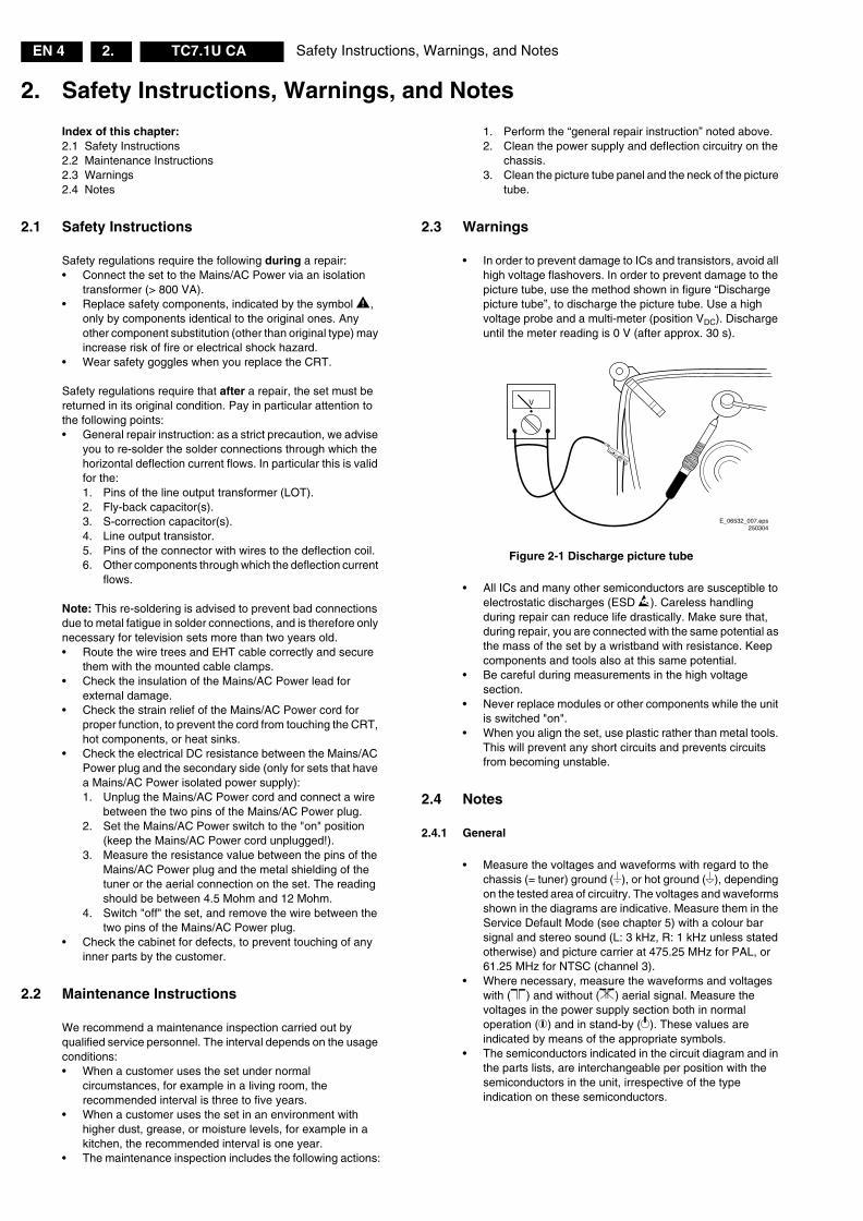
• In order to prevent damage to ICs and transistors, avoid all high voltage flashovers. In order to prevent damage to the picture tube, use the method shown in figure “Discharge picture tube”, to discharge the picture tube. Use a high voltage probe and a multi-meter (position VDC). Discharge until the meter reading is 0 V (after approx. 30 s).
Figure 2-1 Discharge picture tube
• All ICs and many other semiconductors are susceptible to electrostatic discharges (ESD �). Careless handling during repair can reduce life drastically. Make sure that, during repair, you are connected with the same potential as the mass of the set by a wristband with resistance. Keep components and tools also at this same potential.
• Be careful during measurements in the high voltage section.
• Never replace modules or other components while the unit is switched "on".
• When you align the set, use plastic rather than metal tools. This will prevent any short circuits and prevents circuits from becoming unstable.
2.4 Notes
2.4.1 General
• Measure the voltages and waveforms with regard to the chassis (= tuner) ground (�), or hot ground (), depending on the tested area of circuitry. The voltages and waveforms shown in the diagrams are indicative. Measure them in the Service Default Mode (see chapter 5) with a colour bar signal and stereo sound (L: 3 kHz, R: 1 kHz unless stated otherwise) and picture carrier at 475.25 MHz for PAL, or 61.25 MHz for NTSC (channel 3).
• Where necessary, measure the waveforms and voltages with (�) and without () aerial signal. Measure the voltages in the power supply section both in normal operation (�) and in stand-by (�). These values are indicated by means of the appropriate symbols.
• The semiconductors indicated in the circuit diagram and in the parts lists, are interchangeable per position with the semiconductors in the unit, irrespective of the type indication on these semiconductors.
V
E_06532_007.eps250304
Directions for Use EN 5TC7.1U CA 3.
2.4.2 Schematic Notes
• All resistor values are in ohms, and the value multiplier is often used to indicate the decimal point location (e.g. 2K2 indicates 2.2 kohm).
• Resistor values with no multiplier may be indicated with either an "E" or an "R" (e.g. 220E or 220R indicates 220 ohm).
• All capacitor values are given in micro-farads (μ= x10-6), nano-farads (n= x10-9), or pico-farads (p= x10-12).
• Capacitor values may also use the value multiplier as the decimal point indication (e.g. 2p2 indicates 2.2 pF).
• An "asterisk" (*) indicates component usage varies. Refer to the diversity tables for the correct values.
• The correct component values are listed in the Spare Parts List. Therefore, always check this list when there is any doubt.
2.4.3 Lead-free Soldering
Due to lead-free technology some rules have to be respected by the workshop during a repair:• Use only lead-free soldering tin Philips SAC305 with order
code 0622 149 00106. If lead-free solder paste is required, please contact the manufacturer of your soldering equipment. In general, use of solder paste within workshops should be avoided because paste is not easy to store and to handle.
• Use only adequate solder tools applicable for lead-free soldering tin. The solder tool must be able:– To reach a solder-tip temperature of at least 400°C.– To stabilize the adjusted temperature at the solder-tip.– To exchange solder-tips for different applications.
• Adjust your solder tool so that a temperature of around 360°C - 380°C is reached and stabilized at the solder joint. Heating time of the solder-joint should not exceed ~ 4 sec. Avoid temperatures above 400°C, otherwise wear-out of tips will increase drastically and flux-fluid will be destroyed. To avoid wear-out of tips, switch “off” unused equipment or reduce heat.
• Mix of lead-free soldering tin/parts with leaded soldering tin/parts is possible but PHILIPS recommends strongly to avoid mixed regimes. If this cannot be avoided, carefully clear the solder-joint from old tin and re-solder with new tin.
2.4.4 Alternative BOM identification
The third digit in the serial number (example: BF2A0635000001) indicates the number of the alternative
B.O.M. (Bill Of Materials) that has been used for producing the specific TV set. In general, it is possible that the same TV model on the market is produced with e.g. two different types of displays, coming from two different suppliers. This will then result in sets which have the same CTN (Commercial Type Number; e.g. 28PW9515/12) but which have a different B.O.M. number.By looking at the third digit of the serial number, one can identify which B.O.M. is used for the TV set he is working with.If the third digit of the serial number contains the number “1” (example: BF1A063500001), then the TV set has been manufactured according to B.O.M. number 1. If the third digit is a “2” (example: BF2A0635000001), then the set has been produced according to B.O.M. no. 2. This is important for ordering the correct spare parts!For the third digit, the numbers 1...9 and the characters A...Z can be used, so in total: 9 plus 26= 35 different B.O.M.s can be indicated by the third digit of the serial number.
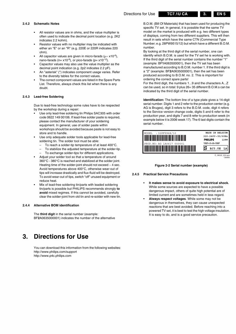
Identification: The bottom line of a type plate gives a 14-digit serial number. Digits 1 and 2 refer to the production center (e.g. AG is Bruges), digit 3 refers to the B.O.M. code, digit 4 refers to the Service version change code, digits 5 and 6 refer to the production year, and digits 7 and 8 refer to production week (in example below it is 2006 week 17). The 6 last digits contain the serial number.
Figure 2-2 Serial number (example)
2.4.5 Practical Service Precautions
• It makes sense to avoid exposure to electrical shock. While some sources are expected to have a possible dangerous impact, others of quite high potential are of limited current and are sometimes held in less regard.
• Always respect voltages. While some may not be dangerous in themselves, they can cause unexpected reactions that are best avoided. Before reaching into a powered TV set, it is best to test the high voltage insulation. It is easy to do, and is a good service precaution.
3. Directions for Use
You can download this information from the following websites:http://www.philips.com/supporthttp://www.p4c.philips.com
E_06532_024.eps130606
MODEL :
PROD.NO:
~
S
32PF9968/10 MADE IN BELGIUM
220-240V 50/60Hz
128W
AG 1A0617 000001 VHF+S+H+UHF
BJ3.0E LA
Mechanical InstructionsEN 6 TC7.1U CA4.
4. Mechanical Instructions
Index of this chapter:4.1 Set Disassembly4.2 Assy / Board Removal4.3 Service Positions4.4 Set Re-assembly Note: Figures below can deviate slightly from the actual situation, due to the different set executions.
4.1 Set Disassembly
Follow the disassemble instructions in described order.
4.1.1 Rear Cover Removal
Warning: disconnect the mains power cord before you remove the rear cover. 1. Remove all the fixation screws of the rear cover [1] and [2]. 2. Now, pull the rear cover backwards and remove it.
Figure 4-1 Rear Cover removal
Figure 4-2 Rear Cover fixation screws
4.2 Assy / Board Removal
Sometimes, it can be necessary to swap a complete assy or Printed Wiring Board (PWB). How that can be done is explained below.
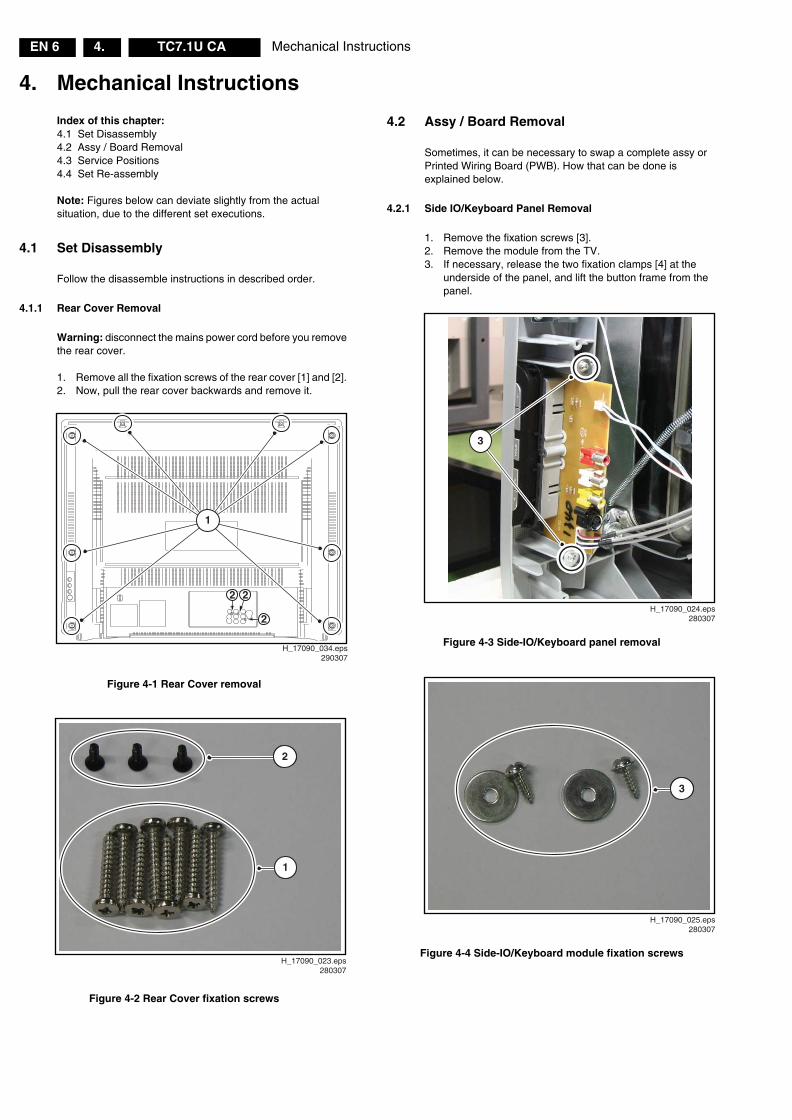
4.2.1 Side IO/Keyboard Panel Removal
1. Remove the fixation screws [3].2. Remove the module from the TV.3. If necessary, release the two fixation clamps [4] at the
underside of the panel, and lift the button frame from the panel.
Figure 4-3 Side-IO/Keyboard panel removal
Figure 4-4 Side-IO/Keyboard module fixation screws
H_17090_034.eps290307
1
2
2
2
H_17090_023.eps280307
2
1
H_17090_024.eps280307
3
3
H_17090_025.eps280307
Mechanical Instructions EN 7TC7.1U CA 4.
Figure 4-5 Button frame removal
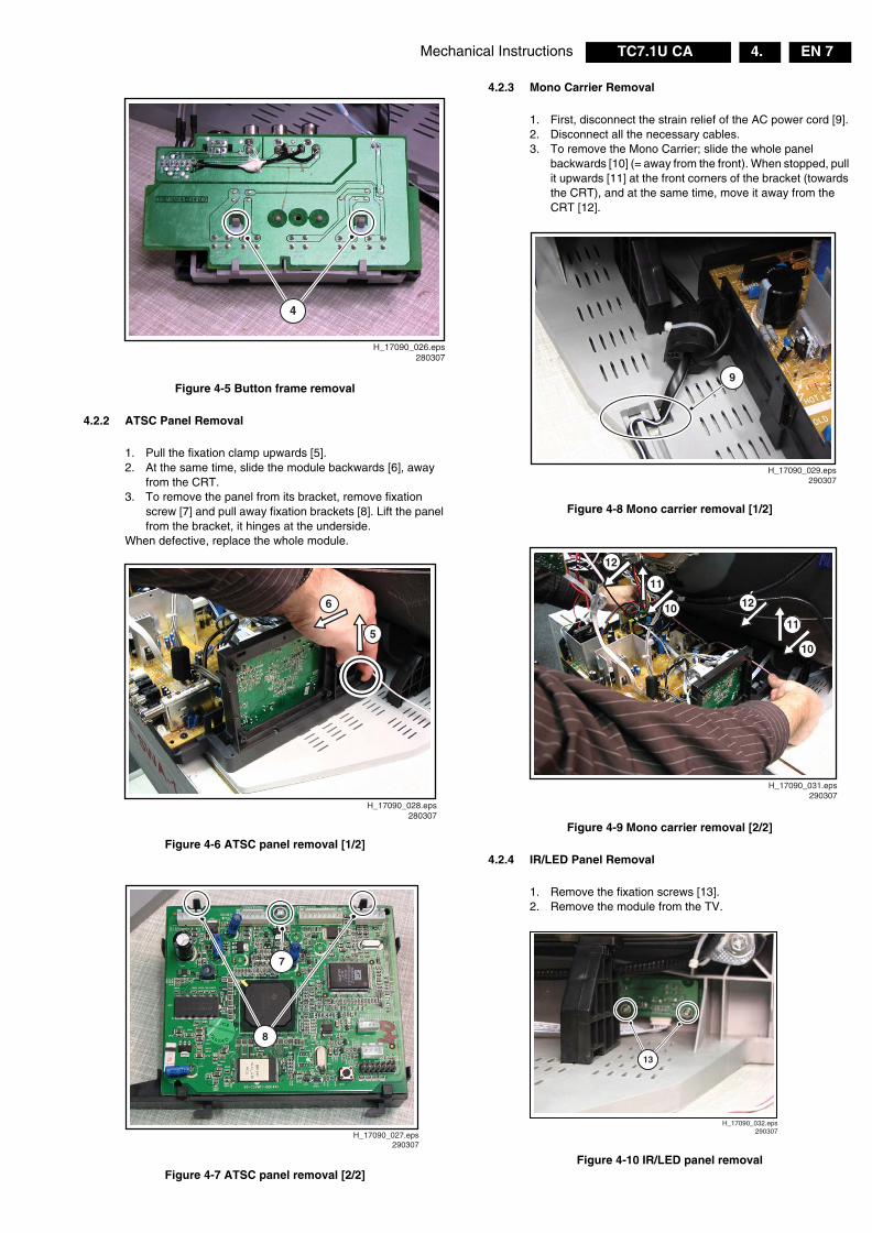
4.2.2 ATSC Panel Removal
1. Pull the fixation clamp upwards [5].2. At the same time, slide the module backwards [6], away
from the CRT.3. To remove the panel from its bracket, remove fixation
screw [7] and pull away fixation brackets [8]. Lift the panel from the bracket, it hinges at the underside.
When defective, replace the whole module.
Figure 4-6 ATSC panel removal [1/2]
Figure 4-7 ATSC panel removal [2/2]
4.2.3 Mono Carrier Removal
1. First, disconnect the strain relief of the AC power cord [9].2. Disconnect all the necessary cables.3. To remove the Mono Carrier; slide the whole panel
backwards [10] (= away from the front). When stopped, pull it upwards [11] at the front corners of the bracket (towards the CRT), and at the same time, move it away from the CRT [12].
Figure 4-8 Mono carrier removal [1/2]
Figure 4-9 Mono carrier removal [2/2]
4.2.4 IR/LED Panel Removal
1. Remove the fixation screws [13].2. Remove the module from the TV.
Figure 4-10 IR/LED panel removal
H_17090_026.eps280307
4
H_17090_028.eps280307
5
6
H_17090_027.eps290307
8
7
H_17090_029.eps290307
9
H_17090_031.eps290307
10
11
1210
11
12
H_17090_032.eps290307
13
Mechanical InstructionsEN 8 TC7.1U CA4.
4.3 Service Positions
For easy measurements, you can use the following service position.
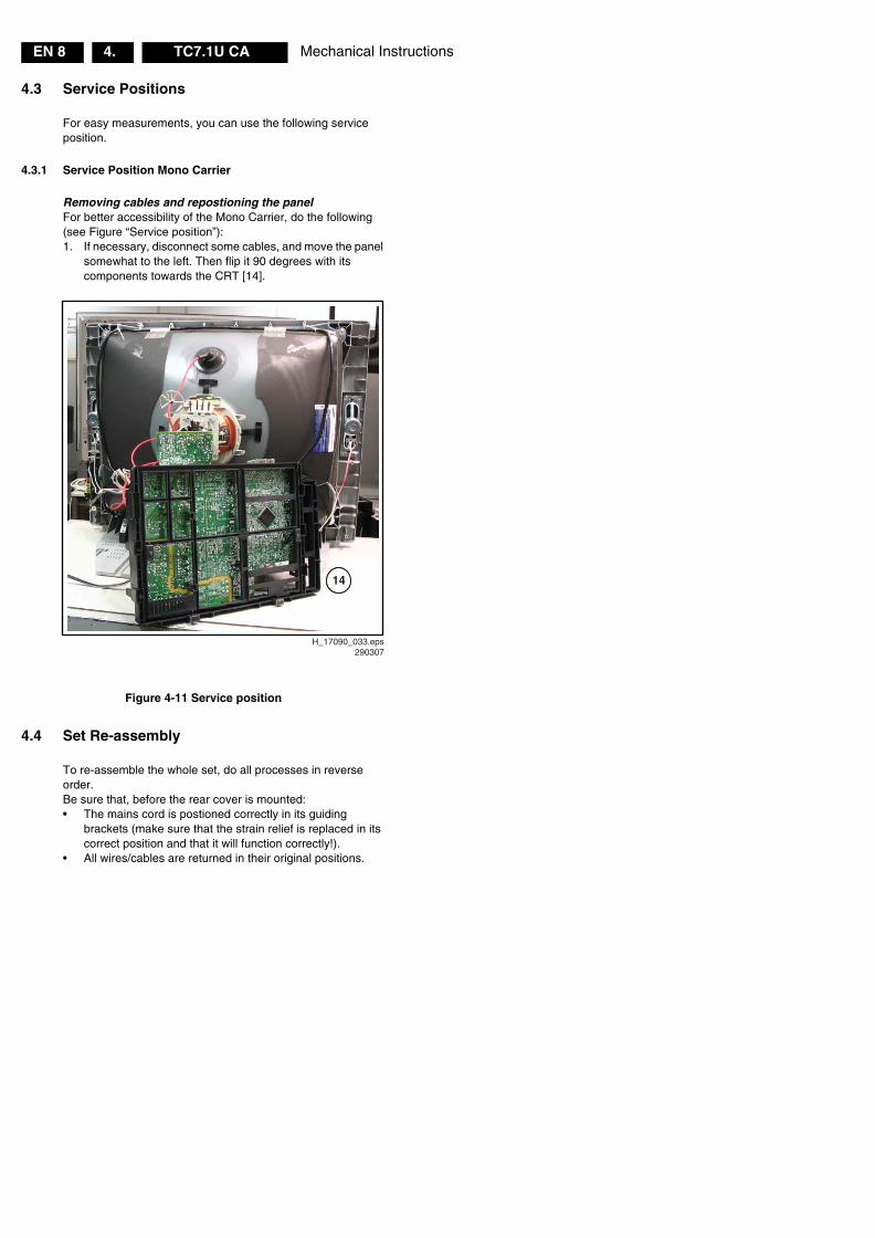
4.3.1 Service Position Mono Carrier
Removing cables and repostioning the panelFor better accessibility of the Mono Carrier, do the following (see Figure “Service position”):1. If necessary, disconnect some cables, and move the panel
somewhat to the left. Then flip it 90 degrees with its components towards the CRT [14].
Figure 4-11 Service position
4.4 Set Re-assembly
To re-assemble the whole set, do all processes in reverse order. Be sure that, before the rear cover is mounted:• The mains cord is postioned correctly in its guiding
brackets (make sure that the strain relief is replaced in its correct position and that it will function correctly!).
• All wires/cables are returned in their original positions.
H_17090_033.eps290307
14
Service Modes, Error Codes, and Fault Finding EN 9TC7.1U CA 5.
5. Service Modes, Error Codes, and Fault Finding
Index of this chapter:5.1 Service Modes5.2 Error Codes5.3 Fault Finding
5.1 Service Modes
For an explanation of the Factory Mode, see chapter 8 “Alignments”.
5.2 Error Codes
Not applicable for this chassis.
5.3 Fault Finding
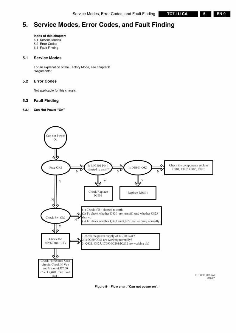
5.3.1 Can Not Power “On”
Figure 5-1 Flow chart “Can not power on”.
H_17090_035.eps300307
Can not Power On
N
Fuse OK?
Check B+ Ok?
Y
Is it IC801 Pin 1 shorted to earth?
Check/Replace IC801
Is DB801 OK? Check the components such as
C801, C802, C806, C807
Y
N
Replace DB801
N
Y
N
(1) Check if B+ shorted to earth. (2) To check whether D820 are turnoff. And whether C823shorted. (3) To check whether Q823 and Q822 are working normally.N
Check the +5VSTand +12V
Check Horizontal Scan circuit: Check H-Vcc and H-out of IC200
Check Q401, T401 and Q411
Y
1.check the power supply of IC200 is ok?2.Is Q080,Q081 are working normally?3. Q821, Q825, IC090 IC201/IC202 are working ok?
Service Modes, Error Codes, and Fault FindingEN 10 TC7.1U CA5.
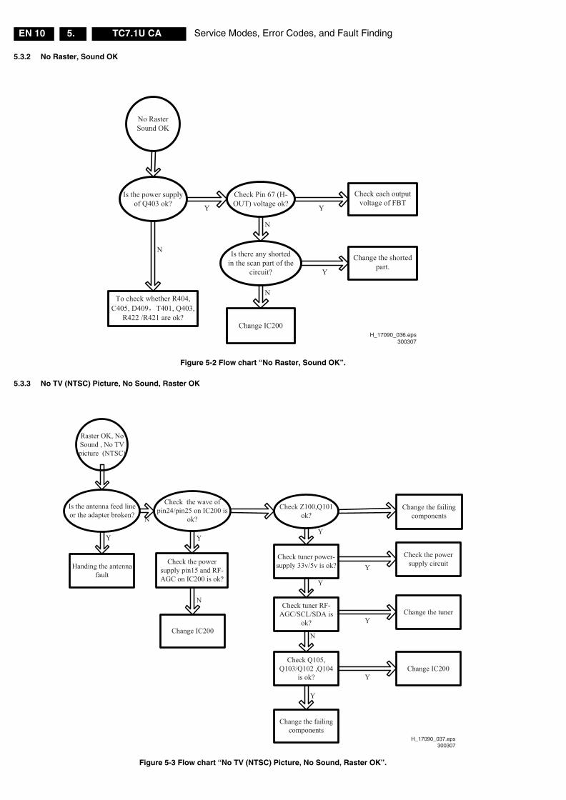
5.3.2 No Raster, Sound OK
Figure 5-2 Flow chart “No Raster, Sound OK”.
5.3.3 No TV (NTSC) Picture, No Sound, Raster OK
Figure 5-3 Flow chart “No TV (NTSC) Picture, No Sound, Raster OK”.
H_17090_036.eps300307
No Raster Sound OK
Change the shorted part.
Change IC200
To check whether R404, C405, D409 T401, Q403,
R422 /R421 are ok?
Y
Y
Y
N
N
N
Is the power supply of Q403 ok?
Check Pin 67 (H-OUT) voltage ok?
Is there any shorted in the scan part of the
circuit?
Check each output voltage of FBT
H_17090_037.eps300307
Change the failing components
Check tuner power-supply 33v/5v is ok?
YY
Check the power supply pin15 and RF-AGC on IC200 is ok?
N
Change IC200
Check tuner RF-AGC/SCL/SDA is
ok?
Y
Check the power supply circuit
N
Check Q105, Q103/Q102 ,Q104
is ok?
Y
Change the failing components
Y
YChange the tuner
YChange IC200
Handing the antenna fault
Y
N
Raster OK, No Sound , No TVpicture (NTSC)
Is the antenna feed line or the adapter broken?
Check the wave of pin24/pin25 on IC200 is
ok?
Check Z100,Q101 ok?
Service Modes, Error Codes, and Fault Finding EN 11TC7.1U CA 5.
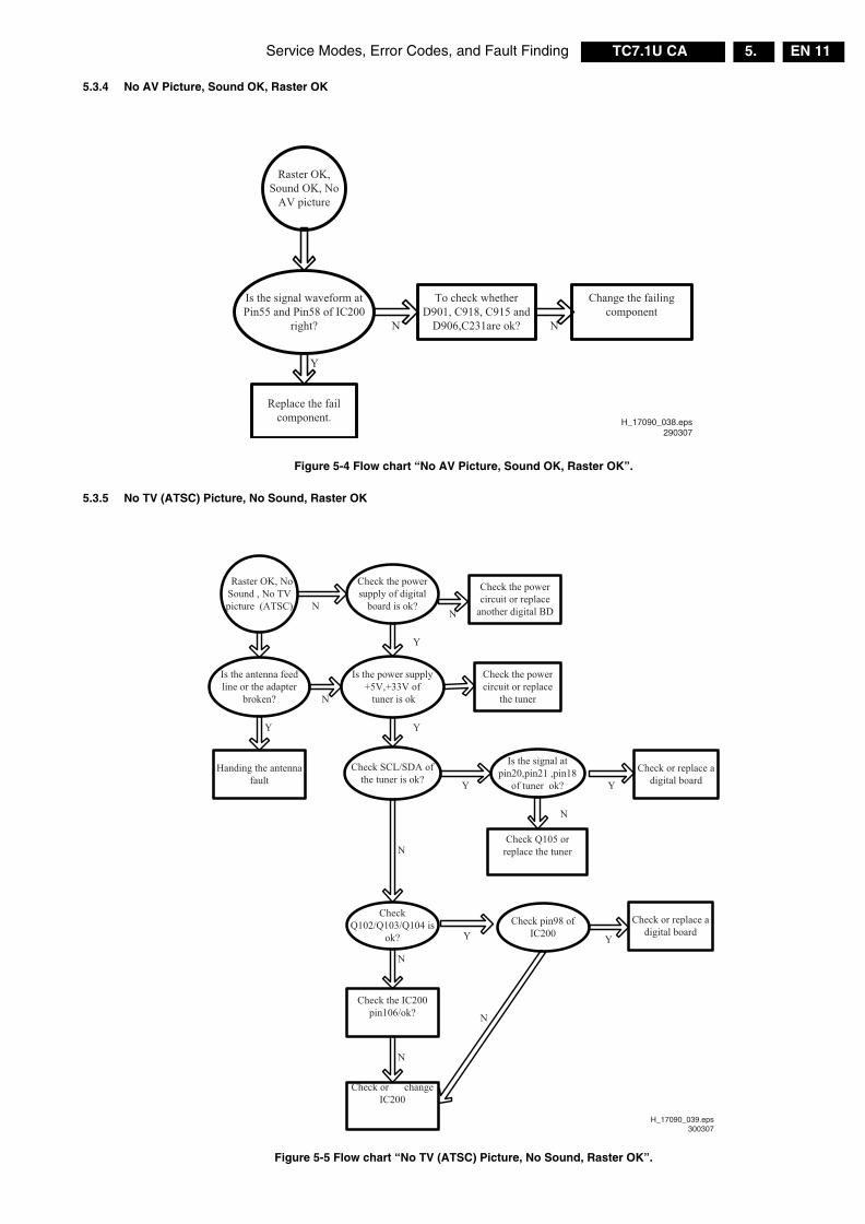
5.3.4 No AV Picture, Sound OK, Raster OK
Figure 5-4 Flow chart “No AV Picture, Sound OK, Raster OK”.
5.3.5 No TV (ATSC) Picture, No Sound, Raster OK
Figure 5-5 Flow chart “No TV (ATSC) Picture, No Sound, Raster OK”.
H_17090_038.eps290307
To check whether D901, C918, C915 and
D906,C231are ok?
Replace the fail component.
N
Y
Change the failing component
N
Raster OK, Sound OK, No
AV picture
Is the signal waveform at Pin55 and Pin58 of IC200
right?
H_17090_039.eps300307
N
Handing the antenna fault
Check the power circuit or replace
the tuner
Check the IC200 pin106/ok?
Y
N
N
YY
Y
Check or replace a digital boardY
Check or change IC200
N
Check Q105 or replace the tuner
N
Y
Check the power circuit or replace
another digital BDN
Check or replace a digital board
Y
N
N
Is the power supply +5V,+33V of tuner is ok
Is the signal at pin20,pin21 ,pin18
of tuner ok?
Check SCL/SDA of the tuner is ok?
CheckQ102/Q103/Q104 is
ok?Check pin98 of
IC200
Check the power supply of digital
board is ok?
Is the antenna feed line or the adapter
broken?
Raster OK, No Sound , No TVpicture (ATSC)
Service Modes, Error Codes, and Fault FindingEN 12 TC7.1U CA5.
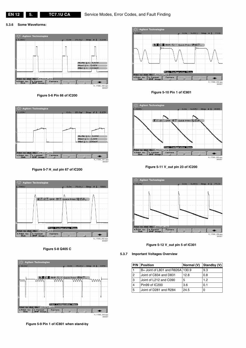
5.3.6 Some Waveforms:
Figure 5-6 Pin 66 of IC200
Figure 5-7 H_out pin 67 of IC200
Figure 5-8 Q405 C
Figure 5-9 Pin 1 of IC801 when stand-by
Figure 5-10 Pin 1 of IC801
Figure 5-11 V_out pin 23 of IC200
Figure 5-12 V_out pin 5 of IC301
5.3.7 Important Voltages Overview
H_17090_050.eps300307
H_17090_051.eps300307
H_17090_052.eps300307
H_17090_053.eps300307
P/N Position Normal (V) Standby (V)
1 B+ Joint of L801 and R826A 130.9 9.3
2 Joint of C834 and D831 12.8 0.8
3 Joint of L212 and C090 5 1.2
4 Pin99 of IC200 3.6 0.1
5 Joint of D281 and R284 24.5 0
H_17090_054.eps300307
H_17090_055.eps300307
H_17090_056.eps300307
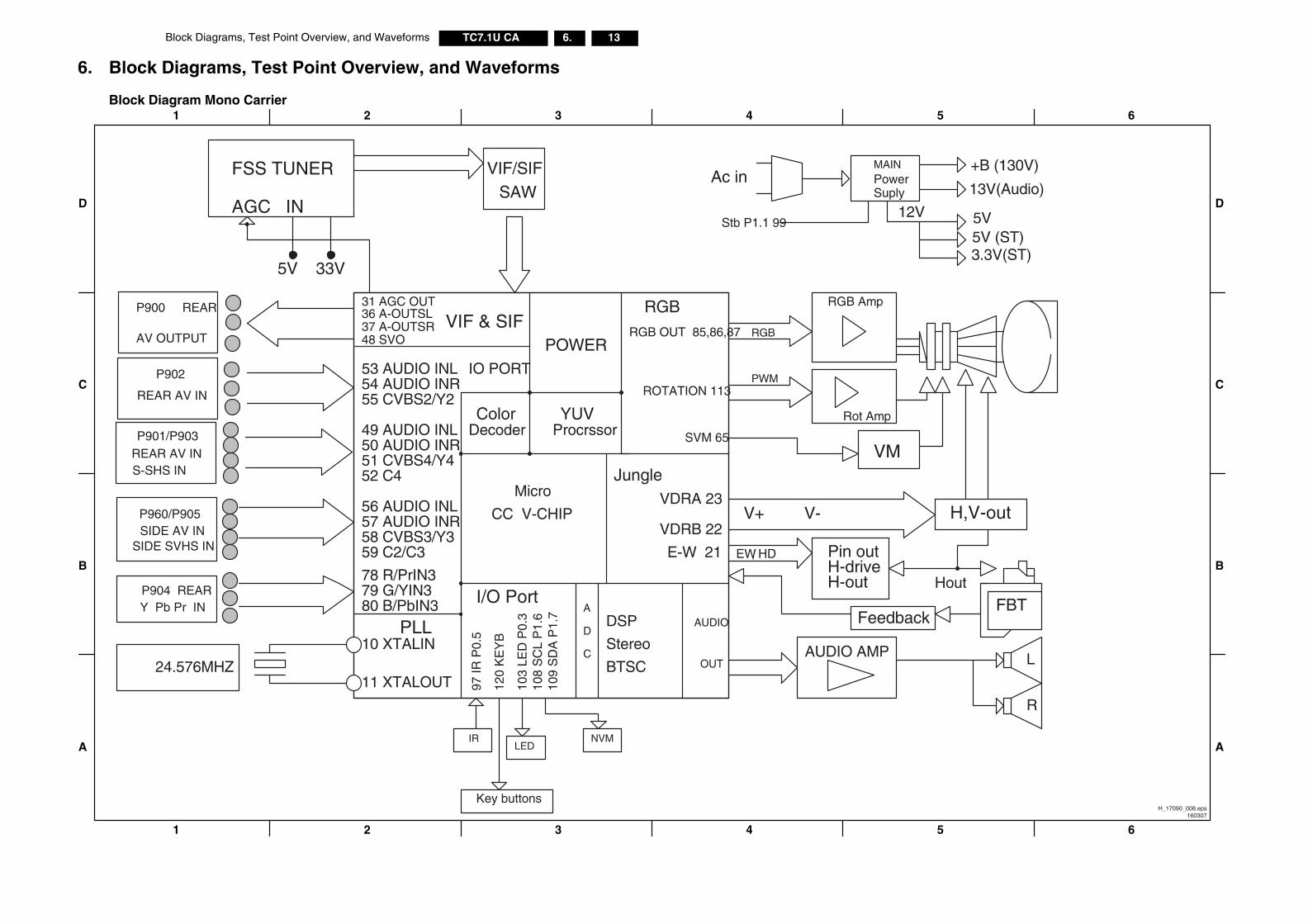
Block Diagrams, Test Point Overview, and Waveforms 13TC7.1U CA 6.
6. Block Diagrams, Test Point Overview, and Waveforms
Block Diagram Mono Carrier
1 2 3 4 65
A
B
C
D
654321
D
C
B
A
FSS TUNER
AGC IN
5V 33V
VIF/SIFSAW
31 AGC OUT36 A-OUTSL37 A-OUTSR48 SVO
P900 REAR VIF & SIF
51 CVBS4/Y452 C4
P901/P903REAR AV INS-SHS IN
55 CVBS2/Y2
58 CVBS3/Y359 C2/C3
79 G/YIN378 R/PrIN3
80 B/PbIN3
P960/P905SIDE AV IN
SIDE SVHS IN
PLL10 XTALIN
11 XTALOUT24.576MHZ
I/O Port
120
KE
YB
97 IR
P0.
5
LED
109
SD
A P
1.7
108
SC
L P
1.6
103
LED
P0.
3
NVM
A
D
C
Key buttons
Stereo
AUDIO
OUT
Micro
CC V-CHIP
JungleVDRA 23
VDRB 22
E-W 21
ColorDecoder
YUVProcrssor
POWER
RGB
RGB OUT 85,86,87
SVM 65
RGB
PWM
VM
H,V-outV+ V-
Pin outH-driveH-out
FBTFeedback
AUDIO AMP L
R
EW, HD
RGB Amp
Rot Amp
Ac in+B (130V)MAIN
PowerSuply
Stb P1.1 99
Hout
49 AUDIO INL50 AUDIO INR
53 AUDIO INL54 AUDIO INR
IO PORT
57 AUDIO INR56 AUDIO INL
P904 REARY Pb Pr IN
BTSC
DSP
ROTATION 113
AV OUTPUT
P902
REAR AV IN
12V
13V(Audio)
5V (ST)3.3V(ST)
5V
IR
H_17090_008.eps160307
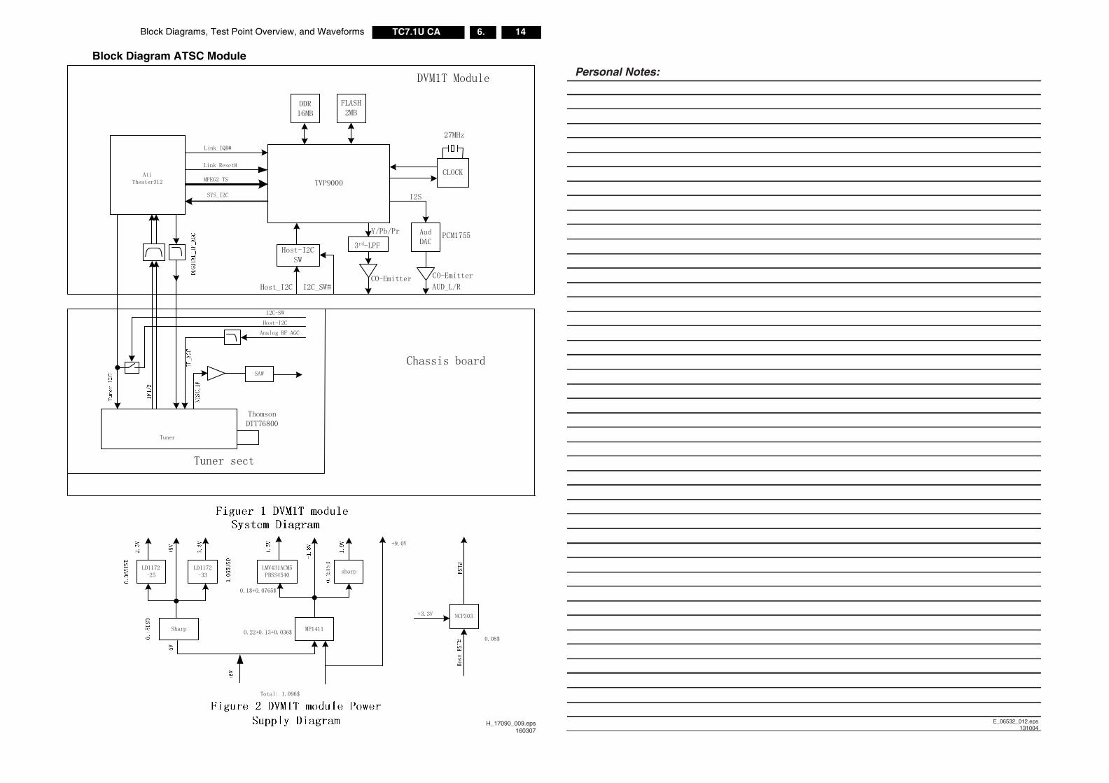
14TC7.1U CA 6.Block Diagrams, Test Point Overview, and Waveforms
Block Diagram ATSC Module
H_17090_009.eps160307
Personal Notes:
E_06532_012.eps131004
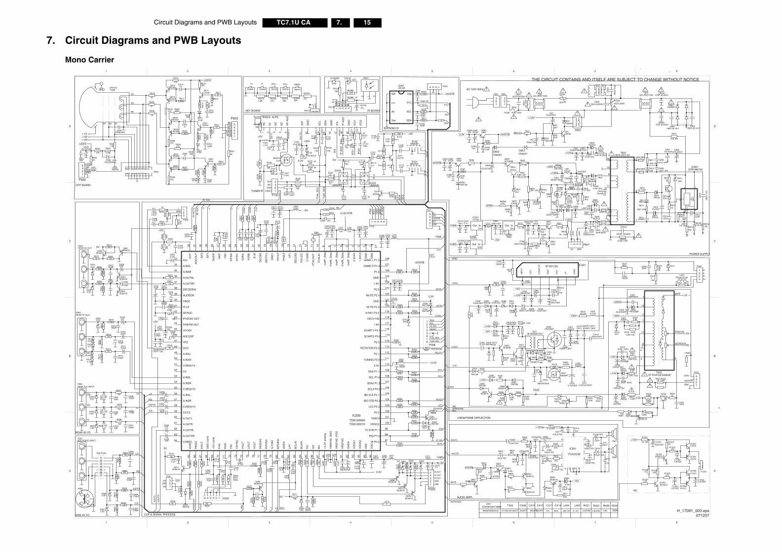
Circuit Diagrams and PWB Layouts 15TC7.1U CA 7.
7. Circuit Diagrams and PWB Layouts
Mono Carrier
1 2 3 4 5 6 87
A
B
C
D
87654321
D
C
B
A
312
IR001
S008
STANDBY
S001A
MENU
S002A
VOL-
S003A
VOL+
S004A
P-
R023A
220R024A330
R025A390
R026A470
R027A3.9K
S006A
P+
D001B LED
1 2 3 4 5P001B
R008B 47
+ C001B47u
+
C90410uFC902
100pF
5VQ901BC857A
P900REAR AV OUT
+
C905
10uF
C903100pF
Y
Cb
Cr
C926100pF
C928100pF
C927100pF
P904REAR YUV INPUT
P951SIDE RUDIO INPUT
C961100pF
C960100pF
C930100pF
C929100pF
Y
C
P960
+
C22710uF
+5V
L20410uH
C2131nF
C201220nF
C2042.2nF
C2304.7nF
+
C2152.2uF
C217100nF
+
C20810uF
L20010uH
C23222nF
C2146n8
C21
610
nF
Z20024.576MHz
C20
6
150n
F
C229100nF
+C25010uF
L00210uH
R23
210
0
C224100nF
C2023n3+
C20010uF
C211220nF
C20522nF
C235100nF
L20510uH
R23
110
0
L20610uH
R21839
R23
010
0
R20
639
K
+
C25333uF
+
C212100uF
+
C2381uF
R2261M
3.3V
+
C2391uF
12345
P202
+C02
100uF/16V
C2420.1uF
+C24110uF
+
C2372.2uF
+
C2362.2uF
Q204BC857A
R22
94.
7K
+
C2032.2uF
R2251K
R2031K
R2021K
+
C234
1uF
5V
C2091nF
Q211BC847A
GN
D1
GN
D2
1.8V
C4
3
3.3V
A3
4
Vre
fP_S
dac
5
Vre
fN_S
dac
6
Vre
fP_S
dac
7
Vre
fN_S
dac
8
vref
P_S
dac
9
XT
ALI
N10
XT
ALO
UT
11
IFVEDIO OUT43
AGC2SIF46
VCC8V45
PH
2LF
16
PH
1LF
17
DVB/FM OUT44
VD
RB
22
SDA2 P1.3 107
SCL P1.6 108
3.3V 110
SDA P1.7 109
IBO D/A P0.1 105
TUNING P2.0 111
P2.1 112
ROTATION P2.2 113
P2.3 114
SCART2 P3.0 115
SCART1 P3.1 116
SCL2 P0.0 106
EH
T32
AG
CO
UT
31
SIF
230
SIF
129
GN
DIF
28
IRE
F27
VS
C26
VIF
IN2
25
VIF
IN1
24
VD
RA
23
D.G
ND
12
VG
/LE
D13
DE
CD
IG14
CVBS2/Y255
SE
CP
LL19
C452
CVBS4/Y451
A.IN4L49
VP
115
VD
DA
294
GN
D1
18
A.OUTL60
A.IN2R54
A.IN2L53
A.IN4R50
CVBSO64
SVO48
AVL33
GND240
PLLIF41
A.OUTSL36
A.IN3L56
A.OUTR61
CVBS3/Y358
A.IN3R57
VP247
SIFAGC42
A.IN5L34
A.IN5R35
A.OUTSR37
DECSDEM38
AUDEEM39
A.OUTHL62
VD
DA
193
GN
DA
92
VR
EF
AD
91
VR
EF
AD
_NE
G
VR
EF
AD
_PO
S
+3.
3V a
nalo
g88
BO
87
GO
86
RO
85
BLK
IN84
BC
LIN
83
LPF
82
GN
D3
81
B/P
bIN
380
G/Y
IN3
79
R/P
rIN
378
VO
UT
76
UO
UT
75
YO
UT
74
YS
YN
C73
PrI
N70
PbI
N71
+5V
com
b69
GN
D c
omb
68
HO
UT
67
FB
ISO
66
SV
M65
A.OUTHR63
IBO STB P0.2 104
LED P0.3 103
P0.4 102
VSSC2 101
VDDC2 100
TV STB P1.1 99
IRQ P1.0 98
IR P0.5 97
VD
D96
VS
S95
P2.5 123
MUTE P2.4 122
GND 121
KEYB P3.3 120
X-RAY P3.2 119
DECV1V8 118
1.8V 117
INS
SW
377
1.8V 124
GND 125
P1.2 126
GAME L P1.5 128D
EC
BG
20
E-W
21
YIN
72
C2/C359
GAME R P1.4 127
IC200
C251
0.1uF
C2522N2
C255220nF
C0180.01uF
L20710uH
L20310uH
+
C22510uF
C226100nF
C017100nF
C261220nF
C260220nF
C023220nF
+C24047uF
TDA12000HTDA12001H
L2111uH
0.1uFC246
C248100nF
C249100nF
L202
1uH
L00110uH
+
C26247uF
L21010uH
L208
10uH
L209
10uH
C258100nF
+
C019100uF
D3091N4001
+
C323100uF/35V
R3131C325
0.33uF
R3141K
+ C324220uF/25V
-14V
C3371000P
R3152K2
R3211
+
C308220uF/25V
+14V
R284100K
R285
470R283430*
R2860
R28268
+12V
+
C31350V/4.7uFD308
4148
D3074148
D3063V9
+
C30747UF/25V
R3001K2
D3001N4148
D400FR104MF
C401220P500V
+C400
22uF/250V
D405FR104MF
C419220P 500V
+
C4161000uF/35V
R427
1/2W FUS-14V
D404FR105
C418220P 500V
+
C4151000uF/35V
R426
1/2W FUS
D406FR104
+
C4174u7/50V
+
C4061000u/25V
12V
R410
C404
22n
R411120 2W
R406470
R4291K
C421100n
T40136-HDR029-XX1*
Q4052SD2638*
L403600UH*
C4083300P/1.6KV
D401RS3FS*
D402FR104
C410 6200P/1.6KV*
C4110.022uF/400V*
C413 6200P/1.6KV*
C414*390n/400V
+14V
R4243.9K
C4202200P
1234
P403
R42210 1/2W *
R41868K
R4203.9/2W
D408
BZX79C5V6
C4070.01uF
C4124.7uF/50V
+200V
Q402C639
R4251/2W 10K
D4135V1
Q281BC847A
Q280BC857A
L400TRL242 31uH
R401 680
R324180
1234
P400
+
C2310.1uF
Cb
Cr
Y
AB
L
RELAY
SCL
SDA
ROTATION
KEYB
MUTE
IR IN
RF
AG
C
RF AGC
VD
RA
VD
RB
E-W
H-OUT
E-W
2 1
Cr Y Cb
C00522pF
C00322pF
C00410nF
1234 P003
SDA
SCL
AO
UT
L
AO
UT
R
SA
ND
CA
ST
H O
UT
123
P201
12V
C256220n
X-RAY
+
C300100uF/50V
ABLSANDCASE
VDRB
C3342200PVDRA
C21022nF
L201
1uH
C222100nF
+
C223100uF
R031100
R0302.2K
R0332K2
X-RAY
+5VSTB
ROTATION
D9055.6V
R923 75 C92310P
D9075.6V R
925
82
D9065.6V R
924
82
D9035.6V R
921
75 C921100P
D9045.6V R
922
75 C92210P
C2071nF
C2430.1u
C2440.1u
C2450.1u
Pb
+5VSTB
1234567
P961
1234567
P200
0.47
1W
R3502K2
C3512200P
R3161K
C3501500P
1W
1W
R036100
C2702200P
R27
033
K
R271
18K
+5V
+3.3V-STB+5V
+
C25747uF
1V8D
1V8A
R0391K
123
P209
R251
1K
R25
2
47K
R2501K R
253
47K+
C2662.2uF
+
C2652.2uF
L
R
D0061N4148
D0051N4148
+3.3V
STB
LED
+
C360100uF
D2045.6V
1 2 3 4 P807
C2670.1uF
+
C2282.2u
R03
1K
Q900BC847A
R13071.2K
R13041K
Q1301BC847A
Q1302BC847A
R130610K R1305
470
R13021K
R1303470
+
C13031uF/50V
+
C13021uF/50V
Q1305C1815
Q1306A1015
+ C13042.2u/50V
Q1303C1815
Q1304A1015
+ C1301100u/25V
R1301
10 2W+12V
12
P1301
D311
R04
947
K
D0103V9
* R435
D28024V
D9105.6V
D9085.6V
Q903BC847A
Q902BC847A
AV
-MU
TE
AV-MUTE
D4121N4001
+14V
Q408BC847A
R2361k
R2443.3K
C264 22n
R245470K
ABL
T80136-LIF007-XX0
C802220n/250VAC
C801AC275V/220n
1R80
11M
1/2
W
123
P801
123
P802
F800
FUSE T5AL 125V
C80
3
400V
/100
n
12
P803
T80236-LIF007-XX0
R8243K9
C804250V AC 4n7
C805250V AC 4n7
DB801D3SB60*
RT802
3D210
D850RU3YX
D820RU3AM
C83410nF
C820470P 2KV
C82410n/500V
C850470P/1KV
C8520.01uF
+
C8511000uF/25V
+C823
220u/160V
+12Va
L801100uH
+130V
+12V
D8211N4148
R840A8.2M 1/2W
12
X800
D811FR104
C840A
2200P AC400V
R826A
22K 2W
R82
310
0K 1
/2W
C804A470P AC400V
C805A470P AC400V
375
6
4 1
IC801STR-W6735
R850
FUS 3A 250V
C80710n 500v
C8123300P
C813100n
C810220P
C81
5
680P
1K
V
R814
2K2 1/4W
R816NC
R816A0.22 2W
R81322 1/4W
D810FR104
R8121K
+
C806470u/200V
+
C8111uF 50V
+C814
10u/35V
D812FR104
R8111K
D8136V2
+
C423220uF/160V
C8261000P
C8250.1 50V
R82533K
IC803TL431
+C844
10u/50V
R827750
IC802615A
+33V
R014K7
Q206BC857A
Q207BC857A
Q208BC857A
R25
722
0
R25
622
0
R25
522
0
R8262.2K
D2811N4148
D2821N4148
130V
D2831N4148
+
C611470uF/16V
R6013K3
R6004K7
R6034K7
C6020.22uF/63VC601
4700p/63V
C6060.22uF/63V
R6043K3
AOUTR
AOUTL
C6054700p/63V
+12Va C61210n
R6120.12/2W
R609
1K
R6072K7
Q601BC847A
Q605BC857A
R605
470
R810
47K 3W
R421
G1G2G3
KR
KG
KB
CRT500TUBE
R518470
R516
470
Q512BC422
Q522BC422
Q532BC422
Q5314544
R517560
R528470
R527560
R538470
R53
410
R5011K
C531330P
R537560
R51515K
12345
P503
12345678
12345678
P500
C5051000p/2KV
L50122uH*
1234
P502
GNDR519
1K
R529
1K
R539
1K
Q513BC423
Q533BC423
Q523BC423
C5121n
C5221n
C5321n
+200V
R526470
R52515K
R53515K
R536470
Q521C4544
Q511C4544
R52
410
C521330P
R51
410
C511330P
R52
327
0
R51
327
0
D5114148
D5214148
R53
327
0
D5314148
R52147
R52
210
K
R51147
R512
10K
R53147
R53
210
K
R50533C504
33n
+
C50322uF/250V
+200V
C4050.1uF
D4091N4148
D4111N4001
R41210K Q403
BC846B
R413820
R540
2.2M
+
C54010U/250V
R5411.5K
D5401N4004
R542
470
5V
470R009B
R0293.3K
R026100
R025100 R027
3.3K
R0325.6K
R0221K
5.6KR023
R4071 1/2W
R24
039
0K
R227470K
R024100
R01810K
R09310K
R22
822
0
L803/J805
D840RU3YX
C840220P/500V
+
C8411000uF/16VL8
04
L803
R824A3K9
R2372.2KR
223
1KR
222
100
R22
01K R22
110
K
R094100
AC 120V 60Hz
J2140
D6234148
J3090
R610
1K
+
C610100uF/16V
R602
470
5VSTB
P600
P601
R23
84.
7K
CRT T402 C410 C414 L400
A68QFN893X002 37-050120-5020T 6800PF 31 UH 5.6OHM 5.6K
Conversion table C408 C413 C411
3300PF 390n 600 UH
L403
5.6OHM
R421 R422 R428
6200PF 27n
R608
2K7
3 4
L806/J804
+
C230A10U
+
C235A10U
R261
75 R26275
R260
75
MUTE
D011N4001
Q01C2236
C8080.01U 1KV
K802
+C8311000u
D830RU3YX
C830220P/500V
+
220UF16VC828
R011100
R009100
0
R010100
+
C402
Q080D667
D0803.9V
C08710n
R090120
+
C083100uF
C08810n
+5VSTB3.3V
Q205BC857A
R23
547
kR
234
56k
D2261N4148
R21
922
0
R40956 1/2W
R21
012
K
R20
710
0
R20
810
0
R20
910
0
R0472.2K
0.47
R241390
R904330
R905330
R90
310
0KR
902
100K
D0081N4148+
C029100u
R05022K R052
10K
R0513.3K
+
C2771000u
C2780.1
L802
R41968 2W
L4044.7mh
R433
THE CIRCUIT CONTAINS AND ITSELF ARE SUBJECT TO CHANGE WITHOUT NOTICE
R9121K
R91075
R9081K
B OUT
G OUTR OUTGND
AKB
GND
12VGND
VM
200V
HERTER
GND
V-
V+
H-
H+
6V GND
R035100 RESET
IIC SW
3.3V
R606
2K7
R0483.3K
R04510K
CRT BOARD
VR
EF
VP
OU
T
GN
D
PO
MP
UP
VC
C
INP
UT
IC301STV8172A
WP
n.c.
A2
Vss
Vdd
PTC
SCL
SDA
IC00124C32
5
4
8
1
10
2
7
11
EHT
FOCUS
SCREEN
T40237-FCAT02-EAA0A*
9
R927
100
R928
100
R926
100
R932100
R929100
R9631K
R96
147
KR
960
47K
R9621K
C342330n
130V
+14V
< H1 >< H2 >< H3 >
< H1 >
< H2 >
< H3 >
P402
R20
0
68K
R204
1K
R20
1
39K
R20
568
0
R034100
R8286.8K
R82233K 2W
C835
0.01u
Q823C1815
Q822C1815
Q821D667
Q8202CS2688
R8321K 1/4W
R831
1.5 3W
R8331K
R8216.8K 5W
R820
4.7 1W
D8328V2
D8239V1
+C829
4700U/16V
D8311N4001
Q825D667
R82947K
R8341K
+5V
C0910.1u
InOutGnd
IC0907805
+
C090220U/16V C832
220U/16V
+
C83310n
InOutGnd
IC2011117D
InOutGnd
IC2021117D
C2180.1u
+
C219100u
C218A0.1u
+
C219A100u1V8D
1V8A
Q081D667
D0815V1
C08610n
R087680
+
C085100uF
C08410n
5VSTBR086
10
D0821N4148
R0227K
R817
120K 2W
D021N4148
D8141H8
+
C01100uF/25V
+12V
C809220P 1KV
C84210nF
R829A4.7K
STBY
RELAY
+ C600
22uF/16V
+
C604
22uF/16V
+ C609
1uF/50V
Q602BC857A
Q604
BC847A
Q603BC847A
D6244148
D6254148
D626
4148
12V
+
C603100uF/16V
+
C607
100uF/16V
+
C608
100uF/16V
+
C613100uF/16V
+
C615100uF/16V
+
C616
470uF/16V
+
C614
470uF/16V
C61747n
C618
47n
R611
33K
IC601
TEA2025B
10
11
7
6
8
9 13 12 5 4
2
3
15
14
16
RT801MZ75-9RM
R815100
D81533V
Q824BF422
D8225V1
D8511N4001
D8521N4001
+C093220U/16V
L212
0.6μH
F802 2A 250V
F801 2A 250V
D414
1N4148
R430
0
Q409
BC857A
D4151N4148 R437
15kR438
36k
C4241nFR439
36k
R012
1.5 3W
BinGinRin
GNDAKB
+200VNC
HeatGND
D0015V1 D002 D004
+
C10010uF
R103
39K
+
C103100uF
L10110uH
+5V
D102BYV79C33
R10
068
KR
101
10K
+33V
R113
8
R11451
+
C10547uF/50V
Q101C3779
C10910nF
R117 150
R116 680
R115
150
L1021UH
+9V
1
2
D100
IN4148
54321
Z100M3953M
12345
P001
C101100P C114
100P
IRLED
R111560
+5VSTBKEYGND
C1060.01uF
1234
P130
R130100
R131100
TO
R91
7
C130100P*
C131100P*
54321
M9370MZ101
3
4
C11010nF
SDA
SCLGND
VIDEO
C10210n
C1080 .01
1
2
3 4
5
6
Q102
UM6KIN
NC
1
5V2
NC
3
NC
4
RF
-AG
C5
33V
11
GN
D12
SC
L14
SD
A15
GN
D16
IFA
17
IF-A
GC
18
GN
D19
IFD
120
IFD
221
TU101 TDQU2 ALPS
C11110n
R10
710
0
R105 alt10K
R106 alt10K
3.3V
C112100n
R1082.2
C113100n
R1102.2
IF-A
GC
IFD
1
IFD
2
IFA
R12122
R12022
R1224.7K
R11210K
R119 alt10K
TU
N_S
CL
TU
N_S
DA
1
2
34
5
6
Q103UM6KIN
5V
C116 alt100n
C115100n
Q104BC847
R11822
SW
SC
LS
DA
5V-T
RF
AG
C-T
33V
-T
SC
L-T
SD
A-T
IFA
GC
-T
IFD
1-T
IFD
2-T
R104100
R109100
alt
altalt
alt
1 2 3 4 5
P100
IFD
1IF
D2
GN
D
IF-A
GC
GN
D
C10710nF
Q407630MFP
Q105BSH103
C117
10n
R287100
Q282BC857A
D2841N4148D285
1N4148
R4285.6K*
R440150K*
BCL
Q404BC857A
D3051N4148 R443
120K R442100K
8
7
1
5
14
15
16
11
9
13
12
T803BCK-4201-XX
R81847K
R440
150K
SDA
SCLIIC SW
RESET
12345678
P008
TUN_SDA
TUN_SCL
Pr
Y
123456 P203
BCL
+
C9181uF
+
C9192.2uF
+
C9172.2uF
C915100pF
C912100pF
C914100pF
P902REAR AV Input
D9015.6V
R91
447
KR
913
47K
R9161K
R9151K
R91
775
R919100
D9145.6V
D9125.6V
D9114.7V
D9134.7V
1 2P001D
KE
Y
GN
DK
EY
VC
CLE
DIR
IR BOARDKEY BOARD
R3
L3
V3/Y3
C3
L3
R3
V3/Y3
C3
SIDE AV I/O
REAR AV I/O
NC
AUDIO AMPL
TUNER IF
POWER SUPPLY
LINE&FRAME DEFLECTION
+5V
CUP & SIGNAL PROCESS
E2PROM I/O
R010B3K9
R010B3K9
PTC
PTC
0
R092 NC
H_17091_003.eps071207
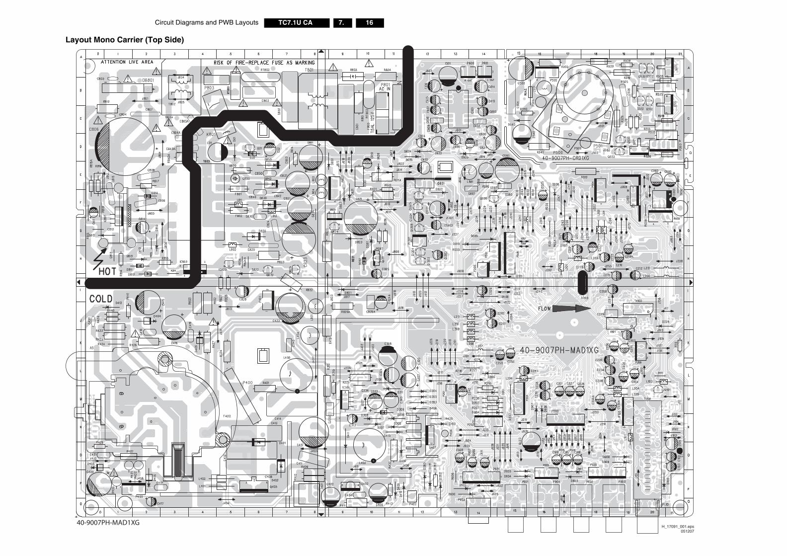
16TC7.1U CA 7.Circuit Diagrams and PWB Layouts
Layout Mono Carrier (Top Side)
40-9007PH-MAD1XGH_17091_001.eps
051207
Circuit Diagrams and PWB Layouts 17TC7.1U CA 7.
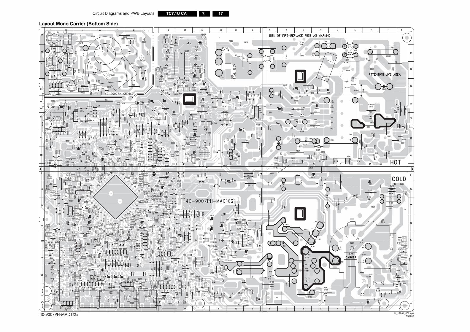
Layout Mono Carrier (Bottom Side)
H_17091_002.eps05120740-9007PH-MAD1XG
18TC7.1U CA 7.Circuit Diagrams and PWB Layouts
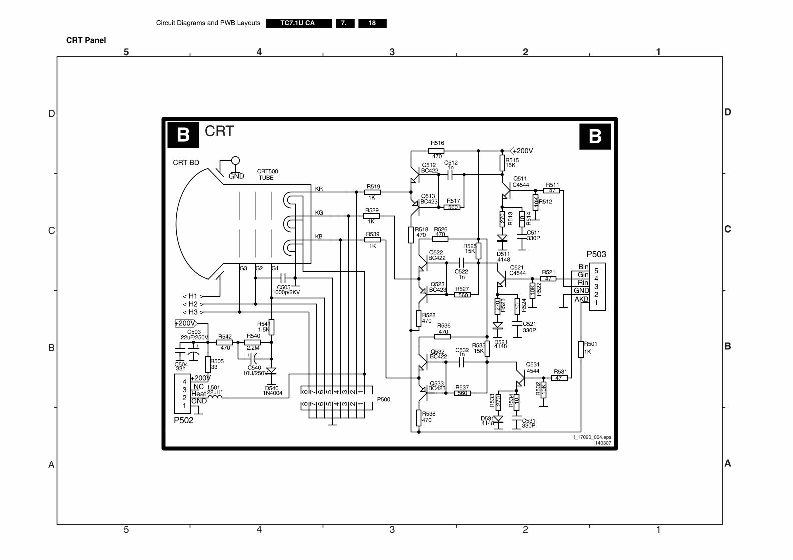
CRT Panel
G1G2G3
KR
KG
KB
CRT500TUBE
R518470
R516
470
Q512BC422
Q522BC422
Q532BC422
Q5314544
R517560
R528470
R527560
R538470
R53
410
R5011K
C531330P
R537560
R51515K
12345
P503
12345678
12345678
P500
C5051000p/2KV
L50122uH*
1234
P502
GNDR519
1K
R529
1K
R539
1K
Q513BC423
Q533BC423
Q523BC423
C5121n
C5221n
C5321n
+200V
R526470
R52515K
R53515K
R536470
Q521C4544
Q511C4544
R52
410
C521330P
R51
410
C511330P
R52
327
0
R51
327
0
D5114148
D5214148
R53
327
0
D5314148
R52147
R52
210
K
R51147
R512
10K
R53147
R53
210
K
R50533C504
33n
+
C50322uF/250V
+200V
R540
2.2M
+
C54010U/250V
R5411.5K
D5401N4004
R542
470
CRT BD
< H1 >< H2 >< H3 >
BinGinRin
GNDAKB
+200VNC
HeatGND
5
5
4
4
3
3
2
2
1
1
D D
C C
B B
A A
CRTB B
H_17090_004.eps140307
Circuit Diagrams and PWB Layouts 19TC7.1U CA 7.
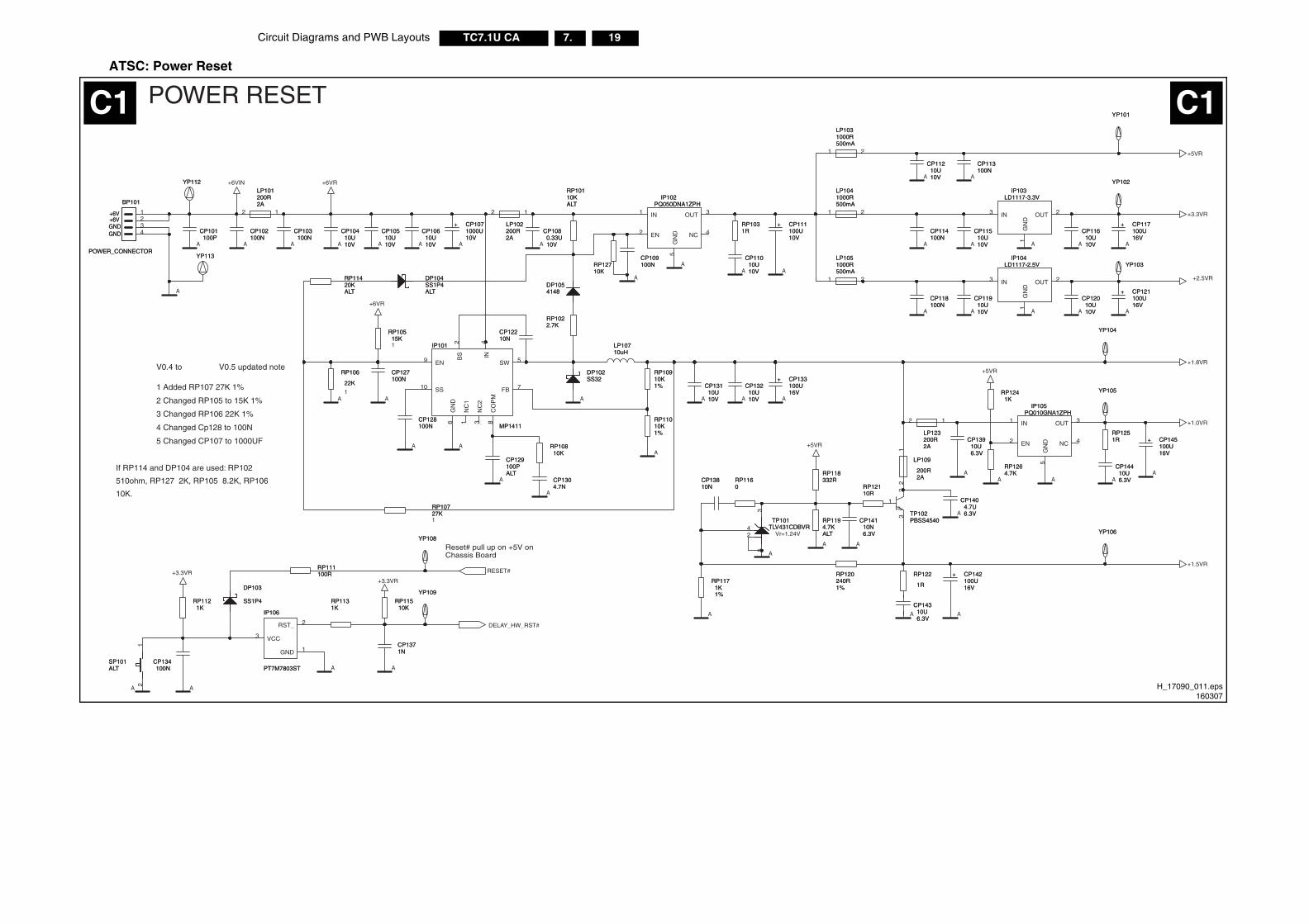
ATSC: Power Reset
A
A
A A
+6VIN
A
A
A
+1.5VR
A
A
A
AAA
A
A
A
A
A
A
AA
A
A A A
+3.3VR
A
+2.5VR
A A A
AA
A
A A
+5VR
AA
A A
A
A
A
A
A
+1.8VR
AA A
A
+1.0VR
+6VR
+5VR
+5VR
+3.3VR+3.3VR
+6VR
A
A
A
A
A
DELAY_HW_RST#
RESET#
Vr=1.24V
Reset# pull up on +5V onChassis Board
1 Added RP107 27K 1%
2 Changed RP105 to 15K 1%
3 Changed RP106 22K 1%
4 Changed Cp128 to 100N
5 Changed CP107 to 1000UF
V0.4 to V0.5 updated note
If RP114 and DP104 are used: RP102
510ohm, RP127 2K, RP105 8.2K, RP106
10K.
1
1
1
1 2
LP1041000R500mA
LP1041000R500mA
YP106YP106
RP122
1R
RP122
1R
CP13910U6.3V
CP13910U6.3V
RP120240R1%
RP120240R1%
10V
CP10410U10V
CP10410U
10V
CP11210U10V
CP11210U
CP134100N
CP134100N
IN1 OUT 3
GN
D5
EN2 NC 4
IP102PQ050DNA1ZPH
IP102PQ050DNA1ZPH
+
16V
CP117100U
+
16V
CP117100U
IN3 OUT 2
GN
D1
IP104LD1117-2.5V
IP104LD1117-2.5V
+
16V
CP145100U
+
16V
CP145100U
CP128100NCP128100N
CP109100NCP109100N
RP12110RRP12110R
RP1171K1%
RP1171K1%
CP101100P
CP101100P
RP1251RRP1251R
NC
11
BS
2
NC
23
IN4
SW 5
GN
D6
FB 7
CO
PM
8
EN9
SS10
IP101
MP1411
IP101
MP1411
RP10110KALT
RP10110KALT
RP10515K
RP10515K
24
35
TP101TLV431CDBVR
TP101TLV431CDBVR
RP10910K1%
RP10910K1%
12
LP109
200R2A
LP109
200R2A
RP1264.7KRP1264.7K
CP1371NCP1371N
DP104SS1P4ALT
DP104SS1P4ALT
1
23 TP102
PBSS4540TP102PBSS4540
10V
CP12010U10V
CP12010U
YP112YP112
1%
RP11010K1%
RP11010K
YP101YP101
YP105YP105
RP1031RRP1031R
10V
CP10610U10V
CP10610U
CP114100NCP114100N
CP12210NCP12210N
1 2
LP1051000R500mA
LP1051000R500mA
+
16V
CP133100U
+
16V
CP133100U
RP1241K
RP1241K
RP1194.7KALT
RP1194.7KALT
+
10V
CP1071000U
+
10V
CP1071000U
IN3 OUT 2
GN
D1
IP103LD1117-3.3V
IP103LD1117-3.3V
YP113YP113
+
16V
CP142100U
+
16V
CP142100U
1234
+6V+6VGNDGND
BP101
POWER_CONNECTOR
+6V+6VGNDGND
BP101
POWER_CONNECTOR
LP10710uHLP10710uH
YP103YP103
1 2
LP1031000R500mA
LP1031000R500mA
CP1404.7U6.3V
CP1404.7U6.3V
RP11420KALT
RP11420KALT
CP129100PALT
CP129100PALT
RP12710KRP12710K 10V
CP11010U10V
CP11010U
CP13810NCP13810N
CP13210U10V
CP13210U10V
RP11510K
RP11510K
RP106
22K
RP106
22K
10V
CP1080.33U10V
CP1080.33U
CP118100NCP118100N
CP127100NCP127100N
10V
CP13110U10V
CP13110U
IN1 OUT 3
GN
D5
EN2 NC 4
IP105PQ010GNA1ZPH
IP105PQ010GNA1ZPH
12
SP101ALTSP101ALT
RP118332RRP118332R
RP10727KRP10727K
DP102SS32DP102SS32
10V
CP11910U10V
CP11910U
YP102YP102
RP10810K
RP10810K
CP103100N
CP103100N
YP104YP104
12
LP123200R2A
LP123200R2A
CP102100NCP102100N
+
10V
CP111100U
+
10V
CP111100U
RP111100RRP111100R
CP14310U6.3V
CP14310U6.3V
10V
CP10510U10V
CP10510U
RP1121K
RP1121K
RP1131KRP1131K
CP1304.7NCP1304.7N
10V
CP11610U10V
CP11610U
YP108YP108
RP1022.7KRP1022.7K
12
LP102200R2A
LP102200R2A
YP109YP109DP103
SS1P4
DP103
SS1P4
CP14110N6.3V
CP14110N6.3V
+
16V
CP121100U
+
16V
CP121100U
10V
CP11510U10V
CP11510U
6.3V
CP14410U6.3V
CP14410U
GND 1
RST_ 2
VCC3
IP106
PT7M7803ST
IP106
PT7M7803ST
CP113100NCP113100N
RP1160RP1160
DP1054148DP1054148
12
LP101200R2A
LP101200R2A
POWER RESETC1 C1
H_17090_011.eps160307
20TC7.1U CA 7.Circuit Diagrams and PWB Layouts
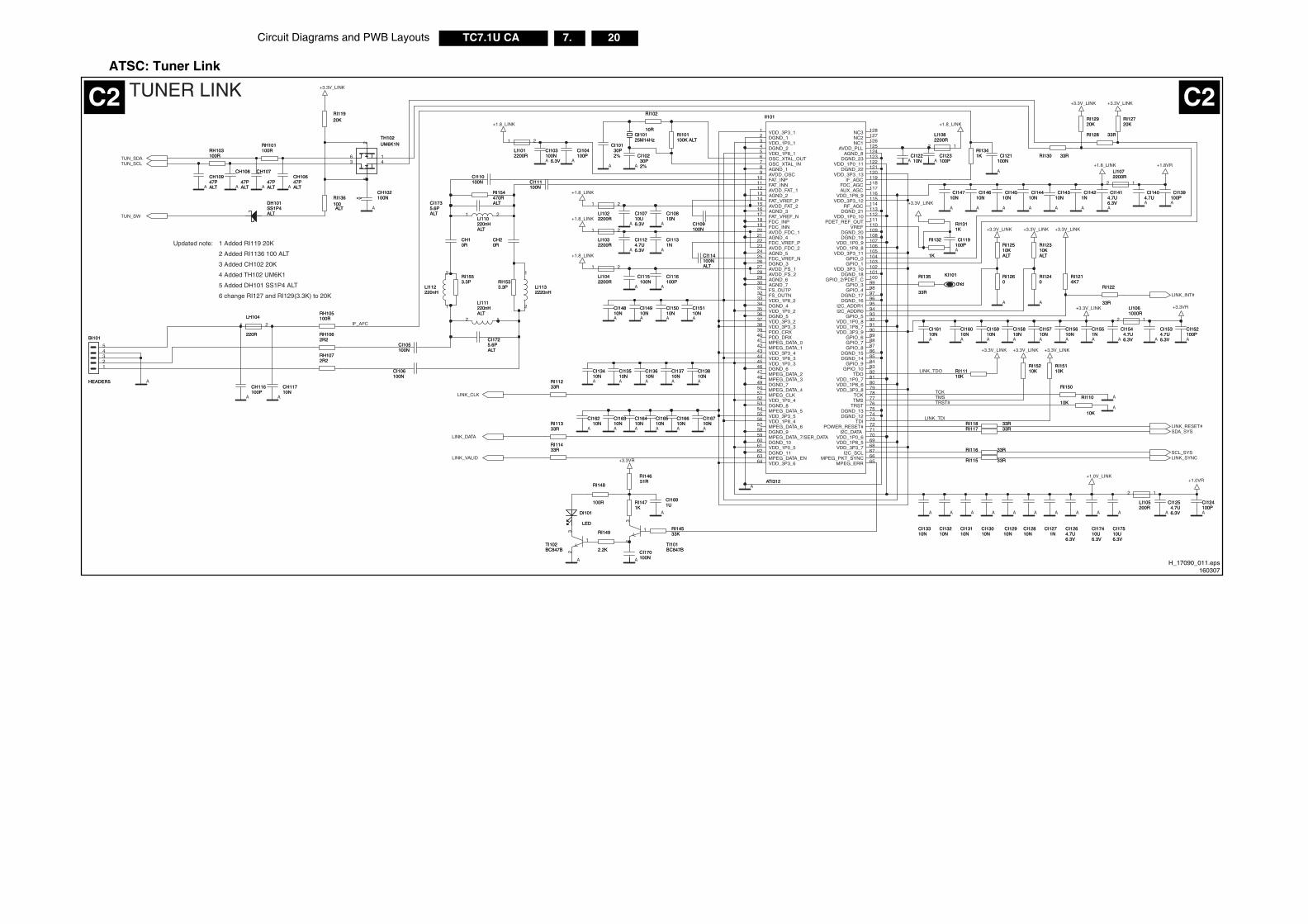
ATSC: Tuner Link
TRST#
TCK
LINK_TDI
LINK_TDO
TMS
IF_AFC
A
+3.3V_LINK
A
A
A
A
A
A
A
A
A
A
A
A
A
A
A
A
A
A
+1.8_LINK
A
+3.3V_LINK
A
A
A
A
A
A
A
+3.3V_LINK
A A
AA
+3.3V_LINK
A
A
A
A
+1.8_LINK
A
A
A
A
A
A
A
+1.0VR
A
A
+3.3V_LINK
A
A
A
A
A
A
A
A
+3.3V_LINK
A
A
+3.3V_LINK
A
A
+3.3VR
A A
+1.8_LINK
A
+1.8_LINK
A
+1.8_LINK
A
A
A
A
+1.8VR
+1.0V_LINK
A
A
+3.3V_LINK
A
+3.3V_LINKA
A
A
A
+3.3V_LINK
A
+3.3VR
+1.8_LINK
A A
A
+3.3V_LINK
A
LINK_SYNC
LINK_RESET#
LINK_CLK
LINK_VALID
SDA_SYS
LINK_INT#
LINK_DATA
SCL_SYS
TUN_SDATUN_SCL
TUN_SW
1 Added RI119 20K
2 Added RI1136 100 ALT
3 Added CH102 20K
4 Added TH102 UM6K1
Updated note:
5 Added DH101 SS1P4 ALT
6 change RI127 and RI129(3.3K) to 20K
CH20RCH20R
CI16610NCI16610N
RI15110KRI15110K
RI1533.3PRI1533.3P
RI11233RRI11233R
RI130 33RRI130 33R
CI10710U6.3V
CI10710U6.3V
CI14710N
CI14710N
CI103100N
6.3V
CI103100N
6.3V
1 2
LI1032200RLI1032200R
CI115100N
CI115100N
CI15710NCI15710N
CI12910NCI12910N
RI115 33RRI115 33R
RI135
33R
RI135
33R
RI101100K ALTRI101100K ALT
CI1414.7U6.3V
CI1414.7U6.3V
1
2
LI112220nHLI112220nH
CH116100PCH116100P
RI122
33R
RI122
33R
CI1735.6PALT
CI1735.6PALT
CI10130P2%
CI10130P2%
CI1131NCI1131N
CI14510N
CI14510N
CI1124.7U6.3V
CI1124.7U6.3V
6.3V
CI17510U6.3V
CI17510U
RI118 33RRI118 33R
DH101SS1P4ALT
DH101SS1P4ALT CI108
10NCI10810N
RI12920KRI12920K
RH105100RRH105100R
CI13510NCI13510N
CI1544.7U6.3V
CI1544.7U6.3V
CI110100NCI110100N
CI123100PCI123100P
CI114100NALT
CI114100NALT
RI117 33RRI117 33R
CI16710NCI16710N
RI116 33RRI116 33R
CI109100NCI109100N
RI102
10R
RI102
10R
12345
BI101
HEADER5
BI101
HEADER5
CI1691UCI1691U
CI14610N
CI14610N
CI14810NCI14810N
CI15910NCI15910N
12
LI105200RLI105200R
CH11710NCH11710N
CH102100NCH102100N
CI1271N
CI1271N
CI124100PCI124100P
CI104100PCI104100P CI102
30P2%
CI10230P2%
RI14651RRI14651R
CI1264.7U6.3V
CI1264.7U6.3V
CI16010NCI16010N
CI139100PCI139
100P
CI121100N
CI121100N
CI15810NCI15810N
CI14910NCI14910N
DI101
LED
DI101
LED
RH1062R2RH1062R2
12
LI111220nHALT
LI111220nHALT
RI1311KRI1311K
RI132
1K
RI132
1K
RI1553.3PRI1553.3P
1
2
3 4
5
6
TH102UM6K1N
<>
TH102UM6K1N
<>
RI1471KRI1471K
RI12720KRI12720K
CI119100P
CI119100P
CI13610NCI13610N
CI15010NCI15010N
CI111100NCI111100N
PAD
KI101
PAD
KI101
1
23
TI102BC847BTI102BC847B
RI154470RALT
RI154470RALT
CI12210N
CI12210N
12
LI1082200RLI1082200R
CI13410NCI13410N
CH10647PALT
CH10647PALT
CI106100NCI106100N
RI11333RRI11333R
CI14310N
CI14310N
CH10RCH10R
CI13010NCI13010N
RI1214K7RI1214K7
6.3V
CI17410U6.3V
CI17410U
CI1725.6PALT
CI1725.6PALT
RI148
100R
RI148
100R
CI13210NCI13210N
CH107
47PALT
CH107
47PALT
CI1421N
CI1421N
RI1240RI1240
CI152100PCI152100P
CI1534.7U6.3V
CI1534.7U6.3V
RI12510KALT
RI12510KALT
CI12810NCI12810N
RH1072R2RH1072R2
RI11433RRI11433R
CH108
47PALT
CH108
47PALT
1 2
LI1042200RLI1042200R
CI1254.7U6.3V
CI1254.7U6.3V
1
2
LI1132220nHLI1132220nH
1
23
TI101BC847BTI101BC847B
CI15110NCI15110N
CI13710NCI13710N
RI14533KRI14533K
RI11920KRI11920K
RI136100ALT
RI136100ALT
12
LI1061000RLI1061000R
CH10947PALT
CH10947PALT
QI10125M14HzQI10125M14Hz1 2
LI1012200RLI1012200R
CI13310NCI13310N
CI1551NCI1551N
CI14410N
CI14410N
CI16310NCI16310N
RH103100RRH103100R
1 2
LI1022200RLI1022200R
RI12310KALT
RI12310KALT
1 2
LH104
220R
LH104
220R
CI16410NCI16410N
RI11110KRI11110K
CI15610NCI15610N
RI149
2.2K
RI149
2.2K
RI128 33RRI128 33R
CI105100NCI105100N
CI1404.7U
CI1404.7U
CI13110NCI13110N
CI16110NCI16110N
RI1341KRI1341K
CI16210N
CI16210N
RI15210KRI15210KCI138
10NCI13810N
12
LI1072200RLI1072200R
RI150
10K
RI150
10KRI110
10K
RI110
10K
VDD_3P3_11
DGND_12
VDD_1P0_13
DGND_24
VDD_1P8_15
OSC_XTAL_OUT6
OSC_XTAL_IN7
AGND_18
AVDD_OSC9
FAT_INP10
FAT_INN11
AVDD_FAT_112
AGND_213
FAT_VREF_P14
AVDD_FAT_215
AGND_316
FAT_VREF_N17
FDC_INP18
FDC_INN19
AGND_421AVDD_FDC_120
FDC_VREF_P22
AVDD_FDC_223
AGND_524
FDC_VREF_N25
DGND_326
AVDD_FS_127
AVDD_FS_228
AGND_629
AGND_730
FS_OUTP31
FS_OUTN32
VDD_1P8_233
DGND_434
VDD_1P0_235
DGND_536
VDD_3P3_237
VDD_3P3_338
PDD_CRX39
PDD_DRX40
MPEG_DATA_041
MPEG_DATA_142
MPEG_DATA_247
MPEG_DATA_348
MPEG_DATA_450
MPEG_DATA_554
MPEG_DATA_657
MPEG_DATA_7/SER_DATA59
VDD_3P3_443
VDD_1P8_344
VDD_1P0_345
DGND_646
DGND_749
MPEG_CLK51
VDD_1P0_452
DGND_853
VDD_3P3_555
VDD_1P8_456
DGND_958
DGND_1060
VDD_1P0_561
DGND_1162
MPEG_DATA_EN63
VDD_3P3_664 MPEG_ERR 65MPEG_PKT_SYNC 66
I2C_SCL 67VDD_3P3_7 68VDD_1P8_5 69VDD_1P0_6 70
I2C_DATA 71POWER_RESET# 72
TDI 73DGND_12 74DGND_13 75
TRST 76TMS 77TCK 78
VDD_3P3_8 79VDD_1P8_6 80VDD_1P0_7 81
TDO 82GPIO_10 83GPIO_9 84
DGND_14 85DGND_15 86
GPIO_8 87GPIO_7 88GPIO_6 89
VDD_3P3_9 90VDD_1P8_7 91VDD_1P0_8 92
GPIO_5 93I2C_ADDR0 94I2C_ADDR1 95
DGND_16 96DGND_17 97
GPIO_4 98GPIO_3 99
GPIO_2/PDET_C 100DGND_18 101
VDD_3P3_10 102GPIO_1 103GPIO_0 104
VDD_3P3_11 105VDD_1P8_8 106VDD_1P0_9 107
DGND_19 108DGND_20 109
VREF 110PDET_REF_OUT 111
VDD_1P0_10 112DGND_21 113RF_AGC 114
VDD_3P3_12 115VDD_1P8_9 116
AUX_AGC 117FDC_AGC 118
IF_AGC 119VDD_3P3_13 120
DGND_22 121VDD_1P0_11 122
DGND_23 123AGND_8 124
AVDD_PLL 125NC1 126NC2 127NC3 128
II101
ATI312
II101
ATI312
CI16510NCI16510N
RI1260RI1260
CI116100PCI116100P
1 2LI110220nHALT
LI110220nHALT
RH101100RRH101100R
CI170100NCI170100N
TUNER LINKC2 C2
H_17090_011.eps160307
Circuit Diagrams and PWB Layouts 21TC7.1U CA 7.
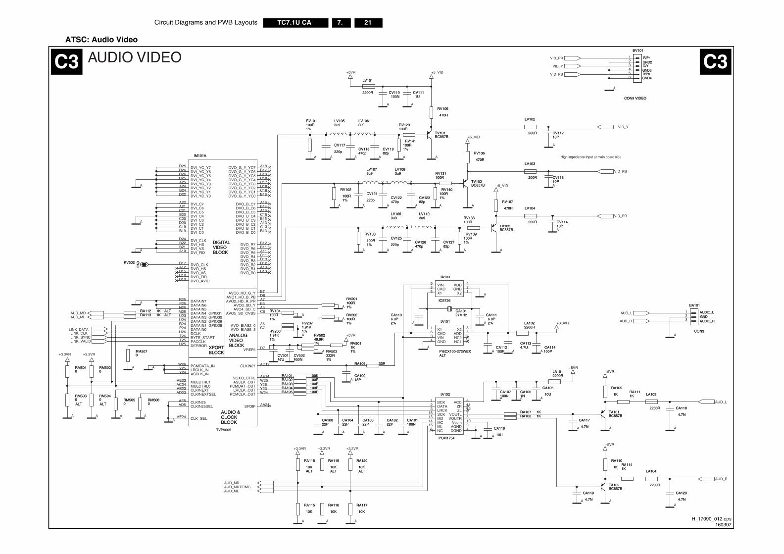
ATSC: Audio Video
A
A
+3.3VR
A
A
+3.3VR
A
A
+5_VID
A
A
A
A
A
A
A
A
A
A
A
A
A
A
A
A
A
A
A
+5_VID
+5_VID
A
+5VR
A
A
+3.3VR
A
+5VR
A
A
A
A
A
A
A
A
A
A
+5VR
A
AA
A
A
A
A
A
A
A
A
A
A
A
A
A
A
A
A
A
+5VR
A
+5VR
AAA
A
A A A
+3.3VR +3.3VR +3.3VR
A
A
A
LINK_DATA
AUD_L
VID_PR
LINK_SYNCLINK_VALID
LINK_CLK
VID_Y
VID_PB
AUD_R
AUD_MD
AUD_MDAUD_MUTE/MCAUD_ML
AUD_ML
VID_Y
VID_PB
VID_PR
AUD_L
AUD_R
High impedance Input at main board side
CA1106.8P2%
CA1106.8P2%
CV110100N
CV110100N
123456
GND2
GND3
GND4
R/Pr
G/Y
B/Pb
BV101
CON9 VIDEO
GND2
GND3
GND4
R/Pr
G/Y
B/Pb
BV101
CON9 VIDEO
RM5070RM5070
CA10918PCA10918P
CV118470pCV118470p
RV139100R1%
RV139100R1%
TV103BC857BTV103BC857B
CV11410PCV11410P
RV50249.9R1%
RV50249.9R1%
RA113 1K ALTRA113 1K ALT
RA117
10K
RA117
10K
LA1022200RLA1022200R
RV102
100R1%
RV102
100R1%
RM5010RM5010
CA1116.8P2%
CA1116.8P2%
CA10322PCA10322P
CA112100PCA112100P
RA103 100RRA103 100RRA104 100RRA104 100R
LA1012200RLA1012200R
CA101100NCA101100N
CV117
220p
CV117
220p
TA102BC857BTA102BC857B
LV104
200R
LV104
200R
TV101BC857BTV101BC857B
RV131100RRV131100R
1 2
LV1093u9LV1093u9
LV103
200R
LV103
200R
RA102 100RRA102 100R
RA118
10KALT
RA118
10KALT
CV12782pCV12782p
CA120
4.7N
CA120
4.7N
CA10422PCA10422P
CV11982pCV11982p
CA10222PCA10222P
RA110
1K
RA110
1K
LA103
2200R
LA103
2200R
CV125
220p
CV125
220p
1 2
LV1073u9LV1073u9
1
32
AUDIO_LGNDAUDIO_R
BA101
CON3
AUDIO_LGNDAUDIO_R
BA101
CON3
RV2071.91K1%
RV2071.91K1%
CV11210PCV11210P
1 2
LV1053u9LV1053u9
CA114100PCA114100P
CV121
220p
CV121
220p
RV140100R1%
RV140100R1%
RV503332R1%
RV503332R1%
X11
VIN3
GND4
CKO6 VDD 5X2 8
NC1 2NC2 7
IA101
PI6CX100-272WEXALT
IA101
PI6CX100-272WEXALT
RA119
10KALT
RA119
10KALT
RA107 1KRA107 1K
RV101100R1%
RV101100R1%
RA112 1K ALTRA112 1K ALT
1 2
LV1103u9LV1103u9
RV141100R1%
RV141100R1%
RM5030ALT
RM5030ALT
CA105
10U
CA105
10U
RV5011K1%
RV5011K1%
RM5050RM5050
CV502100NCV502100N
RA105 100RRA105 100R
LA104
2200R
LA104
2200R
RA120
10KALT
RA120
10KALT
PA
DKV502
PA
DKV502
RV2061.91K1%
RV2061.91K1%
1 2
LV1083u9LV1083u9
RV201100R1%
RV201100R1%
CA1134.7UCA1134.7U
RA115
10K
RA115
10K
QA10127MHzQA10127MHz
RA1111KRA1111K
RV104100R1%
RV104100R1%
TA101BC857BTA101BC857B
LV101
2200R
LV101
2200R
CA1061NCA1061N
RV105
470R
RV105
470RLV102
200R
LV102
200R
CV12382pCV12382p
RM5040ALT
RM5040ALT
CA119
4.7N
CA119
4.7N
TV102BC857BTV102BC857B
DVI_YC_Y0D22DVI_YC_Y1B24DVI_YC_Y2A24DVI_YC_Y3A25DVI_YC_Y4C25DVI_YC_Y5C26DVI_YC_Y6D26DVI_YC_Y7D25
DVI_C0B19DVI_C1C19DVI_C2D20DVI_C3C20DVI_C4B20DVI_C5C21DVI_C6A21DVI_C7A22
DVI_CLKD24
DVI_HSB22
DVI_VSB21
DVI_FIDA19
DVO_CLKD17
DVO_HSA12
DVO_VSD15
DVO_FIDC10
DVO_AVIDD10
DVO_G_Y_YC0 B16DVO_G_Y_YC1 C16DVO_G_Y_YC2 D18DVO_G_Y_YC3 C17DVO_G_Y_YC4 C18DVO_G_Y_YC5 B18DVO_G_Y_YC6 B17DVO_G_Y_YC7 A18
DVO_B_C0 B13DVO_B_C1 C13DVO_B_C2 A13DVO_B_C3 B15DVO_B_C4 C15DVO_B_C5 A15DVO_B_C6 B14DVO_B_C7 A16
DVO_R0 B10DVO_R1 A10DVO_R2 D12DVO_R3 D13DVO_R4 C11DVO_R5 A11DVO_R6 B11DVO_R7 B12
AVO0_HD_G_Y B7
AVO1_HD_B_PB D8
AVO2_HD_R_PR A7
AVO3_SD_Y B5
AVO4_SD_C A5
AVO5_SD_CVBS C6
AVO_BIAS2_0 A6
AVO_BIAS5_3 C7
VREF5 D7
DATAIN1_GPIO28R24
DATAIN0P24
DATAIN2_GPIO29U24DATAIN3_GPIO30U23DATAIN4_GPIO31M25DATAIN5N25DATAIN6P25DATAIN7R25
DCLKU26
BYTE_STARTT26
PACCLKT25
DERRORU25
CLKIN27 AD12
VCXO_CTRL AE14
ASCLK_OUT W25
PCMDAT_OUT Y26
LRCLK_OUT Y23
PCMCLK_OUT W24
SPDIF AA24
PCMDATA_INW26
LRCLK_INY25
ASCLK_INY24
MULCTRL0AC24MULCTRL1AE23
CLKINEXTAB23
CLKINEXTSELAD23
CLKIN25AE5
CLKIN25SELAD5
CLK_SELAE24
DIGITALVIDEOBLOCK
ANALOGVIDEOBLOCK
AUDIO &CLOCKBLOCK
XPORTBLOCK
IM101A
TVP9005
DIGITALVIDEOBLOCK
ANALOGVIDEOBLOCK
AUDIO &CLOCKBLOCK
XPORTBLOCK
IM101A
TVP9005
RA109
1K
RA109
1K
BCK1
DATA2
LRCK3
DGND 4NC5
VCC 6
VOUTL 7
VOUTR 8
AGND 9Vcom 10
ZR 11
ZL 12
MD13
MC14
ML15
SCK16
IA102
PCM1754
IA102
PCM1754
RM5060RM5060
1 2
LV1063u9LV1063u9
CA118
4.7N
CA118
4.7N
RM5020RM5020
RV129100RRV129100R
RV202100R1%
RV202100R1%
RA101 100KRA101 100K
RV106
470R
RV106
470R
RV133100RRV133100R
RA1141KRA1141K
RA116
10K
RA116
10K
CA117
4.7N
CA117
4.7N
CV11310PCV11310P
CV1111U
CV1111U
CA116
10U
CA116
10U
CA10822PCA10822P
CV122470pCV122470p
CV50147UCV50147U
CA107100NCA107100N
RV107
470R
RV107
470R
RA106 33RRA106 33R
CV126470pCV126470p
RA108 1KRA108 1K
X2 1
VIN5
GND 2CKO3VDD 4
X16
IA103
ICS726
IA103
ICS726
RV103
100R1%
RV103
100R1%
AUDIO VIDEOC3 C3
H_17090_012.eps160307
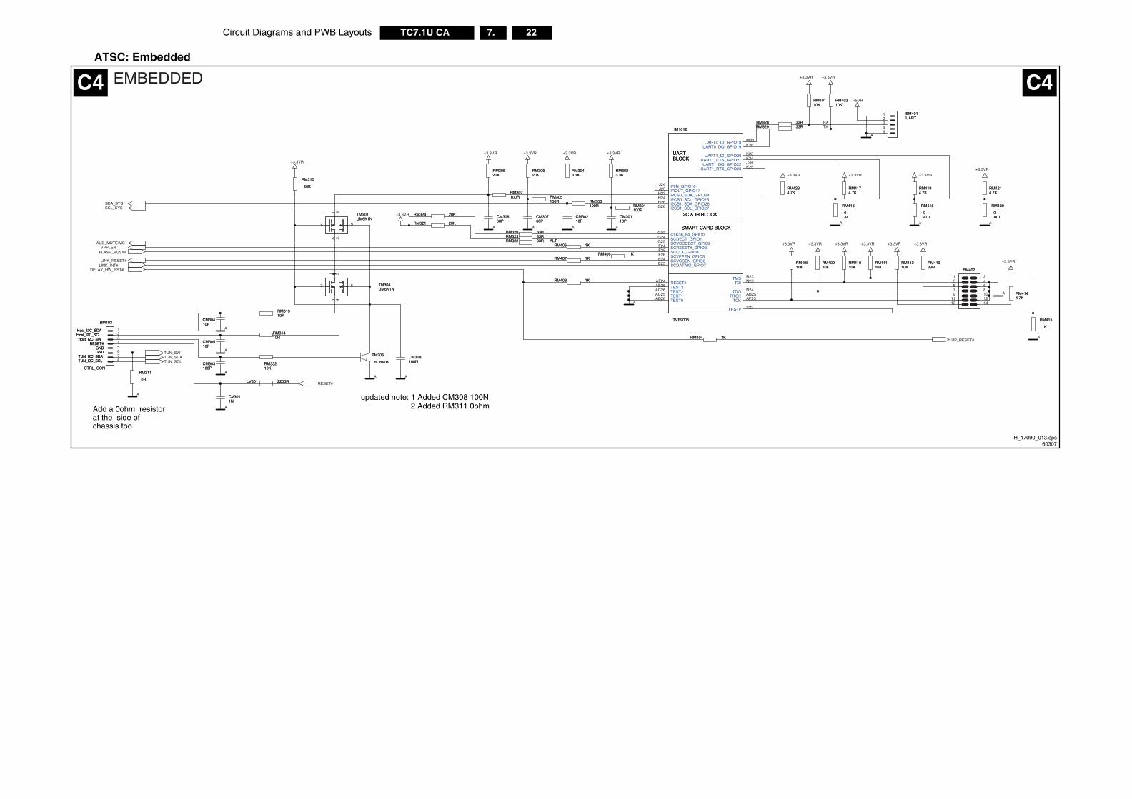
22TC7.1U CA 7.Circuit Diagrams and PWB Layouts
ATSC: Embedded
TXRX
A
+3.3VR
+3.3VR
A
A
+3.3VR
+3.3VR
A
+3.3VR
A
+3.3VR
A
+5VR
+3.3VR
A
+3.3VR
+3.3VR
A
+3.3VR
+3.3VR
+3.3VR
A
+3.3VR
+3.3VR
AA
+3.3VR
+3.3VR
A
+3.3VR
A
+3.3VR
+3.3VR
A
A
A
A
A
SDA_SYS
DELAY_HW_RST#
UP_RESET#
VPP_ENFLASH_BUSY#
AUD_MUTE/MC
LINK_INT#
SCL_SYS
LINK_RESET#
RESET#
TUN_SCLTUN_SDATUN_SW
updated note: 1 Added CM308 100N
Add a 0ohm resistor at the side ofchassis too
2 Added RM311 0ohm
UART0_DI_GPIO18 M23
UART0_DO_GPIO19 K26
UART1_DI_GPIO20 K23
UART1_CTS_GPIO21 K24
UART1_DO_GPIO22 J26
UART1_RTS_GPIO23 K25
IRIN_GPIO16J24
IROUT_GPIO17J25
I2CS0_SDA_GPIO24H23
I2CS0_SCL_GPIO25H24
I2CS1_SDA_GPIO26H26
I2CS1_SCL_GPIO27G26
CLK36_84_GPIO0G23
SCDECT_GPIO1G24
SCVCCDECT_GPIO2G25
SCRESET#_GPIO3F24
SCCLK_GPIO4F25
SCVPPEN_GPIO5F26
SCVCCEN_GPIO6E24
SCDATAIO_GPIO7E25
RESET#AF24
TEST0AB26TEST1AC25TEST2AC26TEST3AE26
TMS R23
TDI N23
TDO N24
RTCK AB25
TCK AF23
TRST# V23
UARTBLOCK
I2C & IR BLOCK
SMART CARD BLOCK
IM101B
TVP9005
UARTBLOCK
I2C & IR BLOCK
SMART CARD BLOCK
IM101B
TVP9005
TM305
BC847B
TM305
BC847B
RM30620KRM30620K
RM33210KRM33210K
CM30410PCM30410P
RM301100RRM301100R
RM418
0ALT
RM418
0ALT
RM328 33RRM328 33R
CM30210PCM30210P
RM41210KRM41210K
CM30510PCM30510P
12345
BM401UARTBM401UART
RM311
0R
RM311
0R
RM323 33RRM323 33R
1413121110987654321
BM402BM402
RM40810KRM40810K
12345678
Host_I2C_SDAHost_I2C_SCL
GND
RESET#GND
Host_I2C_SW
TUN_I2C_SDATUN_I2C_SCL
BM403
CTRL_CON
Host_I2C_SDAHost_I2C_SCL
GND
RESET#GND
Host_I2C_SW
TUN_I2C_SDATUN_I2C_SCL
BM403
CTRL_CON
RM4214.7KRM4214.7K
CV3011NCV3011N
RM31310RRM31310R
RM3043.3KRM3043.3K
RM305100RRM305100R
RM406 1KRM406 1K
RM41333RRM41333R
RM403 1KRM403 1K
1
2
34
5
6
TM304UM6K1NTM304UM6K1N
RM329 33RRM329 33R
RM322 33R ALTRM322 33R ALT
RM40910KRM40910K
CM30668PCM30668P
RM31410RRM31410R
RM4174.7KRM4174.7K
RM4144.7KRM4144.7K
RM3023.3KRM3023.3K
RM303100RRM303100R RM416
0ALT
RM416
0ALT
RM4194.7KRM4194.7K
RM404 1KRM404 1K
RM41010KRM41010K
CM308100NCM308100N
RM420
0ALT
RM420
0ALT
RM405 1KRM405 1K
CM30768PCM30768P
RM415
1K
RM415
1K
RM40210KRM40210K
RM321 20KRM321 20K
RM310
20K
RM310
20K
RM30820KRM30820K
RM307100RRM307100R
CM30110PCM30110P
RM41110KRM41110K
LV301 2200RLV301 2200R
RM320 33RRM320 33R
RM407 1KRM407 1K
RM4234.7KRM4234.7K
RM40110KRM40110K
1
2
34
5
6
TM301UM6K1NTM301UM6K1N
RM324 20KRM324 20K
CM303100PCM303100P
EMBEDDEDC4 C4
H_17090_013.eps160307
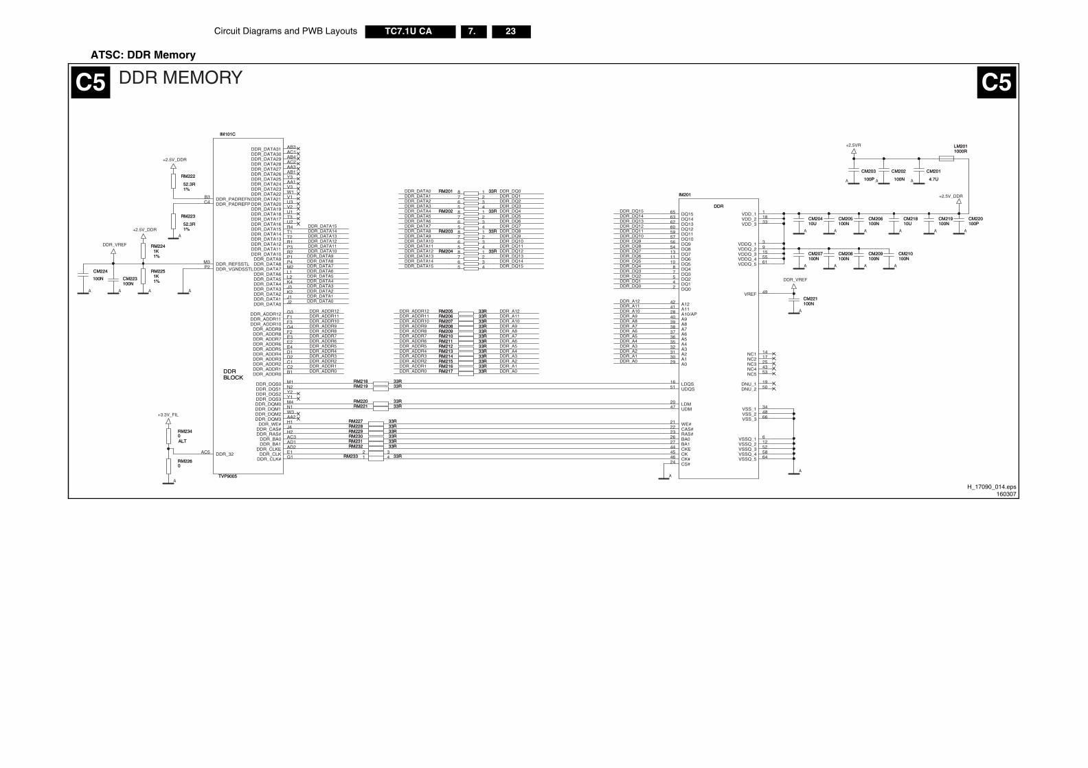
Circuit Diagrams and PWB Layouts 23TC7.1U CA 7.
ATSC: DDR Memory
DDR_DQ9
DDR_DATA1
DDR_DQ15
DDR_A2
DDR_A0
DDR_DQ14
DDR_ADDR1
DDR_ADDR6
DDR_DQ2
DDR_ADDR3DDR_ADDR4
DDR_ADDR9
DDR_DATA12
DDR_A6
DDR_DATA2
DDR_DATA9DDR_DQ7
DDR_DATA11
DDR_ADDR5
DDR_DQ1
DDR_ADDR10
DDR_ADDR2
DDR_A7
DDR_DATA4DDR_DQ0
DDR_DQ13
DDR_DATA7
DDR_A4
DDR_DQ5
DDR_ADDR2
DDR_DATA14
DDR_DATA15
DDR_DATA7
DDR_ADDR10
DDR_ADDR8
DDR_DATA0
DDR_DQ6
DDR_DQ10
DDR_ADDR1
DDR_A10
DDR_DQ11
DDR_ADDR7
DDR_A8
DDR_ADDR3
DDR_DQ3
DDR_DQ8
DDR_A11
DDR_DQ15
DDR_DQ13
DDR_ADDR12
DDR_DATA2
DDR_DQ12
DDR_ADDR6
DDR_DQ8
DDR_DQ0
DDR_DQ12
DDR_A3DDR_ADDR4
DDR_DQ3
DDR_DATA4
DDR_A0
DDR_DQ4
DDR_ADDR8
DDR_DATA13
DDR_DQ4
DDR_ADDR9
DDR_ADDR11
DDR_A9
DDR_A9
DDR_DATA8
DDR_DATA13 DDR_DATA9
DDR_A12
DDR_DATA6 DDR_DQ6DDR_DQ7
DDR_A3
DDR_DQ2
DDR_ADDR0
DDR_A10
DDR_A2
DDR_DATA5
DDR_DATA10DDR_DATA11
DDR_DATA6
DDR_DATA3
DDR_A1
DDR_A12
DDR_DQ5
DDR_DQ11
DDR_DATA14
DDR_DQ10
DDR_DATA1
DDR_ADDR7
DDR_DATA8
DDR_DQ1
DDR_ADDR0
DDR_DQ14
DDR_A6
DDR_DQ9
DDR_DATA5
DDR_ADDR12DDR_ADDR11
DDR_DATA3
DDR_DATA10
DDR_ADDR5
DDR_A8DDR_A5
DDR_DATA12
DDR_A11
DDR_DATA15
DDR_DATA0
DDR_A7
DDR_A5DDR_A4
DDR_A1
A
A
AA
A
DDR_VREF
A
+2.5VR
A
A
A
+2.5V_DDR
+2.5V_DDR
A
A
A
A
A
A
DDR_VREF
A
A
+2.5V_DDR
A
A A
A A
+3.3V_FIL
12345
678RM201 33RRM201 33R
CM205100NCM205100N
RM228 33RRM228 33R
RM213 33RRM213 33R
CM219100NCM219100N
12345
678RM202 33RRM202 33R
CM207100NCM207100N
RM2340ALT
RM2340ALT
RM214 33RRM214 33R
DQ02DQ14DQ25DQ37DQ48DQ510DQ611DQ713DQ854DQ956DQ1057DQ1159DQ1260DQ1362DQ1463DQ1565
A029A130A231A332A435A536A637A738A839A940A10/AP28A1141A1242
LDQS16
UDQS51
UDM47LDM20
WE#21
CAS#22
RAS#23
CS#24
BA026
BA127
CKE44
CK45
CK#46
VDD_1 1
VDD_2 18
VDD_3 33
VDDQ_1 3
VDDQ_2 9
VDDQ_3 15
VDDQ_4 55
VDDQ_5 61
VSSQ_1 6
VSSQ_2 12
VSSQ_3 52
VSSQ_4 58
VSSQ_5 64
VSS_1 34
VSS_2 48
VSS_3 66
NC1 14
NC2 17
NC3 25
NC4 43
NC5 53
DNU_1 19
DNU_2 50
VREF 49
IM201
DDR
IM201
DDR
RM206 33RRM206 33R
12345
678RM203 33RRM203 33R
RM2251K1%
RM2251K1%
RM230 33RRM230 33R
RM215 33RRM215 33R
CM223100NCM223100N
CM220100PCM220100P
CM208100NCM208100N
12345
678RM204 33RRM204 33R
RM209 33RRM209 33R
CM221100NCM221100N
RM216 33RRM216 33R
RM207 33RRM207 33R
RM231 33RRM231 33R
RM223
52.3R1%
RM223
52.3R1%
RM229 33RRM229 33R
RM217 33RRM217 33R
CM201
4.7U
CM201
4.7U
CM203
100P
CM203
100P
CM209100NCM209100N
1 42 3
RM233 33RRM233 33R
RM218 33RRM218 33R
CM210100NCM210100N
CM21810UCM21810U
LM2011000RLM2011000R
CM224
100N
CM224
100N
RM208 33RRM208 33R
RM210 33RRM210 33R
RM205 33RRM205 33R
RM219 33RRM219 33R
RM232 33RRM232 33R
RM227 33RRM227 33R
CM20410UCM20410U
CM202
100N
CM202
100N
RM211 33RRM211 33R
RM220 33RRM220 33R
RM2241K1%
RM2241K1%
CM206100NCM206100N
RM2260RM2260
RM222
52.3R1%
RM222
52.3R1%
RM212 33RRM212 33R
RM221 33RRM221 33R
DDR_DATA0 J2DDR_DATA1 J1DDR_DATA2 K2DDR_DATA3 J3DDR_DATA4 K4DDR_DATA5 L2DDR_DATA6 L1DDR_DATA7 M2DDR_DATA8 P4DDR_DATA9 P1
DDR_DATA10 R2DDR_DATA11 P3DDR_DATA12 R1DDR_DATA13 T2DDR_DATA14 T1DDR_DATA15 R4DDR_DATA16 U2DDR_DATA17 T3DDR_DATA18 U1DDR_DATA19 V2DDR_DATA20 U3DDR_DATA21 V1DDR_DATA22 W1DDR_DATA23 V3DDR_DATA24 AA1DDR_DATA25 Y3DDR_DATA26 AB1DDR_DATA27 AA3DDR_DATA28 AC2DDR_DATA29 AB4DDR_DATA30 AC1DDR_DATA31 AB3
DDR_ADDR0 B1DDR_ADDR1 C2DDR_ADDR2 C1DDR_ADDR3 D2DDR_ADDR4 D1DDR_ADDR5 E4DDR_ADDR6 E2DDR_ADDR7 E3DDR_ADDR8 F2DDR_ADDR9 G4
DDR_ADDR10 F3DDR_ADDR11 F1DDR_ADDR12 G3
DDR_DQS0 M1
DDR_DQS1 N2
DDR_DQS2 Y2
DDR_DQS3 Y1
DDR_DQM0 M4
DDR_DQM1 N1
DDR_DQM2 W3
DDR_DQM3 AA2
DDR_WE# H1
DDR_CAS# J4
DDR_RAS# H2
DDR_BA0 AC3
DDR_BA1 AD1
DDR_CLKE AD2
DDR_CLK E1
DDR_CLK# G1
DDR_PADREFNB3
DDR_PADREFPC4
DDR_REFSSTLM3
DDR_VGNDSSTLP2
DDR_32AC5
DDRBLOCK
IM101C
TVP9005
DDRBLOCK
IM101C
TVP9005
DDR MEMORYC5 C5
H_17090_014.eps160307
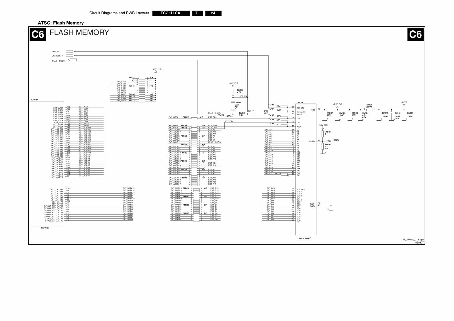
24TC7.1U CA 7.Circuit Diagrams and PWB Layouts
ATSC: Flash Memory
EXT_A3
EXT_A19
EXT_ADDR17
EXT_DATA12
EXT_WE0#
EXT_DATA2
EXT_CS0#EXT_CS2#
EXT_WAIT
EXT_CS1#
EXT_D13EXT_D14
EXT_D0
EXT_OE#
EXT_ADDR17
EXT_DATA14
EXT_DATA3
EXT_DATA10
EXT_A12
EXT_A18
EXT_D10
EXT_DATA13
EXT_A15
EXT_A4
EXT_OE0#
EXT_CS4#
EXT_DATA9EXT_D8
EXT_A1
EXT_DATA11
VPP_EN
EXT_D6
EXT_ADDR15
EXT_ADDR12
EXT_D15
EXT_ADDR9EXT_A14EXT_ADDR12
EXT_A6
EXT_A9
EXT_CE#
EXT_ADDR18
EXT_ADDR7
EXT_D6
EXT_D2
EXT_A2
EXT_A11
EXT_ADDR21
EXT_A8
EXT_DATA6
EXT_ADDR5
EXT_CS2#
EXT_DATA8EXT_D9
EXT_A21
EXT_ADDR10
EXT_A9
EXT_ADDR20
EXT_A5
EXT_ADDR10
EXT_A10
EXT_A16
EXT_ADDR2
EXT_DATA7
EXT_A4
EXT_D4
EXT_ADDR6
EXT_CS0#
EXT_D12
EXT_ADDR18EXT_A18EXT_ADDR4
EXT_A15
EXT_ADDR11
EXT_ADDR21
EXT_ADDR8
EXT_A6
EXT_DATA15
EXT_DATA4
EXT_DATA14
EXT_CS0#
EXT_ADDR16
EXT_ADDR1
EXT_D3
EXT_A8
EXT_DATA5
EXT_ADDR19
EXT_A7
EXT_ADDR4
EXT_A16
EXT_A20
EXT_ADDR0
EXT_CS4#
EXT_D10
EXT_ADDR22
EXT_ADDR7
EXT_ADDR14
EXT_ADDR11
EXT_OE0#
EXT_DATA9EXT_DATA8
EXT_DATA11
EXT_A10
FLASH_BUSY#_
EXT_ADDR0
EXT_D1
EXT_DATA10
EXT_DATA12
EXT_WE0#
EXT_ADDR5
EXT_ADDR9
EXT_DATA2
EXT_DATA15
EXT_ADDR3
EXT_A13
EXT_D11
EXT_DATA13
EXT_A2
EXT_D4EXT_D5
EXT_DATA4
EXT_A0
EXT_ADDR16
EXT_ADDR3
EXT_DATA1
EXT_ADDR1
EXT_CS1#
EXT_WAIT
EXT_OE0#
EXT_D8
EXT_ADDR13
EXT_A17
EXT_CS5#
EXT_ADDR20
EXT_A1
EXT_ADDR8
EXT_A21
EXT_ADDR15
EXT_D2
EXT_D12
EXT_D0
EXT_ADDR14
EXT_D11
EXT_D3
EXT_D15
EXT_A13
EXT_A19
EXT_A12
EXT_ADDR2
EXT_WE1#
EXT_WE1#
EXT_ADDR6
EXT_DATA0EXT_D1
EXT_D13
EXT_ADDR23
EXT_WE#
EXT_CS3#
EXT_ADDR13
EXT_DATA1
EXT_A3
EXT_D7
EXT_A7
EXT_DATA0
EXT_D5
EXT_A20
EXT_DATA3
FLASH_BUSY#
EXT_A11
EXT_A17
EXT_DATA5
EXT_ADDR23
EXT_ADDR22
EXT_CS3#
EXT_A14
EXT_A0
EXT_A5
EXT_D9
EXT_DATA6EXT_DATA7
EXT_D14
EXT_WAIT
EXT_WE0#
EXT_ADDR19
EXT_D7
EXT_CS5#
EXT_OE#
A
+3.3VR
+3.3V_FLS
+3.3V_FLS
+3.3V_FLS
A
A
A AA AA
+3.3V_FLS
A
A
UP_RESET#
VPP_EN
FLASH_BUSY#
RESET#12
WP#/ACC14
RY/BY15
CE#26
OE#28
WE#11
A025
A124
A223
A322
A421
A520
A619
A718
A88
A97
A106
A115
A124
A133
A142
A151
A1648
A1717
A1816
A199
A2010
DQ029DQ131DQ233DQ335DQ438DQ540DQ642DQ744DQ830DQ932DQ1034DQ1136DQ1239DQ1341DQ1443DQ15/A-145
VCC 37
BYTE# 47
NC113
GND1 27
GND2 46
IM102
13-AL016M-90B
IM102
13-AL016M-90B
CM102
100N
CM102
100N
RM143 0ALT
RM143 0ALT
1234 5
678RM142 51RRM142 51R
YM160YM160
CM103
100P
CM103
100P
1234 5
678RM128 51RRM128 51R
YM161YM161
1234 5
678RM123 51RRM123 51R
YM162YM162
EXT_ADDR0 AD11EXT_ADDR1 AF11EXT_ADDR2 AE10EXT_ADDR3 AF12EXT_ADDR4 AE11EXT_ADDR5 AE15EXT_ADDR6 AE16EXT_ADDR7 AD13EXT_ADDR8 AE12EXT_ADDR9 AE17
EXT_ADDR10 AD14EXT_ADDR11 AC15EXT_ADDR12 AD18EXT_ADDR13 AF16EXT_ADDR14 AD16EXT_ADDR15 AC17EXT_ADDR16 AF18EXT_ADDR17 AF19EXT_ADDR18 AF21EXT_ADDR19 AD19EXT_ADDR20 AC20EXT_ADDR21 AE20EXT_ADDR22 AE21EXT_ADDR23 AF20
EXT_WE0# AC19EXT_WE1# AD20
EXT_OE# AF17EXT_CS0# AE13EXT_CS1# AF15EXT_CS2# AE18EXT_CS3# AD17EXT_CS4# AD21EXT_CS5# AD22EXT_WAIT AC12
GPIO8_EXT_DATA0 AF6GPIO9_EXT_DATA1 AE6
GPIO10_EXT_DATA2 AD6GPIO11_EXT_DATA3 AC7GPIO12_EXT_DATA4 AF7GPIO13_EXT_DATA5 AE8GPIO14_EXT_DATA6 AE7GPIO15_EXT_DATA7 AD7
EXT_DATA8 AF8EXT_DATA9 AC10
EXT_DATA10 AD8EXT_DATA11 AC9EXT_DATA12 AF9EXT_DATA13 AD9EXT_DATA14 AF10EXT_DATA15 AD10
IM101D
TVP9005
IM101D
TVP9005
RM122 51RRM122 51R
1234 5
678RM146 51RRM146 51R RM102
0ALT
RM1020ALT
YM901YM901
1234 5
678RM124 51RRM124 51R
1234 5
678RM125 51RRM125 51R
RM109 10KRM109 10K
1234 5
678RM132 51RRM132 51R
RM110 10KRM110 10KRM111 10KRM111 10K
1234 5
678RM129 51RRM129 51R
RM112 10KRM112 10K
CM106100PCM106100P
1234 5
678RM130 51RRM130 51R
YM163YM163
1234 5
678RM131 51RRM131 51R
CM107100NCM107100N
1234 5
678RM145 10KRM145 10K
CM105100NCM105100N
1234 5
678RM141 10KRM141 10K
YM164YM164
RM1010RM1010
1234 5
678RM144 51RRM144 51R
CM101
4.7U6.3V
CM101
4.7U6.3V
CM1044.7U6.3V
CM1044.7U6.3V
YM165YM165
CM111220PALT
CM111220PALT
RM1074.7KRM1074.7K
RM147 51RALT
RM147 51RALT
RM120 51RRM120 51R
12
LM1012200RLM1012200R
RM14051RRM14051R
FLASH MEMORYC6 C6
H_17090_015.eps060307
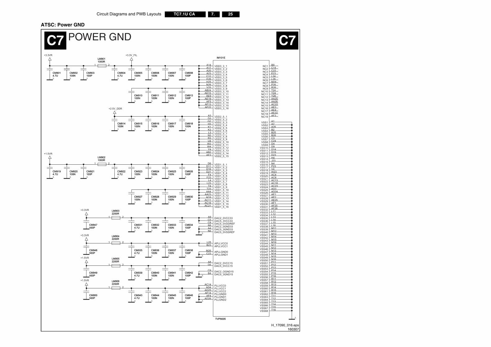
Circuit Diagrams and PWB Layouts 25TC7.1U CA 7.
ATSC: Power GND
A
A AAA
A A A A A A A A
+3.3VR +3.3V_FIL
A A A A A
+2.5V_DDR
AAAA
+1.5VR
AAA A
AA AA
AAA
+3.3VR
AA A A
+3.3VR
AA A A
+1.5VR
AA A A
+1.5VR
A
A
A
AA
A
A
A
ACM944100NCM944100N
CM915100NCM915100N
CM925100NCM925100N
CM9014.7UCM9014.7U
CM932100NCM932100N
CM948100PCM948100P
CM929100NCM929100N
1 2
LM9052200RLM9052200R
CM946100PCM946100P
CM930100PCM930100P
CM926100PCM926100P
CM940100NCM940100N
CM937100NCM937100N
CM9354.7UCM9354.7U
CM942100PCM942100P
CM923100NCM923100N
CM918100NCM918100N
CM910100NCM910100N
CM920100NCM920100N
CM907100NCM907100N
1 2
LM9042200RLM9042200R
CM9044.7UCM9044.7U
VDD3_3_1A14VDD3_3_2A17VDD3_3_3A20VDD3_3_4A23VDD3_3_5C12VDD3_3_6E26VDD3_3_7H25VDD3_3_8N26VDD3_3_9V25VDD3_3_10AB24VDD3_3_11AD15VDD3_3_12AE9VDD3_3_13AE19VDD3_3_14AF5VDD3_3_15AF13VDD3_3_16AF22
VDD2_5_1A3VDD2_5_2D3VDD2_5_3G2VDD2_5_4H3VDD2_5_5K1VDD2_5_6K3VDD2_5_7L3VDD2_5_8N3VDD2_5_9R3VDD2_5_10U4VDD2_5_11W2VDD2_5_12W4VDD2_5_13Y4VDD2_5_14AB2VDD2_5_15AF2
VDD1_5_1D6VDD1_5_2D11VDD1_5_3D16VDD1_5_4D21VDD1_5_5F4VDD1_5_6F23VDD1_5_7L4VDD1_5_8L23VDD1_5_9T4VDD1_5_10T23VDD1_5_11AA4VDD1_5_12AA23VDD1_5_13AC6VDD1_5_14AC11VDD1_5_15AC16VDD1_5_16AC21
DAC2_0VCC33A9DAC5_3VCC33C5DAC5_0VDDREFC8DAC2_0GND33B8DAC5_3GND33A4DAC5_0VSSREFB6
APLLVCC0L25APLLVCC1B23
APLLGND0M26APLLGND1C23
DAC2_OGND15C9DAC5_3GND15B4
PLLVCC0AC14PLLVCC1AD4PLLVCC2AD25PLLGND0AF14PLLGND1AF4PLLGND2AD26
NC1 B9NC2 C14NC3 C22NC4 E23NC5 L24NC6 L26NC7 M24NC8 P26NC9 R26NC10 T24NC11 Y24NC12 Y26NC13 AA25NC14 AA26NC15 AC22NC16 AE3NC17 AE4NC18 AE22NC19 AF3
VSS1 A1VSS2 A2VSS3 A26VSS4 B2VSS5 B25VSS6 B26VSS7 C3VSS8 C24VSS9 D4VSS10 D9VSS11 D14VSS12 D19VSS13 D23VSS14 H4VSS15 J23VSS16 N4VSS17 P23VSS18 V4VSS19 W23VSS20 AC4VSS21 AC8VSS22 AC13VSS23 AC18VSS24 AC23VSS25 AD3VSS26 AD24VSS27 AE1VSS28 AE2VSS29 AE25VSS30 AF1VSS31 AF25VSS32 AF26VSS33 L11VSS34 L12VSS35 L13VSS36 L14VSS37 L15VSS38 L16VSS39 M11VSS40 M12VSS41 M13VSS42 M14VSS43 M15VSS44 M16VSS45 N11VSS46 N12VSS47 N13VSS48 N14VSS49 N15VSS50 N16VSS51 P11VSS52 P12VSS53 P13VSS54 P14VSS55 P15VSS56 P16VSS57 R11VSS58 R12VSS59 R13VSS60 R14VSS61 R15VSS62 R16VSS63 T11VSS64 T12VSS65 T13VSS66 T14VSS67 T15VSS68 T16
DAC2_0VCC15A8DAC5_0VCC15D5
IM101E
TVP9005
IM101E
TVP9005
CM903100PCM903100P
CM916100NCM916100N
CM913100PCM913100P
CM928100NCM928100N
CM949100PCM949100P
CM9224.7UCM9224.7U
CM936100NCM936100N
CM905100NCM905100N
1 2
LM9021000RLM9021000R
CM938100PCM938100P
CM945100NCM945100N
CM933100NCM933100N
CM9434.7UCM9434.7U
CM921100PCM921100P
CM927100NCM927100N
CM912100NCM912100N
1 2
LM9032200RLM9032200R
CM9194.7UCM9194.7U
1 2
LM9011000RLM9011000R
CM914100NCM914100N
CM902100NCM902100N
CM908100PCM908100P
CM934100PCM934100P
CM941100NCM941100N
CM9394.7UCM9394.7U
CM950100PCM950100P
CM924100NCM924100N
CM917100NCM917100N
CM911100NCM911100N
1 2
LM9062200RLM9062200R
CM947100PCM947100P
CM9314.7UCM9314.7U
CM906100NCM906100N
POWER GNDC7 C7
H_17090_016.eps160307
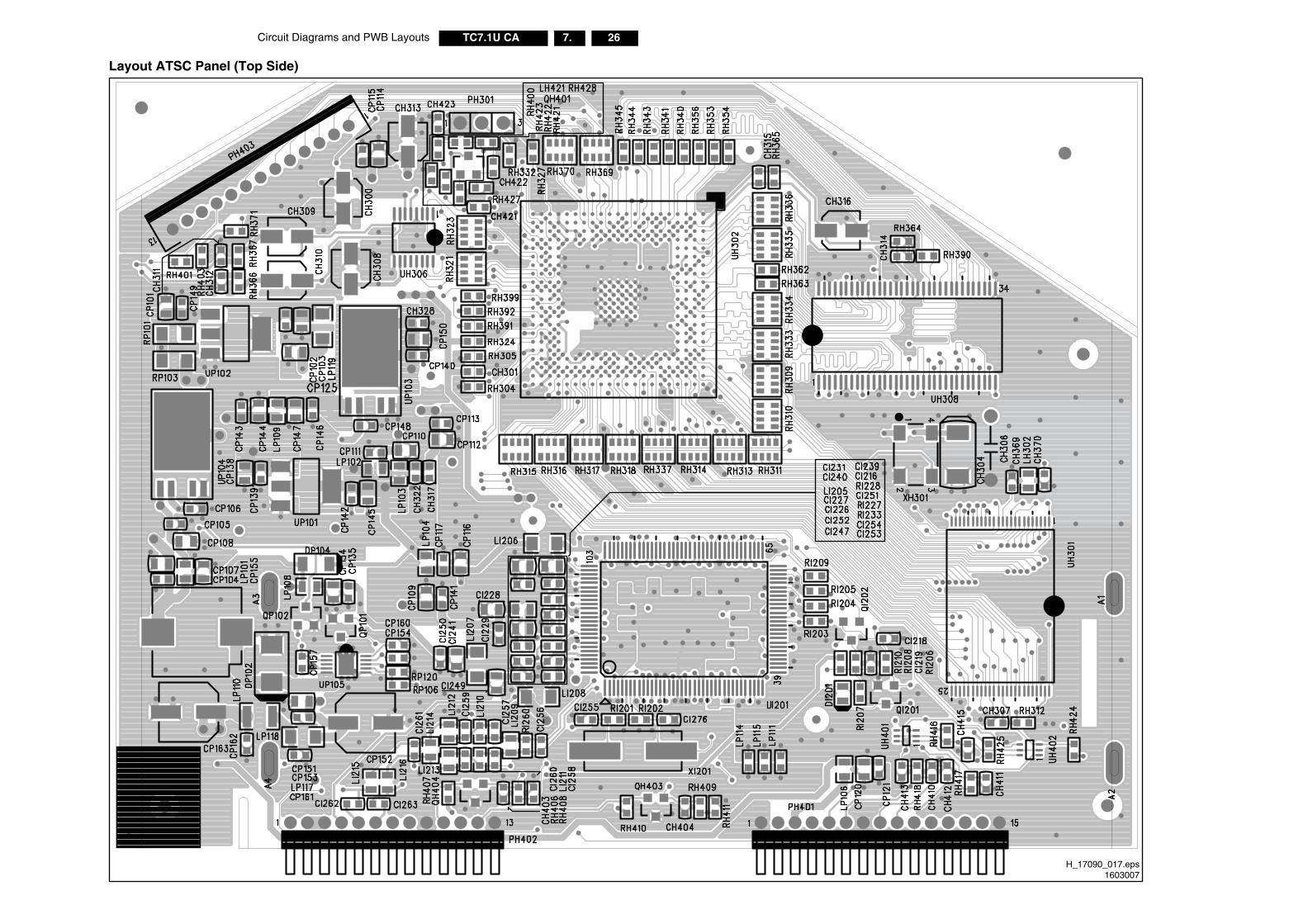
26TC7.1U CA 7.Circuit Diagrams and PWB Layouts
Layout ATSC Panel (Top Side)
H_17090_017.eps1603007
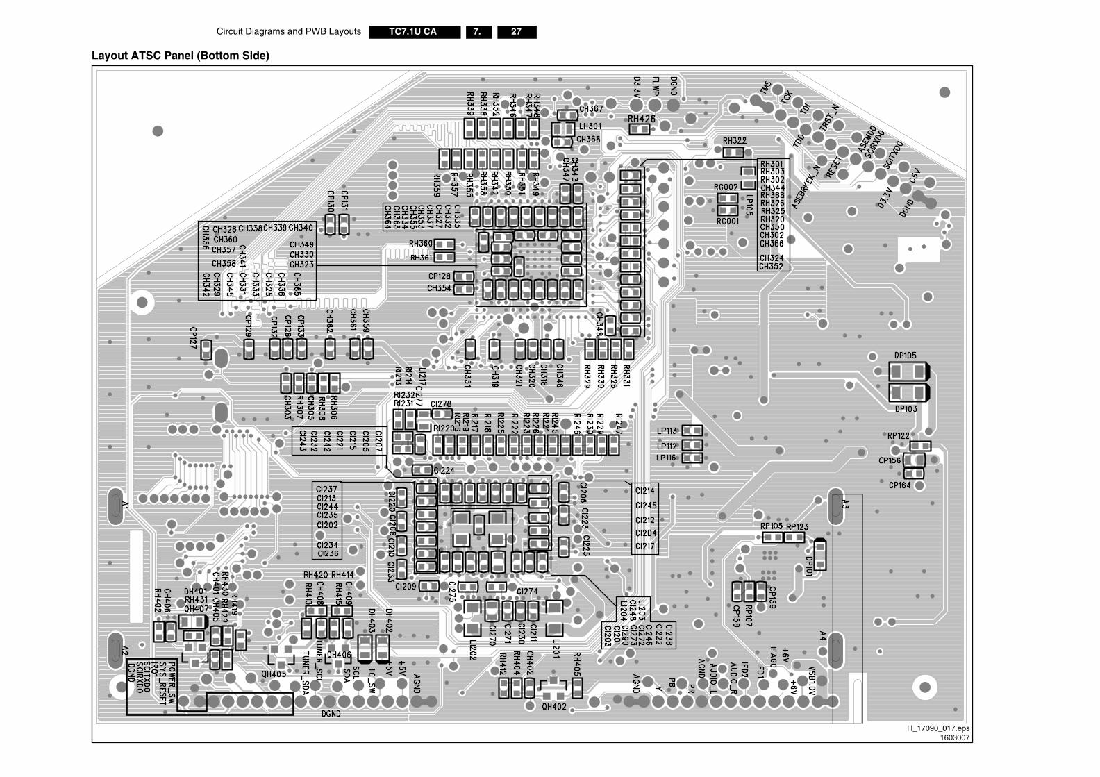
Circuit Diagrams and PWB Layouts 27TC7.1U CA 7.
Layout ATSC Panel (Bottom Side)
H_17090_017.eps1603007
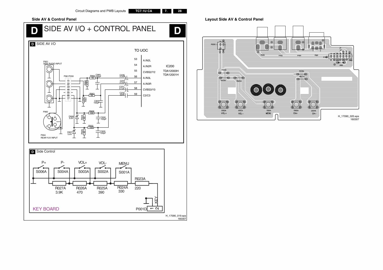
28TC7.1U CA 7.Circuit Diagrams and PWB Layouts
Side AV & Control Panel
SIDE AV I/O + CONTROL PANEL
P904REAR YUV INPUT
P951SIDE RUDIO INPUT
C961100pF
C960100pF
C930100pF
C929100pF
P960
C23222nF
+
C2372.2uF
+
C2362.2uF
CVBS2/Y255
A.IN2R54
A.IN2L53
A.IN3L56
CVBS3/Y358
A.IN3R57
C2/C359
+
C2310.1uF
D9075.6V R
925
82
D9065.6V R
924
821234567
P961
1234567
P200
R932100
R929100
R9631K
R96
147
KR
960
47K
R9621K
TO UOC
IC200
TDA12000HTDA12001H
SIDE AV I/O
S001A
MENU
S002A
VOL-
S003A
VOL+
S004A
P-
R023A
220R024A330
R025A390
R026A470
R027A3.9K
S006A
P+
1 2P001D
KE
Y
KEY BOARD
Side Control
D
D
D D
H_17090_019.eps160307
Layout Side AV & Control Panel
H_17090_020.eps160307
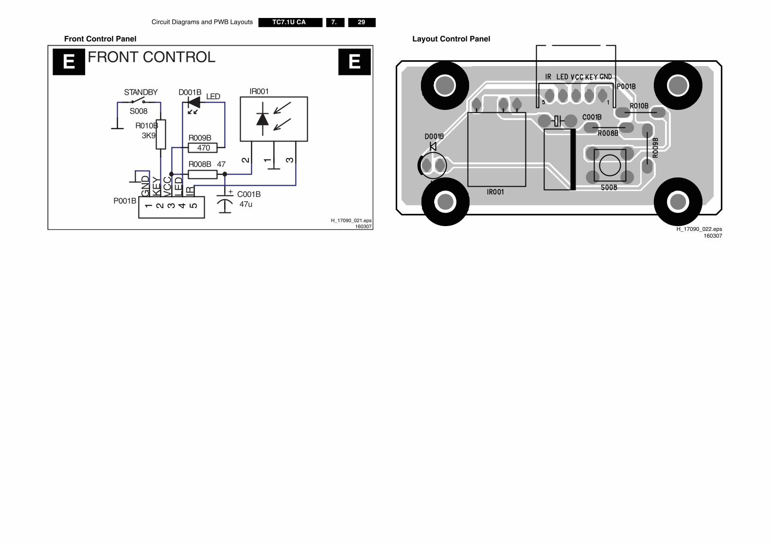
Circuit Diagrams and PWB Layouts 29TC7.1U CA 7.
Front Control Panel
E E
H_17090_021.eps160307
FRONT CONTROL
312
IR001
S008
STANDBY D001B LED
1 2 3 4 5P001B
R008B 47
+ C001B47u
470R009B
R010B3K9
GN
DK
EY
VC
CLE
DIR
Layout Control Panel
H_17090_022.eps160307
30TC7.1U CA 7.Circuit Diagrams and PWB Layouts
Personal Notes:
E_06532_013.eps131004
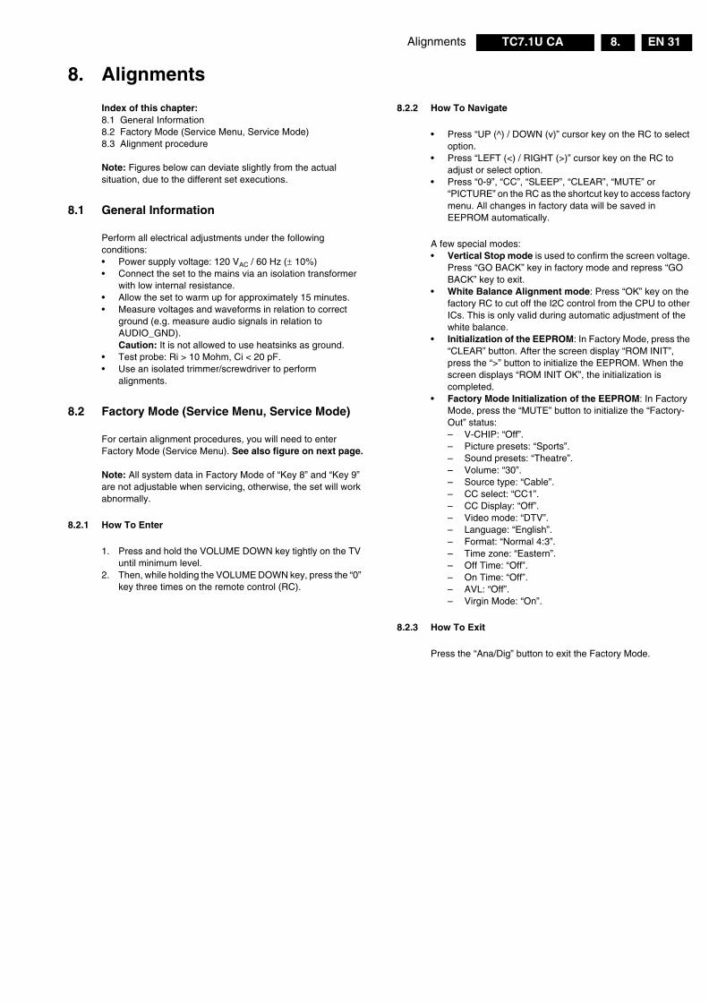
Alignments EN 31TC7.1U CA 8.
8. Alignments
Index of this chapter:8.1 General Information8.2 Factory Mode (Service Menu, Service Mode)8.3 Alignment procedure Note: Figures below can deviate slightly from the actual situation, due to the different set executions.
8.1 General Information
Perform all electrical adjustments under the following conditions:• Power supply voltage: 120 VAC / 60 Hz (± 10%)• Connect the set to the mains via an isolation transformer
with low internal resistance.• Allow the set to warm up for approximately 15 minutes.• Measure voltages and waveforms in relation to correct
ground (e.g. measure audio signals in relation to AUDIO_GND). Caution: It is not allowed to use heatsinks as ground.
• Test probe: Ri > 10 Mohm, Ci < 20 pF.• Use an isolated trimmer/screwdriver to perform
alignments.
8.2 Factory Mode (Service Menu, Service Mode)
For certain alignment procedures, you will need to enter Factory Mode (Service Menu). See also figure on next page. Note: All system data in Factory Mode of “Key 8” and “Key 9” are not adjustable when servicing, otherwise, the set will work abnormally.
8.2.1 How To Enter
1. Press and hold the VOLUME DOWN key tightly on the TV until minimum level.
2. Then, while holding the VOLUME DOWN key, press the “0” key three times on the remote control (RC).
8.2.2 How To Navigate
• Press “UP (^) / DOWN (v)” cursor key on the RC to select option.
• Press “LEFT (<) / RIGHT (>)” cursor key on the RC to adjust or select option.
• Press “0-9”, “CC”, “SLEEP”, “CLEAR”, “MUTE” or “PICTURE” on the RC as the shortcut key to access factory menu. All changes in factory data will be saved in EEPROM automatically.
A few special modes:• Vertical Stop mode is used to confirm the screen voltage.
Press “GO BACK” key in factory mode and repress “GO BACK” key to exit.
• White Balance Alignment mode: Press “OK” key on the factory RC to cut off the I2C control from the CPU to other ICs. This is only valid during automatic adjustment of the white balance.
• Initialization of the EEPROM: In Factory Mode, press the “CLEAR” button. After the screen display “ROM INIT”, press the “>” button to initialize the EEPROM. When the screen displays “ROM INIT OK”, the initialization is completed.
• Factory Mode Initialization of the EEPROM: In Factory Mode, press the “MUTE” button to initialize the “Factory-Out” status:– V-CHIP: “Off”.– Picture presets: “Sports”.– Sound presets: “Theatre”.– Volume: “30”.– Source type: “Cable”.– CC select: “CC1”. – CC Display: “Off”.– Video mode: “DTV”.– Language: “English”.– Format: “Normal 4:3”.– Time zone: “Eastern”.– Off Time: “Off”.– On Time: “Off”.– AVL: “Off”.– Virgin Mode: “On”.
8.2.3 How To Exit
Press the “Ana/Dig” button to exit the Factory Mode.
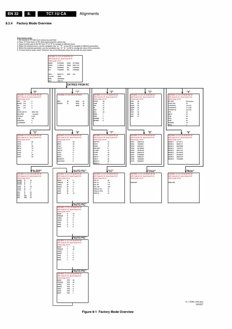
AlignmentsEN 32 TC7.1U CA8.
8.2.4 Factory Mode Overview
Figure 8-1 Factory Mode Overview
Enter factory mode: 1. Set volume to "0" with local volume key and Hold2. Press "0" three times on RC while depressing the volume key.3. Select number pad on the RC from "0" to "9" to navigate to different menu4. Within the selected menu, use the navigation key “▲” “▼” on the RC to navigate to different parameters.5. Within the selected parameter, use the navidation key “◄” “►” on RC to change the value of the parameter.6. To leave factory mode, select "Antenna" key on the RC/power down the set with the main switch.
UOC300C: 2.1.3.2.1 07.02.09 TE1.20APP Code:A1.18 Boot Code:01.01FGPA Code: FF.FFADR0 01010000 ADR1 01110000ADR2 11100010 ADR3 00011110AFC 00000000 RG 01000000CG 11000000 BG 01000000
DEFL 00001111 DISC 128Last NV :6626ERR :00000000REV :402114
ENTRIES FROM RC
"4""3""2""1""0"20.70 1.2.3.1.2 :C003COU02.1ET 90.20.70 1.2.3.1.2 :C003COU10.0ET 91.01.60 1.2.3.1.2 :C003COU 02.1ET 90.20.70 1.2.3.1.2 :C003COU .09 TE1.20 UOC300C: 2.1.3.2.1 07.02.09 TE1.20
APP Code:A1.18 Boot Code:01.01 APP Code:A1.18 Boot Code:01.01 APP Code:A1.18 Boot Code:01.01 APP Code:A1.18 Boot Code:01.01FGPA Code: FF.FF FF.FF :edoC APGFFF.FF :edoC APGFFF.FF :edoC APGF
evitcanI 02CGA FR64HSH84SOPV24RPW83DER0LVL CED23LAP KEPC22RAP12MAV03GPW72NEERG0LVL ONOM
341+5.3LAPKEPFC43WOB13LSV23BPW0LVL CINSAP LVL 0 061+1.3STNKEPFC44WWE23LVADC 521+0.4VUYKEPFC72PWE13CSVDCXO CAP 57 DISC:128 23LPFI44RCU23LCSNICLPINV Inverted 23CTBB84RCL7RBWPSCALE 0.375 46RGP13TWE7FBWPLIM 192 BSWBR 6 46GGPPCENTER 0 BSWBF 9 46BGPLOUDNESS 6 VGEBRI 10
HDOL 3
"9""8""7""6""5".20.70 1.2.3.1.2 :C003COU02.1ET 90.20.70 1.2.3.1.2 :C003COU02.1ET 90.20.70 1.2.3.1.2 :C003COU02.1ET 90.20.70 1.2.3.1.2 :C003COU 09 TE1.20 UOC300C: 2.1.3.2.1 07.02.09 TE1.20
0.10:edoC tooB 81.1A:edoC PPA10.10:edoC tooB 81.1A:edoC PPA10.10:edoC tooB 81.1A:edoC PPA10.10:edoC tooB 81.1A:edoC PPA 1 APP Code:A1.18 Boot Code:01.01FF.FF :edoC APGFFF.FF :edoC APGFFF.FF :edoC APGFFF.FF :edoC APGFFF.FF :edoC APGF
111011101 EDOM0101000010PO134VTPHS82CTNC05XTNC111100002 EDOM1000000120PO13XPHS03CTRB8NTNC000010003 EDOM1100100030PO13NPHS32CLOC04XTRB111010114 EDOM0000010040PO9IRB DSO13TCTNT51NTRB101110005 EDOM0010010050PO01IRB CC13ACTNT31XLOC010011006 EDOM0101000060PO01HDCC0PLOC2NLOC010001007 EDOM0000001070PO03VDCC0SLOC02XTNT010100008 EDOM1010000080PO31H DSO0STRB02NTNT000001019 EDOM0000000190PO03V DSO0TATSSUB
1000000001PO03V UNEM6REVOCERMENU H 7
"etuM""raelC""CC""AUTO PIC”
"AUTO PIC”
"AUTO PIC”
"AUTO PIC”
"PEELS".20.70 1.2.3.1.2 :C003COU02.1ET 90.20.70 1.2.3.1.2 :C003COU02.1ET 90.20.70 1.2.3.1.2 :C003COU02.1ET 90.20.70 1.2.3.1.2 :C003COU 09 TE1.20 UOC300C: 2.1.3.2.1 07.02.09 TE1.20
0.10:edoC tooB 81.1A:edoC PPA10.10:edoC tooB 81.1A:edoC PPA10.10:edoC tooB 81.1A:edoC PPA10.10:edoC tooB 81.1A:edoC PPA 1 APP Code:A1.18 Boot Code:01.01FF.FF :edoC APGFFF.FF :edoC APGFFF.FF :edoC APGFFF.FF :edoC APGFFF.FF :edoC APGF
0410 LOV6M SSABWARM R 18WARM G 11WARM B 4COOL R 18COOL G 11COOL B 4EXC R 32EXC G 38EXC WG 32EXC WB 32
INIC MORTINI MOR01101 LOV01M ELBERT73109 LOV7M ZH001041001 LOV9M ZH003
51VA YALEDY6M ZHK151STN YALEDY8M ZHK351N EFDY01M ZHK8
UOC300C: 2.1.3.2.1 07.02.09 TE1.20APP Code:A1.18 Boot Code:01.01FGPA Code: FF.FFBASS S 22TREBLE S 13100HZ S 6300HZ S 91KHZ S 93KHZ S 98KHZ S 6
UOC300C: 2.1.3.2.1 07.02.09 TE1.20APP Code:A1.18 Boot Code:01.01FGPA Code: FF.FFBASS T 13TREBLE T 22100HZ T 7300HZ T 81KHZ T 63KHZ T 68KHZ T 9
UOC300C: 2.1.3.2.1 07.02.09 TE1.20APP Code:A1.18 Boot Code:01.01FGPA Code: FF.FFBASS STD 28TREBLE STD 26100HZ STD 6300HZ STD 91KHZ STD 83KHZ STD 68KHZ STD 7
H_17090_040.eps300307
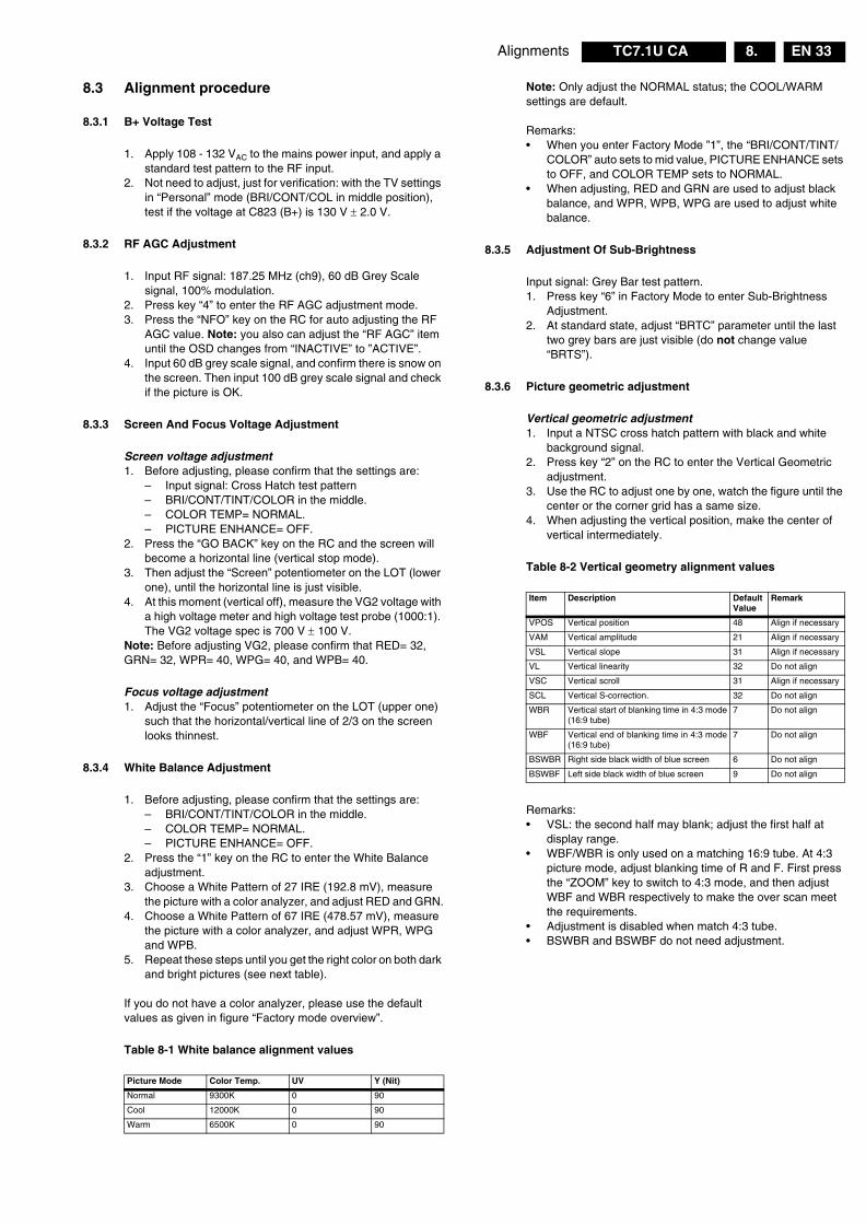
Alignments EN 33TC7.1U CA 8.
8.3 Alignment procedure
8.3.1 B+ Voltage Test
1. Apply 108 - 132 VAC to the mains power input, and apply a standard test pattern to the RF input.
2. Not need to adjust, just for verification: with the TV settings in “Personal” mode (BRI/CONT/COL in middle position), test if the voltage at C823 (B+) is 130 V ± 2.0 V.
8.3.2 RF AGC Adjustment
1. Input RF signal: 187.25 MHz (ch9), 60 dB Grey Scale signal, 100% modulation.
2. Press key “4” to enter the RF AGC adjustment mode.3. Press the “NFO” key on the RC for auto adjusting the RF
AGC value. Note: you also can adjust the “RF AGC” item until the OSD changes from “INACTIVE” to ”ACTIVE”.
4. Input 60 dB grey scale signal, and confirm there is snow on the screen. Then input 100 dB grey scale signal and check if the picture is OK.
8.3.3 Screen And Focus Voltage Adjustment
Screen voltage adjustment1. Before adjusting, please confirm that the settings are:
– Input signal: Cross Hatch test pattern– BRI/CONT/TINT/COLOR in the middle.– COLOR TEMP= NORMAL.– PICTURE ENHANCE= OFF.
2. Press the “GO BACK” key on the RC and the screen will become a horizontal line (vertical stop mode).
3. Then adjust the “Screen” potentiometer on the LOT (lower one), until the horizontal line is just visible.
4. At this moment (vertical off), measure the VG2 voltage with a high voltage meter and high voltage test probe (1000:1). The VG2 voltage spec is 700 V ± 100 V.
Note: Before adjusting VG2, please confirm that RED= 32, GRN= 32, WPR= 40, WPG= 40, and WPB= 40.
Focus voltage adjustment1. Adjust the “Focus” potentiometer on the LOT (upper one)
such that the horizontal/vertical line of 2/3 on the screen looks thinnest.
8.3.4 White Balance Adjustment
1. Before adjusting, please confirm that the settings are:– BRI/CONT/TINT/COLOR in the middle.– COLOR TEMP= NORMAL.– PICTURE ENHANCE= OFF.
2. Press the “1” key on the RC to enter the White Balance adjustment.
3. Choose a White Pattern of 27 IRE (192.8 mV), measure the picture with a color analyzer, and adjust RED and GRN.
4. Choose a White Pattern of 67 IRE (478.57 mV), measure the picture with a color analyzer, and adjust WPR, WPG and WPB.
5. Repeat these steps until you get the right color on both dark and bright pictures (see next table).
If you do not have a color analyzer, please use the default values as given in figure “Factory mode overview”.
Table 8-1 White balance alignment values
Note: Only adjust the NORMAL status; the COOL/WARM settings are default. Remarks: • When you enter Factory Mode ”1”, the “BRI/CONT/TINT/
COLOR” auto sets to mid value, PICTURE ENHANCE sets to OFF, and COLOR TEMP sets to NORMAL.
• When adjusting, RED and GRN are used to adjust black balance, and WPR, WPB, WPG are used to adjust white balance.
8.3.5 Adjustment Of Sub-Brightness
Input signal: Grey Bar test pattern.1. Press key “6” in Factory Mode to enter Sub-Brightness
Adjustment.2. At standard state, adjust “BRTC” parameter until the last
two grey bars are just visible (do not change value “BRTS”).
8.3.6 Picture geometric adjustment
Vertical geometric adjustment1. Input a NTSC cross hatch pattern with black and white
background signal.2. Press key “2” on the RC to enter the Vertical Geometric
adjustment.3. Use the RC to adjust one by one, watch the figure until the
center or the corner grid has a same size. 4. When adjusting the vertical position, make the center of
vertical intermediately.
Table 8-2 Vertical geometry alignment values
Remarks:• VSL: the second half may blank; adjust the first half at
display range.• WBF/WBR is only used on a matching 16:9 tube. At 4:3
picture mode, adjust blanking time of R and F. First press the “ZOOM” key to switch to 4:3 mode, and then adjust WBF and WBR respectively to make the over scan meet the requirements.
• Adjustment is disabled when match 4:3 tube.• BSWBR and BSWBF do not need adjustment.
Picture Mode Color Temp. UV Y (Nit)
Normal 9300K 0 90
Cool 12000K 0 90
Warm 6500K 0 90
Item Description DefaultValue
Remark
VPOS Vertical position 48 Align if necessary
VAM Vertical amplitude 21 Align if necessary
VSL Vertical slope 31 Align if necessary
VL Vertical linearity 32 Do not align
VSC Vertical scroll 31 Align if necessary
SCL Vertical S-correction. 32 Do not align
WBR Vertical start of blanking time in 4:3 mode(16:9 tube)
7 Do not align
WBF Vertical end of blanking time in 4:3 mode(16:9 tube)
7 Do not align
BSWBR Right side black width of blue screen 6 Do not align
BSWBF Left side black width of blue screen 9 Do not align
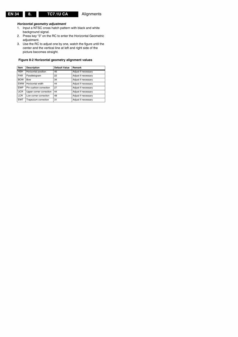
AlignmentsEN 34 TC7.1U CA8.
Horizontal geometry adjustment1. Input a NTSC cross hatch pattern with black and white
background signal.2. Press key “3” on the RC to enter the Horizontal Geometric
adjustment.3. Use the RC to adjust one by one, watch the figure until the
center and the vertical line at left and right side of the picture becomes straight.
Figure 8-2 Horizontal geometry alignment values
Item Description Default Value Remark
HSH Horizontal position 46 Adjust if necessary
PAR Parallelogram 22 Adjust if necessary
BOW Bow 34 Adjust if necessary
EWW Horizontal width 44 Adjust if necessary
EWP Pin cushion correction 27 Adjust if necessary
UCR Upper corner correction 44 Adjust if necessary
LCR Low corner correction 48 Adjust if necessary
EWT Trapezium correction 31 Adjust if necessary
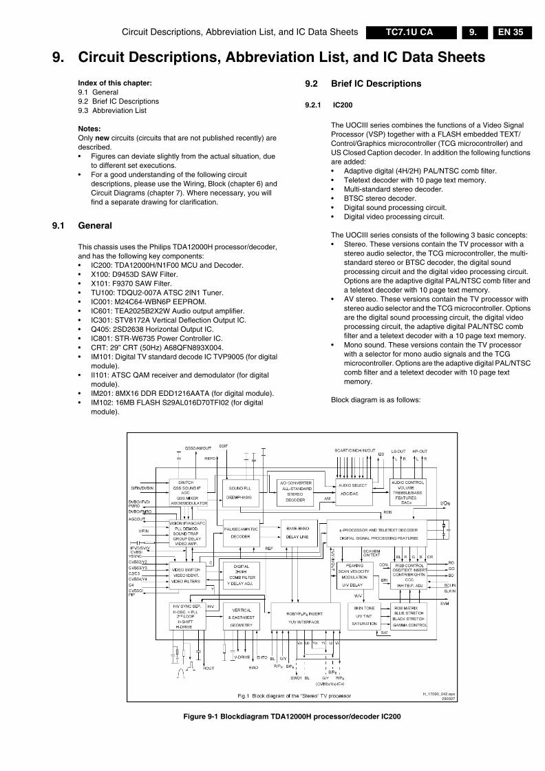
Circuit Descriptions, Abbreviation List, and IC Data Sheets EN 35TC7.1U CA 9.
9. Circuit Descriptions, Abbreviation List, and IC Data Sheets
Index of this chapter:9.1 General9.2 Brief IC Descriptions9.3 Abbreviation List Notes: Only new circuits (circuits that are not published recently) are described. • Figures can deviate slightly from the actual situation, due
to different set executions.• For a good understanding of the following circuit
descriptions, please use the Wiring, Block (chapter 6) and Circuit Diagrams (chapter 7). Where necessary, you will find a separate drawing for clarification.
9.1 General
This chassis uses the Philips TDA12000H processor/decoder, and has the following key components:• IC200: TDA12000H/N1F00 MCU and Decoder.• X100: D9453D SAW Filter.• X101: F9370 SAW Filter.• TU100: TDQU2-007A ATSC 2IN1 Tuner.• IC001: M24C64-WBN6P EEPROM.• IC601: TEA2025B2X2W Audio output amplifier.• IC301: STV8172A Vertical Deflection Output IC.• Q405: 2SD2638 Horizontal Output IC.• IC801: STR-W6735 Power Controller IC.• CRT: 29” CRT (50Hz) A68QFN893X004.• IM101: Digital TV standard decode IC TVP9005 (for digital
module).• II101: ATSC QAM receiver and demodulator (for digital
module).• IM201: 8MX16 DDR EDD1216AATA (for digital module).• IM102: 16MB FLASH S29AL016D70TFI02 (for digital
module).
9.2 Brief IC Descriptions
9.2.1 IC200
The UOCIII series combines the functions of a Video Signal Processor (VSP) together with a FLASH embedded TEXT/Control/Graphics microcontroller (TCG microcontroller) and US Closed Caption decoder. In addition the following functions are added:• Adaptive digital (4H/2H) PAL/NTSC comb filter.• Teletext decoder with 10 page text memory.• Multi-standard stereo decoder.• BTSC stereo decoder.• Digital sound processing circuit.• Digital video processing circuit. The UOCIII series consists of the following 3 basic concepts:• Stereo. These versions contain the TV processor with a
stereo audio selector, the TCG microcontroller, the multi-standard stereo or BTSC decoder, the digital sound processing circuit and the digital video processing circuit. Options are the adaptive digital PAL/NTSC comb filter and a teletext decoder with 10 page text memory.
• AV stereo. These versions contain the TV processor with stereo audio selector and the TCG microcontroller. Options are the digital sound processing circuit, the digital video processing circuit, the adaptive digital PAL/NTSC comb filter and a teletext decoder with a 10 page text memory.
• Mono sound. These versions contain the TV processor with a selector for mono audio signals and the TCG microcontroller. Options are the adaptive digital PAL/NTSC comb filter and a teletext decoder with 10 page text memory.
Block diagram is as follows:
Figure 9-1 Blockdiagram TDA12000H processor/decoder IC200
H_17090_042.eps290307
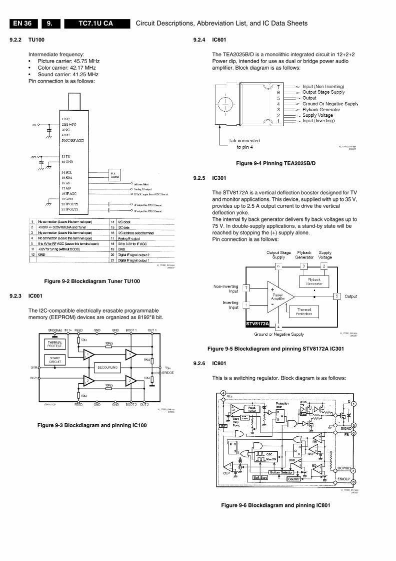
Circuit Descriptions, Abbreviation List, and IC Data SheetsEN 36 TC7.1U CA9.
9.2.2 TU100
Intermediate frequency: • Picture carrier: 45.75 MHz• Color carrier: 42.17 MHz• Sound carrier: 41.25 MHzPin connection is as follows:
Figure 9-2 Blockdiagram Tuner TU100
9.2.3 IC001
The I2C-compatible electrically erasable programmable memory (EEPROM) devices are organized as 8192*8 bit.
Figure 9-3 Blockdiagram and pinning IC100
9.2.4 IC601
The TEA2025B/D is a monolithic integrated circuit in 12+2+2 Power dip, intended for use as dual or bridge power audio amplifier. Block diagram is as follows:
Figure 9-4 Pinning TEA2025B/D
9.2.5 IC301
The STV8172A is a vertical deflection booster designed for TV and monitor applications. This device, supplied with up to 35 V, provides up to 2.5 A output current to drive the vertical deflection yoke.The internal fly back generator delivers fly back voltages up to 75 V. In double-supply applications, a stand-by state will be reached by stopping the (+) supply alone.Pin connection is as follows:
Figure 9-5 Blockdiagram and pinning STV8172A IC301
9.2.6 IC801
This is a switching regulator. Block diagram is as follows:
Figure 9-6 Blockdiagram and pinning IC801
H_17090_043.eps290307
H_17090_044.eps290307
H_17090_045.eps290307
H_17090_046.eps290307
H_17090_047.eps290307
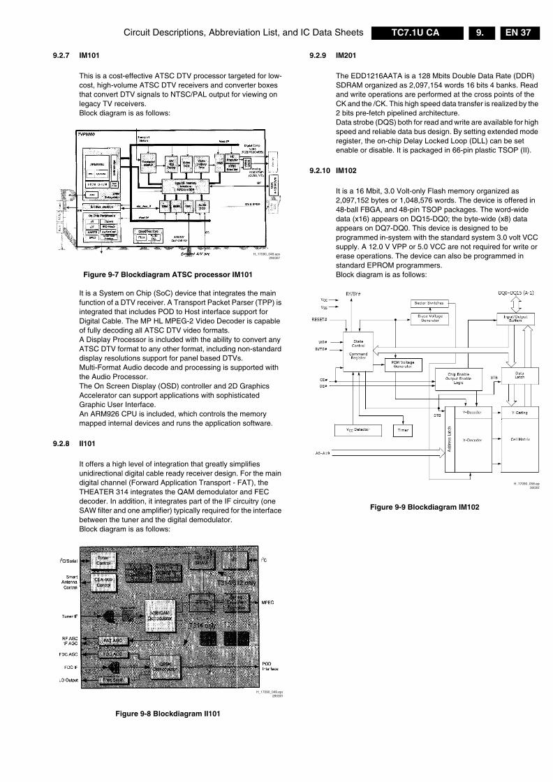
Circuit Descriptions, Abbreviation List, and IC Data Sheets EN 37TC7.1U CA 9.
9.2.7 IM101
This is a cost-effective ATSC DTV processor targeted for low-cost, high-volume ATSC DTV receivers and converter boxes that convert DTV signals to NTSC/PAL output for viewing on legacy TV receivers.Block diagram is as follows:
Figure 9-7 Blockdiagram ATSC processor IM101
It is a System on Chip (SoC) device that integrates the main function of a DTV receiver. A Transport Packet Parser (TPP) is integrated that includes POD to Host interface support for Digital Cable. The MP HL MPEG-2 Video Decoder is capable of fully decoding all ATSC DTV video formats. A Display Processor is included with the ability to convert any ATSC DTV format to any other format, including non-standard display resolutions support for panel based DTVs.Multi-Format Audio decode and processing is supported with the Audio Processor. The On Screen Display (OSD) controller and 2D Graphics Accelerator can support applications with sophisticated Graphic User Interface.An ARM926 CPU is included, which controls the memory mapped internal devices and runs the application software.
9.2.8 II101
It offers a high level of integration that greatly simplifies unidirectional digital cable ready receiver design. For the main digital channel (Forward Application Transport - FAT), the THEATER 314 integrates the QAM demodulator and FEC decoder. In addition, it integrates part of the IF circuitry (one SAW filter and one amplifier) typically required for the interface between the tuner and the digital demodulator.Block diagram is as follows:
Figure 9-8 Blockdiagram II101
9.2.9 IM201
The EDD1216AATA is a 128 Mbits Double Data Rate (DDR) SDRAM organized as 2,097,154 words 16 bits 4 banks. Read and write operations are performed at the cross points of the CK and the /CK. This high speed data transfer is realized by the 2 bits pre-fetch pipelined architecture.Data strobe (DQS) both for read and write are available for high speed and reliable data bus design. By setting extended mode register, the on-chip Delay Locked Loop (DLL) can be set enable or disable. It is packaged in 66-pin plastic TSOP (II).
9.2.10 IM102
It is a 16 Mbit, 3.0 Volt-only Flash memory organized as 2,097,152 bytes or 1,048,576 words. The device is offered in 48-ball FBGA, and 48-pin TSOP packages. The word-wide data (x16) appears on DQ15-DQ0; the byte-wide (x8) data appears on DQ7-DQ0. This device is designed to be programmed in-system with the standard system 3.0 volt VCC supply. A 12.0 V VPP or 5.0 VCC are not required for write or erase operations. The device can also be programmed in standard EPROM programmers.Block diagram is as follows:
Figure 9-9 Blockdiagram IM102
H_17090_048.eps290307
H_17090_049.eps290307
H_17090_058.eps300307
Circuit Descriptions, Abbreviation List, and IC Data SheetsEN 38 TC7.1U CA9.
9.3 Abbreviation List
1080i 1080 visible lines, interlaced1080p 1080 visible lines, progressive scan480i 480 visible lines, interlaced480p 480 visible lines, progressive scanAARA Automatic Aspect Ratio Adaptation:
algorithm that adapts aspect ratio to remove horizontal black bars; keeping up the original aspect ratio
ADC Analogue to Digital ConverterAFC Automatic Frequency Control: control
signal used to tune to the correct frequency
AGC Automatic Gain Control: algorithm that controls the video input of the feature box
AM Amplitude ModulationAR Aspect Ratio: 4 by 3 or 16 by 9ATSC Advanced Television Systems
Committee; HDTV standard for the USA, using MPEG2 for video and Dolby Digital for audio
AV Audio VideoB/G Monochrome TV system. Sound
carrier distance is 5.5 MHzBTSC Broadcast Television System
CommitteeCBA Circuit Board Assembly (or PWB)CVBS Composite Video Blanking and
SynchronizationCVI Component Video InputDAC Digital to analogue ConverterDFU Directions For Use: owner's manualDNR Dynamic Noise ReductionDRAM Dynamic RAMDSP Digital Signal ProcessingDVD Digital Versatile DiscEEPROM Electrically Erasable and
Programmable Read Only MemoryEXT EXTernal (source), entering the set by
SCART or by cinches (jacks)FBL Fast Blanking: DC signal
accompanying RGB signalsFM Field Memory / Frequency ModulationH H_sync HD High Definition: 720p, 1080i, 1080pHP Head PhoneI Monochrome TV system. Sound
carrier distance is 6.0 MHzI2C Integrated IC busIC Integrated CircuitIF Intermediate FrequencyIR Infra RedIRQ Interrupt ReQuestLast Status The settings last chosen by the
customer and read and stored in RAM or in the NVM. They are called at start-up of the set to configure it according the customers wishes
LATAM LATin AMericaLED Light Emitting DiodeLS Loud SpeakerM/N Monochrome TV system. Sound
carrier distance is 4.5 MHzMOSFET Metal Oxide Semiconductor Field
Effect TransistorMPEG Motion Pictures Experts GroupMUTE MUTE LineNAFTA North American Free Trade
Association: Trade agreement between Canada, USA and Mexico
NC Not Connected
NTSC National Television Standard Committee. Color system used mainly in North America and Japan. Color carrier NTSC M/N = 3.579545 MHz, NTSC 4.43 = 4.433619 MHz (this is a VCR norm, it is not transmitted off-air)
NVM Non Volatile Memory: IC containing TV related data (for example, options)
O/C Open CircuitOSD On Screen DisplayPCB Printed Circuit Board (or PWB)PIP Picture In PicturePLL Phase Locked Loop. Used, for
example, in FST tuning systems. The customer can directly provide the desired frequency
PSU Power Supply UnitPWB Printed Wiring Board (or PCB)RAM Random Access MemoryRC Remote Control transmitterRC5 (6) Remote Control system 5 (6), the
signal from the remote control receiver RF Radio FrequencyRGB Red, Green, and Blue. The primary
color signals for TV. By mixing levels of R, G, and B, all colors (Y/C) are reproduced.
RGBHV Red, Green, Blue, Horizontal sync, and Vertical sync
ROM Read Only MemorySC SandCastle: two-level pulse derived
from sync signalsS/C Short CircuitSCL Clock signal on I2C busSD Standard Definition: 480i, 576iSDA Data signal on I2C busSDRAM Synchronous DRAMSIF Sound Intermediate FrequencySMPS Switch Mode Power SupplySND SouNDSOPS Self Oscillating Power SupplySRAM Static RAMSSB Small Signal BoardSTBY Stand-bySVHS Super Video Home SystemSW Sub Woofer / SoftWare / SwitchTHD Total Harmonic DistortionTXT TeleteXTuP MicroprocessorVL Variable Level out: processed audio
output toward external amplifierVCR Video Cassette RecorderVGA Video Graphics ArrayWYSIWYR What You See Is What You Record:
record selection that follows main picture and sound
XTAL Quartz crystalYPbPr Component video (Y= Luminance, Pb/
Pr= Color difference signals B-Y and R-Y, other amplitudes w.r.t. to YUV)
Y/C Video related signals: Y consists of luminance signal, blanking level and sync; C consists of color signal.
Y-OUT Luminance-signalYUV Baseband component video (Y=
Luminance, U/V= Color difference signals)
Spare Parts List EN 39TC7.1U CA 10.
10. Spare Parts List
Set Level
Various
9965 000 44882 ATSC Module� 9965 000 44591 Deg. Coil XC-JQ3350-91� 9965 000 44654 CRT A68QFN893X004P400 9965 000 34424 HS 4p 500/13 TJC1-4YP600 9965 000 34442 HS 2P22 600/7 TJC3-2YSP600 9965 000 36789 Loudsp. 8Ω 5WSP601 9965 000 36789 Loudsp. 8Ω 5W
Mono Carrier [A]
Various
9965 000 44733 EMI Suppr. LGK2629J006 9965 000 27224 0Ω 5% 1/10W 0603J008 9965 000 13966 Ferr. Bead LB3.5X6J114 9965 000 27224 0Ω 5% 1/10W 0603J115 9965 000 27224 0Ω 5% 1/10W 0603J116 9965 000 27224 0Ω 5% 1/10W 0603J118 9965 000 27224 0Ω 5% 1/10W 0603J119 9965 000 27224 0Ω 5% 1/10W 0603J132 9965 000 27224 0Ω 5% 1/10W 0603J138 9965 000 27224 0Ω 5% 1/10W 0603J205 9965 000 27224 0Ω 5% 1/10W 0603J214 9965 000 27224 0Ω 5% 1/10W 0603J225 9965 000 14049 100Ω 5% 0.16WJ256 9965 000 27224 0Ω 5% 1/10W 0603J271 9965 000 27224 0Ω 5% 1/10W 0603J272 9965 000 27224 0Ω 5% 1/10W 0603J273 9965 000 27224 0Ω 5% 1/10W 0603J275 9965 000 27224 0Ω 5% 1/10W 0603J309 9965 000 27224 0Ω 5% 1/10W 0603J401 9965 000 15075 1Ω 5% 1WJ408 9965 000 15717 Wire jumper 8mmJ409 9965 000 27224 0Ω 5% 1/10W 0603J501 9965 000 15717 Wire jumper 8mmJ504 9965 000 17478 0Ω 5% 0.1WJ804 9965 000 13966 Ferr. Bead LB3.5X6J805 9965 000 13966 Ferr. Bead LB3.5X6J901 9965 000 27224 0Ω 5% 1/10W 0603J902 9965 000 27224 0Ω 5% 1/10W 0603J903 9965 000 27224 0Ω 5% 1/10W 0603J917 9965 000 27224 0Ω 5% 1/10W 0603J918 9965 000 27224 0Ω 5% 1/10W 0603J926 9965 000 27224 0Ω 5% 1/10W 0603J927 9965 000 27224 0Ω 5% 1/10W 0603J930 9965 000 27224 0Ω 5% 1/10W 0603J931 9965 000 27224 0Ω 5% 1/10W 0603J932 9965 000 27224 0Ω 5% 1/10W 0603F800 9965 000 15202 Fuse holderF800 9965 000 44736 Fuse 51S050LF801 9965 000 44421 Fuse 2A 250VF802 9965 000 44421 Fuse 2A 250VK801 9965 000 23783 Relay SS-112DM 12VN102 9965 000 27224 0Ω 5% 1/10W 0603P1105 9965 000 44881 Magnetism RingP503 9965 000 34463 HS 5p TJC3-5YP961 9965 000 22958 Y/C Socket VerticalTU100 9965 000 44681 Tuner TDQU2-007AX100 9965 000 44712 SAW FILTER F3953MX101 9965 000 44713 SAW FILTER F9370X200 9965 000 32482 Xtal 24.576MHzZ210 9965 000 27224 0Ω 5% 1/10W 0603Z212 9965 000 44708 Bead 600Ω 25%Z213 9965 000 44708 Bead 600Ω 25%Z214 9965 000 27224 0Ω 5% 1/10W 0603Z216 9965 000 44708 Bead 600Ω 25%Z217 9965 000 27224 0Ω 5% 1/10W 0603Z218 9965 000 44708 Bead 600Ω 25%Z219 9965 000 44708 Bead 600Ω 25%Z221 9965 000 44708 Bead 600Ω 25%Z222 9965 000 27224 0Ω 5% 1/10W 0603Z901 9965 000 44708 Bead 600Ω 25%Z902 9965 000 44708 Bead 600Ω 25%Z903 9965 000 44708 Bead 600Ω 25%Z908 9965 000 44708 Bead 600Ω 25%Z909 9965 000 44708 Bead 600Ω 25%Z910 9965 000 44708 Bead 600Ω 25%Z911 9965 000 44708 Bead 600Ω 25%Z912 9965 000 44708 Bead 600Ω 25%Z913 9965 000 44708 Bead 600Ω 25%Z914 9965 000 44708 Bead 600Ω 25%Z915 9965 000 44708 Bead 600Ω 25%Z916 9965 000 44708 Bead 600Ω 25%
Z917 9965 000 44708 Bead 600Ω 25%
C003 9965 000 14011 22pF 5% 50VC004 9965 000 20344 10nF 50V +80-20% 0603C005 9965 000 14011 22pF 5% 50VC01 9965 000 44700 330µF 20% 25VC017 9965 000 14008 0.1uF 50V +80%~-20%C018 9965 000 20344 10nF 50V +80-20% 0603C019 9965 000 14069 100μF 20% 16VC02 9965 000 14069 100μF 20% 16VC021 9965 000 14069 100μF 20% 16VC022 9965 000 27900 0.22μF 20% 50V 0603C023 9965 000 27900 0.22μF 20% 50V 0603C026 9965 000 14011 22pF 5% 50VC027 9965 000 14011 22pF 5% 50VC029 9965 000 14069 100μF 20% 16VC083 4822 124 40196 220μF 20% 16VC084 9965 000 17523 10nF +80%-20% 50VC085 9965 000 14070 220μF 20% 16VC086 9965 000 17523 10nF +80%-20% 50VC090 9965 000 14070 220μF 20% 16VC091 9965 000 14008 0.1uF 50V +80%~-20%C092 9965 000 14008 0.1uF 50V +80%~-20%C093 9965 000 14070 220μF 20% 16VC100 9965 000 14075 10μF 20% 50VC101 9965 000 13965 100pF 5% 50VC102 9965 000 20344 10nF 50V +80-20% 0603C103 9965 000 15805 100μF 20% 10VC105 9965 000 14076 47μF 20% 50VC106 9965 000 20344 10nF 50V +80-20% 0603C107 9965 000 20344 10nF 50V +80-20% 0603C108 9965 000 20344 10nF 50V +80-20% 0603C109 9965 000 20344 10nF 50V +80-20% 0603C110 9965 000 20344 10nF 50V +80-20% 0603C111 9965 000 20344 10nF 50V +80-20% 0603C114 9965 000 13965 100pF 5% 50VC115 9965 000 14008 0.1uF 50V +80%~-20%C117 9965 000 27374 47nF+80/-20% 50VC200 9965 000 27860 10μF /-20% 16VC201 9965 000 27900 0.22μF 20% 50V 0603C203 9965 000 28015 22μF 20% 50VC204 9965 000 27341 2200pF 10% 50V 0603C205 9965 000 32924 0.022μF 50V 0603C206 9965 000 31805 0.15μF 5% 63VC207 9965 000 20356 1000pF 10% 50V 0603C208 9965 000 27860 10μF /-20% 16VC209 9965 000 20356 1000pF 10% 50V 0603C210 9965 000 32924 0.022μF 50V 0603C211 9965 000 27900 0.22μF 20% 50V 0603C212 9965 000 14069 100μF 20% 16VC213 9965 000 20356 1000pF 10% 50V 0603C214 9965 000 31222 6800pF 10% 50VC215 9965 000 44701 2.2µF 10% 50VC216 9965 000 20344 10nF 50V +80-20% 0603C217 9965 000 14008 0.1uF 50V +80%~-20%C219 9965 000 14069 100μF 20% 16VC219A 9965 000 14069 100μF 20% 16VC222 9965 000 14008 0.1uF 50V +80%~-20%C223 9965 000 15805 100μF 20% 10VC224 9965 000 14008 0.1uF 50V +80%~-20%C225 9965 000 27860 10μF /-20% 16VC227 9965 000 27860 10μF /-20% 16VC228 9965 000 28015 22μF 20% 50VC229 9965 000 14008 0.1uF 50V +80%~-20%C230A 9965 000 27860 10μF /-20% 16VC231 9965 000 22807 0.1μF 50V 20%C232 9965 000 32924 0.022μF 50V 0603C234 9965 000 14037 1μF 20% 50VC235 9965 000 14008 0.1uF 50V +80%~-20%C235A 9965 000 27860 10μF /-20% 16VC236 9965 000 28015 22μF 20% 50VC237 9965 000 28015 22μF 20% 50VC238 9965 000 14037 1μF 20% 50VC239 9965 000 14037 1μF 20% 50VC241 9965 000 27860 10μF /-20% 16VC242 9965 000 14008 0.1uF 50V +80%~-20%C243 9965 000 14008 0.1uF 50V +80%~-20%C244 9965 000 14008 0.1uF 50V +80%~-20%C245 9965 000 14008 0.1uF 50V +80%~-20%C246 9965 000 14008 0.1uF 50V +80%~-20%C248 9965 000 14008 0.1uF 50V +80%~-20%C249 9965 000 14008 0.1uF 50V +80%~-20%C250 9965 000 27860 10μF /-20% 16VC251 9965 000 14008 0.1uF 50V +80%~-20%C252 9965 000 27341 2200pF 10% 50V 0603C253 9965 000 27871 33μF 20% 16VC254 9965 000 13965 100pF 5% 50V
C255 9965 000 27900 0.22μF 20% 50V 0603C256 9965 000 27900 0.22μF 20% 50V 0603C257 9965 000 15182 47μF 20% 25VC258 9965 000 14008 0.1uF 50V +80%~-20%C259 9965 000 13965 100pF 5% 50VC260 9965 000 27900 0.22μF 20% 50V 0603C261 9965 000 27900 0.22μF 20% 50V 0603C262 9965 000 13961 47μF 20% 16VC264 9965 000 31412 22nF 10% 50VC265 9965 000 28015 22μF 20% 50VC266 9965 000 28015 22μF 20% 50VC267 9965 000 14008 0.1uF 50V +80%~-20%C268 9965 000 13965 100pF 5% 50VC270 9965 000 27341 2200pF 10% 50V 0603C271 9965 000 44702 220nF 10% 16VC272 9965 000 44702 220nF 10% 16VC281 9965 000 27300 0.01μF 10% 50VC282 9965 000 27300 0.01μF 10% 50VC283 9965 000 27300 0.01μF 10% 50VC284 9965 000 27300 0.01μF 10% 50VC300 9965 000 15686 100μF 20% 50VC307 9965 000 15182 47μF 20% 25VC308 9965 000 22805 220μUF 25V +/-20%C313 9965 000 14039 4.7μF 20% 50VC323 9965 000 14598 100μF 20% 35VC324 9965 000 14036 100μF 20% 25VC325 9965 000 22941 0.33μF 63V 5% MPEC334 9965 000 30713 2.2nF 10% 50VC337 9965 000 27303 0.033μF 10% 50VC342 9965 000 15112 0.1μF 5% 50VC350 9965 000 14010 1500pF 10% 50VC351 9965 000 27341 2200pF 10% 50V 0603C360 9965 000 15686 100μF 20% 50VC400 9965 000 24628 22μF 250V +/-20%C401 9965 000 15183 220pF 500V 10%C402 9965 000 15085 1000μF 20% 25VC404 9965 000 17521 22nF 5% 63VC405 9965 000 14008 0.1uF 50V +80%~-20%C406 9965 000 15085 1000μF 20% 25VC407 9965 000 20344 10nF 50V +80-20% 0603C408 9965 000 44704 0.0033µF 5% 1.6kVC410 9965 000 44706 0.0068µF 5% 1.6kVC411 9965 000 44707 0.027µF 5% 400VC412 9965 000 15682 Electrolytic CapacitorC413 9965 000 44705 6200pF 5% 1.6kVC414 9965 000 44703 0.39µF 5% 400VC415 9965 000 15683 1000μF 35V 20%C416 9965 000 15683 1000μF 35V 20%C417 9965 000 14039 4.7μF 20% 50VC418 9965 000 15183 220pF 500V 10%C419 9965 000 15183 220pF 500V 10%C420 9965 000 15188 4700pF 250Vac +80-20%C421 9965 000 24355 0.1μF 100V 5% MPEC423 9965 000 15090 100μF 20% 160VC424 9965 000 14008 0.1uF 50V +80%~-20%C503 9965 000 24628 22μF 250V +/-20%C504 9965 000 44678 0.033µF5% 250VC505 9965 000 44382 1000pF 10% 2kVC511 9965 000 20346 330pF 5% 50V 0603C512 9965 000 44679 1000pF 10% 250VC521 9965 000 20346 330pF 5% 50V 0603C522 9965 000 44679 1000pF 10% 250VC531 9965 000 20346 330pF 5% 50V 0603C532 9965 000 44679 1000pF 10% 250VC540 9965 000 14921 10μF 20% 250VC600 9965 000 15084 22μF 20% 16VC601 9965 000 27305 4700pF 10% 50V 0603C602 9965 000 15113 220nF 5% 50VC603 9965 000 14069 100μF 20% 16VC604 9965 000 15084 22μF 20% 16VC605 9965 000 27305 4700pF 10% 50V 0603C606 9965 000 15113 220nF 5% 50VC607 9965 000 14069 100μF 20% 16VC608 9965 000 14069 100μF 20% 16VC609 9965 000 14037 1μF 20% 50VC610 9965 000 14069 100μF 20% 16VC611 9965 000 14599 470μF 20% 16VC612 9965 000 27900 0.22μF 20% 50V 0603C613 9965 000 14069 100μF 20% 16VC614 9965 000 14599 470μF 20% 16VC615 9965 000 14069 100μF 20% 16VC616 9965 000 14599 470μF 20% 16VC617 9965 000 27900 0.22μF 20% 50V 0603C618 9965 000 27900 0.22μF 20% 50V 0603C619 9965 000 13961 47μF 20% 16VC621 9965 000 14069 100μF 20% 16VC622 9965 000 14069 100μF 20% 16VC801 9965 000 44731 33µF 20% 275VC802 9965 000 44730 0.1µF 20 275V
Spare Parts ListEN 40 TC7.1U CA10.
C804 9965 000 15188 4700pF 250Vac +80-20%C804A 9965 000 17914 470pF 10% 400VC805 9965 000 15188 4700pF 250Vac +80-20%C805A 9965 000 17914 470pF 10% 400VC806 9965 000 38929 470μF 200V 20%C807 9965 000 44381 10nF 10% 500VC808 9965 000 44728 10nF 20% 1kVC809 9965 000 44727 220pF 10% 1kVC810 9965 000 13963 220pF 5% 50VC811 9965 000 14037 1μF 20% 50VC812 9965 000 34505 3300pF 50V 10%C813 9965 000 13962 0.1μF 5% 50VC814 9965 000 17906 10μF 20% 35VC815 9965 000 29743 680pF 1kV 10%C820 9965 000 44729 220pF 10% 1kVC823 9965 000 34497 220μF 160V 20%C824 9965 000 44381 10nF 10% 500VC824A 9965 000 44723 33µF 20% 35VC825 9965 000 14008 0.1uF 50V +80%~-20%C826 9965 000 20357 1000PF 50V 5% 0603C828 9965 000 14069 100μF 20% 16VC829 9965 000 34533 4700ΩF 16V 20%C830 9965 000 15183 220pF 500V 10%C831 9965 000 17510 1000μF 16V 20%C832 9965 000 14070 220μF 20% 16VC833 9965 000 20344 10nF 50V +80-20% 0603C834 9965 000 15099 0.01μF +80%~20% 50VC835 9965 000 20344 10nF 50V +80-20% 0603C837 9965 000 17510 1000μF 16V 20%C840 9965 000 15183 220pF 500V 10%C840A 9965 000 22936 2200pF 400Vac 20%C842 9965 000 15099 0.01μF +80%~20% 50VC850 9965 000 15183 220pF 500V 10%C851 9965 000 14067 1000μF 20% 16VC852 9965 000 15099 0.01μF +80%~20% 50VC853 9965 000 27299 3.3μF 20% 50VC902 9965 000 13965 100pF 5% 50VC903 9965 000 13965 100pF 5% 50VC904 9965 000 27860 10μF /-20% 16VC905 9965 000 27860 10μF /-20% 16VC912 9965 000 13965 100pF 5% 50VC914 9965 000 13965 100pF 5% 50VC915 9965 000 13965 100pF 5% 50VC917 9965 000 28015 22μF 20% 50VC918 9965 000 14037 1μF 20% 50VC919 9965 000 28015 22μF 20% 50VC922 9965 000 29848 10pF 5% 50VC923 9965 000 29848 10pF 5% 50VC926 9965 000 13965 100pF 5% 50VC927 9965 000 13965 100pF 5% 50VC928 9965 000 13965 100pF 5% 50VC929 9965 000 13965 100pF 5% 50VC930 9965 000 13965 100pF 5% 50VC960 9965 000 13965 100pF 5% 50VC961 9965 000 13965 100pF 5% 50V
�
R009 9965 000 14049 100Ω 5% 0.16WR01 9965 000 32057 4.7kΩ 1/10W 0603R010 9965 000 32037 100Ω 1/10W 0603R011 9965 000 32037 100Ω 1/10W 0603R012 9965 000 44725 1.5Ω 3WR014 9965 000 32058 47kΩ 1/10W 0603R015 9965 000 32057 4.7kΩ 1/10W 0603R016 9965 000 29781 12kΩ 1/10 0603R017 9965 000 32037 100Ω 1/10W 0603R018 9965 000 32039 10kΩ 1/10W 0603R02 9965 000 32049 27kΩ 5% 1/10WR022 9965 000 12519 1k 5% 0.16WR023 4822 111 31047 5K6 5% 1/6WR024 9965 000 14049 100Ω 5% 0.16WR025 9965 000 32037 100Ω 1/10W 0603R026 9965 000 32037 100Ω 1/10W 0603R027 9965 000 32051 3.3kΩ 1/10W 0603R029 9965 000 32051 3.3kΩ 1/10W 0603R03 9965 000 32038 1kΩ 1/10W 0603R030 4822 111 31038 3.9k 5% 0.16WR031 9965 000 14049 100Ω 5% 0.16WR032 4822 111 31047 5K6 5% 1/6WR033 9965 000 12515 2.2k 5% 0.16WR034 9965 000 32037 100Ω 1/10W 0603R035 9965 000 32037 100Ω 1/10W 0603R036 9965 000 32037 100Ω 1/10W 0603R039 9965 000 32038 1kΩ 1/10W 0603R045 9965 000 32039 10kΩ 1/10W 0603R047 9965 000 32045 2.2kΩ 1/10W 0603R048 9965 000 32051 3.3kΩ 1/10W 0603R049 9965 000 32058 47kΩ 1/10W 0603R050 9965 000 32046 22kΩ 5% 1/10WR051 9965 000 32051 3.3kΩ 1/10W 0603R052 9965 000 32039 10kΩ 1/10W 0603R086 9965 000 15066 10Ω 5% 0.25W
R087 9965 000 17938 750Ω 5% 0.16WR090 9965 000 17494 120Ω 5% 1/6WR092 9965 000 27224 0Ω 5% 1/10W 0603R100 9965 000 31396 68kΩ 1/10W 0603R101 9965 000 32039 10kΩ 1/10W 0603R103 9965 000 32055 39kΩ 5% 1/10WR104 9965 000 30773 47Ω 1/10W 5% 0603R105 9965 000 32057 4.7kΩ 1/10W 0603R106 9965 000 32057 4.7kΩ 1/10W 0603R107 9965 000 32039 10kΩ 1/10W 0603R109 9965 000 30773 47Ω 1/10W 5% 0603R111 4822 053 10561 560Ω 5% 1WR112 9965 000 32039 10kΩ 1/10W 0603R114 9965 000 44420 51Ω 1/10W 0603R115 9965 000 12485 150Ω 5% 0.16WR116 9965 000 27283 680Ω 1/10W 0603R117 9965 000 32041 150Ω 1/10W 0603R118 9965 000 30770 22Ω 1/10W 0603R120 9965 000 30770 22Ω 1/10W 0603R121 9965 000 30770 22Ω 1/10W 0603R122 9965 000 32057 4.7kΩ 1/10W 0603R123 9965 000 32051 3.3kΩ 1/10W 0603R124 9965 000 32037 100Ω 1/10W 0603R130 9965 000 32037 100Ω 1/10W 0603R131 9965 000 32037 100Ω 1/10W 0603R200 9965 000 31396 68kΩ 1/10W 0603R201 9965 000 32055 39kΩ 5% 1/10WR202 9965 000 32038 1kΩ 1/10W 0603R203 9965 000 32038 1kΩ 1/10W 0603R204 9965 000 32038 1kΩ 1/10W 0603R205 9965 000 27283 680Ω 1/10W 0603R206 9965 000 32055 39kΩ 5% 1/10WR207 9965 000 32037 100Ω 1/10W 0603R208 9965 000 32037 100Ω 1/10W 0603R209 9965 000 32037 100Ω 1/10W 0603R210 9965 000 29781 12kΩ 1/10 0603R211 9965 000 27224 0Ω 5% 1/10W 0603R217 9965 000 32058 47kΩ 1/10W 0603R221 9965 000 32039 10kΩ 1/10W 0603R222 9965 000 32037 100Ω 1/10W 0603R223 9965 000 32038 1kΩ 1/10W 0603R225 9965 000 32038 1kΩ 1/10W 0603R226 9965 000 27259 Fuse 1MΩ 5% 1/10WR227 9965 000 31216 270kΩ 1/10W 5%R228 9965 000 32044 220Ω 1/10W 0603R229 9965 000 32057 4.7kΩ 1/10W 0603R230 9965 000 32037 100Ω 1/10W 0603R231 9965 000 32037 100Ω 1/10W 0603R232 9965 000 32037 100Ω 1/10W 0603R234 9965 000 27919 56kΩ 5% 1/10WR235 9965 000 32058 47kΩ 1/10W 0603R236 9965 000 32038 1kΩ 1/10W 0603R237 9965 000 12515 2.2k 5% 0.16WR238 9965 000 32057 4.7kΩ 1/10W 0603R240 9965 000 31217 390kΩ 1/10W 5%R241 9965 000 32053 390Ω 1/10W 0603R244 9965 000 32051 3.3kΩ 1/10W 0603R245 9965 000 32059 0.47MΩ 1/10W 5%R250 9965 000 32038 1kΩ 1/10W 0603R251 9965 000 32038 1kΩ 1/10W 0603R252 9965 000 32058 47kΩ 1/10W 0603R253 9965 000 32058 47kΩ 1/10W 0603R255 9965 000 44693 220Ω 5% 1/2WR256 9965 000 44693 220Ω 5% 1/2WR257 9965 000 44693 220Ω 5% 1/2WR270 9965 000 27236 33kΩ 1/10W 0603R271 9965 000 08285 18k 5% 0.16WR282 9965 000 13958 68Ω 5% 0.17WR283 9965 000 44699 430? 5% 1/10WR284 9965 000 27226 100kΩ 1/10W 0603R285 9965 000 32056 470kΩ 5% 1/10WR286 9965 000 27224 0Ω 5% 1/10W 0603R287 9965 000 32037 100Ω 1/10W 0603R300 9965 000 29821 820Ω 5% 1/10WR313 9965 000 22920 1Ω 1W 5% Wire WoundR314 9965 000 32038 1kΩ 1/10W 0603R315 9965 000 15664 2.2kΩ 5% 1/4WR316 9965 000 32038 1kΩ 1/10W 0603R321 9965 000 44376 1Ω 5% 2WR324 9965 000 44416 180Ω 5% 2WR350 9965 000 32045 2.2kΩ 1/10W 0603R401 9965 000 32936 680Ω 5% 2WR406 9965 000 32056 470kΩ 5% 1/10WR407 9965 000 17499 1Ω 1/2W 5% Res. FuseR409 9965 000 44694 18Ω 5% 1/2WR410 9965 000 44694 18Ω 5% 1/2WR411 9965 000 15175 120Ω 2W 5% Metal OxideR412 9965 000 32039 10kΩ 1/10W 0603R413 9965 000 17864 820Ω 5% 0.16WR418 9965 000 31396 68kΩ 1/10W 0603R419 9965 000 44696 68Ω 5%R420 9965 000 44697 0.56Ω 2WR421 9965 000 44692 Fuse 5.6Ω 5% 2WR422 9965 000 44692 Fuse 5.6Ω 5% 2W
R424 4822 111 31038 3.9k 5% 0.16WR425 9965 000 44695 10kΩ 5% 1/2WR426 9965 000 44691 Fuse 0.47Ω 5% 1/2WR427 9965 000 44691 Fuse 0.47Ω 5% 1/2WR429 9965 000 12519 1k 5% 0.16WR433 9965 000 44695 10kΩ 5% 1/2WR435 9965 000 44689 150kΩ 5% 1/2WR436 9965 000 27224 0Ω 5% 1/10W 0603R437 9965 000 32043 15kΩ 1/10W 0603R438 9965 000 44698 36kΩ 5% 1/10WR439 9965 000 44698 36kΩ 5% 1/10WR440 9965 000 23744 150kΩ 5% 0.17WR442 9965 000 27226 100kΩ 1/10W 0603R443 9965 000 27236 33kΩ 1/10W 0603R501 9965 000 15771 1KΩ 1/4W 5% Carb. FilmR505 9965 000 22916 33Ω 1W 5% Metal OxideR511 9965 000 30773 47Ω 1/10W 5% 0603R512 9965 000 32039 10kΩ 1/10W 0603R513 9965 000 27336 270Ω 5% 1/10WR514 9965 000 30769 10Ω 5% 1/10WR515 9965 000 22919 15kΩ 5% 3W 5%R516 0300 206 47131 470Ω 5% 1/4WR517 9965 000 32060 560Ω 1/10W 0603R518 0300 206 47131 470Ω 5% 1/4WR519 9965 000 44676 1kΩ 10% 1/2WR521 9965 000 30773 47Ω 1/10W 5% 0603R522 9965 000 32039 10kΩ 1/10W 0603R523 9965 000 27336 270Ω 5% 1/10WR524 9965 000 30769 10Ω 5% 1/10WR525 9965 000 22919 15kΩ 5% 3W 5%R526 0300 206 47131 470Ω 5% 1/4WR527 9965 000 32060 560Ω 1/10W 0603R528 0300 206 47131 470Ω 5% 1/4WR529 9965 000 44676 1kΩ 10% 1/2WR531 9965 000 30773 47Ω 1/10W 5% 0603R532 9965 000 32039 10kΩ 1/10W 0603R533 9965 000 27336 270Ω 5% 1/10WR534 9965 000 30769 10Ω 5% 1/10WR535 9965 000 22919 15kΩ 5% 3W 5%R536 0300 206 47131 470Ω 5% 1/4WR537 9965 000 32060 560Ω 1/10W 0603R538 0300 206 47131 470Ω 5% 1/4WR539 9965 000 44676 1kΩ 10% 1/2WR540 9965 000 44677 2.2MΩ 5% 1/4WR541 9965 000 24633 1.5kΩ 10% 1/2WR542 0300 206 47131 470Ω 5% 1/4WR600 9965 000 32057 4.7kΩ 1/10W 0603R601 9965 000 32051 3.3kΩ 1/10W 0603R602 9965 000 32037 100Ω 1/10W 0603R603 9965 000 32057 4.7kΩ 1/10W 0603R604 9965 000 32051 3.3kΩ 1/10W 0603R605 9965 000 32037 100Ω 1/10W 0603R606 9965 000 32048 2.7kΩ 1/10W 0603R607 9965 000 32048 2.7kΩ 1/10W 0603R608 9965 000 32048 2.7kΩ 1/10W 0603R609 9965 000 32038 1kΩ 1/10W 0603R610 9965 000 32038 1kΩ 1/10W 0603R611 9965 000 27236 33kΩ 1/10W 0603R611A 9965 000 34531 0.12Ω 2W Wire WoundR613 9965 000 32039 10kΩ 1/10W 0603R801 9965 000 17901 1M 5% 0.5WR810 9965 000 44719 0.47kΩ 5% 2WR811 9965 000 12519 1k 5% 0.16WR812 9965 000 12519 1k 5% 0.16WR813 9965 000 14059 22Ω 5% 0.25WR814 9965 000 44405 1.2kΩ 5% 1/4WR815 9965 000 14049 100Ω 5% 0.16WR816A 9965 000 22804 0.22Ω 2W Wire WoundR817 9965 000 44718 120kΩ 5% 1WR818 4822 111 31023 47k 5% 0.16WR820 9965 000 22998 4.7Ω 1W 5% Res. FuseR821 9965 000 44724 6.8kΩ 5% 5WR822 9965 000 15778 33kΩ 5% 2WR823 9965 000 44717 100kΩ 1% 1/2WR824 9965 000 44690 RES.M.F 3.9K 1/6W /-1%R824A 9965 000 44690 RES.M.F 3.9K 1/6W /-1%R825 9965 000 27236 33kΩ 1/10W 0603R826 9965 000 15664 2.2kΩ 5% 1/4WR826A 9965 000 15777 22kΩ 5% 2WR827 9965 000 44716 750Ω 1% 1/6WR828 9965 000 32048 2.7kΩ 1/10W 0603R829 9965 000 32058 47kΩ 1/10W 0603R829A 9965 000 32057 4.7kΩ 1/10W 0603R831 9965 000 44725 1.5Ω 3WR832 9965 000 15771 1KΩ 1/4W 5% Carb. FilmR833 9965 000 32045 2.2kΩ 1/10W 0603R840A 9965 000 17902 8.2M 5% 1WR850 9965 000 34537 FUSE 3A 250VACR902 9965 000 27226 100kΩ 1/10W 0603R903 9965 000 27226 100kΩ 1/10W 0603R904 9965 000 32050 330Ω 1/10W 0603R905 9965 000 32050 330Ω 1/10W 0603R908 9965 000 32038 1kΩ 1/10W 0603R910 9965 000 27240 75Ω 1/10W 0603
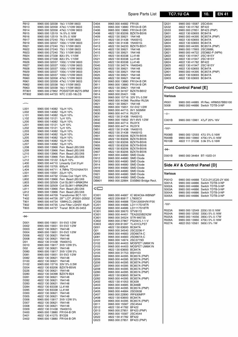
Spare Parts List EN 41TC7.1U CA 10.
R912 9965 000 32038 1kΩ 1/10W 0603R913 9965 000 32058 47kΩ 1/10W 0603R914 9965 000 32058 47kΩ 1/10W 0603R915 9965 000 12519 1k 5% 0.16WR916 9965 000 12519 1k 5% 0.16WR917 9965 000 27240 75Ω 1/10W 0603R919 9965 000 32037 100Ω 1/10W 0603R921 9965 000 27240 75Ω 1/10W 0603R922 9965 000 27240 75Ω 1/10W 0603R923 9965 000 27240 75Ω 1/10W 0603R924 9965 000 27338 82Ω 5% 1/10WR925 9965 000 27338 82Ω 5% 1/10WR926 9965 000 32037 100Ω 1/10W 0603R927 9965 000 32037 100Ω 1/10W 0603R928 9965 000 32037 100Ω 1/10W 0603R929 9965 000 32037 100Ω 1/10W 0603R932 9965 000 32037 100Ω 1/10W 0603R960 9965 000 32058 47kΩ 1/10W 0603R961 9965 000 32058 47kΩ 1/10W 0603R962 9965 000 32038 1kΩ 1/10W 0603R963 9965 000 32038 1kΩ 1/10W 0603RT801 9965 000 27862 POSISTOR MZ75-9RMRT802 9965 000 44720 NTC 2.5D-18LCS
�
L001 9965 000 14082 10μH 10%L002 9965 000 14082 10μH 10%L101 9965 000 14082 10μH 10%L102 9965 000 15121 1μH 10%L200 9965 000 14082 10μH 10%L201 9965 000 15121 1μH 10%L202 9965 000 15121 1μH 10%L203 9965 000 14082 10μH 10%L204 9965 000 14082 10μH 10%L205 9965 000 14082 10μH 10%L206 9965 000 14082 10μH 10%L207 9965 000 14082 10μH 10%L208 9965 000 13966 Ferr. Bead LB3.5X6L209 9965 000 13966 Ferr. Bead LB3.5X6L210 9965 000 13966 Ferr. Bead LB3.5X6L211 9965 000 13966 Ferr. Bead LB3.5X6L212 9965 000 15122 0.6μH 10%L400 9965 000 44710 Linearity Coil 31µHL403 9965 000 15705 600μHL404 9965 000 44711 4.7MHz TD1016A4701L501 9965 000 15591 22μH 10%L801 9965 000 44732 Choke Coil 10µH 10%L802 9965 000 13966 Ferr. Bead LB3.5X6L803 9965 000 32509 Coil SL0811-6R8K2R4L804 9965 000 32509 Coil SL0811-6R8K2R4L811 9965 000 13966 Ferr. Bead LB3.5X6L812 9965 000 13966 Ferr. Bead LB3.5X6T401 9965 000 44709 Transformer BCT-101T402 9965 000 44726 29"" LOT JF0501-20502T801 9965 000 44734 10MHLCL-2802BT802 9965 000 44735 Line Filter LGH2V 40µHT803 9965 000 44737 Transf. BCK-35-0453
�
D001 9965 000 15651 5V-5V2 1/2WD002 9965 000 15651 5V-5V2 1/2WD003 4822 130 30621 1N4148D004 9965 000 15651 5V-5V2 1/2WD006 4822 130 30621 1N4148D008 4822 130 30621 1N4148D01 4822 130 31438 1N4001GD010 9965 000 15817 3V9 1/2W 5%D02 4822 130 30621 1N4148D080 9965 000 15817 3V9 1/2W 5%D081 9965 000 15651 5V-5V2 1/2WD082 4822 130 30621 1N4148D100 4822 130 30621 1N4148D102 9965 000 15716 33V 5% 0.5WD204 4822 130 83206 BZX79-B5V6D226 4822 130 30621 1N4148D280 4822 130 34398 BZX79-B24D281 4822 130 30621 1N4148D282 4822 130 30621 1N4148D283 4822 130 30621 1N4148D284 4822 130 83338 LL4148D285 4822 130 83338 LL4148D300 4822 130 30621 1N4148D305 4822 130 30621 1N4148D306 9965 000 15817 3V9 1/2W 5%D307 4822 130 30621 1N4148D308 4822 130 30621 1N4148D309 4822 130 31438 1N4001GD400 9965 000 13880 FR104-B ORD401 4822 130 41275 BY228D402 9965 000 13880 FR104-B OR
D404 9965 000 44682 FR105D405 9965 000 13880 FR104-B ORD406 9965 000 13880 FR104-B ORD408 4822 130 83206 BZX79-B5V6D409 4822 130 30621 1N4148D411 4822 130 31438 1N4001GD412 4822 130 31438 1N4001GD413 4822 130 34233 BZX79-B5V1D414 4822 130 30621 1N4148D415 4822 130 30621 1N4148D511 4822 130 83338 LL4148D521 4822 130 83338 LL4148D531 4822 130 83338 LL4148D540 5322 130 34574 1N4004GD623 4822 130 30621 1N4148D624 4822 130 30621 1N4148D625 4822 130 30621 1N4148D626 4822 130 30621 1N4148D810 9965 000 13880 FR104-B ORD811 9965 000 13880 FR104-B ORD812 4822 130 30621 1N4148D813 4822 130 34167 BZX79-B6V2D814 9965 000 20421 1H8D815 9965 000 15716 33V 5% 0.5WD820 9965 000 44366 Rectifier RU3AD821 4822 130 30621 1N4148D822 9965 000 15651 5V-5V2 1/2WD823 9965 000 44715 9V1 500MWD830 9965 000 44714 RU3YXD831 4822 130 31438 1N4001GD832 9965 000 15652 8V1-8V5 1/2WD840 9965 000 44714 RU3YXD850 9965 000 44714 RU3YXD851 4822 130 31438 1N4001GD852 4822 130 31438 1N4001GD901 4822 130 83206 BZX79-B5V6D903 4822 130 83206 BZX79-B5V6D904 4822 130 83206 BZX79-B5V6D905 4822 130 83206 BZX79-B5V6D906 4822 130 83206 BZX79-B5V6D907 4822 130 83206 BZX79-B5V6D911 9965 000 44680 SMD DiodeD912 9965 000 44680 SMD DiodeD913 9965 000 44680 SMD DiodeD914 9965 000 44680 SMD DiodeD919 9965 000 44680 SMD DiodeD920 9965 000 44680 SMD DiodeD921 9965 000 44680 SMD DiodeD922 9965 000 44680 SMD DiodeDB801 9965 000 22884 D3SB60 Bridge Rect.
��
IC001 9965 000 44687 IC M24C64-WBN6PIC090 4822 209 80817 L7805CVIC200 9965 000 44688 TDA12000H/N1F00IC201 9965 000 44686 LD1117S18TRIC202 9965 000 44686 LD1117S18TRIC301 9965 000 30670 STV8172IC601 9965 000 44401 TEA2025B2X2WIC801 9965 000 34524 STR-W6735IC802 9965 000 27867 PS2561L1-1-VIC803 4822 209 81397 TL431CLPSTQ001 4822 130 63693 BC847AQ01 9965 000 34540 2SC2236-YQ080 9965 000 44683 2SD667A-CQ081 9965 000 44683 2SD667A-CQ101 9965 000 14974 2SC3779DQ102 9965 000 44403 MOSFET UM6K1NQ103 9965 000 44403 MOSFET UM6K1NQ104 4822 130 63693 BC847AQ105 9965 000 31753 BSH103Q204 9965 000 44395 BC857A (PNP)Q205 9965 000 44395 BC857A (PNP)Q206 9965 000 44395 BC857A (PNP)Q207 9965 000 44395 BC857A (PNP)Q208 9965 000 44395 BC857A (PNP)Q280 9965 000 44395 BC857A (PNP)Q281 4822 130 63693 BC847AQ282 9965 000 44395 BC857A (PNP)Q402 4822 130 41053 BC639Q403 9965 000 44685 BC846BQ404 9965 000 44395 BC857A (PNP)Q405 9965 000 44684 2SD2638Q407 9965 000 22890 IRF630MFPQ408 4822 130 63693 BC847AQ409 9965 000 44395 BC857A (PNP)Q511 9965 000 15587 2SC4544Q512 4822 130 41782 BF422Q513 9965 000 27851 BF423 (PNP)Q521 9965 000 15587 2SC4544Q522 4822 130 41782 BF422Q523 9965 000 27851 BF423 (PNP)
Q531 9965 000 15587 2SC4544Q532 4822 130 41782 BF422Q533 9965 000 27851 BF423 (PNP)Q601 4822 130 63693 BC847AQ602 9965 000 44395 BC857A (PNP)Q603 4822 130 63693 BC847AQ604 4822 130 63693 BC847AQ605 9965 000 44395 BC857A (PNP)Q820 9965 000 17893 2SC2688LQ821 9965 000 44722 2SD882-P (NPN)Q822 4822 130 41947 2SC1815YQ823 4822 130 41947 2SC1815YQ824 4822 130 41782 BF422Q825 4822 130 41947 2SC1815YQ900 4822 130 63693 BC847AQ901 9965 000 44395 BC857A (PNP)Q902 4822 130 63693 BC847AQ903 4822 130 63693 BC847A
Front Control Panel [E]
Various
IR001 9965 000 44885 IR Rec. HRM557BB5100S008 9965 000 44886 Switch TDTB-3-NP
C001B 9965 000 13961 47μF 20% 16V
�
R008B 9965 000 12593 47Ω 5% 0.16WR009B 9965 000 13960 470Ω 5% 0.16WR010B 4822 111 31038 3.9k 5% 0.16W
�
D001B 9965 000 34464 BT-102D-31
Side AV & Control Panel [D]
Various
P001D 9965 000 44888 TJC3-2Y/JC25-2Y 600S001A 9965 000 44886 Switch TDTB-3-NPS002A 9965 000 44886 Switch TDTB-3-NPS003A 9965 000 44886 Switch TDTB-3-NPS004A 9965 000 44886 Switch TDTB-3-NPS005A 9965 000 44886 Switch TDTB-3-NP
�
R023A 9965 000 12549 220Ω 55 0.16WR024A 9965 000 12592 330Ω 5% 0.16WR025A 9965 000 14056 390Ω 5% 0.17WR026A 9965 000 13960 470Ω 5% 0.16WR027A 4822 053 10561 560Ω 5% 1W

Revision ListEN 42 TC7.1U CA11.
11. Revision ListManual xxxx xxx xxxx.0• First release.
Manual xxxx xxx xxxx.1• Front Page: TOC corrected.• Chapter 7: Mono Carrier schematic and PWB layout
updated with newest version.


