Embed Size (px)
Citation preview

Tektronix-
2213OSCILLOSCOPE
SERVICE
INSTRUCTION MANUAL

REV NOV 1981
TABLE O F CONTENTS
2213 Service
Page Page
LIST OF I LLUSTRATIONS . . . . . . . . . . . . . . . . . iv SE CTION 3 THEORY OF OPERATION
LIST OF TABLES . . . . . . . . . . . . . . . . . . . . . . . . ν I NTRODUCTIO N . . . . . . . . . . . . . . . 3-1
OPERATORS SAFETY SUMMARY . . . . . . . . . . . . vi GENER AL DESCR I PTION . . . . . . . . . 3-2DETAILE D CI RCUIT
SERVICING SA FETY SUMMARY . . . . . . . . . . . . . vii DESCR I PTION . . . . . . . . . . . . . . . . . 3-4VERTICAL ATTENUATORS . . . . . 3-4
In put Coup ling . . . . . . . . . . . . . 3-4H igh-Ζ Attenuato r . . . . . . . . . . . 3-4
SE CTION 1 SPECI F ICATION Buffer Amplifier and Low-ΖI NTRODUCTION . . . . . . . . . . . . . 1-1 Attenuator . . . . . . . . . . . . . . . . 3-5ACCESSOR I ES. . . . . . . . . . . . . . . 1-1 Volts/Div Var Circuit andPERFORMANCE CON DITIONS . . . 1-1 X1/X10 Amplifier . . . . . . . . . . . 3-6
VERTICAL PREAMPS. . . . . . . . . . 3-6
SECTION 2 OPERATING I NSTRUCTIONSChan nel 1 Vertical Preamplifier . . 3-6Channel 2 Vertical Preamplifier . . 3-6
PREPARATION FOR USE . . . . . . . . . 2-1 Internal Trigger P ickoffSAFETY . . . . . . . . . . . . . . . . . . . 2-1 Amplifier. . . . . . . . . . . . . . . . . 3-7L I NE VOLTAGE . . . . . . . . . . . . . 2-1 CHANNEL SWITCH ANDPOWER CORD . . . . . . . . . . . . . . . 2-1 VERTICAL OUTPUT . . . . . . . . . . 3-7L I NE FUSE . . . . . . . . . . . . . . . . . 2-1 Diode Gates . . . . . . . . . . . . . . . 3-7
CONTROLS, CO NNECTORS, Delay Line Driver . . . . . . . . . . . 3-8AND I NDICATO RS. . . . . . . . . . . . . . 2-3 Delay Line . . . . . . . . . . . . . . . . 3-9
POWER, DISPLAY, AND Vertical Output Amplifier . . . . . . 3-9PR OBE ADJUST . . . . . . . . . . . . . . 2-3 Chan nel Switch ing LogicVERTICAL . . . . . . . . . . . . . . . . . 2-3 Circuit. . . . . . . . . . . . . . . . . . . 3-9HORIZONTAL . . . . . . . . . . . . . . . 2-5 Internal Trigger Switch ingTRIGGER . . . . . . . . . . . . . . . . . . 2-5 Logic . . . . . . . . . . . . . . . . . . . 3-10RE AR PANEL . . . . . . . . . . . . . . . 2-7 TR IGGER . . . . . . . . . . . . . . . . . . 3-12
OPERATING CONSIDER ATIONS . . . . 2-8 Internal Trigger Amp lifier . . . . . . 3-13GRATICULE . . . . . . . . . . . . . . . . 2-8 Trigger Source-SwitchingGROUNDI NG . . . . . . . . . . . . . . . 2-8 Circuit . . . . . . . . . . . . . . . . . . . 3-13SIGNAL CONNECTIONS . . . . . . . . 2-8 External Trigger Amplifier . . . . . 3-13I NPUT COUPL I NG CAPACITOR Auto Trigger Circuit. . . . . . . . . . 3-13PRECHARGI NG . . . . . . . . . . . . . . 2-8 Trigger Level Comparator . . . . . . 3-14I N ST RUMENT COOL I NG . . . . . . . 2-9 Inverting Amplifier and
OSCI LLOSCOPE DISPLAYS. . . . . . . . 2-9 TV Trigger Circuit . . . . . . . . . . . 3-14I NTRODUCTION . . . . . . . . . . . . . 2-9 Schmitt Trigger Circu it . . . . . . . . 3-15BAS EL I NE T RACE . . . . . . . . . . . . . 2-9 Auto Baseline Circuit . . . . . . . . . 3-15SIGNAL DISPLAY . . . . . . . . . . . . 2-9 SWEEP GENER ATOR ANDMAG N I F IED-SWEEP DISPLAY. . . . 2-10 LOGIC . . . . . . . . . . . . . . . . . . . . 3-15DELAYE D-SWEEP DISPLAY . . . . . 2-10 Miller Sweep Generator . . . . . . . 3-15Χ-Υ DISPLAY . . . . . . . . . . . . . . . 2-10 Sweep Logic . . . . . . . . . . . . . . . 3-16TV SIGNAL DISPLAYS . . . . . . . . . . . 2-11 Delay Circuit . . . . . . . . . . . . . . 3-18
2213 Service
TABLE O F CONTENTS (cont)
SECTION 3 THEORY OF OPERATION (cont)
Page
SECTION 5 ADJUSTMENT PROCEDURE
Page
DETAILE D CI RCUIT I NTROD UCTION . . . . . . . . . . . . . . . 5-1D ESCR I PTION (cont) PURPOSE . . . . . . . . . . . . . . . . . . 5-1
TEST EQUI PMENT REQU I RE D . . . 5-1AUTO I NTENSITY AND Z-AXIS L IMITS AND TO LERANCES . . . . . 5-1AMPL I F IER . . . . . . . . . . . . . . . . . 3-19 PARTIAL PROCEDURES . . . . . . . 5-1
Auto Intensity . . . . . . . . . . . . . 3-19 ADJUSTMENT I NTERACTION . . . 5-1Ζ-Axis Amp lifier . . . . . . . . . . . . 3-20 PREPARATION FOR
HORIZONTA L . . . . . . . . . . . . . . . 3-20 ADJU STMENT. . . . . . . . . . . . . . . 5-3Horizontal Preamp lifier . . . . . . . 3-20 I NDEX TO ADJUSTMENTΧΥ Am p lifier . . . . . . . . . . . . . . 3-21 PROCEDURE . . . . . . . . . . . . . . . . 5-3Horizontal Output Amp lifier . . . . 3-22 POWER SUPPLY AND CRT
POWER SUPPLY . . . . . . . . . . . . . 3-22 DISPLAY . . . . . . . . . . . . . . . . . . . . 5-4Power Input . . . . . . . . . . . . . . . 3-22 VERTICA L . . . . . . . . . . . . . . . . . . . 5-7Preregulator . . . . . . . . . . . . . . . 3-22 HOR IZONTAL . . . . . . . . . . . . . . . . . 5-13Inverter . . . . . . . . . . . . . . . . . . 3-23 TRIGGER I NG . . . . . . . . . . . . . . . . . 5-17CRT Supply . . . . . . . . . . . . . . . 3-24 EXT ERNAL Z-AXIS ANDAuto Focus Circuit . . . . . . . . . . 3-24 PROBE ADJUST . . . . . . . . . . . . . . . . 5-20Low-Voltage Supplies . . . . . . . . . 3-24DC Restorer . . . . . . . . . . . . . . . 3-24 SECTION 6 MAINTENAN CE
STATIC-SENSITIVE COMPONENTS . . 6-1PREVENTIVE MAI NTENANCE . . . . . 6-2
I NTRODUCTION . . . . . . . . . . . . . 6-2GENERAL CARE . . . . . . . . . . . . . 6-2I NSPECTION AN D CLEAN I NG . . . 6-2LUBR ICATION . . . . . . . . . . . . . . 6-4SEM ICONDUCTOR CHECKS . . . . . 6-4
SE CTION 4 PERFORMANCE CHECK PERIODIC READJUSTMENT . . . . . 6-4PROC EDURE TROUBLESHOOTI NG . . . . . . . . . . . . 6-5I NTRODUCTIO N . . . . . . . . . . . . . . . 4-1 INTROD UCTION . . . . . . . . . . . . . 6-5
PURPOSE . . . . . . . . . . . . . . . . . . 4-1 TROUBLESHOOTI NG AIDS . . . . . 6-5TEST EQU IPMENT REQU I RE D . . . 4-1 TROUBLESHOOTI NGL I MITS AND TOLERANCES . . . . . 4-1 EQUIPMENT . . . . . . . . . . . . . . . . 6-7PREPARATIO N . . . . . . . . . . . . . . 4-1 TROUBLESHOOTINGI NDEX TO PERFORMANCE TECHN IQUES . . . . . . . . . . . . . . . 6-7CHECK STEPS . . . . . . . . . . . . . . . 4-3 CORRECTIVE MAINTENANCE . . . . . 6-10
VERTICAL . . . . . . . . . . . . . . . . . . . 4-4 I NTROD UCTION . . . . . . . . . . . . . 6-10
HORIZONTA L . . . . . . . . . . . . . . . . . 4-6 MAI NTENANCE PRECAUTIONS . . 6-10
TR IGGER I NG . . . . . . . . . . . . . . . . . 4-9 OBTAIN I NG REPLACEMENT
EXTERNAL Z-AXIS AND PARTS . . . . . . . . . . . . . . . . . . . . 6-10PR OBE ADJUST. . . . . . . . . . . . . . . . 4-12 MAI NTENANCE AIDS . . . . . . . . . 6-10

TABLE OF CONTENTS (cont)
Page
2213 Service
SECTION 6 MAINTENANCE (cont) SECTION 7 OPTIONS
INTERCONNECTIONS . . . . . . . . . 6-10TRANSISTORS AND SECTION 8 REPLACEABLE ELECTRICAL PARTS
INTEGRATED CIRCUITS . . . . . . . 6-11SOLDERING TECHNIQUES. . . . . . 6-12 SECTION 9 DIAGRAMS
REMOVAL AND REPLACEMENTINSTRUCTIONS . . . . . . . . . . . . . . 6-13 SECTION 10 REPLACEABLE MECHANICAL PARTS
Cabinet . . . . . . . . . . . . . . . . . . 6-13Cathode-Ray Tube . . . . . . . . . . . 6-13 ACCESSORIES
High-Voltage Shield . . . . . . . . . . 6-14Attenuator/Sweep CircuitBoard . . . . . . . . . . . . . . . . . . . 6-14 INTERNATIONAL SALES & SERVICE OFFICESFront-Panel Circuit Board . . . . . . 6-15Main Circuit Board . . . . . . . . . . 6-16 U.S . SALES& SERVICE OFFICESCurrent Limit Circuit Board . . . . 6-18
REPACKAGING FOR SHIPMENT . . 6-18 CHANGE INFORMATION

2213 Service
iv
ιιsτ οF ιιιυsτRατιοιν s
Figure
Page
The 2213 Oscilloscope
viii
2-1
Power-in put-voltage configu rations . . . . . . . . . . . . . . . . . . . . . . . . . . . . . . . . . . . . . . . 2-2
2-2
Line fuse and power cord . . . . . . . . . . . . . . . . . . . . . .
2-2
2-3
Power, d isplay, and probe adjust controls, connector, and i ndicator . . . . . . . . . . . . . . . . .
2-3
2-4
Ve rtical controls and connectors . . . . . . . . . . . . . . . . . . . . . . . . . . . . . . . . . . . . . . . . 2-4
2-5
Horizontal controls . . . . . . . . . . . . . . . . . . . . . . . . . . . . . . . . . . . . . . . . . . . . . . . . . 2-5
2-6
Trigger controls, connecto r , and indicator . . . . . . . . . . . . . . . . . . . . . . . . . . . . . . . . . . 2-6
2-7
Rear-panel connector . . . . . . . . . . . . . . . . . . . . . . . . . . . . . . . . . . . . . . . . . . . . . . . . 2-72-8
Graticule measurement markings . . . . . . . . . . . . . . . . . . . . . . . . . . . . . . . . . . . . . . . . 2-8
3-1
Basic block d iagram of the 2213 Oscilloscope . . . . . . . . . . . . . . . . . . . . . . . . . . . . . . . .
3-33-2
Detailed block diagram of the Channel 1 attenuator and attenuator switching tables . . . . . .
3-53-3
Diode gate biasing for α Channel 1 display . . . . . . . . . . . . . . . . . . . . . . . . . . . . . . . . . . 3-83-4
CHOP VERTICAL MOD E waveforms . . . . . . . . . . . . . . . . . . . . . . . . . . . . . . . . . . . . . 3-113-5
Sweep timing diagram . . . . . . . . . . . . . . . . . . . . . . . . . . . . . . . . . . . . . . . . . . . . . . . 3-163-6
Simplified diagram of the Ζ-Axis Switch i ng Logic circuit . . . . . . . . . . . . . . . . . . . . . . . .
3-183-7
Detailed block diagram of the Horizontal Amplifier . . . . . . . . . . . . . . . . . . . . . . . . . . . .
3-213-8
Simplified diagram of the DC Restorer circuit . . . . . . . . . . . . . . . . . . . . . . . . . . . . . . . .
3-25
4-1
Test setup fo r exte rnal trigger and j itter checks . . . . . . . . . . . . . . . . . . . . . . . . . . . . . . .
4-10
6-1
Multipin connector orientation . . . . . . . . . . . . . . . . . . . . . . . . . . . . . . . . . . . . . . . . . 6-6
9-1
Color codes for resistors and capacitors .9-2
Semiconductor lead configurations .9-3
Locating components on schematic diagrams and circuit board illustrations .9-4
2213 block diagram.9-5
A12-Attenuator/Sweep board .9-6
Ci rcu it view of A12`-Attenuator/Sweep board.9-7
Circuit view of A10-Main board.9-8
A10-Main board .9-9
All -Front Panel board.9-10
A19-Current Limit board.
ιι ι
ιι

LIST OF TABLES
2213 Service
Table Page
1-1 Electrical Characteristics . . . . . . . . . . . . . . . . . . . . . . . . . . . . . . . . . . . . . . . . . . . . . . 1-21-2 Environmental Characteristics . . . . . . . . . . . . . . . . . . . . . . . . . . . . . . . . . . . . . . . . . . 1-61-3 Physical Characteristics. . . . . . . . . . . . . . . . . . . . . . . . . . . . . . . . . . . . . . . . . . . . . . . 1-7
4-1 Test Equipment Required . . . . . . . . . . . . . . . . . . . . . . . . . . . . . . . . . . . . . . . . . . . . . 4-24-2 Deflection Accuracy Limits . . . . . . . . . . . . . . . . . . . . . . . . . . . . . . . . . . . . . . . . . . . . 4-44-3 Settings for Bandwidth Checks . . . . . . . . . . . . . . . . . . . . . . . . . . . . . . . . . . . . . . . . . . 4-54-4 Settings for Timing Accuracy Checks . . . . . . . . . . . . . . . . . . . . . . . . . . . . . . . . . . . . . 4-74-5 Delay Time Range Checks . . . . . . . . . . . . . . . . . . . . . . . . . . . . . . . . . . . . . . . . . . . . . 4-74-6 Switch Combinations for Triggering Checks . . . . . . . . . . . . . . . . . . . . . . . . . . . . . . . . . 4-9
5-1 Adjustment Interactions . . . . . . . . . . . . . . . . . . . . . . . . . . . . . . . . . . . . . . . . . . . . . . 5-25-2 Power Supply Limits and Ripple . . . . . . . . . . . . . . . . . . . . . . . . . . . . . . . . . . . . . . . . 5-55-3 Deflection Accuracy Limits . . . . . . . . . . . . . . . . . . . . . . . . . . . . . . . . . . . . . . . . . . . . 5-85-4 Attenuator Compensation Adjustments . . . . . . . . . . . . . . . . . . . . . . . . . . . . . . . . . . . . 5-105-5 Settings for Bandwidth Checks . . . . . . . . . . . . . . . . . . . . . . . . . . . . . . . . . . . . . . . . . . 5-115-6 Timing Accuracy . . . . . . . . . . . . . . . . . . . . . . . . . . . . . . . . . . . . . . . . . . . . . . . . . . . 5-145-7 Settings for Timing Accuracy Checks . . . . . . . . . . . . . . . . . . . . . . . . . . . . . . . . . . . . . 5-155-8 Delay Time Range Checks . . . . . . . . . . . . . . . . . . . . . . . . . . . . . . . . . . . . . . . . . . . . . 5-155-9 Switch Combinations for Triggering Checks . . . . . . . . . . . . . . . . . . . . . . . . . . . . . . . . . 5-18
6-1 Relative Susceptibility to Static-Discharge Damage . . . . . . . . . . . . . . . . . . . . . . . . . . . . 6-16-2 External Inspection Checklist . . . . . . . . . . . . . . . . . . . . . . . . . . . . . . . . . . . . . . . . . . 6-36-3 Internal Inspection Checklist . . . . . . . . . . . . . . . . . . . . . . . . . . . . . . . . . . . . . . . . . . . 6-36-4 Maintenance Aids . . . . . . . . . . . . . . . . . . . . . . . . . . . . . . . . . . . . . . . . . . . . . . . . . . 6-11

2213 Service
The general safetyand cautions will be found throughout the manual where they apply and do not appear in this summary.
Terms i n Th is Manual
CAUTION statements identify conditions or practicesthat could result in damage to the equ i pment or otherproperty .
WARN I NG statements identify cond itions or practicesthat could result in personal in jury or loss of life .
Terms as Marked on Equipment
CAUTION indicates α personal i njury hazard not imme-diately accessible as one reads the markings, or α hazard toproperty, including the equ ipment itself .
DANGER indicates α personal injury hazard immediatelyaccessible as one reads the mark ing.
Symbols in This Manual
Symbols as Marked on Equ ipment
Power Source
Th is product is intended to operate from α power sou rceth at does not apply more than 250 volts rms between thesupply conductors or between either supply conductor andground. Α protective ground connection by way of theground ing conductor in the power cord is essential for safeoperation .
OPERATORS SAFETY SUMMARY
information in this part of the summary is for both operating and servicing personnel.
This symbol indicates where applicablecautiona ry or other information is to befound. For maximum input voltages, seeTable 1-1 .
DANGER - H igh voltage.
Protective grou nd (earth ) te rminal .
ATTENTION - Refer to manual .
Ground ing the ProductThis product is grounded th rough the groundi ng conductorof the power cord. To avoid electrical shock, plug thepower cord into α p roperly wired receptable before con-necting to the product in put or output terminals . Αprotective ground connection by way of the grou ndingconductor i n the power cord is essential for safe operation.
Danger Arising F rom Loss of GroundUpon loss of the protective-ground connection, all acces-sible conductive parts (includ i ng knobs and controls thatmay appear to be insulating) can render an electric shock.
Use the Proper Power CordUse only the power cord and connector specified foryour product .
Use only α powe r cord th at is in good condition.
Specific warnings
For detailed i nformation on power cords and connectorssee Figure 2-1 .
Use the Proper FuseTo avoid fire hazard , use only α fuse of the correct type,voltage rating and current rati ng as specified in the partslist for you r product .
Do Not Operate in Explosive AtmospheresTo avoid explosion, do not operate th is product in anexplosive atmosphere unless it h as been specifically ce r-tified fo r such operation .
Do Not Remove Covers or PanelsTo avoid personal injury, do not remove the productcovers or panels . Do not operate the produ ct without thecovers and panels properly i nstalled .

Do Not Service Alone
Do not perform internal service or adjustment of thisproduct unless another person capable of rendering firstaid and resuscitation is present .
Use Care When Servicing With Power On
SERVICING SAFETY SUMMARYFOR QUALIFIED SERVICE PERSONNEL ONL Y
Dangerous voltages exist at several points in this product .To avoid personal injury, do not touch exposed connec-tions or components while power is on .
Refer also to thepreceding Operators Safety Summary.
Power Source
2213 Service
Disconnect power before removing protective panels,soldering, or replacing components .
This product is intended to operate from α power sourcethat does not apply more than 250 volts rms between thesupply conductors or between either supply conductorand ground . Α protective ground connection by way of thegrounding conductor in the power cord is essential forsafe operation .

2213 Service
Vill
The 2213 Oscilloscope .3827-01

INTRODUCTION
The TEKTRONIX 2213 Oscilloscope is α rugged, light-weight, dual-channel, 60-MHz instrument that features αbright, sharply defined trace on an 80- by 100-mm cathode-ray tube (crt) . Its vertical system provides calibrateddeflection factors from 2 mV per division to 10 V perdivision . Trigger circuits enable stable triggering over thefull bandwidth of the vertical system . The horizontalsystem provides calibrated sweep speeds from 0.5s perdivision to 50 ns per d ivision along with α delayed-sweepfeature . Α Χ 10 magnifier extends the maximum sweepspeed to 5 ns per division .
ACC ESSOR I ES
The instrument is shipped with the following standardaccessories :
1 Operators manual
2 Probe packages1
Service manual
2 Probe grabber tips
For part numbers and further information about bothstandard and optional accessories, refer to the "Accessories"page at the back of this manual . Your Tektronix represent-ative, your local Tektronix F iel d Office, or the Tektronixproduct catalog can also provide accessories information .
SPECI FICATION
Section 1-2213 Service
PERFORMANC E CONDITIONS
The following electrical characteristics (Table 1-1) arevalid for the 2213 when it h as been adjusted at an ambienttemperature between +2ρ°ς and +30° C, has had a warm-upperiod of at least 20 minutes, and is operating at anambient temperature between 0°C and +50° C (unlessotherwise noted) .
Items listed in the "Performance Requirements" columnare verifiable qualitative or quantitative limits, while itemslisted in the "Supplemental Information" column areeither explanatory notes, calibration setup descriptions,performance characteristics for which no absolute limitsare specified , or characteristics that are impractical tocheck .
Environmental characteristics are given in Table 1-2 .The 2213 meets the requirements of MIL-T-28800B,Class 5 equipment, except where otherwise noted .
Physical characteristics of the instrument are listedin Table 1-3 .

Specification-2213 Service
Performance RequirementsCharacteristics
αPerformance Requ irement not checked in Se rvice Manual .
Table 1-1
Electrical Characteristics
VERTICAL DEFLE CTION SYSTEM
Supplemental Information
Deflection Factor 1Χ gain adjusted with VOLTS/DI Vswitch set to 20 mV per division .
10Χ gain adjusted with VOLTS/DIVswitch set to 2 mV per division .
R ange 2 mV per d ivision to 10 V perdivision i nα 1-2-5 sequence.
Αεευ racy
+20° C to +30°C ±3%ο .
0° C to +50° C +4%ο . α
Range of VOLTS/DIV V ariable Continuously variable between settings.Control. Increases deflection factor by at least
2.5 to 1 .
Step Response Measured with α vertically centered5-division refe rence signal from α 50-Ωsource driving α 50-Ω coaxial cablethat is te rminated in 50 Ω at the inputconnector, with the VOLTS/DIVVariable control in its CA L detent.
R ise Time 5.8 ns or less .
R ise time is calculated f rom theformula:
0.35R ise Time =
BW (in MHz)
B andwidth Measured with α vertically centered6-division refere nce signal from α 50-Ωsource driving α 50-Ω coaxial cablethat is terminated i n 50 Ω , both at theinput connector and at th e P61 20probe input, with the VOLTS/DI VVariable control in its CA L detent.
0°C to +40οC
20 mV to 10 V per Division Dc to at least 60 MHz .
2 mV to 10 mV per Division Dc to at least 50 MHz .
+400 C to +500 C
2 mV to 10 V per Division Dc to at least 50 ΜΗΖ . α
Chop Mode R epetition Rate 250 kH z ±30%ο .

ιιιι
0
ιιιιιιιιιιιιι ιιι
Specification-2213 Se rvice
Table 1-1 (cont)
Characteristics Ι Performance Requirements Ι Supplemental Information
VERTICAL DEFLECTION SYSTEM (cont)
In put Characteristics
Resista nce 1 ΜΩ ±2%.α
Capacitance 30 pF ±3 ρF. α
Maximum Safe Input VoltageQ
DC Coupled 400 V (dc + peak ac) or800 V ρ-ρ ac to 1 kHz or less . α
AC Coupled 400 V (dc + peak ac) or800 V ρ-ρ ac to 1 kHz or lessα
Common-Mode Rejection R atio At least 10 to 1 at 10 MHz. Checked at 20 mV per division for(CMRR) common-mode signals of 8 divisions or
less, with VOLTS/DI V Variable controladju sted for best CMRR at 50 kH z.
TRIGGER SYSTEM
Trigger Sensitivity
AUTO and NORM 0.4 division inte rnal or 50 mV external External trigger signal from α 50-Ωto 2 MHz, i ncreasing to 1 .5 divisions sou rce driving α 50-Ω coaxial cableinte rnal or 250 mV external at 60 MHz . that is terminated in 50 Ω at the input
connector.
W ill trigger on tv line sync componentsin NORM only : > 0.4 d ivision intern alor 50 mV ρ -ρ exte rnal.
AUTO Lowest Usable Frequency 20 Ηz. α
TV F I ELD 2.0 divisions of composite video orcomposite sync . α
External Input
Maximum Input Voltage Q 400 V (dc + peak ac) or800 V ρ-ρ ac at 1 kH z or less . α
In put Resistance 1 ΜΩ ±2%. α
Input Capacitance 30 p F ±3 ρF .α
AC Coupled 10 Hz or less at lower -3 d B point.α
LEVEL Control Range(with NO RM TRIGGER MODE)
ΙΝΤ On screen limits . α
ΕΧΤ and DC At least ±2 V (4 V ρ-ρ) .α
αPerfo rmance Requirement not checked in Service Manual .
1-3

Deflection Factors
Range
'Performance Requirement not checked in Service Manual .
Χ-Υ OPERATION (Χ 1 MAGNIFICATION)
Same as Vertical Deflection System, withboth VOLTS/DIV Variable controls inCAL detent .
REV NOV 1981
ιιι
: ιιι
ιιιιιιι
0ιι
Sweep Rate
Calibrated Range
Α Sweep 0.5 s per division to 0.05 μs per divisionin α 1-2-5 sequence. Χ 10 Magnifierextends maximum sweep speed to 5 nsper division .
Accuracy Unmagnified Magnified Sweep accuracy applies over the cent8 divisions. Exclude the first 25 ns of
+20° C to +30°C ±3°/ο ±5°/ο the sweep for both magnified andunmagnified sweep speeds and exclu
0° C to +50°C ±4ο%α ±6ο%α anything beyond the 100th magnifieddivision .
POSITION Control Range Start of sweep to 100th division willposition past the center vertical graticuleline with Χ10 Magnifier.
Variable Control Range Continuously variable between calibratedsettings . Extends the sweep speeds by atleast α factor of 2.5 .
Delay TimeRange Selector Minimum delay is less than selected values
of 0.5 μs, 10 μs, and 0.2 ms .
MULTIPLIER Control Increases delay time by at least α factorof 20 .
Jitter One part, or less, in 5,000 (0.02%) of themaximum available delay time .
ιSpecification-2213 Service
Table 1-1 (cont)
Characteristics Performance Requirements Supplemental Informationι
ιTRIGGER SYSTEMAcont) ι
LEVEL Control Range (withNORM TRIGGER MODE) (cont)
ΕΧΤ and DC - 10 At least ±20 V (40 V ρ-p) .' ιVAR HOLDOFF Control Range Increases sweep hol doff time by at least
α factor of four.' ιHORIZONTAL D EFLECTION SYSTEM

ι
ι
ι
l ie
ι
ι
ιι
Voltage
Repetition Rate -
Characteristics
Table 1-1 (cont)
Performance Requ irements
Supplemental Information
Χ-Υ OPERATION (Χ1 MAGNIFICATION) (cont)
Deflection Factors (cont)
Accuracy
+20°C to +30°C
0°C to +50°C
Bandwidth
Ι
Ι
Measured with α 5-division referencesignal.
Χ-Axis
Phase Difference Between Χ- andΥ-Axis Amplifiers
Signal at PROBE ADJUST Jack
°Performance Requ i rement not chec ked in Service Manual.
PROBE ADJUST
Z-AXIS INPUT
POWER SOURCE
Specification-2213 Service
Measured with α dc-coupled, 5-divisionreference sign al .
0.5 V ±20%.
1 kHz ±20%.α
REV JUL 1982
1-5
Sensitivity 5 V causes noticeable modulation .Positive-going input signal decreasesintensity
Usable Frequency Range Dc to 5 ΜΗz.α
Maximum Safe Input Voltage 30 V (dc + peak ac) or30 V ρ-ρ ac at 1 kHz or less ."
Input Impedance 10 kΩ ±10%. α
Line Voltage Range 90V to 250V. α
Li ne Frequency Range 48 Hz to 62 Ηz.α Instruments with Current Limit Board
48 Hz to 440 Ηz.α Instruments with Preregulator Board
Maximum Power Consumption 50 W .α Inst ruments with Current Limit Board
40 W .α Instruments with Preregulator Board
Line Fuse 2Α, 250V, Fast I nstruments with Current Limit Board
1 Α, 250V, Slow Instruments with Preregulator Board

Specification-2213 Service
Display Area
Standard Phosphor
Characte ristics
Nominal Accelerating Voltage
αPerfo rmance Requi rement not checked in Service Manual .
Table 1-1 (cont)
Performance Requirements
Supplemental Information
CATHODE-RAY TUBE
80 by 100 mm.a
Ρ31 . α
10,000 V.a
Table 1-2
Environmental Characteristics
Characteristics Description
NOTE
The instrument meets α// of the following Μ/L-Τ-288008 require-ments for Class 5equipment.
Temperature
Operating 0°C to +50° C (+32° F to +122° F) .
Nonoperating -55° C to +75°ς (-67° F to +167° F ) .
Altitude
Operating To 4,500 m (15,000 ft). Maximum operating temperature decreased 1 ° C per300 m (1,000 ft) above 1,500 m (5,000 ft) .
Nonoperating To 15,000 m (50,000 ft) .
Humidity (Operating and Nonoperati ng) 5 cycles (120 hou rs) referenced to MIL-T-28800B, Class 5 instruments.
Vi bration (Operating) 15 minutes along each of 3 major axes at α total displacement of 0.015 inch ρ-ρ(2 .4 g at 55 Hz), with frequency varied from 10 Hz to 55 H z to 10 Hz in1-minute sweeps. Hol d for 10 minutes at 55 Hz . All ma jor resonances must beabove 55 Hz .
Sh ock (Operating and Nonoperating) 30 g, half-sine, 11-ms duration; 3 shocks per axis each direction, for α total of18 shocks.

Table 1-3
Physical Characteristics
Specification-2213 Service
Characteristics Description
Weight
With Front-Panel Cover, Accessories, and Pouch 7.6 kg (16.8 lb).
Without Front-Panel Cover, Accessories, and Pouch 6.1 kg (13.5 lb) .
Domestic Shipping 8.2 kg (18.0 1b) .
Height With Feet and Handle 137 mm (5.4 in) .
Width
With Handle 361 mm (14.2 in) .
Without Handle 328 mm (12.9 in) .
Depth
With Front-Panel Cover 445 mm (17 .5 in) .
Without Front-Panel Cover 439 mm (17.3 in) .
With Handle Extended 511 mm (20.1 in) .

OPERATING INSTRUCTIONS
SAFETY
Refer to the Safety Summaries at the front of thismanual fo r power source, grounding, and other safetyconsiderations pertaining to the use of th e 2213 . Beforeco n necting the instrument to α power sou rce, carefully readthe followi ng information about line voltages, power cords,and fuses ; then verify that the proper power-input fuse isi nstalled .
L I NE VO LTAGE
The instrument is capable of continuous operationusing ac-power-input voltages that range from 90 V to250 V nominal at frequencies from 48 Hz to 62 H z .
POWER CORD
For the 120-V North American customer, the 2213 isdelivered with α three-wire power cord permanentlyattached . At the end of the cord is α three-contact p lug fo rconnection to th e power source and to p rotective ground.Th e plug's protective-grou nd contact connects (through theprotective-ground conductor) to the accessible metal partsof th e instrument . For electrical-shock protection, insertthis plug only into α power-source outlet th at has α securelyg rou nded protective-ground contact .
PREPARATION FOR USE
LI NE FUS E
5 . Reinstall the fuse and fuse-holder cap .
Section 2-2213 Service
For the non-North American customer (and for the240-V North American user), the appropriate power cordis supplied by an option that is specified when the instru-ment is ordered . Th e optional power cords available areillustrated in Figure 2-1 .
The instru ment fuse holder is located on the rear panel(see F igu re 2-2) and contains the line fuse . Verify that th eproper fuse is installed by performi ng the followingprocedure :
1 . Unp lug the power cord from the power-input source(if applicable) .
2 . Press in and slightly rotate the fuse-holder cap coun-terclockwise to release it.
3 . Pull out the cap from the fuse holder, with the fuseattached to the inside of the cap .
4 . Note fuse values and verify proper size (2 Α , 250 V,fast-blow) .

Operating Instructions-2213 Service
α I nstru ments containing theCurrent Limit board have α2Α, 250 V, Fast-blow fuse.
Figur e 2-1. Power-input-voltage configurations.
CAUTIONFOR [σΝΤΙΝυε. RGF ΡGoτε Cτ10Ν
RE11ACI D.11 IT . III"'ΓΥΡε AND
RATIOΙΙ5 ε . DISCOANICT
POWER INPUT BEFORE Ι. Ρ .ROOKS 1-
CAUTION1. AVOID EIECIR11IRDCL THE PLAYERCORD ΡΝΟΓΕΠΙΥε
GROUNDING CONDUCTORMUST SE CONNECTED
TO GROUND
ΕΜτ ε ΑΜΙ 5 ιΝΝτΙσκί3 Ρ050Ιυε G0ιΝ6INPUT
0[CR14111ΙΝΤΕΝSΠι5 νσιτ Ρ P CAUSES
χm ιεερΒιεMODULATION ATNORMAL INTENSITY
"3DV PEAK
2-2
F ig ure 2-2. L i ne fuse and power co rd.
REV JUL 1982
Factory
Plug Powe r Cord Installed Fu se L i ne CordConfiguration Category and Plug Instrument Hol der Plug Fuse
Type Fuse Cap
- U.S . Domestic US 1 Α, 250 Va
Sta ndard 150ΑV Slow-blow AGC/3AG Noneα AGC/3AG
λΙ . ' Euro 1 Α, 250 Va
Option Α1 240V Slow-blow 5χ20 mm None10-16Α 5χ20 mm
-' ~ UK 1 Α, 250 Va 13ΑOption Α2 240V Slow-blow 5χ20 mm Type C
13Α 5χ20 mm
Aust ralian 1 Α, 250 VaOption Α3 240V Slow-blow 5χ20 mm None
10Α 5χ20 mm
North America 1 Α, 250 VaOptionΑ4 240V Slow-blow AGC/3AG None
15Α AGC/3AG3397-03
ιι
ι
ι
ι
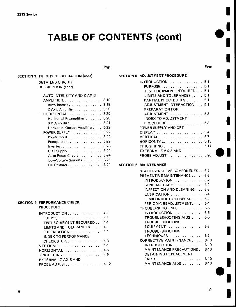
The following descriptions are i ntended to familiarizethe operator with the location, operation, and function ofthe i n str u ment's controls, connectors, and indicato r s .
Refer to F igure 2-3 for location of items 1 th rough 7 .
I ntern al Graticule-E liminates parallax viewing errorbetween the trace and graticule lines. R ise-timeamplit ude and measurement points are indicated atth e left edge of the graticule .
POWER Switch -Turns instrument power on and off .Press in for ON; press again for OFF .
AUTO FOCUS Control-Ad j usts display for optimumdefinition . Once set, t he focus of th e crt display will
MENEM
MENEM
MENEM
Ι
MENEM
MOMME
ONEΙι
2213 6 ο
ΡΜΑ
3397-04
F igure 2-3. Powe r , d isplay, and prob e adj ust cont rols, connecto r ,an d in d icator .
REV NOV 1981
CONTROLS, CONNECTORS, AND INDICATORS
POWER, DISPLAY, ANDPROBE ADJUST
Ope r ating Inst ructions-2213 Service
be maintained as changes occur in th e intensity levelof the trace .
PROBE ADJUST Connector-Provides an approxi-mately 0.5 V, negative-going, square-wave voltage (atapproximately 1 kHz) that permits the operator tocompensate voltage probes and to check operation ofthe oscilloscope vertical system . It is not intended tover ify t he accuracy of the vertical gain or time-basecalibration .
BEAM F IND Switch-When held in, compresses thedisplay to within the graticule area and provides αvisible viewing intensity to aid in locating off-scree nd is plays .
TRACE ROTATION Control-Screwd river controlused to align the crt trace with the horizontalgraticule lines .
AU TO I N TENSITY Control-Adju sts brightness oft h e crt dis p lay . Th is cont r ol h as no effect wh en theBEAM F IND switch is pressed in . Once the controlis set, intensity is automatically maintained atapproximately the same level between S EC/DIVswitch settings from 0.5 ms per division to 0.05 μ sper d ivision .
VERTICAL
Refer to Figu re 2-4 for location of items 8 th rough 16 .
SER IA L and Mod Slots-The SER IAL slot is im-printed with the instrument's serial nu mber . T h eMod slot co ntains the option number that has beeninstalled in t h e instrume n t .
CH 1 OR Χ and CH 2 OR Υ Connectors- Providefor application of external signals to the inputs of
th e vertical d eflection system or for an Χ-Υ display .In t he Χ -Υ mode, th e signal connected to the CH 1O R Χ connector provides horizo n tal deflection,and the signal con n ected to the CH 2 O R Υ con-nector provides vertical deflection .
GND Connector-Provides direct connection toinstrument ch assis ground .
2-3

Operating Instructions-2213 Service
3397-05
2-4
Figure 2-4 . Vertical controls and connectors.
In put Coupling (AC-GND-DC) Switches-Used toselect the method of coupling input signals to thevertical deflection system .
AC-Input signal is capacitively coupled to thevertical amplifier . The do component of the inputsignal is blocked . Low-frequency limit (-3 dBpoint) is approximately 10 Hz .
G ND-The in put of the vertical amplifier isgrounded to provide α zero (ground) reference-voltage d isplay (does n ot ground the input signal) .This switch position allows precharging the inputcoupling capacitor .
DC-All frequency components of the inputsignal are coupled to the vertical deflection system .
CH 1 VOLTS/DIV and CH 2 VOLTS/DIV Switches-Used to select the vertical deflection factor in α 1-2-5sequence . To obtain α calibrated deflection factor,the VOLTS/DIV variable control must be in detent .
1Χ PROBE-Indicates the deflection factorselected when using either α 1 Χ probe or α coaxialcable .
10Χ PROBE-Indicates the deflection factorselected when using α 10Χ probe .
VOLTS/DIV Variable Controls-When rotated coun-ter clockwise out of their detent positions, thesecontrols provide continuously variable, uncalibrateddeflection factors between the calibrated settings ofthe VOLTS/DIV switches . Extends maximum uncali-brated deflection factor to 25 volts per division with IXprobe (α range of at least 2.5 :1) .
INVERT Switch-Inverts the Channel 2 display whenbutton is pressed in . Push button must be pressedin α second time to release it and regain α noninverteddisplay .
VERTICAL MODE Switches-Two three-positionswitches are used to select the mode of operation forthe vertical amplifier system .
CH 1-Selects only the Channel 1 input signal fordisplay .
BOTH-Selects both Channel 1 and Channel 2input signals for display . The BOTH position mustbe selected for either ADD, ALT, or CHOPoperation .
CH 2-Selects only the Channel 2 input signal fordisplay .
ADD-Displays the algebraic sum of the Channel 1and Channel 2 input signals .
ALT-Alternately displays Channel 1 and Channel2 input signals . The alternation occurs duringretrace at the end of each sweep . This modeis useful for viewing both input signals at swee pspeeds from 0.05 μ s per division to 0.2 ms perdivision .
CHOP-The display switches between the Chan-nel 1 and Channel 2 input signals during thesweep . The switching rate is approximately 250kHz . This mode is u seful for viewing both Channel1 and Channel 2 input signals at sweep speedsfrom 0.5 ms per division to 0.5 s per division .
POSITION Controls-Used to vertically position thedisplay on the crt . When the SEC/DIV switch is set toΧ -Υ , the Channel 2 POSITION control moves thedisplay vertically (Y-axis), and the HorizontalPOSITION control moves the display h orizontally(X-axis) .
REV NOV 1981

HOR IZONTAL
Refer to Figure 2-5 for location of items 17 through 22 .
DELAY TIME-Two controls are used in conjun ctionwith I NTENS and DLY'D HORIZONTAL MOD E toselect the amount of delay time between the start ofthe sweep and the begin ning of th e intensified zone.
Range Selector Switch-This three-position switchselects 0.5 μs, 10 μs, and 0.2 ms of delay time . Toincrease the sweep delay from th e calibratedsetting of the Range Selector switch, rotate theMULTIPL I ER cont rol clockwise .
MU LTIPL I ER Control- Provides va riable sweepdelay from less th an 1 to greate r th an 20 times thesetting of the Range Selector switch .
SEC/DIV Switch-Used to select the sweep speedfor the sweep generato r in α 1-2-5 sequence . Forcalibrated sweep speeds, the SEC/DI V Variablecontrol must be i n the calibrated detent (fully clock-wise).
Figure 2-5. Horizontal controls.
Operating Instructions-2213 Service
SEC/DIV Variable Cont rol-Provides continuouslyvariable, uncalibrated sweep speeds to at least 2.5ti mes the calibrated setting . It extends the slowestsweep speed to at least 1 .25 s per division .
Χ10 Magnifier Switch-To increase d is played sweepspeed by α factor of 10, pull out the SEC/DIVVariable knob. The fastest sweep speed can beextended to 5 n s per division . Pu sh in the SEC/DIVVar iable control knob to regain the Χ 1 sweep speed.
HORIZONTA L MODE Switch-Th is three-positionswitch dete rmines the mode of operation for thehorizontal deflection system .
ΝΟ DLY- Horizontal deflection is provided by thesweep generator, without α delayed start, at αsweep speed determined by the S EC/DI V switch .
INTENS-Horizontal deflection is provided by th esweep generato r at α sweep speed determined bythe SEC/DIV switch . The sweep generator alsoprovides an i ntensified zone on the d is play. Th estart of the intensifie d zone represents the sweep-start poi nt when DLY'D HORIZONTAL MODEis selected.
DLY'D-Horizontal deflection is provided by th esweep generato r at α sweep speed determined bythe SEC/DIV switch setting . The start of th esweep is delayed from the in itial sweep-t rigge rpoi nt by α time determined by the setting of theDELAY TIME Range Selector switch and MULTI-PLI ER control .
POSITION Control-Positions the d is play hori-zontally in all modes.
TRIGGER
Refer to Figure 2-6 for location of items 23 th rough 31 .
ΕΧΤ I NPUT Connector-Provides α means of i ntro-ducing extern al signals into the tr igger generator .
ΕΧΤ COUPLI NG Switch-Determines the methodused to couple extern al signals to the Trigge r ci rcu it .
AC-Sign als above 60 Hz are capacitively coupledto the input of the Trigger circuit . Any do com-ponents are blocked, and signals below 60 Hz areattenuated .

Operating Instructions-2213 Service
2-6
DC-All components of the signal are coupled tothe trigger circu itry . Th is position is usefu l fordisplaying low-frequency or low-repetition-ratesignals.
DC=10-External trigger signals are attenu ated byα factor of 10 .
15 SOURC E Switch-Determines the source of thetrigger signal that is coupled to the input of thetrigger circuit .
ΙΝΤ-Permits triggering on signals that are appliedto the CH 1 O R Χ and CH 2 O R Υ input con-nectors . The sou rce of the internal signal isselected by the ΙΝΤ switch .
L I NE-Provides α triggering signal from α samp leof the ac-power-source waveform . Th is triggersou rce is useful when channel-input signals aretime related (multiple or su bmu ltiple) to thefrequency on the powe r-source-input voltage .
ΕΧΤ-Permits triggering on signals applied to theΕΧΤ I NPU T connector.
3397-07
F ig ure 2-6 . T r igge r cont r ols, connector, and indicato r .
2 Ιϊ ΙΝΤ Switch-Selects the source of t h e triggeringsignal when the SO URC E switch is set to ΙΝΤ .
CH 1-The signal app lied to the CH 1 OR Χ inputconnector is the sou rce of the trigger sign al .
VERT MOD E-The internal trigger source isdetermined by the signals selecte d for display bythe VERTICA L MODE switches .
CH 2-The signal a pp lied to the CH 2 OR Υ inputconnector is the source of the trigger signal .
LEVEL Control-Selects the amplitu de point on th etrigger signal at which the sweep is triggered .
TRIG'D Indicator-The lig ht-emitting diode (LED)illuminates to indicate t h at the sweep is triggere d .
SLOPE Switch-Selects the slope of the signal thattriggers the sweep . (also refer to TV Signal Displaysat the end of Section 2) .
-T-Sweep is triggered on the positive-goi ngportion of the trigger sign al .
-\--Sweep is triggered on the negative-goi ngportion of the trigger signal .
MODE Switch-Determines the trigger mode for thesweep .
AUTO-Permits triggering on waveforms havi n grepetition rates of at least 20 Hz . Sweep free-runsin the absence of an adquate trigger signal o r whenthe repetition rate is below 20 Hz . The range ofthe TR IGG ER LEVEL control will compensatefor the amplitude variations of the t r igger signals .
NORM-Sweep is i n itiated when an adequatetrigger signal is applied . In t he absence of α t r iggersignal, no baseline trace will be present . Trigge r ingon television lines is accomplished in th is mode .
TV FIELD-Permits triggeri ng on television field-rate signals (refe r to TV Signal Displays at the endof Section 2) .
VAR HOLDO FF Control-Provides continuous con-trol of holdoff time between sweep s . Increasesthe hol doff time by at least α factor of four. Th iscontrol improves the ability to trigger on aperiod icsignals (such as complex digital wavefo rms) .
REV NOV 1981

ιι ιιιιιιιι10ιιιιιιιι
REAR PANEL
Refer to Figure 2-7 for location of item 32 .
ΕΧΤ Ζ AXIS Connector-Provides α means of con-necting external signals to t h e Z-axis amplifier to
Figu re 2-7. Rear-pan el connector.
Operating Instructions-2213 Service
intensity modulate the crt display . Applied signalsdo not affect dis play wavesh ape . Signals with fastrise times and fall times provide the most abruptintensity change, and α 5-V ρ -ρ signal will producenoticeable modulation . The Z-axis signals mu st betime-related to the display to obtain α stab le present-ation on the crt .
CAUTIONFD CONTINUED FIRE PROTECTIONPC
FACE01111 .11. G11EI1IN
TYPE AND RATED FUSE DISCONNECT
REAL,ΡINPUT
ΘΕ FΟΗΕ REPLACING FUSE
ΙΙΝ 11ΟίΤΑΙΙ RANGE
FU5" Ζ50Υ
90 Ζ50ΕΑ'
ΖΑ FASTΕ%Τ Z AXIS INPUTιΟκσ POSITIVE GOINGINPUT -FEASTS
'ITΡ~ΜΟΥ~
ΙΝτΕΝΙΙΤν
COVFfl RFFFR
Ο
5 VΟίΓ ΡΡ εΑυ5Ε55ΕΝΥΙ C1ΝG TO
ΝΟΠC~Αθ l~
σUΑΙ111ΕD
MODULATION AT
Ρεθ5σχχει
χαΡΜΑι ιχτεχ 5 ιτν
POWERMAX WATTS 55
Μχ
COΡΡΕχτ16Α ΡΜ 5
,DID ΑΘ SIR,
CAUTIONTO AVOID ELECTRICSHOCK THE POWERCIRLD PROTECTIVEGROUNDING CONDUCTED
MOST 81 CONNECTEDTO GROUND
s30V PEAK
,Φ- .
3397-08
2-7

Operating Instructions-2213 Service
OPERATING CONSIDERATIONS
The following basic operati ng information and tech -n iques s h ould be considered before attem pting anymeasu rements.
GRATICULE
The gratic ule is internally marked on the faceplate ofthe crt to enable accurate measu rements with out parallaxerror (see F igure 2-8) . It is marked with eight vertical andten horizontal major d ivision s . Each major division isd ivid ed into five su bdivisions . The vertical deflectionfactors and horizontal timing are cali brated to the graticuleso that accu rate measurements can be made directly fromthe crt . Also, percentage markers for the measu rementof rise and fall times are locate d on the left side of thegraticule .
2-8
GROUN DING
Th e most reliable signal measurements are made wh enthe 2213 and the unit under test a r e connected by α com-mon reference (ground lead), in addition to the signal leador probe . T h e probe's grou nd lead provides the bestg rounding meth od for signal interconnection and ensuresthe maximu m amount of signal-lea d sh iel d ing in the probecable. Α separate ground lead can also be connected fromthe unit under test to the oscilloscope G ND con nectorlocate d on the front panel .
1ST O R LEFT
CENTER
11TH OR R IGHTVERTICA L VERTICAL VERTICALG RATICULE G RATICULE GRATICULE
L INE
LINE
L INE
RISE AND
CENTERFALL TIME
HO RIZONTALMEASUREMENT
GRATICULEPERCENTAGE
LINEMARKERS
4115-16
F ig ure 2-8 . Graticu le measuremen t mark i n gs .
SIGNAL CONNECTIONS
Generally, probes offer the most convenie n t means ofconnecting an input signal to t he instrument . They aresh ielded to prevent pickup of electromagnetic interference,and the supplie d 10Χ probe offers α high input impedancethat minimizes circu it loading . Th is allows t h e ci r cuit undertest to operate with α min imum of change from its normalcond ition as measurements are being made .
Coaxial cables may also be used to connect signals to theinput connectors, but t h ey may have considerable effect onthe accuracy of α displaye d waveform . To maintain theoriginal frequency characteristics of an applied signal,only high -quality, low-loss coaxial cables should be used .Coaxial cables sh ould be terminated at both ends in theircharacteristic impedance . If th is is not possi b le, use suitableimpedance-matching devices .
INPUT COUPLINGCAPACITOR PRECHARGING
When the input coup li ng switch is set to GND, the inputsignal is connected to ground th rough the input couplingcapacitor in series with α 1-ΜΩ resistor to form α pre-charging network . Th is network allows the input couplingcapacitor to ch arge to the average dc-voltage level of thesignal applied to t h e probe . Thus, any large voltagetransients t h at may accidentally be generated will not beapplied to t h e amplifier input when the input couplingswitch is moved from G N D to AC . The precharging net-work also provi des α measu re of protection to the externalcircuitry by reducing the cu rrent levels that can be drawnfrom the extern al circ u itry during capacitor ch arging .
The following procedure should be used whenever theprobe tip is connected to α signal source having α diffe r entdo level t han that previously applied, especially if the dc-level difference is more than 10 times the VO LTS/DI Vswitch setting :
1 . Set the AC-G N D-DC switch to G N D before con-necting the probe tip to α signal source .
2 . Insert th e probe tip into the oscilloscope GNDconnector .

3. Wait several seconds for the input coupling capacitor
to d ischarge .
Display
4. Connect the p robe tip to the signal sou rce.
5. Wait several seconds for the input coupling capacitorto charge .
INTRODUCTION
The procedure in th is section will allow you to set upand operate you r instrument to obtain the most commonlyused oscilloscope d is p lays . Before starting this procedu re,ve rify that the POWER switch is OFF (push button out),then plug the power cord into an approved ac-power-sourceoutlet .
Vertical ( Both Channels)
BASELI NE TRACE
F irst obtain α baseline trace.
1 . Preset th e instrument front-panel controls as follows:
AUTO INTEN SITY
Fully counterclockwise(minimum)
AUTO FOCUS
M id range
AC-GND-DC ACVOLTS/DIV50m (1 Χ )VOLTS/DIV Variable
CAL detent(fully clockwise)
VERTICAL MOD E
CH 1INVERT
Off (button out)POSITIO N
M id range
HorizontalSEC/DIVSEC/DIV Variable
HORIZONTA L MODEΧ10 MagnifierPOSITIO NDELAY TIME
Range SelectorMULTIPL I ER
OSCI LLOSCOPE DISPLAYS
Locked together at 0.5 msCA L detent(fully clockwise)ΝΟ DLYOff (varia ble knob in)M idrange
0.2 msFully counterclockwise
Operating Instructions-2213 Service
6. Set the AC-GND-DC switch to AC. The display will
remain on the screen, and the ac component of the signalcan be measured in the normal manner .
To maintain adequate instrument cooling, the ventila-tion holes on both sides and rear panel of the equ ipmentcabinet must remain free of obstructions .
Trigger
INSTRUMENT COOLING
VAR HOLDO FF
NORM (fully counter-clockwise)
SLOPE
f(lever up)LEVEL
Mid rangeMODE
AUTOΕΧΤ COUPLING
ACSOURCE
ΙΝΤΙΝΤ
VERT MODE
2. Press in th e POWER switch button (ON) and allowthe instrument to warm up for 20 minutes.
3. Ad just the AUTO I NTENSITY control for desiredd isplay brightness .
4. Adju st the V ertical and Horizontal POSITIO Ncontrols to center the trace on the screen .
1 . Obtain α baseline trace .
SIGNAL DIS PLAY
2. Apply α sign al to either vertical-c hannel input con-nector and set the VERTICAL MOD E switch to displayth e channel used . To display two time-related input signalsuse both vertical-c han nel i nput connecto rs and selectBOTH VERTICAL MOD E ; then select either ALT orCHOP, depending on th e frequency of input signals.
3. Ad just the AUTO I NTENSITY control for desireddisplay brig h tness. If the display is not visible with theAUTO I NTENSITY control at midrange, press the BEAMF I N D push button and hold it in wh ile ad j usting theappropriate VOLTS/DIV switch (es) to reduce the vertical
2-9
Operating Instru ctions-2213 Service
dis p lay size . Center the compressed display within thegraticule area using the Vertical and Horizontal POSITIONcontrols, then release the BEAM F I ND push button .
4 . Ad just the T RIGG ER LEVEL control, if necessary,to obtain α stable display .
5 . Set the appropriate VO LTS/DIV switch (es) andreadju st th e Vertical and Horizontal POSITION controlsto center th e dis play with in the graticule area .
6 . Set the S EC/DI V switch for the desire d number ofcycles of th e dis played signal . Then adjust the AUTOFOCUS control for th e best-define d disp lay .
MAGN I F IED-SWEEP DISPLAY
1 . Obtain α Signal Display (see preceding instructions) .
2 . Ad ju st the Horizontal POSITIO N control to move thetrace area that is to be magnified to the center of the crtgraticule (0.5 division on each si d e of th e center verticalgraticule line) . Change the SEC/DI V switch setting asrequired .
3. Pull out the SEC/DI V Variable knob (Χ10) to obtainsweep magnification .
4 . Ad just the Horizontal POSITION control for precisepositioning of the magnified display .
5 . To calculate the magnified sweep speed , divi de theSE C/DIV switch setting by 10 .
D ELAYED-SWEEP DISPLAY
1 . O btain α Signal Display .
2 . Select I NT ENS HO RIZONTAL MOD E and set theDELAY TIME Range Selector switch to the desired amountof delay time .
3. Ad just the AUTO I NT ENSITY control as needed tomake the intensified zone distinguish able from theremainder of the display .
4 . Adjust the D ELAY TIME MULTI PL IER control tomove the start of the intensified zone to the start of thepoint of interest on the crt trace . To capture an eventth at occurs after the sweep ends, adjust th e start of th eintensified zone past the end of the sweep.
1 . Obtain α baseline trace .
Χ-Υ DISPLAY
2 . Use equal-length coaxial cables, or the two 10Χprobes su pplied with the instrument, to apply the hori-zontal signal (X-axis) to the CH 1 O R Χ i n put con nectorand to apply the vertical signal (Y-axis) to the CH 2 OR Υin put connector .
3. Select Χ -Υ mode by switch ing the SEC/DIV switchto its fully countercloc kwise position .
4 . Advance the AUTO I NTENSITY control setting untiltwo dots are displayed . The d isplay can be positionedh orizontally with the Horizontal POSITION control andve rtically with the Channel 2 POSITION control .
ΝΟΤΕ
The display obtained when sinusoidal signals areapplied to the Χ- and Y-axis is called α Lissajousfigure . This display is commonly used to comparethe frequency and phase relationships of two inputsignals. The frequency relationship of the two inputsignals determines the pattern seen. The pattern willbe stable only if α common divisor exists betweenthe two frequencies.

TV SIGNAL DISPLAYS
Displaying α TV Line-rate Signal
1 . Perform the steps and set the controls as outlinedunder Baseline Trace and Signal Display to obtain α basicdisplay of the desired TV signal .
2. Set Α SEC/DIV to 10 Ει s, and Α & Β ΙΝΤ to CH 1 orCH 2 as appropriate fo r applied signal .
3. Set Α TRIGGER SLOPE for α positive-going signal(lever up) if the applied TV signal sync pulses are positive-going, or for α negative-going signal (lever down) if the TVsync pulses are negative-going.
4. Adjust the Α TRIGGER LEVER control for α stabled isplay, and AUTO INTENSITY for desired display bright-ness . If necessa ry, adjust VERTICAL VOLTS/DIV control toobtain 5 divisions or greater amplitude fo r α stable display.
NOV 1981
Operating Inst ructions-2213 Service
Displaying α TV Field-rate Signal
1 . Perform Step 1 under Displaying α TV Line-rateSignal .
2. Set Α SEC/DIV to 2 ms, Α TRIGGER MODE to TVFI ELD and Α & Β ΙΝΤ to CH 1 or CH 2 as appropriate forthe applied signal .
3. Perform Step 3 and 4 under Displaying α TV Line- rateSignal .
4. To display either Field 1 or F ield 2 individually at fastersweep rates (displays of less than one full field), set VERTI-CAL MODE to BOTH and ALT simultaneously . This syn-chronizes the Channel 1 display to one field and theChannel 2 display to the other fiel d.
To change the field that is displayed, interrupt the triggeringby repeatedly setting the AC GND DC switch to GND or dis-connecting the signal from the applied signal input u ntil theother fiel d is displayed. To display both fields simultaneous-ly, apply the input signal to both the CH 1 and CH 2 inputsvia two probes, two cables, or through α dual-input coupler .
To examine either αTV Field-rate or Line-rate signal in moredetail, either the X10 Magnifier or HORIZONTAL MODEfunctions may be employed as described for other signalselsewhere in this manual .
2-1 1

THEORY O F OPERATION
SECTION ORGANIZATION
This section contains α functional description of th e2213 Oscillosco pe circuitry. The d iscussion begins with αgeneral summary of instrument functions followed by αdetailed desc r i ption of each ma jor circuit. Functionalblock diagrams and schematic d iagrams are used to showth e intercon nections between parts of the circuitry, toindicate circuit components, and to identify interrelation-sh ips with the front-panel controls .
Schematic d iagrams and the overall block diagram arelocated in th e tabbed "Diagrams" section at the back ofth is manual . The schematic diagram associated with eachdescription is identified in the text and indicated on th e tabof the app rop riate foldout page by α numbered d iamondsymbol . For best u nderstanding of the circuit beingdescribed , refer to both the approp riate schematic diagraman d th e functional block diagram .
INTRODUCTION
INTEGRAT ED CIRCUIT DESCR IPTIONS
Digital Logic Conventions
Section 3-2213 Service
Digital logic circuits perform many functions within theinstru ment. Functions and operation of the logic circuitsare represented by logic symbology and terminology.Most logic functions are described using the positive-logicconvention . Positive logic is α system of notation wherebythe more positive of two levels is the TRUE (o r 1) state;the more negative level is the FALSE (or 0) state. In th islogic descri ption the TRUE state is referred to as ΗΙ , andthe FALSE state is referred to as LO. Th e specific voltageswh ich constitute α ΗΙ or α LO state vary between specificdevices. For specific device characteristics, refer to themanu facturer's data book.
L inear Devices
The functioning of ind ividual linear integrated circu itdevices in th is section use waveforms or oth er techniquessuch as voltage measurement and simplified diagrams toillustrate their operation.

Theory of Operation-2213 Service
In the following overall fu nctional descri ption of the2213 Oscilloscope, refe r to the basic block diagram ( Fig-ure 3-1) and to the detailed block diagram ( Figure 9-4)located in the "Diagrams" section of th is man u al . InF igures 3-1 and 9-4, the num bered diamond symbol ineach major block refers to the appropriate schematicdiagram number .
Signals to be displayed on the crt are applied to eitherthe CH 1 OR Χ in put connector or the CH 2 O R Υ inputconnector . The signals may be coupled to the attenu atorcircuit either directly (DC) or through an i n put-couplingcapacitor (AC) . The input may also be disconnected andthe input to the attenuators grounded when the G NDposition of the cou pling switch is used . In the G NDposition, the ac-coupling capacitor is allowed to prechargeto the do level present at the input connector . Th is pre-ch arging prevents large trace shifts of the display whenswitching from G ND to AC cou pling .
Each channel output signal f rom the Attenuator cir-cuitry is applied to the Vertical Preamplifier circu itry forfurt h er amplification . Th e Channel 2 Preamplifier i ncludesan Invert feature th at allows the operator to invert theCh annel 2 signal d isp lay on the cathode-ray tube (crt) .Trigger Pickoff Amplifiers in each ch annel supply aninternal trigger signal from either channel signal or fromboth ch annels to the Internal Trigger Amplifier in theTrigger circuitry .
Each channel signal is selected for display in turn by theCh annel Switch ing Logic circuit under control of thefront-panel VERTICAL MODE switches . Th e output signalfrom the Ch annel Switch ing Logic circuit is app lied to αDiode Gate circuit . Th e Diode Gate circuit switches eitherchannel signal (or both signals for ADD) to α Delay LineDriver stage that su pp lies the proper drive and impedancematch to the Delay Line . Th e Delay Line produces approx-imately 100 ns of delay in th e vertical signal to allow theH orizontal circuitry time to produce the necessary sweepto d isp lay the signal .
F inal amplification of the vertical signal is supplied bythe Vertical Output Amplifier . The Vertical OutputAmplifier su pplies the requ ired signal levels necessary toproduce vertical deflection of the electron beam in th e crt .
The Trigger circu itry uses either the Internal Triggersignal derived from the input signal(s), an External Trigger
3-2
GENERAL DESCR IPTION
signal, or α Line Trigger signal obtained from th e ac-power-source in put waveform to develop the triggering signal forthe Sweep Generator. An Auto Trigger circ u it ensures thatth e range of the TRIGG ER LEVEL control conformsapproximately to the peak-to-peak amplitude of th e triggersignal wh en either AUTO or TV F I ELD T RIGG ER MOD Eis selected . In NO RM MODE , th e T R IGG ER LEVELcontrol must be adjusted for the correct trigger signal levelbefore α sweep can be generated .
Α TV Fiel d sync circuit provides stable triggering ontelevision-signal vertical-sync pulses. Triggering at thetelevision line rate is accomplished when either AUTO orNO RM MODE is used .
Th e Sweep Logic circuit controls the generation of theswee p and the unblanking of the Ζ-Axis Amplifier for theSweep d isp lay . When the TRIGG ER MOD E switch isset to either AUTO or TV F I ELD and no trigger signal ispresent, the Auto Baseline circuit causes the Sweep Logiccircuit to produce α sweep after α period of time . In theN O RM position of the T R IGGER MODE switch theAuto Baseline circuit is disabled , and α sweep will not begenerated until α triggering signal is received .
The output gate signal from the Sweep Logic circ u it isapp lied to th e M iller Sweep circuit . This circuit producesα linear sweep output with α run-up time that is controlledby the SE C/DIV switch . The sweep signal is applied toth e Horizontal Preamplifier for initial amplification . F inalamplification of the sweep signal to d rive the crt horizontaldeflection plates is provided by the Horizontal OutputAmplifier .
The Horizo ntal Preamplifier gain is increased by α factorof 10 wh en the Χ 10 Magnifier feature is used . Horizontalpositioning of the display is also accomplished in theHorizontal Pream plifier circu it .
In th e Χ -Υ Mode of operation the CH 1 signal, via theinternal Trigger circuitry, is applied to the ΧΥ Amplifierwhere it is amplified for application to the HorizontalPreamp lifier. In this operating mode, the CH 1 InternalTrigger signal supplies the horizontal deflection to the crt,and ' α sweep signal is not produced by the Miller Sweepcircu it .
Th e HO RIZO NTAL MODE switch ( ΝΟ D LY, I NT ENS,and DLY'D) controls the action of the Delay circuit . Th is

Theory of Operation-2213 Service
CH 1 AND CH 1 AND CH 1+CN 1 0R Χ "~ CH 2 CH 1 CH 2 CH 1- VERT ICAL SIG +
ΛΤΤΕΝUΛΤΟRS VERTICAL CH 2+PREAMPS
CH 2- CHANNEL S WITCH VERT ICAL SIG -
CH 2CH 1 TRIG AND VERT ICAL
CH 2 OR Υ
Ο
CH 2 TRIG OUTPUT
1~7 CH 149 ΙΝ 7CH 1 VERT MODE
BOTH CH 2 TRIGGERΟSOURCE
VERTICAL CH 2
MODE AMALTCHOP
+ ια α
ύ ύά ά
VARIABLESEC/DIV ΧΥ < g
J J CAL TIMING S WITCH Χ
Ι<
CRTά
<V87θ
ω ω
Ο
8 υ
ΉVAR
HOLDOFF AUTO Ζ
ΙΝΤSOURCE LINE
ΕΧΤTRIGGER g = _
X-AXISΧ-AXIS SIG SIG
AUTO
NORMAL IΧΥ
IN.
Ο
ΑΜΡL/ ΗΟRΙΖTV FIELD TRIG SIG ΗΟRΙΖ
\ /AUTO ΧΥ ΧΥOUTPUT ΗΟRΙΖ
ΕΧ7 ~~ BASE LINEINPUT SWEEP ALT SYNC BEAM F IND
GENERATOR 7ΟDLY AND Σ-ΑΧΙS SWP SWP
HORIZONTAL ΙΝΤΕΝS LOGICMODE
DLY'D ι~& U
ε0.2αια < <
DELAY 1 θμαTIME
θ .5μαlip
ΜΙΗ.Τ 1 PL 1 ER
PROBE CRT ANODE .Λ DJUST
Ζ -DR IVE
SWΡ DUTY Σ-DRIVE POWER FOCUS
ΙΝΤΕΝ S LEVEL
AUTO INTENSITYAND Z-AXIS
ΙΝΤΕΝSSUPPLYPROBE INTENSITY - _Λ DJ >
A UTO AND CR7INTENSITY -
Ο CATHODE
BEAM FIND
LINE TRIGGER ν Lγ TO ALL BLOCKS
3827-11
Figure 3-1 . B asic block diagram of the 2213 Oscilloscope .
' @ 3-3

Theory of Operation-2213 Service
circu it functions to either produce no delay, display anintensified zone on the Sweep display, or to delay thestart of the Sweep for α period of time after receivi ng αtriggering signal . The delay time is established by twofront-panel controls : the DELAY TIME switch wh ich setsthe basic delay, and the MULTI PL I ER potentiometerwhich increases the basic delay by α factor of up to twentytimes. Output signals from the Delay circuit are applied toα logic gate circuit to control both the timing of the startof the sweep and the Ζ-Axis drive .
The Ζ-Axis drive from the Sweep Logic circuit is appliedto the Ζ-Axis amplifier. The output signal from the Ζ-AxisAmp lifier circuit sets the crt intensity. Α Chop Blankingsignal from the Chop Oscillator circuit blanks the crtd is play during the transition between the vertical channelswhen using CHOP VERTICAL MODE.
The DC Restoration circuit raises the output level of theΖ-Axis Amp lifier to allow it to be coupled to the crtcontrol grid . Direct coup ling is not employed due to theamplitude of the voltage levels applied to the crt elements .
Input Coupling
3-4
VERTICAL ATTENUATORS
Both the Channel 1 and Channel 2 Attenuator ci rcuits,shown in Diagram 1, are identical in operation. In thefollowing d iscussion, only the Channel 1 Attenuator circu itis descr i bed . The match ing components in the Channel 2Attenuator ci rcu it perform the same function .
The Attenuator circu it (see Figu re 3-2) provides controlof input coupling, vertical deflection factor, and variablevolts- per-division balance . Input signals for crt verticaldeflection may be connected to either or both the CH 1 ORΧ and the CH 2 OR Υ i nput connectors . In the Χ-Υ Modeof operation, th e signal app lied to the CH 1 OR Χ con-nector provides horizontal (Χ-Axis) deflection for th ed isplay, and the signal applied to the CH 2 OR Υ con nectorprovides the vertical (Y-Axis) deflection for the display.
The signal applied to the CH 1 OR Χ in put connectorcan be ac-cou p led , dc-coup led, or internally disconnectedfrom the input of th e H igh-Ζ Input Attenuator circuit .
The Swp Duty signal from the Sweep Logic circuit isapplied to the Auto Intensity circuit. The Auto Inte nsitycircuit provides partial control of the intensity of thed isplay when switch ing between different positio ns of theS EC/DI V switch .
The Power Supply provides all the necessary operatingvoltages for th e instrument circuitry . Operating potentialsare obtained from α circuit composed of the Preregulator,Inverte r and Transformer, and Rectifiers and F ilters . ThePreregulator produces approximately +45 V from the ac-power-input source wh ich is used to drive the 20-kHzInverter stage. The Transformer secondary windings providevarious ac levels that are rectified and filtered to producethe operating voltages. Α H igh -voltage Multiplie r circuitproduces the accelerating, focus, and cathode potentialsrequ ired by the crt.
Α front-panel PROBE ADJUST output is provided foruse in adjusting probe compensation . The voltage at thePR OBE ADJU ST connector is α negative-going square wavethat has α peak-to-peak amplitude of approximately 0.5 Vand α repetition rate of approximately 1 kHz.
DETAILED CIRCU IT DESCR IPTION
Signals applied to the CH 1 input connector are routedthrou gh resistor R101 to Input Coupling switch S101 .When S101 is set for do coupli ng, the CH 1 signal is app lieddirectly to the input of the H igh-Ζ Attenuator stage. Whenac-coupled , the input signal passes th rough R 100 andd c-blocking capacitor C102 . The blocking capacitorprevents the do component of the input signal from beingapplied to the Attenuator circuit . When S101 is set toGND, the direct signal path is opened and the input of theattenuato r is connected to ground . This provides α groundreference without th e need to discon nect the applied signalfrom the input connector. Th e coupling capacitor isallowed to precharge th rough R 102, α high-resistance com-ponent, which is connected across Input Coupling switchS101 in the GND position .
High-Ζ Attenuator
The first section of attenuator switch S105A d i rectsthe input signal to one of three paths: directly throughR103 (no attenuation) ; through α 10Χ attenuato r con-sisting of C105, C107, R 105, R 106, R 107, and R 108;or th rough α 100Χ attenuator consisting of C111, C112,R 110, R 111, R112, R114, and R 115. Medium-frequencynormalization of the i nput capacitance is accomplished by

CH 1 OR Υ
s101
[AC-GNO-DC
HIGH-Ζ ATTENUΛTOR
S105
Q125, Q133ρ131, Q139
- Β . ΒVςDIV \Γ-+8 . βVςR138
STEP ΒΛL
5R143
LOW-Ζ ATTENUΛTOR
XI/X10 ΛΜΡL
-8 .6 VςJVV4- +8 .ΒVςR146
X10 GAIN
382β-21
F ig ure 3-2. Detailed block d iagram of the Channel 1 atte nuator and atte nuator switching tables.
C104 in t h e 10Χ attenuator and by C110 in the 100Χattenuator . Switch S105B connects the app rop riateattenuator output to the input of the Bu ffe r Am plifier .
Buffer Amplifier and Low-Ζ Attenuator
The Buffer Amplifier presents α h igh-impedance, low-capacitance load to the input signal and delivers an accuratereplica of that signal to α low-impedance buffer outputcircuit . T h e Low-Ζ output circu it is composed of α 250-Ωvoltage-divider network ( R 139F th rough R 139J) and theVolts/Div Var circuit ( R141, C141, and R 143) . SwitchS105B selects the approp riate output from t h e voltaged ivider . Th e Buffer Amplifier contains two pat h s : α slowpath consisting of R 116, R 117, U120, and R 119 in parallelwith C119 ; and α fast path through C121 . The signalst h roug h both paths are applied to the gate of Q122.
Theory of Operation-2213 Service
In the slow-path portio n , the i np ut signal is divided byten by the combination of R 117 and R 116 and is thenapp lied to U120 pin 3 . The Buffer Amplifier output signalis also divided by ten by the combination of R 139B ,R 139C, R 139D, and R 139N . Sufficient dc-gate bias forinput FET Q122 is generated by the slow-path circu it toproduce α null (zero difference) between p ins 2 and 3 ofU120 . The closed-loop gain of t h e slow path is matched tothe fast-path gain . If the average output voltage from thefast pat h c h anges, transconductance am plifier U120 adjuststhe do gate bias on Q122 to keep U120 p in 2 and U120pin 3 nulled . This action keeps the slow-path and th efast-pat h gains matched . R esistor R 119 isolates the outputimpedance of U120 from the input of FET 0122 . T h is iso-lation , in com bination with the h igh input impedance ofU 120, prevents h igh-frequency loading of th e input signal .Capacitor C119 compensates for the output capacitanceof U 120 .
3-5
VOLTS/DIV Χ 1 Χ10
2 mV Χ5 mV Χ10 mV Χ20 mV Χ50 mV Χ100 mV Χ
200 mV Χ500 mV Χ
1 V Χ2 V Χ5 V Χ10 V Χ
VO LTS/DIV _ 1 - 2 , 5 _ 5
2 mV Χ5 mV Χ10 mV Χ20 m V Χ50 mV Χ100 mV Χ200 mV Χ500 mV Χ
1 V Χ2 V Χ5 V Χ
Ι 10 V Ι Ι Ι Χ Ι
VOLTS/ _ 1 - 10 =1 00DIV2 m V Χ5 mV Χ10 mV Χ20 mV Χ50 mV Χ100 mV Χ200 mV Χ500 mV Χ
1 V Χ2 V Χ5 V Χ10 V Χ
νοιτs/Dτν _ _ _ _Ι _ _ -
Ι
_ _ _ -
R141CAL
Ι-
ΙΙ
Ι
CH 1 INPUT VOLTS/ CH 1+Χ1 /Χ10
CH 1VERT
BUFFER LOW-Ζ DIV ΛΜΡL SIGAMPLIFIER ΛΤΤΕΝUΛΤΟR VAR
U 145 CH 1- TOU12θ , Q122 -1 > -2 .5, ΡRΕΛΜΡ

Theory of Operation-2213 Se rvice
Step Balance potentiometer R 138 (at p in 1 of R 139) is
adjusted to compensate for inpu t offsets reaching U 120
pins 2 and 3 wh en switching between VOLTS/DIV switchpositions.
In the fast path, th e input signal is ac-cou pled to i nputFET Q122 through C121 . The input FET is arranged in αsource-follower config uration used to drive complementaryemitter followers 0133 and Q134. The combi nation ofQ125, R126, R131, R132, VR 130, and R130 sets αconstant cu rrent through R125 in the source lead of Q122 .Th e voltage drop across R125 biases Q133 and Q134 forabout α 10-mA idle current.
Α bootstrap ci rcuit composed of Q139, VR 122, andR122 connects the Q122 drai n to the Q122 source. Thiscircuit forces the b ias voltage across Q122 to remain con-stant, wh ich i n conjunction with the constant b ias currentsu pplied by R 125, keeps Q122 operating at α constantpower level to prevent distortio n due to changing signalcu rrents .
Complementary emitter followers Q133 and Q134su pply drive current to the =1, =2.5, and =5 voltage dividersand p rovi de impedance match ing between input FET Q122and th e divider network. The b ias levels of Q133 and Q134are stab ilized by emitte r resistors R139A and R139 Erespectively . Average voltage changes occurring in the out-put of Q133 and Q134 are sensed th rough R139B andR139D wh ich are connected to the point of lowestimpedance (the emitters of Q133 and Q134) . ResistorR139C provides α path that completes th e feed back loopto the slow-path portion of the Buffer Amplifier.
Volts/Div Var Circu it and X1/X10 Amplifier
The appropriate voltage divider signal output (=1, =2.5,or =5) is selected by VOLTS/DIV switch S105B and routedto the Volts/Div Var circu it composed of C141, R 141,and R143. . Changes that occur in the Buffer Amplifieroutput im pedance due to setting R141 or switching th ed ivid er outpu t are sensed via R139M . These changes modifyth e slow-pat h feedback signal to cause U 120 to again matchth e gain of both paths.
From the Volts/Div Var circuit, the signal is applied toth e input of the X1/X10 Switchable-gain Amplifier U 145.Amplifier U145 produces α differential output signal fromthe single-ended input signal . The gain of the amplifier iscontrolled by the setting of VOLTS/DIV switch S105 .
Amplifier gain is changed by switch ing between twopairs of transistor amplifiers contained in U 145. Gain of theΧ 10 amplifier pair is adjusted by R 145 to obtai n the
3-6
correct deflection facto r for the 2m, 5m, and 10m VOLTS/DIV switch positions . Resistors 8146, R 147, and R 148act to balance any do offsets between th e Χ 1 and Χ10amplifiers . Trace shift occurring when the VOLTS/DI VVariable control is rotated is minimized by resistor R142which stabilizes the in put bias current to U 145.
VERTICAL PREAMPS
The Channel 1 and Channel 2 Preamp ci rcu itry, shownin Diagram 2, includes the vertical preamplifiers, theinternal trigger pickoff amplifiers, and α common-baseoutput stage for each channel. V ertical positioning of thechannel display is inco rporated in the common-baseamplifier stage.
Channel 1 Vertical Preamplifier
The Channel 1 Vertical Preamplifier produces d iffer-ential output signals to drive the Vertical Output Amp lifie rand internal trigge r signals to drive the Trigger circuitry .
Differential signal current from the Attenuator circuitryis applied to common-base transistors Q157 and Q167th rough cable-terminating resistors R151 and R161respectively . The collector currents of Q157 and 0167 willflow th rough R158 and R168 to produ ce level-sh iftedsignals which drive U170D and U 170E. Balance potenti-ometer R154 is ad justed to balance th e do level of theCh annel 1 output with the Channel 2 output by setting thebias levels of Q157 and Q167 . Channel 1 frequencyresponse is matched to Channel 2 response by adjustingC167 .
Transistors U 170D and U 170E form α common-emitteramplifier. The gain of U 170D and U170E is set by R180(connected between the emitters), and the h igh-frequencyresponse is compensated by C180 . Th e emitte rs are alsoconnected to the bases of U 170C and U 170B respectivelyto provide an internal trigger signal pickoff point. V erticalsignal output current flows from the collectors of U 170Dand U 170E to the emitters of common-base amplifiersQ177 and Q187 . Α shunt resistor gain network ( R 176 andR186) sets the gain of the common-base stage. Channel 1POSITION control R 190 supplies α va r iable offset currentto the emitters of Q177 and Q187 wh ich allows the traceto be vertically positioned on the crt. The common-baseamplifier stage converts the d ifferential signal in put currentto α differential signal output voltage th at is applied to theDiode Gate circu itry (Diagram 3) .
Channel 2 Vertical Preamplifier
Th e Channel 2 Vertical Preamp lifier functions the sameas the Channel 1 Vertical Preamp lifier previously d escri bed,

with the exception of an additional pai r of transistorsthat performs the inverting fu nction . In the Normal modeof operatio n , Q257 and Q267 are biased on and Q258 andQ268 biased off by I NVERT switch S264 grounding oneend of R263 . In the Invert mode (I NVERT switch pressedin), cross-wired transistors Q258 and Q268 are biased onand Q257 and Q267 biased off by g rounding t h e junctionof R256 and R266 . Invert ΒαΙ potentiometer R264 isadj usted to correct for do offsets between the twoswitch i ng-transistor pairs . When R264 is correctly adj usted,α baseline t race will maintain the same vertical positio n ast h e am plifier is switched between Invert and Normal .
Internal Trigger Pickoff Amplifier
The Internal Trigger Pickoff Amplifier supp lies trigge rsign als to the Internal Trigge r Amp lifier in the Triggercircuitry (Diagram 4) . Intern al t r igger signals are providedby the vertical preamplifiers and are applied to the basesof U170 B and U170C (for Ch annel 1) and U270B andU270C (for Chann el 2) . These transistor pairs are biasedon, either individually or together, f rom the InternalTrigger Switch ing Logic ci r cuit (Diagram 3) .
Whe n Channel 1 is t h e selected internal trigger source,Q173 and U 170A (CH 1) will be biased on and Q273(CH 2) biased off . Current flowing through R 173, R183,and R197 will bias on U197A to keep U197E cut off .Emitter current is su pplied to U 170A by U197D . In turn,U170A then supplies emitter current to U17013 and U 170Cto enable th e Channel 1 internal trigger signals to pass toth e Inte rnal Trigger Amplifier .
When Channel 2 is selected as th e internal trigger source,Q273 and U270A will be biased on and Q173 biased off .Transistor U197A will remain on, and current su pplied byU197D will supply emitte r cu rrent to U270A. Then U270Ain turn supplies the emitter current to U270B and U270Cand enables the Channel 2 internal trigge r signals to pass toth e Internal Trigger Amplifier .
When th e TR IGG ER ΙΝΤ sw itch is set to VER T MODE,the actual signal source selected depends on the setting ofthe VERTICAL MOD E switch es . If either CH 1 or CH 2VERTICAL MOD E is selected , t h e precedi ng discussion onCh annel 1 or Ch annel 2 internal trigger signals applies .When the VER TICA L MOD E switch is set to BOTH, theVERTICAL MOD E ADD-A LT-CHOP switch setting deter-mines the switching action for selecting the internal triggersource .
Selecting ADD VERTICAL MOD E causes both i nternaltrigger-select signals (CH 1 Trig and CH 2 Trig) to be LO,an d both Q173 and Q273 are biased off . Transistor U 1 97Ath en becomes biased off causing U197 E to saturate . WithU 197 E saturated, emitter current is supp lied to both
Theory of Operation-2213 Service
Channel 1 and Chan nel 2 Trigger Pickoff Amplifiers
( U 170C and U170B for Ch annel 1 and U270 B and U270Cfor Channel 2) via R196-CR 196 and R296-C R296 respec-tively . When both pickoff amplifiers are enabled, th eresulti ng trigge r signal is th e sum of the Channel 1 andChan nel 2 intern al trigger signals . The su m of the currentsupplied by U197 E to both pickoff amp lifiers is the samemagnitude as th e current from U 197D when either CH 1or CH 2 is selected i ndividually . Th erefore, the do outputto the Internal Trigger Amplifier will be the same for CH 1,CH 2, and ADD VERTICAL MODE trigger signals .
When ALT VER TICA L MODE is selected with thepreviously estab lis h ed settings (VERTICA L MODE toBOTH, ΙΝΤ to VERT MOD E, and SOUR CE to ΙΝΤ ), theinte rnal trigger-select signals alternate between ch annels . Onone sweep the Channel 1 internal trigge r will be selected aspreviously descri bed. On the alternate sweep, C h annel 2internal trigger will be selected , agai n as previouslydescri b ed .
U nder t h e same switch -setting cond itions, selectingCH OP VERTICAL MOD E produces the same trigger-selection cond itions as descri bed for ADD VERTICA LMOD E. The sum of t h e Ch annel 1 and Chan n el 2 i nternaltrigger signals will be passed to the Internal TriggerAmplifie r. See t h e "Internal Trigger Switch i ng Logic"d iscussion for α description of how the internal triggerselectio n signals a re generated .
CHANNEL SWITCHAND VERTICAL OUTPUT
The Channel Switch circuitry, s h own on Diagram 3,selects th e input signal or combination of input signals tobe con nected to the Vertical Output Am plifier . By settingthe logic input into the Ch ann el Switch ing Logic circuit,VERTICAL MOD E switches S315 an d S317 select theinput signal combinations to be displayed . The i n ter n altrigger-select signals a re also generated in t h e ChannelSwitch circuitry .
Diode Gates
The Diode Gates, consisting of eight diodes, act asswitches that are controlled by the Ch annel Sw itch ingLogic circuitry . The Q- and Q-outputs of U317A (pins 5and 6 respectively) control forward biasing of the diodesto tur n the gates on and off .
CHANNEL 1 DISPLAY O NLY. To display only theChannel 1 sign al, t h e CH 1 E nable signal ( U317A pin 5)is ΗΙ and the CH 2 Enable signal (U 317A pin 6) is LO .
3-7

Theory of Operation-2213 Service
W it h CH 1 Enable ΗΙ , gate diodes C R 187 and CR177are reverse biased (see Figure 3-3) . Series gate diodesCR188 and CR178 are forward biased, and the Channel 1vertical signal is allowed to pass to th e Delay Line Driver .Α LO CH 2 Ena ble signal applied to th e Channel 2 gatediodes forward biases CR287 and C R277, and the Ch an-nel 2 vertical-signal current is sh unted away from seriesdiodes CR288 and CR278. The Channel 2 series diodes arereverse biased, and the Channel 2 signal cu rrent is preventedfrom reach ing the Delay Line Driver .
CHANNEL 2 DISPLAY ONLY. When CH 2 VERTICA LMODE is selected, the CH 1 Enable signal goes LO and theCH 2 Enable signal goes ΗΙ . The Channel 1 signal isblocked, and the Chan nel 2 signal reaches the Delay LineDriver .
ADD DISPLAY. Both Diode Gates are biased on to passthe Channel 1 and Channel 2 vertical signals. The channelsignal currents are summed at th e input to th e Delay LineDriver . The Add Enable signal su pplies the extra currentrequired to keep both Diode Gates forward biased and tomaintain th e proper do level at the base of th e Delay LineDriver input transistors (Q331 and Q341) .
3-8
F ig ure 3-3. Diode gate biasi ng fo r α Chann el 1 display.
ALTERNATE AN D CHOPPE D DISPLAY. The DiodeGates are switch ed on and off by the Chan nel Enablesignals from the Channel Switching Logic circuit. WhenALT VERTICAL MODE is selected, th e Diode Gatesare switched at the end of each trace. For CHOPVERTICAL MOD E , the gates are switched at α rate ofabout 250 kH z.
Χ-Υ DISPLAY. Setting th e S EC/DI V switch to theΧ-Υ position activates the Χ-Υ display featu re . The Channel1 Diode Gate is h eld off, and the Channel 2 Diode Gate isbiased on . The Ch annel 2 signal is passed to the Delay LineDriver and u ltimately to the crt to provide the Υ-Axisdisplay deflection . The X-Axis deflection signal is su ppliedto the ΧΥ Amplifier (Diagram 7) from the Ch annel 1 signalvia the Internal Trigger Amplifier (Diagram 4) .
Delay Line Driver
The Delay Line Driver converts the signal current fromthe Diode Gates into α signal voltage for application to theDelay Line. The Delay Line Driver is configured as αdifferential shunt feedback amplifier and is composed ofQ331, Q335, Q341, and Q345 . Input cu rrents to common-
FROMCHANNEL
SWITCHINGLOGIC
ADDENABLE
VERT ICAL SIGNALTO DELAY LINE
DRIVER
SIGNAL PATH
$ REVERSE BIASEDDIODE
3826-25

emitter transisto rs Q331 and Q341 are converted to
voltages at the bases of Q335 and Q345 respectively .
Emitter-follower ou tput transistors Q335 and Q345 th endrive t h e Delay Line through reverse termin ations R335-C335 and R345-C345. Amp lifier compensation is provid edby R 340 and C340, and shunt feedback is supp lied byR336 and R345 .
Delay L ine
Delay Line DL350 provides about 100 ns of delay inthe vertical signal . When using internal triggering (CH 1,CH 2, or VERT MOD E ), the delay time allows the SweepGenerator sufficient time to produce α sweep before th evertical signal reaches the crt deflection plates . This featurepermits viewing the leading edge of the internal signalthat originates the trigger pulse .
Vertical Output Amplifier
The Vertical Output Amplifier, also show n on Diagram 3,provides final amp lification of the input signals for app li-cation to the deflection plates of the crt . Signals from theDelay L i ne are app lied to α differential amplifier inputstage com posed of Q350 and Q360. The Delay Line isterminated in the p roper impedance by resistors R338 andR348 . Resistor R355 sets the gain of Q350 and Q360 .Thermal compensation of the stage gain is provided byth ermisto r RT356, connected in series with R356 acrossR355. The RC networks connected across R355 p rovideboth low- and h igh-frequency com pensation of the stage .
The differential output is app lied to output transistorpairs Q376-Q377 and Q386-Q387 . Th ese transistors form αcommon-emitter shunt-feedback amplifier stage, withR376, R377, R386, and R387 serving as feedback elements .Capacitors C377 and C387, connected across R377 andR387 respectively, p rovide increasing negative feedbackas the signal frequency rises to limit th e amplifier band-width at the upper frequency limit . Output voltage fromthe amplifier is divided between the two transistors of eachhalf . The signal voltage applied to the crt vertical deflectionplates is the sum of voltage d rops across th e pairs (Q376-Q377 and Q386-Q387) . The deflection voltage is pro-portional to the signal current d riving the bases of 0376and Q386.
BEAM F I ND switch S390 (Diagram 6) normally su pp lies-8.6 V directly to R390 to set the stage bias . When th eBEAM F I ND button is pressed in and held, the directvoltage is removed and the -8.6-V bias is provided viaseries resistor R391 . The output voltage swing is therebyreduced to hold th e vertical trace deflection to with in thegraticule area .
Channel Switching Logic Circuit
Theory of Operation-2213 Service
T h e Channel Switch ing Logic circuitry composed of
U310A and U317A selects either Ch annel 1 or Channel 2
and variou s display modes for crt display via front-panelswitches and the Χ -Υ position of the SE C/DI V switch .
When th e instrument is not in th e Χ -Υ Mode, signal
line ΧΥ is grounded th roug h contacts on the SEC/DIVswitch (Diagram 8) . Th is action establishes LO logic levelson pins C, Β , and G of front-panel switch S317 (CH 1-BOTH-CH 2) and on pins C and Β of S305 (I NT) .
Switch S317 selects the vertical channel signal thatdrives the Delay Line Driver via the Ch annel Diode Gates .With S317 set to CH 1, α LO is applied to the Set input(p in 4) of U317A . F lip-flop U317A will then be set, andthe Q output (pin 5) will be ΗΙ . Pin 5 of U317A is the CH 1Enable signal line, and when it is ΗΙ , the Channel 1 verticalsignal is gated to th e Delay Line Driver . When S317 is setto CH 2, the Reset input of U317A (p in 1) will be held LOth rough CR705 . The CH 2 Enable signal ( U317A, pin 5) isth en set Η Ι and the Channel 2 vertical sig n al is gated to theDelay Line Driver .
Setting S317 to the BOTH position removes the LOfrom both the Set and Reset inputs of U317A . This actionallows th e ch annel selected for d isplay to be determinedeit h er by the logic level app lied to the D input ( pin 2) andthe clock applied to pin 3 or by the logic level applied tothe Set and Reset i nputs from the ADD-A LT-C HOP switch.
The ADD-ALT-CHOP switch (S315) is enabled by theLO placed on pins Α , C, and F when th e CH 1-BOTH-CH 2switch is set to BOTH. When in ADD, S315 holds both theSet and R eset input of U317A LO th ro u gh CR706 andCR701 respectively . The Q and Q outputs of U317A willthen be ΗΙ , and both Ch annel 1 and Channel 2 verticalsignals are gated to the Delay Line Driver. The signalcur rent is summed at the input to the Delay Line Drive r ,and the resulting oscilloscope Add vertical display is thealgebraic sum of th e two vertical signals .
The Add Enable circuit, composed of Q316, U 197C,and U315A, is activated when both Diode Gates are turned
on for an Add vertical display . With the Q and Q outputsof U317A ΗΙ , the output of U315A will be LO and tran-sistor Q316 is biased on . The collector of Q316 rises toward+5 V and U197C is biased on . Transistor U197C suppliesthe additional current requ ired to keep both Diode Gatesfo rward biased and to supp ly the proper do level to theDelay Line Driver input . Bypass capacitor C316 preventsswitch ing transients from being introduced into the DelayLine Driver by the Add Enable circuit .
3-9
Theory of Operatio n-2213 Service
When S315 is set to ALT, α ΗΙ is placed on both the Setand Reset inputs of U317A . F li p -flop U 317A will transfe rt h e logic level on the D input (pin 2) to the Q output(pin 5) on each clock-pulse rising edge . Pin 1 of NAN D-gateU310A is held Η Ι by the Chop Oscillator outpu t, and pin 2
follows the Alt Sync sign al produced by the Holdoffcircuit ry in the Α Sweep Generator (Diagram 5) . The
output of U310A (pin 3) is therefore an inverted Alt Syncpulse . Th e signal on the D input of U317A (pin 2) follows
t h e logic level set by the Q output p i n . As each clock pulse
occurs, the states of the Q and Q outputs reverse (toggle),enabli ng Cha n nel 1 and Channel 2 Diode Gates alternatelywith each sweep .
CHOP OSCI LLATOR . Setting S315 to CH OP enablest h e Chop Oscillator and the Ch op Blan k i ng circuit . Pins Cand D of S315 are connected to place α LO logic level ont h e Set in put (pin 10) of U317B . The Q output of U317 B isset ΗΙ and the Chop Oscillator is allowed to ru n . Α ΗΙlevel is p resent on U310D p in 13 due to C308 bei n gc h arged to the ΗΙ level on U310D pin 11 . Wh en pin 12 ofU310D also goes ΗΙ , th e output of U310D goes LO.Capacitor C308 now must discharge to the new do level .As soon as the charge of C308 reaches t h e LO thresholdlevel of U310D, the output at pin 11 switches ΗΙ again andC308 ch a rges toward the ΗΙ logic level (see Figure 3-4) .
When the ΗΙ switch ing threshold level is reached , t h eoutput of U301D changes state to LO again . Th is cyclecontinues at about 500 kHz to produce both the ChopClock and the Chop Blank signals.
The Chop signal is gated throu gh NAN D-gate U310Cand app lied to U310A pin 1 . The Alt Sync pulse on U310Apin 2 is ΗΙ (except during h oldoff time) so the output ofU310A p in 3 is t he inverted Chop Oscillator sig n al onpin 1 . Th is sign al is app lied to the Clock In put (p i n 3) ofU317A to d rive th e Channel Switch i n g circuitry . Since flip-flop U317A clock s with rising edges only, t h e frequency ofth e c h opped channel switching is about 250 kHz .
The signal output from U310C pin 8 is also fed to theChop Blan king circu it . Capacitor C311 and resistors R310and R311 form α differentiating circuit that producespositive and negative short-du ration pu lses when the ChopOscillator sign al changes levels .
The do level at U310B p ins 4 and 5 is set slightly abovethe ΗΙ switching t h reshold logic by α voltage divider con-sisting of R310 and R311 . Positive pulses from C311 con-tinue to hold U310B above the th reshold level, so theoutput remains LO . Negative pulses from C311 d rop below
3-1 0
the threshold level of U310B, and the output of U310Bswitches ΗΙ for α duration of about 0.4 μ s (see Figure 3-4)to produce the positive Chop Blan king pulse . The ChopBlan king pulse is fed to the Ζ-Axis Amp lifier and is used toprevent display of th e t r ansistio ns when switch i ng betweenvertical ch annels .
Internal Trigger Switch ing Logicinternal trigger-selection sig n als to the Trigger Pickoff
Amplifier (Diag ram 2) a r e produced in α logic circu it com-posed of U305B, U305C, U305D, U315B , and U315C .The TR IGGER ΙΝΤ Source switch (S305), i n conju nctionwith CH 1-BOTH-CH 2 switch (S317), determines th ei nternal trigger sou rce selected . When either the CH 1 orCH 2 Internal Trigger signal is selected by S305, theselected channel will be the i nter n al t r igger source . Wh enVERT MODE is selected as the i n tern al t r igger signal, th epositio n of S317 determines the channel(s) selected as th ei nternal trigger sou rce .
CH ANNEL 1 SOURC E. The ΧΥ signal li ne from the ΑS EC/DI V switch (S630B ) applies α LO logic level to ΙΝΤswitch S305 on pins Β and C. In the CH 1 position, theLO is coupled from pin C to pin D and app lied to U305Bpin 4 .
The LO is gated through U305B and applied to the CH 1Trig sign al line i n α wired-AND connection . The LO fromU305B is applie d to Q273 in the Channel 2 Internal TriggerPickoff Amplifier (Diagram 2) to bias it off, thus preventingthe Chan nel 2 signal from being selected . Operation of theInternal Trigger Pickoff Am plifiers is discussed in the"Channel 1 and Ch annel 2 Preamps" circuit descriptions.
Concurrently, p ins 9 and 10 of U305C are pu lled ΗΙth rough R304 and R300 respectively to place α ΗΙ atU305C pin 8 . The ΗΙ from U305C to the wired-ANDconnection on th e CH 2 Trig signal li n e enables the outputof U315B to control the logic level of the CH 2 Trig signal .Control is accomplished by the logic levels on the inputs ofU305D, pins 12 and 13 .
The LO on U305B pin 4 (placed there by S305) alsooccurs on U305D pin 13 . Th is ensures α LO at U305Dpin 11, wh ich is applied to U315C pin 9 and to U315Bpin 5 . The logic l evel applied to U315C pin 9 has no effecton the CH 1 Trig signal because α LO is already p resent atthe wired-AN D connection to the signal line . However, theLO app lied to U315B pin 5 ensures that th e output of
U315B is ΗΙ . When th e CH 2 Trig signal is ΗΙ , Q173 in theChannel 1 Internal Trigger Pickoff Amplifier is biased onand the Channel 1 signal is passed to the Internal TriggerAmplifie r (Diagram 4) .

CHOPOSCILLATORU310C, PIN 8
INPUTTOU310B,
PINS 4 & 5
+5
0
4μs
3826-23
CHANNEL 2 SOURCE. When S305 is set to CH 2, theLO logic level present on S305 pin Β is coupled to p in Αand applied to U305D pin 12 and to U305C pin 10 . Theoutput of U305C at p i n 8 is α LO which is applied to theCH 2 Trig signal line by the wired-AND connection . Whenth e CH 2 Trig signal is LO, the Channel 1 Internal Trigge rPickoff Amplifier is biased off to prevent th e Channel 1signal from reach ing the I nternal Trigge r Amplifier.
The inputs to U305B , pins 4 and 5, are both pulled ΗΙthrou gh R305 and R304 respectively, and the ΗΙ outputfrom pin 6, applied to the wired-A ND connection on theCH 1 Trig signal line, allows U315C to control the CH 1Trig signal logic level. As described in th e precedi ng "Ch an-nel 1 Source" discussion, the logic levels at U305D pins 12
F ig ure 3-4. CHOP VERTICAL MODE wavefo rms .
Theory of Operation-2213 Service
and 13 control the output of U315B. The LO on U305Dpin 12 ensures α LO output at pin 11, wh ich is applied toU315C at pin 9. Th is LO ensu res α ΗΙ output at U315Cpin 8, the CH 1 Trig signal line .
W ith the CH 1 Trig signal ΗΙ , Q273 in the Chan nel 2Trigger P ic koff Amplifier is b iased on and the Chan nel 2signal is passed on to th e Internal Trigge r Amplifier .
VERT MODE SOURCE. Additiohal switch settings areinvolved in determining the internal trigger signal selectionwhen VERT MODE Trigger Source is selected. Both theCH 1-BOTH-CH 2 and the ADD-ALT-CHOP VERTICALMODE switches establish the vertical signal display and, as
3-1 1
THRESHOLD0 ι
Ι Ι
0.4μs+5
CHOP BLANKINGPULSE
U 10B, PIN 60
+5-9CHOP CLOCKU317A, PIN 3
0
Ε`+5
CH 1 ENABLEU317A, PIN 5
0
+5
CH 2 ENABLEU317A, PIN 6
0
Theory of Operation-2213 Service
such, must also be used to obtain the internal vertical modetrigger signal .
When S305 is set to VERT MOD E , the LO logic level onthe ΧΥ signal line is removed from both U305B pin 4 andfrom U305D pins 12 and 13, pulling these i nputs ΗΙ . Ineither ADD or ALT VERTICA L MOD E, U305C pin 9 andU305 B pin 5 are also pulled ΗΙ whenever α LO is not beingapplied from 5315 .
The input conditions just desc r i bed for U305B, U305D,and U305C allow th e logic levels on U315C pin 10 andU315 B pin 4 to control the states of the CH 1 Trig andCH 2 Trig trigge r-selection signals . Input signals to p i ns 10and 4 are obtained from the Channel Enable signals presentat pins 5 and 6 of Channel Switch U317A .
Wh en CH 1 Enable is ΗΙ (selecting the Channel 1 signalfor d isplay), U315C pin 10 is also ΗΙ and U315C pin 8 isLO to disable the Channel 2 Trigger Pickoff Amplifier .Concurrently U317A pin 6 app lies α LO to U315B p in 4,and the ΗΙ output obtained from U315B pin 6 as α resultenables the Channel 1 Trigger Pickoff Amplifier .
For A LT VERTICAL MODE disp lays, the outpu t statesof Channel Switch S317A are switched alternately, at the
end of each sweep, in synchronization with th e Alt Syncsignal . Therefore, on alternate sweeps, the logic levels onU315C pin 10 and on U315B pin 4 also change states .
When the Chan nel 1 sig n al is being displayed, theCh annel 1 Trigger signal is selected as the internal source .For Channel 2 signal displays, the Channel 2 Trigger signalis selected .
An ADD VERTICAL MODE d isp lay causes both pin 5and p in 6 of U317A to be ΗΙ (see "Ch annel Switch ingLogic" d iscussion for α description of the circuit operation) .The sum of the two ch annel vertical signals is d isplayed,and the sum of the two channel trigger signals is used as theinternal trigger signal .
Summation is accom plished by the ΗΙ logic levels from
U317A pins 5 and 6 causing both the CH 1 Trig and CH 2
Trig signals to go LO. With the input transistors to bothTrigger Pickoff Amp lifiers biased off, add itional circuitrywith in th e Trigger Pickoff amp lifiers biases on the p ickofftransistors for both Channel 1 and Channel 2 (see theChannel 1 and Channel 2 Preamplifier circuit descriptions .
Α CHOP VERTICA L MODE disp lay also uses the sum ofthe two internal trigger signals, bu t the switch ing logicinvolved is different from the ADD VERTICAL MOD Ed isplay . With S315 set to CHOP, α LO logic level is appliedto U305B pin 5 and to U305C p in 9 from the ΧΥ signalline via contacts on S315, S317, and S305 . Th e outputs ofboth U305C and U305B are LO and are applied to thewired-AND connection on the CH 1 Trig and CH 2 Trigsignal lines . These LO signals over ride the outputs fromU315C and U315B to hol d th e input transistors of bothChannel 1 and Channel 2 Trigger P ickoff Amplifiers biasedoff . Ch annel 1 and Ch annel 2 Trigger signals are summedas described previously for the ADD VERTICAL MODEdisplay .
Χ -Υ MOD E . Wh en the SEC/DIV switch is set to Χ -Υ ,the Channel 2 signal is selected as th e input to the VerticalOutput Amplifier to provide the Χ-Axis deflection . TheCh annel 1 Trigger signal provides th e Χ-Axis signal to theΧΥ Amplifier (Diagram 7) via the Internal TriggerAmplifier. Therefore, the Trigger Switch ing Logic circu itmu st have inputs that enable the Channel 1 Trigger P ickoffAmplifier.
The LO logic level signal su pplied by the ΧΥ signal lineto S305 a nd S317 is removed by switch ing contacts on theSE C/DIV switch . Concurrently, α LO logic level is placedon the ΧΥ signal line by contacts on the SEC/DI V switch .
The LO on the ΧΥ line is applied to the Reset input ofU317A to select the Ch annel 2 sign al for disp lay . Th is LOis also applied to U305B pin 4 and to U305D pin 13 viaU305A to set up the Trigger Switching Logic that enablesthe Channel 1 Trigger Pickoff Amp lifier.
Α LO on U305B pin 4 ensures th at the outpu t of U305 Bpin 6 is α LO, which is applied to the CH 1 Trig signal lineto d isable the Channel 2 Trigger Pickoff Amp lifier . Th e LOon U305D p in 13 is gated to U315B p i n 5 . With U315Bpin 5 LO, the output of U315 B will be α ΗΙ that, whe nAN Ded wit h the ΗΙ present from U305C pin 8, enables theCh annel 1 Trigger P ickoff Amplifier .
TRIGGER
The Trigger circuit, shown on Diagram 4, is composed ofthe Internal and External Trigger Am plifiers, Sou rce-switching circuit, and Trigger Generator circu it . Includedin the Trigger Generator circuit is the Auto Trigger andAuto Baseline circuitry and th e TV Triggering circuitry .

Internal Trigger Amplifier
The Internal Trigger Amplifier converts the d ifferentialcurrent input f rom the Trigger Pickoff circuit to α ze r o-referenced , si ngle-ended output for use by the Trigge r LevelComparator. Differential signals from the Pickoff Amplifierci r cuit are connected via R421 and R422 to common-basetransistors U421 E and U421 D respectively . TransistorU421C and R428 constitute an i nverting-feedback amp lifierthat converts U421D collector current to α voltage at th ecollector of U421 C. Th is voltage is added in phase with th evoltage drop across R427 produced by the signal current ofU421 E . The resulting sum is α single-ende d voltage sign althat is applied to the base of emitter-follower U421 A . Theemitter-follower stage provides a low-output-impedancesignal source th at drives both the ΧΥ Amplifier (t hroughR701) and emitter-follower U421 B . The output signal fromU421 B is applie d to the Trigge r Source Switching Diodecircuit at the cathode of CR440 where it is available forselectio n as the triggering signal .
Trigger Source-Switch ing Circuit
Trigger signal selection is accomplis h ed by using theSOUR CE switch (5440) to enable o ne of th ree triggeringsignal pat h s (internal, external, or line) to the Trigger LevelComparator circuit . With S440 set to ΙΝΤ , t he i nhibitingvoltage is removed from R438, causing both U421 B anddiode C R440 to be biased on . The internal trigger signal ist h en passed from the emitter of U421 B through d iodeC R440 to the T rigger Level Comparato r and Auto Triggercircuits. The SOUR CE switch prevents th e li n e and externaltriggering signals from reach ing the Trigger Level Com-parator by reve rse biasing d iodes C R444 and CR448and also by reverse biasing Q414 and CR418 through R417.
When S440 is set to L I N E, U421 Β and CR418 are biasedoff through R438 and R417 respectively, wh ile C R444 isenabled by removal of the inh ibiti n g voltage from R446.Similarly, with 5440 set to ΕΧΤ , the external trigger signalis selecte d by biasing off CR444 and U421 B th roughresistors R444 and R438 respectively and by enabling Q414through the removal of the inh ibiting voltage from R417 .
External Trigger Amplifier
Th e External Trigger Amplifier provides α means oftriggering the instrument from an externally supplie d signalthat can be app lie d to the ΕΧΤ I NPUT connecto r . Inputcoupling to t h e Amplifier is selectable by the three-positionΕΧΤ COUPL I N G switch , 5401 . In t he AC positio n , t h edo component of the external trigger signal is blocked bycoupling t h e signal th rough C402 . In the DC position, allcomponents of the signal are coupled d irectly to the gateof Q41 1A th rough an i nput divider composed of R404 andR408 . Resistors R402 and R403 fo rm α voltage-divi dernetwork that attenu ates the signal by α factor of 10 when-ever 5401 is set to DC+10 .
Theory of Operation-2213 Service
Field-effect transistors Q411Α and Q411 Β are α matchedpair . Source-follower Q411A provides α h igh inputimpedance for the external trigger signal . Cu rrent-sourcetransisto r Q411 Β causes Q411 Α to operate at zero gate-to-sou rce bias, so the device functions wit h no do offsetbetween the input and output signals . T h e output signalfrom the source of Q411A drives the base of emitterfollower Q414. The emitter-follower stage lowers theoutput impedance of th e Trigger Am plifie r and functionsas part of th e Trigger Source Switch ing circuitry .
Auto Trigger Circuit
When either AUTO or TV FI ELD triggering is selected,th e Auto Trigger circuit detects positive and negative peak sof the input trigger signal and produces output voltagesthat set the T RIGG ER LEVEL control range to with inth e peak-to-peak amplitude of the triggering signal . T h epeak detectors are disabled when S611 is set to NO RM, andfixed voltage levels are applie d to both ends of TR IGG ERLEVEL potentiometer R455 .
In eit h er AUTO or TV F I ELD, the TR IGGER MOD Eswitch (S611) opens the Auto Disable signal line to allowC R 503 and C R 504 to become reverse b iased . Th is actionisolates the voltage d ivi der network (composed of R525,R527, R528, R526, and Q519) from the + in puts ofU507A and U507 B . The peak detecto rs (composed ofQ503 for the positive peak and Q504 for the negative peak )become enabled when the Auto Disable signal is removed .
The trigger signal is applie d to the bases of Q503 andQ504 via R444 . Positive trigger signal peaks bias Q503 intoconduction, causing its emitter voltage level to rise to thepeak level of the trigge r amplitude minus the base-to-emitter voltage drop .
Capacitor C503 charges up to the positive emittervoltage level . The charge is retained between trigger pulsesdue to the long RC time constant of R505 and C503. Th ecom parator voltage is applied to U507A pin 3 which is αvoltage follower and level sh ifter th at sets the voltage at oneend of the T R IGGER LEVEL potentiometer (13455) .Transistor Q507 p rovides the feedback path for U507Aand thermally compensates fo r Q503 . The base-to-emitte rdrop of Q507 corrects for the do offset introduced byQ503, and potentiometer R511 is adjusted to balance outdo offsets introduced from th e trigger circuitry .
The negative peak detector operates in the same manneras the positive peak detector, with correspond i ngcomponents performing th e i d entical circuit function onthe trigger-signal negative peaks .
Theory of Operation-2213 Se rvice
When S611 is set to NORM, +8.6 V is applied throughthe switch to R525 and R517. Transistor Q519 is biasedinto saturation by the positive voltage, and both C R 503and CR504 become forward biased . Th is action reversebiases peak detector transistors Q503 and Q504 to preventthe trigger signal from affecting the TRIGGER LEVELcontrol range .
W ith CR503 and CR504 forward biased, the voltaged ivider network (R525, R 527, R 526, and R528) sets thein put voltage to U 507A pin 3 and U507B pin 5. Α fixedpositive output voltage from U 507A p in 1 is applied to oneend of R455, and α fixed negative output voltage fromU507 B pin 7 is applied to th e other end of R455.
Trigger Level ComparatorThe Trigge r Level Comparator circuit dete rmines both
the trigger level and slope at which α triggering signal isproduced. Transistors U460E and U460B form α com-parator circuit . It compares the trigger signal level appliedto the base of U460E with the reference do level set by theTRIGGER LEVEL potentiometer ( R455) and appliedto the base of U460B . Slope switching is accomp lished bycontrolling the biasing of transistor p airs U460A-U460Dand U460C-U460F.
When AUTO or TV FI ELD triggering is selected, theAuto Trigger circ u it maintains α do level range at the baseof U460B th at is dependent upon the am plitude of thetrigger input signal . In th is instance, th e Comparator(U460E and U460B) determines the point on th e inputtrigger waveform at which the Schmitt Trigger circuit willproduce an output.
When NORM triggering is selected , the TRIGGERLEVEL potentiometer ( R455) is set manually to α do levelthat will produce α trigger signal at the output of theComparator . If the trigge r signal amplitude at the base ofU460E is below th e reference level, the Sch mitt Triggercircuit will never switch. If the trigger signal is above thereference level, the Sch mitt Trigger circuit output willswitch ΗΙ and remain ΗΙ until either the trigger signal isdecrease d or the reference do level is increased.
The TRIGGER SLOPE switch (S464) controls th eb ias on U460C and U460F. When set to the positive slopeposition, the ground is removed from the bottom end ofR464, and the forward bias is then determined by th evoltage d ivider formed by R462 and R463. Both U460Cand U460F are biased into conduction and carry the signalcurrent from the Comparator transistors . Moving theS LOPE switch to the negative slope positio n g rounds thebottom of R464 and reduces the b ias level of U460C and
3-14
U460F . The fixed bias level on the bases of U460A andU460D is now h igher th an the bias on U460C and U460 Fso that U460A and U460D carry the signal curre nt fromthe Comparator transitors. The collectors of U460A andU460D are cross connected to the collectors of U460F andU460C, so the resulting trigger signal output is i nverted .
Inverting Amplifier and TV Trigger Circuit
Current from one transistor of th e conducti ng p ai r oftransistors chosen by S LOPE switch 5464 is applied toU480C pin 10 . Current from the other side of the Com-parator is applied to p i n 14 at the output side of U480Cth rough R468. P i n 11 of U480C is at α LO logic levelexcept when TV FI ELD triggering is enabled. Th is LOdoes not affect ci rcuit operation in either AUTO o r NORMtriggeri ng.
NOR -gate U480C is an emitter-coupled logic (ECL)device th at is operated in the li near region. In the linearregion, U480C acts as α high-speed inverting amplifier.Common-mode signals such as noise or th ermal d rift inthe Comparator output signal are cancelled by U480Cand associated circuitry . These ty pes of offsets equallyaffect the outputs from both sides of the Comparator .Ch anging current to p i n 10 of U480C causes α correspond-ing voltage change at U480C pin 14 . The voltage changeat one end of R468 is equal in amount and opposite indirection to the voltage change at the other end since thesame common-mode signal from th e oth er h alf of theComparator is applied to the oth er end of R468.
When th e TRIGGER MODE switch is set to TV F I ELD,+8.6 V is applied to the TV Trig E nable signal line . Tran-sistors Q474 and Q476 are b iased on via R474, and U480Cp i n 11 is set ΗΙ , causing th e output of U480C at p in 14 tobe LO .
Current flowing th rough R466 from either U460C orU460D causes α voltage drop that establishes th e biasvoltage on the base of Q474 . Current flowing th rough R473and R472 produces α voltage drop across R473 that estab-lishes the bias voltage on the base of Q476 . The ci rcuitcomponents are selected such that when the Comparatoroutput voltages from both h alves are equal, the basevoltages to both Q474 and Q476 will be the same . Withequal base voltages, each transistor will conduct an equalamou nt of current .
When the Comparator output becomes unbalanced , dueto an input trigger signal, unequal biasing of Q474 andQ476 occurs . In response to α ch anging bias cond ition, thecollector currents vary p roportio nally .

The collector current changes from Q474 are filteredby α network composed of C476, C477, R477, and R478.Th e filter network re jects TV video information andaverages the TV horizontal-sync pu lses. Setting the trigger-level th reshold at near the center of the horizontal-sync-pulse swi ng establishes the untriggered level. When th e TVvertical-sync block occurs, the output of the filter r ises toα level th at will cause the Schmitt Trigger ci rcu it to switch.Precise TV field synchronization is obtained as α result ofthe filtering action .
Th e output signal from the filter is app lied to U480 Bpi n 6. The Sch mitt Trigger circu it responds only to the TVsync signal because p in 7 is held LO by the output ofU480C .
Schmitt Trigger Circuit
W ith α LO on U480B p in 7, the output at pin 3 goesLO as soon as the signal on U480B p in 6 reaches th eswitch ing th reshold. The LO is applied to U480A pin 4 and,together with the fixed LO on pin 5, causes the output ofU480B pin 6 via R480 to reinforce the switchi ng action .As α resu lt, the output signal at U480A pin 2 switchesrap idly .
When the level from the filter network falls to the LOthreshold level, the feedback supplied by R480 holds theSchmitt Trigger switched ΗΙ for α short time . The amou ntof time involved prevents noise occu rring exactly at th ethreshold level from causing false trigge ring.
When eithe r AUTO or NORM triggering is selected,input pin 6 of U480B is held LO, and the Comparatoroutput signal on U480B pin 7 supplies the input to theSchmitt Trigger circuit .
The output of th e Schmitt Trigger ci rcuit is obtai nedfrom U480D pins 9 and 15 . The differential output signalderived from U480D is applied to α two-transistor level-shifting circuit composed of Q492 and Q493 . Th e level-shifting circuit converts the ECL logic levels to TTL logiclevels required for the Sweep Generator . Α signal obtainedfrom the collector of Q493 is used to drive the AutoBaseline circuit .
Auto Baseline Circuit
The Auto Baseline circuit (composed of U640A, Q605,and associated components) is enabled in both AUTO andTV F I ELD triggering modes. Th is circuit provides α signalto the Sweep Generator circuit (Diagram 5) that i nitiatesα sweep if α triggeri ng signal is not received by the Sch mittTrigger circuit with in α period of about 100 ms . Α secondoutput from the ci rcuit illumi n ates the TRIG'D LED onth e instrument front panel when the sweep is triggered.
Theory of Operation-2213 Service
When adequate trigge ring signals are being received, theoutput of Q493 is applied to pin 5 of mon ostable multi-vi brator U640A. The negative-going edge of the signalcauses p in 6 of U640A to switch ΗΙ . The ΗΙ forward biasesCR615, and Q605 is then biased into conduction. WithQ605 conducting, the Auto Baseline signal li ne is held LOto prevent the Sweep Generator circuit from free running.
The amou nt of time that p i n 6 of U640A stays ΗΙwithout receivi ng an input signal is determined by timingcomponents R614 and C614 . If α trigger signal is notreceived in about 100 ms, p i n 6 of U640A will go LO andQ605 will be b iased off. The Auto B aseline signal line thengoes ΗΙ through pull-up resisto r R610, and the SweepGene rator free runs to produce the baseline trace.
In NORM triggering mode, the Auto Disable signal(+8.6 V) is applied to the base circuit of Q605 via CR611and R611 . The signal h ol ds Q605 forward biased andprevents the Sweep Generator from free running.
The other fu nction of th e Auto B aseline circuit is toilluminate the TRIG'D LED when the sweep is properlytriggered. As long as U640A pin 6 remains ΗΙ (t rigge ringsignals occurring with the proper time), TRIG'D LEDDS618 will be illuminated. The trigger mode in u se doesnot affect the operation of the TRIG'D LE D.
SWEEP GENERATOR AND LOGIC
The Sweep Generator and Logic circuitry, shown onDiag ram 5, produces α sawtooth voltage that is amp lifiedby the Horizontal Am plifier to provide ho rizontal deflec-tion on the crt. Th is sawtooth voltage (sweep ) is producedon command from the Sweep Logic circuits . Th e SweepGenerator ci rcuits also produce gate waveforms that areused by the Auto Intensity and Ζ-Axis circuits to establishthe co rrect timing of the crt u nblanking and i ntensitylevels used for viewing the d isplay. See F igu re 3-5 for theSweep timing diagram .
The Sweep Logic circuitry controls the holdoff time,starts the sweep upon reception of α trigger signal, andte rmi nates the sweep at the proper sweep level. When usingAUTO or TV FI ELD triggering, the Sweep Logic circuitrywill cause the Sweep Generator to free ru n, producing αbaseline trace if α trigger signal is not received with in thep redetermined time period.
M iller Sweep Generator
The Miller Sweep ci rcuit is composed of Q630A, Q630B,0631, and associated timing components . The circu itoperates to h ol d the ch arging current to the timing
3- 1 5

Theory of Operatio n-2213 Se rvice
capacitor at α constant value . When α capacitor is chargedi n th is manner, th e rise of voltage across th e capacitor islinea r rather t h an exponential .
Field-effect transistors Q630A and Q630B are matcheddevices . As such , th e IDSS (d rain cu rrent with gate-to-
sou rce shorted ) characteristics of each are nearly i dentical .FET Q630B acts as α source-current supply for Q630Aand hol d s the gate-to-source voltage of Q630B at zero volts .
Α TR IGGERU603,
PINS 4 & 11
SWP GATEU620,PIN 6
COLLECTOR
END OFSWEEP Q640COLLECTOR
U6408,PIN 9
HOLDOFFU603,
PINS 1&13 U
DLY ENDU620
PINS 3 & 13
TRIGGERPOINTS
START OF HOLDOFFN
jEND OF HOLDOFF
SWP GATEU603,PIN 9
HOLDOFFTI M INGU640B,PIN 14
SWP DUTYU620,PIN 8
ALT SYNCCR644,ANODE
LO FOR D
3827-15
3-16
Figure 3-5. Sweep tim i ng diag ram . .
Before α sweep starts, pin 6 of U620 (the Sweep LogicGate) is ΗΙ , and both disconnect diodes (C R 626 andCR630) are forward biased . The charge on the selectedtiming capacitor will be zero volts. When U620 p i n 6 goesLO, the disconnect d iodes become reverse biased and thetiming capacitor begins charging th rough the timing resistorto sta r t the sweep .
The ove r all gai n of the amplifie r composed of source-followe r Q630A and common-emitter amp lifier Q631 isvery h ig h . As the timing capacito r charges, Q631 su ppliesfeedback to the gate of Q630A to hold the gate voltagenearly constant . Voltage across the timing resistor is there-fore constant, and the ch arging current to th e timingcapacitor is constant . The resulting voltage waveformpr oduced at the collector of Q631 is α linear ramp.
When the sweep wavefo rm amplitude reaches about+13 V, the End-of-Sweep Comparator (0640) is biasedon and the Sweep Logic circuit resets. Pin 6 of U620 goesΗΙ to forward bias disconnect d iode CR626, and thecurrent through the timing capacitor reve r ses d irection .The sweep output waveform drops rap i dly until disconnectd iode CR630 also becomes forward biased . At th is poin t,t h e Sweep Generato r is ready to start another sweep .
Sweep LogicFollowing the sweep completion, α fin ite time is
required to discharge the timing capacito r . Th e SweepLogic ci rcuit is prevented from responding to α triggersignal during this time by the Holdoff circu it. The end ofsweep (and start of the holdoff period) is determined byth e End-of-Sweep Comparator (Q640) .
The Sweep ramp waveform is applied to the base ofQ640 through both α voltage divi der and α biasing networkcomposed of R637, R638, and C637. Wh en t h e rampamplitude reaches the th reshold level of Q640, the collecto rof Q640 goes LO, and α LO is placed on both U640Bpin 11 and U607C pin 10 . The output of U607C goes ΗΙ ,and the positive feedback supplied to the base of Q640through R639 speeds up the change of state of Q640 . Byreinforci ng the switching action of Q640 in th is manner,noise occurring at the threshold level of Q640 is over r idden .
The sweep h oldoff period commences when the LOfrom Q640 is applied to pin 11 of monostable multivibrato rU640B . The Q output on pin 9 goes LO and remains LOfor α length of time determi ned by the RC timingcom ponents connected between p ins 14 and 15 of U640B .
H ol doff time can be va r ied from the normal period byusi ng VA R HOLDOFF control R557 . Potentiometer R557

and α voltage divider composed of R645 and R646 establishthe charging voltage of holdoff timing capacitors C645,C646, and C647. The capacitor (or combination ofcapacitors) used is switched into the holdoff circuit bycontacts on S630B, the SEC/DIV timing switch .
During holdoff time, while U640B p in 9 remains LO,the output of U607C will be ΗΙ . Inverter U607B will invertthe ΗΙ to α LO logic level that is then applied to the Resetinputs of both U603A and U603B at pins 1 and 13 respec-tively . The LO at these inputs holds both flip-flops in thereset state, with the Q outputs ΗΙ and Q outputs LO. Inthe reset state, flip-flops U603A and U603B will notrespond to input trigger signals. The Set input of U603B ishel d ΗΙ by the output of U607A and does not affect flip-flop operation. (With AUTO trigger mode selected, αdifferent condition at the Set input of U603B occurs whentriggering signals are not received ; see "Auto BaselineSweep.") .
As long as the Reset input of U603B is held LO, the Qoutput at U603B pin 9 stays LO. The LO is app lied to oneof the inputs of all four AND-gates contained in SweepLogic Gate U620, and output pins 6 and 8 of U620 will beheld ΗΙ . As previously describe d , α ΗΙ on U620 pin 6resets the M iller Sweep Generator.
When the timing capacitor is charged up to the resetthreshold of U640B, the h ol doff time elapses, and U640Bswitches back to the stable state to place α ΗΙ on the Qoutput (pin 9) . The End-of-Sweep Comparator outputon U607C previously became ΗΙ when the M iller SweepGenerator finished resetting. W ith both i nputs of U607Cnow ΗΙ , the output on p in 8 is LO. This LO is invertedto α ΗΙ by U607B and app lied to both U603A and U603 Bto remove the reset condition. The Q output of U603B atpin 9 will remain LO when the reset is removed, while theQ output on U603A (p in 5) will depend on the state of theSet input when the reset is removed.
If the Set input to U603A is ΗΙ when the reset isremoved , the Q output will be LO. However, if the Setinput is LO, the Q output on U603A will be ΗΙ prior tothe reset removal, and it will remain ΗΙ after the reset isremoved . If the Set input of U603A was ΗΙ when the resetwas removed, the triggering signal will make α negativetransistion to set U603A before U 603B is clocked , sinceU603B clocks only on positive transitions .
In either case (with the Set input either ΗΙ or LO whenthe holdoff period end s), the Q output of U603A will beΗΙ as U603B is clocked by the first positive transition ofthe trigger signal after holdoff ends . The ΗΙ output presenton the D input of U603B (pin 12) is then transferred to theQ output (pin 9), where it is app lied to one input of each
Theory of Operation-2213 Service
AND-gate containe d in Sweep Logic Gate U620. Gatingof the Swp Gate signal through U620 is controlled by theH ORIZONTAL MODE switch and the Delay circuit .
AUTO BASELINE SWEEP. This feature causes anautomatic sweep to be generated after about 100 ms ifno trigger signals are received. Generation of the AutoBaseline signal was discussed previously in this section. TheAuto Baseline signal is LO either when trigger signals arebeing received or when the circuit is d isabled by usingNORM triggering .
The Auto Baseline signal is applied to pin 1 of NAND-gate U607A, while the Holdoff Gate signal is applied toU607A pin 2. As long as the Auto Baseline signal remainsLO, the output of U607A on pin 3 will be ΗΙ and will notaffect the Set input of U603B . When the Auto Baselinesignal goes Η Ι in the absence of triggers (using either AUTOor TV FIELD triggering), the output of U607A is aninverted Holdoff Gate signal .
During holdoff, the output of the Holdoff Gate is α LOand places α reset on both U603A and U603B. The resetcauses the Q output of U603B to be LO. At the end of theholdoff period, p in 2 of U607A goes ΗΙ , and the reset isremoved from U603A and U603B . W ith both pins 1 and 2of U607A ΗΙ , the output on pin 3 goes LO, and U603Bbecomes set. Pin 9 of U603B becomes ΗΙ , and if no delayis used U620 pin 6 goes LO to initiate the Sweep. If theinstrument is set for α delay, U620 p in 6 will go LO to startthe sweep at the end of the delay time . As long as no triggersignal is received, U603B will continue to free run in themanner just described to produce α Swp Gate signal toU620 at the end of each holdoff period .
Χ-Υ DISPLAY. Switching the SEC/DIV switch tothe Χ-Υ position applies α LO logic level to U640B pin 11and U607C pin 10 via CR640 and to U607A pin 1 viaCR610. The LO applied to U640B pin 11 prevents theHoldoff monostable multivibrator from being triggere d .The LO applied to U607C pin 10 and to U607A pin 1ensures that both U603A and U603B are held in the resetcondition and do not respond to input trigger signals.
ALT SYNC PULSE. Α shaping network connected toU640B pin 9 converts the lead ing edge of the negative-goingholdoff transitions into α narrow pulse suitable for use asα synchronization signal . Zener diode VR644 holds thevoltage at one end of C644 at about 3 V, while the Qoutput of U640B at pin 9 is ΗΙ . When the Q output ofU640B goes LO at the start of the holdoff period , C644couples the negative-going edge of the pulse to the Alt Syncsignal line .
3-17

Theory of Operation-2213 Service
Capacitor C644 charges rapidly to the new voltagedifference through R642 to produce α very narrow pulseoutput across R642 . When the h oldoff period ends, theQ output of U640B goes ΗΙ again and C644 charges i n th eopposite direction through VR644. The resulting Alt Syncsignal is applied to the Channel Switching circuit to syn-ch ronize the horizontal d isplay with channel switchingtransitions when using ALT VERTICAL MODE .
Delay CircuitThe Delay ci rcuit, composed of Q624, Q632, Q644,
Q650, Q652, U607D, and associated components, generatesthe timing and gate sign als required to produce the inten-sified Sweep display and to provide the variable Sweepdelay . HORIZONTAL MOD E switch 5650 controls thedisplay mode (ΝΟ IDLY, I NTENS, or DLY'D), and DELAYTIME switch S660 selects the basic delay time (0 .2 ms,10 μs, or 0.5 μs) . The DELAY TIME MULTI PL I ERcontrol ( R658) increases the possible delay available by upto at least twenty times the basic delay .
ΝΟ DLY. W it h HOR IZONTAL MOD E switch S650 setto the ΝΟ DLY position, the Delay circuit is disabled andthe Sweep starts immediately after the Swp Gate sign al isproduced by U603B at p in 9. P in D of S650 is open, so p i ns4 and 10 of U620 are pu lled ΗΙ through R608. When the
Swp Gate occurs, p i ns 1, 2, 5, and 9 of U620 all go ΗΙ .The ΗΙ on pin 5 is ANDed with the ΗΙ on pin 4, and U620pi n 6 goes LO to initiate α Sweep. Th e output of the Delaycircuit is d isabled by grounding the base of Q644 throughpin Α of S650 . Th is action holds the Dly Gate signal at thecollector of Q652 at α ΗΙ logic level. W it h the Dly Gatesignal ΗΙ , α ΗΙ is also gated through U620 to p in 8 to b iasoff CR620. Diode CR622 is then forward b iased to enablethe Intens Level current from R622 to the Ζ-D rive line tounblank the crt for the Sweep display .
INTENS. W it h 5650 set to the I NTENS position, theDelay circuit is enabled. Νο delay in the Sweep occurs inthis mode, but an i ntensified zone is d isplayed . The amountof delay between the start of the Sweep and the start ofthe intensified zone is dete rmined by the DELAY TIMEswitch setting and the MULTIPL I ER control position.
The intensified zo ne is generated by gating throughU607D to control the Ζ-Axis gating diodes, CR619 andCR621 (see F igure 3-6) . P i n 12 of U607D is pulled ΗΙth rough R607 as p i n Η of S650 is open. When the delaytime has elapsed, U607D pin 13 is also switched ΗΙ (by theDly Gate signal), and p i n 11 goes LO. Diode CR619becomes reverse b iased , and CR621 passes the I ntens Levelcurrent to the Ζ-Drive li ne. The extra current is added to
FROMHOR I ZONTALMODE SW I TCH
PIN D
HOR IZONTALMODE SW I TCH
PIN Η
SWP DUTY
_ TO AUTOINTENS I TY
CR622
3827-16
3-18
Figure 3-6 . Simplified diagram of the Ζ-Axis Switching Logic circuit .

the Swp Ζ-Axis current al ready present from CR622 tointensify the display. The non-intensified portion of thetrace indicates the amount of total delay time .
DLY'D. In th is position of HORIZONTAL MODEswitch S650, the start of the sweep is delayed by theamount of time established by the Delay circuit . Wh en αtrigger signal clocks U603B to produce α ΗΙ Swp Gatesignal on U603B pin 9, the delay time is started. The ΗΙ isapplied to the base of Q624 via R613 to b ias that transistoroff. Transistor Q624 is used as α switch across the delaytiming capacitors . When biased on, the transistor keeps thetiming capacitors d ischarged. When the transistor is biasedoff, the delay timing capacitors are allowed to ch arge . Boththe amount of capacita nce and the charging voltage are con-trolled by DELAY TIME switch S660 . The DELAY TIMEswitch also controls the voltage range applied to MULTI-PLIER potentiomter R658.
For the longest delay-time range (0 .2 ms), S660 switchesC622 in parallel with C624 . When switched to the 10-μsdelay position, C622 is out of the delay timing circuit .F inally, in the 0.5-μs position, add itional chargi ng cu rrentis supplied to C664 via R692 to increase th e charging rate,and +8.6 V is applied to th e MULTI PL I ER potentiometervia R600. Th e increased voltage ch anges th e control rangeavailable at th e wiper of R658.
At the start of the delay time, U603B pin 8 goes L0.This removes th e positive bias from Q632, and the emittervoltage of 0632 becomes near grou nd potential . As th edelay timing capacitor charges, the base of 0632 remains atα constant voltage, therefore the base of Q652 goes negative .When the base of comparator transistor Q652 reaches αmore negative level than the base of comparator t ransistorQ644 (set by the MULTIPL I ER control), Q652 starts toswitch off and Q644 starts to switch on . The collectorvoltage drop of Q644 is coupled back to the emitter ofQ632 via R641 to complete the switching action . Thecollector voltage of Q652 rises to α ΗΙ logic level whic his applied to Sweep Logic Gate U620 on p i ns 3 and 13. TheΗΙ is ANDed with the ΗΙ Swp Gate signal already presentto produce α LO output at U620 pin 6 and pin 8. The LOat pin 6 in itiates α Sweep, and the LO at pin 8 unblanksthe crt.
In th e D LY'D Mode, pin 12 of U607D is LO, so pin 11will be ΗΙ to bias CR619 on and CR621 off ( Figu re 3-6) .Th is action prevents intensifying current from reachi ng theΖ-Drive line du ring the DLY'D Sweep display.
Duri ng Sweep retrace time, CR 621 is biased off by th eΗΙ applied to CR668 from U603B p in 8 to keep the crtblanked off.
Auto Intensity
Theory of Operation-2213 Service
AUTO I NTENSITYAND Z-AXIS AMPLI FI ER
The pu rpose of the Auto I ntensity ci rcuit, shown inDiagram 6, is to keep the intensity of the trace on the crtat α constant level with changing sweep speeds and triggersignal repetition rates . In conventional oscilloscopes, asthe duty cycle of the displayed trace changes, the intensitywill vary . The Auto Intensity circuit compensates fo r thiseffect by increasing the Ζ-Axis Drive voltage for low Sweepduty factors. The elements of the Auto Inte nsity circuitconsist of fou r blocks : the duty-cycle averager , the boost-factor converter, the intensity-control mu ltiplier, and thecrt triode compensation circuit . The duty-cycle ave ragerconsists of an electronic switching circuit composed ofU825A, U825B, and U825C . The Swp Duty signal th at isapp lied to U825B p in 11 causes th e output voltage at p i n14 to be switched between grou nd and +5 V. The outputvoltage of U825B is averaged by R821 and C821 andapplied to U835A pi n 3 via U825C .
As the sweep duty factor dec reases, the crt beam currentmust be increased to maintain α constant intensity . Toaccomplish the task, the boost-factor converter increasesthe d rive in inverse proportion to the duty factor of thetrace being d isplayed .
Amplifier U 835A is α high-imped ance voltage follower .For 100%ο duty factor, the output voltage will be approxi-mately zero . Decreasing the duty factor to 10ο/ο resu lts inapproximately 4.5 V output, and when no sweep occurs( Οο/ο duty factor) the output will be 5 V. The output ofU835A is applied to α network consisting of CR828,CR 830, and resistors R 827, R828, R829, R 830, and R831 .This network produces an output current wh ich is α non-linear fu nction of the duty-factor voltage . For 10ο%ο dutyfacto r , the outpu t current is 10 times greater th an th ecurrent at 100% duty factor . Maximum available boostlimits at α factor of about 25 :1 .
The nonlinear cu rrent is connected to the emitters ofthe differential amp lifier composed of Q811 and Q812 .The emitte rs of the two amplifier transistors are held at αconstant voltage by the action of Q813 . AUTO INTEN-SITY control R807 is connected to the base of Q811 viaR 811 . It controls the portion of the boost cu rrent that goesto the summing junction of U835B. Boost cu rrent is pro-portional to the true beam current requi red at the facep lateof the crt.
The c rt triode compensation circu it is an inverti ngoperational amplifier with nonlinear feedback. It iscomposed of U835B, R834, R 835, C834, and CR834.Output voltage of the circuit changes i n response to th e
3-19

Theory of Operation-2213 Service
input current in α manner that comp lements the nonlineartriode ch aracte ristics of the crt. Th is output voltage isapplied to the Ζ-Axis Am plifier via the Ζ-Axis Gatingci rcuit . The Intens Level signal is also applied to the Focuscircuit (Diagram 9) for use i n focus track ing of the intensitylevel changes.
The intensity of the display is allowed to reduce to zeroth rough th e action of CR809, VR809, and R809. W ith outthis circuit, the Auto Intensity circuit would not allow theintensity to go to zero when the AUTO I NTENSITYcontrol is set to min imum i ntensity.
Ζ-Axis Amplifier
The Ζ-Axis Amplifier controls the crt intensity levelvia several input-signal sources. The effect of these inputsignals is either to increase or decrease trace intensity or tocompletely blan k portions of the display. Th e Ζ-Drivesignal current and the input current from the Z-AXISI NPUT connector (if in use) are summed at the emitter ofcommon-base amp lifier transistor Q841 . The algebraic sumof these signals determines the collector current of Q841 .In pu t transistor Q841 provides α low-impedance termina-tion fo r th e input signals and isolates the signal sources fromfollowi ng stages of the Ζ-Axis Amp lifie r .
Signal current from Q841 flows th rough C R844 anddevelops α signal voltage drop across R 844. Increasingcurrent th rough Q841 reduces the forward bias of Q844,thereby reducing the current through Q844 . Th is actioncauses the collector voltage of Q844 to go more negative(toward the -8.6 V su pply) and increases the forward b iason emitter-follower Q845 . As emitte r current of Q845increases, negative-going voltage developed across R847 isapplied to the bases of complementary-pair output tran-sistors Q847 and Q850 . Positive transistions of the Ζ-Axissignal are coupled to the base of Q850 via C852 . The fast-rise transitions are amplified by Q850 to speed up theresponse time . For negative transitions of the Ζ-Axis signal,as well as for do and low-frequency signal components,Q847 acts as th e amplifier, with Q850 su pplying thecu rrent.
Diode CR856 prevents the Ζ-Axis output signal fromgoing negative, and neon lamps DS854 and DS856 provideprotection to the Ζ-Axis Amp lifier in the event of high-voltage arcing in the crt.
The am plifier gain with respect to the Ζ-Drive current isset to about 10 by the negative feedback supplied from th ecollectors of Q847 and Q850 to the base of Q845 viafeedback resistor R846. The gain with respect to theexternal Ζ-Axis Input signal is held to about three by R801,R 802, and R803 in se ries with the exte rnal input signal .Diodes CR801 and CR802 provide protection for the
3-20
Ζ-Axis Amplifier in case of an accidental app lication ofexcessive signal amplitude to the Z-AXIS I NPUT connector.
When CHOP VERTICAL MOD E is selected , the ChopB lank signal is applied to the collector of 0841 during th edisplay switch ing time . Signal current is shunted away fromCR844, and the forward bias of Q844 increases to theblanking level. When blanked, the output of the Ζ-AxisAmplifier drops to about +10 V, and the crt beam currentis reduced to below viewing intensity to eliminate ch opswitching transients from the disp lay.
For an Χ-Υ display, the Sweep Ζ-Drive signal cu rrent isswitched off. When the ΧΥ signal is LO, CR837 is forwardbiased and Intens Level current flows th rough R837 toΖ-Axis Amplifier transistor Q841 to establis h th e d isplayintensity.
The last input to the Ζ-Axis Amp lifier is the Beam F i ndcurrent. Normally, BEAM F I N D switch S390 is closed , and-8.6 V is supplied to the base bias network of Q841 andQ844. When the BEAM F I ND switch is opened, the -8.6 Vis removed , and the bias voltage becomes more positive .Transistor Q841 becomes more forward biased wh ile Q844becomes much less forward b iased . The current th roughQ844 is reduced, and the base b ias voltage of Q845 isthereby increased . The output of Q845 th en goes to α levelthat produces α fixed, predetermined Ζ-Axis output signallevel . Thus neither the AUTO INTENSITY control nor theΖ-Drive signal have any control over th e intensity levelof the crt display whenever the BEAM F I N D push buttonis pressed in, and α bright trace (or dot if no sweep ispresent) will be d isplayed .
Horizontal Preamplifier
HORIZONTAL
The Horizontal Amplifier ci rcuit, shown on Diagram 7,provides the output signals th at drive the horizontal crtdeflection plates. Signals applied to the Horizontal P re-amplifier can come from either the M iller Sweep Generato r(for sweep deflection) or from the ΧΥ Amplifier (whenΧ-Υ d isp lay mode is selected ) . See F igure 3-7 for α detailedblock diagram of the Horizontal Amplifier circu it .
The Horizontal POSITIO N control, Χ10 magnifiercircuitry, and the horizontal portion of the beam findercircuitry are also contained in the Horizontal Amplifiercircuit .
Th e sum of the sweep and positioning current is appliedto the input of one side of α differential amplifiercomposed of Q730 and Q731 . For all conditions oth er th an

the Χ-Υ Mod e, ΧΥ Switch transistor Q720 is biased on toprovide α ground reference at the other input of the d if-ferential amp lifier (at the base of Q731). The output ofthe differential amplifier, taken from the collector of Q731,is amplifie d by Q736 .
Α feedback network connected between the output ofQ736 and the base of Q730 provides the circuitry requiredfor the Χ 10 magnification feature. In the unmagnifiedmode, Χ10 Magnifier switch S734 is closed and the feed-back is provided by the paralleled combination of R732and C732 . Resistor R732 sets the unmagnified amplifiergain and C732 provides the HF compensation .
When the Χ10 Magnifier push button is pressed in,S734 opens and additional components are added to thefeedback network . With the feedback reduced, theamp lifier gain is increased by α factor of 10. The Χ10 Gain
FROM Λ SEC/DIV Χ
SWITCHFROM INTERNAL X-AXIS SIG
TRIGGER ΑΜΡL
HORIZONTAL
POSITIONR726
FROM SWEEPGENERATOR
FROM
BEAM FINDZ-AXIS AMPL
MAGNIF IER
ΗΟRΙΣΡRΕΛΜΡ
Q730Q731
Q736
TO CRTHORIZONTALDEFLECTION
PLATES
3827-17
ΧΥ Amplifier
Figure 3-7 . Detailed block diag ram of the Horizontal Amplifie r .
Theory of Operation-2213 Service
potentiometer (R733) is adjusted to produce the exact gainrequired . H igh-speed linearity compensation of the feed-back network is provided by adjustable capacitor C734.
When the Χ-Υ display mode is selected using the SEC/DIV switch, the ΧΥ signal line goes LO and ΧΥ Switchtransistor Q720 is biased off. The ΧΥ signal is also appliedto FET Q714 (used as α switch to p revent crosstalk) in theΧΥ Amplifier to bias it on. With this action, the ΧΥAmplifier is enabled to pass Χ-Axis signals on to theHorizontal Preamplifier. Another function of the ΧΥ signalis to disable the Sweep Generator to prevent the Sweepsignal from being applied to the Horizontal Preamplifier.
The Χ-Axis signal is derived from the Channel 1 internaltrigger signal and applied to the base of Q703. Transistor
3-21

Theory of Operation-2213 Service
Q703 is one-half of α differential amplifier composed ofQ703 and Q706 . The base of 0706 is referenced to groundthrough R706. Transistor Q708 amplifies the output signalfrom the collector of Q706 and applies it to the drain ofFET 0714 . Α feedback network composed of R709, R708,and C708 is connected between the collector of Q708 andthe base of Q703 . The feedback network sets the overallgain of the Χ Υ Amplifie r , with Χ-Gain potentiometer R709adjustable to obtain the exact gain required.
The Χ-Axis signal passes th rough FET Q714 and isapplied to the base of Q731 in the Horizontal Preamplifier .Horizontal position ing cu rrent on the base of 0730 isadded to the Χ-Axis signal by the action of the differentialamplifier. Then the sum of these two currents is amplifiedby Q736 and applied to the input of the Horizontal OutputAmplifier.
Horizontal Output Amplifier
Th e Horizontal Output Amplifier converts the single-ended output of the Preamplifier into the d ifferentialoutput required to drive the crt horizontal deflectionprates . The output stage consists of an input paraphaseamplifier and an output complementary amplifier .
Horizontal signal voltage from Q736 is applied to thebase of Q763 . The base of the other transistor (Q753) inthe paraph ase amplifier, is biased through α voltage dividercomposed of R758, R757, and R 756. Horizontal centeri ngbetween the Χ1 and Χ10 Magnified sweeps is accomplish edby ad justing Mag Registration potentiometer R758 .
Gain of the paraphase amplifier is determined by com-ponents connected between th e emitter leads of Q763 andQ753. The exact gain is ad justed by Horiz Gain potenti-ometer R752.
Transistor Q747 supplies the emitter current to bothQ763 and Q753 . The horizontal portion of the Beam F indcircuitry affects the available current to Q747 . Normally,-8.6 V is app lied to the emitter of Q747 from the BEAMF I N D switch via CR745 and R746 . When the BEAM F I N Dpush button is pressed in, the direct -8.6 V is removed .In th is cond ition, -8.6 V is supplied via R745 wh ichreduces the current available, thereby reducing the outputvoltage swing capability of 0763 and Q753 . Diodes CR772,CR782, CR783, and C R773 prevent the paraphaseam p lifier from overdriving the output amplifier stage whenthe Χ10 Magnification feature is in use.
F inal amplification of th e horizontal deflection signalis provided by the comp lementary-pair output stage. Bothsides of the differential output amplifier are identical infunction, so only one side is d iscussed in d etail .
3-22
Transistors Q780 and Q785 form α cascode feedbackamplifier . Gain of the stage is set by feedback resistorR785, and high-speed compensation is provi ded by C783and adjustable capacitor C784 . For do and low-frequencycomponents of the horizontal deflection signal, Q789 actsas α current source for 0785 . H igh-frequency componentsof the signal are coupled th rough C789 to the emitter of0789 to speed up the output response time .
Emitter voltage for both Q780 and Q770 is supp lied byα circuit composed of Q765 and associated components .The emitter voltage is maintained at α level that providesproper biasing for Q763 and Q753 . Diodes C R 770 andCR780 set up an emitter-bias difference between Q780 andQ770, causing the base voltage of both transistors to beequal.
POWER SUPPLYThe Power Supply circuitry converts the ac-source
voltage into the various voltages needed for instrumentoperation. It consists of the Power I nput, Preregulator, andInverter ci rcuits (which drive the primary of the powertransforme r) and other Secondary circuits (which producethe necessary supply voltages fo r the instrument) .
This instrument has either the Current Limit board (Α19)or the Preregulator board (Α18) installed as part of thepower supply . Refer to theappropriate circuit description foryour particula r instrument configuration .
ΝΟΤΕ
Instruments with α SNΒ020100 or abovecontain thePreregulator board. Some instruments below thisserial number were built containing the Preregulatorboard. To determine if yours is one of these, look tosee if there is an Option 48 sticker attached to therear of the instrument. If there is not an Option 48sticker attached and the serial number is belowΒ020100, your instrument contains the Current Limitboard.
Current Limit Board ConfigurationThe Power switch (S901) connects the line voltage to the
inst rument through li ne fuse F901 and transient suppressorVR901 . Suppressor VR901 protects the instrument fromlarge voltage transients . H igh-frequency line noise is attenu-ated by C901 .
The Preregulator circuit converts the ac-power-source in-put voltage to α regulated do voltage. Α triac is used as αswitch to conduct current during α controlled period of theinput-line-voltage cycle so that energy to be used by theInverter circuit is stored in capacitor C937 .
REV NOV 1982

Current from one side of the ac-power-source input willgo through L925 (α current-limiti ng impedance) and triac0925 . Diodes CR931 and CR933 (on the M ain board) andCR932 and CR934 (on the Current Limit board) form α full-wave bridge rectifier circuit . The rectifie r converts the ac-input voltage into do pulses that charge C937 . Surgearrestor VR938, connected in parallel with C937, conductsto protect the following circuitry should the Preregulato routput voltage become too high.
The two-transistor circuit composed of 0933, 0938, andassociated components provides over-current protection inthe event of triac misfiring or ac-power-source transients .Transistor Q938 is an insulatd-gate FET used as α switch inthe charging path of C937 . Transistor Q933 controls theFET bias to limit the current under abnormal firing conditionsof Q925 . In normal power-supply operation, the voltagedeveloped across R937 is not sufficie nt to bias 0933 intoconduction . The gate-to-source voltage of Q938 is set to10 V by VR934 and R938, so the FET presents α lowresistance to the charging current to C937 . If triac Q925should misfire to cause excessive current, 0933 becomesforward biased and 0938 is switched off to reduce thecurrent. When 0938 switches off, the current that wasflowing through Q938 flows through R939. The voltage dropdeveloped across R939 causes current to flow throughVR933 and R933, which holds Q933 on for most of theremainder of the ac-power-source input cycle. ResistorR939 limits the rate of collapse of the field around L925 toprevent damage to Q938 . Thermistor RT935 adjusts thebias of Q933 over varying ambient temperatures .
PREREGULATOR CONTROL. The ac-source voltage isfull-wave rectified by CR903 through CR906 and applied toα voltage divider composed of R911, R912, and R915.Output from this divider serves as α reference voltage for αramp-and-pedestal comparator utilizi ng α programmableuni junction transistor (PUT), Q921 . Capacitor C912 filte rsthe line noise to prevent false triggeri ng of the PUT.Voltage-dropping resistor R914 provides current for zenerdiodes VR914 and VR915 to produce constant voltagesduring each half of the ac-power-source cycle.
When the instrument is first turned on, C917 is notcharged. Capacitor C915 charges through CR917 to thevoltage of VR915 minus thediodedrop of CR917. When theanode voltage of 0921 is greater than the gate voltage,0921 will fire and C915 will discharge through the primary ofΤ925. This event will happen after the peak of the voltagewaveform . Pulse transformerΤ925 is connected to the gateof Q925, and the discharge of C915 through the Τ925primary winding is coupled to the secondary to cause triacQ925 to conduct. After firing, the triac will turn off againwhen the sinusoidal source voltage crosses through zero .As C917 charges through 8917, Q918 current increasesproportionally to charge C915 more rapidly . When C915charges at α faster rate, the anode voltage of 0921 risesabove the gate voltage earlier in the ac-source cycle andthereby causes Q925 to conduct fo r α longer period of time .
REV NOV 1982
Theory of Operation-2213 Service
The portion of the cycle preceding the zero-crossing pointover which the triac is conducting is called the conductionangle. The conduction angle will increase from nearly zero(at turn on) to an angle sufficient to supply the energyneeded by the inverter. Feedback from the inverter throughoptical isolator U931 holds the correct conduction angle byshunting current from R917. This shunting action controlsthe voltage on C917, thereby controlling the increase inbase voltage on 0918 . This action controls the chargingrate of C915 and therefore the conduction angle of 0925 .
The Preregulator circuit can handle α wide range of inputvoltages by changing the conduction angle of the triac asthe input voltage changes. As the input voltage increases,the conduction angle will decrease to maintain thePreregulator output voltage at α constant level. The voltagedivider composed of R911, R912, and R915 produces anoutput voltage proportional to the input li ne voltage that isapplied to the gate of 0921 . Since VR914 and VR915 h oldbias levels on Q918 constant regardless of input voltage,the point on the cycle at which 0921 fires will vary withchanges in the ac-source votlage. This feed-forward,together with the feedback from the Inverter through opticalisolator U931, ensures α constant Preregulator output tothe Inverter .
Preregulator Board ConfigurationThe Power Input circuit converts the input ac-source volt-
age to filtered do for use by the Preregulator .
The POWER switch (S901) connects the ac-supplysource through fuse F901 to b ridge rectifier CR904. Thebridge full-wave rectifies the source voltage, and its outputis filtered by C909 . Input surge current at the time ofinstrument power-up is limited by thermistors RT901 andRT902 . Initially their resistances are h igh, but as they warmup, their resistances decrease and they dissipate lesspower. The instrument is protecte d from large voltagetransients by suppressor VR901 . Conducted EMI isattenuated by li ne filter FL9001, common-mode transformerΤ901, differential-mode transforme r Τ907, and capacitorsC901, C903, C904, and C905 . Capacitors C907, C908, andC910 form α high-frequency bypass network to prevent thediodes in CR904 from generati ng EMI.
The Preregulator provides α regulated dc-output voltagefor use by the Inverter circuitry .
When the instrument is turned on, voltage developedacross C909 will charge C913 through R911 . When thevoltage has risen to α level high enough that U920 canreliably drive Q933, U920 will receive its Vcc voltagethrough 0915 . This level is set by zener diode VR917 in theemitter circuit of 0917 and by the voltage divider consistingof R912 and R913. The zener diode will keep 0917 off untilthe voltage at its base reaches approximately 6.9V. Then
3-23

Theory of Operatio n-2213 Service
Q917 will be biased into its active region and the resultingcollector current will cause α voltage drop across R916. Thisvoltage drop will bias on Q915, and the positive feedbackthrough R914 will reinforce the turn-on of Q917 . Thus Q915and 0917 will drive each other into saturation very quick ly.Once Q915 is on, U920 will begin to fucntion.
Pulse-width modulator IC U920 controls the outputvoltage of the Preregulator by regu lating the duty cycle ofthe pulse app lied to the gate of Q933 . It utilizes an oscillatorwhose frequency is determined by R920 and C920(approximately 40 kH z) and whose output at pin 5 is αsawtooth voltage. An internal comparator compares th issawtooth voltage with the output voltage produced by thetwo error amplifie rs. Whenever the sawtooth voltage isgreater than the erro r-amplifier output voltage, Q933 isbiased on to supply curren t to both C934 and the rest of thecircuitry . The two error amplifiers are used to maintain αconstant output voltage and to monitor theoutput current ofthe Preregulator . One input of each amp lifier is connectedthrough α divider network to the inte rn al +5V reference .The output voltage of the Preregulator is monitored by thevoltage divider at p in 2. The voltage drop across R933,produced by the Preregulator output current, is app lied tothe current-limit amplifier via R929.
When the instrument is first turned on, the current limitamplifier controls the conduction time of 0933 . While Q933is conducting, the output current increases until αsufficiently large voltage drop is developed across R933 toinvoke the current limit mode . The curren t-limit amplifierholds the ou tput curren t to the current-limit threshold atapproximately 1 ampere. When the voltage across C934reaches approximately 43V , the voltage amplifier startscontrolling the duty cycle of Q933 and the Preregulator willnot limit current unless there is excessive current demand .
W ith Q933 off, C933 charges to the outpu t voltage of thePower Input circuit . When Q933 turns on, current throughthe FET will come from the wind ing connected to pins 1 and2 of Τ933 and from C933 . Cu rrent to C933 is supp lied bythewinding connected to pins 4 and 5 of Τ933. When U920shuts off Q933, the collapsing magnetic field will raise thevoltage at the anode of CR933. Th is diode then becomesforward biased and passes current supp lied by the windingconnected to pins 1 and 2 of Τ933. Th is process willcontinue for each per iod of the oscillator, and the duty cyclewill be altered as necessary to maintain 43V across C934 .To shut off Q933 during each oscillator period , Q931 is usedto discharge the gate-drain capacitance . Pin 10 of U920goes LO, reverse biasing CR931 and turning on Q931 toeffectively short together the gate and source, thus shuttingoff the FET.
Once the supp ly is running, power to U920 will besup plied from the winding connected to pins 6 and 7 ofΤ933. Diode CR913 half-wave rectifies the voltage acrosspins 6 and 7 to keep filter capacitor C913 charged and tomaintain Vcc voltage to U920 through Q915 .
3-24
Instrument protection from excessive outpu t voltage issupp lied by silicon-controlled rectifier 0935. Should thePreregulator output voltage exceed 51V, zener d iodeVR935 will conduct, causing Q935 to also conduct . ThePreregulator ou tpu t current will then be shunted throughQ935, and the output voltage will very quick ly go to zero.With the Vcc voltage of U920 no longer being supp lied bythe win ding connected to pins 6 and 7 of T933, thePreregulator will shut down and Q935 will be reset . Thesupply will then attempt to power up, but will again shutdown once the overvoltage cond ition is reached . Th issequence con tinues until the overvoltage condition iscorrected .
Inverter
The Inverter circuit changes the do voltage from thePreregulator to ac for use by the supplies that are connect-ed to the seconda ries of Τ940.
The output of the Preregulator circuit is applied to thecenter tap of Τ940. Power-switching transistors Q940 and0942 alternate conducting current through R941 from theprimary ci rcuit common to the Preregulato r outpu t line. Thetransistor switching action is controlled by Τ942, α saturat-ing base-drive transformer.
When the instrument is first turned on, one of the switch -ing transistors will start to conduct and the collector voltagewill drop toward thecommon voltage level. Th is will induce αpositive voltage from the lead of Τ942 wh ich is connected tothe base of the conducting transistor to reinforce conduc-tion . Eventually Τ942 will saturate, and as the voltageacross Τ942 (and Τ940) begins to reverse, the conductingtransistor cuts off because of the drop in base drive. Theother transistor will not start conduction until the voltage onthe leads of Τ942 reve rse enough to bias it on . Th is processwill continue, and the saturation time of Τ942 plus the tran-sistor-switch ingtime will determine the frequency of Inverteroperatio n (typ ically 20 kHz) . After the initial Inverter start up,the switching transistors do not saturate ; they remain in theactive region during switching.
In instruments having the Curren t L imit board, diodesCR940 and CR942 serve as α negative-peak detector togenerate α voltage controlling the outputs of both thePreregulator and the error amplifier . In instruments havingthe Preregulator board, diodes CR940 and CR942 serve asα negative-peak detector to generate α voltage fo r control-ling the output of the error amplifier . Capacitor C951 willcharge to the peak amplitude of the collector voltage of0940 and 0942 . Th is voltage level is applied to the dividercomposed of R945, R946, and R947. The error amplifier ,composed of Q948 and Q954, is α differential amplifier thatcompares the reference voltage of VR951 with the voltageon the wiper of potentiometer R946. The cu rren t throughQ954 will set the base drive of Q956 and thereby con trol the
REV NOV 1982

voltage on C957 . This voltage will bias 0940 and Q942 to αlevel that will maintain the peak-to-peak input voltage ofΤ940. The amplitude of the voltage across the transformerprimary winding and thus, that of the secondary voltages ofΤ940, is set by adjusting -8.6 V Adj potentiometer R946 .
At turn on, Q948 is biased off and Q954 is biased on . Allthe current of the error amplifier will therefore go throughQ954 to bias on Q956 . Diode CR956 allows the base ofQ956 to go positive enough to initially turn on Q940 orQ942 . The current through Q956 controls the base drive for0940 and Q942 . Base current provided by base-drive trans-former Τ942 will charge C957 negative with respect to theInverter circuit floating ground (common) level.
NOTEThe following paragraph applies only to instrumentshaving the Current Limit board.
Voltage from CR940 and CR942 also provides αmeasurement of the minimum collector voltage of Q940 andQ942 with respect to the Inverter circuit floating ground .This voltage is fed back to the Preregulator through opticalisolator U931 to control the output voltage from thePreregulator circuit . As the negative peak voltage at thecollectors of the switching transistors is regulated by theerror amplifier with respect to the output of the Preregulator,control of the do level from the preregulator will control theminimum voltage with respect to the floating ground .Potentiometer R952 (Head Room Voltage Adjust) is used toset this minimum voltage level to α point that preventssaturation and excessive power dissipation of the Inverterswitching transistors .
CRT Supply
High-voltage multiplier U990 utilizes the 2-kV winding ofΤ940 to generate 8 kV at one output to drive the crt anode.It also uses an internal half-wave rectifier diode to produce-2 kV for the crt cathode. The -2 kV supply is filtered by αthree-stage low-pass filter composed of C990, R992, R990,C992, R994, and R995. Neon lamp DS870 protects againstexcessive voltage between the crt heater andεrt cathode byconducting if the voltage exceeds approximately 75 V.
Auto Focus Circuit
Focus voltage is also developed from the -2 kV supplyvia α voltage divider composed of R884, R882, AUTOFOCUS potentiometer R883, R881, R880, R879, R878,R872, Auto Focus Adjust potentiometer R875, and 0877 .The focus voltage tracks the intensity level through theaction of Q877 . The Intens Level signal from the AutoIntensity circuit (Diagram 6) is applied to the emitter of Q877through R877 . When the Intens Level signal changes due toα changing display intensity, the current through the dividerresistors changes proportionally . Auto Focus Adjustpotentiometer R875 is adjusted to produce the best focustracking .
REV NOV 1982
Low-Voltage Supplies
DC Restorer
Theory of Operation-2213 Service
The low-voltage supplies utilize the secondary windingsof Τ940 and are all full-wave, center-tapped bridges. The+100 V supply uses CR961 and CR963 for rectification anduses C961 for filtering . Diodes CR965 and CR967 rectify acfrom taps on the 100-V winding, and C965 filters the outputto produce +30 V dc. The diode bridge consisting of CR971through CR974 produces the +8.6 V and -8.6 V supplies .F iltering of the +8.6 V is accomplished by C971, C975, andL971 ; while filtering of the -8.6 V is done by C972, C976,and L972. Voltage regulator U985 uses the rectified +8.6-Vsupply to produce the +5 V output . Diode CR985 protectsthe regulator by not allowing the output voltage to go morepositive than the +8.6 V input voltage.
The DC Restorer circuit produces the crt control-gridbias and couples both do and low-frequency components ofthe Ζ-Axis Amplifier output to the crt control grid . Directcoupling of the Ζ-Axis Amplifier output to the crt control gridis not employed due to the high potential differencesinvolved . Refer to Figure 3-8 during the following discussion.
The ac drive to the DC Restorer circuit is obtained frompin 16 of Τ940. The drive voltage has α peak amplitude ofabout 150 V and α frequency of about 20 kHz. Thesinusoidal drive voltage is coupled through C863 and R863into the DC Restorer circuit at the junction of CR860,CR863, and R864 . The cathode end of CR860 is held atabout +85 V by the voltage applied from the wiper of GridBias potentiometer R860. When the positive peaks of theac-drive voltage reach α level that forward biases CR860,the voltage is clamped at that level.
The Ζ-Axis Amplifier output-signal voltage is applied tothe DC Restorer at the anode end of CR863. The Ζ-Axissignal voltage level varies between +10V and +75V,depending on the setting of the AUTO INTENSITY control.The ac-drive voltage will hold CR863 reverse biased until thevoltage falls below the Ζ-Axis Amplifier output voltage level.At that point, CR863 becomes forward biased and clampsthe junction of CR860, CR863, and R864 to the Ζ-Axisoutput level . Thus, the ac-drive voltage is clamped at twolevels on the positive swing of the cycle to produce anapproximate square-wave signal with α positive dc-offsetlevel.
The DC Restorer is referenced to the -2 kV crt cathodevoltage through R867 and CR867 . Initially, both C865 andC864 will charge up to α level determined by the differencebetween the Ζ-Axis output voltage and cathode voltage.Capacitor C865 charges from the crt cathode throughR867, CR867, CR868, and R865 to the Ζ-Axis output .Capacitor C864 charges through R867, CR867, R864, andCR863 to the Ζ-Axis output .
3-25

When the ac-drive voltage starts its positive transitionfrom the lower clamped level toward the higher clampedlevel, the charge on C864 increases due to the risi ngvoltage. The increase in charge acquired by C864 isproportional to the amplitude of the positive transition.When the ac-drive voltage starts its negative transition fromthe upper clamped level to the lower clamped level, thenegative transition is coupled through C864 to reverse biasCR867 and to forward bias CR868. The increased charge ofC864 is then transferred to C865 as C864 dischargestoward the Ζ-Axis output level. The amount of charge that ist ransferred is proportional to the setting of the AUTOI NTEN SITY control, since that control sets the lowerclamping level of the ac-drive voltage.
The added charge on C865 also determines the control-grid bias voltage. If more charge is added to the chargealready present on C865, the control grid becomes more
3-26
F igure 3-8. Simplified diagram of the DC restorer ci rcuit.
Theory of Operation-2213 Service
negative, and less crt writing-beam current will flow.Conversely, if less charge is added, the cont rol-g r id voltagelevel will be closer to the cathode-voltage level, and more crtwriting-beam current flows.
Dur ing periods that C865 is charging, the crt control-gridvoltage is held constant by the long time-constant dischargepath of C865 through 8868 .
Fast-rise and fast-fall transitions of the Ζ-Axis outputsignal are coupled to the crt control grid through C865 . Thefast transitions start the crt writing-beam current toward thenew intensity level. The DC Restorer outpu t level thenfollows the Ζ-Axis output-voltage level to set the new biasvoltage for the crt control grid .
Neon lamps DS867 and DS868 protect the crt fromexcessive grid-to-cathode voltage if the potential on eitherthe control grid or the cathode is lost for any reason .
+1 Φ0V
-AXISOUTPUT
AC DRIVEVOLTAGE FROMT940, PIN 16
+15ΦV -θ-
η+1 ΦV ΤΟ +75VL-+10V
CATHODE 8867VOLTAGESUPPLY( ;~ -2 kV )
CONTROL GRID
CR867 5Ζ
Ι
(-- ) DS868
DS867
3828-28
ADD NOV 1982
PERFORMANCE CHECK PROC EDURE
ιιιι10ι
ιι
PURPOSE
The "Performance Check Procedure" is used to verifythe instrument's Performance Requirements as listed inthe "Specification" (Section 1 ) and to determine the needfor readjustment . These checks may also be used as anacceptance test, as α preliminary troubleshooting aid, andas α check of the instrument after repair . Removing theinstrument's cover is not necessary to preform this pro-cedure . All checks are made using the operator-accessiblefront- and rear-panel controls and connectors .
To ensure instrument accuracy, its performance shouldbe checked after every 2000 hours of operation or onceeach year, if u sed infrequently .
TEST EQU IPMENT REQU IRED
The test equipment listed i n Table 4-1 is α completelist of the equipment required to accomplish both the"Performance Check Procedure" in this section and the"Adjustment Procedure" in Section 5. Test equipmentspecifications described in Table 4-1 are the minimumnecessary to provide accurate results . Therefore, equipmentused must meet or exceed the listed specifications. Detailedoperating instructions for test equipment are not given inthis procedure . If more operating information is required,refer to the appropriate test-e quipment instruction manual .
When equipment other than that recommended is used,control settings of the test setup may need to be altered .If the exact item of equipment given as an example inTable 4-1 is not available, first check the "Purpose" columnto verify use of this item . If it is used for α check that isof little or no importance to your measurement require-ments, the item and corresponding steps may be deleted.If the check is important, use the "Minimum Specification"column carefully to determine if any other available testequipment might suffice .
INTRODUCTIO N
Section 4-2213 Service
Special fixtures are u sed only where they simplify thetest setup and procedure. These fixtures are available fromTektronix, Inc. and can be ordered by part number throughyour local Tektronix F ield Office or representative .
LIM ITS AND TO LERANCES
The tolerances given in th is procedure are valid for aninstrument th at is operating in and has been previouslycalibrated in an ambient temperature between +20° C and+30° C. The instrument also must have had as least α 20-minute warm-up period . Refer to the "Specification"(Section 1) for tolerances applicable to an instrumentoperating outside this temperature range. All tolerancesspecified are for the instrument only and do not inclu detest-equipment error.
PREPARATION
Test equipment items 1 through 9 in Table 4-1 arerequired to accomplish α complete Performance Check. Atthe beginning of each subsection, in both the "PerformanceCheck Procedure" and the "Adjustment Procedure"sections, there is an equipment-required list showing onlythe test equipment necessary for performing the steps inthat subsection. In this list, the item number that followseach piece of equipment corresponds to the item numberlisted in Table 4-1 .
This procedure is structured in subsections, which canbe performed independently, to permit checking individualportions of the instrument . At the beginning of eachsubsection is α list of all the front-panel control settingsrequired to p repare the instrument for performing Step 1in that subsection . Each succeed ing step within α particularsubsection should then be performed, both in the sequencepresented and in its entirety, to ensure that control-settingchanges will be correct for ensuing steps.

Performance Check Procedure-2213 Service
Table 4-1
Test Equipment Required
'Requires αTM 500-series power-modu le m ai nframe.
Item Νο . and Minimum Examples of SuitableDescription Specification Purpose Test Equipment
1 . Calibration Generator Standard-amplitude signal Vertical and horizontal TEKTRONIX PG 506levels : 10 mV to 50 V . checks and adjustments. Calibration Generator.'Accuracy : ±0.3%.
High -amplitude signal levels :1 V to 60 V.Repetition rate : 1 kHz.
Fast-rise signal level : 1 V .Repetitio n rate : 1 MHz .R ise time : 1 ns or less .Flatness: ±0.5%.
2. Leveled Sine-Wave Frequency : 250 kHz to above Vertical, horizontal, and TEKTRONIX SG 503Generator 70 MHz. Output amplitude : triggering checks and Leveled Sine-Wave
variable from 10 mV to 5 V adjustments . Generator.'ρ-ρ . Output impedance : 50Ω . Display adjustment andReference frequency: 50 kHz. Z-axis check.Amplitude accuracy : constantwithin 3% of refe rence fre-quency as output frequencychanges.
3. Time-Mark Generator Marker outputs : 10 ns to Horizontal checks and TEKTRONIX TG 501 Time-0.5 s. Marker accuracy : adjustments . Mark Generator.a
±0.1%. Trigger output : 1 ms Display ad justment.' to 0.1 μs, time-coi ncident
with markers.
4. Cable (2 required ) Impedance : 50 Ω. Length : Signal interconnection . Tektronix Part Number42 in . Connectors : bnc. 012-0057-01 .
5. Termination Impedance : 50 Ω. Signal termination . Tektronix Part Number(2 requ ired) Connecto rs : bnc . 011-0049-01 .
6. Dual-Input Coupler Connectors : bnc-female-to- Vertical checks and Tektronix Part Numberdual-bnc male . adjustments . 067-0525-01 .
7. 10Χ Attenuator Ratio : 10Χ. Impedance : 50Ω. Vertical compensation and Tektronix Part Num berConnectors : bnc . triggering checks. 011-0059-02.
8. Τ-Connector Connectors : bnc . Signal interconnection . Tektronix Part Number103-0030-00.
9. Adapter Connectors : bnc-male-to- Signal interconnectio n . Tektronix Part Nu mbermi niature probe tip . 013-0084-02.
10. Variable Auto- Capable of supplying 1 .5 Α Instrument input voltage General Radio W8MT3VMtransformer at 115 V. adjustment. Variac Autotransformer .

aRequires αTM 500-series power-module mainframe.
Vertical
Page
1 . Check Deflection Accuracy and Variable R ange . . . 4-42. Check Bandwidth . . . . . . . . . . . . . . . . . . . . . . . 4-53. Check Common-Mode Rejection Ratio . . . . . . . . . 4-5
Horizontal1 . Check Timing Accuracy . . . . . . . . . . . . . . . . . . . 4-62. Check S EC/DIV Variable R ange . . . . . . . . . . . . . . 4-73. Check Delay Time Range . . . . . . . . . . . . . . . . . . 4-7
REV NOV 1981
IN DEX TO PERFORMANCECHECK STEPS
Table 4-1 (cont)
Horizontal (cont)
Page
4. Check Delay Time Jitter . . . . . . . . . . . . . . . . . . . 4-75. Check POSITION Control R ange . . . . . . . . . . . . . 4-86. Check Χ-Gain . . . . . . . . . . . . . . . . . . . . . . . . . . 4-87. Check Χ-Bandwidth . . . . . . . . . . . . . . . . . . . . . . 4-8
Triggering
Performance Check Procedure-2213 Service
1 . Check Internal Triggering . . . . . . . . . . . . . . . . . . 4-92. Check External Triggering . . . . . . . . . . . . . . . . . . 4-10
External Ζ-Axis and Probe Adjust
1 . Check ΕΧΤ Z-AXIS Operation . . . . . . . . . . . . . . . 4-122. Check PROBE ADJUST Operation . . . . . . . . . . . . 4-12
4-3
Item Νο . and Minimum Examples of SuitableDescription Specification Purpose Test Equipment
11 . Digital Voltmeter Range : 0 to 140 V. Dc voltage Power su pply checks and TEKTRONIX DM 501Αaccuracy : ±0.15% . 4 1/2-digit adjustment. Digital Multimeter .adisplay . Vertical adjustment .
12 . Test Oscilloscope Bandwidth : do to 10 MHz. Power su pply ripple check α . TEKTRONIX 2213with included 10Χ probe Minimum deflection factor : and general troubleshooting. Oscilloscope .(Standard Accessory) and 5 mV/div . Accuracy : ±3°/ο. b . TEKTRONIX Ρ61011Χ probe (1 Χ probe is Probe (1 Χ) . Part Numberoption#accessory) . 010-6101-03.
13 . DC Voltmeter R ange : 0 to 2500 V, H igh-voltage power supply Triplett Model 630-NA .calibrated to 1°/ο accuracy at check.-2000 V.
14. Screwdriver Length : 3-in shaft. Adjust variable resistors. Xcelite R-3323.Bit size : 3/32 in .
15. Low-Capacitance Length : 1-in shaft. Adjust variable capacitors. J.F.D . Electronics Corp .Alignment Tool Bit size : 3/32 in . Adjustment Tool Number
5284 .

Performance Check Procedure-2213 Service
Equipment Required (see Table 4-1) :
Cali bration Generator (Item 1)
50-Ω BNC Termination (Item 5)
Leveled Sine-Wave Generator (Item 2)
Dual-Input Couple r (Item 6)
50-Ω BNC Cable (Item 4)
INITIAL CONTROL SETTINGS
b . CHECK-Deflection accuracy is within the limitsgiven in Table 4-2 for each CH 1 VOLTS/DIV switch set-ting and correspond i ng standard-amplitude signal . Whenat the 20-m V VOLTS/DIV switch setting, rotate theCH 1 VOLTS/DIV Variable control fully counterclockwiseand CHECK that the d is play decreases to 2 d ivisions orless . Then return the VOLTS/DIV Variable control tothe CALdetent and continue with the 50-mV check.
PROC EDURE STEPS
1 . Check Deflection Accuracy and Variable Rangeα . Connect α 10-mV standard-amplitude signal to the
CH 1 OR Χ input connector usi ng α 5042 cable .
VERTICAL
Table 4-2
Deflection Accuracy Limits
ε . Set the VERTICAL MOD E switch to CH 2 and movethe cable from the CH 1 OR Χ input connecto r to theCH 2 OR Υ i nput connector.
VOLTS/DIVSwitchSetting
StandardAmplitude
Signal
VerticalDeflection(Divisions)
3% AccuracyL imits
(Divisions)
2 mV 10 mV 5 4.85to5.15
5 mV 20 mV 4 3.88 to 4.12
10 mV 50 mV 5 4.85to5.15
20 mV 0.1 V 5 4.85to5.15
50 mV 0.2 V 4 3.88 to 4.12
0.1 V 0.5 V 5 4.85 to 5.15
0.2 V 1 V 5 4.85 to 5.15
0.5 V 2V 4 3.88to4.12
1 V 5 V 5 4.85to5.15
2 V 10 V 5 4.85to5.15
5 V 20 V 4 3.88 to 4.12
10 V 50 V 5 4.85to5.15
POWER ON (button in)
CRTAUTO INTENSITY As d esiredAUTO FOCUS Best focused d isplay
VerticalPOSITION (both) M idrangeVERTICAL MOD E CH 1CH 1 VOLTS/DIV 2 mVCH 2 VOLTS/DIV 10VVOLTS/DIV Variable(both) CAL detentI NVERT Normal (button out)AC-GND-DC (both) DC
Horizontal
POSITION M idrangeHORIZONTAL MODE ΝΟ DLYSEC/DIV 0.5 msSEC/DIV Variable CA L detentΧ10 Magnifier Off (knob in)
Trigger
VAR HOLLDOFF NORMMODE AUTOSLOPE _rLEVEL M idrangeΙΝΤ VERT MODESOURCE ΙΝΤ

d . CHECK-Deflection accuracy is with in the limitsgiven in Table 4-2 for each CH 2 VOLTS/DIV switch set-ting and correspond i ng standard-amplitude signal . Performthe checks from the bottom to the top of Table 4-2 toavoid unnecessary switch-position changes. When at the20-m V VOLTS/DIV switch setting, rotate the CH 2VOLTS/DIV Variable control fully counterclockwise andCHECK that th e d isplay decreases to 2 divisions or less .Then retu rn the VOLTS/DIV Variable control to theCA L detent and finish the check.
e. Disconnect the test setup.
2. Check Bandwidth
α . Set:
VOLTS/DIV (both )
2 mVSE C/D1V
20 μs
b. Connect the levele d sine-wave generator output viaα 50-Ω cable and α 50-Ω termination to the CH 1 OR Χinput connector .
ε. Set the generator output amplitude for α 5-division,50-kHz display.
d . Change the generator output frequency to the valueshown in Table 4-3 fo r the corresponding VOLTS/DIVswitch setting.
Settings for Bandwidth Checks
Table 4-3
e. CHECK-Display amp litude is 3.5 divisions or greater.
f. Repeat parts ε through e for all indicated CH 1VOLTS/DIV switch settings, up to the output-voltageupper limit of the sine-wave generator being used.
g. Move the generator output signal from the CH 1 ORΧ input connector to the CH 2 OR Υ input connector . Setthe VERTICAL MODE switch to CH 2.
Performance Check Procedure-2213 Service
h . Repeat parts c through e for all indicated CH 2VOLTS/DIV switch settings, up to the output-voltageupper limit of the sine-wave generator being used .
3. Check Common-Mode Rejection Ratioα. Set both VOLTS/DIV switches to 20 mV.
b. Con nect α 10-MHz, levele d sine-wave signal via α50-Ω cable, α 50-Ωtermination, and α dual-i nput couple r tothe CH 1 OR Χ and the CH 2 OR Υ input connectors.
ε . Set the generator output amplitude to produce α6-division display.
d . Vertically cente r the d is play using the Ch annel 2POSITION control . Then set VERTICAL MOD E to CH 1and vertically center the d isplay using the Ch annel 1POSITION control .
e. Set the VERTICAL MOD E switches to BOTH andADD; then push in the I NVERT button.
f. CHECK-Display amplitu de is 0.6 d ivision or less .
g. If the check in part f meets the requ irement, skip topart η . If it does not, continue with part h .
h . Set VERTICAL MOD E to CH 1 .
i .
Change the generator frequency to 50 kHz and adju stthe output to obtain α 6-d ivision d is play.
j . Set VERTICAL MODE to BOTH .
k. Ad just the CH 2 VOLTS/DIV Variable contol forminimum display amplitu de (best CMRR) .
Ι .
Change the generator frequency to 10 MHz.
m. CHECK-Disp lay amplitu de is 0.6 division or less .
η. Disconnect the test setup.
VOLTS/DIVSwitch Settings
GeneratorOutput Frequency
2mV to10mV Ι 50 MHz
20 mV to10 V 1 60 MHz

Pe rfo rmance Check Procedure-2213 Service
Equ ipment Requ ired (see Table 4-1) :
Cali bration Generator (Item 1)
Two 50-Ω BNC Cables (Item 4)
Leveled Sine-Wave Generator (Item 2)
Two 50-Ω BN C Te rminations (Item 5)
Time-Mark Generator (Item 3)
CRT
POWER
ON (button in)
1 . Check Timing Accuracy
AUTO INTENSITY
As desiredAUTO FOCUS
Best focused display
Vertical
Channel 1 POSITION
MidrangeVERTICAL MOD E
CH 1CH 1 VOLTS/DIV0.5 VCH 1 VOLTS/DIVVariable
CAL detentINVERT
Normal (button out)Ch annel 1 AC-G ND-DC
DCChannel 2 AC-G ND-DC
GND
HorizontalPOSITION
Mid rangeHORIZONTAL MODE
ΝΟ DLYSEC/D1 V
0.05 μsSEC/DIV Variable
CAL detentΧ10 Magnifier
Off (knob in)DELAY TIME
0.5 lisMULTIPL I ER <Χ1
Trigger
4-6
HORIZONTAL
IN ITIAL CONTROL SETTINGS
PROCEDURE STEPS
α . Connect 50-ns time markers from the time-markgenerator via α 50-Ω cable and α 50-Ω te rmination to theCH 1 OR Χ input connector. Connect the generator Trigge routput via α 50-Ω cable and α 50-Ω termination to theΕΧΤ I NPUTconnector .
b. Use the Channel 1 POSITION control to center thetrace vertically . Adjust the TRIGGER LEVEL control fo rα stable, triggered display.
ε . Use the Horizontal POSITION control to align the2nd time marker with the 2nd vertical graticu le li ne.
ΝΟΤΕ
When making timing measuremen ts, use as α referencethe same point on each time marker.
d . CHECK-Timing accuracy iswithin 3% (0.24 division)at the 10th vertical gιaticule line . Exclude the fi rst 50 nsof the sweep from the measurement.
e. Repeat parts b th rough d for the remai ning SEC/DIVswitch settings and corresponding time-mark generatoroutput (Normal) settings given in Table 4-4.
f.
Pull out the Χ10 Magnifie r knob.
VAR HOLDOFF
NORM
g. CHECK-Magnified timing accuracy for each SEC/MODE
NORM
DIV switch setting and corresponding time-mark generato r
SLOPE
_T
output (Χ10 Magnified) setting given in Table 4-4. At eachLEVEL
Midrange
setting combination, timing must be accu rate with in 5%ΙΝΤ
VERT MODE(0 .4 division) at the 10th vertical gιaticule line . Excl ude
SOURCE
ΕΧΤ
the first 50 ns of the sweep and any portion past the 100thΕΧΤ CO UPLING
DC=10
magnifie d d ivision.

Table 4-4
Settings for Timing Accuracy Checks
ε . CHE CK-Time markers are 1 division or less apart .
d. Retu rn the SEC/DIV Variable control to th e CA Ldetent.
Performance Check Procedu re-2213 Service
3 . Check Delay Time Rangeα . Set :
Channel 1 AC-GND-DC
GNDHORIZONTAL MOD E
INTENS
b . CHECK-Each DELAY TIME and SEC/DI V com-bi nation under "MULTIPLI ER <Χ1" in Table 4-5 producesα nonintensified display of length shown in the "DisplayLength" column .
ε . Rotate the MULTI PL I ER control to >X20 .
d . CHECK-Each DELAY TIME and SEC/DIV com-bi nation under "MULTIPL I ER >Χ20" in Table 4-5produces α nonintensified d is play of length shown in the"Display Length" column.
Table 4-5
Delay Time Range Checks
b. Select 50-μs time markers from the time-markgenerator.
ε . Align the 1st time marker with the 1st graticu le li ne.Adju st the MULTI PL I ER control so that the intensifiedsweep starts on the 5th time marker to produce α 200-μsdelay.
4-7
SEC/DIV Time-Mark Generator OutputSwitchSetting Normal Χ10 Magnified
0.05μs 50 ns 10 ns0.1 μs 0.1 μs 10 ns0.2 μs 0.2 μs 20 ns0.5 μs 0.5 μs 50 ns
1 μs 1 μs 0.111s2 μs 2μs 0.2 μs5 μs 5 AS 0.5 μs
logs 10 As 1 As20 μs 20 μs 2 μs50 μs 50 μs 5 μs
0.1 ms 0.1 ms lops0.2 ms 0.2 ms 20 μs0.5 ms 0.5 ms 50 μs
1 ms 1 ms 0.1 ms2 ms 2 ms 0.2 ms5 ms 5 ms 0.5 ms
10 ms 10 ms 1 ms20 ms 20 ms 2 ms50 ms 50 ms 5 ms
0.1s 0.1s 10 ms0.2s 0.2s 20 ms0.5s 0.5s 50 ms
MULTI PLIER <Χ1 MULTI PLIER >Χ20
DELAYTIMESetting
SEC/DIVSetting
DisplayLength
(Divisions)SEC/DIVSetting
DisplayLength
(Divisions)
0.5 μs 0.1 μs <5 2μs >5
lops 2μs <5 50μs >4
0.2 ms 50 μs <4 1 ms >4
2. Check SEC/DIVVariable Rangeα . Set :
4. Check Delay Time JitterCH 1 VOLTS/DIV 0.5 VSEC/DIV 0.2 ms α . Set:
SEC/DIV Variable Fully counterclockwiseΧ10 Magnifier Off (knob in) CH 1 VOLTS/DIV 0.5 V
Channel 1 AC-G ND-DC DCSEC/DIV 50 μsDELAY TIME lops
b. Select 0.5-ms time markers from th e time-mark MULTI PLIER <Χ1
generator.

Performance Check Procedure-2213 Service
d . Set the SEC/DIV switch to 0.05 μs and set th eHOR IZO NTA L MODE switch to D LY'D . Adjust theMULTI PL I ER contr ol slightly to br ing the leading edge ofthe time marker with in the graticule area, if it is not alreadyvisib le .
e. CHECK-Jitter on the leading edge of the timemarker does not exceed 0.8 d ivision . Disregard slow d rift .
5. Check POSITION Control Rangeα . Set:
SEC/DIV
logsHOR IZONTA L MODE
ΝΟ DLY
b. Align the 3rd time marker with the center ve rticalgraticule line .
ε. Set the Χ 10 Magnifier knob to on (knob out) .
d . CHECK-Magnified time marker can be positioned tothe left of the cente r vertical graticu le line by rotati ng theHorizontal POSITION cont r ol fu lly counte rclockwise .
e . CHECK-Start of the sweep can be positioned to theright of the center vertical gratic u le line by rotating theH orizon tal POSITION control fully clockwise .
f.
Disconnect the test setup .
6. Check Χ-Gain
α. Set:
CH 1 VOLTS/DIV20 mVSEC/DI V
Χ-Υ
b . Connect α 0.1-V standard-amplitude signal to theCH 1 OR Χ input connecto r u sing α 50-Ω cab le .
ε . CHECK-Display is 5 d ivisions ±0.25 division (4.75to 5.25 divisions).
d . Disconnect the test setup.
7. Check Χ-Bandwidthα . Connect α 50-kHz levele d sine-wave signal via α 50-Ω
cab le and α 50-Ω termi nation to the CH 1 OR Χ inputconnector.
b . Set the generator to obtain α 5-division horizontald isplay.
ε . Ad just the generato r output frequency to 2 MHz.
d . CHECK-Display is at least 3.5 d ivisions in length .
e. Disconnect the test setup .

DELAYED-SWEEP MAGN IFICATION
The delayed-sweep feature of the 2213Α can be used toprovide higher apparent magnification than is provided bythe
X10 Magnifier switch. Apparent magnificatio n occu rs asα result of displaying α selected portion of the trace(INTENS HORIZONTAL MODE) at α faster sweep speed(DLY'D HORIZONTAL MODE) .
When INTENS HORIZONTAL MODE is selected, the in-tensified zone indicates both the location and the start ofthe sweep that will be displayed in DLY'D HORIZONTALMODE. Positio ning of the intensified zone (i .e ., setting theamount of time between start of the sweep and start of theintensified zone) is accomplished with the MULTIPLIERcont rol and the DELAY TIME Range Selector switch. Ath igher sweep speeds the delay time can be adjusted to al-low the starting point of the intensified zone to occur pastthe end of the d isplay .
W ith either INTENS or DLY'D HORIZONTAL MODE se-lected, the DELAY TIME Range Selector switch and theMULTIPLIER control provide continuously variable positio n-ing of the start of the delayed sweep. The DELAY TIMERange Selector switch allows the start of the intensifiedzone to be placed near the point of interest, while theMULTIPL I ER control provides fine adjustment of the inten-sified zone.
When viewing aperiodic signals (such as complex d igitalwaveforms) with DLY'D HORIZONTAL MODE selected, thestart of the sweep may not be at the same point as the startof the intensified zone. It may be necessary to connect αreference signal from the system under test to the ΕΧΤINPUT connecto r and to adjust VAR HOLDOFF control toensure correct display of the selected portion of thewaveform .
Using delayed-sweep magnification may produce α dis-play with some slight horizontal movement (pulse jitter) .Pulse jitter includes not only the inherent uncertainty of trig-gering the delayed sweep at exactly the same trigger pointeach time, bu t also j itter that may be present in the inputsignal .
The following procedure explains how to operate the de-layed-sweep feature and to determine the resulting appar-ent magnification factor .
1 . Preset instrument controls and obtain α baselinetrace.
2. Apply the signal to either vertical channel input con-nector and set the VERTICAL MODE switch to display thechannel used .
3. Set the appropriate VOLTS/DIV switch to produce αdisplay of approximately 5 divisions in amplitude and centerthe display.
4. Set the SEC/DIV switch to α sweep speed which dis-plays at least one complete waveform cycle.
5. Select INTENS HORIZONTAL MODE and set theDELAY TIME Range Selector switch for the appropriate de-layed time . Adjust the MULTI PL IER control to position thestart of the intensified zone to the portion of the display tobe magnified.
NOTE
Since the Delay Ranges areoverlapping and delayfit-ter is proportional to maximum delay of the range,always use thesmallest delay range when in theover-lapping areas.
EXAMPLE: if the delay required Is 0.9 ms, use the20,us range (less than 100 ns jitter) instead of the0.4 ms range (less than 2,us fitter).

Performance Check Procedure-2213 Service
k . Repeat part d.
2. Check External Triggering
α . Set:
4- 1 0
VOLTS/DIV (both)
10 mVVERTICAL MODE
CH 1SEC/DIV
20 μs
b. Connect the test setup as shown in Figure 4-1 .
F igure 41. Test setup for external trigger and jitter checks.
e. Move the signal from the CH 1 OR Χ input connectorto the ΕΧΤ INPUT connector.
f.
Setthe generator to 2 MHz.
g. CHECK-Stable display can be obtained by adjustingthe TRIGGER LEVEL control for each switch combinationgiven in Table 4-6.
h . Remove the 10Χ attenuator from the test setup andset the ΕΧΤ COUPLING switch to DC,10 .
LEVELEDSINE-WAVEGENERATOR
3827-10
REV NOV 1981
h. Set the generator output to produce α 1 .5-division,60-MHz d is p lay.
c. Set the leveled5-division, 50-kHz display .
sine-wave generator to produce α
i . Repeat part d. d. Set:
VERTICAL MODE CH 2j . Move the generator output from the CH 2 OR Υ SEC/DIV 0.2 μS
input connector to the CH 1 OR Χ input connector. Set TRIGGER SOURCE ΕΧΤVERTICAL MODE to CH 1 .

i .
Repeat part g.
m. Set :
j . Set :
VOLTS/DIV (both)
50 mVVERTICAL MODE
CH 1SEC/DIV
20 μsTRIGGER SOURCE
ΙΝΤ
k . Reconnect the test setup as shown in Figure 4-1 .
REV NOV 1981
VERTICAL MODE
CH 2SEC/DIV
0.05μsΧ 10 Magnifier
On (knob out)TRIGGER SOURCE
ΕΧΤ
η . Repeat part e.
ρ . Repeat parts g and h .
q . Repeat part g.
Performance Check Procedure-2213 Service
ο . Set the generator to 60 MHz.
1 . Set the leveled sine-wave generator to produce α5-division, 50-kHz d isplay .
r.
Disconnect the test setup.
4- 1 1

Performance Check Procedure-2213 Service
Equipment Required (see Table 4-1) :
Leveled Si ne-Wave Generator (Item 2)
BNC Τ-Connector (Item 8)
Two 50-Ω BNC Cables (Item 4)
Ρ6120 Probe (provided with instrument)
CRT
POWER
ON
1 . Check ΕΧΤ Ζ-AX 1S Operation
AUTO INTEN SITY
As desiredAUTO FOCUS
Best defined display
Vertical
Ch annel 1 POSITION
MidrangeVERTICAL MOD E
CH 1CH 1 VOLTS/DIV2VCH 1 VOLTS/DIVVariable
CAL detentChannel 1 AC-GND-DC
DC
Horizontal CH 1 VOLTS/DIV10 mVPOSITION
Mid range
SEC/DI V0 .5 msHORIZONTAL MODE
ΝΟ DLYSE C/DIV20μsSE C/DIV Variable
CAL detent
b. Connect the Ρ6120 Probe to the CH 1 0R Χ i nputconnector and insert the probe tip into the PR OBEADJU ST jack on the instrument front panel. If necessary,adjust the probe compensation for α flat-topped square-wave d isplay .
Trigger
4- 1 2
EXTERNAL Z-AXIS AND PROBE ADJUST
IN ITIA L CONTROL SETTINGS
PROCEDURE STEPS
α . Connect the leveled sine-wave generator output viaα Τ-connector and two 50-Ω cables to the EXT Z-AXISI NPUT connector on the rear panel and to the CH 1 OR Χi nput connector.
b. Adjust the generator controls to produce α 5-volt,50 kHz display.
c. CHECK-For noticeable intensity modulation . Thepositive part of the sine wave should be of lower intensityth an the negative part .
d. Discon nect the test setup.
2. Check PROBE ADJUST Operation
α . Set :
VARHOLDOFF NORMMOD E
AUTO
c. CHE CK-Display is 5 divisions ±1 division (4 to 6SLOPE
.f
divisions) .LEVEL
MidrangeΙΝΤ
VERT MODESOURCE
ΙΝΤ
d . Disconnect the test setup.
REV NOV 1981
ADJUSTMENT PROCEDURE
INTRODUCTION
IMPORTANT-PLEASE READ BEFORE
PURPOSE
The "Adjustment Procedu re" is used to return theinstrument to conformance with its "Performance R equ ire-ments" as listed in the "Specification" (Section 1) . Theseadjustments should be performed only afte r the checks inthe "Performance Check Procedure" (Section 4) havei ndicated α need for ad justment of the instrument.
TEST EQUIPMENT REQUIRED
The test equipment listed in Table 4-1 is α completelist of the equ ipment requ ired to accomp lish both the"Adjustment Procedure" in this section and the "Per-formance Check Procedure" in Section 4. Test equipmentspecifications described in Table 4-1 are the minimumnecessary to provide accurate results . Therefore, equipmentused mu st meet or exceed the listed specifications . Detailedoperating instructions for test equ ipment are not given inth is procedure . If more operating information is required,refer to th e appropriate test equipment instruction manual .
When eq ui pment other than that recommended is used,control settings of th e test setup may need to be alte red.If the exact item of equipment given as an examp le inTable 4-1 is not availa ble, first check the "Purpose" columnto verify use of th is item . Then use the "Minimum Spec-ification" col umn to determine if any other available testequ ipment might suffice .
LIMITS AND TOLERANCES
The limits and tolerances stated in th is procedu re areinstrument specifications only if they are listed i n the"Performance Requirements" colum n of the "Specifi-cation" (Section 1) . Tole rances given are applicable only tothe instrument undergoing adjustment and do not includetest equipment error. Adjustment of the instrument must
Section 5-2213 Se rvice
USING TH IS PROCEDURE
be accomp lished at an ambient temperatu re between+20°C and +30° C, and the instrument must have had αwarm-up period of at least 20 minutes.
PARTIAL PROCEDURES
This procedu re is structured in subsections to permitad justment of ind ividual sections of the instrument (exceptthe Power Supply) whenever α complete readjustment isnot required . For examp le, if only the Vertical section failsto meet the Perfo rmance Requirements (o r has had repairsmade or components replaced ), it can be readjusted withlittle or no effect on other sections of the inst rument.However, if the Powe r Supply section has undergonerep airs or adjustments that change the absolute value of anyof the supply voltages, α complete readjustment of thei nst rument may be required .
At the beginning of each subsection is α list of all thefront-panel control settings requi red to prepare the instru-ment for performing Step 1 in that subsection . Eachsucceed i ng step with in α subsection shou ld then be per-fo rmed both in the sequence presented and in its entiretyto ensure th at control settings will be correct for ensuingsteps.
ADJUSTMENT INTERACTION
The use of Table 5-1 is particularly important if α p artialprocedu re is performed or if α circuit requires read justmentdue to α component replacement. To use th is table, firstfind the ad justment that was made (extreme left col umn).Then move to the right, across the row, until you come toα darkened square . From the darkened square, move upth e table to find th e affected adjustment at the heading ofth at column . Ch eck the accuracy of th is ad justment and, ifnecessary, perform read justment.

Adjustment Procedure-2213 Service
Adjust ments orRep lacemen ts Made
Tab l e 5-1Adjustmen t Interactions
Adj ustmen ts Affected
3827-46
ωυω υz υ _z<z ατJ< Σ U φ< J Ο F Ψ
ύ °° m ύ υ έ z z_ z< a- zaF ο ωF Ζ η W Φω < Σ D LL Ζ `-' Σ UJ0 Ο Ζ F- μ J ΟΔ. τ F -- ΨΟ .- < (ΠΧΖ < U F « F Uφ> F < ς φ D Ν υ φ ΖW< (Π υ φ φ J φ Ο Ζ F-00 < υηΣ F(Π ΟΟςΝΟ τ ^- Φ (ΠΖ W Jυ0 ΟΟ << οφ -- οφ < σσ
υ Y JF F φ τ« υχυεα < "-MWφ φ LL F υ»F υ ~ υ "σ ω - νι z F
> ω υ ω ^-zz φ~z- ΝΝφ F -ω(D 0 U 0 "- ΟΣ F W Ψ Lμ ~W F--^- " τ < αΟ" <<- F F0 φ F F- > F φ φ υ (ρ υ υΟ F-Φωφφ (Π ~ W W FF ΖxF W τΟ 0< -- JDι τ F υ«υ>« .-U < > υττΣ LΩτΧ (Π <
-8 .6V ANHEAD ROOM VOLTAGETRACE ROTAT I ONGR I D B I ASAST I GAUTO FOCUS ANGEOMETRYVERT I CAL GA I NATTENUATOR STEP BALANCEATTENUATOR Χ 1 θ BALANCEINVERT BALANCECH 1/CH 2 BALANCEATTENUATOR COMPVERT I CAL OUTPUT COMPCH 1 δ CH 2 HF MATCHHOR I Z GA I NHOR I Z Χ 1 θ GA I NMAG REG ISTRAT I ON5 s T I M I NGH IGH SPEED T I M I NGΧ GA I NSLOPE BALANCEAUTO TR I GGER CENTER I NG Ι Ι Ι Ι Ι ΙCRT REPLACEMENT

Specific interactions are also called out with in certainadjustment steps to indicate that ad justments must berepeated until no fu rther improveme nt is noted.
PREPARATION FOR ADJUSTMENT
It is necessary to remove the instrument cabinet tope rfo rm the Adjustment Procedure . See the "Cabinet"removal instructions located i n the "Maintenance" sectionof the manual .
Before performing th is procedure, do not preset anyinternal controls and do not change the -8.6-V Power-Supply adjustment, si nce that will typically necessitate αcomp lete readjustme nt of the instrument, when only αpartial read justment might otherwise be required . To avoidunnecessary read justment, only change an internal controlsetting whenever α Performance Characteristic cannot bemet with the original setting. If it is necessary to changethe setting of any i nternal control, always ch eck Table 5-1for possible interacting adjustments that might be requ i red.
All test equipment items descr ibed in Table 4-1 arerequired to accomplish α complete Adjustment Procedure .At the beginning of each subsection there is an equipment-requ ired list sh owing only the test equ i pment necessaryfor performing th e steps in that su bsection. In th is list,the item number following each piece of equi pment cor-responds to the item nu mber listed in Table 4-1 .
Make i nitial control setti ngs as listed at the beginni ngof each subsection. Then connect the test equ ipme nt toan appropriate ac-power-input source and connect the 2213to α variable autotransformer (Item 10 in Table 4-1) that isset for 115 V ac . App ly power and allow α 20-minutewarm-up period before commencing any adjustments .
The most accurate display ad justments are made with αstable, well-focused , low-intensity display . Unless otherwisenoted , adju st the AUTO I NTENSITY, AUTO FOCUS, andTRIGGER LEVELcontrols as needed to view the display.
Wherever possible in th is procedure, instrument per-formance is first checked before an adjustment is made.Steps contain ing both checks and adjustments are titled"Check/Ad just." Those steps with only checks are titled"Check."
Adjustment Procedure-2213 Service
INDEX TO ADJUSTMENT PROC EDURE
Power Supply and CRT Display
Page1 . Check/Adjust Power Supply DC Levels
and Ripple . . . . . . . . . . . . . . . . . . . . . . . . . . . 5-42. Check High-Voltage Supply . . . . . . . . . . . . . . . . 5-53. Adjust CRT Grid Bias . . . . . . . . . . . . . . . . . . . . 5-54. Ad just Astigmatism and Auto Focus Tracki ng. . . . 5-55. Check/Adjust Trace Alignment . . . . . . . . . . . . . 5-56. Adju st Geometry . . . . . . . . . . . . . . . . . . . . . . . 5-6
Vertical1 . Adjust Vertical Gain . . . . . . . . . . . . . . . . . . . . 5-72. Adjust Attenuator Step Balance . . . . . . . . . . . . . 5-83. Adjust Attenuator X10 Balance . . . . . . . . . . . . . 5-84. Ch eck Deflection Accuracy and Variable Range . . 5-85. Ch eck I nput Coup li ng . . . . . . . . . . . . . . . . . . . 5-96. Check A LT and CHOP Ope ration . . . . . . . . . . . . 5-97. Ch eck VOLTS/DI V Variable Control
Trace Sh ift . . . . . . . . . . . . . . . . . . . . . . . . . . . 5-98. Adjust Invert Balance . . . . . . . . . . . . . . . . . . . . 5-99. AdjustTrigge r Balance . . . . . . . . . . . . . . . . . . . 5-9
10 . Adjust Attenuator Compensation . . . . . . . . . . . . 5-1011 . Adjust Vertical Output Amplifier Compensation . .5-1012 . Adjust Ch annel Match ing and Check Bandwidth . .5-1113 . Check Common-Mode Rejection Ratio . . . . . . . .5-1114 . Check Channel Isolation . . . . . . . . . . . . . . . . . . 5-1215 . Check POSITION Control Range . . . . . . . . . . . . 5-12
Horizontal
1 .
Adjust Horizontal Amplifier Gain. . . . . . . . . . . .5-132.
Ad just Magnifier Registration
. . . . . . . . . . . . . .5-133.
Adju st 5-μs Timing
. . . . . . . . . . . . . . . . . . . . .5-144.
Adju st H igh-Speed Timing. . . . . . . . . . . . . . . . .5-145.
Check Timing Accuracy . . . . . . . . . . . . . . . . . . 5-146. Check SE C/DIV Variable Range . . . . . . . . . . . . . 5-157.
Check Delay Time R ange . . . . . . . . . . . . . . . . . 5-158.
Check Delay Time J itter . . . . . . . . . . . . . . . . . . 5-159. Check POSITION Control Range . . . . . . . . . . . . 5-16
10 .
Adjust Χ-Gain. . . . . . . . . . . . . . . . . . . . . . . . . 5-1611 .
Check Χ-Bandwidth . . . . . . . . . . . . . . . . . . . . . 5-16
Triggering
1 .
Adjust Trigger Slope Balance . . . . . . . . . . . . . . . 5-172. Check/Adjust Auto Trigger Centering andTRIG'D LE D Ope ration . . . . . . . . . . . . . . . . . . 5-17
3.
Check Internal Trigge ring . . . . . . . . . . . . . . . . . 5-184.
Check External Triggering . . . . . . . . . . . . . . . . . 5-18
External Ζ-Axis and Probe Adjust
1 . Check ΕΧΤ Ζ-ΑΧ 1S Operation . . . . . . . . . . . . . .5-202. Check PR OBE ADJUST Operation . . . . . . . . . . . 5-20

Adjustment Procedure-2213 Service
Equipment Required (see Table 4-1)
Leveled Sine-Wave Generator (Item 2)
Time-Mark Generator (Item 3)
50-Ω BNC Cable (Item 4)
50-Ω BNCTermination (Item 5)
Variable Autotransformer (Item 10)
Digital Voltmeter (Item 11)Test Oscilloscope and 1 Χ Probe (Item 12)
DC Voltmeter (Item 13)Screwdriver (Item 14)
see
Before applying power to the 2213, make the initialcontrol settings Connect the 2213 to an appropriatepower source through α variable autotransformer,adjusted for an output of 115 V. Apply power toboth the instrument and the test equipment andallow α 20-minute warm-up period before com-mencing theadjustments and checks.
5-4
POWER SUPPLY AND CRT DIS PLAY
ΝΟΤΕ
at the back οf this manual for location of test points and adjustments.
PROCEDURE STEPS
1 . Check/Adjust Power Supply DC Levels andRipple (R946 and R952)
ΝΟΤΕ
Review theinformation at thebeginningof the Adjust-ment Procedure before starting this step.
α. Remove the High-Voltage shield (see the "High-Voltage Shield" removal procedure in Section 6) if theinstrument has the Current Limit board (A19). If theinstrument has the Preregulator board (Α18), remove theprotective shield on the bottom of the Main board (A10) toaccess the test point pads.
WA RNING
To avoid electric shock and instrumentdamage whenchecking either the Head Room Voltage or thePreregulator Output Voltage, use a digital voltmeterthat is isolated from groun d, since theInverterpower-supply circuίtη common is at line potential.
b . Connect the digital voltmeter low lead to common(ΤΡ934) . If the instrument has the Current Limit board (Al 9),connect the volts lead to ΤΡ952. If the instrument has thePreregulator board (Al 8), connect the volts lead to ΤΡ940.
ε . CHECK-Reading is +4.2 V to +4.4 V for instru-ments having the Current Limit board. Reading is 41 V to44 V for instruments having the Preregulator board . If thereading is within these limits, skip to part e.
REV NOV 1982
I N ITIAL CONTROL SETTINGS
CRTAUTO INTENSITY As desiredAUTO FOCUS Best focused display
Vertical (both)
POSITION MidrangeVERTICAL MODE CH 1VOLTS/DIV 0.1 VVOLTS/DIV Variable CAL detentAC-GND-DC GND
HorizontalPOSITION MidrangeHORIZONTAL MODE -NO DLYSEC/D 1V 5μsSEC/DIV Variable CAL detentΧ10 Magnifier Off (knob in)
Trigger
VARHOLDOFF NORMTRIGGER MODE TV FIELDTRIGGER SLOPE JTRIGGER LEVEL MidrangeΙΝΤ VERT MODESOURCE ΙΝΤ
NOTEThe following adjustment is only applicable toinstruments having the CurrentLimit board(Α 19).
d . ADJU ST-Head Room Voltage Adjust (R952) for+4.3 V if your instrument contains the Current Limit board.
Adjust for 43 V if your instrument contains thePreregulator board.
e. Disconnect the voltmeter leads.
f. Connect the digital voltmeter low lead to chassisground (ΤΡ501) and connect the volts lead to the -8.6 Vsupply (ΤΡ500).
g. CHECK-Reading is -8.64 V to -8.56 V. If thereading is within these limits, skip to part i .
h . ADJUST-The -8.6 V Adj (R946) for -8.6 V.
i . Re-install the H igh-Voltage shield (see the "High-Voltage Shield" reinstallation procedure in Section 6) or theprotective shield , depending on your instrument.
j . CHECK-Voltage levels of the remaining powersupplies listed in Table 5-2 are within their specified limits .
Table 5-2POWER SUPPLY LIMITS AND RIPPLE
k . Connect the test oscilloscope, using α 1 χ probe, tothe first test p oint indicated in Table 5-2 and connect theprobe ground lead to ΤΡ501 .
Ι . CHECK-Ripple amplitude of the do supply is withinthe typical value given in Table 5-2.
m. Repeat parts k and Ι for each test point in Table 5-2.
REV NOV 1982
η . Disconnect the test setup.
2. Check High-Voltage Supply
Adjustment Procedure-2213 Service
α . Set the POWER switch to OFF (button out) .
b . Set the do voltmeter to α range of at least -2500 Vdo and connect the volts lead to chassis ground. Removethe crt base-socket cover and connect the common lead ofthe do voltmeter to pin 2 on the socket.
c. Set the POWER switch to ON (button in).
d. CHECK-HighVoltage Supply do level is -1900 Vto-2100 V.
e. Set the POWER switch to OFF (button out) .
f . Disconnect the voltmeter leads and re-install the crtbase-socket cover.
g. Set the POWER switch to ON (button in) .
3. Adjust CRT Grid Bias (R860)
α . Set the Α SEC/DIV switch to Χ-Υ .
b. Rotate the AUTO INTENSITY control fullycounterclockwise .
c. Connect α 50 Ω termination to the ΕΧΤ ΖAXIS INPUTconnector located on the rear panel .
d. ADJUST-Both the Grid Bias ad justment (R860) andthe AUTO FOCUS control for α visible dot. Then back offthe Grid Bias potentiometer un til the dot just disappears.
e. Disconnect the test setup.
4. Adjust Astigmatism and Auto Focus Tracking(R887 and R875)
α . Set:
Channel 1 AC-GND-DC
DCΑ SEC/DIV20 μsΑ TRIGGER MODE
AUTO
5-5
PowerSupply
TestPoint
Reading(Volts)
Ρ-Ρ Ripple(mV)
-8.6 V ΤΡ500 -8.56 to -8.64 <10
+5V W985 4.75 to 5.25 <10
+8.6 V W975 8.34 to 8.86 <10
+30 V W965 28.5 to 31 .5 <50
+100 V W966 95 to 105 <200

Adjustment Procedure-2213 Service
b . Connect α leveled sine-wave generator via α 50 Ωcable and α 50 Ω termination to the CH 1 OR Χ inputconnector.
c. Adjust the generator output for α 4-division, 50 kHzdisplay .
d. ADJUST-Both the Astig adjustment (R887) and theAUTO FOCUS control fo r the best focused display over therange of the AUTO I NTENSITY control .
f. ADJUST-Auto Focus Adj (R875) fo r the bestfocused d isplay. Do not change the front panel AUTOFOCUS control .
5. Check/Adjust Trace Alignment (TRACEROTATION)
5-6
e. Set the Α SEC/DIV switch to 5 μs.
g. Disconnect the test setup.
α. Set the Channel 1 AC-GND-DC switch to GND.
b. CHECK-That the trace is parallel to the center hori-zontal graticule line .
c. ADJUST-The front-panel TRACE ROTATION con-trol to align the trace with thecenter horizontal graticule li ne.
6. Adjust Geometry (R870)
α . Set:
CH 1 VOLTS/DIV50 mVChannel 1 AC-GND-DC
DC
b. Connect 50 Ειs time markers from the time-markgenerator via α 50 Ω cable and 50 Ω termination to the CH 1OR Χ input connector.
ε . Adjust the Α AND Β SEC/DIV Variable control for 5markers per division .
d . ADJUST-Geom (R870) for minimum curvature ofthe markers across the graticule area.
e. Disconnect the test setup .
REV NOV 1982

Equipment Required (see Table 4-1) :
Calibration Generator (Item 1)
Leveled Sine-Wave Generator (Item 2)
50-Ω BN C Cable (Item 4)
50-Ω BN C Termination (Item 5)
Du al-In put Coupler (Item 6)
10Χ Attenuator (Item 7)
Adapter (Item 9)
Digital Voltmeter (Item 11)
1 Χ Probe (Item 12)
Screwdriver (Item 14)
Low-Capacitance Alignment Tool (Item 15)
Ρ6120 Probe (Included with inst rument)
CRT
ί40ιύSτΜF Ν{Lτ-έίάΥίΟΝS
IN ITIAL CONTROL SETTINGS
POWER
ON (button in)
AUTO I NTENSITY
As desiredAUTO FOCUS
Vertical (both)
POSITIO NVERTICAL MODEVΟLTS/D 1VVOLTS/DIV VariableI NVERTAC-GΝD-DC
at the back of this manual for locations of test points and adjustments.
Best focused d is play
M idrangeCH 120 mVCAL detentNormal (button out)DC
VERTICAL
and
d isplay .
Adjustment Procedure-2213 Service
PROCEDURE STEPS
1 . Adjust Vertical Gain (R 186, R286, R145, andR245)
α. Connect α 100-mV standard-amp litude signal via50-Ω cable to the CH 1 OR Χ input connector.
α
b. ADJUST-Ch 1 Gain (13186) for an exact 5-division
ε . Move the cable from the CH 1 OR Χ input connectorto the CH 2 OR Υ input connecto r . Change the VERTICA LMODE switch to CH 2.
d . ADJUST-Ch 2 Gain ( R286) for an exact 5-d ivisiond isplay .
5-7
H orizontal
POSITION M idrange e. Change the generator outpu t to 10 mV and set th eHORIZONTAL MOD E ΝΟ DLY CH 1 and CH 2 VOLTS/DIV switches to 2 mV.SEC/DI V 0.5 msSEC/DI V Variable CAL detentΧ10 Magnifier Off (kn ob in) f. ADJUST-Ch 2 Χ10 Vert Gain ( R245) for an exact
5-d ivision display.
Trigger g. Move the cable from the CH 2 OR Υ input connectorVARHOLDO FF NORM to the CH 1 OR Χ input connector. Change the VERTICALTRIGGER MODE AUTO MODE switch to CH 1 .TRIGGER SLOPE fTRIGGER LEVEL M idrangeΙΝΤ VERT MOD E h . ADJUST-Ch 1 Χ10 Vert Gai n (11145) for an exactSOURCE ΙΝΤ 5-division d isplay.

Adjustment Procedure-2213 Service
2. Adjust Attenuator Step Balance(11138 and R238)
α . Set both AC-G ΝD-DC switches to GΝD.
b. Set the CH 1 VOLTS/DIV switch to 10 mV andposition the trace on the center horizontal graticule li neusing the Channel 1 POSITION control .
ε . Change the CH 1 VOLTS/DIV switch to 2 mV.
d. ADJUST-Ch 1 Step ΒαΙ ( R 138) to set the trace onthe center horizontal graticule line .
e. Repeat parts b through d until there is no trace sh iftwhen ch anging the CH 1 VOLTS/DIV switch from 10 mVto 2 mV.
f. Change the VERTICAL MOD E switch to CH 2.
g. Repeat parts b th rough e for Channel 2, adjustingCh 2 Step ΒαΙ (R238) in step d.
3. Adjust Attenuator Χ10 Balance(11146 and R246)
α . Set the CH 2 VOLTS/DIV switch to 20 mV.
b. Position the trace on the center horizontal graticuleline using the Channel 2 POSITIO N control.
5-8
ε . Change the CH 2 VOLTS/DIV switch to 10 mV.
d . ADJUST-Ch 2 Χ 10 ΒαΙ (R246) to set the trace onthe center horizontal graticule line.
e. Repeat parts α through d until there is no trace shiftwhen changing the CH 2 VOLTS/DIV switch from 20 mVto 10 mV.
f. Change the VERTICAL MODE switch to CH 1 .
g. Repeat parts ; α th rough e for Ch annel 1, adjustingCh 1
X10 ΒαΙ (R 146) i n step d .
4. Check Deflection Accuracy and Variable Rangeα . Set :
CH 1 VOLTS/DIV2 mVCH 2 VOLTS/DIV
10VAC-GND-DC (both)
DC
b. CHECK-Deflection accuracy is within the limitsgiven in Table 5-3 for each CH 1 VOLTS/DIV switch set-ting and corresponding standard-amplitude signal . Whenat the 20-mV VOLTS/DIV switch setting, rotate the CH 1VOLTS/DIV Variable control fu lly counte rclockwiseand CHECK that the d is play decreases to 2 divisions or less.Then return the VOLTS/DIV Variable control to the CALdetent and continue with the 50-mV check.
Table 5-3
Deflection Accuracy Limits
ε . Set the VERTICAL MODE switch to CH 2 and movethe cable from the CH 1 OR Χ input connector to theCH 2 OR Υ input connector.
d . CHECK-Deflection accuracy is with in the limitsgiven in Table 5-3 for each CH 2 VOLTS/DIV switch set-ting and corresponding standard-amplitude signal . Performthe checks from the bottom to th e top of Table 5-3 toavoid unnecessary switch-position changes. When at the20-mV VOLTS/DIV switch setting, rotate the CH 2VOLTS/DIV Variable control fully counterclockwise andCHECK that the display decreases to 2 d ivisions or less .
REV NOV 1981
VOLTS/DIVSwitchSetting
StandardAmplitude
Signal
VerticalDeflection(Divisions)
3% AccuracyLimits
(Divisions)
2 mV 10 mV 5 4.85to5.15
5mv 20 mV 4 3.88to4.12
10 mV 50 mV 5 4.85to5.15
20 mV 0.1 V 5 4.85 to 5.15
50 mV 0.2 V 4 3.88 to 4.12
0.1 V 0.5 V 5 4.85to5.15
0.2 V 1 V 5 4.85 to 5.15
0.5 V 2 V 4 3.88to4.12
1 V 5 V 5 4.85 to 5.15
2 V 10 V 5 4.85to5.15
5 V 20 V 4 3.88 to 4 .12
10 V 50 V 5 4.85to5.15

Then return the VOLTS/DIV Variable control to the CALdetent and fi nish the check.
5. Check Input Coupling
α. Set both VOLTS/DIV switches to 50-mV.
b . Set the calibration generator to produce α 200-mVstandard-amplitude signal .
ε. Position the bottom of the signal on the center h ori-zontal graticule li ne using the Ch annel 2 POSITION control .
d . Set the Channel 2 input coupling switch to AC .
e. CHECK-Display is centered about the center hori-zontal graticule line .
f . Set the VERTICAL MOD E switch to CH 1 and movethe input signal from the CH 2 OR Υ input connector tothe CH 1 OR Χ input connecto r.
g. Repeat parts ε th rough e for Ch annel 1 .
6. Check ALT and CHOP Operation
α. Set :
VERTICA L MODE
BOTH-ALTAC-G ND-DC ( both )
GNDSEC/DI V10ms
b . CHECK-Disp lay alternates between the Channel 1and Ch annel 2 d is plays . If necessary, use both POSITIONcontrols to separate the two traces .
ε. Set VERTICAL MOD E to CHOP.
d . CHECK-Channel 1 and Channel 2 displays are bothdisplayed simultaneously .
REV NOV 1981
τAdjustment Procedure-2213 Service
b. Cente r the trace on the center horizontal graticuleline using the Ch annel 1 POSITION control .
ε. Rotate the CH 1 VOLTS/DIV Variable controlcounte rclockwise th rough its full range .
d . CHECK-That the trace does not sh ift more than 2.5divisions.
e. Return the CH 1 VOLTS/DIV Variable control toits CA L detent.
f. Set the VERTICAL MODE switch to CH 2 .
g. Repeat parts b through e for Channel 2.
8. Adjust Invert Balance (11264)
α. Set the CH 2 VOLTS/DIV switch to 20 mV.
b. Center the trace on the cente r horizontal graticu leli ne using the Channel 2 POSITION control .
c. Push in the I NVERT button .
d . ADJUST-Invert ΒαΙ ( R 264) to position the traceon the center horizontal graticule line .
e. Return the I NVERT button to Normal (button out) .
f. Repeat parts ε throu gh e until there is no trace shiftwhen switch ing the I NVERT button between Invert andNormal.
9. Adjust Trigger Balance (11154)
α. Set the ΙΝΤ switch to CH 2.
5-9
7. Check VOLTS/DIVShift
Variable Control Trace
b. Connect the d igital voltmeter low lead to ch assisground (ΤΡ501) and the volts lead to pin 16 of U421 ; notethe voltage read ing for use in part d .
α. Set :ε. Set the Ι NT switch to CH 1 .
VERTICA L MODE CH 1VOLTS/DIV (both ) 2 mVAC-G ND-DC (both ) DC d . ADJUST-Ch 1/Ch 2 Balance ( R 154) so that theSEC/DI V 0.2 ms voltage readi ng is the same as that obtai ned in part b .

Adjustment Procedure-2213 Service
e. Disconnect the test setup .
10 . Adjust Attenuator Compensation (C105,C104, C111, C110, C205, C204, C211, and C210)
α. Set:
CH 1 VOLTS/DIV20mVAC-GND-DC (both)
DCSEC/DI V0.2 ms
b . Connect α 1-kHz, h igh-amplitude square wave via α50-Ω termination, α probe-tip-to-bnc adapter, and a P6120Probe to the CH 1 OR Χ input connecto r.
ε . Set the generator output to produce α 5-divisiondisplay and compensate the probe using the probe com-pensation ad justment (see the probe instruction manual).
5-1 0
d . Set the CH 1 VOLTS/DIV switch to 0.2 V.
e. Replace the probe and p robe-tip-to-bnc adapter withα 50-Ω cable .
f .
Adjust the generator output for α 5-division d is play.
ΝΟΤΕ
Use Table 5-4 to identify the correct capacitor foreach channel adjustment.
g. ADJUST-The =10 LF Comp capacitor fo r best frontcorner .
Table 5-4
Attenuator Compensation Adjustments
h. Replace the cable and 50-Ω termination with theΡ6120 Probe and probe-tip-to-bnc adapte r .
i .
Adju st the generator output for α 5-division display .
j .
ADJUST-The =10 Input C capacitor for best flat top.
k. Repeat parts e throu gh j until no further improve-ment is noted . Add the 50-Ω termination to the cable inpart e.
1 .
Set the CH 1 VOLTS/DIV switch to 2 V .
m. Replace the probe and probe-tip-to-bnc adapterwith the 50-Ω cable .
η . Adjust the generator output for α 5-division display.
ο. ADJUST-The =100 LF Comp capacitor fo r bestfront corner.
ρ. Replace the 50-Ω cable with the probe and p robe-tip-to-bnc adapter.
q . Adjust the generator output to produce α d isplay asclose as possible to 5divisions .
r. ADJU ST-The =100 Input C capacitor for best flattop.
s. Repeat parts m through r u ntil no further improve-ment is noted.
t. Set the VERTICAL MOD E switch to CH 2.
υ . Repeat parts b through s for Channel 2.
ν . Disconnect the test setup .
11 . Adjust Vertical Output Amplifier Compen-sation (13357, C357, R367, R366, and C366)
α . Set :
VOLTS/DIV (both )
20 mVSEC/D ΙV
0.05 μs
b . Connect α 1-MHz, positive-going fast-rise square-wavevia α 50-Ω cable, α 10Χ attenuator, and α 50-Ω terminationto the CH 2 OR Υ input connector.
Adjustment Channell Channel 2
=10 LF Comp C105 C205
=10 Input C C104 C204
=100 LF Comp C111 C211
=100 In put C C110 C210

ε . Adjust the generator output for α 5-division d isplay .
d . Preset H ig h Freq Comp ( R357) fully counter-clockwise .
e. ADJU ST-H igh Freq Comp (C357) u ntil ringing ju stdisappears on the front corner .
f. ADJU ST-Low Freq Comp (R367) and Mid FreqComp (R366 and C366) for best flat top beyond 20 ns
i .
Set the CH 2 VOLTS/DIV switch to 0.1 V and repeatparts f and g for best compromise with the 20-mV VOLTS/DI V switch setting.
j .
Disconnect th e test setup .
b. Connect the leveled sine-wave generator output vieα 50-Ω cable and α 50-Ω termination to the CH 2 OR Υinput connector.
ε . Set the generator output for α 5-d ivision, 50-kHzd isplay.
d. Increase the generator frequency until the displayreduces to 3.5 d ivisions.
e. Move the signal from the CH 2 OR Υ input connectorto the CH 1 OR Χ input connecto r. Set the VERTICA LMODE switch to CH 1 .
f. ADJUST-CH 1 & CH 2 HF Match (C167) for αvertical d is play amplitude of 3.5 divisions .
Adju stment Procedure-2213 Service
g. Set both VOLTS/DIV switches to 2 mV .
h . Set the generator output amplitude fo r α 5-division,50-kHz d isplay .
i . Change the generator output frequency to the valueshown in Table 5-5 for the corresponding VOLTS/DIVswitch setting.
Table 5-5
η . Disconnect the test setup .
j .
CHE CK-Display amplitude is 3.5 d ivisions or greater.
k. Repeat parts h through j for all indicated CH 1VOLTS/DIV switch settings, up to the output-voltageupper limit of the sine-wave generator being used.
13. Check Common-Mode Rejection Ratio
α . Set both VOLTS/DIV switches to 20 mV.
b. Connect α 10-MHz, leveled sine-wave signal via α50-Ω cable, α 50-Ω te rmination, and α du al-i nput cou ple rto the CH 1 OR Χ and the CH 2 OR Υ in put connectors .
ε . Set the generator output amp litude to produce α6-division display .
d . Vertically center the display usi ng the Chan nel 2POSITION control. Then set VERTICAL MODE to CH 1
5-1 1
from the corner. Settings for Bandwidth Checks
VOLTS/DIV Generatorg. ADJUST-R357 and C357 for best corner on the Switch Settings Output Frequency
first 20 η3 of the d isplayed signal .2m V to10mV 50 MHz
h . Repeat parts f and g until no further improvement 20 mV to10 V 60 MHzis noted.
12. Adjust Ch annel Matching (C167) and Check Ι . Move the generato r output signal from the CH 1Bandwidth O R Χ input connector to the CH 2 OR Υ input connector.
Set:α. Set the VERTICA L MODE switch to CH 2.
VOLTS/DIV (both) 20 mV m . Repeat parts h th rough j for all indicated CH 2SEC/D 1 V 20 μs VOLTS/DIV switch settings up to the output-voltage u pper
limit of the sine-wave generator being used .

Adjustment Procedure-2213 Service
e. Disconnect the test setup .
10 . Adjust Attenuator Compensation (C105,C104, C111, C110, C205, C204, C211, and C210)
α. Set:
CH 1 VOLTS/DIV20mVAC-GND-DC (both)
DCSEC/DI V0.2 ms
b . Connect α 1-kHz, h igh-amplitude square wave via α50-Ω termination, α probe-tip-to-bnc adapter, and a P6120Probe to the CH 1 OR Χ input connecto r.
ε . Set the generator output to produce α 5-divisiondisplay and compensate the probe using the probe com-pensation ad justment (see the probe instruction manual).
5-1 0
d . Set the CH 1 VOLTS/DIV switch to 0.2 V.
e. Replace the probe and p robe-tip-to-bnc adapter withα 50-Ω cable .
f .
Adjust the generator output for α 5-division d is play.
ΝΟΤΕ
Use Table 5-4 to identify the correct capacitor foreach channel adjustment.
g. ADJUST-The =10 LF Comp capacitor fo r best frontcorner .
Table 5-4
Attenuator Compensation Adjustments
h. Replace the cable and 50-Ω termination with theΡ6120 Probe and probe-tip-to-bnc adapte r .
i .
Adju st the generator output for α 5-division display .
j .
ADJUST-The =10 Input C capacitor for best flat top.
k. Repeat parts e throu gh j until no further improve-ment is noted . Add the 50-Ω termination to the cable inpart e.
1 .
Set the CH 1 VOLTS/DIV switch to 2 V .
m. Replace the probe and probe-tip-to-bnc adapterwith the 50-Ω cable .
η . Adjust the generator output for α 5-division display.
ο. ADJUST-The =100 LF Comp capacitor fo r bestfront corner.
ρ. Replace the 50-Ω cable with the probe and p robe-tip-to-bnc adapter.
q . Adjust the generator output to produce α d isplay asclose as possible to 5divisions .
r. ADJU ST-The =100 Input C capacitor for best flattop.
s. Repeat parts m through r u ntil no further improve-ment is noted.
t. Set the VERTICAL MOD E switch to CH 2.
υ . Repeat parts b through s for Channel 2.
ν . Disconnect the test setup .
11 . Adjust Vertical Output Amplifier Compen-sation (13357, C357, R367, R366, and C366)
α . Set :
VOLTS/DIV (both )
20 mVSEC/D ΙV
0.05 μs
b . Connect α 1-MHz, positive-going fast-rise square-wavevia α 50-Ω cable, α 10Χ attenuator, and α 50-Ω terminationto the CH 2 OR Υ input connector.
Adjustment Channell Channel 2
=10 LF Comp C105 C205
=10 Input C C104 C204
=100 LF Comp C111 C211
=100 In put C C110 C210

Equipment Required (see Table 4-1) :
Cali bration Generator (Item 1)
Leveled Sine-Wave Generator (Item 2)
Time-Mark Generator (Item 3)
Two 50-Ω BNC Cables (Item 4)
Two 50-Ω BNC Termi nations (Item 5)
Screwdriver (Item 14)
Low-Capacitance Alignment Tool (Item 15)
see
HORIZONTAL
and
Adjustment Procedure-2213 Service
at the back of this manual for test point and adjustment locations
PROCEDURE STEPS
1 . Adjust Horizontal Amplifier Gain (11752 andR733)
α . Connect 0.1-ms time markers from the time-markgenerator via α 50-Ω cable and α 50-Ω termination to theCH 1 OR Χ i nput connector. Connect the generator Triggeroutput via α 50-Ω cable and α 50-Ω termination to the ΕΧΤINPUT connector.
b . ADJUST-Horiz Gai n ( R752) for 1 time marker perdivision .
c. Set the Χ10 Magnifie r on (knob out) and select 10-μstime markers from the time-mark generator.
d . ADJUST-X10 Gain ( R733) for 1 time marker perdivision .
2. Adjust Magn ifier Registration ( R758)
α . Select 0.5-ms time markers from the time-markgenerator and set the Χ10 Magnifie r off (knob in) .
b . Position the middle time marker to the center verticalgraticule line using the Horizontal POSITION control .
ε . Set the
X10 Magnifier on (knob out) .
d . ADJUST-Mag Registration (R 758) to position th emidd le time marker on the center vertical graticule line.
IN ITIAL CONTROL SETTINGS
POWER ON (button in )
CRTAUTO I NTENSITY As desiredAUTO FOCUS Best focused display
Vertical
Channel 1 POSITION M id rangeVERTICAL MODE CH 1CH 1 VOLTS/DIV 0.5 VCH 1 VOLTS/DIVVariable CAL detentI NVERT Normal (button out)Channel 1 AC-G ND-DC DCChannel 2 AC-GND-DC GND
HorizontalPOSITION Mid rangeHORIZONTAL MODE ΝΟ DLYSEC/DIV 0.1 msSE C/DIV Variable CAL detentΧ 10 Magn ifier Off (knob in)MULTI PL I ER <Χ1
Trigger
VARHOLDOFF NORMTR IGGER MODE AUTOSLOPE J_LEVEL MidrangeΙΝΤ VERT MODESOURCE ΕΧΤΕΧΤ CO UPLI NG DC=10

Adjustment Procedure-2213 Service
e. Set the Χ10 Magnifier off (knob i n) .
f. CHECK-There is no discernable shift in th e timemarker when switch ing between Χ10 Magnifier on and Χ10Magnifier off.
g. Turn the Χ 10 Magnifier on ( knob out) and repeatparts b through e until no fu rther imp rovement is noted.
3. Ad just 5-μs Timing (C626)
α . Set the SEC/DIV switch to 5μs .
b . Select 5-μs time markers from the time-markgenerator.
ε . ADJU ST-5 μs Timing (C626) for 1 time marker perdivision across the graticule area .
4. Adjust H igh-Speed Timing (C754, C774, C784,and C734)
α . Set th e SEC/DIV switch to 0.05 μs.
b. Select 50-ns time markers from the time-markgenerator.
ε. ADJU ST-50 ns Linearity (C754) for equally spacedtime marke rs at the start of the sweep .
d . Set the Χ 10 Magnifier on (knob out) and select 10-nstime marke rs from the time-mark generator.
e . ADJUST-5 ns Timing (C774 and C784) alte rnatelyfor one time marker eve ry 2 divisions over the center 8divisions of the magnified sweep.
f. Adju st the Horizontal POSITIO N control so th at the5th time marker is aligned with the 2nd vertical graticuleli ne.
ΝΟΤΕ
/η the next part, keep the adjustment screws for
C774 andC784 as close to the same length as possible.
g. ADJUST-5 ns Linearity (C734) for one time markerevery 2 divisions over th e center 8 divisions of th e mag-nified sweep . Adjust the Horizontal POSITION control tocheck the linea rity to the 15th time marker.
h . Repeat parts e through g u ntil no further improve-ment is noted.
i .
Set the
X10 Magnifier off (knob in) and recenter thetrace using the Horizontal POSITION control .
Repeat p arts b through i until no further improve-j .ment is noted.
5. Check Timing Accuracy
α . Select 50-ns time markers from th e time-markgenerator.
b. Use the Channel 1 POSITION control to center thetrace vertically . Adjust the TRIGGER LEVEL controlfor α stable, triggered display.
ε . Use the Horizontal POSITION control to align thefirst time marker that is 50 ns beyond the start of thesweep with the 2nd vertical graticule line .
When making timing measurements, use as α referencethe same point on each time marker.
d . CHECK-Timing accuracy is with in the limits shownin Table 5-6 for the applicable position of the Χ 10 Mag-nifier. When making the check with the Χ 10 Magnifie r On,exclude any portion of the sweep past the 100th magnifieddivision .
Χ10 Magnifier
Off (knob in)
On (knob out)
ΝΟΤΕ
Table 5-6
Timing Accuracy
Accuracy at 10th Vertical Graticule Line
3°/α (0.24 d ivision )
5% (0.40 division )
e. Repeat parts b th rough d for the SEC/DI V and time-
mark generator setting combinations shown in Table 5-7under the "Normal" column .

Table 5-7
Settings for Timing Accuracy Checks
f. Set:
SEC/D 1V
0.05 μsΧ 10 Magnifier
On (knob out)
g. Select 10-ns time markers from the time-markgenerator.
h . Repeat parts b th rough d for the SEC/DI V and time-mark generator setting combinations shown in Table 5-7u nder the "Χ 10 Magnified" column .
Adjustment Procedure-2213 Service
b. Select 0.5-ms time markers from the time-markgenerator.
ε . CHECK-Time markers are 1 division or less apart.
d. Retu rn the SEC/DI V Variable control to the CALdetent.
7 . Check Delay Time Rangeα . Set :
Channel 1 AC-G ND-DC
GNDHORIZONTAL MODE
I NTENS
b. CHECK-Each DELAY TIME and SEC/DIV com-bination under "MULTI PL I ER <Χ1" in Table 5-8 produ cesα non intensifie d display of length shown in the "DisplayLength " column.
Table 5-8
Delay Time Range Checks
ε. Rotate the MULTIPL I ER control to >Χ20 .
d . CHECK-Each DELAY TIME and SE C/DIV com-bination u nder "MULTI PL I ER >Χ20" in Table 5-8 pro-duces α nonintensified display of length shown in the"Display Length" column .
SE C/DIV Time-Mark Generator OutputSwitchSetting Normal Χ10 Magnified
0.05 μs 50 ns 10 ns0.1 μs 0.1 μs 10 ns0.2 μs 0.2 μs 20 ns0.5 μs 0.5 μs 50 ns
1 μs 1 μs 0.1 μs2 μs 2μs 0.2 μs5 μs 5μs 0.5 μs
logs logs 1 μs20 μs 20μs 2 μs50 μs 50μs 5 μs
0.1 ms 0.1 ms 10,4s0.2 ms 0.2 ms 20 μs0.5 ms 0.5 ms 50 μs
1 ms 1 ms 0.1 ms2 ms 2 ms 0.2 ms5 ms 5 ms 0.5 ms
10 ms 10 ms 1 ms20 ms 20 ms 2 ms50 ms 50 ms 5 ms
0.1s 0.1s 10 ms0.2s 0.2s 20 ms0.5s 0.5s 50 ms
MULTIPL I ER <Χ1 MULTI PLIER >Χ20
DELAYTIMESetting
SE C/DIVSetting
DisplayLength
(Divisions)SE C/DIVSetting
DisplayLength
(Divisions)
0.5 μs 0.1 μs <5 2 μs >5
10 As 2μs <5 50 μs >4
0.2 ms 50μs <4 1 ms >4
6. Check SEC/DI V Variable Range8. Check Delay Time Jitter
α. Set:α. Set :
CH 1 VOLTS/DIV 0.5 VCH 1 VOLTS/DIV 0.5 V Chann el 1 AC-GND-DC DC
SEC/DI V 0.2 ms SEC/D 1 V 50μsSEC/DI V Va riable F ully counterclockwise DELAY TIME 10μsΧ10 Magnifier Off (knob in) MULTI PLI ER <Χ 1

Adjustment Procedure-2213 Service
b. Select 50-μs time markers from the time-markgene rator .
ε . Align the 1st time marker with the 1st graticule li ne.Ad just the MULTI PL I ER control so that the i ntensifiedsweep starts on the 5th time marker to produce α 200-μsdelay.
d . Set the SEC/DIV switch to 0.05 μs and set theHORIZONTAL MODE switch to DLY'D. Adjust theMULTIPL I ER control slightly to bring the lead ing edge ofthe time marker within the graticule area, if it is not alreadyvisible .
e. CHECK-Jitter on the leading edge of the timemarker does not exceed 0.8 division . Disregard slow drift.
9. Check POSITION Control Rangeα . Set:
SEC/DIV
logsHORIZONTA L MODE
ΝΟ DLY
b. Align the 3rd time marker with the center verticalgratic ule line .
c. Set the Χ10 Magnifier knob to On (knob out) .
d . CHECK-Magnified time marke r can be positioned tothe left of the center vertical graticule line by rotating theHorizontal POSITION control fully counterclockwise .
e. CHECK-Start of the sweep can be positioned to theright of the center vertical graticule line by rotating theHorizontal POSITION control fully clockwise .
f.
Disconnect the test setup.
10 . Adjust Χ-Gain
α. Set:
CH 1 VOLTS/DIV20 mVSEC/DI V
Χ-Υ
b. Con nect α 0.1-V standard-amplitude signal to theCH 1 OR Χ in put connector using α 50-Ω cable.
c. ADJUST-Χ Gain (R709) for exactly 5 divisions ofhorizontal deflection.
d. Disconnect the test setup.
11 . Check Χ-Bandwidth
α . Connect α 50-kHz levele d sine-wave signal via α 50-Ωcable and α 50-Ω termi nation to the CH 1 OR Χ inputconnector.
b. Set the generator to obtain α 5-d ivision horizontald isplay .
ε . Ad just the generator output frequency to 2 MHz .
d . CHECK-Display is at least 3.5 d ivisions in length.
e. Disconnect the test setup.

Equipment Requ ired (see Table 4-1) :
Leveled Sine-Wave Generator (Item 2)
50-Ω BNC Cable (Item 4)
50-Ω BNC Terminatio n (Item 5)
10Χ Attenu ator (Item 7)
BNC Τ-Connector (Item 8)Probe-tip-to-BNC Adapter (Item 9)Screwd river (Item 14)
Ρ6120 Probe (provided with inst rument)
CRT
Horizontal
Vertical (both )
INITIAL CONTROL SETTINGS
POWER
ON (button in)
AUTO INTENSITY
As d esi redAUTO FOCUS
Best focused display
POSITION
Mid rangeVERTICAL MOD E
CH 1VOLTS DIV20mVVOLTS/DIV Variable
CAL detentI NVERT
Normal (button out)AC-G ΝD-DC
DC
POSITION
Mid rangeHORIZONTA L MODE
ΝΟ DLY
TRIGGER ING
Adjustment Procedure-2213 Service
at the back of this manual for test point and adjustment locations
PROC EDURE STEPS
1 . Adjust Trigger Slope Balance ( R482)
α . Connect the leveled sine-wave generator output via α50-Ω cable and α 50-Ω termi nation to the CH 1 OR Χinput connector.
b. Ad j ust the generator output for α 50-kHz, 5-divisiondisplay .
ε. ADJU ST-Slope ΒαΙ ( R482) for α positive verticalsh ift of 0.15 division at the sweep start when changing theTRIGG ER SLOPE switch from to f.
2. Check/Adjust Auto Trigger Centering ( R511and R512) and TRIG'D LE D Operation
α . Set:
TR IGG ER LEVEL
Fu lly clockwiseTRIGGER SLOPE
1
SEC/D 1VSEC/DIV V ariableΧ10 Magnifier
20 μsCAL detentOff (knob in)
b. Adjust the generator output for α 1-division display.
c. ADJUST-(+) Auto ( R511) so that the d is play justtriggers on the positive peak of the signal .
Trigger d . Set :VARHOLDO FF NORMΑ TR IGGER MODE AUTO TRIGGER LEVEL Fully counterclockwiseSLO PE TRIGGER SLOPE Ζ.LEVEL M id rangeΙΝΤ VERT MODESOURCE ΙΝΤ e. ADJUST-(-) Auto ( R512) so th at the display justΕΧΤ CO UPLI NG DC triggers on the negative peak of the signal .
Adjustment Procedure-2213 Service
5-1 8
f . Set TR IGGER MODE to NORM .
g. CHE CK-TRIG'D LED is illuminated when α stabledisplay is present and is off when the d isplay is nottrigge red.
3. Check Internal Triggering
α . Set the CH 1 VOLTS/DIV switch to 2 mV.
b . Set the generator output to produce α 4-d ivision,2-MHz display .
ε. Set the CH 1 VOLTS/DIV switch to 20 mV .
d . CHECK-Stable d is play can be obtained by adju stingthe TRIGGER LEVEL control for each switch combinationgiven in Table 5-9.
f .
Repeat part d .
i .
Repeat part d .
Table 5-9
Switch Combinations for Triggering Checks
e . Move the gene rator outpu t from the CH 1 O R Χinpu t connector to the CH 2 OR Υ input connecto r. SetVERTICAL MOD E to CH 2 .
g. Set the SEC/DIV switch to 0.05μs.
h . Set the generator to produce α 1 .5-division, 60-MHzd is play.
j . Move the generator output from the CH 2 OR Υinput connector to the CH 1 OR Χ input connector. SetVERTICAL MODE to CH 1 .
k . Repeat part d .
Ι .
Disconnect the test setup.
4. Check External Triggering
α . Set :
VOLTS/DIV (both)
10mVSEC/DIV20 μsVERTICAL MODE
CH 1
b. Connect the test setup as shown in F igu re 4-1 .
ε . Set the leveled sine-wave generator to produce α5-division, 50-kHz d isplay.
d . Set:
SEC/DIVSOURCEVERTICAL MODE
f .
Set the generator to 2 MHz .
i .
Repeat part g.
j . Set:
0.2 μsΕΧΤCH 2
e . Move the signal from the CH 1 OR Χ input connectorto the ΕΧΤ INPUT connector.
g . CHECK-Stable display can be obtained by adjustingthe TRIGG ER LEVEL cont rol fo r each switch combinationgiven in Table 5-9.
h . Remove the 10Χ attenu ator from the test setup andset the ΕΧΤ COUPL ING switch to DC=10.
VOLTS/DIV (both)
50 mVVERTICAL MODE
CH 1SEC/DIV20 μsSOURCE ΙΝΤ
REV NOV 1981
TRIGGER MODE TRIGGER SLOPE
NO RM 1
NO RM A-
AUTO ί
AUTO f

ιιιι
1 .
Set the leveled sine-wave gene rator to produce α
ο . Set the generator to 60 MHz .5-division, 50-kHz display .
ιιιιιιιιιιιιιι ιι
k. Reconnect the test setup as shown in F igure 4-1 .
π . Repeat part e .
m . Set :ρ . Repeat parts g and h.
VERTICAL MODE
CH 2
q. Repeat part g .SEC/DIV0 .05 μsΧ10 Magnifier
On (knob out)SOURCE
ΕΧΤ
r. Disconnect the test setup .
Adjustment Procedure-2213 Se rvice
REV NOV 1981
5-19

Adjustment Procedure-2213 Service
Equipment Required (see Table 4-1) :
Leveled Sine-Wave Generator (Item 2)
BNC Τ-Connector (Item 8)
Two 50-Ω BNC Cables (Item 4)
Ρ6120 Probe (provide d with i nstrument)
5-20
EXTERNAL Z-AXIS AND PROBE ADJUST
I N ITIAL CONTROL SETTINGS
PROCEDURE STEPS
POWER
ON
1 . Check ΕΧΤ Z-AXIS Operationα. Connect the levele d sine-wave generator output via
α Τ-connector and two 50-Ω cables to the EXT Z-AXISI NPUT connector on the rear panel and to the CH 1 OR Χ
CRT input connector.AUTO I NTENSITY
As desiredAUTO FOCUS
Best defined display
HorizontalPOSITION
MidrangeHORIZONTAL MOD E
ΝΟ DLYSEC/DIV20μsSEC/DIV Variable
CAL detent
Trigger
b. Adjust the generator controls to produce α 5-volt,50 kHz display.
Vertical
ε . CHECK-For noticeable i ntensity modulation. TheCh annel 1 POSITION
Mid range
positive part of the sine wave shou ld be of lower intensityVERTICAL MOD E
CH 1
than the negative part .CH 1 VOLTS/DIV2VCH 1 VOLTS/DIVVariable
CAL detent
d. Disconnect the test setup.Ch annel 1 AC-G ND-DC
DC
2. Check PROBE ADJUST Operationα . Set:
CH 1 VOLTS/DI V10 mVSEC/DI V0 .5 ms
b. Connect the Ρ6120 Probe to th e CH 1 OR Χ inputconnector and insert the probe tip i nto th e PROBEADJUST jack on the i nst rument front panel. If necessary,ad just the probe compensation for α flat-topped square-wave d is play.
VARHOLDO FF NORMTRIGGER MODE
AUTO
ε. CHECK-Display is 5 divisions ±1 division (4 to 6TRIGGER SLOPE
1
d ivisions) .T R IGGER LEVEL
MidrangeΙΝΤ
VERT MODESOURCE
ΙΝΤ
d . Disconnect the test setup.
REV NOV 1981

This section of the manu al contains information for conducting preventive maintenance,maintenance on the 2213 Oscilloscope .
STATIC-S EN SITIVE COMPONENTS
The followi ng precautions are applicable wh en per-forming any maintenance involving internal access to the
instrument .
Static discharge can damage any semiconductorcomponent in th is instrument.
This instrument contains electrical components that aresusceptible to damage from static discharge . Table 6-1lists the relative susceptibility of various classes of semi-conductors . Static voltages of 1 kV to 30 kV are commonin unprotected envi ronments.
When performing maintenance observe the followingprecautions to avoid component damage :
1 . Minimize handling of static-sensitive components .
2. Transport and store static-sensitive components orassemblies in their original containers or on α metal r ail .Label any package that contains static-sensitive componentsor assemblies .
3. Discharge the static voltage from your body bywearing α grounded antistatic wrist strap while handlingthese components. Servicing static-sensitive components orassemblies should be performed only at α static-free workstation by qualified service personnel .
4 . Noth ing capable of generati ng or h olding α staticch arge should be allowed on the work statio n su rface .
MAINTENANCE
troubleshooting, and corrective
Table 6-1
Relative Susceptibility toStatic-Discharge Damage
Section 6-2213 Service
'Voltage equivalent fo r levels (voltage discharged from α 100-pFcapacitor through α resista nce of 100 Ω ) :
1 = 100 to 500V
4= 500 V
7 = 400 to 1000 V (est)2 = 200 to 500 V
5= 400 to 600V
8= 900 V3 = 250 V
6= 600 to 800V
9= 1200 V
5. Keep the component leads shorted together wheneverpossible .
6. P ick up components by thei r bod ies, never by thei rleads.
Semiconductor Classes
Relative
SusceptibilityLevels'
MOS or CMOS microcircuits ord iscretes, or linear microcircuits withMOS inputs ( Most Sensitive) 1
ECL 2
Schottky signal diodes 3
Schottky TT L 4
H igh -f requency b i polar transistors 5
JFET 6
Linear microcircuits 7
Low-power Schottky TT L 8
TT L ( Least Sensitive) 9

Maintenance-2213 Service
7. Do not slide the components over any surface.
8. Avoid handling components in areas that have α flooror work -surface covering capable of generating α staticcharge .
INTRODUCTION
Preventive maintenance consists of cleaning, visualinspection, lubrication, and checking i nstrumentperformance . When accomp lished regula rly, it may preventinstrument malfunction and enhance instrument reliability .The severity of the environment in wh ich the instrument isused determines the requi red frequency of maintenance . Anappropriate time to accomplish preventive maintenance isjust before instrument ad justment.
Th e instrument should be visu ally inspected and cleane das often as operating conditions require . Accumulation ofdirt in the instrument can cause overheating and com-ponent breakdown. Dirt on components acts as aninsulati ng b lanket, preventing efficient heat d issi pation . Italso provides an electrical conduction pat h that could resu ltin inst rument failure, especially under high-h umidityconditions .
GENERAL CARE
The cabinet minimizes accumu lation of dust inside theinstrument and should normally be in place when operatingthe 2213 . The optional front-panel cover provides bothdust and damage protection for the front panel and crtface, and it should be in place whenever the instrument isstored or is being transported.
INSPECTION AND CLEAN I NG
Avoid the use of chemical cleaning agents whichmight damage the plastics used in this instrument.
Use α nonresidue-type cleaner, preferably isopropyl
alcohol, denatured ethyl alcohol, or α solution of 1 %mild detergent with 99% water. Before using any
other type of cleaner, consult your Tektronix ServiceCenter or representative.
9. Use α soldering iron that is connected to earth ground.
10 . Use only approved antistatic, vacuum-type desold er-ing tools for component removal .
PREVENTIVE MAINTENANCE
ExteriorINSPECTION. Inspect the external portions of th e
instrument for damage, wear, and missing parts ; useTable 6-2 as α guide. Instru ments th at appear to have beendropped or otherwise abused should be checked thorough lyto verify correct operation and performance . Deficienciesfound th at could cause personal in jury or could lead tofurther damage to the i nstrument should be repairedimmed iately .
To prevent getting moisture inside the instrumentduring external cleaning, use only enough liquid todampen the cloth or applicator.
CLEAN ING. Loose dust on the outside of the instru-ment can be removed with α soft cloth or small soft-bristlebrush. Th e brush is particularly useful for d islodging d irton and around the controls and connectors . Dirt thatremains can be removed with α soft cloth dampened in αmild dete rgent-and-water solution . Do not use abrasivecleaners . Clean the light filter and the crt face with α softlint-free cloth dampened with either denatured alcohol orα mild detergent-and-water solution .
Interior
To gain access to inte rnal portions of the instrument forinspection and cleaning, refer to th e " Removal andReplacement Instructions" in the "Corrective Maintenance"part of th is section.
I NSPECTION. Inspect the internal portions of theinstrument for damage and wear, using Table 6-3 as α guide.Deficiencies fou nd sh ould be repaired immediately . Thecorrective procedure for most visi ble defects is obvious;however, particular care must be taken if heat-damagedcomponents are found . Overheating usually ind icates othertrouble in th e instrument; therefore, it is important that thecause of overh eating be corrected to prevent recurrenceof the damage.

If any electrical component is replaced , condu ct αPerformance Check of the affected circuit and of otherclosely related ci rcuits (see Section 4) . If repair or replace-ment work is done on any of the power supp lies, conductα complete Performance Check and , if so indicated, aninstrument readjustment (see Section 5) .
Table 6-2
External Inspection Checklist
Table 6-3
Internal Inspection Checklist
Maintenance-2213 Service
To prevent damage from electrical arcing, ensurethat circuit boards and components are dry beforeapplying power to the instrument.
Item Inspect For Repai r Action
Cabi net and Front Cracks, scratches, deformations, and damaged Touch up paint scratches and replace defectivePanel hardware or gaskets . parts.
Front-panel Controls M issing, damaged , or loose knobs, buttons, and Repair or replace missing or defective items.controls .
Connecto rs Broken shells, cracked i nsulation, and deformed R eplace defective parts. Clean or wash out d irt .contacts . Dirt in con nectors .
Carrying Handle Correct operation . Replace defective parts.
Accessories Missing items or parts of items, bent p i ns, R eplace damaged or missing items, frayedbroken or frayed cables, and damaged cables, and defective parts.connectors.
Item I nspect For Repai r Action
Circu it Board s Loose, broken, or corroded sol der connections. Clean solder corrosion with an eraser and fl ushBurned circuit boards . Bu rned, broken, or with isopropyl alcohol . Resolder defectivecracked circuit- run plati ng. connections. Determine cause of bu rned items
and repair . Rep ai r defective circuit runs .
Resistors Burned, cracked , broken, or blistered. Replace defective resistors . Check for cause ofbu rned component and repair as necessary .
Solder Connections Cold solder or rosin joints. Resolder j oint and clean with isopropyl alcohol .
Capacitors Damaged or leaking cases. Corroded solder on Replace defective capacitors . Clean solderleads or terminals. connections and flush with isopropyl alcohol .
Wiring and Cables Loose plugs or connectors. Bu rned , broken, or Firmly seat connectors. Repair or replacefrayed wiring. defective wires or cables .
Ch assis Dents, deformations, and damaged hardware . Straig h ten, repair, or replace defective hardware .

Maintenance-2213 Service
CLEAN I NG. To clean th e inte rio r, blow off dust withdry, low-pressure ai r (approximately 9 psi) . Remove anyremaini ng dust with α soft brush or α cloth dampened withα solution of mild detergent and water. Α cotton-tippedapplicator is useful for cleaning in n arrow spaces and onci rcuit boards.
If these meth ods do not remove all the dust or d irt,the inst rument may be spray washed using α solutionof 5°/ο mild detergent and 95%wate r as follows:
1 . Gain access to the p arts to be cleane d (see "Removaland Replacement Instructions").
2. Spray wash dirty parts with the detergent-an d-watersolution ; then use clean water to thoroughly rinse them .
3. Dry all parts with low-pressure air .
SWITCH CONTACTS. The Vertical and Horizontalattenuators in this instrument are circuit-board mountedrota ry switches . When cleaning them, care must be exer-cised to preserve their h ig h-frequency characteristics .Switch maintenance is seldom necessa ry, but if it isrequ ired , use the following cleaning method and observethe stated precaution.
Use only hot deionized or distilled water, 550 C(131°F), to clean α rotary switch in this instrument.Tap water contains impurities which are left asresiduals after evaporation .
1 . Spray hot water into the slots at the top of eachswitch housing wh ile rotating the switch control knob.Sp ray only for approximately five second s, u si ng anatomizing spray device .
2. Dry both the switch and th e circuit board on wh ichit is mounted , using d ry low-pressure air .
3. Bake the switch and th e ci rcu it board at 75°C(167° F ) for 15 minutes to elimi nate all moisture .
4. Spray α very small amount (only about α 1/2-seco ndsqui rt) of α recommended lubricant, such as Νο Noise,i nto the slots at the top of the switch housing.
5. Rotate the switch control knob about 180° andagain spray α ve ry small amou nt of lubricant into each slot.
Most of the potentiometers used in th is instrument arepermanently sealed and generally do not require periodiclu brication . All switches, both rotary- and leve r-type,are i nstalled with proper lubrication ap plied wh ere neces-sary and will rarely require any add itional lubrication.Therefore, α regular periodic lubrication program for theinst rument is not recommended .
SEMICONDUCTOR CHECKS
Period ic checksconductors in theThe best check ofoperation in the instrument .
LUBRICATION
of the transistors and other semi-oscilloscope are not recommended.semiconductor perfo rmance is actual
PERIODIC READJUSTMENT
To ensu re accurate measurements, check the perform-ance of th is instrument after every 2000 hours of operatio n,or if used infrequently, once each year. In addition, replace-ment of components may necessitate readjustment of theaffected circuits.
Complete Performance Check and Adjustment i nst ru c-tions are given in Sections 4 and 5. The PerformanceCheck Procedure can also be h elpful in localizing certaintrouble i n the i nstrument. In some cases, minor problemsmay be revealed or corrected by readjustment. If only αpartial adju stment is performed, see the i nte raction chart,Table 5-1, fo r possible adjustment inte ractions with othercircuits .

INTRODUCTION
Preventive maintenance performed on α regular b asissh ou ld reveal most potential problems before an instrumentmalfunctions. However, shoul d trou bleshooting be requ ired,the following information is p rovi ded to facilitate locationof α fault . In addition, the material presented in the"Theory of Operation" and the "Diagrams" sections of th ismanu al may be h el pful wh ile trou bleshooting .
TROUBLESHOOTING AIDS
Schematic Diagrams
Com p lete schematic diagrams are located on tabbedfoldout pages in the "Diagrams" section. The portions ofcircuitry th at are mounted on each circuit board areenclosed with in heavy black lines. Also with in the blacklines, near either the top or the bottom edge, are theassembly nu mber and name of the circuit board.
Component numbers and electrical val ues of compo-nents in th is inst rument are shown on th e schematicdiagrams. Refer to the fi rst page of the "Diagrams" sectionfo r definitions of the reference designators and symbolsused to identify components . Important voltages and wave-fo rm reference numbers (enclosed in hexagonal-shapedboxes) are also sh own on each diagram. Waveform illus-trations are located ad j acent to their respective schematicdiagram, and the physical location of each waveform testpoint is shown on the appropriate circu it board illustration .
Circuit Board Illustrations
Circuit board illustrations (showing the physical locationof each component) are provided for use in conjunctionwith each schematic d iagram . Each board illust ration canbe fou nd on the back side of α foldout page, preceding theschematic diagram(s) to which it relates. If more than oneschematic diagram is associated with α particular circuitboard, the board illustration is located on α left-handpage precedi ng the d iagram with wh ich the board is firstassociated .
Also provided in the "Diagrams" section is an illus-tration of the bottom side of the Main ci rcuit board . Th isdrawing facilitates troubleshooting by showing the con-nection pads and the location of components that aremounted on the top side of the board . Probing of Mainboard component signals that are inaccessible from the
TROUBLESHOOTING
top side can be ach ieved without the necessity of dis-assembling portions of the inst rument.
Waveform test-point locations are also identified on theci rcuit board illustration by hexagonal-ou tlined numbersthat correspond to the wavefo rm numbers appearing onboth the schematic diagram and the waveform ill ustration.
Circu it Board LocationsAn illustration dep icting the location of α ci rcuit board
with in the instru ment is shown on the foldout pagead jacent to the ci rcuit board illustration .
Circu it Board Interconnection Diagram
Α circu it board interconnectio n d iagram is also providedin the "Diagrams" sectio n to aid in traci ng α sign al path orpower source between boards. The entire oscilloscope isillust rated, with plu g and j ack nu mbers sh own along withassociated p in numbers . The off-board components are alsoshown, and the schematic diagram numbers on whichthese components can be fou nd are identified.
Power Distribution Diagram
Α Power Distribution diagram is provided to aid introubleshooti ng power-supply problems . This diagramshows se rvice ju mpers used to remove power from thevarious ci rcuit boards. Excessive loading on α power supp lyby α circuit board can be isolated to the faulty board bydisconnecting appropriate service jumpers .
Grid Coord inate System
Maintenance-2213 Service
Each schematic diagram and circuit board illustrationhas α grid border along its left and top edges. Α tablelocated ad jacent to each schematic diagram lists the gridcoord inates of each component shown on that schematic .To aid in physically locating α component on the respectivecircu it board, th is table also lists the circuit-board gridcoordinate of each component.
Adjacent to each circuit board illustration is an alpha-numeric listing of every component mounted on thatboard . Α second column i n this listing identifies theschematic diagram in wh ic h each component can be found .Th ese component-locator tables are especially useful whenmore th an one schematic diagram is associated with αparticula r ci rcuit board .
6-5

Maintenance-2213 Se rvice
Trou bleshooting Charts
The troub leshooting ch arts contai ned in the "Diagrams"section are to be u sed as an aid in locating malfunctioningcircuitry . To use the charts, begin with the TroubleshootingGuide. This chart will help identify α particular problemarea for further troubleshooting .
Note that some troubleshooting-procedure boxes oneach chart contain numbers along their lower edges. Thesenumbers identify the applicable schematic diagram(s) tobe used when performing the action sp ecified in the box.
Both General and Sp ecific notes may be called out inthe troubleshooting-chart boxes. These notes are located onthe inner panels of the fol dout pages . Specific Notescontain procedures or additional information to be used inperforming the particular troubleshooting step called for inthat box. General Notes contain information that pertainsto the overall troubleshooting procedure.
Some malfunctions, especially those involving multip lesimultaneous failures, may require more elaborate trouble-shooting approaches with references to circuit descriptionsin the "Theory of Operation" section of this manual .
Component Color Coding
Information regarding color codes and markings ofresistors and capacitors is located in the color-cod ingillustration (Figure 9-1) at the beginning of the "Diagrams"section.
RESISTOR COLOR CODE . Resistors used in this instru-ment are carbon-film, composition, or precision metal-filmtypes. They are color coded with the ΕΙΑ color code ;however, some metal-film resistors may have the valueprinted on the body . The color code is interpreted bystarting with the stripe that is nearest to one end of theresistor . Composition resistors have four stripes ; theserepresent two significant figures, α multiplier, and αtolerance value. Metal-film resistors have five stripes whichrepresent three significant figures, α multip lier, and αtolerance value.
CAPACITOR MARKINGS . Capacitance values ofcommon d isc capacitors and small electrolytics are markedon the side of the capacitor body . White ceramic capacitorsare color coded in picofarads, using α modified ΕΙΑ code .
Dipped tantalum capacitors are color coded in micro-farads. The color dot indicates both the positive lead andthe voltage rating . Since these capacitors are easily
6-6
destroyed by reversed or excessive voltage, be carefu l to
observe the polarity and voltage rating .
DIODE COLOR CODE . The cathode end of each glass-encased diode is indicated by either α stripe, α series ofstripes, or α dot . F or most silicon or germanium diodesmarked with α series of stripes, the color combination ofthe stripes identifies three d igits of the Tektronix PartNumber, using the resistor color-code system (e .g ., α d iodehaving either α pink or α blue stri pe at the cathode end ,then α brown-gray-green stripe combination, ind icatesTektronix Part Number 152-0185-00) . The cathode andanode end s of α metal-encased diode can be identified bythe diode symbol marked on its body.
Semiconductor Lead ConfigurationsFigure 9-2 in the "Diagrams" section shows the lead
configurations for semiconductor devices used in theinstrument . These lead configurations and case styles aretypical of those available at completion of the design ofthe instrument . Vendor changes and performance improve-ment changes may result in changes of case styles or leadconfigurations. If the device in question does not appear tomatch the configuration in Figure 9-2, examine theassociated circuitry or consult α semiconductor manu-facturer's data sheet.
Multipin Connectors
Multipin connector orientation is indicated by twotriangles: one on the holder and one on the circuit board .Slot numbers are usually molded into the holder. When αconnection is made to circuit-board pins, ensure that thetriangle on the holder and the triangle on the circuit boardare aligned with each other (see Figure 6-1) .
F igure 6-1. Multipin connector orientation.
TROUBLESHOOTING EQU IPMENT
The equ ipment listed in Tab le 4-1, or equivalent equip -
men t, may be useful when troubleshooting th is instrument.
TROUBLESHOOTING TECHN IQUES
The following procedure is arranged in an order th aten ables checking simple trouble possibilities beforerequiring more extensive troubles hooting . The first fourch ecks ensure proper control settings, connections,operation, and ad ju stment . If the trouble is not located bythese checks, th e remai ning steps will aid in locating thedefective component. When the defective component islocated , replace it, using the appropriate replacementprocedu re given under "Corrective Maintenance" in th issection.
3. Visual Check
Before using any test equipment to make measure-ments on static-sensitive, current-sensitive, o r voltage-sensitive components or assemblies, ensure that anyvoltage or current supplied by the test equipmentdoes not exceed the limits of the component to betested.
1 . Check Control Settings
Incorrect control settings can give α false i ndication ofinst rument malfunction. If there is any question about th ecorrect fu nction o r operation of any control, refer toeither the "Operating Instructions" (Section 2) in thismanual or to the instrument Operators Manual .
2. Check Associated Equipment
Before proceed i ng, ensu re that any equipment usedwith this instrument is operating correctly. Verify thatinput signals are properly connected and that th e inter-connecting cables are not defective . Check the power-inpu t-source voltages.
WA RNI N G
To avoid electric shock , disconnect the instrumentfrom the power-inpu t source before performingvisual inspection .
Perform α visual inspection. Th is check may revealbroken connections or wires, damaged components, semi-
conductors not firmly mou nted , damaged circu it boards,or other clues .
WA RNING
Dangerous potentials exist at several points through-out this instrument. If it is operated with the cabinetremoved, do not touch exposed connections orcomponents
4. Check Instrument Performance and Ad justment
Check the performance of either those circuits wheretrouble appears to exist or the entire instrument. Theapparent trouble may only be the result of misadjustment.Complete performance check and ad justment instructionsare given in Sections 4 and 5 of this manu al .
5. Isolate Trou ble to α Circuit
Maintenance-2213 Service
To isolate problems to α particular area, use the trou blesymptom to h el p identify the circu it in wh ich the troubleis located. Refer to the trou bleshooting charts in the"Diagrams" section as an aid in locating α faulty ci rcuit .
6. Check Power Supplies
WA RNI N G
It is recommended for safety that an isolation trans-former be connected between the ac-power sourceand the autotransformer whenever troubleshootingis done in the Preregulator and the Inverter PowerSupply sections. Most autotransformers are NOTisolation transforme rs.
Check the power supplies whenever trouble symptomsappear i n more th an one ci rcu it. The correct output voltageand ripple fo r each supply should be measu red between thesu pply test point and chassis grou nd (see Diag ram 9 and itsassociated ci rcuit board illust ration) . When checking power-supply circuitry u tilizi ng common as the reference, useeith er α DMM or an oscilloscope and observe the precedingWARN I NG . If power supply voltages and ripple are withinthei r listed ranges, the supply can be assu med to beoperating correctly . If any are outside their ranges, thesupply may be either misadjusted or operati ng incorrectly .Α defective component elsewhere in the instrument cancreate the appearance of α power-supply problem and mayalso affect the operation of other circuits .
7. Check Circuit Board Interconnections
Afte r the trouble has been isolated to α particu la rcircuit, again check for loose or broken con nectio nsand heat-damaged components .
6-7

Maintenance-2213 Service
8 . Check Voltages and Waveforms
Often the defective component can be located bychecking the appropr iate voltage o r waveform in the circuit .Typical voltages a re listed on the schematic diagrams .Waveforms are shown adjacent to the schematics, and wave-form test points are indicated on bot h th e schematics andcircu it board illustrations by hexagonal-outlined num bers .
ΝΟΤΕ
Voltages and waveforms given on the schematicdiagrams are not absolute and may vary slightlybetween instruments. To establish operating con-ditions similar to those used to obtain these readings,see the "Voltage and Waveform Setup" conditions inthe "Diagrams" section for the p reliminary equip-ment setup. Note the recommended test equipment,initial front-panel control settings, and cable-connection instructions The control-setting changes(from initial setup) required to obtain the givenwaveforms and voltages are located on the waveform-diagram page.
WA RNI N G
To avoid electric shock, always disconnect the instru -ment from the power input source before removingor replacing components.
9 . Check Ind ividual Components
The following procedu res describe methods of checkingi nd ivi dual components . Two-lead components th at a resoldered in place are most accurately checked by firstdisconnecting one end from the circuit board . Th is isolatesthe measurement from the effects of surround i ng circuitry .See F igure 9-1 for value identification o r Figure 9-2 for
ty p ical semiconductor lead configuration .
When checking semiconductors, observe the static-sensitivity precautions located at the beginning ofthis section.
TRANSISTORS . Α good check of transistor operationis actual performance under operating conditions . Α tran-sistor can most effectively be checked by substituting αknown good component . However, be su re th at ci rcuitconditions are not such that α replacement transistor mig h talso be damaged . If substitute transistors are not available,use α dynamic tester . Static-type testers are not recom-mended , since they do not check operation under simulatedope rating conditio ns .
Wh en troub leshooting transistors in the circu it with αvoltmeter, measure both the emitte r-to-base and emitte r -to-collector voltages to determine whether they are con-sistent wit h normal ci rcuit voltages . Voltages across αtransistor may vary with the type of device and its circuitfunction .
Some of these voltages a re predictable . The emitte r-to-base voltage for α conducti ng silicon transistor willno rmally range from 0.6 to 0.8 V, and the emitter-to-base voltage for α conducting germani um transistor rangesfrom 0.2 to 0.4 V. The emitter-to-collector voltage for αsaturated transisto r is about 0 .2 V. Because th ese valuesare small, the best way to check them is by connecting αsensitive voltmeter across the junction rather th an com-paring two voltages taken with respect to grou nd . If theforme r method is used, both leads of the voltmeter must beisolated f rom ground .
If values less th an these are obtained , eithe r the deviceis sh orted o r no cur rent is flowing in the external circu it .If values exceed th e emitter-to-base values given, either theju nction is reverse biased or the device is defective . Voltagesexceed ing those given for ty pical emitte r-to-collector valuescou l d indicate either α nonsaturated device operatingno rmally or α defective (open-ci rcuited ) t ransistor . If thedevice is conducti ng, voltage will be developed across theresistors in se ries with it ; if it is open, no voltage will bedeveloped across the resistors in series with it, un lesscurrent is being supplied by α parallel path .
When check ing emitter-to-base junctions, do not usean ohmmeter range that has α high internal current.High current can damage the τransistor. Reversebiasing the emitter-to-base junction with α highcurrent may degrade the transistor's current-transferratio (Beta).
Α transistor emitter-to-base junction also can be checkedfor an o pen or shorted cond ition by measuring th eresistance betwee n terminals with an ohmmeter set to αra nge having α low internal source current, such as th eR Χ 1 kΩ range . The junction resistance shou l d be veryh igh in one direction and very low when the meter leadsare reve rsed .
When troubleshooting α fiel d-effect t ransistor, thevoltage across its elements can be checked in th e sameman ner as previously described for oth er transistors.However, remember that in the normal depletion mode ofoperation, the gate-to-source junction is reverse biased ;in the enhanced mode, the junction is forward biased .

INTEGRATED CIRCUITS . An integrated circuit (IC)can be checked with α voltmeter, test oscilloscope, or bydirect substitution . Α good understanding of circuitoperation is essential to troubleshooting α circuit havingan IC . Use care when checking voltages and waveformsaround the IC so that adjacent leads are not shortedtogether. The grabber tip or an IC test clip provides αconvenient means of clipping α test probe to an IC .
When checking α diode, do not use an ohmmeterrange that has α high internal current. High currentcan damage the diode. Checks on diodes can beperformed in much the same manner as on transistoremitter-to-base junctions. Do not check tunnel diodesor back diodes with an ohmmeter; use α dynamictester, such as the TEKTRONIX 576 Curve Tracer.
DIODES . Α d iode can be checked for either an open orα shorted condition by measuring the resistance betweenterminals with an ohmmeter set to α range having α lowinternal source current, such as the R Χ 1 kΩ range. Thediode resistance should be very high in one direction andvery low when the meter leads are reversed .
Silicon diodes should have 0.6 to 0.8 V across theirjunctions when conducting . H igher readings indicate thatthey are either reverse biased or defective, depending onpolarity .
Maintenance-2213 Service
RESISTORS. Check resistors with an ohmmeter. Referto the "Replaceable Electrical Parts" list for the tolerancesof resistors used in this instrument . Α resistor normallydoes not require replacement unless its measured valuevaries widely from its specified value and tolerance.
I NDUCTORS . Check for open inductors by checkingcontinuity with an ohmmeter . Shorted or partially shortedinductors can usually be found by checking the waveformresponse when high-frequency signals are passed throughthe circuit.
CAPACITORS. Α leaky or shorted capacitor can bestbe detected by checking resistance with an ohmmeter setto one of the h ighest ranges . Do not exceed the voltagerating of the capacitor. The resistance reading should beh igh after the capacitor is charged to the output voltageof the ohmmeter . An open capacitor can be detected withα capacitance meter or by checking whether the capacitorpasses ac signals .
10 . Repair and Adjust the Circuit
If any defective parts are located, follow the replace-ment procedures given under "Corrective Maintenance"in this section. After any electrical component has beenreplaced , the performance for that particular circuit shouldbe checked, as well as the performance of other closelyrelated circuits. Since the power supplies affect all circuits,performance of the entire instrument should be checked ifwork has been done in any of the power supplies or if thepower transformer has been replaced . R eadjustment of theaffected circuitry may be necessary. Refer to the "Per-formance Check Procedure" and "Adjustment Procedure"(Sections 4 and 5) and to Table 5-1 (AdjustmentInteractions).

Maintenance-2213 Service
CORRECTIVE MAINTENANCE
INTRODUCTION
Corrective maintenance consists of component replace-ment and instrument rep air . This part of the manualdescribes special techniques and procedures required toreplace components in this instrument. If it is necessary toship your instrument to α Tektronix Service Center forrepair or service, refer to the "Repackaging for Shipment"instructions at the end of this section .
MAINTENANCE PRECAUTIONS
To reduce the possibility of personal injury or instru-ment damage, observe the following precautions .
1 . Disconnect the instrument from the ac power inputsource before removing or installing components .
2. Use care not to interconnect instrument groundswhich may be at different potentials (cross ground ing) .
3. When soldering on circuit board s or small insulatedwires, use only α 15-watt, pencil-type soldering iron .
OBTAIN ING REPLACEMENT PARTS
Most electrical and mechanical parts can be obtainedthrough your local Tektronix F iel d Office or representative .However, many of the standard electronic components canusually be obtained from α local commercial source . Beforepurchasing or ordering α part from α source other thanTektronix, Inc., please check the "Replaceable E lectricalParts" list (Section 8) for the proper value, rating, tolerance,and description .
6- 1 0
ΝΟΤΕ
Physical size and shape of α component may affectinstrument performance, particularly at high fre-quencies. Always use direct-replacement components,unless it is known that α substitute will not degradeinstrument performance.
Special PartsIn addition to the standard electronic components,
some special parts are used in this instrument. Theseparts are manufactured or selected by Tektronix, Inc. tomeet specific performance requirements, or are manu-factured for Tektronix, Inc. in accordance with ourspecifications . The various manufacturers can be identifiedby referring to the "Cross Index-Mfr Code N umber toManufacturer" at the beginning of the "ReplaceableElectrical Parts" list. Most of the mechanical parts usedin this instrument were manufactured by Tektronix, Inc.Order all special parts d irectly from your local TektronixF ield Office or representative .
Ordering PartsWhen ordering replacement parts from Tektronix, Inc.,
be sure to include all of the following information :
1 . Instrument type (include modification or optionnumbers) .
2. Instrument serial number .
3. Α description of the part (if electrical, include itscomponent number).
4. Tektronix part number.
M AINTENANCE AIDS
The maintenance aids listed in Table 6-4 include itemsrequired for performing most of the maintenance pro-cedures on this instrument. Equivalent products may besubstituted for the examples given, provided their char-acteristics are similar.
INTERCONNECTIONS
Pin connectors are used to connect wires to the inter-connecting p ins. They are grouped together and mountedin α p lastic holder and shoul d be removed , reinstalled, orreplaced as α u nit . If an ind ividual wire or connectorin the assembly is faulty, the entire cable assembly shouldbe replaced. To provide correct orientation of this multipinconnector when it is reconnected to its mating p ins, anarrow is stamped on the circuit board, and α matchingarrow is molded i nto the p lastic housing of the multipinconnector. Be sure these arrows are aligned with each otherwhen the multipin connector is reinstalled .

Any replacement component should be of the originaltype or α direct replacement . Bend transisto r leads to fitth eir circuit board holes and cut the lead s to the samelength as the original component . See F igure 9-2 for typicallead-configuration illust rations .
REV NOV 1981
TRANSISTORS ANDINTEGRATED CIRCUITS
Transistors and integrated circuits should not bereplaced u nless they are actually defective . If u nsolderedfrom the circuit boa rd during routine maintenance, returnthem to their o r igi n al board locations . Unnecessary replace-ment or transposing of semiconductor devices may affectthe adj ustment of the instrume n t . When α semiconductor isreplaced, check the performance of any instrumen t ci r cuitthat may be affected .
Table 6-4
Maintenance Aids
Maintenance-2213 Service
To remove α sol dered du al-in-li n e packaged (DI P ) IC, donot heat ad jacent conductors consecutively . Apply heat topins at alternate si des and ends of the IC as solder isremoved . Allow α moment for th e circuit board to coolbefore proceeding to the next pin .
The heat-si nk-mounted power su pply transistors arei n sulated from the heat sink . In add ition, α heat-sin kcompound is used to increase heat transfer capabilities .Rei n stall th e insulators and replace the heat-sink compoundwhen replacing these transistors. The compound shoul d beapplied to both sides of the i n sulators and should beapplied to the bottom side of the transistor where it comesin contact with the insulator .
ΝΟΤΕ
After replacing α power transistor, check that thecollector is not shorted to the heat sink beforeapplying power to the instrument.
6-1 1
Description Specificatio ns Usage Example
1 . Sol dering Iron 15 to 25 W. General soldering and Antex Precision Model C .unsolderi ng .
2 . Torx Screwd rivers Tom tips #Τ7, #Τ 8, #Τ9, Assembly and disassembly . Tektronix Part Numbers#Τ15 and #Τ20 . #Τ 7) 003-1293-00
#Τ8) 003-0964-00#Τ 9) 003-0965-00#T1 5) 003-0966-00#Τ20) 003-0866-00
3 . Nutdrivers 1/4 inch , 9/32 inch , 5/16 Assembly and d isassembly . Xcelite #8, #9, #10, #16,inch , 1/2 inc h , and 9/16 inch . and #18.
4 . Open-end Wrenches 1/4 inch , 7/16 i nch , 1/2 inch , Assembly and disassembly .9/16 inc h , and 5/8 inch .
5 . Allen Wrenches 0.050 inch and 1/16 inch ., Assem bly and disassembly .
6 . Long-nose P liers Component removal andreplacement .
7 . Diagonal Cutters Component removal andreplacement .
8 . Vacuum Solder Νο static charge retention . Unsoldering components . Pace Model PC-10 .Extractor
9 . Lubricant Νο -Noise . Switch lu brication . Tektronix P art N um ber006-0442-02 .
10 . P i n -replacement K it Replace circuit board Tektronix Part N umberconnector p ins. 040-0542-00 .

Maintenance-2213 Service
SO LDER ING TECHNIQUES
The reliability and accuracy of this instrument canbe maintained only if proper soldering techniques areused to remove or replace parts. General solderingtechniques, which apply to maintenance of any precisionelectronic equipment, should be used when working on thisinstrument .
WA RN ING
To avoid an electric-shock haza rd, observe the follow-ing precautions before attempting any soldering:turn the instrument off, disconnect it from the acpower source, and allow approximately three minutesfor the power-supply capacitors to discharge.
Use rosin-core wire solder containing 63% tin and 37%lead . Contact your local Tektronix F ield Office or repre-sentative to obtain the names of approved solder types.
When soldering on circuit boards or small insulatedwires, use only α 15-watt, pencil-type sol dering iron . Αhigher wattage soldering iron can cause etched circuitconductors to separate from the board base material andmelt the insulation on small wires. Always keep thesoldering-iron tip properly tinned to ensure best heat trans-fer from the iron tip to the solder joint. To protect heat-sensitive components, either hold the component lead withlong-nose p liers or place α heat block between the com-ponent body and the solder joint. Apply only enoughsolder to make α firm joint . After soldering, clean the areaaround the solder connection with an approved flux-removing solvent (such as isopro p yl alcohol) and allow it toair dry .
Attempts to unsolder, remove, and resolder leadsfrom the component side of α circuit board maycause damage to the reverse side of the circuit board.
The following techniques should be used to replace αcomponent on any of the circuit boards :
1 . Touch the vacuum desoldering tool to the lead atthe solder connection . Never place the iron directly on theboard ; doing this may damage the board .
ΝΟΤΕ
Some components are difficult to remove from thecircuit boarddue to α bend placed in each lead duringmachine insertion of the component. The purpose ofthe bent leads is to hold the component in placeduring α solder-flow manufacturing process thatsolders
allthe components at once. To make removal
of machine-inserted components easier, straightenthe component leads on the reverse side of the circuitboard with α small screwdriver or pliers It may benecessary to remove the circuit board to gain accessto the component leads on the reverse side of thecircuit boa rd. Circuit-board removal and reinstallationprocedures are discussed later in this section.
2. When removing α multipin component, especially anIC, do not heat adjacent pins consecutively. Apply heat topins at alternate sides and ends of the IC as solder isremoved. Allow α moment for the circuit board to coolbefore proceeding to the next p in .
Excessive heat can cause the etched circuit con-ductors to separate from the circuit board. Neverallow the solder extractor tip to remain at one placeon the board for more than three seconds. Solderwick, spring-actuated or squeeze-bulb solder suckers,and heat blocks (for desoldering multipin com-ponents) must not be used. Damage caused by poorsoldering techniques can void the instrumentwarranty.
3. To replace the component, bend the leads of thereplacement item to fit the holes in the circuit board. If thecomponent is replaced while the board is installed i n theinstrument, cut the leads so they protrude only α smallamount through the reverse side of the circuit board.Excess lead length may cause shorting to other conductiveparts .
4. Insert the leads into the holes of the board so thatthe replacement component is positioned the same as theoriginal component. Most components should be firmlyseated against the circuit board .
5. Touch the soldering iron to the connection and applyenough solder to make α firm solder joint . Do not move thecomponent while the solder hardens.
6. Cut off any excess lead protruding through the circuitboard (if not clipped to size in step 3) .

7 . Clean the area around the solder connection with anapproved flux-removing solven t . Be careful not to removeany of the printed informatio n from the ci rcu it board .
REMOVAL AND REPLACEMENTINSTRUCTIONS
The exploded view drawings in the "ReplaceableMechan ical Parts" list may be helpful during the removaland rein stallation of in dividual subassemblies orcomponents . Circuit board and component locations areshown in the "Diagrams" section.
Cabinet
WARNING
To avoid electric shock, disconnect the instrumentfrom the ac-power-input source before removing orreplacing any component or assembly.
To remove the inst rument cabinet, perform the followingsteps:
1 . Disconnect the instrument from its αι-power-inputsource .
2. On in st ruments with detachable power cords,disconnect the power cord from the in strument.
3. Remove the screw from the righ t rear side of thecabinet and two screws from the rear panel . Then removethe rear panel and, if applicable, feed the nondetachablepower cord through the rear panel as the panel is removed .
4. Pull the front panel and attached chassis forward andout of the cabin et .
To reinstall the cabinet, perform the following steps:
5. Slide the chassis frame into the cabin et from the frontuntil the cabinet is fully in to the front-panel groove and therear of the cabinet is flush with the rear of the chassis.
6. Feed the attached power cord (if applicab le) throughthe hole in the rear panel . Align the rear-panel and sidemounting holes with the screw holes in the chassis frameand reinstall the three sc rews removed in step 3.
REV NOV 1982
Cathode-Ray Tube
Maintenance-2213 Service
To ensure that the cabinet is grounded to theinstrument chassis, thescrew at the right rear side ofthe cabinet shouldbe tightly secured.
7 . Reconnect the powe r cord (if disconnected in step 2) .
WARNING
Use care when handling α crt Breakage of the crtmaycause high-velocity scattering ofglass fragments(implosion). Protective clothing and safety glassesshould be worn. Avoid striking the crt on any objectwhich may cause it to crack or implode. When storingα crt, either place it inαprotective carton or set it facedownon αsmooth surface in α protectedlocation withα soft mat under the faceplate.
To remove the crt, perform the following steps:
1 . Disconnect fo ur deflection-p late wires at the middle ofthe crt neck and unplug the Trace Rotation connector(Ρ8006) from the Front-Panel circu it board (note theconnection locations and wire color for rein stallationreference).
WARN ING
The crt anodeand output terminalof theHigh-VoltageMultiplier will retain α high-voltage charge after theinstrument is turned off. To avoid electrical shock,groundboth the output terminal of the multiplier andthe crt high-voltage anode lead to themain instrumentchassis after disconnecting the high-voltage lead.
2. Unplug the crt anode lead connecto r from the High -Voltage M ultip lier at the front left corner of the H igh -Voltageshield and discharge it to the chassis.
3. Remove two screws th at retain the p lastic crt frameand ligh t filter to the fron t panel . Remove the crt frame andlight filter from the instrument .
3α . For Instruments with the Preregulator board (Α18),remove two nuts securing the shield at the back of the crtand remove the sh ield .
6-1 3

Maintenance-2213 Service
4. W ith the rear of the in st rumen t facing you, place thefingers of both hands over the front edge of the frontsubpanel . Then , using both thumbs, press forward gen tly onthe crt funnel near the front of the crt . When the εrt basepins disengage from the socket, remove the εrt and crtsh ield through the in st rument fron t subpanel . Place the crt inα safe place until it is ready to reinstall . If the plastic crtcorner pads fall out, save them for reinstallation .
To reinstall the crt, perform the following steps:
5. Reinstall any plastic crt co rner pads th at may be ou tof place. Insert the crt, crt sh ield, anode lead, and TraceRotation leads through the front-panel opening. Make sureall pins are straight and th at the indexing keys on the crtbase and socket are aligned . Make sure the εrt sh ieldground clip only makes contact with the outside of the crtsh ield .
6. Push the εrt base into the sock et . Check that they areflush together as viewed from the rear and th at the crt isseated properly in its front-panel opening.
6α . If applicable, reinstall the sh ield at the back of theεrt ; then secure it with two nuts (removed in step 3α) .
7. Reinstall the crt frame and ligh t filter ; then secu rethem with two screws (removed in step 3) .
8. Reconnect the crt anode lead to the H igh-VoltageM ultiplier (disconnected in step 2) .
9. Reconnect the four deflection -plate wi res and theTrace Rotation connection (disconnected in step 1).
High -Voltage Shield
To remove the High -Voltage sh ield, perform the followingsteps:
1 . Remove the screw from the p lastic high-voltage coveron the bottom section of the M ain circuit board . Press gent-ly on the rear of the cover and slide it forward .
2. Remove the screw securing the H igh -Voltage sh ieldto the Main circuit board (located at the bottom of the ci rcuitboard near the right side of the frame) .
3. Remove two screws securing the left rear of the H igh-Voltage sh ield to the back of the chassis frame.
4. Remove the sc rew from the front upper righ t-handcorn er of the H igh-Voltage shield .
6-1 4
5. Remove the screw at the front upper left-hand cornerand rotate the support bracket away from the H igh-Voltagesh ield .
5α . For instruments equ ipped with the Preregulatorboard (Α18), remove the sc rew from the front of the H igh-Voltage Sh ield at the upper-left hand corner .
6. Lift the sh ield up and out of the chassis frame by re-moving the right rear corner first .
To rein stall the H igh -Voltage sh ield, perform the followingsteps:
7. Insert the sh ield into the chassis frame. Make sureth at the sh ield's righ t and back top edges are in their chas-sis frame guides, th at the crt socket-wire assemb ly is in itscutout, and th at the Alt Sweep board is in its p lastic holder.
7α . If applicable, reinstall the screw to the front of theH igh -Voltage Sh ield (removed in step 5α) .
8. Rotate the support brack et back into place and se-cure it with the screw removed in step 5.
9. Reinstall the screw at the upper righ t-hand corn er ofthe sh ield (removed in step 4).
10 . Reinstall two screws secu ring the shield to the backof the chassis frame (removed in step 3) .
11 . Reinstall the screw holding the sh ield to the Maincircuit board at the r ight side of the frame (removed in step2) .
12 . Reinstall the plastic high-voltage cove r on the bot-tom of the M ain circuit board and secure the sh ield andcove r with one screw (removed in step 1) .
Attenuator/Sweep Circuit BoardTo remove the Attenuator/Sweep ci rcuit board , perform
the following step s :
1 . Use α 1/16-inch Allen wrench to loosen theset screwsin the following knobs and remove the knobs: CH 1 andCH 2 VOLTS/DIV Variable, S EC/DIV Variable, andSEC/DIV . Note the position of the SEC/DIV knob forrein stallation reference.
REV NOV 1982

2. Set the CH 1 and CH 2 VOLTS/DIV switches to thesame positio n; then remove thei r knobs by pulli ng straightout from the front panel . Note switch positions forreinstallation reference .
3. Use α 9/16-inch nut driver to remove the nuts secur-ing the VOLTS/DIV switches to the front panel.
4. Disconnect the following connectors from theAttenuator/Sweep circuit board:
α . P1 011, α four-wire connector located behind the CH 1VOLTS/DIV switch assembly .
b . P201 1, α four-wire connector located behind the CH 2VOLTS/DIV switch assembly.
c. Ρ7000, α seven-wire connector located on the rearedge of the ci rcuit board .
d . Ρ6000, α ten-wire connector located on the right edgeof the circuit board.
5. Remove three screws which secure the shield to theMain circuit board (located on the bottom of the M ain circuitboard) .
6. Loosen but do not remove two screws securing thefront of the shield to α bracket on the front panel . Thesescrews are accessible from the bottom of the inst rumentthrough two holes along the front of the M ain circuit board .
7. Pull the Attenuator/Sweep circuit board and shieldassembly straight back from the front of the inst rument untilthe circuit board inte rconnecting pins are disengaged andthe switch shafts are clear of the holes in the Front-Panelci rcuit board . Then lift out the entire assembly through thetop of the instrument.
8. If accessibility to the bottom of the Attenuator/ Sweepcircuit board is desired, remove three screws located atthree corners of the circuit board and two screws from thebottom of the shield and separate the shield from the circuitboard .
To reinstall the Attenuator/Sweep circuit board, performthe following steps:
9. If the shield has been removed, secure it to theAttenuator/Sweep circuit board using three screws(removed in step 8) . Inse rt two screws in the bottom of theshield at the front edge (removed in step 8), but do nottighten them .
REV NOV 1982
Maintenance-2213 Service
10 . Insert the three switch shafts through the holes inthe Front-Panel circuit board and the front panel. Carefullyalign the 10 interconnecting pi ns on the Front-Panel circuitboard with their corresponding connectors on theAttenuator/Sweep circuit board. Push the board forwardinto position, ensuring that the two screws in the bottomshield engage the front-panel bracket .
11 . Tighten two screws securing the shield to the front-panel bracket (loosened in step 6) .
12 . Reinstall three screws secur ing the shield to theMain ci rcuit board (removed in step 5) . Then tighten the two
.screws installed at the front edge of the shield in step 9.
13. Reconnect the four connectors to the Attenuato r/Sweep ci rcuit board that were disconnected in step 4.
14 . Reinstall two 9/16-inch nuts secur ing the VOLTS/DIV switch shafts to the front panel (removed in step 3).
15 . Reinstall the two VOLTS/DIV knobs at the positionsnoted in step 2.
16 . Reinstall the SEC/DIV knob onto its shaft at thesetting noted in step 1 and tighten its set screws.
17 . Rotate the three Variable control shafts fullyclockwise to their calibrated detent positions.
18 . Reinstall the Variable knobs onto their shafts (withthe lettering horizontal and right-side up) and tighten thei rset screws.
Front-Panel Circuit BoardTo remove the Front-Panel circuit board, perform the fol-
lowing steps:
1 . Remove the ειt (see the "Cathode-Ray Tube" removalprocedure) .
2. Remove the Attenuator/Sweep circuit board (see the"Attenuator/Sweep Circuit Board" removal procedure) .
3. Remove the knobs from the following control shaftsby pulling them straight out from the front panel : Channel 1and Channel 2 POSITION, Horizontal POSITION, AUTOFOCUS, AUTO INTENSITY, TRIGGER VAR HOLDOFF,and TRIGGER LEVEL.
6-1 5

Maintenance-2213 Service
27 . Reinstall the High-Voltage shield (see the "High-Voltage Shield" reinstallation procedure).
28 . Reconnect the
MULTIPLIER
potentiometerconnector (Ρ7055) to the Main circuit board (located in frontof the High-Voltage shield) .
29 . Reinstall the Attenuator/Sweep circuit board (seethe "Attenuator/Sweep Circuit Board" reinstallationprocedure) .
NOTEThe instrument has either the Current Limit board(Α 19) or the Preregulator board (A 18) installed. Usethe appropriate board-removal procedure for yourparticular instrument.
Current Limit Circuit BoardTo remove the Current Limit board, perform the following
steps:
1 . Remove the High-Voltage shield (see the "High-Voltage Shield" removal procedure).
2. Disconnect the four single-wire connectors from theCurrent Limit board (Ρ801, Ρ802, P803, and P804).
3. Remove the screw and nut which secure the CurrentLimit board to the chassis frame.
To reinstall the Current Limit board, perform the followingsteps:
4. Reinstall the securing screw and nut (removed in step
5. Reconnect the four single-wire connectors (removedin step 2) .
6 . Reinstall the High-Voltage shield (see the "High-Voltage Shield" reinstallation procedure) .
Preregulator Circuit Board
To remove the Preregulator circuit board, perform thefollowing steps :
1 . Remove the High-Voltage shield (see the "High-Voltage Shield" removal procedure) .
2. Remove two screws securing the Preregulator boardmounting brackets (one at the rear-top of the frame and oneon the right side near the back corner of the frame) .
6- 1 8
3. Remove the securing screw through the access holeof the clear plastic shield from the top of the Preregulatorboard at the front-right corner .
4. Disconnect four wire connectors from the Pre-regulator board and note their positions for reinstallationreference.
To reinstall the Preregulator board, perform the followingsteps:
NOTECheck for sufficient silicon grease and properpositioning of the insulator in the plastic holderhousing 0933.
5. Reconnect two wire connectors (P803 and P804) tothe front edge of the Preregulator board at the positionsnoted in step 4. Then position the board into the instrumentframe.
6. Reconnect two wire conncetors (P801 and P802) tothe left edge of the Preregulator board at the positionsnoted in step 4.
7. Reinstall the securing screw at the top of thePreregulator board (removed in step 3) .
8. Reinstall the two bracket screws (removed in step 2) .
9. Reinstall the High-Voltage shield (see the "High-Voltage Shield" reinstallation procedure) .
REPACKAGING FOR SH IPMENTIf the instrument is to be shipped to α Tektronix Service
Center for service or repair, attach α tag showing: owner(with address) and the name of an individual at your firmthat can be contacted. Include complete instrument serialnumber and α description of the service required. Listings ofTektronix Sales and Service offices, both domestic andinternational, are located at the back of the manual followingthe tabbed "Accessories" page.
Save and reuse the package in which your instrumentwas shipped. If the original packaging is u nfit for use or notavailable, repackage the instrument as follows :
Surround the instrument with polyethylene sheeting toprotect its finish . Obtain α carton of corrugated cardboardhaving α carton test strength of 275 pounds and havinginside dimensions of no less than six inches more than theinstrument dimensions . Cushion the instrument by tightlypacking three inches of dunnage or urethane foam betweencarton and instrument, on all sides. Seal carton withshipping tape or industrial stapler.
REV NOV 1982

4. Remove the AUTO FOCUS control-knob shaftassembly by pulli ng it straight out from the front panel .
5. Remove the POWER switch extension-shaft pushbutton assembly by first pressing in the, POWER button tothe ON position. Insert α scribe or similar tool into the notchbetween the end of the switch shaft and the end of theextension shaft and gently pry the connection apart. Pushthe extension shaft forward, then sideways, to clear theswitch shaft. Then pull the extension shaft back and out ofthe instrument.
6. Disconnect the leads of L925 (inductor), the lead ofthe fuse h older, the lead of the power-cord connector, andfour leads (Ρ801, Ρ802, Ρ803, and Ρ804 from the CurrentLimit board) from the M ain ci rcuit board .
7. Unsolder the rear-panel ΕΧΤ Ζ AXIS connector wirefrom the Main circuit board .
8. Unsolder two sets of crt socket wires from the M aincircuit board, noting wire color and position for reinstallationreference .
9. Unsolder two sets of delay-line wires from the Maincircuit board, noting wire colo r and position for reinstallationrefrence .
10 . Remove two screws securing the power-supplytransistor heat-sink assembly to the right side of the frame.
11 . Remove three screws securing the M ain circuitboard to the instrument frame (one under the ΕΧΤ Ζ AXISconnector and two along the left side of the Main circuitboard) .
12 . Use α vacuum-desoldering tool to unsolder the 39interconnecting wire st raps (connecting the M ain ci rcuitboard to the Front-Panel ci rcuit board) from the Main circuitboard.
ΝΟΤΕ
if α vacuum-desoldering tool is not available, lift eachwire strap out of theMain circuit boardas its joint isheated. Use care to maintain, as nearly as possible,the original shape and spacing of the wire straps tofacilitate replacing the circuit board.
13 . Push the wire-strap connection end of the M aincircuit board down until it is clear of the wire strap ends;then remove it through the bottom of the inst rument frame.Ensure that the interconnectingwire st raps are not bent outof place .
REV NOV 1982
Maintenance-2213 Service
14 . Unsolder the delay-li ne holder tabs from the Maincircuit board.
To replace the Main ci rcuit board, use the followingprocedure:
15 . Insert the d elay-line holde r tabs into the replacementcircuit board and solder them in place . Ensure that the holdin the front tab and the mountinghole in the ci rcuit board arealigned .
16 . Place the Main ci rcuit board into the chassis frame,ensuring that the board is in the guides at the rear and rightside of the frame.
17 . Reinstall three sc rews securing the Main ci rcuitboard to the frame (removed in step 11).
18 . R einstall two securing screws in the power-supplytransistor heat-sink assembly (removed in step 10).
19 . Move the front part of the Main ci rcuit board intoposition . Align the 39 wire st raps and insert them into theircorresponding holes while maintaining their original shapeand spacing.
20 . Resolder the wire straps to the Main circuit board.
21 . Resolder two sets of delay-line wires at the locationnoted in step 9.
22 . Resolder two sets of crt socket wires at thelocations noted in step 8.
23 . Insert and resolder the ΕΧΤ Ζ AXIS connector wireinto the Main circuit board.
24 . Reconnect the leads of L925 (inductor), the fuseholder, the power cord connector, and four wires from theCurrent Limit board (removed in step 6).
25 . Insert the POWER switch extension-shaft pushbutton assembly into the front panel (from the rear) . Use αflat-bit screwdriver to hold the POWER switch shaft fully inand align the extension shaft with the switch shaft. Pressthem together gently until they snap into position .
26 . Reinstall the AUTO FOCUS knob shaft assembly(removed in step 4) .
6-1 7

Maintenance-2213 Service
27 . Reinstall the High-Voltage shield (see the "High-Voltage Shield" reinstallation procedure).
28 . Reconnect the
MULTIPLIER
potentiometerconnector (Ρ7055) to the Main circuit board (located in frontof the High-Voltage shield) .
29 . Reinstall the Attenuator/Sweep circuit board (seethe "Attenuator/Sweep Circuit Board" reinstallationprocedure) .
NOTEThe instrument has either the Current Limit board(Α 19) or the Preregulator board (A 18) installed. Usethe appropriate board-removal procedure for yourparticular instrument.
Current Limit Circuit BoardTo remove the Current Limit board, perform the following
steps:
1 . Remove the High-Voltage shield (see the "High-Voltage Shield" removal procedure).
2. Disconnect the four single-wire connectors from theCurrent Limit board (Ρ801, Ρ802, P803, and P804).
3. Remove the screw and nut which secure the CurrentLimit board to the chassis frame.
To reinstall the Current Limit board, perform the followingsteps:
4. Reinstall the securing screw and nut (removed in step
5. Reconnect the four single-wire connectors (removedin step 2) .
6 . Reinstall the High-Voltage shield (see the "High-Voltage Shield" reinstallation procedure) .
Preregulator Circuit Board
To remove the Preregulator circuit board, perform thefollowing steps :
1 . Remove the High-Voltage shield (see the "High-Voltage Shield" removal procedure) .
2. Remove two screws securing the Preregulator boardmounting brackets (one at the rear-top of the frame and oneon the right side near the back corner of the frame) .
6- 1 8
3. Remove the securing screw through the access holeof the clear plastic shield from the top of the Preregulatorboard at the front-right corner .
4. Disconnect four wire connectors from the Pre-regulator board and note their positions for reinstallationreference.
To reinstall the Preregulator board, perform the followingsteps:
NOTECheck for sufficient silicon grease and properpositioning of the insulator in the plastic holderhousing 0933.
5. Reconnect two wire connectors (P803 and P804) tothe front edge of the Preregulator board at the positionsnoted in step 4. Then position the board into the instrumentframe.
6. Reconnect two wire conncetors (P801 and P802) tothe left edge of the Preregulator board at the positionsnoted in step 4.
7. Reinstall the securing screw at the top of thePreregulator board (removed in step 3) .
8. Reinstall the two bracket screws (removed in step 2) .
9. Reinstall the High-Voltage shield (see the "High-Voltage Shield" reinstallation procedure) .
REPACKAGING FOR SH IPMENTIf the instrument is to be shipped to α Tektronix Service
Center for service or repair, attach α tag showing: owner(with address) and the name of an individual at your firmthat can be contacted. Include complete instrument serialnumber and α description of the service required. Listings ofTektronix Sales and Service offices, both domestic andinternational, are located at the back of the manual followingthe tabbed "Accessories" page.
Save and reuse the package in which your instrumentwas shipped. If the original packaging is u nfit for use or notavailable, repackage the instrument as follows :
Surround the instrument with polyethylene sheeting toprotect its finish . Obtain α carton of corrugated cardboardhaving α carton test strength of 275 pounds and havinginside dimensions of no less than six inches more than theinstrument dimensions . Cushion the instrument by tightlypacking three inches of dunnage or urethane foam betweencarton and instrument, on all sides. Seal carton withshipping tape or industrial stapler.
REV NOV 1982

Section 7-2213 Service
ιιI
There are currently no options available for the 2213, except the optional power cords previously desc r ibed in Section 2 .
ιιιιl ie
ιιιιtιιιι
ι

Replacement parts are available from o r through your localTektronix, Inc. Field Office or representative .
Changes to Tektronix instruments are sometimes made toaccommodate improved components as they become available,and to give you the benefit of the latest circuit improvementsdeveloped in our engineering department. It is therefore impor-tant, when ordering parts, to include the following information inyour order : P art number, instrument type or number, serialnumber, and modification number if applicable .
If α part you have ordered has been replaced with α new orimproved part, your local Tektronix, Inc. Field Officeorrepresen-tative will contact you concerning any change in part number.
Change information, if any, is located at the rear of thismanual .
LIST OF ASSEMBL IESΑ list of assemblies can be found at the beginning of the
Electrical Parts List . The assemblies are listed in numerical order.Whenthe completecomponent numberofapart is known, this listwill identify the assembly in which the part is located.
CROSS INDEX-MFR . CODE NUMBER TOMANUFACTURER
The Mfr . Code Number to Manufacturer i ndex for theElectrical P arts List is located immediately after this page. TheCross Index provides codes, names and addresses of manufac-turers of components listed in the Electrical P arts List .
ABBREVIATIONSAbbreviations conform to American National Standard Y1 .1 .
COMPONENT NUMBER (column one :of t heElectrical Parts List)
Α numbering method has been used to identify assemblies,subassemblies and parts. Examples of this numbering methodand typical expansions are illustrated by the following:
component numberExample α.
A23R1234 Α23 R1234
Assembl number
Circuit number
Read : Resistor 1234 of Assembly 23
Example b.
component number
A23A2R1234 Α23 Α2 R1234Assembly
Subassembly Circuitnumber
number number
Read: R esistor 1234 ο( Subassembly 2 of Assembly 23
REPLACEABLEELECTRICAL PARTSPARTS ORDER ING INFORMATION
Section 8-2213 Service
Only the circuit number will appear on the diagrams andcircuit board illustrations. Each diagram and circuit boardillustration is clearly marked with the assembly number .Assembly numbers are also marked on themechanical explodedviews located in the Mechanical Parts List . The componentnumber is obtained by adding the assembly number prefix to thecircuit number .
The Electrical Parts List is divided and arranged byassemblies in numerical sequence (e .g ., assembly Α1 with itssubassemblies and parts, precedes assembly Α2 with its sub-assemblies and parts) .
Chassis-mounted parts have no assembly number prefixand are located at the end of the Electrical Parts List .
TEKTRON IX PART ΝΟ . (column two of theElectrical Parts List)
Indicates part number to be used when ordering replace-ment part from Tektronix.
SER IAL/MODEL ΝΟ . (columns three and fourof the Electrical Parts List)
Column three (3) indicates the serial number at which thepart wasfirst used. Column four (4) indicatesthe serial numberatwhich the part was removed. Νο serial number entered indicatespart is good for all serial numbers.
NAME & DESCR IPTION (column five of theElectrical Parts List)
In the Parts List, an Item Name is separated from thedescription by α colon ( :) . Because of space limitations, an ItemName may sometimes appear as incomplete . For further ItemName identification, theU.S. Federal Cataloging HandbookH6-1can be utilized where possible.
MFR. CODE (colum n six of the Electrical PartsList)
I ndicates the code number ofthe actual manufacturer ofthepart. (Code to name and address cross reference can be foundimmediately after this page.)
MFR. PART NUMBER (column seven of theElectrical Parts List)
I ndicates actual manufacturers part number .

Replaceable Electrical Parts-2213 Service
8-2
CROSS IN DEX-MFR. COD E NU MBER TO MANUFACTURER
REV OCT 1982
Mfr . Code Manufacturer Address City, State, Zip
OOOFG RIFA WORLD PRODUCTS INC . 7625 BUSH LAKE RDΡ .Ο. BOX 35263 MINNEAPOLIS, MN 55435
OOOIQ HVC CORP . INC . 600 SOUTH MILWAUKEE ST FREDONIA, WI 5302100779 AMP, INC . Ρ 0 BOX 3608 HARRISBURG, PA 1710500853 SANGAMO ELECTRIC CO., S . CAROLINA DIV . Ρ Ο BOX 128 PICKENS, SC 2967101121 ALLEN-BRADLEY COMPANY 1201 2ND STREET SOUTH MILWAUKEE, WI 5320401281 TRW ELECTRONIC COMPONENTS, SEMICONDUCTOR
OPERATIONS 14520 AVIATION BLVD . LAWNDALE, CA 9026001295 TEXAS INSTRUMENTS, INC ., SEMICONDUCTOR Ρ 0 BOX 5012, 13500 Ν CENTRAL
GROUP EXPRESSWAY DALLAS, TX 7522202113 COILCRAFT INC . 1102 SILVER LAKE RD . CARY, IL 6001302114 FERROXCU BE CORPORATION PO BOX 359, MARION ROAD SAUGERTIES, NY 1247702735 RCA CORPORATION , SOLID STATE DIVISION ROUTE 202 SOMERVILLE, NY 0887603508 GENERAL ELECTRIC COMPANY, SEMI-CONDUCTOR
PRODUCTS DEPARTMENT ELECTRONICS PARK SYRACUSE , NY 1320104222 AVX CERAMICS, DIVISION OF ΑΥΧ CORP . Ρ 0 BOX 867, 19TH AVE. SOUTH MYRTLE BEACH, SC 2957704713 MOTOROLA, INC ., SEMICONDUCTOR PROD . DIV . 5005 Ε MCDOWELL RD, PO BOX 20923 PHOENIX, AZ 8503605245 CORCOM INC. 2635 Ν KILDARE AVENUE CHICAGO, IL 6063905347 ULTRONIX, INC . 461 Ν 22ND STREET GRAND JUNCTION, CO 8150105828 GENERAL INSTRUMENT CORP ELECTRONIC
SYSTEMS DIV . 600 W JOHN ST . HICKSVILLE LI, NY 1180207263 FAIRCHILD SEMICONDUCTOR , Α DIV. OF
FAIRCHILD CAMERA AND INSTRUMENT CORP . 464 ELLIS STREET MOUNTAIN VIEW, CA 9404209969 DALE ELECTRONICS, INC . Ρ 0 BOX 180, EAST HIGHWAY 50 ΥΑΝΚΤΟΝ, SD 5707812697 CLAROSTAT MFG . CO ., INC. LOWER WASHINGTON STREET DOVER , NH 0382012969 UNITRODE CORPORATION 580 PLEASANT STREET WATERTOWN, ΜΑ 0217213511 AMPHENOL CARDRE DIV ., BUNKER RAMO CORP. LOS GATOS, CA 9503014552 MICRO SEMICONDUCTOR CORP . 2830 Ε FAIRVIEW ST . SANTA ANA, CA 9270414752 ELECTRO CU BE INC . 1710 S . DEL MAR AVE . SAN GABRIEL, CA 9177615238 ΙΤΤ SEMICONDUCTORS, Α DIVIS ION OF INTER
NATIONAL TELEPHONE AND TELEGRAPH CORP . Ρ . Ο . BOX 168, 500 BROADWAY LAWRENCE, ΜΑ 0184115454 RODAN INDUSTRIES, INC . 2905 BLUE STAR ST . ANAHEIM, CA 9280618324 SIGNETICS CORP. 811 Ε. ARQUES SUNNYVALE, CA 9408619396 ILLINOI S TOOL WORKS, INC . PAKTRON DIV . 900 FOLLIN LANE, SE VIENNA, VA 2218019701 ELECTRA-MIDLAND CORP ., MEPCO ELECTRA INC . Ρ Ο BOX 760 MINERAL WELLS, TX 7606720462 PREM ENTE RPRISES, INC . 3519 Ν . CHAPEL HILL MCHENRY, IL 6005020932 EMCON DIV OF ILLINOIS TOOL WORKS INC . 11620 SORRENTO VALLEY RD
Ρ Ο BOX 81542 SAN DIEGO, CA 9212122229 SOLITRON DEVICES, INC .,
SEMICONDUCTOR GROUP 8808 BALBOA AVENUE SAN DIEGO OPERS, CA 9212322526 BERG ELECTRONICS, INC . YOUK EXPRESSWAY NEW CUMBERLAND, PA 1707024444 GENERAL SEMICONDUCTOR INDUSTRIES INC . 2001 W 10TH PLACE
Ρ . Ο . BOX 3078 ΤΕΜΡΕ, AZ 8528124546 CORNING GLASS WORKS, ELECTRONIC
COMPONENTS DIVIS ION 550 HIGH STREET BRADFORD, PA 1670127014 NATIONAL SEMICONDUCTOR CORP . 2900 SEMICONDUCTOR DR . SANTA CLARA, CA 9505131918 ΙΕΕ/SCHADOW INC . 8081 WALLACE ROAD EDEN PRAIRIE, MN 5534332997 BOURNS, INC ., TRIMPOT PRODUCTS DIV . 1200 COLUMBIA AVE . RIVERSIDE, CA 9250750157 MIDWEST COMPONENTS INC . Ρ . 0 . BOX 787
1981 PORT CITY BLVD . MUSKEGON, MI 4944350434 HEWLETT-PACKARD COMPANY 640 PAGE MILL ROAD PALO ALTO, CA 9430451642 CENTRE ENGINEE R ING INC . 2820 Ε COLLEGE AVEN UE STATE COLLEGE, PA 1680152306 HIGH VOLTAGE DEVICES, INC . 7485 AVENUE 304 VISALIA, CA 9327752769 SPRAGUE GOODMAN ELEC ., INC . 134 FULTON AVENUE GARDEN CITY PARK, NY 1104053184 XC ITON CORPORATION 5 HEMLOCK STREET LATHAN, NY 1211053944 ELT INC ., GLOW LITE DIVIS ION BOX 698 PAULS VALLEY, OK 730755447'3 MATSUSHITA ELECTR IC, CO RP . OF AMERICA 1 PANASONIC WAY SECAUCUS, NJ 0709454937 DEYOUNG MFG., INC . PO BOX 1806, 1517 130TH AVE . BELLEVUE, WA 98009556βπ NICH[CON/AMERICA/CORP . 6435 Ν PROESEL AVENUE CHICAGO, IL 6064556289 SPRAG UE ELECTRIC CO . 87 MARSHALL ST. NORTH ADAMS, ΜΑ 0124731668 Κ-OHM CORP . 16931 MILLIKEN AVE . IRVINE, CA 927135966Π TUSΠNIX INC . 2155 Ν FORBES BLVD TUCSON , AZ 857057 Ι 4ηΠ ΒUSSΜΑΝ M FG., D IVISION OF MCGRAW-
Ευ 1SΟΝ CO . 2536 W . UNIVERSITY ST . ST . LOUI S, NO 6310772982 ERIE TECHNOLOGICAL PRODUCTS, INC . 644 W. 12TH 5Τ. ERIE, PA 1651273138 BECKMAN INSTRUMENTS, INC ., HELIPOT DIV. 2500 HARBOR BLVD. FULLERTON, CA 92634

ιιιι0
ιιιιιιιιιιιι
Replaceable Elect rical Parts-2213 Service
CROSS I N DEX-MFR. CODE NUM BER TO MANUFACTURER
8-3
M fr . Code M anufactu r er Address City, State, Zip
73899 JFD ELECTRONICS COMPONENTS CORP . PINETREE ROAD OXFORD, NC 2756574970 JOHNSON, Ε . F ., CO . 299 10TH AVE . S . W . WASECA , MN 5609375042 TRW ELECTRONIC COMPONENTS, IRC FIXED
RES ISTORS, PHILADELPHIA DIVISION 401 Ν . BROAD ST. PHILADEL PHIA, PA 1910877820 BENDIX CORP ., ΤΗΕ, ELECTRICAL
COMPONENTS DIVISION SHERMAN AVE . SIDNEY, NY 1383880009 TEKTRONIX, INC . Ρ 0 BOX 500 ΒΕΑVΕβΤΟΝ , OR 9707780031 ELECTRA-MIDLAND CORP ., MEPCO D IV . 22 COLUMBIA ROAD MORRISTOWN, NJ 0796081483 INTERNATIONAL RECTIFIER CORP . 9220 SUNSET BL VD. LOS ANGELES, CA 9006982389 SWITCHCRAFT , INC . 5555 Ν. ELSTON AVE . CHICAGO, IL 6063084411 TRW ELECTRONIC COMPONENTS, TRW CAPACITORS 112 W . FIRST ST . OGALLALA , NE 6915390201 MALLORY CAPACITOR CO ., DIV . OF 3029 Ε . WASHINGTON STREET
Ρ. R . MALLORY AND CO ., INC . Ρ . 0 . BOX 372 INDIANAPOLIS, IN 4620691418 RADIO MATERIALS COMPANY, DIV . OF P .R .
MALLORY AND COMPANY, INC . 4242 W BRYN MAWR CHICAGO, IL 6064691637 DALE ELECTRONICS, INC . Ρ . 0 . BOX 609 COLUMBUS, NE 6860199392 MEMPCO/ ELECTRA INC ., ROXBORO DIV . Ρ 0 BOX 1223 ROXBORO, NC 27573

Replaceable Electrical Parts-2213 Service
8-4
REVOCT 1982
Component Νο .Te ktronixPart Νο .
Serial/M odel Νο .Eff Dscont Name & Descri ption
MfrCode Mfr Pa rt N um ber
Α 10 670-6863-00 Β010100 Β016349 CKT BOARD ASSY :MAIN 80009 670-6863-00Α 10 670-6863-01 Β016350 CKT BOARD ASSY :MAIN 80009 670-6863-01ΑlΟΑ l 670-8026-00 CKT BOARD ASSY :DOUBLE XSTR MOD 80009 670-8026-00All 670-6864-00 Β010 Ι 00 Β016349 CKT BOARD ASSY :FRONT PANEL 80009 670-6864-00All 670-6864-01 Β016350 CKT BOARD ASSY :FRONT PANEL 80009 670-6864-01Α12 670-6860-00 Β010100 Β016349 CKT BOARD ASSY :ATTEN/SWEEP 80009 670-6860-00
Α12 670-6860-01 Β016350 CKT BOARD ASSY :ATTEN/SWEEP 80009 670-6860-01Α18 670-7706-00 ΧΒ020100 CKT BOARD ASSY :PREREGULATOR 80009 670-7706-00Α19 670-7498-00 Β0 Ι 0100 Β020099Χ CKT BOARD ASSY :CURRENT LIMIT 80009 670-7498-00
Α10 670-6863-00 Β010100 Β016349 CKT BOARD ASSY :MAIN 80009 670-6863-00Α10 670-6863-01 Β016350 CKT BOARD ASSY :MAIN 80009 670-6863-01AlOC136 283-0220-00 CAP .,FXD ,CER DI :O .O1UF ,20%,50V 72982 8121ΝΟ75Χ7RΟ103ΜAlOC165 281-0064-00 CAP ., VAR, PLSTC :0 .25-1 .5PF ,600V 74970 273-0001-101AlOC170 281-0862-00 CAP .,FXD ,CER DI :O .OO IUF ,+80-20Χ , ΙΟΟV 20932 401-ES-ΙΟΟΑD102ΖAlOC173 281-0814-00 CAP .,FXD ,CER DI : l00PF ,10%,100V 04222 GC70-1-ΑlΟlΚ
AlOC174 283-0154-00 Β010100 Β011399 CAP .,FXD ,CER DI :22PF ,5%,50V 72982 8111B061000220JAlOC174 281-0759-00 Β011400 CAP .,FXD ,CER DI :22PF,10%,100ν 72982 8035D9AADCIG220KAlOC175 281-0791-00 CAP .,FXD ,CER DI :270PF ,10%,100V 72982 8035D2AADX5R271KAlOC179 281-0823-00 CAP .,FXD ,CER DI :47OPF ,10%,50V 12969 CGB471KDNAlOC180 283-0648-00 CAP .,FXD,MICA D : I OPF,5%,100ν 00853 D15IC100DOAlOC185 281-0791-00 CAP .,FXD ,CER DI :270PF ,10%, IOOV 72982 8035D2AADX5R271K
AlOC193 281-0862-00 CAP .,FXD ,CER DI :O .OO IUF ,+80-20%,100V 20932 401-E S- I OOAD102ZAlOC199 290-0136-00 CAP .,FXD ,ELCTLT :2 .2UF ,20%,20Υ 56289 162D225XO020CD2Al OC236 283-0220-00 CAP .,FXD ,CER DI :O .O1UF ,20%,50Υ 72982 8121Ν075Χ7RΟ 103ΜAl OC253 281-0862-00 CAP .,FXD ,CER DI :O .OO IUF,+80-20%,100Υ 20932 401-ES-ΙΟΟΑD102ΖAlOC255 281-0773-00 CAP .,FXD ,CER DI :O .O1UF ,10%,IOOV 04222 GC70-l0103KAlOC260 281-0773-00 CAP .,FXD ,CER DI :O .OIUF ,10%,IOOV 04222 GC70-1C103K
AlOC264 283-0084-00 CAP .,FXD ,CER DI :270PF ,5%,1000V 59660 838-533B271JA lOC265 281-0773-00 CAP .,FXD,CER DI :O .O1UF ,10%, ΙΟΟΥ 04222 GC70-IC103KAlOC270 281-0862-00 CAP .,FXD ,CER DI :O .OO1UF,+80-20%, IOOV 20932 401-ES-IOOAD102ZAlOC273 281-0814-00 CAP .,FXD,CER DI : IOOPF,10%, IOOV 04222 GC70-1-ΑI O IKAlOC275 Ζ81-0791-00 CAP .,FXD ,CER DI :270PF ,10%, ΙΟΟΥ 72982 8035D2AADX5R271KA lOC279 281-0823-00 CAP .,FXD,CER DI :470PF,10%,50Υ 12969 CGB471KDN
A lOC280 283-0648-00 CAP .,FXD,MICA D : IOPF ,5%,100Υ 00853 D151C100DOAlOC284 283-0154-00 Β010100 Β011399 CAP .,FXD,CER DI :22PF ,5%,50Υ 72982 8111B061000220iAlOC284 281-0759-00 Β011400 CAP .,FXD ,CER DI :22PF ,10%,100V 72982 8035D9AADCIG220KA lOC285 281-0791-00 CAP .,FXD,CER DI :27OPF ,10%,100V 72982 8035D2AADX5R271KA lOC293 281-0862-00 CAP .,FXD,CER DI:O .OO1 UF ,+80-20Χ ,100Υ 20932 401-ES-IOOAD102ZAlOC299 290-0136-00 CAP ., FXD ,ELCTLT:2 .2UF ,20%,20V 56289 162D225XO020CD2
AlOC304 281-0773-00 CAP .,FXD ,CER DI :O .O1UF,10%, IOOV 04222 GC70-IC103ΚAlOC305 290-0167-00 CAP .,FXD ,ELCTLT : l 0UF ,20%,15Υ 56289 15OD106XO015B2AlOC308 285-0643-00 CAP ., FXD ,PLSTC :0 .0047UF ,5%,100V 84411 ΤΕΚ-180 47251AlOC310 '281-0775-00 CAP .,FXD ,CER DI :O . IUF ,20%,50Υ 04222 δΑ205ΕΙ04ΜΑΑAlOC311 281-0862-00 CAP .,FXD ,CER DI :O .OO1UF ,+80-20Χ ,100Υ 20932 401-ES- I OOAD102ZAlOC316 281-0862-00 CAP .,FXD ,CER DI :O .OO IUF ,+80-20%,100Υ 20932 401-ES-100AD102Z
AlOC317 281-0775-00 CAP .,FXD ,CER DI :O . lUF ,20%,50Υ 04222 SA205E104MAAAlOC335 281-0810-00 CAP .,FXD ,CER DI :5 .6PF ,0 .5%, I OOV 04222 GC10-lA5R6DAlOC340 281-0645-00 CAP .,FXD ,CER DI :8 .2PF ,+/-0 .25ΡΣ,500Υ 59660 374 018 COR0829CAl OC345 281-0810-00 CAP .,FXD ,CER DI :5 .6PF ,0 .5%,100V 04222 GCl0-lA5R6DAlOC350 281-0823-00 CAP.,FXD ,CER DI :470PF ,10%,50V 12969 CGB471KDNAl OC357 281-0226-00 CAP.,VAR , PLSTC :5 .5-65PF , lO0V 52769 GXD38000
A l OC358 281-0767-00 CAP ., FXD ,CER DI :330PF ,20%,100Υ 12969 CGB331MEXA l OC360 281-0823-00 CAP.,FXD ,CER DI :470PF ,10%,SOV 12969 CGB471KDNA lOC366 281-0234-00 CAP ., VAR , PLSTC :5 .5-65PF , l OOV 80031 2810C5R565UJ02FAl OC367 281-0814-00 CAP .,FXD ,CER DI : IOOPF ,l0%, I OOV 04222 GC70-1-ΑIOIK

ιιιι
ιιιιιι
ιιιιιιιι
ι
Replaceable Electrical Parts-2213 Service
4
REV OCT 1982
8-5
1 Tektronix Serial/Model Νο . MfrComponent ΝΟ . Part Νο . Eff Dsco nt Name & Descri ption Code Mfr Part N um berA l OC368 283-0051-00 CAP ., FXD ,CER DI :0 .0033UF ,5%, IOOV 56289 1C2000G332J100BAlOC372 281-0862-00 ΧΒΟ16050 CAP.,FXD ,CER DI :O .OOIUF ,+80-20%,100V 20932 401-E S- IOOAD102ZA I OC377 283-0348-00 CAP .,FXD,CER DI :O .SPF ,+/-O .1 PF ,100V 51642 100-100-ΝΡΟ-508 ΒAl OC387 283-0348-00 CAP .,FXD,CER DI :0 .5PF ,+/-O .1 PF ,100V 51642 100-100-ΝΡΟ-508 ΒAl OC399 281-0773-00 CAP .,FXD,CER DI :0 .01UF,10%,100V 04222 GC70-IC103KA l OC408 281-0808-00 CAP .,FXD ,CER DI :7PF ,20%,100V 72982 8035D9AAD000709G
AlOC410 28Ι-0862-00 CAP .,FXD ,CER DI :O .OOIUF ,+80-20%,100V 20932 401-ES- I OOAD102ZAlOC412 281-0773-00 CAP .,FXD ,CER DI :O .O1 UF ,10%, IOOV 04222 GC70-1C103KAlOC417 281-0862-00 CAP .,FΧD ,CER DI :O .OO1UF ,+80-20%,100V 20932 401-ES- ΙΟΟΑD102ΖAlOC418 281-0823-00 CAP.,FXD ,CER DI :470PF ,10%,SOV 12969 CGB471 KDNAlOC431 281-0773-00 CAP.,FXD ,CER DI :O .OIUF ,10%,100V 04222 GC70-IC103KAlOC432 281-0773-00 CAP.,FXD ,CER DI :O .O1UF ,10%,100V 04222 GC70-IC103K
Al OC433 281-0862-00 CAP .,FXD ,CER DI :O .OOIUF ,+80-20%, IOOV 20932 401-ES- IOOAD102 ZAl OC437 281-0862-00 CAP.,FXD ,CER DI :O .OOIUF ,+80-20%,100V 20932 401-ES- IOOAD102ZAlOC438 281-0862-00 CAP.,FXD ,CER DI :O .OO1UF ,+80-20%,100V 20932 401-ES-100AD102ZAlOC447 285-1189-00 CAP .,FXD,MTLZD :O .IUF ,5%, I OOV 99392 C280MAH/J100KAl OC448 281-0775-00 CAP .,FXD,CER DI :O . IUF ,20%,50V 04222 SA205EI 04MAAAl OC454 281-0773-00 CAP .,FXD ,CER DI :O .OIUF,10%,100V 04222 GC70-IC103K
AlOC455 281-0862-00 CAP .,FXD ,CER DI :O .OOIUF ,+80-20%,100V 20932 401-ES-IOOAD102ZAlOC457 281-0773-00 CAP .,FXD ,CER DI :O .OIUF ,10%,100Υ 04222 GC70-IC103KAlOC458 281-0773-00 CAP .,FXD ,CER DI :O .OIUF ,10%, ΙΟΟΥ 04222 GC70-IC103KAlOC466 281-0547-00 CAP .,FXD ,CER DI :2 .7PF ,10%,500V 04222 7001-1321AlOC476 281-0773-00 CAP .,FXD ,CER DI :O .O IUF ,10%,100V 04222 GC70-IC103KAlOC477 281-0773-00 CAP .,FXD ,CER DI :O .O1UF ,10%,100V 04222 GC70-IC103K
AlOC480 281-0773-00 CAP .,FXD ,CER DI :O.O IUF ,10%,100Υ 04222 GC70-1C103KAl OC503 290-0246-00 CAP ., FXD ,ELCTLT:3 .3UF ,10%,15V 56289 162D335X9015CD2Al OC504 290-0246-00 CAP ., FXD ,ELCTLT:3 .3UF ,10%,15V 56289 162D335X9015CD2Al OC505 281-0773-00 CAP .,FXD ,CER DI :O .O1UF ,10%,100V 04222 GC70-IC103KAl OC506 283-0177-00 CAP .,FXD ,CER DI : IUF ,+80-20%,25V 56289 273C5A lOC564 281-0773-00 CAP .,FXD ,CER DI :O .OIUF ,10%,100Υ 04222 GC70-IC103K
AlOC601 281-0774-00 CAP .,FXD ,CER DI :0 .022UF ,20%,100V 12969 CGE223MEZA lOC602 281-0862-00 Β010100 Β016499Χ CAP .,FXD ,CER DI :O .OOIUF,+80-20Χ , ΙΟΟV 20932 401-ES- ΙΟΟΑD102ΖA lOC603 281-0775-00 CAP .,FXD ,CER DI :O . IUF,20%,50V 04222 SA205EI04MAAAlOC604 281-0775-00 CAP .,FXD ,CER DI :O . lUF,20%,50V 04222 SA205E104MAAAlOC605 281-0775-00 CAP .,FXD ,CER DI :O . lUF,20%,SOV 04222 SA205E104MAAA1OC606 281-0862-00 CAP.,FXD ,CER DI :O.OO1UF ,+80-20Χ ,100Υ 20932 401-E S-I OOAD102Z
AlOC607 281-0862-00 Β010100 Β016499Χ CAP .,FXD,CER DI :0 .001 UF ,+80-20%,100V 20932 401-ES-IOOAD102ZAl OC608 281-0775-00 CAP ., ΣXD ,CER DI :O . I UF ,20%,50V 04222 SA205EI 04MAAAlOC610 281-0775-00 CAP .,FXD ,CER DI :O . IUF ,20%,50ν 04222 SA205E104MAAAl OC614 290-0135-00 CAP ., FXD , ELCTLT:15UF,20%,20V 56289 150D156XO02OB2AI OC618 281-0773-00 CAP .,FXD ,CER DI :O .OIUF ,10%,100Υ 04222 GC70-IC103KAl OC619 281-0791-00 Β010100 Β010469Χ CAP .,FXD ,CER DI :270PF ,10%,100Υ 72982 8035D2AADX5R271K
AlOC620 290-0808-00 CAP ., FXD ,ELCTLT :2 .7UF ,10%,20V 56289 162D275X9020CD2AlOC622 285-1100-00 CAP ., FXD ,PLSTC :0 .022UF ,5%,200Υ 19396 223JOZPT485AlOC624 283-0397-00 CAP .,FXD ,CER DI :1160PF ,2%,100Υ 04222 3430100AI160PFGAIOC628A,B 295-0138-00 Β010100 Β019549 CAP .SET ,MATCHED : IUF ,O .OIUF ,1%, ΟΑ RANGE 3% 80009 295-0138-00AIOC628A ,B 295-0138-01 Β019550 CAP SET ,MATCHED : IUF ,O .OIUF , I%, ΟΑ RANGE 3% 80009 295-0138-01AlOC637 281-0810-00 CAP .,FXD ,CER DI :5 .6PF ,0 .5%,100V 04222 GC10-1A5R6D
Al OC640 281-0775-00 CAP .,FXD,CER DI :O .1UF ,20%,SOV 04222 SA205EI04MAAAl OC642 281-0770-00 CAP .,FXD ,CER DI :O .OO IUF ,20%,100 Υ 72982 8035D9AADX5R102MAl OC644 281-0770-00 CAP .,FXD ,CER DI :O .OO IUF ,20%, I OOV 72982 8035D9AADX5R102MAl OC645 290-0167-00 CAP ., FXD,ELCTLT : l 0UF,20%,15V 56289 150D106XO01582A lOC646 281-0775-00 CAP .,FXD ,CER DI :O . IUF ,20%,50V 04222 SA205E104MAAA lOC647 281-0772-00 CAP .,FXD ,CER DI :0 .0047UF ,10%,100V 04222 GC70IC472K
A l OC648 281-0773-00 CAP ., FXD ,CER DI :O .OIUF ,10%,100V 04222 GC70-IC103KAlOC649 290-0745-00 CAP .,FXD ,ELCTLT :22UF ,+50-10%,25V 56289 502D225AlOC651 281-0773-00 CAP .,FXD ,CER DI :O .O I UF ,10%,100Υ 04222 GC70-IC103K

Replaceable Electrical Parts-2213 Service
8-6 REV OCT 1982
Com ponent Νο .TektronixPart Νο .
Serial/Model Νο.Eff Dsco n t Name & Descri ption
M frCo de Mfr Part Number
AlOC652 281-0759-00 CAP .,FXD ,CER DI :22PF,10%,100V 72982 8035D9AADCIG220KA lOC666 281-0814-00 CAP .,FXD ,CER DI : IOOPF ,10%,100Υ 04222 GC70-1-ΑΙΟΙΚAlOC668 281-0814-00 CAP .,FXD ,CER DI : l 00PF ,10%,100Υ 04222 GC70-1-ΑlOlKAlOC678 281-0773-00 CAP .,FXD ,CER DI :O .OIUF ,10%,100Υ 04222 GC70-1C103KAlOC702 281-0775-00 CAP .,FXD ,CER DI :O . IUF ,20%,SOV 04222 SA205E104MAAAlOC708 281-0592-00 CAP .,FXD ,CER DI :4 .7PF ,+/-0 .5PF ,500V 59660 301-000-COH0479D
AlOC725 290-0745-00 CAP .,FXD ,ELCTLT :22UF ,+50-10%,25V 56289 . 502D225A lOC745 281-0775-00 CAP .,FXD ,CER DI :O .1UF ,20%,50V 04222 SA205EI04MAAAlOC748 281-0775-00 CAP.,FXD ,CER DI :O .1UF ,20%,50V 04222 SA205E104MAAA lOC754 281-0158-00 CAP .,VAR ,CER D1 :7-45PF ,50V 73899 DVJ-5006AlOC770 283-0198-00 CAP .,FXD ,CER DI :0 .22UF ,20%,50V 56289 1C10Z5U223MO50BA lOC773 283-0158-00 CAP .,FXD ,CER DI :1 PF ,10%,50V 5 1 642 100-050-ΝΡΟ-109Β
AlOC774 281-0214-00 CAP .,VAR,CER DI :0 .5-3PF ,400V 80031 2502AOR503VP02FOAlOC777 281-0771-00 CAP .,FXD ,CER DI :0 .0022UF ,20%,200V 56289 292C Z5U222M200BAlOC779 285-1101-00 CAP ., FXD , PLSTC :0 .022UF ,10%,200Υ 19396 223ΚΟ2ΡΤ485AlOC781 281-0775-00 CAP ., FXD,CER DI :O . IUF ,20%,50V 04222 SA205EI04MAAAlOC783 283-0158-00 CAP .,FXD,CER DI :1PF ,10%,SOV 51642 100-050-ΝΡΟ-109ΒAlOC784 281-0214-00 CAP .,VAR,CER DI :0 .5-3PF ,400V 8003 1 2502ΑΟR503ΥΡ02ΣΟ
AlOC787 281-0771-00 CAP .,FXD ,CER DI :0 .0022UF,20%,200V 56289 292C Z5U222M200BAlOC789 285-1101-00 CAP ., FXD ,PLSTC :0 .022UF ,10%,200V 19396 223ΚΟ2ΡΤ485AlOC796 281-0775-00 CAP .,FXD ,CER DI :O .1UF ,20%,50V 04222 SA205E 104MAAA1OC797 281-0775-00 CAP .,FXD,CER DI :O . IUF ,20%,50V 04222 SA205E104MAAA1OC798 281-0775-00 CAP ., FXD ,CER DI :O . IUF ,20%,SOV 04222 SA205E104MAAA l OC799 283-0057-00 CAP .,FXD ,CER DI :0 .1UF ,+80-20%,200V 56289 2C2OZ5UI04Z200B
AlOC803 281-0820-00 Β010100 Β016499 CAP .,FXD ,CER DI :680PF ,10%,50V 12969 CGB681KDXAl OC803 281-0791-00 Β016500 CAP .,FXD ,CER DI :270PF ,10%,100V 72982 8035D2AADX5R271KAl OC810 281-0773-00 CAP .,FXD ,CER DI :O .OIUF ,10%,100V 04222 GC70-1C103KAl OC820 281-0773-00 CAP .,FXD ,CER DI :O .O1UF ,10%,100V 04222 GC70-1C103KAl OC821 290-0183-00 CAP .,FXD ,ELCTLT :1UF ,10%,35V 90201 TAC105KO35PO2A lOC822 281-0775-00 CAP .,FXD ,CER DI :O . IUF ,20%,50V 04222 SA205EI04MAA
A lOC824 281-0773-00 CAP .,FXD ,CER DI :O .OIUF ,10%,100V 04222 GC70-1C103KAlOC834 281-0756-00 CAP ., FXD,CER DI :2 .2PF ,0.5%,200V 12969 CGB2R2DFNAlOC836 281-0773-00 CAP .,FXD ,CER DI :O .O1UF ,10%,100V 04222 GC70-1C103KA lOC840 281-0775-00 CAP .,FXD ,CER DI :O .1UF ,20%,50V 04222 SA205E104MAAAlOC841 281-0773-00 CAP .,FXD ,CER DI :O .OIUF ,10%,100V 04222 GC70-1C103KA 1OC842 281-0775-00 CAP .,FXD,CER DI :O .1UF ,20%,SOV 04222 SA205EI04MAA
AlOC844 281-0862-00 CAP .,FXD,CER DI :O .OOIUF,+80-20%,100Υ 20932 401-ES-IOOAD 102ZA lOC845 281-0775-00 CAP .,FXD,CER DI :O . IUF ,20%,50V 04222 SA205EI 04MAAA lOC847 281-0775-00 CAP ., FXD,CER DI:O .1UF ,20%,SOV 04222 SA205EI 04MAAAlOC848 281-0775-00 CAP .,FXD ,CER DI :O .1UF ,20%,SOV 04222 SA205E104MAAAlOC849 283-0057-00 CAP ., FXD ,CER DI :O .1UF ,+80-20%,200V 56289 2C2OZ5UI04Z200BAlOC852 283-0057-00 CAP .,FXD ,CER DI :O . IUF ,+80-20%,200V 56289 2C2OZ5UI04Z200B
Al OC854 283-0057-00 CAP .,FXD ,CER DI :O .1 UF ,+80-20%,200V 56289 2C2OZ5UI04Z200BAl OC861 283-0057-00 CAP .,FXD ,CER DI :O . I UF ,+80-20%,200V 56289 2C2OZ5UI04Z200BAlOC863 281-0791-00 CAP ., FXD ,CER DI :270PF ,10%,100V 72982 8035D2AADX5R271KA l OC864 283-0279-00 CAP .,FXD ,CER DI :O .OO IUF ,20%,3000V 59660 878-530 Y5SO102MAl OC865 283-0430-00 CAP .,FXD ,CER DI :0 .02UF ,+80-20%,3000Υ OOO IQ HV0309Al OC871 283-0057-00 CAP .,FXD ,CER DI :O . IUF ,+80-20%,200V 56289 2C2OZ5UI04Z200B
A l OC873 283-0057-00 CAP.,FXD ,CER DI :O . IUF ,+80-20%,200V 56289 2C20Z5U104Z200BA l OC876 283-0057-00 CAP .,FXD ,CER DI :O . IUF ,+80-20%,200Υ 56289 2C2OZ5UI04Z200BΑΙΠC877 283-0057-00 CAP ., FXD ,CER DI :O . IUF ,+80-20%,200V 56289 2C2OZ5UI04Z200BA1OC878 283-0109-00 CAP.,FXD ,CER DI :27PF ,5%,1000V 56289 20C376AIOC879 283-0109-00 CAP .,FXD ,CER DI :27PF ,5%,1000V 56289 20C376A l OC886 283-0057-00 CAP .,FXD ,CER DI :O . IUF ,+80-20%,200Υ 56289 2C2OZ5UI04Z200B
A l OC901 28.5-1196-00 CAP ., FXD , PAPER :O .OIUF ,20%,250V 8441 1 ΡΜΕ 271 Υ 510A lOC912 28 ί -0770-00 Β010100 Β020099Χ CAP ., FXD ,CER DI :O .OOI UF ,20%, IOOV 72982 8035D9AADX5 R102MAlOC915 29Π-0188-00 Β010100 Β020099Χ CAP ., FXD , ELCTLT :O . IUF ,10%,35V 56289 162D104X9035BC2

Replaceable Electrical Parts-2213 Service
REV OCT 1982
8-7
Com po nent Νο .Tektro n ixPart Νο.
Serial/M od el Νο .Eff Dscont Name & Description
MfrCo de Mfr Part Num ber
AlOC917 290-0808-00 Β010100 Β020099Χ CAP .,FXD,ELCTLT :2 .7UF,10%,20Υ 56289 162D275X9020CD2AlOC926 285-1222-00 Β010100 Β020099Χ CAP .,FXD,PLSTC :0 .068UF,20%,250Υ OOOFG ΡΜΕ271 Μ568AlOC937 290-0507-00 Β010100 Β020099 CAP .,FXD,ELCTLT :1800UF,+75-10%,75V 56289 68DIO472AlOC937 290-0831-00 Β020100 CAP .,FXD,ELCTLT :470UF,+50-10%,50V 55680 ULBIH47ITKAANAAlOC945 290-0766-00 ΧΒΟ10250 CAP .,FXD,ELCTLT :2 .2UF,+50-10%,160V 54473 ECEA2CS2R2AlOC947 290-0972-00 ΧΒΟ 12481 CAP .,FXD,ELCTLT :33UF,20%,SOVDC 55680 TLB1H330M
AlOC951 290-0768-00 CAP .,FXD,ELCTLT :l0UF,+50-10%,100V 54473 ECE-A100V10LAlOC956 281-0775-00 CAP .,FXD,CER DI :O .IUF,20%,50Υ 04222 SA205E104MAAAlOC957 290-0183-00 CAP .,FXD,ELCTLT :IUF,10%,35Υ 90201 TAC105KO35PO2AlOC961 290-0947-00 CAP.,FXD,ELCTLT :33UF,+50-10%,160V 55680 160UHU33VB-7AlOC965 290-0946-00 CAP .,FXD,ELCTLT :270UF,10+100%,40V 90201 VPR271N040EIElCAlOC971 290-0945-00 CAP .,FXD,ELCTLT :840UF,10+100%,12V 90201 VPR841NO12EIElC
AlOC972 290-0945-00 CAP .,FXD,ELCTLT :840UF,10+100%,12V 90201 VPR841N012E1EICAlOC975 290-0945-00 CAP .,FXD,ELCTLT :840UF,10+100%,12V 90201 VPR841N012EIElCAlOC976 290-0945-00 CAP .,FXD,ELCTLT :840UF,10+100%,12V 90201 VPR841N012EIElCAlOC977 281-0771-00 CAP .,FXD,CER DI :0 .0022UF,20%,200V 56289 292C Z5U222M200BAlOC985 290-0945-00 CAP .,FXD,ELCTLT :840UF,10+100%,12V 90201 VPR841NO12EIElCAlOC990 283-0430-00 Β010100 Β016499 CAP .,FXD,CER DI :0 .02UF,+80-20%,3000 V OOOIQ HV0309
AlOC990 285-1184-00 Β016500 CAP .,FXD,MTLZD :0 .01 UF,20%,4000Υ 84411 ΤΕΚ-183103040AlOC992 283-0430-00 Β010100 Β016349 CAP .,FXD,CER DI :0 .02UF,+80-20%,3000 V OOOIQ HV0309AlOC992 285-1184-00 Β016350 CAP .,FXD,MTLZD :0 .01 UF,20%,4000Υ 84411 ΤΕΚ-183103040AlOC995 283-0430-00 Β010100 Β016499 CAP .,FXD,CER DI :0 .02UF,+80-20%,3000ν OOOIQ HV0309AlOC995 285-1184-00 Β016500 CAP.,FXD,MTLZD:0.01 UF,20%,4000Υ 84411 ΤΕΚ-183103040AIOCRI77 15Ζ-0141-02 SEMICOND DEVICE :SILICON,30V ,150MA 01295 IN4152R
AIOCRI78 152-0141-02 SEMICOND DEVICE :SILICON,30V,150MA 01295 IN4152RAlOCRI87 152-0141-02 SEMICOND DEVICE :SILICON,30V ,150MA 01295 1Ν415ΖΑAIOCR188 152-0141-02 SEMICOND DEVICE :SILICON,30V ,150MA 01295 IN4152RAlOCR196 152-0141-02 SEMICOND DEVICE:SILICON,30V,150MA 01295 1Ν4152ΑAlOCR277 152-0141-02 SEMICOND DEVICE:SILICON,30V ,150MA 01295 IN4152RA IOCR278 152-0141-02 SEMICOND DEVICE:SILICON,30V ,150MA 01295 1N4152R
A lOCR287 152-0141-02 SEMICOND DEVICE :SILICON,30V,150MA 01295 IN4152RAlOCR288 152-0141-02 SEMICOND DEVICE :SILICON,30V,150MA 01295 IN4152RAlOCR296 152-0141-02 SEMICOND DEVICE :SILICON,30V,150MA 01295 IN4152RAlOCR305 152-0141-02 SEMICOND DEVICE :SILICON,30V ,150MA 01295 IN4152RAlOCR320 152-0141-02 SEMICOND DEVICE :SILICON,30V,150MA 01295 IN4152RAlOCR409 152-0141-02 SEMICOND DEVICE:SILICON,30V ,150MA 01295 IN4152R
AIOCR418 152-0141-02 SEMICOND DEV ICE:SILICON,30V ,150MA 01295 IN4152RAIOCR440 152-0141-02 SEMICOND DEVICE:SILICON,30V,150MA 01295 IN4152RAIOCR444 152-0141-02 SEMICOND DEVICE:SILICON,30V ,150MA 01295 IN4152RAlOCR448 152-0141-02 SEMICOND DEVICE:SILICON,30V ,150MA 01295 1N4152RAlOCR503 152-0141-02 SEMICOND DEVICE:SILICON,30V ,150MA 01295 1N4152RA lOCR504 152-0141-02 SEMICOND DEVICE :SILICON,30V,150MA 01295 1N4152R
AlOCR601 152-0141-02 SEMICOND DEVICE :SILICON,30V,150MA 01295 IN4152RAlOCR610 152-0141-02 SEMICOND DEVICE :SILICON,30V,150MA 01295 IN4152RAIOCR611 152-0141-02 SEMICOND DEVICE :SILICON,30V ,150MA 01295 1N4152RAIOCR615 152-0141-02 SEMICOND DEVICE :SILICON,30V ,150MA 01295 IN4152RAlOCR619 152-0141-02 SEMICOND DEVICE :SILICON,30V ,150MA 01295 IN4152RAlOCR620 152-0141-02 SEMICOND DEVICE :SILICON,30V ,150MA 01295 IN4152R
AlOCR621 152-0141-02 SEMICOND DEVICE :SILICON,30V ,150MA 01295 1N4152 RAlOCR622 152-0141-02 SEMICOND DEVICE :SILICON,30V,150MA 01295 IN4152RAIOCR640 152-0141-02 SEMICOND DEVICE :SILICON,30V ,150MA 01295 IN4152RAlOCR644 152-0141-02 SEMICOND DEVICE :SILICON,30V ,150MA 01295 IN4152RAlOCR668 152-0141-02 SEMICOND DEVICE :SILICON,30V ,150MA 01295 IN4152RAIOCR704 152-0141-02 SEMICOND DEVICE :SILICON,30V,150MA 01295 IN4152R
AlOCR745 152-0141-02 SEMICOND DEVICE :SILICON,30V ,150MA 01295 1 N4152RAlOCR748 152-0141-02 SEMICOND DEVICE :SILICON,30V ,150MA 01295 IN4152RAIOCR749 152-0141-02 SEMICOND DEVICE :SILICON,30V ,150MA 01295 IN4152R

Replaceable Electrical Parts-2213 Service
8-8
REVOCT 1982
Componen t Νο .Te k t ro n ixPart Νο .
Serial/M od el Νο .Eff Dscont Name & Descriptio n
MfrCode M fr Part Num be r
AI OCR770 152-0141-02 SEMICOND DEVICE :SILICON ,30V ,150MA 01295 1N4152RAlOCR772 152-0322-00 SEMI COND DEVICE :SILICON ,15V,HOT CARRIER 50434 5082-2672AIOCR773 152-0141-02 SEMI COND DEVICE :SILICON ,30V ,150MA 01295 IN4152RAlOCR780 152-0141-02 SEMICOND DEVICE :SILICON ,30V ,150MA 01295 1N4152RAIOCR782 152-0322-00 SEMICOND DEVICE :SILICON ,15V ,HOT CARRIER 50434 5082-2672AlOCR783 152-0141-02 SEMICOND DEVICE :SILICON,30V ,150MA 01295 1Ν4152Α
AlOCR801 152-0141-02 SEMICOND DEVICE :SILICON ,30V ,150MA 01295 IN4152RAIOCR802 152-0141-02 SEMICOND DEVICE :SILICON ,30V ,150MA 01295 IN4152RAlOCR809 152-0141-02 SEMICOND DEVICE :SILICON ,30V ,150MA 01295 IN4152RAlOCR828 152-0141-02 SEMICOND DEVICE :SILICON ,30V ,150MA 01295 IN4152RAIOCR830 152-0141-02 SEMICOND DEVICE :SILICON ,30V ,150MA 01295 IN4152RAlOCR833 152-0141-02 SEMICOND DEVICE :SILICON ,30V,150MA 01295 1Ν4152Α
AlOCR834 152-0246-00 SEMICOND DEVICE :SW,SI ,40V ,200MA 03508 DE 140AIOCR837 152-0141-02 SEMICOND DEVICE :SILICON ,30V ,150MA 01295 IN4152RAIOCR844 152-0141-02 SEMICOND DEVICE :SILICON ,30V ,150MA 01295 IN4152RAl OCR856 152-0242-00 SEMICOND DEVICE :SILICON ,225V ,200MA 07263 FDR5004AIOCR860 152-0242-00 SEMICOND DEVICE :SILICON ,225V ,200MA 07263 FDH5004Al OCR863 152-0242-00 SEMICOND DEVICE :SILICON ,225V ,200MA 07263 FDH5004
Al OCR867 152-0242-00 SEMICOND DEVICE :SILICON ,225V ,200MA 07263 FDH5004Al OCR868 152-0242-00 SEMICOND DEVICE :SILICON ,225V ,200MA 07263 FDH5004Al OCR903 152-0040-00 Β010100 Β020099Χ SEMICOND DEVICE :SILICON ,600V ,1 A 15238 LG109Al OCR904 152-0040-00 Β010100 Β020099Χ SEMICOND DEVICE :SILICON ,600V ,1A 15238 LG109Al OCR905 152-0040-00 Β010Ι00 Β020099Χ SEMICOND DEVICE :SILICON ,600V,lA 15238 LG109Al OCR906 152-0040-00 Β010100 Β020099Χ SEMICOND DEVICE :SILICON ,600V,lA 15238 LG109
AI OCR917 152-0141-02 Β010100 Β020099Χ SEMICOND DEVICE :SILICON ,30V,150MA 01295 IN4152RAl OCR931 152-0782-00 Β010100 Β020099Χ SEMICOND DEVICE :RECTIFIER,SILICON ,600V 05828 GP20J-009Al OCR933 152-0782-00 Β010100 Β020099Χ SEMICOND DEVICE :RECTIFIER,SILICON ,600V 05828 GP20J-009AI OCR940 152-0414-00 SEMICOND DEVICE :SILICON ,200V ,0 .75A 12969 UTR308AI OCR942 152-0414-00 SEMICOND DEVICE :SILICON ,200V ,0 .75A 12969 UTR308Al OCR956 152-0141-02 SEMICOND DEVICE :SILICON ,30V ,150MA 01295 1N4152R
A IOCR961 152-0413-00 SEMICOND DEVICE :SILICON ,400V ,750MA 12969 UTR307Al OCR963 152-0413-00 SEMICOND DEVICE :SILICON ,400V ,750MA 12969 UTR307AlOCR965 152-0414-00 SEMICOND DEVICE :SILICON ,200V ,0 .75A 12969 UTR308A IOCR967 152-0414-00 SEMICOND DEVICE :SILICON ,200V ,0 .75A 12969 UTR308Al OCR971 152-0414-00 SEMICOND DEVICE :SILICON ,200V ,0 .75A 12969 UTR308AlOCR972 Ι 52-0414-00 SEMICOND DEVICE :SILICON ,200V ,0 .75A 12969 UTR308
AlOCR973 152-0414-00 SEMICOND DEVICE :SILICON ,200V ,0 .75A 12969 UTR308AlOCR974 152-0414-00 SEMICOND DEVICE :SILICON ,200V,0 .75A 12969 UTR308AlOCR977 152-0413-00 SEMICOND DEVICE :S ILICON ,400V,750MA 12969 UTR307AlOCR985 152-0040-00 SEMICOND DEVICE :SILICON ,600V,1A 15238 LG109AlODS854 150-0035-00 LAMP ,GLOW :90V ,0 .3MA 53944 ΑlΒ-3AlODS856 150-0035-00 LAMP ,GLOW :90V ,0 .3MA 53944 ΑΙΒ-3
Al ODS867 150-0035-00 LAMP ,GLOW:90V ,0 .3MA 53944 ΑlΒ-3AlODS868 150-0035-00 LAMP ,GLOW :90V ,0 .3MA 53944 ΑlΒ-3AlODS870 150-0035-00 LAMP ,GLOW:90V,0 .3MA 53944 ΑΙΒ-3Αl ΟΕ 199 276-0532-00 SHIELDING BEAD, : 02114 56-590-65/4Α6ΑlΟΕ299 276-0532-00 SHIELDING BEAD, : 02114 56-590-65/4Α6Al OL971 108-1058-00 COIL,RF:FIXED,IOUH 02113 Β8724
Al OL972 108-1058-00 COIL,RF:FIXED,I OUH 02113 Β8724Α lΟΡ7055 131-0608-00 TERMINAL,PIN :0 .365 L Χ 0 .025 ΡΗ BRZ GOLD 22526 47357
----- ----- (QTY 3)Αl ΟΡ9000 131-1048-00 TERM .QIK DISC :CKT BD ΜΤ,0.11 Χ 0 .02 00779 61134-1
----- ----- (QTY 2)Αl ΟΡ9025 131-1048-00 Β010100 Β020099 Χ TERM .QIK DISC :CKT BD ΜΤ ,0 .11 Χ 0 .02 00779 61134-1
----- ----- (QTY 2)
AI OQ157 151-0712-00 TRANS ISTOR :SILICON,NPN 0471 3 SPS8223A lOQ167 151-0712-00 TRANS I STOR :SILI CON,NPN 04713 SPS8223

Replaceable Electrical Parts-2213 Service
REV OCT 1982
8-9
Com ponent Νο .Tektronix Serial/ Model Νο .Part Νο . Eff Dscont N ame & Descri ptio n
MfrCode Mf r Part N umber
AIOQ173 151-0188-00 TRANSI STOR:SILICON,PNP 04713 SPS6868KAl OQ177 151-0712-00 TRANSISTOR :S ILICON,NPN 04713 SPS8223Al OQ187 151-0712-00 TRANSISTOR :S ILICON,NPN 04713 SPS8223Al OQ257 151-0712-00 TRANSISTOR:SILICON,NPN 04713 SPS8223Al OQ258 151-0712-00 TRANSISTOR:SILICON,NPN 04713 SPS8223Al OQ267 151-0712-00 TRANSI STOR:SILICON,NPN 04713 SPS8223
AlOQ268 151-0712-00 TRANSI STOR:SILICON,NPN 04713 SPS8223Al OQ273 151-0188-00 TRANSI STOR:SILICON,PNP 04713 SPS6868KAlOQ277 151-0712-00 TRANSI STOR:SILICON,NPN 04713 SPS8223AIOQ287 151-0712-00 TRANSI STOR:SILICON,NPN 04713 SPS8223AIOQ316 151-0188-00 TRANSISTOR :SILICON,PNP 04713 SPS6868KAlOQ331 151-0369-00 TRANSI STOR:SILICON,PNP 01295 SKA6664
AIOQ335 151-0221-02 TRANSISTOR :SILICON,PNP 80009 151-0221-02A IOQ341 151-0369-00 TRANSISTOR :SILICON,PNP 01295 SKA6664AlOQ345 151-0221-02 TRANSISTOR :SILICON,PNP 80009 151-0221-02AlOQ350 151-0271-00 TRANSISTOR :SILICON,PNP 04713 SPS8236AIOQ360 151-0271-00 TRANSISTOR :SILICON,PNP 04713 SPS8236Al OQ376 151-0752-00 TRANSISTOR :S ILICON,NPN 01281 LT4403
Al OQ377 151-0127-00 TRANSISTOR :S ILICON,NPN 07263 S006075Al OQ386 151-0752-00 TRANSISTOR :SILICON,NPN 01281 LT4403Al OQ387 151-0127-00 TRANSISTOR :S ILICON,NPN 07263 S006075Α10Q411Α , Β 151-1042-00 SEMICOND DVC SE :MATCHED PAIR FET 01295 SKA5390AlOQ414 151-0198-00 TRANSI STOR:SILICON,NPN ,SEL FROM MPS918 04713 SPS8802-1Al OQ474 151-0276-00 TRANSI STOR :SILICON,PNP 80009 151-0276-00
AlOQ476 151-0276-00 TRANSI STOR:SILICON,PNP 80009 151-0276-00Al OQ492 151-0221-02 TRANSISTOR :SILICON,PNP 80009 151-0221-ΟΖA lOQ493 151-0221-02 TRANSISTOR :SILICON,PNP 80009 151-0221-02AlOQ503 151-0424-00 TRANSISTOR :SILICON,NPN 04713 SPS8246AlOQ504 151-0199-00 TRANSISTOR :SILICON,PNP 04713 SPS6866KAlOQ507 151-0424-00 TRANSISTOR :SILICON,NPN 04713 SPS8246
AIOQ508 151-0199-00 TRANSISTOR :SILICON,PNP 04713 SPS6866KAlOQ519 151-0190-00 TRANS ISTOR :SILICON,NPN 07263 S032677AlOQ605 151-0190-00 TRANSISTOR :SILICON,NPN 07263 S032677Al OQ624 151-0199-00 TRANSI STOR:SILICON,PNP 04713 SPS6866KAI OQ632 151-0216-00 TRANSISTOR :SILICON,PNP 04713 SPS8803AlOQ640 151-0190-00 TRANS ISTOR:SILICON,NPN 07263 S032677
Al OQ644 151-0190-00 TRANSI STOR :SILICON,NPN 07263 S032677Al OQ650 151-0190-00 TRANSI STOR:SILICON,NPN 07263 S032677AIOQ652 151-0190-00 TRANSISTOR :SILICON,NPN 07263 S032677AlOQ703 151-0276-00 TRANSISTOR:SILICON,PNP 80009 151-0276-00AlOQ706 151-0276-00 TRANSISTOR :SILICON,PNP 80009 151-0276-00AlOQ708 151-0190-00 TRANSISTOR :SILICON,NPN 07263 S032677
AIOQ714 151-1097-00 TRANS ISTOR :SILICON ,FE 04713 SPF713AIOQ747 151-0190-00 TRANSISTOR :SILICON,NPN 07263 S032677AIOQ753 151-0198-00 TRANSISTOR :SILICON,NPN ,SEL FROM MPS918 04713 SPS8802-1AIOQ763 151-0198-00 TRANS ISTOR :S ILICON,NPN ,SEL FROM MPS918 04713 SPS8802-1AlOQ765 151-0190-00 TRANSISTOR :SILICON,NPN 07263 S032677AIOQ770 151-0188-00 TRANS ISTOR :SILICON,PNP 04713 SPS6868K
AlOQ775 151-0347-00 TRANS ISTOR :S ILICON,NPN 56289 2Ν5551AlOQ779 151-0350-00 TRANSI STOR :S ILICON,PNP 04713 SPS6700AlOQ780 151-0190-00 TRANSI STOR :S ILICON,NPN 07263 S032677AlOQ785 151-0347-00 TRANSI STOR:SILICON,NPN 56289 2Ν5551AlOQ789 151-0350-00 TRANSI STOR :SILICON,PNP 04713 SP56700AIOQ811 151-0188-00 TRANSISTOR :SILICON,PNP 04713 SPS6868K
A IOQ812 151-0188-00 TRANSISTOR :SILICON,PNP 04713 SPS6868KAlOQ813 151-0188-00 TRANSISTOR :SILICON,PNP 04713 SPS6868KA IOQ841 151-0190-00 TRANSISTOR :SILICON,NPN 07263 S032677

Replaceable Electrical Parts-2213 Serviceιι
0
ι
Com ponent Νο .TektronixPart Νο .
Serial/Model Νο .Eff Dscont Name & Description
MfrCode Mfr Part Number
AIOQ844 151-0188-00 TRANSISTOR :SILICON .PNP 04713 SPS6868KAlOQ845 151-0188-00 TRANSISTOR:SILICON,PNP 04713 SPS6868KAIOQ847 151-0347-00 TRANSISTOR :SILICON,NPN 56289 2Ν5551AlOQ850 151-0350-00 TRANSISTOR :SILICON,PNP 04713 SP56700AlOQ877 151-0443-00 TRANSISTOR :SILICON,PNP 04713 SPS7950AlOQ918 151-0432-00 Β010100 Β020099Χ TRANSISTOR:SILICON,NPN 27014 ST07391D
AIOQ921 151-0508-00 Β010100 Β020099Χ TRANSISTOR :UJT,S1 ,2N6027,TO-98 03508 2Ν6027AlOQ925 151-0538-00 Β010100 Β020099Χ THYRISTOR :TRIAC,SI,600V,8 .OA,TO-220 02735 OBDAlOQ940 151-0476-02 TRANSISTOR :SILICON,NPN,SEL 04713 ΟΒDAlOQ942 151-0476-02 TRANSISTOR:SILICON,NPN,SEL 04713 OBDAlOQ948 151-0453-00 TRANSISTOR:SILICON,PNP 80009 151-0453-00AlOQ954 151-0453-00 TRANSISTOR:SILICON,PNP 80009 151-0453-00
ΑlΠQ956 151-0432-00 TRANSISTOR:SILICON,NPN 27014 ST07391DAlOR151 315-0360-00 RES .,FXD,CMPSN:36 OHM,5%,0 .25W 01121 CB3605AlOR152 321-0187-00 RES .,FXD,FILM :866 ΟΗΜ ,1%,0 .125W 91637 MFF1816G866ROFAlOR153 321-0225-00 RES .,FXD,FILM :2 .15K ΟΗΜ ,1%,0 .125W 91637 MFF1816G21500FΑlOR1 .54 311-1568-00 RES .,VAR,NONWIR :50 ΟΗΜ,20%,0 .50W 73138 91-90-0AlOR158 321-0126-00 RES .,FXD,FILM :200 ΟΗΜ ,1%,0 .125W 91637 MFF1816G200ROF
AlOR159 321-0199-00 RES .,FXD,FILM :1 .15K ΟΗΜ ,1%,0 .125W 91637 MFF1816GI150OFAlOR161 315-0360-00 RES .,FXD,CMPSN:36 OHM,5%,0 .25W 01121 CB3605AlOR .162 321-0187-00 RES .,FXD,FILM :866 ΟΗΜ ,1%,0 .125W 91637 MFF1816G866ROFAlOR163 321-0224-00 RES .,FXD,FILM :2 .1K ΟΗΜ,1%,0 .125W 91637 MFF1816G21000FAlOR168 321-0126-00 RES .,FXD,FILM :200 ΟΗΜ ,1%,0 .125W 91637 MFF1816G200ROFAlOR169 321-0199-00 RES .,FXD,FILM :1 .15K ΟΗΜ ,1%,0 .125W 91637 MFF1816G11500F
AlOR170 321-0203-00 RES .,FXD,FILM :1 .27K ΟΗΜ ,1%,0 .125W 91637 MFF1816G12700FAlOR172 321-0083-00 RES .,FXD,FILM :71 .5 ΟΗΜ,1%,0 .125W 91637 MFF1816G71RSOFAlOR173 315-0102-00 RES .,FXD,CMPSN:IK OHM,5%,0 .25W 01121 CB1025AlOR174 315-0111-00 RES .,FXD,CMPSN:110 OHM,5%,0 .25W 01121 CB1115AlOR175 315-0102-00 RES .,FXII,CMPSN:IK OHM,5%,0 .25W 01121 CB1025AlOR176 315-0391-00 RES .,FXD,CMPSN:390 OHM,5%,0 .25W 01121 CB3915
AlOR177 321-0091-00 RES .,FXD,FILM :86 .6 ΟΗΜ,1%,0 .125W 91637 MFF1816G86R60FAlOR178 321-0162-00 RES .,FXD,FILM :475 ΟΗΜ ,1%,0 .125W 91637 MFF1816G475ROFΑ lOR179 315-0621-00 RES .,FXD,CMPSN :620 OHM,5%,0 .25W 01121 CB6215AlOR180 321-0088-00 RES .,FXD,FILM :80 .6 ΟΗΜ,1%,0 .125W 91637 MFF1816G80 R60FΑlOR182 321-0083-00 RES .,FXD,FILM :71 .5 ΟΗΜ,1%,0 .125W 91637 MFF1816G71 R50FAlOR183 315-0201-00 RES .,FXD,CMPSN:200 OHM,5%,0 .25W 01121 CB2015
AlOR185 315-0102-00 RES .,FXD,CMPSN:IK OHM,5%,0 .25W 01121 CB1025AlOR186 311-1238-00 RES ., VAR,NONWIR :5K ΟΗΜ,10%,0 .50W 73138 72-27-0A lOR187 321-0091-00 RES .,FXD,FILM :86 .6 ΟΗΜ ,1%,0 .125W 91637 MFF1816G86 R60FA lOR188 321-0162-00 RES .,FXD,FILM :475 ΟΗΜ ,1%,0 .125W 91637 MFF1816G475ROFAlOR189 315-0621-00 RES .,FXD,CMPSN:620 OHM,5%,0 .25W 01121 CB6215AlOR192 321-0231-00 RES .,FXD,FILM :2 .49K ΟΗΜ ,1%,0 .125W 91637 MFF1816G24900F
AlOR193 321-0230-00 RES .,FXD,FILM :2 .43K ΟΗΜ ,1%,0 .125W 91637 MFF1816G24300FΑ l ΠR194 315-0470-00 RES .,FXD,CMPSN:47 OHM,5%,0 .25W 01121 CB4705ΑΙΠR196 315-0681-00 RES .,FXD,CMPSN:680 OHM,5%,0 .25W 01121 CB6815AlOR197 315-0561-00 RES .,FXD,CMPSN:560 OHM,5%,0 .25W 01121 CB5615AlOR 250 315-0911-00 RES .,FXD,CMPSN:910 OHM,5%,0 .25W 01121 CB9115AlOR251 315-0360-00 RES .,FXD,CMPSN:36 OHM,5%,0 .25W 01121 CB3605
AlOR252 321-0188-00 RES .,FXD,FILM :887 ΟΗΜ ,1%,0 .125W 91637 MFF1816GB87ROFA lOR253 321-0203-00 RES .,FXD,FILM :1 .27K ΟΗΜ ,1%,0 .125W 91637 MFF1816GI270OFAlOR254 315-0821-00 RES .,FXD,CMPSN:820 OHM,5%,0 .25W 01121 CB8215Α 1ΟΑ 256 321-0253-00 RES .,FXD,FILM :4 .22. ΟΗΜ ,1%,0 .125W 91637 MFF1816G42200FAlOR258 321-0126-00 RES .,FXD,FILM :200 ΟΗΜ ,1%,0 .125W 91637 MFF1816G200ROFAlOR 259 321-0199-00 RES .,FXD,FILM :1 .15K ΟΗΜ ,1%,0 .125W 91637 MFF1816GI150OF
Αl ΟR261 315-036Π-00 RES .,FXD,CMPSN :36 OHM,5%,0 .25W 01121 CB3605Α 10R 262 321-Π188-00 RES .,FXD,FILM :887 ΟΗΜ , Ι%,0 .125W 91637 MFF1816G887ROFΑΙΛR26 .3 321-0225-00 RES .,FXD,FILM :2 .15K ΟΗΜ ,1%,0 .125W 91637 MFF1816G21500F
8_ 1 0 REV OCT 1982

ιιι
10
ιι
ι
ι
0
ι
Replaceable Electrical Parts-2213 Service
REV OCT 1982
8-11
Component Νο .Tek tron ix Serial/ Mod el Νο .Part Νο . E ff Dscont Name & Description
M frCode Mfr Part Number
Al OR264 311-1567-00 RES .,VAR,NONWIR:TRMR ,100 ΟΙ1Μ ,0 .50W 73138 91-89-0plOR266 321-0253-00 RES .,FXD,FILM:4 .22K ΟΗΜ,1%,0 .125W 91637 MFF 1816G42200FΑlOR268 321-0126-00 RES.,FXD,FILM:200 ΟΗΜ , Ι%,0 .125W 91637 MFF1816G200ROFplOR269 321-0199-00 RES.,FXD,FILM :1 .15K ΟΗΜ,1%,0 .125W 91637 MFF1816GI 150OFΑlOR270 321-0203-00 RES.,FXD,FILM :1 .27K ΟΗΜ ,1%,0 .125W 91637 MFF1816GI 270OFAl OR272 321-0083-00 RES .,FXD,FILM :71 .5 ΟΗΜ ,1%,0 .125W 91637 MFF1816G71 RSOF
Al OR273 315-0102-00 RES .,FXD,CMPSN :1K ΟΗΜ,5%,0.25W 01121 CB1025AlOR275 315-0102-00 RES .,FXD ,CMPSN :IK OHM,5%,0 .25W 01121 CB1025Al OR276 315-0391-00 RES ., FXD ,CMPSN :390 ΟΗΜ ,5%,0 .25ω 01121 CB3915Al OR277 321-0091-00 RES .,FXD,FILM:86 .6 ΟΗΜ,1%,0 .125W 91637 MFF1816G86R60FAlOR278 321-0162-00 RES .,FXD,FILM:475 ΟΗΜ ,1%,0 .125W 91637 MFF1816G475ROFAlOR279 315-0621-00 RES ., FXD ,CMPSN :620 OHM,5%,0 .25W 01121 CB6215
AlOR280 321-0088-00 RES .,FXD,FILM:80 .6 ΟΗΜ,1%,0 .125W 91637 MFF1816GSOR60FAlOR282 321-0083-00 RES .,FXD,FILM:71 .5 ΟΗΜ,1%,0 .125W 91637 MFF1816G71R50FAlOR283 315-0201-00 RES .,FXD ,CMPSN:200 OHM,5%,0 .25W 01121 CB2015AlOR284 315-0111-00 RES.,FXD,CMPSN:110 ΟΗΜ ,5%,0 .25W 01121 CB1115AlOR285 315-0102-00 RES.,FXD,CMPSN:IK OHM,5%,0 .25W 01121 CB1025AlOR286 311-1238-00 RES.,VAR,NONWIR :SK ΟΗΜ,10%,0 .50W 73138 72-27-0
Al OR287 321-0091-00 RES .,FXD,FILM :86 .6 οΗΜ ,1%,0 .125ω 91637 MFF1816G86R60FAl OR288 321-0162-00 ΑES .,FXD,FILM :475 ΟΗΜ,1%,0.125W 91637 MFF1816G475ROFAlOR289 315-0621-00 RES ., FXD ,CMPSN :620 OHM,5%,0 .25W 01121 CB6215pl OR292 321-0231-00 RES .,FXD,FILM :2 .49K ΟΗΜ,1%,0 .125W 91637 MFF1816G24900FAl OR293 321-0230-00 RES .,FXD,FILM:2 .43K ΟΗΜ ,1%,0 .125W 91637 MFF1816G24300 FAlOR294 315-0470-00 RES .,FXD ,CMPSN :47 ΟΗΜ ,5%,0 .25ω 01121 CB4705
Α1ΟR295 315-0102-00 RES .,FXD ,CMPSN:IK OHM,5%,0 .25W 01121 CB1025ΑlOR296 315-0681-00 RES .,FXD ,CMPSN:680 OHM,5%,0 .25W 01121 CB6815ΑlΟΑ297 315-0102-00 RES .,FXD ,CMPSN:IK OHM,5%,0 .25W 01121 CB1025AlOR299 315-0912-00 RES .,FXD ,CMPSN:9 .1K OHM,5%,0 .25W 01121 CB9125Αl OR300 315-0512-00 RES .,FXD ,CMPSN :S .1K OHM,5%,0 .25W 01121 CB5125Al OR301 315-0512-00 RES .,FXD ,CMPSN :5 .1K OHM,5%,0 .25W 01121 CB5125
Α lOR302 315-0512-00 RES ., FXD ,CMPSN :5 .1K OHM,5%,0 .25W 01121 CB5125AlOR304 315-0512-00 RES ., FXD ,CMPSN :5 .1K OHM,5%,0 .25W 01121 CB5125AlOR305 315-0512-00 RES ., FXD,CMPSN :5 .1K OHM,5%,0 .25W 01121 CB5125AlOR306 315-0512-00 RES .,FXD ,CMPSN :5 .1K OHM,5%,0 .25W 01121 CB5125AlOR307 315-0361-00 RE S .,FXD ,CMPSN :360 OHM,5%,0 .25W 01121 CB3615AlOR308 315-0911-00 RES ., FXD ,CMPSN :910 0ΗΜ,5%,0 .25ω 01121 CB9115
plOR310 315-0102-00 RES .,FXD ,CMPSN :1K OHM,5%,0 .25W 01121 CB1025Α lOR311 315-0102-00 RES .,FXD ,CMPSN:1K OHM,5%,0 .25W 01121 CB1025Al OR312 315-0101-00 RES .,FXD ,CMPSN:100 OHM,5%,0 .25W 01121 CB1015AlOR315 315-0103-00 RES .,FXD ,CMPSN :1OK OHM,5%,0 .25W 01121 CB1035ΑlOR316 315-0512-00 RES ., FXD,CMPSN :S .1 K OHM,5%,0 .25W 01121 CB5125Al OR317 315-0101-00 RES ., FXD,CMPSN :100 OHM,5%,0 .25W 01121 CB1015
Al OR318 315-0101-00 RES ., FXD ,CMPSN:100 ΟΗΜ,5%,0 .25ω 01121 CB1015AlOR320 315-0102-00 RES .,FXD ,CMPSN :1K OHM,5%,0 .25W 01121 CB1025AlOR321 315-0512-00 RES .,FXD ,CMPSN :5 .IK OHM,5%,0 .25W 01121 CB5125ΑlOR323 315-0103-00 RES .,FXD ,CMPSN :IOK ΟΗΜ,5%,0 .25ω 01121 CB1035AlOR324 321-0253-00 RES .,FXD,FILM :4 .22K ΟΗΜ,1%,0.125W 91637 MFF1816G42200FAlOR325 321-0253-00 RES .,FXD,FILM:4 .22K ΟΗΜ,1%,0.125W 91637 MFF1816G42200F
Al OR326 315-0362-00 RES .,FXD ,CMPSN :3 .6K OHM,5%,0 .25W 01121 CB3625Al OR327 315-0362-00 RES .,FXD ,CMPSN :3 .6K OHM,5%,0 .25W 01121 CB3625pl OR330 321-0140-00 RES .,FXD,FILM :280 ΟΗΜ,1%,0 .125W 91637 MFF1816G280ROFAlOR331 321-0152-00 RES .,FXD,FILM :374 ΟΗΜ ,1%,0 .125W 91637 MFF1816G374ROFΑlOR332 315-0101-00 RE S ., FXD,CMPSN :100 OHM,5%,0 .25W 01121 CB1015ΑΙΟΑ334 321-0189-00 RES .,FXD,FILM:909 ΟΗΜ ,1%,0 .125W 91637 MFF1816G909ROF
AlOR335 321-0084-00 RES .,FXD,FILM :73 .2 ΟΗΜ ,1%,0 .125W 91637 MFF1816G73R20FAlOR336 321-0183-00 RES .,FXD,FILM:787 ΟΗΜ ,1%,0 .125W 91637 MFF1816G787ROFAlOR338 321-0087-00 RES .,FXD,FILM :78 .7 ΟΗΜ ,1%,0 .125ω 91637 MFF1816G78R70F

Replaceable Electrical Parts-2213 Service
0
8- 1 2
REV OCT 1982
Compone n t Νο .Tektronix Serial/M odel Νο .Part Νο . Eff Dscont Name & Descri ption
MfrCode Mfr Pa r t N umber
AlOR340 315-0201-00 RES .,FXD ,CMPSN :200 OHM,5%,0 .25W 01121 CB2015AlOR341 321-0152-00 RES .,FXD,FILM:374 ΟΗΜ ,1%,0 .125W 91637 MFF1816G374ROFAlOR342 321-0127-00 RES .,FXD,FILM:205 ΟΗΜ ,1%,0 .125W 91637 MFF1816G205ROFAlOR344 321-0189-00 RES .,FXD,FILM:909 ΟΗΜ ,1%,0 .125W 91637 MFF1816G909ROFAlOR345 321-0084-00 RES .,FXD,FILM :73 .2 ΟΗΜ,1%,0 .125W 91637 MFF1816G73R20FA lOR346 321-0183-00 RES .,FXD,FILM:787 ΟΗΜ ,1%,0 .125W 91637 MFF1816G787ROF
ΑlOR348 321-0087-00 RES .,FXD,FILM :78 .7 ΟΝΜ,1%,0 .125W 91637 MFF1816G78R70FAlOR350 315-0221-00 RES .,FXD ,CMPSN:220 OHM,5%,0 .25W 01121 CB2215ΑlOR351 321-0138-00 RES .,FXD,FILM :267 ΟΗΜ,1%,0 .125W 91637 MFF1816G267ROFΑlOR353 315-0390-00 RES .,FXD ,CMPSN:39 OHM,5%,0 .25W 01121 CB3905AlOR354 321-0180-00 RES .,FXD,FILM :732 ΟΝΜ,1%,0 .125W 91637 MFF 1816G732ROFAlOR355 321-0080-00 RES .,FXD,FILM :66 .5 ΟΗΜ,1%,0 .125W 91637 MFF1816G66R50F
AlOR356 315-0621-00 RES .,FXD ,CMPSN:620 OHM,5%,0 .25W 01121 CB6215ΑlOR357 311-1936-00 RES .,VAR,NONWIR :CKT BD ,50 ΟΗΜ,20%,0 .5W 73138 MODEL 72ΧAlOR358 315-0112-00 RES .,FXD ,CMPSN:I .IK OHM,5%,0 .25W 01121 CB1125AlOR360 315-0221-00 RES .,FXD ,CMPSN:220 OHM,5%,0 .25W 01121 CB2215AlOR361 321-0138-00 RES .,FXD,FILM :267 ΟΗΜ,1%,0 .125W 91637 MFF1816G267ROFAlOR363 315-0390-00 RES .,FXD ,CMPSN :39 OHM,5%,0 .25W 01121 CB3905
Al OR364 321-0180-00 RES .,FXD,FILM :732 ΟΗΜ,1%,0 .125W 91637 MFF1816G732ROFAlOR366 311-1236-00 RES .,VAR,NONWIR :250 ΟΗΜ,10%,0 .50W 73138 72-22-0AlOR367 311-1237-00 RES .,VAR,NONWIR:1K ΟΗΜ ,10%,0 .50W 32997 3386Χ-ΤΟ7-102Al OR368 315-0912-00 RE S ., FXD ,CMPSN :9 .1K OHM,5%,0 .25W 01121 CB9125AlOR376 321-0196-00 RES .,FXD,FILM :1 .07K ΟΗΜ,1%,0 .125W 91637 MFF1816GI O70OFAl OR377 321-0190-00 RES .,FXD,FILM:931 ΟΗΜ,1%,0 .125W 91637 MFF1816G931ROF
Al OR378 323-0148-00 RES .,FXD,FILM:340 ΟΗΜ ,1%,0 .50W 91637 MFF1226G340ROFAlOR379 323-0148-00 RES .,FXD,FILM:340 ΟΗΜ,1%,O .SOW 91637 MFF1226G340ROFΑl OR386 321-0196-00 RES .,FXD,FILM:1 .07K ΟΗΜ ,1%,0 .125W 91637 MFF1816GI O70OFAl OR387 321-0190-00 RES .,FXD,FILM:931 ΟΗΜ ,1%,0 .125W 91637 MFF1816G931ROFAl OR388 323-0148-00 RES .,FXD,FILM:340 ΟΗΜ,1%,O .SOW 91637 MFF1226G340ROFAl OR389 323-0148-00 RES .,FXD,FILM:340 ΟΗΜ ,1%,O .SOW 91637 MFF1226G340ROF
ΑlOR390 322-0084-00 RES .,FXD,FILM:73 .2 ΟΗΜ,1%,0.25W 91637 CMF1842G73R20FA lOR391 315-0271-00 RES .,FXD ,CMPSN :270 OHM,5%,0 .25W 01121 CB2715AlOR398 301-0510-00 RES .,FXD ,CMPSN :51 ΟΗΜ ,5%,0 .50W 01121 ΕΒ5105AlOR399 301-0510-00 RES .,FXD,CMPSN :51 ΟΗΜ ,5%,0 .50W 01121 ΕΒ5105AlOR408 321-0427-00 RES .,FXD,FILM :274K ΟΗΜ,1%,0 .125W 24546 NA55D2743FAlOR410 315-0101-00 RES .,FXD ,CMP SN:100 OHM,5%,0 .25W 01121 CB1015
AlOR411 315-0121-00 RES .,FXD ,CΜPSN :120 OHM,5%,0 .25W 01121 CB1215ΑlOR412 315-0100-00 RES .,FXD,CMPSN :10 OHM,5%,0 .25W 01121 CB1005AlOR414 315-0270-00 RES .,FXD ,CMPSN :27 OHM,5%,0 .25W 01121 CB2705Α lOR415 315-0911-00 RES .,FXD ,CΜPSN :910 OHM,5%,0 .25W 01121 CB9115AlOR417 315-0751-00 RES .,FXD ,CMPSN :750 OHM,5%,0 .25W 01121 CB7515AlOR418 315-0360-00 RES .,FXD ,CMPSN :36 ΟΗΜ,5%,0 .25W 01121 CB3605
AlOR421 315-0430-00 RES ., FXD ,CΜPSN :43 OHM,5%,0 .25W 01121 CB4305Al OR422 315-0430-00 RES .,FXD ,CΜPSN :43 ΟΗΜ ,5%,0 .25W 01121 CB4305Al OR423 315-0511-00 RES ., FXD ,CMPSN :510 OHM,5%,0 .25W 01121 CB5115Al OR424 315-0392-00 RES ., FXD ,CMPSN :3.9K OHM,5%,0 .25W 01121 CB3925AlOR426 315-0101-00 RES .,FXD ,CMPSN :100 OHM,5%,0 .25W 01121 CB1015AlOR427 321-0158-00 RES .,FXD,FILM:432 ΟΗΜ ,1%,0 .125W 91637 MFF1816G432ROF
Α lOR428 321-0159-00 RES .,FXD,FILM:442 ΟΗΜ ,1%,0 .125W 91637 MFF1816G442ROFAlOR429 315-0471-00 RES .,FXD ,CMPSN :470 οΗΜ,5%,0 .25ω 01121 CB4715AlOR430 315-0822-00 RES .,FXD ,CMPSN :8 .2K OHM,5%,0 .25W 01121 CB8225ΑlOR431 307-0107-00 RES .,FXD ,CMPSN :5 .6 OHM,5%,0 .25W 01121 CB56G5Α lOR432 307-0107-00 RES .,FXD ,CMPSN :5 .6 ΟΗΜ ,5%,0 .25W 01121 CB56G5A lOR433 315-0331-00 RES .,FXD,CMPSN :330 OHM,5%,0 .25W 01121 CB3315
AlOR435 315-0202-00 RES .,FXD ,CMPSN:2K ΟΗΜ ,5%,0 .25ω 01121 CB2025AlOR437 315-0911-00 RES .,FXD ,CMPSN :910 OHM,5%,0 .25W 01121 CB9115ΑlΟΑ438 315-0751-00 RES .,FXD ,CMPSN :750 OHM,5%,0 .25W 01121 CB7515

10
ιι
ιι
ιιι0
ι
Replaceable Electrical Parts-2213 Service
REV OCT 1982
8-13
Com ponent Νο .Tektron ix Serial/Mod el Νο .Part Νο. Eff Dscont Name & Descri ption
MfrCode Mfr Part Num ber
Al OR440 315-0220-00 RES .,FXD ,CMPSN :22 ΟΗΜ ,5Χ ,0 .25W 01121 CB2205AlOR442 315-0202-00 RES ., FXD ,CMPSN :2K ΟΗΜ,5Χ ,0 .25W 01121 CB2025ΑlOR444 315-0750-00 RES ., FXD ,CMPSN :75 OHM,5%,0 .25W 01121 CB7505AlOR445 315-0911-00 RES ., FXD ,CMPSN :910 ΟΗΜ,5%,0.25ω 01121 CB9115AlOR446 315-0751-00 RES ., FXD ,CMPSN :750 ΟΗΜ,5%,0 .25W 01121 CB7515AlOR447 301-0433-00 RES .,FXD ,CMPSN :43K ΟΗΜ,5%,0 .50W 01121 ΕΒ4335
AlOR448 315-0473-00 RES .,FXD ,CMPSN:47K OHM,5%,0 .25W 01121 CB4735AlOR450 301-0433-00 RES .,FXD ,CMPSN :43K ΟΗΜ ,5Χ ,0 .50W 01121 ΕΒ4335AlOR453 315-0510-00 RES .,FXD ,CMPSN :51 OHM,5%,0 .25W 01121 CB5105AlOR454 315-0514-00 RES .,FXD ,CMPSN:510K OHM,5%,0 .25W 01121 CB5145AlOR456 315-0302-00 RES .,FXD ,CMPSN:3K OHM,5%,0.25W 01121 CB3025Al OR457 315-0100-00 RES .,FXD ,CMPSN :10 OHM,5%,0 .25W 01121 CB1005
Al OR458 315-0100-00 RES ., FXD ,CMPSN :10 OHM,5%,0 .25W 01121 CB1005Αl OR459 315-0103-00 RES .,FXD ,CMPSN :IOK OHM,5%,0 .25W 01121 CB1035AlOR460 321-0207-00 RES .,FXD,FILM:1 .4K ΟΗΜ,1Χ ,0 .125ω 91637 MFF1816GI4000FAlOR461 321-0197-00 RES .,FXD,FILM:I .IK ΟΗΜ,1%,0 .125W 91637 MFF1816G11000FAlOR462 321-0203-00 RES .,FXD,FILM :1 .27K ΟΗΜ ,1%,0 .125W 91637 MFF1816G I 270OFA lOR463 321-0201-00 RES .,FXD,FILM:1 .21K ΟΗΜ ,1Χ ,0 .125W 91637 MFF1816G I 210OF
AlOR464 315-0242-00 RES ., FXD ,CMPSN :2 .4K OHM,5%,0 .25W 01121 CB2425AlOR466 315-0101-00 RES .,FXD ,CMPSN:100 OHM,5%,0 .25W 01121 CB1015AlOR467 315-0681-00 RES .,FXD ,CMPSN :680 OHM,5%,0 .25W 01121 CB6815AlOR468 315-0820-00 RES .,FXD ,CMPSN :82 OHM,5%,0 .25W 01121 CB8205AlOR469 315-0113-00 RES .,FXD ,CMPSN :11K OHM,5%,0 .25W 01121 CB1135AlOR470 315-0201-00 RES .,FXD,CMPSN :200 ΟΗΜ ,5Χ ,0 .25ω 01121 CB2015
Al OR471 315-0432-00 RES ., FXD,CMPSN :4 .3K OHM,5%,0 .25W 01121 CB4325Al OR472 315-0221-00 RES ., FXD,CMPSN :220 OHM,5%,0.25W 01121 CB2215Αl OR473 315-0562-00 RES ., FXD,CMPSN :5.6K OHM,5%,0 .25W 01121 CB5625AlOR474 315-0182-00 RES .,FXD ,CMPSN :1 .8K OHM,5%,0 .25W 01121 CB1825AlOR476 315-0392-00 RES ., FXD ,CMPSN:3.9K OHM,5%,0 .25W 01121 CB3925AlOR477 315-0392-00 RES .,FXD ,CMPSN:3 .9K OHM,5%,0 .25W 01121 CB3925
AlOR478 315-0392-00 RES .,FXD ,CMPSN :3 .9K OHM,5%,0 .25W 01121 CB3925AlOR479 315-0752-00 RES .,FXD ,CMPSN:7 .SK OHM,5%,0.25W 01121 CB7525AlOR480 315-0822-00 RES .,FXD ,CMPSN :8 .2K OHM,5%,0 .25W 01121 CB8225AlOR481 321-0191-00 RES .,FXD,FILM :953 OHM,1X,0 .125W 91637 MFF1816G953ROFAlOR482 311-1238-00 RES .,VAR,NONWIR:SK ΟΗΜ ,10%,O .SOW 73138 72-27-0AlOR483 315-0392-00 RES .,FXD,CMPSN :3 .9K OHM,5%,0 .25W 01121 CB3925
AlOR484 315-0431-00 RES ., FXD,CMPSN :430 OHM,5%,0.25W 01121 CB4315AlOR485 315-0431-00 RES ., FXD ,CMPSN :430 OHM,5%,0 .25W 01121 CB4315AlOR487 301-0360-00 RES ., FXD ,CMPSN :36 ΟΗΜ ,5Χ ,0 .5W 01121 ΕΒ3605A lOR490 315-0241-00 RES .,FXD ,CMPSN:240 OHM,5%,0 .25W 01121 CB2415AlOR491 315-0201-00 RES .,FXD ,CMPSN:200 OHM,5%,0 .25W 01121 CB2015A lOR492 315-0822-00 RES .,FXD ,CMPSN:8 .2K OHM,5%,0 .25W 01121 CB8225
AlOR493 315-0822-00 RES.,FXD ,CMPSN:8 .2K OHM,5%,0 .25W 01121 CB8225AlOR494 315-0151-00 RES.,FXD,CMPSN :150 OHM,5%,0 .25W 01121 CB1515AlOR495 315-0151-00 RES .,FXD ,CMPSN :150 ΟΗΜ ,5%,0 .25W 01121 CB1515ΑlΟΑ496 315-0124-00 RES .,FXD,CMPSN :120K OHM,5%,0 .25W 01121 CB1245ΑlΟΑ497 315-0241-00 RES ., FXD,CMPSN :240 OHM,5%,0 .25W 01121 CB2415ΑlΟΑ501 315-0101-00 RES ., FXD,CMPSN :100 OHM,5%,0 .25W 01121 CB1015
Al OR503 315-0100-00 RES ., FXD,CMPSN :10 OHM,5%,0 .25W 01121 CB1005AlOR504 315-0100-00 RE S ., FXD,CMPSN :10 OHM,5%,0 .25W 01121 CB1005A l OR505 315-0434-00 RES .,FXD ,CMPSN:430K OHM,5%,0 .25W 01121 CB4345A l OR506 315-0434-00 RES.,FXD ,CMPSN:430K OHM,5%,0.25W 01121 CB4345AlOR507 315-0823-00 RES .,FXD,CMPSN:82K OHM,5%,0 .25W 01121 CB8235AlOR508 315-0823-00 RES ., FXD,CMPSN:82K OHM,5%,0 .25W 01121 CB8235
AlOR511 311-1646-00 RES ., VAR,NONWIR :TRMR ,2M OHM ,0.5W 01121 Ε4Α205AlOR512 311-1646-00 RES ., VAR,NONWIR :TRMR ,2M OHM ,O.SW 01121 Ε4Α205AlOR 513 315-0102-00 RES ., FXD,CMPSN :1 K OHM,5%,0 .25W 01121 CB1025

Replaceable Electrical Parts-2213 Service
8- 1 4
REV OCT 1982
Component Νο .Tektronix Serial/ Model Νο .Part Νο . Eff Dscont Name & Descriptio n
MfrCode M fr Part Num ber
AlOR514 31.5-0102-00 RES .,FXD,CMPSN :IK ΟΗΜ ,5%,0 .25W 01121 CB1025AlOR517 315-0103-00 RES .,FXD,CMPSN :IOK ΟΗΜ ,5%,0 .25W 01121 CB1035AlOR518 315-0102-00 RES .,FXD,CMPSN :1K ΟΗΜ,5%,0 .25W 01121 CB1025AlOR519 315-0113-00 RES .,FXD,CMPSN :11K οΗΜ ,5%,0 .25W 01121 CB1135AlOR525 315-0274-00 RES .,FXD,CMPSN :270K ΟΗΜ ,5%,0 .25W 01121 CB2745AlOR526 315-0274-00 RES .,FXD,CMPSN :270K ΟΗΜ ,5%,0 .25W 01121 CB2745
AlOR527 315-0473-00 RES .,FXD,CΜPSN :47K ΟΗΜ ,5%,0 .25W 01121 . CB4735AlOR528 315-0473-00 RES .,FXD,CMPSN :47K ΟΗΜ ,5%,0 .25W 01121 CB4735AlOR601 315-0101-00 RES .,FXD,CMPSN :100 ΟΗΜ ,5%,0 .25W 01121 CB1015AlOR602 315-0102-00 RES .,FXD,CMPSN :1K ΟΗΜ,5%,0 .25W 01121 CB1025AlOR603 315-0102-00 RES .,FXD,CMPSN:1K ΟΗΜ,5%,0 .25W 01121 CB1025AlOR604 315-0102-00 RES .,FXD,CMPSN:1K ΟΗΜ,5%,0 .25W 01121 CB1025
Α lOR605 315-0512-00 RES .,FXD,CMPSN :5 .1K ΟΗΜ,5%,0 .25W 01121 CB5125AlOR606 315-0102-00 RES .,FXD,CMPSN:1K ΟΗΜ,5%,0 .25W 01121 CB1025AlOR607 315-0512-00 RES .,FXD,CMPSN :5 .1K οΗΜ,5%,0 .25W 01121 CB5125AlOR608 315-0512-00 RES .,FXD,CMPSN :5 .1K ΟΗΜ,5%,0 .25W 01121 CB5125AlOR610 315-0512-00 RES .,FXD,CMPSN:5 .1K ΟΗΜ ,5%,0 .25W 01121 CB5125Α lOR611 315-0682-00 RES .,FXD,CMPSN:6 .8K ΟΗΜ,5%,0 .25W 01121 CB6825
AlOR612 315-0163-00 RES .,FXD,CMPSN:16K ΟΗΜ ,5%,0 .25W 01121 CB1635Α lOR613 315-0202-00 RES .,FXD,CMPSN:2K ΟΗΜ,5%,0 .25W 01121 CB2025AlOR614 315-0203-00 RES .,FXD,CMPSN:20K ΟΗΜ,5%,0 .25W 01121 CB2035Α lOR615 315-0621-00 RES .,FXD,CMPSN:620 ΟΗΜ,5%,0 .25W 01121 CB6215AlOR616 315-0512-00 RES .,FXD,CMPSN:S .1K ΟΗΜ ,5%,0 .25W 01121 CB5125Α lOR617 315-0392-00 RES .,FXD,CMPSN:3 .9K οΗΜ ,5%,0 .25W 01121 CB3925
AlOR618 315-0221-00 RES .,FXD,CΜPSN:220 ΟΗΜ,5%,0 .25W 01121 CB2215AlOR619 315-0621-00 RES .,FXD,CMPSN :620 ΟΗΜ,5%,0 .25W 01121 CB6215AlOR620 315-0102-00 RES .,FXD,CΜPSN :IK ΟΗΜ ,5%,0 .25W 01121 CB1025AlOR621 315-0302-00 RES .,FXD,CMPSN :3K ΟΗΜ ,5%,0 .25W 01121 CB3025AlOR622 315-0302-00 RES .,FXD,CMPSN :3K ΟΗΜ ,5%,0 .25W 01121 CB3025AlOR623 315-0681-00 RES .,FXD,CMPSN :680 ΟΗΜ,5%,0 .25W 01121 CB6815
AlOR632 315-0181-00 RES .,FXD,CMPSN:180 ΟΗΜ,5%,0 .25W 01121 CB1815AlOR637 321-0322-00 RES .,FXD,FILM :22 .1K ΟΗΜ ,1%,0 .125W 91637 MFF1816G22101FΑ l ΠR638 321-0319-00 RES .,FXD,FILM:20 .5K οΗΜ ,1%,0 .125W 91637 MFF1816G20501FAlOR639 315-0153-00 RES .,FXD,CMPSN :15K ΟΗΜ,5%,0 .25W 01121 CB1535AlOR640 315-0512-00 RES .,FXD,CMPSN :5 .1K ΟΗΜ ,5%,0 .25W 01121 CB5125ΑlOR641 315-0202-00 RES .,FXD,CMPSN :2K ΟΗΜ ,5%,0 .25W 01121 CB2025
ΑlOR642 315-0222-00 RES .,FXD,CMPSN :2 .2K ΟΗΜ ,5%,0 .25W 01121 CB2225AlOR643 315-0822-00 RES .,FXD,CMPSN :8 .2K ΟΗΜ ,5%,0 .25W 01121 CB8225ΑlOR644 315-0102-00 RES .,FXD,CMPSN :1K ΟΗΜ ,5%,0 .25W 01121 CB1025AlOR648 315-0621-00 RES .,FXD,CMPSN :620 ΟΗΜ,5%,0 .25W 01121 CB6215AlOR650 315-0331-00 RES .,FXD,CMPSN :330 ΟΗΜ,5%,0 .25W 01121 CB3315AlOR657 315-0562-00 RES .,FXD,CMPSN :5 .6K ΟΗΜ ,5%,0 .25W 01121 CB5625
AlOR661 321-0307-00 RES .,FXD,FILM :15 .4K ΟΗΜ , Ι %,0 .125W 91637 MFF1816G15401FAlO R666 315-0820-00 RES .,FXD,CMPSN :82 ΟΗΜ ,5%,0 .25W 01121 CB8205AlOR668 315-0820-00 RES .,FXD,CMPSN :82 ΟΗΜ ,5%,0 .25W 01121 CB8205AlOR670 315-0100-00 RES .,FXD,CMPSN :10 ΟΗΜ ,5%,0 .25W 01121 CB1005AlOR674 315-0621-00 RES .,FXD,CMPSN :620 ΟΗΜ,5%,0 .25W 01121 CB6215AlOR701 321-0235-00 RES .,FXD,FILM :2 .74K ΟΗΜ ,1%,0 .125W 91637 MFF1816G27400F
Αl Π R7Λ2 315-0392-00 RES .,FXD,CMPSN :3 .9K ΟΗΜ ,5%,0 .25W 01121 CB3925AlOR 703 315-0154-00 RES .,FXD,CMPSN :150K ΟΗΜ ,5%,0 .25W 01121 CB1545Αl ΟR7Π4 315-0621-00 RES .,FXD,CMPSN :620 ΟΗΜ,5%,0 .25W 01121 CB6215Α10R 7π 5 315-0752-00 RES .,FXD,CMPSN :7 .SK ΟΗΜ,5%,0 .25W 01121 CB7525AlOR706 315-0202-00 RES .,FXD,CMPSN :2K ΟΗΜ ,5%,0 .25W 01121 CB2025AlOR707 315-0132-00 RES .,FXD,CMPSN :1 .3K ΟΗΜ ,5%,0 .25W 01121 CB1325
ΑΙΛR7 Π9 37_1-0271-00 RES .,FXD,FILM :6 .49K ΟΗΜ ,1%,0 .125W 91637 MFF1816G64900F
AlOR709 3 ί 1-1560-ΠΟ RES .,VAR,NONWIR :5K ΟΗΜ ,20%,0 .50W 73138 91-82-0ΑΙΠR 711 3 ί 5-0272-00 RES .,FXD,CMPSN :2 .7K ΟΗΜ ,5%,0 .25W 01121 CB2725

Replaceable Electrical Pa rts-2213 Service
REV OCT 1982
8- 15
Com ponen t Νο .Te ktronix Serial/Model Νο .Part Νο . Eff Dscont Name & Descri ption
MfrCode Mfr Part Number
AlOR712 315-0512-00 RES .,FXD ,CMPSN:S .1K ΟΗΜ,5%,0 .25W 01121 CB5125AlOR745 315-0221-00 RES .,FXD ,CMPSN:220 ΟΗΜ,5%,0 .25W 01121 CB2215Αl0R746 321-0134-00 RES .,FXD,FILM:243 ΟΗΜ ,1%,0 .125W 91637 MFF1816G243ROFAlOR748 321-0230-00 RES .,FXD,FILM:2 .43K ΟΗΜ,1%,0 .125W 91637 MFF1816G24300FAlOR749 321-0271-00 RES .,FXD,FILM :6 .49K ΟΗΜ,1%,0 .125W 91637 MFF1816G64900FAlOR751 321-0180-00 RES .,FXD,FILM :732 ΟΗΜ,1%,0 .125W 91637 MFF1816G732ROF
Al OR752 311-1560-00 RES .,VAR,NONWIR :5K ΟΗΜ ,20%,O .SOW 73138 91-82-0AlOR753 321-0217-00 RES .,FXD,FILM :1 .78K ΟΗΜ,1%,0 .125W 91637 MFF1816GI780OFAlOR754 315-0100-00 RES .,FXD ,CMPSN :10 ΟΗΜ,5%,0 .25W 01121 CB1005AlOR756 315-0681-00 RES ., FXD ,CMPSN :680 ΟΗΜ ,5%,0 .25W 01121 CB6815Al OR757 315-0103-00 RES ., FXD ,CMPSN :1OK ΟΗΜ ,5%,0 .25W 01121 CB1035Al OR758 311-1559-00 RES .,VAR,NONWIR :1OK ΟΗΜ ,20%,O.SOW 73138 91-81-0
AlOR760 315-0681-00 RES .,FXD ,CMPSN :680 ΟΗΜ,5%,0 .25W 01121 CB6815AlOR761 321-0180-00 RES .,FXD,FILM:732 ΟΗΜ ,1%,0 .125W 91637 MFF1816G732ROFAlOR762 321-0216-00 RES .,FXD,FILM:1 .74K ΟΗΜ ,1%,0 .125W 91637 MFF1816G17400FAlOR763 321-0217-00 RES .,FXD,FILM :1 .78K ΟΗΜ , Ι%,0 .125W 91637 MFF1816GI 780OFAlOR765 321-0204-00 RES .,FXD,FILM :1 .3K ΟΗΜ,1%,0 .125W 91637 MFF1816G13000FAlOR766 321-0271-00 RES .,FXD,FILM:6 .49K ΟΗΜ ,1%,0 .125W 91637 MFF1816G64900F
Al OR768 321-0154-00 RES .,FXD,FILM :392 ΟΗΜ,1%,0 .125W 91637 MFF1816G392ROFΑlOR771 321-0182-00 RES .,FXD,FILM :768 ΟΗΜ, Ι %,0 .125W 91637 MFF1816G768ROFAlOR772 315-0273-00 RES ., FXD,CMPSN :27K ΟΗΜ,5%,0.25W 01121 CB2735Al OR775 323-0312-00 RES .,FXD,FILM:17 .4K ΟΗΜ ,1%,0 .50W 91637 MFF 1226G17401FAl OR776 321-0189-00 RES .,FXD,FILM:909 ΟΗΜ,1%,0 .125W 91637 MFF1816G909ROFAlOR777 315-0470-00 RE S ., FXD ,CMPSN :47 ΟΗΜ ,5%,0 .25W 01121 CB4705
AlOR778 315-0101-00 RES .,FXD ,CMPSN :100 ΟΗΜ ,5%,0 .25W 01121 CB1015AlOR779 315-0273-00 RES .,FXD ,CMPSN :27K ΟΗΜ ,5%,0 .25W 01121 CB2735AlOR780 321-0209-00 RES .,FXD,FILM :1 .47K ΟΗΜ,1%,0.125W 91637 MFF1816GI470OFAlOR781 321-0201-00 RES .,FXD,FILM :1 .21 K ΟΗΜ,1%,0.125W 91637 MFF1816G12100FΑΙΟR782 315-0273-00 RES .,FXD,CMPSN:27K ΟΗΜ ,5%,0 .25W 01121 CB2735AlOR785 323-0312-00 RES .,FXD,FILM:17 .4K ΟΗΜ,1%,0.50W 91637 MFF1226GI 7401 F
Al OR786 321-0189-00 RES .,FXD,FILM :909 ΟΗΜ,1%,0 .125W 91637 MFF1816G909ROFΑl OR787 315-0470-00 RES .,FXD ,CMPSN :47 ΟΗΜ,5%,0 .25W 01121 CB4705ΑlOR788 315-0101-00 RES ., FXD ,CMPSN :100 ΟΗΜ,5%,0.25W 01121 ςΒ1015AlOR789 315-0273-00 RES .,FXD,CMPSN :27K ΟΗΜ,5%,0.25W 01121 CB2735ΑlOR792 321-0265-00 RES .,FXD,FILM:5 .62K ΟΗΜ , Ι%,0 .125W 91637 MFF1816G56200FΑl0R793 321-0382-00 RES .,FXD,FILM:93.1K ΟΗΜ, Ι%,0 .125W 91637 MFF1816G93101F
AlOR796 315-0100-00 RES .,FXD ,CMPSN:10 ΟΗΜ ,5%,0 .25W 01121 CB1005AlOR797 315-0100-00 RES .,FXD ,CMPSN:10 ΟΗΜ ,5%,0 .25W 01121 CB1005AlOR798 315-0100-00 RES .,FXD ,CMPSN :10 ΟΗΜ,5%,0 .25W 01121 CB1005AlOR799 315-0100-00 RES .,FXD ,CMPSN :10 ΟΗΜ,5%,0 .25W 01121 CB1005ΑlΟR801 301-0472-00 RES .,FXD,CMPSN :4 .7K ΟΗΜ,5%,0 .50W 01121 ΕΒ4725Αl0R802 301-0472-00 RES ., FXD,CMPSN :4 .7K ΟΗΜ ,5%,0 .50W 01121 ΕΒ4725
Αl0R803 315-0102-00 RES ., FXD ,CMPSN : IK ΟΗΜ ,5%,0 .25W 01121 CB1025AlOR809 315-0134-00 RES ., FXD ,CMPSN :130K ΟΗΜ,5%,0 .25W 01121 CB1345AlOR810 315-0103-00 RES .,FXD ,CMPSN :IOK ΟΗΜ ,5%,0 .25W 01121 CB1035AlOR811 315-0683-00 RES .,FXD ,CMPSN:68K ΟΗΜ ,5%,0 .25W 01121 CB6835A lOR812 315-0182-00 RES .,FXD ,CMPSN:1 .8K ΟΗΜ,5%,0 .25W 01121 CB1825AlOR813 315-0473-00 RES.,FXD,CMPSN :47K ΟΗΜ ,5%,0 .25W 01121 CB4735
AlOR814 321-0394-00 RES .,FXD,FILM :124K ΟΗΜ , Ι%,0 .125W 91637 MFF1816GI 2402FAlOR816 321-0118-00 RES .,FXD,FILM :165 ΟΗΜ, Ι %,0 .125W 91637 MFF 1816G165ROFAlOR817 321-0157-00 RES .,FXD,FILM:422 ΟΗΜ ,1%,0 .125W 91637 MFF1816G422ROFAlOR820 315-0102-00 RES .,FXD ,CMPSN :IK ΟΗΜ ,5%,0 .25W 01121 CB1025AlOR821 315-0104-00 RES .,FXD ,CMPSN:l00K ΟΗΜ,5%,0.25W 01121 CB1045Α 1 ΟR822 315-0511-00 RES .,FXD ,CMPSN:510 ΟΗΜ,5%,0 .25W 01121 CB5115
Al OR823 315-0512-00 RES ., FXD ,CMPSN :5 .1K ΟΗΜ ,5%,0 .25W 01121 CB5125Al OR827 321-0379-00 RES .,FXD,FILM :86 .6K ΟΗΜ ,1%,0 .125ω 91637 MFF1816C86601 FA l OR828 321-0291-00 RES .,FXD,FILM :10 .5K ΟΗΜ , Ι%,0 .125W 91637 MFF1816GIO501 F

Replaceable Electrical Parts-2213 Service
8- 1 6
REVOCT 1982
Component Νο .Tektro nixPart Νο .
Serial/M odel Νο .Eff Dscont Nam e & Description
MfrCode M fr Part Number
AlOR829 321-0197-00 RES .,FXD,FILM :I .1K ΟΗΜ ,1%,0 .125W 91637 MFF1816GI 1000FAlOR830 315-0123-00 RES ., FXD ,CMPSN :12K OHM,5%,0 .25W 01121 CB1235AlOR831 315-0431-00 RE S ., FXD ,CMPSN :430 OHM,5%,0 .25W 01121 CB4315AlOR834 315-0304-00 RES ., FXD ,CMPSN :300K OHM,5%,0 .25W 01121 CB3045AlOR835 315-0395-00 RES ., FXD,CMPSN :3 .9M OHM,5%,0 .25W 01121 CB3955AlOR836 315-0821-00 RES ., FXD ,CMPSN :820 οΗΜ ,5%,0 .25ω 01121 CB8215
AlOR837 315-0302-00 RES .,FXD ,CMPSN :3K OHM,5%,0 .25W 01121 CB3025AlOR839 315-0472-00 RES .,FXD ,CMPSN :4 .7K OHM,5%,0 .25W 01121 CB4725ΑlOR840 321-0241-00 RES .,FXD,FILM :3 .16K ΟΗΜ,1%,0 .125W 91637 MFF1816G31600FAlOR841 321-0149-00 RES .,FXD,FILM :348 ΟΗΜ,1%,0 .125W 91637 MFF1816G348ROFAlOR842 321-0261-00 RES .,FXD,FILM:5 .11K ΟΗΜ ,1%,0 .125W 91637 MFF1816G51100FΑlOR844 321-0230-00 RES .,FXD,FILM:2 .43K ΟΗΜ ,1%,0 .125W 91637 MFF1816G24300F
Al OR845 321-0221-00 RES .,FXD,FILM:1 .96K ΟΗΜ ,1%,0 .125W 91637 MFF1816GI960OFAlOR846 321-0332-00 RES .,FXD,FILM:28K ΟΗΜ,1%,0 .125W 91637 MFF1816G28001FΑl OR847 315-0102-00 RES .,FXD ,CMPSN :IK OHM,5%,0 .25W 01121 CB1025Al OR849 315-0270-00 RES .,FXD ,CMPSN :27 OHM,5%,0 .25W 01121 CB2705AlOR850 315-0471-00 RES .,FXD ,CMPSN :470 OHM,5%,0 .25W 01121 CB4715Al OR851 315-0222-00 RES .,FXD ,CMPSN :2 .2K OHM,5%,0 .25W 01121 CB2225
A l OR852 315-0104-00 RES .,FXD ,CMPSN :l00K OHM,5%,0 .25W 01121 CB1045Αl OR854 315-0180-00 ΧΒΟ11104 RES.,FXD ,CMPSN :18 OHM,5%,0 .25W 01121 CB 1805ΑlOR856 315-0470-00 RES .,FXD ,CMPSN :47 OHM,5%,0 .25W 01121 CB4705AlOR860 311-1558-00 RES.,VAR,NONWIR :20K ΟΗΜ,20%,0 .50W 73138 91-80-0AlOR861 315-0203-00 RES .,FXD,CMPSN:20K OHM,5%,0 .25W 01121 CB2035ΑlOR863 315-0474-00 RES .,FXD ,CMPSN :470K OHM,5%,0 .25W 01121 CB4745
AlOR864 315-0472-03 RES .,FXD,CMPSN:4 .7K OHM,5%,0 .25W 01121 CB4725AlOR865 315-0470-03 RES .,FXD,CMPSN :47 OHM,5%,0 .25W 01121 CB4705AlOR867 315-0511-02 RES .,FXD ,CMPSN :510 OHM,5%,0 .25W 01121 CB5115AlOR868 315-0226-01 RES ., FXD,CMPSN :22M OHM,5%,0 .25W 01121 CB2265AlOR870 311-1555-00 RES ., VAR,NONWIR :l00K ΟΗΜ,20%,0 .5W 73138 91-77-0Α lOR871 315-0471-00 RES ., FXD,CMPSN :470 OHM,5%,0 .25W 01121 CR4715
ΑlOR872 315-0102-00 RES ., FXD ,CMPSN :1K OHM,5%,0 .25W 01121 CB1025AlOR873 315-0513-00 RES ., FXD ,CMPSN :51K OHM,5%,0 .25W 01121 CB5135Α1ΟΑ874 315-0433-00 RES ., FXD ,CMPSN :43K OHM,5%,0 .25W 01121 CB4335AlOR875 311-1550-00 RES .,VAR,NONWIR :2M ΟΗΜ ,20%,0 .50W 73138 91-72-0ΑlOR876 315-0471-00 RE S ., FXD ,CMPSN :470 OHM,5%,0 .25W 01121 CB4715AlOR877 315-0183-00 RES ., FXD ,CMPSN :18K OHM,5%,0 .25W 01121 CB1835
AlOR878 301-0105-00 RES .,FXD ,CMPSN :IM ΟΗΜ,5Χ , Ο .50W 01121 ΕΒ 1055AlOR879 301-0105-00 RES .,FXD ,CMPSN :1M ΟΗΜ ,5%,0 .50W 01121 ΕΒ1055AlOR880 301-0105-00 RES ., FXD ,CMPSN :1M ΟΗΜ ,5%,0 .50W 01121 ΕΒ1055Al OR881 301-0105-00 RES .,FXD ,CMPSN :1M ΟΗΜ ,5%,0 .50W 01121 ΕΒ1055Αl OR882 301-0105-00 RES .,FXD ,CMPSN :1M ΟΗΜ ,5%,0 .50W 01121 ΕΒ1055Al OR883 311-1933-00 RES .,VAR,NONWIR :PNL ,5M ΟΗΜ ,10%,0 .50W 01121 17ΜΟ95
Al OR884 301-0105-00 RES .,FXD ,CMPSN:IM ΟΗΜ,5%,0 .50W 01121 ΕΒ1055ΑlOR886 315-0471-00 RES .,FXD ,CMPSN:470 OHM,5%,0 .25W 01121 CB4715A lOR887 311-1555-00 RES .,VAR,NONWIR :l00K ΟΗΜ ,20%,0.5W 73138 91-77-0AlOR911 301-0184-00 Β010100 Β020099Χ RES .,FXD,CMPSN :180K ΟΗΜ,5Χ ,0.50W 01121 ΕΒ1845AlOR912 315-0104-00 Β010100 Β020099Χ RES .,VXD ,CMPSN :l00K OHM,5%,0.25W 01121 CB1045ΑlOR914 301-0184-00 Β010100 Β020099Χ RES ., FXD,CMPSN :180K ΟΗΜ ,5%,0 .50W 01121 ΕΒ1845
AlOR915 321-0230-00 Β010100 Β020099Χ RES .,FXD,FILM :2 .43K ΟΗΜ ,1%,0 .125W 91637 MFF1816G24300FΑΙΟΑ916 315-0223-00 Β010100 Β020099Χ RES .,FXD,CMPSN :22K OHM,5%,0 .25W 01121 CB2235AlOR917 315-0154-00 Β010100 Β020099Χ RES .,FXD ,CMPSN τ 150K OHM,5%,0 .25W 01121 CB1545A lOR918 315-0753-00 Β010100 Β020099Χ RES ., FXD,CMPSN :75K OHM,5%,0 .25W 01121 CB7535A lOR 920 301-0105-00 Β010100 Β020099Χ RE S ., FXD ,CMPSN :1M ΟΗΜ,5%,0 .50W 01121 ΕΒ1055AlOR925 315-0510-00 Β010100 Β020099Χ RES .,FXD ,CMPSN :51 ΟΗΜ ,5Χ ,0 .25W 01121 CB5105
AlOR926 301-0471-00 Β010100 Β020099Χ RES .,FXD ,CMPSN :470 ΟΗΜ ,5%,0.50W 01121 ΕΒ4715ΑlOR940 315-0470-00 RES ., FXD ,CMPSN :47 OHM,5%,0 .25W 01121 CB4705Al OR941 308-0677-00 RES ., FXD ,WW:1 ΟΗΜ ,5%,2W 75042 BWH-1R000J

10
REV OCT 1982
Replaceable Electrical Parts-2213 Service
8- 1 7
Com pone n t Νο .TektronixPart Νο .
Serial/Model Νο .Eff Dscont Name & Descri ption
MfrCode Mfr Pa r t N umbe r
Al OR942 315-0470-00 RES ., FXD ,Cλ1PSN :47 ΟΗΜ ,5%,0 .25W 01121 CB4705AlOR945 321-0234-00 RES .,FXD,FILM:2 .67K ΟΗΜ ,1%,0 .125W 91637 MFF1816G2670OFAlOR946 311-1248-00 RES .,VAR,NONWIR :500 ΟΗΜ ,10%,0 .50W 73138 72-23-0A lOR947 321-0304-00 RES .,FXD,FILM:14.3K ΟΗΜ,1Χ ,0 .125W 91637 MFF1816G I4301FA lOR948 315-0102-00 RES .,FXD ,CMPSN :lK ΟΗΜ ,5%,0 .25W 01121 CB1025AlOR950 315-0102-00 RES .,FXD ,CMPSN :IK ΟΗΜ ,5%,0 .25W 01121 CB1025
AlOR951 301-0472-00 RES .,FXD ,CMPSN:4 .7K ΟΗΜ,5%,0.50ω 01121 ΕΒ4725AlOR952 311-1562-00 Β010100 Β020099Χ RES.,VAR,NONWIR :2K ΟΗΜ ,20%,O.SOW 73138 91-84-0AlOR953 315-0361-00 Β010100 Β020099 RES .,FXD ,CMPSN :360 ΟΗΜ ,5%,0 .25W 01121 CB3615AlOR953 315-0203-00 Β020100 RES .,FXD ,CMPSN :20K ΟΗΜ ,5%,0 .25W 01121 CB2035Αl OR954 315-0102-00 RES .,FXD,CMPSN :lK ΟΗΜ,5%,0 .25W 01121 CB1025AlOR956 301-0622-00 RES .,FXD ,CMPSN :6 .2K ΟΗΜ ,5%,0 .50W 01121 ΕΒ6225
Al OR990 315-0101-00 RES .,FXD,CMPSN :100 ΟΗΜ ,5%,0 .25W 01121 CB1015Αl OR992 315-0682-03 RES .,FXD ,CMPSN :6 .8K ΟΗΜ,5%,0 .25 W 01121 CB6825Al OR994 315-0682-03 RES ., FXD,CMPSN :6 .8K ΟΗΜ ,5Χ ,0 .25 W 01121 CB6825Al OR995 315-0101-03 RES .,FXD,CMPSN :100 ΟΗΜ ,5%,0 .25W 01121 CB1015ΑlΟRΤ356 307-0125-00 RES ., THERMAL:500 ΟΗΜ,10Χ,25 DEG C 50157 2D1595Αl OS901 260-1849-00 SWITCH,PUSH :DPDT ,4A ,250VAC,W/BRKT 31918 ΝΕ15/Σ2U 103ΕΕ
ΑlΟΤ448 120-1401-00 XFMR,TRIG : 54937 OBDΑl ΟΤ925 120-1384-00 Β010100 Β020099Χ TRANSFORMER,RF :TOROID ,2 WINDS 80009 120-1384-00ΑlΟΤ940 120-1348-00 XFMR,PWR,SDNδSU :HIGH VOLTAGE 80009 120-1348-00Α lΟΤ942 120-1347-00 TRANSFORMER,RF :DRIVER SATURATING POT CORE 80009 120-1347-00Α lΟΤΡ444 214-0579-00 TERM,TEST POINT :BRS CD PL 80009 214-0579-00ΑΙΟΤΡ500 214-0579-00 TERM,TEST POINT :BRS CD PL 80009 214-0579-00
ΑΙΟΤΡ501 214-0579-00 TERM,TEST POINT :BRS CD PL 80009 214-0579-00Α lΟΤΡ854 214-0579-00 ΧΒΟ16350 TERM,TEST POINT :BRS CD PL 80009 214-0579-00ΑΙΟΤΡ915 214-0579-00 Β010100 Β020099Χ TERM,TEST POINT :BRS CD PL 80009 214-0579-00ΑlΟΤΡ920 214-0579-00 Β010100 Β020099Χ TERM ,TEST POINT :B RS CD PL 80009 214-0579-00ΑΙΟΤΡ921 214-0579-00 ΒΟ10100 Β020099Χ ΤΕΑΜ ,ΤΕ5Τ ΡΟΙΝΤ : ΒβS CD PL 80009 214-0579-00ΑlΟΤΡ934 214-0579-00 TERM ,TEST POINT :BRS CD PL 80009 214-0579-00
ΑlΟΤΡ952 214-0579-00 ΧΒΟ16350 TERM ,TEST POINT:BRS CD PL 80009 214-0579-00AlOU170 156-1294-00 MICROCIRCUIT,LI :FIVE ΝΡΝ TRANSISTOR ARRAY 80009 156-1294-00AlOU 197 156-0048-00 MICROCIRCUIT,LI :FIVE ΝΡΝ TRANSISTOR ARRAY 02735 CA3046AlOU270 156-1294-00 MICROCIRCUIT,LI :FIVE ΝΡΝ TRANSISTOR ARRAY 80009 156-1294-00AlOU305 156-0728-00 Β010100 Β017049 MICROCIRCUIT,DI :QUAD 2-ΙΝΡ POS AND GATES 27014 DM74LS09Α10υ305 156-0728-02 Β017050 MICROCIRCUIT,DI :QUAD 2 IPUT STATE W/OC 80009 156-0728-02
AlOU310 156-0721-00 Β010100 Β012480 MICROC IRCUIT,DI :ST POS-NAND GATES W/ΤΡ OUT 27014 DM74LS132NAlOU310 156-0721-02 Β012481 MICROCIRCUIT,DI :QUAD 2-IN NAND SCHMITT TRI 04713 SN74LS132NDSAlOU315 156-0384-00 Β010100 Β017049 MICROCIRCUIT,DI :QUAD 2-INPUT NAND GATE 80009 156-0384-00AlOU315 156-0384-02 Β017050 MICROCIRCUIT,DI :QUAD 2-ΙΝΡ NAND GATE 01295 SN74LS03AlOU317 156-0388-00 Β010100 Β017049 MICROCIRCUIT,DI :DUAL D-TYPE FLIP-FLOP 80009 156-0388-00AlOU317 156-0388-03 Β017050 MICROCIRCUIT,DI :DUAL D FLIP-FLOP 07263 74LS74A
AlOU421 156-1294-00 MICROCIRCUIT,LI : FIVE ΝΡΝ TRANSISTOR ARRAY 80009 156-1294-00AlOU460 156-0534-00 MICROCIRCUIT,LI :DUAL DIFF AMPL ,14 LD DIP 80009 156-0534-00ΑlOU480 156-0205-00 MICROCIRCUIT,DI :QUAD 2-INPUT NOR GATE 04713 MC10102 ( Ρ OR L)AlOU507 156-0158-00 MICROCIRCUIT,LI :DUAL OPERATIONAL AMPLIFIER 18324 MC1458NΑlOU607 156-0180-04 Β010100 Β016499 MICROCIRCUIT,DI :QUAD 2-INPUT NAND GATE 01295 SN74SOONP3AlOU607 156-0382-02 Β016500 MICROCIRCUIT,DI :QUAD 2-ΙΝΡ NAND GATE 01295 SN74LSOO
AlOU620 156-0875-00 Β010100 Β016249 MICROCIRCUIT,DI :DUAL 2 WIDE 2ΙΝΡ Α01 GATE 27014 DM74LS51 (N OR J)AlOU620 156-0875-02 Β016250 MICROCIRCUIT,DI :DUAL 2-W/2 ΙΝΡ ΑΟΙ GATES 01295 SN74LS51ΑlOU640 156-0405-00 Β010100 Β011599 MICROCIRCUIT ,DI :DUAL RETRIG MONOSTABLE ΜΥ 07263 9602 (PC OR DC)AlOU640 156-1195-00 Β011600 Β019549 MICROCIRCUIT,DI :DUAL RETRIG MONOSTABLE MV 80009 156-1195-00AlOU640 156-1195-01 Β019550 MICROCIRCUIT,DI :DUAL RETRIG/RESET 80009 156-1195-01AlOU825 156-0515-00 MICROCIRCUIT,DI :TRIPLE 3-CRAN ΜUΧ 80009 156-0515-00
AlOU835 156-1191-00 MICROCIRCUIT,LI :DUAL BI-FΕΤ OP-ΑΜΡL ,8 DIP 01295 TL072ACPΑlOU931 156-0885-00 Β010100 Β016349Χ MICROCIRCUIT,LI :OPTOELECTRONIC I SOLATOR 04713 SOC123AAlOU985 156-1263-00 MICROCIRCUIT,LI :VOLTAGE REGULATOR 27014 LM341P-5 . ΟΤΒ

Replaceable Electrical Parts-2213 Service
Tektronix
Serial/ Model ΝΟ .Com ponent ΝΟ .
Part ΝΟ .
Eff
Dscont
Name & DescriptionMfrCo de Mf r Part N umber
ι
ιιιιιι
ιιιιιιιιι
8_ 1 8
REV OCT 1982 :
AlOU990 152-0791-00 SEMICOND DEVICE :V MULTR ,4KV ΙΝ ,8ΚΥ DC OUT 52306 CMX554DAI OVR644 152-0278-00 SEMICOND DEVICE : ZENER ,0 .4W,3V,5% 04713 SZG35009K20AI OVR648 152-0278-00 SEMICOND DEVICE :ZENER,0 .4W,3V ,5% 04713 SZG35009K20AIOVR781 152-0243-00 SEMICOND DEVICE : ZENER,0 .4W,15V ,5% 14552 TD3810983AlOVR809 152-0127-00 SEMICOND DEVICE : ZENER,0 .4W,7 .5V ,5% 04713 SZG35009K2AIOVR847 152-0662-00 SEMICOND DEVICE : ZENER,0 .4W,5V ,1% 04713 SZG195
AlOVR901 307-0456-00 RE S,V SENS ITIVE : 03508 . ΜΟΥ-Υ250LΑ15ΑAIOVR913 152-0304-00 Β010100 Β020099Χ SEMICOND DEVICE : ZENER,0 .4W,20V ,5% 15238 Ζ5411AlOVR914 152-0149-00 Β010100 Β020099Χ SEMICOND DEVICE : ZENER,0 .4W,1OV,5% 04713 SZG35009K3AlOVR915 152-0149-00 Β010100 Β020099Χ SEMICOND DEVICE : ZENER,0 .4W,1OV,5% 04713 SZG35009K3AlOVR938 152-0788-00 Β010100 Β020099Χ SEMICOND DEVICE :TRANSIENT SUPPRESSOR 24444 5ΚΡ45AlOVR951 152-0317-00 SEMICOND DEVICE : ZENER,0 .25W,6 .2V ,5% 04713 SZG20012
AlOW170 131-0566-00 BUS CONDUCTOR : DUMMY RES,2 .375,22 AWG 57668 JWW-0200EOAlOW196 131-0566-00 ΧΒΟ 16350 BUS CONDUCTOR : DUMMY RES,2 .375,22 AWG 57668 JWW-0200EOAlOW197 131-0566-00 BUS CONDUCTOR : DUMMY RES,2 .375,22 AWG 57668 JWW-0200EOAlOW198 131-0566-00 BUS CONDUCTOR :DUMMY RES,2 .375,22 AWG 57668 JWW-0200EOAlOW199 131-0566-00 BUS CONDUCTOR :DUMMY RES,2 .375,22 AWG 57668 JWW-0200EOA lOW269 131-0566-00 ΧΒΟ16350 BUS CONDUCTOR : DUMMY RES,2 .375,22 AWG 57668 JWW-0200EO
Α lOW297 131-0566-00 BUS CONDUCTOR :DUMMY RES,2 .375,22 AWG 57668 JWW-0200EO
A lOW298 131-0566-00 BUS CONDUCTOR : DUMMY RES,2 .375,22 AWG 57668 JWW-0200EOA lOW299 131-0566-00 BUS CONDUCTOR : DUMMY RES,2 .375,22 AWG 57668 JWW-0200EOA lOW300 131-0566-00 BUS CONDUCTOR :DUMMY RES,2 .375,22 AWG 57668 JWW-0200EOA l OW301 131-0566-00 BUS CONDUCTOR :DUMMY RES,2 .375,22 AWG 57668 JWW-0200EOAlOW308 131-0566-00 BUS CONDUCTOR :DUMMY RES,2 .375,22 AWG 57668 JWW-0200EO
AlOW309 131-0566-00 BUS CONDUCTOR : DUMMY RES,2 .375,22 AWG 57668 JWW-0200EOA lOW310 131-0566-00 BUS CONDUCTOR :DUMMY RES,2 .375,22 AWG 57668 JWW-0200EOA lOW311 131-0566-00 BUS CONDUCTOR :DUMMY RES,2 .375,22 AWG 57668 JWW-0200EOAl OW312 131-0566-00 BUS CONDUCTOR : DUMMY RES,2 .375,22 AWG 57668 JWW-0200EOAl OW314 131-0566-00 BUS CONDUCTOR :DUMMY RES,2 .375,22 AWG 57668 JWW-0200EOAl OW315 131-0566-00 BUS CONDUCTOR :DUMMY RES,2 .375,22 AWG 57668 JWW-0200EO
Al OW399 131-0566-00 BUS CONDUCTOR :DUMMY RES,2 .375,22 AWG 57668 JWW-0200EOAl OW418 131-0566-00 BUS CONDUCTOR :DUMMY RES,2 .375,22 AWG 57668 JWW-0200EOAl OW421 131-0566-00 BUS CONDUCTOR :DUMMY RES,2 .375,22 AWG 57668 JWW-0200EOAl OW422 131-0566-00 BUS CONDUCTOR :DUMMY RES,2 .375,22 AWG 57668 JWW-0200EOAl OW430 131-0566-00 BUS CONDUCTOR :DUMMY RES,2 .375,22 AWG 57668 JWW-0200EOA l OW431 131-0566-00 BUS CONDUCTOR :DUMMY RES,2 .375,22 AWG 57668 JWW-0200EO
Al OW432 131-0566-00 BUS CONDUCTOR :DUMMY RES,2.375,22 AWG 57668 JWW-0200EOAl OW444 131-0566-00 BUS CONDUCTOR :DUMMY RES,2 .375,22 AWG 57668 JWW-0200EOΑl OW447 131-0566-00 ΒΟ10100 Β016349Χ BUS CONDUCTOR :DUMMY RES,2.375,22 AWG 57668 JWW-0200EOAl OW448 131-0566-00 BUS CONDUCTOR :DUMMY RES,2 .375,22 AWG 57668 JWW-0200EOAl OW470 131-0566-00 BUS CONDUCTOR :DUMMY RES,2 .375,22 AWG 57668 JWW-0200EOAl OW472 131-0566-00 BUS CONDUCTOR :DUMMY RES,2 .375,22 AWG 57668 JWW-0200EO
Al OW507 131-0566-00 BUS CONDUCTOR :DUMMY RES,2 .375,22 AWG 57668 JWW-0200EOAl OW508 131-0566-00 BUS CONDUCTOR :DUMMY RES,2 .375,22 AWG 57668 JWW-0200EOAl OW519 131-0566-00 BUS CONDUCTOR :DUMMY RES,2 .375,22 AWG 57668 JWW-0200EOΑl OW600 131-0566-00 BUS CONDUCTOR :DUMMY RES,2 .375,22 AWG 57668 JWW-0200EOΑl OW601 131-0566-00 BUS CONDUCTOR :DUMMY RES,2 .375,22 AWG 57668 JWW-0200EOAl OW606 131-0566-00 BUS CONDUCTOR :DUMMY RES,2 .375,22 AWG 57668 JWW-0200EO
Al OW607 131-0566-00 BUS CONDUCTOR :DUMMY RES,2 .375,22 AWG 57668 JWW-0200EOΑl Οω608 131-0566-00 BUS CONDUCTOR :DUMMY RES,2.375,22 AWG 57668 JWW-0200ΕOAl OW622 131-0566-00 BUS CONDUCTOR :DUλMY RES,2 .375,22 AWG 57668 JWW-0200EO
Α l OW640 131-0566-00 BUS CONDUCTOR:DUMMY RES,2 .375,22 AWG 57668 JWW-0200EOΑl OW644 131-0566-00 BUS CONDUCTOR :DUMMY RES,2 .375,22 AWG 57668 JWW-0200EOAl OW652 131-0566-00 BUS CONDUCTOR :DUMMY RES,2 .375,22 AWG 57668 JWW-0200EO
Al OW668 131-0566-00 BUS CONDUCTOR :DUMMY RES,2 .375,22 AWG 57668 JWW-0200EO
Al OW704 131-0566-00 BUS CONDUCTOR :DUMMY RES,2.375,22 AWG 57668 JWW-0200EO
Al OW762 131-0566-00 ΧΒΟ16350 BUS CONDUCTOR:DUMMY RES,2.375,22 AWG 57668 JWW-0200EO

ι
ιιιιιιι ι
REV OCT 1982 .
Replaceable Electr ical Parts-2213 Service
8- 1 9
ι0 Com ponent Νο .TektronixPart Νο.
Serial/M odel Νο .E ff Dscont Name & Description
Mf rCode Mfr Pa r t Number
AlOW763 131-0566-00 BUS CONDUCTOR:DUMMY RES,2 .375,22 AWG 57668 JWW-0200ΕOΑlOW764 131-0566-00 BUS CONDUCTOR: DUMMY RES,2 .375,22 AWG 57668 JWW-0200ΕOAlOW835 131-0566-00 BUS CONDUCTOR: DUMMY RES,2 .375,22 AWG 57668 JWW-0200ΕOι AlOW836 131-0566-00 BUS CONDUCTOR: DUMMY RES,2 .375,22 AWG 57668 JWW-0200ΕOAlOW840 131-0566-00 BUS CONDUCTOR:DUMMY RES,2.375,22 AWG 57668 JWW-0200ΕOAl OW841 131-0566-00 BUS CONDUCTOR:DUMMY RES,2.375,22 AWG 57668 JWW-0200ΕO
ι A lOW842 131-0566-00 BUS CONDUCTOR:DUMMY RES,2 .375,22 AWG 57668 JWW-0200ΕOAlOW843 131-0566-00 BUS CONDUCTOR: DUMMY RES,2.375,22 AWG 57668 JWW-0200ΕOAlOW844 131-0566-00 BUS CONDUCTOR : DUMMY RES,2.375,22 AWG 57668 JWW-0200ΕOA lOW845 131-0566-00 BUS CONDUCTOR:DUMMY RES,2.375,22 AWG 57668 JWW-0200ΕOAlOW846 131-0566-00 BUS CONDUCTOR: DUMMY RES,2.375,22 AWG 57668 JWW-0200ΕOAlOW847 131-0566-00 BUS CONDUCTOR: DUMMY RES,2.375,22 AWG 57668 JWW-0200ΕO
AlOW854 131-0566-00 Β010100 Β011103Χ BUS CONDUCTOR:DUMMY RES,2.375,22 AWG 57668 JWW-0200Ε0AlOW877 131-0566-00 BUS CONDUCTOR: DUMMY RES,2 .375,22 AWG 57668 JWW-0200ΕOAlOW878 131-0566-00 BUS CONDUCTOR:DUMMY RE5,2.375,22 AWG 57668 JWW-0200ΕOAlOW887 131-0566-00 BUS CONDUCTOR:DUMMY RES,2 .375,22 AWG 57668 JWW-0200ΕOA lOW964 131-0566-00 BUS CONDUCTOR:DUMMY RES,2.375,22 AWG 57668 JWW-0200ΕOAlOW965 131-0566-00 BUS CONDUCTOR:DUMMY RES,2 .375,22 AWG 57668 JWW-0200ΕO
1 AlOW966 131-0566-00 BUS CONDUCTOR:DUMMY RES,2 .375,22 AWG 57668 JWW-0200Ε0AlOW967 131-0566-00 BUS CONDUCTOR :DUMMY RES,2 .375,22 AWG 57668 JWW-0200ΕOΑlOW968 131-0566-00 BUS CONDUCTOR:DUMMY RES,2 .375,22 AWG 57668 JWW-0200ΕOA lOW969 131-0566-00 BUS CONDUCTOR:DUMMY RES,2 .375,22 AWG 57668 JWW-0200ΕOAlOW975 131-0566-00 BUS CONDUCTOR:DUMMY RES,2 .375,22 AWG 57668 JWW-0200ΕOAlOW976 131-0566-00 BUS CONDUCTOR:DUMMY RES,2 .375,22 AWG 57668 JWW-0200ΕO
AlOW982 131-0566-00 BUS CONDUCTOR:DUMMY RE5,2 .375,22 AWG 57668 JWW-0200ΕOAlOW985 131-0566-00 BUS CONDUCTOR:DUMMY RES,2 .375,22 AWG 57668 JWW-0200ΕOιι AlOW986 131-0566-00 BUS CONDUCTOR : DUMMY RES,2 .375,22 AWG 57668 JWW-0200ΕOAlOW1001 131-1817-00 LINK ,TERM CONNE :22 AWG,2 .25" LONG 80009 131-1817-00
THRUι AlOW1039 131-1817-00 LINK ,TERM CONNE :22 AWG,2 .25" LONG 80009 131-1817-00
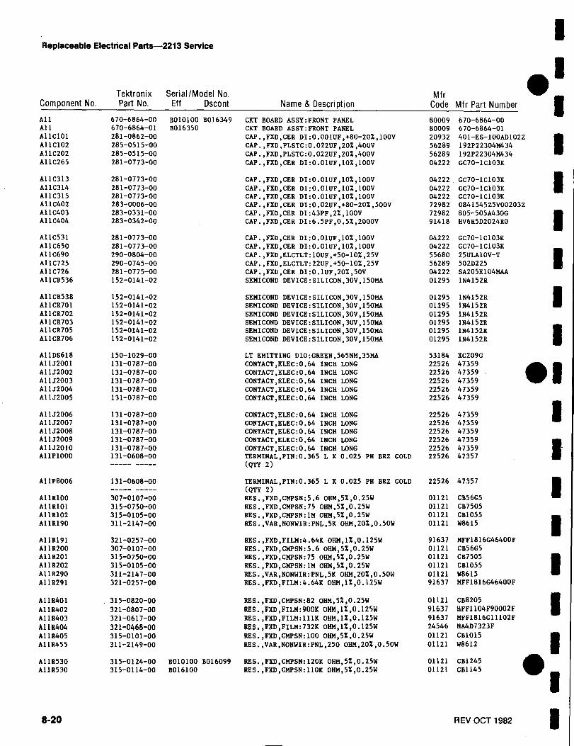
Replaceable Electrical Parts-2213 Service
Tektronix
Serial/Model Νο . Mfr
ι
a
ι8-20
REV OCT 1982
Component Νο . Part Νο . E ff Dscont Name & Description Co d e Mfr Part Number
All 670-6864-00 Β010100 Β016349 CKT BOARD ASSY :FRONT PANEL 80009 670-6864-00All 670-6864-01 Β016350 CKT BOARD ASSY : FRONT PANEL 80009 670-6864-01Al1C101 281-0862-00 CAP .,FXD ,CER DI :O .OOIUF ,+80-20%,100V 20932 401-ES-IOOAD102ZAl 1C102 285-0515-00 CAP ., FXD ,PLSTC :0 .022UF ,20%,400Υ 56289 192Ρ2230414434A11C202 285-0515-00 CAP ., FXD ,PLSTC :0 .022UF ,20%,400Υ 56289 192Ρ22304Μ434Al 1C265 281-0773-00 CAP .,FXD ,CER DI :O .O1UF ,10%,100V 04222 GC70-lClO3K
A11C313 281-0773-00 CAP .,FXD ,CER DI :O .OIUF ,10%,100Υ 04222, GC70-1Cl03KAl 1C314 281-0773-00 CAP .,FXD ,CER DI :O.O1UF ,10%,100Υ 04222 GC70-1C103KA11C315 281-0773-00 CAP .,FXD ,CER DI :O .O1UF ,10%,100V 04222 GC70-1Cl03KAl 1C402 283-0006-00 CAP .,FXD ,CER DI :0 .02UF ,+80-20%,500Υ 72982 0841545 Z5VO0203ZAllC403 283-0331-00 CAP .,FXD ,CER DI :43PF,2%,100V 72982 805-SOSA430GAll C404 283-0342-00 CAP .,FXD ,CER DI :6 .5PF ,0 .5%,2000Υ 91418 HV6 RSD2024RO
AllC531 281-0773-00 CAP .,FXD ,CER DI :O .OIUF ,10%,100V 04222 GC70-l C lO3KA11C650 281-0773-00 CAP .,FXD ,CER DI :O .OIUF,10%,100V 04222 GC70-l ClO3KA11C690 290-0804-00 CAP .,FXD ,ELCTLT: l0UF ,+50-10%,25V 55680 25ULAl OV-ΤAll C725 290-0745-00 CAP ., FXD ,ELCTLT:22UF,+50-10%,25Υ 56289 502D225A11C726 281-0775-00 CAP .,FXD ,CER DI :O . lUF ,20%,50V 04222 SA205E104MAAA11CR536 152-0141-02 SEMICOND DEVICE :SILICON ,30V,150MA 01295 1 N4152R
A11CR538 152-0141-02 SEMICOND DEVICE :SILICON ,30V ,150MA 01295 1 N4152RAlICR701 Ι52-0141-02 SEMICOND DEVICE :SILICON ,30V ,150MA 01295 1N4152RAlICR702 152-0141-02 SEMICOND DEVICE :SILICON ,30V ,150MA 01295 1Ν4152ΑA11CR703 152-0141-02 SEMICOND DEVICE :SILICON ,30V,150MA 01295 1N4152RA11CR705 152-0141-02 SEMICOND DEVICE :SILICON ,30V ,150MA 01295 1N4152RA11CR706 152-0141-02 SEMICOND DEVICE :SILICON ,30V,150MA 01295 1N4152R
AllDS618 150-1029-00 IT EMITTING DIO :GREEN ,565NM,35MA 53184 XC209GAlIJ2001 131-0787-00 CONTACT,ELEC :0 .64 INCH LONG 22526 47359A11J2002 131-0787-00 CONTACT ,ELEC :0 .64 INCH LONG 22526 47359Al 1J2003 131-0787-00 CONTACT,ΕLΕC:0 .64 INCH LONG 22526 47359AlIJ2004 131-0787-00 CONTACT,ELEC :0 .64 INCH LONG 22526 47359A11J2005 131-0787-00 CONTACT,ELEC:0 .64 INCH LONG 22526 47359
AllJ2006 131-0787-00 CONTACT,ELEC:0.64 INCH LONG 22526 47359AIIJ2007 131-0787-00 CONTACT ,ELEC :0 .64 INCH LONG 22526 47359AllJ2008 131-0787-00 CONTACT,ELEC:0 .64 INCH LONG 22526 47359AllJ2009 131-0787-00 CONTACT ,ELEC :0 .64 INCH LONG 22526 47359AllJ2010 131-0787-00 CONTACT ,ELEC :0 .64 INCH LONG 22526 47359Αl ΙΡ1000 131-0608-00 TERMINAL,PIN :0 .365 L Χ 0.025 ΡΗ BRZ GOLD 22526 47357
----- ----- (QTY 2)
Α l ΙΡ8006 131-0608-00 TERMINAL,PIN :0 .365 L Χ 0.025 ΡΗ BRZ GOLD 22526 47357----- ----- (QTY 2)
A lIR100 307-0107-00 RES .,FXD,CMPSN:5 .6 OHM,5%,0 .25W 01121 CB56G5A11R101 315-0750-00 RES .,FXD,CMPSN :75 OHM,5%,0.25W 01121 CB7505AllR102 315-0105-00 RES .,FXD ,CMPSN :IM OHM,5%,0 .25W 01121 CB1055Al 1R190 311-2147-00 RES .,VAR,NONWIR :PNL ,5K ΟΗΜ,20%,0 .50W 01121 W8615
A 1 IR191 321-0257-00 RES .,FXD,FILM:4 .64K ΟΗΜ ,1%,0 .125W 91637 MFF1816G46400FAllR200 307-0107-00 RES .,FXD ,CMPSN :5 .6 OHM,5%,0 .25W 01121 CB56G5Al 1 R201 315-0750-00 RE S ., FXD ,CMPSN :75 OHM,5%,0 .25W 01121 CB7505Al 1 R202 315-0105-00 RES .,$XD ,CMPSN : IM OHM,5%,0 .25W 01121 CB1055ΑlIR290 311-2147-00 RES .,VAR,NONWIR :PNL ,SK ΟΗΜ,20%,0 .50W 01121 W8615AllR291 321-0257-00 RES ., FXD ,FILM:4 .64K ΟΗΜ ,1%,0 .125W 91637 MFF1816G46400 F
A11R401 315-0820-00 RES .,FXD ,CMPSN :82 OHM,5%,0 .25W 01121 CB8205Α11Α402 321-0807-00 RES .,FXD,FILM:900K ΟΗΜ ,1%,0 .125W 91637 RFF1104F90002FΑ11Α403 321-0617-00 RES .,FXD,FILM:111K ΟΗΜ,1%,0 .125W 91637 MFF1816GIII02FAl 1R404 321-0468-00 RES .,FXD,FILM:732K ΟΗΜ, Ι %,0 .125W 24546 NA4D7323FΑ11Α405 315-0101-00 RES .,FXD ,CMPSN:100 OHM,5%,0 .25W 01121 CB1015AlIR455 311-2149-00 RES .,VAR,NONWIR :PNL ,250 ΟΗΜ,20%,O .SOW 01121 W8612
A11R530 315-0124-00 Β010100 Β016099 RES.,FXD ,CMPSN:120K OHM,5%,0.25W 01121 CB1245Α11Α530 315-0114-00 Β016100 RES .,FXD ,CMPSN:110K OHM,5%,0.25W 01121 CB1145

ιιι
ιιιι
ι
ιιι
ι
ι
Replaceable Electrical Parts-2213 Service
REV OCT 1982
8-21
Component Νο .TektronixPart Νο .
Se rial/ Model Νο .Eff Dscont Name & Description
MfrCode Mfr Part Num ber
A11R531 315-0124-00 RES .,FXD,CMPSN :120K OHM,5%,0 .25W 01121 CB1245Α11Α532 315-0434-00 RES .,FXD,CMPSN :430K OHM,5%,0 .25W 01121 CB4345Α11Α536 315-0182-00 RES .,FXD,CMPSN :1 .8K OHM,5%,0 .25W 01121 CB1825Α11Α537 321-0239-00 RES .,FXD,FILM :3 .OIK ΟΗΜ ,1%,0 .125W 91637 MFF1816G30100FΑ11Α538 321-0126-00 RES .,FXD,FILM :200 ΟΗΜ ,1%,0 .125W 91637 MFF1816G200ROFΑ11Α556 315-0102-00 ΧΒΟ 12481 RES .,FXD,CMPSN :lK OHM,5%,0 .25W 01121 CB1025
Α 11Α557 311-2135-00 RES .,VAR,NONWIR :PNL,SOK ΟΗΜ,20%,0 .5W 01121 ω8600Α11Α645 315-0912-00 Β010100 Β012480 RES .,FXD,CMPSN :9 .lK OHM,5%,0 .25W 01121 CB9125Α11Α645 315-0682-00 Β012481 RES .,FXD,CMPSN :6 . 8K OHM,5%,0 .25W 01121 CB6825A11R646 315-0123-00 Β010100 Β012480 RES .,FXD,CMPSN :12K OHM,5%,0 .25W 01121 CB1235Α11 Α646 315-0103-00 Β012481 RES .,FXD,CMPSN :IOK OHM,5%,0 .25W 01121 CB1035A 11R694 321-0451-00 RES .,FXD,FILM :487K ΟΗΜ,1%,0 .125W 91637 MFF1816G48702F
Α11Α726 311-2147-00 RES .,VAR,NONWIR :PNL,5K ΟΗΜ ,20%,O .SOW 01121 W8615A11R807 311-2147-00 RES .,VAR,NONWIR :PNL,SK ΟΗΜ ,20%,0 .50W 01121 W8615Α11 Α808 315-0512-00 RES .,FXD,CMPSN :5 .1K OHM,5%,0.25W 01121 CB5125Α11Α891 311-1562-00 RES .,VAR,NONWIR :2K ΟΗΜ ,20%,0 .50W 73138 91-84-0A11R975 301-0131-00 RES .,FXD,CMPSN :130 ΟΗΜ ,5%,0 .50W 01121 ΕΒ1315A11S101 260-2033-00 SWITCH,SLIDE :DPTT,125V ,0 .5A 82389 OBD
Al1S201 260-2033-00 SWITCH,SLIDE :DPTT,125V,0 .5A 82389 OBDA11S264 260-2075-00 SWITCH,PUSH :SPDT,50VDC,SOOM AMP 80009 260-2075-00Al1S305 260-2033-00 SWITCH,SLIDE :DPTT,125V ,0.5A 82389 OBDAl1S315 260-2033-00 SWITCH,SLIDE :DPTT,125V ,0.5A 82389 OBDA11S317 260-2033-00 SWITCH,SLIDE :DPTT,125V,O .SA 82389 OBDAl1S390 260-2076-00 SWITCH,PUSH :SPST,MOMENTARY,SOVDC,500M AMP 80009 260-2076-00
Al1S401 260-2033-00 SWITCH,SLIDE :DPTT,125V,0 .5A 82389 OBDAl1S440 260-2033-00 SWITCH,SLIDE :DPTT,125V ,0 .5A 82389 OBDAl1S464 Ζ60-2032-00 SWITCH,SLIDE :DPDT,125V ,0 .5A 82389 OBDA11S611 260-2033-00 SWITCH,SLIDE :DPTT,125V,0 .5A 82389 OBDAl1S650 260-2033-00 SWITCH,SLIDE :DPTT,125V,0 .5A 82389 OBDA11S660 260-2033-00 SWITCH,SLIDE :DPTT,125V ,0 .5A 82389 OBD
Al1U535 156-0067-00 MICROCIRCUIT,LI :OPERATIONAL AMPLIFIER 01295 MICβOA741CPAl 1W264 131-0566-00 BUS CONDUCTOR :DUMMY RES,2 .375,22 AWG 57668 JWW-0200Ε0Al 1W265 131-0566-00 BUS CONDUCTOR :DUMMY RES,2 .375,22 AWG 57668 JωW-0200ΕΟAl 1W630 131-0566-00 BUS CONDUCTOR :DUMMY RES,2 .375,22 AWG 57668 JWW-0200ΕOAl 1W635 131-0566-00 Β010100 Β012480Χ BUS CONDUCTOR :DUMMY RES,2 .375,22 AWG 57668 JωW-0200ΕΟAl 1W637 131-0566-00 BUS CONDUCTOR :DUMMY RES,2 .375,22 AWG 57668 JWW-0200ΕO
A11W702 131-0566-00 BUS CONDUCTOR :DUMMY RES,2 .375,22 AWG 57668 JWW-0200ΕO

Replaceable Electrical Parts-2213 Service
8-22
REV OCT 1982
Com ponen t Νο .Tektro n ixPart Νο .
Serial/M od el Νο .Eff Dsco n t Name & Desc r iption
M frCode Mfr Part Num ber
Α 12 670-6860-00 Β010100 Β016349 CKT BOARD ASSY :ATTEN/SWEEP 80009 670-6860-00Α 12 670-6860-01 Β016350 CKT BOARD ASSY : ATTEN/SWEEP 80009 670-6860-01A12C104 281-0078-00 CAP .,VAR,AIR DI :1 .4-7 .3PF ,750V 74970 189-0503-075A 12C105 281-0214-00 CAP .,VAR ,CER DI :0 .5-3PF ,400V 80031 2502AOR503VP02FOA12C107 283-0154-00 CAP .,FXD ,CER DI :22PF ,5%,50V 72982 8111B061000220JA12010 281-0078-00 CAP .,VAR,AIR DI :1 .4-7 .3PF ,750V 74970 189-0503-075
A12011 281-0214-00 CAP .,VAR ,CER DI :0 .5-3PF ,400V 80031 2502AOR503VP02FOA12C112 283-0108-00 CAP .,FXD ,CER DI :22OPF ,10%,200Υ 56289 272C13A12C119 283-0158-00 CAP .,FXD ,CER DI :1 PF ,10%,50Υ 51642 100-050-ΝΡΟ-109ΒA12C121 283-0000-00 CAP .,FXD ,CER DI :O .OO1UF ,+100-0%,SOOV 59660 831-519-Υ5Ρ-102Ρ
A12C123 281-0775-00 CAP .,FXD ,CER DI :O . IUF ,20%,50Υ 04222 SA205E104MAAA12C125 283-0330-00 CAP .,FXD ,CER DI : l00PF ,5%,50V 51642 150-050-ΝΡΟ-IOIJ
A12C132 290-0808-00 CAP ., FXD ,ELCTLT :2 .7UF ,10%,20V 56289 162D275X9020CD2A12C133 283-0000-00 CAP .,FXD ,CER DI :O .OOIUF ,+100-0%,500V 59660 831-519-Υ5Ρ-102ΡA12C134 283-0000-00 CAP .,FXD ,CER DI :O .OO1UF ,+100-0%,500Υ 59660 831-519-Υ5Ρ-102ΡA12C136 283-0220-00 CAP .,FXD ,CER DI :O .O1UF ,20%,50V 72982 8121Ν075Χ7ΑΟ103ΜA12C137 283-0220-00 CAP .,FXD ,CER DI :O .O1UF ,20%,50V 72982 8121NO75X7RO103MA12C139 283-0160-00 CAP .,FXD ,CER DI :1 .SPF ,10%,50V 72982 8101AO58COK159B
A12C140 281-0775-00 CAP .,FXD ,CER DI :O . lUF ,20%,50V 04222 SA205EI04MAAA12C141 283-0175-00 CAP .,FXD ,CER DI : IOPF,5%,200V 51642 W150-200-NPOIOODA12042 283-0201-00 CAP .,FXD ,CER DI :27PF ,10%,200Υ 72982 8101B210X7R0270KA12C144 281-0775-00 CAP .,FXD ,CER DI :O . IUF ,20%,SOV 04222 δΑ205Ε104ΜΑΑA12C204 281-0078-00 CAP .,VAR ,AIR DI :1 .4-7 .3PF ,750V 74970 189-0503-075A12C205 281-0214-00 CAP .,VAR ,CER DI :0 .5-3PF ,400V 80031 2502AOR503VP02FO
A12C207 283-0154-00 CAP .,FXD ,CER DΣ :22PF,5%,50V 72982 8111BO61000220JA12C210 281-0078-00 CAP .,VAR,AIR DI :1 .4-7 .3PF ,750V 74970 189-0503-075A12C211 281-0214-00 CAP .,VAR ,CER DI :0 .5-3PF ,400V 80031 2502AOR503VP02FO
A12C212 283-0108-00 CAP .,FXD ,CER DI :220PF ,10%,200Υ 56289 272C13A12C219 283-0158-00 CAP .,FXD ,CER DI :1PF ,10%,50V 51642 100-050-ΝΡΟ-109Β
A12C221 283-0000-00 CAP .,FXD ,CER DI :O .OOIUF ,+100-0%,500V - 59660 831-519-Υ5Ρ-102Ρ
A12C225 283-0330-00 CAP .,FXD ,CER DI : l00PF ,5%,50V 51642 150-050-ΝΡΟ-101 JA12C232 290-0808-00 CAP .,FXD ,ELCTLT:2 .7UF ,10%,20Υ 56289 162D275X9020CD2
A12C233 283-0000-00 CAP .,FXD ,CER DI :O .OO IUF ,+100-0%,500V 59660 831-519-Υ5Ρ-102ΡA12C234 283-0000-00 CAP .,FXD ,CER DI :O .OO IUF ,+100-0%,500V 59660 831-519-Υ5Ρ-102ΡA12C236 283-0220-00 CAP .,FXD ,CER DI :O .O1UF,20Χ ,50V 72982 8121ΝΟ75Χ7 ΑΟ103ΜA12C237 283-0220-00 CAP .,FXD ,CER DI :O .O1UF ,20%,50Υ 72982 8121ΝΟ75Χ7ΑΟ103Μ
A12C239 283-0160-00 CAP .,FXD ,CER DI :1 .5PF ,10%,50Υ 72982 81OIA058COK159B
A12C241 283-0175-00 CAP .,FXD ,CER DI : IOPF,5%,200V 51642 W150-200-NPOl00DA12C242 283-0201-00 CAP .,FXD ,CER DI :27PF ,10%,200Υ 72982 8101Β210Χ7ΑΟ270Κ
A12C244 281-0775-00 CAP .,FXD ,CER DI :O . IUF ,20%,SOV 04222 SA205E104MAAA12C625 283-0631-00 CAP .,FXD,MICA D:95PF ,1%,100Υ 00853 D151E950FOA12C626 281-0202-00 CAP .,VAR ,PLSTC :1 .5-5 .5PF,100V 80031 2807CIR406MM02F
A12C628A,B 295-0138-00 CAP .SET ,MATCHED:IUF ,O .OIUF ,1Χ,OA RANGE 3% 80009 295-0138-00A12C630 281-0811-00 CAP .,FXD ,CER DI :1OPF,10%,100Υ 72982 8035D2AADCIG100KA12C636 283-0024-00 CAP ., FXD,CER DI :O . lUF ,+80-20%,50V 72982 8121NO83Z5UO104ZA12C677 281-0775-00 CAP .,FXD ,CER DI :O . IUF ,20Χ ,50V 04222 SA205E104MAAA12C679 281-0775-00 CAP .,FXD ,CER DI :O . IUF ,20Χ ,50V 04222 SA205E104MAAA12020 281-0763-00 CAP .,FXD ,CER DI :47PF,10%,100Υ 72982 8035D9AADCIG470K
A12C732 281-0756-00 CAP .,FXD ,CER DI :2 .2PF ,0 .5%,200V 12969 CGB2R2DFN
A12C734 281-0151-00 CAP .,VAR,CER DI :1-3PF ,100V 72982 518-600Α1-3
A12C736 281-0756-00 CAP .,FXD ,CER DI :2 .2PF ,0 .5Χ ,200V 12969 CGB2R2DFNA12038 283-0023-00 CAP .,FXD ,CER DI :O . IUF ,+80-20%,12V 91418 ΜΧ0104Ζ1205Α5
A12C741 283-0023-00 CAP .,FXD ,CER DI :O . I UF ,+80-20%,12V 91418 MX0104Z1205R5
A12C628A, B 295-0138-00 CAP .SET,MATCHED :lUF,ο .OIUF,1%, οΑ RANGE 3% 80009 295-0138-00
A12CR119 152-0246-00 SEMICOND DEVICE :SW ,SI ,40V ,200MA 03508 DE 140A12CR219 152-0246-00 SEMICOND DEVICE :SW ,SI ,40V ,200MA 03508 DE 140
A12CR626 152-0245-00 SEMICOND DEVICE :SILICON ,1ONA AT 5V 12969 NDP539

Replaceable Elect rical Parts-2213 Service
REV OCT 1982
8-23
Component Νο .Te ktronix Serial/Model Νο .Part Νο . Eff Dscont Name & Description
Mf rCode M fr Part Number
A12CR630 152-0141-02 SEMICOND DEVICE :SILICON .30V .150MA 01295 1N4152RΑ12Ρ 1010 131-0608-00 TERMINAL,PIN :0 .365 L Χ 0 .025 ΡΗ BRZ GOLD 22526 47357
(QTY 4)Α12Ρ2000 136-0328-02 SOCKET,PIN TERM:HORIZONTAL 00779 86282-2
(QTY 10)Α12ΡΖ010 131-0608-00 TERMINAL,PIN :0 .365 L Χ 0 .025 ΡΗ BRZ GOLD 22526 47357
(QTY 4)
Α12Ρ6000 131-0608-00 TERMINAL,PIN :0 .365 L Χ 0 .025 ΡΗ BRZ GOLD 22526 47357(QTY 10)
Α12Ρ 7000 131-0608-00 TERMINAL,PIN :0.365 L Χ 0 .025 ΡΗ ΒΑΖ GOLD 22526 47357(QTY 7)
A12Q122 151-1124-00 TRANSISTOR :JFE,N-CHAN ,S I ,SEL 22229 Σ2942A12Q125 151-0711-00 TRANS ISTOR :SILICON,NPN 04713 SPS8224
A12Q133 151-0711-00 TRANS ISTOR:S ILICON,NPN 04713 SPS8224A12Q134 151-0712-00 TRANSISTOR:SILICON,NPN 04713 SPS8223A12Q139 151-0216-00 TRANSISTOR:S ILICON,PNP 04713 SPS8803A12Q222 151-1124-00 TRANSISTOR :JFE,N-CHAN ,SI ,SEL 22229 F2942A12Q225 151-0711-00 TRANSISTOR :SILICON,NPN 04713 SPS8224A12Q233 151-0711-00 TRANSISTOR:SILICON,NPN 04713 SPS8224
A12Q234 151-0712-00 TRANSISTOR:S ILICON,NPN 04713 SPS8223A12Q239 151-0216-00 TRANSISTOR:SILICON,PNP 04713 SPS8803A12Q629 151-0188-00 TRANSISTOR:S ILICON,PNP 04713 SPS6868KA12Q630A ,B 151-1042-00 SEMICOND DVC SE :MATCHED PAIR FET 01295 SKA5390A12Q631 151-0190-00 TRANSISTOR:SILICON,NPN 07263 S032677A12Q720 151-0190-00 TRANSISTOR:SILICON,NPN 07263 S032677
A12Q730 151-0712-00 TRANSISTOR:SILICON,NPN 04713 SPS8223A12Q731 151-0712-00 TRANSISTOR :SILICON,NPN 04713 SPS8223A12Q736 151-0711-00 TRANSISTOR :SILICON,NPN 04713 SPS8224A12R103 315-0240-00 RES ., FXD ,CΜPSN :24 ΟΗΜ ,5%,0 .25W 01121 CB2405Α12Α105 321-0807-01 RES .,FXD,FILM:900K ΟΗΜ,0 .5%,0 .125W 91637 MFF1816G90002DA12R107 321-1389-01 RES .,FXD,FILM:111K ΟΗΜ,0 .5%,0 .125W 91637 MFF1816GIII02D
A12R108 315-0620-00 RES .,FXD ,CMPSN :62 ΟΗΜ ,5%,0 .25W 01121 CB6205Α12Α110 315-0101-00 RES .,FXD ,CMPSN :100 OHM,5%,0 .25W 01121 CB1015Α12Α111 321-0790-01 RES .,FXD,FILM:990K ΟΗΜ,0 .5%,0 .125W 91637 HFF1104G99002DA12R112 315-0120-00 RES .,FXD ,CMPSN:12 OHM,5%,0 .25W 01121 CB1205Α12Α114 321-1289-01 RES .,FXD,FILM :l 0 .1K ΟΗΜ,0 .5%,0 .125W 91637 MFF1816GIO101DA12R115 315-0910-00 RES .,FXD ,CMPSN:91 ΟΗΜ,5Χ ,0 .25ω 01121 CB9105
A12R 116 321-0385-04 RES .,FXD,FILM :l00K ΟΗΜ ,0 .1%,0 .125W 91637 MFF1816DI0002BA12R117 321-0807-04 RES .,FXD,FILM :900K ΟΗΜ ,0 .1%,0.125W 24546 NC55C9003BΑ12Α119 315-0107-00 RES .,FXD,CMPSN :l 00M OHM,5%,0 .25W 01121 CB1075A12R120 315-0104-00 RES .,FXD,CMPSN :l00K OHM,5%,0 .25W 01121 CB1045Α12Α121 315-0435-00 βES .,FXD,CMPSN :4 .3M OHM,5%,0 .25W 01121 CB4355Α12Α122 301-0122-00 RES .,FXD,CMPSN :1 .2K ΟΗΜ ,5%,O .SOW 01121 ΕΒ1225
A12R123 315-0100-00 RES .,FXD,CMPSN :10 OHM,5%,0 .25W 01121 CB1005Α12Α124 315-0102-00 RES .,FXD ,CMPSN :IK OHM,5%,0 .25W 01121 CB1025A12R125 321-0131-00 RES .,FXD,FILM :226 ΟΗΜ,1 Χ ,0 .125W 91637 MFF1816G226ROFA12R126 321-0126-00 RES .,FXD,FILM:200 οΗΜ,1%,0 .125W 91637 MFF1816G200ROFA12R127 315-0470-00 RES ., FXD,CMPSN :47 OHM,5%,0 .25W 01121 CB4705A12R128 315-0102-00 RES .,FXD ,CMPSN :lK OHM,5%,0 .25W 01121 CB1025
A12R130 315-0182-00 RES ., FXD ,CMPSN :1 .SK OHM,5%,0 .25W 01121 CB1825A12R131 321-0254-00 RES .,FXD,FILM:4 .32K 01 M ,1%,0 .125W 91637 MFF1816G43200FΑ12Α132 321-0229-00 RES .,FXD,FILM:2 .37K ΟΗΜ ,1%,0 .125W 91637 MFF1816G23700FA12R133 315-0101-00 RES .,FXD ,CMPSN :100 OHM,5%,0 .25W 01121 CB1015Α12Α134 315-0680-00 RES .,FXD ,CMPSN :68 OHM,5%,0 .25W 01121 CB6805A12R135 315-0472-00 RES .,FXD ,CMPSN :4 .7K OHM,5%,0.25W 01121 CB4725
A 12R136 307-0106-00 RES .,FXD ,CMPSN:4 .7 OHM,5%,0 .25W 01121 CB47G5A12R137 315-0100-00 RES .,FXD ,CMPSN:10 OHM,5%,0 .25W 01121 CB1005

Replaceable Electrical Parts-2213 Service
0
8-24
REVOCT 1982
Component Νο.Tekt ronix Serial/ Mod el Νο .Part Νο . Eff Dscont Name & Descri ption
MfrCo d e Mfr Part N umber
A12R138 311-1559-00 RES .,VAR,NONWIR:1OK ΟΗΜ ,20%,0 .50W 73138 91-81-0A12R139 307-0710-00 RES NTWK,FXD,FI :ATTENUATOR 80009 307-0710-00A12R140 315-0132-00 RES .,FXD ,CMPSN :1 .3K OHM,5%,0 .25W 01121 CB1325Α12Α141 311-2133-00 RES .,VAR,NONWIR :PNL ,500 ΟΗΜ ,20%,0 .50W 12697 CM41766A12R142 315-0304-00 RES.,FXD ,CMPSN :300K OHM,5%,0 .25W 01121 CB3045A12R143 315-0301-00 RES .,FXD ,CMPSN :300 OHM,5%,0 .25W 01121 CB3015
A 12R144 315-0111-00 RES .,FXD,CMPSN:110 ΟΗΜ,5%,0 .25ω 01121 . CB1115Α12Α145 311-1562-00 RES .,VAR,NONWIR :2K ΟΗΜ,20%,0 .50W 73138 91-84-0A12R146 311-0607-00 RES .,VAR,NONWIR :I OK ΟΗΜ ,10%,0 .50W 73138 82-25-2Α 12Α147 315-0393-00 RES .,FXD ,CMPSN :39K OHM,5%,0 .25W 01121 CB3935Α12Α148 315-0111-00 RES .,FXD ,CMPSN :110 OHM,5%,0 .25W 01121 CB1115A 12R149 315-0101-00 RES .,FXD,CMPSN :100 OHM,5%,0 .25W 01121 CB1015
A12R203 315-0240-00 RES .,FXD,CMP SN:24 OHM,5%,0 .25W 01121 CB2405Α12Α205 321-0807-01 RES .,FXD,FILM:900K ΟΗΜ ,0 .5%,0 .125W 91637 MFF1816G90002DΑ 12Α207 321-1389-01 RES .,FXD,FILM:111K ΟΗΜ ,0 .5%,0 .125W 91637 MFF1816G11102DΑ12Α208 315-0620-00 RES .,FXD ,CMPSN:62 OHM,5%,0 .25W 01121 CB6205Α12Α210 315-0101-00 RES .,FXD,CMPSN :100 OHM,5%,0 .25W 01121 CB1015Α 12Α211 321-0790-01 RES .,FXD,FILM:990K ΟΗΜ ,0 .5%,0 .125W 91637 HFF1104G99002 D
A12R212 315-0120-00 RES ., FXD,CMPSN:12 OHM,5%,0 .25W 01121 CB1205Α12Α214 321-1289-01 RES .,FXD,FILM :10 .1 K ΟΗΜ,0 .5%,0 .125W 91637 MFF1816GI O101DA12R215 315-0910-00 RES ., FXD ,CMPSN :91 OHM,5%,0 .25W 01121 CB9105Α12Α216 321-0385-04 RES .,FXD,FILM :100K ΟΗΜ ,0 .1%,0 .125W 91637 MFF1816D10002BA12R217 321-0807-04 RES .,FXD,FILM:900K ΟΗΜ ,0.1%,0 .125ω 24546 NC55C9003BA12R219 315-0107-00 RES ., FXD ,CMPSN :100M OHM,5%,0 .25W 01121 CB1075
Α12Α220 315-0104-00 RES ., FXD ,CMPSN :100K ΟΗΜ ,5%,0 .25W 01121 CB1045A12R221 315-0435-00 RES ., FXD ,CMPSN :4 .3M OHM,5%,0 .25W 01121 CB4355A12R222 301-0122-00 RES ., FXD ,CMPSN :1 .2K ΟΗΜ ,5%,0 .50W 01121 ΕΒ1225Α12Α225 321-0131-00 RES .,FXD,FILM:226 ΟΗΜ,1%,0 .125W 91637 MFF1816G226ROFΑ12Α226 321-0126-00 RES .,FXD,FILM:200 ΟΗΜ ,1Χ ,0 .125W 91637 MFF1816G200ROFΑ12Α227 315-0470-00 RES ., FXD ,CMPSN :47 ΟΗΜ,5%,0 .25W 01121 CB4705
A 12R231 321-0254-00 RES .,FXD,FILM:4 .32K ΟΗΜ ,1%,0 .125W 91637 MFF 1816G43200 FΑ12Α232 321-0229-00 RES .,FXD,FILM:2 .37K οΗΜ ,1Χ ,0 .125ω 91637 MFF 1816G23700FA12R233 315-0101-00 RES .,FXD,CMPSN:100 OHM,5%,0 .25W 01121 CB1015A 12R234 315-0680-00 RES .,FXD ,CMPSN:68 OHM,5%,0 .25W 01121 CB6805Α 12Α235 315-0472-00 RES .,FXD ,CMPSN :4.7K OHM,5%,0 .25W 01121 CB4725A12R236 307-0106-00 RES .,FXD,CMPSN:4 .7 OHM,5%,0 .25W 01121 CB47G5
A 12R237 315-0100-00 RES .,FXD,CMPSN :10 OHM,5%,0 .25W 01121 CB1005A12R238 311-1559-00 RES .,VAR,NONWIR :I OK ΟΗΜ,20Χ ,0 .50W 73138 91-81-0A12R239 307-0710-00 RES NTWK ,FXD,FI :ATTENUATOR 80009 307-0710-00Α 12Α240 315-0132-00 RES .,FXD ,CMPSN :1 .3K OHM,5%,0 .25W 01121 CB1325Α12Α241 311-2133-00 RES .,VAR,NONWIR:PNL,500 ΟΗΜ,20%,O .SOW 12697 CM41766A12R242 315-0304-00 RES ., FXD,CMPSN :300K OHM,5%,0 .25W 01121 CB3045
Α12Α243 315-0301-00 RES ., FXD,CMPSN :300 OHM,5%,0 .25W 01121 CB3015A12R244 315-0111-00 RES ., FXD ,CMPSN :110 OHM,5%,0 .25W 01121 CB1115A12R245 311-0609-00 RES .,VAR,NONWIR :2K ΟΗΜ ,10Χ ,0 .50W 73138 82-26-1Α12Α246 311-0607-00 RES .,VAR,NONWIR:1OK ΟΗΜ ,10%,O.SOW 73138 82-25-2Α12Α247 315-0393-00 RES .,FXD ,CMPSN :39K OHM,5%,0.25W 01121 CB3935A12R248 315-0111-00 RES ., FXD,CMPSN :110 OHM,5%,0 .25W 01121 CB1115
A12R249 315-0101-00 RES ., FXD ,CMPSN :100 OHM,5%,0.25W 01121 CB1015A12R625 322-0519-01 RES .,FXD,FILM:2 .49M ΟΗΜ ,0 .5%,0 .25W 91637 HFF143G24903DA12R626 307-0780-00 RES NTWK,FXD,FI :TIMING 80009 307-0780-00Α12Α627 315-0241-00 RES .,FXD ,CMPSN :240 ΟΗΜ ,5%,0 .25W 01121 CB2415A12R628 315-0100-00 RES .,FXD,CMPSN:10 OHM,5%,0 .25W 01121 CB1005Α12Α629 311-2134-00 RES .,VAR, NONWIR : PNL,500 ΟΗΜ,20%,0 .5W,W/SW 12697 CM41767
A12R630 315-0510-00 RES .,FXD ,CMPSN :51 OHM,5%,0 .25W 01121 CB5105Α12Α631 301-0242-00 RES .,FXD ,CMPSN :2 .4K ΟΗΜ,5%,0 .50W 01121 ΕΒ2425Α12Α633 321-0261-00 RES .,FXD,FILM:5 .11 K ΟΗΜ,1%,0 .125W 91637 MFF1816GS1100F

Replaceable Electrical Parts-2213 Service
REV OCT 1982
8-25
Component Νο .Tekt r onix Se r ial/M odel Νο .Pa rt Νο. Ett Dscont Name & Descri p tion
MfrCode Mfr Part Number
Α12Α636 307-0107-00 RES ., FXD ,CMPSN :5 .6 οΗΜ,5%,0 .25W 01121 CB56G5A12R677 307-0107-00 RES .,FXD ,CMPSN :5 .6 OHM,5%,0 .25W 01121 CB56G5Α12Α679 307-0107-00 RES ., FXD ,CMPSN :5 .6 OHM,5%,0 .25W 01121 CB56G5A12R684 321-0232-00 RES .,FXD,FILM:2 .55K ΟΗΜ ,1%,0 .125W 91637 MFF1816G25500FA12R686 315-0682-00 RES .,FXD ,CMPSN :6 .SK οΗΜ ,5%,0 .25W 01121 CB6825A12R691 315-0470-00 RES ., FXD ,CMPSN :47 OHM,5%,0 .25W 01121 CB4705
A12R720 315-0221-00 RES.,FXD ,CMPSN:220 OHM,5%,0 .25W 01121 CB2215A12R721 315-0101-00 RES.,FXD ,CMPSN:100 OHM,5%,0 .25W 01121 CB1015Α12Α722 315-0152-00 RES.,FXD ,CMPSN:1 .5K OHM,5%,0 .25W 01121 CB1525A12R723 315-0682-00 RES.,FXD ,CMPSN:6 .8K OHM,5%,0 .25W 01121 CB6825Α12Α724 315-0392-00 RES .,FXD,CMPSN:3 .9K OHM,5%,0 .25W 01121 CB3925Α12 Α725 315-0822-00 RES .,FXD,CMPSN:8 .2K OHM,5%,0 .25W 01121 CB8225
A12R728 315-0822-00 RES ., FXD ,CMPSN:8 .2K OHM,5%,0 .25W 01121 CB8225A12R729 321-0159-00 RES.,FXD,FILM :442 ΟΗΜ,1%,0.125W 91637 MFF1816G442ROFA12R730 315-0561-00 RES ., FXD,CMPSN:560 OHM,5%,0 .25W 01121 CB5615A12R731 315-0911-00 RES ., FXD ,CMPSN:910 OHM,5%,0 .25W 01121 CB9115Α12 Α732 321-0206-00 RES .,FXD,FILM :1 .37K ΟΗΜ,1%,0 .125W 91637 MFF1816G1370OFΑ12Α733 311-1562-00 RES .,VAR,NONWIR :2K ΟΗΜ ,20%,0 .50W 73138 91-84-0
Α12Α734 321-0295-00 RES .,FXD,FILM :11 .5K ΟΗΜ ,1%,0 .125W 91637 MFF1816G11501 FΑ12Α736 315-0272-00 RES ., FXD,CMPSN :2 .7K OHM,5%,0 .25W 01121 CB2725A12R737 315-0362-00 RES .,FXD ,CMPSN :3 .6K OHM,5%,0 .25W 01121 CB3625Α12Α738 315-0100-00 RES ., FXD ,CMPSN :10 OHM,5%,0 .25W 01121 CB1005A12R739 315-0560-00 RES ., FXD,CMPSN :56 OHM,5%,0 .25W 01121 CB5605A12R741 315-0100-00 RES .,FXD ,CMPSN :10 OHM,5%,0 .25W 01121 CB1005
Α12ΑΤ144 307-0125-00 RES .,THERMAL :500 ΟΗΜ ,10Χ ,25 DEG C 50157 2D1595Α12ΑΤ244 307-0125-00 RES .,THERMAL :500 ΟΗΜ,10%,25 DEG C 50157 2D1595A12S105A, B 260-2025-00 SWITCH,ROTARY :VERTICAL ATTENUATOR 80009 260-2025-00A12S205A , B 260-2025-00 SWITCH,ROTARY :VERTICAL ATTENUATOR 80009 260-2025-00A12S630A, B 260-2024-00 SWITCH,ROTARY :TIME/DIV Α/Β 80009 260-2024-00A12U120 156-1551-00 MICROCIRCUIT,LI :OPNL AMPL 02735 90593
A12U 145 155-0227-00 MICROCIRCUIT,LI :VERTICAL PREAMP 80009 155-0227-00A12U220 156-1551-00 MICROCIRCUIT,LI :OPNL AMPL 02735 90593A12U245 155-0227-00 MICROCIRCUIT,LI :VERTICAL ΡRΕΑΜΡ 80009 155-0227-00A12VR122 152-0168-00 SEMICOND DEVICE : ZENER ,0 .4W,12V ,5% 04713 SZG35009K4A12VR130 152-0217-00 SEMICOND DEVICE : ZENER,0 .4W,8 .2V,5% 04713 SZG20A12VR222 152-0168-00 SEMICOND DEVICE :ZENER ,0 .4W,12V ,5% 04713 SZG35009K4
A12VR629 152-0647-00 SEMICOND DEVICE : ZENER ,0 .4W ,6 .8V ,5% 04713 SZG35014K3RLA12W116 131-0566-00 BUS CONDUCTOR :DUMMY RES,2 .375,22 AWG 57668 JWW-0200ΕOA12W634 131-0566-00 BUS CONDUCTOR:DUMMY RES,2 .375,22 AWG 57668 JWW-0200ΕOA12W684 131-0566-00 BUS CONDUCTOR:DUMMY RES,2 .375,22 AWG 57668 JWW-0200Ε0
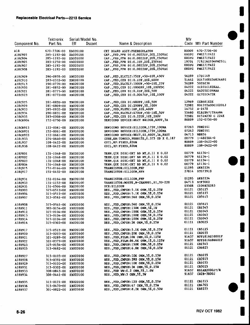
Replaceable Elect rical Parts-2213 Service
8_26
REVOCT 1982
Com ponent Νο .TektronixPart Νο .
Serial/Model Νο .Eff Dscont Name & Descri ption
M frCode M fr Part Num ber
Α18 670-7706-00 ΧΒ020100 CKT BOARD ASSY :PREREGULATOR 80009 670-770δ-00A18C903 285-1192-00 ΧΒ020100 CAP .,FXD,PPR DI :0.0022UF ,20%,250VAC OOOFG ΡΜΕ271Υ422A18C904 285-1192-00 ΧΒ020100 CAP .,FXD,PPR DI :0.0022UF ,20%,250VAC OOOFG ΡΜΕ271Υ422A18C905 285-1250-00 ΧΒ020100 CAP .,FXD,PPR DI :O . lUF,20%,250VAC 19701 719J16G104PM251LA18C907 285-1192-00 ΧΒ020100 CAP .,FXD,PPR DI :0.0022UF ,20%,250VAC OOOFG ΡΜΕ271Υ422A18C908 285-1192-00 ΧΒ020100 CAP .,FXD,PPR DI :0.0022UF ,20%,250VAC OOOFG ΡΜΕ271Υ422
A18C909 290-0978-00 ΧΒ020100 CAP .,FXD , ELCTLT :75UF ,+50-10%,450V 56289_ 17D1149A18C910 283-0335-00 ΧΒ020100 CAP .,FXD ,CER DI :O . IUF ,20%,600Υ 51642 UC47100Z5U824NPSAlSC913 290-0770-00 ΧΒ020100 CAP.,FXD ,ELCTLT : l00UF ,+50-10%,25V 56289 502D230A18C920 281-0852-00 ΧΒ020100 CAP .,FXD ,CER DI :1800PF ,10%,100VDC 04222 GC101C182KAA.A18C921 281-0775-00 ΧΒ020100 CAP .,FXD ,CER DI :O . IUF ,20%,50Υ 04222 SA205E104MAAA 18C923 281-0772-00 ΧΒ020100_ CAP .,FXD ,CER DI :0 .0047UF ,10%, IOOV 04222 GC701C472K
A18C925 281-0820-00 ΧΒ020100 CAP .,FXD ,CER DI :680PF ,10%,50V 12969 CGB681KDXA18C929 281-0809-00 ΧΒ020100 CAP .,FXD ,CER DI :200PF ,5% . I OOV 72982 8013T2ADDCIG201JA 18C933 285-0932-00 ΧΒ020100 CAP .,FXD ,PLSTC : IUF ,10%,400V 14752 Α-1478A18C934 290-0831-00 ΧΒ020100 CAP .,FXD ,ELCTLT:470UF ,+50-10%,50V 55680 ULBlH471TKAANAA18C935 283-0208-00 ΧΒ020100 CAP .,FXD ,CER DI :0 .22UF ,10%,200Υ 72982 815 ΙΝ230 C 224ΚA18CR904 152-0750-00 ΧΒ020100 SEMICOND DEVICE :RECT ΒΑΙDGΕ ,600Υ ,3Α 80009 152-0750-00
A18CR913 152-0061-00 ΧΒ020100 SEMICOND DEVICE :SILICON ,175V ,100MA 07263 FDR2161A18CR931 152-0061-00 ΧΒ020100 SEMICOND DEVICE :SILICON ,175V ,100MA 07263 FDH2161A18CR933 152-0661-00 ΧΒ020100 SEMICOND DEVICE :RECT,S I ,600V ,3A,FAST 04713 MR856A18L933 276-0640-00 ΧΒ020100 CORE,EM :TOROID ,FERRITE ,0 .375 OD Χ 0 .187 00779 1-480304-0A18L937 108-0422-00 ΧΒ020100 COIL,RF :FIXED,82UH 80009 108-0422-00A18L938 108-0422-00 ΧΒ020100 COIL,RF :FIXED,82UH 80009 108-0422-00
Α18Ρ801 131-1048-00 ΧΒ020100 TERM.QIK DISC :CKT BD ΜΤ ,0.11 Χ 0 .02 00779 61134-1Α18Ρ802 131-1048-00 ΧΒ020100 TERM.QIK DISC :CKT BD ΜΤ ,0.11 Χ 0 .02 00779 61134-1Α18Ρ803 131-1048-00 ΧΒ020100 TERM.QIK DISC:CKT BD ΜΤ ,0 .11 Χ 0 .02 00779 61134-1Α18Ρ804 131-1048-00 ΧΒ020100 TERM.QIK DISC :CKT BD ΜΤ ,0.11 Χ 0 .02 00779 61134-1A18Q915 151-0164-00 ΧΒ020100 TRANSISTOR :SILICON,PNP 01295 SKB3334A18Q917 151-0432-00 ΧΒ020100 TRANSISTOR :SILICON,NPN 27014 ST07391D
A18Q931 151-0164-00 ΧΒ020100 TRANSISTOR :SILICON,PNP 01295 SKB3334Α180933 151-1152-00 ΧΒ020100 TRANSISTOR : MOSFE , N-CHANNEL ,SI , TO-220 04713 STP3002A18Q935 151-0506-00 ΧΒ020100 SCR :SILICON 03508 C106B2X283A18R903 315-0512-00 ΧΒ020100 RES .,FXD ,CMPSN :S .1K ΟΗΜ ,5%,0 .25W 01121 CB5125A18R904 315-0512-00 ΧΒ020100 RES .,FXD ,CMPSN :5 .1K ΟΗΜ ,5%,0 .25W 01121 CB5125A18R907 315-0561-00 ΧΒ020100 RES .,FXD ,CMPSN :560 ΟΗΜ,5%,0.25W 01121 CB5615
A18R908 315-0561-00 ΧΒ020100 RES .,FXD ,CMPSN :560 ΟΗΜ,5%,0 .25W 01121 CB5615Α18Α911 303-0154-00 ΧΒ020100 RES .,FXD ,CMPSN :150K ΟΗΜ ,5%,1W 01121 GB1545Α18β912 315-0104-00 ΧΒ020100 RES .,FXD ,CMPSN : l00K ΟΗΜ ,5%,0 .25W 01121 CB1045A18R913 315-0104-00 ΧΒ020100 RES .,FXD ,CMPSN : l00K ΟΗΜ ,5%,0 .25W 01121 CB1045A18R914 315-0104-00 ΧΒ020100 RES .,FXD ,CMPSN : l00K ΟΗΜ ,5%,0 .25W 01121 CB1045A18R916 315-0302-00 ΧΒ020100 RES .,FXD ,CMPSN :3K ΟΗΜ ,5%,0 .25W 01121 CB3025
A18R917 315-0512-00 ΧΒ020100 RES .,FXD ,CMPSN :5 .1K ΟΗΜ ,5%,0 .25W 01121 CB5125A18R920 315-0203-00 ΧΒ020100 RES .,FXD ,CMPSN :20K ΟΗΜ,5%,0.25W 01121 CB2035Α18Α921 321-0289-00 ΧΒ020100 RES .,FXD,FILM:1OK ΟΗΜ,1%,0 .125W 91637 MFF1816GI0001 F
A18R922 321-0379-00 ΧΒ020100 RES .,FXD,FILM:86 .6K ΟΗΜ ,1%,0 .125W 91637 MFF1816G86601FA18R923 315-0154-00 ΧΒ020100 RES .,PXD ,CMPSN :150K ΟΗΜ ,5%,0 .25W 01121 CB1545A18R925 315-0682-00 ΧΒ020100 RE S .,FXD ,CMPSN :6 .8K ΟΗΜ ,5%,0 .25W 01121 CB6825
A18R927 315-0103-00 ΧΒ020100 RES .,FXD ,CMPSN :10K ΟΗΜ,5%,0.25W 01121 CB1035A18R928 315-0391-00 ΧΒ020100 RES .,FXD ,CMPSN :390 ΟΗΜ,5%,0.25W 01121 CB3915A18R929 315-0103-00 ΧΒ020100 RES .,FXD ,CMPSN :10K ΟΗΜ ,5%,0.25W 01121 CB1035A18R931 315-0302-00 ΧΒ020100 RES .,FXD ,CMPSN :3K ΟΗΜ ,5%,0 .25W 01121 CB3025A18R933 308-0843-00 ΧΒ020100 RES .,FXD WW:0.2 ΟΗΜ ,5Χ ,1 .Οω 91637 RSIAR2000JT/β
A18R934 308-0441-00 ΧΒ020100 RES .,FXD ,WW:3 ΟΗΜ,5%,3W 91637 CW2B-3ROOJ
A18R935 315-0121-00 ΧΒ020100 RES .,FXD ,CMPSN :120 ΟΗΜ,5%,0.25W 01121 CB1215A18R936 315-0470-00 ΧΒ020100 RES .,FXD ,CMPSN :47 ΟΗΜ ,5%,0 .25W 01121 CB4705A18R937 301-0822-00 ΧΒ020100 RE S .,FXD ,CMPSN :8 .2K ΟΗΜ ,5%,0 .50W 01121 ΕΒ8225

ιιιι0
ιιιιιιιιιιιιι ιι
REV OCT 1982
Replaceable Electrical Parts-2213 Service
8-27
Component Νο .TektronixPart Νο .
Serial/M odel Νο .Eff Dsco n t Name & Description
MfrCode Mfr Part N umber
Α18ΑΤ901 307-0350-00 ΧΒ020100 RES .,THERMAL :7 .5 ΟΗΜ ,10Χ ,3 .9Χ/DEG C 15454 75DJ7R5R0220SSA18RT902 307-0350-00 ΧΒ020100 RES .,THERMAL :7 .5 ΟΗΜ ,10%,3 .9Χ/DEG C 15454 75DJ7R5R0220SSΑ18Τ901 120-1449-00 ΧΒ020100 XFMR,COM MODE : 02113 Ρ104Α18Τ907 120-1441-00 ΧΒ020100 TRANSFORMER,RF:POT CORE 09969 OBDΑ18Τ933 120-1439-00 ΧΒ020100 TRANSFORMER,RF :ENERGY STORAGE 20462 OBDA18U920 156-1627-00 ΧΒ020100 MICROCIRCUIT,LI :POWER WIDTH MODULATED CONT 01295 TL594CN
A18VR917 152-0166-00 ΧΒ020100 SEMICOND DEVICE :ZENER,0 .4W,6 .2V,5% 04713 SZ11738A18VR935 152-0255-00 ΧΒ020100 SEMICOND DEVICE :ZENER,0 .4W,51V ,5% 80009 152-0255-00

Replaceable Electrical Parts-2213 Service
8-28
00779 61134-100779 61134-100779 61134-100779 61134-1047 1 3 SPS831781 483 IRF9523
011219163791637916379163775042
916370112105347501578000980009
04713 SZG35009K3
670-7498-00ΡΜΕ271Μ568GP20J-009GP20J-OO91N4152RMDL 1/2
RSlAR2000JT/RΕΒ2035C56-20ROJ2D1595152-0268-00152-0286-00
77820 9663-177820 9663-113511 31-27913511 31-279
ΕΒ2035MFF1816G511 ROFMFF1816G280ROFMFF1816GI000OFMFF1816G374ROFBW20-R2700J
NT-34NT-34
54937 5002282
IRF9523
84Α1Α-Β20-J13
154-0838-00
ι
Component Νο .TektronixPart Νο .
Serial/Model Νο .Eff Dscont Name & Desc ription
Α19 670-7498-00 Β010100 Β020099Χ CKT BOARD ASSY:CURRENT LIMITA 19C938 285-1222-00 Β010100 Β020099Χ CAP .,FXD ,PLSTC:0 .068UF ,20%,250ΥA 19CR932 152-0782-00 Β010100 Β020099Χ SEMICOND DEVICE :RECTIFIER,S ILICON ,600VA19CR934 152-0782-00 Β010100 Β020099Χ SEMICOND DEVICE :RECTIFIER,S ILICON ,600VA19CR935 152-0141-02 Β010100 Β020099Χ SEMICOND DEVICE :SILICON,30V ,150MAΑ19Σ937 159-0032-00 Β010100 Β020099Χ FUSE ,CARTRIDGE:3AG,0 .5A ,250V ,SLOW-BLOW
Α19Ρ801 131-1048-00 Β010100 Β020099Χ TERM .QIK DISC :CKT BD ΜΤ ,0 .11 Χ 0 .02Α19Ρ802 131-1048-00 Β010100 Β020099Χ TERM .QIK DISC :CKT BD ΜΤ ,0.11 Χ 0.02Α19Ρ803 131-1048-00 Β010100 Β020099Χ TERM .QIK DISC :CKT BD ΜΤ ,0.11 Χ 0 .02Α19Ρ804 131-1048-00 Β010100 Β020099Χ TERM.QIK DISC :CKT BD ΜΤ ,0 .11 Χ 0 .02Α190933 151-0736-00 Β010100 Β020099Χ TRANSISTOR :SILICON,NPNΑ190938 151-1141-00 Β010100 Β020099Χ TRANSISTOR :SILICON,N-CHANNEL,FET
Α19Α933 301-0203-00 Β010100 Β020099Χ RES .,FXD ,CMPSN:20K ΟΗΜ,5%,O .SOWΑ19Α935 321-0165-00 Β010100 Β013199 RES.,FXD,FILM:511 ΟΗΜ ,1%,0 .125WA19R935 321-0140-00 Β013200 Β020099Χ RES .,FXD,FILM :280 ΟΗΜ ,1%,0 .125WA19R936 321-0193-00 Β010100 Β013199 RES.,FXD,FILM:lK ΟΗΜ,1%,0.125WΑ19Α936 321-0152-00 Β013200 Β020099Χ RES .,FXD,FILM :374 ΟΗΜ ,1%,0 .125WA19R937 308-0710-00 Β010100 Β013199 RES .,FXD ,WW:0 .27 ΟΗΜ,10%,1W
Α19Α937 308-0843-00 Β013200 Β020099Χ RES .,FXD WW:0 .2 ΟΗΜ ,5%,1 .OWA 19R938 301-0203-00 Β010100 Β020099Χ RES .,FXD,CMPSN :20K ΟΗΜ ,5%,0 .50WA19R939 308-0123-00 Β010100 Β020099Χ RES .,FXD ,WW:20 ΟΗΜ,5%,5WA19RT935 307-0125-00 Β010100 Β020099Χ RES .,THERMAL:500 ΟΗΜ , ΙΟΧ ,25 DEG CA19VR933 152-0268-00 Β010100 Β013199 SEMICOND DEVICE : ZENER,0 .4W ,56V ,5%A19VR933 152-0286-00 Β013200 Β020099Χ SEMICOND DEVICE : ZENER,0 .4W,75V,5%
A19VR934 152-0149-00 Β010100 Β020099Χ SEMICOND DEVICE : ZENER ,0 .4W,10V ,5%
CHASSIS PARTS
C401 281-0787-00 CAP .,FXD ,CER DI :15PF,5%,500V
DL350 119-1392-00 DELAY LINE,ELEC :100 ΝΑΝΟ SEC,150 OHM
Σ901 159-0021-00 Β010100 Β020099 FUSE ,CARTRIDGE :3AG,2A ,250V,FAST-BLOWΣ901 159-0019-00 Β020100 FUSE ,CARTRIDGE :3AG, lA ,250V ,SLOW BLOWΣ937 159-0032-00 Β010100 Β020099Χ FUSE ,CARTRIDGE :3AG,O .SA ,250V ,SLOW-BLOW
FL9001 119-1541-00 ΧΒ020100 FILTER,RFI :IA,250VAC
J 1001 131-0126-00 CONNECTOR,RCPT, :BNC, FEMALEJ2001 131-0126-00 CONNECTOR,RCPT, :BNC, FEMALEJ4001 131-0955-00 CONN,RCPT,ELEC :BNC,FEMALEJ8001 131-0955-00 CONN,RCPT,ELEC :BNC,FEMALE
L925 108-1096-00 Β010100 Β020099Χ COIL,RF :FIXED ,16MH ,25%
Q938 151-1141-00 Β01ΟΙΟΟ Β020099Χ TRANSISTOR:SILICON,N-CHANNEL,FET
R658 311-2158-00 RES .,VAR ,WW :PNL ,5K ΟΗΜ ,5%,1W
V870 154-0838-00 ELECTRON TUBE :CRT ,T4652-31-2

Symbols
DIAGRAM S AND CIRCUIT BOARD ILLUSTRATION S
Graphic symbols and class designation letters arebased on ANSI Standard Υ32.2-1975.
Logic symbology is based on ANSI Υ32.14-1973 interms of positive logic. Logic symbols depict the logicfunctio n performed and may differ from the manufac-turer's data.
The overli ne on α signal name indicates that the signalperforms its intended function when it is in the low state.
Abbreviations are based on ANSI Υ1 .1-1972.
Ot her ANSI stand ards that are used in the preparationof diagrams by Tektronix, I nc. are:
The information and s pecial symbols
Assembly Numbers and Grid Coordi nates
Each assembly i n t he i nstrument is assigned anassembly number (e.g ., Α20) . T he assembly numberappears on the circuit board outli ne on thed iagram, i n thetitle for the circuit board component location illustration,and i n the lookup table for the schematic diagram andcorrespondin g component locator illustration . TheReplaceable Electrical Parts list is ar ranged by assembliesi n numerical sequence ; the components are listed bycomponent number "(see followi ng illustration forconstructing α component number) .
Cam SwitchClosure Chart(Dot indicatesswitch closure)
Etched Circuit Board
__Outlined in Black
Refer to W aveform
Function Block . . .. . ...O utline
IC type -"-- - _
Test Voltage --------
Heat Sink
Board Name
Assembly Number-
Tektronix Part Νο . _ .�for circuit boards _-1υ - - . :
_-3 Λ, ζ R12-34
1-1-1-1-1-.111_111 ι1
Υ14.15, 1966
Drafti ng Practices.Υ14.2, 1973
Line Conventions and Letteri ng.Υ10.5, 1968
Letter Symbols for Quantities Used i nElectrical Scien ce an d ElectricalEngi neering.
Component Values
Electrical components shown on the diagrams are i nthe following units unless noted ot herwise :
Capacitors = Values one or greater are i n picofarads (pF) .V alues less t han one are in microfarads(ΝF) .
Resistors = Ohms (Ω) .
below may appear in t his manual.
The schematic diagram and circuit board componentlocation ill ustration have grids. Α lookup table with thegrid coordinates is provi ded for ease of locatin g thecomponent. Onlythecomponents illustrated on thefacingdiagram are listed in the lookup table . When more thanoneschematic diagram is u sed-to illustrate the circuitry onα circuit board, the circuit board ill ustration may onlyappear opposite the first diagram on which it was il-l ustrated; t he lookup table will list t he diagram number ofother diagrams that the circuitry of the circuit boardappears on .
American National Stan dard I nstitute1430 Broadway
New York, New York 10018
SYNC GENER ATOR
τες
SYNC
Modified Component-SeeParts List (Depicted in grey,or with grey outline)
Plug to E.C . B oardi100
Βοχ - Identifies Panelοπ r ols, Connectors andI ndicators
Coaxial connectors:malefemale
Pl ug I ndex ; signifies p i n Νο. 1
S hielding
Selected value, see Parts Listand Maintenance Section forSelection Criteria
Schematic Nameand Number

RESISTORS
COLOR COD E
COMPOSITION
SMALL DISCCA PACITORS
υ CERAMICCA PACITORS
and 0- 1st, 2nd, and 3r d sign ificant figu res
-m u ltiplie r
0-tolerance
a-temp erat u re coefficientΟ and/or
TC
colo r code may not be present0-p olarity and voltage rating
on some cap acitors
F igure 9-1 . Colo r co des fo r resistors and capacitors.
REV DEC 1981
DI PPEDTANTALUMELECTROLYTICS
(1861-20Α) 2662-48
CO L OR SIGN I F ICANT RESISTORS CAPACITORS DIPPEDF IGURES MUL TIPL I ER TO LERANCE MUL TIPL I ER TOLERANCE TANTA LUM
VOLTAGEover 10 pF und er 10 pF RATI N G
BLACK 0 1 --- 1 ±20% ±2 pF 4 V DCBROWN 1 10 ±1% 10 ±1% ±0.1 pF 6VDC
RED 2 102 or 100 =2 ο% 102 or 100 ±2% --- 10 VDCORANGE 3 103 or 1 Κ ±3 ο/ο 103 or 1000 ±3ο/ο --- 15 V DC
YELLOW 4 104 or 10 Κ ±4 ο/ο 104 or 10,000 +100%-9% --- 20 VDC
GREEN 5 10 5 or 100 Κ ='/s% 10 5 or 100,000 ±5 ο/ο ±0.5 pF 25 V DC
BLUE 6 106 or 1 Μ ±/αο/ο 106 or 1,000,000 --- --- 35 VDC
VIOLET 7 --- -11/10% --- --- --- 50 VDC
GRAY 8 --- --- 102 or 0.01 +80% -20% ±0.25 pF ---
WH ITE 9 --- --- 10ι or 0.1 ±10% ±1 pF 3 VDC
GOLD - 10-1 or 0.1 ±5ο/ο --- --- --- ---
SILVER - 10-2 or 0.01 ±1 00/. --- --- --- ---
NONE - --- ±20ο%ο --- ±10% +1 F = --

Β
TRANSISTOR
METAL CASE -JTRANSISTORS
PUT FET
Α G Κ
Q921
TR IAC
FLAT PACK
PLASTICCAS E
TRANSISTORS
Q940 &
Q925
U9Q942
85
REGULATOR
INTEGRATED CI RCUITS
NOTELEAD CONFIGURATIONS AND CASE STYLES ARE TYPICAL, BUT MAYVARY DUE TO VENDOR CHANGES OR INSTRUMENTMODIFICATIONS.
711 &712
ι(3826-17)3827-55
Fig ur e 9-2. Semiconductor lead configu rations.
C
τ t ι
ms-2213 ServiceΗmη
ι
Ε Β
9
Οzιον
α
Section 9-Diagra

2213 Service
To identify any componentmounted on α circuit board andto locate that component in theappropriate schematic diagram
οσαΟm
συα
PULL OUT PAGETABS FOR CIRCUIT
BOARD ILLUSTRATION
5 . Locate the Component on the Circuit Board
1 . Locate the Circuit Board Illustration
α .
b .
In the instrument identify the Assembly Number of thecircuit board in question . The Assembly Number is usuallyprinted on the upper left corner of the circuit board on thecomponent side .
In the manual locate and pull out tabbed page whose titlecorresponds with the Assembly Number of the circuitboard . Circuit board assembly numbers and boardnomenclature are printed on the back side of the tabs(facing the rear of the manual) .
In the manual, locate and pull out the tabbed page whosetitle and Assembly Number correspond with the desiredcircuit board . This information is on the back side of thetabs .
b.
Using the Circuit N umber and grid coordinates, locatethecomponent on the Circuit Board Illustration .
c .
In the circuit board location illustration, determine thelocation of the circuit board in the instrument .
d.
Find the circuit board in the instrument and compare itwith its illustration in the manual to locate the desiredcomponent on the board.
e 67.4CRT ΟσιιΛ εαπγσπιΜ ΙαιΙΙαι.
ΎΤRl`Γ~
2 . Determine the Circuit Νιω
α .
Compare the circuit b αιthe desired εοmφrwttion .
b .
Scan the table adjacentlfind the Circuit Νυmb ιι
ε .
Determine the Schemrcomponent is located
η6 ι
ASSEMBLY NUMBER
ILLUSTRATIONANDCIRCUIT INSTRUMENTCIBOARD NAME
BOARD LOCK
4 . Determine the Circuit Board Illustration and CοnVeLocation
α .
From the schematic diagram, determine the AmNumber of the circuit board on which the εοmρρmounted . This information is boxed and locatedinsof the heavy line that distinguishes the board oud
b.
Scan the Component Location Table for the AmNumber just determined andfind t he Circuit Νυmbιιdesired component.
ε .
Under the BOARD LOCATION column, read tΛcoordinates for the desired component .
Figure 9-3 . Locating components on schematic diagrams so

erm ine the Assembly>Iich t he component isand λocated in α corner
t the board outli ne .
ι the Circu it Num be r
o r e the ci r cuit board with its ill ust r ation and locate(sired componen t by a rea and shape on t he ill u st r a-
I hetablea dj acenttothe Ci r cu it Board Ill u st r ation a nd
he Ci r cu it Number of t he desi red component .
In i ne the Schematic Diag ram Number in w h ich t heanent is located .
ILLUSTRATION FORTRUMENT CIRCUITBOA RD LOCATION
diagrams and ci rcu it boa rd ill u strations .
MANUAL BINDERΙ Α6 ASSEMBLY
MANUAL B INDER
2
3
4
ν
Α
2 0668 R625C603 C641 R 626
C643 R604 R 627C671 C651 R605 R630
ColC615 R 608 R632C616 0606 R609C617 0610 R610C618 0615 R614C619 0645 R616
r
C624 0656 R623C626 0665 R624
COMPONENTS LOCATED ΟΝ SCHEMATIC DIAGRAM
C670 Q670 R 677C671 0672 R679C673 Q673 R680C680C681 R 671 U617Ρ603 R 673 U618Ρ607 R 674 U 619Q669 R675
CIRCUIT SCHEM BOAR D CIRCUIT SCHEM BOARDNUMBER LOCATION LOCATION NUMBER LOCATION LOCATION
Ι3C Q656 2F 2 Θ
CW3 1C 1G ι 0665 1G 18C609 4E « Q668 Ι 2G 2 ΒC612 7C 3EC615 7C 3D Α604 4C 1EC616 2C 3C R605 5 υ 1EC617 7D 3D R608 4E 1υC618 7E 3E R 609 4E 2DC619 6E 3C R610 78 3EC624 4 F 3D R 614 7C 3DC626 7G 2D R616 1C 3D
- R623 40 2EC643 3D 4Β ν R625 7F 2DC 51 3Ε 3 Β 'r 7 F 2D
θ R627 7G 1Dεεσ30
Q606 αε 2DQ610 7C 3D ΤΡ624 3Β 2DQ615 7D 3D0645 3E 3 Β U615 1D 3C
CHASSIS MOUNTED PARTS
CI RC U IT SCHEM BOARD CIRCU IT SCHEM BOARDNUMBER LOCATION LOCATION NUMBER LOCATION LOCATION
L 635 51 C H ASSIS V635 6J C H ASSIS

3 . Locate the Component on the Schematic Diagram
α .
Locate and pull out tabbed page whose number and titlecorrespond with the Schematic Diagram Number justdetermined i n thetable . Schematic diagram nomenclatureand n umbers are printed on the front side of the tabs(facing the front of the manual) .
b.
Scan the Component Location Table adjacent to theschematic diagram and find t he Circuit N umber of thedesired component .
ε .
Under the SCHEM LOCATION column, read the gridcoordinates for the desired component .
d.
Using the Circuit Number and grid coordinates, locatethecomponent on the schematic diagram .
To identify any component in αschematic diagram and to locatethat component on its respectivecircuit board .
PARTIAL Α6 CRT CIRCUIT BOARD
CRT CIRCU IT ιο
3516-81
PULL OUTPAGE TABS
FOR SCHEMATICDIAGRAMS
π
πzπc
SCHEMATIC DIAGRAMNAME AND NUMBER

ι
SLOPE
CH 1 HIGH-ΖATTENUATORAND INPUTCOUPLING
CH 2 HIGH-ΖATTENUATORAND INPUTCOUPLING
CH 1BUFFER AWLQ122, Q1250133, Q134Q139, U 120
CH 2BUFFER AWLQ222, Q225Q233, 02340239, U22θ
ETRIA
Qt 1
Q
CH 1LOW-Ζ
ATTENUATORR139
CH 2LOW-Ζ
ATTENUATORR239
CH 1Χ1/Χ1 θAWLU 146
CH 2Χ1/Χ10AWLU245
CH 1+
CH 2-
CH 2+
ι CH 1 ΡRΕΛΜΡ0157, Q1 β7U17ΘD , Ε
INTERNALTRIGGERPICKOFF
Q173, Q273
CH 2 TR IG+
U170A , Β C
CH 2 ΡRΕΛΜΡ
U197Λ Β D ,Ε
Q258
U270Α ώ PCQ257)0257, 0268U2700 ,E
Ι
CH 1 TRIG-
ΕΧΤCOUPLING
INTERNAL TRIGGER -
CH 2 TR IG-
ΥΑR HOLOOFF
_ΙΝΤ
LINEΕΧΤ
CH 1-
CH 1 AND CH 2VERTICAL PREAMP
CH 1 TR IG+
R557
CH 1 O R Χ
CH 20R Y
ΕΧΤINPUT
S44θSOURCE
S4β4
Sβ11TRIGGERMODE
LEVEL
ΛC-GNO-DC
πυΤ
NOR
TVFIELD
S201
S4θ 1
AC-DC-DC+10
F igure 9-4. 2213 block diagram.
5105
S205
CH 2VOLTS/DIVSWITCH
INVERTS2β4
INTERNAL TRIGGER +
R658
HORIZONTALMODE
S65θ
.5μs
ΝΟ αΥ
αΥ -ο
ΙΝτεΝS
XTGGER υ
t,WL ~ ά1 Λ ,Θ ~ ~
14 χ iω
INTERNALTRIGGER X-AXIS SIGAWL
U421 Α Β C D Ε
TRIGGER
TRIGGER SOURCE TRIGGER TV TRIG SCHMITTDIODE LEVEL AND TR IGGER TRIGGERSWITCHING _ COMPΛRΛTOR INVERTIN AND LEVEL
CRt18 , CR440 U4 β0Λ Β C , AWL SH IFTERCR444 , CR448 D ,Ε ,F Q474 Q492, Q493
Q47β U48θΛ B ,DSLOPE U48θC
Ι mΙ LEVEL
ωRt551 >- AUTO
BASEL INE AUTOAUTO DISABLE Q605 BASEL INE
Uβ4θΛ
αωυ zυυάΗ Ν
_i ΧΙ
S660Χ
DE AYTIME
Χ28
MULTIPLIER

R629CAL
HOLDOFFR557
SWEEPLOGIC
1603Λ ,Β(Ιθ7Α , Θ ,C
HOLDOFF TIMING
SWP GATE
ω
υαsΝ
U64013
r r
CH 1
οzωr<ωο
POSITION
SWEEPLOGICGATINGU62θ
ALT SYNC
END-OF-SWEEPCOMPARATOR
0640
DELAY TIME0624, Q632Q644, 0650
0652
SWEEP GENERATORAND LOGIC
Z-AXISI NPUT
BEAMF I ND
S39θ
υ
L INE TRI GGER
I NTENS LEVEL
AUTO INTENSITYAND Z-AXIS
DELAY LINEDRIVER
Q331, Q336Q341, Q345
ADD ENABLEQ31 βU197CU315A
zz
Φa-0τυ
Χ-AX IS S IGNAL
INTERNALTRIGGER
SWITCHINGLOG IC
U3θ5Λ , θ ,C ,DU3158 ,C
M ILLER SWEEPSWEEPSWP RETRACE Q63ΘΑ ,Β
Q631
SWP DUTY
AUTOAUTO 1 I NTENS ITY
Q811 , Q812 ixSWP DUTY Q813
U825 B ,CU835A ,Β
Z-AXIS GATEI NTENS LEVEL Z-AXIS
U6070 ι CR619Ζ-DR IVE Ζ-DRIVE
AMPLIF I ERCR620 , CR621 Q841, Q844CR622, CR663 Rβθ7 0845, Q847
AUTO INTENSITY Q85θ
Q278 CH 2-
CH 2 POS ITION
CH 1 TRIGCH 2 TRIG
CH 1 ΕΝΛΒLΕCH 2 ΕΝΛΒLΕ
CH 1BOTH CHANNEL
S315CH 2 SWITCHING ALT SYNCS317 LOGIC
TIMING SW ITCH XY VERTICAL ADD U310AMODE ALT U3
17A
ΤΙΜΙΝG ΧΥSWITCHTCH AUTO Ι CHOPAND RC CHOP OSC ILLATORS63θ CHOP AND CHOP BLANK ING
ω U31 θΒ ιC ,DU3178
Σο Νυ=Ιτ
υ υrc
z zΣΗ Η
CH 1+COMMON-BASEπΜΡΙ f1
CHANNEL SWITCHAND VERTICAL OUTPUT
Q177 R 19θ
Q178 CH 1- CHANNELERNΛL DIODE GATEWERWFF CH IG CR177, CR 178
ι Q273 j_ CH 2 TRIGCR187, CR I BB
1 ΛWιθ ,C CR277 , CR2781 ιθ ,D , Ε CH 2+ CR287 , CR288
1 Λ ιΒ ,C COMMON-Τγ BASE R290
ΛΜΡLQ277
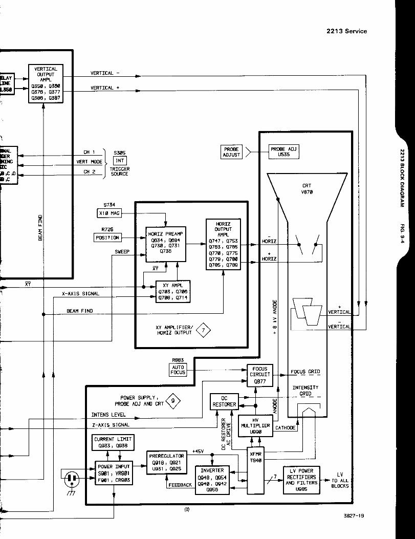
VERTICALOUTPUT
ΛΜΡLQ35θ , Q38θQ37β , Q377Q38β , Q387
IELJ1 Υ
CH
VERTICAL -
VERTICAL
CH 2
S734
S305ΙΝΤ
TRIGGERSOURCE
POWER SUPPLY,PROBE ΛDJ AND CRT
INTENS LEVEL
Z-AXIS S I GNAL
CURRENT LIMITQ933, Q938
ΧΥ ΛΜΡLQ7θ3, Q7θβQ7θ8, Q714
ΧΥ AMPL I F IER/HORIZ OUTPUT
R883AUTOFOCUS
+ηςγ
PROBEADJUST
HORIZOUTPUTΛΜΡL
Q747, Q753Q703, Q705Q770 i 0775Q779, Q78θQ785 ι Q789
2213 Service
3827-19

Crt
2213 Service
TEST WAVEFORM AND VOLTAGE SETUPS
WAVEFORM MEASUREMENTS
On the left- hand pages preceding the schematicd iagrams are test waveform illust rations that are intendedto aid in trou bleshooting the instrument . To test thei nst ru ment fo r these waveforms, make the initial controlsettings as follows:
AUTO INTENSITY
Visible displayAUTO FOCUS
Best focused d isplay
Vertical (Both Channels, if applicable)
Horizontal
POSITION
MidrangeΧ10 MAG
Off ( button in )
HORIZONTAL MOD E
ΝΟ DLY
SEC/DIV
.5 ms
SEC/DIV Variable
CAL detent
Trigger
SLOPELEVELMODEΙΝΤSOURCEVAR HOLDOFF
fMidrangeAUTOVERT MODEΙΝΤM i n (fu lly ccw)
REV DEC 1981
Changes to the control setti ngs fo r specific waveformsare noted at the beginning of each set of wavefo rms . I nputsignals and hookups requ iredare also indicated, if needed,fo r each set of waveforms.
DC VO LTAGE MEASUREMENTS
Typical voltage measurements, located on th eschematic diagram, were obtained with the inst rumentoperating u nder the cond itio ns specified in t he WaveformMeasurement setup . Co ntrol-setting changes required forspecific voltages are indicated on each waveform page.Measurements are referenced to chassis grou nd with theexception of t he Preregu lato r and Inve rte r voltages ond iagram 9. Th ose voltages a re referenced as i ndicated ont he schematic d iagram .
CH 2 INVERT Off ( button out)
VOLTS/DIV 10 mV RECOMMENDED TEST EQU IPMENTVOLTS/DIV Variable CAL detent
AC-G ND-DC GNDTest equipment listed i n Ta ble 4-1 in the "Perfo rmance
POSITION Display Centered C heck Procedure" section 4 of this manual, meets theVERTICAL MODE CH 1 requ ired specifications for testing th is instrument .

POWER SUPPLY ISOLATION PROCEDURE
Each regulated supply has nume rous feed points to external loads throughout the instrument. The powerd istribution diag ram is used in conjunction with the schematic diag rams to determine those loads that can beisolated by removing service jumpers and those that ca nnot .
The power dist ribution diagram is divided i nto ci rcu it boards . Each power supply feed to α circu it board isindicated by the schematic diagram number on which the voltage a ppears. Theschematic diagram grid locationof α service jumper or component is given adjacent to thecomponent number on the power distr ibution d iagram .
If α power supply comes up afte r lifting one of the main j umpers from the power supply to isolate that supply, itis ve ry probable that α short exists in the ci rcu it ry on that supply li ne. By lifti ng jumpers fa rth er down the line, theci rcu it in which α short exists may be located.
Typical resistance values to ground from the regulated su pplies output as measured at the supply test pointsare:
Resistance values significantly lower may i ndicates shortedcomponents in the load. Val ues will vary betweeni nstruments .
Always set the POWER switch to OFF before solder ing or unsoldering service jumpers or other componentsan d befo re attempting to measure components resistance values .
-8.6 V 114 0 at ΤΡ500+8.6 V 95 Ω at W975+5 V 330 Ω at W985+30 V 905 Ω at W965
+100 V 12.5 kΩ at W966

FROMPOWSUPPLYR
+10Ον -
+3Ον ,
-8.6νW9τώ/~bJ
\N96S3S
W2974ι
C91
W9 J~7 R9JΟ
HORIZ. ν ANDλΓι
PULL-UP
~Ce50 ~9gΚ~
C~μΡUίο
AMPL
ν
ν
~-y+8.6υ4W985
C431 ΙΝ7 Τ4 ΙG_(.3
7Ο
BUFFER _
Οωθ ο® SWITCH+5V _
AUTOWSSb
ΙΝΤΕΝSΙΤΥbJ
Ι
ννΓο Ζ©W 4©
TRG
CIRCUITSELEC-T
~ω4ο~~'οΑ1. ιε -sΗΟτ
~ ΡΑατιηL1GΑτΕC01νταοLLGGIG
G317
G310
GΝΟΡ OSG
ΟΟΟ
1~~
VERT CNANwEL SEL Ψ GICΑΝΟ
1 ΝΤ~TRR~~EL LOCIC
- 8"bνDELAY ίοΝΕ-SHOT
Ψ -θ~\/\NΘΑ2
G457 Υ
®C4121
C}41 1 Β92
8Ο -Θ. ιcV 3 2Ο 50URGΕΑTRIG ZD ί_
-H.bV
ΡΑ57
COMPΑRATOR®R31D
Ρ4 ρΑ GΑΤΕΟRESEΓ
νυ9rο
Ι
3C+θbν2
~ +8.bυ2CΗΙές~-1Ζ CN Ι L Cμ2
ν (ΡΑΡΤΙΕ ~ΥΕφΡRΕλ)ΛΡ 20
+Β.bν4Χ AXISAMPL
ςμ
-BbνzG2991
~.Φν2
-8"b2
ιΗ ιC Ε Ζ
νΕRΤ_ΑGΤΤ _ ΟΕ1.ΑΥ
ιΙΝΕ Ο
VERTρ
ΡΡΙΕΡΜΡW29 DRIVER Ρ Α
W9~43J
+1001/GRID BIAS
Ο7 ~7799 RWF9
ΟWRSbOΑΝ ID8J +1~V 1 4L +ICOV GFAΜ ΑDJ.ι ι
W` "~Cb_ι ι ιι ι
C-O,-TL
ΗΟRΙΖΟ Τ
Ζ PXIΑ R8Ν3J SJ AMPL
©ca49~ ΟΟ
0
ρ
+=λο\dVERT
ω 9Φ9 \N3Ά ι399Ο3OUTPUT
E31 83 R79B 7Ν ΑΧ\LΒ .ι Ο +~ν
®©CβΚ7
f
ΑΜΡLΖΑΧΙδ©
-θ.ωνAuΤΟ
0CT%~9J _βbνι
HORIZω87E6 ωθ77 Fοωs ω8Α7 RTeb OUTPUT
31 AMPL 9J IDΖ ΑeηΡι9 Ο -8 .6ν
"νεπτ ουτADD FILT E
CRTω299 WI7O
41- 41-
" NUMBERALI_
INΤΤRIG ΡIGΚΖFF ,ρ C1 RCU_R ΝΙΝ
VERT ΙΧ0ΤΡ JΤ ΑΜΡLΟ3 SHOWN ΟΝ~1-1B.
"4/4 CΟΑΛ )ΟΝΕΜΙΝΤ TRIGBUFFER ΟΝ ΤΗΕ ΑΡΛ

NUMBERAL AND LETTER AT COMPONENTCI RCUIT NUMBER IN DICATESGR IDCOORDI N AT E WHERE COMONENTISSHOWN ON ΤΗΕAPPLICABLE DIAGRAM.COMPONENT VALUESARE SHOWN ONLYON ΤΗΕ APPLICABLE DIAGRAM.
-8.6ν νψ
VERT ΑΤΤΣΝ REF ZEUER1ςΤ3
ΒWΕΕΡ '1ΟυΤΑ.Ε RΕFOβι 8ψ FpFiιΖ
1Cgί9OρμΡ
Rσ-Ι9 ΑξΕΙ8L 'tωΕΕΡMULLEFL41 ΙΝ7ΕRGRΑτΟRδ
33Εμz-ι-z ιREV D EC ι gθι
POWER DISTR I BU TIO N

2213
+3oV~Θ.bVι
LB./-V ~-SOR739iR720 ~630Β-6 i
5205 ι
56308-3ι 4 ν
5630B-s
R725 ι
3
ι
λΟ
CλΖλ7ΡθΟΟ6
ί
R89,5
Ι Re ι
Ι
ΧΥ
ηΙ Ιη
~-CR 7034J W702
W630
53 Ι 7-β,53ΙΤ~~~111 3χΥ - Β - Β
53 ι 7-G ΟS264ρ- _75305-β,S3Ου-ς 1ΝVE R 7 ΙR726 ι
vARHOIDOFF
ΙΟ
JIODIGH I
ΙΝΡΙΠ
J200iGH2ΙΝΡυτ
J4001ΕΧΤ
ΙΝΡUΤ
J1000ΡRο~ε 'ADJU~
ΓΙ55Τ
+&6VW
ΗΟRιΖΟΝΤΑ LPo51710U
8"vRG45
R6-
.CR536
ΗPREAMP ουΤ
--5
βFΑΜFIND
q~ιαν W763υ825Α- ιιυ825Β- Ι3
ι
ΑΙ Ι F RΟΝΤ PAN EL BOAR.
ΑΙΟ ΜΑ1Ν ΘΟΑRD
Ο
-764
t U 507A-Ι
TREGGER IR4441>
`_1!
W508
_8453
U5078-7ΟR6ΙΙ ι R525, R517
R7b0
mΟΨ
ΝοCW3 ύ ύ Ι
τ Ζ
Wb001 -5 -9
R 496F"
sezτ-zoREV FED Oat
R637
ΡΙΟΙΟ ιW1011ί, GND -13Ι CH I(,) -i
C4 Ις-ι ~-2GND ~-4
Rz οιο (ω2οι 1G ND - Ι
}' Ι CH 2(+) ~-i
CH 2l-) ~-2}Ι GN D " -4
Ρ7000Ι ω7ΟΟΙ
~-ι _qί~-i

- R760
Fλ
: ςλl
Q35.
ΓR86Β
R 883~ 4387 Q377
RIBS R178Ι
ΙΙι ι ς _ ι
Q360
.Α.ξ .ΟΤΆ1ΟΝ
R99? yΤ94Ο-5 i
-8700
'94Ο-24-
N .C-
NC.-~
ι
ωα7ΟΟ
{λ3-Ti
λzl'1'
R876 C806 R073
C871C076 R00b C873
R071R887 R574 R870 1
Ρ 9 ΟΟΟGR Y
'6\y
(Ε - Ζ
ι 59 ΟΙ -213F901
J9001 Ο
αιυ
Ζ ΑΧΙ5ωΡυ7
J8001
P902S
-S901-4,5
-R801
ANODE+8KV
ΗΙβΗVO LTAG EM ODULE
ρ RG37
R496'" Γ -ΙV V Λ
ΟΟ 1139 ΙT
ύ ύ ύ ύ ύ ΛC_Ι 3 7 ΖΖ1 Ι
ι3
Ο,7600171-7, σ
z3ez7-zo
REV FED 1987- CIRCUIT 90ARD ΙΝΤΣRCΟΝΝΣCΤΙΟΝ5ΛΟΖΙΖmΛΟΖΥ!

2213 Service
2
3
4
5
Α ' Β ~ C ~ D ~ Ε ~ F
Fig ure 9-5. A12-Attenuator/Sweep boa rd .
! R627='- -`
' β733 0629_ω' '
VR629Ι !742 ι m ~
βG86(- W633
R634
3827-31
©Static Se n sitive DevicesSee Maintenance Section
COMPONENT NUMBER EXAMPLE
Component Numb er
Α23 Α2 R1234
Sc hematicAssem bly~~~~ CircuitNumb er Subassem bly Number
Number (if used)
Chassis-mounted components have no Assembly Numb erprefix-see end of Replaceable Electrical Parts List.

Α12-ΑΤΤΕΝUΑΤΟR/SWEEP BOARD
CI RCUITNUMBER
SCHEMNUMBER
CI RCUITNUMBER
SCHEMNUMBER
CI RCU ITNUMBER
SCHEMNUMBER
CI RCU ITNUMBER
SCHEMNUMBER
CI RCU ITNUMBER
SCHEMNUMBER
CIRCU ITNUMBER
SCHEMNUMBER
C104 1 C628 8 Ρ 6000-7 5 R 120 1 R217 1 R691 8
C105 1 C630 5 Ρ 6000-8 7 R 121 1 R219 1 R720 7
C107 1 C636 8 Ρ 6000-9 7 R122 1 R220 1 R721 7
C110 1 C677 8 Ρ 7000-1 8 R123 1 R221 1 R722 7
C111 1 C679 8 Ρ 7000-2 8 R124 1 R222 1 R723 7
C112 1 C720 7 Ρ7000-3 8 R125 1 R225 1 R724 7
C119 1 C732 7 Ρ7000-4 8 R 126 1 R226 1 R725 7
C121 1 C734 7 Ρ7000-5 7 R 127 1 R227 1 R728 7
C123 1 C736 7 Ρ7000-6 7 R 128 1 R231 1 R729 7
C125 1 C738 8 Ρ7000-7 8 R 130 1 R 232 1 R730 7
C132 1 C741 8 Q122 1 R 131 1 R 233 1 R731 7
C133 1 CR 119 1 Q125 1 R132 1 R 234 1 R732 7
ς 134 1 CR 219 1 Q133 1 R 133 1 R 235 1 R733 7
C136 1 CR 626 5 Q134 1 R 134 1 R 236 1 R 734 7
C137 1 CR 630 5 Q139 1 R 135 1 R 237 1 R 736 7
C139 1 Ρ 1010-1 1 Q222 1 R 136 1 R 238 1 R 737 7
C140 1 Ρ 1010-2 1 Q225 1 R 137 1 R239 1 R 738 8
C141 1 Ρ 1010-3 1 Q233 1 R 138 1 R 240 1 R 739 7
C142 1 Ρ 1010-4 1 0234 1 R139 1 R 241 1 R 741 8
C144 1 Ρ2000-10 5 Q239 1 R 140 1 R 242 1 R T144 1
C204 1 Ρ2000-1 1 Q629 8 R141 1 R 243 1 RT244 1
C205 1 Ρ 2000-2 1 Q630 5 R 142 1 R 244 1 S105 1
C207 1 Ρ 2000-3 1 Q631 5 R 143 1 R 245 1 S205 1
C210 1 Ρ 2000-4 1 Q720 7 R144 1 R 246 1 S630 8
C211 1 Ρ 2000-5 1 Q730 7 R 145 1 R 247 1 S734 7
C212 1 Ρ 2000-6 1 Q731 7 R146 1 R248 1 U 120 1
C219 1 Ρ 2000-7 8 Q736 7 R147 1 R 249 1 U145 1
C221 1 Ρ 2000-8 8 R 103 1 R 148 1 R 625 8 U220 1
C225 1 Ρ 2000-9 7 R 105 1 R 149 1 R 626 8 U245 1
C232 1 Ρ 2010-1 1 R 106 1 R 203 1 R 627 8 VR 122 1
C233 1 Ρ 2010-2 1 R 107 1 R 205 1 R 628 8 VR 130 1
C234 1 Ρ 2010-3 1 R 108 1 R 206 1 R629 8 V8222 1
C236 1 Ρ 2010-4 1 R 110 1 R 207 1 R630 5 VR629 8
C237 1 Ρ6000-10 7 R 111 1 R208 1 R631 5 W116 1
C239 1 Ρ 6000-1 5 R 112 1 R210 1 R633 7 W734 7
C241 1 Ρ 6000-2 7 R114 1 R211 1 R636 8C242 1 Ρ6000-3 7 R 115 1 R 212 1 R677 8
C244 1 Ρ6000-4 5 R 116 1 R 214 1 R679 8
C625 8 Ρ6000-5 5 R 117 1 R215 1 R684 7
C626 8 Ρ6000-6 5 R 119 1 R216 1 R686 8

β114
RIOT
-
-
R2 σ 4 * No R207
Rl12
R106
- `
R212
R20bRl15 ω17 ύ
R215
$lose
Figure 9-6. Circuit view of Αl2-Attenuator/Sweep boa rd .
3827-32
©Static Sensitive Devices
See Maintenance Section
COMPONENT NUMBER EXAMPLE
Component Number
Α23 Α 2 R1234γSchematic
ι
Assembly ~T_Τ
Ί.~ CircuitNumber Subassembly Number
Num ber (if used)
Chassis-mountedcomponents have no Assembly N umberprefix-see end of Replaceable E lectrical P arts List.

CH 1 & CH 2 ATTENUATORS
ASSEMBLY Al 1
CIRCUITNUMBER
J 1001J 2001
2Α7Α
CHASSISCHASSIS
R101R201
2Α7Α
CHASSISCHASSIS
Partial Α 1 1 also shown on diagrams 2, 3, 4, 5, 6, 7, 8 and 9 .
ASSEMBLY Al 2
Partial Α 12 also shown on diagrams 5, 7 and 8.
CHASSIS MOUNTED PARTS
SCHEM BOARDLOCATION Ι LOCATION
CIRCUIT Ι SCHEM Ι BOARDNUMBER LOCATION LOCATION
CIRCUIT Ι
SCHEM
I LOCATIONNUMBER LOCATION LOCATIONCIRCUIT Ι SCHEM Ι BOARDNUMBER LOCATION LOCATION
CIRCUITNUMBER
SCHEMLOCATION
BOARDLOCATION
CIRCUITNUMBER
SCHEMLOCATION Ι
BOARDLOCATION
CIRCUITNUMBER Ι
SCHEMLOCATION Ι
BOARDLOCATION
CIRCUITNUMBER Ι
SCHEMLOCATION Ι
BOARDLOCATION
C104 2E 3 Β Ρ 1010-1 2 Ν 18 R 123 8C 18 R225 8 Η 2C
C105 2E 38 Ρ 1010-2 2 Ν 18 R124 61 2 Β R226 9 Η 1C
C107 3E 3 Β Ρ 1010-3 4Ν 1 Β R125 3Η 2Α R227 8 Η 1C
C110 3E 3Α Ρ 1010-4 4Ν 1 Β R126 4Η 1 Β R231 6Η 1C
C111 3E 3Α Ρ2000-1 3C 4Α R127 4Η 1 Α R232 6G 1C
C112 3E 3Α Ρ2000-2 2C 4Α R128 6-1 2D 8233 71 1C
C119 2G 28 Ρ20 Ο0-3 2C 4Β R130 5Η 1 Α R234 8Η 1C
C121 2G 28 Ρ2000-4 7C 4C R131 5Η 1 Α R235 81 2C
C123 8D 1 Β Ρ20 Ο0-5 7C 4C R132 5G 1 Α R236 9C 1C
C125 3Η 2Α Ρ 2000-6 6C 4C R133 21 1 Α R237 9C 1C
C132 5G 1Α Ρ 2010-1 6Ν 7C R134 4Η 1 Α R238 9Κ 1D
C133 21 2Α Ρ 2010-2 7Ν 1C R135 31 2Α R239 71 2C
C134 41 1Α Ρ 2010-3 9Ν 1C R136 9C 1C R240 7Κ 2C
C136 9D 1C Ρ 2010-4 9Ν 1C R137 8C 1C R241 7Κ 2C
C137 8D 1 Β R138 5Κ 1Β R242 7 Κ 2D
C139 3-1 3Α 0122 2 Η 2Β R139 2J 2Α R243 9 Κ 2C
C140 2 Ν 1 Β 0125 4 Η 1Α R140 3Κ 2Α R244 8 Ν 2D
C141 2 Κ 2 Β Q133 2 Η 2Α R141 3Κ 2 Β R245 8 Ν 1D
C142 2 Ν 28 Q134 4 Η 2Α R142 2Κ 2 Β R246 9 Κ 2CC144 4L 28 Q139 31 2Α R143 4 Κ 2Α R247 9L 1C
C204 7E 3C Ο 222 7 Η 2C R144 3 Ν 28 R248 9L 1C
C205 7E 3D 0225 8 Η 2C R145 3 Ν 18 R249 8 Ν 2D
C207 7E 3D Ο 233 7 Η 2C R146 4 Κ 28C210 8 Ε 3C Q234 8 Η 2C R147 4L 1 Β RT144 3 Ν 2 Β
C211 7E 3C 0239 81 2C R148 41 18 RT244 ΒΝ 2D
C212 8 Ε 3C R149 3 Ν 28
C219 7G 2C R103 2E 38 R203 6E 4C S105A 1E 38
C221 6G 2C R105 2E 38 R205 7E 3D S105B 7 Κ 38
C225 8 Η 2C R106 2E 38 Ρ206 7E 3D S205A 5E 3C
C232 6G 1C R107 3F 36 R207 7F 3C S205B 5 Κ 3C
C233 71 2C R108 2F 38 R208 7F 3CC234 81 1C R110 3E 4Α R210 7E 4C U 120 2G 28
C236 9D 1C Rill 3E 3Α R211 8 Ε 2C U 145 21 2Β
C237 8D 1D R112 3E 3Α R212 8 Ε 3C υ 220 7G 2D
C239 81 3C R114 3F 3Α R214 SF 3C U 245 7L 2D
C241 7Κ 2C R115 3F 3Α R215 7F 3CC242 7Ν 2D R116 2G 38 R216 7G 3C VR122 21 2Α
C244 SL 2D R117 2G 28 R217 7G 2C VR130 6Η 1ΑR119 2G 28 R219 7G 2C VR222 61 2C
CR119 3 Η 2Α R120 3G 2Β R220 8G 2C
CR219 8G 2C R121 3G 2Β R221 6G 2C W 116 2G 38R122 2Η 2Α R222 6 Η 2C
CIRCUITNUMBER Ι
SCHEMLOCATION 1
BOARDLOCATION
CIRCUITNUMBER Ι
SCHEMLOCATION
BOARDLOCATION
CIRCUITNUMBER Ι
SCHEMLOCATION Ι
BOARDLOCATION
CIRCUITNUMBER
SCHEMLOCATION Ι
BOARDLOCATION
C101 3C 38 J2000-2 2C 38 R100 28 3Α S101 2 Β 38
C102 2C 3 Β J2000-3 2C 38 R102 2C 3 Β S201 7 Β 3CC202 68 3C J2000-4 7C 3C R200 6Β 3C
J2000-5 7C 3C R202 6C 3CJ 2000-1 3C 3Α J2000-6 6C 3C

ORΙ%
[ Η 2OR Υ
J1001
)~ΥλΟΙ
RIOI75
75
SIOI--
© Static Sensitive Devices
See Maintenance Section
CO MP O NENT NUMBER EXA MPLE
Com ponentNumb er
Α23Α2 R1234
α,,,,6ιy 4Scbematιc
Number
3,1αs κmδΙ , ~
Lrrcbrt
N"6¢,(Α ,seπ)
Nvm6er
Ct ι ass τ mυυπιe π components hill πσ Aτsem b li N um berρι e ιιν ~-ιee εππ υ1 R , υΙαε III, Ει , εt ιιεαΙ Υαπτ bst.
NUMERAL AND LETTER AT SIGNAL LINES TO ORFRONDTHER DIAGRAMS INDICATES ΤΗΕ GRIDCOORDINATE ON ANOTHER SCHEMATIC (FORΕλΑΜΡ- 4E)
Z213
GI~OG. I~22,~F.22,~F
Rι02IM
Ρ20οο,3
Ρ2WΟ-b
3
α .6 ν4
i8"bV,_Ft$.b
'5
.(D'45RI37 G ι37
ι0rήΟ .
+
+ FQbV6R 237 C237
1Ο ~0.1-F
GND
~ CND
ρι361
-8.6ν
a4F
8,bV5
Rι!1Ab 24
6 iG236Α .7
. ΟΙω.ιF &b\1Ρ 236
b _4 .7
C ιιΟ1.4-7.3
Τ \φINPUT C
ι Ι ι
υ 2 Ι-
24
Bb
RU 1 Rιιzοιc
Ι 2 ξ ξRιια10. (3K
CI1222Ο
β 6
C210 R211 R2121 .4
5~
Ι2 }{{ 2ς Rθ 14+ ιόρ C2 Ι2151
Ο.ιΟΚ Α9ΙΝΡιΙΓ C
22Ο
5EEP OWERDIST R I BUTION
-RΟΝΤ
Α Β
Οοο
οο
ο
Οο ο
οοοο
ο
οοο
ΙΟ98
6
54
32ι
AR
R131<ζ32 κ
R23ιΑ.32 Κ.
-β .bυb
32 223α57K + 2 .7.ι .,F
R2λι
ΙΟ 5105 Ε 5205
9Ι3ύίΤρλΛV I EW
θ
b
5432
C221β 5 1CG0
R132$ 2.27 72.37Κ{27F
R220WΚ
8219ΙΦΜ
ΓΑJJQδi
εΦ9
ηιτ,
RI~47
CFL2197Y $RM
3ez- α.
2εν DEC
-θbν5
77 + ιο αno νοιτ./c ιν :ί-+ Ιο * ιοοΙ.
2 FRΟΝΤ 2 " R
510
SF-C7 ΙΟΝ "4\5Ιρ d HZ
mv
20ι
.ΑINΙΝ 2T RV
FTQHτΙ81-+ οWΝ
Posl τloN 150K)3 (Do ι ι
2Ο RICO
L~ Lc
IV ιν ι2V 2ν
1:V 5ν
10V ι ION ι
Ι
VOL75/DIV52Ο5Α
-10 : ΙΟΟ- 2 FRON T
SECTION Ά5102Ο mv
SWI7CΗ 5ΗΟWΝIN 2717V +1 P .5171οΝ
Ι~2Ορ
I V2V5VιΟυ ι
2 +:
5ι
0 "cA ιΙφ
1o+~ F2ΕΡ_R
5ΕCΤΙΟΝ ιθ'
ιΟ
2ΟΟ ι
ΆΟ ι
Ιν " Ιυ2 V ι P .-5V ι
IOV ι

ςj3Ζι9
R131432Κ-Ο.4
Rz314.32Κ
g122G
W7-27REV D EC 19 θ1
+3CNzR1221 .2κ
2226200.0
VR12zιzν
R234 C434bB .ΦΙι,F~-α.6υb
R139
~41 *2.9 ;5.-2
ι 5Ί ΙΟι
mv Ί20
IIXJ
ιΥ
suΙΓΝ
+θ.6 νφ R243ιΟςR238 30Ο
ιοκ
- Β.6 VςΤΕΡSAL
V OLTS DινSIOSB
τ&bV5R 142
cια ι ?~κιΟ ιο
ΧΙΟ ΙREAR5Κτ1ο1ν°β
ι SW ITCH 51-17.ΝΝιΝ avrtV ΡJSπ1ΟΝ
υΙ45
-B~Vb
+Β.bVSτΟ
C140
Ι Ρ1Ο1ΟΤρ
π1ΙS οΙι~.
rtι ' Ι Ιριο11- ι5Β
Ιχ1Ο
ΝΟΤΕ:LKAJSING FOR R?ΑΙsοιοεαεο ΤΟGROUNID 'ιοΕ CF RZ48 .
CHI ~ CH 2 ATTENUATORS
+2_4 χ1
C14227
R144Ib
2Ι452κCH IΧGΕ1Τ
GAI T,3
ΡιD ιΟ
τονια ι - α5Β
G-11
~ Ι
ι
ριαι-3GND70
ΡΙΟι ι-4ΙΒ
GNpFE011-198Gι-ι z2
s~ώι.το
cεοι ι -ϊ9Β
cι+z
3' ΤΟΊ -ml 3V-4
GNDPRO1 r46β

2213 Service
ν
2
νP'Sύ
R830. R813-
C50 50350
Pr344 ~ .7334ρ94'-~ r -1 4^,
R34'
0335
ι
ϊ
Γ ',34 Ε R3367341
ι-' 331 _R342 R~,
ι : ;4 ι
ρ , ι :1
,r,rQ6 1
~:18 7
ι _� 77 m
Qf 77 ή αUύ
Α 194
ι η ,
Ci67 - R+53 R154ύΙ 5? βλ .52 0? ι ,c
Ί "
β 162υ .
,
ι ., ι 1(-"' ιι 15,
'Α :- iσ
Α2ε. 1R 1 Γμ
;~3Τ5
47501F 45 tP464t4~4
β 487R469
VR483
8170
77'
WΥ70.
R433
.47294 . ,
0
Qg~ηι i264
ισ R7 Π 1 1:7σ5ά r 421 αιη 6
dια.. ,,U421 7327 νι .32 -.:F7433 ει
R422 ρ 1 :5E424 Β429 431
F~ιύ
R423
Wα3τ' 1 α :P44() .: .
C438 C ι' 444 Α 444
ΤΡ 444. -Ρ446
ιη
" .: R461β 460
Uα6 ι α 63;7
εκ:,Rα69
Q ι ιι
η708 ,
R358, . ^.--i338 R350 ~ ..Cls8 . Α1 511t 03 Ε,9 C350
R3'_ ιι 47351Rτ356 ιπ
R
ΤΓ708Η7σ7"
367
266
R Y09
1', ifiA` "Ύν605 °ι αςυ ,
C" :d R467U 603
U480 °-L' 620
357
E199 Ε 299
ι rc Τ ωω
α837 .ι
Rβ.,τη ιl ι,7εη'α817.ι0;Q6Cμ, ιΓ64 .
W,66R638 '_P610.RO ,
C607=
60 Ε47.670
Ι ιs .
.ϊ602
ϋ 305
C6247 Ff~b1
,.,~ +- Grι49 .~6
R6 πΒ
037
-C64&:
R'd7 ' ..
R3906
G Α CΤ 5 -32 005foC618
Oq
R775
Mtsi~Γιί" -ι
C96U
Α78ϋ
R785
,
ι Α492 ι ' α
`
:σίο~
υ, αο ν
Η ι ακrR478
#λ 6j1.
R615 . " : ί U64 : ~rcc
¢¢rc "i
rc¢
3
9Ν1~98 ,: ."`
η α,
.,r
τ
h~:. ι
t ι
-
-Όρό
α α
εο
Α61 Β . .m
ίΓ 7 ,C601,
ά
,
σ σ
Αs14
ύύφ
τΡ50δ---
ΥΊ
rID
4C, _ι
am-
Wool. .. :-4',C .179 . : : . .
,C408
8821,
RSΤ3ι
Ρ 817C822~~1 δ
Q611 pRagRt1'CR833panR827R Β 2^
Cια930
0813'RI B14
ς 433Α
6
'H354ρ164
C368
366
`: Αη 8_ -
8367
Ιτ34$- _
' Σ2361 03"60C360
R253 0~73
32_ ι,RZ5
52
C305
071-4
C841R704R432ρ :. " 1
~ι τfiιώ"ι η cu~m
R38G- :.;:
. .Χ `R788
.C79(,-.. C789 . . .
τα-ξ ρ7 '87--
α7 R78_1
6779 i78 -.R771Ρ778 .:
. R779 :.-Α777C777 . .:
L971
Fig. 9-7. A10-Main board (SN 8020100 & up).
»-R37Τ;!ε> RIM
ι
.J ύιC97$- ' -1 C
- Ο
W5D825 R514--
Α518R5Ζ5Σ{517
511 8 12
β502.'. ϋ507, ι t50! .
C503 αC',. R50 ι':
0608 ι,95277
μΜε,Ν9523
ο518 τ ' R526
Ρ 410'-,~412 :
R417
C622
,C417Q414
35 - ς410'Q411~
R
CIαΡ C2~: η
86 ιλιη �.� ~, R 296n76 ύ rc.. rcU -027β ; .
R295,R299
-198. Η 197- - Α7W
0776. -R273 : . .R2Β3^ . .R 183":
Α07 . 0779
R 173 P297 ' .C 273
Β 323
U 1 7o . m ι~, .. U270
Κ^mm vs C253 ι;17ιι, ιη ω
'

R388
ς3 - " C798ς17ζ - R
(]71 ι
' R763 =e-- R753 -.
,QA-77Z782 _ά
ζ°)OR773 11753 R79C,ς;ΓR765 762 -C796i
C7ς4ι R752 ' R758
Αη9~
W8700
R 875
R 87$R
F
'79 . .
R88ΠR881
G"'~7DS870 D3888
992 ε868
994- "
CR 867 .-, Ρ867: "
CR868--.
ιΡ 9 7:
CF86D" .,: R863::.-
'C863-P86 ι
. :παΚ5-.ιπs
Ρ900~j
W ΣΙQά 0 WM120
I C31-0U 310 ,_R3δ8. .-
;R3(Τ7 .311
C311-
R447
R802
R801
.R850.: :ι840-R852υ8ι51 , .
ύ860
3827-53
REV OCT 1982
©Static Sensitive Devices
See Maintenance Section
COMPONENT NUMBER EXAMPLE
Component Number
-3-' Α ΥR1234
Assembly~
Ι
Schematic1 ιι----.. Circuit
Number Subassembly NumberNumber (λ used)
Chassis- mounted components haveno Assembly Nu mberprefix-see end of Replaceable Electrical Parts List.

A10-MAIN BOARD(SN 8020100 & UP)
TABLE (CONT),N"'
CIRCUITNUMBER
SCHEMNUMBER
CIRCUITNUMBER
SCHEMNUMBER
CIRCUITNUMBER
SCHEMNUMBER
CIRCUITNUMBER
SCHEMNUMBER
CIRCUITNUMBER
SCHEMNUMBER
CIRCUITNUMBER
SCHEMNUMBER
C167 2 C61 B 4 C975 9 DS870 9 0644 5 R 269 2
C170 2 C619 5 C976 9 E199 2 Q650 5 R270 2
C173 2 C620 5 C977 9 E299 2 0652 5 R 272 2
C174 2 C622 5 C985 9 L971 9 Q703 7 R273 2
C175 2 C624 5 C990 9 L972 9 Q706 7 R275 2
C179 2 C637 5 C992 9 Ρ 1011-1 2 0708 7 R276 2
C180 2 C640 4 C995 9 Ρ 1011-2 2 0714 7 R277 2
C185 2 C642 5 CR 177 3 Ρ1011-3 2 0747 7 R278 2
C193 2 C644 5 CR 178 3 Ρ1011-4 2 Q753 7 R279 2
C199 2 C645 5 CR 187 3 Ρ2011-1 2 0763 7 R280 2
C253 2 C646 5 CR 188 3 Ρ2011-2 2 0765 7 R 282 2
C255 2 C647 5 CR 196 2 Ρ2011-3 2 0770 7 R 283 2
C260 2 C648 5 CR 277 3 Ρ2011-4 2 Q775 7 R 284 2
C264 2 C649 5 CR 278 3 Ρ6001-1 5 Q779 7 R285 2
C270 2 C651 5 CR 287 3 Ρ6001-2 7 0780 7 R286 2
C273 2 C652 5 CR 288 3 Ρ6001-3 7 Q785 7 R287 2
C275 2 C666 5 CR 296 2 Ρ6001-4 5 Q789 7 R 288 2
C279 2 C668 5 CR 305 3 Ρ6001-5 5 Q811 6 R 289 2
C280 2 C678 3 CR320 3 Ρ6001-6 5 Q812 6 R 292 2
C284 2 C702 7 CR 409 4 Ρ6001-7 5 0813 6 R 293 2
C285 2 C708 7 CR 418 4 Ρ6001-8 7 0841 6 R294 2
C293 2 C745 7 CR 440 4 Ρ6001-9 7 0844 6 R 295 2
C299 2 C748 7 CR 444 4 Ρ6001-10 7 Q845 6 R296 2
C304 3 C754 7 CR 448 4 Ρ7001-1 9 Q847 6 R 297 2
C305 3 C770 7 CR 503 4 Ρ7001-2 9 Q850 6 R 299 2
C308 3 C773 7 CR 504 4 Ρ7001-3 9 0877 9 R300 3
C310 3 C774 7 CR 601 5 Ρ7001-4 9 0940 9 R 301 3
C311 3 C777 7 CR 610 5 Ρ7001-5 7 Q942 9 R 302 3
C316 3 C779 7 CR 611 4 Ρ7001-6 7 0948 9 R304 3
C317 3 C781 7 CR 615 4 Ρ7001-7 6 0954 9 R305 3
C335 3 C783 7 CR 619 5 Ρ7055-1 5 Q956 9 R306 3
C340 3 C784 7 CR 620 5 Ρ7055-2 5 R 151 2 R307 3
C345 3 C787 7 CR 621 5 Ρ 7055-3 5 R 152 2 R308 3
C350 3 C789 7 CR 622 5 Ρ 8710-1 9 R 153 2 R310 3
C357 3 C796 7 CR 640 5 Ρ 8710-2 9 R154 2 R311 3
C358 3 C797 7 CR644 5 Ρ 8710-3 9 R158 2 R315 3
C360 3 C798 7 CR668 5 Ρ 8710-4 9 R159 2 R316 3
C366 3 C799 7 CR704 3 Ρ 8710-5 9 R 161 2 R317 3
C367 3 C803 6 CR745 7 Ρ 9000-1 9 R162 2 R318 3
C368 3 C810 6 CR748 7 Ρ 9000-2 9 R163 2 R320 3
C377 3 C820 6 CR749 7 Q157 2 R168 2 R321 3
C387 3 C821 6 CR770 7 0167 2 R169 2 R323 3
C399 3 C822 6 CR772 7 0173 2 R170 2 R324 3
C408 4 C824 6 CR773 7 0177 2 R172 2 R325 3
C410 4 C834 6 CR780 7 0187 2 R173 2 R 326 3
C412 4 C836 6 CR782 7 0257 2 R174 2 R 327 3
C417 4 C840 6 CR 783 7 0258 2 R 175 2 R 330 3
ς418 4 C841 7 CR801 6 Q267 2 R 176 2 R331 3
C431 4 C842 6 CR802 6 Q268 2 R 177 2 R 332 3
C432 4 C844 6 CR809 6 Q273 2 R 178 2 R334 3
C433 4 C845 7 CR828 6 Q277 2 R 179 2 R 335 3
ς437 4 C847 6 CR830 6 0287 2 R 180 2 R 336 3
C438 4 C848 6 CR833 6 0316 3 R182 2 R 338 3
ς447 9 C849 6 CR834 6 0331 3 R183 2 R 340 3
C448 9 C652 6 CR837 6 Q335 3 R185 2 R341 3
C454 4 C854 6 CR 844 6 0341 3 R 186 2 R342 3
C455 4 C861 9 CR 856 6 0345 3 R 187 2 R344 3
C457 4 C863 9 CR 860 9 0350 3 R 188 2 R345 3
C458 4 C864 9 CR 863 9 Q360 3 R 189 2 R346 3
C466 4 C865 9 CR 867 9 Q376 3 R192 2 R348 3
C476 4 C871 9 CR 868 9 Q377 3 R 193 2 R350 3
ς 477 4 C873 9 CR 940 9 Q386 3 R 194 2 R 351 3
C480 4 C876 9 CR 942 9 0387 3 R196 2 R 353 3
C503 4 C877 9 CR 956 9 0411 4 R197 2 R 354 3
C504 4 C878 9 CR 961 9 Q414 4 R250 2 R 355 3
C505 4 C879 9 CR 963 9 Q474 4 R251 2 R356 3
C506 4 C886 9 CR 965 9 Q476 4 R252 2 R357 3
C564 5 C901 9 CR967 9 0492 4 R 253 2 R358 3
C601 5 C937 9 CR971 9 0493 4 R254 2 R360 3
C602 5 C945 9 CR972 9 Q503 4 R256 2 R 361 3
C603 6 C947 9 CR 973 9 0504 4 R258 2 R 363 3
C604 5 C951 9 CR 974 9 0507 4 R259 2 R364 3
C605 6 C956 9 CR 977 9 0508 4 R261 2 R366 3
C606 5 C957 9 CR985 9 Q519 4 142 652 2 R367 3
C607 5 C961 9 DS854 6 Q605 4 R263 2 R368 3
C608 5 C965 9 DS856 6 0624 5 R264 2 R376 3
C610 5 C971 9 DS867 9 0632 5 R266 2 R377 3
C614 4 C972 9 DS868 9 0640 5 R268 2 R378 3

A10-MAIN BOARD (CONT)(SN Β020100 & UP)
CIRCUITNUMBER
SCHEMNUMBER
CI RCUITNUMBER
SCHEMNUMBER
CI RCUITNUMBER
SCHEMNUMBER
CI RCUITNUMBER
SCHEMNUMBER
CIRCUITNUMBER
SCHEMNUMBER
CI RCUITNUMBER
SCHEMNUMBER
R379 3 R503 4 R758 7 R874 9 W308 3 W1001-17 5R386 3 R504 4 R760 7 R875 9 W309 3 W1001-18 5R387 3 R505 4 R 761 7 R876 9 W310 3 W1001-19 4R388 3 R506 4 R762 7 R877 9 W311 3 W1001-20 4R389 3 R507 4 R763 7 R878 9 W312 3 W1001-21 4R390 3 R508 4 R765 7 R879 9 W314 3 W1001-22 4R391 3 R511 4 R766 7 R880 9 W315 3 W1001-23 4R408 4 R512 4 R768 7 R881 9 W399 7 W1001-24 4R410 4 R513 4 R771 7 R882 9 W418 4 W1001-25 5R411 4 R514 4 R772 7 R883 9 W421 4 W1001-26 5R412 4 R517 4 R775 7 R884 9 W422 4 W1001-27 5R414 4 R518 4 R776 7 R886 9 W430 4 W1001-28 5R415 4 R519 4 R777 7 R887 9 W431 4 W1001-29 5R 417 4 R525 4 R 778 7 R 940 9 W432 4 W 7001-30 5R418 4 R 526 4 R779 7 R 941 9 W444 4 W1001-31 4R421 4 R527 4 R780 7 R942 9 W447 9 W 1001-32 9R 422 4 R528 4 R781 7 R 945 9 W448 9 W 1001-33 3R423 4 R600 5 R782 7 R 946 9 W470 4 W 1001-34 3R424 4 R 601 5 R785 7 R 947 9 W472 4 W 1001-35 3R426 4 R602 5 R786 7 R948 9 W507 4 W 1001-36 4R427 4 R603 5 R787 7 R 950 9 W508 4 W 1001-37 4R428 4 R 604 5 R788 7 R 951 9 W519 4 W1001-38 4R429 4 R605 4 R789 7 R953 9 W600 5 W 1001-39 4R430 4 R606 5 R792 7 Α954 9 W601 5 W4000-3 9R431 4 R 607 5 R793 7 R 956 9 W606 5 W 4000-23 9R432 4 R608 5 R796 7 R990 9 W607 5 W4000-24 9R433 4 R610 4 R797 7 R992 9 W608 5 W4000-25 9R435 4 R 611 4 R798 7 R994 9 W622 5 W4000-26 9R437 4 R612 4 R799 7 R995 9 W640 5 W8010 9R438 4 R613 5 R801 6 R T356 3 W644 5 W8020 9R440 4 R614 4 R802 6 S901 9 W645 5 W8030 9R442 4 R615 4 R803 6 Τ448 9 W652 3 WB040 9R444 4 R 616 6 R809 6 Τ940 9 W668 5 W8700-1 9R445 4 R617 5 R810 6 Τ942 9 W704 3 W8700-2 9R446 4 R618 4 R811 6 ΤΡ444 4 W763 7 W8700-3 9R447 9 R 619 5 R812 6 ΤΡ500 9 W764 7 W8700-4 9R448 9 R620 5 R813 6 ΤΡ501 9 W835 6 W8700-5 9R450 9 R621 5 R814 6 ΤΡ 934 9 W836 6 W8700-6 9R453 4 R622 5 R816 6 ΤΡ 940 9 W840 7 W8700-7 9R454 4 R623 5 R817 6 ΤΡ952 9 W841 7 W8700-8 9R456 4 R624 5 R820 6 U 170 2 W842 7R457 4 R632 5 R821 6 U 197 2 W 843 6R458 4 R637 5 R822 6 U 197 3 W844 6R459 4 R638 5 R823 6 U270 2 W845 7R460 4 R639 5 R 827 6 U305 3 W 846 7R461 4 R640 5 R828 6 U310 3 W847 7R462 4 R 641 5 R829 6 U 315 3 W854 6R463 4 R642 5 R830 6 U 317 3 W877 9R464 4 R643 5 R 831 6 υ421 4 V4878 9R466 4 R644 5 R834 6 U460 4 W887 9R467' 4 R 648 5 R 835 6 U480 4 W952 9R468 4 R650 5 R836 6 U 507 4 W964 9R469 4 R652 5 R 837 6 U 603 5 W965 9R470 4 R657 5 R 839 6 U 607 5 W966 9R471 4 R 666 5 R840 6 U620 5 W967 7R472 4 R668 5 R 841 6 U640A 4 W968 9R 473 4 R 670 5 R 842 6 U6408 5 W969 7R474 4 R 701 7 R 844 6 U 825 6 V4975 9R476 4 R 702 7 R 845 6 U 835 6 W976 9R 477 4 R 703 7 R 846 6 U 985 9 W982 9R478 4 R704 7 R 847 6 U 990 9 W985 9R479 4 R 705 7 R849 6 VR483 4 W986R480 4 R706 7 R850 6 VR644 5 W1001-1 5R481 4 8707 7 R 851 6 VR648 5 W1001-2 2R 482 4 R708 7 R852 6 VR781 7 W 1001-3 2R483 4 R709 7 R854 6 VR809 6 W 1001-4 3R484 4 R711 7 R856 6 VR847 6 W1001-5 9R485 4 R712 7 R860 9 VR901 9 W 1001-6 3R 487 4 R745 7 R861 9 VR951 9 W 1001-7 2R490 4 R746 7 R863 9 W170 2 W 1001-8 6R 491 4 R748 7 R864 9 W 197 2 ω 1001-9 2R 492 4 R749 7 R865 9 W 198 2 W1001-10 2R 493 4 R751 7 R867 9 W 199 2 ω 1001-11 3R 494 4 R752 7 R868 9 W297 2 W 1001-12 3R495 4 R753 7 R870 9 W298 2 W 1001-13 2R 496 4 R754 7 R871 9 W299 2 W 1001-14 9R497 4 R756 7 R872 9 W300 3 W 1001-15 3R501 4 R757 7 R873 9 W301 3 W 1001-16 3

Ι~
r
C649 φTPSDI
P
" C07R417
pφ- ωθττ
φ
. . . .
m
.ωθ95R524"ρ
ω"
93Ρ512 R482'0 W600-0
0"00R511 ρ
ρ
"
α
Α.yayW
ό°~ι ηε λ
ρ
ρ "
gV .1 R526
ρ
τ=
-
0605
Α
"ρ ρα525 ' ξ
Rs2sR51 θ ,
T "
. .C
ρ R469
R468'
iiω888 ^ ; Ν m A 7R674
W5~ 9 :
τ:.
" " - R487
-
ε
R4 ε602
-.
.
.
.." RSM*
® R454
.C457
RE' 7 .
50 "050 ^ R4~53
R4630503 " °', R504
~C607®
05pj
50G~t ~
c
' C455
m
" R 462
R605 --
J~~~-
-.dmm
Ο 5
ι, - RΓ.1 Γ _ R50 ι
.
R460οWb07
0"
"
" " '
γ . .
R503
0" " "R461 0"
ρ
"
C505
ώ
.
ρ αro
ρρ1®
R639 .
Α
ο ω. π π ι 40
ώρW31
"""" ά
ρ
~
"
όb
ά7 Ρ444"
Ι ι
m
R446 ρ
ρ""ρ
ρ
ρ"R8 16 0
R40 Ρ . . R442
"C4380
-CR444W
R444 "
α0
Ρ7001
" ."ρW431
"CM "
Φ
R423g-
R429ρ
ώ-;. R431
h R424 0
""
Ν e
Ν
R817 ρ
" C431
R70ι γ
"
άR825 " "
R814 ρ
" ο
-
R422ρ
" R445 -
-
R432
ρρ"
Ca32-
1 " R 704η ρ
R428 " α
Υ
C825
"1"
® y
~
Ι
R 4 30
" R707
R 708 " ν
841 0
' " R877 0 ΙR82 ι-
0813." ι
. -42
R
ι -
0ρ R81 3 -
FR829
~" R421 ;R706,
~-
"ρ
-" R830 ". -: . R811 ®
R827#
νόι
..
R701
R705 _-{
ά it
C306" i " ~CR828-:
R436 .- m"
CRθ34 , . ®CR833
"-" " R433 .-
0706
oο
734;
η R812
"R435C433 " 0 "CR 44
0" ώ
ωl
"
.
ε834ρ "
!t Ν
ξό
4ρ8 1
® W7001
~/
μ~
ά
όρ C179ρiC!S
ρ
Ρ 1011
ι Ρ2011 R'6 4 2
""
Ι~Ι
CH 1
.
R266.α
moss t- R161
R25 " ι - . , .
. R256 ρ mώny
- .
R I51"
R 154
R,-61R254R162
ρ
m,( .
:0
R262" R152
R252 ιR153
λ
'_
0 R2500 Α0267.7
Ν"
R263 "Ρ ι 70
"W170 "ι
R270 "
ρ
υ
Ν =
- ι* W299O C270
α -
αί ρ
ι
γ
100 VC
"C253
R305 "
φ
ON ΤΗ 1$C799γ
" C Ι 7
"ω
φ
ρ
ρ
m ^'
^ιισ
ρ C273
" ρ ρ"
"0ρ ρ
ρ
"
ρ R323
R766 "ρ" "ρ R173"
0
4,0 1
όιαι
ρ"" ~ " ι
R" ρ R183ρ " R 97 0
C777ο ..
0 0 111 ρ
"01U270
R197
R777ρ
Α
C71"
"
" R283 ρ "
ρ
ιό y
" R 779
0
ώ
-R77527*0
0 R776β180 " " ρ "
R2Θ0.' . .~ ,OW 798ρ "
0
~. 0 R771
0
" "yΑφfφί .,R176
ρ
Αι9ρ 1276 :3 ηπιιΑγν
R2
c ®
R778 " -79- "
άΝΝρ" " ΝΝ
" " ΑΝΝ
"
99 " ρ φ ρ
φ
ω Q789
tλ "
ρ
""
04
0
"
ρ R295 0 ρ υ ρ
-Γ
, R786
0090 00
0
00 ρ -C374-
0#0
~
~ _ - R781
ΑΑΑΑη" ΑΑρ" ηΑι ~ΑΙΑΑΛι ΛΑιηΑιμξ
R384"
WW (ω0
ώ
R787 " 0"
Α~φίg ΦνώώΝ
III R383
:C787 " ~"""ρm~m νώώ ~1
9-Two
" ΚΙ~11Qι ~
""""
" R 373""α .
- C789- "ά
ό"
R294 "
O R374 " R367
t" Υ.
r. ι
~
: . . R788 " " C781
01θ7Q ι77
"ώD
028Q277III
π " R368"
""" ο 3
03Θ0 Q392~ρ
'~ . .Υ""
πηj
ε368
ε 367
ώR~3eo
R3 θ6 *,4j''1
#" ~φΙ ρ
α ά :, =
~l
ώ
0 R364
0
0 R 363 -
, -- C360
ι
ρii0 R354 0
R36100
R390 -341 R331
366
10C
R336
~353
35000 R376 " 377
"
" R34()
`yr
" R358 "
R336
R350."" R 34
R33
0335
Οι, "
035ο R37ο" 4ρ R 345
-
R335 _ ι
8 ρΙρC345 C335 1 .
β384 Q376
09
REV OCT 1982
F ig . 9-8. Ci r cu it view of Α
R110 - 4 " " Eό ά α άί " R61
® R412 " ο- Ζ R618 ν Ν ~+ ω978ρ ώ ~" α m
" ρ _. τ ξ$
"" " R4 ιο ρ "" " " έά~1 1 ρά3 ρ1έ Qe " "" csn"α~ R61 10
R615ρm "ά"ρ ά ά "π~Q α"°ιά"
® 04_7.$ ρ R477 . ..ά iιι R 476 ς458 ι _ ^'Τ" °α α R478 ,- R479 α σι ~ι οι άδ Ν ξ m®
" ρ ρ R 418 "ρW418 ρ " ε477 : ~',48
$ R4940 0476 , ,ήά ` λ0 R473 ρ ρ R603ρ"" φ ρ W985 A amρ R474 j - "R-0 ,0 ; + R491 C640 yq π ", 862 ρ CR9T
- ρ C822-" W801 0 " F7483
ρ" W470t R490 Α Α C819" jγ-Ν m ι Ι-,
ρ R471 9 " α R 88 " ο φ ' π ρ C878 -" CR3T
" " C975
_ Φ s " " ιθ, :. Ν π π
ρ ρ
Α ρ1 Ν ρ
m3
" ερ W νναοοφιC961
ρ ρ. ρ .

"W968
" R077
" W4484 ";} η
W975 ,W885 ,
2 !
6878 7" -~Mβ
" C848"
0*0
! 0803
*W988
"
DANGER
""" 0R872
100 VOLTS DC PRESENT 8875
ON TH IS AREA OF BOARDΙ C799
ΙC745
i ~!!!R766 !i R 760 i!i 0
#!! Q763
R752 Φ C796~0
C773
iR765
111, 0
R762 0 i
iLIP ρ ά *- R 775 -
"CR773" τ!
! Ρ 796 i
!
770
"CR783"
0R 772 ! !" 41, R 754 `41, _ ΥΥ399- !y
*CR770" *CR782"Q753! R751
-
#_W847- i8
- C779 -
α i 0
NCR7720
R 761
,
!-W848-"
, Ν CR 780
41 R753 i
. R756 -
!
" 7" 1'" R 786 0
ii C783
i R783
0
0 R797
i-W314- i"" " R781
0
- R 785 -60
i C797
"
6 C787 " ~411, R749 0 0
0 R306 fl
" If RR7800
7
! R748 "
ατ 1
Ι" 0 0 R746! 0α i R768 i i β745 i
C748 i
φ,- C7θ9-
9
" CR748i
αΦ
" VR781i
! C798 i
" C745 !
i1788 0 " C781 0 0 R798 !
4~°r Ια
- Ιρρ
-
W311 -0- .ωω Ι -
!ιό ώ
- R379 -ρ 4116 R376 041 R377
OC37"
XΙ
-- R378 -!"" 4376
Ο377
Circuit view of A10-Main board (SN Β020100 & UP)-
!05W6i
r η " " !g _φ!ηΦ
0S854* R856 0`° ηφ
^'
! VR847 7
0C848 ` 0847
RΘ45 at,10
ς
- R846 !β842 4 0841
!41,
! iάi "ω
W8080
- R447 -
! C845
λ~~,, ii W845
Ύ
Α f !i R838 0 ! 0
CR844 °'
R851*W3100 ^ ρ -
R844 00R852α
R840 i i C Θ40ώ ! R841
iiR850 i
i i! "54
!
OCR320'*R31541, υ315 ° υ 317
0R31 a 00R313 0 i C317 i ~
ό α α α αν Φ m φ m ,-,iη iηi^οη iω m π m
Φ m m m" r
!1
Υ871Ο
R320
- R802 -
310
C311 iR 311 i
OR307 iOR308 i"C310 i
3827-54
C854OCR801 "
0 R849 0- R801 -
©Static Se nsitive Devices
See Mainte nance Section
COMPONENT NUMBER EXAMPLE
Component Numbe r
Assembly
CircuitSε bemαtiε
Number Subassembly N umberNumber (if used)
ιCh assis-mounted components have no Assembly Numb erprefix-see end of Replaceable Electrical Parts List .
2213 Service

L
0
φ~ Ζ
2213 Service
2
σΨ~ m
Φ Ca
z~ 4i N
5
W1 ηη1-1 C179
W600W622 -
1 C 1 D 1 Ε 1 F G1 _
C345- : .C α3.5, :R345
ι.Ρ 344 4
R350R35Σ3 '33τΡ
." ::0947 C340
ι . - 4 ι
"36 C35035Q "C358 .
ί_35,
.8351
. Ρ376 , .R°. .λ
.R341 _ ι
α R:166 C366
F "
" R357
R390 .
C253 -R253 ε : ;
R3Q.5 .1 -3
R170 -t 7e
β 270
,602 ι ι η ' ι~
F :;. ι.:C1 ή 7 .
R153 R1' λ
R2520,157
HI52
-.Q268
R262R-1 δ2 `'
C264
2540187
λ2, .R15 ΐ -
rt
Q519 :RSjg C48Q- R467U603
. . . . .
SV198 . U 197
, . R771 -R273'
0775 -. R 776" :
639 R6
C372
cΤΡ¬ι 01
C624 +Q624 :
~ W6 45
0'778
m αι co~
037Ε-..
Q3 1 1 0 λ 3 1
4 .
Υ
C~ 16$-.
".. β 354
R36 1 Q386
CR187
2 ι7 _
- R364 30Q187 . :. .~
~'
' m rzaa C367 .
0348 - . R386()177 Q287'
ι
-α rc ~-
87 .._ _&
8367. .
788 λς 7$1 .C789
~785 R78~.-m Rτ -781.10789. . : R 78 6 .: ..
ς 779
060503 f ι
R46 Π R605R462 Γ 607 U607
U460 R463C457 σ
,02R456 0R4 .9 .
R4 εα
- λ387
R283
-R779 ι
R7754 j-.; R716
R183R197 Q779: R 777 c'.77
7
{777R 173
R766 76_0jFC273 Ρ323 .:. . : . . . . . :
', R882R834 . . μ81?3
C β448'
_.
R43F . R433 "CR 834
GR82cR828
R828
Q7Γ_
" . .
C305
.α-;R880~Εύ'R811 Ρ 827
β 701 R70 ~ Q703:- _R829
P421 R7CR830
bγ4
C'708
ι 7rn
.
Γj 1 .
W448
-
P43030 9707 R708β82 1 .
ι .'
ι4: .:-
R W 4f8 U990-i -U825
R422 . R..4'5
. Η709
R432R817
R4 24
. β429
C431 . :
, .. R,131C822
1 F423
. ; λ ιR44C1'
R 447 ° -β81fi :
α .
F1444 -C438
CR444 :
_
, - R446: .
ί Iετ98Q,71-.
νιΊ
ΤΡ434
ίίι m
m α j .-
:,
Ρ497 .
R511
R512
R 482
άόνά
` , ~ ~`~-
-ι 1? αιχτε;d ννι . ,
ή.- Ε
γ
-$ 71711
Fιύ :; nR1Q om ωι~
f.678
PR9iilr
C622
V~6Π1,- υ
Ρ483
R47(7.
B491
ω b4υ - .rcαάίύ ..ν ~
, :ςη/652
CR971~
ι ιQ64D R603
965 CA9R5 ..rβλ 1 8 W 41
C47 0474 0476 Ι
ο8 ., 7724 17 -γ ιη C418 :
- Ι α17
Η416R479 k402
οΡ Ν "--r rύm Φ
_. ._
-
C4
7
R178
-Al"
r,Α611
U640
rcά
2rc ~ά
l -Q4 ι :. D_
μV9R6ι ι
ι35 G ι Q41 ΤΒ R410-
ro
r610
0ti3
Π fi .0
cι0411A R411 "
R417
όοη
άν ^
618
Τοι
λΙ ~bl ο e οιη
σ α ά
. r614
ω~
αιη .
ω
Γ F.97~C408
C601 : .
ρ-
:ιν¢m
,.
mm . rc
ΤΡ5ΌΆ\.,.... . 1-972
F ig . 9-9. A10-Main board (SN 8020099 & bιk
W) 07Π 7 ΝΣ R§0 1. ..
ι , . ,,. λ55
503Ι Ι
R4534 R464
β 50 Ρ R4540 , 08 . .R577
GR503 R487ΕR δ04
,.R.469
k52 α νβαD '

;F971!iii ~
Ιι Ί
R971
ϊ~R97~ί-βΗ9$5
U990
R883
R 882
_.,R864
α
ι1ι,
3{ R768
R7,45(3~R780 '
R746
C748
.
_ i3_7$2
R748 .
. .
4R7850747 R 749
R 306. 4797,-
13763
R797 :R 753 :--11756
CR772 : Β 7.57_7 2
R7fi1R75,1
Ψ
3.
. R2
R7540753
R775
P796 ... . .R !ιΙ5 '
R762
C796 - ί
jC,'5j*60
. 6763
. C754' R752 1 R 758
/R875R87at_;
DS810 DS867p8868
~Α992 .
R86α 'i .
R994, . :.
C8867 -.R867 (: RR68 " : .
W49 5 ' R864.
97 URS60 C861RA63
Τ 940
ώ
Ί .U985
LV314
W 84 6ω847W399
VR938
ίά!
,'C93 7
W 31 Ρ - iR839ω845
ΤΡ 934
R9 α 1
C845
W96#-~:
Ρ9000 1
Ί
- R 953'
Π 94Λ
- R94Π
R842C842
β 845R847 0,945 ε}
VR24 7
R~46
R85
R860 rm' !α
R~~s Q87~S901
R880
(
_
R 881
Ι ..
- .. R450
W8700
Τ448 ΐ
C901
"RB65
_CR863- Ρ9025-2 -.CR931
Τ 942 - ΤΡ 92 Π
CR933
()9
Q956
R
VR 901
R447
ί σιφϊ1 οο -
Ρ9025-1
°
RΤυ
('926
Ρ 925
R92C
Τ925
®76i
ΐ
. .
}. i ;~Q925ι
V Η 913
R911
CH7~- `
C951m~
U931(1942
Q9541972 ~.
r
~\
Ομύ α
0948
.
C985 ,,
7Ρ952
C947®7~
ΡΤ 2 :R947_
- Ρ950ΓλΙ942
R945 ` .
Η946
.VR951
~%"3+R377
8020099 & below) .
ADDOCT 1982
R )1i -_ ι
R841 -κ840 --R ααα
CR844 "
0844
ΤΡ 915U 92
R 801R844
ρ85ο--ι:84C}°R852R851
α85 ο
β 915VR915
15Ί
"916
ι1ίR918
7 J80D1
3827-34Α
©Static Sensitive DevicesSee Maintenance Section
COMPONENT NUMBER EXAMPLE
Component Number
A23 A
It134
AssemblySchematicCίrcuί t
Number Subassem bly NumberN um ber (if used)
C hassis-mounted components have no Assembly N umberprefix-see end of Replaceable Electrical Parts List.
A10-MAIN
r Ρ 8710Ρ R887 R870
9 C308R378
ω Γ3ΤΛR379 U310 R3)4 . .
C844- R.' - 7
8389 VV843_ ` R 317`- . R316 . "C317 11R318R391 R915 R 3 λΡ
. ..:__:R388_ C399 U320CR745 0316β . . . Γ4 Ι31} β802

A10-MAIN BOAR D(SN Β020099 & BELOW)
TABLE (CONT)
CIRCUITNUMBER
SCHEMNUMBER
CIRCUITNUMBER
SCHEMNUMBER
CIRCUITNUMBER
SCHEMNUMBER
CIRCUITNUMBER
SCHEMNUMBER
CIRCUITNUMBER
SCHEMNUMBER
CIRCUITNUMBER
SCHEMNUMBER
C167 2 C618 4 C972 9 CR973 9 Q785 7 R284 2C170 2 C619 5 C975 9 CR974 9 Q789 7 R 285 2C173 2 C620 5 C976 9 CR977 9 0811 6 R 286 2C174 2 C622 5 C977 9 CR985 9 Q812 6 R 287 2C175 2 C624 5 C985 9 DS854 6 Q813 6 R 288 2C179 2 C637 5 C990 9 DS856 6 0841 6 R 289 2C180 2 C640 4 C992 9 DS867 9 Q844 6 R292 2C185 2 C642 5 C995 9 DS868 9 Q845 6 R293 2C193 2 C644 5 CR177 3 DS870 9 Q847 6 R294 2C199 2 C645 5 CR178 3 E199 2 Q850 6 R295 2C253 2 C646 5 CR187 3 E299 2 0877 9 R296 2C255 2 C647 5 CR188 3 L971 9 Q918 9 ρ297 2C260 2 C648 5 CR196 2 L972 9 0921 9 R299 2C264 2 C649 5 CR 277 3 Ρ 7055-1 5 Q925 9 R300 3C270 2 C651 5 CR278 3 Ρ 7055-2 5 Q940 9 R301 3C273 2 C652 5 CR 287 3 Ρ 7055-3 5 Q942 9 R302 3C275 2 C666 5 CR 288 3 Ρ 8710-1 9 Q948 9 R304 3C279 2 C668 5 CR 296 2 Ρ 8710-2 9 0954 9 R305 3C280 2 C678 3 CR 305 3 Ρ 8710-3 9 0956 9 R306 3C284 2 C702 7 CR 320 3 Ρ8710-4 9 R 151 2 ρ307 3C285 2 C708 7 CR 409 4 Ρ8710-5 9 R152 2 R308 3C293 2 C745 7 CR 418 4 Ρ9000-1 9 R153 2 R310 3C299 2 C748 7 CR 440 4 Ρ9000-2 9 R154 2 R311 3C304 3 C754 7 CR 444 4 Ρ9025-1 9 R158 2 ρ315 3C305 3 C770 7 CR 448 4 Ρ9025-2 9 R159 2 R316 3C308 3 C773 7 CR 503 4 0157 2 R161 2 R317 3C310 3 C774 7 CR 504 4 Q167 2 R162 2 R318 3C311 3 C777 7 CR 601 5 Q173 2 8163 2 R320 3C316 3 C779 7 CR 610 5 Q177 2 R 168 2 R321 3C317 3 C781 7 CR 611 4 0187 2 R 169 2 R 323 3C335 3 C783 7 CR 615 4 0257 2 R 170 2 R324 3C340 3 C784 7 CR 619 5 Q258 2 R172 2 R 325 3C345 3 C787 7 CR 620 5 0267 2 R 173 2 R 326 3C350 3 C789 7 CR 621 5 0268 2 R174 2 R 327 3C357 3 C796 7 CR 622 5 Q273 2 R 175 2 R 330 3C358 3 C797 7 CR 640 5 0277 2 R 176 2 R 331 3C360 3 C798 7 C8644 5 Q287 2 R 177 2 R 332 3C366 3 C799 7 CR 668 5 0316 3 R 178 2 R334 3C367 3 C803 6 CR 704 3 Q331 3 R 179 2 R335 3C368 3 C820 6 CR 745 7 Q335 3 R180 2 R 336 3C372 2 C821 6 CR 748 7 Q341 3 R182 2 R 338 3C377 3 C822 6 CR 749 7 (1345 3 R 183 2 R 340 3C387 3 C824 6 CR770 7 0350 3 R 185 2 R 341 3C399 3 C834 6 CR772 7 Q360 3 R186 2 R 342 3C408 4 C836 6 CR773 7 Q376 3 R 187 2 R 344 3C410 4 C840 6 CR780 7 Q377 3 R 188 2 ρ 345 3C412 4 C841 7 CR782 7 Q386 3 R 189 2 R346 3C417 4 C842 6 CR783 7 0387 3 R 192 2 R 348 3ς418 4 C844 6 CR801 6 0411 4 R193 2 R 350 3ς431 4 C845 7 CR802 6 0414 4 R194 2 R 351 3C432 4 C847 6 CR809 6 Q474 4 R196 2 R 353 3C433 4 C848 6 CR 828 6 0476 4 R197 2 R354 3ς437 4 C849 6 CR 830 6 0492 4 R250 2 R355 3C438 4 C852 6 CR 833 6 0493 4 R 251 2 R356 3C447 9 C854 6 CR 834 6 0503 4 R252 2 R357 3ς448 9 C861 9 CR 837 6 Q504 4 R253 2 R358 3C454 4 C863 9 CR 844 6 Q507 4 R254 2 R360 3C455 4 C864 9 CR 856 6 Q508 4 R256 2 R 361 3C457 4 C865 9 CR 860 9 Q519 4 R258 2 R363 3C458 4 C871 9 CR 863 9 Q605 4 R259 2 R364 3C466 4 C873 9 CR 867 9 Q624 5 R 261 2 R366 3C476 4 C876 9 CR 868 9 Q632 5 R262 2 R367 3ς477 4 C877 9 CR 903 9 0640 5 R 263 2 R368 3C480 4 C878 9 CR 904 9 0644 5 R 264 2 R376 3C503 4 C879 9 CR 905 9 0650 5 R266 2 R 377 3C504 4 C886 9 CR 906 9 0652 5 R 268 2 R378 3C505 4 C901 9 CR 917 9 Q703 7 R 269 2 R 379 3C506 4 C912 9 CR 931 9 Q706 7 R270 2 R 386 3C564 5 C915 9 CR 933 9 0708 7 R272 2 8387 3C601 5 C917 9 CR 940 9 0714 7 R 273 2 R 388 3C602 5 C926 9 CR 942 9 0747 7 R275 2 R 389 3C603 6 C937 9 CR 956 9 Q753 7 R 276 2 R390 3C604 5 C945 9 CR 961 9 0763 7 R277 2 R 391 3C605 6 C947 9 CR963 9 Q765 7 R 278 2 R 408 4C606 5 C951 9 CR965 9 Q770 7 R 279 2 R410 4C607 5 C956 9 CR967 9 Q775 7 R 280 2 R411 4C608 5 C957 9 CR971 9 Q779 7 R 282 2 R 412 4C610 5 C961 9 CR972 9 Q780 7 R 283 2 R 414 4C614 4 C965 9
C971 9
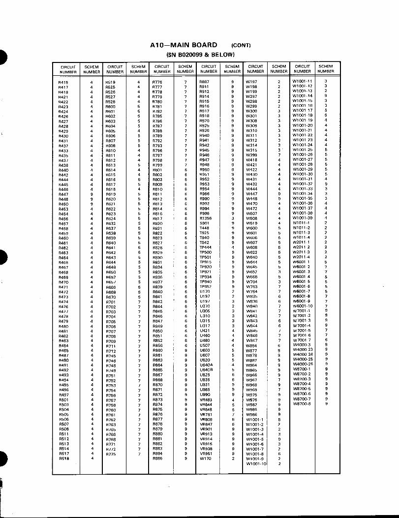
A10-MAIN BOARD
(CONT)
(SN Β020099 & BELOW)
CI RCU ITNUMBER
SCHEMNUMBER
CI R CUITNUMBER
SCHEMNUMBER
CI R C U ITNUMBER
SCHEMNUMBER
CI R C U ITNUMBER
SCHEMNUMBER
CI R CUITNUMBER
SCHEMNUMBER
CI R C U ITNUMBER
SCHEMNUMBER
R415 4 R519 4 R776 7 Ρ 887 9 W 197 2 ω 1001-11 3R417 4 R525 4 R777 7 R911 9 W 198 2 W1001-12 3
R418 4 R526 4 R778 7 R912 9 W 199 2 W 1001-13 2
R421 4 R527 4 R779 7 R914 9 W297 2 W1001-14 9R422 4 R528 4 R780 7 R915 9 W298 2 W 1001-15 3
R423 4 R600 5 R781 7 R916 9 W299 2 W1001-16 3R424 4 R601 5 R782 7 R917 9 W300 3 W 1001-17 5
R426 4 R602 5 R785 7 R918 9 W301 3 W 1001-18 5R427 4 8603 5 R786 7 R920 9 W308 3 W 1001-19 4
R428 4 R604 5 R787 7 R925 9 W309 3 W1001-20 4R429 4 R605 4 R788 7 R926 9 W310 3 W 1001-21 4
R430 4 R606 5 R789 7 R940 9 W311 3 W 1001-22 4R431 4 R607 5 R792 7 R941 9 W312 3 W 1001-23 4
R432 4 R608 5 R793 7 R942 9 W314 3 W 1001-24 4R433 4 R610 4 Ρ 796 7 R945 9 W315 3 W 1001-25 5
R435 4 R611 4 R797 7 R946 9 W399 7 W 1001-26 5R437 4 R612 4 R798 7 R947 9 W418 4 W 1001-27 5
R438 4 R613 5 R799 7 R948 9 W421 4 W1001-28 5R440 4 R614 4 R801 6 R950 9 W422 4 W1001-29 5R442 4 R615 4 R802 6 R951 9 W430 4 W1001-30 5R444 4 R616 6 R803 6 R952 9 W431 4 W 1001-31 4R445 4 R617 5 R809 6 R953 9 W432 4 W1001-32 9R446 4 R618 4 R810 6 R954 9 W444 4 W 1001-33 3R447 9 R619 5 Β 811 6 R956 9 W447 9 W 1001-34 3R448 9 R620 5 R812 6 R990 9 W448 9 W 1001-35 3R450 9 R621 5 R813 6 R992 9 W470 4 W 1001-36 4
R453 4 R622 5 R814 6 R994 9 W472 4 W 1001-37 4R454 4 R623 5 R816 6 R995 9 W 507 4 W 1001-38 4R456 4 R624 5 R817 6 RT356 3 W 508 4 W 1001-39 4R457 4 R632 5 R820 6 S901 9 W 519 4 W101-1 2R458 4 R637 5 R821 6 Τ 448 9 W 600 5 W1011-2 2R459 4 R638 5 R822 6 Τ 925 9 W 601 5 W1011-3 2R460 4 R639 5 R823 6 Τ 940 9 W 606 5 W1011-4 2R461 4 R640 5 R827 6 Τ 942 9 W 607 5 ω2011-1 2R462 4 R641 5 R828 6 ΤΡ444 4 W 608 5 W2011-2 2R463 4 R642 5 R829 6 ΤΡ500 9 W 622 5 W2011-3 2R464 4 R643 5 R830 6 ΤΡ501 9 W 640 5 W2011-4 2R466 4 R644 5 R831 6 ΤΡ915 9 W 644 5 W6001-1 5R467 4 R648 5 R834 6 ΤΡ920 9 W 645 5 W6001-2 7R468 4 R650 5 R835 6 ΤΡ921 9 W 652 3 W6001-3 7R469 4 R652 5 R836 6 ΤΡ934 9 W 668 5 W6001-4 5R470 4 R657 5 R837 6 ΤΡ940 9 W 704 3 W6001-5 5R471 4 R666 5 R839 6 ΤΡ 952 9 W 763 7 W6001-6 5R472 4 R668 5 R840 6 U 170 2 W 764 7 W6001-7 5R473 4 R670 5 R841 6 U 197 2 W 835 6 W6001-8 7R474 4 R701 7 R842 6 U 197 3 W836 6 W6001-9 7R476 4 R702 7 R844 6 U270 2 W 840 7 W6001-10 7R477 4 R703 7 R845 6 U 305 3 W 841 7 W7001-1 9R478 4 R704 7 R846 6 U310 3 W842 7 W7001-2 9
R479 4 R705 7 R947 6 U 315 3 W 843 6 w7001-3 9
R480 4 R706 7 R849 6 U 317 3 W844 6 W7001-4 9R481 4 R707 7 R850 6 U421 4 W845 7 ω 7001-5 7R482 4 R708 7 R851 6 U460 4 W 846 7 W7001-6 7R483 4 R709 7 R852 6 U 480 4 W 847 7 w7001-7 6R484 4 R711 7 R856 6 U 507 4 W854 6 W4000-3 9
R485 4 R712 7 R860 9 U 603 5 W877 9 W4000-23R487 4 R745 7 R861 9 U 607 5 W878 9 W4000-24 9R490 4 R746 7 R863 9 U620 5 W887 9 W4000- 25 9
R491 4 R748 7 R864 9 U640A 4 W964 9 W4000-26 9R492 4 R749 7 R865 9 U640 B 5 W965 9 W8700-1 9R493 4 R7 5 1 7 R867 9 U 825 6 W966 9 W8700-2 9
R494 4 R752 7 R868 9 U 835 6 W967 7 W8700-3 9R495 4 R753 7 R870 9 U 931 9 W968 9 W8700-4 9
R496 4 R754 7 R871 9 U 985 9 W969 7 W8700-5 9R497 4 R756 7 R872 9 U990 9 W975 9 W8700-6 9
R501 4 Ρ 7 57 7 R873 9 VR 483 4 W976 9 W8700- 7R503 4 Ρ 758 7 R874 9 VR 644 5 W982 9 W8700-8 9R504 4 R760 7 R875 9 VR 648 5 W985 9R505 4 R761 7 R876 9 VR 781 7 W986 9R506 4 R762 7 R877 9 VR 809 6 W 1001-1 5R507 4 R763 7 R878 9 VR 847 6 W 1001-2 2R508 4 R765 7 R879 9 VR 901 9 W 1001-3 2R511 4 R766 7 R880 9 VR 913 9 W 1001-4 3R512 4 R768 7 R881 9 VR 914 9 W 1001-5 9R513 4 R771 7 R882 9 VR 915 9 W 1001-6 3R514 4 R772 7 R883 9 VR 938 9 W 1001-7 2R517 4 R775 7 R884 9 VR 951 9 W 1001-8 6R518 4 R886 9 W170 2 W 1001-9 2
W1001-10 2

" 0Ι
C6491'~ 0Ια~
ά α
-
~8 4 C658
1
W65(ιι
ro
m
""" a#- C624- "
Φ
&
W645λ
C406 1 "R41 1#
0_ C604-0
®
~0
0 0 "
Φ R6 1 4Φ
Α Α
"g"~) 411
0 R412 0
οο- ο
Ν 0 R618""
19" R410 "
φ C818"Ι6 C4100i -
0 " 0
" CR61 ,Q4t~τ"
βά
R61 1 R 61 50m
~" #α
4θ L417φ
R47g
φ R479φ
R492°
α
~ι
m m ι
ν =-R417
α Ν 4 '
α
ο Ρi C41 8 0
.7
. R476 -
ο Ε ω"
"_ Φ "
418 **W4180
Cq,6
R
Φ ω ηι Ο9
-
R473
9603%F CR4g ι 640- R470 °- " - "
Rae3
" W640C8221 Ν801 Φ "
" "*0024
R4 7 ι
ω 470 ~,
R490?° Αά
ι st9~~
α
αααα-W8220
"
8" ""
i W800-"
R512
R482
ξ
0 11R511 "
i α
ςββΘΦ
1Φ "
R5ι 9"
ε
i
R -,ϊ
°' Σ ""ΦR517"
"
Σ
R526"
4y C480-
β608 0 Φ ό Ι Ι Ι ;" R525 ® Α
m
" R5284 φ
Φ VR4831α "r
~z
1t "
Νή
ά"" R51 9 " ό m 0
0C
0 R 6 φ R468-
C60 .49 _,κ67.'. .ΝΝ
σΦ R514 "
Cm
" :459
ro ro
`" 1, ι
m" W508 "" i "
i R5270
- R487
φ R4
Φ C602
0
0 -~ C975i R5069 ,α R454"
57
π 67 ύ
<4 -C eo
-ι
" C503 " 40" C504iQ504i R453"
0 R463
. . C608
" ρά
Ν ά όQ507
C50
i"455
m
" R462
ςβ07 -mro
ro
" φτ"" ο Φ
"
0
010
0 R460
R605 ""
" "" . " R503 9ι " "Φ i R461 0 U805
R638 pWb07 ι " ι mΦ
01 wasC505"m'άόης4
"i"
i
ω
ΦRς ;
" W315," "
Φ mNNh $ ά 4
ξ "
"W986"
"ι Ι
ή m R 6 ε
"
"
i
Ι
G96.
, 44 ~ Φ m
ρΆρ ι
"
R816 "
1
Α R 440
CR44
R444Φ ΦΦ "
Α" "
~ι
m
η -
" Φ
[822 4ς
"
°ω ι
R423
R442 .; ι φW431 i
. .
Ι " '
Ι
ή ιmν
.'
0
R8 17 Φ
m~ ® Ρ 424
R4290 0 C43J 0
ω -
4 -
R431 φα_"""
"
"_
R625 φi
R914 40
φ 0
0 R422φ " R4450
-
® R4320
Φi
R428 0 0 C4320 Φφ
Φ
;'04-"φ
C825 "
i1
-
R430φ
φ R707 " " R708 Q
Α
i-&31
"
877 i Ι1
~ ιΙαά " ι
4 .
R427 φ Υ132 "
γ .R8130
Rg~2
"
ώηαρι ~
Ι
R42 1 i
R 706
D
0
ο
0714" R830φ .. R811
R827"
~+ αηι R 701
+~ R705Φ c
λΦ
ό
ς3Γ"" "
"
"
-.
"" η Α mm ;ρΦ " CR 82 0 R828 0 000 ~" R436" m ω "" ® ι Φ$ ορ " -~ CR8
φ CR 833"
"45
" R433"
Q7~ Rm
ο mm- ,
-
βθ34 -'
r" ,
i R81"
Φ
0 C433 " "0
0
0
φ
'
1R835
ιCR44
εθ3α "
ΦΦ0811
Σ ^ ιw100" 7s
Ν ~
ά Υ Α Σ" ««
CH ι
R264
R266 ΦΦ"
ί Ι ~ιόωα .ι ~ιυi CH 2ρ
W1011
W20i+
Φ
ω~+ ύ m~mm
ρ ~4~4 R1 61
9 R251 . .
R256 0 mΦ
,m `
- R150
R154" R261 ,ω- Υ
R 162 φ φ
ο
C264 . R254ίs. R 152
252R153 "
λ } 1R250Q26 , ,
R1170 0 ΦW170 -
R2700257 R263 α ~
ά
" i ΦΙ1~
DA-
29
α
Α
α ρ
ΆΆ
Α
Α
Α-- C270
υ
~
ι
ν
100 V0LωΑό
s
Ν
Rzsa~
-
R305 "
φ φ
ON THIS Νm ύ
°i~m m
"~ll
,
1,ώm
c263
C~'3
α .ι Ι C799~-
C273
R323
Φ iΑΑ
-
R 173
9ρ7
C777
R766 "" R7ι19183 R t97-
$ l"
" R777 α?
Α
""
0
Φ
" R779 Φ ρ m ~- R775 -1
φ R
3
R776"
m ω- ι ¢770R;" R2
Υ"
Φτ"
1n,lss
Φ R771 φ
" ίφy Umi
"α_" β 176 "~ ρ Α " R276 C
R7780 -[779-ιΙη ,°QιΑ" "
nn
" ΦΑ fγ!ιιγ11" Η299 "
0789"
ιmπ "φφ" Φ
φφ "φ
"
" R 295 " Φ `~
τφ" R786 0
001Φ " Φ" ""
Φ " φ " -""" " Φ
-C374-ρρΑ
m " 5Φ R791 "
-~Σέ 0
~7 ΘΑρ ΑΑ p D ""Α" ΑΝΝ ΑΑ φ 40
β 384
ώώώ
m~ς " R787i Φ" "R71~ ιυ-mιόΑΑ~ νν~ όό
R 383ω ro . ι
C787 " Υ" " R7ΑφΦ Φ Φ Jω
ΝιΦΟμφ~~ά
φ
mm
Ρ 371 -
- C789-"9
" RλυR373 4
0
EVER294
β374
R367
~" Υ" V"
" ι R788 " " [781~" " Rλ028
R 368
0
Φ 0ΦηΟ380 Q392, __0187
τ D Φ ~0277~
" R348 φω380 "
R3 Θ 6 "" 1 ""~ί- - y ά
>
C368 0 C367 0
0
"-"1390
+~ι\g l -
:
α27Ί
Φ R364 i
R363 Φ
ά®
° C360
ηi i R354 0
ν0
R360-0 0Ό
.8Φ
4
R361
~i
0 R387 8034 τ
99ti
R342 φ
Φ
Φ
;~`
Α
Λ 38β 390..
.
Α
ρ
_ R
-φ 1i34, -
R331 "
RIMω [3
R357 Φ9R3
-540
~,® R336 ". β356
- R351
R376 00 R377 α-Ϋ .
4ςi R340 " " ι
8Φ
ΦR358.
RR334
ξ
C350
*C377#*R344 + R334 ς" 0335
R350,
α+
0R 345
φ R 335
"350 R370
ι m
. [345
- C335 "
R394
Q376
Q377,~GL *
C972
ΆΣ. .
ρ
ADD OCT 1982
F ig . 9-10 . Ci rcuit view of A10-Main board
ω .ι
"
ή ;υ _ W986 Ι ,ο" 0" W975
- " W8 5 CR9α541 Z~ Φ 652 Ι CR973
ο ιΓ - ιε _ " ra~o CR971
~ Σ Σ ξ - ι "εβ 4βα Ι
ίο

L G i- ~ 1
1 `'~ 1 Κ 1ι
" DA NGER100 VOLTS OC PRESENT R875
$
ON THIS AREA OF OARDς 799
ιι ι
C754
i
ΙRΘ4ϊ
i R766 --60
i
X'-ii i !
~847
C852,.°
1" !
0
ί ,-730763R765752 R762 i
iC796 W
0 C842 04 .
R θαθ
60,
Α ίο 0
R775-
, CR773-
τ
!Ρ 796_
Β
0 R842 00841
Βiώ
{" ω ω! ,p770
ς R 788
R772
R754
_
_
0 C845
0
!!
.At~;χ
'J,-To
CR 770
CR792 ύ 753
R751
iW845 ! !i
4~" ..W847
-- _-!-C779-
y°
_R 72
R757
-W846- !
i R839! ! i
NW
- R85t'
ο
ι
CR790 .-
R753
R756
OW310* ^~ ρ !
~844
-~852 !
~" R786 0
_
ϊ783
- R 7 63
R797
-W314- i
ci R840 - - C840 !
R 781
C797 -
i ω
0R850 00 R-4
J
i
A10-Main board (SN Β020099 & below) .
Ρ871ο
!- C308 -!
F" R787 0
R782
0747
R749
R306 0
0
-
"o C
787 0 Υ
R780
~746 ! 0 R748
71 -01
C854~8
_13
R768
R745 ! 0 C748
!
*CR801
0 R849!1789-~--ι
vi- γR791
i 1798 !
- -1 -Ι
Vale" " ς781
- R798
0C774S
λm
°^
ύ ώ
t O-W311 -!
se- R802 - 9!
-
-R 386-
C99ii j
3827-33Α
40
©Static Sensitive Devices
See Maintenance Section
COMPONENT NUMBER EXAMPLE
Component Number
t hematiAssem bly
cCίrcuif
Number Subassembly . NumberNumber (i f used)
ι
R 386 i ,1φ1
~391
R315 W U315
U 317
w
R3201
0397
R317
R316 00 R313 0
0 C317 0
C311 0ο0
- βb87
-R 389-W849
!
R311 16
R 390 -C844
μR307 -"
R379
®! i !
c
R308- -01111
R376 !0 R377
φ & Φ Φ Φ π !π!π"π !π!
ό
C310
-
chassis-mounted components have ηο Assembly Number"
α C377-
ω rn Ά m
ια
Φ
φ
φ!
miml "ι !~!
pre fix-see end of Re placea ble E lectrical Parts List .
2213 Se rvice

CH 1 & CH 2 VERTICAL PREAMPS
ASSEMBLY Α 10
M BON Ι LO
P artial Α 10 also s hown on diagrams 3, 4, 5, 6, 7 and 9 .
*See Parts List forserial number ranges.
CI RC U ITNUMBER
SCHEM BOAR DL OCATIO N LOCATION
CI RCU ITNUMBER
SCHEMLOCATIO N
BOARDLOCATIO N
CI R C U IT SC HNUMBER Ι LOCAT
C167 2F 4C 0268 8D 4D R250 7EC170 3 F 4C Q273 7Η 4E R251 6CC173 3 Η 4E Q277 6ι 2D R252 6CC174 3J 4C Q287 91- 2D R253 7DC175 11 3D R254 7D
C179 3Μ 5Α R151 1 C 4D R256 7CC180 3F 3C R152 2D 4D R258 7F
C185 51 3C R153 3E 4D R259 7FC193 3L 2D Rl54 3D 4D R261 9CC199 3C 2E R158 2F 4D R262 9CC253 8 Ε 4E Rl59 2F 4D R263 SCC255 78 5E R161 5C 5D R264 7D
C260 8 Β 5E R162 3D 40 R266 8CC264 7C 4E 8163 3E 4C R268 8FC270 7F 4E R168 3F 4C R269 SFC273 7Η 4E R169 4F 4C R270 8F
C275 61 3E Rl70 3 F 4C R272 6JC279 8Μ 5Α R172 2 J 4D R273 7ΗC280 SF 3D R173 3 Η 4E R275 61C284 7J 3E R174 2J 3D R276 6ΚC285 91 3D R175 1J 3D Β 277 6LC293 8L 2D R176 2L 3C R278 6LC299 4C 2D R177 1 L 2D R279 5LC372* 6Η 3F R178 1 L 2C R280 8FCR196 31 4D R179 1L 2C R282 81CR296 71 4D R180 3F 3C R283 7F
R182 41 4C R284 7JE199 3C 4E R183 4G 3E R285 91E299 4C 4F R185 51 3C R286 8 Κ
R186 3 Κ 3C R287 9L
Q157 1 E 4C R187 5 L 2C R288 9L
Q167 4E 4C R188 51- 2C R289 91-
Q173 3Η 4F R189 51- 2C R292 7M
Q177 1 ι 2C R 192 3M 2D R293 8Μ
Q187 5L 2C R 193 3Μ 2D R294 7 ι
Q257 6E 4E R 194 3 ι 2C R295 5G
Q258 7D 4E R196 41 3D R296 71
Ο267 9E 4D R197 5G 3E R297 5GR299 5G
OARDATIO N
CI RCU ITNUMBER
SCHEMLOCATIO N
BOA R DLOCATIO N
4E U1 70A 31 3C5D U1 70B 41 3C4E U l70C 21 3C4E U170D 1 F 3C4E υ 17 οε 5 ε 3C5E U197A 5G 3E4E U197B 5 Η 3E4E U197D 5 Η 3E5D U 197E 5 Η 3E4E U270A 71 3D4E U270B 91 3D5E U270C 61 3D5E U270D 6F 3D4D U270E 9F 3D4D4D W170 4C 4D4E W197 3C 5 F3E W198 3C 3E3E W1 99 3C 2E3D W 297 4C 5F2D W 298 4C 2E2D W299 4C 4E2D W1001-2 5Μ 5Α3D W1001-3 1 Μ 5Α4D W1001-7 7 Β 5Α3E W1001-9 5Μ 6Α4D W 1 ο01-10 9Μ 6Α3D W 1001-13 88 6Α3D W101 1-1 58 5D2D W1011-2 4 Β 5D2D W1011-3 1 Β 5D2D W1011-4 18 5D2E W2011-1 98 5D2E W2011-2 9 Β 5D2D W2011-3 6 Β 5D3E w2011-4 68 5D3D3E3E
ASSEMBLY Α11
CI R C U IT SCHEM BOAR D CI R C U IT SCHEMNUMBER Ι LOCATIO N Ι LOCATIO N NUMBER LOCATION
BOARDLOCATIO N
CI R CU ITNUMBER Ι
SCHEML OCATIO N Ι
BOA RDLOCATION
CI R C U ITNUMBER
SCHEMLOCATION
BOAR DLOCATION
C265 9 Β 1C R291 7 Ν 1C W265 88 2C W1000-10 9Ν 48W1000-2 5 Ν 4Α W1000-13 88 4 Β
R 190 3 Ν 1 Β S264 8Α 2C W1000-3 1 Ν 4ΑR 191 3 Ν 1 Β W1000-7 78 4Α
R290 7 Ν 1C W264 78 28 W1000-9 5 Ν 4 Β
PartialΑ 1 1 also s hown on diagrams 1, 3, 4, 5, 6, 7, 8 and9.

5264INVERT
s; ΙΝ
W IOII Ι (+)RΓΟΜΗρ Ο
_ -3-10-3I4Ν Ι
GND 4-FR OM ΡΙΟΙΟ-4+---~~
4m
FROM 1
9NGNP
FROM
CH IC) W1011-ΖFROM ΡΙΟΙΟ-2-~
GNDFROM ΡΙΟΙΟ- Ι
-
; C
-
CH 2(+)
(+~FP2οΙο-3-~3
ιΡ2ο0Ιο --4
2Ν
ωτοι ιCH2(-)
Ρ2ΟΙΟ-2IN
GND ι rP20 0-1 ~---Ηξ
Ι" L
*8.6vWι 97
WISE, WI99
Ει99
ΟΙθ9 +2.2ΜF~
-8.6ν
p15136
W IOf l
R 25136
R2(.
2213
+1C299297 ηω299ω299Τ2-2-F6νB . 2
5ΕΕ POWER DISTRI BU TION
R26136 + ο
+8.6V2
R252αατο
R262887.0
CHI/CH2TRIG BA LD+ι3.6 V2-
+ .Ο
U270E
U170Dι +ο.,-9
Ι2
R I59ι. ι5Κ
C180
CH2 7R'Gι 0 FR OM
V315B-6BF
βΙ69ιι5ΚωΗ~- 8.6 ~2
Ο
C280ΙΟ
β 269,.15K
~2ί
Ρ259Ι . Ι5Κ
-8 .6ν2
-8 .6ν2
R297Ι
-8.6ν2
R235
C4 ιTRιGFROMU 315C-8®
COO/
α

ΝDΜΕ~ΑιΑΗDLΕΤΤΕΗΑΤ 5ΙGΝΑL υΝΕS Τ00RΜΟΜ 07 ΗΕρ DIAGRAMS INDICATES ΤΗΕ GRIDCOORDINATE ON ANOTHER SCHEMATIC (FORΕιυυνιε. αε)
C142 T R IGFROM
MSLSB-6SF
W"9. ικ
ύΜΑ
1 γΜ-1G
Ιθ150ι 5C- 8TF
3827- 23
R EV AUG 198?-
R173 UI70AQ173 _ α . ο ικ©Ι5
© Static Sen sitive Devices
SeeMamtenance Section
COMPONENT NUMBER EXA MPLE
C273 -L
ι-e-' Α15ΙΟο ;;
U27CA
Component Number
Α~Α2 81 234 εem
Assembly
+
ι
ς h
α1 ιε
Number Sn6αsτembly[υευίΙNumber
Number (ί/ used)
επαππ-mοηια,αεη ρο,eηι , πανe ηηπsse ηα b ι y Ηη m ΝΙαeb-see εηα ηι παριαεeα b ι , ει e ειιιεαι Part, ιι,ι.
U270B4
C I'75270
+ α . ωΜ2
4PΙ 784757.0
Cr ιιW1001
-3ι WI000-3
+3.5 CwMIDRANGE
τ 4 .Η ) CCW
Gw-Β" r.V
RI91-4 .(.4K
+~ CW+4~. MIDRANGE
C-C-3-:v
cω+® MιORANGECI-4-.e-,) CCw
GΑΖ
82914 .64 Κ
-8.(.V
+4 . Β Cνυ+® ΜΙΟRΑαλαG Ε.t3.5 CCW

2213 Service
Fig. 9-11 . Α11-Front Panel board .
3827-35
©Static Sensitive DevicesSee Maintena nce Section
COMPONENT NUMBER EXAMPLE
Component Number
μΑ23 `ΑΤ2'μR1234
Assembly Ι Ι Ι Schematic------~~~ Circuit
Number Su bassembly N umberNumber (if used)
Chassis-mounted components have no Assembly Numberprefix-see end of Replaceable Electrical Parts List.

All-FRONT PANEL BOARD
*See Parts List forserial numbe r ranges .
tOn bac k of board .
$Ch assis mounted .
REV OCT 1982
CI R CUITNUMBER
SCHEMNUMBER
CI R CUITNUMBER
SCHEMNUMBER
CI R CUITNUMBER
SCHEMNUMBER
CI R C U ITNUMBER
SCHEMNUMBER
C101 1 Ρ 1000-1 9 R 975 9 W1000-10 2C102 1 Ρ 1000-2 9 S101 1 W1000-11 3C202 1 Ρ8006-1 9 S201 1 W1000-12 3C265 2 Ρ 8006-2 9 S264 2 W1000-13 2C313 3 R100 1 S305 3 W1000-14 9C314 3 R1011 1 S316 3 W1000-15 3C315 3 R 102 1 S317 3 W1000-16 3C402 4 R 190 2 S390 6 W1000-17 5C403 4 R 191 2 S401 4 W1000-18 5ς404 4 R200 1 S440 4 W1000-19 4C531 9 R201$ 1 S464 4 W1000-2 0 4C650 5 R202 1 S611 4 W1000-21 4C725 t 7 R290 2 S650 5 W1000-22 4C726 7 R291 2 S660 5 W1000-23 4CR536 9 R402 4 U535 9 W1000-24 4CR538 9 R403 4 W264 2 W1000-25 5CR701 3 R404 4 W265 2 W1000-26 5C R702 3 R405 4 W630 3 W1000-27 5CR703 3 R455 4 W635* 5 W1000-28 5C R705 3 R 530 9 W637 5 W1000-29 5CR706 3 R 531 9 W702 3 W1000-30 5DS618 4 R 532 9 W1000-1 5 W1000-31 4J2000-10 5 R 536 9 W1000-2 2 W1000-32 9J 2000-1 1 R 537 9 W1000-2 5 W1000-33 3J2000-2 1 R538 9 W1000-3 2 W1000-34 3J2000-3 1 R556* 5 W1000-3 5 W1000-35 3J2000-4 1 R 557 5 W1000-4 3 W1000-36 4J2000-5 1 R645 5 W1000-5 9 W1000-37 4J2000-6 1 R 646 5 W1000-6 3 W1000-38 4J2000-7 8 R692 5 W1000-7 2 W1000-39 4J 2000-8 8 R726 7 W1000-8 6J 2000-9 7 R807 6 W1000-9 2
R808 6R 891 9

2213 CONTROL SETT I NGSDC Vo l tage
VERT I CAL MODE
CH ITR IGGER MODE
AUTOAC-GND-OC (both)
GNO
AC Wove fοr αιsVERT I CAL MODE
BOTH-CHOPTR I GGER MODE
AUTO
Η8 .3μsA-21- L
3827-39

C HANNEL SWITCH & VERTICAL OUTPUT
ASSEMBLY Α 10
PartialΑ 10 also s how n on diagrams 2, 4, 5, 6, 7 and 9.
ASSEMBLY Al 1
Partial Α 1 1 also sh own on diagrams 1, 2, 4, 5, 6, 7, 8 and 9 .
CHASSIS MOUNTED PARTS
CI RCU ITNUMBER
DL350
SCHEMLOCATIO N
51
BOARDLOCATIO N
CI R CUITNUMBER
CH ASSIS R398R399
SCHEMLOCATIO N
6Ν9Ν
BOARDLOCATIO N
ι
CI RCUITNUMBER
CHASSISC H ASSIS
SCHEML OCATIO N
BOARDLOCATION
ι
CI R CUITNUMBER
SCHEM
I LOCATIONLOCATIO N LOCATIO N
CIRCUITNUMBER Ι
SCHEMLOCATION Ι LOCATION Ι NUMBER Ι LOCATION Ι LOCATION Ι NUMBER Ι LOCATIO N Ι LOCATIO N Ι NUMBER ILOCATION LOCATION
C304 9C 7Α 0341 2Η 2C R338 6 J 1 F U305A 5D 4FC305 5C 5F Q345 2Η 1C R340 4Η 1D U 305 B 7E 4 FC308 9E 1Κ 0350 6L 1 F R 341 3 Η 1C U305C 8 Ε 4 FC310 1Η 1Κ 0360 8ι 2F R342 3 Η 2D U305D 8Ε 4FC311 9E 2Κ 0376 6Ν 1G R344 2 Η 1C U310A 3D 2 ΚC316 5G 21 Ο377 6Ν 1G R345 21 1C U310B 8F 2 ΚC317 1G 2J Q386 8Ν 2G R 346 2 Η 1C U310C 8Ε 2 ΚC335 41 1D Q387 9Ν 2G R348 8 J 2F U310D 8Ε 2 ΚC340 3Η 1C R350 6L 1 F U315A 5F 21C345 21 1C R300 7C 78 R351 6Μ 1 F U315B BF 21C350 6L 1F 8301 2D 6Α R353 7 Κ 1 F U315C 7ε 21C357 7L 2F R302 4D 6Α R 354 7J 2E U315D 9F 21C358 7Κ 2E R304 8D 7 Β R 355 7L 1 F U317B 9D 2JC360 9Μ 2F R304 BD 7Β R356 7L 1 FC366 8Κ 1E R305 5D 4F R357 7 L 1 F W300 8D 5 FC367 8Κ 2E R306 7E 3J R358 7 Κ 1E W301 3D 5 FC368 7J 2E R307 9E 1 Κ R360 8 L 2F W301 8D 5FC377 5Ν 1G R308 9D 1 Κ R361 9Μ 2F W308 3C 8GC387 9Ν 2G R310 8Ε 2Κ R363 8 Κ 2F W309 3D 4JC399 7Ν 21 R311 9F 2Κ R364 BJ 2E W310 30 3JC678 1D 8G R315 5 F 21 R366 7 Κ 1E W 311 3D 2J
R316 5G 21 R 367 7 Κ 2E W 312 9D 2JCR 177 3G 2C R317 3E 21 R368 7 J 2E W 314 1G 31CR 178 2G 2C R318 3E 21 R 376 6 Ν 1G W 315 5C 7CCR 187 3G 2C R320 8G 2Κ R 377 5 Ν 1G W 652 1C 9GCR 188 4G 2C R321 SC 6Α R 378 6 Ν 1 Η W704 5D 5FCR277 3F 2D R323 5G 4E R379 6 Ν 1 Η W1001-4 5C 5ΑCR278 2G 2C R324 4G 2D R386 9 Ν 2G W1001-6 5C 5ΑCR287 3F 2D R325 4G 2D R387 9 Ν 2G W1001-11 4C 6ΑCR288 4G 2D R326 7G 4E R388 8 Ν 2 Η W1001-12 8C 6ΑCR305 7D 5F R327 SG 4E R389 8 Ν 2 Η W 1001-15 1C 6ΑCR320 9G 2Κ R330 3Η 1D R390 8 Ν 1G W 1001-16 2C 6ΑCR 704 6C 7E R331 4Η 1D R 391 8 Ν 21 W1001-33 7C 9Α
R332 31 1D W1001-34 7C 9Α0316 5G 21 R334 41 1D R T356 S L 1 F W1001-35 8C 9ΑQ331 4Η 2D R335 41 1DQ335 4Η 1D R336 4Η 1D U197C 5G 3E
CIRCUITNUMBER Ι
SCHEMLOCATIO N Ι L OCATION Ι
CIRCUITNUMBER Ι
SCHEMLOCATION
BOARDL OCATION NUMBER ΙLOCATION Ι LOCATION Ι NUMBER
SCHEMLOCATIO N Ι
BOA RDLOCATIO N
C313 2C 1C CR 705 4 Β 2 Β W 630 5Β 2Β W 1000-16 2C 48C314 1C 1C CR 706 2Α 2 Β W702 58 2Β W1000-33 7C 4EC315 5 Β 1Α W1000-4 5C 4Α W1000-34 7C 4E
S305 9Α 3E W 1000-6 5C 4Α W1000-35 SC 4ECR 701 4Α 2 Β S315 7Α 2C W1000-11 4C 48CR 702 5 Β 28 S317 3Α 2 Β W 1000-12 8C 4ΒCR 703 6 Β 3D W1000-15 1 C 48

TR IGGER 4Ο
ASSEMBLY Α10
CI R C U IT SCHEM BOARDNUMBER Ι LOCATIO N Ι LOCATIO N
CI R CUITNUMBER
C401
Ι
1 Α
Ι CH ASSIS J4001
SCHEMLOCATIO N
1 Α
BOARD Ι CI RCU ITLOCATIO N NUMBER
CH ASSIS Ι R401
Partial Α 10 also s hown on diagrams 2, 3, 5, 6, 7 and 9.
ASSEMBLY Al 1
CHASSIS MOUNTED PARTS
LOSCHEMCATIO N Ι LOCATIO N
Ι NUMBER
I L OCATION Ι LOCATION
1 Α
Ι CH ASSIS
CI R C U ITNUMBER
SCHEML OCATIO N
BOARDLOCATIO N
CI R CUITNUMBER
SCHEM BOARDLOCATION 1 LOCATIO N
CIR CU ITNUMBER
SCHEMLOCATIO N
BOARDLOCATIO N
CI R CUIT SCHEMNUMBER LOCATION
BOARDLOCATIO N
C408 1D 9Α 0605 6Ν 7E R473 3 J 9D U421A 1G 6DC410 1D 9Α R 474 31 9C U 421B 2G 6D
C412 2D 10Α R408 2C 10Α R 476 3 J 9D U421C 2F 6DC417 5D 9Α R410 1D 9 Β R477 3J 9C U421D 2F 6DC418 5E 9 Β R411 2D 9Α R 478 3J 9C U421 E 1 F 6D
C431 7D 6E 8412 3D 98 R479 3 Κ 9D U460A 5J 7D
C432 8D 6E R414 2D 9Α R 480 4Κ 8C U460B 6J 7DC433 1G 5D R415 2D 9Α R 481 5 Κ 8C U460C 5 Κ 7DC437 5D 10Α R417 5D 9Α R 482 4J 8C U460D 51 7DC438 5G 6D R418 5E 9 Β R 483 41 9C U460E 61 7DC454 6 Κ 7Α R421 1 F 60 R484 4Κ 8C U460F 51 70C455 6 Κ 7C R422 2F 6D R485 4Κ SC U480A 4 Κ 8DC457 80 7D R423 2 F 6D R487 9C 8C U480B 4 Κ 8DC458 7D 9D Β424 2F 6D R490 5 L 9D U480C 41 SDC466 41 SD R426 3F 6C R491 3 L 9D U480D 4 Κ 80C476 31 9C R427 2G 6D R492 6L 9D U507A 7G 78C477 3-1 9C R428 2F 6D R493 4L 8D U507B 8G 78C480 90 8C R429 3G 6D R494 6L 9D U640A 6Μ 9EC503 7F 78 R430 1 F 6D R495 4Μ 8DC504 S F 7C R431 7D 6F R496 5 L 9E VR 483 9C SCC505 6G 7C R432 8D 6F R497 4Κ SDC506 9G 7C R433 1G 5D R 501 5G 7C W418 5E 9 ΒC614 5Μ 9D R435 2Η 5D R 503 7G 7C W421 1E 5DC618 7Μ 9D R437 3G 6C R 504 9G 7C W422 2E 5DC640 9E 9E R438 4G 6C R 505 7 F 7C W430 5 L 8D
R440 4Η 6D R506 8F 7C W431 7D 6ECR 409 2C 10Α R442 4Η 6D R 507 8G 8 Β W432 SD 6ECR 418 5E 7D R444 5 F 6E R 508 9G 88 W444 5G 7D
CR 440 4 Η 6C R445 5F 6E R 511 8Η 813 W470 41 9CCR 444 5 F 6D R446 5E 6D R 512 9Η 88 W472 3D 8C
CR 448 5E 5E R453 6Κ 7C R513 7Η 713 W507 7 Η 7 ΑCR 503 7F 8C R454 5Κ 7C R514 9Η 8Α W508 8 Η 8Α
CR 504 8F SC R456 61 7D R517 8 Ε 8Α W519 9F 8 ΒCR 611 5 Ν 8C R457 8D 9C R 518 9E 8Α W1001-19 3C 7 ΑCR 615 6Μ 9D 8458 7D 9C R 519 9F SC W1001-20 7 Κ 7Α
R459 6J 8D R 525 7E 8Α W1001 -21 7 Κ 7 ΑQ411A 1D 9Α R460 5J 7D R 526 8F SC W1001 -22 7-1 7 ΑQ411 B 20 9Α R461 5 J 7D R 527 7 F SC W1001 -23 8J 7ΑQ414 1D 9Α R462 5Κ 7D R 528 8 F 8C W1001-24 6C 7Α0474 31 9C R463 5Κ 7D R605 6Ν 7E W1001 -31 7 Ν 8ΑQ476 3 J 9D R464 6Κ 7C Β 610 5Ν 7E W1001 -36 5C 9ΑQ492 4 L 8D R466 41 SD R611 5Ν 9D W1001 -37 5C 9ΑQ493 4 L 8D R467 4J SD R612 6Ν 9D W1001 -38 4C 9ΑQ503 6F 7C R468 4J 8D R 614 5Μ 9D W1001 -39 1C 9ΑQ504 9 F 7C R469 4J 8C R615 5Μ 9DQ507 7 Η 7 Θ R470 31 9C R618 7Μ 9DQ508 9 Η 88 R471 41 9CQ519 9 F 8Β R472 4J SD ΤΡ444 5Η 6D
CIRCU IT SCHEM BOAR D CI RC U IT SCHEMNUMBER Ι LOCATION 1 LOCATION NUMBER Ι L OCATION
C402 1Α 3F R 403 28
BOA R D[LOCATION
2F
CI R C U IT SCHEMNUMBER I LOCATION
S464 7 Κ
BOA R DLOCATION
2E
CI R CU ITNUMBER
W1000-23
SCHEMLOCATIO N
8J
Ι
BOARDLOCATIO N
4CC403 28 2 F R 404 1C 3F S611 3Α 2F W1000-24 6C 4DC404 2C 4 F R 405 38 2F W1000-31 7 Ν 4D
R455 8J 2F W1000-19 3C 4C W1000-36 5C 4EDS618 7Ν 2F W1000-20 7Κ 4C W1000-37 5C 4E
S401 18 3F W1000-21 7 Κ 4C W1000-38 4C 4ER 402 28 2 F S440 48 3F W1000-22 7J 4C W1000-39 1C 4F
Partial A11 also shown on diagr ams 1, 2, 3, 5, 6, 7, 8 and9.

ειπINPUT,
ΙθΤΑΤ
ΟΟ2γF~ .Υ
s404εχτ
cειχ~υινG
2213
Ι
ΙΙΙ τ~ωιοm-39 tΠ4Ι 1Α
+8xaq
-&6υ ιLFήΜ
- θ.6V JR432 ω432s.ε
5EE
CO.φ 42ιLyF
R421ίΥ~
ω
43FROM
υπαΒ- Ζ Τ U421EAND
UZTOF3-2
Q414 9J0
R4142-Ι
POWERDISTRIBUTION
INTERNPL.τRIG{£R51GNlL_
FROMυι -Νς.- Γο l-l
21AND
υ2τα-ω
-S.CoVΑR4245.9Κ
R422 λ~ ~.~
Ι
2ω422 45
U421Cςt Vω~1~
ΡΑ29
-αωυ4
C;JJ3
U4ZI
R42-Τ432.0
.τ.s
+S .b4
R5d"Α3Qί
- ΣΙΓσV
+0.b
Γο-)
CJOf1uF
+B;bVq
+α.bVq
AUTO
ΑύΤΟ
R43333ο
U421B
-&bvq
-ν507Α
_
51L)50-TB
τ
-Β.6γq
ί=ο.._
R44o2αF IA422κ
R43S2Κ
ΤΡ444
χι
ΤΟ
+αΥΙ
RaeΙ rw 101ι_-ννι~ -8,ς.,4R5Οτ R611 ί+)
0( 82Κ 2m~μΤΟΟΚ
0.9Λ1Κ
NUMERALΑΝDLΕΤΤΕΡΑΤfFROM ΟΤΝΕΡDΙΑΟΡΑΙ500CCΟΟΡΙΙΝΑΤΕ ΟΗ ΑΝΟΤΙΘώEXAMPLE: 4E)
J. JΒSτRΑΤΕ154-To
3azT-ηRev DEL "
581 +B .(. 34-7y, -g.bV
R4ρ8 ΟΟΙιι,Τ
R45τ C457f R528 +Β.Ν~ΙΟ Ο"Ο"'F 7
4τΚι ι _- Β"ν3 Ι4ΟΠΜ RΙ ς432
ιμ
1 +Ι"2 ιυπο 4Ο"Ο1 ,ιι c cs τ°.ιο4 _ 1

ol
+3V
-FLFLFLnJ-LFLFL= OV
Φ 1SET CH 1 AC-GΝο-α TO GΝο
SWP GATE SET
SET HOR I ZONTAL MODE TO INTENS
ENO OF
DELAY RAMP
DELAY
SWP ΙΝΤ
DELAY
ALT SYNC
θν
-8V
Η
L
Η
L 3827-42
ΗSWP GATE
Ιι
ΗSWP RET RACE
Ι ΙL
ΗSWP UNBLANK
Ι ΙL
+13VΙ SWP Ι
\Ι
ΙΙ
0V
ν Η
Ι END OF SWEEP RE SET
Ι L
ΗHOLDOFF
L
HOLOOFF TIMING +1 .9V
ΙΙ +0 . 9V
Η© J SWP GATE RESE TL
2213 Service 2213 CONTROL SETT I NGSόΣ DC Vo l tages AC Waveforms (con t .)ά α HORIZONTAL MODE ΝΟ DLY TR I GGER MODE AUTOώι0ι TR I GGER MODE AUTO TR I GGER SOURCE ΙΝΤ
ώ > AUTO INTENSITY M i drange ΙΝΤ CH 1ς7 α SEC/D I V 0 .1 ms CH 1 VOLTS/DIV 1 V
ώTR I GGER LEVEL Midrange
άρ AC Waveforms CH 1 INPUT
AC-GND-DC1- kHz si ne wave ) 4ν Ρ-ΡDC
VERTICAL MODE CH 1 DELAY TIME 10 μsHORIZONTAL MODE ΝΟ DLY MULT I PL I ER Χ 1 (full y ccw)

αΝ53ΔΟ
{<λ421Β
L
2
-BbVq
1y5Ό7Α
lF.ιO-ίΒ
RA3S2κ
-ΒΓοΥ4
-$ JoV
2Μ PUTO
ΧAXIS816ΝΑL-To R701
bG
V,150- 7
R513ΙΚ
R5141 Κ
37327-zsREV DEC, 1981
+B.bV
RIRI ΕRALANDLETTER AT SIGNAL LINESTO ORΙΛΟΜ OTHERDIAGRAMS INDICATESTHEGRIDCOORDINATE ON ANOTHER SCHEMATIC (FORUAW- ΙΕ)
U4b0Έ
=OJd
ΝΟ RΜ
Ρ10RΜ
ΡΑ- 74ΙβΚ
-β.ων3
τ 3 . TRIG
Q4-70
RaSb3Κ
οοοι.�F
©Static Sensitive DevicesSeeMaintenance Section
CO MPONENT NUMBER EXAMPLE
Cπ niρρπeπ t N umber
ΑΥ3Α2YR1234
Assembly ~ 1
j
-Scbematι cCιιευιΙ
Number Sub-nobly NumberN-6¢, (it used)
Chassis-mounted εσ m ροπlοt, have πο Asτembly Numberpre(κ-τ ee end of Replaceable Electrical Parts Lιτ 1 .
Ρ473t"(6K
R417 R475 RA-793"sK 39Κ 75Κ
ωιοιο
ωιοοι ι V"000-z2_ - -?R
-75
Τ475
+βηυ3
+4.2 ΗΙLO
UΑWΑ υ4$]0Ιο1ο2 ιοιΟβ
LEVELTRIGGER
ΑΙ Ι ΡΑRΤΙΑL FRONT
Ρ400~ Q493,
TRIGGER54ω4SLOPE
0
*β, ιου3
+4" ι 'cJΑ92
τοΗΟ 0ΟΜ
+9Ν1Χο4013-14
4D .,-~ R6ι42ΟΚ
TRICιC£RsΙGΝΑι
TOR49ς υω~β-1 ι15Ο αε p
W~Α-ς
C~141,5yF
+μαυ3
ΡυτΟ DISPBLEFROM
5(.1 ΖΙΑ ΝK!O1-243Α, !ά.
-THIS CAP* .+Sl
Rb15b20
I-αΓαι5Rεο 12IbK
RueΖ2Ο
-6W
TRIGGER
R ~11
[χΟ1 Ιb-ΒΚ
W05}5. ΙΚ/
ΡΓο1Ο5.1 Κ
WΙφ1 %Ι000-91 31 i
gUTOΒ7iΓ-
fiLΙΝF-TCl-1bοR-1ANDS F
ΑΝ~ΟSF
οsωιαTRK�D
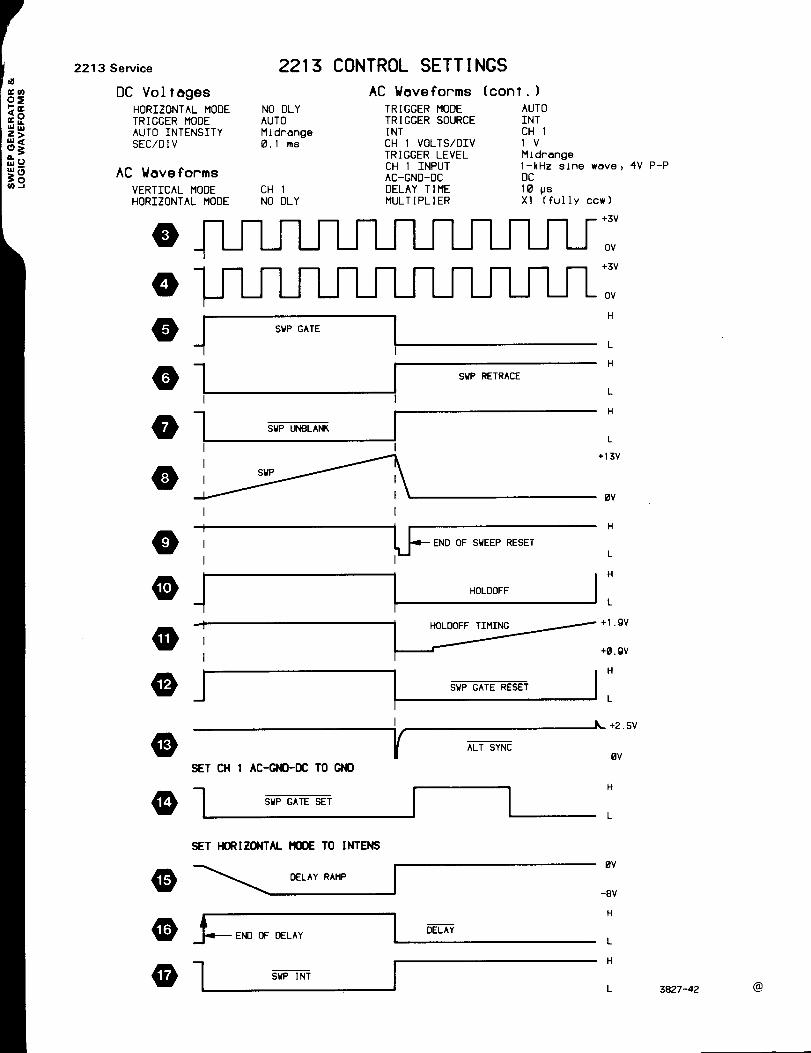
2213 Service
2213 CONTROL SETTINGScam to
OCά Σσώιώ >
ώ
ACά ρ
+3V© υυυυυυυυυυ 0ν+3V
Ο υυ LΙυυ -Fυη 0ν
©
ALT SYN CΘV
SET CH 1 AC-GM-DC TO CND
ΗSWP GATE SE T
L
SET HORIZONTAL MODE TO ΙΝΤΕΝS
θνDELAY RAMP
-8V
Η
END OF DELAY
DELAYL
ΗSWP ΙΝΤ
L 3827-42
ΗSWP GATE
Ιι
ΗSWP RETRACE
Ι Ι LΗ
SWP UNBLANK
Ι ΙL
Ι+13ν
Ι SWP Ι
!Ι
θνΙ
ΗEND OF SWEEP RES ET
Ι Ι LΗ
HOLDOFF
i ι
HOLDOFF TIMING +1 .9V
ΙΙ +θ .9V
ΗSWP GATE RESET
L
Ι +2 . 5V
Vo l tages AC Waveforms (con t .)HORIZONTAL MODE ΝΟ DLY TR I GGER MODE AUTOTR I GGER MODE AUTO TR IGGER SOURCE ΙΝΤAUTO INTENSITY M i drange ΙΝΤ CH 1SEC/D I V 0 .1 ms CH 1 VOLTS/DIV 1 V
TR I GGER LEVEL Midrange
WOVΘ fOΓ ( ΠSCH 1 INPUT 1- kHz s i ne wave, 4V Ρ-ΡAC-GNO-DC DC
VERTICAL MODE CH 1 DELAY TIME 10 μsHORIZONTAL MODE ΝΟ DLY MULT I PL I ER Χ 1 (fully ccw)

SWEEP GENERATOR & LOGIC
5Ο
ASSEMBLY Al 0
PartialΑ 10 also shown on diagrams 2, 3, 4, 6, 7 and 9 .
ASSEMBLY Α11
CI R C U IT SCHEM BOAR DNUMBER LOCATION LOCATION
C650 Ι 68C690 7Α
J2000-10 Ι
20
R556* 1DR557 1DR 645
1 D
PartialΑ 1 1 also s hown on diagrams 1, 2, 3, 4, 6, 7, 8 and 9 .
ASSEMBLY Α12
CI RC U IT SCHEMNUMBER LOCATION
C630
CR626CR630
4 Ν
4L3 ι
1E
3E
2E1F2E
BOA R DLOCATION
4F
4E4F
PartialΑ 12 also s how n on diagrams 1, 7 and 8 .
CHASSIS MOUNTED PARTS
SCHEM BOARD CIRCUIT SCOCATIO N Ι LOCATION
Ι
NUMBER Ι
0
ΙCIRCUIT SCHEM
O
CIRCUIT SCHEM0
ΙCIRCUIT SCHEM
NUMBER LOCATION LOCA70N
NUMBER LOCATION LOCA70N Ι NUMBER LOCATION LΟ CΑ7Ομ
NUMBER L OCATION L OCATION
*See P a rts L ist for ser ial nu mbe r ranges .
ΙCI R C U ITNUMBER
SCHEMLOCATION
BOARDLOCATIO N Ι
CI R C U ITNUMBER
SCHEMLOCATION
BOAR DLOCATION Ι
CI RCU ITNUMBER
SCHEMLOCATIO N
BOARDLOCATION
R 646 1D 2E W635* 1D 2E W1000-25 6C 4DR690 78 W637 1D 2E W1000-26 8C 4D
Ι
R692 ΒΒ 3D W1000-1 Ι, 7C 4Α W1000-27 86 4DR694 8 Β W1000-2 7C 4Α W1000-28 SC 4D
W1000-3 7C 4Α W1000-29 6C 4DS650 6Α 2E W1000-17 9C 4C W1000-30 7C 4D
Ι S660 8Α 3D W1000-18 7C 4C
CI R C U ITNUMBER
SCHEMLOCATION Ι
BOA R DLOCATION
CI R C U ITNUMBER
SCHEMLOCATION Ι
BOA R DLOCATION
CI RC U ITNUMBER Ι LOCATION I
SCHEM BOAR DLOCATION
Ρ2000-10 2D 4E Ρ 6000-7 3D 3F R630 4Μ 4FΡ 6000-1 4 L 4F R631 3Ν 2FΡ 6000-4 4 Ν 3 F Q630A 4Μ 4FΡ 6000-5 3D 3F Q630B 4Μ 4FΡ 6000-6 3D 3F Q631 4 Ν 4F
HEATION 1 LOCATION Ι
CIRCUITNUMBER
SCHEMLOCATION 1 0LOCATION
5E 7F W607 4Η 8Ε
5E 7E W 608 4Η 8Ε
4C 7E W 622 SC 8Α7F 9E W 640 4D 9E
3 F 9F W644 8Η SFSF 9E W668 51 8 Ε
7G 9E W1001-1 7C 5Α8G W 1001-17 9C 6Α8F 9F W1001-18 7C 7Α8G 9F W1001-25 6C 8Α7G 9F W1001-26 BC 8Α91 10F W1001-27 8C 8Α4G BE W 1001-28 8C 8Α4G 8 Ε W1001-29 6C 8Α5 F 7E W1001-30 8 Ε 8Α
W6001-1 4L SF4F 8 Ε W6001-4 4Ν BF4G 8 Ε W6001-5 3D 8F5 F 7E W6001-6 3D BF4E 7E W6001-7 3D BF4E 7E W7055-1 8 .1 10F61 7E W7055-2 8-1 8F41 8 Ε W7055-3 8J BF5D 9E
8F 9F3E 9E
BC 8Α8D 9 Β6 Η 7F
CR621 5 J R638CR622 4J R639CR640 5D R640CR644 3E R641CR668 51 R642
R6430624 7E R6440632 7F R647Q640 5D R6480644 SG R6500650 SG R652Q652 BG R657
R666R600 6J R668R601 6J R670R602 6FR603 4Η U603AR604 6F U603BR606 4J U607AR607 6 Η U607BR608 4Η U607CR613 7E U607DR617 8Ε U 620R619 4J U640BR620 4J VR648R621 5J VR644R622 5JR623 4J W600
R632 7F W601
R637 5EW606
C564 8 Ε 8ΑC601 6Η 9ΒC602* 5G 7EC604 11 7EC606* 5E 7EC607* 5F 7EC608 6D 8GC610 1-1 7EC619 4J 8ΕC620 4Η 8FC622 8Ε 9ΑC624 8Ε 10CC637 5E BFC642 4D 9EC644 3E 9EC645 4D 8FC646 4D 9FC647 4D 9FC648 9 Η BGC649 8 Η 10EC651 9E 7ΑC651 9E 7ΑC652 8F 10EC666 4 Η 8 ΕC668 4G 8 Ε

2213
ΑΙΟ PARTIAL MAIN BOARD
ΡροΟο-lo
ρGΟΟΟ
νν6001
ΗΟ CΟΜ.IV
24642
1000
CR64
2Κ
ALT 310ΑSYNC-~-λ
CG44
ΤΟ U 10Α-2VIA W308
ι V0.b44
-3ν
177 svVpGΑτεTR1e&ER
+5ν Ι \WASIG FR OM
ιyο3Α LϊΟ
-1
82} RG03
Cp~LL9CTOR
,4 ~αηΤ4
b θ
9R b6-
αι
tYcΔ-TG lYι07B-14
"DoΤ45009 .,8 4,5Λ Γσ
C651; .Oyg
+5ν +5ν.θ52 ξΚ44
DLΥ GATE
W644
C!σ4β.Ο4¢
382-1-Ζ~σREV AUG 1982

~Γ1ο4β
;I-011f
ε 3ια2,-τωμkν ι υG ωαα
+5ν
f.-I.22-F
45ΥC604
Ια
Ι ρ. 1A7Fy
F
~
ω6α4
COMPONENT NUMBER EXAMPLE
UG03~Τ4F74 74
G55/ 74ο, 7
R(.00Ι2Κ
©Static Sensitive Devices
SeeMaintenance Section
Component Num ber
Assembly
ι
ι SchematicΦεb
Number SubassemblyNumber (ίΙ υτed)
Number
Ch arms-mounted εα m φπeπi, h ave no Asembly Numberφefia-see end of Replaceable Dectncal Pam U τt .
ΝUMER ΛL ΛΝ DLETTERAT SIGNAL LINESTOORFROM OTHER DIAGRAMS INDICATESΤΗΕ GRIDCOORDINATE ON MOTHER SCHEMATIC (FOREXAMPLE: 4E)
+5 V06/Ο
+SV
Ο. f- F
Ι4 /4r~ -i
β G236 8 0 5γγρ RΕΤ RλCΕ
-8.6V
R601/ΟΟ
FΨ
R658-[ 5 Κ
0Ε7τιαπε
37
P70554-
R6575.6Κ
SWEEP GENERATOR ~ LOGICQ~
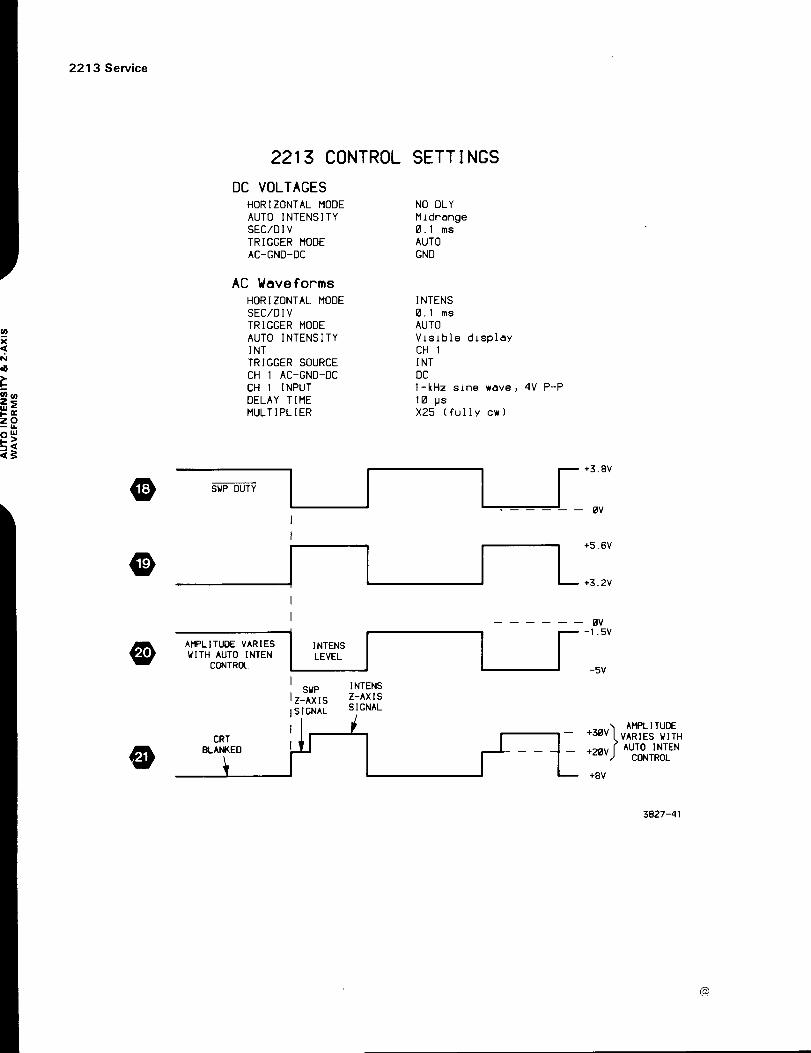
display
2213 Service
2213 CONTROL SETT I NGSDC VOLTAGES
HOR I ZONTAL MODE
ΝΟ OLYAUTO I NTENS I TY
MidrangeSEC/D I V0 .1 msTR I GGER MODE
AUTOAC-GND-DC
GND
AC Wavoforms
r- +3 .8V
_ --- -- θν
+5 .6V
+3 .2V
3827-41
- - - - - - θνr- -1 .SV
AMPL ITUD E VA R I E S INTENS10 WITH AUTO ΙΝΤΕΝ LEVEL
CONTROL -SV
SWP INTENS~ Σ-AX1S Z-AXIS~S Ι GNAL S I GNAL
AMPLITUDECRT +3,,V VAR I ES WITH
BLANKED
L
+2θγ AUTO ΙΝΤΕΝ®CONTROL
+8V
HOR I ZONTAL MODE I NTENSSEC/D I V 0 .1 msTR I GGER MODE AUTOα
ι-ς AUTO I NTENS I TY Visibleα ίΝΤ CH 1
TR I GGER SOURCE ΙΝΤCH 1 AC-GND-DC DCCH 1 I NPUT 1 -kHz sine wave, 4V P-P
Ζ ξ DELAY TIME 10 μsIΊM MULT I PL I ER Χ25 (fu ll y cw )P
Οω

AUTO INTEN SITY & Ζ AXIS
Ο6
P artial Α 10 also shown on diagrams 2, 3, 4, 5, 7 a nd 9.
ASSEMBLY Α 71
J8001 7C CH ASSIS
*See Parts list fo rserial number ranges.
ASSEMBLY A10
CI R CU IT SCHEM BOARD CI R CU ITΙ
SCHEM BOARD CI R C U IT SCHEM BOARD CI R C U IT SCHEM BOARDNUMBER Ι LOCATIO N LOCATIO N NUMBER LOCATIO N LOCATIO N NUMBER L OCATIO N LOCATION NUMBER LOCATIO N LOCATIO N
C603 8 Κ 7E CR834 3 Η 58 R810 6Η 5Α R844 4J 3 ΚC605 8L 8 Ε CR837 31 7F R 811 5G 5 Β R 845 6J 3 ΚC801 6 Η 5 Α CR844 4J 3 Κ R 812 4F 5C R 846 5 Κ 3 ΚC803 61 7G CR856 5Μ 4J R 813 4F 6 Β R 847 5 Κ 4 ΚC820 1C 7E R814 3G 6C R 849 4 L 2 ΚC821 1D 6Α DS854 5Μ 4J R816 3E 6 Β R 850 4 L 3 ΚC822 1C 6Β DS856 6Μ 4J R817 4E 68 R 851 4 L 3 ΚC824 7Ν 6Α R 820 1C 8 Ε R 852 4 L 3 ΚC834 3Η 58 R821 1D 6 Β R 856 5Μ 4 ΚC836 7Μ 58 R822 1C 7EC840 5 J 3Κ Q811 3G 5C R823 1C 7 Β U825B 1D 68
C842 51 3J 0812 3F 5C R827 3 F 5CU825C 2E 6 Β
CB44 61 11 Q813 3F 6C R828 2 F 5C U835A 2E 5 Β
C847 8Κ 4J 0841 41 3 Κ R829 2F 6C υ 835 Β 4 Η 5 Β
C848 6L 4 Κ 0844 5J 3Κ R830 2G 58 VR 809 6G 5ΑC849 4 L 3 Κ 0845 6J 4Κ R831 2F 5Α VR 847 6L 4 ΚC852 5 L 3 Κ Q847 6L 4Κ R834 3Η 58C854 4Μ 2 Κ 0850 5L 3Κ R835 3Η 58 W 835 6Μ 6C
CR801 71 2Κ R 836 4Η 6C W 836 8Μ 7Α
CR802 7Η 3J R 616 2D 7E R837 31 7F W843 61 21CR809 6G 5Α R 801 7E 2Κ R839 51 3J W844 7Κ 7Α
CR828 2F 5Β R 802 7G 2Κ R 840 5J 3Κ W854 4Μ 3Κ
CR830 2F 6C R 803 71 3J R 841 5J 3Κ W1001-8 68 5Α
CR833 4G 5C R 809 6Η 5Α R 842 51 3J W7001-7 1C 6F
CI RC U IT SCHEM BOAR DNUMBER LOCATION LOCATION
CI R C U ITNUMBER
SCHEMLOCATION
BOAR DLOCATION
CI R C U ITNUMBER
SCHEM BOARDLOCATION LOCATIO N
CIRCU ITNUMBER
SCHEM BOAR DLOCATION LOCATION
R807 6Α 1ΑR808 6Α 1Α
S390 8Α 2Α Ι W1000-8 6Β 4Α
Partial Α 1 1 also sh own on diagrams 1, 2, 3, 4, 5, 7, 8 and9.
CHASSIS MOUNTED PARTS
CI R C U IT SCHEM BOAR DNUMBER Ι LOCATIO N Ι LOCATIO N
CI R CUITNUMBER
SCHEMLOCATIO N
BOARDLOCATION
CI R C U ITNUMBER
SCHEM BOARDLOCATIO N LOCATION
CI R CU ITNUMBER
SCHEM BOAR DLOCATION[ LOCATON
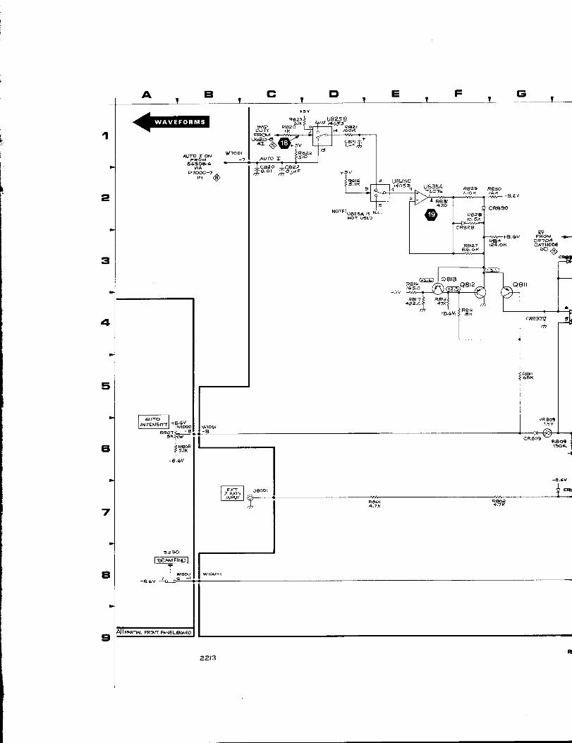
Α.Τ-ΙΝΤΕΝS ΙΤΥ +8.6ν
ω10οΟR85κ ξ- -8
5390
R8ο85. ΙΚ
-B.6V
τ
'ωιοοο Ι Ι ωιοοι- ι
-8.6 14 / ' 2
ι4j Ι ΦRΤμ L FRONT PANELBOARD
2213
εχτΙgχιSINPUT
ουΤ(FRQλUΦ20-β4Ζ
AUTO τ
J 8001
+5 νRθ 23
Ρ8201 χ
ΙΚ
U825B12 1*053882 Ι
14 /ΟΟΚ
-,^Α-RθΟΙ4.ΤΚ
U825C140534 U855A
τιΟί2 R82sI ./OK
R830ly2y -8 .6 V
CR830
χν+θ.αν FROM y~
RB 14 CRT04/24.ΟΚ CATHODE
b0
CR809 RB0913ΟΚ

μν
R836820
8 .6VI
+ BU835
-8.6 ν
TL072
3827- z7
REV AU41982
+ΟΑΙ
Ζ D R IVE
R13394 .7 Η
CR8σ1
+S. fov
~$.6 ν
R8442 .43 Κ
+2 .9
8844
- α.ιν
Rθ46CB421 OHaV
ΤC840 Ι
28 . ΟΚΟ. ~-ρ
8845
FRO
Ο9
`fc84-ιο.~F
-8.6V ~
~
ι -8 "6 V1
C849Ο. Ιμ F
-8. Γε V
R8S ι ~ ς854jg O.~F
Ρ 850
VR θ 47
3 ν
ρ5854
D5856
NUMERAL AND LETTER Α 7 SIGNAL LINES7ΟORFROM OTHER DIAGRAMS INDICATES THE GRIDCOORDINATE ON ANOTHER SCHEMATIC (FOREXAMPLE : 4E)
C8360.01"
+5 ν6
U82 5/4 σ53
4
2,6,7,8,2~J., ς ~2 -g. εν
'rr Ο.θρ 14ιF
ωθ36©Static Sensitive Devices
See ΜαίπΓeπαπε e Section
-8 .6ν
CO M P O NEN T NUMBER EXAMPLE
Component Numb er
Assembly chematic
Number Subzssembly P nbc
Num ber (;f used)
Number
Chess's bοοηηte α εοΙηποη emτ h,,,,, Αττ e οΙων 11-be,c,,e,-- end of Replaceable Elect-I Part, Lit
AUTO INTENSITY It Z AXIS <@>
C1Ο21mΖ
Ν
DΧ_
Ν
+IO0 V ι ι +100 V
+8-(.Vι--~-w-~-s-~45-
ι +8.6VI1 Ο849 U835Ο.~F
5EE TI-072M POWE R
+5Vωθ44 DISTRIBLITO N
C606T05ι+5 ν
O.~F~Ο . jwF

τ
Νσ α
Σ. αΙ ΟdMWα >ακ 3
2213 Service
2213 CONTROL SETT INGSDC Voltages
HOR IZONTAL MODE
ΝΟ DLYTR I GGER MODE
AUTOAC-GND-DC GND
AC WοveformsHOR I ZONTAL POS I T I ON Start of trace at extreme
left vertica l graticu l e line
HORI ZONTAL MODE
ΝΟ ΟLΥVAR HOLDOFF
ΜΙΝ (full y ccw)TR I GGER MODE
AUTOAC-CND-DC (bot h)
CND
REV DEC 1981
+13V
0V+1 V
-1 .3V
+65V
+32V
ι ι ι ι +65V
Φ JVVVL .~.

ΧΥ AMPLI FIER / HORIZ OUTPUT
7Ο
ASSEMBLY Α 10
CI RCU IT SCHEMNUMBER Ι LOCATIO N
BOA R DLOCATION
CIRC U ITNUMBER
1E C726
PartialΑ 10 also shown on diagrams 2, 3, 4, 5, 6 and 9 .
ASSEMBLY Al 1
NUMBER LOCATIO NLOCATIO N Ι LOCATIO N
2C 1E
Ι J2000-9 Ι
2D
BOARDLOCATION
CI R CU IT SCHEM BOARDNUMBER ( LOCATIO N Ι LOCATIO N
3D R 726
Partial Α 11 also shown on diagrams 1, 2, 3, 4, 5, 6, 8 and 9 .
ASSE MBLY Α12
P artial
A12 also shown on diagrams 1, 5 and8.
SCHEM Ι BOA RD Ι CI RCU IT Ι SCHEM
t On back of board .
CI RC U ITNUMBER LOCATION
SCHEMLOCATION
BOAR D CI RC U ITNUMBER I
SCHEMLOCATION
BOAR DLOCATION
CIRCU ITNUMBER Ι
SCHEMLOCATIO N
BOARDLOCATION
CI RC U ITNUMBER LOCATION
SCHEM BOAR DLOCATION
C702 7D 7D CR 783 2L 3 Η R748 51 21 R789 1 Ν 3F
C708 7D 6E R749 51 21 R792 4 Ν 3G
C745 51 21 0703 8D 5E R 751 5-1 31 R793 4 Ν 3G
C748 51 21 Q706 SD 5E R 752 5 Κ 4Η R 796 9-1 31C754 5J 41 Q708 7 F 6E R 753 7 Κ 3 Η R 797 91 31
C770 5Μ 3G 0714 7 ε 6F R 754 4 Κ 31 R 798 SJ 2G
C773 8Μ 3G Q747 5-1 3 Η R 756 7-1 31 R 799 8-1 4F
C774 8Μ 3G Q753 7 Κ 3 Η R757 7,1 31C777 7Ν 3 ε Q763 3 Κ 4 Η R758 7J 4 Η VR 781 2Μ 2G
C779 7Ν 3G 0765 5 L 3G R760 3-1 4GC781 2Μ 2G 0770 7ι 3G R761 4J 31 W399 SJ 31
C783 2Μ 3G 0775 8Ν 3F R762 4 Κ 3 Η W763 3-1 5 F
C784 2Μ 3G Q779 7Ν 3F R763 2 Κ 3 Η W764 3-1 4F
C787 1 Ν 2G 0780 2Μ 2G R765 αι 3 Η W840 91 9F
C789 1 Ν 2G 0785 2Ν 2ε R766 51- 4G W841 91 7F
C796 9-1 31 Q789 1Ν 3G R 768 5Μ 2G W842 91 7F
C797 9Κ 31 R 771 8Ν 3F W845 9-1 3 JC798 SJ 2Η R 701 88 5D R 772 7L 3Η W846 91 31
C799 81 4G R 702 7C 6E R 775 8Μ 3G W847 91 31
C841 9-1 6F R 703 8C 6E R 776 7Ν 3F W967 SJ 5 F
C845 91 3J 8704 613 6 F Β 777 7Ν 3F W969 81 4JR 705 8D 5E R778 8Ν 3F W6001-2 5D S F
CR 745 51 21 R 706 8 Ε 6E R 779 7Ν 3F W6001-3 5D 8F
CR 748 51 21 R 707 8 Ε 6E R 780 2Μ 2G W6001-8 5D S F
CR 749 51 21 R 708 7D 6E R 781 2 Ν 3G W6001-9 5D 8F
CR 770 5Μ 3 Η R 709 7E 6E R782 3L 2G W6001-10 5D BF
CR 772 5 Κ 3 Η R 711 8 F 6E R 785 2Μ 3G W7001-5 31 6FCR773 7 ι 3 Η R 712 6E 6E R 786 1 Ν 3G W7001-6 6F 6FCR780 5Μ 3G R745 5J 2 Η R 787 1 Ν 2GCR782 5 L 3 Η R 746 5J 2 Η R788 2 Ν 2G
CI RCU IT SCHEMNUMBER Ι LOCATIO N
BOARDLOCATIO N
CI R CU ITNUMBER Ι
SCHEMLOCATIO N
BOARDLOCATIO N
CI R C U ITNUMBER Ι
SCHEMLOCATIO N
BOA R DLOCATION
CI RCU ITNUMBER ( L OCATIO N
SCHEM BOAR DLOCATION
C720 4G 2D Ρ 7000-5 31 1D R721 3G 1E R734 2 Η 1E
C732 1G 1D Ρ 7000-6 5G 1D R 722 5F 2D R 736 3 Η 2E
C734 2Η 2E R723 5 F 2D R 737 3 Η 2E
C736 3G 2E 0720 5G 1D R724 2G 1E R 739 3 Η 1D0730 2F 1E R 725 2E 2D
Ρ2000-9 2D 4D 0731 2G 1D R728 2F 2E 5734 1 Η 1D
Ρ6000-2 5D 4 F 0736 3G 1E R729 2E 1EΡ 6000-3 5D 3 F R 730 3G 2E W734 1 Η 1E
Ρ6000-8 5D 3 F R633 2E 1 F R 731 3G 2E W734 2E 1E
Ρ6000-9 5D 3 F R 684 3E 1E R 732 2 F 1EΡ6000-10 5D 3F R 720 5G 1D R733 2G 1E
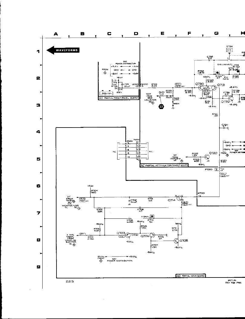
2213
OV
FROM
5EEPOWER DIST RIBUTION
+θ.6 ν
- τ8.6ν
GND GND
-%6ν--&6ν
+B.bV
OV
C725 U200022,F -9
"Ο0176 ΟρΟ
2.
r.
+θ.6V,
...
t-3 3,Ι~
CaND GΓΓ~ι
i/
1_ά~-
~β6V, SEE _ΙΙήV /R7Κ2
Q720
FROM®POWER DISTRI/
-~
S6 Β3Moo® έάκ Μτz
ή)ΙΖ PARTIAL ATTENUATOR/SWEEPBOARCI
-β6V7
Ρ7οοο C0V0
~β.6V4
_+13.~4qFRpM Se EPOWER DISTRIBUTION
Ρ2ΟΟΟ R725-9 8"2Κ
R633 R729422.0SWP 5. ΙΙΚFROM0631
COLLECTOR58
ον
Ρ6842.55Κ
W684
Υ+Ο.7
173222
R732/.37Κ
+"νΤ R2κP7243.9Κ
5734ΧΙΟ
GAΙ___-- -__R
5λ5 LINEARITY ς734ω734 ι-~~
GηηιΟΝR7rK
+8-6ν7R736
C736 $ 2.7Κ2.2
ΧΥ
-327-2ΒΚΕΥ F 48 Ι961

TIM I N G SWITCH
ASSEMBLY Al 1
CI R C U IT SCHEM BOARD CI R C U IT SCHEM BOARDNUMBER LOCATIO N LOCATIO N NUMBER LOCATIO N LOCATIO N
J2000-7 1 Μ 3D J 2000-8 1Μ 3.
PartialΑ 1 1 also s hown on diagrams 1, 2, 3,4,5,6, 7 and 9 .
ASSEMBLY Al 2
CI RC U IT SCHEM BOAR D CI R C U IT SCHEM BOAR DNUMBER LOCATION LOCATION NUMBER LOCATION LOCATION
C625 3L 4E R625 4 F 4EC626 3L 4E R626 3E 4EC628A 2Κ 4D R627 7C 1EC628B 2L 4E R628 2L 4EC636 6L 2E R629 6C 1EC677 7L 3 F R636 6L 2EC679 8L 3 F R677 7L 2EC738 8L 2E R679 8L 2EC741 7L 211 R686 5C 1F
R691 6C 1EΡ2000-7 1Μ 4D R738 BM 2DΡ2000-8 1 Μ 4D R741 7Μ 1EΡ7000-1 6Μ 1DΡ7000-2 7Μ 1D S630A 2 Κ 3DΡ7000-3 8Μ 1D S630B 2G 3DΡ7000-4 7Μ 1D 5630 6E 3DΡ7000-7 1Μ 1D
VR629 6C 1F0629 6C 1F
Partial Α12 also shown on diag rams 1, 5 an d 7.

!~0
5734
χ101GANGEDWΙΤΗ
Ι
b0
IUhEAR1T_Υ C734ω73 Ι -3μ
+8'6ν7R73627Κ
R7373.6Κ
-θGνΡοωΕR
5εεpSTRI B l Π10Nl
] Β27-zαKEY FGB Ι962
ι bV7 +86V~
1 GND
- GND
BEAM FIND -ST&V,FROM5390 45WW1-1 ~~7 22Ο58Β©~ -B.6VI
ΒΕΑΜFΙΝΟ
+Θ.6V
-8.6V
243ΚCR74θCR749
ω7οοιΗΡβΕΑΜΡ OUT- R,7aC-,O
Q7477R751
R746243.0
7.α )
α$.6V1
Ι R7.-&6V, 6'ΜΥ/+'G
REGιSTPMTI0N
50715/LI μEARITY
R757ιΟΚ
Ον
ον ,
Ρ799+ιοΟV
9 t~+IOOVI
ω969 W399 R/7ο+30V
- - -+30 V1
Τ ~.~C841
ω84Ο W841
v845 w846 r~ο97
+Θ-6νΙ
+&6Ν1R763).78K
Ρ753Ι .7ΘΚ
C
SEEP01NERDMTRIBUTION
7834
57275θΤW11ΝG
0.6C783
©Static Sensitive DevicesSeeMaintenance Section
CO MPONENT NUMBER EXA MPLE
C773 Ο.6-3C774
Ι57ι5 ΤιΜΙΝG
Component Number
Α23 Α2 R 1234
A τsem b ly _~ 1 ~$cbematic-'t
N umber Subassembly CiNumber ("fused)
Num b eιR79Gtο Ch-, s-Wed..φη¢πΙlhave πσ As τembly Number
-
-&4~j
4
$ Ο6Ο9
prefα-see end σ( Repaceable Ε1ectdcα 1 Paris bst .
+ ι
Q775
490.blR771768.0
-8 . ΓΡVΙ
rFW-ITΝΟRΙΖ
ηEPFLL¬ΑCΤ)ΕΟΝ
RR~1ΤΝΟRιτ
DEFLECTIONFrL.A7Ε
D3ΓΤm
NUMERALANDLETTER ATSIGNAL LINESTO ORFROM OTHERDIAGRAMS INDICATESΤΗΕGRIDCΟΟΝΟΝΛ7Ε ON ANOTHERSCHEMATICEXAMPLE: 4E) ο
ΧΥΑΜΡLΙ F1ΕR/ ΗΟRΙΖ OUTPUT0
οcVc

2213
SWITCH C LOSED. ο5
SEG DIV
3β2-Γ_29REV οΕι Ι9 ΒΙ
ιίIMMMMMEEMIC
"°ο"σ"0
σ σ ι
ι~ιno
σN ONE
ι
ς
ί
ί"ό"σσ"ί"σσ σ ί εό"ί"ί"ί"σσ "
ί"σσ"σ"ί ξm
0
ίί ί"σ
13
ί"ί"ί"σ.σ~IΙ~
130V
-66.8Κ
5630Α AND Β sεC/DIV( 54oWN IN \ιΧ-Υ ΡΟ"ΙΤιΟΝ /
5ο2ΟΙΟ
m5 2
VR629ί-.., 6-Βν FAR . .1
"'17H 573 ι ΧΙ0 MAC, 50Q629 Ι εω Ζσ
Ρ691 Rfo29 047 500 5
Νς-8 .6V R627
240 .5NOTE ; 2DOT ΙΝρΙ CΡΤΕ1

i 5ωιΓCΗ
INZ r-29ON DEC 1961
-ToC Γo4bVIA
Pocco-'.3ΟΑΝΟ
εχαοα -ω30
© Static Sensitive Devices
See Maintenance Section
COMPO NEN T NUMBER EXAMPLE
Component Num berr------^-A23 A2 R1234
Aasemdly ~
Sc hematic
Number Subassembly Numbe[ιιευιΓ
ιNum b er (ίΓ used) NUMERAL AND LETTER AT SIGNAL LINES TO OR
FROM OTHER DIAGRAMS N.ICATES THE RI .-πισυπ t¢ Π Cοmφπ¢n1thdv¢ πσ 0.ϋ¢m bl Νυπι bΡιCh-. Υ
COORDINATE ON ANOTHER SCHEMATIC LIFO.ρι ef,,
see eπΠ σΙ Re ΡΙά.. ά bΙ, ue[υ mα1 Ρ ,,(, LιτΓ.
EXAMPLE : ΡΕ)
+ ι *
λί ΡΑ ΜΑΤC ΧΕρ ςΕΤC62θΑO ;O~ F
5t.5
C628B_j- F
ΤΙΜΙΝ( , 'η
TI M I NGCAPACITO RS
i' ΤN1S ρ1ΡG .
ΤΗ15 Οι- -θ.6 ν ι
Αυ 7σ Ι
ΧΥ
ΧΥ
C626-Κ -LC625Γ .5-3.5
Τ 95
70 ?Fο3 Ι
CO LLE CTO R4Μ
,
ΤΟ QΦΘσΑςατΕ4Μ
A12 PARTIAL A7TEN VATOR SW EE P B OAR D
FRONT-
P7000
53
6
Ο οπ ΟΟ Ο
ο πΟ Οο Ο
TIMING SWITCH
/2ΙΟ
ό
79
563 Ο Α,9,C'30-M VIEW
ILL--Fl
FR-P7001
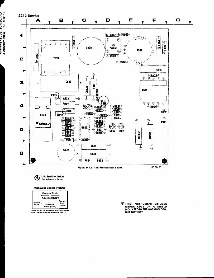
Static Se nsitive DevicesSee Maintenance Section
COMPONENT NUMBER E XAMPLE
Component Number
Α23~ R1234
Assembly
1c,tic
CircuitNumber Subassembly Number
Number (i/ used)
Chassls-mounted components have no assembly Numberprefix-see end of Replacea ble Electrical Parts List.
1,,__
; ;Κ 11 χ
Fig ure 9-12 . Α18 Pre reg u lato r b oa rd .
* THIS INSTRUMENT UTI L IZESEITHER C932 OR Α SH I ELDMOUNTED IN THE Q933 HOLDER,BUT NOT BOTH .

A18-PREREG ULATOR BOARD
REV OCT 1982
CI R C U ITNUMBER
SCHEMNUMBER
CI RC U ITNUMBER
SCHEMNUMBER
CIRCU ITNUMBER
SCHEMNUMBER
C903 9 L937 9 R921 9C904 9 L938 9 R922 9C905 9 Ρ 801 9 R 923 9C907 9 Ρ 802 9 R 925 9C908 9 Ρ 803 9 R 927 9C909 9 Ρ 804 9 R 928 9C910 9 Q915 9 R 929 9C913 9 Q917 9 R 931 9C920 9 Q931 9 R 933 9C921 9 0933 9 R 934 9C923 9 Q935 9 R935 9C925 9 R 903 9 R936 9C929 9 R 904 9 R937 9C932 9 R 907 9 RT901 9C933 9 R 908 9 RT902 9C934 9 R911 9 Τ 901 9C935 9 R 912 9 Τ 907 9CR 904 9 R 913 9 Τ 933 9CR 913 9 R914 9 U920 9CR931 9 R916 9 VR917 9CR933 9 R917 9 VR935 9E933 9 R920 9

φΝ
°- R 914- R921- R927 =-S" C929R929C923 - =~-R 916
R923 - = DanR928 _ -
Q935 '' -- C935
- Q931 ~60
. R 931 :
R912
-
~S
Ρ802
9R 913..
VR 9Ω '
°°R934
\ C913
30R904
Q933
R933
0E933
C933
Τ933
C934
-= R920"' C920 ,-
C925 =- R922
R925R935 -VR935
' R936
ε ,φe
C909
L938
φ φωω
C908
CR904 _ Τ907
Figure 9-13 . Ci rcu it view ofAl8-Pre reg u lato r boa rd .
to
toο
οro
ε,φοΑ
ε,eω
3826-60

ς tε
USE the following waveforms in place of those in the Power Supply diagram in the "Section 9-DIAGRAMS" sectio n of the manual if your
instrument has α Preregulator board .
VlC Σ ..,ι α α:on~ ώοό
~ ά $D ~ Ν~ Ε. ο; αφj ~zι Ca Ν
2213 Service
10
P-
3 V
0 ν
15 V
0 V
150 mV
100 mV
175 V
-175 V
PROBE GROUNDLEAD ON PIN 4OF U920
PROBE G ROUNDLEAD ON PIN 4OF U920
PROBE G ROUN DLEAD ON PIN 4OF U920
3827-52
PROBE G ROUNDLEAD ON PIN 4OF U920
-0Wf-"ι 0 ν
0 V
PROBE GROUNDLEAD ON PIN 4OF U920

2213 Service
2
3826-51
F ig. 9-14. A19-Current Limit board .
© Static Sen sitive DevicesSee Maintenance Sectio n
COMPONEN T NUMBER EXAMPLE
Comp onent Number
~Α2-3 ' Α2~R12-3-4'
Assem bly Ι
Ι schematic--~~ CircuitNumber Subassem bly Number
Number (if used)
Chassis-mounted components have no Assem bly N um berp refix-see en d ο1 Rep laceable Bectrical Parts L ist.
A19-CURRENT LIM IT BOARD
CI R CUITNUMBER
SCHEMNUMBER
CI R CUITNUMBER
SCHEMNUMBER
C938 9 Q938 9C R 932 9 R933 9C R 934 9 R935 9C R 935 9 R936 9F 937 9 R937 9Ρ801 9 R938 9Ρ 802 9 R939 9Ρ 803 9 RT935 9Ρ 804 9 VR933 90933 9 VR934 9

4~
s/
Pre regu lator and i nverter voltages arerefe renced to test point noted adjacen t tothe voltage . Power supply ou tpu t voltagesa re refe renced to chassis ground .
VAR IES WITHAUTOINTENSETTING
DC Voltages
r
2213 CONTRO L SETTINGS
+16VPROBE GROUNDLEAD ON ΤΡ915
6-- 0 V
+20 V
PROBE GRO UNDLEAD ON ΤΡ915
0 V
+11 .8 V
PROBE G ROUNDLEAD ON ΤΡ915
0 V
S ET : SEC/DIVAUTO ΙΝΤΕΝVAR HOLDOFF
-+85 V
+30 V +8 V 0 V
45
ADD OCT 1982
AC WaveformsWARN ING
I nsru men t m u st be connected to theac- power so urce usi ng 1 :1 isolatio ntr a nsfo rmer . Do not co nn ect t he testoscilloscope probe g ro und lead to theinverte r ci r c u it test poi n ts if t h einstr umen t is not isolated . AC-so urcevoltage exist on refe r ence poi nts ΤΡ915and ΤΡ934 .
0.1 mSM IDRANGEΜΙΝ (FULLY CCW)
+11 .8 V
ον
"-,- +8ο ν
'-0 VPRO BE GROUN DLEAD ON ΤΡ934
- +80 V
6-d- 0 VPROBE GROUNDLEAD ON ΤΡ934
-ovPROBE GROUNDLEAD ON ΤΡ934
^~- 0 V
`- -500 mV
3827-43

POWER SUPPLY, PROBE ADJUST & CRT(SN 8020099 & BELOW)
*See Parts List fo rTA BLE (CONT)serial number r a nges .
ASSEMBLY Α 10
CI RCU IT SCHEM BOARD CIRCU IT SCHEM BOARD CI R C U IT SCHEM BOAR D CI RCU IT SCHEM BOARDNUMBER LOCATION LOCATION NUMBER LOCATIO N LOCATIO N NUMBER LOCATION LOCATION NUMBER LOCATIO N LOCATIO N
C447 4Β 5Κ CR967 4Η 7G R872 3L 41 ΤΡ501 7F 10 ΒC448 6Θ 5F CR971 5Η 8G R873 3 Ν 1 1 ΤΡ915 3D 8 ΚC861 4J 71 CR972 6Η 9Η R 874 3 Ν 1 1 ΤΡ920 4C 8 ΚC863 4J 71 CR973 5Η 9G 8875 4L 4Η ΤΡ921 3D 8JC864 3Κ 61 CR974 6Η 9G R876 5 Ν 1 1 ΤΡ934 2E 81C865 3Κ 61 CR977 2Κ 4 Κ R 877 3L 6G ΤΡ940 2 Η 7ΗC871 2Ν 11 CR985 5_1 9G R878 3L 5Η ΤΡ952 5F 10JC873 3Ν 11 Β879 4L 5ΗC876 5Ν 11 DS867 2.1 5 1 R 880 4L 5 Η U931 5E 9 ΚC877 2L 11 DS868 2Κ 5 1 R 881 4L 5 Η U985 6J 9 1C878 4L 5Η DS870 7Κ 5 1 R 882 5L 5Η U990 2 Η 6GC879 4L 5Η R 883 5L 5ΗC886 4 Ν 11 R 884 5 Κ 5 Η VR 901 3 Β 5 ΚC901 28 5Κ R 886 4 Ν 11 VR 913 3C 8 ΚC912 6C 9Κ L971 51 8G R887 4 Ν 1 1 VR914 5D 8 ΚC915 6D 9Κ L972 61 10Η R911 4C 8 Κ VR 915 6D 8 ΚC917 4E 9Κ R 912 6C 9 Κ VR 938 3E 8 1C926 3C 6Κ R 914 4D 8 Κ VR 951 3F 10ΚC937 3E 7J R915 5C 8 ΚC945* 311 101 Ρ 8710-1 4Ν 11 R 916 4E 9 Κ W44
W85 Β58
5J
C947* 4F 10J Ρ8710-2 3Ν 11 R 917 4E 8 ΚW877
3L414Ι
C951 3G 10J Ρ8 710-3 5Ν 11 R 918 5D 9 ΚW878 3L 41
C956 3G 91 Ρ 8710-4 2Ν 1J R920 3D 7 ΚW887 2L 4J
C957 4G 10J Ρ 8710-5 2L 1J R925 2D 7 ΚW964 3J 4J
C961 3J 6G Ρ 9000-1 2Α 6J R 926 3C 6 Κ 4 Ι 9GC965 3 Η 7Η 0 9000-2 3Α 61 R 940 4G 9.1
W96W966
3 7GC971 51 9G Ρ 9025-1 28 6.1 R 941 4G 91
W98
31Ι 6G
C972 61 9G Ρ 9025-2 2C 6.1 R942 4G 10.1 W97576 5J 9G
C975 5 1 BG R945 3 F 101W9 6J 9G
C976 61 10G Q877 3L 5 1 R946 3F 10Κ W982 6J 4JC977 4Κ 7Η Q918 4D 9Κ R 947 4F 10J W985 6J 9GC985 6J 10 1 Q921 3C 8Κ R 948 4F 91 W986 6J 9GC990 2 1 6Η Q925 2C 8Κ R950 3F 10ΚC992 21 6Η 0940 3G 91 R951 4F 91 W1001-5 7F 5Α
C995 2J 6Η 0942 4G 91 R 952 5F 9 Κ W1001-14 7F 6Α
Q948 3F 10Κ R953 5 F 91W1001-32 7 F 9ΑW4000-3 6L 6F
CR860 3J 71 Q954 3F 10Κ R 954 4F 9 ΚCR863 4Κ 61 Q956 4G 9Κ R 956 3G 91 W4000-23
W4000-246L7L
9F9F
CR867 2J 61 R990 2 1 6 ΗW4000-25 7L 9FCR868 2Κ 61 R 447 48 6Κ R 992 2 1 6 Η
Cfl903 3Β 6Κ R 448 58 5Κ R994 2J 6 ΗW4000-26W7001 -1
6L8L
9F6ECR904 48 6Κ R 450 48 5Κ R 995 2J 6 Η
CR905 4Θ 6Κ R 860 3J 4ΚW7001-2W7001-3
8L8L
6E6ECR906 48 6Κ R861 4J 4Κ S901 2Α 5 Κ W7 001-4 8L 6 F
CR917 6D 8Κ R 863 4.1 7 1 W8700-1 5L 5 ΗCR931 3D 6Κ R864 3J 61 Τ448 5 Β 51
W8700-2 7 L 5 ΗCR 933 2D 6Κ Β 865 3Κ 61 Τ 925 3C 7 Κ W8700-3 8L 5 ΗCR940 5G 91 R 867 2J 6Η Τ 940 2 Η 7 Η
W8700-4 8L 5 ΗC R 942 5G 10J R 868 2J 61 Τ 942 4 Η 81
W8700-5 7 L 51CR956 3G 91 R 870 2Ν 1 1
W8700-6 7 L 51C R 961 31 7G R871 2Ν 11 ΤΡ500 7 F 10G W8700-7 7L 5ΙCR963 31 7G W8700-8 5L 5ΙCR965 3Η 7G
Partial Α10 also sh own on diagrams 2, 3, 4, 5, 6 and 7.

POWER SUPPLY, PRO BE ADJU ST & CRT(SN Β020099 & BELOW)
(CONT)
ASSEMBLY Α11
CI RC U IT SCHEM BOARD CIRCU IT SCHEM BOARD CI R CUIT SCHEM BOAR D CI RCU IT SCHEM BOARDNUMBER LOCATION LOCATION NUMBER LOCATIO N LOCATIO N NUMBER LOCATIO N LOCATION NUMBER LOCATIO N LOCATIO N
C531 8C 1D Ρ 1000-2 BE 18 R532 7C 1D U 535 8C 1DΡ 8006-1 1 Ν 2Α R536 8D 1D
CR536 8D 1D Ρ 8006-2 1 Ν 2Α R537 80 1D W 1000-5 7E 4ΑCR538 80 1D R538 8D 1 Β W1000-14 7E 48
8530 8C 1D R891 1 Ν 2Α W 1000-32 7E 4EΡ 1000-1 8 Ε 1Β R531 8C 1D R975 1 Ν 2Α
Partial Α 11 also shown on diagrams 1, 2, 3, 4, 5, 6, 7 and 8.
ASSEMBLY Α 19
CIRCU IT SCHEM BOARD CI R CUIT SCHEM BOARD CI R C U IT SCHEM BOARD CI R C U IT SCHEM BOAR DNUMBER LOCATIO N LOCATIO N NUMBER LOCATION LOCATION NUMBER LOCATIO N LOCATIO N NUMBER LOCATION LOCATION
C938 2G 18 Ρ 801 2E 18 R933 1F 1C RT935 2F 2ΒΡ 802 2E 18 R935 2F 2C
CR932 2E 1 Α Ρ 803 2G 113 R936 2F 28 VR 933 1F 2CCR934 2E 1 Α Ρ 804 1E 18 R937 2F 2Α VR 934 1E 28CR935 2F 2C R938 1G 18
Q933 1 F 28 R939 2G 28F937 2G 2Α Q938 1G 2 Β
CHASSIS MOUNTED PARTS
CIRCUIT SCHEM BOARD CIRCUIT SCHEM BOARD CIRCUIT SCHEM BOARD CIRCUIT SCHEM BOARDNUMBER LOCATION LOCATION NUMBER LOCATION LOCATION NUMBER LOCATION LOCATION NUMBER LOCATION LOCATION
F901 2Α CHASSIS L925 1C CHASSIS Ρ8007-4 5L CHASSIS Ρ8007-12 2L CH ASSISΡ8007-5 4 Ν CHASSIS Ρ8007-14 6Μ CH ASSIS
-11000 BE CHASSIS Ρ 8007-1 6Μ CHASSIS Ρ8007-7 3 Ν CHASSISJ9001 2Α CHASSIS Ρ 8007-2 6Μ CHASSIS Ρ 8007-8 5 Ν CHASSIS V870 1 Μ CH ASSIS
Ρ 8007-3 5L CHASSIS Ρ8007-10 2 Ν CHASSIS

R511(+)
AUTO
R36βMIDFRED -COMP
C357HIGHFREDCOMP R3β7
LOW ,FRED
R186COMP
CH1GAIN
R28βCH2 -0GAIN
C167CHI 8ιCH2 HFMATCH

C357HIGHFREQCOMP
R186CH 1GAIN
R366M IDFREQCOMP
R367LOWFREQCOMP
R286CH2GAIN
R 154C H1/CH2 R264BALANC E INVERT
BAL
C366
R357MID
HIG HFREQ
λ FREQCOMPCO MP
R709Χ
GAIN
ΤΡ500-8.6V
C7745 ns
TIM I NG
W985+5ν
A10-MAIN BOARD ADJU STMENT LOCATIONS
R752HORIZ .GAI N
R758MAG
REGISTRATION
ΤΡ952HEADROOM
VOLTAGE,
R875AUTOFOCUSADJ

3827-37
R887ASTIG
C7845ns
TIM ING
R860GRIDBIAS
R952HEADR OOM
VOLTAGEADJUST
R870GEOM
ΤΡ934COMMON
R946-8.6VADJ
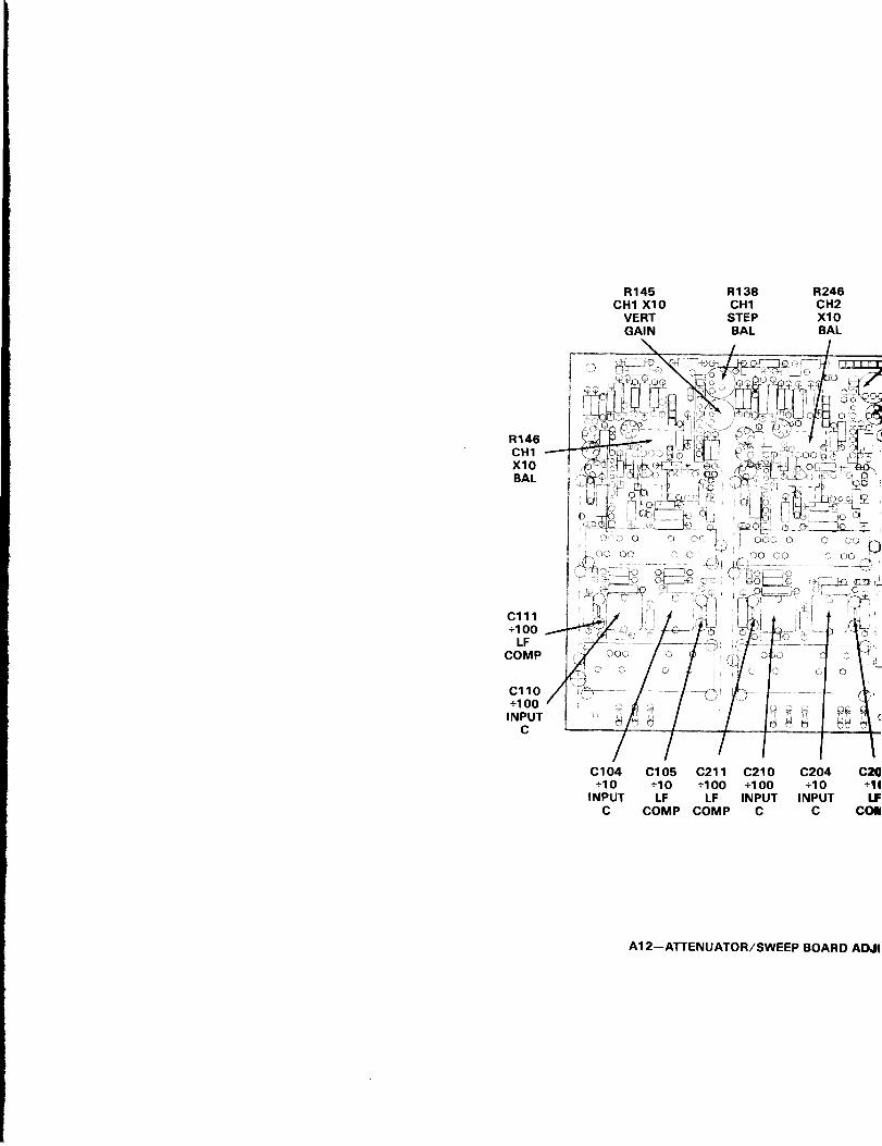
R146CH1Χ10BAL
C111+100LF
COMP
C110=100
INPUTC
R145 R138 R246CΝ 1 Χ10 CH1 CH2VERT STEP Χ10GAIN BAL BAL
C104 C105 C211 C210 C204 C20+10 +10 +100 =100 +10 +14
INPUT LF LF INPUT I NPUT LFC
COMP COMP C
C
COI
A1 2-ATTENUATOR/SWEEP BOAR D ΑW

Ιιι R246
R238
R245Ι `
CH2
CH2
CH2 Χ10Χ10 STEP VERTBAL BAL GAIN
~C204 C205 C626+10
=10
5 μsINPUT LF TIMINGC COMP
BOARD ADJUSTMENT LOCATIONS
3827-38
R733Χ10GAIN

Α . Use schematic diagrams, t he overall b l ock diagram,c i rcuit board i ll ustrations, and ci rcuit descr iptionswhen ana l yzing i nst rumen t ma l functions and l ocatingtest points . The schematic d iagrams inc l ude typ ica lwaveforms and vol tages that are in tended as an ai d1η troub leshooti ng .
Β .
C .
2 .
3 .
GENERAL NOTES
Always set the POWER switch to OFF and unp l ug the l i necord before swapp i ng, removing, or replaci ng components,and before connecti ng or d isconnecti ng instrument leadsand cab l es .
When ana l yzing ci rcuit ma l functions, consi der connectorsand cab l es as possi b le causes of fai l ure .
SPEC IF I C NOTESSet i n itia l front-pane l
VERT I CAL MODEVOLTS/D I VVOLTS/DI V Variab l eAC-GND-DCVer tica l POS I T I ONTR I GGER MODEΙΝΤSOURCESEC/D I VSEC/D I V Var iab l eΧ 1 θ Magn ificationAUTO I NTENS I TYAUTO FOCUSHor izonta l POS I T I ONPOWER SwitchHOR IZONTAL MODE
contro l s as foll ows :
CH 10 .1 VCa l deten tACM idrangeAUTOVERT MODEΙΝΤ0 .1 msCa l detentOff (Cal bu ttonM i drangeMi drangeMi drangeOff (bu ttonΝΟ DLY
out )
Verify t he low-vo l tage power supp l ies at t hefo ll owing test poin ts :
ΝΟΤΕΑ HV probe is required to measure t he -2 kVsupp l y . Turn off the power and make thetest equ i pment connections to t he osci lloscope .Set t he vo l tmeter to read at l east -3 kV, thenturn t he osci ll oscope power bac k on to ta k et he read i ng . After obtai n i ng the reading,turn off the osci lloscope power to disconnectthe test equ i pment connections, and rep l acet he cr t socket cover .
Ver ify t he -2kV supp l y at pin 2 of t he cr t soc k et .The vo l tage shou l d be between -1900 and -2100V .
WA RN I N G
The Preregulator and I nverter ci rcuits have ο fl oatingcommon reference wit h respect to chassis ground .Ac-source poten tial is presen t on the common referencepoi n ts . Connect the i nstrumen t to t he ac-power sourcethrough an iso lation t ransformer to prevent the pos-si b i l ity of persona l i njury or equ i pmen t damage whent roub l eshooting t hese ci rcu its . When an au totronsformeris also used in t he troub l eshooti ng procedure, connectt he iso l ation t ransformer to the ac-power source, t henconnect t he autot ronsformer to the i sol ation t ransformer .F i na ll y, p l ug the instrument power cord into t he auto-transformer ou t l et .
TROUBLESHOOT I NGGU IDE
SET IN I T I ALFRONT-PANEL
CONTROL SETT I NGS(NOTE 1)
CONNECT POWER CORDTO Λ SU ITABLE AC-POWER SOURCE ANDAPPLY POWER TOΤΗΕ I NSTRUMENT
VER I FY LOWVOLTAGE SUPPL I ESAND -2kV SUPPLYARE IN TOLERANCE
(NOTE 2)
Ι
αΑ ;
Vil
Ιαι.~y
NUMBER IND I CATEISCHEMAT I C DI ACIN
SUPPLY TEST POINT TOLERANCE-8 .6V ΤΡ50θ -8 .56 το -8 .64V+8 .6V W975 8 .34 to 8 .86V+5V W985 4 .75 το 5 .25V+30V W965 28 .5 to 31 .5V+10ΘV W966 95 το 105V

YES
ADJUST AUTOFOCUS AND AUTO
INTENS I TYCONTROLS FOR
Α WELL-DEF INEDV I S I BLE DISPLAY .
USE MANUALPERFORMANCE
CHECK PROCEDURETO VER I FYI NSTRUMENTFUNCT I ONS
TROUBLESHOOTPREREGULATORAND I NVERTERC IRCU ITRY .WARN I NG(NOTE 3)
9*
INDICATESTIC DIAGRAM
YES
ΝΟ
TROUBLESHOOTC I RCU I TRYASSOC I ATEDW I TH ANYFAULTY
FUNCT I ONSLOCATED
TROUBLESHOOTFAULTY SUPPLY9*
PRESS INAND HOLDBEAM F I ND
PUSH BUTTON
ΝΟ
YES
SEE MANUALADJUSTMENT
PROCEDURE TOADJUST CRTBI AS AND
AUTO FOCUS
ΝΟ
ιRELEASE BEAM F I ND
CHECK JUNCTION OF R85δAND CR856 FOR Z-AXIS
UNBLANK I NG PULSE (VAR IESFROM OV TO +50V P-P WITHAUTO I NTENS I TY CONTROL )6
CHECK Ρ6008PIN 4 FOR ΤΗΕSWEEP SAWTOOTH
( 13V Ρ-Ρ )
YES
CHECK CRT HOR I ZONTALDEFLECT I ON PLATE P I NSFOR SWEEP SAWTOOTH
( Ζ 4ΘV Ρ-Ρ ON EACH LEAD)
YES
IS TRMNEARLY CEN
IN ΤΗΕ GRAT I CW I TH BOTH POSITI
(HOR I ZONTAL AN[CENTERED 1 Ρ
RANCE
TROUBLESHOOTDC RESTORER
AND CRTC I RCU I T
9
5
TROUBLESHOOTHOR I ZONTALAMPL I F I ER
RELEASBEAM F I
CHECK 111PIN 8 F
SWP DUTY5
TROUBLESHOOTSWEEP
IS CORRECT ΝΟ GENERATORSWEEP SAWTOOTH AND SWEEP
PRESENT? LOG I CCI RCU I TS

IS TRACENEARLY CENTERED
' ΙΝ ΤΗΕ GRAT I CULE AREAΤΗ BOTH POS I T I ON CONTROLSIHOR I ZONTAL AND VERTICAL )
CENTERED IN THE I RRANGE?
YES
RELEASEBEAM F I ND
CHECK U62θPIN 8 FOR
SWP DUTY GATE5
ΝΟ
TROUBLESHOOTΖ-DRI VE SW I TCH I NGLOG I C GATE U620
AND I NPUT S I GNALS5
CHECK U8358 PIN 7FOR I NTENS LEVELCHANGE FROM +0 .6VTO -5V AS AUTO
I NTENS I TY CONTROLI S ROTATED FROMFULLY CW TO CCW6
7
DOES I NTENSLEVEL CHANGECORRECTLY?
TROUBLESHOOTAUTO I NTENS I TY
C I RCU I T
ΝΟ
TROUBLESHOOTYES
_ Ι
Ζ-AX Ι SAMPL I F IER
6
YES
TROUBLESHOOT VERT I CALATTENUATOR X1/X10 AMPL,VERT I CAL PREAMPL I F I ER,AND DELAY L INE DR I VER
FOR SOURCE OF I MBALANCE1 2,3
2213 Service
TROUBLESHOOT ING GU I DE3827-44
HOR I ZONTALLYOFF CENTER
TROUBLESHOOTDOES TRACE ΝΟ VERT I CAL
TROUBLESHOOT COME TO NEAR CENTER OUTPUTHOR I ZONTAL OF GRATICULE AMPL IF I ERAMPL I F I ER AREA? 3C IRCU I TRY
RELEASE BEAMVERT ICALLY F I ND BUTTON
I S TRACE OFF OFF CENTER AND MOMENTAR I LYCENTER HOR I ZONTALLY SHORT ACROSSOR VERT I CALLY? DELAY L I NE LEADS
3

GENERAL NOTESΑ . Use schematic d iagrams, t he overa ll bloc k
diagram, circu it board ill ust rations, andcircu it descr i p tions when analyzing lnstrumen tmal functions and l ocating test poi n ts . Theschematic diagrams inc l ude typ ica l waveformsand vol tages that are intended as an ai din t roubleshooting .
Β . Al ways set the POWER switch to OFF and unp lugt he l ine cord before swapp i ng, removi ng, orrep l acing components, and before connecti ng ordisconnecting lnst rument l eads and cab l es .
C . When ana l yzing ci rcuit ma l functions, consi derconnectors and cables as possib le causes offai l ure .
SPEC I F I C NOTES
WA RN ING
The Preregulator and I nverter circu its have αf l oating common reference wit h respect to chassisground . Ac-source potentia l is presen t on thecommon reference poin ts . Connect the l nstrumen tto the ac-power source t hrough an iso lation t rans-former to prevent t he possi b i l ity of persona l i nj uryor equ ipment damage when troub leshooting t heseci rcuits . When an au tot ransformer is a l so used int he troub l eshooti ng procedure, connect the iso l ationtransformer to t he ac-power source, then connectt he autotransformer to the iso l ation t ransformer .F i nally, p l ug the l nstrument power cord into theautotransformer ou t let .

PREREGULATORAND I NVERTER
TROUBLESHOOT I NG
REMOVE POWER FROMΤΗΕ I NSTRUMENT
TROUBLESHOOTPREREGULATOR
FOR SHORTED OROPEN COMPONENTS
REPLACEFUSE
REMOVE POWERFROM ΤΗΕ
I NSTRUMENT
TROUBLESHOOT TOREMOVE SHORT .
CHECK CR931, CR932CR933, CR934, VR938C937, Q940, AND Q942
FOR SHORTS .(Q94θ AND Q942 SHOULDBE REPLACED AS Α PA I R
I F ONE I S SHORTED)
REV DEC 1981
CONNECT DMM TOMEASURE ΤΗΕ +45V
PREREGULATOROUTPUTACROSS VR938SHORT P I NS 1 AND 2OF U931 TOGETHER
LOWER AUTOTRANSFORMER OUTPUT
TO ZERO V .SHORT BASE OF0956 TO ΤΡ934 .
RA I SE AUTOTRANSFORMER SLOWLY
TO +85V RMS .WATCH +45V LEVEL
TROUBLESHOOTI NVERTER CONTROL
C I RCU ITRYCOMPONENTS
Q948, Q954, Q956AND Τ942
CONNECT I NSTRUMENTTO AC-POWER SOURCE
V I A AN AUTOTRANSFORMER ANDAN ISOLATIONTRANSFORMER(SEE NOTE 1) .
APPLY POWER TO ΤΗΕI NSTRUMENT AND
SLOWLY RA I SE ΤΗΕAUTO TRANSFORMEROUTPUT VOLTAGE .(DO NOT EXCEED85 VRMS I NPUT)
ι

NT ANDΥ RA I SE ΤΗΕTRANSFORMER
VOLTAGE .NOT EXCEED
I NPUT)
YES / τυυrοτεο
YES
Ι
ΝΟ
YES
TROUBLESHOOT SECONDARY POWERSUPPL I ES FOR EXCESS I VE LOAD ING
ON ΤΗΕ PR IMARY C I RCU IT .CHECK Q940 AND Q942 FOR OPEN
SUSPECT EXCESS I VEPOWER SUPPLY LOAD I NG .
SEE POWER SUPPLYISOLAT I ON PROCEDUREADJACENT TO POWER
D I STRIBUT I ON D I AGRAM
TURN OFF POWER TOI NSTRUMENT AND REMOVE
SHORT FROM U931 P I NS 1 δ 2 .REAPPLY POWER AND I NCREASE
AC- I NPUT TO 115V RMS
CHECK Q94θ AND Q942COLLECTOR VOLTAGE W I THRESPECT TO ΤΡ934 FORHEADROOM VOLTAGE
REPLACE DEFECT IVECOMPONENTS AND CHECK
POWER SUPPLY OPERAT ION
POWER SUPPLYRECT I F I ER AND FI LTER
COMPONENTS OK?
YES
ΝΟ
IS VOLTAGEDROP ACROSS R941AT LEAST θ .4V?
ΝΟ
AREALL SECONDARYVOLTAGES WITHIN
TOLERANCE?
I SHEADROOM
VOLTAGE AT LEAST3 .SV?
YES
ΝΟ
YES
ΝΟ
PREREGULATOR ANDI NVERTER TROUBLESHOOT ING
3826-45Α
2213 Service
< mτ
mmλ m4 οm C
TROUBLESHOOT FAULTYPOWER SUPPLY FOR OPEN οο
I NSTRUMENT OR SHORTED COMPONENTS . c~WER SOURCE CHECK XFMR W I ND ING φ Dm ZAN AUTO ΗστORMER AND
όISOLAT I ON DOORMER POWER YES -,000' SECONDARY -N`~ ΝΟ z
NOTE 1 ) . SUPPLY VOLTAGES REMA I N CHECK οPOWER TO ΤΗΕ OK ,IN TOLERANCE? U931

PARTS ORDER ING I NFORMATIO N
Replacement pa rts are available from or through your local
Te k t ron ix, I nc. Field Office or re presentative .
Changes to Tekt ron ix in st rumen ts are sometimes made toaccommodate improved componen ts as they become availab le,and to give you the benefit of the latest ci rcu it improvementsdeveloped in our e n gi n eering departmen t . It is thereforeimporta n t, when order ing parts, to in clude the followinginform atio n in your o rder: Part number, instrumen t type ornumb er, se r ial nu mber, and mod ificatio n number if app licable.
If α p art you have ordere d has been replace d with α new or
improved p art, you r local Tek tron ix, Inc. F ield Office or
represe n tative will contact you conce rn ing any change in p artnumber .
Change in formatio n , if any, is located at the rear of th ismanual.
SPECIAL N OTES AN D SYMB OLSΧΟΟΟ
Part fi r st added at th is serial number
Part removed after th is se r ial numberΟΟΧ
FIGURE AND INDEX NUMBERSItems in th is section a re referenced by figure and
numbers to the illu str ations.
REPLACEABLEMECHANICAL PARTS
index
ABBREVIATIONS
IN DENTATIO N SYSTEM
Section10-2213 Service
This mechanical p arts list is indented to ind icate itemrelationsh ips. Following is an exam p le of the indentation systemused in t he description column .
1 2 3 4 5
Name & Description
Assembly and/or ComponentAttaching parts for Assembly and/or Component
Detail Part of Assembly and/or ComponentAttaching p arts for Detail Part
Parts ο/ Detail PartAttaching parts for Parts ο1 Detail Part
Attach ing Parts always appea r in the same inden tation asthe item it moun ts, wh ile the d etail parts are inden ted to the right .Indented items are part of, and in cluded with , the next hig herinden tation . The separ atio n symb ol ---' --- ind icates theend ofattach ing p arts .
Attach ing parts mu st be purchased sepa rately, unless otherwisespecified .
ITEM NAMEIn the Parts List, an Item Name is separated f rom the
descrip tion byα colon ( :) . Because of space limitations, an ItemName may sometimes appea r as incomp lete . For fu rt her ItemName iden tification , theU.S . Federal Cataloging Handbook Η6-1can be utilize d where possi b le .
INCH ELCTRN ELECTRONNUMBER SIZE ELEC ELECTRICAL
ACTR ACTUATOR ELCTLT ELECTROLYTICADPTR ADAPTER ELEM ELEMENTALIGN ALIGNMENT EPL ELECTRICAL PARTS L ISTAL ALUM INUM EQPT EQU IPMENTASSEM ASSEMBLED ΕΧΤ EXTERNALASSY ASSEMBLY FIL FILLISTER HEADΑΤΤΕΝ ATTENUATOR FLEX FLEXIBLEAWG AMERICAN W IRE GAGE FLH FLAT HEADBD BOA RD FLTR F ILTERBRKT BRACKET FR FRAME or FRONTBRS BRASS FSTNR FASTENERBR Z BRONZE FT FOOTBSHG BU SH ING FXD F IXEDCAB CAB INET GSKT GASKETCAP CAPACITOR HDL HANDLECER CERAM IC HEX HEXAGO NCHAS CHASSIS HEX HD HEXAGONAL HEADCKT CIRCUIT HEX SOC HEXAGONAL SOCKETCOMP COMPOSITION HL CPS HELICAL COMPRESSIONCONN CONNECTOR HLEXT HELICAL EXTEN SIONCOV COVER HV HIGH VOLTAGECPLG COUPL ING IC INTEGRATED CIRCUITCRT CATHODERAY TUBE ID INSIDE DIAMETERDEG DEGREE (DENT IDEN TIFICATIONDWR DRAWER IMPLR IMPELLER
IN INCH S E SINGLE ENDINCA ND INCANDESCENT SECT SECTIONINSUL INSULATOR SEMICOND SEM ICONDUCTORINTL INTERNAL SHLD SH IELDLPHLDR LAMPHOLDER SHLDR SHOULDEREDMACH MACH INE S KT SOCKETMECH MECHANICAL S L SL IDEMTG MOUNTING SLFLKG SELF-LOC K INGNIP N IPPLE S LVG SLEEV INGNONWIRE NOTWIRE WOUND SPR SPR INGOBD ORDER BY DESCRIPTION SO SQUAREOD OUTSID E DIAMETER SST STAI NLESS ST EELOVH OVAL HEAD STL STEELΡΗ BRZ PHOSPHOR BRONZE SW SWITCHPL PLAIN αι PLATE Τ TUBEPLSTC PLASTIC TERM TERM INALΡΝ PART NUMBER THD THREADΡΝΗ PAN HEAD ΤΗΚ TH IC KPWR POWER TNSN TENSIONRCPT RECEPTAC LE TPG TAPP INGRE S RESISTOR TRH TRUSS HEADRGD R IGID V VOLTAGERLF REL I EF VAR VARIABLERTNR RETAINER W/ WITHSCH SOCKE T HEAD W SHR WASHERSCOPE OSCI LLOSCOPE XFMR TRANSFORMERSCR SCREW XSTR TRANSISTOR

Replaceable Mechanical Parts-2213 Service
CROSS I NDEX-MFR. CODE NUMBER TO MANUFACTURER
10-2 REV FEB 1982
M fr . Code Manufacturer Address City, State, Zip
53629 PANEL COMPONENT S CORP . 2015 SECOND ST . BERKELE Y, CA 9417000779 AMP, INC . Ρ 0 BOX 3608 HARRISBURG, PA 1710501536 CAMCAR DIV OF TEXTRON INC. SEMS
PRODUCTS UNIT 1818 CHRISTINA ST . ROCKFORD, IL 6110802768 ILLINOIS TOOL WORKS, INC ., FASTEX DIV . 195 ALGONQUIN ROAD DES PLAINES, IL 6001605820 WAKEFIELD ENGINEERING, INC . AUDUBON ROAD WAKEFIELD, ΜΑ 0188012327 FREEWAY CORPORATION 9301 ALLEN DRIVE CLEVELAND, OH 4412513511 AMPHENOL CARDRE DIV ., BUNKER RAMO CORP . LOS GATOS, CA 9503016428 BELDEN CORP . Ρ. 0 . BOX 1331 RICHMOND, IN 4737423050 PRODUCT COMPONENTS CORP 30 LORRAINE AVE . MT VERNON, NY 1055324931 SPECIALITY CONNECTOR CO., INC . 2620 ENDRESS PLACE GREENWOOD, IN 4614228520 ΗΕΥΜΑΝ MFG . CO . 147 Ν. MICHIGAN AVE . KENILWORTH, NJ 0703371279 CAMBRIDGE THERMIONIC CORP. 445 CONCORD AVE . CAMBRIDGE, ΜΑ 0213871400 BUSSMAN MFG., DIVISION OF MCGRAW-
EDISON CO . 2536 W. UNIVERSITY ST . ST . LOUIS, MO 6310773743 FISCHER SPECIAL MFG . CO . 446 MORGAN ST . CINCINNATI, OH 4520677250 PHEOLL MANUFACTURING CO ., DIVISION
OF ALLIED PRODUCTS CORP . 5700 W. ROOSEVELT RD . CHICAGO, IL 6065078189 ILLINOIS TOOL WORKS, INC .
SHAKEPROOF DIVISION ST . CHARLES ROAD ELGIN, IL 6012078471 TILLEY MFG . CO . 900 INDUSTRIAL RD . SAN CARLOS, CA 9407080009 TEKTRONIX, INC . Ρ 0 BOX 500 ΒΕΑΥΕΑΤΟΝ , OR 9707782389 SWITCHCRAFT, INC. 5555 Ν . ELSTON AVE . CHICAGO, IL 6063083385 CENTRAL SCREW CO . 2530 CRESCENT DR . BROADVIEW, IL 6015393907 TEXTRON INC . CAMCAR DIV 600 18TH AVE ROCKFORD, IL 6110195987 WECKESSER CO ., INC . 4444 WEST IRVING PARK RD . CHICAGO, IL 60641

Replaceable Mechanical Parts-2213 Service
REV OCT 1982
10-3
Fig . &IndexΝο .
Tektronix Serial/ Model Νο .P art Νο . E ff Dscont Qty 1 2 3 4 5 Name & Desc ription
MfrCode Mfr Part Num ber
1- 650-0221-00 1 MECHANICAL KIT : 80009 650-0221-00-Ι 334-5001-00 1 MARKER,IDENT :MKD CAUTION 80009 334-5001-00-2 200-2538-00 1 COVER ,REAR :PLASTIC 80009 200-2538-00
(ATTACHING PARTS)-3 211-0691-00 2 SCREW ,MACHINE :6-32 Χ 0 .625,ΡΝΗ 01536 OBD
-4 390-0790-06 1 CABINET,SCOPE :W/ΣΕΕΤ 80009 390-0790-06(ATTACHING PARTS)
-5 213-0882-00 1 SCREW, TAPPING :6-32 Χ 0 .437 ΤΥΡΕ C 01536 OBD
-6 348-0659-01 2 FOOT ,CABINET:BLACK POLYURETHANE 80009 348-0659-01-7 334-4172-00 1 MARKER,IDENT : 80009 334-4172-00-8 367-0289-00 1 HANDLE ,CARRYING :13 .855,SST 80009 367-0289-00
(ATTACHING PARTS)-9 212-0144-00 2 SCREW , TPG,TF:8-16 Χ 0 .562 L 93907 225-38131-012
-10 334-5002-00 1 PLATE,IDENT :MKD TEKTRONIX 80009 334-5002-00-11 426-1765-00 1 FRAME,CRT : 80009 426-1765-00
(ATTACHING PARTS)-12 211-0690-00 2 SCREW,MACHINE :6-32 Χ 0 .875,PNH ,STL 01536 OBD
-13 337-2775-00 1 SHLD,IMPLOSION : 80009 337-2775-00-14 366-1833-00 6 KNOB:GRAY,0.25 ID Χ 0 .392 Χ 0 .3920D 80009 366-1833-00-15 _____ ____- 2 CONN,RCPT,ELEC :(SEE J1001, J2001 REPL)-16 ----- ----- 1 CONN,RCPT,ELEC :(SEE J4001 REPL)-17 210-0255-00 1 TERMINAL,LUG :0 .391 ID,LOCKING,BRS CD PL 80009 210-0255-00-18 384-1575-00 1 EXTENSION ,SHAFT :FOCUS W/KNOB,PLASTIC 80009 384-1575-00-19 358-0550-00 1 BUSHING,SHAFT:0 .15 ID Χ 0 .31NCH OD,PLSTC 80009 358-0550-00-20 136-0387-01 1 JACK,TIP :BLACK 71279 450-4252-01-0310-21 366-1031-03 2 KNOB :RED--CAL 80009 366-1031-03-22 366-1838-01 2 KNOB :GY,0 .249 ID Χ0 .718 Χ 1 .765 80009 366-1838-01-23 358-0640-00 2 BSHG,MACH THD :0 .5-32 THD Χ 0 .39 ID 80009 358-0640-00-24 366-1405-09 1 KNOB : RED ,CAL ,0 .127X 0 .45 OD 80009 366-1405-09-25 366-1852-01 1 KNOB :GY,SEC/DIV ,0 .25 ID Χ 0 .79 80009 366-1852-01-26 366-2020-01 1 ΚΝΟΒ :0 .252 ID Χ 0 .581 OD Χ 0 .612 80009 366-2020-01_27 _____ ----- 1 RES,VAR,WW:(SEE R658 REPL)
(ATTACHING PARTS)-28 220-0495-00 1 NUT, PLAIN ,HEX . :0 .375-32 Χ 0 .438 INCH BRS 73743 OBD-29 210-0978-00 1 WASHER , FLAT :0 .375 ID Χ 0 .50 INCH OD ,STL 78471 OBD
-30 333-2680-00 1 PANEL,FRONT : 80009 333-2680-00-31 366-2013-00 2 PUSH,BUTTON:DIRTY GRAY,0 .134 SQ Χ 0 .480 Η 80009 366-2013-00-32 348-0660-00 4 CUSHION ,CRT:POLYURETHANE 80009 348-0660-00-33 386-4444-00 1 SUBPANEL,FRONT : 80009 386-4444-00
(ATTACHING PARTS)-34 213-0881-00 2 SCREW, TAPPING :6-32 Χ 0 .25 ΤΥΡΕ C 01536 OBD-35 213-0882-00 2 SCREW, TAPPING :6-32 Χ 0 .437 ΤΥΡΕ C 01536 OBD
-36 377-0512-00 6 INSERT ,KNOB :0 .125 ID Χ 0 .663 L,AL 80009 377-0512-00-37 129-0836-00 2 SPACER ,POST :1 .207 L ,W/0 .5-32 THD 80009 129-0836-00
213-0228-00 2 . SETSCREW:6-32 Χ 0 .125,STL CD PL,HEX SKT-38 384-1503-00 2 EXTENSION SHAFT :5 .4 L Χ 0 .124DIA,PLASTIC 80009 384-1503-00-39 384-1180-00 1 EXTENSION SHAFT :6 .40 INCH LONG 80009 384-1180-00-40 ----- ----- 1 CKT BOARD ASSY :ATTEN/SWEEP (SEE Α12 REPL)
(ATTACHING PARTS)-41 211-0304-00 2 SCREW,MACHINE :4-40 Χ 0.312,ΡΝΗ 01536 OBD
----- ----- - CKT BOARD ASSY INCLUDE S :-42 ----- ----- 25 . TERMINAL,PIN :(SEE Α12Ρ1010,Ρ2010, Ρ6001,
----- ----- - . Ρ 7000 REPL)-43 136-0328-02 10 . SOCKET,PIN TERM :HORIZONTAL 00779 86282-2-44 1 . RES .,VAR,NONWIR :(SEE A12R629 REPL)
(ATTACHING PARTS)-45 210-0413-00 1 . NUT , PLAIN ,HEX . :0 .375-32 Χ 0 .50 INCH,STL 73743 3145-402-46 210-0012-00 1 . WASHER,LOCK :INTL,0 .375 ID Χ 0 .50" OD STL 78189 1220-02-00-0541C

Replaceable Mechanical Parts-2213 Serviceι
10-4
REVOCT 1982 1
ιiι
ι ιιι
Fig . &IndexΝΟ .
1-47-48
Tek tron ix Serial/ Model Νο .Part Νο . Eff Dscont
----- ---------- -----
Qty
12
1 2 3 4 5 N ame & Desc r ip tion
. SWITCH,ROTARY :(SEE A12S630A, B REPL)
. RES .,VAR,NONWIR :(SEE A12R141, R241 REPL)
MfrCode Mfr Part Number
(ATTACHING PARTS)-49 210-0413-00 1 . ΝUΤ, ΡLΑΙΝ ,ΗΕΧ . :0 .375-32 Χ 0 .50 INCH ,STL 73743 3145-402-50 210-0012-00 1 . WASHER,LOCK:INTL ,0 .375 ID Χ 0 .50" OD STL 78189 1220-02-00-0541C
-5Ι ----- ----- 2 . SWITCH,ROTARY :(SEE Al 2S105AB ,S205AB REPL)-52 407-2585-00 1 BRACKET ,GROUND :CIRCUIT BOARD,BRASS 80009 407-2585-00-53 337-2892-00 1 SHIELD,ELEC :CIRCUIT BOARD 80009 337-2892-00
(ATTACHING PARTS)-54 211-0304-00 1 SCREW,MACHINE :4-40 Χ 0 .312,ΡΝΗ 01536 OBD-55 129-0906-00 1 SPACER , POST :0 .685 L W/4-40 ΙΝΤ 6 ΕΧΤ THD 80009 1 Ζ9-0906-00
-56 ----- ----- 1 CKT BOARD ASSY:FRONT PANEL(SEE All REPL)(ATTACHING PARTS)
-57 211-0304-00 3 SCREW,MACHINE :4-40 Χ 0 .312, ΡΝΗ 01536 OBD
CKT BOARD ASSY INCLUDES :-58 ----- ----- 4 . TERMINAL,PIN :(SEE ΑΙΙΡ1000, Ρ800δ REPL)-59 ----- ----- 10 . CONTACT,ELEC :(SEE A11J2001 REPL)-60 ----- ----- 10 . SWITCH,SLIDE :(SEE AllS101,S201,S305,S315,
- . S317,S401,S440,S611,S650,S660 REPL)-61 361-1081-00 1 . SPACER,LED :PLASTIC 80009 361-1081-00-62 ----- ----- 1 . RES .,VAR,NONWIR:(SEE AlIR455 REPL)-63 ----- ----- Ι . RES .,VAR,NONWIR:(SEE ΑlIR557 REPL)-64 ----- ----- 1 . SWITCH,SLIDE :(SEE All S464 REPL)-65 ----- ----- Ι . SWITCH,PUSH : ( SEE A12S264 REPL)-6δ ----- ----- 1 . SWITCH,PUSH :(SEE All S390 REPL)-δ7 ----- ----- 4 . RES .,VAR,NONWIR:(SEE ΑllRl90,Α290, Α726,
- . R807 REPL)-68 407-2584-00 1 BRACKET ,GROUND :FRONT PANEL,BRASS 80009 407-2584-00
(ATTACHING PARTS)-69 211-0304-00 2 SCREW ,MACHINE :4-40 Χ 0 .312,ΡΝΗ 01536 OBD-70 343-0089-00 1 CLAMP ,LOOP :LARGE 80009 343-0089-00-71 441-1535-00 1 CHASSI S,SCOPE : FRONT MAIN 80009 441-1535-00
(ATTACHING PARTS)-72 213-0881-00 2 SCREW,TAPPING :6-32 Χ 0 .25 ΤΥΡΕ C 01536 OBD
1 TRANSI STOR:(SEE Q938 REPL)(ATTACHING PARTS)
211-0318-00 1 SCREW,MACHINE :4-40 Χ 0 .75,FLH ,100 DEG 93907 OBD210-0586-00 1 NUT,PL,ASSEM WA :4-40 Χ 0 .25,STL CD PL 83385 OBD
342-0582-00 1 INSULATOR,PLATE :TRANSISTOR ,CERAMIC 80009 342-0582-00343-1025-00 1 RETAINER,XSTR : 80009 343-1025-00----- ----- 1 CKT BOARD ASSY:CURRENT LIMIT(SEE Α19 REPL)344-0154-03 2 . CLIP,ELECTRICAL :FUSE ,CKT BD MT 80009 344-0154-03


2213 OSCILLOSCOPE


ν 198 1 2213 OSCI LLOSCOPE

Replaceable Mechanical Parts-2213 Service
REV OCT 1982
10-5
Fig . &IndexΝο .
Te ktronixPart Νο .
Serial/ Model Νο .Eff Dsco n t Qty 1 2 3 4 5 Name & Description
MfrCode Mfr Part Number
2-1 334-4251-00 1 MARKER,IDENT :MKD CAUTION 80009 334-4251-00-2 337-2773-00 1 SHIELD,ELEC : POWER SUPPLY, LOWER,PLSTC 80009 337-2773-00
(ATTACHING PARTS)-3 211-0304-00 1 SCREW,MACHINE :4-40 Χ 0 .312, ΡΝΗ 01536 OBD
-4 386-4613-00 1 SUPPORT,SHIELD : 80009 386-4613-00(ATTACHING PARTS)
-5 211-0305-00 2 SCREW ,MACHINE :4-40 Χ 0 .437, ΡΝΗ 01536 OBD-6 334-4251-00 1 MARKER,IDENT :MKD CAUTION 80009 334-4251-00-7 348-0721-00 1 GROMMET, PLASTIC : BLACK POLYSUFONE 80009 348-0721-00-8 348-0555-00 1 GROMMET,PLASTIC :SIL GY,U SHAPE ,0 .52 ID 80009 348-0555-00-9 337-2772-00 1 SHIELD,ELEC : POWER SUPPLY,AL 80009 337-2772-00
(ATTACHING PARTS)-10 211-0304-00 Β010100 Β012480 3 SCREW,MACHINE :4-40 Χ 0 .312, ΡΝΗ 01536 OBD
211-0305-00 Β012481 3 SCREW,MACHINE :4-40 Χ 0 .437, ΡΝΗ 01536 OBD-11 211-0303-00 2 SCREW,MACHINE :4-40 Χ 0 .25,FLH 100 DEG 01536 OBD
-12 366-1480-03 1 PUSH BUTTON :BLACK ,OFF 80009 366-1480-03-13 384-1576-00 Β010100 Β016349 1 EXTENSION SHAFT :12 .809 L , PLASTIC 80009 384-1576-00
384-1576-01 Β016350 1 EXTENSION SHAFT :12 .809 L ,PLASTIC 80009 384-1576-01-14 ----- ----- 1 CKT BOARD ASSY :MAIN(SEE AN REPL)
(ATTACHING PARTS)-15 213-0882-00 3 SCREW ,TAPPING :6-32 Χ 0 .437 TYPE C 01536 OBD-16 211-0302-00 2 SCREW,MACHINE :4-40 Χ 0 .75,ΡΝΗ 01536 OBD
----- ----- - CKT BOARD ASSY INCLUDES :-17 ----- ----- 3 . TERMINAL,PIN :(SEE ΑlΟΡΙ011,Ρ2011, Ρ6001,
----- ----- - . Ρ7001,Ρ7055 REPL)-18 ----- ----- 1 . RES .,VAR,NONWIR:(SEE AlOR883 REPL)
(ATTACHING PARTS)-19 220-0495-00 1 . ΝUΤ ,ΡLΑΙΝ, ΗΕΧ. :0.375-32 Χ 0 .438 INCH BRS 73743 OBD-20 337-2945-00 1 . SHIELD,ELEC :POTENTIOMETER 80009 337-2945-00-21 361-1047-00 1 . SPACER,VAR RES :0.3 Χ 0 .615 ΧΟ .55 80009 361-1047-00-22 214-0498-00 Β010100 Β017549 2 . HEAT SINK ,XSTR : TO-18,AL BLACK ANODIZED 05820 201-AB
214-3414-00 Β017550 2 . HEAT S INK ,XSTR : TO-92/ΤΟ-18,ALUMINUM 13103 2224Β-23 200-2735-00 1 . COVER,POWER SW : 80009 200-2735-00-24 ----- ----- 1 . SWITCH,PUSH;(SEE Al OS901 REPL)-25 343-0088-00 1 . CLAMP ,LOOP :0 .062 INCH DIA 80009 343-0088-00-26 131-1048-00 4 . TERM.QIK DISC :CKT BD ΜΤ ,0 .11 Χ 0.02 00779 61134- ί-27 ----- ----- 1 . MICROCIRCUIT,LI :(SEE AlOU990 REPL)-28 ----- ----- 1 . THYRISTOR:(SEE Al OQ925 REPL)
(ATTACHING PARTS)-29 211-0304-00 1 . SCREW,MACHINE :4-40 Χ 0 .312, ΡΝΗ 01536 OBD-30 210-0406-00 1 . NUT,PLAIN,HEX . :4-40 Χ 0 . 188 INCH,BRS 73743 12161-50
-31 ----- ----- 9 . TERM ,TEST ΡΟΙΝΤ :(SEE ΑΙΟΤΡ444, ΤΡ500, ΤΡ501,----- ----- - . ΤΡ915, ΤΡ920, ΤΡ921,ΤΡ934, ΤΡ940,ΤΡ952 REPL)
-32 343-0969-00 1 . RETAINER ,XSTR :POLYPHENYLENESULFIDE 80009 343-0969-00(ATTACHING PARTS)
-33 211-0691-00 1 . SCREW ,ΜACHINE :6-32 Χ 0 .625,ΡΝΗ 01536 OBD-34 210-0457-00 1 . NUT,PL ,ASSEM WA :6-32 Χ 0 .312,STL CD PL 83385 OBD
-35 ----- ----- 2 . TRANSISTOR :(SEE AI OQ940,Q942 REPL)-36 342-0555-00 1 . INSULATOR,PLATE :HEAT SINK,AL 80009 342-0555-00-37 ----- ----- 1 . MICROCIRCUIT,LI :(SEE AlOU985 REPL)
(ATTACHING PARTS)-38 211-0304-00 1 . SCREW,MACHINE :4-40 Χ 0 .312,ΡΝΗ 01536 OBD-39 210-0586-00 1 . NUT ,PL ,ASSEM WA:4-40 Χ 0 .25,STL CD PL 83385 OBD
-40 407-2729-00 1 . BRACKET ,HEAT SK :AL 80009 407-2729-00(ATTACHING PARTS)
-41 211-0303-00 2 . SCREW,MACHINE :4-40 Χ 0 .25, FLH 100 DEG 01536 OBD-42 214-0973-00 Β010100 Β014899 Χ 1 . HEAT SINK ,ELEC :0 .28 Χ 0 .18 OVAL Χ 0 .187"Η 80009 214-0973-00
334-5001-06 ΧΒ020100 1 MARKER,IDENT :MKD CAUTION200-2809-00 ΧΒ020100 1 COVER ,CRT :REAR,ALUMINUM

Replaceable Mechanical Parts-2213 Service
10-β
ιι
REV OCT 1982
1
Fig . &In d exΝο .
Te ktron ixPart Νο .
Serial/ M od el Νο .Eff Dscont Qty 1 2 3 4 5 Name & Desc r i ption
M frCode Mfr Part Number
2-43 214-1061-05 1 SPRINC,GROUND:PLATED 80009 214-1061-05-44 200-2519-00 1 CAP .,CRT SOCKET:NATURAL LΕΧΑΝ 80009 200-2519-00-45 ----- ----- 1 DELAY LINE,ELEC :(SEE DL350 REPL)
(ATTACHING PARTS)-46 213-0882-00 2 SCREW , TAPPING :6-32 Χ 0 .437 ΤΥΡΕ C 01536 OBD
-47 426-1766-00 1 MOUNT,RESILIENT :CRT ,REAR 80009 426-1766-00-48 136-0202-04 1 5ΚΤ , ΡL-IN ELEK :ELECTRON ΤUΒΕ ,14 CONT 80009 136-0202-04-49 334-1379-00 1 LABEL:CRT,ADHE SIVE BACK 80009 334-1379-00-50 334-1951-00 1 MARKER,IDENT :CRT WARNING 80009 334-1951-00-51 337-2774-00 1 SHIELD,ELEC :CRT ,STEEL 80009 337-2774-00-52 386-4443-00 1 SUPPORT,SHIELD :CRT,FRONT,PLASTIC 80009 386-4443-00-53 ----- ----- 1 ELECTRON TUBE :(SEE V870 RΕΡL)-54 134-0158-00 2 BUTTON , PLUG :0 .187 DIA,NYLON 02768 207-080501-00-55 334-3379-02 1 MARKER,IDENT :MARKED GROUNDSYMBOL 80009 334-3379-02-56 131-0955-00 1 CONN,RCPT,ELE C : BNC, FEMALE 13511 31-279-57 200-2264-00 1 CAP .,FUSEHOLDER :3AG FUSES 53629 ΣΕΚ 031 1666-58 200-1388-03 1 COVER ,FUSE,LEAD :POLYURETHANE 80009 200-1388-03-59 204-0833-00 1 BODY, FUSEHOLDER :3AG fi 5 Χ 20ΜΜ FUSE S 53629 031 .1653(MDLFEU)
(ATTACHING PARTS)-60 210-1039-00 1 WASHER ,LOCK : INT ,0.521 ID Χ 0.625 INCH OD 24931 OBD
-61 210-0202-00 1 TERMINAL ,LUG :0 .146 ID,LOCKING,BRZ TINNED 78189 2104-06-00-252ΟΝ(ATTACHING PARTS)
-62 210-0457-00 1 NUT,PL,ASSEM WA:6-32 Χ 0.312,STL CD PL 83385 OBD
-63 348-0738-00 Β010100 Β020099Χ 1 GROMMET ,PLASTIC :0 .312 ID,NYLON,BLACK 28520 SB-437-5-64 337-2947-00 Β010100 Β020099 1 SHIELD,ELEC : INDUCTOR 80009 337-2947-00
337-3047-00 Β020100 1 SHIELD,ELEC : POWER SUPPLY(ATTACHING PARTS)
-65 211-0303-00 2 SCREW, MACHINE :4-40 Χ 0.25, FLH 100 DEG 01536 OBD
-66 1 COIL,RF:(SEE L925 REPL)-67 161-0033-26 Β010100 Β013039 1 CABLE ASSY, PWR :3,18 AWG,125V ,101 .3 L 16428 ΚΗ-9230
161-0104-00 Β013040 1 CABLE ASSY , PWR, :3 WIRE ,98 .0" LONG 16428 ΚΗ8352-68 358-0161-01 Β010100 Β013039Χ 1 BSHG,STRAIN RLF :FOR 0 .29 INCHDIA CABLE 28520 1154 SR-5L-1
348-0746-00 Β010100 Β020099Χ 1 CUSHION,IDCTR :MOLDED POLYURETHANE 80009 348-0746-00211-0303-00 1 SCREW ,MACHINE :4-40 Χ 0 .25,FLH 100 DEG 01536 OBD210-0586-00 1 NUT,PL,ASSEM WA :4-40 Χ 0 .25,STL CD PL 83385 OBD131-1084-03 ΧΒΟ13040 Β020099Χ 1 CONN , RCPT ,ELEC :PWR ,MALE ,250VAC,6A 82389 EAC-301210-0586-00 ΧΒΟ13040 1 NUT,PL ,ASSEM WA :4-40 Χ 0 .25,STL CD PL 83385 OBD210-0803-00 ΧΒΟ13040 1 WASHER , FLAT :0 .15 ID Χ 0 .032 THK ,STL CD PL 12327 OBD211-0323-00 ΧΒΟ13040 1 SCREW,MACHINE :4-40 Χ 0 .312, FLH,100 DEG 83385 OBD213-0882-00 ΧΒΟ13040 1 SCREW ,TAPPING :6-32 Χ 0 .437 ΤΥΡΕ C 01536 OBD343-0002-00 ΧΒΟ13040 1 CLAMP , LOOP :0 .188 INCH DIA 95987 3-16-6Β337-3053-00 ΧΒ020100 1 SHIELD,ELEC : EMI 80009 337-3053-00407-2790-00 ΧΒ020100 1 BRACKET ,CKT BD :VERTICAL ALUMINUM407-2791-00 ΧΒ020100 1 BRACKET,ANGLE :CIRCUIT BOARD,AL 80009 407-2791-00386-4923-00 ΧΒ020100 3 SPACER ,CKT BD:FLAME-RETARDANT NYLON 06915 CBS-4Μ
(ATTACHING PARTS)211-0304-00 ΧΒ020100 6 SCREW , MACHINE :4-40 Χ 0 .312,ΡΝΗ 01536 OBD
195-0389-00 ΧΒΟ 13040 1 LEAD,ELECTRICAL :18 AWG,4 .0 L ,5-4 80009 195-0389-00195-5498-00 ΧΒΟ 13040 1 LEAD,ELECTRfCAL :18 AWG,2 .5 L ,8-9 80009 195-5498-00195-5499-00 ΧΒΟ13040 1 LEAD,ELECTRICAL :18 AWG,3 .5 L ,8-0 80009 195-5499-00
-69 200-2531-00 Β010100 Β013039Χ 1 COVER,POWER :PLASTIC 80009 200-2531-00-70 441-1536-00 Β010100 Β013039 1 CHASSI S,SCOPE : REAR MAIN 80009 441-1536-00
441-1536-01 Β013040 1 CHASSI S,SCOPE : REAR 80009 441-1536-01(ATTACHING PARTS)
-71 213-0881-00 2 SCREW ,TAPPING :6-32 Χ 0 .25 ΤΥΡΕ C 01536 OBD
----- ----- 1 CKT BOARD ASSY :(SEE Α18 REPL)195-9543-00 ΧΒ020100 1 . LEAD,ELECTRICAL:18 AWG,6 .0 L ,0-Ν 80009 195-9543-00210-0202-00 ΧΒ020100 1 . TERMINAL ,LUG :0 .146 ID,LOCKING, BRZ TINNED 78189 2104-06-00-252 ΟΝ214-3413-00 ΧΒ020100 1 . HEAT SINK,ELEC :CKT BD 80009 214-3413-00

Replaceable Mechanical Parts-2213 Service
REV OCT 1982
10-7
F ig . &IndexΝο .
TektronixPart Νο .
Serial/Model Νο .Eff Dscont Qty 1 2 3 4 5 N ame & Description
MfrCode Mfr Part Num ber
2-72 ----- ----- 1 CKT BOARD ASSY :CURRENT LΙΜΙΤ(SEE Α19 REPL)(ATTACHING PARTS)
-73 213-0882-00 1 SCREW, TAPPING:6-32 Χ 0 .437 ΤΥΡΕ C 01536 OBD-74 210-0457-00 1 NUT,PL,ASSEM ωΑ :6-32 Χ 0 .312,STL CD PL 83385 OBD
-75 ----- ----- 4 . TERM ,QIK DISC :CKT BD ΜΤ,0 .11 Χ 0 .02----- ----- - . (SEE Α19Ρ801,802,803,804 REPL)
-76 344-0154-03 2 . CLIP,ELECTRICAL :FUSE ,CKT BD MT 80009 344-0154-03-77 342-0582-00 Β010100 Β020099 1 . INSULATOR,PLATE :TRANSISTOR,CERAMIC 80009 342-0582-00
342-0582-01 Β020100 1 . INSULATOR,PLATE :TRANSISTOR,CERAMIC 80009 342-0582-01-78 343-1025-00 1 . RETAINER,XSTR : 80009 343-1025-00
386-1556-00 Β010100 Β015919Χ 2 SUPPORT ,CKT BD :0 .215 H ,ACETAL 80009 386-1556-00361-0122-00 ΧΒΟ15920 1 SPACER,SLEEVE :0 .125 L Χ 0 .12 ID BRS 80009 361-0122-00
(ATTACHING PARTS)211-0304-00 Β010100 Β015919 1 SCREW ,MACHINE :4-40 Χ 0 .312,ΡΝΗ 01536 OBD211-0305-00 Β015920 1 SCREW,MACHINE :4-40 Χ 0 .437,ΡΝΗ 01536 OBD

Replaceable Mechanical Parts-2213 Service
Fig . &I n dex
Te ktro n ix
Serial/ M o d el Νο .Νο .
Part Νο .
Eff
Dscont
Qty 1 2 3 4 5
Name & Descriptio nCode
Mfr Part Number
10-8
WIRE ASSEMBLIES
Mf r
ADD OCT 1982
175-4662-00 1 CA ASSY ,SP ,ELEC :4,22 AWG,3 .5 L ,RIBBON 80009 175-4662-00- (FROM Α10 ΤΟ Α12Ρ1100)
352-0162-02 2 . CONN BODY,PL,EL :4 WIRE RED 80009 352-0162-02175-4663-00 1 CA ASSY ,SP ,ELEC :4,22 AWG,5 .5 L ,RIBBON 80009 175-4663-00
- (FROM Α10 ΤΟ Α12Ρ2100)352-0162-00 2 . HLDR ,7ERM CONN :4 WIRE BLACK 80009 352-0162-00175-4664-00 1 CA ASSY ,SP ,ELEC :7,22 AWG,4 .0 L ,RIBBON 80009 175-4664-00
- (FROM ΑlΟΡ7001 ΤΟ Α12Ρ7000)352-0165-00 1 . CONN BODY,PL,EL :7 WIRE BLACK 80009 352-0165-00175-4665-00 1 CA ASSY,SP , ELEC :10,22 AWG,7 .OL,RIBBON 80009 175-4665-00
- (FROM ΑlΟΡ6001 ΤΟ Α12Ρ6000)352-0168-00 2 . CONN BODY,PL,EL :10 WIRE BLACK 80009 352-0168-00175-4466-00 1 CABLE ASSY, RF :50 OHM COAX,4 .0 L ,9-1 80009 175-4466-00352-0169-00 1 . HLDR ,7ERM CONN:2 WIRE BLACK 80009 352-0169-00175-3615-00 1 CA ASSY,SP , ELEC :3,26 AWG,9 .0 L ,RIBBON 80009 175-3615-00
- (FROM AlOP7005 TO D1,350)352-0161-00 Ι . HLDR ,7ERM CONN:3 WIRE,BLACK 80009 352-0161-00

F ig . &Index
Tektronix
Serial/ Model Νο .Νο .
Part Νο .
E ff
Dscont
Qty 1 2 3 4 5
N ame & DescriptionCo de
Mfr Part Num ber
ACCESSORIE S
M fr
2213 OSCI LLOSCOPE
-1 010-6120-01 2 PROBE ,VOLTAGE : P6120,1 . 5M L ,10 Χ W/ACCE SS 80009 010-6120-01
013-0191-00 2 TIP,PROBE :W/ACTUATOR 80009 013-0191-00
070-3397-00 1 MANUAL , TECH :OPE RATORS,2213 80009 070-3397-00
070-3827-00 1 MANUAL,TECH :SERVICE ,2213 80009 070-3827-00
159-Π021-00 1 FUSE ,CARTRIDGE :3AG,2A ,250V , FAST-BLOW 71400 AGC 2
OPTIONAL ACCE SSORIES
020-0672-00 1 ACCESSORY KIT : 80009 020-0672-00
-2 200-2520-00 1 . COVER,SCOPE :FRONT,ABS 80009 200-2520-00
-3 016-0677-00 1 . POUCH,ACCESSORY : 80009 015-0677-00
386-4674-00 1 . . PLATE,MOUNTING : ACCESSORY POUCH 80009 386-4674-00
386-2370-00 2 . . PLATE,REINF :ACCESSORY POUCH 80009 386-2370-00
212-0068-00 4 STL. . SCREW,MACHINE :8-32 Χ 0 .312 INCH,TRH 77250 OBD220-0736-00 4 . . NUT,PL,EXT WSHR :8-32 Χ 0 .344 HEX,NYLON 23050 OBD