Embed Size (px)
Citation preview

2008 JINST 3 S08005
PUBLISHED BY INSTITUTE OF PHYSICS PUBLISHING AND SISSA
RECEIVED: February 19, 2008ACCEPTED: June 14, 2008
PUBLISHED: August 14, 2008
THE CERN LARGE HADRON COLLIDER: ACCELERATOR AND EXPERIMENTS
The LHCb Detector at the LHC
The LHCb Collaboration
ABSTRACT: The LHCb experiment is dedicated to precision measurements of CP violation andrare decays of B hadrons at the Large Hadron Collider (LHC) at CERN (Geneva). The initialconfiguration and expected performance of the detector and associated systems, as established bytest beam measurements and simulation studies, is described.
KEYWORDS: Large detector systems for particle and astroparticle physics; Particle trackingdetectors; Gaseous detectors; Calorimeters; Cherenkov detectors; Particle identification methods;Photon detectors for UV, visible and IR photons; Detector alignment and calibration methods;Detector cooling and thermo-stabilization; Detector design and construction technologies andmaterials.
c© 2008 IOP Publishing Ltd and SISSA http://www.iop.org/EJ/jinst/

2008 JINST 3 S08005
The LHCb Collaboration
Centro Brasileiro de Pesquisas Físicas (CBPF), Rio de Janeiro, BrazilA. Augusto Alves Jr., L.M. Andrade Filho,1 A.F. Barbosa, I. Bediaga, G. Cernicchiaro, G. Guerrer,H.P. Lima Jr, A.A. Machado, J. Magnin, F. Marujo, J.M. de Miranda, A. Reis, A. Santos, A. Toledo
Instituto de Física - Universidade Federal do Rio de Janeiro (IF-UFRJ), Rio de Janeiro,BrazilK. Akiba, S. Amato, B. de Paula, L. de Paula, T. da Silva,2 M. Gandelman, J.H. Lopes,B. Maréchal, D. Moraes,3 E. Polycarpo, F. Rodrigues
Laboratoire d’Annecy-le-Vieux de Physique des Particules (LAPP), Université de Savoie,CNRS/IN2P3, Annecy-le-Vieux, FranceJ. Ballansat, Y. Bastian, D. Boget, I. De Bonis, V. Coco, P.Y. David, D. Decamp, P. Delebecque,C. Drancourt, N. Dumont-Dayot, C. Girard, B. Lieunard, M.N. Minard, B. Pietrzyk, T. Rambure,G. Rospabe, S. T’Jampens
Laboratoire de Physique Corpusculaire Université Blaise Pascal (LPC), CNRS/IN2P3,Aubière, FranceZ. Ajaltouni, G. Bohner, R. Bonnefoy, D. Borras,|| C. Carloganu, H. Chanal, E. Conte, R. Cornat,M. Crouau, E. Delage, O. Deschamps,49 P. Henrard, P. Jacquet, C. Lacan, J. Laubser, J. Lecoq,R. Lefèvre, M. Magne, M. Martemiyanov,51 M.-L. Mercier, S. Monteil, V. Niess, P. Perret,G. Reinmuth, A. Robert ,4 S. Suchorski
Centre de Physique des Particules de Marseille, Aix-Marseille Université (CPPM)CNRS/IN2P3, Marseille, FranceK. Arnaud, E. Aslanides, J. Babel,5 C. Benchouk,6 J.-P. Cachemiche, J. Cogan, F. Derue,7
B. Dinkespiler, P.-Y. Duval, V. Garonne,8 S. Favard,9 R. Le Gac, F. Leon, O. Leroy, P.-L. Liotard,∗∗
F. Marin, M. Menouni, P. Ollive, S. Poss, A. Roche, M. Sapunov, L. Tocco,|| B. Viaud,10
A. Tsaregorodtsev
Laboratoire de l’Accélérateur Linéaire (LAL), Université Paris-Sud, CNRS/IN2P3, Orsay,FranceY. Amhis, G. Barrand, S. Barsuk, C. Beigbeder, R. Beneyton, D. Breton, O. Callot, D. Charlet,B. DŠ’Almagne, O. Duarte, F. Fulda-Quenzer, A. Jacholkowska,11 B. Jean-Marie, J. Lefrancois,F. Machefert, P. Robbe, M.-H. Schune,V. Tocut, I. Videau
– ii –

2008 JINST 3 S08005
Laboratoire de Physique Nucléaire et des Hautes Energies(LPNHE), Universités Paris VI etVII, CNRS/IN2P3, Paris, FranceM. Benayoun, P. David, L. Del Buono, G. Gilles
Fakultät Physik, Technische Universität Dortmund, Dortmund, GermanyM. Domke, H. Futterschneider,12 Ch. Ilgner, P. Kapusta,12,52 M. Kolander, R. Krause,12 M. Lieng,M. Nedos, K. Rudloff, S. Schleich, R. Schwierz,12 B. Spaan, K. Wacker, K. Warda
Max-Planck-Institute for Nuclear Physics, Heidelberg, GermanyM. Agari,|| C. Bauer, D. Baumeister,|| N. Bulian,∗∗ H.P. Fuchs, W. Fallot-Burghardt,|| T. Glebe,||
W. Hofmann, K.T. Knöpfle, S. Löchner,13 A. Ludwig, F. Maciuc, F. Sanchez Nieto,14
M. Schmelling, B. Schwingenheuer, E. Sexauer,|| N.J. Smale,15 U. Trunk, H. Voss
Physikalisches Institut der Universität Heidelberg, Heidelberg, Germany J. Albrecht,S. Bachmann, J. Blouw, M. Deissenroth, H. Deppe,13 H.B. Dreis, F. Eisele, T. Haas, S. Hansmann-Menzemer,‡ S. Hennenberger, J. Knopf, M. Moch,‡ A. Perieanu,‡ S. Rabenecker, A. Rausch,C. Rummel, R. Rusnyak, M. Schiller,‡ U. Stange, U. Uwer, M. Walter, R. Ziegler
Università di Bologna and Sezione INFN, Bologna, ItalyG. Avoni, G. Balbi,53 F. Bonifazi, D. Bortolotti, A. Carbone, I. D’Antone, D. Galli,53 D. Gregori,53
I. Lax, U. Marconi, G. Peco, V. Vagnoni, G. Valenti, S. Vecchi
Università di Cagliari and Sezione INFN, Cagliari, ItalyW. Bonivento, A. Cardini, S. Cadeddu, V. DeLeo,|| C. Deplano, S. Furcas, A. Lai, R. Oldeman,D. Raspino, B. Saitta, N. Serra
Università di Ferrara and Sezione INFN, Ferrara, ItalyW. Baldini, S. Brusa, S. Chiozzi, A. Cotta Ramusino, F. Evangelisti, A. Franconieri, S. Germani,16
A. Gianoli, L. Guoming, L. Landi, R. Malaguti, C. Padoan, C. Pennini, M. Savriè, S. Squerzanti,T. Zhao,17 M. Zhu
Università di Firenze and Sezione INFN, Firenze, ItalyA. Bizzeti,54 G. Graziani, M. Lenti, M. Lenzi, F. Maletta, S. Pennazzi, G. Passaleva, M. Veltri,56
Laboratori Nazionali di Frascati dell’INFN, Frascati, ItalyM. Alfonsi, M. Anelli, A. Balla, A. Battisti, G. Bencivenni, P. Campana, M. Carletti, P. Ciambrone,G. Corradi, E. Dané,57 A. DiVirgilio, P. DeSimone, G. Felici, C. Forti,49 M. Gatta, G. Lanfranchi,F. Murtas, M. Pistilli, M. Poli Lener, R. Rosellini, M. Santoni, A. Saputi, A. Sarti, A. Sciubba,57
A. Zossi
Università di Genova and Sezione INFN, Genova, ItalyM. Ameri, S. Cuneo, F. Fontanelli, V. Gracco, G. Miní, M. Parodi, A. Petrolini, M. Sannino,A. Vinci
– iii –

2008 JINST 3 S08005
Università di Milano-Bicocca and Sezione INFN, Milano, ItalyM. Alemi, C. Arnaboldi, T. Bellunato, M. Calvi, F. Chignoli, A. De Lucia, G. Galotta, R. Mazza,C. Matteuzzi, M. Musy, P. Negri, D. Perego,§ G. Pessina
Università di Roma "La Sapienza" and Sezione INFN, Roma, ItalyG. Auriemma,58 V. Bocci, A. Buccheri, G. Chiodi, S. Di Marco, F. Iacoangeli, G. Martellotti,R. Nobrega,59 A. Pelosi, G. Penso,59 D. Pinci, W. Rinaldi, A. Rossi, R. Santacesaria, C. Satriano,58
Università di Roma “Tor Vergata” and Sezione INFN, Roma, ItalyG. Carboni, M. Iannilli, A. Massafferri Rodrigues,18 R. Messi, G. Paoluzzi, G. Sabatino,60
E. Santovetti, A. Satta
National Institute for Subatomic Physics, Nikhef, Amsterdam, NetherlandsJ. Amoraal, G. van Apeldoorn,∗∗ R. Arink,∗∗ N. van Bakel,19 H. Band, Th. Bauer, A. Berkien,M. van Beuzekom, E. Bos, Ch. Bron,∗∗ L. Ceelie, M. Doets, R. van der Eijk,|| J.-P. Fransen,P. de Groen, V. Gromov, R. Hierck,|| J. Homma, B. Hommels,20 W. Hoogland,∗∗ E. Jans, F. Jansen,L. Jansen, M. Jaspers, B. Kaan,∗∗ B. Koene,∗∗ J. Koopstra, F. Kroes,∗∗ M. Kraan, J. Langedijk,∗∗
M. Merk, S. Mos, B. Munneke, J. Palacios, A. Papadelis, A. Pellegrino,49 O. van Petten, T. du Pree,E. Roeland, W. Ruckstuhl,† A. Schimmel, H. Schuijlenburg, T. Sluijk, J. Spelt, J. Stolte, H. Terrier,N. Tuning, A. Van Lysebetten, P. Vankov, J. Verkooijen, B. Verlaat, W. Vink, H. de Vries,L. Wiggers, G. Ybeles Smit, N. Zaitsev,|| M. Zupan,|| A. Zwart
Vrije Universiteit, Amsterdam, NetherlandsJ. van den Brand, H.J. Bulten, M. de Jong, T. Ketel, S. Klous, J. Kos, B. M’charek, F. Mul,G. Raven, E. Simioni
Center for High Energy Physics, Tsinghua University (TUHEP), Beijing, People’s Republicof ChinaJ. Cheng, G. Dai, Z. Deng, Y. Gao, G. Gong, H. Gong, J. He, L. Hou, J. Li, W. Qian, B. Shao,T. Xue, Z. Yang, M. Zeng
AGH-University of Science and Technology, Cracow, PolandB. Muryn, K. Ciba, A. Oblakowska-Mucha
Henryk Niewodniczanski Institute of Nuclear Physics Polish Academy of Sciences, Cracow,PolandJ. Blocki, K. Galuszka, L. Hajduk, J. Michalowski, Z. Natkaniec, G. Polok, M. Stodulski, M. Witek
Soltan Institute for Nuclear Studies (SINS), Warsaw, PolandK. Brzozowski, A. Chlopik, P. Gawor, Z. Guzik, A. Nawrot, A. Srednicki, K. Syryczynski,M. Szczekowski
– iv –

2008 JINST 3 S08005
Horia Hulubei National Institute for Physics and Nuclear Engineering, IFIN-HH, Magurele-Bucharest, RomaniaD.V. Anghel, A. Cimpean, C. Coca, F. Constantin, P. Cristian, D.D. Dumitru, D.T. Dumitru,G. Giolu, C. Kusko, C. Magureanu, Gh. Mihon, M. Orlandea, C. Pavel, R. Petrescu, S. Popescu,T. Preda, A. Rosca, V.L. Rusu, R. Stoica, S. Stoica, P.D. Tarta
Institute for Nuclear Research (INR), Russian Academy of Science, Moscow, RussiaS. Filippov, Yu. Gavrilov, L. Golyshkin, E. Gushchin, O. Karavichev, V. Klubakov, L. Kravchuk,V. Kutuzov, S. Laptev, S. Popov
Institute for Theoretical and Experimental Physics (ITEP), Moscow, RussiaA. Aref’ev, B. Bobchenko, V. Dolgoshein, V. Egorychev, A. Golutvin, O. Gushchin,A. Konoplyannikov,49 I. Korolko, T. Kvaratskheliya, I. Machikhiliyan,49 S. Malyshev, E. May-atskaya, M. Prokudin, D. Rusinov, V. Rusinov, P. Shatalov, L. Shchutska, E. Tarkovskiy,A. Tayduganov, K. Voronchev, O. Zhiryakova
Budker Institute for Nuclear Physics (INP), Novosibirsk, RussiaA. BobrovA. Bondar, S. Eidelman, A. Kozlinsky, L. Shekhtman
Institute for High Energy Physics (IHEP), Protvino, RussiaK.S. Beloous, R.I. Dzhelyadin,49 Yu.V. Gelitsky, Yu.P. Gouz, K.G. Kachnov, A.S. Kobelev,V.D. Matveev, V.P. Novikov, V.F. Obraztsov, A.P. Ostankov, V.I. Romanovsky, V.I. Rykalin,A.P. Soldatov, M.M. Soldatov, E.N. Tchernov, O.P. Yushchenko
Petersburg Nuclear Physics Institute, Gatchina, St-Petersburg, RussiaB. Bochin, N. Bondar, O. Fedorov, V. Golovtsov, S. Guets, A. Kashchuk,49V. Lazarev, O. Maev,P. Neustroev, N. Sagidova, E. Spiridenkov, S. Volkov, An. Vorobyev, A. Vorobyov
University of Barcelona, Barcelona, SpainE. Aguilo, S. Bota, M. Calvo, A. Comerma, X. Cano, A. Dieguez, A. Herms, E. Lopez,S. Luengo,61 J. Garra, Ll. Garrido, D. Gascon, A. Gaspar de Valenzuela,61 C. Gonzalez, R. Gra-ciani, E. Grauges, A. Perez Calero, E. Picatoste, J. Riera,61 M. Rosello,61 H. Ruiz, X. Vilasis,61
X. Xirgu
University of Santiago de Compostela (USC), Santiago de Compostela, SpainB. Adeva, X. Cid Vidal, D. Martınez Santos, D. Esperante Pereira, J.L. Fungueiriño Pazos,A. Gallas Torreira, C. Lois Gómez, A. Pazos Alvarez, E. Pérez Trigo, M. Pló Casasús, C. Ro-driguez Cobo, P. Rodríguez Pérez, J.J. Saborido, M. Seco P. Vazquez Regueiro
Ecole Polytechnique Fédérale de Lausanne (EPFL), Lausanne, SwitzerlandP. Bartalini,21 A. Bay, M.-O. Bettler, F. Blanc, J. Borel, B. Carron,|| C. Currat, G. Conti,O. Dormond,||Y. Ermoline,22 P. Fauland, L. Fernandez,|| R. Frei, G. Gagliardi,23 N. Gueissaz,G. Haefeli, A. Hicheur, C. Jacoby,|| P. Jalocha,|| S. Jimenez-Otero, J.-P. Hertig, M. Knecht,F. Legger, L. Locatelli, J.-R. Moser, M. Needham, L. Nicolas, A. Perrin-Giacomin, J.-P. Perroud,∗∗
C. Potterat, F. Ronga,24 O. Schneider, T. Schietinger,25 D. Steele, L. Studer,|| M. Tareb, M.T. Tran,J. van Hunen,|| K. Vervink, S. Villa,|| N. Zwahlen
– v –

2008 JINST 3 S08005
University of Zürich, Zürich, SwitzerlandR. Bernet, A. Büchler, J. Gassner, F. Lehner, T. Sakhelashvili, C. Salzmann, P. Sievers, S. Steiner,O. Steinkamp, U. Straumann, J. van Tilburg, A. Vollhardt, D. Volyanskyy, M. Ziegler
Institute of Physics and Technologies, Kharkiv, UkraineA. Dovbnya, Yu. Ranyuk, I. Shapoval
Institute for Nuclear Research, National Academy of Sciences of Ukraine, KINR, Kiev,UkraineM. Borisova, V. Iakovenko, V. Kyva, O. Kovalchuk O. Okhrimenko, V. Pugatch,Yu. Pylypchenko,26
H.H. Wills Physics Laboratory, University of Bristol, Bristol, United KingdomM. Adinolfi, N.H. Brook, R.D. Head, J.P. Imong, K.A. Lessnoff, F.C.D. Metlica, A.J. Muir,J.H. Rademacker, A. Solomin, P.M. Szczypka
Cavendish Laboratory, University of Cambridge, Cambridge, United KingdomC. Barham, C. Buszello, J. Dickens, V. Gibson, S. Haines, K. Harrison, C.R. Jones, S. Katvars,U. Kerzel, C. Lazzeroni,27 Y.Y. Li ,§ G. Rogers, J. Storey,28 H. Skottowe, S.A. Wotton
Science and Technology Facilities Council: Rutherford-Appleton Laboratory (RAL), Didcot,United KingdomT.J. Adye, C.J. Densham, S. Easo, B. Franek, P. Loveridge, D. Morrow, J.V. Morris, R. Nandaku-mar, J. Nardulli, A. Papanestis, G.N. Patrick, S. Ricciardi, M.L. Woodward, Z. Zhang
University of Edinburgh, Edinburgh, United KingdomR.J.U. Chamonal, P.J. Clark, P. Clarke, S. Eisenhardt, N. Gilardi, A. Khan,29 Y.M. Kim, R. Lam-bert, J. Lawrence, A. Main, J. McCarron, C. Mclean, F. Muheim, A.F. Osorio-Oliveros, S. Playfer,N. Styles, Y. Xie
University of Glasgow, Glasgow, United KingdomA. Bates, L. Carson, F. da Cunha Marinho, F. Doherty, L. Eklund, M. Gersabeck, L. Haddad,A.A. Macgregor, J. Melone, F. McEwan, D.M. Petrie, S.K. Paterson,49,§ C. Parkes, A. Pickford,B. Rakotomiaramanana, E. Rodrigues, A.F. Saavedra,30 F.J.P. Soler,62 T. Szumlak, S. Viret
Imperial College London, London, United KingdomL. Allebone, O. Awunor, J. Back,31 G. Barber, C. Barnes, B. Cameron, D. Clark, I. Clark, P. Dor-nan, A. Duane, C. Eames, U. Egede, M. Girone,49 S. Greenwood, R. Hallam, R. Hare, A. Howard,32
S. Jolly, V. Kasey, M. Khaleeq, P. Koppenburg, D. Miller, R. Plackett, D. Price, W. Reece, P. Sav-age, T. Savidge, B. Simmons,3 G. Vidal-Sitjes, D. Websdale
– vi –

2008 JINST 3 S08005
University of Liverpool, Liverpool, United KingdomA. Affolder, J.S. Anderson,∗ S.F. Biagi, T.J.V. Bowcock, J.L. Carroll, G. Casse, P. Cooke, S. Don-leavy, L. Dwyer, K. Hennessy,∗ T. Huse, D. Hutchcroft, D. Jones, M. Lockwood, M. McCubbin,R. McNulty,∗ D. Muskett, A. Noor, G.D. Patel, K. Rinnert, T. Shears, N.A. Smith, G. Southern,I. Stavitski, P. Sutcliffe, M. Tobin, S.M. Traynor,∗ P. Turner, M. Whitley, M. Wormald, V. Wright
University of Oxford, Oxford, United KingdomJ.H. Bibby, S. Brisbane, M. Brock, M. Charles, C. Cioffi, V.V. Gligorov, T. Handford, N. Harnew,F. Harris, M.J.J. John, M. Jones, J. Libby, L. Martin, I.A. McArthur, R. Muresan, C. Newby,B. Ottewell, A. Powell, N. Rotolo, R.S. Senanayake, L. Somerville, A. Soroko, P. Spradlin,P. Sullivan, I. Stokes-Rees,||,§ S. Topp-Jorgensen, F. Xing, G. Wilkinson
Physics Department, Syracuse University, Syracuse, N.Y, United States of AmericaM. Artuso, I. Belyaev, S. Blusk, G. Lefeuvre, N. Menaa, R. Menaa-Sia, R. Mountain, T. Skwar-nicki, S. Stone, J.C. Wang
European Organisation for Nuclear Research (CERN), Geneva, SwitzerlandL. Abadie, G. Aglieri-Rinella, E. Albrecht, J. André,∗∗ G. Anelli,|| N. Arnaud, A. Augustinus,F. Bal, M.C. Barandela Pazos,¶ A. Barczyk ,33 M. Bargiotti, J. Batista Lopes, O. Behrendt,S. Berni, P. Binko,|| V. Bobillier, A. Braem, L. Brarda, J. Buytaert, L. Camilleri, M. Cambpell,G. Castellani, F. Cataneo,∗∗ M. Cattaneo, B. Chadaj, P. Charpentier, S. Cherukuwada,¶ E. Chesi,∗∗
J. Christiansen, R. Chytracek,34 M. Clemencic, J. Closier, P. Collins, P. Colrain,|| O. Cooke,||
B. Corajod, G. Corti, C. D’Ambrosio, B. Damodaran,¶ C. David, S. de Capua, G. Decreuse, H. De-gaudenzi, H. Dijkstra, J.-P. Droulez,∗∗ D. Duarte Ramos, J.P. Dufey,∗∗ R. Dumps, D. Eckstein,35
M. Ferro-Luzzi, F. Fiedler ,36 F. Filthaut,37 W. Flegel,∗∗ R. Forty, C. Fournier, M. Frank, C. Frei,B. Gaidioz, C. Gaspar, J.-C. Gayde, P. Gavillet,∗∗ A. Go,38 G. Gracia Abril,|| J.-S. Graulich,39
P.-A. Giudici, A. Guirao Elias, P. Guglielmini, T. Gys, F. Hahn, S. Haider, J. Harvey, B. Hay,||
J.-A. Hernando Morata, J. Herranz Alvarez, E. van Herwijnen, H.J. Hilke,∗∗ G. von Holtey,∗∗
W. Hulsbergen, R. Jacobsson, O. Jamet, C. Joram, B. Jost, N. Kanaya, J. Knaster Refolio,S. Koestner, M. Koratzinos,40 R. Kristic, D. Lacarrère, C. Lasseur, T. Lastovicka,41 M. Laub,D. Liko,42 C. Lippmann,43 R. Lindner, M. Losasso, A. Maier, K. Mair, P. Maley,|| P. Mato Vila,G. Moine, J. Morant, M. Moritz,|| J. Moscicki, M. Muecke,44 H. Mueller, T. Nakada,63 N. Neufeld,J. Ocariz,45 C. Padilla Aranda, U. Parzefall,46 M. Patel, M. Pepe-Altarelli, D. Piedigrossi,M. Pivk,|| W. Pokorski, S. Ponce,34 F. Ranjard, W. Riegler, J. Renaud,∗∗ S. Roiser, A. Rossi,L. Roy, T. Ruf, D. Ruffinoni,∗∗ S. Saladino,|| A. Sambade Varela, R. Santinelli, S. Schmelling,B. Schmidt, T. Schneider, A. Schöning,24 A. Schopper, J. Seguinot,47 W. Snoeys, A. Smith,A.C. Smith,¶ P. Somogyi, R. Stoica,¶ W. Tejessy,∗∗ F. Teubert, E. Thomas, J. Toledo Alarcon,48
O. Ullaland, A. Valassi,34 P. Vannerem,∗∗ R. Veness, P. Wicht,∗∗ D. Wiedner, W. Witzeling,A. Wright,|| K. Wyllie, T. Ypsilantis,†
1now at COPPE - Universidade Federal do Rio de Janeiro, COPPE-UFRJ, Rio de Janeiro, Brazil2now at Universidade Federal de Santa Catarina, Florianopolis, Brazil3now at European Organisation for Nuclear Research (CERN), Geneva, Switzerland
– vii –

2008 JINST 3 S08005
4now at LPNHE, Université Pierre et Marie Curie, Paris, France5now at Faculté de Sciences Sociales de Toulouse, Toulouse, France6now at Université des Sciences et de la Technologie, Houari Boumediéne, Alger,Algérie7now at Laboratoire de Physique Nucléaire et de Hautes Energies, Paris, France8now at Laboratoire de l’Accélérateur Linéaire, Orsay, France9now at Observatoire de Haute Provence, Saint-Michel de l’Observatoire, France
10now at Université de Montréal, Montréal, Canada11now at Laboratoire de Physique Théorique et Astroparticule, Université de Montpellier,
Montpellier, France12now at Institut für Kern- und Teilchenphysik, Technische Universität Dresden, Dresden, Germany13now at Gesellschaft für Schwerionenforschung (GSI) Darmstadt, Germany14now at Universitat Autonoma de Barcelona/IFAE, Barcelona, Spain15now at Forschungszentrum Karlsruhe, Eggenstein-Leopoldshafen, Germany16now at Università di Perugia, Perugia, Italy17now at Institute of High Energy Physics (IHEP), Beijing, People’s Republic of China18now at Universidade do Estado do Rio de Janeiro (UERJ), Rio de Janeiro, Brazil19now at Stanford University, Palo Alto,United States of America20now at Cavendish Laboratory, University of Cambridge, Cambridge, United Kingdom21now at University of Florida, Gainesville, United States of America22now at Michigan State University, Lansing, United States of America23now at University of Genova and INFN sez. Genova, Genova, Italy24now at Eidgenössische Technische Hochshule Zürich, Zürich, Switzerland25now at Paul Scherrer Institute, Villigen, Switzerland26now at the University of Oslo, Oslo, Norway27now at University of Birmingham, Birmingham, United Kingdom28now at TRIUMF, Vancouver, Canada29now at Brunel University, Uxbridge, United Kingdom30now at University of Sydney, Sydney, Australia31now at University of Warwick, Warwick, United Kingdom32now at University College, London, United Kingdom33now at California Institute of Technology (Caltech),Pasadena, United States of America34now at IT Department, CERN, Geneva, Switzerland35now at Deustches Elektronen-Synchrotron (DESY), Hamburg, Germany36now at Ludwigs-Maximilians University, Munich, Germany37now at Radboud University Nijmegen, Nijmegen, The Netherlands38now at National Center University, Taiwan, Taiwan39now at University of Geneva, Geneva, Switzerland40now at AB Department, CERN, Geneva, Switzerland41now at Oxford University, Oxford, United Kingdom42on leave from Institute of High Energy Physics, Vienna, Austria43now at Gesellschaft für Schwerionenforschung (GSI), Darmstadt, Germany44now at University of Technology, Graz, Austria45now at Université de Paris VI et VII (LPNHE), Paris, France
– viii –

2008 JINST 3 S08005
46now at Albert-Ludwigs-University, Freiburg, Germany47Emeritus, Collège de France, Paris, France48now at Polytechnical University of Valencia, Valencia, Spain49also at CERN, Geneva, Switzerland51also at Institute for Theoretical and Experimental Physics(ITEP), Moscow, Russia52also at Henryk Niewodniczanski Institute of Nuclear Physics, Polish Academy of Sciences,
Cracow, Poland53also at Alma Mater Studiorum, Università di Bologna, Bologna, Italy54also at University of Modena, Modena, Italy55also at University of Florence, Florence, Italy56also at University of Urbino, Urbino, Italy57also at Dipartimento di Energetica, Università di Roma La Sapienza, Roma, Italy58also at University of Basilicata, Potenza, Italy59also at University of Roma “La Sapienza”, Rome, Italy60also at LNF, Frascati, Italy61also at Enginyeria i Arquitectura La Salle, Universitat Ramon Llull, Barcelona, Spain62also at Rutherford Appleton Laboratory, Chilton, Didcot, United Kingdom63also at Ecole Polytechnique Fédérale de Lausanne, Lausanne, Switzerland∗from University College Dublin (UCD), Dublin, Ireland‡supported by the Emmy Noether Programme of the Deutsche Forschungsgemeinschaft§partially supported by the European Community’s 5th PCRDT Marie Curie Training Site Pro-gramme, at the Centre de Physique des Particules de Marseille, under the Host Fellowship contractHPMT-CT-2001-00339
¶supported by Marie Curie Early Stage Research Training Fellowship of the European Community’sSixth Framework Programme under contract numbers MEST-CT-2004-007307-MITELCO andMEST-CT-2005-020216-ELACCO||currently not working in HEP∗∗retired
†deceased
Corresponding author: Clara Matteuzzi ([email protected])
– ix –

2008 JINST 3 S08005
Contents
The LHCb Collaboration ii
1 Physics motivations and requirements 1
2 The LHCb Detector 22.1 Detector layout 22.2 Architecture of the front-end electronics 3
3 The interface to the LHC machine 63.1 Beampipe 6
3.1.1 Layout 63.1.2 Vacuum chamber 9
3.2 The Beam Conditions Monitor 9
4 Magnet 114.1 General description 114.2 Field mapping 13
5 Tracking 155.1 Vertex locator 15
5.1.1 Requirements and constraints 165.1.2 Sensors and modules 205.1.3 Mechanics 255.1.4 Electronics chain 285.1.5 Material budget 335.1.6 Test Beam detector commissioning 345.1.7 VELO software 365.1.8 VELO performance 40
5.2 Silicon Tracker 425.2.1 Tracker Turicensis 435.2.2 Inner Tracker 495.2.3 Electronics 555.2.4 Detector performance 58
5.3 Outer Tracker 615.3.1 Detector layout 625.3.2 Detector technology 635.3.3 Electronics 665.3.4 Test Beam results 695.3.5 Alignment and monitoring 70
6 Particle identification 72
– x –

2008 JINST 3 S08005
6.1 RICH 726.1.1 RICH 1 726.1.2 RICH 2 776.1.3 Radiators 816.1.4 Mirror reflectivity studies 826.1.5 Photon Detectors 836.1.6 Electronics 876.1.7 Monitoring and control 906.1.8 RICH performance 93
6.2 Calorimeters 966.2.1 General detector structure 976.2.2 Electronics overview 986.2.3 The pad/preshower detector 986.2.4 The electromagnetic calorimeter 1036.2.5 The hadron calorimeter 1076.2.6 Electronics of ECAL/HCAL 1136.2.7 Electronics of PS and SPD detectors 1186.2.8 Monitoring and high voltage system 122
6.3 Muon System 1256.3.1 Overview 1256.3.2 Wire chambers 1306.3.3 GEM chambers 1376.3.4 Muon System mechanics 1416.3.5 Electronics 1426.3.6 LV and HV systems 1466.3.7 Experiment control system 1476.3.8 Gas system 1476.3.9 Performance 148
7 Trigger 1517.1 Level 0 trigger 153
7.1.1 Overview 1537.1.2 Architecture 1547.1.3 Technology 161
7.2 High Level Trigger 1647.3 HLT1 1657.4 HLT2 1667.5 HLT monitoring 166
8 Online System 1678.1 System decomposition and architecture 1678.2 Data Acquisition System 1678.3 Timing and Fast Control 170
– xi –

2008 JINST 3 S08005
8.4 Experiment Control System 171
9 Computing and Resources 174
10 Performance 17710.1 Track reconstruction 17710.2 Particle identification 180
10.2.1 Hadron identification 18110.2.2 Muon identification 18210.2.3 Electron identification 18210.2.4 Photon identification 18410.2.5 π0 reconstruction 18410.2.6 Expected global performance 185
11 Summary 187
Bibliography 190
– xii –

2008 JINST 3 S08005
Chapter 1
Physics motivations and requirements
LHCb is an experiment dedicated to heavy flavour physics at the LHC [1, 2]. Its primary goal isto look for indirect evidence of new physics in CP violation and rare decays of beauty and charmhadrons.
The current results in heavy flavour physics obtained at the B factories and at the Tevatron are,so far, fully consistent with the CKM mechanism. On the other hand, the level of CP violation inthe Standard Model weak interactions cannot explain the amount of matter in the universe. A newsource of CP violation beyond the Standard Model is therefore needed to solve this puzzle. Withmuch improved precision, the effect of such a new source might be seen in heavy flavour physics.Many models of new physics indeed produce contributions that change the expectations of the CPviolating phases, rare decay branching fractions, and may generate decay modes which are forbid-den in the Standard Model. To examine such possibilities, CP violation and rare decays of Bd, Bs
and D mesons must be studied with much higher statistics and using many different decay modes.With the large bb production cross section of ∼ 500 µb expected at an energy of 14 TeV, the
LHC will be the most copious source of B mesons in the world. Also Bc and b-baryons suchas Λb will be produced in large quantities. With a modest luminosity of 2× 1032 cm−2s−1 forLHCb, 1012 bb pairs would be produced in 107 s, corresponding to the canonical one year of datataking. Running at the lower luminosity has some advantages: events are dominated by a single ppinteraction per bunch crossing (simpler to analyse than those with multiple primary pp interactions),the occupancy in the detector remains low and radiation damage is reduced. The luminosity for theLHCb experiment can be tuned by changing the beam focus at its interaction point independentlyfrom the other interaction points. This will allow LHCb to maintain the optimal luminosity for theexperiment for many years from the LHC start-up.
The LHCb detector must be able to exploit this large number of b hadrons. This requires anefficient, robust and flexible trigger in order to cope with the harsh hadronic environment. The trig-ger must be sensitive to many different final states. Excellent vertex and momentum resolution areessential prerequisites for the good proper-time resolution necessary to study the rapidly oscillatingBs-Bs meson system and also for the good invariant mass resolution, needed to reduce combina-torial background. In addition to electron, muon, γ , π0 and η detection, identification of protons,kaons and pions is crucial in order to cleanly reconstruct many hadronic B meson decay final statessuch as B0→ π+π−, B→DK(∗) and Bs→D±s K∓. These are key channels for the physics goals ofthe experiment. Finally, a data acquisition system with high bandwidth and powerful online dataprocessing capability is needed to optimise the data taking.
– 1 –

2008 JINST 3 S08005
Chapter 2
The LHCb Detector
2.1 Detector layout
LHCb is a single-arm spectrometer with a forward angular coverage from approximately 10 mradto 300 (250) mrad in the bending (non-bending) plane. The choice of the detector geometry isjustified by the fact that at high energies both the b- and b-hadrons are predominantly produced inthe same forward or backward cone.
The layout of the LHCb spectrometer is shown in figure 2.1. The right-handed coordinatesystem adopted has the z axis along the beam, and the y axis along the vertical.
Intersection Point 8 of the LHC, previously used by the DELPHI experiment during the LEP
Figure 2.1: View of the LHCb detector.
– 2 –

2008 JINST 3 S08005
time, has been allocated to the LHCb detector. A modification to the LHC optics, displacing theinteraction point by 11.25 m from the centre, has permitted maximum use to be made of the existingcavern for the LHCb detector components.
The present paper describes the LHCb experiment, its interface to the machine, the spectrom-eter magnet, the tracking and the particle identification, as well as the trigger and online systems,including front-end electronics, the data acquisition and the experiment control system. Finally,taking into account the performance of the detectors as deduced from test beam studies, the ex-pected global performance of LHCb, based on detailed MonteCarlo simulations, is summarized.
The interface with the LHC machine is described in section 3. The description of the de-tector components is made in the following sequence: the spectrometer magnet, a warm dipolemagnet providing an integrated field of 4 Tm, is described in section 4; the vertex locator system(including a pile-up veto counter), called the VELO, is described in section 5.1; the tracking systemmade of a Trigger Tracker (a silicon microstrip detector, TT) in front of the spectrometer magnet,and three tracking stations behind the magnet, made of silicon microstrips in the inner parts (IT)and of Kapton/Al straws for the outer parts (OT) is described in sections 5.2 and 5.3; two RingImaging Cherencov counters (RICH1 and RICH2) using Aerogel, C4F10 and CF4 as radiators, toachieve excellent π-K separation in the momentum range from 2 to 100 GeV/c, and Hybrid Pho-ton Detectors are described in section 6.1; the calorimeter system composed of a Scintillator PadDetector and Preshower (SPD/PS), an electromagnetic (shashlik type) calorimeter (ECAL) and ahadronic (Fe and scintillator tiles) calorimeter (HCAL) is described in section 6.2; the muon de-tection system composed of MWPC (except in the highest rate region, where triple-GEM’s areused) is described in section 6.3. The trigger, the online system, the computing resources and theexpected performance of the detector are described in sections 7, 8, 9, and 10, respectively.
Most detector subsystems are assembled in two halves, which can be moved out separatelyhorizontally for assembly and maintenance, as well as to provide access to the beampipe.
Interactions in the detector material reduce the detection efficiency for electrons and photons;multiple scattering of pions and kaons complicates the pattern recognition and degrades the mo-mentum resolution. Therefore special attention was paid to the material budget up to the end of thetracking system. Estimations of the material budget of the detector [3] using realistic geometriesfor the vacuum chamber and all the sub-detectors show that at the end of the tracking, just beforeentering RICH2, a particle has seen, on average, about 60% of a radiation length and about 20% ofan absorption length.
2.2 Architecture of the front-end electronics
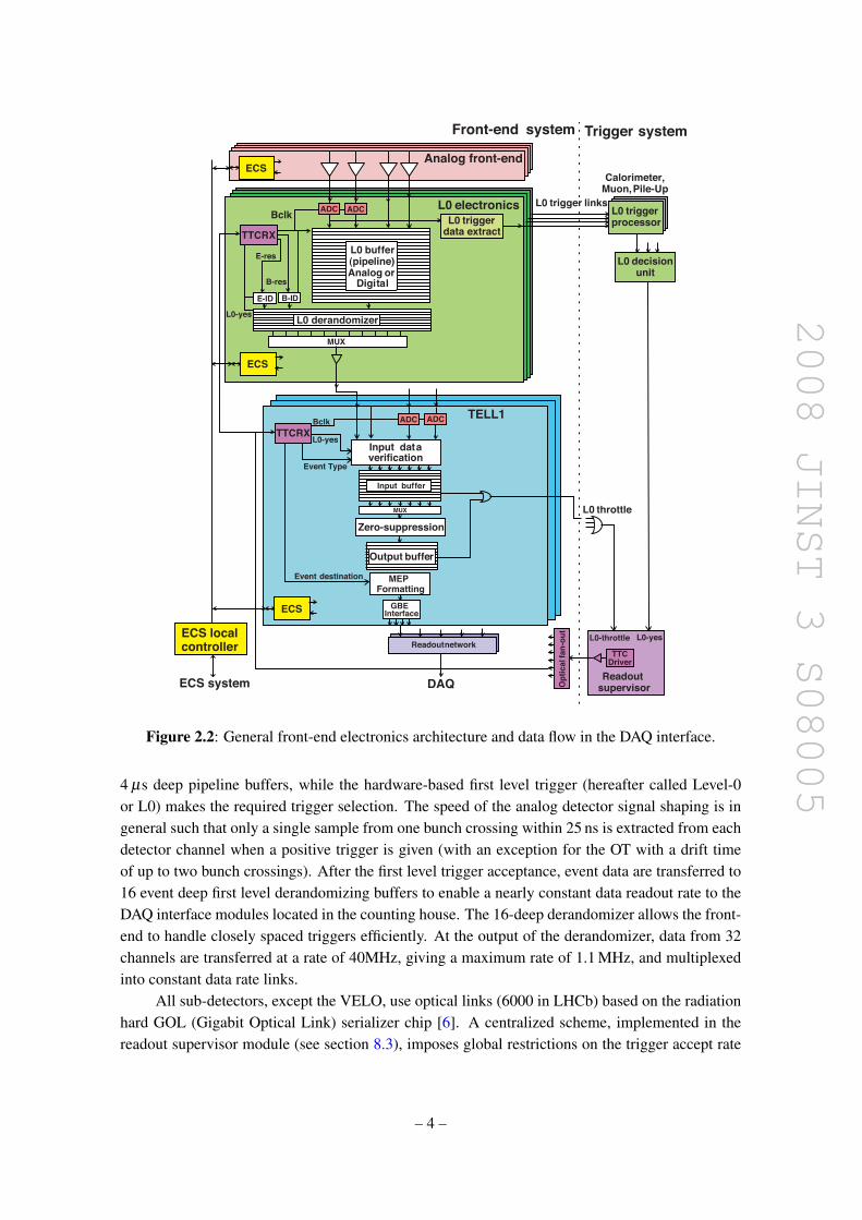
The front-end architecture chosen for LHCb [4, 5] has to a very large extent been determined bythe requirement of making a hardware-based short latency trigger, with an efficient event selection,for complicated B events. A fast first level trigger has been found capable of making an eventrate reduction of the order of 1 in 10. This has for the chosen LHCb luminosity enforced the useof a front-end architecture with a first level trigger rate of up to 1 MHz. This was considered tobe the highest rate affordable for the data acquisition system (DAQ) and required readout links.The general front-end electronics architecture and data flow in the DAQ interface are shown infigure 2.2. All sub-detectors store sampled detector signals at the 40 MHz bunch crossing rate in
– 3 –
2008 JINST 3 S08005
L0 electronics
TELL1
L0 triggerdata extractTTCRX
ADC ADC
B-IDE-ID
MUX
Bclk
B-res
E-res
L0-yes
MUX
TTCRX
ADC ADCBclk
L0-yes
Event Type
Event destination
GBEInterfaceECS
ECS
Readoutnetwork
L0 triggerprocessor
L0 decisionunit
TTCDriver
L0-yesL0-throttle
Readoutsupervisor
ECS localcontroller
DAQ Op
tica
lfa
n-o
ut
ECS system
L0 buffer(pipeline)Analog or
Digital
Zero-suppression
Input dataverification
MEPFormatting
Input buffer
Output buffer
L0 derandomizer
L0 trigger links
Calorimeter,Muon,Pile-Up
L0 throttle
Front-end system Trigger system
ECSAnalog front-end
Figure 2.2: General front-end electronics architecture and data flow in the DAQ interface.
4 µs deep pipeline buffers, while the hardware-based first level trigger (hereafter called Level-0or L0) makes the required trigger selection. The speed of the analog detector signal shaping is ingeneral such that only a single sample from one bunch crossing within 25 ns is extracted from eachdetector channel when a positive trigger is given (with an exception for the OT with a drift timeof up to two bunch crossings). After the first level trigger acceptance, event data are transferred to16 event deep first level derandomizing buffers to enable a nearly constant data readout rate to theDAQ interface modules located in the counting house. The 16-deep derandomizer allows the front-end to handle closely spaced triggers efficiently. At the output of the derandomizer, data from 32channels are transferred at a rate of 40MHz, giving a maximum rate of 1.1 MHz, and multiplexedinto constant data rate links.
All sub-detectors, except the VELO, use optical links (6000 in LHCb) based on the radiationhard GOL (Gigabit Optical Link) serializer chip [6]. A centralized scheme, implemented in thereadout supervisor module (see section 8.3), imposes global restrictions on the trigger accept rate
– 4 –

2008 JINST 3 S08005
to prevent overflows of the derandomizer buffers and the following readout and data processingstages. Specific test and monitoring features are integrated into the different front-end systems toassure that thorough testing and monitoring can be made [7] as indicated in figure 2.2.
The Trigger, Timing and Control system (TTC) developed for the LHC experiments [8] isused to distribute clock and sampling phase, timing control (reset and synchronization signals),trigger (trigger accept and trigger types) and a set of dedicated test and calibration commands toall front-end and DAQ interface modules. Control and monitoring of the front-end electronicsare based on either the LHCb specific SPECS control interface or the ELMB CAN bus moduledeveloped by ATLAS [9].
The reception of accepted event data from the sub-detectors is handled by 350 9U VME sizedDAQ interface modules in the counting house. These Field Programmable Gate Array (FPGA)based modules receive front-end data, perform data and event synchronization verifications, ap-propriate zero-suppression and/or data compression, data buffering and finally send the event in-formation to the DAQ system over up to four Gigabit-Ethernet links per module, as indicated inthe lower part of figure 2. The DAQ interface module is in general based on a highly flexible andprogrammable module named TELL1 [10] with the exception of the RICH detector that has chosento use a dedicated module1 (c.f. section 6.1).
The electronics equipment is located in two different areas. Front-end electronics are in-stalled on the subdetectors or in their close vicinity. Readout and trigger electronics as well as theExperiment Control System and the Data Acquisition system are located in a radiation protectedcounting house, composed of three levels of electronic barracks separated by a concrete shieldingfrom the experimental area. The control room of the experiment in located on the ground floor.
The present paper does not contain a dedicated chapter with the detailed description of theelectronics. The implementation of the specific front-end electronics is described in more detailin the chapters on the individual sub-detectors. Details of the readout supervisor, the ExperimentControl System (ECS) and the DAQ system are described as part of the online system (section 8).
Radiation tolerance of the electronics
All detector components need to tolerate significant radiation doses. Parts of the trigger outside ofthe counting house are no exception.
The front-end electronics of each sub-detector are located either within the sub-detector it-self or on its periphery. Sub-detector specific ASIC’s and modules have been custom developed tohandle the signal processing needed for the large channel counts in an environment with signifi-cant radiation levels. Radiation resistance requirements for all locations with electronics have beendefined based on FLUKA simulations with appropriate safety factors [11] (e.g. 10 MRad and 1014
1 MeV-neutron equivalent (neq) per cm2 for the front-end chip used for the VELO and the SiliconTracker; 4 kRad and 1012 neq/cm2 for the ECAL/HCAL electronics, over 10 years of running).Extensive radiation tests have been made for all electronics components used in the front-end elec-tronics, to verify their correct behaviour, after radiation (total dose and displacement damage), andduring radiation exposure (single event upsets).
1Called UKL1 board.
– 5 –

2008 JINST 3 S08005
Chapter 3
The interface to the LHC machine
3.1 Beampipe
The beampipe design is particularly delicate since the LHCb experiment is focussed on the highrapidity region, where the particle density is high. The number of secondary particles dependson the amount of material seen by incident primary particles. The mass of the beampipe and thepresence of flanges and bellows have a direct influence on the occupancy, in particular for thetracking chambers and the RICH detectors. Optimisation of the design and selection of materialswere therefore performed in order to maximize transparency in these critical regions [12, 13].
3.1.1 Layout
The beampipe, schematically represented in figure 3.1, includes the forward window of the VELOcovering the full LHCb acceptance and four main conical sections, the three closer to the interactionpoint being made of beryllium and the one further away of stainless steel.
Beryllium was chosen as the material for 12 m out of the 19 m long beampipe, for its hightransparency to the particles resulting from the collisions. It is the best available material for thisapplication given its high radiation length combined with a modulus of elasticity higher than thatof stainless steel. However, its toxicity [14], fragility and cost are drawbacks which had to be takeninto account in the design, installation and operation phases. Flanges, bellows and the VELO exitwindow are made of high strength aluminium alloys which provide a suitable compromise betweenperformance and feasibility. The remaining length, situated outside the critical zone in terms oftransparency, is made of stainless steel, a material widely used in vacuum chambers because ofits good mechanical and vacuum properties. The VELO window, a spherically shaped thin shellmade of aluminium 6061-T6, is 800 mm in diameter and was machined from a specially forgedblock down to the final thickness of 2 mm. The machining of the block included a four convolutionbellows at its smallest radius. The first beampipe section (UX85/1), that traverses RICH1 and TT(see figure 3.2), is made of 1 mm thick Be, includes a 25 mrad half-angle cone and the transition tothe 10 mrad half-angle cone of the three following beampipe sections. In order to avoid having aflange between the VELO window and UX85/1, the two pieces were electron beam welded beforeinstallation. Sections UX85/2 (inside the dipole magnet) and UX85/3 (that traverses the Tracker,RICH2, M1 and part of ECAL) are 10 mrad beryllium cones of wall thickness varying from 1
– 6 –

2008 JINST 3 S08005
Figure 3.1: The 19 m long vacuum chamber inside the LHCb experiment is divided into fourmain sections. The first three are made of machined beryllium cones assembled by welding andthe fourth of stainless steel. Bellows expansion joints provide interconnect flexibility in order tocompensate for thermal expansions and mechanical tolerances.
to 2.4 mm as the diameter increases from 65 up to 262 mm. UX85/3 is connected to a stainlesssteel bellows through a Conflat seal on the larger diameter. The transition between aluminium andstainless steel is formed using an explosion bonded connection. The three Be beampipes weremachined from billets up to 450 mm long and assembled by arc welding with a non-consumableelectrode under inert gas protection (TIG) to achieve the required length. TIG welding was alsoused to connect the aluminium flanges at the extremities of the tubes.
The UX85/4 section completes the 10 mrad cone and includes a 15 half-angle conical ex-tremity that provides a smooth transition down to the 60 mm final aperture. It was manufacturedfrom rolled and welded stainless steel sheet of 4 mm thickness. A copper coating of 100 µm wasdeposited before assembly on the downstream side end cone to minimise the impedance seen bythe beam. The aluminium and stainless steel bellows compensate for thermal expansion duringbakeout and provide the necessary flexibility to allow beampipe alignment. Optimised Ultra HighVacuum (UHV) flanges were developed in order to minimise the background contribution from thevarious connections in the high transparency region [15]. The resulting flange design is based onall-metal Helicoflex seals and high strength AA 2219 aluminium alloy flanges to ensure reliableleak tightness and baking temperatures up to 250C. A relatively low sealing force allows the useof aluminium and a significant reduction of the overall mass compared to a standard Conflat flange.
Another important source of background is the beampipe support system [16]. Eachbeampipe section must be supported at two points, with one fixed, i.e. with displacements re-strained in all directions, and the other movable, the latter allowing free displacements along the
– 7 –

2008 JINST 3 S08005
Figure 3.2: View of the VELO exit window and UX85/1 beampipe as installed inside the RICH1gas enclosure.
Figure 3.3: Optimised beampipe support inside the acceptance region. A system of eight highresistance cables and rods provide the required rigidity in all directions. A polyimide-graphitering split in several parts, which are bolted together between the collar and the beampipe, preventsscratches on the beryllium and reduces local stresses at the contact surfaces.
beampipe axis. The fixed supports, which must compensate the unbalanced vacuum forces due tothe conical shape of the beampipe, are each constructed using a combination of eight stainless steelcables or rods mounted under tension, pulling in both upstream and downstream directions with anangle to the beam axis (figure 3.3). Where a movable support is required to allow thermal expan-sion, four stainless steel cables are mounted in the plane perpendicular to the beampipe, blocking allmovements except along the beam axis. The support cables and rods are connected to the beampipethrough aluminium alloy collars with minimised mass, and an intermediate polyimide-graphite ringto avoid scratching the beryllium and to reduce stresses on contacting surfaces.
The experiment beam vacuum is isolated from the LHC with two sector valves, installed atthe cavern entrances, which allow interventions and commissioning independently of the machinevacuum system.
– 8 –

2008 JINST 3 S08005
3.1.2 Vacuum chamber
In order to achieve an average total dynamic pressure of 10−8 to 10−9 mbar with beam passingthrough, the LHCb beampipe and the VELO RF-boxes are coated with sputtered non-evaporablegetter (NEG) [17]. This works as a distributed pump, providing simultaneously low outgassing anddesorption from particle interactions with the walls. Another purpose of the NEG coating is to pre-vent electron multipacting [18] inside the chamber, since the secondary electron emission yield ismuch lower than for the chamber material. The UHV pumping system is completed by sputter-ionpumps in the VELO vessel and at the opposite end of the beampipe in order to pump non-getterablegases. Once the NEG coating has been saturated, the chamber must be heated periodically (bakedout) to 200C, for 24 hours, in order to recover the NEG pumping capacity. The temperature willhave to be gradually increased with the number of activation cycles, however it is limited to 250Cin the optimised flange assemblies for mechanical reasons. Before NEG activation, the vacuumcommissioning procedure also includes the bakeout of the non-coated surfaces inside the VELOvacuum vessel to a temperature of 150C. Removable heating jackets are installed during shut-downs covering the VELO window and the beampipe up to the end of RICH2. From there to theend of the muon chambers, a permanent system is installed. As there are no transparency con-straints, the insulation of the beampipe inside the muon filters is made from a mixture of silica,metal oxides and glass fiber, whilst the heating is provided by standard resistive tapes.
Such an optimised vacuum chamber must not be submitted to any additional external pres-sure or shocks while under vacuum, due to the risk of implosion. Hence, it must be vented toatmospheric pressure before certain interventions in the surrounding detectors. Saturation of theNEG coating and consequent reactivation after the venting will be avoided by injecting an inert gasnot pumped by the NEG. Neon was found to be the most suitable gas for this purpose because ofits low mass and the fact that it is not used as a tracer for leak detection, such as helium or argon.However, commercially available Ne must first be purified before injection. A gas injection systeminstalled in the cavern will provide the clean neon to be injected simultaneously into both VELObeam vacuum and detector vacuum volumes, as the pressure difference between the two volumesmust be kept lower than 5 mbar to prevent damage to the VELO RF-boxes (c.f. section 5.1).
3.2 The Beam Conditions Monitor
In order to cope with possible adverse LHC beam conditions, particularly with hadronic showerscaused by misaligned beams or components performance failures upon particle injection into theLHC, the LHCb experiment is equipped with a Beam Conditions Monitor (BCM) [19]. This systemcontinuously monitors the particle flux at two locations in the close vicinity of the vacuum chamberin order to protect the sensitive LHCb tracking devices. In the case of problems, the BCM systemwill be the first to respond and will request a dump of the LHC beams. The BCM connects toboth the LHCb experiment control system and to the beam interlock controller of the LHC [20].As a safety system, the BCM is equipped with an uninterruptable power supply and continuouslyreports its operability also to the vertex locator control system through a hardwired link.
The BCM detectors consist of chemical-vapor deposition (CVD) diamond sensors, whichhave been proven to withstand radiation doses as high as those that may occur in LHC accident
– 9 –

2008 JINST 3 S08005
Figure 3.4: Schematic view of the eight CVD-diamond sensors surrounding the beampipe at thedownstream BCM station.
scenarios. In order to assure compatibility of the signals with those from other LHC experiments,the dimensions of the sensors are the same as those of the ATLAS and CMS experiments, i.e. theirthickness is 500 µm, the lateral dimensions are 10 mm ×10 mm, with a centered 8 mm ×8 mmmetallized area. The metallization is made of a 500 Å thick gold layer on a 500 Å thick layer oftitanium. The radiation resistance of the metallization has been studied with the exposure of a4 mm2 surface to 4×10¹⁵ protons of an energy of 25 MeV over 18 hours. No sign of degradationwas observed.
The two BCM stations are placed at 2131 mm upstream and 2765 mm downstream from theinteraction point. Each station consists of eight diamond sensors, symmetrically distributed aroundthe vacuum chamber with the sensitive area starting at a radial distance of 50.5 mm (upstream) and37.0 mm (downstream). Figure 3.4 shows the downstream BCM station around the beampipe. Thesensors are read out by a current-to-frequency converter card [21] with an integration time of 40 µs,developed for the Beam Loss Monitors of the LHC.
Simulations were carried out with the GAUSS package [22] to study the expected perfor-mance of the BCM. Unstable beam situations are described in a simplified way in generating7 GeV protons at 3000 mm upstream of the interaction point in a direction parallel to the beamand in calculating the energy deposited in the BCM sensors caused by these protons. All sensorsexperience an increase of their signals due to hadronic showers produced by the protons in inter-mediate material layers. Assuming that during unstable LHC beam condition, the beam comes asclose as 475 µm (approximately 6 times its RMS) to the RF foil of the VELO (see section 5.1), itwould take 40–80 µs of integration time (or about 20 LHC turns) for the BCM to detect the criticalsituation and request a beam dump.
– 10 –
2008 JINST 3 S08005
Chapter 4
Magnet
4.1 General description
A dipole magnet is used in the LHCb experiment to measure the momentum of charged particles.The measurement covers the forward acceptance of ±250 mrad vertically and of ±300 mrad hor-izontally. The super-conducting magnet originally proposed in the Technical Proposal [1], wouldhave required unacceptably high investment costs and very long construction time. It was replacedby a warm magnet design with saddle-shaped coils in a window-frame yoke with sloping poles inorder to match the required detector acceptance. Details on the design of the magnet are given in theMagnet Technical Design Report [23] and in [24, 25]. The design of the magnet with an integratedmagnetic field of 4 Tm for tracks of 10 m length had to accommodate the contrasting needs for afield level inside the RICHs envelope less than 2 mT and a field as high as possible in the regions be-tween the vertex locator, and the Trigger Tracker tracking station [26]. The design was also drivenby the boundary conditions in the experimental hall previously occupied by the DELPHI detector.This implied that the magnet had to be assembled in a temporary position and to be subdivided intotwo relatively light elements. The DELPHI rail systems and parts of the magnet carriages havebeen reused as the platform for the LHCb magnet for economic reasons. Plates, 100 mm thick, oflaminated low carbon steel, having a maximum weight of 25 tons, were used to form the identi-cal horizontal bottom and top parts and the two mirror-symmetrical vertical parts (uprights) of themagnet yoke.1 The total weight of the yoke is 1500 tons and of the two coils is 54 tons.
The two identical coils are of conical saddle shape and are placed mirror-symmetrically toeach other in the magnet yoke. Each coil consists of fifteen pancakes arranged in five tripletsand produced of pure Al-99.7 hollow conductor in an annealed state which has a central coolingchannel of 25 mm diameter. The conductor has a specific ohmic resistance below 28 Ω· m at20C. It is produced in single-length of about 320 m by rotary extrusion2 and tested for leakswith water up to 50 bars and for extrusion imperfections before being wound. The coils wereproduced in industry3 with some equipment and technical support from CERN. Cast Aluminumclamps are used to hold together the triplets making up the coils, and to support and centre the
1Jebens, Germany.2Holton Machinery, Bournemouth, UK.3SigmaPhi, Vannes, France.
– 11 –

2008 JINST 3 S08005
Figure 4.1: Perspective view of the LHCb dipole magnet with its current and water connections(units in mm). The interaction point lies behind the magnet.
coils with respect to the measured mechanical axis of the iron poles with tolerances of severalmillimeters. As the main stress on the conductor is of thermal origin, the design choice was toleave the pancakes of the coils free to slide upon their supports, with only one coil extremity keptfixed on the symmetry axis, against the iron yoke, where electrical and hydraulic terminationsare located. Finite element models (TOSCA, ANSYS) have been extensively used to investigatethe coils support system with respect to the effect of the electromagnetic and thermal stresseson the conductor, and the measured displacement of the coils during magnet operation matchesthe predicted value quite well. After rolling the magnet into its nominal position, final precisealignment of the yoke was carried out in order to follow the 3.6 mrad slope of the LHC machineand its beam. The resolution of the alignment measurements was about 0.2 mm while the magnetcould be aligned to its nominal position with a precision of±2 mm. Details of the measurements ofthe dipole parameters are given in table 4.1. A perspective view of the magnet is given in figure 4.1.
The magnet is operated via the Magnet Control System that controls the power supply andmonitors a number of operational parameters (e.g. temperatures, voltages, water flow, mechanicalmovements, etc.). A second, fully independent system, the Magnet Safety System (MSS), ensuresthe safe operation and acts autonomously by enforcing a discharge of the magnet if critical param-eters are outside the operating range. The magnet was put into operation and reached its nominal
– 12 –

2008 JINST 3 S08005
Table 4.1: Measured main parameters of the LHCb magnet.
Non-uniformity of |B| ±1% in planes xy of 1 m2 from z=3m to z=8 m∫Bdl upstream TT region (0–2.5 m) 0.1159 Tm∫
Bdl downstream TT region (2.5 - 7.95 m) 3.615 TmMax field at HPD’s of RICH1 20x10−4 T (14x10−4 T with mu-metal)Max field at HPD’s of RICH2 9x10⁻⁴ T
Electric power dissipation 4.2 MWInductance L 1.3 H
Nominal / maximum current in conductor 5.85 kA / 6.6 kATotal resistance (two coils + bus bars) R = 130 mΩ @ 20 C
Total voltage drop (two coils) 730 VTotal number of turns 2 x 225
Total water flow 150 m3/hWater Pressure drop 11 bar @ ∆T = 25C
Overall dimensions H x V x L 11m x 8 m x 5 mTotal weight 1600 tons
current of 5.85 kA in November 2004, thereby being the first magnet of the LHC experiments op-erational in the underground experimental areas. Several magnetic field measurement campaignshave been carried out during which the magnet has shown stable and reliable performance.
4.2 Field mapping
In order to achieve the required momentum resolution for charged particles, the magnetic field in-tegral
∫Bdl must be measured with a relative precision of a few times 10−4 and the position of
the B-field peak with a precision of a few millimetres. A semi-automatic measuring device wasconstructed which allowed remotely controlled scanning along the longitudinal axis of the dipoleby means of an array of Hall probes. The measuring machine was aligned with a precision of 1 mmwith respect to the experiment reference frame. The support carrying the Hall probes could be man-ually positioned in the horizontal and vertical direction such as to cover the magnetic field volumeof interest. The Hall probe array consisted of 60 sensor cards mounted on a G10 support covering agrid of 80 mm x 80 mm. Each sensor card contained three Hall probes mounted orthogonally on acube together with a temperature sensor and the electronics required for remote readout. These 3Dsensor cards4 have been calibrated to a precision of 10−4 using a rotating setup in an homogeneousfield together with an NMR for absolute field calibration [27]. The calibration process allowed cor-recting for non-linearity, temperature dependence and non-orthogonal mounting of the Hall probes.
The goal of the field mapping campaigns was to measure the three components of the mag-netic field inside the tracking volume of the detector for both magnet polarities and to compare it tothe magnetic field calculations obtained with TOSCA.5 For the measurement of CP asymmetries it
4Developed in collaboration between CERN and NIKHEF for the ATLAS muon system.5Vector Field TM.
– 13 –
2008 JINST 3 S08005
B/B δ-0.01 -0.005 0 0.005 0.01
En
trie
s
0
500
1000
1500
2000
2500
3000
3500
4000
1
0.75
0.5
0.25
0
-0.25
-0.5
-0.75
-1
x = 0y = 0
0 200 400 600 800 1000z (cm)
B ( T
)
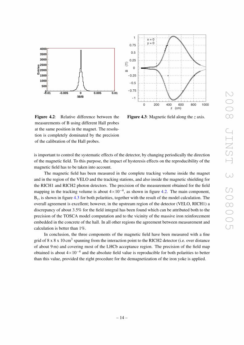
Figure 4.2: Relative difference between themeasurements of B using different Hall probesat the same position in the magnet. The resolu-tion is completely dominated by the precisionof the calibration of the Hall probes.
Figure 4.3: Magnetic field along the z axis.
is important to control the systematic effects of the detector, by changing periodically the directionof the magnetic field. To this purpose, the impact of hysteresis effects on the reproducibility of themagnetic field has to be taken into account.
The magnetic field has been measured in the complete tracking volume inside the magnetand in the region of the VELO and the tracking stations, and also inside the magnetic shielding forthe RICH1 and RICH2 photon detectors. The precision of the measurement obtained for the fieldmapping in the tracking volume is about 4×10⁻⁴, as shown in figure 4.2. The main component,By, is shown in figure 4.3 for both polarities, together with the result of the model calculation. Theoverall agreement is excellent; however, in the upstream region of the detector (VELO, RICH1) adiscrepancy of about 3.5% for the field integral has been found which can be attributed both to theprecision of the TOSCA model computation and to the vicinity of the massive iron reinforcementembedded in the concrete of the hall. In all other regions the agreement between measurement andcalculation is better than 1%.
In conclusion, the three components of the magnetic field have been measured with a finegrid of 8 x 8 x 10 cm3 spanning from the interaction point to the RICH2 detector (i.e. over distanceof about 9 m) and covering most of the LHCb acceptance region. The precision of the field mapobtained is about 4×10⁻⁴ and the absolute field value is reproducible for both polarities to betterthan this value, provided the right procedure for the demagnetization of the iron yoke is applied.
– 14 –

2008 JINST 3 S08005
Chapter 5
Tracking
The LHCb tracking system consists of the vertex locator system (VELO) and four planar trackingstations: the Tracker Turicensis (TT) upstream of the dipole magnet and T1-T3 downstream of themagnet. VELO and TT use silicon microstrip detectors. In T1-T3, silicon microstrips are used inthe region close to the beam pipe (Inner Tracker, IT) whereas straw-tubes are employed in the outerregion of the stations (Outer Tracker, OT). The TT and the IT were developed in a common projectcalled the Silicon Tracker (ST).
The VELO is described in section 5.1 the ST in section 5.2 and the OT in section 5.3.
5.1 Vertex locator
The VErtex LOcator (VELO) provides precise measurements of track coordinates close to the in-teraction region, which are used to identify the displaced secondary vertices which are a distinctivefeature of b and c-hadron decays [28]. The VELO consists of a series of silicon modules, eachproviding a measure of the r and φ coordinates, arranged along the beam direction (figure 5.1).Two planes perpendicular to the beam line and located upstream of the VELO sensors are calledthe pile-up veto system and are described in section 7.1. The VELO sensors are placed at a radialdistance from the beam which is smaller than the aperture required by the LHC during injection andmust therefore be retractable. The detectors are mounted in a vessel that maintains vacuum aroundthe sensors and is separated from the machine vacuum by a thin walled corrugated aluminum sheet.This is done to minimize the material traversed by a charged particle before it crosses the sensorsand the geometry is such that it allows the two halves of the VELO to overlap when in the closedposition. Figure 5.2 shows a cross section of the VELO vessel, illustrating the separation betweenthe primary (beam) vacuum and the secondary (detector) vacuum enclosed by the VELO boxes.Figure 5.3 shows an expanded view from inside one of the boxes, with the sides cut away to showthe staggered and overlapping modules of the opposite detector half. The corrugated foils, hereafterreferred to as RF-foils, form the inner faces of the boxes (RF-boxes) within which the modules arehoused. They provide a number of functions which are discussed in the following sections.
– 15 –

2008 JINST 3 S08005
Figure 5.1: Cross section in the (x,z) plane of the VELO silicon sensors, at y = 0, with the detectorin the fully closed position. The front face of the first modules is also illustrated in both the closedand open positions. The two pile-up veto stations are located upstream of the VELO sensors.
5.1.1 Requirements and constraints
The ability to reconstruct vertices is fundamental for the LHCb experiment. The track coordinatesprovided by the VELO are used to reconstruct production and decay vertices of beauty- and charm-hadrons, to provide an accurate measurement of their decay lifetimes and to measure the impactparameter of particles used to tag their flavour. Detached vertices play a vital role in the High LevelTrigger (HLT, see section 7.2), and are used to enrich the b-hadron content of the data written totape, as well as in the LHCb off-line analysis. The global performance requirements of the detectorcan be characterised with the following interrelated criteria:
• Signal to noise1 ratio (S/N): in order to ensure efficient trigger performance, the VELOaimed for an initial signal to noise ratio of greater than 14 [29].
• Efficiency: the overall channel efficiency was required to be at least 99% for a signal to noisecut S/N> 5 (giving about 200 noise hits per event in the whole VELO detector).
1Signal S is defined as the most probable value of a cluster due to a minimum-ionizing particle and noise N as theRMS value of an individual channel.
– 16 –

2008 JINST 3 S08005
Figure 5.2: Cross section of the VELO vacuum vessel, with the detectors in the fully closedposition. The routing of the signals via kapton cables to vacuum feedthroughs are illustrated. Theseparation between the beam and detector vacua is achieved with thin walled aluminium boxesenclosing each half.
Figure 5.3: Zoom on the inside of an RF-foil, as modelled in GEANT, with the detector halves inthe fully closed position. The edges of the box are cut away to show the overlap with the staggeredopposing half. The R- and φ -sensors are illustrated with alternate shading.
– 17 –

2008 JINST 3 S08005
• Resolution: a spatial cluster resolution of about 4 µm was aimed at for 100 mrad tracks in thesmallest strip pitch region (about 40 µm), in order to achieve the impact parameter resolutionperformance described in section 10. Furthermore, it was required that the resolution not bedegraded by irradiation nor by any aspect of the sensor design.
Another important consideration is the spillover probability, which is defined as the fraction of thepeak signal remaining after 25 ns. An additional requirement imposed on the system, affecting thereadout electronics, is that the spillover probability be less than 0.3, in order to keep the number ofremnant hits at a level acceptable for the HLT [30].
The construction of the VELO followed a number of requirements and constraints, which arebriefly described in this section.
Geometrical
The VELO has to cover the angular acceptance of the downstream detectors, i.e. detect particleswith a pseudorapidity in the range2 1.6 < η < 4.9 and emerging from primary vertices in the range|z|< 10.6 cm. The detector setup was further constrained by the following considerations:
• Polar angle coverage down to 15 mrad for a track emerging at z=10.6 cm downstream fromthe nominal interaction point (IP), together with the minimum distance of the sensitive areato the beam axis (8mm, see below), and the requirement that a track should cross at leastthree VELO stations, defined the position zN−2 of the first of the three most downstreamstations: zN−2 ' 65 cm.
• A track in the LHCb spectrometer angular acceptance of 300mrad should cross at least threeVELO stations. Given a maximum3 outer radius of the sensors of about 42mm, the distancebetween stations in the central region needed to be smaller than 5cm. Requiring four stationsto be traversed (or allowing for missing hits in one of four stations), imposed a modulepitch of at most 3.5 cm. Dense packing of stations near the IP also reduces the averageextrapolation distance from the first measured hit to the vertex.
• For covering the full azimuthal acceptance and for alignment issues, the two detector halveswere required to overlap. This was achieved by shifting along z the positions of sensors inone half by 1.5cm relative to sensors in the opposite half.
The use of cylindrical geometry (rφ coordinates), rather than a simpler rectilinear scheme,was chosen in order to enable fast reconstruction of tracks and vertices in the LHCb trigger. Indeed,simulations showed that 2D (rz) tracking allows a fast reconstruction in the HLT with sufficientimpact parameter resolution to efficiently select events with b-hadrons. For this reason, an rφ ge-ometry was selected for the design. Each VELO module was designed to provide the necessary3D spatial information to reconstruct the tracks and vertices. One of the two sensors of the mod-ule, called the φ -measuring sensor, or φ -sensor, provides information on the azimuthal coordinate
2Some coverage of negative pseudorapidity is used to improve the primary vertex reconstruction and, using twospecial stations, to reduce the number of multiple-interaction events passing the Level-0 trigger (L0, see section 7.1).
3This allowed the use of 10cm Si wafers for sensor production.
– 18 –

2008 JINST 3 S08005
around the beam. The other sensor, called the r-measuring sensor, or R-sensor, provides informa-tion on the radial distance from the beam axis. The third coordinate is provided by knowledgeof the position of each sensor plane within the experiment. The rz tracking requirement imposesthe additional constraint that the VELO circular strips should be centered as perfectly as possiblearound the beam axis. The result of simulation studies showing how the trigger performance woulddegrade as a function of various VELO R-sensor misalignments [31] indicate that the R-sensorsshould be mounted with a mechanical accuracy of better than 20 µm in x and y relative to each otherwithin each half, and the two halves should be aligned to better than 100 µm relative to each otherin these coordinates. The number of strips for both sensor types needed to satisfy the competingrequirements of the LHCb environment, physics and a budgetary limit, is about 180000 channels.
Environmental
The VELO detector will be operated in an extreme radiation environment with strongly non-uniform fluences. The damage to silicon in the most irradiated area for one nominal year ofrunning, i.e. an accumulated luminosity of 2 fb−1, is equivalent to that of 1 MeV neutrons witha flux of 1.3×10¹⁴ neq/cm2, whereas the irradiation in the outer regions does not exceed a flux of5×1012 neq/cm2. The detector is required to sustain 3 years of nominal LHCb operation. In orderto evacuate the heat generated in the sensor electronics (in vacuum) and to minimize radiation-induced effects, the VELO cooling system was required to be capable of maintaining the sensorsat a temperature between -10 and 0C with a heat dissipation of about 24 W per sensor and hybrid.To increase the sensor lifetime, continuous cooling after irradiation was also requested (with theaim to expose the irradiated sensors to room temperature for periods shorter than 1 week per year).
The sensor full depletion voltage is expected to increase with fluence. The ability to increasethe operational bias voltage to ensure full depletion during the 3 years lifetime of the sensors wasimposed as a further requirement.
Machine integration constraints
The required performance demands positioning of the sensitive area of the detectors as close aspossible to the beams and with a minimum amount of material in the detector acceptance. This isbest accomplished by operating the silicon sensors in vacuum. As a consequence, integration intothe LHC machine became a central issue in the design of the VELO, imposing a number of specialconstraints which are briefly discussed here.
• The amount of material in front of the silicon detector is mainly determined by the necessityto shield against RF pickup and the mechanical constraint of building a sufficiently rigidfoil. The detectors operate in a secondary vacuum and hence the foils are not required towithstand atmospheric pressure. However, the design of the vacuum system had to ensurethat the pressure difference between detector and beam vacuum never be so large as to causeinelastic deformations of the detector box. The VELO surfaces exposed to beam-inducedbombardment (secondary electrons, ions, synchrotron radiation) needed to be coated withsuitable material in order to maintain beam-induced effects, such as electron multipactingand gas desorption, at acceptable levels for efficient LHC and LHCb operation. The LHC
– 19 –

2008 JINST 3 S08005
beam vacuum chamber, and therefore also the VELO vacuum vessel, were required to bebakeable (to 160C in the case of the VELO).
• A short track extrapolation distance leads to a better impact parameter measurement. There-fore, the innermost radius of the sensors should be as small as possible. In practice, this islimited by the aperture required by the LHC machine. During physics running conditions,the RMS spread of the beams will be less than 100 µm, but for safety reasons, the closestapproach allowed to the nominal beam axis is 5mm. This value is dominated by the yetunknown closed-orbit variations of the LHC and could be reduced in an upgraded detector.To this must be added the thickness of the RF-foil, the clearance between the RF-foil andthe sensors, and the design of about 1mm of guard-ring structures on the silicon. Takingeverything into account, the sensitive area can only start at a radius of about 8mm.
• During injection, the aperture required by the LHC machine increases, necessitating retrac-tion of the two detector halves by 3cm, which brings the movable parts into the shadow ofthe LHCb beampipe (54mm diameter). Furthermore, the repeatability of the beam positionscould not be guaranteed, initially, to be better than a few mm. This imposed that the VELOdetectors be mounted on a remote-controllable positioning system, allowing fine adjustmentin the x and y directions.
• The need for shielding against RF pickup from the LHC beams, and the need to protect theLHC vacuum from outgassing of the detector modules, required a protection to be placedaround the detector modules. This function is carried out by the RF-foils, which representa major fraction of the VELO material budget in the LHCb acceptance. In addition, thebeam bunches passing through the VELO structures will generate wake fields which canaffect the LHC beams. The RF foils, together with wake field suppressors which provide theconnection to the rest of the beampipe, also provide the function of suppressing wake fieldsby providing continuous conductive surfaces which guide the mirror charges from one endof the VELO vessel to the other. These issues have been addressed in detail [32] and arefurther discussed in section 5.1.3.
5.1.2 Sensors and modules
Sensors
The severe radiation environment at 8mm from the LHC beam axis required the adoption of aradiation tolerant technology. The choice was n-implants in n-bulk technology with strip isolationachieved through the use of a p-spray. The minimum pitch achievable4 using this technology wasapproximately 32 µm, depending on the precise structure of the readout strips. For both the R andφ -sensors the minimum pitch is designed to be at the inner radius to optimize the vertex resolution.
The conceptual layout of the strips on the sensors is illustrated in figure 5.4. For the R-sensorthe diode implants are concentric semi-circles with their centre at the nominal LHC beam position.In order to minimize the occupancy each strip is subdivided into four 45 regions. This also hasthe beneficial effect of reducing the strip capacitance. The minimum pitch at the innermost radius
4The company chosen to fabricate the LHCb sensors was Micron Semiconductor Ltd.
– 20 –

2008 JINST 3 S08005
Figure 5.4: Sketch illustrating the rφ geometry of the VELO sensors. For clarity, only a portionof the strips are illustrated. In the φ -sensor, the strips on two adjacent modules are indicated, tohighlight the stereo angle. The different arrangement of the bonding pads leads to the slightlylarger radius of the R-sensor; the sensitive area is identical.
is 38 µm, increasing linearly to 101.6 µm at the outer radius of 41.9 mm. This ensures that mea-surements along the track contribute to the impact parameter precision with roughly equal weight.
The φ -sensor is designed to readout the orthogonal coordinate to the R-sensor. In the simplestpossible design these strips would run radially from the inner to the outer radius and point at thenominal LHC beam position with the pitch increasing linearly with radius starting with a pitch of35.5 µm. However, this would result in unacceptably high strip occupancies and too large a strippitch at the outer edge of the sensor. Hence, the φ -sensor is subdivided into two regions, innerand outer. The outer region starts at a radius of 17.25 mm and its pitch is set to be roughly half(39.3 µm) that of the inner region (78.3 µm), which ends at the same radius. The design of thestrips in the φ -sensor is complicated by the introduction of a skew to improve pattern recognition.At 8 mm from the beam the inner strips have an angle of approximately 20 to the radial whereasthe outer strips make an angle of approximately 10 to the radial at 17 mm. The skew of inner andouter sections is reversed giving the strips a distinctive dog-leg design. The modules are placed sothat adjacent φ -sensors have the opposite skew with respect to the each other. This ensures thatadjacent stations are able to distinguish ghost hits from true hits through the use of a traditionalstereo view. The principal characteristics of the VELO sensors are summarized in table 5.1.
The technology utilized in both the R- and φ -sensors is otherwise identical. Both sets ofsensors are 300 µm thick. Readout of both R- and φ -sensors is at the outer radius and requiresthe use of a second layer of metal (a routing layer or double metal) isolated from the AC-coupleddiode strips by approximately 3 µm of chemically vapour deposited (CVD) SiO2. The secondmetal layer is connected to the first metal layer by wet etched vias. The strips are biased using
– 21 –

2008 JINST 3 S08005
Table 5.1: Principal characteristics of VELO sensors.
R sensor φ -sensornumber of sensors 42 + 4 (VETO) 42readout channels per sensor 2048 2048sensor thickness 300 µm 300 µmsmallest pitch 40 µm 38 µmlargest pitch 102 µm 97 µmlength of shortest strip 3.8 mm 5.9 mmlength of longest strip 33.8 mm 24.9 mminner radius of active area 8.2 mm 8.2 mmouter radius of active area 42 mm 42 mmangular coverage 182 deg ≈ 182 degstereo angle - 10–20 degdouble metal layer yes yesaverage occupancy 1.1% 1.1/0.7% inner/outer
polysilicon 1 MΩ resistors and both detectors are protected by an implanted guard ring structure.The pitch as a function of the radius r in µm increases linearly and is given by the following
expressions:
R− sensor : 40+(101.6−40)× r−819041949−8190
φ − sensor : 37.7+(79.5−37.7)× r−817017250−8170
(r < 17250)
φ − sensor : 39.8+(96.9−39.8)× r−1725042000−17250
(r > 17250)
The sensors were developed for high radiation tolerance. Early prototype detectors used p-stop isolation. This was later replaced by p-spray isolated detectors which showed much higherresistance to micro-discharges. The n+n design was compared with an almost geometrically iden-tical p+n design and was shown to have much better radiation characteristics as measured by chargecollection as a function of voltage.
Prototype sensors were also irradiated with non-uniform fluence in order to study the effectsof cluster bias due to inhomogeneous irradiation. It was shown that the transverse electric fieldsproduce less than 2 µm effects on the cluster centroid.
A subset of the production sensors were exposed to a high neutron fluence (1.3×10¹⁴ neq/cm2) representing 1 year of operation at nominal luminosity. A strong suppression ofsurface breakdown effects was demonstrated. The evolution of the depletion voltage was foundto correspond to the expectation over LHC operation: with an integrated luminosity of 2 fb−1 peryear, the maximum deliverable full depletion voltage (500 V) is reached after approximately 3years. During production the possibility arose of manufacturing full size n+p sensors. These areexpected to have similar long term radiation resistance characteristics to the n+n technology, butfeature some advantages, principally in cost of manufacture due to the fact that double sided pro-cessing is not needed. One full size module was produced in this technology and installed in oneof the most upstream slots. It is forseen to replace all the VELO modules after damage due toaccumulated radiation or beam accidents. The replacement modules will be constructed in the n+ptechnology [33].
– 22 –

2008 JINST 3 S08005
Modules
The module has three basic functions. Firstly it must hold the sensors in a fixed position relative tothe module support. Secondly it provides and connects the electrical readout to the sensors. Finallyit must enable thermal management of the modules which are operating in vacuum.
Each module is designed to hold the sensors in place to better than 50 µm in the plane perpen-dicular to the beam and within 800 µm along the direction of the beam. Sensor-to-sensor alignment(within a module) is designed to be better than 20 µm.
The module is comprised of a substrate, for thermal management and stability, onto whichtwo circuits are laminated. This forms the hybrid. The substrate is fabricated in-house and is ap-proximately 120×170×1 mm. It has a core of 400 µm thick thermal pyrolytic graphite (TPG),and is encapsulated, on each side, with 250 µm of carbon fibre (CF). A CF frame of about 7 mmthickness surrounds the TPG and is bonded directly to the CF encapsulation to prevent delamina-tion. The TPG is designed to carry a maximum load of 32 W away from the front-end chips. Asemicircular hole is cut into the substrate under the region where the detectors are glued. Particularattention in the design and fabrication process is given to producing almost planar hybrids, to sim-plify the subsequent module production. Typical non-planarities of order 250 µm were achieved.
The circuits5 were commercially hand populated to minimize exposure of the hybrid tohigh temperature and hence the possibility of delamination. The sensor front-end ASICs (Beetle1.5 [34]) were then glued to the circuits. A total of 32 Beetle chips are used in each module. Kaptonpitch adaptors,6 were glued to the circuits in order to facilitate the wire bonding of the sensors tothe Beetle chips. Sensors were glued to the double-sided hybrid with a sensor-to-sensor accuracyof better than 10 µm. The sensors were bonded to the electronics using a combination of H&K 710and K&S 8090 bonding machines with 25 µm thick Al wire. After bonding and final testing 99.4%of all strips were operational, with no sensor having more than 30/2048 faulty channels.
The final mechanical mounting of the hybrid was to the module pedestal and base. Thepedestal is a low mass CF fibre construction designed to hold the hybrid stably. It is a hollowrigid structure approximately 140×150×10 mm. Holes are drilled where appropriate to reducethe possibility of outgassing. One end was glued to the hybrid and the other to a CF base whichcontains two precisely manufactured invar feet. The design of the base allows repeatable mountingof the module to the module support with a precision a better than 10 µm. The accuracy of thefinal assembled modules satisfied the design criteria. The complete module, in schematic and afterfinal assembly, is illustrated in figure 5.5.
The thermal performance of the modules was required to be such that the silicon could be op-erated below zero degrees, for a minimum cooling liquid temperature of -30C. The performanceof each module was monitored individually in a vacuum tank during construction with a thermalcamera, as illustrated in figure 5.6. After the final cooling connections had been made on the mod-ule bases, all modules were rechecked for their thermal performance in vacuum. The temperaturedifference between the cooling blocks and the silicon is estimated to be about (21.4± 1)C forindividually cooled modules, and an improvement of up to 2C is expected when the modules are
5The circuits were fabricated and laminated to the substrates by Stevenage Circuits, Ltd.6The pitch adapters were manufactured at CERN.
– 23 –

2008 JINST 3 S08005
Figure 5.5: The left part of the figure illustrates the principal components of the VELO module.The right part of the figure is a photograph of the module as finally mounted. The short kaptoncables are visible, along with the clamps at the base which prevent any long kapton cable movementcoupling to the module itself. The aluminium blocks encasing the stainless steel CO2 cooling tubesare also partially visible.
Figure 5.6: Quality control of the VELO modules. The left part of the figure shows an exampleof a thermograph which was routinely taken on both sides of the module during the construction.The right plot shows an example of a noise uniformity measurement for all the φ -sensors. Thegreen squares are before common mode correction, and the red circles after the common modecorrection. The error bars show the noise spread which is due to varying strip capacitances on thesensor.
cooled simultaneously. At the same time, the noise uniformity of the modules was checked, asshown in figure 5.6.
Each module was transported to CERN in a dedicated transport box [35] and submitted toa visual inspection with a high resolution microscope, including the survey of all bond wires, on
– 24 –

2008 JINST 3 S08005
Figure 5.7: Overview of the VELO vacuum vessel.
reception. After this it underwent a 16 hour burn-in [36] consisting of a sequence of powering,cooling and data taking cycles, in vacuum. This was designed to uncover any inherent weaknessesintroduced to the modules during manufacturing. Of all the modules transported, one was finallytaken as a reserve as a result of the burn-in procedure, and a second was rejected after assemblydue to a slightly worse thermal performance.
5.1.3 Mechanics
Introduction
The ultra high vacuum requirements of the LHC ring, the necessity for wake field suppression,the need to shield the detectors from electromagnetic effects induced by the high frequency beamstructure, and the necessity to retract the detectors by 30 mm from the interaction region duringinjection of a new LHC fill, make the VELO mechanical design demanding. To meet all these con-straints, a design with two detector halves was chosen, each placed inside a thin-walled aluminumbox, as introduced in the previous sections. Aluminum was chosen since it has a relatively low Z(resulting in a small radiation length), good electrical conductivity, and can be machined quite eas-ily. The side walls of these boxes are 0.5 mm thick. In order to allow for overlap in the two detectorhalves, the top surfaces of these vacuum boxes have a corrugated shape and are made from 0.3 mmthick AlMg3 foil (an aluminum alloy with 3% magnesium). The two detector boxes are placed ina 1.4 m long vacuum vessel with a diameter of 1.1 m. The whole assembly is shown in figure 5.7.Two rectangular bellows allow for the movement of the detector boxes inside the vacuum system.Each detector support is connected via three spheres on holders placed within circular bellows to
– 25 –

2008 JINST 3 S08005
Figure 5.8: Exploded view of the module support and the modules (a), and the RF box (b). Thecorrugated foil on the front face of the box, which forms a beam passage can be seen. Its formallows the two halves to overlap when in the closed position.
the movement mechanism that is located outside the vacuum vessel. The module support, illus-trated in figure 5.8, is mounted on bearings which lie in precisely machined slots inside the detectorsupport and is bolted into position against three precision surfaces. The positioning of the moduleson the module support is fully constrained with a combination of a slot and a dowel pin. The po-sitioning of the modules relative to one another is determined by the precision of the machining ofthe module support. The positioning of the two halves relative to each other is determined by theprecision of the module support, together with its positioning inside the detector support, whichis adjustable. To suppress wake field effects, the dimension of the beampipe as seen by the pro-ton beams has to vary very gradually. To match the beampipe upstream and downstream from theVELO, wake field suppressors made of 50 µm thick copper-beryllium have been constructed, so agood electrical match is provided in both the open and closed positions.
The durability of the wake field suppressors has been tested by performing an opening andclosing movement 30,000 times, after which no damage was observed. A photograph of the down-stream wake field suppressors is shown in figure 5.9. The exit foil of the vessel consists of a 2 mmthick aluminum window (see section 3).
Movement system
Before the LHC ring is filled, the detectors have to move away from the interaction region by30 mm in order to allow for beam excursions during injection and ramping. After stable beamconditions have been obtained, the detectors should be placed into an optimized position centeredin x and y around the interaction region. This position is not exactly known beforehand; it mayvary over ± 5 mm in both x and y, even from fill to fill. Therefore, a procedure has been developedto determine the beam position with the detectors not completely moved in, and then move to
– 26 –
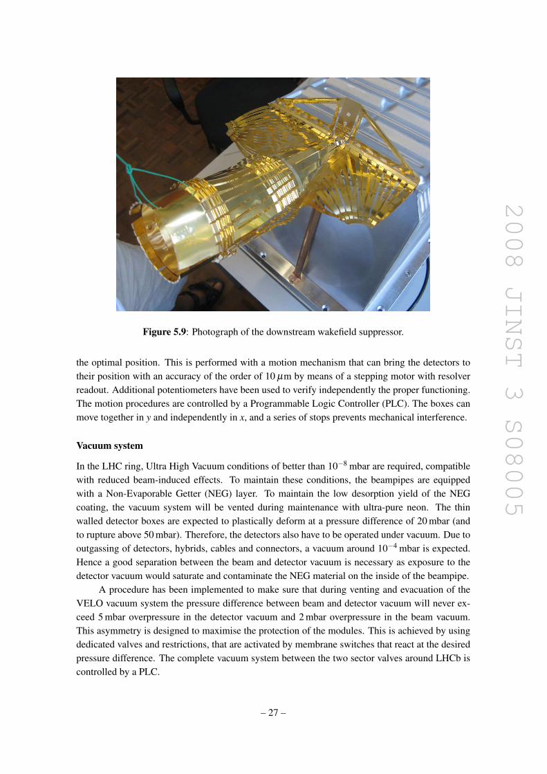
2008 JINST 3 S08005
Figure 5.9: Photograph of the downstream wakefield suppressor.
the optimal position. This is performed with a motion mechanism that can bring the detectors totheir position with an accuracy of the order of 10 µm by means of a stepping motor with resolverreadout. Additional potentiometers have been used to verify independently the proper functioning.The motion procedures are controlled by a Programmable Logic Controller (PLC). The boxes canmove together in y and independently in x, and a series of stops prevents mechanical interference.
Vacuum system
In the LHC ring, Ultra High Vacuum conditions of better than 10−8 mbar are required, compatiblewith reduced beam-induced effects. To maintain these conditions, the beampipes are equippedwith a Non-Evaporable Getter (NEG) layer. To maintain the low desorption yield of the NEGcoating, the vacuum system will be vented during maintenance with ultra-pure neon. The thinwalled detector boxes are expected to plastically deform at a pressure difference of 20 mbar (andto rupture above 50 mbar). Therefore, the detectors also have to be operated under vacuum. Due tooutgassing of detectors, hybrids, cables and connectors, a vacuum around 10−4 mbar is expected.Hence a good separation between the beam and detector vacuum is necessary as exposure to thedetector vacuum would saturate and contaminate the NEG material on the inside of the beampipe.
A procedure has been implemented to make sure that during venting and evacuation of theVELO vacuum system the pressure difference between beam and detector vacuum will never ex-ceed 5 mbar overpressure in the detector vacuum and 2 mbar overpressure in the beam vacuum.This asymmetry is designed to maximise the protection of the modules. This is achieved by usingdedicated valves and restrictions, that are activated by membrane switches that react at the desiredpressure difference. The complete vacuum system between the two sector valves around LHCb iscontrolled by a PLC.
– 27 –

2008 JINST 3 S08005
Figure 5.10: VELO readout chain for one side of one module.
Cooling system
Since the detectors and read-out electronics are operated inside the vacuum system, active coolingis required. Furthermore, in order to limit the effects of radiation damage of the silicon sensors,the irradiated sensors should be operated and kept at temperatures below -5C at all times. Theradiation hard refrigerant in the system is two-phase CO2 cooled by a conventional freon cooler.The liquid CO2 is transported via a 60 m long transfer line to the VELO, where it is distributedover 27 capillaries per detector half. Each capillary is thermally connected to five cooling blocksthat are attached to each detector module. A redundant pumping system is incorporated, so thatalso during maintenance periods cooling capacity is available. The complete cooling system iscontrolled by a PLC.
5.1.4 Electronics chain
The electronics layout is summarised in figure 5.10, which shows the readout chain for one side ofone module. The individual components are discussed in this section.
Beetle chip
The VELO uses the Beetle, a custom designed radiation hard ASIC based on 0.12 µm CMOStechnology7 with an analog front-end, as the FE chip [34]. The chip was designed with a peakingtime and sampling frequency to match the LHC bunch crossing rate of 40 MHz, and to be ableto readout at a speed which can match the L0 accept rate of 1 MHz. For a full discussion ofthe design requirements see [28, 37]. Each of the 128 channels consists of a charge sensitive
7IBM, USA.
– 28 –
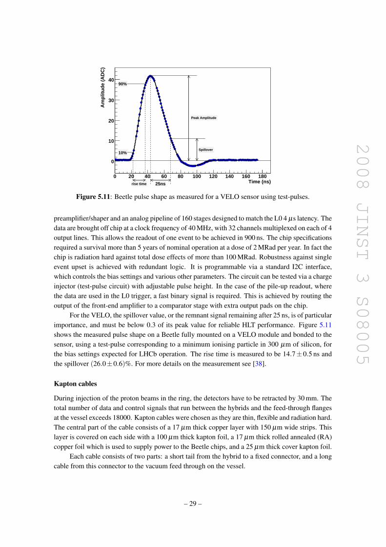
2008 JINST 3 S08005
Time (ns)0 20 40 60 80 100 120 140 160 180
Am
plit
ud
e (A
DC
)
0
10
20
30
40
Spillover
25ns
Peak Amplitude
rise time
10%
90%
Figure 5.11: Beetle pulse shape as measured for a VELO sensor using test-pulses.
preamplifier/shaper and an analog pipeline of 160 stages designed to match the L0 4 µs latency. Thedata are brought off chip at a clock frequency of 40 MHz, with 32 channels multiplexed on each of 4output lines. This allows the readout of one event to be achieved in 900 ns. The chip specificationsrequired a survival more than 5 years of nominal operation at a dose of 2 MRad per year. In fact thechip is radiation hard against total dose effects of more than 100 MRad. Robustness against singleevent upset is achieved with redundant logic. It is programmable via a standard I2C interface,which controls the bias settings and various other parameters. The circuit can be tested via a chargeinjector (test-pulse circuit) with adjustable pulse height. In the case of the pile-up readout, wherethe data are used in the L0 trigger, a fast binary signal is required. This is achieved by routing theoutput of the front-end amplifier to a comparator stage with extra output pads on the chip.
For the VELO, the spillover value, or the remnant signal remaining after 25 ns, is of particularimportance, and must be below 0.3 of its peak value for reliable HLT performance. Figure 5.11shows the measured pulse shape on a Beetle fully mounted on a VELO module and bonded to thesensor, using a test-pulse corresponding to a minimum ionising particle in 300 µm of silicon, forthe bias settings expected for LHCb operation. The rise time is measured to be 14.7± 0.5 ns andthe spillover (26.0±0.6)%. For more details on the measurement see [38].
Kapton cables
During injection of the proton beams in the ring, the detectors have to be retracted by 30 mm. Thetotal number of data and control signals that run between the hybrids and the feed-through flangesat the vessel exceeds 18000. Kapton cables were chosen as they are thin, flexible and radiation hard.The central part of the cable consists of a 17 µm thick copper layer with 150 µm wide strips. Thislayer is covered on each side with a 100 µm thick kapton foil, a 17 µm thick rolled annealed (RA)copper foil which is used to supply power to the Beetle chips, and a 25 µm thick cover kapton foil.
Each cable consists of two parts: a short tail from the hybrid to a fixed connector, and a longcable from this connector to the vacuum feed through on the vessel.
– 29 –

2008 JINST 3 S08005
Repeater boards
The repeater board (RPT) is located directly outside of the VELO tank inside repeater crates. TheRPT function is mainly a repeater for the differential signals arriving at the board, including datasignals, Time and Fast Control (TFC, see section 8.3) and FE chips configuration signals. Also, mo-nitoring signals are sent out via the board to the detector slow control system. The RPT carries thevoltage regulators required by the FE and the L0 electronics service system. For flexibility in designand mainly for maintenance, the RPT is built as a motherboard hosting several mezzanine cards:
• Four Driver Cards: four driver cards are mounted in the RPT board as mezzanine cards.Each card contains 16 fully differential analog drivers. Because the data streams are sent tothe digitizer card via a 60 m individual shielded twisted-pair cable, the drivers include a lineequalizer to compensate distortions introduced by the cable.
• One LV card: the low voltage card provides the power for the FE hybrid, the analog drivercards and the ECS card (c.f. 8.4). Eight radiation hard voltage regulators are mounted on theboard. Each voltage is monitored through an amplifier. The card is supplied by three powersupplies located at 60 m cable distance. Sense-lines are used to compensate the voltage dropthrough the long supply cable.
• One ECS card: the ECS repeats the signals for the I2C configuration bus and controls andmonitors the LV regulators. The applied voltage and the current limit signals are multiplexedand sent on differential lines. The ECS card communicates with the control boards locatedin intermediate crates 15 m away from the VELO.
Another part implemented on the board is the TFC functionality. These fast LVDS signalsare signals required by the FE chips and are sent through a LVDS repeater mounted on the board.The boards and their components underwent radiation tests to confirm that they could tolerate morethan ten times the expected level of 73 kRad during 10 years of operation [39].
Control board
The control board [40] is the heart of the control system of the L0 electronics. The timingsignals and fast commands from the Readout Supervisor are distributed to the L0 electronics viathe control board. Moreover the configuration data is received by the SPECS slave [41] on thecontrol board and distributed to the configurable components via I2C. The monitored voltages aredigitized on the control board and the values are propagated to the ECS system via the SPECSbus. Each control board supports six VELO electronics hybrids or two PU electronics hybrids andfour PU optical boards.
Temperature board
The temperatures of the electronics hybrids and voltage regulators are monitored by the tempera-ture boards. The temperature boards also generate signals to the VELO interlock board, which isthe last safety mechanism in case of failure (see below). Each temperature board hosts one ELMB(Embedded Local Monitoring Board [9]) and four Interlock Boxes (IBox [42]) , which together
– 30 –

2008 JINST 3 S08005
serve 16 repeater boards. The ELMB has an embedded Atmel ATMega128 processor and com-municates with the supervisory system via a CAN bus. It has digital I/O ports, 64 16-bit ADCchannels and a voltage reference circuit. This provides a stand-alone system for temperature moni-toring read out via a CAN bus. The IBox supplies a voltage across the NTC resistor and a precisionresistor in series. The voltage drop across the NTC resistor is compared to a reference on the IBoxand two bits per temperature channel are generated signalling the states OK, too warm, too cold orerror. The ELMB is in this configuration connected in parallel with the IBox, passively monitor-ing the voltage drop and hence the temperature. The interlock states of the 64 temperature sensorsare read out by one temperature board and combined into a common interlock state of the board.This interlock matrix is implemented in an FPGA and provides the facility to monitor the interlockstatus and mask faulty channels.
VELO specific TELL1 features
The TELL1 boards of LHCb are described in section 8.2. Specific to the VELO is the digitizationof the data on the TELL1 and the complex pre-processing of the data.
Due to the high radiation levels and space constraints, the digitization of the data and the useof optical drivers close to the detector were discarded as solutions for the VELO. As a consequence,the analog data are directly transmitted to the TELL1 board and digitized on plug-in cards. EachTELL1 board deals with the data from one sensor, i.e. 64 analog links, and features 4 A-Rx cards.One A-Rx card provides 16 channels of 10-bit ADC’s to sample the analog data from 4 Beetle chipsat 40 MHz. In order to compensate for the time skew of the signals resulting from different cablelengths the sampling time can be chosen by phase adjustable programmable clocks, individuallyfor each ADC channel.
After digitization, the TELL1 performs data processing in the ppFPGAs (pre-processing FP-GAs, of which there are four per TELL1) before sending the zero-suppressed data to the triggerfarm [43]. The first stages are implemented in 10-bits and the precision is then reduced to 8bits. The steps in this data processing include pedestal subtraction, cross-talk removal, channelre-ordering, common mode suppression, and clustering. Pedestal subtraction is implemented witha running average pedestal following algorithm available, if required, to calculate the value foreach channel. Although most of the signal distortion in the long data cable is removed alreadythrough frequency compensation, a Finite Impulse Response Filter is used to correct for cross-talkand further improve the system performance. In both the R- and the φ -sensors, adjacent physicalstrips are scrambled in the readout chain. For the clustering it is essential to bring them back intoorder by implementing a channel reordering step. Common mode suppression algorithms may beperformed in both the readout chip channel ordering and in the physical strip ordering. This allowscorrelated noise pickup or other baseline level shifts on the sensors or in the front-end chips andreadout chain to be corrected. A mean common mode algorithm that corrects for a constant shiftand a linear common mode algorithm that corrects for both a constant and a slope are implementedover appropriate groupings of channels. The last processing step is the clustering [44]. Strips areselected as seeding strips if the signal passes a certain seeding threshold. Strips next to the seedingstrips are included in the cluster if their signals are above the inclusion threshold cut. A cluster canbe formed by a maximum of four strips. The cluster centre is calculated with a 3-bit precision.
– 31 –

2008 JINST 3 S08005
The VELO raw data are sent in a format that allows a fast access of the cluster informationby the trigger by sending the calculated 14-bit cluster position. For more refined calculations ofthe cluster centre and offline analyses, the ADC information of all strips is added in another datablock [45].
The VELO hardware interlock system
The VELO is protected with a simple and failsafe hardware interlock system. An overview of itsfunctionality is given in [46]. Switching on the low voltage when the VELO is not properly cooledis for instance prevented by this system. The status of the cooling, vacuum, motion and detectorfront-end systems and the BCM (cf. section 3) are combined in an interlock logic unit and fedback to high and low voltage systems and to the motion and cooling system. The interlock unit isbased on a FPGA to provide flexibility and possible future interfacing to PVSS (see section 8.4)for monitoring. All input signals are continuously monitored and their status shown on the frontpanel LED’s. The inputs are fail safe such that any disconnection or power loss will result in abad status and the interlocks will fire. Any of the inputs may additionally be forced to a goodstatus by internal switches for debugging or override purposes, and this is also indicated on thefront panel. The interlock outputs are also fail safe such that cable removal or power failure willresult in module power and cooling being removed. The status of the outputs is shown on thefront panel and all individual outputs can be overidden by internal switches. Hardware signals arealso exchanged between motion, cooling and vacuum PLCs to prevent, for example, cooling whenthere is no vacuum. As the VELO cannot be allowed to move in while the LHC beam is not stable,beam inhibit and beam status signals are exchanged with the BCM and the LHC beam interlocksystem [20]. Direct signals from the LHC sector valves and the neon injection system are givento the VELO vacuum system to prevent venting, evacuating or neon injection when one of thesesystems is not ready.
LV system
The VELO and pile-up low voltage system is based on a multi-channel power supply system.8 Allthe power supplies are installed in the detector counting house. Each module has 12 fully floatingchannels and can supply 4 repeater boards. Each channel has its own voltage sense-line to permita correction to be made for any voltage drop over the long distance cable. Each repeater boardrequires three voltages which are supplied over shielded twisted-pairs. The LV power suppliesinterface to the hardware interlock system.
HV system
The silicon sensors will be operated under a reverse bias ranging from 100–500 V, with the oper-ating voltage being increased as the sensors undergo radiation damage. The biasing scheme tiesthe n+ strips to ground, and applies a negative voltage to the backplane. The high voltage sys-tem utilises 6 power supply modules,9 each controlling up to 16 sensors, which are housed in an
8Manufactured by CAEN.9Manufactured by ISEG Spezialelektronik GmbH.
– 32 –

2008 JINST 3 S08005
uninterruptible power supply crate in the detector counting house. The output is fed via 37-corecables to a patch panel in the counting house. Long 56-core cables connect the counting house to asecond patch panel located near the detector. Three-core cables then provide the high voltage, highvoltage guard and ground to the repeater board of each module. The high voltage guard connec-tion provides the voltage to a guard trace on the sensor hybrids, which surrounds the detector highvoltage trace, thus reducing possibilities of shorting. The high voltage guard line can be connectedto the high voltage or left floating by adjustment of jumper switches in the counting house patchpanel. The high voltage system is controlled through PVSS. Voltage and current limits are also setin hardware on the power supply units. The high voltage power supplies interface to the hardwareinterlock system.
Grounding and power supply
The power distribution and grounding scheme partitioning of the VELO and the pile-up electronicsfollows the detector topology. Each silicon detector with its hybrid forms a group. The numberof groups connected to the same power distribution connection is k ept to a minimum. Thereare in total 84 VELO and 4 pile-up hybrids with 16 FE chips each installed inside the tank. Thetank is the central part of the system and is connected to the LHC machine. The LHC machineearth cables form part of the cavern network grounding. All metallic devices, such as electricalcabinets and cable trays, have ground connection to the main VELO tank support. All electricaldevices forming part of the cooling and vacuum system must be grounded for safety reasons. Allcomponents connected to the main power network line are equipped with protection circuits andelectrically floating devices made of conductive material are not permitted.
The analog FE electronics is potentially prone to pickup from external noise sources. Theeffects are minimised by keeping the signal current path as short as practicable. The referencevoltage of the charge preamplifier in the FE chip is internally connected to the ground pins of thechip. The current loop for the signal generated in the sensor is closed through the sensor bias line.The bias line is AC-connected to the reference ground of the FE chip. The silicon detectors andhybrids are located close to the detector RF shield, which is connected to the ground. Potentialdifferences between these two components give rise to the main source of noise in the detector.This is minimised by keeping the hybrid ground plane at the same potential as the RF shield. Eachhybrid ground plane is tied to the module support with a silver-plated copper grounding strap.
5.1.5 Material budget
The material budget was investigated in the simulation by generating straight tracks originatingfrom the interaction point and extrapolating them through the VELO. The radiation length seenby the track was calculated for each volume it crossed in the geometry description. The averageradiation length is shown as a function of the azimuthal angle φ and the pseudorapidity η , with1.6< η <4.9 in figure 5.12. The contribution of the major components is also shown. The averageradiation length of the VELO is 17.5% of a radiation length with the largest contribution comingfrom the RF-foil.
– 33 –
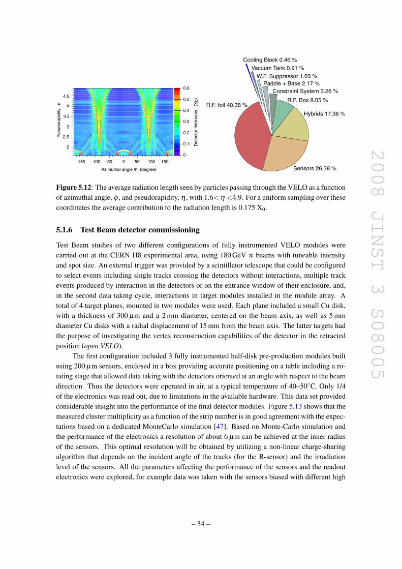
2008 JINST 3 S08005
Pse
ud
ora
pid
ity
η
4.5
4
3.5
3
2.5
2
Azimuthal angle Φ (degree)
-150 -100 -50 0 50 100 150
0.6
0.5
0.4
0.3
0.2
0.1
0
De
tecto
r th
ickn
ess
(X
0)
R.F. foil 40.38 %
Sensors 26.38 %
Cooling Block 0.46 %
Vacuum Tank 0.91 %
W.F. Suppressor 1.03 %
Paddle + Base 2.17 %
Constraint System 3.26 %
R.F. Box 8.05 %
Hybrids 17.36 %
Figure 5.12: The average radiation length seen by particles passing through the VELO as a functionof azimuthal angle, φ , and pseudorapidity, η , with 1.6< η <4.9. For a uniform sampling over thesecoordinates the average contribution to the radiation length is 0.175 X0.
5.1.6 Test Beam detector commissioning
Test Beam studies of two different configurations of fully instrumented VELO modules werecarried out at the CERN H8 experimental area, using 180 GeV π beams with tuneable intensityand spot size. An external trigger was provided by a scintillator telescope that could be configuredto select events including single tracks crossing the detectors without interactions, multiple trackevents produced by interaction in the detectors or on the entrance window of their enclosure, and,in the second data taking cycle, interactions in target modules installed in the module array. Atotal of 4 target planes, mounted in two modules were used. Each plane included a small Cu disk,with a thickness of 300 µm and a 2 mm diameter, centered on the beam axis, as well as 5 mmdiameter Cu disks with a radial displacement of 15 mm from the beam axis. The latter targets hadthe purpose of investigating the vertex reconstruction capabilities of the detector in the retractedposition (open VELO).
The first configuration included 3 fully instrumented half-disk pre-production modules builtusing 200 µm sensors, enclosed in a box providing accurate positioning on a table including a ro-tating stage that allowed data taking with the detectors oriented at an angle with respect to the beamdirection. Thus the detectors were operated in air, at a typical temperature of 40–50C. Only 1/4of the electronics was read out, due to limitations in the available hardware. This data set providedconsiderable insight into the performance of the final detector modules. Figure 5.13 shows that themeasured cluster multiplicity as a function of the strip number is in good agreement with the expec-tations based on a dedicated MonteCarlo simulation [47]. Based on Monte-Carlo simulation andthe performance of the electronics a resolution of about 6 µm can be achieved at the inner radiusof the sensors. This optimal resolution will be obtained by utilizing a non-linear charge-sharingalgorithm that depends on the incident angle of the tracks (for the R-sensor) and the irradiationlevel of the sensors. All the parameters affecting the performance of the sensors and the readoutelectronics were explored, for example data was taken with the sensors biased with different high
– 34 –

2008 JINST 3 S08005
Software Strip ID
2-S
trip
Clu
ster
Rat
e
1600 1700 1800 1900 20000
0.1
0.2
0.3
0.4
0.5(a)Testbeam
Simulation
1600 1700 1800 1900 20000
0.1
0.2
0.3
0.4
0.5(b)
1600 1700 1800 1900 20000
0.1
0.2
0.3
0.4
0.5(c)
1600 1700 1800 1900 20000
0.1
0.2
0.3
0.4
0.5(d)
Figure 5.13: Fraction of two strip clusters in R-sensors, for different beam track angles with respectto the normal to the detector planes: a) 0, b) 5, c) 10 d) 15. The horizontal axis represents thestrip number, corresponding to a progressively coarser inter-strip pitch.
voltages, and the operating parameters of the Beetle chip were changed. In addition, the noise per-formance was studied both with random triggers, and with electronic calibration runs. These datavalidate in a multi-detector configuration the laboratory characterization of the individual modulecomponents. The data acquisition and monitoring infrastructure planned for the experiment wereused. The system performance was excellent.
The second data set was taken using a system of 10 production modules including 300 µmthick sensors, mounted in the vacuum tank built for the final system, reading out 6 of them indifferent combinations, depending upon the trigger scheme chosen. Most of the data was takenin vacuum (below 10−3 mbar) and at a temperature of about -3C. This test beam cycle providedvaluable operating experience with the cooling system built for the experiment and with vacuumimplementation and monitoring. Data were taken in air at room temperature, and it was con-firmed that the module positions remained stable through the transition between air and vacuumand throughout temperature cycling.
The production detectors operated with a signal to noise ratio of between 17 and 25, de-pending on strip length, where signal is defined as the most probable value of the charge clusterproduced by a minimum ionizing particle (MIP) and noise is the incoherent noise measured fromcalibration data after subtracting the coherent noise component. Their performance proved to beremarkably stable throughout the 14 days of data taking. Single track and interaction trigger datacomplement the first data set in assessing the hit resolution as a function of angle. In addition, tar-get data produced reconstructed primary vertices from all the targets that help in tuning the vertexreconstruction algorithms.
– 35 –

2008 JINST 3 S08005
5.1.7 VELO software
Reconstruction software
The TELL1 data processing boards (see sections 5.1.4 and 8.2) perform a set of processing algo-rithms on the raw VELO data and identify clusters for use in the trigger and for off-line physicsanalysis. For use in the trigger the clusters are stored in a compressed form that is optimised forspeed and provides 3-bit precision on the inter-strip position of the clusters using a simple weightedpulse height algorithm. For offline use a higher precision calculation, and an estimate of the uncer-tainty on this position, is provided [48]. This calculation uses the inter-strip pitch and track angleas well as the pulse-height of the strips in the cluster.
In addition to the standard output data format of the TELL1, a number of other output formatsare provided for calibration and monitoring purposes and are decoded in the software framework.Notably, these include a non zero-suppressed raw data format, where the ADC values (at 8-bitprecision) are provided for all strips.
A bit-perfect emulation of the full TELL1 processing algorithm is available in the softwareframework. Using the emulation the raw data can be processed to produce the cluster format. Theperformance of the TELL1 algorithms can thus be assessed at each stage of the processing. Theemulation is also used to tune the optimal settings of the adjustable parameters in the TELL1, suchas the signal thresholds used in the clustering algorithm.
A simulation framework for the VELO has been provided. This framework describes thematerial and layout of the VELO detector. The response of the silicon detectors and front-end chippulse shape to the passage of particles is described, based on physically motivated parametrisationstuned to describe laboratory and test beam data. The resulting simulated analog signals are passedthrough the emulated TELL1 clustering algorithm and the output clusters are stored in the sameformat as for the real data [49].
Monitoring
The VELO data monitoring can be divided into two strands: the short term operational checksperformed on-line; and the longer-term off-line performance monitoring.
The on-line monitoring is performed using the LHCb monitoring farm. Cluster and trackmonitoring, including monitoring of residuals for the alignment, is performed using the standardoutput data. Raw data is also produced for a subset of events at a rate of a fraction of a Hz and,through use of a special calibration trigger, read out to the monitoring farm. This rate allows theperformance of individual channels to be accurately assessed on a timescale of one hour. The fullinformation of the TELL1 processing boards is available through monitoring using the TELL1credit-card PC. Preliminary tests of the on-line monitoring have already been performed in theVELO test beam.
A critical element of the monitoring is the determination of the beam-position. The alignmentframework, reconstruction, pattern recognition, track fitting and vertex-finding algorithms are usedto build up a 3 dimensional picture of the beam position. This monitoring process is used todetermine the correct step-wise movements that are required to close the two halves and centre
– 36 –

2008 JINST 3 S08005
them around the beam at the start of an LHC fill. The beam stability is then monitored duringLHC operation.
The off-line monitoring uses a range of analyses to assess the performance and to tune op-erational parameters including the high voltage applied to each sensor, the TELL1 hit processingparameters, and the cluster resolution model used in the tracking. The analyses include: timealignment studies for beam synchronisation; charge collection efficiency and signal-to-noise stud-ies; resolution studies as a function of detector pitch and projected angle; cross-coupling, pedestal,noise and common-mode noise studies making particular use of the TELL1 emulation. These stud-ies use the full range of VELO TELL1 output formats for the data and also make use of specialcalibration trigger and test-pulses generated in the Beetle front-end chip of the VELO modules.
Alignment
The alignment of the VELO relies on three components: the precision construction and assemblyof the hardware; the metrology of the individual modules and assembled system; and the softwarealignment of the system using tracks.
The construction and assembly of the system is reported elsewhere in this section. The con-struction precision has tight mechanical tolerances, for example the silicon sensors are nominallylocated only 1 mm from the the aluminium RF foil. However, the driving factor for the requiredconstruction tolerance is the successful operation of the LHCb trigger. The VELO pattern recog-nition algorithm, used to identify high impact parameter tracks in the trigger, is performed forspeed reasons initially in the rz projection. This requires that the strips on the R-sensors accuratelydescribe circles around the beam position.
A survey of the individual modules and of the assembled halves on the module supports wasperformed. The relative positions of the modules and of the R- and φ -sensors on a single modulewere measured to a precison of better than 10 µm. The silicon sensors were found to have nosignificant curvature: 8 points were measured on the surface of the silicon sensors and the meanRMS deviation of the sensors from a plane was found to be 14 µm. The deviations of the modulesfrom their nominal positions are shown in figure 5.14 for the two detector halves (A and C sides).The scatters give an impression of the total assembly precision. In the x coordinate the scatteris very small, and the overall offsets are fully compensated by the fact that the two halves moveindependently in x. In y there is a small slope seen in the C-side results, which was traced to thefact that the module support was not perfectly flat, but had a 40 µm corkscrew twist between thecorners. The resulting slope was fully compensated by adjustments of the detector supports duringthe installation of the halves.
The precision survey is an important element of the alignment: not only does it provide thestarting position for the VELO software alignment but it also constrains degrees of freedom ofthe system which will not be possible to accurately measure with data. For example, the overall zpositions of the sensors are obtained from the metrology. The sensor alignment parameters obtainedfrom the survey were propagated to the LHCb conditions database.
Whilst the survey was performed at room temperature and pressure, no significant deviationsare expected for the final system. The module support will be maintained at a constant temperatureof 20C. The deviations of the system under vacuum have been determined from the software
– 37 –

2008 JINST 3 S08005
-200 0 200 400 600 800
-100
-50
0
50
100 m)µOffset in x (
mµScatter = 7.5-200 0 200 400 600 800-6
-4
-2
0
2
4
6Rotation about x=0 (mrad)
Scatter = 0.5mrad
-200 0 200 400 600 800
-100
-50
0
50
100 m)µOffset in y (
mµScatter = 10.1-200 0 200 400 600 800-6
-4
-20
2
4
6Rotation about y=0 (mrad)
Scatter = 2.3mrad
-200 0 200 400 600 800-500-400-300-200-100
0100200300400500
m)µOffset in z (
mµScatter = 125.9
mm-200 0 200 400 600 800-0.6
-0.4
-0.2
0
0.2
0.4
0.6Rotation about z=0 (mrad)
radµScatter = 96.4
-200 0 200 400 600 800
-100
-50
0
50
100 m)µOffset in x (
mµScatter = 8.7-200 0 200 400 600 800-6
-4
-2
0
2
4
6Rotation about x=0 (mrad)
Scatter = 0.5mrad
-200 0 200 400 600 800
-100
-50
0
50
100 m)µOffset in y (
mµScatter = 24.4-200 0 200 400 600 800-6
-4
-20
2
4
6Rotation about y=0 (mrad)
Scatter = 1.6mrad
-200 0 200 400 600 800-500-400-300-200-100
0100200300400500
m)µOffset in z (
mµScatter = 112.5
mm-200 0 200 400 600 800-0.6
-0.4
-0.2
0
0.2
0.4
0.6Rotation about z=0 (mrad)
radµScatter = 144.9
Figure 5.14: Results of the metrology of the fully mounted VELO halves vs z. The deviationsfrom nominal are shown for every sensor. The six plots on the left show the result for the A side,and on the right for the C side. The rz tracking is sensitive to scatters and offsets in the x coordinate(between modules) and y coordinate (between modules, and between the detector halves).
alignment in a test beam using a partially assembled VELO and seen to be typically 10 µm or less,as shown in figure 5.15.
As previously stated, prior to the LHC establishing stable beams, the VELO is in a retractedposition and is brought into its nominal position only after stable beam is established. The positionof the two halves will be known through the motion control and position measurement system toan accuracy of 10 µm. Combining this information with the relative alignment of the modulesobtained from the previous fill is expected to provide sufficient alignment accuracy for operationof the VELO trigger. However, the option to perform a software alignment at the start of each fillremains, should this prove necessary.
The software alignment procedure for the detector divides into four distinct parts:
• An alignment of the relative position of the R and Φ sensors on each module using the shapeof the residual distributions across the sensors.
• An alignment of the modules within each VELO-half box using the residuals of hits onreconstructed tracks.
• A relative alignment of the two half-boxes with respect to each other principally relying onusing tracks passing through the geometrical overlap between the modules in the two half-boxes.
• A global alignment of all sub-detectors relative to each other. This part is reviewed in [50].
– 38 –

2008 JINST 3 S08005
Module number0 5 10 15 20
m)
µM
isal
ign
men
t va
lue
(in
-50
-40
-30
-20
-10
0
10
20
30
40
50
Module number0 5 10 15 20
m)
µM
isal
ign
men
t va
lue
(in
-100
-80
-60
-40
-20
0
20
40
60
80
100
Module number0 5 10 15 20
Mis
alig
nm
ent
valu
e (i
n m
rad
)
-1
-0.8
-0.6
-0.4
-0.2
-0
0.2
0.4
0.6
0.8
1
Figure 5.15: x-axis translation alignment constants of the VELO modules determined by softwarealignment from data recorded during the VELO test beam in air (open circles) and in vacuum (solidpoints). The modules are seen to be stable in the different conditions, including different thermalgradients across the modules.
Relative sensor alignment
The R- and φ -sensors bonded in an individual module have had their relative positions measuredduring the system metrology. To further improve and monitor their relative misalignment a methodhas been developed that exploits distortions observed in the residuals across the sensor. It can beshown that the relation between residuals (εR/Φ) and misalignments in the sensor plane (∆x,∆y,∆γ )is given by
εR = −∆x cosφtrack +∆y sinφtrack (R sensor)εΦ = +∆x sinφtrack +∆y cosφtrack +∆γrtrack (Φ sensor)
, (5.1)
where rtrack and φtrack are the radius and the azimuthal angle of the extrapolated track position,respectively. The misalignments ∆x,∆y are determined by a fit to the shape of the residual distribu-tion as a function of the azimuthal angle, while ∆γ , the rotation misalignment around the z-axis, isdetermined by a fit to the shape of the residual distribution as a function of the radius. The optimalalignment can be found after three iterations of this procedure, using the previously determinedalignment constants as input to the next iteration.
The method has been tested using MonteCarlo simulations and VELO test beam data. It hasbeen shown that an alignment precision at the µm level can be achieved for ∆x and ∆y, while ∆γ
will be determined to higher precision by the module alignment algorithm.
– 39 –

2008 JINST 3 S08005
Module alignment and VELO half alignment
The module alignment and the VELO half alignment are dependent on the same approach, a non-iterative method using matrix inversion. The alignment is based upon a χ2 function produced fromthe residuals between the tracks and the measured clusters. The track and alignment parameterscan be obtained through minimisation of this χ2 function.
The equations which describe the trajectories of particles are expressed as a linear combi-nation of both the local (track-dependent) parameters and the global (alignment) parameters. Alltracks are correlated since the global alignment parameters are common to each track, hence it isnecessary to fit all tracks simultaneously.
The χ2 function can be minimised by solving the set of simultaneous equations given by thederivatives of the χ2 with respect to the local track parameters and global alignment parameters.This results in a system of equations of a final size, ntotal given by:
ntotal = nlocal×ntracks +nglobal (5.2)
where nlocal is the number of local parameters per track (four parameters for a straight line in3D) , ntracks is the number of tracks used for the alignment and nglobal is the number of align-ment constants. Whilst the direct inversion of such large matrices is not computationally practi-cal, the alignment can be handled by inverting the matrix by partition, thus reducing the problemto a nglobal× nglobal matrix inversion. Inversion by partitioning is handled by the Millepede pro-gram [51].
The number of tracks required for an effective alignment is relatively modest but the align-ment is improved by using a mixture of tracks from primary vertex interactions and a comple-mentary track set from a source such as beam-halo particles. The relative alignment of the twohalf-boxes is primarily constrained by tracks that pass through both halves. However, when theVELO is retracted an alternative technique is required which relies upon fitting primary verticesusing tracks fitted in both halves of the VELO. The CPU requirements of the alignment are alsolow: of order minutes on a single PC.
Tests using data from the VELO test beam and on MonteCarlo simulation have demonstratedthat x and y-axis translations of the modules can be constrained at the few µm level and rotationsaround the z axis of order 0.1 mrad, with weaker sensitivity obtained to the other degrees of free-dom. MonteCarlo simulation tests have demonstrated that x and y translations of the half-boxescan be constrained at better than 20 µm and rotations around these axes to better than 0.1 mrad.Rotations around the z-axis are constrained at the 0.2 mrad level.
5.1.8 VELO performance
The VELO layout has been optimised to minimise the amount of material in the acceptance whileproviding good geometrical coverage. All tracks inside the LHCb acceptance (1.6 < η < 4.9)pass through at least three modules, as shown in figure 5.16.
The individual hit resolution of the sensors has been determined in a test beam and is a strongfunction of the sensor pitch and projected angle (the angle perpendicular to the strip direction), asshown in figure 5.17. The best raw resolution obtained is 7 µm. As shown in figure 5.18 perfor-
– 40 –

2008 JINST 3 S08005
N. of stations crossed by tracks Rapidity η
0
1
2
3
4
5
2 2.5 3 3.5 4 4.50
2
4
6
8
10x 104
2 4 6 8 10 12 14
Entr
ies
N. of sta
tions c
rossed b
y tra
cks
Figure 5.16: The left plot shows the number of stations hit per track in the VELO and the rightplot shows the number of hits of a track in the VELO modules as a function of the pseudorapidityof the track. The dashed line indicates the limit above which 95% of the tracks lie.
30 40 50 60 70 80 90 100
resolu
tion (
µm
)
0
5
10
15
20
25
30
DataFit to dataBinary
pitch (µm)
30 40 50 60 70 80 90 1000
5
10
15
20
25
30
DataFit to dataBinary
Φ sensors R sensors
pitch (µm)
resolu
tion (
µm
)
Figure 5.17: The raw hit resolution as a function of strip pitch as measured in the test beam forparticles of normal incidence. The dashed line indicates the resolution expected for digital readout.The data points show the resolution as measured from the weighted centre of the charges on thestrips.
mance improves for the low angle tracks when imperfections in the weighted charge distributionbetween two strips are taken into account [52].
In addition, crosstalk originating from inter-strip coupling, from coupling between electronicchannels, and from signal feed-forward and backward in the analog transmission have not beentaken into account. Once these have been fully parametrised further improvement in the resolutionobtained from the system is anticipated.
– 41 –

2008 JINST 3 S08005
Track angle (deg)
0 1 2 3 4 5 6 7 8 9R
eso
lutio
n
(µ
m)
0
2
4
6
8
10
12
14
16
18
20
Weighted Mean
Corrected
Figure 5.18: The individual hit resolution of a VELO R-sensor as a function of the projected anglefor a pitch of 85 µm. The open circles show the resolution as derived from a weighted mean.The filled circles include the corrections for the imperfections in the weighted charge distributionbetween two strips.
5.2 Silicon Tracker
The Silicon Tracker (ST) comprises two detectors: the Tracker Turicensis10 (TT) [2, 53] and theInner Tracker (IT) [54]. Both TT and IT use silicon microstrip sensors with a strip pitch of about200 µm. The TT is a 150 cm wide and 130 cm high planar tracking station that is located up-stream of the LHCb dipole magnet and covers the full acceptance of the experiment. The IT coversa 120 cm wide and 40 cm high cross shaped region in the centre of the three tracking stationsdownstream of the magnet. Each of the four ST stations has four detection layers in an (x-u-v-x)arrangement with vertical strips in the first and the last layer and strips rotated by a stereo angleof -5 and +5 in the second and the third layer, respectively. The TT has an active area of about8.4 m2 with 143360 readout strips of up to 38 cm in length. The IT has an active area of 4.0 m2
with 129024 readout strips of either 11 cm or 22 cm in length.The main design choices for the Silicon Tracker detectors were largely driven by the following
considerations:Spatial resolution. Simulation studies have demonstrated that a single-hit resolution of about
50 µm is adequate for both the TT and the IT. The momentum resolution of the spectrometer isthen dominated by multiple scattering over almost the full range of particle momenta. Readoutstrip pitches of about 200 µm meet this requirement and were therefore chosen for both detectors.
Hit occupancy. Charged particle densities of about 5×10⁻² per cm2 for minimum bias eventsare expected in the innermost regions of the TT. They fall off by two orders of magnitude to about 5×10⁻⁴ per cm2 in the outermost regions of the detector. Different readout strip lengths were chosenfor different regions of the detector to keep maximum strip occupancies at the level of a few percentwhile minimizing the number of readout channels. For the IT, expected charged-particle densitiesfor minimum-bias events range from about 1.5 ×10⁻² per cm2 close to the LHC beampipe to 2×10⁻³ per cm2 in the outer regions of the detector. Also here, the chosen strip geometries result inmaximum strip occupancies that do not exceed a few percent.
10The Tracker Turicensis was formerly known as the Trigger Tracker.
– 42 –

2008 JINST 3 S08005
Signal shaping time. In order to avoid pile-up of events from consecutive LHC bunch cross-ings, fast front-end amplifiers with a shaping time of the order of the bunch crossing interval of25 ns have to be used. The benchmark parameter is the remaining fraction of the signal ampli-tude at the sampling time of the subsequent bunch crossing, 25 ns after the maximum of the pulse.Simulation studies have shown that signal remainders of 50% for the TT and 30% for the IT areacceptable for the track reconstruction algorithms.
Single-hit efficiency. Each detection layer should provide full single-hit efficiency for mini-mum ionising particles while maintaining an acceptably low noise hit rate. The critical parameteris the signal-to-noise ratio, defined as the most probable signal amplitude for a minimum ionisingparticle divided by the RMS of the single strip noise distribution. Test beam studies have shownthat the hit efficiency starts to decrease rapidly as the signal-to-noise ratio drops below 10:1. Thedetector was designed such that a signal-to-noise ratio in excess of 12:1 can be expected taking intoaccount the expected deterioration from radiation damage corresponding to ten years of operationat nominal luminosity.
Radiation damage. For ten years of operation at nominal luminosity, expected 1 MeV neutronequivalent fluences in the innermost regions of the detectors do not exceed 5×10¹⁴ per cm2 for theTT and 9×10¹² per cm2 for the IT. Basic design rules for radiation hard silicon sensors werefollowed to ensure that the detectors will survive these fluences. The detector was designed andtested to work at bias voltages of up to 500 V. The sensors need to be operated at a temperature of5C or lower to suppress radiation damage induced leakage currents to a level where (a) shot noisedoes not significantly deteriorate the signal-to-noise performance of the detector and (b) the risk ofthermal runaway due to the power dissipated by the leakage currents is avoided.
Material budget. As the momentum resolution of the LHCb spectrometer is dominated bymultiple scattering, the material budget of the detectors had to be kept as small as possible. The TTwas designed such that front-end readout electronics and mechanical supports are located outsideof the LHCb acceptance. This was not possible in the case of the IT, which is located in front of theactive region of the OT detectors. Here, a significant design effort was made to keep the amount ofmaterial for mechanical supports and for the cooling of front-end electronics as small as possible.
Number of readout channels. Readout electronics are a major contribution to the overall costof the detector. The largest readout pitches compatible with the required spatial resolution and thelongest readout strips compatible with requirements on occupancy and signal-to-noise performancewere chosen in order to minimize the number of readout channels.
Different constraints on the detector geometries resulted in different designs for the detec-tor modules and station mechanics of the TT and the IT. These are described in sections 5.2.1and 5.2.2, respectively. Common to both parts of the ST are the readout electronics, the powerdistribution, and the detector control and monitor systems. These are the topic of section 5.2.3. Fi-nally, the expected detector performance, based on test beam measurements and simulation studies,is discussed in section 5.2.4.
5.2.1 Tracker Turicensis
All four detection layers of the TT are housed in one large light tight and thermally and electricallyinsulated detector volume, in which a temperature below 5C is maintained [55]. The detector
– 43 –

2008 JINST 3 S08005
Figure 5.19: Layout of the third TT detection layer. Different readout sectors are indicated bydifferent shadings.
volume is continuously flushed with nitrogen to avoid condensation on the cold surfaces. To aidtrack reconstruction algorithms, the four detection layers are arranged in two pairs, (x,u) and (v,x),that are separated by approximately 27 cm along the LHC beam axis.
The layout of one of the detection layers is illustrated in figure 5.19. Its basic building blockis a half module that covers half the height of the LHCb acceptance. It consists of a row of sevensilicon sensors organized into either two or three readout sectors. The readout hybrids for all read-out sectors are mounted at one end of the module. The regions above and below the LHC beampipeare covered by one such half module each. The regions to the sides of the beampipe are coveredby rows of seven (for the first two detection layers) or eight (for the last two detection layers) 14-sensor long full modules. These full modules cover the full height of the LHCb acceptance and areassembled from two half modules that are joined together end-to-end. Adjacent modules withina detection layer are staggered by about 1 cm in z and overlap by a few millimeters in x to avoidacceptance gaps and to facilitate the relative alignment of the modules. In the u and v detectionlayers, each module is individually rotated by the respective stereo angle.
A main advantage of this detector design is that all front-end hybrids and the infrastructurefor cooling and module supports are located above and below the active area of the detector, outsideof the acceptance of the experiment.
TT detector modules
The layout of a half module is illustrated in figure 5.20. It consists of a row of seven silicon sensorswith a stack of two or three readout hybrids at one end. For half modules close to the beampipe,where the expected particle density is highest, the seven sensors are organized into three readoutsectors (4-2-1 type half modules).
For the other half modules, the sensors are organized into two readout sectors (4-3 type halfmodules). In both cases, the first readout sector (L sector) is formed by the four sensors closest to
– 44 –

2008 JINST 3 S08005
Figure 5.20: View of a 4-2-1 type TT detector module.
the readout hybrids and furthest away from the beam. The strips of the four sensors are bondedtogether and directly connected to the lower-most readout hybrid. For 4-3 type half modules,the strips of the remaining three sensors are bonded together and form the second readout sector(M sector). They are connected via a 39 cm long Kapton flex cable (interconnect cable) to asecond readout hybrid mounted on top of the L hybrid. For 4-2-1 type half modules, the threeremaining sensors are subdivided into an intermediate two sensor sector (M sector) and a thirdsector consisting of the single sensor closest to the beam (K sector). The two readout sectors areconnected via 39 cm respectively 58 cm long Kapton interconnect cables to two separate front-endhybrids that are mounted on top of the L hybrid. Bias voltage is provided to the sensor backplanesvia a thin Kapton flex cable that runs along the back of the half module. The half module ismechanically held together by two thin fibreglass/carbon fibre rails that are glued along the edgesof the L hybrid and the seven silicon sensors.
Silicon sensors. The silicon sensors for the TT are 500 µm thick, single sided p+-on-n sen-sors.11 They are 9.64 cm wide and 9.44 cm long and carry 512 readout strips with a strip pitch of183 µm.
Kapton interconnect cables. The Kapton interconnect cables for the M and K readout sectorswere produced using standard plasma-etching technology.12 They carry 512 signal strips and twopairs of bias voltage and ground strips on a 100 µm thick Kapton substrate. The strips consist of7 µm thick copper with a 1 µm thick gold plating, are 15 µm wide and have a pitch of 112 µm.A short pitch-adapter section in which the strip pitch widens to 180 µm permits to directly wire-bond the strips on the cable to the silicon sensor strips. A copper mesh backplane provides a solidground connection and shielding against pick-up noise. The small strip width was required to keepthe strip capacitance of the cable small, but led to an unacceptably low production yield for fault
11The sensors are identical in design to the OB2 sensors used in the Outer Barrel of the CMS Silicon Tracker [56] andwere produced by Hamamatsu Photonics K.K., Hamamatsu City, Japan.
12The Kapton interconnect cables were produced by Dyconex AG, Bassersdorf, Switzerland.
– 45 –
2008 JINST 3 S08005
free cables of the required length. The 39 cm long cables for the M sectors therefore had to beassembled from two shorter pieces, and the 58 cm long cables for the K sectors were assembledfrom three pieces. The pieces were joined together end-to-end by gluing them onto a thin stripof fibreglass reinforced epoxy. An electrically conductive adhesive tape was used to provide theelectrical connection between the copper mesh backplanes of the two cable pieces. The signal, biasvoltage and ground strips on the strip side of the cables were joined together by wire bonds.
Kevlar caps. Small Kevlar caps protect the wire bond rows on the strip side of the Kaptoninterconnect cables as well as those between silicon sensors. These caps are glued onto the surfaceof the cable or the sensors using standard two component epoxy glue.13
Readout hybrids. The front-end readout hybrids [57] consist of a carrier plate, a pitch adapter,and a four layer Kapton flex circuit that carries four front-end readout chips, some passive SMDcomponents and an 80-pin board-to-board connector.14 Through this connector, the multiplexedanalog detector signals are read out and the control signals, low voltage and bias voltage are pro-vided to the half module. Two of the four conductive layers of the flex circuit are used for digitaland analog power and ground. The other two layers carry the signal and control lines. Due tomechanical constraints, three variants of the readout hybrid are used for the three different types ofreadout sectors. The Kapton flex circuits for all three variants are identical except for a differentoverall length. The upper hybrids have to be shorter than the lower ones to make the readout con-nectors on all hybrids accessible when these are mounted on top of each other. The carrier platesgive mechanical stability to the hybrid and act as a heat sink for the heat produced by the front-endchips. The pitch adapter matches the input pitch of the front-end chips to the pitch of the siliconsensors in case of the L hybrid and to the pitch of the Kapton interconnect cable in case of theK and M hybrids. For these, the carrier plate is made from gold plated copper and the pitch adapteris a rectangular piece of alumina (Al2O3) substrate with strip lines produced using standard thinfilm technology. The pitch adapter is glued onto the carrier plate together with the Kapton flexcircuit. The carrier plate for the L hybrid is a much more complicated piece that consists of alu-minium nitride substrate and combines several functionalities.15 First of all, it carries not only thestrip lines of the pitch adapter for the L sector, produced using standard thick film technology, butalso additional traces and vias that serve to connect the bias voltage for all readout sectors. Next,the support rails of the detector module are glued along the sides of this carrier plate. And finally,this carrier plate provides the mechanical and thermal interface of the half module to the detectorstation. All these functionalities will be described in more detail below. Aluminium nitride waschosen as the material for this carrier plate because of its high thermal conductivity and its smallthermal expansion coefficient that is reasonably well matched to that of the silicon sensors.
The K and M hybrids are mounted on top of the carrier plate of the L hybrid using 2.5 mmthick spacers made of copper. These ensure good thermal contact between the carrier plates of theK and M hybrids and the one of the L hybrid.
Support rails. The two half module support rails are 5.5 mm high and consist of a 1 mm thickstrip of carbon fibre glued to a 1 mm thick strip of fibreglass reinforced epoxy. A small groove
13Araldite 2011 (AW106/HV953U), by Huntsman Advanced Materials, Basel, Switzerland.14The flex circuits were produced by Optiprint AG, Berneck, Switzerland.15The production of the pitch adapters for the K and M hybrids and of the aluminium nitride carrier plate for the
L hybrids as well as the assembly and bonding of all hybrids was done by RHe Microsystems, Radeberg, Germany.
– 46 –

2008 JINST 3 S08005
Figure 5.21: View of the TT station mechanics.
is milled into the flat side of the fibreglass strip which permits to slide the rail over the edges ofthe seven silicon sensors and the carrier plate of the L hybrid. The rail is glued to these usingstandard two component epoxy glue. The rôle of the fibreglass strip is to ensure the necessaryelectrical insulation between the strip side of the silicon sensors (which are at ground potential)and their backplanes (which carry the bias voltage of up to 500 V). The mechanical rigidity of therail is defined mainly by the carbon fibre strip. The fibreglass strip spans the full length of the halfmodule but the carbon fibre strip ends at the fourth silicon sensor from the hybrids. This permits tojoin two half modules to a 14-sensor long full module by gluing an additional carbon fibre strip tothe free sections of fibreglass strip on both half modules.
Bias voltage. Bias voltage is supplied separately for each of the readout sectors on a halfmodule via the cable that plugs into the corresponding front-end hybrid. From the hybrid it isconnected to aluminium traces on the carrier plate of the L sector, using wire bonds in case of theL hybrid and thin copper wires in case of the M and K hybrids. From here, all bias voltages arebrought to the back of the half module through aluminium vias that are embedded in the aluminiumnitride substrate. Finally, a thin Kapton flex cable, which is glued along the back of the halfmodule and carries one copper trace per readout sector, carries the bias voltage to the backplanesof the silicon sensors. The electrical connections between the Kapton flex cable and the sensorbackplanes and between the cable and the bias voltage pads on the back of the aluminium nitrideare made by wire bonding.
TT detector station
An isometric drawing of the detector station is shown in figure 5.21. It consists of two halves, oneon each side of the LHC beampipe.
The half stations are mounted on rails and can be retracted horizontally for detector mainte-nance and bakeouts of the LHC beampipe. The main structural element of each half station is aC-shaped aluminium frame. It carries a detector box that is made of light weight aluminium clad
– 47 –

2008 JINST 3 S08005
foam. This box is open on the side facing the beampipe such that the two half stations in data takingposition define one large volume that contains all detector modules. Mounted against the top andbottom walls of the detector box are horizontal cooling plates that provide the mechanical supportfor the detector modules as well as cooling of the front-end hybrids and the detector volume. Thecooling plates incorporate cooling pipes through which C6F14 at -15C is circulated as a coolingagent. Additional cooling elements are mounted vertically, close to the outer side walls of thedetector volume. All electrical signals (detector signals, control signals and supply voltages) aretransmitted on Kapton-flex cables through specially designed feedthroughs in the top and bottomwalls of the detector box.
Detector box. The C-shaped support frames are assembled from 15 mm thick aluminiumplates. They rest on a lower precision rail and are guided by an upper precision rail. These tworails are aligned parallel to each other to better than 100 µm in order to avoid possible distortionsof the C-frame during insertion or retraction. Mounted flat against the inner surfaces of the C-frames are stiff sandwich plates consisting of a 30 mm thick aramid honeycomb structure with1 mm thick aluminium cladding. These sandwich plates define the outer walls of the detector box.The front and rear walls of the box are made of 40 mm thick panels of polyetherimide foam16
that are laminated on both sides with 25 µm of aluminium for electrical insulation and 275 µm ofKevlar for mechanical protection. These panels are screwed against the outer walls of the box andcan be easily removed for the installation and maintenance of detector modules. Similar platesof 40 mm thick aluminium and Kevlar clad polyetherimide foam are also mounted flat against theinner surfaces of the outer walls of the box to improve thermal insulation here. Finally, the detectorvolume is closed off around the LHC beampipe by two specially machined semicylindrical piecesthat again consist of the same polyetherimide foam clad with aluminium and Kevlar. The wallthickness of these beampipe insulation pieces is 30 mm, except for cutouts at the locations of thedetection layers. Here, the wall thickness is reduced to about 5 mm to reduce the dead space inbetween the beampipe and the innermost detector modules. A clearance of 5 mm between thedetector box and the beampipe had to be maintained to satisfy LHC safety demands.
Cooling plates. There are a total of four cooling plates, one for each quadrant of the detector.They are mounted horizontally onto pillars made of polyacetal (POM) that are fixed against theupper or the lower walls of the detector box. A drawing of a cooling plate is shown in figure 5.22.It is a precisely machined plate of 8 mm thick aluminium that measures 897 mm in x and 348 mmin z. Machined into its outer surface are semicircular grooves into which two coiled aluminiumcooling pipes with an outer diameter of 10 mm and a total length of about 3.5 m are glued. Its innersurface is machined to an overall flatness of better than 100 µm.
Cooling balconies. Mounted vertically against the flat inner surface of the cooling plate arethe aluminium cooling balconies that provide the mechanical, thermal and electrical interface be-tween cooling plate and detector modules. Precision holes and pins ensure the accurate positioningof the balconies on the cooling plate. The detector module is screwed onto the flat, vertical surfaceof the balcony, ensuring a large contact surface and therefore good thermal contact between thebalcony and the aluminium nitride carrier plate of the half module. The correct positioning of themodule is ensured by precision holes and pins in the balcony and laser cut holes in the aluminium
16Airex R82.60, by Gaugler & Lutz oHG, Aalen-Ebnat, Germany.
– 48 –
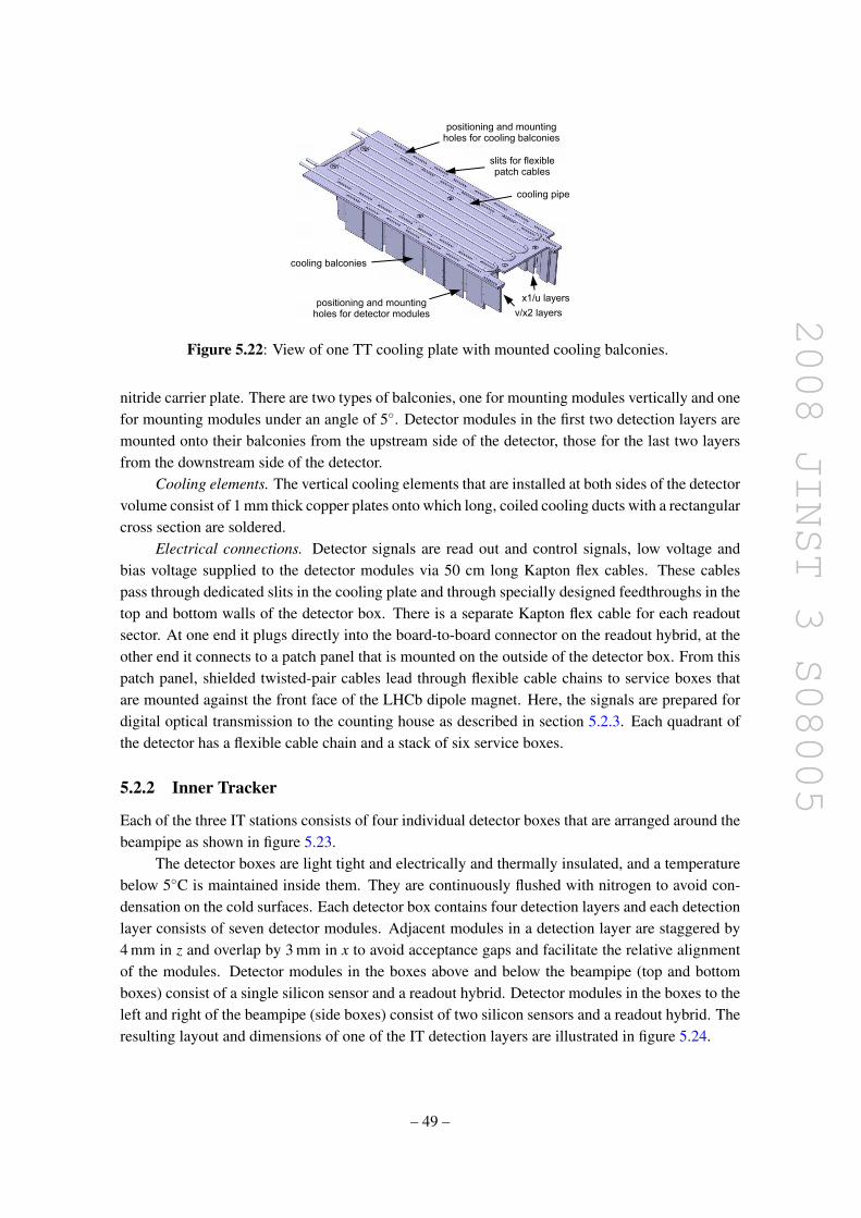
2008 JINST 3 S08005
Figure 5.22: View of one TT cooling plate with mounted cooling balconies.
nitride carrier plate. There are two types of balconies, one for mounting modules vertically and onefor mounting modules under an angle of 5. Detector modules in the first two detection layers aremounted onto their balconies from the upstream side of the detector, those for the last two layersfrom the downstream side of the detector.
Cooling elements. The vertical cooling elements that are installed at both sides of the detectorvolume consist of 1 mm thick copper plates onto which long, coiled cooling ducts with a rectangularcross section are soldered.
Electrical connections. Detector signals are read out and control signals, low voltage andbias voltage supplied to the detector modules via 50 cm long Kapton flex cables. These cablespass through dedicated slits in the cooling plate and through specially designed feedthroughs in thetop and bottom walls of the detector box. There is a separate Kapton flex cable for each readoutsector. At one end it plugs directly into the board-to-board connector on the readout hybrid, at theother end it connects to a patch panel that is mounted on the outside of the detector box. From thispatch panel, shielded twisted-pair cables lead through flexible cable chains to service boxes thatare mounted against the front face of the LHCb dipole magnet. Here, the signals are prepared fordigital optical transmission to the counting house as described in section 5.2.3. Each quadrant ofthe detector has a flexible cable chain and a stack of six service boxes.
5.2.2 Inner Tracker
Each of the three IT stations consists of four individual detector boxes that are arranged around thebeampipe as shown in figure 5.23.
The detector boxes are light tight and electrically and thermally insulated, and a temperaturebelow 5C is maintained inside them. They are continuously flushed with nitrogen to avoid con-densation on the cold surfaces. Each detector box contains four detection layers and each detectionlayer consists of seven detector modules. Adjacent modules in a detection layer are staggered by4 mm in z and overlap by 3 mm in x to avoid acceptance gaps and facilitate the relative alignmentof the modules. Detector modules in the boxes above and below the beampipe (top and bottomboxes) consist of a single silicon sensor and a readout hybrid. Detector modules in the boxes to theleft and right of the beampipe (side boxes) consist of two silicon sensors and a readout hybrid. Theresulting layout and dimensions of one of the IT detection layers are illustrated in figure 5.24.
– 49 –

2008 JINST 3 S08005
Figure 5.23: View of the four IT detector boxes arranged around the LHC beampipe.
Figure 5.24: Layout of an x detection layer in the second IT station.
IT detector modules
An exploded view of a detector module is shown in figure 5.25. The module consists of either oneor two silicon sensors that are connected via a pitch adapter to a front-end readout hybrid. Thesensor(s) and the readout hybrid are all glued onto a flat module support plate. Bias voltage isprovided to the sensor backplane from the strip side through n+ wells that are implanted in the n-type silicon bulk. A small aluminium insert (minibalcony) that is embedded into the support plateat the location of the readout hybrid provides the mechanical and thermal interface of the moduleto the detector box.
Silicon sensors. Two types of silicon sensors of different thickness, but otherwise identical indesign, are used in the IT.17 They are single-sided p+-on-n sensors, 7.6 cm wide and 11 cm long,and carry 384 readout strips with a strip pitch of 198 µm. The sensors for one-sensor modulesare 320 µm thick, those for two-sensor modules are 410 µm thick. As explained in section 5.2.4below, these thicknesses were chosen to ensure sufficiently high signal-to-noise ratios for eachmodule type while minimising the material budget of the detector.
17The sensors were designed and produced by Hamamatsu Photonics K.K., Hamamatsu City, Japan.
– 50 –

2008 JINST 3 S08005
Figure 5.25: Exploded view of a two-sensor IT module. One-sensor modules are similar exceptthat the support plate is shorter and carries only one sensor.
Readout hybrids. The IT front-end readout hybrids consist of a four layer Kapton flex circuitthat is very similar in design and routing to that of the TT hybrids, and a pitch adapter that is similarto that used for the M and K hybrids of the TT.18 The only differences are (a) that the Kapton flexcircuit for the IT carries only three front-end chips and (b) that it incorporates an 89 mm longreadout tail with straight traces, at the end of which a 60-pin board-to-board connector is mounted.The pitch adapter is glued onto the Kapton flex circuit and the Kapton flex circuit is glued directlyonto the module support plate.
Module support plate. The module support plate19 consists of a 1 mm thick sheet of polyether-imide foam20 sandwiched in between two 200 µm thick layers of carbon fibre composite. The latterare produced from two layers of thermally highly conductive carbon fibres21 that are oriented at±10 with respect to the module axis. A 25 µm thick Kapton foil is laminated on top of the uppercarbon fibre layer to electrically insulate it from the backplane of the silicon sensors, which car-ries the sensor bias voltage of up to 500 V. The support plate extends on all sides by 1 mm overthe edges of the silicon sensors to protect these mechanically. The edges of the support plate aresealed with a non conductive epoxide resin to prevent loose fibres from sticking out and touchingthe sensor, where they might cause a short between the strip side and the backplane. At the loca-tion of the front-end readout chips, a 70 mm wide, 15 mm high and 1.5 mm thick aluminium piececalled minibalcony is inserted in the support plate. It is glued to the support plate using thermallyconductive glue.22
Minibalcony. The minibalcony defines the mechanical and thermal interface of the module tothe detector box. It is machined to a flatness of better than 30 µm and contains precision holes for
18The production of flex prints and pitch adapters and the assembly of the readout hybrids took place at the same twocompanies as for the TT.
19The module support plates were produced by Composite Design, Echandens, Switzerland.20Airex R82.60, by Gaugler & Lutz oHG, Aalen-Ebnat, Germany.21K13D2U, by Mitsubishi Chemical Corp., Tokyo, Japan.22TRA-DUCT 2902, by TRA-CON Inc., Bedford, Massachusetts, USA.
– 51 –
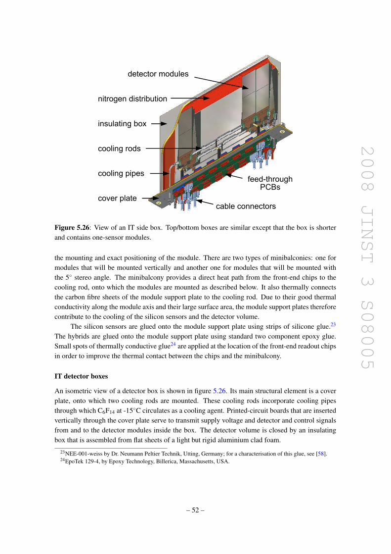
2008 JINST 3 S08005
Figure 5.26: View of an IT side box. Top/bottom boxes are similar except that the box is shorterand contains one-sensor modules.
the mounting and exact positioning of the module. There are two types of minibalconies: one formodules that will be mounted vertically and another one for modules that will be mounted withthe 5 stereo angle. The minibalcony provides a direct heat path from the front-end chips to thecooling rod, onto which the modules are mounted as described below. It also thermally connectsthe carbon fibre sheets of the module support plate to the cooling rod. Due to their good thermalconductivity along the module axis and their large surface area, the module support plates thereforecontribute to the cooling of the silicon sensors and the detector volume.
The silicon sensors are glued onto the module support plate using strips of silicone glue.23
The hybrids are glued onto the module support plate using standard two component epoxy glue.Small spots of thermally conductive glue24 are applied at the location of the front-end readout chipsin order to improve the thermal contact between the chips and the minibalcony.
IT detector boxes
An isometric view of a detector box is shown in figure 5.26. Its main structural element is a coverplate, onto which two cooling rods are mounted. These cooling rods incorporate cooling pipesthrough which C6F14 at -15C circulates as a cooling agent. Printed-circuit boards that are insertedvertically through the cover plate serve to transmit supply voltage and detector and control signalsfrom and to the detector modules inside the box. The detector volume is closed by an insulatingbox that is assembled from flat sheets of a light but rigid aluminium clad foam.
23NEE-001-weiss by Dr. Neumann Peltier Technik, Utting, Germany; for a characterisation of this glue, see [58].24EpoTek 129-4, by Epoxy Technology, Billerica, Massachusetts, USA.
– 52 –

2008 JINST 3 S08005
Figure 5.27: View of an IT cooling rod with a few detector modules.
Cover plate. The cover plate is made from a a 14 mm thick polymethacrylimide foam (Ro-hacell) sandwiched in between two layers of carbon fibre composite. Four printed-circuit boards,one for each detection layer, are inserted vertically through slits in the cover plate. They havefour copper layers and serve to feed supply voltage and detector and control signals through thebox. The outer layers carry the detector bias voltage and the analog and digital supply voltage,respectively. The two inners layers are used for the differential signals. Inside the detector box,the printed-circuit boards carry 60-pin board-to-board connectors into which the Kapton tails ofthe readout hybrids are plugged. Outside the box they are equipped with low mass connectors forsignal cables and bias voltage cables. Cooling and nitrogen supply pipes also pass through thecover plate. Finally, the cover plate contains mounting holes for fixing the detector box on the ITsupport frames described below.
Cooling rods. An isometric view of the two cooling rods is shown in figure 5.27. They aremounted on the cover plate using pillars made out of a carbon fibre composite. Each cooling rod ismachined out of a single piece of aluminium. It consists of a 3 mm thick central part and verticalmounting surfaces for each of the detector modules. An aluminium cooling pipe with an outerdiameter of 6 mm and a wall thickness of 0.4 mm is glued into a semicircular groove that runsalong the central part of the cooling rod. The mounting surfaces for the detector modules are 6 mmhigh and 70 mm wide and contain precision holes and pins to ensure the accurate positioning of themodules. Detector modules are mounted on both sides of the cooling rod, such that each coolingrod supports a pair of detection layers. The cooling pipes on the two cooling rods are connected inseries using a short nitrile rubber hose.
Box enclosure. The box enclosure is assembled from 6 mm thick, flat sheets of polyisocya-nurat (PIR) foam reinforced with a single, 200 µm thick carbon fibre skin and clad on both sides
– 53 –

2008 JINST 3 S08005
Figure 5.28: Front view of an IT detector station.
with 25 µm thick aluminium foil. For the side of the box facing the beampipe, the wall thicknessis reduced to 2 mm to decrease the distance between the beam and the innermost detector modules.Mounted on the inside wall of the enclosure is a distribution channel for the nitrogen with whichthe box is flushed. Small inserts made of fibreglass reinforced epoxy are embedded in the upperrim of the enclosure and permit to screw it onto the cover plate.
IT detector station
A front view of a detector station is shown in figure 5.28.The detector boxes are mounted onto two support frames that are mounted on rails and can be
retracted horizontally for detector maintenance and bakeouts of the LHC beampipe. The supportframes are suspended from the upper support rail, which is mounted onto the Outer Tracker bridge(see section 5.3) and are guided by the lower rail that is mounted onto the LHCb bunker. Theinnermost sections of both support rails are precision machined to ensure an accurate positioningof the support frames in data taking position. The support frames are assembled from rectangu-lar rods made of fibreglass reinforced epoxy and carbon fibre composite and from flat plates ofaramide honeycomb clad with skins of a carbon fibre composite. Signal and bias voltage cablesand flexible supply lines for C6F14 and nitrogen are routed along the support frames from the de-tector boxes to the lower end of the support frame. Here, the service boxes are mounted in whichthe detector signals are prepared for digital optical transmission to the counting house as describedin section 5.2.3. Optical fibres, cables and supply tubes are further routed through a flexible cablechain that is fixed to the lower end of the support frame at one end and to the edge of the LHCbbunker at the other end.
– 54 –

2008 JINST 3 S08005
5.2.3 Electronics
A central position in the ST electronics is occupied by the service boxes [59] that have alreadybeen mentioned in the descriptions of the TT and IT detector stations. The service boxes arelocated close to the detectors but outside of the acceptance of the experiment. They are custom-made crates that hold 12 (TT) or 16 (IT) digitizer cards, a backplane for the distribution of controlsignals and low voltage, and a control card that provides interfaces to the LHCb Timing and FastControl system (TFC, see section 8.3) and Experiment Control System (ECS, see section 8.4).On the digitizer cards, the analog output signals from the front-end readout chips are digitized,multiplexed and converted to optical signals. They are further transmitted via 120 m long opticalfibres to the counting house, where they are received on the TELL1 board (see section 8.2).
Bias voltage for the silicon sensors and operation voltage for the readout electronics are pro-vided by commercial voltage supplies. The grounding scheme follows LHCb grounding rules layedout in [60]. Temperature and humidity sensors are installed at various locations inside the detectorboxes and on the service box backplane to monitor environmental conditions.
Readout and data transmission
Front-end chips. Both the TT and the IT make use of the Beetle front-end readout chip.25 Four (TT)or three (IT) Beetle chips are located on a front-end readout hybrid. Each Beetle chip amplifiesand shapes the detector signals of 128 readout strips, samples them at the LHC bunch crossingfrequency of 40 MHz, stores the sampled data in an analog pipeline, and upon a Level-0 triggeraccept transmits the analog data 32-fold multiplexed via four differential output ports.
Copper cables. All output signals from one front-end hybrid are transmitted from the detectorboxes to the service boxes via a shielded 68-wire twisted-pair cable. Only 32 (TT) or 24 (IT) ofthe 68 wires are needed for the transmission of the detector signals. The remaining wires are usedto provide timing and slow-control signals, low voltage and ground from the service box to thefront-end hybrid. The twisted-pair cables are between 2.7 m (IT bottom boxes) and 8 m (TT) long.Since, in the case of the IT, they go through the acceptance of the experiment, custom-made cableswith significantly reduced shielding braids are employed to minimize the material budget.
Digitizer cards. Each digitizer card processes the data from one front-end hybrid. There aretwo variants of the card: a TT version to process the data from the four chip hybrids of the TT andan IT version to process the data from the three chip IT hybrids. The basic functional block for theprocessing of the signals from a single Beetle chip is illustrated in figure 5.29. Four differentialline receivers convert the signals from the four Beetle output ports from differential to single-endedand match the signal levels to the input range of the ADC chips. Four single channel 8-bit ADCchips are used to digitize the data. These ADC chips operate at 40 MHz and are phase locked tothe sampling clock of the Beetle chip. The 4×8-bit wide output data from the four ADC chips isthen fed into a single Gigabit Optical Link (GOL) chip [6]. The GOL multiplexes the data andencodes them to a single Gigabit Ethernet data stream with a data rate of 1.6 Gbit/s. The laserdriver integrated into the GOL chip is used to drive a 850 nm wavelength VCSEL diode that feedsthe digitized optical data into a single optical fibre. This functional block is repeated four times on
25The Beetle front-end chip is a common development for ST and VELO. It has already been described in sec-tion 5.1.4.
– 55 –

2008 JINST 3 S08005
Figure 5.29: Functional block for the processing of the data from one Beetle chip. This functionalblock is repeated four times on a TT digitizer card and three times on an IT digitizer card.
a TT digitizer card and three times on an IT digitizer card. In addition, both variants of the cardcarry a central functional block for the distribution of the timing and control signals that the cardreceives from the service box control card.
Optical fibres. To transmit the data from the service boxes to the counting house, the outputsof twelve VCSEL diodes, corresponding to three TT digitizer cards or four IT digitizer cards, areconnected to one twelve-fibre optical ribbon cable. This grouping defines a readout partitioninginto groups of three readout sectors for the TT and four detector modules for the IT. The samepartitioning is followed by the low voltage and bias voltage distribution and by the detector controlsystem. A TT service box holds twelve (four groups of three), an IT service box 16 (four groups offour) digitizer cards. Both types of service boxes, therefore, feed four twelve-fibre ribbon cables.
TELL1 boards. In the counting house, two fibre ribbon cables are connected to each TELL1board. One TELL1 board therefore receives the data from six TT readout sectors or eight ITmodules. A total of 84 TELL1 boards is required to read out the 280 readout sectors of the TTand the 336 detector modules of the IT. The functionality of the TELL1 board is described insection 8.2. Pedestals are calculated and subtracted for each readout channel, common-mode noiseis calculated and subtracted for each event. A cluster-finding algorithm is applied and the positionsand ADC values of the clusters are transmitted to the computer farm. Non-zero-suppressed datacan be transmitted for monitoring and debugging purposes.
Detector control and monitoring
Detector control and monitoring is the main task of the service box control cards [61].TFC. The control card holds a TTCrq mezzanine [62], which collects clock, trigger and tim-
ing information from the TFC network. The TFC signals are distributed to the digitizer cards viaimpedance controlled differential traces on the service box backplane. All GOL chips and Beetlechips associated with the same service box receive their clock signal from the same TTCrq mezza-nine. The layouts of the backplane and the digitizer cards were optimized to equalize trace lengths,resulting in signal propagation time differences that do not exceed 3 ns.
ECS. The interface to the ECS is provided by two SPECS slave mezzanines that are mountedon each control card and that provide a total of eight I2C busses. Four of these busses are used
– 56 –

2008 JINST 3 S08005
to control the GOL chips per group of three (TT) respectively four (IT) digitizer cards. The otherfour are used to control the Beetle chips per group of three respectively four readout hybrids.In addition, 36 I/O control lines permit to individually switch off the low-voltage regulators thatprovide the power for the readout hybrids and digitizer cards (see below).
Monitoring. The SPECS mezzanines also provide a number of ADC channels that are em-ployed to read out temperature sensors (PT1000) and humidity sensors at various locations in thedetector boxes. Additional ADC chips are located on each digitizer card. They are employed tomonitor over-current conditions of the Beetle chips and to read out a PT1000 temperature sensorthat is located on each readout hybrid.
Power distribution and grounding scheme
Low voltage. Low voltage levels of 2.5 V, 3.3 V and 5 V are required for the Beetle, GOL andADC chips, the line receivers, and various LVDS drivers on the digitizer cards and the servicebox backplane. They are derived from voltage levels of about 5.5 V and 8 V that are generatedby MARATON power supplies26 in the LHCb cavern. The MARATON supplies are connected tothe service box backplanes where they drive radiation tolerant programmable linear power regu-lators.27 Two of these power regulators are used to provide each readout hybrid with digital andanalog power. Analog and digital power for the Beetle chips are kept separate throughout the sys-tem and are connected only on the readout hybrids. Another two power regulators provide eachgroup of three (TT) respectively four (IT) digitizer cards with the required voltage levels, follow-ing the partitioning defined by the readout. These power regulators are located on the service boxbackplane and control card. They are cooled using the LHCb mixed water cooling system. Theregulators for each readout hybrid and for each group of three respectively four digitizer cards canbe individually switched off via the ECS.
Bias voltage. Detector bias voltage is provided by commercial high-voltage supplies28 locatedin the counting house. It is connected to the detector boxes via 120 m long cables. The HV modulescan provide up to 500 V and deliver a current of up to 10 mA per channel. Only the innermostreadout sectors of the TT have individual HV channels to cope with the sensor leakage currentsexpected after several years of operation. Everywhere else, groups of three TT readout sectors andfour IT detector modules are connected to one HV channel, following the same partitioning as thereadout. Each readout sector and detector module, however, has a separate supply line from a HVpatch panel in the counting house to the detector. The HV patch panel carries a jumper for eachreadout sector and detector module. This permits to manually disconnect individual readout sectorsand detector modules from their HV supply.
Grounding scheme. The grounding scheme [63] of the detector boxes is illustrated in fig-ure 5.30. The common ground for each detector box is defined by the cooling plates (TT) respec-tively cooling rods (IT) onto which the detector modules are mounted as described in sections 5.2.1and 5.2.2. Thin copper wires are employed to connect ground pads on each of the Kapton flex prints
26MARATON low voltage power supply system for hazardous hostile environment, by W-IE-NE-R, Plein & BausGmbH, Burscheid, Germany.
27LHC4913, developed by the CERN micro-electronics group and produced by ST Microelectronics, Geneva,Switzerland.
28CAEN SY1527 crates with A1511B modules, by CAEN S.p.A., Viareggio, Italy.
– 57 –
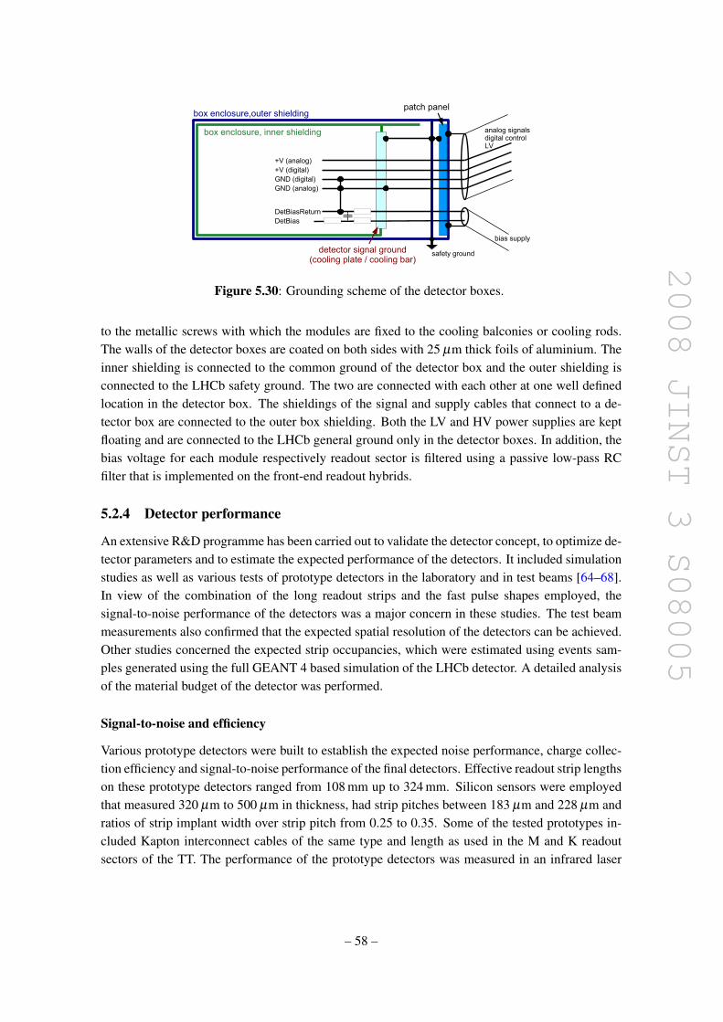
2008 JINST 3 S08005
Figure 5.30: Grounding scheme of the detector boxes.
to the metallic screws with which the modules are fixed to the cooling balconies or cooling rods.The walls of the detector boxes are coated on both sides with 25 µm thick foils of aluminium. Theinner shielding is connected to the common ground of the detector box and the outer shielding isconnected to the LHCb safety ground. The two are connected with each other at one well definedlocation in the detector box. The shieldings of the signal and supply cables that connect to a de-tector box are connected to the outer box shielding. Both the LV and HV power supplies are keptfloating and are connected to the LHCb general ground only in the detector boxes. In addition, thebias voltage for each module respectively readout sector is filtered using a passive low-pass RCfilter that is implemented on the front-end readout hybrids.
5.2.4 Detector performance
An extensive R&D programme has been carried out to validate the detector concept, to optimize de-tector parameters and to estimate the expected performance of the detectors. It included simulationstudies as well as various tests of prototype detectors in the laboratory and in test beams [64–68].In view of the combination of the long readout strips and the fast pulse shapes employed, thesignal-to-noise performance of the detectors was a major concern in these studies. The test beammeasurements also confirmed that the expected spatial resolution of the detectors can be achieved.Other studies concerned the expected strip occupancies, which were estimated using events sam-ples generated using the full GEANT 4 based simulation of the LHCb detector. A detailed analysisof the material budget of the detector was performed.
Signal-to-noise and efficiency
Various prototype detectors were built to establish the expected noise performance, charge collec-tion efficiency and signal-to-noise performance of the final detectors. Effective readout strip lengthson these prototype detectors ranged from 108 mm up to 324 mm. Silicon sensors were employedthat measured 320 µm to 500 µm in thickness, had strip pitches between 183 µm and 228 µm andratios of strip implant width over strip pitch from 0.25 to 0.35. Some of the tested prototypes in-cluded Kapton interconnect cables of the same type and length as used in the M and K readoutsectors of the TT. The performance of the prototype detectors was measured in an infrared laser
– 58 –

2008 JINST 3 S08005
capacitance (pF)0 10 20 30 40 50
EN
C (
e)
0
500
1000
1500
2000
2500
3000
3500
( Vfs = 400 mV )
ladders in test beam:ENC = 700 e + 47.9 e / pF
discrete capacitances:ENC = 580 e + 48.8 e / pF
track position
0 0.2 0.4 0.6 0.8 1
S/N
(4
str
ips)
0
5
10
15
20
three sensors + Kapton interconnect
(Vbias = 475V, Vfs = 400 mV)
Figure 5.31: ENC obtained in test beam mea-surements as a function of the measured totalstrip capacitance of the tested prototype mod-ules. The full line is a fit to the test beam re-sults, the dashed line describes the results oflaboratory measurements in which discrete ca-pacitances were attached directly to the input ofthe Beetle chips.
Figure 5.32: Most probable signal-to-noise ra-tio as a function of the inter-strip position (0= centre of left strip, 1 = centre of right strip)measured in a CERN test beam. In order torule out a potential bias due to clustering algo-rithms, the signal was calculated as the sum ofthe charges on the four strips closest to the par-ticle impact point given by a beam telescope.
test stand and in several test beam periods in a 120 GeV π− beam at CERN. The expected noiseperformance of the various detector configurations was also investigated in a SPICE simulationthat included a detailed description of the Beetle front-end, and in which the readout strips of thedetectors were described as an extended LCR network [69]. The results of this simulation agreedwith the test beam measurements. The measured noise performance is summarized in figure 5.31.In this figure, the measured equivalent noise charge (ENC) for the different tested detector config-urations is shown as a function of their total strip capacitance. A linear dependence is observedand the slope of a line fitted to the data agrees well with that obtained in test-bench measurementsof the Beetle chips, in which discrete load capacitances were attached to the Beetle inputs. Boththe measurements and the SPICE simulations have demonstrated that the Kapton interconnect ca-bles behave purely as an additional load capacitance and cause no deterioration of the quality andintegrity of the detector signals.
Measurements of the charge collection efficiency were performed as a function of the posi-tion on the detector. No significant dependence was found on the position along the readout strips.However, in the direction orthogonal to the strips, a significant drop of the charge collection ef-ficiency was observed in the central region between two readout strips. The effect is illustratedin figure 5.32 for a prototype module with the same detector geometry as a three-sensor readoutsector of the TT. A similar charge loss was observed for all tested detector configurations. Its sizedid not depend on the strip length but was found to depend on the strip geometry. It decreased
– 59 –

2008 JINST 3 S08005
with increasing ratio of implant width to strip pitch (w/p) and with increasing sensor thickness (d)and depended roughly linearly on the ratio (p−w)/d. The charge loss could not be reduced byoverbiasing the detectors or by increasing the shaping time within the limits allowed by the Beetlechips. It is attributed to charge trapping at the interface between the silicon bulk and the siliconoxide in between the readout strips.
This charge loss does not affect particle detection efficiency as long as the signal-to-noise ratioin the central region in between the strips remains high enough. Full particle detection efficiencyabove 99.8% was measured for all detector configurations as long as the most probable signal-to-noise ratio stayed above 10:1. Below that value, the particle detection efficiency started to decreaserather quickly. With the chosen thicknesses for the silicon sensors, most probable signal-to-noiseratios in excess of 12:1 are expected over the full surface of the detectors for both types of ITmodules and all four types of TT readout sectors.
Spatial resolution and alignment
The spatial resolution of the detector modules was measured in test beams and was found to beabout 50 µm, consistent with the expected resolution for the chosen strip pitches. Simulation stud-ies have shown that, for two-strip clusters, it should be possible to further improve the spatialresolution by taking into account the position-dependent charge-sharing between the strips.
In order not to compromise the spatial resolution of the detectors, the positioning of eachsensitive detector element in the x coordinate should be known to better than about 25 µm. Therelative positioning accuracy of the individual silicon sensors on a detector module was monitoredthroughout the module production and was found to be better than 10 µm R.M.S. Various surveysof module positions inside the detector boxes and of detector boxes with respect to the LHCbreference frame have been performed. The results of these measurements are foreseen to be usedto provide initial values for the software alignment of the detectors that will use reconstructedtracks from the LHCb spectrometer.
Strip occupancies
The strip occupancies presented here [70] were obtained from a sample of 5000 Bd→ J/ψ(µ+µ−)KS(π+π−) events. The simulation software includes detailed descriptions of the detector geometryand of the signal collection, amplification and digitization. The simulation of the detector responsewas tuned to reproduce the results of the test beam measurements described before. For the TT,average strip occupancies of up to about 3.5% are found in the K sectors close to the beampipe.They drop to about 0.35% in the outermost L sectors. For the side boxes of the first IT station,average strip occupancies drop from about 2.5% on the strips closest to the beam to about 0.5% onthe outermost strips. In the top/bottom boxes, occupancies vary between 0.5% and 0.3%. In thesecond and the third IT station, occupancies are about 10%, respectively 20% lower than in the first.This is mainly due to the larger distance of these stations from the beampipe supports (see section 3)that are located at the exit of the LHCb magnet and are a prolific source of secondary particles.
– 60 –

2008 JINST 3 S08005
Figure 5.33: Radiation length of the TT as a function of the pseudorapidity η and the azimuthalangle φ .
Material budget
A careful analysis was performed of all materials that are located inside the acceptance of theexperiment. Based on this analysis, a detailed description of all active detector elements and asimplified description of the passive components has been implemented [71, 72] in the XML basedLHCb detector geometry description.
For the TT, where most of the dead material from detector supports, cooling etc. is locatedoutside the acceptance, the material distribution is rather uniform. In total, it amounts to about0.04 X0, where more than 0.02 X0 are due to the active material of the silicon sensors. An increaseup to almost 0.13 X0 is observed in the very forward region, due to the material of the insulationpiece around the beampipe. The result of a material scan as a function of the azimuthal angle φ
and the pseudorapidity η is shown in figure 5.33. The scan was performed by generating straighttracks originating from the nominal interaction point, extrapolating them through the TT station,and adding up the radiation lengths of all volumes in the geometry description that they crossed.
The material distribution for the IT is much less uniform, due to the readout hybrids, mechan-ical supports, cooling pipes and cables that are located inside the LHCb acceptance. In the activeregion of the detector, close to the beampipe, the material budget adds up to about 0.035 X0 perstation, out of which more than 0.015 X0 are due to the active material of the silicon sensors. Thematerial budget peaks at almost 0.30 X0 in the very narrow region of the cooling rods. The resultof a material scan for one IT station is shown in figure 5.34.
5.3 Outer Tracker
The LHCb Outer Tracker (OT) is a drift-time detector [73], for the tracking of charged particles andthe measurement of their momentum over a large acceptance area. Excellent momentum resolutionis necessary for a precise determination of the invariant mass of the reconstructed b-hadrons: amass resolution of 10 MeV/c2 for the decay B0
s → D−s π+ translates into a required momentum res-olution of δp/p≈ 0.4%. The reconstruction of high multiplicity B decays demands a high tracking
– 61 –

2008 JINST 3 S08005
Figure 5.34: Radiation length of one IT station as a function of the pseudorapidity η and theazimuthal angle φ .
efficiency and at the same time a low fraction of wrongly reconstructed tracks: a track efficiencyof 95% would result, for the decay B0
s → D−s π+, in an overall reconstruction efficiency of 80%.
5.3.1 Detector layout
The OT is designed as an array of individual, gas-tight straw-tube modules. Each module containstwo staggered layers (monolayers) of drift-tubes with inner diameters of 4.9 mm. As a countinggas, a mixture of Argon (70%) and CO2 (30%) is chosen in order to guarantee a fast drift time(below 50 ns), and a sufficient drift-coordinate resolution (200 µm). The gas purification, mixingand distribution system foresees the possibility of circulating a counting gas mixture of up to threecomponents in a closed loop [74].
The detector modules are arranged in three stations (see figure 5.35). Each station consistsof four layers, arranged in an x-u-v-x geometry: the modules in the x-layers are oriented vertically,whereas those in the u and v layers are tilted by ± 5o with respect to the vertical, respectively. Thetotal active area of a station is 5971×4850 mm2. The outer boundary corresponds to an acceptanceof 300 mrad in the magnet bending plane (horizontal) and 250 mrad in the non-bending plane (ver-tical). The inner cross-shaped boundary of the OT acceptance was determined by the requirementthat occupancies should not exceed 10% at a luminosity of 2×1032 cm−2 s−1 (this area is coveredby the IT, see section 5.2.2).
The OT assembly is shown in figure 5.35. The detector modules are supported by aluminiumstructures. Each station is split into two halves, retractable on both sides of the beam line. Eachhalf consists of two independently movable units of two half layers (C-frames). The modulesare positionned on the C-frames by means of precision dowel pins. The C-frames also providerouting for all detector services (gas, low and high voltage, water cooling, data fibres, slow and fastcontrol). The OT C-frames are sustained by a stainless steel structure (OT bridge), equipped withrails allowing the independent movement of all twelve C-frames.
– 62 –

2008 JINST 3 S08005
Figure 5.35: Arrangement of OT straw-tube modules in layers and stations (left) and overviewof the OT bridge carrying the C-frames (right). The C-frames on both sides of the beam pipe areretracted.
5.3.2 Detector technology
Design
The design of the straw-tube module is based on the following requirements:
• Rigidity: the mechanical stability must guarantee the straw-tube position within a precisionof 100 (500) µm in the x (z) direction; the anode wire has to be centered with respect to thestraw tube within 50 µm over the entire straw length. The module box must be gas-tight andmust withstand an overpressure of 10 mbar. The leak rate at this pressure has to be below8×10−4 l/s.
• Material budget: to limit multiple scattering and the material in front of the calorimeters, thematerial introduced in the OT active area must not exceed few percent of a radiation lengthX0 per station.
• Electrical shielding: the drift tubes must be properly shielded to avoid crosstalk and noise.Each straw must have a firm connection to the module ground. The module envelope itselfmust form a Faraday cage connected to the ground of the straw tubes and of the front-endelectronics.
• Radiation hardness: the detector should withstand 10 years of operation at the nominal lumi-nosity without a significant degradation of its performance. During that time the anode wireswill accumulate a charge of up to 1 C/cm in the most irradiated area. As a consequence, alldetector materials have to be radiation resistant and must have low outgassing.
The layout of the straw-tube modules is shown in figure 5.36. The modules are composedof two staggered layers (monolayers) of 64 drift tubes each. In the longest modules (type F) themonolayers are split longitudinally in the middle into two sections composed of individual straw
– 63 –

2008 JINST 3 S08005
10.7
340
31.00
5.25
5.50 4.90
s
p
s
p
340m
m
p
s
p
s
4900mm
Figure 5.36: Cross section of a straw-tubes module (left) and overview of a straw-tubes moduledesign (right).
tubes. Both sections are read out from the outer end. The splitting in two sections is done at adifferent position for the two monolayers to avoid insensitive regions in the middle of the module.F-modules have an active length of 4850 mm and contain a total of 256 straws. In addition to theF-type modules there exist short modules (type S) which are located above and below the beampipe. These modules have about half the length of F-type modules, contain 128 single drift tubes,and are read out only from the outer module end. A layer half is built from 7 long and 4 shortmodules. The complete OT detector consists of 168 long and 96 short modules and comprisesabout 55000 single straw-tube channels.
Construction
The straw tubes are produced by winding together two strips of thin foils,29 as shown in figure 5.37:the inner (cathode) foil is made of 40 µm carbon doped polyimide (Kapton-XC30); the outer foil(Kapton-aluminium) is a laminate31 made of 25 µm polyimide, to enhance the straws gas tightness,and 12.5 µm aluminium, crucial to ensure fast signal transmission and good shielding.
To build a monolayer the straw-tubes were glued to panels with a cored sandwich structureconsisting of a 10 mm Rohacell core and two 120 µm carbon fibre skins. High precision aluminiumtemplates (figure 5.37) were used during the glueing to position the straw-tubes to better than50 µm over the entire module length. After the straw-tubes were glued to the panel the wiring wasstarted. A gold-plated tungsten wire32 with a diameter of 25.4 µm is used for the anodes. The wirewas sucked through the straw-tube. At each end the wire is guided using injection-molded Norylendpieces. To centre the wire also along the straw-tube Noryl wire locators had been placed every80 cm inside the straws. The wires were strung with a tension of 0.7 N and were soldered to 5 mmlong pads of a printed circuit board.
Special holding-devices, shown in figure 5.38, were used to keep the support panels flat towithin 100 µm during the glueing of the straws and wiring. They were also used to assemble twomonolayer panels into a detector module (figure 5.38). The sides of the modules were closed by400 µm thick carbon fibre sidewalls. Spacers at the two module ends ensure the proper separation
29Lamina Dieletrics Ltd., UK.30DuPontTM.31GTS Flexible Materials Ltd., USA.32California Fine Wire, USA.
– 64 –

2008 JINST 3 S08005
inside
inner d.
9.0Kapton−aluminium
Kapton XC
Kapton Aluminium outside
4.90
9.0
Kapton XC
(a)
inside
inner d.
9.0Kapton−aluminium
Kapton XC
Kapton Aluminium outside
4.90
9.0
Kapton XC
(b)
Figure 5.37: Left: (a) scheme of the straw winding using two foils; (b) Kapton-XC as inner foiland a Kapton-aluminium laminate as outer foil. Right: straws on the high precision aluminiumtemplate.
Figure 5.38: Left: straw-tube monolayer on a holding-device ready for gluing. Right: two straw-tube monolayers in a holding device while being glued to form a detector module.
of the two monolayers and provide an interface to the module gas pipes. All glueing steps wereperformed using Araldite AY103 in combination with the HY991 hardener. The glue viscosity wasenhanced by adding silica gel.
The side walls and also the inner sides of the support panels are covered by the Kapton-alumi-nium laminate, which ensures the gas tightness of the module and provides a closed Faraday cage.
The construction of the detector modules was completed by three production sites in abouttwo years. All detector parts were centrally checked and then distributed to the production sites.The production procedure and the quality monitoring steps and tools were the same in all produc-
– 65 –

2008 JINST 3 S08005
tion sites. Quality assurance included the check of the wire tension, pitch, and leakage current (inair) prior to the module sealing. Finished modules were tested for gas tightness. Using CO2 ascounting gas the modules were operated with a slowly increasing anode voltage to ensure that theleakage current per wire dropped below 1 nA for a voltage of 1700 V. Finally, the uniformity of thesignal response of all drift cells was checked with a radioactive source.
Material budget
The forward geometry of the LHCb detector allows all detector services and supports of the OT tobe located outside the detector acceptance. The OT material inside the LHCb acceptance (12 layersof modules) is estimated from the weights of the single components and the total amount of glueused (140 g per panel, 400 g to glue straw-tubes and to close the module) [75]. The total materialof one station (four layers of modules, i.e. 8 monolayer panels) is on average equivalent to 3.2% ofX0. The total OT material sums up to 9.6% of X0.
Ageing tests
In the region closest to the beam axis, the OT detector modules are foreseen to operate under par-ticle rates per straw length of up 100 kHz/cm. Extensive ageing studies of test modules and ofscaled-down prototypes showed that the detector technology is resistant to radiation doses corre-sponding to accumulated charges of up to 1.3 C/cm. No hints of a change of the gas amplificatonwere seen in these studies which were performed with an average acceleration factor of a approxi-mately 25.
However, irradiating mass production modules with low intensity β or γ sources with accel-eration factors of O(1) produced a significant drop of the gas amplification. Most strikingly, thisgain loss was not observed in the region of highest irradiation intensity (anode currents around 20nA/cm) but at modest intensities and anode currents of 2–5 nA/cm [76]. The damage was onlyobserved upstream (with respect to the gas flow) of the irradiating source. An analysis of the af-fected anode wires revealed a thin (less than 1 µm thick) insulating deposit. Although the exactmechanism is not yet understood, the glue (Araldite AY103) used to build the modules is identifiedas cause of the depositions. A number of preventive and remedial actions have been studied: long-term flushing of the detector modules with gas (CO2) as well as warming-up the modules to 40oCwhile being flushed, significantly reduce this effect. Large anode currents deliberately provokedby increasing the high voltage above the nominal operating voltage can be used to clean the anodewires, should the insulating deposits reduce the gain beyond an acceptable level.
5.3.3 Electronics
The front-end (FE) electronics measures the drift times of the ionization clusters produced bycharged particles traversing the straw-tubes with respect to the beam crossing (BX) signal [77].The drift times are digitized for every bunch crossing (25 ns) and stored in a digital pipeline toawait the Level-0 decision. On a positive L0 decision, the digitized data of up to 3 bunch crossings(to cover a time range of up to 75 ns) is transmitted via optical links to the Level-1 buffer (TELL1)
– 66 –

2008 JINST 3 S08005
(8ch)
ASDBLR board
GOL board
OTIS board
HV LVTFCECSL1
ch 0−63ch 64−127
(128ch)
(32ch)
HV board(32ch)
(16ch) ASDBLR
(32ch)OTIS
Figure 5.39: Design (left) and photograph (right) of the FE electronics mounted in a FE box. Inthe photograph the HV boards are not visible, because hidden by the ASDBLR boards.
boards. The radiation dose expected for the front-end electronics is only 10 kRad, well below themaximum tolerable dose of 2 Mrad.
As shown in figure 5.39, the FE electronics has a modular design, consisting of several inter-connected boards housed inside a metallic box (FE box). These boxes are mounted at each end ofthe detector modules. A FE box is the smallest independent readout unit of the OT: the digitizeddata of the 128 channels of one module are sent via an optical link and received by the TELL1board; high- and low-voltage, as well as fast- and slow-control signals are connected to each FEbox individually. In total, 432 FE boxes are used to read out the OT detector.
The main components of the OT readout electronics are the High Voltage (HV) board, theASDBLR board, the OTIS board, and the GOL auxiliary (GOL/AUX) board.
Four 32-channel HV boards plug directly into the signal feedthrough of each straw-tube mod-ule. The signal feedthrough is provided by a passive printed circuit board (PCB) built into themodule end and defining the reference ground for the straw-tubes and readout electronics. The HVboard has a single HV connection and is thus the smallest independent HV supply unit. Anodesignals are decoupled using 300 pF capacitors33 on the PCB.
Each ASDBLR board hosts two ASDBLR chips [78]. These are custom integrated circuits,providing the complete analog signal processing chain (amplification, shaping, baseline restoration,and discrimination) for straw sensors. The ASDBLR is implemented in bipolar technology andproduced with the radiation hard DMILL process It includes eight identical channels per chip, witha peaking time of 7–8 ns, selectable shaping circuits and a three-state LVDS output. The EquivalentNoise Charge (ENC) at the ASDBLR input is about 2200 e− + 140 e−/pF, corresponding to a globalENC of about 0.9 fC when connected to the detector.
The hit outputs of two ASDBLR boards (32 channels) are connected to an OTIS board, whichhosts one OTIS chip for drift time digitization. The OTIS ASIC is a radiation hard 32-channelTime-to-Digital Converter (TDC), developed specifically for the OT and manufactured in a stan-dard 0.25 µm CMOS process [79, 80]. The OTIS block diagram is shown in figure 5.40. TheTDC core measures the arrival time of the ASDBLR signals with respect to the LHC clock prop-agating through a 25 ns long Delay Locked Loop (DLL), a regulated chain of 32 double-staged
33JOHANSON 302R29W331KV4E.
– 67 –

2008 JINST 3 S08005
in(0) in(1) in(31)
Channel mask register
6464
Clock
BCC DLL
8 HR HR HR
646464DLLlocklost
PBdata PPL PPLStatus
6 6
ACPipeline
Derandomizing buffer
Sparsification (optional)
Truncation (optional)
8
8
Readout buffer
Readoutinterface
DACs for ASD biasing
Slow control IF
(I2C)
8
Data output
SCL
SDA
Trigger
PPL
6
160
240
48
TDC +
Hit
DLL
DAC
BX
8
OTIS
32 ch
ASD
(8 ch)
Derandomizer
buffer Control
circuit
Readout
bufferI2C interface
SDA SCL not ResetTTCrx
TTC
GOL
Gbit
link
Pipeline
memory
Fine time
Drifttime
Trigger
Straw tube(w. particle track)
Figure 5.40: OTIS Block Diagram.
delay elements. The time digitization is done using the 64 delay-stages of the DLL (64 time bins)giving a theoretical bin size of 390 ps. The drift time data is stored in a pipeline memory with adepth of 164 events, allowing a L0 trigger latency of 160 clock cycles to compensate for triggerrate fluctuations. If a trigger occurs, the corresponding data words of up to 3 bunch crossings (thenumber of bunch crossings transferred is selectable) are transferred to a derandomizing buffer, ableto store data from up to 16 consecutive triggers. Both, pipeline memory and derandomizing bufferare dual-ported SRAM memories. A control unit processes and reads out the data of each triggeredevent within 900 ns. The readout interface of the OTIS chip is 8-bit wide.
The data processing within the OTIS is clock driven. The chip operates synchronous to the40 MHz LHC clock. A standard I2C interface is used for setup and slow control.
The OTIS boards in a FE box are connected to one GOL/AUX board. This board [81] pro-vides the outside connections to the FE box: the power connection, the interface to the fast-control(BX clock, triggers, resets) and the interface to the slow-control (I2C). Three power regulatorssupply the different voltages (+2.5 V ±3.0 V) needed by the OTIS and the ASDBLR chips. TheGOL/AUX board hosts the GOL optical serializer chip [6] connected to an optical receiver mezza-nine card on the TELL1 board.
As the data volume of the OT is large compared to other sub-detectors only the optical linksof the nine FE boxes belonging to a layer quadrant are connected to a single TELL1 board. To readout the 432 FE boxes of the OT 48 TELL1 boards are used.
Cooling
As the FE box is entirely closed, cooling of the electronic components inside the boxes is necessary.All electronic boards are therefore mounted on a cooling frame (see figure 5.39) which is screwedto water-cooled plates on the C-frames.
– 68 –

2008 JINST 3 S08005
Figure 5.41: Left: hit efficiency as a function of the distance to the anode wire. Right: relationbetween the drift time and the calculated hit distance to the wire. Note the maximum drift time ofapproximately 45 ns.
High-voltage system
Each FE box has four independent HV connections, one for each 32-channels HV board. TwoCAEN SY1527LC mainframes, each equipped with four 28-channels A1833BPLC supply boards,are used as HV supply. Using an 8-to-1 distribution scheme the 1680 HV connections of thedetector are mapped on 210 CAEN HV channels. The distribution is realized using a patch panelwich offers the possibility to disconnect individual HV boards (32 channels) by means of an HVjumper. Both components, the HV supply as well as the patch panel are located in the countinghouse. Access to the HV system during data taking is therefore possible.
5.3.4 Test Beam results
To determine the performance of the detector modules in combination with the readout electron-ics, 4 short modules from the mass production equipped with FE boxes were tested at the 6 GeVelectron beam of the DESY II facility in Hamburg [82]. Although the number of OT modules (4modules, or 8 monolayers) was sufficient to allow full track reconstruction, a silicon strip telescopewas used to provide redundant information for the determination of the coordinates at which thebeam particle traverses the detector. The trigger signal (which was also used offline as a time refer-ence) was generated by a coincidence of two scintillator counters installed downstream of the OTmodules. The nominal counting gas mixture Ar/CO2 was used.
The electron beam illuminated up to 7 straws per monolayer. In the offline analysis, therelation between the measured drift time and the distance to the wire (R-t relation, see figure 5.41)was established using the predicted distance of closest approach of the particle to the anode wire.The R-t relation was then used to convert measured drift times to coordinates. The hit findingefficiency, shown as a function of the distance to the wire in figure 5.41, is determined by verifying
– 69 –

2008 JINST 3 S08005
Figure 5.42: Performance of the straw-tube module: the position resolution (left) and the averageefficiency (right) of a single cell are shown as a function of the HV value. The different curves cor-respond to different discriminator threshold voltages, and different distances between the electronbeam spot and the front-end electronics.
whether the OT produced a hit at the predicted position. The position resolution is determinedby comparing the measured hit coordinates to the predicted ones (residual) and by fitting a singlegaussian to the distribution.
The performance of the OT straw-tube modules is determined for HV values ranging be-tween 1200 and 1700 V, and for ASDBLR discriminator thresholds ranging from 1.5 fC to 5.5 fC.As shown in figure 5.42, efficiencies larger than 99% in the centre of the straw (dropping at theedge of the straw) and position resolutions of single cells below 200 µm can be attained for highvoltage values above 1550 V. The noise level was found to be low: at a high voltage of 1550 Vand a discriminator threshold voltage of 800 mV (corresponding to a signal threshold of 4 fC),the noise rate is below 1 kHz per channel. This corresponds to an average channel occupancy of(7.5×10⁻³
)%. The probability to find a coherent hit in neighbouring channels (crosstalk) is found
to be lower than 5% for high voltage values below 1600 V and discriminator threshold voltagesabove 800 mV (4 fC).
5.3.5 Alignment and monitoring
Errors in the mechanical alignment of the drift tubes can significantly degrade the track recon-struction. A single cell resolution of about 200 µm requires that the drift tubes be aligned withinan accuracy of 100 µm (1 mm) in the x (z) coordinate. Therefore, care was taken during eachstep of the detector construction and installation to minimize alignment errors. The issue of themechanical tolerances in the module production has been discussed in section 5.3.2. All detectorC-frames which hold the modules were built with stringent requirements on the mechanical toler-ances [83, 84]. During installation the positions of all modules were surveyed and the C-framespositions have been adjusted accordingly.
The reproducibility of the C-frames positioning after movement was checked to be better thanthe 200 µm precision of the optical survey.
– 70 –

2008 JINST 3 S08005
LED
Coded Mask
Ras
Mux
Mas
terM
ux
Top
Mux
Lens
On C−frame
CCD camera
On bridge
Figure 5.43: Schematic of the RASNIK alignment system.
The stability of the C-frames relative position during data taking is monitored by means ofthe RASNIK system [85], whose basic idea is to project the image of a detailed pattern through alens onto a CCD camera (figure 5.43). Movements perpendicular to the optical axis are observedas change of the pattern position processed by the CCD camera, whereas movements along theaxis are measured by the change in the image size. A total of 50 RASNIK lines are used for theOT monitoring. The intrinsic resolution of the system perpendicular (parallel) to the beam axis isbetter than 10 (150) µm respectively [86].
– 71 –

2008 JINST 3 S08005
Chapter 6
Particle identification
6.1 RICH
Particle identification (PID) is a fundamental requirement for LHCb. It is essential for the goals ofthe experiment to separate pions from kaons in selected B hadron decays. At large polar angles themomentum spectrum is softer while at small polar angles the momentum spectrum is harder; hencethe particle identification system consistes of two RICH detectors to cover the full momentumrange. The upstream detector, RICH 1, covers the low momentum charged particle range ∼1–60 GeV/c using aerogel and C4F10 radiators, while the downstream detector, RICH 2, covers thehigh momentum range from ∼15 GeV/c up to and beyond 100 GeV/c using a CF4 radiator (seefigure 6.1). RICH 1 has a wide acceptance covering the full LHCb acceptance from ±25 mrad to±300 mrad (horizontal) and ±250 mrad (vertical) and is located upstream of the magnet to detectthe low momentum particles. RICH 2 is located downstream of the magnet and has a limitedangular acceptance of ∼±15 mrad to ±120 mrad (horizontal) and ±100 mrad (vertical) but coversthe region where high momentum particles are produced. In both RICH detectors the focusing ofthe Cherenkov light is accomplished using a combination of spherical and flat mirrors to reflect theimage out of the spectrometer acceptance. In the RICH 1 the optical layout is vertical whereas inRICH 2 is horizontal. Hybrid Photon Detectors (HPDs) are used to detect the Cherenkov photonsin the wavelength range 200–600 nm. The HPDs are surrounded by external iron shields and areplaced in MuMetal cylinders to permit operation in magnetic fields up to 50 mT. The RICH detectorsystem including its electronics, monitoring, control, and the performance are described below.
6.1.1 RICH 1
The RICH 1 detector [2, 87] is located upstream of the LHCb dipole magnet, between the VELOand the Trigger Tracker, see figure 2.1. RICH 1 contains aerogel and fluorobutane (C4F10) gasradiators, providing PID from approximately 1−−60GeV/c for particles inside the acceptance.A schematic, 3D model and photo of the RICH 1 detector is shown in figure 6.2. It is aligned tothe LHCb coordinate axes and occupies the region 990 < z < 2165mm. The z-axis follows thebeamline which is inclined at 3.6 mrad to the horizontal. The overall design has to respect thefollowing constraints:
– 72 –
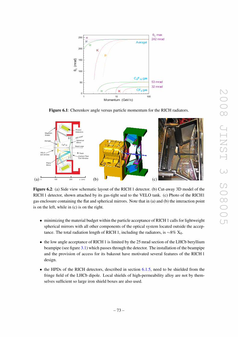
2008 JINST 3 S08005
θ C(m
rad)
250
200
150
100
50
0
1 10 100
Momentum (GeV/c)
Aerogel
C4F10 gas
CF4 gas
eµ
p
K
π
242 mrad
53 mrad
32 mrad
θC max
Kπ
Figure 6.1: Cherenkov angle versus particle momentum for the RICH radiators.
(a)
250 mrad
Track
Beam pipe
Photon
Detectors
Aerogel
VELOexit window
Spherical
Mirror
Plane
Mirror
C4F10
0 100 200 z (cm)
Magnetic
Shield
Carbon Fiber
Exit Window
(b) (c)
Figure 6.2: (a) Side view schematic layout of the RICH 1 detector. (b) Cut-away 3D model of theRICH 1 detector, shown attached by its gas-tight seal to the VELO tank. (c) Photo of the RICH1gas enclosure containing the flat and spherical mirrors. Note that in (a) and (b) the interaction pointis on the left, while in (c) is on the right.
• minimizing the material budget within the particle acceptance of RICH 1 calls for lightweightspherical mirrors with all other components of the optical system located outside the accep-tance. The total radiation length of RICH 1, including the radiators, is ∼8% X0.
• the low angle acceptance of RICH 1 is limited by the 25 mrad section of the LHCb berylliumbeampipe (see figure 3.1) which passes through the detector. The installation of the beampipeand the provision of access for its bakeout have motivated several features of the RICH 1design.
• the HPDs of the RICH detectors, described in section 6.1.5, need to be shielded from thefringe field of the LHCb dipole. Local shields of high-permeability alloy are not by them-selves sufficient so large iron shield boxes are also used.
– 73 –

2008 JINST 3 S08005
The HPDs are located outside of the LHCb acceptance, above and below the beamline, in a regionwhere the iron shield can be accommodated. Additional planar (flat) mirrors are required to reflectthe image from the tilted spherical mirrors onto the photon detector planes.
Optical system
The parameters of the RICH 1 optical layout have been optimized with the aid of simulation.Charged particle tracks, originating from the interaction point (IP) are followed through the RICH 1radiators. Cherenkov photons are generated uniformly along the length of each track in the aero-gel and gas radiators, using the appropriate refractive indices for photons within the wavelengthacceptance of the HPD photocathodes. These photons are ray-traced through the optical systemand their impact points on the planes of HPDs are recorded. The Cherenkov angle at emission isthen reconstructed for each photon in turn, assuming that the emission point is midway along thetrack trajectory through the radiator. As the true emission point is randomly distributed along thetrack, the tilted mirror geometry causes the reconstructed Cherenkov angle to differ from its truevalue and results in a smearing of the reconstructed angle. The RMS of the resulting distributionis referred to as the emission point error. The RICH 1 optical system is designed such that theemission point error is not larger than other sources of finite angular resolution, such as the HPDpixel size and the chromatic dispersion of the radiator.
In addition to the emission point error, the optical layout determines the required area ofcoverage of the two HPD planes. The optimization procedure required close to 100% geometricalacceptance for photons emitted by the gas radiator, while a compromise dictated by the cost, andnot affecting significantly the final expected performance, reduced the acceptance for the aerogelphotons to 68%. The parameters of the optics are constrained by limited space and the tilt of thespherical mirrors must ensure that the flat mirrors lie outside the acceptance of the charged particletrackers. The location of the photon detector planes is also determined by the performance of themagnetic shield boxes. To avoid loss of efficiency, the HPD planes must be in a region where thefield does not exceed 3 mT and be tilted to ensure that, on average, Cherenkov photons strike theHPDs at close to normal incidence.
The parameters resulting from the optimization procedure have been adopted for the engi-neering design of RICH 1. The spherical mirrors have radius of curvature 2700 mm with centresof curvature at x,y,z = 0,±838,−664mm, which define the mirror tilt. This results in an emissionpoint error of 0.67 mrad for the gas radiator, a value that is negligible compared with other sourcesof error for the aerogel. The flat mirrors are tilted at an angle 0.250 rad with respect to the y-axis,with horizontal edges lying closest to the beam line located at y,z =±350,1310mm. The two HPDplanes are centered at x,y,z = 0,±1187,1502mm and tilted at an angle 1.091 rad with respect tothe y-axis. They are each covered with 7 rows of 14 HPDs, hexagonally close packed, with centresseparated by 89.5 mm. This results in two detector planes of 1302 mm× 555 mm each.
Spherical mirrors
The spherical mirrors are located within the LHCb acceptance and are traversed by charged parti-cles and photons. Glass mirrors and their associated supports would contribute about 8% X0, so acarbon fibre reinforced polymer (CFRP) substrate, with the mirror support outside the acceptance,
– 74 –

2008 JINST 3 S08005
(a) (b) (c)
Figure 6.3: Photo of (a) the internal structure of the RICH 1 carbon fibre (CFRP) mirror; (b) aCFRP mirror; (c) the spherical mirror array viewed from the front, mounted onto its CFRP supportframe.
is adopted to keep the material budget below 2% X0. The two tilted spherical mirror surfaces,one above the beryllium beampipe, the other below, are each composed of two CFRP mirrors,making four mirror quadrants in total [88]. Each mirror has dimensions 830 mm× 630 mm whenprojected onto the x− y plane. The mirror construction is from two CFRP1 sheets, moulded overa polished glass mandrel to a spherical surface of 2700 mm radius and separated by a reinforc-ing matrix of CFRP cylinders, configured as shown in figure 6.3a. The box elements at the twoouter edges provide stiffness for the three-point mounting brackets that attach the mirror to a CFRPframe (see figure 6.3c). Each mirror has a circular cut-out of radius 62.5 mm to provide a nominal10 mm clearance from the beampipe (see figure 6.3b). The overall structure has an areal density of6 kg m−2, thus contributing about 1.5% X0 to the material budget of RICH 1.
The geometrical quality of a spherical mirror is characterized by the variation in the meanradius R of each mirror and the parameter D0, the diameter of the image in which is contained95% of the light from a point source placed at the centre of curvature. Provided D0 < 2.5mm and∆R/R < 1%, the geometry of the mirrors provides a negligible contribution to the reconstructedCherenkov angle precision. The manufacturing and subsequent quality assurance ensures that themirrors satisfy these specifications.
The mirror assembly is made from two CFRP half frames. Each carries an upper and a lowerquadrant. The half frames are divided in this way to allow insertion into the RICH 1 gas enclosure(described further on in this section) from either side of the beampipe, following which the framesare clamped to form a rigid structure around the periphery. The CFRP frame is mounted on rails andsupported by an optical alignment rig. Upper and lower mirror pairs are aligned to a common centreof curvature and the CFRP frame is surveyed. This frame is then installed in the gas enclosure usingan identical rail system, where the frame can again be surveyed and adjusted if necessary. Simula-tions [89] have shown that provided all mirror segments are aligned to a precision of about 1 mrad,the alignment can be further corrected using data from reconstructed Cherenkov ring images.
The mirrors are coated using a deposition of Al(80nm)+MgF2(160nm). The reflectivity thatcan be achieved on the CFRP substrate is the same as that on a glass support, as shown by curve Vin figure 6.6 and described in section 6.1.4.
1Fibres: Toray M46J; Matrix: Bryte Technologies, EX-1515 cyanate ester resin; Manufacturer: Composite Mir-ror Applications Inc.,Tucson, USA.
– 75 –

2008 JINST 3 S08005
Flat mirrors
The flat mirrors are assembled into two planes, one above and one below the beamline. They arelocated outside of the acceptance, so glass substrates can be used. Each plane comprises eightrectangular mirrors with dimensions 380 mm × 347.5 mm, fabricated using 6.5 mm thick Simax2
glass. As for the spherical mirrors, the flat mirror geometry is characterized through the parametersR and D0. All mirrors have |R| > 600m and D0 < 2.5mm. Assuming the deviations from surfacesphericity are randomly distributed, this value of D0 contributes < 0.2mrad to the single photonCherenkov angle precision. The mirrors are coated using the same (Al+SiO2+HfO2) process usedfor the RICH 2 mirrors (section 6.1.2). Each of the eight mirror segments is connected to a three-point adjustment system via a polycarbonate flange, described in section 6.1.2. The adjustmentmechanism is bolted to a rigid plate that is suspended from rails. The eight mirror segments are ad-justed in angle to form a single plane, then the angle of this plane is set using the optical alignmentrig. Following alignment and survey, the plate is mounted on an identical rail system attached tothe upstream wall of the RICH 1 gas enclosure, where the angle can again be surveyed and adjustedif necessary.
RICH 1 structure
The total weight of the RICH 1 detector is about 16 tons, mainly due to the magnetic shieldingboxes. The lower box is fixed to the LHCb cavern floor and supports the gas enclosure and thelower photon detector assembly. The upper box is fixed to the cavern wall and supports the upperphoton detector assembly.
Gas enclosure
The functions of the gas enclosure are to contain the C4F10 gas radiator and to provide a light-tightand mechanically stable platform for all optical components. The gas enclosure must sustain a±300 Pa pressure differential between the C4F10 gas and the outside atmospheric environment. Itis essentially a six-sided box machined from 30 mm thick aluminium alloy tooling plate3 that iswelded at the edges to form a 600 kg structure with a total volume of about 3.5 m3 (see figure 6.2c).All six faces have apertures. The boundaries of the upstream and downstream apertures are clearof the RICH 1 acceptance region. The upstream face attaches to a 300 µm thick stainless steelbellows that provides a gas-tight, mechanically compliant (axial stiffness 37 Nmm−1) seal to thedownstream face of the VELO vacuum tank. The downstream face is closed by a low-mass exitwindow that is sealed to a flange on the beryllium beampipe using a 1 mm thick opaque mouldedsilicone4 diaphragm. The exit window is manufactured from a sandwich of two 0.5 mm thickCFRP skins separated by 16 mm thick polymethacrylimid foam. Its radiation length correspondsto 0.6% X0. The choice of material thickness for the exit window is a compromise between materialbudget and the deflection (±4mm) due to the ±300 Pa pressure differential that will be maintainedby the C4F10 gas system.
23.3 borosilicate glass by SKLÁRNY KAVALIER, a.s. COMPAS, Kinskeho 703, CZ-51101 Turnov.3C250, cast using type 5083 alloy.4Dow Corning Sylgard 186, with 5% black pigment added.
– 76 –

2008 JINST 3 S08005
The side faces of the gas enclosure are fully open to maximize access for installation of theoptical components and to the beampipe. They are closed by 10 mm thick aluminium door panels.With the doors bolted in place the maximum displacement of any part (except the exit window)of the gas enclosure due to variations of gas pressure is less than 150 µm. Apertures above andbelow the beamline are sealed using windows that allow Cherenkov light to reach the HPDs. Thesewindows are 8 mm thick quartz5 with dimensions 1360 mm× 574 mm, fabricated from two equal-size panes, glued together along one edge. The quartz windows are coated with MgF2 to reducesurface reflection losses from 8% to 4%.
Magnetic shield boxes
The HPDs are located in the upstream fringe field of the LHCb dipole of about 60 mT. They operateat full efficiency at a B-field up to a maximum of 3 mT. So the shield boxes need to attenuatethe external field by a factor of at least 20, they need to be large enough to accommodate theHPDs and their associated readout, and they must not obstruct Cherenkov light falling on the HPDphotocathodes. In addition, the bending of charged particles in the region between the VELO andthe TT station provides a momentum measurement that is important for the trigger. Therefore, indesigning the magnetic shields, due consideration was given to maintaining the field integral in thisregion.
A schematic of the shielding structure is shown in figure 6.2. The magnetic design wasoptimized using the OPERA/TOSCA6 finite element modelling software. It is assembled from 50and 100 mm thick high purity ARMCO7 plates. Measurements made with the shields in place andthe LHCb dipole at full field indicate that the maximum B-field at the HPD plane is 2.4 mT, whilethe field integral between the IP (z = 0) and the TT (z = 2500 mm) is 0.12 Tm. Further details ofthe modelling and measurements are reported in reference [90]. The overall dimensions (x,y,z)of the shield are 1950 mm× 4000 mm×1175 mm. The weight of each box is about 75 kN and themagnetic forces at full field are about 50 kN. The rigidity of the shielding structure and mountingensures that any displacement of the HPD assembly is less than 0.5 mm when the LHCb magnetcurrent is switched on.
6.1.2 RICH 2
The RICH 2 detector [91, 92] is located between the last tracking station and the first muon station,see figure 2.1. It contains a CF4 gas radiator, providing PID from approximately 15 to≥ 100 GeV/cfor particles within the reduced polar angle acceptance of ±120 mrad (horizontal) and ±100 mrad(vertical). Two schematics and a photograph of the RICH 2 detector are shown in figure 6.4. It isaligned vertically, with its front face positioned at 9500 mm from the interaction point and with adepth of 2332 mm. The overall design had to comply with the following constraints:
• the supporting structures and the photon detectors need to be placed outside the acceptanceof the spectrometer and the HPDs are located left and right of the beamline where the iron
5HERAEUS Suprasil 2B.6Vector Fields plc, Oxford, UK.7ARMCO - Stabilized iron; C≤ 0.01%, S= 0.01%, Mn≤ 0.06%, Si: traces, P= 0.01%.
– 77 –

2008 JINST 3 S08005
(a)
120mrad
Flat mirror
Spherical mirror
Central tube
Quartz plane
Magnetic shieldingHPD
enclosure
2.4 m
300mrad
CF4
(b)
FlatMirrorPanel
MagneticShieldingand PhotonDetectorHousing
Spherical
Mirrors
Central
Tube
7.2
m
photo to be changed
(c)
Figure 6.4: (a) Top view schematic of the RICH 2 detector. (b) A schematic layout of the RICH 2detector. (c) A photograph of RICH 2 with the entrance window removed.
shielding is accommodated. To shorten the overall length of the detector, the reflected imagesfrom tilted spherical mirrors are reflected by flat secondary mirrors onto the detector planes.The requirement that the photon detectors are situated outside the full LHCb acceptancedefines the lateral dimensions of the detector. The total radiation length of RICH 2, includingthe gas radiator, is about 0.15 X0.
• the lower angular acceptance of the RICH 2 detector, 15 mrad, is limited by the necessaryclearance of 45 mm around the beampipe. This distance is required to accommodate theheating jacket and thermal insulation which is required for the bakeout of the vacuum cham-ber (chapter 3). To gain mechanical stability of RICH 2 and minimize the material in theacceptance of the spectrometer, the detector does not split in two halves along the x = 0plane.
• as for RICH 1, the HPDs are located in large iron boxes in order to be shielded from thefringe field of the LHCb dipole.
Optical system
The final adjustment of the optical layout of RICH 2 has been performed with the aid of simulation,in a similar way to that described in section 6.1.1. This involves defining the position and radiusof curvature of the two spherical mirror planes, the position of the two flat mirror planes, andthe position of the two photon detector planes. The smearing of the reconstructed Cherenkov angledistribution provides a measure of the quality of the focusing. The RMS of the emission-point errorshould be small compared to the other contributions to the Cherenkov angle resolution such as thepixelization of the photon detectors and the chromatic dispersion of the radiator. The latter effect isthe limiting factor for the resolution in RICH 2, and corresponds to an uncertainty of 0.42 mrad onthe Cherenkov angle per photon [91]. The optical elements of RICH 2 must therefore be set suchthat the emission-point error is small compared to this value.
The parameters resulting from the optimization procedure have been adopted for the engi-neering design of RICH 2. The spherical mirrors have radius of curvature 8600 mm with centres of
– 78 –

2008 JINST 3 S08005
0.00
0.01
0.02
0.03
0.04
60000 70000 80000 90000 100000
Radius of curvature (mm)
An
gu
lar
reso
luti
on
(m
rad
)
0.00
0.01
0.02
0.03
0.04
8500 8550 8600 8650 8700
Radius of curvature (mm)
An
gu
lar
reso
luti
on
(m
rad
)Spherical Mirrors Flat Mirrors
Figure 6.5: Angular precision as a function of radius of curvature for the spherical and the flatmirrors in RICH 2. The angular precision of a mirror is defined as the RMS angular deviation ofthe normal to the mirror surface at the given point from the radius of curvature R, and is related toD0 by the expression D0/8R, under the assumption that the light distribution of the spot is gaussian.
curvature at x,y,z = ±3270,0,3291mm which defines the mirror tilt. The flat mirrors are tilted atan angle 0.185 rad with respect to the x-axis, with vertical edges lying closest to the beam line lo-cated at x,z =±1234,9880mm. The two HPD planes are centered at x,y,z =±3892,0,10761mmand tilted at an angle 1.065 rad with respect to the x-axis. They are each covered with 9 rows of 16HPDs, hexagonally close packed, with centres separated by 89.5 mm. This results in two detectorplanes of 710 mm× 1477 mm each.
Spherical and flat mirrors
There are two spherical mirror surfaces and two planes of flat mirrors, assembled either side of thebeamline. The mirror substrates are made from 6 mm thick Simax glass; the development of thesemirrors is described elsewhere [93–96]. The spherical mirrors are composed of hexagonal mirrorelements with a circumscribed diameter of 510 mm, and there are 26 mirrors (or half-mirrors) ineach plane. The flat mirror surfaces are formed from 20 rectangular mirror segments in each plane,each 410×380 mm2 in area. The greatest challenge for the manufacturers was the stability of thethin flat mirror substrates, leading to highly astigmatic or edge deformations. We have thereforechosen to use as flat mirrors, substrates with a finite but large radius of curvature, of about 80 m.The measured properties of the mirrors are shown in figure 6.5. The impact on the resolution isdiscussed in section 6.1.8.
Mirror support and alignment
The mirror supports are the crucial elements that will allow the construction of a near perfectreflective surface from the individual mirror segments; the initial alignments of the mirrors mustbe better than 1 mrad to have a negligible effect on the Cherenkov ring reconstruction [89]. Each
– 79 –
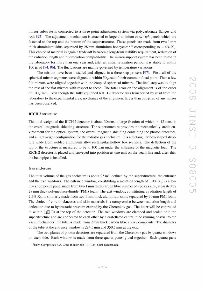
2008 JINST 3 S08005
mirror substrate is connected to a three-point adjustment system via polycarbonate flanges androds [92]. The adjustment mechanism is attached to large aluminium sandwich panels which arefastened to the top and the bottom of the superstructure. These panels are made from two 1 mmthick aluminium skins separated by 28 mm aluminium honeycomb,8 corresponding to ∼ 4% X0.This choice of material is again a trade-off between a long-term stability requirement, reduction ofthe radiation length and fluorocarbon compatibility. The mirror-support system has been tested inthe laboratory for more than one year and, after an initial relaxation period, it is stable to within100 µrad [94, 96]. The fluctuations are mainly governed by temperature variations.
The mirrors have been installed and aligned in a three-step process [97]. First, all of thespherical mirror segments were aligned to within 50 µrad of their common focal point. Then a fewflat mirrors were aligned together with the coupled spherical mirrors. The final step was to alignthe rest of the flat mirrors with respect to these. The total error on the alignment is of the orderof 100 µrad. Even though the fully equipped RICH 2 detector was transported by road from thelaboratory to the experimental area, no change of the alignment larger than 300 µrad of any mirrorhas been observed.
RICH 2 structure
The total weight of the RICH 2 detector is about 30 tons, a large fraction of which, ∼ 12 tons, isthe overall magnetic shielding structure. The superstructure provides the mechanically stable en-vironment for the optical system, the overall magnetic shielding containing the photon detectors,and a lightweight configuration for the radiator gas enclosure. It is a rectangular box-shaped struc-ture made from welded aluminium alloy rectangular hollow box sections. The deflection of thetop of the structure is measured to be < 100 µm under the influence of the magnetic load. TheRICH 2 detector is placed and surveyed into position as one unit on the beam line and, after this,the beampipe is installed.
Gas enclosure
The total volume of the gas enclosure is about 95 m3, defined by the superstructure, the entranceand the exit windows. The entrance window, constituting a radiation length of 1.0% X0, is a lowmass composite panel made from two 1 mm thick carbon fibre reinforced epoxy skins, separated by28 mm thick polymethacrylimide (PMI) foam. The exit window, constituting a radiation length of2.5% X0, is similarly made from two 1 mm thick aluminium skins separated by 30 mm PMI foam.The choice of core thicknesses and skin materials is a compromise between radiation length anddeflection due to hydrostatic pressure exerted by the Cherenkov gas. The latter will be controlledto within +200
−100 Pa at the top of the detector. The two windows are clamped and sealed onto thesuperstructure and are connected to each other by a castellated central tube running coaxial to thevacuum chamber; the tube is made from 2 mm thick carbon fibre epoxy composite. The diameterof the tube at the entrance window is 284.5 mm and 350.5 mm at the exit.
The two planes of photon detectors are separated from the Cherenkov gas by quartz windowson each side. Each window is made from three quartz panes glued together. Each quartz pane
8Euro-Composites S.A, Zone Industrielle - B.P. 24, 6401 Echternach.
– 80 –

2008 JINST 3 S08005
is 740 mm by 1480 mm and 5 mm thick, with the light opening being 720 mm by 1460 mm. Thequartz plates have the same antireflective coating as for RICH 1 (section 6.1.1).
Magnetic shielding structure
The RICH 2 detector is positioned almost halfway between the 1600 ton iron yoke of the dipole andthe massive ferromagnetic structure of the hadron calorimeter, shown in figure 2.1. The maximumstray field in the region where the photon detectors are located is more than 15 mT and is rapidlyvarying in all directions [98]. The magnetic shield boxes, which are bolted onto both sides of theRICH 2 structure, must provide a mechanically stable and light tight environment for the photondetectors and attenuate the magnetic stray field by a factor of ≥ 15. The shielding, shown infigure 6.4, is a trapezoidal structure made from 60 mm thick ARMCO iron plates. The residualmagnetic field measured at the position of the photon detector plane is between 0.2 and 0.6 mT, tobe compared to the simulated value of ≤ 0.4 mT.
6.1.3 Radiators
Aerogel is the ideal radiator to cover the very difficult range of refractive indices between gas andliquid. Silica aerogel is a colloidal form of quartz, solid but with an extremely low density. Itsrefractive index is tuneable in the range 1.01–1.10, and is ideal for the identification of particleswith momentum of a few GeV/c. Aerogel has a long-established use in threshold Cherenkovcounters. The development of high quality very clear samples [99] has allowed its use in RICHdetectors. The dominant cause of photon loss within aerogel is Rayleigh scattering; this leadsto the transmission of light with wavelength λ through a block of thickness L being proportionalto e−CL/λ 4
, where the clarity coefficient, C, characterizes the transparency of the sample. Largehygroscopic silica aerogel [99] tiles of dimension 20.0 × 20.0 × 5.1 cm3 have been produced andtested for the LHCb experiment [100]. The refractive index is 1.030 at λ=400 nm and the clarity isbelow C = 0.0054 µm4/cm. The effect of scattering in the aerogel dominates at high energy, so athin (0.30 mm) window of glass is placed after the aerogel to absorb the photons with Eγ > 3.5 eV.This serves to reduce the chromatic aberration.
For a track passing through 5 cm of aerogel with n = 1.03, the resulting number of detectedphotoelectrons in a saturated ring (β=1) is expected to be ∼6.5, calculated by MonteCarlo consid-ering the detailed geometrical setup of the optics of RICH 1 and the wavelength response of thephoton detectors. The MonteCarlo was found to describe reasonably well the number of photo-electrons measured in a test beam [100]. Tests have shown [101] that the optical properties will notdegrade significantly over the timescale of the LHCb experiment. The aerogel is stable against in-tense irradiation and shows no significant change in transparency once tested after an accumulatedfluence of up to 5.5 x 10¹³/cm2 of neutrons or protons, nor after a γ dose of 2.5× 10⁵ Gy. It is sensi-tive to water vapour absorption, but its transparency can be restored after a bakeout of the tiles. Thevolume of aerogel required is modest, ∼ 30 `, so its replacement, if required, would be relativelystraightforward. The refractive index is fairly uniform across a tile, despite the large transversedimension and thickness. The spread has been measured [102] to be σn−1/(n− 1) ∼ 0.76%. InRICH 1 the aerogel sits in the C4F10 gas radiator. Tests have shown that C4F10 does not significantlydegrade the aerogel performance [103].
– 81 –

2008 JINST 3 S08005
The fluorocarbon gases C4F10 (RICH 1) and CF4 (RICH 2) were chosen because their refrac-tive indices are well matched to the momentum spectrum of particles from B decays at LHCb andbecause they have a low chromatic dispersion. The refractive indices at 0C and 101325 Pa areparameterized by:
C4F10 : (n−1)×106 = 0.25324/(73.7−2−λ−2)
andCF4 : (n−1)×106 = 0.12489/(61.8−2−λ
−2)
where the photon wavelength λ is in nm [104]. For C4F10, n=1.0014 and for CF4, n=1.0005 atλ = 400 nm. The effective radiator lengths are about 95 cm in C4F10 and 180 cm in CF4. Theestimated photoelectron yield is ∼30 and ∼22 respectively for charged β ≈ 1 particles.
The gas radiators are operated slightly above atmospheric pressure . 50 Pa (measured at thetop of the gas vessel) and at ambient temperature. Pressure and temperature are recorded in order tocompensate variations in the refractive index (section 6.1.7). These fluorocarbons are transparentwell below 150 nm; CO2 is used as a pressure balancing gas which itself is transparent down to180 nm [105]. Since the quantum efficiency of the HPDs is zero below 190 nm (section 6.1.5),air contamination does not significantly affect the photon yield. O2 and H2O contamination arehowever kept low at about 100 ppm, mainly due to possible radiation-induced formation of HF.The CO2 fraction is kept constant at ∼1%.
6.1.4 Mirror reflectivity studies
Several reflectivity coatings are available for RICH mirrors; the choice depends on the Cherenkovphoton spectrum, the mean angle of incidence, the long term stability and compatibility to fluoro-carbons. Seven different coatings have been tested [93, 106] and the reflectivity measured with aspectrophotometer at an incidence angle of 30, close to the average angle with which the photonswill impinge on the RICH 2 mirrors. The results are shown in figure 6.6. The reflectivity coatingsfor the RICH 1 mirrors have been optimized for the the different mean angles of incidence, i.e. 25
for the spherical mirrors and 45 for the flat mirrors.Simulation studies have been performed by convoluting the reflectivity data with the quantum
efficiency of the photon detectors, the Cherenkov photon energy spectra and the transmittance ofthe CF4 radiator in RICH 2. The results of the simulation, in terms of the relative number ofdetected photons, are summarised in table 6.1.
The reflectivity of the two coatings with a layer of hafnium oxide (HfO2) is very high inthe near UV (curve I and II in figure 6.6), where the quantum efficiency of the photon detectoris peaked. The simulation shows that good matching, taking into account the two reflections onspherical and flat mirrors, leads to a detected photon yield 5% higher for this coating comparedto other UV extended coatings with magnesium fluoride (MgF2) as the surface layer. Magnesiumfluoride coatings have been successfully used in RICH detectors with C4F10 and C5F12 gas radiatorsin the DELPHI [107] and COMPASS [108] experiments, and hafnium oxide coatings have beensuccessfully tested in C6F14 vapour. Hafnium oxide also provides a very hard and chemically inertprotective layer for the mirrors. For these reasons the Al + SiO2 + HfO2 coating was chosen for allRICH 1 and RICH 2 glass mirrors. SiO2 is used for the middle layer of the multi-layer coating, andnot MgF2, for technical reasons.
– 82 –

2008 JINST 3 S08005
50
60
70
80
90
100
1 2 3 4 5 6 7
Photon energy (eV)
Mir
ror
refl
ecti
vit
y (
%)
200 nm300400500600
I
II
III
IV
V
VI
VII
I Al + MgF + HfO
II Average RICH 2 spherical mirrors
Al + SiO + HfO
III Cr 20nm + Al 90nm + SiO 15nm
IV Cr + Al + SiO 30nm
V Al + MgF 80nm
VI Al 90nm + SiO 120nm
VII Cr 10nm + Al 90nm + MgF 46.5nm
2 2
2
2
2
2
2
2 2
Figure 6.6: Reflectivity of several mirror coatings on glass as a function of the photon energy. Theangle of incidence is 30.
Table 6.1: Relative number of detected photons simulated in RICH 2 for different mirror coatings.The values are normalised to the highest photoelectron yield, set to 1.
Coating Photoelectron yieldCr + Al + SiO2 (30 nm) 0.865Al + SiO2 0.945Cr + Al + MgF2 0.947Al + MgF2 0.960Cr + Al + SiO2 (15 nm) 0.960Al + SiO2 + HfO2 1Al + MgF2 + HfO2 1.00
6.1.5 Photon Detectors
Pixel Hybrid Photon Detector
The RICH detectors utilize Hybrid Photon Detectors (HPDs) to measure the spatial positions ofemitted Cherenkov photons. The HPD is a vacuum photon detector in which a photoelectron, re-leased from the conversion in a photocathode of an incident photon, is accelerated by an appliedhigh voltage of typically 10 to 20 kV onto a reverse-biased silicon detector. During the photoelec-tron energy dissipation process in silicon, electron-hole pairs are created at an average yield of onefor every 3.6 eV of deposited energy. Carefully-designed readout electronics and interconnects tothe silicon detector result in very high efficiency at detecting single photoelectrons.
A dedicated pixel-HPD has been developed by LHCb, in close collaboration with in-dustry [109]. The specific RICH requirements are a large area coverage (∼3.5 m2) with highactive-to-total area ratio after close-packing (64%), high granularity (2.5×2.5 mm2 at the photo-cathode) and high speed (25 ns timing resolution). The pixel-HPD is shown in figure 6.7. It is
– 83 –

2008 JINST 3 S08005
Figure 6.7: Left: a schematic and right: a photograph of the pixel-HPD.
based on an electrostatically focussed tube design with a tetrode structure, de-magnifying by afactor of ∼5 the photocathode image onto a small silicon detector array. The silicon detector issegmented into 1024 pixels, each 500 µm×500 µm in size and arranged as a matrix of 32 rows and32 columns. This leads to the required pixel size at the HPD entrance window of 2.5×2.5 mm2.The nominal operating voltage of the HPD is -20 kV, corresponding to ∼5000 electron-hole pairsreleased in the silicon.
The silicon pixel detector array is bump-bonded to a binary readout chip (section 6.1.6). Thisflip-chip assembly is mounted and wire-bonded onto a Pin Grid Array (PGA) ceramic carrier, form-ing the HPD anode. Since all anode parts are encapsulated in vacuum, they must be compatiblewith the vacuum tube technologies, and must stand high (300C) bakeout temperatures. In par-ticular, a specific fine-pitch bump-bonding process has been developed for this application.9 TheHPD entrance window is fabricated from quartz and forms a spherical surface, with 7 mm thick-ness and 55 mm inner radius of curvature. The photocathode is of the thin-S20 multi-alkali type,deposited on the quartz inner surface. Normally-incident Cherenkov photons to the HPD plane canbe detected over an active diameter of 75 mm and, since the overall tube diameter is 83 mm, theintrinsic tube active area fraction is (75/83)2=0.817. A total of 484 tubes (196 for RICH1 and 288for RICH2) are required to cover the four RICH photon detection surfaces.
The demagnification by 5 of the photoelectron image is achieved by biasing the photocathodeat -20 kV, the first electrode at -19.7 kV and the second electrode at -16.4 kV. The RMS values forthe point spread function (PSF) at the pixel array are constant over the tube radius and equal to80 µm for red light and 180 µm for blue-near UV light, in the absence of magnetic field.
HPD test results
The HPDs have been fabricated in industry10 and were then qualified at two test facilities to deter-mine their efficiency and optimum working parameters, before installation at CERN. Each HPD inturn was placed in a light-tight box, illuminated with an LED of wavelength 470 nm, and read outby custom electronics. A selection of test results is presented below. Measurements of the quantumefficiencies (QEs) were carried out after manufacture at Photonis-DEP. Measurements were then
9VTT, Finland.10Photonis-DEP, Roden, Netherlands.
– 84 –

2008 JINST 3 S08005
Figure 6.8: QE measurement for one of thebest HPD.
Figure 6.9: The average QE(%) at 270 nm ver-sus the HPD batch number.
0 0.2 0.4 0.6 0.8 10
50
100
150
200
250
300
350
400
Fre
quency,
H
PD
s
Ion feedback probability (%) Dark counts (kHz cm-2)
0 5 10 15 200
50
100
150
200F
requency,
H
PD
s
Figure 6.10: Distributions of the ion-feedback rate (left) and of the dark-count rates (right).
repeated at the test facilities for a subsample of 10% of the HPDs, using a calibrated photodiodeand a quartz-tungsten halogen lamp. The QE curve for one of the best tubes is shown in figure 6.8.The average QE value per HPD batch number and the running average QE value are shown infigure 6.9 for all HPDs (484 tubes plus 66 spares). The QE curves show an average maximum of31% at 270 nm, considerably above the specification minimum of 20%.
The vacuum quality in the HPD tube is determined by measuring ion feedback. During theacceleration process, photoelectrons may hit residual gas atoms, producing ions. These drift to thephotocathode, releasing 10–40 electrons which are detected 200–300 ns after the primary photonsignal. Figure 6.10 shows that the ion feedback rate is well below the specification maximum of1%, indicating that the vacuum quality is excellent.
An important quality factor of an HPD is low dark-count rate, the main sources beingthermionic electron emission at the photocathode, electrostatic field emission and any resulting
– 85 –

2008 JINST 3 S08005
Figure 6.11: Left: the RICH 2 column mounting scheme and right: a photograph of a column.
ion feedback. Figure 6.10 shows the measured dark-count rates in the sample of HPDs in a runwith the LEDs off. Dark-count rates are typically below the specification value, 5 kHz/cm2 withrespect to the photocathode area, which in turn is∼103 less than the maximum occupancy expectedin the RICH detectors.
HPD testing was carried out at a rate of 30–40 HPDs per month. A total of 97% have beenfound to meet or exceed the design criteria in key areas.
Photon Detector integration
The HPDs are grouped in four detection planes (two for RICH1 and two for RICH2) and positionedon a hexagonal lattice. The hexagonal close-packing factor is 0.907. Each tube is completely sur-rounded by a 1 mm thick cylindrical magnetic shield which protects against stray external B-fieldsup to 5 mT (the maximum field value within the RICH 1 magnetic shielding has been measuredto be 2.4 mT, see section 6.1.1). A tube-to-tube pitch of 89.5 mm in both RICH detectors hasbeen chosen, resulting in a packing factor of (75/89.5)2×0.907=0.64. The HPDs are mounted oncolumns which are installed in the magnetic shielding boxes of the two RICH detectors. There are2×7 columns of HPDs in RICH 1 with 14 HPDs per column and 2×9 columns in RICH 2 with16 HPDs per column. Figure 6.11 illustrates the column mounting scheme for RICH 2. The col-umn also contains front-end electronics boards (one per pair of HPDs), power supply distribution,cabling and active cooling, all within one mechanical module. The electronics boards and powerdistribution are described in section 6.1.6.
– 86 –

2008 JINST 3 S08005
6.1.6 Electronics
The RICH electronics system reads out data from the HPDs (about 5×10⁵ channels) and conformsto the general electronics architecture of LHCb (see section 2.2). The electronics system is dividedinto so-called Level-0 (L0) and Level-1 (L1) regions. The L0 electronics are all located on-detectorwhere they will be exposed to radiation and must therefore contain only radiation-qualified com-ponents. The L1 electronics modules are housed in the counting house behind the radiation-shieldwall and hence are not required to be radiation tolerant.
Level-0 electronics
The L0 electronics comprises the pixel chip, ZIFs/kaptons, L0 board and LV/HV distribution, andis described below.
Pixel Readout Chip: At the beginning of the electronics readout chain is the LHCBPIX1 pixelchip [110] that forms part of the anode assembly of the HPD (section 6.1.5). The chip has beendesigned in a commercial 0.25 µm CMOS process using special layout techniques to enhance itsresistance to radiation. The chip is connected to a silicon pixel sensor by an array of solder bump-bonds, one per channel. Each pixel measures 62.5 µm by 500 µm and 8192 pixels are arranged as amatrix of 32 columns by 256 rows. Circuitry on the chip logically ORes eight adjacent pixels, thustransforming the matrix into 1024 channels of 32 by 32, each of size 500 µm by 500 µm. Signalsfrom the silicon sensor are amplified, shaped and then compared with a global threshold. Hits arebuffered for the duration of the Level-0 trigger latency and triggered events are then read out byway of a 16-deep multi-event FIFO buffer. The 32 columns are read out in parallel. The analogbehaviour of the chip is crucial for a good photodetection efficiency, in particular low noise anduniform threshold. Measured values are well within the HPD specifications, with typically 160electrons noise, compared to a signal of 5000 electrons, and a mean threshold of 1200 electronswith RMS spread of 100 electrons.
ZIFs and Kaptons: Signals to and from the HPD pass through the pins of the ceramic pin-grid-array carrier. This is plugged into a 321-pin Zero-Insertion-Force (ZIF) connector mounted on asmall circuit board. The board also contains passive components for filtering and line-termination.Signals are then transmitted on two Kapton cables which also carry the low-voltage power to theHPD. These Kaptons allow mechanical flexibility between the mounting of the HPDs and the otherLevel-0 components.
L0 Board: The L0 board [111] acts as an interface between the HPDs and the ECS (Exper-iment Control System), TFC (Timing and Fast Control) and data transmission systems. This in-terfacing is implemented in the Pixel Interface (PINT). The antifuse gate array, ACTEL AX1000,was chosen for its tolerance to single event effects (single event latch-up and single event upset).Its main tasks are to receive data from two HPDs, add headers containing event information anddata-integrity checks, and transfer events to the data transmission system. A total of 242 L0 boardsare used in the RICH detectors. A photograph of a single board is shown in figure 6.12. The tol-erance of the PINT to single event effects was verified by irradiation tests to simulate the expecteddose in the LHCb environment. The measured rate of single event upset (SEU) was negligible, nocases of latch-up were observed and chips survived many times the expected dose of ionising radi-
– 87 –

2008 JINST 3 S08005
Figure 6.12: A photograph of the L0 board. The optical receiver and transmitters are visible at thetop. The PINT gate array is in the centre of the board.
ation. All other components on the L0 board have been designed in radiation-hardened or toleranttechnologies already qualified to levels far in excess of the RICH environment.
The optical data transmission consists of Gigabit Optical Link (GOL) chips [112] and VerticalCavity Surface Emitting Lasers (VCSEL). The GOLs serialise the data into a 1.6 Gbit/s bit streamusing 8 b/10 b encoding and the VCSELs convert this into an optical signal of 850 nm wavelength.Two output fibres, one per HPD, transmit the data from each L0 board. At a 1MHz trigger rate, theaggregate output data rate from the RICH photon detectors is in the region of 500 Gbit/s distributedover 484 optical fibres. Also on the board is a TTCrx [113] which generates the 40 MHz clock andtrigger and calibration signals. The input to the TTCrx arrives on fibres connected to the globalTFC system. Finally, a chip known as the Analog-Pilot generates reference voltages required bythe HPDs and digitizes monitoring signals such as the temperature of the board as measured byPT1000 sensors.
LV/HV Distribution: The low voltages required by the HPDs and the L0 boards are providedby the LV distribution system. These voltages are generated locally using radiation-tolerant linearvoltage regulators mounted on the LV boards. Each LV board can power two L0 boards indepen-dently, and four LV boards are daisy-chained together in an HPD column. The top-most containsa SPECS slave module [41] which provides the interface for the configuration of the HPDs andL0 boards in that column. The SPECS interface is also used for switching on and off the voltageregulators, thus allowing careful control of the powering of the column.
The high voltages for the HPDs are provided by the HV distribution system [114]. As shownin figure 6.13b, the three voltages are derived from a 20 kV input by means of a resistive divider,one per half-column, and short circuit protection is provided by 1 Gohm resistors in series witheach HPD voltage line. Various measures have been taken to minimise the risk of discharge orbreakdown. The bare PCB of the HV cards is machined to introduce cuts around critical pointswhich are then filled with dielectric gel to improve insulation. After component mounting andcabling, the entire assembly is encapsulated in silicone rubber. A photograph of a completed boardis shown in figure 6.13. A total of 242 boards are used to equip the RICH detectors.
Figure 6.14 shows a photograph of all front-end electronics components mounted on a RICHHPD column. On the left are the Kapton cables shown plugged into the L0 boards, then comes a
– 88 –

2008 JINST 3 S08005
(a) (b)
Figure 6.13: A photograph (a) and the scheme (b) of an HV board. Around the board is the siliconecoating.
Figure 6.14: A photograph of L0, LV and HV boards mounted on a RICH HPD column.
cable tray to carry the optical fibres. Next comes the LV board which has heat sinks mounted onthe surface of the voltage regulators. At the far right are the HV boards.
Level-1 electronics
The RICH L1 electronics, located off-detector in the counting room, has been designed to imple-ment data compression and also to serve as the interface between the custom data transmissionprotocol of the L0 electronics and the industry-standard Gbit Ethernet protocol used by the DAQnetwork. The off-detector electronics also performs the important function of isolating the DAQnetwork from errors induced in the L0 data due to radiation induced SEU.
Each incoming serial data channel is first converted from optical to electrical using AgilentHFBR-782 optical receivers. The serial electrical data are then AC coupled to dedicated I/O pinsof Virtex2Pro FPGAs, where they are deserialised using integrated Gbit transceivers that are com-
– 89 –

2008 JINST 3 S08005
patible with the data encoding used by the GOL serialisers in the L0 electronics. All further dataprocessing is done in the FPGA programmable logic.
The L1 electronics modules are controlled by signals broadcast synchronously to all subdetec-tors by the readout supervisor. These signals are used to control the generation of the data packetssent by the L1 to the DAQ network (see section 8.3). The data content of these packets is extractedfrom the incoming L0 data frames. The generation of the data packets operates autonomously tothe arrival of the L0 data and therefore cannot be disrupted by incoming erroneous data. In orderto predict the time of arrival of the L0 data frames so that they can be correctly inserted into thegenerated data packets, the operation of the L0 electronics is emulated in the off-detector modulesusing the TFC broadcast signals.
Once the incoming data frames have been received, the zero-suppression algorithm (L1 mod-ule copies only the non-zero bytes into the zero-suppressed buffer) is applied in parallel to allstreams. The fully pipelined algorithm operates at the 1 MHz input event rate and therefore doesnot introduce dead-time. Zero-suppressed data are buffered in internal memory in the four ingressFPGAs before being multiplexed into multi-HPD event packets. These packets are then forwardedto the egress FPGA which further multiplexes the data into multi-event packets and transmits themusing Gbit Ethernet protocol to the DAQ network using the LHCb quad Gbit Ethernet interface.
The L1 module is configured and monitored via an LHCb Credit Card PC (CCPC) [115]interface. The L1 modules are in 9U format and each can receive data from a maximum of 36HPDs. The input links are distributed across three 12-channel optical receivers and four Virtex2Proingress FPGAs. For 1 MHz operation, the data throughput is expected to be limited by the capacityof the four 1 Gbit/s DAQ links at higher luminosity. Static load balancing is done by physicallydistributing the input fibre-optic cables across the modules. The bandwidth is distributed across 21L1 boards to avoid bottlenecks and problems associated with inhomogeneous occupancies in thedifferent parts of the RICH detectors.
6.1.7 Monitoring and control
The RICH Detector Control System (DCS) [116] monitors the working conditions of both RICH 1and RICH 2, controls the operating conditions and ensures the integration of RICHes in the LHCbdetector control system. It is composed of several parts:
• Power supply control and monitoring (low voltage, silicon detector bias and very highvoltage);
• Environment monitoring (temperature, pressure, humidity);
• Gas quality monitoring (gas purity);
• Magnetic distortion monitoring (and correction);
• Laser alignment monitoring system.
Power supplies
Low voltage (5 V) for the front-end electronic boards is provided by commercial off-the-shelf de-vices, the Wiener MARATON power supply. It is radiation and magnetic field tolerant, and can
– 90 –

2008 JINST 3 S08005
be remotely monitored via a network using standard software interfaces provided by the manu-facturer (OPC server). Other lower voltages (e.g. 3.3 V) required by the electronics componentsare generated, regulated and monitored on each front-end LV board. In addition, to improve re-liability, temperature sensors placed near hot spots and critical points allow a quick check of theintegrity of the electronics. A similar solution has been adopted for biasing the HPD internal sili-con pixel detectors: a standard CAEN SY1527 mainframe power supply with plug-in modules. Forthe very high voltage of the HPDs (20 kV), no satisfactory commercial solution was found so thesystem was designed in-house. The system is built around a commercial HV module (ISEG CPn–200 504 24 10) controlled and monitored by a pair of DACs and ADCs connected via an I2C businterface to a CCPC running the software to regulate the voltage and to connect to the network. TheCCPC, using a bare-bones version of Linux, runs the control program which, in an endless loop,checks all voltages and currents, and via a DIM protocol [117] reports measurements to the highlevel control system. In the unlikely case of a loss of the network connection, the CCPC can stillcheck the working conditions and cut power to the HPDs to avoid damage to personnel and HPDs.
Environment
Environmental monitoring (temperature, pressure, humidity of the radiator gas and HPD planes) isachieved using standard commercial sensors, namely platinum resistors for temperature, diaphragmsensors for pressure and HMX2000-HT sensors (by Hygrometrix) for humidity. All these devicesare mounted in the harsh radiation environment hence they must be read by radiation tolerantelectronics i.e. the Embedded Local Monitor Board (ELMB) [118].
Gas quality
The purity of the gas radiator is critical to obtain good photon transparency and for this reason aquick analysis tool to spot any contamination is employed. The stability of the gas composition ischecked by periodically monitoring the speed of sound of the gas in the vessel. The speed of sound
is given by vs =√
γRTM where γ = Cp
Cvis the ratio of specific heats of the gas, R is the universal gas
constant, T the absolute temperature and M the average molecular mass. The speed is monitoredby measuring the time that a sound pulse takes to propagate from an electrostatic transducer tothe end of a cylindrical vessel and then, reflected by the end wall, back to the same transducer,working now as a microphonic sensor. For RICH 1 this vessel is 0.5 m long and the measured timeinterval is of the order of 10 ms in C4F10. For RICH 2 the vessel is approximately 0.3 m long andthe relative propagation time is of the order of 3.8 ms in CF4. The whole system is built around atimer/counter provided by a National Instrument acquisition board. The internal counter, runningat 20 MHz, provides 50 ns time resolution, more than adequate to detect a 1% CO2 contamination(which will give a 50 µs change in C4F10 and 30 µs change in CF4 for the total transit time). Thereare two such systems for each RICH detector, one placed on the inlet pipe and the second on theoutlet of the fluid system. A typical measurement is shown in figure 6.15 which shows the changein the propagation time when the percentage of CO2 changes from 0 to 5%.
– 91 –
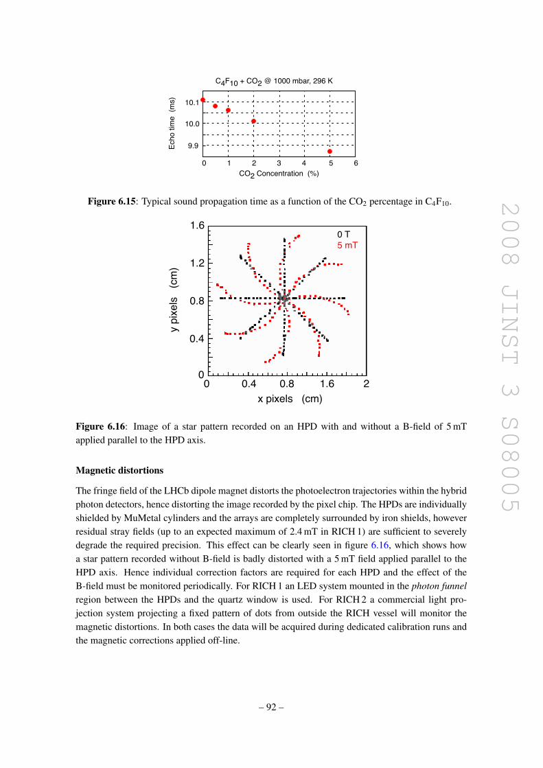
2008 JINST 3 S08005
10.1
10.0
9.9Ech
o t
ime
(m
s)
0 1 2 3 4 5 6
CO2 Concentration (%)
C4F10 + CO2 @ 1000 mbar, 296 K
Figure 6.15: Typical sound propagation time as a function of the CO2 percentage in C4F10.
0 T
5 mT
y p
ixels
(
cm
)
0
0.4
0.8
1.2
1.6
0 0.4 0.8 1.6 2
x pixels (cm)
Figure 6.16: Image of a star pattern recorded on an HPD with and without a B-field of 5 mTapplied parallel to the HPD axis.
Magnetic distortions
The fringe field of the LHCb dipole magnet distorts the photoelectron trajectories within the hybridphoton detectors, hence distorting the image recorded by the pixel chip. The HPDs are individuallyshielded by MuMetal cylinders and the arrays are completely surrounded by iron shields, howeverresidual stray fields (up to an expected maximum of 2.4 mT in RICH 1) are sufficient to severelydegrade the required precision. This effect can be clearly seen in figure 6.16, which shows howa star pattern recorded without B-field is badly distorted with a 5 mT field applied parallel to theHPD axis. Hence individual correction factors are required for each HPD and the effect of theB-field must be monitored periodically. For RICH 1 an LED system mounted in the photon funnelregion between the HPDs and the quartz window is used. For RICH 2 a commercial light pro-jection system projecting a fixed pattern of dots from outside the RICH vessel will monitor themagnetic distortions. In both cases the data will be acquired during dedicated calibration runs andthe magnetic corrections applied off-line.
– 92 –

2008 JINST 3 S08005
CCD Camera
Optical Fiber
Focalizer
Beam Splitter
Spherical Mirror
Laser Source
Figure 6.17: Schematic of the mirror alignment monitoring system.
Mirror alignment
Mechanical stability of the mirrors is of paramount importance to achieve the required Cherenkovangular resolution. This stability is challenging due to the size of the mirrors and the difficulty ofsecuring them without introducing mechanical distortions to the reflecting surface. An alignmentsystem which uses a CCD camera monitors mirror movements. On the focal plane of a givenmirror, the images of two light spots are formed: the first comes directly from a laser source andthe second is reflected back from the monitored mirror. Any change in the relative position of thetwo spots is an indication of mirror mechanical misalignment and the information is used to makean off-line correction. A schematic of the system is shown in figure 6.17. The laser light sourcefeeds a bundle of optical fibers which generate all the required light paths (eight mirrors will bemonitored in RICH 1, 16 in RICH 2). The beams are then directed to the beam splitters whichguide the reference beams directly to the CCDs and the secondary beams to the mirrors.
It can be demonstrated that there is a linear transformation law between a change in the mirrortilt (∆Θx,∆Θy) and the relative movement of the reflected spot on the CCD (∆x,∆y):
∆Θx = A∆x +B∆y
∆Θy = C∆x +D∆y,
where the parameters A to D are fixed constants which depend on the geometry of the system.The mirror tilts can then be determined by inverting this transformation after observing the spotmovement. The system tracks the displacement between the two beam spots, even if the spotsmove together, with an accuracy of better than 0.01 mrad.
6.1.8 RICH performance
Test Beam studies
An extensive test beam programme has allowed the RICH photodetectors, readout electronics andradiators to be evaluated with Cherenkov radiation in a realistic environment. Of particular impor-
– 93 –

2008 JINST 3 S08005
Table 6.2: Comparison of the measured and expected photon yields for the individual HPDs in theRICH test beam run. The first column indicates the label of each HPD.
HPD µmeas. µexp µmeas./µexp
L0 8.1 ±0.10 11.4 ±0.73 0.71 ±0.07L1 10.2 ±0.16 10.0 ±0.66 1.02 ±0.07C1 11.5 ±0.33 11.2 ±0.78 1.02 ±0.07R0 8.7 ±0.24 8.9 ±0.73 0.98 ±0.09R1 10.1 ±0.03 10.7 ±0.83 0.95 ±0.08
tance has been the comparison of the expected and observed photoelectron yields and Cherenkovangle resolutions. Because the predictions of these quantities for test beam operation are madeusing a simulation with identical assumptions to those of the full LHCb MonteCarlo, agreementbetween prediction and observation is an important indicator that the RICH system will perform tospecification.
A demonstrator RICH detector was operated in a test beam utilizing pre-production photondetectors and realistic prototypes of the associated RICH electronics [119]. The tests were per-formed at the CERN-PS in the T9 facility using 10 GeV/c pions together with an N2 gas radiatorto generate Cherenkov light. The HPDs were arranged in columns with the close-packing arrange-ment that will be used in the experiment and were read out at the LHC frequency of 40 MHz.In this configuration, the Cherenkov rings from the N2 gas radiator were fully contained within asingle HPD. Having included corrections for the asynchronous nature of the test beam set-up, thephotoelectron yields were found to be in good agreement with those expected from the MonteCarlosimulation, as shown in table 6.2. A distribution of the number of pixel hits observed per event ona single HPD is shown in figure 6.18. Uncertainties in the corrections for the asynchronous beamstructure explain the residual differences between the data and simulated distributions.
The distribution of reconstructed Cherenkov angles was also found to be in good agree-ment with the simulation (see figure 6.19). The Cherenkov angle resolution was determined tobe 1.66±0.03 mrad, to be compared with the simulation expectation of 1.64 mrad. The dominantcontributions to the Cherenkov angle resolution came from the uncertainty in the beam direction,the HPD point-spread function and the HPD pixelisation. The relative contributions of the lattertwo effects were significant owing to the test beam geometry but are not expected to be dominantin the final LHCb experiment.
Detector simulation
The LHCb RICH system is modelled as part of the LHCb Simulation program based on theGEANT4 simulation toolkit (see chapter 10). All important aspects of the geometry and the ma-terial description are fully simulated. A database is setup with all this information which is theninput into the simulation and the reconstruction programs.
The Cherenkov light generation is performed inside GEANT4, and the photons propagatedwith full knowledge of the expected reflectivities, transmissions and refraction effects at the variousoptical elements. The Rayleigh scattering in aerogel and absorption in the various media are also
– 94 –

2008 JINST 3 S08005
Number of hit pixels4 6 8 10 12 14 16 18 20 22
Nu
mb
er o
f ev
ents
0
500
1000
1500
2000
2500
3000
3500
4000
Cherenkov angle (mrad)10 12 14 16 18 20 22 24 26 28 30
En
trie
s
0
5000
10000
15000
20000
25000
30000
35000
Figure 6.18: Number of pixel hits per event fordata (points) and simulation (histogram) for asingle HPD used in the RICH test beam run.
Figure 6.19: Reconstructed Cherenkov anglefor data (solid histogram) and simulation (dot-ted line) on one of the HPDs used in the 2004RICH test beam run.
included. Inside the HPDs, using the measured quantum efficiencies and cross-focussing relations,the photoelectrons created from the photocathode are mapped down onto the silicon detectors (hitslocation and energy). From these hits, the charge sharing in the pixels and the response of front-end readout are modelled in a separate package, which creates the digitized hits in the same formatwhich will be output from the operational detector. All known sources of background are simulated.The most important components come from Rayleigh scattered photons in the aerogel, rings fromsecondary particles without associated reconstructed tracks and Cherenkov light generation in theHPD windows from traversing charged particles. More information on the LHCb RICH simulationmay be found in [120]. Figure 6.20 shows a simulated event display in RICH 1.
For a given pixel-track association, the apparent Cherenkov angle is reconstructed throughknowledge of the track direction, the hit pixel location, and the geometry of the RICH optics. Thisreconstruction assumes that the Cherenkov photon was emitted at the midpoint of the radiator.In simulation the resolution on the Cherenkov angle per photoelectron, and the mean number ofphotoelectrons detected per β ≈ 1 track can be determined by using truth information to ensure thatthe hit pixel-track association is correct. The mean number of photoelectrons is found to be 6.7for aerogel, 30.3 for C4F10 and 21.9 for CF4. The resolution results are shown in table 6.3, whereboth the total resolutions and the individual contributions are listed. The single photoelectronresolution is largest for the aerogel, at 2.6 mrad, and smallest for the CF4, at 0.7 mrad. Theseresolutions receive contributions from the uncertainty associated with the photon emission point,the chromatic dispersion of the radiator, the finite pixel size and the point spread function (togetherlisted as ‘HPD’ in the table). For the aerogel it is the chromatic dispersion error which dominates,whereas for the other two radiators the contributions are well matched. An additional uncertaintycomes from the reconstruction of the track direction.
The resulting particle identification performance of the RICH system will be discussed insection 10.
– 95 –

2008 JINST 3 S08005
(cm)
(cm)
Figure 6.20: Display of a typical LHCb event in RICH 1.
Table 6.3: Single photoelectron resolutions for the three RICH radiators. All numbers are in mrad.Individual contributions from each source are given, together with the total.
Aerogel C4F10 CF4
Emission 0.4 0.8 0.2Chromatic 2.1 0.9 0.5HPD 0.5 0.6 0.2Track 0.4 0.4 0.4Total 2.6 1.5 0.7
6.2 Calorimeters
The calorimeter system performs several functions. It selects transverse energy hadron, electronand photon candidates for the first trigger level (L0), which makes a decision 4µs after the inter-action. It provides the identification of electrons, photons and hadrons as well as the measurementof their energies and positions. The reconstruction with good accuracy of π0 and prompt photonsis essential for flavour tagging and for the study of B-meson decays and therefore is important forthe physics program.
The set of constraints resulting from these functionalities defines the general structure andthe main characteristics of the calorimeter system and its associated electronics [1, 121]. Theultimate performance for hadron and electron identification will be obtained at the offline analysislevel. The requirement of a good background rejection and reasonable efficiency for B decays addsdemanding conditions on the detector performance in terms of resolution and shower separation.
– 96 –

2008 JINST 3 S08005
Outer section :
Inner section :
121.2 mm cells
2688 channels
40.4 mm cells
1536 channels
Middle section :
60.6 mm cells
1792 channels
Outer section :
Inner section :
262.6 mm cells
608 channels
131.3 mm cells
860 channels
Figure 6.21: Lateral segmentation of the SPD/PS and ECAL (left) and the HCAL (right). Onequarter of the detector front face is shown. In the left figure the cell dimensions are given for theECAL.
6.2.1 General detector structure
A classical structure of an electromagnetic calorimeter (ECAL) followed by a hadron calorimeter(HCAL) has been adopted. The most demanding identification is that of electrons. Within thebandwidth allocated to the electron trigger (cf. section 7.1.2) the electron Level 0 trigger is requiredto reject 99% of the inelastic pp interactions while providing an enrichment factor of at least 15in b events. This is accomplished through the selection of electrons of large transverse energyET . The rejection of a high background of charged pions requires longitudinal segmentationof the electromagnetic shower detection, i.e. a preshower detector (PS) followed by the mainsection of the ECAL. The choice of the lead thickness results from a compromise betweentrigger performance and ultimate energy resolution [122]. The electron trigger must also reject abackground of π0’s with high ET . Such rejection is provided by the introduction, in front of thePS, of a scintillator pad detector (SPD) plane used to select charged particles. A thin lead converteris placed between SPD and PS detectors. At Level 0, the background to the electron trigger willthen be dominated by photon conversions in the upstream spectrometer material, which cannotbe identified at this stage. Optimal energy resolution requires the full containment of the showersfrom high energy photons. For this reason, the thickness of ECAL was chosen to be 25 radiationlengths [123]. On the other hand, the trigger requirements on the HCAL resolution do not imposea stringent hadronic shower containment condition. Its thickness is therefore set to 5.6 interactionlengths [124] due to space limitations.
The PS/SPD, ECAL and HCAL adopt a variable lateral segmentation (shown in figure 6.21)since the hit density varies by two orders of magnitude over the calorimeter surface. A segmenta-tion into three different sections has been chosen for the ECAL and projectively for the SPD/PS.Given the dimensions of the hadronic showers, the HCAL is segmented into two zones with largercell sizes.
All calorimeters follow the same basic principle: scintillation light is transmitted to a Photo-Multiplier (PMT) by wavelength-shifting (WLS) fibres. The single fibres for the SPD/PS cells areread out using multianode photomultiplier tubes (MAPMT), while the fibre bunches in the ECALand HCAL modules require individual phototubes. In order to have a constant ET scale the gain inthe ECAL and HCAL phototubes is set in proportion to their distance from the beampipe. Sincethe light yield delivered by the HCAL module is a factor 30 less than that of the ECAL, the HCALtubes operate at higher gain.
– 97 –

2008 JINST 3 S08005
6.2.2 Electronics overview
The basic structure is dictated by the need to handle the data for the Level 0 trigger as fast aspossible. The front-end electronics and the PS/SPD photomultipliers are located at the detectorperiphery. The HCAL and ECAL phototubes are housed directly on the detector modules. Thesignals are shaped directly on the back of the photomultiplier for the PS/SPD or after 12 m and 16 mlong cables for ECAL and HCAL respectively. They are then digitized in crates positioned on top ofthe detectors and the trigger circuits, hosted in the same crates, perform the clustering operationsrequired by the trigger [125]. For each channel, the data, sampled at the bunch crossing rate of40 MHz, are stored in a digital pipeline until the Level-0 trigger decision. In order to exploit theintrinsic calorimeter resolution over the full dynamic range, ECAL and HCAL signals are digitizedby a 12-bit flash ADC [126]. Ten bits are enough for the preshower, and the SPD information isonly one bit, a simple discriminator recording whether a cell has been hit or not [127, 128]. Anadditional requirement is to reduce the tails of signals associated to the bunch crossing precedingthe one being sampled. For ECAL and HCAL, this goal can be achieved at the percent level bysuitable signal treatment within 25 ns. In the case of the PS and SPD, the signal shape fluctuationsrequire the longest possible signal integration time. They therefore use a different front-end designfor the integrator, as described in section 6.2.7. Finally, in order not to degrade the resolution, theelectronic noise must remain at the least significant bit level [129]. At the short shaping times beingused, this requires careful design of the very front-end part.
6.2.3 The pad/preshower detector
The pad/preshower (SPD/PS) detector uses scintillator pad readout by WLS fibres that are coupledto MAPMT via clear plastic fibres. The choice of a 64 channel MAPMT allowed the design of afast, multi-channel pad detector with an affordable cost per channel.
The SPD/PS detector consists of a 15 mm lead converter 2.5 X0 thick, that is sandwichedbetween two almost identical planes of rectangular scintillator pads of high granularity with a totalof 12032 detection channels (figure 6.22 left). The sensitive area of the detector is 7.6 m wideand 6.2 m high. Due to the projectivity requirements, all dimensions of the SPD plane are smallerthan those of the PS by ∼0.45%. The detector planes are divided vertically into two halves. Eachcan slide independently on horizontal rails to the left and right side in order to allow service andmaintenance work. The distance along the beam axis between the centres of the PS and the SPDscintillator planes is 56 mm. In order to achieve a one-to-one projective correspondence with theECAL segmentation (described in section 6.2.4), each PS and SPD plane is subdivided into inner(3072 cells), middle (3584 cells) and outer (5376 cells) sections with approximately 4 × 4, 6 × 6and 12 × 12 cm2 cell dimensions.
The cells are packed in∼48× 48 cm2 boxes (detector units) that are grouped into supermod-ules. Each supermodule has a width of ≈ 96 cm, a height of ≈ 7.7 m and consists of detector unitsthat form 2 rows and 13 columns. The space available for the SPD/PS detector between the firstmuon chamber and the electromagnetic calorimeter is only 180 mm. Figure 6.22 (right) shows anindividual scintillator pad with the WLS fibre layout. The diameter of the WLS fibre groove isa few mm smaller than the tile size; exact parameters of the tile geometry can be found in [130].The basic plastic component is polystyrene to which primary and secondary WLS dopants, parater-
– 98 –

2008 JINST 3 S08005
Figure 6.22: Front view of one half of the SPD/PS installed in the LHCb experimental hall (left).Individual scintillator pad with the WLS fibre layout and the LED housing in the middle (right).
phenyl (PTP), 1.5% and POPOP, 0.04%, are added.11 The square structure of a pad is cut out from a15 mm thick scintillator plate, and the scintillator surface is polished to reach the necessary opticalquality. In order to maximize the light collection efficiency, WLS fibres are coiled and placed intoa ring groove that is milled in the body of the cell. The rectangular cross section of the groove is4.1 mm deep and 1.1 mm wide. The groove contains 3.5 loops of WLS fibre. The number of loopswas chosen to achieve an overall optimization of the light collection efficiency [131] and the signalformation [132]. Two additional grooves are milled in the scintillator allowing both ends of theWLS fibre to exit the plate. The fibre is glued inside the groove12 using a dedicated semi-automaticdevice that provides the winding of the fibre and a uniform glue filling along the groove. A 1.0 mmdiameter Y11(250) MS70 multi-cladding S-type WLS fibre13 was chosen as a reasonable compro-mise between light output and durability. The pad is wrapped with 0.15 mm thick TYVEK14 paperin order to improve the light reflection and to minimize the dead space between adjacent pads.Light produced by an ionizing particle in the scintillator is guided by the WLS fibre to the exit ofthe detector box. At this point optical connectors (described in [130]) join the WLS fibres to longclear fibres. The two clear fibres connected to the two ends of the WLS fibre of a given pad areviewed by a single MAPMT pixel [130]. The length of clear fibres varies from 0.7 to 3.5 m butall the fibres connected to a particular PMT have the same length in accordance with the front-endelectronics specification [127, 128]. The clear fibre allows the transport of the scintillator lightfrom the SPD/PS planes over a few metres to the multi-anode PMT without significant attenuation.
The scintillator cells are grouped into self-supporting detector units that are packed insidesquare boxes with dimension 476 mm × 476 mm (SPD) and 478 mm × 478 mm (PS) boxes, yield-
11produced at SSI Institute for Single Crystals NAS of Ukraine, 60 Lenin Ave, Kharkov, 61001, Ukraine.12with BICRON BC-600 glue, BICRON Corp., 12345 Kinsman Rd. Newbury OH 440 USA.13KURARAY Corp., 3-10, Nihonbashi, 2 chome, Chuo-ku, Tokyo, Japan.14TYVEK of type 1057D used, product of E.I. du Pont de Nemours and Company.
– 99 –

2008 JINST 3 S08005
Figure 6.23: Fibre routing for the inner (left) and outer (right) module boxes.
ing a total of 26 boxes per supermodule. Since there are three sections with different cell sizesfor the SPD/PS planes, the boxes are filled with a different number of pads with sizes that add upto 119 mm for the SPD to 119.5 mm for the PS planes. A dedicated fibreglass technology of boxmanufacturing was developed in order to obtain stiff boxes with a minimum amount of materialbetween the adjacent cells of neighbouring boxes. The lateral walls of the monolithic box frame aremanufactured using Fibreglass Reinforced Plastic (FGRP) with a wall thickness of 0.3 mm. Thisfabrication method consists of a one cycle polymerization process with predefined curing param-eters. To ensure light tightness a layer of black paper was incorporated in addition to the FGRPlayer. The top and bottom layers of the box are made of 2 mm thick Al plate and G10 plastic. Thebottom cover is glued to the FGRP frame by epoxy and the top one is fixed by screws. On the topcover there are output plastic ports, made of relatively cheap pressure die casting technology, dis-posed to allow exit of fibre bundles out of the box. The module assembly procedure is as follows.All cells in a detector unit are grouped in matrices of 4×4 cells. The scintillator pads with gluedWLS fibres are placed into the box after quality control tests. The fibre ends are grouped by 32, fitinto a light-tight flexible tube and glued into an optical connector, before being cut and polished.The routing of fibres inside a box from one matrix is shown in figure 6.23. The bending diameteralways exceeds 100 mm. Depending on the number of scintillator cells inside a unit, the boxes areequipped with one (outer region), four (middle region) or nine (inner region) output port(s) andlight connector(s).
The detector units are designed to be mounted on a supermodule support plate. All super-modules of the SPD/PS planes have identical design. Each consists of 26 detector units mountedon a long aluminium strip in two columns. The photomultiplier tubes are located on both the topand bottom ends of the supermodule support outside the detector acceptance. The detector unitsare optically connected to the PMTs by bundles of 32 clear fibres, enclosed in a light-tight plastictube, by means of a photo-tube coupler. The PMT is a (8-stage) R5900-M64 manufactured byHamamatsu15[133, 134] and has a bialkali photocatode segmented into 64 pixels of 2 × 2 mm2.The HV is provided by a Cockroft-Walton voltage multiplier.
The quality of the phototubes has been extensively studied using measurements of the nonuni-formities of anode response within one MAPMT, the linearity over the required dynamic range ofthe PS, the absolute gain of the MAPMT channels and the electronic crosstalk. The nonuniformity
15HAMAMATSU Photonics KK, Electron Tube Center, 314-5, Shimokanzo, Toyooka-village, Iwata-gun, Shizuoka-ken, 438-01 Japan.
– 100 –
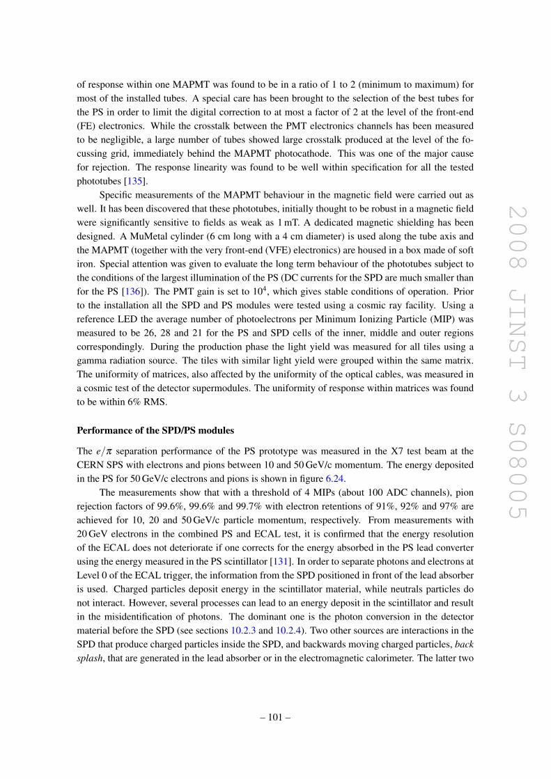
2008 JINST 3 S08005
of response within one MAPMT was found to be in a ratio of 1 to 2 (minimum to maximum) formost of the installed tubes. A special care has been brought to the selection of the best tubes forthe PS in order to limit the digital correction to at most a factor of 2 at the level of the front-end(FE) electronics. While the crosstalk between the PMT electronics channels has been measuredto be negligible, a large number of tubes showed large crosstalk produced at the level of the fo-cussing grid, immediately behind the MAPMT photocathode. This was one of the major causefor rejection. The response linearity was found to be well within specification for all the testedphototubes [135].
Specific measurements of the MAPMT behaviour in the magnetic field were carried out aswell. It has been discovered that these phototubes, initially thought to be robust in a magnetic fieldwere significantly sensitive to fields as weak as 1 mT. A dedicated magnetic shielding has beendesigned. A MuMetal cylinder (6 cm long with a 4 cm diameter) is used along the tube axis andthe MAPMT (together with the very front-end (VFE) electronics) are housed in a box made of softiron. Special attention was given to evaluate the long term behaviour of the phototubes subject tothe conditions of the largest illumination of the PS (DC currents for the SPD are much smaller thanfor the PS [136]). The PMT gain is set to 104, which gives stable conditions of operation. Priorto the installation all the SPD and PS modules were tested using a cosmic ray facility. Using areference LED the average number of photoelectrons per Minimum Ionizing Particle (MIP) wasmeasured to be 26, 28 and 21 for the PS and SPD cells of the inner, middle and outer regionscorrespondingly. During the production phase the light yield was measured for all tiles using agamma radiation source. The tiles with similar light yield were grouped within the same matrix.The uniformity of matrices, also affected by the uniformity of the optical cables, was measured ina cosmic test of the detector supermodules. The uniformity of response within matrices was foundto be within 6% RMS.
Performance of the SPD/PS modules
The e/π separation performance of the PS prototype was measured in the X7 test beam at theCERN SPS with electrons and pions between 10 and 50 GeV/c momentum. The energy depositedin the PS for 50 GeV/c electrons and pions is shown in figure 6.24.
The measurements show that with a threshold of 4 MIPs (about 100 ADC channels), pionrejection factors of 99.6%, 99.6% and 99.7% with electron retentions of 91%, 92% and 97% areachieved for 10, 20 and 50 GeV/c particle momentum, respectively. From measurements with20 GeV electrons in the combined PS and ECAL test, it is confirmed that the energy resolutionof the ECAL does not deteriorate if one corrects for the energy absorbed in the PS lead converterusing the energy measured in the PS scintillator [131]. In order to separate photons and electrons atLevel 0 of the ECAL trigger, the information from the SPD positioned in front of the lead absorberis used. Charged particles deposit energy in the scintillator material, while neutrals particles donot interact. However, several processes can lead to an energy deposit in the scintillator and resultin the misidentification of photons. The dominant one is the photon conversion in the detectormaterial before the SPD (see sections 10.2.3 and 10.2.4). Two other sources are interactions in theSPD that produce charged particles inside the SPD, and backwards moving charged particles, backsplash, that are generated in the lead absorber or in the electromagnetic calorimeter. The latter two
– 101 –
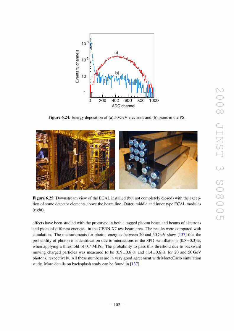
2008 JINST 3 S08005
a)
b)
ADC channel
Events
/5 c
ha
nnels
Figure 6.24: Energy deposition of (a) 50 GeV electrons and (b) pions in the PS.
Figure 6.25: Downstream view of the ECAL installed (but not completely closed) with the excep-tion of some detector elements above the beam line. Outer, middle and inner type ECAL modules(right).
effects have been studied with the prototype in both a tagged photon beam and beams of electronsand pions of different energies, in the CERN X7 test beam area. The results were compared withsimulation. The measurements for photon energies between 20 and 50 GeV show [137] that theprobability of photon misidentification due to interactions in the SPD scintillator is (0.8±0.3)%,when applying a threshold of 0.7 MIPs. The probability to pass this threshold due to backwardmoving charged particles was measured to be (0.9±0.6)% and (1.4±0.6)% for 20 and 50 GeVphotons, respectively. All these numbers are in very good agreement with MonteCarlo simulationstudy. More details on backsplash study can be found in [137].
– 102 –

2008 JINST 3 S08005
Table 6.4: Main parameters of the LHCb electromagnetic calorimeter. (*) Only 1536 channels areactive, instead of 1584, due to the clearance around the beam.
Inner section Middle section Outer sectionInner dimension, x× y, cm2 65×65 194×145 388×242Outer dimension, x× y, cm2 194×145 388×242 776×630Cell size, cm2 4.04×4.04 6.06×6.06 12.12×12.12# of modules 176 448 2688# of channels 1536∗ 1792 2688# of cells per module 9 4 1# of fibres per module 144 144 64Fibre density, cm−2 0.98 0.98 0.44
6.2.4 The electromagnetic calorimeter
The shashlik calorimeter technology, i.e. a sampling scintillator/lead structure readout by plasticWLS fibres, has been chosen for the electromagnetic calorimeter not only by LHCb but by a num-ber of other experiments [138, 139]. This decision was made taking into account modest energyresolution, fast time response, acceptable radiation resistance and reliability of the shashlik tech-nology, as well as the experience accumulated by other experiments [140–142]. Specific featuresof the LHCb shashlik ECAL are an improved uniformity and an advanced monitoring system. Thedesign energy resolution of σE/E = 10%/
√E⊕ 1% (E in GeV) results in a B mass resolution of
65 MeV/c2 for the B→ K∗γ penguin decay with a high-ET photon and of 75 MeV/c2 for B→ ρπ
decay with the π0 mass resolution of ∼ 8 MeV/c2.The electromagnetic calorimeter, shown in figure 6.25 (left), is placed at 12.5 m from the
interaction point. The outer dimensions of the ECAL match projectively those of the trackingsystem, θx < 300 mrad and θy < 250 mrad; the inner acceptance is mainly limited by θx,y > 25 mradaround the beampipe due to the substantial radiation dose level. The hit density is a steep functionof the distance from the beampipe, and varies over the active calorimeter surface by two orders ofmagnitude. The calorimeter is therefore subdivided into inner, middle and outer sections (table 6.4)with appropriate cell size, as shown in figure 6.25 (right).
A module is built from alternating layers of 2 mm thick lead, 120 µm thick, white, reflectingTYVEK16 paper and 4 mm thick scintillator tiles. In depth, the 66 Pb and scintillator layers forma 42 cm stack corresponding to 25 X0. The Moliere radius of the stack is 3.5 cm. The stack iswrapped with black paper, to ensure light tightness, pressed and fixed from the sides by the weldingof 100 µm steel foil.
The scintillator tiles are produced from polystyrene17 with 2.5% PTP18 and 0.01% POPOP19
admixtures. The scintillator tile production employs a high pressure injection moulding technique.Tile edges are chemically treated to provide diffusive reflection and consequently improved light
16TYVEK of type 1025D used, product of E.I. du Pont de Nemours and Company.17Polystherene in pellets, Polystyrol 165H, [Cn Hn], product of BASF AG, Badische Anilin- & Soda Fabrik Aktienge-
sellschaft, Carl-Bosch-Strasse 38, D-67056 Ludwigshafen, Germany, mailto:[email protected], p-Terphenyl, 1,4-Diphenylbenzene, [C6 H5 C6 H4 C6 H5], product of FLUKA(TM), Sigma-Aldrich Chemie
GmbH, CH-9470, Buchs, Switzerland, mailto:[email protected], 1,4-Bis(5-phenyl-2-oxazolyl)benzene, [C24 H16 N2 O2], product of FLUKA(TM), Sigma-Aldrich Chemie
GmbH, CH-9470, Buchs, Switzerland, mailto:[email protected].
– 103 –

2008 JINST 3 S08005
Figure 6.26: Hamamatsu R7899-20 phototube, light mixer and MuMetal magnetic shielding screen(left). Cockcroft-Walton voltage multiplier (right).
collection efficiency and prevent tile-to-tile light crosstalk for the inner and middle modules. Thetile-to-tile light yield fluctuation has an RMS smaller than 2.5%. The Pb plates are producedusing sheet-metal stamping. In order to ease handling of the lead plates during module assemblythe plates are covered with a 3µm thick layer of tin. Both the scintillator tiles and lead platesincorporate a pattern of precisely positioned holes that are needed for the traversing fibres. Thedemanding tolerances are ensured by injection moulding for the scintillator tiles and a punchingtechnique for the lead plates.
The light from the scintillator tiles is absorbed, re-emitted and transported by 1.2 mm diam-eter WLS Kuraray Y-11(250)MSJ fibres, traversing the entire module. In order to improve lightcollection efficiency the fibres are looped such that each traverses the module twice, the looped partremaining in a housing outside the front of the module. Fibre bending under uniformly distributeddry heat made it possible to produce fibre loops with radii as small as 10 mm, where the light lossis determined by the geometrical optics of reflection down the loop. When measured after the fi-bre loop, the light yield varies from loop to loop with an RMS of the spread of 1.6%. The fibresbelonging to each cell are bundled at the rear end of the module and polished.
The light is read out with Hamamatsu R7899-20 phototubes where the high voltage is pro-vided by a Cockcroft-Walton (CW) base (figure 6.26).
Before installation all ECAL modules underwent detailed quality control at various stages ofproduction. The final control was made with cosmic rays [143]. The standard deviations of themean energy deposition by a MIP in the ECAL module was measured to be 7.4%, 4.4% and 6.0%for the outer, middle and inner sections respectively. The number of photoelectrons recorded fora MIP and for electrons in the test beam was calculated using the measurements of the amplitudeand width of the LED signal. This method gives for the inner modules about 3100 photoelectronsper GeV of deposited energy, 3500 for the middle and 2600 for the outer modules. The differencesare due to the differing WLS fibre density in the inner, middle and outer modules and to the cellsize differences which influence the probability of photon absorption in the scintillating tiles.
Performance of the ECAL modules
The energy resolution and, in particular, the uniformity in response of the ECAL were studied atthe test beam [144]. Only a few percent of the scintillation light is registered by the phototubes
– 104 –

2008 JINST 3 S08005
Figure 6.27: Uniformity of response to 100 GeV/c2 muons of the inner module. The scan wasmade in 1 mm wide slices through the fibre positions (left) and in between two fibre rows (right).
after capture and re-emission in the WLS fibres; about half of this light is delivered by the WLSfibres close to the light’s origin. Some lateral nonuniformity in the light collection efficiency wasexpected from two sources: imperfect reflection from tile edges (the so-called global nonuniformityeffect), and a dependence on the emission point of the scintillating light with respect to the fibres(local or inter-fibre nonuniformity). The global nonuniformity depends on the mean light path,which is a function of tile transparency, edge reflection quality and fibre density. In addition themodule response at the edge is further degraded due to the presence of the stainless steel foilsbetween the active volumes of two adjacent modules. The local nonuniformity is affected by theinter-fibre distance and the diameter of the fibre.
The light collection efficiency was studied using test beam data and a dedicated MonteCarlosimulation of the light propagation and absorption in the plastic tiles which takes into account thetransparency of the scintillator as a function of wavelength, the tile-edge and TYVEK reflectionproperties and the WLS fibre absorption spectrum. The modules of the inner, middle and outersections were scanned using 100 GeV/c muons with a 1 mm transverse step. As shown in fig-ure 6.27, the measured inner module response is well described by MonteCarlo simulation. Shownare two different scans for the inner module, one using 1 mm wide slices through the WLS fi-bre positions (left plot), and the other between two fibre rows (right plot). In the outer modulesthe inter-fibre nonuniformity is slightly higher due to a factor of 1.5 larger fibre-to-fibre distance(15 mm instead of 10 mm for the inner and middle modules). The global nonuniformity of responsewas measured to be negligible for all module types. A slight increase of response in the vicinityof the module edges is explained by diffuse reflection from the boundary layer introduced by thededicated chemical treatment of the tile edges. The effect of signal loss in the dead material be-tween the modules is overcompensated by 8% at -20 and 20 mm, as visible in figure 6.27 (right).Electromagnetic showers of electrons and photons considerably reduce the inter-fibre nonunifor-mity of response compared to that measured for MIPs. The results of a lateral scan with 50 GeV/celectrons is shown in figure 6.28 for the inner and outer ECAL modules. The module response is
– 105 –

2008 JINST 3 S08005
Figure 6.28: Uniformity of response to 50 GeV/c electrons of the inner (left) and outer (right)modules. The scan was made in 1 mm wide slices through the fibre positions.
2
4
50 100
3
10
σ(E
)/E
(%
)
E (GeV)
Figure 6.29: The energy resolution as measured with electrons over a surface of (± 15 mm , ±30 mm) in an outer module.
uniform within 0.8%. The energy resolution of the ECAL modules has been determined at thetest beam. The parametrization σE/E =a/
√E⊕b⊕c/E (E in GeV) is used, where a, b and c stand
for the stochastic, constant and noise terms respectively. Depending on the type of module and testbeam conditions the stochastic and constant terms were measured to be 8.5% < a < 9.5% and b∼0.8% (see figure 6.29).
– 106 –

2008 JINST 3 S08005
Distance to PM (cm) Distance to PM (cm)
Lig
htyi
eld
Lig
htyi
eld
Figure 6.30: Scintillator (left) and WLS fibre (right) degradation and annealing effect after irradi-ation at LIL. The light yield (scintillator) and PMT current (fibres) are shown vs. the distance tothe PMT (the shower maximum position corresponds to a distance from the PMT of 42 cm).
Radiation resistance of the ECAL modules
Detailed measurements and simulation studies were performed to determine the degradation ofthe ECAL resolution due to radiation damage of the optical components. The expected annualradiation dose at the shower maximum for the ECAL modules closest to the beampipe is 0.25 MRadassuming a luminosity of 2× 1032cm−2s−1 and 107 s per nominal year. The optical componentsof the ECAL modules, namely the 40×40mm2 scintillating tiles and WLS fibres, were irradiatedat the LEP Injector Linac (LIL) at CERN with electrons of 500 MeV energy. The total irradiationdose was as large as 5 MRad at a dose delivery rate of 10 Rad/s; that is 200 times higher than therate expected at LHCb. Figure 6.30 shows the degradation in light yield and transparency, and thesubsequent annealing of the irradiated components as a function of the distance to the phototube. Inorder to determine the degradation of the energy resolution due to irradiation, the energy responseof the ECAL module was simulated using the expected longitudinal dose profile and the measureddegradation of the scintillating tiles and WLS fibres in accordance with figure 6.30. The effectsinduced by irradiation of 2.2 MRad leads to an increase of the constant term from 0.8% up to 1.5%.Such a degradation in the ECAL resolution is expected after about eight years of operation undernominal conditions and is acceptable. However, taking into account simulation uncertainties onthe expected radiation doses at the LHC, the ECAL detector was designed such that the modulesclosest to the beampipe could be replaced if this should become necessary.
6.2.5 The hadron calorimeter
The LHCb hadron calorimeter (HCAL) [1, 121] is a sampling device made from iron and scintillat-ing tiles, as absorber and active material respectively. The special feature of this sampling structureis the orientation of the scintillating tiles that run parallel to the beam axis. In the lateral direction
– 107 –

2008 JINST 3 S08005
Figure 6.31: View from upstream of the HCAL detector installed behind the two retracted ECALhalves in the LHCb cavern (left). A schematic of the internal cell structure (right). The explodedview of two scintillator-absorber layers illustrates the elementary periodic structure of a HCALmodule.
tiles are interspersed with 1 cm of iron, whereas in the longitudinal direction the length of tiles andiron spacers corresponds to the hadron interaction length λI in steel. The light in this structure iscollected by WLS fibres running along the detector towards the back side where photomultipliertubes (PMTs) are housed. As shown in figure 6.31, three scintillator tiles arranged in depth are inoptical contact with 1.2 mm diameter Kuraray20 Y-11(250)MSJ fibre [145] that run along the tileedges. The total weight of the HCAL is about 500 tons.
The HCAL is segmented transeversely [146] into square cells of size 131.3 mm (inner section)and 262.6 mm (outer section). Readout cells of different sizes are defined by grouping together dif-ferent sets of fibres onto one photomultiplier tube that is fixed to the rear of the sampling structure.The lateral dimensions of the two sections are ±2101 mm and ±4202 mm in x and ±1838 mm and±3414 mm in y for the inner and outer section, respectively. The optics is designed such that thetwo different cell sizes can be realized with an absorber structure that is identical over the wholeHCAL. The overall HCAL structure is built as a wall, positioned at a distance from the interactionpoint of z=13.33 m with dimensions of 8.4 m in height, 6.8 m in width and 1.65 m in depth. Thestructure is divided vertically into two symmetric parts that are positioned on movable platforms,to allow access to the detector. Each half is built from 26 modules piled on top of each other in thefinal installation phase. The assembled HCAL is shown in figure 6.31(left). The absorber structure,shown in figure 6.31 (right), is made from laminated steel plates of only six different dimensionsthat are glued together. Identical periods of 20 mm thickness are repeated 216 times in the mod-ule. One period consists of two 6 mm thick master plates with a length of 1283 mm and a heightof 260 mm that are glued in two layers to several 4 mm thick spacers of 256.5 mm in height andvariable length. The space is filled with 3 mm scintillator.
20KURARAY Corp., 3-10, Nihonbashi, 2 chome, Chuo-ku, Tokyo, Japan.
– 108 –

2008 JINST 3 S08005
The periodic structure of the system is designed to be self supporting and uniformly instru-mented with no dead zones. To facilitate the construction of modules, each module is subdividedinto eight sub-modules that have a manageable size for assembly from the individual absorberplates. A total of 416 submodules have been produced to form 52 modules needed to build upthe two halves of the HCAL structure. The mechanical structure is reinforced by welded crossmembers and is completely independent from the optical instrumentation.
The optics of the tile calorimeter consists of three components: the scintillating tile, theWLS fibre and a small square light mixer just in front of the photo-multiplier entrance window.The scintillating light propagates through the 3 mm thick tile to its edges where it is collected by1.2 mm diameter WLS fibres.
In total more than 86000 tiles of two different dimensions have been produced by the costeffective casting technology using polystyrene as a base and two dopants: paraterphenyl (PTP,1.75%) and POPOP (0.05%). Each tile of 197× 256 mm2 or 197× 127 mm2 is wrapped in a120–150 micron thick TYVEK envelope.21
The edges of a tile are wrapped in such a way that the fibre running along the edge can beeasily inserted between the envelope and the tile edge during the module optics assembly. Thisreflective envelope avoids light crosstalk between adjacent edges of the small tiles, enhances thelight collection in the wavelength shifting fibre and in addition protects the optical reflective sur-face of the tiles. Each fibre collects light from three scintillator tiles arranged along the showerdevelopment direction. There are a total of 50k fibres in the HCAL with an identical length of1.6 m. In order to increase the light collection efficiency both fibre ends were cut with a diamondmill, and opposite to the photomultiplier end coated with a layer of reflective aluminum depositedin vacuum. The reflectivity of all fibres was checked on a measuring stand specially designed forthat purpose. All fibres were measured to have a mirror reflectivity in the range of (85± 10)%.The light propagates along the fibre by total reflection but tiles located further from the PMT yieldless light due to attenuation in the WLS fibre. To compensate for this effect, the tile-fibre opticalcontact was progressively reduced for the different tile layers in depth. The last tile layer closestto the PMT has an optical contact reduced by 22% as compared to the first layer at the entry of theHCAL. This precaution minimizes the difference in response between tiles, providing light to thesame PMT with a uniformity at a level of a few percent.
Each cell is read out by one photomultiplier tube that is attached to the rear mechanicalstructure of the module. The optical connection between the fibre bundle and the photomultiplieris ensured by a 35 mm long light mixer of square shape. To shield the photomultiplier tube fromthe stray magnetic field the tube, including the light mixer, is housed inside a 3 mm thick iron tubeand MuMetal foil. The influence of the magnetic field on a PMTs performance was studied duringthe LHCb magnet measurement. A field of approximately 2 mT along z, but negligible in x and y,is expected in the region of the HCAL PMTs [23]. No variation of the monitoring LED signal hasbeen observed within about 0.1% measurement error while switching on and off the magnet fullpower and when changing its polarity.
In order to monitor the HCAL stability an embedded self-calibrating scheme with 137Csgamma source has been implemented [147]. A capsule of 10 mCi activity can be transported
21TYVEK of type 1057D used, product of E.I. du Pont de Nemours and Company.
– 109 –

2008 JINST 3 S08005
RMS (%)
Num
ber
of cells
300
250
200
150
100
50
00 2 4 6 8 10 12 14 16 18 20
Angle (degree)
<E>
(G
eV
)Figure 6.32: The distribution of RMS lightyield for tiles read out by the same PMT.
Figure 6.33: The angular dependence of theHCAL prototype response at different energies.
through a stainless steel pipe fed through all tiles. The source is encapsulated in a 2 mm diam-eter, 4 mm long stainless steel tube that is welded at both ends. The hydraulic driving system filledwith distilled water includes a garage to store the source, and computer controlled pump and valvesthat allow reversal of the water flow direction. A separate readout circuit measures the integratedanode current every 5 ms resulting from the scan of a half detector when the source propagatessequentially through 26 HCAL modules with an average velocity of about 20–40 cm/s. This pro-cedure takes less than one hour. The method was widely used both during construction and inthe final test of modules before installation in the cavern. Furthermore this system is used for theabsolute calibration of the HCAL in-situ.
Beam tests performed with several HCAL modules allow the correspondence between theanode current induced by the radioactive source and the measured beam particle energy to bedetermined. Being absolutely calibrated the HCAL provides a unique possibility to cross-checkthe calibration of the upstream detectors (e.g. electromagnetic calorimeter) by comparison of theaverage energy deposition of the hadronic shower in the corresponding cells of two detectors. Theenergy sharing function varies slowly over the calorimeter surface and can be extracted from theMonteCarlo simulation.
The tile response during optics assembly was monitored using the radioactive source system.A maximum deviation of 20% from the average anode current for tiles grouped to the same PMTwas accepted. The tiles and fibres not satisfying this requirement have been replaced. A distributionof the RMS of tile responses within the groups coupled to the same PMT is shown in figure 6.32.The mean value of this distribution is 4.7%.
– 110 –

2008 JINST 3 S08005
0 5 10 15 20 25 30 35 40
Channel
120
100
80
60
40
20
0
full
tile
half
tile
Nun
ber o
f p.e
./G
eV
Figure 6.34: The light yield for the HCAL module measured in the test beam. The left part ofthe plot corresponds to 8 big cells of 26× 26 cm2. The other 32 cells comprise half-size cells of13×13 cm2.
Performance of the HCAL modules
The performance of the HCAL has been studied with prototypes [148] and continuously checkedduring module assembly using the CERN SPS test beam [149]. The dependence of the HCALresponse on the angle of the incoming particle has been studied by rotating the detector between0 and 15 around a vertical axis that traverses the HCAL close to the average shower maximum.Figure 6.33 shows the response of the 5.6 λI long prototype for pion energies between 10 GeV and80 GeV. From a lateral scan of the particle beam across the prototype front surface the uniformityin response is measured to be well within ±3%.
During the assembly process [150] tiles with similar properties were grouped into the samecell to minimize nonuniformities. The light yield of all cells from one typical module is shown infigure 6.34. In total five modules (out of 52) were tested in the beam with an average light yield of105 p.e./GeV.
The moderate requirements for the HCAL energy resolution allow the ratio of the active topassive material in the detector to be as low as 0.18. Furthermore, owing to the limited spaceavailable, the length of the HCAL has been chosen at 5.6 λI . The upstream ECAL adds a further1.2 λI . Beam-test measurements were compared in detail with results using different softwarepackages for the simulation of the hadronic shower development. The energy response to 50 GeVpions is shown by the hatched histogram in the left-hand plot of figure 6.35. The tail towards lowenergies due to leakage of the shower is easily seen. However, this tail is not a concern for thehadron trigger performance since it only introduces some minor inefficiency for high ET signalevents but does not affect the rejection of low ET minimum-bias events. The black dots showthe result of a MonteCarlo simulation that is in good agreement with the data, when using theGEANT (MICAP+FLUKA) interface. The energy resolution has been determined by fitting theenergy spectrum with a gaussian distribution bounded by ±2.5σ . The resolution extracted from afit to the data at several energies is σE/E = (69±5)%/
√E⊕ (9±2)% (E in GeV) as shown in the
right-hand plot of figure 6.35.
– 111 –

2008 JINST 3 S08005
10
12
14
16
18
20
22
24
26
28
30
0 20 40 60 80 100
Energy (GeV)R
eso
luti
on
()
TEST-BEAM DATA
GEANT 3.21 (GEISHA+FLUKA)
GEANT 3.21 (MICAP+FLUKA)
(69 5)% / √E + (9±2) % (fit on data)±
%
Figure 6.35: Left: energy response for 50 GeV pions from test-beam data (hatched) and fromsimulation (dots). Right: HCAL energy resolution, both for data and for simulation with threedifferent hadronic simulation codes. The curve is a fit to the data.
Time (ns)
Pu
lse
sig
na
l
(mV
)
-5 5 15 25 35 45
0
-100
-200
-300
-400
-500
-600
Figure 6.36: The average signal pulse shape of 30 GeV electrons in tile layers at different depths.
Another important feature of the HCAL is its signal timing properties. A precise signal shapemeasurement has been done with an electron beam of 30 GeV hitting layers of tiles at differentdepths. For this purpose the HCAL modules have been rotated by 90 and moved transversely withrespect to beam line. Average pulse shapes of the detected signals are shown in figure 6.36. The
– 112 –

2008 JINST 3 S08005
variation of the shape is due to light reflection from the mirror at the end of the fibre opposite to thePMT. For layer 1, for example, the direct and reflected light reach the PMTs simultaneously, butfor layer 6, closest to the PMT, the direct light reaches the photocathode earlier than the reflectedone by the propagation delay in the 1.2 m long WLS fibre.
Radiation resistance of the HCAL modules
A comprehensive study of the degradation under irradiation has been performed for all opticalcomponents of the HCAL [151]. Scintillating tiles and WLS fibres have been irradiated at the IHEP70 GeV proton synchrotron near the internal target area to get realistic environmental conditionsas expected during the LHC operation. The transparency of tiles degrades by 25% after 250 kRadirradiation, but then steadily decreases by a further 20% with irradiation up to 1.4 MRad. Therelative light yield after irradiation shows almost the same behaviour. Another important effect isthe radiation degradation of the WLS fibres which introduces a longitudinal nonuniformity of thecalorimeter response [152]. For example, the attenuation length in the WLS fibre degrades by 30%after irradiation with a dose of about 0.5 MRad, which corresponds to 10 years of operation for themost central cells of the HCAL at nominal luminosity of 2×1032cm−2s−1. As a result of the sameamount of irradiation, the constant term of the HCAL resolution degrades by 20%. To monitorthe fibres radiation damage we intend to use the embedded calibration system with the radioactivesource, that allows measurement of the response from each tile along the detector depth with a fewpercent accuracy.
6.2.6 Electronics of ECAL/HCAL
Because of the similarity of input signals and functionalities, it has been decided to use a com-mon electronic system for the ECAL and HCAL. This system is based on a deadtimeless and lowpedestal integrator system using delay lines, followed by ADCs and pipeline buffers. Each card isconnected to 32 channels of the ECAL or the HCAL. After digitization in the front-end card thedata is processed further and sent to a trigger validation card. The data is also pipelined and storedon the front-end card, and then sent through the back plane to a calorimeter readout card (CROC).
Pulse shaping and front-end chip
In order to take advantage of the inherent speed of the scintillator and WLS based calorimetersystem the electronic system is capable of measuring every bunch crossing independently of signalsfrom associated neighboring bunch crossings (pileup). The PMT pulses therefore are shaped toeliminate the small tail of pulses extending beyond 25 ns. A schematic of the PMT signal shapingand of the front-end chip is shown in figure 6.37 for HCAL. The PMT pulse is shortened by aclipping line which is a cable for the HCAL and a delay chip for the ECAL due to lack of space.The length of the line is typically one metre, giving a FWHM of about 10 ns. The resistor load atthe end of the line is adjusted to obtain a return to a 0 Volt level after clipping. Due to fluctuations inthe number of photoelectrons as a function of time, a fluctuation is also present in the shaped pulse.However the effect is small, especially for the ECAL where about 3000 photoelectrons producedper GeV. The pulses are then sent along 10 m of coaxial cables to the front-end cards which reside in
– 113 –

2008 JINST 3 S08005
BICMOS 0.8µm Integrated Circuit4 Channels per chip
Figure 6.37: Schematic of the PM signal shaping and of the front-end chip.
crates above the calorimeters. The pulse-shape distortion produced by the cable is compensated tofirst order by a pole-zero circuit placed after the integrator. The first element of the pole-zero card isa front-end chip which contains a buffer amplifier and an integrator. To discharge the integrator thesame pulse is subtracted in a buffer amplifier after a 25 ns delay obtained by a lumped-element delayline. Simulated input and output pulses using a 10 ns rectangular pulse are shown in figure 6.38, aswell as an average 80 GeV PM HCAL pulse (averaged over 1000 measurements on a digital scope)and the resulting integrated pulse.
The schematic of the analog chip is given in figure 6.39. The circuit has been realized inAMS 0.8 µm BICMOS technology. A typical noise of 150 µV has been obtained after a 25 nsintegration, which should correspond to a total noise of less than one ADC count. As measuredwith prototypes, the tail of the pulse integral in the next sampling is about 2% with an additionalfluctuation of 1%. The impact of the amplifier noise on the physics performance is found to benegligible compared to the energy resolution of the ECAL.
The ECAL/HCAL front-end board
Figure 6.40 shows the block diagram of the 32 channel front-end board. It is a 9U board usingVME mechanics with a specialized serial bus used for Experiment Control System purposes (seesection 8.4). The pulses from the front-end chip, described above, are sent to 12-bit ADCs. Thepulses after integration are flat (within 1%) over ±2 ns around the maximum. To strobe at themaximum of the pulse, the different delays in the photomultipliers have to be compensated. This isachieved by adjusting the clock of each ADC by a delay chip to an accuracy of 1 ns. The digitizedoutput of the ADCs are then resynchronized to a common clock (per card) in a register at the inputof the next chip. The pulses at the integrator output can be subject to baseline shift and to the
– 114 –

2008 JINST 3 S08005
Figure 6.38: Left: simulated input pulse of a 10 ns rectangular pulse and the corresponding outputpulse of the integrator: buffer output current before integration (top) and output integrated signal(bottom). Right: 80 GeV HCAL signals. The upper figure shows the PM signal with and withoutclipping, the lower one shows the same clipped signal at the output of the integrator.
Figure 6.39: Schematic of the analog chip.
influence of low frequency pickup noise which would cause slow variation of the ADC pedestal.These variations are cancelled through a digital differentiation by subtracting the digitization in a
– 115 –

2008 JINST 3 S08005
Figure 6.40: Block diagram of the front-end board, for ECAL and HCAL.
preceding sample (25 ns before). This subtraction also defines the effective integration time of theamplifier and therefore limits the integrated thermal noise from the buffer amplifier. To decreasethe possibility of subtracting a signal present in the same channel, the quantity subtracted is actu-ally the smallest of the two preceding measurements. Even at the highest occupancy, about 5%, theprobability of subtracting a significant signal is therefore reduced to less than 0.25%. Simulationshave shown that this procedure introduces negligible deterioration of energy and position mea-surements [129]. However the procedure introduces a pedestal shift of about 40% of the 40 MHznoise (i.e less then one ADC count) and an increase of the 40 MHz noise by 16%. The subtractionof the smallest of the two preceding samples is performed in 8 dedicated anti-fuse based FPGAs(cf. section 7.1.3) 22 called FE-PGAs, each of these being used to process four ADC channels [153].Actually each FE-PGA has, for each ADC channel, four functional blocks. The first one processesthe input ADC data, as described above. The second block produces the trigger data, converting the12 bits of the ADC to 8 bits by a simplified multiplier with an adjustable 8 bits calibration constant.The third block is in charge of storing the data (12 ADC bits and 8 trigger bits per ADC, 80 bitsper FE-PGA), during the L0 latency, and upon L0-Yes store again the data in a derandomizer andsend them as four successive groups of 20 bits to the SEQ-PGA. The last block of the FE-PGApermits injecting test values at the input, in place of the ADC values, in order to check the properbehaviour of the card.
22AX250 anti-fuse PGA from ACTEL.
– 116 –
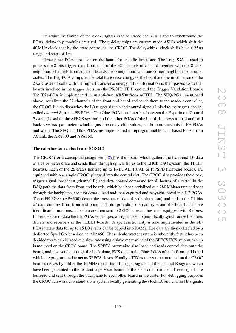
2008 JINST 3 S08005
To adjust the timing of the clock signals used to strobe the ADCs and to synchronize thePGAs, delay-chip modules are used. These delay chips are custom made ASICs which shift the40 MHz clock sent by the crate controller, the CROC. The delay-chips’ clock shifts have a 25 nsrange and steps of 1 ns.
Three other PGAs are used on the board for specific functions: The Trig-PGA is used toprocess the 8 bits trigger data from each of the 32 channels of a board together with the 8 side-neighbours channels from adjacent boards 4 top neighbours and one corner neighbour from othercrates. The Trig-PGA computes the total transverse energy of the board and the information on the2X2 cluster of cells with the highest transverse energy. This information is then passed to furtherboards involved in the trigger decision (the PS/SPD FE Board and the Trigger Validation Board).The Trig-PGA is implemented in an anti-fuse AX500 from ACTEL. The SEQ-PGA, mentionedabove, serializes the 32 channels of the front-end board and sends them to the readout controller,the CROC. It also dispatches the L0 trigger signals and control signals linked to the trigger, the so-called channel B, to the FE-PGAs. The Glue-PGA is an interface between the Experiment ControlSystem (based on the SPECS system) and the other PGAs of the board. It allows to load and readback constant parameters which adjust the delay chip values, calibration constants in FE-PGAsand so on. The SEQ and Glue PGAs are implemented in reprogrammable flash-based PGAs fromACTEL the APA300 and APA150.
The calorimeter readout card (CROC)
The CROC (for a conceptual design see [129]) is the board, which gathers the front-end L0 dataof a calorimeter crate and sends them through optical fibres to the LHCb DAQ system (the TELL1boards). Each of the 26 crates housing up to 16 ECAL, HCAL or PS/SPD front-end boards, areequipped with one single CROC, plugged into the central slot. The CROC also provides the clock,trigger signal, broadcast (channel B) and slow control command for all boards of a crate. In theDAQ path the data from front-end boards, which has been serialized at a 280 Mbits/s rate and sentthrough the backplane, are first deserialized and then captured and resynchronized in 4 FE-PGAs.These FE-PGAs (APA300) detect the presence of data (header detection) and add to the 21 bitsof data coming from front-end boards 11 bits providing the data type and the board and crateidentification numbers. The data are then sent to 2 GOL mezzanines each equipped with 8 fibres.In the absence of data the FE-PGAs send a special signal used to periodically synchronize the fibresdrivers and receivers in the TELL1 boards. A spy functionality is also implemented in the FE-PGAs where data for up to 15 L0 events can be copied into RAMs. The data are then collected by adedicated Spy-PGA based on an APA450. These dcalorimeter system is inherently fast, it has beendecided to ata can be read at a slow rate using a slave mezzanine of the SPECS ECS system, whichis mounted on the CROC board. The SPECS mezzanine also loads and reads control data onto theboard, and also sends through the backplane, ECS data to the Glue-PGAs of each front-end boardwhich are programmed to act as SPECS slaves. Finally a TTCrx mezzanine mounted on the CROCboard receives by a fiber the 40 MHz clock, the L0 trigger signal and the channel B signals whichhave been generated in the readout supervisor boards in the electronic barracks. These signals arebuffered and sent through the backplane to each other board in the crate. For debugging purposesthe CROC can work as a stand alone system locally generating the clock L0 and channel B signals.
– 117 –

2008 JINST 3 S08005
Calorimeter specific TELL1 features
The TELL1 boards of LHCb are described in section 8.2. The specifications of the calorimetersare described in [154].
A preprocessor FPGA (PP-FPGA) collects and treats the incoming data from front-end boardssent by the CROC to the TELL1 board through an optical receiver mezzanine card (O-Rx card)which ensures the optical to electrical conversion and data synchronization. The PP-FPGA treatsthe event according to the detector identification (ECAL/HCAL or PS/SPD). Inside each PP-FPGA,a zero suppression is performed on the events during physics runs for PS/SPD data and a datacompression without loss of information for ECAL and HCAL data [155]. The output data ofeach PP-FPGA are collected by the SyncLink-FPGA which then packs them in a Multiple EventPacket (MEP). For each event, the SyncLink-FPGA gives the trigger type of the run (physics orcalibration) to the PP-FPGA. The MEPs are sent to the DAQ through a Gigabit-Ethernet (GBE)card. The output bandwidth of the GBE limits the use of one among the two O-Rx cards for ECALand HCAL and thus two PP-FPGAs among the four. The two O-Rx cards are used for PS/SPD. Incase of no data and/or synchronization error from the optical input links in the O-Rx card, an errorbank is optionally generated (it is suppressed by default due to bandwidth limit). In order to keeptrack of these errors, a minimal information is kept in each event header.
The LED monitoring system is described in section 6.2.8. During calibration runs the LEDdata are not affected by the zero suppression, and only non-zero values are kept for PS/SPD. Duringphysics runs, the data coming from the PIN boards (FE boards devoted to the PIN diode signals ofECAL/HCAL) are ignored.
6.2.7 Electronics of PS and SPD detectors
The signal of the PS and SPD has about the same duration as the ECAL and HCAL pulses; on av-erage 85% of the charge is obtained in 25 ns. However, since the average number of photoelectronsis only about 25 per MIP, there are very large fluctuations in the signal pulse shape [156]. It wastherefore considered unreasonable to try to implement the delay-line pulse shaping used for theECAL/HCAL. On the other hand, since the useful dynamic range of the PS is typically only from1 MIP to 100 MIP, an ADC with only 10-bits can be used and pedestal stability is not as importantas for the ECAL/HCAL electronics, although it is important to integrate the signal over a time aslong as possible within the 25 ns limitations. The phototube chosen to detect the light from the PSand SPD fibres is a 64 channel multi-anode PM. The HV is common to all 64 channels and there isa nonadjustable gain dispersion among these channels of a factor of 3, which however is constantin time. For this reason it was decided to introduce a Very Front End (VFE) stage of integration onthe back of the phototubes in order to compensate the gain variation using a digital correction of afactor up to 2 in the front-end electronics.
The PS very front-end design
The solution adopted for the PS is to alternate every 25 ns between two integrators and to reset oneintegrator when the other one is active. The signal is sampled by track-and-hold circuits and theoutput of the active integrator is chosen by a multiplexer, followed by a twisted-pair cable driver.
– 118 –

2008 JINST 3 S08005
100!
buffer
buffer
T/H
T/H
clockdivisor
clock reset40MHz
50!
50!input−
input+
multiplexercurrentconvoyer
Figure 6.41: Schematic of the PS Very Front-End integrator (top) and a photograph of the integratorcard mounted behind the MAPMT (bottom).
All circuit elements are functioning in differential mode to improve stability and pickup-noiserejection. The circuit design is shown in figure 6.41 and its detailed description is given in [157].The phasing of the clock with respect to the signal determines the start of the integration. Sincethe length of the 64 fibres connected to a given PM are identical and the delay inside the PM isidentical within a fraction of 1 ns, it is sufficient to have one clock adjustment (in steps of 1 ns)per phototube. The amplifier integrator circuit is realized in monolithic AMS 0.8 µm BICMOStechnology with 4 channels implemented per chip. The dynamic range is 1 Volt with a noise of1 mV. Sixteen chips are grouped in a card on each phototube. The outputs of each chip (4 channels)are sent through 27 m long ethernet cables23 with RJ45 connectors to the ADC located on the FEboard. Two clock and two reset signals delivered by the corresponding FE board are received bythe VFE board through a cable of the same type as those used for the signal.
23from Kerpen company, Geramny.
– 119 –

2008 JINST 3 S08005
Figure 6.42: Left: block diagram of the SPD VFE card. Right: picture of the VFE assembly wherethe components are a) PMT base board, b) ASICs board and c) FPGA board.
The SPD very front-end and control board design
The SPD function is to discriminate between charged particles and neutrals in a detector whichmatches the preshower and ECAL cell size. The SPD signals are obtained, as in the case of the PS,from 64 channel multianode photomultipliers. The main difference of specification is that thereis no compelling reason to perform pulseheight analysis on SPD signals. It was therefore decidedto use a simpler solution with a simple discriminator output and a threshold set at 0.5 MIP thusobtaining 98% efficiency on charged particles [131, 137]. The principle of the design is shownin figure 6.42 and described in [127]. Although the functional architecture of a signal processingchannel is similar to that of the PS, the circuits have been designed for the SPD specifically [158,159]. The main architectural difference is the inclusion of an on chip pile-up compensation systemand a comparator. The pile-up compensation system takes a tunable fraction of the integratoroutput at the current period and stores it on a track and hold circuit. This cancels on average thecharge delivered by a pulse in the time interval between 25 and 50 ns after its start. The referencethreshold value is set by a 7-bit DAC. The integration of each channel uses an independent DAC tocompensate the offsets and the gain nonuniformity of the PMT. The circuit is realized in the AMSBICMOS 0.8 µm technology with 8 channels per chip. There are two external (not on-chip) DAC,with I2C interface to set some analogue references for the signal processing part. The control unit,the digital processing and clock divider used to obtain the 20 MHz clock that controls the ASICsare implemented in a reprogrammable FPGA, the ProASIC Plus ACTEL APA300. Triple votingregisters (TVRs) are used to minimize signal event upset (SEU) errors. The digital processingconsists of mapping PMT channels to given serializer channels to match the PS and SPD detectorcell and injecting arbitrary patterns to test the detector data flow. The 64 channels and the 20 MHzclock are sent via standard shielded twisted pair (SSTP) LAN cables to the PS/SPD FE board,by means of 4 serializer chips (DS90CR215) with 3 data pairs and 1 clock pair each, requiring aserializing factor of 7. Control boards provide the VFE cards with links to the ECS and the timingand fast control (TFC) system. The boards are located in the FE crates. Two boards are needed foreach of the 8 crates corresponding to the PS/SPD subsystem.
– 120 –

2008 JINST 3 S08005
The PS/SPD front-end board
The PS/SPD front-end boards implement functions similar to the HCAL/ECAL boards i.e an ADCfor the preshower signal, pedestal correction and gain calibration, preparation of the trigger infor-mation, pipeline storage and selection of data for readout upon reception of trigger signals. ThePS/SPD board handles 64 PS data channels for raw data readout and trigger purposes, and 64SPD single bit trigger channels. The PS raw data dynamic range corresponds to 10 bits, codingenergy from 0.1 MIP(1 ADC count) to 100 MIPs. A general overview of the board is given in fig-ure 6.43 for the PS. An identical board is used for the SPD. Its general architecture is similar to theECAL/HCAL boards with five major components:
• An analog block receiving the 64 analog PS channels from the VFE part and digitizing them.Each channel is composed of a fully differential operational amplifier followed by a 10-bit40 MHz differential ADC. A synchronization signal (clock and reset) is sent to the VFE.
• A processing block made of 8 identical FE PGAs. Each of them is in charge of processing8 PS channels. After applying corrections for pedestal subtraction, gain adjustment andpile-up, the 10-bit data are coded into an 8-bit floating format. A trigger bit is producedfor each channel by applying a threshold on the corrected data. Eight SPD channels arealso received. Two PS and SPD channels are packed together, stored and retrieved after L0.Two blocks of memory per two channels are used in each FE PGA for the L0 pipeline andderandomizer. The processing block is very resource consuming. Since the VFE comprisestwo interleaved integrators working in alternance, the gain and offset corrections have tobe applied differently for two consecutive events leading to two effective subchannels perphysical channel. Also the data inputs, 8 SPD channels of 1-bit and 8 PS channels of 10 bitsare important. Consequently, the FE PGA chosen was the AX1000 of the ACTEL anti-fusetechnology.
• A trigger block made of one Trig-PGA. It handles the processing for the production of the L0information. The block receives the address of each cell and its local maximum of transverseenergy from the ECAL Front End Board (FEB). As the ECAL electronics is organized into32 channel boards, each 64 channel PS/SPD FEB is seen by the system as two 32 channelhalf boards, each receiving its own request address. The Trig-PGA is an APA450 of theACTEL ProASIC plus Flash based FPGA family.
• A SEQ PGA builds the data block after a L0-Yes signal, and sends it to the CROC. It alsoissues control and synchronization signals for the other 8 FE PGAs and the Trig-PGA.
• A SPECS slave called GLUE PGA handling all the I2C communication of the board. Thelast two blocks, SEQ PGA and GLUE PGA, are identical to the ones of the ECAL/HCALFE electronics and are described in reference [128].
All registers holding permanent information are radiation protected in static mode by triplevoting and, during data transfers, by Hamming code.
– 121 –

2008 JINST 3 S08005
Figure 6.43: Schematic of the front-end board for the PS.
6.2.8 Monitoring and high voltage system
The calorimeter High Voltage (HV) and LED light intensity control systems share a common con-trol board, the HV-LED-DAC board, that interfaces them to the Experiment Control System (ECS).
The High Voltage system
All calorimeter subdetectors are equipped with Hamamatsu photomultipliers. Eight thousandR7899-20 tubes are used for ECAL and HCAL and two hundred 64 channels multi-anode R7600-00-M64 for the SPD/PS detectors. All PMTs passed quality checks on dedicated test benchesbefore installation on the detectors. The quality requirements included a better than 5% linearityand better than 3% gain stability as a function of rate, a low dark current and, for the SPD/PSPMTs, pixel-to-pixel uniformity of better than 1 to 3 (minimum to maximum) and crosstalk of lessthan 2%.
The HV system for the PMTs (figure 6.44) is based on a Cockroft-Walton (CW) voltageconverter located on the base of each PMT and controlled by HV-LED-DAC control boards locatedin a few boxes distributed over the detector periphery and connected to the (ECS) by a SPECS [160]serial bus. For the SPD and PS the CWs and control boards are located in a VME crate on top ofthe ECAL and the HV is distributed to the PMTs with cables. The maximum HV is 1500 V forECAL and HCAL and 800 V for SPD and PS. The CW base [161] is a reoptimized and radiationhard version of the one used in the HERA-B experiment [162]. It is implemented on a 25 mmx 60 mm CW board and consists of 22 multiplication stages, a control operational amplifier, an
– 122 –

2008 JINST 3 S08005
Figure 6.44: An overview of the High Voltage system of the calorimeter.
oscillator of 50 kHz and fast transistor switches. It features individual and precise gain adjustmentof each PMT, effective operation at high background anode current, low power dissipation and onlylow voltage (± 6V) power supplies. It requires, in addition, 100 V which is converted locally to ahigh voltage in the 100–2000 V range selectable through a 0 to 5V control voltage supplied by thecontrol board. This conversion, being made locally for ECAL and HCAL, minimizes the numberof high voltage cables and connectors. The characteristics of the CW are a gain drop of less than2% for anode currents as high as 12 µA, a voltage ripple of less than 200 mV, a spread of outputvoltages of about 1% and a power consumption of less than 130 mW. Each HV-LED-DAC boardcan control 200 CWs and consists of a mother board and four mezzanine cards. A SPECS slavemezzanine is used for interconnection to the ECS system. The 200 PMTs are controlled by five 40-channel HV control signal generating cards using 12-bit DAC integrated circuits. A control logicboard equipped with a radiation tolerant FPGA ACTEL APA075 provides an interface betweenthe ECS and the 200 DAC signal generating integrated circuits. This board also allows automatedmonitoring and ramp-up of the high voltage. The fourth mezzanine card generates a 16 channelLED intensity control signal.
The LED monitoring system
The energy calibration of each cell of the ECAL calorimeter is obtained during data-taking by avariety of methods, such as monitoring their response to electrons, π0’s and minimum ionizingparticles. ECAL and HCAL stability is monitored using LEDs, in order to obtain the best energyresolution essential for both triggering and reconstruction issues. The concept of the sytem is out-lined in figure 6.45. Each cell of the four subdetectors is illuminated by an LED. They are triggeredby LED drivers (labeled LED in figure 6.45) and their intensity controlled by the HV-LED-DACboards. Multichannel LED Trigger Signal Boards (LEDTSB) perform the overall control and ad-just the timing. For SPD and PS an individual LED is located on each tile and illuminates thePMT through the scintillator. Groups of 16 LEDs are controlled by 770 LED drivers located on thesupermodules which are fired by 100 trigger channels.
On ECAL, LEDs are located in light-tight boxes situated above and below the calorimeter.
– 123 –

2008 JINST 3 S08005
LEDTSB CROC FEBs
TTCrx
SPECSslave
Bchannel
CLK
PIN withAmplifier PMT
LED
8
Front-End Crate
Time alignmentcircuits
1
2
3
4
5
6 Inner
Middle
Outer
Figure 6.45: A sketch of the LED monitoring of the calorimeter.1: FE crate backplane over whichthe monitoring trigger request is transmitted, 2: LED trigger pulse cable, 3: Clear fibre to cell, 4:PMT signal cable, 5: Clear fibre to PIN diode, 6: PIN signal cable.
Each LED illuminates 9 or 16 cells via clear fibres routing the light to a connector at the front ofeach cell, and from there via a second clear fibre traversing the module and conducting the lightdirectly through the light mixer to the PMT. Each LED also illuminates a PIN diode for monitoringthe stability of the LED light output. There are 456 LEDs, each controlled by the LED driver, and124 PIN diodes so that the LEDs sharing a PIN can be fired at different times.
Each HCAL module is equipped with two LEDs each illuminating every cell in the module.Since the PMTs in a module have different gains, which depend on the average momentum of theparticles they are detecting, the light output of the two LEDs is set in the ratio of 1:4. Clear fibresbring the light of both LEDs to each PMT via its light mixer. One PIN diode monitors the stabilityof each LED. The 2 LEDs in each of the 52 modules illuminate 16 or 40 cells and are controlledby 104 LED drivers.
A LED monitoring sequence is initiated by the Readout Supervisor (RS) upon request andtransmitted to the LEDTSBs via the CROCs and the FE crate backplane. The LEDTSBs are locatedin the front-end crates on the calorimeter platforms and each controls 64 LED drivers. A total of686 LED drivers in the system therefore require 12 LEDTSBs. A correspondence between LEDsor groups of LEDs fired by each LEDTSB is preprogrammed in the LEDTSB FPGA. This allowsa different pattern of the 64 drivers to be fired in each of 64 consecutive triggering sequences, thusproviding maximum flexibility. The LED firing time is adjusted in the LEDTSB in steps of 1 ns soas to arrive at the first cell of the readout pipeline, 16 clock cycles (400 ns) after the RS pulse. Itemerges 4 µs later from the pipeline in time for the calorimeter trigger.
The LED trigger boards are decoupled with air transformer, are edge triggered, and use faston board pulse shapers. They provide a pulse of less than 25 ns to fit within an LHC bucket andwith a shape compatible with that generated by a particle.
The light intensity of the LEDs is controlled via ECS by the HV-LED-DAC boards whichare located in areas of low radiation. A wide range of intensities is implemented to monitor thelinearity of the PMTs.
– 124 –
2008 JINST 3 S08005
For each LED monitoring sequence a subset of each of the subdetectors is illuminated. Agiven group of channels is fired at a rate of 20–30 Hz, resulting in an overall monitoring rate of 1kHz. For each trigger 3–5% of the channels contain data.
These data are read out and transferred to a monitoring farm, consisting of a dedicated node ofthe processing farm where they are analyzed to check the stability of the calorimeters. Should anychannel be observed to be drifting in gain an alarm is generated. Depending on the type of alarm,the run is paused or a suitable correction to the HV computed and applied via the ECS system.
The LED system is also used to detect malfunctioning cells and bad cable connections. Italso allows a first relative timing of the cells.
6.3 Muon System
Muon triggering and offline muon identification are fundamental requirements of the LHCb exper-iment. Muons are present in the final states of many CP-sensitive B decays, in particular the twogold-plated decays, B0
d→ J/ψ (µ+µ−)K0S and B0
s → J/ψ (µ+µ−)φ [2]. They play a major role inCP asymmetry and oscillation measurements, since muons from semi-leptonic b decays provide atag of the initial state flavor of the accompanying neutral B mesons. In addition, the study of rareB decays such as the flavour-changing neutral current decay, B0
s → µ+µ−, may reveal new physicsbeyond the Standard Model [163].
The muon system provides fast information for the high-pT muon trigger at the earliest level(Level-0) and muon identification for the high-level trigger (HLT) and offline analysis.
6.3.1 Overview
The muon system [164–166], shown in figure 6.46, is composed of five stations (M1-M5) of rect-angular shape, placed along the beam axis. The full system comprises 1380 chambers and covers atotal area of 435 m2. The inner and outer angular acceptances of the muon system are 20 (16) mradand 306 (258) mrad in the bending (non-bending) plane respectively. This results in an acceptanceof about 20% for muons from inclusive b semileptonic decays.
Stations M2 to M5 are placed downstream the calorimeters and are interleaved with iron ab-sorbers 80 cm thick to select penetrating muons. The minimum momentum of a muon to cross thefive stations is approximately 6 GeV/c since the total absorber thickness, including the calorime-ters, is approximately 20 interaction lengths. Station M1 is placed in front of the calorimeters and isused to improve the pT measurement in the trigger. The geometry of the five stations is projective,meaning that all their transverse dimensions scale with the distance from the interaction point.
The detectors provide space point measurements of the tracks, providing binary (yes/no) in-formation to the trigger processor (see section 7.1) and to the DAQ. The information is obtained bypartitioning the detector into rectangular logical pads whose dimensions define the x,y resolution.
The muon trigger is based on stand-alone muon track reconstruction and pT measurementand requires aligned hits in all five stations. Stations M1–M3 have a high spatial resolution alongthe x coordinate (bending plane). They are used to define the track direction and to calculate thepT of the candidate muon with a resolution of 20%. Stations M4 and M5 have a limited spatialresolution, their main purpose being the identification of penetrating particles.
– 125 –
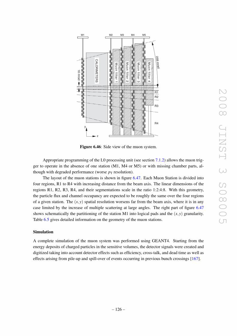
2008 JINST 3 S08005
16
mra
d
258 m
rad
Mu
on
filter 1
R2
R3
R4
R1
y
z
Mu
on
filter 4
Mu
on
filter 3
Mu
on
filter 2
CA
LO
RIM
ET
ER
S
M1 M2 M3 M4 M5
Figure 6.46: Side view of the muon system.
Appropriate programming of the L0 processing unit (see section 7.1.2) allows the muon trig-ger to operate in the absence of one station (M1, M4 or M5) or with missing chamber parts, al-though with degraded performance (worse pT resolution).
The layout of the muon stations is shown in figure 6.47. Each Muon Station is divided intofour regions, R1 to R4 with increasing distance from the beam axis. The linear dimensions of theregions R1, R2, R3, R4, and their segmentations scale in the ratio 1:2:4:8. With this geometry,the particle flux and channel occupancy are expected to be roughly the same over the four regionsof a given station. The (x,y) spatial resolution worsens far from the beam axis, where it is in anycase limited by the increase of multiple scattering at large angles. The right part of figure 6.47shows schematically the partitioning of the station M1 into logical pads and the (x,y) granularity.Table 6.5 gives detailed information on the geometry of the muon stations.
Simulation
A complete simulation of the muon system was performed using GEANT4. Starting from theenergy deposits of charged particles in the sensitive volumes, the detector signals were created anddigitized taking into account detector effects such as efficiency, cross-talk, and dead time as well aseffects arising from pile-up and spill-over of events occurring in previous bunch crossings [167].
– 126 –

2008 JINST 3 S08005
BEAM PIPE
M1R1 M1R2
M1R3
M1R4
R1 R2 R3 R4 x
y
∆x
∆y
Figure 6.47: Left: front view of a quadrant of a muon station. Each rectangle represents onechamber. Each station contains 276 chambers. Right: division into logical pads of four chambersbelonging to the four regions of station M1. In each region of stations M2-M3 (M4-M5) the numberof pad columns per chamber is double (half) the number in the corresponding region of station M1,while the number of pad rows per chamber is the same (see table 6.5).
A realistic simulation of the detector occupancy requires the detailed description of the cav-ern geometry and of the beam line elements and the use of very low energy thresholds in GEANT4.The CPU time needed for such a simulation would be prohibitive for the stations M2–M5 inter-leaved with iron filters. The strategy chosen to overcome this problem was therefore to generateonce for all a high statistics run of minimum bias events with low thresholds. The distributions ofhit multiplicities obtained were parametrized and then used to statistically add hits to the standardLHCb simulated events. The latter were obtained by running GEANT4 at higher thresholds andwith a simplified geometry of the cavern and the beam line [168]. Simulated events have been ex-tensively used to evaluate the rates in the various detector regions in order to establish the requiredrate capabilities and ageing properties of the chambers and to evaluate the data flow through theDAQ system [169]. At a luminosity of 2×1032 cm−2 s−1 the highest rates expected in the innerregions of M1 and M2 are respectively 80 kHz/cm2 and 13 kHz/cm2 per detector plane. In the de-tector design studies, a safety factor of 2 was applied to the M1 hit multiplicity and the low energybackground in stations M2-M5 has been conservatively multiplied by a factor of 5 to account foruncertainties in the simulation.
Detector technology
The LHC bunch crossing rate of 40 MHz and the intense flux of particles in the muon system [169]impose stringent requirements on the efficiency, time resolution, rate capability and ageing char-acteristics of the detectors, as well as on the speed and radiation resistance of the electronics.
– 127 –

2008 JINST 3 S08005
Table 6.5: Basic information for the five stations M1–M5 and the four regions R1–R4. All dimen-sions in cm. z: distance of the stations from the IP; ∆x and ∆y: dimensions of a quadrant in eachstation (see figure 6.47). Rows R1-R4: granularity of the different regions of the muon detector asseen by trigger and DAQ. Number of logical pads per chamber (in brackets) and size of the logicalpads, along x and y. In parentheses: size of the logical pads projected onto station M1.
M1 M2 M3 M4 M5z 1210 1527 1647 1767 1887
∆x 384 480 518 556 594∆y 320 400 432 464 495
[24×8] [48×8] [48×8] [12×8] [12×8]R1 1×2.5 0.63×3.1 0.67×3.4 2.9×3.6 3.1×3.9
(0.5×2.5) (0.5×2.5) (2×2.5) (2×2.5)[24×4] [48×4] [48×4] [12×4] [12×4]
R2 2×5 1.25×6.3 1.35×6.8 5.8×7.3 6.2×7.7(1×5) (1×5) (4×5) (4×5)
[24×2] [48×2] [48×2] [12×2] [12×2]R3 4×10 2.5×12.5 2.7×13.5 11.6×14.5 12.4×15.5
(2×10) (2×10) (8×10) (8×10)[12×1] [24×1] [24×1] [6×1] [6×1]
R4 8×20 5×25 5.4×27 23.1×29 24.8×30.9(4×20) (4×20) (16×20) (16×20)
Multi-wire proportional chambers (MWPC) are used for all regions except the inner region of sta-tion M1 where the expected particle rate exceeds safety limits for ageing. In this region triple-GEMdetectors are used [166].
The trigger algorithm requires a five-fold coincidence between all the stations, therefore theefficiency of each station must be high enough to obtain a trigger efficiency of at least 95%, withina time window smaller than 25 ns in order to unambiguously identify the bunch crossing.24 Thenecessary time resolution is ensured by a fast gas mixture and an optimized charge-collectiongeometry both for the MWPC and the GEM detectors. Moreover, the chambers are composed offour or two OR-ed gas gaps depending on station. In stations M2–M5 the MWPCs are composed offour gas gaps arranged in two sensitive layers with independent readout. In station M1 the chambershave only two gas gaps to minimize the material in front of the electromagnetic calorimeter. Inregion M1R1 two superimposed GEM chambers connected in OR are used.
To simplify the synchronization procedure and improve time alignment, the readout electron-ics is equipped with a 4-bit TDC which allows a fine time measurement of the signals with respectto the 25 ns machine clock. The fine time tuning is perfomed by selecting the hits belonging topenetrating tracks.
In addition, the use of two layers with independent HV supplies and the flexibility of thereadout provide a high degree of redundancy built into the system.
24In the following, the system has been characterized assuming a conservative 20 ns window.
– 128 –

2008 JINST 3 S08005
Table 6.6: Readout methods used in the muon chambers.
Readout type RegionMWPCWire pads R4Mixed wire-cathode pads R1-R2 in M2-M3Cathode pads everywhere elseGEMAnode pads M1R1
Readout
To satisfy the requirements of spatial resolution and rate capability that vary strongly over the de-tectors, different technical solutions are employed for the MWPC in different stations and regions.
All the chambers are segmented into physical pads: anode wire pads or cathode pads in theMWPCs and anode pads in the GEM chambers. Each physical pad is read out by one front-end(FE) electronics channel. The FE electronics is based on custom radiation-hard chips especiallydeveloped for the muon system. The input stage can be wired to handle either signal polarity:negative for anode pads, positive for cathode pads.
The electronics includes flexible logical units performing the OR of a variable number of FEchannels following the requirements of the readout. The readout methods used in different detectorregions are summarized in table 6.6.
The R4 regions contain most of the chambers and the spatial resolution required there isrelatively modest. Therefore the simplest and safest technology was adopted: the physical padsare a group of adjacent wires connected together to the same FE channel. The length of the anodewires defines the spatial y resolution, all the wires being aligned vertically. The requirement on theresolution limits the vertical size of the chambers to 20−−30 cm, and results in a large number ofchambers.
Cathode pads (anode pads for GEM) are obtained by etching the desired pattern in thecathode (anode) planes. As can be seen from figure 6.47 all pads in R3 chambers can be accesseddirectly from the upper and lower sides. On the other hand, the chambers belonging to R1 andR2 have a chessboard pad structure so that a multilayer printed circuit board is used to bring thesignals outside.
To keep the noise and the dead-time of the FE channels to an acceptable level, the rate of agiven pad and its electrical capacitance must be limited. This implies that in most chambers thesize of the physical pads (either wire or cathode pads) must be smaller than required by spatialresolution. In these cases up to four adjacent physical pads are OR-ed by the FE electronics tobuild a logical pad. However, in regions R1-R2 of stations M2-M3 the required spatial resolutionin x imposes logical pads which are too small to be practically built. For those chambers a mixedreadout has been adopted: a narrow wire-strip to define the x resolution, and a larger cathode padto define the y resolution, together defining are the logical channels seen by the trigger and DAQ.Logical pads are then obtained as an AND between wire and cathode pads (figure 6.48).
– 129 –

2008 JINST 3 S08005
HV
FE
FE
0.63 x 3.1 cm2
3.75 x 3.1 cm2
Figure 6.48: Scheme of the mixed wire-cathode pads readout in one M2R1 chamber. Two wire-pad and two cathode-pad readout channels are shown. The coincidence between crossing verticalwire-pads and the cathode physical pads defines the logical pads, shown in black.
In the M1 station, where the foreseen channel occupancy is high, the signals from the logicalpads are sent directly to the trigger and DAQ. In most of the other regions, in order to reducethe number of output optical fibres, several contiguous logical pads are further OR-ed to buildlarger logical channels in the form of vertical and horizontal strips. The logical pads are thenreconstructed by the coincidence of two crossing strips. This operation is performed in the Level-0Trigger Processor (see 7.1) and in the DAQ TELL1 boards (see 8.2).
Figure 6.49 shows the partitioning of a quadrant of stations M2 and M3 into sectors contain-ing the crossing strips. The sector size is adapted to the trigger processing elements that work on afixed number of logical pads belonging to a projective tower over the five stations.
The full muon system comprises 122112 physical channels ORed into 25920 logical channelswhich are transmitted via optical links to the Level-0 trigger and DAQ electronics. Appropriatecombinations of logical channels in the Level-0 and High-Level Trigger provide the 55296 logicalpads used for the muon tracking.
The specifications of the MWPCs and GEMs and their performance are summarised in thefollowing sections.
6.3.2 Wire chambers
Design
The LHCb muon system comprises 1368 Multi Wire Proportional Chambers. Prototype stud-ies [170–176] showed that a time resolution of about 5 ns can be achieved in a gas gap with awire plane of 2 mm spacing, symmetrically placed in a 5 mm gas gap, using fast, non-flammable,gas mixtures of Ar/CO2/CF4 with 40% Ar and variable concentrations of CO2/CF4. Finally the
– 130 –

2008 JINST 3 S08005
R1
R2
R3
R4
R1 R2 R3 R4
VERTICAL STRIP
HORIZONTAL
STRIP
LOGICAL
PAD
BEAM PIPE
Figure 6.49: Front view of one quadrant of stations M2 and M3 showing the partitioning intosectors. In one sector of each region a horizontal and a vertical strip are shown. The intersectionof a horizontal and a vertical strip defines a logical pad (see text). A Sector of region R1 (R2, R3,R4) contains 8 (4, 4, 4) horizontal strips and 6 (12, 24, 24) vertical strips.
Table 6.7: Main MWPC parameters.
Parameter Design value
No. of gaps 4 (2 in M1)Gas gap thickness 5 mmAnode-cathode spacing 2.5 mmWire Gold-plated Tungsten 30 µm diameterWire spacing 2.0 mmWire length 250 to 310 mmWire mechanical tension 0.7 NTotal no. of wires ≈ 3 ·106
Operating voltage 2.5–2.8 kVGas mixture Ar / CO2 / CF4 (40:55:5)Primary ionisation ' 70 e−/cmGas Gain ' 105 @ 2.65 kVGain uniformity ±20% typicalCharge/MIP (one gap) ' 0.6 pC @ 2.65 kV
mixture Ar/CO2/CF4(40 : 55 : 5) was adopted. By OR-ing the signals from two adjacent gasgaps the resulting double gap has an efficiency better than 95% in a 20 ns window at a gas gain ofG ' 105. This gain is achieved at a voltage of 2600–2700 V [177]. Prototype tests with intensebeams (100 kHz/cm2) confirmed the prediction that space-charge effects are negligible at the ratesexpected for the experiment [178].
The main parameters of the MWPC detectors are summarized in table 6.7. Detailed simu-lations [179] based on GARFIELD [180] were performed to optimize the design and to establish
– 131 –

2008 JINST 3 S08005
0 5 10 15 20 25 30 35 40 45
100
98
96
94
92
90
88
86
14
12
10
8
6
4
2
0
99 %
95 %
THRESHOLD (% OF THE AVERAGE SIGNAL)
EF
FIC
IEN
CY
(
%)
TIM
E
RE
SO
LU
TIO
N (
r.m
.s.)
(
ns)
eff.
r.m.s.
Figure 6.50: MWPC double-gap efficiency and time resolution vs. discriminator threshold for aprototype chamber. Solid lines: experimental results. The MonteCarlo simulation is shown in grey;the band accounts for different track angles.
the geometrical tolerances for the chamber construction. The primary ionisation was simulated byHEED [181] and drift and diffusion by MAGBOLTZ [182]. The design of the pad readout wasoptimized with SPICE [69] in order to keep the cross-talk between pads below 5%. The maximaldeviations of the construction parameters was established under the assumption of a maximumvariation of gas gain of ±20%.
Figure 6.50 shows the good agreement of a MonteCarlo simulation for double-gap efficiencyand time resolution versus FE threshold and the values measured on for a chamber prototype.
In stations M2–M5 a chamber is made of four equal gas gaps superimposed and rigidlystacked together with the gas flowing serially through all the gaps. Two contiguous gas gaps havetheir corresponding readout electrodes (either wire or cathode pads) hard-wired together in OR toform a double gap layer. The readout electrodes of the resulting layer are in turn connected to sep-arate FE channels. As already mentioned, the M1 chambers contain only two gas gaps. These twogaps form the two layers which are readout independently. In order to maximize operation flexibil-ity each gap has its own HV line and can be powered or switched off independently of the others.
Figure 6.51 shows an exploded schematic view of a chamber. The structural elements of thechamber are the panels, 9 mm thick, made of an insulating core sandwiched between two conduct-ing planes. The conducting planes inside the chamber form the cathodes while the two externalplanes are grounded and act as an electrical shield. The panels are stacked using 2.5 mm thick PCBbars glued to the panels and superimposed to create the 5 mm gas gap. The wires are soldered andglued to the wire fixation bars while other bars seal the gap along the periphery. The 5 mm gap isensured by several precision dowels inserted in the bars.
A cross section of a chamber is shown in figure 6.52. A U-shaped brass channel runningaround the chamber edges is soldered to the outer conductive planes to complete the chamberFaraday cage. The front-end boards, the LV voltage regulators and the HV filters are mounted
– 132 –

2008 JINST 3 S08005
WIRE
FIXATION
BAR
GAP BAR
SIDE BAR
PANEL
SPACER SPACER
Figure 6.51: Exploded schematic view of a chamber showing the various elements.
CONTROL CONNECTOR
CARDIAC
SPB
SMD CAPACITOR
SOLDERING
GLUE
ANODE WIRE
READOUT CONNECTOR
71
74.6
FARADAY CAGE
PANEL
WIRE FIXATION BAR
Figure 6.52: Cross section of a wire chamber showing the four gas gaps and the connection to thereadout electronics. SPB: Spark Protection Board; CARDIAC: FE Electronics Board. In this casethe hardwired OR forming the two Double Gaps (see text) is achieved in the SPB.
inside the Faraday cage to minimize electrical pickup. The HV is brought in through a custom-made multipin connector and multiconductor cable. LVDS shielded cables are used for signaltransmission and control.
The general design and construction is the same for all chambers and is discussed in detailin [183].
Chamber construction
Given the large number of chambers, the production was distributed among six production sites. Agreat effort went into ensuring that all those sites had equivalent facilities and tooling, albeit withsome flexibility. The same stringent quality criteria and test protocols were adopted throughout toensure a constant quality of the produced chambers.
– 133 –

2008 JINST 3 S08005
Figure 6.53: Panels mounted onto the winding machine frame ready to start wiring. The twocombs which guide the wire are also visible. Below the panel in the foreground there is a secondone attached to the underside of the frame. The two panels are wound simultaneously.
Panels The panels are the basis of the chamber mechanical structure. A panel consists of twocopper clad fire-resistant fibreglass epoxy laminates (FR4), interleaved with a structural core. Thepanels are individually wired and then assembled to form the complete chamber.
The panel precision and its planarity define the gap quality. Therefore it is very importantto achieve tight tolerances and stability in time, coupled with adequate robustness. In addition thepanels must be light and stiff and easily adapted to mass production. The choice for the structuralcore was a polyurethane foam core for stations M2–M5 and a light honeycomb core for station M1where a lower material budget is mandatory.
The panels were produced industrially. For the M2–M5 chambers precision machined moldswere used to inject the polyurethane foam into the FR4 sandwich. Three molds of different sizesproduced all the panels. For M1 chambers the core was made from a light NOMEX R© sheetpurchased with precise tolerance on thickness, and glued between the two FR4 foils. The pressureduring gluing was assured by a vacuum bag. So the planarity of the panels is due to the quality ofthe honeycomb core and of the flatness of the assembly table.
The wire fixation bars (figure 6.51) were glued to the panels before the wiring process usingan epoxy adhesive.25 The gluing was performed on a special table which ensured the exact heightof the bars above the panel itself.
Wiring Specially built automatic winding machines were used in all the production sites torapidly perform panel wiring. The machines could wind one or two panels simultaneously in aboutone hour for the largest chambers. The panels were fixed to a rigid frame, and grooved dowels(combs) were installed parallel to the panels long sides (figure 6.53). To achieve the requiredprecision on wire pitch, the wire spacing was determined by the combs while the wire height withrespect to the cathode-plane was adjusted by precision bars mounted to the frame. The windingmachines were equipped with brake motors or electronic devices to keep the mechanical wiretension constant.
Once the winding was completed, the wires were glued and soldered. The wires were gluedto the wire fixation bars using epoxy adhesive before soldering. This procedure guarantees that the
25Adekit A140 epoxy, Axon Technologies, USA.
– 134 –

2008 JINST 3 S08005
Figure 6.54: A M1R4 chamber completely assembled before the installation of the Faraday cage.The three honeycomb panels are visible. On the corners of the panels there are plastic inserts withinternal channels for gas circulation. The gas nipples are inserted in the top and bottom panels.Decoupling HV capacitors, resistors and connectors for the FE boards are mounted on the printedcicuit boards on the right.
wires are kept in place with a fixed height with respect to the cathode plane. The gluing also keepsthe wire tension to its nominal value.
Due to the large number of solder joints in the construction of the chambers, the use ofan automated and reliable method was desirable. Automatic soldering stations [183] both withconventional soldering heads and with laser heads were employed.
Final assembly In the final assembly of the chamber the panels were superimposed and gluedtogether using cylindrical precision spacers for alignment (see figure 6.51). The glue26 ensuresthe chamber gas tightness. In the chambers of region R1 in stations M2–M3 and of region R2in stations M1–M3, no glue was used and gas tightness was ensured by O-rings made of naturalrubber. This allows to open the chambers easily if needed. Screws were used to keep togetherthe panels. Finally the brass channels forming the Faraday cage were soldered to the outer coppercladding of the panels. Figure 6.54 shows an assembled M1R4 without Faraday cage.
Quality control and testing
Uniform quality of the chambers produced in the various sites was ensured by stringent quality testsof the individual chamber components and of the assembled chambers [184–186]. All the panelswere individully measured at production and then shipped to the production sites where they werechecked once more before assembly. Despite the tight tolerances the yield of good panels was 90%.
Once the panels were produced, the pitch and the mechanical tension were measured for allwires. The wire pitch was determined with an automated device based on two digital cameras [186].The distribution of the measured wire pitch has an r.m.s. of 16 µm. Only a very small number ofwires with pitch value outside tolerance (±0.1 mm) had to be replaced.
26Adekit A145 and Araldite 2011 epoxy, Huntsman Advanced Materials, Switzerland.
– 135 –

2008 JINST 3 S08005
0.3 0.4 0.5 0.6 0.7 0.8 0.9 1.0 1.1
102
103
104
105
10
1
WIRE TENSION (N)
NU
MB
ER
OF
WIR
ES
Figure 6.55: Distribution of the mechanical tensions of the wires as deduced from a measurementof the wire mechanical resonant frequency. The mean value of the tension is 0.73 N with an r.m.s.of 0.091 N. The wires having a tension outside the interval 0.5−1 N (dashed lines) were replaced.
To determine the wire mechanical tension automated systems were developed [187, 188]which measures the mechanical resonant frequency of each wire. The distribution of the wiretension measured on the above mentioned sample is reported in figure 6.55.
The checks on the assembled chambers consisted of a gas leak test and a HV test at 2800–2900 V using the standard gas mixture. The chamber gas leakage was determined by monitoringthe decrease in time of an initial overpressure of 5 mbar. The method [186] had a sensitivity ofabout 0.01 mbar/hour well below the maximum gas leakage rate accepted of 2 mbar/hour.
The uniformity of the gas gain in the gaps was systematically checked using radioactivesources mounted on automated tables which performed an (x,y) scan over the complete chambersurface [185, 186, 189]. Figure 6.56 shows the gain measurement on a sample of 184 chambers.
All the above checks were performed without the readout electronics installed.Finally all chambers, fully equipped with the front-end electronics, underwent a final test
with cosmic rays prior to installation and the electronic noise was checked once more when thechambers were mounted in the experiment. The maximum accepted noise rate was 1 kHz per FEchannel, a value which has no impact on the trigger system.
In addition, all the chambers for the regions exposed to the largest particle flux, were con-ditioned at the CERN Gamma Irradiation Facility (GIF) [190] to ensure their stable functionalityunder high radiation.
Important information about the individual components and the final chamber was stored ina database. This allows to retrieve at any time the results of all quality control measurements andwill aid in understanding possible problems.
Aging properties
Extensive aging tests were performed on prototypes at the CERN GIF and at the Calliope27 facility.The goal of the tests was to prove that the performance of these chambers is not deteriorated by
27ENEA-Casaccia Research Centre, Rome.
– 136 –

2008 JINST 3 S08005
CHAMBER NUMBER0 20 40 60 80 100 120 140 160 180
GA
IN (
a.u
.)
0
100
200
300
400
500
600
700
800
M3R3 M5R3 M5R4
Figure 6.56: Gain uniformity measured for a sample of 184 chambers. The bars are proportional tothe total gain spread of a double gap. The horizontal lines indicate the allowed acceptance intervalsfor good (in blue) and spare (in red) chambers.
the large radiation dose expected in the experiment in ten years of operation (108 s) at the nominalluminosity of 2×1032 cm−2 s−1 . In these tests the gain loss was measured against a non-irradiatedreference chamber or gas gap.
In the test performed at the GIF facility at CERN, a four gap MWPC was irradiated for sixmonths, accumulating a charge of 0.25 C/cm without detecting any gain loss [191].
In an accelerated test during 30 days of irradiation at the 60Co source of Calliope, we mon-itored the currents in five four-gap MWPCs: four test chambers and a reference one [176, 192].The chambers were operated at a voltage of 2.75 kV, corresponding to a gas gain of 1.8 ·105 [177],twice the value that will be adopted in the experiment. The largest integrated charge collected ona chamber wire was 0.44 C/cm. This corresponds [169] to about 7 years (107 s/year) of operationof the most irradiated chamber (in M1R2) at a luminosity of 2×1032 cm−2 s−1 , assuming a safetyfactor of 2. No gain loss or other significant effect was detected.
6.3.3 GEM chambers
In the innermost region R1 of the station M1, the most stringent requirements for the detectoris a rate capability of up to 500 kHz/cm2 of charged particles. Due to the large particle flux inthis region the chambers must also be especially radiation hard such that no ageing effects will bevisible in 10 years of LHCb operation. This is difficult to achieve in wire chambers unless the gainis decreased, at the price of a worse signal-to-noise ratio.
After an extensive R&D program triple-GEM chambers with active area of 20×24 cm2 wereselected for M1R1. Each of the 12 chambers consists of two triple-GEM detectors superimposedand forming the two sensitive layers, which are then logically OR-ed.
– 137 –

2008 JINST 3 S08005
CATHODE
GEM 1
GEM 2
GEM 3
ANODE PCB
READOUT ELECTRONICS
DRIFT GAP gD ED
1st TRANSFER GAP gT1
ET1
2nd TRANSFER GAP gT2
ET2
INDUCTION GAP gI
EI
V1
V2
V3
1 mm
2 mm
1 mm
3 mm
Figure 6.57: Schematic cross section of atriple-GEM detector showing the most rele-vant elements and dimensions (see text).
BACK-PLANE
HONEYCOMB
ANODE READOUT1 mm FRAME
2 mm FRAME
2 nd GEM FOIL
1 mm FRAME
1 st GEM FOIL
3 mm FRAME
CATHODE
HONEYCOMB
BACK-PLANE
3 rd GEM FOIL
Figure 6.58: Exploded view of a triple-GEMdetector.
Design
The triple-GEM detector, which consists of three gas electron multiplier (GEM) [193–195] foilssandwiched between anode and cathode planes, can effectively be used as tracking detectorwith good time and position resolution. A cross section of the detector, showing the differentelements and their physical dimensions, is shown in figure 6.57. An exploded view is presented infigure 6.58.
The ionisation electrons, produced in the drift gap between the cathode and the first GEMfoil, are attracted by electric fields through the three GEM foils where they are multiplied. Oncethey cross the last GEM foil they drift to the anode in the induction gap, giving rise to an inducedcurrent signal on the pads.
Prototype tests have shown that the fast Ar/CO2/CF4(45 : 15 : 40) gas mixture allowed toachieve a time resolution better than 3 ns, to be compared with the time resolution of ∼10 ns ob-tained with the standard Ar/CO2 (70:30) gas mixture [196].
Another improvement in time performance has been obtained by optimizing the detectorgeometry. Mechanical considerations indicate that a minimum distance of 1 mm should be keptbetween GEM foils. The size of the drift gap gD is large enough to guarantee full efficiencyfor charged tracks. The first transfer gap gT 1 is kept as small as possible to avoid that primaryelectrons produced in the same gap give rise to a signal over threshold. The second transfer gapgT 2 is larger than the first one to let the diffusion spread the charge over more holes and then lowerthe discharge probability. The induction gap gI is kept as small as possible to maximize the signalfraction integrated by the amplifier.
The best values of the gap fields and of the voltage across the GEM foils were determinedexperimentally by optimizing time resolution versus discharge probability and are typically ED =3.5 kV/cm, ET = 3.5 kV/cm and EI = 5 kV/cm and V1 = 440 V, V2 = 430 V, V3 = 410 V. The anodepad printed circuit board is such that the pad to pad distance is 0.6 mm and the pads are surroundedby a ground grid of 0.2 mm thickness to suppress cross-talk.
– 138 –

2008 JINST 3 S08005
Figure 6.59: Stretching of a GEM foil.Figure 6.60: GEM chamber fully assem-bled with the 24 FE electronics boards. Thecutouts in the Faraday cage allow the inser-tion of the cable connectors.
Measurements on prototype chambers made of two detectors in OR showed an efficiencybetter than 96% in a 20 ns window at a gain of 6 ·103. The pad cluster size upper limit of 1.2 andthe discharge studies suggested a maximum working gain of about 2 ·104 [195].
Chamber construction
All the critical steps in chamber assembly were carried out in class 1000 clean rooms or underclass 1000 huts, with controlled temperature and humidity conditions. The huts were used for alloperations involving GEM foils.
The GEM foils, 50 µm thick Kapton with two-sided Cu cladding of 5 µm, have an activearea of 202× 242 mm2 and were manufactured by the CERN-EST-DEM workshop. The holeshave a bi-conical structure with external (internal) diameter of 70 (50) µm and a pitch of 140 µm.In order to limit the damage in case of discharge, one side of the GEM foil is divided into sixsectors, of about 33 mm × 240 mm. The separation between sectors is 200 µm. Each individualfoil was visually inspected for defects and for leakage current. Then the foils were stretched witha mechanical tension of about 1 kg/cm with a special device visible in figure 6.59.
After the GEM stretching, a fibreglass frame was glued on the GEM foil using a Ciba2012 epoxy. Both cathode and readout pad electrodes, realized on standard 1.0 mm thick printedcircuit board, were respectively coupled with a 1.0 mm fibreglass foil by means of an 8 mm thickhoneycomb structure, The back-panel with a 12 µm copper layer deposition on its external side isused as a Faraday cage for the detector. The stiff cathode and pad panels act as support plates forthe whole detector. These panels house two gas inlets and two gas outlets, made with machinedStesalit inserts.
All fibreglass parts that are in contact with the sensitive volume of the detector, were visuallyinspected in order to eliminate any residual spikes or broken fibres. They were then cleaned in anultrasonic bath with de-mineralized water and dried in an oven at a temperature of 80oC duringone night.
– 139 –

2008 JINST 3 S08005
20
15
10
5
0
2
4
6
8
GA
IN
(a.u
.)y (cm)
04
812
1620
24x (cm)
Figure 6.61: Response uniformity of a GEM chamber measured with an X-ray gun. The RMSgain variation over the 24×8 pads is typically less than 10%.
The detectors were built on a high-precision reference plane by piling up and gluing togetherthe component parts in the following order (see figure 6.58): cathode panel; the first GEM foil(GEM1) glued on a 3 mm thick fibreglass frame; the second GEM foil (GEM2) glued on a 1 mmthick frame; the third GEM foil (GEM3) glued on a 2 mm thick frame and then the last 1 mmthick frame followed by the pad panel. All the gluing operations were performed using AralditeAY103 epoxy and HY991 hardener. The aging properties of both glues have been studied duringirradiation tests [197, 198]. A complete chamber is shown in figure 6.60.
Quality control and testing
Several quality checks were performed on individual detector components before chamber assem-bly. Since the cathode and anode panels are the main mechanical structure of the detector, theywere checked for planarity. Measurements over the whole panels showed that the deviation fromthe average plane was of the order of 50 µm (r.m.s).
The quality of GEM foils was checked by performing various tests. A preliminary opticalinspection was performed with a microscope to check for photolithographic imperfections. If theGEM foil passed the visual inspection, a high voltage test was performed. Such a test was done ina gas tight box, flushed with nitrogen too keep the relative humidity at ∼25% level. The foil wasaccepted if the leakage current was less than 1 nA at 500 V.
After construction, the detector gas leak rate was measured. This measurement was per-formed by inflating the detector to an overpressure of ∼10 mbar together with another gas-tightchamber used as reference, and recording the overpressure decay. The typical gas leak rate of adetector is of the order of few mbar/day. At the gas flow forseen in the experiment (80 cm3/min)this leakage rate will result in an acceptable humidity level lower than 100 ppm.
A gain uniformity test, performed with an X-ray gun, checked both the mechanical toleranceand the response uniformity of single detectors. A typical result is presented in figure 6.61. Thecurrent signals induced on each of the 192 pads of each detector were corrected for temperatureand pressure variations. The current deviations from the average were all below 20% with a typicalRMS < 10%. Finally, a cosmic ray test was performed on all chambers fully equipped with front-end electronics.
– 140 –

2008 JINST 3 S08005
Discharge and aging properties
The use of the non-standard Ar/CO2/CF4(45 : 15 : 40) gas mixture required the demonstration ofhigh robusteness of the GEM to discharges and ageing effects. In fact the choice of the electricfield in the detector gaps and the unbalanced configuration of the voltages applied to the GEM foils(V1 > V2 > V3, see figure 6.57) are the result of a minimization of discharges produced by al-pha particles. More than 5000 discharges were integrated with neither breakdown nor performancelosses using alpha particles and a high intensity low momentum pion/proton beam. These measure-ments demonstrated that GEMs in M1R1 can operate safely. The large fraction of CF4 in the gasrequired that a global irradiation test of the final chamber be performed to check the compatibilitybetween the construction materials and the gas mixture. For this reason a test was performed at theCalliope facility with an intense gamma ray flux from a 60Co source. In this test, a charge of 2.2C/cm2 on the anode pads and GEM3 foil was integrated. This is the charge foreseen for more than10 years running if the GEMs are operated with a gain of∼6000 and a safety factor of 2 is applied.The performance of these chambers was measured in a test beam before and after irradiation andno damage or performance losses were detected [197, 198].
6.3.4 Muon System mechanics
All muon stations, including the iron filters, are separated into two halves which can move onrails away from the beampipe for maintenance and installation. The chambers, mounted on sup-port walls, can also move with respect to the iron filters which are normally located close to thebeampipe. Iron plugs minimize the free space between the beampipe and the iron filters to reducesmall-angle background.
For M2–M5 two large support structures built from iron beams accomodate the suspensionsfor the four chamber support walls and have platforms for the electronics racks and gas systems.Cable chains are used to connect the cables, fibers, gas pipes and water cooling pipes with theoutside. Station M1 has independent support structure and the related racks are located on the floorof the cavern. Cable chains are used in M1 to carry the 1200 cables to the racks.
The walls are designed to support the weight of the half-stations with minimal thickess andare built of aluminium sandwich plates. M1 wall is thinner to minimize material in front of theelectromagnetic calorimeter. This is possible since the weight of M1 chambers is reduced thanksto the use of only two gaps and honeycomb panels. The material budget of the M1 station is 0.26X0 on average with the chambers and the FE electronics contributing 0.16 X0 and the mechanics,cables and gas pipes contributing the rest.
Alignment
The position of the chambers must be adjusted in order to minimize chamber overlaps which wouldintroduce ambiguities. Moreover, since the muon trigger relies on the projectivity of the stations,a precise relative space alignment has to be performed, in particular in the inner region where anaccuracy of about 1 mm is required.
The chambers are mounted with screws on angle brackets fixed to the supporting walls. Thewalls were first precisely aligned by adjusting the overhead suspensions, then each chamber was
– 141 –

2008 JINST 3 S08005
Off Detector
Electronics
Boards
(ODE)
122 k Physical channels
Intermediate
Boards (IB) Logical
channel
generation
DIALOG
Front End Boards (CARDIAC)
Service Boards (SB) Front-end controls
I2C bus
CARIOCA CARIOCA CARIOCA
25k channels
8.6k
logical
channels
17.3k
logical
channels
IN R
AC
KS
O
N C
HA
MB
ER
S
Pulse Distribution
Module (PDM)
Muon TELL1
L0 muon
trigger processors
ECS
TTCrx (clock)
ECS
ECS
Programmable phase
Programmable delays
Mask, OR/AND logics
42k channels
TFC
TTCrx (clock)
TFC
IN COUNTING HOUSE
BX synchronization
Fine time measurement
L0 buffer
Trigger & DAQ interfaces DAQ
Figure 6.62: Simplified scheme of the Muon electronics architecture.
aligned relative to the wall. The position was adjusted vertically using spacers and horizontally viathe slotted holes in the brackets. For horizontal and vertical alignment, the reference points were thesupport wall edge close to the beampipe and the top edge, respectively. Finally, the equipped wallswere precisely aligned together using as reference each half-station, the centre of the beampipe.The reproducibility of the measurements is O(1) mm and the reproducibility of the position aftermoving the walls is of the same order.
6.3.5 Electronics
Figure 6.62 shows schematically the architecture of the Muon readout electronics. The task of theelectronics is twofold: prepare the information needed by the Level-0 muon trigger and send thedata to the DAQ system. The main steps are:
i. the front-end CARDIAC boards perform the amplification, shaping and discrimination of the≈ 120 k chamber signals. The time alignment to within 1.6 ns of the different channelsneeded to correct for different cable lengths and different chamber behaviour is also done inthis step. This is mandatory since the Muon Trigger is fully synchronous with is also donein this step, the LHC cycle.
ii. The ≈ 26k logical-channel signals are generated by suitable logical ORs of the physicalchannels. This step is performed on the FE boards and on special Intermediate Boards (IB),when the logical channel spans more than one FE board.
iii. The Off Detector Electronics (ODE) boards receive the signals from the logical channels.They are tagged with the number of the bunch crossing (BX identifier) and routed to thetrigger processors via optical links without zero suppression.
– 142 –

2008 JINST 3 S08005
iv. The fine time information, measured by the TDC on the ODE boards, is added and the dataare transmitted via optical links to the TELL1 board and from the TELL1 to the DAQ system.
As far as possible, step ii. is performed on the chambers front-end boards in order to mini-mize the number of LVDS links exiting the detector. The other steps are performed on dedicatedelectronics boards mounted on racks on the left and right sides of the muon stations M2–M5 whichalso accomodate the LV and HV power supplies. Since the racks are installed on the same struc-ture which supports the stations, cable chains for the chambers could be avoided. For station M1the electronics racks are placed under the RICH and, as mentioned above, are connected via cablechains to the chamber walls.
Radiation issues
The Muon electronics must operate reliably for more than 10 years in a hostile environment. TheFE boards in the regions close to the beampipe are exposed to very high radiation doses: in M1 themaximum total ionising dose (TID) foreseen in 10 years is 5000 Gy. This decreases by only a factor3 for M2. The maximum neutron and hadron fluences are in the range of 1013/ cm2. Therefore, allthe ASICs used in the FE Electronics were produced using radiation-hard technology.
The radiation dose is considerably less on the detector periphery where the electronics racksare located. TID values of up to 10 Gy in 10 years are expected in the electronics racks.28 Thesedoses nevertheless dictate the use of radiation tolerant components or a proper qualification ofcommercial components.
For complex logic design, two kinds of FPGA both from the ACTEL family are used. TheA54SX family was chosen first for good radiation immunity and was used in the IntermediateBoards (IB). A more advanced type of FPGA from the flash-based ProASICPLUS APA family,was chosen in the design of ODE, PDM and SB boards. Based on ACTEL flash technology,ProASICPLUS devices offer reprogrammability and nonvolatility in a high density programmablelogic product. The ProASICPLUS is also suitable in a high radiation environment thanks to theradiation hardness of its flash cells.
Commercial off-the-shelf electronics (COTS) was used for glue logic and signal conversion.All chip were validated with respect to the radiation environment.
Dedicated ASICs
The large number of channels in the muon system, the flexibility necessary to adapt the readoutscheme to the different regions, the necessity to synchronize all the channels in a 20 ns window, thehigh radiation expected in M1 and in the inner regions led us to develop three dedicated rad-hardASICs (CARIOCA, DIALOG and SYNC) using IBM 0.25 micron technology. All chips provide andaccept logical LVDS data.
Front-end board
The chamber readout is performed via front-end boards (CARDIAC) [199] plugged directly ontothe chambers. Each CARDIAC has 16 inputs and 8 outputs, and is equipped with two CARIOCA
28this value includes a safety factor of 2.
– 143 –

2008 JINST 3 S08005
Figure 6.63: Top and bottom views of the CARDIAC board, showing the two CARIOCA chips andthe DIALOG chip.
chips and one DIALOG chip, as shown in figure 6.63. A special diode circuit protects the front-endamplifiers from sparks and is mounted on a separated board.
The CARIOCA [200–202] is a front-end amplifier-shaper-discriminator chip with eight chan-nels whose input polarity is selectable. The front-end current preamplifier can handle well the largespread in detector capacitances encountered in the muon chambers (from 20 pF for the M1R1 to220 pF for the M5R4 chambers). The peaking time is ∼10 ns at the lowest detector capacitance.The input impedance is 50 Ohm which is important to reduce internal pad-pad cross-talk. Thechip includes tail cancellation and baseline restoring. The dead time of a fired channel, almostindependent of the pulse height, is in the range 50–60 ns.
The CARIOCA has separate thresholds for all the channels in order to overcome the problemof channel-to-channel uniformity in the internal discriminators. Equivalent noise is about 2000electrons at 0 capacitance, and increases as (42–45) e/pF. Power consumption is about 45 mW/ch.
The DIALOG [203, 204] chip has 16 inputs to receive the outputs from two CARIOCA chips,and performs the logical OR of corresponding pads in the two layers of a chamber to form logicalchannels. The DIALOG is equipped with adjustable delays for every input allowing the variousinput signals to be aligned with a step of 1.6 ns. In addition, the DIALOG also allows setting theCARIOCA thresholds and can mask individual channels. It also contains features useful for systemset-up, monitoring and debugging. Triple-voting and auto-corrected registers are used to increasesingle event upset immunity.
The CARDIAC boards are enclosed inside the chamber Faraday cage, together with radiation-tolerant voltage regulators (LH4913) which supply the necessary 2.5 V to the boards. The R4chambers use only three CARDIAC boards and one regulator each, while the M1R2 chambers re-quire 24 CARDIAC boards and six regulators each.
Given the large number of readout channels the muon system comprises nearly 8000 CAR-DIACs. All the boards were tested after assembly, and had to pass successfully a thermal cycle tobe accepted. Once mounted on the chamber the characteristics of each board, in particular withrespect to noise, were measured again.
A special version of the CARIOCA chip, with lower threshold and longer shaping time becauseof the lower gas gain, CARIOCAGEM [202], has been produced for use on the GEMs. The tailcancellation is suppressed considering the purely electron signal in the GEM case. A more compactCARDIAC card has also been designed, given the tight space available in the R1 region.
– 144 –

2008 JINST 3 S08005
SB and PDM boards
The front-end boards are managed by the Service Boards (SB) [205] that handle the setting of thethresholds in the CARIOCA chip, as well as the adjustable delays, the channel masking and thesetting of the AND/OR logics in the DIALOG chip. Each SB houses four ELMB [206] modulesbased on an 8-bit microcontroller (Atmel ATMega128) whose firmware was customized to permitI2C communication with the CARDIACs via twelve serial links. Each SB can control up to 192CARDIAC boards. The full system comprises 156 SBs, managing the approximately 8000 CAR-DIAC boards of the muon system. Most of the calibration and test procedures of the front-end areimplemented in the ELMB firmware and are performed directly by the SBs.
A Pulse Distribution Module (PDM) resides in each of the 10 crates containing the serviceboards. The PDM is based on an ELMB and houses one TTCrx chip which generates low-jitterpulses in a chosen phase relation with the LHC machine clock. The pulses are then distributed tothe service boards by means of a custom back plane. This facility is crucial for the time alignmentof the muon system.
IB board
Whenever the generation of the logical channels is not possible at the DIALOG level, an additionallogical layer is needed. This happens in regions R2, R3 and R4 of stations M2 to M5. The neededlayer, the Intermediate Board (IB), implements the necessary logic on three ACTEL A54SX16Aanti-fuse FPGAs. Anti-fuse technology offers good tolerance against high radiation doses. The IBhas been tested successfully with up to 68.5 Gy without failures. The system comprises 168 IBboards which are installed in the electronics racks.
ODE board
The ODE board [207] contains the Level-0 pipelines and DAQ interface. It synchronizes signalsand dispatches them to the Level-0 trigger. Each ODE receives synchronous TFC signals by way ofa TTCrx chip [113]. On-board clock de-jittering and distribution is managed by a QPLL chip [208].A total of 152 ODE installed on the same racks as the IBs, are used.
Each board receives up to 192 logical channels and outputs data to the Level-0 muon triggerand to the DAQ system. The incoming signals are assigned the appropriate BX identifier and aresent to the Level-0 muon trigger directly via twelve 1.6 Gb/s optical links, each served by one GOLchip [209]. In parallel, the data are sent to the Level-0 pipelines, where they reside for 4 µs beforereceiving the L0-accept signal. Upon reception of a trigger, data are written into the L0 derandom-izer, a FIFO programmable to a maximum depth of 16 data words. The derandomizer allows thedata to be read out at a regular rate of 1.1 MHz with a safe margin with respect to the L0 averagetrigger rate of 1 MHz. Its programmable depth allows it to cope with instantaneous bursts of up to16 consecutive triggers. Finally the data are formatted and sent to the TELL1 boards. The LVDSreceivers, the Level-0 pipelines, the Level-0 derandomizer and the 4-bit TDC for fine time align-ment are integrated into a single component, the SYNC chip [204]. The chip incorporates a numberof error-detection features, allowing remote control and diagnosis of possible malfunctions on theboards. The other main board components (board controller, Level-0 buffer and DAQ interfaces)
– 145 –

2008 JINST 3 S08005
are based on one FPGA.29 Each ODE board also contains a CAN node, based on one EmbeddedLocal Monitor Board (ELMB) [206], for board control via the ECS.
Channel mapping to the Level-0 trigger is organized by grouping the logical channels in threedifferent ways. This is accomplished placing the SYNC chips on daughter-boards of three differentsizes, containing 2, 4 or 6 chips, while the ODE mother board is always the same. In the three cases12, 8 or 6 links respectively are active on the daughter board. The design of the ODE board has beenvery challenging because it must cope with several, and sometime contradictory, requirements.Due to the limited space available, the board has a high channel density (192 differential inputsinto a 6U card), and should provide a good level of flexibility and at the same time match thedifferent trigger sector topologies. High signal integrity is also mandatory to guarantee high qualityoptical transmission. For radiation tolerance, a triple modular redundancy technique has been usedwhenever possible to increase single event upset immunity.
Muon TELL1 features
Upon reception of a trigger, the data from the detector logical channels are transmitted from theODE to the TELL1 and from the TELL1 to the DAQ system. The description of the TELL1board is given in section 8.2. The muon-specific TELL1 board, performs standard control of eventsynchronization, as well as zero suppression and is also programmed to reconstruct the logical padsas the intersection of two crossing logical channels of the stations M2 to M5. This information isadded to the event data to speed up the muon identification algorithm used in the HLT trigger. Themuon system requires 14 TELL1 boards (four in the M1 and M2 stations and 2 in the M3, M4, andM5 stations). These numbers are determined by data flow and connectivity requirements as well asthe required ECS partitioning.
6.3.6 LV and HV systems
The Low Voltage and High Voltage systems are based on radiation-tolerant power supplies. Theyare installed in the pit on racks on both sides of the muon stations M2–M5 and in the radiation safearea under the RICH. Eight LV power supplies30 are used for the CARDIAC boards and ten for theoff-detector electronics boards.
The HV cabling for the wire chambers is designed to supply independently all the gaps, i.e.potentially about 5000 channels. Two distinct power supply systems are used. The first system,developed by PNPI and the University of Florida for CMS, is based on 36-channel modules andpowers the R4 and R3 chambers in M2-M5. Some of the gaps of R4 chambers are connected inparallel in groups of four via patch panels. In this way the number of independent HV channels isreduced from 3840 to 1920. The gaps connected in parallel always belong to different chambers tominimize the loss of efficiency in case, e.g., one gap should become shorted. The second systemis a commercial one based on 32-channel modules.31 It powers the chambers more exposed to
29 ACTEL flash ProASICPLUS FPGA (APA450PQG208).30MARATON low voltage power supply system for hazardous hostile environment; W-IE-NE-R, Plein & Baus
GmbH, Burscheid, Germany.31CAEN Easy 3000 and A3535P.
– 146 –

2008 JINST 3 S08005
radiation and drawing larger currents, and for this reason all the 1152 channels can be individuallycontrolled and monitored.
Both HV systems have been tested for radiation resistance (hadrons, total dose and neutrons)and are apt to satisfy LHCb requirements for 10-year operation with a 10-fold safety factor.
The GEM detectors require several voltages to operate. To achieve maximum flexibility andsafety a customized system [210] was designed, which allows independent settings for all of theGEM electrodes for a total of 168 channels. This system is entirely installed in the counting house.
6.3.7 Experiment control system
The control of the muon detectors is carried out with a distributed system where the processingcapacity is shared among the system nodes. CANBus was chosen because of its features of multi-master protocol with real-time capability, error correction, long distance communication and lownoise. CAN nodes based on ELMBs are present in the ODE, SB and PDM boards. The imple-mentation of calibration and test procedures in the ELMB firmware, as is the case for the SBs,maximizes the parallelism of the system and minimizes the traffic on the CANBus which is onlyused to communicate the results of the procedures.
All the physical channels which cannot be accessed via DAQ can be monitored via ECSwhile running the experiment to measure noise level and detecting dead channels. More complexprocedures such as noise measurements at several thresholds to detect faulty FE channels will beperformed offline, The pulse system (PDM) will allow for checks of the time alignment of the fulldetector.
The ECS software (see section 8.4) was developed in PVSS following the general experimentguidelines and exploiting the tools provided by the LHCb PVSS framework. The muon ECS ispartitioned in two independent left-right halves and is organized in hierarchycal topological struc-tures. Each device of the muon system, like SBs, ODE Boards, HV and LV power supplies, is seenas a Finite State Machine with well defined states and interactions with other machines.
Ten PCs running PVSS programs are used to manage all the CARDIAC, ODE and SB boards.Six are used to control the HV and LV power supplies and one to monitor the environment pressureand temperature. The entire hierarchy is controlled by two PCs, one for the left and one for theright side of the muon system.
6.3.8 Gas system
The gas system has been designed in collaboration with the CERN Gas Group. Due to the ratherlarge gas volume of the MWPCs (8.3 m3), a recirculation system is used with a planned regenera-tion rate of about 90%. A pump in the return line allows the gas to be compressed before enteringthe gas building at the surface, where the mixing and purifying units are located. The purifier inthe recirculation circuit contains two cleaning agents: a molecular sieve to keep the water contami-nation below the level of 100 ppm, and activated copper as a reducing agent for oxygen impurities,which should be kept below the 50 ppm level. A humidity and an oxygen meter allow for measure-ment of the impurity concentration before or after the purifier. Due to the small gas volume of only10 litres, a vented system is used for the GEM chambers.
– 147 –

2008 JINST 3 S08005
HV(V)2300 2350 2400 2450 2500 2550 2600 2650 2700
Eff
icie
ncy
0.5
0.6
0.7
0.8
0.9
1
four gapsthree gapstwo gapsone gap
M5R4, threshold 14fC
HV(V)2300 2350 2400 2450 2500 2550 2600 2650 2700
Eff
icie
ncy
0.5
0.6
0.7
0.8
0.9
1
four gapsthree gapstwo gapsone gap
M4R2, threshold 8fC
Figure 6.64: Plateau curves showing the efficiency in a 20 ns window for an anode-readout cham-ber (left) and a cathode-readout chamber (right). The four curves refer to different number of gapsbeing operated (see text). The threshold values in fC are also indicated, a lower value being usedfor cathode readout.
The flow rate varies across the detector surface from one volume exchange per hour, for theregions exposed to the largest irradiation (inner regions of station M1), to two volume exchangesper day for the outer regions of stations M4 and M5. Six distribution circuits are used: two for M1,two for M2–M3 and two for M4–M5. They are equipped with gas flow meters for the inputs andoutputs of each supply line.
While the 12 GEM chambers have individual supply lines, only 180 supply lines are usedfor the 1368 MWPCs. To maintain still a parallel gas supply for each chamber, which is requiredto ensure an optimal performance of each individual chamber, several distributors serving 5–8chambers have been installed on the support walls. In order to equalize the gas flow throughthe chambers connected to each distributor, capillaries with an impedance of about 1 mbar areintroduced at the input of each chamber.
6.3.9 Performance
MWPC
Extensive tests were performed on prototypes and final MWPCs both in test beams and with cos-mic rays at the production sites to measure the chamber performance. All measurements wereconservatively done using a 20 ns time window.
Whereas MWPCs are expected to operate normally with four gaps in OR (two in case of M1chambers), it is possible that a chamber will be operated with fewer gaps. Figure 6.64 shows theefficiency as a function of the applied voltage for the largest chamber with anode readout (M5R4)and for one chamber with cathode readout (M4R2). The curves are given for the standard four-gap OR configuration, but also for three-gap configuration (one double-gap fully working and thesecond with one gap shut off), for two gaps read by the same front-end and finally for the single-gap case. The curves show clearly the large improvement obtained by adding gaps, but also that,
– 148 –

2008 JINST 3 S08005
HV(V)2300 2350 2400 2450 2500 2550 2600 2650 2700
Eff
icie
ncy
0.5
0.6
0.7
0.8
0.9
1
clu
ster
siz
e
1
1.05
1.1
1.15
1.2
1.25
efficiency - four gapsefficiency - two gapscluster size - four gapscluster size - two gaps
M5R4, threshold 14fC
HV(V)2300 2350 2400 2450 2500 2550 2600 2650 2700
Eff
icie
ncy
0.5
0.6
0.7
0.8
0.9
1
clu
ster
siz
e
1
1.05
1.1
1.15
1.2
1.25
efficiency - four gapsefficiency - two gapscluster size - four gapscluster size - two gaps
M4R2, threshold 8fC
Figure 6.65: Efficiency and cluster size in a 20 ns window for the four-gap and double-gap config-urations vs. HV. Anode readout-type chamber (left) and cathode readout-type chamber (right).
in case one gap should be shut off during the data taking, the redundancy built into the chamberswill make the loss in performance negligible.
Another important parameter is the cluster size, i.e. the average number of pads fired by acrossing particle. The cluster size affects directly the space resolution and the pT measurementin the Level-0 trigger since the yes-no readout does not allow an interpolation between adjacentpads. A non-negligible contribution to the cluster size comes simply from the geometry giventhe fact that inclined tracks can cross two adjacent pads belonging to different gaps. Anothercontribution comes from the chamber itself: inductive and capacitive cross-talk in the chamber andin the electronics. The design criteria requires that the intrinsic cluster size should be less than 1.2.This is well satisfied as can be seen in figure 6.65 which shows the cluster size distribution for theM5R4 and M2R4 chambers measured with perpendicular tracks [211]. Cosmic rays have also beenused to check the gas gain uniformity on final chambers [212].
The rate capability of the MWPCs was studied at the CERN GIF [213] test beam. The detec-tion efficiency of the chamber exposed to the intense gamma flux was measured with a 100 GeVmuon beam. The chamber performance was studied for several detector gap configurations anddifferent values of the background rate from the source.
No effect was detected at the maximum gamma rate allowed at the GIF where a currentdensity of 28 nA/cm2 was measured at a high voltage of 2.75 kV. This value is about the oneexpected in the chamber with the highest occupancy in the nominal conditions of running. This isin agreement with the results of the simulations [179] which show that space charge effects due toaccumulation of ions are expected only at much higher currents.
GEM chambers
Triple-GEM detectors with the final FE electronics were tested both in a dedicated 40 MHz testbeam and with cosmics in the lab.
Efficiency and cluster size in a 20 ns window, as a function of gain, are shown in figure 6.66for a chamber composed of two triple-GEM detectors. Thanks to the longer shaping time of theCARIOCAGEM with respect to the standard CARIOCA chip the beginning of the efficiency plateau
– 149 –

2008 JINST 3 S08005
Detector Gain0 2000 4000 6000 8000 10000 12000
Eff
icie
ncy
in 2
0 n
s
0.7
0.75
0.8
0.85
0.9
0.95
1
ORLeftRight
Detector Gain0 2000 4000 6000 8000 10000 12000
Clu
ster
Siz
e in
20
ns
1
1.02
1.04
1.06
1.08
1.1
1.12
ORLeftRight
Figure 6.66: Efficiency and cluster size in a 20 ns window vs. gain for a chamber composed of twotriple-GEM detectors. The curves show the data for the single detectors and for the OR of the two.
has moved from a detector gain of 6000 to 4000. This allows to operate the chambers with anintegrated charge decreased by 30% and in safer conditions with respect to discharges.
– 150 –

2008 JINST 3 S08005
Chapter 7
Trigger
The LHCb experiment plans to operate at an average luminosity of 2×1032 cm−2 s−1 , much lowerthan the maximum design luminosity of the LHC, reducing the radiation damage to the detectorsand electronics. Futhermore, the number of interactions per bunch crossing is dominated by singleinteractions, which facilitates the triggering and reconstruction by assuring low channel occupancy.Due to the LHC bunch structure and low luminosity, the crossing frequency with interactions visi-ble1 by the spectrometer is about 10 MHz, which has to be reduced by the trigger to about 2 kHz, atwhich rate the events are written to storage for further offline analysis. This reduction is achievedin two trigger levels [214] as shown in figure 7.1: Level-0 (L0) and the High Level Trigger (HLT).The L0 trigger is implemented using custom made electronics, operating synchronously with the40 MHz bunch crossing frequency, while the HLT is executed asynchronously on a processor farm,using commercially available equipment. At a luminosity of 2×1032 cm−2 s−1 the bunch cross-ings with visible pp interactions are expected to contain a rate of about 100 kHz of bb-pairs. How-ever, only about 15% of these events will include at least one B meson with all its decay productscontained in the spectrometer acceptance. Furthermore the branching ratios of interesting B mesondecays used to study for instance CP violation are typically less than 10−3. The offline analysisuses event selections based on the masses of the B mesons, their lifetimes and other stringent cutsto enhance the signal over background. For the best overall performance the trigger was thereforeoptimised to achieve the highest efficiency for the events selected in the offline analysis, whilerejecting uninteresting background events as strongly as possible.
The purpose of the L0 trigger is to reduce the LHC beam crossing rate of 40 MHz to the rateof 1 MHz with which the entire detector can be read out. Due to their large mass, B mesons decaysoften produce particles with large transverse momentum (pT) and energy (ET) respectively. TheLevel-0 trigger attempts to reconstruct:
• the highest ET hadron, electron and photon clusters in the calorimeters,
• the two highest pT muons in the muon chambers.
In addition, a pile-up system in the VELO estimates the number of primary pp interactions in eachbunch crossing. The calorimeters calculate the total observed energy and an estimate for the num-
1 An interaction is defined to be visible if it produces at least two charged particles with sufficient hits in the VELOand T1–T3 to allow them to be reconstructible.
– 151 –

2008 JINST 3 S08005
40 MHz
1 MHz
40 kHz
2 kHz
HLT:Confirm level-0µ, e, h, alleys
inclusive/exclusiveselections
Pile-up systemCalorimetersMuon system
Full detectorinformation
Level-0:pT of
µ, e, h, Custom Electronics
Events Filter Farm
Figure 7.1: Scheme of the LHCb trigger.
ber of tracks, based on the number of hits in the SPD. With the help of these global quantities eventsmay be rejected, which would otherwise be triggered due to large combinatorics, and would occupya disproportionate fraction of the data-flow bandwidth or available processing power in the HLT.
A Level-0 Decision Unit (DU) collects all the information and derives the final Level-0 triggerdecision for each bunch crossing. It allows for overlapping of several trigger conditions and forprescaling.
The L0 trigger system is fully synchronous with the 40 MHz bunch crossing signal of theLHC. The latencies are fixed and depend neither on the occupancy nor on the bunch crossinghistory. All Level-0 electronics is implemented in fully custom-designed boards which make useof parallelism and pipelining to do the necessary calculations with sufficient speed.
In order to be able to reduce the event rate from 1 MHz down to 2 kHz, the HLT makesuse of the full event data. The generic HLT algorithms refine candidates found by the Level-0trigger and divide them into independent alleys (see section 7.2). The alleys to be followed areselected from the Level-0 decision. The alley selections are based on the principle of confirming aprevious trigger stage by requiring the candidate tracks to be reconstructed in the VELO and/or theT-stations. Requiring candidate tracks with a combination of high pT and/or large impact parameterreduces the rate to about 30 kHz. At this rate interesting final states are selected using inclusiveand exclusive criteria.
Generally speaking, selection cuts are relaxed compared to the offline analysis, in order tobe able to study the sensitivity of the selections and to profit from refinements due to improvedcalibration constants. A large fraction of the output bandwidth is devoted to calibration and moni-toring. In order to monitor trigger efficiencies and systematic uncertainties both trigger levels canbe emulated fully on stored data.
– 152 –

2008 JINST 3 S08005
VELO MUONSPD/PS ECAL+HCAL
2048 2592019420
Figure 7.2: Overview of the Level-0 trigger. Every 25 ns the pile-up system receives 2048 chan-nels from the pile-up detector, the Level-0 calorimeters 19420 channels from the scintillating paddetector, preshower, electromagnetic and hadronic calorimeters while the Level-0 muon handles25920 logical channels from the muon detector.
7.1 Level 0 trigger
7.1.1 Overview
As shown in figure 7.2, the Level-0 trigger is subdivided into three components: the pile-up system,the Level-0 calorimeter trigger and the Level-0 muon trigger. Each component is connected to onedetector and to the Level-0 DU which collects all information calculated by the trigger systems toevaluate the final decision.
The pile-up system aims at distinguishing between crossings with single and multiple visibleinteractions. It uses four silicon sensors of the same type as those used in the VELO to measurethe radial position of tracks. The pile-up system provides the position of the primary verticescandidates along the beam-line and a measure of the total backward charged track multiplicity.
The Calorimeter Trigger system looks for high ET particles: electrons, γ’s, π0’s or hadrons.It forms clusters by adding the ET of 2×2 cells and selecting the clusters with the largest ET.Clusters are identified as electron, γ or hadron based on the information from the SPD, PS, ECALand HCAL Calorimeter. The ET of all HCAL cells is summed to reject crossings without visibleinteractions and to reject triggers on muon from the halo. The total number of SPD cells with a hitare counted to provide a measure of the charged track multiplicity in the crossing.
The muon chambers allow stand-alone muon reconstruction with a pT resolution of ∼ 20%.Track finding is performed by processing elements which combine the strip and pad data fromthe five muon stations to form towers pointing towards the interaction region. The Level-0 muontrigger selects the two muons with the highest pT for each quadrant of the muon detector.
– 153 –

2008 JINST 3 S08005
Add
SPD
multiplicity
Highest
Electron
Highest
Photon
Highest
local πo
Highest
global πo
Level 0 Decision Unit
Highest
Hadron
Second
Highest
Total
Energy
Merge back to 50
16 inputs 28 inputs 28 inputs 28 inputs 28 inputs 80 inputs 120 m optical link
Add
8 inputs SPDmultiplicity
Validation Card
80 linksfrom 50 cards LVDS links
14 ECAL crates
4 HCAL crates
8 Prs/SPD crates
8 cards per half crate
Pla
tform
on to
p o
f calo
rimete
r Ba
rrack
PreShower / SPD ECAL HCAL
Detector + PM
8x4 cells/FE card
10 m cables
One Validation card
per half ECAL crate
One SPD sum per
half PreShower crate
Selection Crate
10 m optical link
L0 Decision Unit
FE
FE
FE
FE
FE
FE
FE
FE
FE
FE
FE
FE
FE
FE
FE
FE
FE
FE
FE
FE
4 outputs
highest highestglobal πo
highest local πo
highest photon
highest electron
8 inputs x 8 bits
LUTE
TOT
LUTaddress match
8 inputs 4 inputs
Address
Figure 7.3: Overview of the Level-0 calorimeter trigger architecture.
The Level-0 DU collects all information from Level-0 components to form the Level-0 trig-ger. It is able to perform simple logic to combine all signatures into one decision per crossing. Thisdecision is passed to the Readout Supervisor (see section 8.3) which transmits it to the front-endelectronics.
The latency of Level-0, i.e. the time elapsed between a pp interaction and the arrival of theLevel-0 trigger decision at the front-end electronics, is fixed to 4 µs. This time which includes thetime-of-flight of the particles, cable delays and all delays in the front-end electronics, leaves 2 µsfor the processing of the data in the Level-0 trigger to derive a decision.
7.1.2 Architecture
Calorimeter trigger
A zone of 2 by 2 cells is used, since it is large enough to contain most of the energy, and smallenough to avoid overlap of various particles. Ultimately, only the particle with the highest ET entersinto the trigger decision. Therefore, to minimize the number of candidates to be processed, onlythe highest ET candidate is kept at this stage.
These candidates are provided by a three step selection system as shown in figure 7.3:
• a first selection of high ET deposits is performed on the Front-End card, which is the samefor ECAL and HCAL. Each card handles 32 cells, and the highest ET sum over the 32 sumsof 2× 2 cells is selected. To compute these 32 sums, access to cells in other cards is animportant issue.
– 154 –

2008 JINST 3 S08005
• the Validation Card merges the ECAL with the PS and SPD information prepared by thepreshower front-end card. It identifies the type of electromagnetic candidate, electron, γ
or π0. Only the highest ET candidate per type is selected and sent to the next stage. Thesame card also adds the energy deposited in ECAL to the corresponding hadron candidates.Similar cards in the PreShower crates compute the SPD multiplicity.
• the Selection Crate selects the candidate with the highest ET for each type, and also producesa measure of the total ET in HCAL and the total SPD multiplicity.
The first two steps are performed on the calorimeter platform, at a location where the radi-ation dose is expected to be below 50 Gy over the whole lifetime of the experiment, and wheresingle event upsets are expected to occur. Each component has been tested for radiation toleranceand robustness against single event upsets. Anti-fuse FPGAs are used, as well as triple-votingtechniques.
The trigger interface is housed in one anti-fuse FPGA from ACTEL for ECAL/HCAL front-end cards and in one flash EEPROM based FPGA for PS/SPD front-end boards. There is a largedata flow between these components at a frequency of 40 MHZ, through a dedicated backplane,where interconnections are realized by point-to-point links running a multiplexed LVDS signals at280 MHz. The same backplane is used for PreShower, ECAL and HCAL crates.
The validation card is a 9U board with 16 layers. Clusters, PS and SPD hit maps arrivethrough the backplane via 20 LVDS links running at 280 MHz. The cluster identification is per-formed by two ProAsic FPGAs from ACTEL. Electron, γ , hadron and π0 candidates are trans-mitted to the selection crate via an 8-channel optical mezzanine which serializes data at 1.6 Gbpsand drives a ribbon of 12 fibres. The control of the validation and calorimeter front-end cards areperformed by a SPECS interface.
The selection crate is located in the counting house in a radiation free environment. It is amodular system containing eight 16-layer 9U VME selection boards. The design of the selectionboards is unique and adapted to perform both the electromagnetic and the hadron clusters selection.The electromagnetic cluster selection is performed on one board for each cluster type (electron, γ ,π0) while the hadron selection requires three boards. The results of the two first boards are transmit-ted to the third one where the final selection is performed. Finally, one board is used to sum the SPDmultiplicity. Inputs arrive via 28 optical links grouped into three ribbons of 12 fibres. High-speedserial signals are deserialized by 28 TLK2501 chips.2 The selection of the highest ET candidate ofeach type is performed by six FPGAs from the Xilink Virtex II family. The selected candidates aresent to the Level-0 DU via a mezzanine with 1-channel high speed optical link. Inputs and outputsof the Selection Boards are sent to the data acquisition system via two high speed optical linksconnected to the TELL1 board. The Selection Boards are controlled by a credit card PC.
The types and total numbers of boards for the Level-0 Calorimeters Trigger are summarizedin table 7.1.
– 155 –

2008 JINST 3 S08005
Table 7.1: Boards of the Level-0 calorimeters trigger.
Boards Number
ECAL/HCAL front-end 246PS/SPD front-end 1008-channels optical mezzanine 801-channels optical mezzanine 40Validation card 28SPD Control board 16Selection Board 8
Figure 7.4: Overview of the Level-0 muon architecture.
Muon trigger
An overview of the Level-0 muon architecture is given in figure 7.4 and a detailed descriptionin [215]. Each quadrant of the muon detector is connected to a Level-0 muon processor via 456optical links grouped in 38 ribbons containing 12 optical fibres each. An optical fibre transmitsserialized data at 1.6 Gbps over a distance of approximately 100 meters. The 4 Level-0 muonprocessors are located in the counting house, a place immune to radiation effects.
A L0 muon processor looks for the two muon tracks with the largest and second largest pT.The track finding is performed on the logical pads. It searches for hits defining a straight linethrough the five muon stations and pointing towards the interaction point. The position of a trackin the first two stations allows the determination of its pT. The final algorithm is very close to theone reported in the Technical Proposal [1] and in the Muon Technical Design Report [164].
Seeds of the track finding algorithm are hits in M3. For each logical pad hit in M3, anextrapolated position is set in M2, M4 and M5 along a straight line passing through the hit and theinteraction point. Hits are looked for in these stations in search windows termed Field Of Interest(FOI) which are approximately centred on the extrapolated positions. FOIs are opened along the x-
2from Texas Instrument, USA.
– 156 –

2008 JINST 3 S08005
axis for all stations and along the y-axis only for stations M4 and M5. The size of the FOI dependson the station being considered, the level of background and the minimum-bias retention allowed.When at least one hit is found inside the FOI for each station M2, M4 and M5, a muon track isflagged and the pad hit in M2 closest to the extrapolation from M3 is selected for a subsequent use.
The track position in station M1 is determined by making a straight-line extrapolation fromM3 and M2, and identifying, in the M1 FOI, the pad hit closest to the extrapolation point.
Since the logical layout is projective, there is a one-to-one mapping from pads in M3 to padsin M2, M4 and M5. There is also a one-to one mapping from pairs of pads in M2 and M3 to padsin M1. This allows the track finding algorithm to be implemented using only logical operations.
To simplify the processing and to hide the complex layout of the stations, the muon detectoris subdivided into 192 towers (48 per quadrant) pointing towards the interaction point. All towershave the same layout with 288 logical pads3 each. Therefore, the same algorithm can be executedin each tower. Each tower is connected to a processing element, the basic component of the Level-0Muon processor.
To collect data coming from a tower spread over five stations and to send them to the process-ing element, a patch panel close to the muon processor is used.
Processing elements have to exchange a large number4 of logical channels with each other toavoid inefficiencies on borders of towers. The topology of the data exchange depends strongly onthe location of the tower.
A processing element runs 96 tracking algorithms in parallel, one per M3 seed, on logicalchannels from a tower. It is implemented in a FPGA named Processing Unit (PU). A process-ing board contains four PUs and an additional FPGA to select the two muons with the highesttransverse momentum within the board. A Level-0 Muon processor consists of a crate housing 12Processing Boards, a custom backplane and a controller board. The custom backplane is manda-tory to exchange logical channels between PUs. The controller board collects candidates found bythe 12 Processing Boards and selects the two with the highest pT. It also distributes signals comingfrom the TTC.
The Level-0 Muon implementation relies on the massive use of multigigabit serial links de-serialized inside FPGAs. Processors are interfaced to the outside world via optical links whileprocessing elements are interconnected with high speed copper serial links.
The Processing Board contains five FPGAs from the Altera Stratix GX family and 92 highspeed serial links with serialiazers and deserializers embedded in FPGAs. The board sends datato the data acquisition system via two high speed optical links. The processing board is remotelycontrolled via Ethernet by a credit card PC running Linux. The size of the printed circuit is 366.7×220 mm and is composed of 18 layers and a total of 1512 components. The power consumption isless than 60 W.
The Controller Board contains two FPGAs from the Stratix GX family. The board sharesmany common functionalities with the Processing Board: the same credit card PC, the samemechanism to send information to the data acquisition system. The printed circuit measues
3 48 pads from M1, 2×96 pads from M2 and M3, 2×24 pads from M4 and M5.4 A processing element handles 288 logical pads. It sends a maximum of 224 and receives a maximum of 214 logical
channels from neighbouring elements.
– 157 –

2008 JINST 3 S08005
Table 7.2: Boards of the Level-0 muon trigger.
Boards Number
Processing Board 48Controller Board 4Backplane 4
366.7× 220 mm and is composed of 14 layers with 948 mounted components. The power con-sumption is less than 50 W.
The backplane contains 15 slots: 12 for the Processing Boards, one for the Controller Boardand two for test. It distributes power supplies, signals coming from the TTC, and assures theconnectivity between the processing elements via 288 single-ended links (40 MHz) and 110 dif-ferential high speed serial links (1.6 Gbps). The size of the 18-layer printed circuit board is395,4×426,72 mm.
The types and total numbers of boards for the Level-0 Muon Trigger are summarized intable 7.2.
Pile-Up system
The pile-up system consists of two planes (A and B) perpendicular to the beam-line and located up-stream of the VELO (see figure 5.1). Each 300 µm thick silicon plane consists of two overlappingVELO R-sensors which have strips at constant radii, and each strip covers 45. In both planes theradii of track hits, ra and rb, are measured. The hits belonging to tracks from the same origin havethe simple relation k = rb/ra, giving:
zv =kza− zb
k−1(7.1)
where zb , za are the detector positions and zv is the position of the track origin on the beam axis,i.e. the vertex. The equation is exact for tracks originating from the beam-line. All hits in thesame octant of both planes are combined according to equation 7.1 and the resulting values of zv
are entered into an appropriately binned histogram, in which a peak search is performed, as shownin figure 7.5. The resolution of zv is limited to around 3 mm by multiple scattering and the hitresolution of the radial measurements. All hits contributing to the highest peak in this histogramare masked, after which a second peak is searched for. The height of this second peak is a measureof the number of tracks coming from a second vertex. A cut is applied on this number to detectmultiple interactions. If multiple interactions are found, the crossing is vetoed.
The architecture of the pile-up system is shown in figure 7.6. It uses the signals of the inte-grated comparators of the Beetle chips located on the four hybrids. The outputs of neighbouringcomparators are OR-ed in groups of four, resulting in 256 LVDS links running at 80 Mbit/s perhybrid, which send the Level-0 signals to eight Optical Transmission Boards. Two Optical Trans-mission Boards cover one quadrant. They time align and multiplex input hit maps to four VertexProcessing Boards. Hit maps of one bunch crossing are sent to one of the four Vertex ProcessingBoard (VEPROB) in four consecutive clock cycles, while hit maps of the following bunch crossing
– 158 –

2008 JINST 3 S08005
AB
rb(i) ra(i)
bundle/z-axis
zazbz (cm)
Vertex2
Vertex1
-10 100
1
2
3
4
0
En
trie
s
zv2zv1
Figure 7.5: The basic principle of detecting vertices in an event. The hits of plane A and B arecombined in a coincidence matrix. All combinations are projected onto a zv-histogram. The peaksindicated correspond to the two interaction vertices in this particular MonteCarlo event. After thefirst vertex finding iteration, the hits corresponding to the two highest bins are masked, resulting inthe hatched histogram.
Figure 7.6: Overview of the Level-0 pile-up Architecture.
are sent to the second VEPROB in four consecutive clock cycles. Bunch-crossings are distributedover the four Vertex Processing Boards in a round-robin fashion. The Optical transmision board isa 9U board controlled by a SPEC interface via the VELO control board.
Vertex Processing boards are 9U boards located in the radiation-free electronics barracks.They are connected to the Optical Transmission boards via 24 high speed optical links. The vertexprocessing board is the key component of the pile-up system. It houses a large FPGA from XilinxVirtex II family which runs the pile-up algorithm. A board handles one of four events and sendsits trigger decision to the output board via a high speed copper link (1.6 Gbps). The VEPROB iscontrolled by a credit card PC and sends the inputs and outputs of the vertex finding algorithm tothe DAQ system via two high speed optical links.
The output board is a simple 9U board multiplexing the inputs from the vertex processing
– 159 –

2008 JINST 3 S08005
Table 7.3: Boards of the pile-up system.
Boards Number
Hybrids 4Optical Transmition Board 8Vertex Processing Board 4Output Board 1
Figure 7.7: Level-0 DU architecture.
board and sends the number of primary pp interactions for each bunch crossing to the Level-0 DU.In addition, the output boards make histograms of trigger decisions made by the pile-up system.These histograms are accessible via the ECS interface.
The types total numbers of boards for the pile-up system are summarized in table 7.3.
Decision Unit
The Level-0 DU receives information from the calorimeter, muon and pile-up sub-triggers at40 MHz, which arrive at different fixed times. The computation of the decision can start with asub-set of information coming from a Level-0 sub-trigger, after which the sub-trigger informationis time aligned. An algorithm is executed to determine the trigger decision. The decision is sent tothe Readout Supervisor, which makes the ultimate decision about whether to accept an event or not.The Readout Supervisor is able to generate and time-in all types of self-triggers (random triggers,calibration, etc.) and to control the trigger rate by taking into account the status of the differentcomponents in order to prevent buffer overflows and to enable/disable the triggers at appropriatetimes during resets.
The architecture of the Level-0 DU is shown in figure 7.7. For each data source, a PartialData Processing system performs a specific part of the algorithm and the synchronisation betweenthe various data sources. Then a trigger definition unit combines the information from the abovesystems to form a set of trigger conditions based on multi-source information.
The trigger conditions are logically OR-ed to obtain the Level-0 decision after they have beenindividually downscaled if necessary.
– 160 –

2008 JINST 3 S08005
TLK
TLK
HFBR-782BEHFBR-772BP
GOL
Transmitter side
Optical patch panel
TTCrxclock QPLL
12
34
56
78
910
11GOL12
QPLL
12
34
56
78
910
1112
Receiver side
Figure 7.8: Overview of ribbon optical link.
The Level-0 DU is based on the TELL1 board with optical cards replaced by a single mezza-nine in which Level-0 DU hardware is implemented. Inputs are received on two ribbons of 12 highspeed optical links. Serial signals are deserialized by a 24 TLK2501 chip.5 and sent to two largeFPGAs from the Stratix Family. Electron, γ , π0, hadron and muon candidates as well as interme-diate and final decisions are sent to the DAQ via the TELL1 mother boards. This information canbe used later on by the HLT to confirm the Level-0 candidates using more refined algorithms.
7.1.3 Technology
The implementation of the Level-0 trigger relies on the massive use of large FPGAs, high speedserial links and common techniques which simplify debugging and commissioning.
High speed links
The transport of information from the front-end electronics to Level-0 trigger boards located in thebarrack is based on three concepts:
• serialization of the detector data;
• use of optical links as transport media;
• use of high density devices.
High speed serial transmission reduces the number of signal lines required to transmit data fromone point to another. It also offers a high level of integration with many advantages: high reliability
5from Texas Instrument, USA.
– 161 –

2008 JINST 3 S08005
for data transfer over 100 meters; complete electrical isolation avoids ground loops and commonmode problems. In addition, the integration of several high speed optical links in a single deviceincreases data rate while keeping a manageable component count and a reasonable cost.
Ribbon optical links integrate twelve optical transmitters (fibres, receivers) in one module.The important benefit of ribbon optical links is based on low-cost array integration of electronicand opto-electronic components. It also results a low power consumption and a high level ofintegration.
An overview of the ribbon optical link developed for the Level-0 trigger is shown in fig-ure 7.8. The emitter stage relies on twelve serializer chips connected to one optical transmitter.The serializer is the GOL, a radiation hard chip designed by the CERN microelectronic group,which every 25 ns, transforms a 32-bit word into a serial signal with a frequency of 1.6 GHz usinga 8B/10B encoding. High frequency signals are converted into optical signals by the 12-channeloptical transmitter from Agilent HFBR-772BE. The module is designed to operate multimode fi-bres at a nominal wavelength of 850 nm.
Initially the LHC clock distribution was not intended to be used for optical data transmissionand hence, does not fulfill the severe jitter constraints required by high speed serializers. The GOLrequires a maximum jitter of 100 ps peak to peak to operate correctly whereas the LHC clock jitteris as large as 400 or 500 ps. To reduce the jitter, a radiation hard chip, the QPLL, designed by theCERN microelectronics group is used. It filters out the jitter up to an acceptable value with thehelp of a reference quartz crystal associated to a phase locked loop.
The emitter side is close to the detector in a place where the radiation dose is below 50 Gyover 10 years where single event upsets (SEU) are expected to occur. The GOL and QPLL chipsare radiation hard chips immune to SEU. However, the optical transceiver is a commercial com-ponent designed to work in an environment free of radiation. An irradiation campaign took placeat the Paul Scherrer Institute in December 2003. The component was found to work within itsspecifications up to a total dose of 150 Gy. The cross-section for single event upsets is equal to(4.1±0.1)×10−10 cm2 per single optical link. The expected SEU rate is 1 every 220 minutes forthe Level-0 muon trigger. When this happens, a single optical link emitter is not synchronized withits receiver anymore. All emitter/receiver pairs are resynchronized automatically at the end of eachLHC cycle. Therefore, the link will not transmit data during a maximum of one LHC cycle or89 µs. The corresponding inefficiency is negligible.
The physical media between the front-end electronic boards and the Level-0 trigger boardconsist of ribbons of twelve fibres with MPO connectors on both sides (∼ 10 m.), MPO-MPOpatch panels, long cables containing eight ribbons with MPO connectors (∼ 80 m.), fanout panels(MPO-MPO or MPO-SC), short ribbons of twelve fibres (∼ 3 m) with MPO connector on one sideand a MPO or 12 SC connectors on the other side.
The receiving side is the mirror of the emitting side. Optical signals are converted into1.6 Gbps serial electrical signals by the 12-channel optical receiver HFBR-782BE. The twelvehigh-frequency signals are deserialized into 16-bit words at 80 MHz by twelve TLK2501 chips.The receiving side is located in the counting room. Therefore standard components can be used. Inthe muon processing board, where the density of input signal is high, TLK2501 chips are replacedby serializers and deserializers embedded in the Stratix GX FPGA.
– 162 –

2008 JINST 3 S08005
The routing of the differential high speed traces between serializer/deserializer and the opticaltransceiver requires considerable care since the geometry of the tracks must be totally controlledto guarantee good impedance matching and to minimize electromagnetic emissions to the environ-ment as well as sensitivity to electromagnetic perturbations from the environment.
The performance of the optical link has been measured with several setups in different ways.The bit error ratio measured with Lecroy SDA11000 Serial Data Analyser is below 10−16 for asingle fibre of 100 m long.
Field Programmable Gate Arrays
Three FPGA technologies are used in the Level-0 trigger. They are characterized by the way theyare configured:
• Anti-fuse based FPGAs (ACTEL AX family), that can be programmed only once;
• Flash-EEPROM based FPGAs (ACTEL pro-ASIC family), that can be erased and repro-grammed;
• RAM based FPGAs (Altera Acex, Flex, Stratix and Stratix GX families or Xilinx Virtexfamily) that can be reprogrammed an unlimited number of times.
Anti-fuse and flash FPGAs are used in the front-end boards close to the detector and aretherefore exposed to significant radiation doses. These components have been tested in heavy ionbeams and have shown very low sensitivity to single event upsets and single event latch-up. Specialmechanisms such as triple-voting or horizontal and vertical parity are implemented to increase theprotection of registers containing critical data. Dose effects begin to appear in Flash based FPGAsfor doses an order of magnitude above the total dose received during 10 years by the trigger front-end electronics.
RAM-based FPGAs are known to be very sensitive to single event upsets. For this reasontheir use is restricted to boards located in the barracks which is a radiation free area.
All the FPGAs used in the trigger provide for good visibility of internal node behavior duringthe debug phase by providing embedded logic analyzer features (Silicon Explorer for ACTEL,SignalTap for the largest components of the Altera family and Chipscope for the Xilinx family).
Debugging and monitoring tools
Each Level-0 trigger board includes either a credit card PC or a SPECS component interfaced tothe embedded FPGAs by a custom 16-bit bus. By this means the operation of any of the FPGAs iscontrolled and error detection mechanisms, such as error counters, spy and snooping mechanismsare implemented.
To test a complete sub-trigger in stand-alone mode, a data injection buffer to substitute inputdata is implemented. Results of the processing can be read back via the credit card PC at the outputof dedicated SPY memories
The level-0 trigger is a very complex system. Any malfunctions can therefore be difficultto understand and interpret. At each stage the input and results of the processing are logged. In
– 163 –

2008 JINST 3 S08005
pT − µ
ET-hadron
ET-electron
µ-alley
pµ1T + p
µ2T µµ-alley
hadron-alley
electron-alley≤
1M
Hz
∼30
kH
z
∼2
kH
z
B→ Dsh
B→ µ(h)X
Bs → φφ
Bs → φγ
J/ψ(µµ)
B→ hh
etc., etc....ET − γ, π0 γ, π0-alley
HLT1 HLT2L0
Figure 7.9: Flow-diagram of the different trigger sequences.
addition, a software emulator was developped which reproduces the behaviour of the hardware atthe bit level. By comparing results computed by the hardware with those of the emulator run onthe same input data, any faulty components can quickly be located.
7.2 High Level Trigger
The High Level Trigger (HLT) consists of a C++ application which runs on every CPU of the EventFilter Farm (EFF). The EFF contains up to 2000 computing nodes and is described in section 8.Each HLT application has access to all data in one event, and thus, in principle, could execute theoff-line selection algorithms. However, given the 1 MHz output rate of the Level-0 trigger andCPU power limitations, the HLT aims to reject the bulk of the uninteresting events by using onlypart of the full event data. In this section, the algorithm flow is described which, according toMonteCarlo simulation studies, is thought to give the optimal performance within the allowed timebudget. However, it should be kept in mind that since the HLT is fully implemented in software, itis very flexible and will evolve with the knowledge of the first real data and the physics prioritiesof the experiment. In addition the HLT is subject to developments and adjustments following theevolution of the event reconstruction and selection software.
A schematic of the overall trigger flow is shown in figure 7.9. Level-0 triggers on having atleast one cluster in the HCAL with Ehadron
T > 3.5 GeV, or the ECAL with Ee, γ, π0
T > 2.5 GeV, or amuon candidate in the muon chambers with pµ
T > 1.2 GeV, or pµ1T + pµ2
T > 1. GeV, where µ1 and µ2
are the two muons with the largest pT. The above thresholds are typical for running at a luminosityof 2× 1032 cm−2s−1, but depend on luminosity and the relative bandwidth division between thedifferent Level-0 triggers. All Level-0 calorimeter clusters and muon tracks above threshold arepassed to the HLT as part of the Level-0 trigger information as described in section 7.1.2, and willbe referred to as Level-0 objects henceforward.
The HLT is subdivided in two stages, HLT1 and HLT2. The purpose of HLT1 is to reconstructparticles in the VELO and T-stations corresponding to the Level-0 objects, or in the case of Level-0γ and π0 candidates to confirm the absence of a charged particle which could be associated to theseobjects. This is called Level-0 confirmation, and the details of how this is achieved within the
– 164 –

2008 JINST 3 S08005
CPU time budget is explained below. HLT1 should reduce the rate to a sufficiently low level toallow for full pattern recognition on the remaining events, which corresponds to a rate of about 30kHz. At this rate HLT2 performs a combination of inclusive trigger algorithms where the B decayis reconstructed only partially, and exclusive trigger algorithms which aim to fully reconstruct B-hadron final states.
7.3 HLT1
HLT1 starts with so-called alleys, where each alley addresses one of the trigger types of the Level-0trigger. About∼ 15% of the Level-0 events are selected by multiple triggers, and will consequentlypass by more than one alley. To confirm the Level-0 objects each alley makes use of the followingalgorithms:
L0→T: The Level-0 objects are assumed to originate from the interaction region, whichdefines the whole trajectory of the candidate in the spectrometer. So-called T-seeds are recon-structed in the T-stations, decoding only the hits in a window around the trajectory, or in case ofthe calorimeter clusters the two trajectories corresponding to the two charge hypothesis. The seedsare required to match the Level-0 object in both space and momentum.
L0→VELO: VELO-seeds are reconstructed in two stages. First the information from theR-sensors are used to reconstruct 2D-tracks. The χ2 is calculated for the matching of a 2D trackwith the Level-0 object, and only candidates with a sufficiently low χ2 are used to reconstruct aVELO-seed using the φ -sensor information. These VELO-seeds in turn are required to match theLevel-0 object with a sufficiently small χ2. In addition the 2D-tracks are used to reconstruct theprimary vertexes in the event [216].
VELO→T: The VELO-seeds above define a trajectory in the T-stations, around which a T-seed is reconstructed completely analogue to the L0→T algorithm described above.
T→VELO: this algorithm finds the VELO-seeds which match a T-seed, using an algorithmanalogue to the L0→VELO algorithm, but now starting from a T-seed, rather than a Level-0 object.
Each HLT1 alley uses a sequence of the above algorithms to reduce the rate. An algorithmcommon to all alleys is used for computing the primary vertex with the 2D tracks reconstructed inthe VELO. While the alleys are operating independently, care has been taken to avoid having toreconstruct the same track or primary vertex twice to avoid wasting precious CPU power.
While the bandwidth division between the alleys has not been defined, the performance of thealleys will be illustrated with two typical alleys, the muon and hadron alleys running at a luminosityof 2×1032 cm−2s−1.
The HLT1 µ-alley input rate will be ∼230 kHz, and contain 1.2 L0µ objects per event.L0µ →T reduces the rate to 120 kHz, while the number of candidates increases to 1.8 T-seeds perevent. T→VELO reduces the rate to 80 kHz. Requiring the remaining candidates to have an impactparameter to any primary vertex larger than 0.1 mm reduces the rate to 10 kHz. The HLT1 hadron-alley input rate will be ∼600 kHz, and contain 1.3 L0hadron objects per event. L0hadron →VELO,requiring a 0.1 mm impact parameter of the VELO-seeds to any primary vertex reduces the rate to300 kHz which contain 2.2 VELO-seeds per event. VELO→T reduces this rate to 30 kHz with1.2 candidates per event. Since this rate is still too large for the HLT2 stage, a further reduction isobtained by requiring a VELO-track with a distance of closest approach to the confirmed Level-0
– 165 –

2008 JINST 3 S08005
track of less than 0.2 mm, and a pT of at least 1 GeV. This reduces the rate to 11 kHz with 3.2candidate secondary vertices per event. The other HLT1 alleys employ similar strategies.
7.4 HLT2
The combined output rate of events accepted by the HLT1 alleys is sufficiently low to allow anoff-line track reconstruction as described in section 10.1. The HLT-tracks differ from the off-linein not having been fitted with a Kalman filter to obtain a full covariance matrix since this is tooCPU intensive. Prior to the final selection, a set of tracks is selected with very loose cuts on theirmomentum and impact parameter. These tracks are used to form composite particles, such asK∗→ K+π−, φ → K+K−, D0→ hh, Ds→ K+K−π− and J/ψ → µ+µ−, which are subsequentlyused for all selections to avoid duplication in the creation of final states.
The HLT2 stage uses therefore cuts either on invariant mass, or on pointing of the B momen-tum towards the primary vertex. The resulting inclusive and exclusive selections aim to reducethe rate to about 2 kHz, the rate at which the data is written to storage for further analysis. Theexclusive triggers are sensitive to tracking performance, while the inclusive triggers select partialB decays to φX, J/ψX, D∗X, µ±X, µ±hX and µ+µ−X and therefore are less dependent on theon-line reconstruction. However, the exclusive selection of these channels produces a smaller rate,thus allowing for a more relaxed set of cuts. The final trigger is the logical OR of the inclusive andexclusive selections.
7.5 HLT monitoring
Each HLT1 alley and HLT2 selection produces summary information which is written to storagefor the accepted events. This summary contains the information of all tracks and vertexes whichtriggered the event. It is foreseen to reserve a significant fraction of the output bandwidth fortriggers on semi-leptonic B-decays, hence a sample in which the trigger did not bias the decay ofthe accompanying B-hadron. The summary information is used to check if an event would havetriggered, even if the B decay of interest would not have participated in the trigger. It thereforeallows to study the trigger performance. The summary information also guarantees that during theanalysis the trigger source of an individual event is known.
To assure that during off-line analysis the trigger conditions are known, the combinationof trigger algorithms with their selection parameters will be assigned a unique key, the TriggerConfiguration Key (TCK). All trigger configurations with their associated TCK are pre-loaded inthe EFF before a fill. To change from one trigger configuration to another one, for example tofollow the decaying luminosity in a fill, a new TCK must be selected. This TCK is attached by theTime and Fast Control system (TFC, see section 8.3) to each event, and it steers the configurationof the algorithms on the EFF and allows full traceability of the used configuration.
– 166 –

2008 JINST 3 S08005
Chapter 8
Online System
The task of the Online system is to ensure the transfer of data from the front-end electronics topermanent storage under known and controlled conditions. This includes not only the movement ofthe data themselves, but also the configuration of all operational parameters and the monitoring ofthese, as well as environmental parameters, such as temperatures or pressures. The online systemalso must ensure that all detector channels are properly synchronized with the LHC clock. TheLHCb Online system is described in detail in [214, 217, 218]
8.1 System decomposition and architecture
The LHCb Online system consists of three components:
• the Data Acquisition (DAQ) system,
• the Timing and Fast Control (TFC) system,
• the Experiment Control System (ECS).
The general architecture of the LHCb online system is shown in figure 8.1.
8.2 Data Acquisition System
The purpose of the Data Acquisition (DAQ) system is the transport of the data belonging to a givenbunch crossing,and identified by the trigger, from the detector front-end electronics to permanentstorage. The design principles for the DAQ architecture (figure 8.1) are:
• Simplicity: simple protocols and a small number of components with simple functionalities
• Scalability: ability to react to changing system parameters, such as event sizes, trigger ratesor the CPU needs of trigger algorithms.
• Only point-to-point links: components are connected through point-to-point links only. Nobuses are used (outside monolithical boards). This leads to a more robust system.
– 167 –

2008 JINST 3 S08005
Figure 8.1: General architecture of the LHCb Online system with its three major components:Timing and Fast Controls, Data Acquisition and Experiment Control System. A blow-up of the theTFC box is shown in figure 8.3.
• Use of Commercial off-the-shelf (COTS) products and, wherever possible, commodity com-ponents and protocols.
These principles allowed to construct a reliable and robust system with enough flexibility tocope with possible new requirements, motivated by experience with real data.
Data from the on/near-detector electronics (front-end electronics) are collected in LHCb-widestandardized readout boards (TELL1).1 Figure 8.2 shows a simplified block diagram of the TELL1board. A detailed description can be found in [10].
Data are received from the detector electronics either by optical or analogue receiver cardsand processed in four pre-processing FPGAs,2 where common-mode processing, zero-suppressionor data compression is performed depending on the needs of individual detectors. The resultingdata fragments are collected by a fifth FPGA (SyncLink) and formatted into a raw IP-packet thatis subsequently sent to the DAQ system via the 4-channel GbEthernet mezzanine card. The boardinterfaces to the Experiment Control System (ECS) by means of a credit-card sized PC mounted onthe board. Clock and synchronization signals (e.g. triggers) are transmitted through the on-boardTrigger, Timing and Control (TTC) interface [219]. Flow control to the TFC system is performedthrough the throttle signal driven by the SyncLink FPGA.
1The RICH detectors use a specific board (c.f. 6.1) which is, from the data readout point of view, functionallyidentical to the TELL1.
2Altera Stratix 1S25.
– 168 –

2008 JINST 3 S08005
A-Rx
ECS TTC DAQ4 × 1 Gbit/s
Throttle
FE links
TELL1
PP-FPGA
SyncLink-FPGA
16 × 10 bitA-Rx
FE links
PP-FPGA
16 × 10 bit
O-Rx
FE links
PP-FPGA
12 × 1.28 Gbit/s
PP-FPGA
ECS TTCrx GBE FEM
Figure 8.2: Simplified block diagram of the common readout board TELL1. The FEM (Front-EndMultiplexer) allows to merge event fragments from several input links to form one output fragment.
In the CPU farm, the HLT algorithm selects interesting interactions; upon a positive decision,the data are subsequently sent to permanent storage. The HLT (see 7.2) is expected to reduce theoverall rate from the original trigger rate of 1 MHz to ~2 kHz, hence by a factor of 500. Thestorage system is expected to have a capacity of ~40 TB, which should offer sufficient buffer spaceto cope with possible interruptions of the transfer to permanent storage at CERN. Gigabit-Ethernetwas chosen as link technology, mainly because of its wide, almost monopoly-like, acceptance inthe LAN market and its low price. The very wide range of speed from 10 Mb/s to 10 Gb/s, and theavailability of very big switches (>1200 ports per chassis) are also important assets.
The TELL1 board offers 4 Gb Ethernet ports as output stages. Some of these are fed into alarge switching network providing the connectivity between the TELL1 boards and the individualFarm nodes. To overcome the significant overhead per frame of Ethernet, the concept of Multi-Event Packets has been devised, in which the data of several triggers (~10) are collected in one IPpacket and transferred subsequently through the network. The size of the CPU farm running theHLT trigger algorithms is determined by the average execution time of the HLT algorithm per eventbut also possibly by the maximum bandwidth into an individual processing node: if the execution
– 169 –

2008 JINST 3 S08005
time were to be very low, the input bandwidth might constitute the limiting factor and the numberof boxes would have to be increased. The HLT algorithms are executed on a sizeable farm of CPUs.It’s is expected to consist of 1000–2000 1U servers containing CPUs with multi-core technologies.The starting size of the farm will be about 200 servers. The maximum available space is 2200 U.The large number of CPUs is organized into 50 sub-farms of 20–40 CPUs each. The scalabilityis then guaranteed since one sub-farm is a functional unit and there is no cross-communicationbetween sub-farms.
The quality of the acquired data is checked in a separate monitoring farm that will receiveevents accepted by the HLT and will house user-defined algorithms to determine e.g. the efficienciesof detector channels or the mass resolution of the detector. Also, some rate of L0 accepted andrandom triggers will be used to monitor the trigger itself.
8.3 Timing and Fast Control
The TFC system drives all stages of the data readout of the LHCb detector between the front-endelectronics and the online processing farm by distributing the beam-synchronous clock, the L0trigger, synchronous resets and fast control commands. The system is a combination of electroniccomponents common to all LHC experiments and LHCb custom electronics. The TFC architectureshown in figure 8.3 can be described in terms of three main ingredients, the TFC distributionnetwork, the trigger throttle network, and the TFC master (Readout Supervisor).
The TFC optical distribution network with transmitters and receivers is based on the LHC-wide TTC system developed at CERN [219]. In addition to transmitting the beam synchronousclock, the protocol features a low-latency trigger channel and a second channel with framed userdata used to encode the control commands. A switch has been developed and introduced into thedistribution network to allow a dynamic partitioning of the LHCb detector to support independentand concurrent sub-detector activities such as commissioning, calibration and testing.
The optical throttle network is used to transmit back-pressure, that is a trigger inhibit, fromthe asynchronous parts of the readout system to the Readout Supervisor in case of congestion of thedata path. The network incorporates a Throttle Switch to support the requirement that the readoutsystem is partitionable, and to allow modules to perform an OR of the throttle signals of eachsub-system locally.
The heart of the system, the Readout Supervisor, implements the interface between the LHCbtrigger system and the readout chain. The Readout Supervisor synchronizes trigger decisions andbeam-synchronous commands to the LHC clock and orbit signal provided by the LHC. It is alsocapable of producing a variety of auto-triggers for sub-detector calibration and tests, and performsthe trigger control as a function of the load on the readout system. In order to perform dynamicload balancing among the nodes in the online processing farm, the Readout Supervisor also selectsand broadcasts the destination for the next set of events to the Readout Boards based on a creditscheme in which the farm nodes send data requests directly to the Readout Supervisor.
For each trigger the Readout Supervisor transmits a data bank over the readout network whichis appended to the event data and which contains the identifier of the event, the time and the sourceof the trigger.
– 170 –
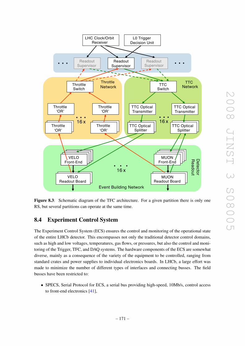
2008 JINST 3 S08005
Readout
Supervisor
ThrottleSwitch
TTCSwitch
d d
LHC Clock/OrbitReceiver
Event Building Network
TTC Optical
Transmitter
VELOReadout Board
TTC OpticalSplitter
MUONReadout Board
MUON
TTC OpticalTransmitter
Throttle
‘OR’
Throttle
‘OR’
Throttle‘OR’
Throttle‘OR’
ReadoutSupervisor
ReadoutSupervisor
. . .
. . . . . . 16 x 16 x
L0 Trigger
Decision Unit
Throttle
NetworkTTC
Network
De
tecto
rR
ea
do
ut
VELO
TTC OpticalSplitter
. . . . . .
16 x
Front-End Front-End
Figure 8.3: Schematic diagram of the TFC architecture. For a given partition there is only oneRS, but several partitions can operate at the same time.
8.4 Experiment Control System
The Experiment Control System (ECS) ensures the control and monitoring of the operational stateof the entire LHCb detector. This encompasses not only the traditional detector control domains,such as high and low voltages, temperatures, gas flows, or pressures, but also the control and moni-toring of the Trigger, TFC, and DAQ systems. The hardware components of the ECS are somewhatdiverse, mainly as a consequence of the variety of the equipment to be controlled, ranging fromstandard crates and power supplies to individual electronics boards. In LHCb, a large effort wasmade to minimize the number of different types of interfaces and connecting busses. The fieldbusses have been restricted to:
• SPECS, Serial Protocol for ECS, a serial bus providing high-speed, 10Mb/s, control accessto front-end electronics [41],
– 171 –
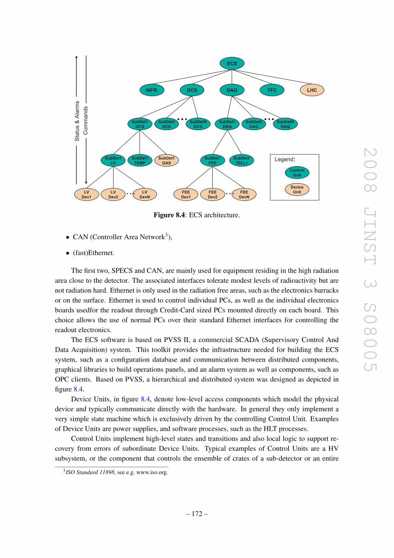
2008 JINST 3 S08005
INFR. DCS DAQ TFC LHC
ECS
SubDetN
DCS
SubDetN
DAQ
SubDet2
DCS
SubDet2
DAQ
SubDet1
DCS
SubDet1
DAQ
SubDet1
LV
SubDet1
TEMP
SubDet1
FEE
SubDet1
TELL1
LV
Dev1
LV
Dev2
LV
DevN
SubDet1
GAS
FEE
Dev1
FEE
Dev2
FEE
DevN
Control
Unit
Device
Unit……
Legend:
Com
mands
Sta
tus &
Ala
rms
Figure 8.4: ECS architecture.
• CAN (Controller Area Network3),
• (fast)Ethernet.
The first two, SPECS and CAN, are mainly used for equipment residing in the high radiationarea close to the detector. The associated interfaces tolerate modest levels of radioactivity but arenot radiation hard. Ethernet is only used in the radiation free areas, such as the electronics barracksor on the surface. Ethernet is used to control individual PCs, as well as the individual electronicsboards usedfor the readout through Credit-Card sized PCs mounted directly on each board. Thischoice allows the use of normal PCs over their standard Ethernet interfaces for controlling thereadout electronics.
The ECS software is based on PVSS II, a commercial SCADA (Supervisory Control AndData Acquisition) system. This toolkit provides the infrastructure needed for building the ECSsystem, such as a configuration database and communication between distributed components,graphical libraries to build operations panels, and an alarm system as well as components, such asOPC clients. Based on PVSS, a hierarchical and distributed system was designed as depicted infigure 8.4.
Device Units, in figure 8.4, denote low-level access components which model the physicaldevice and typically communicate directly with the hardware. In general they only implement avery simple state machine which is exclusively driven by the controlling Control Unit. Examplesof Device Units are power supplies, and software processes, such as the HLT processes.
Control Units implement high-level states and transitions and also local logic to support re-covery from errors of subordinate Device Units. Typical examples of Control Units are a HVsubsystem, or the component that controls the ensemble of crates of a sub-detector or an entire
3ISO Standard 11898, see e.g. www.iso.org.
– 172 –

2008 JINST 3 S08005
sub-farm of the Event Filter Farm. Control Units can be controlled by other Control Units, to allowthe building of a hierarchy of arbitrary depth. State sequencing in the ECS system is achieved usinga Finite State Machine package, based on SMI++ that allows creating complex logic needed, forexample, for implementing elaborate sequencing or automatic error recovery.
The distributed components of the ECS system are connected with a large Ethernet networkconsisting of several hundred Gigabit and Fast Ethernet links.
– 173 –

2008 JINST 3 S08005
Chapter 9
Computing and Resources
This section describes the dataflow of the LHCb computing model for all stages in the processingof the real and simulated LHCb events [22]. The roles of the various Tier centres are discussed andthe distribution of the processing load and storage are outlined.
There are several phases in the processing of event data. The various stages normally followeach other in a sequential manner, but some stages may be repeated a number of times. Theworkflow presented here reflects the present understanding of how to process the data. A schematicof the logical dataflow is shown in figure 9.1 and is described in more detail below.
The raw data from the detector is produced via the Event Filter farm of the online system. Thefirst step is to collect data, triggering on events of interest. The raw data are transferred to the CERNTier 0 centre for further processing and archiving. The raw data, whether real or simulated, mustthen be reconstructed to form physical quantities such as the calorimeter clusters needed to providethe energy of electromagnetic and hadronic showers, tracker hits to be associated to tracks whoseposition and momentum are to be determined. Information about particle identification (electron,photon, π0, charged hadrons, muon) is also reconstructed from the appropriate sub-systems. The
Figure 9.1: The LHCb computing logical dataflow model.
– 174 –
2008 JINST 3 S08005
event reconstruction results in the generation of new data, the Data Summary Tape (DST). Onlyenough data will be stored in the DST to allow the physics pre-selection algorithms to be run atthe next stage: this is known as a reduced DST (rDST). The first pass of the reconstruction willhappen in quasi-real time. It is planned to reprocess the data of a given year once, after the end ofdata taking for that year, and then periodically as required. This is to accommodate improvementsin the reconstruction algorithms and to make use of improved determinations of the calibration andalignment of the detector in order to generate new improved rDST information.
The rDST is analysed in a production-type mode in order to produce streams of selectedevents for further individual analysis. This activity is known as stripping. The rDST informationis used to determine the four-momentum vectors corresponding to the measured particles, to locateprimary and secondary vertices and reconstruct composite particles such as B candidates. A pre-selection algorithm will be provided for each channel of interest. Since these algorithms use toolsthat are common to many different physics analyses they are run in production-mode as a first stepin the analysis process. The events that pass the selection criteria will be fully re-reconstructed,recreating the full information associated with each event. The output of the stripping stage willbe referred to as the (full) DST and contains more information than the rDST. Before being stored,the events that pass the selection criteria will have their raw data added in order to have as detailedevent information as needed for the analysis. An event tag collection will also be created for fasterreference to selected events. The tag contains a brief summary of each event’s characteristics aswell as the results of the pre-selection algorithms and a reference to the actual DST record. Theevent tags are stored in files independent of the actual DST files. It is planned to run this production-analysis phase 4 times per year: once with the original data reconstruction; once with the re-processing of the raw data, and twice more, as the selection cuts and analysis algorithms evolve.
The baseline LHCb computing model is based on a distributed multi-tier regional centremodel. It attempts to build in flexibility that will allow effective analysis of the data whether theGrid middleware meets expectations or not. A schematic of the LHCb computing model is givenin figure 9.2.
CERN is the central production centre and will be responsible for distributing the raw datain quasi-real time to the Tier-1 centres. CERN will also take on the role of a Tier-1 centre. Sixadditional Tier-1 centres have been identified: CNAF (Italy), FZK (Germany), IN2P3 (France),NIKHEF (The Netherlands), PIC (Spain) and RAL (United Kingdom): there is also a number ofTier-2 computing centres. CERN and the Tier-1 centres will be responsible for all the production-processing phases associated with the real data. The raw data will be stored in its entirety atCERN, with another copy distributed across the other 6 Tier-1 centres. The second pass of thefull reconstruction of the raw data will also use the resources of the LHCb online farm. As theproduction of the stripped DSTs will occur at these computing centres, it is envisaged that themajority of the distributed analyses will be performed at CERN and at the Tier-1 centres. Thecurrent year’s stripped DST will be distributed to all centres to ensure load balancing. It shouldbe noted that although no user analysis is envisaged at the Tier-2 centres in the baseline modelpresented, it should not be proscribed, particularly for the larger Tier-2 centres.
It is expected that the reconstruction and the first stripping of data at CERN and at the Tier-1centres will follow the production in quasi real-time, with a maximum delay of a few days. TheDST output of the stripping will remain on disk for analysis and be distributed to all other Tier-1centres and CERN, whilst the raw and rDST will be migrated to the mass storage system, MSS.
– 175 –
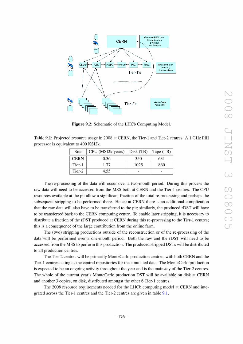
2008 JINST 3 S08005
Figure 9.2: Schematic of the LHCb Computing Model.
Table 9.1: Projected resource usage in 2008 at CERN, the Tier-1 and Tier-2 centres. A 1 GHz PIIIprocessor is equivalent to 400 KSI2k.
Site CPU (MSI2k.years) Disk (TB) Tape (TB)
CERN 0.36 350 631Tier-1 1.77 1025 860Tier-2 4.55 - -
The re-processing of the data will occur over a two-month period. During this process theraw data will need to be accessed from the MSS both at CERN and the Tier-1 centres. The CPUresources available at the pit allow a significant fraction of the total re-processing and perhaps thesubsequent stripping to be performed there. Hence at CERN there is an additional complicationthat the raw data will also have to be transferred to the pit; similarly, the produced rDST will haveto be transferred back to the CERN computing centre. To enable later stripping, it is necessary todistribute a fraction of the rDST produced at CERN during this re-processing to the Tier-1 centres;this is a consequence of the large contribution from the online farm.
The (two) stripping productions outside of the reconstruction or of the re-processing of thedata will be performed over a one-month period. Both the raw and the rDST will need to beaccessed from the MSS to perform this production. The produced stripped DSTs will be distributedto all production centres.
The Tier-2 centres will be primarily MonteCarlo production centres, with both CERN and theTier-1 centres acting as the central repositories for the simulated data. The MonteCarlo productionis expected to be an ongoing activity throughout the year and is the mainstay of the Tier-2 centres.The whole of the current year’s MonteCarlo production DST will be available on disk at CERNand another 3 copies, on disk, distributed amongst the other 6 Tier-1 centres.
The 2008 resource requirements needed for the LHCb computing model at CERN and inte-grated across the Tier-1 centres and the Tier-2 centres are given in table 9.1.
– 176 –

2008 JINST 3 S08005
Chapter 10
Performance
The data used to study the performance of the LHCb detector has been obtained from detailedMonteCarlo simulation, which produces a raw data format identical to real data. The proton-protoncollisions are simulated with the PYTHIA program [220]. The generated particles are trackedthrough the detector and the surrounding material using the GEANT package [221]. The geometryand material composition of the LHCb detector are described in detail. The detector response,resolution, noise, crosstalk, etc. have been tuned to comply with test beam results. Details aboutthis can be found in [2].
The performance quoted in this chapter is only qualitative, for two main reasons: 1) theMonteCarlo estimations are being constantly refined due to better and more detailed description ofthe detector, its material, the response of the electronics, more realistic source of noise, and alsodue to improvements in GEANT, and 2) more importantly, the real performance will be establishedand understood only using the first collected data as LHC will collide beams.
In the following, a description of the procedures for the main LHCb detector tasks, i.e. track-ing, vertex reconstruction, particle identification, mass reconstruction, is given.
10.1 Track reconstruction
In the track reconstruction software the hits in the VELO, the TT, the IT and the OT detectorsare combined to form particle trajectories from the VELO to the calorimeters. The reconstructionalgorithm aims to find all tracks in the event which leave sufficient detector hits, and not only thosefrom b-hadron decay.
Depending on their trajectories inside the spectrometer the following classes of tracks aredefined, illustrated in figure 10.1:
• Long tracks, traversing the full tracking set-up from the VELO to the T stations. These havethe most precise momentum determination and therefore are the most important set of tracksfor b-hadron decay reconstruction.
• Upstream tracks, traversing only the VELO and TT stations. These are in general lower mo-mentum tracks that are bent out of the detector acceptance by the magnetic field. However,they pass through the RICH 1 detector and may generate Cherenkov photons if they have
– 177 –

2008 JINST 3 S08005
Upstream track
TT
VELO
T1 T2 T3
T track
VELO track
Long track
Downstream track
0
0
-0.2
-0.4
-0.6
-0.8
-1.0
-1.22 4 6 8 z (m)
By (
T)
Figure 10.1: A schematic illustration of the various track types: long, upstream, downstream,VELO and T tracks. For reference the main B-field component (By) is plotted above as a functionof the z coordinate.
velocities above threshold. They are therefore used to understand backgrounds in the RICHparticle identification algorithm. They may also be used for b-hadron decay reconstructionor flavour tagging, although their momentum resolution is rather poor.
• Downstream tracks, traversing only the TT and T stations. The most relevant cases are thedecay products of K0
S and Λ that decay outside the VELO acceptance.
• VELO tracks, measured in the VELO only and are typically large angle or backward tracks,useful for the primary vertex reconstruction.
• T tracks: are only measured in the T stations. They are typically produced in secondaryinteractions, but are useful for the global pattern recognition in RICH 2.
The track reconstruction starts with a search for track seeds, the initial track candidates [222],in the VELO region and the T stations where the magnetic field is low. After tracks have beenfound, their trajectories are refitted with a Kalman filter [223] which accounts for multiple scatter-ing and corrects for dE/dx energy loss. The quality of the reconstructed tracks is monitored by theχ2 of the fit and the pull distribution of the track parameters.
The pattern recognition performance is evaluated in terms of efficiencies and ghost rates. Theefficiencies are normalized to the reconstructible track samples. To be considered reconstructible,a track must have a minimum number of hits in the relevant subdetectors. To be considered assuccessfully reconstructed, a track must have at least 70% of its associated hits originating froma single MonteCarlo particle. The reconstruction efficiency is defined as the fraction of recon-structible tracks that are successfully reconstructed, and the ghost rate is defined as the fraction of
– 178 –

2008 JINST 3 S08005
Figure 10.2: Display of the reconstructed tracks and assigned hits in an event. The insert shows azoom in the plane (x,y) into the VELO region.
reconstructed tracks that are not matched to a true MonteCarlo particle. The results quoted in thissection are obtained from a sample of B0→ J/ψ K0
S events.An example of a reconstructed event is displayed in figure 10.2. The average number of
successfully reconstructed tracks in fully simulated bb events is about 72, which are distributedamong the track types as follows: 26 long tracks, 11 upstream tracks, 4 downstream tracks, 26VELO tracks and 5 T tracks. The track finding performance is summarized in the following forthe most important cases: the long tracks, the low momentum (upstream) tracks and K0
S decay(downstream) tracks.
The efficiency to find as a long track the trajectory of a particle with momentum larger than10 GeV/c is on average ∼94%. The corresponding average ghost fraction is about 9%, but mostghost tracks have a low reconstructed pT.
The momentum and impact parameter resolutions of the reconstructed long tracks are shownin figure 10.3. The momentum resolution is plotted as a function of the track momentum and isseen to be increasing from δ p/p = 0.35% for low momentum tracks to δ p/p = 0.55% for tracks atthe high end of the spectrum. In the same figure the momentum spectrum for B decay tracks is alsoillustrated. The impact parameter resolution is plotted as function of 1/pT of the track. The lineardependence can be parametrized as σIP = 14 µm + 35 µm/pT with pT in GeV/c. For comparisonthe 1/pT spectrum of B decay particles in the detector acceptance is plotted in the same figure.
The efficiency of the upstream track finding for particles with p > 1 GeV/c is approximately75% with a corresponding ghost rate of 15%. The momentum resolution is only δ p/p∼ 15%, dueto the small value of the total magnetic field integral in the considered region.
The efficiency for finding downstream tracks above 5 GeV/c is about 80%. Since the down-stream tracks traverse most of the magnetic field, the momentum resolution is relatively good withan average of δ p/p = 0.43% for pions originating from K0
S decays in B0→ J/ψ K0S events. In order
– 179 –

2008 JINST 3 S08005
0
0.1
0.2
0.3
0.4
0.5
0.6
0.7
dp
/p
(%)
0
200
400
600
800
a)
0 20 40 60 80 100 120 140
0
0.02
0.04
0.06
0.08
0.1
0.12
0.14
0.16
IP r
eso
luti
on
(m
m)
1/p t (GeV/c) -1
0
250
500
750
1000
0 0.5 1 1.5 2 2.5 3 3.5 4
b)
p (GeV/c)
Figure 10.3: Resolution on the reconstructed track parameters at the production vertex of thetrack: (a) momentum resolution as a function of track momentum, (b) impact parameter resolution,calculated as the sum of the errors in the three projections added in quadrature, as a function of1/pT. For comparison, the 1/pT spectra of B decay particles are shown in the lower part of theplots.
to maintain high efficiency, the reconstruction allows for typically two or three track candidates inthe TT to be linked to a single track seed in the T stations.
K0S candidates are reconstructed through their decay to π+π−. For K0
S from B0 → J/ψ K0S
decays, about 25% decay inside the active region of the VELO, 50% decay outside the active re-gion of the VELO but upstream of TT, and the rest decay after TT, and will therefore be difficultto reconstruct. The K0
S that decay outside the active region of the VELO but before TT are recon-structed using pairs of oppositely charged downstream tracks. The pions from K0
S that decay withinthe VELO acceptance give either a long track or an upstream track. The corresponding mass plotsare shown in figure 10.4. As can be seen, there exists some combinatorial background from othertracks in the signal events, particularly for the long-upstream category, but this background can beremoved by the additional requirements that are imposed when reconstructing the B meson.
10.2 Particle identification
The information from the two RICH detectors, the calorimeters and the muon system is combinedfor optimal identification of charged particle types (e,µ,π,K,p). Photons and neutral pions (γ,π0)are identified using the electromagnetic calorimeter, where the π0→ γγ decay may be detected astwo separate electromagnetic clusters or as a merged cluster.
– 180 –

2008 JINST 3 S08005
(a)
(c)
(b)
Invariant mass (MeV/c2)
200
100
400
300
200
100
150
100
50
0 400 450 500 550 600
Ent
ries
Figure 10.4: Reconstruction of K0S→ π+π−. The π+π− invariant mass is shown in B0→ J/ψ K0
Ssignal events, using different categories of tracks for the pion candidates: (a) downstream-downstream, (b) long-long, (c) long-upstream. Combinations coming from true K0
S are indicatedby the shaded histograms.
10.2.1 Hadron identification
Particle identification with the RICH system is performed as follows. The baseline algorithm isbased on a log-likelihood approach which matches the observed pattern of hit pixels in the RICHphotodetectors to that expected from the reconstructed tracks under a given set of particle hypothe-ses [224]. In constructing this likelihood it is necessary to calculate the effective emission anglefor all pixel-track combinations which could physically be associated through Cherenkov radia-tion. The likelihood is maximised by varying the particle hypotheses of each track in turn, throughelectron, muon, pion, kaon and proton. As the likelihood considers all found tracks in the event,and all three radiators simultaneously, the method is referred to as the global pattern-recognition.
The output of the global pattern-recognition is a best hypothesis for each track, and the de-crease in log-likelihood when changing from this solution to another hypothesis.
The RICH system provides good particle identification over the entire momentum range.The average efficiency for kaon identification for momenta between 2 and 100 GeV/c is ε(K →K) ∼95%, with a corresponding average pion misidentification rate ε(π → K) ∼5%. Around30 GeV/c the identification probability is ∼97% and the misidentification probability ∼5%.
Other methods have been investigated to find the Cherenkov rings in the absence of trackinginformation. These include Markov chain MonteCarlo and Hough Transform techniques [225].
– 181 –

2008 JINST 3 S08005
Such approaches may be particularly useful in the early stages of data taking, when it may be nec-essary to study the performance of the RICH detector independently of spectrometer information.
For physics analyses and detector diagnostics it will be very important to understand theperformance of the RICH particle identification independently of simulation studies. The dominantD∗±→D0(K−π−)π± decay mode will provide a very high statistics unbiased sample of pions andkaons which may be used to measure the RICH performance directly. Studies indicate that withkinematic cuts alone purities of > 95% can be achieved.
10.2.2 Muon identification
Muons are identified by extrapolating well reconstructed tracks with p > 3 GeV/c into the muonstations (particles with p < 3 GeV/c do not reach the muon system). Hits are searched within fieldsof interest (FOI) around the extrapolation point of the track in each muon station, parameterized as afunction of momenta for each station and region. A track is considered as a muon candidate when aminimum number of stations (2–4 depending on momentum) have hits in their corresponding FOI.This number optimizes the resulting efficiency [226].
Using a sample of B0→ J/ψ K0S the muon identification efficiency was measured to be ε(µ→
µ)∼ 94% with a corresponding misidentification ε(π→ µ)∼ 3%. The efficiency is a flat functionof the momentum above 10 GeV/c.
Discriminating variables helping to improve the muon selection purity are constructed fromthe comparison of slopes in the muon system and the main tracker, and from the average track-hitdistance of all hits in FOI associated to the track. For each track the difference in log-likelihoodbetween the muon hypothesis and pion hypothesis is determined, and summed with the values fromthe RICH and calorimeter systems (if available). By doing this the pion misidentification rate canbe reduced to ∼1%, whilst maintaining a muon efficiency of ∼93% for muons above 3 GeV/c.
The high purity that can be achieved with such cuts is illustrated in figure 10.5 where theµ+µ− mass plot is shown at the first step in the analysis of B0
s → J/ψ φ events, taking all oppositelycharged pairs of tracks from signal events that pass the muon identification requirements. The J/ψ
mass peak is reconstructed with a resolution of about 13 MeV/c2.
10.2.3 Electron identification
The electron identification [227] is mainly based on the balance of track momentum and energy ofthe charged cluster in the ECAL (figure 10.6), and the matching between the corrected barycenterposition of the cluster with the extrapolated track impact point.
A second estimator is related to the bremsstrahlung photons emitted by electrons before themagnet. As there is little material within the magnet, such neutral clusters are expected in a welldefined position given by the electron track extrapolation from before the magnet, as illustratedin figure 10.7: if an electron radiates photons when passing through material before the magnet,a cluster with energy E1 is seen in the ECAL. If it radiates after the magnet, the bremsstrahlungphoton will not lead to a separate cluster. For electron identification the corresponding clusterenergy E2 will be compared to the track momentum E2 = p, while the energy of the electron at theorigin is E0 = E1 +E2.
– 182 –

2008 JINST 3 S08005
2.7 2.8 2.9 3 3.1 3.2 3.3 3.40
200
400
600
800
1000
1200
1400
µ+µ− mass (GeV/c2)
En
trie
s
3.5
Figure 10.5: Invariant mass plots for the reconstruction of J/ψ → µ+µ− decays in B0s → J/ψ φ
signal events.
0.01
0.02
0.03
0.04
0.05
0 0.2 0.4 0.6 0.8 1 1.2 1.4 1.6 1.8 2 0
electrons
hadrons
Ecluster / ptrack
arb
itra
ry s
cale
E1
E2
E0
p
Magnet ECAL
e
γ
γ
Figure 10.6: The ratio of uncorrected energyof the charged cluster in ECAL to the momen-tum of reconstructed tracks for electrons (openhistogram) and hadrons (shaded histogram).
Figure 10.7: Schematic illustration ofbremsstrahlung correction.
Further improvement in electron identification is obtained by using the track energy depo-sition in the preshower detector and the deposition of the energy along the extrapolated particletrajectory in the hadronic calorimeter HCAL.
For particle identification, the calorimeter information is combined with that from the RICHand muon detectors.
To illustrate the performance of electron reconstruction, the J/ψ mass plot for the decayJ/ψ → e+e− is shown as open points in figure 10.8. The signal is fitted with a function plus aradiative tail, to account for the imperfect correction of bremsstrahlung. The background tracks are
– 183 –
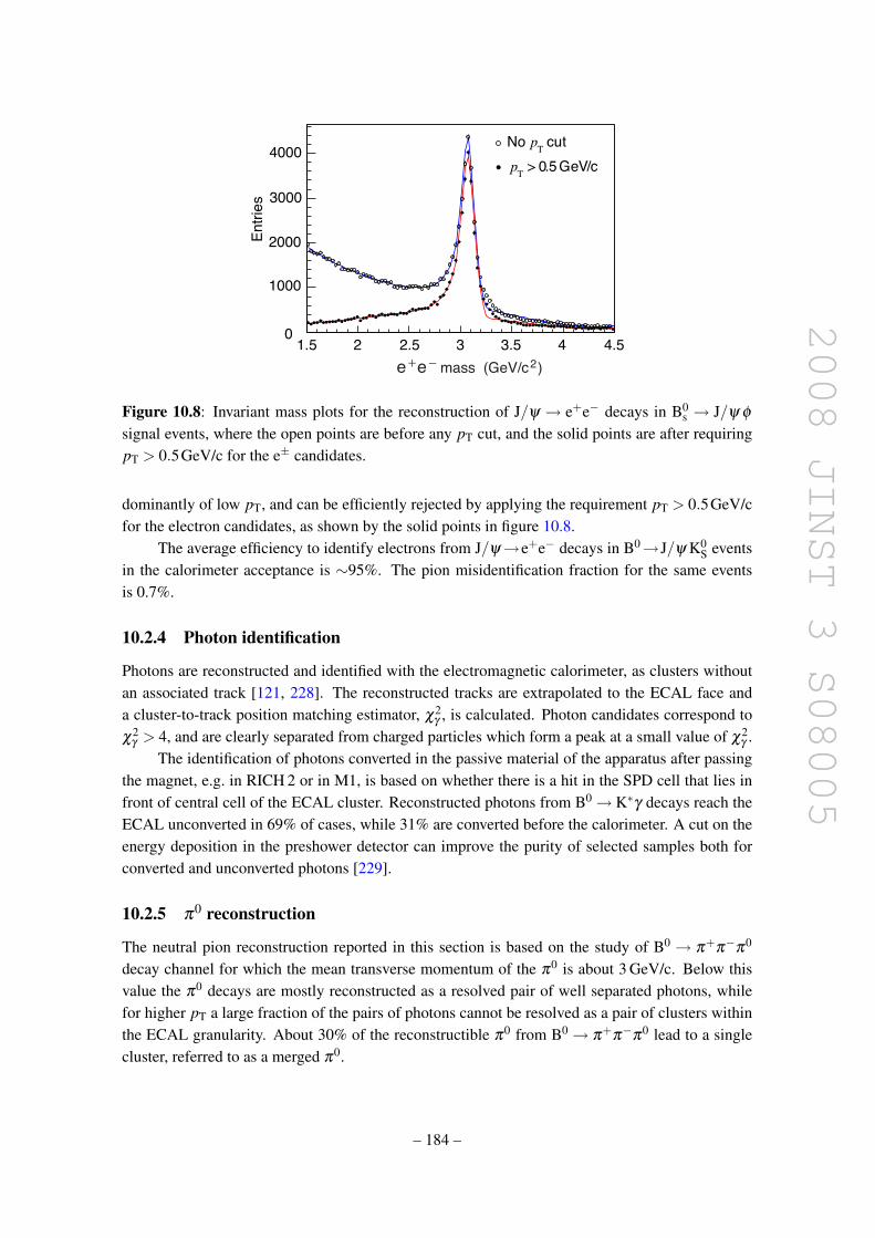
2008 JINST 3 S08005
0
1000
2000
3000
No pT
cut
pT > 0.5 GeV/c
Entr
ies
4000
e +e − mass (GeV/c2)
1.5 2 2.5 3 3.5 4 4.5
Figure 10.8: Invariant mass plots for the reconstruction of J/ψ → e+e− decays in B0s → J/ψ φ
signal events, where the open points are before any pT cut, and the solid points are after requiringpT > 0.5GeV/c for the e± candidates.
dominantly of low pT, and can be efficiently rejected by applying the requirement pT > 0.5GeV/cfor the electron candidates, as shown by the solid points in figure 10.8.
The average efficiency to identify electrons from J/ψ→e+e− decays in B0→J/ψ K0S events
in the calorimeter acceptance is ∼95%. The pion misidentification fraction for the same eventsis 0.7%.
10.2.4 Photon identification
Photons are reconstructed and identified with the electromagnetic calorimeter, as clusters withoutan associated track [121, 228]. The reconstructed tracks are extrapolated to the ECAL face anda cluster-to-track position matching estimator, χ2
γ , is calculated. Photon candidates correspond toχ2
γ > 4, and are clearly separated from charged particles which form a peak at a small value of χ2γ .
The identification of photons converted in the passive material of the apparatus after passingthe magnet, e.g. in RICH 2 or in M1, is based on whether there is a hit in the SPD cell that lies infront of central cell of the ECAL cluster. Reconstructed photons from B0→ K∗γ decays reach theECAL unconverted in 69% of cases, while 31% are converted before the calorimeter. A cut on theenergy deposition in the preshower detector can improve the purity of selected samples both forconverted and unconverted photons [229].
10.2.5 π0 reconstruction
The neutral pion reconstruction reported in this section is based on the study of B0 → π+π−π0
decay channel for which the mean transverse momentum of the π0 is about 3 GeV/c. Below thisvalue the π0 decays are mostly reconstructed as a resolved pair of well separated photons, whilefor higher pT a large fraction of the pairs of photons cannot be resolved as a pair of clusters withinthe ECAL granularity. About 30% of the reconstructible π0 from B0→ π+π−π0 lead to a singlecluster, referred to as a merged π0.
– 184 –

2008 JINST 3 S08005
Invariant mass (MeV/c2)
40 80 120 160 2000
2000
4000
6000
8000
10000(b) π0 → γ (e+e−)
Entr
ies
2000
4000
6000
8000
10000
12000
14000(a) π0 → γγ
Entr
ies
Invariant mass (MeV/c2)
40 80 120 160 2000
Figure 10.9: π0 mass distributions, where (a) neither photon has converted, (b) one γ converted be-fore the calorimeter. The conversions are identified using the SPD information. The contributionsof true π0 are indicated by the shaded histograms.
Figure 10.9 shows the mass distributions obtained in the case where both photon candidateswith pT > 200 MeV/c reach the calorimeter (a), and for the case that one photon converted be-fore the calorimeter (b), where the identification of the conversion relies on the SPD signal. Thedistributions are fitted with the sum of a gaussian and a polynomial function to describe the com-binatorial beckground. The fit results in both cases in a mass resolution for the π0 of ∼10 MeV/c2.
An algorithm has been developed to disentangle a potential pair of photons merged into asingle cluster. The energy of each cell of the cluster is shared between two virtual sub-clustersaccording to an iterative procedure based on the expected transverse shape of photon showers. Eachof the two sub-clusters is then reconstructed as coming from a photon, as for isolated photons.
The reconstruction efficiency for π0 that give photons inside the geometrical acceptance issummarized in figure 10.10 for the resolved and merged case.
10.2.6 Expected global performance
Given the reconstruction performance described above, the global performance for the reconstruc-tion of B decays in the LHCb detector is expected to be: a primary vertex resolution of ∼ 10 µmtransverse to the beam axis and ∼ 60 µm along the beam axis; an invariant mass resolution typ-ically in the range between 12 MeV/c and 25 MeV/c; and a proper lifetime resolution of ∼ 40 fs,with a dependence on the decay channel studied.
– 185 –

2008 JINST 3 S08005
0
20
40
60
80
2 4 6 8 10
Eff
icie
ncy
(%
)
pT (π0) (GeV/c)
Figure 10.10: The reconstruction efficiency for π0 decaying into photons inside the geometricalacceptance with pT > 200MeV/c, versus the π0 transverse momentum. The contributions fromresolved and merged π0 reconstruction are indicated by the solid and dashed histograms, respec-tively.
– 186 –

2008 JINST 3 S08005
Chapter 11
Summary
The LHCb experiment has been described as it will be operational at the start up of the LHC, in-cluding the detector, its interface to the machine, the hardware-based first level and software-basedhigh level triggers, and the online system. The intrinsic performance of all detector components,as studied in the laboratory and with test-beam measurements, corresponds to expectations. Theoverall performance for event reconstruction has also been presented, including tracking, vertexingand particle identification, as determined through detailed simulation.
The LHCb experiment will be operational at the time of the very first collisions of the LHC.The first data will be used to measure the real performance of the detector, the trigger behaviour,the reconstruction capabilities and the event selections, and to ensure that the design resolutionshave been achieved. This will permit interesting results to be produced in the domain of heavyflavour physics, even with the first period of stable beams in the LHC. The experiment and itsassociated computing tools will allow a search to be made for the effects of new physics, throughhigh precision measurements of CP violation and rare decays in the b- and c-physics sectors.
– 187 –

2008 JINST 3 S08005
Acknowledgements
We are greatly indebted to all CERN departments, without whose support, assistance and activecontribution, the preparation of the experimental site, its infrastructure and installation of the LHCbdetector would not have been possible.
We are deeply grateful to our colleagues from the LHC machine for the collaborative relation-ship and friendly cooperation which enabled running both projects smoothly and effective close toeach other.
We acknowledge all the funding agencies which supported the construction and the commis-sioning of the LHCb detector and also provided the computing infrastructure:Brazil: CNPq, FINEP and FAPERJChina: the National Natural Science Foundation of China under contract Nos. 10225522,10421140657, 10620130426, and the Key Laboratory of Particle and Imaging (Tsinghua Univer-sity), Ministry of Education of the People’s Republic of ChinaFrance: CNRS-Institut National de Physique Nucléaire et de Physique des Particules (IN2P3)Germany: Bundesministerium für Bildung und Forschung and Deutsche ForschungsgemeinschaftItaly: Istituto Nazionale di Fisica Nucleare (INFN)The Netherlands: Foundation of Fundamental Research of Matter (FOM)Poland: Ministry of Science and Higher EducationRomania: Ministry of Education and ResearchRussia: the Ministry of Science and Technology for the Russian Federation and the Russian FederalAgency for Atomic EnergySpain: the Spanish MEC (projects FPA2005-06889, FPA2005-06441, FPA2005-07761-C02-01,FPA2005-07761-C02-02, and project CPAN CSD2007-00042 of the Programme Consolider-Ingenio 2010), the "Generalitat de Catalunya" (AGAUR 2005SGR00385) and by the "Xunta deGalicia" (PGIDIT 06PXIC206066PN)Switzerland: the State Secretariat for Education and Research, the Swiss National Science Foun-dation and the Ecole Polytechnique Fédérale de Lausanne; the cantons of Vaud and ZuerichUkraine: Academy of Sciences of UkraineUnited Kingdom: the Science and Technology Facilities Council (previously PPARC), the RoyalSocietyUnited States of America: the U. S. National Science Foundation.
We also acknowledge the European Community support through the projects: HELEN, IN-TAS, Marie Curie, RII3-CT-2004506078; the regional support from the Region Auvergne (France).
– 188 –

2008 JINST 3 S08005
The construction of the detector would not have been possible without the technical supportin each of the participating laboratories: we wish to thank A. Iacoangeli of Università Roma LaSapienza; R. Lunadei and C. Piscitelli of INFN-Roma1; W. Lau, J. Tacon, M. Tacon and S. Yangof Oxford.
– 189 –

2008 JINST 3 S08005
Bibliography
[1] LHCb collaboration, A Large Hadron Collider beauty experiment, Technical Proposal,CERN-LHCC-98-004, http://cdsweb.cern.ch/record/622031.
[2] LHCb collaboration, R. Antunes-Nobrega et al., LHCb reoptimized detector design andperformance, CERN-LHCC-2003-030, http://cdsweb.cern.ch/record/630827.
[3] M. Needham and T. Ruf, Estimation of the material budget of the LHCb detector, NoteLHCb-2007-025, http://cdsweb.cern.ch/record/1023537.
[4] J. Christiansen, Requirements to the L0 front-end electronics, Note LHCb-2001-014,http://cdsweb.cern.ch/record/691647.
[5] J. Christiansen, Requirements to the L1 front-end electronics, EDMS documenthttps://edms.cern.ch/document/715154.
[6] P. Moreira et al., G-Link and gigabit ethernet compliant serializer for LHC datatransmission, IEEE Nucl. Sci. Symp. Conf. Rec. 2 (2000) 9/6; A radiation tolerant gigabitserializer for LHC data transmission, http://edms.cern.ch/file/906036/1/.
[7] J. Christiansen, Test, time alignment, calibration and monitoring in the LHCb front-endelectronics, EDMS document https://edms.cern.ch/document/692583.
[8] B. Taylor, Timing distribution at the LHC, Proceedings of the LECC 2002 Workshop,Colmar France (2002), http://cdsweb.cern.ch/record/592719.
[9] Embedded Local Monitor Board home page,http://elmb.web.cern.ch/ELMB/ELMBhome.html.
[10] G. Haefeli et al., The LHCb DAQ interface board T ELL1, Nucl. Instrum. Meth. A 560(2006) 494.
[11] Radiation hardness assurance,http://lhcb-elec.web.cern.ch/lhcb-elec/html/radiation_hardness.htm.
[12] G. Corti and G. von Holtey, Study of beampipe induced background in the LHCb detectorfor the optimization of the vacuum chamber design, Note LHCb-2003-085.
– 190 –

2008 JINST 3 S08005
[13] J.R. Knaster, The vacuum chamber in the interaction region of particle colliders: ahistorical study and developments implemented in the LHCb experiment at CERN, Ph.D.Thesis, CERN-ETSII, Geneva Switzerland (2004).
[14] CERN Safety Instruction IS nr 25, http://safety-commission.web.cern.ch/safety-commission/SC-site/sc_pages/documents/instructions.html
[15] R. Veness et al., Study of minimised UHV flanges for LHC experiments, CERN Vacuumtech. Note EDMS document https://edms.cern.ch/document/350384.
[16] D. Ramos, Design of the fixed beampipe supports inside the acceptance region of the LHCbexperiment, CERN Vacuum Tech. Note, EDMS documenthttps://edms.cern.ch/document/882924.
[17] C. Benvenuti et al., Vacuum properties of TiZrV non-evaporable getter films, Vacuum 60(2001) 57.
[18] O. Grobner, Overview of the LHC vacuum system, Vacuum 60 (2001) 25.
[19] L. Fernandez-Herando et al., The radiation monitoring system for the LHC experimentalareas, TS-Note-2004-006, http://cdsweb.cern.ch/record/740728.
[20] B. Todd et al., The architecture, design and realisation of the LHC beam interlock system,in Proceedings of the 10th ICALEPCS International Conference on Accelerator & LargeExperimental Physics Control System, Geneva Switzerland (2005).
[21] E. Effinger et al., Single gain radiation tolerant LHC beam loss acquisition card, inProceedings of the 8th European Workshop on Beam Diagnostics and Instrumentation forParticle Accelerators, Venice Italy (2007), http://cdsweb.cern.ch/record/1045244.
[22] LHCb collaboration, R. Antunes-Nobrega et al., LHCb computing technical design report,CERN-LHCC-2005-019, http://cdsweb.cern.ch/record/835156.
[23] LHCb collaboration, S. Amato et al., LHCb magnet technical design report,CERN-LHCC-2000-007, http://cdsweb.cern.ch/record/424338.
[24] J. André et al., Status of the LHCb magnet system, IEEE Trans. Appl. Supercond. 12 (2002)366.
[25] J. André, et al., Status of the LHCb dipole magnet, IEEE Trans. Appl. Supercond. 14 (2004)509.
[26] M. Patel, M. Losasso and T. Gys., Magnetic shielding studies of the LHCb rich photondetectors, Nucl. Instrum. Meth. A 553 (2005) 114.
[27] F. Bersgma, Calibration of Hall sensors in three dimensions, in Proceedings of the 13th
International Magnetic Measurement Workshop (IMMW13), SLAC Stanford, CaliforniaU.S.A. (2003), http://cdsweb.cern.ch/record/1072471.
– 191 –

2008 JINST 3 S08005
[28] LHCb collaboration, P.R. Barbosa-Marinho et al., Vertex locator technical design report,CERN-LHCC-2001-011, http://cdsweb.cern.ch/record/504321.
[29] P. Koppenburg, Simulation of the vertex trigger preprocessor:effects of noise on L1performance, Note LHCb-1999-003, http://cdsweb.cern.ch/record/691699.
[30] P. Koppenburg, Effect of pulse overspill on the level 1 trigger, Note LHCb-2001-078,http://cdsweb.cern.ch/record/684442.
[31] D. Petrie, C. Parkes and S. Viret, Study of the impact of VELO misalignments on the LHCbtracking and L1 trigger performance, Note LHCb-2005-056,http://cdsweb.cern.ch/record/899299.
[32] M. Ferro-Luzzi et al., A first study of wake fields in the LHCb detector, Note LHCb-99-041,http://cdsweb.cern.ch/record/684454; Wake fields in the LHCb vertex detector, NoteLHCb-99-043, http://cdsweb.cern.ch/record/691632;N. Van Bakel et al., Wake fields in the LHCb vertex detector: alternative design for thewake fields suppressor, Note LHCb-99-044, http://cdsweb.cern.ch/record/691599.
[33] LHCb VELO GROUP collaboration, Review of the planned replacement of n-on-n withn-on-p detectors for LHCb-Velo, EDMS document https://edms.cern.ch/document/883223.
[34] S. Löchner and M. Schmelling, The Beetle Reference Manual, Note LHCb-2005-105,http://cdsweb.cern.ch/record/1000429.
[35] R. Mountain et al., VELO module transport box document and operational guide, SyracuseUniversity note, SU-LHCb-2006-02-03.
[36] A. Bates et. al., A facility for long term evaluation and quality assurance of LHCb vertexdetector modules, Note LHCb-2007-102, http://cdsweb.cern.ch/record/1061056.
[37] M. Schmelling, Specification of the front-end electronics for the LHCb vertex locator, NoteLHCb-2001-048, http://cdsweb.cern.ch/record/691610.
[38] A. Bates et. al., VELO module characterisation: results from the Glasgow LHCb VELOmodule burn-in, Note LHCb-2007-103, http://cdsweb.cern.ch/record/1046811.
[39] L. Eklund et. al., Radiation tests of the VELO ECS and Analogue Repeater Mezzanines,Note LHCb-2006-001, http://cdsweb.cern.ch/record/926372.
[40] L. Eklund, Control and monitoring of VELO and pile-up level 0 electronics, EDMSdocument https://edms.cern.ch/document/596194.
[41] D. Breton and D. Charlet, SPECS: the Serial Protocol for the Experiment Control System ofLHCb, Note LHCb-2003-004, http://cdsweb.cern.ch/record/681284.
[42] S. Kersten and P. Kind, Technical description of the interlock circuit and system of theATLAS pixel detector, ATL-IP-ES-0041.
– 192 –

2008 JINST 3 S08005
[43] G. Haefeli, Contribution to the development of the acquisition electronics for the LHCbexperiment, LPHE Master thesis, Lausanne Switzerland (2004).
[44] LHCb ST and VELO GROUP collaborations, G. Haefeli and A. Gong, LHCb VELO andST clusterization on T ELL1 EDMS document https://edms.cern.ch/document/690585.
[45] LHCb VELO GROUP, D. Eckstein, VELO raw data format and strip numbering, EDMSdocument https://edms.cern.ch/document/637676.
[46] LHCb VELO GROUP collaboration, M. Ferro-Luzzi, VELO hardware interlocks, EDMSdocument https://edms.cern.ch/document/706629.
[47] M. Artuso and J.C. Wang, Study of the spatial resolution achievable with the BTeV pixelsensors, Nucl. Instrum. Meth. A 465 (2000) 115 [hep-ex/0007054].
[48] C. Parkes and T. Szumlak, VELO event model, Note LHCb-2006-054,http://cdsweb.cern.ch/record/989093.
[49] C. Parkes, T. Ruf and T. Szumlak, Reconstruction of cluster positions in the LHCb VELO,Note LHCb-2007-151, http://cdsweb.cern.ch/record/1074928.
[50] W. Baldini et al., LHCb alignment strategy, Note LHCb-2006-035,http://cdsweb.cern.ch/record/964804.
[51] V. Blobel and C. Kleinwort, A new method for the high-precision alignment of trackdetectors, Contribution to the Conference on Advanced Statistical Techniques in ParticlePhysics PHYSTAT2002, Durham U.K., hep-ex/0208021.
[52] T.W. Versloot, Position reconstruction and charge distribution in LHCb VELO siliconsensors, Note LHCb-2007-119, http://cdsweb.cern.ch/record/1073483.
[53] J. Gassner, M. Needham and O. Steinkamp, Layout and expected performance of the LHCbTT station, Note LHCb-2003-140, http://cdsweb.cern.ch/record/728548.
[54] LHCb collaboration, P.R. Barbosa-Marinho et al., LHCb inner tracker technical designreport, CERN-LHCC-2002-029, http://cdsweb.cern.ch/record/582793.
[55] J. Gassner, F. Lehner and S. Steiner, The mechanical design of the LHCb silicon triggertracker, Note LHCb-2004-110, http://cdsweb.cern.ch/record/858499.
[56] J.-L. Agram et al., The silicon sensors for the Compact Muon Solenoid tracker — designand qualification procedure, Note CMS-2003-015, http://cdsweb.cern.ch/record/687875.
[57] A. Bay et al., Hybrid design, procurement and testing for the LHCb silicon tracker, NoteLHCb-2005-061, http://cdsweb.cern.ch/record/885752.
[58] I. Abt et al., Gluing silicon with silicone, Nucl. Instrum. Meth. A 411 (1998) 191.
[59] A. Vollhardt, A radiation tolerant fiber-optic readout system for the LHCb silicon tracker,Note LHCb-2005-032, http://cdsweb.cern.ch/record/872267.
– 193 –

2008 JINST 3 S08005
[60] V. Bobillier, J. Christiansen and R. Frei, Grounding, shielding and power distribution inLHCb, Note LHCb-2004-039, http://cdsweb.cern.ch/record/738180.
[61] D. Esperante and A. Vollhardt, Design and development of the control board for the LHCbsilicon tracker, Note LHCb-2007-153, http://cdsweb.cern.ch/record/1082457.
[62] TTCrq, http://proj-qpll.web.cern.ch/proj-qpll/ttcrq.htm.
[63] C. Bauer et al., Grounding, shielding and power distribution for the LHCb silicon tracking,Note LHCb-2004-101, http://cdsweb.cern.ch/record/836185.
[64] M. Agari et al., Test beam results of multi-geometry prototype sensors for the LHCb innertracker, Note LHCb-2002-058, http://cdsweb.cern.ch/record/684437.
[65] R. Bernhard et al., Measurements of prototype ladders for the silicon tracker with laser,Note LHCb-2003-075, http://cdsweb.cern.ch/record/684488.
[66] M. Agari et al., Test-beam measurements on prototype ladders for the LHCb TT station andInner Tracker, Note LHCb-2003-082, http://cdsweb.cern.ch/record/722699.
[67] J. Gassner et al., Measurements of prototype ladders for the TT station with a laser, NoteLHCb-2004-102, http://cdsweb.cern.ch/record/818585.
[68] M. Agari et al., Measurements of a prototype ladder for the TT station in a 120 GeV/c π−
beam, Note LHCb-2004-103, http://cdsweb.cern.ch/record/811085.
[69] S. Köstner and U. Straumann, Noise considerations for the beetle amplifier used with longsilicon strip detectors, Note LHCb-2005-029, http://cdsweb.cern.ch/record/837194.
[70] M. Needham, Silicon tracker occupancies and clustering, Note LHCb-2007-024,http://cdsweb.cern.ch/record/1023456.
[71] M. Needham and D. Volyanskyy, Updated geometry description for the LHCb triggertracker, Note LHCb-2006-032, http://cdsweb.cern.ch/record/961216.
[72] A. Perrin and K. Vervink, The inner tracker detector description and its implementation inthe XML database, Note LHCb-2006-018, http://cdsweb.cern.ch/record/962061.
[73] LHCb collaboration, P.R. Barbosa-Marinho et al., Outer tracker technical design report,CERN-LHCC-2001-024, http://cdsweb.cern.ch/record/519146.
[74] S. Bachmann, Specifications for the drift gas quality of the outer tracking system, NoteLHCb-2002-031; Proposal for the gas distribution in the outer tracking system, NoteLHCb-2003-054.
[75] J. Nardulli and N. Tuning, A study of the material in an outer tracker module, NoteLHCb-2004-114, http://cdsweb.cern.ch/record/815493.
[76] T. Haas, Aging phenomena in the LHCb outer tracker, Nucl. Instrum. Meth. A 581 (2007)164.
– 194 –

2008 JINST 3 S08005
[77] A. Berkien et al., The LHCb outer tracker front-end electronics, Note LHCb-2005-025,http://cdsweb.cern.ch/record/1089278;Y. Guz et al., Study of the global performance of an LHCb OT front-end electronicsprototype, Note LHCb-2004-120.
[78] N. Dressnandt et al., Implementation of the ASDBLR and DTMROC ASICS for the ATLASTRT in DMILL technology, Proceedings of the 6th Workshop on Electronics for LHCExperiments, Cracow Poland (2000), http://cdsweb.cern.ch/record/478863;R. Bevensee et al., An amplifier-shaper-discriminator with baseline restoration for theATLAS transition radiation tracker, IEEE Trans. Nucl. Sci. 43 (1996) 1725.
[79] H. Deppe, et al., The OTIS reference manual, Note LHCb-2008-010,http://cdsweb.cern.ch/record/1089277.
[80] U. Stange, Development and characterization of a rad hard readout chip for the LHCbouter tracker detector, PhD Thesis, Heidelberg Germany (2005).
[81] U. Uwer et al., Specifications for the IF13-2 prototype of the auxiliary board for the outertracker, Note LHCb-2005-039.
[82] G.W. van Apeldoorn et al., Beam tests of final modules and electronics of the LHCb outertracker in 2005, Note LHCb-2005-076, http://cdsweb.cern.ch/record/896901.
[83] T. Bauer, J. Nardulli and N. Tuning, Flatness of an outer tracker module, NoteLHCb-2005-009.
[84] N. Tuning and A. Pellegrino, Flatness of an outer tracker layer in a prototype C-frame,Note LHCb-2008-003.
[85] H. Dekker et al., The RASNIK/CCD 3-dimensional alignment system, in Proceedings of the3rd International Workshop On Accelerator Alignment (IWAA 93), Annecy France (1993).
[86] M. Adamus, A. Nawrot and M. Szczekowski, Alignment system for the outer trackerdetector in LHCb experiment, Note LHCb-2001-006, http://cdsweb.cern.ch/record/691623;M. Adamus et al., First results from a prototype of the RASNIK alignment system for theouter tracker detector in LHCb experiment, Note LHCb-2002-016.
[87] LHCb RICH GROUP collaboration, N. Brook et al., LHCb RICH 1 engineering designreview report, Note LHCb-2004-121, http://cdsweb.cern.ch/record/897981.
[88] F. Metlica, Development of light-weight spherical mirrors for RICH detectors, NIMA48462, http://dx.doi.org/10.1016/j.nima.2008.07.026.
[89] A. Papanestis, Limits of software compensation for mirror misalignment of the RICHdetectors, Note LHCb-2001-141.
[90] R. Plackett, Photon detectors for the Ring Imaging Cherenkov detectors of the LHCbexperiment, PhD Thesis, University of London, London U.K. (2006).
– 195 –

2008 JINST 3 S08005
[91] LHCb collaboration, S. Amato et al., LHCb RICH technical design report,CERN-LHCC-2000-037, http://cdsweb.cern.ch/record/494263.
[92] LHCb RICH GROUP collaboration, M. Adinolfi et al., LHCb RICH 2 engineering designreview report, Note LHCb-2002-009, http://cdsweb.cern.ch/record/691478.
[93] T. Bellunato, Development of ring imaging Cherenkov detectors for LHCb, PhD Thesis,Università degli Studi di Milano, Milano Italy (2001).
[94] M. Laub, Development of opto-mechanical tools and procedures for a new generation ofRICH-detectors at CERN, PhD Thesis, Ceské vysoké ucení technické v Praze, PragueCzech Republic (2001).
[95] L. Fernández Hernando, New automatic techniques to test optical components of the nextgeneration of RICH detectors at CERN, PhD Thesis, Universitat Politècnica de Catalunya,Barcelona Spain (2001).
[96] G. Aglieri-Rinella, Development of the photon detection, acquisition and optical systems ofmodern ring imaging Cherenkov detectors, PhD Thesis, Università degli Studi di Palermo,Palermo Italy (2006).
[97] C. D’Ambrosio et al., The optical systems of LHCb RICHes: a study on the mirror wallsand mirrors specifications, Note LHCb-2000-071, http://cdsweb.cern.ch/record/691486.
[98] T. Gys, Magnetic field simulations for the LHCb-RICH 2 detector, Note LHCb-2002-029;M. Patel et al., Magnetic shielding studies of the RICH photon detectors, NoteLHCb-2005-055, http://cdsweb.cern.ch/record/920381;M. Alemi, Passive magnetic shielding calculation for the photodetectors of RICH2, NoteLHCb-1998-017, http://cdsweb.cern.ch/record/691679.
[99] M.Y. Barnykov et al., Development of aerogel Cherenkov counters with wavelength shiftersand phototubes, Nucl. Instrum. Meth. A 419 (1998) 584.
[100] T. Bellunato et al., Performance of aerogel as Cherenkov radiator, Nucl. Instrum. Meth. A519 (2004) 493.
[101] T. Bellunato et al., Study of ageing effects in aerogel, Nucl. Instrum. Meth. A 527 (2004)319.
[102] T. Bellunato et al., Refractive index inhomogeneity within an aerogel block, Nucl. Instrum.Meth. A 556 (2006) 140.
[103] D. Perego, Ageing tests and recovery procedures of silica aerogel, Note LHCb-2008-004.
[104] O. Ullaland, Fluid systems for RICH detectors, Nucl. Instrum. Meth. A 553 (2005) 107.
[105] M. Bosteels et al., LHCb RICH gas system proposal, LHCb-2000-079,http://cdsweb.cern.ch/record/684687.
– 196 –

2008 JINST 3 S08005
[106] A. Braem et al., Metal multi-dielectric mirror coatings for Cherenkov detectors, Nucl.Instrum. Meth. A 553 (2005) 182.
[107] E. Albrecht et al., Operation, optimisation and performance of the DELPHI RICHdetectors, Nucl. Instrum. Meth. A 433 (1999) 47.
[108] E. Albrecht et al., The mirror system of COMPASS RICH 1, Nucl. Instrum. Meth. A 502(2003) 236;P. Fauland, The COMPASS experiment and the RICH-1 detector, PhD Thesis, UniversitätBielefeld, Mannheim Germany (2004).
[109] M. Alemi et al., First operation of a hybrid photon detector prototype with electrostaticcross-focussing and integrated silicon pixel readout, Nucl. Instrum. Meth. A 449 (2000) 48.
[110] K. Wyllie et al., Silicon detectors and electronics for pixel hybrid photon detectors, Nucl.Instrum. Meth. A 530 (2004) 82.
[111] M. Adinolfi, System test of a three-column LHCb RICH 2 prototype detector, Nucl.Instrum. Meth. A 553 (2005) 328.
[112] P. Moreira et al., A radiation tolerant gigabit serializer for LHC data transmission,Proceedings of the Seventh Workshop on Electronics for LHC Experiments,CERN-LHCC-2001-034, http://cdsweb.cern.ch/record/588665.
[113] J. Christiansen et al., Receiver ASIC for timing, trigger and control distribution in LHCexperiments, IEEE Trans. Nucl. Sci 43 (1996) 1773;TTCrx reference manual V. 3.10, http://ttc.web.cern.ch/TTC/TTCrx_manual3.10.pdf,(2005).
[114] C. Arnaboldi et al., The high voltage distribution system for the hybrid photodetectorarrays of RICH 1 and RICH 2 at LHCb, IEEE Nucl. Sci. Symp. Conf. Rec. 1 (2005) 413.
[115] C. Gaspar et al, The use of credit card-sized PCs for interfacing electronics boards to theLHCb ECS, Note LHCb-2001-147.
[116] C. D’Ambrosio et al., The LHCb RICH detector control system, Note LHCb-2004-071,http://cdsweb.cern.ch/record/793159.
[117] C. Gaspar and M. Dönszelmann, DIM: a distributed information management system forthe DELPHI experiment at CERN, presented at IEEE Conference REAL TIME ’93,Vancouver Canada (1993), http://cdsweb.cern.ch/record/254799.
[118] B. Hallgren et al., The Embedded Local Monitor Board (ELMB) in the LHC front-end I/Ocontrol system, presented at the 7th Workshop on Electronics for LHC Experiments,Stockholm Sweden (2001), http://cdsweb.cern.ch/record/530675.
[119] M. Adinolfi et al., Performance of the LHCb RICH photodetectors in a charged particlebeam, Nucl. Instrum. Meth. A 574 (2007) 39.
– 197 –

2008 JINST 3 S08005
[120] S. Easo et al., Simulation of LHCb RICH detectors using GEANT4, IEEE Trans. Nucl. Sci.52 (2005) 1665.
[121] LHCb collaboration, S. Amato et al., LHCb calorimeters technical design report,CERN-LHCC-2000-036, http://cdsweb.cern.ch/record/494264.
[122] E. Guschin and S.V. Laptev, Monte-Carlo study of LHCb preshower, NoteLHCb-2000-030, http://cdsweb.cern.ch/record/691547.
[123] S. Barsuk et al., Design and construction of the electromagnetic calorimeter for the LHCbexperiment, Note LHCb-2000-043, http://cdsweb.cern.ch/record/691508.
[124] R. Djeliadine, O. Iouchtchenko and V.F. Obraztsov, LHCb hadron trigger and HCAL cellsize and length optimisation, Note LHCb-1999-035, http://cdsweb.cern.ch/record/691688.
[125] C. Beigbeder-Beau et al., A joint proposal for the level 0 calorimetric triggers, NoteLHCb-99-017, http://cdsweb.cern.ch/record/691582.
[126] C. Beigbeder-Beau et al., The front-end electronics for LHCb calorimeters, NoteLHCb-2000-028, http://cdsweb.cern.ch/record/691705.
[127] S. Bota et al., Scintillator pad detector front-end electronics, Note LHCb-2000-027,http://cdsweb.cern.ch/record/691544.
[128] G. Böhner et al., Front-end electronics for the LHCb preshower detector, NoteLHCb-2000-048, http://cdsweb.cern.ch/record/691511.
[129] B. Delcourt, J. Lefrançois, Investigation of widening of the π0 mass peak with electronicdefects, Note LHCb-2000-029, http://cdsweb.cern.ch/record/691719.
[130] S.N. Filippov et al., Design and construction of the LHCb scintillator-pad/preshowerdetector, Note LHCb-2000-042, http://cdsweb.cern.ch/record/691521.
[131] S.N. Filippov et al., Experimental performance of PS/SPD prototypes, NoteLHCb-2000-031, http://cdsweb.cern.ch/record/691545.
[132] G. Böhner et al., Very front-end electronics for LHCb preshower, Note LHCb-2000-047,http://cdsweb.cern.ch/record/691512.
[133] Z. Ajaltouni et al., Study of multianode photomultipliers for the electromagneticcalorimeter preshower read out of the LHCb experiment, Nucl. Instrum. Meth. A 504(2003) 9; Photomultiplier pulse read out system for the preshower detector of the LHCbexperiment, Nucl. Instrum. Meth. A 504 (2003) 250.
[134] E. Aguiló et al., Test of multi-anode photomultiplier tubes for the LHCb scintillator paddetector, Nucl. Instrum. Meth. A 538 (2005) 255.
[135] E. Graugés et al., Mass characterization of MaPMT tubes for the LHCb scintillator paddetector, Nucl. Instrum. Meth. A 572 (2007) 427.
– 198 –

2008 JINST 3 S08005
[136] S. Monteil, Photodetector performance for the LHCb pre-shower detector, in Proceedingsof the 11th International Conference on Calorimetry in High-Energy Physics, CALOR2004, Perugia Italy (2004).
[137] L. Garrido et al., Results of tagged photon test beam for the scintillator pad detector, NoteLHCb-2000-032, http://cdsweb.cern.ch/record/691546;E. Aguiló et al., Backsplash testbeam results for the SPD subdetector of LHCb, Nucl.Instrum. Meth. A 546 (2005) 438.
[138] HERA-B collaboration, HERA-B: an experiment to study CP violation in the B systemusing an internal target at the HERA proton ring. Proposal, DESY-PRC-94-002; HERA-B:an experiment to study CP violation in the B system using an internal target at the HERAproton ring. Design report, DESY-PRC-95-01.
[139] PHENIX collaboration, PHENIX: preliminary conceptual design report,BNL-PROPOSAL-R2.
[140] HERA-B collaboration, E. Tarkovsky, The HERA-B electromagnetic calorimeter, Nucl.Instrum. Meth. A 379 (1996) 515.
[141] A. Bazilevsky et al., Performance of the PHENIX EM calorimeter, IEEE Trans. Nucl. Sci.43 (1996) 1491.
[142] J. Badier et al., Shashlik calorimeter beam-test results, Nucl. Instrum. Meth. A 348 (1994)74.
[143] A. Arefiev et al., Design, construction, quality control and performance study with cosmicrays of modules for the LHCb electromagnetic calorimeter, Note LHCb-2007-148,http://cdsweb.cern.ch/record/1080559.
[144] A. Arefiev et al., Beam test results of the LHCb electromagnetic calorimeter, NoteLHCb-2007-149, http://cdsweb.cern.ch/record/1103500.
[145] V. Brekhovskikh et al., The WLS fiber time properties study, Note LHCb-2000-039,http://cdsweb.cern.ch/record/691514.
[146] R.I. Dzhelyadin, The LHCb hadron calorimeter, Nucl. Instrum. Meth. A 494 (2002) 332,also in Proceedings of the 8th International Conference on Instrumentation for CollidingBeam Physics, Novosibirsk Russia (2002).
[147] L.G. Afanasieva et al., The hadron calorimeter design and construction, NoteLHCb-2000-045, http://cdsweb.cern.ch/record/691506.
[148] M. Bonnet et al., The hadron calorimeter prototype design and construction, NoteLHCb-2000-035, http://cdsweb.cern.ch/record/691513.
[149] C. Coca et al., The hadron calorimeter prototype beam-test results, Note LHCb-2000-036,http://cdsweb.cern.ch/record/691519.
– 199 –

2008 JINST 3 S08005
[150] R.I. Dzhelyadin et al., The hadron calorimeter module-0 construction, NoteLHCb-2001-122.
[151] G.I. Britvich et al., The HCAL optics radiation damage study, Note LHCb-2000-037,http://cdsweb.cern.ch/record/691516.
[152] I. Korolko, J. Ocariz and A. Schopper, HCAL performance with irradiatedsub-components, Note LHCb-2000-038, http://cdsweb.cern.ch/record/691524.
[153] C. Beigbeder-Beau et al., The readout of the LHCb calorimeters, Note LHCb-2000-046,http://cdsweb.cern.ch/record/691493.
[154] N. Dumont-Dayot, The preprocessor FPGA for the ECAL/HCAL and PS/SPD detectors,LAPP EDMS I-008689 https://edms.in2p3.fr/file/I-008689/1/pp-fpga-firmware.pdf.
[155] D. Boget et al., The readout of the LHCb calorimeters, EDMS 527942http://edms.cern.ch/document/527942.
[156] G. Böhner, LHCb preshower signal characteristics, Note LHCb-2000-026,http://cdsweb.cern.ch/record/691597.
[157] D. Gascón et al, The front-end electronics of the scintillator pad detector of LHCbcalorimeter, in Proceedings of the 12th LECC Workshop, Valencia Spain (2006),http://cdsweb.cern.ch/record/1027429.
[158] D. Gascón et al., A BICMOS synchronous pulse discriminator for the LHCb calorimetersystem, in Proceedings of the 8th LECC Workshop, Colmar France (2002),http://cdsweb.cern.ch/record/619291.
[159] S. Luengo et al., SPD very front end electronics, Nucl. Instrum. Meth. A 567 (2006) 310.
[160] D. Breton and D. Charlet, Using the SPECS in LHCb, Note LHCb-2003-005.
[161] A. Arefiev et al., Design of PMT base for the LHCb electromagnetic calorimeter, NoteLHCb-2003-150.
[162] G. Avoni et al., The HERA-B ECAL electronics and monitoring, in Proceedings ofInternational Conference on Calorimetry in Particle Physics, CALOR 2000, Annecy France(2000).
[163] S. Amato et al., Analysis of the B0s → µ+µ− decay with the reoptimized LHCb detector,
Note LHCb-2003-165, http://cdsweb.cern.ch/record/726431.
[164] LHCb collaboration, LHCb muon system technical design report, CERN-LHCC-2001-010,http://cdsweb.cern.ch/record/504326.
[165] LHCb collaboration, LHCb addendum to the muon system technical design report,CERN-LHCC-2003-002, http://cdsweb.cern.ch/record/600536.
– 200 –

2008 JINST 3 S08005
[166] LHCb collaboration, LHCb second addendum to the muon system technical design report,CERN-LHCC-2005-012, http://cdsweb.cern.ch/record/831955.
[167] G. Martellotti, R. Santacesaria and A. Satta, Muon system digitization, NoteLHCb-2004-063, http://cdsweb.cern.ch/record/784561.
[168] R. Santacesaria and A. Satta, A new calculation of the low energy background in the muonsystem, Note LHCb-2003-057, http://cdsweb.cern.ch/record/684464.
[169] G. Martellotti, R. Santacesaria and A. Satta, Particle rates in the LHCb muon detector,Note LHCb-2005-075, http://cdsweb.cern.ch/record/896904.
[170] B. Bochin et al., Wire pad chamber for LHCb muon system, Note LHCb-2000-003,http://cdsweb.cern.ch/record/681334.
[171] B. Bochin et al., Beam tests of WPC-7 prototype of wire pad chambers for the LHCb muonsystem, Note LHCb-2000-102, http://cdsweb.cern.ch/record/691718.
[172] D. Hutchcroft et al., Results obtained with the first four gap MWPC prototype chamber,Note LHCb-2001-024, http://cdsweb.cern.ch/record/691631.
[173] B. Bochin et al., Test results of a full size prototype of the muon chambers for region M2/R4of the LHCb muon system, Note LHCb-2002-025, http://cdsweb.cern.ch/record/681216.
[174] B. Maréchal et al., Construction and test of the prototype chamber for region 1 of the LHCbmuon station 2, Note LHCb-2002-034, http://cdsweb.cern.ch/record/691482.
[175] M. Anelli et al., Test of MWPC prototypes for R3 of the LHCb muon system, NoteLHCb-2004-074, http://cdsweb.cern.ch/record/793160.
[176] G. Lanfranchi, Time resolution and aging properties of the MWPCs for the LHCb muonsystem, Nucl. Instrum. Meth. A 535 (2004) 221.
[177] E. Danè et al., Detailed study of the gain of the MWPCs for the LHCb muon system, Nucl.Instrum. Meth. A 572 (2007) 682.
[178] A. Kachtchouk et al., Performance study of a MWPC prototype for the LHCb muon systemwith the ASDQ chip, Note LHCb-2000-062, http://cdsweb.cern.ch/record/681340.
[179] W. Riegler, Detector physics and performance: simulation of the MWPCs for the full LHCbmuon system, Note LHCb-2000-060, http://cdsweb.cern.ch/record/681186.
[180] R. Veenhof, Garfield — simulation of gaseous detectors,http://consult.cern.ch/writeup/garfield/.
[181] I. Smirnov, Heed: interactions of particles with gases, http://consult.cern.ch/writeup/heed/.
[182] S. Biagi, Magboltz: transport of electrons in gas mixtures,http://consult.cern.ch/writeup/magboltz/.
– 201 –

2008 JINST 3 S08005
[183] A. Kachtchouk et al., Design and construction of the wire chambers for the LHCb muonsystem, Note LHCb-2001-026, http://cdsweb.cern.ch/record/684460.
[184] M. Anelli et al., Quality tests of the LHCb muon chambers at the LNF production site,IEEE Trans. Nucl. Sci. 53 (2006) 330.
[185] A.F. Barbosa et al., Production and quality control of MWPC for the LHCb muon system atCERN, IEEE Trans. Nucl. Sci. 53 (2006) 336.
[186] E. Dané, D. Pinci and A. Sarti, Results of the quality controls of the four-gap MWPCsproduced at LNF for LHCb, IEEE Trans. Nucl. Sci. 54 (2007) 354.
[187] P. Ciambrone et al., Automated wire tension measurement system for LHCb muonchambers, Nucl. Instrum. Meth. A 545 (2005) 156.
[188] W. Baldini et al., A laser based instrument for MWPC wire tension measurement, NoteLHCb-2007-120, http://cdsweb.cern.ch/record/1055333.
[189] A. Alves et al., Results of the MWPC gas gain uniformity test performed at CERN, NoteLHCb-2007-115, http://cdsweb.cern.ch/record/1054084.
[190] S. Agosteo et al., A facility for the test of large-area muon chambers at high rates, Nucl.Instrum. Meth. A 452 (2000) 94.
[191] V. Souvorov et al., First results of an aging test of a full scale MWPC prototype for theLHCb muon system, Nucl. Instrum. Meth. A 515 (2003) 220.
[192] M. Anelli et al., Extensive ageing test of two prototypes of four-gap MWPC for the LHCbmuon system, Note LHCb-2004-029, http://cdsweb.cern.ch/record/733605.
[193] F. Sauli, GEM: a new concept for electron amplification in gas detectors, Nucl. Instrum.Meth. A 386 (1997) 531.
[194] G. Bencivenni et al., Advances in triple-GEM detector operation for high-rate particletriggering, Nucl. Instrum. Meth. A 513 (2003) 264.
[195] M. Alfonsi et al., Advances in fast multi-GEM-based detector operation for high-ratecharged-particle triggering, IEEE Trans. Nucl. Sci. 51 (2004) 2135.
[196] A. Bressan et al., Beam tests of the gas electron multiplier, Nucl. Instrum. Meth. A 425(1999) 262.
[197] M. Alfonsi et al., Studies of etching effects on triple-GEM detectors operated with CF/sub4/-based gas mixtures, IEEE Trans. Nucl. Sci. 52 (2005) 2872.
[198] M. Alfonsi et al., Aging measurements on triple-GEM detectors operated with CF4 basedgas mixtures, Nucl. Phys. B 150 (Proc. Suppl.) (2006) 159.
[199] W. Bonivento, D. Marras and G. Auriemma, Production of the front-end boards of theLHCb muon system, Note LHCb-2007-150, http://cdsweb.cern.ch/record/1079951.
– 202 –

2008 JINST 3 S08005
[200] D. Moraes et al., CARIOCA 0.25 µm CMOS fast binary front-end for sensor interface usinga novel current-mode feedback technique, , IEEE Proc. Int. Symp. Circuits Syst. 1 (2001)360.
[201] W. Bonivento et al., Status of the CARIOCA project, in Proceedings of the 7th workshop onelectronics for LHC experiments, Stockholm Sweden (2001), http://lhc-electronics-workshop.web.cern.ch/LHC-electronics-workshop/2001/muon/moraesboniv.pdf.
[202] W. Bonivento, Design and performance of the front-end electronics of the LHCb muondetector, in Proceedings of the 11th workshop on electronics for LHC and futureexperiments, Heidelberg Germany (2005), http://www.lecc2005.uni-hd.de/.
[203] S. Cadeddu, C. Deplano and A. Lai, The DIALOG chip in the front-end electronics of theLHCb muon detector, IEEE Trans. Nucl. Sci. 52 (2005) 2726.
[204] S. Cadeddu et al., DIALOG and SYNC: a VLSI chip set for timing of the LHCb muondetector, IEEE Trans. Nucl. Sci. 51 (2004) 1961.
[205] V. Bocci et al., The services boards system for the LHCb muon detector (equalization,timing and monitoring of the 120k front end channels in the LHCb muon detector), IEEENucl. Sci. Symp. Conf. Rec. 3 (2007) 2134.
[206] Technical documentation on the ELMB can be found at Embedded Local Monitor Boardhome page, http://elmb.web.cern.ch/ELMB/ELMBhome.html.
[207] G. Felici et al., The L0 Off Detector Electronics (ODE) for the LHCb muon spectrometer, inProceedings of the 10th Workshop on Electronics for LHC and future experiments, BostonU.S.A. (2004), http://lhc-workshop-2004.web.cern.ch/lhc-workshop-2004/.
[208] P. Moreira, QPLL manual v. 1.1,http://proj-qpll.web.cern.ch/proj-qpll/images/qpllManual.pdf, (2005).
[209] P. Moreira et al., A radiation tolerant gigabit serializer for LHC data transmission, inProceedings of the 7th Workshop on Electronics for LHC Experiments, Stockholm Sweden(2001), http://lhc-electronics-workshop.web.cern.ch/LHC-electronics-workshop/2001/opto/Moreira.pdf.
[210] G. Corradi et al., A novel high-voltage system for a triple GEM detector, Nucl. Instrum.Meth. A 572 (2007) 96.
[211] G. Sabatino et al., Cluster size measurements for the LHCb muon system M5R4 MWPCsusing cosmic rays, Note LHCb-2006-011, http://cdsweb.cern.ch/record/939097.
[212] S. de Capua et al., Study of gas gain uniformity for the LHCb muon system MWPCs usingcosmic rays, Note LHCb-2006-010, http://cdsweb.cern.ch/record/939085.
[213] M. Anelli et al., Test of a MPWC for the LHCb muon system at the GIF at CERN, NoteLHCb-2005-003, http://cdsweb.cern.ch/record/815058.
– 203 –

2008 JINST 3 S08005
[214] LHCb collaboration, R. Antunes-Nobrega et al., LHCb trigger system technical designreport, CERN-LHCC-2003-031, http://cdsweb.cern.ch/record/630828.
[215] E. Aslanides et al., The level-0 muon trigger for the LHCb experiment, Nucl. Instrum.Meth. A 579 (2007) 989.
[216] M. Krasowski et al., Primary vertex reconstruction, Note LHCb-2007-011,http://cdsweb.cern.ch/record/1057577.
[217] LHCb collaboration, P.R. Barbosa-Marinho et al., LHCb online system technical designreport, CERN-LHCC-2001-040, http://cdsweb.cern.ch/record/545306.
[218] LHCb collaboration, Addendum to the LHCb online system technical design report,CERN-LHCC-2005-039, http://cdsweb.cern.ch/record/903611.
[219] RD12 collaboration, Timing, Trigger and Control (TTC) systems for the LHC,http://ttc.web.cern.ch/TTC/ and links therein.
[220] T. Sjöstrand et al., High-energy physics event generation with PYTHIA 6.1, Comput. Phys.Commun. 135 (2001) 238 [hep-ph/0010017].
[221] GEANT detector description and simulation tool, CERN Program Library long writeupW5013 (1994).
[222] J. van Tilburg, Matching VELO tracks with seeding tracks, Note LHCb-2001-103,http://cdsweb.cern.ch/record/691686;R. Forty, Track seeding, Note LHCb-2001-109, http://cdsweb.cern.ch/record/691473;R. Hierck, Track following in LHCb, Note LHCb-2001-112,http://cdsweb.cern.ch/record/691752;M. Benayoun and O. Callot, The forward tracking, an optical model method, NoteLHCb-2002-008, http://cdsweb.cern.ch/record/684710;Y. Xie, Short track reconstruction with VELO and TT, Note LHCb-2003-100,http://cdsweb.cern.ch/record/684462;O. Callot, M. Kucharczyk and M. Witek, VELO-TT track reconstruction, NoteLHCb-2007-010, http://cdsweb.cern.ch/record/1027834;D. Hutchcroft et al., VELO pattern recognition, Note LHCb-2007-013,http://cdsweb.cern.ch/record/1023540;O. Callot and S. Hansmann-Menzemer, Performance of the forward tracking, NoteLHCb-2007-015, http://cdsweb.cern.ch/record/1033584;R. Forty and M. Needham, Updated performance of the T-seeding, Note LHCb-2007-023,http://cdsweb.cern.ch/record/1023581;O. Callot, Downstream pattern recognition, Note LHCb-2007-026,http://cdsweb.cern.ch/record/1025827;M. Needham, Performance of the track matching, Note LHCb-2007-129,http://cdsweb.cern.ch/record/1060807; Performance of the LHCb track reconstructionsoftware, Note LHCb-2007-144, http://cdsweb.cern.ch/record/1080556.
– 204 –

2008 JINST 3 S08005
[223] R. Hierck et al., Performance of the LHCb OO track-fitting software, NoteLHCb-2000-086, http://cdsweb.cern.ch/record/684697;E. Rodrigues, The LHCb track Kalman fit, Note LHCb-2007-014;E. Bos et al., The trajectory model for track fitting and alignment, Note LHCb-2007-008,http://cdsweb.cern.ch/record/1025826.
[224] R. Forty and O. Schneider, RICH pattern recognition, Note LHCb-98-040,http://cdsweb.cern.ch/record/684714.
[225] R. Muresan, Cherenkov ring reconstruction methods, Note LHCb-2007-121,http://cdsweb.cern.ch/record/1057872.
[226] J.R.T. de Mello Neto and M. Gandelman, Muon ID performance with the reoptimizedLHCb detector, Note LHCb-2003-089, http://cdsweb.cern.ch/record/691744;M. Gandelman and E. Polycarpo, The performance of the LHCb muon identificationprocedure, Note LHCb-2007-145, http://cdsweb.cern.ch/record/1093941.
[227] H. Terrier and I. Belyaev, Particle identification with LHCb calorimeters, NoteLHCb-2003-092, http://cdsweb.cern.ch/record/691743.
[228] V. Breton, N. Brun and P. Perret, A clustering algorithm for the LHCb electromagneticcalorimeter using cellular automaton, Note LHCb-2001-123,http://cdsweb.cern.ch/record/681262.
[229] O. Deschamps et al., Photon and neutral pion reconstruction, Note LHCb-2003-091,http://cdsweb.cern.ch/record/691634.
– 205 –


