Embed Size (px)
Citation preview

The next 25 years of surface physics
E.W. Plummer a,b,*, Ismail a,b, R. Matzdorf c, A.V. Melechko a,b,Jiandi Zhang d
a Department of Physics and Astronomy, The University of Tennessee, 200 South College, Knoxville,
TN 37996-1200, USAb Oak Ridge National Laboratory (ORNL), Oak Ridge, TN 37831-6057, USA
c Universit�at W�urzburg, Experimentelle Physik IV, Am Hubland, 97074 W�urzburg, Germanyd Department of Physics, Florida International University, Miami, FL 33199, USA
Abstract
The 20th International Seminar on Surface Physics commemorates the last quarter of a
century in surface physics and serves as the commencement of the next millennium. This
article attempts to identify the guiding directions for the next 25 years of surface physics
relevant to the field of condensed matter physics. The message is that Surface Science and
specifically surface physics must undergo a Cultural Revolution from a technique-driven to
science-driven discipline. There are tremendously exciting opportunities for surface physics
but to take advantage of them will require a change in our culture and most importantly in the
education of the next generation of surface scientist. Some of the opportunities that exist in
complex highly correlated systems in reduced dimensionality will be presented to illustrate the
pivotal role that surface physicists can play in contemporary Condensed Matter Phys-
ics. � 2001 Elsevier Science Ltd. All rights reserved.
1. Introduction
The objective of this paper is to attempt to identify the opportunities and chal-lenges for the field of surface physics in the arena of modern condensed matterphysics (CMP) as we enter the new millennium. Very exciting opportunities existoutside of the field of physics, in biology, chemistry, environmental sciences, etc.Even within the discipline of physics, there are exciting prospects that have little todo with CMP, such as biophysics, atomic and molecular physics, even astrophysics.
Progress in Surface Science 67 (2001) 17–44
www.elsevier.com/locate/progsurf
* Corresponding author. Tel.: +1-423-974-0768; fax: +1-423-974-6378.
E-mail address: [email protected] (E.W. Plummer).
0079-6816/01/$ - see front matter � 2001 Elsevier Science Ltd. All rights reserved.
PII: S 0 0 7 9 - 6 8 1 6 ( 0 1 ) 0 0 0 1 4 - 4

The previous papers by Professors Naumovets and Davison has outlined the historyof this Seminar Series on Surface Physics and presented their outlook for the future,which is aimed in most cases at more practical applications of surface science. Here,we address only one question about the future. How can a surface physicist be in themain stream of CMP, or why is not surface physics in the main stream of CMP?
To understand where we are going, we need to understand the history of surfacescience. The successes of the field have been documented in a special issue of SurfaceScience: The First Thirty Years [1], and Naumovets and Davison in the previousarticle have succinctly summarized the present environment. Surface physics hasbeen very successful and it is now a mature field. But being a mature field is a di-saster, since by definition the field is not at the frontier of physics. It means there isnothing exciting left to do. Mature means dying. Nuclear Physics is a mature field. Aclear indicator of what is happening to surface physics is given by the sessions of theMarch American Physical Society meeting devoted to surfaces. In 1985, 14% of thesessions were devoted to surface physics, even in 1990 when high Tc was in full swing15% of the sessions were on surfaces. But in the recent March meetings the per-centage has fallen to � 4%. The APS is considering revamping the sorting categories,eliminating most of the categories under surfaces and interfaces and placing themunder the other major categories, i.e., surfaces of semiconductor sessions are orga-nized in the semiconductor category. This is a not so subtle statement that surfacephysics, as a discipline, does not need to exist.
How can surface physics be a mature-dying field, when surfaces and interfaces areso important? In this age of Nanotechnology, where the promise is to shape theworld atom by atom, leading to the next industrial revolution [2], surface physicsshould be at the very forefront. What is wrong? Is there anything wrong? Thesequestions can be answered by rephrasing the questions. Will surfaces and interfacesbe important in the Nanotechology world? The answer is undoubtedly yes! Will ourcommunity participate in the great discoveries awaiting us in the next 25 years? Theanswer is not so clear. Maybe the kind of surface scientist that we have been trainingwill not be engaged in the discovery of new emergent phenomena.
The problem that has arisen is related to our past culture. We have worked sohard to develop both experimental and theoretical techniques capable of probingsurfaces that this has become an end in itself. We are a technique-driven discipline. Itis acceptable to publish papers that report one more precise measurement. It is ac-ceptable to publish a paper that reports an agreement between theory and experi-ment, without any attempt to explain what is going on. It is acceptable to dospectroscopy for spectroscopy. It is acceptable and encouraging to do surfaces forsurfaces. A quotation from Phil Anderson’s 1978 Nobel lecture challenges our cul-ture.
Very often a simplified model throws more light on the real workings ofnature than any number of ab initio calculations of individual situations,which, even where correct, often contain so much detail as to concealrather than reveal reality. It can be a disadvantage rather than an advan-tage to be able to compute or measure too accurately, since often what
18 E.W. Plummer et al. / Progress in Surface Science 67 (2001) 17–44
one measures or computes is irrelevant in terms of mechanism. After all,the perfect computation simple reproduces Nature, it does not explainher.
Understanding surfaces has been so hard that we have fallen into the trap ofbelieving that the end is a better measurement or a better calculation. In this mode itreally does not matter what you measure or what you calculate, so why not keep ondoing the same thing. A good example is CO on Ni.
For the surface community to contribute in a significant way to CMP in the next25 years we must change our culture. If we do not learn to evolve, then SurfacePhysics as a discipline will go the way of the dinosaurs and the APS surface sortingcategories.• We must move from a technique-driven discipline to a science-driven discipline.• We must put a premium on understanding, not the act of measuring or calculat-ing.
• We must stop studying surfaces for the sake of surface science, but ask about theimpact on CMP. No more CO on Ni!
• We must move from the simple systems to complex systems.• We must engage in contemporary CMP.
In Section 2, we will address some of the major themes in modern CMP, one beingthat synthesis of new complex materials is driving the science and technology.Therefore, we will introduce the concept of science-driven synthesis. In the past 25years, it was fair to ask any and every new Ph.D., ‘‘What piece of equipment did youbuild’’. Now we must ask ‘‘What new material did you synthesize or fabricate, andwhat new science did you learn?’’
Our challenge to every reader is to write your own version of the next sections.Section 2 is about the contemporary focus of your field. What are the big questionsthat scientists are asking? and Section 3, how can surface scientists engage and havean impact?
2. Contemporary CMP: some philosophy!
Since the discovery of high-temperature superconductivity (HTS) less than 15years ago, the materials community has learned to appreciate the beauty and im-portance of complexity. For example, the properties of HTS, ferromagnetism, fer-roelectricity, colossal magnetoresistance (CMR) and good metallic electricalconductivity all can be obtained from just the ABO3 ‘perovskite’-structure com-pounds, which are themselves only a subset of the much larger family of complexmetal oxides (CMOs). Such richness of properties within only a subset of materialsis an example of a significant new theme in materials science: the fundamentalimportance of learning how to synthesize and manipulate increasingly complexmaterials, because of the startling properties and the new and unexpected in-sights that they reveal [3–10]. Coupled with this is a new recognition, cross-cuttingmany disciplines, that complex systems constitute most of the tangible universe [11]
E.W. Plummer et al. / Progress in Surface Science 67 (2001) 17–44 19

and are the basis for future technology [2]. Consequently, the development ofmethods and models to synthesize and simulate complex systems is extremely usefulto society.
It is now clear that discoveries of new phenomena result from exploring thefrontiers of complexity in all its forms, and that the materials community must de-velop special tools to synthesize and to simulate complex systems in order to makerapid progress. Though there are many aspects of complexity, we have learned thatone key characteristic is the possibility of creating spectacularly new phenomenasimply by adding new components to a given material. This is illustrated by thediscoveries of CMR and HTS. A second successful approach to create new phe-nomena is to artificially grow complex, multilayered structures out-of-equilibrium, inorder to place dissimilar materials in close proximity, thereby producing unusual andpotentially useful couplings of cooperative phenomena, for example, magnetic or-dering and a structural transition, or magnetism and electrical conductivity or su-perconductivity. What we have learned from both approaches is that complex orcomposite systems do not behave simply as a linear combination of the properties ofthe parent materials. In a much earlier time, Sir Arthur Eddington aptly and elo-quently described this situation in saying
We used to think if we knew one, we knew two, because one and one aretwo. We are finding that we must learn a great deal more about ‘and’.
But the most important thing we have learned is that complexity is a Fountain ofYouth. Pushing the frontiers of chemically and structurally complex materials willalways cause new phenomena to emerge. Consequently, the subjects of complexityand cooperative phenomena are fundamental, long-term interests of science and so-ciety. Some time ago Phil Anderson presciently observed that [12]
. . . at each new level of complexity, entirely new properties appear, andthe understanding of these behaviors requires research which I think isas fundamental in its nature as any other.
A survey of recent Nobel Prizes clearly illustrates this point – two prizes associ-ated with the quantum and fractional quantum hall effect in artificially constructedlayered semiconducting materials; a prize for high Tc in complex transition-metaloxides; chemistry prizes for synthesis of C60 and conducting polymers.
The opportunity, for those who seize it (and the risk, for those who ignore it) isthat whoever controls complex materials controls science and technology, i.e., progressis materials-driven. We are entering a ‘‘New World of Designer Materials,’’ designedfor scientific and technological impact. As surface physicists, let us become engaged!
Intimately associated with the world of complex and artificially structured ma-terials are two important concepts, reduced dimensionality and broken symmetry.Many of these materials are layered, highly correlated and inhomogeneous, leadingto absolutely new physics. Birgeneau and Kastner in their editorial in the specialissue of Science, devoted to Correlated Electron Systems wrote, ‘‘In the mid-1970s,many solid-state physicists, including ourselves, felt that our field was reachingmaturity – our self-satisfaction was completely misplaced. A remarkable variety of
20 E.W. Plummer et al. / Progress in Surface Science 67 (2001) 17–44

new materials have been discovery that cannot be understood at all with traditionalideas – highly correlated electron system present us with profound new problemsthat almost certainly will represent deep and formidable challenges well into this newcentury’’.
These contemporary CMP questions seemed to be designed for a surface physi-cist. We have the tools and the experience to make a real impact, if we engage. In thefollowing, we try to illustrate ways to engage; first to take our surface systems anduse them to illustrate the physics relevant to questions being asked by the CMPcommunity, second to use our techniques, both experimental and theoretical, on newmaterials in the CMP community, and third to make new materials.
3. Surface physics and CMP
3.1. A surface science system; defect-mediated phase transitions, from charge densitywaves to defect density waves
In this section, we draw from our experience to address the question of how to useour systems to impact the CMP community. The general subject addressed here isthe role of defects in a 2D phase transition, a subject that has created a lot ofspeculation in the CMP community[13–17]. Mutka, in his article on the influence ofdefects and impurities on charge density waves (CDWs) comments [14]
Defects in CDW compounds are inevitable and their influence on theCDW phenomana is more a rule than an exception. The strong connec-tion to defects influences the whole physics of CDWs with consequencesthat are manifest in a wide space and time scale from microscopic to mac-roscopic. This is the reason why microstructural characterization of theCDW is of primary importance...
He speculates on the proposition of metastable defect configurations, and to theconcept of defect-density waves (DDW) [14]. Baldae has hypothesized that a mod-ulation of the occupation probability of defects along the one-dimensional (1D)lattice occurs in potassium cyano-platinide (Krogmann salt) [15,16].
Before discussing the scanning tunneling microscope (STM) experiments on thedynamic role of defects in a CDW condensation it is appropriate to describe thesurface system being studied and its history. Fig. 1 shows on the left the marblemodel for the 1/3 of a monolayer adsorbate (aqua colored) in a (
p3�p
3ÞR30�structure on top of the (1 1 1) face of Ge or Si. This is a commonly observedstructure for adsorbates on these surfaces, but the adsorbates of interest here areother elements (Sn and Pb) in the IVa column of the periodic table, shown on theright of Fig. 1. This room temperature (RT) structure is referred to as the a-phase,whose family of adsorbate-substrates has been studied by the surface community for�20 years [18], but it was not until 1996 that someone cooled the sample anddiscovered that there was a phase transition to a (3� 3) structure [19,20]. Carpinellidiscovered that for both Sn or Pb on Ge(1 1 1) the low temperature phase was a
E.W. Plummer et al. / Progress in Surface Science 67 (2001) 17–44 21

CDW [19,20]. On the left of Fig. 2 the STM images from Carpinelli are displayed.At RT (small insets) both the filled state and empty state images display the samestructure consistent with the known structure of the (
p3�p
3ÞR30� phase [21]. Incontrast, the low temperature images with the 3� 3 symmetry are completelycomplementary, the definition of a CDW. The empty-state images display a hon-eycomb structure and the filled-state image a hexagonal one. In the new 3� 3 unitcell, two atoms are bright and one dark in the empty state image and vice versa forthe filled state image. Two adsorbate atoms have a deficiency in charge and one anexcess.
This discovery of a CDW transition has created a lot of activity in the surfacecommunity. The Sn or Pb on Ge(1 1 1) systems have been studied with STM, UPS,XPS, AREPS, HREELS, LEED, and XRD and over 10 first principles calculationshave been published. Yet, all this work has had very little impact on the CMPcommunity. Why? First, the CMP community believes that they have already seenthis type of behavior in the metal chalcogenides [22], and second no new under-standing of these CDW systems has come from experiments or calculations. It iscute, and the pictures made the cover of Nature, but that is all there is. This is surface
Fig. 1. Marble models for 1/3-monolayer a-phase of adsorbates (aqua) on (1 1 1) surface of Ge or Si. Theðp3�p
3ÞR30� unit cell is shown at top and (3� 3) unit cell of CDW phase is shown at bottom. On right
is a cut out of IVa column of periodic chart.
22 E.W. Plummer et al. / Progress in Surface Science 67 (2001) 17–44

Fig. 2. Empty and filled state STM images of CDW transition observed by Carpinelli (pictured on the right) and published in Nature, for Sn and Pb a-phaseon Ge(1 1 1) [19,20]. Small insets are RT image and big panels display images at �60 K. Images at low temperature are complimentary.
E.W.Plummeretal./Progress
inSurfaceScien
ce67(2001)17–44
23

science for surface science. It is a good example of what Anderson was talking aboutin his 1978 Nobel Lecture.
Melechko’s realization that the defects were controlling and intimately involvedin this CDW transition has attracted the attention of the CMP community, becausenow the surface scientist can address fundamental questions, at the atomic scale,associated with defect mediated 2D phase transitions [23–25]. The arrows in Fig. 2point to the defects in the Sn/Ge film. The vast majority of the defects are Gesubstitutional atoms in the Sn overlayer. About 10% of the defects are vacancies.Fig. 3 shows an expanded view of a single Ge substitutional defect on the left and asingle vacancy on the right for the Sn/Ge system. The white lines on this figureshow that, even at RT, the presence of a Ge defect wants to create a honeycombstructure and the vacancy a hexagonal distortion. Melechko observed that as hedropped the temperature the spatial extent of the damped CDW increased, growinguntil the damped CDW waves from different defects overlapped, giving very in-tricate interference patterns in the STM images [23,24]. The experimental obser-vations lead to the construction of the following ansatz to fit the experimentalimages:
Ið~rÞ ¼ f ffiffi3
p�
ffiffi3
p ð~rÞ þXN
n
Ane�j~r�~rn jlðT Þ
X3
i
cosð~kið~r �~rnÞ þ /nÞ: ð1Þ
The first term is the intensity in the RTp3�p
3 filled-state image and the secondterm describes the damped CDW waves. The first sum is over the three k vectors thatdescribe the 3� 3 phase, and the second sum is over all defects n. The only pa-rameters are the phase of the wave at the defect /n and the decay length lðT Þ. The
Fig. 3. STM images at RT of effect of single defect for a-phase of Sn on Ge(1 1 1) [23,24]. (a) Ge sub-
stitutional defect and (b) a vacancy.
24 E.W. Plummer et al. / Progress in Surface Science 67 (2001) 17–44

phase is determined by the nature of the defect and is shown in Fig. 3. A Ge sub-stitutional atom does not want to be at a charge maximum, so the phase is p. Ex-perience showed that all of the STM images could be uniquely fitted with a singleparameter lðT Þ.
Fig. 4 displays the measured inverse decay length 1=lðT Þ as a function of tem-perature for Sn/Ge(1 1 1) [24]. The two STM images on the right show a simulation(top) and an actual filled-state image at the bottom (T ¼ 165 K). The best fit for l is24 �A, which reproduces the details of the experimental image. lðT Þ diverges atT1 � 70 K indicating that a single defect would induce a phase transition at thistemperature. That a real phase transition occurs is indicated by the image at thelower left taken at 55 K. Images at this low temperature show CDW domains andvery sharp domain walls, neither of which can be simulated by (1). There are twopotential problems with this interpretation. First, a single Ge substitutional defectwould generate a honeycomb filled-state image, as seen in Fig. 3 and expressed by(1). The low temperature filled-state images have a hexagonal array of bright atoms.The second problem is associated with the defect density. At a 4–5% defect density,there is an average spacing lav, shown by the dashed horizontal line in Fig. 4. WhenlðT Þ � lav, the defects begin to feel each other. Remember that each defect isprobogating a damped CDW and Ge substitutional defects do not like being at acharge maximum. All of these complications indicate that the defects play a dynamicrole in the CDW condensation.
The speculation that the defects are dynamic participants in the CDW conden-sation has been proven using the variable temperature STM. The (3� 3) unit cell inFig. 1 shows that there are three Sn atoms in each cell. If we arbitrarily color thethree blue, red and yellow, as in the bottom left of Fig. 5, it is clear that each defines adifferent 3� 3 lattice shown at the top of Fig. 5. The consequence of this is that therecan be three different CDW domains depending upon where you start constructingyour lattice. The hexagonal array of bright (negatively charged) atoms in the filled-state image of the CDW phase (see Fig. 2) indicates that in each domain all theatoms on a given lattice will be bright, while the atoms on the other two lattices willbe dark. For illustration, let us assume we have a CDW with the negatively chargedatoms on the red lattice. All Sn atoms on the red lattice are negatively charged andall Sn atoms on the blue or yellow lattices are positively charged. Now consider arandom distribution of Ge substitutional defects in this ‘‘red’’ CDW domain. 1/3 ofthese defects would find themselves on the red lattice where they do not want to be,because of the excess charge. There is an electrostatic force pushing the defects off ofthe red lattice. Do they move? The STM image on the right of Fig. 5 shows that theydo move. The ‘‘B’’ domain in this figure is CDW on the red lattice and when youcount the number of defects on each lattice you find 16 on yellow, 18 on blue andonly 4 on the red lattice. At RT, such a count would have showed a random dis-tribution on all three lattices.
Melechko and Braun performed a careful statistical counting of the defects toprove that the defects moved. A sampling grid (80 �A�80 �A) slightly smaller than theaverage CDW domain size (100 �A�100 �A) was used to quantify the defect alignmenton a large number of STM images at RT [23,24]. If all of the defects were on two of
E.W. Plummer et al. / Progress in Surface Science 67 (2001) 17–44 25

Fig. 4. (a) Measured decay length kðT Þ of damped CDW emanating from defects in a-phase of Sn on Ge(1 1 1) [24]. STM images on right show simulated (b)
and real image (c) at T ¼ 165 K for l ¼ 24 �A. Image at bottom left shows CDW domain walls at T ¼ 55 K.
26
E.W.Plummeretal./Progress
inSurfaceScien
ce67(2001)17–44

Fig. 5. Observation of defect alignment within individual CDW domains (b). (a) is a representation of three lattices available for formation of a CDW
domain. On bottom right is a model of unit cell for (3� 3) structure [24].
E.W.Plummeretal./Progress
inSurfaceScien
ce67(2001)17–44
27
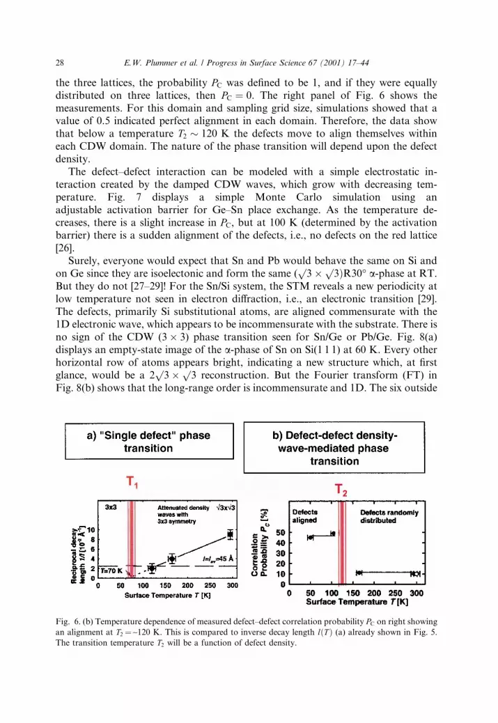
the three lattices, the probability PC was defined to be 1, and if they were equallydistributed on three lattices, then PC ¼ 0. The right panel of Fig. 6 shows themeasurements. For this domain and sampling grid size, simulations showed that avalue of 0.5 indicated perfect alignment in each domain. Therefore, the data showthat below a temperature T2 � 120 K the defects move to align themselves withineach CDW domain. The nature of the phase transition will depend upon the defectdensity.
The defect–defect interaction can be modeled with a simple electrostatic in-teraction created by the damped CDW waves, which grow with decreasing tem-perature. Fig. 7 displays a simple Monte Carlo simulation using anadjustable activation barrier for Ge–Sn place exchange. As the temperature de-creases, there is a slight increase in PC, but at 100 K (determined by the activationbarrier) there is a sudden alignment of the defects, i.e., no defects on the red lattice[26].
Surely, everyone would expect that Sn and Pb would behave the same on Si andon Ge since they are isoelectonic and form the same (
p3�p
3ÞR30� a-phase at RT.But they do not [27–29]! For the Sn/Si system, the STM reveals a new periodicity atlow temperature not seen in electron diffraction, i.e., an electronic transition [29].The defects, primarily Si substitutional atoms, are aligned commensurate with the1D electronic wave, which appears to be incommensurate with the substrate. There isno sign of the CDW (3� 3) phase transition seen for Sn/Ge or Pb/Ge. Fig. 8(a)displays an empty-state image of the a-phase of Sn on Si(1 1 1) at 60 K. Every otherhorizontal row of atoms appears bright, indicating a new structure which, at firstglance, would be a 2
p3�p
3 reconstruction. But the Fourier transform (FT) inFig. 8(b) shows that the long-range order is incommensurate and 1D. The six outside
Fig. 6. (b) Temperature dependence of measured defect–defect correlation probability PC on right showingan alignment at T2 ¼ ~120 K. This is compared to inverse decay length lðT Þ (a) already shown in Fig. 5.
The transition temperature T2 will be a function of defect density.
28 E.W. Plummer et al. / Progress in Surface Science 67 (2001) 17–44

Fig. 7. Simulation of defect–defect interaction as function of temperature. At 300 K there are an equal number of defects on three different lattices (red, blue
and yellow) indicated in the left panel. At 90 K they have totally aligned on blue and yellow lattices.
E.W.Plummeretal./Progress
inSurfaceScien
ce67(2001)17–44
29

spots are from thep3�p
3 structure and there is a new ‘‘spot’’ marked by thearrows. This spot is not where a 2
p3 spot should be, but rotated 7–8� from the
vertical. Most important is the observation that there is no new LEED pattern at lowtemperatures. You are seeing a pure electronic reconstruction with no accompanyinglattice distortion.
It is quite easy to isolate the different phenomena in this image by filtering the FTand then back FT to reproduce a real-space image. Fig. 8(c) is constructed by usingonly the spots in FT of Fig. 8(b), i.e., the
p3 spots and the incommensurate new
spot. This real-space image has no defects and clearly shows the 1D electronic dis-tortion on the RT
p3�p
3 phase. In Fig. 8(d) we have removed thep3�p
3 latticeby removing the diffraction spots in the FT of Fig. 8(b) and then back transforming.Now we can see the 1D wave, but it is also obvious that the defects have alignedthemselves commensurate with this one-dimension incommensurate electronic wave.�75% of the defects are in the dark regions of the electronic wave. This is the firstdirect observation of a DDW [29].
Together, the thin-film systems presented here serve as a magnificent arena for thestudy of the dynamics of defects in a two-dimensional (2D) phase transition. But thistype of behavior is not restricted to the systems shown in Fig. 1. If you scan theliterature, you can find many tempting STM figures. For example, a little filtering ofthe RT image of hydrogen terminated SiC(0 0 0 1) indicates the presence of waves[30]. Will there be a transition as the temperature is lowered? The images of theSi(1 1 1)-
p3�p
3-Ag surface show beautiful domain walls like we have reported forthe CDW structure of Sn on Ge(1 1 1) [31].
Fig. 8. (a) Empty state STM images of a-phase of Sn on Si(1 1 1). (b) FT of image in (a). (c) STM image
constructed from diffraction spots in FT in (b). (d) STM image created by back FT of FT in (b) withoutp3�p
3 diffraction spots [29].
30 E.W. Plummer et al. / Progress in Surface Science 67 (2001) 17–44

3.2. Ferromagnetism at surface of p-wave superconductor Sr2RuO4
In this section, we illustrate the impact that can be achieved by using the arsenalof experimental and theoretical surface tools to study complex systems currently ofinterest to the CMP community. It is our contention (the reader can be the judge)that we have proven Phil Anderson wrong. You can do very sophisticated mea-surements and first principles calculations to learn new physics, if you treat them astools and keep focused on the physics. This example concerns the observation of asurface reconstruction at the surface of the unconventional superconductor Sr2RuO4
[32], driven by surface stress and aided by a soft bulk soft phonon. Theory confirmsthe origin of the reconstruction and predicts that the surface ground state is ferro-magnetic (FM), i.e., a ferromagnetic surface on a superconductor [33].
The strong mutual coupling between charge and spin of the electrons and thelattice degrees of freedom in transition-metal oxides (TMOs) results in effects such ascharge-, orbital-, and spin-ordering; colossal magnetoresistance; and unconventionalsuperconductivity [5–10,34]. Fig. 9 shows schematically this close coupling in thesehighly correlated systems. For example, the application of a magnetic field (mag-netism) drives a metal-to-insulator transition (electronic structure) and, in manycases, a lattice distortion [34]. Conceptually, creating a surface by cleaving a singlecrystal is a controlled way to disturb the coupled system by breaking the symmetrywithout changing the stoichiometry. This unique environment at the surface couldproduce new phenomena, while providing a fresh approach to the study of the spin-charge-lattice coupling in these complex materials. Here we show, using the un-conventional superconductor Sr2RuO4, that all of these expectations can be realized.Even for this layered material, where the bonding between layers is weak and theelectrons are strongly localized to the layers, the surface has a surprising new phase,which clearly elucidates the close coupling in the bulk between lattice distortions and
Fig. 9. Schematic illustration of close coupling between spin-charge-lattice degrees of freedom in TMOs.
Breaking symmetry by creating surface can be used to modify and probe this close coupling.
E.W. Plummer et al. / Progress in Surface Science 67 (2001) 17–44 31

magnetism. Furthermore, the influence of surfaces and interfaces on thin-filmproperties is of technological interest for the design of TMO devices [35].
In Section 1 we briefly mentioned the perovskite compounds, and that they were amember of a broader class of materials called the Ruddlesden–Popper (RP) series(see Fig. 10), with the general formula ðR1�xAxÞnþ1MnO3nþ1. In these compounds, R isusually a trivalent rare-earth, A is a divalent alkaline-earth, and M is a transition-metal ion. The structure of the RP phases is made up of n consecutive perovskitelayers (AMO3) alternating with rock salt layers, so that their formula can be repre-sented by (AO)(AMO3Þn, where n represents the number of connected layers of vertexsharing MO6 octahedra. n ¼ 1 is a 2D layered material with only one layer of oc-tahedra. n ¼ 2 has two connected layers of octahedra. As n increases, the materialsbecome more 3D in character and the electronic band width increases. The prop-erties of these materials are controlled by tuning the band filling by adjusting therelative concentration of divalent (A) and trivalent (R) atoms. In most of the in-teresting cases, the transition metal can have multiple valency, leading to charge,spin and orbital ordering [8,34]. Here we will discuss the n ¼ 1 member of this series,known as 214 materials, because they are layered and cleave easily. In the last sec-tion, measurement on the n ¼ 1 systems have been made using thin-films grown vialaser molecular beam epitaxy [36].
Sr2RuO4, the only known layered perovskite without copper that exhibits su-perconductivity, has attracted much attention, because it shows spin-triplet pairingwith a p-wave order parameter [37]. The bulk has a non-distorted tetragonal K2NiF4
structure with a nonmagnetic ground state. However, this ground state is close tostructural and magnetic instabilities, characterizing a common feature in this class of
Fig. 10. Three members of RP series n ¼ 1; n ¼ 2; and n ¼ 1. Aqua colored balls are di or trivalent
atoms, where transition metal–oxygen octahedra are shown in light green.
32 E.W. Plummer et al. / Progress in Surface Science 67 (2001) 17–44

materials that the energy difference between different structural/magnetic phases isvery small. Inelastic neutron scattering experiments show that the phonon modecorresponding to the in-plane octahedron rotation with R3 symmetry exhibits asignificant drop in energy near the zone boundary (see Fig. 11) [38]. The existence ofspin fluctuations has been documented by nuclear magnetic resonance experiments.This is important, because theory suggests that the spin-triplet pairing for the un-conventional superconductivity in Sr2RuO4 is mediated by exchange of FM spinfluctuations [39].
Fig. 12 shows a large-scale STM image of a surface cleaved inside the vacuumsystem and transferred to the STM stage. It shows very large flat terraces with anextension up to 10 lm. All step heights are integral multiples of half the unit cell (6.4�A) shown on the left. Both LEED I–V measurements and calculations prove thatthe surface is the SrO plane, as expected. High resolution STM images and LEEDdiffraction show that the surface is not bulk truncated but reconstructed into aðp2�p
2ÞR45� structure, as can be seen in the STM image and LEED patterndisplayed in Fig. 13. There are missing fractional-order spots in the LEED patternindicating the presence of glide planes and a p4gm plane group symmetry. Given therestrictions of p4gm symmetry, and the fact that there is a soft-bulk zone boundary
Fig. 11. Diagram showing soft-bulk phonon mode [38] (a) and the zone boundary rotation of octahedron
(b).
E.W. Plummer et al. / Progress in Surface Science 67 (2001) 17–44 33

Fig. 12. Large-scale STM image of Sr2RuO4 cleaved in vacuum on the right. The figure on the left shows cleavage planes and step height. The crystal cleaves
without breaking the RuO6 Octahedra.
34
E.W.Plummeretal./Progress
inSurfaceScien
ce67(2001)17–44

phonon corresponding to rotation of the octahedron (Fig. 11(b)), the surfacestructure could have been deduced. This approach would have been Anderson’sway, but we are surface physicists (and not nearly as smart), so we did it the hardway.
Fig. 11 displayed on the left the bulk phonon modes with the mode of interesthighlighted in red [38]. On the right is the zone boundary rotation pattern of thisbulk phonon in the plane of the surface. Our results show that at the surface thisdynamic bulk mode freezes into a static lattice distortion. The structure was deter-mined using LEED I–V analysis. The intensity vs. energy of five nonequivalent in-teger beams and three nonequivalent fractional beams has been measured andcompared with calculated intensities for surface model structures compatible withthe p4gm symmetry. The best fit to experimental spectra was obtained for a surfacestructure with the octahedra rotated by 9� 3�. First-principles calculations of theground-state surface structure have been conducted within the generalized gradientapproximation (GGA). Our calculations confirm that octahedra rotation indeedhappens on the surface but not in the bulk (Fig. 14). The optimized structure for anonmagnetic surface is a surface layer with octahedra rotated by 6:5� (Fig. 14). Thisreconstruction, driven by compressive strain in the RuO2 layers, lowers the energy by14 meV per formula unit (f.u.). The calculation of the surface structure for FMordering in the surface illustrates what is so unique about these materials. The FMordering stabilizes the distortion further and increases the rotation angle to 9 (Fig.14) to gain additional energy of 51 meV/f.u.
We have been able to analyze the different d-orbital character of each band at theFermi surface and address the coupling of these states to phonons and spin fluctu-
Fig. 13. High resolution STM image (a) and LEED pattern (b) of freshly cleaved surface. Surface re-
constructs to (2� 2) configuration with new unit cell shown by green box on left. The STM image is taken
at room temperature with sample bias voltage +0.5V.
E.W. Plummer et al. / Progress in Surface Science 67 (2001) 17–44 35

ations giving a clear picture of what occurs at the surface [33]. The key orbital is thedxy , since the R3 bulk phonon mode couples strongly with this orbital which is pri-marily responsible for the van Hove singularity (VHS) slightly above EF at theBrillouin zone boundary. Most importantly it is the dxy orbital that is primarilyresponsible to FM spin-fluctuation. This observation at the surface of Sr2RuO4
opens up many exciting prospects, relevant to the bulk and surface properties ofthese layered TMOs. One exciting and relevant example is the coexistence of FMorder and superconductivity [40,41].What is wrong? Not a single sample was synthesized by a surface physicists. We
just characterized and calculated.Who ever controls the materials controls the scienceand technology!
Before leaving this subject, let us return to the question of the role of defects. Fig.13 shows on the left a different region of the surface than displayed in Fig. 13, wherethe defect density is much higher. The defects, presumably vacancies, forming quasi-ordered rows, and stabilizing the bulk 1� 1 structure that can be seen in the STMimage (top right). The STM image clearly shows that one out of the two atoms ineach unit cell is being imaged, either Sr or O. A simple argument, based on theexpected density of states near the Fermi energy, would conclude that the O atomsare being imaged. In fact, theoretical calculations of the surface local density of
Fig. 14. First principles (GGA) calculation of total energy per f.u. versus octahedron rotations angle.
Both FM and NM cases are displayed for bulk and surface. FM ordered state is commensurate with
lattice, while AF state is calculated with planar Q ¼ ðp=a;p=aÞ.
36 E.W. Plummer et al. / Progress in Surface Science 67 (2001) 17–44

Fig. 15. (a) High resolution STM image of Sr2RuO4 at 25K showing region of sample with high defect density. (b) Comparison of experimental imaged and
theoretical calculation of image by Fang and Terakura. In (a) the sample bias voltage was +0.5 V.
E.W.Plummeretal./Progress
inSurfaceScien
ce67(2001)17–44
37

states, shown at the bottom right of Fig. 15 prove that the STM image, ‘‘sees’’ the Sratoms. The apparent contradiction is easily reconciled, when the orbital character ofthe wave functions being imaged is analyzed. What the STM is seeing are the in-plane O p-orbitals, all pointing in the direction of the Sr atoms. Preliminary ob-servations indicate that this low temperature quasi-ordered array of defects (DDW)melts at elevated temperatures.
3.3. Electronic inhomogeneities in transition metal oxides
Electronic phase separation in highly correlated systems is one of the currently hotsubjects in CMP [8,42–47]. Undoubtedly, the best known representative of thisphenomena is ‘‘stripes’’ in the high temperature superconductors [8,44]. In this case,neutron scattering revealed the existence of correlated strips of spin and holes in thecopper oxide superconductors [44]. This has led to what is referred to as ‘‘stripol-ogy’’, generating exciting speculation about the nature of these spin and electroninhomogeneous phases in highly correlated systems [42,43]. Recent electron mi-croscopy and STM studies of the CMR perovskites show electronic phase separationon the � lm scale. The temperature and magnetic field dependence of the phasesindicates that conductivity in these materials is a percolation process [45,46]. Theexcitement here is that there is electronic phase separation without either a structuralchange or component phase separation.
Surface experiments using STM for topography and scanning tunneling spec-troscopy (STS) for the electronic density of states promise to have a profound impacton this subject. Here is an area where surface physicists, with their knowledge ofpreparation and care of surfaces and of various spectrocopies, can impact CMP.
Let us begin by describing our experiments on another n ¼ 1 member of the RPseries (Fig. 10), La0:5Sr1:5MnO4 [47,48]. The average manganese valence is Mn3:5þ,however, below Tc � 217 K, the system forms an alternative Mn3þ=Mn4þ charge-ordered state [47,48] and eg-electron orbital ordering on Mn3þ site [49]. BelowTN � 110 K, this paramagnetic system becomes antiferromagnetically ordered [50].The system becomes insulating in both the charge- and orbital-ordered phases fromsemiconducting at RT [50]. Fig. 16 shows a large-scale STM image after cleaving thismaterial at RT in a vacuum. The surfaces are very flat with large terraces just likewas observed for Sr ruthenate (Fig. 12). LEED patterns show only a 1� 1 structureand preliminary LEED I–V analysis indicates a bulk-like termination with the sur-face plane being the (La,Sr)O layer. This is not what should have been seen, since thecharge-ordered state should have produced 1/2-ordered spots and the orbital-ordered state should have had 1/4-order spots. What is surprising is the electronicroughness of the surface. A line scan across the steps (yellow line) is shown in theupper right. The electronic roughness is almost as large as the step height. Fig. 17shows a higher resolution STM image of one of the flat terraces. The size of thedifferent domains is � 10 nm and the corrugation with a one volt bias in �6 �A. Theorigin of the roughness is primarily electronic, because STS measurement show thatthe band gap is spatially varying, as shown for two positions in the bottom rightpanel of Fig. 17.
38 E.W. Plummer et al. / Progress in Surface Science 67 (2001) 17–44

Fig. 16. (a) Large-scale STM image of freshly vacuum cleaved La0:5Sr1:5MnO4: The yellow arrow show the position of the line scan shown in (b). (b) A
comparison of the line scan across the steps for La0:5Sr1:5MnO4 and Sr2RuO4.
E.W.Plummeretal./Progress
inSurfaceScien
ce67(2001)17–44
39

Fig. 17. Expanded image of La0:5Sr1:5MnO4 taken with +1 V bias. (b) STS data for several regions of the sample showing a variation in the band gap.
40
E.W.Plummeretal./Progress
inSurfaceScien
ce67(2001)17–44

Fig. 18. (a) Topographical STM image of Bi2Sr2CaðCu1�xZnxÞO8þd and (b) map of superconducting energy gap width (M). (c) is a plot of the distribution of
superconducting gap size.
E.W.Plummeretal./Progress
inSurfaceScien
ce67(2001)17–44
41

This type of image has been seen for several different TMO surfaces, includinglaser MBE grown films of La0:7Sr0:3MnO3 [36,51], cleaved samples of La1:0Sr2:0MnO7
[51], and single crystals of high temperature superconductors [51–53]. There is ageneral picture emerging from this limited data set based on the following two ob-servations: (1) The spatial inhomogeneities seem to be pinned, in the sense that theydo not move or fluctuate. As the temperature or magnetic field is changed, the in-homogeneities only change their size. (2) TMOs that have perfect stoichiometry andare either metallic or semiconducting do not exhibit spatial electronic inhomoge-neities. For example, the images of Sr2RuO4; shown in Fig. 13 are like a normalmetal. We have also achieved the same quality images of the double-layered materialSr3Ru2O7. Kawai at the March 2000 APS meeting was the first to suggest that thesedata implied inhomogeneous stoichiometry on the nanometer scale [51]. In the caseof the CMR materials, the inhomogeneity occurs in the concentration of the divalentand trivalent components, for example, La and Sr. For superconductors it may bethe spatial variation in the oxygen concentration.
In Fig. 18 we show Shuheng Pan’s tour de force [51,53]. On the left is an ordinarySTM topographical image of Bi2Sr2CaCu2O8þx while the plot of the right (b) shows asuperconducting energy gap map of the sample [53]. Fig. 18(c) displays a histogramof the superconducting gap size revealing ~50% spatial variation. These authors wereable to show that there was a strong cross-correlation between the spatial variationsin the superconducting energy gap D and the local denstity of states (LDOS), bothmeasured by the STM operating in the spectroscopy mode. Both the spatial varia-tions in the LDOS and the superconducting gap D occured on a surprisingly shortdistance scale ~1.4 nm, which is in fact shorter that the in-plane superconductingcoherence length. The authors show that this is the appropriate length scale for theaverage spacing of O dopant atoms in the CuO2 planes. The picture that emergesfrom these measurements and models emphasize the role of local physics in high-Tc
superconductivity [53].What an exciting prospect. Surface scientists will change the way the CMP com-
munity thinks.
Acknowledgements
This work was founded by the National Science Foundation through grant No.DMR-9801830, and conducted at the Oak Ridge National Laboratory, managed byUT-Battelle, LLC, for the US Department of Energy under contract DE-AC05-00OR22725.
References
[1] C.B. Duke (Ed.), Surface Science, The First Thirty Years, North-Holland, 1994.
[2] Nanotechnology: Shaping the world Atom by Atom, National Science and Technology Council,
Committee on Technology (1999) http://www.nano.gov/press.htm.
42 E.W. Plummer et al. / Progress in Surface Science 67 (2001) 17–44
[3] Condensed-Matter and Materials Physics: Basic Research for Tomorrow’s Technology, Committee
on Condensed-Matter and Materials Physics, National Research Council, National Academy Press,
Washington, DC, 1999, p. 10.
[4] Complex Systems: Science for the 21st Century, Office of Science workshop, US Department of
Energy, 5–6 March 1999, available at http://www.er.doe.gov/production/bes/complexsystems.htm.
[5] J. Birgeneau, M.A. Kastner, Correlated electron systems, Science 288 (2000) 437.
[6] J.S. Osborne, Correlated electron systems, Science 288 (2000) 468.
[7] Y. Tokura, N. Nagaosa, Correlated electron systems, Science 288 (2000) 462.
[8] J. Orenstein, A.J. Millis, Correlated electron systems, Science 288 (2000) 468.
[9] S. Sachdev, Correlated electron systems, Science 288 (2000) 475.
[10] P.W. Anderson, Correlated electron systems, Science 288 (2000) 48.
[11] P. Ball, Nature 402 (Supp.) (1999) C73.
[12] P.W. Anderson, Science 177 (1972) 393.
[13] G. Gruner, Density Waves in Solids, Addison-Wesley, Reading, MA, 1994.
[14] H. Mutka, Influence of defects and imputities on CDW systems, in: F.W. Boswell, J.C. Bennet (Eds.),
Advances in Crystallography and Microanalysis of CDW Modulated Crystals, Kluwer Academic
Publishers, Dordrecht, 1999.
[15] I. Baldea, M. Badescu, Phys. Rev. B 48 (1993) 8619.
[16] I. Baldea, M. Apostol, J. Phys. C 18 (1985) 6135.
[17] B.I. Halperin, C.M. Varma, Phys. Rev. B 14 (1976) 4030.
[18] T. Ichikawa, S. Ino, Surf. Sci. 105 (1981) 395.
[19] J.M. Carpinelli, H.H. Weitering, M. Bartkowiak, E.W. Plummer, R. Stumpf, Nature 381 (1996) 398.
[20] J.M. Carpinelli, H.H. Weitering, M. Bartkowiak, R. Stumpf, E.W. Plummer, Phys. Rev. Lett. 79
(1997) 1859.
[21] J.S. Pedersen, R. Feidenhans’l, M. Nielsen, K. Kjaer, Surf. Sci. 189/190 (1987) 1047.
[22] R.V. Coleman, B. Giambattista, P.K. Hansma, A. Johnson, W.W. McNairy, C.G. Slough, Adv.
Phys. 37 (1988) 559.
[23] A.V. Melechko, J. Braun, H.H. Weitering, E.W. Plummer, Phys. Rev. Lett. 83 (1999) 999.
[24] A.V. Melechko, J. Braun, H.H. Weitering, E.W. Plummer, Phys. Rev. B 61 (2000) 2235.
[25] H.H. Weitering, J.M. Carpinelli, A.V. Melechko, J. Zhang, M. Bartkowiak, E.W. Plummer, Science
285 (1999) 2107.
[26] A.V. Melechko, Ph.D. thesis, The University of Tennessee, 2000.
[27] L. Ottaviano, M. Crivellari, G. Profeta, A. Continenza, L. Lozzi, S. Santucci, J. Vac. Sci. Technol. A
18 (2000) 1946.
[28] R.I.G. Uhrberg, H.M. Zhang, T. Balasubramanian, S.T. Jemander, N. Lin, G.V. Hansson, Phys.
Rev. B 62 (2000) 1.
[29] L. Ottaviano, A.V. Melechko, S. Santucci, E.W. Plummer, Phys. Rev. Lett. 86 (2001) 1809.
[30] L. Li, C. Tindall, O. Takaoka, Y. Hasegawa, T. Sakurai, Surf. Sci. 385 (1997) 60.
[31] X. Tong, Y. Sugiura, T. Nagao, T. Takami, S. Takeda, S. Ino, S. Hasegawa, Surf. Sci. 408 (1998) 146.
[32] Y. Maeno, H. Hashimoto, K. Yoshida, S. Nishizaki, T. Fugita, J.G. Bednorz, F. Lichtenberg, Nature
372 (1994) 532.
[33] R. Matzdorf, Z. Fang, Ismail, J. Zhang, T. Kimura, Y. Tokura, K. Terakura, E.W. Plummer, Science
289 (2000) 746.
[34] M. Imada, A. Fujimori, Y. Tokura, Rev. Mod. Phys. 70 (1998) 1039.
[35] M. Izumi, Y. Konishi, T. Nishihara, S. Hayashi, M. Sinohara, M. Kawasaki, Appl. Phys. Lett. 73
(1998) 2497.
[36] N. Okawa, H. Tanaka, R. Akiyama, T. Matsumoto, T. Kawai, Solid State Comm. 114 (2000) 601.
[37] Y. Maeno, Physica B 281/282 (2000) 865.
[38] M. Braden, et al., Phys. Rev. B 57 (1998) 1236.
[39] I.I. Mazin, D.J. Singh, Phys. Rev. Lett. 82 (1999) 4324.
[40] W.E. Pickett, R. Weht, A.b. Shick, Phys. Rev. Lett. 83 (1999) 3713.
[41] C. Bernhard, et al., Phys. Rev. B 59 (1999) 14099.
[42] A. Moreo, S. Yonoki, E. Dagotto, Science 283 (1999) 2034.
E.W. Plummer et al. / Progress in Surface Science 67 (2001) 17–44 43

[43] S.A. Kevelson, E. Fradkin, V.J. Emery, Nature 393 (1998) 550.
[44] J.M. Tranquada, et al., Phys. Rev. Lett. 79 (1997) 2133.
[45] M. Uehara, S. Mori, C.H. Chen, S.-W. Cheong, Nature 399 (1999) 560.
[46] M. Fathe, S. Freisem, A.A. Menovsky, Y. Tomioka, J. Aarts, J.A. Mydosh, Science 285 (1999) 1540.
[47] B.J. Sternlieb, J.P. Hill, U.C. Wildgruber, G.M. Luke, B. Nachumi, Y. Moritomo, Y. Tokura, Phys.
Rev. Lett. 76 (1996) 2169.
[48] W. Bao, C.H. Chen, S.A. Carter, S-W. Cheong, Solid-State commun. 98 (1996) 55.
[49] Y. Murakami, H. Kawada, H. Kawata, M. Tanaka, T. Arima, Y. Moritomo, Y. Tokura, Phy. Rev.
Lett. 80 (1998) 1932.
[50] Y. Moritomo, Y. Tomioka, A. Asamitsu, Y. Tokura, Y. Matsui, Phys. Rev. B 51 (1995) 3297.
[51] Symposium on STM Imaging of Transition Metal Oxides, March APS meeting, 2000.
[52] T. Cren, D. Roditchev, W. Sacks, J. Klein, cond-mat/0006039, 2 June 2000.
[53] S.H. Pan, J.P. O’Neal, R.L. Badzey, C. Chamon, H. Ding, J.R. Engelbrecht, Z. Wang, H. Eisaki,
S. Uchida, A.K. Gupta, K.-W. Ng, E.W. Hudson, K.M. Lang, J.C. Davis, to be published.
44 E.W. Plummer et al. / Progress in Surface Science 67 (2001) 17–44


