Embed Size (px)
Citation preview

This content has been downloaded from IOPscience. Please scroll down to see the full text.
Download details:
IP Address: 193.52.97.8
This content was downloaded on 21/11/2013 at 13:35
Please note that terms and conditions apply.
Thermal conductivity measurement of AlN films by fast photothermal method
View the table of contents for this issue, or go to the journal homepage for more
2012 J. Phys.: Conf. Ser. 395 012089
(http://iopscience.iop.org/1742-6596/395/1/012089)
Home Search Collections Journals About Contact us My IOPscience

Thermal conductivity measurement of AlN films by
fast photothermal method.
K. Ait Aissa1, N. Semmar2, D. De Sousa Meneses3, L. Le Brizoual1,M. Gaillard2, A. Petit2, P-Y. Jouan1, C. Boulmer-Leborgne2 andM.A.Djouadi1
1 Universite de Nantes, CNRS, Institut des Materiaux Jean Rouxel, UMR 6502, 2 rue de laHoussiniere B.P. 32229 - 44322 Nantes cedex 3, France.2 GREMI, Groupe de Recherche sur l’Energie des Milieux Ionises, UMR-7344,CNRS-Universite d’Orleans, 14 rue d’Issoudun, BP 6744, 45067 Orleans Cedex2, France.3 Conditions Extremes et Materiaux : Haute Temperature et Irradiation, UPR3079 CNRS, 1DAvenue de la Recherche Scientifique, 45071 Orleans Cedex.
E-mail: [email protected]
Abstract. Aluminum nitride (AlN) films were deposited by reactive direct current MagnetronSputtering (dcMS) on Si (100) substrates, with different thicknesses, in Ar−N2 gas mixture. Thefilms were characterized by X-ray diffraction (XRD), profilometry, scanning electron microscopyand UV-Visible Ellipsometry. The effect of the thickness on the thermal conductivity of AlNfilms was investigated using a fast IR pyrometry device. The XRD measurements show thatAlN films are texturated along (002) direction. Moreover, X-ray rocking curve measurementsindicate that the crystalline quality of the AlN is improved with the increase of film thickness.Optical analyses by IR spectroscopy and UV-Visible Ellipsometry demonstrate a high opticalband gap of pure AlN films with semi-transparent behaviour in the IR range (1 to 7 µm). Theeffective thermal conductivity of the AlN films is strongly dependent on the film thickness. Aneffective thermal conductivities between (80 ± 05) and (175 ± 15) W.m−1.K−1 were measuredfor 260 and 8000 nm thick AlN film.
1. IntroductionAluminum nitride is an important III-V material due to its unique thermal, mechanical andoptical properties. It can be applied as active and passive layer in microelectronic devices,heat sinks in electronic packaging applications, component for acoustic wave devices and UVelectroluminescent device [1]. It has been proposed as an alternative to alumina and Beryllia forthermal management application [2], because of its high thermal conductivity and small thermalexpansion mismatch compared to that of silicon. The thermal conductivity of bulk AlN, at roomtemperature, along the c-axis can be as high as 320 W.m−1.K−1 [3], but it is usually considerablylower for polycrystalline AlN. This significant thermal conductivity reduction is caused by thepresence of oxygen impurities [3-5]. Hence it has been shown that the thermal conductivity ofAlN is inversely proportional to the oxygen content in the AlN lattice [3, 6]. In addition, thethermal conductivity of a thin film and bulk material can be substantially different because ofthe microstructure, including lattice impurities or defects [3], crystallite phase, grain boundaries,and porosity. Recenltly, the thermal conductivity value of AlN films deposited on silicon has been
6th European Thermal Sciences Conference (Eurotherm 2012) IOP PublishingJournal of Physics: Conference Series 395 (2012) 012089 doi:10.1088/1742-6596/395/1/012089
Published under licence by IOP Publishing Ltd 1

raised up to 170 W.m−1.K−1, thanks to the improvement of crystalline quality and reductionof oxygen content in the films [7].To date, many deposition techniques for AlN films have been reported including: ChemicalVapor Deposition (CVD) [1], and Molecular Beam Epitaxy (MBE) [8]. However, these methodsare expensive and the required high temperatures to reach satisfying properties are oftenincompatible with microelectronic processes. Among other techniques, the Reactive MagnetronSputtering process (RMS) is an attractive deposition technique because it presents advantagesof being low temperature and low cost methods, and it allows fine tuning of the materialcharacteristics [9-11].This paper reports on the microstructure dependence of the thermal conductivity of AlN films.Those are deposited by dcMS, with a (002) single orientation along c-axis direction. The effectof the thickness on the thermal conductivity was investigated using the photothermal methodin the nanosecond time domain.
2. Experimental procedure2.1. Aluminum nitride depositionAluminum nitride films were deposited on Si (100) substrates, without intentional heating bydc reactive magnetron sputtering, using aluminum target (50 mm in diameter and 99.999 %purity), in an argon and nitrogen atmosphere, with a target-substrate distance of 30 mm. Thesputtering pressure was fixed at 0.4 Pa. The residual pressure in reactor chamber was less than6 · 10−6 Pa. The total gas flux rate during deposition was maintained constant at 40 sccm whileN2 to Ar gas ratio was fixed at 35. An unbalanced magnetron sputtering system powered by a150 W dc power supply was used. In order to check the effect of the thickness on the thermal con-ductivity, different samples were prepared by varying the film thickness from 260 up to 8000 nm.
The films were characterized by X-ray diffraction, using D5000 MOXTEK diffractometer with(Cu Kα) radiation (λ = 0.1540598 nm) in the θ− 2θ Bragg Brentano and θ− θ Rocking Curveconfigurations. The surface morphology and microstructural characterization were carried outby field emission gun scanning electron microscopy (ZEISS SUPRA 40), Refractive index (n)and extinction coefficient (k) were characterized with Ellipsometry measurements, performedwith a phase modulated Ellipsometer Horiba Jobin Yvon UVISEL and infrared reflectivitymeasurements performed on a Bruker IFS 113 v spectrometer with an instrumental resolutionof 4 cm−1. The thicknesses of the films were estimated by using a DEKTAK VEECO 8 profiler.
2.2. Thermal measurement set-upThe thermal conductivity of AlN films was measured with a nanosecond pulsed photothermalmethod (PPT). The experimental set-up (Fig 1) was described in detail in Refs [12, 13]. Thismethod consists of detection of the IR radiations emitted from the surface of a sample afterits interaction with a pulsed-laser beam. The sample, being heated by a UV KrF laser pulse(λ = 248 nm, τ = 27 ns), emits IR thermal waves that are focalized by two parallel off-axisparabolic mirrors into the active area (0.25 mm diameter) of an IR detector. The IR detector iscooled with liquid nitrogen and has a wide spectral range from 2 to 12 µm (300− 3000 K) withan integrated preamplifier of 100 MHz. The output signal of the IR detector is readed by anumerical oscilloscope (500 MHz bandwidth) that can give simultaneously the time distributionof the KrF laser beam (UV) and the IR signal variations at the nanosecond time scale.
6th European Thermal Sciences Conference (Eurotherm 2012) IOP PublishingJournal of Physics: Conference Series 395 (2012) 012089 doi:10.1088/1742-6596/395/1/012089
2

Figure 1. Schematic view of the fast IR pyrometry setup.
3. Results3.1. Structural properties
Figure 2. X-Ray Diffraction patternsof AlN films deposited with differentthicknesses.
Figure 3. Rocking curve FWHM (002) valuesof AlN layers as a function of the AlN filmthickness.
The XRD diffraction patterns of AlN films deposited with different thicknesses are shown inFig 2. The θ − 2θ measurement exhibits a narrow peak with a full width at half maximum(FWHM) lower than 0.2◦. The films exhibit a single orientation along c-axis direction, whichis attributed to wurtzite-type structure of AlN. The effect of AlN film thickness on the FWHMvalues of the (002)-peak rocking curve is presented in Fig 3. It is shown that the FWHM valuedecrease with AlN film thickness. In fact, it appears clearly that the c-axis orientation (rep-resented by the decrease of FWHM value) depend directly on the film thickness up to a valueof approximately 6000 nm. Once this value is reached, there is no influence of the layer thick-ness on FWHM (002)-rocking curve values. Such results, which indicate an improvement of thecrystalline quality with the increase of film thickness, have been obtained as a result of the use
6th European Thermal Sciences Conference (Eurotherm 2012) IOP PublishingJournal of Physics: Conference Series 395 (2012) 012089 doi:10.1088/1742-6596/395/1/012089
3

of an unbalanced configuration of magnetron sputtering. This promotes high ion/neutral ratioand deposition energy in the range of 20 to 50 eV [14].
3.2. Optical properties
Figure 4. Optical indices of the AlN thin film deduced from infrared reflectivity measurements(a) and UV ellipsometry (b).
Several experiments were conducted on AlN thin films by Fourier Transform IR spectroscopyand UV-visible ellipsometry in order to cover the whole optical range, i.e. from 0.05 to 6 eV (402to 48300 cm−1). Fig 4a, reports the refractive index (n) and extinction coefficient (k) deducedfrom infrared reflectivity measurements. The optical response is typical of that of a dielectricmaterial where the low wavenumber part, below 1000 cm−1, corresponds to the phonon responseof AlN. The optical gap for which the material can be considered as nearly transparent (very lowabsorption coefficient) spans between 0.25 and 3 eV . Fig 4b contains the spectral evolution ofthe optical indices in visible and UV ranges obtained by ellipsometry, the spectral trends showthat the electronic absorption starts to be significant only above 3 eV . In the near infrared andvisible ranges, the refractive index of the AlN film is close to 2.1 a value corresponding to thatof bulk AlN [15].
3.3. Thermal propertiesFor thermal measurement, the AlN films were coated by titanium (Ti) layer (Fig 5) which actsas an optical transducer to conversion the UV photon flux into IR radiation. In order to obtainabsolute temperature evolution, it was necessary to calibrate the IR detector response. In thiscalibration process [16], the samples are heated to different levels of temperatures and for eachtemperature value; a detector output voltage is measured. The obtained calibration curve (Fig6) is then used to transform the measured voltage (Fig 7a) to the temperature values (Fig 7b).
6th European Thermal Sciences Conference (Eurotherm 2012) IOP PublishingJournal of Physics: Conference Series 395 (2012) 012089 doi:10.1088/1742-6596/395/1/012089
4

Figure 5. SEM image of the transversalsection of Ti thin layer deposited on AlN film.
Figure 6. Calibration curve for the Ti/AlN.
Fig 5. Show the cross section SEM image of 8000 nm thick AlN films coated with ∼200 nmthick Ti layer transducer. The AlN film shows a very compact and dense structure, without anyvoid. Such structure can be associated to zone 2 of the Thornton materials diagram [17] evenif these films were synthesized without intentional heating of the substrate (temperature < 250◦C). The film density promotes an abrupt interface with the post deposited Ti metallic coatingas it is shown in the inset of Fig 5.
Typical result from the IR detector is plotted in Fig 7. in case of 200 nm Ti on 8000 nm thickAlN film. Using the calibration procedure, one should calculate the returned surface tempera-ture in the nanosecond scale.
Figure 7. Voltage response (a) and dynamic temperature (b) of the IR detector from Ti/AlNsample surface after laser beam fluence of 4.8 mJ.mm−2.
From those signals, a multilayer model [16], is used under Comsol Multiphysics to extract theconductivity values that allow the best fitting of the experiment signals. Because it is difficultto evaluate directly the thermal contact resistance due to AlN/Si interface, the computation
6th European Thermal Sciences Conference (Eurotherm 2012) IOP PublishingJournal of Physics: Conference Series 395 (2012) 012089 doi:10.1088/1742-6596/395/1/012089
5

of the equivalent thermal resistance of the whole contributions (effective thermal conductivity)including the interface and the microstructure defects, gives a value close to 2·10−9 K.m2.W−1.
Figure 8. (a) Effective thermal conductivity, - (b) Thermal resistance, as a function of thethickness AlN films.
Fig 8. shows the effective thermal conductivity and related thermal resistance as a function ofthickness. Both thermal properties increase with the film thickness. According to the results ofthe XRD analysis it can be claimed that the increased thermal conductivity of AlN film from80 to 175 W.m−1.K−1 with increasing the film thickness from 260 to 8000 nm is primarily dueto lower FWHM (002)- rocking curve which followed an increase in size grain size. In general,the size of a grain is proportional to the thickness of the thin film if other process conditions areunchanged [18] and the low thermal conductivity at 260 nm may be due to lattice mismatch atthe interface of AlN/Si. The film interfacial regions near the substrate have generally a poormicrostructure due to lattice mismatch [19]. This increasing of the thermal conductivity goeswith increasing of the thermal resistance between all the AlN film and the Si substrate, with avalue of 0.52·10−8 to 4.8·10−8 K.m2.W−1 for a thickness range from 260 to 8000 nm, this resultagrees with that reported by C. Duquenne [7]. This thermal resistance is not only attributed tothe interfacial amorphous layer between the AlN film and the substrate but also to defaults allalong the film thickness.
To analyse the accuracy of such measurements the sensitivity of our IR method is evaluated atdifferent thermal conductivity values: 50, 100 and 150 W.m−1.K−1 as plotted in Fig 9. Themaximum sensitivity is obtained in the time range of 5 to 10 ns, close to the maximum input laserbeam. For example, considering a sensitivity of 0.4 W−1.m.K2, which corresponds to a surfacetemperature of 600 K, one could evaluate from the calibration curve, the variation of the outputvoltage for 1 K deviation : δU/δT = 4a4T
3 ' 0.3 mV.K−1. From those values, the variationof output voltage versus thermal conductivity is roughly 0.12 mV.W−1.m.K. That means 1mV deviation is corresponding to less than 10 W.m−1.K−1 thermal conductivity variations. Inevidence higher is the temperature level; better is the the sensitivity to the thermal conductivitychanges.However, in this case, such estimation is conducted on a wide temperature range (300 to 650 K
6th European Thermal Sciences Conference (Eurotherm 2012) IOP PublishingJournal of Physics: Conference Series 395 (2012) 012089 doi:10.1088/1742-6596/395/1/012089
6
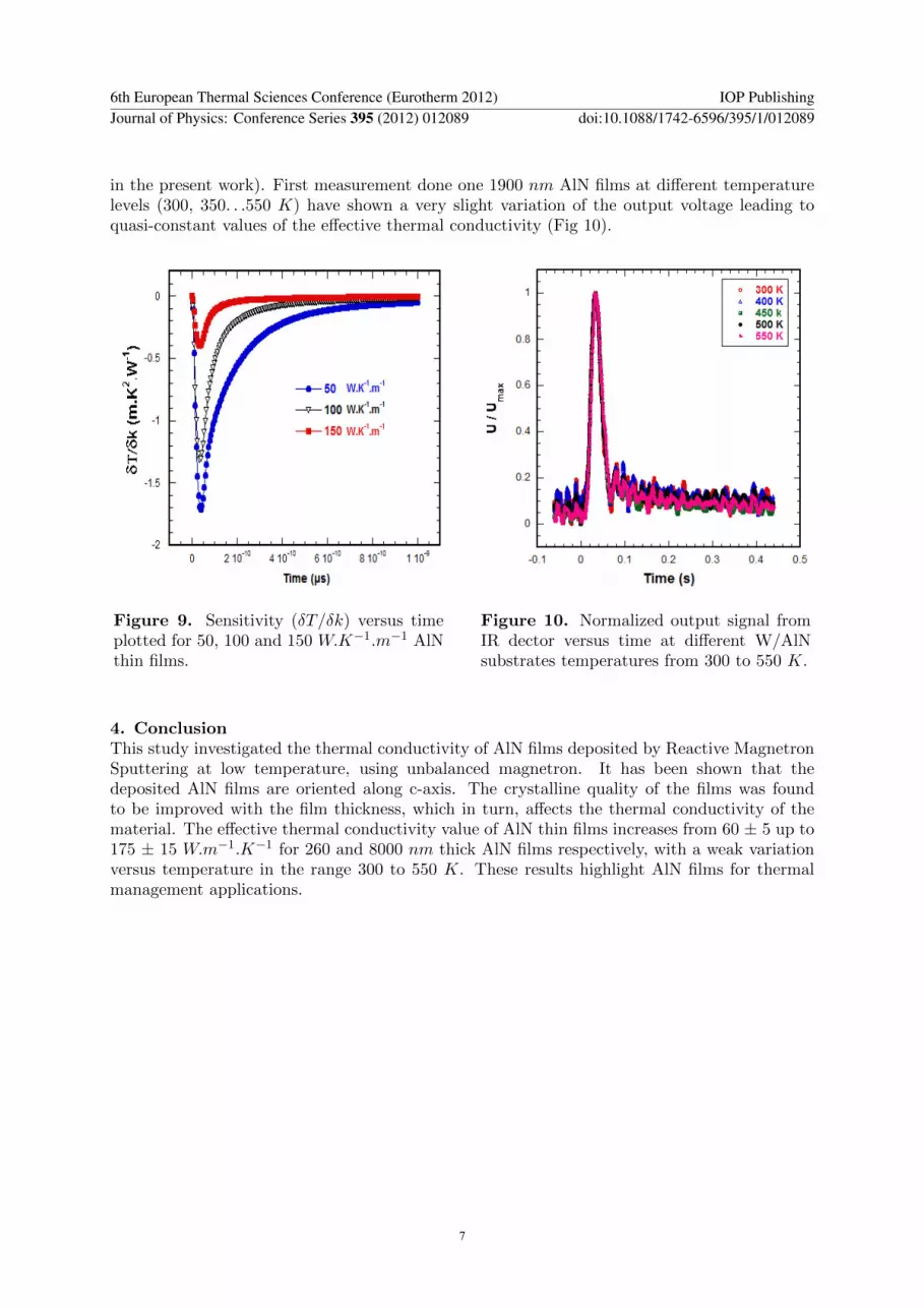
in the present work). First measurement done one 1900 nm AlN films at different temperaturelevels (300, 350. . .550 K) have shown a very slight variation of the output voltage leading toquasi-constant values of the effective thermal conductivity (Fig 10).
Figure 9. Sensitivity (δT/δk) versus timeplotted for 50, 100 and 150 W.K−1.m−1 AlNthin films.
Figure 10. Normalized output signal fromIR dector versus time at different W/AlNsubstrates temperatures from 300 to 550 K.
4. ConclusionThis study investigated the thermal conductivity of AlN films deposited by Reactive MagnetronSputtering at low temperature, using unbalanced magnetron. It has been shown that thedeposited AlN films are oriented along c-axis. The crystalline quality of the films was foundto be improved with the film thickness, which in turn, affects the thermal conductivity of thematerial. The effective thermal conductivity value of AlN thin films increases from 60 ± 5 up to175 ± 15 W.m−1.K−1 for 260 and 8000 nm thick AlN films respectively, with a weak variationversus temperature in the range 300 to 550 K. These results highlight AlN films for thermalmanagement applications.
6th European Thermal Sciences Conference (Eurotherm 2012) IOP PublishingJournal of Physics: Conference Series 395 (2012) 012089 doi:10.1088/1742-6596/395/1/012089
7

References
[1] Radhakrishan G 1995 J. Appl. Phys. 10 1237.[2] Melloch Micheal R, Adesida Ilesanmi, Isaacs-Smith T,Madangarli V and Sudarshan T.S 1997 J. Electron.
Mater. 26 212.[3] Slack G A, Tanzilli R A, Pohl R O and Vandersande J W 1987 J. Phys. Chem. Solids 48 647.[4] Warti K, Ishizaki K and Fujikawa T 1992 J. Mater. Sci. 27 2630.[5] Wartari K, Ishizaki K and Tsuchiya F 1993 J. Mater. Sci. 28 3714.[6] Dinwiddie R B, Whittaker A J and Onn D J 1989 J. thermophys. 10 1084.[7] Duquenne C, Besland M.P, Tessier P.Y, Gautron E, Scudeller Y and Averty D 2012 J. Phys. D 45 015301.[8] Tanaka S, Kem R.S, Bentley J and Davis R.F 1996 J. Appl. Phys. 35 1641.[9] Khanna A and Bhat D.G 2007 J. Vac. Sci. Technol. A 25 565.[10] Drusedau T.P and Blasing J 2000 Thin Solid Films 378 31.[11] Vergara L, Clement M, Iborra E and al 2004 Diam. Relat. Mater. 13 842.[12] Amin-Chalhoub E, Semmar N, Coudron L, Gautier G, Gaillard M, Petit A, Boulmer-Leborgne C and Millon
E 2011 Journal of Physics D: Applied Physics D 44 355401.[13] Martan J, Semmar N, Boulmer-Leborgne C, Plantin P and Le Menn E 2006 Nano. Microscale Thermophys.
Eng. 10 12.[14] Duquenne C, Popescu B, Tessier P.Y, Besland M.P, Scudeller Y, Brylinski C, Delage S and Djouadi M.A
2007 Plasma Process. Polym. 4 S1 S5.[15] Legrand P.B, Wautelet M, Dugnoille B, Dauchot J.P and Hecq M 1994 Thin solid Films 248 220.[16] Martan J, Semmar N, Leborgne C, Le Menn E and Mathias J 2005 Applied Surface Science 247 63.[17] Thornton J.A 1977 Annual review of materials science 7 260.[18] Mayadas A.F and Shatzkers M 1970 Phys. Rev. B 1 1382.[19] Abdallah B, Duquenne C, Besland M P, Gautron E, Jouan P Y, Tessier P Y, Brault J, Cordier Y and Djouadi
M A 2008 Eur. Phys. J. Appl. Phys. 43 309.
6th European Thermal Sciences Conference (Eurotherm 2012) IOP PublishingJournal of Physics: Conference Series 395 (2012) 012089 doi:10.1088/1742-6596/395/1/012089
8


