Embed Size (px)
Citation preview

THz emission from coherent plasmons in InAs nanowires
D. V. Seletskiy a, M.P. Hasselbeck a, M. Sheik-Bahae a, J.G. Cederberg b, and A.A. Talin c
aDepartment of Physics and Astronomy, University of New Mexico,Albuquerque NM87131,USA;
bSandia National Laboratories, Albuquerque NM 87185, USA;cSandia National Laboratories, Livermore, CA 94551, USA;
ABSTRACT
We report the first observation of coherent plasmon emission of THz radiation from arrays of semiconductornanowires. The THz signal strength from InAs nanowires is comparable to a planar substrate, indicating thenanowires are highly efficient emitters. This is explained by the preferential orientation of plasma motion tothe wire surface, which overcomes radiation trapping by total-internal reflection. Using a bulk Drude model,we identify the average donor density and mobility in the nanowires in a non-contact manner. Contact I-V transconductance measurements provide order of magnitude agreement with values obtained from the THzspectra.
Keywords: coherent plasmons, nanowires, THz radiation, ultrafast spectroscopy, InAs
1. INTRODUCTION
The development of electromagnetic radiation sources on the nano-scale is an area of current active research.The THz spectral region is particularly interesting because structures can be fabricated with sub-wavelengthdimensions. Nanowires are receiving increasing attention for use as lasers, light-emitting diodes, waveguides, andinter-connects. The study of nanowire optics at far-infrared frequencies, however, has only just commenced.1
We report what we believe is the first observation of THz emission from freestanding semiconductor nanowires.When excited with ultrashort laser pulses, high mobility InAs nanowires act as sub-wavelength antennas thatcan efficiently couple far-infrared radiation from coherent plasmons into free-space.
Excitation of semiconductor surfaces by ultrashort laser pulses with photon energy above the band gap energycan produce THz emission through a variety of mechanisms. Radiation from optical rectification,2 current surge,3
coherent plasmons,4 and coherent phonons5 have all been observed. Ultrafast charge transport perpendicular tothe surface, however, leads to macroscopic dipoles that are poorly oriented for efficient coupling of radiation tofree space. The vast majority of this dipole radiation is trapped because of total internal reflection; the problemis illustrated schematically Fig. 1 (top). It has been shown that dc magnetic fields (∼ 1 T) can rotate chargemotion via the Lorentz force and dramatically increase the emitted radiation.6, 7 Another approach is to makethe air-semiconductor interface perpendicular to the primary radiation lobe; this has been accomplished with ahigh-index prism.8 A free-standing semiconductor nanowire, as we show here, addresses the trapping problemby having its primary surface parallel to the direction of charge transport with a radiating volume much smallerthan the free-space wavelength, i.e. � λ3. This results in an effective material refractive index of ∼ 1, whichessentially eliminates total internal reflection. The effect is sketched in Fig. 1 (bottom). Figure 2 presents thecalculated enhancement of radiation outcoupling of an InAs nanowire compared to a bulk substrate as a functionof observation angle θ0.
When illuminated with ultrashort near-infrared laser pulses, InAs will re-radiate a broadband THz pulse dueto non-phasematched optical rectification of the excitation pulse spectrum.9 At lower irradiance, nonlinear (χ2)rectification is dramatically reduced and the radiation is primarily driven by ultrafast charge transport. Thischarge may be optically injected by the pump pulse (i.e. photocarriers that generate a current surge) or it maybe the motion of a cold, quiescent charge distribution in the material. The former effect generally leads to a
Corresponding author: Denis Seletskiy e-mail: [email protected]
Invited Paper
Ultrafast Phenomena in Semiconductors and Nanostructure Materials XIII, edited by Kong-Thon Tsen, Jin-Joo Song, Markus Betz, Abdulhakem Y. Elezzabi,
Proc. of SPIE Vol. 7214, 72140Y · © 2009 SPIE · CCC code: 0277-786X/09/$18 · doi: 10.1117/12.810875
Proc. of SPIE Vol. 7214 72140Y-1

5o
4o
3o
oo 15 30 45 60 75 90
00
Figure 1. Top: Ultrafast charge transport in a semiconductor substrate creates a radiation dipole (double arrow) thatis oriented parallel to the surface. Coupling to free-space is greatly reduced by total internal reflection. The escape cone(dashed line) poorly overlaps the dipole radiation lobes. Bottom: A free-standing nanowire overcomes radiation trappingbecause charge motion is parallel to the primary surface.
Figure 2. Calculated enhancement of radiation outcoupling efficiency using elementary Fresnel analysis. The observationangle θ0 is referred to the surface normal of the substrate.
half-cycle THz pulse caused by ultrafast, ambipolar diffusion of hot electrons and holes known as the photo-Dember current.10 The photo-Dember effect has been shown to be operative in narrow-gap semiconductors suchas InAs.6, 11 In addition, the ultrafast Dember field transient can excite cold carriers in the bulk as the resultof long-range Coulomb coupling to mobile charges. Cold carriers move to screen the surface field perturbation,which starts coherent plasma oscillations that can also radiate at THz frequencies.12 Our experiments haveshown that cold coherent plasmons are the primary THz radiation source in InAs in the low irradiance regime(i.e. where optical rectification is negligible). Coherent plasma behavior is well described by the classical Drudemodel.13
Proc. of SPIE Vol. 7214 72140Y-2

2. EXPERIMENT
We grow single crystal InAs nanowires in a process that is detailed elsewhere.14 Briefly, a (111) GaAs(B)substrate is coated with a 1 nm Au layer and heated in the presence of AsH3. This causes the formation of AuGaseed particles on the substrate surface. Upon exposure to TMIn, InAs nanowires grow from the AuGa seeds.The nanowires have a length of roughly 15 μm, diameter tapering from 150 to 50 nm, and a surface coverageof ∼ 0.2 μm2. We assume that quantum confinement of electrons and holes is negligible and bulk transport isapplicable. An SEM photograph of a typical sample is presented in Fig. 3.
Figure 3. SEM photograph of ∼ 15 μm long InAs nanowires grown on a Si:GaAs(111)B substrate.
Three different samples are studied: 1) a nanowire array similar to that shown in Fig. 3; 2) a slightly n-dopedInAs planar substrate; and 3) a control sample that is identical to Sample 1 except the nanowires are removed.Sample 3 is a 200 nm InAs wetting layer on a GaAs substrate. The control sample is essential to isolate thecontribution of the InAs wires from the InAs wetting layer, which builds up during the growth process.
We perform ultrafast THz spectroscopy using a system that has a uniform, broadband spectral responseexceeding 10 THz.4, 15 Autocorrelation signals are generated using a Michelson interferometer arrangement.Two pump pulses from a mode-locked Ti:sapphire laser oscillator (duration: 60 fs; center wavelength: 820 nm)are focused on the room temperature sample substrate at a 45◦ angle of incidence and slightly separated positionswith adjustable delay. The emitted electromagnetic radiation is collected in the specular direction and focused ona liquid-He cooled Si bolometer. The interferometric signals are not phase-resolved, but do provide the frequencyand coherence length of the far-infrared electromagnetic pulse.
In a second setup, 30-fs pulses from a regeneratively amplified, 1 kHz Ti:sapphire laser system are incidenton the sample without focusing. Phase-resolved THz transients are detected using a (110) ZnTe crystal andfree-space electro-optic sampling.16
3. RESULTS
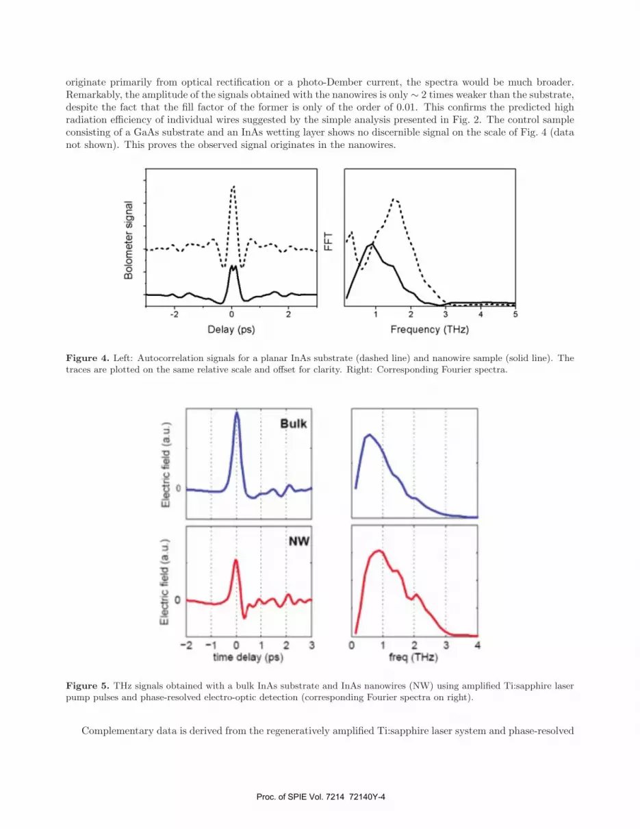
Linear interferograms obtained with an n-InAs planar substrate and InAs nanowire sample using the bolometersetup are presented in Fig. 4 (left). The traces and corresponding Fourier spectra (Fig. 4, right) are similar,indicating the physical mechanism driving the radiation is the same, i.e. coherent plasma. If the THz pulses
Proc. of SPIE Vol. 7214 72140Y-3
I-LLU-
1 2 3 4 5
Frequency (THz)
0
E Ie
clnc
fiel
d a
u)E
lect
ric b
eld
(a u
)0
originate primarily from optical rectification or a photo-Dember current, the spectra would be much broader.Remarkably, the amplitude of the signals obtained with the nanowires is only∼ 2 times weaker than the substrate,despite the fact that the fill factor of the former is only of the order of 0.01. This confirms the predicted highradiation efficiency of individual wires suggested by the simple analysis presented in Fig. 2. The control sampleconsisting of a GaAs substrate and an InAs wetting layer shows no discernible signal on the scale of Fig. 4 (datanot shown). This proves the observed signal originates in the nanowires.
Figure 4. Left: Autocorrelation signals for a planar InAs substrate (dashed line) and nanowire sample (solid line). Thetraces are plotted on the same relative scale and offset for clarity. Right: Corresponding Fourier spectra.
Figure 5. THz signals obtained with a bulk InAs substrate and InAs nanowires (NW) using amplified Ti:sapphire laserpump pulses and phase-resolved electro-optic detection (corresponding Fourier spectra on right).
Complementary data is derived from the regeneratively amplified Ti:sapphire laser system and phase-resolved
Proc. of SPIE Vol. 7214 72140Y-4

4 i I H I
10A Nanoprobe
FET U A A
10' A Aa':a U U
1o2
100IU
U
.
a
U
U
U
20 40 60 80 100 120 20 40 60 80 100 120Radius (nm) Radius (nm)
c)
1019.
4.
I. . 1. 1. t.
2
E 18. 10
U - A UC
8 2-U U4 Uu U
1Ol AA
o AA A
AU
2-
1Ol6
electro-optic sampling. Figure 5 shows similar THz radiation transients for the substrate (top) and nanowires(bottom), consistent with heavily damped coherent plasma motion.
The coherent plasma starting mechanism is not well understood. A photo-Dember field requires the presenceof a spatially inhomogeneous distribution of photocarriers in the wires to initiate ultrafast diffusion. The diameterof the wires is comparable to the absorption depth of 800 nm light in InAs, which presents the possibility ofinhomogeneous photo-excitation at non-normal incidence. Alternatively, AuGa nanoparticles are present at thetips of the wires, likely causing a space-charge field at the metal-semiconductor interface. Ultrafast screening ofthis field could launch coherent plasma motion, as occurs in GaAs.17
The time-dependent motion of the plasmon x(t) is described by the classical, one-dimensional harmonicoscillator18:
d2
dt2x(t) + γ
d
dtx(t) + ω2
p x(t) =e
m∗E(z, t) (1)
where E(z, t) is the position-dependent electric field transient, γ is the momentum relaxation rate which definesthe mobility, e is the electronic charge, m∗ is the electron effective mass (m∗ = 0.023m at the Γ-valley of InAs),and
ωp =
√Ne2
m∗εoε∞(2)
is the plasma frequency (mks units). N is the density of the cold background electrons, i.e. excluding the hotelectron-hole pairs injected by the ultrashort pump pulse. The THz signals radiate at a frequency:
ν =12π
√ω2
p −γ2
4. (3)
Analysis of the nanowire data displayed in Fig. 4 assuming an electron-donor ion plasma (i.e. neglecting holes)estimates an electron density for the wire ensemble in the range 0.5–2 ×1015 cm−3 and mobility of 12,500 cm2/Vs. The extracted mobility is only about 2 times smaller than we measure with the InAs substrate. It should benoted that the ultrafast experiments will tend to underestimate the intrinsic mobility due to momentum relaxingcollisions of cold electrons with hot, photo-injected holes.17
Figure 6. Transconductance data for individual InAs nanowires studied as field-effect transistors (squares) or with anSTM nanoprobe (triangles).
Proc. of SPIE Vol. 7214 72140Y-5

Contact transconductance measurements are made with individual nanowires of varying radius. These areperformed as two separate measurements involving: i) wires fabricated as field-effect transistors and ii) a tunnelingmicroscope nanoprobe.19 Results are shown in Fig. 6 indicating an electron density in the range 4 ×10¹⁶ – 2×1018 cm−3 and mobility spanning 100–3000 cm2/V s.
ACKNOWLEDGMENTS
D. Seletskiy would like to acknowledge support of the NSF IGERT traineeship program.
REFERENCES1. P. Parkinson, J. Lloyd-Hughes, Q. Gao, H. H. Tan, C. Jagadish, M. B. Johnston, and L. M. Herz, “Transient
terahertz conductivity of GaAs nanowires,” Nano Lett. 7, pp. 2162 – 2165, 2007.2. S. L. Chuang, S. Schmitt-Rink, B. I. Greene, P. N. Saeta, and A. F. J. Levi, “Optical rectification at
semiconductor surfaces,” Phys. Rev. Lett. 68, p. 102, 1992.3. X. C. Zhang, B. B. Hu, J. T. Darrow, and D. H. Auston, “Generation of femtosecond electromagnetic pulses
from semiconductor surfaces,” Appl. Phys. Lett. 56, p. 1011, 1990.4. R. Kersting, K. Unterrainer, G. Strasser, H. F. Kauffman, and E. Gornik, “Few cycle THz emission from
cold plasma oscillations,” Phys. Rev. Lett. 79, p. 3038, 1997.5. T. Dekorsy, H. Auer, C. Waschke, H. J. Bakker, H. G. Roskos, H. Kurz, V. Wagener, and P. Grosse,
“Emission of submillimeter electromagnetic waves by coherent phonons,” Phys. Rev. Lett. 74, pp. 738–742,1995.
6. M. B. Johnston, D. M. Whittaker, A. Corchia, A. G. Davies, and E. H. Linfield, “Simulation of terahertzgeneration at semiconductor surfaces,” Phys. Rev. B 65, p. 165301, 2002.
7. J. Shan, C. Weiss, R. Wallenstein, R. Beigang, and T. F. Heinz, “Origin of magnetic field enhancement inthe generation of terahertz radiation from semiconductor surfaces,” Opt. Lett. 26, p. 849, 2001.
8. M. B. Johnston, D. M. Whittaker, A. Dowd, A. G. Davies, E. H. Linfield, X. Li, and D. A. Ritchie,“Generation of high-power terahertz pulses in a prism,” Opt. Lett. 27, p. 1935, 2002.
9. P. Gu, M. Tani, S. Kono, K. Sakai, and X.-C. Zhang, “Study of terahertz radiation from InAs and InSb,”J. Appl. Phys. 51, pp. 5533–5537, 2002.
10. T. Dekorsy, H. Auer, H. J. Bakker, H. G. Roskos, and H. Kurz, “THz electromagnetic emission by coherentinfrared-active phonons,” Phys. Rev. B 53, p. 4005, 1996.
11. J. N. Heyman, P. Neocleous, D. Hebert, P. A. Crowell, T. Muller, and K. Unterrainer, “Terahertz emissionfrom GaAs and InAs in a magnetic field,” Phys. Rev. B 64, p. 085202, 2001.
12. M. P. Hasselbeck, D. Stalnaker, L. A. Schlie, T. J. Rotter, A. Stintz, and M. Sheik-Bahae, “Emission ofterahertz radiation from coupled plasmon-phonon modes in InAs,” Phys. Rev. B 65, p. 233203, 2002.
13. R. Kersting, J. N. Heyman, G. Strasser, and E. Gornik, “Cold plasmons in n-doped GaAs,” Phys. Rev.B 58, p. 4553, 1998.
14. J. Cederberg, B. Swartzentruber, K. Cross, D. Alliman, A. Talin, D. Seletskiy, M. Hasselbeck, and M. Sheik-Bahae, “Electrical and optical properties of oriented InAs nanowires grown on GaAs(111)B,” in ICMOVPE-14, (Metz, France), 2008.
15. M. Joffre, A. Bonvalet, A. Migus, and J.-L. Martin, “Femtosecond diffracting Fourier-transform infraredinterferometer,” Opt. Lett. 21, p. 964, 1996.
16. Q. Wu and X.-C. Zhang, “Free-space electro-optics sampling of mid-infrared pulses,” Appl. Phys. Lett. 71,p. 1285, 1997.
17. G. C. Cho, T. Dekorsy, H. J. Bakker, R. Hovel, and H. Kurz, “Generation and relaxation of coherentmajority plasmons,” Phys. Rev. Lett. 77, pp. 4062–4065, 1996.
18. W. Sha, A. L. Smirl, and W. F. Tseng, “Coherent plasma oscillations in bulk semiconductors,” Phys. Rev.Lett. 74, p. 4273, 1995.
19. A. A. Talin, F. Leonard, B. S. Swartzentruber, X. Wang, and S. D. Hersee, “Unusually strong space-charge-limited current in thin wires,” Phys. Rev. Lett. 101, p. 076802, 2008.
Proc. of SPIE Vol. 7214 72140Y-6


