Embed Size (px)
Citation preview

Timing Analysis for Extended Burst-Mode Circuits �
Supratik Chakrabortyy
[email protected] L. Dilly
[email protected] Y. Yunz
Kun-Yung Changy
Abstract
We describe an efficient timing analysis technique for ex-tended burst-mode circuits implemented according to the3D design style. Gate-level 3D circuits with uncertaincomponent delays are analyzed, and safe bounds on tim-ing constraints for correct circuit operation are computed.We employ two passes of multi-valued logic simulation toprecisely identify gates where timing constraint violationsmanifest themselves. Signal propagationdelay bounds fromthe primary inputs to these gates are then used to computeglobal timing constraints for correct circuit operation. Tim-ing constraints identified by our tool represent conservativeapproximations to the true timing requirements in the worst-case. In practice, our results are accurate on almost all ofthe 3D benchmarks we have experimented with.
1. Introduction
As designers strive to improve the performance of hard-ware systems, there has been a renewed interest in asyn-chronous design methodologies [24, 8, 20, 19, 2, 26, 25, 16,15]. One promising design style is burst-mode design devel-oped by Yun, Dill and Nowick [21, 27]. Burst-mode designbegins with a state-machine specification, somewhat likeconventional synchronous state-machine synthesis methods.However, the transitions in the machine are governed by theinputs themselves, not by a clock. The most general form ofburst-mode specification, called extended burst-mode, alsoallows the sampling of level signals, called conditionals, todetermine the choice of next state and output in the machine.
Unlike some design styles [8, 2], all burst-mode imple-mentation methods generate circuits that depend on certain
�This work was supported by a grant from the Semiconductor ResearchCorporation, ref. 95-DJ-389
yComputer Systems Laboratory, Stanford University, Stanford, CA94305, USA
zDept. of Electrical and Computer Engg., University of California, SanDiego, La Jolla, CA 92093-0407, USA
timing constraints for their correct operation. The precisevalues of these constraints depend on the actual delays ofgates and wires in the circuit implementation. However,statistical variations in IC processing conditions, operatingconditions, etc. result in uncertainties in gate and wire de-lays in a chip. Consequently, the problem of determiningsafe timing constraints for correct operation of burst-modecircuits in the presence of uncertain component delays is animportant and interesting problem.
In this paper, we describe an efficient timing analysistechnique for determining global timing constraints of ex-tended burst-mode circuits implemented according to the3D design style [26]. We choose to analyze 3D circuitsbecause we believe that this is currently the most practicalimplementation method for extended burst-mode circuits.We consider gate-level circuits, where the delays of gatesand wires are allowed to vary within specified intervals.This insures that our analysis takes into account the effectof uncertain component delays. Our goal is to computesafe bounds on global timing constraints required for cor-rect operation of the 3D circuit. The computed constraintsshould be safe in the sense that, when satisfied, they shouldguarantee correct operation of the 3D circuit for all possiblevariations of component delays within the specified bounds.The challenge is to compute the constraints as accurately aspossible (so that the performance of the 3D machine doesnot suffer) while remaining efficient.
The work described in this paper assumes that 3D designis free of bugs. This implies that a spurious transition orhazard cannot appear at an output of a 3D circuit if allglobal timing constraints are satisfied. However, the circuitcan have spurious transitions at internal gates even whenall timing constraints are met. 3D design guarantees thatthese transitions are eventually masked out before reachingthe primary outputs of the circuit. Our technique for timinganalysis of 3D circuits is premised on this observation.
Our timing analysis technique essentially works by ap-plying the following two-step procedure for each transitionin the extended burst-mode specification:

� We first identify the gates where a global timing con-straint violationpotentiallymanifests itself. We chooseto call such gates as problem gates. Note that, in gen-eral, the set of problem gates is a subset of the set ofall gates with spurious transitions or hazards on theiroutput. We will illustrate this by means of an examplelater in the paper.
� We then apply a min-max timing simulation algorithmto determine bounds on the signal propagation delaysfrom each transitioning primary and feedback input tothese problem gates.
Global timing constraints required for the circuit to correctlyexecute an extended burst-mode state transition are thenobtained by comparing signal propagation delays from therelevant primary and feedback inputs to the problem gates.
In order to identify problem gates, we use an abstract 13-valued signal algebra. Although the details are somewhatdifferent from previous work, we are essentially follow-ing a long tradition of hazard analysis using multi-valuedlogic [9, 10, 3, 14, 5]. The identification of problem gates isaccomplished by performing 13-valued simulations of the3D circuit under two different conditions. We first simulatethe circuit under the assumption that all global timing con-straints are satisfied. Then we relax our assumption aboutglobal timing constraints being satisfied and resimulate thecircuit. Gates which did not have spurious transitions orhazards on their outputs in the first simulation pass but ex-hibit potential hazards in the second pass are the problemgates where global timing constraint violations potentiallymanifest themselves.
The problem of computing exact bounds on signal prop-agation delays from the circuit inputs to the problem gatesis, in general, computationally intractable [11]. However,we feel that it is very important that a timing analysis toolbe able to analyze all reasonable sized circuits fast enough.Existing polynomial-time approximate algorithms [3, 22]are not well-suited for our purpose because they are knownto produce extremely pessimistic results in the presence ofreconvergent fanouts. Consequently, we have designed ourown approximate min-max timing simulationalgorithm (thiswork is reported in a companion paper [4]). Our algorithmperforms an efficient and effective reconvergent fanout anal-ysis, thereby producing more accurate results than [3, 22],and has a worst-case complexity that is polynomial in thecircuit-size. Nevertheless, the approximate nature of ourtiming simulation technique implies that in the worst-casescenario, timing constraints identified by our tool repre-sent conservative approximations to the true timing require-ments. For example, fundamental-mode constraints com-puted by our timing analyzer could be larger than the trueminimum delay needed between successive input transi-tions, in the worst-case scenario. Experiments on a suite
of 3D benchmarks, however, indicate that our analysis isreasonably accurate, while being fast enough even on mod-erately large circuits.
The primary contributions of the work reported in thispaper can be summarized as follows:
� A method for fast and reasonably accurate timing anal-ysis of extended burst-mode circuits (implemented ac-cording to the 3D design style) is presented.
� A tool for automatic timing analysis of 3D circuits withbounded component delays is reported. Our tool au-tomatically performs the following computations foreach state transition in the extended burst-mode speci-fication:
– Checks whether feedback delays are large enoughto prevent malfunctioning of the circuit. If it isdetected that feedback paths do not have sufficientdelays on them, our tool automatically determinesadditional delays to be inserted in the feedbackpaths.
– Extracts setup and hold-time constraints for allconditional signals.
– Extracts fundamental-mode constraints on transi-tioning input signals.
These timing constraints are explained in more detaillater in the paper.
� To the best of our knowledge, this is the first completelyautomated tool that analyzes gate-level 3D circuits withbounded component delays and extracts informationabout the global timing constraints required for cor-rect circuit operation. Thus, our tool automaticallyextracts information about 3D circuits similar to theinformation that appears in the “data sheet” providedby a component manufacturer.
1.1. Related work
Time-symbolic simulation [13] and coded time symbolicsimulation [12] are two well-known techniques for hazarddetection and timing verification of asynchronous circuits.The work of [7] also addresses the problem of verifying agate level implementation of an asynchronous circuit withbounded wire delays. Although these methods yield precisetiming results, their worst-case simulation complexity is ex-ponential in the circuit size for each set of input transitionssimulated. Pruning techniques [6] can be used to reducethe number of delay inequality regions to a certain extent;however the effectiveness of pruning strongly depends onthe interval during which the outputs are observed.
The work of [15] addresses the problem of synthesizinghazard-free asynchronous circuits from Signal Transition

Graphs (STG) using the bounded wire delay model. Theauthors of [15] also describe a technique for determiningdelays that need to be inserted between STG signal transi-tions in order to eliminate any hazards that remain after logicsynthesis. Although our timing analysis technique is specif-ically geared for analyzing extended burst mode circuits,the basic simulation strategy could be useful in determin-ing STG signal timing constraints in circuits synthesizedaccording to [15]. This is because these circuits are hazard-free regardless of component delays if timing constraintsbetween STG signal transitions are met. Therefore, ourtwo-step technique of identifying gates where a timing con-straint violation manifests itself could probably work heretoo. However, the analysis of such circuits is beyond thescope of this paper.
In [18], Linderman describes a sophisticated min-maxtiming simulator, called MTV, that has a worst case sim-ulation complexity that is exponential in the circuit size.Simulators like MTV are not suitable for timing analysis ofextended burst-mode circuits because: (a) they require theuser to specify the relative transition times of the primaryinputs, which is contrary to our requirements: we wouldlike to determine constraints on the primary input transi-tion times that guarantee correct functioning of the circuit;and (b) they do not generate signal propagation delays fromeach primary input to each internal gate, which is vital fordetermining timing constraints for correct circuit operation.
2. Extended burst-mode specifications and 3Ddesign
In this section, we briefly review extended burst-modespecifications [27] and the 3D design style [26]. Severalconcepts and definitions from [27] and [26] that are usedlater in the paper are briefly described here.
2.1. Extended burst-mode specification
Figure 1 shows an example of an extended burst modespecification of a circuit which works as follows:If the mode bit s is 1 when it is sampled by the rising edge ofsignal c, then output x follows c for one cycle while outputy remains 0. If the sampled value of s is 0, y follows c andx remains 0.
Signals like c which are not enclosed within angle brack-ets are called edge signals. Signals enclosed within anglebrackets (like hs+i) represent conditional or level signals.An edge signal with a + or a � symbol represents a termi-nating transition, while one with a � symbol represents a adirected don’t care (not shown in Figure 1). A terminatingtransition, like c+, indicates that c must transition from lowto high, or if it is already high, it must stay there. The in-terpretation of c� is similar. When a signal x has a directed
2 0 1
<s+>c+/x+<s->c+/y+
c-/x-c-/y-
Figure 1. Example of extended burst modespecification
don’t care specified on it (x�), there must exist a sequenceof state transitions in the extended burst-mode specificationlabeled with x�. This sequence may have one or more statetransitions labeled with x
� and must end in a state transi-tion labeled with a terminating transition on x (x+ or x�).Such a sequence indicates that the signal x must undergothe terminating transition exactly once at some point dur-ing the sequence of state transitions. The exact point whenthe signal transitions is not specified. However, if we havea terminating transition immediately followed by anotherterminating transition on the same signal (e.g., the signal c
in S0hs+ic+=x+
! S1c�=x�
! S0 in Figure 1), then the sec-ond transition (c�) must occur during the state transition itlabels. A transition of this type is therefore called a com-pulsory transition. The interpretation of conditional signalsis as follows: a conditional signal like hs+i is sampled byother edge signals and represents the condition “if s is high”.The interpretation of hs�i is similar. If a state transition inthe extended burst-mode specification is not labeled with alevel signal, the signal may change freely during the transi-tion. However, if an edge signal does not appear in the labelof a state-transition, it is not allowed to change.
When the machine implementing the extended burst-mode specification is in a given state, and all conditionalsignals are stable at their desired values, the arrivals of allthe terminating edges of an input burst cause the correspond-ing output burst to be produced and the machine transitionsto the specified next state. The edges in an input burstcan appear in any temporal order. Conditional signals musthowever stabilize to their desired values a certain setup timebefore the first compulsory transition, and remain stable un-til a certain hold time after the last terminating transition.Output transitions may be generated in any order. The en-vironment is assumed to wait for the machine to stabilizebefore the compulsory edges of the next input burst are ap-plied at the primary inputs. This is the classical fundamentalmode environmental constraint of Unger [23]. For example,if we were to represent the behavior of a D flip-flop as an ex-tended burst-mode specification, then the data input wouldbe a conditional (level) input, while the clock would be anedge input.

2.2. 3D implementation of burst-mode
A 3D asynchronous finite state machine is formally rep-resented as a 4-tuple (X;Y; Z; �) [26], where X is a setof primary input symbols, Y a set of primary output sym-bols, Z a possibly empty set of state variable symbols, and� : X � Y � Z ! Y � Z is a next-state function. Thehardware implementation of a 3D finite state machine con-sists of a combinational network implementing the next statefunction, with some of its outputs fed back as inputs to thenetwork. The synthesis method developed in [26] guaran-tees that if the feedback paths are opened, the combinationallogic network implementing the next state function is freeof function and logic hazards assuming an unbounded wiredelay model. A 3D implementation of the extended burstmode specification of Figure 1 is shown in Figure 2.
xx
f
yf y
qf
pf
s
c1
2
3
4
5
6
7
8
9
10
Feedback Delays
x
p
q
y
Feedback Delays
Figure 2. 3D Implementation
Given an input burst, the response of a 3D machine can beconsidered to be comprised of two or three phases dependingon the circuit implementation (Figure 3). During the firstphase, transitions applied to the primary inputs propagateforward through the circuit and give rise to transitions onthe primary outputs and/or state signals. These signal tran-sitions are then fed back as inputs to the 3D circuit, and thesecond phase of operation commences. During this phase,signal transitions which were fed back as inputs at the endof the first phase propagate forward through the combina-tional circuit. If the delays in the feedback paths are notsufficiently large, these feedback transitions also potentiallyinteract with primary input transitions from the first phasestill propagating through the circuit. If the 3D circuit hasonly two phases of operation, the circuit stabilizes after thesecond phase. However, if there are three phases of opera-tion, transitions on some primary outputs or state signals areproduced at the end of the second phase as well. These are
again fed back as inputs to the circuit, and the third phase ofoperation ensues. This phase is quite similar to the secondphase of operation and all signals in the circuit stabilize atthe end of the third phase.
����������������
φ3
φ2
φ1
Combinational Logic
Inputs Primary
Outputs (or State )
State (or Outputs)
Figure 3. Phases in the operation of a 3D machine
There are certain global timing constraints that need tobe satisfied when the sequential behavior of a 3D machineis considered. These are summarized below:
� Fundamental-mode requirements, which gives the min-imum interval of time that must elapse between the lastprimary output transition of the present burst and thefirst compulsory input transition of the next burst.
� Minimum feedback delay requirements, which gives themagnitude of additional delays that need to be insertedin the feedback paths to avoid essential hazards [23],
� Setup and hold-time requirements for conditional sig-nals, which give the minimum interval of time beforethe first compulsory transition and after the last termi-nating transition in an input burst, when all sampledconditional signals should remain stable.
3. Timing analysis of 3D circuits
In this section, we first mention a special property of 3Dcircuits that proves extremely useful in the design of ourtiming analysis technique. We then give a brief overview ofa 13-valued signal algebra, and show how it can be used toefficiently identifyproblem gates in a 3D circuit. Finally, webriefly describe our polynomial-time min-max timing sim-ulation algorithm and show how it can be used to determinetiming constraints for proper operation of the 3D circuit.Details of the 13-valued algebra and min-max timing simu-lation algorithm may be found in a companion paper [4].
3.1. A special property of 3D circuits
We describe a special property of 3D circuits that provesextremely useful in designing a simple, fast and reasonably

accurate technique for determining global timingconstraintsfor correct operation. Consider an extended burst-modespecification and its 3D implementation. If we break openthe feedback loops in the 3D circuit and analyze the re-sulting combinational circuit for each phase of an extendedburst-mode state transition, then 3D design guarantees thefollowing:
� Any hazard appearing on the primary outputs of thecircuit during the first phase of operation is due to asetup-time constraint violation.
� If we assume that no setup-time violations have oc-curred, any hazard appearing on the primary outputsduring the second and third phases of operation of themachine is either due to a minimum feedback delayconstraint violation or a hold-time constraint violation.
� If we assume that there are no setup-time, feedback-delay or hold-time constraint violations, any hazardappearing on a primary output when two consecutiveinput bursts are applied is due to a fundamental-modeconstraint violation.
The above property implies that it is advantageous to con-sider the combinational part of a 3D circuit and analyzethe phases in an extended burst-mode state transition oneat a time. This would enable us to isolate the interactionsof multiple timing constraint violations and identify eachtype of timing constraint relatively easily. We use this keyidea in designing an efficient and reasonably accurate timinganalysis technique for 3D circuits.
3.2. 13-valued signal algebra
In this subsection, we outlinean abstract 13-valued signalalgebra similar to that used in [5]. Our timing analysis tooluses this algebra to succinctly represent signal transitionsand analyze hazards in 3D circuits. Details of our 13-valuedalgebra may be found in a companion paper [4].
The waveform on each signal (wire or gate output) isrepresented using a triple: hb;m; ei. b and e representthe initial and final states of the signal and are assignedvalues from 1, 0 and X (representing an unknown signalvalue which could be 0, 1 or changing repeatedly). Them component represents the intermediate behavior of thesignal and is assigned a value from 1, 0, ", # and X. Anm component of X indicates that the signal potentially hasmultiple transitions on it. Using this representation, thereare two constant values h1; 1; 1i and h0; 0; 0i; two cleantransitions h1; #; 0i and h0; "; 1i; two static hazards h0; X; 0iand h1; X; 1i; two dynamic hazards h0; X; 1i and h1; X; 0i;one completely undefined signal, hX;X;Xi; two signalswhich are undefined to begin with but eventually settle toconstant binary values, hX;X; 1i and hX;X; 0i; and two
signals which have constant binary values to begin with buteventually become undefined, h1; X;Xi and h0; X;Xi.
Every Boolean function can be extended to operate onvalues from the 13-valued algebra [4]. The 13-valued outputof a Boolean function represents the worst-case waveformthat can appear at the output for any ordering of the inputwaveforms represented by the 13-valued inputs (here, worst-case means a hazard waveform is produced if there existsany input ordering that actually produces a hazard at theoutput). For efficiency, a table of the behavior of standardgates on all 13-valued inputs can be precomputed.
13-valued simulation of a combinational circuit proceedsin the obvious way: we process gates in topological order,and evaluate the 13-valued waveform at each gate outputfrom the 13-valued waveforms on its inputs. As an example,consider the circuit in Figure 4, and let us concentrate onlyon the 13-valued annotations shown in the figure. This isthe same circuit as that in Figure 2 with the feedback wiresseparated into feedback outputs and feedback inputs. Letus assume that feedback inputs p
f
and y
f
are held at h111i,while feedback inputs x
f
and q
f
are held at h000i. Wenow apply a falling transition on edge input c, while levelinput s is allowed to transition in an unconstrained way (wewill see later that this essentially simulates the first phase
of operation of the 3D machine during the S1c�=x�
! S0
transition of Figure 1). The result of performing a 13-valued simulation is shown as 13-valued annotations on thegate outputs in Figure 4.
y
xxf
yf
pf
qf
1 0 0 1
1 0
1 0
0 1
s
c1
2
3
4
5
6
7
8
9
10
x
y
p
q
xxx
111
xx0000
000
111
[1,2]
[1,2]
[2,3]
[2,3]
[2,3]
GATE AND WIRE DELAYS ARE [MIN, MAX]
[1,2]
[1,2]000
xx0
111
[1,2]
000
111
111
000
[1,2]
[1,2]
111
xxx
[1,2]
[2,4]
[2,4]
del[c]=[3,5]
del[c]=[7,13]
111
[3,6]
Figure 4. First phase of operation of 3D machine.
3.3. Identifying problem gates in 3D circuits
We now describe how 13-valued simulation can be usedto efficiently identify problem gates in a 3D circuit. Recallthat a problem gate is one where a global timing constraint vi-
olation (say, setup-time violation during an extended burst-mode transition involving sampling of level signals) man-ifests itself. In order to identify problem gates, we breakopen the feedback loops in the 3D circuit and perform 13-valued simulation of the underlying combinational circuitunder the following two conditions.
1. First, we assume that there are no global timing con-straint violations. The corresponding 13-valued wave-forms at the inputs of the combinational circuit aredetermined and a 13-valued simulation is performed.All gates with potential spurious transitions or hazardson their outputs are marked.
2. Next, we relax our assumption about the global timingconstraint (the one in which we are interested) beingsatisfied, determine the corresponding 13-valued inputwaveforms and resimulate the circuit.
Gates which were not marked in step 1, but have potentialhazards on their outputs in step 2 are identified as the prob-lem gates where a timing constraint violation potentiallymanifests itself. In order to see the rationale behind this,notice that gates which were marked in step 1 had spurioustransitions or hazards despite all global timing constraintsbeing satisfied. 3D design guarantees that these transitionswill get masked before reaching the primary outputs of thecircuit. Thus, spurious transitions or hazards on these gatesare not manifestations of the timing constraint violation thatwe simulated in step 2 above. Consequently, gates whichwere not marked in the first pass, but have potential haz-ards on their outputs in the second pass are exactly the gateswhere the timing constraint violation potentially manifestsitself. Step 1, therefore, acts as the reference or controlsimulation which helps us weed out the gates which poten-tially have spurious transitions or hazards on their outputs,but which do not really exhibit a timing constraint violationeffect.
As an example, consider the circuit in Figure 4. We wish
to simulate the transitionS1c�=x�
! S0 (see Figure 1) on this3D machine and identify problem gates where minimumfeedback delay constraint violations manifest themselves.Let us assume that the stable values of the feedback inputsin state S1 are: p
f
= y
f
= h111i and x
f
= q
f
= h000i(given the extended burst-mode specification of Figure 1 andthe 3D implementation of Figure 2, it can easily be verifiedthat these are the unique stable values of the feedback inputsin state S1).
We now simulate the first phase of operation of the 3Dmachine. Since the extended burst-mode transition that weare simulating does not involve sampling of any conditionalsignal, we set the conditional input s to hXXXi. Thismodels the fact that s can transition freely during the cur-rent state transition. Edge input c is set to h1 # 0i to model a
falling transition on it. The result of our 13-valued simula-tion is shown as 13-valued annotations in Figure 4. Clearly,gates 2 and 3 potentially have spurious transitions on theiroutputs despite no global timing constraints being violated.Therefore, we mark these gates (shown shaded in dark inFigure 4). Note that, by virtue of the 3D design style, thesespurious transitions get masked before reaching the outputsof the circuit.
y
xxf
yf
pf
qf
1 0
0 1
0 1
s
c1
2
3
4
5
6
7
8
9
10
x
y
p
q
000
xxx
111
000
111
111
xxx
111
000
000111
111
000
000
000
000
111
111Gates 2 and 3 marked from previous pass
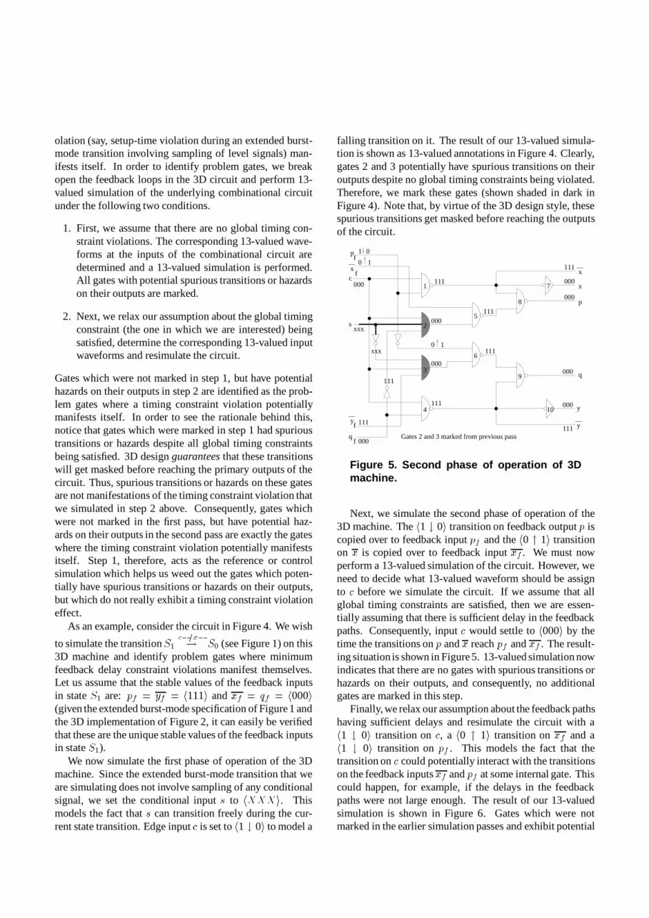
Figure 5. Second phase of operation of 3Dmachine.
Next, we simulate the second phase of operation of the3D machine. The h1 # 0i transition on feedback output p iscopied over to feedback input p
f
and the h0 " 1i transitionon x is copied over to feedback input x
f
. We must nowperform a 13-valued simulation of the circuit. However, weneed to decide what 13-valued waveform should be assignto c before we simulate the circuit. If we assume that allglobal timing constraints are satisfied, then we are essen-tially assuming that there is sufficient delay in the feedbackpaths. Consequently, input c would settle to h000i by thetime the transitions on p and x reach p
f
and x
f
. The result-ing situation is shown in Figure 5. 13-valued simulation nowindicates that there are no gates with spurious transitions orhazards on their outputs, and consequently, no additionalgates are marked in this step.
Finally, we relax our assumption about the feedback pathshaving sufficient delays and resimulate the circuit with ah1 # 0i transition on c, a h0 " 1i transition on x
f
and ah1 # 0i transition on p
f
. This models the fact that thetransition on c could potentially interact with the transitionson the feedback inputsx
f
and pf
at some internal gate. Thiscould happen, for example, if the delays in the feedbackpaths were not large enough. The result of our 13-valuedsimulation is shown in Figure 6. Gates which were notmarked in the earlier simulation passes and exhibit potential

y
xxf
yf
pf
qf
1 0 0 11 0
0 1
1 0
0 1
0 1 del[c]=[5,9]; del[ pf ]=[4,7]
��del[c]=[5,9]; del[ xf ]=[3,5]������������������
������������������
������������������
������������������
������������
������������
������������
������������
s
c1
2
3
4
5
6
7
8
9
10
x
y
p
q
xxx
xx0
000
111
[1,2]
[1,2]
[2,3]
[2,3]
[2,3]
GATE AND WIRE DELAYS ARE [MIN, MAX]
[1,2]
[1,2]
xx0
111
[1,2]
111
000
[1,2]
[1,2]
xxx
[1,2]
[2,4]
[2,4]111
1x0
0x0
1x1
1x1
[3,6]
Figure 6. Identifying problem gates, and min-max timing analysis
hazards on their outputs in this pass are gates 5, 6, 8 and9 (shown lightly shaded Figure 6). We therefore identifythese gates as the problem gates where a feedback delayconstraint violation potentially manifests itself. Notice thatgates 2 and 3 still potentially have spurious transitions ontheir outputs. However, these were marked in an earlierpass, and are consequently not identified as problem gatesby our algorithm. This clearly shows that in general, theset of problem gates is a subset of the set of all gates withspurious transitions or hazards on their outputs.
On examining the situation in Figure 6 more closely, wefind that indeed, if we have sufficient delay in the feedbackpath from x to x
f
, the h0 " 1i transition on x
f
will reachgate 5 after the h1 # 0i transition on c reaches gate 2 andstabilizes its output to 0. As a result, gates 5 and 8 will nothave any hazard on their outputs. Similarly, if the feedbackpath p! p
f
has a large enough delay, the h1 # 0i transitionon p
f
will reach gate 6 (after inversion) after the h1 # 0itransition on c propagates to gate 3 and stabilizes its outputto 0. This, in turn, will eliminate the hazards on gates6 and 9. Consequently, we really need to analyze signalpropagation delays from the primary and feedback inputs togates 5 and 6 in order to determine our required feedbackdelay constraints.
In this subsection, we have demonstrated how 13-valuedsimulation can be used to efficiently isolate the problemgates in a 3D circuit. Our next mission is to compute signalpropagation delays bounds from the circuit inputs to thesegates.
3.4. Min-max timing simulation
In this subsection, we outline the input-output charac-teristics of our min-max timing simulation algorithm. Thedetails of the algorithm may be found in a companion pa-per [4].
There are two inputs to our algorithm. The first is acombinational circuit with minimum and maximum delayannotations on each gate. The second is an input stimulusconsisting of 13-valued signals associated with the circuitinputs. The output of our algorithm is an assignment of a 13-valued signal to each gate,G, modeling the output waveformresulting from the input. In addition, G is annotated with aset of intervals, one for each circuit input i, representing theshortest and longest propagation delays from i to the outputof G, for the given input stimulus.
Our min-max timing simulator incorporates an efficientand effective reconvergent fanout analysis algorithm [4].Our reconvergent fanout analysis technique is able to detectseveral instances of signal transition orderings that go un-detected with previously published polynomial-time [3, 22]and some exponential-time [18] algorithms. This enablesus to compute signal propagation delays from the circuitinputs to the gates with increased accuracy. The worst-casecomplexity of our min-max timing simulation algorithm is: O(n
2g
:n
pi
:n
2fanin
), where n
g
= number of gates in thecircuit, n
pi
= number of circuit inputs, and n
fanin
= max-imum fanin of a gate. However, in reality, we have a multi-plicative factor of at most 10:n
g
instead of n2g
and nfanin
isusually restricted to 4 or 5 for technological reasons.
3.5. Determining timing constraints for correct cir-cuit operation
Once we have identified the problem gates in a 3D circuit,signal propagation delays from the primary and feedback in-puts to these gates need to be compared to determine timingconstraints for correct circuit operation. The general ideabehind this technique is that a problem gate G has a po-tential hazard on its output because transitions propagatingfrom two circuit inputs i and j (primary or feedback) reachthe gate in the wrong order. Therefore, we must determineconstraints on the transition times of i and j to insure thattransitions propagating from these inputs reach gate G inthe correct order. In this subsection, we show how this canbe accomplished utilizing the information computed by ourmin-max timing simulation algorithm.
Let G:del[i] be a tuple (t; T ) containing a lower and anupper bound of the signal propagation delay from circuitinput i to gate G. These tuples are computed by our min-max timing simulator for each gate G in the circuit, andfor each transitioning circuit input i. A sufficient conditionto insure that the transition from circuit input j reaches

problem gate G before that from i, is that j transitions atleast G:del[j]:T �G:del[i]:t time units before i transitions.Note that the length of a sensitized path from i toG dependson the stimulus applied to the circuit inputs, in general.Consequently, we need to recompute the del tuples for eachgate each time a new input stimulus is applied to the circuit.
As an example, let us consider the circuits in Figures 4and 6. We now concentrate on the gate and wire delayannotations shown in these figures. Figure 4 shows signalpropagation delay bounds for gates 1 and 8 computed duringthe first phase of simulation. Similarly, Figure 6 showssignal propagation delay bounds for gates 5 and 6 computedduring the final phase of simulation. The delay bounds inFigure 6 indicate that a transition on circuit input c takes amaximum of 9 time units to reach the output of gate 5, whilea transition on x
f
takes a minimum of 3 time units to reachthe output of the same gate. Consequently, in order to insurethat the transition on c reaches gate 5 before the transition onx
f
does, xf
must transitionat least 9�3 = 6 time units afterc transitions. However, x itself transitions at least 3 timeunits after c transitions (obtained from Figure 4). Therefore,the additional feedback delay needed in the x ! x
f
pathis 6 � 3 = 3 time units. A similar analysis for gate 6indicates that p
f
must transition at least 9 � 4 = 5 timeunits after c transitions. However, we know from Figure 4that p transitions at least 7 time units after c transitions.Consequently, we do not need to insert any additional delayin the p ! p
f
in order to insure that the machine correctly
executes theS�1 c�x�
! S0 state transition. This shows howthe inherent delays of circuit components often obviate theneed for inserting additional feedback delays.
3.6. 3D timing analysis tool
The method for determining minimum feedback con-straints outlined above can easily be extended to determinesetup and hold-time constraints for 3D circuits. In orderto identify fundamental-mode timing constraints, each pairof adjacent state transitions, S0 ! S1 ! S2, in the ex-tended burst-mode specification needs to be simulated. Thebasic technique for determining fundamental-mode timingconstraints is the same as that for the other timing con-straints. The only difference is that we now model interac-tions between transitioning feedback signals of theS0 ! S1
transition and transitioning primary inputs of the S1 ! S2
transition.These ideas have been incorporated in a timing analysis
tool for 3D asynchronous finite state machines. The struc-ture of the tool is shown in Figure 7. The top-level analyzerfirst breaks the feedback loops in a gate-level 3D circuit toobtain a combinational network. It then looks at the ex-tended burst-mode specification and analyzes the combina-tional circuit obtained above for each phase of each extended
PrimaryInputStimulus
Top-level analyzer
Timing Informationand
GlobalTimingConstraints
Extended Burst-Mode Specificationand
Gate Level 3D Circuit
13-valuedoutput waveforms
Identify ProblemSimulation and
Gates
13-Valued
Min-MaxCombinational
TimingSimulator
Figure 7. Timing analysis tool for 3D circuits
burst-mode state transition. This involves determining the13-valued stimuli to apply to the inputs of the combinationalcircuit and performing a 13-valued simulation of the circuit.Signals with directed don’t-care transitions are assumed tobe transitioning since this would lead to the worst-case sit-uation as far as violation of timing constraints is concerned.Problem gates for each type of global timing constraint vio-lation are identified and then our min-max timing simulatoris invoked. The results of the timing simulator are fed backto the top-level analyzer. Timing information and 13-valuedoutput waveforms computed by the simulator are used bythe top-level analyzer to: (a) determine timing constraintsfor correct circuit operation and (b) determine 13-valuedwaveforms and timing information to copy from the feed-back outputs to the corresponding feedback inputs. Theseare then passed on to the 13-valued simulator and min-maxtiming simulator for another pass of analysis. The iterationcontinues until we have examined each extended burst-modestate transition for setup, hold and feedback timing con-straint violations, and also examined each pair of adjacentstate transitions for fundamental-mode timing constraint vi-olations.
The complexity of our timing analysis technique isbounded above by (n
2transitions
� C
min�max
), wheren
transitions
represents the number of state transitions inthe extended burst-mode specification and C
min�max
rep-resents the complexity of the min-max timing simulation al-gorithm. Since C
min�max
for our simulator is polynomialin the circuit-size, the overall complexity of our timing-analysis method is polynomial in the circuit-size and in thesize of the extended burst-mode specification.

4. Experimental results
We have applied our timing analysis tool to a suite ofasynchronous benchmarks synthesized according to the 3Dstyle. The benchmark characteristics are shown in Table 1.
3D States State Inputs GatesBenchmark Trans.ircv 16 22 8 107ircv-bm 8 10 7 58ircv-csm 8 10 7 64isend 24 32 8 247isend-bm 12 15 7 104isend-csm 12 15 7 81trcv 16 22 8 96trcv-bm 8 10 7 58trcv-csm 8 10 7 59tsend 22 30 8 182tsend-bm 11 14 7 65tsend-csm 11 14 7 69biu-dma2fifo 12 15 6 81biu-fifo2dma 11 13 6 77scsi-init-send 7 8 5 33scsi-targ-send 7 8 5 41pscsi 45 62 11 350
Table 1. Benchmark Characteristics
Table 2 gives the actual time taken by our tool to exerciseall the extended burst-mode state transitions specified for a3D benchmark and determine the global timing constraintsrequired for correct circuit operation. The CPU times shownare on a DEC 5000/240 machine. The “Analysis Time”for a 3D benchmark reported in Table 2 does not includethe time required to read in the circuit description and theextended burst-mode specification, nor does it include thetime required to topologically sort the gates.
The timing parameters obtained for each benchmark areindicated in Table 3. For each benchmark circuit, gate de-lays are estimated for a Hitachi CMOS gate library [1].Each gate has a nominal delay given by: t = t0 +K � C,where C = 0:4� Effective fanout, where Effective fanout=
P
all fanout gates
(Normalized load of fanout gate).The t0;K and Normalized load figures have been obtainedfrom the Hitachi data book [1] and are different for rising andfalling transitions. In our experiments, the actual gate delaysare assumed to vary within (0:9 � nominal delay; 1:1 �nominal delay). We also assume zero delays for the wires,since we do not have post-layout information about the de-lays of wires in the circuit.
It may be noted here that an inverter with a fanout of 4has a rising delay of 2.12ns and a falling delay of 1.74nsin this library. The timing constraints shown in Table 3are normalized with respect to the delay of an inverter withfanout 4 (FO4 delay), which is assumed to be 2ns.
3D AnalysisBenchmark Time(s)ircv 1.375ircv-bm 0.309ircv-csm 0.339isend 7.738isend-bm 1.052isend-csm 0.698trcv 1.318trcv-bm 0.332trcv-csm 0.328tsend 4.761tsend-bm 0.466tsend-csm 0.492biu-dma2fifo 0.711biu-fifo2dma 0.590scsi-init-send 0.105scsi-targ-send 0.155pscsi 17.171
Table 2. Analysis Times
The timing constraints reported in Table 3 are computedin the following manner. The “Minimum feedback” con-straint is obtained by determining the minimum feedbackdelay required in each feedback path for each extended burst-mode state transition, and then taking the maximum of thesevalues over all extended burst-mode state transitions and allfeedback paths. The “Setup Time” constraint is obtained bydetermining the setup time constraint for each conditionalsignal being sampled in each extended burst-mode state tran-sition, and then taking the maximum of these values overall extended burst-mode transitions and all conditional in-puts. The “Hold Time” constraint is computed in a similarfashion using the hold times of conditional inputs. “Fund-mode constraint” is determined by computing the maximumfundamental mode timing constraint for each pair of consec-utive state transitions in the extended burst-mode specifica-tion, and then taking the maximum of these values over allpairs of consecutive transitions. Note that this assumes thatno other timing constraint violation (like setup or hold-timeviolation) has occurred in each of the pair of transitions. Inaddition, fundamental-mode constraints reported in the tablegive the minimum interval of time that must elapse betweenthe last primary output transition of the present burst andthe first compulsory input transition of the next burst.
It may be noted here that benchmark “pscsi” does nothave any conditional input. Consequently, our tool com-putes the setup and hold-time constraints of this circuit tobe 0.
We have checked the accuracy of our timing results for allof our benchmarks except “pscsi”. Our strategy for check-ing the accuracy of our results consists of running the timinganalysis tool in an interactive debugging mode. Whenevera timing constraint is detected, and is larger than was pre-viously detected, our tool prints out the state of the entire

3D Minimum Setup Hold Fund-modeBenchmark feedback Time Time constraint
(FO4 (FO4 (FO4 (FO4delays) delays) delays) delays)
ircv 0.000 1.361 7.140 4.789ircv-bm 0.000 0.000 4.488 1.959ircv-csm 0.000 0.519 4.015 1.497isend 0.000 1.028 8.189 3.996isend-bm 0.000 0.492 7.231 3.751isend-csm 0.000 0.924 6.226 3.589trcv 0.000 0.995 5.594 2.715trcv-bm 0.243 0.080 5.501 2.073trcv-csm 0.000 0.681 3.775 1.395tsend 0.000 2.632 7.777 3.403tsend-bm 0.000 0.371 5.860 2.600tsend-csm 0.000 0.757 3.984 1.102biu-dma2fifo 0.000 0.213 7.390 2.550biu-fifo2dma 0.298 0.592 4.753 1.357scsi-init-send 0.000 0.213 2.564 0.044scsi-targ-send 0.000 0.000 4.172 0.540pscsi 0.000 0.000 0.000 3.505
Table 3. Results of Timing Analysis
circuit with the thirteen-valued waveforms and the delaybound annotations. We then check to see whether the tim-ing constraint reported by our tool is conservative or exact.Although this process is very time-consuming and painstak-ing, it is feasible since the sizes of the circuits involved arenot very large (“pscsi”, on the other hand, is reasonablylarge for manual inspection). We have found that timingconstraints identified by our tool are accurate for all of the3D benchmarks other than “pscsi”. Even with “pscsi”, ourtool reports that no additional delays need to be inserted inthe feedback paths. Since this is a conservative approxima-tion to the true feedback delay requirement, we can inferthat additional feedback delays are actually not required inthis circuit. The fundamental-mode constraint extracted byour tool for “pscsi” also seems quite realistic, and we knowthat this is a conservative approximation (an upper bound)of the true minimum fundamental-mode constraint. Thus,our timing analysis technique is fairly accurate.
Our results indicate that our timing analysis technique isfast enough even when considering 30 � 40 distinct statetransitions and dealing with moderately large 3D circuits.Since all analysis algorithms used in our tool have complex-ity that is polynomial in the circuit size, we do not expectany significant performance degradation even with larger3D circuits.
Our analysis shows that for practical 3D circuits, addi-tional feedback delays are almost never needed – the inherentdelays of gates are sufficient to ensure that essential hazardsdon’t occur. Setup-time constraints are also quite reasonable(of the order of one gate delay). However, the maximum
hold times are usually long since the machine often has towait for feedback signal transitions in the third phase ofoperation for some internal gates to become desensitized tothe conditionals. This can possibly be overcome by someamount of careful redesigning to insure that feedback signaltransitions in the second phase desensitize all gates to theconditional inputs. Fundamental-mode timing constraintsfor our 3D benchmarks also appear to be reasonable, sincethe environment will take a few gate delays’ time to react tothe primary output transitionsanyway. On the whole, timingrequirements for 3D design do not seem very restrictive onthe environment.
To the best of our knowledge, the timing analysis toolreported in this paper is the first completely automated toolthat analyzes 3D circuits with bounded component delaysand determines global timing constraints required for correctcircuit operation. Consequently, we are unable to presentperformance comparison results with other tools with simi-lar capabilities.
5. Conclusion
We believe that fully speed-independent and delay-insensitive design styles are too inefficient for use in manyapplications. For maximum performance, asynchronous de-sign styles will need to exploit some knowledge about thetiming of their components and the environment. Hence,timing analyzers will be essential asynchronous design tools.
In this paper, we have presented an efficient timing anal-ysis technique for determining global timing constraints ofextended burst-mode circuits implemented according to the3D design style. To the best of our knowledge, this is the firstcompletely automated tool that performs such an analysisof gate-level 3D circuits with bounded component delays.Although timing constraints identified by our tool representconservative approximations to the true timing requirementsin the worst-case scenario, experimental results indicate thatour results are accurate for almost all of the 3D benchmarkswe analyzed. The efficiency and accuracy of our timinganalysis technique makes it very easy for a designer to makeincremental optimizations and hand-tunings to a 3D circuitand verify the timing properties almost immediately. Thisproves extremely helpful in the design cycle of practical 3Dcircuits.
The work reported in this paper can potentially be ex-tended for other interesting applications. For example, onecould modify our timing analysis algorithm to verify thecorrectness of a 3D design by simulation. Another inter-esting application could be to determine if the gate andwire-delays in a 3D circuit permit the elimination of somehardware required for insuring hazard-free behavior. Thiscould be used, for example, to optimize the area of a 3Dcircuit. Subsequently, timing constraints required for cor-
rect operation of the modified circuit can be obtained usinga modified version of the timing analysis algorithm reportedin this paper.
References
[1] Hitachi High Speed CMOS Gate Array: HG62E Series De-sign Manual.
[2] P. Beerel and T. H.-Y. Meng. Automatic gate-level synthesisof speed-independent circuits. In Proceedings of the 1992IEEE/ACM International Conference on Computer AidedDesign, Nov. 1992.
[3] M. Breuer and A. Friedman. Diagnosis and Reliable Designof Digital Systems. Computer Science Press, 1976.
[4] S. Chakraborty and D. L. Dill. More accurate polynomial-time min-max timing simulation. In Proceedingsof the ThirdInternational Symposium on Advanced Research in Asyn-chronous Circuits and Systems, April 1997.
[5] T. J. Chakraborty, V. D. Agrawal, and M. L. Bushnell. Delayfault models and test generation for random logic sequen-tial circuits. In Proceedings of the 29th ACM/IEEE DesignAutomation Conference, pages 165–72, 1992.
[6] S. Devadas, K. Keutzer, S. Malik, and A. Wang. Eventsuppression: Improving the efficiency of timing simula-tion for synchronous digital circuits. IEEE Transactions onComputer Aided Design of Integrated Circuits and Systems,13(6):814–822, June 1994.
[7] S. Devadas, K. Keutzer, S. Malik, and A. Wang. Verificationof asynchronous interface circuits with bounded wire delays.IEEE Journal of VLSI Signal Processing, 7(1-2):161–182,February 1994.
[8] J. C. Ebergen. A formal approach to designing delay-insensitive circuits. Distributed Computing, 5(3):107–119,1991.
[9] E. B. Eichelberger. Hazard detection in combinational andsequential switching circuits. IBM Journal of Research andDevelopment, 9, Mar. 1965.
[10] G. Fantauzzi. An algebraic model for the analysis of logicalcircuits. IEEE Transactions on Computers, C-23:576–581,June 1974.
[11] N. Ishiura. Studies on Logic Simulation and Hardware De-scription Languages. PhD thesis, Kyoto University, Kyoto,Japan, Dec. 1990.
[12] N. Ishiura, Y. Deguchi, and S. Yajima. Coded time-symbolicsimulation using shared binary decision diagram. In Pro-ceedings of the 27th ACM/IEEE Design Automation Confer-ence, pages 130–145, 1990.
[13] N. Ishiura, M. Takahashi, and S. Yajima. Time symbolicsimulation for accurate timing verification of asynchronousbehavior of logic circuits. In Proceedings of the 26thACM/IEEE Design Automation Conference, pages 497–502,1989.
[14] D. S. Kung. Hazard-non-increasing gate-level optimizationalgorithms. In Proceedings of the 1992 IEEE/ACM Interna-tional Conference on Computer Aided Design, pages 631–634. IEEE Computer Society Press, November 1992.
[15] L. Lavagno, K. Keutzer, and A. Sangiovanni-Vincentelli.Synthesis of hazard-free asynchronouscircuits with boundedwire delays. IEEE Transactions on Computer-Aided Designof Integrated Circuits and Systems, 14(1):61–86, Jan. 1995.
[16] K.-J. Lin, J.-W. Kuo, and C.-S. Lin. Direct synthesis ofhazard-free asynchronous circuits from STGs based on lockrelation and MG-decomposition approach. In Proceedingsof the European Design and Test Conference EDAC-ETC-EUROASIC, pages 178–183, Mar. 1994.
[17] M. Linderman and M. Leeser. Simulation of digital circuitsin the presence of uncertainty. In Proceedings of the 1994IEEE International Conference on Computer Aided Design,pages 248–251, 1994.
[18] M. H. Linderman. Simulation of Digital Circuits in the Pres-ence of Uncertainty. PhD thesis, Cornell University, 1994.
[19] C. W. Moon. Synthesis and Verification of AsynchronousCircuits from Graph Specifications. PhD thesis, Universityof California, Berkeley, 1992.
[20] S. M. Nowick and D. L. Dill. Automatic synthesis of locally-clocked asynchronous state machines. In Proceedings of the1991 IEEE International Conference on Computer AidedDesign, pages 318–321, November 1991.
[21] S. M. Nowick and D. L. Dill. Synthesis of asynchronousstate machines using a local clock. In Proceedings of the1991 IEEE International Conference on Computer Design:VLSI in Computers and Processors, pages 192–197. IEEEComputer Society Press, October 1991.
[22] E. Ulrich, K. Lentz, S. Demba, and R. Razdan. Concurrentmin-max simulation. In EDAC. Proceedingsof the EuropeanConference on Design Automation, pages 554–557, 1991.
[23] S. H. Unger. Asynchronous Sequential Switching Circuits.Wiley-Interscience, New York, NY, 1969.
[24] P. Vanbekbergen, F. Catthoor, G. Goossens, and H. De Man.Optimized synthesis of asynchronous control circuits fromgraph-theoretic specifications. In Proceedings of the 1990IEEE International Conference on Computer Aided Design.IEEE Computer Society Press, 1990.
[25] A. V. Yakovlev, L. Lavagno, and A. Sangiovanni-Vincentelli.A unified signal transition graph model for asynchronouscontrol circuit synthesis. Proceedings of the 1992 IEEEInternational Conference on CAD, Nov. 1992.
[26] K. Y. Yun and D. L. Dill. Automatic synthesis of 3D asyn-chronous finite-state machines. In Proceedings of the 1992IEEE/ACM International Conference on Computer AidedDesign, pages 576–580. IEEE Computer Society Press,November 1992.
[27] K. Y. Yun and D. L. Dill. Unifying syn-chronous/asynchronous state machine synthesis. In Pro-ceedings of the 1993 IEEE/ACM International Conferenceon Computer Aided Design, pages 255–260. IEEE ComputerSociety Press, November 1993.


